ISFET- based microsystem for biomedical applications. PhD t
232
Vilouras, Anastasios (2021) Ultra-thin and flexible CMOS technology: ISFET- based microsystem for biomedical applications. PhD thesis. http://theses.gla.ac.uk/82122/ Copyright and moral rights for this work are retained by the author A copy can be downloaded for personal non-commercial research or study, without prior permission or charge This work cannot be reproduced or quoted extensively from without first obtaining permission in writing from the author The content must not be changed in any way or sold commercially in any format or medium without the formal permission of the author When referring to this work, full bibliographic details including the author, title, awarding institution and date of the thesis must be given Enlighten: Theses https://theses.gla.ac.uk/ [email protected]
-
Upload
khangminh22 -
Category
Documents
-
view
0 -
download
0
Transcript of ISFET- based microsystem for biomedical applications. PhD t

Vilouras, Anastasios (2021) Ultra-thin and flexible CMOS technology: ISFET-based microsystem for biomedical applications. PhD thesis. http://theses.gla.ac.uk/82122/
Copyright and moral rights for this work are retained by the author
A copy can be downloaded for personal non-commercial research or study, without prior permission or charge
This work cannot be reproduced or quoted extensively from without first obtaining permission in writing from the author
The content must not be changed in any way or sold commercially in any format or medium without the formal permission of the author
When referring to this work, full bibliographic details including the author, title, awarding institution and date of the thesis must be given
Enlighten: Theses https://theses.gla.ac.uk/
Ultra-thin CMOS Technology:
ISFET-Based Sensing Microsystem for
Wearable and Implantable Biomedical
Applications
Anastasios Vilouras
A thesis submitted to the
Department of Electronics and Electrical Engineering
at the University of Glasgow
in fulfilment of the requirements for the
Degree of Doctor of Philosophy
December 2020
i
Abstract
A new paradigm of silicon technology is the ultra-thin chip (UTC) technology and the emerging
applications. Very thin integrated circuits (ICs) with through-silicon vias (TSVs) will allow the
stacking and interconnection of multiple dies in a compact format allowing a migration towards
three-dimensional ICs (3D-ICs). Also, extremely thin and therefore mechanically bendable
silicon chips in conjunction with the emerging thin-film and organic semiconductor technologies
will enhance the performance and functionality of large-area flexible electronic systems.
However, UTC technology requires special attention related to the circuit design, fabrication,
dicing and handling of ultra-thin chips as they have different physical properties compared to
their bulky counterparts. Also, transistors and other active devices on UTCs experiencing
variable bending stresses will suffer from the piezoresistive effect of silicon substrate which
results in a shift of their operating point and therefore, an additional aspect should be considered
during circuit design.
This thesis tries to address some of these challenges related to UTC technology by focusing
initially on modelling of transistors on mechanically bendable Si-UTCs. The developed
behavioural models are a combination of mathematical equations and extracted parameters from
BSIM4 and BSIM6 modified by a set of equations describing the bending-induced stresses on
silicon. The transistor models are written in Verilog-A and compiled in Cadence Virtuoso
environment where they were simulated at different bending conditions.
To complement this, the verification of these models through experimental results is also
presented. Two chips were designed using a 180 nm CMOS technology. The first chip includes
nMOS and pMOS transistors with fixed channel width and two different channel lengths and two
different channel orientations (0° and 90°) with respect to the wafer crystal orientation. The
second chip includes inverter logic gates with different transistor sizes and orientations, as in the
previous chip. Both chips were thinned down to ∼20m using dicing-before-grinding (DBG)
prior to electrical characterisation at different bending conditions.
Furthermore, this thesis presents the first reported fully integrated CMOS-based ISFET
microsystem on UTC technology. The design of the integrated CMOS-based ISFET chip with
512 integrated on-chip ISFET sensors along with their read-out and digitisation scheme is
presented. The integrated circuits (ICs) are thinned down to ∼30m and the bulky as well as
thinned ICs are electrically and electrochemically characterised. Also, the thesis presents the first
reported mechanically bendable CMOS-based ISFET device demonstrating that mechanical
deformation of the die can result in drift compensation through the exploitation of the
piezoresistive nature of silicon. Finally, this thesis presents the studies towards the development
of on-chip reference electrodes and biodegradable and ultra-thin biosensors for the detection of
neurotransmitters such as dopamine and serotonin.
ii
Table of Contents
Abstract ........................................................................................................................................ i
List of Tables .............................................................................................................................. v
List of Figures ............................................................................................................................ vi
List of Publications .................................................................................................................. xv
Acknowledgements ................................................................................................................ xvii
Author’s Declaration ............................................................................................................. xviii
Glossary of Abbreviations ...................................................................................................... xix
Chapter 1. Introduction ............................................................................................................1
1.1 Motivation ....................................................................................................................1
1.2 Research Objectives ..................................................................................................5
1.3 Research Contributions .............................................................................................5
1.4 Thesis organisation ....................................................................................................7
Chapter 2. Literature Review ............................................................................................... 10
2.1 Introduction ............................................................................................................. 10
2.2 Potentiometric Electrochemical Ion-Sensitive Electrodes ............................... 12
2.2.1 Overview of Potentiometric Metal-Oxide Based Electrochemical pH Sensors
........................................................................................................................................... 13
2.2.2 Sensing Mechanisms.............................................................................................. 14
2.2.3 Properties and Non-Ideal Characteristics of Potentiometric pH Sensors.... 19
2.2.4 Mechanically Flexible Potentiometric Ion-Sensitive Electrodes ................... 22
2.3 Ion-Sensitive Field-Effect Transistor: Operation, Sensor Interface and
On-Chip Signal Processing Techniques ............................................................................ 23
2.3.1 Operation and Theory of pH Sensitivity ............................................................ 23
2.3.2 ISFET Read-Out Topologies ................................................................................. 31
2.3.3 Circuit-Level and Post-Processing Techniques for Mitigation of ISFET Non-
Ideal Effects ..................................................................................................................... 34
2.4 Ion-Sensitive Field-Effect Transistor: Applications and Advances ................. 37
2.4.1 Applications of ISFET-Based Sensing Systems .................................................. 37
2.4.2 Mechanically Flexible ISFET-Based Sensors towards Wearable Healthcare
Devices .............................................................................................................................. 40
2.5 Summary ................................................................................................................... 44
Chapter 3. Modelling, Simulations and Validation of Mechanically Bendable
Integrated CMOS Devices ....................................................................................................... 45
3.1 Introduction................................................................................................................... 45
3.2 Mechanical Characterisation of Ultra-Thin Silicon Chips ................................. 47
3.3 Strain Effects: From Silicon Substrate to Integrated Devices and Circuits ... 50
3.3.1 Strain Effects on Bulk Silicon .............................................................................. 50
iii
3.3.2 Strain Effects on MOSFETs and Ion-Sensitive Field-Effect Transistors ........ 53
3.3.3 Strain Effects on Basic CMOS Circuit Blocks ..................................................... 58
3.4 Compact Modelling of CMOS-Based Devices and Sensors on Bendable
Ultra-Thin Chips .................................................................................................................. 62
3.4.1 Modelling of Bending Stress Effect on Metal Oxide Semiconductor Field-
Effect Transistors ............................................................................................................ 62
3.4.2 Modelling of Bending Stress Effect on Ion-Sensitive Field-Effect Transistors
........................................................................................................................................... 70
3.5 Electrical Characterisation and Model Evaluation of Transistors, Circuits and
Sensors on Ultra-Thin Chips .............................................................................................. 74
3.5.1 Experimental Evaluation of MOSFET Model on Ultra-Thin Chips .................. 75
3.5.2 Experimental Evaluation of ISFET Model on Ultra-Thin Chips ...................... 79
3.6 Summary ........................................................................................................................ 85
Chapter 4. Fabrication and Characterisation of Thick-Film Reference Electrodes and
Ultra-Flexible Biosensors ....................................................................................................... 87
4.1 Introduction ............................................................................................................. 87
4.2 Screen Printed Thick Film Reference Electrode for Electrochemical Sensing
87
4.2.1 Fabrication of Reference Electrode .................................................................. 88
4.2.2 Fabrication of RuO2 Based Ion-Sensitive Electrode ........................................ 90
4.2.3 Electrochemical Characterisation, Results and Discussion ........................... 91
4.3 Chitosan - Graphene Oxide Based Ultra-Thin and Biodegradable Biosensors 97
4.3.1 Chitosan-Graphene Oxide-based ultra-thin conformable sensing patch for
cell-health monitoring.................................................................................................... 98
4.3.2 Mesoporous Chitosan Based Conformable and Resorbable Biostrip for
Dopamine Detection ..................................................................................................... 102
4.3.3 Graphene Oxide-Chitosan Based Ultra-Flexible Electrochemical Sensor for
Detection of Serotonin ................................................................................................. 111
4.4 Summary ................................................................................................................. 116
Chapter 5. ISFET Readout IC System Architecture .......................................................... 118
5.1 Introduction ........................................................................................................... 118
5.2 System Design ........................................................................................................ 118
5.3 System Requirements ........................................................................................... 119
5.4 Chip Architecture .................................................................................................. 120
5.4.1 Standard Pixel Readout Topology .................................................................... 121
5.4.2 Standard Pixel Readout Topology with Improved Fill-Factor ..................... 126
5.4.3 Current-Mode Pixel Readout Topology ........................................................... 129
5.4.4 Pixel Selection ..................................................................................................... 132
5.4.5 Unity Gain Amplifier........................................................................................... 134
5.5 Summary ................................................................................................................. 136
iv
Chapter 6. Post-Processed Ultra-Thin CMOS Chips ......................................................... 139
6.1 Introduction................................................................................................................. 139
6.2 Protection of Front Active Side during Back-Etching ..................................... 140
6.3 Fabrication of Ultra-Thin CMOS Chips ............................................................... 142
6.3.1 Chemical Wet Etching using PDMS as Protective Layer ............................... 142
6.3.2 Back-Lapping ....................................................................................................... 149
6.4 Transfer and Bonding of Ultra-Thin Chips on Flexible Substrates ................ 154
6.4.1 Design and Fabrication of Flexible Printed Circuit Boards .................... 154
6.4.2 Transfer and Bonding of Ultra-Thin Chips ...................................................... 155
6.5 Summary ................................................................................................................. 156
Chapter 7. Characterisation of CMOS ISFETs and Circuits on Ultra-Thin Chips ......... 158
7.1 Introduction................................................................................................................. 158
7.2 Characterisation of Bulky and Ultra-Thin CMOS-based ISFET Chips ............. 159
7.2.1 Hardware Setup .................................................................................................. 159
7.2.2 Software Setup .................................................................................................... 161
7.2.3 On-Chip Active Pixel Circuits ............................................................................ 163
7.3 Ultra-Thin ISFET with Bending Induced Performance Enhancement ........... 171
7.3.1 Characterisation of Drift in Fabricated MOSFETs .......................................... 173
7.3.2 Behavior of Drift in Bendable EG-ISFETs ........................................................ 173
7.3.3 Compensation of Drift by Bending the EG-ISFETs on Si-UTCs ..................... 175
7.4 Summary ................................................................................................................. 179
Chapter 8. Conclusion and Future Work ........................................................................... 182
8.1 Conclusion ................................................................................................................... 182
8.2 Future Work ........................................................................................................... 184
References .............................................................................................................................. 188

v
List of Tables
Table 2.1: Values of dissociation constants, the density of sites and pH at the point of zero charges of
different oxides [187]. ............................................................................................................................... 29
Table 2.2: ISFET gate ion-sensitive materials, properties and deposition method. .................................. 29
Table 2.3: Analytes found in sweat, tears and blood along with their diagnostic significance [286, 287].
.................................................................................................................................................................. 41
Table 3.4: List of Young’s modulus and Poisson ratio of some of the materials of interest. .................... 49
Table 3.5: List of measured fundamental coefficients (× 10 − 12𝑃𝑎 − 1) at 298K along with their linear
combinations [317, 371]. .......................................................................................................................... 53
Table 3.6: Piezoresistive coefficients (× 10 − 12𝑃𝑎 − 1) of NMOS devices on (100) silicon [378]. .... 56
Table 3.7: Piezoresistive coefficients of PMOS devices on (100) silicon (× 10 − 12𝑃𝑎 − 1) [378]. ..... 57
Table 3.8: Comparison table of inverters fabricated on ultra-thin chips. .................................................. 59
Table 3.9: Measured values of switching threshold, input-high and input-low voltage of the inverters on
the ultra-thin chip with channel-length of 0.18µm at different bending conditions [316]. ....................... 59
Table 3.10: Measured values of switching threshold, input-high and input-low voltage of the inverters on
the ultra-thin chip with channel-length of 0.35µm at different bending conditions [316]. ....................... 60
Table 3.11: Summary table of the formulas and parameters used in the model of MOST devices which
include the effect of bending stress. .......................................................................................................... 68
Table 3.12: The measured values used to model the drifting behaviour of the drain-current of EG-ISFET
at different pH conditions. ........................................................................................................................ 73
Table 3.13: The measured values of carriers’ mobility under planar and different bent conditions. ........ 77
Table 4.14: Design specifications. .......................................................................................................... 115
Table 5.15: Design specifications. .......................................................................................................... 120
Table 5.16: Dimensions of transistors of unity-gain folded cascode amplifier. ...................................... 135
Table 6.17: Comparison table between different materials used as etch mask or front-side protection
during wet-etching of silicon [333]. ........................................................................................................ 141
Table 7.18: List of measured performance parameters of the folded-cascode unity-gain amplifier. ...... 171
vi
List of Figures
Figure 1.1: (a) Implantable telemetry platform systems with ASIC for in vivo monitoring of
gastrointestinal physiological information [59, 61], (b) Implantable bio-signal recording microsystems on
endoscopes and catheters [62-68], (c) Temperature, load and strain sensing microsystems embedded in
orthopaedic and dental implants [69-72], (d) High-density self-calibrating and wirelessly powered sub-
retinal and epi-retinal artificial vision prosthesis [73-76], (e) Energy harvesting microsystem with self-
supplied power-management circuitry [81] and (f) Implantable bio-signal recording microsystems on
ultra-thin probes [25, 77-80]. ...................................................................................................................... 4
Figure 1.2: Flowchart showing the connection between the chapters of the thesis..................................... 9
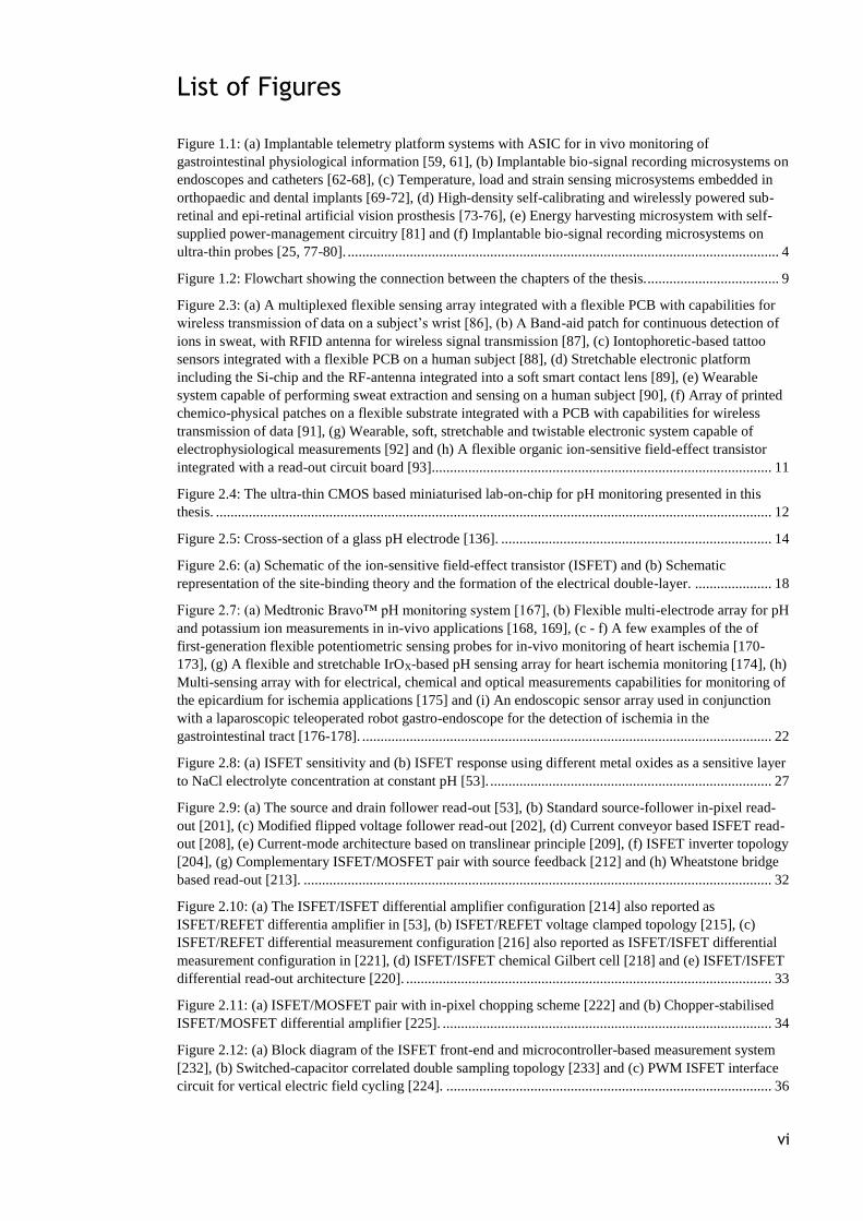
Figure 2.3: (a) A multiplexed flexible sensing array integrated with a flexible PCB with capabilities for
wireless transmission of data on a subject’s wrist [86], (b) A Band-aid patch for continuous detection of
ions in sweat, with RFID antenna for wireless signal transmission [87], (c) Iontophoretic-based tattoo
sensors integrated with a flexible PCB on a human subject [88], (d) Stretchable electronic platform
including the Si-chip and the RF-antenna integrated into a soft smart contact lens [89], (e) Wearable
system capable of performing sweat extraction and sensing on a human subject [90], (f) Array of printed
chemico-physical patches on a flexible substrate integrated with a PCB with capabilities for wireless
transmission of data [91], (g) Wearable, soft, stretchable and twistable electronic system capable of
electrophysiological measurements [92] and (h) A flexible organic ion-sensitive field-effect transistor
integrated with a read-out circuit board [93]............................................................................................. 11
Figure 2.4: The ultra-thin CMOS based miniaturised lab-on-chip for pH monitoring presented in this
thesis. ........................................................................................................................................................ 12
Figure 2.5: Cross-section of a glass pH electrode [136]. .......................................................................... 14
Figure 2.6: (a) Schematic of the ion-sensitive field-effect transistor (ISFET) and (b) Schematic
representation of the site-binding theory and the formation of the electrical double-layer. ..................... 18
Figure 2.7: (a) Medtronic Bravo™ pH monitoring system [167], (b) Flexible multi-electrode array for pH
and potassium ion measurements in in-vivo applications [168, 169], (c - f) A few examples of the of
first-generation flexible potentiometric sensing probes for in-vivo monitoring of heart ischemia [170-
173], (g) A flexible and stretchable IrOX-based pH sensing array for heart ischemia monitoring [174], (h)
Multi-sensing array with for electrical, chemical and optical measurements capabilities for monitoring of
the epicardium for ischemia applications [175] and (i) An endoscopic sensor array used in conjunction
with a laparoscopic teleoperated robot gastro-endoscope for the detection of ischemia in the
gastrointestinal tract [176-178]. ................................................................................................................ 22
Figure 2.8: (a) ISFET sensitivity and (b) ISFET response using different metal oxides as a sensitive layer
to NaCl electrolyte concentration at constant pH [53]. ............................................................................. 27
Figure 2.9: (a) The source and drain follower read-out [53], (b) Standard source-follower in-pixel read-
out [201], (c) Modified flipped voltage follower read-out [202], (d) Current conveyor based ISFET read-
out [208], (e) Current-mode architecture based on translinear principle [209], (f) ISFET inverter topology
[204], (g) Complementary ISFET/MOSFET pair with source feedback [212] and (h) Wheatstone bridge
based read-out [213]. ................................................................................................................................ 32
Figure 2.10: (a) The ISFET/ISFET differential amplifier configuration [214] also reported as
ISFET/REFET differentia amplifier in [53], (b) ISFET/REFET voltage clamped topology [215], (c)
ISFET/REFET differential measurement configuration [216] also reported as ISFET/ISFET differential
measurement configuration in [221], (d) ISFET/ISFET chemical Gilbert cell [218] and (e) ISFET/ISFET
differential read-out architecture [220]. .................................................................................................... 33
Figure 2.11: (a) ISFET/MOSFET pair with in-pixel chopping scheme [222] and (b) Chopper-stabilised
ISFET/MOSFET differential amplifier [225]. .......................................................................................... 34
Figure 2.12: (a) Block diagram of the ISFET front-end and microcontroller-based measurement system
[232], (b) Switched-capacitor correlated double sampling topology [233] and (c) PWM ISFET interface
circuit for vertical electric field cycling [224]. ......................................................................................... 36
vii
Figure 2.13: (a) Programmable gate ISFET/MOSFET differential amplifier [237] and (b) Feedback
topology to periodically reset the potential of ISFET’s floating gate [238]. ............................................. 37
Figure 2.14: (a) Flexible organic field-effect transistor based lactate biosensor [297], (b) Flexible pH and
temperature sensors integrated on the same substrate [294], (c) Ion-sensitive organic field-effect
transistor of flexible plastic substrate [93], (d) Printed ammonia gas sensor based on organic thin-film
transistors with fluorinated PDFDT [298], (e) Flexible and transparent ultra-thin film transistors with
semiconductor thickness of 4nm used for the detection of ammonia [299], (f) MEMS cantilever that can
be used a biosensor by monitoring the applied strain on the fabricated FET at the moment of biomolecule
binding [300], (g) Flexible organic field-effect transistors based on polyphenol-embedded conjugated
polymers microchannels able to detect hazardous reactive oxygen species [301], (h) Flexible Ph5T2-
based field-effect transistor-based hydrogen sulphide sensor [302], (i) Flexible organic thin-film
transistors based ammonia sensors on Arylite substrate [303], (j) Schematic of the fabricated flexible
DDFTTF organic field-effect transistor based amphetamine-type stimulants senor on an ITO-coated PEN
substrate [304] and (k) 𝐼𝑛2𝑂3 based biosensing nanoribbon field-effect transistor integrated on various
surfaces such as watch-bands, artificial arms and eyeball replicas [305]. ................................................ 43
Figure 3.15: Graphical illustration showing the different considerations that require attention during the
design of mechanically bendable ICs [85]. ............................................................................................... 46
Figure 3.16: (a) 3-point and (b) 4-point bending setup showing the neutral plane with a red dotted line,
defined as the plane at which the stress is null [85]. ................................................................................. 48
Figure 3.17: (a) The general band structure of unstrained silicon calculated by the pseudopotential
method (CB is the conduction band, and VB is the valence band), (b) The constant energy surface of
unstrained silicon (six-fold degeneracy) and (c) The conduction band splitting under strain on (001)
plane [361]. ............................................................................................................................................... 51
Figure 3.18: (a) Quantised energy levels formed in the inversion layer of an unstrained MOS device
when bias is applied at the gate terminal, (b) Quantised energy levels formed in the inversion layer of a
uniaxially strained MOS device. ............................................................................................................... 56
Figure 3.19: (a) SEM image of the surface morphology of the RuO2 based ion-sensitive material on a
45µm thick silicon substrate before 1000 bending cycles, (b) SEM image of the surface morphology of
the RuO2 based ion-sensitive material on a 45µm thick silicon substrate after 1000 bending cycles and (c)
Sensitivity measurement (Open circuit potential vs. pH value) of the RuO2 based ion-sensitive electrode
on a 45µm thick silicon substrate before and after 1000 bending cycles at a maximum nominal strain of
±21×10−4 [194]. ........................................................................................................................................ 58
Figure 3.20: Measured transient characteristics of the inverters on ultra-thin chips under (a) Planar, (b)
Tensile and (c) Compressive bending states [316]. .................................................................................. 60
Figure 3.21: Schematics of the developed ISFET behavioural micromodel. (a) ISFET behavioural macro-
model equivalent electronic circuit and (b) ISFET equivalent circuit. ..................................................... 71
Figure 3.22: Behaviour of drift in bendable EG-ISFETs under dynamic bending showing that the drift-
rate does not change. These results were obtained after 1000 bending cycles of the EG-ISFETs. Drifting
current of EG-ISFET biased at 𝑉𝑅. 𝐸. = 𝑉𝐺𝑆 = 2𝑉 and 𝑉𝐷𝑆 = 0.4𝑉 at pH 9 [194]. ............................. 74
Figure 3.23: Microphotograph of fabricated chips. (a) Chip with integrated nMOS and pMOS transistors
with different channel orientations. (b) Chip with integrated inverter logic gates. (c) Top view of the
fabricated inverters using an optical microscope (x100 times). (d) Illustration of the thinning process
using DBG post-processing technique. (e) AFM and (f) microscopic images of backside thinned chip
using DBG [316]. ...................................................................................................................................... 75
Figure 3.24: (a) 3D printed structures used to bend the ultra0thin CMOS dies. The bending radii of these
structures are 40mmn 20mm and 10mm, (b) Thin chip on flexible PCB, and experimental setup for (c)
tensile and (d) compressive mechanical bending stress [316]. ................................................................. 76
Figure 3.25: Simplified block diagram of the measurement setup. ........................................................... 77
Figure 3.26: Measured (symbols) and simulated (lines) transfer and output characteristic curves of nMOS
and pMOS transistors under planar, tensile, and compressive bending conditions. (a) Output
characteristic (𝐼𝐷𝑆 − 𝑉𝐷𝑆). And (b) Transfer characteristics (𝐼𝐷𝑆 − 𝑉𝐺𝑆) of nMOS transistors with a
channel length of 0.18 μm. (c) Output characteristic (𝐼𝐷𝑆 − 𝑉𝐷𝑆) and (d) Transfer characteristics (𝐼𝐷𝑆 −
viii
𝑉𝐺𝑆) of pMOS transistors with a channel length of 0.18 μm. (e) Output characteristic (𝐼𝐷𝑆 − 𝑉𝐷𝑆) and
(f) Transfer characteristics (𝐼𝐷𝑆 − 𝑉𝐺𝑆) of nMOS transistors with a channel length of 0.35 μm. (g)
Output characteristic (𝐼𝐷𝑆 − 𝑉𝐷𝑆) and (h) Transfer characteristics (𝐼𝐷𝑆 − 𝑉𝐺𝑆) of pMOS transistors
with a channel length of 0.35 μm [316]. ................................................................................................... 78
Figure 3.27: Experimental and simulation data of voltage transfer curve of inverter with 0.18 μm channel
length under (a) planar (black) / tensile bending at 40 mm bending radius (red) / tensile bending at 20
mm bending radius (blue), (b) planar (black) / compressive bending at 40 mm bending radius (red) /
compressive bending at 20 mm bending radius (blue). Experimental and simulation results of inverter
with 0.35 μm channel length under (c) planar (black) / ensile bending at 40 mm bending radius (red) /
tensile bending at 20 mm bending radius (blue) and (d) planar (black) / compressive bending at 40 mm
bending radius (red) / compressive bending at 20 mm bending radius (blue). Voltage transfer curve of the
flexible inverter at different bending (e) downward (tensile) and (f) upward (compressive) reported in
[390]. Simulation results based on the proposed compact model of the inverter at different (g) downward
and (h) upward radii corresponding to the characterizations shown in (e) and (f) [316]. ......................... 80
Figure 3.28: (a) Fabricated chip (chip area is 1 1 cm2) with four n-channel transistors and the bending
axis. (b) Designed fingers of the transistor with channel dimension of W/L = 2000µm / 12µm. (c)
Illustration of the extended-gate ISFET configuration where the mechanically flexible MOSFETs are
connected to the flexible silicon substrate on which the RuO2-based ion-sensitive material and the
reference-electrode were fabricated and (d) SEM image of the cross-section of the thin chip on the
polyimide-based flexible PCB showing the thickness of the chip and FPCB [194]. Courtesy: The
photolithography masks used for the fabrication of MOSFETs were designed by Shoubhik Gupta, the
fabrication of chips was carried out by the staff of the Fondazione Bruno Kessler (FBK) institute, Italy,
and the RuO2 material synthesis and ISE fabrication was carried out by Dr. Libu Manjakkal. ............... 81
Figure 3.29: I-V characteristics of the fabricated bendable transistors. (a) Transfer characteristic of
MOSFET (also shown in a semi-logarithmic scale) at planar, 21x10-4 nominal compressive strain, and
21x10-4 nominal tensile strained conditions at different 𝑉𝐷𝑆 (0.1V, 0.2V, 0.3V, 0.4V, 0.5V). (b)
Visualization of 𝐼𝐷𝑆 increase when the fabricated MOSFETs experience 21x10-4 nominal tensile strain
at the same 𝑉𝐷𝑆 used in Figure 3.14(a). (c) Visualization of 𝐼𝐷𝑆 decrease when the MOSFETs
experience 21x10-4 nominal compressive strain at the same 𝑉𝐷𝑆 used in Figure 3.14(a). (d) Output
characteristics of MOSFET at planar, 21x10-4 nominal compressive strain, and 21x10-4 nominal tensile
strain bending conditions at different 𝑉𝐺𝑆 (0.5V, 1V, 1.5V). (e) Visualization of 𝐼𝐷𝑆 increase when the
MOSFETs experience 21x10-4 nominal tensile strain at the same 𝑉𝐺𝑆 used in Figure 3.14(d). (f)
Visualization of 𝐼𝐷𝑆 decrease when the MOSFETs experience 21x10-4 nominal compressive strain at the
same 𝑉𝐺𝑆 used in Figure 3.14(d) [194]. ................................................................................................... 82
Figure 3.30: I-V and I-t characteristics of the thin and bendable EG-ISFETs. (a) Measured (compact
lines) and simulated (dotted lines) ISFET transfer characteristics at pH 5, 7, and 9 at the planar condition.
(b) Measured (compact lines) and simulated (dotted lines) ISFET transfer characteristics at pH 5 under
planar (red line), 21x10-4 nominal compressive strain (yellow line), and 21x10-4 nominal tensile strain
(blue line). (c) Measured (compact lines) and simulated (dotted lines) ISFET transfer characteristics at
pH 7 under planar (red line), 21x10-4 nominal compressive strain (yellow line), and 21x10-4 nominal
tensile strain (blue line). (d) Measured (compact lines) and simulated (dotted lines) ISFET transfer
characteristics at pH 9 under planar (red line), 21x10-4 nominal compressive strain (yellow line), and
21x10-4 nominal tensile strain (blue line). (e) – (g) Measured and simulated ISFET transient response at
pH 5, 7, and 9 at the planar condition and (h) h Root mean square (R.M.S.) error between measured and
simulated results. All measurements and simulations were performed at 𝑉𝑅. 𝐸. = 𝑉𝐺𝑆 = 2𝑉 and 𝑉𝐷𝑆 =
0.4𝑉 [194]. ................................................................................................................................................ 84
Figure 4.31: (a) The fabrication steps of the thick-film reference electrode and (b) Comparison of the
thick film and commercial glass reference electrode [131]. Courtesy to Dr Libu Manjakkal who led this
work. ......................................................................................................................................................... 89
Figure 4.32: SEM image of the glass-KCl 2D film [131]. Courtesy to Dr Libu Manjakkal who led this
work. ......................................................................................................................................................... 90
Figure 4.33: Schematic illustration of the fabricated ion-sensitive gates and reference electrodes. (a) The
fabricated ion-sensitive RuO2-based electrode and reference electrode (R.E.) on a rigid LTCC substrate.
(b) The fabricated ion-sensitive RuO2-based electrode and reference electrode (R.E.) on an ultra-thin and
flexible silicon substrate [194]. Courtesy to Dr Libu Manjakkal who fabricated the sensor. ................... 90

ix
Figure 4.34: (a) Scanning electron microscopic (SEM) image of surface morphology of the RuO2-based
ion-sensitive oxide on rigid LTCC substrate, (b) Scanning electron microscopic (SEM) image of surface
morphology of the RuO2-based ion-sensitive oxide on flexible silicon substrate before 1000 bending
cycles, (c) Scanning electron microscopic (SEM) image of surface morphology of the RuO2-based ion-
sensitive oxide on the flexible silicon substrate after 1000 bending cycles at maximum 40 mm bending
radius, (d) Cross-section of the screen-printed RuO2 layer showing thickness of 10μm and (e) Photograph
of a thin silicon substrate compared with a brittle silicon piece with deposited electrodes [194]. Courtesy
to Dr Libu Manjakkal who synthesised the RuO2 paste. ........................................................................... 91
Figure 4.35: Potential (emf) between the fabricated thick-film RE with various thickness of the KCl layer
versus a commercially available standard glass-RE [131]. Courtesy to Dr Libu Manjakkal who led this
work. ......................................................................................................................................................... 92
Figure 4.36: (a) CV response of the fabricated thick-film RE under different scanning rates and (b) The
variation of the cathodic and anodic (inset) peak current with scan rate [131]. Courtesy to Dr Libu
Manjakkal who led this work. ................................................................................................................... 93
Figure 4.37: Response of the fabricated thick-film reference electrode against a commercially available
glass Ag/AgCl reference electrode in different concentrations of NaCl [131]. Courtesy to Dr Libu
Manjakkal who led this work. ................................................................................................................... 94
Figure 4.38: (a) Open circuit potential as a function of pH for RuO2-based ion-sensitive electrode on rigid
LTCC substrate and (b) Open circuit potential as a function of pH for RuO2-based ion-sensitive electrode
on flexible silicon substrate before and after 1000 bending cycles at maximum 40mm bending radius
[194]. ......................................................................................................................................................... 94
Figure 4.39: Nyquist plot for the two-electrode system in pH 7 solution [131]. Courtesy to Dr Libu
Manjakkal who led this work. ................................................................................................................... 95
Figure 4.40: (a) The experimental setup with a temperature regulated system connected to the digital-
multimeter and the LabVIEW interface, (b) Stability of potential at buffer solution of pH value 5 on
different temperature and (c) Potential value vs Temperature plot [131]. Courtesy to Dr Libu Manjakkal
who led this work. ..................................................................................................................................... 96
Figure 4.41: (a) Part of the LabVIEW program which calculates the sensitivities by the slope of the
accurate best fit, (b) Part of the LabVIEW program which calculates the levels of pH of an unknown
solution and (c) Obtained and fitted graph respectively for sensor’s sensitivity at 55°C [131]. Courtesy to
Dr Libu Manjakkal who led this work. ..................................................................................................... 97
Figure 4.42: (a) Schematics representing the fabrication process of the GO-Chit sensing patch for cell-
health monitoring, (b) Photograph of the fabricated GO-Chit sensing patch and (c) Surface morphology
of the fabricated GO-Chit sensing patch also showing the thickness of the patch obtained using the
Dektak XT profilometer [413]. Courtesy to Prof. Md Abdul Kafi and Dr Ambarish Paul who led this
work. ......................................................................................................................................................... 99
Figure 4.43: (a) Illustration of the Cys-RGD assisted cell adhesion on the Au electrode, (b) SEM image
of the self-assembled RGD nano-dots on the electrode, (c) Focal adhesion formation on RGD
functionalised sensor-patch, (d) SEM image of the immobilised cell on non-RGD functionalised sensor
patch and (e) Optical image of the immobilised cell on the Au electrode’s micro-gap and
paraformaldehyde-fixed dehydrated sample in the inset [413]. Courtesy to Prof. Md Abdul Kafi and Dr
Ambarish Paul who led this work. .......................................................................................................... 100
Figure 4.44: (a) Cyclic voltammetry graph obtained from a GO-Chit substrate with HDF cells
immobilised and (b) Cyclic voltammetry graph obtained from a GO-Chit substrate with HDF cells
immobilised run for 50 cycles [413]. Courtesy to Prof. Md Abdul Kafi and Dr Ambarish Paul who led
this work. ................................................................................................................................................ 101
Figure 4.45: (a) Cyclic voltammetry graph of HDF immobilized GO-Chit substrate at various period of
post-seeding and (b) Changes in the Ipc peak intensities at different periods of cell growth on the GO-
Chit substrate [413]. Courtesy to Prof. Md Abdul Kafi and Dr Ambarish Paul who led this work. ....... 102
Figure 4.46: Design and dimensions of the laser-cut PVC hard mask [410]. Courtesy to Prof. Md Abdul
Kafi and Dr Ambarish Paul who led this work. ...................................................................................... 103
x
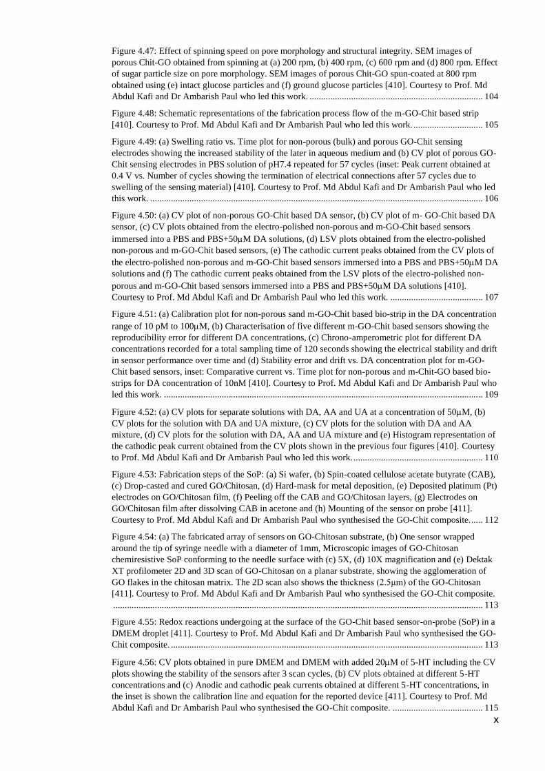
Figure 4.47: Effect of spinning speed on pore morphology and structural integrity. SEM images of
porous Chit-GO obtained from spinning at (a) 200 rpm, (b) 400 rpm, (c) 600 rpm and (d) 800 rpm. Effect
of sugar particle size on pore morphology. SEM images of porous Chit-GO spun-coated at 800 rpm
obtained using (e) intact glucose particles and (f) ground glucose particles [410]. Courtesy to Prof. Md
Abdul Kafi and Dr Ambarish Paul who led this work. ........................................................................... 104
Figure 4.48: Schematic representations of the fabrication process flow of the m-GO-Chit based strip
[410]. Courtesy to Prof. Md Abdul Kafi and Dr Ambarish Paul who led this work. .............................. 105
Figure 4.49: (a) Swelling ratio vs. Time plot for non-porous (bulk) and porous GO-Chit sensing
electrodes showing the increased stability of the later in aqueous medium and (b) CV plot of porous GO-
Chit sensing electrodes in PBS solution of pH7.4 repeated for 57 cycles (inset: Peak current obtained at
0.4 V vs. Number of cycles showing the termination of electrical connections after 57 cycles due to
swelling of the sensing material) [410]. Courtesy to Prof. Md Abdul Kafi and Dr Ambarish Paul who led
this work. ................................................................................................................................................ 106
Figure 4.50: (a) CV plot of non-porous GO-Chit based DA sensor, (b) CV plot of m- GO-Chit based DA
sensor, (c) CV plots obtained from the electro-polished non-porous and m-GO-Chit based sensors
immersed into a PBS and PBS+50M DA solutions, (d) LSV plots obtained from the electro-polished
non-porous and m-GO-Chit based sensors, (e) The cathodic current peaks obtained from the CV plots of
the electro-polished non-porous and m-GO-Chit based sensors immersed into a PBS and PBS+50M DA
solutions and (f) The cathodic current peaks obtained from the LSV plots of the electro-polished non-
porous and m-GO-Chit based sensors immersed into a PBS and PBS+50M DA solutions [410].
Courtesy to Prof. Md Abdul Kafi and Dr Ambarish Paul who led this work. ........................................ 107
Figure 4.51: (a) Calibration plot for non-porous sand m-GO-Chit based bio-strip in the DA concentration
range of 10 pM to 100M, (b) Characterisation of five different m-GO-Chit based sensors showing the
reproducibility error for different DA concentrations, (c) Chrono-amperometric plot for different DA
concentrations recorded for a total sampling time of 120 seconds showing the electrical stability and drift
in sensor performance over time and (d) Stability error and drift vs. DA concentration plot for m-GO-
Chit based sensors, inset: Comparative current vs. Time plot for non-porous and m-Chit-GO based bio-
strips for DA concentration of 10nM [410]. Courtesy to Prof. Md Abdul Kafi and Dr Ambarish Paul who
led this work. .......................................................................................................................................... 109
Figure 4.52: (a) CV plots for separate solutions with DA, AA and UA at a concentration of 50M, (b)
CV plots for the solution with DA and UA mixture, (c) CV plots for the solution with DA and AA
mixture, (d) CV plots for the solution with DA, AA and UA mixture and (e) Histogram representation of
the cathodic peak current obtained from the CV plots shown in the previous four figures [410]. Courtesy
to Prof. Md Abdul Kafi and Dr Ambarish Paul who led this work. ........................................................ 110
Figure 4.53: Fabrication steps of the SoP: (a) Si wafer, (b) Spin-coated cellulose acetate butyrate (CAB),
(c) Drop-casted and cured GO/Chitosan, (d) Hard-mask for metal deposition, (e) Deposited platinum (Pt)
electrodes on GO/Chitosan film, (f) Peeling off the CAB and GO/Chitosan layers, (g) Electrodes on
GO/Chitosan film after dissolving CAB in acetone and (h) Mounting of the sensor on probe [411].
Courtesy to Prof. Md Abdul Kafi and Dr Ambarish Paul who synthesised the GO-Chit composite. ..... 112
Figure 4.54: (a) The fabricated array of sensors on GO-Chitosan substrate, (b) One sensor wrapped
around the tip of syringe needle with a diameter of 1mm, Microscopic images of GO-Chitosan
chemiresistive SoP conforming to the needle surface with (c) 5X, (d) 10X magnification and (e) Dektak
XT profilometer 2D and 3D scan of GO-Chitosan on a planar substrate, showing the agglomeration of
GO flakes in the chitosan matrix. The 2D scan also shows the thickness (2.5μm) of the GO-Chitosan
[411]. Courtesy to Prof. Md Abdul Kafi and Dr Ambarish Paul who synthesised the GO-Chit composite.
................................................................................................................................................................ 113
Figure 4.55: Redox reactions undergoing at the surface of the GO-Chit based sensor-on-probe (SoP) in a
DMEM droplet [411]. Courtesy to Prof. Md Abdul Kafi and Dr Ambarish Paul who synthesised the GO-
Chit composite. ....................................................................................................................................... 113
Figure 4.56: CV plots obtained in pure DMEM and DMEM with added 20M of 5-HT including the CV
plots showing the stability of the sensors after 3 scan cycles, (b) CV plots obtained at different 5-HT
concentrations and (c) Anodic and cathodic peak currents obtained at different 5-HT concentrations, in
the inset is shown the calibration line and equation for the reported device [411]. Courtesy to Prof. Md
Abdul Kafi and Dr Ambarish Paul who synthesised the GO-Chit composite. ....................................... 115
xi
Figure 5.57: (a) Finished chip layout and (b) Block diagram of the chip architecture. .......................... 119
Figure 5.58: (a) Schematic of the 88 array and of the in-pixel standard readout topology, (b) Layout of
the in-pixel standard readout topology (poly-layer together with the first two metal-layers) and (c)
Layout of the 88 array including the decoder and the analogue multiplexer. ....................................... 122
Figure 5.59: (a) Simulated SNR vs. Input signal amplitude and (b) THD vs. Input signal amplitude of the
standard readout topology at different strain condition (i.e. planar, tension and compression). ............. 125
Figure 5.60: (a) Schematic of the 88 array and of the in-pixel standard readout topology with improved
fill-factor, (b) Layout of the in-pixel readout topology (poly-layer together with the first two metal-
layers) and (c) Layout of the 88 array including the decoder and the analogue multiplexer. ............... 126
Figure 5.61: (a) Simulated SNR vs. Input signal amplitude, (b) THD vs. Input signal amplitude of the
standard readout topology with improved fill-factor at different strain condition (i.e. planar, tension and
compression). .......................................................................................................................................... 129
Figure 5.62: (a) Schematic of the 88 array and of the in-pixel current-mode readout topology, (b)
Layout of the in-pixel readout topology (poly-layer together with the first two metal-layers) and (c)
Layout of the 88 array including the decoder and the analogue multiplexer. ....................................... 130
Figure 5.63: (a) Simulated SNR vs. Input signal amplitude, (b) THD vs. Input signal amplitude of the
current-mode readout topology at different strain condition (i.e. planar, tension and compression). ..... 132
Figure 5.64: Schematic and truth table of the decoder. ........................................................................... 133
Figure 5.65: Simulated (a) on-resistance, (b), THD vs. DC level at the input of the transmission gate, (c)
THD vs. input signal amplitude and (d) SNR vs. input signal amplitude of the transmission gate at
different strain conditions. ...................................................................................................................... 133
Figure 5.66: (a) Schematic and (b) Layout of the two-stage folded-cascode amplifier. ......................... 135
Figure 5.67: (a) Simulated SNR vs. Input signal amplitude, (b) THD [%] and (c) THD [dB] vs. Input
signal amplitude of the unity-gain folded cascode amplifier at different strain condition (i.e. planar,
tension and compression). ....................................................................................................................... 136
Figure 5.68: (a) The architecture of the complete signal chain from an 88 ISFET array. (b, d, f)
Monte-Carlo simulations of the SNR of the complete signal chain using an input signal amplitude of
1.2mVp-p and the standard pixel readout, standard pixel readout with improved fill-factor and current-
mode topologies, respectively. (c, e, g) Monte-Carlo simulations of the THD of the complete signal chain
using an input signal amplitude of 1.2mVp-p and the standard pixel readout, standard pixel readout with
improved fill-factor and current-mode topologies, respectively. ............................................................ 137
Figure 6.69: Classification of various silicon thinning techniques for realising ultra-thin silicon wafers
and chips [58]. ........................................................................................................................................ 139
Figure 6.70: Illustration of the process followed to realise ultra-thin silicon using a PDMS as protective
layer [333]. .............................................................................................................................................. 142
Figure 6.71: Image of (a) wafer backside showing the etching window defined using PDMS, (b) optical
image of the capacitive device on front-side and (c) the etching setup [333]. ........................................ 143
Figure 6.72: (a) 3D scan of etched step showing the masking property of PDMS. The red area was
masked with PDMS and the blue area shows the silicon region, (b) SEM image of the 22.78m thick
silicon obtained after 6 hours of etching, (c) Optical image of the etched backside showing the etch pits
created during etching due to preferential etching of different crystallographic planes and (d) SEM image
of hillocks formed on the silicon surface due to micro-masking effect due to hydrogen formed as a by-
product of the chemical reaction between silicon and TMAH [333]. ..................................................... 144
Figure 6.73: SEM image of PDMS surface (a) Before etching and (b) After 2 hours of etching in TMAH.
3D profile scan of PDMS surface at the end of (c) 2 hours, (d) 4 hours, (e) 6 hours and (f) 8 hours of
etching in TMAH and (g) Plot of the surface of PDMS vs etching time showing an almost linear increase
in the roughness with time [333]. ........................................................................................................... 145
Figure 6.74: (a) Reaction mechanism between TBAF and PDMS based on the nucleophilic attack of
fluoride ion on the siloxane bond leading to the dissolution of the PDMS chain in the solvent. SEM
image of silicon sample during (b) midway of PDMS etching and (c) after PDMS etching [333]. ....... 148
xii
Figure 6.75: (a) Image of thinned sample integrated into polyimide foil and placed over a 3D printed
bending structure with bending radius of 10mm, (b) C-V plot of capacitive structures before and after
thinning obtained using PDMS as a protective coating and (c) C-V plot of a sample capacitive device
before and after thinning using ProTEK as protection coating [333]. .................................................... 148
Figure 6.76: Image of (a) Bonding wax, (b) Glass circular carrier with a diameter of 106mm, (c) Pressing
system used to ensure uniformly spread bonding wax at the interface between glass-carrier and silicon
sample, (d) Thickness measuring tool, (e) PM5 Logitech precision lapping and polishing machine (left)
and jig (right) and (f) Lapping plates. ..................................................................................................... 150
Figure 6.77: Photographs of the two 2-inch wafers thinned down to the ultra-thin regime to optimise the
thinning process. ..................................................................................................................................... 152
Figure 6.78: (a) The fabricated chip (1 1 cm2) with four n-channel transistors and (b) the SEM image of
the cross-section of the thin chip on a polyimide-based flexible PCB showing the thickness of the chip
and FPCB. (c) Photograph of thin silicon compared the bulky silicon dies with deposited ion-sensitive
electrodes and (d) the SEM image of the cross-section of the RuO2-based ion-sensitive electrode [194].
Courtesy to Dr Shoubhik Gupta who designed the photolithography masks used for the fabrication of the
four n-channel transistors which was done in the Fondazione Bruno Kessler (FBK) institute. .............. 152
Figure 6.79: Time-lapse of the fabricated RuO2-based ion-sensitive electrode on the ultra-thin and
mechanically flexible silicon substrate. .................................................................................................. 153
Figure 6.80: (a - e) Photographs of the ultra-thin ICs compared with the bulky counterpart and (f) Surface
profile of the ultra-thin chip measured using the DektakXT Stylus Surface Profiling System. .............. 153
Figure 6.81: Microscopic images of the backside after back-lapping of the dies. .................................. 154
Figure 6.82: (a) Designed and (b) Fabricated flexible PCB. ................................................................... 154
Figure 6.83: Photographs of the (a, b) Glued ultra-thin IC and (c) Wire-bonded ultra-thin IC on the
FPCB. ..................................................................................................................................................... 155
Figure 6.84: Photographs of the encapsulated ICs on the FPCB. ........................................................... 156
Figure 7.85: Experimental setup for the characterisation of signal-to-noise ratio (SNR), input-referred
noise, total harmonic distortion (THD) and noise spectral density of each ISFET active-pixel. (b)
Experimental setup for the characterisation of pH sensitivity, drift and hysteresis. ............................... 160
Figure 7.86: (a) Analogue recording of the output voltage of an 88 ISFET array with improved fill-
factor captured in an oscilloscope and (b) The same recording captured by a Mbed LPC1768
microcontroller and visualised in real-time using Matlab. ...................................................................... 162
Figure 7.87: Flowcharts of Mbed and Matlab programs to acquire and visualise the data acquired from
the chip. .................................................................................................................................................. 162
Figure 7.88: Flowchart of the data analysis script in Python for the extraction of SNR, input-referred
noise, THD and noise spectral density from the obtained PSD plots. ..................................................... 163
Figure 7.89: Measured average noise spectral density of the standard pixel readout topology on bulky
and ultra-tin ICs. ..................................................................................................................................... 164
Figure 7.90: (a - c) Histograms of the measured performance parameters of the 88 standard pixel
readout ISFET array on the bulky (~250 m thick) IC, (d - f) Histograms of the measured performance
parameters of the 88 standard pixel readout ISFET array on the ultra-thin (30 m thick) IC. ............. 165
Figure 7.91: Measured average noise spectral density of the standard pixel with improved fill-factor
readout topology on bulky and ultra-tin ICs. .......................................................................................... 166
Figure 7.92: (a - c) Histograms of the measured performance parameters of the 88 standard pixel with
improved fill-factor readout ISFET array with improved fill-factor on the bulky (~250 m thick) IC, (d -
f) Histograms of the measured performance parameters of the 88 standard pixel with improved fill-
factor readout ISFET array on the ultra-thin (30 m thick) IC. .............................................................. 166
Figure 7.93: Measured average noise spectral density of the current-mode pixel readout topology on
bulky and ultra-thin ICs. ......................................................................................................................... 167
xiii
Figure 7.94: (a - c) Histograms of the measured performance parameters of the 88 current-mode pixel
readout ISFET array on the bulky (~250 m thick) IC, (d - f) Histograms of the measured performance
parameters of the 88 current-mode pixel readout ISFET array on the ultra-thin (30 m thick) IC. ..... 168
Figure 7.95: Average drift characteristics of the output voltage at pH7 obtained from the (a) Standard
pixel readout topology, (b) Standard pixel readout topology with improved fill-factor, (c) Current-mode
pixel readout topology. (d) Transient loop of step changes in pH of the DMEM solution over time and (e)
pH-sensitivity plot obtained by averaging the output voltage of the pixels of an 88 array. .................. 169
Figure 7.96: (a) Test configuration of the folded-cascode amplifier connected in a unity-gain
configuration driving the loads which resemble the on-chip SAR ADC input impedance and capacitance.
The obtained noise spectral density when was the applied signal at the input of the unity-gain amplifier
was (b) DC, (c) 2mVp-p @ 50Hz, (d) 5mVp-p @ 50Hz, (e) 10mVp-p @ 50Hz and (f) 100mVp-p @ 50Hz.
................................................................................................................................................................ 170
Figure 7.97: Illustration of electrical conductance modulation due to change in the piezoresistance of
silicon. (a) Schematic including an array of ISFETs on flexible CMOS chips interfaced on a hybrid
large-area flexible system experiencing different bending stresses. (b) Illustration of the current density
in the channel region of an n-channel MOSFET during planar conditions. (c) Illustration of the current
density in the channel region of an n-channel MOSFET during compressive bending conditions. (d)
Illustration of the current density in the channel region of an n-channel MOSFET during tensile bending
conditions. (e) The extended-gate RuO2-based ISFET configuration used in this work where the
mechanically flexible MOSFETs are connected to (f) the mechanically flexible silicon Si-substrate on
which the RuO2-based ion-sensitive material and the reference-electrode were fabricated [194]. ......... 172
Figure 7.98: (a) The measurement setup for the characterization of the drift of the fabricated MOSFETs
and (b) Transient plot of the fabricated MOSFETs’ drain-current [194]. Courtesy: The photolithography
masks used for the fabrication of MOSFETs were designed by Shoubhik Gupta, the fabrication of chips
was carried out by the staff of the Fondazione Bruno Kessler (FBK) institute, Italy. ............................ 173
Figure 7.99: (a) The measurement setup for the characterization of the drift of the fabricated EG-ISFETs,
(b) Repeatability test of the bending effect on EG-ISFETs at pH9 biased in the linear region (𝑉𝑅. 𝐸. =
𝑉𝐺𝑆 = 2𝑉 and 𝑉𝐷𝑆 = 0.4𝑉). The inset shows the transient plot of drain-current with the baseline
removed for better observation of the reproducibility of the bending effect in the performance of devices
on mechanically flexible UTC. (c) Repeatability test of the bending effect on EG-ISFETs at pH9 biased
in the saturation region (𝑉𝑅. 𝐸. = 𝑉𝐺𝑆 = 1𝑉 and 𝑉𝐷𝑆 = 0.4𝑉). The results were obtained after 1000
bending cycles [194]. Courtesy: The 3D-printed automated custom made bending setup was developed
by Adamos Christou. .............................................................................................................................. 174
Figure 7.100: (a) Drifting current of EG-ISFET at pre-bent condition biased in the linear region at
𝑉𝑅. 𝐸. = 𝑉𝐺𝑆 = 2𝑉 and 𝑉𝐷𝑆 = 0.4𝑉 at pH 7 and (b) Drifting current of EG-ISFET at pre-bent condition
biased in the saturation region at 𝑉𝑅. 𝐸. = 𝑉𝐺𝑆 = 1𝑉 and 𝑉𝐷𝑆 = 0.4𝑉 at pH 9. The results were
obtained after 1000 bending cycles [194]. .............................................................................................. 175
Figure 7.101: Behaviour of drift of EG-ISFETs on mechanically bendable Si-substrate under dynamic
bending showing that the drift-rate remains unchanged irrespective of the bending condition. The EG-
ISFET is biased in the linear region at 𝑉𝑅. 𝐸. = 𝑉𝐺𝑆 = 2𝑉 and 𝑉𝐷𝑆 = 0.4𝑉 at pH 9. The results were
obtained after 1000 bending cycles [194]. .............................................................................................. 175
Figure 7.102: Depiction of the different parameters used to calculate the bending radius of the thin chip
over time as the motorised press is applying sequential strain on it. The parameter c is constant and equal
to 5 cm and the parameter h was calculated for every second knowing the velocity of the structure. The
velocity was known and provided by the LabVIEW programme with which the motorised press was
controlled [194]. ..................................................................................................................................... 176
Figure 7.103: (a) Photograph of the motorized press at the moment of contact with the flexible printed-
circuit-board (FPCB), (b) Photograph of the motorized press when it has reached the mid-point of the
overall travelled distance and the chip is bent under 80mm bending radius, (c) Photograph of the
motorized press when it has reached maximum travelled distance and the chip is bent at 40mm bending
radius, (d) Velocity vs. Time plot describing the movement of the motorized press, (e) Calculated
Bending Radius vs. Time diagram plot used to achieve drift-free ISFET response, (f) Calculated Strain
vs. Time diagram plot used to achieve drift-free ISFET response, (g) Transient response of ISFET under
planar condition compared with the drift-free response achieved by applying sequentially increased

xiv
tensile strain and (h) Comparison of planar and drift-free ISFET response showing the error bars. All
measurements were performed at biasing conditions of: 𝑉𝑅. 𝐸. = 𝑉𝐺𝑆 = 1𝑉 and 𝑉𝐷𝑆 = 0.4𝑉 [194]. 178
Figure 7.104: pH response of the fabricated RuO2-based EG-ISFETs under unstrained and sequentially
strained conditions at a sequence of step changes in pH from 7.9 to 3.9 to 4.5 to 6.1. The MOSFET is
biased at 𝑉𝐺𝑆 = 1𝑉 and 𝑉𝐷𝑆 = 0.4𝑉 [194]. ......................................................................................... 179
Figure 8.105: Printed Ag/AgCl pattern on silicon nitride deposited on a silicon substrate using super-
inkjet (SIJ) printing. ................................................................................................................................ 186
xv
List of Publications
Journal Articles
1. A. Vilouras, A. Christou, L. Manjakkal and R. Dahiya, "Ultra-thin Ion-Sensitive Field-
Effect Transistors Chips with Bending Induced Performance Enhancement," ACS Appl.
Electron. Mater., vol. 2, pp. 2601–2610, 2020.
2. S. Gupta, A. Vilouras and R. Dahiya, "Polydimethylsiloxane as polymeric protective
coating for fabrication of ultra-thin chips," Microelectronic Engineering, vol. 221, p.
111157, 2020.
3. P. K. Dubey, N. Yogeswaran, F. Liu, A. Vilouras, B. Kaushik and R. Dahiya,
"Monolayer MoSe based tunneling field effect transistor for ultra-sensitive strain
sensing," IEEE Transactions on Electron Devices, 2020.
4. M. A. Kafi, A. Paul, A. Vilouras and R. Dahiya, "Mesoporous chitosan based
conformable and resorbable biostrip for dopamine detection," Biosensors and
Bioelectronics, vol. 147, p. 111781, 2020.
5. M. A. Kafi, A. Paul, A. Vilouras, E. Hosseini and R. Dahiya, "Chitosan-Graphene Oxide
based Ultra-thin and Flexible Sensor for Diabetic Wound Monitoring," IEEE Sensors
Journal, 2019.
6. C. G. Núñez, A. Vilouras, W. T. Navaraj, F. Liu and R. Dahiya, "ZnO Nanowires Based
Flexible UV Photodetector System for Wearable Dosimetry," IEEE Sensors Journal,
2018.
7. L. Manjakkal, A. Vilouras and R. Dahiya, "Screen printed thick film reference
electrodes for electrochemical sensing," IEEE Sensors Journal, vol. 18, pp. 7779-7785,
2018.
8. A. Vilouras, H. Heidari, S. Gupta and R. Dahiya, "Modeling of CMOS Devices and
Circuits on Flexible Ultrathin Chips," IEEE Transactions on Electron Devices, vol. 64,
pp. 2038-2046, 2017.
9. S. Gupta, H. Heidari, A. Vilouras, L. Lorenzelli and R. Dahiya, "Device modelling for
bendable piezoelectric FET-based touch sensing system," IEEE Transactions on Circuits
and Systems I: Regular Papers, vol. 63, pp. 2200-2208, 2016.
Conference Presentations
1. A. Vilouras and R. Dahiya, " Ultra-Thin Chips with Current-Mode ISFET Array for
Continuous Monitoring of Body Fluids pH," in IEEE International Symposium on
Circuits and Systems (ISCAS), 2021.

xvi
2. M. Bhattacharjee, A. Vilouras and R. Dahiya, "Microdroplet Based Organic Vapour
Sensor on a Disposable GO-Chitosan Flexible Substrate," in IEEE International
Conference on Flexible and Printable Sensors and Systems (FLEPS), 2019, pp. 1-3.
3. A. Vilouras, A. Paul, M. A. Kafi and R. Dahiya, "Graphene Oxide-Chitosan Based
Ultra-Flexible Electrochemical Sensor for Detection of Serotonin," in IEEE Sensors
Conference, 2018, pp. 1-4. (Best lecture presentation paper award)
4. M. A. Kafi, A. Paul, A. Vilouras and R. Dahiya, "Chitosan-Graphene Oxide Based
Ultra-Thin Conformable Sensing Patch for Cell-Health Monitoring," in IEEE Sens.
Conf., 2018, pp. 1-4.
5. A. Vilouras, W. T. Navaraj, H. Heidari and R. Dahiya, "Flexible pressure sensing system
for tongue-based control of prosthetic hands," in IEEE Sens. Conf., 2017, pp. 1-3.
6. A. Vilouras and R. Dahiya, "Compact model for flexible ion-sensitive field-effect
transistor," in IEEE Biomedical Circuits and Systems Conference (BioCAS), 2017, pp.
1-4.
7. S. Gupta, A. Vilouras, H. Heidari and R. Dahiya, "Device modelling of silicon based
high-performance flexible electronics," in IEEE International Symposium on Industrial
Electronics (ISIE), 2017, pp. 2089-2092.
8. S. Wen, H. Heidari, A. Vilouras and R. Dahiya, "A wearable fabric-based RFID skin
temperature monitoring patch," in IEEE Sens. Conf. 2016, 2016, pp. 1-3.
9. W. T. Navaraj, F. Liu, A. Vilouras, D. Shaktivel, C. G. Núñez, H. Heidari, F. Labeau,
D. Gregory and R. Dahiya, "Modelling of nanowire FETs based neural network for
tactile pattern recognition in E-skin," in IEEE Biomedical Circuits and Systems
Conference (BioCAS), 2016, pp. 572-575.

xvii
Acknowledgements
I would like to acknowledge the Engineering and Physical Sciences Research Council (EPSRC)
Centre for Doctoral Training in Intelligent Sensing and Measurement for funding this project
under the grant EP/L016753/1.
I would like to express my utmost gratitude and thanks to my supervisor Prof. Ravinder Dahiya
for his continuous support through my PhD. I appreciate his trust and the freedom he gave me to
explore my own research interest, without which this research outcome could never be possible.
I also thank Prof. David R. S. Cumming for being my second supervisor and Prof. Sandy Cochran
for allowing me access to his research laboratory and to the lapping machine. A great thanks goes
to Mr Joe Ashby. Without his assistance the wire bonding of ultra-thin ICs would not have been
possible. Further, I am grateful for the excellent service from the electronics workshop and the
James Watt Nanofabrication Centre (JWNC) staff. I must also thank Prof. Andy Harvey and Prof.
Ian Underwood for their support and valuable advices. Also, I sincerely thank all of the people
working in the CDT-ISM, and especially Michelle, Aimee and Charlotte, for their help
throughout these years.
I want to extend my sincere thanks to all the members of Bendable Electronics and Sensing
Technologies group. I am particularly indebted to Dr Libu Manjakkal, Prof. Md. Abdul Kafi, Dr
Ambarish Paul and Dr Shoubhik Gupta who were closely associated in shaping some key
outcomes of the research presented in this thesis and the associated publications. Also, I would
like to thank Dr Emre Ozan Polat, Dr Hadi Heidari, Dr Ensieh Seyed Hosseini, Dr Carlos García
Núñez, Dr Dhayalan Shakthivel, Dr Nivasan Yogeswaran, Dr William Taube Navaraj, Dr
Wenting Dang, Dr Fengyuan Liu, Dr Mitradip Bhattacharjee, Dr Abhilash Pullanchiyodan, Dr
Yogeenth Kumaresan, Dr Saoirse Dervin, Dr Abhishek Dahiya, Markellos Ntagios, Adamos
Christou and Ayoub Zumeit. It has been a great pleasure working with you all. I would also like
to thank Dr Christos Giagkoulovits for the countless hours of talking about engineering and for
being a fantastic flatmate and a great friend.
Finally, I would like to express my deepest gratitude to my family for their unconditional love
and support. I dedicate this work to all of you and especially my father for being the source of
strength in my life and my mother for her relentless encouragement and support. I also thank my
future wife, Vasiliki, for being my better half in every sense throughout this journey. Thank you
for your love and for your complete faith in me; this success is as much yours as it is mine.

xviii
Author’s Declaration
I hereby declare that this thesis was composed and originated entirely by myself in the School of
Engineering at The University of Glasgow except where explicitly stated otherwise in the text,
and that this work has not been submitted for any other degree or professional qualifications.
Anastasios Vilouras

xix
Glossary of Abbreviations
IoE Internet of everything
ADC Analogue-to-digital converter
CMOS Complementary metal-oxide semiconductor
TSV Through-silicon via
FPGA Field programmable gate array
ISFET Ion-sensitive field-effect transistor
MOSFET Metal-oxide-semiconductor field-effect transistor
IC Integrated circuit
PSRR Power supply rejection ratio
CMRR Common-mode rejection ratio
UTC Ultra-thin chip
PDK Process design kit
FPCB Flexible printed circuit board
PoC Point-of-care
ISE Ion-selective electrode
LOC Lab-on-chip
R.E. Reference electrode
Edl Electrical double-layer
IoE Internet of Everything
UTC Ultra-thin chip
IC Integrated circuit
CB Conduction band
VB Valence band
PVT Process, voltage, temperature variations
PVTS Process, voltage, temperature, stress variations
FPCB Flexible printed circuit board
R.E. Reference electrode
LTCC Low-temperature co-fired ceramic
EIS Electrochemical impedance spectroscopy
UI User interface
LOD Limit of detection
ND Neurodegenerative diseases
SoP Sensors-on-Probe
SNR Signal-to-noise ratio
SNDR Signal-to-noise & distortion ratio
SAR Successive-approximation
SF Source-follower

xx
LDO Low dropout
DAC Digital-to-analogue converter
RTS Random telegraph signal
PSD Power spectral density
RMS Root mean square
PDK Process design kit
THD Total harmonic distortion
MEMS Microelectromechanical systems
EDP Ethylene-diamine-pyrocatechol
TMAH Tetramethylammonium hydroxide
KOH Potassium hydroxide
FoM Figure-of-Merit
SNR Signal-to-noise ratio
PSD Power spectral density
DMEM Dulbecco's Modified Eagle Medium
FFT Fast Fourier Transform
1
Chapter 1. Introduction
1.1 Motivation
The ageing rate of the population and especially the group of people aged over 60 years old is
predicted to double from 11% to 22% by 2050, according to the World Health Organisation [1].
Among the ageing countries, those categorised as low-income countries have deficiencies in
infrastructures, funds and resources and thus their incomplete healthcare system cannot provide
the necessary healthcare support to people in need. Besides, as it was recently observed during
the COVID-19 pandemic, the current ageing society faces some important and special healthcare
challenges due to the limited hospital resources, doctors and related facilities which forced most
of the population all around the globe to local lockdowns and limited working and consuming
activities during the year of 2020. Even though a few attempts have been already made from the
academic world to provide low-cost resources, such as ventilators [2], it is also in high demand
to meet the needs of the growing ageing population in the long-term in the form of remote
personalised diagnosis and treatment using miniaturised wearable or implantable point-of-care
(PoC) biomedical diagnostic instruments. This is particularly important since the current
biomedical diagnostic tools used for highly sensitive measurements to accurately monitor
diseases or to understand their underlying causes, such as ultrasound, flow cytometry and genetic
sequencing [3-7], require bulky and expensive sample preparation and evaluation instruments
which can be operated only by trained personnel. As such, these diagnostic tools are only
available in established hospitals or clinics.
Sensing technologies are thus important and are increasingly being used towards the internet-of-
everything (IoE) for various applications. Among them, biochemical sensing systems are
particularly important in the domains of medical science through the discovery of biological
mechanisms or in environmental as well as water and food quality monitoring. Further, wearable
and implantable point-of-care (PoC) biomedical devices that have been explored towards rapid
clinical-grade decision-making systems will be able to mitigate delays in treatment and be used
anytime-anywhere leading to more personalized diagnosis and treatment [8-13]. Recent advances
in the field of wearable and implantable sensing microsystems enabled the development of
devices that can monitor heart rate [14, 15], blood oxygenation and pressure [16-18], respiration
rate [19, 20], body posture [21], skin stretching [22], skin temperature [23] and brain activity [24,
25]. Moreover, recent studies have also demonstrated wearable systems capable of continuous
measurements of chemicals such as electrolytes and metabolites in bio-fluids [26-29] while
others have pushed the field of wearables a step closer to sensing microsystems that can
2
seamlessly comply with the curvilinear geometry of human tissues allowing robust recordings
while providing comfort to the user in the daily-life activities. [30, 31].
The miniaturization of these devices is, therefore, of high importance to ensure adequate form
factors that can easily be integrated into wearable smart gadgets, such as wrist bands, watches or
rings, or to be implanted without causing bleeding or damage to the tissues. With such
technology, not only the elderly will benefit but also other population groups like athletes or
subjects suffering from disabilities. Another field that this technology can be proven useful is in
forensic applications, in research laboratories as well as in the consumer market since wearable
and implantable sensing microsystems can be used for continuous and real-time monitoring of
human or animal physiology [32-35]. Complementary metal-oxide-semiconductor (CMOS)
technology is a well-established and proven technology through the continuous scaling in the
features of the integrated devices following Moore’s Law [36] allowing the realization of
sophisticated and fast data processing on custom-made application-specific integrated circuits
(ASICs). As an example, at the end of 2019 consumer products have been released into the
market with microprocessors fabricated in the 7nm CMOS technology while it is expected to
have mass-production of chips in the 5nm technology by 2020 and in the 3nm technology by the
end of 2021. The capability for high-level of integration makes CMOS process a highly useful
technology which can be utilized in analogue, digital and mixed-signal integrated circuits (ICs)
where transceivers, amplifiers, data-converters, micro-controllers/processors as well as a
variability of integrated sensing modalities (e.g. photodiodes, biochemical and touch/pressure
sensors) can all be integrated on the same silicon die or on a three-dimensional (3D) stack of
silicon dies realizing a miniaturized and highly compact microsystem [37-42]. In applications
where bio-fluids are under test, the integrated sensors are physically interfaced with fluidic
samples which can be moved towards or away from the sensing sites using a microfluidic system.
The complete system, termed also as lab-on-chip (LOC), can perform one or several laboratory
functions using a very small volume of fluidic samples (micro- or even pico-liters) [43-45].
One category of CMOS-based biochemical sensors able to measure ultra-small volumes of fluids
is the ion-sensitive field-effect transistor (ISFET). ISFETs were introduced by P. Bergveld in
1970 for brain-based electrophysiological characterisation research [46] and can be easily
adapted in the CMOS fabrication process through the method that was first reported by Bausells
et al. [47]. ISFETs offer a method of detection that can be fast, specific, and non-destructive. An
ISFET sensor is essentially a pH sensor that can be used for label-free detection of H+ ions.
However, ISFETs can be used as a platform for various biochemical sensing applications after
modification of the sensing layer including DNA sequencing, enzyme kinetics, gas sensing,
detection of positive ions (e.g. sodium, potassium, calcium), detection of negative ions (e.g.
chloride, phosphate, nitrate) as well as detection of biomolecules (e.g. adenosine triphosphate,
dopamine, lactate) [48-53]. In addition, ISFETs, and every MOSFET-based sensor such as the
piezoelectric oxide semiconductor field-effect transistors (POSFETs) which have recently
3
integrated on robots [54], are offering several advantages, such as high input-impedance, low
output-impedance, extremely fast response and small area allowing their implementation in
arrayed formats with in-pixel amplification and digitisation schemes. However, since the area of
the analogue front-end amplifiers is limited by the size of the pixel, there is a trade-off between
power consumption, noise and spatial resolution.
However, the performance itself is not enough as emerging applications like wearables or
implantables require the silicon dies to be also miniaturised in the z-direction, targeting
conformability on three-dimensional curvilinear shapes or low tissue damage [55, 56]. However,
silicon wafers are brittle and manufactured to be thick and mechanically stiff for reliability and
better automated-handling purposes precluding their use in the aforementioned applications.
Fortunately, with the appropriate silicon-thinning and handling techniques, silicon wafers and
dies can be thinned down to the ultra-thin regime (< 50µm) where can become bendable and
conformable on curvilinear surfaces [57, 58]. Ultra-thin silicon provides several aspects that
cannot be realized using the conventional bulky silicon wafers. For example, the ultra-thin form
factor of CMOS chips allows the dies to be easier integrated into compact systems, such as
systems-on-pill (SoP) [59-61], mini endoscopes and catheters [62-68], orthopedic or dental
implants [69-72] and sub- or epi-retinal implants [73-76], as shown in Figure 1.1(a-d). Also, it
allows the chips to be implanted without severely damaging the tissues, such as in systems for
bioimpedance, neural signal, EMG signal recording probes or for intracranial pressure
monitoring applications allowing the integration of microelectrodes, bio-chemical, pressure,
temperature and optical sensors along with their signal amplification, processing and
communication units on the same compact system [25, 77-80], as shown in Figure 1.1(f). Finally,
the ultra-thin form factor allows the integration of energy harvesting schemes along with the
power management circuit blocks allowing the design of energy-autonomous wearable or
implantable health monitoring/management systems [81], as shown in Figure 1.1(e).
Additionally, the thinning process offers several other advantages including the improvement of
heat dissipation between the chip and the package, the realization of back-illuminated imagers
with a wider angular response, the improvement of quality-factor (𝑄𝑓𝑎𝑐𝑡𝑜𝑟) of inductors due to
reduced Si-substrate resistivity and the 3D-stacking of silicon dies (3D ICs) [57]. On top of all
that, the circuits on ultra-thin silicon have all the advantages offered by CMOS technology, such
as low power consumption, low noise, high speed, scalability and very-large-scale integration
capabilities. Furthermore, the mechanical flexibility and shape adaptability of Si-UTCs allows
them to seamlessly be integrated on curvilinear surfaces, such as on soft tissues or the curvilinear
surfaces of robots, robotic prosthetic limbs and smart wearables, such as wrist-bands, contact
lenses, glasses and rings [31, 39, 56, 82-84]. Finally, the mechanical flexibility also allows the
integration of ultra-thin and flexible CMOS ICs with thin-film or organic large-area electronics
providing an overall hybrid solution for RFID tags, security applications, driver ICs in large and
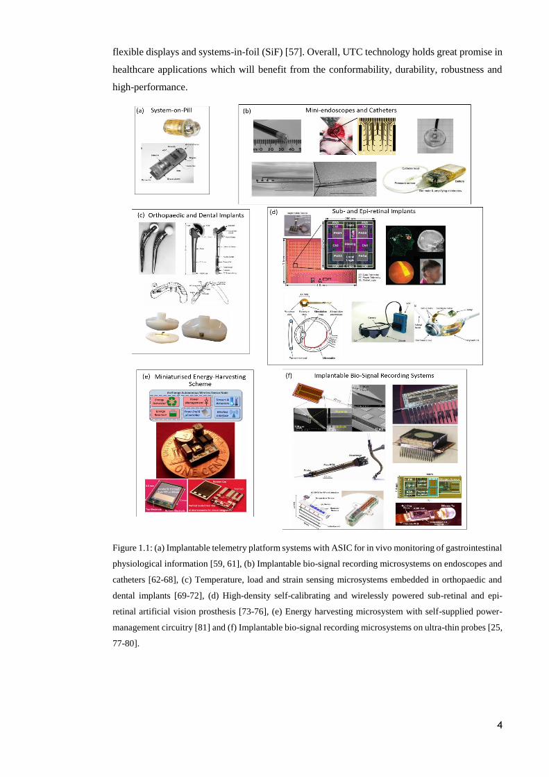
4
flexible displays and systems-in-foil (SiF) [57]. Overall, UTC technology holds great promise in
healthcare applications which will benefit from the conformability, durability, robustness and
high-performance.
Figure 1.1: (a) Implantable telemetry platform systems with ASIC for in vivo monitoring of gastrointestinal
physiological information [59, 61], (b) Implantable bio-signal recording microsystems on endoscopes and
catheters [62-68], (c) Temperature, load and strain sensing microsystems embedded in orthopaedic and
dental implants [69-72], (d) High-density self-calibrating and wirelessly powered sub-retinal and epi-
retinal artificial vision prosthesis [73-76], (e) Energy harvesting microsystem with self-supplied power-
management circuitry [81] and (f) Implantable bio-signal recording microsystems on ultra-thin probes [25,
77-80].
5
1.2 Research Objectives
The main objective of this work was to develop a fully-integrated and low-power ISFET-based
sensing microsystem using UTC technology. To this end, a low-noise and low-power
CMOS-based IC with 512 ISFET sensors, on-chip recording amplifiers and ADCs was designed,
thinned to the ultra-thin regime (~30m) and characterized before and after thinning
demonstrating the suitability of a miniaturised ultra-thin lab-on-chip microsystem for pH
monitoring of body-fluids which can be conformably and seamlessly integrated on the skin or be
an active component of a minimally invasive implantable system. The in-pixel circuitry was
designed with low-noise specifications required for biomedical applications and considering a
maximum signal amplitude of 10mVp-p. The pH range for wearable applications where sweat I
the target analyte is between pH5 and pH9, while the pH resolution is not stringent and can be
kept at 0.1 pH.
The design of accurate control and readout electronics using UTC technology requires a thorough
knowledge of the operation of ISFETs and an understanding of mechanisms and effects on the
performance of CMOS-based devices and circuits when they experience bending-induced
stresses. Therefore, it is required to fabricate MOSFET and ISFET devices using UTC
technology and characterise their electrical behaviour so that to develop robust compact models
which can capture any performance variation due to bending-induced stresses. These models can
subsequently be used as an extra verification step during performance simulations of the
integrated circuits. Also, it is important to design, fabricate and analyse the performance of
various peripheral devices, such as on-chip planar Ag/AgCl/KCl reference electrodes which are
essential for the proper operation of ISFETs, and ultra-flexible and biodegradable biosensors
towards the development of a conformable or minimally-invasive fully-integrated point-of-care
diagnostic tool.
1.3 Research Contributions
This PhD thesis covers the modelling, design, implementation and characterisation of low-noise
and power fully-integrated ISFET-based sensing microsystems using UTC technology. This
work extends significantly the state-of-art of CMOS-based microsystems developed using ultra-
thin chip technology and presents innovative research on important aspects of sensors, device
modelling, exploitation of bending stresses and design of integrated readout circuits for pH-
monitoring applications developed on ultra-thin silicon substrates, as explained in more detail
below.
1) A better understanding of mechanisms and effects of bending-induced stresses on the
performance of CMOS-based devices and circuits and the development of compact
behavioural models for CMOS-based MOSFET (NMOS and PMOS) devices which can
6
be compiled into computer-aided design (CAD) tools widely used for simulations of
circuits’ performance. To this aim, a script was written in Verilog-A and compiled in the
Cadence Virtuoso platform. These models, which are a combination of mathematical
equations and extracted parameters from BSIM4 and BSIM6, were validated through
experiments on fabricated devices on Si-UTCs at different strain conditions and were
further used for the design of the fully-integrated ISFET-based sensing microsystem on
UTCs.
2) A better understanding of the fundamentals of electrochemical mechanisms, the theory
of pH-sensitivity and operation of CMOS-based ISFETs under different bending-
induced stresses and the development of compact behavioural models for mechanically
bendable CMOS-based ISFET which can also be compiled into computer-aided design
(CAD) tools. To attain this aim, a script was also written in Verilog-A and compiled in
the Cadence Virtuoso platform. The model, which is a combination of mathematical
equations that describes the electrochemical reactions at the interface between ISFET
and aqueous electrolytic medium, were validated through experiments on fabricated
devices on Si-UTCs at different pH and strain conditions and were further used for the
design of the fully-integrated ISFET-based sensing microsystem on UTCs.
3) Wafer- and chip-scale thinning procedures using wet-etching and lapping techniques are
developed. To this goal, the use of tetramethylammonium hydroxide (TMAH) acting as
the silicon etchant and polydimethylsiloxane (PDMS) acted as the chip’s active side
protective layer was initially explored. Furthermore, the thinning procedure of silicon
using a chemo-mechanical thinning process termed as “lapping” technique was
established ensuring faster material removal (etch rate of ∼9 μm/min) using abrasive as
well as colloidal polishing slurry. Lapping technique was then used to thin-down the
fully-integrated ISFET-based ICs to a thickness of 30m.
4) Planar on-chip reference electrodes on UTCs and ultra-flexible and biodegradable
biosensors for the detection of dopamine and serotonin are designed, fabricated and
characterised. The aim towards an on-chip reference electrode was attained in
collaboration with Dr Libu Manjakkal and planar Ag/AgCl/KCl based reference
electrodes were developed on rigid as well as ultra-thin silicon substrates and further
characterised. Also, the goal towards the development of ultra-flexible and
biodegradable biosensors was attained in collaboration with Prof. Md Abdul Kafi and Dr
Ambarish Paul. To this end, graphene-oxide and chitosan-based sensors were developed
for the detection of dopamine and serotonin present in blood-equivalent chemical
solutions. In these studies, I was also an active investigator offering support in the
7
methodology, characterisation, data analysis and writing of the research articles. Also,
the study for the detection of serotonin, which I was leading, won the best paper award
in the IEEE Sensors Conference 2018.
5) RuO2-based ISFET devices are developed on ultra-thin (~45m) silicon chips which can
be calibrated by applying external stresses on their ultra-thin silicon substrate and
compensate for ISFET instabilities, such as the low-frequency temporal variation of the
operating point of ISFETs, a phenomenon termed as “drift”. This objective was attained
using the lapping technique to thin the silicon chip on which the ISFET was fabricated.
Also, the compensation of drift was achieved using a custom-made automated 3D-
printed bending setup developed by the colleague Adamos Christou. This work opens a
new direction towards the exploitation of externally-applied bending stresses for
performance enhancement of CMOS-based integrated devices and circuits.
6) A fully-integrated low-noise and power ISFET-based IC is designed and developed using
UTC technology. To attain this goal, Cadence tools were used and the chip was taped-
out and fabricated using a commercially available 350nm CMOS process. Using the
developed behavioural models previously discussed and the models from the process
design kit (PDK) of the Austria Microsystems (AMS) foundry, this thesis presents
detailed planning for block-level designs and simulations of three different in-pixel
topologies including theory and noise analysis. On-chip there is a unity-gain amplifier
which drives and settles the kickback caused by the charge rebalancing on the on-chip
SAR ADC (adopted from the library provided by the foundry) input at the start of the
acquisition period. The fabricated chips were thinned down to the ultra-thin regime using
lapping technique and the facilities of the University of Glasgow and packaged on
polymeric FPCBs before electrical and electrochemical characterisation at different pH
conditions in body-fluid equivalent aqueous solutions, such as Dulbecco's Modified
Eagle Medium (DMEM).
1.4 Thesis organisation
Following the Introduction, this thesis is organised as follows:
Chapter 2 presents an overview of potentiometric electrochemical sensors with
emphasis on pH sensing applications. In particular, the sensing mechanisms, different
materials that have been used along with their properties and non-ideal effects that they
commonly exhibit are discussed. In addition, the operation principles, theory and
applications of ISFETs is given. Furthermore, the technological advancements towards
the realization of mechanically flexible and stretchable ion-sensitive electrodes (ISEs)
8
integrated on the human body are discussed, following with the advancements towards
the realization of mechanically flexible ISFETs on polymeric substrates. Also, an
overview of the read-out topologies and circuit-level and post-processing techniques for
mitigation of ISFETs’ non-ideal effects is given. Finally, an overview of the advances in
healthcare applications that ultra-thin CMOS chips (UTCs) have and will bring in the
future is provided.
Chapter 3 describes the formulation and model validation through electrical
characterisation of MOSFETs, ISFETs and simple digital gates fabricated on ultra-thin
chips. The MOSFET device model was developed using the piezoresistance theory and
the changes in carriers’ mobility and threshold voltage were considered as the main
contributor towards the shift of devices’ drain-current. In addition, the model includes
the changes in the transistor’s channel area (Width and Length) as a result of bending.
Furthermore, the ISFET, which is the main focus of this thesis, was modelled as a two
stages device comprising of the electrochemical (i.e. the electrode-electrolyte interface)
and the electronic (i.e. the MOSFET device) part while the effect of drift in ISFET’s
performance was also included in the model. The models were implemented in Verilog-
A and compiled in Cadence Virtuoso 6.1.6 environment. Also, this chapter presents the
validation of these models through electrical and electrochemical characterisation of the
fabricated ultra-thin chips at different bending and pH conditions.
Chapter 4 describes the design, fabrication and performance analysis of planar on-chip
reference electrodes on UTCs and ultra-flexible and biodegradable biosensors for the
detection of dopamine and serotonin. More specifically, the fabrication and
characterisation of the Ag/AgCl/KCl reference electrodes and RuO2-based ion-sensitive
electrodes on rigid and flexible substrates will be presented. Also, this chapter includes
the fabrication and characterisation of ultra-flexible, biocompatible and biodegradable
sensors based on graphene-oxide/chitosan composite used for the detection of dopamine
and serotonin in blood-equivalent chemical solutions, such as Dulbecco's Modified
Eagle Medium (DMEM).
Chapter 5 presents the detailed planning for block-level designs, simulations and layout
of the low-noise and power fully-integrated ISFET-based sensing microsystem including
theory and noise analysis. Detailed planning for block-level designs and simulations of
three different in-pixel topologies, unity-gain amplifiers and digital circuits for pixel
selection will be presented. The effects of the circuit non-ideal factors including noise
and transistor mismatches are analysed and consciously considered in the circuit design
and layout. Also, the effects bending strain on the performance of these circuits, which
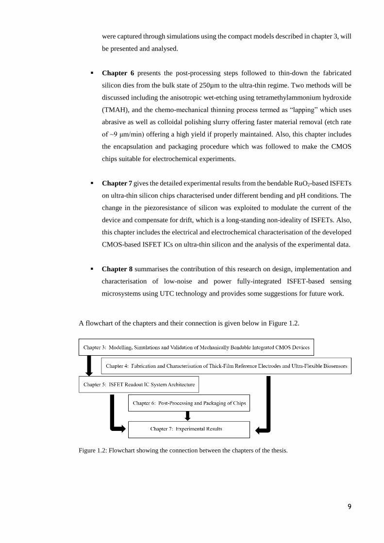
9
were captured through simulations using the compact models described in chapter 3, will
be presented and analysed.
Chapter 6 presents the post-processing steps followed to thin-down the fabricated
silicon dies from the bulk state of 250µm to the ultra-thin regime. Two methods will be
discussed including the anisotropic wet-etching using tetramethylammonium hydroxide
(TMAH), and the chemo-mechanical thinning process termed as “lapping” which uses
abrasive as well as colloidal polishing slurry offering faster material removal (etch rate
of ~9 μm/min) offering a high yield if properly maintained. Also, this chapter includes
the encapsulation and packaging procedure which was followed to make the CMOS
chips suitable for electrochemical experiments.
Chapter 7 gives the detailed experimental results from the bendable RuO2-based ISFETs
on ultra-thin silicon chips characterised under different bending and pH conditions. The
change in the piezoresistance of silicon was exploited to modulate the current of the
device and compensate for drift, which is a long-standing non-ideality of ISFETs. Also,
this chapter includes the electrical and electrochemical characterisation of the developed
CMOS-based ISFET ICs on ultra-thin silicon and the analysis of the experimental data.
Chapter 8 summarises the contribution of this research on design, implementation and
characterisation of low-noise and power fully-integrated ISFET-based sensing
microsystems using UTC technology and provides some suggestions for future work.
A flowchart of the chapters and their connection is given below in Figure 1.2.
Figure 1.2: Flowchart showing the connection between the chapters of the thesis.
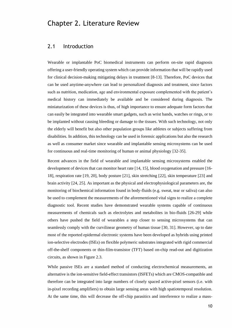
10
Chapter 2. Literature Review
2.1 Introduction
Wearable or implantable PoC biomedical instruments can perform on-site rapid diagnosis
offering a user-friendly operating system which can provide information that will be rapidly used
for clinical decision-making mitigating delays in treatment [8-13]. Therefore, PoC devices that
can be used anytime-anywhere can lead to personalized diagnosis and treatment, since factors
such as nutrition, medication, age and environmental exposure complemented with the patient’s
medical history can immediately be available and be considered during diagnosis. The
miniaturization of these devices is thus, of high importance to ensure adequate form factors that
can easily be integrated into wearable smart gadgets, such as wrist bands, watches or rings, or to
be implanted without causing bleeding or damage to the tissues. With such technology, not only
the elderly will benefit but also other population groups like athletes or subjects suffering from
disabilities. In addition, this technology can be used in forensic applications but also the research
as well as consumer market since wearable and implantable sensing microsystems can be used
for continuous and real-time monitoring of human or animal physiology [32-35].
Recent advances in the field of wearable and implantable sensing microsystems enabled the
development of devices that can monitor heart rate [14, 15], blood oxygenation and pressure [16-
18], respiration rate [19, 20], body posture [21], skin stretching [22], skin temperature [23] and
brain activity [24, 25]. As important as the physical and electrophysiological parameters are, the
monitoring of biochemical information found in body-fluids (e.g. sweat, tear or saliva) can also
be used to complement the measurements of the aforementioned vital signs to realize a complete
diagnostic tool. Recent studies have demonstrated wearable systems capable of continuous
measurements of chemicals such as electrolytes and metabolites in bio-fluids [26-29] while
others have pushed the field of wearables a step closer to sensing microsystems that can
seamlessly comply with the curvilinear geometry of human tissue [30, 31]. However, up to date
most of the reported epidermal electronic systems have been developed as hybrids using printed
ion-selective electrodes (ISEs) on flexible polymeric substrates integrated with rigid commercial
off-the-shelf components or thin-film-transistor (TFT) based on-chip read-out and digitization
circuits, as shown in Figure 2.3.
While passive ISEs are a standard method of conducting electrochemical measurements, an
alternative is the ion-sensitive field-effect transistors (ISFETs) which are CMOS-compatible and
therefore can be integrated into large numbers of closely spaced active-pixel sensors (i.e. with
in-pixel recording amplifiers) to obtain large sensing areas with high spatiotemporal resolution.
At the same time, this will decrease the off-chip parasitics and interference to realize a mass-
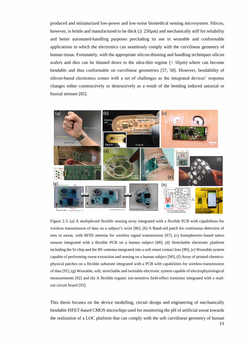
11
produced and miniaturized low-power and low-noise biomedical sensing microsystem. Silicon,
however, is brittle and manufactured to be thick (≥ 250µm) and mechanically stiff for reliability
and better automated-handling purposes precluding its use in wearable and conformable
applications in which the electronics can seamlessly comply with the curvilinear geometry of
human tissue. Fortunately, with the appropriate silicon-thinning and handling techniques silicon
wafers and dies can be thinned down to the ultra-thin regime (< 50µm) where can become
bendable and thus conformable on curvilinear geometries [57, 58]. However, bendability of
silicon-based electronics comes with a set of challenges as the integrated devices’ response
changes either constructively or destructively as a result of the bending induced uniaxial or
biaxial stresses [85].
Figure 2.3: (a) A multiplexed flexible sensing array integrated with a flexible PCB with capabilities for
wireless transmission of data on a subject’s wrist [86], (b) A Band-aid patch for continuous detection of
ions in sweat, with RFID antenna for wireless signal transmission [87], (c) Iontophoretic-based tattoo
sensors integrated with a flexible PCB on a human subject [88], (d) Stretchable electronic platform
including the Si-chip and the RF-antenna integrated into a soft smart contact lens [89], (e) Wearable system
capable of performing sweat extraction and sensing on a human subject [90], (f) Array of printed chemico-
physical patches on a flexible substrate integrated with a PCB with capabilities for wireless transmission
of data [91], (g) Wearable, soft, stretchable and twistable electronic system capable of electrophysiological
measurements [92] and (h) A flexible organic ion-sensitive field-effect transistor integrated with a read-
out circuit board [93].
This thesis focuses on the device modelling, circuit design and engineering of mechanically
bendable ISFET-based CMOS microchips used for monitoring the pH of artificial sweat towards
the realization of a LOC platform that can comply with the soft curvilinear geometry of human
12
skin (Figure 2.4). In this chapter, a literature review is presented with a focus on CMOS-
compatible ISFETs along with their theory, proposed readout circuitries and applications. More
specifically, in Section 2.2 the sensing mechanisms and the properties of the interface between
the electrolyte under test and the metal-oxide based ion-sensitive electrodes will be discussed
and a brief overview of the metal-oxide based pH sensors reported in literature will be given.
Furthermore, the operation of the ion-sensitive field-effect transistor along with the theory of pH
sensitivity, read-out topologies and circuit-based techniques for compensation of the ISFET’s
instabilities, such as the offset, flicker noise and drift will be presented in Section 2.3. Finally, in
Section 2.4 an overview of the reported mechanically flexible pH sensors, including ISFETs, and
the history of ISFET applications will be briefly covered.
Figure 2.4: The ultra-thin CMOS based miniaturised lab-on-chip for pH monitoring presented in this
thesis.
2.2 Potentiometric Electrochemical Ion-Sensitive Electrodes
The ion-sensitive electrodes (ISEs) that are commonly used in the detection of pH are mainly
based on glass-electrodes, metal-oxide (𝑀𝑂𝑥) electrodes and metal/metal-oxide electrodes, each
offering a set of advantages and disadvantages [94]. For example, the glass-electrodes (Figure
2.5) exhibit very good pH response as well as sensitivity (very close to the ideal “Nernstian”
behaviour), they are highly accurate, stable over long periods of time (even up to years) and are
very selective offering a useful pH meter especially for laboratory applications. However, they
exhibit chemical instability in very strong acidic or alkaline environments and they are bulky,
fragile and difficult to be miniaturised precluding their use especially in the next-generation of
implantable, ingestible or wearable microsystems. These drawbacks have motivated researchers
13
to explore other ways of monitoring the level of pH using materials such as the metal oxides
(𝑀𝑂𝑥) [94].
2.2.1 Overview of Potentiometric Metal-Oxide Based Electrochemical pH
Sensors
The importance of ion-sensitive metal oxides (𝑀𝑂𝑥) was initially highlighted in [46, 95], where
it has been observed a good sensitivity towards ionic activities for a wide range of ion
concentrations. To date, several transition and post-transition metal-oxides, perovskite materials
as well as mixed-oxides have been used in pH sensing applications, including RuO2, IrO2, PtO2,
SiO2, Si3N4, Al2O3, Ta2O5, ZnO, BN, ZrO2, TiN, HfO2, TiO2, SnO2, CeO2, OsO2, Co2O3, WO3,
PbO2, TiO-SnO-SnO2, IrO2-TiO2, RuO2-TiO2, etc [96-108]. The characteristics of 𝑀𝑂𝑥 that make
them appealing in electrochemical/biochemical applications are their high sensitivity, long life-
time, fast response, good stability and their biocompatibility along with their compatibility with
CMOS fabrication processes allowing their use in miniaturised systems making them suitable for
food/water quality monitoring, wearable/implantable devices for chronic diseases or in systems
used for industrial applications.
Among the various applications that 𝑀𝑂𝑥 have been used, their most successful sensing modality
is the pH sensing which is essential for many chemical and biological reactions [27, 109-113].
For example, the value of pH on a chronic wound site on skin has a pH value of ~ pH 7 – 8.5,
which varies from an unwounded skin site (~ pH 5.5) due to the presence of enzymes and
bacterial colonies [114]. Furthermore, the monitoring of pH value of skin could indicate the
presence of pathogens or diseases of the skin such as atopic or irritant contact dermatitis or acne
vulgaris [110, 115]. Also, the value of pH carries information regarding the protein denaturation,
growth and mortality of microorganisms, gelification, as well as the germination or inactivation
of bacterial spores, which are especially important in food quality monitoring having also
applications in the forensic analysis [116-119]. Finally, water pollution monitoring is another
application in which monitoring of pH provides useful insights into the quality of water, which
should normally be between pH 6.5 and 8.5 [120-122].
The sensitivity of 𝑀𝑂𝑥 towards H+ ions is mainly dependent on the composition of the material
and the deposition method since the morphological properties, such as the surface homogeneity,
porosity and crystalline structure are the main contributors for the formation of the electrical
double-layer. For example, the pH sensitivity of RuO2, IrO2, TiO2, SnO2, Ta2O5, ZnO and WO3
showed variations when they were fabricated by screen-printing [121, 123, 124], sol-gel [96,
125, 126], electrodeposition [98, 105, 127] or sputtering [125, 128, 129]. Also, despite the
fabrication process, a potentiometric electrochemical pH sensor requires a reference electrode
(R.E.) for proper operation, the fabrication of which is equally important in ensuring stable and
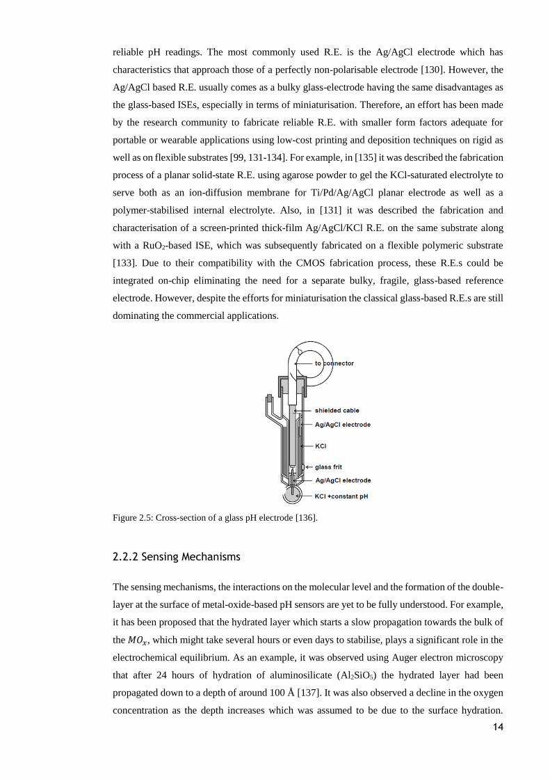
14
reliable pH readings. The most commonly used R.E. is the Ag/AgCl electrode which has
characteristics that approach those of a perfectly non-polarisable electrode [130]. However, the
Ag/AgCl based R.E. usually comes as a bulky glass-electrode having the same disadvantages as
the glass-based ISEs, especially in terms of miniaturisation. Therefore, an effort has been made
by the research community to fabricate reliable R.E. with smaller form factors adequate for
portable or wearable applications using low-cost printing and deposition techniques on rigid as
well as on flexible substrates [99, 131-134]. For example, in [135] it was described the fabrication
process of a planar solid-state R.E. using agarose powder to gel the KCl-saturated electrolyte to
serve both as an ion-diffusion membrane for Ti/Pd/Ag/AgCl planar electrode as well as a
polymer-stabilised internal electrolyte. Also, in [131] it was described the fabrication and
characterisation of a screen-printed thick-film Ag/AgCl/KCl R.E. on the same substrate along
with a RuO2-based ISE, which was subsequently fabricated on a flexible polymeric substrate
[133]. Due to their compatibility with the CMOS fabrication process, these R.E.s could be
integrated on-chip eliminating the need for a separate bulky, fragile, glass-based reference
electrode. However, despite the efforts for miniaturisation the classical glass-based R.E.s are still
dominating the commercial applications.
Figure 2.5: Cross-section of a glass pH electrode [136].
2.2.2 Sensing Mechanisms
The sensing mechanisms, the interactions on the molecular level and the formation of the double-
layer at the surface of metal-oxide-based pH sensors are yet to be fully understood. For example,
it has been proposed that the hydrated layer which starts a slow propagation towards the bulk of
the 𝑀𝑂𝑥, which might take several hours or even days to stabilise, plays a significant role in the
electrochemical equilibrium. As an example, it was observed using Auger electron microscopy
that after 24 hours of hydration of aluminosilicate (Al2SiO5) the hydrated layer had been
propagated down to a depth of around 100 Å [137]. It was also observed a decline in the oxygen
concentration as the depth increases which was assumed to be due to the surface hydration.

15
However, in the same study, the compositional profile of silicon nitride (Si3N4), which was
hydrated for 14 hours and measured again using Auger electron microscopy was found to be
unaltered showing evidence that the behaviour of every metal-oxides should be individually
characterized to conclude on their performance (i.e. sensitivity, stability, selectivity, impedance,
capacitance, etc.). Below, an attempt to explain the formation of the electrode potential at the
electrode/electrolyte interface regarding the potentiometric 𝑀𝑂𝑥 based pH sensors based on the
literature is given.
The first observations that counter-ions are attracted and co-ions are repelled by charged
electrodes immersed in an electrolytic solution were done by Hermann von Helmholtz in 1853
[138], where it was showed that the electrical double layer formed at the surface of the electrode
is essentially a molecular dielectric that stores charge. This first model predicts a constant
differential capacitance, which is dependent on the thickness of the double layer and the dielectric
constant of the solution, and independent of the charge density. However, this first approximation
does not take into consideration the diffusion and mixing of ions in the solution, the interaction
between the dipoles of the solution and electrode, and the factor of possible adsorption of ions of
the solution onto the surface of the electrode.
After almost 50 years, Louis George Gouy and David Leonard Chapman, respectively, observed
in 1910 and 1913 that the ionic concentration and the applied potential on the electrode can result
in fluctuation of the double-layer capacitance. According to this improved model, there is a
change in the distribution of ions as a function of distance from the surface of the electrode,
following the Maxwell-Boltzmann statistics. However, the Gouy-Chapman model fails for
highly charged double layers.
In 1924, after almost 10 years Otto Stern proposed the combination of the Helmholtz and Gouy
and Chapman models [139]. In his model, Stern considered that ions either adhere to the surface
of the electrode giving an internal Stern layer or form the Gouy-Chapman diffuse layer. However,
Stern’s model considers ions as point charges assuming that the closest distance an ion can
approach the electrode is in the order of the ionic radius. This is limiting in the sense that it
assumes that all the ionic interactions in the diffuse layer are Coulombic in nature. Also, the
model assumes a constant dielectric permittivity across the double layer which further limits its
use.
Twenty years after, D. C. Grahame proposed an improvement of Stern’s model in [140]. He
proposed that some species from the solution, either ionic or uncharged, that have lost their
solvation shell can penetrate the Stern layer. In his study, he named these ions as “specifically
adsorbed ions”. In this model, there are three regions: (i) the diffuse layer, (ii) the Outer
Helmholtz layer (OHL), which passes through the centres of the solvated ions which are closer
to the surface of the electrode, and (iii) the Inner Helmholtz layer (IHL) which passes through
the centres of the “specifically adsorbed ions”, as is shown in Figure 2.6. Since Grahame’s model,
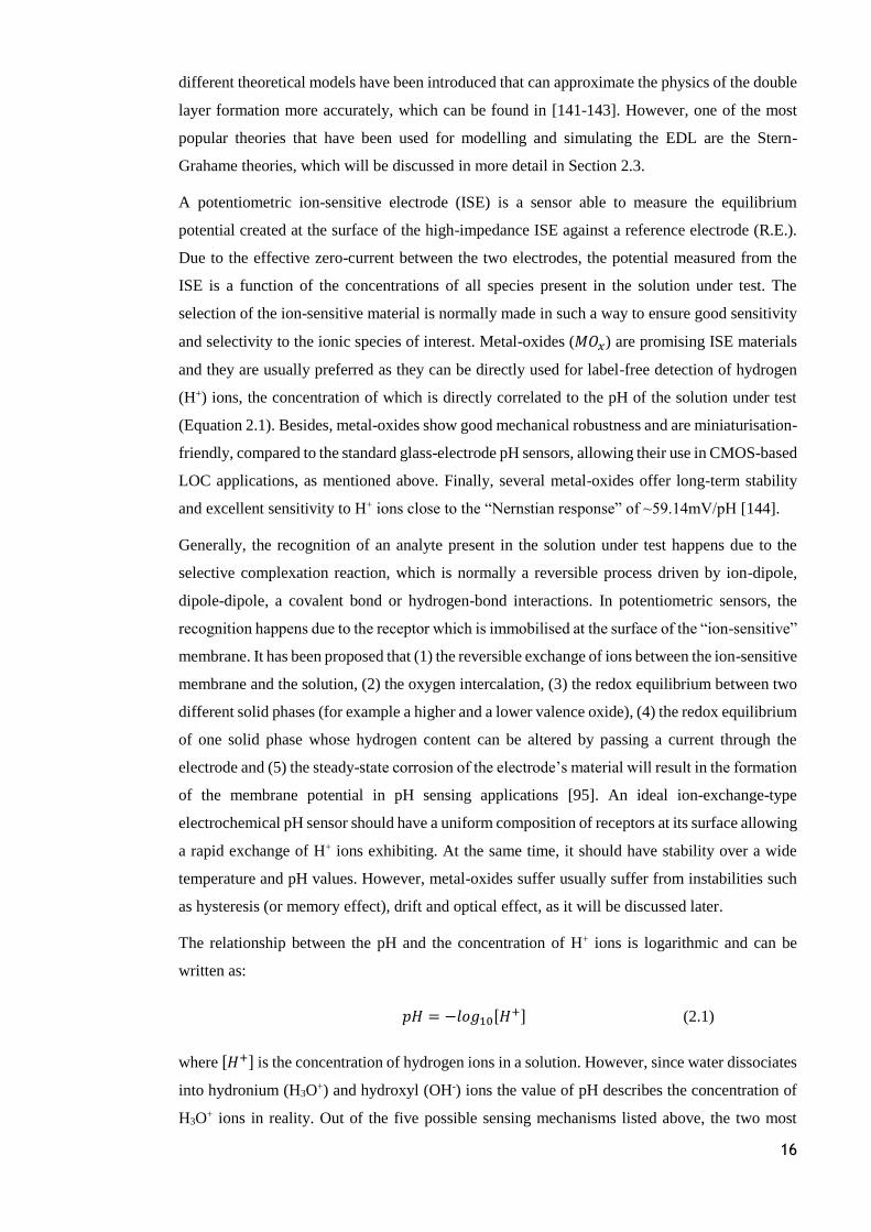
16
different theoretical models have been introduced that can approximate the physics of the double
layer formation more accurately, which can be found in [141-143]. However, one of the most
popular theories that have been used for modelling and simulating the EDL are the Stern-
Grahame theories, which will be discussed in more detail in Section 2.3.
A potentiometric ion-sensitive electrode (ISE) is a sensor able to measure the equilibrium
potential created at the surface of the high-impedance ISE against a reference electrode (R.E.).
Due to the effective zero-current between the two electrodes, the potential measured from the
ISE is a function of the concentrations of all species present in the solution under test. The
selection of the ion-sensitive material is normally made in such a way to ensure good sensitivity
and selectivity to the ionic species of interest. Metal-oxides (𝑀𝑂𝑥) are promising ISE materials
and they are usually preferred as they can be directly used for label-free detection of hydrogen
(H+) ions, the concentration of which is directly correlated to the pH of the solution under test
(Equation 2.1). Besides, metal-oxides show good mechanical robustness and are miniaturisation-
friendly, compared to the standard glass-electrode pH sensors, allowing their use in CMOS-based
LOC applications, as mentioned above. Finally, several metal-oxides offer long-term stability
and excellent sensitivity to H+ ions close to the “Nernstian response” of ~59.14mV/pH [144].
Generally, the recognition of an analyte present in the solution under test happens due to the
selective complexation reaction, which is normally a reversible process driven by ion-dipole,
dipole-dipole, a covalent bond or hydrogen-bond interactions. In potentiometric sensors, the
recognition happens due to the receptor which is immobilised at the surface of the “ion-sensitive”
membrane. It has been proposed that (1) the reversible exchange of ions between the ion-sensitive
membrane and the solution, (2) the oxygen intercalation, (3) the redox equilibrium between two
different solid phases (for example a higher and a lower valence oxide), (4) the redox equilibrium
of one solid phase whose hydrogen content can be altered by passing a current through the
electrode and (5) the steady-state corrosion of the electrode’s material will result in the formation
of the membrane potential in pH sensing applications [95]. An ideal ion-exchange-type
electrochemical pH sensor should have a uniform composition of receptors at its surface allowing
a rapid exchange of H+ ions exhibiting. At the same time, it should have stability over a wide
temperature and pH values. However, metal-oxides suffer usually suffer from instabilities such
as hysteresis (or memory effect), drift and optical effect, as it will be discussed later.
The relationship between the pH and the concentration of H+ ions is logarithmic and can be
written as:
𝑝𝐻 = −𝑙𝑜𝑔10[𝐻+] (2.1)
where [𝐻+] is the concentration of hydrogen ions in a solution. However, since water dissociates
into hydronium (H3O+) and hydroxyl (OH-) ions the value of pH describes the concentration of
H3O+ ions in reality. Out of the five possible sensing mechanisms listed above, the two most

17
prominent that can provide a close explanation for the sensitivity of metal-oxides towards the
H3O+ (or H+ for simplicity) ions are:
(i) The reversible oxygen’s intercalation [95, 145].
(ii) The ion-exchange from the –OH surface layer [146].
While the general mechanism at the sensing surface can be written as:
𝑀𝑂𝑥 + 2𝛿𝐻+ + 2𝛿𝑒− ⇔ 𝑀𝑂𝑥−𝛿 + 𝛿𝐻2𝑂 (2.2)
where 𝑀𝑂𝑥 is a higher metal-oxide and 𝑀𝑂𝑥−𝛿 is a lower metal-oxide.
Based on the reversible oxygen’s intercalation theory, the electrode potential can be written as:
𝐸 =𝑅𝑇
𝐹𝑙𝑛𝑎𝐻+
1 +𝑅𝑇
2𝐹𝑙𝑛𝑎0
𝑠 + 𝑐𝑜𝑛𝑠𝑡. (2.3)
where 𝑎𝐻+1 is the hydrogen ion activity in the liquid phase, 𝑎0
𝑠 is the oxygen activity in the solid
phase, 𝑇 is the temperature, 𝑅 is the universal gas constant and 𝐹 is the Faraday constant.
In addition, based on the ionic-exchange theory the electrode potential can also be written as:
𝐸 =𝑅𝑇
𝐹𝑙𝑛[𝐻+] +
𝑅𝑇
𝛿𝐹𝑙𝑛 [
𝑀𝑂𝑥(𝑂𝐻)𝑦
𝑀𝑂𝑥−𝛿(𝑂𝐻)𝑦+𝛿] + 𝑐𝑜𝑛𝑠𝑡. (2.4)
According to the site-binding theory, one of the most prominent theories, when a metal-oxide
(𝑀𝑂𝑥) is exposed in an aqueous solution, the development of O-, OH and OH2+ sites at the surface
of the 𝑀𝑂𝑥 starts to occur, as shown in Figure 2.6. Hydrogen and hydroxide ions are subsequently
beginning the migration towards and from the bulk of the solution resulting in a donor/acceptor
mechanism that can be written as:
𝑀 − 𝑂− + 𝐻𝑆+ ⇔ 𝑀 − 𝑂𝐻 (2.5)
𝑀 − 𝑂𝐻 + 𝐻𝑆+ ⇔ 𝑀 − 𝑂𝐻2
+ (2.6)
With the dissociation constants written as:
𝐾𝑎 =[𝑀−𝑂−][𝐻+]𝑆
[𝑀−𝑂𝐻] (2.7)
𝐾𝑏 =[𝑀−𝑂𝐻][𝐻+]𝑆
[𝑀−𝑂𝐻2+]
(2.8)
where [𝑀 − 𝑂−], [𝑀 − 𝑂𝐻] and [𝑀 − 𝑂𝐻2+] are the concentrations of the negative, neutral and
positive surface groups at the surface of the metal-oxide, respectively.
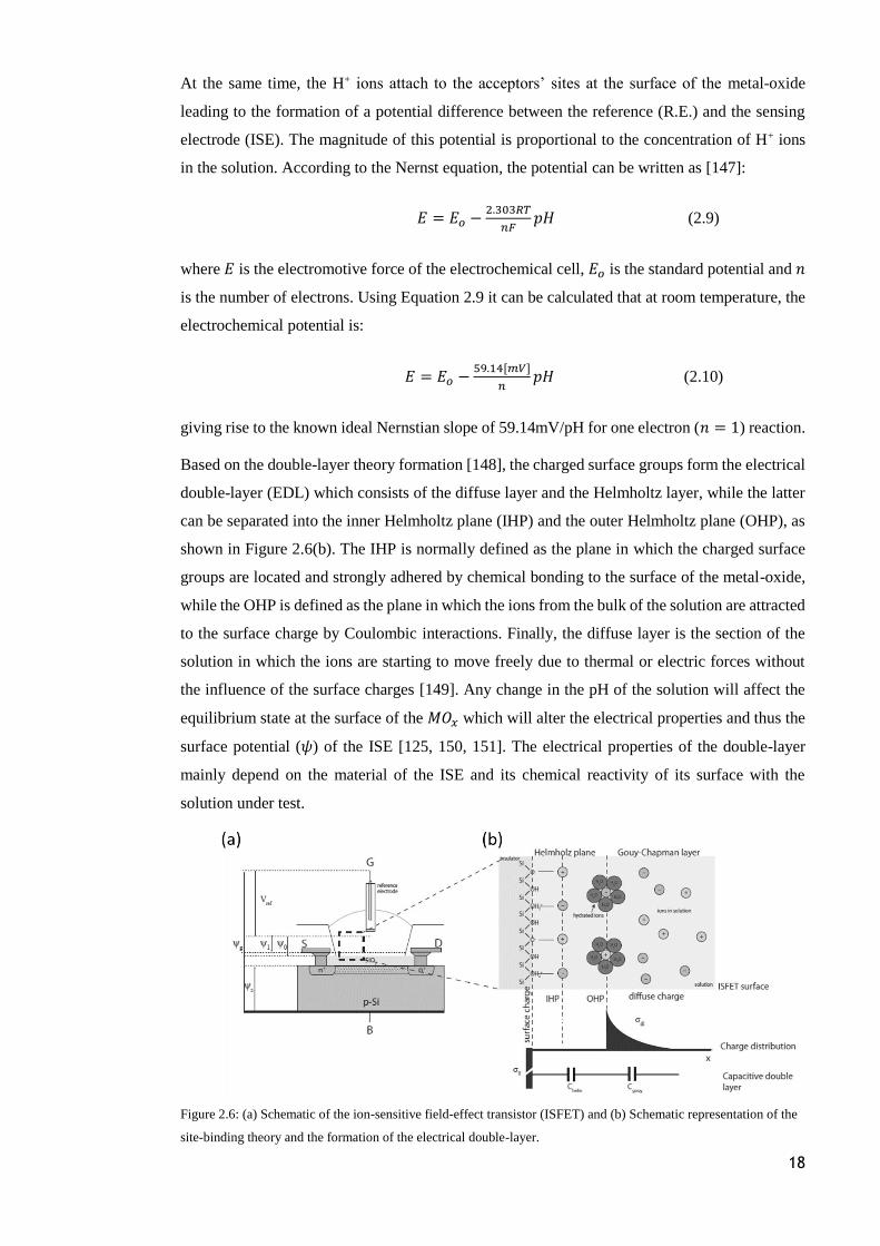
18
At the same time, the H+ ions attach to the acceptors’ sites at the surface of the metal-oxide
leading to the formation of a potential difference between the reference (R.E.) and the sensing
electrode (ISE). The magnitude of this potential is proportional to the concentration of H+ ions
in the solution. According to the Nernst equation, the potential can be written as [147]:
𝐸 = 𝐸𝑜 −2.303𝑅𝑇
𝑛𝐹𝑝𝐻 (2.9)
where 𝐸 is the electromotive force of the electrochemical cell, 𝐸𝑜 is the standard potential and 𝑛
is the number of electrons. Using Equation 2.9 it can be calculated that at room temperature, the
electrochemical potential is:
𝐸 = 𝐸𝑜 −59.14[𝑚𝑉]
𝑛𝑝𝐻 (2.10)
giving rise to the known ideal Nernstian slope of 59.14mV/pH for one electron (𝑛 = 1) reaction.
Based on the double-layer theory formation [148], the charged surface groups form the electrical
double-layer (EDL) which consists of the diffuse layer and the Helmholtz layer, while the latter
can be separated into the inner Helmholtz plane (IHP) and the outer Helmholtz plane (OHP), as
shown in Figure 2.6(b). The IHP is normally defined as the plane in which the charged surface
groups are located and strongly adhered by chemical bonding to the surface of the metal-oxide,
while the OHP is defined as the plane in which the ions from the bulk of the solution are attracted
to the surface charge by Coulombic interactions. Finally, the diffuse layer is the section of the
solution in which the ions are starting to move freely due to thermal or electric forces without
the influence of the surface charges [149]. Any change in the pH of the solution will affect the
equilibrium state at the surface of the 𝑀𝑂𝑥 which will alter the electrical properties and thus the
surface potential (𝜓) of the ISE [125, 150, 151]. The electrical properties of the double-layer
mainly depend on the material of the ISE and its chemical reactivity of its surface with the
solution under test.
Figure 2.6: (a) Schematic of the ion-sensitive field-effect transistor (ISFET) and (b) Schematic representation of the
site-binding theory and the formation of the electrical double-layer.
19
2.2.3 Properties and Non-Ideal Characteristics of Potentiometric pH Sensors
The ISEs should be conditioned prior to use, following a procedure to ensure stable results and
proper operation. This is normally done by immersing the ISEs and the R.E. in a control solution
for at least 10 minutes before use. Also, a more optimum conditioning procedure includes a
sequential immersion of the ISE and R.E. to the control solution, removal, washing, drying and
re-immersion until the two consecutive readings are within a 1mV of difference. Also, a more
careful pre-treatment should be followed when the ISE is either used for the first time or stored
for a prolonged time without being used. This may include overnight soaking to achieve stable
readings. Finally, care should be taken in the storing of the ISE and R.E. especially when they
are stored for a prolonged time. For example, the ion-sensitive layer can be stored inside a plastic
cap avoiding any oxidation, corrosion or mechanical damage. The main reason for proper storage
is to avoid any cause of slow or reduced response or sensitivity ensuring proper operation and
stable recordings. However, even though a proper protocol is followed the ISE might exhibit
errors in their characteristics. In general, the performance of potentiometric pH sensors is
determined by their sensitivity, response time, long-term stability and interference of other ions,
while non-ideal effects such as drift, hysteresis and optical effects also need to be considered.
More specifically, the response time, which is defined as the required time for the open circuit
potential (or electromotive force) to reach 90% of an equilibrium value after the sensor is
immersed into the solution under test, can be analysed by measuring the output voltage at
solutions with different pH value. Response time is dependent both on the morphological
properties of the 𝑀𝑂𝑥 (composition, thickness, porosity, etc.) as well as the value of the pH
measurement range. Regarding the former, the morphological properties of the 𝑀𝑂𝑥 are directly
related to the fabrication process. For example, it was observed that an ISE with a thickness of 2
µm exhibited a response time of ~80 to 120 seconds, while the same ISE with a thickness of 5
µm exhibited an improved response time of ~25 seconds [152]. This improvement was associated
with the size and faceting of the grains as well as to the increase in the porosity at the surface of
the thicker ISE. It is worthy to be mentioned here, that when a solution reacts with a 𝑀𝑂𝑥 at its
surface there are two significant complex interfaces that are formed: (1) The outer surface which
is the 𝑀𝑂𝑥/solution macro boundaries and (2) the inner surface which is defined as the
𝑀𝑂𝑥/solution micro boundaries due the ionic penetration through the pores at the surface of the
𝑀𝑂𝑥. Both of these complex interfaces are significant for the faster response. Finally, regarding
the relationship between the value of the pH measurement range with the response time, it has
been observed that most of the potentiometric 𝑀𝑂𝑥 based pH sensors show a faster response in
the acidic region compared to the alkaline, while in the neutral pH region the response time is
the slowest compared to the other two regions of pH [123, 153].
Furthermore, the interference from other ions present in the solution is a drawback of 𝑀𝑂𝑥 based
pH sensors and should be considered during the characterisation of the sensor. More specifically,
20
due to the reaction of other ions with the 𝑀𝑂𝑥 surface the output measured potential from the
sensor might be affected. According to the International Union of Pure and Applied Chemistry
(IUPAC) recommendation [154], in order to characterise the selectivity of the sensor, the
“selectivity coefficient” (𝐾𝐴,𝐵𝑝𝑜𝑡
) should be evaluated by means of the electromotive force
produced by the ISE which has been immersed into a solution in which a primary (𝐴) and an
interfering ion (𝐵) are present and in two separate solutions in which only one type of ions is
present. Usually, the majority of 𝑀𝑂𝑥 based pH sensors show very good selectivity [123, 147,
155], however, the influence of the interfering ions depends on their concentration in the solution
and the type of the 𝑀𝑂𝑥 material. In any case, the interfering agent can be chemically removed
either by precipitation or complexing it with other reagents.
Moreover, the drift effect is another very important non-ideality of 𝑀𝑂𝑥 based potentiometric
sensors which can be characterised as a slow monotonic temporal change of the output voltage
at a constant temperature, solution composition and R.E. potential, which can last up to several
weeks after the fabrication of the sensor [124]. A few parameters that may affect the rate and
duration of the drift effect are the quality and composition of the sensitive layer, type of 𝑀𝑂𝑥
material, 𝑀𝑂𝑥 layer thickness, 𝑀𝑂𝑥 surface homogeneity and porosity, temperature, storing and
pre-conditioned procedures as well as the pH of the solution itself [125, 147]. As an example, it
was observed that the drift-rate increases as the pH of the solution under test increase from acidic
to basic and it was suggested that the presence of the lower diffusion mobility OH- ions may
cause this increase in the drift rate [156]. Moreover, the properties of the reference electrode may
also affect the drift effect [125, 157]. Finally, it was observed that even with the same fabrication
process the sensor might exhibit different drift rates [128]. A comparison table for the effect of
drift on different 𝑀𝑂𝑥 based pH sensors is given in [94].
In addition, hysteresis or “memory effect” is another non-ideality of 𝑀𝑂𝑥 based pH sensors
which arises due to the constant removal and replacing of the ISE in different solutions and
depend upon the relative concentration of ions in the old and new solution [125, 158]. Therefore,
if one solution is measured again after measuring a different one, it is impossible to give the same
reading the second time. It has been observed that he hysteresis in the acidic region is smaller
compared to the alkaline region, which is also attributed to the lower diffusion mobility OH- ions
compared to the H+ ions which are in excess in acidic solutions. Since the hysteresis is normally
characterised performing a loop measurement starting from a pH value and gradually altering it
until the initial pH value is achieved again, it has been observed that the hysteresis width
increases as the loop time also increases [128]. A comparison table for the effect of hysteresis on
different 𝑀𝑂𝑥 based pH sensors is given in [94].
Furthermore, the optical effect which occurs when the ion-sensitive 𝑀𝑂𝑥 based electrode is
exposed to light while it is measuring the value of pH [125, 159], affects the reading from the
sensor and it can be considered as an unwanted artefact. This sensitivity towards light has also
21
been explored as a dual-mode pH/photon sensor [160]. However, the optical effect should be
avoided where possible in order to ensure reliable recordings of pH [161, 162]. It should be noted,
that the optical effect is especially worrisome in FET-based pH sensors, such as the ion-sensitive
field-effect transistor (ISFET). The photosensitivity of ISFETs has been attributed to two main
mechanisms. The first is associated with the generation and recombination of electron/hole pairs
due to the photons’ absorption in the depletion layer of the underlying MOSFET device leading
to an increase of the Drain-current in the OFF-state in the subthreshold region which in turns
results in an increase of the leakage current through the Source-Bulk and Drain-Bulk pn-junctions
resulting in fluctuations of the Drain-current when incident photons hit the open-gate
configuration of the sensor. The second mechanism is associated with the threshold voltage
variations of the ISFET device due to the 𝑀𝑂𝑥 photo-charging, which was supported by
photoconductivity studies on Ta2O5 [163, 164].
Finally, 𝑀𝑂𝑥 based pH sensors and especially ISFETs are prone to errors due to temperature
effect. While drift and hysteresis effects are mainly associated with the chemical reactions at the
interface between the ISE and solution, temperature and optical effects are mainly associated
with the electronic component of ISFET, i.e. the MOSFET device. Regarding temperature effect,
simulations and measurements of the thermally affected ISFET behaviour [165] have shown that
the temperature mostly affects the mobility and the threshold voltage of the underlying MOSFET
which results in a shift of the output voltage per degrees Celsius (mV/oC) and therefore the sensor
requires regular calibration using on-chip temperature sensors and based on the signal-
conditioning function of the form [166]:
𝑝𝐻 = 𝑝𝐻𝑚𝑒𝑎𝑠𝑢𝑟𝑒𝑑 + [(𝑇𝐶𝐼𝑆𝐹𝐸𝑇−𝑆×𝑇𝐶𝐸𝑒𝑙𝑐𝑡𝑟𝑜𝑙𝑦𝑡𝑒)𝛿𝑇
𝑆] (2.11)
where 𝑇𝐶𝐼𝑆𝐹𝐸𝑇 is the temperature coefficient of ISFET, 𝑇𝐶𝐸𝑒𝑙𝑐𝑡𝑟𝑜𝑙𝑦𝑡𝑒 is the temperature
sensitivity of the electrolyte, 𝑆 is the device sensitivity, 𝛿𝑇 is the difference the measured and
calibrated temperature and 𝑝𝐻𝑚𝑒𝑎𝑠𝑢𝑟𝑒𝑑 is the measured pH value without temperature correction.
The equation which describes the relationship between carriers’ mobility and the temperature is:
𝜇(𝑇) = 𝜇𝑜 × (𝑇
𝑇𝑁𝑂𝑀)𝑈𝑇𝐸
+ 𝑈𝑇𝐿(𝑇 − 𝑇𝑁𝑂𝑀) (2.12)
where 𝜇𝑜 is the carriers’ mobility value extracted at a temperature 𝑇𝑁𝑂𝑀 and 𝑈𝑇𝐸 and 𝑈𝑇𝐿 are
the mobility temperature coefficients. Below, a more detailed discussion on ISFETs and their
operation is given.
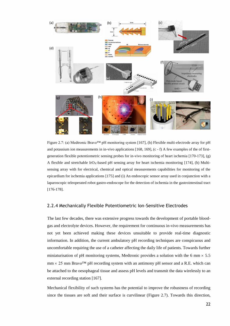
22
Figure 2.7: (a) Medtronic Bravo™ pH monitoring system [167], (b) Flexible multi-electrode array for pH
and potassium ion measurements in in-vivo applications [168, 169], (c - f) A few examples of the of first-
generation flexible potentiometric sensing probes for in-vivo monitoring of heart ischemia [170-173], (g)
A flexible and stretchable IrOX-based pH sensing array for heart ischemia monitoring [174], (h) Multi-
sensing array with for electrical, chemical and optical measurements capabilities for monitoring of the
epicardium for ischemia applications [175] and (i) An endoscopic sensor array used in conjunction with a
laparoscopic teleoperated robot gastro-endoscope for the detection of ischemia in the gastrointestinal tract
[176-178].
2.2.4 Mechanically Flexible Potentiometric Ion-Sensitive Electrodes
The last few decades, there was extensive progress towards the development of portable blood-
gas and electrolyte devices. However, the requirement for continuous in-vivo measurements has
not yet been achieved making these devices unsuitable to provide real-time diagnostic
information. In addition, the current ambulatory pH recording techniques are conspicuous and
uncomfortable requiring the use of a catheter affecting the daily life of patients. Towards further
miniaturisation of pH monitoring systems, Medtronic provides a solution with the 6 mm 5.5
mm 25 mm Bravo™ pH recording system with an antimony pH sensor and a R.E. which can
be attached to the oesophageal tissue and assess pH levels and transmit the data wirelessly to an
external recording station [167].
Mechanical flexibility of such systems has the potential to improve the robustness of recording
since the tissues are soft and their surface is curvilinear (Figure 2.7). Towards this direction,
23
many flexible arrays of ISEs have been fabricated targeting robust myocardial measurements.
Lindner et al. [168] have reported the fabrication and functionalisation of eight ISEs on flexible
polyimide substrate for in-vitro and in-vivo detection of pH, potassium ions and calcium ions
tested in serum and blood. It was observed a reduction in the sensitivity in the case of in-vivo
measurements which was attributed to biofouling. Also, in [169] a similar electrode array has
been reported for pH and potassium ions detection exhibiting near-Nernstian sensitivity and drift
of 0.08 mV/hour targeting the detection of acute ischemia in several sites of the heart. It was
demonstrated that a greater change in tissue pH value occurred closer to the ischemic region.
Furthermore, in [170-173] some needle-shaped probes have been reported for electrical
impedance as well as pH and potassium ion measurements.
Furthermore, Rogers’ group has reported the fabrication of flexible and stretchable IrOX-based
pH sensing arrays tested on a rabbit and human hearts undergoing ischemia and demonstrated a
mostly stable performance within typical physiological temperature variations and a variation of
almost 1 pH value difference between the baseline and the pH values measured after induced
ischemia [174]. In another study reported in [175], they have fabricated arrays of different
sensing modalities for electrical, chemical and optical measurements for cardiac monitoring.
Finally, an endoscopic sensor array has been reported in [176-178] and used in conjunction with
a laparoscopic teleoperated robot gastro-endoscope for the detection of ischemia in the
gastrointestinal tract. The R.E. that was used was based on carbon-ink and Ag/AgCl covered with
Nafion while PVC, PEDOT and PEDOT-PEG were used as ion-selective membranes for the
ISEs. Response time of 18 seconds and a near-Nernstian response has been reported for the pH
sensors.
2.3 Ion-Sensitive Field-Effect Transistor: Operation, Sensor
Interface and On-Chip Signal Processing Techniques
2.3.1 Operation and Theory of pH Sensitivity
The ion-sensitive field-effect transistor (ISFET) is a solid-state potentiometric FET-based sensor
which was introduced in 1970 by Piet Bergveld initially targeting neurophysiological
measurements [46], shown in Figure 2.6(a). The conventional ISFET device comprises of the
ion-sensitive layer, which is usually a metal-oxide based material, deposited on top of the
inversion layer of the underlying MOSFET device and in contact with the solution under test,
which is biased through a reference electrode (typically an Ag/AgCl based R.E.) acting as the
Gate terminal of ISFET [53]. ISFET can thus be directly used as a pH sensor capable for label-
free detection of H+ ions or it can serve as a platform for a diversity of ionic or molecular sensing
applications by modifying the surface of the ion-sensitive oxide at the interface with the solution.
24
Furthermore, ISFETs have also been used as physical sensors for measurements of flow
direction, velocity and measurements of the diffusion coefficient using in-situ electrochemically
generated hydroxyl (OH-) ions through the electrolysis of water [179].
ISFETs can be easily adapted in the CMOS fabrication process through the method that was first
reported by Bausells et al. [47]. CMOS compatible ISFETs, and in general all the extended-gate
ISFETs (EG-ISFETs), are fabricated by extending the intrinsic poly-silicon gate (IPG) of the
underlying MOSFET device to the surface of the CMOS chip through a stack of metal layers
connected through vias. Finally, the ion-sensitive material is deposited on top of the last metal-
layer and the solution under test, which is in contact with the ion-sensitive material, is biased
through an Ag/AgCl based reference electrode, as depicted in Figure 2.4. However, CMOS-
compatible ISFETs exhibit lower ionic sensitivity compared to their conventional counterparts
because of the quality of ion-sensitive layer of the former which typically is thermally grown
SiO2, compared to the ion-sensitive layer of the latter which is deposited on top of a metal layer
normally using plasma-enhanced chemical vapour deposition (PECVD) resulting in a lower
content in surface binding-sites. Overall the main advantages of CMOS-compatible ISFETs are
listed below:
High input-impedance.
Possibility for on-chip integration in large numbers (e.g. millions), along with adequate signal
conditioning, biasing, temperature/drift/offset compensation and digitisation circuits.
Low-cost when the CMOS chips are fabricated in large numbers.
Ability to measure ultra-small liquid volumes.
Serves as a platform for multi-species detection by functionalising the ion-sensitive oxide’s
surface with different ion/molecule-specific layers.
Fast response, robustness and durability.
Ability to be dry-stored and sterilised.
Since ISFET is a MOSFET-based sensor, the formulae describing the operation of the electronic
component of ISFET are the same. A detailed discussion and formulation of the different regions
of operation of a MOSFET device are given in Section 3.4 of Chapter 3. However, it should be
noted that the threshold voltage of an ISFET sensor is different from that of a MOSFET device
since the characteristics of the solution under test will also affect the threshold voltage of the
sensor, which can be written as [53]:
𝑉𝑇𝐻(𝐼𝑆𝐹𝐸𝑇) = 𝑉𝑇𝐻(𝑀𝑂𝑆𝐹𝐸𝑇) + 𝑉𝑐ℎ𝑒𝑚 (2.13)
where:
𝑉𝑐ℎ𝑒𝑚 = 𝐸𝑟𝑒𝑓 − 𝜓0 + 𝜓𝑙𝑗 + 𝜒𝑠𝑜𝑙 (2.14)
25
where 𝐸𝑟𝑒𝑓 is the potential of the reference electrode (R.E.), 𝜒𝑠𝑜𝑙 is the solution dipole potential
and 𝜓0 and 𝜓𝑙𝑗 are the potential drop at the ion-sensitive layer/electrolyte interface and the
reference electrode/electrolyte interface, respectively. The most important of these terms is the
potential 𝜓0, which is the only term in Equation 2.14 which is not constant during pH
measurements.
Similarly to the previous conversation on the sensing mechanisms of 𝑀𝑂𝑥 based potentiometric
pH sensors in the Section 2.2.2, when the ISFET is immersed into a solution and the ion-sensitive
metal-oxide gate of the transistor comes into contact with the solution under test, amphoteric
hydroxyl (OH) groups are formed on the surface of the oxide, which can either accept or donate
hydrogen ions (H+) from and to the solution. The concentration of H+ ions at the surface of the
gate oxide, which denotes the acidity or basicity of the solution, will effectively change the
potential at the surface of the oxide. A CMOS-compatible ISFET fabricated in an unmodified
CMOS process, in which the ion-sensitive layer consists of a stack of Si3N4 on top of a SiO2 both
deposited using PECVD technique, the equilibrium reactions between the surface of the Si3N4-
based and SiO2-based ion-sensitive gate oxide and the solution can be written as:
For SiO2:
𝑆𝑖𝑂𝐻 ⇔ 𝑆𝑖𝑂− + 𝐻+ (2.15)
𝑆𝑖𝑂𝐻2+ ⇔ 𝑆𝑖𝑂𝐻 + 𝐻+ (2.16)
For Si3N4:
𝑆𝑖 − 𝑂𝐻2+ + 𝐻2𝑂 ↔ 𝑆𝑖 − 𝑂𝐻 + 𝐻3𝑂
+ (2.17)
𝑆𝑖 − 𝑂𝐻 + 𝐻2𝑂 ↔ 𝑆𝑖 − 𝑂− + 𝐻3𝑂+ (2.18)
and
𝑆𝑖3𝑁4 + 6𝐻2𝑂 ↔ 3𝑆𝑖𝑂2 + 4𝑁𝐻3 (2.19)
The surface of the metal-oxide based gate acts as a buffer to any changes in the concentration of
H+ ions in the bulk solution, which in turns is related to the value of pH of the solution given by
Equation 2.1. The derivation of pH was initially described by the Henderson-Hasselbalch
equation [180]. When the pH value of the solution under test increases, the solution becomes
more alkaline (basic) and the concentration of H+ ions decreases. For his change to be
compensated the surface of the ion-sensitive ISFET’s gate donates hydrogen ions to the solution
resulting in becoming more negatively charged, causing the accumulation of fewer electrons in
the channel region of an n-type ISFET and the decrease of the drain current of the device. On the
contrary, when the pH value of the solution decreases, the solution becomes more acidic and the

26
concentration of H+ increases. This change is compensated by receiving H+ ions from the
solution. In that case, the ion-sensitive metal-oxide becomes more positively charged, which
results in the accumulation of more electrons in the channel region of an n-type ISFET increasing
the drain current of the device. The opposite will occur in the case of a p-type ISFET.
The surface potential (𝜓0) at the oxide-solution interface is dependent on the pH value in the
bulk of the solution (𝑝𝐻𝐵), the absolute temperature of the solution (𝑇), and the sensitivity
parameter (𝑎), according to the following equation [181]:
𝛿𝜓0
𝛿𝑝𝐻𝐵= −2.3
𝑘𝑇
𝑞𝑎 (2.20)
From the first observations on ISFET’s performance, it was concluded that the surface reactions
between the ions of the solution and the ion-sensitive gate of ISFET can determine the response
mechanism of the device. Due to these surface reactions, an electrostatic potential (𝜓0) is
developed in the electrolyte solution, near the oxide surface, which is described by Equation 2.20.
The parameter 𝑎 is Nernstian in nature and can vary between 0 and 1. Essentially, the closer to
the value of 1 the more Nernstian the response of ISFET becomes, i.e. the closer the response to
a glass membrane ISE, in which 𝛿𝜓0 ≅ −59.2𝑚𝑉/𝑝𝐻 at 298𝐾. Theoretically, the sensitivity 𝑎
can be written with the following equation:
𝑎 =1
2.3𝑘𝑇𝐶𝑑𝑙𝑞2𝛽𝑖𝑛𝑡
+1 (2.21)
where 𝐶𝑑𝑙 is double layer capacity at the oxide-solution interface, and 𝛽𝑖𝑛𝑡 is the intrinsic buffer
capacity of the oxide surface.
As it was discussed earlier, the oxide surface potential (𝜓0) depends on the pH value of the
solution and therefore on the 𝑉𝑡ℎ, based on Equation 2.14. If all the rest of the parameters in
Equation 2.14 are constant, the threshold voltage of the device will be dependent only on the pH
value, according to the following equation:
𝛿𝑉𝑡ℎ
𝛿𝑝𝐻𝐵= −2.3
𝑘𝑇
𝑞𝑎 (2.22)
It should be mentioned that the parameter 𝛽𝑖𝑛𝑡 can be described as the measure of the ability of
the ion-sensitive surface to accept or donate hydrogen ions to and from the solution and is given
by the following equation:
𝛿𝜎0
𝛿𝑝𝐻𝑆= −𝑞
𝛿[𝐵]
𝛿𝑝𝐻𝑆= −𝑞𝛽𝑖𝑛𝑡 (2.23)
As it can be derived from Equation 2.21, the higher the value of 𝛽𝑖𝑛𝑡 the closer to 1 is the
denominator and the closer to the Nernstian response is the sensitivity of the oxide, as shown in
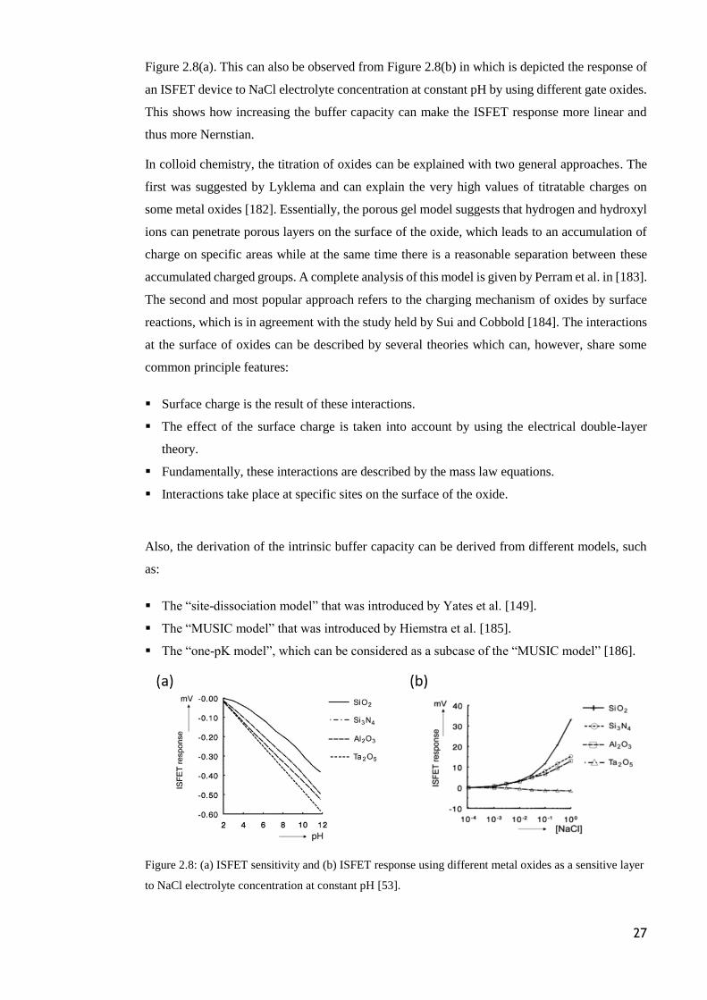
27
Figure 2.8(a). This can also be observed from Figure 2.8(b) in which is depicted the response of
an ISFET device to NaCl electrolyte concentration at constant pH by using different gate oxides.
This shows how increasing the buffer capacity can make the ISFET response more linear and
thus more Nernstian.
In colloid chemistry, the titration of oxides can be explained with two general approaches. The
first was suggested by Lyklema and can explain the very high values of titratable charges on
some metal oxides [182]. Essentially, the porous gel model suggests that hydrogen and hydroxyl
ions can penetrate porous layers on the surface of the oxide, which leads to an accumulation of
charge on specific areas while at the same time there is a reasonable separation between these
accumulated charged groups. A complete analysis of this model is given by Perram et al. in [183].
The second and most popular approach refers to the charging mechanism of oxides by surface
reactions, which is in agreement with the study held by Sui and Cobbold [184]. The interactions
at the surface of oxides can be described by several theories which can, however, share some
common principle features:
Surface charge is the result of these interactions.
The effect of the surface charge is taken into account by using the electrical double-layer
theory.
Fundamentally, these interactions are described by the mass law equations.
Interactions take place at specific sites on the surface of the oxide.
Also, the derivation of the intrinsic buffer capacity can be derived from different models, such
as:
The “site-dissociation model” that was introduced by Yates et al. [149].
The “MUSIC model” that was introduced by Hiemstra et al. [185].
The “one-pK model”, which can be considered as a subcase of the “MUSIC model” [186].
Figure 2.8: (a) ISFET sensitivity and (b) ISFET response using different metal oxides as a sensitive layer
to NaCl electrolyte concentration at constant pH [53].

28
Below only the first model will be used to derive the equation for the intrinsic buffer capacity of
several oxides. The full derivation of the intrinsic buffer capacity using the “MUSIC model” can
be found in [181].
The site-dissociation model was developed to describe the charge accumulation mechanism of
the double-layer from the metal-oxide side (𝑀𝑂𝑥). However, it can also be used to describe the
charging mechanisms of ceramics, such as the Si3N4. The equilibrium reactions between the
surface of the ion-sensitive Gate metal-oxide and the solution under test were previously given
in Equations 2.5 and 2.6. Furthermore, the surface reactions at the solution-oxide interface have
the following thermodynamic equations:
𝜇𝐴𝑂𝐻0 + 𝑘𝑇𝑙𝑛𝜐𝐴𝑂𝐻 = 𝜇𝐴𝑂−
0 + 𝑘𝑇𝑙𝑛𝜐𝐴𝑂− + 𝜇𝐻𝑆
+0 + 𝑘𝑇𝑙𝑛𝑎
𝐻𝑆+ (2.24)
𝜇𝐴𝑂𝐻2+
0 + 𝑘𝑇𝑙𝑛𝜐𝐴𝑂𝐻2+ = 𝜇
𝐴𝑂𝐻0 + 𝑘𝑇𝑙𝑛𝜐𝐴𝑂𝐻 + 𝜇
𝐻𝑆+
0 + 𝑘𝑇𝑙𝑛𝑎𝐻𝑆
+ (2.25)
Where 𝐻𝑆+ = 𝐻+𝑒𝑥𝑝 (
−𝑞𝜓0
𝑘𝑇).
From where the dissociation constants (also given in Equations 2.7 and 2.8) can be derived and
be written as:
𝐾𝑎 = 𝑒𝑥𝑝 (𝜇𝐴𝑂𝐻
0 −𝜇𝐴𝑂−0 −𝜇
𝐻𝑆+
0
𝑘𝑇) (2.26)
𝐾𝑏 = 𝑒𝑥𝑝(𝜇
𝐴𝑂𝐻2+
0 −𝜇𝐴𝑂𝐻−0 −𝜇
𝐻𝑆+
0
𝑘𝑇) (2.27)
where 𝜇𝑖0 is the standard chemical potential of the i-species. Furthermore, the relationship
between bulk activity (𝑎𝐻𝑆+) and the surface activity (𝑎𝐻𝑆
+) of hydrogen ions is given by the
Boltzmann equation and can be written as:
𝑎𝐻𝑆+ = 𝑎𝐻𝐵
+𝑒𝑥𝑝 (−𝑞𝜓0
𝑘𝑇) (2.28)
while the surface charge density, 𝜎0, can be written as:
𝜎0 = 𝑞(𝜐𝐴𝑂𝐻2+ − 𝜐𝐴𝑂−) = 𝑞𝑁𝑆(𝛳
+ − 𝛳−) (2.29)
where 𝑁𝑆 is the density of the available sites, and 𝛳− and 𝛳+ are the fractions of 𝐴𝑂− and 𝐴𝑂𝐻2+
of 𝑁𝑆, respectively. Combining Equations 2.24, 2.25 and 2.29, the surface charge density can
also be written as:
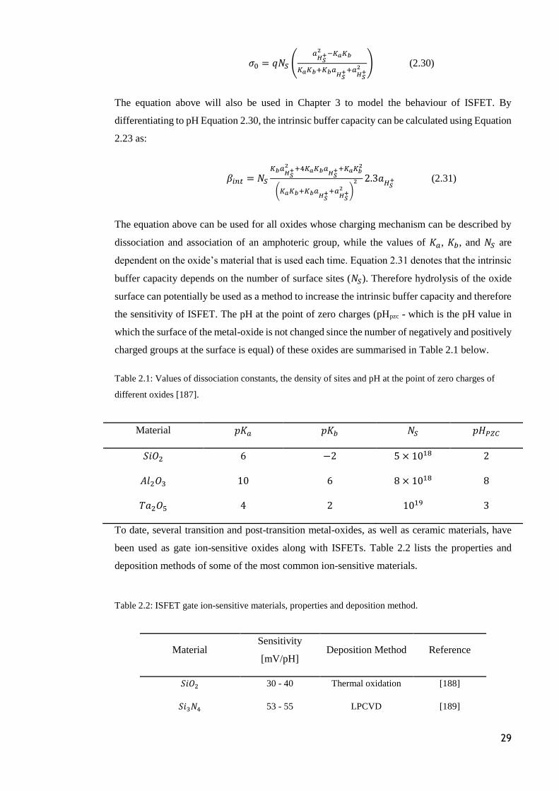
29
𝜎0 = 𝑞𝑁𝑆 (𝑎
𝐻𝑆+
2 −𝐾𝑎𝐾𝑏
𝐾𝑎𝐾𝑏+𝐾𝑏𝑎𝐻𝑆
++𝑎𝐻𝑆
+2 ) (2.30)
The equation above will also be used in Chapter 3 to model the behaviour of ISFET. By
differentiating to pH Equation 2.30, the intrinsic buffer capacity can be calculated using Equation
2.23 as:
𝛽𝑖𝑛𝑡 = 𝑁𝑆
𝐾𝑏𝑎𝐻𝑆
+2 +4𝐾𝑎𝐾𝑏𝑎
𝐻𝑆++𝐾𝑎𝐾𝑏
2
(𝐾𝑎𝐾𝑏+𝐾𝑏𝑎𝐻𝑆
++𝑎𝐻𝑆
+2 )
2 2.3𝑎𝐻𝑆
+ (2.31)
The equation above can be used for all oxides whose charging mechanism can be described by
dissociation and association of an amphoteric group, while the values of 𝐾𝑎, 𝐾𝑏, and 𝑁𝑆 are
dependent on the oxide’s material that is used each time. Equation 2.31 denotes that the intrinsic
buffer capacity depends on the number of surface sites (𝑁𝑆). Therefore hydrolysis of the oxide
surface can potentially be used as a method to increase the intrinsic buffer capacity and therefore
the sensitivity of ISFET. The pH at the point of zero charges (pHpzc - which is the pH value in
which the surface of the metal-oxide is not changed since the number of negatively and positively
charged groups at the surface is equal) of these oxides are summarised in Table 2.1 below.
Table 2.1: Values of dissociation constants, the density of sites and pH at the point of zero charges of
different oxides [187].
Material 𝑝𝐾𝑎 𝑝𝐾𝑏 𝑁𝑆 𝑝𝐻𝑃𝑍𝐶
𝑆𝑖𝑂2 6 −2 5 × 10¹⁸ 2
𝐴𝑙2𝑂3 10 6 8 × 10¹⁸ 8
𝑇𝑎2𝑂5 4 2 1019 3
To date, several transition and post-transition metal-oxides, as well as ceramic materials, have
been used as gate ion-sensitive oxides along with ISFETs. Table 2.2 lists the properties and
deposition methods of some of the most common ion-sensitive materials.
Table 2.2: ISFET gate ion-sensitive materials, properties and deposition method.
Material Sensitivity
[mV/pH] Deposition Method Reference
𝑆𝑖𝑂2 30 - 40 Thermal oxidation [188]
𝑆𝑖3𝑁4 53 - 55 LPCVD [189]
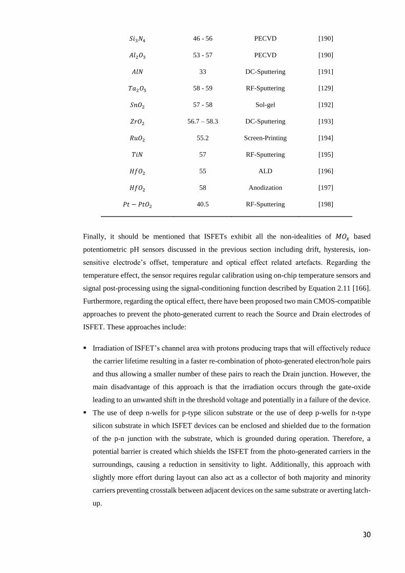
30
𝑆𝑖3𝑁4 46 - 56 PECVD [190]
𝐴𝑙2𝑂3 53 - 57 PECVD [190]
𝐴𝑙𝑁 33 DC-Sputtering [191]
𝑇𝑎2𝑂5 58 - 59 RF-Sputtering [129]
𝑆𝑛𝑂2 57 - 58 Sol-gel [192]
𝑍𝑟𝑂2 56.7 – 58.3 DC-Sputtering [193]
𝑅𝑢𝑂2 55.2 Screen-Printing [194]
𝑇𝑖𝑁 57 RF-Sputtering [195]
𝐻𝑓𝑂2 55 ALD [196]
𝐻𝑓𝑂2 58 Anodization [197]
𝑃𝑡 − 𝑃𝑡𝑂2 40.5 RF-Sputtering [198]
Finally, it should be mentioned that ISFETs exhibit all the non-idealities of 𝑀𝑂𝑥 based
potentiometric pH sensors discussed in the previous section including drift, hysteresis, ion-
sensitive electrode’s offset, temperature and optical effect related artefacts. Regarding the
temperature effect, the sensor requires regular calibration using on-chip temperature sensors and
signal post-processing using the signal-conditioning function described by Equation 2.11 [166].
Furthermore, regarding the optical effect, there have been proposed two main CMOS-compatible
approaches to prevent the photo-generated current to reach the Source and Drain electrodes of
ISFET. These approaches include:
Irradiation of ISFET’s channel area with protons producing traps that will effectively reduce
the carrier lifetime resulting in a faster re-combination of photo-generated electron/hole pairs
and thus allowing a smaller number of these pairs to reach the Drain junction. However, the
main disadvantage of this approach is that the irradiation occurs through the gate-oxide
leading to an unwanted shift in the threshold voltage and potentially in a failure of the device.
The use of deep n-wells for p-type silicon substrate or the use of deep p-wells for n-type
silicon substrate in which ISFET devices can be enclosed and shielded due to the formation
of the p-n junction with the substrate, which is grounded during operation. Therefore, a
potential barrier is created which shields the ISFET from the photo-generated carriers in the
surroundings, causing a reduction in sensitivity to light. Additionally, this approach with
slightly more effort during layout can also act as a collector of both majority and minority
carriers preventing crosstalk between adjacent devices on the same substrate or averting latch-
up.
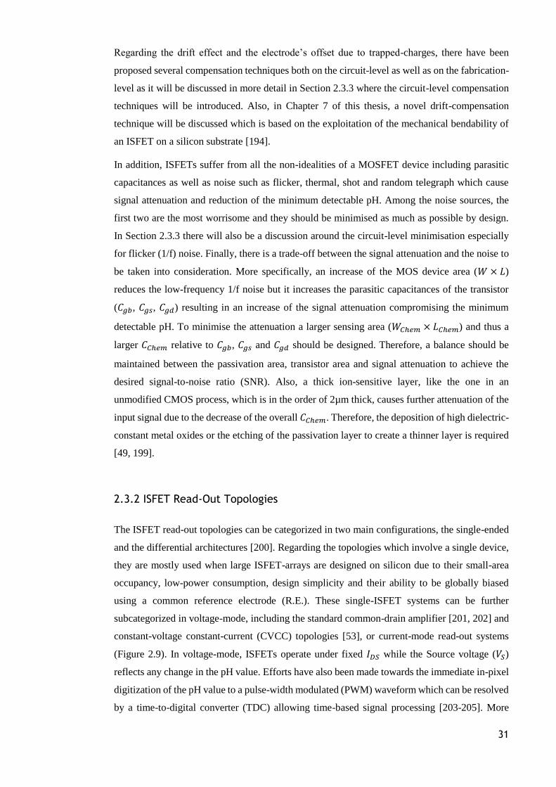
31
Regarding the drift effect and the electrode’s offset due to trapped-charges, there have been
proposed several compensation techniques both on the circuit-level as well as on the fabrication-
level as it will be discussed in more detail in Section 2.3.3 where the circuit-level compensation
techniques will be introduced. Also, in Chapter 7 of this thesis, a novel drift-compensation
technique will be discussed which is based on the exploitation of the mechanical bendability of
an ISFET on a silicon substrate [194].
In addition, ISFETs suffer from all the non-idealities of a MOSFET device including parasitic
capacitances as well as noise such as flicker, thermal, shot and random telegraph which cause
signal attenuation and reduction of the minimum detectable pH. Among the noise sources, the
first two are the most worrisome and they should be minimised as much as possible by design.
In Section 2.3.3 there will also be a discussion around the circuit-level minimisation especially
for flicker (1/f) noise. Finally, there is a trade-off between the signal attenuation and the noise to
be taken into consideration. More specifically, an increase of the MOS device area (𝑊 × 𝐿)
reduces the low-frequency 1/f noise but it increases the parasitic capacitances of the transistor
(𝐶𝑔𝑏, 𝐶𝑔𝑠, 𝐶𝑔𝑑) resulting in an increase of the signal attenuation compromising the minimum
detectable pH. To minimise the attenuation a larger sensing area (𝑊𝐶ℎ𝑒𝑚 × 𝐿𝐶ℎ𝑒𝑚) and thus a
larger 𝐶𝐶ℎ𝑒𝑚 relative to 𝐶𝑔𝑏, 𝐶𝑔𝑠 and 𝐶𝑔𝑑 should be designed. Therefore, a balance should be
maintained between the passivation area, transistor area and signal attenuation to achieve the
desired signal-to-noise ratio (SNR). Also, a thick ion-sensitive layer, like the one in an
unmodified CMOS process, which is in the order of 2µm thick, causes further attenuation of the
input signal due to the decrease of the overall 𝐶𝐶ℎ𝑒𝑚. Therefore, the deposition of high dielectric-
constant metal oxides or the etching of the passivation layer to create a thinner layer is required
[49, 199].
2.3.2 ISFET Read-Out Topologies
The ISFET read-out topologies can be categorized in two main configurations, the single-ended
and the differential architectures [200]. Regarding the topologies which involve a single device,
they are mostly used when large ISFET-arrays are designed on silicon due to their small-area
occupancy, low-power consumption, design simplicity and their ability to be globally biased
using a common reference electrode (R.E.). These single-ISFET systems can be further
subcategorized in voltage-mode, including the standard common-drain amplifier [201, 202] and
constant-voltage constant-current (CVCC) topologies [53], or current-mode read-out systems
(Figure 2.9). In voltage-mode, ISFETs operate under fixed 𝐼𝐷𝑆 while the Source voltage (𝑉𝑆)
reflects any change in the pH value. Efforts have also been made towards the immediate in-pixel
digitization of the pH value to a pulse-width modulated (PWM) waveform which can be resolved
by a time-to-digital converter (TDC) allowing time-based signal processing [203-205]. More
32
compact in-pixel voltage-mode read-out topologies have also been proposed to reduce further
the area of the pixel allowing even more pixels to be integrated on-chip allowing very high
density arrays [206, 207]. In current-mode topologies, the current of ISFET (𝐼𝐷𝑆) is measured
allowing fast signal-processing in the current-domain [208-210]. In Chapter 5 of this thesis, two
voltage-mode and one novel current-mode read-out topologies are further discussed towards the
design of the CMOS chip shown in Figure 2.4. Finally, single-ISFET read-out topologies have
also been used as standalone circuits exploiting the advantages offered by operational amplifiers
connected in feedback mode controlling the reference electrode’s potential [211-213].
Figure 2.9: (a) The source and drain follower read-out [53], (b) Standard source-follower in-pixel read-
out [201], (c) Modified flipped voltage follower read-out [202], (d) Current conveyor based ISFET read-
out [208], (e) Current-mode architecture based on translinear principle [209], (f) ISFET inverter topology
[204], (g) Complementary ISFET/MOSFET pair with source feedback [212] and (h) Wheatstone bridge
based read-out [213].
The second category of read-out topologies, the differential ISFET topologies (Figure 2.10), offer
all the advantages of a differential circuit including the rejection of common-mode and power-
supply variations as well as the minimization of drift and temperature effects. For example, Wong
et al. [214] had reported the first differential ISFET topology in which two unity-gain amplifiers
with one ISFET/MOSFET input-pair each and with ISFETs having different sensitivities were
connected to a difference amplifier. One of the ISFETs was immersed into a buffer solution of
known pH while the other was immersed in the solution under test. The output voltage of the
difference amplifier reflected the pH difference between the two ISFETs. In that context, similar
differential architectures having as input-pair a combination of ISFET/REFET have also been
reported in [53, 215, 216]. The REFET, which acts as the reference electrode transistor, has
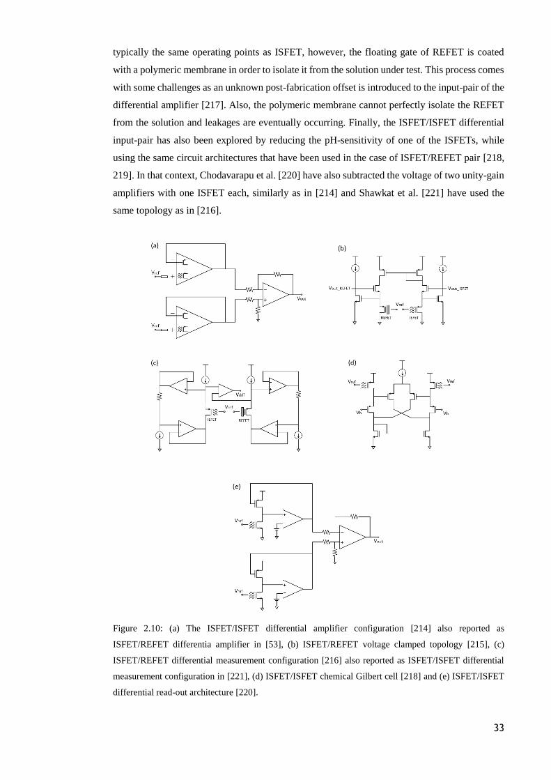
33
typically the same operating points as ISFET, however, the floating gate of REFET is coated
with a polymeric membrane in order to isolate it from the solution under test. This process comes
with some challenges as an unknown post-fabrication offset is introduced to the input-pair of the
differential amplifier [217]. Also, the polymeric membrane cannot perfectly isolate the REFET
from the solution and leakages are eventually occurring. Finally, the ISFET/ISFET differential
input-pair has also been explored by reducing the pH-sensitivity of one of the ISFETs, while
using the same circuit architectures that have been used in the case of ISFET/REFET pair [218,
219]. In that context, Chodavarapu et al. [220] have also subtracted the voltage of two unity-gain
amplifiers with one ISFET each, similarly as in [214] and Shawkat et al. [221] have used the
same topology as in [216].
Figure 2.10: (a) The ISFET/ISFET differential amplifier configuration [214] also reported as
ISFET/REFET differentia amplifier in [53], (b) ISFET/REFET voltage clamped topology [215], (c)
ISFET/REFET differential measurement configuration [216] also reported as ISFET/ISFET differential
measurement configuration in [221], (d) ISFET/ISFET chemical Gilbert cell [218] and (e) ISFET/ISFET
differential read-out architecture [220].
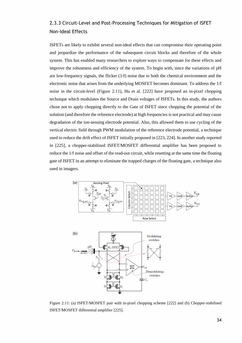
34
2.3.3 Circuit-Level and Post-Processing Techniques for Mitigation of ISFET
Non-Ideal Effects
ISFETs are likely to exhibit several non-ideal effects that can compromise their operating point
and jeopardize the performance of the subsequent circuit blocks and therefore of the whole
system. This has enabled many researchers to explore ways to compensate for these effects and
improve the robustness and efficiency of the system. To begin with, since the variations of pH
are low-frequency signals, the flicker (1/f) noise due to both the chemical environment and the
electronic noise that arises from the underlying MOSFET becomes dominant. To address the 1/f
noise in the circuit-level (Figure 2.11), Hu et al. [222] have proposed an in-pixel chopping
technique which modulates the Source and Drain voltages of ISFETs. In this study, the authors
chose not to apply chopping directly to the Gate of ISFET since chopping the potential of the
solution (and therefore the reference electrode) at high frequencies is not practical and may cause
degradation of the ion-sensing electrode potential. Also, this allowed them to use cycling of the
vertical electric field through PWM modulation of the reference electrode potential, a technique
used to reduce the drift effect of ISFET initially proposed in [223, 224]. In another study reported
in [225], a chopper-stabilized ISFET/MOSFET differential amplifier has been proposed to
reduce the 1/f noise and offset of the read-out circuit, while resetting at the same time the floating
gate of ISFET in an attempt to eliminate the trapped charges of the floating gate, a technique also
used in imagers.
Figure 2.11: (a) ISFET/MOSFET pair with in-pixel chopping scheme [222] and (b) Chopper-stabilised
ISFET/MOSFET differential amplifier [225].
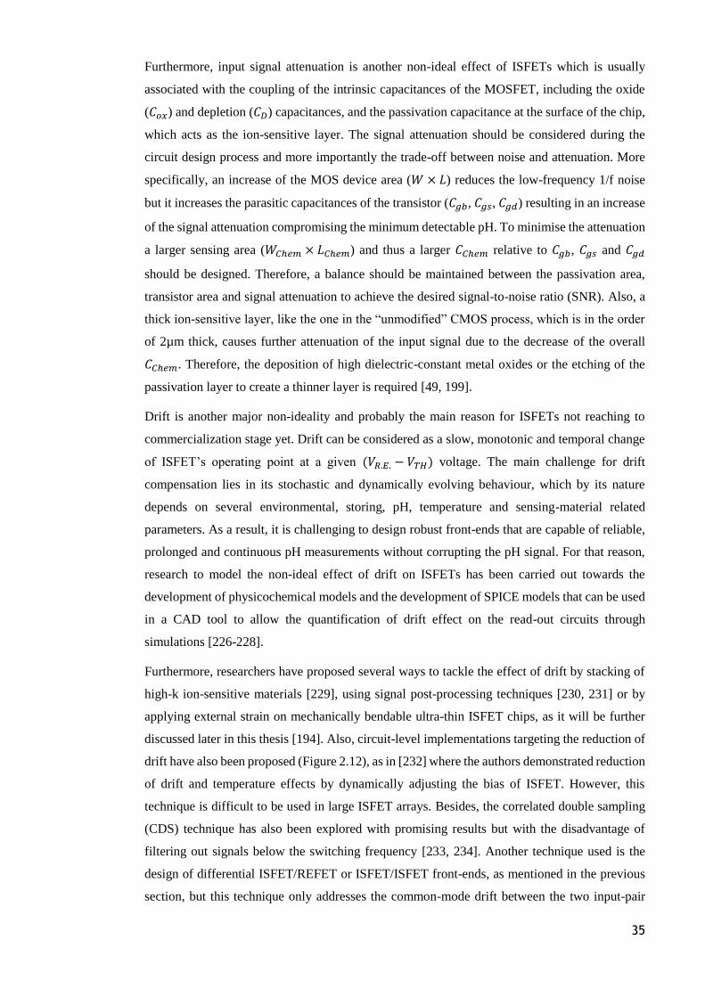
35
Furthermore, input signal attenuation is another non-ideal effect of ISFETs which is usually
associated with the coupling of the intrinsic capacitances of the MOSFET, including the oxide
(𝐶𝑜𝑥) and depletion (𝐶𝐷) capacitances, and the passivation capacitance at the surface of the chip,
which acts as the ion-sensitive layer. The signal attenuation should be considered during the
circuit design process and more importantly the trade-off between noise and attenuation. More
specifically, an increase of the MOS device area (𝑊 × 𝐿) reduces the low-frequency 1/f noise
but it increases the parasitic capacitances of the transistor (𝐶𝑔𝑏, 𝐶𝑔𝑠, 𝐶𝑔𝑑) resulting in an increase
of the signal attenuation compromising the minimum detectable pH. To minimise the attenuation
a larger sensing area (𝑊𝐶ℎ𝑒𝑚 × 𝐿𝐶ℎ𝑒𝑚) and thus a larger 𝐶𝐶ℎ𝑒𝑚 relative to 𝐶𝑔𝑏, 𝐶𝑔𝑠 and 𝐶𝑔𝑑
should be designed. Therefore, a balance should be maintained between the passivation area,
transistor area and signal attenuation to achieve the desired signal-to-noise ratio (SNR). Also, a
thick ion-sensitive layer, like the one in the “unmodified” CMOS process, which is in the order
of 2µm thick, causes further attenuation of the input signal due to the decrease of the overall
𝐶𝐶ℎ𝑒𝑚. Therefore, the deposition of high dielectric-constant metal oxides or the etching of the
passivation layer to create a thinner layer is required [49, 199].
Drift is another major non-ideality and probably the main reason for ISFETs not reaching to
commercialization stage yet. Drift can be considered as a slow, monotonic and temporal change
of ISFET’s operating point at a given (𝑉𝑅.𝐸. − 𝑉𝑇𝐻) voltage. The main challenge for drift
compensation lies in its stochastic and dynamically evolving behaviour, which by its nature
depends on several environmental, storing, pH, temperature and sensing-material related
parameters. As a result, it is challenging to design robust front-ends that are capable of reliable,
prolonged and continuous pH measurements without corrupting the pH signal. For that reason,
research to model the non-ideal effect of drift on ISFETs has been carried out towards the
development of physicochemical models and the development of SPICE models that can be used
in a CAD tool to allow the quantification of drift effect on the read-out circuits through
simulations [226-228].
Furthermore, researchers have proposed several ways to tackle the effect of drift by stacking of
high-k ion-sensitive materials [229], using signal post-processing techniques [230, 231] or by
applying external strain on mechanically bendable ultra-thin ISFET chips, as it will be further
discussed later in this thesis [194]. Also, circuit-level implementations targeting the reduction of
drift have also been proposed (Figure 2.12), as in [232] where the authors demonstrated reduction
of drift and temperature effects by dynamically adjusting the bias of ISFET. However, this
technique is difficult to be used in large ISFET arrays. Besides, the correlated double sampling
(CDS) technique has also been explored with promising results but with the disadvantage of
filtering out signals below the switching frequency [233, 234]. Another technique used is the
design of differential ISFET/REFET or ISFET/ISFET front-ends, as mentioned in the previous
section, but this technique only addresses the common-mode drift between the two input-pair
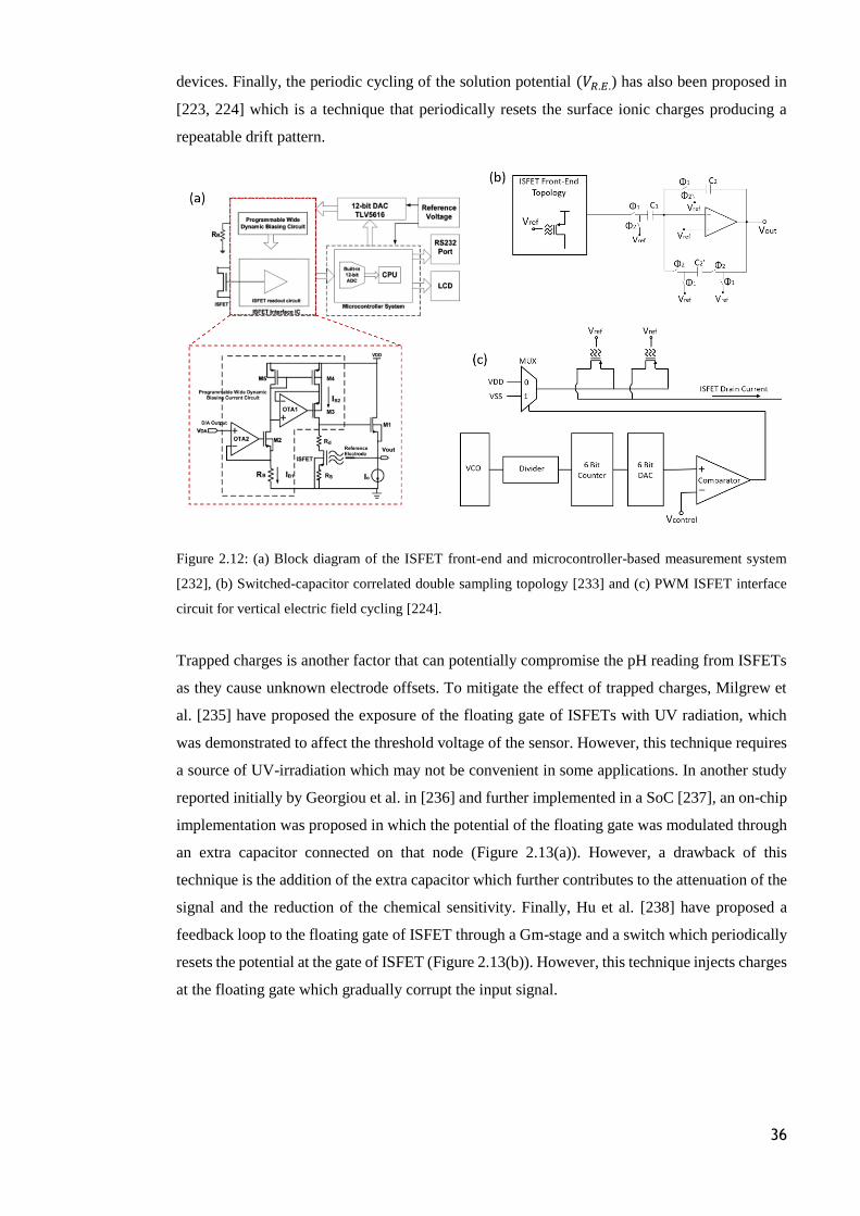
36
devices. Finally, the periodic cycling of the solution potential (𝑉𝑅.𝐸.) has also been proposed in
[223, 224] which is a technique that periodically resets the surface ionic charges producing a
repeatable drift pattern.
Figure 2.12: (a) Block diagram of the ISFET front-end and microcontroller-based measurement system
[232], (b) Switched-capacitor correlated double sampling topology [233] and (c) PWM ISFET interface
circuit for vertical electric field cycling [224].
Trapped charges is another factor that can potentially compromise the pH reading from ISFETs
as they cause unknown electrode offsets. To mitigate the effect of trapped charges, Milgrew et
al. [235] have proposed the exposure of the floating gate of ISFETs with UV radiation, which
was demonstrated to affect the threshold voltage of the sensor. However, this technique requires
a source of UV-irradiation which may not be convenient in some applications. In another study
reported initially by Georgiou et al. in [236] and further implemented in a SoC [237], an on-chip
implementation was proposed in which the potential of the floating gate was modulated through
an extra capacitor connected on that node (Figure 2.13(a)). However, a drawback of this
technique is the addition of the extra capacitor which further contributes to the attenuation of the
signal and the reduction of the chemical sensitivity. Finally, Hu et al. [238] have proposed a
feedback loop to the floating gate of ISFET through a Gm-stage and a switch which periodically
resets the potential at the gate of ISFET (Figure 2.13(b)). However, this technique injects charges
at the floating gate which gradually corrupt the input signal.
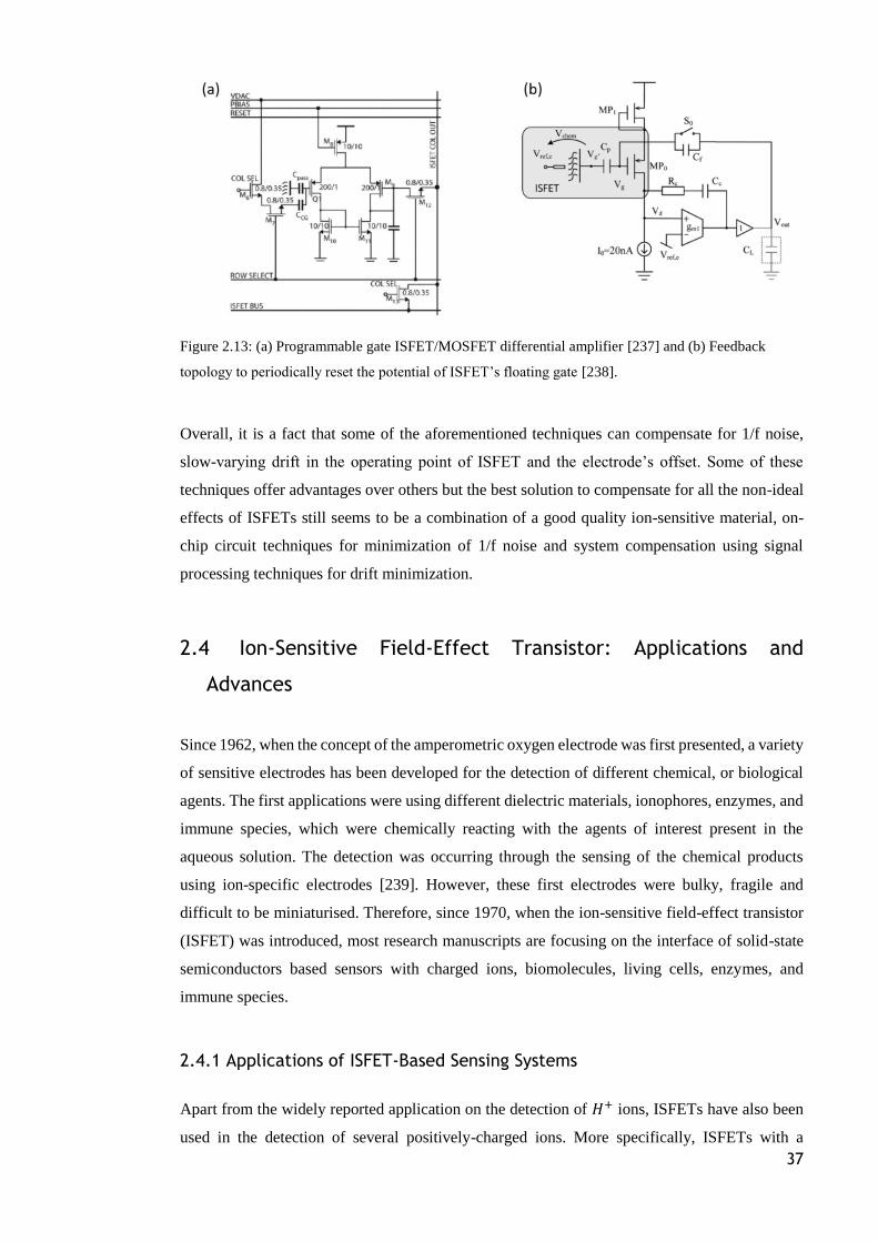
37
Figure 2.13: (a) Programmable gate ISFET/MOSFET differential amplifier [237] and (b) Feedback
topology to periodically reset the potential of ISFET’s floating gate [238].
Overall, it is a fact that some of the aforementioned techniques can compensate for 1/f noise,
slow-varying drift in the operating point of ISFET and the electrode’s offset. Some of these
techniques offer advantages over others but the best solution to compensate for all the non-ideal
effects of ISFETs still seems to be a combination of a good quality ion-sensitive material, on-
chip circuit techniques for minimization of 1/f noise and system compensation using signal
processing techniques for drift minimization.
2.4 Ion-Sensitive Field-Effect Transistor: Applications and
Advances
Since 1962, when the concept of the amperometric oxygen electrode was first presented, a variety
of sensitive electrodes has been developed for the detection of different chemical, or biological
agents. The first applications were using different dielectric materials, ionophores, enzymes, and
immune species, which were chemically reacting with the agents of interest present in the
aqueous solution. The detection was occurring through the sensing of the chemical products
using ion-specific electrodes [239]. However, these first electrodes were bulky, fragile and
difficult to be miniaturised. Therefore, since 1970, when the ion-sensitive field-effect transistor
(ISFET) was introduced, most research manuscripts are focusing on the interface of solid-state
semiconductors based sensors with charged ions, biomolecules, living cells, enzymes, and
immune species.
2.4.1 Applications of ISFET-Based Sensing Systems
Apart from the widely reported application on the detection of 𝐻+ ions, ISFETs have also been
used in the detection of several positively-charged ions. More specifically, ISFETs with a
38
modified surface have been reported for the detection of ammonium ions (𝑁𝐻4+) where the 𝑆𝑖𝑂2-
based ion-sensitive gate was covered with an intermediate hydrogel layer of poly(2-hydroxyethyl
methacrylate) (polyHEMA). The siloprene membrane showed close to Nernstian response in a
wide range of 𝑁𝐻4+ activity (10−4 to 10−1) with good selectivity in the presence of 0.1M of 𝑁𝑎+
[240]. Chalcogenide glass-based (𝐶𝑑𝑆𝐴𝑔𝐼𝐴𝑠2𝑆3) modified ISFETs have also been used as
cadmium ion (𝐶𝑑2+) sensors exhibiting a sensitivity of ~25.1mV/decade over a linear range of
response until 6.3 × 10⁻⁶ mol/l [241]. Surface-modified ISFETs with photo-cured polyurethane-
based polymer membranes have been used as calcium ions (𝐶𝑎2+) sensors exhibiting sensitivity
of 27.9mV/pCa and stability up to 6 weeks [242]. In addition, functionalised ISFETs have been
used as sodium (𝑁𝑎+) [243] and potassium (𝐾+) ions [244] sensors employing sodium and
potassium-selective membranes exhibiting sensitivities of more than 50mV/decade
and -30mV/decade, respectively. Finally, surface-functionalised ISFETs have also been used as
chromium ions (𝐶𝑟6+) [245], iron ions (𝐹𝑒3+) [246], mercuric ions (𝐻𝑔2+) [247], or as a
multi-positive ion sensor [248].
Furthermore, ISFETs have also been used as a platform for the detection of negatively-charged
ions. More specifically, photo-cured polyurethane-based polymer membranes were used to
functionalise ISFETs with six different ionophores targeting chloride ions (𝐶𝑙−) [249]. In another
application, the enzyme horseradish peroxidase has been immobilised in bovine serum albumin
(BSA) gel and the composite has been used to functionalise the gate of ISFETs for the detection
of cyanide ions (𝐶𝑁−). Moreover, the deposition of 𝐿𝑎𝐹3 on the gate of an ISFET was proven
for the detection of fluoride ions (𝐹−) exhibiting a near-Nernstian sensitivity [250].
Functionalised ISFETs have also been widely used for the detection of nitrates (𝑁𝑂3−), which is
especially useful in water and soil-quality monitoring applications [251, 252]. For example,
trioctadecyhnethylammonium nitrate (𝑇𝑂𝐷𝑀𝐴 − 𝑁𝑂3), tritetradecylmethylammonium nitrate
(𝑇𝑇𝐷𝑀𝐴 − 𝑁𝑂3) and tridodecylmethylammonium nitrate (𝑇𝐷𝐷𝑀𝐴 − 𝑁𝑂3) have all been used
to functionalise ISFETs for the detection of 𝑁𝑂3− exhibiting linear responses over a wide range
of nitrate concentrations [253]. Also, a PVC-sebacate based membrane has been used as a 𝑁𝑂3−
sensitive membrane on top of an ISFET device exhibiting fast response (<25 seconds), linearity
range extending for more than three decades and a near-Nernstian (52-54 mV/decade) response
[254]. Finally, other negatively-charged ions that have been detected using functionalised
ISFETs include phosphate ions (𝐻2𝑃𝑂4−) for flow-cell applications [255], as well as sulfate ions
(𝑆𝑂42−) [256].
Another big category of applications where ISFETs have been proven includes the detection of
biomolecules using immobilised enzymes near the surface of the sensor. As a result, the 𝐻+ ions
or any acid or base, which are among the by-products of the chemical reaction between the
immobilised enzymes and the targeted biomolecule, change the local pH of the solution which is
subsequently detected by the underlying ISFET. For example, the immobilisation of
39
acetylcholine esterase (𝐴𝐶ℎ𝐸) at the gate of an ISFET sensor resulted in the detection of low
concentrations (10−5 𝑀) of acetylcholine through the pH variation of the solution which was
caused by the acetic acid formation which is a by-product of the bio-catalysed hydrolysis of
acetylcholine [257]. Also, using the same sensing principle ATP-hydrolyrase embedded in a
polyacrylamide soft gel (PASG) and deposited on a 𝑇𝑎2𝑂5 based ISFET gate was used to detect
adenosine triphosphate (ATP) through the enzymatic production of 𝐻+ ions [258]. In the same
way, it was also possible to detect the concentration of proteins from the products of the protein
digestion by enzymes. For example, in [52] two configurations of chemically- modified ISFETs
were reported. The first employs a functionalised ISFET with phenylboronic-acid targeting the
analysis of dopamine and tyrosinase activities and the second employs tyramine or dopamine
modified ISFET gate-surface for the analysis of tyrosinase activities. More recently, Cheah et al.
[49] have reported a 256x256 ISFET array for the analysis of enzyme kinetics, calculation of the
Michaelis-Menten constant and quantification of glucose concentration through the activity of
hexokinase. Besides, ISFETs have been widely proven in the detection of DNA biomolecules
either by immobilising DNA strands on the ISFET gate sensing area [259] or by using
microfluidic channels that bring the complementary DNA strands close to each other directly
above the gate area of ISFET [48]. Finally, surface-functionalised ISFETs have also been used
as creatinine [260], dopamine [261], glucose [262], lactate [263], penicillin [264], triglyceride
[265], trypsin [266] and urea [267] sensor.
Finally, ISFETs have been explored for the monitoring of cell responses, since the real-time
monitoring of electro-physiological response of living cells to numerous stimuli, or the
monitoring of cytotoxic effects in response to hazardous substances can be proven significant in
the research towards the curing of diseases and the realisation of personalised medicines.
Therefore, a different type of cells, such as neural, cardiac, human dermal fibroblast, etc. have
been integrated with CMOS chips, and particularly with ISFET devices. For example, it has been
reported the use of a membrane-less CMOS-based sensor to measure the extracellular
acidification and respiration rate of colon adenocarcinoma cell line LS174T (ATTC CL 187)
[268]. In addition, Milgrew et al. [269] have reported the fabrication of a 16x16 ISFET array for
direct extracellular imaging, while Wang et al. [270] have proposed a 10x10 ISFET array for
non-invasive monitoring of the concentration of extracellular ions, such as 𝐶𝑎2+, 𝑁𝑎+, 𝐾+, etc.
and have shown that such devices can be used for real-time and long term analysis of cell
coupling. In another study, it has been reported a similar approach by using a 32x32 ISFET array
for the detection of 𝑁𝑎+ and 𝐾+ ions using selective polymer membranes, which were deposited
on the surface of the array [271]. Such a system can also be used for non-invasive extracellular
ion monitoring in applications targeting the integration of the nervous system with prosthetic
robotic devices. Finally, Georgiou et al. [272] have reported an attempt to model the metabolic
functions in biology using devices such as ISFETs.
40
2.4.2 Mechanically Flexible ISFET-Based Sensors towards Wearable Healthcare
Devices
Advances in wearable and conformable electronic and sensing systems integrated with soft
and/or curvilinear surfaces, such as biological tissues, present an exciting opportunity for
continuous and real-time measurements of health parameters in a non-invasive manner. Such
systems can prove useful as a diagnostic tool which coupled with data transmission capabilities
can enable remote medicine practices, self-monitoring of health or improve the quality of life of
people with disabilities [27-29]. Also, mechanically flexible sensing systems can be proven
useful in consumer or industrial applications permitting, for example, the continuous quality
monitoring of packages food [273, 274] or the unsupervised operation of heavy machinery in
unpredictable environments among humans, obstacles or in underwater or space environments
[39, 275]. One of the major advantages of wearable/epidermal electronics fabricated in thin and
conformable form factors is that they allow natural and intimate compliance with the soft and
curvilinear surfaces, such as the humans’ skin, ensuring robust physical and electro-physiological
measurements [276-279].
These advances have permitted the development of devices capable of monitoring of heart rate,
blood oxygenation and pressure, respiration rate, body posture, skin stretching, skin temperature
as well as brain activity. Multifunctional, wearable and non-invasive healthcare sensing systems,
however, also require monitoring of the body’s chemical state which is another important
indicator of health. Bio-chemical information found in sweat, tears or saliva, for example, can
provide useful information which is important to a wide variety of subjects ranging from athletes
to the elderly. In particular, parameters such as nitrogenous compounds such as amino acids and
urea [280], electrolytes (e.g. sodium, potassium, chloride and bicarbonate) and metabolites (e.g.
lactate and pyruvate) found in sweat may indicate an underlying disease [281]. Also, the
determination of pH in sweat is another important parameter which can reflect metabolic activity
or indicate the body’s exercise intensity and dehydration level. Table 2.3 lists some of the
analytes found in body-fluids and their concentrations.
To date, most of the reported epidermal electronic systems with on-board signal processing and
data-transmission blocks have been developed as hybrids using printed ion-selective electrodes
(ISEs) on flexible substrates integrated with rigid commercial off-the-shelf components or thin-
film-transistor (TFT) based read-out circuits [282-285], as shown in Figure 2.3. While passive
ISEs are a standard method of conducting electrochemical measurements, an alternative is to use
the ion-sensitive field-effect transistors (ISFETs), which offer the advantages discussed in
Section 2.3. As was also previously discussed, functionalized ISFETs with an appropriate ion or
molecule-specific membrane can be employed in a variety of applications. However, despite the
progress towards the development and utilisation of ion and molecule-specific membranes, in all
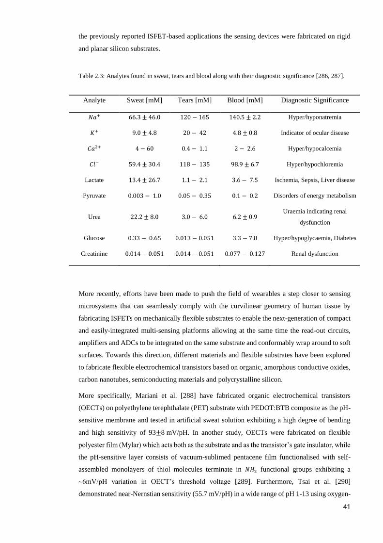
41
the previously reported ISFET-based applications the sensing devices were fabricated on rigid
and planar silicon substrates.
Table 2.3: Analytes found in sweat, tears and blood along with their diagnostic significance [286, 287].
Analyte Sweat [mM] Tears [mM] Blood [mM] Diagnostic Significance
𝑁𝑎+ 66.3 ± 46.0 120 − 165 140.5 ± 2.2 Hyper/hyponatremia
𝐾+ 9.0 ± 4.8 20 − 42 4.8 ± 0.8 Indicator of ocular disease
𝐶𝑎2+ 4 − 60 0.4 − 1.1 2 − 2.6 Hyper/hypocalcemia
𝐶𝑙− 59.4 ± 30.4 118 − 135 98.9 ± 6.7 Hyper/hypochloremia
Lactate 13.4 ± 26.7 1.1 − 2.1 3.6 − 7.5 Ischemia, Sepsis, Liver disease
Pyruvate 0.003 − 1.0 0.05 − 0.35 0.1 − 0.2 Disorders of energy metabolism
Urea 22.2 ± 8.0 3.0 − 6.0 6.2 ± 0.9 Uraemia indicating renal
dysfunction
Glucose 0.33 − 0.65 0.013 − 0.051 3.3 − 7.8 Hyper/hypoglycaemia, Diabetes
Creatinine 0.014 − 0.051 0.014 − 0.051 0.077 − 0.127 Renal dysfunction
More recently, efforts have been made to push the field of wearables a step closer to sensing
microsystems that can seamlessly comply with the curvilinear geometry of human tissue by
fabricating ISFETs on mechanically flexible substrates to enable the next-generation of compact
and easily-integrated multi-sensing platforms allowing at the same time the read-out circuits,
amplifiers and ADCs to be integrated on the same substrate and conformably wrap around to soft
surfaces. Towards this direction, different materials and flexible substrates have been explored
to fabricate flexible electrochemical transistors based on organic, amorphous conductive oxides,
carbon nanotubes, semiconducting materials and polycrystalline silicon.
More specifically, Mariani et al. [288] have fabricated organic electrochemical transistors
(OECTs) on polyethylene terephthalate (PET) substrate with PEDOT:BTB composite as the pH-
sensitive membrane and tested in artificial sweat solution exhibiting a high degree of bending
and high sensitivity of 93±8 mV/pH. In another study, OECTs were fabricated on flexible
polyester film (Mylar) which acts both as the substrate and as the transistor’s gate insulator, while
the pH-sensitive layer consists of vacuum-sublimed pentacene film functionalised with self-
assembled monolayers of thiol molecules terminate in 𝑁𝐻2 functional groups exhibiting a
~6mV/pH variation in OECT’s threshold voltage [289]. Furthermore, Tsai et al. [290]
demonstrated near-Nernstian sensitivity (55.7 mV/pH) in a wide range of pH 1-13 using oxygen-
42
plasma-treated carbon nanotube thin-films (CNTFs) ultrasonically sprayed on an extended-gate
ISFET (EG-ISFET) configuration on a polyimide substrate.
Also, low-temperature polycrystalline silicon (LTPS) based thin-film transistors (TFTs) were
explored to fabricate both tactile and pH sensors on polymeric substrates using ZnO-
nanostructures as the pH-sensing membrane exhibiting a near-Nernstian response [291]. Despite
the low-temperature fabrication process and the mechanical flexibility of the reported ISFET,
ZnO is not stable in acidic solutions (normally below pH6) and therefore it can only be used for
a limited pH range in the alkaline region. In another study, a 5×5 disposable pH-sensitive array
based on a PANI-membrane connected in an extended-gate configuration with a reusable
InGaZnO-based flexible transistor array has been reported exhibiting a super-Nernstian response
of 66.5 mV/pH [292].
Metal-oxides have also been used as pH-sensitive layers connected in an extended-gate
configuration with TFTs. For example, in [293] an amorphous InGaZnO-based TFT fabricated
on polyethylene naphthalate (PEN) substrate was connected as an EG-ISFET with a tin-dioxide
(𝑆𝑛𝑂2) ion-sensitive electrode fabricated using PEN substrate as well. The reported pH-
sensitivity of the flexible EG-ISFET was super-Nernstian in a range between pH3 to pH10.
Multifunctional flexible sensors based on InGaZnO-based TFTs were also fabricated on
polyimide substrate integrating both an 𝐴𝑙2𝑂3-based ISFET and a resistive temperature sensor.
The flexible ISFET showed a sensitivity of 51.2 mV/pH while the temperature sensor showed a
change in the resistivity of 0.85% per [294].
In another study, a TFT-based ISFET with indium tin oxide (ITO) acting as the ion-sensitive
layer fabricated on a plastic flexible substrate exhibited a sensitivity of 50 mV/pH. The flexible
EG-ISFET was also integrated with a transimpedance amplifier and a 10-bit ADC which were
designed and fabricated on silicon using a 500nm CMOS process [295]. Finally, single-wall
carbon nanotube-based transparent and flexible electrochemical transistors have also been
reported as pH as well as glucose sensors by utilising the enzyme of glucose oxidase (GOx)
showing a sensitivity of 18-45 µA/mM [296]. Finally, a few more studies in the field of
mechanically flexible ISFET-based chemical and bio-sensors are given in Figure 2.14.
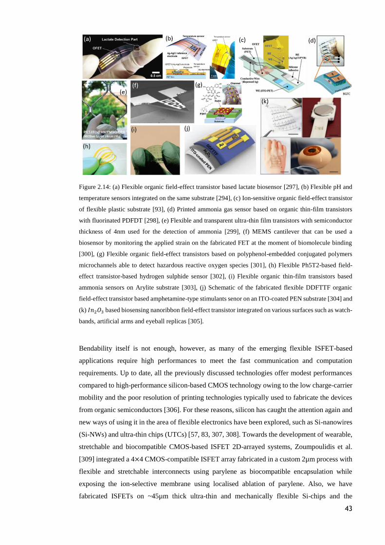
43
Figure 2.14: (a) Flexible organic field-effect transistor based lactate biosensor [297], (b) Flexible pH and
temperature sensors integrated on the same substrate [294], (c) Ion-sensitive organic field-effect transistor
of flexible plastic substrate [93], (d) Printed ammonia gas sensor based on organic thin-film transistors
with fluorinated PDFDT [298], (e) Flexible and transparent ultra-thin film transistors with semiconductor
thickness of 4nm used for the detection of ammonia [299], (f) MEMS cantilever that can be used a
biosensor by monitoring the applied strain on the fabricated FET at the moment of biomolecule binding
[300], (g) Flexible organic field-effect transistors based on polyphenol-embedded conjugated polymers
microchannels able to detect hazardous reactive oxygen species [301], (h) Flexible Ph5T2-based field-
effect transistor-based hydrogen sulphide sensor [302], (i) Flexible organic thin-film transistors based
ammonia sensors on Arylite substrate [303], (j) Schematic of the fabricated flexible DDFTTF organic
field-effect transistor based amphetamine-type stimulants senor on an ITO-coated PEN substrate [304] and
(k) 𝐼𝑛2𝑂3 based biosensing nanoribbon field-effect transistor integrated on various surfaces such as watch-
bands, artificial arms and eyeball replicas [305].
Bendability itself is not enough, however, as many of the emerging flexible ISFET-based
applications require high performances to meet the fast communication and computation
requirements. Up to date, all the previously discussed technologies offer modest performances
compared to high-performance silicon-based CMOS technology owing to the low charge-carrier
mobility and the poor resolution of printing technologies typically used to fabricate the devices
from organic semiconductors [306]. For these reasons, silicon has caught the attention again and
new ways of using it in the area of flexible electronics have been explored, such as Si-nanowires
(Si-NWs) and ultra-thin chips (UTCs) [57, 83, 307, 308]. Towards the development of wearable,
stretchable and biocompatible CMOS-based ISFET 2D-arrayed systems, Zoumpoulidis et al.
[309] integrated a 4×4 CMOS-compatible ISFET array fabricated in a custom 2µm process with
flexible and stretchable interconnects using parylene as biocompatible encapsulation while
exposing the ion-selective membrane using localised ablation of parylene. Also, we have
fabricated ISFETs on ~45µm thick ultra-thin and mechanically flexible Si-chips and the
44
mechanical flexibility of chips was exploited to reduce the sensor’s drift [194]. Finally, as it will
also be discussed in Chapters 5, 6 and 7 of this thesis in further detail, a thin (~30 µm)
CMOS-based miniaturised ISFET-based microsystem was also designed and engineered towards
a fully-integrated wearable lab-on-chip platform, as shown in Figure 2.4.
2.5 Summary
In this chapter, initially, an overview of potentiometric electrochemical sensors with emphasis
on pH sensing applications has been outlined including discussions on the sensing mechanisms,
different materials that have been used along with their properties and non-ideal effects that they
commonly exhibit. ISFETs are probably the most promising among the pH-sensing
potentiometric electrochemical sensors and therefore emphasis has been given in the discussion
of their operation principles, theory and applications where ISFETs have been successfully used.
However, the recent advances in wearable and implantable systems require the sensors to be
conformably integrated with the soft and curvilinear tissues and organs of the body to obtain
robust recordings and provide comfort to the user in the daily-life activities. The technological
advancements towards the realization of mechanically flexible and stretchable ion-sensitive
electrodes (ISEs) integrated on the human body were initially discussed, following with the
advancements towards the realization of mechanically flexible ISFETs on polymeric substrates.
However, bendability itself is not enough as many of the emerging flexible ISFET-based
applications require high performances in terms of noise, speed and power-consumption as well
as the ability to meet the high bandwidth required in IoT (0.3 – 3 GHz). Therefore, silicon has
caught the attention and new ways of using it in the form of ultra-thin chips (UTCs) have been
explored. Thus, an overview of the read-out topologies and circuit-level and post-processing
techniques for mitigation of ISFETs’ non-ideal effects has been given and the development of
CMOS-based ISFET sensor arrays was provided. Finally, an overview of the advances in
healthcare applications that ultra-thin CMOS chips (UTCs) have and will bring in the future has
been provided. In conclusion, despite the plethora of challenges, CMOS-based UTCs hold a great
promise for advances in many areas where high-performance flexible or conformable electronics
are needed.
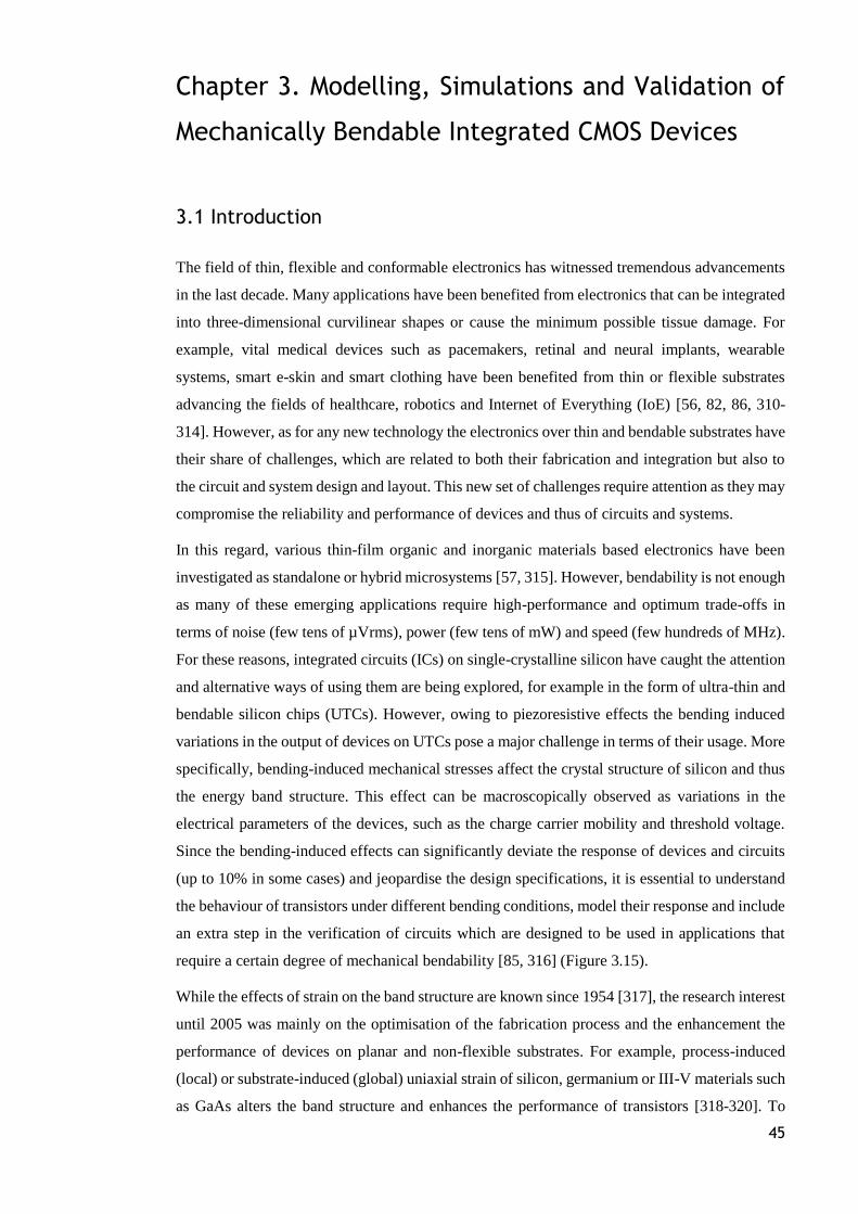
45
Chapter 3. Modelling, Simulations and Validation of
Mechanically Bendable Integrated CMOS Devices
3.1 Introduction
The field of thin, flexible and conformable electronics has witnessed tremendous advancements
in the last decade. Many applications have been benefited from electronics that can be integrated
into three-dimensional curvilinear shapes or cause the minimum possible tissue damage. For
example, vital medical devices such as pacemakers, retinal and neural implants, wearable
systems, smart e-skin and smart clothing have been benefited from thin or flexible substrates
advancing the fields of healthcare, robotics and Internet of Everything (IoE) [56, 82, 86, 310-
314]. However, as for any new technology the electronics over thin and bendable substrates have
their share of challenges, which are related to both their fabrication and integration but also to
the circuit and system design and layout. This new set of challenges require attention as they may
compromise the reliability and performance of devices and thus of circuits and systems.
In this regard, various thin-film organic and inorganic materials based electronics have been
investigated as standalone or hybrid microsystems [57, 315]. However, bendability is not enough
as many of these emerging applications require high-performance and optimum trade-offs in
terms of noise (few tens of µVrms), power (few tens of mW) and speed (few hundreds of MHz).
For these reasons, integrated circuits (ICs) on single-crystalline silicon have caught the attention
and alternative ways of using them are being explored, for example in the form of ultra-thin and
bendable silicon chips (UTCs). However, owing to piezoresistive effects the bending induced
variations in the output of devices on UTCs pose a major challenge in terms of their usage. More
specifically, bending-induced mechanical stresses affect the crystal structure of silicon and thus
the energy band structure. This effect can be macroscopically observed as variations in the
electrical parameters of the devices, such as the charge carrier mobility and threshold voltage.
Since the bending-induced effects can significantly deviate the response of devices and circuits
(up to 10% in some cases) and jeopardise the design specifications, it is essential to understand
the behaviour of transistors under different bending conditions, model their response and include
an extra step in the verification of circuits which are designed to be used in applications that
require a certain degree of mechanical bendability [85, 316] (Figure 3.15).
While the effects of strain on the band structure are known since 1954 [317], the research interest
until 2005 was mainly on the optimisation of the fabrication process and the enhancement the
performance of devices on planar and non-flexible substrates. For example, process-induced
(local) or substrate-induced (global) uniaxial strain of silicon, germanium or III-V materials such
as GaAs alters the band structure and enhances the performance of transistors [318-320]. To
46
mention a few, Si/Si-Ge heterostructures create compressive bi-axial tensile stress in the order of
700 MPa in the whole wafer substrate [321] and likewise, layout-dependent stresses, such as
shallow trench isolation (STI) technique which are used to prevent leakage current between
adjacent devices, can exert more than 750 MPa of compressive stress in the vicinity area changing
the charge carrier mobility of devices through the band structure modification, and thus alter the
threshold voltage (𝑉𝑇ℎ) depending the variation of the doping profile [322]. Despite the progress,
the modelling of bending-induced effects on the performance of devices on mechanically flexible
silicon substrates and their inclusion on compact models used in SPICE simulations is relatively
a new development [316, 323, 324].
This chapter primarily discusses the following points:
The formulation of bending-induced stresses on silicon and their impact on the behaviour
of transistors.
The modelling of NMOS, PMOS and ISFET devices on ultra-thin CMOS chips. The
developed behavioural models are a combination of mathematical equations and
extracted parameters from BSIM4 and BSIM6 including modified by a set of equations
describing the bending-induced stresses on silicon. The models are written in Verilog-A
and compiled in the Cadence Virtuoso environment where they were simulated at
different bending conditions.
The verification of the developed behavioural models through experimental results.
Finally, these models have been used during the readout circuit design discussed in
Chapter 5.
Figure 3.15: Graphical illustration showing the different considerations that require attention during the
design of mechanically bendable ICs [85].
47
3.2 Mechanical Characterisation of Ultra-Thin Silicon Chips
It is equally important to ensure mechanically robust and reliable ultra-thin chips (UTCs) as well
as reliable operation of the circuit on UTCs. In particular, the strength of thin silicon chips is an
important aspect to improve the yield and avoid possible fracture of the chip. The theoretical
strength of a material can be estimated using the equation [325]:
𝜎𝑠𝑡𝑟 = √𝛾𝐸
𝑎 (3.1)
where 𝛾 is the surface energy, 𝐸 is Young’s modulus and 𝑎 is the lattice constant of the material.
UTCs require an extra post-processing step to reduce the substrate’s thickness down to the ultra-
thin regime (<50μm). Different techniques have been explored to realise UTCs [58] like for
example back-grinding, TAIKO, dicing before grinding, reactive ion etching, controlled spalling,
proton-induced exfoliation, anisotropic wet etching, epitaxial silicon over porous silicon and bulk
removal in a silicon-on-insulator (SOI) wafer [326-335]. The strength of UTCs varies with the
technique adopted during post-processing as the strength is a parameter that depends on the defect
state caused by the manufacturing process [336]. For instance, a 15-20μm UTC obtained using
reactive ion etching exhibits the highest strength of 2.34 GPa and can bend down to 2.5mm
bending radius without fracturing. On the other hand, a UTC obtained by grinding and polishing
can bend down to 33mm bending radius without braking and a UTC obtained by dicing-before-
grinding technique exhibits a strength between 1.6 and 2.7 GPa for a 48μm die. It is worth
mentioning that during the abrasive back-grinding process there are defects induced at the
backside of the chip which leads to residual stresses [337]. These defects can be removed by
polishing steps to reach a defect-free surface.
Furthermore, the mechanical strength of UTCs also depends on the packaging and the amount of
on-chip electronics. More specifically, it has been observed that UTCs mounted on flexible
polymeric substrates using low-stress epoxies can undergo multiple reversible bending cycles.
Also, the fracture strength of encapsulated UTCs has been increased up to 190% allowing an
85% increase in the bending radius compared to UTCs which are not embedded in flexible
supporting substrates [194, 338-340]. Similarly, the mechanical strength of UTCs is also related
to the amount of on-chip electronics and the amount of processing the chip has undergone. For
instance, it has been observed that a blank UTCs without any processing is mechanically stronger
compared to a UTC with CMOS circuitry [341, 342]. UTCs may experience different types of
deformation such as shearing, torsion, tension or compression, which can be quantified in terms
of stress in a uniaxial or biaxial geometry [343]. The first geometry considers that the device
bends in just one direction, whereas the second geometry considers that the device bends in both
orthogonal directions normally occurring when there is an elastic anisotropy or an applied
constraint.
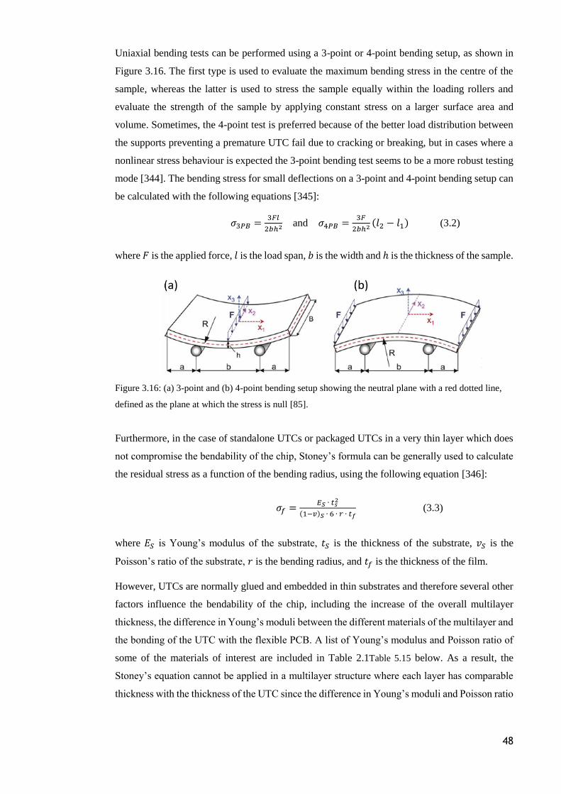
48
Uniaxial bending tests can be performed using a 3-point or 4-point bending setup, as shown in
Figure 3.16. The first type is used to evaluate the maximum bending stress in the centre of the
sample, whereas the latter is used to stress the sample equally within the loading rollers and
evaluate the strength of the sample by applying constant stress on a larger surface area and
volume. Sometimes, the 4-point test is preferred because of the better load distribution between
the supports preventing a premature UTC fail due to cracking or breaking, but in cases where a
nonlinear stress behaviour is expected the 3-point bending test seems to be a more robust testing
mode [344]. The bending stress for small deflections on a 3-point and 4-point bending setup can
be calculated with the following equations [345]:
𝜎3𝑃𝐵 =3𝐹𝑙
2𝑏ℎ2 and 𝜎4𝑃𝐵 =3𝐹
2𝑏ℎ2(𝑙2 − 𝑙1) (3.2)
where 𝐹 is the applied force, 𝑙 is the load span, 𝑏 is the width and ℎ is the thickness of the sample.
Figure 3.16: (a) 3-point and (b) 4-point bending setup showing the neutral plane with a red dotted line,
defined as the plane at which the stress is null [85].
Furthermore, in the case of standalone UTCs or packaged UTCs in a very thin layer which does
not compromise the bendability of the chip, Stoney’s formula can be generally used to calculate
the residual stress as a function of the bending radius, using the following equation [346]:
𝜎𝑓 =𝐸𝑆 ∙ 𝑡𝑠
2
(1−𝑣)𝑆 ∙ 6 ∙ 𝑟 ∙ 𝑡𝑓 (3.3)
where 𝐸𝑆 is Young’s modulus of the substrate, 𝑡𝑆 is the thickness of the substrate, 𝑣𝑆 is the
Poisson’s ratio of the substrate, 𝑟 is the bending radius, and 𝑡𝑓 is the thickness of the film.
However, UTCs are normally glued and embedded in thin substrates and therefore several other
factors influence the bendability of the chip, including the increase of the overall multilayer
thickness, the difference in Young’s moduli between the different materials of the multilayer and
the bonding of the UTC with the flexible PCB. A list of Young’s modulus and Poisson ratio of
some of the materials of interest are included in Table 2.1Table 5.15 below. As a result, the
Stoney’s equation cannot be applied in a multilayer structure where each layer has comparable
thickness with the thickness of the UTC since the difference in Young’s moduli and Poisson ratio
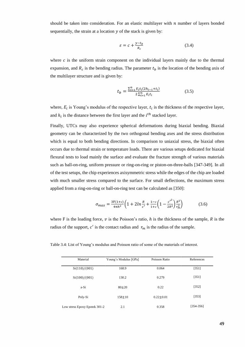
49
should be taken into consideration. For an elastic multilayer with 𝑛 number of layers bonded
sequentially, the strain at a location 𝑦 of the stack is given by:
휀 = 𝑐 +𝑦−𝑡𝑏
𝑅𝑐 (3.4)
where 𝑐 is the uniform strain component on the individual layers mainly due to the thermal
expansion, and 𝑅𝑐 is the bending radius. The parameter 𝑡𝑏 is the location of the bending axis of
the multilayer structure and is given by:
𝑡𝑏 =∑ 𝐸𝑖𝑡𝑖(2ℎ𝑖−1+𝑡𝑖)
𝑛𝑖=1
2∑ 𝐸𝑖𝑡𝑖𝑛𝑖=1
(3.5)
where, 𝐸𝑖 is Young’s modulus of the respective layer, 𝑡𝑖 is the thickness of the respective layer,
and ℎ𝑖 is the distance between the first layer and the 𝑖𝑡ℎ stacked layer.
Finally, UTCs may also experience spherical deformations during biaxial bending. Biaxial
geometry can be characterized by the two orthogonal bending axes and the stress distribution
which is equal to both bending directions. In comparison to uniaxial stress, the biaxial often
occurs due to thermal strain or temperature loads. There are various setups dedicated for biaxial
flexural tests to load mainly the surface and evaluate the fracture strength of various materials
such as ball-on-ring, uniform pressure or ring-on-ring or piston-on-three-balls [347-349]. In all
of the test setups, the chip experiences axisymmetric stress while the edges of the chip are loaded
with much smaller stress compared to the surface. For small deflections, the maximum stress
applied from a ring-on-ring or ball-on-ring test can be calculated as [350]:
𝜎𝑚𝑎𝑥 =3F(1+𝑣)
4πℎ2 (1 + 2𝑙𝑛𝑅
𝑐′ +1−𝑣
1+𝑣(1 −
𝑐′2
2𝑅2)𝑅2
𝑟𝑚2 ) (3.6)
where F is the loading force, 𝑣 is the Poisson’s ratio, ℎ is the thickness of the sample, 𝑅 is the
radius of the support, 𝑐′ is the contact radius and 𝑟𝑚 is the radius of the sample.
Table 3.4: List of Young’s modulus and Poisson ratio of some of the materials of interest.
Material Young’s Modulus [GPa] Poisson Ratio References
Si⟨110⟩/(001) 168.9 0.064 [351]
Si⟨100⟩/(001) 130.2 0.279 [351]
a-Si 80±20 0.22 [352]
Poly-Si 158±10 0.22±0.01 [353]
Low stress Epoxy Epotek 301-2 2.1 0.358 [354-356]
50
Polyimide Kapton 5.37 0.32 [357]
Silicon Dioxide 60.1±3.4 0.15 [358]
PECVD Silicon Nitride 152 0.20 [359]
Ruthenium Oxide 275 0.34 [360]
3.3 Strain Effects: From Silicon Substrate to Integrated Devices
and Circuits
3.3.1 Strain Effects on Bulk Silicon
The crystal structure of silicon is classified under the diamond structure and belongs to the cubic
system of Bravais lattice as it consists of two interspersed face centred cubic lattices (fcc) with
cube side of a=0.543nm [361]. It comprises of 8 atoms per unit cell and the basic properties of
the crystal structure are reflected in its band structure, shown in Figure 3.17(a). Further, electrons
in a semiconductor experience the periodic potential of the crystal lattice and this potential leads
to the formation of energy bands. The conduction band (CB) edge is located near the zone
boundary annotated by X points along the Δ symmetry lines, while the valence bands (VB)
contain the last filled energy levels which at T=0K are filled, whereas the conduction bands are
empty. Finally, the band gap (𝐸𝑔𝑎𝑝) separates the CB from the VB. In crystalline-Si the bandgap
is 1.12eV at room temperature and it slightly decreases as the temperature increases.
As is shown in Figure 3.17, the principal conduction band CB minima in the general band
structure of unstrained silicon are located along the [100], [010], and [001] directions.
Additionally, the energy of the two lowest CBs are degenerate at the X-points and close to the
CB edge, the band structure can be approximated by constant ellipsoidal energy surfaces, shown
in Figure 3.17(b), and a parabolic energy dispersion [362]. In unstrained conditions, the six-fold
degeneracy of the valleys arises due to the symmetry of the lattice along the [100], [010], and
[001] directions and the electrons occupy all of these 3 pairs equally, making the transport
isotropic.
Intrinsic to the band structure are several symmetry properties which are modified by the
application of strain. The effect of strain on the conductivity of Si was first investigated by Smith
[317] and the principal finding of his experimental work was the observation of a change in the
Si resistivity on applying uniaxial tensile stress. This change occurs due to the modification of
the electronic band structure and thus to the modification of the effective mass which leads to
mobility enhancement [363]. Therefore, the value of the longitudinal (𝑚𝑙) and transversal
electron mass (𝑚𝑡) change under the influence of strain, which also induces a shift in the energy
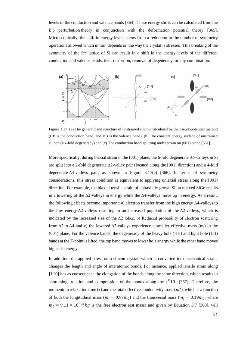
51
levels of the conduction and valence bands [364]. These energy shifts can be calculated from the
k·p perturbation theory in conjunction with the deformation potential theory [365].
Microscopically, the shift in energy levels stems from a reduction in the number of symmetry
operations allowed which in turn depends on the way the crystal is stressed. This breaking of the
symmetry of the fcc lattice of Si can result in a shift in the energy levels of the different
conduction and valence bands, their distortion, removal of degeneracy, or any combination.
Figure 3.17: (a) The general band structure of unstrained silicon calculated by the pseudopotential method
(CB is the conduction band, and VB is the valence band), (b) The constant energy surface of unstrained
silicon (six-fold degeneracy) and (c) The conduction band splitting under strain on (001) plane [361].
More specifically, during biaxial strain in the (001) plane, the 6-fold degenerate Δ6-valleys in Si
are split into a 2-fold degenerate Δ2-valley pair (located along the [001] direction) and a 4-fold
degenerate Δ4-valleys pair, as shown in Figure 3.17(c) [366]. In terms of symmetry
considerations, this stress condition is equivalent to applying uniaxial stress along the [001]
direction. For example, the biaxial tensile strain of epitaxially grown Si on relaxed SiGe results
in a lowering of the Δ2-valleys in energy while the Δ4-valleys move up in energy. As a result,
the following effects become important: a) electron transfer from the high energy Δ4-valleys to
the low energy Δ2-valleys resulting in an increased population of the Δ2-valleys, which is
indicated by the increased size of the Δ2 lobes. b) Reduced probability of electron scattering
from Δ2 to Δ4 and c) the lowered Δ2-valleys experience a smaller effective mass (mt) in the
(001) plane. For the valence bands, the degeneracy of the heavy hole (HH) and light hole (LH)
bands at the Γ-point is lifted, the top band moves to lower hole energy while the other band moves
higher in energy.
In addition, the applied stress on a silicon crystal, which is converted into mechanical strain,
changes the length and angle of interatomic bonds. For instance, applied tensile strain along
[110] has as consequence the elongation of the bonds along the same direction, which results in
shortening, rotation and compression of the bonds along the [110] [367]. Therefore, the
momentum relaxation time (𝜏) and the total effective conductivity mass (𝑚∗), which is a function
of both the longitudinal mass (𝑚𝑙 = 0.97𝑚0) and the transversal mass (𝑚𝑡 = 0.19𝑚0, where
𝑚0 = 9.11 × 10⁻³¹𝑘𝑔 is the free electron rest mass) and given by Equation 3.7 [368], will

52
change because of the applied stress due to the lift of degeneracy and repopulation of the valleys
with electrons.
𝑚∗ = [1
6(
2
𝑚𝑙+
4
𝑚𝑡)]
−1= 0.26𝑚0 (3.7)
As a result, the mobility of the charge carriers will change since it is defined by the Drude model
as:
𝜇 =| |
| |=
𝑞∙𝜏
𝑚∗∙𝑚0 (3.8)
Where |𝑣 | is the constant average velocity, | | is the applied electric field and 𝑞 is the electron
charge.
Furthermore, the silicon crystal has isotropic conductivity, which results in parallel current flow
to the applied electric field. The ratio between the current density to the electric field is known
as conductivity and the reverse of conductivity (𝜎) as resistivity (𝜌) and both are related to the
silicon’s band structure through the concentration of majority and minority charge carriers and
their mobilities through the following equation:
𝜎 =1
𝜌= 𝑞(𝑛𝜇𝑛 + 𝑝𝜇𝑝) (3.9)
where 𝜇𝑛 is the electron mobility, 𝜇𝑝 is the hole mobility, 𝑛 is the concentration of electrons and
𝑝 is the concentration of holes.
Upon application of stress, the cubic symmetry of silicon brakes resulting in an anisotropic
conductivity and thus in a change in silicon’s resistivity, which is also termed as piezoresistivity,
which varies with stress. This change in silicon’s resistivity can be expressed as [369]:
𝑑𝑟𝑖𝑗
𝑟=
𝑑𝜌𝑖𝑗
𝜌= 𝛱𝑖𝑗𝑘𝑙 ∙ 𝜎𝑘𝑙 + 𝛱𝑖𝑗𝑘𝑙𝑚𝑛 ∙ 𝜎𝑘𝑙 ∙ 𝜎𝑚𝑛, for 𝑖, 𝑗, 𝑘, 𝑙, 𝑚, 𝑛 = 1,2,3 (3.10)
where 𝑟 and 𝜌 are the unstressed initial resistance and resistivity, 𝜎𝑘𝑙 and 𝜎𝑚𝑛 are the components
of stress tensor [370] and 𝛱𝑖𝑗𝑘𝑙, 𝛱𝑖𝑗𝑘𝑙𝑚𝑛 are the first and second order piezoresistive coefficients.
For a (001) silicon, which is prevalent in the semiconductor industry, and uniaxial stress along
the same direction the first-order piezoresistive tensor reduces to three independent piezoresistive
coefficients, the longitudinal 𝛱11 which refers to 0o between the direction of stress and that of
current along [100], the transversal 𝛱12 which refers to 90o between the direction of stress and
that of current along [100], and the shear coefficient 𝛱44 [317]. These fundamental coefficients
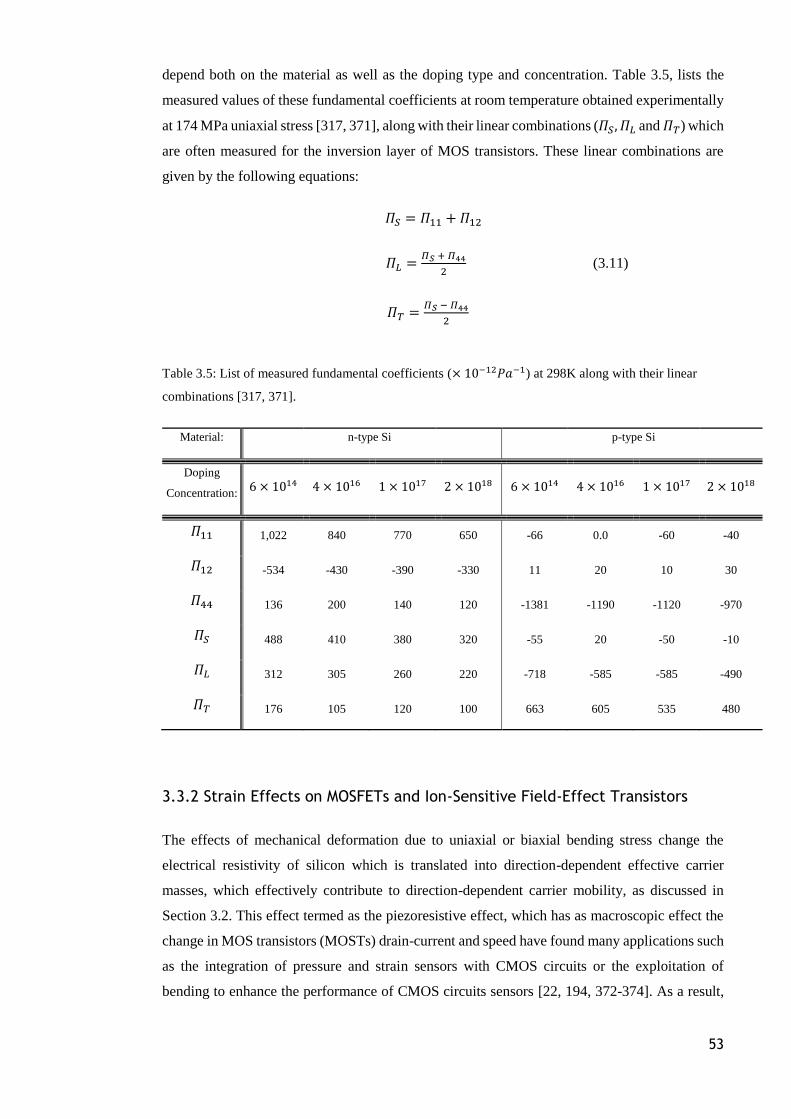
53
depend both on the material as well as the doping type and concentration. Table 3.5, lists the
measured values of these fundamental coefficients at room temperature obtained experimentally
at 174 MPa uniaxial stress [317, 371], along with their linear combinations (𝛱𝑆, 𝛱𝐿 and 𝛱𝑇) which
are often measured for the inversion layer of MOS transistors. These linear combinations are
given by the following equations:
𝛱𝑆 = 𝛱11 + 𝛱12
𝛱𝐿 =𝛱𝑆 + 𝛱44
2 (3.11)
𝛱𝑇 =𝛱𝑆 − 𝛱44
2
Table 3.5: List of measured fundamental coefficients (× 10−12𝑃𝑎−1) at 298K along with their linear
combinations [317, 371].
Material: n-type Si p-type Si
Doping
Concentration: 6 × 10¹⁴ 4 × 10¹⁶ 1 × 10¹⁷ 2 × 10¹⁸ 6 × 10¹⁴ 4 × 10¹⁶ 1 × 10¹⁷ 2 × 10¹⁸
𝛱11 1,022 840 770 650 -66 0.0 -60 -40
𝛱12 -534 -430 -390 -330 11 20 10 30
𝛱44 136 200 140 120 -1381 -1190 -1120 -970
𝛱𝑆 488 410 380 320 -55 20 -50 -10
𝛱𝐿 312 305 260 220 -718 -585 -585 -490
𝛱𝑇 176 105 120 100 663 605 535 480
3.3.2 Strain Effects on MOSFETs and Ion-Sensitive Field-Effect Transistors
The effects of mechanical deformation due to uniaxial or biaxial bending stress change the
electrical resistivity of silicon which is translated into direction-dependent effective carrier
masses, which effectively contribute to direction-dependent carrier mobility, as discussed in
Section 3.2. This effect termed as the piezoresistive effect, which has as macroscopic effect the
change in MOS transistors (MOSTs) drain-current and speed have found many applications such
as the integration of pressure and strain sensors with CMOS circuits or the exploitation of
bending to enhance the performance of CMOS circuits sensors [22, 194, 372-374]. As a result,
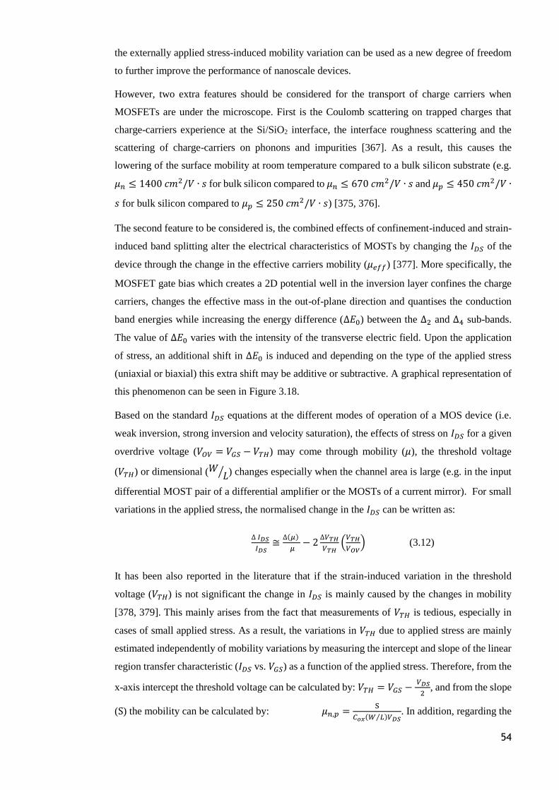
54
the externally applied stress-induced mobility variation can be used as a new degree of freedom
to further improve the performance of nanoscale devices.
However, two extra features should be considered for the transport of charge carriers when
MOSFETs are under the microscope. First is the Coulomb scattering on trapped charges that
charge-carriers experience at the Si/SiO2 interface, the interface roughness scattering and the
scattering of charge-carriers on phonons and impurities [367]. As a result, this causes the
lowering of the surface mobility at room temperature compared to a bulk silicon substrate (e.g.
𝜇𝑛 ≤ 1400 𝑐𝑚2/𝑉 ∙ 𝑠 for bulk silicon compared to 𝜇𝑛 ≤ 670 𝑐𝑚2/𝑉 ∙ 𝑠 and 𝜇𝑝 ≤ 450 𝑐𝑚2/𝑉 ∙
𝑠 for bulk silicon compared to 𝜇𝑝 ≤ 250 𝑐𝑚2/𝑉 ∙ 𝑠) [375, 376].
The second feature to be considered is, the combined effects of confinement-induced and strain-
induced band splitting alter the electrical characteristics of MOSTs by changing the 𝐼𝐷𝑆 of the
device through the change in the effective carriers mobility (𝜇𝑒𝑓𝑓) [377]. More specifically, the
MOSFET gate bias which creates a 2D potential well in the inversion layer confines the charge
carriers, changes the effective mass in the out-of-plane direction and quantises the conduction
band energies while increasing the energy difference (∆𝐸0) between the ∆2 and ∆4 sub-bands.
The value of ∆𝐸0 varies with the intensity of the transverse electric field. Upon the application
of stress, an additional shift in ∆𝐸0 is induced and depending on the type of the applied stress
(uniaxial or biaxial) this extra shift may be additive or subtractive. A graphical representation of
this phenomenon can be seen in Figure 3.18.
Based on the standard 𝐼𝐷𝑆 equations at the different modes of operation of a MOS device (i.e.
weak inversion, strong inversion and velocity saturation), the effects of stress on 𝐼𝐷𝑆 for a given
overdrive voltage (𝑉𝑂𝑉 = 𝑉𝐺𝑆 − 𝑉𝑇𝐻) may come through mobility (𝜇), the threshold voltage
(𝑉𝑇𝐻) or dimensional (𝑊 𝐿⁄ ) changes especially when the channel area is large (e.g. in the input
differential MOST pair of a differential amplifier or the MOSTs of a current mirror). For small
variations in the applied stress, the normalised change in the 𝐼𝐷𝑆 can be written as:
∆ 𝐼𝐷𝑆
𝐼𝐷𝑆≅
∆(𝜇)
𝜇− 2
∆𝑉𝑇𝐻
𝑉𝑇𝐻(𝑉𝑇𝐻
𝑉𝑂𝑉) (3.12)
It has been also reported in the literature that if the strain-induced variation in the threshold
voltage (𝑉𝑇𝐻) is not significant the change in 𝐼𝐷𝑆 is mainly caused by the changes in mobility
[378, 379]. This mainly arises from the fact that measurements of 𝑉𝑇𝐻 is tedious, especially in
cases of small applied stress. As a result, the variations in 𝑉𝑇𝐻 due to applied stress are mainly
estimated independently of mobility variations by measuring the intercept and slope of the linear
region transfer characteristic (𝐼𝐷𝑆 vs. 𝑉𝐺𝑆) as a function of the applied stress. Therefore, from the
x-axis intercept the threshold voltage can be calculated by: 𝑉𝑇𝐻 = 𝑉𝐺𝑆 − 𝑉𝐷𝑆
2, and from the slope
(S) the mobility can be calculated by: 𝜇𝑛,𝑝 =S
𝐶𝑜𝑥(𝑊 𝐿⁄ )𝑉𝐷𝑆. In addition, regarding the
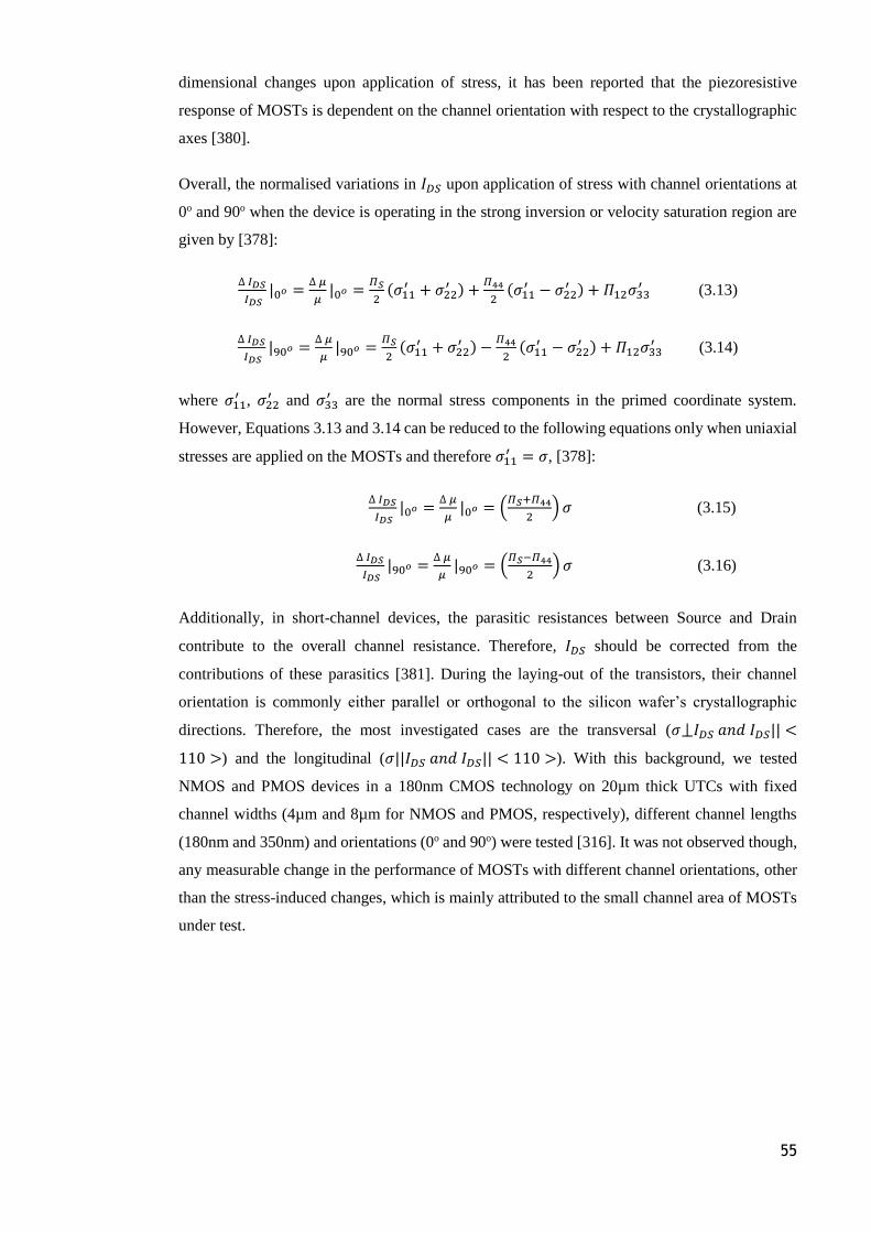
55
dimensional changes upon application of stress, it has been reported that the piezoresistive
response of MOSTs is dependent on the channel orientation with respect to the crystallographic
axes [380].
Overall, the normalised variations in 𝐼𝐷𝑆 upon application of stress with channel orientations at
0o and 90o when the device is operating in the strong inversion or velocity saturation region are
given by [378]:
∆ 𝐼𝐷𝑆
𝐼𝐷𝑆|0𝑜 =
∆ 𝜇
𝜇|0𝑜 =
𝛱𝑆
2(𝜎11
′ + 𝜎22′ ) +
𝛱44
2(𝜎11
′ − 𝜎22′ ) + 𝛱12𝜎33
′ (3.13)
∆ 𝐼𝐷𝑆
𝐼𝐷𝑆|90𝑜 =
∆ 𝜇
𝜇|90𝑜 =
𝛱𝑆
2(𝜎11
′ + 𝜎22′ ) −
𝛱44
2(𝜎11
′ − 𝜎22′ ) + 𝛱12𝜎33
′ (3.14)
where 𝜎11′ , 𝜎22
′ and 𝜎33′ are the normal stress components in the primed coordinate system.
However, Equations 3.13 and 3.14 can be reduced to the following equations only when uniaxial
stresses are applied on the MOSTs and therefore 𝜎11′ = 𝜎, [378]:
∆ 𝐼𝐷𝑆
𝐼𝐷𝑆|0𝑜 =
∆ 𝜇
𝜇|0𝑜 = (
𝛱𝑆+𝛱44
2) 𝜎 (3.15)
∆ 𝐼𝐷𝑆
𝐼𝐷𝑆|90𝑜 =
∆ 𝜇
𝜇|90𝑜 = (
𝛱𝑆−𝛱44
2) 𝜎 (3.16)
Additionally, in short-channel devices, the parasitic resistances between Source and Drain
contribute to the overall channel resistance. Therefore, 𝐼𝐷𝑆 should be corrected from the
contributions of these parasitics [381]. During the laying-out of the transistors, their channel
orientation is commonly either parallel or orthogonal to the silicon wafer’s crystallographic
directions. Therefore, the most investigated cases are the transversal (𝜎⟘𝐼𝐷𝑆 𝑎𝑛𝑑 𝐼𝐷𝑆|| <
110 >) and the longitudinal (𝜎||𝐼𝐷𝑆 𝑎𝑛𝑑 𝐼𝐷𝑆|| < 110 >). With this background, we tested
NMOS and PMOS devices in a 180nm CMOS technology on 20µm thick UTCs with fixed
channel widths (4µm and 8µm for NMOS and PMOS, respectively), different channel lengths
(180nm and 350nm) and orientations (0o and 90o) were tested [316]. It was not observed though,
any measurable change in the performance of MOSTs with different channel orientations, other
than the stress-induced changes, which is mainly attributed to the small channel area of MOSTs
under test.
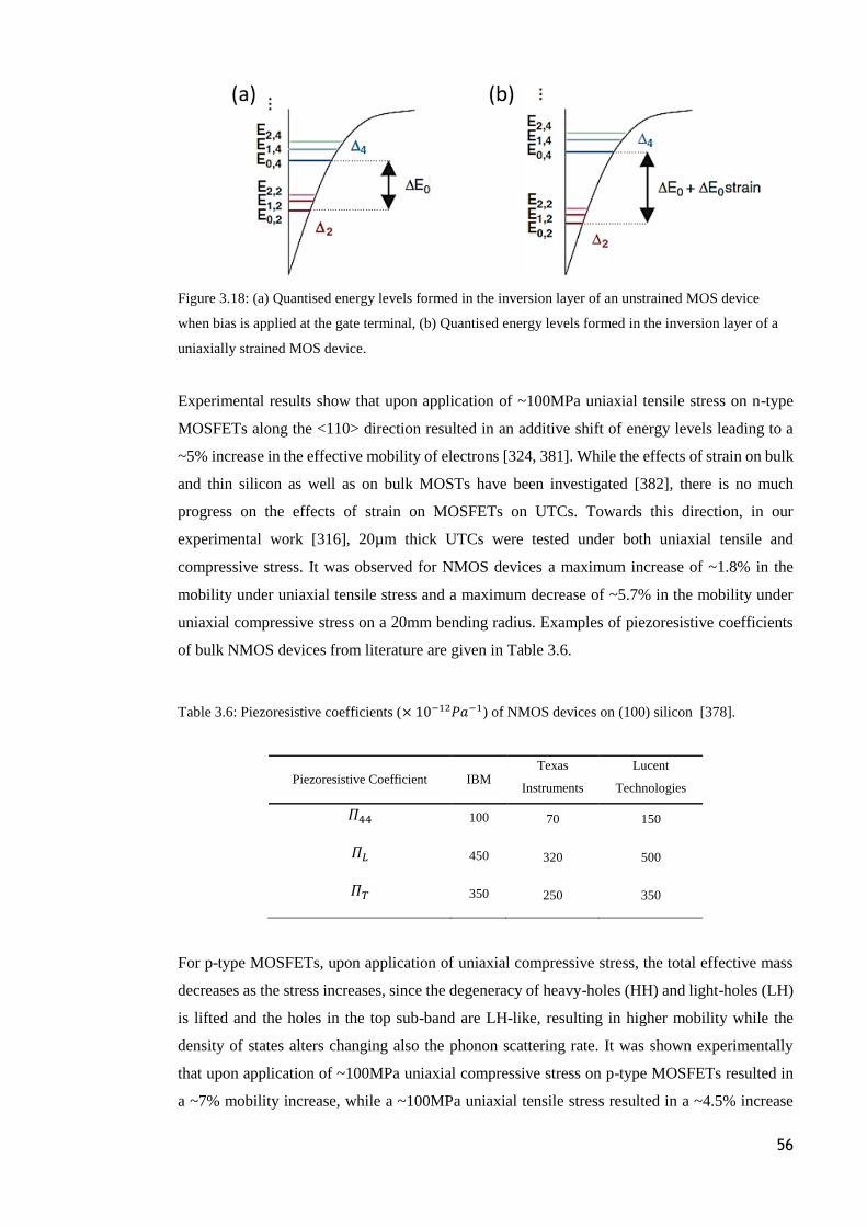
56
Figure 3.18: (a) Quantised energy levels formed in the inversion layer of an unstrained MOS device
when bias is applied at the gate terminal, (b) Quantised energy levels formed in the inversion layer of a
uniaxially strained MOS device.
Experimental results show that upon application of ~100MPa uniaxial tensile stress on n-type
MOSFETs along the <110> direction resulted in an additive shift of energy levels leading to a
~5% increase in the effective mobility of electrons [324, 381]. While the effects of strain on bulk
and thin silicon as well as on bulk MOSTs have been investigated [382], there is no much
progress on the effects of strain on MOSFETs on UTCs. Towards this direction, in our
experimental work [316], 20µm thick UTCs were tested under both uniaxial tensile and
compressive stress. It was observed for NMOS devices a maximum increase of ~1.8% in the
mobility under uniaxial tensile stress and a maximum decrease of ~5.7% in the mobility under
uniaxial compressive stress on a 20mm bending radius. Examples of piezoresistive coefficients
of bulk NMOS devices from literature are given in Table 3.6.
Table 3.6: Piezoresistive coefficients (× 10−12𝑃𝑎−1) of NMOS devices on (100) silicon [378].
Piezoresistive Coefficient IBM Texas
Instruments
Lucent
Technologies
𝛱44 100 70 150
𝛱𝐿 450 320 500
𝛱𝑇 350 250 350
For p-type MOSFETs, upon application of uniaxial compressive stress, the total effective mass
decreases as the stress increases, since the degeneracy of heavy-holes (HH) and light-holes (LH)
is lifted and the holes in the top sub-band are LH-like, resulting in higher mobility while the
density of states alters changing also the phonon scattering rate. It was shown experimentally
that upon application of ~100MPa uniaxial compressive stress on p-type MOSFETs resulted in
a ~7% mobility increase, while a ~100MPa uniaxial tensile stress resulted in a ~4.5% increase
57
[381, 383]. In our experimental work [316], it was observed for PMOS devices a maximum
increase of ~3.9% in the mobility under uniaxial tensile stress and a maximum increase of
~5.02% in the mobility under uniaxial compressive stress on a 20mm bending radius. Examples
of piezoresistive coefficients of bulk PMOS devices from literature are given in Table 3.7.
Table 3.7: Piezoresistive coefficients of PMOS devices on (100) silicon (× 10−12𝑃𝑎−1) [378].
Piezoresistive Coefficient IBM Texas
Instruments
Lucent
Technologies
𝛱44 -950 -800 -1,000
𝛱𝐿 -500 -415 -600
𝛱𝑇 450 385 400
Finally, CMOS compatible ion-sensitive field-effect transistors (ISFETs) have the same
operation as a MOSFET device, except that the gate of the ISFET is a reference electrode which
is immersed into an electrolyte, as discussed in Chapter 2. An ion-sensitive material is deposited
on top of MOSFET’s gate electrode which acts as the transducer, while the electrolyte is biased
by the reference electrode. Therefore, the previous discussion related to the stress effects on
MOSFETs also applies in the case of ISFETs. However, there is no much progress on the effects
of stress on the ion-sensitive material. Towards this direction, in our experimental work, we
fabricated RuO2-based ISFETs on 45µm thick UTCs and we measured the sensitivity of the
10µm thick ion-sensitive material (i.e. RuO2) before and after 1000 bending cycles [194].
RuO2-based pH sensors were reported in the past and exhibit good chemical stability and
restrained space charge accumulation close to Nernstian response (59 mV/pH) in a wide range
of pH [147]. It was observed that the sensitivity on H+ ions of RuO2 was unaffected (exhibiting
a maximum percentage variation of 0.03%) under the same maximum nominal strain (±21×10−4),
as is shown in Figure 3.19(c). Therefore, it can be concluded that any stress-induced variation in
ISFETs’ performance under deflections where the sensor experiences a maximum nominal strain
of ±21×10−4 are attributed only to the effects of stress on the MOS structure, which comprises
ISFETs.
However, as the applied stress increases more cracks at the surface and bulk of the ion-sensitive
material will be introduced which may lead to faster material degradation and even to failure of
the sensor. On the other hand, these cracks may result in a higher surface area leading to a slightly
increased sensitivity on H+ ions. Based upon the modulus of elasticity of 10µm to 30µm thick
UTCs, however, it is easy to argue that stress-induced cracks on the surface and bulk of the ion-
sensitive material will be negligible for the stress of interest in packaged ICs (< 500 MPa). Images
acquired using a scanning electron microscope (SEM) show that the surface of the 10µm thick
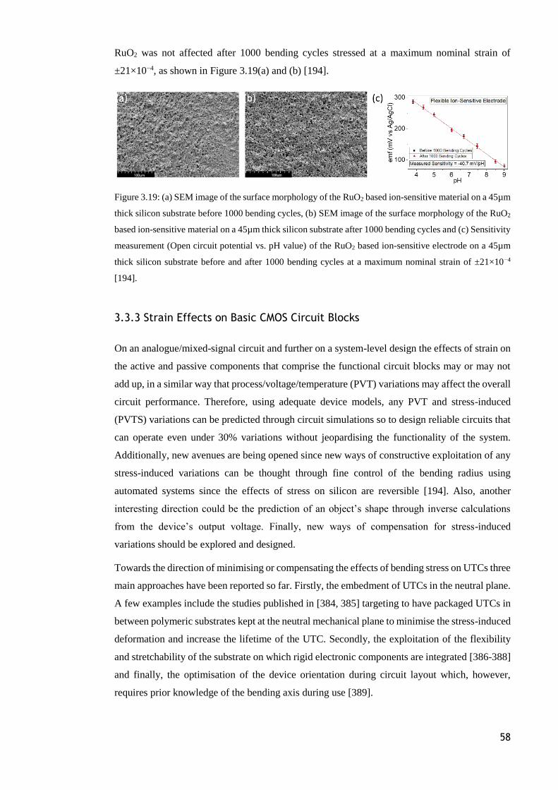
58
RuO2 was not affected after 1000 bending cycles stressed at a maximum nominal strain of
±21×10−4, as shown in Figure 3.19(a) and (b) [194].
Figure 3.19: (a) SEM image of the surface morphology of the RuO2 based ion-sensitive material on a 45µm
thick silicon substrate before 1000 bending cycles, (b) SEM image of the surface morphology of the RuO2
based ion-sensitive material on a 45µm thick silicon substrate after 1000 bending cycles and (c) Sensitivity
measurement (Open circuit potential vs. pH value) of the RuO2 based ion-sensitive electrode on a 45µm
thick silicon substrate before and after 1000 bending cycles at a maximum nominal strain of ±21×10−4
[194].
3.3.3 Strain Effects on Basic CMOS Circuit Blocks
On an analogue/mixed-signal circuit and further on a system-level design the effects of strain on
the active and passive components that comprise the functional circuit blocks may or may not
add up, in a similar way that process/voltage/temperature (PVT) variations may affect the overall
circuit performance. Therefore, using adequate device models, any PVT and stress-induced
(PVTS) variations can be predicted through circuit simulations so to design reliable circuits that
can operate even under 30% variations without jeopardising the functionality of the system.
Additionally, new avenues are being opened since new ways of constructive exploitation of any
stress-induced variations can be thought through fine control of the bending radius using
automated systems since the effects of stress on silicon are reversible [194]. Also, another
interesting direction could be the prediction of an object’s shape through inverse calculations
from the device’s output voltage. Finally, new ways of compensation for stress-induced
variations should be explored and designed.
Towards the direction of minimising or compensating the effects of bending stress on UTCs three
main approaches have been reported so far. Firstly, the embedment of UTCs in the neutral plane.
A few examples include the studies published in [384, 385] targeting to have packaged UTCs in
between polymeric substrates kept at the neutral mechanical plane to minimise the stress-induced
deformation and increase the lifetime of the UTC. Secondly, the exploitation of the flexibility
and stretchability of the substrate on which rigid electronic components are integrated [386-388]
and finally, the optimisation of the device orientation during circuit layout which, however,
requires prior knowledge of the bending axis during use [389].
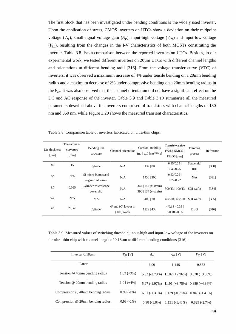
59
The first block that has been investigated under bending conditions is the widely used inverter.
Upon the application of stress, CMOS inverters on UTCs show a deviation on their midpoint
voltage (𝑉𝑀), small-signal voltage gain (𝐴𝑣), input-high voltage (𝑉𝐼𝐻) and input-low voltage
(𝑉𝐼𝐿), resulting from the changes in the I-V characteristics of both MOSTs constituting the
inverter. Table 3.8 lists a comparison between the reported inverters on UTCs. Besides, in our
experimental work, we tested different inverters on 20µm UTCs with different channel lengths
and orientations at different bending radii [316]. From the voltage transfer curve (VTC) of
inverters, it was observed a maximum increase of 4% under tensile bending on a 20mm bending
radius and a maximum decrease of 2% under compressive bending on a 20mm bending radius in
the 𝑉𝑀. It was also observed that the channel orientation did not have a significant effect on the
DC and AC response of the inverter. Table 3.9 and Table 3.10 summarise all the measured
parameters described above for inverters comprised of transistors with channel lengths of 180
nm and 350 nm, while Figure 3.20 shows the measured transient characteristics.
Table 3.8: Comparison table of inverters fabricated on ultra-thin chips.
Die thickness
[µm]
The radius of
curvature
[mm]
Bending test
structure Channel orientation
Carriers’ mobility
(µ𝑛 | µ𝑝) [cm2/Vs]
Transistors size
(W/L) NMOS |
PMOS [µm]
Thinning
process Reference
40 15 Cylinder N/A 132 | 80 0.35/0.25 |
0.45/0.25
Sequential
RIE [390]
30 N/A Si micro-bumps and
organic adhesive N/A 1450 | 300
0.22/0.22 |
0.22/0.22 N/A [391]
1.7 0.085 Cylinder/Microscope
cover slip N/A
342 | 158 (x-strain)
396 | 134 (y-strain) 300/13 | 100/13 SOI wafer [384]
0.3 N/A N/A N/A 400 | 70 40/500 | 40/500 SOI wafer [385]
20 20, 40 Cylinder 0o and 90o layout in
[100] wafer 1229 | 438
4/0.18 - 0.35 |
8/0.18 - 0.35 DBG [316]
Table 3.9: Measured values of switching threshold, input-high and input-low voltage of the inverters on
the ultra-thin chip with channel-length of 0.18µm at different bending conditions [316].
Inverter 0.18µm 𝑉𝑀 [V] 𝐴𝑣 𝑉𝐼𝐻 [V] 𝑉𝐼𝐿 [V]
Planar 1 6.09 1.148 0.852
Tension @ 40mm bending radius 1.03 (+3%) 5.92 (-2.79%) 1.182 (+2.96%) 0.878 (+3.05%)
Tension @ 20mm bending radius 1.04 (+4%) 5.97 (-1.97%) 1.191 (+3.75%) 0.889 (+4.34%)
Compression @ 40mm bending radius 0.99 (-1%) 6.01 (-1.31%) 1.139 (-0.78%) 0.840 (-1.41%)
Compression @ 20mm bending radius 0.98 (-2%) 5.98 (-1.8%) 1.131 (-1.48%) 0.829 (-2.7%)
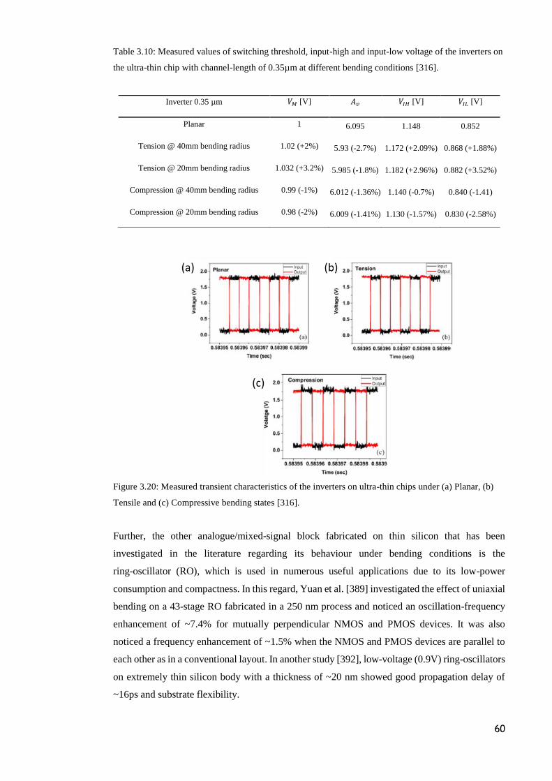
60
Table 3.10: Measured values of switching threshold, input-high and input-low voltage of the inverters on
the ultra-thin chip with channel-length of 0.35µm at different bending conditions [316].
Inverter 0.35 µm 𝑉𝑀 [V] 𝐴𝑣 𝑉𝐼𝐻 [V] 𝑉𝐼𝐿 [V]
Planar 1 6.095 1.148 0.852
Tension @ 40mm bending radius 1.02 (+2%) 5.93 (-2.7%) 1.172 (+2.09%) 0.868 (+1.88%)
Tension @ 20mm bending radius 1.032 (+3.2%) 5.985 (-1.8%) 1.182 (+2.96%) 0.882 (+3.52%)
Compression @ 40mm bending radius 0.99 (-1%) 6.012 (-1.36%) 1.140 (-0.7%) 0.840 (-1.41)
Compression @ 20mm bending radius 0.98 (-2%) 6.009 (-1.41%) 1.130 (-1.57%) 0.830 (-2.58%)
Figure 3.20: Measured transient characteristics of the inverters on ultra-thin chips under (a) Planar, (b)
Tensile and (c) Compressive bending states [316].
Further, the other analogue/mixed-signal block fabricated on thin silicon that has been
investigated in the literature regarding its behaviour under bending conditions is the
ring-oscillator (RO), which is used in numerous useful applications due to its low-power
consumption and compactness. In this regard, Yuan et al. [389] investigated the effect of uniaxial
bending on a 43-stage RO fabricated in a 250 nm process and noticed an oscillation-frequency
enhancement of ~7.4% for mutually perpendicular NMOS and PMOS devices. It was also
noticed a frequency enhancement of ~1.5% when the NMOS and PMOS devices are parallel to
each other as in a conventional layout. In another study [392], low-voltage (0.9V) ring-oscillators
on extremely thin silicon body with a thickness of ~20 nm showed good propagation delay of
~16ps and substrate flexibility.
61
Another very important and widely used analogue block is the current mirror, which mirrors the
current flowing from one branch to another. The mirroring action depends on the transistors’
aspect ratio, mobility and feeds current and as expected the output current will vary as these
parameters change upon externally applied stress on the thin silicon substrate. Towards the
investigation to overcome the piezoresistive effects of bending on CMOS current mirrors and
realise a stable circuit, in the study reported in [393] the transistors of the current mirror were
orthogonally oriented during layout and a UTC with a thickness of 20µm was realised using
ChipFilm technology. The investigation showed that the output current change (∆𝐼2 𝐼2⁄ ) can be
written as:
∆ 𝐼2
𝐼2=
𝜇2−𝜇1
𝜇2=
(𝜇0+𝛱2×𝜎)−(𝜇0+𝛱1×𝜎)
𝜇0+𝛱2×𝜎= (𝛱2 − 𝛱1) × 𝜎 (3.17)
where 𝜇, 𝛱 and 𝜎 are the mobility, piezoresistive coefficients and stress, respectively.
Another block, which probably is the most important in analogue/mixed-signal circuits is the
differential operational amplifier. In literature, there can be found a few studies on amplifiers
fabricated on flexible substrates using different semiconducting materials. For example, an a:Si
op-amp reported in [394] as part of a 4-bit DAC fabricated on glass substrate showed a voltage
gain of 40dB and a unity-gain frequency at ~50kHz. However, a:Si-based circuits suffer from
performance degradation due to the shift in threshold voltage of the devices. Further, an op-amp
based on IGZO fabricated on polyimide substrate showed an open-loop voltage gain of 18.7dB
and unity-gain frequency of 472 kHz with CMRR of 40dB [395]. The amplifier exhibited the
same behaviour after bending at 5mm bending radius showing the robustness of this n-type
material. However, it is still a challenge to have a p-type material and thus all circuits using IGZO
are designed using only NMOS devices. In another study, Ahn et al. [396] fabricated differential
amplifiers using ultra-thin single-crystal silicon ribbons on flexible plastic substrates. The
amplifiers that can be bent on a 6mm bending radius exhibited a voltage gain of 4dB and a unity-
gain frequency at ~100 kHz. Finally, another example is the study reported in [397] where a low-
noise amplifier (LNA) fabricated using a 180nm CMOS technology was thinned don to 90µm
and was integrated on a plastic substrate. However, the effects of bending-induced stresses were
not provided.
Finally, another important block that can be realised on UTCs and meet the performance
requirements is the memory cell. In this regard, a study published in [398] demonstrated a non-
volatile resistive random access memory (RRAM) array using Si-based transistors acting as the
switching element and a memristor on a polyimide-based substrate. Further, a static random
access memory (SRAM) presented in [332] was tested under different bending conditions with
bending axis similar to the that of the flow of current showing that the fabricated transistors
exhibit a variation in their threshold voltage. Finally, improvements have been reported in
memory cells on UTCs through simultaneous roll-transfer and interconnection using a roll-to-
62
plate anisotropic conductive film packaging as reported in [399], where the fabricated Si-based
flexible NAND flash memory showed adequate performance in terms of 𝐼𝑜𝑛 𝐼𝑜𝑓𝑓⁄ ratio (>102 at
𝑉𝑟𝑒𝑎𝑑), long retention (>104 seconds) and reproducible endurance (>103 switching cycles).
3.4 Compact Modelling of CMOS-Based Devices and Sensors on
Bendable Ultra-Thin Chips
The metal oxide semiconductor transistors (MOSTs) are the fundamental building block of
integrated circuits. Nowadays, integrated MOST devices are much greater in numbers than
bipolar transistors. The main reason for that is the continuous decrease of the MOSTs length
which results in a continuous increase in the transistors’ speed, in competition with the bipolar
technology. And since the BICMOS technology is always more expensive than CMOS, the latter
is usually preferred when it is compared with the former in terms of cost and performance.
The prediction of analogue/mixed-signal circuit performance by means of simple expressions is
important. Therefore, there is a need for simple models that can describe the small-signal
operation of each transistor, which can be used to simulate the circuit performance using
conventional simulators. In these simulators, much more accurate and more complicated models
can be subsequently used to verify the circuit performance.
3.4.1 Modelling of Bending Stress Effect on Metal Oxide Semiconductor Field-
Effect Transistors
An n-type MOST device is a 4-terminal device (Gate, Source, Drain, Bulk) which upon
application of a positive voltage at the Gate terminal with respect to the Source (𝑉𝐺𝑆) creates a
negative-charged inversion layer. The inversion layer connects the n+ doped Source and Drain
terminals in a non-homogeneous way. Application of positive 𝑉𝐷𝑆 causes some current 𝐼𝐷𝑆 to
flow from Drain to Source. Zooming deeper into the channel region, in the p-n junction between
the n+ doped regions and the p-type substrate, a depletion layer is created which gives rise to the
depletion layer capacitance (𝐶𝐷 =휀𝑆𝑖
𝑡𝑆𝑖⁄ ) which normally is about one-third of the oxide
capacitance (𝐶𝑜𝑥 =휀𝑜𝑥
𝑡𝑜𝑥⁄ ). It should be noted, that the inversion layer is as much coupled to
the Gate through 𝐶𝑜𝑥 as it is to the Bulk terminal through 𝐶𝐷. Therefore, a change in the
conductivity of the channel (and thus the 𝐼𝐷𝑆) caused by a change in the Gate voltage will be
caused similarly by a change in the Bulk voltage. The width of the depletion region mostly
depends on the bulk doping levels (𝑁𝐵) and the voltage across it, described the following
equation:

63
𝑡𝑆𝑖 = √2 𝑆𝑖(𝜑−𝑉𝐵𝐷)
𝑞𝑁𝐵 (3.18)
where 𝜑 is the junction built-in voltage and 𝑉𝐵𝐷 is the Drain-Bulk voltage. Finally, it should be
noted that the doping level is not the same for pMOS and nMOS devices since pMOS transistors
are implemented on separate n-wells which always have higher doping levels than the common
p-substrate on which all nMOS transistors are implemented. Therefore, pMOS devices have
usually higher 𝐶𝐷 compared to nMOS.
Once the inversion layer is formed, the 𝐼𝐷𝑆 starts flowing as soon as 𝑉𝐺𝑆 exceeds the threshold
voltage (𝑉𝑇𝐻). As 𝑉𝐺𝑆 increases above 𝑉𝑇𝐻 the current increases in a nonlinear way. Also, at a
fixed 𝑉𝐺𝑆 as 𝑉𝐷𝑆 increases the current will initially increase linearly until the point (𝑉𝐷𝑆 = 𝑉𝐺𝑆 −
𝑉𝑇𝐻) where 𝐼𝐷𝑆 levels off towards a nearly constant value, entering the saturation region. In the
linear region, the MOST device operates as a voltage-controlled resistor with resistance value
given as:
𝑅𝑜𝑛 =1
𝜇𝑒𝑓𝑓𝐶𝑜𝑥
𝑊𝑒𝑓𝑓
𝐿𝑒𝑓𝑓(𝑉𝐺𝑆−𝑉𝑇𝐻)
(3.19)
where 𝑊𝑒𝑓𝑓 =𝑊𝑑𝑟𝑎𝑤𝑛
𝑁𝐹+ 𝑋𝑊 − 2𝑑𝑊 and 𝐿𝑒𝑓𝑓 = 𝐿𝑑𝑟𝑎𝑤𝑛 + 𝑋𝐿 − 2𝑑𝐿. The parameter 𝑁𝐹 is the
number of fingers and the parameters 𝑋𝑊 and 𝑋𝐿 are parameters which account the channel
width and length offset due to masking and etch effects, respectively, and can be considered 0
for initial calculations. Finally, the parameters 𝑑𝑊 and 𝑑𝐿 are parameters modelled in the BSIM4
model [400]. The formula for effective mobility (𝜇𝑒𝑓𝑓) can also be found in [400], also used in
BSIM6 model (mobMode=3), also given in Table 3.11. The equation above shows a direct
influence of 𝑉𝐺𝑆 on the 𝑅𝑜𝑛. However, the influence of 𝑉𝐵𝑆 cannot be directly observed as it is
embedded in the threshold voltage, given in the equation below:
𝑉𝑇𝐻 = 𝑉𝑇𝐻0 + 𝛾[√𝛷𝑆 − 𝑉𝐵𝑆 − √𝛷𝑆] (3.20)
where 𝑉𝑇𝐻0 is the threshold voltage at 𝑉𝐵𝑆 = 0𝑉, 𝛾 is a technology-dependent body bias
coefficient parameter given by 𝛾 =√2𝑞 𝑆𝑖𝑁𝑠𝑢𝑏𝑠𝑡𝑟𝑎𝑡𝑒
𝐶𝑜𝑥, and 𝛷𝑆 is the surface potential. From the
equation above, it can be seen that an increase in 𝑉𝐵𝑆 will cause an increase in the width of the
depletion region under the channel area increasing also the 𝑉𝑇𝐻 and eventually decreasing the
𝐼𝐷𝑆. In the linear region, the current for Drain to Source can be modelled as:
𝐼𝐷𝑆(𝑙𝑖𝑛𝑒𝑎𝑟) = 𝜇𝑒𝑓𝑓𝐶𝑜𝑥𝑊𝑒𝑓𝑓
𝐿𝑒𝑓𝑓[(𝑉𝐺𝑆 − 𝑉𝑇𝐻)𝑉𝐷𝑆 −
𝑉𝐷𝑆2
2] (1 − 𝜆𝑉𝐷𝑆) (3.21)
Furthermore, MOST devices are also used as amplifiers when they are operating in the saturation
region (𝑉𝐷𝑆 ≥ 𝑉𝐺𝑆 − 𝑉𝑇𝐻) since their transconductance increases and they can generate a gain.

64
From the transfer characteristic (𝐼𝐷𝑆 − 𝑉𝐺𝑆) of the MOST device we can distinguish three regions
of operation when the transistor fulfils the condition of 𝑉𝐷𝑆 ≥ 𝑉𝐺𝑆 − 𝑉𝑇𝐻, i.e. the weak inversion,
the strong inversion (or square-law region) and the velocity saturation. Below is given the
detailed derivation of the main equations that comprise the MOST model described by the
BSIM6 model [401].
In the weak inversion, the MOSTs operate at very low currents, which is mainly due to diffusion
of charge carriers. The model in this region contains an exponential rather than a square-law
characteristic given by:
𝐼𝐷𝑆(𝑤.𝑖.) = 𝐼𝐷𝑆0𝑊𝑒𝑓𝑓
𝐿𝑒𝑓𝑓𝑒𝑥𝑝
𝑉𝐺𝑆𝑛𝑘𝑇/𝑞⁄
(3.22)
where 𝐼𝐷𝑆0 is the current at 𝑉𝐺𝑆 = 𝑉𝑇𝐻, 𝑘𝑇
𝑞 is the thermal voltage and 𝑛 = 1 +
𝐶𝐷
𝐶𝑜𝑥 is the slope
factor in the charge based model which depends on the biasing voltages. In the weak inversion,
the transconductance of the transistor, which is the derivative of the current with respect to 𝑉𝐺𝑆,
can be written as:
𝑔𝑚(𝑤.𝑖.) =𝐼𝐷𝑆(𝑤.𝑖.)
𝑛𝑘𝑇/𝑞 (3.23)
When a MOST device is operating in the strong inversion or square-law region, the current can
be expressed as:
𝐼𝐷𝑆(𝑠.𝑖.) = 𝜇𝑒𝑓𝑓𝐶𝑜𝑥1
2𝑛
𝑊𝑒𝑓𝑓
𝐿𝑒𝑓𝑓(𝑉𝐺𝑆 − 𝑉𝑇𝐻)2 (3.24)
While the transconductance can be written as:
𝑔𝑚(𝑠.𝑖.) =2𝐼𝐷𝑆(𝑠.𝑖.)
𝑉𝐺𝑆−𝑉𝑇𝐻= 𝜇𝑒𝑓𝑓𝐶𝑜𝑥
1
𝑛
𝑊𝑒𝑓𝑓
𝐿𝑒𝑓𝑓(𝑉𝐺𝑆 − 𝑉𝑇𝐻) (3.25)
From the equation above it can be seen that at a fixed 𝑉𝐺𝑆 − 𝑉𝑇𝐻 the transconductance is
proportional to the current. Furthermore, the small-signal model of a MOST also has a finite
output impedance, which can be described as:
𝑟𝐷𝑆 =𝑉𝐸𝐿
𝐼𝐷𝑆=
1
𝜆𝐼𝐷𝑆 (3.26)
where 𝑉𝐸 is the Early voltage and 𝜆 is the parameter expressing the channel length modulation
showing that current is increasing somewhat for an increased 𝑉𝐷𝑆. The gain that can be provided
by a single transistor biased at a constant current in a common-source configuration can be
expressed in terms of the transconductance and the output impedance (𝑟𝐷𝑆) as:

65
𝐴𝑣 = −𝑔𝑚𝑟𝐷𝑆 = −2𝑉𝐸𝐿
𝑉𝐺𝑆−𝑉𝑇𝐻 (3.27)
From the equation above it can also be seen that to obtain a large gain the channel length (𝐿)
should be large while the 𝑉𝐺𝑆 − 𝑉𝑇𝐻 should be as small as possible. Finally, the crossover point
between weak inversion and strong inversion can be obtained by equating the Equations 3.23 and
3.25:
(𝑉𝐺𝑆 − 𝑉𝑇𝐻)𝑤.𝑖. 𝑡𝑜 𝑠.𝑖. = 2𝑛𝑘𝑇
𝑞 (3.28)
The current at the crossover point can be written as:
(𝐼𝐷𝑆)𝑤.𝑖. 𝑡𝑜 𝑠.𝑖. = 𝜇𝑒𝑓𝑓𝐶𝑜𝑥1
2𝑛
𝑊𝑒𝑓𝑓
𝐿𝑒𝑓𝑓(2𝑛
𝑘𝑇
𝑞)2 (3.29)
The transition current, (𝐼𝐷𝑆)𝑤.𝑖. 𝑡𝑜 𝑠.𝑖., depends on the area of the transistor (𝑊
𝐿). The smooth
transition between weak and strong inversion can therefore be summarised and modelled using
the BSIM6 model with the following equations:
𝐼𝐷𝑆(𝑠.𝑖.)= 𝜇𝑒𝑓𝑓𝐶𝑜𝑥
1
2𝑛
𝑊𝑒𝑓𝑓
𝐿𝑒𝑓𝑓[(𝑉𝐺𝑆 − 𝑉𝑇𝐻)𝑤.𝑖. 𝑡𝑜 𝑠.𝑖.]
2[𝑙𝑛(1 + 𝑒𝑉)]2 (3.30)
where the parameter 𝑉 represents the ratio between the overdrive voltage divided by the
crossover overdrive voltage:
𝑉 =𝑉𝐺𝑆−𝑉𝑇𝐻
(𝑉𝐺𝑆−𝑉𝑇𝐻)𝑤.𝑖. 𝑡𝑜 𝑠.𝑖. (3.31)
For small 𝑉, 𝑙𝑛(1 + 𝑒𝑉) ≅ 𝑒𝑉:
𝐼𝐷𝑆 = 𝜇𝑒𝑓𝑓𝐶𝑜𝑥1
2𝑛
𝑊𝑒𝑓𝑓
𝐿𝑒𝑓𝑓[(𝑉𝐺𝑆 − 𝑉𝑇𝐻)𝑤.𝑖. 𝑡𝑜 𝑠.𝑖.]
2𝑒𝑥𝑝 (𝑉𝐺𝑆−𝑉𝑇𝐻
𝑛𝑘𝑇/𝑞) (3.32)
For large 𝑉, 𝑙𝑛(1 + 𝑒𝑉) ≅ 𝑉, and based on Equation 3.31:
𝐼𝐷𝑆 = 𝜇𝑒𝑓𝑓𝐶𝑜𝑥1
2𝑛
𝑊𝑒𝑓𝑓
𝐿𝑒𝑓𝑓[𝑉𝐺𝑆 − 𝑉𝑇𝐻]2 (3.33)
Finally, the transconductance can be calculated as the derivative of the current:
𝐺𝑚 =𝑔𝑚
𝐼𝐷𝑆
𝑛𝑘𝑇
𝑞=
1−𝑒−√𝐼𝐶
√𝐼𝐶 (3.34)
where the parameter 𝐼𝐶 =𝐼𝐷𝑆
(𝐼𝐷𝑆)𝑤.𝑖. 𝑡𝑜 𝑠.𝑖.. Therefore, for large 𝐼𝐶:
𝐺𝑚 =1
√𝐼𝐶 (3.35)

66
And for small 𝐼𝐶:
𝐺𝑚 = 1 −√𝐼𝐶
2 (3.36)
As the current further increases, the MOST devices move from strong inversion towards the
velocity saturation region, where most of the charge carriers are moving through the channel at
maximum speed (𝑣𝑠𝑎𝑡) resulting in a linear increase of current with the drive voltage and a
levelling of the transconductance. Because of the high electric field in the channel region, the
electrons collide with each other increasing their speed. The expression that models the current
in the velocity saturation region is given as:
𝐼𝐷𝑆(𝑣.𝑠.)= 𝑊𝑒𝑓𝑓𝐶𝑜𝑥𝑣𝑠𝑎𝑡(𝑉𝐺𝑆 − 𝑉𝑇𝐻) (3.37)
From the equation above, it can be seen a linear dependence of the current versus 𝑉𝐺𝑆. The
transconductance of the transistor, which is the maximum achievable transconductance, can be
written as:
𝑔𝑚(𝑣.𝑠.) = 𝑊𝑒𝑓𝑓𝐶𝑜𝑥𝑣𝑠𝑎𝑡 (3.38)
Therefore, the 𝑔𝑚(𝑣.𝑠.) has become a constant and only depends on the width (𝑊) of the channel,
the technology parameter 𝐶𝑜𝑥 and physics (𝑣𝑠𝑎𝑡). However, for this reason, the velocity
saturation region of operation is not preferred during the design of circuits since the
transconductance cannot further increase as the power consumption increases, and thus
transistors are normally biased at 𝑉𝐺𝑆 values to keep the devices in the strong inversion but close
to the saturation velocity region.
The linearization of current versus 𝑉𝐺𝑆 can also be expressed by a parameter 𝜃, termed as velocity
saturation coefficient, which if introduced in the current expression of the strong inversion,
initially given in Equation 3.24, the current in the velocity saturation can be written as:
𝐼𝐷𝑆(𝑣.𝑠) =𝜇𝑒𝑓𝑓𝐶𝑜𝑥
1
2𝑛
𝑊𝑒𝑓𝑓
𝐿𝑒𝑓𝑓(𝑉𝐺𝑆−𝑉𝑇𝐻)2
1+𝜃(𝑉𝐺𝑆−𝑉𝑇𝐻) (3.39)
From the equation above it can be seen that at large (𝑉𝐺𝑆 − 𝑉𝑇𝐻) the expression resembles the
one in Equation 3.24 but with the parameter 𝜃 at the denominator. This parameter is mainly used
to lump all physical phenomena causing the linearization of current in the velocity saturation
region, such as the effect of vertical field (𝐸𝐶) across the oxide. As a result, the transconductance
can be derived by taking the derivative of the current, given as:
𝑔𝑚(𝑣.𝑠.) = 𝜇𝑒𝑓𝑓𝐶𝑜𝑥1
2𝑛
1
𝜃
𝑊𝑒𝑓𝑓
𝐿𝑒𝑓𝑓 (3.40)

67
The equation above should be equal to Equation 3.38 and thus at large (𝑉𝐺𝑆 − 𝑉𝑇𝐻):
𝜃 =1
𝐿
𝜇𝑒𝑓𝑓
2𝑛𝑣𝑠𝑎𝑡 (3.41)
Thus, an inverse proportionality between the parameter 𝜃 and the channel length (𝐿) is observed.
Finally, by equating the transconductance in strong inversion and velocity saturation the
transition voltage drive between strong inversion and velocity saturation can be obtained as:
(𝑉𝐺𝑆 − 𝑉𝑇𝐻)𝑠.𝑖. 𝑡𝑜 𝑣.𝑠. =1
𝜃≅ 2𝑛𝐿𝑒𝑓𝑓
𝑣𝑠𝑎𝑡
𝜇𝑒𝑓𝑓 (3.42)
It is clear from the equation above that the transition drive voltage between strong inversion and
velocity saturation is not constant as it depends on the channel length. Using the transition drive
voltage, we can also write the transition current as:
(𝐼𝐷𝑆)𝑠.𝑖. 𝑡𝑜 𝑣.𝑠. = 𝜇𝑒𝑓𝑓𝐶𝑜𝑥1
2𝑛𝑊𝑒𝑓𝑓𝐿𝑒𝑓𝑓 [
2𝑛𝑣𝑠𝑎𝑡
𝜇𝑛]2 (3.43)
Finally, the expression for the transconductance covering both the strong inversion and the
velocity saturation regions is:
1
𝑔𝑚=
1
𝑔𝑚(𝑠.𝑖.)+
1
𝑔𝑚(𝑣.𝑠.) (3.44)
As the frequencies increase, the parasitic capacitance of a MOST device starts to play a
significant role. First, the total oxide capacitance (𝐶𝑜𝑥(𝑡𝑜𝑡𝑎𝑙) = 𝑊𝑒𝑓𝑓𝐿𝐶𝑜𝑥) which overlaps both
the Source and Drain wells giving rise to two more parasitic capacitance (𝐶𝑂𝑆 and 𝐶𝑂𝐷). Also,
the depletion capacitance to the substrate (𝐶𝐶𝐵) formed by the depletion layer of the channel and
the capacitances between Source-to-Bulk and Drain-to-Bulk (𝐶𝑆𝐵 and 𝐶𝐷𝐵), all should be
considered. We can also define the capacitance 𝐶𝐺𝑆 =2
3𝐶𝑜𝑥(𝑡𝑜𝑡𝑎𝑙) =
2
3𝑊𝑒𝑓𝑓𝐿𝐶𝑜𝑥 and we can
assume that the channel has almost vanished at the side of the Drain terminal causing a reduction
of the 𝐶𝑜𝑥(𝑡𝑜𝑡𝑎𝑙) by a factor 2/3. Finally, the parameter 𝑓𝑇, which is a figure-of-merit and can be
described as the frequency at which the output current (𝑖𝐷𝑆) is equal to the input current (𝑖𝐺𝑆),
can be written as:
𝑓𝑇 =𝑔𝑚
2𝜋𝐶𝐺𝑆=
1
2𝜋
3
2𝑛
𝜇𝑒𝑓𝑓
𝐿2(𝑉𝐺𝑆 − 𝑉𝑇𝐻) (3.45)
It is therefore obvious that 𝑓𝑇 is defined by the transconductance and the 𝐶𝐺𝑆 and by further
expanding these parameters it can be seen that 𝑓𝑇 is eventually proportional to the (𝑉𝐺𝑆 − 𝑉𝑇𝐻)
and 𝜇𝑛 and inversely proportional to 𝐿2. It is worth mentioning that from the equation above it
can be seen that for high-frequency design the channel length should be the lowest possible while
the driving voltage (𝑉𝐺𝑆 − 𝑉𝑇𝐻) should be large, which is the exact opposite of what the design
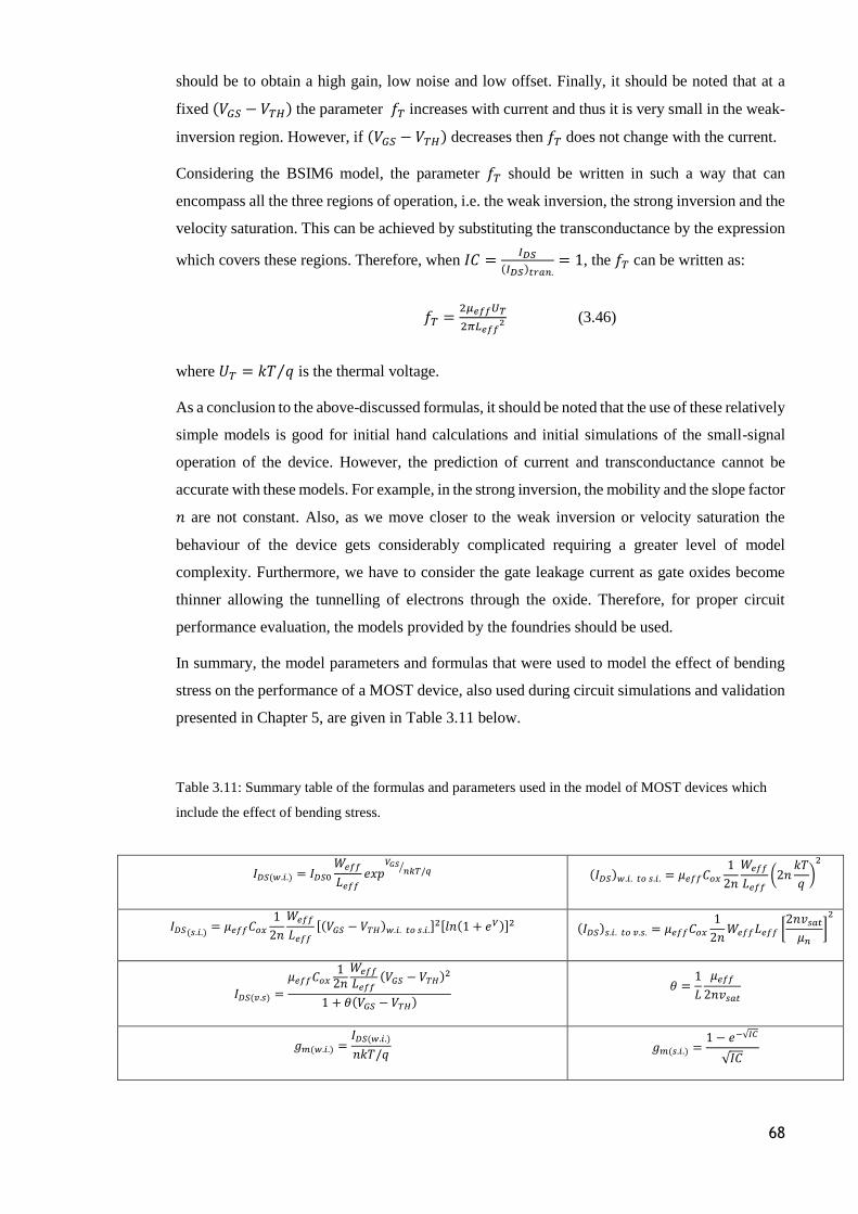
68
should be to obtain a high gain, low noise and low offset. Finally, it should be noted that at a
fixed (𝑉𝐺𝑆 − 𝑉𝑇𝐻) the parameter 𝑓𝑇 increases with current and thus it is very small in the weak-
inversion region. However, if (𝑉𝐺𝑆 − 𝑉𝑇𝐻) decreases then 𝑓𝑇 does not change with the current.
Considering the BSIM6 model, the parameter 𝑓𝑇 should be written in such a way that can
encompass all the three regions of operation, i.e. the weak inversion, the strong inversion and the
velocity saturation. This can be achieved by substituting the transconductance by the expression
which covers these regions. Therefore, when 𝐼𝐶 =𝐼𝐷𝑆
(𝐼𝐷𝑆)𝑡𝑟𝑎𝑛.= 1, the 𝑓𝑇 can be written as:
𝑓𝑇 =2𝜇𝑒𝑓𝑓𝑈𝑇
2𝜋𝐿𝑒𝑓𝑓2 (3.46)
where 𝑈𝑇 = 𝑘𝑇 𝑞⁄ is the thermal voltage.
As a conclusion to the above-discussed formulas, it should be noted that the use of these relatively
simple models is good for initial hand calculations and initial simulations of the small-signal
operation of the device. However, the prediction of current and transconductance cannot be
accurate with these models. For example, in the strong inversion, the mobility and the slope factor
𝑛 are not constant. Also, as we move closer to the weak inversion or velocity saturation the
behaviour of the device gets considerably complicated requiring a greater level of model
complexity. Furthermore, we have to consider the gate leakage current as gate oxides become
thinner allowing the tunnelling of electrons through the oxide. Therefore, for proper circuit
performance evaluation, the models provided by the foundries should be used.
In summary, the model parameters and formulas that were used to model the effect of bending
stress on the performance of a MOST device, also used during circuit simulations and validation
presented in Chapter 5, are given in Table 3.11 below.
Table 3.11: Summary table of the formulas and parameters used in the model of MOST devices which
include the effect of bending stress.
𝐼𝐷𝑆(𝑤.𝑖.) = 𝐼𝐷𝑆0
𝑊𝑒𝑓𝑓
𝐿𝑒𝑓𝑓𝑒𝑥𝑝
𝑉𝐺𝑆𝑛𝑘𝑇/𝑞⁄
(𝐼𝐷𝑆)𝑤.𝑖. 𝑡𝑜 𝑠.𝑖. = 𝜇𝑒𝑓𝑓𝐶𝑜𝑥
1
2𝑛
𝑊𝑒𝑓𝑓
𝐿𝑒𝑓𝑓(2𝑛
𝑘𝑇
𝑞)2
𝐼𝐷𝑆(𝑠.𝑖.)= 𝜇𝑒𝑓𝑓𝐶𝑜𝑥
1
2𝑛
𝑊𝑒𝑓𝑓
𝐿𝑒𝑓𝑓
[(𝑉𝐺𝑆 − 𝑉𝑇𝐻)𝑤.𝑖. 𝑡𝑜 𝑠.𝑖.]2[𝑙𝑛(1 + 𝑒𝑉)]2 (𝐼𝐷𝑆)𝑠.𝑖. 𝑡𝑜 𝑣.𝑠. = 𝜇𝑒𝑓𝑓𝐶𝑜𝑥
1
2𝑛𝑊𝑒𝑓𝑓𝐿𝑒𝑓𝑓 [
2𝑛𝑣𝑠𝑎𝑡
𝜇𝑛]2
𝐼𝐷𝑆(𝑣.𝑠) =
𝜇𝑒𝑓𝑓𝐶𝑜𝑥12𝑛
𝑊𝑒𝑓𝑓
𝐿𝑒𝑓𝑓(𝑉𝐺𝑆 − 𝑉𝑇𝐻)2
1 + 𝜃(𝑉𝐺𝑆 − 𝑉𝑇𝐻)
𝜃 =1
𝐿
𝜇𝑒𝑓𝑓
2𝑛𝑣𝑠𝑎𝑡
𝑔𝑚(𝑤.𝑖.) =𝐼𝐷𝑆(𝑤.𝑖.)
𝑛𝑘𝑇/𝑞 𝑔𝑚(𝑠.𝑖.) =
1 − 𝑒−√𝐼𝐶
√𝐼𝐶

69
𝑔𝑚(𝑣.𝑠.) = 𝜇𝑒𝑓𝑓𝐶𝑜𝑥
1
2𝑛
1
𝜃
𝑊𝑒𝑓𝑓
𝐿𝑒𝑓𝑓 𝑛 = 1 +
𝐶𝐷
𝐶𝑜𝑥
𝑓𝑇 =2𝜇𝑒𝑓𝑓𝑈𝑇
2𝜋𝐿𝑒𝑓𝑓2 𝐼𝐶 =
𝐼𝐷𝑆
(𝐼𝐷𝑆)𝑤.𝑖. 𝑡𝑜 𝑠.𝑖.
𝑊𝑒𝑓𝑓 =𝑊𝑑𝑟𝑎𝑤𝑛
𝑁𝐹+ 𝑋𝑊 − 2𝑑𝑊 𝐿𝑒𝑓𝑓 = 𝐿𝑑𝑟𝑎𝑤𝑛 + 𝑋𝐿 − 2𝑑𝐿
𝜇𝑒𝑓𝑓 =
𝜇0 [1 − 𝑒(−
𝐿𝑒𝑓𝑓
𝐿𝑃)]
1 + (𝜇𝐴 + 𝜇𝐶𝑉𝐵𝑆)𝑉𝐺𝑆 + 2𝑉𝑇𝐻
𝑡𝑜𝑥+ 𝜇𝐵 (
𝑉𝐺𝑆 + 2𝑉𝑇𝐻
𝑡𝑜𝑥)2
+ 𝜇𝐷 (𝑉𝑇𝐻𝑡𝑜𝑥
𝑉𝐺𝑆 + 2𝑉𝑇𝐻)2 𝑉𝑇𝐻 = 𝑉𝑇𝐻0 + 𝛾[√𝛷𝑆 − 𝑉𝐵𝑆 − √𝛷𝑆]
As discussed in Section 3.3.2, the effects of mechanical deformation due to uniaxial or biaxial
bending stress change the semiconductor properties by changing the band structure and the
effective carrier masses, resulting in an effective change in threshold voltage and carrier mobility.
The expression for the strain-induced threshold voltage can be written as [402]:
𝑉𝑇𝐻(휀) = 𝑉𝑇𝐻 + ∆𝑉𝑇𝐻(휀) (3.47)
where 𝑉𝑇𝐻 is the threshold voltage before the application of strain given in Equation 3.20 and
∆𝑉𝑇𝐻(휀) is the change in the threshold voltage upon application of uniaxial strain, given as [402]:
∆𝑉𝑇𝐻(휀) =𝑚−1
𝑞[∆𝐸𝑔(휀)] (3.48)
where ∆𝐸𝑔(휀)(≅ −6.19 × 휀) is the change in energy gap upon application of uniaxial strain on
[110] direction and 𝑚 is the body-effect coefficient. Therefore, substituting Equations 3.4 and
3.20 the equation describing the threshold voltage upon application of strain can be expressed as:
𝑉𝑇𝐻(𝑅𝑐) = 𝑉𝑇𝐻0 + 𝛾[√𝛷𝑆 − 𝑉𝐵𝑆 − √𝛷𝑆] −𝑚−1
𝑞[6.19 (𝑐 +
𝑦−𝑡𝑏
𝑅𝑐)] (3.49)
where 𝑡𝑏 is given in Equation 3.5.
Furthermore, based on the effective mobility equation given in Table 3.11, the Equations 3.15
and 3.16, the Equation 3.49 and the relationship between stress and strain based on Hook’s Law
(𝜎 = 𝐸휀, where 𝜎 is the stress), the equations describing the channel-orientation dependent
mobility upon application of strain are:
𝜇𝑒𝑓𝑓(𝑅𝑐)|0𝑜 =
𝜇0[1−𝑒(−
𝐿𝑒𝑓𝑓𝐿𝑃
)]
1+(𝜇𝐴+𝜇𝐶𝑉𝐵𝑆)𝑉𝐺𝑆+2𝑉𝑇𝐻(𝑅𝑐)
𝑡𝑜𝑥+𝜇𝐵(
𝑉𝐺𝑆+2𝑉𝑇𝐻(𝑅𝑐)
𝑡𝑜𝑥)2
+𝜇𝐷(𝑉𝑇𝐻(𝑅𝑐)𝑡𝑜𝑥
𝑉𝐺𝑆+2𝑉𝑇𝐻)2 [1 + (
𝛱𝑆+𝛱44
2)𝐸(𝑐 +
𝑦−𝑡𝑏
𝑅𝑐)]
(3.50)

70
𝜇𝑒𝑓𝑓(𝑅𝑐)|90𝑜 =
𝜇0[1−𝑒(−
𝐿𝑒𝑓𝑓𝐿𝑃
)]
1+(𝜇𝐴+𝜇𝐶𝑉𝐵𝑆)𝑉𝐺𝑆+2𝑉𝑇𝐻(𝑅𝑐)
𝑡𝑜𝑥+𝜇𝐵(
𝑉𝐺𝑆+2𝑉𝑇𝐻(𝑅𝑐)
𝑡𝑜𝑥)2
+𝜇𝐷(𝑉𝑇𝐻(𝑅𝑐)𝑡𝑜𝑥
𝑉𝐺𝑆+2𝑉𝑇𝐻)2 [1 + (
𝛱𝑆−𝛱44
2) 𝐸(𝑐 +
𝑦−𝑡𝑏
𝑅𝑐)]
(3.51)
Finally, upon bending the effective width and length of the transistors change since the chip is
not planar anymore. Therefore, the effective width and length become the effective arc width and
arc length, which depends on the bending radius, 𝑅𝑐. Based on the general equation used for the
calculation of the arc length of a circle and based on the equations for the effective width and
length of a transistor given in in Table 3.11, the MOST’s arc width (Arc 𝑊𝑒𝑓𝑓) and arc length
(Arc 𝐿𝑒𝑓𝑓) can be written as:
Arc 𝑊𝑒𝑓𝑓 = 2 × 𝑅𝑐 × 𝑎𝑟𝑐𝑠𝑖𝑛 (𝑊𝑑𝑟𝑎𝑤𝑛
𝑁𝐹+𝑋𝑊−2𝑑𝑊
2𝑅𝑐) (3.52)
Arc 𝐿𝑒𝑓𝑓 = 2 × 𝑅𝑐 × 𝑎𝑟𝑐𝑠𝑖𝑛 (𝐿𝑑𝑟𝑎𝑤𝑛+𝑋𝐿−2𝑑𝐿
2𝑅𝑐) (3.53)
It should be noted, that when the bending radius is infinite (i.e. the chip is at the planar condition)
the equations given in Table 3.11 should be used.
3.4.2 Modelling of Bending Stress Effect on Ion-Sensitive Field-Effect
Transistors
The ion-sensitive field-effect transistor (ISFET) consists of an ion-sensitive layer capable for
label-free detection of H+ ions deposited on top of a MOSFET structure, as discussed in Chapter
2. The operation of ISFET is similar to a MOST device except that the ion-sensitive Gate is
exposed to a chemical solution and influenced by a reference potential through a chemically-
inert reference electrode (R.E.). Since ISFETs are essentially MOST devices they can be
monolithically integrated along with recording amplifiers and ADCs to reduce the off-chip
parasitics and interference. CMOS-compatible ISFETs are fabricated by extending the intrinsic
polysilicon Gate (IPG) through a stack of metal layers to the surface of the chip on top of which
the ion-sensitive layer is subsequently deposited. Every ion-sensitive material exhibits a different
sensitivity to H+ ions which can be expressed as a function of the double-layer capacitance and
the intrinsic buffer capacity of the oxide.
The physicochemical macro-models of ISFETs reported in several studies [403-405] consider
ISFETs as two stages coupled together, i.e. the electrochemical stage (the electrode-electrolyte
interface) and the electronic stage (the MOST device), as shown in Figure 3.21. However, none
of the above-referenced models has considered the effects of external mechanical bending. For
the first stage, regarding the bending of the ion-sensitive layer, it was experimentally observed
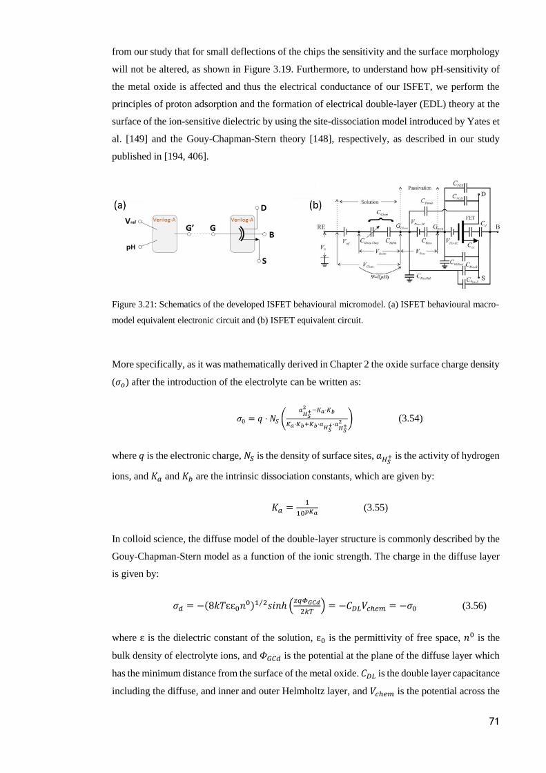
71
from our study that for small deflections of the chips the sensitivity and the surface morphology
will not be altered, as shown in Figure 3.19. Furthermore, to understand how pH-sensitivity of
the metal oxide is affected and thus the electrical conductance of our ISFET, we perform the
principles of proton adsorption and the formation of electrical double-layer (EDL) theory at the
surface of the ion-sensitive dielectric by using the site-dissociation model introduced by Yates et
al. [149] and the Gouy-Chapman-Stern theory [148], respectively, as described in our study
published in [194, 406].
Figure 3.21: Schematics of the developed ISFET behavioural micromodel. (a) ISFET behavioural macro-
model equivalent electronic circuit and (b) ISFET equivalent circuit.
More specifically, as it was mathematically derived in Chapter 2 the oxide surface charge density
(𝜎𝑜) after the introduction of the electrolyte can be written as:
𝜎0 = 𝑞 · 𝑁𝑆 (𝑎
𝐻𝑆+
2 −𝐾𝑎·𝐾𝑏
𝐾𝑎·𝐾𝑏+𝐾𝑏·𝑎𝐻𝑆
+·𝑎𝐻𝑆
+2 ) (3.54)
where 𝑞 is the electronic charge, 𝑁𝑆 is the density of surface sites, 𝑎𝐻𝑆+ is the activity of hydrogen
ions, and 𝐾𝑎 and 𝐾𝑏 are the intrinsic dissociation constants, which are given by:
𝐾𝑎 =1
10𝑝𝐾𝑎 (3.55)
In colloid science, the diffuse model of the double-layer structure is commonly described by the
Gouy-Chapman-Stern model as a function of the ionic strength. The charge in the diffuse layer
is given by:
𝜎𝑑 = −(8𝑘𝑇ɛɛ0𝑛0)1 2⁄ 𝑠𝑖𝑛ℎ (
𝑧𝑞𝛷𝐺𝐶𝑑
2𝑘𝑇) = −𝐶𝐷𝐿𝑉𝑐ℎ𝑒𝑚 = −𝜎0 (3.56)
where ɛ is the dielectric constant of the solution, ɛ0 is the permittivity of free space, 𝑛0 is the
bulk density of electrolyte ions, and 𝛷𝐺𝐶𝑑 is the potential at the plane of the diffuse layer which
has the minimum distance from the surface of the metal oxide. 𝐶𝐷𝐿 is the double layer capacitance
including the diffuse, and inner and outer Helmholtz layer, and 𝑉𝑐ℎ𝑒𝑚 is the potential across the

72
double-layer capacitance. Differentiation of Equation 3.56 gives the series capacitance of the
diffuse layer and the outer Helmholtz layer:
𝐶𝐷𝑖𝑓𝑓𝑢𝑠𝑒 =𝜕𝜎𝑑
𝜕𝛷𝐺𝐶𝑑=
(2 ɛ0𝑧2𝑞2𝑛0
𝑘𝑇)1 2⁄
𝑐𝑜𝑠ℎ(𝑧𝑞𝛷𝐺𝐶𝑑
2𝑘𝑇)
1+(𝑥𝑔𝑐𝑑
ɛ0)(
2 ɛ0𝑧2𝑞2𝑛0
𝑘𝑇)1 2⁄
𝑐𝑜𝑠ℎ(𝑧𝑞𝛷𝐺𝐶𝑑
2𝑘𝑇)
(3.57)
where 𝑥𝑔𝑐𝑑 is the distance in which the potential is 𝛷𝐺𝐶𝑑. Because 𝑥𝑔𝑐𝑑 ≪, Equation 3.57 can be
approximated with the equation:
𝐶𝐷𝑖𝑓𝑓𝑢𝑠𝑒 = (2 ɛ0𝑧
2𝑞2𝑛0
𝑘𝑇)1 2⁄
𝑐𝑜𝑠ℎ (𝑧𝑞𝛷𝐺𝐶𝑑
2𝑘𝑇) (3.58)
Based on Graham’s theory of the development of the double layer there is another layer termed
as inner Helmholtz layer, which effectively creates another capacitance in series with 𝐶𝐷𝑖𝑓𝑓𝑢𝑠𝑒.
The inner Helmholtz unit-area capacitance can be described using the following equation:
𝐶𝐼𝐻𝑃 =ɛ𝑂𝐻𝑃·ɛ𝐼𝐻𝑃
ɛ𝑂𝐻𝑃·𝑑𝐼𝐻𝑃+ɛ𝐼𝐻𝑃·𝑑𝑂𝐻𝑃 (3.59)
where ɛ𝑂𝐻𝑃 and ɛ𝐼𝐻𝑃 are the outer and inner Helmholtz plane dielectric constants, respectively,
and 𝑑𝑂𝐻𝑃 and 𝑑𝐼𝐻𝑃 are the distances between the metal-oxide and the outer and inner Helmholtz
planes, respectively. Therefore, the total CDL including the effect of passivation capacitance can
be written as:
𝐶𝐷𝐿 =1
𝐶𝐷+
1
𝐶𝐼𝐻𝑃+
1
𝐶𝑝𝑎𝑠𝑠 (3.60)
where 𝐶𝑝𝑎𝑠𝑠 is the passivation capacitance which couples the chemical potential and therefore
influences the chemical response of the sensor. As the condition of charge neutrality of the
electrochemical stage of ISFET is given by:
𝜎𝑑 + 𝜎0 = 0 (3.61)
Therefore, by using Equation 3.58 and 3.59 to calculate Equation 3.60, and Equation 3.54, 3.56
and 3.60, we obtained the electrolyte-oxide surface potential as a function of the pH and the
surface potential:
𝑉𝑐ℎ𝑒𝑚 = 𝑓(𝑝𝐻, 𝑉𝑐ℎ𝑒𝑚) (3.62)
Finally, it should be noted that the above model formulation can be used for any type of ion-
sensing material by changing the density of surface sites (𝑁𝑆), the activity of hydrogen ions
(𝑎𝐻𝑆+), and the intrinsic dissociation constants (𝐾𝑎 and 𝐾𝑏) in Equation 3.54.
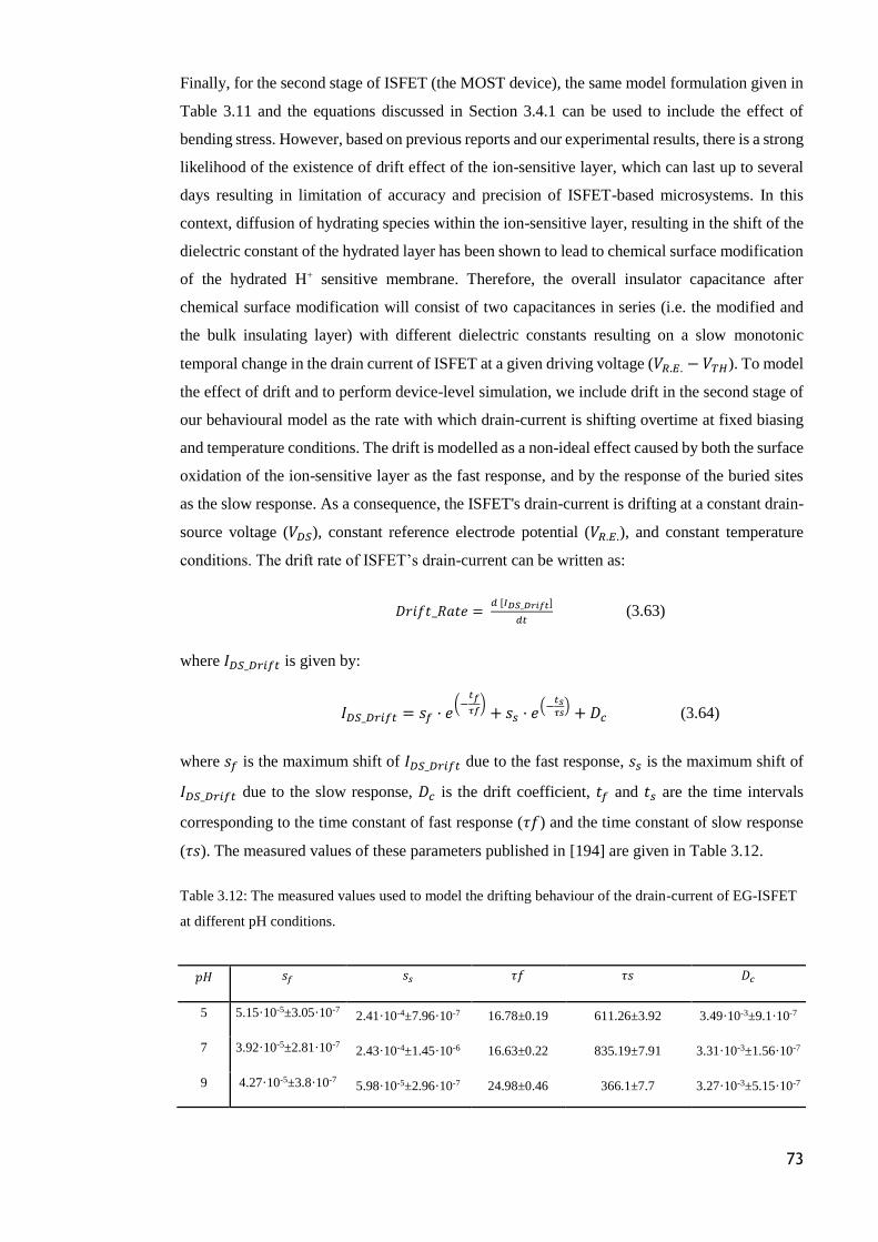
73
Finally, for the second stage of ISFET (the MOST device), the same model formulation given in
Table 3.11 and the equations discussed in Section 3.4.1 can be used to include the effect of
bending stress. However, based on previous reports and our experimental results, there is a strong
likelihood of the existence of drift effect of the ion-sensitive layer, which can last up to several
days resulting in limitation of accuracy and precision of ISFET-based microsystems. In this
context, diffusion of hydrating species within the ion-sensitive layer, resulting in the shift of the
dielectric constant of the hydrated layer has been shown to lead to chemical surface modification
of the hydrated H+ sensitive membrane. Therefore, the overall insulator capacitance after
chemical surface modification will consist of two capacitances in series (i.e. the modified and
the bulk insulating layer) with different dielectric constants resulting on a slow monotonic
temporal change in the drain current of ISFET at a given driving voltage (𝑉𝑅.𝐸. − 𝑉𝑇𝐻). To model
the effect of drift and to perform device-level simulation, we include drift in the second stage of
our behavioural model as the rate with which drain-current is shifting overtime at fixed biasing
and temperature conditions. The drift is modelled as a non-ideal effect caused by both the surface
oxidation of the ion-sensitive layer as the fast response, and by the response of the buried sites
as the slow response. As a consequence, the ISFET's drain-current is drifting at a constant drain-
source voltage (𝑉𝐷𝑆), constant reference electrode potential (𝑉𝑅.𝐸.), and constant temperature
conditions. The drift rate of ISFET’s drain-current can be written as:
𝐷𝑟𝑖𝑓𝑡_𝑅𝑎𝑡𝑒 = 𝑑 [𝐼𝐷𝑆_𝐷𝑟𝑖𝑓𝑡]
𝑑𝑡 (3.63)
where 𝐼𝐷𝑆_𝐷𝑟𝑖𝑓𝑡 is given by:
𝐼𝐷𝑆_𝐷𝑟𝑖𝑓𝑡 = 𝑠𝑓 · 𝑒(−
𝑡𝑓
𝜏𝑓)+ 𝑠𝑠 · 𝑒
(−𝑡𝑠𝜏𝑠
)+ 𝐷𝑐 (3.64)
where 𝑠𝑓 is the maximum shift of 𝐼𝐷𝑆_𝐷𝑟𝑖𝑓𝑡 due to the fast response, 𝑠𝑠 is the maximum shift of
𝐼𝐷𝑆_𝐷𝑟𝑖𝑓𝑡 due to the slow response, 𝐷𝑐 is the drift coefficient, 𝑡𝑓 and 𝑡𝑠 are the time intervals
corresponding to the time constant of fast response (𝜏𝑓) and the time constant of slow response
(𝜏𝑠). The measured values of these parameters published in [194] are given in Table 3.12.
Table 3.12: The measured values used to model the drifting behaviour of the drain-current of EG-ISFET
at different pH conditions.
𝑝𝐻 𝑠𝑓 𝑠𝑠 𝜏𝑓 𝜏𝑠 𝐷𝑐
5 5.15·10-5±3.05·10-7 2.41·10-4±7.96·10-7 16.78±0.19 611.26±3.92 3.49·10-3±9.1·10-7
7 3.92·10-5±2.81·10-7 2.43·10-4±1.45·10-6 16.63±0.22 835.19±7.91 3.31·10-3±1.56·10-7
9 4.27·10-5±3.8·10-7 5.98·10-5±2.96·10-7 24.98±0.46 366.1±7.7 3.27·10-3±5.15·10-7
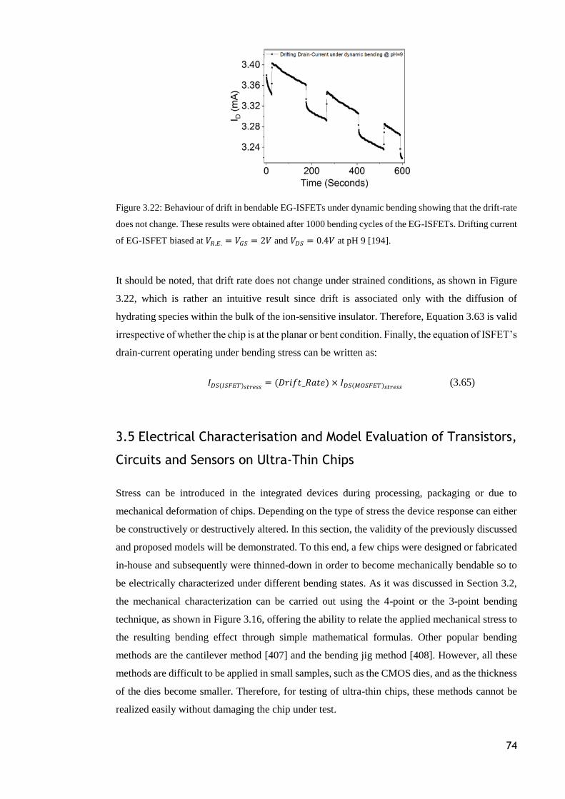
74
Figure 3.22: Behaviour of drift in bendable EG-ISFETs under dynamic bending showing that the drift-rate
does not change. These results were obtained after 1000 bending cycles of the EG-ISFETs. Drifting current
of EG-ISFET biased at 𝑉𝑅.𝐸. = 𝑉𝐺𝑆 = 2𝑉 and 𝑉𝐷𝑆 = 0.4𝑉 at pH 9 [194].
It should be noted, that drift rate does not change under strained conditions, as shown in Figure
3.22, which is rather an intuitive result since drift is associated only with the diffusion of
hydrating species within the bulk of the ion-sensitive insulator. Therefore, Equation 3.63 is valid
irrespective of whether the chip is at the planar or bent condition. Finally, the equation of ISFET’s
drain-current operating under bending stress can be written as:
𝐼𝐷𝑆(𝐼𝑆𝐹𝐸𝑇)𝑠𝑡𝑟𝑒𝑠𝑠= (𝐷𝑟𝑖𝑓𝑡_𝑅𝑎𝑡𝑒) × 𝐼𝐷𝑆(𝑀𝑂𝑆𝐹𝐸𝑇)𝑠𝑡𝑟𝑒𝑠𝑠
(3.65)
3.5 Electrical Characterisation and Model Evaluation of Transistors,
Circuits and Sensors on Ultra-Thin Chips
Stress can be introduced in the integrated devices during processing, packaging or due to
mechanical deformation of chips. Depending on the type of stress the device response can either
be constructively or destructively altered. In this section, the validity of the previously discussed
and proposed models will be demonstrated. To this end, a few chips were designed or fabricated
in-house and subsequently were thinned-down in order to become mechanically bendable so to
be electrically characterized under different bending states. As it was discussed in Section 3.2,
the mechanical characterization can be carried out using the 4-point or the 3-point bending
technique, as shown in Figure 3.16, offering the ability to relate the applied mechanical stress to
the resulting bending effect through simple mathematical formulas. Other popular bending
methods are the cantilever method [407] and the bending jig method [408]. However, all these
methods are difficult to be applied in small samples, such as the CMOS dies, and as the thickness
of the dies become smaller. Therefore, for testing of ultra-thin chips, these methods cannot be
realized easily without damaging the chip under test.
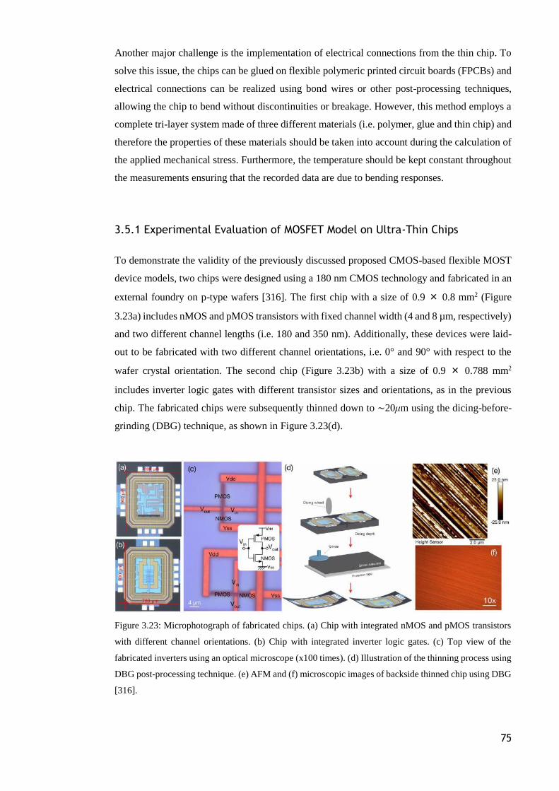
75
Another major challenge is the implementation of electrical connections from the thin chip. To
solve this issue, the chips can be glued on flexible polymeric printed circuit boards (FPCBs) and
electrical connections can be realized using bond wires or other post-processing techniques,
allowing the chip to bend without discontinuities or breakage. However, this method employs a
complete tri-layer system made of three different materials (i.e. polymer, glue and thin chip) and
therefore the properties of these materials should be taken into account during the calculation of
the applied mechanical stress. Furthermore, the temperature should be kept constant throughout
the measurements ensuring that the recorded data are due to bending responses.
3.5.1 Experimental Evaluation of MOSFET Model on Ultra-Thin Chips
To demonstrate the validity of the previously discussed proposed CMOS-based flexible MOST
device models, two chips were designed using a 180 nm CMOS technology and fabricated in an
external foundry on p-type wafers [316]. The first chip with a size of 0.9 × 0.8 mm2 (Figure
3.23a) includes nMOS and pMOS transistors with fixed channel width (4 and 8 µm, respectively)
and two different channel lengths (i.e. 180 and 350 nm). Additionally, these devices were laid-
out to be fabricated with two different channel orientations, i.e. 0° and 90° with respect to the
wafer crystal orientation. The second chip (Figure 3.23b) with a size of 0.9 × 0.788 mm2
includes inverter logic gates with different transistor sizes and orientations, as in the previous
chip. The fabricated chips were subsequently thinned down to ∼20μm using the dicing-before-
grinding (DBG) technique, as shown in Figure 3.23(d).
Figure 3.23: Microphotograph of fabricated chips. (a) Chip with integrated nMOS and pMOS transistors
with different channel orientations. (b) Chip with integrated inverter logic gates. (c) Top view of the
fabricated inverters using an optical microscope (x100 times). (d) Illustration of the thinning process using
DBG post-processing technique. (e) AFM and (f) microscopic images of backside thinned chip using DBG
[316].
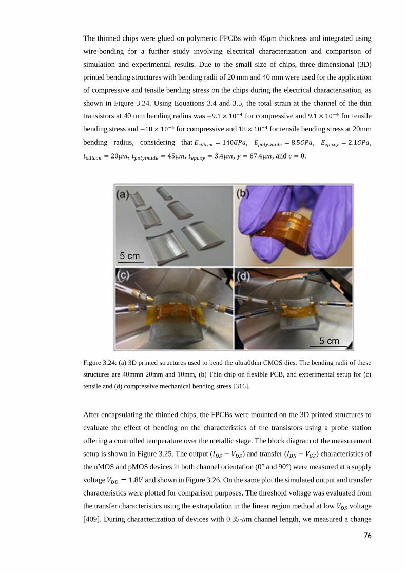
76
The thinned chips were glued on polymeric FPCBs with 45µm thickness and integrated using
wire-bonding for a further study involving electrical characterization and comparison of
simulation and experimental results. Due to the small size of chips, three-dimensional (3D)
printed bending structures with bending radii of 20 mm and 40 mm were used for the application
of compressive and tensile bending stress on the chips during the electrical characterisation, as
shown in Figure 3.24. Using Equations 3.4 and 3.5, the total strain at the channel of the thin
transistors at 40 mm bending radius was −9.1 × 10⁻⁴ for compressive and 9.1 × 10⁻⁴ for tensile
bending stress and −18 × 10−4 for compressive and 18 × 10−4 for tensile bending stress at 20mm
bending radius, considering that 𝐸𝑠𝑖𝑙𝑖𝑐𝑜𝑛 = 140𝐺𝑃𝑎, 𝐸𝑝𝑜𝑙𝑦𝑖𝑚𝑖𝑑𝑒 = 8.5𝐺𝑃𝑎, 𝐸𝑒𝑝𝑜𝑥𝑦 = 2.1𝐺𝑃𝑎,
𝑡𝑠𝑖𝑙𝑖𝑐𝑜𝑛 = 20µ𝑚, 𝑡𝑝𝑜𝑙𝑦𝑖𝑚𝑖𝑑𝑒 = 45µ𝑚, 𝑡𝑒𝑝𝑜𝑥𝑦 = 3.4µ𝑚, 𝑦 = 87.4µ𝑚, and 𝑐 = 0.
Figure 3.24: (a) 3D printed structures used to bend the ultra0thin CMOS dies. The bending radii of these
structures are 40mmn 20mm and 10mm, (b) Thin chip on flexible PCB, and experimental setup for (c)
tensile and (d) compressive mechanical bending stress [316].
After encapsulating the thinned chips, the FPCBs were mounted on the 3D printed structures to
evaluate the effect of bending on the characteristics of the transistors using a probe station
offering a controlled temperature over the metallic stage. The block diagram of the measurement
setup is shown in Figure 3.25. The output (𝐼𝐷𝑆 − 𝑉𝐷𝑆) and transfer (𝐼𝐷𝑆 − 𝑉𝐺𝑆) characteristics of
the nMOS and pMOS devices in both channel orientation (0° and 90°) were measured at a supply
voltage 𝑉𝐷𝐷 = 1.8𝑉 and shown in Figure 3.26. On the same plot the simulated output and transfer
characteristics were plotted for comparison purposes. The threshold voltage was evaluated from
the transfer characteristics using the extrapolation in the linear region method at low 𝑉𝐷𝑆 voltage
[409]. During characterization of devices with 0.35-μm channel length, we measured a change
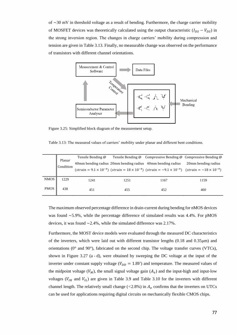
77
of ∼30 mV in threshold voltage as a result of bending. Furthermore, the charge carrier mobility
of MOSFET devices was theoretically calculated using the output characteristic (𝐼𝐷𝑆 − 𝑉𝐷𝑆) in
the strong inversion region. The changes in charge carriers’ mobility during compression and
tension are given in Table 3.13. Finally, no measurable change was observed on the performance
of transistors with different channel orientations.
Figure 3.25: Simplified block diagram of the measurement setup.
Table 3.13: The measured values of carriers’ mobility under planar and different bent conditions.
Planar
Condition
Tensile Bending @
40mm bending radius
(𝑠𝑡𝑟𝑎𝑖𝑛 = 9.1 × 10⁻⁴)
Tensile Bending @
20mm bending radius
(𝑠𝑡𝑟𝑎𝑖𝑛 = 18 × 10−4)
Compressive Bending @
40mm bending radius
(𝑠𝑡𝑟𝑎𝑖𝑛 = −9.1 × 10⁻⁴)
Compressive Bending @
20mm bending radius
(𝑠𝑡𝑟𝑎𝑖𝑛 = −18 × 10−4)
NMOS 1229 1241 1251 1167 1159
PMOS 438 451 455 452 460
The maximum observed percentage difference in drain-current during bending for nMOS devices
was found ∼5.9%, while the percentage difference of simulated results was 4.4%. For pMOS
devices, it was found ∼2.4%, while the simulated difference was 2.17%.
Furthermore, the MOST device models were evaluated through the measured DC characteristics
of the inverters, which were laid out with different transistor lengths (0.18 and 0.35μm) and
orientations (0° and 90°), fabricated on the second chip. The voltage transfer curves (VTCs),
shown in Figure 3.27 (a - d), were obtained by sweeping the DC voltage at the input of the
inverter under constant supply voltage (𝑉𝐷𝐷 = 1.8𝑉) and temperature. The measured values of
the midpoint voltage (𝑉𝑀), the small signal voltage gain (𝐴𝑣) and the input-high and input-low
voltages (𝑉𝐼𝐻 and 𝑉𝐼𝐿) are given in Table 3.9 and Table 3.10 for the inverters with different
channel length. The relatively small change (<2.8%) in 𝐴𝑣 confirms that the inverters on UTCs
can be used for applications requiring digital circuits on mechanically flexible CMOS chips.
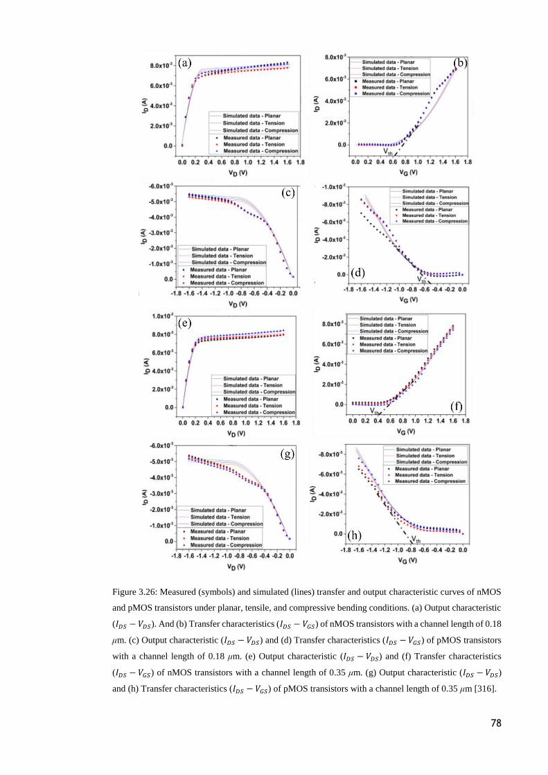
78
Figure 3.26: Measured (symbols) and simulated (lines) transfer and output characteristic curves of nMOS
and pMOS transistors under planar, tensile, and compressive bending conditions. (a) Output characteristic
(𝐼𝐷𝑆 − 𝑉𝐷𝑆). And (b) Transfer characteristics (𝐼𝐷𝑆 − 𝑉𝐺𝑆) of nMOS transistors with a channel length of 0.18
μm. (c) Output characteristic (𝐼𝐷𝑆 − 𝑉𝐷𝑆) and (d) Transfer characteristics (𝐼𝐷𝑆 − 𝑉𝐺𝑆) of pMOS transistors
with a channel length of 0.18 μm. (e) Output characteristic (𝐼𝐷𝑆 − 𝑉𝐷𝑆) and (f) Transfer characteristics
(𝐼𝐷𝑆 − 𝑉𝐺𝑆) of nMOS transistors with a channel length of 0.35 μm. (g) Output characteristic (𝐼𝐷𝑆 − 𝑉𝐷𝑆)
and (h) Transfer characteristics (𝐼𝐷𝑆 − 𝑉𝐺𝑆) of pMOS transistors with a channel length of 0.35 μm [316].
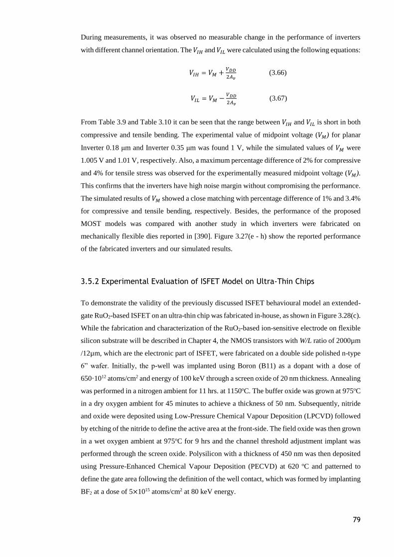
79
During measurements, it was observed no measurable change in the performance of inverters
with different channel orientation. The 𝑉𝐼𝐻 and 𝑉𝐼𝐿 were calculated using the following equations:
𝑉𝐼𝐻 = 𝑉𝑀 +𝑉𝐷𝐷
2𝐴𝑣 (3.66)
𝑉𝐼𝐿 = 𝑉𝑀 −𝑉𝐷𝐷
2𝐴𝑣 (3.67)
From Table 3.9 and Table 3.10 it can be seen that the range between 𝑉𝐼𝐻 and 𝑉𝐼𝐿 is short in both
compressive and tensile bending. The experimental value of midpoint voltage (𝑉𝑀) for planar
Inverter 0.18 μm and Inverter 0.35 μm was found 1 V, while the simulated values of 𝑉𝑀 were
1.005 V and 1.01 V, respectively. Also, a maximum percentage difference of 2% for compressive
and 4% for tensile stress was observed for the experimentally measured midpoint voltage (𝑉𝑀).
This confirms that the inverters have high noise margin without compromising the performance.
The simulated results of 𝑉𝑀 showed a close matching with percentage difference of 1% and 3.4%
for compressive and tensile bending, respectively. Besides, the performance of the proposed
MOST models was compared with another study in which inverters were fabricated on
mechanically flexible dies reported in [390]. Figure 3.27(e - h) show the reported performance
of the fabricated inverters and our simulated results.
3.5.2 Experimental Evaluation of ISFET Model on Ultra-Thin Chips
To demonstrate the validity of the previously discussed ISFET behavioural model an extended-
gate RuO2-based ISFET on an ultra-thin chip was fabricated in-house, as shown in Figure 3.28(c).
While the fabrication and characterization of the RuO2-based ion-sensitive electrode on flexible
silicon substrate will be described in Chapter 4, the NMOS transistors with W/L ratio of 2000µm
/12µm, which are the electronic part of ISFET, were fabricated on a double side polished n-type
6” wafer. Initially, the p-well was implanted using Boron (B11) as a dopant with a dose of
650·1012 atoms/cm2 and energy of 100 keV through a screen oxide of 20 nm thickness. Annealing
was performed in a nitrogen ambient for 11 hrs. at 1150oC. The buffer oxide was grown at 975oC
in a dry oxygen ambient for 45 minutes to achieve a thickness of 50 nm. Subsequently, nitride
and oxide were deposited using Low-Pressure Chemical Vapour Deposition (LPCVD) followed
by etching of the nitride to define the active area at the front-side. The field oxide was then grown
in a wet oxygen ambient at 975oC for 9 hrs and the channel threshold adjustment implant was
performed through the screen oxide. Polysilicon with a thickness of 450 nm was then deposited
using Pressure-Enhanced Chemical Vapour Deposition (PECVD) at 620 oC and patterned to
define the gate area following the definition of the well contact, which was formed by implanting
BF2 at a dose of 5×10¹⁵ atoms/cm2 at 80 keV energy.
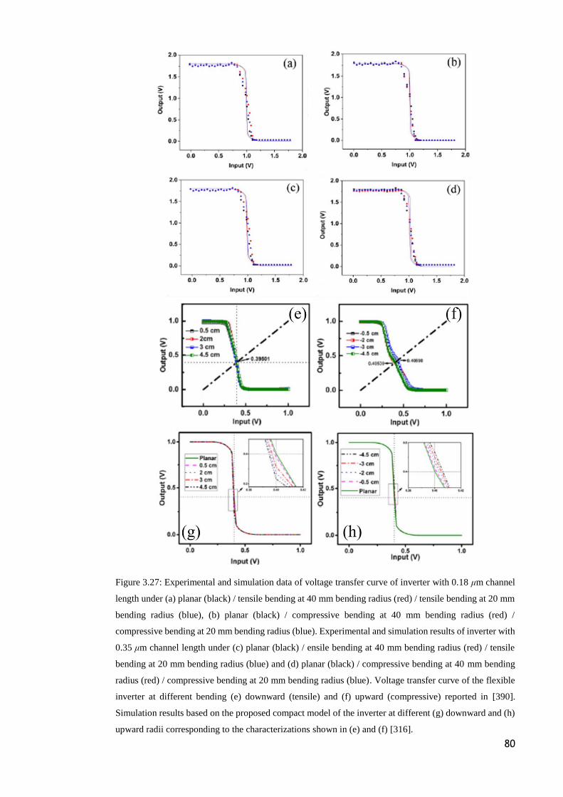
80
Figure 3.27: Experimental and simulation data of voltage transfer curve of inverter with 0.18 μm channel
length under (a) planar (black) / tensile bending at 40 mm bending radius (red) / tensile bending at 20 mm
bending radius (blue), (b) planar (black) / compressive bending at 40 mm bending radius (red) /
compressive bending at 20 mm bending radius (blue). Experimental and simulation results of inverter with
0.35 μm channel length under (c) planar (black) / ensile bending at 40 mm bending radius (red) / tensile
bending at 20 mm bending radius (blue) and (d) planar (black) / compressive bending at 40 mm bending
radius (red) / compressive bending at 20 mm bending radius (blue). Voltage transfer curve of the flexible
inverter at different bending (e) downward (tensile) and (f) upward (compressive) reported in [390].
Simulation results based on the proposed compact model of the inverter at different (g) downward and (h)
upward radii corresponding to the characterizations shown in (e) and (f) [316].
81
Successively, the Source and Drain regions were formed by implanting phosphorus with dose
5×10¹⁵ atoms/cm2 and energy 80keV followed by implantation of arsenic with dose 2×10¹⁵
atoms/cm2 and energy 120 keV. The contacts were formed by initially using plasma-etching
followed by an oxide etch-dip before metal deposition. Next, Ti/Al:Si (60 nm/600 nm) was
sputtered at room temperature. After sintering of contacts, a layer of protective overglass (SiOx)
was deposited over the wafer. Finally, the contact pads were opened.
Figure 3.28: (a) Fabricated chip (chip area is 1 1 cm2) with four n-channel transistors and the bending
axis. (b) Designed fingers of the transistor with channel dimension of W/L = 2000µm / 12µm. (c)
Illustration of the extended-gate ISFET configuration where the mechanically flexible MOSFETs are
connected to the flexible silicon substrate on which the RuO2-based ion-sensitive material and the
reference-electrode were fabricated and (d) SEM image of the cross-section of the thin chip on the
polyimide-based flexible PCB showing the thickness of the chip and FPCB [194]. Courtesy: The
photolithography masks used for the fabrication of MOSFETs were designed by Shoubhik Gupta, the fabrication of chips was carried
out by the staff of the Fondazione Bruno Kessler (FBK) institute, Italy, and the RuO2 material synthesis and ISE fabrication was
carried out by Dr. Libu Manjakkal.
Subsequently, the chips were thinned down to 44.76μm thickness using the lapping technique
and were glued on polymeric FPCBs with 64µm thickness, as shown in Figure 3.28(d). The chips
were then integrated using wire-bonding for a further study involving electrical characterization
and comparison of simulation and experimental results. The measurement setup used for the
characterisation of ISFETs on ultra-thin chips was similar to that shown in Figure 3.25 and the
bending of chips was done using the 3D printed structures shown in Figure 3.24. Initially, the
transistors were characterised under planar and bent conditions at 40mm bending radius. Using
Equations 3.4 and 3.5, the total strain at the channel of the thin transistors at 40 mm bending
radius was −21 × 10−4 for compressive and 21 × 10−4 for tensile bending stress. The transfer and
output characteristics (𝐼𝐷𝑆 − 𝑉𝐺𝑆 and 𝐼𝐷𝑆 − 𝑉𝐷𝑆) of the fabricated MOSFETs on ultra-thin chips
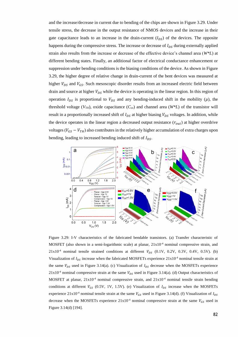
82
and the increase/decrease in current due to bending of the chips are shown in Figure 3.29. Under
tensile stress, the decrease in the output resistance of NMOS devices and the increase in their
gate capacitance leads to an increase in the drain-current (𝐼𝐷𝑆) of the devices. The opposite
happens during the compressive stress. The increase or decrease of 𝐼𝐷𝑆 during externally applied
strain also results from the increase or decrease of the effective device’s channel area (W*L) at
different bending states. Finally, an additional factor of electrical conductance enhancement or
suppression under bending conditions is the biasing conditions of the device. As shown in Figure
3.29, the higher degree of relative change in drain-current of the bent devices was measured at
higher 𝑉𝐷𝑆 and 𝑉𝐺𝑆. Such mesoscopic disorder results from an increased electric field between
drain and source at higher 𝑉𝐷𝑆 while the device is operating in the linear region. In this region of
operation 𝐼𝐷𝑆 is proportional to 𝑉𝐷𝑆 and any bending-induced shift in the mobility (µ), the
threshold voltage (VTH), oxide capacitance (Cox) and channel area (W*L) of the transistor will
result in a proportionally increased shift of 𝐼𝐷𝑆 at higher biasing 𝑉𝐷𝑆 voltages. In addition, while
the device operates in the linear region a decreased output resistance (𝑟𝑜𝑢𝑡) at higher overdrive
voltages (𝑉𝐺𝑆 − 𝑉𝑇𝐻) also contributes in the relatively higher accumulation of extra charges upon
bending, leading to increased bending induced shift of 𝐼𝐷𝑆.
Figure 3.29: I-V characteristics of the fabricated bendable transistors. (a) Transfer characteristic of
MOSFET (also shown in a semi-logarithmic scale) at planar, 21x10-4 nominal compressive strain, and
21x10-4 nominal tensile strained conditions at different 𝑉𝐷𝑆 (0.1V, 0.2V, 0.3V, 0.4V, 0.5V). (b)
Visualization of 𝐼𝐷𝑆 increase when the fabricated MOSFETs experience 21x10-4 nominal tensile strain at
the same 𝑉𝐷𝑆 used in Figure 3.14(a). (c) Visualization of 𝐼𝐷𝑆 decrease when the MOSFETs experience
21x10-4 nominal compressive strain at the same 𝑉𝐷𝑆 used in Figure 3.14(a). (d) Output characteristics of
MOSFET at planar, 21x10-4 nominal compressive strain, and 21x10-4 nominal tensile strain bending
conditions at different 𝑉𝐺𝑆 (0.5V, 1V, 1.5V). (e) Visualization of 𝐼𝐷𝑆 increase when the MOSFETs
experience 21x10-4 nominal tensile strain at the same 𝑉𝐺𝑆 used in Figure 3.14(d). (f) Visualization of 𝐼𝐷𝑆
decrease when the MOSFETs experience 21x10-4 nominal compressive strain at the same 𝑉𝐺𝑆 used in
Figure 3.14(d) [194].
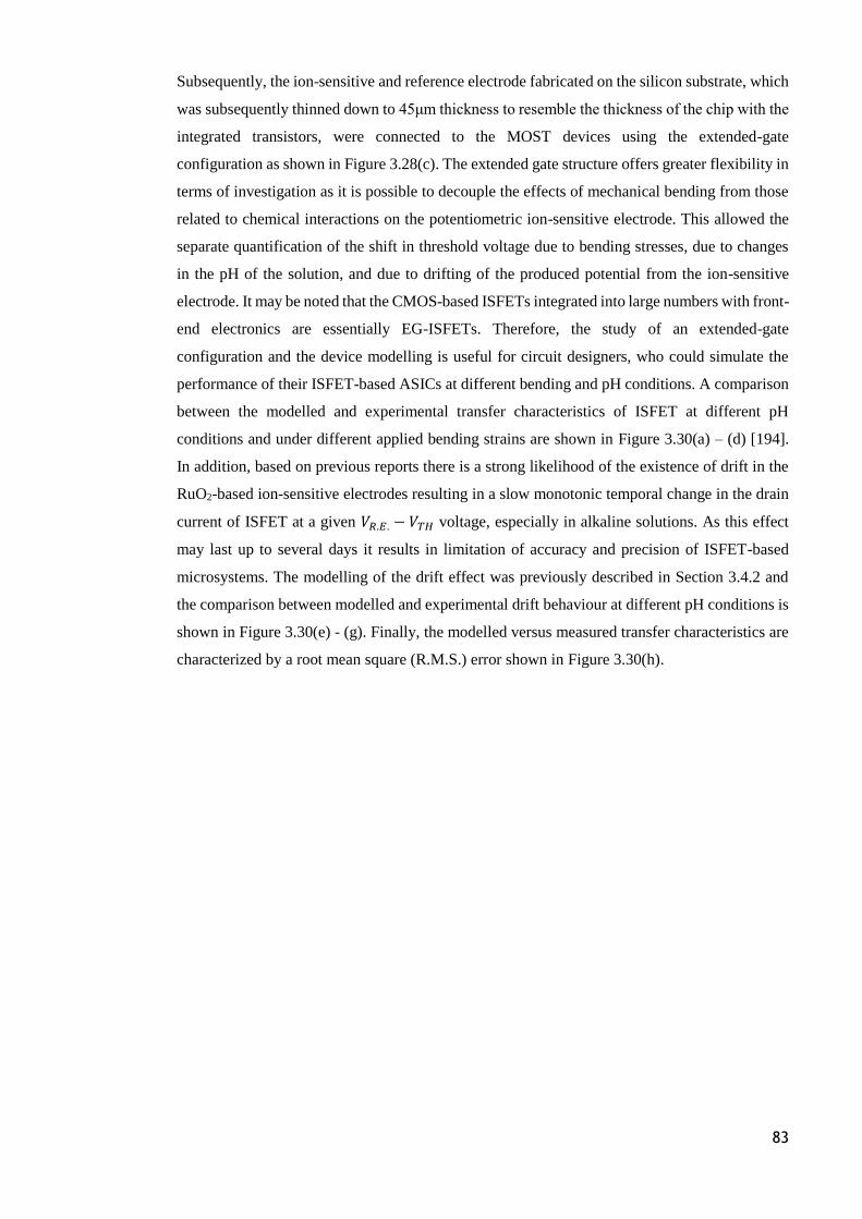
83
Subsequently, the ion-sensitive and reference electrode fabricated on the silicon substrate, which
was subsequently thinned down to 45μm thickness to resemble the thickness of the chip with the
integrated transistors, were connected to the MOST devices using the extended-gate
configuration as shown in Figure 3.28(c). The extended gate structure offers greater flexibility in
terms of investigation as it is possible to decouple the effects of mechanical bending from those
related to chemical interactions on the potentiometric ion-sensitive electrode. This allowed the
separate quantification of the shift in threshold voltage due to bending stresses, due to changes
in the pH of the solution, and due to drifting of the produced potential from the ion-sensitive
electrode. It may be noted that the CMOS-based ISFETs integrated into large numbers with front-
end electronics are essentially EG-ISFETs. Therefore, the study of an extended-gate
configuration and the device modelling is useful for circuit designers, who could simulate the
performance of their ISFET-based ASICs at different bending and pH conditions. A comparison
between the modelled and experimental transfer characteristics of ISFET at different pH
conditions and under different applied bending strains are shown in Figure 3.30(a) – (d) [194].
In addition, based on previous reports there is a strong likelihood of the existence of drift in the
RuO2-based ion-sensitive electrodes resulting in a slow monotonic temporal change in the drain
current of ISFET at a given 𝑉𝑅.𝐸. − 𝑉𝑇𝐻 voltage, especially in alkaline solutions. As this effect
may last up to several days it results in limitation of accuracy and precision of ISFET-based
microsystems. The modelling of the drift effect was previously described in Section 3.4.2 and
the comparison between modelled and experimental drift behaviour at different pH conditions is
shown in Figure 3.30(e) - (g). Finally, the modelled versus measured transfer characteristics are
characterized by a root mean square (R.M.S.) error shown in Figure 3.30(h).
84
Figure 3.30: I-V and I-t characteristics of the thin and bendable EG-ISFETs. (a) Measured (compact lines)
and simulated (dotted lines) ISFET transfer characteristics at pH 5, 7, and 9 at the planar condition. (b)
Measured (compact lines) and simulated (dotted lines) ISFET transfer characteristics at pH 5 under planar
(red line), 21x10-4 nominal compressive strain (yellow line), and 21x10-4 nominal tensile strain (blue line).
(c) Measured (compact lines) and simulated (dotted lines) ISFET transfer characteristics at pH 7 under
planar (red line), 21x10-4 nominal compressive strain (yellow line), and 21x10-4 nominal tensile strain (blue
line). (d) Measured (compact lines) and simulated (dotted lines) ISFET transfer characteristics at pH 9
under planar (red line), 21x10-4 nominal compressive strain (yellow line), and 21x10-4 nominal tensile
strain (blue line). (e) – (g) Measured and simulated ISFET transient response at pH 5, 7, and 9 at the planar
condition and (h) h Root mean square (R.M.S.) error between measured and simulated results. All
measurements and simulations were performed at 𝑉𝑅.𝐸. = 𝑉𝐺𝑆 = 2𝑉 and 𝑉𝐷𝑆 = 0.4𝑉 [194].
85
3.6 Summary
One of the challenges for silicon-based flexible electronics is that the devices’ response changes
constructively or destructively as a result of bending induced stresses. More specifically,
mechanical stresses, either internally or externally applied, affect the carrier mobility and
threshold voltage altering the DC parameters of the device. For circuit design purposes, in
applications that require a certain degree of mechanical flexibility from CMOS chips and to
predict the response of circuits under different bending states, it is important to understand these
variations and derive computationally efficient representations of the device behaviour
compatible to computer-aided design (CAD) tools. This chapter presented the formulation and
model validation through electrical characterisation of MOST devices, ISFETs and simple digital
gates fabricated on ultra-thin chips, which showed good matching with the simulated results. The
MOST device model was developed using the piezoresistance theory and the changes in carriers’
mobility and threshold voltage were considered as the main contributor towards the shift of the
device’s drain-current. Also, the model includes the changes in the transistor’s channel area
(Width and Length) as a result of bending, but the effect of area change becomes more prominent
as the area and bending curvature increase. Furthermore, the ISFET, which is the main focus of
this thesis, was modelled as a two stages device comprising of the electrochemical (i.e. the
electrode-electrolyte interface) and the electronic (i.e. the MOST device) part while the effect of
drift in ISFET’s performance was also included in the model. The models were implemented in
Verilog-A and compiled in Cadence Virtuoso 6.1.6 environment. It should be noted that these
models need further development to include the effect of bending stresses on the noise
performance of MOSTs. Also, the oxide capacitance (COX) as well as all the rest of the parasitic
capacitances of an MOST device should be modified from planar to cylindrical capacitances
when bending stresses are taken into account. These capacitances have not been modified in the
present model because in reality the chips presented in the thesis cannot significantly bend and
thus all these capacitances are approximately planar.
Finally, it should be noted that mounting of ultra-thin chips on flexible substrates, such as an
FPCBs, will result in complicated inherent stress distribution, mainly caused by the different
properties of the 3-layer stack (PCB-glue-chip). To avoid chip-to-chip variations which may be
caused by the assembly process several devices on the same chip should be measured to capture
the potential position- and time-dependent effects of the 3-layer stack on the performance of the
devices and circuits. It is also important to conduct the measurements in a noise-free environment
and to keep the biasing and temperature conditions are stable as possible and to have ideally to
have calibrated temperature sensors on-chip to ensure that the captured data reflect the variation
of the devices’ performance solely due to bending. However, such an environment is usually very
difficult to be realised. Finally, it would be useful to conduct comparable measurements on

86
devices both on bulky and ultra-thin chips since the former will not experience any bending–
induced variation.
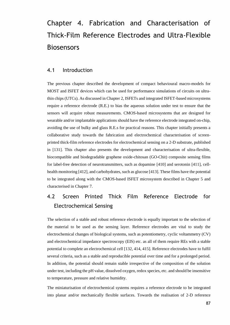
87
Chapter 4. Fabrication and Characterisation of
Thick-Film Reference Electrodes and Ultra-Flexible
Biosensors
4.1 Introduction
The previous chapter described the development of compact behavioural macro-models for
MOST and ISFET devices which can be used for performance simulations of circuits on ultra-
thin chips (UTCs). As discussed in Chapter 2, ISFETs and integrated ISFET-based microsystems
require a reference electrode (R.E.) to bias the aqueous solution under test to ensure that the
sensors will acquire robust measurements. CMOS-based microsystems that are designed for
wearable and/or implantable applications should have the reference electrode integrated on-chip,
avoiding the use of bulky and glass R.E.s for practical reasons. This chapter initially presents a
collaborative study towards the fabrication and electrochemical characterisation of screen-
printed thick-film reference electrodes for electrochemical sensing on a 2-D substrate, published
in [131]. This chapter also presents the development and characterisation of ultra-flexible,
biocompatible and biodegradable graphene oxide-chitosan (GO-Chit) composite sensing films
for label-free detection of neurotransmitters, such as dopamine [410] and serotonin [411], cell-
health monitoring [412], and carbohydrates, such as glucose [413]. These films have the potential
to be integrated along with the CMOS-based ISFET microsystem described in Chapter 5 and
characterised in Chapter 7.
4.2 Screen Printed Thick Film Reference Electrode for
Electrochemical Sensing
The selection of a stable and robust reference electrode is equally important to the selection of
the material to be used as the sensing layer. Reference electrodes are vital to study the
electrochemical changes of biological systems, such as potentiometry, cyclic voltammetry (CV)
and electrochemical impedance spectroscopy (EIS) etc. as all of them require REs with a stable
potential to complete an electrochemical cell [132, 414, 415]. Reference electrodes have to fulfil
several criteria, such as a stable and reproducible potential over time and for a prolonged period.
In addition, the potential should remain stable irrespective of the composition of the solution
under test, including the pH value, dissolved oxygen, redox species, etc. and should be insensitive
to temperature, pressure and relative humidity.
The miniaturisation of electrochemical systems requires a reference electrode to be integrated
into planar and/or mechanically flexible surfaces. Towards the realisation of 2-D reference
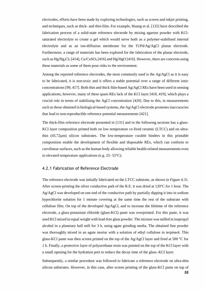
88
electrodes, efforts have been made by exploring technologies, such as screen and inkjet printing,
and techniques, such as thick- and thin-film. For example, Huang et al. [135] have described the
fabrication process of a solid-state reference electrode by mixing agarose powder with KCl-
saturated electrolyte to create a gel which would serve both as a polymer-stabilised internal
electrolyte and as an ion-diffusion membrane for the Ti/Pd/Ag/AgCl planar electrode.
Furthermore, a range of materials has been explored for the fabrication of the planar electrode,
such as Hg/Hg2Cl2 [414], Cu/CuSO4 [416] and Hg/HgO [416]. However, there are concerns using
these materials as some of them pose risks to the environment.
Among the reported reference electrodes, the most commonly used is the Ag/AgCl as it is easy
to be fabricated, it is non-toxic and it offers a stable potential over a range of different ionic
concentrations [99, 417]. Both thin and thick film-based Ag/AgCl REs have been used in sensing
applications, however, many of these quasi-REs lack of the KCl layer [418, 419], which plays a
crucial role in terms of stabilising the AgCl concentration [420]. Due to this, in measurements
such as those obtained in biological-based systems, the Ag/AgCl electrode promotes inaccuracies
that lead to non-reproducible reference potential measurements [421].
The thick-film reference electrode presented in [131] and in the following sections has a glass-
KCl layer composition printed both on low temperature co-fired ceramic (LTCC) and on ultra-
thin (45.72µm) silicon substrates. The low-temperature curable binders in this printable
composition enable the development of flexible and disposable REs, which can conform to
curvilinear surfaces, such as the human body allowing reliable health-related measurements even
in elevated temperature applications (e.g. 25- 55°C).
4.2.1 Fabrication of Reference Electrode
The reference electrode was initially fabricated on the LTCC substrate, as shown in Figure 4.31.
After screen-printing the silver conductive path of the R.E. it was dried at 120oC for 1 hour. The
Ag/AgCl was developed on one end of the conductive path by partially dipping it into in sodium
hypochlorite solution for 1 minute covering at the same time the rest of the substrate with
cellulose film. On top of the developed Ag/AgCl, and to increase the lifetime of the reference
electrode, a glass-potassium chloride (glass-KCl) paste was overprinted. For this paste, it was
used KCl mixed in equal weight with lead-free glass powder. The mixture was milled in isopropyl
alcohol in a planetary ball mill for 3 h, using agate grinding media. The obtained fine powder
was thoroughly mixed in an agate mortar with a solution of ethyl cellulose in terpineol. This
glass-KCl paste was then screen printed on the top of the Ag/AgCl layer and fired at 500 °C for
1 h. Finally, a protective layer of polyurethane resin was painted on the top of the KCl layer with
a small opening for the hydration port to reduce the decay time of the glass–KCl layer.
Subsequently, a similar procedure was followed to fabricate a reference electrode on ultra-thin
silicon substrates. However, in this case, after screen printing of the glass-KCl paste on top of
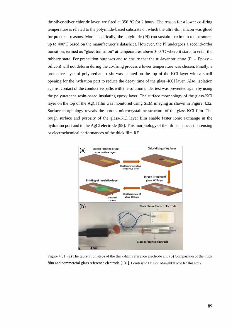
89
the silver-silver chloride layer, we fired at 350 °C for 2 hours. The reason for a lower co-firing
temperature is related to the polyimide-based substrate on which the ultra-thin silicon was glued
for practical reasons. More specifically, the polyimide (PI) can sustain maximum temperatures
up to 400oC based on the manufacturer’s datasheet. However, the PI undergoes a second-order
transition, termed as “glass transition” at temperatures above 300 oC where it starts to enter the
rubbery state. For precaution purposes and to ensure that the tri-layer structure (Pi – Epoxy –
Silicon) will not deform during the co-firing process a lower temperature was chosen. Finally, a
protective layer of polyurethane resin was painted on the top of the KCl layer with a small
opening for the hydration port to reduce the decay time of the glass–KCl layer. Also, isolation
against contact of the conductive paths with the solution under test was prevented again by using
the polyurethane resin-based insulating epoxy layer. The surface morphology of the glass-KCl
layer on the top of the AgCl film was monitored using SEM imaging as shown in Figure 4.32.
Surface morphology reveals the porous microcrystalline structure of the glass-KCl film. The
rough surface and porosity of the glass-KCl layer film enable faster ionic exchange in the
hydration port and to the AgCl electrode [99]. This morphology of the film enhances the sensing
or electrochemical performances of the thick film RE.
Figure 4.31: (a) The fabrication steps of the thick-film reference electrode and (b) Comparison of the thick
film and commercial glass reference electrode [131]. Courtesy to Dr Libu Manjakkal who led this work.
90
Figure 4.32: SEM image of the glass-KCl 2D film [131]. Courtesy to Dr Libu Manjakkal who led this work.
4.2.2 Fabrication of RuO2 Based Ion-Sensitive Electrode
The performance of the developed REs was evaluated under different pH conditions by using
them along with a pH sensing electrode based on RuO2. The ion-sensitive RuO2-based electrode
was fabricated on the same substrate as the reference electrode (Figure 4.33) as follows: A silver
paste (Dupont 5000) was screen-printed on the substrate following by drying at 120 oC for 20
minutes to create the connections for the sensing and the reference electrode. At the same time,
RuO2 (99.9%, Aldrich) was wet-ball milled in isopropyl alcohol for 5 hours using a planetary ball
mill (Fritsch Pulverisette 5, Germany) followed by drying at 70 °C to obtain a fine powder. A
40 wt% of ethylcellulose acting as a binder was mixed with terpineol added drop-wise which is
acting as a solvent. Subsequently, they were mixed with the RuO2 powder using an agate mortar
for 30 minutes. Next, a 3 3 mm2 and 10μm thick film were screen-printed on top of the Ag
layer. Isolation against contact of conductive paths with the solution under test was prevented by
stacking blank green tape pieces on the appropriate locations and using isostatic lamination
(Pacific Trinetics Corporation, USA) under a pressure of 20 MPa at 70 °C for 10 min, followed
by co-firing at 850 oC for 1 hour with a heating rate of 4 °C/min. The surface morphology of the
fabricated rigid ion-sensitive electrode is shown in Figure 4.34(a).
Figure 4.33: Schematic illustration of the fabricated ion-sensitive gates and reference electrodes. (a) The
fabricated ion-sensitive RuO2-based electrode and reference electrode (R.E.) on a rigid LTCC substrate.
(b) The fabricated ion-sensitive RuO2-based electrode and reference electrode (R.E.) on an ultra-thin and
flexible silicon substrate [194]. Courtesy to Dr Libu Manjakkal who fabricated the sensor.
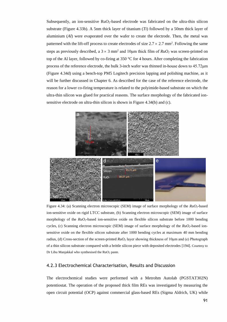
91
Subsequently, an ion-sensitive RuO2-based electrode was fabricated on the ultra-thin silicon
substrate (Figure 4.33b). A 5nm thick layer of titanium (Ti) followed by a 50nm thick layer of
aluminium (Al) were evaporated over the wafer to create the electrode. Then, the metal was
patterned with the lift-off process to create electrodes of size 2.7 2.7 mm2. Following the same
steps as previously described, a 3 3 mm2 and 10μm thick film of RuO2 was screen-printed on
top of the Al layer, followed by co-firing at 350 °C for 4 hours. After completing the fabrication
process of the reference electrode, the bulk 3-inch wafer was thinned in-house down to 45.72μm
(Figure 4.34d) using a bench-top PM5 Logitech precision lapping and polishing machine, as it
will be further discussed in Chapter 6. As described for the case of the reference electrode, the
reason for a lower co-firing temperature is related to the polyimide-based substrate on which the
ultra-thin silicon was glued for practical reasons. The surface morphology of the fabricated ion-
sensitive electrode on ultra-thin silicon is shown in Figure 4.34(b) and (c).
Figure 4.34: (a) Scanning electron microscopic (SEM) image of surface morphology of the RuO2-based
ion-sensitive oxide on rigid LTCC substrate, (b) Scanning electron microscopic (SEM) image of surface
morphology of the RuO2-based ion-sensitive oxide on flexible silicon substrate before 1000 bending
cycles, (c) Scanning electron microscopic (SEM) image of surface morphology of the RuO2-based ion-
sensitive oxide on the flexible silicon substrate after 1000 bending cycles at maximum 40 mm bending
radius, (d) Cross-section of the screen-printed RuO2 layer showing thickness of 10μm and (e) Photograph
of a thin silicon substrate compared with a brittle silicon piece with deposited electrodes [194]. Courtesy to
Dr Libu Manjakkal who synthesised the RuO2 paste.
4.2.3 Electrochemical Characterisation, Results and Discussion
The electrochemical studies were performed with a Metrohm Autolab (PGSTAT302N)
potentiostat. The operation of the proposed thick film REs was investigated by measuring the
open circuit potential (OCP) against commercial glass-based REs (Sigma Aldrich, UK) while
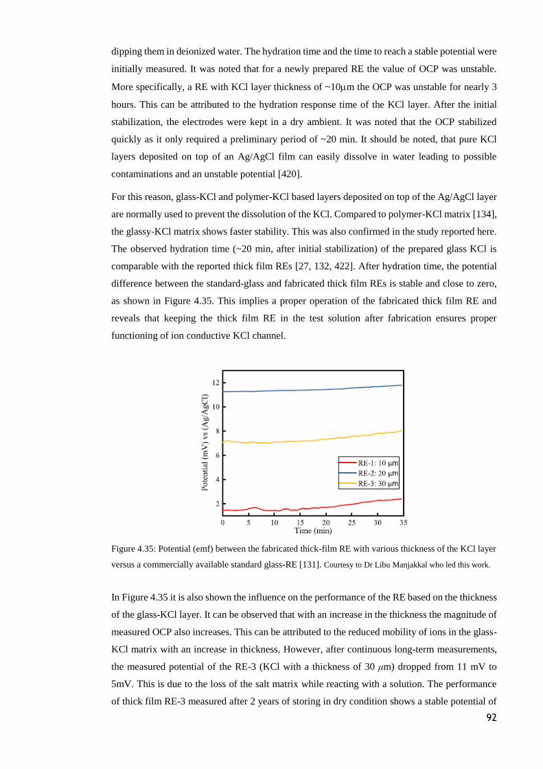
92
dipping them in deionized water. The hydration time and the time to reach a stable potential were
initially measured. It was noted that for a newly prepared RE the value of OCP was unstable.
More specifically, a RE with KCl layer thickness of ~10m the OCP was unstable for nearly 3
hours. This can be attributed to the hydration response time of the KCl layer. After the initial
stabilization, the electrodes were kept in a dry ambient. It was noted that the OCP stabilized
quickly as it only required a preliminary period of ~20 min. It should be noted, that pure KCl
layers deposited on top of an Ag/AgCl film can easily dissolve in water leading to possible
contaminations and an unstable potential [420].
For this reason, glass-KCl and polymer-KCl based layers deposited on top of the Ag/AgCl layer
are normally used to prevent the dissolution of the KCl. Compared to polymer-KCl matrix [134],
the glassy-KCl matrix shows faster stability. This was also confirmed in the study reported here.
The observed hydration time (~20 min, after initial stabilization) of the prepared glass KCl is
comparable with the reported thick film REs [27, 132, 422]. After hydration time, the potential
difference between the standard-glass and fabricated thick film REs is stable and close to zero,
as shown in Figure 4.35. This implies a proper operation of the fabricated thick film RE and
reveals that keeping the thick film RE in the test solution after fabrication ensures proper
functioning of ion conductive KCl channel.
Figure 4.35: Potential (emf) between the fabricated thick-film RE with various thickness of the KCl layer
versus a commercially available standard glass-RE [131]. Courtesy to Dr Libu Manjakkal who led this work.
In Figure 4.35 it is also shown the influence on the performance of the RE based on the thickness
of the glass-KCl layer. It can be observed that with an increase in the thickness the magnitude of
measured OCP also increases. This can be attributed to the reduced mobility of ions in the glass-
KCl matrix with an increase in thickness. However, after continuous long-term measurements,
the measured potential of the RE-3 (KCl with a thickness of 30 μm) dropped from 11 mV to
5mV. This is due to the loss of the salt matrix while reacting with a solution. The performance
of thick film RE-3 measured after 2 years of storing in dry condition shows a stable potential of
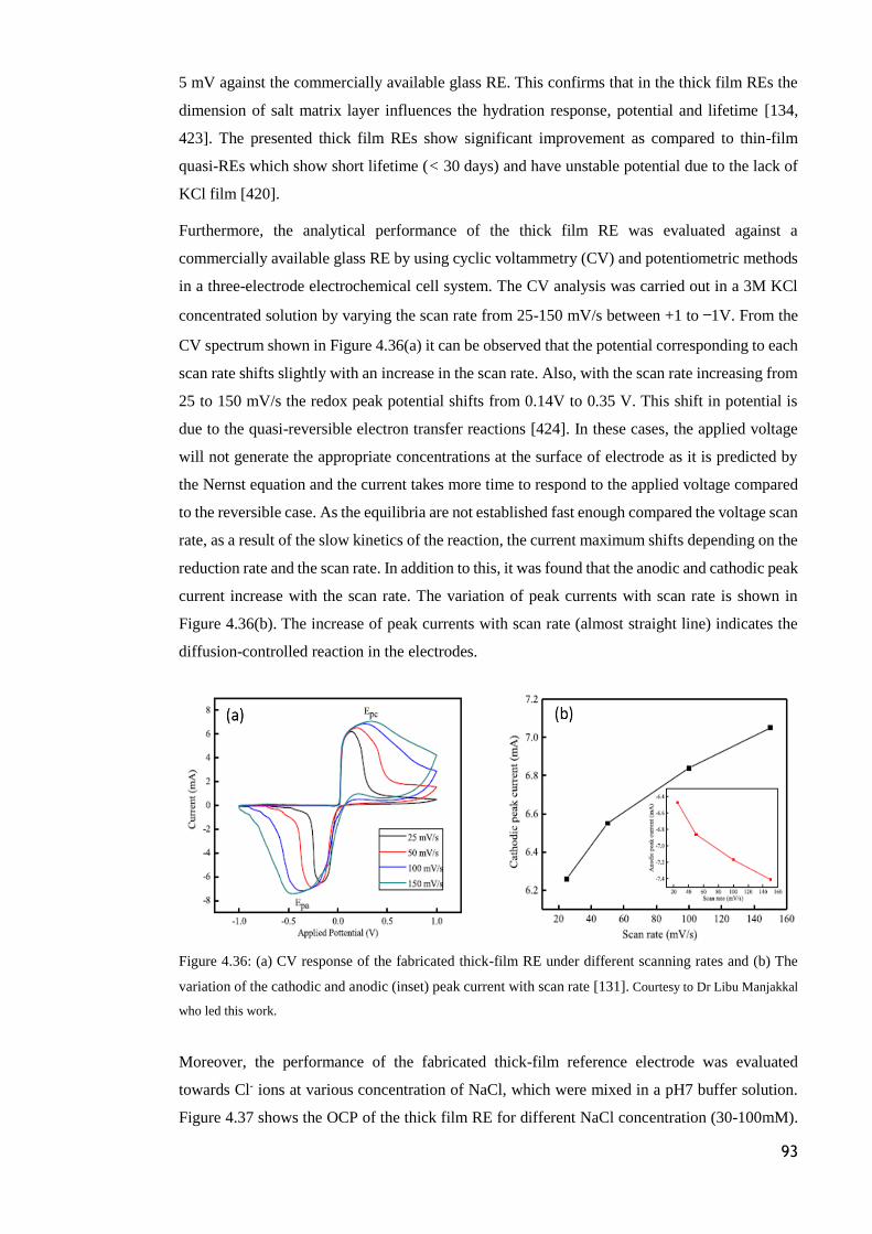
93
5 mV against the commercially available glass RE. This confirms that in the thick film REs the
dimension of salt matrix layer influences the hydration response, potential and lifetime [134,
423]. The presented thick film REs show significant improvement as compared to thin-film
quasi-REs which show short lifetime (< 30 days) and have unstable potential due to the lack of
KCl film [420].
Furthermore, the analytical performance of the thick film RE was evaluated against a
commercially available glass RE by using cyclic voltammetry (CV) and potentiometric methods
in a three-electrode electrochemical cell system. The CV analysis was carried out in a 3M KCl
concentrated solution by varying the scan rate from 25-150 mV/s between +1 to −1V. From the
CV spectrum shown in Figure 4.36(a) it can be observed that the potential corresponding to each
scan rate shifts slightly with an increase in the scan rate. Also, with the scan rate increasing from
25 to 150 mV/s the redox peak potential shifts from 0.14V to 0.35 V. This shift in potential is
due to the quasi-reversible electron transfer reactions [424]. In these cases, the applied voltage
will not generate the appropriate concentrations at the surface of electrode as it is predicted by
the Nernst equation and the current takes more time to respond to the applied voltage compared
to the reversible case. As the equilibria are not established fast enough compared the voltage scan
rate, as a result of the slow kinetics of the reaction, the current maximum shifts depending on the
reduction rate and the scan rate. In addition to this, it was found that the anodic and cathodic peak
current increase with the scan rate. The variation of peak currents with scan rate is shown in
Figure 4.36(b). The increase of peak currents with scan rate (almost straight line) indicates the
diffusion-controlled reaction in the electrodes.
Figure 4.36: (a) CV response of the fabricated thick-film RE under different scanning rates and (b) The
variation of the cathodic and anodic (inset) peak current with scan rate [131]. Courtesy to Dr Libu Manjakkal
who led this work.
Moreover, the performance of the fabricated thick-film reference electrode was evaluated
towards Cl- ions at various concentration of NaCl, which were mixed in a pH7 buffer solution.
Figure 4.37 shows the OCP of the thick film RE for different NaCl concentration (30-100mM).

94
The OCP of the electrode in each solution is almost stable after an initial drift and it shows
variations with different concentrations. These analytical performance and hydration response
studies show that the fabricated REs present a good alternative to glass REs.
Figure 4.37: Response of the fabricated thick-film reference electrode against a commercially available
glass Ag/AgCl reference electrode in different concentrations of NaCl [131]. Courtesy to Dr Libu Manjakkal
who led this work.
One of the main applications of planar reference electrodes is in the development of miniaturized
electrochemical sensors. Therefore, the fabricated thick-film REs were also characterised along
with the potentiometric RuO2-based pH-sensitive electrodes, which were fabricated as discussed
in Section 4.2.2. A detailed study of this pH sensor was needed to evaluate its applications in the
fields of biomedical, water and food quality monitoring in which the normal pH range varies
between 4.5 and 9. Here, the variation of potential with time was tested for pH values between 4
and 9. The OCP was recorded for 100 seconds for each solution. After cleaning the sensor, it was
transferred to the next pH solution. The OCP as a function pH values for the RuO2-based ion-
sensitive electrode on rigid LTCC and ultra-thin and flexible silicon substrates before and after
1000 bending cycles are shown in Figure 4.38.
Figure 4.38: (a) Open circuit potential as a function of pH for RuO2-based ion-sensitive electrode on rigid
LTCC substrate and (b) Open circuit potential as a function of pH for RuO2-based ion-sensitive electrode
on flexible silicon substrate before and after 1000 bending cycles at maximum 40mm bending radius [194].
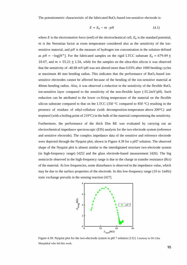
95
The potentiometric characteristic of the fabricated RuO2-based ion-sensitive electrode is:
𝐸 = 𝐸0 − 𝑚 · 𝑝𝐻 (4.1)
where 𝐸 is the electromotive force (emf) of the electrochemical cell, 𝐸0 is the standard potential,
𝑚 is the Nernstian factor at room temperature considered also as the sensitivity of the ion-
sensitive material, and 𝑝𝐻 is the measure of hydrogen ion concentration in the solution defined
as 𝑝𝐻 = −log [𝐻+]. For the fabricated samples on the rigid LTCC substrate 𝐸0 = 679.49 ±
10.47, and 𝑚 = 55.21 ± 1.56, while for the samples on the ultra-thin silicon it was observed
that the sensitivity of -40.68 mV/pH was not altered more than 0.03% after 1000 bending cycles
at maximum 40 mm bending radius. This indicates that the performance of RuO2-based ion-
sensitive electrodes cannot be affected because of the bending of the ion-sensitive material at
40mm bending radius. Also, it was observed a reduction in the sensitivity of the flexible RuO2
ion-sensitive layer compared to the sensitivity of the non-flexible layer (-55.2mV/pH). Such
reduction can be attributed to the lower co-firing temperature of the material on the flexible
silicon substrate compared to that on the LTCC (350 °C compared to 850 °C) resulting in the
presence of residues of ethyl-cellulose (with decomposition temperature above 200°C) and
terpineol (with a boiling point of 219°C) in the bulk of the material compromising the sensitivity.
Furthermore, the performance of the thick film RE was evaluated by carrying out an
electrochemical impedance spectroscopic (EIS) analysis for the two-electrode system (reference
and sensitive electrode). The complex impedance data of the sensitive and reference electrode
were depicted through the Nyquist plot, shown in Figure 4.39 for a pH7 solution. The observed
shape of the Nyquist plot is almost similar to the interdigitated structure two-electrode system
(in high-frequency range) [425] and the glass electrode-based measurement [426]. The big
semicircle observed in the high-frequency range is due to the charge in transfer resistance (Rct)
of the material. At low frequencies, some disturbance is observed in the impedance value, which
may be due to the surface properties of the electrode. In this low-frequency range (10 to 1mHz)
ionic exchange prevails in the sensing reaction [427].
Figure 4.39: Nyquist plot for the two-electrode system in pH 7 solution [131]. Courtesy to Dr Libu
Manjakkal who led this work.
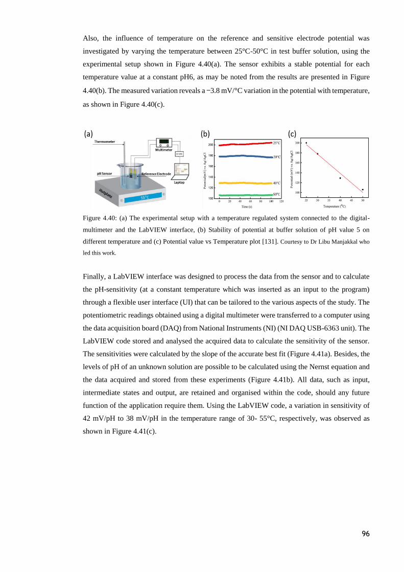
96
Also, the influence of temperature on the reference and sensitive electrode potential was
investigated by varying the temperature between 25°C-50°C in test buffer solution, using the
experimental setup shown in Figure 4.40(a). The sensor exhibits a stable potential for each
temperature value at a constant pH6, as may be noted from the results are presented in Figure
4.40(b). The measured variation reveals a −3.8 mV/°C variation in the potential with temperature,
as shown in Figure 4.40(c).
Figure 4.40: (a) The experimental setup with a temperature regulated system connected to the digital-
multimeter and the LabVIEW interface, (b) Stability of potential at buffer solution of pH value 5 on
different temperature and (c) Potential value vs Temperature plot [131]. Courtesy to Dr Libu Manjakkal who
led this work.
Finally, a LabVIEW interface was designed to process the data from the sensor and to calculate
the pH-sensitivity (at a constant temperature which was inserted as an input to the program)
through a flexible user interface (UI) that can be tailored to the various aspects of the study. The
potentiometric readings obtained using a digital multimeter were transferred to a computer using
the data acquisition board (DAQ) from National Instruments (NI) (NI DAQ USB-6363 unit). The
LabVIEW code stored and analysed the acquired data to calculate the sensitivity of the sensor.
The sensitivities were calculated by the slope of the accurate best fit (Figure 4.41a). Besides, the
levels of pH of an unknown solution are possible to be calculated using the Nernst equation and
the data acquired and stored from these experiments (Figure 4.41b). All data, such as input,
intermediate states and output, are retained and organised within the code, should any future
function of the application require them. Using the LabVIEW code, a variation in sensitivity of
42 mV/pH to 38 mV/pH in the temperature range of 30- 55°C, respectively, was observed as
shown in Figure 4.41(c).
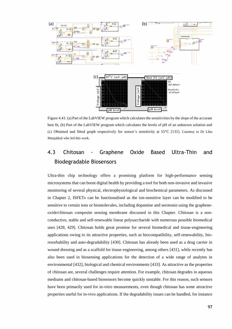
97
Figure 4.41: (a) Part of the LabVIEW program which calculates the sensitivities by the slope of the accurate
best fit, (b) Part of the LabVIEW program which calculates the levels of pH of an unknown solution and
(c) Obtained and fitted graph respectively for sensor’s sensitivity at 55°C [131]. Courtesy to Dr Libu
Manjakkal who led this work.
4.3 Chitosan - Graphene Oxide Based Ultra-Thin and
Biodegradable Biosensors
Ultra-thin chip technology offers a promising platform for high-performance sensing
microsystems that can boost digital health by providing a tool for both non-invasive and invasive
monitoring of several physical, electrophysiological and biochemical parameters. As discussed
in Chapter 2, ISFETs can be functionalised as the ion-sensitive layer can be modified to be
sensitive to certain ions or biomolecules, including dopamine and serotonin using the graphene-
oxide/chitosan composite sensing membrane discussed in this Chapter. Chitosan is a non-
conductive, stable and self-renewable linear polysaccharide with numerous possible biomedical
uses [428, 429]. Chitosan holds great promise for several biomedical and tissue-engineering
applications owing to its attractive properties, such as biocompatibility, self-renewability, bio-
resorbability and auto-degradability [430]. Chitosan has already been used as a drug carrier in
wound dressing and as a scaffold for tissue engineering, among others [431], while recently has
also been used in biosensing applications for the detection of a wide range of analytes in
environmental [432], biological and chemical environments [433]. As attractive as the properties
of chitosan are, several challenges require attention. For example, chitosan degrades in aqueous
mediums and chitosan-based biosensors become quickly unstable. For this reason, such sensors
have been primarily used for in-vitro measurements, even though chitosan has some attractive
properties useful for in-vivo applications. If the degradability issues can be handled, for instance
98
by tuning the surface properties of chitosan, then it would be possible for chitosan to be used in
unexplored areas.
A few methods have already been explored recently to overcome the issue of stability by using
glutaraldehyde and graphene oxide (GO). For example, with glutaraldehyde-chitosan cross-
linking, it has been possible to develop stable scaffold for 3D growth and proliferation of cell in
tissue engineering [431]. Furthermore, in the case of graphene oxide, the crosslinking between
carboxyl (-COOH) group of chitosan and hydroxyl (–OH) group of GO has been shown to
improve the stability [434]. Also, the chitosan-GO (chi-GO) surface offer suitable conditions for
metallization due to the improved stability, which helps the realisation of electrodes at its surface
towards the fabrication of contacts and other complex structures using microfabrication steps.
Due to body organs being soft and curvy, the in-vivo applications also require the Chi-GO sensors
to be flexible and conformable. In this regard, the presented studies in the following sections take
advantage of recent advances in flexible and stretchable electronics technology [27, 58, 194, 435,
436] to develop Chi-GO based ultra-thin and highly conformable sensors patches. Finally, it may
be noted that the presented Chit-GO sensing material can also be integrated with the CMOS chip
presented in Chapter 5, using various deposition techniques. The film may act as the sensing
material for several bio-chemical applications, as will be discussed in the following Sections.
4.3.1 Chitosan-Graphene Oxide-based ultra-thin conformable sensing patch
for cell-health monitoring
The developed patch comprises of an array of biosensors made from gold (Au) electrodes on
ultra-thin (2.8μm) and highly conformable GO-Chit substrate with a micro-gap of 60μm bridged
with human dermal fibroblast (HDF) cells. The fabricated sensors have been used to demonstrate
the label-free monitoring of proliferation of HDF cells [413].
4.3.1.1 Fabrication and Functionalisation of the GO-Chitosan Film
The ultra-thin GO-Chit film was prepared on cellulose acetate butyrate (CAB) film which acts
as the sacrificial layer and prevents mechanical damage of GO-Chit during fabrication peel off
from the substrate. The GO-Chit solution was prepared by dissolving 2ml of an aqueous solution
of GO (ultra-high concentrated single-layer GO solution, Graphene Supermarket, 6.2 g/l) and 0.5
g of CS (high molecular weight, Sigma Aldrich Co., 3050, USA) in 50 ml of distilled water
followed by 4.5 ml of 2% acetic acid. The solution was mixed using a magnetic stirrer at 1300
rpm for 12 hours at 40C until the GO is well dispersed in dissolved CS. The prepared CS-GO
solution was spun-coated at 1000 rpm for 30 s on pre-coated CAB on Si substrate. A 5 wt.%
CAB dissolved in ethyl-L-lactate which was used for pre-coating Si wafer was used as the
sacrificial layer. The spin-coated GO-Chit on CAB/Si was dried overnight before metallization.
Subsequently, a thin layer of gold (Ti/Au) of thickness 10/30 nm was evaporated on the CS-GO
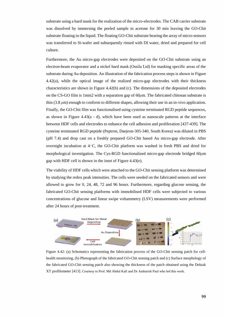
99
substrate using a hard mask for the realization of the micro-electrodes. The CAB carrier substrate
was dissolved by immersing the peeled sample in acetone for 30 min leaving the GO-Chit
substrate floating in the liquid. The floating GO-Chit substrate bearing the array of micro-sensors
was transferred to Si-wafer and subsequently rinsed with DI water, dried and prepared for cell
culture.
Furthermore, the Au micro-gap electrodes were deposited on the GO-Chit substrate using an
electron-beam evaporator and a nickel hard mask (Ossila Ltd) for masking specific areas of the
substrate during Au deposition. An illustration of the fabrication process steps is shown in Figure
4.42(a), while the optical image of the realized micro-gap electrodes with their thickness
characteristics are shown in Figure 4.42(b) and (c). The dimensions of the deposited electrodes
on the CS-GO film is 1mm2 with a separation gap of 60μm. The fabricated chitosan substrate is
thin (3.8 μm) enough to conform to different shapes, allowing their use in an in-vivo application.
Finally, the GO-Chit film was functionalised using cysteine terminated RGD peptide sequences,
as shown in Figure 4.43(a - d), which have been used as nanoscale patterns at the interface
between HDF cells and electrodes to enhance the cell adhesion and proliferation [437-439]. The
cysteine terminated RGD peptide (Peptron, Daejeon-305-340, South Korea) was diluted in PBS
(pH 7.4) and drop cast on a freshly prepared GO-Chit based Au micro-gap electrode. After
overnight incubation at 4C, the GO-Chit platform was washed in fresh PBS and dried for
morphological investigation. The Cys-RGD functionalized micro-gap electrode bridged 60μm
gap with HDF cell is shown in the inset of Figure 4.43(e).
The viability of HDF cells which were attached to the GO-Chit sensing platform was determined
by studying the redox peak intensities. The cells were seeded on the fabricated sensors and were
allowed to grow for 0, 24, 48, 72 and 96 hours. Furthermore, regarding glucose sensing, the
fabricated GO-Chit sensing platforms with immobilised HDF cells were subjected to various
concentrations of glucose and linear swipe voltammetry (LSV) measurements were performed
after 24 hours of post-treatment.
Figure 4.42: (a) Schematics representing the fabrication process of the GO-Chit sensing patch for cell-
health monitoring, (b) Photograph of the fabricated GO-Chit sensing patch and (c) Surface morphology of
the fabricated GO-Chit sensing patch also showing the thickness of the patch obtained using the Dektak
XT profilometer [413]. Courtesy to Prof. Md Abdul Kafi and Dr Ambarish Paul who led this work.
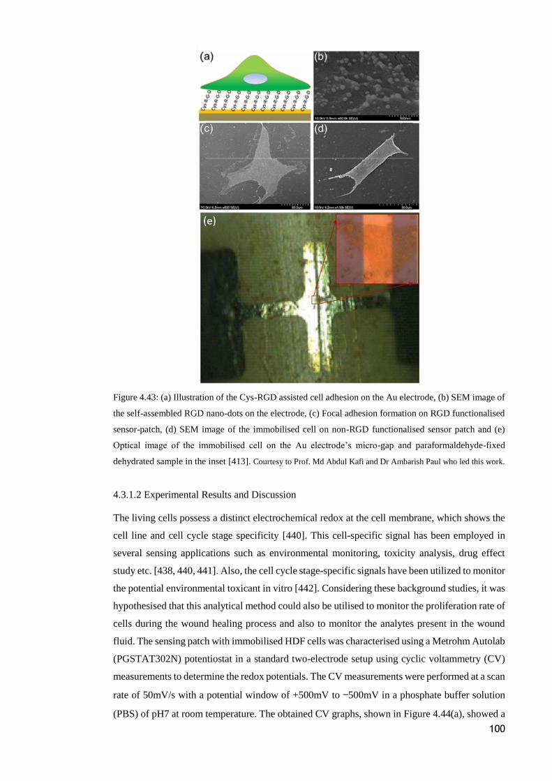
100
Figure 4.43: (a) Illustration of the Cys-RGD assisted cell adhesion on the Au electrode, (b) SEM image of
the self-assembled RGD nano-dots on the electrode, (c) Focal adhesion formation on RGD functionalised
sensor-patch, (d) SEM image of the immobilised cell on non-RGD functionalised sensor patch and (e)
Optical image of the immobilised cell on the Au electrode’s micro-gap and paraformaldehyde-fixed
dehydrated sample in the inset [413]. Courtesy to Prof. Md Abdul Kafi and Dr Ambarish Paul who led this work.
4.3.1.2 Experimental Results and Discussion
The living cells possess a distinct electrochemical redox at the cell membrane, which shows the
cell line and cell cycle stage specificity [440]. This cell-specific signal has been employed in
several sensing applications such as environmental monitoring, toxicity analysis, drug effect
study etc. [438, 440, 441]. Also, the cell cycle stage-specific signals have been utilized to monitor
the potential environmental toxicant in vitro [442]. Considering these background studies, it was
hypothesised that this analytical method could also be utilised to monitor the proliferation rate of
cells during the wound healing process and also to monitor the analytes present in the wound
fluid. The sensing patch with immobilised HDF cells was characterised using a Metrohm Autolab
(PGSTAT302N) potentiostat in a standard two-electrode setup using cyclic voltammetry (CV)
measurements to determine the redox potentials. The CV measurements were performed at a scan
rate of 50mV/s with a potential window of +500mV to −500mV in a phosphate buffer solution
(PBS) of pH7 at room temperature. The obtained CV graphs, shown in Figure 4.44(a), showed a

101
quasi-reversible redox peak with cathodic peak (Ipc) at +300mV and anodic peak (Ipa) at −
300mV. The absence of these peaks from sensors which lack immobilised HDF cells confirmed
that such redox reactions originated from the immobilised HDF cells. The quasi-reversibility was
confirmed with the peak potential difference ≥100mV between Ipc – Ipa and the current ratio
Ipc/Ipa is ≥1 [443, 444]. Also, freshly prepared sensor-patches were subjected to CV
measurements for 50 scan cycles at similar potential windows and scan rates to verify the
robustness of the measurements. The redox peak showed stability to scan rates and scan cycles
and no significant difference in the current peak was observed for up to 50 scan cycles, as shown
in Figure 4.44(b).
Figure 4.44: (a) Cyclic voltammetry graph obtained from a GO-Chit substrate with HDF cells immobilised
and (b) Cyclic voltammetry graph obtained from a GO-Chit substrate with HDF cells immobilised run for
50 cycles [413]. Courtesy to Prof. Md Abdul Kafi and Dr Ambarish Paul who led this work.
Finally, the developed GO-Chit sensing platform with immobilised HDF cells was used to
monitor the proliferation of cells in-vitro. To monitor this, the sensing patch was employed for
CV measurement at 24 hours interval and the cell proliferation was monitored over the growth
period up to 96 hours. The CV peak intensities became prominent with increased cell growth
period as shown in Figure 4.45(a). Both Ipc and Ipa peak showed a similar trend of enhancement
without any peak shift and therefore, both peak values obtained from voltammogram could be
considered as sensing values. A linear plot was obtained between the current intensities Ipc and
post-seeding periods, as shown in Figure 4.45(b). This peak enhancement is due to the redox of
an increased number of cells bridging the micro-gap electrode [445].
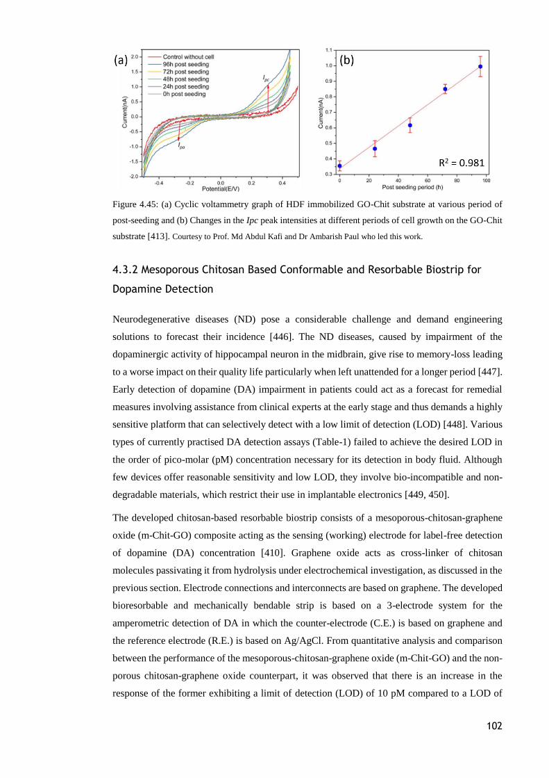
102
Figure 4.45: (a) Cyclic voltammetry graph of HDF immobilized GO-Chit substrate at various period of
post-seeding and (b) Changes in the Ipc peak intensities at different periods of cell growth on the GO-Chit
substrate [413]. Courtesy to Prof. Md Abdul Kafi and Dr Ambarish Paul who led this work.
4.3.2 Mesoporous Chitosan Based Conformable and Resorbable Biostrip for
Dopamine Detection
Neurodegenerative diseases (ND) pose a considerable challenge and demand engineering
solutions to forecast their incidence [446]. The ND diseases, caused by impairment of the
dopaminergic activity of hippocampal neuron in the midbrain, give rise to memory-loss leading
to a worse impact on their quality life particularly when left unattended for a longer period [447].
Early detection of dopamine (DA) impairment in patients could act as a forecast for remedial
measures involving assistance from clinical experts at the early stage and thus demands a highly
sensitive platform that can selectively detect with a low limit of detection (LOD) [448]. Various
types of currently practised DA detection assays (Table-1) failed to achieve the desired LOD in
the order of pico-molar (pM) concentration necessary for its detection in body fluid. Although
few devices offer reasonable sensitivity and low LOD, they involve bio-incompatible and non-
degradable materials, which restrict their use in implantable electronics [449, 450].
The developed chitosan-based resorbable biostrip consists of a mesoporous-chitosan-graphene
oxide (m-Chit-GO) composite acting as the sensing (working) electrode for label-free detection
of dopamine (DA) concentration [410]. Graphene oxide acts as cross-linker of chitosan
molecules passivating it from hydrolysis under electrochemical investigation, as discussed in the
previous section. Electrode connections and interconnects are based on graphene. The developed
bioresorbable and mechanically bendable strip is based on a 3-electrode system for the
amperometric detection of DA in which the counter-electrode (C.E.) is based on graphene and
the reference electrode (R.E.) is based on Ag/AgCl. From quantitative analysis and comparison
between the performance of the mesoporous-chitosan-graphene oxide (m-Chit-GO) and the non-
porous chitosan-graphene oxide counterpart, it was observed that there is an increase in the
response of the former exhibiting a limit of detection (LOD) of 10 pM compared to a LOD of

103
100nM observed from the later. Since the device involves biocompatible materials and utilizes
eco-friendly fabrication process, the work aligns well with green technology.
4.3.2.1 Design and Fabrication of the m-GO-Chitosan Based 3-Electrode Sensor
The fabrication process of the developed m-GO-Chit based 3-electrode sensors was initiated by
preparing a chitosan solution. High MW chitosan was used as the substrate because of its high
mechanical stability due to the long polymeric chain. To prepare 1% chitosan solution, 500 mg
of chitosan powder was added to 44.6 ml of DI water and stirred in a magnetic stirrer at 1200
rpm for 1 h at 37oC to achieve uniform dispersion. The chitosan was acetylated by the addition
of 4.4 ml of acetic acid to form a thick jelly like solution. The acetylated chitosan solution was
aspirated and stored at 4oC for the subsequent solution casting. The chitosan solution was then
drop-casted on a graphene sheet through a laser-cut PVC hard mask, the dimensions of which
are shown in Figure 4.46. The chitosan membrane formed on the hard-masked graphene sheet
was dried at room temperature for 12 hours before peeling off. Continuous and uniform layers of
mechanically exfoliated crumpled graphene flakes were transferred to the chitosan substrate in
the region where the chitosan solution was exposed to the graphene sheet. The chitosan
membrane with graphene interconnects was then peeled off and fixed on a rigid glass substrate
for further processing regarding the deposition of GO-Chit working electrode (WE) and Ag/AgCl
reference electrode (RE).
Figure 4.46: Design and dimensions of the laser-cut PVC hard mask [410]. Courtesy to Prof. Md Abdul Kafi
and Dr Ambarish Paul who led this work.
The mesoporous GO-Chit was prepared using the leaching process by the leading authors of this
study [410]. Briefly, glucose granules of average particle size 5μm were used as the particulate
and Chit-GO as the matrix. The granulated glucose was initially ground in a mortar and pestle to
yield a uniform size distribution before mixing with as prepared Chit-GO solution in the ratio 5:3
by wt. After 2 hours of the slow curing process, the sugar particles were leached and became of
size around 1μm prior solidification, giving an average pore size of 1μm. The GO-Chit solution,
which contains a uniform dispersion of GO micro-sheets forming a uniform GO network
throughout the bulk of Chit-GO solution was prepared as described in Section 4.3.1. The resultant
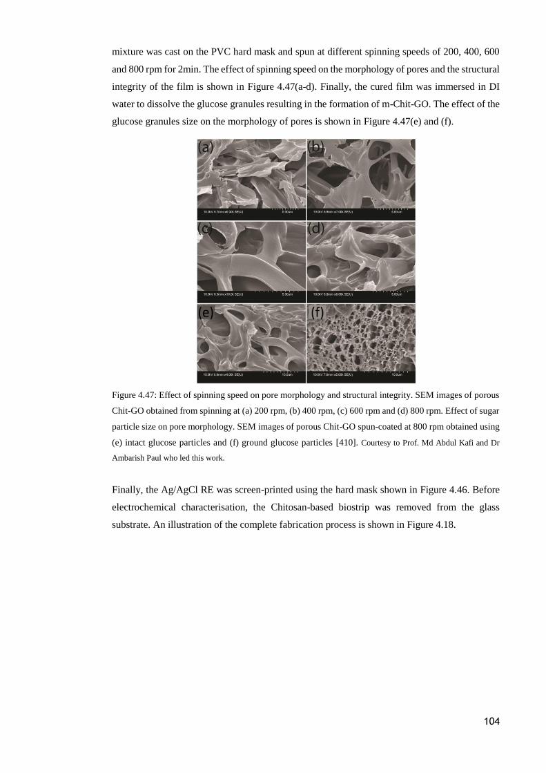
104
mixture was cast on the PVC hard mask and spun at different spinning speeds of 200, 400, 600
and 800 rpm for 2min. The effect of spinning speed on the morphology of pores and the structural
integrity of the film is shown in Figure 4.47(a-d). Finally, the cured film was immersed in DI
water to dissolve the glucose granules resulting in the formation of m-Chit-GO. The effect of the
glucose granules size on the morphology of pores is shown in Figure 4.47(e) and (f).
Figure 4.47: Effect of spinning speed on pore morphology and structural integrity. SEM images of porous
Chit-GO obtained from spinning at (a) 200 rpm, (b) 400 rpm, (c) 600 rpm and (d) 800 rpm. Effect of sugar
particle size on pore morphology. SEM images of porous Chit-GO spun-coated at 800 rpm obtained using
(e) intact glucose particles and (f) ground glucose particles [410]. Courtesy to Prof. Md Abdul Kafi and Dr
Ambarish Paul who led this work.
Finally, the Ag/AgCl RE was screen-printed using the hard mask shown in Figure 4.46. Before
electrochemical characterisation, the Chitosan-based biostrip was removed from the glass
substrate. An illustration of the complete fabrication process is shown in Figure 4.18.
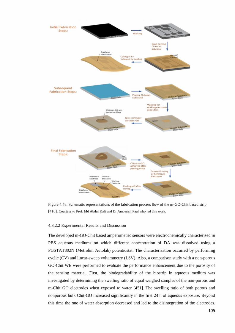
105
Figure 4.48: Schematic representations of the fabrication process flow of the m-GO-Chit based strip
[410]. Courtesy to Prof. Md Abdul Kafi and Dr Ambarish Paul who led this work.
4.3.2.2 Experimental Results and Discussion
The developed m-GO-Chit based amperometric sensors were electrochemically characterised in
PBS aqueous mediums on which different concentration of DA was dissolved using a
PGSTAT302N (Metrohm Autolab) potentiostat. The characterisation occurred by performing
cyclic (CV) and linear-sweep voltammetry (LSV). Also, a comparison study with a non-porous
GO-Chit WE were performed to evaluate the performance enhancement due to the porosity of
the sensing material. First, the biodegradability of the biostrip in aqueous medium was
investigated by determining the swelling ratio of equal weighed samples of the non-porous and
m-Chit GO electrodes when exposed to water [451]. The swelling ratio of both porous and
nonporous bulk Chit-GO increased significantly in the first 24 h of aqueous exposure. Beyond
this time the rate of water absorption decreased and led to the disintegration of the electrodes.
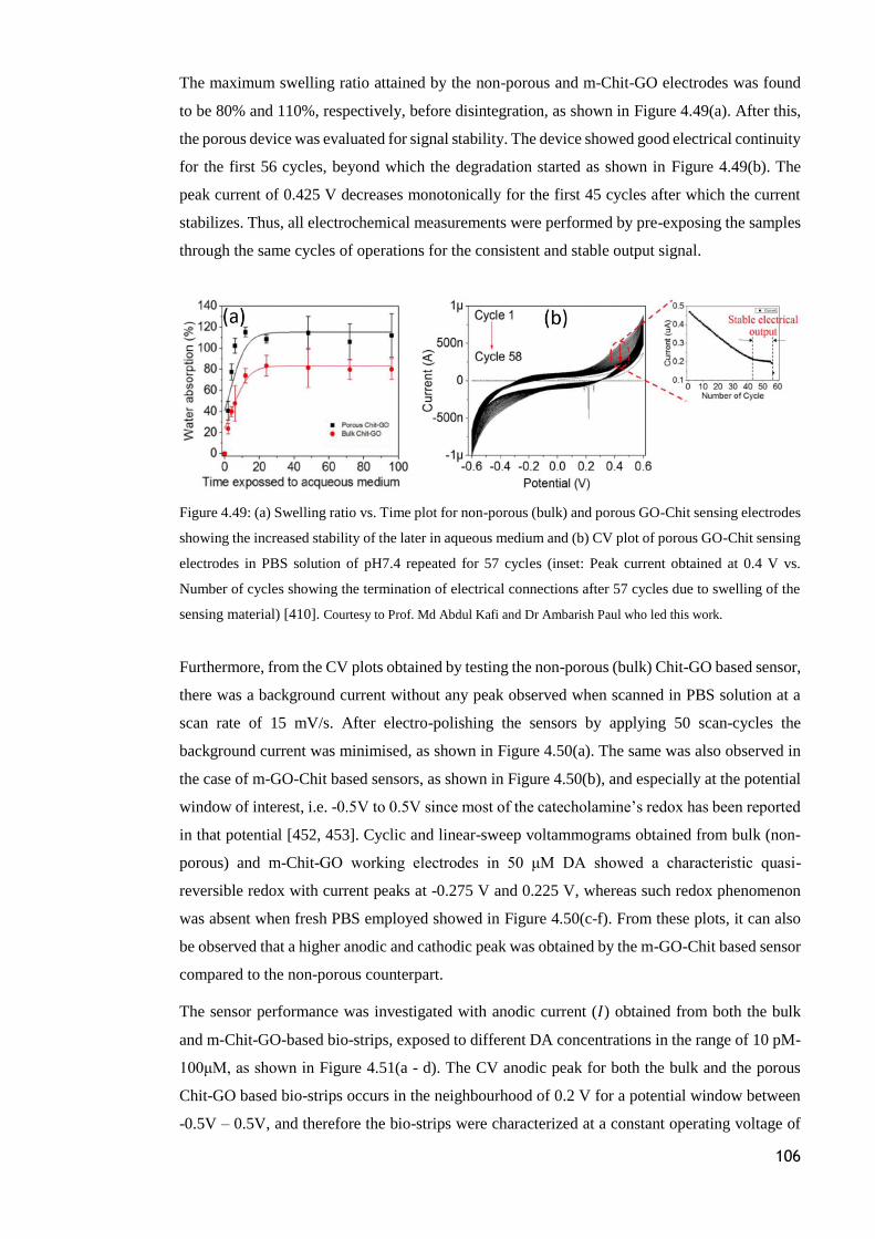
106
The maximum swelling ratio attained by the non-porous and m-Chit-GO electrodes was found
to be 80% and 110%, respectively, before disintegration, as shown in Figure 4.49(a). After this,
the porous device was evaluated for signal stability. The device showed good electrical continuity
for the first 56 cycles, beyond which the degradation started as shown in Figure 4.49(b). The
peak current of 0.425 V decreases monotonically for the first 45 cycles after which the current
stabilizes. Thus, all electrochemical measurements were performed by pre-exposing the samples
through the same cycles of operations for the consistent and stable output signal.
Figure 4.49: (a) Swelling ratio vs. Time plot for non-porous (bulk) and porous GO-Chit sensing electrodes
showing the increased stability of the later in aqueous medium and (b) CV plot of porous GO-Chit sensing
electrodes in PBS solution of pH7.4 repeated for 57 cycles (inset: Peak current obtained at 0.4 V vs.
Number of cycles showing the termination of electrical connections after 57 cycles due to swelling of the
sensing material) [410]. Courtesy to Prof. Md Abdul Kafi and Dr Ambarish Paul who led this work.
Furthermore, from the CV plots obtained by testing the non-porous (bulk) Chit-GO based sensor,
there was a background current without any peak observed when scanned in PBS solution at a
scan rate of 15 mV/s. After electro-polishing the sensors by applying 50 scan-cycles the
background current was minimised, as shown in Figure 4.50(a). The same was also observed in
the case of m-GO-Chit based sensors, as shown in Figure 4.50(b), and especially at the potential
window of interest, i.e. -0.5V to 0.5V since most of the catecholamine’s redox has been reported
in that potential [452, 453]. Cyclic and linear-sweep voltammograms obtained from bulk (non-
porous) and m-Chit-GO working electrodes in 50 μM DA showed a characteristic quasi-
reversible redox with current peaks at -0.275 V and 0.225 V, whereas such redox phenomenon
was absent when fresh PBS employed showed in Figure 4.50(c-f). From these plots, it can also
be observed that a higher anodic and cathodic peak was obtained by the m-GO-Chit based sensor
compared to the non-porous counterpart.
The sensor performance was investigated with anodic current (𝐼) obtained from both the bulk
and m-Chit-GO-based bio-strips, exposed to different DA concentrations in the range of 10 pM-
100μM, as shown in Figure 4.51(a - d). The CV anodic peak for both the bulk and the porous
Chit-GO based bio-strips occurs in the neighbourhood of 0.2 V for a potential window between
-0.5V – 0.5V, and therefore the bio-strips were characterized at a constant operating voltage of
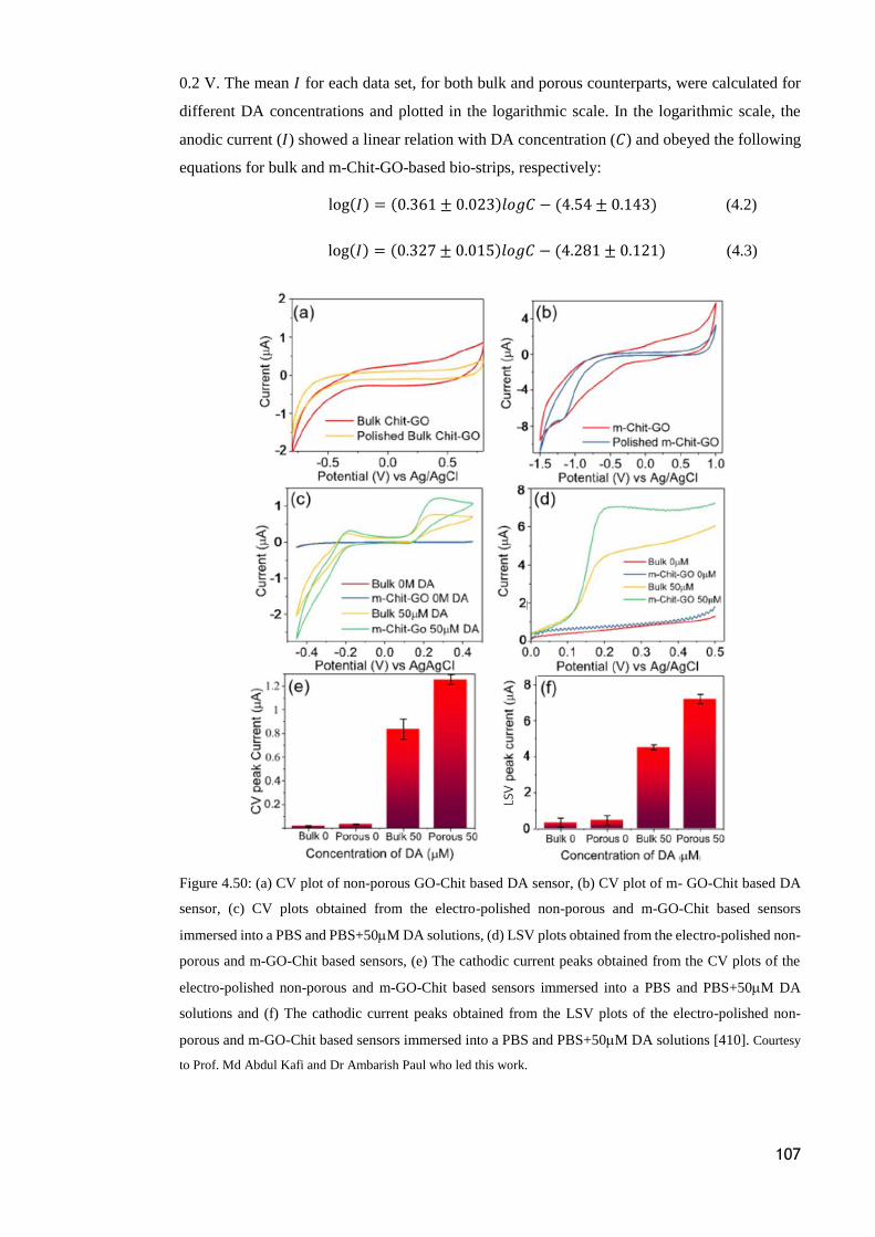
107
0.2 V. The mean 𝐼 for each data set, for both bulk and porous counterparts, were calculated for
different DA concentrations and plotted in the logarithmic scale. In the logarithmic scale, the
anodic current (𝐼) showed a linear relation with DA concentration (𝐶) and obeyed the following
equations for bulk and m-Chit-GO-based bio-strips, respectively:
log(𝐼) = (0.361 ± 0.023)𝑙𝑜𝑔𝐶 − (4.54 ± 0.143) (4.2)
log(𝐼) = (0.327 ± 0.015)𝑙𝑜𝑔𝐶 − (4.281 ± 0.121) (4.3)
Figure 4.50: (a) CV plot of non-porous GO-Chit based DA sensor, (b) CV plot of m- GO-Chit based DA
sensor, (c) CV plots obtained from the electro-polished non-porous and m-GO-Chit based sensors
immersed into a PBS and PBS+50M DA solutions, (d) LSV plots obtained from the electro-polished non-
porous and m-GO-Chit based sensors, (e) The cathodic current peaks obtained from the CV plots of the
electro-polished non-porous and m-GO-Chit based sensors immersed into a PBS and PBS+50M DA
solutions and (f) The cathodic current peaks obtained from the LSV plots of the electro-polished non-
porous and m-GO-Chit based sensors immersed into a PBS and PBS+50M DA solutions [410]. Courtesy
to Prof. Md Abdul Kafi and Dr Ambarish Paul who led this work.
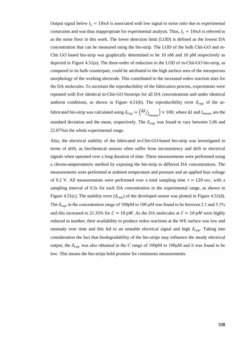
108
Output signal below 𝐼𝐿 = 10𝑛𝐴 is associated with low signal to noise ratio due to experimental
constraints and was thus inappropriate for experimental analysis. Thus, 𝐼𝐿 = 10𝑛𝐴 is referred to
as the noise floor in this work. The lower detection limit (LOD) is defined as the lowest DA
concentration that can be measured using the bio-strip. The LOD of the bulk Chit-GO and m-
Chit GO based bio-strip was graphically determined to be 10 nM and 10 pM respectively as
depicted in Figure 4.51(a). The three-order of reduction in the LOD of m-Chit-GO bio-strip, as
compared to its bulk counterpart, could be attributed to the high surface area of the mesoporous
morphology of the working electrode. This contributed to the increased redox reaction sites for
the DA molecules. To ascertain the reproducibility of the fabrication process, experiments were
repeated with five identical m-Chit-GO biostrips for all DA concentrations and under identical
ambient conditions, as shown in Figure 4.51(b). The reproducibility error 𝛿𝑟𝑒𝑝 of the as-
fabricated bio-strip was calculated using 𝛿𝑟𝑒𝑝 = (∆𝐼𝐼𝑚𝑒𝑎𝑛
⁄ ) × 100, where ∆𝐼 and 𝐼𝑚𝑒𝑎𝑛 are the
standard deviation and the mean, respectively. The 𝛿𝑟𝑒𝑝 was found to vary between 5.06 and
22.87%in the whole experimental range.
Also, the electrical stability of the fabricated m-Chit-GO-based bio-strip was investigated in
terms of drift, as biochemical sensors often suffer from inconsistency and drift in electrical
signals when operated over a long duration of time. These measurements were performed using
a chrono-amperometric method by exposing the bio-strip to different DA concentrations. The
measurements were performed at ambient temperature and pressure and an applied bias voltage
of 0.2 V. All measurements were performed over a total sampling time 𝜏 = 120 𝑠𝑒𝑐, with a
sampling interval of 0.5s for each DA concentration in the experimental range, as shown in
Figure 4.51(c). The stability error (𝛿𝑟𝑒𝑝) of the developed sensor was plotted in Figure 4.51(d).
The 𝛿𝑟𝑒𝑝 in the concentration range of 100pM to 100 μM was found to be between 2.1 and 5.3%
and this increased to 21.35% for 𝐶 = 10 𝑝𝑀. As the DA molecules at 𝐶 = 10 𝑝𝑀 were highly
reduced in number, their availability to produce redox reactions at the WE surface was low and
unsteady over time and this led to an unstable electrical signal and high 𝛿𝑟𝑒𝑝. Taking into
consideration the fact that biodegradability of the bio-strips may influence the steady electrical
output, the 𝛿𝑟𝑒𝑝 was also obtained in the C range of 100pM to 100μM and it was found to be
low. This means the bio-strips hold promise for continuous measurements.
109
Figure 4.51: (a) Calibration plot for non-porous sand m-GO-Chit based bio-strip in the DA concentration
range of 10 pM to 100M, (b) Characterisation of five different m-GO-Chit based sensors showing the
reproducibility error for different DA concentrations, (c) Chrono-amperometric plot for different DA
concentrations recorded for a total sampling time of 120 seconds showing the electrical stability and drift
in sensor performance over time and (d) Stability error and drift vs. DA concentration plot for m-GO-Chit
based sensors, inset: Comparative current vs. Time plot for non-porous and m-Chit-GO based bio-strips
for DA concentration of 10nM [410]. Courtesy to Prof. Md Abdul Kafi and Dr Ambarish Paul who led this work.
Finally, the developed m-GO-Chit amperometric sensors were characterised in terms of
specificity for DA. The specificity was investigated by performing CVs before and after mixing
uric acid (UA) and ascorbic acid (AA), which acted as the interfering agents, in the PBS+DA
solution. The concentration of the interfering agents was 50M. From the plot shown in Figure
4.22(a), the stoichiometric differences of the analytes DA, AA and UA became evident. Two
separate redox peaks from DA and UA were observed at 0.2 V and 0.4 V, respectively, whereas
a wide peak between 0.2 and 0.4 V was observed from AA indicating the redox peaks are analyte-
specific. When DA redox peaks were compared with that from a mixture of DA and UA solutions
(Figure 4.22b), two distinctly separated cathodic peaks of significantly enhanced current
intensities were observed, which was attributed to the increased concentration of DA-UA in the
solution. This was also confirmed by the disappearance of AA peaks when similar experiments
were conducted with DA and AA mixture solutions, as shown in Figure 4.22(c). When the
experiment was repeated with a mixture of DA, UA and AA, no characteristics peak of AA can
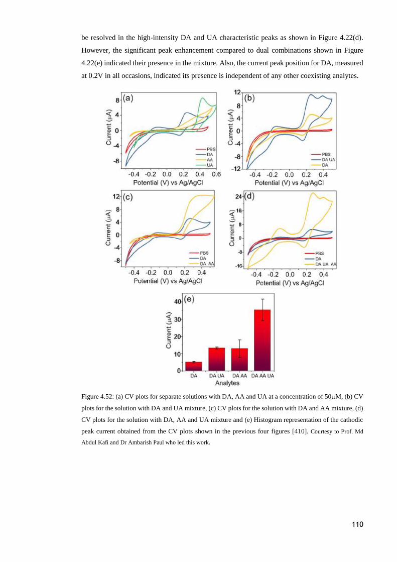
110
be resolved in the high-intensity DA and UA characteristic peaks as shown in Figure 4.22(d).
However, the significant peak enhancement compared to dual combinations shown in Figure
4.22(e) indicated their presence in the mixture. Also, the current peak position for DA, measured
at 0.2V in all occasions, indicated its presence is independent of any other coexisting analytes.
Figure 4.52: (a) CV plots for separate solutions with DA, AA and UA at a concentration of 50M, (b) CV
plots for the solution with DA and UA mixture, (c) CV plots for the solution with DA and AA mixture, (d)
CV plots for the solution with DA, AA and UA mixture and (e) Histogram representation of the cathodic
peak current obtained from the CV plots shown in the previous four figures [410]. Courtesy to Prof. Md
Abdul Kafi and Dr Ambarish Paul who led this work.
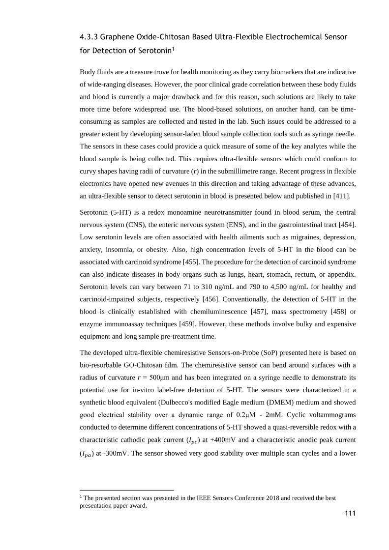
111
4.3.3 Graphene Oxide-Chitosan Based Ultra-Flexible Electrochemical Sensor
for Detection of Serotonin1
Body fluids are a treasure trove for health monitoring as they carry biomarkers that are indicative
of wide-ranging diseases. However, the poor clinical grade correlation between these body fluids
and blood is currently a major drawback and for this reason, such solutions are likely to take
more time before widespread use. The blood-based solutions, on another hand, can be time-
consuming as samples are collected and tested in the lab. Such issues could be addressed to a
greater extent by developing sensor-laden blood sample collection tools such as syringe needle.
The sensors in these cases could provide a quick measure of some of the key analytes while the
blood sample is being collected. This requires ultra-flexible sensors which could conform to
curvy shapes having radii of curvature (r) in the submillimetre range. Recent progress in flexible
electronics have opened new avenues in this direction and taking advantage of these advances,
an ultra-flexible sensor to detect serotonin in blood is presented below and published in [411].
Serotonin (5-HT) is a redox monoamine neurotransmitter found in blood serum, the central
nervous system (CNS), the enteric nervous system (ENS), and in the gastrointestinal tract [454].
Low serotonin levels are often associated with health ailments such as migraines, depression,
anxiety, insomnia, or obesity. Also, high concentration levels of 5-HT in the blood can be
associated with carcinoid syndrome [455]. The procedure for the detection of carcinoid syndrome
can also indicate diseases in body organs such as lungs, heart, stomach, rectum, or appendix.
Serotonin levels can vary between 71 to 310 ng/mL and 790 to 4,500 ng/mL for healthy and
carcinoid-impaired subjects, respectively [456]. Conventionally, the detection of 5-HT in the
blood is clinically established with chemiluminescence [457], mass spectrometry [458] or
enzyme immunoassay techniques [459]. However, these methods involve bulky and expensive
equipment and long sample pre-treatment time.
The developed ultra-flexible chemiresistive Sensors-on-Probe (SoP) presented here is based on
bio-resorbable GO-Chitosan film. The chemiresistive sensor can bend around surfaces with a
radius of curvature r = 500μm and has been integrated on a syringe needle to demonstrate its
potential use for in-vitro label-free detection of 5-HT. The sensors were characterized in a
synthetic blood equivalent (Dulbecco's modified Eagle medium (DMEM) medium and showed
good electrical stability over a dynamic range of 0.2μM - 2mM. Cyclic voltammograms
conducted to determine different concentrations of 5-HT showed a quasi-reversible redox with a
characteristic cathodic peak current (𝐼𝑝𝑐) at +400mV and a characteristic anodic peak current
(𝐼𝑝𝑎) at -300mV. The sensor showed very good stability over multiple scan cycles and a lower
1 The presented section was presented in the IEEE Sensors Conference 2018 and received the best
presentation paper award.
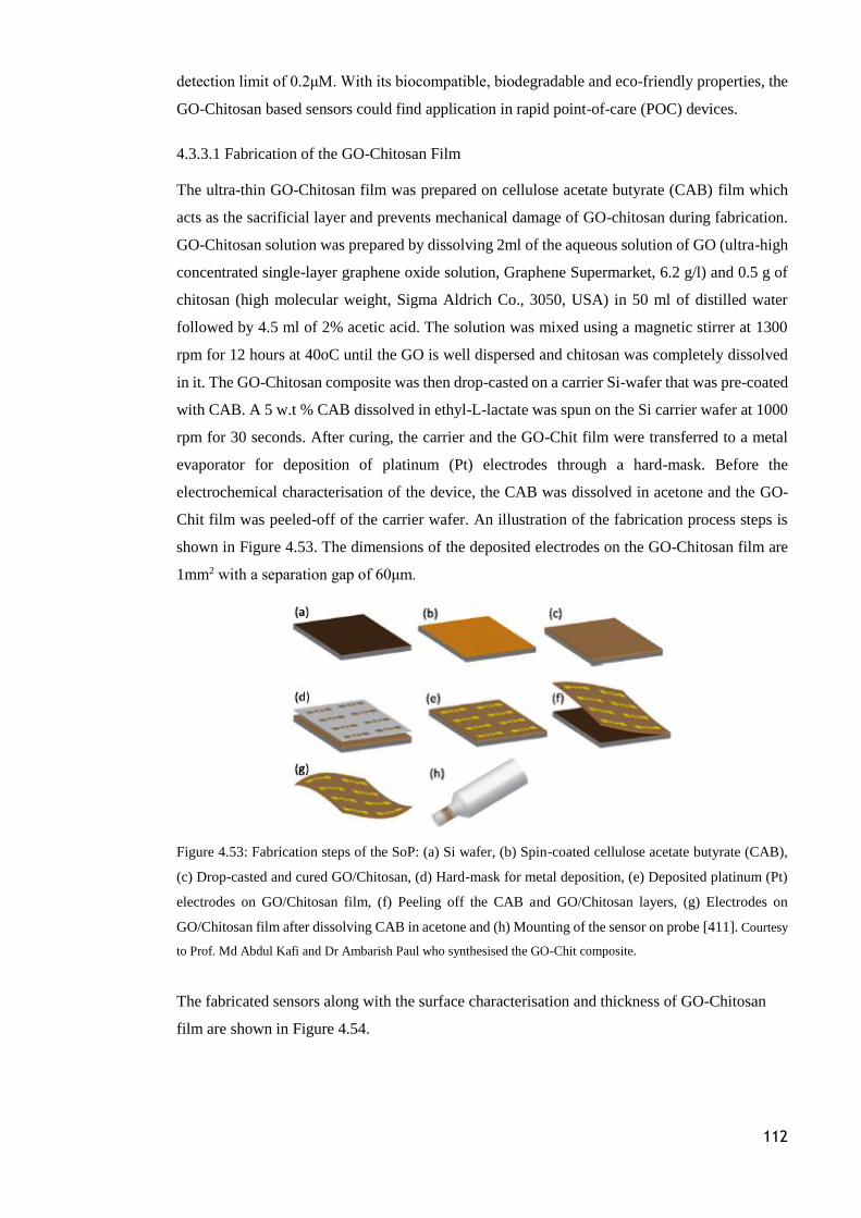
112
detection limit of 0.2μM. With its biocompatible, biodegradable and eco-friendly properties, the
GO-Chitosan based sensors could find application in rapid point-of-care (POC) devices.
4.3.3.1 Fabrication of the GO-Chitosan Film
The ultra-thin GO-Chitosan film was prepared on cellulose acetate butyrate (CAB) film which
acts as the sacrificial layer and prevents mechanical damage of GO-chitosan during fabrication.
GO-Chitosan solution was prepared by dissolving 2ml of the aqueous solution of GO (ultra-high
concentrated single-layer graphene oxide solution, Graphene Supermarket, 6.2 g/l) and 0.5 g of
chitosan (high molecular weight, Sigma Aldrich Co., 3050, USA) in 50 ml of distilled water
followed by 4.5 ml of 2% acetic acid. The solution was mixed using a magnetic stirrer at 1300
rpm for 12 hours at 40oC until the GO is well dispersed and chitosan was completely dissolved
in it. The GO-Chitosan composite was then drop-casted on a carrier Si-wafer that was pre-coated
with CAB. A 5 w.t % CAB dissolved in ethyl-L-lactate was spun on the Si carrier wafer at 1000
rpm for 30 seconds. After curing, the carrier and the GO-Chit film were transferred to a metal
evaporator for deposition of platinum (Pt) electrodes through a hard-mask. Before the
electrochemical characterisation of the device, the CAB was dissolved in acetone and the GO-
Chit film was peeled-off of the carrier wafer. An illustration of the fabrication process steps is
shown in Figure 4.53. The dimensions of the deposited electrodes on the GO-Chitosan film are
1mm2 with a separation gap of 60μm.
Figure 4.53: Fabrication steps of the SoP: (a) Si wafer, (b) Spin-coated cellulose acetate butyrate (CAB),
(c) Drop-casted and cured GO/Chitosan, (d) Hard-mask for metal deposition, (e) Deposited platinum (Pt)
electrodes on GO/Chitosan film, (f) Peeling off the CAB and GO/Chitosan layers, (g) Electrodes on
GO/Chitosan film after dissolving CAB in acetone and (h) Mounting of the sensor on probe [411]. Courtesy
to Prof. Md Abdul Kafi and Dr Ambarish Paul who synthesised the GO-Chit composite.
The fabricated sensors along with the surface characterisation and thickness of GO-Chitosan
film are shown in Figure 4.54.
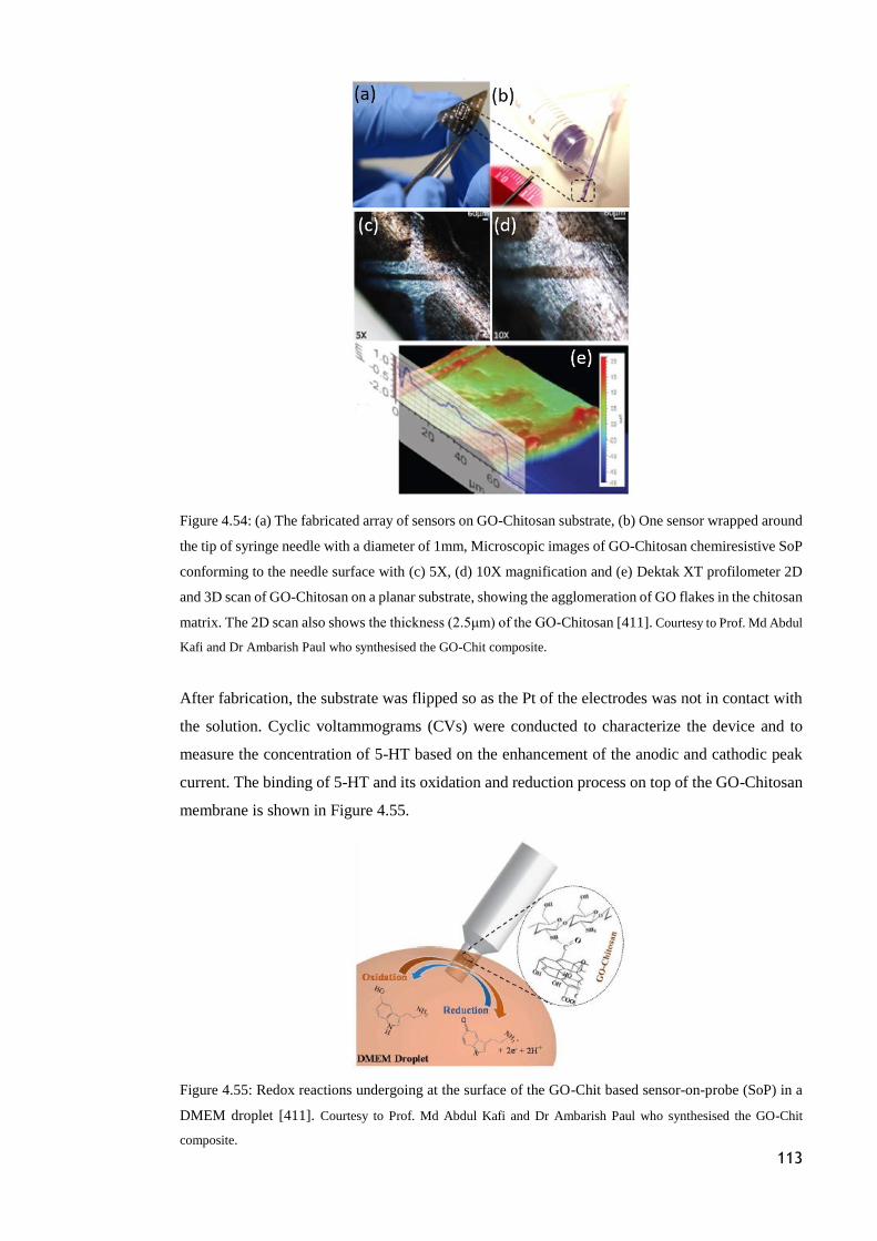
113
Figure 4.54: (a) The fabricated array of sensors on GO-Chitosan substrate, (b) One sensor wrapped around
the tip of syringe needle with a diameter of 1mm, Microscopic images of GO-Chitosan chemiresistive SoP
conforming to the needle surface with (c) 5X, (d) 10X magnification and (e) Dektak XT profilometer 2D
and 3D scan of GO-Chitosan on a planar substrate, showing the agglomeration of GO flakes in the chitosan
matrix. The 2D scan also shows the thickness (2.5μm) of the GO-Chitosan [411]. Courtesy to Prof. Md Abdul
Kafi and Dr Ambarish Paul who synthesised the GO-Chit composite.
After fabrication, the substrate was flipped so as the Pt of the electrodes was not in contact with
the solution. Cyclic voltammograms (CVs) were conducted to characterize the device and to
measure the concentration of 5-HT based on the enhancement of the anodic and cathodic peak
current. The binding of 5-HT and its oxidation and reduction process on top of the GO-Chitosan
membrane is shown in Figure 4.55.
Figure 4.55: Redox reactions undergoing at the surface of the GO-Chit based sensor-on-probe (SoP) in a
DMEM droplet [411]. Courtesy to Prof. Md Abdul Kafi and Dr Ambarish Paul who synthesised the GO-Chit
composite.
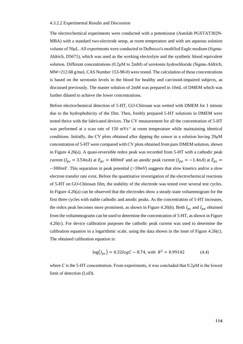
114
4.3.2.2 Experimental Results and Discussion
The electrochemical experiments were conducted with a potentiostat (Autolab PGSTAT302N-
MBA) with a standard two-electrode setup, at room temperature and with am aqueous solution
volume of 50μL. All experiments were conducted in Dulbecco's modified Eagle medium (Sigma-
Aldrich, D5671), which was used as the working electrolyte and the synthetic blood equivalent
solution. Different concentrations (0.2μM to 2mM) of serotonin hydrochloride (Sigma-Aldrich,
MW=212.68 g/mol, CAS Number 153-98-0) were tested. The calculation of these concentrations
is based on the serotonin levels in the blood for healthy and carcinoid-impaired subjects, as
discussed previously. The master solution of 2mM was prepared in 10mL of DMEM which was
further diluted to achieve the lower concentrations.
Before electrochemical detection of 5-HT, GO-Chitosan was wetted with DMEM for 1 minute
due to the hydrophobicity of the film. Then, freshly prepared 5-HT solutions in DMEM were
tested thrice with the fabricated devices. The CV measurement for all the concentration of 5-HT
was performed at a scan rate of 150 mVs-1 at room temperature while maintaining identical
conditions. Initially, the CV plots obtained after dipping the sensor in a solution having 20μM
concentration of 5-HT were compared with CV plots obtained from pure DMEM solution, shown
in Figure 4.26(a). A quasi-reversible redox peak was recorded from 5-HT with a cathodic peak
current (𝐼𝑝𝑐 = 3.54𝑛𝐴) at 𝐸𝑝𝑐 = 400𝑚𝑉 and an anodic peak current (𝐼𝑝𝑎 = −1.4𝑛𝐴) at 𝐸𝑝𝑐 =
−300𝑚𝑉. This separation in peak potential (>59mV) suggests that slow kinetics and/or a slow
electron transfer rate exist. Before the quantitative investigation of the electrochemical reactions
of 5-HT on GO-Chitosan film, the stability of the electrode was tested over several test cycles.
In Figure 4.26(a) can be observed that the electrodes show a steady-state voltammogram for the
first three cycles with stable cathodic and anodic peaks. As the concentration of 5-HT increases,
the redox peak becomes more prominent, as shown in Figure 4.26(b). Both 𝐼𝑝𝑐 and 𝐼𝑝𝑎 obtained
from the voltammograms can be used to determine the concentration of 5-HT, as shown in Figure
4.26(c). For device calibration purposes the cathodic peak current was used to determine the
calibration equation in a logarithmic scale, using the data shown in the inset of Figure 4.26(c).
The obtained calibration equation is:
log(𝐼𝑝𝑐) = 0.32𝑙𝑜𝑔𝐶 − 8.74, with 𝑅2 = 0.99142 (4.4)
where 𝐶 is the 5-HT concentration. From experiments, it was concluded that 0.2μM is the lowest
limit of detection (LoD).
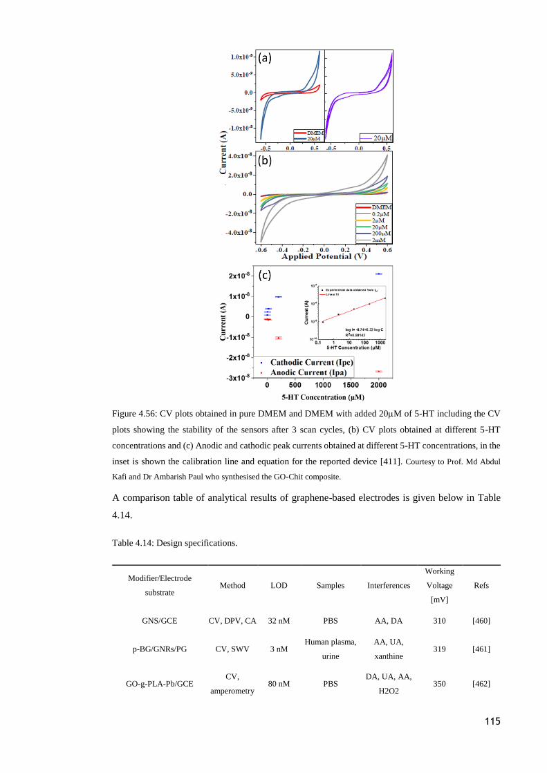
115
Figure 4.56: CV plots obtained in pure DMEM and DMEM with added 20M of 5-HT including the CV
plots showing the stability of the sensors after 3 scan cycles, (b) CV plots obtained at different 5-HT
concentrations and (c) Anodic and cathodic peak currents obtained at different 5-HT concentrations, in the
inset is shown the calibration line and equation for the reported device [411]. Courtesy to Prof. Md Abdul
Kafi and Dr Ambarish Paul who synthesised the GO-Chit composite.
A comparison table of analytical results of graphene-based electrodes is given below in Table
4.14.
Table 4.14: Design specifications.
Modifier/Electrode
substrate Method LOD Samples Interferences
Working
Voltage
[mV]
Refs
GNS/GCE CV, DPV, CA 32 nM PBS AA, DA 310 [460]
p-BG/GNRs/PG CV, SWV 3 nM Human plasma,
urine
AA, UA,
xanthine 319 [461]
GO-g-PLA-Pb/GCE CV,
amperometry 80 nM PBS
DA, UA, AA,
H2O2 350 [462]
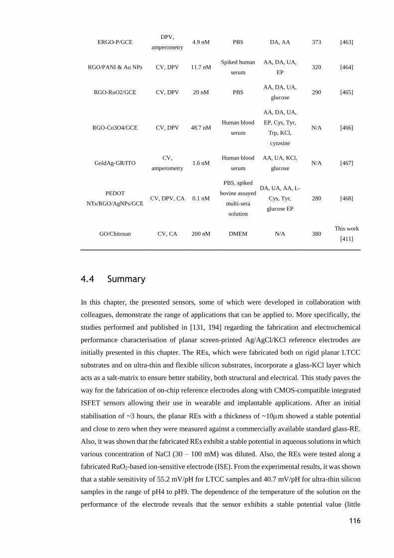
116
ERGO-P/GCE DPV,
amperometry 4.9 nM PBS DA, AA 373 [463]
RGO/PANI & Au NPs CV, DPV 11.7 nM Spiked human
serum
AA, DA, UA,
EP 320 [464]
RGO-RuO2/GCE CV, DPV 20 nM PBS AA, DA, UA,
glucose 290 [465]
RGO-Co3O4/GCE CV, DPV 48.7 nM Human blood
serum
AA, DA, UA,
EP, Cys, Tyr,
Trp, KCl,
cytosine
N/A [466]
GoldAg-GR/ITO CV,
amperometry 1.6 nM
Human blood
serum
AA, UA, KCl,
glucose N/A [467]
PEDOT
NTs/RGO/AgNPs/GCE CV, DPV, CA 0.1 nM
PBS, spiked
bovine assayed
multi-sera
solution
DA, UA, AA, L-
Cys, Tyr,
glucose EP
280 [468]
GO/Chitosan CV, CA 200 nM DMEM N/A 380 This work
[411]
4.4 Summary
In this chapter, the presented sensors, some of which were developed in collaboration with
colleagues, demonstrate the range of applications that can be applied to. More specifically, the
studies performed and published in [131, 194] regarding the fabrication and electrochemical
performance characterisation of planar screen-printed Ag/AgCl/KCl reference electrodes are
initially presented in this chapter. The REs, which were fabricated both on rigid planar LTCC
substrates and on ultra-thin and flexible silicon substrates, incorporate a glass-KCl layer which
acts as a salt-matrix to ensure better stability, both structural and electrical. This study paves the
way for the fabrication of on-chip reference electrodes along with CMOS-compatible integrated
ISFET sensors allowing their use in wearable and implantable applications. After an initial
stabilisation of ~3 hours, the planar REs with a thickness of ~10m showed a stable potential
and close to zero when they were measured against a commercially available standard glass-RE.
Also, it was shown that the fabricated REs exhibit a stable potential in aqueous solutions in which
various concentration of NaCl (30 – 100 mM) was diluted. Also, the REs were tested along a
fabricated RuO2-based ion-sensitive electrode (ISE). From the experimental results, it was shown
that a stable sensitivity of 55.2 mV/pH for LTCC samples and 40.7 mV/pH for ultra-thin silicon
samples in the range of pH4 to pH9. The dependence of the temperature of the solution on the
performance of the electrode reveals that the sensor exhibits a stable potential value (little
117
variation of -3.8 mV/°C) for each temperature. These are promising results showing that further
miniaturisation of these REs can be proven useful towards on-chip REs for microsystems
designed for various wearable and/or implantable applications.
Furthermore, the studies performed regarding the development of ultra-flexible, bio-resorbable
and eco-friendly graphene-oxide/chitosan-based biosensors for label-free amperometric and
chemiresistive detection of dopamine, uric acid, ascorbic acid, serotonin as well as monitoring
of cells’ proliferation published in [410, 411, 413] were also presented in this chapter. In section
4.3.1, the development of a GO-Chit based ultra-thin bio-platform is presented for cell-health
monitoring using a label-free electrochemical method. The CV plots of the sensors with HDF
cells immobilized at their surface showed a quasi-reversible redox behaviour with characteristic
cathodic peak (Ipc) and anodic peak (Ipa) at +300mV, and −300mV, respectively. The
measurements were taken at time intervals of 24 hours and the cell proliferation was monitored
over the growth period up to 96 hours. From CV plots it was observed an increase in both the
cathodic and anodic peak currents the growth period of HDF cell without potential shift reflecting
the numbers of the healthy cells attached on the electrode (0-96h). A linear plot (R2 = 0.981)
derived from Ipc vales with post-seeding period shows that the device is capable of monitoring
cell health by analyzing and quantifying the redox peak intensities [413].
Besides, the development of a mesoporous GO-Chit (m-GO-Chit) based working electrode was
discussed in section 4.3.2 and the electrochemical characterisation was presented. It was shown
that m-GO-Chit Wes exhibit a significantly lower LOD (10 pM) compared to the non-porous
GO-Chit (100nM), which was attributed to the increased surface area of mesoporous electrodes
which provided increased redox sites for DA molecules. The biostrip also offers good electrical
stability with stability error of 5.3% and reduced drift in sensor output which makes it suitable
for continuous monitoring. Also, good selectivity towards DA molecules against interfering
agents of UA and AA was shown. However, at low concentrations, increased drift was observed
at the output of the biostrip indicating that before use they should be calibrated [410].
Finally, an ultra-thin, flexible, biodegradable, and biocompatible GO modified chitosan-based
chemiresistor has been presented in section 4.3.3 for in-situ label-free detection of Serotonin (5-
HT). The GO-Chitosan composite is used both as the substrate of the electrodes as well as the 5-
HT sensitive layer. The presented serotonin sensor can be bent and conform to surfaces with very
small bending radii, in the micrometre scale. Cyclic voltammograms conducted to determine
different concentrations of 5-HT (0.2μM to 2mM) in DMEM showed a quasi-reversible redox
with a characteristic cathodic peak current (𝐼𝑝𝑐) at +400mV and a characteristic anodic peak
current (𝐼𝑝𝑎) at -300mV. The sensor showed very good stability over multiple scan cycles and a
lower detection limit of 0.2μM [411]. However, further investigation and optimisation of the
sensor and the measuring conditions could be proven useful and enhance the lowest limit of
detection.
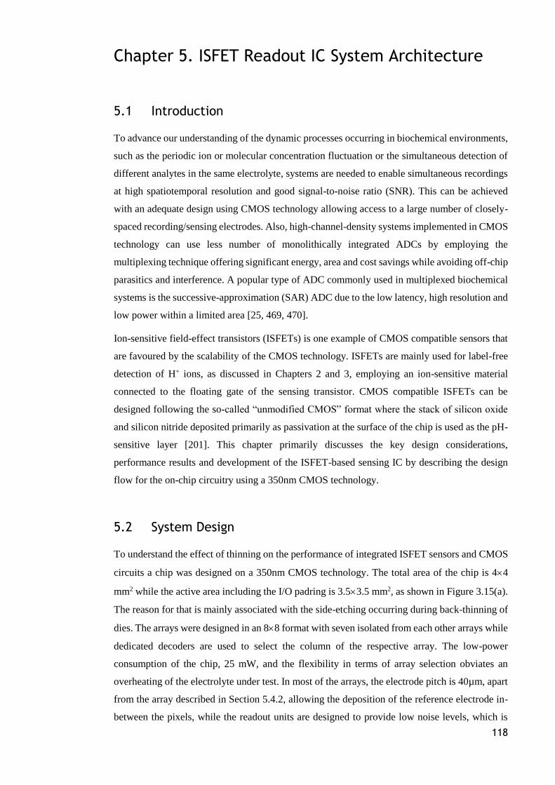
118
Chapter 5. ISFET Readout IC System Architecture
5.1 Introduction
To advance our understanding of the dynamic processes occurring in biochemical environments,
such as the periodic ion or molecular concentration fluctuation or the simultaneous detection of
different analytes in the same electrolyte, systems are needed to enable simultaneous recordings
at high spatiotemporal resolution and good signal-to-noise ratio (SNR). This can be achieved
with an adequate design using CMOS technology allowing access to a large number of closely-
spaced recording/sensing electrodes. Also, high-channel-density systems implemented in CMOS
technology can use less number of monolithically integrated ADCs by employing the
multiplexing technique offering significant energy, area and cost savings while avoiding off-chip
parasitics and interference. A popular type of ADC commonly used in multiplexed biochemical
systems is the successive-approximation (SAR) ADC due to the low latency, high resolution and
low power within a limited area [25, 469, 470].
Ion-sensitive field-effect transistors (ISFETs) is one example of CMOS compatible sensors that
are favoured by the scalability of the CMOS technology. ISFETs are mainly used for label-free
detection of H+ ions, as discussed in Chapters 2 and 3, employing an ion-sensitive material
connected to the floating gate of the sensing transistor. CMOS compatible ISFETs can be
designed following the so-called “unmodified CMOS” format where the stack of silicon oxide
and silicon nitride deposited primarily as passivation at the surface of the chip is used as the pH-
sensitive layer [201]. This chapter primarily discusses the key design considerations,
performance results and development of the ISFET-based sensing IC by describing the design
flow for the on-chip circuitry using a 350nm CMOS technology.
5.2 System Design
To understand the effect of thinning on the performance of integrated ISFET sensors and CMOS
circuits a chip was designed on a 350nm CMOS technology. The total area of the chip is 44
mm2 while the active area including the I/O padring is 3.53.5 mm2, as shown in Figure 3.15(a).
The reason for that is mainly associated with the side-etching occurring during back-thinning of
dies. The arrays were designed in an 88 format with seven isolated from each other arrays while
dedicated decoders are used to select the column of the respective array. The low-power
consumption of the chip, 25 mW, and the flexibility in terms of array selection obviates an
overheating of the electrolyte under test. In most of the arrays, the electrode pitch is 40µm, apart
from the array described in Section 5.4.2, allowing the deposition of the reference electrode in-
between the pixels, while the readout units are designed to provide low noise levels, which is
119
essential due to the low amplitude of the biochemical input signals. The amplified and
multiplexed signals are then connected to a passive RC low-pass filter (LPF) with a cut-off
frequency of 10 kHz and subsequently digitised at 90 kS/s by an on-chip 10-bit SAR ADC
(adopted from the library provided by the foundry). On-chip there is also one 10-bit DAC (cell
from the foundry’s library) which externally receives addresses to bias the active pixels of the
array under test. Finally, there are two unity-gain amplifiers to ensure proper biasing of pixels
and to drive as well as to settle the kickback caused by the charge rebalancing on the on-chip
SAR ADC input at the start of the acquisition period. Figure 3.15(b) shows the block diagram of
the finished chip.
Figure 5.57: (a) Finished chip layout and (b) Block diagram of the chip architecture.
5.3 System Requirements
To enable a broad range of experiments, the chip was designed aiming at a versatile platform
capable of recording multiple analytes. Even though the primary goal using this chip is towards
measurements of the pH of an electrolyte, it is possible to use the chip on other potentiometric
applications after proper post-processing and modification of the chip’s top sensing layer,
including the detection of dopamine and serotonin using the graphene-oxide/chitosan composite
sensing membrane discussed in Chapter 4. Therefore, as per the initial specifications, listed in
Table 5.15 below, the target is to design for a higher input signal amplitude range than that which
is considered adequate in pH monitoring applications. Besides, the chip was designed towards
low-power wearable applications and mainly for non-invasive pH monitoring of body fluids,
such as sweat and tears. To this end, the ICs were post-processed and the bulk of the silicon
substrate was removed using the lapping technique to realise dies with thickness ~30 µm to allow
them to comfortably be worn and be easily integrated into a wearable system which may require
compactness and conformability. To avoid side-etching of the I/O padring during chip thinning
using the lapping process, the active area of the die was restricted to 500 nm below the total area
of the chip, as shown in Figure 3.15(a). This 500 nm of bare silicon from each side of the die can
120
also be exploited during the post-processing of the die to fabricate, for instance, Pt-resistors that
can be used as temperature sensors. Finally, the pH range of interest is between 5 and 9 targeting
the detection of pH levels in the body fluids.
Table 5.15: Design specifications.
Maximum sensing area 60µm X 60µm
Maximum power per pixel 100µW
Input signal amplitude 10mVp-p
pH resolution 0.1 of pH
pH range 5 - 9
SNR ≥ 50 𝑑𝐵
THD ≤ −40 𝑑𝐵
Supply voltage ≤ 3.3V
5.4 Chip Architecture
Low total harmonic distortion (THD) and good signal-to-noise ratio (SNR), as well as transistor
matching uniformity, is desired across all pixels of each array to ensure good resolution in terms
of minimum detectable pH value. The IC presented in this thesis were designed using the
Cadence Virtuoso 6.1.6 platform and features 512 ISFET sensors and three different in-pixel
readout topologies, which were fabricated by Austria-Microsystems (AMS) in a 350nm, double-
poly, 4-metal CMOS process on a silicon p-doped substrate. The dedicated 4-bit decoders (3-bits
are the binary inputs and 1-bit is the “Enable”) receive externally addresses while each dedicated
8-to-1 analogue multiplexer passes the amplified pixel output signals to the passive LPF. The
splitting of the arrays offers four main advantages on the expense of a higher number of I/O pads:
(i) The easier compartmentation of the surface of the chip in case multiple analytes are measured
simultaneously, (ii) The reduction of the power consumption of the chip as there is the possibility
of turning-off selected arrays, (iii) The selection of a pseudo-random combination of pixels by
activating two or more arrays simultaneously allowing the simultaneous detection of pH from
different regions (and not in a rolling shutter fashion commonly employed) and (iv) Different
readout topologies can be used on the same die, mainly for test purposes, avoiding
channel-to-channel crosstalk present in multiplexed systems and caused by large voltage
differences between adjacent pixels. In the following sections, the three in-pixel analogue front-
end topologies are discussed.
121
5.4.1 Standard Pixel Readout Topology
The standard pixel readout is based on the source-follower (SF) configuration first introduced by
Bergveld [53]. In this configuration the drain current (𝐼𝐷𝑆) of ISFET is fixed while its source
voltage (𝑉𝑆) reflects the change in the pH of the electrolyte under test. The advantages of this
topology are the low power consumption, high-input impedance, low-output impedance and its
compactness as it requires only four transistors under the pH-sensing electrode, including the
active load, the sensing transistor and the low on-resistance transmission gate. However, source-
followers exhibit low PSRR which makes their use associated with a low-dropout (LDO) circuit
for keeping the power supply as stable as possible. Also, source-followers suffer from a second-
order effect termed as “body-effect”. That means that as the output voltage of the source follower
changes, the threshold voltage of the input transistor also changes as there is a dependence
between the threshold voltage and the source-to-bulk voltage (𝑉𝑆𝐵) of the input transistor. As a
result, the transconductance (𝑔𝑚) also changes. To minimise this effect, a PMOS source follower
was used in the expense of a higher output impedance due to the lower carrier mobility of PMOS
devices. Finally, the gain of the source-follower (Equation 5.1) suffers from nonlinearities due
to its dependence on the input signal amplitude and electrode’s offset reflected as variations in
the transconductance (𝑔𝑚) of the input transistor. However, with proper biasing these
nonlinearities are not significant given that linearity requirement in pH-sensing applications are
not very stringent, therefore the design of the different blocks in the signal chain can be relaxed
while maintaining the noise specifications.
𝐴𝑆𝐹 =
1
𝑔𝑚𝑏2||𝑟𝑜1||𝑟𝑜2
1
𝑔𝑚𝑏2||𝑟𝑜1||𝑟𝑜2+
1
𝑔𝑚2
(5.1)
where 𝑔𝑚𝑏 is the bulk-to-source transconductance, 𝑟𝑜 is the output resistance and 𝑔𝑚 is the gate-
to-source transconductance of the transistor.
The presented circuit operates at 1V with a total static power consumption of 3 µW providing
the ability to sense the full pH range (1 - 12). In the schematic and layout of this topology, shown
in Figure 5.58(a) and (b), the transistors M1 (WM1/LM1 = 2µm/1µm) and M2 (WM2/L M2 =
10µm/0.35µm), act as the active load and the ion-sensitive transistor, respectively. The floating
gate of M2 is connected through a four-metal stack to the top passivation layer, which consists
of a PECVD deposited stack of 1m silicon-nitride on top of a 1m layer of silicon-oxide. The
circuit also incorporates a low on-resistance transmission gate for column addressing. Scanning
of the array is achieved with on 4-bit (3 bits for addressing and 1 bit for “Enable”) decoder
addressing the columns and an 8-to-1 analogue multiplexer located outside the aperture of the
array reading the analogue output of the rows. Each pixel incorporates multiple guard-rings
around the sensing transistor and pixel topology to reduce the current injection and potential
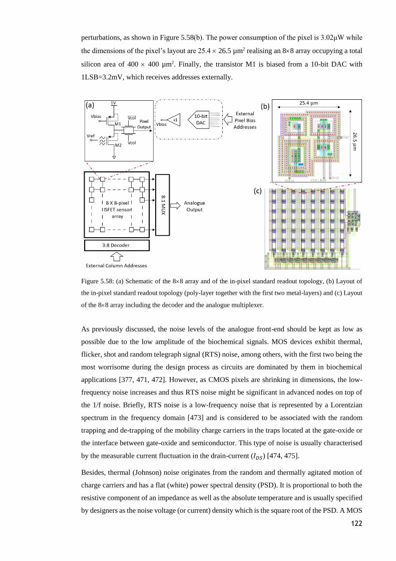
122
perturbations, as shown in Figure 5.58(b). The power consumption of the pixel is 3.02μW while
the dimensions of the pixel’s layout are 25.4 26.5 µm2 realising an 88 array occupying a total
silicon area of 400 400 µm2. Finally, the transistor M1 is biased from a 10-bit DAC with
1LSB=3.2mV, which receives addresses externally.
Figure 5.58: (a) Schematic of the 88 array and of the in-pixel standard readout topology, (b) Layout of
the in-pixel standard readout topology (poly-layer together with the first two metal-layers) and (c) Layout
of the 88 array including the decoder and the analogue multiplexer.
As previously discussed, the noise levels of the analogue front-end should be kept as low as
possible due to the low amplitude of the biochemical signals. MOS devices exhibit thermal,
flicker, shot and random telegraph signal (RTS) noise, among others, with the first two being the
most worrisome during the design process as circuits are dominated by them in biochemical
applications [377, 471, 472]. However, as CMOS pixels are shrinking in dimensions, the low-
frequency noise increases and thus RTS noise might be significant in advanced nodes on top of
the 1/f noise. Briefly, RTS noise is a low-frequency noise that is represented by a Lorentzian
spectrum in the frequency domain [473] and is considered to be associated with the random
trapping and de-trapping of the mobility charge carriers in the traps located at the gate-oxide or
the interface between gate-oxide and semiconductor. This type of noise is usually characterised
by the measurable current fluctuation in the drain-current (𝐼𝐷𝑆) [474, 475].
Besides, thermal (Johnson) noise originates from the random and thermally agitated motion of
charge carriers and has a flat (white) power spectral density (PSD). It is proportional to both the
resistive component of an impedance as well as the absolute temperature and is usually specified
by designers as the noise voltage (or current) density which is the square root of the PSD. A MOS

123
device exhibits thermal noise due to the resistive channel, polysilicon Gate resistor (𝑅𝐺),
substrate resistance and Source resistance while the latter depends on the effective channel-
length. Even though the Gate material is highly doped it can make a large contribution depending
on the dimensions and on how long is the Gate line prolonged. Therefore, 𝑅𝐺 depends on the
layout style. In ISFETs, 𝑅𝐺 is always higher in value because the gate of the sensing transistor is
extended to the surface of the die using all the available metal layers and vias of the CMOS
process that is used. Thus, the extended-Gate metal and the contact resistances between the
different metal layers further increase the value of 𝑅𝐺. Further, the thermal noise of the channel
can be represented by a noise current source between Drain and Source terminals (in parallel to
the 𝑔𝑚𝑉𝑔𝑠 current source in the small-signal MOS equivalent circuit) and can be expressed as:
𝑑𝐼𝐷𝑆2 =
4𝑘𝑇
𝑅𝑐ℎ𝑎𝑛𝑛𝑒𝑙𝑑𝑓 = 4𝑘𝑇
2
3𝑔𝑚𝑑𝑓 (5.2)
where 𝑘 is the Boltzmann’s constant [J/K] and 𝑇 is the temperature [K]. The channel noise current
(𝑑𝐼𝐷𝑆2 ) can be shifted to the input by dividing it by 𝑔𝑚
2 to get:
𝑑𝑉𝑒𝑞,𝑡ℎ2 = 4𝑘𝑇𝑅𝑒𝑓𝑓𝑑𝑓 (5.3)
where 𝑅𝑒𝑓𝑓 is:
𝑅𝑒𝑓𝑓 =2
3𝑔𝑚+ 𝑅𝐺 + 𝑅𝑆𝑜𝑢𝑟𝑐𝑒 + 𝑅𝐵𝑢𝑙𝑘(𝑛 − 1)2 (5.4)
where: (𝑛 − 1) =𝐶𝑑𝑒𝑝𝑙𝑒𝑡𝑖𝑜𝑛
𝐶𝑜𝑥=
𝑔𝑚𝑏
𝑔𝑚.
By contrast, the flicker (1/f) noise is considered to be associated with the surface states caused
by the cutting off of the silicon’s crystal structure at its surface where the gate oxide is grown on
top. Flicker noise has a power spectral density inversely proportional to the frequency up to the
1/f corner frequency, above which the flat PSD of thermal noise starts to dominate. The
expression commonly used for the equivalent input-referred flicker noise is:
𝑑𝑉𝑒𝑞,1/𝑓2 =
𝑘𝑓
𝑊𝐿𝐶𝑜𝑥2
𝑑𝑓
𝑓 (5.5)
where 𝑘𝑓 is a process-dependent coefficient, 𝑊𝐿 is the transistor’s size and 𝐶𝑜𝑥 is the gate-oxide
capacitance per unit area.
From Equation 5.5 it can be seen that a MOS device with thin gate-oxide and a large 𝑊 × 𝐿
product shows little 1/f noise. Besides, when thermal and flicker noise are examined together and
the equivalent input-referred noise is the sum of Equation 5.3 and 5.5, there is a crossover from
1/f to thermal noise and their asymptotes are met at a frequency termed as the “corner frequency,
𝑓𝑐”. The corner frequency proportionally depends on the DC-biasing current. Thus, as the
DC-biasing current (and therefore the power consumption) increases the transconductance
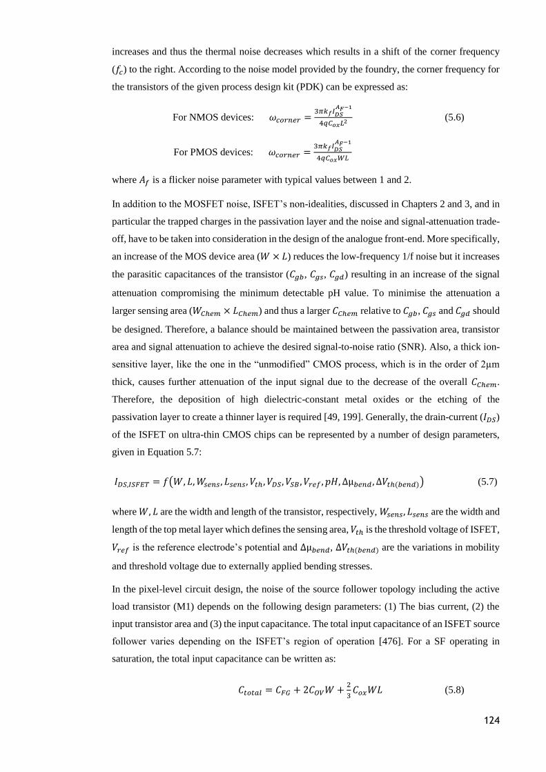
124
increases and thus the thermal noise decreases which results in a shift of the corner frequency
(𝑓𝑐) to the right. According to the noise model provided by the foundry, the corner frequency for
the transistors of the given process design kit (PDK) can be expressed as:
For NMOS devices: 𝜔𝑐𝑜𝑟𝑛𝑒𝑟 =3𝜋𝑘𝑓𝐼𝐷𝑆
𝐴𝐹−1
4𝑞𝐶𝑜𝑥𝐿2 (5.6)
For PMOS devices: 𝜔𝑐𝑜𝑟𝑛𝑒𝑟 =3𝜋𝑘𝑓𝐼𝐷𝑆
𝐴𝐹−1
4𝑞𝐶𝑜𝑥𝑊𝐿
where 𝐴𝑓 is a flicker noise parameter with typical values between 1 and 2.
In addition to the MOSFET noise, ISFET’s non-idealities, discussed in Chapters 2 and 3, and in
particular the trapped charges in the passivation layer and the noise and signal-attenuation trade-
off, have to be taken into consideration in the design of the analogue front-end. More specifically,
an increase of the MOS device area (𝑊 × 𝐿) reduces the low-frequency 1/f noise but it increases
the parasitic capacitances of the transistor (𝐶𝑔𝑏, 𝐶𝑔𝑠, 𝐶𝑔𝑑) resulting in an increase of the signal
attenuation compromising the minimum detectable pH value. To minimise the attenuation a
larger sensing area (𝑊𝐶ℎ𝑒𝑚 × 𝐿𝐶ℎ𝑒𝑚) and thus a larger 𝐶𝐶ℎ𝑒𝑚 relative to 𝐶𝑔𝑏, 𝐶𝑔𝑠 and 𝐶𝑔𝑑 should
be designed. Therefore, a balance should be maintained between the passivation area, transistor
area and signal attenuation to achieve the desired signal-to-noise ratio (SNR). Also, a thick ion-
sensitive layer, like the one in the “unmodified” CMOS process, which is in the order of 2µm
thick, causes further attenuation of the input signal due to the decrease of the overall 𝐶𝐶ℎ𝑒𝑚.
Therefore, the deposition of high dielectric-constant metal oxides or the etching of the
passivation layer to create a thinner layer is required [49, 199]. Generally, the drain-current (𝐼𝐷𝑆)
of the ISFET on ultra-thin CMOS chips can be represented by a number of design parameters,
given in Equation 5.7:
𝐼𝐷𝑆,𝐼𝑆𝐹𝐸𝑇 = 𝑓(𝑊, 𝐿,𝑊𝑠𝑒𝑛𝑠, 𝐿𝑠𝑒𝑛𝑠, 𝑉𝑡ℎ, 𝑉𝐷𝑆, 𝑉𝑆𝐵 , 𝑉𝑟𝑒𝑓 , 𝑝𝐻, ∆µ𝑏𝑒𝑛𝑑 , ∆𝑉𝑡ℎ(𝑏𝑒𝑛𝑑)) (5.7)
where 𝑊, 𝐿 are the width and length of the transistor, respectively, 𝑊𝑠𝑒𝑛𝑠, 𝐿𝑠𝑒𝑛𝑠 are the width and
length of the top metal layer which defines the sensing area, 𝑉𝑡ℎ is the threshold voltage of ISFET,
𝑉𝑟𝑒𝑓 is the reference electrode’s potential and ∆µ𝑏𝑒𝑛𝑑, ∆𝑉𝑡ℎ(𝑏𝑒𝑛𝑑) are the variations in mobility
and threshold voltage due to externally applied bending stresses.
In the pixel-level circuit design, the noise of the source follower topology including the active
load transistor (M1) depends on the following design parameters: (1) The bias current, (2) the
input transistor area and (3) the input capacitance. The total input capacitance of an ISFET source
follower varies depending on the ISFET’s region of operation [476]. For a SF operating in
saturation, the total input capacitance can be written as:
𝐶𝑡𝑜𝑡𝑎𝑙 = 𝐶𝐹𝐺 + 2𝐶𝑂𝑉𝑊 +2
3𝐶𝑜𝑥𝑊𝐿 (5.8)
125
where 𝐶𝐹𝐺 is the total capacitance at the floating gate of ISFET, 𝐶𝑜𝑥 is the Gate to Channel
capacitance per unit area [fF/µm2] and 𝐶𝑂𝑉 is the overlap parasitic capacitances per unit length
[fF/µm] between Gate, Source and Drain which are proportional only to the width (𝑊) of the
transistor.
Besides, the noise of the active load transistor (M1) has little effect on the overall 1/f noise and
can be designed freely according to the bias current requirements. Considering the noise
contribution of transistor M1 the total flicker noise PSD can be written as [477]:
𝑑𝑉𝑒𝑞,1/𝑓2 =
1
𝑓[
𝑘𝑓
𝑊2𝐿2𝐶𝑜𝑥2 + (
𝑔𝑚1
𝑔𝑚2)2 𝑘𝑓
𝑊1𝐿1𝐶𝑜𝑥2 ] (5.9)
where 𝑔𝑚1 and 𝑔𝑚2 are the transconductance of M1 and M2, respectively.
Figure 5.59: (a) Simulated SNR vs. Input signal amplitude and (b) THD vs. Input signal amplitude of the
standard readout topology at different strain condition (i.e. planar, tension and compression).
Finally, thermal noise has the main contribution in the white noise of the SF while shot noise can
be neglected during noise optimisation by design as it does not depend on the design parameters.
On contrary, shot noise depends on the Gate-to-Source leakage current (𝑖𝑛2 = 2𝑞𝐼𝐺𝑆∆𝑓), which
is negligible since 𝐼𝐺𝑆 is very small. Therefore, since thermal noise PSD in strong inversion and
saturation is given by Equation 5.3, the total input-referred noise contribution of the SF
(including the effect of externally applied stresses on ultra-thin CMOS dies) can be represented
as the sum of thermal and flicker noise and can be written as:
𝑑𝑉𝑡𝑜𝑡𝑎𝑙2 = [
𝑘𝑓
𝑊2(𝑏𝑒𝑛𝑑)𝐿2(𝑏𝑒𝑛𝑑)𝐶𝑜𝑥2 + (
𝑔𝑚1(𝑏𝑒𝑛𝑑)
𝑔𝑚2(𝑏𝑒𝑛𝑑))2 𝑘𝑓
𝑊1(𝑏𝑒𝑛𝑑)𝐿1(𝑏𝑒𝑛𝑑)𝐶𝑜𝑥2 ]
1
𝑓+ 4𝑘𝑇 [
2
3𝑔𝑚2(𝑏𝑒𝑛𝑑)+ 𝑅𝐺 + 𝑅𝑆𝑜𝑢𝑟𝑐𝑒 +
𝑅𝐵𝑢𝑙𝑘(𝑛 − 1)2] 𝑑𝑓 (5.10)
Finally, using the compact model presented in Chapter 3 (Section 3.4.1), the simulated SNR
versus input signal amplitude and THD versus input signal amplitude at different strain
conditions are shown in Figure 5.59. It may be noticed that a better performance (higher SNR
and lower THD) is observed at tensile stress while the opposite occurs at a compressive bending
scenario. The maximum percentage increase in SNR at tensile bending was found to be 3.43%
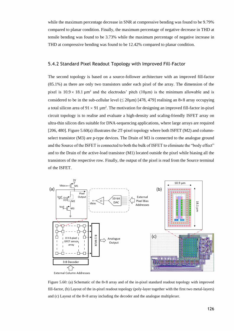
126
while the maximum percentage decrease in SNR at compressive bending was found to be 9.79%
compared to planar condition. Finally, the maximum percentage of negative decrease in THD at
tensile bending was found to be 3.73% while the maximum percentage of negative increase in
THD at compressive bending was found to be 12.42% compared to planar condition.
5.4.2 Standard Pixel Readout Topology with Improved Fill-Factor
The second topology is based on a source-follower architecture with an improved fill-factor
(85.1%) as there are only two transistors under each pixel of the array. The dimension of the
pixel is 10.9 18.1 µm2 and the electrodes’ pitch (10µm) is the minimum allowable and is
considered to be in the sub-cellular level (≤ 20µm) [478, 479] realising an 88 array occupying
a total silicon area of 91 91 µm2. The motivation for designing an improved fill-factor in-pixel
circuit topology is to realise and evaluate a high-density and scaling-friendly ISFET array on
ultra-thin silicon dies suitable for DNA-sequencing applications, where large arrays are required
[206, 480]. Figure 5.60(a) illustrates the 2T-pixel topology where both ISFET (M2) and column-
select transistor (M3) are p-type devices. The Drain of M3 is connected to the analogue ground
and the Source of the ISFET is connected to both the bulk of ISFET to eliminate the “body effect”
and to the Drain of the active-load transistor (M1) located outside the pixel while biasing all the
transistors of the respective row. Finally, the output of the pixel is read from the Source terminal
of the ISFET.
Figure 5.60: (a) Schematic of the 88 array and of the in-pixel standard readout topology with improved
fill-factor, (b) Layout of the in-pixel readout topology (poly-layer together with the first two metal-layers)
and (c) Layout of the 88 array including the decoder and the analogue multiplexer.
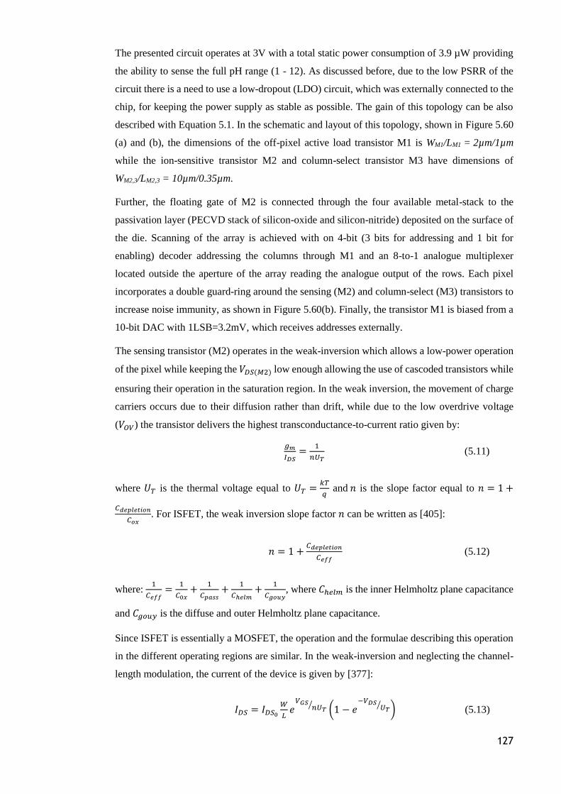
127
The presented circuit operates at 3V with a total static power consumption of 3.9 µW providing
the ability to sense the full pH range (1 - 12). As discussed before, due to the low PSRR of the
circuit there is a need to use a low-dropout (LDO) circuit, which was externally connected to the
chip, for keeping the power supply as stable as possible. The gain of this topology can be also
described with Equation 5.1. In the schematic and layout of this topology, shown in Figure 5.60
(a) and (b), the dimensions of the off-pixel active load transistor M1 is WM1/LM1 = 2µm/1µm
while the ion-sensitive transistor M2 and column-select transistor M3 have dimensions of
WM2,3/LM2,3 = 10µm/0.35µm.
Further, the floating gate of M2 is connected through the four available metal-stack to the
passivation layer (PECVD stack of silicon-oxide and silicon-nitride) deposited on the surface of
the die. Scanning of the array is achieved with on 4-bit (3 bits for addressing and 1 bit for
enabling) decoder addressing the columns through M1 and an 8-to-1 analogue multiplexer
located outside the aperture of the array reading the analogue output of the rows. Each pixel
incorporates a double guard-ring around the sensing (M2) and column-select (M3) transistors to
increase noise immunity, as shown in Figure 5.60(b). Finally, the transistor M1 is biased from a
10-bit DAC with 1LSB=3.2mV, which receives addresses externally.
The sensing transistor (M2) operates in the weak-inversion which allows a low-power operation
of the pixel while keeping the 𝑉𝐷𝑆(𝑀2) low enough allowing the use of cascoded transistors while
ensuring their operation in the saturation region. In the weak inversion, the movement of charge
carriers occurs due to their diffusion rather than drift, while due to the low overdrive voltage
(𝑉𝑂𝑉) the transistor delivers the highest transconductance-to-current ratio given by:
𝑔𝑚
𝐼𝐷𝑆=
1
𝑛𝑈𝑇 (5.11)
where 𝑈𝑇 is the thermal voltage equal to 𝑈𝑇 =𝑘𝑇
𝑞 and 𝑛 is the slope factor equal to 𝑛 = 1 +
𝐶𝑑𝑒𝑝𝑙𝑒𝑡𝑖𝑜𝑛
𝐶𝑜𝑥. For ISFET, the weak inversion slope factor 𝑛 can be written as [405]:
𝑛 = 1 +𝐶𝑑𝑒𝑝𝑙𝑒𝑡𝑖𝑜𝑛
𝐶𝑒𝑓𝑓 (5.12)
where: 1
𝐶𝑒𝑓𝑓=
1
𝐶0𝑥+
1
𝐶𝑝𝑎𝑠𝑠+
1
𝐶ℎ𝑒𝑙𝑚+
1
𝐶𝑔𝑜𝑢𝑦, where 𝐶ℎ𝑒𝑙𝑚 is the inner Helmholtz plane capacitance
and 𝐶𝑔𝑜𝑢𝑦 is the diffuse and outer Helmholtz plane capacitance.
Since ISFET is essentially a MOSFET, the operation and the formulae describing this operation
in the different operating regions are similar. In the weak-inversion and neglecting the channel-
length modulation, the current of the device is given by [377]:
𝐼𝐷𝑆 = 𝐼𝐷𝑆0
𝑊
𝐿𝑒
𝑉𝐺𝑆𝑛𝑈𝑇
⁄(1 − 𝑒
−𝑉𝐷𝑆𝑈𝑇
⁄) (5.13)
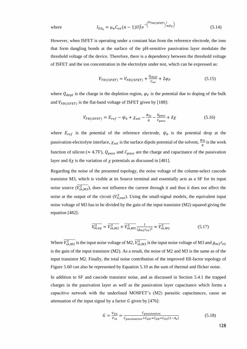
128
where 𝐼𝐷𝑆0= µ𝑛𝐶𝑜𝑥(𝑛 − 1)𝑈𝑇
2𝑒−(
𝑉𝑇𝐻(𝐼𝑆𝐹𝐸𝑇)𝑛𝑈𝑇
⁄ ) (5.14)
However, when ISFET is operating under a constant bias from the reference electrode, the ions
that form dangling bonds at the surface of the pH-sensitive passivation layer modulate the
threshold voltage of the device. Therefore, there is a dependency between the threshold voltage
of ISFET and the ion concentration in the electrolyte under test, which can be expressed as:
𝑉𝑇𝐻(𝐼𝑆𝐹𝐸𝑇) = 𝑉𝐹𝐵(𝐼𝑆𝐹𝐸𝑇) +𝑄𝑑𝑒𝑝𝑙
𝐶𝑜𝑥+ 2𝜑𝐹 (5.15)
where 𝑄𝑑𝑒𝑝𝑙 is the charge in the depletion region, 𝜑𝐹 is the potential due to doping of the bulk
and 𝑉𝐹𝐵(𝐼𝑆𝐹𝐸𝑇) is the flat-band voltage of ISFET given by [188]:
𝑉𝐹𝐵(𝐼𝑆𝐹𝐸𝑇) = 𝐸𝑟𝑒𝑓 − 𝜓0 + 𝜒𝑠𝑜𝑙 −𝛷𝑆𝑖
𝑞−
𝑄𝑝𝑎𝑠𝑠
𝐶𝑝𝑎𝑠𝑠+ 𝛿𝜒 (5.16)
where 𝐸𝑟𝑒𝑓 is the potential of the reference electrode, 𝜓0 is the potential drop at the
passivation-electrolyte interface, 𝜒𝑠𝑜𝑙 is the surface dipole potential of the solvent, 𝜑𝑆𝑖
𝑞 is the work
function of silicon (≈ 4.7𝑉), 𝑄𝑝𝑎𝑠𝑠 and 𝐶𝑝𝑎𝑠𝑠 are the charge and capacitance of the passivation
layer and 𝛿𝜒 is the variation of 𝜒 potentials as discussed in [481].
Regarding the noise of the presented topology, the noise voltage of the column-select cascode
transistor M3, which is visible at its Source terminal and essentially acts as a SF for its input
noise source (𝑉𝑖𝑛,𝑀32 ), does not influence the current through it and thus it does not affect the
noise at the output of the circuit (𝑉𝑛,𝑜𝑢𝑡2 ). Using the small-signal models, the equivalent input
noise voltage of M3 has to be divided by the gain of the input transistor (M2) squared giving the
equation [482]:
𝑉𝑖𝑛,𝑒𝑞2 = 𝑉𝑖𝑛,𝑀2
2 + 𝑉𝑖𝑛,𝑀32 1
(𝑔𝑚2𝑟𝑜2)2≈ 𝑉𝑖𝑛,𝑀2
2 (5.17)
Where 𝑉𝑖𝑛,𝑀22 is the input noise voltage of M2, 𝑉𝑖𝑛,𝑀3
2 is the input noise voltage of M3 and 𝑔𝑚2𝑟𝑜2
is the gain of the input transistor (M2). As a result, the noise of M2 and M3 is the same as of the
input transistor M2. Finally, the total noise contribution of the improved fill-factor topology of
Figure 5.60 can also be represented by Equation 5.10 as the sum of thermal and flicker noise.
In addition to SF and cascode transistor noise, and as discussed in Section 5.4.1 the trapped
charges in the passivation layer as well as the passivation layer capacitance which forms a
capacitive network with the underlined MOSFET’s (M2) parasitic capacitances, cause an
attenuation of the input signal by a factor 𝐺 given by [476]:
𝐺 =𝑉𝐹𝐺
𝑉𝑖𝑛=
𝐶𝑝𝑎𝑠𝑠𝑖𝑣𝑎𝑡𝑖𝑜𝑛
𝐶𝑝𝑎𝑠𝑠𝑖𝑣𝑎𝑡𝑖𝑜𝑛+𝐶𝐺𝐷+𝐶𝐺𝐵+𝐶𝐺𝑆(1−𝐴𝑣) (5.18)
129
where 𝑉𝐹𝐺 is the potential of the floating-gate, 𝐶𝐺𝐷 is the Gate-to-Drain parasitic capacitance,
𝐶𝐺𝐵 is the Gate-to-Bulk parasitic capacitance, 𝐶𝐺𝑆 is the Gate-to-Source parasitic capacitance
and 𝐴𝑣 is the gain of the SF topology.
The attenuation has eventually as a result the increase of the total input-referred noise and the
reduction of the minimum detectable input signal, and thus the minimum detectable pH value.
Finally, using the compact model presented in Chapter 3, the simulated SNR versus input signal
amplitude and THD versus input signal amplitude at different strain conditions are shown in
Figure 5.61 It may be noticed that a minor increment in performance (higher SNR and lower
THD) is observed at tensile stress while a larger degradation in performance occurs at a
compressive bending scenario. The maximum percentage increase in SNR at tensile bending was
found to be 3.28% while the maximum percentage decrease in SNR at compressive bending was
found to be 35.17% compared to planar condition. Finally, the maximum percentage of negative
increase in THD at tensile bending was found to be 26.58% while the maximum percentage of
negative increase in THD at compressive bending was found to be 40.14% compared to planar
condition indicating that THD deteriorates under both bending scenarios.
Figure 5.61: (a) Simulated SNR vs. Input signal amplitude, (b) THD vs. Input signal amplitude of the
standard readout topology with improved fill-factor at different strain condition (i.e. planar, tension and
compression).
5.4.3 Current-Mode Pixel Readout Topology
The third in-pixel topology, shown in Figure 5.62(a), is operating in the current-mode. The
transistors M1-M3 (WM1/LM1 = 1µm/0.5µm and WM2,3/LM2,3 = 40µm/0.9µm) act as the current
source biasing at constant current the transistor M4 (WM4/LM4 = 60µm/0.5µm), which acts as the
pH-sensing transistor. The transistor M1 is biased through the 10-bit DAC, which receives
addresses externally, to calibrate the pixels of the array. The current flowing through M4 is
mirrored from the M5, M6 current mirror (WM5,6/LM5,6 = 1µm/20µm) to the output stage of the
topology. The output of the pixel is read from the Drain of M7 (WM7/LM7 = 1µm/10µm) which
along with transistor M8 (WM8/LM8 = 2µm/4µm) form a common-gate amplifier acting both as
the column-select circuit and as a current buffer. The power consumption of the pixel is 6.28μW
130
while the dimensions of the pixel’s layout are 44.9 33.5 µm2 realising an 88 array occupying
a total silicon area of 400 400 µm2.
The operation of the pixel is as follows: Any variation in the input voltage of M4 due to pH or
reference electrode potential will cause a variation in the 𝑉𝐷𝑆(𝑀4), which will be seen as a 180o
phase-shifted variation at the output of the pixel through the common-gate topology realised by
transistors M7 and M8. More specifically, an increase in ISFET’s input voltage will force 𝐼𝐷𝑆(𝑀4)
to increase which will subsequently cause a decrease in 𝑉𝐷𝑆(𝑀4). This will increase in 𝑉𝐺𝑆(𝑀5)
and 𝑉𝐺𝑆(𝑀6) which will lead to a decrease in 𝑉𝐷𝑆(𝑀6) and to an increase in 𝐼𝐷𝑆(𝑀6) will also flow
through M8 producing a decrease in the output voltage of the pixel. The opposite will occur when
the input voltage of M4 decreases.
Figure 5.62: (a) Schematic of the 88 array and of the in-pixel current-mode readout topology, (b) Layout
of the in-pixel readout topology (poly-layer together with the first two metal-layers) and (c) Layout of the
88 array including the decoder and the analogue multiplexer.
The current sources were designed with a low 𝑔𝑚
𝐼𝐷𝑆⁄ (or high overdrive voltage) to minimise
the mismatch errors and the output noise. This is because the fractional error in the currents being
mirrored in a 1:1 current mirror is given by the following Equation 5.19:
∆𝐼𝐷𝑆
𝐼𝐷𝑆=
∆𝛽
𝛽−
𝑔𝑚
𝐼𝐷𝑆∆𝑉𝑇𝐻 (5.19)
where 𝛽 = 𝜇𝐶𝑜𝑥𝑊
𝐿.
Also, the output noise of the 1:1 current mirror M5 and M6 is given by:
𝑖𝑜𝑢𝑡2 = 𝑖𝑀4
2 + 𝑖𝑀52 + 𝑖𝑀6
2 (5.20)

131
where 𝑖𝑀42 , 𝑖𝑀5
2 and 𝑖𝑀62 are the noise current in the channel of the MOS devices M4, M5 and M6,
respectively, given by Equation 5.2. Therefore, it can be seen that to decrease the noise of a
current source, 𝑔𝑚 should be decreased.
Finally, the common-gate stage consisting of transistors M7 and M8 receives the input signal at
the Source-terminal of M7 while its Gate-terminal is biased from the column-select decoder. The
input impedance of the common-gate, which is approximately 1
𝑔𝑚7+𝑔𝑚𝑏7, is relatively low and
further decreases due to the body-effect. This proves useful in the presented circuit as the sensor’s
(M4) information is carried by the current flowing at the input of the common gate amplifier.
The transistors M6, M7 and M8 form a cascode topology offering high output impedance, which
can be described as:
𝑅𝑜𝑢𝑡 ≅ (𝑔𝑚7𝑟𝑜7𝑟𝑜6)||(𝑟𝑜8) (5.21)
where 𝑟𝑜6 and 𝑟𝑜7 are the output impedance of M6 and M7, respectively.
The output current can be described by the following relationship [482]:
𝐼𝑜𝑢𝑡 = 𝑔𝑚6𝑉𝐺𝑆6𝑟𝑜6
𝑟𝑜6+1
𝑔𝑚2+𝑔𝑚𝑏2||𝑟𝑜7
(5.22)
At low frequencies, the main contributors of the input-referred noise of the cascode M6-M8 are
the devices M6 and M8, since M7 does not affect 𝑉𝑛,𝑜𝑢𝑡, as described in Section 5.4.2. The noise
contributed by these two devices (including the effect of externally applied stresses on ultra-thin
CMOS dies) can be quantified as in a common-source stage and can be written as [482]:
𝑉𝑛,𝑖𝑛2 = 4𝑘𝑇 (
𝑔𝑚8(𝑏𝑒𝑛𝑑)
𝑔𝑚6(𝑏𝑒𝑛𝑑)2 +
1
𝑔𝑚6(𝑏𝑒𝑛𝑑)) +
1
𝐶𝑜𝑥[
𝐾𝑃𝑔𝑚8(𝑏𝑒𝑛𝑑)2
(𝑊𝐿)𝑀8𝑔𝑚6(𝑏𝑒𝑛𝑑)2 +
𝐾𝑁
(𝑊𝐿)𝑀6]
1
𝑓
(5.23)
where 𝐾𝑃 and 𝐾𝑁 are the flicker noise coefficients for PMOS and NMOS devices, respectively.
Finally, using the compact model presented in Chapter 3, the simulated SNR versus input signal
amplitude and THD versus input signal amplitude at different strain conditions are shown in
Figure 5.63. It may be noticed that a minor increment, as well as reduction in performance (SNR
and THD), is observed at tensile as well as at a compressive bending scenario, respectively. This
makes the presented topology a good candidate for ISFET read-out with low sensitivity to PVT
and bending-induced variations. The maximum percentage increase in SNR at tensile bending
was found to be 0.51% while the maximum percentage decrease in SNR at compressive bending
was found to be 1.37% compared to planar condition. Finally, the maximum percentage of
negative decrease in THD at tensile bending was found to be 4.87% while the maximum
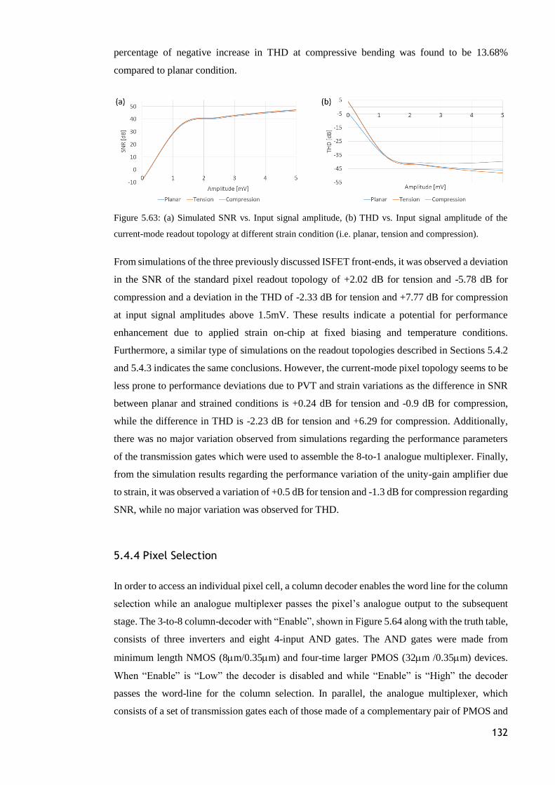
132
percentage of negative increase in THD at compressive bending was found to be 13.68%
compared to planar condition.
Figure 5.63: (a) Simulated SNR vs. Input signal amplitude, (b) THD vs. Input signal amplitude of the
current-mode readout topology at different strain condition (i.e. planar, tension and compression).
From simulations of the three previously discussed ISFET front-ends, it was observed a deviation
in the SNR of the standard pixel readout topology of +2.02 dB for tension and -5.78 dB for
compression and a deviation in the THD of -2.33 dB for tension and +7.77 dB for compression
at input signal amplitudes above 1.5mV. These results indicate a potential for performance
enhancement due to applied strain on-chip at fixed biasing and temperature conditions.
Furthermore, a similar type of simulations on the readout topologies described in Sections 5.4.2
and 5.4.3 indicates the same conclusions. However, the current-mode pixel topology seems to be
less prone to performance deviations due to PVT and strain variations as the difference in SNR
between planar and strained conditions is +0.24 dB for tension and -0.9 dB for compression,
while the difference in THD is -2.23 dB for tension and +6.29 for compression. Additionally,
there was no major variation observed from simulations regarding the performance parameters
of the transmission gates which were used to assemble the 8-to-1 analogue multiplexer. Finally,
from the simulation results regarding the performance variation of the unity-gain amplifier due
to strain, it was observed a variation of +0.5 dB for tension and -1.3 dB for compression regarding
SNR, while no major variation was observed for THD.
5.4.4 Pixel Selection
In order to access an individual pixel cell, a column decoder enables the word line for the column
selection while an analogue multiplexer passes the pixel’s analogue output to the subsequent
stage. The 3-to-8 column-decoder with “Enable”, shown in Figure 5.64 along with the truth table,
consists of three inverters and eight 4-input AND gates. The AND gates were made from
minimum length NMOS (8m/0.35m) and four-time larger PMOS (32m /0.35m) devices.
When “Enable” is “Low” the decoder is disabled and while “Enable” is “High” the decoder
passes the word-line for the column selection. In parallel, the analogue multiplexer, which
consists of a set of transmission gates each of those made of a complementary pair of PMOS and
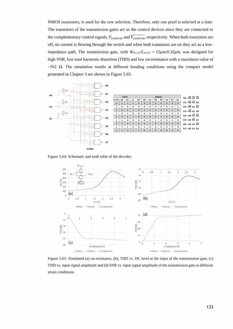
133
NMOS transistors, is used for the row selection. Therefore, only one pixel is selected at a time.
The transistors of the transmission gates act as the control devices since they are connected to
the complementary control signals, 𝑉𝑐𝑜𝑛𝑡𝑟𝑜𝑙 and 𝑉𝑐𝑜𝑛𝑡𝑟𝑜𝑙 , respectively. When both transistors are
off, no current is flowing through the switch and when both transistors are on they act as a low-
impedance path. The transmission gate, with WN1,P1/LN1,P1 = 15µm/0.35µm, was designed for
high SNR, low total harmonic distortion (THD) and low on-resistance with a maximum value of
~562 Ω. The simulation results at different bending conditions using the compact model
presented in Chapter 3 are shown in Figure 5.65.
Figure 5.64: Schematic and truth table of the decoder.
Figure 5.65: Simulated (a) on-resistance, (b), THD vs. DC level at the input of the transmission gate, (c)
THD vs. input signal amplitude and (d) SNR vs. input signal amplitude of the transmission gate at different
strain conditions.

134
5.4.5 Unity Gain Amplifier
The multiplexed analogue signals were subsequently passed through a passive RC filter with a
cut-off frequency of 10 kHz and a folded-cascode amplifier connected in a unity-gain
configuration, which drives and settles the kickback caused by the charge rebalancing on the on-
chip SAR ADC input at the start of the acquisition period. The two-stage folded-cascode
amplifier adopted from [483] is shown in Figure 5.66. The first stage of the amplifier consists of
an input PMOS differential-pair (M1, M2), a current sink (M9, M10), a common-gate NMOS
structure (M3, M4) and two high-swing current mirrors (M5-M8). The folded-cascode can be
considered as a symmetrical amplifier, since the input transistors see the same DC-voltage and
impedance at their drain nodes, with the drain nodes of M4 and M6 to be the only point of the
high impedance of the first stage, since all other nodes are at 1 𝑔𝑚⁄ level. The output impedance
of the first stage can be written as:
𝑟𝑜𝑢𝑡 = 𝑔𝑚6𝑟𝐷𝑆6𝑟𝐷𝑆8 || 𝑔𝑚4𝑟𝐷𝑆4(𝑟𝐷𝑆10 || 𝑟𝐷𝑆1) (5.24)
Where: 𝑟𝐷𝑆 =1
𝜆1
2𝜇𝐶𝑂𝑋
𝑊
𝐿(𝑉𝐺𝑆−𝑉𝑇𝐻)2
. The gain of the first stage is, therefore: 𝐴𝑉 = 𝑔𝑚1𝑟𝑜𝑢𝑡.
At low frequencies, the noise that appears at the output is associated with the transistors 𝑀1,2,
𝑀7,8 and 𝑀9,10. Therefore, the input-referred thermal noise density, including the effect of
externally applied stresses on ultra-thin CMOS dies, can be written as:
𝑒𝑛
2
∆𝑓=
𝑖𝑛,𝑜𝑢𝑡2
∆𝑓
1
𝐺𝑚2 =
16𝑘𝑇
3𝑔𝑚1(𝑏𝑒𝑛𝑑)2 (𝑔𝑚1(𝑏𝑒𝑛𝑑) + 𝑔𝑚7(𝑏𝑒𝑛𝑑) + 𝑔𝑚9(𝑏𝑒𝑛𝑑))
(5.25)
Finally, assuming a mismatch on the threshold voltage (𝑉𝑇𝐻) of MOST devices, the input-
referred offset (including the effect of externally applied stresses on ultra-thin CMOS dies) can
be written as below since the mismatched from the cascode transistors (M3 – M6) do not appear
at the input:
𝜎𝑜𝑠,𝑖𝑛2 = 𝜎𝑉𝑇𝐻𝑀1,2
2 + (𝑔𝑚7(𝑏𝑒𝑛𝑑)
𝑔𝑚1(𝑏𝑒𝑛𝑑))2
𝜎𝑉𝑇𝐻𝑀7,8
2 + (𝑔𝑚9(𝑏𝑒𝑛𝑑)
𝑔𝑚1(𝑏𝑒𝑛𝑑))2
𝜎𝑉𝑇𝐻𝑀9,10
2
(5.26)
The second stage of the unity-gain amplifier is a single transistor (M12) with an active load
(M13), which allows an improved output swing and slew rate. Even when the output voltage
comes close to the positive supply-rail and transistor M12 enters the linear region (and therefore
it loses its gain), the distortion still gets suppressed due to the sufficient gain of the first stage.
However, the GBW is now set by 𝑔𝑚1 and 𝐶𝐶. Besides, there are two non-dominant poles, one
at low frequencies which is normally produced at the output node and one at higher frequencies
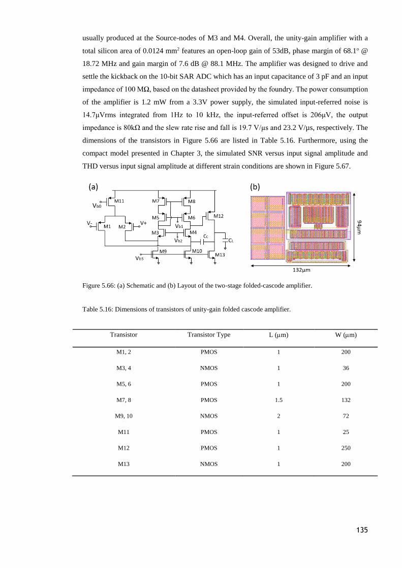
135
usually produced at the Source-nodes of M3 and M4. Overall, the unity-gain amplifier with a
total silicon area of 0.0124 mm2 features an open-loop gain of 53dB, phase margin of 68.1o @
18.72 MHz and gain margin of 7.6 dB @ 88.1 MHz. The amplifier was designed to drive and
settle the kickback on the 10-bit SAR ADC which has an input capacitance of 3 pF and an input
impedance of 100 MΩ, based on the datasheet provided by the foundry. The power consumption
of the amplifier is 1.2 mW from a 3.3V power supply, the simulated input-referred noise is
14.7μVrms integrated from 1Hz to 10 kHz, the input-referred offset is 206μV, the output
impedance is 80kΩ and the slew rate rise and fall is 19.7 V/µs and 23.2 V/µs, respectively. The
dimensions of the transistors in Figure 5.66 are listed in Table 5.16. Furthermore, using the
compact model presented in Chapter 3, the simulated SNR versus input signal amplitude and
THD versus input signal amplitude at different strain conditions are shown in Figure 5.67.
Figure 5.66: (a) Schematic and (b) Layout of the two-stage folded-cascode amplifier.
Table 5.16: Dimensions of transistors of unity-gain folded cascode amplifier.
Transistor Transistor Type L (m) W (m)
M1, 2 PMOS 1 200
M3, 4 NMOS 1 36
M5, 6 PMOS 1 200
M7, 8 PMOS 1.5 132
M9, 10 NMOS 2 72
M11 PMOS 1 25
M12 PMOS 1 250
M13 NMOS 1 200
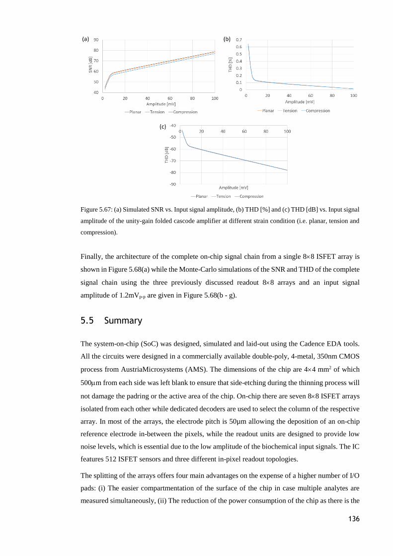
136
Figure 5.67: (a) Simulated SNR vs. Input signal amplitude, (b) THD [%] and (c) THD [dB] vs. Input signal
amplitude of the unity-gain folded cascode amplifier at different strain condition (i.e. planar, tension and
compression).
Finally, the architecture of the complete on-chip signal chain from a single 88 ISFET array is
shown in Figure 5.68(a) while the Monte-Carlo simulations of the SNR and THD of the complete
signal chain using the three previously discussed readout 88 arrays and an input signal
amplitude of 1.2mVp-p are given in Figure 5.68(b - g).
5.5 Summary
The system-on-chip (SoC) was designed, simulated and laid-out using the Cadence EDA tools.
All the circuits were designed in a commercially available double-poly, 4-metal, 350nm CMOS
process from AustriaMicrosystems (AMS). The dimensions of the chip are 44 mm2 of which
500m from each side was left blank to ensure that side-etching during the thinning process will
not damage the padring or the active area of the chip. On-chip there are seven 88 ISFET arrays
isolated from each other while dedicated decoders are used to select the column of the respective
array. In most of the arrays, the electrode pitch is 50µm allowing the deposition of an on-chip
reference electrode in-between the pixels, while the readout units are designed to provide low
noise levels, which is essential due to the low amplitude of the biochemical input signals. The IC
features 512 ISFET sensors and three different in-pixel readout topologies.
The splitting of the arrays offers four main advantages on the expense of a higher number of I/O
pads: (i) The easier compartmentation of the surface of the chip in case multiple analytes are
measured simultaneously, (ii) The reduction of the power consumption of the chip as there is the
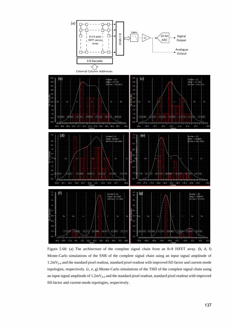
137
Figure 5.68: (a) The architecture of the complete signal chain from an 88 ISFET array. (b, d, f)
Monte-Carlo simulations of the SNR of the complete signal chain using an input signal amplitude of
1.2mVp-p and the standard pixel readout, standard pixel readout with improved fill-factor and current-mode
topologies, respectively. (c, e, g) Monte-Carlo simulations of the THD of the complete signal chain using
an input signal amplitude of 1.2mVp-p and the standard pixel readout, standard pixel readout with improved
fill-factor and current-mode topologies, respectively.
138
possibility of turning-off selected arrays, (iii) The selection of a pseudo-random combination of
pixels by activating two or more arrays simultaneously allowing the simultaneous detection of
pH from different regions (and not in a rolling shutter fashion commonly employed) and (iv)
Different readout topologies can be used on the same die, mainly for test purposes, avoiding
channel-to-channel crosstalk present in multiplexed systems and caused by large voltage
differences between adjacent pixels. The low-power consumption of the chip, 25 mW, and the
flexibility in terms of array selection obviates an overheating of the electrolyte under test. The
amplified and multiplexed signals are then connected to a passive RC low-pass filter (LPF) with
a cut-off frequency of 10 kHz and subsequently digitised at 90 kS/s by an on-chip 10-bit SAR
ADC (adopted from the library provided by the foundry). On-chip there is also one 10-bit DAC
(cell from the foundry’s library) which externally receives addresses to bias the active pixels of
the array under test. Finally, two unity-gain amplifiers ensure proper biasing of pixels as well as
the driving of the ADC and settling of the kickback caused by the charge rebalancing on ADC’s
input at the start of the acquisition period. During simulations of circuits’ performance, an extra
step was also added to capture any strain-induced performance variations using the developed
macro-model for MOST and ISFET devices described in Chapter 3.
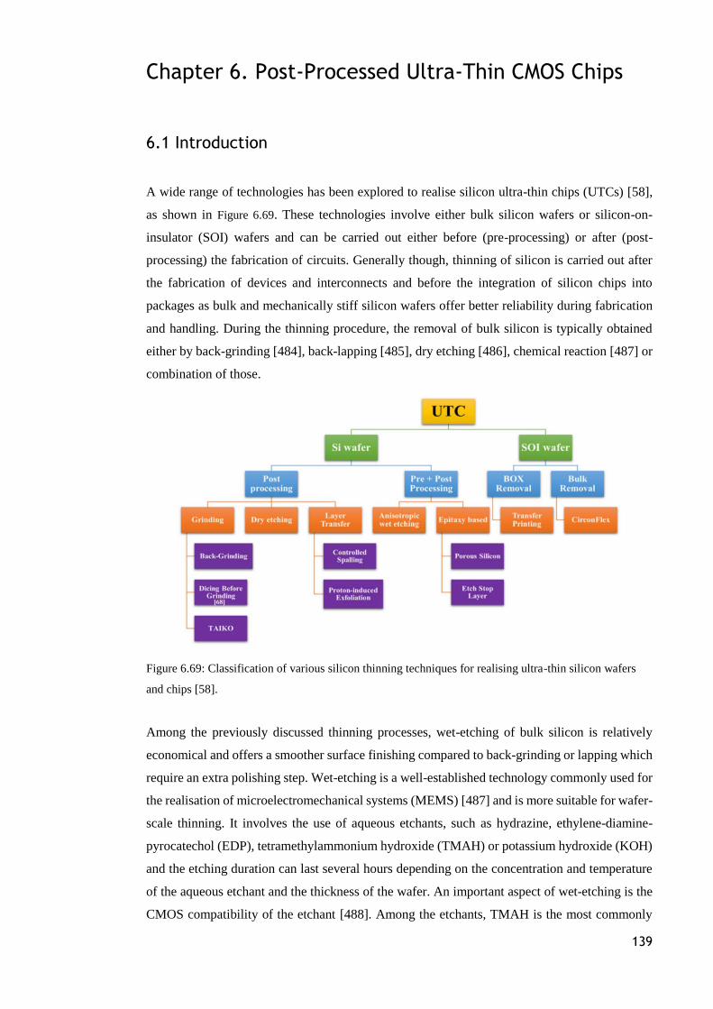
139
Chapter 6. Post-Processed Ultra-Thin CMOS Chips
6.1 Introduction
A wide range of technologies has been explored to realise silicon ultra-thin chips (UTCs) [58],
as shown in Figure 6.69. These technologies involve either bulk silicon wafers or silicon-on-
insulator (SOI) wafers and can be carried out either before (pre-processing) or after (post-
processing) the fabrication of circuits. Generally though, thinning of silicon is carried out after
the fabrication of devices and interconnects and before the integration of silicon chips into
packages as bulk and mechanically stiff silicon wafers offer better reliability during fabrication
and handling. During the thinning procedure, the removal of bulk silicon is typically obtained
either by back-grinding [484], back-lapping [485], dry etching [486], chemical reaction [487] or
combination of those.
Figure 6.69: Classification of various silicon thinning techniques for realising ultra-thin silicon wafers
and chips [58].
Among the previously discussed thinning processes, wet-etching of bulk silicon is relatively
economical and offers a smoother surface finishing compared to back-grinding or lapping which
require an extra polishing step. Wet-etching is a well-established technology commonly used for
the realisation of microelectromechanical systems (MEMS) [487] and is more suitable for wafer-
scale thinning. It involves the use of aqueous etchants, such as hydrazine, ethylene-diamine-
pyrocatechol (EDP), tetramethylammonium hydroxide (TMAH) or potassium hydroxide (KOH)
and the etching duration can last several hours depending on the concentration and temperature
of the aqueous etchant and the thickness of the wafer. An important aspect of wet-etching is the
CMOS compatibility of the etchant [488]. Among the etchants, TMAH is the most commonly
140
used as it is nontoxic, CMOS compatible and has very good anisotropic etching characteristics.
The use of TMAH leads to higher undercutting compared to other etchants, such as KOH, and
for that isopropyl alcohol (IPA) is generally added to TMAH [489].
In the previous Chapter, it was discussed the design, simulations and layout of the ISFET-based
IC. This Chapter discusses the thinning, bonding and chip packaging on thin polymeric printed-
circuit boards (PCBs) so that the ICs can be tested and characterised in aqueous environments.
More specifically, this Chapter presents two optimised silicon thinning methods to realise wafer-
as well as chip-scale ultra-thin silicon. The first method2 involves alkaline wet-etching of silicon
using tetramethylammonium hydroxide (TMAH) acting as the silicon etchant and
polydimethylsiloxane (PDMS) acting as the protective coating during wet etching of silicon. This
optimised low-cost process was employed for wafer-scale etching to achieve devices over large-
area thin silicon so that they can conform over curvilinear surfaces. Furthermore, the second
silicon-thinning method is related to using a chemo-mechanical thinning process termed as
“lapping” technique ensuring faster material removal (etch rate of ∼9 μm/min) with high yield
using abrasive as well as colloidal polishing slurry. Also, this chapter describes the packaging
procedure of the developed ultra-thin chips before they can be tested in electrochemical
experiments. To this end, the developed silicon dies were embedded and wire-bonded on
polyimide-based flexible printed circuit boards (FPCBs) and were encapsulated to isolate the
bond-pad connections making the devices operational in aqueous environments without
compromising the electrical connections.
6.2 Protection of Front Active Side during Back-Etching
The protection of the front-side of the wafer during back-etching is a critical step. If it fails, then
the etchant, during wet or back-lapping, will penetrate to the front-side and damage the fabricated
circuits. During back-lapping, the wafers/dies are placed face-down on a holder where they are
glued using a bonding wax which also protects the front active side from getting damaged during
the thinning process. In both cases, the protective material is in contact with the ion-sensitive
layer of ISFET and care should be taken during its removal. A way to overcome this issue that
can potentially compromise the sensitivity of ISFETs is to have a sacrificial layer (e.g.
photoresist), which will make the removal of the protective layer easier and at the same time will
protect the surface of ISFETs. In the case of lapping however, the bonding wax can be easily
removed with acetone and since the wax is usually thin (e.g. few microns in thickness) the
removal is fast and a small amount of acetone is needed. Also, during chemical wet etching, one
of the basic arrangements to protect the front-side is to place the wafer in a Teflon-based holder,
which protect the front-side with a rubber O-ring. The O-ring essentially shields the edges of the
2 This method was developed and optimised in collaboration with Dr Shoubhik Gupta.
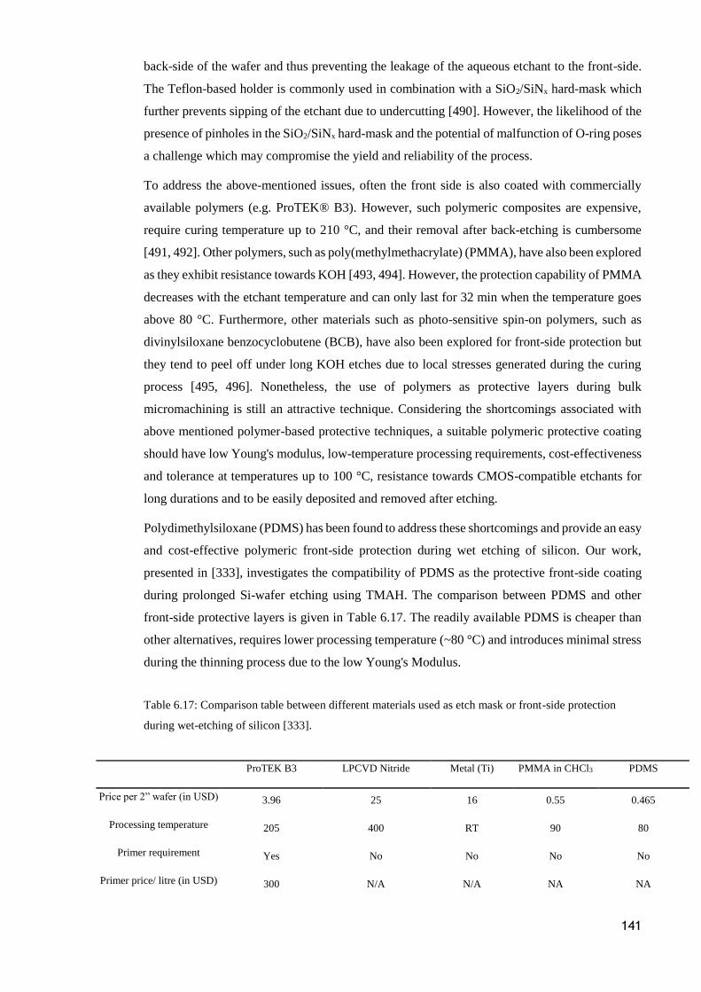
141
back-side of the wafer and thus preventing the leakage of the aqueous etchant to the front-side.
The Teflon-based holder is commonly used in combination with a SiO2/SiNx hard-mask which
further prevents sipping of the etchant due to undercutting [490]. However, the likelihood of the
presence of pinholes in the SiO2/SiNx hard-mask and the potential of malfunction of O-ring poses
a challenge which may compromise the yield and reliability of the process.
To address the above-mentioned issues, often the front side is also coated with commercially
available polymers (e.g. ProTEK® B3). However, such polymeric composites are expensive,
require curing temperature up to 210 °C, and their removal after back-etching is cumbersome
[491, 492]. Other polymers, such as poly(methylmethacrylate) (PMMA), have also been explored
as they exhibit resistance towards KOH [493, 494]. However, the protection capability of PMMA
decreases with the etchant temperature and can only last for 32 min when the temperature goes
above 80 °C. Furthermore, other materials such as photo-sensitive spin-on polymers, such as
divinylsiloxane benzocyclobutene (BCB), have also been explored for front-side protection but
they tend to peel off under long KOH etches due to local stresses generated during the curing
process [495, 496]. Nonetheless, the use of polymers as protective layers during bulk
micromachining is still an attractive technique. Considering the shortcomings associated with
above mentioned polymer-based protective techniques, a suitable polymeric protective coating
should have low Young's modulus, low-temperature processing requirements, cost-effectiveness
and tolerance at temperatures up to 100 °C, resistance towards CMOS-compatible etchants for
long durations and to be easily deposited and removed after etching.
Polydimethylsiloxane (PDMS) has been found to address these shortcomings and provide an easy
and cost-effective polymeric front-side protection during wet etching of silicon. Our work,
presented in [333], investigates the compatibility of PDMS as the protective front-side coating
during prolonged Si-wafer etching using TMAH. The comparison between PDMS and other
front-side protective layers is given in Table 6.17. The readily available PDMS is cheaper than
other alternatives, requires lower processing temperature (~80 °C) and introduces minimal stress
during the thinning process due to the low Young's Modulus.
Table 6.17: Comparison table between different materials used as etch mask or front-side protection
during wet-etching of silicon [333].
ProTEK B3 LPCVD Nitride Metal (Ti) PMMA in CHCl3 PDMS
Price per 2” wafer (in USD) 3.96 25 16 0.55 0.465
Processing temperature 205 400 RT 90 80
Primer requirement Yes No No No No
Primer price/ litre (in USD) 300 N/A N/A NA NA
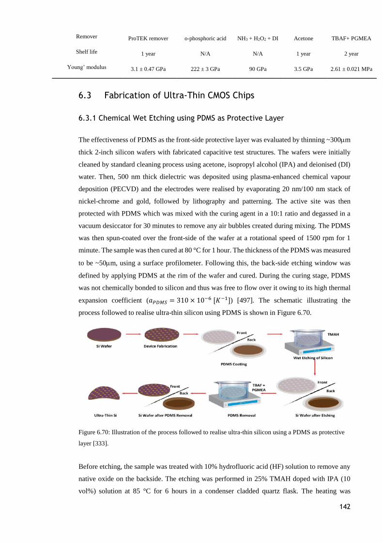
142
Remover ProTEK remover o-phosphoric acid NH3 + H2O2 + DI Acetone TBAF+ PGMEA
Shelf life 1 year N/A N/A 1 year 2 year
Young’ modulus 3.1 ± 0.47 GPa 222 ± 3 GPa 90 GPa 3.5 GPa 2.61 ± 0.021 MPa
6.3 Fabrication of Ultra-Thin CMOS Chips
6.3.1 Chemical Wet Etching using PDMS as Protective Layer
The effectiveness of PDMS as the front-side protective layer was evaluated by thinning ~300m
thick 2-inch silicon wafers with fabricated capacitive test structures. The wafers were initially
cleaned by standard cleaning process using acetone, isopropyl alcohol (IPA) and deionised (DI)
water. Then, 500 nm thick dielectric was deposited using plasma-enhanced chemical vapour
deposition (PECVD) and the electrodes were realised by evaporating 20 nm/100 nm stack of
nickel-chrome and gold, followed by lithography and patterning. The active site was then
protected with PDMS which was mixed with the curing agent in a 10:1 ratio and degassed in a
vacuum desiccator for 30 minutes to remove any air bubbles created during mixing. The PDMS
was then spun-coated over the front-side of the wafer at a rotational speed of 1500 rpm for 1
minute. The sample was then cured at 80 °C for 1 hour. The thickness of the PDMS was measured
to be ~50m, using a surface profilometer. Following this, the back-side etching window was
defined by applying PDMS at the rim of the wafer and cured. During the curing stage, PDMS
was not chemically bonded to silicon and thus was free to flow over it owing to its high thermal
expansion coefficient (𝑎𝑃𝐷𝑀𝑆 = 310 × 10−6 [𝐾−1]) [497]. The schematic illustrating the
process followed to realise ultra-thin silicon using PDMS is shown in Figure 6.70.
Figure 6.70: Illustration of the process followed to realise ultra-thin silicon using a PDMS as protective
layer [333].
Before etching, the sample was treated with 10% hydrofluoric acid (HF) solution to remove any
native oxide on the backside. The etching was performed in 25% TMAH doped with IPA (10
vol%) solution at 85 °C for 6 hours in a condenser cladded quartz flask. The heating was
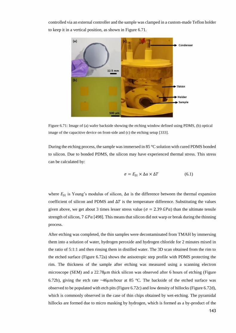
143
controlled via an external controller and the sample was clamped in a custom-made Teflon holder
to keep it in a vertical position, as shown in Figure 6.71.
Figure 6.71: Image of (a) wafer backside showing the etching window defined using PDMS, (b) optical
image of the capacitive device on front-side and (c) the etching setup [333].
During the etching process, the sample was immersed in 85 °C solution with cured PDMS bonded
to silicon. Due to bonded PDMS, the silicon may have experienced thermal stress. This stress
can be calculated by:
𝜎 = 𝐸𝑆𝑖 × ∆𝑎 × ∆𝑇 (6.1)
where 𝐸𝑆𝑖 is Young’s modulus of silicon, ∆𝑎 is the difference between the thermal expansion
coefficient of silicon and PDMS and ∆𝑇 is the temperature difference. Substituting the values
given above, we get about 3 times lesser stress value (𝜎 = 2.39 𝐺𝑃𝑎) than the ultimate tensile
strength of silicon, 7 𝐺𝑃𝑎 [498]. This means that silicon did not warp or break during the thinning
process.
After etching was completed, the thin samples were decontaminated from TMAH by immersing
them into a solution of water, hydrogen peroxide and hydrogen chloride for 2 minutes mixed in
the ratio of 5:1:1 and then rinsing them in distilled water. The 3D scan obtained from the rim to
the etched surface (Figure 6.72a) shows the anisotropic step profile with PDMS protecting the
rim. The thickness of the sample after etching was measured using a scanning electron
microscope (SEM) and a 22.78m thick silicon was observed after 6 hours of etching (Figure
6.72b), giving the etch rate ~46m/hour at 85 °C. The backside of the etched surface was
observed to be populated with etch pits (Figure 6.72c) and low density of hillocks (Figure 6.72d),
which is commonly observed in the case of thin chips obtained by wet-etching. The pyramidal
hillocks are formed due to micro masking by hydrogen, which is formed as a by-product of the
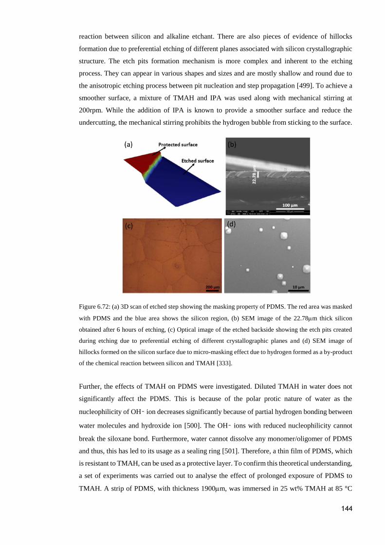
144
reaction between silicon and alkaline etchant. There are also pieces of evidence of hillocks
formation due to preferential etching of different planes associated with silicon crystallographic
structure. The etch pits formation mechanism is more complex and inherent to the etching
process. They can appear in various shapes and sizes and are mostly shallow and round due to
the anisotropic etching process between pit nucleation and step propagation [499]. To achieve a
smoother surface, a mixture of TMAH and IPA was used along with mechanical stirring at
200rpm. While the addition of IPA is known to provide a smoother surface and reduce the
undercutting, the mechanical stirring prohibits the hydrogen bubble from sticking to the surface.
Figure 6.72: (a) 3D scan of etched step showing the masking property of PDMS. The red area was masked
with PDMS and the blue area shows the silicon region, (b) SEM image of the 22.78m thick silicon
obtained after 6 hours of etching, (c) Optical image of the etched backside showing the etch pits created
during etching due to preferential etching of different crystallographic planes and (d) SEM image of
hillocks formed on the silicon surface due to micro-masking effect due to hydrogen formed as a by-product
of the chemical reaction between silicon and TMAH [333].
Further, the effects of TMAH on PDMS were investigated. Diluted TMAH in water does not
significantly affect the PDMS. This is because of the polar protic nature of water as the
nucleophilicity of OH– ion decreases significantly because of partial hydrogen bonding between
water molecules and hydroxide ion [500]. The OH– ions with reduced nucleophilicity cannot
break the siloxane bond. Furthermore, water cannot dissolve any monomer/oligomer of PDMS
and thus, this has led to its usage as a sealing ring [501]. Therefore, a thin film of PDMS, which
is resistant to TMAH, can be used as a protective layer. To confirm this theoretical understanding,
a set of experiments was carried out to analyse the effect of prolonged exposure of PDMS to
TMAH. A strip of PDMS, with thickness 1900m, was immersed in 25 wt% TMAH at 85 °C
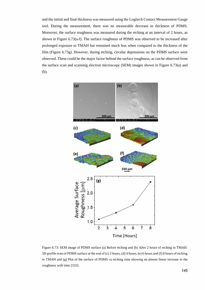
145
and the initial and final thickness was measured using the Logitech Contact Measurement Gauge
tool. During the measurement, there was no measurable decrease in thickness of PDMS.
Moreover, the surface roughness was measured during the etching at an interval of 2 hours, as
shown in Figure 6.73(a-f). The surface roughness of PDMS was observed to be increased after
prolonged exposure to TMAH but remained much less when compared to the thickness of the
film (Figure 6.73g). However, during etching, circular depressions on the PDMS surface were
observed. These could be the major factor behind the surface roughness, as can be observed from
the surface scan and scanning electron microscopy (SEM) images shown in Figure 6.73(a) and
(b).
Figure 6.73: SEM image of PDMS surface (a) Before etching and (b) After 2 hours of etching in TMAH.
3D profile scan of PDMS surface at the end of (c) 2 hours, (d) 4 hours, (e) 6 hours and (f) 8 hours of etching
in TMAH and (g) Plot of the surface of PDMS vs etching time showing an almost linear increase in the
roughness with time [333].
146
After the thinning process was completed PDMS should be removed from the front-side to allow
electrical contact with the fabricated devices. The methods commonly used to remove cured
PDMS of a silicon surface are (i) scrapping, (ii) dry etching using fluorine-based reactive ion
etching [502], (iii) swelling of PDMS using appropriate organic solvents [503] and (iv) chemical-
mechanical removal [504]. These methods can be used alone or in combination depending on the
application. In the present case, where PDMS is over thin silicon, mechanical scrapping using
tweezers and further cleaning using a pressurised spray is not possible as these steps are likely to
break the chip. Similarly, swelling of the PDMS with a nonpolar organic solvent such as hexane,
toluene, chloroform, and peeling it off can introduce mechanical stresses which may lead to
breakage of the thin silicon [505]. Furthermore, these processes do not guarantee PDMS a
residues-free surface. Besides, after dry etching of PDMS, substantial surface roughness is
produced. Besides, dry-etching might also damage the Si surface as the recipe used for dry
etching of PDMS is similar to that for silicon (Si) and silicon dioxide (SiO2) [506, 507]. Finally,
the use of chemical-mechanical removal with strong alkaline solutions such as sodium hydroxide
(NaOH) or other lower boiling point alcohols, such as methanol and isopropanol, which cause a
base induced chemical degradation of —Si—O—Si— chain leading to removal or dissolution of
silicone (PDMS) residues, are associated with safety and flammability hazards as well as
environmental concerns.
Considering the above issues, wet chemical etching is explored to remove PDMS after thinning.
The organic reactive reagents based chemistry such as quaternary ammonium fluoride (QAF)
(e.g. TBAF) in low solubility solvents such as di-substituted amides (e.g. Nmethylpyrrolidinone
(NMP), dimethylformamide (DMF)), tetrahydrofuran (THF) or PGMEA) have been shown to
yield good results for the removal of PDMS [508]. These solutions cause fluoride-ion-assisted
rapid disruption/disintegration of the PDMS polymer matrix to monomers/oligomers, followed
by its dissolution in the solvent. This mostly removes the residues by dislodging PDMS from the
surface and, to a large extent, by dissolving PDMS residues through breakage of Si-O bonds and
formation of Si-F bonds, which is similar to the etching of glass in hydrogen fluoride.
Similar chemistry with a dilute solution of TBAF (1% weight concentration) in hydrophobic non-
hydroxylic aprotic PGMEA, has also been used in this case. The reaction mechanism between
PDMS and TBAF is thought to be assisted by nucleophilic substitution at Si-O-Si bond by naked
fluoride generated from TBAF followed by siloxane bond cleavage [509, 510]. Nucleophilic
substitution is an important class of reactions in which an electron-rich nucleophile selectively
bonds with or attacks the positive or the partially positive charge of an atom or a group of atoms
to replace a leaving group [511]. Nucleophilic substitution requires the attacking species to be a
strong base, which at first seems to be impossible with naked fluoride since it is a weak base due
to lower electronegativity. However, nucleophilicity is not a property inherent to a given species;
it can be affected by the medium it is dissociating in. For example, in a polar-protic solvent,
where the nucleophile can participate in hydrogen bonding. In doing so, the nucleophile is
147
considerably less reactive since its lone pairs of electrons are interacting with the electron-poor
hydrogen atoms of the solvent. This is the reason why the polar aprotic solvent is used in this
work for utilising the reactivity of unstable fluoride. In polar aprotic solvent, nucleophiles do not
have hydrogen bonds, allowing the nucleophiles to have greater freedom in solution. Under these
conditions, nucleophilicity connects well with basicity and fluoride ion, being the most unstable
of the halide ions and so best nucleophile [512], reacts fastest with electrophiles, which in this
work is siloxane bond.
The mechanism of fluoride-induced siloxane bond cleavage is represented in Figure 6.74(a). The
fluoride ion attacks the silicon atom of Si-O-Si bond, which breaks towards the oxygen due to
higher electronegativity, thus breaking the polymer chain in oligomers. PDMS removal rates
depend on two factors: (1) the reactivity of TBAF with Si–O bonds in the solvent, which in turn
depends on the polarity of the solvent, and (2) the degree of dissolution offered by solvent to the
oligomers of PDMS. At this point, solvent plays an important role in the dissolution of oligomers.
The PGMEA was considered a more suitable solvent for TBAF than THF, due to a higher boiling
point (145 °C) compared to that of THF (66 °C) [509]. The samples were immersed in the
solution of TBAF in PGMEA for 5 hours, and then in pure PMA solution for 1 hour to make sure
that there is no residue left on the front surface. This can be observed more clearly from Figure
6.74(b), which shows the SEM image of the sample in mid-way during PDMS removal step
where small spherical residues of PDMS can be seen, whereas Figure 6.74(c) shows the image
at the final stage of PDMS removal and a clean surface of the silicon substrate can be observed.
This experiment furthers strength our previous work of PDMS removal reported in [508].
Finally, the fabricated capacitors (Figure 6.75a) on the front-side of the silicon wafers, were
characterised before and after the thinning process. A summit 12 k auto-prober with control
measure units were used to run capacitance-voltage (C-V) measurements, shown in Figure
6.75(b). It was observed that the capacitance values remain almost unchanged (~18.5 pF) in the
scan range of -2V to 2V before and after thinning. Moreover, the device-to-device variation
measured for 4 different devices also shows minimal deviation (inset of Figure 6.75b). To further
validate the efficacy of the approach presented in this, we repeated a similar silicon etching
process with a commercially available ProTEK protection layer. The sample was composed of
capacitive structures with aluminium nitride as the dielectric. The protective coating was
removed after etching using the chemical composition supplied by the supplier. The electrical
characterisation of the device, shown in Figure 6.75(c), carried out before and after etching
showed again a negligible change.
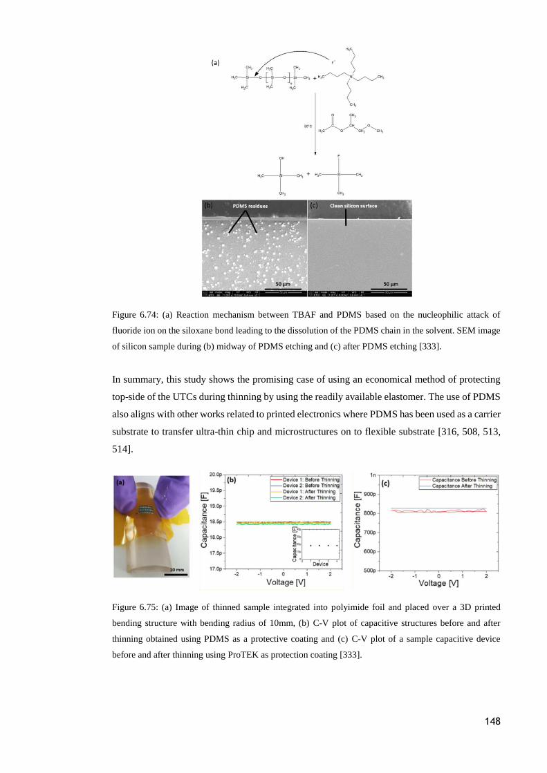
148
Figure 6.74: (a) Reaction mechanism between TBAF and PDMS based on the nucleophilic attack of
fluoride ion on the siloxane bond leading to the dissolution of the PDMS chain in the solvent. SEM image
of silicon sample during (b) midway of PDMS etching and (c) after PDMS etching [333].
In summary, this study shows the promising case of using an economical method of protecting
top-side of the UTCs during thinning by using the readily available elastomer. The use of PDMS
also aligns with other works related to printed electronics where PDMS has been used as a carrier
substrate to transfer ultra-thin chip and microstructures on to flexible substrate [316, 508, 513,
514].
Figure 6.75: (a) Image of thinned sample integrated into polyimide foil and placed over a 3D printed
bending structure with bending radius of 10mm, (b) C-V plot of capacitive structures before and after
thinning obtained using PDMS as a protective coating and (c) C-V plot of a sample capacitive device
before and after thinning using ProTEK as protection coating [333].
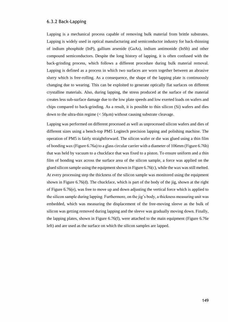
149
6.3.2 Back-Lapping
Lapping is a mechanical process capable of removing bulk material from brittle substrates.
Lapping is widely used in optical manufacturing and semiconductor industry for back-thinning
of indium phosphide (InP), gallium arsenide (GaAs), indium antimonide (InSb) and other
compound semiconductors. Despite the long history of lapping, it is often confused with the
back-grinding process, which follows a different procedure during bulk material removal.
Lapping is defined as a process in which two surfaces are worn together between an abrasive
slurry which is free-rolling. As a consequence, the shape of the lapping plate is continuously
changing due to wearing. This can be exploited to generate optically flat surfaces on different
crystalline materials. Also, during lapping, the stress produced at the surface of the material
creates less sub-surface damage due to the low plate speeds and low exerted loads on wafers and
chips compared to back-grinding. As a result, it is possible to thin silicon (Si) wafers and dies
down to the ultra-thin regime (< 50m) without causing substrate cleavage.
Lapping was performed on different processed as well as unprocessed silicon wafers and dies of
different sizes using a bench-top PM5 Logitech precision lapping and polishing machine. The
operation of PM5 is fairly straightforward. The silicon wafer or die was glued using a thin film
of bonding wax (Figure 6.76a) to a glass circular carrier with a diameter of 106mm (Figure 6.76b)
that was held by vacuum to a chuckface that was fixed to a piston. To ensure uniform and a thin
film of bonding wax across the surface area of the silicon sample, a force was applied on the
glued silicon sample using the equipment shown in Figure 6.76(c), while the wax was still melted.
At every processing step the thickness of the silicon sample was monitored using the equipment
shown in Figure 6.76(d). The chuckface, which is part of the body of the jig, shown at the right
of Figure 6.76(e), was free to move up and down adjusting the vertical force which is applied to
the silicon sample during lapping. Furthermore, on the jig’s body, a thickness measuring unit was
embedded, which was measuring the displacement of the free-moving sleeve as the bulk of
silicon was getting removed during lapping and the sleeve was gradually moving down. Finally,
the lapping plates, shown in Figure 6.76(f), were attached to the main equipment (Figure 6.76e
left) and are used as the surface on which the silicon samples are lapped.
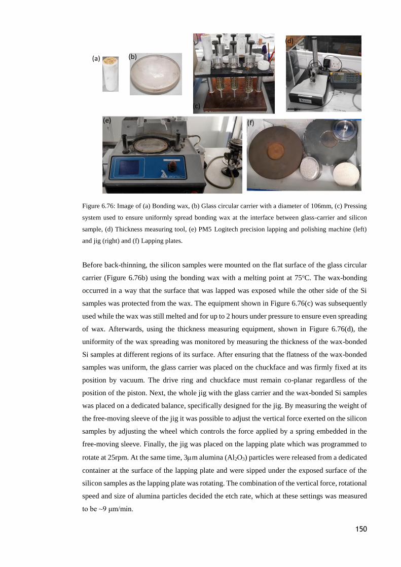
150
Figure 6.76: Image of (a) Bonding wax, (b) Glass circular carrier with a diameter of 106mm, (c) Pressing
system used to ensure uniformly spread bonding wax at the interface between glass-carrier and silicon
sample, (d) Thickness measuring tool, (e) PM5 Logitech precision lapping and polishing machine (left)
and jig (right) and (f) Lapping plates.
Before back-thinning, the silicon samples were mounted on the flat surface of the glass circular
carrier (Figure 6.76b) using the bonding wax with a melting point at 75oC. The wax-bonding
occurred in a way that the surface that was lapped was exposed while the other side of the Si
samples was protected from the wax. The equipment shown in Figure 6.76(c) was subsequently
used while the wax was still melted and for up to 2 hours under pressure to ensure even spreading
of wax. Afterwards, using the thickness measuring equipment, shown in Figure 6.76(d), the
uniformity of the wax spreading was monitored by measuring the thickness of the wax-bonded
Si samples at different regions of its surface. After ensuring that the flatness of the wax-bonded
samples was uniform, the glass carrier was placed on the chuckface and was firmly fixed at its
position by vacuum. The drive ring and chuckface must remain co-planar regardless of the
position of the piston. Next, the whole jig with the glass carrier and the wax-bonded Si samples
was placed on a dedicated balance, specifically designed for the jig. By measuring the weight of
the free-moving sleeve of the jig it was possible to adjust the vertical force exerted on the silicon
samples by adjusting the wheel which controls the force applied by a spring embedded in the
free-moving sleeve. Finally, the jig was placed on the lapping plate which was programmed to
rotate at 25rpm. At the same time, 3m alumina (Al2O3) particles were released from a dedicated
container at the surface of the lapping plate and were sipped under the exposed surface of the
silicon samples as the lapping plate was rotating. The combination of the vertical force, rotational
speed and size of alumina particles decided the etch rate, which at these settings was measured
to be ~9 μm/min.
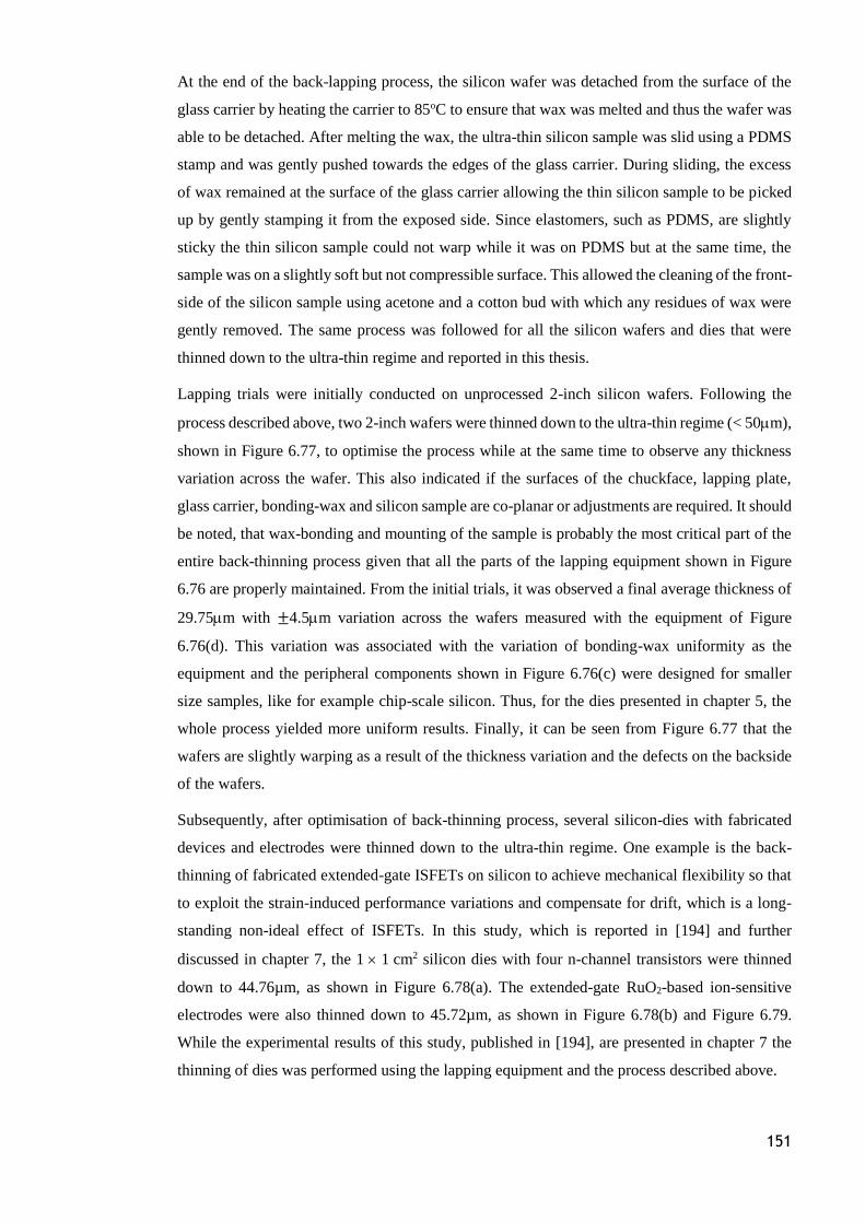
151
At the end of the back-lapping process, the silicon wafer was detached from the surface of the
glass carrier by heating the carrier to 85oC to ensure that wax was melted and thus the wafer was
able to be detached. After melting the wax, the ultra-thin silicon sample was slid using a PDMS
stamp and was gently pushed towards the edges of the glass carrier. During sliding, the excess
of wax remained at the surface of the glass carrier allowing the thin silicon sample to be picked
up by gently stamping it from the exposed side. Since elastomers, such as PDMS, are slightly
sticky the thin silicon sample could not warp while it was on PDMS but at the same time, the
sample was on a slightly soft but not compressible surface. This allowed the cleaning of the front-
side of the silicon sample using acetone and a cotton bud with which any residues of wax were
gently removed. The same process was followed for all the silicon wafers and dies that were
thinned down to the ultra-thin regime and reported in this thesis.
Lapping trials were initially conducted on unprocessed 2-inch silicon wafers. Following the
process described above, two 2-inch wafers were thinned down to the ultra-thin regime (< 50m),
shown in Figure 6.77, to optimise the process while at the same time to observe any thickness
variation across the wafer. This also indicated if the surfaces of the chuckface, lapping plate,
glass carrier, bonding-wax and silicon sample are co-planar or adjustments are required. It should
be noted, that wax-bonding and mounting of the sample is probably the most critical part of the
entire back-thinning process given that all the parts of the lapping equipment shown in Figure
6.76 are properly maintained. From the initial trials, it was observed a final average thickness of
29.75m with ±4.5m variation across the wafers measured with the equipment of Figure
6.76(d). This variation was associated with the variation of bonding-wax uniformity as the
equipment and the peripheral components shown in Figure 6.76(c) were designed for smaller
size samples, like for example chip-scale silicon. Thus, for the dies presented in chapter 5, the
whole process yielded more uniform results. Finally, it can be seen from Figure 6.77 that the
wafers are slightly warping as a result of the thickness variation and the defects on the backside
of the wafers.
Subsequently, after optimisation of back-thinning process, several silicon-dies with fabricated
devices and electrodes were thinned down to the ultra-thin regime. One example is the back-
thinning of fabricated extended-gate ISFETs on silicon to achieve mechanical flexibility so that
to exploit the strain-induced performance variations and compensate for drift, which is a long-
standing non-ideal effect of ISFETs. In this study, which is reported in [194] and further
discussed in chapter 7, the 1 1 cm2 silicon dies with four n-channel transistors were thinned
down to 44.76µm, as shown in Figure 6.78(a). The extended-gate RuO2-based ion-sensitive
electrodes were also thinned down to 45.72µm, as shown in Figure 6.78(b) and Figure 6.79.
While the experimental results of this study, published in [194], are presented in chapter 7 the
thinning of dies was performed using the lapping equipment and the process described above.
152
Figure 6.77: Photographs of the two 2-inch wafers thinned down to the ultra-thin regime to optimise the
thinning process.
Figure 6.78: (a) The fabricated chip (1 1 cm2) with four n-channel transistors and (b) the SEM image of
the cross-section of the thin chip on a polyimide-based flexible PCB showing the thickness of the chip and
FPCB. (c) Photograph of thin silicon compared the bulky silicon dies with deposited ion-sensitive
electrodes and (d) the SEM image of the cross-section of the RuO2-based ion-sensitive electrode [194].
Courtesy to Dr Shoubhik Gupta who designed the photolithography masks used for the fabrication of the
four n-channel transistors which was done in the Fondazione Bruno Kessler (FBK) institute.
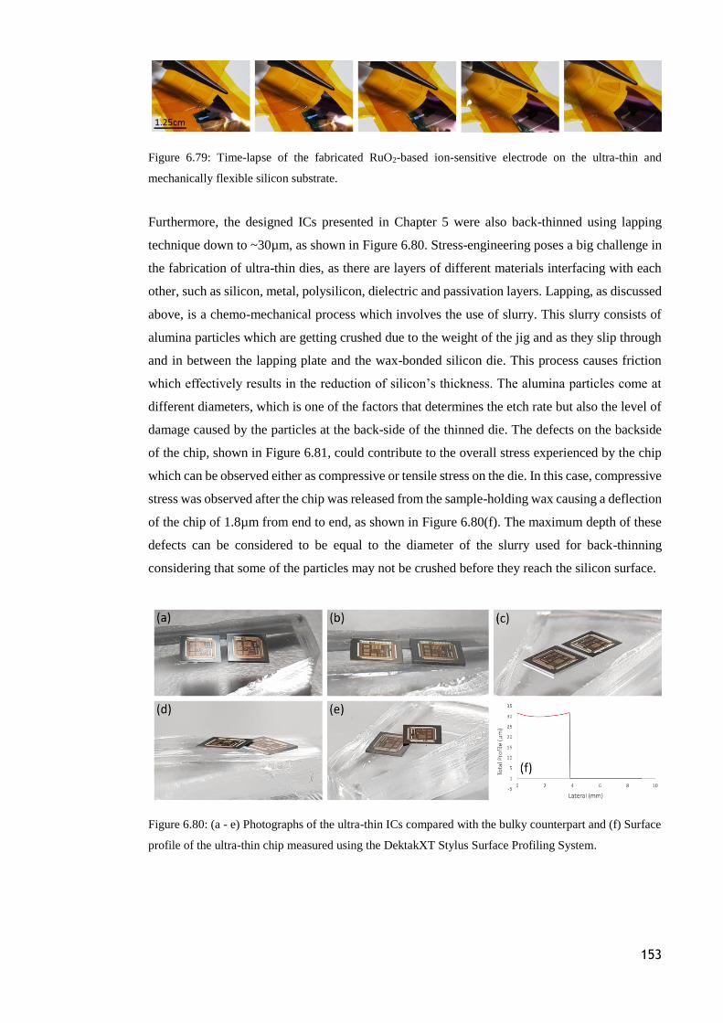
153
Figure 6.79: Time-lapse of the fabricated RuO2-based ion-sensitive electrode on the ultra-thin and
mechanically flexible silicon substrate.
Furthermore, the designed ICs presented in Chapter 5 were also back-thinned using lapping
technique down to ~30µm, as shown in Figure 6.80. Stress-engineering poses a big challenge in
the fabrication of ultra-thin dies, as there are layers of different materials interfacing with each
other, such as silicon, metal, polysilicon, dielectric and passivation layers. Lapping, as discussed
above, is a chemo-mechanical process which involves the use of slurry. This slurry consists of
alumina particles which are getting crushed due to the weight of the jig and as they slip through
and in between the lapping plate and the wax-bonded silicon die. This process causes friction
which effectively results in the reduction of silicon’s thickness. The alumina particles come at
different diameters, which is one of the factors that determines the etch rate but also the level of
damage caused by the particles at the back-side of the thinned die. The defects on the backside
of the chip, shown in Figure 6.81, could contribute to the overall stress experienced by the chip
which can be observed either as compressive or tensile stress on the die. In this case, compressive
stress was observed after the chip was released from the sample-holding wax causing a deflection
of the chip of 1.8µm from end to end, as shown in Figure 6.80(f). The maximum depth of these
defects can be considered to be equal to the diameter of the slurry used for back-thinning
considering that some of the particles may not be crushed before they reach the silicon surface.
Figure 6.80: (a - e) Photographs of the ultra-thin ICs compared with the bulky counterpart and (f) Surface
profile of the ultra-thin chip measured using the DektakXT Stylus Surface Profiling System.
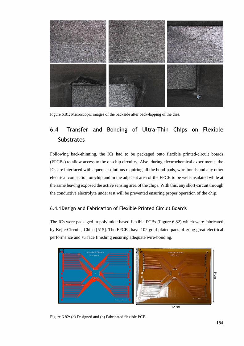
154
Figure 6.81: Microscopic images of the backside after back-lapping of the dies.
6.4 Transfer and Bonding of Ultra-Thin Chips on Flexible
Substrates
Following back-thinning, the ICs had to be packaged onto flexible printed-circuit boards
(FPCBs) to allow access to the on-chip circuitry. Also, during electrochemical experiments, the
ICs are interfaced with aqueous solutions requiring all the bond-pads, wire-bonds and any other
electrical connection on-chip and in the adjacent area of the FPCB to be well-insulated while at
the same leaving exposed the active sensing area of the chips. With this, any short-circuit through
the conductive electrolyte under test will be prevented ensuring proper operation of the chip.
6.4.1 Design and Fabrication of Flexible Printed Circuit Boards
The ICs were packaged in polyimide-based flexible PCBs (Figure 6.82) which were fabricated
by Kejie Circuits, China [515]. The FPCBs have 102 gold-plated pads offering great electrical
performance and surface finishing ensuring adequate wire-bonding.
Figure 6.82: (a) Designed and (b) Fabricated flexible PCB.
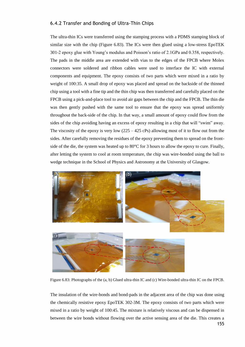
155
6.4.2 Transfer and Bonding of Ultra-Thin Chips
The ultra-thin ICs were transferred using the stamping process with a PDMS stamping block of
similar size with the chip (Figure 6.83). The ICs were then glued using a low-stress EpoTEK
301-2 epoxy glue with Young’s modulus and Poisson’s ratio of 2.1GPa and 0.358, respectively.
The pads in the middle area are extended with vias to the edges of the FPCB where Molex
connectors were soldered and ribbon cables were used to interface the IC with external
components and equipment. The epoxy consists of two parts which were mixed in a ratio by
weight of 100:35. A small drop of epoxy was placed and spread on the backside of the thinned
chip using a tool with a fine tip and the thin chip was then transferred and carefully placed on the
FPCB using a pick-and-place tool to avoid air gaps between the chip and the FPCB. The thin die
was then gently pushed with the same tool to ensure that the epoxy was spread uniformly
throughout the back-side of the chip. In that way, a small amount of epoxy could flow from the
sides of the chip avoiding having an excess of epoxy resulting in a chip that will “swim” away.
The viscosity of the epoxy is very low (225 – 425 cPs) allowing most of it to flow out from the
sides. After carefully removing the residues of the epoxy preventing them to spread on the front-
side of the die, the system was heated up to 80°C for 3 hours to allow the epoxy to cure. Finally,
after letting the system to cool at room temperature, the chip was wire-bonded using the ball to
wedge technique in the School of Physics and Astronomy at the University of Glasgow.
Figure 6.83: Photographs of the (a, b) Glued ultra-thin IC and (c) Wire-bonded ultra-thin IC on the FPCB.
The insulation of the wire-bonds and bond-pads in the adjacent area of the chip was done using
the chemically resistive epoxy EpoTEK 302-3M. The epoxy consists of two parts which were
mixed in a ratio by weight of 100:45. The mixture is relatively viscous and can be dispensed in
between the wire bonds without flowing over the active sensing area of the die. This creates a
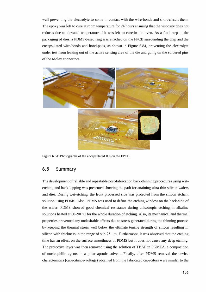
156
wall preventing the electrolyte to come in contact with the wire-bonds and short-circuit them.
The epoxy was left to cure at room temperature for 24 hours ensuring that the viscosity does not
reduces due to elevated temperature if it was left to cure in the oven. As a final step in the
packaging of dies, a PDMS-based ring was attached on the FPCB surrounding the chip and the
encapsulated wire-bonds and bond-pads, as shown in Figure 6.84, preventing the electrolyte
under test from leaking out of the active sensing area of the die and going on the soldered pins
of the Molex connectors.
Figure 6.84: Photographs of the encapsulated ICs on the FPCB.
6.5 Summary
The development of reliable and repeatable post-fabrication back-thinning procedures using wet-
etching and back-lapping was presented showing the path for attaining ultra-thin silicon wafers
and dies. During wet-etching, the front processed side was protected from the silicon etchant
solution using PDMS. Also, PDMS was used to define the etching window on the back-side of
the wafer. PDMS showed good chemical resistance during anisotropic etching in alkaline
solutions heated at 80–90 °C for the whole duration of etching. Also, its mechanical and thermal
properties prevented any undesirable effects due to stress generated during the thinning process
by keeping the thermal stress well below the ultimate tensile strength of silicon resulting in
silicon with thickness in the range of sub-25 μm. Furthermore, it was observed that the etching
time has an effect on the surface smoothness of PDMS but it does not cause any deep etching.
The protective layer was then removed using the solution of TBAF in PGMEA, a composition
of nucleophilic agents in a polar aprotic solvent. Finally, after PDMS removal the device
characteristics (capacitance-voltage) obtained from the fabricated capacitors were similar to the
157
one measured before initiating the thinning process indicating that silicon etching and PDMS
removal procedure did not damage the capacitors.
Furthermore, the back-lapping process which was optimised on 2-inch silicon wafers was further
used to thin-down to the ultra-thin regime silicon dies of various dimensions, including the
developed ICs presented in Chapter 5. Lapping was performed using a PM5 Logitech precision
lapping and polishing machine to ensure faster material removal (etch rate of ~9 μm/min) with
high yield if properly maintained, using abrasive as well as colloidal polishing slurry. The etch
rate during lapping depends on the force that is applied on the sample during lapping, the size of
the alumina particles in the slurry, and the rotations per minute (rpm) of the plate. In comparison
with grinding, there is no need for an extra stress-relieving step such as slow ion etching or
chemical-mechanical polishing since during lapping the sample was polished as the last step of
the thinning process without removing it from the sample-holding jig. Besides, there is no need
for a protection tape commonly used in grinding which can increase the probability of breakage
of thinned wafers and chips during their delamination of the tape. Instead, it was used a thin film
(1μm) of bonding wax with a melting point of 75 °C.
Finally, the thin ICs were packaged on a 63.66μm thick polymeric flexible PCBs using low-stress
EpoTEK 301-2 epoxy glue with Young’s modulus and Poisson’s ratio of 2.1GPa and 0.358,
respectively. After carefully removing the residues of the epoxy preventing them to spread on
the front-side of the die and after curing the epoxy at 80°C for 3 hours, the chips were wire-
bonded on the FPCBs using the ball to wedge technique. The insulation of the wire-bonds and
bond-pads in the adjacent area of the chip was done using the chemically resistive epoxy EpoTEK
302-3M to allow the use of chemicals, such as buffer solutions and Dulbecco's Modified Eagle
Medium (DMEM), during electrical and electrochemical characterisation of chips, presented in
the following chapter.
158
Chapter 7. Characterisation of CMOS ISFETs and
Circuits on Ultra-Thin Chips
7.1 Introduction
The two previous chapters described the circuit design considerations and the on-chip topologies
of the presented ISFET-based SoC. Also, post-fabrication processing regarding thinning of dies
was described and bonding, as well as encapsulation of ICs, was also presented. This chapter
presents the characterisation results of:
I. The first reported ultra-thin CMOS-based ISFET ASIC on 30µm thickness Si-substrate.
The bulky and on ultra-thin chips were characterised and the experimental result are
compared. The experimental results are also compared with the simulation results
presented in Chapter 5 including important figures-of-merit (FoM), such as signal-to-
noise ratio (SNR), input-referred noise, total harmonic distortion (THD) and noise
spectral density. Besides, the chips were characterised to determine the pH sensitivity,
drift and hysteresis of ISFETs. The chips were tested in Dulbecco's Modified Eagle
Medium (DMEM), which normally serves as a standard cell-culture medium used for
maintaining mammalian cells in-vitro. However, in this case, it was used as an equivalent
of body-fluid due to its complex composition. DMEM contains a mixture of various
inorganic salts, amino acids, vitamins and carbohydrates, such as glucose, and makes it
a good control medium for biochemical experiments. The pH value of DMEM was tuned
by adding diluted KOH and HCl in the solution. A pH range between pH5 to pH9 was
preferred since it resembles the pH range of body-fluids, such as sweat and blood.
II. The first reported mechanically bendable single ISFET devices on ultra-thin Si-substrate
(45µm thickness). The mechanically bendable ISFETs were characterised at different pH
and bending conditions using standard pH buffer solutions. The changes in the
performance of the single-ISFETs on UTCs upon experiencing externally-applied strain
were exploited and through fine control in the μm-scale of the Si-substrate’s bending
radius and by correlating the applied strain with the electrical measurements, the system
transformed into a controllable and reversible electrical conductance modulator targeting
real-time active drift compensation irrespective of the evolution of drift’s behaviour over
time [194].
The detailed results are further discussed in the following sections.
159
7.2 Characterisation of Bulky and Ultra-Thin CMOS-based ISFET
Chips
To ensure proper characterisation of CMOS chips a suitable experimental procedure must be
developed. This includes ensuring that the chips are encapsulated correctly and that the
appropriate instrumentation equipment and measurement method is chosen. The ICs, which were
prepared as described in Chapter 5 and Chapter 6, were connected to external instrumentation
which was supplying the input signals and was acquiring the output signals. The ICs did not
require front-side post-processing to operate as there is already deposited in the foundry a
passivation layer consisting of 1µm thick 𝑆𝑖3𝑁𝑋 layer on top of a 1µm 𝑆𝑖𝑂𝑋 layer. Therefore, the
integrated ISFET arrays were characterised as received from the foundry in an “unmodified”
CMOS process. The advantages of the “unmodified” CMOS are that the fabrication cost is
eventually reduced and the integrated ISFETs can still function as pH sensors. However, the
sensitivity towards 𝐻+ ions of the unmodified passivation layer is reduced compared to other
metal-oxides, as was indicated in Chapter 2. The necessary hardware setup and software
programs that were developed to bias and read from the ICs are explained in the following
sections.
7.2.1 Hardware Setup
Two experimental setups were developed to characterise the important figures-of-merit (FoM),
such as the signal-to-noise ratio (SNR), input-referred noise, total harmonic distortion (THD),
noise spectral density, pH sensitivity, drift and hysteresis. Initially, the bulky and ultra-thin
(30µm thick) CMOS-based ISFET ICs were characterised in an aqueous solution of pH5, pH7
and pH9 to obtain the power spectral density (PSD) plots for each pixel by performing Fast
Fourier Transform (FFT) to the output voltage using an MSO-X 4154A oscilloscope, from
Keysight with a sampling rate of 5GSa/sec. The aqueous solution was initially biased through an
external miniaturised reference electrode (MF-2056, from Alvatek) which was connected to a
waveform generator (T3AFG120, from Teledyne LeCroy) providing the input signal (frequency
and amplitude). The experimental setup is shown in Figure 7.85(a). Furthermore, to analyse the
raw data from the obtained PSD plots, a script was written using Python programming language
to extract the SNR, input-referred noise, THD and noise spectral density. Finally, using the same
experimental setup (Figure 7.85a), the ICs were characterised in DMEM solution to obtain the
noise spectral density from each ISFET-based active pixel when the solution is biased with a DC
potential through the reference electrode, resembling real-life measurements.
Furthermore, the ICs were characterised for pH sensitivity, drift and hysteresis in a Dulbecco's
Modified Eagle Medium (DMEM) solution for the range of pH5 to pH9 since this range
resembles the range of pH values that can be measured in body-fluids, such as sweat, blood or
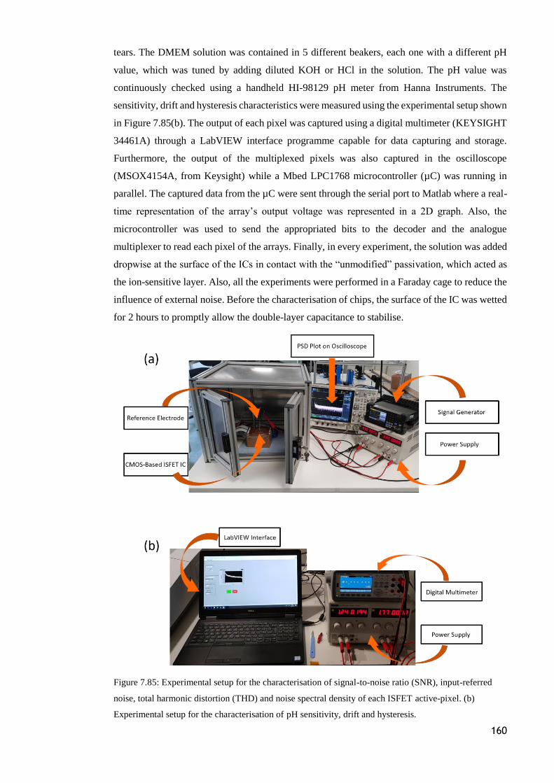
160
tears. The DMEM solution was contained in 5 different beakers, each one with a different pH
value, which was tuned by adding diluted KOH or HCl in the solution. The pH value was
continuously checked using a handheld HI-98129 pH meter from Hanna Instruments. The
sensitivity, drift and hysteresis characteristics were measured using the experimental setup shown
in Figure 7.85(b). The output of each pixel was captured using a digital multimeter (KEYSIGHT
34461A) through a LabVIEW interface programme capable for data capturing and storage.
Furthermore, the output of the multiplexed pixels was also captured in the oscilloscope
(MSOX4154A, from Keysight) while a Mbed LPC1768 microcontroller (µC) was running in
parallel. The captured data from the µC were sent through the serial port to Matlab where a real-
time representation of the array’s output voltage was represented in a 2D graph. Also, the
microcontroller was used to send the appropriated bits to the decoder and the analogue
multiplexer to read each pixel of the arrays. Finally, in every experiment, the solution was added
dropwise at the surface of the ICs in contact with the “unmodified” passivation, which acted as
the ion-sensitive layer. Also, all the experiments were performed in a Faraday cage to reduce the
influence of external noise. Before the characterisation of chips, the surface of the IC was wetted
for 2 hours to promptly allow the double-layer capacitance to stabilise.
Figure 7.85: Experimental setup for the characterisation of signal-to-noise ratio (SNR), input-referred
noise, total harmonic distortion (THD) and noise spectral density of each ISFET active-pixel. (b)
Experimental setup for the characterisation of pH sensitivity, drift and hysteresis.
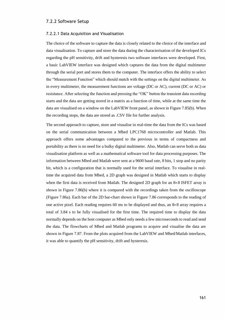
161
7.2.2 Software Setup
7.2.2.1 Data Acquisition and Visualisation
The choice of the software to capture the data is closely related to the choice of the interface and
data visualisation. To capture and store the data during the characterisation of the developed ICs
regarding the pH sensitivity, drift and hysteresis two software interfaces were developed. First,
a basic LabVIEW interface was designed which captures the data from the digital multimeter
through the serial port and stores them to the computer. The interface offers the ability to select
the “Measurement Function” which should match with the settings on the digital multimeter. As
in every multimeter, the measurement functions are voltage (DC or AC), current (DC or AC) or
resistance. After selecting the function and pressing the “OK” button the transient data recording
starts and the data are getting stored in a matrix as a function of time, while at the same time the
data are visualised on a window on the LabVIEW front panel, as shown in Figure 7.85(b). When
the recording stops, the data are stored as .CSV file for further analysis.
The second approach to capture, store and visualise in real-time the data from the ICs was based
on the serial communication between a Mbed LPC1768 microcontroller and Matlab. This
approach offers some advantages compared to the previous in terms of compactness and
portability as there is no need for a bulky digital multimeter. Also, Matlab can serve both as data
visualisation platform as well as a mathematical software tool for data processing purposes. The
information between Mbed and Matlab were sent at a 9600 baud rate, 8 bits, 1 stop and no parity
bit, which is a configuration that is normally used for the serial interface. To visualise in real-
time the acquired data from Mbed, a 2D graph was designed in Matlab which starts to display
when the first data is received from Matlab. The designed 2D graph for an 88 ISFET array is
shown in Figure 7.86(b) where it is compared with the recordings taken from the oscilloscope
(Figure 7.86a). Each bar of the 2D bar-chart shown in Figure 7.86 corresponds to the reading of
one active pixel. Each reading requires 60 ms to be displayed and thus, an 88 array requires a
total of 3.84 s to be fully visualised for the first time. The required time to display the data
normally depends on the host computer as Mbed only needs a few microseconds to read and send
the data. The flowcharts of Mbed and Matlab programs to acquire and visualise the data are
shown in Figure 7.87. From the plots acquired from the LabVIEW and Mbed/Matlab interfaces,
it was able to quantify the pH sensitivity, drift and hysteresis.
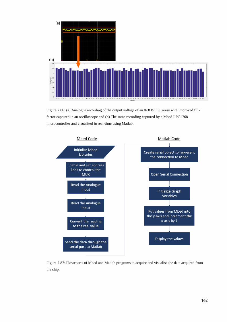
162
Figure 7.86: (a) Analogue recording of the output voltage of an 88 ISFET array with improved fill-
factor captured in an oscilloscope and (b) The same recording captured by a Mbed LPC1768
microcontroller and visualised in real-time using Matlab.
Figure 7.87: Flowcharts of Mbed and Matlab programs to acquire and visualise the data acquired from
the chip.
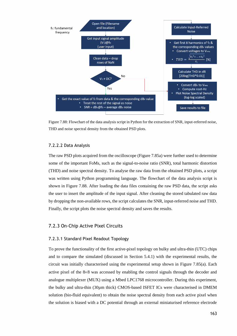
163
Figure 7.88: Flowchart of the data analysis script in Python for the extraction of SNR, input-referred noise,
THD and noise spectral density from the obtained PSD plots.
7.2.2.2 Data Analysis
The raw PSD plots acquired from the oscilloscope (Figure 7.85a) were further used to determine
some of the important FoMs, such as the signal-to-noise ratio (SNR), total harmonic distortion
(THD) and noise spectral density. To analyse the raw data from the obtained PSD plots, a script
was written using Python programming language. The flowchart of the data analysis script is
shown in Figure 7.88. After loading the data files containing the raw PSD data, the script asks
the user to insert the amplitude of the input signal. After cleaning the stored tabulated raw data
by dropping the non-available rows, the script calculates the SNR, input-referred noise and THD.
Finally, the script plots the noise spectral density and saves the results.
7.2.3 On-Chip Active Pixel Circuits
7.2.3.1 Standard Pixel Readout Topology
To prove the functionality of the first active-pixel topology on bulky and ultra-thin (UTC) chips
and to compare the simulated (discussed in Section 5.4.1) with the experimental results, the
circuit was initially characterised using the experimental setup shown in Figure 7.85(a). Each
active pixel of the 88 was accessed by enabling the control signals through the decoder and
analogue multiplexer (MUX) using a Mbed LPC1768 microcontroller. During this experiment,
the bulky and ultra-thin (30µm thick) CMOS-based ISFET ICs were characterised in DMEM
solution (bio-fluid equivalent) to obtain the noise spectral density from each active pixel when
the solution is biased with a DC potential through an external miniaturised reference electrode
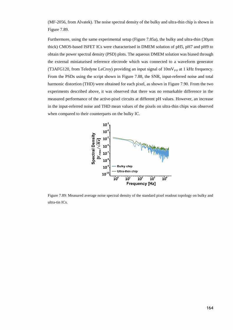
164
(MF-2056, from Alvatek). The noise spectral density of the bulky and ultra-thin chip is shown in
Figure 7.89.
Furthermore, using the same experimental setup (Figure 7.85a), the bulky and ultra-thin (30µm
thick) CMOS-based ISFET ICs were characterised in DMEM solution of pH5, pH7 and pH9 to
obtain the power spectral density (PSD) plots. The aqueous DMEM solution was biased through
the external miniaturised reference electrode which was connected to a waveform generator
(T3AFG120, from Teledyne LeCroy) providing an input signal of 10mVp-p at 1 kHz frequency.
From the PSDs using the script shown in Figure 7.88, the SNR, input-referred noise and total
harmonic distortion (THD) were obtained for each pixel, as shown in Figure 7.90. From the two
experiments described above, it was observed that there was no remarkable difference in the
measured performance of the active-pixel circuits at different pH values. However, an increase
in the input-referred noise and THD mean values of the pixels on ultra-thin chips was observed
when compared to their counterparts on the bulky IC.
Figure 7.89: Measured average noise spectral density of the standard pixel readout topology on bulky and
ultra-tin ICs.
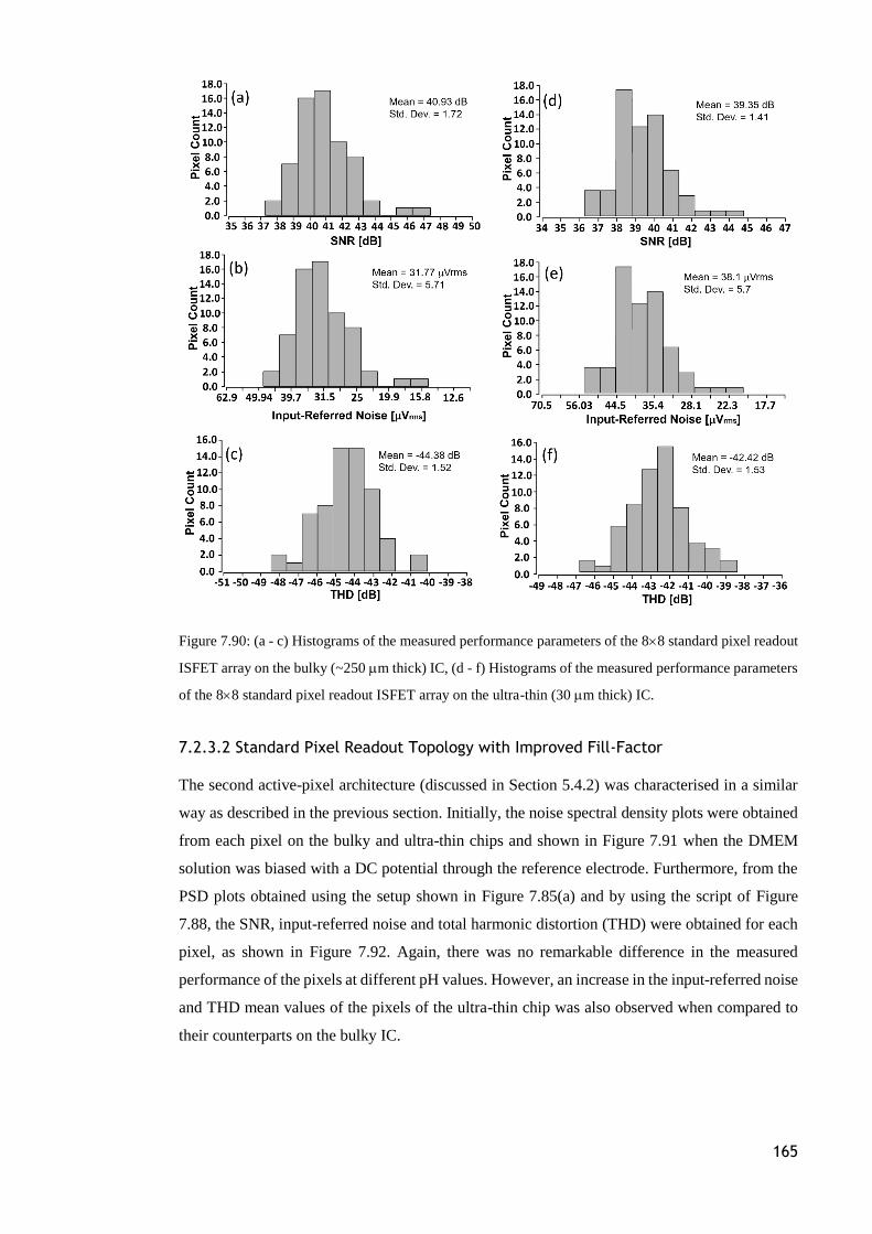
165
Figure 7.90: (a - c) Histograms of the measured performance parameters of the 88 standard pixel readout
ISFET array on the bulky (~250 m thick) IC, (d - f) Histograms of the measured performance parameters
of the 88 standard pixel readout ISFET array on the ultra-thin (30 m thick) IC.
7.2.3.2 Standard Pixel Readout Topology with Improved Fill-Factor
The second active-pixel architecture (discussed in Section 5.4.2) was characterised in a similar
way as described in the previous section. Initially, the noise spectral density plots were obtained
from each pixel on the bulky and ultra-thin chips and shown in Figure 7.91 when the DMEM
solution was biased with a DC potential through the reference electrode. Furthermore, from the
PSD plots obtained using the setup shown in Figure 7.85(a) and by using the script of Figure
7.88, the SNR, input-referred noise and total harmonic distortion (THD) were obtained for each
pixel, as shown in Figure 7.92. Again, there was no remarkable difference in the measured
performance of the pixels at different pH values. However, an increase in the input-referred noise
and THD mean values of the pixels of the ultra-thin chip was also observed when compared to
their counterparts on the bulky IC.
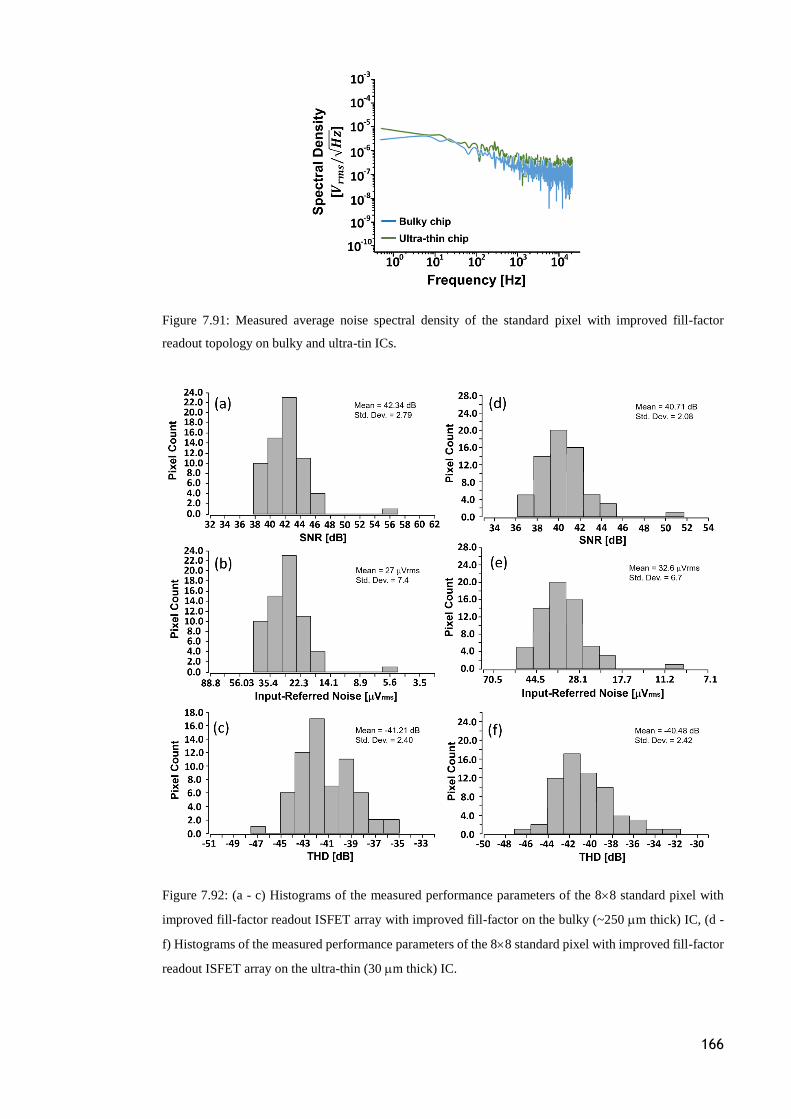
166
Figure 7.91: Measured average noise spectral density of the standard pixel with improved fill-factor
readout topology on bulky and ultra-tin ICs.
Figure 7.92: (a - c) Histograms of the measured performance parameters of the 88 standard pixel with
improved fill-factor readout ISFET array with improved fill-factor on the bulky (~250 m thick) IC, (d -
f) Histograms of the measured performance parameters of the 88 standard pixel with improved fill-factor
readout ISFET array on the ultra-thin (30 m thick) IC.
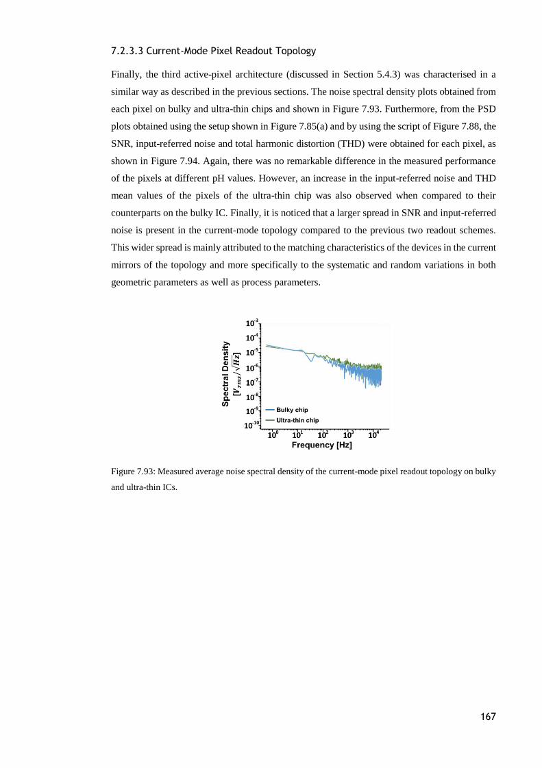
167
7.2.3.3 Current-Mode Pixel Readout Topology
Finally, the third active-pixel architecture (discussed in Section 5.4.3) was characterised in a
similar way as described in the previous sections. The noise spectral density plots obtained from
each pixel on bulky and ultra-thin chips and shown in Figure 7.93. Furthermore, from the PSD
plots obtained using the setup shown in Figure 7.85(a) and by using the script of Figure 7.88, the
SNR, input-referred noise and total harmonic distortion (THD) were obtained for each pixel, as
shown in Figure 7.94. Again, there was no remarkable difference in the measured performance
of the pixels at different pH values. However, an increase in the input-referred noise and THD
mean values of the pixels of the ultra-thin chip was also observed when compared to their
counterparts on the bulky IC. Finally, it is noticed that a larger spread in SNR and input-referred
noise is present in the current-mode topology compared to the previous two readout schemes.
This wider spread is mainly attributed to the matching characteristics of the devices in the current
mirrors of the topology and more specifically to the systematic and random variations in both
geometric parameters as well as process parameters.
Figure 7.93: Measured average noise spectral density of the current-mode pixel readout topology on bulky
and ultra-thin ICs.
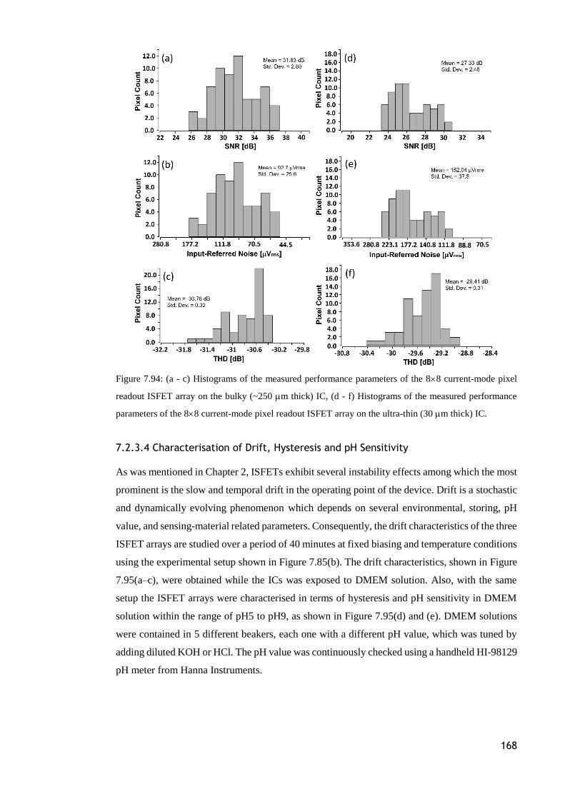
168
Figure 7.94: (a - c) Histograms of the measured performance parameters of the 88 current-mode pixel
readout ISFET array on the bulky (~250 m thick) IC, (d - f) Histograms of the measured performance
parameters of the 88 current-mode pixel readout ISFET array on the ultra-thin (30 m thick) IC.
7.2.3.4 Characterisation of Drift, Hysteresis and pH Sensitivity
As was mentioned in Chapter 2, ISFETs exhibit several instability effects among which the most
prominent is the slow and temporal drift in the operating point of the device. Drift is a stochastic
and dynamically evolving phenomenon which depends on several environmental, storing, pH
value, and sensing-material related parameters. Consequently, the drift characteristics of the three
ISFET arrays are studied over a period of 40 minutes at fixed biasing and temperature conditions
using the experimental setup shown in Figure 7.85(b). The drift characteristics, shown in Figure
7.95(a–c), were obtained while the ICs was exposed to DMEM solution. Also, with the same
setup the ISFET arrays were characterised in terms of hysteresis and pH sensitivity in DMEM
solution within the range of pH5 to pH9, as shown in Figure 7.95(d) and (e). DMEM solutions
were contained in 5 different beakers, each one with a different pH value, which was tuned by
adding diluted KOH or HCl. The pH value was continuously checked using a handheld HI-98129
pH meter from Hanna Instruments.
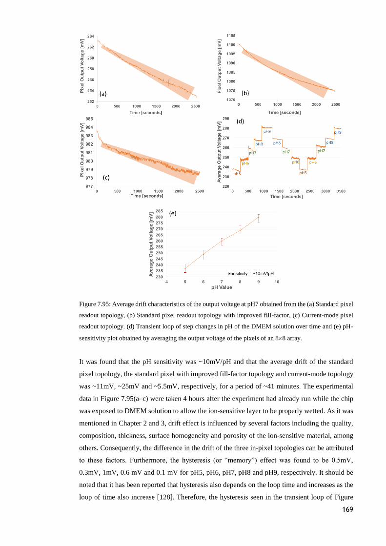
169
Figure 7.95: Average drift characteristics of the output voltage at pH7 obtained from the (a) Standard pixel
readout topology, (b) Standard pixel readout topology with improved fill-factor, (c) Current-mode pixel
readout topology. (d) Transient loop of step changes in pH of the DMEM solution over time and (e) pH-
sensitivity plot obtained by averaging the output voltage of the pixels of an 88 array.
It was found that the pH sensitivity was ~10mV/pH and that the average drift of the standard
pixel topology, the standard pixel with improved fill-factor topology and current-mode topology
was ~11mV, ~25mV and ~5.5mV, respectively, for a period of ~41 minutes. The experimental
data in Figure 7.95(a–c) were taken 4 hours after the experiment had already run while the chip
was exposed to DMEM solution to allow the ion-sensitive layer to be properly wetted. As it was
mentioned in Chapter 2 and 3, drift effect is influenced by several factors including the quality,
composition, thickness, surface homogeneity and porosity of the ion-sensitive material, among
others. Consequently, the difference in the drift of the three in-pixel topologies can be attributed
to these factors. Furthermore, the hysteresis (or “memory”) effect was found to be 0.5mV,
0.3mV, 1mV, 0.6 mV and 0.1 mV for pH5, pH6, pH7, pH8 and pH9, respectively. It should be
noted that it has been reported that hysteresis also depends on the loop time and increases as the
loop of time also increase [128]. Therefore, the hysteresis seen in the transient loop of Figure
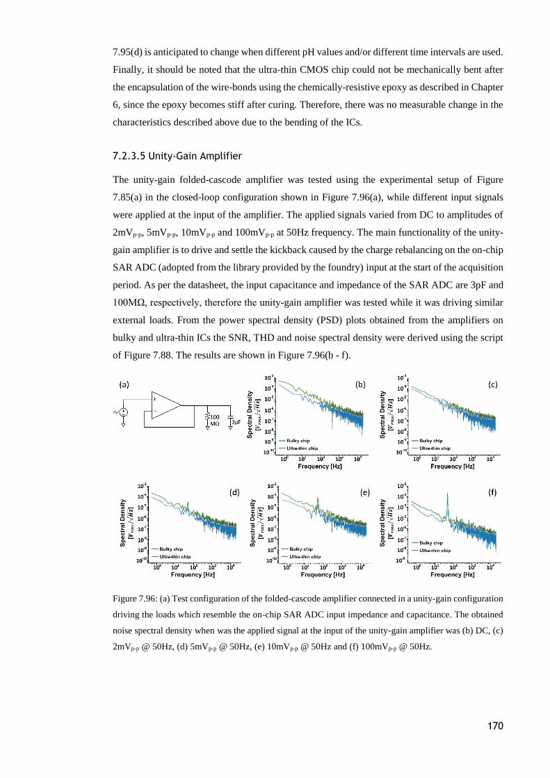
170
7.95(d) is anticipated to change when different pH values and/or different time intervals are used.
Finally, it should be noted that the ultra-thin CMOS chip could not be mechanically bent after
the encapsulation of the wire-bonds using the chemically-resistive epoxy as described in Chapter
6, since the epoxy becomes stiff after curing. Therefore, there was no measurable change in the
characteristics described above due to the bending of the ICs.
7.2.3.5 Unity-Gain Amplifier
The unity-gain folded-cascode amplifier was tested using the experimental setup of Figure
7.85(a) in the closed-loop configuration shown in Figure 7.96(a), while different input signals
were applied at the input of the amplifier. The applied signals varied from DC to amplitudes of
2mVp-p, 5mVp-p, 10mVp-p and 100mVp-p at 50Hz frequency. The main functionality of the unity-
gain amplifier is to drive and settle the kickback caused by the charge rebalancing on the on-chip
SAR ADC (adopted from the library provided by the foundry) input at the start of the acquisition
period. As per the datasheet, the input capacitance and impedance of the SAR ADC are 3pF and
100MΩ, respectively, therefore the unity-gain amplifier was tested while it was driving similar
external loads. From the power spectral density (PSD) plots obtained from the amplifiers on
bulky and ultra-thin ICs the SNR, THD and noise spectral density were derived using the script
of Figure 7.88. The results are shown in Figure 7.96(b - f).
Figure 7.96: (a) Test configuration of the folded-cascode amplifier connected in a unity-gain configuration
driving the loads which resemble the on-chip SAR ADC input impedance and capacitance. The obtained
noise spectral density when was the applied signal at the input of the unity-gain amplifier was (b) DC, (c)
2mVp-p @ 50Hz, (d) 5mVp-p @ 50Hz, (e) 10mVp-p @ 50Hz and (f) 100mVp-p @ 50Hz.
171
As it can be seen from Figure 7.96(b - f), there is an increase in the flicker (1/f) noise of the
amplifier on the ultra-thin IC when compared to the bulky counterpart. Finally, the derived SNR
and THD are given in Table 7.18, below.
Table 7.18: List of measured performance parameters of the folded-cascode unity-gain amplifier.
Input Signal Amplitude
[mVp-p] SNR [dB] THD [%] THD [dB]
2 23.74 ± 7.6 5.322 ± 0.3 −25.48 ± 0.48
5 30.07 ± 3.14 2.58 ± 1.7 −31.77 ± 4.39
10 36.8 ± 0.5 1.22 ± 0.075 −38.27 ± 0.52
100 58.9 ± 0.13 0.3 ± 0.014 −50.46 ± 0.4
7.3 Ultra-Thin ISFET with Bending Induced Performance
Enhancement
ISFETs are traditionally known to exhibit several instability effects among which the most
prominent is the slow and temporal drift in the operating point of the device, as was also observed
in the experimental results shown in Figure 7.95(a-c). As discussed in Chapter 2 and 3, drift
prohibits the use of ISFETs in applications which require continuous pH monitoring. Drift also
requires special attention during the design of the read-out electronic system to be compensated.
The drifting phenomenon in ISFETs has been established through numerous studies and has been
described as a stochastic and dynamically evolving phenomenon which depends on several
environmental, storing pH, and sensing-material related parameters. In this regard, mechanical
means such as bending induced changes in the device response can offer an alternative or
complementation of the other drift-compensation techniques discussed in Chapter 2, such as the
stacking of high-k ion-sensitive materials, the use of signal-processing techniques and/or the on-
chip circuit-level implementations.
Here, it is the first time to demonstrate real-time active drift compensation by exploiting the
piezo-resistive nature of silicon. More specifically, as the sequential externally applied dynamic
strain on an ultra-thin silicon substrate is increasing, the energy of the split conduction sub-band
Δ4 reduces with respect to Δ2 (see Chapter 3 for more details). The splitting and lowering of
bands decrease the effective carriers’ mass, which subsequently changes the surface carrier
mobility resulting in a relative change of Drain-current. Therefore, the ISFET-based UTC can be
transformed into a controllable and reversible electrical conductance modulator through fine
control of the Si-substrate’s bending radius, as shown in Figure 7.97(a-d).
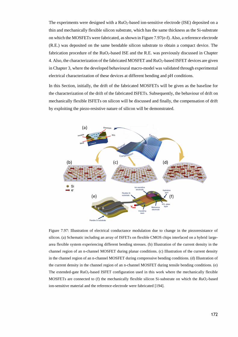
172
The experiments were designed with a RuO2-based ion-sensitive electrode (ISE) deposited on a
thin and mechanically flexible silicon substrate, which has the same thickness as the Si-substrate
on which the MOSFETs were fabricated, as shown in Figure 7.97(e-f). Also, a reference electrode
(R.E.) was deposited on the same bendable silicon substrate to obtain a compact device. The
fabrication procedure of the RuO2-based ISE and the R.E. was previously discussed in Chapter
4. Also, the characterization of the fabricated MOSFET and RuO2-based ISFET devices are given
in Chapter 3, where the developed behavioural macro-model was validated through experimental
electrical characterization of these devices at different bending and pH conditions.
In this Section, initially, the drift of the fabricated MOSFETs will be given as the baseline for
the characterization of the drift of the fabricated ISFETs. Subsequently, the behaviour of drift on
mechanically flexible ISFETs on silicon will be discussed and finally, the compensation of drift
by exploiting the piezo-resistive nature of silicon will be demonstrated.
Figure 7.97: Illustration of electrical conductance modulation due to change in the piezoresistance of
silicon. (a) Schematic including an array of ISFETs on flexible CMOS chips interfaced on a hybrid large-
area flexible system experiencing different bending stresses. (b) Illustration of the current density in the
channel region of an n-channel MOSFET during planar conditions. (c) Illustration of the current density
in the channel region of an n-channel MOSFET during compressive bending conditions. (d) Illustration of
the current density in the channel region of an n-channel MOSFET during tensile bending conditions. (e)
The extended-gate RuO2-based ISFET configuration used in this work where the mechanically flexible
MOSFETs are connected to (f) the mechanically flexible silicon Si-substrate on which the RuO2-based
ion-sensitive material and the reference-electrode were fabricated [194].
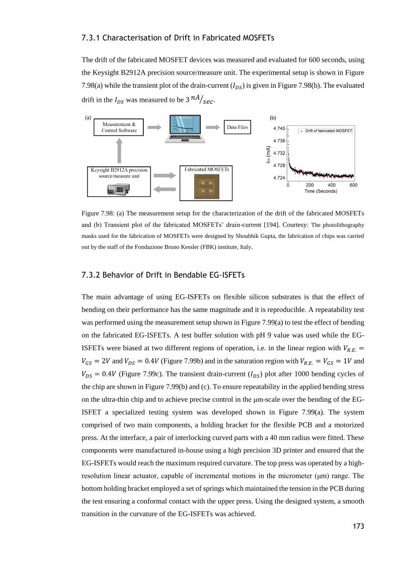
173
7.3.1 Characterisation of Drift in Fabricated MOSFETs
The drift of the fabricated MOSFET devices was measured and evaluated for 600 seconds, using
the Keysight B2912A precision source/measure unit. The experimental setup is shown in Figure
7.98(a) while the transient plot of the drain-current (𝐼𝐷𝑆) is given in Figure 7.98(b). The evaluated
drift in the 𝐼𝐷𝑆 was measured to be 3𝑛𝐴𝑠𝑒𝑐⁄ .
Figure 7.98: (a) The measurement setup for the characterization of the drift of the fabricated MOSFETs
and (b) Transient plot of the fabricated MOSFETs’ drain-current [194]. Courtesy: The photolithography
masks used for the fabrication of MOSFETs were designed by Shoubhik Gupta, the fabrication of chips was carried
out by the staff of the Fondazione Bruno Kessler (FBK) institute, Italy.
7.3.2 Behavior of Drift in Bendable EG-ISFETs
The main advantage of using EG-ISFETs on flexible silicon substrates is that the effect of
bending on their performance has the same magnitude and it is reproducible. A repeatability test
was performed using the measurement setup shown in Figure 7.99(a) to test the effect of bending
on the fabricated EG-ISFETs. A test buffer solution with pH 9 value was used while the EG-
ISFETs were biased at two different regions of operation, i.e. in the linear region with 𝑉𝑅.𝐸. =
𝑉𝐺𝑆 = 2𝑉 and 𝑉𝐷𝑆 = 0.4𝑉 (Figure 7.99b) and in the saturation region with 𝑉𝑅.𝐸. = 𝑉𝐺𝑆 = 1𝑉 and
𝑉𝐷𝑆 = 0.4𝑉 (Figure 7.99c). The transient drain-current (𝐼𝐷𝑆) plot after 1000 bending cycles of
the chip are shown in Figure 7.99(b) and (c). To ensure repeatability in the applied bending stress
on the ultra-thin chip and to achieve precise control in the μm-scale over the bending of the EG-
ISFET a specialized testing system was developed shown in Figure 7.99(a). The system
comprised of two main components, a holding bracket for the flexible PCB and a motorized
press. At the interface, a pair of interlocking curved parts with a 40 mm radius were fitted. These
components were manufactured in-house using a high precision 3D printer and ensured that the
EG-ISFETs would reach the maximum required curvature. The top press was operated by a high-
resolution linear actuator, capable of incremental motions in the micrometer (μm) range. The
bottom holding bracket employed a set of springs which maintained the tension in the PCB during
the test ensuring a conformal contact with the upper press. Using the designed system, a smooth
transition in the curvature of the EG-ISFETs was achieved.
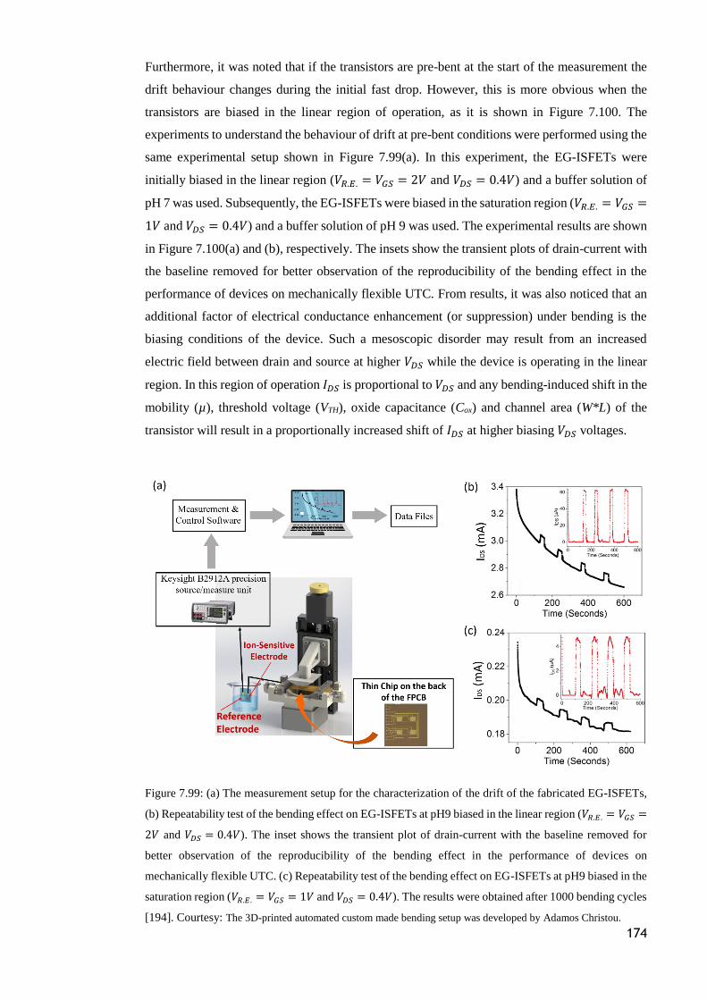
174
Furthermore, it was noted that if the transistors are pre-bent at the start of the measurement the
drift behaviour changes during the initial fast drop. However, this is more obvious when the
transistors are biased in the linear region of operation, as it is shown in Figure 7.100. The
experiments to understand the behaviour of drift at pre-bent conditions were performed using the
same experimental setup shown in Figure 7.99(a). In this experiment, the EG-ISFETs were
initially biased in the linear region (𝑉𝑅.𝐸. = 𝑉𝐺𝑆 = 2𝑉 and 𝑉𝐷𝑆 = 0.4𝑉) and a buffer solution of
pH 7 was used. Subsequently, the EG-ISFETs were biased in the saturation region (𝑉𝑅.𝐸. = 𝑉𝐺𝑆 =
1𝑉 and 𝑉𝐷𝑆 = 0.4𝑉) and a buffer solution of pH 9 was used. The experimental results are shown
in Figure 7.100(a) and (b), respectively. The insets show the transient plots of drain-current with
the baseline removed for better observation of the reproducibility of the bending effect in the
performance of devices on mechanically flexible UTC. From results, it was also noticed that an
additional factor of electrical conductance enhancement (or suppression) under bending is the
biasing conditions of the device. Such a mesoscopic disorder may result from an increased
electric field between drain and source at higher 𝑉𝐷𝑆 while the device is operating in the linear
region. In this region of operation 𝐼𝐷𝑆 is proportional to 𝑉𝐷𝑆 and any bending-induced shift in the
mobility (µ), threshold voltage (VTH), oxide capacitance (Cox) and channel area (W*L) of the
transistor will result in a proportionally increased shift of 𝐼𝐷𝑆 at higher biasing 𝑉𝐷𝑆 voltages.
Figure 7.99: (a) The measurement setup for the characterization of the drift of the fabricated EG-ISFETs,
(b) Repeatability test of the bending effect on EG-ISFETs at pH9 biased in the linear region (𝑉𝑅.𝐸. = 𝑉𝐺𝑆 =
2𝑉 and 𝑉𝐷𝑆 = 0.4𝑉). The inset shows the transient plot of drain-current with the baseline removed for
better observation of the reproducibility of the bending effect in the performance of devices on
mechanically flexible UTC. (c) Repeatability test of the bending effect on EG-ISFETs at pH9 biased in the
saturation region (𝑉𝑅.𝐸. = 𝑉𝐺𝑆 = 1𝑉 and 𝑉𝐷𝑆 = 0.4𝑉). The results were obtained after 1000 bending cycles
[194]. Courtesy: The 3D-printed automated custom made bending setup was developed by Adamos Christou.
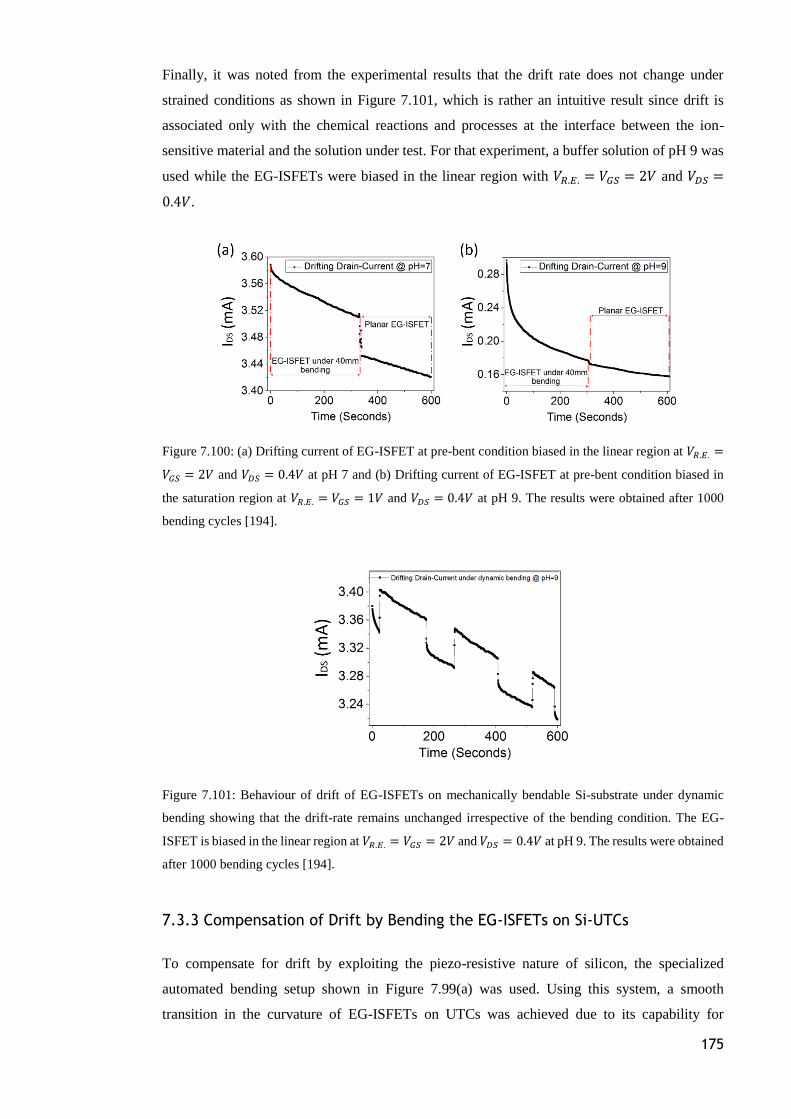
175
Finally, it was noted from the experimental results that the drift rate does not change under
strained conditions as shown in Figure 7.101, which is rather an intuitive result since drift is
associated only with the chemical reactions and processes at the interface between the ion-
sensitive material and the solution under test. For that experiment, a buffer solution of pH 9 was
used while the EG-ISFETs were biased in the linear region with 𝑉𝑅.𝐸. = 𝑉𝐺𝑆 = 2𝑉 and 𝑉𝐷𝑆 =
0.4𝑉.
Figure 7.100: (a) Drifting current of EG-ISFET at pre-bent condition biased in the linear region at 𝑉𝑅.𝐸. =
𝑉𝐺𝑆 = 2𝑉 and 𝑉𝐷𝑆 = 0.4𝑉 at pH 7 and (b) Drifting current of EG-ISFET at pre-bent condition biased in
the saturation region at 𝑉𝑅.𝐸. = 𝑉𝐺𝑆 = 1𝑉 and 𝑉𝐷𝑆 = 0.4𝑉 at pH 9. The results were obtained after 1000
bending cycles [194].
Figure 7.101: Behaviour of drift of EG-ISFETs on mechanically bendable Si-substrate under dynamic
bending showing that the drift-rate remains unchanged irrespective of the bending condition. The EG-
ISFET is biased in the linear region at 𝑉𝑅.𝐸. = 𝑉𝐺𝑆 = 2𝑉 and 𝑉𝐷𝑆 = 0.4𝑉 at pH 9. The results were obtained
after 1000 bending cycles [194].
7.3.3 Compensation of Drift by Bending the EG-ISFETs on Si-UTCs
To compensate for drift by exploiting the piezo-resistive nature of silicon, the specialized
automated bending setup shown in Figure 7.99(a) was used. Using this system, a smooth
transition in the curvature of EG-ISFETs on UTCs was achieved due to its capability for

176
incremental motions in the micrometer (μm) range. Figure 7.103(a-c) show the ISFET chip under
planar and bent conditions at 80 mm and 40 mm bending radius, respectively. The corresponding
velocity variation with time of the motorized press is presented in Figure 7.103(d). By knowing
the velocity with which the motorised press was moving and the total distance of the movement
the period during which the motorised press was moving with a specific velocity was calculated.
Subsequently, the height of the circular section (ℎ) shown in Figure 7.102 was calculated using
the following equation:
ℎ = 𝑢 · 𝑡 (7.1)
where 𝑢 is the velocity of the motorised press, and 𝑡 is the time. By knowing that 𝑐 = 50 𝑚𝑚
(Figure 7.102), we calculated the bending radius at each time by using the following equation:
𝑟 =ℎ
2+
𝑐2
8·ℎ (7.2)
where 𝑟 is the radius of the circle, ℎ is the height of the circular section, and 𝑐 is the length of the
chord of the circular segment, as shown in Figure 7.102. The bending radius at each time interval
of the motorized press’ movement is shown in Figure 7.103(e).
Figure 7.102: Depiction of the different parameters used to calculate the bending radius of the thin chip
over time as the motorised press is applying sequential strain on it. The parameter c is constant and equal
to 5 cm and the parameter h was calculated for every second knowing the velocity of the structure. The
velocity was known and provided by the LabVIEW programme with which the motorised press was
controlled [194].
Finally, the strain at each time interval was calculated using the following equation:
휀 = 𝑐 +𝑦−𝑡𝑏
𝑅𝑐 (7.3)
where 𝑐 is the uniform strain component on the individual layers mainly due to the thermal
expansion, and 𝑅𝑐 is the bending radius. The parameter 𝑡𝑏 is the location of the bending axis of
the tri-layer structure (PI, epoxy, silicon) where the strain is null and is given by:
177
𝑡𝑏 =∑ 𝐸𝑖𝑡𝑖(2ℎ𝑖−1+𝑡𝑖)
𝑛𝑖=1
2∑ 𝐸𝑖𝑡𝑖𝑛𝑖=1
(7.4)
where, 𝐸𝑖 is Young’s modulus of the respective layer, 𝑡𝑖 is the thickness of the respective layer,
and ℎ𝑖 is the distance between the first layer and the 𝑖𝑡ℎ stacked layer.
A detailed mechanism thus emerges, as indicated in Figure 7.103(d-f): As sequentially applied
external dynamic tensile strain on a silicon substrate is increasing, the effective reduction in
carriers’ mass which subsequently changes the charged surface carriers’ mobility and the
resistivity of silicon (Si) in combination with the increase in gate capacitance and the change in
the channel dimensions (W/L) results in an overall change in the drain-current of the device.
With the overall relative change of current, the system transforms into a controllable and
reversible electrical conductance modulator targeting real-time active drift compensation.
In this context, the presented results represent an important advance with the 1.3 orders of
magnitude improved stability (drift rate changed from -557 nA/min. for planar ISFET
to -28 nA/min. ± 0.16 nA/min. for ISFETs on 44.76μm thick UTCs under sequentially applied
external dynamic tensile strain) over a 417.3 seconds (~7 min.) period of time at fixed biasing
and temperature conditions. The mechanically flexible RuO2-based ISFETs on UTCs have
shown to reproducibly enhance the performance even after 1000 bending cycles The mean
absolute current over this period was 161.48 ± 5.64×10⁻⁴ μA. As it was observed from the
experimental results, the performance of EG-ISFETs changes only due to bending of the
electronic part (i.e. transistor) and does not get affected by the bending of the ion-sensitive and
reference electrodes.
Furthermore, by using the data from the plots shown in Figure 7.103(e-f) the extracted equations
which represent the bending radius and strain as a function of time are:
𝐵𝑒𝑛𝑑𝑖𝑛𝑔 𝑟𝑎𝑑𝑖𝑢𝑠 (𝑡) = 𝐵𝑅1 × 𝑒[−
(𝑡−𝑡0)
𝑡1]+ 𝐵𝑅2 × 𝑒
[−(𝑡−𝑡0)
𝑡2]+ 𝐵𝑅3 × 𝑒
[−(𝑡−𝑡0)
𝑡3]+ 𝐶𝐵𝑅
(7.5)
𝑆𝑡𝑟𝑎𝑖𝑛 (𝑡) = 𝑆1 × 𝑡 + 𝑆2 × 𝑡2 + 𝑆3 × 𝑡3 + 𝑆4 × 𝑡4 + 𝑆5 × 𝑡5 + 𝐶𝑠 (7.6)
As can be seen from Equations 7.5 and 7.6 the relationship between the applied strain and the
cancellation of drift is not linear. Finally, the transient response of ISFET under planar conditions
is also compared with the drift-free response achieved by applying sequentially increased strain
using the automated bending setup (Figure 7.99a) which has been now pre-programmed to
perform the movement described in Figure 7.103(d). The comparison of planar and drift-free
ISFET response showing the error bars is presented in Figure 7.103(g-h).
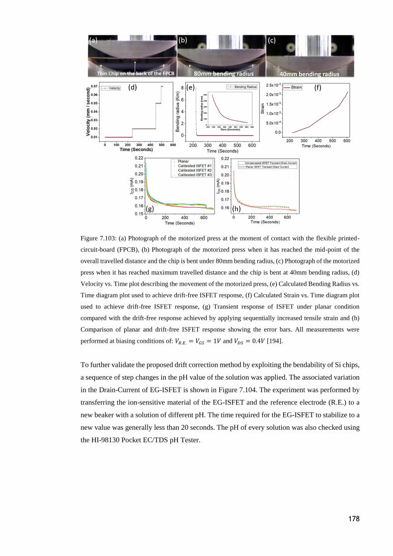
178
Figure 7.103: (a) Photograph of the motorized press at the moment of contact with the flexible printed-
circuit-board (FPCB), (b) Photograph of the motorized press when it has reached the mid-point of the
overall travelled distance and the chip is bent under 80mm bending radius, (c) Photograph of the motorized
press when it has reached maximum travelled distance and the chip is bent at 40mm bending radius, (d)
Velocity vs. Time plot describing the movement of the motorized press, (e) Calculated Bending Radius vs.
Time diagram plot used to achieve drift-free ISFET response, (f) Calculated Strain vs. Time diagram plot
used to achieve drift-free ISFET response, (g) Transient response of ISFET under planar condition
compared with the drift-free response achieved by applying sequentially increased tensile strain and (h)
Comparison of planar and drift-free ISFET response showing the error bars. All measurements were
performed at biasing conditions of: 𝑉𝑅.𝐸. = 𝑉𝐺𝑆 = 1𝑉 and 𝑉𝐷𝑆 = 0.4𝑉 [194].
To further validate the proposed drift correction method by exploiting the bendability of Si chips,
a sequence of step changes in the pH value of the solution was applied. The associated variation
in the Drain-Current of EG-ISFET is shown in Figure 7.104. The experiment was performed by
transferring the ion-sensitive material of the EG-ISFET and the reference electrode (R.E.) to a
new beaker with a solution of different pH. The time required for the EG-ISFET to stabilize to a
new value was generally less than 20 seconds. The pH of every solution was also checked using
the HI-98130 Pocket EC/TDS pH Tester.
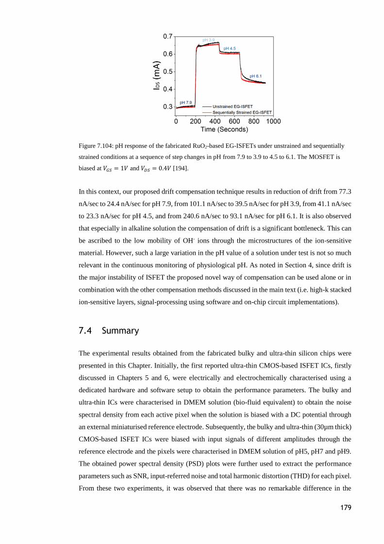
179
Figure 7.104: pH response of the fabricated RuO2-based EG-ISFETs under unstrained and sequentially
strained conditions at a sequence of step changes in pH from 7.9 to 3.9 to 4.5 to 6.1. The MOSFET is
biased at 𝑉𝐺𝑆 = 1𝑉 and 𝑉𝐷𝑆 = 0.4𝑉 [194].
In this context, our proposed drift compensation technique results in reduction of drift from 77.3
nA/sec to 24.4 nA/sec for pH 7.9, from 101.1 nA/sec to 39.5 nA/sec for pH 3.9, from 41.1 nA/sec
to 23.3 nA/sec for pH 4.5, and from 240.6 nA/sec to 93.1 nA/sec for pH 6.1. It is also observed
that especially in alkaline solution the compensation of drift is a significant bottleneck. This can
be ascribed to the low mobility of OH- ions through the microstructures of the ion-sensitive
material. However, such a large variation in the pH value of a solution under test is not so much
relevant in the continuous monitoring of physiological pH. As noted in Section 4, since drift is
the major instability of ISFET the proposed novel way of compensation can be used alone or in
combination with the other compensation methods discussed in the main text (i.e. high-k stacked
ion-sensitive layers, signal-processing using software and on-chip circuit implementations).
7.4 Summary
The experimental results obtained from the fabricated bulky and ultra-thin silicon chips were
presented in this Chapter. Initially, the first reported ultra-thin CMOS-based ISFET ICs, firstly
discussed in Chapters 5 and 6, were electrically and electrochemically characterised using a
dedicated hardware and software setup to obtain the performance parameters. The bulky and
ultra-thin ICs were characterised in DMEM solution (bio-fluid equivalent) to obtain the noise
spectral density from each active pixel when the solution is biased with a DC potential through
an external miniaturised reference electrode. Subsequently, the bulky and ultra-thin (30µm thick)
CMOS-based ISFET ICs were biased with input signals of different amplitudes through the
reference electrode and the pixels were characterised in DMEM solution of pH5, pH7 and pH9.
The obtained power spectral density (PSD) plots were further used to extract the performance
parameters such as SNR, input-referred noise and total harmonic distortion (THD) for each pixel.
From these two experiments, it was observed that there was no remarkable difference in the
180
measured performance of the active-pixel circuits at different pH values. However, an increase
in the input-referred noise and THD mean values of the pixels on ultra-thin chips (UTCs) was
observed when compared to their counterparts on the bulky ICs indicating that thinning should
be treated as an additional source of the noise. Also, an increased flicker (1/f) noise of the unity-
gain amplifier on the ultra-thin ICs was observed when it was compared to the bulky counterpart.
The experimental results show a deviation of approximately 15 dB to 20 dB in SNR and THD
compared to the simulation results presented in Chapter 5, which is mainly attributed to the signal
attenuation due to the thick and low-quality passivation layer of the unmodified surface of the
CMOS ICs and due to the distortion of the input signal caused by the aqueous medium under
test. Finally it should be noted that, the highest SNR among the three readout topologies was
observed from the standard pixel readout with improved fill factor while the first standard readout
pixel topology showed the best THD among the three. However, from simulation results it was
observed that the current-mode topology has better immunity to PVT and bending-induced
variations.
A pH sensitivity of ~10mV/pH was measured for the “unmodified” CMOS-based ISFET IC and
an average drift rate of ~11mV, ~25mV and ~5.5mV for a period of ~41 minutes was observed
from the three different in-pixel topologies when the ICs were exposed in a Dulbecco's Modified
Eagle Medium (DMEM) aqueous solution with pH values ranging from pH5 to pH9, resembling
the pH range found in body-fluids. The hysteresis (or “memory”) effect was found to be 0.5mV,
0.3mV, 1mV, 0.6 mV and 0.1 mV for pH5, pH6, pH7, pH8 and pH9, respectively. These
experimental data were taken after 4 hours of the experiment had already run while the chip was
exposed to DMEM solution to allow the ion-sensitive layer to be properly wetted. Finally, it
should be noted that the ultra-thin CMOS chips could not be mechanically bent after the
encapsulation of the wire-bonds using the chemically-resistive epoxy (see Chapter 6) since the
epoxy becomes stiff after curing. Therefore, there was no measurable change in the
characteristics described above due to the bending of ICs.
Furthermore, the first reported mechanically bendable RuO2-based ISFET on a silicon substrate
was characterised during automated sequential bending. It was demonstrated that the relative
shift in electrical conductivity of an ISFET on ultra-thin silicon chips (UTCs) depends both on
the applied nominal strain and the biasing conditions. However, it does not depend on the
mechanical deformation of the electrolyte-insulator interface. Furthermore, as was also
mentioned in Chapter 3 and Chapter 4, the sensitivity of RuO2 is unaffected even after 1000
bending cycles at a maximum applied nominal strain of ±21 × 10−4 (40mm bending radius).
Besides, it was demonstrated that drift rate does not change under strained conditions, which is
a rather intuitive result since drift is associated only with the chemical reactions and processes at
the interface between the ion-sensitive material and the solution under test. Overall, it was
demonstrated that non-linear bending of the UTC leads to the cancellation of drift for up to ~7
181
minutes by exploiting the piezoresistive nature of silicon and that drift compensation can be
further improved by reducing further the thickness of UTC by allowing the chip to bend at higher
bending curvatures. It should be noted, that the demonstration of drift compensation in ISFETs
by bending the UTC is a proof-of-concept and that the scope of this study is much larger as it
stimulates new directions for flexible circuits and systems. Also, the device characterization
during automated sequential bending of silicon can provide useful information about the
transistor that is undergoing bending and can be considered as useful performance evaluation as
well as a failure analysis tool.
With this study, overall it was demonstrated that non-linear bending of the chip leads to the
cancellation of drift. From a practical standpoint, a compact and low-cost 3D-printed automated
bending setup was designed and built with overall size 10 12 cm2 which is capable of
accommodating the full range of displacement of the motorized press. The motorized press was
operated by a high-resolution linear actuator, capable of incremental motions in the micrometer
(μm) range allowing fine control of bending radius. However, it should be noted that bending of
the chip can be also achieved with soft actuators such as electroactive polymers, shape memory
alloys or pneumatic actuators embedded on the back-side of the FPCB [516] to further reduce
the size of the bending setup. Overall, the proposed system can be integrated into robots used in
remote and harsh environments (e.g. space applications) or for laboratory analysis of samples
that require continuous measurements, such as the pH value of blood.
182
Chapter 8. Conclusion and Future Work
8.1 Conclusion
Sensor technologies are increasingly being used towards the internet-of-everything (IoE) for
various applications. Among them, biochemical sensing systems are particularly important in the
domains of medical science through the discovery of biological mechanisms or in the domains
of environmental as well as water and food quality monitoring. Furthermore, wearable and
implantable point-of-care (PoC) biomedical devices have been explored towards rapid clinical-
grade decision-making systems that will be able to mitigate delays in treatment. More
specifically, recent advances in the field of wearable and implantable sensing microsystems
enabled the development of devices that can monitor heart rate, blood oxygenation and pressure,
respiration rate, body posture, skin stretching, skin temperature and brain activity. Moreover,
recent studies have also demonstrated wearable systems capable of continuous measurements of
biochemical samples such as electrolytes and metabolites in bio-fluids while others have pushed
the field of wearables a step closer to sensing microsystems that can seamlessly comply with the
curvilinear geometry of human tissues, allowing robust recordings while providing comfort to
the user in the daily-life activities.
The miniaturisation of these systems is thus of great importance to achieve high performance,
robust measurements but also to increase the comfort of the user. The complementary
metal-oxide-semiconductor (CMOS) technology is a great candidate to achieve this. Using
CMOS technology a large number of closely spaced sensing electrodes can be monolithically
integrated along with recording amplifiers and analogue-to-digital converters (ADCs) on the
same substrate obtaining large sensing areas, high spatiotemporal resolution while allowing
access to a large number of high-performance recording channels with a small number of I/O
pads avoiding off-chip parasitics and interference. One category of CMOS-based sensors able to
monitor ultra-small volumes of biochemical samples is the ion-sensitive field-effect transistors
(ISFETs), which were introduced in 1970 by P. Bergveld for electrophysiological measurements
in the brain. ISFETs can be easily adapted in the CMOS fabrication process offering a method
of detection that can be fast, specific and non-destructive to the medium under test. ISFETs are
essentially pH sensors that can be used for label-free detection of H+ ions. Besides, ISFETs can
be used as a platform of various biochemical sensing applications in the potentiometric mode
after modification/functionalisation of the sensing layer, including DNA sequencing, enzyme
kinetics, gas sensing, detection of positive ions (e.g. sodium, potassium, calcium), detection of
negative ions (e.g. chloride, phosphate, nitrate) as well as detection of biomolecules (e.g.
adenosine triphosphate, dopamine, lactate), as discussed in Chapter 2.
183
The performance itself is not enough, however, as the next generation applications wearable and
implantable systems will also require the silicon dies to be miniaturised in the z-direction,
targeting conformability on three-dimensional soft and curvilinear surfaces as well as low tissue
damage when implanted. However, silicon wafers and dies are brittle and manufactured to be
thick and mechanically stiff for reliability and better automated-handling purposes precluding
their use in the aforementioned applications. With the appropriate silicon-thinning and handling
techniques, however, they can be thinned down to the ultra-thin regime (< 50µm). Ultra-thin
silicon (UTC) technology can provide several aspects that cannot be realized using the
conventional bulky silicon wafers. For example, the ultra-thin form factor of CMOS chips allows
the dies to be easier integrated into compact systems, such as systems-on-pill (SoP), mini
endoscopes and catheters, orthopedic or dental implants and sub- or epi-retinal implants. Also, it
allows the chips to be implanted without severely damaging the tissues, such as in systems for
bioimpedance, neural signal, EMG signal recording probes or for intracranial pressure
monitoring applications, as discussed in Chapter 2. Finally, the mechanical flexibility and shape
adaptability of Si-UTCs allows them to seamlessly be integrated on curvilinear surfaces, such as
on soft tissues, robotic parts or in smart wearables, such as wrist-bands, contact lenses, glasses
and rings. Overall, UTC technology holds great promise in healthcare applications which will
benefit from the conformability, durability, robustness and high-performance. This thesis
presents the engineering of a fully-integrated and low-power ISFET-based sensing microsystem
using UTC technology. The body of the presented work in this thesis consists of modelling,
design, simulations, back-thinning and characterisation of ultra-thin integrated CMOS-based
chips capable of pH monitoring on bio-fluid equivalent media. It also includes the fabrication
and characterisation of planar (2D) reference electrodes, which are essential for the proper
operation of ISFETs, as well as the characterisation of biosensing, GO/Chitosan ultra-thin films
for the detection of dopamine and serotonin, presented in Chapter 4 and developed in
collaboration with colleagues from Bendable Electronics and Sensing technologies (B.E.S.T.)
group. These biosensing films are CMOS-compatible and thus can be integrated with the
developed system-on-ultra-thin chip (SoUTC). The significant research outcomes of the thesis
are summarised below:
The development and experimental validation of the first reported compact models for
CMOS-based MOSFET and ISFET devices which include the effects of externally applied
bending stresses on their performance. These models, presented in Chapter 3, are a
combination of mathematical equations and extracted parameters from BSIM4 and BSIM6
are developed using Verilog-A. From the experimental results, the models show a close
matching with the simulated characteristics and therefore, they extend the state-of-art by
providing a computationally efficient representation of the devices’ behaviour under planar
and strained conditions developed as a script compatible to computer-aided design (CAD)
tools, such as Cadence Virtuoso environment.
184
The establishment and optimisation of the wafer- and chip-scale back-thinning procedures
using wet-etching and back-lapping techniques. Using both of these techniques several
silicon wafers and dies were successfully thinned down to the ultra-thin regime. The detailed
results of these studies are presented in Chapter 6.
The first reported fully-integrated low-noise ISFET-based CMOS ASIC on ultra-thin chips.
The designs, presented in Chapter 5, were verified using both the models from the process
design kit (PDK) provided by the foundry as well as using the developed behavioural models
designed in Verilog-A. The fabricated dies were subsequently back-thinned down to 30µm
and were electrically and electrochemically characterised in a Dulbecco's Modified Eagle
Medium (DMEM) aqueous solution with pH values ranging from pH5 to pH9. The detailed
results of these studies are presented in Chapter 7.
The first reported mechanically bendable ISFET devices on silicon ultra-thin chips
(44.76µm). Through fine control of bending radius in the micrometre scale, the
mechanically flexible ISFETs are shown to reproducibly enhance the performance even
after 1000 bending cycles. The 1.3 orders of magnitude improved stability (i.e. the drift rate
changed from −557 nA/min to −28 ± 0.16 nA/min) are observed over a time period of 417.3
s (∼7 min) at fixed biasing and temperature conditions and under different pH conditions.
The detailed results and discussion around these studies are presented in Chapters 3 and 7.
The development and characterisation of planar (2D) Ag/AgCl/KCl reference electrodes
(REs) on rigid LTCC as well as on mechanically bendable silicon substrates. The reference
electrodes showed a stable potential and close to zero when measured against a
commercially available standard glass reference electrode and a stable potential in aqueous
solutions in which various concentration of NaCl (30 – 100 mM) was diluted. Also, the
development and characterisation of biocompatible, biodegradable and ultra-flexible
Graphene-Oxide/Chitosan-based biosensors for the detection of dopamine and serotonin.
The sensors offer good electrical stability and reduced drift in sensor output which makes it
suitable for continuous monitoring. The detailed results of these studies are presented in
Chapter 4.
8.2 Future Work
The emphasis of this multidisciplinary study was placed on the engineering of a complete
working pH-sensing microsystem using ultra-thin chip (UTC) technology rather than on
185
optimising all the individual components. Consequently, it is now possible to identify several
key areas where additional research is required to address, improve and further develop the
technology and the autonomy of the system. These include:
Improvements can be implemented in the design of the pH-sensing IC. As discussed in
Chapter 7, the commands to configure the IC are sent by a Mbed microcontroller. As a
line of future work, the microcontroller can be embedded into the pH sensing IC. Also,
the power consumption could be further reduced by optimising the design of opamps,
ADC and DAC. Also, an adaptive biasing of pixels can be developed to automatically
calibrate the ISFET pixels of the arrays. Finally, transceiver circuits can also be
integrated on-chip to allow wireless communication with portable electronic devices,
such as mobile phones as not all of them offer USB connection as a propriety interface.
By improving the functionality of the IC, the system can become lighter and easier to be
integrated on smart wearables, such as wrist-bands, contact lenses and smart rings, as
well as on ingestible systems, such as smart pills.
The development of appropriate bonding techniques to acquire reliable and robust
connections from the bonding pads on ultra-thin ICs to the pads on flexible PCBs
allowing the silicon dies to bend if required without compromising the continuity of the
connections. Promising techniques seem to be the printing and photolithography
techniques. Also, flip-chip bonding of UTCs on flexible polymeric substrates via
through-silicon vias (TSVs) is another promising approach. Regarding printing, despite
that conventional printing techniques, such as screen-printing, are not adequate due to
the resolution that can be achieved with them, there are a few techniques, like super
inkjet (SIJ) printing, that can be explored to obtain thin (nanometre scale) and fine
(micrometre scale) conductive interconnects. As an alternative, the ICs could also
wirelessly communicate with off-chip components allowing data transmission and
powering of ICs through indicative coupling reducing to the bare minimum the need of
bond-pads and wire-bonds.
The development of appropriate packaging is also critical for the realisation of
mechanically bendable ultra-thin chips that can be used in aqueous environments. A
polymeric and passivating coating, such as polyimide or PDMS which can be patterned
to expose the sensing area to the aqueous solution while keeping the wire-bonds and
bond-pads passivated could be a promising solution. Leakages of aqueous solutions
through the interface of the polymers with the ICs or leakages through the bulk of the
polymers should also be examined.
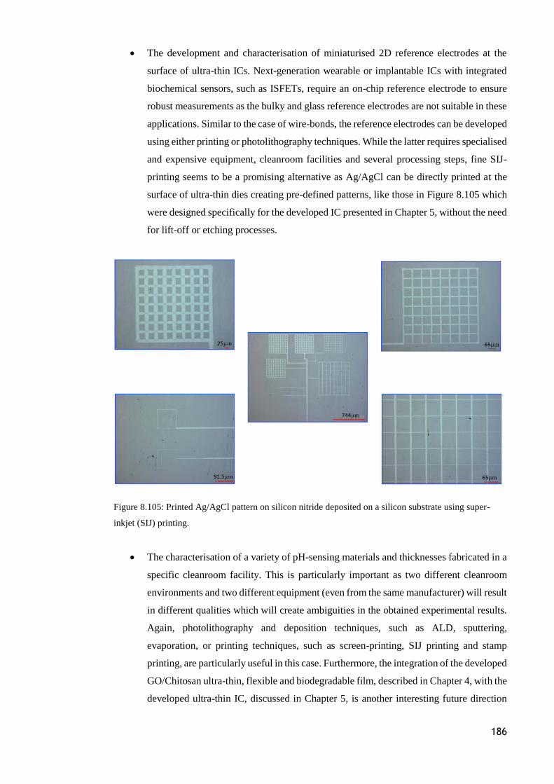
186
The development and characterisation of miniaturised 2D reference electrodes at the
surface of ultra-thin ICs. Next-generation wearable or implantable ICs with integrated
biochemical sensors, such as ISFETs, require an on-chip reference electrode to ensure
robust measurements as the bulky and glass reference electrodes are not suitable in these
applications. Similar to the case of wire-bonds, the reference electrodes can be developed
using either printing or photolithography techniques. While the latter requires specialised
and expensive equipment, cleanroom facilities and several processing steps, fine SIJ-
printing seems to be a promising alternative as Ag/AgCl can be directly printed at the
surface of ultra-thin dies creating pre-defined patterns, like those in Figure 8.105 which
were designed specifically for the developed IC presented in Chapter 5, without the need
for lift-off or etching processes.
Figure 8.105: Printed Ag/AgCl pattern on silicon nitride deposited on a silicon substrate using super-
inkjet (SIJ) printing.
The characterisation of a variety of pH-sensing materials and thicknesses fabricated in a
specific cleanroom facility. This is particularly important as two different cleanroom
environments and two different equipment (even from the same manufacturer) will result
in different qualities which will create ambiguities in the obtained experimental results.
Again, photolithography and deposition techniques, such as ALD, sputtering,
evaporation, or printing techniques, such as screen-printing, SIJ printing and stamp
printing, are particularly useful in this case. Furthermore, the integration of the developed
GO/Chitosan ultra-thin, flexible and biodegradable film, described in Chapter 4, with the
developed ultra-thin IC, discussed in Chapter 5, is another interesting future direction

187
towards the development of fully-integrated ultra-thin CMOS-based microsystems for
the detection of neurotransmitters, such as dopamine and serotonin.
The behavioural macromodels of MOSFET and ISFET devices, discussed in Chapter 3,
can be further developed to include the effects of strain in the noise performance of
devices. As it was observed from experimental results presented in Chapter 7, the circuits
on ultra-thin dies exhibit a variation in the average SNR and THD compared to their
counterparts on bulky silicon dies indicating that thinning of ICs should be treated as an
additional source of noise and distortion.
188
References
[1] "WHO Ageing and Life Course. Available at: http://www.who.int/ageing/en/." [2] A. Christou, et al., "GlasVent-The rapidly deployable emergency ventilator," Global
Challenges, 2020. [3] X. Huang, et al., "A high-frequency transimpedance amplifier for CMOS integrated 2D
CMUT array towards 3D ultrasound imaging," in International Conference of the IEEE Engineering in Medicine and Biology Society (EMBC), 2013, pp. 101-104.
[4] I. Kim, et al., "CMOS ultrasound transceiver chip for high-resolution ultrasonic imaging systems," IEEE Trans. Biomed. Circuits Syst., vol. 3, pp. 293-303, 2009.
[5] H. M. Shapiro, Practical flow cytometry: John Wiley & Sons, 2005. [6] J. Shendure and H. Ji, "Next-generation DNA sequencing," Nat. Biotechnol., vol. 26, pp.
1135-1145, 2008. [7] M. Margulies, et al., "Genome sequencing in microfabricated high-density picolitre
reactors," Nature, vol. 437, pp. 376-380, 2005. [8] J. H. Nichols, "Point-of-care testing," in Contemporary Practice in Clinical Chemistry, ed:
Elsevier, 2020, pp. 323-336. [9] M. Yang, et al., "Barcoded point-of-care bioassays," Chem. Soc. Rev., vol. 48, pp. 850-
884, 2019. [10] J. Yao, et al., "A wearable point-of-care system for home use that incorporates plug-
and-play and wireless standards," IEEE T. Inf. Technol. B., vol. 9, pp. 363-371, 2005. [11] S. Vaddiraju, et al., "Emerging synergy between nanotechnology and implantable
biosensors: a review," Biosens. Bioelectron., vol. 25, pp. 1553-1565, 2010. [12] L. C. Clark Jr, "Implantable glucose sensor," ed: Google Patents, 2004. [13] M. Dobos-Hardy, "Implantable artificial kidney," ed: Google Patents, 1992. [14] S. P. Lee, et al., "Highly flexible, wearable, and disposable cardiac biosensors for remote
and ambulatory monitoring," NPJ Digit. Med., vol. 1, pp. 1-8, 2018. [15] M. Chen, et al., "A 400 GΩ input-impedance active electrode for non-contact
capacitively coupled ECG acquisition with large linear-input-range and high CM-interference-tolerance," IEEE Trans. Biomed. Circuits Syst., vol. 13, pp. 376-386, 2019.
[16] M. Rothmaier, et al., "Photonic textiles for pulse oximetry," Opt. Express, vol. 16, pp. 12973-12986, 2008.
[17] K. Meng, et al., "Flexible weaving constructed self‐powered pressure sensor enabling continuous diagnosis of cardiovascular disease and measurement of cuffless blood pressure," Adv. Funct. Mater., vol. 29, p. 1806388, 2019.
[18] Q. Lin, et al., "A 119dB Dynamic Range Charge Counting Light-to-Digital Converter For Wearable PPG/NIRS Monitoring Applications," IEEE Trans. Biomed. Circuits Syst., vol. 14, pp. 800-810, 2020.
[19] Z. Liu, et al., "Flexible piezoelectric nanogenerator in wearable self-powered active sensor for respiration and healthcare monitoring," Semicond. Sci. Technol., vol. 32, p. 064004, 2017.
[20] J. Xu, et al., "A 36 μW 1.1 mm 2 reconfigurable analog front-end for cardiovascular and respiratory signals recording," IEEE Trans. Biomed. Circuits Syst., vol. 12, pp. 774-783, 2018.
[21] Y. Cha, et al., "Patient posture monitoring system based on flexible sensors," Sensors, vol. 17, p. 584, 2017.
[22] M. Bhattacharjee, et al., "PEDOT: PSS Microchannel‐Based Highly Sensitive Stretchable Strain Sensor," Adv. Electron. Mater., p. 2000445, 2020.
[23] B. W. An, et al., "Transparent and flexible fingerprint sensor array with multiplexed detection of tactile pressure and skin temperature," Nat. Com., vol. 9, pp. 1-10, 2018.
189
[24] C. Grozea, et al., "Bristle-sensors—low-cost flexible passive dry EEG electrodes for neurofeedback and BCI applications," J. Neural Eng., vol. 8, p. 025008, 2011.
[25] S. Wang, et al., "A Compact Quad-Shank CMOS Neural Probe with 5,120 Addressable Recording Sites and 384 Fully Differential Parallel Channels," IEEE Trans. Biomed. Circuits Syst., vol. 13, pp. 1625-1634, 2019.
[26] M. Bariya, et al., "Wearable sweat sensors," Nat. Electron., vol. 1, pp. 160-171, 2018. [27] W. Dang, et al., "Stretchable wireless system for sweat pH monitoring," Biosens.
Bioelectron., vol. 107, pp. 192-202, 2018. [28] W. Jia, et al., "Electrochemical tattoo biosensors for real-time noninvasive lactate
monitoring in human perspiration," Anal. Chem., vol. 85, pp. 6553-6560, 2013. [29] J. Kim, et al., "Wearable salivary uric acid mouthguard biosensor with integrated
wireless electronics," Biosens. Bioelectron., vol. 74, pp. 1061-1068, 2015. [30] T. R. Ray, et al., "Bio-integrated wearable systems: a comprehensive review," Chemical
reviews, vol. 119, pp. 5461-5533, 2019. [31] R. Dahiya, et al., "Large-area soft e-skin: The challenges beyond sensor designs," P. IEEE,
vol. 107, pp. 2016-2033, 2019. [32] J. Kim, et al., "Wearable biosensors for healthcare monitoring," Nat. Biotechnol., vol.
37, pp. 389-406, 2019. [33] H. Teymourian, et al., "Wearable Electrochemical Sensors for the Monitoring and
Screening of Drugs," ACS Sens., 2020. [34] M. Han, et al., "Catheter-integrated soft multilayer electronic arrays for multiplexed
sensing and actuation during cardiac surgery," Nat. Biomed. Eng., pp. 1-13, 2020. [35] H. Jeong, et al., "Continuous on-body sensing for the COVID-19 pandemic: Gaps and
opportunities," Sci. Adv., vol. 6, p. eabd4794, 2020. [36] G. E. Moore, "Lithography and the future of Moore's law," in Integrated Circuit
Metrology, Inspection, and Process Control IX, 1995, pp. 2-17. [37] F. M. Della Rocca, et al., "A 128 x 128 SPAD Motion-Triggered Time-of-Flight Image
Sensor With In-Pixel Histogram and Column-Parallel Vision Processor," IEEE J. Solid-State Circuits, 2020.
[38] Q. Lin, et al., "Wearable Multiple Modality Bio-signal Recording and Processing on Chip: A Review," IEEE Sens. J., 2020.
[39] R. S. Dahiya and M. Valle, Robotic tactile sensing: technologies and system: Springer Science & Business Media, 2012.
[40] W. Tse-Hung, "Sensing circuit for capacitive touch panel," ed: Google Patents, 2012. [41] J.-S. An, et al., "28.1 A Capacitive Touch Chipset with 33.9 dB Charge-Overflow
Reduction Using Amplitude-Modulated Multi-Frequency Excitation and Wireless Power and Data Transfer to an Active Stylus," in IEEE International Solid-State Circuits Conference-(ISSCC), 2020, pp. 430-432.
[42] N. Papadopoulos, et al., "Touchscreen tags based on thin-film electronics for the Internet of Everything," Nat. Electron., vol. 2, pp. 606-611, 2019.
[43] R. Daw and J. Finkelstein, "Insight: Lab on a chip," Nature, vol. 442, pp. 367-418, 2006. [44] P. Abgrall and A. Gue, "Lab-on-chip technologies: making a microfluidic network and
coupling it into a complete microsystem—a review," J. Micromech. Microeng., vol. 17, p. R15, 2007.
[45] A. Van Reenen, et al., "Integrated lab-on-chip biosensing systems based on magnetic particle actuation–a comprehensive review," Lab Chip, vol. 14, pp. 1966-1986, 2014.
[46] P. Bergveld, "Development of an ion-sensitive solid-state device for neurophysiological measurements," IEEE T. Bio-Med. Eng., pp. 70-71, 1970.
[47] J. Bausells, et al., "Ion-sensitive field-effect transistors fabricated in a commercial CMOS technology," Sens. Actu. B: Chemical, vol. 57, pp. 56-62, 1999.
[48] C. Toumazou, et al., "Simultaneous DNA amplification and detection using a pH-sensing semiconductor system," Nat. Methods, vol. 10, pp. 641-646, 2013.
[49] B. C. Cheah, et al., "An integrated circuit for chip-based analysis of enzyme kinetics and metabolite quantification," IEEE T. Biomed. Circ. S., vol. 10, pp. 721-730, 2016.
190
[50] J. H. Shin, et al., "ISFET-based differential pCO2 sensors employing a low-resistance gas-permeable membrane," Anal. Chem., vol. 68, pp. 3166-3172, 1996.
[51] P. D. Van der Wal, et al., "New membrane materials for potassium-selective ion-sensitive field-effect transistors," Anal. Chim. Acta, vol. 231, pp. 41-52, 1990.
[52] R. Freeman, et al., "Analysis of Dopamine and Tyrosinase Activity on Ion‐Sensitive Field‐Effect Transistor (ISFET) Devices," Chem. Eur. J., vol. 13, pp. 7288-7293, 2007.
[53] P. Bergveld, "Thirty years of ISFETOLOGY: What happened in the past 30 years and what may happen in the next 30 years," Sens. Actu. B: Chemical, vol. 88, pp. 1-20, 2003.
[54] R. S. Dahiya, et al., "Tactile sensing chips with POSFET array and integrated interface electronics," IEEE Sens. J., vol. 14, pp. 3448-3457, 2014.
[55] J. J. Jun, et al., "Fully integrated silicon probes for high-density recording of neural activity," Nature, vol. 551, pp. 232-236, 2017.
[56] J. Park, et al., "Soft, smart contact lenses with integrations of wireless circuits, glucose sensors, and displays," Sci. Adv., vol. 4, p. eaap9841, 2018.
[57] J. Burghartz, Ultra-thin chip technology and applications: Springer Science & Business Media, 2010.
[58] S. Gupta, et al., "Ultra-thin chips for high-performance flexible electronics," npj Flex. Electron., vol. 2, p. 8, 2018.
[59] N. Zarate, et al., "Accurate localization of a fall in pH within the ileocecal region: validation using a dual-scintigraphic technique," American Journal of Physiology-Gastrointestinal and Liver Physiology, vol. 299, pp. G1276-G1286, 2010.
[60] L. Lu, et al., "An implantable telemetry platform system with ASIC for in vivo monitoring of gastrointestinal physiological information," IEEE Sens. J., vol. 15, pp. 3524-3534, 2015.
[61] E. A. Johannessen, et al., "Biocompatibility of a lab-on-a-pill sensor in artificial gastrointestinal environments," IEEE Trans. Biomed. Eng., vol. 53, pp. 2333-2340, 2006.
[62] S. Abdul, et al., "The use of electrical impedance spectroscopy in the detection of cervical intraepithelial neoplasia," International Journal of Gynecologic Cancer, vol. 16, 2006.
[63] Y. Wan, et al., "Sensitivity study of an ultrasound coupled transrectal electrical impedance tomography system for prostate imaging," Physiological measurement, vol. 31, p. S17, 2010.
[64] H.-G. Jahnke, et al., "Impedance spectroscopy—an outstanding method for label-free and real-time discrimination between brain and tumor tissue in vivo," Biosens. Bioelectron., vol. 46, pp. 8-14, 2013.
[65] T. Süselbeck, et al., "In vivo intravascular electric impedance spectroscopy using a new catheter with integrated microelectrodes," Basic research in cardiology, vol. 100, pp. 28-34, 2005.
[66] R. Tan, et al., "Development of a fully implantable wireless pressure monitoring system," Biomedical microdevices, vol. 11, pp. 259-264, 2009.
[67] J. Melgaard and N. Rijkhoff, "Detecting the onset of urinary bladder contractions using an implantable pressure sensor," IEEE Transactions on Neural Systems and Rehabilitation Engineering, vol. 19, pp. 700-708, 2011.
[68] P. K. Eide and A. Bakken, "The baseline pressure of intracranial pressure (ICP) sensors can be altered by electrostatic discharges," Biomedical engineering online, vol. 10, p. 75, 2011.
[69] F. Graichen, et al., "Hip endoprosthesis for in vivo measurement of joint force and temperature," Journal of Biomechanics, vol. 32, pp. 1113-1117, 1999.
[70] F. Graichen, et al., "Implantable 9-channel telemetry system for in vivo load measurements with orthopedic implants," IEEE transactions on biomedical engineering, vol. 54, pp. 253-261, 2007.
[71] W. Hasenkamp, et al., "Design and test of a MEMS strain-sensing device for monitoring artificial knee implants," Biomedical microdevices, vol. 15, pp. 831-839, 2013.
191
[72] W. Claes, et al., "A low power miniaturized autonomous data logger for dental implants," Sensors and Actuators A: Physical, vol. 97, pp. 548-556, 2002.
[73] M. Monge, et al., "A fully intraocular high-density self-calibrating epiretinal prosthesis," IEEE transactions on biomedical circuits and systems, vol. 7, pp. 747-760, 2013.
[74] K. Stingl, et al., "Artificial vision with wirelessly powered subretinal electronic implant alpha-IMS," Proceedings of the Royal Society B: Biological Sciences, vol. 280, p. 20130077, 2013.
[75] M. S. Humayun, et al., "Interim results from the international trial of Second Sight's visual prosthesis," Ophthalmology, vol. 119, pp. 779-788, 2012.
[76] S. Klauke, et al., "Stimulation with a wireless intraocular epiretinal implant elicits visual percepts in blind humans," Investigative ophthalmology & visual science, vol. 52, pp. 449-455, 2011.
[77] C. M. Lopez, et al., "A Neural Probe With Up to 966 Electrodes and Up to 384 Configurable Channels in 0.13$\mu $ m SOI CMOS," IEEE Trans. Biomed. Circuits Syst., vol. 11, pp. 510-522, 2017.
[78] K. D. Wise, et al., "Wireless implantable microsystems: high-density electronic interfaces to the nervous system," Proceedings of the IEEE, vol. 92, pp. 76-97, 2004.
[79] A. Cavallini, et al., "A Subcutaneous Biochip for Remote Monitoring of Human Metabolism: packaging and biocompatibility assessment," IEEE Sens. J., vol. 15, pp. 417-424, 2014.
[80] W. P. Chan, et al., "A monolithically integrated pressure/oxygen/temperature sensing SoC for multimodality intracranial neuromonitoring," IEEE Journal of Solid-State Circuits, vol. 49, pp. 2449-2461, 2014.
[81] E. E. Aktakka and K. Najafi, "A micro inertial energy harvesting platform with self-supplied power management circuit for autonomous wireless sensor nodes," IEEE Journal of Solid-State Circuits, vol. 49, pp. 2017-2029, 2014.
[82] R. Dahiya, "E-Skin: From humanoids to humans," P. IEEE, vol. 107, pp. 247-252, 2019. [83] R. S. Dahiya and S. Gennaro, "Bendable ultra-thin chips on flexible foils," IEEE Sens. J.,
vol. 13, pp. 4030-4037, 2013. [84] M. Konijnenburg, et al., "A Multi (bio) sensor Acquisition System With Integrated
Processor, Power Management, $8\times 8$ LED Drivers, and Simultaneously Synchronized ECG, BIO-Z, GSR, and Two PPG Readouts," IEEE Journal of Solid-State Circuits, vol. 51, pp. 2584-2595, 2016.
[85] H. Heidari, et al., "Bending induced electrical response variations in ultra-thin flexible chips and device modeling," Appl. Phys. Rev., vol. 4, p. 031101, 2017.
[86] W. Gao, et al., "Fully integrated wearable sensor arrays for multiplexed in situ perspiration analysis," Nature, vol. 529, pp. 509-514, 2016.
[87] D. P. Rose, et al., "Adhesive RFID sensor patch for monitoring of sweat electrolytes," IEEE Trans. Biomed. Eng, vol. 62, pp. 1457-1465, 2014.
[88] J. Kim, et al., "Noninvasive alcohol monitoring using a wearable tattoo-based iontophoretic-biosensing system," ACS Sens., vol. 1, pp. 1011-1019, 2016.
[89] A. Vásquez Quintero, et al., "Stretchable electronic platform for soft and smart contact lens applications," Adv. Mater. Technol., vol. 2, p. 1700073, 2017.
[90] S. Emaminejad, et al., "Autonomous sweat extraction and analysis applied to cystic fibrosis and glucose monitoring using a fully integrated wearable platform," Proceedings of the National Academy of sciences, vol. 114, pp. 4625-4630, 2017.
[91] S. Imani, et al., "A wearable chemical–electrophysiological hybrid biosensing system for real-time health and fitness monitoring," Nature Com., vol. 7, pp. 1-7, 2016.
[92] S. Xu, et al., "Soft microfluidic assemblies of sensors, circuits, and radios for the skin," Science, vol. 344, pp. 70-74, 2014.
[93] Q. Li, et al., "Integrated low voltage ion sensing organic field effect transistor system on plastic," IEEE Elec. Dev. Let., vol. 39, pp. 591-594, 2018.
[94] L. Manjakkal, et al., "Metal oxides based electrochemical pH sensors: Current progress and future perspectives," Prog. Mater. Sci., vol. 109, p. 100635, 2020.

192
[95] A. Fog and R. P. Buck, "Electronic semiconducting oxides as pH sensors," Sens. Actu., vol. 5, pp. 137-146, 1984.
[96] W.-D. Huang, et al., "A flexible pH sensor based on the iridium oxide sensing film," Sens. Actu. A: Physical, vol. 169, pp. 1-11, 2011.
[97] M. Wang, et al., "A long-term stable iridium oxide pH electrode," Sens. Actu. B: Chemical, vol. 81, pp. 313-315, 2002.
[98] E. Prats-Alfonso, et al., "Iridium oxide pH sensor for biomedical applications. Case urea–urease in real urine samples," Biosens. Bioelectron., vol. 39, pp. 163-169, 2013.
[99] L. Manjakkal, et al., "Fabrication of thick film sensitive RuO2-TiO2 and Ag/AgCl/KCl reference electrodes and their application for pH measurements," Sens. Actu. B: Chemical, vol. 204, pp. 57-67, 2014.
[100] R. Zhao, et al., "A pH sensor based on the TiO2 nanotube array modified Ti electrode," Electrochim. Acta, vol. 55, pp. 5647-5651, 2010.
[101] P.-Y. Chen, et al., "Drift and light characteristics of EGFET based on SnO2/ITO sensing gate," Life Science Journal, vol. 10, 2013.
[102] H.-H. Li, et al., "An Extended-Gate Field-Effect Transistor With Low-Temperature Hydrothermally Synthesized $\hbox SnO _ 2 $ Nanorods as pH Sensor," IEEE Elec. Dev. Lett., vol. 33, pp. 1495-1497, 2012.
[103] L. Manjakkal, et al., "Microstructural, impedance spectroscopic and potentiometric analysis of Ta2O5 electrochemical thick film pH sensors," Electroanalysis, vol. 27, pp. 770-781, 2015.
[104] M. Chen, et al., "Electrochemical impedance spectroscopy study of Ta2O5 based EIOS pH sensors in acid environment," Sens. Actu. B: Chemical, vol. 192, pp. 399-405, 2014.
[105] L. Santos, et al., "WO3 nanoparticle-based conformable pH sensor," ACS Appl. Mater. Inter., vol. 6, pp. 12226-12234, 2014.
[106] L. Maiolo, et al., "Flexible pH sensors based on polysilicon thin film transistors and ZnO nanowalls," Appl. Phys. Lett., vol. 105, p. 093501, 2014.
[107] S. M. Al-Hilli, et al., "ZnO nanorods as an intracellular sensor for p H measurements," J. Appl. Phys., vol. 102, p. 084304, 2007.
[108] H.-H. Li, et al., "Coaxial-structured ZnO/silicon nanowires extended-gate field-effect transistor as pH sensor," Thin Solid Films, vol. 529, pp. 173-176, 2013.
[109] L. Manjakkal, et al., "Flexible self-charging supercapacitor based on graphene-Ag-3D graphene foam electrodes," Nano Energy, vol. 51, pp. 604-612, 2018.
[110] A. J. Bandodkar, et al., "Tattoo-based potentiometric ion-selective sensors for epidermal pH monitoring," Analyst, vol. 138, pp. 123-128, 2013.
[111] J. Kim, et al., "A wearable fingernail chemical sensing platform: pH sensing at your fingertips," Talanta, vol. 150, pp. 622-628, 2016.
[112] H. Cao, et al., "An implantable, batteryless, and wireless capsule with integrated impedance and pH sensors for gastroesophageal reflux monitoring," IEEE Trans. Biomed. Eng., vol. 59, pp. 3131-3139, 2012.
[113] Y. Lian, et al., "Nanomaterials for intracellular pH sensing and imaging," in Novel Nanomaterials for Biomedical, Environmental and Energy Applications, ed: Elsevier, 2019, pp. 241-273.
[114] T. Guinovart, et al., "Bandage‐based wearable potentiometric sensor for monitoring wound pH," Electroanalysis, vol. 26, pp. 1345-1353, 2014.
[115] V. F. Curto, et al., "Real-time sweat pH monitoring based on a wearable chemical barcode micro-fluidic platform incorporating ionic liquids," Sens. Actu. B: Chemical, vol. 171, pp. 1327-1334, 2012.
[116] A. M. Gibson, et al., "Predicting microbial growth: growth responses of salmonellae in a laboratory medium as affected by pH, sodium chloride and storage temperature," Int. J. Food Microbiol., vol. 6, pp. 155-178, 1988.
[117] E. Kress-Rogers, "Solid-state pH sensors for food applications," Trends in food science & technology, vol. 2, pp. 320-324, 1991.
193
[118] N. Uria, et al., "Miniaturized metal oxide pH sensors for bacteria detection," Talanta, vol. 147, pp. 364-369, 2016.
[119] V. Stippl, et al., "Development of a method for the optical in-situ determination of pH value during high-pressure treatment of fluid food," Innovative Food Science & Emerging Technologies, vol. 5, pp. 285-292, 2004.
[120] V. K. Gupta, et al., "Removal of cadmium and nickel from wastewater using bagasse fly ash—a sugar industry waste," Water research, vol. 37, pp. 4038-4044, 2003.
[121] R. Martínez-Máñez, et al., "A multisensor in thick-film technology for water quality control," Sens. Actu. A: Physical, vol. 120, pp. 589-595, 2005.
[122] J. K. Atkinson, et al., "An investigation of the performance characteristics and operational lifetimes of multi-element thick film sensor arrays used in the determination of water quality parameters," Sens. Actu. B: Chemical, vol. 54, pp. 215-231, 1999.
[123] L. Manjakkal, et al., "Potentiometric RuO2–Ta2O5 pH sensors fabricated using thick film and LTCC technologies," Talanta, vol. 147, pp. 233-240, 2016.
[124] S. Zhuiykov, "Morphology of Pt-doped nanofabricated RuO2 sensing electrodes and their properties in water quality monitoring sensors," Sens. Actu. B: Chemical, vol. 136, pp. 248-256, 2009.
[125] Y.-H. Liao and J.-C. Chou, "Preparation and characteristics of ruthenium dioxide for pH array sensors with real-time measurement system," Sens. Actu. B: Chemical, vol. 128, pp. 603-612, 2008.
[126] G. Da Silva, et al., "Development of low-cost metal oxide pH electrodes based on the polymeric precursor method," analytica chimica acta, vol. 616, pp. 36-41, 2008.
[127] S. A. Marzouk, et al., "Electrodeposited iridium oxide pH electrode for measurement of extracellular myocardial acidosis during acute ischemia," Analytical chemistry, vol. 70, pp. 5054-5061, 1998.
[128] C.-N. Tsai, et al., "Study on the time-dependent slow response of the tin oxide pH electrode," IEEE Sens. J., vol. 6, pp. 1243-1249, 2006.
[129] D.-H. Kwon, et al., "Effects of heat treatment on Ta2O5 sensing membrane for low drift and high sensitivity pH-ISFET," Sens. Actu. B: Chemical, vol. 34, pp. 441-445, 1996.
[130] J. G. Webster, Medical instrumentation: application and design: John Wiley & Sons, 2009.
[131] L. Manjakkal, et al., "Screen printed thick film reference electrodes for electrochemical sensing," IEEE Sens. J., vol. 18, pp. 7779-7785, 2018.
[132] M. Sophocleous and J. K. Atkinson, "A review of screen-printed silver/silver chloride (Ag/AgCl) reference electrodes potentially suitable for environmental potentiometric sensors," Sens. Actu. A: Physical, vol. 267, pp. 106-120, 2017.
[133] L. Manjakkal, et al., "Flexible printed reference electrodes for electrochemical applications," Adv. Mater. Technol., vol. 3, p. 1800252, 2018.
[134] A. Cranny and J. K. Atkinson, "Thick film silver-silver chloride reference electrodes," Meas. Sci. Technol., vol. 9, p. 1557, 1998.
[135] I.-Y. Huang and R.-S. Huang, "Fabrication and characterization of a new planar solid-state reference electrode for ISFET sensors," Thin solid films, vol. 406, pp. 255-261, 2002.
[136] P. Bergveld, "ISFET, theory and practice," in IEEE Sens. Conf., 2003. [137] M. Esashi and T. Matsuo, "Integrated micro multi ion sensor using field effect of
semiconductor," IEEE Trans. Biomed. Eng., pp. 184-192, 1978. [138] H. Helmoltz, "Ueber einige Gesetze der Verteilung elektrischer Ströme in körperlichen
Leitern, mit Anwendung auf die thierisch elektrischen Versuche," Ann. Phys. Chem., vol. 3, pp. 353-377, 1853.
[139] O. Stern, "The theory of the electrolytic double-layer," Z. Elektrochem, vol. 30, pp. 1014-1020, 1924.
[140] D. C. Grahame, "The electrical double layer and the theory of electrocapillarity," Chem. Rev., vol. 41, pp. 441-501, 1947.
194
[141] J. M. Bockris, et al., "On the structure of charged interfaces," in Electrochemistry, ed: Elsevier, 1965, pp. 832-863.
[142] B. E. Conway, "Transition from “supercapacitor” to “battery” behavior in electrochemical energy storage," J. Electrochem, Soc., vol. 138, p. 1539, 1991.
[143] R. A. Marcus and N. Sutin, "Electron transfers in chemistry and biology," Biochimica et Biophysica Acta (BBA)-Reviews on Bioenergetics, vol. 811, pp. 265-322, 1985.
[144] K. Cheng, "Explanation of misleading Nernst slope by Boltzmann equation," Microchem., vol. 59, pp. 457-461, 1998.
[145] H. N. McMurray, et al., "Novel thick-film pH sensors based on ruthenium dioxide-glass composites," Sens. Actu. B: Chemical, vol. 28, pp. 9-15, 1995.
[146] S. Trasatti, "Physical electrochemistry of ceramic oxides," Electrochimica acta, vol. 36, pp. 225-241, 1991.
[147] P. Kurzweil, "Metal oxides and ion-exchanging surfaces as pH sensors in liquids: State-of-the-art and outlook," Sensors, vol. 9, pp. 4955-4985, 2009.
[148] A. J. Bard, et al., Electrochemical methods: fundamentals and applications vol. 2: wiley New York, 1980.
[149] D. E. Yates, et al., "Site-binding model of the electrical double layer at the oxide/water interface," J. Chem. Soc. Farad. T. 1, vol. 70, pp. 1807-1818, 1974.
[150] L. Manjakkal, et al., "Electrochemical impedance spectroscopic analysis of RuO2 based thick film pH sensors," Electrochim. Acta, vol. 168, pp. 246-255, 2015.
[151] M. Kosmulski, "The pH-dependent surface charging and the points of zero charge," J. Colloid Interface Sci., vol. 253, pp. 77-87, 2002.
[152] S. Zhuiykov, et al., "Influence of thickness of sub-micron Cu2O-doped RuO2 electrode on sensing performance of planar electrochemical pH sensors," Mat. Lett., vol. 75, pp. 165-168, 2012.
[153] J. Yang, et al., "Digital pH test strips for in-field pH monitoring using iridium oxide-reduced graphene oxide hybrid thin films," ACS Sens., vol. 1, pp. 1235-1243, 2016.
[154] R. P. Buck and E. Lindner, "Recommendations for nomenclature of ionselective electrodes (IUPAC Recommendations 1994)," Pure and Applied Chemistry, vol. 66, pp. 2527-2536, 1994.
[155] R. H. Labrador, et al., "An electrochemical characterization of thick-film electrodes based on RuO2-containing resistive pastes," J. Electroanal. Chem., vol. 611, pp. 175-180, 2007.
[156] L. Bousse and P. Bergveld, "The role of buried OH sites in the response mechanism of inorganic-gate pH-sensitive ISFETs," Sens. Actu., vol. 6, pp. 65-78, 1984.
[157] B. E. Horton, et al., "A varactor-based, inductively coupled wireless pH sensor," IEEE Sens. J., vol. 11, pp. 1061-1066, 2010.
[158] L. Manjakkal, et al., "Sensing mechanism of RuO2–SnO2 thick film pH sensors studied by potentiometric method and electrochemical impedance spectroscopy," J. Electroanal. Chem., vol. 759, pp. 82-90, 2015.
[159] Y. A. Tarantov, et al., "Optical and thermal sensitivity of pH-ISFET with Ta2O5 membrane," Sens. Actu. A: Physical, vol. 28, pp. 197-202, 1991.
[160] W.-E. Hsu, et al., "A pH/Light Dual-Modal Sensing ISFET Assisted by Artificial Neural Networks," ECS Trans., vol. 89, p. 31, 2019.
[161] P. Gimmel, et al., "Reduced light sensibility in optimized Ta2O5-ISFET structures," Sens. Actu. B: Chemical, vol. 4, pp. 135-140, 1991.
[162] C.-L. Wu, et al., "Study on SnO2/Al/SiO2/Si ISFET with a metal light shield," Mat. Chem. Phys., vol. 63, pp. 153-156, 2000.
[163] F. G. Ullman, "Photoconduction and trapping in sputtered tantalum oxide films," J. Phys. Chem. Sol., vol. 28, pp. 279-289, 1967.
[164] L. Apker and E. Taft, "Photoconduction in Anodic Ta 2 O 5," Phys. Rev., vol. 88, p. 58, 1952.
[165] G. Massobrio and S. Martinoia, "Modelling the ISFET behaviour under temperature variations using BIOSPICE," Electronics Letters, vol. 32, pp. 936-938, 1996.
195
[166] A. Morgenshtein, Design and methodology of ISFET (Ion sensitive field effect transistor) microsystems for bio-telemetry: Technion-Israel Institute of Technology, Department of Biomedical Engineering, 2003.
[167] J. E. Pandolfino, et al., "Ambulatory esophageal pH monitoring using a wireless system," The American journal of gastroenterology, vol. 98, pp. 740-749, 2003.
[168] E. Lindner, et al., "In vivo and in vitro testing of microelectronically fabricated planar sensors designed for applications in cardiology," Fresenius' journal of analytical chemistry, vol. 346, pp. 584-588, 1993.
[169] V. V. Cosofret, et al., "Microfabricated sensor arrays sensitive to pH and K+ for ionic distribution measurements in the beating heart," Anal. Chem., vol. 67, pp. 1647-1653, 1995.
[170] A. Ivorra, et al., "Minimally invasive silicon probe for electrical impedance measurements in small animals," Biosens. Bioelectron., vol. 19, pp. 391-399, 2003.
[171] R. Gómez, et al., "A SiC microdevice for the minimally invasive monitoring of ischemia in living tissues," Biomedical microdevices, vol. 8, pp. 43-49, 2006.
[172] A. Errachid, et al., "New technology for multi-sensor silicon needles for biomedical applications," Sens. Actu. B: Chemical, vol. 78, pp. 279-284, 2001.
[173] M. Tijero, et al., "SU-8 microprobe with microelectrodes for monitoring electrical impedance in living tissues," Biosens. Bioelectron., vol. 24, pp. 2410-2416, 2009.
[174] H. J. Chung, et al., "Stretchable, multiplexed pH sensors with demonstrations on rabbit and human hearts undergoing ischemia," Advanced healthcare materials, vol. 3, pp. 59-68, 2014.
[175] L. Xu, et al., "3D multifunctional integumentary membranes for spatiotemporal cardiac measurements and stimulation across the entire epicardium," Nat. Com., vol. 5, pp. 1-10, 2014.
[176] I. B. Tahirbegi, et al., "Real-time monitoring of ischemia inside stomach," Biosens. Bioelectron., vol. 40, pp. 323-328, 2013.
[177] I. B. Tahirbegi, et al., "In vivo ischemia monitoring array for endoscopic surgery," Biosens. Bioelectron., vol. 61, pp. 124-130, 2014.
[178] M. Mir, et al., "Miniaturizable ion-selective arrays based on highly stable polymer membranes for biomedical applications," Sensors, vol. 14, pp. 11844-11854, 2014.
[179] A. Poghossian, et al., "Multi-parameter detection of (bio-) chemical and physical quantities using an identical transducer principle," Sens. Actu. B: Chemical, vol. 91, pp. 83-91, 2003.
[180] H. N. Po and N. Senozan, "The Henderson-Hasselbalch equation: its history and limitations," J. Chem. Educ., vol. 78, p. 1499, 2001.
[181] R. Van Hal, et al., "A general model to describe the electrostatic potential at electrolyte oxide interfaces," Adv. Colloid Interface Sci., vol. 69, pp. 31-62, 1996.
[182] J. Lyklema, "The electrical double layer on oxides," Croatica Chemica Acta, vol. 43, pp. 249-260, 1971.
[183] J. Perram, et al., "The oxide-solution interface," Australian Journal of Chemistry, vol. 27, pp. 461-475, 1974.
[184] W. M. Siu and R. S. Cobbold, "Basic properties of the electrolyte—SiO 2—Si system: physical and theoretical aspects," IEEE Transactions on Electron Devices, vol. 26, pp. 1805-1815, 1979.
[185] T. Hiemstra, et al., "Multisite proton adsorption modeling at the solid/solution interface of (hydr) oxides: A new approach: I. Model description and evaluation of intrinsic reaction constants," J. Colloid Interface Sci., vol. 133, pp. 91-104, 1989.
[186] G. H. Bolt, "Soil chemistry, B. Physico-chemical models," 1979. [187] L. Bousse, et al., "Zeta potential measurements of Ta2O5 and SiO2 thin films," J. Colloid
Interface Sci., vol. 147, pp. 22-32, 1991. [188] L. Bousse, et al., "Operation of chemically sensitive field-effect sensors as a function of
the insulator-electrolyte interface," IEEE Trans. Elect. Dev., vol. 30, pp. 1263-1270, 1983.
196
[189] M. Yuqing, et al., "Ion sensitive field effect transducer-based biosensors," Biotechnol. Adv., vol. 21, pp. 527-534, 2003.
[190] T. Matsuo and M. Esashi, "Methods of ISFET fabrication," Sens. Actu., vol. 1, pp. 77-96, 1981.
[191] S. Sinha, et al., "Fabrication, characterization and electrochemical simulation of AlN-gate ISFET pH sensor," Journal of Materials Science: Materials in Electronics, vol. 30, pp. 7163-7174, 2019.
[192] J.-C. Chou, et al., "SnO2 separative structure extended gate H+-ion sensitive field effect transistor by the sol–gel technology and the readout circuit developed by source follower," Japanese journal of applied physics, vol. 42, p. 6790, 2003.
[193] K.-M. Chang, et al., "Characteristics of zirconium oxide gate ion-sensitive field-effect transistors," Japanese Journal of Applied Physics, vol. 46, p. 4333, 2007.
[194] A. Vilouras, et al., "Ultra-thin Ion-Sensitive Field-Effect Transistors Chips with Bending Induced Performance Enhancement," ACS Appl. Electron. Mater., vol. 2, pp. 2601–2610, 2020.
[195] Y.-L. Chin, et al., "Titanium nitride membrane application to extended gate field effect transistor pH sensor using VLSI technology," Japanese journal of applied physics, vol. 40, p. 6311, 2001.
[196] V. Jankovic and J. Chang, "HfO2 and ZrO2–based microchemical ion sensitive field effect transistor (ISFET) sensors: simulation & experiment," Journal of The Electrochemical Society, vol. 158, p. P115, 2011.
[197] C.-Y. Chen, et al., "Characteristics of Cost-Effective Ultrathin HfTiO x Film as Sensitive Membrane in ISFET Fabricated by Anodization," Journal of The Electrochemical Society, vol. 156, p. H225, 2009.
[198] K. Tsukada, et al., "Platinum-platinum oxide gate pH ISFET," Japanese journal of applied physics, vol. 28, p. 2450, 1989.
[199] M. A. Al-Rawhani, et al., "Multimodal integrated sensor platform for rapid biomarker detection," IEEE Trans. Biomed. Eng, vol. 67, pp. 614-623, 2019.
[200] N. Moser, et al., "ISFETs in CMOS and emergent trends in instrumentation: A review," IEEE Sens. J., vol. 16, pp. 6496-6514, 2016.
[201] B. Nemeth, et al., "High-resolution real-time ion-camera system using a CMOS-based chemical sensor array for proton imaging," Sens. Actu. B: Chemical, vol. 171, pp. 747-752, 2012.
[202] S. Thanapitak and C. Sawigun, "Flipped voltage follower ISFET readout circuits," in International Symposium on Next-Generation Electronics (ISNE), 2016, pp. 1-2.
[203] K. Wang, et al., "A TDC based ISFET readout for large-scale chemical sensing systems," in IEEE Biomed. Circ. Sys. Conf. (BioCAS), 2012, pp. 176-179.
[204] Y. Liu, et al., "Minimal readout scheme for ISFET sensing arrays based on pulse width modulation," Electron. Lett., vol. 48, pp. 548-549, 2012.
[205] A. T. Do, et al., "Improved inverter-based read-out scheme for low-power ISFET sensing array," Electron. Lett., vol. 49, pp. 1517-1518, 2013.
[206] B. Merriman, et al., "Progress in ion torrent semiconductor chip based sequencing," Electrophoresis, vol. 33, pp. 3397-3417, 2012.
[207] F. Keith, et al., "Two-transistor pixel array," ed: Google Patents, 2013. [208] J. Zeng, et al., "A 128× 128 current-mode ultra-high frame rate ISFET array with in-pixel
calibration for real-time ion imaging," IEEE Trans. Biomed. Circuits Syst., vol. 14, pp. 359-372, 2020.
[209] L. M. Shepherd and C. Toumazou, "A biochemical translinear principle with weak inversion ISFETs," IEEE Trans. Circ. Sys. I, vol. 52, pp. 2614-2619, 2005.
[210] B. Premanode, et al., "Ultra-low power precision ISFET readout using global current feedback," Electron. Lett., vol. 42, pp. 1264-1265, 2006.
[211] A. Morgenshtein, et al., "CMOS Readout Circuitry for Biomedical ISFET-Based Microsystems," presented at the European Conference on Solid-State Transducers
197
[212] A. Morgenshtein, et al., "CMOS readout circuitry for ISFET microsystems," Sens. Actu. B: Chemical, vol. 97, pp. 122-131, 2004.
[213] A. Morgenshtein, et al., "Wheatstone-Bridge readout interface for ISFET/REFET applications," Sens. Actu. B: Chemical, vol. 98, pp. 18-27, 2004.
[214] H.-S. Wong and M. H. White, "A CMOS-integrated'ISFET-operational amplifier'chemical sensor employing differential sensing," IEEE Trans. Elect. Dev., vol. 36, pp. 479-487, 1989.
[215] L. Shepherd, et al., "A novel voltage-clamped CMOS ISFET sensor interface," in IEEE International Symposium on Circuits and Systems, 2007, pp. 3331-3334.
[216] M. Milgrew, et al., "The development of scalable sensor arrays using standard CMOS technology," Sens. Actu. B: Chemical, vol. 103, pp. 37-42, 2004.
[217] M. Sohbati, et al., "REFET replication for ISFET-based SNP detection arrays," in IEEE International Symposium on Circuits and Systems (ISCAS), 2013, pp. 185-188.
[218] M. Kalofonou and C. Toumazou, "A Low Power Sub-$\mu $ W Chemical Gilbert Cell for ISFET Differential Reaction Monitoring," IEEE T. Biomed. Circ. S., vol. 8, pp. 565-574, 2013.
[219] G. Nabovati, et al., "A sigma delta ISFET readout circuit for Lab-on-Chip applications," in IEEE International New Circuits and Systems Conference (NEWCAS), 2013, pp. 1-4.
[220] V. Chodavarapu, et al., "Differential read-out architecture for CMOS ISFET microsystems," Electron. Lett., vol. 41, pp. 698-699, 2005.
[221] M. S. A. Shawkat and N. McFarlane, "A single-chip ISFET based pH Sensor," in IEEE Sens. Conf., 2016, pp. 1-3.
[222] K. Hu, et al., "Noise CMOS ISFETs Using In-Pixel Chopping," in IEEE Biomedical Circuits and Systems Conference (BioCAS), 2019, pp. 1-4.
[223] D. Welch, et al., "Experimental and simulated cycling of ISFET electric fields for drift reset," IEEE Elec. Dev. Let., vol. 34, pp. 456-458, 2013.
[224] S. Shah and J. B. Christen, "Pulse width modulation circuit for ISFET drift reset," in IEEE Sens. Conf., 2013, pp. 1-4.
[225] M. Asgari and K.-s. Lee, "A single-ended chopper-stabilized ISFET amplifier for continuous pH measurement applications," in IEEE International Midwest Symposium on Circuits and Systems (MWSCAS), 2015, pp. 1-4.
[226] S. Jamasb, et al., "A physical model for drift in pH ISFETs," Sens. Actu. B: Chemical, vol. 49, pp. 146-155, 1998.
[227] J.-C. Chou and C.-N. Hsiao, "Drift behavior of ISFETs with a-Si: H-SiO2 gate insulator," Mater. Chem. Phys., vol. 63, pp. 270-273, 2000.
[228] S. Martinoia, et al., "Modeling ISFET microsensor and ISFET-based microsystems: a review," Sensor Actuat. B-Chem., vol. 105, pp. 14-27, 2005.
[229] H.-J. Jang and W.-J. Cho, "High performance silicon-on-insulator based ion-sensitive field-effect transistor using high-k stacked oxide sensing membrane," Appl. Phys. Lett., vol. 99, p. 043703, 2011.
[230] S. Sinha, et al., "Temperature and temporal drift compensation for Al2O3-gate ISFET-based pH sensor using machine learning techniques," Microelectron. J., vol. 97, p. 104710, 2020.
[231] R. Bhardwaj, et al., "Modeling and simulation of temperature drift for ISFET‐based pH sensor and its compensation through machine learning techniques," Int. J. Circ. Theor. App., vol. 47, pp. 954-970, 2019.
[232] D. Chen and P. K. Chan, "An intelligent ISFET sensory system with temperature and drift compensation for long-term monitoring," IEEE Sens. J., vol. 8, pp. 1948-1959, 2008.
[233] B. Premanode, et al., "Drift reduction in ion-sensitive FETs using correlated double sampling," Electron. Lett., vol. 43, p. 1, 2007.
[234] B. Raducanu, et al., "Sensing device with array of microelectrodes," ed: Google Patents, 2020.
198
[235] M. J. Milgrew and D. R. Cumming, "Matching the transconductance characteristics of CMOS ISFET arrays by removing trapped charge," IEEE Trans. Elect. Dev., vol. 55, pp. 1074-1079, 2008.
[236] P. Georgiou and C. Toumazou, "CMOS-based programmable gate ISFET," Electron. Lett., vol. 44, pp. 1289-1291, 2008.
[237] T. G. Constandinou, et al., "A CMOS-based lab-on-chip array for the combined magnetic stimulation and opto-chemical sensing of neural tissue," in International Workshop on Cellular Nanoscale Networks and their Applications, 2010, pp. 1-6.
[238] Y. Hu and P. Georgiou, "A robust ISFET pH-measuring front-end for chemical reaction monitoring," IEEE Trans. Biomed. Circuits Syst., vol. 8, pp. 177-185, 2014.
[239] A. Turner, et al., Biosensors: fundamentals and applications: Oxford university press, 1987.
[240] Z. Brzózka, et al., "Durable NH4+-sensitive CHEMFET," Sens. Actu. B: Chemical, vol. 44, pp. 527-531, 1997.
[241] J. P. Kloock, et al., "PLD-prepared cadmium sensors based on chalcogenide glasses—ISFET, LAPS and μISE semiconductor structures," Sens. Actu. B: Chemical, vol. 118, pp. 149-155, 2006.
[242] A. Bratov, et al., "Ion-selective field effect transistor (ISFET)-based calcium ion sensor with photocured polyurethane membrane suitable for ionised calcium determination in milk," Anal. Chim. Acta, vol. 408, pp. 57-64, 2000.
[243] M. Chudy, et al., "Multi-ion analysis based on versatile sensor head," Sens. Actu. B: Chemical, vol. 78, pp. 320-325, 2001.
[244] J. Artigas, et al., "Development of a multiparametric analyser based on ISFET sensors applied to process control in the wine industry," Sens. Actu. B: Chemical, vol. 89, pp. 199-204, 2003.
[245] A. Zazoua, et al., "Development of a hexavalent chromium ISFET sensor with a polymeric membrane including tributylphosphate," Mater. Sci. Eng. C, vol. 26, pp. 568-570, 2006.
[246] M. L. Kruzel and K. S. Myers, "Iron detecting sensors," ed: Google Patents, 1999. [247] V. Volotovsky, et al., "Urease-based biosensor for mercuric ions determination," Sens.
Actu. B: Chemical, vol. 42, pp. 233-237, 1997. [248] J.-R. Zhang, et al., "All CMOS Integrated 3D-Extended Metal Gate ISFETs for pH and
Multi-Ion (Na+, K+, Ca 2+) sensing," in IEEE International Electron Devices Meeting (IEDM), 2018, pp. 12.1. 1-12.1. 4.
[249] A. Bratov, et al., "Investigation of chloride sensitive ISFETs with different membrane compositions suitable for medical applications," Anal. Chim. Acta, vol. 514, pp. 99-106, 2004.
[250] M. Wen, et al., "Developments in the analysis of fluoride 1993-1995," Fluoride, vol. 29, pp. 82-88, 1996.
[251] S. J. Birrell and J. W. Hummel, "Membrane selection and ISFET configuration evaluation for soil nitrate sensing," Transactions of the ASAE, vol. 43, p. 197, 2000.
[252] A. Beltran, et al., "Development of Durable Nitrate‐Selective Membranes for All‐Solid State ISE and ISFET Sensors Based on Photocurable Compositions," Electroanalysis, vol. 14, pp. 213-220, 2002.
[253] S. Wakida, et al., "A preliminary application of highly sensitive nitrate ISFETs to acid-rain monitoring," Sens. Actu. B: Chemical, vol. 24, pp. 222-224, 1995.
[254] L. Campanella, et al., "Sensitive membrane ISFETs for nitrate analysis in waters," Sens. Actu. B: Chemical, vol. 27, pp. 329-335, 1995.
[255] W. Wróblewski, et al., "Nitrate-selective chemically modified field effect transistors for flow-cell applications," Anal. Chim. Acta, vol. 416, pp. 97-104, 2000.
[256] J. Liu, et al., "Sulfate ion-selective field effect transistors prepared by sol–gel technique," Sens. Actu. B: Chemical, vol. 66, pp. 216-218, 2000.

199
[257] A. Hai, et al., "Acetylcholinesterase–ISFET based system for the detection of acetylcholine and acetylcholinesterase inhibitors," Biosens. Bioelectron., vol. 22, pp. 605-612, 2006.
[258] S. Migita, et al., "Enzyme-based field-effect transistor for adenosine triphosphate (ATP) sensing," Anal. Sci., vol. 23, pp. 45-48, 2007.
[259] G. Xu, et al., "Optimization of CMOS-ISFET-based biomolecular sensing: analysis and demonstration in DNA detection," IEEE Trans. Elect. Dev., vol. 63, pp. 3249-3256, 2016.
[260] B. Premanode and C. Toumazou, "A novel, low power biosensor for real time monitoring of creatinine and urea in peritoneal dialysis," Sens. Actu. B: Chemical, vol. 120, pp. 732-735, 2007.
[261] S. Palit, et al., "Ultrasensitive dopamine detection of indium-zinc oxide on PET flexible based extended-gate field-effect transistor," Sens. Actu. B: Chemical, vol. 310, p. 127850, 2020.
[262] K.-Y. Park, et al., "ISFET glucose sensor system with fast recovery characteristics by employing electrolysis," Sens. Actu. B: Chemical, vol. 83, pp. 90-97, 2002.
[263] J.-J. Xu, et al., "A sensitive biosensor for lactate based on layer-by-layer assembling MnO 2 nanoparticles and lactate oxidase on ion-sensitive field-effect transistors," Chem. Comm., pp. 792-794, 2005.
[264] A. Poghossian, et al., "An ISFET-based penicillin sensor with high sensitivity, low detection limit and long lifetime," Sens. Actu. B: Chemical, vol. 76, pp. 519-526, 2001.
[265] A. Vijayalakshmi, et al., "Enzyme field effect transistor (ENFET) for estimation of triglycerides using magnetic nanoparticles," Biosens. Bioelectron., vol. 23, pp. 1708-1714, 2008.
[266] M. Marrakchi, et al., "Development of trypsin biosensor based on ion sensitive field-effect transistors for proteins determination," Materials Science and Engineering: C, vol. 26, pp. 369-373, 2006.
[267] Y. Rayanasukha, et al., "Non-enzymatic urea sensor using molecularly imprinted polymers surface modified based-on ion-sensitive field effect transistor (ISFET)," Surface and Coatings Technology, vol. 306, pp. 147-150, 2016.
[268] M. Lehmann, et al., "Simultaneous measurement of cellular respiration and acidification with a single CMOS ISFET," Biosens. Bioelectron., vol. 16, pp. 195-203, 2001.
[269] M. Milgrew, et al., "A large transistor-based sensor array chip for direct extracellular imaging," Sens. Actu. B: Chemical, vol. 111, pp. 347-353, 2005.
[270] P. Wang, et al., "Cell-based biosensors and its application in biomedicine," Sens. Actu. B: Chemical, vol. 108, pp. 576-584, 2005.
[271] N. Moser, et al., "An ion imaging ISFET array for potassium and sodium detection," in IEEE International Symposium on Circuits and Systems (ISCAS), 2016, pp. 2847-2850.
[272] P. Georgiou and C. Toumazou, "A silicon pancreatic beta cell for diabetes," IEEE Trans. Biomed. Circuits Syst., vol. 1, pp. 39-49, 2007.
[273] P. Puligundla, et al., "Carbon dioxide sensors for intelligent food packaging applications," Food Control, vol. 25, pp. 328-333, 2012.
[274] E. L. Tan, et al., "A wireless, passive sensor for quantifying packaged food quality," Sensors, vol. 7, pp. 1747-1756, 2007.
[275] V. J. Lumelsky, et al., "Sensitive skin," IEEE Sens. J., vol. 1, pp. 41-51, 2001. [276] H. Fang, et al., "Capacitively coupled arrays of multiplexed flexible silicon transistors for
long-term cardiac electrophysiology," Nat. Biomed. Eng., vol. 1, pp. 1-12, 2017. [277] S. M. Won, et al., "Recent advances in materials, devices, and systems for neural
interfaces," Adv. Mater., vol. 30, p. 1800534, 2018. [278] A. J. Bandodkar, et al., "Tattoo‐based wearable electrochemical devices: a review,"
Electroanalysis, vol. 27, pp. 562-572, 2015. [279] Y.-H. Chen, et al., "Comb-shaped polymer-based Dry electrodes for EEG/ECG
measurements with high user comfort," in IEEE Engineering in Medicine and Biology Society Conference (EMBC), 2013, pp. 551-554.
200
[280] M. M. Raiszadeh, et al., "Proteomic analysis of eccrine sweat: implications for the discovery of schizophrenia biomarker proteins," J. Proteome Res., vol. 11, pp. 2127-2139, 2012.
[281] Y. H. Caplan and B. A. Goldberger, "Alternative specimens for workplace drug testing," J. Anal. Toxicol., vol. 25, pp. 396-399, 2001.
[282] K. Myny, et al., "15.2 A flexible ISO14443-A compliant 7.5 mW 128b metal-oxide NFC barcode tag with direct clock division circuit from 13.56 MHz carrier," in IEEE International Solid-State Circuits Conference (ISSCC), 2017, pp. 258-259.
[283] N. Papadopoulos, et al., "Flexible 16nJ/cs 134S/s 6b MIM C-2C ADC using Dual Gate Self-aligned Unipolar Metal-Oxide TFTs," in IEEE Custom Integrated Circuits Conference (CICC), 2019, pp. 1-4.
[284] T. Kaya, et al., "Wearable sweat sensors: background and current trends," Electroanalysis, vol. 31, pp. 411-421, 2019.
[285] J. Heikenfeld, et al., "Wearable sensors: modalities, challenges, and prospects," Lab on a Chip, vol. 18, pp. 217-248, 2018.
[286] S. R. Corrie, et al., "Blood, sweat, and tears: developing clinically relevant protein biosensors for integrated body fluid analysis," Analyst, vol. 140, pp. 4350-4364, 2015.
[287] N. M. Farandos, et al., "Contact lens sensors in ocular diagnostics," Adv. Healthc. Mater., vol. 4, pp. 792-810, 2015.
[288] F. Mariani, et al., "PEDOT: dye-based, flexible organic electrochemical transistor for highly sensitive pH monitoring," ACS Appl. Mater. Interfaces, vol. 10, pp. 22474-22484, 2018.
[289] A. Caboni, et al., "Flexible organic thin-film transistors for pH monitoring," IEEE Sens. J., vol. 9, pp. 1963-1970, 2009.
[290] W.-L. Tsai, et al., "Functionalized carbon nanotube thin films as the pH sensing membranes of extended-gate field-effect transistors on the flexible substrates," IEEE Trans. Nanotech., vol. 13, pp. 760-766, 2014.
[291] G. Fortunato, et al., "LTPS TFT technology on flexible substrates for sensor applications," in International Workshop on Active-Matrix Flatpanel Displays and Devices (AM-FPD), 2014, pp. 311-314.
[292] S. Honda, et al., "Detachable Flexible ISFET‐Based pH Sensor Array with a Flexible Connector," Adv. Electron. Mater., p. 2000583.
[293] J.-H. Jeon and W.-J. Cho, "High-performance extended-gate ion-sensitive field-effect transistors with multi-gate structure for transparent, flexible, and wearable biosensors," Science and Technology of Advanced Materials, 2020.
[294] S. Nakata, et al., "Wearable, flexible, and multifunctional healthcare device with an ISFET chemical sensor for simultaneous sweat pH and skin temperature monitoring," ACS Sens., vol. 2, pp. 443-448, 2017.
[295] S. Shah, et al., "Biosensing platform on a flexible substrate," Sens. Actu. B: Chemical, vol. 210, pp. 197-203, 2015.
[296] D. Lee and T. Cui, "Low-cost, transparent, and flexible single-walled carbon nanotube nanocomposite based ion-sensitive field-effect transistors for pH/glucose sensing," Biosens. Bioelectron., vol. 25, pp. 2259-2264, 2010.
[297] T. Minamiki, et al., "Fabrication of a flexible biosensor based on an organic field-effect transistor for lactate detection," Anal. Sci., p. 18SDN02, 2018.
[298] B. Nketia-Yawson, et al., "Highly sensitive flexible NH3 sensors based on printed organic transistors with fluorinated conjugated polymers," ACS Applied Materials & Interfaces, vol. 9, pp. 7322-7330, 2017.
[299] F. Zhang, et al., "Ultrathin film organic transistors: precise control of semiconductor thickness via spin‐coating," Adv. Mater., vol. 25, pp. 1401-1407, 2013.
[300] D. Thuau, et al., "Piezoelectric polymer gated OFET: Cutting-edge electro-mechanical transducer for organic MEMS-based sensors," Sci. Rep., vol. 6, pp. 1-8, 2016.
201
[301] J. Jeong, et al., "Ultrasensitive detection of hazardous reactive oxygen species using flexible organic transistors with polyphenol-embedded conjugated polymer sensing layers," J. Hazard. Mater., vol. 355, pp. 17-24, 2018.
[302] K. Tang, et al., "Effect of the Deformation State on the Response of a Flexible H 2 S Sensor Based on a Ph5T2 Single-Crystal Transistor," IEEE Electron Device Lett., vol. 39, pp. 119-122, 2017.
[303] X. Yu, et al., "Flexible spray-coated TIPS-pentacene organic thin-film transistors as ammonia gas sensors," J. Mater. Chem., vol. 1, pp. 6532-6535, 2013.
[304] Y. Jang, et al., "Point-of-use detection of amphetamine-type stimulants with host-molecule-functionalized organic transistors," Chem, vol. 3, pp. 641-651, 2017.
[305] Q. Liu, et al., "Highly sensitive and wearable In2O3 nanoribbon transistor biosensors with integrated on-chip gate for glucose monitoring in body fluids," ACS nano, vol. 12, pp. 1170-1178, 2018.
[306] S. Khan, et al., "Technologies for printing sensors and electronics over large flexible substrates: a review," IEEE Sens. J., vol. 15, pp. 3164-3185, 2014.
[307] K. Takei, et al., "Nanowire active-matrix circuitry for low-voltage macroscale artificial skin," Nature Mater., vol. 9, pp. 821-826, 2010.
[308] S. Khan, et al., "Flexible MISFET devices from transfer printed Si microwires and spray coating," IEEE J. Electron Devices Soc., vol. 4, pp. 189-196, 2016.
[309] T. Zoumpoulidis, et al., "Stretchable array of ISFET devices for applications in biomedical imagers," in IEEE Sens. Conf., 2009, pp. 7-12.
[310] J. A. Rogers, et al., "Materials and mechanics for stretchable electronics," Science, vol. 327, pp. 1603-1607, 2010.
[311] L. N. Ayton, et al., "An update on retinal prostheses," Clinical Neurophysiology, vol. 131, pp. 1383-1398, 2020.
[312] C. M. Lopez, et al., "An implantable 455-active-electrode 52-channel CMOS neural probe," IEEE J. Solid-State Circuits, vol. 49, pp. 248-261, 2013.
[313] G. Wang, et al., Flexible and Wearable Electronics for Smart Clothing: John Wiley & Sons, 2020.
[314] J. Zhao, et al., "A fully integrated and self-powered smartwatch for continuous sweat glucose monitoring," ACS Sens., vol. 4, pp. 1925-1933, 2019.
[315] H. Rempp, et al., "Ultra-thin chips on foil for flexible electronics," in ISSCC Dig. Tech. Pap. I, 2008, pp. 334-617.
[316] A. Vilouras, et al., "Modeling of CMOS Devices and Circuits on Flexible Ultrathin Chips," IEEE T. Electron Dev., vol. 64, pp. 2038-2046, 2017.
[317] C. S. Smith, "Piezoresistance effect in germanium and silicon," Physical review, vol. 94, p. 42, 1954.
[318] H. Manasevit, et al., "Electron mobility enhancement in epitaxial multilayer Si‐Si1− x Ge x alloy films on (100) Si," Appl. Phys. Lett., vol. 41, pp. 464-466, 1982.
[319] K.-H. Hong, et al., "Strain-driven electronic band structure modulation of Si nanowires," Nano Lett., vol. 8, pp. 1335-1340, 2008.
[320] Y. Song, et al., "Mobility enhancement technology for scaling of CMOS devices: overview and status," J. Electron. Mater., vol. 40, p. 1584, 2011.
[321] J. Richter, et al., "Piezoresistance of silicon and strained Si0. 9Ge0. 1," Sens. Actu. A: Physical, vol. 123, pp. 388-396, 2005.
[322] M. Miyamoto, et al., "Impact of reducing STI-induced stress on layout dependence of MOSFET characteristics," IEEE Trans. Elect. Dev., vol. 51, pp. 440-443, 2004.
[323] A. B. Kahng, et al., "Exploiting STI stress for performance," in IEEE/ACM International Conference on Computer-Aided Design, 2007, pp. 83-90.
[324] N. Wacker, et al., "Compact modeling of CMOS transistors under variable uniaxial stress," Solid State Electron., vol. 57, pp. 52-60, 2011.
[325] D. R. Clarke, "Fracture of silicon and other semiconductors," in Semiconductors and semimetals. vol. 37, ed: Elsevier, 1992, pp. 79-142.

202
[326] N. Maeda, et al., "Development of sub 10-µm ultra-thinning technology using device wafers for 3D manufacturing of terabit memory," in IEEE VLSIT, 2010, pp. 105-106.
[327] K. Shinsho, et al., "Evaluation of monolithic Silicon-on-Insulator pixel devices thinned to 100 μm," in IEEE NSS/MIC, 2010, pp. 646-649.
[328] S. Takyu, et al., "A study on chip thinning process for ultra thin memory devices," in IEEE ECTC., 2008, pp. 1511-1516.
[329] H. Yoo, "Dicing before grinding process for preparation of semiconductor," ed: Google Patents, 2012.
[330] S. Kazmi, et al., "Deep reactive ion etching of in situ boron doped LPCVD Ge0. 7Si0. 3 using SF6 and O2 plasma," Microelectron. Eng., vol. 110, pp. 311-314, 2013.
[331] S. Sivaram, et al., "Method to form a photovoltaic cell comprising a thin lamina," ed: Google Patents, 2013.
[332] D. Shahrjerdi and S. W. Bedell, "Extremely flexible nanoscale ultrathin body silicon integrated circuits on plastic," Nano Lett., vol. 13, pp. 315-320, 2013.
[333] S. Gupta, et al., "Polydimethylsiloxane as polymeric protective coating for fabrication of ultra-thin chips," Microelectron. Eng., vol. 221, p. 111157, 2020.
[334] J. N. Burghartz, et al., "A new fabrication and assembly process for ultrathin chips," IEEE T. Electron Dev., vol. 56, pp. 321-327, 2009.
[335] J. N. Burghartz, "Silicon-on-Insulator (SOI) Wafer-Based Thin-Chip Fabrication," in Ultra-thin Chip Technology and Applications, ed: Springer, 2011, pp. 61-67.
[336] D. A. Van Den Ende, et al., "Mechanical and electrical properties of ultra-thin chips and flexible electronics assemblies during bending," Microelectron. Reliab., vol. 54, pp. 2860-2870, 2014.
[337] Y. Yang, et al., "Process induced sub-surface damage in mechanically ground silicon wafers," Semicond. Sci. Technol., vol. 23, p. 075038, 2008.
[338] S. I. Park, et al., "Theoretical and experimental studies of bending of inorganic electronic materials on plastic substrates," Adv. Funct. Mater., vol. 18, pp. 2673-2684, 2008.
[339] D.-Y. Khang, et al., "A stretchable form of single-crystal silicon for high-performance electronics on rubber substrates," Science, vol. 311, pp. 208-212, 2006.
[340] N. Palavesam, et al., "Investigations of the fracture strength of thin silicon dies embedded in flexible foil substrates," in IEEE International Symposium for Design and Technology in Electronic Packaging (SIITME), 2014, pp. 267-271.
[341] D. A. Van Den Ende, et al., "Mechanical and electrical properties of ultra-thin chips and flexible electronics assemblies during bending," Microelectronics Reliability, vol. 54, pp. 2860-2870, 2014.
[342] K. H. Cherenack, Fabricating silicon thin-film transistors on plastic at 300 c: Citeseer, 2009.
[343] B. J. Goodno and J. M. Gere, Mechanics of materials: Cengage Learning, 2020. [344] S. Schönfelder, Experimentelle und theoretische Untersuchungen zur Festigkeit dünner
Siliziumsubstrate: IWM, 2010. [345] D. Munz and T. Fett, Ceramics: mechanical properties, failure behaviour, materials
selection vol. 36: Springer Science & Business Media, 1999. [346] G. G. Stoney, "The tension of metallic films deposited by electrolysis," Proceedings of
the Royal Society of London. Series A, Containing Papers of a Mathematical and Physical Character, vol. 82, pp. 172-175, 1909.
[347] H. Wagemans, "Ball-on-ring test revisited," Journal of the American Ceramic Society, vol. 72, pp. 1538-1541, 1989.
[348] S. Schoenfelder, et al., "Comparison of test methods for strength characterization of thin solar wafer," in Proceedings of the 22nd European Photovoltaic Solar Energy Conference, 2007, pp. 1636-1640.
[349] C. Huang and C. Hsueh, "Piston-on-three-ball versus piston-on-ring in evaluating the biaxial strength of dental ceramics," Dental materials, vol. 27, pp. e117-e123, 2011.
[350] D. K. Shetty, et al., "Biaxial flexure tests for ceramics," American Ceramic Society Bulletin, vol. 59, pp. 1193-1197, 1980.
203
[351] J. Korvink and O. Paul, MEMS: A practical guide of design, analysis, and applications: Springer Science & Business Media, 2010.
[352] D. M. Follstaedt, et al., "Mechanical properties of ion-implanted amorphous silicon," Journal of materials research, vol. 19, pp. 338-346, 2004.
[353] W. N. Sharpe, "Murray lecture tensile testing at the micrometer scale: Opportunities in experimental mechanics," Experimental Mechanics, vol. 43, pp. 228-237, 2003.
[354] D. Henry, "Materials and coatings for medical devices: cardiovascular," ASM International, Ohio, USA, pp. 151-186, 2009.
[355] H. Cease, et al., "Measurement of mechanical properties of three epoxy adhesives at cryogenic temperatures for CCD construction," Fermi Lab Report Fermilab-TM-2366-A, 2006.
[356] E.-T.-.-E. T. Inc. [357] i. K. P. F. DuPont. [358] W. Sharpe, et al., "Strain measurements of silicon dioxide microspecimens by digital
imaging processing," Exp. Mech., vol. 47, pp. 649-658, 2007. [359] E. Cianci, et al., "Young’s modulus and residual stress of DF PECVD silicon nitride for
MEMS free-standing membranes," Microelectron. Eng., vol. 84, pp. 1296-1299, 2007. [360] Y. Li and Z. Zeng, "Elastic properties of transition metal dioxides: XO2 (X= Ru, Rh, Os,
and Ir)," Int. J. Mod. Phys. C, vol. 19, pp. 1269-1275, 2008. [361] J. H. Davies, The physics of low-dimensional semiconductors: an introduction:
Cambridge university press, 1998. [362] S.-E. Ungersböck, Advanced modeling of strained CMOS technology, 2007. [363] K. Uchida, et al., "Carrier transport in (110) nMOSFETs: Subband structures, non-
parabolicity, mobility characteristics, and uniaxial stress engineering," in International Electron Devices Meeting, 2006, pp. 1-3.
[364] V. Sverdlov, Strain-induced effects in advanced MOSFETs: Springer Science & Business media, 2011.
[365] Y. Peter and M. Cardona, Fundamentals of semiconductors: physics and materials properties: Springer Science & Business Media, 2010.
[366] G. L. Bir and G. E. Pikus, Symmetry and strain-induced effects in semiconductors vol. 484: Wiley New York, 1974.
[367] Y. Sun, et al., "Physics of strain effects in semiconductors and metal-oxide-semiconductor field-effect transistors," J. Appl. Phys., vol. 101, p. 104503, 2007.
[368] N. Mohta and S. Thompson, "Strained Si-the next vector to extend Moore’s law," IEEE Circ. Dev. Mag., vol. 21, 2005.
[369] D. Lovett, Tensor properties of crystals: CRC Press, 2018. [370] S. P. Timoshenko and S. Woinowsky-Krieger, Theory of plates and shells: McGraw-hill,
1959. [371] D. Colman, et al., "Mobility Anisotropy and Piezoresistance in Silicon p‐Type Inversion
Layers," J. Appl. Phys., vol. 39, pp. 1923-1931, 1968. [372] P. K. Dubey, et al., "Monolayer MoSe₂-Based Tunneling Field Effect Transistor for
Ultrasensitive Strain Sensing," IEEE Trans. Elect. Dev., vol. 67, pp. 2140-2146, 2020. [373] K. Cheng, et al., "Extremely thin SOI (ETSOI) CMOS with record low variability for low
power system-on-chip applications," in IEEE IEDM, 2009, pp. 1-4. [374] C. Le Royer, et al., "First demonstration of ultrathin body c-SiGe channel FDSOI
pMOSFETs combined with SiGe (: B) RSD: Drastic improvement of electrostatics (V th, p tuning, DIBL) and transport (μ 0, I sat) properties down to 23nm gate length," in IEEE IEDM, 2011, pp. 16.5. 1-16.5. 4.
[375] W. Liu, "MOSFET models for SPICE simulation," Including BSIM3v3 and BSIM4, 2001. [376] R. Hull, Properties of crystalline silicon: IET, 1999. [377] Y. Tsividis and C. McAndrew, Operation and Modeling of the MOS Transistor: Oxford
Univ. Press, 2011. [378] A. T. Bradley, et al., "Piezoresistive characteristics of short-channel MOSFETs on (100)
silicon," IEEE Trans. Elect. Dev., vol. 48, pp. 2009-2015, 2001.
204
[379] A. P. Dorey, "A high sensitivity semiconductor strain sensitive circuit," Solid-State Electron., vol. 18, pp. 295-299, 1975.
[380] A. Dorey and T. Maddern, "The effect of strain on MOS transistors," Solid-State Electron., vol. 12, pp. 185-189, 1969.
[381] C. Gallon, et al., "Electrical analysis of mechanical stress induced by STI in short MOSFETs using externally applied stress," IEEE Trans. Elect. Dev., vol. 51, pp. 1254-1261, 2004.
[382] T. Maegawa, et al., "Strain effects on electronic bandstructures in nanoscaled silicon: From bulk to nanowire," IEEE Trans. Elect. Dev., vol. 56, pp. 553-559, 2009.
[383] M. Chu, et al., "Comparison between high-field piezoresistance coefficients of Si metal-oxide-semiconductor field-effect transistors and bulk Si under uniaxial and biaxial stress," J. Appl. Phys., vol. 103, p. 113704, 2008.
[384] D.-H. Kim, et al., "Stretchable and foldable silicon integrated circuits," Science, vol. 320, pp. 507-511, 2008.
[385] S.-W. Hwang, et al., "Biodegradable elastomers and silicon nanomembranes/nanoribbons for stretchable, transient electronics, and biosensors," Nano Lett., vol. 15, pp. 2801-2808, 2015.
[386] T. Li, et al., "Compliant thin film patterns of stiff materials as platforms for stretchable electronics," J. Mater. Res., vol. 20, pp. 3274-3277, 2005.
[387] K. Harris, et al., "Flexible electronics under strain: a review of mechanical characterization and durability enhancement strategies," J. Mater. Sci., vol. 51, pp. 2771-2805, 2016.
[388] N. Naserifar, et al., "Material gradients in stretchable substrates toward integrated electronic functionality," Adv. Mater., vol. 28, pp. 3584-3591, 2016.
[389] F. Yuan, et al., "Performance enhancement of ring oscillators and transimpedance amplifiers by package strain," IEEE Trans. Elect. Dev., vol. 53, pp. 724-729, 2006.
[390] G. Torres Sevilla, et al., "High performance high-κ/metal gate complementary metal oxide semiconductor circuit element on flexible silicon," Appl. Phys. Lett., vol. 108, p. 094102, 2016.
[391] H. Kino, et al., "Investigation of local bending stress effect on complementary metal–oxide–semiconductor characteristics in thinned Si chip for chip-to-wafer three-dimensional integration," Jpn. J. Appl. Phys., vol. 52, p. 04CB11, 2013.
[392] D. Shahrjerdi, et al., "Mechanically flexible nanoscale silicon integrated circuits powered by photovoltaic energy harvesters," Solid-State Electron., vol. 117, pp. 117-122, 2016.
[393] M.-U. Hassan, et al., "Anomalous stress effects in ultra-thin silicon chips on foil," in Tech. Dig. - IEEE Int. Electron Devices Meet., 2009, pp. 1-4.
[394] Y.-C. Tarn, et al., "An amorphous-silicon operational amplifier and its application to a 4-bit digital-to-analog converter," IEEE J. Solid-State Circuits, vol. 45, pp. 1028-1035, 2010.
[395] C. Zysset, et al., "IGZO TFT-based all-enhancement operational amplifier bent to a radius of 5 mm," IEEE Elec. Dev. Lett., vol. 34, pp. 1394-1396, 2013.
[396] J.-H. Ahn, et al., "Bendable integrated circuits on plastic substrates by use of printed ribbons of single-crystalline silicon," Appl. Phys. Lett., vol. 90, p. 213501, 2007.
[397] H. Kao and T. Chang, "Integrated the inductors on ultra‐thin Si substrate to improve the RF performance for low‐noise amplifier applications," Microwave Opt. Technol. Lett., vol. 52, pp. 1576-1579, 2010.
[398] S. Kim, et al., "Flexible memristive memory array on plastic substrates," Nano Lett., vol. 11, pp. 5438-5442, 2011.
[399] D. H. Kim, et al., "Simultaneous roll transfer and interconnection of flexible silicon NAND flash memory," Adv. Mater., vol. 28, pp. 8371-8378, 2016.
[400] Y. Chauhan, et al., "BSIM4 4.8. 1 MOSFET Model," Berkeley: University of California, 2017.
[401] Y. S. Chauhan, et al., "BSIM6: Analog and RF compact model for bulk MOSFET," IEEE Trans. Elect. Dev., vol. 61, pp. 234-244, 2013.
205
[402] J.-S. Lim, et al., "Comparison of threshold-voltage shifts for uniaxial and biaxial tensile-stressed n-MOSFETs," IEEE Electron Device Lett., vol. 25, pp. 731-733, 2004.
[403] S. Martinoia and G. Massobrio, "A behavioral macromodel of the ISFET in SPICE," Sensor Actuat. B-Chem., vol. 62, pp. 182-189, 2000.
[404] Y. Liu, et al., "An extended CMOS ISFET model incorporating the physical design geometry and the effects on performance and offset variation," IEEE T. Electron Dev., vol. 58, pp. 4414-4422, 2011.
[405] P. Georgiou and C. Toumazou, "ISFET characteristics in CMOS and their application to weak inversion operation," Sens. Actu. B: Chemical, vol. 143, pp. 211-217, 2009.
[406] A. Vilouras and R. Dahiya, "Compact model for flexible ion-sensitive field-effect transistor," in IEEE Biomed. Circ. Sys. Conf. (BioCAS), 2017, pp. 1-4.
[407] N. Watanabe, et al., "Breakdown voltage in uniaxially strained n-channel SOI MOSFET," Jpn. J. Appl. Phys., vol. 43, p. 2134, 2004.
[408] R. Sakurai, "Ultra-thin and flexible LSI driver mounted electronic paper display using quick-response liquid-powder technology," J. Soc. Inf. Displ., vol. 16, pp. 155-160, 2008.
[409] D. K. Schroder, Semiconductor material and device characterization: John Wiley & Sons, 2015.
[410] M. A. Kafi, et al., "Mesoporous chitosan based conformable and resorbable biostrip for dopamine detection," Biosens. Bioelectron., vol. 147, p. 111781, 2020.
[411] A. Vilouras, et al., "Graphene Oxide-Chitosan Based Ultra-Flexible Electrochemical Sensor for Detection of Serotonin," in IEEE Sens. Conf., 2018, pp. 1-4.
[412] M. A. Kafi, et al., "Chitosan-graphene oxide based ultra-thin conformable sensing patch for cell-health monitoring," in IEEE Sens. Conf., 2018, pp. 1-4.
[413] M. A. Kafi, et al., "Chitosan-Graphene Oxide-Based Ultra-Thin and Flexible Sensor for Diabetic Wound Monitoring," IEEE Sens. J., vol. 20, pp. 6794-6801, 2019.
[414] M. W. Shinwari, et al., "Microfabricated reference electrodes and their biosensing applications," Sensors, vol. 10, pp. 1679-1715, 2010.
[415] X. Sun and M. Wang, "Fabrication and characterization of planar reference electrode for on-chip electroanalysis," Electrochimica Acta, vol. 52, pp. 427-433, 2006.
[416] G. Schimo, et al., "Hydrogel-based flexible micro-reference electrodes for use in alkaline and neutral pH solutions," Journal of Solid State Electrochemistry, vol. 20, pp. 2749-2757, 2016.
[417] I. Shitanda, et al., "An instantly usable paper-based screen-printed solid-state KCl/Ag/AgCl reference electrode with long-term stability," Analyst, vol. 140, pp. 6481-6484, 2015.
[418] B. J. Polk, et al., "Ag/AgCl microelectrodes with improved stability for microfluidics," Sens. Actu. B: Chemical, vol. 114, pp. 239-247, 2006.
[419] H. Suzuki, et al., "Problems associated with the thin-film Ag/AgCl reference electrode and a novel structure with improved durability," Sens. Actu. B: Chemical, vol. 46, pp. 104-113, 1998.
[420] U. Guth, et al., "Solid-state reference electrodes for potentiometric sensors," Journal of Solid State Electrochemistry, vol. 13, pp. 27-39, 2009.
[421] D. W. Kimmel, et al., "Electrochemical sensors and biosensors," Analytical chemistry, vol. 84, pp. 685-707, 2012.
[422] Ł. Tymecki, et al., "Screen-printed reference electrodes for potentiometric measurements," Analytica Chimica Acta, vol. 526, pp. 3-11, 2004.
[423] L. Manjakkal, et al., "Electrochemical sensors with screen printed Ag| AgCl| KCl reference electrodes," in IEEE Sens. Conf., 2017, pp. 1-3.
[424] T. Y. Kim, et al., "A solid-state thin-film Ag/AgCl reference electrode coated with graphene oxide and its use in a pH sensor," Sensors, vol. 15, pp. 6469-6482, 2015.
[425] L. Manjakkal, et al., "X-ray photoelectron spectroscopic and electrochemical impedance spectroscopic analysis of RuO2-Ta2O5 thick film pH sensors," Analytica Chimica Acta, vol. 931, pp. 47-56, 2016.
206
[426] S. Huang, et al., "Performance of surface renewable pH electrodes based on RuO 2–graphite–epoxy composites," Analytical Methods, vol. 9, pp. 1650-1657, 2017.
[427] L. Manjakkal, et al., "Printed flexible electrochemical pH sensors based on CuO nanorods," Sensors and Actuators B: Chemical, vol. 263, pp. 50-58, 2018.
[428] M. A. Kafi, et al., "Graphene oxide-chitosan based flexible biosensor," in IEEE Sens. Conf., 2017, pp. 1-3.
[429] E. Muthusankar and D. Ragupathy, "Chitosan based nanocomposite biosensors: A recent review," Sensor Letters, vol. 16, pp. 81-91, 2018.
[430] W. Suginta, et al., "Electrochemical biosensor applications of polysaccharides chitin and chitosan," Chem. Rev., vol. 113, pp. 5458-5479, 2013.
[431] M. A. Kafi, et al., "Proliferation behavior of mesenchymal stem cells in peptide functionalized chitosan scaffolds," in The 15th International Conference on Biomedical Engineering, 2014, pp. 279-282.
[432] Y. W. Fen, et al., "Surface plasmon resonance optical sensor for detection of Pb2+ based on immobilized p-tert-butylcalix [4] arene-tetrakis in chitosan thin film as an active layer," Sens. Actu. B: Chemical, vol. 171, pp. 287-293, 2012.
[433] K. Ragavan, et al., "Chitosan as a peroxidase mimic: Paper based sensor for the detection of hydrogen peroxide," Sens. Actu. B: Chemical, vol. 272, pp. 8-13, 2018.
[434] L. He, et al., "Chitosan/graphene oxide nanocomposite films with enhanced interfacial interaction and their electrochemical applications," Applied surface science, vol. 314, pp. 510-515, 2014.
[435] R. S. Dahiya, "Epidermial electronics: Flexible electronics for biomedical applications," 2015.
[436] W. Dang, et al., "Printable stretchable interconnects," Flexible and Printed Electronics, vol. 2, p. 013003, 2017.
[437] M. A. Kafi, et al., "Cell adhesion, spreading, and proliferation on surface functionalized with RGD nanopillar arrays," Biomaterials, vol. 33, pp. 731-739, 2012.
[438] M. A. Kafi, et al., "Fabrication of cell chip for detection of cell cycle progression based on electrochemical method," Analytical chemistry, vol. 83, pp. 2104-2111, 2011.
[439] J. Huang, et al., "Impact of order and disorder in RGD nanopatterns on cell adhesion," Nano letters, vol. 9, pp. 1111-1116, 2009.
[440] M. N. Berry and M. B. Grivell, "An electrochemical description of metabolism," in Bioelectrochemistry of cells and tissues, ed: Springer, 1995, pp. 134-158.
[441] M. A. Kafi, et al., "Effects of nanopatterned RGD peptide layer on electrochemical detection of neural cell chip," Biosensors and Bioelectronics, vol. 26, pp. 1359-1365, 2010.
[442] M. A. Kafi, et al., "Electrochemical cell chip to detect environmental toxicants based on cell cycle arrest technique," Biosensors and Bioelectronics, vol. 41, pp. 192-198, 2013.
[443] M. Kafi, et al., "Cell chip with nano-scale peptide layer to detect dopamine secretion from neuronal cells," Journal of nanoscience and nanotechnology, vol. 11, pp. 7086-7090, 2011.
[444] M. H. Bridge, et al., "Electrochemical investigation into the redox activity of Fe (II)/Fe (III) in the presence of nicotine and possible relations to neurodegenerative diseases," Biochimica et Biophysica Acta (BBA)-Molecular Basis of Disease, vol. 1690, pp. 77-84, 2004.
[445] M. A. Kafi, et al., "Nanoscale fabrication of a peptide layer in cell chip to detect effects of environmental toxins on HEK293 cells," Biotechnology letters, vol. 32, pp. 1797-1802, 2010.
[446] M. Prince, et al., "Recent global trends in the prevalence and incidence of dementia, and survival with dementia," Alzheimer's research & therapy, vol. 8, p. 23, 2016.
[447] G. B. Frisoni, et al., "Strategic roadmap for an early diagnosis of Alzheimer's disease based on biomarkers," The Lancet Neurology, vol. 16, pp. 661-676, 2017.
207
[448] T. Suominen, et al., "Determination of serotonin and dopamine metabolites in human brain microdialysis and cerebrospinal fluid samples by UPLC-MS/MS: discovery of intact glucuronide and sulfate conjugates," PLoS One, vol. 8, p. e68007, 2013.
[449] S. Joshi, et al., "Regenerative, highly-sensitive, non-enzymatic dopamine sensor and impact of different buffer systems in dopamine sensing," Biosensors, vol. 8, p. 9, 2018.
[450] J. S. Lee, et al., "Highly Sensitive and Selective Field‐Effect‐Transistor NonEnzyme Dopamine Sensors Based on Pt/Conducting Polymer Hybrid Nanoparticles," Small, vol. 11, pp. 2399-2406, 2015.
[451] R. Pabari and Z. Ramtoola, "Effect of a disintegration mechanism on wetting, water absorption, and disintegration time of orodispersible tablets," Journal of young pharmacists, vol. 4, pp. 157-163, 2012.
[452] E. Peltola, et al., "Electrochemical fouling of dopamine and recovery of carbon electrodes," Anal. Chem., vol. 90, pp. 1408-1416, 2018.
[453] J. Zhou, et al., "Simultaneous determination of dopamine, serotonin and ascorbic acid at a glassy carbon electrode modified with carbon-spheres," Sensors, vol. 13, pp. 14029-14040, 2013.
[454] P. A. Robiolio, et al., "Carcinoid heart disease: correlation of high serotonin levels with valvular abnormalities detected by cardiac catheterization and echocardiography," Circulation, vol. 92, pp. 790-795, 1995.
[455] G. K. Dimitriadis and G. Kaltsas, "Tumour Detection in Syndromic NET: Carcinoid Syndrome," in Neuroendocrine Tumors in Real Life, ed: Springer, 2018, pp. 161-169.
[456] D. O'Toole, et al., "Treatment of carcinoid syndrome: a prospective crossover evaluation of lanreotide versus octreotide in terms of efficacy, patient acceptability, and tolerance," Cancer, vol. 88, pp. 770-776, 2000.
[457] J. L. Adcock, et al., "Determination of selected neurotransmitter metabolites using monolithic column chromatography coupled with chemiluminescence detection," Talanta, vol. 67, pp. 585-589, 2005.
[458] A. El‐Beqqali, et al., "Determination of dopamine and serotonin in human urine samples utilizing microextraction online with liquid chromatography/electrospray tandem mass spectrometry," Journal of separation science, vol. 30, pp. 421-424, 2007.
[459] J. Chauveau, et al., "Rapid and specific enzyme immunoassay of serotonin," Clinical chemistry, vol. 37, pp. 1178-1184, 1991.
[460] S. K. Kim, et al., "Electrochemical determination of serotonin on glassy carbon electrode modified with various graphene nanomaterials," Sensors and Actuators B: Chemical, vol. 174, pp. 285-291, 2012.
[461] M. Raj and R. N. Goyal, "Graphene nanoribbons/poly-bromocresol green based sensor for the simultaneous determination of 3, 4-dihydroxyphenylacetic acid and 5-hydroxyindoleacetic Acid," Journal of The Electrochemical Society, vol. 164, p. B695, 2017.
[462] H. S. Han, et al., "Synthesis of graphene oxide grafted poly (lactic acid) with palladium nanoparticles and its application to serotonin sensing," Applied surface science, vol. 284, pp. 438-445, 2013.
[463] H. S. Han, et al., "Electrochemical biosensor for simultaneous determination of dopamine and serotonin based on electrochemically reduced GO-porphyrin," Sensors and Actuators B: Chemical, vol. 190, pp. 886-895, 2014.
[464] C. Xue, et al., "Electrochemical serotonin sensing interface based on double-layered membrane of reduced graphene oxide/polyaniline nanocomposites and molecularly imprinted polymers embedded with gold nanoparticles," Sensors and Actuators B: Chemical, vol. 196, pp. 57-63, 2014.
[465] B. Devadas, et al., "Electrochemical preparation of a reduced graphene oxide/ruthenium oxide modified electrode and its application to the simultaneous determination of serotonin and melatonin," Science of Advanced Materials, vol. 7, pp. 654-662, 2015.
208
[466] B. Dinesh, et al., "In situ electrochemical synthesis of reduced graphene oxide-cobalt oxide nanocomposite modified electrode for selective sensing of depression biomarker in the presence of ascorbic acid and dopamine," Journal of Electroanalytical Chemistry, vol. 786, pp. 169-176, 2017.
[467] T. D. Thanh, et al., "A novel sensitive sensor for serotonin based on high-quality of AuAg nanoalloy encapsulated graphene electrocatalyst," Biosensors and Bioelectronics, vol. 96, pp. 186-193, 2017.
[468] N. K. Sadanandhan, et al., "PEDOT-reduced graphene oxide-silver hybrid nanocomposite modified transducer for the detection of serotonin," Journal of Electroanalytical Chemistry, vol. 794, pp. 244-253, 2017.
[469] C. M. Lopez, et al., "A multimodal CMOS MEA for high-throughput intracellular action potential measurements and impedance spectroscopy in drug-screening applications," IEEE J. Solid-State Circuits, vol. 53, pp. 3076-3086, 2018.
[470] S. Song, et al., "A 769 μW Battery-Powered Single-Chip SoC With BLE for Multi-Modal Vital Sign Monitoring Health Patches," IEEE Trans. Biomed. Circuits Syst., vol. 13, pp. 1506-1517, 2019.
[471] C. C. Enz and E. A. Vittoz, Charge-based MOS transistor modeling: the EKV model for low-power and RF IC design: John Wiley & Sons, 2006.
[472] P. R. Gray, et al., Analysis and design of analog integrated circuits: Wiley, 2001. [473] M. Kirton and M. Uren, "Noise in solid-state microstructures: A new perspective on
individual defects, interface states and low-frequency (1/ƒ) noise," Adv. Phys., vol. 38, pp. 367-468, 1989.
[474] K. Ralls, et al., "Discrete resistance switching in submicrometer silicon inversion layers: Individual interface traps and low-frequency (1 f?) noise," Phys. Rev. Lett., vol. 52, p. 228, 1984.
[475] K. K. Hung, et al., "Random telegraph noise of deep-submicrometer MOSFETs," IEEE Electron Device Lett., vol. 11, pp. 90-92, 1990.
[476] N. Miscourides and P. Georgiou, "Impact of technology scaling on ISFET performance for genetic sequencing," IEEE Sens. J., vol. 15, pp. 2219-2226, 2014.
[477] N. Kawai and S. Kawahito, "Noise analysis of high-gain, low-noise column readout circuits for CMOS image sensors," IEEE Trans. Elect. Dev., vol. 51, pp. 185-194, 2004.
[478] M. S. Lewicki, "A review of methods for spike sorting: the detection and classification of neural action potentials," Netw. Comput. Neural Syst., vol. 9, pp. R53-R78, 1998.
[479] D. Jäckel, et al., "Applicability of independent component analysis on high-density microelectrode array recordings," J. Neurophysiol., vol. 108, pp. 334-348, 2012.
[480] J. M. Rothberg, et al., "An integrated semiconductor device enabling non-optical genome sequencing," Nature, vol. 475, pp. 348-352, 2011.
[481] L. Bousse, "Single electrode potentials related to flat‐band voltage measurements on EOS and MOS structures," J. Chem. Phys., vol. 76, pp. 5128-5133, 1982.
[482] B. Razavi, Design of analog CMOS integrated circuits: Tata McGraw-Hill Education, 2002.
[483] D. B. Ribner and M. A. Copeland, "Design techniques for cascoded CMOS op amps with improved PSRR and common-mode input range," IEEE J. Solid-State Circuits, vol. 19, pp. 919-925, 1984.
[484] Y. Mizushima, et al., "Behavior of copper contamination on backside damage for ultra-thin silicon three dimensional stacking structure," Microelectronic Engineering, vol. 167, pp. 23-31, 2017.
[485] K. W. Torrance, et al., "Wax Mounting, Backlapping and Chemo-Mechanical Polishing of 150mm (6 Inch) GaAs Wafers," in GaAs MANTECH Conf, 1999, pp. 183-185.
[486] S. Reyntjens and R. Puers, "A review of focused ion beam applications in microsystem technology," Journal of micromechanics and microengineering, vol. 11, p. 287, 2001.
[487] G. T. Kovacs, et al., "Bulk micromachining of silicon," Proceedings of the IEEE, vol. 86, pp. 1536-1551, 1998.
209
[488] N. H. Tea, et al., "Hybrid postprocessing etching for CMOS-compatible MEMS," Journal of Microelectromechanical Systems, vol. 6, pp. 363-372, 1997.
[489] A. Merlos, et al., "TMAH/IPA anisotropic etching characteristics," Sensors and Actuators A: Physical, vol. 37, pp. 737-743, 1993.
[490] M. R. Marks, et al., "Ultrathin wafer pre-assembly and assembly process technologies: A review," Critical Reviews in Solid State and Materials Sciences, vol. 40, pp. 251-290, 2015.
[491] W. Lang, "Silicon microstructuring technology," Materials Science and Engineering: R: Reports, vol. 17, pp. 1-55, 1996.
[492] R. Ab Rahim, et al., "ProTEK PSB coating as an alternative polymeric protection mask for KOH bulk etching of silicon," Microsystem technologies, vol. 19, pp. 905-914, 2013.
[493] G. Canavese, et al., "Polymeric mask protection for alternative KOH silicon wet etching," Journal of Micromechanics and Microengineering, vol. 17, p. 1387, 2007.
[494] D. S. Bodas, et al., "Comparative study of spin coated and sputtered PMMA as an etch mask material for silicon micromachining," Sensors and Actuators A: Physical, vol. 120, pp. 582-588, 2005.
[495] K. Minami, et al., "Optical in situ monitoring of silicon diaphragm thickness during wet etching," in Proceedings IEEE Micro Electro Mechanical Systems An Investigation of Micro Structures, Sensors, Actuators, Machines and Robotic Systems, 1994, pp. 217-222.
[496] D. Bodas, et al., "PMMA As an etch mask for silicon micromachining a feasibility study," Journal of the Indian Institute of Science, vol. 81, p. 645, 2013.
[497] J. N. Lee, et al., "Solvent compatibility of poly (dimethylsiloxane)-based microfluidic devices," Analytical chemistry, vol. 75, pp. 6544-6554, 2003.
[498] H. Wang, et al., "Study on the thermal stress distribution of crystalline silicon solar cells in BIPV," Energy Procedia, vol. 88, pp. 429-435, 2016.
[499] R. Dahiya, et al., "PDMS residues-free micro/macrostructures on flexible substrates," Microelectronic Engineering, vol. 136, pp. 57-62, 2015.
[500] H. Sun and S. G. DiMagno, "Anhydrous tetrabutylammonium fluoride," Journal of the American Chemical Society, vol. 127, pp. 2050-2051, 2005.
[501] E. F. Aziz, et al., "Interaction between liquid water and hydroxide revealed by core-hole de-excitation," Nature, vol. 455, pp. 89-91, 2008.
[502] M. Gosálvez and R. Nieminen, "Surface morphology during anisotropic wet chemical etching of crystalline silicon," New Journal of Physics, vol. 5, p. 100, 2003.
[503] Z. Wang, et al., "Crosslinking effect on polydimethylsiloxane elastic modulus measured by custom‐built compression instrument," Journal of Applied Polymer Science, vol. 131, 2014.
[504] J. Garra, et al., "Dry etching of polydimethylsiloxane for microfluidic systems," Journal of Vacuum Science & Technology A: Vacuum, Surfaces, and Films, vol. 20, pp. 975-982, 2002.
[505] K. S. Ryu, et al., "A method for precision patterning of silicone elastomer and its applications," Journal of microelectromechanical systems, vol. 13, pp. 568-575, 2004.
[506] R. Dangla, et al., "Microchannel deformations due to solvent-induced PDMS swelling," Lab on a Chip, vol. 10, pp. 2972-2978, 2010.
[507] M. Vlachopoulou, et al., "Patterning of thick polymeric substrates for the fabrication of microfluidic devices," in Journal of Physics: Conference Series, 2005, p. 293.
[508] H. S. Radhakrishnan, et al., "Improving the quality of epitaxial foils produced using a porous silicon-based layer transfer process for high-efficiency thin-film crystalline silicon solar cells," IEEE Journal of Photovoltaics, vol. 4, pp. 70-77, 2013.
[509] R. Legtenberg, et al., "Anisotropic reactive ion etching of silicon using SF 6/O 2/CHF 3 gas mixtures," Journal of the electrochemical society, vol. 142, p. 2020, 1995.
[510] S. Park, et al., "Epoxide opening with tetrabutylammonium fluoride (TBAF)," Bulletin of the Korean Chemical Society, vol. 28, pp. 1834-1836, 2007.

210
[511] M. Kleiman, et al., "Determination of Factors Influencing the Wet Etching of Polydimethylsiloxane Using Tetra‐n‐butylammonium Fluoride," Macromolecular Chemistry and Physics, vol. 217, pp. 284-291, 2016.
[512] M. B. Smith, March's advanced organic chemistry: reactions, mechanisms, and structure: John Wiley & Sons, 2020.
[513] W. T. Navaraj, et al., "Wafer scale transfer of ultrathin silicon chips on flexible substrates for high performance bendable systems," Advanced Electronic Materials, vol. 4, p. 1700277, 2018.
[514] J. Brugger, et al., "High-yield wafer chuck for single-sided wet etching of MEMS structures," in Proceedings of International Solid State Sensors and Actuators Conference, 1997, pp. 711-713.
[515] "Kejie Circuits, https://www.kejiepcb.com/." [516] L. Hines, et al., "Soft actuators for small‐scale robotics," Adv. Mater., vol. 29, p.
1603483, 2017.