Irreversibility field up to 42 T of GdBa2Cu3O7-delta thin films grown by PLD and its dependence on...
7
Irreversibility field up to 42 T of GdBa 2 Cu 3 O 7-δ thin films grown by PLD and its dependence on deposition parameters This article has been downloaded from IOPscience. Please scroll down to see the full text article. 2010 Supercond. Sci. Technol. 23 105017 (http://iopscience.iop.org/0953-2048/23/10/105017) Download details: IP Address: 193.174.238.126 The article was downloaded on 21/09/2010 at 13:03 Please note that terms and conditions apply. View the table of contents for this issue, or go to the journal homepage for more Home Search Collections Journals About Contact us My IOPscience
-
Upload
independent -
Category
Documents
-
view
3 -
download
0
Transcript of Irreversibility field up to 42 T of GdBa2Cu3O7-delta thin films grown by PLD and its dependence on...

Irreversibility field up to 42 T of GdBa2Cu3O7-δ thin films grown by PLD and its dependence
on deposition parameters
This article has been downloaded from IOPscience. Please scroll down to see the full text article.
2010 Supercond. Sci. Technol. 23 105017
(http://iopscience.iop.org/0953-2048/23/10/105017)
Download details:
IP Address: 193.174.238.126
The article was downloaded on 21/09/2010 at 13:03
Please note that terms and conditions apply.
View the table of contents for this issue, or go to the journal homepage for more
Home Search Collections Journals About Contact us My IOPscience

IOP PUBLISHING SUPERCONDUCTOR SCIENCE AND TECHNOLOGY
Supercond. Sci. Technol. 23 (2010) 105017 (6pp) doi:10.1088/0953-2048/23/10/105017
Irreversibility field up to 42 T ofGdBa2Cu3O7-δ thin films grown by PLDand its dependence on depositionparameters
St Rosenzweig, J Hanisch, K Iida, A Kauffmann, Ch Mickel,T Thersleff, J Freudenberger, R Huhne, B Holzapfel and L Schultz
IFW Dresden, Helmholtzstraße, 20, 01069 Dresden, Germany
E-mail: [email protected]
Received 3 June 2010, in final form 12 August 2010Published 17 September 2010Online at stacks.iop.org/SUST/23/105017
AbstractWe investigated the irreversibility field of GdBa2Cu3O7−δ thin films grown epitaxially bypulsed laser deposition on single crystalline LaAlO3(100) substrates in pulsed magnetic fieldsup to 42 T and at temperatures between 50 and 100 K. The critical temperature Tc reachedvalues of 93.5 K with a �Tc of 0.6 K and an inductively measured self-field critical currentdensity Jc at 77 K of 3.7 MA cm−2. The pulsed magnetic field measurements yield a strongdependence of Hirr on the deposition rate, but the film thickness has a small influence on theresistive transition in high magnetic fields. A maximum irreversibility field Hirr of 40.1 T wasmeasured at a temperature of 50 K for a 300 nm thick film.
(Some figures in this article are in colour only in the electronic version)
1. Introduction
For a successful market penetration of high-temperaturesuperconducting wires and tapes, e.g. for applications asDC and AC cables in large scale devices such as particleaccelerators, in power plant generators or in electrical motors,higher irreversibility fields Hirr and critical current densitiesJc than achieved to date are necessary. The challenge ofsuch applications in strong magnetic fields favours materialsother than YBa2Cu3O7 (YBCO) with better superconductingproperties, as the Hirr values of YBCO thin films are toolow. Due to its higher transition temperature, Tc, its highercritical current density values [1] and the superior pinningproperties due to a larger degree of rare-earth/Ba disorder [2],GdBa2Cu3O7−δ (GBCO) has routinely been considered asa replacement for the standard YBCO [3–6]. Up to now,most investigations of the irreversibility field, Hirr, at lowtemperatures have been done on YBCO [7, 8]. Therefore, westudied the behaviour of GBCO thin films in high magneticfields above 9 T. In particular, we report on the dependence
of Hirr on the deposition rate and the thickness of GBCO thinfilms.
2. Experimental details
GBCO thin films were grown on 10 mm × 10 mm ×1 mm LaAlO3 (LAO) single crystalline substrates using pulsedlaser deposition (PLD). Commercial sintered GBCO targetswith a diameter of 2 cm were used to prepare the films. AKrF excimer laser with a wavelength of 248 nm was appliedat an energy of 235 mJ and a laser repetition rate of 2 Hz,leading to an energy density at the target surface of 2.0 J cm−2.The target–substrate distance was about 6 cm. A depositiontemperature of 910 ◦C was used. The oxygen partial pressureduring deposition was 0.3 mbar with a flow of 44 sccm oxygen.The number of laser pulses was varied between 500 and10 000 leading to a thickness between 50 nm and 530 nm,respectively. Additionally, the deposition rate was reduced forselected samples to achieve a similar thickness with higherpulse numbers. After deposition, the substrates were cooled
0953-2048/10/105017+06$30.00 © 2010 IOP Publishing Ltd Printed in the UK & the USA1
Supercond. Sci. Technol. 23 (2010) 105017 St Rosenzweig et al
20 40 60 80 100
101
102
103
104
105
106
107
(010
)L
AO
(00
3)
(009
)
(008
)
(007
)L
AO
(00
2)
(006
)
(005
)
(004
)L
AO
(00
1)
(003
)
(002
)
Inte
nsi
ty (
cps)
Angle 2θθθθ (°)
(001
)
Figure 1. XRD scan for GBCO showing a good c-axis orientation(300 nm, 1 A/pulse).
down in 5 min to 750 ◦C, where oxygen loading at 400 mbarwas started. The procedure was finished by cooling in thispressure at a slow rate of 20 K min−1 to room temperature.More details about sample preparation may be found in [9].
To check the crystalline structure of the GBCO samples,x-ray diffraction (XRD) was used in a Phillips XPert systemapplying Co Kα radiation for standard θ–2θ scans in Bragg–Brentano geometry as well as Cu Kα for texture investigationsin a four-circle goniometer. The surface morphology of thesamples was studied by scanning electron microscopy (SEM).The thickness of the films was measured on patterned sampleedges using atomic force microscopy (AFM). The criticaltemperatures, Tc, as well as self-field critical current densitiesJc at 77 K were measured inductively. Selected sampleswere patterned and measured resistively applying a standardfour-point geometry. Resistivity measurements, R(B), wererealized in pulsed magnetic fields up to 42 T using a cryostat
equipped with a solenoid operating in pulsed mode. A detaileddescription of the used facility is given in [10]. The four-probetechnique was applied in AC mode with a current amplitudeof about 1 mA and a frequency of 10 kHz. To exclude apossible heating of the sample during the measurement, theresults were checked against changed current amplitude andmaximum field. Finally, transmission electron microscopy(TEM) investigations were performed using an FEI TecnaiT20 microscope equipped with a LaB6 filament operating at200 kV. The thin film cross-section lamella was prepared byconventional means including mechanical polishing and ionmilling.
3. Results and discussion
3.1. Structural properties
The θ–2θ measurements revealed a highly oriented growthof the GBCO thin films. The (00l) peaks in the XRD scan(figure 1) indicate a clear c-axis texture. Only very smallimpurity peaks are visible in these scans. However, they couldnot be indexed unambiguously.
Texture measurements were performed to clarify theepitaxial growth of the superconducting layer on the substrate.The resulting pole figures show a cube-on-cube epitaxialrelationship between the LAO substrate (figure 2(a)) and theGBCO layer (figure 2(b)). The average full width at halfmaximum �φ was determined to 1.3◦ for GBCO (102) incomparison to 0.3◦ for the LAO substrate (110), which ismainly due to the device broadening. No evidence for an a-axisoriented texture component was found in any measurement.
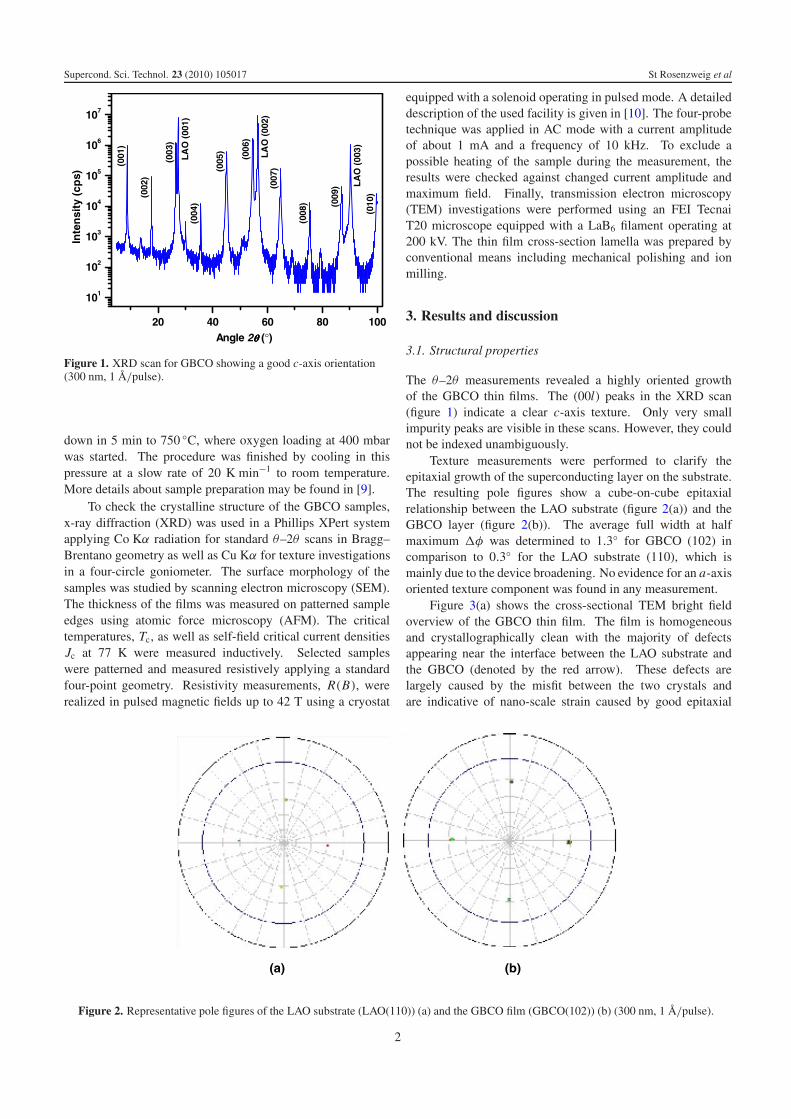
Figure 3(a) shows the cross-sectional TEM bright fieldoverview of the GBCO thin film. The film is homogeneousand crystallographically clean with the majority of defectsappearing near the interface between the LAO substrate andthe GBCO (denoted by the red arrow). These defects arelargely caused by the misfit between the two crystals andare indicative of nano-scale strain caused by good epitaxial
(a) (b)
Figure 2. Representative pole figures of the LAO substrate (LAO(110)) (a) and the GBCO film (GBCO(102)) (b) (300 nm, 1 A/pulse).
2
Supercond. Sci. Technol. 23 (2010) 105017 St Rosenzweig et al
Figure 3. (a) Cross-sectional TEM overview of the GBCO thin film (thickness: 300 nm, deposition rate: 1 A/pulse) on the LAO substrate.The red arrow indicates the boundary between substrate and film. Near the interface, a large density of stacking faults is observed. Defectsprotruding along other axes, such as threading dislocations or vacancy strain fields, appear confined to localized regions near the substrateinterface. (b) Selected area electron diffraction pattern of the GBCO reveals a highly crystalline structure. Gd2O3 particles are embeddedthroughout the film with a large number appearing at the surface, as evidenced in (c). These precipitates appear nearly circular in the 2D TEMprojection (likely spherical in 3D) and have an approximate average diameter of 25 nm. (d) SEM picture shows a typical pinhole structure ofthe film surface and surface Gd2O3 particles as small white dots.
growth. Throughout the rest of the film, only occasional Gd-124 stacking faults are observed (horizontal lines extendingparallel to the ab-plane). These are also largely confined to theregion near the substrate interface. Overall, the film shows ahigh degree of crystallinity, as illustrated by the representativeselected area electron diffraction pattern in figure 3(b). High-resolution TEM investigations reveal that numerous Gd2O3
particles are embedded throughout the film with a large numberappearing at the surface, as evidenced in figure 3(c). Theseprecipitates appear nearly circular in the 2D TEM projection(likely spherical in 3D) and have an approximate averagediameter of 25 nm. These surface Gd2O3 particles are probablyalso detected on the film surface by SEM, showing up assmall white dots in figure 3(d). The microstructural surfaceassessment by SEM further reveals a typical morphology witha large density of pinholes.
3.2. Superconducting properties
The superconducting properties of the films were studied withinductive and resistive methods. Figure 4 shows the transitioncurves of three patterned samples prepared with differentthicknesses and deposition rates. The Tc,90 values of the filmsinvestigated are about 93.5 K and are therefore between 1and 2 K higher than values in comparable standard YBCOthin films [7, 11, 12]. The critical temperature seems to beindependent of the deposition rate. In figure 5, the dependenceof the inductively measured critical temperature Tc and itstransition width �Tc on the film thickness d is shown. Aslight decrease of Tc and a broadening of the transition upto 4 K with decreasing film thicknesses were found below avalue of 300 nm. This might be explained with the highernumbers of defects found in the TEM investigations close tothe substrate (figure 3(a)). The maximal transition temperatureof 92.6 K with a transition width of 0.6 K was obtained for a
3

Supercond. Sci. Technol. 23 (2010) 105017 St Rosenzweig et al
Figure 4. Transition curves showing the dependence of the resistivityon the temperature for GBCO samples grown under differentconditions.
Figure 5. Dependence of Tc and �Tc on the film thickness(measured inductively).
layer thickness of about 300 nm. No further improvement ofTc was found in thicker layers.
The maximal values of the inductively measured criticalcurrent density Jc at 77 K in self-field and their dependenceon the film thickness are shown in figure 6. The highestvalue of about 3.7 MA cm−2 was found for a GBCO filmhaving a thickness of 300 nm prepared with a deposition rate of0.5 A/pulse. The two films deposited with different depositionrates but having a similar thickness of about 300 nm showdistinct differences in Jc. The film with the lower depositionrate (0.5 A/pulse) shows a significantly larger self-field Jc thanthe film with larger deposition rate (1 A/pulse). Recently,Hengstberger et al and Sanchez et al have shown that thespecial geometry of thin films and coated conductors leadsto a reduction of Jc due to self-field effects even without a
Figure 6. Dependence of self-field Jc at 77 K on the film thickness(measured inductively).
thickness dependence of Jc [13]. On the other hand, thenumber and dimension of different microstructural defects(example secondary phases and misorientations) may increasewith higher film thickness leading to a reduction in Jc [14].
3.3. High field measurements
The resistance of three samples with different GBCO thicknessand/or deposition rate was measured in a pulsed high magneticfield up to 42 T. The R(B) curves at different temperaturesof the 300 nm thick sample (1 A/pulse) are shown in figure 7(B ‖ c). The dependence of the resistance R (normalized to theresistivity at 100 K) on the temperature T in several magneticfields between 10 and 42 T is shown in figure 8 for the samesample. These data are extracted from the R(B) measurementsof figure 7.
The dependence of the irreversibility field Hirr, determinedwith a criterion of 1% of R(95 K), on the temperature Tis plotted for these three samples in figure 9. The differentbehaviour for the two 300 nm thick samples prepared with thedifferent deposition rates (0.5 and 1 A/pulse) is remarkable,whereas an almost similar curve was measured for the filmsprepared with the same deposition rate (0.5 A/pulse). Thedifferent behaviour of the samples with a similar thicknessmight be caused by the different deposition rates. Whereasthe high-rate sample has a lower self-field Jc, it shows a higherHirr at all temperatures. The higher deposition rate seems tofavour the formation of defects that are active at high magneticfields. In addition, this sample shows higher Hirr values thancomparable GBCO samples of other groups [15].
In general, Hirr seems to be mainly independent of thethickness, but appears to be influenced by the depositionconditions. Particularly, the Hirr values are found to be largerfor higher deposition rate; as shown with the two samples withapproximately the same thickness of 300 nm. Near Tc the
4

Supercond. Sci. Technol. 23 (2010) 105017 St Rosenzweig et al
Figure 7. R(B) curves for a GBCO thin film for differenttemperatures (1 A/pulse, sample thickness d = 300 nm).
Figure 8. Normalized R(T ) plots for different magnetic fields (linesare guides to the eye) for data of figure 7.
temperature dependence of Hirr can be fitted with a power lawof the form
Hirr ∼ (1 − T/Tc)β, (1)
where the exponent β is a fit parameter. The two films ofaround 300 nm thickness show a β value of 1.4, the 530 nmthick film has a slightly lower β of 1.3. These values arein the expected range of 1.3–1.5 and can be explained by aflux creep model [16] as well as the vortex glass–vortex liquidtransition [17].
4. Summary
We prepared GBCO thin film samples on LAO substrates byPLD with thicknesses between 50 and 530 nm. Investigationsof the structural properties show a clean growth process at aslow laser repetition rate of 2 Hz. TEM measurements provedthe structural quality showing mainly defects near the interfacebetween the substrate and the film. A transition temperature Tc
Figure 9. Hirr(T ) curves and their dependence on the thickness ofthe GBCO thin film samples. The lines are fits to equation (1).
up to 93.7 K with a transition width �Tc of 0.6 K was obtainedfor a 300 nm thick sample. The inductive measurements at77 K in self-field showed a maximum value of the criticalcurrent density Jc of 3.7 MA cm−2. High field measurementsup to 42 T revealed that Hirr(T ) is mainly independent of thefilm thickness, but is strongly dependent on the deposition rateduring sample preparation.
Acknowledgments
The work was partially supported by the Saxonian StateMinistry of Cultural Affairs. We gratefully thank HJahnel, Werner-Heisenberg-Gymnasium Riesa, for fruitfuldiscussions, M Kuhnel and P Pahlke for their help with thesample preparation and the inductive Jc measurements andU Fiedler for the inductive Tc measurements. We thankDr K Nenkov for the sample preparation for the pulse fieldmeasurements and E Stilp for the pulse field measurements.
References
[1] Jia Q X, Maiorov B, Wang H, Lin Y, Foltyn S R, Civale L andMacManus-Driscoll J L 2005 IEEE Trans. Appl. Supercond.15 2723
[2] Murakami M, Sakai N, Higuchi T and Yoo S I 1996 Supercond.Sci. Technol. 9 1015–32
[3] Cai C, Holzapfel B, Hanisch J, Fernandez L andSchultz L 2004 Phys. Rev. B 69 104531
[4] Feldmann D M, Ugurlu O, Maiorov B, Stan L, Holesinger T G,Civale L, Foltyn S R and Jia Q X 2007 Appl. Phys. Lett.91 162501
[5] Horide T, Matsumoto K, Ichinose A, Mukaida M,Yoshida Y and Horii S 2007 Supercond. Sci. Technol.20 303–6
[6] Song S H, Ko K P, Ko R K, Song K J, Moon S H and Yoo S I2007 Physica C 463–465 497–500
[7] Miura N, Nakagawa H, Sekitani T, Naito M, Sato H andEnomoto Y 2002 Physica B 319 310–20
[8] Hanisch J, Kozlova N, Cai C, Nenkov K, Fuchs G andHolzapfel B 2007 Supercond. Sci. Technol. 20 228–31
5

Supercond. Sci. Technol. 23 (2010) 105017 St Rosenzweig et al
[9] Rosenzweig St, Hanisch J, Huhne R, Holzapfel B andSchultz L 2010 J. Phys.: Conf. Ser. 234 012035
[10] Krug H et al 2001 Physica B 294/295 605–11[11] Holesinger T G, Maiorov B, Ugurlu O, Civale L, Chen Y,
Xiong X, Xie Y and Selvamanickam V 2009 Supercond. Sci.Technol. 22 045025
[12] Huhne R, Sarma V S, Okai D, Thersleff T, Schultz L andHolzapfel B 2007 Supercond. Sci. Technol. 20 709
[13] Hengstberger F, Eisterer M and Weber H W 2010 Appl. Phys.Lett. 96 022508
Sanchez A et al 2010 Appl. Phys. Lett. 96 072510[14] Foltyn et al 2007 Nat. Mater. 6 631[15] Schlesier K, Huhtinen H and Paturi P 2010 Supercond. Sci.
Technol. 23 055010[16] Yeshurun Y and Malozemoff A 1988 Phys. Rev. Lett.
60 2202–5[17] Fisher M 1989 Phys. Rev. Lett. 62 1415–8
6