
IO-103 Oscilloscope - Frank's electron Tube Data sheets
152
5 -INCH TRiGGEREQ SWI~~P C~SCILLCySCOPE MaDE~ 10-103 Gapyri~t ®1971 n.rrn co~.p.~y A!! rights resrrvrd 595-1327-C3
-
Upload
khangminh22 -
Category
Documents
-
view
2 -
download
0
Transcript of IO-103 Oscilloscope - Frank's electron Tube Data sheets

5-INCH TRiGGEREQ SWI~~P C~SCILLCySCOPE MaDE~ 10-103
Gapyri~t ®1971 n.rrn co~.p.~y
A!! rights resrrvrd 595-1327-C3

/~
Dear Customer:
You have just purchased one of the best performing electronic products in the world —your Heathkit.
Here's how we aim to keep it that way:
Your Heathkit Warranty .~
.~ During your first 90 days of ownership, any parts which we find are defective, either in materials or
workmanship, will bo replaced or repaired free of charge. And we'll pay shipping charges to get those parts to
you —anywhere in the world.
If we determine a defective part has caused your Heathkit to need other repair, through no fault of yours, we
will service it free — at the factory, at any retail Heathkit Electronic Center, or through any of our authorized
overseas distributors.
This protection is exclusively yours as the original purchaser, Naturally, it doesn't cover damage by use of
acid-core solder, incorrect assembly, misuse, fire, flood or acts of God. But, it does insure the performance of
your Heathkit anywhere in the world —for most any other reason.
After-Warranty Service
What happens after warranty? We won't let you down. If your Heathkit needs repairs or you need a part, just write or call the factory, your nearest retail Heathkit Electronic Center, or any Heath authorized overseas distributor. We maintain an inventory of replacement parts for each Heathkit model at most locations —even for models that no longer appear in our current product line-up. Repair service and technical consultation is available through all locations.
We hope you'll never need our repair or replacement services, but it's nice to know you're protected anyway —and tfiat cheerful help is nearby.
Sincerely,
HEATH COMPANY
Benton Harbor, Michigan 49022
0 ~~~~~~UdJ6U~UbUBJ~~b,Ig~Jb~~~~
.~
.~
.~
~~

Assembly and operation
of the
5-INCH TRIGGERED SWEEP OSCILLOSCOPE
MODEL 10-103
HEATH COMPANY BENTON HARBOR, MICHIGAN 49022

TABLE OF CONTENTS
INTRODUCTION 5
UNPACKING 7
POWER SUPPLY CIRCUIT BOARD Parts List 9 Step-by-Step Assembly 10
VERTICAL A~,IPLIFIER CIRCUIT BOARD Parts List 15
Step-by-Step Assembly 16
SWEEP GENERATOR-HORIZONTAL AMPLIFIER CIRCUIT BOARD Parts List 21 Step-by-Step Assembly 23
ATTENUATOR CIRCUIT BOARD Parts List 33 Step-by-Step Assembly 34
Switch Prewiring 36 Circuit Board Final Wiring 38
CHASSIS Parts List 39 Step-by-Step Assembly
Main Chassis Assembly 42 Rear Panel Assembly 46 Alternate Line Voltage Wiring 48 Circuit Board Bracket Assembly 49 Front Panel Parts Mounting 50 Front Panel Wiring 54 Wire Harness Installation 57 Power Supply Final Wiring and Installation 58
2 H~ATHKIT~
r

Sweep Generator-Horizontal Amplifier Wiring 62 Time/CM Switch Wiring and Installation 66 Vertical Circuit Assembly and Wiring 70 CRT Installation and Wiring 74 Handle Mounting 78 Knob Installation 78 Test Cable Assembly 81
INITIAL TESTS Contra) Settings 83
Adjustments 84
CALIBRATION 87
CABINET ASSEMBLY 91
OPERATION AND APPLICATIONS 93 Time/CM-Frequency Correlation Chart 100
IN CASE OF DIFFICULTY 101 Troubleshooting Chart 102 Factory Repair Service 103 Replacement Parts and Price Information 103
SPECIFICATIONS 105
CIRCUIT DESCRIPTION 107
CIRCUIT BOARD X-RAY VIEWS 111
VOLTAGE CHART 114
CHASSIS PHOTOGRAPHS 116
TRANSISTOR CROSS REFERENCE CHART 120
DIODE CROSS REFERENCE CHART 121
SCHEMATIC (fold-out from page) 121
H~ATHKZT" 3

Page 4

INTRODUCTION
The cathode ray oscilloscope is one of the most versatile instruments available, It can be used to measure ac and do voltages, frequency, or phase, as well as to study the waveforms of complex signals. These capabilities make the oscilloscope valuable for waveform analysis, particularly in audio, television, and transmitter work.
The Heathkit Model 10-103 5" Triggered Sweep Oscilloscope is an accurate and dependable instrument which has a wide range of applications. When properly assembled and calibrated, this Oscilloscope can be used to observe or measure all types of electrical and electronic waveforms within its listed specifications, from relatively simple sine and square waves to complex pulse and composite signals. The basic uses of this instrument are similar to those of other oscilloscopes with comparable sensitivity and frequency response.
The following professional features make the 10-103 Oscilloscope outstanding: an accurately calibrated vertical attenuator switch with variable control; triggered horizontal sweep circuits; calibrated time base switch (seven decade
steps, variable within each step); a display magnifier that will
double any portion of a normal display; provisions for use of
external triggering signals or a horizontal deflection signal.
f ver.y'~~,~~-E - vcc:Lzycf~~ vcr.~;~~icY--"~~
~fUV, •$~ ~Giyl,i
H~ATHKZT~'
The Oscilloscope uses four printed circuit boards which minimize point-to-point wiring and reduce construction time. The transformer operated, silicon rectifier power supply can be wired to operate from 110-130 volt, or 220-260 volt ac power lines. This Oscilloscope has good display stability because both amplifiers and the sweep circuit power supplies are zener regulated. The primary circuit of the power transformer is fused for protection from overload.
Other features include: an all solid-state circuit (except for the CRT►, high input sensitivity, modern styling, moderate price, and versatility. Its rugged construction and ease of operation add to its usefulness and long life.
NOTE: The following test instruments will be required to perform the adjustments in the "Calibration" section of this Manual; a high impedance input voltmeter and an instrument (or instruments) capable of producing a sine wave of 10 kHz and square waves at 1000 Hz and 100 kHz.
Refer to the "Kit Builders Guide" for complete information on unpacking, parts identification, tools, wiring, soldering,
and step-by-step assembly procedures.
5

Page 6

UNPACKING
The Oscilloscope packaging consists of the large shipping carton which contains smaller packages and a number of loose parts. Some of the smaller packages have numbers 1 through 4 stamped on them. After these four numbered packages have been removed from the large carton, the remaining parts in the carton will be package #5.
You will be directed to open each package as it is needed. Each of the assembly sections of the Manual contains its own parts list and step-by-step instructions. At the beginning of each parts list you will be instructed which numbered package to open. You will also be directed to remove some of the parts from package #5 to complete each assembly section.
To avoid intermixing parts do not open any of the parts packages until directed to do so at the beginning of one of the parts lists. Any part that is packaged in an individual envelope with a part number on it should be placed back in
H~ATHKIT ~`
its envelope after it is identified until that part is called for in a step.
Refer to the "Kit Builders Guide" for additional
information on unpacking, parts identification, tools, wiring,
soldering, and step-by-step assembly procedures.
To order replacement parts, refer to the price column in the Parts Lists and use the Parts Order Form furnished with this kit.
The prices in these Parts Lists apply only on purchases from the Heath Company where shipment is to a U.S.A.
destination. Add 10% (minimum 25 cents) to the price when
ordering from a Heathkit Electronic Center to cover local
sales tax, postage, and handling. Outside the U.S.A., parts
and service are available from your local Heathkit source and will reflect additional transportation, taxes, duties, and rates of exchange.
7

Page 8

POWER SUPPLY CIRCUIT BOARD
PARTS LIST
Unpack the package marked the following list. The key numbers on the "Power Pictorial" (fold-out from Page
1 and check each part against
numbers correspond to the Supply Circuit Board Parts 11).
KEY PART No. No.
PARTS Per Kit
DESCRIPTION PRICE Each
KEY PART PARTS DESCRIPTION PRICE No. No. Per Kit Each
RESISTORS
1/2-Watt, 10%
CAPACITORS
Electrolytic Al 1-6 1 470 S2 (yellow-violet-
brown ) .10 B 1 25-43 1 70 µF 1.15
62 25-121 1 500 µF 1.30 Al 1-35 1 1 MSZ (brown-black-
green) .10
Other Capacitors 63 21-44 1 .005 µF disc .15 64 23-62 3 .1 µF, tubular .75
1-Watt, 10% A2 1-55-1 1 180 Sl (brown-gray-
brown ) .10 CONTROL
A2 1-19-1 1 220 S2 (red-red-brown) .10 C1 10-384 1 500 kSt control .30 A2 1-54-1 1 270 S2 (red-violet-brown) .10 A2 1-20-1 1 330 S2 (orange-orange-
brown) .10 DIODES-TRANSISTORS
A2 1-32-1 1 470 kSZ (yellow-violet- yellow)
.10 D1 56-48 2 BZT110A diode 3.15 D1 56-55 1 VR-36A diode 1.00
A2 1-37-1 1 3.3 MS2 (orange-orange- green)
.10 D1 56-66 1 1 N3035 diode .90 D1 56-68 1 ZVR-68 diode 1.50 D1 56-79 10 R4507-5 diode 1.60
D1 57-27 8 1 N2071 diode .25 Other Resistors D1 57-52 2 5D20 diode 1.20 A3 1-13-2 1 220 S2, 2-watt (red-red
brown) .15 NOTE: Transistors are marked for identification in one of
the following four ways. A3 1-23-2 1 5600 S2, 2-watt (green-
blue-red) .30
1. Part number.
A3 1-17-2 1 6800 SZ, 2-watt (blue- gray-red)
.15 2. Transistor type number. 3. Part number and transistor type number.
A4 3-41-5 1 140 S2, 5-watt .15 4. Part number with a transistor type number other
A4 3-5-5 1 210 SZ, 5-watt .25 than the one listed.
A4 3-9-7 1 100 S2, 7-watt .15 D2 417-175 1 2N5294 transistor 1.45
A4 3-12-7 1 700 St, 7-watt .15 D3 417-245 2 D40N1 transistor .95
H~ATHKIT''° 9

Page 10
KEY PART PARTS DESCRIPTION PRICE No. No. Per Kit Each
HARDWARE
E1 250-213 3 4-40 x 5/16" screw .05 E2 252-2 3 4-40 nut .05 E3 250-229 4 6-32 x 1 /4°' screw .05 E4 254-9 3 #4lockwasher .05
E5 255-152 2 Plastic spacer .15
MISCELLANEOUS
F1 215-57-1 2 Large heat sink .15 F2 215-44 1 Small heat sink .65
F3 490-5 1 Nut starter .10 Solder (Additional 3' rolls of solder #331-6, can be ordered for 15 cents each.►
KEY PART PARTS DESCRIPTION No. No. Per Kit
PARTS FROM PACK #5
PRICE Each
85-470-2 1 Power supply circuit 2.05 board
597-260 1 Parts Order Form 597-308 1 Kit Builders Guide
1 Manual (See front cover 2.00 for part number.)
NOTE: See Page 103 for "Replacement Parts and Price Information."
STEP-BY-STEP ASSEMBLY
Before starting to assemble this kit, read the "Kit Builders Guide" for complete information on wiring, soldering, and step-by-step assembly procedures. NOTE: Install 1 /2-watt resistors on the power supply circuit board unless otherwise specified.
NOTE: When you install transistors in the following Pictorials, refer to "Transistor Installation" (fold-out from Page 10) to help you correctly identify each transistor type.

TRANSISTOR INSTALLATION
Transistors, because they are small and use very little power, permit high-performance, compact designs that were not feasible with electron tubes. Along with their virtues, however, many transistors do present a problem to the kit builder. Since most transistors are small, the leads must be grouped closely, making them difficult to identify correctly.
~i;r35' ~i~~. ~~1~~'- cutt~l~~ly{i. igituvl -',v~x~14Y~
Install each transistor by:
1. Comparing it with the ones shown on this chart. Be sure to correctly identify the transistor and its E, B,
and C leads.
2. Placing the E, B, and C leads into the corresponding E, B, and C holes at the proper location on the circuit board.
3. Positioning the transistor 1 /4" above the circuit board. Then solder the leads to the foil and cut off the excess lead lengths.
To help you avoid any problem in identifying transistor leads, we have provided the drawings below to show the lead arrangements for a variety of transistor types. Refer to these drawings, as directed in the Manual, when you install transistors.
HEATH PART NUMBER
CASE BASING
417-33 E i000~ B ~.~
C
417-154
~1
~
~
~
\\ ~ TAB \\\\\1
S TAB
(0 of~ o
B
417-169
417-241
S D G 0 0 0
417-173
_ TA B {
E B C OR EBC OR C~E o00
C E
B
GR OR
B
III U U TAB
'1
~
417-175
B C E
l
417-113
417-201 OR ~
II II IUI
E C B E C B
i ooi pR o 0 0
~-~
417-245
BEVEL
E B C
1
~
O
~ ~ I ~
1--BEVEL ~~

HEATHKIT Page 11
START i Position the power supply circuit board as shown in this Pictorial. Then proceed with the following steps.
NOTE: DIODES MAY BE SUPPLIED IN ANYOFTHE FOLLOWING SHAPES. THE CATHODE END OF THE DIODE IS MARKED WITH A BAND OR BANDS. ALWAYSPOSITION THIS END AS SHOWN IN THE PICTORIAL,
BAND OR BANDS
( t1 Install five R4507-5 diodes (#56-79) at ZD409. Be sure to position the banded ends as shown.
( '~) 5D20 diode (#57-52) at D402. ,
~7 5D20 diode (#57-52) at D401.
(~() 330 SZ, 1-watt (orange-orange-brown l .
( Y~ 22052, 1-watt (red-red-brownl.
(U 470 SZ, 1/2-watt (yellow-violet-brown 1.
((') VR-36A diode (#56-55) at ZD404.
FOR GOOD SOLDERED CONNECTIONS. VOU MUST KEEP THE SOLDERING IRON TIP CLEAN...
` /~
WIPE IT OFTEN WITH A \-_ ` T/ DAMP SPONGE OR CLOTH. --1//
( 1 Solder the leads to the foil and cut off the excess lead lengths.
1 Locate eight 1 N2071 diodes (#57-27). They will be installed in the following steps.
( 1 1N2071 diode atD406. ~y S1 .~~
1 1 N2071 diode at D405.
( 1 1 N2071 diode at D408.
( 1 1 N2071 diode at D407. "
1 1 N2071 diode at D412.
1 1 N2071 diode at D411.
( 1 1 N2071 diode at D414.
( l 1 N2071 diode at D413.
( 1 Solder the leads to the foil and cut off the excess lead lengths.
PICTORIAL 1-1
CONTINUE (~) 1 MS2, 1/2-watt (brown-black -green).
Iv{) Five R4507-5 diodes (#56-79) at ZD403. Be sure to position the banded ends as shown.
~ (\) 470 kSt, 1-watt (Yellow-violet-yel low).
'K) 3.3 MS2, 1-watt (orange-orange- green).
~C 1 220 SZ, 2-watt (red-red-brown).
(XI 27052, 1-watt (red-violet-brownl.
1 Solder the leads to the foil and cut off the excess lead lengths.
NOTE: When you are instructed to mount a power resistor 3/16" above the circuit board as shown, use a 1" x 1" piece of 3/16" cardboard (from shipping carton) for a spacer. Solder each resistor as it is installed, cut off the excess lead lengths,
and then remove the cardboard spacer.
~~
\~
((~~~~~„„,,~ 1" x 1"
-'~•~• . \ - SPACER
3/16"
1 ~) 140 S2, 5-watt. Position this resistor 3/16" above the circuit board.
( ''~) 210 52, 5-watt. Position this resistor 3/16" above the circuit board.
( (,) 180 SZ 1•watt (brown-gray-brown).
' 1,1 ZVR-68 diode 1#56-681 at ZD416.
I l y,l BZT110A diode (#56-48) at ZD415.
I R l 5600 52,2-watt (green-blue-redl.
(~ 1 6800 52,2-watt (blue-gray-redl.
( 1 ) 1 N3035 diode (#56-66) at ZD418.
(~) BZT110A diode (#56-48) at ZD417.
(r) 100 52, 7-watt. Position this resistor 3/16" above the circuit board.
1 ~) 700 S2, 7-watt. Position this resistor 3/16" above the circuit board.
1 Solder the leads to the foil and cut
off the excess lead lengths.
( 1 Carefully recheck all the diodes
installed in this Pictorial and be sure they are positioned with the banded ends as shown.

Page 12
START i NOTE: In the following steps, you will be instructed to mount two transistors onto
heat sinks and to install them onto the circuit board. Read and perform each step
carefully. See Pictorial 1-2. When hard-
ware is called for in a step, only the screw size will be given. For instance, if 4-00 x
5/16" hardware is called for, it means that a 4-40 x 5/16" screw, one or more #4 lockwashers, and a 4-40 nut should be used. The Pictorial or Detail will show the proper number of lockwashers used. The
plastic nut starter provided with this kit can be used to pick up and start 6-32 and
4-40 nuts on screws.
( , 1 Refer to Detail 1.2A and mount a
D40N1 transistor (#417-245) onto
the fry ntnt of a large heat sink with
4.40 x 5/16" hardware as shown. Be sure the transistor points straight
down.
( ; 1 Similarly, mount the other D40N1 transistor (# 417-245) onto the rear of a large heat sink with 4-40 x
5/16" hardware as shown in Detail
1-2C. Refer to the Pictorial to be
sure the transistors are properly
mounted.
(~ 1 Refer to Detail 1.26, and place a plastic spacer between the two heat
sinks at A. Then loosely secure the spacer and heat sinks with two 6-32 x 1 /4" screws as shown.
( ' 1 In the same manner, install a plastic spacer at B with two 6-32 x 1 /4" screws.
1 Refer to Detail 1-2C and install the transistor-heat sink assembly onto the circuit board at 0402 and 0403 as shown. Press the transistors into
the circuit board until both ends of the two heat sinks touch the board.
1 Solder all of the transistor leads to
the foil and cut off the excess lead lengths. Tighten the four 6-32 x 1 /4" screws at A and B.
The steps performed in this Pictorial are in this area of the circuit board.
IDENTIFICATION
DRAWING
PART NUMBER
~~
f®
~Q403
' - "~~~1 ! Q402 1:~:::~ ~--.. r.,.~,~-. . . . .
PICTORIAL 1-2
~~
FRONT
4-40 z 5/16' SCREW
#4 LOCKWASHER
E B C
Detail 1-2A
4-40 NUT
~~
BEVELED CORNER
~J
HEAT SINK
HEAT SINK
6-32 x 114" ~ ~ SCREW \
PLASTIC SPACER
6-32 x 114" SCREW
Detail 1-2B

POWER SUPPLY CIRCUIT BOARD PARTS PICTORIAL
D1
D2
Cl
oR OR OR/l

VERTICAL AMPLIFIER CIRCUIT BOARD
PARTS PICTORIAL
i OR
D
i E6
O E9
~~

Page 13
STAf~T ( ') 500 kS2 control (#10-384). Solder
the leads to the foil.
NOTE: Before installing disc capacitors in this kit, use long-nose pliers to remove the excess insulation from the capacitor leads.
~~ REMOVE
INSULATION ON LEADS ~I
( ,,) .005 µF, 1.6 kV disc capacitor. Solder the leads to the foil and cut ~ off the excess lead lengths.
( ") Install a 2N5294 transistor 1#417-175) onto a small heat sink with 4-40 x 5/16" hardware. Be sure the hole in the end of the heat sink is upward as shown. Be sure the transistor points straight down.
#4 HOLE LOCKWASHER
4-40//~~~ NUT1(r~''(L.,'>> ~ 4-40 x 5/16"
~= ~~scREw
Uu
o
I'
.::.U~-:,-~::::... ::i:'.4Fih~'G::.
( l,'Mount the assembly on 0401 as shown. leads to the
excess lead lengths.
~
, U /' iv E.
transistor-heat sink the circuit board at
Solder the transistor foil and cut off the
PICTORIAL 1-3
CONTINUE
NOTE: When you install each of the following three capacitors, always match the banded end of the capacitor with the
band mark on the circuit board.
BAND
( ~) .1 µF, 1.6 kV capacitor.
I (. 1 .1 µF, 1.6 kV capacitor.
" ( ) .1 µF, 1.6 kV capacitor.
NOTE: When you install an electrolytic capacitor, always match the positive (+) marked end of the capacitor with the positive (+) mark on the circuit board.
} t
x
( 1 500 µF electrolytic.
~ (~) 70 µF electrolytic.
( 1 Solder the leads to the foil and cut off the excess lead lengths.
12 1 Carefully inspect the foil side of the circuit board and be sure there are
no solder bridges between foils.
Set the circuit board aside temporarily.

Page 14

VERTICAL AMPLIFIER CIRCUIT BOARD
PARTS LIST Unpack the package marked 2 and check each part against the following list. The key numbers correspond to the numbers on the "Vertical Amplifier Circuit Board Parts Pictorial" (fold-out from Page 12).
KEY PART PARTS No. No. Per Kit
DESCRIPTION PRICE Each
KEY PART PARTS DESCRIPTION PRICE No. No. Per Kit Each
RESISTORS 1/2-Watt
DIODES-TRANSISTORS
Al 1-83 4 56 St (green-blue- black )
.10 D1 56-19 2 VR-9.1 diode 1.00 D1 56-56 2 1 N4149 diode .20
Al 1-3 1 100 Sl (brown-black- brown►
.10 NOTE: Transistors are marked for identification in one of the following four ways.
Al 1-112 2 180 St (brown-gray- brown)
.10 1. Part number. 2. Transistor type number.
Al 1-4 2 330 S2 (orange-orange- brown►
.10 3. Part number and transistor type number. 4. Part number with a transistor type number other
Al 1-6
Al 1-9 Al 1-20
2
2 1
470 S2 (yellow-violet-brown►
1000 S2 (brown-black-red) 10 kSZ (brown-black-orange)
.10
.10 .10
than the one listed.
D2 417-83 2 L842 transistor .75 D2 417-118 2 2N3393 transistor .40 D3 417-201 2 X29A829 transistor .50 D4 417-169 3 MPF105 transistor 1.50
Other Resistors D5 417-245 2 D40N 1 transistor .95 A2 5-4-10 2 3000 SZ (3 kSZ►, 10-watt,
film .35
HARDWARE
CAPACITORS E1 250-34 2 4-40 x 1 /2" screw .05
Mica B 1 20-108 61 20-106
1 1
200 p F 390 pF
.20
.30
E2 252-2 2 4-40 nut .05
E3 254-9 2 #4lockwasher .05 E4 250-229 2 6-32 x 1 /4" screw .05 E5 251-1 2 Spade bolt .05
Electrolytic E6 252-3 4 6-32 nut .05
62 25-54 1 10 µF .20 E7 253-27 6 #16 flat washer .05
63 25-57 1 100 µF 1.00 E8 254-1 4 #6lockwasher .05
B3 25-230 1 2000 µF 1.90 MISCELLANEOUS
Other Capacitors 64 25-221 65 31-49
1 1
2.2 µF tantalum 250-1000 pF trimmer
.40
.85
E9 215-44 2 Heat sink .65 85-468-5 1 Vertical amplifier circuit 1.65
board
CONTROL NOTE: See Page 103 for "Replacement Parts and Price
C1 10-381 1 500 SZ control .35 Information."
H TATHKIT~" 15

Page 16
STEP-BY-STEP ASSEMBLY IDENTIFICATION
DRAWING
START
i NOTE: Only part of the vertical amplifier circuit board is shown in the following Pictorials. An identification drawing at the top of each of these Pictorials shows the area of the circuit board to be assembled.
Position the vertical amplifier circuit board with the part number as shown in the identification drawing. Then complete each step on the Pictorial.
( K) 1000 SZ (brown-black-red►.
(1) 330 S2 (orange-orange-brownl.
( 'l) 470 SZ (yellow-violet-brownl.
1( 1 56 SZ (green-blue-blackl.
1 1 1 56 S2 (green-blue-blackl.
(~ ) 180 S2 (brown-gray-brown).
(; 1 180 SZ (brown-gray-brown►.
NOTE: DIODES MAY BE SUPPLIED IN ANYOF THE FOLLOWING SHAPES. THE CATHODE END OF THE DIODE IS MARKED WITH A BAND OR BANDS. ALWAYSPOSITION THIS END AS SHOWN IN THE PICTORIAL.
,~+~ 9~ ,~~/ Y~
BAND OR BANDS
( ~) VR-9.1 diode (#56-19) at 20104.
(~ 1 470 St (Yellow-violet-brown).
( + 1 56 S2 (green-blue-black).
( ~ 1 330 SZ (orange-orange-brownl.
( `) 1000 SZ (brown-black-red).
FOR GOOD SOLDERED CONNECTIONS, YOU MUST _ KEEP THE SOLDERING IRON TIP CLEAN...
WIPE IT OFTEN WITH A DAMP SPONGE OR CLOTH.
(~ ► Solder the leads to the foil and cut off the excess lead lengths.
PART NUMBER
PICTORIAL 2-1
The steps performed in this Pictorial are in this area of the circuit board.
CONTINUE
NOTE: When you install an electrolytic capacitor, always match the positive-marked end of the capacitor with the positive (+) mark on the circuit board.
x~,• . ~ x
l+1 END
(~~) 10 µF electrolytic.
NOTE: Tantalum capacitors may be marked two ways as shown. When install-ing the following capacitors, be sure to match the positive (+) sign or color dot on the capacitor with the positive (+) marking on the circuit board.
POSITIVE ' ~ SIGN 1+1 ,
I ~ COLOR h t DOT
(; 1 2.2 µF tantalum capacitor.
i ( ~) VR-9.1 diode (#56-19) at ZD101.
(~~) 10052(brown-black-brown).
(~ 1 1 N4149 diode 1#56.56) at D102.
(~ 1 1 N4149 diode (#56-56) at D103.
(C) 10 kS2 (brown-black-orange►.
( ~) 56 S2 (green-blue-blackl.
(t) Solder the leads to the foil and cut off the excess lead lengths.

Page 17
START i
NOTE: Position the circuit board as shown in the identification drawing. Then complete the following steps. When you install transistors in this Pictorial, refer to "Transistor Installation" (fold-out from Page 10) to help you correctly identify each transistor type.
Turn the circuit board foil side up and install the trimmer capacitor (#31-49) in the following manner as shown.
FOIL SIDE OF
CIRCUIT BOARC
.::~~.
( ' 1 Twist the two indicated side lugs (on the component side of the circuit board) 1/8 turn with pliers.
TWIST ll8
TURN END
LEAVES
COMPONEN~T~S .IDE OF CIRCUIT BOARD
1 Solder all the small end leaves together on the component side of the circuit board.
SOLDER END
LEAVES:'
C OIVI P~ON~E~IVT ~5~1 ~D~E ~0 F CIRCUIT BOARD
( {) Solder the indicated lugs to the foil on the foil side of the circuit board.
FOIL SIDE OF
CIRCUIT -BOARD
SOLDER
IDENTIFICATION DRAWING
PART NUMBER
The steps performed in this Pic-torial are in this area of the circuit board.
PICTORIAL 2-2
CONTINUE
~) 500 S2 control (#10-3811. Solder the leads to the foil.
:::~.
_.:I:_..;,::,'.•• •.• `..cis `: .;i:i::
NOTE: Install the next three transistors as shown. Solder the leads to the foil and cut off the excess lead lengths.
FLA TSIDE
f .,, l j 4~~ WIDE +
SPACE
:::' D ~::.::.; ~~~.
I (~ ) MPF105 transistor (#417.169) at 0101,
~ ( ' 1 MPF105 transistor (#417-169) at 0104.
~ (~ 1 MPF105 transistor (#417-169) at 0105.
~ ( '~ 1 2000 µF electrolytic. Be sure to position the positive 1+) lead as shown.
`. 1 100 µF electrolytic. Be sure to position the positive (+) lead as shown.
`) 3000 St 13 kSll, 10-watt. Position this resistor 3/16" above the board with a cardboard spacer.
( ) 3000 St 13 kSZI, 10-watt. Position
~ this resistor 3/16" above the board
with a cardboard spacer.
( 1 Solder the leads to the foil and cut
off the excess lead lengths.

Page 18
START NOTE: Position the circuit board as shown in the identification drawing, then proceed with the following steps. When you install transistors in this Pictorial, refer to "Transistor Installation" (fold-out from Page 10) to help you correctly identify each transistor type.
NOTE: shown. Solder off the excess
1I
Install transistors in each lead to the lead lengths.
/ FLAT
I
the foil
manner and cut
~ 1/4"
—~ OR
~ 1/4"
`~,) X29A829 transistor (#417-201) at , 0109.
`J L842 transistor (#417-83) at 0107.
'~) 2N3393 transistor (#417-118) at 0102.
( ~) 200 pF mica. Solder the leads to the foil and cut off any excess lead lengths.
1) 390 pF mica. Solder the leads to the foil and cut off any excess lead lengths.
2N3393 transistor (#417-118) at 0103.
( ) X29A829 transistor (#417-201) at 0108.
E L842 transistor (#417-831 at 0106.
Refer to Detail 2-3A and mount a spade lug onto a heat sink with 6-32 x 1 /4" hardware as shown. Be sure the shoulder of the spade lug is under the edge of the heat sink.
( ) In the same manner, mount another spade lug onto the remaining heat sink with 6-32 x 1 /4" hardware.
IDENTIFICATION DRAWING
PART NUMBER
PICTORIAL 2-3
#6 LOCKWASHER
6-32 NUT
The steps performed in this Pictorial are in this area of the circuit board.
SPADE LUG
SHOULDER
Deta i 12-3A
6-32 x 1/4" SCREW

Paye 19
IDENTIFICATION DRAWING
START
NOTE: In the following steps, you will be instructed to mount two transistors onto separate heat sinks. Carefully observe the
outline of transistors 0111 and 0112 on the circuit board and note that they face
in opposite directions. The transistors will therefore be mounted onto the heat sinks to face in opposite directions.
~ 1 Mount a D40N1 transistor onto one of the heat sink assemblies. Position the beveled corner of the transistor
toward the heat sink as shown. Use a 4.40 x 1/2" screw, three #6 flat washers, a #4 lockwasher, and a 4-40 nut.
4-40 x 1/2" SCREW ~~ .0 ~~~ #q LOCK ~~ ~ WASHER
n ~.
FLAT WASHER
~~
~~' ~/ 4-40
BEVELED / ~ NUT
CORNER JJ
1 Carefully form the transistor leads as shown in Detail 2-4A. Install the transistor and heat sink onto the circuit board at 0111 as shown.
( ) Secure the heat sink to the circuit board with a 6-32 nut and a #6 lockwasher. Solder the transistor leads to the foil and cut off the excess lead lengths.
The steps performed in this Pictorial are in this area of the circuit board.
PART
NUMBER
PICTORIAL 2-4
FORM 1RANSISTOR
LEADS
Detail 2-4A
CONTINUE V
( ) Mount a D40N1
(#417-245) onto the assembly. Position corner of the transistor the heat sink as shown. 1/2" screw, three #6 r4 lockwasher, and a
4 40 x ll2" FLAT
SCREW I WASHER
~~^
_
~~ C~
I
~lJ I
BEVELED
transistor other heat
the away
Use flat washers, 4.40 nut.
#4 WASHER
C~
CORN\\//E))R
' -sink
beveled from
a 4-40 x a
LOC K
4-40 ~~NUT
(
1
) Form the transistor leads as shown in Detail 2-4A. Install the transistor
and the heat sink onto the circuit board at 0112 as shown.
1 Secure the heat sink to the circuit board with a 6-32 nut and a #6 lockwasher. Solder the transistor leads to the foil and cut off the
excess lead lengths.
( ) Carefully check the foil side of the
circuit board and make sure all
connections are soldered and that
there are no solder bridges between
foils.
Set the circuit board aside temporarily.

Page 20

SWEEP GENERATOR-HORIZONTAL AMPLIFIER CIRCUIT BOARD
PARTS LIST
Unpack the package marked 3 and check each part against the following list. The key numbers correspond to the numbers on the "Sweep Generator-Horizontal Amplifier Circuit Board Parts Pictorial" (fold-out from Page 23).
KEY PART PARTS DESCRIPTION PRICE KEY PART PARTS DESCRIPTION PRICE No. No. Per Kit Each No. No. Per Kit Each
RESISTORS 1 /2-Watt, 10% A2 1-3 1 100 S2 (brown-black- .10
1 /4-Watt, 10% brown ) Al 1-42-12 3 22 S2 (red-red-black) .10 A2 1-45 2 22052 (red-red-brown) .10 Al 1-1-12 1 100 S2 (brown-black-
brown ) .10 A2 1-4 2 330 S2 (orange-orange-
brown) .10
Al 1-17-10 10 220 S2 (red-red-brown) .10 A2 1-6 4 470 S2 (yellow-violet- .10 Al 1-35-12 1 470 SZ (yellow-violet- .10 brown )
brown ) A2 1-9 6 1000 S2 (brown-black- .10 Al 1-2-12 10 1000 SZ (brown-black- .10 red)
red) A2 1-20 1 10 k52 (brown-black- .10 Al 1-4-12 4 2200 S2 (red-red-red) .10 orange)
Al 1-6-12 2 3300 SZ (orange-orange- red)
.10 A2 1-35 1 1 MS2 (brown-black- green)
.10
Al 1-7-12 2 3900 SZ (orange-white- red►
.10 Other Resistor
Al 1-9-12 2 10 kSt (brown-black- orange)
.10 A3 5-3-7 3 10 kS2, 7-watt, film .25
Al 1-10-12 1 15 kSZ (brown-green- orange)
.10 CAPACITORS
Al 1-32-12 2 100 kSt (brown-black- .10 Mica yellow) B1 20-52 1 7.5 pF .35
Al 1-19-12 1 1 MS2 (brown-black- .10 B1 20-114 1 270 pF .20 green) B1 20-113 1 470 pF .30
HEATHKIT'" 21

Page 22
KEY PART No. No.
PARTS Per Kit
DESCRIPTION PRICE Each
Disc 62 21-9 2 100 pF .10
62 21-56 1 470 pF .10
62 21-16 3 .01 µF .10
Electrolytic 63 25-221 1 2.2 ~cF tantalum .40 64 25-54 1 10 ~tF .20 65 25-57 1 100 ~~F 1.00 B5 25-230 2 2000 r~F 1.90
CONTROLS
C1 10-917 1 200 S2 .50 C1 10-918 1 500 Sl .45 C1 10-398 2 2000 S2 (2 kSt) .30 C1 10-904 2 5000 Sl (5 kS2) .55 C1 10-386 2 10 kSt .30
DIODES
D1 56-19 2 VR-9.1 1.00 D 1 56-26 1 1 N 191 .20 D1 56-44 2 1N4653 1.15 D1 56-56 4 1 N4149 .20 D1 56-58 1 1 N709A .65 D1 56-68 1 ZVR-68 1.50
KEY PART PARTS DESCRIPTION No. No. Per Kit
PRICE Each
TRANSISTORS NOTE: Transistors are marked for identification in one of the following four ways.
1. Part number. 2. Transistor type number. 3. Part number and transistor type number. 4. Part number with a transistor type number other
than the one listed.
E1 417-83 13 L842 .75 E1 417-118 9 2N3393 .40 E2 417-201 2 X29A829 .50 E3 417-154 3 2N2369 1.65 E4 417-169 4 MPF105 JFET 1.50 E4 417-241 2 EL131 JFET 2.55 E5 417-173 1 ETS083 .45 E6 417-245 2 D40N1 .95
MISCELLANEOUS
F1 443-44 1 SN7413N integrated circuit
1.95
F2 432-144 14 IC connector .01 F3 259-20 2 Circuit board pin .05
PART FROM PACK #5
85-1132-1 1 Sweep generator-hori- zontal amplifier circuit board
3.10
NOTE: See Page 103 for "Replacement Parts and Price Information."

Page 23
STEP-BY-STEP ASSEMBLY IDENTIFICATION
DRAWING pART ~,~NUMBER
r The steps performed in this Pictorial are in this area of the circuit board.
START
Position the sweep generator-horizontal amplifier circuit board as shown in the identification drawing; then proceed with the following steps.
NOTE: The resistors that you will install in this Pictorial are 1/4-watt resistors unless otherwise specified.
`) 22052 (red-red-brownl.
(`\ 1 220 S2 Ired-red-brown).
2200 S2 (red-red-redl. ~)
(,) 3900 S2 (orange-white-redl.
(~ 220 SZ (red-red-brownl.
`) 1000 S2 (brown-black-redl. '
( 1 Solder the leads to the foil and cut off the excess lead lengths.
(~) 100 kS2 (brown-black-yellowl. '
\) 1 MSt (brown-black-greenl. '
( `) 3300 S2 (orange-orange-red).
(~ 3300 S2 (orange-orange-red).
~) 3900 SZ (orange-white-redl.
FOR GOOD SOLDERED CONNECTIONS, YOU MUST KEEP THE SOLDERING
e
IRON TIP CLEAN... -~, • -
WIPE IT OFTEN WITH A DAMP SPONGE OR CLOTH.
( \) Solder the leads to the foil and cut
off the excess lead lengths. PICTORIAL 3-1
CONTINUE
~ ('~) 22 S2 (red-red-black►.
~ (\) 1000 S2 (brown-black•red).
~l 220 SZ (red-red-brownl.
( ~ 1000 S2 (brown-black-redl.
~) 15 kS2 (brown-green-orange).
220 S? (red-red-brown).
I V 100052 (brown-black-redl.
( '~) 470 S2, 1 /2-watt (Yellow-violet-brown).
Solder the leads to the foil and cut off the excess lead lengths.
1 220 S2 (red-red-brownl. \(~
10 kSt (brown-black-orangel. p )
(~ 1 470 SZ (Yellow-violet-brownl.
(~ 1 2200 SZ Ired-red-redl.
('~) 10 kS2 (brown-black-orangel.
\) 22 SZ (red-red-black).
(\) 2200 S2 (red-red-redl.
1 ~) 470 S2, 1 /2-watt (Yellow-violet-brown).
I J 22 S2 (red-red-blackl.
li 1 Solder the leads to the foil and cut off the excess lead lengths.

Page 24
START NOTE: When
i Pictorial, refer
(fold-out correctly Install each shown. Solder off the excess
you install transistors
to "Transistor Installation"
from Page 101 to identify each transistor
of the following transistors
each lead to the foil
lead lengths.
FLAT
r l OR
`.E`-`.:
help
in this
you type.
as and cut
1I4"
. . .. ...
1/4 . .
B:: ... .FLAT...
( ~ 2N3393 transistor (#417-118) at 0316.
(~) L842 transistor (#417-83) at 0315.
(~ L842 transistor (#417-831 at 0307.
( `~ L842 transistor (#417-83) at 0306.
( ~~ L842 transistor (#417-83) at 0305.
NOTE: Before installing the following disc capacitors, use long-nose pliers to remove the excess insulation from the capacitor
leads. Solder the leads as each capacitor is installed.
~~ REMOVE
INSULATION ON LEADS ~1
(~ .01 µF disc.
(~) .01 µF disc.
NOTE: Install the following the "B" lead leads into
board. Solder off the excess
the next two transistors in manner as shown: Cut off
and then insert the other two their correct holes in the circuit
each lead to the foil and cut lead lengths.
FLAT
II CUT OFF THE _ ~ 'B" LEAD
B 1/4 . ,
(\~ L842 transistor (#417-831 at D301.
1 `L L842 transistor 1#417-831 at D302.~
IDENTIFICATION DRAWING
PART
NUMBER
The steps performed in this Pictorial are in
this area of the circuit board.
PICTORIAL 3-2
CONTINUE V
°.OTE: I N ANYOF THE IS HANDS. END
DIODES ',1AY BE SUPPL IED THE FOLLOWING SHAPES.
CATHODE END OF THE DIODE ~1ARKED WITH A BAND OR
ALWAYS POSITION THIS AS SHOWN IN THE PICTORIAL,
BAP,D OR BANDS
f•) 1 N4653 diode (#56-441 at ZD303.
~ I ZVR-68 diode (#56-681 at ZD309.
I 1N191 diode (#56-26) at D307.
(\ 1 1 N4149 diode (#56-56) at D304.
(~) 1N4653 diode (#56-441 at ZD308.
`) 470 pF disc.
( 1 L842 transistor (#417-83) at 0304.
(~) 2N3393 transistor (#417-118) at 0308.
\) 2N3393 transistor (#417-118) at Q303.
I ~J Solder the leads to the foil and cut off the excess lead lengths.

SWEEP GENERATOR-HORIZONTAL AMPLIFIER PARTS PICTORIAL
D1
Al
B1
OR w~~ OR
pl~ ~~ ~, a n
0000000
E6
C

Page 25
PART NUMBER
START
NOTE: When you install transistors in this Pictorial, refer to "Transistor Installation" (fold-out from Page 10) to help you
correctly identify each transistor type.
Install the next two transistors as shown. Solder the leads to the foil and cut off the
excess lead lengths.
FLAT Ii
/ 1/4"
-::~ S . :~j' ; .:.6
FLA/AT
(-~ EL131 transistor (#417-241) at
0314.
1 ~) E L131 transistor (#417-241) at 0302.
NOTE: Install controls when called for in the following steps. Solder the lugs to the foil as the control is installed.
~v ~~ 7~
Ij~l 5000 S2 15 k52) control (#10-904).
1 ~ 2000 St control (#10-3981.
i IDENTIFICATION DRAWING
The steps performed in this Pictorial are in this area of the circuit board.
PICTORIAL 3-3
CON~TIy
NUE V
( ,~1 Install and solder circuit at TP7 and TP2 as shown.
board
~ STOP RIDGE
pins
the
O
1
( Y
O
Cut
foil
III ////.~i'/~ ~ - \C OFF PIN
SOLDER
the excess pin lengths from
side of the board.
. ( )\ 5000 S2 (5 kSt) control (#10.904). Solder the leads to the foil.
NOTE: shown. off the
Install the next three Solder each lead to the excess lead~~l
--
e~~ngths.
A
transistors as foil and cut
1 4' . . , A'J IDE
C . ~... E
( ~:) 2N2369 transistor (#417-154) at 1 0319.
~ ( ~ 2N2369 transistor (#417-1541 at 0317.
~ (\) 2N2369 transistor (#417-154) at 0318.
~ l ~l 10 kS2 control (#10-3861. Solder the leads to the foil.

Page 26
PART NUMBER
START i
NOTE: The resistors that you will install in this Pictorial are 1/4-watt resistors
unless otherwise specified.
( y) 1000 S2 (brown-black-redl.
(~) 1000 S2 (brown-black-red).
(J 7.5 pF mica.
1~ 1 220 S2 (red-red-brown).
( ~~) 1000 St (brown-black-redl•
1 Solder the leads to the foil and cut ' off the excess lead lengths.
~,-) 220 Sl (red-red-brownl.
( ~) 220 S2 (red-red-brown).
~+) 1 N4149 diode (#56-56) at D305.
( ~1 100 kS2 (brown-black-yellowl.
( ~l 1000 S2 (brown•black-redl.
FOR GOOD SOLDERED CONNECTIONS, VOU MUST _ KEEP THE SOLDERING / IRON TIP CLEAN... - -- ~ WIPE IT OFTEN WITH A [)AMP SPONGE OR CLOTH.
1`. 1 Solder the leads to the foil and cut off the excess lead lengths.
IDENTIFICATION DRAWING
The steps performed in this Pictorial are in this area of the circuit board.
PICTORIAL 3-4
CONTINUE
(,r 1 1000 S2 (brown-black-red).
( c') 100 pF disc.
(~• 1 100 pF disc.
( ~) 10 kSt control 1#10-3861. Solder the control leads to the foil.
(`~,) 220 Sl (red-red-brown).
") 200 S2 control (#10-9171.
.1 Solder the leads to the foil and cut off the excess lead lengths.
('; 1 1000 >Z (brown-black-redl.
'~ 100 S2, 1/2-watt (brown-black-brown ).
d1 VR•9.1 diode (#56-19) at ZD203.
(~ 1 VR-9.1 diode (#56-19) at ZD206.
l il 2200 Sl (red-red-redl.
(\ ) 100 S2 (brown-black-brown).
~, 1 Solder the leads to the foil and cut off the excess lead lengths.

Page 27
START
i ( ) Locate the SN7413N integrated
circuit 1#443-44).
(~ Cut the 14-pin connector strip into
two 7-pin strips.
PART NUMBER
IDENTIFICATION DRAWING
The steps performed in this Pictorial are in this area of the circuit board.
PICTORIAL 3-5
CONTINUE ~I Install the two 7-pin connector strips and the integrated circuit (ICI in the following manner:
~) Install the two 7-pin connector strips on the IC.
L~', DOT OR NOTCH
(ti) Position the notch or dot end of the IC over the dot screened on the
circuit board; then install the con-nector strips into the circuit board.
UOT
~)
Solder the 7-pin connector strips to the foil on the circuit board. DO NOT solder the IC pins to the connector strips. Use a small-tip soldering iron. Since the IC con-nectors are close together, do not place the soldering iron tip between them, as this increases the possibility of a solder bridge.
1\ If a solder bridge occurs, turn the circuit board foil-side down and hold the soldering iron tip between the two points that are bridged. The solder will flow down the tip of the soldering iron.
CIRCUIT ~®~@~e~©~~~®~m~ BOARD
1 1 1 1 ] 1 1
F O I L S U U u-~~U U U
SOLDERING /' \SOLDER
IRON ~ ~ BRIDGE
1 1 Remove the bands that join the
\ connectors. Do this by first bending the band toward the integrated circuit; then bend it outward as shown.
—~ r, r n n ~ ~ ,-'
BANDS

Page 28
START
NOTE: When you install transistors in this ,
Pictorial, refer to 'Transistor Installation"
(fold-out from Page 10) to help you
correctly identify each transistor type.
( ?~ Bend the leads of a 10 kS2, film resistor to fit the holes circuit board. Then install tor using a piece of carton
as a spacer. Solder the resistor
to the foil and cut off
lead lengths. Remove the
spacer.
7-watt, in the
the resis-cardboard
leads the excess
cardboard
NOTE: shown. off the
~~
'
Install the following Solder each lead excess lead lengths.
FLAT
transistor to the foil
as and cut
OR EBC
FLAT
OR
1 ~ 1 ETS083 transistor (#417-173) at 0321.
NOTE: When you install an electrolytic capacitor, always match the positive (+) marked end of the capacitor with the positive (+) mark on the circuit board.
~-t
(~ 2000 µF electrolytic. Solder the leads to the foil and cut off the excess lead lengths.
(~) 2000 uF electrolytic. Solder the leads to the foil and cut off the excess lead lengths.
PART NUMBER
. •. Ewa
IDENTIFICATION DRAWING
The steps performed in this Pictorial are in this area of the circuit board.
PICTORIAL 3-6
CONTINUE
NOTE: Install shown. Solder off the excess
the next each lead to lead lengths.
FLAT
OR
B.::';.
FLAT
five transistors the foil
as and cut
E:;.. . ~ ~.:
-~ 1/4"
`.: E''':: C;~:.
}
,., 1/4..
g :•: . .:. C. '~:...::;
( ) L842 transistor (#417-83) at 0309.
( ~) L842 transistor 1#417-83) at Q301.
h~.l 2N3393 transistor Q311.
(#417-118) at
~' 2N3393 transistor Q312.
(#417-118) at
\%1 2N3393 transistor Q313.
(#417-118) at

Page 29
IDENTIFICATION DRAWING
START i
Position the sweep generator-horizontal amplifier circuit board as shown in the identification drawing; then proceed with the following steps.
NOTE: The resistors that you will install in this Pictorial are 1/2-watt resistors unless otherwise specified.
°':OTE: DIODES 11AY BE SUPPL IED I '~ ANYOF THE FOLL0IVING SHAPES. THE CATHODE END OF THE DIODE IS ',LARKED WITH A BAND OR 3A~DS. ALIVAYSPOSITION THIS Eb.D AS SHO~NN IN THE PICTORIAL.
~~ ',~/
Ye
BAND OR BANDS
(~ 1N4149 diode (#56-56) at D204.
1,,1 1N4149diode l#56-56) at D205.
~L) 1000 S2lbrown-black-redl.
(~ 1000 S2 (brown-black-redl.
( \) 1 N709A diode (#56-581 at ZD207.
\) 220 S2 (red-red-brownl.
'?L 330 S2 (orange-orange-brown).
111 Solder the leads to the foil and cut off the excess lead lengths.
PART NUMBER
The steps performed in this Pictorial are in this area of the circuit board.
1
~:~~~: . .~?}~
PICTORIAL 3-7
1
CONTINUE V
1 ~~~ 1000 S2 (brown-black-redl.
( ,X) 1 MSl (brown-black-green).
('~) 470 S2 (yellow-violet-brownl.
[~) 10 kS2 (brown-black-orangel.
(}~) 470 St (Yellow-violet-brownl.
~) 1000 S2 (brown-black-redl.
( ~ Solder the leads to the foil and cut off the excess lead lengths.
( ~,) 1000 S2lbrown-black-redl.
(~ 1 1000 S2 (brown-black-redl.
' l0 1 220 SZ (red-red-brown).
(J 330121orange-orange-brownl.
(~) 10 kS2, 7-watt film. Use a cardboard spacer.
(\) 10 kSt, 7-watt film. Use a cardboard spacer.
Y~' Solder the leads to the foil and cut off the excess lead lengths.

Page 30
START
NOTE: When you install transistors in this Pictorial, refer to "Transistor Installation" (fold-out from Page 10) to help you correctly identify each transistor type.
( `d 10 µF electrolytic. Be sure to match
~ the positive (+) lead of the capacitor
with the positive (+) mark on the
circuit board.
~x~' • ':. / ~. .~~:.
(+1 END
Solder the capacitor leads to the
foil.
NOTE: Install the next shown. Solder the leads off the excess lead lengths.
two transistors as to the foil and cut
FLAT SIDE
WIDE SPACE :•
.. .~:.: D :•.::~.:;:.
1 .'• 1Tj4 ~~
+j
( {} MPF105 transistor (#417-169) at ~ 0202.
(X) MPF105 transistor (#417-1691 at ~
0207.
( \1 100 µF electrolytic. Be sure to match the positive (+) lead of the
capacitor with the positive (+) mark '
on the circuit board.
(,,~1 Solder the capacitor leads to the foil and cut off the excess lead lengths.
The steps performed in this Pictorial are in this area of the circuit board.
.::.::.:.: IDENTIFICATION
DRAWING
PICTORIAL 3-8
PART NUMBER
CONTINUE
NOTE: Install the following the "B" lead and leads into their board. Solder each off the excess lead
1/4"
the next two transistors in manner as shown: Cut off
then insert the other two correct holes in the circuit
lead to the foil and cut lengths.
FLAT
I CUT OFF THE _ ~ "B" LEAD
B
s (t,~i L842 transistor (#417-83) at D201.
(~) L842 transistor (#417-831 at D202.
(~~') 2000 S2 control (#10-398). Solder the leads to the foil.
NOTE: Install the next shown. Solder the leads off the excess lead lengths.
FLAT SIDE
:~;D::: 5::,;.;
WIDE SPACE
two transistors as to the foil and cut
....~G:.:
I (\] MPF105 transistor (#417-169) at 0206.
I(rl MPF105 transistor (#417-169) at 0201.
(~ 1 .01 µF disc.
(~ 1 500 S2 control (#10-9181. Solder the c leads to the foil.
( ~~•) 270 pF mica.
\~ 470 nF mica.
(~) Solder the leads to the foil and cut off the excess lead lengths.

Page 31
IDENTIFICATION DRAWING
START
NOTE: When you install transistors in this Pictorial, refer to "Transistor Installation" (fold-out from Page 101 to help you
correctly identify each transistor type.
NOTE: Tantalum capacitors may be marked two ways as shown. When install-ing the following capacitor, be sure to match the positive (+) sign or color dot with the positive l+) marking on the circuit board.
MAY BE MARKED WITH POSITIVE 1+1 SIGN
OR COLOR DOT POSITIVE
' SIGN 1+1
COLOR DOT
;f:••:~
(~ 2.2 µF tantalum capacitor. Solder the leads to the foil and cut off the ' excess lead lengths.
NOTE: Install the shown. Match the with the bevel board. Solder the off the excess lead
next two transistors as bevel on the transistor
outline on the circuit leads to the foil and cut lengths.
BEVEL
"~:.
1'~tl D40N1 transistor (#417-245) at 0214.
(~) D40N1 transistor (#417-245) at 0213.
PART : : : : : ~ NUMBER C O N T I N U E
The steps performed in this Pictorial are in this area of the circuit board.
PICTORIAL 3-9
NOTE: Install sistors as foil and cut
Ih~~/
each of the following shown. Solder each
off the excess lead
/ FLAT
OR
; ..
lengths.
i
lead
~
tran-to the
1/4"
ti
ll4"
. C :.. .
FLAT
1 `k~ 2N3393 transistor (#417-1181 at 0204.
(~ 2N3393 transistor (#417-118) at 0203.
, (~) 2N3393 transistor (#417-118) at
~ 0205.
~; L842 transistor (#417-831 at 0209.
(~~) L842 yransistor (#417-83) at 0208.
, ( >~ X29A829 transistor (#417-201) at 0212.
(~ X29A829 transistor (#417-201) at 0211.
(~ Carefully inspect the foil side of the ~ circuit board to make sure all con-
nections are soldered and that there are no solder bridges between foils.
Set the circuit board aside temporarily.

Page 32
PARTS PICTORIAL
A1,
D1

ATTENUATOR CIRCUIT BOARD
PARTS LIST
Unpack the package marked 4 and check each part against
the following list. The key numbers correspond to the
numbers on the "Parts Pictorial."
KEY PART No. No.
PARTS Per Kit
DESCRIPTION PRICE Each
KEY PART No. No.
PARTS Per Kit
DESCRIPTION PRICE Each
RESISTORS
Al 1-35 A2 2-159 A2 2-83 A2 2-50 A2 2-41 A2 2-51
CAPACITORS
1 2 1 1 1 1
1 MSZ (brown-black-green)
100 SZ precision
200 S2 precision
10 kSZ precision 90 kSZ precision 900 kS2 precision
.10
.20
.25
.20
.20
.20
MISCELLANEOUS
NOTE: Transistors are marked for identification in one of the following four ways.
1. Part number. 2. Transistor type number. 3. Part number and transistor type number. 4. Part number with atransistor-type number other
than the one listed.
B1 20-100 1 30 pF mica .15 D1 417-83 2 L842 transistor .75 62 21-16 2 .01 /~F disc .10 D1 417-118 1 2N3393 transistor .40 63 31-56 2 1.5-20 pF trimmer .30 D1 417-169 1 MPF105 transistor 1.50 B4 31-49 1 250-1000 pF trimmer .85 85-1238-1 1 Attenuator circuit board .85
344-59 1 White wire .05/ft CONTROLS-SWITCH
NOTE: See Page 103 for "Replacement Parts and Price C1 10-397 1 200 S2 control .35 Information." C1 10-391 1 1000 S2 (1 kS2) control .45
C2 12-80 1 50 kSt dual control 1.10
C3 63-612 1 2-wafer switch with control
5.00
HEATHKZT" 33

Page 34
STEP-BY-STEP ASSEMBLY CONTINUE
START i Position the attenuator circuit board as
shown in this Pictorial. Then proceed with
the following steps.
NOTE: As each of the components is
installed on this circuit board, solder its
leads to the foil and cut off any excess
lead lengths. When you install transistors in this Pictorial, refer to "Transistor
Installation" (fold-out from Page 101 to help you correctly identify each transistor type.
( ~) 2N3393 transistor 02.
(#417-1181
FLAT
OR
at
NOTE: Install the the following manner the "B" lead and leads into their correct
board.
next two transistors in as shown: Cut off
then insert the other two holes in the circuit
~ f LA T SIDE
~B
CUT OFF THE "B" LEAD
1/~
I
( ~. L842 transistor (#417-83) at D1.
l ~,1 L842 transistor (#417.83) at D2.
( ,) MPF105 transistor 01.
FLAT SIDE
WIDE SPACE
(#417-169) at
~:.: D~.,::.,.:.
f••• 11a ~~
++j
( 1 .01 µF disc. I
FOR GOOD SOLDERED CONNECTIONS, VOU MUST ~~ ~j KEEP THE SOLDERING f ~ /J IRON TIP CLEAN.. . % I \" ~
WIPE IT OFTEN WITH A ~ ' DAMP SPONGE OR CLOTH \~~
PICTORIAL 4-1
( 1 200 S2 control (#10-3971. leads to the foil.
~~
`~
~~
{I ~
- I' J
Solder the
.1j{
( /) Solder the capacitor green) resistor. capacitor to 3/4".
SOLDER
~~~~
leads of to a 1 MSt
Cut leads. Cut
~~
.O1
a .01 µF disc (brown-black-
off the excess one resistor lead
SOLDER
~
CUT
( 1 Install the long resistor lead through the circuit board at D, and push it down until the assembly touches the circuit board. Position the capacitor between D1 and D2; then solder the lead to the foil and cut off the excess lead length.
( ,) 10kSZprecision.
PJOTE: Carefully 1000 pF trimmer which will be step. Note the metal capacitor, directly washer. This leaf exactly as shown to solder all the foil side of the board.
~' .,
study the capacitor
installed in leaf on
under must
in the Pictorial. end leaves
~
e/~
I
top of the 250 (#31-49)
the following the top of the
the screw and be positioned
Be sure together on the
TOP LEAF d
:::,'LEAVES
(~ ) 250-1000 pF (#31.491.
( ) 900 kSt precision.
( , ) 1.5-20 pF trimmer (#31-56).
i , 1 1.5-20 pF trimmer (#31-56).
( 1 1000 S2 control (#10-3911• SOlder
the leads to the foil.

Page 35
50k4 DUAL CONTROL
#12 80
PICTORIAL 4-2 Refer to Pictorial 4-2 for the following steps.
( Turn the circuit board foil-side-up and position it as shown in the Pictorial.
( ) Refer to Detail 4-2A and carefully inspect the dual `~ control (#12-80). Locate lugs 3 and 4; then remove
these lugs with a pair of diagonal cutters. Bend lugs 1 and 6 as shown in the Detail.
(v Install the dual 50 kSt control on the foil side of the circuit board at FA as shown in the Detail. Be sure the control lugs are toward the cutout corner of the circuit board. Then twist the mounting tabs on the component side of the circuit board 1/8 turn to hold the control in place.
NOTE: When bare wire is called for, as in the following step, use white hookup wire. Cut the wire to the length indicated and then remove the insulation from the wire.
( ) Refer to Pictorial 4-2 and pass one end of a 3/4" bare wire through hole H from the component side of the circuit board. Connect this wire to lug 1 of control FA (S-1). Solder the other end of the wire to the circuit board foil and cut off the excess length.
"(~~) Pass a 1 " length of bare wire through hole J. Connect this wire to lug 6 of control FA (S-1). Solder the other end of the wire to the foil and cut off the excess length.
3/ 4 ~~2 l~
~ 1 " 2
s
CUT OFF LUG 4
50kS2 DUAL
CONTROL #lz-so
6 CUT OFF LUG 3
Detail 4-2A
Page 36
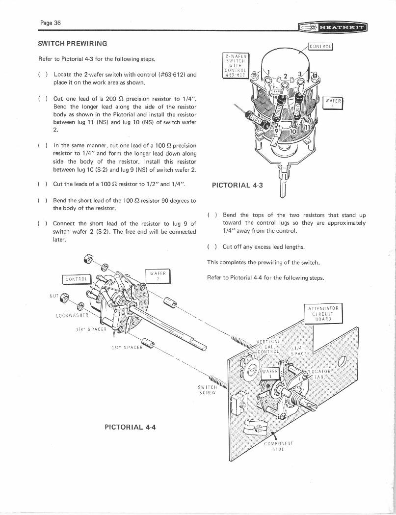
SWITCH PREWIRING
Refer to Pictorial 4-3 for the following steps.
( ) Locate the 2-wafer switch with control (#63-612) and place it on the work area as shown.
( ) Cut one lead of a 200 S2 precision resistor to 1 /4". Bend the longer lead along the side of the resistor body as shown in the Pictorial and install the resistor between lug 11 (NS) and lug 10 (NS) of switch wafer 2.
( ► In the same manner, cut one lead of a 100 St precision resistor to 1 /4" and form the longer lead down along side the body of the resistor. Install this resistor between lug 10 (S-2) and lug 9 (NS) of switch wafer 2.
( ) Cut the leads of a 100 S2 resistor to 1/2" and 1/4".
( ► Bend the short lead of the 100 S2 resistor 90 degrees to the body of the resistor.
( ) Connect the short lead of the resistor to lug 9 of switch wafer 2 (S-2►. The free end will be connected later.
CONTROL
NUT
v \~ LOCKWASHER
WAFER I z
PICTORIAL 4-4
CONTROL
2-l'JAFER S6VITCH
L^J I T H CONTROL #63-612
PICTORIAL 4-3
( ) Bend the tops of the two resistors that stand up toward the control lugs so they are approximately 1/4" away from the control.
( ) Cut off any excess lead lengths.
This completes the prewiring of the switch.
Refer to Pictorial 4-4 for the following steps.
SWITCH SCREW
COMPONENT SIDE
ATTENUATOR CIRCUIT BOARD

Page 37
( ) Remove the two 3/8" spacers from between the control and wafer 2.
114 ' ~ SPACER
318"~ SPACER
CONTROL
NUT
(~,° LOCKWASHER
U
3l8" SPACER
WAFER I 2
ll4" SPACER
.M.,~~ PHENOLIC SPACERS (REMOVE AND DISCARD)
WAFER I 1
DETENT
Detail 4-4A
Refer to Detail 4-4A and disassemble the 2-wafer switch with control as follows:
( ) Remove the two nuts and two lockwashers from the long switch screws.
) Carefully remove the control,
3/ 4 ~~2 ,~ ~ ( < < t
Carefully remove wafer 2, making certain not to rotate the center segment of the wafer (the rotor).
NOTE: Wafer 2 must go back onto the switch assembly exactly as it was originally. Be sure to study it carefully and to reinstall it properly later.
( ) Remove the two rear 1/4" spacers from the screws.
( ► There may be phenolic spacers between the four 1/4" spacers as shown in the Detail. If so, remove and discard these spacers.
Note that the remaining assembly consists of the switch detent, two long screws, two 3/8" spacers, switch wafer 1, and two 1 /4" spacers.
Refer to Pictorial 4-4 and install the switch assembly onto the attenuator circuit board as follows:
( ) Hold the circuit board so the component side of the board is facing you.
( )
1 )
Push the switch screws through the screw holes in the circuit board. Make sure the locator tab on the switch
detent is facing toward the Vertical Cal control in the
upper left corner of the circuit board.
Place the two 1/4" spacers onto the screws, followed by switch wafer 2 with its components positioned toward the upper left corner of the circuit board, two 3/8" spacers, and then the control.
Secure the assembly to the circuit board with the two lockwashers and two nuts previously removed from the assembly.
,~„ 2„ 3„ 4„ 5„
I ~ l I I

Page 38
ATTENUATOR CIRCUIT BOARD
114 SPACER ~~ % ~— ~» i)- loon
PICTORIAL 4-5
CIRCUIT BOARD FINAL WIRING
Refer to Pictorial 4-5 for the following steps.
Y Push the free lead of the 100 Sl precision resistor connected to lug 9 of switch wafer 2 into the hole near the 1 /4" switch spacer as shown (S-1►. (NOTE: This hole is not marked.)
Refer to Pictorial 4-6 for the following steps.
( ) Bend and connect the free lead of the resistor-capacitor assembly coming from hole D on the circuit board to lug 11 of switch wafer 1 (S-1).
( ~) Pass a 1 " bare wire through switch lug 9 of wafer 1 and through hole N in the circuit board. Solder the wire to the foil and to switch lug 9 and cut off any excess wire lengths.
NOTE: When switch lugs are called out as "8F" and "8R", as in the following step, this indicates that lug 8F is on the Front of the wafer, or that lug 8R is on the _Rear of the wafer.
~„ 2„
t 1
ATTENUATOR CIRCUIT BOARD
PICTORIAL 4-6
(\) Pass a 1" bare wire through lug 8F, through lug 8R, and into hole F in the circuit board. Solder the wire to the foil and to both wafer lugs, then cut off any excess wire length.
( 1)c
Refer to Detail 4-6A and solder a 30 pF mica capacitor to a 90 kSZ precision resistor. Cut off the excess capacitor leads. Cut the resistor leads to 3/4".
( 11 ) Pass one of the resistor leads through lug 2 of wafer 1 (S-2) and through hole G in the circuit board (S-1►. Pass the other resistor lead through lug 5 of wafer 1 (S-2) and through hole K in the circuit board (S-1). Remove any excess lead lengths from the foil side of the board.
Set the attenuator circuit board assembly aside temporarily.
3" I
Detail 4-6A
4" I
5" I

CHASSIS PARTS PICTORIAL
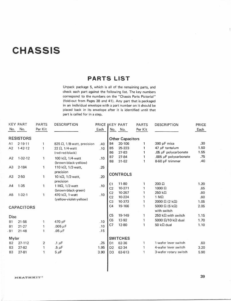
CHASSIS
PARTS LIST Unpack package 5, which is all of the remaining parts, and check each part against the following list. The key numbers correspond to the numbers on the "Chassis Parts Pictorial" (fold-out from Pages 38 and 411. Any part that is packaged in an individual envelope with a part number on it should be placed back in its envelope after it is identified until that part is called for in a step.
KEY PART No. No.
PARTS Per Kit
DESCRIPTION PRICE Each
KEY PART No. No.
PARTS Per Kit
DESCRIPTION PRICE Each
RESISTORS Other Capacitors Al 2-19-11 1 825 S2, 1 /8-watt, precision .40 64 20-106 1 390 pF mica .30
A2 1-42-12 1 22 S2, 1 /4-watt .10 65 25-223 1 47 µF tantalum 1.50
(red-red-black) 66 27-83 1 .05 µF polycarbonate 1.55
A2 1-32-12 1 100 kS2, 1 /4-watt .10 B7 27-84 1 .005 µF polycarbonate .75
(brown-black-yellow) 68 31-52 1 8-60 pF trimmer .40
A3
A3
2-184
2-50
1
1
110 kS2, 1 /2-watt, precision 10 kS2, 1 /2-watt,
.25
.20 CONTROLS
precision A4 1-35 1 1 MS2, 1 /2-watt
(brown-black-green) .10 C1
C2
11-80 10-271
1 1
200 S2 1000 SZ
1.20 .65
A5 1-32-1 1 470 kS2, 1-watt .10 C2 C2
10-267 10-224
1 1
250 kS2 1 MS2
.60
.60 (yellow-violet-yellow)
C3 10-373 1 2000 S2 (2 kS2) 1.05
CAPACITORS C4 19-166 1 5000 S2 (5 kS2) with switch
2.05
Disc C5 19-149 1 250 kS2 with switch 1.15
61 21-56 1 470 pF .10 C6 12-92 1 5000 52/10 kSZ dual 1.70
B1 21-27 1 .005 µ F .10 C7 12-80 1 50 kS2 dual 1.10
B 1 21-48 1 .05µF .15
Mylar SWITCHES B2 27-112 2 .1 µF .25 D 1 62-36 1 1-wafer lever switch .60 63 27-82 1 .5 µF 1.95 D2 62-34 1 4-wafer lever switch 3.20 B3 27-81 1 5µF 3.90 D3 63-613 1 3-wafer rotary switch 5.90
H~ATHKIT "' 39

Page 40
KEY PART PARTS No. No. Per Kit
INSULATORS
DESCRIPTION PRICE Each
E 1 73-2 6 3/4" grommet .10 E2 73-3 5 1 /2" grommet .10 E3 73-4 2 5/16" grommet .10 E4 73-5 1 Cushion strip .10 E5 73-34 2 Boot .10
E6 75-71 1 Strain relief .10
METAL PARTS
F 1 90-513-1 2 Cabinet shell 3.75 F2 100-292 1 CRT shield 19.05 F3 100-1046 1 Transformer shield 2.70 F4 200-598 1 Chassis 2.60 F5 200-630 1 Lower bracket 1.05 F6 203-771-1 1 Rear panel 2.35 F7 203-786-1 1 Front panel 4.60 F8 204-1169 1 Circuit board bracket 1.00 F9 204-1170 2 CRT mounting bracket .35 F10 204-1171-1 1 Top bracket 1.30 F11 204-1198 1 CRT shield bracket .10 F12 204-1814 1 L-bracket .30 F 13 206-518 1 Transformer cover .50 F 14 207-1 2 CRT clamp .20
PLASTIC PARTS
G1 210-48 1 Bezel 1.20 G2 211-49 1 Handle assembly 2.15 G3 214-117 1 CRT cover 2.20 G4 255-7 1 1-3/4" spacer .40 G5 261-28 4 Plastic foot .05 G6 413-10 1 Red lens .10 G7 414-6 1 Green screen .40 G8 414-23 1 Graticule 4.90
KNOBS-KNOB INSERTS
H1 462-247 3 1"pointer knob .35 H2 462-248 2 11 /16" pointer knob .60 H3 462-249 4 11 /16" plain knob .40 H4 462-276 3 Short pointer knob .25 H5 462-322 5 Lever knob .10 H6 455-50 6 Large-shaft knob
insert -10
H7 455-51 3 Small-shaft knob insert
.10
H8 455-52 3 Short knob insert .10
KEY PART PARTS No. No. Per Kit
DESCRIPTION PRICE Each
TERMINAL STRIPS-CONNECTOR-SOCKET
J1 431-42 1 5-lug terminal strip .10 J2 431-90 1 2-lug terminal strip .10
(foot on right►
J3 431-91 1 2-lug terminal strip .10 (foot on left)
J4 431-82 1 3-lug terminal collar .10
J5 432-59 1 BNC connector with hardware
1.65
J6 434-41 1 12-lug tube socket .30
WIRE-CABLE
89-23 1 Line cord .75 134-237 1 Test cable with 2.20
BNC connector 134-298 1 Wire harness 5.70 340-3 1 Bare wire (in small
envelope►
.05/ft
343-7 1 Shielded cable .05/ft 344-50 1 Black wire .05/ft 344-52 1 Red wire .05/ft 347-2 1 300-ohm twin
lead .05/ft
HARDWARE
#6 Hardware K 1 250-229 54 6-32 x 1 /4" screw .05 K2 250-162 2 6-32 x 1/2" screw .05 K3 250-26 2 6-32 x 5/8" screw .05 K4 252-3 20 6-32 nut .05 K5 254-1 35 #6lockwasher .05 K6 255-94 10 17/32" spacer .10 K7 259-1 1 #6 solder lug .05
#10 Hardware K8 250-50 20 10-32 x 3/8" screw .05 K9 252-5 6 10-32 nut .05 K10 254-3 6 #101ockwasher .05
Other Hardware K11 250-213 11 4-40 x 5/16" screw .05 K12 250-137 4 8-32 x 3/8" screw .05 K13 250-287 4 Panel stud .05 K14 252-2 7 4-40 nut .05 K15 252-7 9 Control nut .05 K16 252-73 1 Speed Nut* .05
*Registered Trademark, Tinnerman Co.

Page 41
KEY PART No. No.
PARTS Per Kit
DESCRIPTION PRICE Each
KEY PART PARTS DESCRIPTION PRICE
No. No. Per Kit Each
Other Hardware (cont'd.) Miscellaneous (cont'd.)
NOTE: Transistors are marked for identification in one of K17 252-86 4 Knurled nut .10
the following four ways. K18 253-10 11 Control flat washer .05 K19 254-4 5 Control lockwasher .05
1. Part number. K20 254-9 12 #4lockwasher .05 2. Transistor type number. K21 255-151 2 4-40 tapped spacer .15 3. Part number and transistor type number. K22 259-27 1 Control solder lug .05 4. Part number with a transistor type number other
than the one listed.
L6 417-201 1 X29A829 transistor .50 421-23 1 1-ampere, slow-blow fuse .30
L7 422-1 1 Fuseholder .25 MISCELLANEOUS L8 436-11 3 Red banana jack .15
L8 436-22 1 Black banana jack .15
L1 54-285 1 Power transformer 13.40 390-362 1 Fuse label .10
L2 56-26 1 1 N 191 diode .25 391-34 1 Blue and white label
L3 260-16 2 Alligator clip .10 L9 391-54 1 "Heathkit" nameplate .15
411-265 1 5DEP1F CRT 23.50 L4 412-15 1 NE-2H neon lamp .20 NOTE: See Page 103 for "Replacement Parts and Price L5 412-31 2 Incandescent lamp .50 Information."
Chassis Parts Pictorial (Cont'd.)
~~a~
~s
l9
HEATHKIT

Page 42
STEP-BY-STEP ASSEMBLY
(TRANSFORMER I COVER
TRANSFORMER( SHIELD
PICTORIAL 5-1
MAIN GHASSIS ASSEMBLY
Refer to Pictorial 5-1 for the following steps.
( ► Install 3/4" grommets at BS, BR, BF and BA as shown.
( ► Install 1/2" grommets at BJ, BK, and BP.
Refer to Detail 5-1A for the following steps.
( ► Locate the transformer cover (#206-518) and install 1/2" grommets in holes BG and BH as shown.
( ) Position the power transformer (#54-285) on its top as shown. NOTE: The flanged sides of the transformer cover will face downward, and the transformer will be mounted on the underside of the chassis, upside down.
GRN-BLK BLK 2-BRN RED-BLK YEL-BLK 2-BLU
FLANGED SIDE
® ~
~® —o
- -1 ~ ~/
2-WHT YEL-RED GRN RED YEL YEL-GRN RED
,GRN
MAI N CHASSIS
10-32 NUT
#10 LOCKWASHER
TRANSFORMER COVER
l#206-5181
10-32 x 318" ~~ SCREW
Detail 5-1 A
POWER TRANSFORMER (#54-285)

Chassis Parts Pictorial (Cont'd.)
~K4~ Kf ~~ -,,~ r"
5 iiiiiiuiiiiui ~~~u~uiuuuuW ~ ~~i
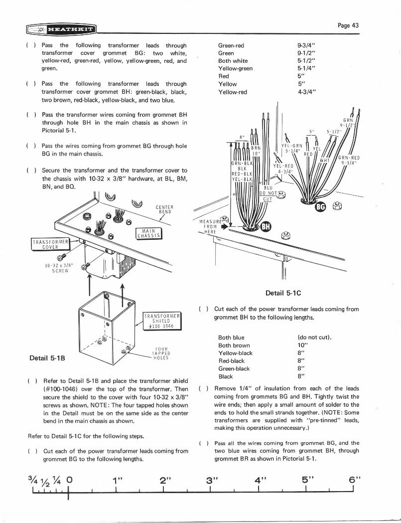
( )
Pass the following transformer leads through transformer cover grommet BG: two white, yellow-red, green-red, yellow, yellow-green, red, and green.
Pass the following transformer leads through transformer cover grommet BH: green-black, black, two brown, red-black, yellow-black, and two blue.
( ) Pass the transformer wires coming from grommet BH through hole BH in the main chassis as shown in Pictorial 5-1.
1 ► Pass the wires coming from grommet BG through hole BG in the main chassis.
( ) Secure the transformer and the transformer cover to the chassis with 10-32 x 3/8" hardware, at BL, BM, BN, and BQ.
1
TRANSFORMER COVER
10-32 x 318" SCREW
Detail 5-1 B
1
i
R_
~3
'w~i ~ i
t:
V
CENTER BEND
l MAIN
CHASSIS
TRANSFORMER SHIELD
#100-1046
FOUR TAPPED HOLES
Refer to Detail 5-1B and place the transformer shield (#100-1046) over the top of the transformer. Then secure the shield to the cover with four 10-32 x 3/8" screws as shown. NOTE: The four tapped holes shown in the Detail must be on the same side as the center bend in the main chassis as shown.
Refer to Detail 5-1C for the following steps.
( ► Cut each of the power transformer leads coming from grommet BG to the following lengths.
3/ 4 ~~2 ,~ 1 ~ l `
1" 1
2" l
Page 43
Green-red 9-3/4" Green 9-1 /2" Both white 5-1 /2" Yellow-green 5-1 /4" Red 5"
Yellow 5"
Yellow-red 4-3/4"
-:,.h~ ~~~~ B ONGRN-BLK
BLK RED-BLK YEL-BLK
MEASURE~~ FROM
THERE
fl
YEL-GRN ~ YEL 5-114"
\\
\\
YEL-RED 4-314"
BLU DO NOT CUT
u
lV
Detail 5-1 C
RED
GRN 9-1/2I
5-1/2" ~~
WHT GRN-RED 9-3/4"
( ) Cut each of the power transformer leads coming from grommet BH to the following lengths.
l 1
Both blue Both brown Yellow-black Red-black Green-black Black
(do not cut). 10" B.,
B.,
8" 8"
Remove 1/4" of insulation from each of the leads coming from grommets BG and BH. Tightly twist the wire ends; then apply a small amount of solder to the ends to hold the small strands together. (NOTE: Some transformers are supplied with "pre-tinned" leads, making this operation unnecessary.)
( ) Pass all the wires coming from grommet BG, and the two blue wires coming from grommet BH, through grommet BR as shown in Pictorial 5-1.
3" 4" 5" I I 1
6" I

Page 44
. od ~
4 -WAFER LEVER SWITCH
ASSEMBLY
TWIST TABS: 1 l8 °. TURN
MAIN CHASSIS
SOkS2 DUAL
CONTROL
PICTORIAL 5-2
Detail 5-2A
SOk4 DUAL
CONTROL (#12-801

Page 45
Refer to Pictorial 5-2 for the following steps.
( ) Refer to Detail 5-2A and mount a 50 kSt dual control (#12-80) at BB. Position the control as shown in the Pictorial. Twist the mounting tabs 1 /8 turn to hold the control to the chassis.
( 1 Locate the 4-wafer lever switch assembly (#62-34) and remove one nut and one lockwasher from each of the mounting screws as shown in Detail 5-26. Mount this switch assembly as shown in the Pictorial at BT and BU on the chassis and secure it with the lockwasher and nut previously removed from the assembly.
( ) Install five 17/32" spacers at the five chassis locations marked BX. Use 6-32 x 1/4" screws and #6 lockwashers as shown in Detail 5-2C.
( ) Install one 17/32" spacer at BY with a #6 solder lug and a 6-32 x 1 /4" screw as shown.
Set the chassis assembly aside temporarily.
6-32 x 114" SCREW
~I
~o
4 -WAFER LEVER
SWITCH ASSEMBLY
~,
a~
Detail 5-2B
MAIN CHASSIS
s/
MAIN CHASSIS
#6 LOCKWASHER
/ 17132" TAPPED SPACER
O
'-: VY
#6 SOLDER LUG
~,
e ~_
E
Detail 5-2C
4\,
O

Page 46
REAR PANEL ASSEMBLY
Refier to Pictorial 6-1 (fold-out from Page 47) for the following steps.
( ) Install 3/4" grommets at HA and HB.
CRT MOUNTING BRACKET
~~~
6-32 x 114" SCREW
~~
Detail 6-1 A
6-32 NUT
#6 LOCKWASHER
/~
OUTSIDE OF
~!~ REAR PANEL
( ) Mount a CRT mounting bracket at HD on the outside of the rear panel with 6-32 x 1 /4" hardware as shown in Detail 6-1 A.
CRT 1OUNTING
BRACKET
®lll~'
6-32 x 114" SCREW
Detail 6-1 B
6-32 NUT
#6 ~LOCKWASHER
OUTSIDE OF
'~~ REAR PANEL
( ) Mount another CRT mounting bracket at HC as shown in Detail 6-1 B.
( ) Position the lower bracket (#200-630) against the rear panel as shown in the Pictorial.
( ) Refer to Detail 6-1 C and loosely mount the fuseholder at HG with 6-32 x 1 /2" hardware.

Page 47
FUSEHOLDER
6-3®UT
~I i
/ #6 LOC KWASHER
REAR PANEL
#6 LOCKWASHER
LOWER
BRACKET
Detai 16-1 C
6-32 x 112" SCREW
~C~
( ) Refer to Detail 6-1 D and loosely mount a 5-lug terminal strip at HF with 6-32 x 1/2" hardware. Position the terminal strip as shown in the Pictorial.
( 1 Space the edge of the lower bracket parallel to the edge of the rear panel. Then tighten the fuseholder
and terminal strip screws.
( ) Prepare the line cord as follows: Separate the wires for 2-1/2"; then twist the wire ends tightly and apply a small amount of solder to each wire end to hold the strands together.
3/ 4 ~~2 1~4 1 " 2" I ~ ~ ~ i ~
5 -LUG TERMINAL STRIP
#6 L(ICKWASHER
6-32 \ NUT
~?
O~
(REAR PANELI
~6 LOCKWASHER
Detail 6-1 D
6-32 x 1/2" SCREW
LOWER BRACKET,
( ► Pass the line cord wire ends 3-1 /2" through the rear panel at HE. Refer to Detail 6-1 E and install a strain relief on the line cord and install it in the rear panel as shown.
Detail 6-1 E
3" 4" 5" 6" ~ ~ ► l

Page 48
ALTERNATE LINE VOLTAGE WIRING
Refer to Pictorial 6-2 (fold-out from this page) for the following steps.
Two sets of line voltage wiring instructions are given below, one for 120 Vac line voltage and the other for 240 Vac line voltage. In the United States, 120 Vac is most often used, while in countries other than the United States 240 Vac is more common. USE ONLY THE INSTRUCTIONS THAT AGREE WITH THE LINE VOLTAGE IN YOUR AREA.
120 ~ac Wiring
' EYELET 5
2" BROWiJ r
~_~ BRowru ~'(\
~', Detail 6-2A
( ) Temporarily refer to Detail 8-1A and Page 56 and cut two 2" lengths of s andecf brown wire from the indicated leads at BO# f the wire harness.
Refer to Detail 6-2A for the folllo~ving steps.
~\ Prepare the two lengths of brown wire cut off the wiring harness as follows: ~,
( ) Remove 1/4" of insulation frorrl, the ends of both wires.
( ) Twist the bare wire strands together and melt a small amount of solder on the four ends to hold the strands together.
NOTE: In the following steps, be sure to wrap the wire ends firmly around the terminal strip lugs to assure a good mechanical gonnection.
( ► Connect a 2" length of brown wire between lug 1 (NS) an~lug 2 (NS) of terminal strip HF.
( 1 Connect a 2" length of brown wire between lug 4 (NS) .and lug 5 (NS) of terminal strip HF.
240 Vac Wiring
Detail 6-2B
( ) Temporarily refer to Detail 8-1A on Page 56 and cut two 2" lengths of stranded brown wire from the indicated leads at BO#8 of the wire harness.
Refer to Detail 6-26 for the following steps.
( ) Prepare one 2" length of brown wire from the wiring harness by removing 1/4" of insulation from each end. Discard the second 2" length of brown wire.
NOTE: In the following step, be sure to wrap the wire ends firmly around the terminal strip lugs to assure a good mechanical connection.
( ) Connect the prepared 2" brown wire between lug 2 (NS) and lug 4 (NS) of terminal strip HF.
( ► Connect the green line cord wire to lug 3 of terminal strip HF (S-1►.
( ► Connect the ribbed line cord wire to lug 5 of terminal strip FiF (NS).
( ) Connect the smooth line cord wire to lug 2 of the fuseholder (S-1).
( ) Pass the following transformer wires down through grommet BK on the main chassis: black, green-black, yellow-black, and red-black.
( ) Position the rear panel close to the main chassis as shown in Pictorial 6-2.
Connect the following transformer wires to terminal strip HF as directed:
( ) Black to lug 5 IS-3). NOTE: Solder step is (S-2) if your oscilloscope is wired for 240 Vac.

PICTORIAL 6-1

MAIN CHASSIS
LOWER
BRACKET
SMOOTH LEAD
6-32 NUT
J#6 LOCKbVASHER
GRN-BLK BLK
~%
I YEL-BLK RED-BLK
~ ~ ® O
e.~
® ~®
C, 6-32 x 1/4" , EVE. SCREW
PICTORIAL 6-2
INSET
RIBBED
CROSS-SECTION OF LINE CORD
REAR PANEL

CIRCUIT BOARD
BRACKET
PICTORIAL 6-3
#6 LOCKWASHER

Page 49
Green-black to lug 4 (S-2).
Yellow-black to lug 2 (S-2).
Red-black to lug 1 (NS1.
Mount the rear panel onto the main chassis with four 6-32 x 1 /4" hardware as shown.
CIRCUIT BOARD BRACKET ASSEMBLY
Refer to Pictorial 6-3 (fold-out from Page 48) for the following steps.
CIRCUIT BOARD
BRACKET
a UNDERSIDE OF WAFER
4-40 TAPPED SPACER
0
Detail 6-3A
4 LOCKWASHER
4-40 x 5116" SCREWS
( ) Loosely mount 4-40 tapped spacers at CA and CB on the circuit board bracket with 4-40 x 5/16" hardware as shown in Detail 6-3A.
( ) Mount the 1-wafer lever switch on spacers CA and CB with 4-40 x 5/16" screws. Position the switch wafer so the lugs are toward the bracket and the switch lever emerges from the underside of the wafer. Tighten the screws on the underside of the bracket.
3/ 4 ~~2 ~~4 ~ I l l ~ l
1" I
2" ~ I
Detail 6-3B
( ) Refer to Detail 6-3B and pass the lead on the banded end of a .1 /.cF Mylar capacitor through lug 8 of switch CC (S-2). Do not cut this lead. Connect the other capacitor lead to lug 10 of the switch (S-11. Position the capacitor under the switch wafer as shown.
Detail 6-3C
CIRCUIT BOARDI BRACKET
#6 LOCKWASHER
6-32 NUT
( ) Refer to Detail 6-3C and secure the circuit board bracket to the main chassis with 6-32 x 1 /4" hardware as shown.
( ) Secure the circuit board bracket to the lower bracket with 6-32 x 1 /4" hardware as shown in the Pictorial.
3" I
4„ 5„ 6„ I t ~ I

Page 50
Detail 6-4A
FRONT PANEL PARTS MOUNTING
Refer to Pictorial 6-4 (fold-out from Page 51) for the following steps.
( ► Refer to Detail 6-4A and mount a red lens at A as shown. Secure it in place by pushing the Speed Nut onto the lens.
CONTROL LOCKWASHER
CONTROL
CONTROL FLAT WASHER
Detail 6-4B
Refer to Detail 6-4B for the following steps.
( ) Mount a 200 S2 control (#11-80) at B with control hardware as shown.
CONTROL NUT
( ► Mount a 250 kS2 control (#10-267) at D with control hardware as shown.
3/ 4 ~~2 1/ ~ I , I ~ ,(
( ) Mount a 5000 SZ/10 kSZ dual control (#12-92) at AA
with control hardware as shown.
( ) Mount 5/16" grommets at N and P.
50004 CONTROL
WITH SWITCH 1#19-1661
TWIST 90 DEGREES
SWITCH
200052 CONTROL l#10-3731
Detail 6-4C
Refer to Detail 6-4C for the following steps.
( ) Locate the 5000 SZ control with switch (#19-166). Twist lugs 6 and 7 of the switch 90 degrees as shown.
( ) Connect the 2000 S2 (2 kSZ) control (#10-373) between switch lugs 6 (S-1) and 7 (S-1). Hold the control as close as possible to the switch lugs while soldering the leads. Then cut off the excess lead lengths.
( ► Refer to Pictorial 6-4 and mount the 5000 SZ control with switch assembly at Y on the front panel as shown. Use a control lockwasher, a control flat washer, and a control nut.
( ) Refer to Detail 6-4D and mount the CRT shield bracket to the CRT shield with 6-32 x 1/4" hardware as shown. Slide the bracket to the rear as far as possible. Then tighten the screws lightly (so you can still move the bracket when you apply pressure); the screws will have a final adjustment later.
~„ 2,,. 3„ 4„ 5„ 6„ I ~ I 1 I 1 ~ ~

Page 51
6-32 NUT
#6 LOCKWASHER
CRT SHIELD
r
REAR
CRT SHIELD
BRACKET
U 6-32x1/4" SCREW
Detail 6-4D
i
( ► Refer to Detail 6-4E (fold-out from this page) and mount the CRT shield on the front panel as shown. Be sure the CRT shield bracket at the rear is pointing downward. Loosely secure the CRT shield at S and X with 8-32 x 3/8" screws and panel studs.
( ) Loosely mount a 2-lug terminal strip (with the foot positioned to the left) at M with an 8-32 screw and a panel stud. Position the terminal strip as shown in Pictorial 6-4.
( ) Loosely mount a 2-lug terminal strip (with the foot positioned to the right) at R with an 8-32 x 3/8" screw and a panel stud. Position the terminal strip as shown in the Pictorial,
( ) Locate the graticule (#414-23).
( ) Mount the graticule on the front panel studs as shown in Detail 6-4F. Tighten the 8-32 x 3/8" screw slightly; then check the graticule to see that it slides easily off and onto the studs. If necessary, use asmall-bladed
screwdriver as shown in Detail 6-4G and reposition the studs slightly. Then recheck the graticule to see that it slides easily off and onto the mounting studs.
( ) Tighten the mounting screws securely.
Set the graticule aside temporarily.
THREADED STUD
Detail 6-4G
SMALL- BLADED SCREWDRIVER

Page 52
Refer to Pictorial 6-5 (fold-out from this page) for the following steps.
NOTE: As a result of tightening the screws in the following step, the CRT shield bracket (against the rear panel) will be pressed forward slightly and will be in its final position. It will be necessary to temporarily mount the front panel in order to tighten the CRT shield bracket screws.
( ► Carefully align the lever switches with their slots in the front panel and secure the front panel to the chassis with two 6-32 x 1 /4" screws as shown.
( ) Remove the two screws holding the front panel to the chassis, and lift the front panel from the chassis.
( ► Securely tighten the two screws holding the CRT shield bracket to the CRT shield.
( ) Once again, place the front panel onto the chassis as shown in the Pictorial, and loosely secure it with the two 6-32 x 1 /4" screws.
~ ~uiy 6-32 x 1/4" SCREW
NSIDE OF REAR PANEL
~#ems, CKWASHER
6-32 NUT
CIRCUIT BOARD
BRACKET
Deta i 16-6A
BNC CONNECTOR
BNC CONNECTOR HARDWARE
Refer to Pictorial 6f (fold-out from this page) for the following steps.
( ) Refer to Detail 6-6A and install a BNC connector at the VERT IN location on the front panel. Use the hardware supplied with the connector and a control solder lug. Do not tighten the nut.
Detail 6-5A ( ) Install a 250 kSl control with switch (#19-149) at BC in the main chassis and through the front panel. Use a
( ) Refer to Detail 6-5A and secure the CRT shield control flat washer and a control nut as shown in bracket to the rear panel with 6-32 x 1 /4" hardware as Detail 6-66. Position the three control lugs downward. shown. Do not tighten the control nut.
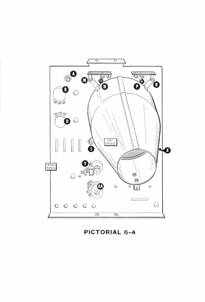
0 0
~ ,
FRONT PANEL
C ~
PICTORIAL 6-4

8-32 x 318" SCREW
Detail 6-4E
FRONT PANEL
PANEL STUD
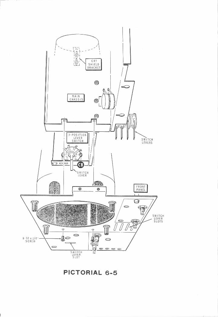
6-32 x ll4" SCREW
C RT SHIELD
BRACKET
MAIN CHASSIS
3 - POSITION LEVER
SWITCH
SWITCH LEVER SLOT
PICTORIAL 6-5
SWITCH LEVERS
SWITCH LEVER SLOTS

VERT IN
HORIZ EXT GND IN
IVPP TRIG
FRONT I PANEL 1
PICTORIAL 6-6

Page 53
CONTROL NUT
CONTROL FLAT WASHER
INSIDE
FRONT PANEL
~~
CONTROL LUGS
1M4 CONTROL !#10-2241
Detail 6-66
( ) Install a 1 MS2 control 1#10-224) at BE as shown in the Pictorial with a control flat washer and a control nut. Position the control lugs upward, then tighten this and the control nut in the previous step securely.
( ) Tighten the two front panel screws and the BNC connector nut.
Refer to Detail 6-6C for the following steps.
( ) Locate the hole labeled GND in the lower right edge of the front panel. Install a black banana jack (#436-22) in this hole; then loosely fasten the jack to the front panel and lower bracket with the nut supplied with the jack.
( 1 In the same manner, install the three red banana jacks (#436-11) at 1 VPP, EXT TRIG, and HORIZ IN.
( ) Tighten the nuts on all four banana jacks securely.
25pk~2 CONTROL
WITH SWITCH l#19-1491
Detail 6-6C

Page 54 ®HEATHKIT
FRONT PANEL WIRING
Refer to Pictorial 7-1 (fold-out from Page 55) and Detail 7-1 A for the following steps. Detail 7-1 A is divided into parts, and each step will refer to one of these parts.
PART 1
NEON LAMP
3/
t
CIiT OFFrAND
CISCARD ,
PART 2
LENS
~~~'// BACK OF~
FRONT PANEL
PART 3
3 TERMINAL COLLAR
PART a PART 5
3
VIEI'v FROM REAR
Detail 7-1A
( ~ Refer to Part 1 and cut the leads of the neon lamp to a length of 3/4".
(~) Refer to Part 2 and insert the lamp as far as it will go into the lens at A.
(~ ) Position the terminal collar as shown in the Pictorial and in Part 3 of the Detail, and push the collar onto the lens until the ends of the collar and lens are flush with each other as shown in Part 4.
(/ 1 Refer to the Pictorial and Part 4 of the Detail and connect one lamp lead to lug 2 (NS) and the other lamp lead to lug 3 (NS) of the terminal collar.
3/ 4 ~~2 ,~ ~ I ~ ► I
~„ 2 „
l T I
( ) Refer to Part 5 and connect a 100 kSZ (brown-black-yellow), 1/4-watt resistor between lug 1 (NS) and lug 2 (S-2) of the terminal collar. Cut off any excess lead lengths.
( /) Locate the two incandescent lamps (#412-31).
INSIDE OF
FRONT PANEL
Detail 7-1 B
OUTSIDE OF FRONT PANEL
( ► Refer to Detail 7-1 B and place one of these lamps into grommet P. Install the lamp so that 3/16" of the bulb protrudes from the front of the grommet.
( \a Connect one lamp lead to the eyelet of lug 1 (S-1) and the other lamp lead to the eyelet of lug 2 IS-1) of terminal strip R.
( )/ In the same manner, install the other incandescent (/ lamp into grommet N. Leave 3/16" of the bulb of this
lamp protruding from the front of the grommet.
1~1
U` )
Connect one lamp lead to the eyelet of lug 1 (S-1) and the other lead to the eyelet of lug 2 of terminal strip M.
Connect a 470 kS2, 1-watt resistor from lug 3 of control BC (S-11 to lug 1 of control BE (5-1►. Cut off any excess lead lengths.
NOTE: When wire is called for, as in the following step, cut the wire to the indicated length and remove 1 /4" of insulation from each end.
( T► Connect a 1-3/4" white wire from lug 6 of wafer 2 (S-1) to lug 2 of wafer 1 (NS) of switch BW.
3„ 4„ 5„ 6„ 1 I I

Page 55
( ~ Connect the positive (+) lead of a 47 µF tantalum capacitor to lug 4 (NS), and the other lead to lug 2 (S-2) of wafer 1 of switch BW. Cut off any excess lead lengths.
( },Y Pass the lead from the banded end of a .1 µF Mylar capacitor through lug 6 of wafer 4 (S-2) to lug 4 of wafer 3 (S-1) of switch BW. Connect the other capacitor lead to lug 6 of wafer 3 of switch BW (NS).
PREPARE EACH END AS SHOWN
ilz
> l4"~ .--~
•==-%w~ '"~~S H I E L D LEA D
>/z" ~ l/a"
`~; CUT .,,~,~
TAKING CARE NOT TO CUT THE VERY THIN WIRES OF THE SHIELD LEAD, REMOVE THE OUTER INSULATION.
PEEL OFF THE FOIL AND STRAIGHTEN OUT THE THIN WIRES OF THE SHIELD LEAD.
FOIL
SHIELD LEAD
REMOVE THE INNER INSULATION AND TWIST THE SMALL WIRES OF THE SHIELD LEAD. APPLY SMALL AMOUNTS OF SOLDER TO THE END OF THE SHIELD LEAD AND THE INNER LEAD.
SOLDER ,//
TWIST AND SOLDER
Detail 7-1 C
Refer to Detail 7-1 C and prepare an 8" length of shielded cable as shown.
1 Connect the end of the cable without a shield lead to lug 4 of switch wafer 4 (S-1).
( ~ Route the cable close to controls Y and AA as shown and connect the inner lead of the free cable end to banana jack K (S-1). Connect the shield lead to banana jack J (NS).
NOTE: When you are instructed to prepare lengths of wire ahead of time, as in the following step, use the white wire supplied with the kit. To prepare a wire, cut it to the indicated length; then remove 1/4" of insulation from each end.
( ) Prepare the following lengths of wire:
3-1 /4" 3-1 /2" 3-1 /2"
5" 5-1 /2"
Connect a 3-1/4" length of were from lug 1 of terminal strip R (S-1) to lug 2 of terminal strip M (NS1.
( `) Connect a 4" length of wire from lug 2 of terminal strip R(S-1) to lug 1 of terminal strip M (NS).
1 ,) Route a 5" length of wire through grommet BA and connect it from lug 1 of terminal strip M (S-2) to lug 2 of control B (S-1).
(~ Connect a 3-1/2" length of wire from lug 3 of terminal collar A (S-21 to lug 3 of control D (NS1.
( \) Connect a 3-1/2" length of wire from lug 1 of terminal collar A (S-2) to lug 1 of control D (NS).
( 1,z) Connect a 5-1/2" length of wire from lug 1 of control D (S-2) to ground lug BY (NS).
(\) Locate the two blue transformer leads at grommet BR on the main chassis. Twist these leads together and route them as shown.
NOTE: After you route the two blue leads to their proper lugs in the following steps, cut off the excess lead lengths. Then remove 1/4" of insulation from each lead end before you connect it to a lug.
( ~) Pass one blue transformer lead through grommet BA and connect it to lug 2 of terminal strip M (S-2).
(~ Connect the remaining blue transformer lead to lug 1 of control B (S-1).

FRONT PANEL
O 2; .~~ LAMP\
3 3-112"
PICTORIAL 7-1

Page 56
2 LARGE BROWN W HITE-BLUE WHITE-RED WHITE - GREEN
RED BROWN BLUE WHITE -BLACK WHITE-GRAY GRAY SHIELDED WHITE SHIELDED BLUE SHIELDED VIOLET SHIELDED ORANGE SHIELDED RED SHIELDED BROWN SHIELDED YELLOW SHIELDED
RED GRAY BLACK BROWN BLUE ORANGE WHITE W HITE-YELLOW WHITE-VIOLET WHITE -BROWN WHITE SHIELDED
3/ 4 ~~2 11~
~ 1 . 1 ~ ~
GREEN 2 YELLOW 2 VIOLET WHITE-VIOLET WHITE -BROWN LARGE WHITE LARGE RED LARGE BLUE LARGE GREEN
YELLOW V I OLET RED WHITE -YELLOW WHITE-ORANGE YELLOW SHIELDED ORANGE SHIELDED RED SHIELDED BROWN SHIELDED GREEN SHIELDED
~„ 2„
~ I ~
BLUE ORANGE GREEN SHIELDEp
YELLOW BLACK ORANGE BLUE WHITE GREEN VIOLET
2 BLACK ORANGE 2 GREEN
12 LARGE GREEN GRAY WHITE-BLACK WHITE-GRAY GRAY SHIELDED VIOLET SHIELDED BLUE SHIELDED
Detail 8-1 A
3" I I
LARGE BLUE LARGE RED LARGE WHITE WHITE -BLUE WHITE -GREEN
RED 2 WHITE -RED WHITE-ORANGE
4" 5" 6" I I ~ ~

2)
3
WHT-RED
WAFER 1
RED
WHT-BLK
FRONT I PANEL
`~
~~.
BRN
SHIELDED SHIELDED O GRAY
SHIELDED WHT VIOL
LARGE BROWN
~~r TrI
" Y WHT-G RN
~ ~\ ~~ WHT-BLU ~~ ~~~
- ~~
\ /
~~ AFER 4
WHT GRAY'-- ~\~
WAFER 2 WAFER 3I
T~
WHT-VIOL
WHT-YEL
2252 1/4 WATT RESISTO R
W 1
SHIELDED BLU ~\.~
SHIELDED~~' ~ ~%/ YEL ~5
%~
BRN~~3 ~`~_~
~WHT-BRN
VVHT
BRN SHIELDED
RED SHIELDED
WHT-BRN
WHT-VIOL
e
_~~\`'~_
PICTORIAL 8-1
MAIN CHASSIS
J
3
C C
i
0
i
d

Page 57
WIRE HARNESS INSTALLATION l White-blue to lug 2 of control BE (S-1►.
Refer to Pictorial 8-1 (fold-out from Page 56) for the ( \) White-green to lug 2 of control D (S-1►. following steps.
( ') Locate the wire harness and form it as shown in Detail 8-1A. When the wire harness is placed into the kit, Connect the wires of BO#2 as follows: Breakouts (BO) 1, 2, and 3 will be toward the front panel. (~) Yellow shielded cable to lug 5, wafer 4 of switch BW
(S-1►.
(~ ( ''~ Install the wire harness as shown in the Pictorial, so
the main cable of the harness from front to rear is above the fold in the main chassis, along the heavy dashed line.
( ~. ) Locate the four long wires wrapped together (BO#10 and BO#11) coming from BO#6. Push these wires through grommet BP; they will be connected later.
( °), Similarly, locate the five wires wrapped together at BO#9. Push these wires through grommet BS as shown; they will be connected later.
Connect the wires of BO#1 to the front panel as follows:
( ,) Either large brown wire to lug 4 of control BC (S-11.
( 'y The other large brown wire to lug 5 of control BC (S-1). ( ~ Brown wire to lug 5, wafer 1 of switch BW (S-1►.
(\ ► White-red to lug 3 of control D (S-2).
White shielded cable to lug 6, wafer 3 of switch BW (S-2).
Violet shielded cable to lug 5, wafer 2 of switch BW IS-1).
Blue shielded cable to lug 4, wafer 2 of switch BW (S-1►.
White-gray to lug 3, wafer 1 of switch BW (S-1).
Gray shielded cable to lug 4, wafer 1 of switch BW IS-2).
Brown shielded cable to lug 5 of control Y (S-1).
Red shielded cable to lug 4 of control Y (S-1).

Page 58
(~ White-black wire to lug 6, wafer 1 of switch BW (S-1). (~ 4-1/2" black wire at F (S-11.
(~ Red wire to lug 7, wafer 1 of switch BW (S-1). ( 1 4-1 /2" red wire at D (S-1).
NOTE: The blue wire and the orange shielded cable from BO#2 will be connected later.
1 ) Cut both leads of a 22 St (red-red-black), 1/4-watt resistor to 1/4". Install this resistor between lug 1 (S-1) and lug 4 (NS) of control AA. Cut off the excess lead length at lug 1.
Connect the wires of BO#3 to the front panel as follows:
( `I-) White-brown to lug 3 of control Y (S-11.
( ~~.) White-yellow to lug 2 of control Y (S-1).
( ',) White-violet to lug 1 of control Y (S-1).
( `) White to banana jack L (S-1).
( "~) Brown to lug 2 of control AA (S-1►.
(~) -Gray to lug 3 of control AA (S-1).
The remaining wires from BO#3 will be connected later.
Connect the wires from BO#4 as follows:
( '.) White-violet to lug 5 of control BB IS-1 ►.
( ~~) Two violet wires to lug 6 of control BB (S-2).
( ) Two yellow wires to lug 1 of control BB (S-2).
( ;) White-brown to lug 2 of control BB (S-1).
The remaining wires from BO#4 will be connected later.
POWER SUPPLY FINAL WIRING AND INSTALLATION
Refer to Pictorial 8-2 (fold-out from Page 59) for the following steps.
Prepare and install the following wires on the power supply ( ,) Red to Z (5-1►. circuit board. NOTE: The free end of each wire will be connected later. (~) White-orange to Y (S-1).
( ,~) 2" white wire at A (S-11. (`) Either white-red to AB (S-1).
NOTE: In the following steps, you will be instructed to connect wires from the wiring harness to the power supply circuit board. Do this by turning the oscilloscope on its side so the working area will be in a horizontal position. Solder each wire to the foil as it is installed and cut off any excess wire lengths.
Connect the wires from BO#4 to the power supply circuit board in the following steps.
(v Large green to J (S-1).
( ~) Large blue to E (S-1).
( ~) Large red to K (S-1).
( ,) Large white to C (S-1►.
NOTE: The green wire will be connected later.
Connect the wires of BO#6 to the power supply circuit board as follows:
( ~) Green to L (S-1►.
( ~~) Black to h1 (S-1).
('~) Violet to N (S-1►.
(`) Blue to P (S-1).
(~ Yellow to R (S-1►.
( ~) Orange to S IS-1).
(~ White to T (S-1►.
Connect the wires of BO#7 to the power supply circuit board as follows:
( ~) 4" white wire at B (S-11. (~~) The remaining white-red to AA (S-1).
3/ 4 ~~2 ,/ ~ ~„ 2„
~ ~ ~ ~ 1 1
3„ 4„ 5„ 6 „

Page 59
,~ - ...,. ~~~ % '~.
~./~ .,, `'-:
m
WHT
WIRE HARNESS POSITION
~~ ~ ~_
\ ~~~~~~
~~
Ou ©
U
o~o
POWER SUPPLY CIRCUIT BOARD
~ \WHT
~~~~~~R ~
WHT-ORG
WIRE HARNESS
PICTORIAL 8-2

#6 LOCKWASHER
BLK \ \
WIRE HARNESS POSITION
j urrrr~~-~
Page 60
Ti9 6-32 x 1/4" ~~ SCREW
POWER SUPPLY CIRCUIT BOARD
1-AMPERE SLOW-BLOW ~
FUSE
#6 LOCKWASHER
WIRE HARNESS
INSET
CHASSIS
~ f1 $6 LOCKWASHER
6-32 x /4" SCREW
~a~~~~~~~\\D
PICTORIAL 8-3

Page 61
Refer to Pictorial 8-3 (fold-out from Page 60) for the following steps.
Connect the power transformer leads coming from grommet BR to the power supply circuit board in the following steps. So►der each lead as it is installed and cut off any excess lead lengths.
Red to hole AC (S-1).
Yellow-red to hole AD (S-1),
Yellow-green to hole X (S-1).
Yellow to hole W (S-1).
Either white to hole V (S-1),
The other white lead to hole U (S-1).
Green to hole H (S-1►.
Green-red to hole G (S-1).
Connect the following two wires coming from BO#8 of the wire harness.
( ~) Remove 1/4" of insulation from each of the brown wires. Add a small amount of solder to hold the small strands together.
(i) Either brown to lug 1 of terminal strip HF (S-3). NOTE: The solder step is (S-2) if your oscilloscope is wired for 240 Vac.
( , ) The other brown wire to lug 1 of fuseholder HG (S-1).
( `~) Install a 1-ampere slow-blow fuse in fuseholder HG.
NOTE: If your Oscilloscope is wired for 240 volts, install a 1/2-ampere, slow-blow fuse (not supplied) in fuseholder HG.
REPLACE FUSE WITH SAME
TYPE AND RATING JA `'~B 390 - 362
Detail 8-3A
( \) Locate the fuse replacement label (#390-3621. Write the size and type of fuse you are using in the space provided on the label; for example, "1-A, S/B." See Detail 8-3A.
(~) Remove the paper backing from the fuse replacement label and place it along side the fuseholder as shown in Pictorial 8-3.
Refer to the inset drawing on Pictorial 8-3 and install the power supply circuit board on the chassis in the following manner:
( ,,
) Place a #6 lockwasher between each of the two spacers and the circuit board at the upper right and upper left corners of the circuit board. Just start the two 6-32 x 1 /4" screws into the spacers.
( .,) Secure the lower edge of the power supply circuit board with three 6-32 x 1 /4" screws. Tighten these screws securely.
6-32 x 1/4" SCREW
L-BRACKET ~\\ \~~
1-314' PHENOLIC
SPACER
HEAT SINK
6-32 x 114"~ ,SCREW
TOP EDGE OF POWER SUPPLY CIRCUIT BOARD
\~ IIf
\~~~~\
Detail 8-3B
Refer to Detail 8-36 for the following steps.
(~ Install a 1-3/4" phenolic spacer on the top of the heat sink with a 6-32 x 1/4" screw.
( ) Loosely mount the L-bracket on the top edge of the ~ power supply circuit board as shown in Pictorial 8-3.
Use a 6-32 x 1 /4" screw.
( ~ )
( l
Tighten the top two corner screws securely.
Fasten the top of the L-bracket to the 1-3/4" phenolic spacer from Q401 with a 6-32 x 1 /4" screw as shown in the Pictorial.
( ") Tighten the three 6-32 x 1 /4" spacer and L-bracket ~' mounting screws.
Connect the wires coming from the power supply circuit board in the following steps. As each wire is connected, solder it to the designated point and cut off any excess wire lengths.
White wire from A to ground lug BY (S-21.
White wire from B to lug 1 of control BC (S-1).
Red wire from D to lug 2 of control BC (S-1).
Black wire from F to lug 3 of control BE (S-1).

Page 62
SWEEP GENERATOR-HORIZONTAL AMPLIFIER WIRING
Refer to Pictorial 9-1 following steps.
BANDED END
Detail 9-1 A
the (fold-out from Page 63) for
SWEEP GENERATOR HORIZONTAL AMPLIFIER CIRCUIT BOARD
NOTE: When you install components in the next two steps, push just the tip of the lead through the circuit board; then solder the lead to the foil. Do not cut either lead of the components; they will be connected later. Refer to Detail 9-1 A for the following steps.
(` ► Connect the banded end of a 1 N191 diode (#56-26) to J on the sweep generator-horizontal amplifier circuit board (S-1).
1t► Install one lead of a .05 µF disc capacitor at E on the circuit board (S-1►.
Prepare and install the indicated lengths of hookup wire in the following steps. The free ends will be connected later. After each wire has been soldered to the foil, cut off any excess wire lengths.
( ) 1-1 /2" white wire to F (S-1).
2" white wire to K (S-1►.
3" white wire to A (S-1).
3-1/2" red wire to B (S-11.
3" black wire to C (S-1).
NOTE: In the following steps, you will connect the wires and shielded cables from wire harness 60#12 and BO#13 to the sweep generator-horizontal amplifier circuit board. As each wire or cable is installed, solder it to the circuit board foil and cut off any excess wire lengths. The circuit board will be installed in the chassis later.
Connect the wires from BO#13 to the sweep generator-horizontal amplifier circuit board as follows:
( ~'') White-orange to ZZ (S-1).
3,4 ~~2 ,~ ~ , , ~. ~, i 1" 2"
( ~) Red to XX (S-1).
NOTE: In the next two steps only, install the shielded cable inner conductors first, as instructed. Then install the shield lead as directed and pull the shield lead as far as possible through the circuit board before soldering the shield to the foi I .
( t) Red shielded cable; inner lead to UU (S-1), shield lead to SS (S-1►.
( ~y Brown shielded cable; inner lead to VV (S-1), shield lead to TT (S-1).
(~') Orange shielded cable; inner lead to PP (S-11, shield lead to NN (S-1).
(~~) Yellow shielded cable; inner lead to KK (S-1), shield lead to LL (S-1►.
(~) Green shielded cable; inner lead to HH (S-1►, shield lead to GG (S-11.
Yellow wire to JJ (S-1).
White-yellow wire to RR (S-1).
(~ ) Violet wire to N1ti1 (S-1►.
(~~►
C`~ )
Connect the wires from BO#12 to the sweep generator-horizontal amplifier circuit board as follows:
. t l~ 1
l~ )
Il!)
1 l~l
l `f
Large green to AA (S-1).
Either black wire to T (S-1).
The other black wire to S (S-1).
Gray wire to U (S-1).
Gray shielded cable; inner lead to CC (S-1), shield lead to Z IS-1).
( .~) Blue shielded cable; inner lead to M (S-11, shield lead to N (S-1).
(`~ ) Violet shielded cable; inner lead to P (S-1), shield lead to R (S-1).
(`= ) Either green wire to ~^J (S-1).
(` ► The other green wire to X (S-11.
( .,) White-black wire to Y (S-1).
( ~" ) White-gray wire to DD (S-1).
( ~') Orange wire to EE (S-1►.
3" 1 L
4" 1
5" I
6 "

Page 63
~' , .
BLK
WIRE HARNESS
LARGE GRN
~ / /A
~~ ~
GRAY' ~ -
~i F
B1J ~ ~ ~~
B L K ~~~~~ ~ ~ ~ ~ B ~~+~ T W
SHIELDED/,~~ ,~~ ~~~ ~ ~ GRY
1 W1H T ~~F~ ~---~ -yJ ~I~11- IJ~ % (~ J ~ ~ ~~ I SI IH I IE I D E D '
~'~ ~R
T `NHT~ Z'' ~~ = WHT-GRAY
/r'~ P1 - BlK ~pD -` ~~ ~ i
E ~ ..s} {~F O R G 1 1 1, ,l,
y ~ ~~ —~
/I~JI
IIIYII~T T T
r
?-~WHT ORG
YEL ~ SHIELDED GRN
SHIELDED ~/,
e
ORG - SHIELDED
'4 .~
V V~~1-
JI~ t} ~ Y
}— (~~
yql
RR~ ~HT-YEL
Y~ ~ ~ } 4
~BRN XX SHIELDED
SHRELDDED 1
~l
~yq{
I
T
T Y
SWEEP GENERATOR -HORIZONTAL Ah1PLI FIER
CIRCUIT BOARD
3/ 4 1~2 ~~4 I , ► ~ `
PICTORIAL 9-1
~„ 2„
T l i
3" 1 i
4" 1
5" I
I
6" I
/~

Page 64 ®HEATHKIT
Refer to Pictorial 9-2 (fold-out from Page 65) for the following steps.
(,` 1 Place the sweep generator-horizontal amplifier circuit board into place over the cutout in the lower bracket.
Perform the following six steps to install the sweep generator-horizontal amplifier circuit board on the lower bracket. Use 4-40 x 5/16" hardware. See Detail 9-2A (fold-out from this page►.
('~) 1. Press the circuit board down onto the bracket.
( ) 2. Slide a #4 lockwasher between the circuit board foil and the lower bracket and line up the washer with the holes in the circuit board and the bracket.
( ) 3. Push a 4-40 x 5/16" screw through the lower bracket, the lockwasher, and the circuit board.
Hold the screw in place.
( ) 4. Place a #4 lockwasher on the end of the screw.
( ) 5. Start a 4-40 nut on the end of the screw. Do not tighten the nut and screw.
( ) 6. Repeat steps 1 through 5 until the three screws at
GA, GC, and GF are installed.
NOTE: In the following step use 4-40 x 5/16" hardware.
Push the screw through the bracket, through the circuit
board, then place a lockwasher and a nut on the screw.
is ) Four 4-40 x 5/16" screws, four #4 lockwashers, and four 4-40 nuts at GB, GD, GE, and GG.
( `~ Tighten all seven circuit board mounting screws.
Connect the wires coming from the sweep generator-horizontal amplifier circuit board in the following steps.
(~J ) White wire coming from F to banana plug J (NS).
(„► White wire coming from K to lug 6 of control AA IS-1).
(y Free end of diode coming from J to lug 5 of control AA (S-1►.
3/ 4 ~~2 ,~4 0 '' " 2
~ s
~ ~ ~ ) ~ 1 1 1
( `') White wire coming from A to lug 4 of control AA (S-21.
Connect the wires from BO#3 of the wire harness to the sweep generator-horizontal amplifier circuit board as follows:
(',, ~) White shielded cable; inner lead to H (S-1), shield lead to G (S-1).
Blue wire to D (S-1).
Red wire to L (S-1).
Black wire to FF (S-11.
Form the harness wires toward the front panel as shown in Pictorial 9-2.
TWIN LEAD
I ~/ ~/~ ~/
C~
-- 114"
(
1~ )
/O
3-1/4"~I
)~
i s'
t~ 114" --{
Detail 9-2B
Refer to Detail 9-2B and prepare a 15" length of 300 SZ twin lead as shown. Then twist the bare wire ends tightly and melt a small amount of solder on the strands to hold them together.
Refer to the Pictorial and connect end A of the twin
lead to the sweep generator-horizontal amplifier
circuit board as follows: one lead to WW IS-11; the
other lead to YY (S-1►. Cut off the excess lead lengths.
(~ ► Pass the free end of the twin lead through grommet
BS. NOTE: Carefully trace the side of the twin lead
connected to YY on the circuit board.
(,`;) Pass the free end of the twin lead through grommet HB in the rear panel, as shown, so the wire lead from YY on the circuit board is toward the bottom of this grommet. The free end of this twin lead will be connected later.
Set the Oscilloscope aside temporarily.
3" 4" 1
5" 6" I l t

~r~4 40 NUT
~~#4 LOCKWASHER
Detail 9-2A
LOWER BRACKET

Page 65
WIRE HARNESS
® ~o ~_ WHT ~ ~ ~ ~~ ~ ~
~ ~ ~®
~ ~~ o ~ ~ ~ BLU~ { } WHT ~ ~ ~ O O~ T T 1,
SHIELDED T ~ ~ ~ I ~+ ~--
II I /,j I Fi~m ~ ~ 0 -~~ } ~ —~~ 1
G ~ —RED ~ -~
~ ~ i F ~ ~~ ~ ~ ~ ~TY~ ~~,1 s ' ® V ~FF ® +
O
ml
I~O(I~~ ~.
PICTORIAL 9-2
INSET
OUTSIDE OF REAR PANNEL
\ ir.
~ _
® YY LEAD

Page 66
6" SHIELDED
INNER LEAD
4
SHIELD LEAD
R -c,_ INNER
SHIELDED I~;`~=2
METAL WAFER
2-3/4''
3/4" BARE WIRE
1F
3 -WAFER ROTARY SWITCH l#63-6131
82552\=
5 _ ~`'~ 6 F
2F ~
SHIELD LEAD
DUAL CONTROL
PICTORIAL 10-1
3-WAFER ROTARY SWITCH WIRING AND INSTALLATION
Refer to Pictorial 10-1 for the following steps.
WAFERI 3
X29A829 l#417-2011
TRANSISTOR
6F
/ 2-112"
! WHITE
WAFERI 1
( ) Locate the 3-wafer rotary switch with dual control (#63-613) and position it so the control lugs are up as shown.
8-60 pF TRIMMER 1#31 -521
3" BARE `WIRE
SOLDER
SOLDER
CUT
TRIMMER ~ — LEAVES
\// ' 390 pF MICA
CAPACITOR
J CUT
_TRIMMER LEAVES
~cuT
C
Detail 10-1A
Refer to Detail 10-1A and prepare an 8-60 pF trimmer (#31-52), a 390 pF mica capacitor, and a 3" heavy bare wire in the following manner:
(~'~ ) Slide the 3" heavy bare wire through both lugs of the trimmer .capacitor. Center the trimmer on the bare wire.
(J ) Push each of the leads of a 390 pF mica capacitor through one lug of the trimmer capacitor. Center the mica capacitor between the lugs as shown, and bend the mica capacitor leads outward.
( ~' 1 Apply solder to both lugs of the trimmer capacitor. Use the solder generously and be sure the bare wire and mica capacitor leads are firmly soldered to the trimmer lugs.
(` ) Cut and discard only the excess mica capacitor leads.
( ' ) Cut the center segment of the heavy bare wire between the trimmer lugs as shown. Do not cut the ends of the bare wire outside the trimmer lugs.
(~ 1 Connect the assembly between lugs 1 R of wafer 3 (NS) and 1 F of wafer 2 (S-2) of the switch. Cut off the excess bare wire lengths.
1 Connect a 3/4" bare wire between lugs 1 F (NS) and 2F (S-1) of wafer 2. Be sure to position the trimmer capacitor outward as shown in the Pictorial.

WAFER 1
12
3 -WAFER ROTARY SWITCH
5-1/2"
WAFER 1
;~C SIG 5F6F 7
WAFER 2
WAFER 3
SWEEP GENERATOR HORIZONTAL AMPLIFIER
CIRCUIT BOARD
PICTORIAL 10-3
BB
WIRE HARNESS
swlrcH CONTROL

Page 67
(~) Connect one end of a 2-3/4" white wire to lug 1 R of wafer 3 (NS). Connect the other end of this wire to lugs 3R (S-2) and 3F (S-1) of wafer 2.
(~ 1 Connect one end of a 2-3/4" white wire to lugs 2R and 2F of wafer 3. Solder both lugs and the wire together. Connect the other end of this wire to lug 4F of wafer 2 (NS).
(V) Connect one end of an 825 SZ precision resistor to lug 4F of switch wafer 3 (S-1). Connect the other end of the resistor to lug 2 of the dual control (NS►. Cut off the excess lead lengths.
('~ ) Connect one end of a 10 kSZ precision resistor to lug 5R of switch wafer 3 (S-1►. Pass the other end of this resistor through lug 3 (NS) to lug 2 (S-2) of the dual control. Cut off the excess lead lengths.
(V) Connect one end of a 110 kSZ precision resistor to lug 6F of switch wafer 3 (S-1). Connect the other end of this resistor to lug 3 of the dual control (S-3). Cut off the excess lead lengths.
Refer to Detail 10-1 B and prepare a 6" length and an 8" length of shielded cable as shown.
( ~) Connect the inner lead of the 6" shielded cable to lug 5 (S-1) and the shield lead to lug 6 (NS) of the dual control.
( . ) Remove the shield lead from the free end of the 6" cable.
( ~') Connect the inner lead of the 6" shielded cable to lug 5F of switch wafer 1 (S-1).
Connect the inner lead of the 8" shielded cable to lug 4 (S-1) and the shield lead to lug 6 (S-21 of the dual control. The free end of the 8" shielded cable will be connected later.
NOTE: When you install the transistor in the following step, refer to "Transistor Installation" (fold-out from Page 101 to help you correctly identify the transistor type.
('.) ) Refer to Detail 10-1 C and install an X29A829 (#417-201) transistor on switch wafer 2 as follows: emitter (E) lead to lug 4F (S-21, collector (C) lead to lug 5F (NS), and base (B) lead to lug 6F (NS). Cut off the excess lead lengths.
3/ 4 1~2 1~4 0
~ ~ ~ ~ > 2" 1
1
~. 3la'
1 /a"
~.—.~.
PREPARE EACH END AS SHOWN
3/4"—a
1 /a"
~~- -...~ ~.
SHIELD LEAD
.s
TAKING CARE NOT TO CUT THE VERY THIN WIRES OF THE SHIELD LEAD, REMOVE THE OUTER INSULATION.
PEEL OFF THE FOIL AND STRAIGHTEN OUT THE THIN WIRES OF THE SHIELD LEAD.
FOIL
SHIELD LEAD
REMOVE THE INNER INSULATION AND TWIST THE SMALL WIRES OF THE SHIELD LEAD. APPLY SMALL AMOUNTS OF SOLDER TO THE END OF THE SHIELD LEAD AND THE INNER LEAD.
SOLDER ~!I
:~ TWIST AND SOLDER
Detail 10-16
Connect a 2-1 /2" white wire to lug 5F of switch wafer 2 (NS). The free end will be connected later.
3" 1
Detai 1 10-1 C
X29A829 #air-2oi~
TRANSISTOR
WAFER 2
5" l
6 " 1

Page 68
METAL WAFER
3" WHITE
BANDED END
5µF
. 5µF
3" WHITE
7
2 1/z" WHITE
7R
3 -WAFER ROTARY SWITCH
I
10' 11Rn
DUAL CONTROL
12R
1R .05µF
005µF
BANDED END
12F
LOCATING LUG
PICTORIAL 10-2
WAFER z
WAFER T
Refer to Pictorial 10-2 for the following steps.
E
(~ )
tJ)
~\J)
\i)
Twist switch wafer 3 lugs 10R, 11 R, and 12R, 45 degrees as shown.
Pass a 2" bare wire from lug 1 R (S-3), through lug 12R (NS1, through lug 11 R (NS►, through lug 10R (NS1, to lug 9R (NS) of switch wafer 3.
Prepare a 3" length of white wire.
Connect one end of the 3" wire to lug 9R of switch wafer 3 (NS). The free end will be connected later.
(~) Pass the lead from the banded end of a 5 !.cF Mylar capacitor through lug 9R of switch wafer 3 (S-4) to the metal wafer on the front of the dual control as shown. Cut the lead 1 /8" beyond the metal wafer; then bend it down over the wafer edge and solder it to the flat side of the wafer.
( U) Pass the free lead of the 5µF capacitor through lug 9F (S-2) to lug 8F (S-1) of switch wafer 2. Cut off the excess lead length.
Connect a .5 uF Mylar capacitor from lug 10R of wafer 3 (S-3) to lug 10F of wafer 2 (S-1) of the switch. Be sure the banded end of the capacitor is toward wafer 3. Cut off the excess lead lengths.
( `~ ) Connect a .05 µF polycarbonate capacitor from lug 11 R of switch wafer 3 (S-3) to lug 11 F of switch wafer 2 (S-1►. Position the banded end toward wafer 3. Cut off the excess lead lengths.
('`~) Connect a .005 µF polycarbonate capacitor from lug 12R of switch wafer 3 (S-3) to lug 12F of switch wafer 2 (S-11. Position the banded end toward wafer 3. Cut off the excess lead lengths.
( '- 1 Prepare a 3" length of white wire.
(~) Connect the 3" white wire to lug 7R of switch wafer 2 (S-1). The free end will be connected later.

(`~1
(~)
Page 69
Connect a .005 µF disc capacitor between lug 7R (NS) and lug 8R (NS) of switch wafer 1.
Connect a 470 pF disc capacitor between lug 8R (S-2) and lug 9R (S-1) of switch wafer 1.
Cut the excess lead lengths from both disc capacitors.
Locate the free end of the 2-1/2" white wire coming from lug 5F of switch wafer 2. Connect this wire to lug 10F (S-1) of switch wafer 1.
Refer to Pictorial 10-3 (fold-out from Page 66) for the following steps.
NOTE: Before you install the 3-wafer rotary switch, study the Pictorial and previous Pictorials once again to be sure the wires, cables, and harness wires are properly positioned as illustrated.
('~) Place a control flat washer on the shaft of the three-wafer rotary switch. Install the switch assembly through the front panel as shown in the Pictorial. Be sure the locating lug enters the small hole along side the large shaft hole. Secure the switch with a control flat washer and a control nut.
('~) Connect the red wire coming from B on the sweep generator-horizontal amplifier circuit board to lug 5F, wafer 2 of the 3-wafer rotary switch (S-31.
( ..) Connect the black wire coming from C on the sweep generator-horizontal amplifier circuit board to lug 6F, wafer 2 of the 3-wafer rotary switch (S-2).
(. ) Connect the .05 disc capacitor coming from E on the circuit board to lug 7R of switch wafer 1 (S-21.
( ") Locate the free end of the white wire coming from lug 7R of switch wafer 2. Connect this wire to sweep generator-horizontal amplifier circuit board location V (S-11.
(') Locate the free end of the white wire coming from lug 9R of switch wafer 3. Connect this wire to circuit board location BB (S-1).
(~~~) Locate the green wire coming from BO#4 of the wire harness. Connect the free end of this wire to lug 1 of the switch control (S-1►.
( ', ► Connect the blue wire coming from wire harness BO#2 to lug 1 R, wafer 1 of the 3-wafer rotary switch (NS).
( Connect the inner lead of the orange shielded cable coming from BO#2 to lug 11 F, wafer 1 of the 3-wafer rotary switch (S-1).
('. ) Connect the orange wire coming from harness BO#2 to lug 6R, wafer 1 of the 3-wafer rotary switch (NS).
(',~) Locate the free end of the shielded cable coming from lugs 4 and 6 of the switch control. Connect the shield lead of this cable to banana jack J (S-3). Connect the inner lead of this cable to banana jack H (S-11.
( ) Prepare a 4-1 /2"length of white wire.
(L `) Connect one end of the 4-1/2" wire to lug 1 R, wafer 1 of the 3-wafer rotary switch (S-21. Connect the other end of this wire to lug 1, wafer 1 of switch BW (S-1).
(1:)
(~ 1
Prepare a 5-1 /2" length of white wire.
Connect one end of the 5-1/2"wire to lug 6R, wafer 1 of the 3-wafer rotary switch (S-21. Connect the other end of this wire to lug 12, wafer 1 of switch BW (S-1).
NOTE: Check wires and component leads to be sure they are not touching one another nor any metal parts of the switch assembly.
3/ 4 ~~2 ~~4 ~„ 2„ 3" 4" 5" 6"
( i ~ ~ I ~ I I I I I

Page 70
VERTICAL CIRCUIT ASSEMBLY AND WIRING
NOTE: In the following steps you will interwire several components that make up the vertical input and amplifier circuits. You will need the vertical amplifier circuit board, the attenuator circuit board, and some other components that will be called for in the steps.
( ) Prepare the following lengths of wire.
2" red 2" black 2" white 2-1 /2" white
DUAL I CONTROL
2" B L
~L 2" R
5
.2 I~~R\
~ 2" WHT
~2 1/2" WHT
ATTENUATOR CIRCUIT BOARD
Detail 11-1A
Refer to Pictorial 11-1 and Detail 11-1 A. NOTE: In the following steps, you will install wires on the foil side of the attenuator circuit board. Locate the hole on the component side, turn the board over, and install the wire. Solder the wire to the board and cut off any excess wire lengths.
( ~) 2" red wire to L (S-11. This hole is lettered on the component side of the circuit board.
( y-1` 2" black wire to M (S-1). This hole is lettered on the component side of the circuit board.
( ~ 2" white wire to lug 2 of the dual control (S-1►.
( ~) 2-1 /2" white wire to lug 5 of the dual control (S-1).
( ) Locate the 1000 S2 (1 kSZ) control (#10-271).
( ~1 Position this control near the attenuator circuit board. Then connect the wire from lug 5 of the dual control
to lug 3 of the 1000 SZ control (#10-271) (S-1). Connect the wire from lug 2 of the dual control to lug 1 of the 1000 S2 control (S-1►.
;._, . Prepare a 4" vvk~ite wire. Connect one end of this wire to lug 2 of the 1000 S2 control (S-1). The free end will be connected later.
ATTENUATOR CONTROL
a' B K
1 3/4" WHT
~~..~ 73
~,-2~~~
2-3/4" I Iced
WHT
ATTENUATOR CIRCUIT BOARD
Detail 11-1 B
Refer to Detail 11-1 B for the following steps.
(~ ~- Prepare the following lengths of wire.
1-3/4" white 2-3/4" white 4" black
4-3/4" white 5-1/4" red 2-1 /4" white
4-3/4" WHT
s->la" RED
( S~) Remove an additional 1/4" of insulation from a 1-3/4" length of white wire. Pass this end of the wire through lug 3 (S-2) to lug 2 (S-1) of the attenuator control. Connect the free end of this wire to lug 11, wafer 2 of the attenuator switch (S-2).
( ~ Connect one end of a 2-3/4" white wire to lug 6, wafer 2 of the attenuator switch (S-1). The free end will be connected later.

W HT-RED
L
O GRN SHIELDED
i
i -,u\ ~+ B
0
DCG ~ +~ E~
l
r T
-o
C
.. ~
L000 n ONTROL
ATTENUATOR BOARD
a~BLK ~ _
~/ "-_'
iCJ L WHT
~ o Detail 11-1D
\~
PICTORIAL 11-1
VERTICAL AMPLIFIER I CIRCUIT BOARD
ATTENUATOR CIRCUIT BOARD

Page 71
( ~) 4" black wire to C (S-1►. The free end will be i connected later.
( ) 4-3/4" white wire to B (S-1►. The free end will be connected later.
(` ) 5-1 /4" red wire to A (S-1). The free end will be ~ connected later.
( ► 2-1 /4" white wire to E (S-1). Connect the other end of
~ this wire to lug 1 of the attenuator control (S-11.
~, 1 Refer to Detail 11-1C and install 17/32" spacers at DA, DB, DC, and DD on the vertical amplifier circuit board. Use 6-32 x 1 /4" hardware as shown.
6-32 x 114" SCREW
8 11
~/
COMPONENT
~_I_ ~ SID E
VERTICAL AMPLIFIER CIRCUIT BOARD
~~ #6 LOCKWASHER
17132" SPACER
Detail 11-1C
~~
WIRE COMING FROM:
WIRE COLOR:
CONNECT TO VERTICAL AMPLIFIER:
( ~ Con Attenuator Black Hole L (S-1). board
( .\ Bon Attenuator White Hole H (S-1►. board
Red Hole E (S-1).
ttf: l' ( `) Lug 2 of the ~Ih#t~ Hole J (S-1).
1000 S2 control
(~~,.) Lug 6, wafer 2 of White Hole G (S-1).
( ~) A on Attenuator board
the attenuator switch
( ~►`. Connect a 1-3/4" length of black wire to M (S-1) on the vertical amplifier circuit board. The free end will be connected later.
(l, ) Locate the wire harness coming through the main
chassis grommet at BP. The wires make up BO#10 and BO#11. Pass these wires downward through grommet BJ as shown in Pictorial 11-1. NOTE: These wires will
be connected to the vertical amplifier in the following
steps.
Connect the wires from BO#1 1 in the following steps.
l`~ ) Blue wire to K (S-1).
Refer to Detail 11-1 D (fold-out from Page 70) for the (` 1 Orange wire to F (S-1). following steps.
( ~) Green shielded cable; inner lead to D (S-1). NOTE: You will wire the vertical amplifier circuit board in the following steps. As each wire is installed, solder it to the ( ) Connect the white-red wire from BO#10 to B on the foil and cut off the excess length. vertical amplifier circuit board (S-1).
3/ 4 ~~2 ,/ ~ ~ ~ ~ 1 ~ ~ L
~„ 2„
L 3„ ~„ 5„
1 ~ I I 6 " I

Page 72
314"--{ TWIN LEAD
C~
~~ ~' ~~ 114"
,~, ~~
15"
3-114"—~I
)~
~O~
l l4" - -i ~~
Detail 11-2A
Refer to Pictorial 11-2 (fold-out from Page 73) for the
following steps.
f ) Refer to Detail 11-2A and prepare a 15" length of 300
SZ twin lead as shown. Then twist the bare wire ends
tightly and melt a small amount of solder on the
strands to hold them together.
( ) Connect the wires of end A of the twin lead to the vertical amplifier circuit board as follows: One wire to hole A (S-1) and the other wire to hole C (S-1). Cut off any excess wire lengths.
C 10004 ONTROL
Y
,;:
CONTROL LOCKWASHER PANEL
FRONT
~ SMALL HOLE ~'
~_
CONTROL FLAT
WASHER
LOCATING LUG
Detail 11-2B
CONTROL NUT
CONTROL FLAT WASHER
`~
\A
CONTROL NUT
NOTE: Before you install the 1000 S2 control, the vertical amplifier circuit board, and the attenuator circuit board, study the Pictorial and position these components approximately as they appear when installed. Once this is
3/ 4 ~~2 ,/ 1 ~ I 1
~„ 2„
I
done, it will be easy to lift them into the compartment and position them so the control and switch shafts can be installed properly into the front panel holes.
Refer to Detail 1 1-26 for the following steps.
Place a control lockwasher on the 1000 S2 control.
Place a control flat washer on the shaft of the attenuator switch.
Position the two circuit boards and the control into the vertical compartment as shown in the Detail.
Install the 1000 St control at Z on the front panel. Use a control flat washer and a control nut.
Install the attenuator switch into hole AB in the front panel. Be sure to align the locating lug with the small hole in the panel. Then secure the switch to the panel with a control flat washer and a control nut.
(~) Refer to Detail 11-2C and install the vertical amplifier circuit board on the circuit board bracket with four 6-32 x 1 /4" screws and two #6 lockwashers as shown. Be sure to place the lockwashers between the spacers indicated and the circuit board bracket.
( ~.) Pass the 300 St twin lead upward through grommet BF; then to the rear and through grommet HA as shown in the Pictorial. Be sure the wire connected to C on the vertical amplifier is toward the bottom of grommet HA.
(~) Connect the red wire coming from Lon the attenuator circuit board to lug 11 of switch CC (S-11.
(`,_) Connect the black wire coming from M on the attenuator circuit board to lug 9 of switch CC (NS1.
( ) Connect the short black wire coming from M on the vertical amplifier circuit board to lug 9 of switch CC (NS).
(`~) Connect one end of a 2-1 /2" black wire to the BNC solder lug (S-1). Connect the other end to lug 9 of switch CC (S-3►.
l
1 Locate the free end of the bare wire at lug 8 of switch CC. Cut this wire to 1-3/8". Measure from lug 8.
1✓ Connect the free end of this wire to the center conductor of the BNC jack (S-1).
3„ 4„ 5„ l I_ 1
6" I

FRONT PANEL
PICTORIAL 12-1

Page 73
Detail 11-2C
REAR PANEL
3004 TWIN LEAD
U
VERTICAL AMPLI FI ER CIRCUIT BOARD
PICTORIAL 11-2
CIRCUIT BOARD
BRACKET
BLK
FOIL SIDE
BLK
RED~-
FRONT PANEL
SMALL HOLE
- ~~ 2-112" ~ ~- f BLK
1-3/8" -
BARE WIRE
BNC CONNECTOR
i

Page 74
REAR PANEL
LARGE WHT
CRT HOLE
~~
.~
~~ BRN WIRES ~ \0 M B H
WHT-BLU
~ 1
';
Detail 12-1 A
CRT INSTALLATION AND WIRING
WHT-GRN
Refer to Pictorial 12-1 (fold-out from this page) for the following steps.
(`~,_,) Refer to Detail 12-1A and pass the brown wires coming from grommet BH through the top of grommet HA in the rear panel.
t` ,~ Similarly, pass the small white-green and white-blue wires of BO#9 of the wire harness through grommet HA in the rear panel.
(,~) Pass the large white, red, and blue wires from BO#9 of the wire harness through grommet HB in the rear panel.
2" CUSHION STRIP
Detail 12-1 B
(~') Cut the cushion strip into two 2" lengths.
('~) Refer to Detail 12-16 and place a length of cushion strip onto each of the CRT clamps as shown.
t` i WARNING: Handle the CRT very carefully. Because of its
i high vacuum, do not strike, scratch, or subject the CRT to more than moderate pressure at any time. A fracture of the
g/ass could result in an implosion of considerable violence capable of causing personal injury.
Carefully unpack the CRT.
Place the CRT face down on a cloth pad and press the 12-pin tube socket onto the pins of the CRT.
Install the CRT through the opening in the front panel.
Refer to Detail 12-1 C for the following steps.
( `v) Position the CRT and socket so the locating key on the socket is at the 1 1 o'clock position as viewed from the rear.
(`~,) Install the two CRT clamps on the CRT brackets,
around the neck of the CRT tube, and loosely secure them with 6-32 x 5/8" hardware as shown in the Detail.
NOTE: There may be a protective covering on the graticule or green screen to protect these parts from being scratched. Remove the coverings before you install the parts in the following step.

Page 75
6-32 NUT-►
i~ #6 LOCKWASHER
LOCATING KEY
111 O'CLOCK POSITIONI
CRT CLAMP~~
TUBE SOCKET
CRT CLAMP
CUSHION STRIP
c~✓/
6-32 x 5l8" SCREW
Detail 12-1 C
~r) Carefully remove any dust from the face of the CRT.
When you install the graticule in the following step, position the black painted side toward the CRT.
Refer to Detail 12-1 D and install the green screen, graticule, and bezel over the face of the CRT. Position the notch in the bezel upward as shown.
Push the CRT forward through the rear panel until its face rests against inside surface of the green screen. Slide the CRT clamps as far forward as they will go in their notched holes.
REAR PANEL
CRT FACE '
Q
/C \
~ ~~% / % I C~~,~~ ~l //////////_lll~
GREEN\/SCREEN ~ \
GRATICULE
BEZEL
Detail 12-1 D
NOTCH
KNURLED NUT
,\ i

Page 76
BLUE AND WHITF LABEL
BRN
LARGE WHT
WHT-GRN
1MS2~ ll2 WATT RESISTOR
IBRN
CRT BUCKET
PICTORIAL 12-2
REAR PANEL

Page 77
Detail 12-2A
Refer to Pictorial 12-2 and Detail 12-2A for the following steps.
( -~) Connect the bottom wire of the twin lead coming from grommet HA to lug 7 of the CRT socket (S-1).
(~ Connect the top wire of the twin lead coming from grommet HA to lug 6 of the CRT socket (S-1).
~„ 2„
1 , 1
( 'J Connect the bottom wire of the twin lead coming from grommet HB to lug 9 of the CRT socket (S-1).
( ~ Connect the top wire of the twin lead coming from grommet HB to lug 10 of the CRT socket (S-1).
Refer to Pictorial 12-2 (on Page 76) for the following steps.
Connect the wire harness leads and a resistor to the CRT socket in the following steps.
White-green wire to lug 8 IS-11.
White-blue wire to lug 4 (S-1).
Large blue wire to lug 3 (S-1).
Cut both leads of a 1 MS2 (brown-black-green), 1/2-watt resistor to 1/2". Connect this resistor between lug 1 (NS) and lug 2 (NS).
Large red wire to lug 2 (S-2►.
Large white wire to lug 1 (NS).
Connect either of the brown transformer leads to lug 1 (S-3).
Connect the remaining brown transformer lead to lug 12 (S-1).
Remove the paper backing from the blue and white label and press the label into place on the upper center portion of the rear panel. Be sure to refer to the numbers on the label in any communications you have with the Heath Company about this kit.
3" 4" 5" I 1 I
6" I

Page 78
HANDLE MOUNTING g
Refer to Pictorial 13-1 for the following steps.
( ) Mount the handle to the top bracket as shown. Use two #10 lockwashers and two 10-32 nuts.
( )
l )
Mount the top
bracket to the front and rear panels. Use four 10-32 x 3/8" screws and be sure that the handle is toward the rear of the Oscilloscope as shown.
REAR PANEL
/U
c
~~
Remove the protective backing from the "Heathkit" nameplate and install it at the top of the front panel as shown. Press it firmly into place.
KNOB INSTALLATION
Refer to Pictorial 14-1 (fold-out from Page 79) for the
following steps.
( ) Turn all the control and switch shafts on the front
panel to their full counterclockwise positions.
( ► Push a large-shaft knob insert onto the Trace shaft. Then press an 1 1/16" plain knob onto the insert.
( ) Remove both the knob and the knob insert as one unit. Refer to the inset drawing on the Pictorial and press the insert all the way into the knob cavity with a nut driver or other suitable tool. Replace the knob on the Trace switch shaft.
I n the same manner, install knobs at the following locations.
( ) 11 /16" plain knob on the Focus control shaft.
( ) 11/16" plain knob on the Graticule control shaft.
( ► 11/16" plain knob on the Astig control shaft.
NOTE: In the following steps, pointer knobs will be installed on the various remaining control and switch shafts. Do not press the knob firmly onto the knob insert until you are sure the knob is correctly aligned.
HANDLE
v
#lo LOCKWASHER C:U
10-32 NUT
PICTORIAL 13-1
10-32 x 318" SCREW
HEATHKIT NAMEPLATE
( ) Place large-shaft knob inserts on the two Position control shafts. Then turn both of these controls to their center positions. Repeat this step until you are sure the controls are at the center of their rotation.
( ) Refer to Detail 14-1A and install an 11/16" pointer knob on the horizontal (right) Position control shaft so the pointer is directly in line with the small dot in the center of the double arrow. Then remove the knob and knob insert from the shaft and seat the insert into the knob cavity as in previous steps. Replace the knob on the horizontal Position control shaft.
In the same manner, install an 11/16" pointer knob on the vertical (left) Position control shaft.

INSET
NUT DRIVER
KNOB INSERT
HEATHKIT
M E A T M K I T O H C I L L O E C O P E NooeL to-ioa
VERT IN
Q VOLTS/CM
• VARIABLE
vosrtloR vosmoN PULL FOR Z%
TRACE PULL ON GRATICULE
INTENSITY
FOCUS ASTIG
TRIGGER
Q TIME/CM • VARIABLE
/~ cnL
ExT. Ix
Nna¢ GAIN
Q TRIG LEVEL • STAlILITY O O O O
IVPP E%T TRIG GND HORIZ IN
PICTORIAL 14-1

Page 79
HORIZONTAL POSITION CONTROL SHAFT
:KNOB;::: INSERT:
11116" POINTER KNOB
Detail 141 A
CONTROL SHAFT
FLUSH SIDE OF
SHORT LUGS
Detail 141 B
SHORT KNOB INSERT
incorrectly if they are inverted. To properly install the short insert, it must be placed on the shaft so the recessed part of the short lug is toward the front panel as shown in Detail 14-1 B. The flush side of the short lugs will face outward.
( ) Install three short knob inserts on the Volts/cm, the Time/cm, and the Trig Level control shafts.
( ) Place a 1" pointer knob on the Time/cm switch shaft, and align the pointer with the "100 ms" dot. Press the knob onto the insert. Then remove the knob and insert as a unit and press the insert into the knob as in the previous steps. Replace the knob onto the Time/cm switch shaft.
( ) In the same manner, install a 1" pointer knob on the Volts/cm switch shaft. Position the knob pointer at the dot by the " 20."
NOTE: The knob will be installed on the Trig Level control later.
( ► Place a small-shaft knob insert onto each of the following controls: Volts/cm Variable, Time/cm Variable, and Stability.
NOTE: In the following steps, short pointer knobs will be installed on the controls indicated in the previous step. Make sure each control is fully counterclockwise; then position white dot on the small pointer knob at 7 o'clock. Install the insert into the knob cavity as in the previous steps.
( ) Small pointer knob on the Volts/cm (Variable) control shaft.
( ) Small pointer knob on the Time/cm (Variable) control shaft.
The small pointer knob will be installed on the Stability control shaft later.
Refer to Pictorial 14-1 for the following steps.
( )
( 1
(
)
)
Lever knob on the AC-GND-DC switch shaft.
Lever knob on the INT-EXT switch shaft.
Lever knob on the AC-DC switch shaft.
Lever knob on the Plus-Minus ("+ and —") switch
NOTE: In the following three steps, the short knob inserts shaft. and their respective knobs will be installed. Each of the short knob inserts are made so they will fit the control shaft ( ) Lever knob on the Auto-Norm switch shaft.

Page 80
3/4 ~~2 ,~ ~ I ~ ~ ( ~
1" l
TEST CABLE
2" 1
RUBBER INSULATOR
PICTORIAL 15-1
3" I
ALLIGATOR CLIP
5" I
6"

i HEATHKIT i POWER LAMP
1
2
4
6
1
8
TRACE CONTROL WITH SWITCH
Switches the ac power on and adjusts the intensity of the trace.
FOCUS CONTROL
Adjusts the sharpness of the trace.
TRIGGER MODE, AC/DC
With this switch in the AC position, any do component in the trigger signal is removed,
so do shifts in the signal will not affect the trigger level. In the DC position the trigger signal is direct coupled and the sweep can be
triggered from do level changes, or very low frequency ac signals.
TRIGGER INT/EXT
Internal or External triggering signals are selected by this switch.
VERTICAL POSITION CONTROL
Adjusts the vertical position of the trace.
VOLTS/CM SWITCH
Each of the nine positions of this attenuator switch is marked for the number of volts required to produce a pattern one
centimeter high on the graticule. The Volts/CM calibration is accurate only when the Variable control is fully clockwise.
VARIABLE
This control is used with the VOLTS/CM switch to provide a continuous adjustment of the vertical amplitude. When this control is maximum clockwise, the VOLTS/CM switch is calibrated to the voltage indicated by the pointer.
AC-GND-DC SWITCH
Blocks do signals when in the ac position. Ac signals are displayed at do levels when in the do position. Amplifier input is shunted to ground when the switch is in the GND position.
VERTICAL INPUT CONNECTORS
Provides means of applying the vertical
signal to the scope.
VERT IN
I I I I I I III
N E A T N K I T O S C I L L O S C O P E MODEL 10-103
~ VOLTS/CM
• VARIABLE
ry CAL
AC GND DC
10 STABILITY CONTROL
This control adjusts the sweep generator
circuits for stable operation.
POSITION POSITION
PULL fOR 2X
Q TRIG LEVEL
• STABILITY
11 TRIGGER LEVEL CONTROL
This control adjusts the trigger circuit so the
sweep can be started at any position on the
input signal waveform.
FIGURE 1-1
10
TRACE PULL ON GRATICULE
INTENSITY
FOCUS ASTIG
INT
TRIGGER AC t /
::I
.:.
U J EXT DC
v
AUTO
v
NORM
100 Ns 10 ps
• • 1 mS~
••
,L : y5
mss S'..;,r:8~~~_ ~.1 MS
100 ms ~ ~~,,.~.,,.~ ~~ ~ EXT. IN
~ TIME/CM • VARIABLE
~~
CAL
O O O
HORIZ GAIN
IVPP \EXT TRIG GND HORIZ IN
12 1 VOLT PEAK-TO•PEAK CONNECTOR
A 1 volt peak-to-peak signal is present at this
connector. This signal can be used as a
comparison to determine the value of an unknown voltage.
Indicates when the ac power is turned on.
GRATICULE CONTROL
Adjusts the intensity of the lighting for the graticule over the face of the CRT.
ASTIG
This control adjusts the shape of the spot on the face of the CRT. It is used in conjunction with the FOCUS control to obtain the sharpest, clearest display on the CRT.
TRIGGER MODE,+/-
Selects the slope of the waveform, plus (+) or minus 1-1, that will be used to trigger the horizontal sweep.
TRIGGER MODE, AUTO/NORM
The NORM position allows the point on the waveform at which the sweep starts to be adjusted with the TRIG LEVEL Control. In the AUTO position, The AC/DC switch and the Trigger Level control have no effect, and a trace is visible at all times.
HORIZONTAL POSITION CONTROL Adjusts the horizontal position of the trace. Pulling the switch increases the horizontal gain rate two times.
TIME/CM SWITCH The time required for the beam to sweep
one centimeter is determined by the
TIME/CM switch and the 2X switch. The switch positions are calibrated when the VARIABLE control is in the clockwise position.
VARIABLE CONTROL (HORIZONTAL GAIN)
This control is used with the TIME/CM switch to provide a continuous adjustment
of sweep time. The time base is calibrated only when the VARIABLE control is in the maximum clockwise position. This knob is the horizontal gain control when the TIME/CM switch is in the EXT IN position.
HORIZONTAL INPUT CONNECTOR
Allows the sweep signal to be applied by an external generator. The internal sweep-
generator is turned off when the TIME/CM switch is in the EXT IN position.
EXTERNAL TRIGGER CONNECTOR
External source trigger input.
21
20
19
18
11
16
15
14
13

Page 81
TEST CABLE ASSEMBLY
Refer to Pictorial 15-1 (on Page 80) for the following steps.
PREPARE THE END AS SHOWN
SHIELD
TAKING CARE NOT TO CUT THE OUTER SHIELD OF VERY THIN WIRES, REMOVE THE OUTER INSULATION.
PUSH BACK THE SHIELD. THEN MAKE AN OPENING IN THE SHIELD AND BEND OVER AS SHOWN. PICK OUT THE INNER LEAD.
REMOVE THE INNER INSULATION AND STRETCH OUT THE SHIELD. APPLY A SMALL AMOUNT OF SOLDER TO THE END OF THE SHIELD AND THE INNER LEAD. USE ONLY ENOUGH HEAT FOR THE SOLDER TO FLOW.
SOLDER
Detail 15-1 A
O
Detail 15-1 B
O
INNER LEAD
SOLDER
( ► Refer to Pictorial 15-1 and push rubber insulators onto the inner lead and the shield lead of the cable.
( ) Refer to Detail 15-1 B and install an alligator clip on the inner lead of the cable as shown in Parts 1 and 2 of the Detail.
SHIELD LEAD
i
~)22~Z~ZZIZZZZZ
BEND AND SOLDER
Detail 15-1 C
( ) Refer to Detail 15-1C and install an alligator clip on the shield lead of the cable as shown. Then push the rubber insulators down over the alligator clips after the clips have cooled.
( ) Refer to Detail 15-1 A and prepare the indicated end This completes the "Step-by-Step Assembly" of your of the cable assembly as shown. Oscilloscope except for "Cabinet Assembly" to follow later.

Page 82 ~~~ HEATHKZT

INITIAL TESTS
CONTROL SETTINGS
FRONT PANEL
NOTE: Refer to Figure 1-1 (fold-out from Page 80). In the following steps, all front panel controls will be called out in capital letters just as they appear on the front of the Oscilloscope. The following markings are on the front panel in abbreviated form. The numbers in parentheses refer to the control key numbers on Figure 1-1.
MARKING FULL MEANING
ASTIG (20) Astigmatism
INT (4) Internal
EXT (4) External
AUTO (18) Automatic
NORM (181 Normal
VOLTS/CM (6) Volts per centimeter
CAL (7) (15) Calibration or Calibrated
POS ADJ (5) (17) Position adjust
BAL Balance
TIME/CM (16) Time per centimeter
TRIG LEVEL(11) Trigger level
EXT IN (16) External input
HORIZ GAIN (15) Horizontal gain
1VP-P (12) 1 volt peak-to-peak
HFiATHK2T~
MARKING FULL MEANING
EXT TRIG (13► External trigger
GND Ground
HORIZ IN (14) Horizontal input
NOTE: Do not plug the ac line cord into an outlet until you are instructed to do so.
Set the front panel controls as directed in the following groups of steps.
Beam and Scale Controls
( ) TRACE (1): Full clockwise and pushed in.
( ) GRATICULE (21►: Full clockwise.
( ► FOCUS (2): Center of rotation.
( ) ASTIG (20): Center of rotation.
Position Controls
( ) VERTICAL: Center of range (dot).
( ) HORIZONTAL: Center of range (dot1, and pushed in.
Vertical Controls
( ) VOLTS/CM:20.
( ) VARIABLE: Full clockwise (CAL).
( ) AC-GND-DC: GND.
83

Page 84
Time Base
( ') TRIGGER LEVEL: Counterclockwise.
( ;► STABILITY: Counterclockwise.
( ;) TIME/CM: EXT IN.
f ( ) HORIZ GAIN: Counterclockwise.
( ) TRIGGER switches: INT, AC, +, AUTO.
INTERNAL
In the following steps the internal controls will be preset. These controls should be set when looking at the control from the position shown in a specific Figure.
Refer to Figures 2-1 through 2-3 (fold-out from Page 84) for the following steps. Set these controls to the center of rotation unless instructed to do otherwise.
Front Panel (Figure 2-1)
( ) BAL.
( ) POS ADJ.
( ') CAL.
Chassis Right Side (Figure 2-3)
( ;~) Position Adjust.
( ' ) CRT Bias.
SWEEP CAL.
FEEDBACK ADJUST.
LEVEL SET.
TRIGGER BALANCE.
DC LEVEL.
DC BALANCE.
GAIN CAL.
( ) HORIZONTAL 100 V ADJUST.
Bottom of Chassis (Figure 2-2A)
(~) Vert 100 Volt Adjust: Maximum clockwise.
ADJUSTMENTS
If the Oscilloscope operates abnormally at any time during the following adjustments, turn it off immediately and refer to the "In Case of Difficulty" section of the Manual on Page 101.
You will need an 11-megohm input voltmeter, or equivalent, for the following adjustments.
Figure 1-1 (fold-out from Page 80) shows the front panel of the Oscilloscope. Study the Figure carefully, as well as the chart on Figure 1-2, to identify the function of each switch, control, jack, and connector. The chart shows which of the controls interact with each other.
CONTROLS THAT WORK TOGETHER
1 2 3 4 5 6 1 8 9 10 11 12 13 14 15 16 11 18 19 20 TRACE
VERTICAL DISPLAY
HORIZONTAL INPUT
AUTOMATIC TRIGGER
NORMAL TRIGGER
~~////,7
Figure 1-2
/~/~~~
%% ~ , %%~ ~~///
r
l
I

O
® O UNDERSIDE OF
CIRCUIT BOARD BRACKET
VERTICAL COMPENSATION
O
VERT 100 V ADJUST
O
FIGURE 2-2
(C~~r~
I T 0 8 C I l L 0 6 0 C MODEL i0-t0]
•,]
40~ ~~~~ ~.OS
Q VOLTS/CM
• VARIABLE
~~ c>, )
nC (;Nu
0
VERT IN
rosmoR
Ros
0
no]
FIGURE 2-1
FEED BACK ADJUST
TRIGGER BALANCE
POS
Ruu
Q TRIC • STA
DC LEVEL GAIN CAL
HORIZ Q201 HORIZ DC BALANCE 100V A61UST
FIGURE 2-3
COLLECTORS
FIGURE 2-7
SWEEP & TRIGGER SWITCH
FIGURE 2-8

Page 85
CAUTION: PROCEED WITH CARE DURING THE FOLLOWING STEPS UNTIL THE SIDE COVERS ARE INSTALLED. BOTH AC AND DC VOLTAGES IN SOME AREAS MAY EXCEED 1300 VOLTS. SEE PHOTOGRAPHS (FOLD-OUT FROM PAGE 891.
NOTE: Several adjustments will be made by inserting a slender screwdriver or other alignment tool through a metal panel. If the tool is made of metal, care must be taken that the side of the tool does not come in contact with the panel. Wrap plastic electrical tape around the shank of the metal tool prior to making any through-the-panel adjustments.
( ) Connect the Oscilloscope line cord plug to an ac outlet.
( ) Ground the negative voltmeter test lead to the Oscilloscope chassis. Turn the voltmeter on and set the controls to measure +10 volts dc.
( ) Pull the TRACE control on the Oscilloscope to the ON position and allow the Oscilloscope to warm up for at least 1 minute. During warmup, turn the GRATICULE control and observe the lighting; check to see that the red power light is operating. You may also wish to check, at this time, for any unusual occurances such as over-heating components, etc.
Figure 2-4
( )
(
)
( )
(
)
1 )
Connect your voltmeter to the vertical +g volt supply. A convenient point would be the positive (+) lead of capacitor C104, shown in Figure 2-2B. This voltage should read low.
Refer to Figure 2-2A and turn the VERT 100 V ADJUST control counterclockwise until the voltage on the positive (+) lead of C104 reaches +9 volts (±10%) and no further change is noted on the voltmeter.
Refer to Figure 2-4 and place the positive VTVM lead on the Source (S) of transistor 01. Adjust the vertical BAL control (Figure 2-1) until a reading of zero volts is obtained. NOTE: As the VTVM reading approaches zero, reduce the setting of the VTVM attenuator switch for greater sensitivity.
Set the VTVM attenuator to measure +200 volts dc.
Refer to Figure 2-4 and measure the voltages on the collectors of transistors 0111 and 0112 on the vertical amplifier circuit board. Adjust the POS ADJ control through the front panel until these voltages are equal. NOTE: As this control is rotated, the voltage on one collector will decrease, while the voltage on the other collector will increase.

Page 86
l 1 Refer to Figure 2-2 (fold-out from Page 84) and turn the Vert 100-volt Adjust control counterclockwise for a 100-volt reading on the collectors of 0111 and 0112. NOTE: It may be necessary to readjust the POS ADJ control, as this interacts with the Vert 100-volt Adjust control; carefully readjust both controls as required.
( ) Recheck the +g volt supply. If low, readjust the Vert 100-volt Adjust control.
l 1 Set the VTVM to measure +10 volts dc.
Refer to Figure 2-3 and place the positive VTVM lead on the Source (S) of transistor 0201. Adjust the
HORIZ DC BALANCE control until a reading of zero volts is obtained. NOTE: As the VTVM reading approaches zero, reduce the setting of the VTVM range switch for greater sensitivity.
( ) Reset the VTVM to measure +200 volts dc.
( ) Refer to Figure 2-3 and measure the voltage on the collectors of transistors 0213 and 0214. Adjust
POSITION ADJUST control BB until these voltages are equal.
( ► Turn the Horiz 100V ADJUST control for 100-volt meter reading on the collectors of transistors 0213 and 0214. NOTE: It may be necessary to readjust POSITION ADJUST control BB; then once again adjust the Horiz 100V ADJUST control until the desired results are obtained. Do this carefully.
( ► Turn the CRT BIAS control on the power supply circuit board until a spot appears on the face of the CRT.
( ► Turn the TRACE control (Figure 1-1) full counterclockwise. Then adjust the CRT BIAS control until the spot just disappears (or until the CRT BIAS control is fully counterclockwise).
( ) Turn the TRACE control until the spot reappears on the face of the CRT. Adjust the FOCUS and ASTIG controls for minimum spot size.

CALIBRATION
TRIGGER CIRCUITS
Refer to Figure 1-1 (fold-out from Page 80) and set the front panel controls as follows:
( ► TIME/CM: 100 /.is.
( ) VARIABLE (Time/CM): Maximum clockwise.
( ) TRIGGER switches: INT, AC, +, AUTO.
( ) TRIGGER LEVEL: Maximum counterclockwise.
1 1 STABILITY: Full counterclockwise.
1 ) Refer to Figure 2-3 (fold-out from Page 84) and connect the common VTVM lead to the Oscilloscope chassis and the positive lead to TP 1 (source of transistor 03021. Set the VTVM range to +5 volts. Then adjust the LEVEL SET control for zero volts.
( ► Connect the positive lead of the VTVM to TP 2 (source of transistor 0314). Adjust the FEEDBACK ADJ control for .2 volts.
( ► Turn the STABILITY control (Figure 1-1) until the trace appears on the face of the CRT.
( ) Adjust the FOCUS and ASTIG (Astigmatism) controls for the sharpest trace.
( ► Adjust the horizontal POSITION control (Figure to its mid-position (dot).
( )
1-11
Refer to Figure 2-3 and adjust POS ADJ BB control so the trace starts at the left vertical graticule line.
H~ATHK2T~'
( ) Check to see that the horizontal trace is parallel with the horizontal graticule lines. If these lines are parallel, proceed to step 5. If they are not parallel, complete all the following numbered steps.
1. Note the relative position of the horizontal trace and unplug the line cord.
2. Rotate the CRT.
3. Plug in the line cord and again check the position of the horizontal trace.
4. Repeat steps 1 through 3 as necessary to align the horizontal trace.
5. After the trace has been correctly aligned, unplug the line cord and tighten the CRT clamp nuts. Plug the line cord into an ac outlet.
NOTE: To properly perform the following calibration steps, you will need a signal generator capable of producing a sine wave of 10 kHz and square waves at 1000 Hz and 100 kHz.
( 1 Set the output of the signal generator to produce a
sine wave of approximately 10 kHz.
1 Connect the output of the generator to the VERT IN
jack (Figure 1-1) of the Oscilloscope.
( ) Set the VOLTS/CM switch to .5 and the VARIABLE control fully clockwise.
Set the Oscilloscope AC-GND-DC switch to AC.
( 1 Set the amplitude control on the signal generator to display approximately 4 cm on the CRT screen.
87

Page 88
( ) Center the CRT display by adjusting the vertical POSITION control.
( ► Refer to Figure 2-3 and adjust the TRIGGER BALANCE control until the signal on the CRT is stabilized or "synchronized." This will be a condition where the sine wave displayed is steady and unshifting.
( ) Move the Trigger AUTO-NORM switch on the front panel to the NORM position. The CRT display should disappear. If it does not, return the switch to AUTO, turn the STABILITY control slightly counterclockwise and readjust the TRIGGER BALANCE control. After that is done, once again set the AUTO-NORM switch to the NORM position to cause the trace to disappear.
( ) Adjust the TRIGGER LEVEL control (Figure 1-1) to lock in the signal display.
( ) Move the TRIGGER +/— switch to the "—" position. If the trace disappears from the CRT, carefully note the position of the TRIGGER LEVEL control. Turn the TRIGGER LEVEL control until the trace appears on the CRT. Note the position of the TRIGGER LEVEL control again.
( ) Set the TRIGGER LEVEL control to a position midway between the two noted settings.
( ) Adjust the TRIGGER BALANCE control (Figure 2-3) until the signal on the CRT locks in. Switch the TRIGGER +/— switch between the +position and the — position while further adjusting the TRIGGER BALANCE control until the trace starts at the same point in both switch positions.
( 1 Place the AUTO-NORM switch in the AUTO position.
( 1 Work the TRIGGER +/— switch up and down while observing the trace on the CRT. The trace should start an equal distance above and below the centerline of the graticule. If it does not, adjust the LEVEL SET control (Figure 2-3) until the traces for the switch positions are the same distance above and below the centerline.
( ) Set the TRIGGER AC-DC switch to DC.
1 ) Work the AC-DC switch up and down while observing the trace on the CRT. Adjust the DC LEVEL control (Figure 2-3) until the trace starts at the same point in both switch positions.
( 1 Set the TRIGGER switches to: INT, AC, +, NORM.
( ) Work the TRIGGER +/— switch up and down while observing the trace on the CRT. Adjust the TRIGGER LEVEL control until the trace starts at the same point on the horizontal centerline.
( ) Remove the knob bushing from the STABILITY control on the front panel (Figure 1-1).
( ) Install the remaining 1" pointer knob on the TRIG LEVEL knob insert so the pointer is at the 12 o'clock position (See Page 79 for details on knob installation.►
( ) Replace the knob insert on the shaft of the STABILITY control. Turn the control shaft fully counterclockwise.
l ) Install the remaining small pointer knob on tt~e STABILITY shaft insert so the pointer dot is at the 7 o'clock position. (See Page 79 for details on knob installation.)
SWEEP CALIBRATION
( ) Set the trigger switches: INT, AC, +, AUTO.
( ) Reset the STABILITY control for a steady trace on the CRT.
( ► Refer to Figure 2-3 and adjust the GAIN CAL control so there is an 8 cm horizontal display on the CRT. NOTE: Each graticule square is 1 cm x 1 cm.
Connect a 1000 Hz square wave signal to the VERT IN jack of the Oscilloscope.
( ► Adjust the SWEEP CAL control (Figure 2-3) for a display of 1-1/2 cycles on the CRT. NOTE: The accuracy of the time base is directly related to the accuracy of the 1000 Hz input signal.

Page 89
Figure 2-5
( ) Adjust the GAIN CAL control (Figure 2-3) until one cycle is 10 cm in length as shown in Figure 2-5. Note that in viewing a 1000 Hz square wave, the vertical lines may not be visible. This is because the rise time is too rapid to be seen on the CRT.
( ) Turn the TIME/CM switch (Figure 1-1) to 1 ms. Pull the horizontal POSITION control out to the X2 position.
i
~~
X2 CALIBRAT CONTROL %
Figure 2-6A
/,
Figure 2-66
( ) Refer to Figure 2-6A and adjust the X2 Calibrate control until 5 complete cycles equal 10 cm as shown in Figure 2-66.
l
( )
l
Push the X2 switch on the horizontal POSITION control in, then turn the TIME/CM switch to the 1µs position
Adjust the output of the signal generator to provide a 100 kHz square wave signal to the VERT IN jack of the Oscilloscope. The signal on the CRT may resemble A, B, or C of Figure 2-7 (fold-out from Page 84) at this time.
Refer to Figure 2-8 (fold-out from Page 84) and adjust trimmer capacitor C317 until 1 cycle produces a 10 cm display on the CRT. Use the Horiz Pos control to move the trace to the left so that you do not use the first 1 /2 cycle of the square wave. If you cannot obtain one full cycle on the CRT, check the 1000 Hz calibration (7 steps prior to this one).
Set the VOLTS/CM switch to the .05 position.
Set the signal to approximately 4 cm of vertical deflection on the CRT.
( ) Turn the (Time/cm) VARIABLE control counter-clockwise to display several cycles.

Page 90
B
Figure 2-7 (Repeat)
VERTICAL COMPENSATION
Figure 2-7 shows the conditions of the correct amount of circuit compensation, too little and too much. After making the following adjustments, the waveform should appear as shown in Part A of Figure 2-7.
( 1 Adjust the Vertical Compensation trimmer (Figure 2-2) on the vertical amplifier circuit board until the waveform appears as shown in Part A of Figure 2-7.
( 1 Set the signal generator to produce a 1000 Hz square wave.
Set the VOLTS/CM switch (Figure 1-1) to 2.
Set the TIME/CM switch to 100 ,tts, and the VARIABLE control to display several cycles on the CRT.
1 Adjust the signal generator amplitude to produce a 4 cm vertical display on the CRT.
Adjust 2 volt trimmer capacitor C1 (Figure 2-11 until the waveform appears as shown in Part A of Figure 2-7.
( ) Turn the VOLTS/CM switch to the 5 volt position.
( ) If possible, increase the signal generator output amplitude to display 4 cm of vertical signal on the CRT.
( ► Adjust 5 volt trimmer capacitor C5 until the waveform appears as shown in Part A of Figure 2-7.
( ► Repeat all of the "Vertical Compensation" steps until no further improvement is noted.
NOTE: In the following steps, you will adjust the X10 low capacity trimmer. If you do not have an X10 low capacity probe, adjust trimmer C2 in the following step. If you do have a low capacity probe, proceed to "With Low Capacity Probe."
Without Low Capacity Probe
( ► Turn X10 Low Capacity Trimmer C2 clockwise until it is just snug, then turn it counterclockwise one-quarter turn. Proceed to "Vertical Calibration."
With Low Capacity Probe
1 ► Set the signal generator to produce a 1000 Hz square wave signal to the VERT IN jack on the Oscilloscope.
( ► Turn the VOLTS/CM switch (Figure 1-1) to the .05 volt position.
( 1 Set the amplitude of the signal generator to produce a 4 cm vertical deflection on the CRT.
1
( 1
Adjust the trimmer capacitor on the X10 low capacity probe to produce a waveform as shown in Part A of Figure 2-7.
Turn the VOLTS/CM switch to the .5 volt position.
If possible, increase the amplitude of the CRT display to 4 cm.
( ► Adjust X10 Low Capacity Trimmer C2 (Figure 2-1) to produce a waveform as shown in Part A of Figure 2-7.
VERTICAL CALIBRATION
( 1 Set the TIME/CM switch to 1 ms.
( 1 Set the VOLTS/CM switch to .2.
( 1 Connect the VERT IN test cable to the 1V P-P. (It is not necessary to connect the test cable shield lead.)
( ) AC-GND-DC switch: AC.
( ) Adjust (Time/cm) VARIABLE to produce several cycles on the CRT.
( ) Refer to Figure 2-1 and adjust the CAL control for 5 cm of vertical deflection.
( ) Disconnect all cables from the Oscilloscope.
( ) Push in the TRACE knob on the front panel to turn the Oscilloscope off; then remove the ac line cord plug from the wall outlet.
This completes the calibration of your Oscilloscope.
NOTE: It is suggested you repeat the "Calibration" after your Oscilloscope has operated several hours, and periodically thereafter. Allow sufficient warm-up time (at least 30 minutes► before you start the calibration.
Proceed to "Cabinet Assembly."

PHOTOGRAPHS
HIGH VOLTAGE AREA
HIGH VOLTAGE AREA
HIGH VOLTAGE AREA
HIGH VOLTAGE AREA
HIGH VOLTAGE AREA
HIGH VOLTAGE AREA
9
m

I CRT COVER
rrr~~ r?~© r?~O
i ' I u10-32 x 318"
SCREW
PICTORIAL 16-1

CABINET ASSEMBLY
Refer to Pictorial 16-1 (fold-out from Page 90) and Detail 16-1A for the following steps.
( ) Remove the backing paper from two plastic feet. Install the feet on the bottom side of one cabinet shell at the indicated locations.
1 1 Similarly, install two plastic feet on the other cabinet shell.
Refer to Pictorial 16-1 for the following steps.
( ) Mount both cabinet shells. Use eight 10-32 x 3/8" screws and six 6-32 x 1 /4" screws. Do not tighten any screws until they are all started in their holes.
( ~ Install the CRT cover on the rear panel as shown. Use eight 6-32 x 1 /4" screws.
NOTE: Be sure to refer to the numbers on the blue and white identification label in any communications you have with the Heath Company about this kit.
HH'ATHKIT~"
Detail 16-1 A
CABINET
SHELL
PLASTIC
FOOT
y~i'i%/~ I•~~~''"''~ I 1 /a..
~ I~i~ I, , i-~I
~.I,—~ ~~
ila~~''
91

Page 92

OPERATION AND APPLICATIONS
The "Initial Tests" and "Calibration" sections of the Manual introduced you to the operation of your Oscilloscope (see Figure 1-7, fold-out from Page 801. This section will help you obtain the greatest use from your instrument by showing you various uses and applications for it.
NOTE: Your Oscilloscope has a highly sensitive do amplifier. It is therefore normal for the trace to drift vertically somewhat during the first half hour or so after it is turned on. Occasionally, the DC BALANCE control should be readjusted. Perform this adjustment carefully, in the following manner:
1. Set the AC-GND-DC switch to GND.
2. Turn the VOLTS/CM switch to .05.
3. Turn the (Volts/cm) VARIABLE control alternately clockwise and counterclockwise and note the shift in the trace location.
q, Adjust the BAL control through the front panel until no trace movement is observed between the clockwise and counterclockwise positions of the VARIABLE control.
t'rf>c c -
H~ATHKIT~'
WAVEFORM DISPLAY
Lines or waveforms appear on the face of a cathode ray tube (CRT) when its electron beam is deflected by varying charges on its deflection plates. Generally, an internal sweep generator in the oscilloscope varies the charge on the horizontal deflection plates and moves the beam rapidly from left to right. Horizontal sweep can also be produced by applying an external sweep signal to the HORIZ IN jack of the Oscilloscope.
Vertical deflection results from a signal applied to the VERT IN jack of the Oscilloscope. The signal is amplified and applied to the vertical deflection plates in the CRT.
When the period of the vertical input signal is equal to the horizontal sweep time, one complete cycle will be displayed on the CRT face. If the signal frequency is higher, more than one cycle will be displayed. The height of the waveform on the screen will be proportional to the amplitude of the vertical input signal, and can be controlled by the setting of the VARIABLE control and the VOLTS/CM switch.
With this very brief theory of operation you can see that an oscilloscope will display the waveform of the signal voltage that is fed to its vertical input. The signal voltage may be taken from an audio amplifier, a television receiver, a transmitter, or almost any electronic circuit. Some of the more common oscilloscope applications are described in the following paragraphs.
93

Page 94
Figure 3-1
OPERATIONAL EXAMPLE
The following example will help you become more familiar with the control functions, especially the sweep and trigger
controls.
Connect a sine wave source to the vertical INPUT connector. Set the TRIGGER switches to INT, AC, (+1, and NORM.
Set the TRIGGER LEVEL control all the way to either end of its rotation, and turn the STABILITY control clockwise. When a trace appears on the screen, slowly turn the STABILITY control counterclockwise until the trace just disappears; the STABILITY control should remain in that
position, as it will seldom need adjustment. If the STABILITY control is ever adjusted for a complex or unusual waveform, it should be readjusted by following the instructions of this paragraph.
Now turn the TRIGGER LEVEL control to about the center of rotation, where the trace should reappear. Adjust the VOLTS/CM switch to obtain a trace 3 or 4 centimeters high. Adjust the HORIZONTAL POSITION control so the left edge of the trace is just inside the left margin of the graticule. Set the TIME/CM switch to display a few cycles of the waveform. Adjust the VERTICAL POSITIONING control to center the trace vertically. Now carefully readjust the TRIGGER LEVEL control and observe how the left edge (starting point) of the sweep moves upward as the control is turned clockwise, and downward as the control is turned counterclockwise. See A on Figure 3-1. Switch the TRIGGER +/— switch to the "—" position, and note that the TRIGGER LEVEL control has the same effect except that the sweep start point is on the negative slope of the waveform.
There is no fixed rule for setting the TRIGGER LEVEL control, as no two waveforms are alike. For example, assume that you want to examine the "spike" on waveform B of Figure 3-1. By adjusting the TRIGGER LEVEL control so
the sweep starts just before the spike, as in C in Figure 3-1, and decreasing the time required for one complete sweep by changing the position of the TIME/CM and/or X2 multiplier
switches, the spike can be spread out across a large area of
the screen for closer observation, as in D of Figure 3-1.
By reading the TIME/CM and X2 multiplier switch settings, the duration of the spike can be determined. This feature is also useful to observe distortion in circuits using square wave signals.
The TIME/CM and X2 multiplier switches should be set to display the desired waveform or portion of a waveform. Occasionally it may also be necessary to use the VARIABLE. However, the sweep time is not calibrated when the VARIABLE is used. Refer to the formula on Page 99, or the "TIME/CM FREQUENCY Correlation Chart" on Page 100 to determine unknown frequencies or sweep times when the calibrated positions of the TIME/CM and X2 multiplier switches are used.
The TRIGGER INT/EXT switch permits you to choose
between internal or external triggering signals. The INT
(internal) trigger uses a portion of the vertical input signal. The EXT (external) trigger position allows the sweep to be triggered from external sources, such as TV horizontal or vertical sync pulses, that are not necessarily related to the vertical input signal.
When the TRIGGER AUTO/NORM switch is in the AUTO position, the TRIGGER LEVEL control is disabled, and a sweep appears on the screen even in the absence of a signal. The AUTO position is useful for simple waveforms with frequencies from about 100 cycles and upward. This switch position is also useful for signals that are too weak to trigger the sweep circuits in the normal position.
The TRIGGER AC/DC switch will normally be in the AC position except when using very low frequency or DC signals as a trigger source.

Page 95
10-103
AF GENERATOR
~'
ea o ~ ~ ~~\
OR
i AMPLIFIER UNDER
TEST
AUDIO AMPLIFIER CIRCUITS
~~ INPUT OUTPUT
Figure 3-2
You can observe frequency response, distortion, and gain in an audio amplifier by observing its output waveform when a sine wave or a square wave is applied to the amplifier input.
Figure 3-2 shows a typical setup for checking an audio amplifier. The audio generator injects either a low distortion sine wave or square wave signal into the input of the amplifier. The amplifier's output terminates in the proper load for the amplifier, and the oscilloscope is connected across this load.
A
Figure 3-3
The waveform produced by the audio generator will not be changed as it passes through properly operating circuits of a high-fidelity amplifier. However, if any circuit is not operating properly, the output waveform will be distorted.
Figure 3-3A shows a sine wave with a serious flattening of one peak. This represents about 10% harmonic distortion, which could be caused by an improperly biased stage or a defective tube or transistor in a push-pull stage. Figure 3-36 indicates third harmonic distortion, which is a particularly
OR
O
J HEATHKIT
WWEWE~WEWW WEWWElWWW■ iI11WW111 WWWWE3IWWW~ U~EE7~\W~
O
o • o+ o.
0 V•
'0 0
~ VERT
CORRECT AMPLIFIER INPUT
LOAD
objectionable amplifier fault. Figure 3-3C shows a flattening of both peaks, which usually indicates an overdriven stage somewhere in the amplifier.
Figure 3-4
While a sine wave signal will tell a lot about an amplifier, a square wave gives an additional indication of amplifier performance with respect to frequency response, amplitude distortion, and phase shift. The square wave generator must produce a clean waveform with straight sides, sharp corners, and flat horizontal lines, as shown in Figure 3-4A.
When a low frequency square wave signal is fed into the input of an amplifier, its output waveform will be a faithfully reproduced square wave if its frequency response is good and if little amplitude or phase distortion occurs in its circuits. The shape of the leading edge of an output waveform, as shown in Figure 3-4B, indicates poor high frequency response. This may be caused by amplitude distortion (clipping►, or phase shift, or both.
The slope of the flat portion of the waveform, as shown in Figure 3-4C, indicates poor low frequency response.

Page 96
60 Hz
COMPOSITE
VIDEO SIGNAL 15750 Hz
HOR120NTAL SAWTOOTH
WAVEFORM
Figure 3-5
TELEVISION RECEIVER CIRCUITS
An oscilloscope can also be used to service television receivers. There are two methods of using the oscilloscope in TV service work. One is the point-to-point probing to study components of a transmitted television signal and their effect on receiver circuits. The other method uses the signal from a sweep generator and is used primarily for the alignment of a receiver. These two methods will be treated separately in the following paragraphs.
Point-to-Point Signal Tracing
Most television manufacturers supply service information that shows correct oscilloscope patterns at various points in the receiver. These patterns are generally of the composite video signal or synchronizing signals that are received from a television transmitter, or generated within the receiver. Some of these patterns are shown in Figure 3-5, with the signal frequency indicated for each pattern. No special
equipment is required for observing these patterns on your
Oscilloscope, except a demodulator probe to detect modulation envelopes in the i-f or rf amplifier sections.
Figure 3-6 is a simplified block diagram of a typical television receiver. It shows various stages and points for connecting the oscilloscope probe. The letters at each test point indicate the type of probe to use, and the setting of the Oscilloscope's sweep speed. These letters are defined in the following chart.
60 Hz
VERTICAL SYNC PULSE WAVEFORM
PROBE SWEEP SPEED
R Direct H 20 µs/cm
D Demodulator V 5 ms/cm
A Audio test frequency
NOTE: For simplicity, all amplifier stages are shown within one block of the diagram in Figure 3-6. Tests may be made at the input or output of individual amplifier stages using the indicated probe and sweep frequency.
At any point up to the video detector, the voltages will be quite small and considerable vertical gain will be required. Within the sync circuits and deflection circuits, however, these voltages are larger and very little amplification is required.
In checking the waveforms, remember that two basic frequencies are involved in the television signal. The vertical or field frequency is 60 Hz. Any investigation of the circuit except within the horizontal oscillator, its differentiator network, and the horizontal amplifier stages, can generally be made using a sweep speed of 5 ms/cm. In order to study the horizontal pulse shape or the operation of the horizontal deflection system, it is generally necessary to operate the sweep generator at 20 µs/cm. This sweep rate will show the waveform of about three lines of the signal.

Page 97
VIDEO I F AMP
SOUND I-F AMPLIFIER
AND DISCRIMINATOR
VIDEO
DETECTOR
AF AMP
VIDEO AMPLIFIER
D -C RESTORER
SYNC
SEPARATION
HORIZONTAL AFC
CONTROL
HORIZ OSC
CONTROL
VERTICAL OSCILLATOR
AND AMP
TO VERT DEFLEC YOKE
LOW VOLT SUPPLY
Figure 3-6
The point-to-point signal tracing method of analysis is most helpful in going through a receiver, since faulty receiver operation is generally caused by the loss of all or a significant portion of the picture information and pulses at some stage within the receiver. With a basic understanding of the function of each part of the signal and with a knowledge of what the signal actually looks like at any part of the receiver, it is a comparatively simple matter to isolate the defective portion and the particular component causing the failure.
Bear in mind that a phase shift of 180 degrees takes place in
some circuits of a receiver. Therefore, the pattern displayed on the oscilloscope screen may be inverted in some cases. The pattern or form of the wave should not be changed however.
HI -VOLT
SUPPLY
HORIZONTAL OUTPUT
AND DAMPER
sT0 SPKR
TO ~ CR TUBE
GRID OR CATHODE
TO HORIZ DEFLEC YOKE
Video amplifier response can be measured in exactly the same manner described for testing an audio amplifier and again a square wave signal is the most efficient method to use. Because a video amplifier must pass signals as low as 20 Hz and as high as 4 or 5 MHz, a more comprehensive test is required. Usually a 60 Hz check is made to cover low and medium frequency characteristics. Asecond check at 25 kHz covers the high frequency portion of the response curve. Again, such tests require accuracy on the part of the Oscilloscope. The signal tracing technique can be used in these tests also. The square wave generator is fed directly into the first video amplifier stage. Very low signal input will be required. Then the Oscilloscope is connected to various stages, starting near the output end and working back until any distortion is isolated. Patterns such as Figure 3-4 B (o n Page 951 are responsible for poor picture detail or fuzziness while distortion of the waveform shown in Figure 3-4C can cause shading of the picture from top to bottom.

Page 98
TV RECE IVtR
00 O
TO OUTPUT OE COLOR BAND PASS 1RANSTORMER
TO GRID OF FIRS1
VIDEO AMP
AITENUAIOR
~BB8BBB6
J POST MARKERISWEEP GENEkATOR
a~R~~~Nae~e~~~ee~el~ ®OOOO~E
/~
HORIZ
~'~ I-F/RF VSM
Figure 3-7
Receiver Alignment
Alignment of television rf and i-f circuits requires the use of
an alignment sweep generator as well as the Oscilloscope.
This sweep generator supplies an rf signal that sweeps across all the frequencies of a television channel or i-f amplifier 60 times a second. The sweep generator also supplies 60 Hz sweep voltage to the Horizontal input of the Oscilloscope. Figure 3-7 shows a typical setup for the alignment of a television receiver.
The exact procedure for alignment differs with various
receivers and with different sweep generators.
Manufacturer's service data usually includes alignment procedures and correct response waveforms.
GOOD RESPON51
n
SHARP PEAKED DOUBLE PEAKED
e
Figure 3-8
c
Figure 3-8A shows a typical response curve for a properly aligned receiver. Notice that the top part of the waveform is essentially flat, and tapers sharply at both ends. The waveform shown in Figure 3-86 might result if the i-f stages of the receiver were aligned too sharply or all at the same frequency. This would produce a narrow bandwidth and
\ SCOPE VERY
TRACE INPUT
10-103
NEATHKIT
~~ . o. , , o 'o n
L
:~. omom
'VERY
HORIZ IN
seriously affect picture quality. A misalignment of one or more i-f stages would produce a waveform like that shown in Figure 3-8C, which would also reduce picture quality.
AC VOLTAGE MEASUREMENTS
Because of its characteristics, the oscilloscope is particularly suited to the measurement of ac voltages. In some television circuits it is imperative that such measurements be made accurately with respect to wave shape, so that the
conventional rms-indicating ac voltmeter is no longer adequate. Most television service bulletins specify peak-to-peak voltages which appear at various points of the circuit.
The oscilloscope can be used to display and accurately measure these voltages. It can be easily calibrated for this purpose by using a known accurate external ac voltage source or, in the case of this Oscilloscope, the built-in 1 volt peak-to-peak reference source.
This oscilloscope will normally measure 120 volts, but can be calibrated for measuring higher voltages by "uncalibrating" to a lower 1 volt reference mark on the graticule with the VARIABLE control.
The following relationships exist for sine wave ac voltages:
rms x 1.414 =Peak Voltage rms x 2.828 =Peak-to-Peak Voltage Peak Voltage x .707 =rms Voltage Peak-to-Peak Voltage x 0.3535 =rms Voltage

Page 99
FREQUENCY MEASUREMENTS
Frequency measurements can be made with an accuracy limited only by the reference source available. At times, this can be the 60 Hz line frequency which is usually controlled very closely. The unknown frequency is applied to the vertical input and the reference frequency to the horizontal
input. The internal sweep generator is not used. The resultant pattern may take on any one of a number of shapes. Typical patterns are shown in Figure 3-9. These patterns are called Lissajous figures. They are obtained when sinusoidal ac voltages are applied simultaneously to the two sets of oscilloscope plates. The resultant pattern depends upon the relative amplitudes, frequencies, and phase of the two voltages. The frequency ratio can be figured from the formula:
fx = Thxf
Tv
where fX is the unknown frequency. Th is the number of
loops which touch the horizontal tangent line; Tv is the
number of loops which touch the vertical tangent line; f is
the known frequency.
HORIZONTAL TANGENT LINE
f X f J~
VERTICAL TANGENT LINE
Figure 3-9
When using Lissajous figures, it is good practice to have the figure rotating slowly rather than stationary. This eliminates the possibility of an error in counting the tangent points. If
the pattern is stationary, a double image may be formed. In
such cases, the end of the trace should be counted as
one-half a tangent point rather than a full point. This
condition may occur when neither frequency can be varied.
~ D ~ 0°,360° 30° 330 60°,300° 90° 270
iza°,2ao° fso°,zfo°
Figure 3-10
PHASE MEASUREMENTS
iso°
It is sometimes necessary to determine the phase relationship between two ac voltages of the same frequency. This can be accomplished quite easily by applying one of the voltages to the horizontal input and the other voltage to the vertical input. The phase relationship can be estimated from Figure 3-10.
NOTE: For proper displays, the horizontal amplifier gain must be set to equal the vertical gain.
To calculate the phase relationship, use the following formula:
A Sin ©_ —
B
X AXIS
Y AXIS
Figure 3-11
As shown in Figure 3-11, the distance A is measured from
the X axis to the intercept point of the trace and the Y axis.
The distance to B represents the heights of the pattern above
the X axis. The axis of the ellipse must pass through the
point 0.

Page 100
TIME/CM-TO-FREQUENCY CORRELATION
Use the following formula to determine the frequency of a
waveform displayed on the CRT:
NOTE: The long vertical and horizontal lines on the graticule are spaced 1 cm (centimeter) apart. The short lines on the center vertical and horizontal lines are 2 mm (millimeters) apart. The usable graticule area is 6 cm high and 10 cm wide.
Multiplier switch setting (X1 or X2) Frequency =
TIME/CM switch setting X number of centimeters on CRT for 1 cycle of the unknown frequency.
NOTE: The VARIABLE control cannot be used in computing this equation since there are no calibrated values associated with it. This control must be kept in the CAL position to make proper calculations.
TIME/CM-FREGIUENCY CORRELATION CHART
TIME/CM SWITCH
I MULTI- PLIER
TIME FOR 1 CM SWEEP
FREQUENCY (Hz) FOR 1 CYCLE/10 CM
(full screen width)
FREQUENCY IHz1 FOR 5 CYCLES/10 CM
(full screen width)
.1 µ sec X2 .05 µ sec 2,000,000 10,000,000
.1 µ sec X 1 .1 µ sec 1,000,000 5,000,000
1 µ sec X2 .5 µ sec 200,000 1,000,000
1 µ sec X1 1 µ sec 100,000 500,000
10 µ sec X2 5 µ sec 20,000 100,000
10 µ sec X 1 10 µ sec 10,000 50,000
100 µ sec X2 50 µ sec 2,000 10,000
100 µ sec X1 100 µ sec 1,000 5,000
1 m sec X2 .5 m sec 200 1,000
1 m sec X 1 1 m sec 100 500
10 m sec X2 5 m sec 20 100
10 m sec X 1 10 m sec 10 50
100 Ms X2 50 m sec 2 10
100 Ms X1 100 rr, sec 1 5

IN CASE OF DIFFICULTY
This section of the Manual is divided into three parts. The first part, titled "General Troubleshooting Information," describes what to do about difficulties that may occur right after the kit is assembled.
The second part, titled "Finding the Area of Trouble," describes a method for locating trouble in the differential amplifiers.
The third part, a "Troubleshooting Chart," is provided to assist you in servicing if the general information does not clear up the problem, or if difficulties occur after the Oscilloscope has been in operation for some time. This chart lists a number of possible difficulties that could arise, and lists several possible causes.
Before starting any troubleshooting procedure, try to narrow the problem down to a specific area by trying the various functions of the instrument.
GENERAL TROUBLESHOOTING INFORMATION
The following paragraphs deaf with the types of difficulties that may show up right after a kit is assembled. These difficulties are most likely to be caused by assembly errors or faulty soldering. These checks will help you locate any error of this type that might have been made.
1. Recheck the wiring. Trace each wire lead in colored pencil on the Pictorial as it is checked. It is frequently helpful to have a friend check your work. Someone who is not familiar with the unit may notice something consistently overlooked by the builder.
2. About 90% of the kits that are returned for repair do not function properly due to poor solder connections. Therefore, many troubles can be eliminated by reheating all connections to make sure that they are soldered as described in the Kit Builders Guide.
3. Check to make sure that all transistors are in their proper locations. Make sure each transistor lead is connected to the proper point and the transistor flats are properly positioned.
HFiATHKZT'
4. Check the values of the parts. Be sure that the proper part has been wired into the circuit as shown in the pictorial diagrams and called out in the wiring instructions.
5. Check for bits of solder, wire ends, or other foreign matter which may be lodged in the wiring. Check for solder bridges between circuit board foils. Compare your foil pattern against the °'Circuit Board X-Ray Views" on Pages 111 and 112.
Finding the Area of Trouble
A review of the Circuit Description and Block Diagram (fold-out from Page 106) may also be helpful in locating the trouble.
If, after careful checks, the trouble is still not located and a voltmeter is available, check the voltage readings against those shown on the Schematic Diagram (fold-out from Page 121) and Voltage Charts on Page 114. NOTE: All voltage readings were taken with an 11 megohm input voltmeter. Voltages may vary as much as ±20%.
Because most of the circuits are do coupled, it is almost impossible to list troubles in a "cause and effect" type of chart. For example, a saturated transistor on one side of a differential amplifier may appear as a trouble on the other side. However, a Troubleshooting Chart is provided to help you isolate the probelm to a particular area of the Osc i I I oscope.
Since the POSITION controls are at the front of each differential amplifier and affect each succeeding stage, they serve as troubleshooting aids. When troubleshooting the vertical amplifier, for instance, first check the associated power supply voltages. Then check the collector voltages of transistors 0111 and 0112. These voltages should vary as the vertical POSITION control is turned. If these voltages change accordingly, the trouble is in the CRT circuit. If the voltages do not change, the problem is either in 0111 or 0112, or the preceding stages. Move the voltmeter to the preceding stage (0108 or 0109) and repeat the procedure until the trouble is located.
101

Page 102
NOTE: In an extreme case where you are unable to resolve a the "Kit Builders Guide," and to the "Factory Repair difficulty, refer to the "Service" section and the Warranty in Service" information on Page 103 of this Manual.
Troubleshooting Chart
DIFFICULTY POSSIBLE CAUSE
Neither pilot lamp nor 1. Fuse blown. CRT filaments light. 2. On-Off switch.
3. No ac power from outlet. 4. Transformer.
Pilot lamp lights, CRT 1. Transformer. filament does not light. 2. CRT.
No spot or trace on CRT. 1. Positioning or intensity controls improperly adjusted.
2. High voltage power supply. 3. CRT.
Dot cannot be centered 1. Vertical position controls. vertically. 2. Vertical amplifier.
Dot cannot be positioned 1. Horizontal position controls. horizontally. 2. Horizontal amplifier.
No vertical deflection. 1. Vertical amplifier.
No horizontal deflection. 1. Horizontal amplifier. 2. Sweep circuits.
Poor focus. 1. CRT. 2. Focus control. 3. Astigmatism control. 4. Resistors R401, R402, R404,
R503, R504, and R505.
Trace acts erratic when 1. Clean the window with detergent the window is touched. to a►iminate static charge.
Cannot synchronize sweep generator 1. Trigger switch in the EXT position. with input signal frequency, 2. STABILITY control misadjusted.
3. Transistor 0301.
No retrace blanking or 1. Transistor 0321. poor retrace blanking. 2. Diode ZD309.

Page 103
FACTORY REPAIR SERVICE
You can return your completed kit to the Heath Company Service Department to have it repaired for a minimum service fee. (Kits that have been modified will not be accepted for repair.) Or, if you wish, you can deliver your kit to a nearby Heathkit Electronic Center. These centers are listed in your Heathkit catalog.
To be eligible for replacement parts under the terms of the warranty, equipment returned for factory repair service, or delivered to a Heathkit Electronic Center, must be accompanied by the invoice or the sales slip, or a copy of either. If you send the original invoice or sales slip, it will be returned to you.
If it is not convenient to deliver your kit to a Heathkit Electronic Center, please ship it to the factory at Benton Harbor, Michigan and observe the following shipping instructions:
Prepare a letter in duplicate, containing the following information:
• Your name and return address. • Date of purchase. • A brief description of the difficulty. • The invoice or sales slip, or a copy of either. • Your authorization to ship the repaired unit back to
you C.O.D. for the service and shipping charges, plus the cost of parts not covered by the warranty.
Attach the envelope containing one copy of this letter directly to the unit before packaging, so that we do not overlook this important information. Send the second copy of the letter by separate mail to Heath Company, Attention: Service Department, Benton Harbor, Michigan 49022.
Check the equipment to see that all parts and screws are in place. Then, wrap the equipment in heavy paper. Place the equipment in a strong carton, and put at least THREE INCHES of resilient packing material (shredded paper, excelsior, etc.) on all sides, between the equipment and the carton. Seal the carton with gummed paper tape, and tie it with a strong cord. Ship it by prepaid express, United Parcel Service, or insured parcel post to:
Heath Company Service Department Benton Harbor, Michigan 49022
NOTE: Do not send Manuals or test cables to Heath Company.
REPLACEMENT PARTS AND PRICE INFORMATION
To order Replacement Parts: Use the Parts Order Form
furnished with this kit. If one is not available, see
"Replacement Parts" in the "Kit Builders Guide."
The prices in the Parts Lists apply only on purchases from
the Heath Company where shipment is to a U.S.A.
destination. Add 10% (minimum 25 cents) to the price when
ordering from a Heathkit Electronic Center to cover local
sales tax, postage, and handling. Outside the U.S.A., parts
and service are available from your local Heathkit source and will reflect additional transportation, taxes, duties, and rates of exchange.

Page 104 H ~ATHKIT

SPECIFICATIONS
VERTICAL CHANNEL
Input Impedance
Sensitivity
1 megohm shunted by 30 pF.
50 mV/centimeter.
Frequency Response DC to 10 MHz ±3 dB @ 3 cm deflection. DC to 8 MHz ±3 d& @ 6 cm deflection.
Rise Time Less than 50 nanoseconds.
Attenuator 9-position, .05 to 20 volts/cm (1, 2, 5 sequence), ±3%.
HORIZONTAL CHANNEL
Input Impedance 100 kSl.
Sensitivity 0.25 volt/cm (uncalibrated).
Frequency Response DC to 500 kHz ±3 d6.
TIME BASE
Sweep 7 decade steps, 100 milliseconds to 100 nanoseconds/cm, ±5%.
Horizontal Expansion X2 ±5%.
Trigger Modes (switch selected) AUTO/NORMAL. +/— (plus or minus). AC/DC. 1 NT/E XT.
Trigger Sensitivity (internal) 1 cm display. (external) 0.5 volt peak-to-peak.
H FiATHKIT :~ 105

Page 106
GENERAL
CRT 5DEP1 F, 6 x 10 centimeter viewing area, green, medium persistence phosphor.
Graticule Engraved, 6 x 10 cm, edge lighted.
Power Supplies All solid-state rectifiers. All amplifier supplies regulated.
Power Requirements 110-130 or 220-260 Vac 50/60 Hz 35 watts.
Overall Dimensions 12-3/4" high, 9-1 /4" wide, 16-1 /4" long. These dimensions include all protruding surfaces: knobs, handle, feet, etc.
Net Weight 26-1/2 lbs.
The Heath Company reserves the right to discontinue instruments and to change specifications at any time without incurring any obligation to incorporate new features in instruments previously sold.

DC
INPUT ATTENUATOR
VERTICAL GAIN
INPUT ';UTPUT FET ATTENUATOR Q1
--► --►
DIFFERENTIAL AMPLIFIER Q 104, Q 106. Q108,Q111, Q 10 7, Q 10 9,
Q112
VERTICAL O POS.
VERTICAL POSITION
FETS
Q 101, Q 105
INT
VERTICAL INPUT
I
TRIGGER INPUT
a o • EXT AC-DC
~-~►
TRIGGER LEVEL
TRIGGER INPUT FET
Q302
TRIGGER AMPLI FI ER Q304, Q305, Q306, Q307
TRIGGER CIRCUIT
IC -301,Q309, Q311, Q312, Q313, Q314,
Q315
STABILITY C~o--
SWEEP GENERATOR Q317, Q318, Q319, Q322
VARIABLE FREQUENCY O
EXT C~ HORIZONTAL
INP^^UT ^^
~J"~.J EXT
INT
HORIZONTAL CAL
HORIZONTAL. INPUT FETS
Q201, Q206
HORIZONTAL POSITION
FETS Q202, Q207
HORIZ. O POS.
BLOCK DIAGRAM
DIFFERENTIAL AMPLIFIER Q208, Q209, Q211, Q212, Q213, Q214
--► BLANKING
AMPLIFIER Q321
CRT
POWER SUPPLY
D401 THRU D418 Q401, Q402,
Q403
+5V ISWEEPI +9V IVERT) +9V IHORIZI
+180V
+lsov 1100V
9V IHORIZI -9V IVERTI
SV ISWEEPI

A~~ Vi1"1l: ~AIJ~~I'Li11 ~ ~i~k'~i~C(l;Ysl
CIRCUIT DESCRIPTION
Refer to the Schematic Diagram (fold-out from Page 119) and the Block Diagram (fold-out from Page 106) while reading this Circuit Description.
To help you locate specific parts in the Oscilloscope or on the Schematic, the resistors, capacitors, transistors, and diodes are numbered in the following groups.
0-99 Parts mounted on the attenuator circuit board.
100-199 Parts mounted on the vertical amplifier circuit board.
200-299 Parts in the horizontal amplifier circuit.
300-399 Parts in the sweep generator circuit.
400-499 Parts mounted on the power supply circuit board.
500-599 Parts mounted on the chassis.
ATTENUATOR
A signal applied to the VERT IN connector is coupled through the AC-GND-DC switch to the frequency-
compensated attenuator network. Capacitor C501 blocks the do when the AC-GND-DC switch is in the AC position
and the vertical amplifier input is grounded when the switch is in the GND position.
The attenuator system consists of three parts: the input attenuator with compensating capacitors, source follower
Q1 and associated components, and the output attenuator.
The input and output attenuators work together to provide the total attenuation selected by the attenuator switch.
HEATHFLZT'~
The output attenuator is a voltage divider circuit made up of resistors R4, R5, R7, R8, and R9. Assume the attenuator switch to be in its most clockwise position. Counterclockwise movement of the switch will then move the output attenuator through its other two positions. In
position four, the output attenuator returns to its most sensitive position while the input attenuator moves to its second position, decreasing the input sensitivity by a factor of 10. This sequence is repeated through the seventh switch position, decreasing the input sensitivity by a total of 100. The output attenuator provides a 1-2-5 sequence repeatedly, while the input section attenuates by decades.
The input signal is coupled through resistor R2 and capacitor C3 to the gate of transistor 01. Resistor R2 limits the current in the circuit, while diodes D1 and D2 provide
zener voltage-limiting on the gate of Q1. This prevents
damage to the transistor if the VOLTS/CM switch is in a low
range and a high potential is applied to the input. Capacitor
C3 improves high frequency response by forming a high frequency path around R2. The action of diodes D1 and D2
limits the gate voltage on Q1 to ±9 volts.
Transistor 01 is afield-effect transistor (FET) connected as
a source follower. This type of transistor provides the high
impedance input necessary to prevent loading of the input
attenuator. Transistor 02 is a constant current source for
the input FET. Diodes D102 and D103 in the Vertical
Amplifier each provide a ,6 volt drop (total 1.2 volts) and hold the bases of Q2, Q102, and 02103 at a constant voltage.
Since the emitter voltage on Q2 remains at a fixed potential
difference from the base voltage, the constant voltage across emitter resistor R11 {DC Gal) holds the current through
R11, Q2, and Q1 constant. Resistor R11 is adjusted to
establish the source of 01 at zero volts when there is no
input signal.
107

Page 108
A signal applied to the gate of 01 will emerge noninverted at the source due to source follower action. This voltage is then coupled to the output attenuator from which a portion of
the signal is coupled to the gate of source follower 0104.
VERTICAL AMPLIFIER
Source-follower 0104 provides high impedance coupling to the output attenuator circuit to prevent loading, and a low impedance output to amplifier transistor 0106. Transistor
0103 forms a constant current source for differential amplifier transistors 0106 and 0107. Since the emitter of
each transistor is connected to this constant current source, the current source serves as a common emitter resistor. Transistors 0101 and 0105, and their associated components, form a temperature compensation network. If one side of the amplifier becomes warm, then the other side is similarly affected and the output voltage remains
unchanged.
When the output from source follower transistor 0104 is
amplified by transistor 0106, a portion of the signal applied
to the base is seen at the emitter. Because transistors 0106
and 0107 have a common emitter resistor (constant current source 0103), the signal present at the emitter of 0106 is coupled to the emitter of 0107. The signal at the collector of transistor 0107 is 180 degrees out of phase with that at
the collector of 0106. This creates apush-pull type of
amplifier required to drive the deflection plates of the CRT.
Capacitor C103 is an emitter bypass capacitor to boost the
gain at high frequencies. Emitter resistors R107 and R108
establish the do gain of the vertical amplifier.
The vertical positioning voltage is applied to the gate of transistor 0101 and then coupled through transistor 0105 to amplifier transistor 0107. 0107 functions as a grounded-base amplifier whose base is controlled by the voltage present at Position control R514. This control can move the trace up or down by changing the do voltage at the
base of transistor 0107. This either balances or upsets the
balance of the differential amplifier. When the amplifier is balanced the trace will be in the center of the screen.
Driver transistors 0108 and 0109 are high gain common emitter amplifiers that drive the output transistors. Capacitor C105 ac couples the emitters of 0108 and 0109 at high frequencies and improves the high frequency response.
Output amplifiers 0111 and 0112 again amplify the differential signal and drive the vertical deflection plates of the CRT. The vertical deflection plate voltages (collectors of 0111 and 0112) are adjusted toyo 100 volts do by constant
br•:,v~c, - "uc~cvmumJ
,,
i~~- )ti,,.f i ,;i'.
Q Gvc.'Y\ ~ W~ V ~ Ui Ch'K-~
.~
Fs'J~~ ~,. ..
current source 0103 and the 100 V adjust control, R104, in its emitter circuit.
HORIZONTAL AMPLIFIER
The horizontal amplifier is part of the circuitry on the sweep generator-horizontal amplifier circuit board.
Operation of the horizontal amplifier is similar to that of the vertical amplifier. The major difference is in the attenuator system. In the horizontal amplifier, the input is coupled from the HORIZ IN connector and control R348, through the Time/cm switch, to the input of transistor 0201. The source resistance of 0201 is provided by the action of constant current source transistor 0203. The horizontal trace X2 function is accomplished by reducing the emitter-to-emitter resistance of deflection amplifiers 0208 and 0209. X2 CAL control R513 is adjusted to produce exactly twice the deflection voltage at the output.
The sawtooth voltage produced by the sweep generator is amplified by the horizontal amplifier and applied to the horizontal deflection plates of the CRT. This linearly increasing voltage causes the electron beam to sweep across the face of the CRT from left to right. The sweep speed of the electron beam is determined by the Time/cm switch on the front panel.
SWEEP AND TRIGGER CIRCUITS
The sweep generator circuits are part of the circuitry on the sweep generator-horizontal amplifier circuit board.
The INT-EXT trigger switch on the front panel determines whether the internal trigger signal or an external trigger signal will be used to start the sweep. In either case, the selected signal is coupled to the gate of transistor 0302.
Internal triggering is accomplished by coupling a signal from the vertical amplifier, through transistor 0301 and DC Level control R301, to trigger amplifier input stage 0302. R301 is adjusted to obtain zero volts do at the gate of 0302. The Level Set control varies the voltage on the source of transistor 0302 by changing the current level through transistor 0303. The source voltage of 0302 is set at zero volts when the Auto-Norm trigger switch is in the Auto position. When the Auto-Norm switch is in the Norm position, the Trig Level control on the front panel performs the function of selecting the current through transistor Q303; thus controlling the point at which the sweep genera((~~t~~or will trigger.
oJ~-C,"~ ~ .wt .¢nrtllv~wi+.cY.!} "(SL+.L•-G~)ti ~. w

Page 109
i
Both gain and do level control are achieved as the signal is coupled through transistors Q304 and Q306, a differential amplifier. Capacitor C303 is a high frequency ac coupler between the emitters of the differential amplifier. The output of this amplifier is coupled through emitter follower output transistors Q305 and Q307 to the +/— switch on the front panel. Transistor Q308 is a constant current source for transistors Q304 and C+306. The collector current of Q308 is determined by Trig Bal control R315 in its emitter circuit. The Trig Bal control is adjusted to present the proper do level to the input of integrated circuit IC-301.
IC-301 is a dual Schmitt trigger. The A section of the IC is used to shape the wave of the trigger signal, while the B section is used as a voltage sensor to turn the sweep off at the end of each sweep cycle.
Refer to Figure 4-1. The output of IC-301 B (pin 8) is high most of the time. This positive voltage turns on transistor Q318 which, in turn, turns off Q317 and allows the selected sweep capacitor to charge. The high output from IC3016 also turns on transistor Q311 which grounds one input (pin 41 of IC-301 A. This keeps other input pulses at pin 1 out of the circuit so that IC-301 B will not trigger before the sweep is completed.
STABILITY control R5086 is set to bias the input of IC-3018 to a voltage level slightly more positive than the
IN
45V
reset voltage. As the sweep capacitor charges, it overrides this voltage (after being coupled through source follower and emitter follower transistors Q314 and Q315) and continues to increase until the output of IC-3018 goes low. Then transistor Q318 is turned off and transistor Q317 is turned on shorting out the sweep capacitor. Transistor Q311 is also turned off which causes pin 4 of IC-301 A to go high.
The next positive-going input pulse to pin 1 then drives the output low turning off transistor Q309. A positive pulse is then coupled through capacitor C313 and sets the output of
IC-301 B low. After the input pulse at IC-301 A is gone, pin 1 again is low and pin 6 then goes high and turns on transistor Q309. The negative pulse coupled through capacitor C313 causes the output of IC-301 B to go high. The output stays high because this input is biased between the turn on and turn off points of the Schmitt trigger. Then the process repeats itself.
Transistor Q321 is the unblanking amplifier. This amplifier receives signals from the sweep circuits to properly bias the CRT, turning the electron beam on and off as required. Feedback from Q321, through transistor Q319, holds the start of the trace until Q321 has returned to its quiescent condition from the preceding sweep. This prevents shortening of the trace due to insufficient rise time in transistor Q321.
Figure 4-1
220
+SV
CONSTANT
CURRENT
SOURCE
~~315
Q317
CONSTANT CURRENT souRCE
-5V
~ ~
SWEEP - CHARGING T CA PAC ITO R
Q314
~ v j~ur.~' "3

Page 110
Transistors 0312 and 0313 form a Schmitt trigger circuit which is modified by a negative feedback signal coupled from the collector of 0312 back to its base through resistor R320. The base of 0312 is capacitively coupled to ground to forma free-running multivibrator. This multivibrator operates on the three high ranges of the TIME/CM switch and is used to provide a better baseline on the CRT. Normally when a triggered sweep circuit is operating in the automatic mode, the baseline will fade as the sweep rate is increased. To prevent this, the mulitivibrator is used to provide an increasing trigger repetition rate as the sweep speed is increased. At the lower sweep speeds, the generator
will be automatically "retriggered" at about 50 Hz. Should a higher frequency be available, such as that from the multivibrator described above, the generator circuit will lock onto the faster rate.
The TIME/CM switch determines the value of the sweep capacitor, and the amount of current flowing through transistor 0322. As the sweep capacitor charges, a positive-going ramp voltage (sawtooth) is generated. The speed of the horizontal sweep is determined by the particular timing capacitor chosen and by its charging current.
POWER SUPPLY
Line voltage is connected through the slow-blow fuse and the power switch on the TRACE control to the primary windings of the power transformer. The dual-primary transformer windings may be connected in parallel for 120-volt operation or in series for 240-volt operation.
The high-voltage secondary winding of the power transformer is connected to the voltage doubler circuit consisting of D401, D402, C403, and C404. Resistor R403 and capacitor C402 filter this negative high voltage which is coupled through resistor R502 to the grid of the CRT. The intensity and focusing voltages are also supplied to the CRT from the voltage divider network consisting of resistors R404, R505, R504, R503, and R402. A separate 6.3 volt winding supplies the CRT filament voltage.
Two secondary transformer windings supply graticule lighting and calibration voltages to the front panel. One of these windings supplies a 1 volt peak-to-peak voltage to the
+9 VERTU
+~J HORIZ~
+s ~ SWEEP
-9 VERT ~
-9 HORIZ~
-s ~ SWEEP
RLS
RL6
Figure 4-2
Q401
R408
~_ /j~ZD404 C414
1V P-P banana jack on the front panel. The other winding provides the necessary voltage to illuminate the graticule lights, the intensity of which is varied by GRATICULE control R507.
The low voltage secondary winding is connected to the full-wave rectifier diodes D405, D406, D407, and D408. Zener diode ZD404 and resistor R408 maintain a constant voltage to the base of pass transistor 0401. (Figure 4-2 shows a simplified schematic of this power supply.) The output from the series pass transistor is a regulated 36 volts. By connecting equal loads from each side of the supply to ground, shown as R L1 through RL6, six separate do output voltages are obtained. These are: +9 volts (vent), +g volts
volts (sweep), -9 volts (vert), (horiz), +5 volts Isweep), -5 and -9 volts (horiz►.
Deflection potentials are obtained from another secondary winding connected to the full-wave bridge rectifier diodes D411, D412, D413, and D414. Zener diodes ZD417 and ZD418 provide a regulated +150 volt do output through transistor 0403 and dropping resistor R416. Zener diodes ZD415 and ZD416, provide a regulated +180 volt do output through transistor 0402 and dropping resistor R417.

CIRCUIT BOARD X-RAY VIEV1i'S
NOTE: To determine the value (22 kSl, .05 µF, etc.) of one 2. Note the identification number of the part of these parts, you may proceed in either of the following (R-number, C-number, etc.1. Then locate the ways. same identification number next to the part on
the Schematic. The value, or "description," of most parts will be near this number. For diodes
1. Refer to the place where the part is installed in and transistors, refer to the transistor-diode identification chart on Pages 1 17 and 1 18. the Step-by-Step instructions.
ATTENUATOR (Viewed from foil side)
HEATHKZT 111

Page 112
1
~t
Q112
1E
Q111~
B~
M
8
Q
R105
Q 107
E S -r Q1Q5
D v o ~
y
o ~
'f~~ ¢
~ ~ ~
~ i G S 4~
N Q101 ~
~ Q 1 t32 C
T ~,.,, ~ rM ~ n 1 oz o a ~I ~ U~ ~~ ~D'103
-~ ~ n Q ` ZDiOi ~ 103 B
~~-, D .~._ T G o
c a
'T
0 106
B
VERTICAL AMPLIFIER
(Viewed from component side)
D ¢ — ..r
Q104

Page 1 13
I
caoz
I
- R 403 - ~
-{I ~4 }-~~ p D402
~ ~ ~H I ~-
R401
R404
1
'~ '~' -~"
~- ZD409 -'[]'
4C 0~1 ----
ZD303 ~~~
[~R 304}
-{R~~33~~4}-~wlf"
—" C 315 + -' E_ f"~ G L~ Q319
I R352~}- V R338}- ©~
) E BB '{1k ~' {R349?-~ '~R33 } C ~Q317
QC ~C ~ ~ ^ ~ ~~ ~R330
~ o ~. J `X ~ B 1~1 ~ -{R310} (~ r~ B m T O
R__343E- '{R342- Q318
R318 E ~Q 307
Y Y
~ B
1C301 ~ CC Q
~ o -~R312- E---~Q 06 ~ ~t .T OC ~
R340~ '~' . ~ ~'
'" DD ~ ~O C303
U E O -R32f~- 350 ~ ~ R316 }- E C B cv ~
-fR319~ ~ --~ ~`~ ~© EE Y ram ~Q305C{R307}- i ~U E
N 1 B M o B
n ~ C - R311}- --~~ ~ D301
T' T C r~.~t.! ro
N.T ~t~Q30- 8~ B C~ (~ D302
E ~ E r~ ~ rR308~ E S~Q302 o ® Q308~ B
D307 ~ R33~~
SWEEP GENERATOR-HORIZONTAL AMPLIFIER (Viewed from Foil Side)
1
R407
I
8412
~ ~
~R4 ~9 R411
aooa
f
R413
ZD404
E C B
di t i~
Q401
_L_. I
f
1
C405
m
a N
0 N
R406 ~ ~~ + D407
R405 D406I # ~ ID408
aaooa o ~
R414
k
R417
`J
0 d w ~~
m R415
J U
m
0 N
n 0 0 N
1
L~
R416
T —
a-D411 i 0413
~„
D412
a
n T4,4
POWER SUPPLY (Viewed from Component Side)

CIRCUIT BOARD
VOLTAGE CHARTS ~~
b B C ~
Q3~~ $ ~~ ~ z- 9~ Q$72 1
e ~ n$ OS G~--- E
4304 7.2 "J
1 .8 B Q E
C Q305 5
11306 6
C
0
1z
7.8 B ---{~- E Q307 C
~~
l `~ _ ~' Q3
~ G
~ D t~37a
s
E
a
Q~
Q316
~ 0
z~
.a►
Q318~e
C
~7 C~7 c --~}-- ~
7 c~~7s
~►
E~
Q
B
~~ r e e
o ~3z1
.~► 01373
C
L"''J~fl
Q371
4309
~►
0301
F
1s
Q202
5
Q204
Q[O7
0
G
D
f— ~ B tF ~ Q2051
0203
G
Q20t
r,
~► s- c ~—
Q212
.~..^ E ~~0209~ E
7.6
8.4
~~~ ~ E
~X208 --5 0~ a a R Qa~s _ 1 ~
Q274
(SWEEP GENERATOR-HORIZONTAL AMPLIFIER (Viewed from Foil Side)
~s
Q273 E
~~
-, ~)
POWER SUPPLY (Viewed from Component Side)
114 H FiATHKZT"

®H]~ATHSIT Page 115
Q112
Q111
<' ~> 10o e
~_ —,O Q109 Q107 C
B ~,_ E
E C 8 2,
8.2
E
Q10~C 4
e
1.7
Q 106
B
C
2.3 ~._.
S G Q1051 1
D
C
Q103 B
G 1 Q 104
(Y~--- D-C9~
S
1.0
_ D 01101
~ Q102
S 2.3
E
VERTICAL AMPLIFIER (Viewed from component side)
nz ~_a Q1
s E \ ~~.
7.8 G
DeUends on settiny of DC Balance control.
ATTENUATOR
(Viewed from foil side)

CHASSIS PHOTOGRAPHS
R514

~HEATHKZT Page 117
C502 SW505 SW 506 SV'J503 SW 507 4
R508A
R 509 R508B
C503
SW 304
C306
SW 304
(FRONT VIEW)
D306
Q322
TIME/CM SWITCH
R346 R347
R348A R348B

Page 118
PL503
V501
H E A T N K I T O i C t L L O i C O P E te4"SE. ~~.io~
R502
V 501

Page 119
SW 502
R 503
R 505
C502

Page 12Q H~ATHKIT
TRANSISTOR CROSS REFERENCE CHART
DESIGNATION HEATH NUMBER
MANUFACTURER'S TYPE NUMBER
BASING DIAGRAM
Q1, Q2 Q101, Q104, Q105, Q201, Q202, Q206,
Q207 417-169 ~,1PF105
GATE 0~1
~ ~ O DRAIN
~~ SOURCE
Q302, Q314 417-241 FC131
Q108, Q109, Q211, Q212, Q322 417-201 X29A829
BASE
~p~--, COLLECTOR ~O
~~EMITTER IO
Q2, Q102, Q103, Q203, Q204, Q205, Q303, Q308, Q311, Q312, Q313, Q316
5?r I1~ 2N3393
Q106, Q107, Q208, Q209, Q301, Q304, Q305, Q306,
Q307, Q309, Q315 417 23 LS42
r ~~ BASE
~ COLLECTOR 10
L ~ EMITTER
Q111, Q112, Q213, Q214, Q402, Q403 417-24~ D40°,1
COLLECTOR
I ~' BASE
EMITTER
Q317, Q318, Q319 417 1>4 2N2369
p EMITTER
O~ BASE
0~---~- COLLECTOR
Q321 ail -173 ETS083
COLLECTOR IBASE +O
EMITTER~OO R
EMITTER -A p C)~~ B A S E ~O Q~COLLECTOR~
Q401 417-175 2N52?4
,~ EMITTER
I COLLECTOR ~: BASE

Page 121
DIODE CROSS REFERENCE CHART
DESIGNATION HEATH
NUMBER MANUFACTURER'S
TYPE NUMBER IDENTIFICATION
D1 , D2, D201 , D202. D301, D322 Al i `'
L842 (TRANSISTOR USED AS DIODE(
NC: BASE _ CUT
~~
LEAD OFF
~O COLLECTOR !~
EMITTER
D102, D103, D204, D205, D304, D305 `'~ '>~~ 1N4149
D306, D307 5b 'e Idyl
BRN WHT BRN
D401, D402 57-52 SD2U ~~~ — ~
D405, D406, D407, D408, D411 , D412, D413, D414
51-21 1(\207 1
ZD101, ZD102. ZD104,
ZD203, ZD206
VR-9. 1 19. 1 VOLT, 25mA
ZENER DIODE( B
ZD-207 56-58 1N709A
16.2 VOLT, 25mA ZENER DIODE (
(~ )
ZD303. ZD308 56-44 IN4653
14.1 VOLT, 53mA ZENER DIODE(
8 ---- -
ZD309. ZD416 56-68 ZVR-68
168 VOLT, 7mA ZENER DIODE --
ZD403, ZD409 _ F IVE EACH
#56-79 REQUIRED
R4507 5 1275 VOLT, 23mA ZENER DIODE(
I~~
ZD404 5b-55 VR-36A
136 VOLT, 4mA ZENER DIODE(
~
ZD415, ZD417 56-a~ BZT110A
1110 VOLT, 6.9mA ZENER DIODE(
20418 ;~, nc IN3035
143 VOLT, 6mA ZENER DIODE
1~

~[swsol
~--H'(O^RIZ~.
V GND =
BO SW)DI ~1~
lUG luG
SW303 SW506
°®
V
~R PUMfRN BB OFPLV
' aD
©GI xIRAAWP ORII. L
41 AO
0 0 ~© © O
.4.~`J
ATTENUATOR BOARD
O QD an
LBROAR 0 P
10 UP 5118 GA
IpD S ZFFP G GPO Oxl
®N iNiFR plxFt 1 -- - I~ICIaCUII BDARD
i0 QR ON
P PPIv eoARD
RoQiON
suPPtr
O BQ 0
POWBOAR PPIV D
w ~c p04
t0 SW sOSi1 G1 ~
0303 0308
~~
2~[ =ozoa o0
"3 ® yzwol
sWEEP GENERATOR-MOR120NTAL AMPLIFIER BOARD
mo] ~
',wca zP IOIUW 505
om C
rvc[ wc[
O SU c OD
1 eoo
OIOB X937
'S~W]04 BNW E04 M
w~.
0111
3O Rza
o•°~o o4~c]le
4~Oe
S1M~031T
]In v ~~ A O
- Q~~ 0]19 ~'4+ ;sao .. , ~ 4 3@J
~i~'Ru
b,R
0321
~~ ~zozae
aoo~
0213
~orw~l W P i s vp~r BOARD
0 Plx ! Oi iH
IL V501 ~xAL Of tW t Di
10 Ox ON SWP 4F
BOAR DIZ AWP
* V501 xu, of Iwlx uwDl
Ra ❑L Ox NIR $DPPIY BOANO
~ 0 O'w[RiSUO ~Y BOARD
~a~ I
POWfRs UrJP Lr
BOARD
T
n wxr
®"
POWER su~OM1 BGARD
NOIF. 1V TWIN LEAD IB US[010 CONNECT 10 CR[ SOONfI LUGS 0 AND 1 IVFRIILAL Plwlff 1, AND 10 lU4f 9 ANO 101XORIZONIAI PlAlff 1.
ID O ON VIRI. AMP. BOARD
sovsPDl:
r
S 1vp Gix nUxlL AL..
~1
- ; V
_ 1
V(R A.IP BOARD o04
~ ~B r[xT.
R SI IA OA< G •B 5
SwP GfN nOR13 AMP BOARD L w[tP
AO !'
OA < ew Ill -B v[xr V[RI. '!'BOARD Y
XO ~~S''~~ N < B sw[[P S 1'~P Gf N- OAYZ~AMP BOARD L ]
O IV PP VAXB< F~-~
I-wc P[o• OM1 iRONI 11 1
CONIR~~O11l IRf01
i OMIT Ox vF RI. A BOARD
10 ~Ox SNP GFM1-xORIZ AMP BOARD
© AN SwP G[N-xORIZ P BOARD
I ABIt IIr
~x~lsA O~ ~Yllnali<.
LOWER SUPPLY BOARD
SCHEMATIC OF THE
HEATHKIT
5 —INCH TRIGGERED SWEEP OSCILLOSCOPE
MODEL 10-103
240 VOLT WIRING
110-00 VAC soFeo Nz
NOTES:
1. ALL RESISTORS IN THE SWFFP GENCRATOR CIRCUIT ARF 1/1 WATT UNLESS OTHERWISE INDICATED.
2. ALl OTHER RESISTORS ARE Ill WgiT UNlE55 OIMERWI $f INDI LAiED.
Io QL o POWER SUPPI[ BOARD
3.
~xAliN011W IN l[A50'
R. ALl VOLTAGES WERE MEASURED WIIX A NIGH IMPEDANCE INPUT VOLTMETER FROM THE POINT INDICATED 70 CHASSIS GROUND. VOLTAGE$ NAV VARY x101. ANO ARf TAKEN UNDER THE FOLLOWING CONOI TIONS:
A. SW~501 IN GNO POSITION. B. NO HORIZONTAL INPUT SIGNAL. C. ALL TRIGGER SWITCHES UP. D. TIMEICM ISWFEPI SWI iCX SW -30B IN THE EUIIY CLOCKWISE "EX7. IN"
POSITION. F. STABILITY CON7 ROL NA%IMUM CCW.
ALL CAPACITORS Lf SS THAN ON[ 1,01 ETC. 1 ARf IN yf ALL O1 NER CAPACITORS 9 ARE IN PF UNLCSS OTHERWISE INDICATED.
iNE AC ~GND-DC SWITCH, SW -501, IS SHOWN IN THE OC POSITION.
TRIGGER SWITCHES SW -503, SW -501, SN'-505. AND SW~506 ARf SHOWN WITH THEIR IF VF RS IN THE DOWN P051710N. ~
6. iNf VO LISICM AND iI MEICM SWITCHES ARF SHOWN IN THEIR FULLY COUN7FR-CLOCKWISC POSITIONS.
7. Q THIS SY5IBOL INDICATES iXE DC VOL7AGf THAI SHOULD BE PRES FNI Ai TNF INDICATED LIRCUIi POINT.
THIS SYMBOL INDICATES CI RCUIi BOARD GROUND.
10. = THIS SYMBOL INDICATES CHASSIS GROUND.
11. ROTARY SWITCHES ARF VIEWED FROM iXf $HAFT END OF THE $WITCHES.
It. LEVER SWIiC HES ARE VIEWED FROM TNF CO NTAC7 SIDE OF THE SWITCH WAFER.
NOTE: lf7TER-NUNB[R DfSIGNAilONS FOR RESISTORS, CAPACI70R5, ETC., NAVE BFfN PLACED IN THE FOLLOWING GROUPS:
1 ~9Y ATTENUATOR BOARD. 101 199 VERiICAI AMPLIFIER BOARD. ZO1 -299 NORIZONi AI AMPL If TER CIRCUITS. 301 399 SWEEP GENE RAiOR CIRCUITS. 101 ~A99 POWER SUPPLY BOARD. ' 501 ~5Y9 CHASSIS MOUNTED PA Ri S.

TYPICAL COMPONENT TYPES
This chart is a guide to commonly used types of elec-• Lions should prove helpful in identifying most parts a; a tronic components. The symbols and related illustra-• reading the schematic diagrams.
I r Y Y v
POTENTIOMETER (CONTROL)
Jv~nnn~ i
TRANSFORMER (IRON CORE)
TRANSFORMER I ~ (ADJUSTABLE
POWDERED IRON CORE ARROW INDICATES DIR—ECTION OF CORE
( I MOVEMENT TO INCREASE INDUCTANCE
ELECTROLYTIC CAPACITOR
VARIABLE CA PAC I TO R
~~
PN P
BASE
BASE
NPN` ~ EMITTER
PLATE
SUPPRESSOR SCREEN GRID TUBE G ATHODE
FILAMENT
COLLECTOR
TRANSISTOR
EMITTER COLLECTOR
RECTI FIER (DIODE)
NEON BULB
TRANSFORMER
(ADJUSTABLE CORE
1 l . POWER TRANS-FORMER
C PHON O JACK ILLUMINATING
BULB
O u
PHONE JACK
METER
I NDUCTOR (COIL)
P I EZOELECTR IC CRYSTAL
BINDING POST
RECEPTACLE
S PEAKER
MICROPHONE
—r~~ SPST SWITCH
(TOGGLE ~~~ —~
—~ ~~"~-DPDT
SWITCH (ROTARY)
0
0 0
FUSE
ANTENNA
GENERAL LOOP
/ / / J / EARTH GROUND
~_ CHASSIS GROUND
CONDUCTORS
NOT CONNE~ ED SHIELDED CONNECTED

4~
k
i
I--I~ATI--~ Ct~M~~'~~
THE WORLD'S F/NEST iLECTRON/C EQU/PMENT ~N K/T FORM
urrio iN u.s.a.

VERT. IN
O HORIZ
O
GND
O EXT:
TRIG
r 1 1 1 1
CSO/ .I
RED
AG GND DG
SW501
--~(.ol R2
WAFEP.IF
2
~/ \ 1.5-20~ \
R/ 900K
Qt
U ~ cs
90K 30 OK 250-
T ~ ~'l000
~8.4~
5~ \
ATTENUATOR BOARD
R// 200
Dc BALANCE
C4
vasITIGN A )JU ST
R ~3 SOK
r +9 1
4 BLK BLK
~J
TO SW304 1R
LUG UL G 6
n
1V PP BOARD
R34BB IooK
SW 304 WAFER IF
EXT. HORIZ GAIN
WHT
POSITION
RED \ -~
1
Q101
c/0/ +I z.zµF
NJ
QI 02 O -7.8
© ~~
D 103 8.4
R/02
D 102 ~ 100
ZDIOI
Co>
ILI ~ f L VERTICAL AMPLIFIER BOARD
TO QD ON VERT AMP BOARD
IN T. EXT.
SW503
C503
AC DC
SW506
ON SWEEP --{CC GENERATOR-
cso2 HORIZ. AMPL.
AUTO NORM
SW504
~ TO QT ON PUWER SUPPLY
BRN
- t
S W505
TO SNITCH 504
LUG 1
TO PPI ON SWP GEN-
HORIZ AMP BOARD
S W 304 WAFER 1R
TO SW 5051 /~I ~c3os 005
C304 470
1 Q301 1
3.6
TO R5116 LUG 6
~~~ TO SWEEP GENERATOR -L- -I HORIZONTAL AMPLIFIER
a CIRCUIT BOARD
TO GROUND
ON FRONT 1 PANEL _ ;
1 1
w
1 1
RJO/ IOK
m
1 1 1 1 1
DC LEVEL
a9
cJ/7 T 100
C JO/ .01
~~
R 302 IM
1 R 307 ~ IOOK
1 v 1 D301 1
RED
TRIGGER LEVEL
BLK
TO Q ON POWER SUPPLY
BOARD
1 1
WHT/BLK ~7
TO®ON POWER SUPPLY BOARD
POSITION nDJusT
VIOL
TO ~N ON vPOWER SUPPLY O
TO S W304 WAFER IF --
LUG 11 w
PoslnoN IHORIZ 1
r
~~ c zo/ .ol
R20/ IM
~D 201
+5
P 302
D302
[/ ZD303
+g
1
C306
LUG 4 ~ ~ T~ . ~,L
P
~5
Tcl swsoa LUG 12
O J m
C307 .005
c3oa
~I 05 C309 .5
C3//
'SW 304 WAFER 2F
•
~ R 3/0 1000
R307 3300
D2 02
Q305
1.8
Q304
TPI
0~
+S
C30' 470
~~ R3// 232/2
~--~' - -
_2
U
Q308
R3/4 2200
-3.4
Q306
O
TRIG BAL
RJ/6 470
RJ/7 3300
Q307 1.8~
RJ/8 470
D 305 ..
Q104
O
Q106
2.3
R/03 1000
C3/2 390
C3/3 g_ , 60-+.-
R/06 330
1.7
,R/07 56
C/03 1 ~=- 390
R/OB 56
QI08 _8.2
8.2
R!// 56
CN +I
200
_ C/OS
"goo
RI/2 155
F
I'~'~Z DI04
d
Qm to
7
R//7 3000 IOW
R//3 R//5 a7o lao
R//4~ a7o
--Z c/oe~ T 250-
1 R//6 1000 PF
S IBO
1 1
♦s TO ~S ON oR~ POWER SUPPLY BOARD
W FiT-~RED %
tt 1 c/o71 ~JI00 tv7 G1.F
TO SW 505 TO SW 504 LUG 3 ~ /~i LUG 6
WHT I
GRY .~ •~ ~~
t5
RJ26 330 RJ27
1000
R323 •67 1000
~o
,~.,~~ Q312
56
R3/9 220
RJ22 2200
R324 R325 loo l000 ~~✓v--
4201
R J09
'_--~-,,Y,,~—
GAIN CAL.
'~~
0 Q203
3
c2o2 2.2µF
Q202
-Ls ~~~ O ~,©
O
-7.8
R202 200
DC BALANCE
Q205O
Q204Q -780
~©
Z D205
D206
- 8,4
R203
1 100 S R2/0 . IOK
2 D203
D V
L~
SWEEP GENERATOR-FORIZONTAL AMPLIFIER BOARD
1.14
C NC~
N G
r
~
'~
NG~
~--~ e
r ~~j /
Q I~~ ~
SW304 SW304 0
RJIS WAFER 2R WAFER 3F IIOK
WHT
I
tiR316 ~szs
I o
VCi'~
13
12 NC
I I NC
.10 NC
IC301
NC
B
CJ/4
1 R329 1 1000
n~au 220
R342 2zo
R344
b