Investigation of Structural and Optical Parameters of Cu-Ag–In–Se Thin Films Deposited by...
31
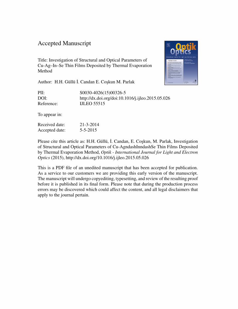
Accepted Manuscript Title: Investigation of Structural and Optical Parameters of Cu-Ag–In–Se Thin Films Deposited by Thermal Evaporation Method Author: H.H. G¨ ull¨ u ˙ I. Candan E. Cos ¸kun M. Parlak PII: S0030-4026(15)00326-5 DOI: http://dx.doi.org/doi:10.1016/j.ijleo.2015.05.026 Reference: IJLEO 55515 To appear in: Received date: 21-3-2014 Accepted date: 5-5-2015 Please cite this article as: H.H. G¨ ull¨ u, ˙ I. Candan, E. Cos ¸kun, M. Parlak, Investigation of Structural and Optical Parameters of Cu-AgndashInndashSe Thin Films Deposited by Thermal Evaporation Method, Optik - International Journal for Light and Electron Optics (2015), http://dx.doi.org/10.1016/j.ijleo.2015.05.026 This is a PDF file of an unedited manuscript that has been accepted for publication. As a service to our customers we are providing this early version of the manuscript. The manuscript will undergo copyediting, typesetting, and review of the resulting proof before it is published in its final form. Please note that during the production process errors may be discovered which could affect the content, and all legal disclaimers that apply to the journal pertain.
Transcript of Investigation of Structural and Optical Parameters of Cu-Ag–In–Se Thin Films Deposited by...
Accepted Manuscript
Title: Investigation of Structural and Optical Parameters ofCu-Ag–In–Se Thin Films Deposited by Thermal EvaporationMethod
Author: H.H. Gullu I. Candan E. Coskun M. Parlak
PII: S0030-4026(15)00326-5DOI: http://dx.doi.org/doi:10.1016/j.ijleo.2015.05.026Reference: IJLEO 55515
To appear in:
Received date: 21-3-2014Accepted date: 5-5-2015
Please cite this article as: H.H. Gullu, I. Candan, E. Coskun, M. Parlak, Investigationof Structural and Optical Parameters of Cu-AgndashInndashSe Thin Films Depositedby Thermal Evaporation Method, Optik - International Journal for Light and ElectronOptics (2015), http://dx.doi.org/10.1016/j.ijleo.2015.05.026
This is a PDF file of an unedited manuscript that has been accepted for publication.As a service to our customers we are providing this early version of the manuscript.The manuscript will undergo copyediting, typesetting, and review of the resulting proofbefore it is published in its final form. Please note that during the production processerrors may be discovered which could affect the content, and all legal disclaimers thatapply to the journal pertain.
Page 1 of 30
Accep
ted
Man
uscr
ipt
1
Investigation of Structural and Optical Parameters of Cu-Ag–In–Se Thin
Films Deposited by Thermal Evaporation Method
H.H. Güllü1,3, İ. Candan1,3, E. Coşkun1,2, M. Parlak1,3,*
1Department of Physics, Middle East Technical University (METU), 06800 Ankara, Turkey
2Department of Physics, Çanakkale Onsekiz Mart University, 17100 Çanakkale, Turkey
3Center for Solar Energy Research and Applications (GÜNAM), METU, Ankara 06800, Turkey
*Corresponding author: Tel: +90 312 2107646; Fax: +90 312 2105099
Email: [email protected]
Abstract
Annealing effect on the structural and optical properties of the quaternary Cu-Ag-In-Se thin film deposited by the thermal evaporation has been investigated. The evaporation source was prepared by using vertical Bridgman-Stockbarger crystal growth system. Structural analysis indicated that annealing the films following to the deposition resulted in the changes from amorphous to polycrystalline phase with the preferred orientation along (112) direction. In order to determine the optical properties of the thin films as a function of annealing temperature, the transmission measurements were carried out in between 300-2000 nm. The optical band gap values were lying in between 1.29 and 1.50 eV upon annealing the thin films in the temperature range of 300-500°C. The refractive indices of the samples were in the range of 2.7-3.8 depending on the wavelength region and annealing temperature by applying the envelope method. The other optical constants of the samples were also calculated using Cauchy Method and Single Oscillator Model.
Keywords: Thin film, chalcogenide, vapor deposition, X-ray diffraction, optical properties
Page 2 of 30
Accep
ted
Man
uscr
ipt
2
1. Introduction
One of the major research areas on thin film technology is the photovoltaic device
applications. It is the most promising one as a future energy technology. Since the thin film
technology provides fewer material uses, and simpler processing steps as compared to a
traditional wafer based crystalline solar cells. Thin films of a-Si, CdTe, Cu(In,Ga)Se2 and
related I-III-VI2 chalcopyrite compounds, have been of great interest for both the research and
commercial solar cell applications because of their many advantageous properties over the
bulk crystalline technologies. Mainly, their high absorption coefficients (> 104 cm-1) [1], only
a few microns of the material are needed to absorb the incident light, whereas in crystalline
silicon structure several microns are needed to obtain similar results. This leads to a decrease
in the constituent materials for the thin film devices, which results in lower costs. For this
purpose, recently, there has been a great deal of interest in the study of thin film growth
methods and characterization [2].
Polycrystalline thin film solar cells based on CuInSe2 (CIS) and AgInSe2 (AIS) ternary
chalcopyrite semiconductor compounds belong to a group of I-III-VI2 compounds are popular
in solar cell applications [3] and non-linear optical devices due to being stable and efficient
absorber material [4]. Family of these ternary chalcogenides is isoelectronic with the zinc-
blende II-VI compound semiconductors. By substituting two cations instead of one in a
regular zinc-blende type lattice, alternative series of bonds can be obtained which results in
differences with respect to the structural, electronic and optical properties. These chalcopyrite
semiconductors within the same family have direct band gap, and high absorption
coefficients, which make them popular in the device applications [5].
Studies on the quaternary compound, CuxAg1-xInSe2 (similarly Cu1-xAgxInSe2) (CAIS) films
as an absorber material for hetero-junction solar cells are a subject of interest since by
changing the composition of the constituent elements in the quaternary alloys, it enables to
the tuning of the material properties. Therefore, this quaternary alloy, which is the
combination of the ternary chalcopyrite compounds CIS and AIS, can give opportunity to
change the structural, optical and electrical characteristics of the material for the requirements
on usage. The optical band gap of these compounds for x = 0.5 is lying in the range of 1.05
eV - 1.24 eV [6, 7].
Page 3 of 30
Accep
ted
Man
uscr
ipt
3
In this work, we have studied on the structural and optical characteristics of thin films
deposited by using CAIS single crystal as an evaporation source. The characterization of the
thermally evaporated CAIS thin films were carried by means of X-ray diffraction and spectral
transmittance measurements. The post-annealing process was applied to the films under
nitrogen atmosphere, in order to see the effect of annealing process on the film properties. The
optical constants of the films were determined using Envelope and Cauchy Methods and
Single Oscillator Model.
2. Experimental Details
As an evaporation source for the thermal evaporation of the CAIS thin films, the CAIS crystal
was synthesized by mixing stoichiometric amount of high purity Cu, Ag, In and Se elements
(99.999% pure elements from Alfa-Aesar, US) which were in 0.5:0.5:1:2 molar ratio. These
elements were loaded into a chemically cleaned quartz crucible. Before sealing the quartz
ampoule, it was evacuated for 2 hours with Varian turbo pump to reach 10-5 Torr vacuum
level. Following to this process, the quartz ampule was placed in a specially designed vertical
Lindberg furnace. In order to satisfy homogeneity and also to start the initial chemical
reaction in the prepared mixture, the sealed quartz tube was heated slowly with the 100°C/hr
ramp rate up to 1050°C and kept at this temperature for 4 days, and by shaking frequently at
this temperature before starting the cooling. Then, the CAIS polycrystalline structure was
grown by using the Crystalox MSD-4000 model three-zone vertical Bridgman–Stockbarger.
The furnace was arranged so that the upper temperature zone was maintained about 1150 °C
which is over the melting point of the material to be grown, while the middle zone was kept
about 950°C and the lower zone was about 850°C. The temperature gradient was 10 K/cm and
the translation of the crucible was performed with 1.0 mm/h. Then, the cooling process was
done by the same rate as in heating treatment. Therefore, the crystal growth process in the
Bridgman-Stockbarger system was taken approximately 6 days. As a result of these processes,
the crystal extracted from the grown ingot was used as an evaporation source.
0ptically flat soda lime glasses were used as a substrate material for the thin film deposition.
Before starting to thermal deposition process, approximately 2 gr. crystal powder was
prepared as an evaporation source, and then placed into an alumina coated tungsten boat and
the substrate holder was placed about 15 cm above the source. During the deposition under
vacuum about 10-5 Torr, the substrate temperature was kept about 200°C and the deposition
Page 4 of 30
Accep
ted
Man
uscr
ipt
4
rate was around 4-5 Å/sec measured by Inficon XTM/2 deposition monitor connected to the
quartz crystal inside the vacuum chamber.
The annealing process was applied using annealing furnace under the nitrogen atmosphere in
the temperature range of 300-500°C for 30 minutes. Besides, the thickness of the as-grown
and annealed films was measured electromechanically by a Dektak 6M profilometer.
X-ray diffraction (XRD) measurements by using a Rigaku Miniflex XRD system equipped
with Cu Kα radiation source were used to obtain the structural properties of the deposited
CAIS thin films. Also, the peak matching analysis was made by using the computer software
and the database of international crystal diffraction (ICDD) cards. In order to complete the
structural analysis, the elemental atomic compositions of the samples were measured with an
energy dispersive X-ray analysis (EDXA) facility attached to the JSM-6400 scanning electron
microscope (SEM). Finally, the spectral transmittance measurements were carried out by
using Perkin-Elmer Lambda 950 UV/Vis/NIR spectrophotometer in the wavelength range of
300-2000 nm.
3. Results and Discussion
The compositions of the films obtained from EDX analysis showed that the films deposited
by thermal evaporation of CAIS single crystal powder are composed of Cu, Ag, In and Se
atoms. The atomic percentage of the constituent elements in the structure as a function of the
annealing temperatures was tabulated in Table 1. As seen from the table, the compositons of
both as-grown and annealed samples show Cu- and Ag- deficient; and In- and Se-rich
behavior. The different vapor pressures of the constituent elements result in the difficulty to
deposit the stoichometric thin film structure by thermal evaporation and may be responsible
for obtaining the off-stoichiometric CAIS thin films [6, 8]. Furthermore, it was found that
there was a remarkable change in atomic percentage of the constituent elements following to
the post-depositional annealing. As the annealing temperature increases, the decrease in the
atomic percentage of Se indicates the possible segregation and/or re-evaporation of Se atoms
from the film surface due to the high vapor pressure of selenium before making the bond with
the other elements [9].
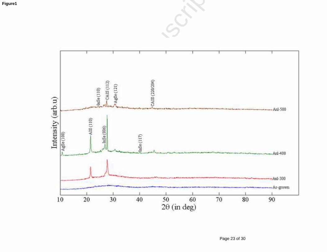
In order to analyze the diffraction patterns of the deposited thin films, XRD measurements
were carried out. As seen from Fig.1, the XRD measurements indicate that the CAIS thin
Page 5 of 30
Accep
ted
Man
uscr
ipt
5
films deposited at the substrate temperature of 200 oC have amorphous structure in the as-
grown form. Therefore, post-thermal heat treatment under different temperatures were applied
to provide the thermal energy to the constituent elements to complete thermal kinetics for the
nucleation stage in the thin film structure. Although, the phases included in powder source
were not transformed to the structure of thermally deposited CAIS films, the transformation
from the amorphous to the polycrystalline phase took place at the annealing temperature of
300 oC. The reasons of having an amorphous for as-grown film and the transformation to
polycrystalline phase in this temperature may be due to deposition of films at low substrate
temperature, 200 oC when compared to the previous studies [6, 11, 12], since the impinging
atoms can prefer placing at fixed positions due to the insufficient thermal energy to complete
the migration and nucleation stages during deposition [6]. On the other hand, the annealed
films showed the same structural behavior in the quaternary phase with Cu0.5Ag0.5InSe2 thin
films [6]. Despite CAIS diffraction peaks of the samples, there were extra diffraction peaks in
the XRD pattern of each thin film. XRD data of the samples were compared with the most
appropriate ICDD database to identify the structures of these diffraction peaks.
In the multi-phase CAIS films, the main orientation direction was obtained at about 26.3°
along (112) direction with tetragonal crystalline structure [6]. Actually, the growth CIS
usually leads to the films with the preferred (112) faceting [14]. The same behavior has been
observed for AIS films [15]. The reported structural parameters calculated from this
diffraction phase are a = 5.937 Å and c = 11.633 Å [6,7]. The tetragonal distortion (c/2a) for
these chalcopyrite materials was found approximately as 0.051. In the case of CAIS material,
replacing Cu atom with Ag, it was evaluated that there is a distortion to form the tetragonal
structure using these ternary compounds. The previous works about AgInSe2 indicated that
significant deviation from the stoichiometry of the film structure resulted in secondary phase
formation (Ag2Se and In2Se3) [18]. Under this study, these additional binary phases were also
observed in the annealed films. It is understood that the thin films consist of a mixture of
crystalline phases (quaternary, ternary and binary) of the constituent atoms (Cu, Ag, In, Se) of
powder source. Therefore, annealing at high temperatures modifies the film structure.
The average microcrystalline grain size D was estimated from the XRD pattern using the
Scherrer’s formula [19] expressed as;
cos0K
D (1)
Page 6 of 30
Accep
ted
Man
uscr
ipt
6
where K is structure factor equal to 0.94 [20], 0 is the wavelength of X-rays, is defined
as full width half maximum (FWHM) value, and is the diffraction angle. The grain sizes of
the thin films deposited by thermal evaporation were found 32, 40 and 26 nm with the
increasing annealing temperature from 300 to 500 °C. The increase in grain size can be taken
as the indication of improvement in crystallinity following to the annealing process.
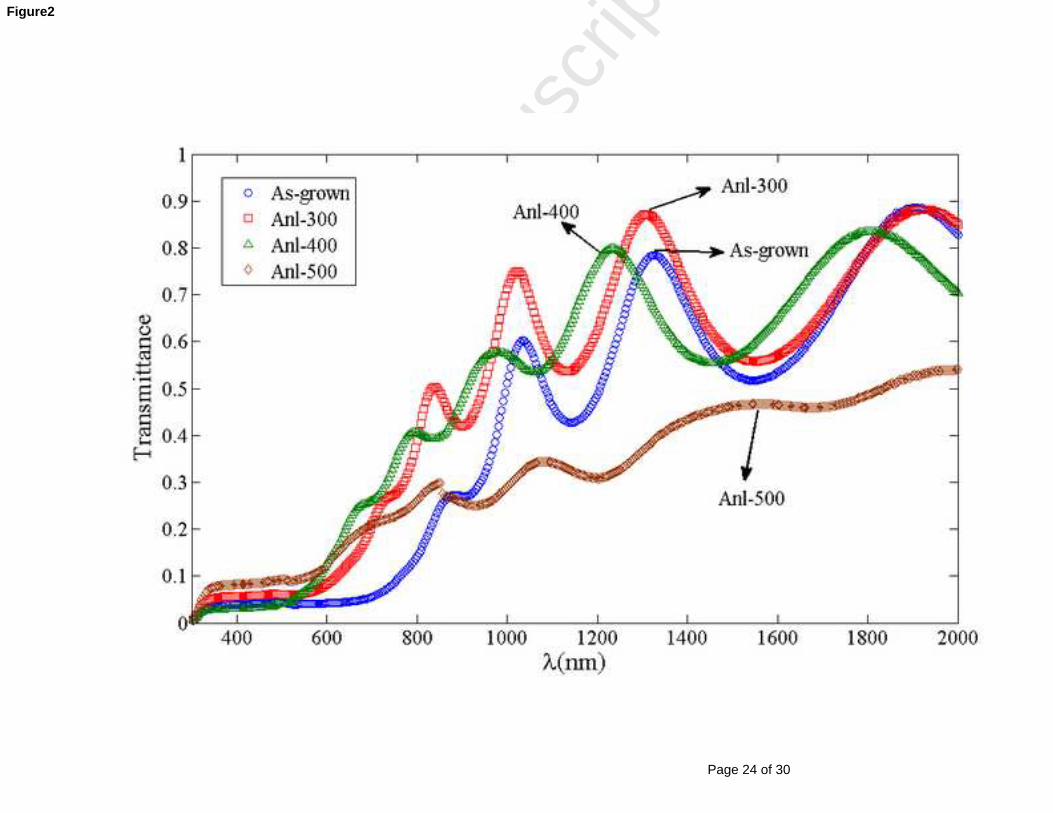
The optical characterization of the films was carried out by measuring the transmission of the
samples at room temperature in the wavelength range of 300-2000 nm. The wavelength
dependence of the transmission for all samples is shown in Fig.2. As seen from Fig.2, the
transmittance spectrum of the films shows interference fringes with a sharp fall at the band
edge in the region 800–2000 nm; whereas the interference effects disappear below this region.
This wavelength interval can be named as a strong absorption region for the films since the
transmission of the films decreases sharply with decreasing wavelength. Having uniform
sequential maxima and minima of the interference fringes at the transparent wavelength
region can be accepted as an indication of the optical homogeneity of the deposited films [21].
The optical transmission values of the as-grown films increased to about 90% in the
transparent region; and this increase depending on the increase in the wavelength was seen for
all the films. Although, the CAIS film annealed at 300 °C showed the same behavior with the
as-grown film, the film annealed at 400 and 500 °C had the different optical characteristics in
terms of their transmission spectra. Therefore, the systematic change between the films was
destroyed with the annealing at 400 °C. There was a wavelength shift in the transmission
spectrum of these samples and a remarkable decrease in the transmission of the 500 °C
annealed film. As observed from the XRD results, this decrease can be explained by the
structural modifications. In general, decrease in the transmittance of thin films is mainly
related with the surface morphology, the grain structure and the defect density [22]. In fact,
the composition of constituent elements, Cu, Ag and In in the film structure became more
effective with increasing annealing temperature, the segregation and/or re-evaporation of Se
in the film structure resulted in a Se deficiency as comparing with the as-deposited one;
therefore the surface may increase the construction of a pseudo-metallic surface forming a
more reflective surface [23].
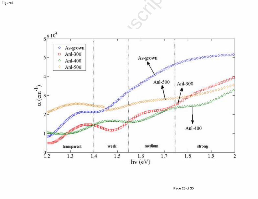
The absorption coefficient ( ) of the samples was calculated using the transmission values by
means of the relation;
Page 7 of 30
Accep
ted
Man
uscr
ipt
7
))(
1ln(
1)(
Td (2)
where )(T is the normalized transmittance and d thickness of the thin films. The absorption
spectrum of the samples can be divided into four principle regions named as strong, medium,
weak and transparent regions depending on the variation of absorption coefficient with
wavelength [24]. As seen from Fig.3, the absorption coefficient decreases with increasing
annealing temperature in the medium and weak absorption regions. The absorption
coefficients of these CAIS samples vary in between 5.0x10³ and 5.0x10⁴ (cm-1) depending on
the annealing temperature.
In order to determine optical constants, such as refractive index n(λ), Envelope Method (EM)
developed by Swanepoel [24] was used. In this method, maximum and minimum values of
the transmittance data in the interference patterns must be defined as a function of the
wavelength . However, other method based on the approach of Manifacier et al. [25] needs
creating an upper and lower envelope of the transmission spectrum beyond the absorption
edge. For all of the CAIS films, this method was used, except the film annealed at 500 °C
because of non-systematic fringe distribution.
According to EM, the complex refractive index can be written as,
)()()( inn (3)
where )(n is the real and )( is the imaginary part of the complex refractive index )(n
.
For the calculation of )(n in the weak and medium absorption regions, the transmittance
maximum, MT and minimum, mT values for each wavelength ( ) must be determined.
Therefore, the refractive index, )(n , can be expressed as,
2/12/120
22 ])([ nnNNn s (4)
where is N equal to;
Page 8 of 30
Accep
ted
Man
uscr
ipt
8
mM
mMs
s
TT
TTnn
nnN
0
220 2
2(5)
.
In Eq.4 and 5, 0n is the refractive index of the surrounding environment (air) which is equal
to 10 n , MT and mT are the maximum and minimum values of the envelope curves obtained
from transmittance, respectively; sn is the refractive index of the glass substrate which is
approximately equal to 1.51 over the wavelength range of 300 - 1100 nm; and it was
calculated from its transmission spectrum using the relation [26];
1
112
SSs
TTn (6)
here Ts is the maximum value of transmittance of )(T .
As a result of the EM analysis, the refractive index values were found to be in the range of
2.5-3.8 in the wavelength region 800-2000 nm. On the other hand, annealing temperature
higher than 400 °C affected the film structures adversely and their optical measurement
values were not appropriate to use EM, there was a huge difference observed in the refractive
index as compared with the samples annealed at 300 and 400 °C. However, there was an
increase in n(λ) values for the films annealed at these temperatures because of the increases in
the reflectivity due to the structural and compositional changes with annealing.
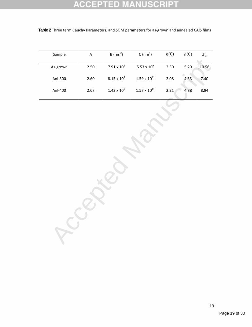
In order to make further analysis and to compare the refractive index of the samples, the
dispersion relation of the film in the visible region can be described by the Cauchy's relation
[27];
42)(
CB
An (7)
where A, B and C are Cauchy constants that depend on the optical characteristics of the film.
Fig.4 shows the theoretical fit of Eq.7 to the experimental values. The calculated values of the
Cauchy parameters were given in Table 2 for all samples.
Page 9 of 30
Accep
ted
Man
uscr
ipt
9
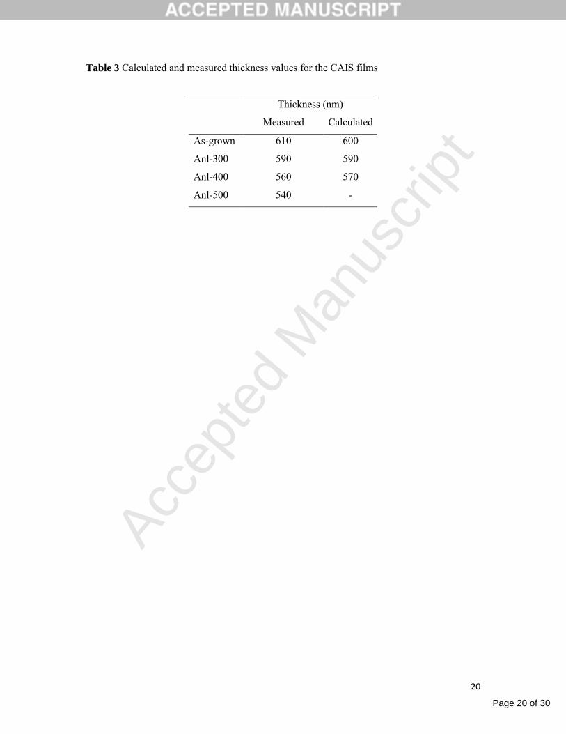
Considering the basic equation for interference fringes;
mnd 2 (8)
where m is an integer defined for maxima or minima, the refractive indices at two adjacent
)(T maxima (or minima) at wavelengths 1 and 2 , 1n and 2n can be used to calculate the
thickness of the sample by the equation as;
)nn(2d
1221
21
(9)
This equation is very sensitive to errors in n values [19]. The results of the thickness
calculations by using Eq.9 and measured by Dektak profilometer were given in Table 3. The
homogeneity in the thickness of each sample was checked by measuring it from the different
parts of the surface area with the profilometer. The calculated and measured thicknesses of the
films were found to be in a good agreement with each other in the corresponding about 10 nm
measurement error interval. According to these results, the thickness of the films decreased
with the increase in the annealing temperature. That can be taken as the indication of the
decrease in the amount of some constituent elements in the structure of the films. Moreover,
the sharp decrease in the thickness of 500 °C annealing may support the idea that there was a
segregation and re-evaporation of constituent elements by resulting in the structural
modification.
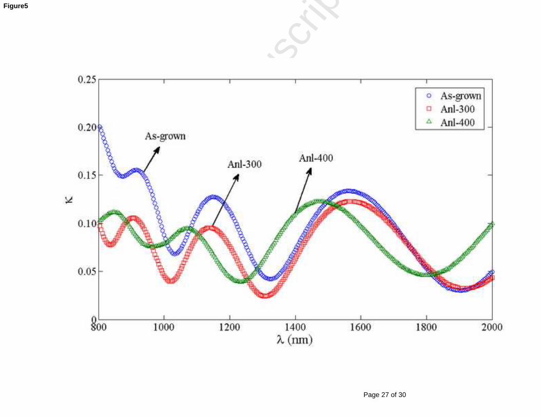
Furthermore, the imaginary part of the complex refractive index, )( extinction coefficient
of the films was evaluated by using the expression [28];
)(4
)( (10)
and the variations of the extinction coefficients with the wavelength for each annealing
temperature were plotted in Fig.5. As seen from the figure, the calculated values )( of the
as-grown and annealed CAIS films show the similar variations in the wavelength range of 800
- 2000 nm.
Page 10 of 30
Accep
ted
Man
uscr
ipt
10
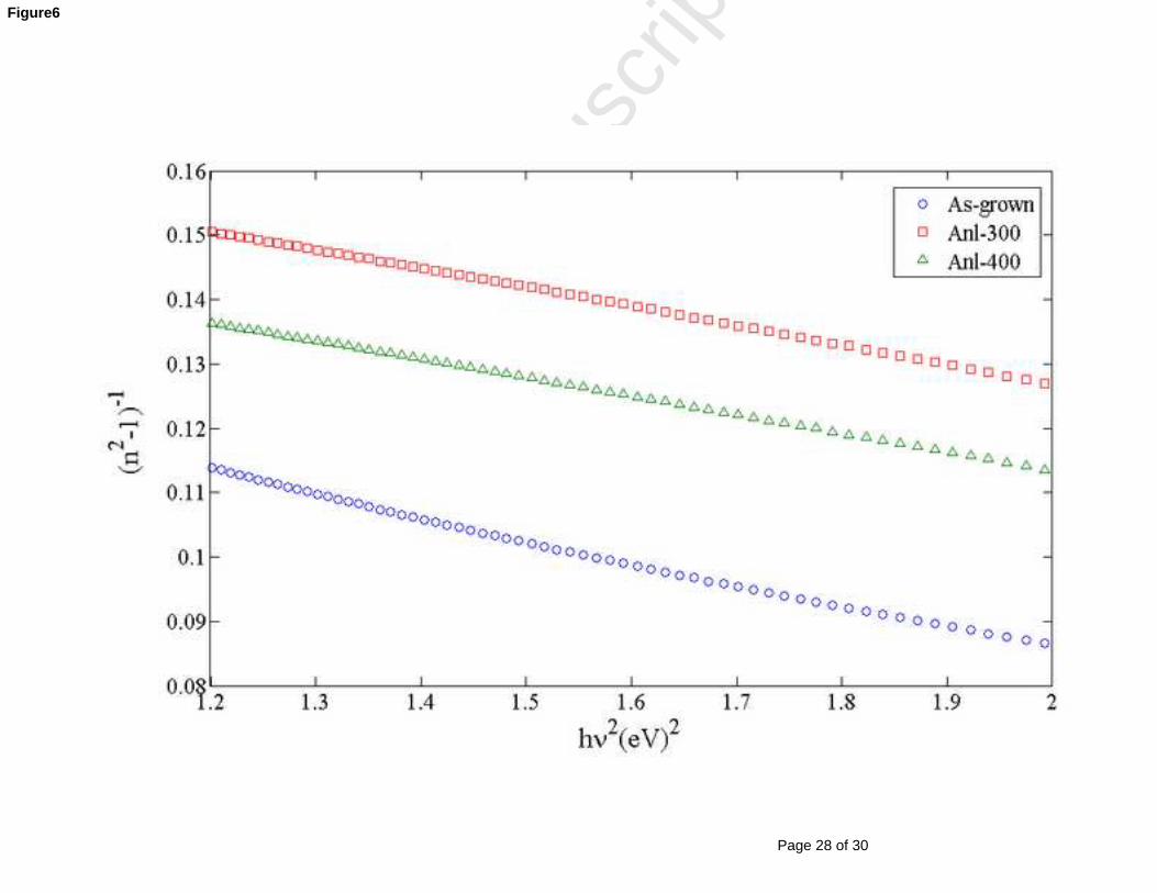
By the way, the dispersion of refractive index plays an important role in the optical properties
of thin film materials [29], and it was analyzed with the Single Oscillator Model (SOM) by
using the Wemple–Di Domenico relation [24, 25] as;
222 1)(
EE
EEEn
p
dp
(11)
where dE is related to the strength of the inter-band optical transitions, pE gives the average
energy gap also called oscillatory energy, and E is the photon energy in terms of h . The
SOM parameters, dE and pE were calculated from the [ 1)( 2 hn ] versus 2)( h plots for
as-grown and annealed films (see Fig.6), and the corresponding results were tabulated in
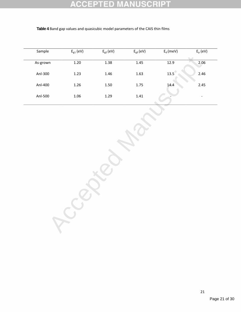
Table 4. By the analysis of dE values, it was defined that the strongest optical transition
probability is dominant for the samples annealed at 300 °C (see Table 4). In other words, the
optical properties of CAIS thin films strongly depend on the structural formations.
The obtained )(n values can be expressed in terms of the dielectric constant )( as [28];
2/12/1 ))()(())(()( imre in (12)
and by using Eq.3, the real and the imaginary part of the )( can be written as;
2)()( nre (13)
)(2)( im (14)
by the approximations of the calculated )( values which are very small as compared with
)(n values. The real part, )( re , was calculated by using Eq.13, and the result of this
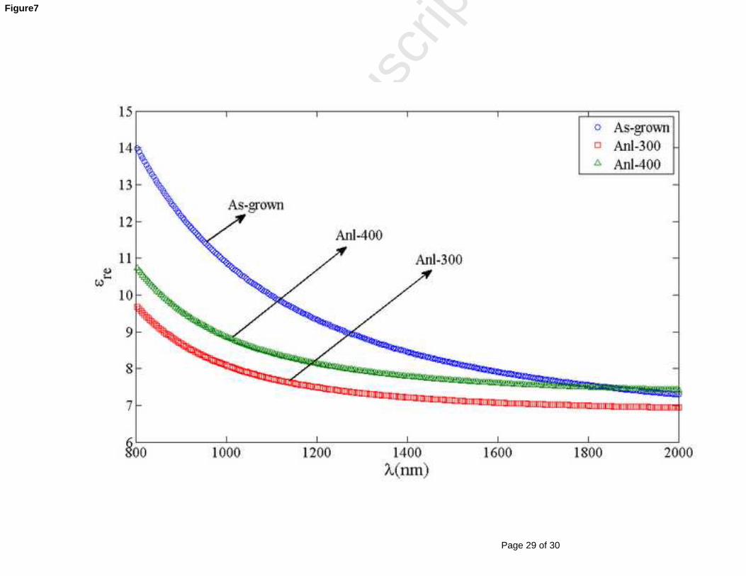
calculation with respect to wavelength is given in Fig.7.
By using SOM model, the refractive index )0(n at zero photon energy (static refractive
index) is also known as the infinite wavelength dielectric constant that can be deduced from
the dispersion relationship by extrapolation of the linear part of the plots given in Fig.6 [28].
Page 11 of 30
Accep
ted
Man
uscr
ipt
11
Moreover, the static dielectric constant )0( can be determined from the corresponding
intercept value. The high-frequency dielectric constant can be obtained from the )( re
values of the films [28]. This optical dielectric constant related to the square of the refractive
index observed for the smallest band gap value corresponds to the long-wavelength refractive
index of the material. Therefore, these values were deduced at the wavelength region below to
the minimum absorption edge. The calculated optical constants by using these approaches and
Fig.7, were summarized in Table 4. According to the Lyddane-Sache-Teller relation [30], it
was observed that the CAIS films have hetero-polar crystal structure.
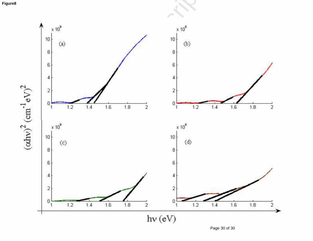
On the other hand, the plot of the optical absorption coefficient α versus photon energy
)( h showed principle regions as in the work of Wood and Tauc [31]. In the strong absorption
region, the absorption coefficient of a direct transition is related to the band gap energy and
can be expressed as;
2/1)()( gEhAh (15)
where A is an energy-independent constant and gE is the forbidden band gap energy.
Therefore, from the plot of 2)( h versus )( h (see Fig.8), the band gap values can be
defined by extrapolation of the straight line on the energy axis. Three distinct local maxima
were investigated in the high absorption region of the corresponding CAIS films. In other
words, these CAIS films have three intrinsic band-to-band transitions showing the splitting of
the valance band into three bands due to hybridization d-like valance band states and p-like
conduction band states [33]. This has been attributed [6, 15, 34] to the crystal-field splitting of
the valence bands and spin-orbit splitting. In compound semiconductors, the conduction band
minimum is mostly related with the cation (s-orbital), while anion p-orbital is corresponding
to the valence band maximum [35]. In I-III-VI2 compounds, usually s-orbital of III-group of
elements, In or Ga, contributes to the conduction band minimum while the Se 4p-orbitals
contribute to the valence band maximum [16]. However, the transition metals, Cu and Ag,
introduce d-orbital, which have an effect on the position of the valence band maximum. These
d-levels affect both the optical band gap and the separation of the spin-orbit splitting in the
valence bands. Calculated 2gE values can be accepted as the main band-to-band transition
because of having the longest linearity for the fundamental absorption edge. In literature, the
studies on the optical properties of CAIS films have shown that the compound has a direct
Page 12 of 30
Accep
ted
Man
uscr
ipt
12
optical band gap that ranges from 1.21 to 1.25 eV [7], and also due to being quaternary alloy
of CIS and AIS, it was also expected in between 1.05 and 1.24 eV. However, the contribution
of the elements, especially excess In, in the composition of the films depending on the
deposition method and annealing parameters may be the reason of high band gap values than
reported CAIS thin film studies.
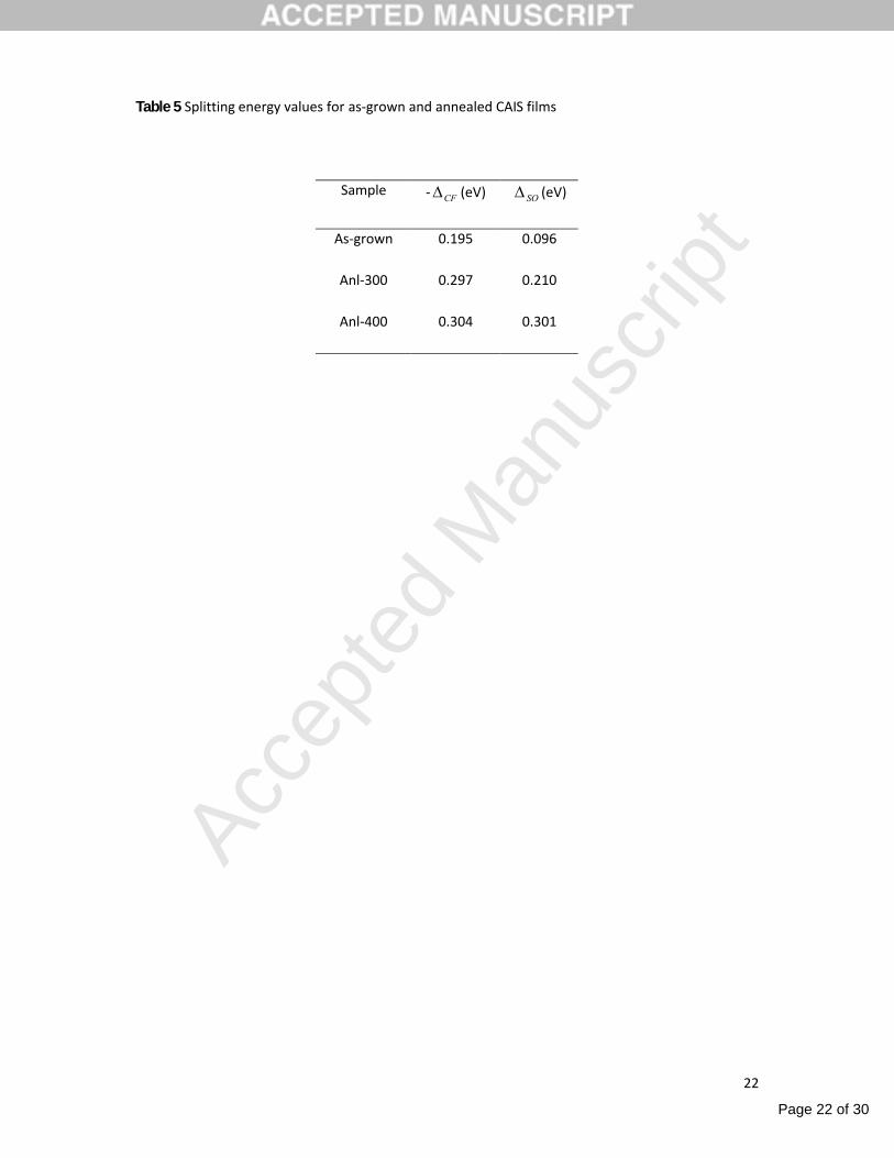
From the quasi-cubic model for the splitting of p-like levels in a nearly cubic crystals,
including both the effects of a non-cubic crystalline field and spin-orbit interaction, by using
the adapted form to chalcopyrite compounds [16, 36], we can calculate the spin orbit splitting
of the valence bands in a cubic field, SO and crystal-field splitting of the valence bands in
the absence of spin-orbit interaction, CF from the three-fold optical band gap by using the
following expression;
2/1
22,1 )(
3
8)(
2
1)(
2
1
SOCFSOCFSOCFE (16)
where 2,1E are the energy differences in the form, 121 gg EEE and 232 gg EEE . The
corresponding splitting energies are related to the energies of the Г7 relative to the Г6 level in
the valence band of a chalcopyrite crystal [16]. The calculated values using Eq.16 were listed
in Table 5. It was observed that there was an increase in both SO and CF values with
increasing annealing temperature up to 400 °C. This can be related with structural changes
and modifications by post-thermal heat treatments as observed from the structural analysis. In
this quaternary compound, CAIS films with the chalcopyrite structure, the crystal field-
splitting can be related to the tetragonal distortion along the c-axis [16];
)2(2
3a
cbCF (17)
where b is the deformation potential. From the tetragonal distortion value calculated for the
main orientation of the CAIS structure, CF was calculated as in between -0.26 and -0.40 eV.
Page 13 of 30
Accep
ted
Man
uscr
ipt
13
4. Conclusion
In this work, detail structural and optical characteristics of the thermally evaporated and
annealed CAIS thin films were studied. According to the structural and the compositional
analyses carried out on the as-grown and annealed films, there was In-rich, Cu and Ag-
deficient structure as compared with the evaporation powder. These results imply that the
different vapor pressures of the constituent elements result in the difficulty to deposit the
stoichometric thin film structure by thermal evaporation of the sintered ternary powder and
may be responsible for obtaining the off-stoichiometric CAIS thin films. The XRD results
showed that the deposited CAIS samples are amorphous in nature and it transforms to the
polycrystalline phase as a result of annealing processes. Also, the resulting polycrystalline
phase is composed of the mixture of different crystalline phases. The room temperature
optical measurements were performed on the as-grown and annealed samples, and their
analyses by using the EM, Cauchy fitting and SOM allowed us to calculate and compare the
optical constants, n , and . The evaluated values were consistent and found to be in good
agreement with each other. The band gap energies obtained from the absorption spectrums of
the CAIS films were 1.38, 1.46, 1.50, 1.29 eV for the as-grown and annealed films at 300,
400 and 500 °C, respectively. The changes in these values imply the improvement in the
crystallinity upto the annealing at 400 oC, whereas further annealing above this value resulted
in the deformation in the structure by increasing the defect levels in the band edge region. The
distinct intrinsic transitions obtained from the variation of the absorption values with photon
energies are indicating the existence of the valence band splitting. As explained and
discussed, the variations in the structural and optical properties of the films were related with
the compositional changes initiated with the deposition and annealing processes.
Acknowledgement
This work was financed by Middle East Technical University (METU-BAP) under Grant No.
BAP-01-05-2013-005. Also, one of the authors would like to thank to TUBITAK-BIDEB for
the financial supports during this study.
Page 14 of 30
Accep
ted
Man
uscr
ipt
14
References
[1] N. Kavcar, Sol. Energ Mat. Sol. C., 52 (1998) 183-195
[2] K.L. Chopra, S.R. Das, Thin Film Solar Cells, Plenum Press, New York, 1983
[3] K.L. Chopra, K.L. Paulson, V. Dutta, Prog. Photovolt. 12 (2004) 69–92
[4] R. Asokamani, R.M. Amirthakumari, R. Rita, C. Ravi, Phys. Stat. Sol. (b) 213 (1999) 349
[5] J.L. Shay, B. Tell, H.M. Kasper, M.M. Schiavone, Phys. Rev. B 7 (1973) 10
[6] G.V. Rao, G.H. Chandra, O.M. Hussain, S. Uthana, B.S. Nadiu, J. Alloys Compd. 325
(2001) 12-17
[7] G.V. Rao, G.H. Chandra, P.S. Reddy, O.M. Hussain, K.T.R. Reddy, S. Uthana, Surf.
Instrum. and Vac. Technol. 67 (2002) 293-298
[8] C.M. Joseph, C.S. Menon, Semicond. Sci. Technol. 11 (1996) 1668
[9] A. Roth, Vacuum Technology, North Holland, Amsterdam, 1980
[10] R. Bacewicz, J.R. Durrant, T.F. Ciszek, S.K. Deb, Ternary and Multinary Compounds:
Proceedings of the 7th International Conference (1987) 155-160
[11] G.V. Rao, G.H. Chandra, P.S. Reddy, O.M. Hussain, K.T.R. Reddy, S. Uthana, J.
Optoelect. and Adv. Mat. 4 (2002) 387-392
[12] G.V. Rao, G.H. Chandra, O.M. Hussain, S. Uthana, B.S. Naidu, Cryst. Res. Technol. 36
(2000) 571–576
[13] H.V. Campe, Thin Solid Films 111 (1984) 17
[14] D. Liao, A. Rockett, J. Appl. Phys. 91 (2002) 1978
[15] P.P. Ramesh, S. Uthanna, B.S. Naidu, P.J. Reddy, J. Mater. Sci. Lett. 15 (1996) 116-119
[16] J.L. Shay, J.H. Wernick, Ternary Chalcopyrite Semiconductors: Growth, Electronic
Properties and Applications, Pergamon, Oxford, 1975
[17] L.I. Berger, Semiconductor Materials, CRC Press, New York, 1997
[18] I. Olekseyuk, O. Krykhovets, J. Alloys Compd. 316 (2001) 193-202
[19] E.F. Kaelble, Handbook of X-Rays, McGraw-Hill Inc., USA, 1967
[20] J.I. Langford, A.J.C. Willson, J. Appl. Cryst. 11 (1978) 102-113
[21] N. Khemiri, A. Sinaoui, M. Kanzari, Physica B 406 (2011) 1778-1783
[22] N. Revathi, P. Prathap, Y.P.V. Subbaiah, K. T. Ramakrishna Reddy, J. Phys. D 41 (2008)
155404
[23] H. Karaağaç, M. Kaleli, M. Parlak, J. Phys. D: Appl. Phys. 42 (2009) 165413
[24] R. Swanepoel, J. Phys. E 16 (1983) 1214
[25] J.C. Manifacier, J. Gasiot, J.P. Fillard, J. Phys. E 9 (1976) 1002
Page 15 of 30
Accep
ted
Man
uscr
ipt
15
[26] G.K.L. Goh, C.P.K. Liew, J. Kim, T.J. White, J. Cryst. Growth 291 (2006) 94
[27] M. Fox, Optical Properties of Solids, Oxford University Press, London, 2001
[28] S. Adachi, Optical Properties of Crystalline and Amorphous Semiconductors, Kluwer
Academic Publishers, Boston/Dordrecht/London, 1999
[29] A.F. Qasrawi, Opt. Mater. 29 (2007) 1751-1755
[30] A.J. Sievers, J.B. Page, Phys. Rev. B 41 (1990) 3455
[31] D.J. Wood, J. Tauc, Phys. Rev. B 5 (1972) 3144-3151
[32] E.A. Davis, N.F. Mott, Philos. Mag. 22 (1970) 903
[33] F. Habashi, Chalcopyrite: Its Chemistry and Metallurgy, McGraw-Hill, USA, 1978
[34] J. Shay, B. Tell, H. Kasper, L. Schiavone, Phys. Rev. B 7 (1973) 4485–4490
[35] M.S. Al-Kotb, W. Puff, S.A. Hassan, M. Mohsen, Mater. Sci. Forum 363-365 (2001)
150-152
[36] J.E. Rowe, J.L. Shay, Phys. Rev. B 3 (1971) 451
[37] L.L. Kazmerski, Polycrystalline and Amorphous Thin Films and Devices, Academic
Press, London, 1980
Page 16 of 30
Accep
ted
Man
uscr
ipt
16
List of Tables
Table 1 EDXA results of CAIS thin films at atomic percentage
Table 2 Three term Cauchy Parameters, and SOM parameters for as-grown and annealed
CAIS films
Table 3 Calculated and measured thickness values for the CAIS films
Table 4 Band gap values and quasicubic model parameters of the CAIS thin films
Table 5 Splitting energy values for as-grown and annealed CAIS films
Page 17 of 30
Accep
ted
Man
uscr
ipt
17
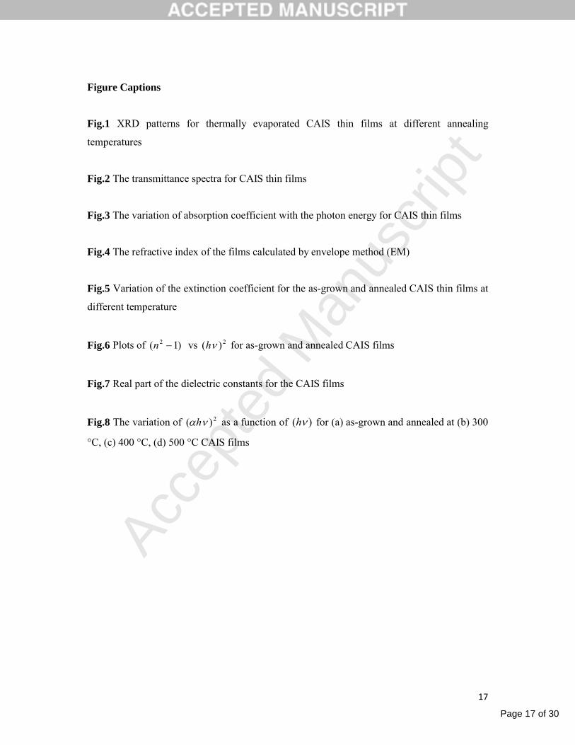
Figure Captions
Fig.1 XRD patterns for thermally evaporated CAIS thin films at different annealing
temperatures
Fig.2 The transmittance spectra for CAIS thin films
Fig.3 The variation of absorption coefficient with the photon energy for CAIS thin films
Fig.4 The refractive index of the films calculated by envelope method (EM)
Fig.5 Variation of the extinction coefficient for the as-grown and annealed CAIS thin films at
different temperature
Fig.6 Plots of )1( 2 n vs 2)( h for as-grown and annealed CAIS films
Fig.7 Real part of the dielectric constants for the CAIS films
Fig.8 The variation of 2)( h as a function of )( h for (a) as-grown and annealed at (b) 300
°C, (c) 400 °C, (d) 500 °C CAIS films
Page 18 of 30
Accep
ted
Man
uscr
ipt
18
Table 1 EDXA results of CAIS thin films at atomic percentage
Sample Cu (at %) Ag (at %) In (at %) Se (at %)
As-grown 0.86 1.86 42.20 55.08
Anl-300 1.14 1.76 43.39 53.71
Anl-400 1.76 1.58 43.49 53.17
Anl-500 1.77 2.47 43.77 52.04
Page 19 of 30
Accep
ted
Man
uscr
ipt
19
Table 2 Three term Cauchy Parameters, and SOM parameters for as-grown and annealed CAIS films
Sample A B (nm2) C (nm4) )0(n )0(
As-grown 2.50 7.91 x 10⁵ 5.53 x 10⁹ 2.30 5.29 10.56
Anl-300 2.60 8.15 x 10⁴ 1.59 x 10¹¹ 2.08 4.33 7.40
Anl-400 2.68 1.42 x 10⁵ 1.57 x 10¹¹ 2.21 4.88 8.94
Page 20 of 30
Accep
ted
Man
uscr
ipt
20
Table 3 Calculated and measured thickness values for the CAIS films
Thickness (nm)
Measured Calculated
As-grown 610 600
Anl-300 590 590
Anl-400 560 570
Anl-500 540 -
Page 21 of 30
Accep
ted
Man
uscr
ipt
21
Table 4 Band gap values and quasicubic model parameters of the CAIS thin films
Sample Eg1 (eV) Eg2 (eV) Eg3 (eV) Ed (meV) Ep (eV)
As-grown 1.20 1.38 1.45 12.9 2.06
Anl-300 1.23 1.46 1.63 13.5 2.46
Anl-400 1.26 1.50 1.75 14.4 2.45
Anl-500 1.06 1.29 1.41 - -
Page 22 of 30
Accep
ted
Man
uscr
ipt
22
Table 5 Splitting energy values for as-grown and annealed CAIS films
Sample - CF (eV) SO (eV)
As-grown 0.195 0.096
Anl-300 0.297 0.210
Anl-400 0.304 0.301
Page 23 of 30
Accep
ted
Man
uscr
ipt
Figure1
Page 24 of 30
Accep
ted
Man
uscr
ipt
Figure2
Page 25 of 30
Accep
ted
Man
uscr
ipt
Figure3
Page 26 of 30
Accep
ted
Man
uscr
ipt
Figure4
Page 27 of 30
Accep
ted
Man
uscr
ipt
Figure5
Page 28 of 30
Accep
ted
Man
uscr
ipt
Figure6
Page 29 of 30
Accep
ted
Man
uscr
ipt
Figure7
Page 30 of 30
Accep
ted
Man
uscr
ipt
Figure8