Introduction to Quantum mechanics and Solid State Physics
22
Problems in Solid State Physics for Electrical and Chemical Engineers A. S´ olyom Dept. Atomic Physics Faculty of Natural Sciences Budapest University of Technology and Economics - BME April 10, 2020
-
Upload
khangminh22 -
Category
Documents
-
view
1 -
download
0
Transcript of Introduction to Quantum mechanics and Solid State Physics

Problems in Solid State Physics for Electrical andChemical Engineers
A. SolyomDept. Atomic Physics
Faculty of Natural SciencesBudapest University of Technology and Economics - BME
April 10, 2020

Contents
1 Formulas used in the solutions 21.1 Solid State Physics . . . . . . . . . . . . . . . . . . . . . . . . . . . . . . 2
I

The problems presented here together with their solutions help the deeper under-standing of the lectures. Similar problems may be given in the tests. We tried to give avery detailed solution for every one of them, however in the tests you need not give somuch details. This material will be refreshed from time to time, so please check the dateon the title page!

Chapter 1
Formulas used in the solutions
1.1 Solid State Physics
Reciprocal LatticeThere exists an algebraic formula between the b1, b2, b3 primitive reciprocal latticevectors and the three primitive direct lattice vectors a1, a2, a3
b1 = 2πa2 × a3
a1 · (a2 × a3)
b2 = 2πa3 × a1
a1 · (a2 × a3)
b3 = 2πa1 × a2
a1 · (a2 × a3)
(1.1.1)
Effective MassThe effective masses of electrons and holes in Si and Ge are in Table 1.1. Thefcolorboxgrayblue!30effective mass for conductivity of electrons mcc is what we must usefor mobility or diffusion constant calculations. For cubic isotropic semiconductors withanisotropic dispersion relations minima (again e.g. Si and Ge), one has to sum over theeffective masses in the different minima along the equivalent directions. The resultingeffective mass for bands which have ellipsoidal constant energy surfaces is given by:
mcc =3
1
ml
+1
ml
+1
mt
2

electronsrel. eff.mass Si Ge
longitudinal ml/me 0.98 1.59transverse mt/me 0.19 0.0815dens.of.states mc/me 0.36 0.22conduct. mcc/me 0.26 0.12
holesrel. eff.mass Si Ge
heavy mh/me 0.49 0.33light mlp/me 0.16 0.043split-off band mso/me 0.24 0.084dens.of.states mv/me 0.81 0.34
Table 1.1: Effective masses in Si and Ge
Density of State Factors in Semiconductors
Nc(T ) = 2.5 1019
(mc
me
) 32(
T
300K
) 32
(1.1.2)
Pv(T ) = 2.5 1019
(mh
me
) 32(
T
300K
) 32
(1.1.3)
Primitive Vectors for the bcc lattice
Figure 1.1: Two different primitive vector sets for the bcc lattice.a) a1 = aex, a2 = aey, a3 = aez
b) a1 =a
2(ey + ez − ex), a2 =
a
2(ez + ex − ey), a3 =
a
2(ex + ey − ez)
drift velocity :
vdrift = µE (1.1.4)
3

where the constant of proportionality is thefcolorboxgrayblue!30mobility µ of the electrons
µ =
(eτ
me
)(1.1.5)
Conductivity vs. Relaxation Time
j(= σE) =
(ne2τ
me
)E
and
σ =ne2τ
me
(1.1.6)
One way to determine the value of τ is from (1.1.6), where the density n of conductionelectrons is
n = LAZρmA
(1.1.7)
Current Density in Semiconductors
j = e(nc µe + pv µh)E (1.1.8)
j = nie〈v〉 = nie(µe + µh)E and
j = σE
σ = nie(µe + µh) (1.1.9)
Fermi Energies
Metal| Li Na K Rb Cs Cu Ag Au Mg AlEF (eV )| 4.7 3.1 2.1 1.8 1.5 4.1 5.5 5.5 7.3 11,9
Table 1.2: Fermi energies of some metals
Any of these energy states can be occupied by 2 electrons with opposite spins. Ifeach atom contribute s conduction electrons to the crystal then at T = 0K all possibleenergy states below
EF (= Emax,occupied) =~2π2
2mea2s
2(1.1.10)
4
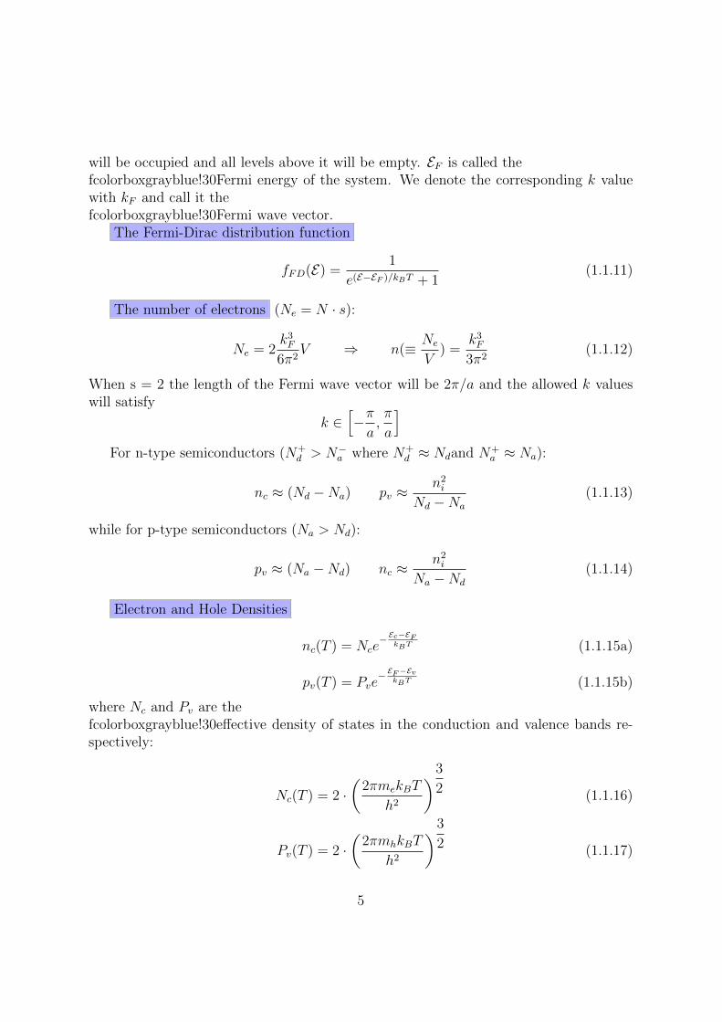
will be occupied and all levels above it will be empty. EF is called thefcolorboxgrayblue!30Fermi energy of the system. We denote the corresponding k valuewith kF and call it thefcolorboxgrayblue!30Fermi wave vector.
The Fermi-Dirac distribution function
fFD(E) =1
e(E−EF )/kBT + 1(1.1.11)
The number of electrons (Ne = N · s):
Ne = 2k3F6π2
V ⇒ n(≡ Ne
V) =
k3F3π2
(1.1.12)
When s = 2 the length of the Fermi wave vector will be 2π/a and the allowed k valueswill satisfy
k ∈[−πa,π
a
]For n-type semiconductors (N+
d > N−a where N+d ≈ Ndand N+
a ≈ Na):
nc ≈ (Nd −Na) pv ≈n2i
Nd −Na
(1.1.13)
while for p-type semiconductors (Na > Nd):
pv ≈ (Na −Nd) nc ≈n2i
Na −Nd
(1.1.14)
Electron and Hole Densities
nc(T ) = Nce−Ec−EF
kBT (1.1.15a)
pv(T ) = Pve−EF−Ev
kBT (1.1.15b)
where Nc and Pv are thefcolorboxgrayblue!30effective density of states in the conduction and valence bands re-spectively:
Nc(T ) = 2 ·(
2πmekBT
h2
)3
2 (1.1.16)
Pv(T ) = 2 ·(
2πmhkBT
h2
)3
2 (1.1.17)
5

In doped semiconductors:
n(d)c (T ) = ni e
−E(d)F−EF
kBT for an n-type semiconductor (1.1.18a)
p(a)v (T ) = ni e−EF−E
(a)F
kBT for a p-type semiconductor (1.1.18b)
Extents of the Depletion Rangion
dn =
√Na
Nd(Nd +Na)
ε∆ϕ
2 e
dp =
√Nd
Na(Nd +Na)
ε∆ϕ
2 e
(1.1.19)
E (d)F =1
2(Ec + Edonor) +
3
4kBT ln
(mh
mc
)(1.1.20a)
E (a)F =1
2(Ev + Eacceptor) +
3
4kBT ln
(mh
mc
)(1.1.20b)
Donor and Acceptor levels
acceptor in B Al Ga In TeSi 0.046 0.057 0.065 0.16 0.26Ge 0.01 0.01 0.061 0.011 0.01
donor in P As Sb BiSi 0.046 0.057 0.065 0.16 .Ge 0.01 0.01 0.061 0.011 .
Table 1.3: Shallow donor and acceptor levels in Si and Ge in eV.
Built-In Potential
e∆ϕ = kBT ln
(NdNa
n2i (T )
)(1.1.21)
Mass-Action in Doped Semiconductors
For intrinsic semiconductors
nc(T ) = pv(T ) (1.1.22)
6

ni ≡ nc(T ) = pv(T ) =√Nc(T )Pv(T ) e
− Eg2kBT (1.1.23)
built-in potential
∆ϕ =1
ekBT ln
(NdNa
n2i
)(1.1.24)
Curie-Weiss law
M =C
T − λCB (1.1.25)
χ =C
T − λC=
C
T − Tc(1.1.26)
Material Tc (K)
Co 1388Fe 1043MnBi 630Ni 627MnSb 587CrO2 386MnAs 318Gd 292Dy 88EuO 69
Table 1.4: Courier temperatures of some crystalline materials(Source:Wikipedia)
7

Problem 1.An infinite number of points are aligned along a line so that the distance between
the n-th and (n + 1)-th points is dn = 7.8 [(n mod 2) · 0.21 + (1 − n mod 2) · 0.17] nm,where a mod b is the remainder of the integer division a/b. May these points describea one dimensional linear “crystal” and if they do then what do the neighboring pointscorrespond to or if they do not then why not?
Solution:If n is an even number then n mod 2 is 0, if it is an odd number then it is 1. From the
definition above the distances between consecutive points are d1 = 7, 8 · 1.7 = 1.33nmwhen n is even and d2 = 7.8 ·2.1 = 1.64nm when n is odd. These distances are repeated,which means this structure has a translational symmetry, i.e. it may correspond to acrystal. These points may refer to atoms in a diatomic crystal with a two atom basisand a base vector of d1 + d2 = 2.97nm
Problem 2.What are the coordination numbers for an sc, a bcc and an fcc lattice?
Solution:To calculate the coordination number you may select any lattice point. We select the
ones easiest to calculate the coordinates for.
• sc - 6, because any corner point has 2 nearest neighbors in all 3 orthogonal planesthat go through it
• fcc - 12, because any corner point has 4 nearest neighbors in all 3 orthogonal planesthat go through it
• bcc - 8, because the center point has 8 neighbors
Problem 3.Calculate the surface density of atoms in a bcc crystal with lattice constant a =
0.5nm (= 5 ), if the surface plane cuts the cells diagonally so that it is perpendicular tothe plane of the a1 and a2 vectors1.
Solution:
1i.e. it is a (110) plane - see Miller indices below
8

The plane in question goes through 4 corner atoms and the middle atom of the cell.Only 1/4th of each of the cross sections of the corner atoms belong to our cell, while thecross section of the middle atom is completely inside it. Therefore the number of atomson this plane is 2. The area of the plane is a · a
√2 , so the density of atoms is
2
a2√
2=
√2
(0.5 10−9)2= 5.66 1018atoms
m2
Problem 4.Enumerate the symmetries the following “crystal” has.
Solution:
This “crystal” has the following symmetry elements:
• 1 - 4-fold rotation axis (A4)
• 4 - 2-fold rotation axes (A2), 2 cutting the faces and 2 cutting the edges
• 5 mirror planes (m), 2 cutting across the faces, 2 cutting through theedges, and one cutting horizontally through the center.
9

• There is a center of symmetry (i) in the center of the prism (not shown).
Problem 5.Is the hexagonal lattice in Fig.?? a Bravais lattice? Why? If it is not then create the
equivalent Bravais lattice from it!Solution:
The hexagonal lattice in Fig.?? is not a Bravais lattice, because the orientation ofthe surrounding points is different when viewed from points P and Q.
Select PQ and the equivalent other point pairs as a basis and select the points at themiddle of these pairs as points of the point lattice. In the unnumbered Figure the bluelattice points form a Bravais lattice.
Problem 6.Prove that the reciprocal lattice of an fcc lattice is a bcc lattice!
Solution:Start with the following selection of primitive fcc lattice vectors:
Then the 3 primitive vectors in (1.1.1) are
a1 =a
2(i + k)
a2 =a
2(i + j)
a3 =a
2(j + k)
(1.1.27)
10

Determine first the denominator in (1.1.1), which is the volume of the primitive cell:
a1 · (a2 × a3) =a
2(i + k) ·
(a2
(i + j)× a
2(j + k)
)=a3
8(i + k) · ((i + j)× (j + k))
=a3
8[i · (i× j) + i · (i× k)
+ i · (j× k) + k · (i× j)
+ k · (i× k) + k · (j× k)]
=a3
8(i · (j× k) + k · (i× j))
here we used that i, j and k are perpendicular to each other. Furthermore
i× j = k, j× k = i and k× i = j
Therefore
a1 · (a2 × a3) =a3
4
Now work with the numerators using the same formulas for i, j and k:
a2 × a3 =a2
4(k− j + i)a3 × a1 =
a2
4(i− k + j)a1 × a2 =
a2
4(j− i + k)
Which gives us the reciprocal base vectors:
b1 =2π
a(k− j + i)
b2 =2π
a(i− k + j)
b3 =2π
a(j− i + k)
(1.1.28)
Compare (1.1.28) with vectors in Fig. 1.1 to see that we, in fact got the primitive vectorsof a bcc lattice. The only difference is that the length is now. 2π
a.
Because the reciprocal lattice of a reciprocal lattice is the original (direct) lattice, wealso proved that the reciprocal lattice of a bcc lattice is an fcc lattice.
Problem 7.Determine the Miller indexes for the plane on the figure!
11

Solution:The intersections with the three axes are at 4 a1, 3 a2 and 2 a3. Then the inverse
intercepts in lattice vector units are:
1
4,1
3,1
2
To get integer numbers we have to calculate the lowest common denominator (smallestcommon multiple) of this fraction, which is 12. Multiplying each fraction with 12 givesthe three Miller indexes: (346)
Problem 8.In the previous example let the length of all the three base vectors of the direct lattice
to be a = 5 nm. Determine the distance of lattice planes (346).Solution:
The three basis vectors are of the same length and they are perpendicular to eachother. Therefore the same is true for the reciprocal base vectors. By substitution into
(1.1.1) this length is b =2 π
a= 1.26nm−1. The length of the reciprocal vector perpen-
dicular to the (346) planes is
|g346| =√
32 + 42 + 62 · 2π
a=√
61 · 2π
a(=√
61 · 1.26 = 9.81nm−1)
The distance of the planes (346) therefore is
d346 =2π
|g346|=
a√61
= 0.64nm
12

Problem 9.The 3 base vectors of a crystal are orthogonal and 2.3, 3.4 and 4.5 nm long. What is
the distance of lattice planes (211)?Solution:
The distance can be calculated from (??):
d211 =1√
22/2.32 + 1/3.42 + 1/4.62= 1.060nm (1.1.29)
Problem 10.Draw all 9 lattice planes and determine the Miller indexes in a simple cubic Bravais
lattice.Solution:
(Where is the origin of the 3 lattice vectors in the cubes?)Problem 11.Determine the possible diffraction angles for an X-ray of 10 keV from the (111) planes
of a simple cubic lattice, if the lattice constant is a = 5.3 A.Solution:
Calculate the wavelength of the X-ray:
E = h ν =h c
λ⇒ λ =
h c
E= 1.24 10−10m
13

To apply Bragg’s law we need to calculate the distance of the lattice planes of Millerindices (111), which are planes going through 3 non adjacent corner of the cube. Thedistance of two such planes that intersects a primitive cell (see the figure in the previousexample) is 3rd of the body diagonal:
d =1
3
√3 a = 0.305nm
The possible diffraction angles are determined by:
2 d sinθ = nλ
sinθ = nλ
2 d= 0.20325n
because |sin x| ≤ 1 n = 1, 2, 3, 4, i.e. the angles are
11.73o, 23.99o, 37.57o, and 54.39o
Problem 12.Aluminum has three valence electrons per atom, an atomic weight of 0.02698 kg/mol,
a density of 2700kg/m3, and a conductivity of 3.54 107 S/m. Calculate the electronmobility in aluminum. Assume that all three valence electrons of each atoms are free.
Solution:The number of aluminum atoms per m3 is
na = 6.021023 atoms/mol · 1/0.02698 mol/kg · 2700 kg/m3
= 6.024 1028 atoms/m3
Thus the electron density in aluminum is
n = 3 · 6.024 1028 atoms/m3 = 1.807 1029 electron/m3
From (1.1.5)
µ =σ
ne=
3.54 107
1.807 1029 · 1.6022 10−19= 1.22 10−3m/s
Problem 13.What is the value of τ in silver at t = 0 oC if the measured resistivity is 1.51·10−8 Ωm?
Solution:From (1.1.6), (1.1.7) using the definition of ρ
τ =me
ρ(T )n e2=
meA
LA Z ρm e2 ρ
14

Silver has a single 5s1 electron so Z = 1 and the mass density is ρm = 10.49 g/cm3 =1.049 · 104 kg/m3, A = 107.8682 g/mol = 0.1078682 kg/mol and ρ(273K) = 1.51 ·10−8 Ωm. After substitution
τ = 4.013 · 10−14 s
Problem 14.What is the quasi-free electron density in copper? Calculate the Fermi velocity and
momentum tooSolution:
From Table 1.2 and formulas (1.1.12) and (1.1.10)
ncopper =(2me EF )3/2
3π2 ~3= 3.77 1028 electron
m3
vF = 1.2 106m/s = 0.004 c kF = 1.0 10111/m
Problem 15.Let the dispersion relations of electrons in the valence and conduction bands near the
band edges are approximated by the following functions:
Ev(k) = −3.024 10−20 eV m2 · (k − 2.45108 1
m)2 + 13 eV
Ec(k) = 4.65 10−20 J m2 · k2 + 11.9 eV
Express the effective mass of electrons in units of the free electron massme = 9.1 · 10−31kg in the valence and conduction bands!
Solution:In 1D
1
meff
=1
~2d2E(k)
dk2
The energies converted to Joule from eV are:
Ev(k) = −4.845 10−39 J m2 · (k − 2.45108)2 + 2.08 · 10−18 J
Ec(k) = +7.450 10−39 J m2 · k2 + 1.91 · 10−18 J
Both energy functions have the form E = a · (k − b)2 + d. The second derivative of
both functions gives twice the coefficient of the 2nd order terms (a =d2Ed k2
), and so the
electron effective masses in the conduction and valence bands are:
m(c)eff = − ~2
1.490 · 10−38= −7.46 · 10−31[kg] = −0.819me
m(v)eff =
~2
9.690 · 10−39= 1.14 · 10−30[kg] = 1.260me
15

Problem 16.A rectangular copper strip 1.5 cm wide and 0.10 cm thick carries a current of 5.0 A.
Find the Hall voltage for a 1.2 T magnetic field applied in a direction perpendicular to thestrip. The molar mass and density of copper is M = 0.0635 kg/mol, and ρ = 8920 kg/m3
respectively.Solution:
The electron configuration of copper is [Ar]3d104s1, therefore each copper atom pro-vides one conduction electron. The number of electrons (or atoms) per unit volume(n) can be determined from the atomic mass and density of copper using the Avogadronumber LA:
n =LAVmol
=LA ρ
Vmol ρ=LA ρ
M
Substituting this into2 (??) gives
UH =M I B
LA ρ q d
=0.0635kg/
mol · 5.0A · 1.2T6.02 · 1023 1/mol · 8920kg/m
3 · 1.60 · 10−19C · 10−3m
UH = 0.44µV
This is a very small voltage and it is hard to measure.Problem 17.Put a silicon (a semiconductor) sample of the same dimensions as in the previous
example in magnetic field of the same magnitude. Determine the Hall voltage if itcarries a current of 0.1 A! nsilicon = 1.0 · 1020 1/m3.
Solution:Substituting I, B and n into equation (??) gives
UH =IB
e d nsilicon= 7.5mV
which is readily measured.Problem 18.Compare the electron excitation probabilities in silicon at room temperature and at
T = 450K.Solution:
Substituting into the probability formula: at room temperature
P(300K) = 3.32 10−19,
2ncopper = LA ρM = 6.02·1023 1/mol·8920kg/m
3
0.0635kg/mol= 8.46 · 1028 1/m3
16

while at T = 450K:P(450K) = 4.79 10−13
So the ratio of these probabilities is
P(450K)
P(300)= 1.44 106
i.e. the number of electrons available for conduction is about 106 larger at 450K than at300 K. In the same range the increase in the resistivity because of lattice vibrations isabout linear. As a consequence resistivity of Si decreases with increasing temperature,i.e. has a negative thermal coefficient contrary to metals. The same is true for allsemiconductors.
Problem 19.A rod of intrinsic Si is 1 cm long and has a diameter of 1mm. At room temperature,
the intrinsic concentration in the silicon is ni = 1.5 1016m−3. The electron and holemobilities are µe = 0.13m2V −1s−1 and µh = 0.05m2V −1s−1 respectively. Calculate theconductivity σ of silicon and the resistance R of the rod.
Solution:
σ = nie(µe + µh) = 4.33 10−41/Ωm
R =l
σd2π/4= 29.4MΩ
Problem 20.Calculate the effective densities of states in the conduction and valence bands of
germanium and silicon at 300 K.Solution:
Substitute the effective masses for the density of states from Table 1.1 into (1.1.16)and (1.1.17).
cm−3 Ge SiNc(300K) 1.02 1019 2.81 1019
Pv(300K) 5.64 1018 1.83 1019
Problem 21.A rod of n-type extrinsic Si is 1 cm long and has a diameter of 1mm. At room
temperature, the donor concentration is 5 1014 atom/cm3 and this corresponds to 1 im-purity for 108 Si atoms. A steady 2µA current is flowing through the bar. Determine theelectron and hole concentrations, the conductivity and the voltage across the rod. Theintrinsic electron concentration in silicon is3 ni = 1.01 1010m−3. The electron mobilityis µe = 0.13m2 V −1 s−1.
Solution:
3The previously accepted value before 1991 was 1.45 · 1010 m−3
17

n-type: Na ≈ 0. From (1.1.13) n = Nd = 5 10201/m3,
pv =n2i
Nd
= 4.5 10131/m3
From (1.1.8) and using that pv nc
σ = encµe = 0.104S/m
The voltage across the rod:
U =I l
σA= 0.12V
Problem 22.Determine the ratio of conduction electrons from P dopants in Si to the intrinsic
electron concentration at the following temperatures: room temperature, 100oC and500oC! Assume that the concentration of P is about 10−8 times smaller than that of theSi atoms. Is it possible for the intrinsic electron concentration to become larger than theone due to the dopants and if so at which temperature?
Solution:a)
P is a donor atom, therefore the ratio of the conduction electrons from P and from thevalence band can be calculated using the Fermi energy for donor states. and neglecting
the factor ln
(mc
mh
):
E (d)F = (Ec − Ed)/2, EF = (Ec − Ev)/2 = Eg/2
n(d)c (T )
Nd
= e−E(d)F
kBT ,nc(T )
n= e
− EFkBT
n(d)c (T )
ni(T )=Nd
n· e−E(d)F
kBT
e− EF
kBT
=Nd
n· e−
E(d)F−EF
kBT =Nd
n· e−
(Ec−Ed)−Eg2 kBT
Here Nd
nis about 10−8. kBT at room temperature (300 K) equals to 0.0258 eV. At other
T temperatures kB T = kB T(room) · T
T (room)= 0.0258 eV · T
300K,
therefore at 100oC (373K) and 500oC (773K) kB T is 1.243 ·0.0258 eV = 3.208 ·10−2 eVand 2.577 · 0.0258 eV = 6.648 · 10−2 eV respectively. Using these numbers
n(d)c (T )
ni(T )= 10−8 · e−
(0.046−1.12) eV2·0.0258 eV = 10−8 · e
1.0742·0.0258 = 4.375 · 1010
n(d)c (373K)
ni(373K)= 10−8 · e
1.0742·0.0321 = 9.605 · 106
n(d)c (773K)
ni(773K)= 10−8 · e
1.0742·0.0665 = 1.707 · 10−1
18

b)
The intrinsic electron concentration reaches n(d)c when
10−8 · e1.074 eV2·kB ·T = 1 ⇒ 1.074 eV
2 · kB · T= ln(108)
From which
kB T =1.074 eV
36.84= 0.0583 eV ⇒ T =
0.0583 eV
0.0258 eV· T (room) = 678K
Problem 23.Calculate the total voltage difference (the built in potential) between the n-type and p-
type part for a uniformly doped Silicon p-n junction with Nd = Na = 1017cm−3 at roomtemperature. The intrinsic carrier density is 1.45 1014m−3 Will the built-in potentialincrease or decrease with an increase in temperature?
Solution:From formula (1.1.24)
Vp−n ≡ ∆ϕ =1
ekBT ln
(NdNa
n2i
)(1.1.30)
Vp−n =1.38 10−23[J
K] 300[K]
1
1.6022 10−19[As]ln
(1017 1017
(1.45 1014)2
)=0.34V
Substituting back the formula of n2i (T ) from (1.1.23):
n2i = Nc(T )Pv(T ) e
− EgkBT
and Nc(T ) = and Pv(T ), from (1.1.3)
Nc(T ) = 2.5 1019
(mc
me
) 32(
T
300K
) 32
Pv(T ) = 2.5 1019
(mh
me
) 32(
T
300K
) 32
we find that Vp−n is of the form:
e Vp−n = A · T −B · T · ln T + Eg
When T increases the change in the term containing −T · ln T is larger than the changein the term containing T → the voltage decreases.
Problem 24.
19

Determine the widths dn and dp and the electrical field strength for the Si p-n junctionof the previous example. The relative permittivity of Si is εr = 16.0.
Solution:We may write (1.1.19) in a more convenient form:
dn = 5257
√Na
Nd(Nd +Na)
εr∆ϕ
2[nm]
dp = 5257
√Nd
Na(Nd +Na)
εr∆ϕ
2[nm]
(1.1.31)
Substituting the data from the previous example gives dn = dp = 425.8 nm.The magnitude of E is ∆ϕ/(dn + dp) = 0.82V/4.258 10−7 m = 1.93 107 V/m.
Problem 25.The susceptibility of a ferromagnetic material is χ = 0.0116 at T = 1100 K and
χ = 0.0042 at T = 1200 K. What material is it? What is the value of C for thismaterial?
Solution:Calculate its Curie temperature first. Using (1.1.26) for both susceptibility we get
two equations for the two unkonwn, from which both Tc and C (and therefore λ too) canbe determined
χ1 =C
T1 − Tc⇒ C = χ1 · (T1 − Tc)
χ2 =C
T2 − Tc⇒ C = χ2 · (T2 − Tc)
χ1 · (T1 − Tc) = χ2 · (T2 − Tc)
Tc =χ1 · T1 − χ2 · T2
χ1 − χ2
= 1043 K
Using Table 1.4 we find the material is iron. Furthermore from the equations above weget the value of C = 0.66.
20