
Introduction to Electrical Engineering by b.l thereja
896
Introduction to Electrical Engineering Mulukutla S. Sarma OXFORD UNIVERSITY PRESS
Transcript of Introduction to Electrical Engineering by b.l thereja
Introduction to Electrical Engineering
Mulukutla S. Sarma
OXFORD UNIVERSITY PRESS

I N T R O D U C T I O N T OE L E C T R I C A L E N G I N E E R I N G

the oxford series in electrical and computer engineering
Adel S. Sedra, Series Editor
Allen and Holberg, CMOS Analog Circuit DesignBobrow, Elementary Linear Circuit Analysis, 2nd EditionBobrow, Fundamentals of Electrical Engineering, 2nd EditionBurns and Roberts, Introduction to Mixed Signal IC Test and MeasurementCampbell, The Science and Engineering of Microelectronic FabricationChen, Analog & Digital Control System DesignChen, Digital Signal ProcessingChen, Linear System Theory and Design, 3rd EditionChen, System and Signal Analysis, 2nd EditionDeCarlo and Lin, Linear Circuit Analysis, 2nd EditionDimitrijev, Understanding Semiconductor DevicesFortney, Principles of Electronics: Analog & DigitalFranco, Electric Circuits FundamentalsGranzow, Digital Transmission LinesGuru and Hiziroglu, Electric Machinery and Transformers, 3rd EditionHoole and Hoole, A Modern Short Course in Engineering ElectromagneticsJones, Introduction to Optical Fiber Communication SystemsKrein, Elements of Power ElectronicsKuo, Digital Control Systems, 3rd EditionLathi, Modern Digital and Analog Communications Systems, 3rd EditionMartin, Digital Integrated Circuit DesignMcGillem and Cooper, Continuous and Discrete Signal and System Analysis, 3rd EditionMiner, Lines and Electromagnetic Fields for EngineersRoberts and Sedra, SPICE, 2nd EditionRoulston, An Introduction to the Physics of Semiconductor DevicesSadiku, Elements of Electromagnetics, 3rd EditionSantina, Stubberud, and Hostetter, Digital Control System Design, 2nd EditionSarma, Introduction to Electrical EngineeringSchaumann and Van Valkenburg, Design of Analog FiltersSchwarz, Electromagnetics for EngineersSchwarz and Oldham, Electrical Engineering: An Introduction, 2nd EditionSedra and Smith, Microelectronic Circuits, 4th EditionStefani, Savant, Shahian, and Hostetter, Design of Feedback Control Systems, 3rd EditionVan Valkenburg, Analog Filter DesignWarner and Grung, Semiconductor Device ElectronicsWolovich, Automatic Control SystemsYariv, Optical Electronics in Modern Communications, 5th Edition

INTRODUCTION TOELECTRICAL ENGINEERING
Mulukutla S. SarmaNortheastern University
New York OxfordOXFORD UNIVERSITY PRESS
2001

Oxford University Press
Oxford New YorkAthens Auckland Bangkok Bogota Buenos Aires CalcuttaCape Town Chennai Dar es Salaam Delhi Florence Hong Kong IstanbulKarachi Kuala Lumpur Madrid Melbourne Mexico City MumbaiNairobi Paris Sao Paulo Shanghai Singapore Taipei Tokyo Toronto Warsaw
and associated companies inBerlin Ibadan
Copyright © 2001 by Oxford University Press, Inc.
Published by Oxford University Press, Inc.,198 Madison Avenue, New York, New York, 10016http://www.oup-usa.org
Oxford is a registered trademark of Oxford University Press
All rights reserved. No part of this publication may be reproduced,stored in a retrieval system, or transmitted, in any form or by any means,electronic, mechanical, photocopying, recording, or otherwise,without the prior permission of Oxford University Press.
Library of Congress Cataloging-in-Publication Data
Sarma, Mulukutla S., 1938–Introduction to electrical engineering / Mulukutla S. Sarma
p. cm. — (The Oxford series in electrical and computer engineering)ISBN 0-19-513604-7 (cloth)1. Electrical engineering. I. Title. II. Series.
TK146.S18 2001621.3—dc21 00-020033
Acknowledgments—Table 1.2.2 is adapted from Principles of Electrical Engineering (McGraw-Hill Series in Electrical Engineering), by Peyton Z.Peebles Jr. and Tayeb A. Giuma, reprinted with the permission of McGraw-Hill, 1991; figures 2.6.1, 2.6.2 are adapted from Getting Started withMATLAB 5: Quick Introduction, by Rudra Pratap, reprinted with the permission of Oxford University Press, 1998; figures 4.1.2–4.1.5, 4.2.1–4.2.3,4.3.1–4.3.2, are adapted from Electric Machines: Steady-State Theory and Dynamic Performance, Second Edition, by Mulukutla S. Sarma, reprintedwith the permission of Brooks/Cole Publishing, 1994; figure 4.6.1 is adapted from Medical Instrumentation Application and Design, by John G. Webster,reprinted with the permission of John Wiley & Sons, Inc., 1978; table 4.6.1 is adapted from “Electrical Safety in Industrial Plants,” IEEE Spectrum, byRalph Lee, reprinted with the permission of IEEE, 1971; figure P5.3.1 is reprinted with the permission of Fairchild Semiconductor Corporation; figures5.6.1, 6.6.1, 9.5.1 are adapted from Electrical Engineering: Principles and Applications, by Allen R. Hambley, reprinted with the permission of PrenticeHall, 1997; figure 10.5.1 is adapted from Power System Analysis and Design, Second Edition, by Duncan J. Glover and Mulukutla S. Sarma, reprintedwith the permission of Brooks/Cole Publishing, 1994; figures 11.1.2, 13.2.10 are adapted from Introduction to Electrical Engineering, Second Edition,by Clayton Paul, Syed A. Nasar, and Louis Unnewehr, reprinted with the permission of McGraw-Hill, 1992; figures E12.2.1(a,b), 12.2.2–12.2.5, 12.2.9–12.2.10, 12.3.1–12.3.3, 12.4.1, E12.4.1, P12.1.2, P12.4.3, P12.4.8, P12.4.12, 13.1.1–13.1.8, 13.2.1–13.2.9, 13.2.11–13.2.16, 13.3.1–13.3.3, E13.3.2,13.3.4, E13.3.3, 13.3.5–13.3.6 are adapted from Electric Machines: Steady-State Theory and Dynamic Performance, Second Edition, by Mulukutla S.Sarma, reprinted with the permission of Brooks/Cole Publishing, 1994; figure 13.3.12 is adapted from Communication Systems Engineering, by John G.Proakis and Masoud Salehi, reprinted with the permission of Prentice Hall, 1994; figures 13.4.1–13.4.7, E13.4.1(b), 13.4.8–13.4.12, E13.4.3, 13.4.13,13.6.1 are adapted from Electric Machines: Steady-State Theory and Dynamic Performance, Second Edition, by Mulukutla S. Sarma Brooks/ColePublishing, 1994; figures 14.2.8, 14.2.9 are adapted from Electrical Engineering: Concepts and Applications, Second Edition, by A. Bruce Carlson andDavid Gisser, reprinted with the permission of Prentice Hall, 1990; figure 15.0.1 is adapted from Communication Systems, Third Edition, by A. BruceCarlson, reprinted with the permission of McGraw-Hill, 1986; figures 15.2.15, 15.2.31, 15.3.11 are adapted from Communication Systems Engineering,by John G. Proakis and Masoud Salehi, reprinted with the permission of Prentice Hall, 1994; figures 15.2.19, 15.2.27, 15.2.28, 15.2.30, 15.3.3, 15.3.4,15.3.9, 15.3.10, 15.3.20 are adapted from Principles of Electrical Engineering (McGraw-Hill Series in Electrical Engineering), by Peyton Z. PeeblesJr. and Tayeb A. Giuma, reprinted with the permission of McGraw-Hill, 1991; figures 16.1.1–16.1.3 are adapted from Electric Machines: Steady-StateTheory and Dynamic Performance, Second Edition, by Mulukutla S. Sarma, reprinted with the permission of Brooks/Cole Publishing, 1994; table16.1.3 is adapted from Electric Machines: Steady-State Theory and Dynamic Performance, Second Edition, by Mulukutla S. Sarma, reprinted with thepermission of Brooks/Cole Publishing, 1994; table 16.1.4 is adapted from Handbook of Electric Machines, by S. A. Nasar, reprinted with the permissionof McGraw-Hill, 1987; and figures 16.1.4–13.1.9, E16.1.1, 16.1.10–16.1.25 are adapted from Electric Machines: Steady-State Theory and DynamicPerformance, Second Edition, by Mulukutla S. Sarma, reprinted with the permission of Brooks/Cole Publishing, 1994.
Printing (last digit): 10 9 8 7 6 5 4 3 2 1
Printed in the United States of Americaon acid-free paper

To my grandchildren
Puja SreeSruthi LekhaPallavi Devi
* * *
and those to come

This page intentionally left blank

CONTENTS
List of Case Studies and Computer-Aided Analysis xiii
Preface xv
Overview xxi
PART 1 ELECTRIC CIRCUITS
1 Circuit Concepts 3
1.1 Electrical Quantities 41.2 Lumped-Circuit Elements 161.3 Kirchhoff’s Laws 391.4 Meters and Measurements 471.5 Analogy between Electrical and Other Nonelectric Physical Systems 501.6 Learning Objectives 521.7 Practical Application: A Case Study—Resistance Strain Gauge 52
Problems 53
2 Circuit Analysis Techniques 66
2.1 Thévenin and Norton Equivalent Circuits 662.2 Node-Voltage and Mesh-Current Analyses 712.3 Superposition and Linearity 812.4 Wye–Delta Transformation 832.5 Computer-Aided Circuit Analysis: SPICE 852.6 Computer-Aided Circuit Analysis: MATLAB 882.7 Learning Objectives 922.8 Practical Application: A Case Study—Jump Starting a Car 92
Problems 94
3 Time-Dependent Circuit Analysis 102
3.1 Sinusoidal Steady-State Phasor Analysis 1033.2 Transients in Circuits 1253.3 Laplace Transform 1423.4 Frequency Response 154
vii
viii CONTENTS
3.5 Computer-Aided Circuit Simulation for Transient Analysis, AC Analysis, andFrequency Response Using PSpice and PROBE 168
3.6 Use of MATLAB in Computer-Aided Circuit Simulation 1733.7 Learning Objectives 1773.8 Practical Application: A Case Study—Automotive Ignition System 178
Problems 179
4 Three-Phase Circuits and Residential Wiring 198
4.1 Three-Phase Source Voltages and Phase Sequence 1984.2 Balanced Three-Phase Loads 2024.3 Measurement of Power 2084.4 Residential Wiring and Safety Considerations 2124.5 Learning Objectives 2154.6 Practical Application: A Case Study—Physiological Effects of Current and
Electrical Safety 216Problems 218
PART 2 ELECTRONIC ANALOG AND DIGITAL SYSTEMS
5 Analog Building Blocks and Operational Amplifiers 223
5.1 The Amplifier Block 2245.2 Ideal Operational Amplifier 2295.3 Practical Properties of Operational Amplifiers 2355.4 Applications of Operational Amplifiers 2445.5 Learning Objectives 2565.6 Practical Application: A Case Study—Automotive Power-Assisted Steering
System 257Problems 258
6 Digital Building Blocks and Computer Systems 268
6.1 Digital Building Blocks 2716.2 Digital System Components 2956.3 Computer Systems 3166.4 Computer Networks 3206.5 Learning Objectives 3256.6 Practical Application: A Case Study—Microcomputer-Controlled
Breadmaking Machine 325Problems 326
7 Semiconductor Devices 339
7.1 Semiconductors 3397.2 Diodes 3407.3 Bipolar Junction Transistors 358

CONTENTS ix
7.4 Field-Effect Transistors 3677.5 Integrated Circuits 3787.6 Learning Objectives 3797.7 Practical Application: A Case Study—Electronic Photo Flash 380
Problems 380
8 Transistor Amplifiers 393
8.1 Biasing the BJT 3948.2 Biasing the FET 3958.3 BJT Amplifiers 3998.4 FET Amplifiers 4058.5 Frequency Response of Amplifiers 4098.6 Learning Objectives 4148.7 Practical Application: A Case Study—Mechatronics: Electronics Integrated
with Mechanical Systems 414Problems 415
9 Digital Circuits 422
9.1 Transistor Switches 4239.2 DTL and TTL Logic Circuits 4279.3 CMOS and Other Logic Families 4319.4 Learning Objectives 4379.5 Practical Application: A Case Study—Cardiac Pacemaker, a Biomedical
Engineering Application 438Problems 439
PART 3 ENERGY SYSTEMS
10 AC Power Systems 451
10.1 Introduction to Power Systems 45210.2 Single- and Three-Phase Systems 45510.3 Power Transmission and Distribution 46010.4 Learning Objectives 46610.5 Practical Application: A Case Study—The Great Blackout of 1965 466
Problems 468
11 Magnetic Circuits and Transformers 471
11.1 Magnetic Materials 47211.2 Magnetic Circuits 47511.3 Transformer Equivalent Circuits 47911.4 Transformer Performance 48611.5 Three-Phase Transformers 49011.6 Autotransformers 492

x CONTENTS
11.7 Learning Objectives 49411.8 Practical Application: A Case Study—Magnetic Bearings for Space
Technology 494Problems 495
12 Electromechanics 505
12.1 Basic Principles of Electromechanical Energy Conversion 50512.2 EMF Produced by Windings 51412.3 Rotating Magnetic Fields 52212.4 Forces and Torques in Magnetic-Field Systems 52612.5 Basic Aspects of Electromechanical Energy Converters 53912.6 Learning Objectives 54012.7 Practical Application: A Case Study—Sensors or Transducers 541
Problems 542
13 Rotating Machines 553
13.1 Elementary Concepts of Rotating Machines 55313.2 Induction Machines 56313.3 Synchronous Machines 58213.4 Direct-Current Machines 59413.5 Learning Objectives 61013.6 Practical Application: A Case Study—Wind-Energy-Conversion
Systems 610Problems 612
PART 4 INFORMATION SYSTEMS
14 Signal Processing 625
14.1 Signals and Spectral Analysis 62614.2 Modulation, Sampling, and Multiplexing 64014.3 Interference and Noise 64914.4 Learning Objectives 65814.5 Practical Application: A Case Study—Antinoise Systems, Noise
Cancellation 658Problems 659
15 Communication Systems 666
15.1 Waves, Transmission Lines, Waveguides, and Antenna Fundamentals 67015.2 Analog Communication Systems 68515.3 Digital Communication Systems 71015.4 Learning Objectives 73015.5 Practical Application: A Case Study—Global Positioning Systems 731
Problems 732

CONTENTS xi
PART 5 CONTROL SYSTEMS
16 Basic Control Systems 747
16.1 Power Semiconductor-Controlled Drives 74816.2 Feedback Control Systems 77916.3 Digital Control Systems 80516.4 Learning Objectives 81416.5 Practical Application: A Case Study—Digital Process Control 815
Problems 816
Appendix A: References 831
Appendix B: Brief Review of Fundamentals of Engineering(FE) Examination 833
Appendix C: Technical Terms, Units, Constants, and ConversionFactors for the SI System 835
Appendix D: Mathematical Relations 838
Appendix E: Solution of Simultaneous Equations 843
Appendix F: Complex Numbers 846
Appendix G: Fourier Series 847
Appendix H: Laplace Transforms 851
Index 855

This page intentionally left blank

LIST OF CASE STUDIES ANDCOMPUTER-AIDED ANALYSIS
Case Studies
1.7 Practical Application: A Case Study—Resistance Strain Gauge 522.8 Practical Application: A Case Study—Jump Starting a Car 923.8 Practical Application: A Case Study—Automotive Ignition System 1784.6 Practical Application: A Case Study—Physiological Effects of Current and Electrical Safety
2165.6 Practical Application: A Case Study—Automotive Power-Assisted Steering System 2576.6 Practical Application: A Case Study—Microcomputer-Controlled
Breadmaking Machine 3257.7 Practical Application: A Case Study—Electronic Photo Flash 3808.7 Practical Application: A Case Study—Mechatronics: Electronics Integrated with Mechanical
Systems 4149.5 Practical Application: A Case Study—Cardiac Pacemaker, a Biomedical Engineering
Application 43810.5 Practical Application: A Case Study—The Great Blackout of 1965 46611.8 Practical Application: A Case Study—Magnetic Bearings for Space Technology 49412.7 Practical Application: A Case Study—Sensors or Transducers 54113.6 Practical Application: A Case Study—Wind-Energy-Conversion Systems 61014.5 Practical Application: A Case Study—Antinoise Systems, Noise Cancellation 65815.5 Practical Application: A Case Study—Global Positioning Systems 73116.5 Practical Application: A Case Study—Digital Process Control 815
Computer-Aided Analysis
2.5 Computer-Aided Circuit Analysis: SPICE 852.6 Computer-Aided Circuit Analysis: MATLAB 883.5 Computer-Aided Circuit Simulation for Transient Analysis, AC Analysis, and Frequency
Response Using PSpice and PROBE 1683.6 Use of MATLAB in Computer-Aided Circuit Simulation 173
xiii

This page intentionally left blank

PREFACE
I. OBJECTIVES
The purpose of this text is to present a problem-oriented introductory survey text for the ex-traordinarily interesting electrical engineering discipline by arousing student enthusiasm whileaddressing the underlying concepts and methods behind various applications ranging from con-sumer gadgets and biomedical electronics to sophisticated instrumentation systems, computers,and multifarious electric machinery. The focus is on acquainting students majoring in all branchesof engineering and science, especially in courses for nonelectrical engineering majors, with thenature of the subject and the potentialities of its techniques, while emphasizing the principles.Since principles and concepts are most effectively taught by means of a problem-oriented course,judicially selected topics are treated in sufficient depth so as to permit the assignment of adequatelychallenging problems, which tend to implant the relevant principles in students’ minds.
In addition to an academic-year (two semesters or three quarters) introductory coursetraditionally offered to non-EE majors, the text is also suitable for a sophomore survey coursegiven nowadays to electrical engineering majors in a number of universities. At a more rapid paceor through selectivity of topics, the introductory course could be offered in one semester to eitherelectrical and computer engineering (ECE) or non-EE undergraduate majors. Although this bookis written primarily for non-EE students, it is hoped that it will be of value to undergraduate ECEstudents (particularly for those who wish to take the Fundamentals of Engineering examination,which is a prerequisite for becoming licensed as a Professional Engineer), to graduate ECEstudents for their review in preparing for qualifying examinations, to meet the continuing-education needs of various professionals, and to serve as a reference text even after graduation.
II. MOTIVATION
This text is but a modest attempt to provide an exciting survey of topics inherent to the electricaland computer engineering discipline. Modern technology demands a team approach in whichelectrical engineers and nonelectrical engineers have to work together sharing a common technicalvocabulary. Nonelectrical engineers must be introduced to the language of electrical engineers,just as the electrical engineers have to be sensitized to the relevance of nonelectrical topics.
The dilemma of whether electrical engineering and computer engineering should be separatecourses of study, leading to distinctive degrees, seems to be happily resolving itself in the directionof togetherness. After all, computers are not only pervasive tools for engineers but also theirproduct; hence there is a pressing need to weave together the fundamentals of both the electricaland the computer engineering areas into the new curricula.
An almost total lack of contact between freshmen and sophomore students and the Departmentof Electrical and Computer Engineering, as well as little or no exposure to electrical and computer
xv

xvi PREFACE
engineering, seems to drive even the academically gifted students away from the program. Aninitial spark that may have motivated them to pursue electrical and computer engineering has tobe nurtured in the early stages of their university education, thereby providing an inspiration tocontinue.
This text is based on almost 40 years of experience teaching a wide variety of courses toelectrical as well as non-EE majors and, more particularly, on the need to answer many of thequestions raised by so many of my students. I have always enjoyed engineering (teaching, research,and consultation); I earnestly hope that the readers will have as much fun and excitement in usingthis book as I have had in developing it.
III. PREREQUISITES AND BACKGROUND
The student will be assumed to have completed the basic college-level courses in algebra,trigonometry, basic physics, and elementary calculus. A knowledge of differential equationsis helpful, but not mandatory. For a quick reference, some useful topics are included in theappendixes.
IV. ORGANIZATION AND FLEXIBILITY
The text is developed to be student-oriented, comprehensive, and up to date on the subject withnecessary and sufficient detailed explanation at the level for which it is intended. The key wordin the organization of the text is flexibility.
The book is divided into five parts in order to provide flexibility in meeting differentcircumstances, needs, and desires. A glance at the Table of Contents will show that Part 1 concernsitself with basic electric circuits, in which circuit concepts, analysis techniques, time-dependentanalysis including transients, as well as three-phase circuits are covered. Part 2 deals withelectronic analog and digital systems, in which analog and digital building blocks are consideredalong with operational amplifiers, semiconductor devices, integrated circuits, and digital circuits.
Part 3 is devoted to energy systems, in which ac power systems, magnetic circuits andtransformers, principles of electromechanics, and rotating machines causing electromechanicalenergy conversion are presented. Part 4 deals with information systems, including the underlyingprinciples of signal processing and communication systems. Finally, Part 5 presents control sys-tems, which include the concepts of feedback control, digital control, and power semiconductor-controlled drives.
The text material is organized for optimum flexibility, so that certain topics may be omittedwithout loss of continuity when lack of time or interest dictates.
V. FEATURES
1. The readability of the text and the level of presentation, from the student’s viewpoint,are given utmost priority. The quantity of subject matter, range of difficulty, coverage of topics,numerous illustrations, a large number of comprehensive worked-out examples, and a variety ofend-of-chapter problems are given due consideration, to ensure that engineering is not a “plug-in”or “cookbook” profession, but one in which reasoning and creativity are of the highest importance.
2. Fundamental physical concepts, which underlie creative engineering and become the mostvaluable and permanent part of a student’s background, have been highlighted while giving dueattention to mathematical techniques. So as to accomplish this in a relatively short time, muchthought has gone into rationalizing the theory and conveying in a concise manner the essentialdetails concerning the nature of electrical and computer engineering. With a good grounding

PREFACE xvii
in basic concepts, a very wide range of engineering systems can be understood, analyzed, anddevised.
3. The theory has been developed from simple beginnings in such a manner that it can readilybe extended to new and more complicated situations. The art of reducing a practical device to anappropriate mathematical model and recognizing its limitations has been adequately presented.Sufficient motivation is provided for the student to develop interest in the analytical proceduresto be applied and to realize that all models, being approximate representations of reality, shouldbe no more complicated than necessary for the application at hand.
4. Since the essence of engineering is the design of products useful to society, the endobjective of each phase of preparatory study should be to increase the student’s capability todesign practical devices and systems to meet the needs of society. Toward that end, the studentwill be motivated to go through the sequence of understanding physical principles, processes,modeling, using analytical techniques, and, finally, designing.
5. Engineers habitually break systems up into their component blocks for ease of under-standing. The building-block approach has been emphasized, particularly in Part II concerninganalog and digital systems. For a designer using IC blocks in assembling the desired systems,the primary concern lies with their terminal characteristics while the internal construction of theblocks is of only secondary importance.
6. Considering the world of electronics today, both analog and digital technologies are givenappropriate coverage. Since students are naturally interested in such things as op amps, integratedcircuits, and microprocessors, modern topics that can be of great use in their career are emphasizedin this text, thereby motivating the students further.
7. The electrical engineering profession focuses on information and energy, which are thetwo critical commodities of any modern society. In order to bring the message to the forefront forthe students’ attention, Parts III, IV, and V are dedicated to energy systems, information systems,and control systems, respectively. However, some of the material in Parts I and II is critical to theunderstanding of the latter.
An understanding of the principles of energy conversion, electric machines, and energysystems is important for all in order to solve the problems of energy, pollution, and poverty thatface humanity today. It can be well argued that today’s non-EEs are more likely to encounterelectromechanical machines than some of the ECEs. Thus, it becomes essential to have sufficientbreadth and depth in the study of electric machines by the non-ECEs.
Information systems have been responsible for the spectacular achievements in communica-tion in recent decades. Concepts of control systems, which are not limited to any particular branchof engineering, are very useful to every engineer involved in the understanding of the dynamicsof various types of systems.
8. Consistent with modern practice, the international (SI) system of units has been usedthroughout the text. In addition, a review of units, constants and conversion factors for the SIsystem can be found in Appendix C.
9. While solid-state electronics, automatic control, IC technology, and digital systems havebecome commonplace in the modern EE profession, some of the older, more traditional topics,such as electric machinery, power, and instrumentation, continue to form an integral part of thecurriculum, as well as of the profession in real life. Due attention is accorded in this text to suchtopics as three-phase circuits and energy systems.
10. Appendixes provide useful information for quick reference on selected bibliography forsupplementary reading, the SI system, mathematical relations, as well as a brief review of theFundamentals of Engineering (FE) examination.

xviii PREFACE
11. Engineers who acquire a basic knowledge of electric circuits, electronic analog and digitalcircuits, energy systems, information systems, and control systems will have a well-roundedbackground and be better prepared to join a team effort in analyzing and designing systems.Therein lies the justification for the Table of Contents and the organization of this text.
12. At the end of each chapter, the learning objectives of that chapter are listed so that thestudent can check whether he or she has accomplished each of the goals.
13. At the very end of each chapter, Practical Application: A Case Study has been includedso that the reader can get motivated and excited about the subject matter and its relevance topractice.
14. Basic material introduced in this book is totally independent of any software that mayaccompany the usage of this book, and/or the laboratory associated with the course. The commonsoftware in usage, as of writing this book, consists of Windows, Word Perfect, PSPICE, MathCAD, and MATLAB. There are also other popular specialized simulation programs such as SignalProcessing Workstation (SPW) in the area of analog and digital communications, Very HighLevel Description Language (VHDL) in the area of digital systems, Electromagnetic TransientsProgram (EMTP) in the field of power, and SIMULINK in the field of control. In practice,however, any combination of software that satisfies the need for word processing, graphics, editing,mathematical analysis, and analog as well as digital circuit analysis should be satisfactory.
In order to integrate computer-aided circuit analysis, two types of programs have beenintroduced in this text: A circuit simulator PSpice and a math solver MATLAB. Our purposehere is not to teach students how to use specific software packages, but to help them developan analysis style that includes the intelligent use of computer tools. After all, these tools arean intrinsic part of the engineering environment, which can significantly enhance the student’sunderstanding of circuit phenomena.
15. The basics, to which the reader is exposed in this text, will help him or her to selectconsultants—experts in specific areas—either in or out of house, who will provide the knowledgeto solve a confronted problem. After all, no one can be expected to be an expert in all areasdiscussed in this text!
VI. PEDAGOGY
A. OutlineBeyond the overview meant as an orientation, the text is basically divided into five parts.
Part 1: Electric Circuits This part provides the basic circuit-analysis concepts and tech-niques that will be used throughout the subsequent parts of the text. Three-phase circuits havebeen introduced to develop the background needed for analyzing ac power systems. Basic notionsof residential circuit wiring, including grounding and safety considerations, are presented.
Part 2: Electronic Analog and Digital Systems With the background of Part I, the studentis then directed to analog and digital building blocks. Operational amplifiers are discussed as anespecially important special case. After introducing digital system components, computer systems,and networks to the students, semiconductor devices, integrated circuits, transistor amplifiers, aswell as digital circuits are presented. The discussion of device physics is kept to the necessaryminimum, while emphasis is placed on obtaining powerful results from simple tools placed instudents’ hands and minds.
Part 3: Energy Systems With the background built on three-phase circuits in Part I, acpower systems are considered. Magnetic circuits and transformers are then presented, before thestudent is introduced to the principles of electromechanics and practical rotating machines thatachieve electromechanical energy conversion.

PREFACE xix
Part 4: Information Systems Signal processing and communication systems (both analogand digital) are discussed using the block diagrams of systems engineering.
Part 5: Control Systems By focusing on control aspects, this part brings together thetechniques and concepts of the previous parts in the design of systems to accomplish specifictasks. A section on power semiconductor-controlled drives is included in view of their recentimportance. The basic concepts of feedback control systems are introduced, and finally the flavorof digital control systems is added.
Appendices The appendices provide ready-to-use information:Appendix A: Selected bibliography for supplementary readingAppendix B: Brief review of fundamentals of engineering (FE) examinationAppendix C: Technical terms, units, constants, and conversion factors for the SI systemAppendix D: Mathematical relations (used in the text)Appendix E: Solution of simultaneous equationsAppendix F: Complex numbersAppendix G: Fourier seriesAppendix H: Laplace transforms
B. Chapter IntroductionsEach chapter is introduced to the student stating the objective clearly, giving a sense of whatto expect, and motivating the student with enough information to look forward to reading thechapter.
C. Chapter EndingsAt the end of each chapter, the learning objectives of that chapter are listed so that the studentcan check whether he or she has accomplished each of the goals.
In order to motivate and excite the student, practical applications using electrical engineeringprinciples are included. At the very end of each chapter, a relevant Practical Application: A CaseStudy is presented.
D. IllustrationsA large number of illustrations support the subject matter with the intent to motivate the studentto pursue the topics further.
E. ExamplesNumerous comprehensive examples are worked out in detail in the text, covering most of thetheoretical points raised. An appropriate difficulty is chosen and sufficient stimulation is built into go on to more challenging situations.
F. End-of-Chapter ProblemsA good number of problems (identified with each section of every chapter), with properly gradedlevels of difficulty, are included at the end of each chapter, thereby allowing the instructorconsiderable flexibility. There are nearly a thousand problems in the book.
G. Preparation for the FE ExamA brief review of the Fundamentals of Engineering (FE) examination is presented in AppendixB in order to aid the student who is preparing to take the FE examination in view of becoming aregistered Professional Engineer (PE).
VII. SUPPLEMENTS
A Solutions Manual to Accompany Introduction to Electrical Engineering, by M.S. Sarma(ISBN 019-514260-8), with complete detailed solutions (provided by the author) for all problemsin the book is available to adopters.

xx PREFACE
MicroSoft PowerPoint Overheads to Accompany Introduction to Electrical Engineering(ISBN 019-514472-1) are free to adopters. Over 300 text figures and captions are available forclassroom projection use.
A web-site, MSSARMA.org, will include interesting web links and enhancement materials,errata, a forum to communicate with the author, and more.
A CD-ROM Disk is packaged with each new book. The CD contains:
• Complete Solutions for Students to 20% of the problems. These solutions have beenprepared by the author and are resident on the disk in Adobe Acrobat (.pdf) format. Theproblems with solutions on disk are marked with an asterisk next to the problem in the text.
• The demonstration version of Electronics Workbench Multisim Version 6, an in-novative teaching and learning software product that is used to build circuits and tosimulate and analyze their electrical behavior. This demonstration version includes 20demo circuit files built from circuit examples from this textbook. The CD also includesanother 80 circuits from the text that can be opened with the full student or educationalversions of Multisim. These full versions can be obtained from Electronics Workbench atwww.electronicsworkbench.com.
To extend the introduction to selected topics and provide additional practice, we recommendthe following additional items:
• Circuits: Allan’s Circuits Problems by Allan Kraus (ISBN 019-514248-9), which includesover 400 circuit analysis problems with complete solutions, many in MATLAB and SPICEform.
• Electronics: KC’s Problems and Solutions to Accompany Microelectronic Circuits by K.C.Smith (019–511771-9), which includes over 400 electronics problems and their completesolutions.
• SPICE: SPICE by Gordon Roberts and Adel Sedra (ISBN 019-510842-6) features over 100examples and numerous exercises for computer-aided analysis of microelectronic circuits.
• MATLAB: Getting Started with MATLAB by Rudra Pratap (ISBN 019-512947-4) providesa quick introduction to using this powerful software tool.
For more information or to order an examination copy of the above mentioned supplementscontact Oxford University Press at [email protected].
VIII. ACKNOWLEDGMENTS
The author would like to thank the many people who helped bring this project to fruition. Anumber of reviewers greatly improved this text through their thoughtful comments and usefulsuggestions.
I am indebted to my editor, Peter C. Gordon, of Oxford University Press, who initiatedthis project and continued his support with skilled guidance, helpful suggestions, and greatencouragement. The people at Oxford University Press, in particular, Senior Project Editor KarenShapiro, have been most helpful in this undertaking. My sincere thanks are also due to Mrs. SallyGupta, who did a superb job typing most of the manuscript.
I would also like to thank my wife, Savitri, for her continued encouragement and support,without which this project could not have been completed. It is with great pleasure and joy that Idedicate this work to my grandchildren.
Mulukutla S. SarmaNortheastern University

OVERVIEW
What is electrical engineering? What is the scope of electrical engineering?To answer the first question in a simple way, electrical engineering deals mainly with
information systems and with power and energy systems. In the former, electrical means areused to transmit, store, and process information; while in the latter, bulk energy is transmittedfrom one place to another and power is converted from one form to another.
The second question is best answered by taking a look at the variety of periodicals publishedby the Institute of Electrical and Electronics Engineers (IEEE), which is the largest technicalsociety in the world with over 320,000 members in more than 140 countries worldwide. Table Ilists 75 IEEE Society/Council periodicals along with three broad-scope publications.
The transactions and journals of the IEEE may be classified into broad categories of devices,circuits, electronics, computers, systems, and interdisciplinary areas. All areas of electricalengineering require a working knowledge of physics and mathematics, as well as engineeringmethodologies and supporting skills in communications and human relations. A closely relatedfield is that of computer science.
Obviously, one cannot deal with all aspects of all of these areas. Instead, the general conceptsand techniques will be emphasized in order to provide the reader with the necessary backgroundneeded to pursue specific topics in more detail. The purpose of this text is to present the basictheory and practice of electrical engineering to students with varied backgrounds and interests.After all, electrical engineering rests upon a few major principles and subprinciples.
Some of the areas of major concern and activity in the present society, as of writing thisbook, are:
• Protecting the environment
• Energy conservation
• Alternative energy sources
• Development of new materials
• Biotechnology
• Improved communications
• Computer codes and networking
• Expert systems
This text is but a modest introduction to the exciting field of electrical engineering. However,it is the ardent hope and fervent desire of the author that the book will help inspire the readerto apply the basic principles presented here to many of the interdisciplinary challenges, some ofwhich are mentioned above.
xxi

xxii OVERVIEW
TABLE I IEEE Publications
Publication Pub ID
IEEE Society/Council PeriodicalsAerospace & Electronic Systems Magazine 3161Aerospace & Electronic Systems, Transactions on 1111Annals of the History of Computing 3211Antennas & Propagation, Transactions on 1041Applied Superconductivity, Transactions on 1521Automatic Control, Transactions on 1231Biomedical Engineering, Transactions on 1191Broadcasting, Transactions on 1011Circuits and Devices Magazine 3131Circuits & Systems, Part I, Transactions on 1561Circuits & Systems, Part II, Transactions on 1571Circuits & Systems for Video Technology, Transactions on 1531Communications, Transactions on 1201Communications Magazine 3021Components, Hybrids, & Manufacturing Technology, Transactions on 1221Computer Graphics & Applications Magazine 3061Computer Magazine 3001Computers, Transactions on 1161Computer-Aided Design of Integrated Circuits and Systems, Transactions on 1391Consumer Electronics, Transactions on 1021Design & Test of Computers Magazine 3111Education, Transactions on 1241Electrical Insulation, Transactions on 1301Electrical Insulation Magazine 3141Electromagnetic Compatibility, Transactions on 1261Electron Device Letters 3041Electron Devices, Transactions on 1151Electronic Materials, Journal of 4601Energy Conversion, Transactions on 1421Engineering in Medicine & Biology Magazine 3091Engineering Management, Transactions on 1141Engineering Management Review 3011Expert Magazine 3151Geoscience & Remote Sensing, Transactions on 1281Image Processing, Transactions on 1551Industrial Electronics, Transactions on 1131Industry Applications, Transactions on 1321Information Theory, Transactions on 1121Instrumentation & Measurement, Transactions on 1101Knowledge & Data Engineering, Transactions on 1471Lightwave Technology, Journal of 4301LTS (The Magazine of Lightwave Telecommunication Systems) 3191Magnetics, Transactions on 1311Medical Imaging, Transactions on 1381Micro Magazine 3071Microelectromechanical Systems, Journal of 4701Microwave and Guided Wave Letters 1511Microwave Theory & Techniques, Transactions on 1181Network Magazine 3171Neural Networks, Transactions on 1491Nuclear Science, Transactions on 1061Oceanic Engineering, Journal of 4201Parallel & Distributed Systems, Transactions on 1501Pattern Analysis & Machine Intelligence, Transactions on 1351Photonics Technology Letters 1481Plasma Science, Transactions on 1071Power Delivery, Transactions on 1431
Continued

OVERVIEW xxiii
TABLE I Continued
Publication Pub ID
Power Electronics, Transactions on 4501Power Engineering Review 3081Power Systems, Transactions on 1441Professional Communication, Transactions on 1251Quantum Electronics, Journal of 1341Reliability, Transactions on 1091Robotics & Automation, Transactions on 1461Selected Areas in Communication, Journal of 1411Semiconductor Manufacturing, Transactions on 1451Signal Processing, Transactions on 1001Signal Processing Magazine 3101Software Engineering, Transactions on 1171Software Magazine 3121Solid-State Circuits, Journal of 4101Systems, Man, & Cybernetics, Transactions on 1271Technology & Society Magazine 1401Ultrasonics, Ferroelectrics & Frequency Control, Transactions on 1211Vehicular Technology, Transactions on 1081
Broad Scope PublicationsIEEE Spectrum 5001Proceedings of the IEEE 5011IEEE Potentials 5061
A historical perspective of electrical engineering, in chronological order, is furnished in TableII. A mere glance will thrill anyone, and give an idea of the ever-changing, fast-growing field ofelectrical engineering.
TABLE II Chronological Historical Perspective of Electrical Engineering
1750–1850 Coulomb’s law (1785)Battery discovery by VoltaMathematical theories by Fourier and LaplaceAmpere’s law (1825)Ohm’s law (1827)Faraday’s law of induction (1831)
1850–1900 Kirchhoff’s circuit laws (1857)Telegraphy: first transatlantic cables laidMaxwell’s equations (1864)Cathode rays: Hittorf and Crookes (1869)Telephony: first telephone exchange in New Haven, ConnecticutEdison opens first electric utility in New York City (1882): dc power systemsWaterwheel-driven dc generator installed in Appleton, Wisconsin (1882)First transmission lines installed in Germany (1882), 2400 V dc, 59kmDc motor by Sprague (1884)Commercially practical transformer by Stanley (1885)Steinmetz’s ac circuit analysisTesla’s papers on ac motors (1888)Radio waves: Hertz (1888)First single-phase ac transmission line in United States (1889): Ac power systems, Oregon City to
Portland, 4 kV, 21 kmFirst three-phase ac transmission line in Germany (1891), 12 kV, 179 kmFirst three-phase ac transmission line in California (1893), 2.3 kV, 12 kmGenerators installed at Niagara Falls, New YorkHeaviside’s operational calculus methods

xxiv OVERVIEW
1900–1920 Marconi’s wireless telegraph system: transatlantic communication (1901)Photoelectric effect: Einstein (1904)Vacuum-tube electronics: Fleming (1904), DeForest (1906)First AM broadcasting station in Pittsburgh, PennsylvaniaRegenerative amplifier: Armstrong (1912)
1920–1940 Television: Farnsworth, Zworykin (1924)Cathode-ray tubes by DuMont; experimental broadcastingNegative-feedback amplifier by Black (1927)Boolean-algebra application to switching circuits by Shannon (1937)
1940–1950 Major advances in electronics (World War II)Radar and microwave systems: Watson-Watts (1940)Operational amplifiers in analog computersFM communication systems for military applicationsSystem theory papers by Bode, Shannon, and WienerENIAC vacuum-tube digital computer at the University of Pennsylvania (1946)Transistor electronics: Shockley, Bardeen, and Brattain of Bell Labs (1947)Long-playing microgroove records (1948)
1950–1960 Transistor radios in mass productionSolar cell: Pearson (1954)Digital computers (UNIVAC I, IBM, Philco); Fortran programming languageFirst commercial nuclear power plant at Shippingport, Pennsylvania (1957)Integrated circuits by Kilby of Texas Instruments (1958)
1960–1970 Microelectronics: Hoerni’s planar transistor from Fairchild SemiconductorsLaser demonstrations by Maiman (1960)First communications satellite Telstar I launched (1962)MOS transistor: Hofstein and Heiman (1963)Digital communications765 kV AC power lines constructed (1969)Microprocessor: Hoff (1969)
1970–1980 Microcomputers; MOS technology; Hewlett-Packard calculatorINTEL’s 8080 microprocessor chip; semiconductor devices for memoryComputer-aided design and manufacturing (CAD/CAM)Interactive computer graphics; software engineeringPersonal computers; IBM PCArtificial intelligence; roboticsFiber optics; biomedical electronic instruments; power electronics
1980–Present Digital electronics; superconductorsNeural networks; expert systemsHigh-density memory chips; digital networks

I N T R O D U C T I O N T OE L E C T R I C A L E N G I N E E R I N G

This page intentionally left blank

PART
ELECTRICAL CIRCUITSONE

This page intentionally left blank

1 Circuit Concepts
1.1 Electrical Quantities
1.2 Lumped-Circuit Elements
1.3 Kirchhoff’s Laws
1.4 Meters and Measurements
1.5 Analogy between Electrical and Other Nonelectric Physical Systems
1.6 Learning Objectives
1.7 Practical Application: A Case Study—Resistance Strain Gauge
Problems
Electric circuits, which are collections of circuit elements connected together, are the mostfundamental structures of electrical engineering. A circuit is an interconnection of simple elec-trical devices that have at least one closed path in which current may flow. However, we mayhave to clarify to some of our readers what is meant by “current” and “electrical device,” atask that we shall undertake shortly. Circuits are important in electrical engineering becausethey process electrical signals, which carry energy and information; a signal can be any time-varying electrical quantity. Engineering circuit analysis is a mathematical study of some usefulinterconnection of simple electrical devices. An electric circuit, as discussed in this book, isan idealized mathematical model of some physical circuit or phenomenon. The ideal circuitelements are the resistor, the inductor, the capacitor, and the voltage and current sources. Theideal circuit model helps us to predict, mathematically, the approximate behavior of the actualevent. The models also provide insights into how to design a physical electric circuit to perform adesired task. Electrical engineering is concerned with the analysis and design of electric circuits,systems, and devices. In Chapter 1 we shall deal with the fundamental concepts that underlieall circuits.
Electrical quantities will be introduced first. Then the reader is directed to the lumped-circuit elements. Then Ohm’s law and Kirchhoff’s laws are presented. These laws are sufficient
3

4 CIRCUIT CONCEPTS
for analyzing and designing simple but illustrative practical circuits. Later, a brief introduc-tion is given to meters and measurements. Finally, the analogy between electrical and othernonelectric physical systems is pointed out. The chapter ends with a case study of practicalapplication.
1.1 ELECTRICAL QUANTITIES
In describing the operation of electric circuits, one should be familiar with such electrical quantitiesas charge, current, and voltage. The material of this section will serve as a review, since it willnot be entirely new to most readers.
Charge and Electric Force
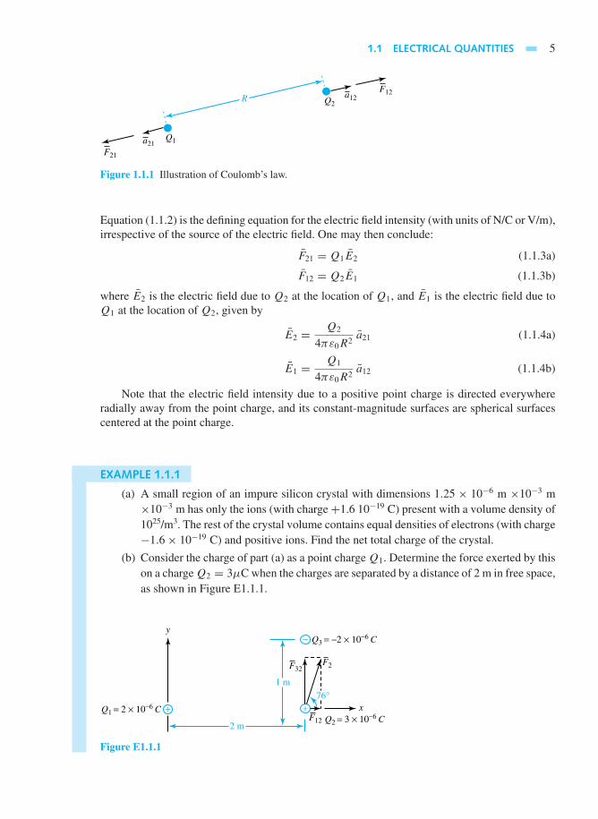
The proton has a charge of +1.602 10−19 coulombs (C), while the electron has a charge of−1.602 × 10⁻¹⁹ C. The neutron has zero charge. Electric charge and, more so, its movementare the most basic items of interest in electrical engineering. When many charged particles arecollected together, larger charges and charge distributions occur. There may be point charges (C),line charges (C/m), surface charge distributions (C/m2), and volume charge distributions (C/m3).
A charge is responsible for an electric field and charges exert forces on each other. Likecharges repel, whereas unlike charges attract. Such an electric force can be controlled and utilizedfor some useful purpose. Coulomb’s law gives an expression to evaluate the electric force innewtons (N) exerted on one point charge by the other:
Force on Q1 due to Q2 = F21 = Q1Q2
4πε0R2a21 (1.1.1a)
Force on Q2 due to Q1 = F12 = Q2Q1
4πε0R2a12 (1.1.1b)
where Q1 and Q2 are the point charges (C); R is the separation in meters (m) between them; ε0
is the permittivity of the free-space medium with units of C2/N · m or, more commonly, faradsper meter (F/m); and a21 and a12 are unit vectors along the line joining Q1 and Q2, as shown inFigure 1.1.1.
Equation (1.1.1) shows the following:
1. Forces F21 and F12 are experienced by Q1 and Q2, due to the presence of Q2 and Q1,respectively. They are equal in magnitude and opposite of each other in direction.
2. The magnitude of the force is proportional to the product of the charge magnitudes.
3. The magnitude of the force is inversely proportional to the square of the distance betweenthe charges.
4. The magnitude of the force depends on the medium.
5. The direction of the force is along the line joining the charges.
Note that the SI system of units will be used throughout this text, and the student should beconversant with the conversion factors for the SI system.
The force per unit charge experienced by a small test charge placed in an electric field isknown as the electric field intensity E, whose units are given by N/C or, more commonly, voltsper meter (V/m),
E = limQ→0
F
Q(1.1.2)
1.1 ELECTRICAL QUANTITIES 5
R
Q1
Q2
a21
a12
F21
F12
Figure 1.1.1 Illustration of Coulomb’s law.
Equation (1.1.2) is the defining equation for the electric field intensity (with units of N/C or V/m),irrespective of the source of the electric field. One may then conclude:
F21 = Q1E2 (1.1.3a)
F12 = Q2E1 (1.1.3b)
where E2 is the electric field due to Q2 at the location of Q1, and E1 is the electric field due toQ1 at the location of Q2, given by
E2 = Q2
4πε0R2a21 (1.1.4a)
E1 = Q1
4πε0R2a12 (1.1.4b)
Note that the electric field intensity due to a positive point charge is directed everywhereradially away from the point charge, and its constant-magnitude surfaces are spherical surfacescentered at the point charge.
EXAMPLE 1.1.1
(a) A small region of an impure silicon crystal with dimensions 1.25 × 10−6 m ×10−3 m×10−3 m has only the ions (with charge+1.6 10−19 C) present with a volume density of1025/m3. The rest of the crystal volume contains equal densities of electrons (with charge−1.6× 10⁻¹⁹ C) and positive ions. Find the net total charge of the crystal.
(b) Consider the charge of part (a) as a point charge Q1. Determine the force exerted by thison a charge Q2 = 3µC when the charges are separated by a distance of 2 m in free space,as shown in Figure E1.1.1.
Q3 = −2 × 10⁻⁶ C
F12
F2F32
Q2 = 3 × 10⁻⁶ C2 m
1 m
76°
y
xQ1 = 2 × 10⁻⁶ C
−
+ +
Figure E1.1.1

6 CIRCUIT CONCEPTS
(c) If another charge Q3 = −2µC is added to the system 1 m above Q2, as shown in FigureE1.1.1, calculate the force exerted on Q2.
So l u t i on
(a) In the region where both ions and free electrons exist, their opposite charges cancel, andthe net charge density is zero. From the region containing ions only, the volume-chargedensity is given by
ρ = (1025)(1.6× 10⁻¹⁹) = 1.6× 10⁶ C/m3
The net total charge is then calculated as:
Q = ρv = (1.6× 10⁶)(1.25× 10−6 × 10−3 × 10⁻³) = 2× 10⁻⁶ C
(b) The rectangular coordinate system shown defines the locations of the charges: Q1 =2×10⁻⁶ C; Q2 = 3×10⁻⁶ C. The force that Q1 exerts on Q2 is in the positive directionof x, given by Equation (1.1.1),
F12 = (3× 10⁻⁶)(2× 10⁻⁶)
4π(10−9/36π)22ax = ax 13.5× 10⁻³ N
This is the force experienced by Q2 due to the effect of the electric field of Q1. Note thevalue used for free-space permittivity, ε0, as (8.854×10⁻¹²), or approximately 10−9/36πF/m. ax is the unit vector in the positive x-direction.
(c) When Q3 is added to the system, as shown in Figure E1.1.1, an additional force on Q2
directed in the positive y-direction occurs (since Q3 and Q2 are of opposite sign),
F32 = (3× 10⁻⁶)(−2× 10⁻⁶)
4π(10−936π)12(−ay) = ay 54× 10−3 N
The resultant force F2 acting on Q2 is the superposition of F12 and F32 due to Q1 andQ3, respectively.
The vector combination of F12 and F32 is given by:
F2 =√F 2
12 + F 232 tan−1 F32
F12
=√
13 .52 + 542 × 10−3 tan−1 54
13 .5
= 55.7× 10⁻³ 76° N
Conductors and Insulators
In order to put charge in motion so that it becomes an electric current, one must provide a paththrough which it can flow easily by the movement of electrons. Materials through which chargeflows readily are called conductors. Examples include most metals, such as silver, gold, copper,and aluminum. Copper is used extensively for the conductive paths on electric circuit boards andfor the fabrication of electrical wires.

1.1 ELECTRICAL QUANTITIES 7
Insulators are materials that do not allow charge to move easily. Examples include glass,plastic, ceramics, and rubber. Electric current cannot be made to flow through an insulator, sincea charge has great difficulty moving through it. One sees insulating (or dielectric) materials oftenwrapped around the center conducting core of a wire.
Although the term resistance will be formally defined later, one can say qualitatively thata conductor has a very low resistance to the flow of charge, whereas an insulator has a veryhigh resistance to the flow of charge. Charge-conducting abilities of various materials vary ina wide range. Semiconductors fall in the middle between conductors and insulators, and havea moderate resistance to the flow of charge. Examples include silicon, germanium, and galliumarsenide.
Current and Magnetic Force
The rate of movement of net positive charge per unit of time through a cross section of a conductoris known as current,
i(t) = dq
dt(1.1.5)
The SI unit of current is the ampere (A), which represents 1 coulomb per second. In mostmetallic conductors, such as copper wires, current is exclusively the movement of free electronsin the wire. Since electrons are negative, and since the direction designated for the currentis that of the net positive charge movement, the charges in the wire are thus moving in thedirection opposite to the direction of the current designation. The net charge transferred at aparticular time is the net area under the current–time curve from the beginning of time to thepresent,
q(t) =t∫
−∞i(τ ) dτ (1.1.6)
While Coulomb’s law has to do with the electric force associated with two charged bodies,Ampere’s law of force is concerned with magnetic forces associated with two loops of wire carryingcurrents by virtue of the motion of charges in the loops. Note that isolated current elements donot exist without sources and sinks of charges at their ends; magnetic monopoles do not exist.Figure 1.1.2 shows two loops of wire in freespace carrying currents I1 and I2.
Considering a differential element dl1 of loop 1 and a differential element dl2 of loop 2,the differential magnetic forces dF21 and dF12 experienced by the differential current elementsI1 dl1, and I2 dl2, due to I2 and I1, respectively, are given by
dF21 = I1 dl1 ×(µ0
4π
I2dl2 × a21
R2
)(1.1.7a)
dF12 = I2 dl2 ×(µ0
4π
I1dl1 × a12
R2
)(1.1.7b)
where a21 and a12 are unit vectors along the line joining the two current elements,R is the distancebetween the centers of the elements, µ0 is the permeability of free space with units of N/A2 orcommonly known as henrys per meter (H/m). Equation (1.1.7) reveals the following:
1. The magnitude of the force is proportional to the product of the two currents and theproduct of the lengths of the two current elements.

8 CIRCUIT CONCEPTS
Loop 1 Loop 2
R
I1I2
a12dl1
dl2a21
Figure 1.1.2 Illustration of Ampere’s law (offorce).
2. The magnitude of the force is inversely proportional to the square of the distance betweenthe current elements.
3. To determine the direction of, say, the force acting on the current element I1 dl1, the crossproduct dl2 × a21 must be found. Then crossing dl1 with the resulting vector will yieldthe direction of dF21.
4. Each current element is acted upon by a magnetic field due to the other current element,
dF21 = I1 dl1 × B2 (1.1.8a)
dF12 = I2dl2 × B1 (1.1.8b)
where B is known as the magnetic flux density vector with units of N/A ·m, commonlyknown as webers per square meter (Wb/m2) or tesla (T).
Current distribution is the source of magnetic field, just as charge distribution is the sourceof electric field. As a consequence of Equations (1.1.7) and (1.1.8), it can be seen that
B2 = µ0
4πI2 dl2 × a21 (1.1.9a)
B1 = µ0
4π
I1 dl1 × a12
R2(1.1.9b)
which depend on the medium parameter. Equation (1.1.9) is known as the Biot–Savart law.Equation (1.1.8) can be expressed in terms of moving charge, since current is due to the flowof charges. With I = dq/dt and dl = v dt , where v is the velocity, Equation (1.1.8) can berewritten as
dF =(dq
dt
)(v dt)× B = dq (v × B) (1.1.10)
Thus it follows that the force F experienced by a test charge q moving with a velocity v in amagnetic field of flux density B is given by
F = q (v × B) (1.1.11)
The expression for the total force acting on a test charge q moving with velocity v in a regioncharacterized by electric field intensity E and a magnetic field of flux density B is
F = FE + FM = q (E + v × B) (1.1.12)
which is known as the Lorentz force equation.

1.1 ELECTRICAL QUANTITIES 9
EXAMPLE 1.1.2
Figure E1.1.2 (a) gives a plot of q(t) as a function of time t .
(a) Obtain the plot of i(t).
(b) Find the average value of the current over the time interval of 1 to 7 seconds.
3
t, seconds
−1
0 1 2 3 4 5 6 7 8 9 10
q(t), coulombs
(a)
t, seconds
i(t), amperes
−2.0
(b)
1.01.5
1 2 3 4 5 6 7 8 9 10
Figure E1.1.2 (a) Plot of q(t).(b) Plot of i(t).
So l u t i on
(a) Applying Equation (1.1.5) and interpreting the first derivative as the slope, one obtainsthe plot shown in Figure E1.1.2(b).
(b) Iav = (1/T )∫ T
0 i dt . Interpreting the integral as the area enclosed under the curve, onegets:
Iav = 1
(7− 1)[(1.5× 2)− (2.0× 2)+ (0× 1)+ (1× 1)] = 0
Note that the net charge transferred during the interval of 1 to 7 seconds is zero in this case.

10 CIRCUIT CONCEPTS
EXAMPLE 1.1.3
Consider an infinitesimal length of 10−6 m of wire whose center is located at the point (1, 0, 0),carrying a current of 2 A in the positive direction of x.
(a) Find the magnetic flux density due to the current element at the point (0, 2, 2).
(b) Let another current element (of length 10−3 m) be located at the point (0, 2, 2), carryinga current of 1 A in the direction of (−ay + az). Evaluate the force on this current elementdue to the other element located at (1, 0, 0).
So l u t i on
(a) I1dl1 = 2× 10⁻⁶ax . The unit vector a12 is given by
a12 = (0− 1)ax + (2− 0)ay + (2− 0)az√12 + 22 + 22
= (−ax + 2ay + 2az)
3Using the Biot–Savart law, Equation (1.1.9), one gets
[B1](0,2,2) = µ0
4π
I1 dl1 × a12
R2
where µ0 is the free-space permeability constant given in SI units as 4π × 10−7 H/m,and R2 in this case is (0− 1)2 + (2− 0)2 + (2− 0)2, or 9. Hence,
[B1](0,2,2) = 4π × 10−7
4π
[(2× 10⁻⁶ax)× (−ax + 2ay + 2az)
9× 3
]
= 10−7
27× 4× 10−6(az − ay) Wb/m2
= 0.15× 10⁻¹³(az − ay) T
(b) I2 dl2 = 10−3(−ay + az)
dF12 = I2dl2 × B1
= [10−3(−ay + az)]× [0.15× 10⁻¹³(az − ay)
] = 0
Note that the force is zero since the current element I2 dl2 and the field B1 due to I1 dl1
at (0, 2, 2) are in the same direction.
The Biot–Savart law can be extended to find the magnetic flux density due to a current-carrying filamentary wire of any length and shape by dividing the wire into a number ofinfinitesimal elements and using superposition. The net force experienced by a current loop canbe similarly evaluated by superposition.
Electric Potential and Voltage
When electrical forces act on a particle, it will possess potential energy. In order to describe thepotential energy that a particle will have at a point x, the electric potential at point x is defined as
1.1 ELECTRICAL QUANTITIES 11
v(x) = dw(x)
dq(1.1.13)
where w(x) is the potential energy that a particle with charge q has when it is located at theposition x. The zero point of potential energy can be chosen arbitrarily since only differences inenergy have practical meaning. The point where electric potential is zero is known as the referencepoint or ground point, with respect to which potentials at other points are then described. Thepotential difference is known as the voltage expressed in volts (V) or joules per coulomb (J/C).If the potential at B is higher than that at A,
vBA = vB − vA (1.1.14)
which is positive. Obviously voltages can be either positive or negative numbers, and it follows that
vBA = −vAB (1.1.15)
The voltage at point A, designated as vA, is then the potential at point A with respect to theground.
Energy and Power
If a charge dq gives up energy dw when going from point a to point b, then the voltage acrossthose points is defined as
v = dw
dq(1.1.16)
If dw/dq is positive, point a is at the higher potential. The voltage between two points is thework per unit positive charge required to move that charge between the two points. If dw and dqhave the same sign, then energy is delivered by a positive charge going from a to b (or a negativecharge going the other way). Conversely, charged particles gain energy inside a source where dwand dq have opposite polarities.
The load and source conventions are shown in Figure 1.1.3, in which point a is at ahigher potential than point b. The load receives or absorbs energy because a positive chargegoes in the direction of the current arrow from higher to lower potential. The source hasa capacity to supply energy. The voltage source is sometimes known as an electromotiveforce, or emf, to convey the notation that it is a force that drives the current through thecircuit.
The instantaneous power p is defined as the rate of doing work or the rate of change ofenergy dw/dt,
p = dw
dt=(dw
dq
) (dq
dt
)= vi (1.1.17)
The electric power consumed or produced by a circuit element is given by its voltage–currentproduct, expressed in volt-amperes (VA) or watts (W). The energy over a time interval is foundby integrating power,
w =T∫
0
p dt (1.1.18)
which is expressed in watt-seconds or joules (J), or commonly in electric utility bills in kilowatt-hours (kWh). Note that 1 kWh equals 3.6× 10⁶ J.

12 CIRCUIT CONCEPTS
Load iabvab
a
b
+
−
Source ibavab
a
i
b
+
−
Figure 1.1.3 Load and source conventions.
EXAMPLE 1.1.4
A typical 12-V automobile battery, storing about 5 megajoules (MJ) of energy, is connected to a4-A headlight system.
(a) Find the power delivered to the headlight system.
(b) Calculate the energy consumed in 1 hour of operation.
(c) Express the auto-battery capacity in ampere-hours (Ah) and compute how long theheadlight system can be operated before the battery is completely discharged.
So l u t i on
(a) Power delivered: P = V I = 124 = 48W.
(b) Assuming V and I remain constant, the energy consumed in 1 hour will equal
W = 48(60× 60) = 172.8× 10³J = 172.8kJ
(c) 1 Ah = (1 C/s)(3600 s) = 3600C. For the battery in question, 5 × 10⁶J/12 V =0.417 × 10⁶C. Thus the auto-battery capacity is 0.417 × 10⁶/3600 ∼= 116 Ah. Withoutcompletely discharging the battery, the headlight system can be operated for 116/4= 29hours.
Sources and Loads
A source–load combination is represented in Figure 1.1.4. A node is a point at which two ormore components or devices are connected together. A part of a circuit containing only onecomponent, source, or device between two nodes is known as a branch. A voltage rise indicatesan electric source, with the charge being raised to a higher potential, whereas a voltage dropindicates a load, with a charge going to a lower potential. The voltage across the source is thesame as the voltage across the load in Figure 1.1.4. The current delivered by the source goesthrough the load. Ideally, with no losses, the power (p = vi) delivered by the source is consumedby the load.
When current flows out of the positive terminal of an electric source, it implies that non-electric energy has been transformed into electric energy. Examples include mechanical energytransformed into electric energy as in the case of a generator source, chemical energy changed
1.1 ELECTRICAL QUANTITIES 13
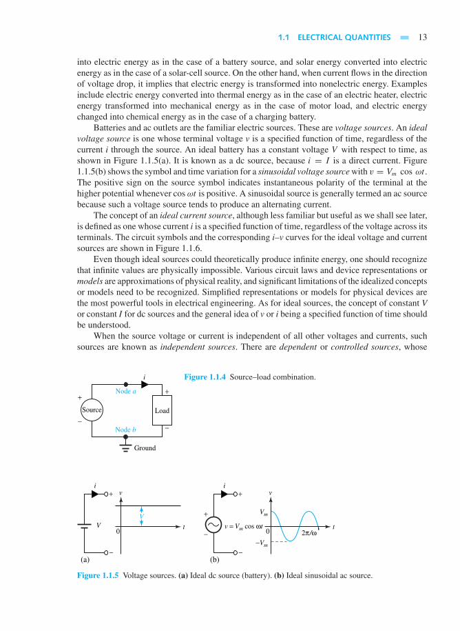
into electric energy as in the case of a battery source, and solar energy converted into electricenergy as in the case of a solar-cell source. On the other hand, when current flows in the directionof voltage drop, it implies that electric energy is transformed into nonelectric energy. Examplesinclude electric energy converted into thermal energy as in the case of an electric heater, electricenergy transformed into mechanical energy as in the case of motor load, and electric energychanged into chemical energy as in the case of a charging battery.
Batteries and ac outlets are the familiar electric sources. These are voltage sources. An idealvoltage source is one whose terminal voltage v is a specified function of time, regardless of thecurrent i through the source. An ideal battery has a constant voltage V with respect to time, asshown in Figure 1.1.5(a). It is known as a dc source, because i = I is a direct current. Figure1.1.5(b) shows the symbol and time variation for a sinusoidal voltage source with v = Vm cos ωt .The positive sign on the source symbol indicates instantaneous polarity of the terminal at thehigher potential whenever cos ωt is positive. A sinusoidal source is generally termed an ac sourcebecause such a voltage source tends to produce an alternating current.
The concept of an ideal current source, although less familiar but useful as we shall see later,is defined as one whose current i is a specified function of time, regardless of the voltage across itsterminals. The circuit symbols and the corresponding i–v curves for the ideal voltage and currentsources are shown in Figure 1.1.6.
Even though ideal sources could theoretically produce infinite energy, one should recognizethat infinite values are physically impossible. Various circuit laws and device representations ormodels are approximations of physical reality, and significant limitations of the idealized conceptsor models need to be recognized. Simplified representations or models for physical devices arethe most powerful tools in electrical engineering. As for ideal sources, the concept of constant Vor constant I for dc sources and the general idea of v or i being a specified function of time shouldbe understood.
When the source voltage or current is independent of all other voltages and currents, suchsources are known as independent sources. There are dependent or controlled sources, whose
Source
Node b
Node a
Ground
i
+
−
+
−
Load
Figure 1.1.4 Source–load combination.
+
−
0
v
tV
(a)
V
i+
+
−
−
0
v
t
(b)
v = Vm cos ωt
−Vm
Vm
2π/ω
i
Figure 1.1.5 Voltage sources. (a) Ideal dc source (battery). (b) Ideal sinusoidal ac source.

14 CIRCUIT CONCEPTS
vs
is
+
+
−
−
0
i
vvs vsis
is
(a)
i+
−
0
i
v
(b)
v
Figure 1.1.6 Circuit symbols and i–v curves. (a) Ideal voltage source. (b) Ideal current source.
voltage or current does depend on the value of some other voltage or current. As an example, avoltage amplifier producing an output voltage vout = Avin, where vin is the input voltage and A isthe constant-voltage amplification factor, is shown in Figure 1.1.7, along with its controlled-sourcemodel using the diamond-shaped symbol. Current sources controlled by a current or voltage willalso be considered eventually.
Waveforms
We are often interested in waveforms, which may not be constant in time. Of particular interestis a periodic waveform, which is a time-varying waveform repeating itself over intervals of timeT > 0.
f (t) = f (t ± nT ) n = 1, 2, 3, · · · (1.1.19)
The repetition time T of the waveform is called the period of the waveform. For a waveformto be periodic, it must continue indefinitely in time. The dc waveform of Figure 1.1.5(a) can beconsidered to be periodic with an infinite period. The frequency of a periodic waveform is thereciprocal of its period,
f = 1
THertz (Hz) (1.1.20)
A sinusoidal or cosinusoidal waveform is typically described by
f (t) = A sin(ωt + φ) (1.1.21)
where A is the amplitude, φ is the phase offset, and ω = 2πf = 2π/T is the radian frequencyof the wave. When φ = 0, a sinusoidal wave results, and when φ = 90°, a cosinusoidal waveresults. The average value of a periodic waveform is the net positive area under the curve for oneperiod, divided by the period,
Fav = 1
T
T∫0
f (t) dt (1.1.22)
++
− −vin vout
(a)
Voltageamplifier
++
−−
Avin vout
(b)
Figure 1.1.7 Voltage amplifier and itscontrolled-source model.

1.1 ELECTRICAL QUANTITIES 15
The effective, or root-mean square (rms), value is the square root of the average of f 2(t),
Frms =
√√√√√ 1
T
T∫0
f 2(t) dt (1.1.23)
Determining the square of the function f (t), then finding the mean (average) value, and finallytaking the square root yields the rms value, known as effective value. This concept will be seento be useful in comparing the effectiveness of different sources in delivering power to a resistor.The effective value of a periodic current, for example, is a constant, or dc value, which deliversthe same average power to a resistor, as will be seen later.
For the special case of a dc waveform, the following holds:
f (t) = F ; Fav = Frms = F (1.1.24)
For the sinusoid or cosinusoid, it can be seen that
f (t) = A sin(ωt + φ); Fav = 0; Frms = A/√
2 ∼= 0.707 A (1.1.25)
The student is encouraged to show the preceding results using graphical and analytical means.Other common types of waveforms are exponential in nature,
f (t) = Ae−t/τ (1.1.26a)
f (t) = A(1− e−t/τ ) (1.1.26b)
where τ is known as the time constant. After a time of one time constant has elapsed, looking atEquation (1.1.26a), the value of the waveform will be reduced to 37% of its initial value; Equation(1.1.26b) shows that the value will rise to 63% of its final value. The student is encouraged tostudy the functions graphically and deduce the results.
EXAMPLE 1.1.5
A periodic current waveform in a rectifier is shown in Figure E1.1.5. The wave is sinusoidal forπ/3 ≤ ωt ≤ π , and is zero for the rest of the cycle. Calculate the rms and average values of thecurrent.
i
10
π3
π 2π ωt
Figure E1.1.5
So l u t i on
Irms =
√√√√√√ 1
2π
π/3∫0
i2 d(ωt)+π∫
π/3
i2 d(ωt)+2π∫π
i2 d(ωt)

16 CIRCUIT CONCEPTS
Notice that ωt rather than t is chosen as the variable for convenience; ω = 2πf = 2π/T;and integration is performed over three discrete intervals because of the discontinuous currentfunction. Since i = 0 for 0 ≤ ωt < π/3 and π ≤ ωt ≤ 2π ,
Irms =√√√√√ 1
2π
π∫π/3
102 sin2 ωt d(ωt) = 4.49 A
Iav = 1
2π
π∫π/3
10 sin ωt d(ωt) = 2.39 A
Note that the base is the entire period 2π , even though the current is zero for a substantial part ofthe period.
1.2 LUMPED-CIRCUIT ELEMENTS
Electric circuits or networks are formed by interconnecting various devices, sources, and com-ponents. Although the effects of each element (such as heating effects, electric-field effects,or magnetic-field effects) are distributed throughout space, one often lumps them together aslumped elements. The passive components are the resistance R representing the heating effect,the capacitance C representing the electric-field effect, and the inductance L representing themagnetic-field effect. Their characteristics will be presented in this section. The capacitor modelsthe relation between voltage and current due to changes in the accumulation of electric charge, andthe inductor models the relation due to changes in magnetic flux linkages, as will be seen later.While these phenomena are generally distributed throughout an electric circuit, under certainconditions they can be considered to be concentrated at certain points and can therefore berepresented by lumped parameters.
Resistance
An ideal resistor is a circuit element with the property that the current through it is linearlyproportional to the potential difference across its terminals,
i = v/R = Gv, or v = iR (1.2.1)
which is known as Ohm’s law, published in 1827. R is known as the resistance of the resistorwith the SI unit of ohms (), and G is the reciprocal of resistance called conductance, with the SIunit of siemens (S). The circuit symbols of fixed and variable resistors are shown in Figure 1.2.1,along with an illustration of Ohm’s law. Most resistors used in practice are good approximationsto linear resistors for large ranges of current, and their i–v characteristic (current versus voltageplot) is a straight line.
The value of resistance is determined mainly by the physical dimensions and the resistivityρ of the material of which the resistor is composed. For a bar of resistive material of length l andcross-sectional area A the resistance is given by
R = ρl
A= l
σA(1.2.2)
where ρ is the resistivity of the material in ohm-meters ( ·m), and σ is the conductivity of thematerial in S/m, which is the reciprocal of the resistivity. Metal wires are often considered as ideal
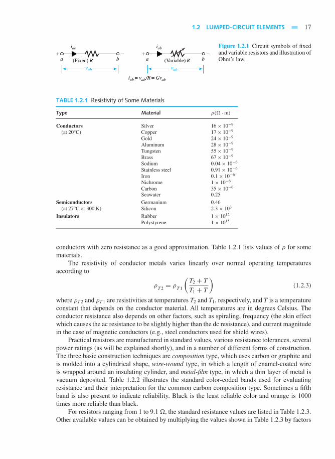
1.2 LUMPED-CIRCUIT ELEMENTS 17
iab
vab
Ra b(Fixed)+ −
iab
iab = vab/R = Gvab
vab
Ra b(Variable)+ −
Figure 1.2.1 Circuit symbols of fixedand variable resistors and illustration ofOhm’s law.
TABLE 1.2.1 Resistivity of Some Materials
Type Material ρ( ·m)
Conductors Silver 16× 10−9
(at 20°C) Copper 17× 10−9
Gold 24× 10−9
Aluminum 28× 10−9
Tungsten 55× 10−9
Brass 67× 10−9
Sodium 0.04× 10⁻⁶
Stainless steel 0.91× 10⁻⁶
Iron 0.1× 10⁻⁶
Nichrome 1× 10⁻⁶
Carbon 35× 10−6
Seawater 0.25
Semiconductors Germanium 0.46(at 27°C or 300 K) Silicon 2.3× 10³
Insulators Rubber 1× 10¹²
Polystyrene 1× 10¹⁵
conductors with zero resistance as a good approximation. Table 1.2.1 lists values of ρ for somematerials.
The resistivity of conductor metals varies linearly over normal operating temperaturesaccording to
ρT 2 = ρ
T 1
(T2 + T
T1 + T
)(1.2.3)
where ρT 2 and ρT 1 are resistivities at temperatures T2 and T1, respectively, and T is a temperatureconstant that depends on the conductor material. All temperatures are in degrees Celsius. Theconductor resistance also depends on other factors, such as spiraling, frequency (the skin effectwhich causes the ac resistance to be slightly higher than the dc resistance), and current magnitudein the case of magnetic conductors (e.g., steel conductors used for shield wires).
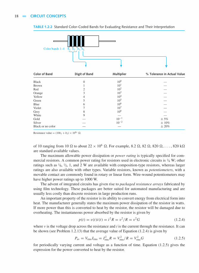
Practical resistors are manufactured in standard values, various resistance tolerances, severalpower ratings (as will be explained shortly), and in a number of different forms of construction.The three basic construction techniques are composition type, which uses carbon or graphite andis molded into a cylindrical shape, wire-wound type, in which a length of enamel-coated wireis wrapped around an insulating cylinder, and metal-film type, in which a thin layer of metal isvacuum deposited. Table 1.2.2 illustrates the standard color-coded bands used for evaluatingresistance and their interpretation for the common carbon composition type. Sometimes a fifthband is also present to indicate reliability. Black is the least reliable color and orange is 1000times more reliable than black.
For resistors ranging from 1 to 9.1 , the standard resistance values are listed in Table 1.2.3.Other available values can be obtained by multiplying the values shown in Table 1.2.3 by factors
18 CIRCUIT CONCEPTS
TABLE 1.2.2 Standard Color-Coded Bands for Evaluating Resistance and Their Interpretation
Color bands 1–4 b1 b2 b3 b4
Color of Band Digit of Band Multiplier % Tolerance in Actual Value
Black 0 100 —Brown 1 101 —Red 2 102 —Orange 3 103 —Yellow 4 104 —Green 5 105 —Blue 6 106 —Violet 7 107 —Grey 8 108 —White 9 — —Gold — 10−1 ± 5%Silver — 10−2 ± 10%Black or no color — — ± 20%
Resistance value = (10b1 + b2)× 10b3 .
of 10 ranging from 10 to about 22 × 106 . For example, 8.2 , 82 , 820 , . . . , 820 kare standard available values.
The maximum allowable power dissipation or power rating is typically specified for com-mercial resistors. A common power rating for resistors used in electronic circuits is 14 W; otherratings such as 18, 12, 1, and 2 W are available with composition-type resistors, whereas largerratings are also available with other types. Variable resistors, known as potentiometers, with amovable contact are commonly found in rotary or linear form. Wire-wound potentiometers mayhave higher power ratings up to 1000 W.
The advent of integrated circuits has given rise to packaged resistance arrays fabricated byusing film technology. These packages are better suited for automated manufacturing and areusually less costly than discrete resistors in large production runs.
An important property of the resistor is its ability to convert energy from electrical form intoheat. The manufacturer generally states the maximum power dissipation of the resistor in watts.If more power than this is converted to heat by the resistor, the resistor will be damaged due tooverheating. The instantaneous power absorbed by the resistor is given by
p(t) = v(t)i(t) = i2R = v2/R = v2G (1.2.4)
where v is the voltage drop across the resistance and i is the current through the resistance. It canbe shown (see Problem 1.2.13) that the average value of Equation (1.2.4) is given by
Pav = VrmsIrms = I 2rmsR = V 2
rms/R = V 2rmsG (1.2.5)
for periodically varying current and voltage as a function of time. Equation (1.2.5) gives theexpression for the power converted to heat by the resistor.

1.2 LUMPED-CIRCUIT ELEMENTS 19
TABLE 1.2.3 Standard Available Values of Resistors
1.0 1.5 2.2 3.3 4.7 6.81.1 1.6 2.4 3.6 5.1 7.51.2 1.8 2.7 3.9 5.6 8.21.3 2.0 3.0 4.3 6.2 9.1
Series and parallel combinations of resistors occur very often. Figure 1.2.2 illustrates thesecombinations.
Figure 1.2.2(a) shows two resistors R1 and R2 in series sharing the voltage v in directproportion to their values, while the same current i flows through both of them,
v = vAC = vAB + vBC = iR1 + iR2 = i(R1 + R2) = iReq
or, when R1 and R2 are in series,
Req = R1 + R2 (1.2.6)
Figure 1.2.2(b) shows two resistors in parallel sharing the current i in inverse proportion totheir values, while the same voltage v is applied across each of them. At node B,
i = i1 + i2 = v
R1+ v
R2= v
(1
R1+ 1
R2
)= v/
(R1R2
R1 + R2
)= v
Req
or, when R1 and R2 are in parallel,
Req = R1R2
R1 + R2or
1
Req= 1
R1+ 1
R2or Geq = G1 +G2 (1.2.7)
Notice the voltage division shown in Figure 1.2.2(a), and the current division in Figure1.2.2(b).
i
A
C
(a) (b)
B
+
−
v = vAC = vAB + vBC vAD = vBC = v
vAB = iR1
=
=
vR1
R1 + R2
vBC = iR2
R1
R2
A
D
B
C
+
−
i = i1 + i2
i2 = v/R2
= vG2
i1 = v/R1= vG1
R1 R2=iG2
G1 + G2
=iG1
G1 + G2
vR2
R1 + R2
Figure 1.2.2 Resistances in series and in parallel. (a) R1 and R2 in series. (b) R1 and R2 in parallel.
EXAMPLE 1.2.1
A no. 14 gauge copper wire, commonly used in extension cords, has a circular wire diameter of64.1 mils, where 1 mil = 0.001 inch.
(a) Determine the resistance of a 100-ft-long wire at 20°C.

20 CIRCUIT CONCEPTS
(b) If such a 2-wire system is connected to a 110-V (rms) residential source outlet in orderto power a household appliance drawing a current of 1 A (rms), find the rms voltage atthe load terminals.
(c) Compute the power dissipated due to the extension cord.
(d) Repeat part (a) at 50°C, given that the temperature constant for copper is 241.5°C.
So l u t i on
(a) d = 64.1 mils = 64.1 × 10⁻³ in = 64.1 × 10−3 × 2.54 cm/1 in × 1 m/100 cm =1.628× 10⁻³ m. From Table 1.2.1, ρ of copper at 20°C is 17× 10−9 m,
l = 100 ft = 100 ft × 12 in
1 ft× 2.54 cm
1 in× 1 m
100 cm= 30.48 m
A = πd2
4= π(1.628× 10⁻³)2
4= 2.08× 10⁻⁶ m2
Per Equation (1.2.2),
R20°C = 17× 10−9 × 30.48
2.08× 10⁻⁶‘ ∼= 0.25
(b) Rms voltage at load terminals, V = 110 − (0.25)2 = 109.5 V (rms). Note that two100-ft-long wires are needed for the power to be supplied.
(c) Power dissipated, per Equation (1.2.5), P = (1)2(0.25)(2) = 0.5 W.
(d) Per Equation (1.2.3),
ρ50°C = ρ20°C
(50+ 241.5
20+ 241.5
)= 17× 10−9 × 291.5
261.5= 18.95× 10⁻⁹ ·m
Hence,
R50°C = 18.95× 10−9 × 30.48
2.08× 10⁻⁶∼= 0.28
EXAMPLE 1.2.2
(a) Consider a series–parallel combination of resistors as shown in Figure E1.2.2(a). Findthe equivalent resistance as seen from terminals A–B.
(b) Determine the current I and power P delivered by a 10-V dc voltage source applied atterminals A–B, with A being at higher potential than B.
(c) Replace the voltage source by an equivalent current source at terminals A–B.
(d) Show the current and voltage distribution clearly in all branches of the original circuitconfiguration.
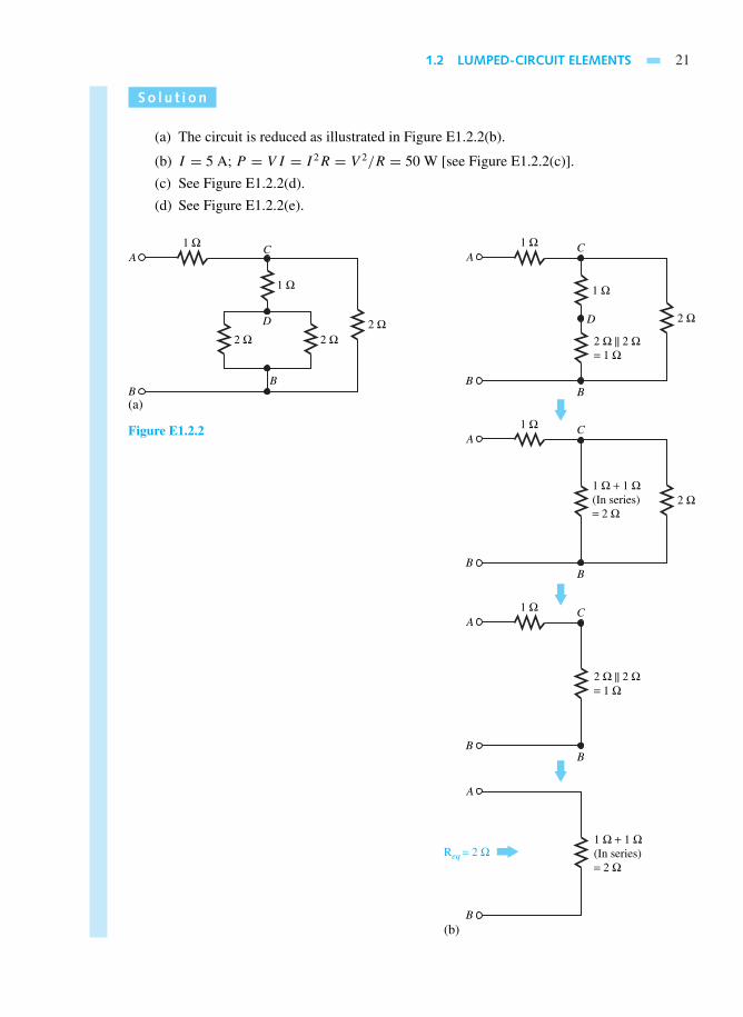
1.2 LUMPED-CIRCUIT ELEMENTS 21
So l u t i on
(a) The circuit is reduced as illustrated in Figure E1.2.2(b).
(b) I = 5 A; P = V I = I 2R = V 2/R = 50 W [see Figure E1.2.2(c)].
(c) See Figure E1.2.2(d).
(d) See Figure E1.2.2(e).
(a)
A
BB
2 Ω
1 Ω
1 Ω
2 Ω2 ΩD
C
Figure E1.2.2
A
B
D
1 Ω
2 Ω || 2 Ω= 1 Ω
2 Ω || 2 Ω= 1 Ω
1 Ω + 1 Ω(In series)= 2 Ω
1 Ω + 1 Ω(In series)= 2 Ω
1 Ω
2 Ω
C
B
A
B
1 Ω
2 Ω
C
B
A
B
1 Ω C
B
A
B(b)
Req = 2 Ω

22 CIRCUIT CONCEPTS
10 V
B
AI = 10/2 = 5 A
2 Ω+
−
(c) B
A
V = 5 × 2 = 10 V5 A 2 Ω
+
−(d)
(e)
A
B B
2 Ω
1 Ω
1 Ω5 A
5 A
2.5 A2.5 A
2.5 V
1.25 A1.25 A
5 V
5 V10 V
2 Ω
2 ΩD
C
+
+
−
+−
2.5 V+−
2.5 V+−
+−
−
Maximum Power Transfer
In order to investigate the power transfer between a practical source and a load connected to it,let us consider Figure 1.2.3, in which a constant voltage source v with a known internal resistanceRS is connected to a variable load resistance RL. Note that when RL is equal to zero, it is calleda short circuit, in which case vL becomes zero and iL is equal to v/RS . When RL approachesinfinity, it is called an open circuit, in which case iL becomes zero and vL is equal to v. One isgenerally interested to find the value of the load resistance that will absorb maximum power fromthe source.
The power PL absorbed by the load is given by
PL = i2LRL (1.2.8)
where the load current iL is given by
iL = v2
RS + RL
(1.2.9)
Substituting Equation (1.2.9) in Equation (1.2.8), one gets
PL = v2
(RS + RL)2RL (1.2.10)
For given fixed values of v and RS , in order to find the value of RL that maximizes the powerabsorbed by the load, one sets the first derivative dPL/dRL equal to zero,
dPL
dRL
= v2(RL + RS)2 − 2v2RL(RL + RS)
(RL + RS)4= 0 (1.2.11)

1.2 LUMPED-CIRCUIT ELEMENTS 23
v
B
A
RL
RS
vL
iL
iL
+
−
Source −
+
Load
Figure 1.2.3 Power transfer between source and load. Note: RL = 0implies short circuit; vL = 0 and iL = v
RSand RL → • implies open
circuit; iL = 0 and vL = v.
which leads to the following equation:
(RL + RS)2 − 2RL(RL + RS) = 0 (1.2.12)
The solution of Equation (1.2.12) is given by
RL = RS (1.2.13)
That is to say, in order to transfer maximum power to a load, the load resistance must be matchedto the source resistance or, in other words, they should be equal to each other.
A problem related to power transfer is that of source loading. Figure 1.2.4(a) illustrates apractical voltage source (i.e., an ideal voltage source along with a series internal source resistance)connected to a load resistance; Figure 1.2.4(b) shows a practical current source (i.e., an idealcurrent source along with a parallel or shunt internal source resistance) connected to a loadresistance. It follows from Figure 1.2.4(a) that
vL = v − vint = v − iLRS (1.2.14)
where vint is the internal voltage drop within the source, which depends on the amount of currentdrawn by the load. As seen from Equation (1.2.14), the voltage actually seen by the load vLis somewhat lower than the open-circuit voltage of the source. When the load resistance RL isinfinitely large, the load current iL goes to zero, and the load voltage vL is then equal to theopen-circuit voltage of the source v. Hence, it is desirable to have as small an internal resistanceas possible in a practical voltage source.
From Figure 1.2.4(b) it follows that
iL = i − iint = i − vL
RS
(1.2.15)
where iint is the internal current drawn away from the load because of the presence of the internalsource resistance. Thus the load will receive only part of the short-circuit current available fromthe source. When the load resistance RL is zero, the load voltage vL goes to zero, and the load
v
(a)
RL
RS
vL
vint
iL
++ −
−
Voltage source −
+
Load
i
(b)
RLRS
vL
iint
iL
Current source −
+
Load
Figure 1.2.4 Source-loadingeffects.

24 CIRCUIT CONCEPTS
current iL is then equal to the short-circuit current of the source i. Hence, it is desirable to haveas large an internal resistance as possible in a practical current source.
Capacitance
An ideal capacitor is an energy-storage circuit element (with no loss associated with it) repre-senting the electric-field effect. The capacitance in farads (F) is defined by
C = q/v (1.2.16)
where q is the charge on each conductor, and v is the potential difference between the twoperfect conductors. With v being proportional to q, C is a constant determined by the geometricconfiguration of the two conductors. Figure 1.2.5(a) illustrates a two-conductor system carrying+q and −q charges, respectively, forming a capacitor.
The general circuit symbol for a capacitor is shown in Figure 1.2.5(b), where the currententering one terminal of the capacitor is equal to the rate of buildup of charge on the plateattached to that terminal,
i(t) = dq
dt= C
dv
dt(1.2.17)
in which C is assumed to be a constant and not a function of time (which it could be, if theseparation distance between the plates changed with time).
The terminal v–i relationship of a capacitor can be obtained by integrating both sides ofEquation (1.2.17),
v(t) = 1
C
t∫−∞
i(τ ) dτ (1.2.18)
which may be rewritten as
v(t) = 1
C
t∫0
i(τ ) dτ + 1
C
0∫−∞
i(τ ) dτ = 1
C
t∫0
i(τ ) dτ + v(0) (1.2.19)
where v(0) is the initial capacitor voltage at t = 0.The instantaneous power delivered to the capacitor is given by
p(t) = v(t)i(t) = C v(t)dv(t)
dt(1.2.20)
whose average value can be shown (see Problem 1.2.13) to be zero for sinusoidally varying currentand voltage as a function of time. The energy stored in a capacitor at a particular time is foundby integrating,
A
B A B
+q chargePotential vA
−q chargePotential vB
Potential difference = v = vA − vB; C = q/v
Ci(t)
v(t)
(a) (b)i(t) = = C ;
dqdt C
1v(t) =dvdt i(τ) dτ∫
t
C1=
+ −
i(τ) dτ + v(0)∫0
t
Figure 1.2.5 Capacitor. (a) Two perfect conductors carrying +q and −q charges. (b) Circuit symbol.

1.2 LUMPED-CIRCUIT ELEMENTS 25
w(t) =t∫
−∞p(τ) dτ = C
t∫−∞
v(τ)dv(τ)
dτ= 1
2Cv2(t)− 1
2Cv2(−∞) (1.2.21)
Assuming the capacitor voltage to be zero at t = −∞, the stored energy in the capacitor at sometime t is given by
w(t) = 1
2Cv2(t) (1.2.22)
which depends only on the voltage of the capacitor at that time, and represents the stored energyin the electric field between the plates due to the separation of charges.
If the voltage across the capacitor does not change with time, no current flows, as seen fromEquation (1.2.17). Thus the capacitor acts like an open circuit, and the following relations hold:
C = Q
V; I = 0, W = 1
2CV 2 (1.2.23)
An ideal capacitor, once charged and disconnected, the current being zero, will retain a potentialdifference for an indefinite length of time. Also, the voltage across a capacitor cannot changevalue instantaneously, while an instantaneous change in the capacitor current is quite possible.The student is encouraged to reason through and justify the statement made here by recallingEquation (1.2.17).
Series and parallel combinations of capacitors are often encountered. Figure 1.2.6 illustratesthese.
It follows from Figure 1.2.6(a),
v = vAC = vAB + vBC
dv
dt= dvAB
dt+ dvBC
dt= i
C1+ i
C2= i
(C1 + C2
C1C2
)= i
Ceq
or, when C1 and C2 are in series,
Ceq = C1C2
C1 + C2or
1
Ceq= 1
C1+ 1
C2(1.2.24)
Referring to Figure 1.2.6(b), one gets
i = i1 + i2 = C1dv
dt+ C2
dv
dt= (C1 + C2)
dv
dt= Ceq
dv
dt
or, when C1 and C2 are in parallel,
Ceq = C1 + C2 (1.2.25)
Note that capacitors in parallel combine as resistors in series, and capacitors in series combine asresistors in parallel.
B
C1i1 i2
C2
CD
AB
C1C2
A
C
v v
i i
+
−
+
−
(a) (b)
Figure 1.2.6 Capacitors in series and in parallel. (a) C1and C2 in series. (b) C1 and C2 in parallel.
26 CIRCUIT CONCEPTS
The working voltage for a capacitor is generally specified by the manufacturer, thereby givingthe maximum voltage that can safely be applied between the capacitor terminals. Exceeding thislimit may result in the breakdown of the insulation and then the formation of an electric arc betweenthe capacitor plates. Unintentional or parasitic capacitances that occur due to the proximity ofcircuit elements may have serious effects on the circuit behavior.
Physical capacitors are often made of tightly rolled sheets of metal film, with a dielectric(paper or nylon) sandwiched in between, in order to increase their capacitance values (or abilityto store energy) for a given size. Table 1.2.4 lists the range of general-purpose capacitances togetherwith the maximum voltages and frequencies for different types of dielectric materials. Practicalcapacitors come in a wide range of values, shapes, sizes, voltage ratings, and constructions. Bothfixed and adjustable devices are available. Larger capacitors are of the electrolytic type, usingaluminum oxide as the dielectric.
TABLE 1.2.4 Characteristics of General-Purpose Capacitors
Capacitance Maximum Voltage Frequency RangeMaterial Range Range (V) (Hz)
Mica 1 pF to 0.1 µF 50–600 103–1010
Ceramic 10 pF to 1 µF 50–1600 103–1010
Mylar 0.001 F to 10 µF 50–600 102–108
Paper 10 pF to 50 µF 50–400 102–108
Electrolytic 0.1 µF to 0.2 F 3–600 10–104
Note: 1 pF = 10−12 F; 1 µF = 10−6 F.
EXAMPLE 1.2.3
(a) Consider a 5-µF capacitor to which a voltage v(t) is applied, shown in Figure E1.2.3(a),top. Sketch the capacitor current and stored energy as a function of time.
(b) Let a current source i(t) be attached to the 5-µF capacitor instead of the voltage source ofpart (a), shown in Figure E1.2.3(b), top. Sketch the capacitor voltage and energy storedas a function of time.
(c) If three identical 5-µF capacitors with an initial voltage of 1 mV are connected (i) inseries and (ii) in parallel, find the equivalent capacitances for both cases.
So l u t i on
(a) From Figure E1.2.3(a) it follows that
v(t) = 0 , t ≤ −1 µ s
= 5(t + 1) mV, − 1 ≤ t ≤ 1 µ s
= 10 mV, 1 ≤ t ≤ 3 µ s
= −10(t − 4) mV, 3 ≤ t ≤ 4 µ s
= 0 , 4 ≤ t µ s

1.2 LUMPED-CIRCUIT ELEMENTS 27
−2 1
v(t), mV
v(t)
t, µs
5 µF
t, µs
i(t), mA
2 3 64 5−1
−2 1
25
−50
250
10
2 3 64 5−1
t, µs
w(t), pJ
−2 1
(a)
2 3 64 5−1
v(t)
i(t)+
−
+
−
50
90100
125 122.5
40
10
−2 1
i(t), mA
t, µs2 3 64 5−1
10
t, µs
v(t), mV
−2 1
7654321
2 3 64 5−1
t, µs
w(t), pJ
1
(b)
2 3 64 5−1
v(t)5 µFi(t)
i(t)+
−
C3 CeqC2C1
+v1(0)− +v2(0)− +v3(0)− v(0) = v1(0) + v2(0) + v3(0)
A
(c)
i BA
v
B+ −
+ −
+ −
v+ −
A
B
v
i
i1 i2 i3
+
−(d)
Ceq
v(0)
A
B
vv
i+
−
+
−C2
v(0)+
−C1
v(0)+
−C3
v(0)+
−
Figure E1.2.3

28 CIRCUIT CONCEPTS
Since
i(t) = Cdv
dt= (5× 10⁻⁶)
dv
dt
it follows that
i(t) = 0, t ≤ −1 µ s
= 25 mA, − 1 ≤ t ≤ 1 µ s
= 0, 1 ≤ t ≤ 3 µ s
= −50 mA, 3 ≤ t ≤ 4 µ s
= 0, 4 ≤ t µ s
which is sketched in the center of Figure E1.2.3(a).
Since the energy stored at any instant is
w(t) = 1
2Cv2(t) = 1
2(5× 10⁻⁶)v2(t)
it follows that:
w(t) = 0, t ≤ −1 µ s
= 62.5 (t2 + 2t + 1) pJ, − 1 ≤ t ≤ 1 µ s
= 250 pJ, 1 ≤ t ≤ 3 µ s
= 250 (t2 − 8t + 16) pJ, 3 ≤ t ≤ 4 µ s
= 0, 4 ≤ t µ s
which is sketched at the bottom of Figure E1.2.3(a).
(b) From Figure E1.2.3(b) it follows that
i(t) = 0, t ≤ −1 µ s
= 5 (t + 1) mA, − 1 ≤ t ≤ 1 µ s
= 10 mA, 1 ≤ t ≤ 3 µ s
= −10 (t − 4) mA, 3 ≤ t ≤ 4 µ s
= 0, 4 ≤ t µ s
Since
v(t) = 1
C
t∫−∞
i(τ ) dτ = 1
5× 10⁻⁶
t∫−∞
i(τ ) dτ
it follows that
v(t) = 0, t ≤ −1 µ s
=(t2
2+ t + 1
2
)mV, − 1 ≤ t ≤ 1 µ s

1.2 LUMPED-CIRCUIT ELEMENTS 29
= 2t mV, 1 ≤ t ≤ 3 µ s
= −t2 + 8t − 9 mV, 3 ≤ t ≤ 4 µ s
= 7 mV, 4 ≤ t µ s
which is sketched in the center of Figure E1.2.3(b).
Since the energy stored at any instant is
w(t) = 1
2Cv2(t) = 1
2(5× 10⁻⁶)v2(t)
it follows that
w(t) = 0, t ≤ −1 µ s
= 2.5 (t2
2+ t + 1
2)2 pJ, − 1 ≤ t ≤ 1 µ s
= 10t2 pJ, 1 ≤ t ≤ 3 µ s
= 2.5 (−t2 + 8t − 9)2 pJ, 3 ≤ t ≤ 4 µ s
= 122.5pJ, 4 ≤ t µ s
which is sketched at the bottom of Figure E1.2.3(b).
(c) (i)
1
Ceq= 1
C1+ 1
C2+ 1
C3= 3
5× 10⁻⁶, or Ceq = 5
3× 10⁻⁶F = 5
3µF,
with an initial voltage v(0) = 3 mV [Figure E1.2.3(c)].
(ii)
Ceq = C1 + C2 + C3 = 3× 5× 10−6 F = 15 µF
with an initial voltage v(0) = 1 mV [Figure E1.2.3(d)].
Inductance
An ideal inductor is also an energy-storage circuit element (with no loss associated with it) like acapacitor, but representing the magnetic-field effect. The inductance in henrys (H) is defined by
L = λ
i= Nψ
i(1.2.26)
where λ is the magnetic-flux linkage in weber-turns (Wb·t), N is the number of turns of the coil,and Nψ is the magnetic flux in webers (Wb) produced by the current i in amperes (A). Figure1.2.7(a) illustrates a single inductive coil or an inductor of N turns carrying a current i that islinked by its own flux.
The general circuit symbol for an inductor is shown in Figure 1.2.7(b). According to Faraday’slaw of induction, one can write
v(t) = dλ
dt= d(Nψ)
dt= N
dψ
dt= d(Li)
dt= L
di
dt(1.2.27)
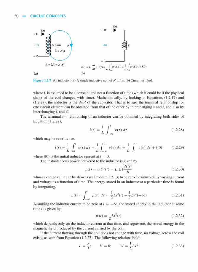
30 CIRCUIT CONCEPTS
i(t)i(t)
(a)
L
+
−
+
−
v(t)v(t) N turns
L = λ/i = Nψ/i
λ = Nψ
ψ
(b)
v(t) = L ;didt L
1i(t) = ∫ v(τ) dτt
L1= ∫ v(τ) dτ + i(0)
0
t
Figure 1.2.7 An inductor. (a) A single inductive coil of N turns. (b) Circuit symbol.
where L is assumed to be a constant and not a function of time (which it could be if the physicalshape of the coil changed with time). Mathematically, by looking at Equations (1.2.17) and(1.2.27), the inductor is the dual of the capacitor. That is to say, the terminal relationship forone circuit element can be obtained from that of the other by interchanging v and i, and also byinterchanging L and C.
The terminal i–v relationship of an inductor can be obtained by integrating both sides ofEquation (1.2.27),
i(t) = 1
L
∫ t
−∞v(τ) dτ (1.2.28)
which may be rewritten as
i(t) = 1
L
∫ t
0v(τ) dτ + 1
L
∫ 0
−∞v(τ) dτ = 1
L
∫ t
0v(τ) dτ + i(0) (1.2.29)
where i(0) is the initial inductor current at t = 0.The instantaneous power delivered to the inductor is given by
p(t) = v(t)i(t) = Li(t)di(t)
dt(1.2.30)
whose average value can be shown (see Problem 1.2.13) to be zero for sinusoidally varying currentand voltage as a function of time. The energy stored in an inductor at a particular time is foundby integrating,
w(t) =∫ t
−∞p(τ) dτ = 1
2Li2(t)− 1
2Li2(−∞) (1.2.31)
Assuming the inductor current to be zero at t = −∞, the stored energy in the inductor at sometime t is given by
w(t) = 1
2Li2(t) (1.2.32)
which depends only on the inductor current at that time, and represents the stored energy in themagnetic field produced by the current carried by the coil.
If the current flowing through the coil does not change with time, no voltage across the coilexists, as seen from Equation (1.2.27). The following relations hold:
L = λ
I; V = 0; W = 1
2LI 2 (1.2.33)

1.2 LUMPED-CIRCUIT ELEMENTS 31
Under dc conditions, an ideal inductor acts like an ideal wire, or short circuit. Note that thecurrent through an inductor cannot change value instantaneously. However, there is no reason torule out an instantaneous change in the value of the inductor voltage. The student should justifythe statements made here by recalling Equation (1.2.27).
If the medium in the flux path has a linear magnetic characteristic (i.e., constant permeability),then the relationship between the flux linkages λ and the current i is linear, and the slope of thelinear λ–i characteristic gives the self-inductance, defined as flux linkage per ampere by Equation(1.2.26). While the inductance in general is a function of the geometry and permeability of thematerial medium, in a linear system it is independent of voltage, current, and frequency. If theinductor coil is wound around a ferrous core such as iron, the λ–i relationship will be nonlinearand even multivalued because of hysteresis. In such a case the inductance becomes a functionof the current, and the inductor is said to be nonlinear. However, we shall consider only linearinductors here.
Series and parallel combinations of inductors are often encountered. Figure 1.2.8 illustratesthese.
By invoking the principle of duality, it can be seen that the inductors in series combine likeresistors in series and capacitors in parallel; the inductors in parallel combine like resistors inparallel and capacitors in series. Thus, when L1 and L2 are in series,
Leq = L1 + L2 (1.2.34)
and when L1 and L2 are in parallel,
Leq = L1L2
L1 + L2or
1
Leq= 1
L1+ 1
L2(1.2.35)
A practical inductor may have considerable resistance in the wire of a coil, and sizablecapacitances may exist between various turns. A possible model for a practical inductor couldbe a combination of ideal elements: a combination of resistance and inductance in series, with acapacitance in parallel. Techniques for modeling real circuit elements will be used extensively inlater chapters.
Practical inductors range from about 0.1 µH to hundreds of millihenrys. Some, meant forspecial applications in power supplies, can have values as large as several henrys. In general, thelarger the inductance, the lower its frequency is in its usage. The smallest inductance values aregenerally used at radio frequencies. Although inductors have many applications, the total demanddoes not even remotely approach the consumption of resistors and capacitors. Inductors generallytend to be rather bulky and expensive, especially in low-frequency applications. Industry-widestandardization for inductors is not done to the same degree as for more frequently used devicessuch as resistors and capacitors.
i
A
C
(a) (b)
B
+
−
L1
L2
A
D
B
vv
C
+
−
i
i2i1
L1 L2
Figure 1.2.8 Inductors in series and par-allel. (a) L1 and L2 in series. (b) L1 and L2in parallel.
32 CIRCUIT CONCEPTS
EXAMPLE 1.2.4
(a) Consider a 5-µH inductor to which a current source i(t) is attached, as shown in FigureE1.2.3(b). Sketch the inductor voltage and stored energy as a function of time.
(b) Let a voltage source v(t) shown in Figure E1.2.3(a) be applied to the 5-µH inductorinstead of the current source in part (a). Sketch the inductor current and energy stored asa function of time.
(c) If three identical 5-µH inductors with initial current of 1 mA are connected (i) in seriesand (ii) in parallel, find the equivalent inductance for each case.
So l u t i on
(a) From the principle of duality and for the given values, it follows that the inductor-voltagewaveform is the same as the capacitor-current waveform of Example 1.2.3(a), in whichi(t) is to be replaced by v(t), and 25 and −50 mA are to be replaced by 25 and −50 mV.The stored energy w(t) is the same as in the solution of Example 1.2.3(a).
(b) The solution is the same as that of Example 1.2.3(b), except that v(t) in mV is to bereplaced by i(t) in mA.
(c) (i) Looking at the solution of Example 1.2.3(c), part (ii),
Leq = L1 + L2 + L3 = 3× 5× 10−6 H = 15 µH
with an initial current i(0) = 1 mA.
(ii) Following the solution of Example 1.2.3(c), part (i),
1
Leq= 1
L1+ 1
L2+ 1
L3= 3
5× 10⁻⁶or Leq = 5
3× 10⁻⁶ H = 5
3µH
with an initial current i(0) = 3 mA.
When more than one loop or circuit is present, the flux produced by the current in oneloop may link another loop, thereby inducing a current in that loop. Such loops are said tobe mutually coupled, and there exists a mutual inductance between such loops. The mutualinductance between two circuits is defined as the flux linkage produced in one circuit by a currentof 1 ampere in the other circuit. Let us now consider a pair of mutually coupled inductors, asshown in Figure 1.2.9. The self-inductances L11 and L22 of inductors 1 and 2, respectively, aregiven by
L11 = λ11
i1(1.2.36)
and
L22 = λ22
i2(1.2.37)
where λ11 is the flux linkage of inductor 1 produced by its own current i1, and λ22 is the fluxlinkage of inductor 2 produced by its own current i2. The mutual inductances L12 and L21 aregiven by

1.2 LUMPED-CIRCUIT ELEMENTS 33
L12 = λ12
i2(1.2.38)
and
L21 = λ21
i1(1.2.39)
where λ12 is the flux linkage of inductor 1 produced by the current i2 in inductor 2, and λ21 is theflux linkage of inductor 2 produced by the current i1 in inductor 1.
If a current of i1 flows in inductor 1 while the current in inductor 2 is zero, the equivalentfluxes are given by
ψ11 = λ11
N1(1.2.40)
and
ψ21 = λ21
N2(1.2.41)
where N1 and N2 are the number of turns of inductors 1 and 2, respectively. That part of the fluxof inductor 1 that does not link any turn of inductor 2 is known as the equivalent leakage flux ofinductor 1,
ψl1 = ψ11 − ψ21 (1.2.42)
Similarly,
ψl2 = ψ22 − ψ12 (1.2.43)
The coefficient of coupling is given by
k = √k1k2 (1.2.44)
i1 i2i2 = 0 i1 = 0
v2open
v1open
(a) (b)
+
−
+
−
+
−
+
−
v1 v2
N1turns
N2turns
N1turns
N2turns
ψ21
ψl1 ψl2
ψ12
i1 i2
v2
(c)
+
−
+
−
v1
N2 turnsN1 turns
ψ21
ψ12
ψl1
ψl2
Figure 1.2.9 Mutually coupled inductors.

34 CIRCUIT CONCEPTS
where k1 = ψ21/ψ11 and k2 = ψ12/ψ22. When k approaches unity, the two inductors are saidto be tightly coupled; and when k is much less than unity, they are said to be loosely coupled.While the coefficient of coupling can never exceed unity, it may be as high as 0.998 for iron-coretransformers; it may be smaller than 0.5 for air-core transformers.
When there are only two inductively coupled circuits, the symbol M is frequently used torepresent the mutual inductance. It can be shown that the mutual inductance between two electriccircuits coupled by a homogeneous medium of constant permeability is reciprocal,
M = L12 = L21 = k√L11L22 (1.2.45)
The energy considerations that lead to such a conclusion are taken up in Problem 1.2.30 as anexercise for the student.
Let us next consider the energy stored in a pair of mutually coupled inductors,
Wm = i1λ1
2+ i2λ2
2(1.2.46)
where λ1 and λ2 are the total flux linkages of inductors 1 and 2, respectively, and subscript mdenotes association with the magnetic field. Equation (1.2.46) may be rewritten as
Wm = i1
2(λ11 + λ12)+ i2
2(λ22 + λ21)
= 1
2L11i
21 +
1
2L12i1i2 + 1
2L22i
22 +
1
2L21i1i2
or
Wm = 1
2L11i
21 +Mi1i2 + 1
2L22i
22 (1.2.47)
Equation (1.2.47) is valid whether the inductances are constant or variable, so long as themagnetic field is confined to a uniform medium of constant permeability.
Where there are n coupled circuits, the energy stored in the magnetic field can be expressed as
Wm =n∑
j=1
n∑k=1
1
2Ljkij ik (1.2.48)
Going back to the pair of mutually coupled inductors shown in Figure 1.2.9, the flux-linkagerelations and the voltage equations for circuits 1 and 2 are given by the following equations, whilethe resistances associated with the coils are neglected:
λ1 = λ11 + λ12 = L11i1 + L12i2 = L11i1 +Mi2 (1.2.49)
λ2 = λ21 + λ22 = L21i1 + L22i2 = Mi1 + L22i2 (1.2.50)
υ1 = dλ1
dt= L11
di1
dt+M
di2
dt(1.2.51)
υ2 = dλ2
dt= M
di1
dt+ L22
di2
dt(1.2.52)
For the terminal voltage and current assignments shown in Figure 1.2.9, the coil windingsare such that the fluxes produced by currents i1 and i2 are additive in nature, and in such a casethe algebraic sign of the mutual voltage term is positive, as in Equations (1.2.51) and (1.2.52).
In order to avoid drawing detailed sketches of windings showing the sense in which eachcoil is wound, a dot convention is developed, according to which the pair of mutually coupledinductors of Figure 1.2.9 are represented by the system shown in Figure 1.2.10. The notation
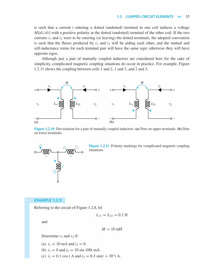
1.2 LUMPED-CIRCUIT ELEMENTS 35
is such that a current i entering a dotted (undotted) terminal in one coil induces a voltageM[di/dt] with a positive polarity at the dotted (undotted) terminal of the other coil. If the twocurrents i1 and i2 were to be entering (or leaving) the dotted terminals, the adopted conventionis such that the fluxes produced by i1 and i2 will be aiding each other, and the mutual andself-inductance terms for each terminal pair will have the same sign; otherwise they will haveopposite signs.
Although just a pair of mutually coupled inductors are considered here for the sake ofsimplicity, complicated magnetic coupling situations do occur in practice. For example, Figure1.2.11 shows the coupling between coils 1 and 2, 1 and 3, and 2 and 3.
i1 i2
(a)
+
−
+
−
L11
M
L22v1 v2
i1 i2
(b)
+
−
+
−
L11
M
L22v1 v2
Figure 1.2.10 Dot notation for a pair of mutually coupled inductors. (a) Dots on upper terminals. (b) Dotson lower terminals.
2
31
Figure 1.2.11 Polarity markings for complicated magnetic couplingsituations.
EXAMPLE 1.2.5
Referring to the circuit of Figure 1.2.8, let
L11 = L22 = 0.1 H
and
M = 10 mH
Determine v1 and v2 if:
(a) i1 = 10 mA and i2 = 0.
(b) i1 = 0 and i2 = 10 sin 100t mA.
(c) i1 = 0.1 cos t A and i2 = 0.3 sin(t + 30°) A.

36 CIRCUIT CONCEPTS
Also find the energy stored in each of the above cases at t = 0.
So l u t i on
L11 = L22 = 0.1H; M = 10 mH = 10× 10−3 H
v1 = L11di1
dt+M
di2
dt; v2 = M
di1
dt+ L22
di2
dt
Wm = energy stored = 1
2L11i
21 + L12i1i2 + 1
2L22i
22
(a) Since both i1 and i2 are constant and not a function of time,
v1 = 0; v2 = 0
Wm = 12 (0.1)(10× 10−3)2 + 0+ 0 = 5× 10⁻⁶ J = 5 µJ
(b) v1 = 0+ 10× 10−3(10× 100 cos 100t)10−3 = 10 cos 100t mV
v2 = 0+ 0.1(10× 100 cos 100t)10−3 = 100 cos 100t mV = 0.1 cos 100t V
Wm = 0+ 0+ 12 (0.1)(100 sin2 100t)10−6; Wm = 0 at t = 0
(c) v1 = 0.1(−0.1 sin t)+10×10−3[0.3 cos(t +30°)] = −10 sin t +3 cos(t +30°) mV
v2 = 10×10−3 (−0.01 sin t)+0.1[0.3 cos(t +30°)] = − sin t +30 cos(t +30°) mV
Wm = 12 (0.1)(0.01 cos2 t)+ (10× 10−3)(0.1 cos t)[0.3 sin(t + 30°)]+ 1
2 (0.1)[0.09 sin2(t + 30°)]; at t = 0
Wm = 12 (0.1)(0.01)+ 10× 10−3(0.1)(0.15)+ 1
2 (0.1)(
0.094
) = 1.775 µJ
Transformer
A transformer is basically a static device in which two or more stationary electric circuits arecoupled magnetically, the windings being linked by a common time-varying magnetic flux. Allthat is really necessary for transformer action to take place is for the two coils to be so positionedthat some of the flux produced by a current in one coil links some of the turns of the other coil.Some air-core transformers employed in communications equipment are no more elaborate thanthis. However, the construction of transformers utilized in power-system networks is much moreelaborate to minimize energy loss, to produce a large flux in the ferromagnetic core by a current inany one coil, and to see that as much of that flux as possible links as many of the turns as possibleof the other coils on the core.
An elementary model of a two-winding core-type transformer is shown in Figure 1.2.12.Essentially it consists of two windings interlinked by a mutual magnetic field. The winding thatis excited or energized by connecting it to an input source is usually referred to as the primarywinding, whereas the other, to which the electric load is connected and from which the outputenergy is taken, is known as the secondary winding. Depending on the voltage level at whichthe winding is operated, the windings are classified as HV (high voltage) and LV (low voltage)windings. The terminology of step-up or step-down transformer is also common if the mainpurpose of the transformer is to raise or lower the voltage level. In a step-up transformer, theprimary is a low-voltage winding whereas the secondary is a high-voltage winding. The oppositeis true for a step-down transformer.

1.2 LUMPED-CIRCUIT ELEMENTS 37
Mutual flux
LoadPrimarywinding(N1 turns)
Secondarywinding(N2 turns)
Ferromagnetic coreof infinite permeability
Resistive loadwith resistance R2
+
−
+
−
+
−
e1 = v1
e2 = v2
i1
v1
i2
φ
Figure 1.2.12 Elementary model of a two-winding core-type transformer (ideal transformer).
An ideal transformer is one that has no losses (associated with iron or copper) and noleakage fluxes (i.e., all the flux in the core links both the primary and the secondary windings).The winding resistances are negligible. While these properties are never actually achieved inpractical transformers, they are, however, approached closely. When a time-varying voltage v1
is applied to the N1-turn primary winding (assumed to have zero resistance), a core flux φ isestablished and a counter emf e1 with the polarity shown in Figure 1.2.12 is developed such thate1 is equal to v1. Because there is no leakage flux with an ideal transformer, the flux φ also linksall N2 turns of the secondary winding and produces an induced emf e2, according to Faraday’slaw of induction. Since v1 = e1 = dλ1/dt = N1 dφ/dt and v2 = e2 = dλ2/dt = N2 dφ/dt , itfollows from Figure 1.2.12 that
v1
v2= e1
e2= N1
N2= a (1.2.53)
where a is the turns ratio. Thus, in an ideal transformer, voltages are transformed in the directratio of the turns. For the case of an ideal transformer, since the instantaneous power input equalsthe instantaneous power output, it follows that
v1i1 = v2i2 ori1
i2= v2
v1= N2
N1= 1
a(1.2.54)
which implies that currents are transformed in the inverse ratio of the turns.Equivalent circuits viewed from the source terminals, when the transformer is ideal, are
shown in Figure 1.2.13. As seen from Figure 1.2.13(a), since v1 = (N1/N2)v2, i1 = (N2/N1)i2,and v2 = i2RL, it follows that
v1
i1=(N1
N2
)2
RL = a2RL = R′L (1.2.55)
where R′L is the secondary-load resistance referred to the primary side. The consequence ofEquation (1.2.55) is that a resistance RL in the secondary circuit can be replaced by an equivalentresistance R′L in the primary circuit in so far as the effect at the source terminals is concerned. Thereflected resistance through a transformer can be very useful in resistance matching for maximumpower transfer, as we shall see in the following example. Note that the circuits shown in Figure1.2.13 are indistinguishable viewed from the source terminals.

38 CIRCUIT CONCEPTS
−
+
N1
Ideal transformer(a)
N2
v1
i1 i2
v2
+
−
+
−
RL
−
+
N1 N2
(b)
v1
i1 i2
+
−
−
+
(c)
v1
i1
+
−
RL = RLN1
N2
2( )
RL = RLN1
N2
2( ) = a2RL
′
′
Figure 1.2.13 Equivalent circuits viewed from sourceterminals when the transformer is ideal.
EXAMPLE 1.2.6
Consider a source of voltage v(t) = 10√
2 sin 2t V, with an internal resistance of 1800 . Atransformer that can be considered ideal is used to couple a 50- resistive load to the source.
(a) Determine the primary to secondary turns ratio of the transformer required to ensuremaximum power transfer by matching the load and source resistances.
(b) Find the average power delivered to the load.
So l u t i on
By considering a constant voltage source (with a given internal resistance RS) connected to avariable-load resistance RL, as shown in Figure E1.2.6(a), for a value of RL equal to RS givenby Equation (1.2.13), the maximum power transfer to the load resistance would occur when theload resistance is matched with the source resistance.
(a) For maximum power transfer to the load, R′L (i.e., RL referred to the primary side of thetransformer) should be equal to RS , which is given to be 1800 . Hence,
R′L = a2RL = 50a2 = 1800 or a2 = 36, or a = 6.
Thus N1/N2 = 6 [see Figure E1.2.6(b)].

1.3 KIRCHHOFF’S LAWS 39
(b) By voltage division [see Figure E1.2.6(c)] one gets
v′L =1800
1800+ 1800(10√
2 sin 2t) = (5√
2 sin 2t) V
which has an rms value of 5 V. Hence, the average power delivered to the load resistance(R′L or RL) is
Pav = (V ′L RMS)2
1800= 25
1800W ∼= 13.9 mW
Note that vL across RL is (5√
2/6) sin 2t V, and iL through RL is (5√
2/6× 50) sin 2tA. The rms value of iL is then 5/300 A, and the rms value of vL is 5/6 V. Thus,
Pav = 5
300× 5
6W ∼= 13.9 mW
which is also the same as
Pav = I 2L RMS RL = V 2
L RMS/RL
−
+ RSv RL
(a)
Lυ Lυ′−
+
RS = 1800 Ω
RL = 50 Ω10 2 sin 2t V
N1 N2iLiL
Ideal transformer
(b)
Source Load
+
−
+
−
:′
Lυ ′ ′−
+
RS = 1800 Ω
RL = 1800 Ω10 2 sin 2t V
iL
(c)
+
−
′
Figure E1.2.6
1.3 KIRCHHOFF’S LAWS
The basic laws that must be satisfied among circuit currents and circuit voltages are known asKirchhoff’s current law (KCL) and Kirchhoff’s voltage law (KVL). These are fundamental forthe systematic analysis of electric circuits.
KCL states that, at any node of any circuit and at any instant of time, the sum of all currentsentering the node is equal to the sum of all currents leaving the node. That is, the algebraic sum of
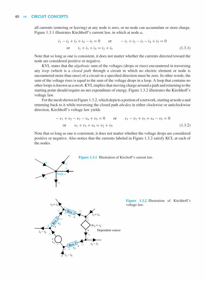
40 CIRCUIT CONCEPTS
all currents (entering or leaving) at any node is zero, or no node can accumulate or store charge.Figure 1.3.1 illustrates Kirchhoff’s current law, in which at node a,
i1 − i2 + i3 + i4 − i5 = 0 or − i1 + i2 − i3 − i4 + i5 = 0
or i1 + i3 + i4 = i2 + i5 (1.3.1)
Note that so long as one is consistent, it does not matter whether the currents directed toward thenode are considered positive or negative.
KVL states that the algebraic sum of the voltages (drops or rises) encountered in traversingany loop (which is a closed path through a circuit in which no electric element or node isencountered more than once) of a circuit in a specified direction must be zero. In other words, thesum of the voltage rises is equal to the sum of the voltage drops in a loop. A loop that contains noother loops is known as a mesh. KVL implies that moving charge around a path and returning to thestarting point should require no net expenditure of energy. Figure 1.3.2 illustrates the Kirchhoff’svoltage law.
For the mesh shown in Figure 1.3.2, which depicts a portion of a network, starting at node a andreturning back to it while traversing the closed path abcdea in either clockwise or anticlockwisedirection, Kirchhoff’s voltage law yields
− v1 + v2 − v3 − v4 + v5 = 0 or v1 − v2 + v3 + v4 − v5 = 0
or v1 + v3 + v4 = v2 + v5 (1.3.2)
Note that so long as one is consistent, it does not matter whether the voltage drops are consideredpositive or negative. Also notice that the currents labeled in Figure 1.3.2 satisfy KCL at each ofthe nodes.
i4 i5
i2
i1
i3Node a
Figure 1.3.1 Illustration of Kirchoff’s current law.
Box 5
Box 3
Box 2
c
d
e
a
bDependent source
−
−−
−
−
++
+
+
+
i3i2
v2
v1
Av2 = v4
v5
v3
i1
i5
i1 − i5
i1 − i2
i2 + i3
i3 + i4
i4 − i5
i4
Figure 1.3.2 Illustration of Kirchhoff’svoltage law.

1.3 KIRCHHOFF’S LAWS 41
In a network consisting of one or more energy sources and one or more circuit elements,the cause-and-effect relationship in circuit theory can be studied utilizing Kirchhoff’s laws andvolt-ampere relationships of the circuit elements. While the cause is usually the voltage or currentsource exciting the circuit, the effect is the voltages and currents existing in various parts ofthe network.
EXAMPLE 1.3.1
Consider the circuit shown in Figure E1.3.1 and determine the unknown currents using KCL.
iS = 10 A i1 = 5 A
i4 = 3 A i2 = 4 Ai5 = ? i3 = ?
+−
Node aNode b
Node c
Figure E1.3.1
So l u t i on
Let us assign a + sign for currents entering the node and a − sign for currents leaving the node.Applying KCL at node a, we get
+ iS − i1 − i4 − i5 = 0
or
10− 5− 3− i5 = 0 or i5 = 2 A
Applying KCL at node b, we get
+ i1 − i2 − i3 = 0
or
5− 4− i3 = 0 or i3 = 1 A
The student is encouraged to rework this problem by:
(a) Assigning a − sign for currents entering the node and a + sign for currents leaving thenode; and
(b) Applying the statement that the sum of the currents entering a node is equal to the sumof the currents leaving that node.

42 CIRCUIT CONCEPTS
EXAMPLE 1.3.2
For the circuit shown in Figure E1.3.2, use KCL and KVL to determine i1, i2, vbd and vx . Also,find veb.
d
e
b fa c
+−
+
−+
+ −
−
−+
8 A
20 V
3 V
i1 = ?
ibfab = 5 V
i2 = ?
−3 A
10 A 8 V
υ
bd = ?υ +
−x = ?υ
Figure E1.3.2
So l u t i on
Using KCL at node c, we get
i1 = 8+ (−3 = 5 A
Using KCL at node f, we have
ibf = i1 − (−3) = 5+ 3 = 8 A
Applying KCL at node b, we get
10 = i2 + ibf = i2 + 8 or i2 = 2 A
Using KVL around the loop abdea in the clockwise direction, we have
vab + vbd + vde + vea = 0
or
5+ vbd + 8− 20 = 0 or vbd = 20− 8− 5 = 7 V
Note that in writing KVL equations with + and − polarity symbols, we write the voltage with apositive sign if the+ is encountered before the− and with a negative sign if the− is encounteredfirst as we move around the loop.
Applying KVL around the loop abfcea in the clockwise direction, we get
vab + vbf + vf c + vce + vea = 0
or
5+ 0+ 3+ vx + (−20) = 0 or vx = 20− 3− 5 = 12 V
Note that a direct connection between b and f implies ideal connection, and hence no voltagebetween these points.
The student is encouraged to rewrite the loop equations by traversing the closed path in theanticlockwise direction.
Noting that veb = ved + vdb, we have

1.3 KIRCHHOFF’S LAWS 43
veb = −8− 7 = −15 V
Alternatively,
veb = vea + vab = −20+ 5 = −15 V
or
veb = vec + vcf + vf b = −vx + vcf + 0 = −12− 3 = −15 V
The student should observe that vbe = −veb = 15 V and node b is at a higher potential thannode e.
EXAMPLE 1.3.3
Referring to Figure 1.3.2, let boxes 2, 3, and 5 consist of a 0.2-H inductor, a 5- resistor, and a0.1-F capacitor, respectively. Given A = 5, and v1 = 10 sin 10t, i2 = 5 sin 10t , and i3 = 2 sin10t − 4 cos 10t, find i5.
So l u t i on
From Equation (1.2.19),
v2 = Ldi2
dt= 0.2
d
dt(5 sin 10t) = 10 cos 10t V
From Equation (1.2.1),
v3 = Ri3 = 5(2 sin 10t − 4 cos 10t) = 10 sin 10t − 20 cos 10t V
From Equation (1.3.2),
v5 = v1 + v3 + v4 − v2 = v1 + v3 + 5v2 − v2
= 10 sin 10t + (10 sin 10t − 20 cos 10t)+ 4(10 cos 10t)
= 20 sin 10t + 20 cos 10t V
From Equation (1.2.9),
i5 = Cdv5
dt= 0.1
d
dt(20 sin 10t + 20 cos 10t)
= 20 cos 10t − 20 sin 10t A
Note the consistency of voltage polarities and current directions in Figure 1.3.2.
EXAMPLE 1.3.4
Consider the network shown in Figure E1.3.4(a).
(a) Find the voltage drops across the resistors and mark them with their polarities on thecircuit diagram.
(b) Check whether the KVL is satisfied, and determine Vbf and Vec.

44 CIRCUIT CONCEPTS
(c) Show that the conservation of power is satisfied by the circuit.
−
+
−
+R1 = 10 Ω
I
R2 = 40 Ω
R4 = 50 Ω
R3 = 20 Ω12 V 24 V
a b c d
f e
(a)
Figure E1.3.4
−
+
+ − −
+12 V
5 V
− +1 V − +4 V − +2 V
24 V
a b c d
f e
(b)
So l u t i on
(a) From Ohm’s law, the current I is given by
I = 24− 12
10+ 40+ 20+ 50= 12
120= 0.1 A
Therefore, voltage drops across the resistors are calculated as follows:
Vba = IR1 = 0.1× 10 = 1 V
Vcb = IR2 = 0.1× 40 = 4 V
Vdc = IR3 = 0.1× 20 = 2 V
Vfe = IR4 = 0.1× 50 = 5 V
These are shown in Figure E1.3.4(b) with their polarities. Note that capital letters areused here for dc voltages and currents.
(b) Applying the KVL for the closed path edcbafe, we get
− 24+ 2+ 4+ 1+ 12+ 5 = 0
which confirms that the KVL is satisfied,
Vbf = Vba + Vaf = 1+ 12 = 13 V
Vec = Ved + Vdc = −24+ 2 = −22 V
(c) Power delivered by 24-V source = 24× 0.1 = 2.4 W
Power delivered by 12-V source = −12× 0.1 = −1.2 W
Power absorbed by resistor R1 = (0.1)2 × 10 = 0.1 W
Power absorbed by resistor R2 = (0.1)2 × 40 = 0.4 W
Power absorbed by resistor R3 = (0.1)2 × 20 = 0.2 W

1.3 KIRCHHOFF’S LAWS 45
Power absorbed by resistor R4 = (0.1)2 × 50 = 0.5 W
Power delivered by sources = 2.4− 1.2 = 1.2 W
Power absorbed by resistors R1, R2, R3, and R4 = 0.1+ 0.4+ 0.2+ 0.5 = 1.2 W
The conservation of power is satisfied by the circuit.
EXAMPLE 1.3.5
Given the network in Figure E1.3.5,
(a) Find the currents through resistors R1, R2, and R3.
(b) Compute the voltage V1.
(c) Show that the conservation of power is satisfied by the circuit.
R1 = R2 =
I1
V1
I2 I3
12 A 6 A6 Ω
Ground node
Node 1
R3 =4 Ω 12 Ω
Figure E1.3.5
So l u t i on
(a) Applying the KCL at node 1, we have
12 = V1
R1+ V1
R2+ V1
R3+ 6 = V1
(1
6+ 1
4+ 1
12
)+ 6 = V1
2+ 6
Therefore, V1 = 12 V. Then,
I1 = 12
6= 2 A
I2 = 12
4= 3 A
I3 = 12
12= 1 A
(b) V1 = 12 V
(c) Power delivered by 12-A source = 12× 12 = 144 W
Power delivered by 6-A source = −6× 12 = −72 W
Power absorbed by resistor R1 = I 21 R1 = (2)26 = 24 W

46 CIRCUIT CONCEPTS
Power absorbed by resistor R2 = I 22 R2 = (3)24 = 36 W
Power absorbed by resistor R3 = I 23 R3 = (1)212 = 12 W
Power delivered by sources = 144− 72 = 72 W
Power absorbed by resistors R1, R2, and R3 = 24+ 36+ 12 = 72 W
The conservation of power is satisfied by the circuit.
EXAMPLE 1.3.6
Consider the network shown in Figure E1.3.6 containing a voltage-controlled source producingthe controlled current ic = gv, where g is a constant with units of conductance, and the controlvoltage happens to be the terminal voltage in this case.
(a) Obtain an expression for Req = v/i.
(b) For (i) gR = 1/2, (ii) gR = 1, and (iii) gR = 2, find Req and interpret what it means ineach case.
Rv ic = gviR
i
Node 2
Node 1
−
+
Figure E1.3.6
So l u t i on
(a) Applying the KCL at node 1, we get
i + ic = iR = v
R
Therefore,
i = v
R− ic = v
R− gv = 1− gR
Rv
Then,
Req = v
i= R
1− gR
(b) (i) For gR = 1/2, Req = 2R. The equivalent resistance is greater than R; the internalcontrolled source provides part of the current through R, thereby reducing the inputcurrent i for a given value of v. When i < v/R, the equivalent resistance is greaterthan R.

1.4 METERS AND MEASUREMENTS 47
(ii) For gR = 1, Req → ∞. The internal controlled source provides all of the currentthrough R, thereby reducing the input current i to be zero for a given value of v.
(iii) For gR = 2, Req = −R, which is a negative equivalent resistance. This means thatthe controlled source provides more current than that going through R; the currentdirection of i is reversed when v > 0. However, the relation v = Reqi is satisfied atthe input terminals.
1.4 METERS AND MEASUREMENTS
The subject of electrical measurements is such a large one that entire books have been written onthe topic. Only a few basic principles will be introduced here. Practical measurements are madewith real instruments, which in general disturb the operation of a circuit to some extent when theyare connected. Measurements may be affected by noise, which is undesirable randomly varyingsignals.
Voltmeter
In order to measure the potential difference between two terminals or nodes of a circuit, a voltmeteris connected across these two points. A practical voltmeter can usually be modeled as a parallelcombination of an ideal voltmeter (through which no current flows) and a shunt resistance RV, asshown in Figure 1.4.1. The internal resistance RV of an ideal voltmeter is infinite, while its valuein practice is of the order of several million ohms. There are what are known as dc voltmetersand ac voltmeters. An ac voltmeter usually measures the rms value of the time-varying voltage.
Rv
−
+
−
+Idealvoltmeter
Practical voltmeter
Figure 1.4.1
EXAMPLE 1.4.1
An electromechanical voltmeter with internal resistance of 1 k and an electronic voltmeter withinternal resistance of 10 M are used separately to measure the potential difference between Aand the ground of the circuit shown in Figure E1.4.1. Calculate the voltages that will be indicatedby each of the two instruments and the percentage error in each case.
Rv−
+
−
+
Ground Voltmeter
2 V
10 kΩ
10 kΩ
A Figure E1.4.1

48 CIRCUIT CONCEPTS
So l u t i on
When no instrument is connected, by voltage division, V + AG = 1 V. With internal resistanceRV of the instrument, the voltmeter reading will be
VA = 2.0
(RV ‖104
RV ‖104 + 104
)= 2
(RV · 104
RV + 104
)/( RV · 104
RV + 104+ 104
)
= 2RV · 104
2× 10⁴ RV + 108
With RV = 1000,
VA = 2× 10⁷
2× 10⁷ + 108= 2
2+ 10= 2
12= 0.1667 V
for which the percent error is1− 0.1667
1× 100 = 83.33%
With RV = 107 ,
VA = 2× 10¹¹
2× 10¹¹ + 108= 2000
2000+ 1= 0.9995 V
for which the percent error is
1− 0.9995
1× 100 = 0.05%
One can see why electronic voltmeters which have relatively very large internal resistance areoften used.
Ammeter
In order to measure the current through a wire or line of a circuit, an ammeter is connected inseries with the line. A practical ammeter can usually be modeled as a series combination of anideal ammeter and an internal resistance RI. The potential difference between the two terminalsof an ideal ammeter is zero, which corresponds to zero internal resistance. There are what areknown as dc ammeters and ac ammeters. An ac ammeter usually measures the rms value of thetime-varying current. Note that for the ammeter to be inserted for measuring current, the circuithas to be broken, whereas for the voltmeter to be connected for measuring voltage, the circuitneed not be disassembled.
Multimeters that measure multiple ranges of voltage and current are available in practice.Ohmmeters measure the dc resistance by the use of Ohm’s law. A multimeter with scales forvolts, ohms, and milliamperes is known as VOM. An ohmmeter should not be used to measurethe resistance of an electronic component that might be damaged by the sensing current.
Instrument Transformers
These are generally of two types, potential transformers (PTs) and current transformers (CTs).They are designed in such a way that the former may be regarded as having an ideal potentialratio, whereas the latter has an ideal current ratio. The accuracy of measurement is quite importantfor ITs that are commonly used in ac circuits to supply instruments, protective relays, and controldevices.

1.4 METERS AND MEASUREMENTS 49
PTs are employed to step down the voltage to a suitable level, whereas CTs (connected inseries with the line) are used to step down the current for metering purposes. Often the primary ofa CT is not an integral part of the transformer itself, but is a part of the line whose current is beingmeasured. In addition to providing a desirable low current in the metering circuit, the CT isolatesthe meter from the line, which may be at a high potential. Note that the secondary terminalsof a CT should never be open-circuited under load. The student is encouraged to reason andjustify this precaution. One of the most useful instruments for measuring currents in the ampererange is the clip-on ammeter combining the CT with one-turn primary and the measurementfunctions.
Oscilloscope
To measure time-varying signals (voltages and currents), an instrument known as an oscilloscopeis employed. It can be used as a practical electronic voltmeter which displays a graph of voltageas a function of time. Such a display allows one not only to read off the voltage at any instant oftime, but also to observe the general behavior of the voltage as a function of time. The horizontaland vertical scales of the display are set by the oscilloscope’s controls, such as 5 ms per eachhorizontal division and 50 V per each vertical division. For periodic waveforms, the movinglight spot repeatedly graphs the same repetitive shape, and the stationary waveform is seen. Fornonperiodic cases, a common way of handling is to cause the oscilloscope to make only one singlegraph, representing the voltage over a single short time period. This is known as single-sweepoperation. Since the display lasts for only a very short time, it may be photographed for laterinspection.
Digital meters are generally more accurate and can be equipped with more scales and broaderranges than analog meters. On the other hand, analog meters are generally less expensive and givean entire range or scale of reading, which often could be very informative. A digital oscilloscoperepresents the combination of analog and digital technologies. By digital sampling techniques,the oscilloscope trace is digitized and stored in the digital memory included with the digitaloscilloscope. Digital oscilloscopes are generally more costly than analog ones, but their capabilityin the analysis and processing of signals is vastly superior.
Wheatstone Bridge
Null measurements are made with bridge circuits and related configurations. They differ fromdirect measurements in that the quantity being measured is compared with a known referencequantity. The balancing strategy avoids undesirable interaction effects and generally results inmore accurate measurement than the direct one.
By far the most common is the Wheatstone bridge designed for precise measurement ofresistance. Figure 1.4.2 shows the basic circuit in which the measurement of an unknown resistanceRx is performed by balancing the variable resistances Ra and Rb until no current flows throughmeter A. Under this null condition,
Rx = Ra
Rb
· Rs (1.4.1)
where Rs is the known standard resistance. There are other bridge-circuit configurations tomeasure inductance and capacitance. Typical instruments utilizing bridge circuits are found instrain gauges measuring stress and in temperature measuring systems with thermocouples andthermistors.

50 CIRCUIT CONCEPTS
V
RaRb
Rs Rx
A
Figure 1.4.2 Basic Wheatstone bridge circuit for resistancemeasurement.
EXAMPLE 1.4.2
Redraw the Wheatstone bridge circuit of Figure 1.4.2 and show that Equation (1.4.1) holds goodfor the null condition when the meter A reads zero current.
So l u t i on
Rb Rs
P Q
Ra
vPQ = 0
Rx
v
Figure E1.4.2 Figure 1.4.2 redrawn.
Under null condition, VPQ = 0, or P and Q are at the same potential. Using the voltage divisionprinciple, (
V
Rb + Ra
)Rb =
(V
Rs + Rx
)Rs
yielding RxRb = RaRs , which is the same as Equation (1.4.1).
1.5 ANALOGY BETWEEN ELECTRICAL AND OTHER NONELECTRICPHYSICAL SYSTEMS
Systems such as those encountered in mechanics, thermodynamics, and hydraulics can be repre-sented by analogous electric networks, from the response of which the system characteristics canbe investigated. The analogy, of course, is a mathematical one: that is, two systems are analogousto each other if they are described by similar equations. The analogous electric quantities for amechanical system are listed in Table 1.5.1.
Consider a tank filled with water, as shown in Figure 1.5.1, with input flow rate Fi and outputflow rate Fo = h/R, where h is the fluid level or head and R is related to the diameter of thepipe, denoting the fluid resistance. Let A be the cross-sectional area of the tank. We may think ofthe fluid as being analogous to charge, and the fluid flow as being analogous to current. Then, ineffect, the water tank acts as a capacitor storing charge, which is fluid in this case. This analogyis illustrated in Table 1.5.2.
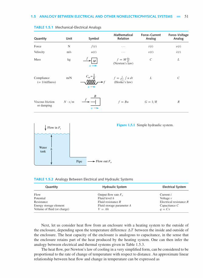
1.5 ANALOGY BETWEEN ELECTRICAL AND OTHER NONELECTRICPHYSICAL SYSTEMS 51
TABLE 1.5.1 Mechanical-Electrical Analogs
Mathematical Force–Current Force–VoltageQuantity Unit Symbol Relation Analog Analog
Force N f (t) · · · i(t) v(t)
Velocity m/s u(t) · · · v(t) i(t)
Mass kg f = M dudt
C L
(Newton’s law)
f
B
Cm =
M
f
u
1K
u
u
fCompliance m/N f = 1
Cm
∫u dt L C
(= 1/stiffness) (Hooke’s law)
Viscous friction N · s/m f = Bu G = 1/R R
or damping
Pipe
Watertank
h
Flow out Fo
Flow in FiFigure 1.5.1 Simple hydraulic system.
TABLE 1.5.2 Analogy Between Electrical and Hydraulic Systems
Quantity Hydraulic System Electrical System
Flow Output flow rate Fo Current iPotential Fluid level h Voltage vResistance Fluid resistance R Electrical resistance REnergy storage element Fluid storage parameter A Capacitance CVolume of fluid (or charge) V = Ah q = Cv
Next, let us consider heat flow from an enclosure with a heating system to the outside ofthe enclosure, depending upon the temperature difference T between the inside and outside ofthe enclosure. The heat capacity of the enclosure is analogous to capacitance, in the sense thatthe enclosure retains part of the heat produced by the heating system. One can then infer theanalogy between electrical and thermal systems given in Table 1.5.3.
The heat flow, per Newton’s law of cooling in a very simplified form, can be considered to beproportional to the rate of change of temperature with respect to distance. An approximate linearrelationship between heat flow and change in temperature can be expressed as

52 CIRCUIT CONCEPTS
TABLE 1.5.3 Analogy Between Thermal and Electrical Systems
Thermal System Electrical System
Heat ChargeHeat flow CurrentTemperature difference VoltageAmbient temperature Ground referenceHeat capacity CapacitanceThermal resistance Electrical resistance
Heat flow ∼= k
xT (1.5.1)
where k is a constant, and k/x in thermal systems is analogous to conductance in electricalsystems. Then Newton’s law of cooling, in a very simplified form, can be seen to be a thermalversion of Ohm’s law.
1.6 LEARNING OBJECTIVES
The learning objectives of this chapter are summarized here, so that the student can check whetherhe or she has accomplished each of the following.
• Review of basic electrical quantities.
• Application of Coulomb’s law, Ampere’s law, and the Biot–Savart law.
• Energy and power computations in a circuit consisting of a source and a load.
• Calculation of average and RMS values for periodic waveforms, and time constant forexponential waveforms.
• i–v relationships for ideal resistors, capacitors, and inductors; duality principle.
• Reduction of series and parallel combinations of resistors, capacitors, and inductors.
• Solution of simple voltage and current divider circuits.
• Computation of power absorbed by a resistor, and energy stored in a capacitor or inductor.
• Maximum power transfer and matched load.
• Volt-ampere equations and energy stored in coupled inductors.
• Ideal transformer and its properties.
• Application of Kirchhoff’s current and voltage laws to circuits.
• Measurement of basic electrical parameters.
• Analogy between electrical and other nonelectric physical systems.
1.7 PRACTICAL APPLICATION: A CASE STUDY
Resistance Strain Gauge
Mechanical and civil engineers routinely employ the dependence of resistance on the physicaldimensions of a conductor to measure strain. A strain gauge is a device that is bonded to thesurface of an object, and whose resistance varies as a function of the surface strain experiencedby the object. Strain gauges can be used to measure strain, stress, force, torque, and pressure.

PROBLEMS 53
The resistance of a conductor with a circular cross-sectional area A, length l, and conductivityσ is given by Equation (1.2.2),
R = l
σA
Depending on the compression or elongation as a consequence of an external force, the lengthchanges, and hence the resistance changes. The relationship between those changes is given bythe gauge factor G,
G = R/R
l/l
in which the factor l/l, the fractional change in length of an object, is known as the strain.Alternatively, the change in resistance due to an applied strain ε(= l/l) is given by
R = R0Gε
where R0 is the zero-strain resistance, that is, the resistance of the strain gauge under no strain.A typical gauge has R0 = 350 and G = 2. Then for a strain of 1%, the change in resistance isR = 7 . A Wheatstone bridge as presented in Section 1.4 is usually employed to measure thesmall resistance changes associated with precise strain determination.
A typical strain gauge, shown in Figure 1.7.1, consists of a metal foil (such as nickel–copperalloy) which is formed by a photoetching process in multiple conductors aligned with the directionof the strain to be measured. The conductors are usually bonded to a thin backing made out ofa tough flexible plastic. The backing film, in turn, is attached to the test structure by a suitableadhesive.
Metal foil
R
Copper-plated solder tabsfor electrical connections
Flexible plasticbacking film
Direction ofstrain tobe measured
Figure 1.7.1 Resistance strain gauge and circuitsymbol.
1
PROBL EMS
1.1.1 Consider two 1-C charges separated by 1 m in freespace. Show that the force exerted on each is aboutone million tons.
*1.1.2 Point charges, each of√
4πε0 C, are located atthe vertices of an equilateral triangle of side a.Determine the electric force on each charge.
1.1.3 Two charges of equal magnitude 5µC but oppositesign are separated by a distance of 10 m. Findthe net force experienced by a positive charge
*Complete solutions for problems marked with an asterisk can be found on the CD-ROM packaged with this book.
q = 2 µC that is placed midway between the twocharges.
1.1.4 The electric field intensity due to a point charge infree space is given to be
(−ax − ay + az)/√
12V/m at (0,0,1)
and 6 az at (2,2,0)
Determine the location and the value of the pointcharge.
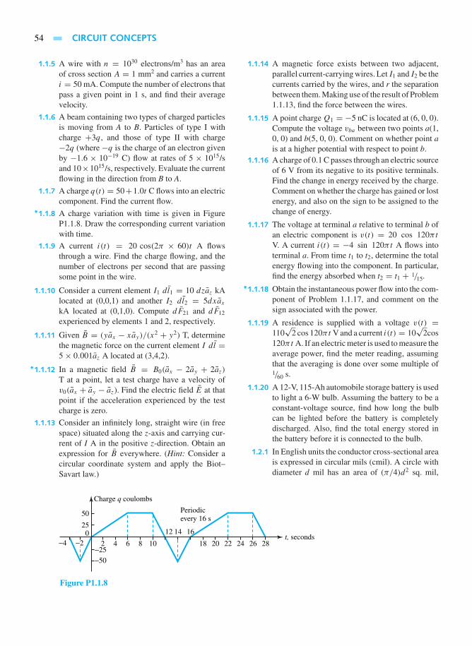
54 CIRCUIT CONCEPTS
1.1.5 A wire with n = 1030 electrons/m3 has an areaof cross section A = 1 mm2 and carries a currenti = 50 mA. Compute the number of electrons thatpass a given point in 1 s, and find their averagevelocity.
1.1.6 A beam containing two types of charged particlesis moving from A to B. Particles of type I withcharge +3q, and those of type II with charge−2q (where−q is the charge of an electron givenby −1.6 × 10⁻¹⁹ C) flow at rates of 5 × 10¹⁵/sand 10×1015/s, respectively. Evaluate the currentflowing in the direction from B to A.
1.1.7 A charge q(t) = 50+1.0t C flows into an electriccomponent. Find the current flow.
*1.1.8 A charge variation with time is given in FigureP1.1.8. Draw the corresponding current variationwith time.
1.1.9 A current i(t) = 20 cos(2π × 60)t A flowsthrough a wire. Find the charge flowing, and thenumber of electrons per second that are passingsome point in the wire.
1.1.10 Consider a current element I1 dl1 = 10 dzaz kAlocated at (0,0,1) and another I2 dl2 = 5dxaxkA located at (0,1,0). Compute dF21 and dF12
experienced by elements 1 and 2, respectively.
1.1.11 Given B = (yax − xay)/(x2 + y2) T, determine
the magnetic force on the current element I dl =5× 0.001az A located at (3,4,2).
*1.1.12 In a magnetic field B = B0(ax − 2ay + 2az)T at a point, let a test charge have a velocity ofv0(ax + ay − az). Find the electric field E at thatpoint if the acceleration experienced by the testcharge is zero.
1.1.13 Consider an infinitely long, straight wire (in freespace) situated along the z-axis and carrying cur-rent of I A in the positive z-direction. Obtain anexpression for B everywhere. (Hint: Consider acircular coordinate system and apply the Biot–Savart law.)
1.1.14 A magnetic force exists between two adjacent,parallel current-carrying wires. Let I1 and I2 be thecurrents carried by the wires, and r the separationbetween them. Making use of the result of Problem1.1.13, find the force between the wires.
1.1.15 A point charge Q1 = −5 nC is located at (6, 0, 0).Compute the voltage vba between two points a(1,0, 0) and b(5, 0, 0). Comment on whether point ais at a higher potential with respect to point b.
1.1.16 A charge of 0.1 C passes through an electric sourceof 6 V from its negative to its positive terminals.Find the change in energy received by the charge.Comment on whether the charge has gained or lostenergy, and also on the sign to be assigned to thechange of energy.
1.1.17 The voltage at terminal a relative to terminal b ofan electric component is v(t) = 20 cos 120πtV. A current i(t) = −4 sin 120πt A flows intoterminal a. From time t1 to t2, determine the totalenergy flowing into the component. In particular,find the energy absorbed when t2 = t1 + 1/15.
*1.1.18 Obtain the instantaneous power flow into the com-ponent of Problem 1.1.17, and comment on thesign associated with the power.
1.1.19 A residence is supplied with a voltage v(t) =110√
2 cos 120πt V and a current i(t) = 10√
2cos120πt A. If an electric meter is used to measure theaverage power, find the meter reading, assumingthat the averaging is done over some multiple of1/60 s.
1.1.20 A 12-V, 115-Ah automobile storage battery is usedto light a 6-W bulb. Assuming the battery to be aconstant-voltage source, find how long the bulbcan be lighted before the battery is completelydischarged. Also, find the total energy stored inthe battery before it is connected to the bulb.
1.2.1 In English units the conductor cross-sectional areais expressed in circular mils (cmil). A circle withdiameter d mil has an area of (π/4)d2 sq. mil,
2−25
−2−4
−50
50
250
4 6 8
Charge q coulombs
Periodicevery 16 s
10
12 14 16
18 20 22 24 26 28t, seconds
Figure P1.1.8

PROBLEMS 55
or d2 cmil. The handbook for aluminum electricalconductors lists a dc resistance of 0.01558 per1000 ft at 20°C for Marigold conductor, whosesize is 1113 kcmil.
(a) Verify the dc resistance assuming an increasein resistance of 3% for spiraling of the strands.
(b) Calculate the dc resistance at 50°C, giventhat the temperature constant for aluminumis 228.1°C.
(c) If the 60-Hz resistance of 0.0956 /mile at50°C is listed in the handbook, determine thepercentage increase due to skin effect or fre-quency.
1.2.2 MCM is the abbreviation for 1 kcmil. (See Prob-lem 1.2.1 for a definition of cmil.) Data for com-mercial-base aluminum electrical conductors lista 60-Hz resistance of 0.0880 /km at 75°C for a795-MCM conductor.
(a) Determine the cross-sectional conducting areaof this conductor in m2.
(b) Calculate the 60-Hz resistance of this con-ductor in /km at 50°C, given a temperatureconstant of 228.1°C for aluminum.
*1.2.3 A copper conductor has 12 strands with eachstrand diameter of 0.1328 in. For this conductor,find the total copper cross-sectional area in cmil(see Problem 1.2.1 for definition of cmil), andcalculate the dc resistance at 20°C in (ohms/km),assuming a 2% increase in resistance due to spi-raling.
1.2.4 A handbook lists the 60-Hz resistance at 50°C of a900-kcmil aluminum conductor as 0.1185 /mile.If four such conductors are used in parallel to forma line, determine the 60-Hz resistance of this linein /km per phase at 50°C.
1.2.5 Determine Req for the circuit shown in FigureP1.2.5 as seen from terminals A–B.
1.2.6 Viewed from terminals A–B, calculate Req for thecircuit given in Figure P1.2.6.
1.2.7 Find Req for the circuit of Figure P1.2.7.
*1.2.8 Determine Req for the circuit of Figure P1.2.8 asseen from terminals A–B.
1.2.9 A greatly simplified model of an audio systemis shown in Figure P1.2.9. In order to transfermaximum power to the speaker, one should selectequal values of RL and RS . Not knowing that
A
B
2 Ω
2 Ω2 Ω
2 Ω
1 Ω
Figure P1.2.5
A
B
4 Ω
5 Ω
2 Ω
1 Ω
1 Ω3 Ω
3 ΩFigure P1.2.6

56 CIRCUIT CONCEPTS
the internal resistance of the amplifier isRS = 8,one has connected a mismatched speaker withRL = 16 . Determine how much more powercould be delivered to the speaker if its resistancewere matched to that of the amplifier.
1.2.10 For the circuit of Figure P1.2.10:
(a) Find an expression for the power absorbed bythe load as a function of RL.
(b) Plot the power dissipated by the load as a func-tion of the load resistance, and determine thevalue of RL corresponding to the maximumpower absorbed by the load.
1.2.11 A practical voltage source is represented by anideal voltage source of 30 V along with a seriesinternal source resistance of 1.2 . Compute thesmallest load resistance that can be connected tothe practical source such that the load voltage
A
Reυ ⇒
B
2 Ω
3 Ω
4 Ω8 Ω
2 Ω
4 ΩFigure P1.2.7
A
B
4 Ω
4 Ω
2 Ω2 Ω
2 Ω
Figure P1.2.8
Amplifier(source)
Speaker(load)
RL VL
RS
−
+
−
+
VS
Figure P1.2.9
Source
500 Ω
Load
RLVL−
++
−
10 V
Figure P1.2.10

PROBLEMS 57
would not drop by more than 2% with respect tothe source open-circuit voltage.
*1.2.12 A practical current source is represented by anideal current source of 200 mA along with a shuntinternal source resistance of 12 k. Determine thepercentage drop in load current with respect to thesource short-circuit current when a 200- load isconnected to the practical source.
1.2.13 Let v(t) = Vmax cos ωt be applied to (a) a pureresistor, (b) a pure capacitor (with zero initial ca-pacitor voltage, and (c) a pure inductor (with zeroinitial inductor current). Find the average powerabsorbed by each element.
1.2.14 If v(t) = 120√
2 sin 2π × 60t V is applied toterminals A–B of problems 1.2.5, 1.2.6, 1.2.7, and1.2.8, determine the power in kW converted to heatin each case.
1.2.15 With a direct current of I A, the power expended asheat in a resistor ofR is constant, independent oftime, and equal to I 2R. Consider Problem 1.2.14and find in each case the effective value of thecurrent to give rise to the same heating effect as inthe ac case, thereby justifying that the rms valueis also known as the effective value for periodicwaveforms.
1.2.16 Consider Problem 1.2.14 and obtain in each case areplacement of the voltage source by an equivalentcurrent source at terminals A–B.
1.2.17 Consider Problem 1.2.5. Let VAB = 120 V (rms).
Show the current and voltage distribution clearlyin all branches of the original circuit configuration.
*1.2.18 Determine the voltages Vx using voltage divisionand equivalent resistor reductions for the circuitsshown in Figure P1.2.18.
1.2.19 Find the currents Ix using current division andequivalent resistor reductions for the networksgiven in Figure P1.2.19.
1.2.20 Considering the circuit shown in Figure P1.2.20,sketch v(t) and the energy stored in the capacitoras a function of time.
1.2.21 For the capacitor shown in Figure P1.2.21 con-nected to a voltage source, sketch i(t) and w(t).
*1.2.22 The energy stored in a 2-µF capacitor is given bywc(t) = 9e−2t µJ for t ≥ 0. Find the capacitorvoltage and current at t = 1 s.
1.2.23 For a parallel-plate capacitor with plates of areaA m2 and separation d m in air, the capacitancein farads may be computed from the approximaterelation
C ≈ ε0A
d= 8.854× 10⁻¹²A
d
Compute the area of each plate needed to developC = 1 pF for d = 1 m. (You can appreciatewhy large values of capacitance are constructedas electrolytic capacitors, and modern integrated-circuit technology is utilized to obtain a wide va-riety of capacitance values in an extremely smallspace.)
(a)
1 Ω3 Ω
2 Ω
2 Ω Vx
−
+
+
−12 V
(b)
4 Ω
2 Ω2 Ω+
−Vx
+
−
15 V
(d)
4 Ω
1 Ω
3 Ω1 Ω
−
+9V
(c)
3 Ω 2 Ω2 Ω
+ −
Vx
+
−
6V
Vx
+
−
Figure P1.2.18

58 CIRCUIT CONCEPTS
(a)
6 Ω3 Ω
Ix
Ix
Ix1 Ω
1 Ω
1 Ω
2 Ω2 Ω
6 A
10 A
(c)
3 Ω
2 Ω2 Ω
4 Ω
Ix
(d)(b)
2 Ω
3 Ω
5 Ω
6 A
2 Ω4 Ω
8 A
Figure P1.2.19
100 µF−1
−1
1
1 2 3
2
+
−i(t)
i(t), mA
v(t) t, µs
Figure P1.2.20
3 µF−1
−1
−2
1
1 2 3
+
−
v(t), mV
i(t)
v(t) t, µs4 5
Figure P1.2.21

PROBLEMS 59
1.2.24 Determine the equivalent capacitance at terminalsA–B for the circuit configurations shown in FigureP1.2.24.
1.2.25 For the circuit shown in Figure P1.2.25, sketch i(t)and w(t). See Problem 1.2.21 and check whetherthe duality principle is satisfied.
1.2.26 For the circuit given in Figure P1.2.26, sketch v(t)
and w(t). See Problem 1.2.20 and check whetherthe duality principle is satisfied.
*1.2.27 The energy stored in a 2-µH inductor is given bywL(t) = 9e−2t µJ for t ≥ 0. Find the inductorcurrent and voltage at t = 1 s. Compare the resultsof this problem with those of Problem 1.2.22 andcomment.
6 µFA
B
5 µF
(a)
1 µF
10 pF
10 pF
10 pF
10 pF
A
B
BA
(b)
2 µF2 µF
3 µF3 µF
5 µF
2 µF
3 µF
(c)
Figure P1.2.24
−1
−3
−6
3
1 2 3
+
−
v(t), mV
i(t)
v(t) L = 3 µH t, µs4 5
Figure P1.2.25

60 CIRCUIT CONCEPTS
10
20
30
−1 1
(20t + 10)(−10t + 40)
10t30
10(t + 1)
0
L = 100 pH
2 3
+
−
i(t), A
i(t) v(t)
t, µs4 5
Figure P1.2.26
1.2.28 The inductance per unit length in H/m for parallel-plate infinitely long conductors in air is given byL = µ0d/w = 4π×10−7d/w, where d and w arein meters. Compute L (per unit length) for d = 1 mand w = 0.113 m. See Problem 1.2.23 and showthat the product of inductance (per unit length) andcapacitance (per unit length) is µ0ε0.
1.2.29 Determine the duals for the circuit configurationsof Problem 1.2.24 and determine the equivalentinductance at terminals A–B for each case.
1.2.30 Consider a pair of coupled coils as shown in Figure1.2.10 of the text, with currents, voltages, andpolarity dots as indicated. Show that the mutualinductance is L12 = L21 = M by followingthese steps:
(a) Starting at time t0 with i1(t0) = i2(t0) = 0,maintain i2 = 0 and increase i1 until, at timet1, i1(t1) = I1 and i2(t1) = 0. Determinethe energy accumulated during this time. Nowmaintaining i1 = I1, increase i2 until at timet2, i2(t2) = I2. Find the corresponding energyaccumulated and the total energy stored attime t2.
(b) Repeat the process in the reverse order, al-lowing the currents to reach their final values.Compare the expressions obtained for the totalenergy stored and obtain the desired result.
1.2.31 For the coupled coils shown in Figure P1.2.31, adot has been arbitrarily assigned to a terminal as
indicated. Following the dot convention presentedin the text, place the other dot in the remainingcoil and justify your answer with an explanation.Comment on whether the polarities are consistentwith Lenz’s law.
*1.2.32 For the configurations of the coupled coils shownin Figure P1.2.32, obtain the voltage equations forv1 and v2.
1.2.33 The self-inductances of two coupled coils are L11
and L22, and the mutual inductance between themis M. Show that the effective inductance of the twocoils in series is given by
Lseries = L11 + L22 ± 2M
and the effective inductance of the two coils inparallel is given by
Lparallel = L11L22 −M2
L11 ∓ 2M + L22
Specify the conditions corresponding to differentsigns of the term 2M.
1.2.34 For the coupled inductors shown in FigureP1.2.34, neglecting the coil resistances, write thevolt-ampere relations.
1.2.35 Consider an amplifier as a voltage source with aninternal resistance of 72 . Find the turns ratio ofthe ideal transformer such that maximum poweris delivered when the amplifier is connected to an8- speaker through an N1 : N2 transformer.
1.2.36 For the circuit shown in Figure P1.2.36, determinevout(t).
Figure P1.2.31

PROBLEMS 61
L11 L22
i1 i2
v1 v2
+
−
+
−
M
(a)
L11 L22
i1 i2
v1 v2
−
+
−
+
M
(b)
Figure P1.2.32
i2
i1
v2
v1 v3
L22
L12 L13L23
L11 L33
+−+ −
+ −
i3
Figure P1.2.34
18 Ω 2 Ω
Idealtransformer
Idealtransformer
vin =18 sin 10t V
Vout (t)
3:1 1:2
36 Ω 3 Ω+
−
+
−
Figure P1.2.36
*1.2.37 A 60-Hz, 100-kVA, 2400/240-V (rms) transformeris used as a step-down transformer from a trans-mission line to a distribution system. Consider thetransformer to be ideal.
(a) Find the turns ratio.
(b) What secondary load resistance will cause thetransformer to be fully loaded at rated voltage(i.e., delivering the rated kVA), and what isthe corresponding primary current?
(c) Determine the value of the load resistancereferred to the primary side of the transformer.
1.2.38 A transformer is rated 10 kVA, 220:110 V (rms).Consider it an ideal transformer.
(a) Compute the turns ratio and the winding cur-rent ratings.
(b) If a 2- load resistance is connected across the110-V winding, what are the currents in thehigh-voltage and low-voltage windings whenrated voltage is applied to the 220-V primary?
(c) Find the equivalent load resistance referred tothe 220-V side.
1.3.1 Some element voltages and currents are given inthe network configuration of Figure P1.3.1. De-

62 CIRCUIT CONCEPTS
termine the remaining voltages and currents. Alsocalculate the power delivered to each element aswell as the algebraic sum of powers of all ele-ments, and comment on your result while identi-fying sources and sinks.
*1.3.2 Calculate the voltage v in the circuit given inFigure P1.3.2.
1.3.3 Determine v, i, and the power delivered to el-ements in the network given in Figure P1.3.3.Check whether conservation of power is satisfiedby the circuit.
1.3.4 For a part of the network shown in Figure P1.3.4,given that i1 = 4 A; i3(t) = 5e−t , and i4(t) = 10cos 2t, find v1, v2, v3, v4, i2, and i5.
1.3.5 For the circuit given in Figure P1.3.5, given thatVAC = 10 V and VBD = 20 V, determine V1
and V2. Show that the conservation of power issatisfied by the circuit.
*1.3.6 The current sources in Figure P1.3.6 are given tobe IA = 30 A and IB = 50 A. For the values ofR1 = 20 ,R2 = 40 , and R3 = 80 , find:
(a) The voltage V.
(b) The currents I1, I2, and I3.
(c) The power supplied by the current sourcesand check whether conservation of power issatisfied.
1.3.7 Show how the conservation of power is satisfiedby the circuit of Figure P1.3.7.
1.3.8 Given that V0 = 10 V, determine IS in the circuitdrawn in Figure P1.3.8.
4 V
6 V
8 V
10 V
+
+
+
−
−
−
+
−
+
− +
+ −
+ −
−
b
ad
e
f
vGvB
vC
iA
iD
iF
L3
iE
iH
c
4 V 3 A
2 A
1 A
L1
L2
G
F
E
D
C
A
B
H
Figure P1.3.1
−4 V6 V
−2 V+
+
−
−
+
− +
6 V4 V ++ −
−12 V+ −
−
−
H
AB
I
F E
v = ?
C
D
G
+
−
12 V
Figure P1.3.2

PROBLEMS 63
3 V
vCFiy
ixiz
+
−
+
−
+
− +
vAB+ −
−1 V
−2 V
+ −
−
1 V
+
−
F
AB
C
D
H
v = ?
i = ?
G
6 A
E
−
+
4 V
3 A 2 AS
Figure P1.3.3
2 H 10 Ω
0.1 F
1 H
i5
i1i4i3
i2
v3 v1
v2
+
+ −
v4+ −
−
+
−
D
CB
A
Figure P1.3.4
2 Ω
4 Ω
3 Ω1 Ω
I
+
−
+
−
D C
BA
V1 V2
Figure P1.3.5
I3I2I1
R1 V+
−R2 R3 IBIA
Figure P1.3.6
1.3.9 Consider the circuit shown in Figure P1.3.9.
(a) Given v(t) = 10e−t V, find the current sourceis(t) needed.
(b) Given i(t) = 10e−t A, find the voltage sourcevs(t) needed.
1.3.10 An operational amplifier stage is typically repre-sented by the circuit of Figure P1.3.10. For thevalues given, determine Vout and the power sup-plied by the 2.5-V source.
1.4.1 A voltmeter with a full scale of 100 V has aprobable error of 0.1% of full scale. When this
meter is employed to measure 100 V, find thepercent of probable error that can exist.
1.4.2 A current of 65 A is measured with an analogammeter having a probable error of ±0.5% offull scale of 100 A. Find the maximum probablepercentage error in the measurement.
1.4.3 Error specifications on a 10-A digital ammeterare given as 0.07% of the reading, 0.05% of fullscale, 0.005% of the reading per degree Celsius,and 0.002% of full scale per degree Celsius. The10-A analog meter error specification is given as0.5% of full scale and 0.001% of the reading per
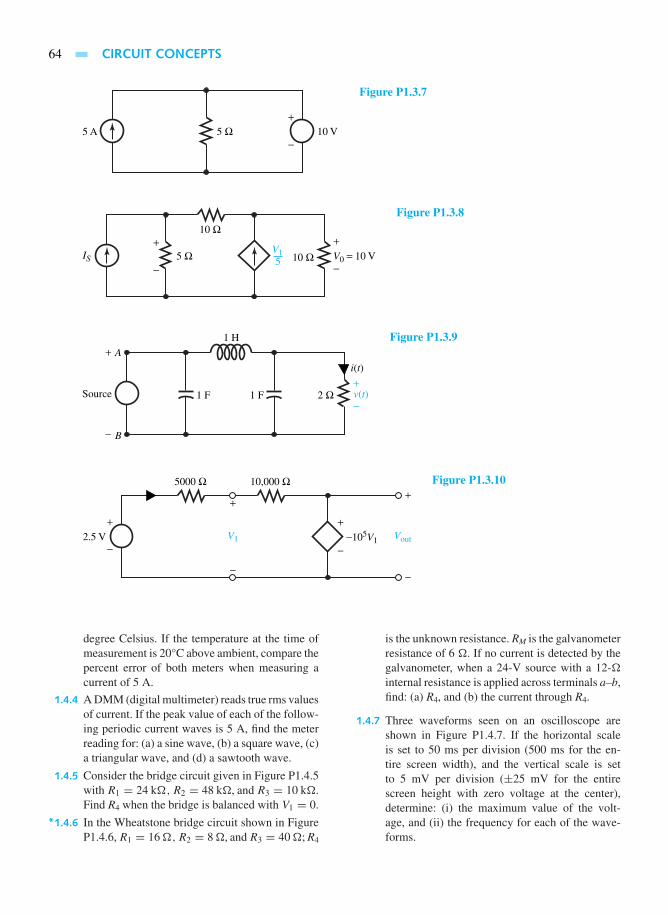
64 CIRCUIT CONCEPTS
+
−5 A 5 Ω 10 V
Figure P1.3.7
+
−
+
−IS 5 Ω
10 Ω
10 Ω5 V0 = 10 VV1
Figure P1.3.8
+
−
+
−
1 F 1 F
1 H
Source 2 Ω v(t)
i(t)
B
A
Figure P1.3.9
+
−
+
+
−
−
+
−2.5 V
5000 Ω 10,000 Ω
−105V1V1 Vout
Figure P1.3.10
degree Celsius. If the temperature at the time ofmeasurement is 20°C above ambient, compare thepercent error of both meters when measuring acurrent of 5 A.
1.4.4 A DMM (digital multimeter) reads true rms valuesof current. If the peak value of each of the follow-ing periodic current waves is 5 A, find the meterreading for: (a) a sine wave, (b) a square wave, (c)a triangular wave, and (d) a sawtooth wave.
1.4.5 Consider the bridge circuit given in Figure P1.4.5with R1 = 24 k,R2 = 48 k, and R3 = 10 k.Find R4 when the bridge is balanced with V1 = 0.
*1.4.6 In the Wheatstone bridge circuit shown in FigureP1.4.6,R1 = 16,R2 = 8, andR3 = 40; R4
is the unknown resistance. RM is the galvanometerresistance of 6 . If no current is detected by thegalvanometer, when a 24-V source with a 12-internal resistance is applied across terminals a–b,find: (a) R4, and (b) the current through R4.
1.4.7 Three waveforms seen on an oscilloscope areshown in Figure P1.4.7. If the horizontal scaleis set to 50 ms per division (500 ms for the en-tire screen width), and the vertical scale is setto 5 mV per division (±25 mV for the entirescreen height with zero voltage at the center),determine: (i) the maximum value of the volt-age, and (ii) the frequency for each of the wave-forms.

PROBLEMS 65
R4R2
VinV1
R1
+ + −
−
R3
Figure P1.4.5
R4 = ?
RM = 6 Ω
b
a
R2 = 8 ΩR1 = 16 Ω
12 Ω
+
− R3 = 40 Ω24 V
G
Figure P1.4.6
(a) (b) (c)
Figure P1.4.7 (a) Sinusoidal wave. (b) Rectangular wave. (c) Sawtooth wave.

2 Circuit Analysis Techniques
2.1 Thévenin and Norton Equivalent Circuits
2.2 Node-Voltage and Mesh-Current Analyses
2.3 Superposition and Linearity
2.4 Wye-Delta Transformation
2.5 Computer-Aided Circuit Analysis: SPICE
2.6 Computer-Aided Circuit Analysis: MATLAB
2.7 Learning Objectives
2.8 Practical Application: A Case Study—Jump Starting a Car
Problems
In Chapter 1 the basic electric circuit concepts were presented. In this chapter we consider somecircuit analysis techniques, since one needs not only basic knowledge but also practical andefficient techniques for solving problems associated with circuit operations.
One simplifying technique often used in complex circuit problems is that of breaking thecircuit into pieces of manageable size and analyzing individually the pieces that may be alreadyfamiliar. Equivalent circuits are introduced which utilize Thévenin’s and Norton’s theorems toreplace a voltage source by a current source or vice versa. Nodal and loop analysis methods are thenpresented. Later the principles of superposition and linearity are discussed. Also, wye–delta trans-formation is put forth as a tool for network reduction. Finally, computer-aided circuit analyses withSPICE and MATLAB are introduced. The chapter ends with a case study of practical application.
2.1 THÉVENIN AND NORTON EQUIVALENT CIRCUITS
For a linear portion of a circuit consisting of ideal sources and linear resistors, the volt–ampere(v–i) relationship at any two accessible terminals can be expressed by the linear equation
v = Ai + B (2.1.1)
66

2.1 THÉVENIN AND NORTON EQUIVALENT CIRCUITS 67
where A and B are two constants. The Thévenin equivalent circuit at any two terminals a and b(to replace the linear portion of the circuit) is given by
v = RThi + voc (2.1.2)
where it can be seen that
RTh = v/i|voc=0 (2.1.3)
and
voc = v|i=0 (2.1.4)
Thus, voc is known as the open-circuit voltage (or Thévenin voltage) with i = 0, and RTh is theThévenin equivalent resistance (as seen from the terminals a–b) with voc = 0. Equation (2.1.4)accounts for the ideal sources present in that linear portion of the circuit, as shown in Figure2.1.1(a), whereas Equation (2.1.3) implies deactivating or zeroing all ideal sources (i.e., replacingvoltage sources by short circuits and current sources by open circuits). The model with the voltagesource voc in series with RTh is known as Thévenin equivalent circuit, as shown in Figure 2.1.1(b).
Equation (2.1.1) may be rewritten as
i = v
A− B
A= v
RTh− voc
RTh= v
RTh− isc (2.1.5)
which is represented by the Norton equivalent circuit with a current source isc in parallel withRTh, as shown in Figure 2.1.1(c). Notice that with v = 0, i = −isc. Also, isc = voc/RTh, orvoc = iscRTh.
Besides representing complete one-ports (or two-terminal networks), Thévenin and Nortonequivalents can be applied to portions of a network (with respect to any two terminals) tosimplify intermediate calculations. Moreover, successive conversions back and forth between thetwo equivalents often save considerable labor in circuit analysis with multiple sources. Sourcetransformations can be used effectively by replacing the voltage source V with a series resistanceR by an equivalent current source I (= V/R) in parallel with the same resistance R, or vice versa.
ai i
i
b
+ ++
−
−−
a
b
+
−
a
b
+
−
Linear portionof circuitconsisting ofideal sourcesand linearresistors
voc isc RTh
RTh
(c)(b)(a)
v/RTh
v v v
Figure 2.1.1 Equivalent circuits. (a) Two-terminal or one-port network. (b) Thévenin equivalent circuit.(c) Norton equivalent circuit.
EXAMPLE 2.1.1
Consider the circuit shown in Figure E2.1.1(a). Reduce the portion of the circuit to the left ofterminals a–b to (a) a Thévenin equivalent and (b) a Norton equivalent. Find the current throughR = 16 , and comment on whether resistance matching is accomplished for maximum powertransfer.

68 CIRCUIT ANALYSIS TECHNIQUES
a
b
24 Ω
48 Ω
6 A
(a)
96 V
I = ?
+
−
R = 16 Ω
a
Voc
b
IL
24 Ω48 Ω
(b)
96 V 144 V+
−
+
+
−
−
a
b
24 Ω48 Ω
(c)
a
b
16 Ω
(d)
R = 16 Ω
I
128 V
+
−
Isc
a
b
48 Ω 24 Ω
(e)
2A 6A
+
−
a
b
24 Ω48 Ω
(f)
Figure E2.1.1
a
b
I
16 Ω8 A R =16 Ω
(g)
So l u t i on
The 6-A source with 24 in parallel can be replaced by a voltage source of 6× 24 = 144 V with24 in series. Thus, by using source transformation, in terms of voltage sources, the equivalentcircuit to the left of terminals a–b is shown in Figure E2.1.1(b).

2.1 THÉVENIN AND NORTON EQUIVALENT CIRCUITS 69
(a) KVL: 144− 24IL − 48IL − 96 = 0, or 72IL = 48, or IL = 2/3 A
Voc = 144− 24(2/3) = 128 V
Deactivating or zeroing all ideal sources, i.e., replacing voltage sources by shortcircuits in the present case, the circuit of Figure E2.1.1(b) reduces to that shown inFigure E2.1.1(c).
Viewed from terminals a–b, the 48- resistor and the 24- resistor are in parallel,
RTh = 48‖24 = 48× 24
48+ 24= 16
Thus, the Thévenin equivalent to the left of terminals a–b, attached with the 16- resistor,is shown in Figure E2.1.1(d). Note that the Thevenin equivalent of any linear circuitconsists of a single Thevenin voltage source in series with a single equivalent Theveninresistance.
The current in the 16- resistor to the right of terminals a–b can now be found,
I = 128/32 = 4 A
(b) The 96-V source with 48 in series can be replaced by a current source of 96/48 = 2A with a parallel resistance of 48 . Thus, by using source transformation, in termsof current sources, the equivalent circuit to the left of terminals a–b is given in FigureE2.1.1(e).
Shorting terminals a–b, one can find Isc, Isc = 8 A. Replacing current sources byopen circuits, viewed from terminals a–b, RTh = 48‖24 = 16 , which is the same as inpart (a). The circuit of Figure E2.1.1(e) to the left of terminals a–b reduces to that shownin Figure E2.1.1(f).
Thus, the Norton equivalent to the left of terminals a–b, attached with the 16-resistor, is given in Figure E2.1.1(g). Note that the Norton equivalent of any linearcircuit consists of a single current source in parallel with a single equivalent Theveninresistance.
The current in the 16- resistor to the right of terminals a–b can now be found. I = 4 A,which is the same as in part (a).
The equivalent source resistance, also known as the output resistance, is the same as the loadresistance of 16 in the present case. Hence, resistance matching is accomplished for maximumpower transfer.
EXAMPLE 2.1.2
Consider the circuit of Figure E2.1.2(a), including a dependent source. Obtain the Théveninequivalent at terminals a–b.

70 CIRCUIT ANALYSIS TECHNIQUES
a
b
I
200 Ω 9 I
2000 Ω
+
−
(a)
I1
10 V
Figure E2.1.2
a
b
Isc
I
200 Ω 9 I
2000 Ω
+
−
(b)
I1
10 V
a
b
RTh = 10 Ω
+
−
+
−
(c)
0.5 V
So l u t i on
First, the open-circuit voltage at terminals a–b is to be found.
KCL at node a: I + 9I = I1, or I1 = 10I
KVL for the left-hand mesh: 2000I + 200I1 = 10, or 4000I = 10, or I = 1/400 A
Voc = 200I1 = 200(1/400) = 0.5 V
Because of the presence of a dependent source, in order to find RTh, one needs to determine Isc
after shorting terminals a–b, as shown in Figure E2.1.2(b).Note that I1 = 0, since Vab = 0.
KCL at node a: Isc = 9I + I = 10I
KVL for the outer loop: 2000I = 10, or I = 1/200 A
Isc = 10(1/200) = 1/20 A
Hence the equivalent Thévenin resistance RTh viewed from terminals a–b is
RTh = Voc
Isc= 0.5
1/20= 10
Thus, the Thévenin equivalent is given in Figure E2.1.2(c).
The preceding examples illustrate how a complex network could be reduced to a simplerepresentation at an output port. The effect of load on the terminal behavior or the effect of anoutput load on the network can easily be evaluated. Thévenin and Norton equivalent circuitshelp us in matching, for example, the speakers to the amplifier output in a stereo system. Suchequivalent circuit concepts permit us to represent the entire system (generation and distribution)

2.2 NODE-VOLTAGE AND MESH-CURRENT ANALYSES 71
connected to a receptacle (plug or outlet) in a much simpler model with the open-circuit voltageas the measured voltage at the receptacle itself.
When a system of sources is so large that its voltage and frequency remain constant regardlessof the power delivered or absorbed, it is known as an infinite bus. Such a bus (node) has a voltageand a frequency that are unaffected by external disturbances. The infinite bus is treated as an idealvoltage source. Even though, for simplicity, only resistive networks are considered in this section,the concept of equivalent circuits is also employed in ac sinusoidal steady-state circuit analysisof networks consisting of inductors and capacitors, as we shall see in Chapter 3.
2.2 NODE-VOLTAGE AND MESH-CURRENT ANALYSES
The node-voltage and mesh-current methods, which complement each other, are well-orderedsystematic methods of analysis for solving complicated network problems. The former is basedon the KCL equations, whereas the KVL equations form the basis for the latter. In both methodsan appropriate number of simultaneous algebraic equations are developed. The unknown nodalvoltages are found in the nodal method, whereas the unknown mesh currents are calculated in theloop (or mesh) method. A decision to use one or the other method of analysis is usually based onthe number of equations needed for each method.
Even though, for simplicity, only resistive networks with dc voltages are considered in thissection, the methods themselves are applicable to more general cases with time-varying sources,inductors, capacitors, and other circuit elements.
Nodal-Voltage Method
A set of node-voltage variables that implicitly satisfy the KVL equations is selected in order toformulate circuit equations in this nodal method of analysis. A reference (datum) node is chosenarbitrarily based on convenience, and from each of the remaining nodes to the reference node, thevoltage drops are defined as node-voltage variables. The circuit is then described completely bythe necessary number of KCL equations whose solution yields the unknown nodal voltages fromwhich the voltage and the current in every circuit element can be determined. Thus, the numberof simultaneous equations to be solved will be equal to one less than the number of networknodes. All voltage sources in series with resistances are replaced by equivalent current sourceswith conductances in parallel. In general, resistances may be replaced by their correspondingconductances for convenience. Note that the nodal-voltage method is a general method of networkanalysis that can be applied to any network.
Let us illustrate the method by considering the simple, but typical, example shown in Figure2.2.1. By replacing the voltage sources with series resistances by their equivalent current sourceswith shunt conductances, Figure 2.2.1 is redrawn as Figure 2.2.2, in which one can identify threenodes, A, B, and O.
Notice that the voltages VAO, VBO, and VAB satisfy the KVL relation:
VAB + VBO − VAO = 0, or VAB = VAO − VBO = VA − VB (2.2.1)
where the node voltages VA and VB are the voltage drops from A to O and B to O, respectively.With node O as reference, and with VA and VB as the node-voltage unknown variables, one canwrite the two independent KCL equations:
Node A: VAG1 + (VA − VB)G3 = I1, or (G1 +G3)VA −G3VB = I1 (2.2.2)
Node B: VBG2 − (VA − VB)G3 = I2, or −G3VA + (G2 +G3)VB = I2 (2.2.3)

72 CIRCUIT ANALYSIS TECHNIQUES
R3
R1 R2
Node O
Node A Node B
V1
+
−V2
+
−
Figure 2.2.1 Circuit for illustration of nodal-voltage method.
I1 = G1 =
O Reference
A B
V1 VAO = VA VBO = VB
VAB = VA − VB
R1
+
+ −
−
+
−I2 = V2
R2
1R1
G2 = 1R2
G3 = 1R3
Figure 2.2.2 Redrawn Figure 2.2.1 for node-voltage method of analysis.
An examination of these equations reveals a pattern that will allow nodal equations to bewritten directly by inspection by following the rules given here for a network containing nodependent sources.
1. For the equation of node A, the coefficient of VA is the positive sum of the conductancesconnected to node A; the coefficient of VB is the negative sum of the conductancesconnected between nodes A and B. The right-hand side of the equation is the sum ofthe current sources feeding into node A.
2. For the equation of node B, a similar situation exists. Notice the coefficient of VB to bethe positive sum of the conductances connected to node B; the coefficient of VA is thenegative sum of the conductances connected between B and A. The right-hand side of theequation is the sum of the current sources feeding into node B.
Such a formal systematic procedure will result in a set of N independent equations of thefollowing form for a network with (N + 1) nodes containing no dependent sources:
G11V1 − G12V2 − · · · − G1NVN = I1
−G21V1 + G22V2 − · · · − G2NVN = I2
......
−GN1V1 − GN2V2 − · · · + GNNVN = IN (2.2.4)
where GNN is the sum of all conductances connected to node N, GJK = GKJ is the sum of allconductances connected between nodes J and K, and IN is the sum of all current sources enteringnode N. By solving the equations for the unknown node voltages, other voltages and currents inthe circuit can easily be determined.

2.2 NODE-VOLTAGE AND MESH-CURRENT ANALYSES 73
EXAMPLE 2.2.1
By means of nodal analysis, find the current delivered by the 10-V source and the voltage acrossthe 10- resistance in the circuit shown in Figure E2.2.1(a).
20 Ω 25 Ω
5 Ω8 Ω
4 Ω
10 Ω
(a)
10 V
20 V
+
+−
−
Figure E2.2.1
= 0.2S
O Reference(b)
AB
C
15
= 0.125 S18
= 0.25 S
20/4 = 5 A
14
= 0.05 S120 = 0.04 S1
25= 2 A10
5
20 Ω 25 Ω
5 Ω
AB
O
C8 Ω
4 Ω
10 Ω
(c)
10 V
20 V
+
+−
−
So l u t i on
STEP 1: Replace all voltage sources with series resistances by their corresponding Nortonequivalents consisting of current sources with shunt conductances. The given circuit is redrawnin Figure E2.2.1(b) by replacing all resistors by their equivalent conductances.

74 CIRCUIT ANALYSIS TECHNIQUES
STEP 2: Identify the nodes and choose a convenient reference node O. This is also shown inFigure E2.2.1(b).
STEP 3: In terms of unknown node-voltage variables, write the KCL equations at all nodes(except, of course, the reference node) by following rules 1 and 2 for nodal equations given inthis section.
Node A: (0.2+ 0.125+ 0.25)VA − 0.125VB − 0.25VC = 2− 5 = −3
Node B: −0.125VA + (0.125+ 0.05+ 0.1)VB − 0.1VC = 0
Node C: −0.25VA − 0.1VB + (0.25+ 0.1+ 0.04)VC = 5
Rearranging, one gets0.575 VA − 0.125 VB − 0.25 VC = −3
−0.125 VA + 0.275 VB − 0.1 VC = 0−0.25 VA − 0.1 VB + 0.39 VC = 5
STEP 4: Simultaneously solve the independent equations for the unknown nodal voltages byGauss elimination or Cramer’s rule. In our example, the solution yields
VA = 4.34 V ; VB = 8.43V ; VC = 17.77 V
STEP 5: Obtain the desired voltages and currents by the application of KVL and Ohm’s law. Tofind the current I in the 10-V source, since it does not appear in Figure E2.2.1(b) redrawn fornodal analysis, one has to go back to the original circuit and identify the equivalence betweennodes A and O, as shown in Figure E2.2.1(c).
Now one can solve for I, delivered by the 10-V source,
VA = 4.34 = −5I + 10 or I = 5.66
5= 1.132 A
The voltage across the 10- resistance is VB−VC = 8.43−17.77 = −9.34 V. The negative signindicates that node C is at a higher potential than node B with respect to the reference node O.
Nodal analysis deals routinely with current sources. When we have voltage sources alongwith series resistances, the source-transformation technique may be used effectively to convertthe voltage source to a current source, as seen in Example 2.2.1. However, in cases where we haveconstrained nodes, that is, the difference in potential between the two node voltages is constrainedby a voltage source, the concept of a supernode becomes useful for the circuit analysis, as shownin the following illustrative example.
EXAMPLE 2.2.2
For the network shown in Figure E2.2.2, find the current in each resistor by means of nodalanalysis.
So l u t i on
Note that the reference node is chosen at one end of an independent voltage source, so that thenode voltage VA is known at the start,
VA = 12 V

2.2 NODE-VOLTAGE AND MESH-CURRENT ANALYSES 75
Reference node
Supernode
A CB
+
+ −
−ICIB
IA
12 V 4 A2 Ω
2 Ω
1 Ω
24 V
Figure E2.2.2
Note that we cannot express the branch current in the voltage source as a function of VB and VC .Here we have constrained nodes B and C. Nodal voltages VB and VC are not independent. Theyare related by the constrained equation
VB − VC = 24 V
Let us now form a supernode, which includes the voltage source and the two nodes B and C,as shown in Figure E2.2.2. KCL must hold for this supernode, that is, the algebraic sum of thecurrents entering or leaving the supernode must be zero. Thus one valid equation for the networkis given by
IA − IB − IC + 4 = 0 or12− VB
2− VB
2− VC
1+ 4 = 0
which reduces to
VB + VC = 10
This equation together with the supernode constraint equation yields
VB = 17 V and VC = −7 V
The currents in the resistors are thus given by
IA = 12− VB
2= 12− 17
2= −2.5 A
IB = VB
2= 17
2= 8.5 A
IC = VC
1= −7
1= −7 A
Mesh-Current Method
This complements the nodal-voltage method of circuit analysis. A set of independent mesh-current variables that implicitly satisfy the KCL equations is selected in order to formulate circuitequations in this mesh analysis. An elementary loop, or a mesh, is easily identified as one ofthe “window panes” of the whole circuit. However, it must be noted that not all circuits can belaid out to contain only meshes as in the case of planar networks. Those which cannot are callednonplanar circuits, for which the mesh analysis cannot be applied, but the nodal analysis can beemployed.
A mesh current is a fictitious current, which is defined as the one circulating around a meshof the circuit in a certain direction. While the direction is quite arbitrary, a clockwise direction

76 CIRCUIT ANALYSIS TECHNIQUES
is traditionally chosen. Branch currents can be found in terms of mesh currents, whose solutionis obtained from the independent simultaneous equations. The number of necessary equations inthe mesh-analysis method is equal to the number of independent loops or meshes.
All current sources with shunt conductances will be replaced by their corresponding Théveninequivalents consisting of voltage sources with series resistances. Let us illustrate the method byconsidering a simple, but typical, example, as shown in Figure 2.2.3.
Replacing the current source with shunt resistance by the Thévenin equivalent, Figure 2.2.3 isredrawn as Figure 2.2.4, in which one can identify two elementary loops, or independent meshes.
By assigning loop or mesh-current variables I1 and I2, as shown in Figure 2.2.4, both in theclockwise direction, one can write the KVL equations for the two closed paths (loops) ABDA andBCDB,
Loop ABDA: I1R1 + (I1 − I2)R2 = V1 − V2 or (R1 + R2)I1 − R2I2 = V1 − V2 (2.2.5)
Loop BCDB: I2R3 + (I2 − I1)R2 = V2 − V3 or −R2I1 + (R2 + R3)I2 = V2 − V3 (2.2.6)
Notice that current I1 exists in R1 and R2 in the direction indicated; I2 exists in R2 and R3 in thedirection indicated; hence, the net current in R2 is I1− I2 directed from B to D. An examination ofEquations (2.2.5) and (2.2.6) reveals a pattern that will allow loop equations to be written directlyby inspection by following these rules:
1. In the first loop equation with mesh current I1, the coefficient of I1 is the sum of theresistances in that mesh; the coefficient of I2 is the negative sum of the resistances commonto both meshes. The right-hand side of the equation is the algebraic sum of the sourcevoltage rises taken in the direction of I1.
2. Similar statements can be made for the second loop with mesh current I2. (See also thesimilarity in setting up the equations for the mesh-current and nodal-voltage methods ofanalysis.)
Such a formal systematic procedure will yield a set of N independent equations of thefollowing form for a network with N independent meshes containing no dependent sources:
R3 I3
R2R1
+
−
+
−V2V1
Figure 2.2.3 Circuit for illustration of mesh-current method.
+
−
+
−
I1 I2
V3 V3 = I3R3V1
R1 R3
A B
D
C
+
−V2
R3
Figure 2.2.4 Redrawn Figure 2.2.3 for mesh-current method of analysis.

2.2 NODE-VOLTAGE AND MESH-CURRENT ANALYSES 77
R11I1 − R12I2 − · · · − R1NIN = V1
−R21I1 + R22V2 − · · · − R2NIN = V2...
...
−RN1I1 − RN2V2 − · · · + RNNIN = VN
(2.2.7)
where RNN is the sum of all resistances contained in mesh N,RJK = RKJ is the sum of allresistances common to both meshes J and K, and VN is the algebraic sum of the source-voltagerises in mesh N, taken in the direction of IN.
By solving the equations for the unknown mesh currents, other currents and voltages in thecircuit elements can be determined easily.
EXAMPLE 2.2.3
By means of mesh-current analysis, obtain the current in the 10-V source and the voltage acrossthe 10- resistor in the circuit of Example 2.2.1.
So l u t i on
STEP 1: Replace all current sources with shunt resistances by their corresponding Théveninequivalents consisting of voltage sources with series resistances. Conductances included in thecircuit are replaced by their equivalent resistances.
In this example, since there are no current sources and conductances, the circuit of FigureE2.2.1(a) is redrawn as Figure E2.2.3 for convenience.
+
+−
−
I1 I2
10 V
20 V
5 Ω
4 Ω
8 Ω 10 Ω
20 Ω 25 Ω
I3
Figure E2.2.3
STEP 2: Identify elementary loops (meshes) and choose a mesh-current variable for eachelementary loop, with all loop currents in the same clockwise direction. Mesh currents I1, I2,and I3 are shown in Figure E2.2.3.
STEP 3: In terms of unknown mesh-current variables, write the KVL equations for all meshesby following the rules for mesh analysis.
Loop 1 with mesh current I1: (5+ 8+ 20)I1 − 20I2 − 8I3 = 10Loop 2 with mesh current I2: −20I1 + (20+ 10+ 25)I2 − 10I3 = 0Loop 3 with mesh current I3: −8I1 − 10I2 + (4+ 10+ 8)I3 = 20
Rearranging, one gets
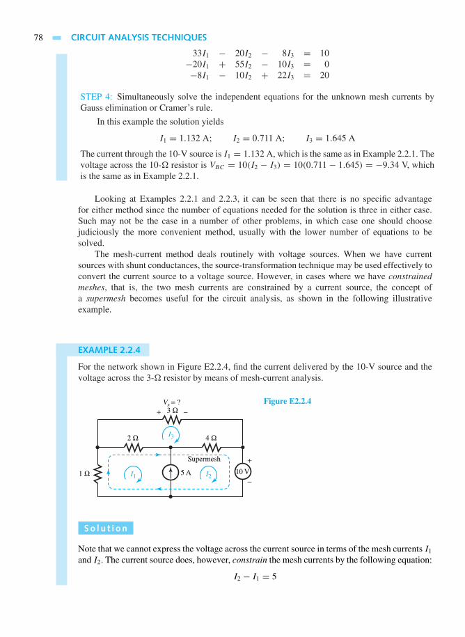
78 CIRCUIT ANALYSIS TECHNIQUES
33I1 − 20I2 − 8I3 = 10−20I1 + 55I2 − 10I3 = 0−8I1 − 10I2 + 22I3 = 20
STEP 4: Simultaneously solve the independent equations for the unknown mesh currents byGauss elimination or Cramer’s rule.
In this example the solution yields
I1 = 1.132 A; I2 = 0.711 A; I3 = 1.645 A
The current through the 10-V source is I1 = 1.132 A, which is the same as in Example 2.2.1. Thevoltage across the 10- resistor is VBC = 10(I2 − I3) = 10(0.711− 1.645) = −9.34 V, whichis the same as in Example 2.2.1.
Looking at Examples 2.2.1 and 2.2.3, it can be seen that there is no specific advantagefor either method since the number of equations needed for the solution is three in either case.Such may not be the case in a number of other problems, in which case one should choosejudiciously the more convenient method, usually with the lower number of equations to besolved.
The mesh-current method deals routinely with voltage sources. When we have currentsources with shunt conductances, the source-transformation technique may be used effectively toconvert the current source to a voltage source. However, in cases where we have constrainedmeshes, that is, the two mesh currents are constrained by a current source, the concept ofa supermesh becomes useful for the circuit analysis, as shown in the following illustrativeexample.
EXAMPLE 2.2.4
For the network shown in Figure E2.2.4, find the current delivered by the 10-V source and thevoltage across the 3- resistor by means of mesh-current analysis.
1 Ω
3 Ω
4 Ω2 Ω
+
+ −
−10 V5 A
Supermesh
I1 I2
I3
Vx = ? Figure E2.2.4
So l u t i on
Note that we cannot express the voltage across the current source in terms of the mesh currents I1
and I2. The current source does, however, constrain the mesh currents by the following equation:
I2 − I1 = 5

2.2 NODE-VOLTAGE AND MESH-CURRENT ANALYSES 79
Let us now form a supermesh, which includes meshes 1 and 2, as shown in Figure E2.2.4. Wenow write a KVL equation around the periphery of meshes 1 and 2 combined. This yields
1I1 + 2(I1 − I3)+ 4(I2 − I3)+ 4(I2 − I3)+ 10 = 0
Next we write a KVL equation for mesh 3,
3I3 + 4(I3 − I2)+ 2(I3 − I1) = 0
Now we have the three linearly independent equations needed to find the three mesh currentsI1, I2, and I3. The solution of the three simultaneous equations yields
I1 = −25A
9A; I2 = 20
9A; I3 = 70
27A
The current delivered by the 10-V source is−I2, or−20/9 A. That is to say, the 10-V sourceis absorbing the current 20/9 A.
The voltage across the 3- resistor is Vx = 3I3 = 3(70/27) = 70/9 = 7.78 V.
Node-Voltage and Mesh-Current Equations with Controlled Sources
Since a controlled source acts at its terminals in the same manner as does an independent source,source conversion and application of KCL and KVL relations are treated identically for bothtypes of sources. Because the strength of a controlled source depends on the value of a voltageor current elsewhere in the network, a constraint equation is written for each controlled source.After combining the constraint equations with the loop or nodal equations based on treating allsources as independent sources, the resultant set of equations are solved for the unknown currentor voltage variables.
EXAMPLE 2.2.5
Consider the circuit in Figure E2.2.5(a), which include a controlled source, and find the currentin the 5-V source and the voltage across the 5- resistor by using (a) the loop-current methodand (b) the node-voltage method.
So l u t i on
(a) Loop-Current Method: The voltage-controlled current source and its parallel resistanceare converted into a voltage-controlled voltage source and series resistance. When youare source transforming dependent sources, note that the identity of the control variable(i.e., the location in the circuit) must be retained. The converted circuit is shown in FigureE2.2.5(b) with the chosen loop currents I1 and I2.
The KVL equations are
For loop carrying I1: (10+ 4+ 2)I1 − 2I2 = 5For loop carrying I2: −2I1 + (2+ 10+ 5)I2 = −5V1
The constraint equation is
V1 = (I1 − I2)2

80 CIRCUIT ANALYSIS TECHNIQUES
2 Ω 0.5 V1V1 5 Ω V = ?
I = ?10 Ω
10 Ω
4 Ω
(a)
5 V+
−
+
−
+
−
Figure E2.2.5
2 ΩV1 5 Ω
0.5 V1 × 10 = 5 V110 Ω 10 Ω4 Ω
(b)
5 V+
−
+ −
+
−I1 I2
0.5 V1
(c)O Reference
A BC
= 0.2 S15
= 0.5 S12
14
= 0.5 A510
= 0.1 S
= 0.25 S
110
= 0.1 S110
V1
+
−
Combining the constraint equation with the loop equations, one gets
16I1 − 2I2 = 5; −2I1 + 17I2 = −10(I1 − I2), or 8I1 + 7I2 = 0
from which
I1 = 35/128 A; I2 = −5/16 A
Thus, the current through the 5-V source is I = I1 = 35/128 = 0.273 A, and thevoltage across the 5- resistor is V = 5I2 = 5(−5/16) = −1.563 V.
(b) Node-Voltage Method: The 5-V voltage source with its 10- series resistor is replacedby its Norton equivalent. Resistances are converted into conductances and the circuit isredrawn in Figure E2.2.5(c) with the nodes shown.
The nodal equations are
A : (0.1+ 0.25)VA − 0.25VB = 0.5
B : −0.25VA + (0.25+ 0.5+ 0.1)VB − 0.1VC = 0.5V1
C : −0.1VB + (0.1+ 0.2)VC = −0.5V1
2.3 SUPERPOSITION AND LINEARITY 81
The constraint equation is
V1 = VB
Combining these with the nodal equations already written, one has0.35 VA − 0.25 VB = 0.5−0.25 VA + 0.35 VB − 0.1 VC = 0
0.4 VB + 0.3 VC = 0
Solving, one gets
VA = 2.266V ; VB = 1.173; VC = −1.564 V
Notice that VC = −1.564 V is the voltage V across the 5- resistor, which is almost thesame as that found in part (a).
In order to find the current I through the 5-V source, one needs to go back to theoriginal circuit and recognize that
5− 10I = VA = 2.266 or I = 0.273 A
which is the same as that found in part (a).
2.3 SUPERPOSITION AND LINEARITY
Mathematically a function is said to be linear if it satisfies two properties: homogeneity (propor-tionality or scaling) and additivity (superposition),
f (Kx) = Kf (x) (homogeneity) (2.3.1)
where K is a scalar constant, and
f (x1 + x2) = f (x1)+ f (x2) (additivity) (2.3.2)
Linearity requires both additivity and homogeneity. For a linear circuit or system in whichexcitations x1 and x2 produce responses y1 and y2, respectively, the application of K1x1 andK2x2 together (i.e., K1x1 + K2x2) results in a response of (K1y1 + K2y2), where K1 and K2
are constants. With the cause-and-effect relation between the excitation and the response, alllinear systems satisfy the principle of superposition. A circuit consisting of independent sources,linear dependent sources, and linear elements is said to be a linear circuit. Note that a resistiveelement is linear. Capacitors and inductors are also circuit elements that have a linear input–outputrelationship provided that their initial stored energy is zero. Nonzero initial conditions are to betreated as independent sources.
In electric circuits, the excitations are provided by the voltage and current sources, whereasthe responses are in terms of element voltages and currents. All circuits containing only idealresistances, capacitances, inductances, and sources are linear circuits (described by linear dif-ferential equations). For a linear network consisting of several independent sources, accordingto the principle of superposition, the net response in any element is the algebraic sum of theindividual responses produced by each of the independent sources acting only by itself. While eachindependent source acting on the network is considered separately by itself, the other independentsources are suppressed; that is to say, voltage sources are replaced by short circuits and currentsources are replaced by open circuits, thereby reducing the source strength to zero. The effect ofany dependent sources, however, must be included in evaluating the response due to each of theindependent sources, as illustrated in the following example.

82 CIRCUIT ANALYSIS TECHNIQUES
EXAMPLE 2.3.1
Determine the voltage across the 20- resistor in the following circuit of Figure E2.3.1 (a) withthe application of superposition.
(a)
V3
6 Ω
6 A
12 Ω 20 Ω80 Ω18 V V
+
−
+
−
Figure E2.3.1
(b)
V ′
BA
3VA′3
6 Ω
12 Ω 20 Ω80 Ω18 V VA′ = V ′ =+
−
+
−I1′
(c)
V″
BA
3VA″3
6 Ω
12 Ω 20 Ω80 ΩVA″ = V″ =+
−
6 A
So l u t i on
Let us suppress the independent sources in turn, recognizing that there are two independentsources. First, by replacing the independent current source with an open circuit, the circuit isdrawn in Figure E2.3.1(b). Notice the designation of V ′ across the 12- resistor and V ′/3 as thedependent current source for this case. At node B,(
1
80+ 1
20
)V ′B =
V ′A3
or V ′B =V ′A48
For the mesh on the left-hand side, (6+12)I ′1 = 18, or I ′1 = 1 A. But, I ′1 = V ′A/12, orV ′A = 12 V.The voltage across the 20- resistor from this part of the solution is
V ′B =12
48= 1
4V
2.4 WYE-DELTA TRANSFORMATION 83
Next, by replacing the independent voltage source with a short circuit, the circuit is shown inFigure E2.3.1(c). Notice the designation of V ′′ across the 12- resistor and V ′′/3 as the dependentcurrent source for this case. At node A,(
1
6+ 1
12
)V ′′A = 6 or V ′′A = 24 V
and at node B,(1
80+ 1
20
)V ′′B =
V ′′A3− 6 = 24
3− 6 = 2 or V ′′B = 32 V
Thus, the voltage across the 20- resistor for this part of the solution is
V ′′B = 32 V
Then the total net response, by superposition, is
VB = V ′B + V ′′B =1
4+ 32 = 32.25 V
The principle of superposition is indeed a powerful tool for analyzing a wide range of linearsystems in electrical, mechanical, civil, or industrial engineering.
2.4 WYE-DELTA TRANSFORMATION
Certain network configurations cannot be reduced or simplified by series–parallel combinationsalone. In some such cases wye–delta (Y–) transformation can be used to replace three resistorsin wye configuration by three resistors in delta configuration, or vice versa, so that the networksare equivalent in so far as the terminals (A, B, C) are concerned, as shown in Figure 2.4.1.
For equivalence, it can be shown that (see Problem 2.4.1)
RA = RABRCA
RAB + RBC + RCA
; RB = RABRBC
RAB + RBC + RCA
;
RC = RCARBC
RAB + RBC + RCA
(2.4.1)
RAB = RARB + RBRC + RCRA
RC
; RBC = RARB + RBRC + RCRA
RA
;
RCA = RARB + RBRC + RCRA
RB
(2.4.2)
For the simple case when RA = RB = RC = RY, and RAB = RBC = RCA = R, Equations(2.4.1) and (2.4.2) become
RY = R
3(2.4.3)
R = 3RY (2.4.4)

84 CIRCUIT ANALYSIS TECHNIQUES
(b)(a)
BB
CC
AA
RAB
RA
RCRB
RCA
RBC
Figure 2.4.1 Wye–delta transfor-mation. (a) Wye configuration. (b)Delta configuration.
EXAMPLE 2.4.1
Use delta–wye transformation for network reduction and determine the current through the 12-resistor in the circuit of Figure E2.4.1(a).
+
−144 V
(a)
3 Ω
4 Ω
4 ΩA
O
BC
8 Ω
2 Ω 12 Ω
I = ?
Figure E2.4.1
+
−
(b)
3 Ω
A C
B
2 Ω
12 Ω
I = ?R3 = 2 Ω
R2 = 2 ΩR1 = 1 Ω
IA
144 V
So l u t i on
The delta-connected portion between terminals A–B–C is replaced by an equivalent wye connec-tion [see Equation (2.4.1)] with
R1 = 4× 4
4+ 8+ 4= 1
R2 = 4× 8
4+ 8+ 4= 2

2.5 COMPUTER-AIDED CIRCUIT ANALYSIS: SPICE 85
R3 = 4× 8
4+ 8+ 4= 2
The circuit is redrawn in Figure E2.4.1(b).Using the KVL equation,
IA = 144
(3+ 1)+ (4 ‖14 )= 81
4A
By current division,
I = 81
4× 4
18= 9
2= 4.5 A
2.5 COMPUTER-AIDED CIRCUIT ANALYSIS: SPICE
A word of caution is appropriate if this is the student’s first experience with simulation. Just as theproliferation of calculators did not eliminate the need to understand the theory of mathematics,circuit simulation programs do not eliminate the need to understand circuit theory. However,computer-aided tools can free the engineer from tedious calculations, thereby freeing more timefor doing the kind of creative work a computer cannot do.
A circuit-analysis program known as SPICE, an acronym for simulation program withintegrated circuit emphasis, is introduced in this section. The original SPICE program wasdeveloped in the early 1970s at the University of California at Berkeley. Since that time, variousSPICE-based commercial products have been developed for personal computer and workstationplatforms.1
A block diagram summarizing the major features of a SPICE-based circuit simulationprogram is shown in Figure 2.5.1. Micro Sim Corporation has developed a design center in
Inputprocessor
(Schematics)Circuit
file
Circuitdiagrams
Net list
Analysistype
Commands
Simulationprocessor(PSpice)
Outputprocessor(Probe)
Analysissummary
AnalysisresultsResponse
data file
Devicelibrary
Outputfile
Figure 2.5.1 Major features of a SPice-based circuit simulation program.
1For supplementary reading on SPICE, the student is encouraged to refer to G. Roberts and A. Sedra, SPICE, 2nd ed., published byOxford University Press (1997), and to P. Tuinenga, SPICE, 3rd ed., published by Prentice Hall (1995).

86 CIRCUIT ANALYSIS TECHNIQUES
which the input processor is called Schematics, the simulation processor is a version of SPICEcalled PSpice, and the output processor is called PROBE. These three programs, working together,create a graphical environment in which the circuit diagram and the analysis objectives are enteredusing Schematics, the circuit is analyzed using PSpice, and the resulting circuit responses areviewed using PROBE. A student’s version of these programs is widely available and is used inthis book.
The first step for describing the circuit is to number the circuit nodes. The reference node (orground node) is labeled as zero (0), and in PSpice syntax the other node names can be numbers orletters. In order to describe the circuit, statements are written with a separate statement for eachcircuit element. The name of an element must begin with a particular letter identifying the kindof circuit element. Some of these are listed here:
R Resistor
V Independent voltage source
I Independent current source
G Voltage-controlled current source
E Voltage-controlled voltage source
F Current-controlled current source
H Current-controlled voltage source
While the original SPICE recognized only uppercase letters, PSpice is actually case insensitive.Because PSpice does not recognize subscripts, R1, for example, will be represented by R1, and soon. The name of each circuit element must be unique. Numerical values can be specified in thefollowing forms:
4567 or 4567.0 or 4.567 E3
SPICE uses the following scale factor designations:
T = 1E12 G = 1E9 MEG = 1E6K = 1E3 M = 1E − 3 U = IE − 6N = 1E − 9 P = 1E − 12 F = 1E − 15
Sometimes, for clarity, additional letters following a numerical value may be used; but these areignored by SPICE. For example, 4.4 KOHMS is recognized as the value 4400, and “ohms” isignored by the program. Comment statements are identified by an asterisk (*) in the first column,and these are helpful for making the program meaningful to users. PSpice also allows insertingcomments on any line by starting the comment with a semicolon. Figure 2.5.2 shows the fourtypes of controlled sources and their corresponding PSpice statements.
While SPICE is capable of several types of analysis, here we illustrate how to solve resistivecircuits containing dc sources using the DC command. PSpice can sweep the value of the source,when the starting value, the end value, and the increment between values are given. If thestarting and end values are the same, the solution is carried out for only a single value of thesource.
Next we give an example of PSpice analysis. Note that SPICE has capabilities far beyondwhat we use in this section, and clearly, one can easily solve complex networks by using programslike PSpice.

2.5 COMPUTER-AIDED CIRCUIT ANALYSIS: SPICE 87
N 1
GNAME N1 N2 NC+ NC− GMVALUE
+
−N 2
NC+
NC−
Gmvx vx
N+
ENAME N+ N− NC+ NC− AVVALUE(a) (b)
+
+
−
−N−
NC+
NC−
Avvx vx
N 1
FNAME N1 N2 VSENSE AIVALUEVSENSE NC1 NC2 O
N 2
N+
HNAME N+ N− VSENSE RMVALUEVSENSE N1 N2 O(c) (d)
+
−
N−
NC 1
NC 2
Rmix
ix
Aiixvsense
+
−
NC 1
NC 2
ix
vsense
+
−
Figure 2.5.2 Four types of controlled sources and their corresponding PSpice statements. (a) Voltage-controlled voltage source. (b) Voltage-controlled current source. (c) Current-controlled voltage source.(d) Current-controlled current source.
EXAMPLE 2.5.1
Develop and execute a PSpice program to solve for the current I2 in Figure E2.5.1(a).
So l u t i on
Figure E2.5.1(b) is drawn showing the node numbers, and adding a voltage source of zero valuein series with R1, because there is a current-controlled source. The program is as follows:
EXAMPLE E2.5.1(a) A Title Identifying the Program.
* THE CIRCUIT DIAGRAM IS GIVEN IN FIGURE E2.5.1(b); a comment
statement
* CIRCUIT DESCRIPTION WITH COMPONENT STATEMENTS
IS 0 1 3
R1 1 4 5
R2 1 2 10
R3 2 0 2
R4 3 0 5
HCCVS 2 3 VSENSE 2
VSENSE 4 3 0
* ANALYSIS REQUEST
• DC IS 3 3 1
* OUTPUT REQUEST
• PRINT DC I(R2) V(1) V(2) V(3)
• END ; an end statement

88 CIRCUIT ANALYSIS TECHNIQUES
After executing the program, from the output file, I2 = I (R2) = 0.692 A.
(a)
R2 = 10 Ω
R1 = 5 Ω
R3 =2 Ω
R4 =5 Ω
IS = 3 A
I2
Ix
2Ix
+ −
Figure E2.5.1 (a) Circuit. (b) Redrawn circuitfor developing a PSpice program.
(b)
12
4
3
R2 = 10 Ω
R1 = 5 Ω vsense
R3 =2 Ω
R4 =5 ΩIS = 3 A
I2
Ix
2Ix
+ −
+ −
2.6 COMPUTER-AIDED CIRCUIT ANALYSIS: MATLAB
This text does not teach MATLAB; it assumes that the student is familiar with it through previouswork. Also, the book does not depend on a student having MATLAB. MATLAB, however,provides an enhancement to the learning experience if it is available. If it is not, the problemsinvolving MATLAB can simply be skipped, and the remainder of the text still makes sense.If one wants to get a quick introduction, the book entitled Getting Started with MATLAB 5 byR. Pratap, listed under Selected Bibliography for Supplemental Reading for Computer-AidedCircuit Analysis, may be a good source.
MATLAB (MATrix LABoratory), a product of The Math Works, Inc., is a software packagefor high-performance numerical computation and visualization. It is simple, powerful, andfor most purposes quite fast with its easy-to-learn and easy-to-use language. It provides aninteractive environment with hundreds of built-in functions for technical computation, graphics,and animation. MATLAB also provides easy extensibility with its own high-level programminglanguage.

2.6 COMPUTER-AIDED CIRCUIT ANALYSIS: MATLAB 89
MATLAB
MATrix LABoratory
MATLABprogramming
language
And many more
Computations Linear algebra Data analysis
Signal processing Polynomials & interpolation
Quadrature Solution of ODEs
EXTRA
FUNCTIONS
EXTRA
FUNCTIONS
Toolboxes(collections of specialized functions)
2D graphics3D graphicsColor and lightingAnimation
Graphics
User-written functions
Built-in functions
Interface with C andFortran programs
External interface(Mex-files)
Signal processingStatisticsControl systemSystem indentificationNeural networksCommunicationsSymbolic mathematics (Maple inside)Electrical machines
Image processingSplinesRobust controlµ-analysis & synthesisOptimizationFinancial
Figure 2.6.1 Schematic diagram of MATLAB’s main features.
Figure 2.6.1 illustrates MATLAB’s main features. The built-in functions with their state-of-the-art algorithms provide excellent tools for linear algebra computations, data analysis, signalprocessing, optimization, numerical solution of ordinary differential equations (ODE), numericalintegration (Quadrature), and many other types of scientific and engineering computations.Numerous functions are also available for 2D and 3D graphics as well as for animation. Users canalso write their own functions, which then behave just like the built-in functions. MATLAB evenprovides an external interface to run Fortran and C programs. Optional “toolboxes,” which arecollections of specialized functions for particular applications, are also available. For example,

90 CIRCUIT ANALYSIS TECHNIQUES
the author of this text has developed “Electrical Machines Toolbox” for the analysis and designof electrical machines.
The MATLAB environment consists of a command window, a figure window, and a platform-dependent edit window, as illustrated in Figure 2.6.2. The command window, which is the mainwindow, is characterized by the MATLAB command prompt >>. All commands, includingthose for running user-written programs, are typed in this window at the MATLAB prompt. Thegraphics window or the figure window receives the output of all graphics commands typed in thecommand window. The user can create as many figure windows as the system memory wouldallow. The edit window is where one writes, edits, creates, and saves one’s own programs in filescalled M-files. Most programs that are written in MATLAB are saved as M-files, and all built-infunctions in MATLAB are M-files.
Let us now take an illustrative example in circuits to solve a set of simultaneous equationswith the use of MATLAB.
0.80.60.40.2
0
0
Circle of radius R = 1
% This is the command prompt
% Here is a simple command
>>
>>
ans =
>> area = pix5^2 % Assign to a variable
area =
78.5398
4
2 + 2
-0.5-1 0.5 1
-0.2-0.4-0.6-0.8
Graphicswindow
Command window
Edit window(with M-files)
%~~~~~~~~~~~~~~~~~~~~~~~~~~~~~~~~~~~~~~~~~~~~~~~~~~~~~% This is a script file to plot a circle.% you may specify a 'radius.'% To execute, just type 'circle'%~~~~~~~~~~~~~~~~~~~~~~~~~~~~~~~~~~~~~~~~~~~~~~~~~~~~~if exist ('radius') R = radius;else R = 1;endt=linspace(0,2*pi,100);x=R*cos(t); y=R*sin(t);
Figure 2.6.2 Illustration of a command window, a figure window, and a platform-dependent edit windowin the MATLAB environment.

2.6 COMPUTER-AIDED CIRCUIT ANALYSIS: MATLAB 91
EXAMPLE 2.6.1
Consider the circuit shown in Figure E2.6.1 and identify the connection equations to be thefollowing:
Node A: IS + I1 + I4 = 0; Loop 1: − VS + V1 + V2 = 0Node B: − I1 + I2 + I3 = 0; Loop 2: − V1 + V4 − V3 = 0Node C: − I3 − I4 + I5 = 0; Loop 3: − V2 + V3 + V5 = 0
The element equations are given byVS = 15; V1 = 60I1; V2 = 90I2
V3 = 50I3; V4 = 90I4; V5 = 60I5
Solve these 12 simultaneous equations by using MATLAB and find the voltage across the 50-resistor in the circuit. Also evaluate the total power dissipated in the circuit.
VS = 15 V
V5
V3I5
I4
I3
I2
I1
IS60 Ω
Loop1
Loop2
90 Ω
50 Ω
60 Ω
C
A
B
90 Ω
+
− ++ −
−V2
+
−
V1
+
−V4
+
−
Loop3
Figure E2.6.1 Circuit for Example 2.6.1.
So l u t i on
The M-file and answers are as follows.function example261
clc
% Given Connection Equations
eqn01 = ’Is + I1 + I4 = 0’;
eqn02 = ’-I1 + I2 + I3 = 0’;
eqn03 = ’-I3 - I4 + I5 = 0’;
eqn04 = ’-Vs + V1 + V2 = 0’;
eqn05 = ’-V1 - V3 + V4 = 0’;
eqn06 = ’-V2 + V3 + V5 = 0’;
% Element Equations
eqn07 = ’Vs = 15’;
eqn08 = ’V1 = 60*I1’;
eqn09 = ’V2 = 00*I2’;
eqn10 = ’V3 = 50*I3’;
eqn11 = ’V4 = 90*I4’;
eqn12 = ’V5 = 60*I5’;

92 CIRCUIT ANALYSIS TECHNIQUES
% Solve Equations
sol = solve (eqn01, eqn02, eqn03, eqn04, eqn05, eqn06, . . .
eqn07, eqn08, eqn09, eqn10, eqn11, eqn12, . . .
‘I1, I2, I3, I4, I5, Is, V1, V2, V3, V4, V5, Vs’);
% Answers
V3 = eval (sol. V3)
Is = eval (sol. Is)
eval (sol.I1*sol.V1 +sol.I2*sol.V2+sol.I3*sol.V3+sol.I4*sol.V4+
sol.I5*sol.V5)
V3 = 1.2295
IS = -0.2049
ans = 3.0738
2.7 LEARNING OBJECTIVES
The learning objectives of this chapter are summarized here, so that the student can check whetherhe or she has accomplished each of the following.
• Obtaining Thévenin equivalent circuit for a two-terminal (or one-port) network with orwithout dependent sources.
• Obtaining Norton equivalent circuit for a two-terminal (or one-port) network with or withoutdependent sources.
• Nodal-voltage method of network analysis, including the concept of a supernode.
• Mesh-current method of network analysis, including the concept of a supermesh.
• Node-voltage and mesh-current equations with controlled sources and their constraintequations.
• Analysis of linear circuits, containing more than one source, by using the principle ofsuperposition.
• Wye–delta transformation for resistive network reduction.
• Computer-aided circuit analysis using SPICE and MATLAB.
2.8 PRACTICAL APPLICATION: A CASE STUDY
Jump Starting a Car
Voltage and current in an electric network are easily measured. They obey Kirchoff’s laws, KCLand KVL, and facilitate the monitoring of energy flow. For these reasons, voltage and current areused by engineers in order to describe the state of an electric network.
When a car battery is weak, say 11 V in a 12-V system, in order to jump-start that car, webring in another car with its engine running and its alternator charging its battery. Let the healthyand strong battery have a voltage of 13 V. According to the recommended practice, one shouldfirst connect the positive terminals with the red jumper cable, as shown in Figure 2.8.1, and thencomplete the circuit between the negative terminals with the aid of the black jumper cable. Notethat the negative terminal of any car battery is always connected to its auto chasis.
Applying KVL in Figure 2.8.1, we have
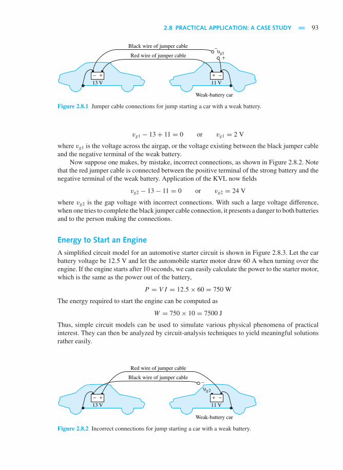
2.8 PRACTICAL APPLICATION: A CASE STUDY 93
Black wire of jumper cable
Weak-battery car
Red wire of jumper cable
+
+
−
−
11 V
υg1
+−13 V
Figure 2.8.1 Jumper cable connections for jump starting a car with a weak battery.
vg1 − 13+ 11 = 0 or vg1 = 2 V
where vg1 is the voltage across the airgap, or the voltage existing between the black jumper cableand the negative terminal of the weak battery.
Now suppose one makes, by mistake, incorrect connections, as shown in Figure 2.8.2. Notethat the red jumper cable is connected between the positive terminal of the strong battery and thenegative terminal of the weak battery. Application of the KVL now fields
vg2 − 13− 11 = 0 or vg2 = 24 V
where vg2 is the gap voltage with incorrect connections. With such a large voltage difference,when one tries to complete the black jumper cable connection, it presents a danger to both batteriesand to the person making the connections.
Energy to Start an Engine
A simplified circuit model for an automotive starter circuit is shown in Figure 2.8.3. Let the carbattery voltage be 12.5 V and let the automobile starter motor draw 60 A when turning over theengine. If the engine starts after 10 seconds, we can easily calculate the power to the starter motor,which is the same as the power out of the battery,
P = V I = 12.5× 60 = 750 W
The energy required to start the engine can be computed as
W = 750× 10 = 7500 J
Thus, simple circuit models can be used to simulate various physical phenomena of practicalinterest. They can then be analyzed by circuit-analysis techniques to yield meaningful solutionsrather easily.
Black wire of jumper cable
Weak-battery car
Red wire of jumper cable
+ −
−
11 V
υg2
+−13 V
Figure 2.8.2 Incorrect connections for jump starting a car with a weak battery.
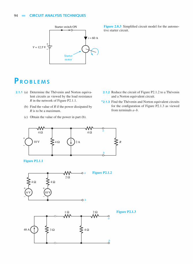
94 CIRCUIT ANALYSIS TECHNIQUES
+
−V = 12.5 V
Startermotor
Starter switch ON
i = 60 Α
Figure 2.8.3 Simplified circuit model for the automo-tive starter circuit.
PROBL EMS
2.1.1 (a) Determine the Thévenin and Norton equiva-lent circuits as viewed by the load resistanceR in the network of Figure P2.1.1.
(b) Find the value of R if the power dissipated byR is to be a maximum.
(c) Obtain the value of the power in part (b).
2.1.2 Reduce the circuit of Figure P2.1.2 to a Théveninand a Norton equivalent circuit.
*2.1.3 Find the Thévenin and Norton equivalent circuitsfor the configuration of Figure P2.1.3 as viewedfrom terminals a–b.
a
b
4 Ω 2 A
4 Ω 4 Ω
10 V R+
−
Figure P2.1.1
a
b
4 Ω
+
−
4 Ω2 Ω
6 V
+
−10 V
Figure P2.1.2
a
b
3 Ω 4 Ω
1 Ω 2 Ω
48 A
Figure P2.1.3

PROBLEMS 95
2.1.4 Obtain the Thévenin and Norton equivalent cir-cuits for the portion of the circuit to the left ofterminals a–b in Figure P2.1.4, and find the currentin the 200- resistance.
2.1.5 Determine the voltage across the 20- load resis-tance in the circuit of Figure P2.1.5 by the use ofthe Thévenin equivalent circuit.
2.1.6 Find the current in the 5- resistance of the circuitof Figure P2.1.6 by employing the Norton equiv-alent circuit.
*2.1.7 Obtain the voltage across the 3-k resistor of thecircuit (transistor amplifier stage) given in Figure
P2.1.7 by the use of the Thévenin equivalent cir-cuit.
2.1.8 Reduce the circuit of Figure P2.1.8 to a Théveninand a Norton equivalent circuit with respect toterminals a–b.
2.1.9 (a) Redraw the circuit in Figure P2.1.9 by replac-ing the portion to the left of terminals a–b withits Thévenin equivalent.
(b) Redraw the circuit of Figure P2.1.9 by replac-ing the portion to the right of terminals a′–b′with its Thévenin equivalent.
a
b
100 Ω 200 Ω
20 Ω
40 Ω 80 Ω
0.8 A1.2 A
12 V
I = ?
+
−
Figure P2.1.4
a
b
6 Ω 20 Ω
4 Ω 5 Ω
++ −
−
+
−20 V Vab = ?V1
V1
5
Figure P2.1.5
a
b
2 Ω
5 Ω
10 Ω 20 Ω
+
−−
+
+−
50 V
I = ?
V1
10 V1
Figure P2.1.6
a
b
3 kΩ
1 kΩ
20 kΩ
1 kΩ
+
−
+
−
+
−
−
1 mV
105 I1
I1
Vab = ?
Figure P2.1.7

96 CIRCUIT ANALYSIS TECHNIQUES
2.1.10 (a) Consider the Wheatstone bridge circuit givenin Figure P2.1.10(a) and find the Théveninequivalent with respect to terminals a–b.
(b) Suppose a source with resistance is connectedacross a–b, as shown in Figure P2.1.10(b).Then find the current Iab.
2.2.1 In the circuit given in Figure P2.2.1, determine thecurrent I through the 2- resistor by (a) the nodal-voltage method, and (b) mesh-current analysis.
2.2.2 Consider the circuit of Figure P2.2.2 and rearrangeit such that only one loop equation is required tosolve for the current I.
a
b
2 Ω
4 Ω
2 Ω 2 Ω
4 A
10 V
12 V
+
+
−
−
Figure P2.1.8
a′
b′
a
b
R1 R3
R2
2 Ω
+
−V1
Figure P2.1.9
a b
+
−12 V
4 Ω
6 Ω
3 Ω12 Ω
(a)
Figure P2.1.10
a b+ −5 V
5 Ω(b)
I2 Ω
1 Ω 1 A2 A
3 A
4 A
3 Ω
Figure P2.2.1

PROBLEMS 97
2.2.3 Use the node-voltage method to find the currentI through the 5- resistor of the circuit of FigureP2.2.3.
2.2.4 Use the node-voltage method to determine thevoltage across the 12- resistor of the circuit givenin Figure P2.2.4. Verify by mesh analysis.
2.2.5 Determine the current I through the 10- resistorof the circuit of Figure P2.2.5 by employing thenode-voltage method. Check by mesh analysis.
*2.2.6 (a) Find the voltage across the 8-A current sourcein the circuit of Figure P2.2.6 with the use ofnodal analysis.
(b) Determine the current in the 0.5- resistor ofthe circuit by mesh analysis.
2.2.7 By using the mesh-current method, determine thevoltage across the 1-A current source of the circuitof Figure P2.2.7, and verify by nodal analysis.
2.2.8 Find the current I1 through the 20- resistor of thecircuit of Figure P2.2.8 by both mesh and nodalanalyses.
2.2.9 Determine the voltage V in the circuit of FigureP2.2.9 by nodal analysis and verify by mesh anal-ysis.
2.2.10 Find the current I in the circuit of Figure P2.2.10by mesh analysis and verify by nodal analysis.
2 Ω
3 Ω 2 Ω
+
+ −−
2 A 3 A
I
9 V
4 V
Figure P2.2.2
12 Ω
6 Ω 3 Ω
5 Ω
I
−
+
+
−
24 V
30 V
Figure P2.2.3
2 Ω
3 Ω4 Ω
4 Ω
8 Ω
12 Ω
−
+−
+V
144 V
Figure P2.2.4
10 Ω
20 Ω 40 Ω
50 Ω120 Ω
I
−
+
−
+
−
+
6 V 48 V30 V
Figure P2.2.5
8 A
0.5 Ω0.125 Ω
0.25 Ω
0.25 Ω
−
+
−
+
+ −
4 V
4 V
3 V
Figure P2.2.6
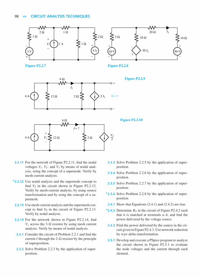
98 CIRCUIT ANALYSIS TECHNIQUES
1 Ω1 A
2 Ω 1 Ω1 Ω
V
2 Ω
+
−−
+
−
+
5 V3 V
Figure P2.2.7
30 I1
I120 Ω
10 Ω5 Ω 10 Ω
−
+ −
+10 V
−
+
50 V
Figure P2.2.8
12 Ω 2 Ω
6 Ω+
−
4 A 2 I1 V = ?
I1
Figure P2.2.9
12 Ω 2 Ω
6 Ω
+
−4 A V1
V12
I = ?
Figure P2.2.10
2.2.11 For the network of Figure P2.2.11, find the nodalvoltages V1, V2, and V3 by means of nodal anal-ysis, using the concept of a supernode. Verify bymesh-current analysis.
*2.2.12 Use nodal analysis and the supernode concept tofind V2 in the circuit shown in Figure P2.2.12.Verify by mesh-current analysis, by using sourcetransformation and by using the concept of a su-permesh.
2.2.13 Use mesh-current analysis and the supermesh con-cept to find V0 in the circuit of Figure P2.2.13.Verify by nodal analysis.
2.2.14 For the network shown in Figure P2.2.14, findVx across the 3- resistor by using mesh currentanalysis. Verify by means of nodal analysis.
2.3.1 Consider the circuit of Problem 2.2.1 and find thecurrent I through the 2- resistor by the principleof superposition.
2.3.2 Solve Problem 2.2.3 by the application of super-position.
2.3.3 Solve Problem 2.2.5 by the application of super-position.
2.3.4 Solve Problem 2.2.6 by the application of super-position.
2.3.5 Solve Problem 2.2.7 by the application of super-position.
*2.3.6 Solve Problem 2.2.8 by the application of super-position.
2.4.1 Show that Equations (2.4.1) and (2.4.2) are true.
*2.4.2 Determine RS in the circuit of Figure P2.4.2 suchthat it is matched at terminals a–b, and find thepower delivered by the voltage source.
2.4.3 Find the power delivered by the source in the cir-cuit given in Figure P2.4.3. Use network reductionby wye–delta transformation.
2.5.1 Develop and execute a PSpice program to analyzethe circuit shown in Figure P2.5.1 to evaluatethe node voltages and the current through eachelement.

PROBLEMS 99
R2 = 10 Ω R4 = 5 Ω
R1 = 20 Ω
R3 = 10 Ω10 V
32
1
15 V
+−
+
−
Figure P2.2.11
1 Ω 1 Ω 2 Ω2 A
12 V1 2+ −
Figure P2.2.12
2 Ω
4 Ω4 A V0
4 V
24 V
+
+
−
+
−
− Figure P2.2.13
2 Ω
Vx = ?3 Ω1 Ω5 A
6 V
4 A
+
+
−
−
Figure P2.2.14
2.5.2 Develop and execute a PSpice program to findthe node voltages and the current through eachelement of the circuit given in Figure P2.5.2.
*2.5.3 For the circuit shown in Figure P2.5.3, developand execute a PSpice program to obtain the nodevoltages and the current through each element.
2.5.4 For the circuit given in Figure P2.5.4, develop andexecute a PSpice program to solve for the nodevoltages.
2.5.5 Write and execute a PSpice program to analyze theresistor bridge circuit shown in Figure P2.5.5 tosolve for the node voltages and the voltage-sourcecurrent. Then find the voltage across the 50-resistor and the total power supplied by the source.
2.6.1 The current through a 2.5-mH indicator is adamped sine given by i(t) = 10e−500t sin 2000t.
With the aid of MATLAB, plot the waveformsof the inductor current i(t), with voltage v(t) =L di/dt , power p(t) = vi, and energy w(t) =∫ t
0 p(τ) dτ . Starting at t = 0, the plots shouldinclude at least one cycle and at least 20 points percycle.
*2.6.2 An interface circuit consisting of R1 and R2 isdesigned between the source and the load, as il-lustrated in Figure P2.6.2 such that the load seesa Thevenin resistance of 50 between terminalsC and D, while simultaneously the source sees aload resistance of 300 between A and B. UsingMATLAB, find R1, and R2.Hint: solve the two nonlinear equations given by(R1 + 300)R2
R1 + 300+ R2= 50; R1 + 50R2
R2 + 50= 300

100 CIRCUIT ANALYSIS TECHNIQUES
3 Ω
3 Ω
9 Ω
3 ΩRS
B
A
9 Ω
−
+
9 V
Figure P2.4.2
26 Ω
8 Ω 6 Ω
4 Ω
4 Ω
13 Ω
−
+
12 V
Figure P2.4.3
VS = 15 V IS = 1 A
R1 = 5 Ω
R2 = 10 Ω
1 2
O
+
−
Figure P2.5.1
2.5 Vx
R2 = 20 Ω
VxR1 = 10 Ω
1 2
O
IS = 1 A+
−
+−
Figure P2.5.2
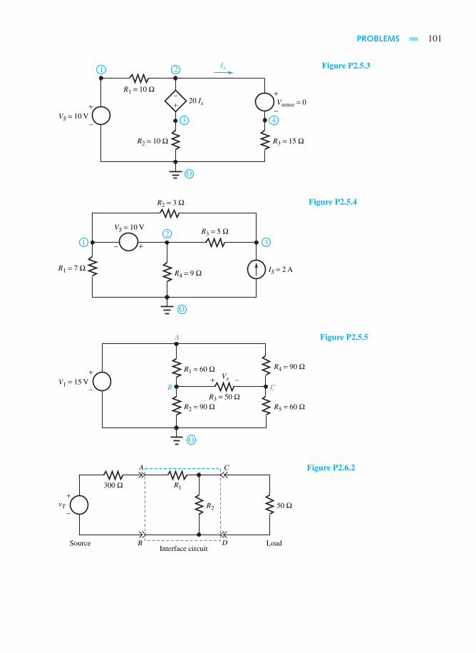
PROBLEMS 101
20 Ix
Ix
R1 = 10 Ω
Vsense = 0
R2 = 10 Ω R3 = 15 Ω
1 2
3 4
O
VS = 10 V
+−
+
−
+
−
Figure P2.5.3
R4 = 9 ΩR1 = 7 Ω
VS = 10 V R3 = 5 Ω
IS = 2 A
R2 = 3 Ω
O
32
1 +−
Figure P2.5.4
Vx
R2 = 90 Ω
R1 = 60 Ω
CB
A
R5 = 60 ΩR3 = 50 Ω
R4 = 90 Ω
O
V1 = 15 V+
−+ −
Figure P2.5.5
R2
R1
CA
DB
vT
300 Ω
Source LoadInterface circuit
50 Ω+
−
Figure P2.6.2
3 Time-Dependent Circuit Analysis
3.1 Sinusoidal Steady-State Phasor Analysis
3.2 Transients in Circuits
3.3 Laplace Transform
3.4 Frequency Response
3.5 Computer-Aided Circuit Simulation for Transient Analysis, ac Analysis, and Frequency
Response Using PSpice and PROBE
3.6 Use of MATLAB in Computer-Aided Circuit Simulation
3.7 Learning Objectives
3.8 Practical Application: A Case Study—Automotive Ignition System
Problems
The response of networks to time-varying sources is considered in this chapter. The specialcase of sinusoidal signals is of particular importance, because the low-frequency signals (i.e.,currents and voltages) that appear in electric power systems as well as the high-frequency signalsin communications are usually sinusoidal. The powerful technique known as phasor analysis,which involves the use of complex numbers, is one of the electrical engineer’s most importanttools developed to solve steady-state ac circuit problems. Since a periodic signal can be expressedas a sum of sinusoids through a Fourier series, and superposition applies to linear systems, phasoranalysis will be used to determine the steady-state response of any linear system excited by aperiodic signal. Thus the superposition principle allows the phasor technique to be extended todetermine the system response of a linear system. The sinusoidal steady-state response of linearcircuits is presented in Section 3.1. The response when the excitation is suddenly applied orsuddenly changed is examined next in Section 3.2. The total response of a system containingenergy-storage elements (capacitors and inductors) is analyzed in terms of natural and forcedresponses (or transient and steady-state responses). The Laplace transformation, which provides
102

3.1 SINUSOIDAL STEADY-STATE PHASOR ANALYSIS 103
a systematic algebraic approach for determining both the forced and the natural componentsof a network response, is then taken up in Section 3.3. The concept of a transfer function isalso introduced along with its application to solve circuit problems. Then, in Section 3.4 thenetwork response to sinusoidal signals of variable frequency is investigated. Also, two-portnetworks and block diagrams, in terms of their input–output characteristics, are dealt with inthis chapter. Finally, computer-aided circuit simulations using PSpice and PROBE, as well asMATLAB are illustrated in Sections 3.5 and 3.6. The chapter ends with a case study of practicalapplication.
3.1 SINUSOIDAL STEADY-STATE PHASOR ANALYSIS
The kind of response of a physical system in an applied excitation depends in general on thetype of excitation, the elements in the system and their interconnection, and also on the pasthistory of the system. The total response generally consists of a forced response determined bythe particular excitation and its effects on the system elements, and a natural response dictatedby the system elements and their interaction. The natural response caused by the energy storageelements in circuits with nonzero resistance is always transient; but the forced response causedby the sources can have a transient and a steady-state component. The boundary conditions(usually initial conditions), representing the effect of past history in the total response, decidethe amplitude of the natural response and reflect the degree of mismatch between the originalstate and the steady-state response. However, when excitations are periodic or when they areapplied for lengthy durations, as in the case of many applications, the solution for the forcedresponse is all that is needed, whereas that for the natural response becomes unnecessary. Whena linear circuit is driven by a sinusoidal voltage or current source, all steady-state voltagesand currents in the circuit are sinusoids with the same frequency as that of the source. Thiscondition is known as the sinusoidal steady state. Sinusoidal excitation refers to excitationwhose waveform is sinusoidal (or cosinusoidal). Circuits excited by constant currents or voltagesare called dc circuits, whereas those excited by sinusoidal currents or voltages are known asac circuits.
Sinusoids can be expressed in terms of exponential functions with the use of Euler’s identity,
ejθ = cos θ + jsin θ (3.1.1)
e−jθ = cos θ − jsin θ (3.1.2)
cos θ = ejθ + e−jθ
2(3.1.3)
sin θ = ejθ − e−jθ
2j(3.1.4)
where j represents the imaginary number√−1. The reader is expected to be conversant with
complex numbers.If we are able to find the response to exponential excitations, ejθ or e−jθ , we can use the
principle of superposition in order to evaluate the sinusoidal steady-state response. With this inmind let us now study the response to exponential excitations.
Responses to Exponential Excitations
Let us consider Aest as a typical exponential excitation in which A is a constant and s is a complex-frequency variable with a dimension of 1/second such that the exponent st becomes dimensionless.

104 TIME-DEPENDENT CIRCUIT ANALYSIS
The variable s can assume real, imaginary, or complex values. The time-invariant dc source isrepresented by setting s = 0. The use of s = jω would imply sinusoidal excitation.
Note that Aest is the only function for which a linear combination of
K1Aest +K2
d
dt
(Aest
)+K3
∫Aest
in which K1, K2, and K3 are constants has the same shape or waveform as the original signal.Therefore, if the excitation to a linear system is Aest, then the response will have the samewaveform.
Recall the volt–ampere relationships (for ideal elements) with time-varying excitation.For the resistor R:
vR = RiR (3.1.5)
iR = GvR (3.1.6)
For the inductor L:
vL = LdiL
dt(3.1.7)
iL = 1
L
∫vL dt (3.1.8)
For the capacitor C:
vC = 1
C
∫iC dt (3.1.9)
iC = CdvC
dt(3.1.10)
With exponential excitation in which v(t) = Vest and i(t) = Iest, it can be seen that the followingholds good because exponential excitations produce exponential responses with the same expo-nents. (Notationwise, note that v(t) and i(t) represent the real-valued signals, whereas v(t) andi(t) represent complex-valued signals.)
For R:
VR = RIR (3.1.11)
IR = GVR (3.1.12)
For L:
VL = (sL)IL (3.1.13)
IL = (1/sL)VL (3.1.14)
For C:
VC = (1/sC)IC (3.1.15)
IC = (sC)VC (3.1.16)
The preceding equations resemble the Ohm’s law relation. The quantities R, sL, and 1/sC have thedimension of ohms, whereas G, 1/sL, and sC have the dimension of siemens, or 1/ohm. The ratioof voltage to current in the frequency domain at a pair of terminals is known as the impedance,designated by Z(s), whereas that of current to voltage is called the admittance, designated by
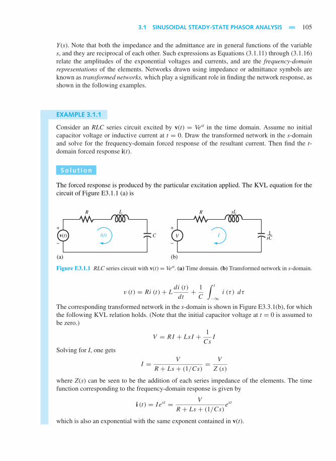
3.1 SINUSOIDAL STEADY-STATE PHASOR ANALYSIS 105
Y(s). Note that both the impedance and the admittance are in general functions of the variables, and they are reciprocal of each other. Such expressions as Equations (3.1.11) through (3.1.16)relate the amplitudes of the exponential voltages and currents, and are the frequency-domainrepresentations of the elements. Networks drawn using impedance or admittance symbols areknown as transformed networks, which play a significant role in finding the network response, asshown in the following examples.
EXAMPLE 3.1.1
Consider an RLC series circuit excited by v(t) = Vest in the time domain. Assume no initialcapacitor voltage or inductive current at t = 0. Draw the transformed network in the s-domainand solve for the frequency-domain forced response of the resultant current. Then find the t-domain forced response i(t).
So l u t i on
The forced response is produced by the particular excitation applied. The KVL equation for thecircuit of Figure E3.1.1 (a) is
−
+v(t) i(t) C
LR
(a)
−
+V I 1
sL
sC
R
(b)
Figure E3.1.1 RLC series circuit with v(t)= Vest. (a) Time domain. (b) Transformed network in s-domain.
v (t) = Ri (t)+ Ldi (t)
dt+ 1
C
∫ t
−∞i (τ ) dτ
The corresponding transformed network in the s-domain is shown in Figure E3.3.1(b), for whichthe following KVL relation holds. (Note that the initial capacitor voltage at t = 0 is assumed tobe zero.)
V = RI + LsI + 1
CsI
Solving for I, one gets
I = V
R + Ls + (1/Cs)= V
Z (s)
where Z(s) can be seen to be the addition of each series impedance of the elements. The timefunction corresponding to the frequency-domain response is given by
i (t) = Iest = V
R + Ls + (1/Cs)est
which is also an exponential with the same exponent contained in v(t).
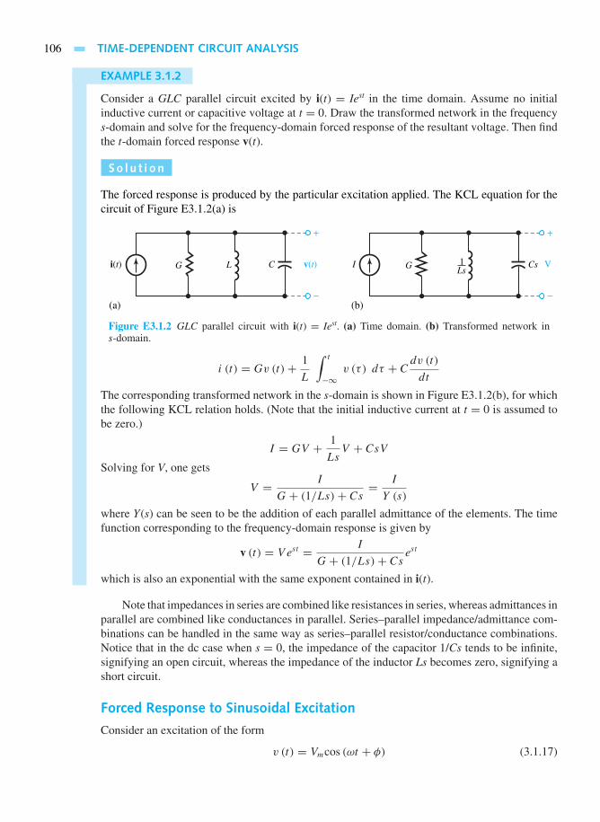
106 TIME-DEPENDENT CIRCUIT ANALYSIS
EXAMPLE 3.1.2
Consider a GLC parallel circuit excited by i(t) = Iest in the time domain. Assume no initialinductive current or capacitive voltage at t = 0. Draw the transformed network in the frequencys-domain and solve for the frequency-domain forced response of the resultant voltage. Then findthe t-domain forced response v(t).
So l u t i on
The forced response is produced by the particular excitation applied. The KCL equation for thecircuit of Figure E3.1.2(a) is
v(t)
−
+
V
−
+
i(t) CLG
(a)
I CsG
(b)
1Ls
Figure E3.1.2 GLC parallel circuit with i(t) = Iest. (a) Time domain. (b) Transformed network ins-domain.
i (t) = Gv (t)+ 1
L
∫ t
−∞v (τ) dτ + C
dv (t)
dt
The corresponding transformed network in the s-domain is shown in Figure E3.1.2(b), for whichthe following KCL relation holds. (Note that the initial inductive current at t = 0 is assumed tobe zero.)
I = GV + 1
LsV + CsV
Solving for V, one gets
V = I
G+ (1/Ls)+ Cs= I
Y (s)
where Y(s) can be seen to be the addition of each parallel admittance of the elements. The timefunction corresponding to the frequency-domain response is given by
v (t) = V est = I
G+ (1/Ls)+ Csest
which is also an exponential with the same exponent contained in i(t).
Note that impedances in series are combined like resistances in series, whereas admittances inparallel are combined like conductances in parallel. Series–parallel impedance/admittance com-binations can be handled in the same way as series–parallel resistor/conductance combinations.Notice that in the dc case when s = 0, the impedance of the capacitor 1/Cs tends to be infinite,signifying an open circuit, whereas the impedance of the inductor Ls becomes zero, signifying ashort circuit.
Forced Response to Sinusoidal Excitation
Consider an excitation of the form
v (t) = Vmcos (ωt + φ) (3.1.17)

3.1 SINUSOIDAL STEADY-STATE PHASOR ANALYSIS 107
where Vm is the peak amplitude and φ is the phase angle. This may be expressed in terms of
exponential functions as
v (t) = Vm
2
[ej (ωt+φ) + e−j (ωt+φ)] = Vae
jωt + Vbe−jωt (3.1.18)
where Va = (Vm/2) ejφ and Vb = (Vm/2) e−jφ . Note that VaandVb are complex numbers.
Even though Equation (3.1.17) is a cosine function that is considered here, recall that any
sine, cosine, or combination of sine and cosine waves of the same frequency can be written as a
cosine wave with a phase angle. Some useful trigonometric identities are as follows:
sin (ωt + φ) = cos(ωt + φ − π
2
)(3.1.19)
Acos ωt + Bsin ωt =√A2 + B2 cos (ωt − φ) (3.1.20)
where φ = tan−1 (B/A).
By expressing the sinusoidal excitation as the sum of two exponentials, as in Equation
(3.1.18), the method developed to find the response to exponential excitations can easily be
extended with the principle of superposition to obtain the forced response to sinusoidal excitation,
as illustrated in the following example.
EXAMPLE 3.1.3
Consider an RLC series circuit excited by v(t) = Vm cos ωt in the time domain. By usingsuperposition, solve for the time-domain forced response of the resultant current through thefrequency-domain approach.
So l u t i on
Figures E3.1.3(a) and E3.1.3(b) are equivalent in the time domain. Figure E3.1.3(c) shows thetransformed networks with the use of superposition. It follows then
I1 = Vm/2
R + jωL+ (1/jωC)= Vm/2
R + j [ωL− (1/ωC)]= I1e
jθ1
I2 = Vm/2
R − jωL+ (1/jωC)= Vm/2
R − j [ωL− (1/ωC)]= I2e
jθ2
where
I1 = I2 = Vm/2
R2 + [ωL− (1/ωC)]2 ; θ1 = −θ2 = −tan−1 ωL− (1/ωC)
R
The student is encouraged to use a knowledge of complex numbers and check these results.The corresponding time functions are given by
i1 (t) = I1ejθ1ejωt and i2 (t) = I2e
−jθ1e−jωt
By superposition, the total response is
i (t) = Vm[R2 + ωL− (1/ωC)2]1/2 cos (ωt + θ1) = Imcos (ωt + θ1)
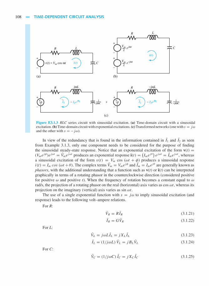
108 TIME-DEPENDENT CIRCUIT ANALYSIS
−
+v(t) = Vm cos ωt i(t) C
LR
(a)
−
+
−
+= I1e jθ1I1
R
= I2e jθ2+ I2
−jωLR
(c)
−
+e jωt
i(t)
C
LR
(b)
Vm2
−
+e−jωtVm
2
Vm2
Vm2jωC
1−jωC
1
jωL
Figure E3.1.3 RLC series circuit with sinusoidal excitation. (a) Time-domain circuit with a sinusoidalexcitation. (b) Time-domain circuit with exponential excitations. (c) Transformed networks (one with s = jωand the other with s = −jω).
In view of the redundancy that is found in the information contained in I1 and I2 as seenfrom Example 3.1.3, only one component needs to be considered for the purpose of findingthe sinusoidal steady-state response. Notice that an exponential excitation of the form v(t) =(Vme
jφ)ejωt = Vmejωt produces an exponential response i(t) = (Imejθ) ejωt = Ime
jωt , whereasa sinusoidal excitation of the form v(t) = Vm cos (ωt + φ) produces a sinusoidal responsei(t) = Im cos (ωt + θ). The complex terms Vm = Vme
jφ and Im = Imejθ are generally known as
phasors, with the additional understanding that a function such as v(t) or i(t) can be interpretedgraphically in terms of a rotating phasor in the counterclockwise direction (considered positivefor positive ω and positive t). When the frequency of rotation becomes a constant equal to ω
rad/s, the projection of a rotating phasor on the real (horizontal) axis varies as cos ωt , whereas itsprojection on the imaginary (vertical) axis varies as sin ωt .
The use of a single exponential function with s = jω to imply sinusoidal excitation (andresponse) leads to the following volt–ampere relations.
For R:
VR = RIR (3.1.21)
IR = GVR (3.1.22)
For L:
VL = jωLIL = jXLIL (3.1.23)
IL = (1/jωL) VL = jBLVL (3.1.24)
For C:
VC = (1/jωC) IC = jXCIC (3.1.25)

3.1 SINUSOIDAL STEADY-STATE PHASOR ANALYSIS 109
IC = jωCVC = jBCVC (3.1.26)
where XL = ωL is the inductive reactance, XC = −1/ωC is the capacitive reactance, BL =−1/ωL is the inductive susceptance, and BC = ωC is the capacitive susceptance. (Notice thatthe fact 1/j = −j has been used.)
The general impedance and admittance functions with s = jω for sinusoidal excitation aregiven by
Z (jω) = R + jX = 1
Y (jω)(3.1.27)
Y (jω) = G+ jB = 1
Z (jω)(3.1.28)
where the real part is either the resistance R or the conductance G, and the imaginary part is eitherthe reactance X or the susceptance B.
A positive value of X or a negative value of B indicates inductive behavior, whereas capacitivebehavior is indicated by a negative value of X or a positive value of B. Further, the followingKVL and KCL equations hold:
V = ZI = (R + jX) I (3.1.29)
I = Y V = (G+ jB) V (3.1.30)
Phasor Method
For sinusoidal excitations of the same frequency, the forced or steady-state responses are betterfound by the technique known as the phasor method. Time functions are transformed to the phasorrepresentations of the sinusoids. For example, current and voltage in the time domain are givenby the forms
i = √2 Irmscos (ωt + α) = Re[√
2 Irmsejαejωt
](3.1.31)
v = √2 Vrmscos (ωt + β) = Re[√
2 Vrmsejβejωt
](3.1.32)
and where Re stands for the “real part of”; their corresponding phasors in the frequency domainare defined by
I = Irmsejα = Irms α (3.1.33)
V = Vrmsejβ = Vrms β (3.1.34)
Notice that the magnitudes of the phasors are chosen for convenience to be the rms values of theoriginal functions (rather than the peak amplitudes), and angles are given by the argument of thecosine function at t = 0. The student should observe that phasors are referenced here to cosinefunctions. Therefore, the conversion of sine functions into equivalent cosine functions makes itmore convenient for expressing phasor representations of sine functions. The phasor volt-ampereequations for R, L, and C are given by Equations (3.1.21) through (3.1.26), whereas the phasoroperators Z and Y are given by Equations (3.1.27) and (3.1.28). The KVL and KCL equations(3.1.29) and (3.1.30) hold in phasor form.

110 TIME-DEPENDENT CIRCUIT ANALYSIS
EXAMPLE 3.1.4
Let ω = 2π × 60 rad/s corresponding to a frequency of 60 Hz.
(a) Consider v(t) = 100√
2 cos(ωt + 30°) V and i(t) = 10√
2 sin(ωt + 30°) A. Find thecorresponding phasors V and I by choosing the rms values for the phasor magnitudes.
(b) Consider the phasors V and I as obtained in part (a), and show how to obtain the time-domain functions.
So l u t i on
(a) v(t) = 100√
2 cos(ωt + 30°) V = Re[100√
2 ej 30°ejωt]
Suppressing the explicit time variation and choosing the rms value for the phasormagnitude, the phasor representation in the frequency domain then becomes
V = 100 30° = 100ej 30° = 100ejπ/6 = 100 (cos30°+ j sin30°) V
Similarly, for the current:
I = 10 − 60° = 10e−j 60° = 10e−jπ/3 = 10 (cos60°− j sin60°) A
since sin(ωt + 30°) = cos(ωt + 30°− 90°) = cos(ωt − 60°).
(b) Now that V = 100 30°, the corresponding time-domain function v(t) is obtained asv(t) = Re [
√2 V ejωt ] = Re [
√2 100ej 30°ejωt ], or v(t) = Re [100
√2 ej (ωt+30°)] =
100√
2cos(ωt + 30°) V. Note that the multiplicative factor of√
2 is used to obtain thepeak amplitude, since for sinusoids the peak value is
√2 times the rms value.
Similarly, i(t) = Re [10√
2 ej (ωt−60°)] = 10√
2cos(ωt − 60°) = 10√
2sin(ωt + 30°) A, where ω = 2πf = 2π × 60 rad/s in this case.
For the three linear time-invariant passive elements R (pure resistance), L (pure inductance),and C (pure capacitance), the relationships between voltage and current in the time domain aswell as in the frequency domain are shown in Figure 3.1.1.
Phasors, being complex numbers, can be represented in the complex plane in the conventionalpolar form as an arrow, having a length corresponding to the magnitude of the phasor, and an angle(with respect to the positive real axis) that is the phase of the phasor. In a phasor diagram, thevarious phasor quantities corresponding to a given network may be combined in such a way thatone or both of Kirchhoff’s laws are satisfied. In general the phasor method of analyzing circuitsis credited to Charles Proteus Steinmetz (1865–1923), a well-known electrical engineer with theGeneral Electric Company in the early part of the 20th century.
The phasor diagram may be drawn in a number of ways, such as in a polar (or ray) form,with all phasors originating at the origin, or in a polygonal form, with one phasor located at theend of another, or in a combination of these, depending on the convenience and the point to bemade. Such diagrams provide geometrical insight into the voltage and current relationships in anetwork. They are particularly helpful in visualizing steady-state phenomena in the analysis ofnetworks with sinusoidal signals.

3.1 SINUSOIDAL STEADY-STATE PHASOR ANALYSIS 111
−
+
vR = RiRZR = R
iR
iR
vR
t
(a)
(b)
diL
vRR
dt
−
+
vL = L
dvCdtiC = C
ZL = jωL
1
Direction ofrotation of phasors
Phasors in Frequency DomainTime Domain
iωCZC =
iLiL vL
tvLL
(c)
−
+
iCiC
vC
tvCC
−
+
IR
IRVR
−
+
IL
VL
−
+
IC
VCZC
ZL
ZR
IC
VL = ZLIL
VR = ZRIR
VC = ZCIC
VL
VC
VR
Direction ofrotation of phasors
90
90
IL
Direction ofrotation of phasors
Figure 3.1.1 Voltage and current relationships in time domain and frequency domain for elements R, L,and C. (a) Current is in phase with voltage in a purely resistive circuit (unity power factor). (b) Current lagsvoltage by 90° with a pure inductor (zero power factor lagging). (c) Current leads voltage by 90° with a purecapacitor (zero power factor leading).
In constructing a phasor diagram, each sinusoidal voltage and current is represented by aphasor of length equal to the rms value of the sinusoid, and with an angular displacement fromthe positive real axis, which is the angle of the equivalent cosine function at t = 0. This use of thecosine is arbitrary, and so also the use of the rms value. Formulation in terms of the sine functioncould just as well have been chosen, and the amplitude rather than the rms value could havebeen chosen for the magnitude. While phasor diagrams can be drawn to scale, they are usuallysketched as a visual check of the algebraic solution of a problem, especially since the KVL andKCL equations can be shown as graphical addition.
The reference of a phasor diagram is the line θ = 0. It is not really necessary that any voltageor current phasor coincide with the reference, even though it is often more convenient for the

112 TIME-DEPENDENT CIRCUIT ANALYSIS
analysis when a given voltage or current phasor is taken as the reference. Since a phasor diagram isa frozen picture at one instant of time, giving the relative locations of various phasors involved, andthe whole diagram of phasors is assumed to be rotating counterclockwise at a constant frequency,different phasors may be made to be the reference simply by rotating the entire phasor diagramin either the clockwise or the counterclockwise direction.
From the viewpoints of ease and convenience, it would be a matter of common sense tochoose the current phasor as the reference in the case of series circuits, in which all the elementsare connected in series, and the common quantity for all the elements involved is the current.Similarly for the case of parallel circuits, in which all the elements are connected in paralleland the common quantity for all the elements involved is the voltage, a good choice for thereference is the voltage phasor. As for the series–parallel circuits, no firm rule applies to allsituations.
Referring to Figure 3.1.1(a), in a purely resistive circuit, notice that the current is in phasewith the voltage. Observe the waveforms of iR and vR in the time domain and their relativelocations in the phasor domain, notice the phasors VR chosen here as a reference, and IR , whichis in phase with VR . The phase angle between voltage and current is zero degrees, and the cosineof that angle, namely, unity or 1 in this case, is known as the power factor. Thus a purely resistivecircuit is said to have unity power factor.
In the case of a pure inductor, as shown in Figure 3.1.1(b), the current lags (behind) thevoltage by 90°, or one can also say that the voltage leads the current by 90°. Observe the currentand voltage waveforms in the time domain along with their relative positions, as well as therelative phasor locations of VL and IL in the phasor domain, with VL chosen here as a reference.The phase angle between voltage and current is 90°, and the cosine of that angle being zero, thepower factor for the case of a pure inductor is said to be zero power factor lagging, since thecurrent lags the voltage by 90°.
For the case of a pure capacitor, as illustrated in Figure 3.1.1(c), the current leads the voltageby 90°, or one can also say that the voltage lags the curent by 90°. Notice the current and voltagewaveforms in the time domain along with their relative positions, as well as the relative phasorlocations of VC and IC in the phasor domain, with VC chosen here as a reference. The phase anglebetween voltage and current is 90°, and the cosine of that angle being zero, the power factor forthe case of a pure capacitor is said to be zero power factor leading, since the current leads thevoltage by 90°.
The circuit analysis techniques presented in Chapter 2 (where only resistive networks areconsidered for the sake of simplicity) apply to ac circuits using the phasor method. However,the constant voltages and currents in dc circuits are replaced by phasor voltages and currentsin ac circuits. Similarly, resistances and conductances are replaced by the complex quantitiesfor impedance and admittance. Nodal and mesh analyses, being well-organized and systematicmethods, are applied to ac circuits along with the concepts of equivalent circuits, superposition,and wye–delta transformation.
Power and Power Factor in ac Circuits
Power is the rate of change of energy with respect to time. The unit of power is a watt (W),which is a joule per second (J/s). The use of rms or effective values of voltage and current allowsthe average power to be found from phasor quantities. Let us consider a circuit consisting ofan impedance Z φ = R + jX excited by an applied voltage of v(t) = √2 Vrmscos (ωt + φ),producing a current of i(t) = √2 Irmscosωt . The corresponding voltage and current phasors arethen given by V φandI 0°, which satisfy the Ohm’s-law relation V /I = V φ/I 0° = Z φ.

3.1 SINUSOIDAL STEADY-STATE PHASOR ANALYSIS 113
The instantaneous power p(t) supplied to the network by the source is
p (t) = v (t) · i (t) = √2 Vrmscos (ωt + φ) · √2 Irms cos ωt (3.1.35)
which can be rearranged as follows by using trigonometric relations:
p (t) = VrmsIrms cos φ (1+ cos 2ωt)− VrmsIrms sin φ sin 2ωt
= VrmsIrms cos φ + VrmsIrms cos (2ωt + φ) (3.1.36)
A typical plot of p(t) is shown in Figure 3.1.2, revealing that it is the sum of an average component,V rmsIrms cos φ, which is a constant that is time independent, and a sinusoidal component, V rmsIrms
cos(2ωt+φ), which oscillates at a frequency double that of the original source frequency and haszero average value. The average component represents the electric power delivered to the circuit,whereas the sinusoidal component reveals that the energy is stored over one part of the periodand released over another, thereby denoting no net delivery of electric energy. It can be seen thatthe power p(t) is pulsating in time and its time-average value P is given by
Pav = VrmsIrms cos φ (3.1.37)
since the time-average values of the terms cos 2ωt and sin 2ωt are zero. Note that φ is the angleassociated with the impedance, and is also the phase angle between the voltage and the current.The term cos φ is called the power factor. An inductive circuit, in which the current lags thevoltage, is said to have a lagging power factor, whereas a capacitive circuit, in which the currentleads the voltage, is said to have a leading power factor. Notice that the power factor associatedwith a purely resistive load is unity, whereas that of a purely inductive load is zero (lagging) andthat of a purely capacitive load is zero (leading).
Equation (3.1.37), representing the average power absorbed by the entire circuit, known asthe real power or active power, may be rewritten as
P = VrmsIrms cos φ = I 2rmsR (3.1.38)
where φ is the phase angle between voltage and current. Equation (3.1.38) can be identified asthe average power taken by the resistance alone, since
pR (t) = vR (t) i (t) = i2R =(√
2 Irms cos ωt)2
R = I 2rmsR (1+ cos 2ωt) (3.1.39)
One should recognize that the other two circuit elements, pure inductance and pure capacitance,do not contribute to the average power, but affect the instantaneous power.
For a pure inductor L,
pL (t) = vL (t) i (t) = iLdi
dt
VRMSIRMS cos φ VRMSIRMS cos(2ωt + φ)+p(t) =
Pav
p(t)
t, s
Instantaneous power
0
sinusoidal componentaverage component
p, W Figure 3.1.2 Typical plot of in-stantaneous power p(t) and averagepower Pav.

114 TIME-DEPENDENT CIRCUIT ANALYSIS
=(√
2 Irms cos ωt)L(−√2 ωIrms sin ωt
)= −I 2
rmsXL sin 2ωt (3.1.40)
where XL = ωL is the inductive reactance.For a pure capacitor C,
pC (t) = vC (t) i (t) = i1
C
∫i dt
=(√
2 Irms cos ωt) 1
C
(√2
ωIrms sin ωt
)= −I 2
rmsXC sin 2ωt (3.1.41)
where XC = −1/ωC is the capacitive reactance.The amplitude of power oscillation associated with either inductive or capacitive reactance
is thus seen to be
Q = I 2rmsX = VrmsIrms sin φ (3.1.42)
which is known as the reactive power or imaginary power. Note that φ is the phase angle betweenvoltage and current. The unit of real power is watts (W), whereas that of reactive power is reactivevolt amperes (VAR). The complex power is given by
S = S φ = P + jQ = VRMSIRMS (cos φ + j sin φ) = VrmsI∗rms (3.1.43)
where I ∗rms is the complex conjugate of I . The magnitude of S, given by√P 2 +Q2, is known as
the apparent power, with units of volt-amperes (VA). The concept of a power triangle is illustratedin Figure 3.1.3. The power factor is given by P/S.
The condition for maximum power transfer to a load impedance ZL (= RL + jXL)
connected to a voltage source with an impedance of ZS (= RS + jXS) (as illustrated in Figure3.1.4) can be shown to be
ZL = Z∗S or RL = RS and XL = −XS (3.1.44)
When Equation (3.1.44) is satisfied, the load and the source are said to be matched. If source andload are purely resistive, Equation (3.1.44) reduces to RL = RS .
In the phasor method of analysis, the student should recall and appropriately apply the circuit-analysis techniques learned in Chapter 2, which include nodal and mesh analyses, Thevenin andNorton equivalents, source transformations, superposition, and wye–delta transformation.
S = VRMSIRMS (VA)
P = VRMSIRMS cos φ (W)
Q = VRMSIRMS sin φ (VAR)QPφ = tan−1( )
Figure 3.1.3 Power triangle.
ZL = ZS*
(RL = RS and XL = −XS)
Source
+
−
Load
ZS
VSZL
Figure 3.1.4 Illustration of maxi-mum power transfer.

3.1 SINUSOIDAL STEADY-STATE PHASOR ANALYSIS 115
EXAMPLE 3.1.5
Consider an RLC series circuit excited by v (t) =(
100√
2 cos 10t)
V, with R = 20 , L = 1
H, and C = 0.1 F. Use the phasor method to find the steady-state response current in the circuit.Sketch the corresponding phasor diagram showing the circuit-element voltages and current. Alsodraw the power triangle of the load.
So l u t i on
The time-domain circuit and the corresponding frequency-domain circuit are shown in FigureE3.1.5. The KVL equation is
V = VR + VL + VC = I
(R + jωL+ 1
jωC
)Note that ω = 10 rad/s in our example, and rms values are chosen for the phasor magnitudes.Thus,
100 0° = I (20+ j10− j1) or I = 100 0°
20+ j9= 100 0°
21.93 24.23°= 4.56 − 24.23° A
Then i(t) = Re[√
2 I ejωt], which is
i (t) = √2 (4.56) cos (10t − 24.23°) A.
The phasor diagram is shown in Figure E3.1.5(c).
−
++ − +
+
−
−
v(t) = 100 2 cos ωt C = 0.1 F V =
vR vL+ − +
+=
−
−VR VL
VCvC
i(t)
L = 1 HR = 20 Ω jωL = j10 Ω
Ω
R = 20 Ω
(a)
−
+V100 0° I
(b)
jωC1
j1 = −j
φ = 24.23
VL = 45.6 ∠(90 − 24.23) = jXL I
(VL + VC)
VR + VL + VC = V = 100 ∠0 V
VC = 4.5 ∠−(90 + 24.23) = jXC I
VR = 91.2 ∠−24.23 = IR
(c)I
Figure E3.1.5 (a) Time-domain circuit. (b) Frequency-domain circuit. (c) Phasor diagram. (d) Powertriangle.

116 TIME-DEPENDENT CIRCUIT ANALYSIS
φ = 24.23°
S = VRMSIRMS = 456 VA
PR = 415.9 W = PS
QS = 187.1 VAR
(d)
QC = −20.8 VAR
P2 + Q2QL = 207.9 VAR
Figure E3.1.5 Continued
Note that the power factor of the circuit is cos(24.23°) = 0.912 lagging, since the current islagging the voltage in this inductive load.
PR = V 2R rms/R = I 2
rmsR = (4.56)2 20 = 415.9 W
A resistor absorbs real power.
QL = V 2L rms/XL = I 2
rmsXL = (4.56)2 10 = 207.9 VAR
An inductor absorbs positive reactive power.
QC = V 2C rms/XC = I 2
rmsXC = (4.56)2 (−1) = −20.8 VAR
A capacitor absorbs negative reactive power (or delivers positive reactive power).The power triangle is shown in Figure E3.1.5(d). Note that PS (=PR) is delivered by the
source; and QS (= QL + QC) is delivered by the source. Note that QC is negative.
EXAMPLE 3.1.6
Draw the phasor diagrams for an RLC series circuit supplied by a sinusoidal voltage source witha lagging power factor and a GLC parallel circuit supplied by a sinusoidal current source with aleading power factor.
So l u t i on
For the RLC series circuit in the frequency domain in Figure E3.1.6(a), the phasor diagram forthe case of a lagging power factor is shown in Figure E3.1.6(b).
For the GLC parallel circuit in the frequency domain in Figure E3.1.6(c), the phasor diagramfor the case of a leading power factor is shown in Figure E3.1.6(d).
−
++ − +
+
−
−
V
VR VL
VCI
jXL = jωL
jXC = = = j ( )−
R
(a)
jωC1
ωC1
ωC−j
Figure E3.1.6 (a) RLC series circuit infrequency domain. (b) Phasor diagramfor lagging power factor. (c) GLC paral-lel circuit in frequency domain. (d) Pha-sor diagram for leading power factor.

3.1 SINUSOIDAL STEADY-STATE PHASOR ANALYSIS 117
φωC
1
VR = R I
VL + VC = j(ωL − ) IVR + VL + VC = V
I = I ∠0° (Reference)
(b)
Figure E3.1.6 Continued
I V
−
+
(c)
R1GR =
IR IL IC
ωL1jBL = j(− jBC = jωC)
φωL1
IR = V/R
IC + IL = j(ωC − ) VIR + IL + IC = I
V = V ∠0° (Reference)
(d)
EXAMPLE 3.1.7
Two single-phase 60-Hz sinusoidal-source generators (with negligible internal impedances) aresupplying to a common load of 10 kW at 0.8 power factor lagging. The impedance of the feederconnecting the generator G1 to the load is 1.4 + j1.6 , whereas that of the feeder connectingthe generator G2 to the load is 0.8+ j1.0 . If the generator G1, operating at a terminal voltageof 462 V (rms), supplies 5 kW at 0.8 power factor lagging, determine:
(a) The voltage at the load terminals;
(b) The terminal voltage of generator G2; and
(c) The real power and the reactive power output of the generator G2.
So l u t i on
(a) From Equation (3.1.37) applied to G1, 462I1(0.8) = 5× 10³, or I1 = 13.53 A. With V1
taken as reference, the phasor expression for I1 is given by I1 = 13.53 − cos−1 0.8 =13.53 − 36.9° A, since G1 supplies at 0.8 lagging power factor.
The KVL equation yields
VL = 462 0°− (13.53 − 36.9°) (1.4+ j 1.6) = 433.8 − 0.78° V
The magnitude of the voltage at the load terminals is 433.8 V (rms).
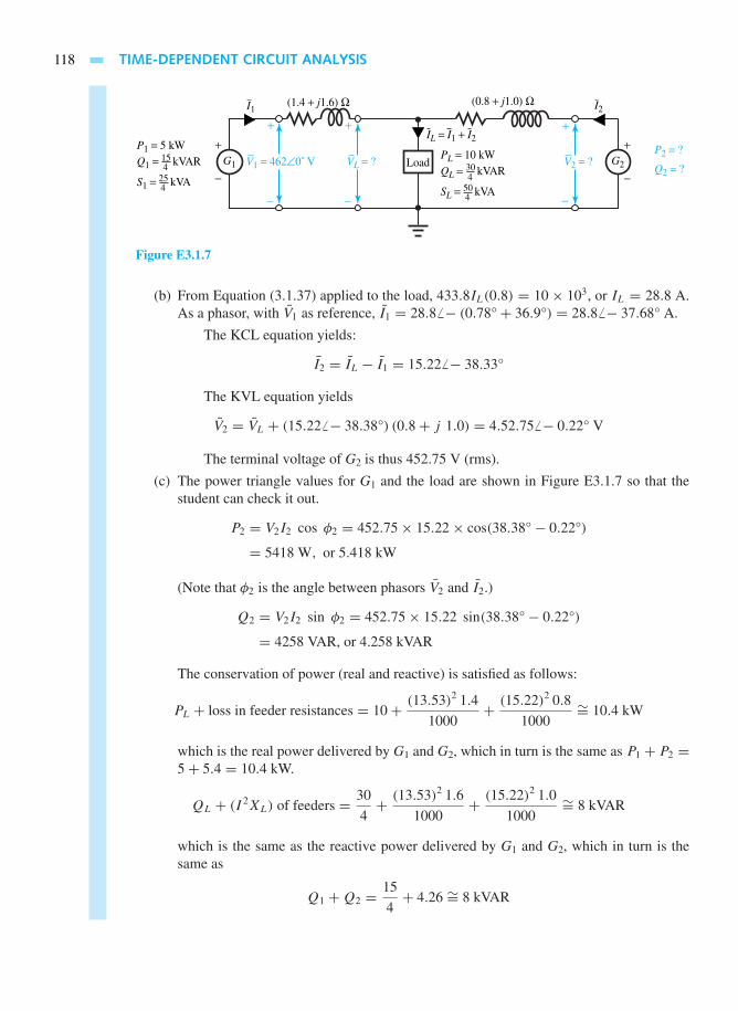
118 TIME-DEPENDENT CIRCUIT ANALYSIS
−
+
+
−
+
−
V1 = 462∠0˚ V
I1
VL = ?P1 = 5 kWQ1 = kVAR G1
−
+G2
S1 = kVA
P2 = ?
Q2 = ?
(1.4 + j1.6) Ω (0.8 + j1.0) Ω
IL = I1 + I2
415
425
PL = 10 kWQL = kVAR
SL = kVA430
450
I2
+
−
V2 = ?Load
Figure E3.1.7
(b) From Equation (3.1.37) applied to the load, 433.8IL(0.8) = 10 × 103, or IL = 28.8 A.As a phasor, with V1 as reference, I1 = 28.8 − (0.78°+ 36.9°) = 28.8 − 37.68° A.
The KCL equation yields:
I2 = IL − I1 = 15.22 − 38.33°
The KVL equation yields
V2 = VL + (15.22 − 38.38°) (0.8+ j 1.0) = 4.52.75 − 0.22° V
The terminal voltage of G2 is thus 452.75 V (rms).
(c) The power triangle values for G1 and the load are shown in Figure E3.1.7 so that thestudent can check it out.
P2 = V2I2 cos φ2 = 452.75× 15.22× cos(38.38°− 0.22°)
= 5418 W, or 5.418 kW
(Note that φ2 is the angle between phasors V2 and I2.)
Q2 = V2I2 sin φ2 = 452.75× 15.22 sin(38.38°− 0.22°)
= 4258 VAR, or 4.258 kVAR
The conservation of power (real and reactive) is satisfied as follows:
PL + loss in feeder resistances = 10+ (13.53)2 1.4
1000+ (15.22)2 0.8
1000∼= 10.4 kW
which is the real power delivered by G1 and G2, which in turn is the same as P1 + P2 =5+ 5.4 = 10.4 kW.
QL + (I 2XL) of feeders = 30
4+ (13.53)2 1.6
1000+ (15.22)2 1.0
1000∼= 8 kVAR
which is the same as the reactive power delivered by G1 and G2, which in turn is thesame as
Q1 +Q2 = 15
4+ 4.26 ∼= 8 kVAR
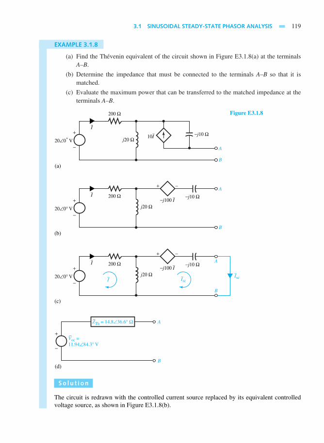
3.1 SINUSOIDAL STEADY-STATE PHASOR ANALYSIS 119
EXAMPLE 3.1.8
(a) Find the Thévenin equivalent of the circuit shown in Figure E3.1.8(a) at the terminalsA–B.
(b) Determine the impedance that must be connected to the terminals A–B so that it ismatched.
(c) Evaluate the maximum power that can be transferred to the matched impedance at theterminals A–B.
−
+20∠0˚ V
I
200 Ω
j20 Ω−j10 Ω
A
B
10I
(a)
Figure E3.1.8
−
+20∠0° V
I 200 Ω
(b)
j20 Ω
−j10 Ω−j100 I
+ −A
B
−
+20∠0° V
I A
B
200 Ω
(c)
j20 Ω
−j10 Ω−j100 I
+ −
IscI Isc
−
+Voc =11.94∠84.3° V
(d)
A
B
ZTh = 14.8∠36.6° Ω
So l u t i on
The circuit is redrawn with the controlled current source replaced by its equivalent controlledvoltage source, as shown in Figure E3.1.8(b).
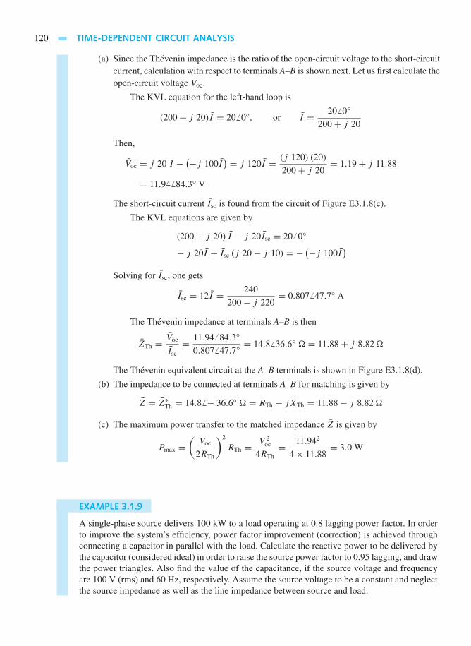
120 TIME-DEPENDENT CIRCUIT ANALYSIS
(a) Since the Thévenin impedance is the ratio of the open-circuit voltage to the short-circuitcurrent, calculation with respect to terminals A–B is shown next. Let us first calculate theopen-circuit voltage Voc.
The KVL equation for the left-hand loop is
(200+ j 20)I = 20 0°, or I = 20 0°
200+ j 20
Then,
Voc = j 20 I − (−j 100I) = j 120I = (j 120) (20)
200+ j 20= 1.19+ j 11.88
= 11.94 84.3° V
The short-circuit current Isc is found from the circuit of Figure E3.1.8(c).
The KVL equations are given by
(200+ j 20) I − j 20Isc = 20 0°
− j 20I + Isc (j 20− j 10) = − (−j 100I)
Solving for Isc, one gets
Isc = 12I = 240
200− j 220= 0.807 47.7° A
The Thévenin impedance at terminals A–B is then
ZTh = Voc
Isc= 11.94 84.3°
0.807 47.7°= 14.8 36.6° = 11.88+ j 8.82
The Thévenin equivalent circuit at the A–B terminals is shown in Figure E3.1.8(d).
(b) The impedance to be connected at terminals A–B for matching is given by
Z = Z∗Th = 14.8 − 36.6° = RTh − jXTh = 11.88− j 8.82
(c) The maximum power transfer to the matched impedance Z is given by
Pmax =(
Voc
2RTh
)2
RTh = V 2oc
4RTh= 11.942
4× 11.88= 3.0 W
EXAMPLE 3.1.9
A single-phase source delivers 100 kW to a load operating at 0.8 lagging power factor. In orderto improve the system’s efficiency, power factor improvement (correction) is achieved throughconnecting a capacitor in parallel with the load. Calculate the reactive power to be delivered bythe capacitor (considered ideal) in order to raise the source power factor to 0.95 lagging, and drawthe power triangles. Also find the value of the capacitance, if the source voltage and frequencyare 100 V (rms) and 60 Hz, respectively. Assume the source voltage to be a constant and neglectthe source impedance as well as the line impedance between source and load.

3.1 SINUSOIDAL STEADY-STATE PHASOR ANALYSIS 121
So l u t i on
−
+V
(a)
Inductiveload
Capacitor added (in parallel)for power factor correction (improvement)
C
Source
SL =P
P = PS = PR = 100 kW
QL = 75 kVAR = P tan φL
(b)
QC = −42.13kVAR
QS = 32.87kVAR
1002 + 752 = 125 kVA
cos φL
cos−10.95 = 18.19° = φS
cos−1 0.8 = 36.87° = φL
=
Figure E3.1.9 (a) Circuit.(b) Power triangles.
The circuit and the power triangles are shown in Figure E3.1.9. The real power P = PS = PR
delivered by the source and absorbed by the load is not changed when the capacitor (consideredideal) is connected in parallel with the load. After the capacitor is connected, noting that QC isnegative, QS = QL + QC = 100 tan(18.19) = 32.87 kVAR,
SS = P
cos φS
= 100
0.95= 105.3 kVa
(Note that the power factor correction reduces the current supplied by the generator signifi-cantly.) So
QC = QS −QL = 32.87− 75 = −43.13 kVAR
Thus the capacitor is delivering 43.13 kVAR to the system (or absorbing negative kVAR). Then
V 2rms
XC
= 1002
XC
= −43.13× 10³ or XC = −0.232 = − 1
ωC
or
C = 1
2π × 60× 0.232= 0.0114 F or 11.4 mF
Fourier Series
The phasor method of circuit analysis can be extended (by using the principle of superposition)to find the response in linear systems due to nonsinusoidal, periodic source functions. A periodicfunction (t) with period T can be expressed in Fourier series,
f (t) =∞∑n=0
an cos nωt +∞∑n=1
bn sin nωt (3.1.45)

122 TIME-DEPENDENT CIRCUIT ANALYSIS
where ω = 2πf = 2π/T is the fundamental angular frequency, a0 is the average ordinate or thedc component of the wave, (a1 cos ωt + b1 sin ωt) is the fundamental component, and (an cos nωt+ bn sin nωt), for n ≥ 2, is the nth harmonic component of the function.
The Fourier coefficients are evaluated as follows:
a0 = 1
T
∫ T
0f (t) dt (3.1.46)
an = 2
T
∫ T
0f (t) cos nωt dt, n ≥ 1 (3.1.47)
bn = 2
T
∫ T
0f (t) sin nωt dt, n ≥ 1 (3.1.48)
The exponential form of the Fourier series can be shown to be given by
f (t) =∞∑
n=−∞Cne
jnωt (3.1.49)
where
Cn = 1
T
∫ T
0f (t) e−jnωt dt (3.1.50)
Even though the exact representation of the nonsinusoidal, periodic wave requires an infinitenumber of terms in the Fourier series, a good approximation for engineering purposes can beobtained with comparatively few first terms, since the amplitude of the harmonics decreasesprogressively as the order of the harmonic increases.
The system response is determined by the principle of superposition, and the phasor techniqueyields the steady-state response. Each frequency component of the response is produced bythe corresponding harmonic of the excitation. The sum of these responses becomes the Fourierseries of the system response. Note that while the phasor method is employed to determine eachfrequency component, the individual time functions must be used in forming the series for thesystem response. Such a method of analysis is applicable to all linear systems.
EXAMPLE 3.1.10
(a) Find the Fourier series for the square wave shown in Figure E3.1.10(a).
(b) Let a voltage source having the waveform of part (a) with a peak value of 100 V and afrequency of 10 Hz be applied to an RC series network with R = 20 and C = 0.1 F.Determine the first five nonzero terms of the Fourier series of vC(t).
So l u t i on
(a) From Equation (3.1.46),

3.1 SINUSOIDAL STEADY-STATE PHASOR ANALYSIS 123
(a)
v(t)
Vm
tT
Period T = =
4T2
3T4
2πω
1f
−
+
−
+
V VC
20 Ω
=
(c)
−
+
−
+v(t)
i(t)
vC(t)C = 0.1 F
R = 20 Ω
(b)
I
1jωC
Ω10jω
Figure E3.1.10 (a) Square wave. (b) Time-domain circuit. (c) Frequency-domain circuit.
a0 = 1
T
∫ T
0f (t) dt = 1
T
(∫ T/4
0Vm dt +
∫ T
3T/4Vm dt
)= Vm
2
From Equation (3.1.47),
an = 2
T
(∫ T/4
0Vm cos nωt dt +
∫ T
π/4Vm cos nωt dt
)and
an =
0, for even n
±2Vm
nπ, for odd n, where the algebraic sign is + for n = 1
and changes alternately for each successive term.
From Equation (3.1.48),
bn = 2
T
(∫ T/4
0Vm sin nωt dt +
∫ T
3T/4Vm sin nωt dt
)= 0
which can also be seen from symmetry of the square wave with respect to the chosenorigin.
The Fourier series is then
v (t) = Vm
2+ 2Vm
πcos ωt − 2Vm
3πcos 3ωt + 2Vm
5πcos 5ωt − 2Vm
7πcos 7ωt + · · ·
(b) The time-domain and frequency-domain circuits are shown in Figures E3.1.10(b) and(c). Note that the capacitive impedance is expressed in terms of ω, since the frequencyof each term of the Fourier series is different. The general phasor expressions for I andVC are given by

124 TIME-DEPENDENT CIRCUIT ANALYSIS
I = V
20+ (10/jω)
VC =(
10
jω
)I = V
1+ 2jω
Treating each Fourier-series term separately, we have the following.
1. For the dc case, ω = 0; VC dc = 50 V.
2. For the fundamental component,
v1(t) = 63.7 cos(20πt), V1 = 63.7√2 0°
VC1 = (63.7/√
2) 0°
1+ j (40π)= 0.51√
2 − 89.5° V
and
vC1 = 0.51 cos(20πt − 89.5°) V
3. For the third harmonic (ω = 3× 20π ) component,
v3(t) = −21.2 cos(60 πt), V3 = −21.2√2 0°
VC3 = −(21.2/√
2) 0°
1+ j 2(60π)= −0.06√
2 − 89.8° V
and
vC3(t) = −0.06 cos(60πt − 89.8°) V
4. For the fifth harmonic (ω = 5× 20π) component,
v5(t) = 12.73 cos(100πt), V5 = 12.73√2 0°
VC5 =(
12.73/√
2) 0°
1+ j 2(100π)= 0.02√
2 − 89.9° V
and
vC5(t) = 0.02 cos(100πt − 89.9°) V
5. For the seventh harmonic (ω = 7× 20π ) component,
v7(t) = −9.1 cos(140πt), V7 = − 9.1√2 0°
VC7 = −(9.1/√2) 0°
1+ j 2(140π)= −0.01√
2 − 89.9° V
and
vC7(t) = −0.01 cos(140πt − 89.9°) V
Thus,
vC(t) = 50+ 0.51 cos(20πt − 89.5°)− 0.06 cos(60πt − 89.8°)
+ 0.02 cos(100πt − 89.9°)− 0.01 cos(140πt − 89.9°) V
in which the first five nonzero terms of the Fourier series are shown.
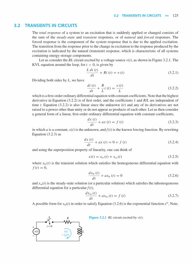
3.2 TRANSIENTS IN CIRCUITS 125
3.2 TRANSIENTS IN CIRCUITS
The total response of a system to an excitation that is suddenly applied or changed consists ofthe sum of the steady-state and transient responses, or of natural and forced responses. Theforced response is the component of the system response that is due to the applied excitation.The transition from the response prior to the change in excitation to the response produced by theexcitation is indicated by the natural (transient) response, which is characteristic of all systemscontaining energy-storage components.
Let us consider the RL circuit excited by a voltage source v(t), as shown in Figure 3.2.1. TheKVL equation around the loop, for t > 0, is given by
Ldi (t)
dt+ Ri (t) = v (t) (3.2.1)
Dividing both sides by L, we havedi (t)
dt+ R
Li (t) = v (t)
L(3.2.2)
which is a first-order ordinary differential equation with constant coefficients. Note that the highestderivative in Equation (3.2.2) is of first order, and the coefficients 1 and R/L are independent oftime t. Equation (3.2.2) is also linear since the unknown i(t) and any of its derivatives are notraised to a power other than unity or do not appear as products of each other. Let us then considera general form of a linear, first-order ordinary differential equation with constant coefficients,
dx (t)
dt+ ax (t) = f (t) (3.2.3)
in which a is a constant, x(t) is the unknown, and f (t) is the known forcing function. By rewritingEquation (3.2.3) as
dx (t)
dt+ ax (t) = 0+ f (t) (3.2.4)
and using the superposition property of linearity, one can think of
x(t) = xtr (t)+ xss(t) (3.2.5)
where xtr(t) is the transient solution which satisfies the homogeneous differential equation withf (t) = 0,
dxtr (t)
dt+ axtr (t) = 0 (3.2.6)
and xss(t) is the steady-state solution (or a particular solution) which satisfies the inhomogeneousdifferential equation for a particular f (t),
dxss (t)
dt+ axss (t) = f (t) (3.2.7)
A possible form for xtr(t) in order to satisfy Equation (3.2.6) is the exponential function est. Note,
−
+v(t) i(t)
= iL(t)L
RS
t = 0
Figure 3.2.1 RL circuit excited by v(t).

126 TIME-DEPENDENT CIRCUIT ANALYSIS
however, that the function est used here in finding transient solutions is not the generalized phasorfunction used earlier for exponential excitations. Thus let us try a solution of the form
xtr (t) = Aest (3.2.8)
in which A and s are constants yet to be determined. Substituting Equation (3.2.8) into Equation(3.2.6), we get
sAest + aAest = 0 or (s + a)Aest = 0 (3.2.9)
which implies
s + a = 0 or s = −a (3.2.10)
since A cannot be zero (or xtr would be zero for all t causing a trivial solution), and est cannot bezero for all t regardless of s. Thus the transient solution is given by
xtr (t) = Ae−at (3.2.11)
in which A is a constant yet to be determined.We already know how to find the steady-state solution xss(t) for dc or ac sources, and the
principle of superposition can be used if we have more than one source. To find that part ofthe steady-state solution due to a dc source, deactivate or zero all the other sources, and replaceinductors with short circuits, and capacitors with open circuits, and then solve the resulting circuitfor the voltage or current of interest. To find that part of the steady-state solution due to an acsource, deactivate or zero all the other sources and use the phasor method of Section 3.1. Thesolution to Equation (3.2.3) or Equation (3.2.4) is then given by Equation (3.2.5) as the sum ofthe transient and steady-state solutions,
x(t) = xtr (t)+ xss(t) = Ae−at + xss(t) (3.2.12)
In order to evaluate A, let us apply Equation (3.2.12) for t = 0+ which is immediately after t = 0,
x(0+) = A+ xss(0+) or A = x(0+)− xss(0
+) (3.2.13)
where x(0+) is the value of x(t) at the initial time and denotes the initial condition on x(t), andxss(0+) would be found from xss(t) corresponding to t = 0. Thus the total solution for x(t) for allt ≥ 0 is given by
x (t) = [x(0+)− xss(0+)]e−at︸ ︷︷ ︸
(transient response)
+ xss(t)︸ ︷︷ ︸(steady-state response)
= [x(0+)e−at ]︸ ︷︷ ︸(natural response)
−xss(0+)e−at + xss(t)︸ ︷︷ ︸
(forced response)
(3.2.14)
Note that the transient solution involving e−at eventually goes to zero as time progresses (assuminga to be positive). At a time t = 1/a, the transient solution decays to 1/e, or 37% of its initial valueat t = 0+. The reciprocal of a is known as the time constant with units of seconds,
τ = 1/a (3.2.15)
Thus Equation (3.2.14) can be rewritten as
x (t) = [x (0+)− xss(0+)]e−t/τ + xss (t) (3.2.16)
which is an important result as a solution of Equation (3.2.3). Then we can easily write the solutionof Equation (3.2.2) corresponding to the RL circuit of Figure 3.2.1, and that will involve i(0+),which is the same as iL(0+), which is the value of the inductor current immediately after theswitch is closed.
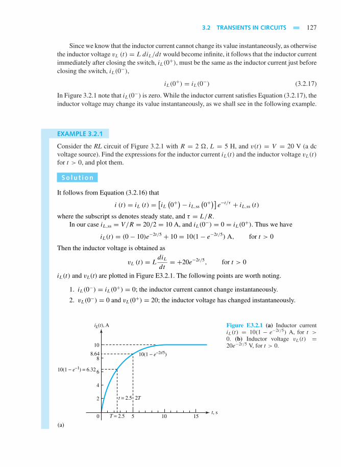
3.2 TRANSIENTS IN CIRCUITS 127
Since we know that the inductor current cannot change its value instantaneously, as otherwisethe inductor voltage vL (t) = L diL/dt would become infinite, it follows that the inductor currentimmediately after closing the switch, iL(0+), must be the same as the inductor current just beforeclosing the switch, iL(0−),
iL(0+) = iL(0
−) (3.2.17)
In Figure 3.2.1 note that iL(0−) is zero. While the inductor current satisfies Equation (3.2.17), theinductor voltage may change its value instantaneously, as we shall see in the following example.
EXAMPLE 3.2.1
Consider the RL circuit of Figure 3.2.1 with R = 2 ,L = 5 H, and v(t) = V = 20 V (a dcvoltage source). Find the expressions for the inductor current iL(t) and the inductor voltage vL(t)for t > 0, and plot them.
So l u t i on
It follows from Equation (3.2.16) that
i (t) = iL (t) =[iL(0+)− iL,ss
(0+)]e−t/τ + iL,ss (t)
where the subscript ss denotes steady state, and τ = L/R.In our case iL,ss = V/R = 20/2 = 10 A, and iL(0−) = 0 = iL(0+). Thus we have
iL(t) = (0− 10)e−2t/5 + 10 = 10(1− e−2t/5) A, for t > 0
Then the inductor voltage is obtained as
vL (t) = LdiL
dt= +20e−2t/5, for t > 0
iL(t) and vL(t) are plotted in Figure E3.2.1. The following points are worth noting.
1. iL(0−) = iL(0+) = 0; the inductor current cannot change instantaneously.
2. vL(0−) = 0 and vL(0+) = 20; the inductor voltage has changed instantaneously.
0 5
t = 2.5
10(1 − e−1) = 6.32
10(1 − e−2t/5)
iL(t), A
t, s
8.64
T = 2.5
2T
10
(a)
2
4
6
8
10
15
Figure E3.2.1 (a) Inductor currentiL(t) = 10(1 − e−2t/5) A, for t >0. (b) Inductor voltage vL(t) =20e−2t/5 V, for t > 0.

128 TIME-DEPENDENT CIRCUIT ANALYSIS
0 5
20e−1 = 7.36
20e−2t/5
vL(t), V
t, sT = 2.5 10
(b)
20
15
Figure E3.2.1 Continued
3. After one time constant has elapsed, the inductor current has risen to 63% of its final orsteady-state value. After five time constants, it would reach 99% of its final value.
4. After one time constant, the inductor voltage has decayed to 37% of its initial value. Theinductor voltage, in this example, eventually decays to zero as it should, since in the steadystate the inductor behaves as a short circuit for dc sources.
The resistor voltage and resistor current, if needed, can be found as follows:
iR (t) = iL (t) = i (t) = 10(1− e−2t/5
)A, for t > 0
vR (t) = RiR (t) = 20(1− e−2t/5
)V, fort > 0
Note that the KVL equation v(t) = V = vR(t)+ vL(t) = 20 is satisfied.
EXAMPLE 3.2.2
Consider the RC circuit of Figure E3.2.2(a) with R = 2 ,C = 5 F, and i(t) = I = 10 A (adc current source). Find the expressions for the capacitor voltage vC(t) and the capacitor currentiC(t) for t > 0, and plot them.
So l u t i on
The KCL equation at the upper node for t > 0 is given by
iC + iR = i (t) , or CdvC (t)
dt+ vC (t)
R= i (t) or
dvC (t)
dt+ 1
RCvC (t) = i (t)
C
This equation is the same in form as Equation (3.2.3). The total solution, which is of the form ofEquation (3.2.16), can be written as
vC (t) = [vC (0+)− vC,ss(0+)]e−t/(RC) + vC,ss (t)
where RC is the time constant T, which is 10 s in this case. vC,ss(t) = RI = 20 V in our case,since the source is dc and the capacitor current iC = C (dvC/dt) = 0 in the steady state for t > 0,denoting an open circuit. Then the solution is given by
vC (t) = [vC (0+)− 20]e−t/10 + 20 V, for t > 0
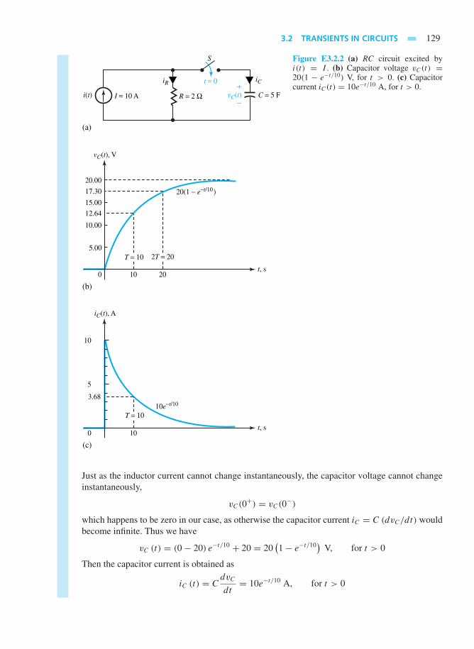
3.2 TRANSIENTS IN CIRCUITS 129
i(t)
iR iC
S
vC(t)I = 10 A
t = 0
R = 2 Ω C = 5 F−
+
(a)
Figure E3.2.2 (a) RC circuit excited byi(t) = I . (b) Capacitor voltage vC(t) =20(1 − e−t/10) V, for t > 0. (c) Capacitorcurrent iC(t) = 10e−t/10 A, for t > 0.
0
12.64
20(1 − e−t/10)
vC(t), V
T = 10 2T = 20
t, s10
(b)
20.00
17.30
15.00
5.00
10.00
20
0
3.6810e−t/10
iC(t), A
T = 10
t, s10
(c)
10
5
Just as the inductor current cannot change instantaneously, the capacitor voltage cannot changeinstantaneously,
vC(0+) = vC(0
−)
which happens to be zero in our case, as otherwise the capacitor current iC = C (dvC/dt) wouldbecome infinite. Thus we have
vC (t) = (0− 20) e−t/10 + 20 = 20(1− e−t/10
)V, for t > 0
Then the capacitor current is obtained as
iC (t) = CdvC
dt= 10e−t/10 A, for t > 0

130 TIME-DEPENDENT CIRCUIT ANALYSIS
vC(t) and iC(t) are plotted in Figures E3.2.2(b) and (c). The following points are noteworthy.
1. vC(0+) = vC(0−); the capacitor voltage cannot change instantaneously.
2. iC(0−) = 0 and iC(0+) = 10 A; the capacitor current has changed instantaneously.
3. After one time constant has elapsed, the capacitor voltage has risen to 63% of its final(steady-state) value. After five time constants, it would reach 99% of its final value.
4. After one time constant the capacitor current has decayed to 37% of its initial value. Thecapacitor current, in this example, eventually decays to zero as it should, since in thesteady state the capacitor behaves as an open circuit for dc sources.
The resistor voltage and current, if desired, can be found as follows:
vR (t) = vC (t) = 20(1− e−t/10
)V, for t > 0
iR (t) = vR (t) /R = 10(1− e−t/10
)A, for t > 0
Note that the KCL equation i(t) = I = iC(t)+ iR(t) = 10 is satisfied. The charge transferred tothe capacitor at steady-state is:
Qss = CVC,ss = 5× 20 = 100 C
Examples 3.2.1 and 3.2.2 are chosen with zero initial conditions. Let us now consider nonzeroinitial conditions for circuits still containing only one energy-storage element, L or C.
EXAMPLE 3.2.3
For the circuit of Figure E3.2.3(a), obtain the complete solution for the current iL(t) through the5-H inductor and the voltage vx(t) across the 6- resistor.
t = 0
(a)
iL(t)
vL(t)
4 Ω
S
5 Ω6 Ω
10 V
5 A5 H
b
a
−
+
+
−
vx(t)+
−
Figure E3.2.3
(b)
4 ΩS
5 Ω6 Ω
RTh =4 + 6 = 10 Ω
Open
Shortb
a

3.2 TRANSIENTS IN CIRCUITS 131
(c)
iL, ss(t)= −10/10 = −1 A
4 ΩS
5 Ω6 Ω
10 V
Short5 A
b
a
−
+
t = 0−
vx(o−)+
−−
+
(d)
iL(o−)= A(by superposition)
37
4 Ω
S
5 Ω6 Ω
10 V
Short5 A
b
a
50
Figure E3.2.3 Continued
So l u t i on
The Thévenin resistance seen by the inductor for t > 0 is found by considering the circuit fort > 0 while setting all ideal sources to zero, as shown in Figure E3.2.3(b).
The time constant of the inductor current is τ = L/RTh = 5/10 = 0.5 s. The steady-state value of the inductor current for t > 0, iL,ss(t), is found by replacing the inductor bya short circuit (since the sources are both dc) in the circuit for t > 0, as shown in FigureE3.2.3(c).
The initial current at t = 0−, iL(0−), is found from the circuit for t < 0 as the steady-state
value of the inductor current for t < 0. Figure E3.2.3(d) is drawn for t < 0 by replacing theinductor with a short circuit (since both sources are dc).
One can solve for iL(0−)
by superposition to yield iL(0−) = 50/37 A = iL
(0+), by
the continuity of inductor current. Then the solution for the inductor current for t > 0 can bewritten as
iL (t) =[iL(0+)− iL, ss
(0+)]e−RTh t/L + iL,ss (t) , for t > 0
In our example,
iL (t) =(
50
37+ 1
)e−2t − 1 =
(87
37e−2t − 1
)A, for t > 0
In the circuit for t = 0− [Figure E3.2.3(d)], notice that vx(0−) has a nonzero value, which can beevaluated by superposition as vx
(0−) = −220/37 V.
For t > 0, vx (t) = −6iL (t) = −(522/37) e−2t + 6. Note that vx, ss = 6 V, andvx(0+) = −522/37+ 6 = −300/37 V, which shows an instantaneous change in vx at t = 0.
EXAMPLE 3.2.4
Consider the circuit of Figure E3.2.4(a) and obtain the complete solution for the voltage vC(t)across the 5-F capacitor and the voltage vx(t) across the 5- resistor.

132 TIME-DEPENDENT CIRCUIT ANALYSIS
t = 0S
(a)
iC(t)
vC(t)
1 Ω
vx(t)5 Ω4 Ω10 V
5 Fb
a−+
+
−
+
−
Figure E3.2.4
(b)
1 ΩShort
5 Ω4 Ω
RTh = 5 + 1 = 6 ΩSb
a
S
10 V−+
+
−
(c)
vC, ss(t) = −10 V
1 Ω
5 Ω4 Ω
Open
b
a
S
10 V−+
+
−
+
−vC(o−) = −40/9 Vvx(o
−)
t = o−
1 Ω
5 Ω4 Ω
Open
b
a
(d)
So l u t i on
(Note that the procedure is similar to that of Example 3.2.3.) The Thévenin resistance seen by thecapacitor for t > 0 is found by considering the circuit for t > 0 while setting all ideal sources tozero, as shown in Figure E3.2.4(b).
The time constant of the capacitor voltage is τ = RThC = 6 × 5 = 30 s. The steady-statevalue of the capacitor voltage for t > 0, vC, ss(t), is found by replacing the capacitor by an opencircuit (since the source is dc in the circuit for t > 0), as shown in Figure E3.2.4(c).
The initial capacitor voltage at t = 0−, vC(0−), is found from the circuit for t < 0 as thesteady-state value of the capacitor voltage for t < 0. Figure E3.2.4(d) is drawn for t < 0 byreplacing the capacitor with an open circuit (since the source is dc).
One can solve for vC(0−) to yield vC(0−) = −40/9 V = vC
(0+), by the continuity of the
capacitor voltage. Then the solution for the capacitor voltage for t > 0 can be written as
vC (t) = [vC (0+)− vC, ss(0+)]e−t/(RThC) + vC, ss (t) , for t > 0

3.2 TRANSIENTS IN CIRCUITS 133
In our example,
vC (t) =(−40
9+ 10
)e−t/30 − 10 =
(50
9e−t/30 − 10
)V, for t > 0
In the circuit of Figure E3.2.4(d) for t = 0−, notice that vx(0−) = 50/9 V. For t > 0, vx(t)= −5iC(t).
The capacitor current is found by
iC (t) = CdvC (t)
dt= (5)
(−50
9· 1
30
)e−t/30 = −25
27e−t/30 A
Then vx(t) = −5iC(t) = (125/27)e−t/30 A, for t > 0. Note that vx(0+) = 125/27 V, and
vx, ss = 0. The resistor voltage has changed value instantaneously at t = 0.
One should recognize that, in the absence of an infinite current, the voltage across a capacitorcannot change instantaneously: i.e., vC(0−) = vC(0+). In the absence of an infinite voltage,the current in a inductor cannot change instantaneously: i.e., iL(0−) = iL(0+). Note that aninstantaneous change in inductor current or capacitor voltage must be accompanied by a changeof stored energy in zero time, requiring an infinite power source. Also observe that the voltagesacross a resistor, vR(0−) and vR(0+), are in general not equal to each other, unless the equalitycondition is forced by iL(0−) or vC(0−). The voltage across a resistor can change instantaneouslyin its value.
So far we have considered circuits with only one energy-storage element, which are knownas first-order circuits, characterized by first-order differential equations, regardless of how manyresistors the circuit may contain. Now let us take up series LC and parallel LC circuits, bothinvolving the two storage elements, as shown in Figures 3.2.2 and 3.2.3, which are known assecond-order circuits characterized by second-order differential equations.
Referring to Figure 3.2.2, the KVL equation around the loop is
vL (t)+ vC (t)+ RThi (t) = vTh (t) (3.2.18)
vTh(t) iL(t) = iC(t) = i(t)
b
aiL(t) = iC(t)
C
L
Idealsourcesandlinearresistors
Thévenin equivalent
b
(t > 0)
a
+
− +
−
+
−
vC(t)
vL(t)
C
L
RTh
Figure 3.2.2 Series LC case with ideal sources and linear resistors.
iEQ(t) vL(t)RTh Lv(t) = vL(t) = vC(t)
b
a
CL C
iL(t) iC(t)Idealsourcesandlinearresistors b
(t > 0) Norton equivalent
a+
−
vC(t)+
−
iL(t) iC (t)
Figure 3.2.3 Parallel LC case with ideal sources and linear resistors.

134 TIME-DEPENDENT CIRCUIT ANALYSIS
With iL(t) = iC(t) = i(t), vL (t) = L diL (t) /dt , and vC (t) = 1C
∫ t
−∞ iC (τ ) dτ , one obtainsthe following equation in terms of the inductor current:
LdiL (t)
dt+ 1
C
∫ τ
−∞iL (τ ) dτ + RThiL (t) = vTh (t) (3.2.19)
Differentiating Equation (3.2.19) and dividing both sides by L, one gets
d2iL (t)
dt2+ RTh
L
diL (t)
dt+ 1
LCiL (t) = 1
L
dvTh (t)
dt(3.2.20)
Referring to Figure 3.2.3, the KCL equation at node a is
iL (t)+ iC (t)+ vC (t)
RTh= iEQ (t) (3.2.21)
With vL(t) = vC(t) = v(t), iC (t) = C dvC(t)
dt, and iL (t) = 1
L
∫ t
−∞ vC (τ) dτ , one obtains thefollowing equation in terms of the capacitor voltage
CdvC (t)
dt+ 1
L
∫ t
−∞vC (τ) dτ + vC (t)
RTh= iEQ (t) (3.2.22)
Differentiating Equation (3.2.22) and dividing both sides by C, one gets
d2vC (t)
dt2+ 1
CRTh
dvC (t)
dt+ 1
LCvC (t) = 1
C
diEQ (t)
dt(3.2.23)
Equations (3.2.20) and (3.2.23) can be identified to be second-order, constant-coefficient,linear ordinary differential equations of the form
d2x (t)
dt2+ a
dx (t)
dt+ bx (t) = f (t) (3.2.24)
Note for the series LC case,
a = RTh
Land b = 1
LC(3.2.25)
and for the parallel LC case,
a = 1
RThCand b = 1
LC(3.2.26)
Because of the linearity of Equation (3.2.24), the solution will consist of the sum of a transientsolution xtr(t) and a steady-state solution xss(t),
x(t) = xtr (t)+ xss(t) (3.2.27)
where xtr(t) satisfies the homogeneous differential equation with f (t) = 0,
d2xtr (t)
dt2+ a
dxtr (t)
dt+ bxtr (t) = 0 (3.2.28)
and xss(t) satisfies the following for a particular f (t),
d2xss (t)
dt2+ a
dxss (t)
dt+ bxss (t) = f (t) (3.2.29)
For obtaining the steady-state solution due to a dc source, recall replacing inductors withshort circuits and capacitors with open circuits. For the steady-state solution due to a sinusoidalsource, simple methods have been developed in Section 3.1.
Now for the transient solution, a possible form for xtr(t) in order to satisfy Equation (3.2.28)is the exponential function est. Thus let us try a solution of the form
3.2 TRANSIENTS IN CIRCUITS 135
xtr(t) = Aest (3.2.30)
Substituting Equation (3.2.30) in Equation (3.2.28), one gets
s2Aest + asAest + bAest = 0 or(s2 + as + b
)Aest = 0 (3.2.31)
which can be true only if
s2 + as + b = 0 (3.2.32)
Equation (3.2.32) is known as the characteristic equation of the differential equation. The tworoots s1 and s2 of Equation (3.2.32) are given by
s1 , s2 = −a
2± 1
2
√a2 − 4b = −a
2
(1±
√1− 4b
a2
)(3.2.33)
Three possibilities arise:
Case 1: The two roots will be real and unequal (distinct), if
(4b
a2
)< 1.
Case 2: The two roots will be real and equal, if
(4b
a2
)= 1.
Case 3: The two roots will be complex conjugates of each other, if
(4b
a2
)> 1.
Let us now investigate these cases in more detail.
Case 1: Roots Real and Unequal (Distinct)
For 4b/a2 < 1, from Equation (3.2.33) it is clear that both roots will be negative if a ispositive. For realistic circuits with positive values of RTh, L, and C, a will be positive, andhence both roots will be negative. With s1 = −α1 and s2 = −α2 (where α1 and α2 arepositive numbers), the transient (natural) solution will be of the form
xtr (t) = A1e−α1t + A2e
−α2t (3.2.34)
where A1 and A2 are constants to be determined later. Note that Equation (3.2.34) containsthe sum of two decaying exponentials.
Case 2: Roots Real and Equal
For 4b = a2, the roots will be equal and negative, as one can see from Equation (3.2.33).With s1 = s2 = −a/2 = −α (where α is positive), let us look at the nature of thetransient solution. For the case of real, repeated roots, not only xtr(t)= A1e
−αt satisfies thedifferential equation, Equation (3.2.28), but also xtr(t) = A2te
−αt can be seen to satisfyEquation (3.2.28). By superposition, the form of the transient solution will be seen to be
xtr (t) = A1e−αt + A2te
−αt = (A1 + A2t) e−αt (3.2.35)
which contains two constants (to be determined later), as it should for the solution of asecond-order differential equation.
136 TIME-DEPENDENT CIRCUIT ANALYSIS
Case 3: Complex Conjugate Roots
For(4b/a2
)> 1, as seen from Equation (3.2.33), the roots will be complex conjugates of
each other. With s1 = −α + jβ and s2 = −α − jβ (where α and β are positive numbers),the transient solution will be of the form
xtr (t) = A1e(−α+jβ)t + A2e
(−α−jβ)t = e−αt(A1e
jβt + A2e−jβt) (3.2.36)
in which A1 and A2 will turn out to be complex conjugates of each other, since the transientsolution must be real. An alternative, and more convenient, form of Equation (3.2.36) isgiven by
xtr (t) = e−αt (C1 cos βt + C2 sin βt) (3.2.37)
in which C1 and C2 are real constants to be determined later. Another alternative form ofEquation (3.2.37) can be shown to be
xtr (t) = Ce−αt sin (βt + φ) (3.2.38)
Note that in all three cases [see Equations (3.2.34), (3.2.35), and (3.2.38)] with nonzero α‘sthe transient solution will eventually decay to zero as time progresses. The transient solution issaid to be overdamped, critically damped, and underdamped, corresponding to Cases 1, 2, and3, respectively. Justification of the statement can be found from the solution of the followingexample.
EXAMPLE 3.2.5
Consider the circuit of Figure 3.2.2 for t > 0 with zero initial conditions, vTh(t) = 1 V (dc), andRTh = 2 ; L = 1 H. Determine the complete response for vC(t) for capacitance values of:
(a) (25/9) F
(b) 1.0 F
(c) 0.5 F
So l u t i on
The KVL equation around the loop is given by
2i (t)+ 1
(di (t)
dt
)+ 1
C
∫ t
−∞i (τ ) dτ = 1.0
Since
vC(t) = 1
C
∫ t
−∞i (τ ) dτ and i (t) = iC (t) = C
dvC (t)
dt
the differential equation in terms of vC(t) is obtained as
2CdvC (t)
dt+ C
d2vC (t)
dt2+ vC (t) = 1.0

3.2 TRANSIENTS IN CIRCUITS 137
The steady-state response vC, ss(t) due to a dc source is determined by replacing inductors withshort circuits and capacitors with open circuits,
vC, ss(t) = V0 = 1.0 V
[Note that vC, ss(t) is of the form of the excitation and is a constant V0; substitution of V0 forvC, ss(t) gives 0+ 0+ V0 = 1.0.]
The transient response is obtained from the force-free (homogeneous) equation, which is
2CdvC, tr
dt+ C
d2vC, tr (t)
dt2+ vC, tr (t) = 0
Assuming vC, tr(t) to be of the form Aest, the values of s are determined from
Aest[2Cs + Cs2 + 1
] = 0 or Cs2 + 2Cs + 1 = 0
and the roots are
s1, s2 = −2C ±√(2C)2 − 4C
2C= −1
(1±
√1− 1
C
)
(a) For C = 25/9 F, the values of s1 and s2 are
s1 = −0.2 and s2 = −1.8
The transient response is given by (see Case 1 with real and unequal roots)
vC, tr(t) = A1e−0.2t + A1e
−1.8t V
and the total (complete) response is
vC(t) = vC, ss(t)+ vC, tr(t) or vC(t) = 1.0+ A1e−0.2t + A2e
−1.8t V
where A1 and A2 are to be evaluated from the initial conditions,
vC(0−) = 0, iL(0
−) = i(0−) = 0
By the continuity principle, vC(0+) = 0 and iL(0+) = 0. Also, iL(0+) = iC(0+) anddvC/dt
(0+) = iC(0+)/C = 0. Expressing dvC(t)/dt as dvC(t)/dt = −0.2A1e
−0.2t −1.8A2e
−1.8t , evaluating dvC(0+)/dt and vC(0+) yields
vC(0+) = 0 = 1+ A1 + A2
dvC
dt
(0+) = 0 = −0.2A1 − 1.8A2
Simultaneous solution yields A1 = −1.125 and A2 = 0.125. Hence the completesolution is
vC(t) = 1.0− 1.125e−0.2t + 0.125e−1.8t V
(b) For C = 1.0 F, the values of s1 and s2 are both equal; s1 = s2 = −1. Corresponding toCase 2 with real and equal roots, the transient response is given by Equation (3.2.35),
vC, n (t) = (A1 + A2t) e−αt = (A1 + A2t) e
−t

138 TIME-DEPENDENT CIRCUIT ANALYSIS
The complete response is vC(t) = 1.0+ (A1 + A2t) e−t . Evaluating both vC and dvC/dt
at t = 0+, we have
vC(0+) = 0 = 1+ A1
dvC
dt(0+) = 0 = A2 − A1
These equations result in A1 = A2 = −1, from which it follows that
vC(t) = 1− e−t − te−t = 1− (t + 1)e−t V
(c) For C = 0.5 F, the values of s1 and s2 are obtained as s1 = (−1+j1) and s2 = (−1−j1)(see Case 3 with complex conjugate roots). The transient response is of the form ofEquation (3.2.38),
vC, n (t) = Ae−αtsin (βt + φ)
where α = 1 and β = 1 in our case. The complete solution is then vC(t) = 1.0 +Ae−t sin(βt + φ) V. From the initial conditions vC(0+) = 0 and dvC/dt
(0+) = 0,
evaluating both at t = 0+ yields
vC(0+) = 0 = 1+ A sin φ
dvC
dt
(0+) = 0 = A(cos φ − sin φ)
Simultaneous solution yields A = −√2 and φ = π/4. Thus the complete response isgiven by
vC (t) = 1.0−√2 e−t sin(t + π
4
)V
The total responses obtained for the three cases are plotted in Figure E3.2.5. These cases aresaid to be overdamped for case (a), critically damped for case (b), and underdamped for case (c).
1 −√2e−t sin (t + )(c)
(b)criticallydamped
(a) overdamped1 −1.125e−0.2t + 0.125e−1.8t
0 1 2 3 4 5
Time, s
Cap
acito
r vo
ltage
, V
0
0.2
0.4
0.6
0.8
1.0
1.2
6 7 8 9 10
Under damped
1 −e−t (t + 1)
π4
Figure E3.2.5 Total responsesobtained.
A system that is overdamped [Figure E3.2.5(a)] responds slowly to any change in excitation.The critically damped system [Figure E3.2.5(b)] responds smoothly in the speediest fashionto approach the steady-state value. The underdamped system [Figure E3.2.5(c)] responds mostquickly accompanied by overshoot, which makes the response exceed and oscillate about the

3.2 TRANSIENTS IN CIRCUITS 139
steady-state value while it gradually approaches the steady-state value. Practical systems aregenerally designed to yield slightly underdamped response, restricting the overshoot to be lessthan 10%.
Let us next consider circuits with two energy-storage elements (L and C) and nonzero initialconditions.
EXAMPLE 3.2.6
Determine iL(t) and vC(t) for t > 0 in the circuit given in Figure E3.2.6(a).
(a)
iL(t)
vC(t)
t = 0
S
4 Ω2 Ω
4 V
1 H
F13
10 V
+
− +
−+
−
Figure E3.2.6
(b)
4 Ω Short2 Ω
4 V
10 V
+
− +
−Open+
−(c)
iL
vC
4 Ω
4 V
1 H
F13
+
−+
−
So l u t i on
From the circuit for t = 0− drawn in Figure E3.2.6(b), we have
iL(0−) = 0 = iL(0
+) and vC(0−) = (10− 4
6× 4
)+ 4 = 8 V = vC
(0+)
From the circuit for t > 0 drawn in Figure E3.2.6(c), we have iL, ss = 0; vC, ss = 4 V. WithR = 4 ,L = 1 H, and C = 1/3 F, s2 + R
Ls + 1
LC= s2 + 4s + 3 = 0. With s1 = −1 and
s2 = −3, iL, tr (t) = A1e−t + A2e
−3t ; vC, tr (t) = B1e−t + B2e
−3t . The complete solutions aregiven by
iL (t) = A1e−t + A2e
−3t and vC (t) = 4+ B1e−t + B2e
−3t
Since
vL(0+) = L
diL
dt
(0+) = −A1 − 3A2 = 4− 4iL
(0+)− vC
(0+) = 4− 8 = −4
iC(0+) = C
dvC
dt
(0+) = 1
3(−B1 − 3B2) = iL
(0+) = 0
it follows that A1 + 3A2 = 4 and B1 + 3B2 = 0.
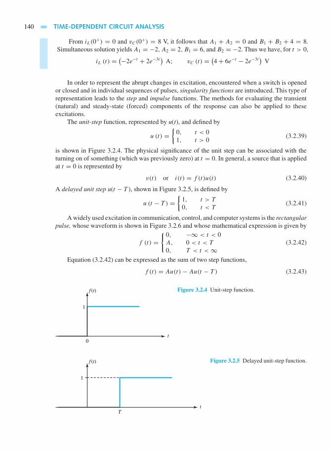
140 TIME-DEPENDENT CIRCUIT ANALYSIS
From iL(0+) = 0 and vC(0+) = 8 V, it follows that A1 + A2 = 0 and B1 + B2 + 4 = 8.Simultaneous solution yields A1 = −2, A2 = 2, B1 = 6, and B2 = −2. Thus we have, for t > 0,
iL (t) =(−2e−t + 2e−3t
)A; vC (t) = (4+ 6e−t − 2e−3t
)V
In order to represent the abrupt changes in excitation, encountered when a switch is openedor closed and in individual sequences of pulses, singularity functions are introduced. This type ofrepresentation leads to the step and impulse functions. The methods for evaluating the transient(natural) and steady-state (forced) components of the response can also be applied to theseexcitations.
The unit-step function, represented by u(t), and defined by
u (t) =
0, t < 01, t > 0
(3.2.39)
is shown in Figure 3.2.4. The physical significance of the unit step can be associated with theturning on of something (which was previously zero) at t = 0. In general, a source that is appliedat t = 0 is represented by
v(t) or i(t) = f (t)u(t) (3.2.40)
A delayed unit step u(t − T ), shown in Figure 3.2.5, is defined by
u (t − T ) =
1, t > T
0, t < T(3.2.41)
A widely used excitation in communication, control, and computer systems is the rectangularpulse, whose waveform is shown in Figure 3.2.6 and whose mathematical expression is given by
f (t) = 0, −∞ < t < 0A, 0 < t < T
0, T < t <∞(3.2.42)
Equation (3.2.42) can be expressed as the sum of two step functions,
f (t) = Au(t)− Au(t − T ) (3.2.43)
f (t)
t
1
0
Figure 3.2.4 Unit-step function.
f (t)
t
1
T
Figure 3.2.5 Delayed unit-step function.

3.2 TRANSIENTS IN CIRCUITS 141
f (t)
t
A
T0
Figure 3.2.6 Rectangular pulse.
The student is encouraged to justify this statement by drawing graphically. For determining theresponse of a circuit to a pulse excitation, using the principle of superposition, the response to eachcomponent can be found and the circuit response obtained by summing the component responses.The decomposition of pulse-type waveforms into a number of step functions is commonly used.
In order to represent the effects of pulses of short duration and the responses they produce,the concept of unit-impulse function δ(t) is introduced,
δ(t) = 0 for t = 0, and∫ ∞
−∞δ (t) dt =
∫ 0+
0−δ (t) dt = 1 (3.2.44)
Equation (3.2.44) indicates that the function is zero everywhere except at t = 0, and the areaenclosed is unity. In order to satisfy this, δ(t) becomes infinite at t = 0. The graphical illustrationof a unit-impulse function is shown in Figure 3.2.7. The interpretation of i(t) = Aδ (t − T ) isthat δ (t − T ) is zero everywhere except at t = T (i.e., the current impulse occurs at t = T ), andthe area under i(t) is A.
f (t)
t
1
12
− ∆0 1
2(a)
∆
u (t)
t
1
0
(b)
As ∆ → 0
d f (t)dt
t12
− ∆0 1
2(c)
∆
1∆
δ (t) = du(t) dt
t0
(d)
As ∆ → 0
Figure 3.2.7 Graphic illustration of unit-impulse function. (a) A modified unit-step function in which thetransition from zero to unity is linear over a -second time interval. (b) Unit-step function: the graph ofpart (a) as→ 0. (c) The derivative of the modified unit-step function depicted in part (a) (area enclosed= 1). (d) Unit-impulse function: the graph of part (c) as → 0 [
∫∞−∞ δ(t)dt = ∫ 0+
0− δ(t)dt = 1]

142 TIME-DEPENDENT CIRCUIT ANALYSIS
The form of the natural response due to an impulse can be found by the methods presentedin this section. As for the initial capacitor voltages and inductor currents, notice that a currentimpulse applied to a capacitance provides an initial voltage of
vC(0+) = q
C(3.2.45)
where q is the area under the current impulse. Similarly, a voltage impulse applied to an inductanceprovides an initial current of
iL(0+) = λ
L(3.2.46)
where λ is the area under the voltage impulse. The impulse function allows the characterizationof networks in terms of the system’s natural response, which is dependent only on the networkelements and their interconnections. Once the impulse response is known, the system responseto nearly all excitation functions can be determined by techniques that are available, but notdisclosed here in view of the scope of this text.
3.3 LAPLACE TRANSFORM
Many commonly encountered excitations can be represented by exponential functions. Thedifferential equations describing the networks are transformed into algebraic equations withthe use of exponentials. So far, methods have been developed to determine the forced re-sponse and the transient response in Sections 3.1 and 3.2. The operational calculus was de-veloped by Oliver Heaviside (1850–1925) based on a collection of intuitive rules; the trans-formation is, however, named after Pierre Simon Laplace (1749–1827) because a completemathematical development of Heaviside’s methods has been found in the 1780 writings ofLaplace. The Laplace transformation provides a systematic algebraic approach for determiningthe total network response, including the effect of initial conditions. The differential equa-tions in the time domain are transformed into algebraic equations in the frequency domain.Frequency-domain quantities are manipulated to obtain the frequency-domain equivalent of thedesired result. Then, by taking the inverse transform, the desired result in the time domainis obtained.
The single-sided Laplace transform of a function f (t) is defined by
L [f (t)] = F(s) =∫ ∞
0f (t) e−st dt (3.3.1)
where f (t) = 0 for t < 0, and s is a complex-frequency variable given by s = σ + jω. Thefrequency-domain function F(s) is the Laplace transform of the time-domain function f (t). Whenthe integral of Equation (3.3.1) is less than infinity and converges, f (t) is Laplace transformable.Note that for σ > 0, e−st decreases rapidly, making the integral converge. The uniqueness of theLaplace transform leads to the concept of the transform pairs,
L[f (t)] = F(s)⇔ L−1 [F(s)] = f (t) (3.3.2)
which states that the inverse Laplace transform of F(s) is f (t). It should be noted that the Laplacetransform is a linear operation such that
L[Af1(t)+ Bf2(t)] = AF1(s)+ BF2(s) (3.3.3)
in which A and B are independent of s and t, and F1(s) and F2(s) are the Laplace transforms of f1(t)
and f2(t), respectively. Using the definition of Equation (3.3.1), Table 3.3.1 of Laplace transformpairs is developed for the most commonly encountered functions. Note that it is assumed that

3.3 LAPLACE TRANSFORM 143
f (t) = 0 for t < 0 and all f (t) exist for t ≥ 0. Also note that in Table 3.3.1, functions 8 through20 can be considered as being multiplied by u(t).
From Table 3.3.1 of Laplace transform pairs one can see that
L[df (t)
dt
]= sF (s)− f
(0+)
(3.3.4)
By recalling that vL = LdiL/dt and iC = C dvC/dt and the principle of continuity of the inductorcurrent and the capacitor voltage, the significance of the term f (0+) in Equation (3.3.4) is that theinitial condition is automatically included in the Laplace transform of the derivative, and hence
TABLE 3.3.1 Laplace Transform Pairs
f(t) in time domain = L-1[F(s)] ⇔ F(s) in frequency domain = Lf[(t)]
(1)df (t)
dtsF (s)− f (0+)
(2)d2f (t)
dt2s2F(s)− sf (0+)− df
dt(0+)
(3)dnf (t)
dtnsnF (s)− sn−1f (0+)− sn−2 df
dt(0+)− · · · d
n−1f
dtn−1(0+)
(4) g(t) =∫ t
0f (t) dt
F (s)
s+ g(0+)
s
(5)∫ t
0f (τ)g(t − τ) dτ F (s)G(s)
(6) u(t), unit-step function1
s
(7) δ(t), unit-impulse function 1
(8) t1
s2
(9)tn−1
(n− 1)!, n integer
1
sn
(10) ε−at1
s + a
(11) tε−at1
(s + a)2
(12) tn−1 ε−at(n− 1)!
(s + a)n
(13) sin ωtω
s2 + ω2
(14) cos ωts
s2 + ω2
(15) sin(ωt + θ )s sin θ + ω cos θ
s2 + ω2
(16) cos(ωt + θ )s cos θ − ω sin θ
s2 + ω2
(17) ε−at sin ωtω
(s + a)2 + ω2
(18) ε−at cos ωts + a
(s + a)2 + ω2
(19) tε−at sin ωt2ω(s + a)
[(s + a)2 + ω2]2
(20) tε−at cos ωt(s + a)2 − ω2
[(s + a)2 + ω2]2

144 TIME-DEPENDENT CIRCUIT ANALYSIS
becomes an inherent part of the final total solution. For cases with zero initial condition, it can beseen that multiplication by s in the frequency domain corresponds to differentiation in the timedomain, and dividing by s in the frequency domain corresponds to integration in the time domain.
Some other properties of the Laplace transform are listed in Table 3.3.2.From the entries of Table 3.3.2, observe the time–frequency dualism regarding frequency
differentiation, frequency integration, and frequency shifting. The initial-value and final-valuetheorems also display the dualism of the time and frequency domains. As seen later, these theoremswill be effectively applied in the network solutions.
In order to use the tabulated transform pairs of Table 3.3.1, algebraic manipulations willbecome necessary to make F(s) correspond to one of the tabulated entries. While the process maybe simple in some cases, in other cases F(s) may have to be rearranged in a systematic way asa sum of component functions whose inverse transforms are tabulated. A formalized approachto resolve F(s) into a summation of simple factors is known as the method of partial-fractionexpansion (Heaviside expansion theorem).
Let us consider a rational function (i.e., one that can be expressed as a ratio of twopolynomials),
F (s) = N (s)
D (s)(3.3.5)
where N(s) denotes the numerator polynomial and D(s) denotes the denominator polynomial. Asa first step in the expansion of the quotient N(s)/D(s), we check to see that the degree of thepolynomial N is less than that of D. If this condition is not satisfied, divide the numerator by thedenominator to obtain an expansion in the form
N (s)
D (s)= B0 + B1s + B2s
2 + · · · + Bm−nsm−n + N1 (s)
D (s)(3.3.6)
where m is the degree of the numerator and n is the degree of the denominator.
TABLE 3.3.2 Some Properties of the Laplace Transform
Property Time Domain Frequency Domain
Linearity af (t)± bg (t) aF (s)± bG (s)
Time delay of shift f (t − T )u(t − T ) e−sT F (s)
Periodic function f (t) = f (t + nT ) f (t), 0 ≤ t ≤ TF(s)
1− e−T swhere
F (s) = ∫ T0 f (t) e−st dt
Time scaling f (at)1
aF( sa
)Frequency differentiation tf (t) −dF (s)
ds(multiplication by t)
Frequency integrationf (t)
t
∫ ∞
s
F (s) ds(division by t)
Frequency shifting f (t)e−at F (s + a)
(exponential translation)
Initial-value theorem limt→0
f (t) = f (0+) lims→∞ sF (s)
Final-value theorem limt→∞ f (t) = f (∞) where limit exists lim
s→0sF (s)

3.3 LAPLACE TRANSFORM 145
The roots of the equation
N(s) = 0 (3.3.7)
are said to be the zeros of F(s); and the roots of the equation
D(s) = 0 (3.3.8)
are said to be the poles of F(s).The new function F1(s) given by N1(s)/D(s) is such that the degree of the denominator
polynomial is greater than that of the numerator. The denominator polynomial D(s) is typicallyof the form
D (s) = ansn + an−1s
n−1 + · · · + a1s + a0 (3.3.9)
By dividing the numerator N1(s) and the denominator D(s) by an, F1(s) may be rewritten asfollows:
F1 (s) = N2 (s)
D1 (s)= N2 (s)
sn + an−1
ansn−1 + · · · + a0
an
(3.3.10)
The particular manner of evaluating the coefficients of the expansion is dependent upon the natureof the roots of D1(s) in Equation (3.3.10). We shall now discuss different cases of interest. Thepossible forms of the roots are (1) real and simple (or distinct) roots, (2) conjugate complex roots,and (3) multiple roots.
Real and Simple (or Distinct) Poles
If all the poles of F1(s) are of first order, Equation (3.3.10) may be written in terms of a partial-fraction expansion as
F1 (s) = N2 (s)
(s − p1) (s − p2) · · · (s − pn)(3.3.11)
or
F1 (s) = K1
s − p1+ K2
s − p2+ · · · + Kn
s − pn
(3.3.12)
where p1, p2, . . . , pn are distinct, and K1, K2, . . . , Kn are nonzero finite constants. For any k, theevaluation of the residue Kk of F1(s) corresponding to the pole s = pk is done by multiplyingboth sides by (s − pk) and letting s → pk ,
Kk = lims→pk
[(s − pk) F1 (s)] (3.3.13)
Equation (3.3.13) is valid for k = 1, 2, . . . , n. Once the K’s are determined in Equation (3.3.12),the inverse Laplace transform of each of the terms can be written easily in order to obtain thecomplete time solution.
Conjugate Complex Poles
It is possible that some of the poles of Equation (3.3.10) are complex. Since the coefficients ak
in Equation (3.3.9) are real, complex poles occur in complex conjugate pairs and will always beeven in number. Let us consider a pair of complex poles for which case Equation (3.3.10) may bewritten as

146 TIME-DEPENDENT CIRCUIT ANALYSIS
F1 (s) = N2 (s)
(s + a + jb) (s + a − jb)D2 (s)(3.3.14)
or
F1 (s) = K1
s + (a + jb)+ K2
s + (a − jb)+ N3 (s)
D2 (s)(3.3.15)
The procedure for finding K1 and K2 is the same as outlined earlier for unrepeated linear factorsor simple poles. Thus we have
K1 = lims→(−a−jb)
[(s + a + jb) F1 (s)] (3.3.16)
and
K2 = lims→(−a+jb)
[(s + a − jb) F1 (s)] (3.3.17)
It can be shown that K1 and K2 are conjugates of each other. The terms in the time function,L−1[F(s)], due to the complex poles of F1(s), are then found easily.
Alternate Representation for Complex Poles
Complex poles can be combined to yield a quadratic term in the partial fraction expansion. Therepresentation may best be illustrated by considering one real pole and two complex conjugatepoles. Let us then consider
F1 (s) = N2 (s)
(s − p1) (s + a + jb) (s + a − jb)
= N2 (s)
(s − p1)[(s + a)2 + b2
]= N2 (s)
(s − p1)(s2 + As + B
) (3.3.18)
which can be rewritten as
F1 (s) = K1
s − p1+ K2s +K3
s2 + As + B(3.3.19)
Evaluating K1 as before, one has
K1 = lims→p1
[(s − p1) F1 (s)] (3.3.20)
It follows from Equations (3.3.18) and (3.3.19) that
N2 (s) = K1(s2 + As + B
)+ (K2s +K3) (s − p1) (3.3.21)
Since Equation (3.3.21) must hold for all values of s, the coefficients of various powers of s onboth sides of the equality must be equal. These equations of equality are then solved to determineK2 and K3.
Even if many pairs of complex conjugate poles occur, this procedure may be used, re-membering that the partial fraction for each complex conjugate pair will be of the formdiscussed.
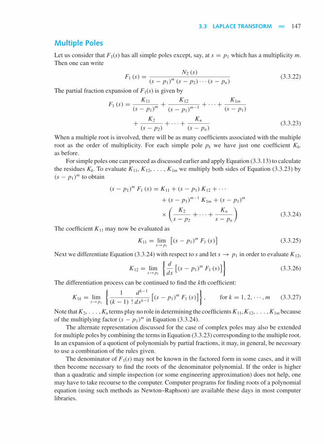
3.3 LAPLACE TRANSFORM 147
Multiple Poles
Let us consider that F1(s) has all simple poles except, say, at s = p1 which has a multiplicity m.Then one can write
F1 (s) = N2 (s)
(s − p1)m (s − p2) · · · (s − pn)
(3.3.22)
The partial fraction expansion of F1(s) is given by
F1 (s) = K11
(s − p1)m +
K12
(s − p1)m−1 + · · · +
K1m
(s − p1)
+ K2
(s − p2)+ · · · + Kn
(s − pn)(3.3.23)
When a multiple root is involved, there will be as many coefficients associated with the multipleroot as the order of multiplicity. For each simple pole pk we have just one coefficient Kk,as before.
For simple poles one can proceed as discussed earlier and apply Equation (3.3.13) to calculatethe residues Kk. To evaluate K11, K12, . . . , K1m we multiply both sides of Equation (3.3.23) by(s − p1)
m to obtain
(s − p1)m F1 (s) = K11 + (s − p1)K12 + · · ·
+ (s − p1)m−1 K1m + (s − p1)
m
×(
K2
s − p2+ · · · + Kn
s − pn
)(3.3.24)
The coefficient K11 may now be evaluated as
K11 = lims→p1
[(s − p1)
m F1 (s)]
(3.3.25)
Next we differentiate Equation (3.3.24) with respect to s and let s → p1 in order to evaluate K12,
K12 = lims→p1
d
ds
[(s − p1)
m F1 (s)]
(3.3.26)
The differentiation process can be continued to find the kth coefficient:
K1k = lims→p1
1
(k − 1) !
dk−1
dsk−1
[(s − p1)
m F1 (s)]
, for k = 1, 2, · · · ,m (3.3.27)
Note that K2, . . . , Kn terms play no role in determining the coefficients K11, K12, . . . , K1m becauseof the multiplying factor (s − p1)
m in Equation (3.3.24).The alternate representation discussed for the case of complex poles may also be extended
for multiple poles by combining the terms in Equation (3.3.23) corresponding to the multiple root.In an expansion of a quotient of polynomials by partial fractions, it may, in general, be necessaryto use a combination of the rules given.
The denominator of F1(s) may not be known in the factored form in some cases, and it willthen become necessary to find the roots of the denominator polynomial. If the order is higherthan a quadratic and simple inspection (or some engineering approximation) does not help, onemay have to take recourse to the computer. Computer programs for finding roots of a polynomialequation (using such methods as Newton–Raphson) are available these days in most computerlibraries.

148 TIME-DEPENDENT CIRCUIT ANALYSIS
With the aid of theorems concerning Laplace transforms and the table of transforms, lin-ear differential equations can be solved by the Laplace transform method. Transformations ofthe terms of the differential equation yields an algebraic equation in terms of the variable s.Thereafter, the solution of the differential equation is affected by simple algebraic manipulationsin the s-domain. By inverting the transform of the solution from the s-domain, one can getback to the time domain. The response due to each term in the partial-fraction expansion isdetermined directly from the transform table. There is no need to perform any kind of inte-gration. Because initial conditions are automatically incorporated into the Laplace transformsand the constants arising from the initial conditions are automatically evaluated, the resultingresponse expression yields directly the total solution. The flow diagram is illustrated in Fig-ure 3.3.1.
Eliminating the need to write the circuit differential equations explicitly, transformed net-works, which are networks converted directly from the time domain to the frequency domain,are used. For the three elements R, L, and C, the transformed network equivalents, using Ta-ble 3.3.1, are based on the Laplace transforms of their respective volt-ampere characteristics,as follows:
L [v (t) = Ri (t)] → V (s) = RI (s) (3.3.28)
L[v (t) = L
di (t)
dt
]→ V (s) = sLI (s)− Li
(0+)
(3.3.29)
L[v (t) = 1
C
∫ t
−∞i (t) dt
]→ V (s) = 1
CsI (s)+ v
(0+)
s(3.3.30)
Note that∫ 0−∞ i (t) dt = q
(0−)
and q(0−)/C = v
(0−) = v(0+) because of continuity of
capacitor voltage. Figure 3.3.2 shows the time-domain networks and the transformed networkequivalents in the frequency domain for elements R, L, and C. Notice the inclusion of the initialinductor current by means of the voltage term [Li(0+)] and the initial capacitor voltage by thevoltage [v(0+)/s]. Source conversion can be applied to obtain alternate transformed equivalentnetworks, as shown in Figure 3.3.2.
The following procedure is applied for the solution of network problems utilizing thetransformed networks in the frequency domain.
1. Replace the time-domain current and voltage sources by the Laplace transforms of theirtime functions; similarly, replace the dependent-source representations. Transform thecircuit elements into the frequency domain with the use of Figure 3.3.2.
2. For the resultant transformed network, write appropriate KVL and KCL equations usingthe mesh and nodal methods of analysis.
3. Solve algebraically for the desired network response in the frequency domain.
Integro-differentialequation
Laplacetransformation
Agebraicmanipulation
Algebraicequations
Initialconditions
Inversetransform
Standardforms
Totalsolution
Figure 3.3.1 Flow diagram forLaplace transformation methodof solving differential equations.

3.3 LAPLACE TRANSFORM 149
v(t)
v(t) = Ri(t)
i (t)R1 2
Resistance+ − V(s)
V(s) = RI(s)
I(s)R1
Time − Domain Network Transformed Network in Frequency Domain
2
+ −
I(s)
I(s)
I(s)
v(t)
v(t) = L dtdi
i (t)L
1 2Inductance
+ −
V(s) = LsI(s) − Li(0+)
V(s)
or
Li(0+)Ls1 2− +
−+
I(s) = +Ls
V(s)s
i(0+)
V(s)
i(0+)/s
Ls1 2
−+
I(s)
v(t)
v(t) = ∫i(t)dtC1
i (t)C1 2
Capacitance+ − V(s)
or
v (0+)/s1/Cs
1/Cs
1 2+ −
−+
V(s) = I(s) +Cs1
sv(0+)
V(s)
I(s) = Cs V(s) − Cv(0+)Cv(0+)
1 2
−+
(a)
(b)
(c)
Figure 3.3.2 Time-domain networks and transformed network equivalents in frequency domain forR, L, and C.
4. By taking the inverse Laplace transform of the frequency-domain response, obtain thetime-domain response.
Let us illustrate the use of this procedure with some examples.
EXAMPLE 3.3.1
Consider the circuit shown in Figure E3.3.1(a) in which the switch S has been in position 1 for along time. Let the switch be changed instantaneously to position 2 at t = 0. Obtain v(t) for t ≥ 0with the use of the Laplace transform method.

150 TIME-DEPENDENT CIRCUIT ANALYSIS
(a)
v(t)2 F
4 Ω
1
2
10 V2 Ω
1 H
t = 0S
+
−
+
−
Figure E3.3.1
V(s)I(s)
(b)
10s
2s
2 Ω
s
+
+
−−
So l u t i on
With switch S in position 1 for a long time,
vC(0−) = vC(0
+) = 10 V
iL(0−) = iL(0
+) = 0
The transformed network in the frequency domain is shown in Figure E3.3.1(b).The KVL equation is given by
I (s)
(2
s+ 2+ s
)= 10
s
or
I (s) = 10
s2 + 2s + 2and V (s) = I (s) (2+ s)
Thus,
V (s) = 10 (s + 2)
s2 + 2s + 2= K1
s + 1− j1+ K∗
1
s + 1+ j1
where
K1 = 10 (−1+ j1+ 2)
(−1+ j1)+ 1+ j1= 5√
2 e−jπ/4
By taking the inverse Laplace transform, we get
v (t) = 10√
2 e−t cos(t − π
4
)V
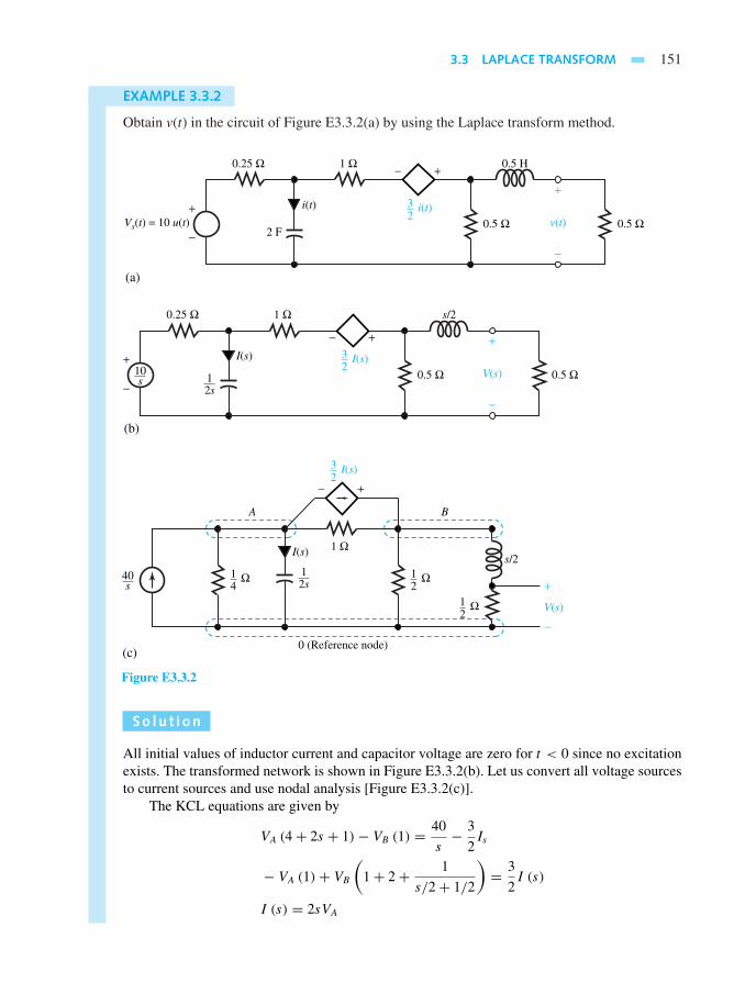
3.3 LAPLACE TRANSFORM 151
EXAMPLE 3.3.2
Obtain v(t) in the circuit of Figure E3.3.2(a) by using the Laplace transform method.
++−
−
v(t)i(t)i(t)
Vs(t) = 10 u(t)
(a)
0.5 Ω
32
0.25 Ω 1 Ω 0.5 H
2 F0.5 Ω
+
−
++−
−
V(s)I(s)I(s)
(b)
0.5 Ω
32
0.25 Ω 1 Ω s/2
0.5 Ω+
−10s 1
2s
I(s)s/2
(c)
1 Ω
+
+
−
−
I(s)
B
0 (Reference node)
V(s)
32
Ω14
Ω12
Ω12
40s
12s
A
Figure E3.3.2
So l u t i on
All initial values of inductor current and capacitor voltage are zero for t < 0 since no excitationexists. The transformed network is shown in Figure E3.3.2(b). Let us convert all voltage sourcesto current sources and use nodal analysis [Figure E3.3.2(c)].
The KCL equations are given by
VA (4+ 2s + 1)− VB (1) = 40
s− 3
2Is
− VA (1)+ VB
(1+ 2+ 1
s/2+ 1/2
)= 3
2I (s)
I (s) = 2sVA

152 TIME-DEPENDENT CIRCUIT ANALYSIS
Substitution of I(s) and solving for VB gives
VB = 10 (3s + 1) (s + 1)
3s(s2 + 3s + 2
)VA = 1/2
1/2+ s/2VB = 1
s + 1VB = 10(3s + 1)
3s(s + 1)(s + 2)= K1
s+ K2
s + 1+ K3
s + 2
where
K1 = 10 (0+ 1)
3 (0+ 1) (0+ 2)= 5
3
K2 = 10 (−3+ 1)
3 (−1) (−1+ 2)= 20
3
K3 = 10 (−6+ 1)
3 (−2) (−2+ 1)= −25
3
Therefore,
v (t) =(
5
3+ 20
3e−t − 25
3e−2t
)u (t) V
Note that Thévenin’s and Norton’s network theorems are applicable in the frequency domain.
Network functions (also known as system functions) are defined as the ratio of the response tothe excitation in the frequency domain, as illustrated in Figure 3.3.3. Driving-point impedancesand admittances are network functions, as shown in Figure 3.3.4.
The concept of transfer functions is illustrated in Figure 3.3.5, in which the response measuredat one pair of terminals is related to an excitation applied to another pair of terminals.
x(t)
x(t) y(t)(a)
Linear system
Excitation Differentialequation
y(t)
Response
X(s)
H(s) = Y(s)X(s)
(b)
Linear system
H(s)
Y(s)
Figure 3.3.3 Linear system with no initial energy storage. (a) Time domain. (b) Frequency domain.
Driving-point impedance Z(s) = V(s) / I(s)Driving-point admittance Y(s) = I(s) / V(s)
+
−V(s)
I(s)
Network
Figure 3.3.4 Network functions.
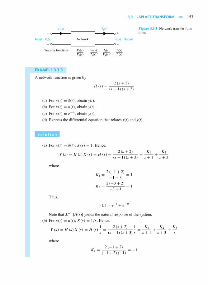
3.3 LAPLACE TRANSFORM 153
Transfer functions V2(s); V2(s)
; I2(s)
; I2(s)
V1(s) I1(s) V1(s) I1(s)
+
−
+
−V1(s) V2(s)
I1(s) I2(s)
NetworkInput Output
Figure 3.3.5 Network transfer func-tions.
EXAMPLE 3.3.3
A network function is given by
H (s) = 2 (s + 2)
(s + 1) (s + 3)
(a) For x(t) = δ(t), obtain y(t).
(b) For x(t) = u(t), obtain y(t).
(c) For x(t) = e−4t , obtain y(t).
(d) Express the differential equation that relates x(t) and y(t).
So l u t i on
(a) For x(t) = δ(t), X(s) = 1. Hence,
Y (s) = H (s)X (s) = H (s) = 2 (s + 2)
(s + 1) (s + 3)= K1
s + 1+ K2
s + 3
where
K1 = 2 (−1+ 2)
−1+ 3= 1
K2 = 2 (−3+ 2)
−3+ 1= 1
Thus,
y (t) = e−t + e−3t
Note that L−1 [H(s)] yields the natural response of the system.
(b) For x(t) = u(t),X(s) = 1/s. Hence,
Y (s) = H (s)X (s) = H (s)1
s= 2 (s + 2)
(s + 1) (s + 3)
1
s= K1
s + 1+ K2
s + 3+ K3
s
where
K1 = 2 (−1+ 2)
(−1+ 3) (−1)= −1
154 TIME-DEPENDENT CIRCUIT ANALYSIS
K2 = 2 (−3+ 2)
(−3+ 1) (−3)= −1
3
K3 = 2 (0+ 2)
(0+ 1) (0+ 3)= 4
3
Thus,
y (t) = −e−t − 1
3e−3t + 4
3
The first two terms on the right-hand side are the natural response arising from H(s),whereas the last term is the forced response arising from X(s). Note that K3 is H (s) |s=0,while X (s) = 1/s.
(c) For x(t) = e−4t , X(s) = 1/(s + 4). Hence,
Y (s) = H (s)X (s) = H (s)1
s + 4= 2 (s + 2)
(s + 1) (s + 3)
1
(s + 4)
= K1
s + 1+ K2
s + 3+ K3
s + 4
where
K1 = 2 (−1+ 2)
(−1+ 3) (−1+ 4)= 1
3
K2 = 2 (−3+ 2)
(−3+ 1) (−3+ 4)= 1
K3 = 2 (−4+ 2)
(−4+ 1) (−4+ 3)= −4
3
Thus,
y (t) = 1
3e−t + e−3t − 4
3e−4t
The first two terms on the right-hand side are the natural response arising from H(s),whereas the last term is the forced response arising from X(s). Note that K3 isH (s) |s=−4,whereas X(s) = 1/(s + 4).
(d) Y (s) = H (s)X (s) = 2 (s + 2)
(s + 1) (s + 3)X (s)
or (s + 1) (s + 3) Y (s) = 2 (s + 2)X (s), or(s2 + 4s + 3
)Y (s) = (2s + 4)X (s). Rec-
ognizing that multiplication by s in the frequency domain corresponds to differentiationin the time domain, the differential equation is expressed as
d2y
dt2+ 4
dy
dt+ 3y = 2
dx
dt+ 4x
3.4 FREQUENCY RESPONSE
Earlier we examined the circuit response to sinusoids that have a fixed frequency. Now let usexamine the response of a circuit to a sinusoidal source, called an oscillator, whose frequency canbe varied. Known as the frequency response, it is often expressed as a network function, which is anoutput–input ratio. In order to visualize the changes in phase shift and amplitude as the frequency of

3.4 FREQUENCY RESPONSE 155
the input signal changes, a graphical display of the frequency-response characteristics of networksis often employed.
A filter is a network used to select one range of frequencies, while rejecting all otherfrequencies. Let us now consider simple networks which function as filters. For the RC networkshown in Figure 3.4.1, the voltage transfer function Vout/Vin is given by
H (jω) = Vout
Vin= 1
1+ jωRC= 1√
1+ (ωRC)2 − tan−1 (ωRC) = H (ω) θ (ω) (3.4.1)
where H(ω) is the amplitude ratio and θ(ω) is the phase shift. Defining the cutoff frequency asthe frequency ω at which H(ω) is reduced to 1/
√2, or 0.707 of its maximum value (which is 1.0
at ω = 0), it follows that
ωCO = 1
RC(3.4.2)
and the phase shift becomes −45° at that cutoff frequency, as shown in Figure 3.4.2. The powerdelivered to the circuit, at this frequency, is one-half the maximum power. As a consequence, ωCO
is also called the half-power point, or half-power angular frequency. We see that this filter circuitof Figure 3.4.1 is indeed a low-pass filter because any input signal components at ω << ωCO arepassed to the output with virtually unchanged amplitude and phase, whereas any componentsat ω >> ωCO have greatly reduced output amplitudes. ωCO roughly divides the passband(region of transmitted frequencies) from the stopband (region of high attenuation). The rangeof transmitted frequencies is known as the bandwidth. Note that in Figure 3.4.1 the low-passfiltering properties come from the fact that the capacitor is an open circuit for ω = 0 but becomesa short circuit for ω → ∞ and “shorts out” any high-frequency voltage components across theoutput.
The low-pass simple filter circuits are shown in Figure 3.4.3 and Figure 3.4.4 gives the high-pass simple filter circuits. Note the interchange of resistance and reactance, which converts alow-pass filter into a high-pass filter, or vice versa.
VoutVin Ω1jωc
R Ω+
−
+
−
−−−−
Figure 3.4.1 RC network.
−45°
−90°
ωco = 1/RC ωω
Phase shift θ (ω)
Passband
Amplitude ratio H (ω)
1.0
0.707
0
Figure 3.4.2 Frequency response ofRC network of Figure 3.4.1.

156 TIME-DEPENDENT CIRCUIT ANALYSIS
−
+
−
+
(a)
Vin
jωL
jωC1
R Vout
−
+
−
+
(b)
Vin
R
Vout
Figure 3.4.3 Low-pass simple filter circuits. (a) RL low-pass filter. (b) RC low-pass filter.
−
+
−
+
(a)
Vin jωL jωC1R
Vout
−
+
−
+
(b)
Vin R Vout
Figure 3.4.4 High-pass simple filter circuits (a) RL highpass filter. (b) RC high-pass filter.
The low-pass transfer function, given by Equation (3.4.1), can be written as
H (ω) = 1√1+ (ω/ωCO)
2; θ(ω) = − tan−1 ω
ωCO(3.4.3)
which also applies to the RL low-pass filter with ωCO = R/L.The high-pass transfer function for either of the circuits of Figure 3.4.4 is given by
H (ω) = (ω/ωCO)√1+ (ω/ωCO)
2; θ (ω) = 90°− tan−1 ω
ωCO(3.4.4)
where ωCO = R/L or 1/RC. The ideal response characteristics of low pass, high pass, bandpass,and band reject are shown in Figure 3.4.5.
Due to the greater availability and lower cost of capacitors and the undesirable resistanceusually associated with inductors, virtually all simple filter designs employ capacitors rather thaninductors, despite the similarity of RL and RC circuits. More sophisticated filters use two or morereactive elements in order to have essentially constant or flat H(ω) over the passband and narrowtransition between the passband and the stopband.
One of the most common forms of display of the network function H (jω) is the Bodediagram. In this diagram the magnitude and phase of H (jω) are plotted separately as functionsof the frequency variable ω. A logarithmic scale is used for the frequency variable in orderto accommodate wide frequency ranges, and the magnitude of the network function H(ω) isexpressed in decibels (dB) as
H(dB) = 20 log10 H (3.4.5)
The two portions of the Bode plot, H(ω) and θ(ω), are graphed on semilog axes. The advantageof this technique is that rather than plotting the network characteristic point by point, one canemploy straight-line approximations to obtain the characteristic quite efficiently.
Asymptotic Bode plots lead to simply drawn approximate characteristics which are quiteadequate for many purposes and reduce the calculational complications greatly. The frequencyresponse is found by substituting s = jω in the network function H(s). Let

3.4 FREQUENCY RESPONSE 157
(a)
H(ω)
0
Passband
Ideal
Actual
ωωco
(b)
H(ω)
0
Passband
Ideal
Actual
ωωco
(c)
H(ω)
0
Passband
Ideal
Actual
ωω1 ω2
(d)
H(ω)
0
Passband
Ideal
Actual
ωω1 ω2
Passband
Figure 3.4.5 Ideal response characteristics. (a) Low pass. (b) High pass. (c) Band pass. (d) Band reject.
H (jω) = k
(1+ jω
01
) (1+ jω
02
)· · ·(
1+ jω
0m
)(
1+ jω
p1
) (1+ jω
p2
)· · ·(
1+ jω
pn
) (3.4.6)
where−01,−02, . . . ,−0m are the zeros, and−p1,−p2, . . . ,−pn are the poles of the networkfunction. Equation (3.4.6) is clearly the product of a constant and a group of terms having the form(1+ jω/ω0) or 1/(1+ jω/ω0). Each of these terms can be considered as an individual phasor,and H (jω) has a magnitude given by the product of the individual magnitudes (or the sum of theindividual terms expressed in dB) and an angle given by the sum of the individual angles. Thusthe behavior of functions (1 + jω/ω0) and 1/(1 + jω/ω0) is to be clearly understood for theconstruction of Bode plots.
Let us first consider H1(jω) = 1 + jω/ω0. For ω/ω0 << 1 (i.e., low frequencies), themagnitude H1(ω) ∼= 1, or H1(ω)dB = 20 log 1 = 0 dB. The break frequency is ω = ω0. At highfrequencies (i.e., ω/ω0 >> 1), the function behaves as
H1 (ω) ∼= ω
ω0or H1 (ω)dB = 20 log
ω
ω0
at ω/ω0 = 1,
H1 (ω)dB = 0 dB
at ω/ω0 = 10,
H1 (ω)dB = 20 log 10 = 20 dB
and at ω/ω0 = 100,
H1 (ω)dB = 20 log 100 = 40 dB

158 TIME-DEPENDENT CIRCUIT ANALYSIS
Since factors of 10 are linear increments on the logarithmic frequency scale, the plot of 20 log(ω/ω0) versus ω on a semilog paper is a straight line with a slope of +20 dB/decade or +6dB/octave, as shown in Figure 3.4.6. Note that an octave represents a factor of 2 in frequency,whereas a decade represents a factor of 10. The angle associated with H1(jω) is θ1(ω) =tan−1(ω/ω0). At low frequencies (ω ≤ 0.1ω0), θ1
∼= 0; for frequencies ω ≥ 10ω0, θ1∼= 90°;
and at ω = ω0, θ1 = +45°. This leads to the straight-line approximations for θ1(ω), as shownin Figure 3.4.6. For 0.1ω0 ≤ ω ≤ 10ω0, the slope of θ1(ω) versus ω is approximately given by+45°/decade (over two decades centered at the critical frequency) or +13.5°/octave. Thus theasymptotic Bode plot for H1(jω) = 1+ jω/ω0 is drawn in Figure 3.4.6. Figure 3.4.7 gives theasymptotic Bode plot for H2(jω) = 1/(1+ jω/ω0) with a similar kind of reasoning. The studentis encouraged to justify the plot. The dashed curves in Figures 3.4.6 and 3.4.7 indicate the exactmagnitude and phase responses.
The process of developing asymptotic Bode plots is then one of expressing the networkfunction in the form of Equation (3.4.6), locating the break frequencies, plotting the componentasymptotic lines, and adding these to get the resultant. The following example illustrates theprocedure.
0
−90
−45
45
90
−20
20
0
40
θ1(ω), deg
Slope =+20 dB/decade or+6 dB/octave
Slope = +45° /decade or +13.5° /octave
0.1 ω0 1 ω0 10 ω0 100 ω0
ωAsymptotic
Exact
ω
Asymptotic
Exact
ω, rad/s
H1(ω) dB Figure 3.4.6 Asymptotic Bode plot for H1(jω) =1+ jω/ω0.
EXAMPLE 3.4.1
Sketch the asymptotic Bode plot for
H (s) = 104 (s + 50)
s2 + 510s + 5000

3.4 FREQUENCY RESPONSE 159
So l u t i on
H(s) = 100(1+ s/50)
(1+ s/10)(1+ s/500)or H (jω) = 100(1+ jω/50)
(1+ jω/10)(1+ jω/500)
The break frequencies are 10 and 500 rad/s for the denominator and 50 rad/s for the numerator.The component straight-line segments are drawn as shown in Figure E3.4.1. Note that the effectof the constant multiplier 100 in H (jω) is to add a constant value, 20 log 100= 40 dB, as markedin the Bode plot. The resultant asymptotic magnitude H(ω) and angle θ(ω) characteristics areindicated by the dashed lines.
H(ω), dB
0
−60
−90
−30
+60
+30
+90
−30
−20
−10
20
0
40
30
10
θ(ω), deg
10.1 10 100 1000
Angle of1 )(1 + jω /10
10,000
ω
ω
Angular frequency, rad/s (logarithmic scale)
Magnitude of1 )(1 + jω /500
Angle of1 )(1 + jω /500
Magnitude of
Magnitude of (1 + jω /50)
Angle of (1 + jω /50)
1 )(1 + jω /10
Angle θ (ω)
H(ω) dB40 dB
Figure E3.4.1 Asymptotic Bode plot.
As seen from Example 3.4.1, the frequency response in terms of the asymptotic Bode plot isobtained with far less computation than needed for the exact characteristics. With little additionaleffort, by correcting errors at a few frequencies within the asymptotic plot, one can get a sufficientlyaccurate result for most engineering purposes. While we have considered H (jω) of the typegiven by Equation (3.4.6) with only simple poles and zeros, two additional cases need furtherconsideration:

160 TIME-DEPENDENT CIRCUIT ANALYSIS
H2(ω), dB
0
−90
−45
45
90
−20
20
0
40
θ2(ω), deg
Slope = −20 dB/decade or −6 dB/octave
Slope = −45° /decade or −13.5° /octave
0.1 ω0 1 ω0 10 ω0
ω, rad/s
100 ω0
Asymptotic
ExactAsymptotic
Exact
ω
ω
Figure 3.4.7 Asymptotic Bode plot for H2(jω) =1/(1+ jω/ω0).
Case 1: Zero or Pole at Origin
lims→0 H(s) = Ksn, where n can be any positive or negative integer. The magnitudecharacteristic for this factor has a slope of 20n dB/decade and passes through K dB atω = 1, while the component angle characteristic has a constant value of n× 90°.
Case 2: Some Zeros or Poles Occur as Complex Conjugate Pairs
Let
H(s) =(
1+ s
α + jβ
)(1+ s
α − jβ
)= 1+ 2
α
α2 + β2s + s2
α2 + β2
With a break frequency of√α2 + β2, the magnitude is characterized by a slope of 40
dB/decade for ω ≥ √α2 + β2, and the angle characteristic shows a slope of 90°/decade inthe range of 0.1
√α2 + β2 ≤ ω ≤ 10
√α2 + β2. The asymptotic Bode plot for this case is
shown in Figure 3.4.8.
Note that the angle and magnitude characteristics will have the opposite sign for the case ofa complex conjugate pair of poles. It should also be pointed out that the straight-line quadraticrepresentations are not generally good approximations (particularly in the one-decade region oneither side of the break frequency), and a few points may be calculated to obtain the correct curvesin the questionable frequency range.
For the series RLC circuit, the input admittance is given by

3.4 FREQUENCY RESPONSE 161
H(ω), dB
θ(ω), deg0
90
0
180
80
40
0.1 1 10 100
ω / α2 + β2
Slope = 90°/decade
Slope = 40 dB/decade
ω / α2 + β2
Figure 3.4.8 Asymptotic Bode plot for
the quadratic H(s) = 1 + 2α
α2 + β2s +
s2
α2 + β2.
Y (jω) = 1
R + jωL+ 1/jωC= 1
R + j (ωL− 1/ωC)(3.4.7)
At the series resonant frequency ω0 = 1/√LC,
Y (jω0) = 1
R= Y0
corresponds to maximum admittance (or minimum impedance). The ratio Y/Y0 can be written as
Y
Y0(jω) = R
R + j
(ωL− 1
ωC
) = 1
1+ j
(L
R
)(ω − 1
ωLC
)
= 1
1+ jω0L
R
(ω
ω0− ω0
ω
) (3.4.8)
Introducing a quality factor QS = ω0L/R and per-unit source frequency deviation δ = (ω −ω0)/ω0,
Y
Y0(jω) = 1
1+ jQS
(ω
ω0− ω0
ω
) = 1
1+ jδQS
(2+ δ
1+ δ
) (3.4.9)
For δ << 1, i.e., for small frequency deviations around the resonant frequency, Equation (3.4.9)becomes, near resonance,
Y
Y0(jω) = 1
1+ j2δQS
(3.4.10)
which is the equation of the universal resonance curve plotted in Figure 3.4.9. The curveapplies equally well to the parallel GLC circuit with Z/Z0 as the ordinate, when the value ofQp = ω0C/G. The bandwidth and the half-power points in a resonant circuit (either series orparallel) correspond to ω0/Q and 2δQ = ±1 when the magnitude Y/Y0 or Z/Z0 is 0.707.
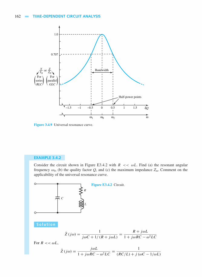
162 TIME-DEPENDENT CIRCUIT ANALYSIS
0.707
1.0
−1.5 −1 −0.5 0.50
YY0
ZZ0
Bandwidthor
ForseriesRLC
( ) Forparallel
GLC( )
Half-power points
δQ1 1.5
ω1 ω0 ωω2
Figure 3.4.9 Universal resonance curve.
EXAMPLE 3.4.2
Consider the circuit shown in Figure E3.4.2 with R << ωL. Find (a) the resonant angularfrequency ω0, (b) the quality factor Q, and (c) the maximum impedance Zm. Comment on theapplicability of the universal resonance curve.
R
L
C
Figure E3.4.2 Circuit.
So l u t i on
Z (jω) = 1
jωC + 1/ (R + jωL)= R + jωL
1+ jωRC − ω2LC
For R << ωL,
Z (jω) = jωL
1+ jωRC − ω2LC= 1
(RC/L)+ j (ωC − 1/ωL)

3.4 FREQUENCY RESPONSE 163
ω0 = 1√LC
; Q = ω0L
R; Zm = L
RC= RQ2
The universal resonance curve and the conclusions obtained from it apply to this circuit, providedωL >> R, or Q ≥ 10.
Two-Port Network Parameters
A pair of terminals at which a signal may enter or leave a network is called a port, and a networkhaving two such pairs of terminals, labeled generally input and output terminals, is known as a two-port network. A two-port network forms a very important building block in electronic systems,communication systems, automatic control systems, transmission and distribution systems, or inother systems in which an electric signal or electric energy enters the input terminals, is actedupon by the network, and leaves via the output terminals.
The two-port network (or two-terminal-pair network) shown in Figure 3.4.10 is describedby port currents and voltages (i.e., four variables) related by a set of linear equations in terms oftwo-port parameters. Of the six possible parameter sets, the three used extensively in electroniccircuit analysis are given next in the frequency domain.
1. Two-port admittance or y parameters (in siemens),
I1 = y11V1 + y12V2 = yiV1 + yrV2 (3.4.11)
I2 = y21V1 + y22V2 = yf V1 + yoV2 (3.4.12)
where
y11 = yi = I1
V1
∣∣∣∣∣V2=0
= short-circuit input admittance
y12 = yr = I1
V2
∣∣∣∣∣V1=0
= short-circuit reverse transfer admittance
y21 = yf = I2
V1
∣∣∣∣∣V2=0
= short-circuit forward transfer admittance
y22 = yo = I2
V2
∣∣∣∣∣V1=0
= short-circuit output admittance
2. Two-port impedance or z parameters (in ohms),
V1 = z11I1 + z12I2 = ziI1 + zrI2 (3.4.13)
V2(s)V1(s)
I2(s)I1(s)
1
1′
2
2′
+
−
+
−
Figure 3.4.10 Two-port network (ortwo-terminal-pair network).

164 TIME-DEPENDENT CIRCUIT ANALYSIS
V2 = z21I1 + z22I2 = zf I1 + zoI2 (3.4.14)
where
z11 = zi = V1
I1
∣∣∣∣∣I2=0
= open-circuit input impedance
z12 = zr = V1
I2
∣∣∣∣∣I1=0
= open-circuit reverse transfer impedance
z21 = zf = V2
I1
∣∣∣∣∣I2=0
= open-circuit forward transfer impedance
z22 = zo = V2
I2
∣∣∣∣∣I1=0
= open-circuit output impedance
3. Two-port hybrid or h parameters,
V1 = h11I1 + h12V2 = hiI1 + hrV2 (3.4.15)
I2 = h21I1 + h22V2 = hf I1 + hoV2 (3.4.16)
where
h11 = hi = V1
I1
∣∣∣∣∣V2=0
= short-circuit input impedance (ohms)
h12 = hr = V1
V2
∣∣∣∣∣I1=0
= open-circuit reverse voltage gain (dimensionless)
h21 = hf = I2
I1
∣∣∣∣∣V2=0
= short-circuit forward current gain (dimensionless)
h22 = ho = I2
V2
∣∣∣∣∣I1=0
= open-circuit output admittance (siemens)
EXAMPLE 3.4.3
Consider Equations (3.4.11) through (3.4.16). Develop the y-parameter, z-parameter, and h-parameter equivalent circuits. Also express the z-parameters in terms of y-parameters.
So l u t i on
Equations (3.4.11) and (3.4.12) can be expressed as
− I1 + (y11 + y12) V1 − y12 (V1 − V2) = 0
− I2 + (y22 + y12) V2 − y12 (V2 − V1)+ (y21 − y12) V1 = 0

3.4 FREQUENCY RESPONSE 165
The y-parameter equivalent circuit that satisfies these equations is shown in Figure E3.4.3(a).
V2V1
−y12
y11 + y12 y22 + y12 (y21 − y12)V1
I2I1
1
1′(a)
2
2′
+
−
+
−
Figure E3.4.3 (a) y-para-meter equivalent circuit.(b) z-parameter equivalentcircuit. (c) h-parameterequivalent circuit.
V2V1 z12
z22 − z12z11 − z12(z21 − z12)I1
I2I1
1
1′(b)
2
2′
++−
−
+
−
V2V1 h12V2 h21I1 h22
h11 I2I1
1
1′(c)
2
2′
+
+
−
−
+
−
Equations (3.4.13) and (3.4.14) can be arranged as
V1 = (z11 − z12) I1 + z12 (I1 + I2)
V2 = (z21 − z12) I1 + (z22 − z12) I2 + z12 (I1 + I2)
The z-parameter equivalent circuit that satisfies these equations is shown in Figure E3.4.3(b).The h-parameter equivalent circuit satisfying Equations (3.4.15) and (3.4.16) is shown in FigureE3.4.3(c).
Equations (3.4.11) and (3.4.12) can be solved simultaneously to yield
V1 = y22
y11y22 − y12y21I1 + −y12
y11y22 − y12y21I2
V2 = −y21
y11y22 − y12y21I1 + y11
y11y22 − y12y21I2
By comparing these with Equations (3.4.13) and (3.4.14), one gets
z11 = y22
y11y22 − y12y21; z12 = −y12
y11y22 − y12y21
z21 = −y21
y11y22 − y12y21; z22 = y11
y11y22 − y12y21
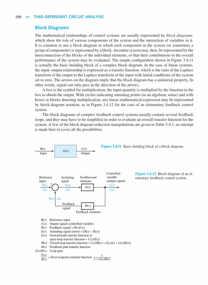
166 TIME-DEPENDENT CIRCUIT ANALYSIS
Block Diagrams
The mathematical relationships of control systems are usually represented by block diagrams,which show the role of various components of the system and the interaction of variables in it.It is common to use a block diagram in which each component in the system (or sometimes agroup of components) is represented by a block. An entire system may, then, be represented by theinterconnection of the blocks of the individual elements, so that their contributions to the overallperformance of the system may be evaluated. The simple configuration shown in Figure 3.4.11is actually the basic building block of a complex block diagram. In the case of linear systems,the input–output relationship is expressed as a transfer function, which is the ratio of the Laplacetransform of the output to the Laplace transform of the input with initial conditions of the systemset to zero. The arrows on the diagram imply that the block diagram has a unilateral property. Inother words, signal can only pass in the direction of the arrows.
A box is the symbol for multiplication; the input quantity is multiplied by the function in thebox to obtain the output. With circles indicating summing points (in an algebraic sense) and withboxes or blocks denoting multiplication, any linear mathematical expression may be representedby block-diagram notation, as in Figure 3.4.12 for the case of an elementary feedback controlsystem.
The block diagrams of complex feedback control systems usually contain several feedbackloops, and they may have to be simplified in order to evaluate an overall transfer function for thesystem. A few of the block diagram reduction manipulations are given in Table 3.4.1; no attemptis made here to cover all the possibilities.
R(s)Input
C(s)Output
G(s)Figure 3.4.11 Basic building block of a block diagram.
E(s)R(s)e(t)r(t)
B(s)
Feedforwardelements
Controlledvariable(output signal)
Actuatingsignal
Feedbacksignal
Feedback elements
Reference inputR(s)Output signal (controlled variable)C(s)Feedback signal = H(s)C(s)B(s)Actuating signal (error) = [R(s) − B(s)]E(s)
Feedback path transfer functionH(s)Loop gainG(s)H(s)
R(s)Error-response transfer function
E(s)
Forward path transfer function oropen-loop transfer function =
G(s)
C(s)/R(s) = G(s)/[1 + G(s)H(s)]M(s)
Referenceinput
C(s)c(t)
G(s)
H(s)
11 + G(s)H(s)
=
Closed-loop transfer function =C(s)/E(s)
+
−
b(t)
Figure 3.4.12 Block diagram of an el-ementary feedback control system.
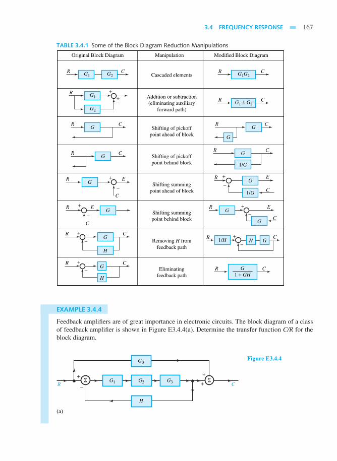
3.4 FREQUENCY RESPONSE 167
TABLE 3.4.1 Some of the Block Diagram Reduction Manipulations
Cascaded elements
Addition or subtraction(eliminating auxiliary
forward path)
Shifting of pickoffpoint ahead of block
Shifting of pickoffpoint behind block
Shifting summingpoint ahead of block
Shifting summingpoint behind block
Removing H fromfeedback path
Eliminatingfeedback path
Original Block Diagram Manipulation Modified Block Diagram
G2G1C G1G2
CR
G1 + GH
CR
G1 ± G2CR
R
GCR
G
G
CR
GC
E
C
RG
C
C
R
G2
G1+
−+R
C
1/G
1/H
G−+R
H
1/G
G+
−R C
G
G+
−R E
H
G+
−R C
H G+
−R C
G+
−
R E
C
G+
−R E
EXAMPLE 3.4.4
Feedback amplifiers are of great importance in electronic circuits. The block diagram of a classof feedback amplifier is shown in Figure E3.4.4(a). Determine the transfer function C/R for theblock diagram.
G0
G3 CRG2
H
(a)
G1Σ+
++
−Σ
Figure E3.4.4

168 TIME-DEPENDENT CIRCUIT ANALYSIS
G0
CR
H
(b)
Σ+
++
−ΣGA = G1G2G3
Figure E3.4.4 Continued
G0
C
R
(c)
+
+ ΣGA
1 + GAH
R C
(d)
GA1 + GAH
G0 +
So l u t i on
The three blocks in cascade are combined to yield GA = G1G2G3, as illustrated in FigureE3.4.4(b).
By eliminating the feedback path, the circuit of Figure E3.4.4(c) is obtained. By eliminatingthe auxiliary forward path, one gets the circuit of Figure E3.4.4(d). Thus,
C
R= G0 + GA
1+GAH
where GA = G1G2G3.
A linear system of equations can also be represented diagrammatically by a signal-flow graph(consisting of nodes and branches), which is used to describe a system schematically in terms ofits constituent parts. However, in view of the scope of this text, the topic of signal-flow graph isnot presented.
3.5 COMPUTER-AIDED CIRCUIT SIMULATION FOR TRANSIENT ANALYSIS, ACANALYSIS, AND FREQUENCY RESPONSE USING PSPICE AND PROBE
Transient Analysis
PSpice is capable of performing transient circuit analysis, for which the request is given by thefollowing statement:
• TRAN TSTEP TSTOP TSTART TMAX UIC
where TSTEP is the interval between points printed, plotted, or reported to PROBE, TSTOPis the time value for which the analysis is stopped, TSTART is the beginning time value for

3.5 COMPUTER-AIDED CIRCUIT SIMULATION 169
which results are printed, plotted, or reported to PROBE, TMAX is the maximum time incrementbetween computed values, and UIC is a keyword that causes PSpice to use initial conditionsspecified for inductors and capacitors in the element statements. In case of omission, TSTARTdefaults to zero and TMAX to (TSTOP − TSTART)/50. If UIC is omitted, PSpice computesinitial conditions by assuming that the circuit is dc steady state prior to t = 0. Let us present anillustrative example.
EXAMPLE 3.5.1
Develop and execute a program to analyze the circuit shown in Figure E3.5.1(a), and use PROBEfor plotting vC(t).
−
+
−
+Vs = 10 V vC (t)
i(0) = 0; vC (0) = 0 C
RLt = 0
(a)
10 mH 100 ΩInitial conditions
1 µFi(t)
Figure E3.5.1
−
+
−
+vC (t); vC (0) = 0
1 2 3
0
C
RL
(b)
10 mH 100 Ω
1 µFi(t); i(0) = 0
Voltage V vC(t)
t, ms(c)
0.2
5
0
10
15
0.4 0.6 0.8 1.0
So l u t i on
The program is as follows:
EXAMPLE E3.5.1
* THE CIRCUIT DIAGRAM SUITABLE FOR ANALYSIS IS GIVEN IN
FIGURE E3.5.1(b)

170 TIME-DEPENDENT CIRCUIT ANALYSIS
VS 1 0 10
L 1 2 10 MH IC = 0, INITIAL CURRENT IS ZERO
R 2 3 100
C 3 0 1 UF IC = 0; INITIAL VOLTAGE IS ZERO
* TRANSIENT ANALYSIS REQUEST
• TRAN 0.02 MS IMS 0 0.02 MS UIC
• PROBE
• END
A plot of vC(t) is shown in Figure E3.5.1(c).
Steady-State Sinusoidal Analysis with PSpice
PSpice can easily solve steady-state ac circuits for currents and voltages. Ac voltage sources,which must begin with the letter V, are specified by statements of the form
VNAME N+ N− AC VPEAK PHASE
where VNAME is the name of the voltage source, N+ is the node number of the positive reference,N− is the node number of the negative reference, AC indicates that this is an ac source, VPEAKis the peak value of the voltage, and PHASE is the phase angle of the source in degrees. Currentsources, which must begin with the letter I, are specified in a similar manner, with the referencedirection for the current source pointing from the first node number given in the statement to thesecond node number.
The ac analysis request is made with a statement of the form
• AC LIN NPOINTS STARTFREQ STOPFREQ
where • AC designates a request for frequency analysis, LIN defines a linear frequency sweepwith NPOINTS specifying the number of points in the sweep starting at the STARTFREQ andfinishing at the STOPFREQ. For example, to carry out a steady-state ac analysis for a frequencyof 60 Hz, the analysis request would be
• AC LIN 1 60 60
Let us present an illustrative example.
EXAMPLE E3.5.2
Use PSpice to solve for the amplitude and phase of the current and the voltage across the inductorin the circuit shown in Figure E3.5.2(a).
So l u t i on
The program is as follows:
* THE CIRCUIT DIAGRAM SUITABLE FOR ANALYSIS IS GIVEN IN
FIGURE E3.5.2(b)
VS 1 0 AC 100 30
R 1 2 100
L 2 3 0.3 H
C 3 0 40 UF

3.5 COMPUTER-AIDED CIRCUIT SIMULATION 171
• AC LIN 1 79.58 79.58
* 79.58 IS THE SOURCE FREQUENCY IN HZ GIVEN BY 500/(2π)
• PRINT AC IM(R) IP(R) VM(2,3) VP(2,3)
* IM(R) AND IP(R) DENOTE RESPECTIVELY MAGNITUDE AND PHASE OF THE
CURRENT THROUGH THE R ELEMENT
* VM (2,3) AND VP (2,3) DENOTE RESPECTIVELY MAGNITUDE AND PHASE OF
THE VOLTAGE BETWEEN NODES 2 AND 3 WITH THE POSITIVE REFERENCE AT
NODE 2
• END
After executing the program, the output file contains the following results:FREQ I(R) IP(R) V(2,3) VP(2,3)
7.958E + 01 7.071E − 01 −1.500E + 01 1.061E + 02 7.500E + 01
Note that I(R) is the same as IM(R) directed from the first node number, 1 in this case, given for Rto the second node number, 2 in this case; V(2,3) is the same as VM(2,3). Thus the phasor currentis given by IR = 0.7071 − 15°, and the voltage across the inductor is given by VL = 106.1 75°.Note that the magnitudes are the peak values.
−
+vs(t) = 100 cos(500t + 30°)
(a)
R = 100 Ω
L = 0.3 H
C = 40 µF
i(t)
Figure E3.5.2
−
+vs(t) = 100 cos(500t + 30°)
(b)
R = 100 Ω
L = 0.3 H
C = 40 µF
iR(t)
−
+vL(t)
1 2
3
0
Analysis of Frequency Response with PSpice and PROBE
PSpice can readily accomplish the circuit analysis as a function of frequency, and PROBEcan display Bode plots for magnitude and phase of network transfer functions. Besides thelinear (LIN) frequency sweep that we used in steady-state sinusoidal analysis, with a sim-ilar syntax statement, a logarithmic frequency sweep, with points specifying the number ofpoints per octave (an octave represents a twofold increase in frequency) or per decade (adecade represents a tenfold increase in frequency), can be specified. For example, thestatement
• AC DEC 20 10HZ 1MEGHZ

172 TIME-DEPENDENT CIRCUIT ANALYSIS
requests frequency analysis with 20 points per decade, which is usually a suitable value, starting at
10 Hz and ending at 1 MHz. Note that the frequencies would be uniformly spaced on a logarithmic
frequency scale.
EXAMPLE E3.5.3
Develop a PSpice program and use PROBE to obtain Bode plots of the magnitude and phase ofthe transfer function Vout /Vin for the high-pass filter circuit shown in Figure E3.5.3(a) along withnode numbers. This filter is to pass components above 1 kHz and reject components below 1 kHz.
−
+
−
+
Vin = 1∠0° Vout
(a)
R = 314.1 Ω
L = 50 mH
C = 0.507 µF1 2 3
0
Figure E3.5.3 (a) High-passfilter circuit. (b) MagnitudeBode plot. (c) Phase plot.
|H(f )|dB
(b)
100 Hz
−60
−80
−40
−20
0
20
1.0 kHz10 Hz 10 kHz 100 kHz(c)
100 Hz
180°
0°
45°
90°
135°
1.0 kHz10 Hz 10 kHz 100 kHz
So l u t i on
The transfer function H (f ) = Vout/Vin is numerically equal to V(3) since the amplitude of Vin
is given as 1 V. Thus to obtain a plot of the transfer-function magnitude in decibels, the PROBEmenu commands can be used to request a plot of VDB (3). A Bode plot of the transfer functioncan be obtained by requesting a plot of VP (3). The program is as follows:
EXAMPLE E3.5.3
THE CIRCUIT DIAGRAM IS SHOWN IN FIGURE E3.5.3(a)
VIN 1 0 AC 1
R 1 2 314.1
C 2 3 0.507 UF
L 3 0 50 MH

3.6 USE OF MATLAB IN COMPUTER-AIDED CIRCUIT SIMULATION 173
• AC DEC 20 10 HZ 100KHZ
* ANALYSIS EXTENDS FROM TWO DECADES BELOW TO TWO DECADES ABOVE
1 KHZ, THAT IS, FROM 10 HZ TO 100 KHZ.
• PROBE
* RESULTS ARE SAVED FOR DISPLAY BY THE PROBE PROGRAM
• END
Figures E3.5.3(b) and (c) display the magnitude and phase plots. Note that the filter gain is nearly0 dB for frequencies above 1 kHz and falls at the rate of 40 dB per decade for frequencies below1 kHz.
3.6 USE OF MATLAB IN COMPUTER-AIDED CIRCUIT SIMULATION
We shall illustrate the use of MATLAB by considering the following three examples.
EXAMPLE 3.6.1
This example is concerned with steady-state sinusoidal analysis by using mesh equations andMATLAB. Let us consider the circuit shown in Figure E3.6.1 and find the input impedance at theinput interface terminals A–B and the ratio VO/VS .
−
+
−
+
Vs = 10 ∠0°Zin
IBIA
IC
ZC1 ZC2
ZL2 RL VO
A
B
Rs = 50 Ω
ZL1 = j100 Ω
−j50 Ω −j50 Ω
j100 Ω 50 Ω
Figure E3.6.1
So l u t i on
Note that
ZIN = VS
IA− RS and K = VO
VS
= RLIB
VS
The M-file and answers are as follows:
function example361
clc
% Circuit Parameters
RS = 50;
RL = 50;
VS = 10;

174 TIME-DEPENDENT CIRCUIT ANALYSIS
% Element parameters
ZL1 = 100j;
ZL2 = 100j;
ZC1 = -50j;
ZC2 = -50j;
% I = inverse (Z) *V
I = inv ([RS+ZC1+ZL2 -ZL2 -ZC1;
-ZL2 ZL2+ZC2+RL -ZC2;
-ZC1 -ZC2 ZC1+ZC2+ZL1]) * [VS 0 0]’;
% Mesh Currents
IA = I(1)
IB = I(2)
IC = I(3)
% Answers
KI + RL*IB/VS
ZIN + VS/IA-RS
IA + 0.0100 - 0.0300i
IB = -0.0100 + 0.0300i
IC = 0 - 0.1000i
K = -0.0500 + 0.1500i
ZIN = 5.0000e+01 + 3.0000e+02i
EXAMPLE 3.6.2
Consider the circuit shown in Figure E3.6.2 in the t-domain as well as in the s-domain. Formulatethe s-domain nodal equations and use MATLAB to solve for VA(s) and VB(s).
iS(t)
L
CR R
(a)
IS(s) CvC(0)
VA(s)at node A
VB(s)at node B
Ls
Cs1
(b)
siL(0)
Figure E3.6.2 (a) t-domain. (b) s-domain.
So l u t i on
At node A:VA(s)
R+ VA(s)− VB(s)
Ls− IS(s)+ iL(0)
s= 0
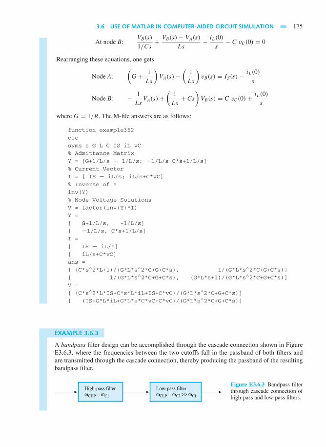
3.6 USE OF MATLAB IN COMPUTER-AIDED CIRCUIT SIMULATION 175
At node B:VB(s)
1/Cs+ VB(s)− VA(s)
Ls− iL(0)
s− C vC(0) = 0
Rearranging these equations, one gets
Node A:
(G+ 1
Ls
)VA(s)−
(1
Ls
)vB(s) = IS(s)− iL(0)
s
Node B: − 1
LsVA(s)+
(1
Ls+ Cs
)VB(s) = C vC(0)+ iL(0)
s
where G = 1/R. The M-file answers are as follows:
function example362
clc
syms s G L C IS iL vC
% Admittance Matrix
Y = [G+1/L/s − 1/L/s; −1/L/s C*s+1/L/s]
% Current Vector
I = [ IS − iL/s; iL/s+C*vC]
% Inverse of Y
inv(Y)
% Node Voltage Solutions
V = factor(inv(Y)*I)
Y =
[ G+1/L/s, -1/L/s]
[ −1/L/s, C*s+1/L/s]
I =
[ IS − iL/s]
[ iL/s+C*vC]
ans =
[ (C*s∧2*L+1)/(G*L*s∧2*C+G+C*s), 1/(G*L*s∧2*C+G+C*s)][ 1/(G*L*s∧2*C+G+C*s), (G*L*s+1)/(G*L*s∧2*C+G+C*s)]V =
[ (C*s∧2*L*IS-C*s*L*iL+IS+C*vC)/(G*L*s∧2*C+G+C*s)][ (IS+G*L*iL+G*L*s*C*vC+C*vC)/(G*L*s∧2*C+G+C*s)]
EXAMPLE 3.6.3
A bandpass filter design can be accomplished through the cascade connection shown in FigureE3.6.3, where the frequencies between the two cutoffs fall in the passband of both filters andare transmitted through the cascade connection, thereby producing the passband of the resultingbandpass filter.
ωCHP = ωC1
High-pass filterωCLP = ωC2 >> ωC1
Low-pass filterFigure E3.6.3 Bandpass filterthrough cascade connection ofhigh-pass and low-pass filters.

176 TIME-DEPENDENT CIRCUIT ANALYSIS
In this so-called Butterworth bandpass filter, the center frequency and the bandwidth of thebandpass filter are given by
ω0 = √ωC1ωC2 and B = ωC2 − ωC1
and
ω0
B= Q
√ωC1
ωC2<< 1
where ωCHP = ωC1 is the cutoff frequency of the high-pass filter and ωCLP = ωC2 is the cutofffrequency of the low-pass filter.
In order to design a bandpass filter with a passband gain of 0 dB and cutoff frequencies ofωC1 = 10 rad/s and ωC2 = 50 rad/s, with the stopband gains of less than −20 dB at 2 rad/s and250 rad/s, one has chosen the following low-pass and high-pass transfer functions:
TLP(s) = 1
(s/50)2 +√2(s/50)+ 1
THP(s) = (s/10)2
(s/10)2 +√2(s/10)+ 1
When circuits realizing these two functions are connected in cascade, the overall transfer functionis given by
TBP(s) = THP(s)× TLP(s)
Use MATLAB to illustrate the specified bandpass response with the center frequency ω0 =√10× 50 = 22.4 rad/s, the bandwidth B = 50 − 10 = 40 rad/s, and the filter quality factor
Q = ω0/B = 0.56. Note that Q being less than 1 indicates a broad-band response.
So l u t i on
The M-file and answers are as follows:
function example363
clc
% 2nd order Butterworth low pass wc = 50
TLPs = tf(1,[1/50∧2 sqrt (2)/50 1])
% 2nd order Butterworth high pass wc = 10
THPs = tf([1/10∧2 0 0], [1/10∧2 sqrt(2)/10 1])
% 4th order Butterworth bandpass wc1 = 10 wc2 = 50
TBPS = TLPs * THPs
bode (TBPs, 1,1e3);
Transfer function:
1--------------------------
0.0004 s∧2 + 0.02828 s + 1
Transfer function:
0.01 s∧2-----------------------
0.01 s∧2 + 0.1414 s + 1

3.7 LEARNING OBJECTIVES 177
Transfer function:
0.01 s∧2-----------------------------------------------------
4e-06 s∧4 + 0.0003394 s∧3 + 0.0144 s∧2 + 0.1697 s + 1Ph
ase
(deg
); M
agni
tude
(dB
)
−150
−100
−50
0
50
100
150
100 101
Bode Diagrams
Frequency (rad/sec)
102 103
−50
−40
−30
−20
−10
0
Figure E3.6.3 (Part Two) Bode plots for Example 3.6.3.
3.7 LEARNING OBJECTIVES
The learning objectives of this chapter are summarized here so that the student can check whetherhe or she has accomplished each of the following.
• Response to exponential excitations.
• Representation of sinusoidal signals by complex phasors.
• Impedance and admittance of common circuit elements in series–parallel combinations.
• Frequency-domain representations and transformed networks.
• Forced response to sinusoidal excitation.
• Phasor method of analysis and phasor diagrams.
• Real, reactive, and apparent powers in ac circuits.
• Fourier series (trigonometric and exponential forms).
• Transient and steady-state responses (natural and forced responses) of first- and second-order circuits.
• Accounting for the effect of nonzero initial conditions.

178 TIME-DEPENDENT CIRCUIT ANALYSIS
• Expressing pulses in terms of step and impulse functions.
• Laplace transformation method of solving differential equations.
• Time-domain networks and transformed networks in frequency domain for networkanalysis.
• Network transfer functions.
• Frequency response of networks.
• Low-pass and high-pass filter circuits.
• Bode diagrams and asymptotic Bode plots.
• Two-port network parameters.
• Block diagram representation of simple systems.
• Transient analysis, ac analysis, and frequency response using PSpice and PROBE.
• Use of MATLAB in circuit simulation.
3.8 PRACTICAL APPLICATION: A CASE STUDY
Automotive Ignition System
Ignition systems in automobiles have been designed as a straightforward application of electricaltransients. Figure 3.8.1 shows a simplified ignition circuit for an internal-combustion engine.The primary inductance, current-limiting resistance, and capacitance form an underdamped seriesRLC circuit. Thus, when the points open, an oscillatory current flows through the primary, therebyinducing the required voltage in the secondary. The points form a switch, which opens and closesas the engine rotates, exactly at the instant when an ignition spark is needed by one of the cylinders.
During the period when the points are closed, current builds up rather slowly in the primarywinding of the coil, which consists of a pair of mutually coupled inductors, as shown in Figure3.8.1. The current is interrupted rapidly when the points open. The resulting large rate of changeof current induces a large voltage across the coil secondary, which is connected to the appropriatespark plug by the distributor.
The resistance limits the current in case the engine stops with the points closed. Since thevoltage across a capacitance cannot change instantaneously, the capacitor prevents the voltage
PointsCondenser
Primary Secondary
Coil(Mutually coupled
inductors)Distributor
Sparkplug
12 V
+
−
Figure 3.8.1 Simplified ignition cir-cuit for an internal-combustion en-gine.
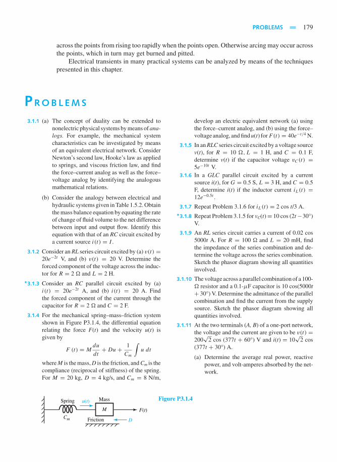
PROBLEMS 179
across the points from rising too rapidly when the points open. Otherwise arcing may occur acrossthe points, which in turn may get burned and pitted.
Electrical transients in many practical systems can be analyzed by means of the techniquespresented in this chapter.
PROBL EMS
3.1.1 (a) The concept of duality can be extended tononelectric physical systems by means of ana-logs. For example, the mechanical systemcharacteristics can be investigated by meansof an equivalent electrical network. ConsiderNewton’s second law, Hooke’s law as appliedto springs, and viscous friction law, and findthe force–current analog as well as the force–voltage analog by identifying the analogousmathematical relations.
(b) Consider the analogy between electrical andhydraulic systems given in Table 1.5.2. Obtainthe mass balance equation by equating the rateof change of fluid volume to the net differencebetween input and output flow. Identify thisequation with that of an RC circuit excited bya current source i(t) = I .
3.1.2 Consider an RL series circuit excited by (a) v(t) =20e−2t V, and (b) v(t) = 20 V. Determine theforced component of the voltage across the induc-tor for R = 2 and L = 2 H.
*3.1.3 Consider an RC parallel circuit excited by (a)i(t) = 20e−2t A, and (b) i(t) = 20 A. Findthe forced component of the current through thecapacitor for R = 2 and C = 2 F.
3.1.4 For the mechanical spring–mass–friction systemshown in Figure P3.1.4, the differential equationrelating the force F(t) and the velocity u(t) isgiven by
F (t) = Mdu
dt+Du+ 1
Cm
∫u dt
where M is the mass, D is the friction, and Cm is thecompliance (reciprocal of stiffness) of the spring.For M = 20 kg, D = 4 kg/s, and Cm = 8 N/m,
develop an electric equivalent network (a) usingthe force–current analog, and (b) using the force–voltage analog, and find u(t) forF(t) = 40e−t/4 N.
3.1.5 In an RLC series circuit excited by a voltage sourcev(t), for R = 10 ,L = 1 H, and C = 0.1 F,determine v(t) if the capacitor voltage vC(t) =5e−10t V.
3.1.6 In a GLC parallel circuit excited by a currentsource i(t), for G = 0.5 S, L = 3 H, and C = 0.5F, determine i(t) if the inductor current iL(t) =12e−0.5t .
3.1.7 Repeat Problem 3.1.6 for iL(t) = 2 cos t/3 A.
*3.1.8 Repeat Problem 3.1.5 for vC(t)= 10 cos (2t−30°)V.
3.1.9 An RL series circuit carries a current of 0.02 cos5000t A. For R = 100 and L = 20 mH, findthe impedance of the series combination and de-termine the voltage across the series combination.Sketch the phasor diagram showing all quantitiesinvolved.
3.1.10 The voltage across a parallel combination of a 100- resistor and a 0.1-µF capacitor is 10 cos(5000t+ 30°) V. Determine the admittance of the parallelcombination and find the current from the supplysource. Sketch the phasor diagram showing allquantities involved.
3.1.11 At the two terminals (A, B) of a one-port network,the voltage and the current are given to be v(t) =200√
2 cos (377t + 60°) V and i(t) = 10√
2 cos(377t + 30°) A.
(a) Determine the average real power, reactivepower, and volt-amperes absorbed by the net-work.
F(t)
D
u(t)Spring
Friction
Mass
Cm
M
Figure P3.1.4

180 TIME-DEPENDENT CIRCUIT ANALYSIS
(b) Find the equivalent components of the net-work representing the effect at the terminalsA–B.
(c) Find the Thévenin impedance (or the driving-point impedance) as seen from the terminalsA–B.
3.1.12 Repeat Problem 3.1.11 if the 60-Hz voltage andthe current at the terminals are given to be V =100 V (rms), I = 10 A (rms), power factor = 0.8leading.
*3.1.13 Use (a) mesh analysis and (b) nodal analysis todetermine the current through the 4- resistor ofthe circuit of Figure P3.1.13.
3.1.14 Use (a) mesh analysis and (b) nodal analysis todetermine the voltage V at the terminals A–B ofFigure P3.1.14.
3.1.15 (a) Obtain a Thévenin equivalent circuit at termi-nals A–B in the circuit of Problem 3.1.14.
(b) What impedance ZL, when connected to A–B,produces maximum power in ZL?
(c) Find the value of the maximum power in ZL.
3.1.16 In the circuit of Problem 3.1.13, find the Théveninequivalent of the network as seen by the 4-
resistor, and then determine the current in the 4-resistor.
3.1.17 A 6.6-kV line feeds two loads connected in par-allel. Load A draws 100 kW at 0.6 lagging powerfactor, and load B absorbs 100 kVA at 0.8 laggingpower factor.
(a) For the combined load, calculate the realpower, reactive power, volt-amperes, and linecurrent drawn from the supply.
(b) If the power factor on the supply end is to beunity, determine the value of the capacitanceto be placed across the load if the frequencyof excitation is 60 Hz.
*3.1.18 Three loads in parallel are supplied by a single-phase 400-V, 60-Hz supply:
Load A: 10 kVA at 0.8 leading power factorLoad B: 15 kW at 0.6 lagging power factorLoad C: 5 kW at unity power factor
(a) Find the real power, reactive power, volt-amperes, and line current drawn from thesupply by the combined load.
(b) If the supply line is to operate at 0.9 leadingpower factor, determine the value of the ca-pacitance to be placed across the load.
−
+20∠0° V
2∠−30° A
j24 Ω
−j4 Ω
4 Ω
10 Ω
18 Ω
8 Ω
Figure P3.1.13
−
+
−
+
−
+
−
+
12∠0° V V1
A
B
V−j2 Ω
−j1 Ω
1 Ω
3 Ω2 Ω
3V1
Figure P3.1.14

PROBLEMS 181
3.1.19 Determine the Fourier series for the periodic wave-forms given in Figure P3.1.19.
3.1.20 Find the exponential form of the Fourier series ofthe periodic signal given in Figure P3.1.20. Alsodetermine the resulting series if T = 2τ .
*3.1.21 The first four harmonics in the Fourier series of acurrent waveform given by
i (t) = 2Imπ
sin2πt
T− Im
πsin
4πt
T
+ 2Im3π
sin6πt
T− Im
2πsin
8πt
T
where Im = 15 mA and T = 1 ms. If sucha current is applied to a parallel combination ofR = 5 k and C = 0.1 µF, determine the
output waveform of the voltage vO(t) across theload terminals.
3.1.22 The full-wave rectified waveform, approximatedby the first three terms of its Fourier series, is givenby v (ωt) = Vmsin (ωt/2), for 0 ≤ ωt ≤ 2π , and
v (t) = 2Vm
π− 4Vm
3πcos ωt + 4Vm
15πcos 2ωt
whereVm = 100 V andω = 2π×120 rad/s. If v(t)is applied to the circuit shown in Figure P3.1.22,find the output voltage vO(t).
3.2.1 Determine i(t) in the circuit of Figure P3.2.1 andsketch it.
*3.2.2 Obtain i(t) in the circuit of Figure P3.2.2 andsketch it.
−T −τ τ T0
0
v(t)
A
(a)
−T −ττ T
t
t
i(t)
A
−A
(b)
Figure P3.1.19
t
i(t)
A
−T −τ τ T
Half-cycle of cosine
0
Figure P3.1.20
182 TIME-DEPENDENT CIRCUIT ANALYSIS
v(t) vO(t)
10 Ω10 Ω 5 mH
90 Ω500 µF+
+
−−
Figure P3.1.22
20 V
i(t)
S
t = 0
8 Ω
6 H
+
−
Figure P3.2.1
24 V
i(t)
S
t = 0
4 Ω
6 Ω10 H
+
−
Figure P3.2.2
3.2.3 Determine and sketch v(t) in the circuit of FigureP3.2.3.
3.2.4 Determine and sketch v(t) in the circuit of FigureP3.2.4.
3.2.5 Obtain and sketch i(t) in the circuit of FigureP3.2.5.
3.2.6 Obtain and sketch i(t) in the circuit of FigureP3.2.6.
*3.2.7 Determine and sketch i(t) in the circuit of FigureP3.2.7.
3.2.8 In the circuit of Figure P3.2.8,
i (t) =
10 A, for t < 024e−t , for t ≥ 0
Find: v(0+), iL(0+),dv
dt(0+), and
diL
dt(0+).
3.2.9 In the circuit of Figure P3.2.9,
v (t) =
24 V, for t < 012 cos t, for t ≥ 0
Determine vC(0+), iC(0+),
dvC
dt(0+), and,
diC
dt(0+).
*3.2.10 In the circuit of Figure P3.2.10,
v (t) =
0, for t < 00.4t, for t ≥ 0
Evaluate: vO(0+) and dvOdt
(0+).3.2.11 Reconsider Problem 3.2.10 and obtain vO(t) for
t ≥ 0.3.2.12 Consider the circuit of Figure P3.2.12. Determine
and sketch iL(t) and vC(t) for capacitance valuesof(a) 1/6 F, (b) 1/8 F, and (c) 1/26 F. Note that the
capacitance values are chosen here for calcu-lational ease, even though they are too big andnot typical.
3.2.13 For the circuit of Figure P3.2.13, determine andsketch iL(t) and vC(t) for inductance values of
(a) 3/4 H, (b) 2/3 H, and (c) 3/17 H. Note that theinductance values are chosen here for calcula-tional ease, even though they are too big andnot typical.
*3.2.14 Consider the circuit of Figure P3.2.14 in whichthe switch S has been open for a long time and isclosed at t = 0. Determine vC(t) for t ≥ 0.
3.2.15 In the circuit of Figure P3.2.15, obtain iL(t) andvC(t).
10 A v(t)
S
t = 0
4 Ω F23
+
−
Figure P3.2.3
12 A v(t)
S
t = 0
4 Ω
2 Ω
F12
+
−
Figure P3.2.4

PROBLEMS 183
10 V
i(t)
S
t = 0
4 Ω
4 Ω4 H+
−
Figure P3.2.5
20 V
i(t)
S
t = 0
6 Ω4 Ω
6 H+
−
Figure P3.2.6
10 A
S
t = 0
6 Ω4 Ω
16 V+
− i(t)
10 H
Figure P3.2.7
4 Ω
+
−
iL(t)
v(t)i(t)1 H
Figure P3.2.8
24 Ω 1 F
8 Ω+
−
+
−
iC(t)
vC(t)v(t)
Figure P3.2.9
0.02 µF200 Ω+
−10 v1(t)v1(t)v(t)
i(t)
+
+
−
vO(t)
+
−
−
Figure P3.2.10
10 V vC(t)
iL(t)S
t = 0 R = 8 Ω L = 2 H
C+
−
+
−
Figure P3.2.12
5 A vC(t)
iL(t)
S
t = 0
R = 1 Ω16
C = F34
L = H+
−
Figure P3.2.13

184 TIME-DEPENDENT CIRCUIT ANALYSIS
100 Ω1 mH
10 cos 106 t vC(t)
i(t)
S
t = 00.1 µF
99i(t)+
−
+
−
Figure P3.2.14
2 Ω
2 Ω 2 A13
L = H10 sin (3t + 20°) V
vC
iL
S
t = 0
32
C = F+
−
+
−
Figure P3.2.15
3.2.16 Determine iL(t) and vC(t) in the circuit of FigureP3.2.16.
3.2.17 Express the waveform of the staircase type shownin Figure P3.2.17 as a sum of step functions.
3.2.18 The voltage waveform of Figure P3.2.18 is appliedto an RLC series circuit with R = 2 ,L = 2 H,andC = 1 F. Obtain i(t) in the series circuit. (Notethat the capacitor and inductor values are chosenhere for calculational ease, although they are toobig and not typical.)
3.2.19 (a) Let a unit impulse of current i(t) = δ(t) beapplied to a parallel combination of R = 3
and C = 12 F. Determine the voltage vC(t)
across the capacitor.
(b) Repeat (a) for i(t) = δ(t − 3).
(Note that the capacitance value is chosen herefor calculational ease, even though it is too bigand not typical.)
3.2.20 (a) Let a unit impulse of voltage v(t) = δ(t) beapplied to a series combination of R = 20
and L = 10 mH. Determine the current i(t) inthe series circuit.
(b) Repeat (a) for v(t) = δ(t)+ δ(t − 3).
3.3.1 Determine the Laplace transform for each of thefollowing functions from the basic definition ofEquation (3.3.1).
(a) f1(t) = u(t)
(b) f2(t) = e−at
(c) f3(t) = df (t)
dt, assuming f (t) is transform-
able.
(d) f4(t) = t
(e) f5(t) = sin ωt
(f) f6(t) = cos(ωt + θ)
(g) f7(t) = te−at
(h) f8(t) = sinh t
(i) f9(t) = cosh t
(j) f10(t) = 5f (t)+ 2df (t)
dt3.3.2 Using the properties listed in Table 3.3.2, deter-
mine the Laplace transform of each of the follow-ing functions.
(a) te−t
(b) t2e−t
(c) te−2t sin 2t
(d)1− cos t
t
(e)e−2t sin 2t
t*3.3.3 Given the frequency-domain response of an RL
circuit to be
I (s) = 10
2s + 5
determine the initial value and the final value of thecurrent by using the initial-value and final-valuetheorems given in Table 3.3.2.

PROBLEMS 185
4 Ω
10 V45
H20 V
iL(t)
S
t = 0
4 Ω
+
−
+
−vC(t)1
20F
+
−
Figure P3.2.16
f (t)
Step functions
t
5
0 1
10
15
20
25
2 3 4 5 6 7 8 9
Figure P3.2.17
v, V
t, s1 2
10
−10
Figure P3.2.18
3.3.4 Determine the inverse Laplace transform of eachof the following functions.
(a)6(s + 3)
s2 + 2s + 10
(b)s + 2
(s + 1)(s + 3)(s + 4)
(c)8(s + 1)
s(s2 + 2s + 2)
(d)s2 + 4s + 5
s2 + 3s + 2
(e)2(s + 2)
s(s + 1)3
(f)s + 1
s3 + 4s2 + 3s
(g)10(s2 + 3s + 2)
3(s2 + 2s + 2)
(h)(s + 1)(s + 2)
s2(s2 + 2s + 2)
(i)4s
(s2 + 4)(s + 2)
(j)4s
[(s + 2)2 + 4
]23.3.5 Solve the following differential equations (along
with the conditions) for t ≥ 0.
(a)d2v
dt2+ 5
dv
dt+ 4v = 10u (t) ; v (0+) = dv
dt(0+) = 0

186 TIME-DEPENDENT CIRCUIT ANALYSIS
(b) 3d2i
dt2+7
di
dt+2i = 10cos2t; i (0+) = 4A;di
dt(0+) = −4A/s
(c)d2i
dt2+ 2
di
dt+ 2i = sint − e−2t ; i (0+) =
0 ;didt
(0+) = 4A/s
Identify the forced and natural response compo-nents in each case.
3.3.6 Determine the Laplace transform of the waveformshown in Figure P3.3.6.
3.3.7 In the circuit shown in Figure P3.3.7, the switch S
has been open for a long time. At t = 0, the switchis closed. Find the currents i1(t) and i2(t) for t ≥ 0with the use of the Laplace transform method.
*3.3.8 Determine v(t) and iL(t) in the circuit shown inFigure P3.3.8, given that i(t) = 10te−t u(t).
3.3.9 The switch S in the circuit of Figure P3.3.9 hasbeen open for a long time before it is closed att = 0. Determine vL(t) for t ≥ 0.
3.3.10 Determine v(t) in the circuit of Figure P3.3.10 ifi(t) is a pulse of amplitude 100 µA and duration10 µs.
f (t)
t, seconds1 2
10
−10
Figure P3.3.6
S
t = 0
8 Ω
4 Ω
2 Ω
100 V
+
−
i2(t)i1(t)
2 H
1 H Figure P3.3.7
10 Ω 9iL(t)
+
−
i(t)
iL(t)
v(t) 1 H
Figure P3.3.8
10 V
S
t = 0
0.05 F5 Ω+
−
+
−vL(t)2 H
Figure P3.3.9
PROBLEMS 187
4 pF
1000 Ω 500 Ω100 i1100 pFi(t)
i1
v(t)
+
−
Figure P3.3.10
3.3.11 For the networks shown in Figure P3.3.11, deter-mine the transfer function G(s) = Vo(s)/Vi(s).
3.3.12 The response v(t) of a linear system to a unit-stepexcitation i(t) is given by v(t) = (5 − 3e−t +2e−2t ) u(t). Determine the transfer functionH(s) = V (s)/I (s).
*3.3.13 The response y(t) of a linear system to a unit-stepexcitation is y(t) = (4− 10e−t + 8e−2t ) u(t).
(a) Find the system function.
(b) Find the frequency at which the forced re-sponse is zero.
3.3.14 The unit impulse response h(t) of a linear systemis h(t) = 5e−t cos(2t − 30°). Determine H(s).
3.3.15 The response y(t) of a linear system to an excitationx(t) = e−2t u(t) is y(t) = (t + 2)e−t u(t). Findthe transfer function.
3.3.16 A filter is a network employed to select one rangeof frequencies while rejecting all other frequen-cies. A basic building block often used in inte-grated-circuit filters is shown in Figure P3.3.16.Determine the following for the circuit:
(a) Transfer function Vo(s)/Vi(s).
(b) Response vo(t) for vi(t) = u(t).
(c) Driving-point impedance Vi(s)/Ii(s).
3.4.1 For the circuits shown in Figure P3.4.1, sketchthe frequency response (magnitude and phase) ofVout/Vin.
*3.4.2 Design the low-pass filter shown in Figure P3.4.2(by determining L) to have a half-power frequencyof 10 kHz.
3.4.3 Design the high-pass filter shown in Figure P3.4.3(by determining C) to have a half-power frequencyof 1 MHz.
3.4.4 Determine L and C of the bandpass filter circuitof Figure P3.4.4 to have a center frequency of 1MHz and a bandwidth of 10 kHz. Also find the Qof the filter.
3.4.5 Determine L and C of the band reject filter circuitof Figure P3.4.5 to have a center frequency of 100
kHz and a bandwidth of 5 kHz. Also find the Q ofthe filter.
3.4.6 Determine the voltage transfer function of the low-pass filter circuit shown in Figure P3.4.6, and findthe expression for ω0.
*3.4.7 Determine the voltage transfer function of thehigh-pass filter circuit shown in Figure P3.4.7, andfind the expression for ω0.
3.4.8 Let a square-wave voltage source having an am-plitude of 5 V, a frequency of 1 kHz, a pulse widthof 0.5 ms, and an internal source resistance of50 be applied to a resistive load of 100 . Afilter (inductance L) is inserted between sourceand load in order to reduce all the high-frequencycomponents above 5 kHz. Determine (a) L of thelow-pass filter, (b) amplitude spectra of VL and VS,and (c) vL(t).
3.4.9 Sketch the asymptotic Bode diagrams for the fol-lowing functions:
(a) H1 (s) = 200
(1+ s)(
1+ s
10
)
(b) H2 (s) = 200s
(1+ s)(
1+ s
10
)
(c) H3 (s) =200
(1+ s
10
)(1+ s)
(1+ s
20
)
(d) H4 (s) =0.5(
1+ s
10
)(1+ s)2
(1+ s
40
)
(e) H5 (s) = 0.5 (1+ s)2
s(
1+ s
10
) (1+ s
50
)
(f) H6 (s) =20(
1+ s
8
)(1+ s)
(1+ s
10
)2 (1+ s
40
)

188 TIME-DEPENDENT CIRCUIT ANALYSIS
R1 R2
C1
(a)
vi
+
−
vo
+
−
C2
R
(b)
vi
+
−
vo
+
−
R1 R2
C
L
(e)
vi
+
−
vo
+
−
L
R1
R1
R2
R2
C
C C
(c)
vi
+
−
vo
+
−
vo
+
−(d)
vi
+
−
+
vo RC C
C
L L
L
+
−
(f)
vi
−
C
L
Figure P3.3.11
v1
2 Ω
1 F
vi(t) vo(t)0.5 Ω 2v1
iC(t)+
−
+
−
+
−
+
−
1 F
Figure P3.3.16

PROBLEMS 189
Vout
(a)
Vin jω Ω
10 Ω+
−
+
−
−−−−
Vout
(b)
Vin Ω30jω
Ω1000jω
10 Ω+
−
+
−
−−−−
Vout
(c)
Vin
10 Ω+
−
+
−
−−−−jω4 Ω
Figure P3.4.1
vS (t)+
−
+
−
vL(t)RL = 30 Ω
LRS = 30 Ω
Figure P3.4.2
vS (t)+
−
+
−
vL(t)RL = 50 Ω
CRS = 50 Ω
Figure P3.4.3
vS (t)+
−
+
−
vL(t)RL = 50 Ω
CLRS = 50 Ω
Figure P3.4.4

190 TIME-DEPENDENT CIRCUIT ANALYSIS
vS (t)+
−
+
−
vL(t)RL = 100 Ω
RS = 100 ΩC
L
Figure P3.4.5
vS (t)+
−
+
−
vL(t)RLC
LRS
Figure P3.4.6
vS (t)+
−
+
−
vL(t)RLL
CRS
Figure P3.4.7
3.4.10 Reconsider Problem 3.4.9 and the correspondingasymptotic Bode plots.
(a) Find H1, H2, and H3 at ω = 5 rad/s.
(b) At what angular frequency ω is the magni-tude of H4(jω) one-half of the magnitude ofH4(j5)?
(c) Determine the angular frequency at whichH6(ω) is 0 dB and the angular frequency atwhich θ6(ω) = −180°.
(d) Let H5(s) = V2/V1. For v1(t) = 0.1 cos 20t,find the steady-state value of v2(t).
3.4.11 Sketch the idealized (asymptotic) Bode plot forthe transfer function
H (jω) = 10 (1+ j2ω)
(1+ j10ω) (1+ j0.25ω)
Find the angular frequency at which H(ω) is 0 dBand the angular frequency at which θ(ω) = −60°.
*3.4.12 The loop gain of an elementary feedback controlsystem (see Figure 3.4.12) is given byG(s)·H(s),which is 10/(1+ s/2)(1+ s/6)(1+ s/50). Sketchthe asymptotic Bode plot of the loop-gain function.Gain margin (GM) is defined by [−20 log |G(ωπ )
H (ωπ )|], which is the negative of the magnitudeof the loop gain at ω = ωπ, ωπ represents theangular frequency at which the loop gain reachesa phase of −π . If ωu represents the value of ω
where the loop gain has a magnitude of unity, thenphase margin (PM) is defined by the phase of theloop gain at ω = ωu plus π . Evaluate GM and PMfor this case from the asymptotic Bode plot.
3.4.13 Sketch the asymptotic Bode plots for the follow-ing loop-gain functions, and find the approximatevalues of gain and phase margins in each case. (Fordefinitions of GM and PM, see Problem 3.4.12.)
(a) G1 (s)H1 (s) =12 (0.7+ s)
(0.003+ s) (0.04+ s) (7+ s)
(b) G2 (s)H2 (s) = 100(1+ s/3.9607)
s(1+ 2s)(1+ s/39.607)
3.4.14 (a) For a series RLC resonant circuit, find an ex-pression for the voltage across the resistanceVR and obtain the ratio VR/VS, where VS is theapplied voltage. Identify the expressions forthe series resonant frequency and bandwidth.
(b) Determine the resonant frequency and band-width, given the voltage transfer function tobe 103/(s2 + 103s + 1010).
3.4.15 A simple parallel resonant circuit withL = 50µHis used to perform the frequency selection. The cir-cuit is to be tuned to the first station at a frequencyof 1000 kHz. In order to minimize the interaction

PROBLEMS 191
between signals, the tuning circuit response mustattenuate the signal of the second station (with afrequency of 1020 kHz) by four times.
(a) Determine the values of G and C.
(b) Find the bandwidth of the circuit.
3.4.16 The twin-tee or notch network shown in FigureP3.4.16 is often used to obtain band-reject charac-teristics.
(a) Determine the transfer function V2/I1.
(b) Find the angular frequency at which the trans-fer function will be zero.
*3.4.17 A gyrator is sometimes used in integrated circuitsto simulate inductances. Consider the circuit ofFigure P3.4.17 consisting of a gyrator.
(a) Show that the impedance as seen to the rightat terminals 1–1′ can be represented by aninductor in series with a resistor.
(b) Determine the resonant frequency and band-width for the following values:
R = 105; g = 10−3 S;C1 = C2 = 100 pF.
3.4.18 (a) Consider the capacitor-input filter circuit ofFigure P3.4.18 and obtain the z-parameters forthe circuit.
(b) Determine the transfer function V2/V1 whenI2 is zero.
3.4.19 The circuit shown in Figure P3.4.19 is the equiv-alent circuit of a field-effect transistor (FET) am-plifier stage.
(a) Determine the y-parameters.
(b) For values of µ = gm/gd >> 1, obtain ay-parameter equivalent circuit.
3.4.20 For the circuit shown in Figure P3.4.20, obtain:
(a) z- and y-parameters;
(b) Transfer function I2/I1 when V2 = 0.
3.4.21 For the capacitor input filter circuit of Problem3.4.18, determine the h-parameters.
2 R 2 R
+
12CsRV1
I1 I2
1Cs
1Cs
−
+
V2
−
Figure P3.4.16
vA
+
−
vB
+
1
1′
RgvAgvBC1 C2
−
2
2′Gyrator
Figure P3.4.17
V2V1
R1 Ls
I1 I2
R2
+
−
+
−
1Cs
Figure P3.4.18

192 TIME-DEPENDENT CIRCUIT ANALYSIS
*3.4.22 Determine the h-parameters for the circuit shownin Figure P3.4.22 and obtain the transfer functionV2/V1 when I2 = 0.
3.4.23 A negative impedance converter circuit shown inFigure P3.4.23 is used in some applications whereinductors cannot be utilized or where negativeresistance is beneficial.
(a) Determine the h-parameters for the network.
(b) When the resistance R is connected across ter-minals 2–2′, find the impedance seen lookinginto terminals 1–1′.
3.4.24 Show that the block diagram of Figure P3.4.24can be reduced to the form of Figure 3.4.12. FindGeq(s) and Heq(s).
3.4.25 Show that the block diagram of Figure P3.4.25(a)can be reduced to that of Figure P3.4.25(b).
V1
1′
1
2′
2+
−
−
++
−
V2
gmVgs
Rk
gd
1 ΩVgs
s
g Figure P3.4.19
V
2'
2+
+ −
−
V2
+
−
V1 R2
R
1Cs
I2I1
gV
1'
1
Figure P3.4.20
2′
2+
−
V2
+
−
V1 R2
R1
1C1s
I2I1
1′
1
Figure P3.4.22
2′
2
4 IA
IyIx R R
1′
1IA
Figure P3.4.23
R(s)+−+− ++
H1
G5
G2G1 G3 G4 G6
H2
Figure P3.4.24

PROBLEMS 193
+−
+−
+++
+++
H0
H1
H2
(a)
(b)
G2G1
G1G4 (H0 + G2G3)
H3
H3 (H1 + H2)
G3 G4
Figure P3.4.25
−
+ ++
H1
G1R(s)
C (s)Σ Σ G2
H2
G3
Figure P3.4.26
−
+
+
−
+
−
H1
G1R(s)
C (s)Σ Σ G2
H2
H3
G3Σ
Figure P3.4.27
3.4.26 The block diagram of Figure P3.4.26 represents amultiloop control system.
(a) Determine the transfer function C(s)/R(s).
(b) For G2G3H2 = 1, evaluate C(s)/R(s).
*3.4.27 Determine the transfer function C(s)/R(s) of thenested-loop feedback system shown in FigureP3.4.27.
3.4.28 The equations for a two-port network are given by
V1 = z11I1 + z12I2
0 = z21I1 + (z22 + ZL)I2
V2 = −I2ZL
(a) Satisfying the equations, develop a block dia-gram.
(b) Find the transfer function V2/V1.
3.5.1 In the circuit shown in Figure P3.5.1 the switchopens at t = 0. Develop and execute a PSpiceprogram to solve for v(t), and use PROBE toobtain a plot of v(t).Hint: Use the following analysis request:
• TRAN 0.1 MS 50 MS 0 0.1 MS UIC
3.5.2 Obtain a plot of the current i(t) in the circuit ofFigure P3.5.2 by writing a PSpice program andusing the following analysis request:
• TRAN 0.2 MS 80 MS 0 0.2 MS UIC
Hint: Note that a sinusoidal voltage source is spec-ified in PSpice by the statement
VSIN NODEPLUS NODEMINUS
SIN (VDC VPEAK FREQ TD
DF PHASE)

194 TIME-DEPENDENT CIRCUIT ANALYSIS
where VSIN is the name of the source, NODE-PLUS is the number identifying the positive node,NODEMINUS is the number identifying the nega-tive node, VDC is the dc offset, VPEAK is the peakvalue of the ac component, FREQ is the frequencyin hertz, TD is the time delay in seconds, DF is adamping factor, and PHASE is the phase angle indegrees. The voltage generated is then given by
v(t) = VDC+ VPEAK sin[PHASE],
for 0 < t < TD
= VDC+ VPEAK sin[2π
FREQ(t − TD)+ PHASE]
× exp[−DF(t − TD)],
for TD < t
Also note that DF = 0 for a constant-amplitudesinusoid.
*3.5.3 With the initial voltage across the capacitor beingvC(0) = 10 V, obtain a plot of vC(t) for the circuitof Figure P3.5.3 by writing a PSpice program.Hint: Use the following analysis request:
• TRAN 0.02 10 0 0.02 UIC
3.5.4 For the circuit shown in Figure P3.5.4, solve fori(t) by writing and executing a PSpice program,and obtain a plot of i(t) by using PROBE.Take the hint from Problem 3.5.2 for specifying thesinusoidal voltage source in the PSpice program.Also use the following analysis request:
• TRAN 0.1 MS 100 MS 0 0.1 MS UIC
3.5.5 A dc source is connected to a series RLC circuit bya switch that closes at t = 0, as shown in FigureP3.5.5, with initial conditions. For the values ofR = 20, 40, and 80 , solve for vC(t) by writingand executing a PSpice program, and obtain plotsby using PROBE.Hint: Use the following analysis request:
•TRAN IUS 2MS 0 1US UIC
3.5.6 In the circuit of Figure P3.5.6, solve for phasorsV1 and V2 with peak magnitudes by writing andexecuting a PSpice program.
1 mA R = 10 kΩ C = 1 µFt = 0 v(t)
+
−
Figure P3.5.1
vs(t) = 2 sin(200 t)
1 R = 5 kΩ
C = 1 µF vC (t); vC (0) = 1 Vi(t)
++
−−
O
2 Figure P3.5.2
1
R = 2 MΩC = 1 µFvC (t) = v1vC(0) = 10 V
+
−
O
Figure P3.5.3

PROBLEMS 195
L = 1 HiL(0) = 0
R = 300 Ω
vs = 10 sin 300 t i(t)+
−
Figure P3.5.4
vC (t); vC (0) = 0C = 5 µF
RL = 2 mHt = 0
vs = 50 Vi(t)i(0) = 0
+
−
+
−
Figure P3.5.5
2000 µF
10 Ω 0.1 H2 sin(100t) 1.5 cos(100t)
O
1 2 Figure P3.5.6
vR100 Ω
vL
vC
0.2 µF
50 mH
vs(t) = 10 cos(104t) i
+
−
+
+ −
+−
−
Figure P3.5.7
v2(t) = 100 cos(100t + 30°)
100 Ω 0.5 H
vR vL
v1(t) = 100 sin(100t)i(t)
+
−
+++ − −
−
Figure P3.5.8
3.5.7 For the circuit shown in Figure P3.5.7, find thephasor values (with peak magnitudes) of I , VR,
VL, and VC by using PSpice.
*3.5.8 Use PSpice to find the phasor I (with peak mag-nitude) for the circuit shown in Figure P3.5.8.
3.5.9 A low-pass filter circuit is shown in Figure P3.5.9.
Using a PSpice program and PROBE, obtain theBode magnitude plot for the transfer functionH (f ) = Vout/Vin for the frequency range of 10Hz to 100 kHz. Determine the fall-off rate (indB/decade) of the magnitude at high frequencies,and also the half-power frequency.

196 TIME-DEPENDENT CIRCUIT ANALYSIS
3.5.10 A high-pass filter circuit is shown in FigureP3.5.10. Using a PSpice program and PROBE,obtain the Bode magnitude plot for the transferfunction H (f ) = Vout/Vin for frequency rangingfrom 10 Hz to 100 kHz. Determine the rate (indB/decade) at which the magnitude falls off at lowfrequencies, and also the half-power frequency.
3.5.11 A bandpass filter circuit is shown in FigureP3.5.11. Develop a PSpice program and usePROBE to obtain a Bode magnitude plot for thetransfer function H (f ) = Vout/Vin for frequencyranging from 1 Hz to 1 MHz. At what rate (indB/decade) does the magnitude fall off at low andhigh frequencies? Also determine the half-powerfrequencies.
3.6.1 A periodic sequence of exponential wave formsforms a pulse train whose first cycle is repre-sented by
v(t) = [u(t)− u(t − T0)]vAe−t/TC
Use MATLAB to find V rms of the pulse train forvA = 10 V, TC = 2 ms, and T0 = 5TC .
3.6.2 Use MATLAB to obtain the Laplace transform ofthe waveform
f (t) = [200te−25t + 10e−50t sin(25t)]u(t)
which consists of a damped ramp and a dampedsine. Also show the pole–zero plot of the transformF(s).
3.6.3 With the use of MATLAB, find the expression forthe waveform f (t) corresponding to a transform
F(s) with a zero at s = −400, a simple zero ats = −1000, a double pole at s = j400, a doublepole at s = −j400, and a value at s = 0 ofF(0) = 2× 10⁻⁴. Plot f (t).
3.6.4 Consider the circuit shown in Figure P3.6.4 in thetime domain as well as in the s-domain. Its transferfunction V2(s)/V1(s) can be shown to be
T (s) = s/RC
s2 + s/RC + 1/LC
= Ls/R
LCs2 + (Ls/R)+ 1
which is a second-order bandpass transfer functionwith a center frequency at ω0 = 1/
√LC. Using
MATLAB, evaluate the straight-line and actualgain response of the RLC circuit for the givenvalues.
*3.6.5 Using MATLAB, plot the gain and phase responseof the transfer function
T (s) = 5000(s + 100)
s2 + 400s + (500)2
3.6.6 The dual situations of Figure E3.6.3 is shown inFigure P3.6.6, in which a high-pass and a low-pass filter are connected in parallel to produce abandstop filter.With ωCLP = 10 << ωCHP = 50, ω0 =√
10× 50 = 22.4 rad/s, and
TLP(s) = 1
(s/10)2 +√2(s/10)+ 1
THP(s) = (s/50)2
(s/50)2 +√2(s/50)+ 1
200 Ω
R2
200 Ω+
+
−
−
R1
Vin 1 µF__
Vout
__C1 C2 1 µF
2 31
O
Figure P3.5.9
0.1 µF+
+
−
−
C1
0.1 µF
C2
Vin R1
__Vout
__2 kΩ R2 2 kΩ
2 31
O
Figure P3.5.10

PROBLEMS 197
the overall transfer function is given by
TBS(s) = TLP(s)+ THP(s)
Using MATLAB, plot the bandstop response.
3.6.7 An expression for a sawtooth wave over the in-ternal 0 ≤ t ≤ T0 is given by f (t) = At/T0.The student is encouraged to check the Fouriercoefficients to be a0 = A/2, an = 0 for all n, andbn = −A/(nπ) for all n. The Fourier series forthe sawtooth wave is then given by
f (t) = A
2+
∞∑n=1
(− A
nπ
)sin (2πnt/T )
Using MATLAB, with A = 10 and T0 = 2 ms,plot the truncated series representations of thewaveform f (5, t), which is the sum of the dc com-ponent plus the first 5 harmonics, and f (10, t),which is the sum of the dc component plus thefirst 10 harmonics.
3.6.8 The steady-state circuit i(t) in a series RL circuitdue to a periodic sawtooth voltage is given by
i(t) = VA
2R+ VA
R
∞∑n=1
1
nπ√
1+ (nω0L/R)2
cos(nω0t + 90°− θn)
where θn = tan−1(nω0L/R). With the parametersVA = 25 V, T0 = 5 µs, ω0 = 2π/T0, L = 40 µH,and R = 50 , by using MATLAB, plot truncatedFourier series representations of i(t) using the dcplus first 5 harmonics and the dc plus first 10harmonics.Hint:
I0 = VA
2R; In = VA
R
1
nπ√
1+ (nω0LR−1)2;
θn = tan−1(nω0L/R)
f (k, t) = I0 +k∑
m=1
Im cos(mω0t + 0.5π − θm)
Plot from t = 0 to 2 T0 with a time-step intervalof T0/400.
+
+
−
−
R1 = 200 Ω C2 = 0.1 µF
Vin C1
__Vout
__10 µF R2 = 2 kΩ
2 31
O
Figure P3.5.11
+
+
−
−
1.59 kΩ
v1(t)C
10 nF
RL
12 µH v2(t)
(a)
+
+
−
−
R
V1(s) Cs1
Ls V2(s)
(b)
Figure P3.6.4 (a) t-domain. (b) s-domain.
+
+
High-pass filterωCHP >> ωCLP
Low-pass filterωCLP
Figure P3.6.6 Bandstop filter through the parallel connec-tion of high-pass and low-pass filters.
4 Three-Phase Circuits andResidential Wiring
4.1 Three-Phase Source Voltages and Phase Sequence
4.2 Balanced Three-Phase Loads
4.3 Measurement of Power
4.4 Residential Wiring and Safety Considerations
4.5 Learning Objectives
4.6 Practical Application: A Case Study—Physiological Effects of Current and Electrical Safety
Problems
We shall conclude Part 1 of this book on electric circuits with a treatment of three-phase circuits,an aspect of circuit theory important to the discussion of electric machines and to the bulktransfer of electric energy. After explaining the phase sequence of three-phase source voltages,balanced three-phase loads and power in three-phase circuits are considered. Then the elementsof residential wiring, including grounding and safety considerations, are presented. The chapterends with a case study of practical application.
The three-phase system is by far the most common polyphase system used for generation,transmission, and heavy power utilization of ac electric energy because of its economic andoperating advantages. An ideal three-phase source generates three sinusoidal voltages of equalamplitudes displaced from each other by an angle of 120° in time. The voltages generated bythe giant synchronous generators in power stations are practically sinusoidal with a frequencyof 60 Hz in the United States, or 50 Hz in the United Kingdom and many other countries. Eventhough voltages and currents are sinusoidal, the power delivered to a balanced load is constantfor a three-phase system. The three-phase scheme of power transmission offers the advantages ofusing the ac mode, constant power flow, and high power transfer capability.
4.1 THREE-PHASE SOURCE VOLTAGES AND PHASE SEQUENCE
The elementary three-phase, two-pole generator shown in Figure 4.1.1 has three identical statorcoils (aa′, bb′, and cc′) of one or more turns, displaced by 120° in space from each other. The
198

4.1 THREE-PHASE SOURCE VOLTAGES AND PHASE SEQUENCE 199
rotor carries a field winding excited by the dc supply through brushes and slip rings. When therotor is driven at a constant speed, voltages of equal amplitude but different phase angle will begenerated in the three phases in accordance with Faraday’s law. Each of the three stator coilsconstitutes one phase of this single generator. If the field structure is so designed that the flux isdistributed sinusoidally over the poles, the flux linking any phase will vary sinusoidally with time,and sinusoidal voltages will be induced in the three phases. These three induced voltage waveswill be displaced by 120 electrical degrees in time because the stator phases are displaced by 120°in space. When the rotor is driven counterclockwise, Figure 4.1.2(a) shows the wave forms andFigure 4.1.2(b) depicts the corresponding phasors of the three voltages. The time origin and thereference axis are chosen on the basis of analytical convenience. In a balanced system, all threephase voltages are equal in magnitude but differ from each other in phase by 120°. The sequenceof voltages in Figure 4.1.2(b), corresponding to that of Figure 4.1.2(a), is known as the positivesequence (a–b–c). On the other hand, if the rotor is driven clockwise, then Figure 4.1.2(c) showsthe corresponding phasor of the three voltages; the sequence of voltages in Figure 4.1.2(c) isknown as negative sequence (a–c–b). Notice that in positive sequence Ebb′ lags Eaa′ by 120°,and Ecc′ lags Ebb′ by 120°; in negative sequence, however, Ecc′ lags Eaa′ by 120°, and Ebb′ lagsEcc′ by 120°.
The stator phase windings may be connected in either wye (also known as star or symbolicallyrepresented as Y) or delta (also known as mesh or symbolically represented as ), as shownschematically in Figure 4.1.3. Almost all ac generators (otherwise known as alternators) havetheir stator phase windings connected in wye. By connecting together either all three primedterminals or all three unprimed terminals to form the neutral of the wye, a wye connectionresults. If a neutral conductor is brought out, the system is known as a four-wire, three-phasesystem; otherwise it is a three-wire, three-phase system. A delta connection is effected for thearmature of the generator by connecting terminals a′ to b, b′ to c, and c′ to a. The generatorterminals A, B, C (and sometimes N for a wye connection) are brought out as shown in Figure4.1.3. In the delta-connection, no neutral exists, and hence only a three-wire, three-phase systemcan be formed. Note that a phase is one of the three branch circuits making up a three-phase circuit.In a wye connection, a phase consists of those circuit elements connected between one line andneutral; in a delta circuit, a phase consists of those circuit elements connected between two lines.
A-Phase
Armatureor
stator
ArmatureCoil sides
Fieldwinding
Fieldsysten
or rotor
Rotation
c′ b′
a′
cb
a
N S
Figure 4.1.1 Elementary three-phase, two-pole ac generator.

200 THREE-PHASE CIRCUITS AND RESIDENTIAL WIRING
120°
120°
120°
120°
120°0
240°
(a)
(b)
Volts
eaa′ ebb′
Ebb′Ecc′
c b
a
Eaa′
a′c′
b′
ecc′
ωt
(c)
Ecc′Ebb′
b c
a
Eaa′
a′c′
b′
Figure 4.1.2 (a) Waveforms intime domain. (b) Positive-sequence (a–b–c) phasors. (c) Ne-gative-sequence (a–c–b) phasors.
From the nature of the connections shown in Figure 4.1.3 it can be seen that the line-to-linevoltages (VL-L or VL) are equal to the phase voltage Vph for the delta connection, and the linecurrent is equal to the phase current for the wye connection. A balanced wye-connected three-phase source and its associated phasor diagram are shown in Figure 4.1.4, from which it can beseen that the line-to-line voltage is equal to
√3 times the phase voltage (or the line-to-neutral
voltage). The student should be able to reason on similar lines and conclude that, for the balanceddelta-connected three-phase source, the line current will be equal to
√3 times the phase current.
The notation using subscripts is such that VAB is the potential at point A with respectto point B, IAB is a current with positive flow from point A to point B, and IA, IB, and IC
are line currents with positive flow from the source to the load, as shown in Figure 4.1.5.The notation used is rather arbitrary. In some textbooks a different notation for the voltageis adopted such that the order of subscripts indicates the direction in which the voltage riseis taken. The student should be careful not to get confused, but try to be consistent withany conventions chosen. The rms values are usually chosen as magnitudes of the phasorsfor convenience. It is customary to use the letter symbol E for generated emf and V forterminal voltage. Sometimes the two are equal, but sometimes not. If we should neglect theexistence of the generator winding impedance, the generated emf will be equal to the terminalvoltage of the generator. Although the three-phase voltages are generated in one three-phasealternator, for analytical purposes this is modeled by three identical, interconnected, single-phase sources.
The one-line equivalent circuit of the balanced wye-connected three-phase source is shownin Figure 4.1.4(c). The line-to-neutral (otherwise known as phase) voltage is used; it may be taken

4.1 THREE-PHASE SOURCE VOLTAGES AND PHASE SEQUENCE 201
VL−L
Vph
(a)
(b)
b
b ′
ILA
C
B
a
a ′
c ′
c
Iph
Nn
c ′
c
b
b ′
A
a
a ′
Iph
B
C
IL
VL−L = 3 VphIL = Iph
VL−L
VL−L = VphIL = 3 Iph
Figure 4.1.3 Schematic representation of generator windings. (a) Balanced wye connection. (b) Balanceddelta connection.
as a reference with a phase angle of zero for convenience. This procedure yields the equivalentsingle-phase circuit in which all quantities correspond to those of one phase in the three-phasecircuit. Except for the 120° phase displacements in the currents and voltages, the conditions inthe other two phases are the same, and there is no need to investigate them individually. Linecurrents in the three-phase system are the same as in the single-phase circuit, and total three-phasereal power, reactive power, and volt-amperes are three times the corresponding quantities in thesingle-phase circuit. Line-to-line voltages, in magnitude, can be obtained by multiplying voltagesin the single-phase circuit by
√3.
When a system of sources is so large that its voltage and frequency remain constant regardlessof the power delivered or absorbed, it is known as an infinite bus. Such a bus has a voltage anda frequency that are unaffected by external disturbances. The infinite bus is treated as an idealvoltage source.
Phase Sequence
It is standard practice in the United States to designate the phase A–B–C such that under balancedconditions the voltage and current in the A-phase lead in time the voltage and current in theB-phase by 120° and in the C-phase by 240°. This is known as positive phase sequence A–B–C.The phase sequence should be observed either from the waveforms in the time domain shown inFigure 4.1.2(a) or from the phasor diagrams shown in Figure 4.1.2(b) or 4.1.4(b), and not fromspace or schematic diagrams, such as Figures 4.1.3 and 4.1.4(a). If the rotation of the generatorof Figure 4.1.1 is reversed, or if any two of the three leads from the armature (not counting theneutral) to the generator terminals are reversed, the phase sequence becomes A–C–B (or C–B–Aor B–A–C), which is known as negative phase sequence.
Only the balanced three-phase sources are considered in this chapter. Selection of onevoltage as the reference with a phase angle of zero determines the phase angle of all the othervoltages in the system for a given phase sequence. As indicated before, the reference phasoris chosen arbitrarily for convenience. In Figure 4.1.4(b), VBC is the reference phasor, and withthe counterclockwise rotation (assumed positive) of all the phasors at the same frequency, the

202 THREE-PHASE CIRCUITS AND RESIDENTIAL WIRING
(a)
(c)
A
C
B
ebn
ean
VBN
VAN VABVCA
VCN
VBCC
Bus
or
(b)
B
A
N
N
cb
a
necn
Vph
−+
−
−
+
+ VBC = VL ∠0° (Ref.) VAN = ∠90°VL
3
VAB = VL ∠120° VBN = ∠−30°VL
3
VCA = VL ∠240°
VL−N
IL
VCN = ∠−150°VL
3
Figure 4.1.4 (a) Balanced wye-connected, three-phase source. (b) Phasor diagram for three-phase source(sequence ABC). Note that such relations as VAB = VAN + VNB are satisfied; also VAN + VBN + VCN = 0;VAB + VBC + VCA = 0. (c) Single-line equivalent circuit.
sequence can be seen to be A–B–C. Unless otherwise mentioned, the positive phase sequence isto be assumed.
4.2 BALANCED THREE-PHASE LOADS
Three-phase loads can be connected in either wye (also known as star or Y) or delta (otherwiseknown as mesh or ). If the load impedances in each of the three phases are the same in bothmagnitude and phase angle, the load is said to be balanced.
For the analysis of network problems, transformations for converting a delta-connectednetwork to an equivalent wye-connected network and vice versa will be found to be useful.The relationships for interconversion of wye and delta networks are given in Figure 4.2.1. Theseare similar to those given in Section 2.4 for resistive network reduction. They can be obtainedby imposing the condition of equivalence that the impedance between any two terminals forone network be equal to the corresponding impedance between the same terminals for the othernetwork. The details are left as a desirable exercise for the student. For the balanced case, eachwye impedance is one-third of each delta impedance; conversely, each delta impedance is threetimes each wye impedance.
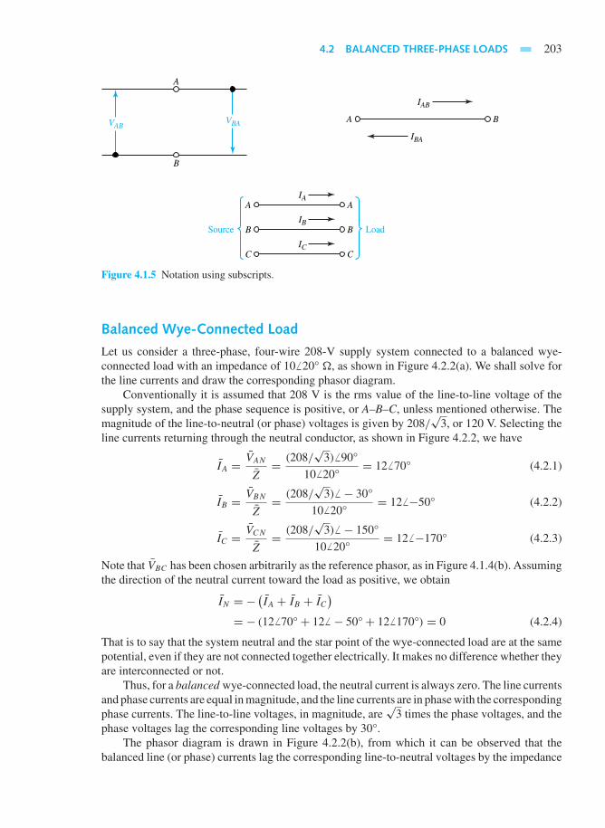
4.2 BALANCED THREE-PHASE LOADS 203
A
B
LoadSource
BAVABVBA
IBA
IAB
IAAA
IBBB
ICCC
Figure 4.1.5 Notation using subscripts.
Balanced Wye-Connected Load
Let us consider a three-phase, four-wire 208-V supply system connected to a balanced wye-connected load with an impedance of 10 20° , as shown in Figure 4.2.2(a). We shall solve forthe line currents and draw the corresponding phasor diagram.
Conventionally it is assumed that 208 V is the rms value of the line-to-line voltage of thesupply system, and the phase sequence is positive, or A–B–C, unless mentioned otherwise. Themagnitude of the line-to-neutral (or phase) voltages is given by 208/
√3, or 120 V. Selecting the
line currents returning through the neutral conductor, as shown in Figure 4.2.2, we have
IA = VAN
Z= (208/
√3) 90°
10 20°= 12 70° (4.2.1)
IB = VBN
Z= (208/
√3) − 30°
10 20°= 12 −50° (4.2.2)
IC = VCN
Z= (208/
√3) − 150°
10 20°= 12 −170° (4.2.3)
Note that VBC has been chosen arbitrarily as the reference phasor, as in Figure 4.1.4(b). Assumingthe direction of the neutral current toward the load as positive, we obtain
IN = −(IA + IB + IC
)= − (12 70°+ 12 − 50°+ 12 170°) = 0 (4.2.4)
That is to say that the system neutral and the star point of the wye-connected load are at the samepotential, even if they are not connected together electrically. It makes no difference whether theyare interconnected or not.
Thus, for a balanced wye-connected load, the neutral current is always zero. The line currentsand phase currents are equal in magnitude, and the line currents are in phase with the correspondingphase currents. The line-to-line voltages, in magnitude, are
√3 times the phase voltages, and the
phase voltages lag the corresponding line voltages by 30°.The phasor diagram is drawn in Figure 4.2.2(b), from which it can be observed that the
balanced line (or phase) currents lag the corresponding line-to-neutral voltages by the impedance

204 THREE-PHASE CIRCUITS AND RESIDENTIAL WIRING
Z B
Y–∆ transformation
For the balanced case,
ZABA
C
B
ZA
ZC
ZAB =ZAZB + ZBZC + ZCZA
ZC
ZBC =ZAZB + ZBZC + ZCZA
ZA
ZCA =ZAZB + ZBZC + ZCZA
ZB
ZAB = ZBC = ZCA = Z∆ = 3ZY
∆–Y transformation
For the balanced case,13
ZA =ZABZCA
ZAB + ZBC + ZCA
ZB =ZABZBC
ZAB + ZBC + ZCA
ZC =ZCAZBC
ZAB + ZBC + ZCA
ZA = ZB = ZC = ZY = Z∆
ZC
A Z BC
Figure 4.2.1 Wye–delta and delta–wye transformations.
angle (20° in our example). The load power factor is given by cos 20° for our problem, and it issaid to be lagging in this case, as the impedance angle is positive and the phase current lags thecorresponding phase voltage by that angle.
The problem can also be solved in a simpler way by making use of a single-line equivalentcircuit, as shown in Figure 4.2.2.(c),
IL = VL−NZ
= (208/√
3) 0°
10 20°= 12 − 20° (4.2.5)
in which VL−N is chosen as the reference for convenience. The magnitude of the line currentand the power factor angle are known; the negative sign associated with the angle indicates thatthe power factor is lagging. By knowing that the line (or phase) currents IA, IB, IC lag theirrespective voltages VAN , VBN , and VCN by 20°, the phase angles of various voltages and currents,if desired, can be obtained with respect to any chosen reference, such as VBC .
Balanced Delta-Connected Load
Next, let us consider the case of a balanced delta-connected load with impedance of 5 45°
supplied by a three-phase, three-wire 100-V system, as shown in Figure 4.2.3(a). We shalldetermine the line currents and draw the corresponding phasor diagram.
With the assumed positive phase sequence (A–B–C) and with VBC as the reference phasor,the line-to-line voltages VAB, VBC , and VCA are shown in Figure 4.2.3. The rms value of theline-to-line voltages is 100 V for our example. Choosing the positive directions of the line andphase currents as in Figure 4.2.3(a), we have
IAB = VAB
Z= 100 120°
5 45°= 20 75° (4.2.6)
IBC = VBC
Z= 100 0°
5 45°= 20 − 45° (4.2.7)
ICA = VCA
Z= 100 240°
5 45°= 20 195° (4.2.8)
By the application of Kirchhoff’s current law at each of the vertices of the delta-connectedload, we obtain
IA = IAB + IAC = 20 75° − 20 195° = 34.64 45° (4.2.9)
IB = IBA + IBC = −20 75° + 20 − 45° = 34.64 − 75° (4.2.10)
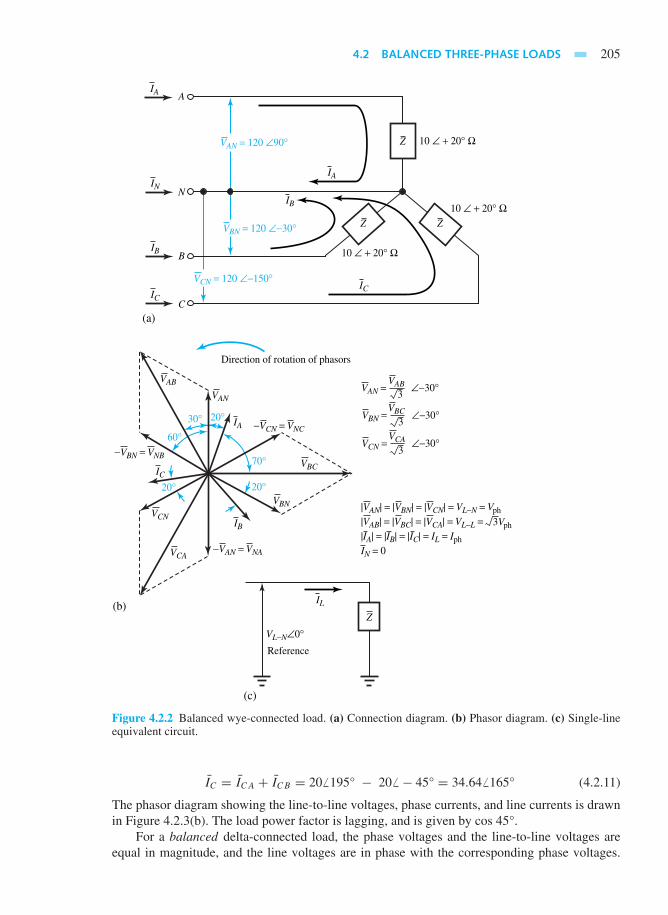
4.2 BALANCED THREE-PHASE LOADS 205
30°
IB
IC
IA
IC
IA
IB
IL
IC
Z
10 ∠ + 20° Ω
VCN = 120 ∠−150°
20°
20°20°
70°
60°
(a)
(b)
(c)
10 ∠ + 20° Ω
10 ∠ + 20° ΩZ
VAB
VBC
3
Z
VCA
VCN
VBN
VAN
−VCN = VNC
|VAN| = |VBN| = |VCN| = VL−N = Vph
|VAB| = |VBC| = |VCA| = VL−L =
VL−N∠0°
|IA| = |IB| = |IC| = IL = Iph
IN = 0
VAN = ∠−30°VAB
−VBN = VNB
−VAN = VNA
VBN = 120 ∠−30°
VAN = 120 ∠90°
A
N
B
C
Z
IB
IN
IA
3VBN = ∠−30°
VBC
3VCN = ∠−30°
VCA
3Vph
Direction of rotation of phasors
Reference
Figure 4.2.2 Balanced wye-connected load. (a) Connection diagram. (b) Phasor diagram. (c) Single-lineequivalent circuit.
IC = ICA + ICB = 20 195° − 20 − 45° = 34.64 165° (4.2.11)
The phasor diagram showing the line-to-line voltages, phase currents, and line currents is drawnin Figure 4.2.3(b). The load power factor is lagging, and is given by cos 45°.
For a balanced delta-connected load, the phase voltages and the line-to-line voltages areequal in magnitude, and the line voltages are in phase with the corresponding phase voltages.

206 THREE-PHASE CIRCUITS AND RESIDENTIAL WIRING
IAB
IBC
ICA
IC
IA
IAB
IAC
ICA
IBC IL
IB
IC
VBC = 100 ∠0°
45°
45°30°
30°
Direction of rotation of phasors
45°
45°
(a)
(b) (c)
5 ∠45° Ω5 ∠45° Ω
5 ∠45° Ω
Z
VAB
ZY
VCA
VBC
|VAB| = |VBC| = |VCA| = VL−L = Vph
|IAB| = |IBC| = |ICA| = Iph
VL−N = ∠0°
∠45° Ω
∆
|IA| = |IB| = |IC| = IL =IA = ∠−30°
VCA = 100 ∠240°
VAB = 100 ∠120°
A
B
C
IB
IA
3Iph
3 IAB
IB = ∠−30°3 IBC
IC = ∠−30°3 ICA
3100
35
Z
Z
Figure 4.2.3 Balanced delta-connected load. (a) Connection diagram. (b) Phasor diagram. (c) Single-lineequivalent circuit.
The line currents, in magnitude, are√
3 times the phase currents, and the phase currents lead thecorresponding line currents by 30°.
The preceding example can also be solved by the one-line equivalent method for which thedelta-connected load is replaced by its equivalent wye-connected load. The single-line equivalentcircuit is shown in Figure 4.2.3(c). The details are left as an exercise for the student.
Power in Balanced Three-Phase Circuits
The total power delivered by a three-phase source, or consumed by a three-phase load, is foundsimply by adding the power in each of the three phases. In a balanced circuit, however, this is

4.2 BALANCED THREE-PHASE LOADS 207
the same as multiplying the average power in any one phase by 3, since the average power is thesame for all phases. Thus one has
P = 3 VphIph cos φ (4.2.12)
where Vph and Iph are the magnitudes of any phase voltage and phase current, cos φ is the loadpower factor, and φ is the power factor angle between the phase voltage Vph and the phase currentIph corresponding to any phase. In view of the relationships between the line and phase quantitiesfor balanced wye- or delta-connected loads, Equation (4.2.12) can be rewritten in terms of theline-to-line voltage and the line current for either wye- or delta-connected balanced loading asfollows:
P = √3 VLIL cos φ (4.2.13)
where VL and IL are the magnitudes of the line-to-line voltage and the line current. φ is still theload power factor angle as in Equation (4.2.12), namely, the angle between the phase voltage andthe corresponding phase current.
In a balanced three-phase system, the sum of the three individually pulsating phase powersadds up to a constant, nonpulsating total power of magnitude three times the average realpower in each phase. That is, in spite of the sinusoidal nature of the voltages and currents,the total instantaneous power delivered into the three-phase load is a constant, equal to thetotal average power. The real power P is expressed in watts when voltage and current areexpressed in volts and amperes, respectively. You may recall that the instantaneous power insingle-phase ac circuits absorbed by a pure inductor or capacitor is a double-frequency sinusoidwith zero average value. The instantaneous power absorbed by a pure resistor has a nonzeroaverage value plus a double-frequency term with zero average value. The instantaneous reactivepower is alternately positive and negative, indicating the reversible flow of energy to andfrom the reactive component of the load. Its amplitude or maximum value is known as thereactive power.
The total reactive power Q (expressed as reactive volt-amperes, or VARs) and the volt-amperes for either wye- or delta-connected balanced loadings are given by
Q = 3 VphIph sin φ (4.2.14)
or
Q = √3 VLIL sin φ (4.2.15)
and
S = ∣∣S∣∣ = √P 2 +Q2 = 3 VphIph =√
3 VLIL (4.2.16)
where the complex power S is given by
S = P + jQ (4.2.17)
In speaking of a three-phase system, unless otherwise specified, balanced conditions areassumed. The terms voltage, current, and power, unless otherwise identified, are conventionallyunderstood to imply the line-to-line voltage (rms value), the line current (rms value), and the totalpower of all three phases. In general, the ratio of the real or average power P to the apparentpower or the magnitude of the complex power S is the power factor, which happens to be cos φin the sinusoidal case.
208 THREE-PHASE CIRCUITS AND RESIDENTIAL WIRING
EXAMPLE 4.2.1
(a) A wye-connected generator is to be designed to supply a 20-kV three-phase line. Findthe terminal line-to-neutral voltage of each phase winding.
(b) If the windings of the generator of part (a) were delta-connected, determine the outputline-to-line voltage.
(c) Let the 20-kV generator of part (a) supply a line current of 10 A at a lagging power factorof 0.8. Compute the kVA, kW, and kVAR supplied by the alternator.
So l u t i on
(a) VL−N = Vph = 20/√
3 = 11.547 kV
(b) VL = Vph = 11.547 kV
(c) kVA = √3 (20)(10) = 346.4
kW = 346.4(0.8) = 277.12
kVAR = 346.4(0.6) = 207.84
4.3 MEASUREMENT OF POWER
A wattmeter is an instrument with a potential coil and a current coil so arranged that itsdeflection is proportional to VI cos θ , where V is the voltage (rms value) applied acrossthe potential coil, I is the current (rms value) passing through the current coil, and θ is theangle between V and I . By inserting such a single-phase wattmeter to measure the averagereal power in each phase (with its current coil in series with one phase of the load and itspotential coil across the phase of the load), the total real power in a three-phase system canbe determined by the sum of the wattmeter readings. However, in practice, this may not bepossible due to the nonaccessibility of either the neutral of the wye connection, or the individualphases of the delta connection. Hence it is more desirable to have a method for measuringthe total real power drawn by a three-phase load while we have access to only three lineterminals.
The three-phase power can be measured by three single-phase wattmeters having current coilsin each line and potential coils connected across the given line and any common junction. Sincethis common junction is completely arbitrary, it may be placed on any one of the three lines, inwhich case the wattmeter connected in that line will indicate zero power because its potential coilhas no voltage across it. Hence, that wattmeter may be dispensed with, and three-phase power canbe measured by means of only two single-phase wattmeters having a common potential junctionon any of the three lines in which there is no current coil. This is known as the two-wattmetermethod of measuring three-phase power. In general, m-phase power can be measured by meansof m− 1 wattmeters. The method is valid for both balanced and unbalanced circuits with eitherthe load or the source unbalanced.
Figure 4.3.1 shows the connection diagram for the two-wattmeter method of measuring three-phase power. The total real power delivered to the load is given by the algebraic sum of the twowattmeter readings,
P = WA +WC (4.3.1)

4.3 MEASUREMENT OF POWER 209
A
B
C
Potential coil
Current coil
Three-phaseload
Single-phasewattmeter WC
Single-phasewattmeter WA
+−
+−
+−
+−
Figure 4.3.1 Connection diagram for two-wattmeter method of measuring three-phase power.
The significance of the algebraic sum will be realized in the paragraphs that follow. Two wattmeterscan be connected with their current coils in any two lines, while their potential coils are connectedto the third line, as shown in Figure 4.3.1. The wattmeter readings are given by
WA = VAB · IA · cos θA (4.3.2)
where θA is the angle between the phasors VAB and IA, and
WC = VCB · IC · cos θC (4.3.3)
where θC is the angle between the phasors VCB and IC .The two-wattmeter method, when applied to the balanced loads, yields interesting results.
Considering either balanced wye- or delta-connected loads, with the aid of the correspondingphasor diagrams drawn earlier for the phase sequence A–B–C (Figures 4.2.2. and 4.2.3), it can beseen that the angle between VAB and IA is (30° + φ) and that between VCB and IC is (30 − φ),where φ is the load power factor angle, or the angle associated with the load impedance. Thus,we have
WA = VLIL cos (30°+ φ) (4.3.4)
and
WC = VLIL cos (30°− φ) (4.3.5)
where VL and IL are the magnitudes of the line-to-line voltage and line current, respectively.Simple manipulations yield
WA +WC =√
3 VLIL cos φ (4.3.6)
and
WC −WA = VLIL sin φ (4.3.7)
from which,
tan φ = √3WC −WA
WC +WA
(4.3.8)

210 THREE-PHASE CIRCUITS AND RESIDENTIAL WIRING
When the load power factor is unity, corresponding to a purely resistive load, both wattmeterswill indicate the same wattage. In fact, both of them should read positive; if one of the wattmetershas a below-zero indication in the laboratory, an upscale deflection can be obtained by simplyreversing the leads of either the current or the potential coil of the wattmeter. The sum of thewattmeter readings gives the total power absorbed by the load.
At zero power factor, corresponding to a purely reactive load, both wattmeters will againhave the same wattage indication but with the opposite signs, so that their algebraic sum willyield zero power absorbed, as it should. The transition from a negative to a positive value occurswhen the load power factor is 0.5 (i.e., φ is equal to 60°). At this power factor, one wattmeterreads zero while the other one reads the total real power delivered to the load.
For power factors (leading or lagging) greater than 0.5, both wattmeters read positive, and thesum of the two readings gives the total power. For a power factor less than 0.5 (leading or lagging),the smaller reading wattmeter should be given a negative sign and the total real power absorbed bythe load (which has to be positive) is given by the difference between the two wattmeter readings.Figure 4.3.2 shows a plot of the load power factor versus the ratio Wl /Wh, where Wl and Wh arethe lower and higher readings of the wattmeters, respectively.
Another method that is sometimes useful in a laboratory environment for determiningwhether the total power is the sum or difference of the two wattmeter readings is describedhere. To begin, make sure that both wattmeters have an upscale deflection. To perform thetest, remove the lead of the potential coil of the lower reading wattmeter from the commonline that has no current coil, and touch the lead to the line that has the current coil of thehigher reading wattmeter. If the pointer of the lower reading wattmeter deflects upward, thetwo wattmeter readings should be added; if the pointer deflects in the below-zero direction, thewattage reading of the lower reading wattmeter should be subtracted from that of the higherreading wattmeter.
Given the two wattmeter readings from the two-wattmeter method used on a three-phasebalanced load, it is possible to find the tangent of the phase impedance angle as
√3 times the ratio
of the difference between the two wattmeter readings and their sum, based on Equation (4.3.8).If one knows the system sequence and the lines in which the current coils of the wattmeters arelocated, the sign for the angle can be determined with the aid of the following expressions. Forsequence A–B–C,
tan φ = √3WC −WA
WC +WA
= √3WA −WB
WA +WB
= √3WB −WC
WB +WC
(4.3.9)
and for sequence C–B–A,
1.0
0.80.6
0.40.5
0.2
Pow
er fa
ctor
lead
or
lag
+0.5+0.250 +1.0+0.75−0.75−1.0 −0.25−0.50
WlWh
Figure 4.3.2 Plot of load powerfactor versus Wl /Wh.

4.3 MEASUREMENT OF POWER 211
tan φ = √3WA −WC
WA +WC
= √3WB −WA
WB +WA
= √3WC −WB
WC +WB
(4.3.10)
The two-wattmeter method discussed here for measuring three-phase power makes use ofsingle-phase wattmeters. It may be noted, however, that three-phase wattmeters are also available,which, when connected appropriately, indicate the total real power absorbed. The total reactivepower associated with the three-phase balanced load is given by
Q = √3 VLIL sin φ = √3 (WC −WA) (4.3.11)
based on the two wattmeter readings of the two-wattmeter method.With the generator action of the source assumed, +P for the real power indicates that the
source is supplying real power to the load; +Q for the reactive power shows that the source isdelivering inductive VARs while the current lags the voltage (i.e., the power factor is lagging); and−Q for the reactive power indicates that the source is delivering capacitive VARs or absorbinginductive VARs, while the current leads the voltage (i.e., the power factor is leading).
EXAMPLE 4.3.1
Considering Figure 4.3.1, let balanced positive-sequence, three-phase voltages with VAB =100√
3 0° V (rms) be applied to terminals A, B, and C. The three-phase wye-connected balancedload consists of a per-phase impedance of (10 + j10). Determine the wattmeter readings ofWA and WC. Then find the total three-phase real and reactive powers delivered to the load. Basedon the wattmeter readings of WA and WC , compute the load power factor and check the signassociated with the power factor angle.
So l u t i on
VAB = 100√
3 0° V; VBC = 100√
3 − 120°; VCA = 100√
3 120°
VAN = 100 − 30° V; VBN = 100 − 150°; VCN = 100 90°
IA = VAN
Z= 100 − 30°
10√
2 45°= 5√
2 − 75° A (rms)
IC = VCN
Z= 100 90°
10√
2 45°= 5√
2 45° A (rms)
The load power factor angle φ = 45°, and it is a case of lagging power factor with the inductiveload.
WA = VABIA cos (30°+ φ) = 100√
3(
5√
2)
cos 75° = 317 W
WC = VCBIC cos (30°− φ) = 100√
3(
5√
2)
cos 15° = 1183 W
The total three-phase real power delivered to the load
WA +WC = 317+ 1183 = 1500 W
which checks with√3 VLIL cos φ = √3 100
√3(
5√
2)
cos 45° = 1500 W

212 THREE-PHASE CIRCUITS AND RESIDENTIAL WIRING
The total three-phase reactive power delivered to the load is√3(WC −WA) =
√3(1183− 317) = 1500 VAR
which checks with√3VLIL sin φ = √3(100
√3)(5
√2) sin 45° = 1500 VAR
For positive-sequence A–B–C,
tan ∅ = √3
(WC −WA
WC +WA
)= √3
(1183− 317
1183+ 317
)= 1.0
or ∅ = 45° with a positive sign, implying thereby that it corresponds to an inductive or laggingload, which checks with the given load specification. The load power factor is given by
cos ∅ = 0.707
and is lagging in this case.
4.4 RESIDENTIAL WIRING AND SAFETY CONSIDERATIONS
Residential electric power service commonly consists of a three-wire ac system supplied by thelocal power company. A distribution transformer with a primary and two secondaries formed witha center tap on the secondary side, as illustrated in Figure 4.4.1, is located on a utility pole, fromwhich three wires originate. Two of them are known as “hot” wires, while the third is called aneutral wire, which is connected to earth ground. In accordance with standard insulation colorcodes, “hot” wires are denoted by either B (black) or R (red), neutral by W (white), and ground(or uninsulated wire) by G (green). The functional difference between neutral and ground wireswill be brought out later when considering circuit wiring.
Domestic loads consisting of 120-V appliances and lighting, divided nearly equally betweenthe two 120-V (rms) secondaries, are connected from hot wires to neutral. Appliances such aselectric ranges and water heaters are supplied with 240-V (rms) power from the series-connectedsecondaries, as shown in Figure 4.4.1.
Minimizing the power loss in the lines (known as I2R loss) is important from the viewpointof efficiency and reducing the amount of heat generated in the wiring for safety considerations.Since the power loss in the lines is directly related to the current required by the load, a lowerline loss will be incurred with the 240-V wiring in delivering the necessary power to a load. Forthe lower voltage case, however, the size of the wires is increased, thereby reducing the wireresistance, in an effort to minimize line losses. Problem 4.4.2 deals with these considerations.
120 V
120 VEarthground
2400 V
SecondariesPrimary
240 VNeutral(white) W
R (Red)
B (Black)Hot
Hot
240-Vappliances
120-Vappliances
120-Vappliances
Figure 4.4.1 Three-winding distribution transformer providing dual-voltage ac supply.

4.4 RESIDENTIAL WIRING AND SAFETY CONSIDERATIONS 213
The three-line cable coming out of the secondaries of the distribution transformer on theutility pole passes through the electric meter that measures energy consumption in kilowatt-hoursand terminates at the main panel. Figure 4.4.2 shows a typical wiring arrangement for a residence.At the main panel, circuit breakers serve the joint role of disconnecting switches and overcurrentprotection; the neutral is connected to a busbar (bus) and in turn to the local earth ground; the hotlines are connected to individual circuits for lighting and appliances, as illustrated in Figure 4.4.2.The circuit breaker labeled GFCI (ground-fault circuit interruption), used for safety primarilywith outdoor circuits and in bathrooms, has additional features that will be described later. Notethat every outgoing “hot” wire must be connected to a circuit breaker, whereas every neutral wireand ground wire must be tied directly to earth ground at the neutral busbar.
Today most homes have three-wire connections to their outlets, one of which is shown inFigure 4.4.3. The need for both ground and neutral connections needs to be explained, since theground conductor may appear to be redundant, playing no role in the actual operation of a load thatmight be connected to the receptacle. From the viewpoint of safety, the ground connection is usedto connect the metallic chassis of the appliance to earth ground. Without the ground conductorconnected to the metal case of the appliance, as shown in Figure 4.4.4(a), the appliance chassiscould be at any potential with respect to ground, possibly even at the “hot” wire’s potential if a partof the “hot” wire were to lose some insulation and come in contact with the inside of the chassis.An unintended connection may occur because of the corrosion of insulation or a loose mechanicalconnection. Poorly grounded appliances can thus be a significant hazard by providing a path toground through the body of a person touching the chassis with a hand. An undersized groundloop current limited by the body resistance may flow directly through the body to ground andcould be quite harmful. Typically, the circuit breaker would not operate under such circumstances.
RMain
breaker
20 A
15 A
G
G
W
W
W or G
GFCIR Outdoor
lighting(120-V circuitwith GFCI)
Electric stove(240-V circuit)
Kitchen appliances(120-V circuit)
Bedroom lighting(120-V circuit)
Basement lighting(120-V circuit)
Earth ground
Neutral busbar (bus)
R
B
B20 A
20 A
20 ABus BBus R
B W
20 A
GW
B
GW
B
Figure 4.4.2 Typical wiring arrangement for a residence Note: Currentsand voltages shown are rms magnitudes.
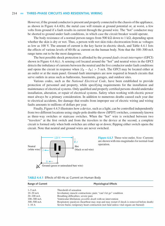
214 THREE-PHASE CIRCUITS AND RESIDENTIAL WIRING
However, if the ground conductor is present and properly connected to the chassis of the appliance,as shown in Figure 4.4.4(b), the metal case will remain at ground potential or, at worst, a fewvolts from ground if a fault results in current through the ground wire. The “hot” conductor maybe shorted to ground under fault conditions, in which case the circuit breaker would operate.
The body resistance of a normal person ranges from 500 k down to 1 k, depending uponwhether the skin is dry or wet. Thus, a person with wet skin risks electrocution from ac voltagesas low as 100 V. The amount of current is the key factor in electric shock, and Table 4.4.1 liststhe effects of various levels of 60-Hz ac current on the human body. Note that the 100–300-mArange turns out to be the most dangerous.
The best possible shock protection is afforded by the ground-fault circuit interrupter (GFCI)shown in Figure 4.4.4(c). A sensing coil located around the “hot” and neutral wires in the GFCIdetects the imbalance of currents between the neutral and the live conductor under fault conditionsand opens the circuit in response when |IB − IW | > 5 mA. The GFCI may be located either atan outlet or at the main panel. Ground-fault interrupters are now required in branch circuits thatserve outlets in areas such as bathrooms, basements, garages, and outdoor sites.
Various codes, such as the National Electrical Code, have been established to provideprotection of personnel and property, while specifying requirements for the installation andmaintenance of electrical systems. Only qualified and properly certified persons should undertakeinstallation, alteration, or repair of electrical systems. Safety when working with electric powermust always be a primary consideration. In addition to numerous deaths caused each year dueto electrical accidents, fire damage that results from improper use of electric wiring and wiringfaults amounts to millions of dollars per year.
Finally, Figure 4.4.5 illustrates how a device, such as a light, can be controlled independentlyfrom two different locations using single-pole double-throw (SPDT) switches, commonly knownas three-way switches or staircase switches. When the “hot” wire is switched between two“travelers” at the first switch and from the travelers to the device at the second, a completecircuit is formed only when both switches are either up or down; flipping either switch opens thecircuit. Note that neutral and ground wires are never switched.
120 V
Ground (green or uninsulated bare wire)
Hot(black or red wire)
Neutral(white wire)
0
I
I
Figure 4.4.3 Three-wire outlet. Note: Currentsare shown with rms magnitudes for normal-loadoperation.
TABLE 4.4.1 Effects of 60-Hz ac Current on Human Body
Range of Current Physiological Effects
1–5 mA Threshold of sensation10–20 mA Involuntary muscle contractions; pain; “can’t let go” condition20–100 mA Breathing difficulties; severe pain100–300 mA Ventricular fibrilation; possible death with no intervention300–500 mA Respiratory paralysis (heartbeat may stop and may restart if shock is removed before death)1–10 A Severe burns; temporary heart contraction (not fatal unless vital organs are burned)

4.5 LEARNING OBJECTIVES 215
120 V
Metallic chassis
−
+ Unintended connection(wiring fault)
(a)
B
Load120 V
?
Metallic chassis
−
+ Unintended connection(wiring fault)
(b)
B
Load120 V
IG
Metallic chassis
−
+ Unintended connection(wiring fault)
(c)
B
GW
W
GW
Load120 V GFCI
Sensing coil
IB
IW
Figure 4.4.4 Appliance with wiring fault. Note: Currents and voltagesshown are rms magnitudes. (a) Ungrounded chassis. (b) Grounded chassis.(c) Grounded chassis with GFCI in circuit.
4.5 LEARNING OBJECTIVES
The learning objectives of this chapter are summarized here, so that the student can check whetherhe or she has accomplished each of the following.
• Phase sequence of balanced three-phase voltages and currents.
• Wye–delta and delta–wye conversions for networks containing impedances.
• Circuit analysis with balanced three-phase source and balanced wye-connected load.
• Circuit analysis with balanced three-phase source and balanced delta-connected load.

216 THREE-PHASE CIRCUITS AND RESIDENTIAL WIRING
SPDT SPDT
Travelers
3-way switch #1 3-way switch #2
W
B
G
Figure 4.4.5 Three-wayswitch connections to operate adevice.
• Real, reactive, and apparent powers in three-phase circuits.
• Measurement of three-phase power by two single-phase wattmeters.
• Basic notions of residential circuit wiring, including grounding and safety considerations.
4.6 PRACTICAL APPLICATION: A CASE STUDY
Physiological Effects of Current and Electrical Safety
Various effects that electric current may have on the human body and the current levels at whichthey occur are illustrated in Figure 4.6.1. Note that small currents can have serious effects. Theranges in Figure 4.6.1, however, represent variations among individuals in body size, condition,and tolerance to electric shock. The region of the body through which the current passes is crucial.
The current can easily be estimated by the application of Ohm’s law,
I = V/R
where R is the resistance of the circuit of which a person’s body might become a part. Most seriouselectric shocks occur where a person is in simultaneous contact with the so-called hot wire andthe ground. Ground may be the dry or moist earth, the plumbing of a house, or even a concretefloor that is connected to the plumbing. The circuit resistance would include not only the body
Threshold ofperception
Let-go current
Respiratory paralysis, fatigue, pain
Ventricular fibrillation
Burns, injury
Sustained myocardialcontraction
1 mA 10 mA 100 mA 1 A 10 A 100 A
Figure 4.6.1 Physiological effects of electricity. (Adapted from J. G. Webster, Medical Instrumentation,Application and Design, Houghton Mifflin, 1978.)

4.6 PRACTICAL APPLICATION: A CASE STUDY 217
TABLE 4.6.1 Resistance Estimates for Various Skin-Contact Conditions
Resistance
Condition Dry Wet
Finger touch 40 k–1000 k 4–15 kHand holding wire 15–50 k 3–6 kFinger–thumb grasp 10–30 k 2–5 kHand holding pliers 5–10 k 1–3 kPalm touch 3–8 k 1–2 kHand around 1 1
2 -in pipe (or drill handle) 1–3 k 0.1–1.5 kTwo hands around 1 1
2 -in pipe 0.5–1.5 k 250–750
Hand immersed 200–500
Foot immersed 100–300
Human body, internalexcluding skin, 200–1000
Adapted from R. Lee, “Electrical Safety in Industrial Plants,” IEEE Spectrum (June 1971).
TABLE 4.6.2 Resistance Estimates for Equal Areas (130 cm2)of Various Materials
Material Resistance
Rubber gloves or soles >20 M
Dry concrete above grade 1–5 M
Dry concrete on grade 0.2–1 M
Leather sole, dry, including foot 0.1–0.5 M
Leather sole, damp, including foot 5–20 kWet concrete on grade 1–5 k
Adapted from R. Lee, “Electrical Safety in Industrial Plants,” IEEE Spectrum (June 1971).
resistance but also the resistance of the shoes and the resistance between the shoes and ground.Tables 4.6.1 and 4.6.2 give basic information for estimating the total resistance to ground.
Let us estimate the current caused when a person is standing on moist ground with leather-soled damp shoes and unwillingly grabs hold of 240-V wire with a wet palm. Referring to Tables4.6.1 and 4.6.2 and taking the lowest values, one has 1 k for the grasp, 200 for the body, and5 k for the feet and shoes. Thus the largest current the victim might carry would be 240V/6.2k, or about 40 mA. From Figure 4.6.1 one can see that there is a good chance that the victimwould be unable to release the grasp and unable to breathe. Thus a dangerous situation may exist.
When a person is experiencing electric shock, because the damaging effects are progressive,time becomes a critical factor. First, the source of electric energy should be removed from theshock victim, even before an emergency medical service is called in. CPR (cardiopulmonaryresuscitation) may have to be administered by a trained person. The condition of ventricularfibrillation occurs, the heart loses its synchronized pumping action, and the blood circulationceases. Sophisticated medical equipment may be needed to restore coherent heart pumping.
When working around electric power, the following general precautions are to be taken:
• Make sure that the power is off before working on any electric wiring or electric equipment.
• Wear rubber gloves and rubber-soled shoes, if possible.
• Avoid standing on a wet surface or on moist ground.
• Avoid working alone, as far as possible, around exposed electric power.

218 THREE-PHASE CIRCUITS AND RESIDENTIAL WIRING
PROB L EMS
*4.1.1 The line-to-line voltage of a balanced wye-connected three-phase source is given as 100 V.Choose VAB as the reference.
(a) For the phase sequence A–B–C, sketch thephasor diagram of the voltages and find theexpressions for the phase voltages.
(b) Repeat part (a) for the phase sequence C–B–A.
4.2.1 A three-phase, three-wire 208-V system is con-nected to a balanced three-phase load. The linecurrents IA, IB , and IC are given to be in phasewith the line-to-line voltages VBC, VCA, and VAB ,respectively. If the line current is measured to be10 A, find the per-phase impedance of the load.
(a) If the load is wye-connected.
(b) If the load is delta-connected.
*4.2.2 Consider a three-phase 25-kVA, 440-V, 60-Hzalternator operating at full load (i.e., deliveringits rated kVA) under balanced steady-state condi-tions. Find the magnitudes of the alternator linecurrent and phase current.
(a) If the generator windings are wye-connected.
(b) If the generator windings are delta-connected.
4.2.3 Let the alternator of Problem 4.2.2 supply a linecurrent of 20 A at a power factor of 0.8 lagging.Determine:
(a) The kVA supplied by the machine.
(b) The real power kW delivered by the generator.
(c) The reactive power kVAR delivered by thealternator.
4.2.4 A balanced wye-connected load with a per-phaseimpedance of 4 + j3 is supplied by a 173-V,60-Hz three-phase source.
(a) Find the line current, the power factor, the totalvolt-amperes, the real power, and the reactivepower absorbed by the load.
(b) Sketch the phasor diagram showing all thevoltages and currents, with VAB as the ref-erence.
(c) If the star point of the load is connected tothe system neutral through an ammeter, whatwould the meter read?
4.2.5 A balanced delta-connected load with a per-phaseimpedance of 12 + j9 is supplied by a 173-V,60-Hz three-phase source.
(a) Determine the line current, the power factor,the total volt-amperes, the real power, and thereactive power absorbed by the load.
(b) Compare the results of Problem 4.2.5(a) withthose obtained in Problem 4.2.4(a), and ex-plain why they are the same.
(c) Sketch the phasor diagram showing all volt-ages and currents, with VAB as the reference.
4.2.6 A 60-Hz, 440-V, three-phase system feeds twobalanced wye-connected loads in parallel. Oneload has a per-phase impedance of 8 + j3 andthe other 4 − j1 . Compute the real power inkW delivered to (a) the inductive load, and (b) thecapacitive load.
*4.2.7 Balanced wye-connected loads drawing 10 kWat 0.8 power factor lagging and 15 kW at 0.9power factor leading are connected in parallel andsupplied by a 60-Hz, 300-V, three-phase system.Find the line current delivered by the source.
4.2.8 A balanced delta-connected load with a per-phaseimpedance of 30+ j10 is connected in parallelwith a balanced wye-connected load with a per-phase impedance of 40−j10 . This load combi-nation is connected to a balanced three-phase sup-ply through three conductors, each of which has aresistance of 0.4 . The line-to-line voltage at theterminals of the load combination is measured tobe 2000 V. Determine the power in kW:
(a) Delivered to the delta-connected load.
(b) Delivered to the wye-connected load.
(c) Lost in the line conductors.
4.2.9 Three identical impedances of 30 30° are con-nected in delta to a three-phase 173-V system byconductors that have impedances of 0.8+ j0.6
each. Compute the magnitude of the line-to-linevoltage at the terminals of the load.
4.2.10 Repeat Problem 4.2.9 for a delta-connected set ofcapacitors with a per-phase reactance of −j60
connected in parallel with the load, and comparethe result with that obtained in Problem 4.2.9.
4.2.11 Two balanced, three-phase, wye-connected loadsare in parallel across a balanced three-phase sup-ply. Load 1 draws a current of 20 A at 0.8 powerfactor leading, and load 2 draws a current of 30A at 0.8 power factor lagging. For the combinedload compute:

PROBLEMS 219
(a) The current taken from the supply and thesupply power factor.
(b) The total real power in kW supplied by thesource, if the supply voltage is 400 V.
4.2.12 Two balanced, three-phase, wye-connected loadsare in parallel across a balanced, three-phase sup-ply. Load 1 draws 15 kVA at 0.8 power factorlagging, and load 2 draws 20 kVA at 0.6 powerfactor leading. Determine:
(a) The total real power supplied in kW.
(b) The total kVA supplied.
(c) The overall power factor of the combinedload.
*4.2.13 Two balanced, wye-connected, three-phase loadsare in parallel across a balanced, three-phase 60-Hz, 208-V supply. The first load takes 12 kW at 0.6power factor lagging, and the second load takes 15kVA at 0.8 power factor lagging.
(a) Draw the power triangle for each load and forthe combination.
(b) What is the total kVA supplied?
(c) Find the supply power factor, and specifywhether lagging or leading.
(d) Compute the magnitude of the current drawnby each load and drawn from the supply.
(e) If wye-connected capacitors are placed in par-allel with the two loads in order to improvethe supply power factor, determine the valueof capacitance in farads in each phase neededto bring the overall power factor to unity.
4.2.14 A three-phase balanced load draws 100 kW at0.8 power factor lagging. In order to improve thesupply power factor to 0.95 leading, a synchronousmotor drawing 50 kW is connected in parallel withthe load. Compute the kVAR, kVA, and the powerfactor of the motor (specify whether lagging orleading).
4.2.15 (a) A balanced wye-connected load with per-phase impedance of 20+j10 is connected toa balanced 415-V, three-phase supply throughthree conductors, each of which has a seriesimpedance of 2+ j4 . Find the line current,the voltage across the load, the power deliv-ered to the load, and the power lost in the lineconductors.
(b) Repeat the problem if the three per-phaseload impedances of part (a) were connectedin delta.
4.2.16 A balanced electrical industrial plant load of 9.8MW with 0.8 lagging power factor is supplied bya three-phase 60-Hz system having a maximumrating (load-carrying capacity) of 660 A at 11 kV(line-to-line voltage).
(a) Determine the apparent power and the reactivepower drawn by the load.
(b) Additional equipment, consisting of a loadof 1.5 MW and 0.7 MVAR lagging, is to beinstalled in the plant. Compute the minimumrating in MVA of the power factor correctioncapacitor that must be installed if the rating ofthe line is not to be exceeded. Find the systempower factor.
(c) If the capacitor, consisting of three equal sec-tions, is connected in delta across the supplylines, calculate the capacitance required ineach section.
4.2.17 Derive the relationships given in Figure 4.2.1 forthe wye–delta and the delta–wye transformations.
4.2.18 Two three-phase generators are supplying to acommon balanced three-phase load of 30 kW at0.8 power factor lagging. The per-phase imped-ance of the lines connecting the generator G1 tothe load is 1.4 + j1.6 , whereas that of thelines connecting the generator G2 to the load is0.8 + j1 . If the generator G1, operating at aterminal voltage of 800 V (line to line), supplies15 kW at 0.8 power factor lagging, find the voltageat the load terminals, the terminal voltage of thegenerator G2, and the real power, as well as thereactive power output of the generator G2.
4.3.1 Determine the wattmeter readings when the two-wattmeter method is applied to Problem 4.2.4, andcheck the total power obtained.
4.3.2 When the two-wattmeter method for measuringthree-phase power is used on a certain balancedload, readings of 1200 W and 400 W are obtained(without any reversals). Determine the delta-connected load impedances if the system voltageis 440 V. With the information given, is it possibleto find whether the load impedance is capacitiveor inductive in nature?
4.3.3 The two-wattmeter method for measuring three-phase power is applied on a balanced wye-connected load, as shown in Figure 4.3.2, and thereadings are given by
WC = 836W and WA = 224 W

220 THREE-PHASE CIRCUITS AND RESIDENTIAL WIRING
If the system voltage is 100 V, find the per-phaseimpedance of the load. In this problem, is it pos-sible to specify the capacitive or inductive natureof the impedance?
4.3.4 Two wattmeters are used, as shown in Figure 4.3.1,to measure the power absorbed by a balanceddelta-connected load. Determine the total power inkW, the power factor, and the per-phase impedanceof the load if the supply-system voltage is 120 Vand the wattmeter readings are given by
(a) WA = −500 W, and WC = 1300 W.
(b) WA = 1300 W, and WC = −500 W.
*4.3.5 Referring to Problem 4.2.15(b), with a phase volt-age as the reference phasor and with a positive-phase-sequence supply system, two single-phasewattmeters are used to measure the power deliv-ered to the load. The wattmeter current coils arearranged as in Figure 4.3.1 to carry the currents IA
and IC, whereas the potential coils share a commonconnection at the node B. Determine the readingsof the two wattmeters WA and WC, and verify thatthe sum of these readings equals the total powerin the load.
4.4.1 Referring to Figure 4.4.1, let VBN = VRN =120 V rms magnitude, and VBR = 240 V rmsmagnitude. Write down expressions for vBN(t),vRN(t), and vBR(t), and sketch them as a functionof time.
*4.4.2 Consider a 240-V supply feeding a resistive loadof 10 kW through wires having a total resistanceof R = 0.02 . For the same load, let a 120-Vsupply be used with a total wire resistance of R/2= 0.01 . Compute the I2R loss in the lines forboth cases and compare.
4.4.3 A person, while driving a car in a cyclone andwaiting at an intersection, hears a thumping soundwhen a power line falls across the car and makescontact with the chassis. The power line voltage toground is 2400 V. Instinctively he steps out ontothe wet ground, while holding the door handle,to check out the external situation. Assuming hisbody resistance to be 10 k and negligible auto-chassis resistance, comment on what might hap-pen to the individual. Would it have been saferfor him to remain in the car until some help ar-rived?

PART
ELECTRONIC ANALOG ANDDIGITAL SYSTEMS
TWO

This page intentionally left blank

5 Analog Building Blocks andOperational Amplifiers
5.1 The Amplifier Block
5.2 Ideal Operational Amplifier
5.3 Practical Properties of Operational Amplifiers
5.4 Applications of Operational Amplifiers
5.5 Learning Objectives
5.6 Practical Application: A Case Study—Automotive Power-Assisted Steering System
Problems
Electronic systems usually process information in either analog or digital form. In order to processthe two different kinds of signals, analog circuits and digital circuits have been devised. Whilealmost all technology was of the analog type until around 1960, due to the advent of integratedcircuits (ICs), digital technology has grown tremendously.
In analog systems, a signal voltage or current is made proportional to some physical quantity.Since voltages (or currents) can take on any values over a continuous range between someminimum and some maximum, analog systems are also known as continuous-state systems.These are to be distinguished from digital or discrete-state systems, in which only certain valuesof voltage (or current) are allowed.
Most circuits found in analog systems are linear circuits in which one voltage (or current) ismeant to be linearly proportional to another. Linear active circuits are also known as amplifiers,which are the building blocks of linear systems with analog technology.
When describing and analyzing electric systems, which are often large and complex, it is veryhelpful to consider such large systems as being built from smaller units, called building blocks.These are then the subunits, which can be connected to form larger circuits or systems. Moreimportantly, the building blocks can be described adequately by their simple terminal properties.Thus, with the building block point of view, one is not concerned with the interiors of the blocks,only with how they perform as seen from the outside.
The concept of a model, which is a collection of ideal linear circuit elements simulatingapproximately the behavior of a real circuit element or a building block under certain limitations,
223
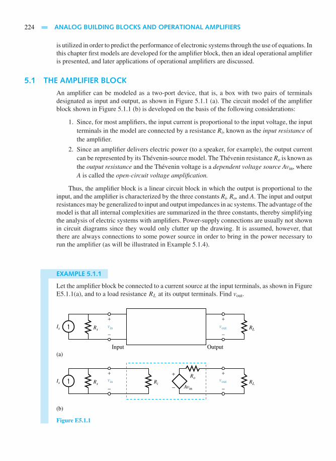
224 ANALOG BUILDING BLOCKS AND OPERATIONAL AMPLIFIERS
is utilized in order to predict the performance of electronic systems through the use of equations. Inthis chapter first models are developed for the amplifier block, then an ideal operational amplifieris presented, and later applications of operational amplifiers are discussed.
5.1 THE AMPLIFIER BLOCK
An amplifier can be modeled as a two-port device, that is, a box with two pairs of terminalsdesignated as input and output, as shown in Figure 5.1.1 (a). The circuit model of the amplifierblock shown in Figure 5.1.1 (b) is developed on the basis of the following considerations:
1. Since, for most amplifiers, the input current is proportional to the input voltage, the inputterminals in the model are connected by a resistance Ri, known as the input resistance ofthe amplifier.
2. Since an amplifier delivers electric power (to a speaker, for example), the output currentcan be represented by its Thévenin-source model. The Thévenin resistance Ro is known asthe output resistance and the Thévenin voltage is a dependent voltage source Avin, whereA is called the open-circuit voltage amplification.
Thus, the amplifier block is a linear circuit block in which the output is proportional to theinput, and the amplifier is characterized by the three constants Ri, Ro, and A. The input and outputresistances may be generalized to input and output impedances in ac systems. The advantage of themodel is that all internal complexities are summarized in the three constants, thereby simplifyingthe analysis of electric systems with amplifiers. Power-supply connections are usually not shownin circuit diagrams since they would only clutter up the drawing. It is assumed, however, thatthere are always connections to some power source in order to bring in the power necessary torun the amplifier (as will be illustrated in Example 5.1.4).
EXAMPLE 5.1.1
Let the amplifier block be connected to a current source at the input terminals, as shown in FigureE5.1.1(a), and to a load resistance RL at its output terminals. Find vout.
+
−
+
−
Input Output(a)
(b)
Ri
Ro
Avin
vin vout
vin vout RLIs Rs
+
−RLRs
+
−
+
−Is
Figure E5.1.1
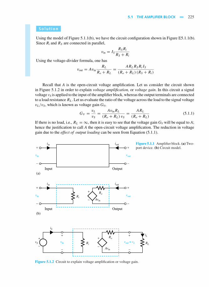
5.1 THE AMPLIFIER BLOCK 225
So l u t i on
Using the model of Figure 5.1.1(b), we have the circuit configuration shown in Figure E5.1.1(b).Since Ri and RS are connected in parallel,
vin = ISRSRi
RS + Ri
Using the voltage-divider formula, one has
vout = AvinRL
Ro + RL
= ARLRSRiIS
(Ro + RL) (RS + Ri)
Recall that A is the open-circuit voltage amplification. Let us consider the circuit shownin Figure 5.1.2 in order to explain voltage amplification, or voltage gain. In this circuit a signalvoltage vS is applied to the input of the amplifier block, whereas the output terminals are connectedto a load resistance RL. Let us evaluate the ratio of the voltage across the load to the signal voltagevL/vS , which is known as voltage gain GV,
GV = vL
vS= AvinRL
(Ro + RL) vS= ARL
(Ro + RL)(5.1.1)
If there is no load, i.e., RL = ∞, then it is easy to see that the voltage gain GV will be equal to A;hence the justification to call A the open-circuit voltage amplification. The reduction in voltagegain due to the effect of output loading can be seen from Equation (5.1.1).
+
−
+
−
iin iout
vin vout
Input Output(a)
+
−
+
−
iin
Ri
Ro
Avin
iout
vin vout
Input Output(b)
+
−
Figure 5.1.1 Amplifier block. (a) Two-port device. (b) Circuit model.
Ri
Ro
Avin
vout = vLvin
+
−
RL
iL
iS
+
−
+
−
+
−vS
Figure 5.1.2 Circuit to explain voltage amplification or voltage gain.

226 ANALOG BUILDING BLOCKS AND OPERATIONAL AMPLIFIERS
By defining the current gain GI to be the ratio of the current throughRL to the current throughvS, one gets
GI = iL
iS= Avin/ (Ro + RL)
vin/Ri
= ARi
Ro + RL
(5.1.2)
The power gain GP, defined by the ratio of the power delivered to the load to the power givenout by the signal source, is obtained as
GP = v2L/RL
v2S/Ri
= G2V Ri
RL
= A2RLRi
(Ro + RL)2= GVGI (5.1.3)
Note that, for fixed values of Ro and Ri, GP is maximized when RL is chosen equal to Ro, and thiscorresponds to maximum power transfer to the load. One should also note that the added poweremerging from the output comes from the power source that powers the amplifier, even thoughthe power-supply connections are usually not shown on the circuit diagram, and that the existenceof power gain does not violate the law of energy conservation.
EXAMPLE 5.1.2
The constants of an amplifier are given byA = 1, Ri = 10,000, andRo = 100 . It is driven bya Thévenin source with vTh(t)= VO cos ωt and RTh= 20,000 . The amplifier output is connectedto a 100- load resistance. Find the power amplification, if it is defined as the ratio of the powerdelivered to the load to the maximum power available from the Thévenin source.
So l u t i on
The corresponding circuit diagram is shown in Figure E5.1.2. The instantaneous power deliveredto RL is given by
Ro = 100 Ω
RTh = 20,000 Ω
Avin = vin
vinRL =100 Ω
Ri =10,000 Ω
Signal source LoadAmplifier
vTh =VO cos ωt
+
−
+
−
+
−
Figure E5.1.2 Circuit diagram.
PL (t) = i2L (t) RL =
[Avin (t)
Ro + RL
]2
RL
The time-averaged power PL is obtained by representing vin(t) by its phasor Vin,
PL = 1
2
∣∣Vin
∣∣2 A2RL
(Ro + RL)2
Note that the time average of a product of sinusoids is given by

5.1 THE AMPLIFIER BLOCK 227
Time average of [v (t) v (t)] = 1
2Re[V V ∗
] = ∣∣V ∣∣22
The maximum power is derived from a Thévenin source when it is loaded by a resistanceequal to RTh. The maximum power thus obtainable, known as available power PAVL, is given by
PAVL =∣∣VTh
∣∣28RTh
In this circuit, ∣∣Vin
∣∣2 = R2i
(Ri + RTh)2
∣∣VTh
∣∣2Note that the peak value of the sinusoid is used here for the magnitude of the phasor in theseexpressions. Thus,
GP = PL
PAVL= 4A2RLR
2i RTh
(Ro + RL)2 (Ri + RTh)
2
Substituting the values given, one gets
GP = 4 (1)2 (100) 108 (20,000)
(100+ 100)2 (10,000 + 20,000)2 =200
9= 22.22
Note that although the amplifier’s open-circuit voltage amplification A is only unity, substantialpower gain is obtained in this case since the current gain is greater than unity and GP = GVGI.In applications of microwave technology, the function of the amplifier is to magnify very smallpower to a measurable level with as little random noise as possible. The source signal may befrom a radio telescope, and the available power may be determined by the power captured by theantenna dish.
EXAMPLE 5.1.3
Quite often an amplifier is used as a component of an amplifier circuit. Consider the amplifiercircuit shown in Figure E5.1.3, which contains an amplifier block as an internal component. Findthe input resistance R′i , the output resistance R′o, and the open-circuit voltage amplification A′ ofthe larger circuit.
RS A
B
vout R2
Amplifierblock
with constantsRi , Ro , A
vS RL
+
−
R1
+
−
C
D
vin
+
−
Figure E5.1.3
So l u t i on
The input resistance looking into terminals A and B is

228 ANALOG BUILDING BLOCKS AND OPERATIONAL AMPLIFIERS
R′i = R1 + Ri
The output resistance is the same as the Thévenin resistance seen from terminals C and D. Turningoff independent source vS, vin becomes zero, and as a consequence the dependent source in theamplifier block goes to zero. Looking to the left of terminals C and D, R2 and Ro can be seen tobe in parallel,
R′o =R2Ro
R2 + Ro
The open-circuit voltage gain of the larger circuit is
A′ = vCD
vAB
With
vCD = R2
Ro + R2Avin and vin = Ri
Ri + R1vAB
we have
A′ = vCD
vAB= AR2Ri
(Ro + R2) (Ri + R1)
In further calculations, the dashed box can simply be replaced by the model with parametersR′i , R′o, and A′. The reader should note that in general R′i may depend on RL, and R′o may dependon RS , even though in this simple example they do not.
Two of the most important considerations that influence amplifier design are power-handlingcapacity and frequency response. In practice, the performance of an amplifier is limited by itsability to dissipate heat, known as its power dissipation. The electric power that is converted toheat in an amplifier can be calculated when the currents and voltages are known at all its terminals,including the power-supply terminals.
EXAMPLE 5.1.4
For the amplifier circuit shown in Figure E5.1.4 with Ri∼= ∞, Ro
∼= 0, A = 10, RL =100 , and vin = 1 V, calculate the power dissipated in the amplifier if the voltage at thepower-supply terminal Vps is given to be 20 V and Ips is assumed to be equal to IL.
voutvin
+
−RL
v = 0
(1)
(2)
(3)
(4)
(5)
(6)
v = vps
IL+
−
Ips
Ips
Figure E5.1.4

5.2 IDEAL OPERATIONAL AMPLIFIER 229
So l u t i on
We have
P =6∑
n=1
VnIn
where Vn is the voltage at terminal n and In is the current flowing into terminal n. Note that currentsI1 and I2 are zero since Ri = ∞, vout= Avin= 10(1)= 10 V. The power supply maintains terminal5 at V5 = Vps = 20 V and terminal 6 at V6 = 0; I3 = −I4 and I5 = −I6. Then
P = V3I3 + V4I4 + V5I5 + V6I6 = V3 (−IL)+ V4IL + V5Ips − V6Ips
= (V4 − V3) IL +(VpsIps
) = −VoutIL + VpsIps
= (Vps − Vout)Ips =
(Vps − Vout
)IL
Noting that IL = Vout/RL, one has
P = (20− 10)
(10
100
)= 1W
Since many amplifiers are designed with large values of Ri in order to keep the input powerlow, the approximation of Ri
∼= ∞ is often justified. However, the assumption that Ips= IL is notas justified because a certain amount of additional current (though kept small in order to minimizethe waste) will pass directly through the amplifier from terminal 5 to terminal 6 without goingthrough the load, making Ips slightly larger than IL.
The behavior of an amplifier always depends on the frequency of the sinusoidal signalin question. In general, the parameters of the amplifier model vary with the signal frequency.The variation of
∣∣A∣∣, as well as that of the phase angle θA, with frequency for an ampli-fier is known as its frequency response. The value of
∣∣A(f )∣∣ always drops off at sufficientlyhigh frequencies. Since A(ω) = Vout/Vin, the phase difference θA between output and in-put sinusoids is also a function of frequency. However, at low frequencies θA is often zero,and therefore A can be regarded as real. Figure 5.1.3 shows variations of
∣∣A∣∣ and θA typ-ical of audio, video, bandpass, and operational amplifiers. The input and output resistancesshould be generalized to impedances Zi(ω) and Zo(ω) when frequency effects are important.However, most commercial amplifiers are designed to make Zi and Zo real and constant overthe useful frequency range of the amplifier block. If the frequency response of a block it-self is known, the frequency response of a larger circuit containing the amplifier block canbe found.
5.2 IDEAL OPERATIONAL AMPLIFIER
The operational amplifier, known also as op amp, consists of several transistors, diodes, capacitors,and resistors. It is available in integrated-circuit form for less than one U.S. dollar. Beinginexpensive, compact, and versatile, operational amplifiers are used in a variety of simple circuits.Op-amp circuits, as we will see later, usually contain negative feedback.
Op-amp circuits themselves can be regarded as building blocks. These blocks are charac-terized by their input resistance, output resistance, and open-circuit voltage amplification. Thesymbol for the op amp is shown in Figure 5.2.1. Two terminals labeled + and − are availablefor inputs. The voltages of these terminals are labeled with respect to the common terminal,
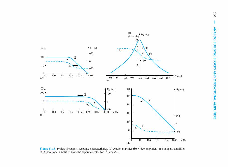
230ANALOGBUILD
INGBLOCKSANDOPER
ATIO
NALAMPLIFIER
S
|A|
|A|(log scale)
|A|−
−
−
− −
−
−
|A|− θA, deg
θA
θA, deg
f, GHz
θA+90
−90
−90
+ 90
0
9.6 9.8 10.410.310.110.0(c)
10.29.7 9.9
2
7
10
5
3
4
0
100
100 1 k 10 k 100 k(a)
10 f, Hz
10
1
|A|
|A| θA, deg
θA
+90
−90
0102
103
104
105
10 100 1 k 100 k10 k(d)
1 f, Hz
10
1
|A|
|A| θA, deg
θA
+90
−90
0
100
100 1 k 10 k 100 k 100 M1 M 10 M(b)
10 f, Hz
10
1
Figure 5.1.3 Typical frequency response characteristics. (a) Audio amplifier (b) Video amplifier. (c) Bandpass amplifier.(d) Operational amplifier. Note the separate scales for
∣∣A∣∣ and θA.

5.2 IDEAL OPERATIONAL AMPLIFIER 231
+
−−
−
+++
−
vo = A(vp − vn); A ≥ 105
vd = vp − vnvp
−
+vn
Ground Zo
Zi
A
i Figure 5.2.1 Operational amplifier.
denoted by a ground symbol. The output voltage is related to the difference between the two inputvoltages as
vo = A(vp − vn) (5.2.1)
where A is the open-loop voltage gain. Thus, the op amp is basically a form of differen-tial amplifier, in which the difference vp − vn is amplified. For an output voltage on theorder of 12 V, the difference voltage vd is on the order of 0.12 mV, or 120 µV. The inputimpedance Zi is on the order of 1 M, while the output impedance Zo is on the order of 100 to 1 k.
The practical op-amp characteristics are approximated in the ideal op amp shown in Figure5.2.2. Because of the high input impedance, very large gain, and the resulting small differencevoltage vd in practical op amps, the ideal op amp is approximated by the following two charac-teristics:
1. The input currents ip and in are zero, ip = in = 0.
2. The difference voltage vd is zero, vd = 0.
The principle of virtual short circuit, illustrated by the preceding, is utilized in analyzing circuitscontaining ideal op amps. The accompanying principle of negative feedback is explained later.The ideal op-amp technique is based on the approximations that A ∼= ∞, Zi
∼= ∞, and Zo∼= 0.
The output voltage can always be found from the ideal op-amp technique in the usual op-ampfeedback circuits, since the precise values of A, Zi, and Zo have negligible influence on the answer,as shown in Example 5.2.1.
The op amp is composed of a number of transistor stages on a single chip and pro-vides the characteristics of a voltage-controlled voltage source. The so-called ideal op ampis characterized by infinite bandwidth. However, it is pertinent to mention that the band-width of an op amp without feedback is quite small. In commercially available op amps,while the open-loop voltage gain A is rather large (usually 105 or greater), the range of fre-quency for which this gain is achieved is limited. The asymptotic Bode diagram shown inFigure 5.2.3 illustrates the frequency characteristic for the open-loop voltage gain. For fre-quencies below fh, the open-loop gain is a constant Ao; for frequencies beyond fh, the open-loop gain decreases. The frequency fh is known as the open-loop bandwidth, as it separates
+
−
−
++
−
vo
vd = 0vp
−
+vn
ip = 0
in = 0
Figure 5.2.2 Ideal operational amplifier.
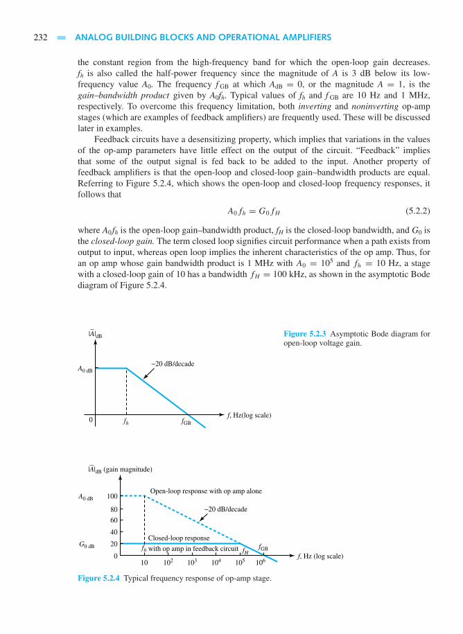
232 ANALOG BUILDING BLOCKS AND OPERATIONAL AMPLIFIERS
the constant region from the high-frequency band for which the open-loop gain decreases.fh is also called the half-power frequency since the magnitude of A is 3 dB below its low-frequency value A0. The frequency f GB at which AdB = 0, or the magnitude A = 1, is thegain–bandwidth product given by A0fh. Typical values of fh and f GB are 10 Hz and 1 MHz,respectively. To overcome this frequency limitation, both inverting and noninverting op-ampstages (which are examples of feedback amplifiers) are frequently used. These will be discussedlater in examples.
Feedback circuits have a desensitizing property, which implies that variations in the valuesof the op-amp parameters have little effect on the output of the circuit. “Feedback” impliesthat some of the output signal is fed back to be added to the input. Another property offeedback amplifiers is that the open-loop and closed-loop gain–bandwidth products are equal.Referring to Figure 5.2.4, which shows the open-loop and closed-loop frequency responses, itfollows that
A0fh = G0fH (5.2.2)
where A0 fh is the open-loop gain–bandwidth product, fH is the closed-loop bandwidth, and G0 isthe closed-loop gain. The term closed loop signifies circuit performance when a path exists fromoutput to input, whereas open loop implies the inherent characteristics of the op amp. Thus, foran op amp whose gain bandwidth product is 1 MHz with A0 = 105 and fh = 10 Hz, a stagewith a closed-loop gain of 10 has a bandwidth fH = 100 kHz, as shown in the asymptotic Bodediagram of Figure 5.2.4.
−20 dB/decade
|A|dB
A0 dB
0f, Hz(log scale)
fh fGB
Figure 5.2.3 Asymptotic Bode diagram foropen-loop voltage gain.
−20 dB/decade
Open-loop response with op amp alone
Closed-loop response
with op amp in feedback circuit
|A|dB (gain magnitude)
A0 dB
010 102 103 104 105 106
20
40
60
80
100
f, Hz (log scale)fH
fhG0 dB fGB
Figure 5.2.4 Typical frequency response of op-amp stage.

5.2 IDEAL OPERATIONAL AMPLIFIER 233
EXAMPLE 5.2.1
(a) Consider the circuit of the inverting amplifier shown in Figure E5.2.1(a), including anideal op amp. Show that the voltage gain of the overall circuit vo/vi is independent of theop-amp parameters.
(b) Without considering the op-amp gain to be infinite, investigate the effect of a finite valueof A, the open-circuit voltage amplification of the op amp, on the voltage gain of theoverall circuit.
(c) Let Ri = 2 k and Rf = 80 k in Figure E5.2.1(a). Find the voltage gain of the overallcircuit: (i) if the op-amp gain is infinite, and (ii) if the op amp gain is 100.
−
+−
−
+++
+ −
−
vo
vo
vdvi
(a)
(b)
1
2
3
in = 0
= 0
if
if
ii
Ri
vi
− +
Rf
Ri
Rf
vi
vo
vp
vn
+
−A(vp - vn)
Figure E5.2.1 (a) Inverting ampli-fier. (b) Equivalent circuit.
So l u t i on
(a) Notice that a resistor Ri is placed in the − lead, whereas the + lead is connected to thecommon terminal (ground). Also, a feedback resistor Rf is connected between the− leadand the output lead. Noting that in = 0 and ii = if , the KVL equation around the outsideloop yields
vi = Riii + Rf if + vo
Since vd = 0, it follows that ii = vi/Ri . Thus, one gets
vi =(Ri + Rf
) viRi
+ vo
Solving for the voltage gain, vo/vi = −Rf /Ri , where the negative sign implies that thisis an inverting amplifier, i.e., the output voltage is 180° out of phase with the input voltage.

234 ANALOG BUILDING BLOCKS AND OPERATIONAL AMPLIFIERS
The voltage gain is independent of the op-amp parameters. By selecting the resistorsto achieve the desired ratio, constructing a linear amplifier with a prescribed voltagegain is rather simple. It may further be noted that the output impedance is Zo =0, with zero output impedance of the ideal op amp; the input impedance is Zi =vi/ii = Ri .
(b) The equivalent circuit of the inverting amplifier is shown in Figure E5.2.1(b). The currentthrough the feedback resistor if is given by
if = vo − vi
Rf + Ri
The voltage at the inverting input vn is
vn = vi + Riif
Combining these two equations, one gets
vn = vi + Ri
(vo − vi
Rf + Ri
)
Since vp is connected directly to ground, vp = 0; the output voltage vo is
vo = −Avn = −A[vi + Ri
(vo − vi
Rf + Ri
)]
The voltage gain of the overall circuit is then given by
vo
vi= −
1−(
Ri
Ri + Rf
)1
A+(
Ri
Ri + Rf
)
If A becomes infinitely large, 1/A→ 0, and the preceding expression reduces to−Rf /Ri ,obtained in part (a). Clearly as A → ∞, the inverting terminal voltage vn = −vo/A isgoing to be very small, practically on the order of microvolts. Then it may be assumedin the inverting amplifier that vn is virtually zero, i.e., vn ∼= 0.
(c) (i) When A is infinitely large,vo
vi= −Rf
Ri
= −80
2= −40
(ii) When A has a finite value of 100,
vo
vi= −
1−(
Ri
Ri + Rf
)1
A+(
Ri
Ri + Rf
) = − 1− 2
821
100+ 2
82
= −28.4
The principle of negative feedback is clearly illustrated in the operation of the invertingamplifier in Example 5.2.1, since negative feedback is used to keep the inverting terminal voltageas close as possible to the noninverting terminal voltage. One way of viewing negative feedbackis to consider it as a self-balancing mechanism which allows the amplifier to preserve zero

5.3 PRACTICAL PROPERTIES OF OPERATIONAL AMPLIFIERS 235
potential difference between its input terminals. The effect of the feedback connection fromoutput to inverting input is then to force the voltage at the inverting input to be equal to that atthe noninverting input. This is equivalent to stating that for an op amp with negative feedback,vn ∼= vp. The analysis of the op amp is greatly simplified if one assumes that in = 0 and vn = vp.The voltage gain of the overall circuit of Figure E5.2.1(a) is called the closed-loop gain, becausethe presence of a feedback connection between the output and the input constitutes a closed loopas per the terminology used in the field of automatic control, which is presented in Section 16.2.
EXAMPLE 5.2.2
(a) Consider the circuit of the noninverting amplifier in Figure E5.2.2, including an ideal opamp. Obtain an expression for the voltage gain of the overall circuit.
(b) Let Ri = 10 k and Rf = 240 k in Figure E5.2.2. Find the voltage gain of the overallcircuit.
+
−−
−
+++
−
vo
vd = 0
vi
1
23
if
ip = 0
ii
in = 0
Rf
Ri
Figure E5.2.2 Noninverting amplifier.
So l u t i on
(a) Note that the input is directly connected to the + terminal. Resistors Ri and Rf areconnected as in the previous example. Since the input current ip= 0, the input impedanceis infinite. Because in = 0, ii = if . The KVL equation around the loop containing Ri andRf gives
vo = −(Ri + Rf )ii
Because of the virtual short circuit,vi = −Riii . Thus, for the case of a simple noninvertingamplifier, one gets
vo
vi= 1+ Rf
Ri
(b) For the given values of Ri and Rf,
vo
vi= 1+ 240
10= 25
5.3 PRACTICAL PROPERTIES OF OPERATIONAL AMPLIFIERS
To achieve voltage gain and consequently power gain, the op amp must be biased by a dc source.The biasing network is comprised of the power supply and the passive circuit elements surrounding

236 ANALOG BUILDING BLOCKS AND OPERATIONAL AMPLIFIERS
the device that provide the correct dc levels at the terminals. Terminals at which the dc bias isto be connected are provided on the op-amp package with the actual biasing networks connectedinternally. The manufacturer specifies the permissible range of supply-voltage values and thecorresponding op-amp characteristics.
Manufacturers add prefixes to type numbers such as 741 to indicate their own codings, eventhough the specifications are similar. For example,
µA 741 FairchildLM 741 National Semiconductors
An extra letter is sometimes added to indicate a temperature specification. For example,
µA 741 A Military specification for guaranteed operation between −55 and +125°CµA 741 C Commercial specification for temperature range of 0 to 70°C
Practical op amps are composed of several amplifier stages, a typical structure of which isshown in Figure 5.3.1. The three building blocks are the input differential amplifier, the commonemitter stage, and the emitter follower output stage. Some of the op-amp practical propertiesfollow.
OPEN-LOOP VOLTAGE GAIN A
The op amp amplifies the difference vd between the voltage on the noninverting (+) terminaland the inverting (−) terminal; see Figure 5.3.2. The term “open loop” implies that there is noexternal feedback connection between the output and either of the inputs. A is defined as theratio of the change in output voltage to the change in differential input voltage, usually for a loadresistance of no less than 2 k. A typical value for A is 2× 10⁵.
INPUT RESISTANCE Ri
Input resistance is the open-loop incremental resistance looking into the two input terminals,and is typically 2 M. Manufacturers sometimes quote the resistance between inputs and ground.
OUTPUT RESISTANCE Ro
The open-loop output resistance is usually between 50 and 500 , with a typical value of 75
for the 741. Thus one can see that Figure 5.3.3 is the representation of an op amp as a circuitelement or block.
vpvo
vn
Differentialamplifier
Commonemitterstage
Emitterfolloweroutput
Figure 5.3.1 Typical op-amp stages.
−+
−−
++
+
−
vo = Avd = A(vp − vn)vp
vn
Figure 5.3.2 Op-amp symbol with signal voltages.

5.3 PRACTICAL PROPERTIES OF OPERATIONAL AMPLIFIERS 237
−
−−
+
+
++
−
vo
vn
vp
Ri
+
−
A(vp − vn)
Figure 5.3.3 Op amp as a circuit componentblock.
Common-Mode Rejection Ratio (CMRR)
When there is a common-mode input voltage, i.e., when the input signals are equal and greaterthan zero, the output voltage of an ideal op amp is zero because vd is equal to zero. In general, thecommon-mode input vC is defined as
(vp + vn
)/2; and the difference signal vd = vp−vn is to be
amplified. Common-mode gain AC is defined as the ratio vo/vC when vd = 0. The common-moderejection ratio (CMRR) is defined by A/AC, but is usually expressed in units of decibel (dB),
CMRR = 20 log10A
AC
(5.3.1)
It is typically 90 dB, i.e., A/AC∼= 32,000. The ideal op amp, however, has infinite CMRR.
To explain further, an op amp can be considered a special type of differential amplifier.The object of a differential amplifier, which is formally presented a little later, is to amplify“differences” in voltage between the two inputs, and to be unresponsive to voltage changes thatappear simultaneously on both inputs. The differential-mode input signal is the difference betweenvp and vn; that is to say, vd= vp− vn. The common-mode input signal is the average value of the twoinput signals; that is to say, vc = (v1 + v2)/2. The output voltage of the amplifier vo is given by vo
= vdAd+ vcAc, where Ad (called simply A previously) is the differential-mode voltage gain and Ac
is the common-mode voltage gain. Under ideal conditions, Ac is equal to zero and the differentialamplifier completely rejects the common-mode signals. The departure from this ideal conditionis a figure of merit for a differential amplifier and is measured by CMRR, which is the ratio ofAd to Ac. CMRR can thus be seen as a measure of an amplifier’s ability to distinguish betweendifferential-mode and common-mode signals. One of the practical advantages of a differentialamplifier is its rejection of unwanted signals or noise.
INPUT OFFSET VOLTAGE VOS
When both inputs are tied to ground, i.e., both differential-mode and common-mode inputs arezero, the output should be zero. In practice there will be mismatches in amplifier components, andif there is a mismatch in an input stage, the effect will be amplified, leading to a significant outputvoltage. The input offset voltage VOS is the differential input voltage required to make the outputzero, and is typically 1 mV. With some op amps, e.g., the 741, two voltage offset terminals areprovided, and by connecting a potentiometer between them and taking the slider to the specifieddc supply rail (or bus), as in Figure 5.3.4, the potentiometer can then be adjusted to zero the offsetvoltage.

238 ANALOG BUILDING BLOCKS AND OPERATIONAL AMPLIFIERS
−
+
2
3
15
6
10kΩ
Pin 1 labeled “− offset null”Pin 5 labeled “+ offset null”
V−
Figure 5.3.4 Offset null terminals of 741 connected to10-k potentiometer and negative supply rail to zero theoffset voltage.
INPUT BIAS CURRENT IB
When operated at extremely low quiescent current values, the base bias currents will be low; butthey do have to be taken into consideration. The input bias current IB for an op amp is defined asthe average of the two input currents with the inputs grounded (see Figure 5.3.5), i.e.,
IB = IBp + IBn
2(5.3.2)
A typical value for a µA 741 is 80 nA; for a µA 771 it is 50 pA. When the resistance of the sourcefeeding the op amp is large enough, the input bias current may have an adverse effect. As shownin Figure 5.3.6, where the noninverting input is grounded and the inverting input is connectedto a source of 1-M resistance and of voltage vS momentarily at 0 V, the bias current of 80 nAgenerates a voltage of −80 mV on the noninverting input.
INPUT OFFSET CURRENT IOS
The adverse effect of the input bias current mentioned would be nullified if both inputs wereconnected to equal resistances (one of which could be a passive resistor) and if IBp = IBn. Thedifferential input would then be zero. However, if the input bias currents are unequal, as shown inFigure 5.3.7, there will be a finite differential input voltage. It then becomes necessary to specifythe difference between the bias currents, and this is the input offset current IOS,
IOS = IBp − IBn (5.3.3)
A typical value for IOS is 20 nA. Both IB and IOS are usually measured with the output at 0 V; butin practice the output voltage has little effect.
−
+IBn
IBp
Figure 5.3.5 Bias currents of op amp.
−+vS = 0
RS = 1 MΩ
VB = −80 mV
80 nA Figure 5.3.6 Illustration of input voltage generated by biascurrent.

5.3 PRACTICAL PROPERTIES OF OPERATIONAL AMPLIFIERS 239
−
+
RS IBn
RSIBp
Figure 5.3.7 Illustration of unequal bias currents, which will causea differential input voltage even with equal source resistances.
Power-Supply Rejection Ratio (PSRR)
An op amp’s ability to disregard changes in power-supply voltage is measured by the power-supply rejection ratio (PSRR), which is specified by the change in offset voltage VOS for a 1-Vchange in dc power supply and is usually expressed in µV/V. A typical value is 15 µV/V.
Maximum Differential Input Voltage
This is the maximum value of differential input voltage vp − vn that can be applied withoutdamaging the op amp.
Maximum Common-Mode Input Voltage
This is the maximum voltage that the two inputs can be raised above ground potential before theop amp becomes nonlinear.
Output Voltage Swing
Ideally this is equal to the difference between the two supply rail voltages, although in practice itis a few volts less.
Internal Frequency Compensation
Some op amps, such as the 741, have internal RC networks which are intentionally designed toreduce gain at high frequency. The result (shown in Figure 5.2.4) is that the open-loop gain beginsto fall at a few hertz and then has a characteristic falling at 20 dB/decade or 6 dB/octave (i.e.,gain ∝ 1/f ) until eventually the gain becomes unity (0 dB) at about 1 MHz.
External Frequency Compensation
For applications requiring a more extended high-frequency response, there are op amps with nointernal compensation, and external frequency-compensation terminals are provided on these opamps (for example, the 709) so that the frequency response can be tailored to avoid instabilitywithout the heavy degrading of frequency response due to internal compensation. A typicalfrequency-compensation circuit for the µA 709 is illustrated in Figure 5.3.8. Op-amp manufac-turers supply plots of open- and closed-loop responses for various values of components connectedto the frequency-compensation terminals.
Slew Rate
Slew (or slewing) rate is a measure of how fast the output voltage can change. It is given by themaximum value of dvo/dt , which is normally measured in response to a large input voltage step

240 ANALOG BUILDING BLOCKS AND OPERATIONAL AMPLIFIERS
−
+
2
3
18
µA 7095
6
C1
C2
R2 (use 50 Ω when amplifier isoperated with capacitive loading)
R1
Range of C1 10–5000 pFRange of R1 0–1.5 kΩRange of C2 3–200 pF
Figure 5.3.8 Typical frequency-compensationcircuit for Fairchild µA 709.
and is therefore usually associated with low closed-loop voltage gain. For a 741 the slew rate is0.5 V/µs at A = 1. For more recently developed op amps, the slew rate ranges from 5 to 100V/µs. The effect of the slew rate in response to an input step voltage is shown in Figure 5.3.9.If one attempts to make the output voltage change faster than the slew rate, nonlinearity will beintroduced. When specifying such output voltage requirements as rise time, output voltage, andfrequency, it is necessary to choose an op amp with a slew rate that meets the specifications. Witha sine-wave input, the slew rate limits a combination of maximum operating frequency and outputvoltage magnitude.
The slew rate occurs because at some stage in the amplifier a frequency-compensatingcapacitor will have to be charged, and the available limited charging current restricts the maximumrate of change of the capacitor voltage. With externally compensated op amps, such as the 709,slew rates will depend on the value of the compensating capacitors, which are in turn chosenon the basis of the closed-loop gain needed. The lower the gain, the higher the compensatingcapacitors, and hence the lower the slew rate. For a µA 709, the slew rate is 0.3 V/µs at A = 1and 1.5 V/µs at A = 10.
Noise
This refers to the small, rapidly varying, random spurious signals generated by all electroniccircuits. Noise places a limit on the smallness of signals that can be used. The subject of randomsignals and noise belongs to a branch of electrical engineering known as communication theory.
Stability
The amplifier is said to be stable when it performs its function reliably under all normal operatingconditions. By definition, a system is stable if its response to an excitation that decays to
0.5 µs0
0
vd
1 V
v0
1 V
Figure 5.3.9 Effect of op-amp slew rate with step voltage input.
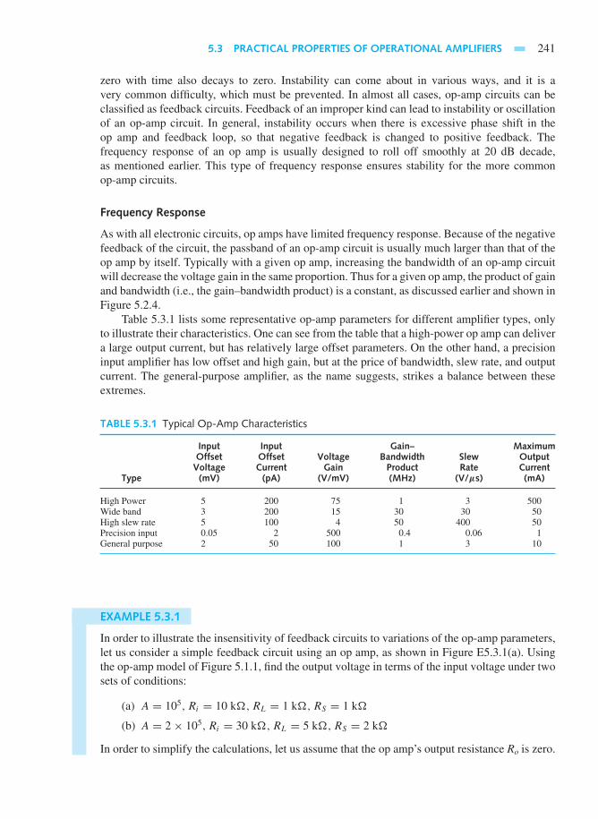
5.3 PRACTICAL PROPERTIES OF OPERATIONAL AMPLIFIERS 241
zero with time also decays to zero. Instability can come about in various ways, and it is avery common difficulty, which must be prevented. In almost all cases, op-amp circuits can beclassified as feedback circuits. Feedback of an improper kind can lead to instability or oscillationof an op-amp circuit. In general, instability occurs when there is excessive phase shift in theop amp and feedback loop, so that negative feedback is changed to positive feedback. Thefrequency response of an op amp is usually designed to roll off smoothly at 20 dB decade,as mentioned earlier. This type of frequency response ensures stability for the more commonop-amp circuits.
Frequency Response
As with all electronic circuits, op amps have limited frequency response. Because of the negativefeedback of the circuit, the passband of an op-amp circuit is usually much larger than that of theop amp by itself. Typically with a given op amp, increasing the bandwidth of an op-amp circuitwill decrease the voltage gain in the same proportion. Thus for a given op amp, the product of gainand bandwidth (i.e., the gain–bandwidth product) is a constant, as discussed earlier and shown inFigure 5.2.4.
Table 5.3.1 lists some representative op-amp parameters for different amplifier types, onlyto illustrate their characteristics. One can see from the table that a high-power op amp can delivera large output current, but has relatively large offset parameters. On the other hand, a precisioninput amplifier has low offset and high gain, but at the price of bandwidth, slew rate, and outputcurrent. The general-purpose amplifier, as the name suggests, strikes a balance between theseextremes.
TABLE 5.3.1 Typical Op-Amp Characteristics
Input Input Gain– MaximumOffset Offset Voltage Bandwidth Slew OutputVoltage Current Gain Product Rate Current
Type (mV) (pA) (V/mV) (MHz) (V/µs) (mA)
High Power 5 200 75 1 3 500Wide band 3 200 15 30 30 50High slew rate 5 100 4 50 400 50Precision input 0.05 2 500 0.4 0.06 1General purpose 2 50 100 1 3 10
EXAMPLE 5.3.1
In order to illustrate the insensitivity of feedback circuits to variations of the op-amp parameters,let us consider a simple feedback circuit using an op amp, as shown in Figure E5.3.1(a). Usingthe op-amp model of Figure 5.1.1, find the output voltage in terms of the input voltage under twosets of conditions:
(a) A = 105, Ri = 10 k,RL = 1 k,RS = 1 k
(b) A = 2× 10⁵, Ri = 30 k,RL = 5 k,RS = 2 k
In order to simplify the calculations, let us assume that the op amp’s output resistance Ro is zero.

242 ANALOG BUILDING BLOCKS AND OPERATIONAL AMPLIFIERS
−
−
+RS
RL
Ri
(a)
(b)
vS
vo
RL
+RS
vS
vo
+
−A(v+ − v−)
Figure E5.3.1
So l u t i on
Replacing the op amp by its model, we have the circuit shown in Figure E5.3.1(b). The nodalequation at the node labeled + is
vS − v+RS
+ vo − v+Ri
= 0
Also,
vo = A (v+ − v−) and v− = vo
Thus,
vo = A (v+ − vo)
Solving, one gets
vo = vSA
A+ 1
Ri
Ri + [RS/ (1+ A)]
Evaluating vo/vS for the given two conditions, we have
(a) vo/vS = 0.999989
(b) vo/vS = 0.999994
Thus, we see that the output voltage (using negative feedback) is very nearly independent of Ri,Ro, and A, provided the op amp’s parameters remain in their allowable ranges.
EXAMPLE 5.3.2
Find the maximum frequency of an output sine wave which can be produced at an amplitude of1.5 V if the op-amp slew rate is 0.5 V/µs.

5.3 PRACTICAL PROPERTIES OF OPERATIONAL AMPLIFIERS 243
So l u t i on
vo = Vm sin ωt
dvo
dt= ωVm cos ωt
slew rate = maximum value ofdvo
dt= ωVm = 0.5
10−6
Hence,
ω = 0.5
1.5× 10⁻⁶or f = 53 kHz
EXAMPLE 5.3.3Consider the op-amp circuit shown in Figure E5.3.3 and obtain expressions for the open-loopvoltage gain at (a) low and (b) high frequencies. Also determine relations for the 3-dB pointfrequency and the phase shift.
So l u t i on
Using phasors and the voltage-divider rule,
Vo =(
XC
XC + Ro
)AVd, where XC = 1
jωC
(a) At low frequencies, XC becomes very large so that XC >> Ro. Then,
Vo = AVd
The output signal is in phase with the input signal, since complex voltage gain A is thesame as A.
(b) At higher frequencies, XC becomes comparable to Ro. Let AF be the complex open-loopvoltage gain at frequency f. Then,
AF = 1/jωC
[Ro + (1/jωC)] Ao
−
+
vo
Ro
v− − v+ = vd
AvdC
+
Figure E5.3.3

244 ANALOG BUILDING BLOCKS AND OPERATIONAL AMPLIFIERS
or
AF = Ao
1− jωRoC
= Ao(1− jωRoC)
1+ (ωRoC)2∣∣AF
∣∣ = AF = Ao√1+ (ωRoC)2
At the 3-dB point, or half-power frequency fh,AF = Ao/√
2, so that
ωhRoC = 1 or fh = 1
2πRoC
Denoting AF = AFejφ , where φ indicates that the output leads the input,
tan φ = −ωRoC
At very high frequencies, tan φ → −∞ and φ → 3π/2, so that the output leads the input by3π/2 or lags it by π/2. This is the largest phase shift possible.
5.4 APPLICATIONS OF OPERATIONAL AMPLIFIERS
An op amp along with a few external components (resistors and capacitors) is capable ofperforming many different operations—hence the name operational. The linear operations ofintegration, differentiation, addition, and subtraction that were needed in analog computers aresome of the early applications. Other linear applications include instrumentation amplifiers,voltage-to-current and current-to-voltage converters, voltage followers, and active filters. Opamps are also utilized in nonlinear applications such as limiters, comparators, voltage regulators,signal rectifiers and detectors, logarithmic amplifiers, multipliers, and many digital circuits.
Negative feedback (which is said to be degenerative) is used to improve amplifier performanceby sacrificing gain. The opposite situation of positive feedback (which is said to be regenerative)is also utilized, and gain is increased to the extent that an amplifier will produce an output signalwith no input. This leads to sinusoidal oscillators and nonsinusoidal waveform generators.
This section concentrates on a limited range of op-amp applications.
Inverting Amplifier
One common op-amp circuit is shown in Figure 5.4.1. For the case of finite voltage gain Ao of anop amp that is otherwise ideal, the output voltage becomes
−
+vo
vi
i2
i1
v1
v2 = 0
1 (inverting terminal)
2 (noninverting terminal)
3
R1
R2
+
−
Figure 5.4.1 Inverting amplifier.

5.4 APPLICATIONS OF OPERATIONAL AMPLIFIERS 245
vo = Ao (v2 − v1) (5.4.1)
Since v2 = 0, because terminal 2 is grounded,
v1 = − vo
Ao
(5.4.2)
Thus one gets
i1 = vi − v1
R1= vi + (vo/Ao)
R1(5.4.3)
i2 = v1 − vo
R2= − (vo/Ao)− vo
R2(5.4.4)
Since no current is drawn by terminal 1 of the ideal op amp,
i2 = i1 (5.4.5)
Hence,vo
vi= −R2
R1
1
1+ [(R1 + R2) /AoR1](5.4.6)
which is the expression for the circuit gain. Now, if Ao →∞, we havevo
vi= −R2
R1, if Ao →∞ (5.4.7)
which is independent of the op amp’s gain Ao (see Example 5.2.1). The sign inversion associatedwith Equation (5.4.7) makes the amplifier “inverting.” Generally if Ao is at least 200 times themagnitude of R2/R1, then the actual gain given by Equation (5.4.6) will be within 1% of the idealgain given by Equation (5.4.7). Assuming infinite gain of the op amp, it follows that
vd = v2 − v1 = 0 or v1 = v2 (5.4.8)
Since terminal 2 is at ground potential (zero) in Figure 5.4.1, terminal 1 is said to be a virtualground. Notice that when R2=R1, the inverting amplifier becomes a voltage follower with invertedsign and a gain magnitude of unity.
Noninverting Amplifier
It is called “noninverting” because there is no sign inversion. A typical circuit is shown in Figure5.4.2. With a finite op-amp gain Ao,
v2 − v1 = vo
Ao
or v1 = v2 − vo
Ao
(5.4.9)
−
+vo
vi
i2
i1
v1
v2 = vi
3
2
1R1
R2
+
−
Figure 5.4.2 Noninverting amplifier.

246 ANALOG BUILDING BLOCKS AND OPERATIONAL AMPLIFIERS
i1 = −v1
R1= −v2
R1+ vo
AoR1(5.4.10)
i2 = v1 − vo
R2= v2
R2− vo
R2
(1
Ao
+ 1
)(5.4.11)
Since the ideal op amp draws no current,
i1 = i2 (5.4.12)
Also, as seen from Figure 5.4.2,
v2 = vi
In equating Equations (5.4.10) and (5.4.11), one gets
vo
vi= vo
v2=(
1+ R2
R1
)1
1+ [(R1 + R2) /AoR1](5.4.13)
For Ao →∞, the ideal circuit gain isvo
vi= 1+ R2
R1(5.4.14)
(See Example 5.2.2.) Note that if R2 = 0, for any nonzero value of R1,
vo
vi= 1 (5.4.15)
which is the gain of an ideal voltage follower. The same result applies if R1 → ∞ (i.e., opencircuit) for any finite R2.
Inverting Summing Amplifier
The circuit of Figure 5.4.1 is extended by adding other input points, as shown in Figure 5.4.3.Because of the virtual ground at terminal 1 (ideal op-amp assumption), the response of the circuitto any one input is not affected by the presence of the other N − 1 inputs. Based on Equation(5.4.7) one can write the total output as the sum of all responses,
vo = −(Rf
R1vi1 + Rf
R2vi2 + · · · + Rf
RN
viN
)= −Rf
N∑n=1
vin
Rn
(5.4.16)
viN
−
+vo
vi1
vi2
3
2
1
RNRf
R2
R1 Figure 5.4.3 Inverting summing amplifier.
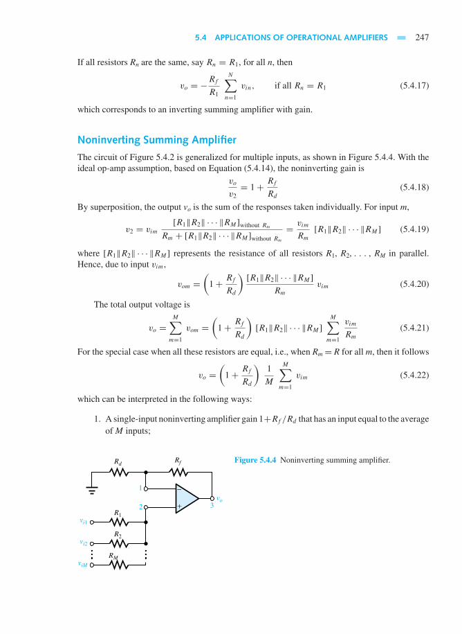
5.4 APPLICATIONS OF OPERATIONAL AMPLIFIERS 247
If all resistors Rn are the same, say Rn = R1, for all n, then
vo = −Rf
R1
N∑n=1
vin, if all Rn = R1 (5.4.17)
which corresponds to an inverting summing amplifier with gain.
Noninverting Summing Amplifier
The circuit of Figure 5.4.2 is generalized for multiple inputs, as shown in Figure 5.4.4. With theideal op-amp assumption, based on Equation (5.4.14), the noninverting gain is
vo
v2= 1+ Rf
Rd
(5.4.18)
By superposition, the output vo is the sum of the responses taken individually. For input m,
v2 = vim[R1‖R2‖ · · · ‖RM ]without Rm
Rm + [R1‖R2‖ · · · ‖RM ]without Rm
= vim
Rm
[R1‖R2‖ · · · ‖RM ] (5.4.19)
where [R1‖R2‖ · · · ‖RM ] represents the resistance of all resistors R1, R2, . . . , RM in parallel.Hence, due to input vim,
vom =(
1+ Rf
Rd
)[R1‖R2‖ · · · ‖RM ]
Rm
vim (5.4.20)
The total output voltage is
vo =M∑
m=1
vom =(
1+ Rf
Rd
)[R1‖R2‖ · · · ‖RM ]
M∑m=1
vim
Rm
(5.4.21)
For the special case when all these resistors are equal, i.e., when Rm= R for all m, then it follows
vo =(
1+ Rf
Rd
)1
M
M∑m=1
vim (5.4.22)
which can be interpreted in the following ways:
1. A single-input noninverting amplifier gain 1+Rf /Rd that has an input equal to the averageof M inputs;
−
+vo
vi1
vi2
viM
32
1
Rd
RM
Rf
R2
R1
Figure 5.4.4 Noninverting summing amplifier.

248 ANALOG BUILDING BLOCKS AND OPERATIONAL AMPLIFIERS
2. An M-input noninverting summing amplifier for which the gain seen by each input is(1+ Rf /Rd
)/M .
Current-to-Voltage Amplifier
The basic circuit is shown in Figure 5.4.5, which is similar to that of an inverting amplifier (Figure5.4.1). The − input is connected directly to a current source supplying current iS. Node X is avirtual ground, so that
iS = − vo
Rf
(5.4.23)
Hence
vo = −Rf iS (5.4.24)
which shows that the degree of amplification depends on the value of Rf.
Current-to-Current Amplifier
The circuit given in Figure 5.4.6 is to amplify a current fed to the input of the op amp. ApplyingKCL at Y,
i1 + iS = io (5.4.25)
Since i1 = −vY /R1, Equation (5.4.25) becomes
iS − vY
R1= io (5.4.26)
Because X is a virtual ground, vY = −iSRf . Hence Equation (5.4.26) becomes
iS
(1+ Rf
R1
)= io (5.4.27)
The current gain is then given by
−
+voiS X
Rf Figure 5.4.5 Current-to-voltage amplifier.
−
+iS X
YRf iS
io
i1
R1
(Feedback resistor) RL(Load resistor)
Figure 5.4.6 Current-to-current amplifier.
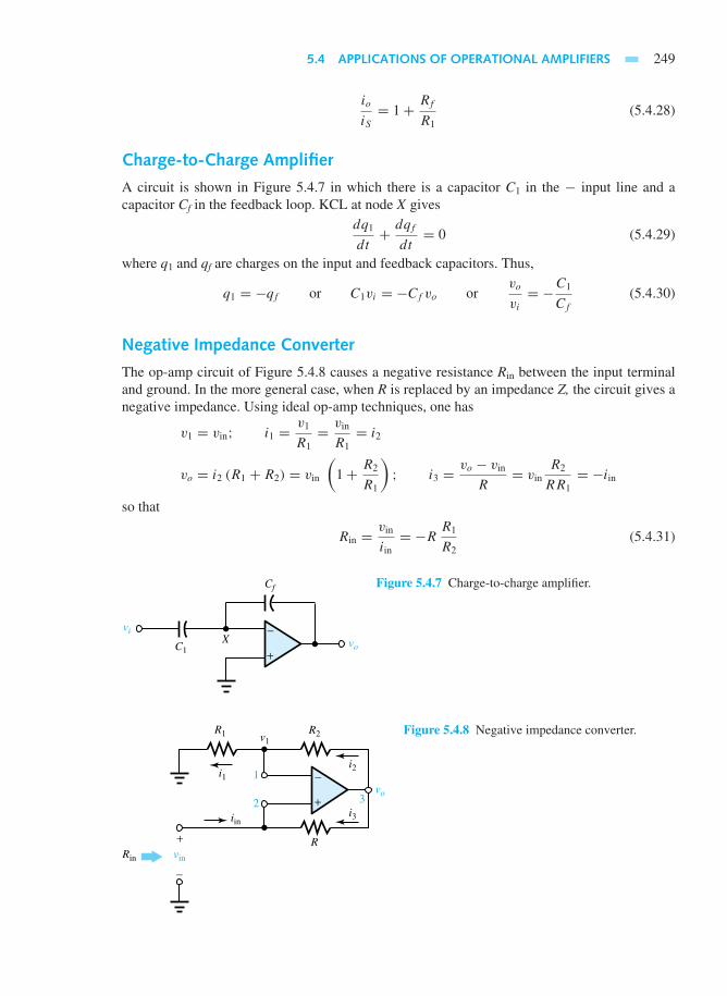
5.4 APPLICATIONS OF OPERATIONAL AMPLIFIERS 249
io
iS= 1+ Rf
R1(5.4.28)
Charge-to-Charge Amplifier
A circuit is shown in Figure 5.4.7 in which there is a capacitor C1 in the − input line and acapacitor Cf in the feedback loop. KCL at node X gives
dq1
dt+ dqf
dt= 0 (5.4.29)
where q1 and qf are charges on the input and feedback capacitors. Thus,
q1 = −qf or C1vi = −Cf vo orvo
vi= −C1
Cf
(5.4.30)
Negative Impedance Converter
The op-amp circuit of Figure 5.4.8 causes a negative resistance Rin between the input terminaland ground. In the more general case, when R is replaced by an impedance Z, the circuit gives anegative impedance. Using ideal op-amp techniques, one has
v1 = vin; i1 = v1
R1= vin
R1= i2
vo = i2 (R1 + R2) = vin
(1+ R2
R1
); i3 = vo − vin
R= vin
R2
RR1= −iin
so that
Rin = vin
iin= −R R1
R2(5.4.31)
−
+vo
X
Cf
C1
vi
Figure 5.4.7 Charge-to-charge amplifier.
−
+vo
i2
i3iin
i1
v1
vinRin
32
1
R1 R2
R+
−
Figure 5.4.8 Negative impedance converter.

250 ANALOG BUILDING BLOCKS AND OPERATIONAL AMPLIFIERS
which is a negative resistance. The negative impedance converter is useful in transforming avoltage source into a current source by means of a voltage-to-current converter (see Problem5.4.9). It has also been used in a class of active filters.
Differential Amplifier
Figure 5.4.9 shows a weighted differencing amplifier, where “weighted” refers to the fact thatthe output voltage has the form vo = wava + wbvb, in which the weighting coefficients wa andwb are the voltage gains seen by the inputs. Since the network is linear, superposition can beapplied for analysis. First, by grounding the input terminal of R3, let us make va = 0. Exceptfor the presence of R3 in parallel with R4, between terminal 2 and ground, the circuit is that ofan inverting amplifier of gain −R2/R1 to the input vb. Since no current flows at terminal 2, itfollows that
wb = −R2
R1(5.4.32)
Next, by grounding the left terminal of R1, let us make vb = 0. With respect to the voltage onterminal 2, note that the circuit is that of a noninverting amplifier with gain 1 + R2/R1. Thevoltage divider, consisting of R3 and R4, corresponds to a gain of R4/(R3+R4) from the input toterminal 2. Thus the overall gain becomes
wa =(
1+ R2
R1
)R4
R3 + R4(5.4.33)
Finally, the overall response is obtained by superposition,
vo = wava + wbvb =(
1+ R2
R1
)R4
R3 + R4va − R2
R1vb
or
vo = R2
R1
[1+ (R1/R2)
1+ (R3/R4)va − vb
](5.4.34)
When R1/R2 = R3/R4,
vo = R2
R1(va − vb) (5.4.35)
−
+ vo
vbb
32
1
R1 R2
R4R3
va
a
Figure 5.4.9 Weighted differencing amplifier.

5.4 APPLICATIONS OF OPERATIONAL AMPLIFIERS 251
which corresponds to the response of a differential amplifier. Usually resistor values are so chosenthatR3 = R1 andR4 = R2 for some practical reasons. Improved versions of differential amplifiersare available commercially.
Integrators
Figure 5.4.10 shows a noninverting integrator, which can be seen to be a negative impedanceconverter added with a resistor and a capacitor. Noting that vo = 2v1 and i3 = v1/R, the totalcapacitor current is
i = iin + i3 = vin − v1
R+ v1
R= vin
R(5.4.36)
The capacitor voltage is given by
v1 (t) = 1
C
∫ t
−∞i (ξ) dξ = 1
RC
∫ t
−∞vin (ξ) dξ (5.4.37)
Thus,
vo (t) = 2
RC
∫ t
−∞vin (ξ) dξ (5.4.38)
which shows that the circuit functions as an integrator.Replacing R2 in the inverting amplifier of Figure 5.4.1 by a capacitance C results in the
somewhat simpler integrator circuit shown in Figure 5.4.11, known as an inverting integrator, orMiller integrator. With ideal op-amp techniques, iC = iin = vin/R. The voltage across C is justvo, so that
−
+vo
R1 v1
v1
i3iin
i
C
R1
R
Negative impedance converter
Rvin
Figure 5.4.10 Noninverting integrator.
−
+vo
1
2 3
C
iCiin
Rvin
Figure 5.4.11 Inverting integrator (Miller integrator).

252 ANALOG BUILDING BLOCKS AND OPERATIONAL AMPLIFIERS
vo (t) = − 1
C
∫ t
−∞iC (ξ) dξ = − 1
RC
∫ t
−∞vin (ξ) dξ (5.4.39)
which illustrates that the network behaves as an integrator with sign inversion.
Differentiator
Shown in Figure 5.4.12 is a differentiator which is obtained by replacing R1 in the invertingamplifier of Figure 5.4.1 by a capacitor C. Assuming ideal op-amp characteristics, one has i = iCand vo = −Ri = −RiC . But since iC (t) = C dvin (t) /dt , we get
vo (t) = −RC dvin (t)
dt(5.4.40)
which corresponds to a differentiator with a gain of −RC. In practice, however, differen-tiators are normally avoided because of high-frequency noise (which is accentuated due toa transfer function that increases with frequency) and stability problems (which make themoscillate).
Inductorless (Active) Filters
Filters (used to pass or eliminate certain frequency components of a signal) that are suitablefor IC fabrication, but which do not contain inductors, are known as active filters. They havethe op amp as a common component. Figure 5.4.13 shows the basic op-amp circuit withfrequency-dependent impedances. The voltage gain or voltage transfer function of this circuitis given by
vo
vi= −Zf
Zi
(5.4.41)
with Zi = Ri and Zf = Rf ‖(1/jωCf ) (i.e., Rf and Cf in parallel). We have a low-passfilter with
vo
vi= −Rf
Ri
1
1+ jωRfCf
= −Rf
Ri
1
1+ (jf/fl)(5.4.42)
−
+vo
1
2 3
C
iiC
Rvin
Figure 5.4.12 Differentiator.
−
++vo
+
−
vi
Zf
Zi
−
Figure 5.4.13 Basic op-amp active filter.
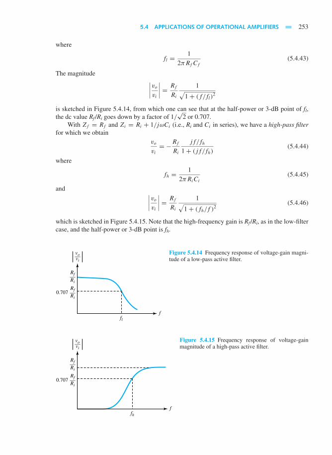
5.4 APPLICATIONS OF OPERATIONAL AMPLIFIERS 253
where
fl = 1
2πRfCf
(5.4.43)
The magnitude ∣∣∣∣vovi∣∣∣∣ = Rf
Ri
1√1+ (f/fl)
2
is sketched in Figure 5.4.14, from which one can see that at the half-power or 3-dB point of fl,the dc value Rf /Ri goes down by a factor of 1/
√2 or 0.707.
With Zf = Rf and Zi = Ri + 1/jωCi (i.e., Ri and Ci in series), we have a high-pass filterfor which we obtain
vo
vi= −Rf
Ri
jf/fh
1+ (jf/fh)(5.4.44)
where
fh = 1
2πRiCi
(5.4.45)
and ∣∣∣∣vovi∣∣∣∣ = Rf
Ri
1√1+ (fh/f )
2(5.4.46)
which is sketched in Figure 5.4.15. Note that the high-frequency gain is Rf /Ri, as in the low-filtercase, and the half-power or 3-dB point is fh.
vovi
Rf
Ri
Rf0.707Ri
ffl
Figure 5.4.14 Frequency response of voltage-gain magni-tude of a low-pass active filter.
vovi
Rf
Ri
Rf0.707Ri
ffh
Figure 5.4.15 Frequency response of voltage-gainmagnitude of a high-pass active filter.

254 ANALOG BUILDING BLOCKS AND OPERATIONAL AMPLIFIERS
vo
f0
High pass
Resultantbandpass
characteristic
Low pass
vi
f
Figure 5.4.16 Bandpass filter seen as a combina-tion of low-pass and high-pass filter characteris-tics.
By using a low-pass and a high-pass filter and overlapping their transfer functions, as shownin Figure 5.4.16, one can construct a bandpass filter with
Zf = Rf
∥∥∥∥ 1
jωCf
= Rf
1+ jωRfCf
(i.e., Rf and Cf in parallel)
and
Zi = Ri + 1
jωCi
(i.e., Ri and Ci in series)
in which case
vo
vi= −Zf
Zi
= −Rf
Ri
1(1+ jωRfCf
)[1+ 1/ (jωRiCi)]
(5.4.47)
Denoting
fl = 1
2πRiCi
(5.4.48a)
and
fh = 1
2πRfCf
(5.4.48b)
Equation (5.4.47) can be rewritten as
vo
vi= −Rf
Ri
1
(1+ fl/fh)+ j (f/fh − fl/f )
= −Rf
Ri
fh/(fh + fl)
1+ j (f 2 − flfh)/[f (fl + fh)](5.4.49)
whose magnitude is sketched in Figure 5.4.17. Notice that the magnitude response is a maximumwith a value ofRf /Ri at f0 = √flfh, and if fl << fh, then the magnitude becomes (0.707Rf /Ri
at fl and fh. The bandwidth (BW) may then be defined as

5.4 APPLICATIONS OF OPERATIONAL AMPLIFIERS 255
Rf0.707Ri
Rf
Ri
vo
f0
BW
fl fh
vi
f
Figure 5.4.17 Frequency response of voltage-gain magnitude of a bandpass active filter.
BW = fh − fl, for fl << fh
Analog Computers
Although not used as much as the digital computer (which nowadays forms the basic tool fornumerical analysis and the solution of algebraic as well as differential equations), the analogcomputer still retains some significant advantages over the digital computer. A physical systemcan be represented by a set of differential equations which can be modeled on an analog computerthat uses continuously varying voltages to represent system variables. The differential equationis solved by the computer, whereas the modeled quantities are readily varied by adjusting passivecomponents on the computer. The mathematical functions (integration, addition, scaling, andinversion) are provided by op amps.
The analog computer components are shown in Figure 5.4.18. Let the ordinary differentialequation to be solved be
d2y (t)
dt2+ a1
dy (t)
dt+ a2y (t) = f (t) (5.4.50)
which can be rearranged by isolating the highest derivative term as
y = −a1y − a2y + f (5.4.51)
subject to the initial conditions
y (0) = y0 (5.4.52a)
and
dy
dt
∣∣∣∣t=0
= y1 (5.4.52b)
The simulation of the solution is accomplished by the connection diagram of Figure 5.4.19. Timescaling is done by redefining t as t = ατ , in which case the differential equation [Equation(5.4.50)] becomes
d2y (τ)
dτ 2= −αa1
dy (τ)
dτ− α2a2y (τ)+ α2f (τ) (5.4.53)

256 ANALOG BUILDING BLOCKS AND OPERATIONAL AMPLIFIERS
−+
+vo
x y+
−
vi
+
−
vi R
Ri
−
+kvi
−
Rf
RfA =
A
y = −Ax(a)
(b)
Ri
−
−+
++vo
x y+
−
vi
Ri
−
VC (0)
y(0)Cf
1y(t) = − ∫
t
0 x (τ) dτ + y(0)
(d)
RiCf
−+
+vo
x2 a2 y
xn an
... ...
... x1 a1
v1
R1
−
v2
R2
vn
Rn
Rf
1
y = −a1x1 − a2x2 − ... −anxn
(c)
k
1
Figure 5.4.18 Analog computer components. (a) Basic op amp to provide integer multiplication. (b) Po-tentiometer for providing noninteger gains of less than 1. (c) Summer. [Note: y = x1 + x2 + · · · + xn, bychoosing Rf /R1 = Rf /R2 = · · · = Rf /Rn = 1.] (d) Integrator. [Note: Cf is charged to an initial valueVC(0) to provide the initial condition on y; with RiCf = 1, y = − ∫ t
0 x (τ) dτ + y (0).]
The coefficients may simply be scaled by the appropriate factors to change the solution time ofthe analog computer. For example, if α = 20, then t = 20 s corresponds to τ = 1 s, and thus thesolution time may be reduced.
5.5 LEARNING OBJECTIVES
The learning objectives of this chapter are summarized here, so that the student can check whetherhe or she has accomplished each of the following.

5.6 PRACTICAL APPLICATION: A CASE STUDY 257
y = −∫t
0 ydτ + y(0)
y−y.
y.
.
. .. . .y = −a1 y − a2 y + f.. .
..y
−f
y0y = −∫
t
0 ydτ − y(0)f (t)
a1
a1ya2y
a2
1
IntegratorIntegrator
Multiplicative constants
Summer
−y1
1
1
1−1
Figure 5.4.19 Connection diagram for analog computer simulation for solving the second-order differentialequation y = −a1y − a2y + f subject to initial conditions y (0) = y0 and y (0) = y1.
• Amplifier block as a two-port device and its circuit model.
• Ideal operational amplifier and its characteristics.
• Analysis and design of simple amplifier circuits including feedback.
• Properties of practical op-amps.
• Op-amp applications, including active filters.
• Understanding the operation of analog computers.
5.6 PRACTICAL APPLICATION: A CASE STUDY
Automotive Power-Assisted Steering System
In terms of negative feedback, there exists an analogy between the operational amplifier andthe power-steering mechanism of an automobile. The hydraulic pump is analogous to the powersupply in an op-amp circuit. The position of the booster-cylinder piston that is linked to the steeringis analogous to the op-amp output signal; the mechanical linkage between the control valve andthe booster-cylinder piston is analogous to the feedback circuit; the control-valve response to thedifference between the input from the steering wheel and the position of the steering linkage isanalogous to the op-amp response to its differential input signal. Thus the automotive power-assisted steering system is but an example of negative feedback in a mechanical sense.
Figure 5.6.1 illustrates in a simplified manner how a hydraulic pump driven by the enginecontinuously supplies pressure to a control valve which in turn supplies the fluid to the two sidesof the booster cylinder. A negative feedback path is established from the booster cylinder throughthe mechanical linkage back to the control valve.
For straight steering, the pressure applied is equal on both sides of the cylinder and, as such,no turning force results. When the steering wheel is moved by the driver to turn the wheels in thedesired direction, more pressure is applied to one side of the cylinder or the other.
A mechanical feedback arm from the steering linkage causes the valve to return to its neutralposition as the wheels turn, thereby allowing the driver to make a gradual turn. As and when thesteering wheel is turned, the wheels move a proportional amount rather than moving all the wayto the extreme position.
Feedback control systems are discussed in Section 16.2 in more detail.
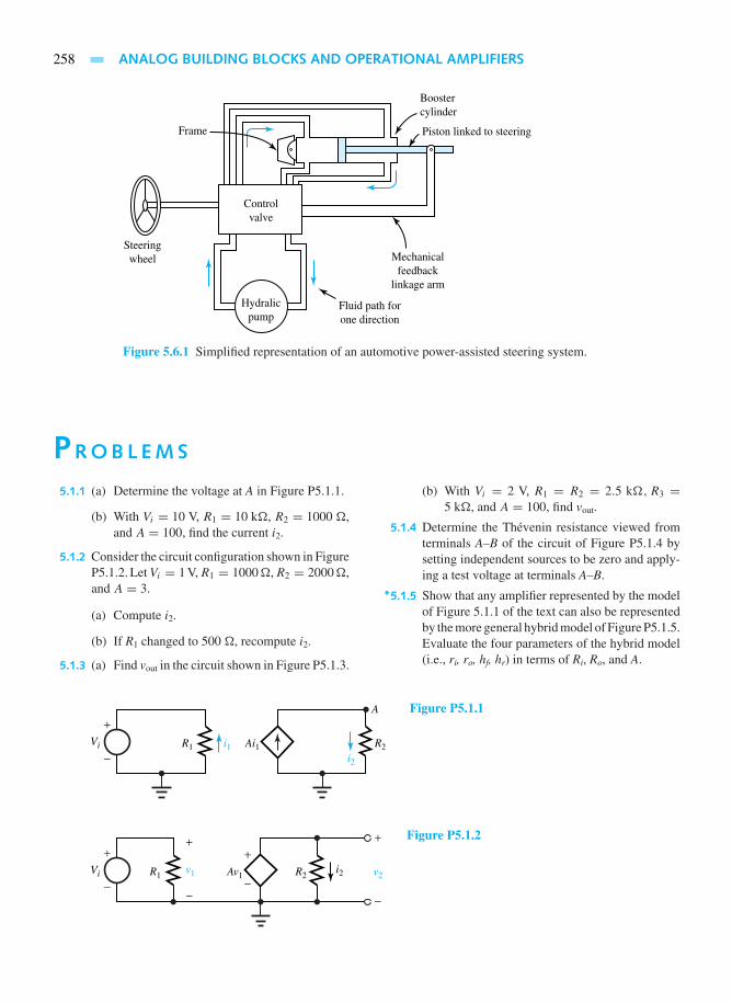
258 ANALOG BUILDING BLOCKS AND OPERATIONAL AMPLIFIERS
Boostercylinder
Piston linked to steering
Mechanicalfeedback
linkage arm
Fluid path forone direction
Hydralicpump
Controlvalve
Steeringwheel
Frame
Figure 5.6.1 Simplified representation of an automotive power-assisted steering system.
PROBL EMS
5.1.1 (a) Determine the voltage at A in Figure P5.1.1.
(b) With Vi = 10 V, R1 = 10 k, R2 = 1000 ,and A = 100, find the current i2.
5.1.2 Consider the circuit configuration shown in FigureP5.1.2. LetVi = 1 V,R1 = 1000,R2 = 2000,and A = 3.
(a) Compute i2.
(b) If R1 changed to 500 , recompute i2.
5.1.3 (a) Find vout in the circuit shown in Figure P5.1.3.
(b) With Vi = 2 V, R1 = R2 = 2.5 k,R3 =5 k, and A = 100, find vout.
5.1.4 Determine the Thévenin resistance viewed fromterminals A–B of the circuit of Figure P5.1.4 bysetting independent sources to be zero and apply-ing a test voltage at terminals A–B.
*5.1.5 Show that any amplifier represented by the modelof Figure 5.1.1 of the text can also be representedby the more general hybrid model of Figure P5.1.5.Evaluate the four parameters of the hybrid model(i.e., ri, ro, hf, hr) in terms of Ri, Ro, and A.
R1 R2
A
Ai1i1i2
+
−Vi
Figure P5.1.1
R1 R2Av1v1 v2
i2
+
−
+
−
Vi
+
−
+
−
Figure P5.1.2

PROBLEMS 259
5.1.6 Consider Example 5.1.2. Let A = 1 and Ri = Ro.Show that no matter what values of RTh andRL areused, the power gain as defined in that example isless than unity, and find the maximum value it canhave.
5.1.7 (a) Figure P5.1.7 shows a circuit containing anamplifier block. Find the open-circuit voltageamplification of the circuit.
(b) Let the output terminals be connected to a loadresistance RL. Find the input resistance R′i .
5.1.8 (a) Consider the amplifier block in the circuitconfiguration of Figure P5.1.8. Find an ex-pression for v2/v1 in terms of Ri, Ro, and A ofthe amplifier.
(b) Determine the output resistance of the circuit.
*5.1.9 (a) Two amplifiers, which can be represented bythe model of Figure 5.1.1 of the text, are con-nected in cascade (that is, head to tail), asshown in Figure P5.1.9. Let their parametersbe Ri1, Ro1, A1, and Ri2, Ro2, A2, respectively.Find vx /v1.
(b) Discuss how the answer is influenced by theratio Ri2/Ro1, particularly when this ratio ap-proaches zero or infinity.
5.1.10 Reconsider Problem 5.1.9. If we define a powergain GP as the ratio of the power dissipated in RL
to the power produced by the source v1, find an
R2
A
R1
R3Ai1
vout
i1
+
−Vi
Figure P5.1.3
R1 R2
Ai1
B
Ai1+
−v1(t)
Figure P5.1.4
ri
hf i i
D
C
ii
++
−−
hrvo voro
B
A
Figure P5.1.5
+
−
vout
+
−
vin
R1
Figure P5.1.7
+
−
v2D
C
B
A Amplifier(in) block (out)+
−v1
Figure P5.1.8
++
− −
vxv2 RL iLAmplifier1
Amplifier2
+
−v1
i1 Figure P5.1.9

260 ANALOG BUILDING BLOCKS AND OPERATIONAL AMPLIFIERS
expression for GP for the case when Ri1 = Ri2 =Ri , and Ro1 = Ro2 = Ro.
5.1.11 Consider Example 5.1.4. For what value of Vout isthe power dissipation maximum?
5.1.12 In the circuit of Example 5.1.4 let vin = 1−0.5 cosωt. Determine the time-averaged power dissipatedin the amplifier.
*5.1.13 In the circuit of Example 5.1.4, what is the smallestvalue of RL so that no matter what value vout takesin the range of 0 to 20 V, the power dissipation inthe amplifier never exceeds 50 mW?
5.1.14 (a) An audio amplifier withRi = 10 k,Ro = 0,and A (ω), as shown in Figure 5.1.13(a), isused in the circuit shown in Figure P5.1.14with RS = 1 k,RL = 16 , and C =0.2 µF. Sketch GV(f ) versus frequency ifGV(f ) is defined by GV (f ) = ∣∣VL
∣∣ / ∣∣VS
∣∣.(b) Find f max for this circuit if f max, the maximum
usable frequency, is defined as the frequency
at which GV has dropped 6 dB below its max-imum value.
5.2.1 Using the ideal op-amp technique, find the closed-loop voltage amplificationA′ for the circuit shownin Figure P5.2.1.
5.2.2 Find vo in the circuit shown in Figure P5.2.2 byusing the ideal op-amp technique.
5.2.3 In the circuit shown in Figure P5.2.3, use the idealop-amp technique to find:
(a) vo as a function of vi.
(b) The voltage at A.
*5.2.4 Determine the open-circuit output voltage vo of thesystem shown in Figure P5.2.4 as a function of theinput voltage vi.
5.2.5 Find the gain vo /vi for the circuit shown in FigureP5.2.5 and comment on the effects of R3 and R4 onthe gain.
++
− −
VLVinC−− −− −−
RL
RS
VS
Figure P5.1.14
−+ vovi
R1
R2
R3
Figure P5.2.1
−+
vo
RF
I
Figure P5.2.2
−+
vovi A2 V
− +
Figure P5.2.3

PROBLEMS 261
5.2.6 Determine vo /vi for the circuit shown in FigureP5.2.6 if the op amps are ideal.
5.2.7 Find vo /vi for the circuit shown in Figure P5.2.7 ifthe op amp is ideal.
5.2.8 Consider the inverting amplifier of Example 5.2.1.Let a voltmeter be connected (negative voltmeter
terminal at terminal 3) between terminal 3 andground to measure voltages accurately between1 and 10 V. Let Ri = 1 k and vi = 10 V(dc). Determine the relation between voltage in-dication and Rf, noting that this circuit is an elec-tronic ohmmeter capable of measuring the valueof Rf.
−
+vo
vi A
RF1
R1
R2
RF2
BC −
+
Figure P5.2.4
−
+
vavo
1
2
Idealop amp
R2
vi
R3
R4
R1 Figure P5.2.5
−+
vo
vi
1000 Ω
2000 Ω
500 Ω
2000 Ω
−+
500 Ω
Figure P5.2.6
vo
vi
i i v1 v2
R1
R2
R3
+−RS
i1i
Figure P5.2.7

262 ANALOG BUILDING BLOCKS AND OPERATIONAL AMPLIFIERS
*5.2.9 Consider the noninverting amplifier of Example5.2.2. Let Ri = 1 k and Rf = 2 k. Let the opamp be ideal, except that its output cannot exceed±12 V at a current of ±10 mA.
(a) Find the minimum load resistor that can beadded between terminal 3 and ground.
(b) Determine the largest allowable magnitudefor vi when using the minimum load resis-tance.
5.2.10 An op amp has an open-loop frequency responseas shown in Figure 5.2.4.
(a) Find the approximate bandwidth of the circuitusing this op amp:
(i) With a closed-loop voltage gain of 100;
(ii) With a voltage gain of 1000.
(b) Determine the gain–bandwidth product forthis op amp.
5.2.11 Consider the generalized circuit shown in Fig-ure P5.2.11, which contains two elements withimpedances Z1 and ZF . Using the phasor tech-niques to study the response of op-amp circuits to
sinusoidal signals, obtain a general expression forA′ = Vo/Vi in terms of the op-amp parametersA, Ri , and Ro and the impedances Z1 and ZF . Inthe limit, as Ri → ∞, Ro → 0, and A → ∞,what is the effect on the result? Considering thehigh-frequency response, without the assumptionof A→∞, find an expression for A′.
5.3.1 Figure P5.3.1 gives the frequency-response graphsfor a 709 op amp. Choose compensating compo-nents for the circuit (see Figure 5.3.8) to have again of 100 and a frequency response of up to 100kHz.
5.3.2 Find the maximum amplitude of an output voltagesine wave that an op amp with a slew rate of 0.5V/µs can deliver at f = 100 kHz.
*5.3.3 An op amp has a slew rate of 0.7 V/µs. Find themaximum amplitude of an undistorted output sinewave that the op amp can produce at a frequency of50 kHZ. Also determine the maximum frequencyof undistorted output that the op amp will produceat an amplitude of 3 V.
−+ +
Vo
+
− −
−
Vi
ZF
Z1
−
−
− Figure P5.2.11
80
60
40
20
0
−20100 1 k 10 k
Frequency, Hz
Clo
sed-
loop
vol
tage
gai
n, d
B
100 k 1 M 10 M
C1 = 5000 pF, R1 = 1.5 kΩ, C2 = 200 pF
C1 = 500 pF, R1 = 1.5 kΩ, C2 = 20 pF
C1 = 100 pF, R1 = 1.5 kΩ, C2 = 3 pF
C1 = 10 pF, R1 = 0, C2 = 3 pF
VS = ±15 VTA = 25° C
Figure P5.3.1 Frequency responsefor various parameters (709). Source:Fairchild.

PROBLEMS 263
5.3.4 In order to minimize output voltage offsets inpractical op-amp circuits, one provides a dc pathfrom each input terminal to ground, makes eachinput terminal see the same external resistanceto ground, and uses external balancing circuits,if necessary, to null any remaining output offsetvoltage.
(a) Consider the input-offset voltage-nulling cir-cuit for an inverting amplifier shown in FigureP5.3.4 (a). Let R1 = 1.5 k,R2 = 22 k,
R6 = 100 k,R5 = 500 k,R4 = 200 ,and V = 12 V. Find the range of input offsetvoltages that can be generated at terminal 2 ofthe op amp. Also find R3 such that the inputterminals see the same external resistance toground.
(b) To examine the effects of input bias currentson the inverting amplifier, consider the circuit
shown in Figure P5.3.4(b). Show that it isdesirable to choose R3, which is equal to aparallel combination of R1 and R2. Comparethe residual output voltage to what occurs ifR3 were zero.
(c) Reconsider the circuit of part (b). Let R1 =5 k, and R2 = 70 k. Let the op-amp biascurrents be Ib1 = 50 nA and Ib2 = 60 nA, butotherwise let the op amp be ideal. Determinethe value of R3 that should be used. Also, whenthe input signal is zero, find the residual outputoffset voltage.
5.3.5 A noninverting op-amp circuit and its closed-looprepresentation are given in Figure P5.3.5. Obtainan expression for the closed-loop transfer functionH(ω) = Y (ω)/X(ω) and comment on how itbehaves for large loop gain [i.e., when the productH1(ω)H2(ω) is large].
−
+vo
vi
R2R1
R5
R6
R3
R4
1
3
(a)
2+V
−V
vo
Ib1
1
2
(b)
+
−
v1
v2
I1 I2
R1 R2
Ib2
R3 Ib2
Figure P5.3.4

264 ANALOG BUILDING BLOCKS AND OPERATIONAL AMPLIFIERS
*5.4.1 An op amp has a finite gain of only 50, but isotherwise ideal. For the inverting-amplifier circuitof Figure 5.4.1, if R2 = 20 k, what value of R1
would be needed to give a gain of −15? If the opamp’s gain could be increased by 20%, find thenew gain.
5.4.2 Consider an inverting-amplifier circuit with posi-tive noninverting input, as shown in Figure P5.4.2with values. Obtain vo.
5.4.3 Let vS in Problem 5.4.2 be a sine wave of peakvoltage 3 V. Sketch vo. Rework the problem with
R2 = 40 k instead of 30 k, and sketch vo.
5.4.4 Consider the op-amp circuit of Figure P5.4.4.Sketch the waveforms of vS and vo, if vS is asinusoidal voltage source with a peak value of 2 V.
5.4.5 In the ideal inverting summing amplifier circuit(see Figure 5.4.3) with two inputs, for Rf =10 k, find R1 and R2 so that vo = −10vi1−5vi2.
5.4.6 Consider Figure 5.4.4 of the noninverting sum-ming amplifier. Let Rm = (m + 0.5)50 ,m =1, 2, 3, 4, and 5. Also let Rd = 50 and Rf =3 k. Find vo.
−+
+
−
R2
A(ω) A(ω)H1(ω)
x (t)
y (t)
R2
R1
x (t) y (t)
R1
Σ+
−H1(ω) =
H2(ω)
Ao
I + j(ω/ωh)
Inputx (t)
Forward network
Feedback network
xe(t)
xf (t)
y (t)output
Σ
H2(ω) =R1
R1 + R2
Figure P5.3.5
−+
vovS = 3 V
1 V
R2
R1
A
B
i
i
30 kΩ+15 V
−15 V10 kΩ
Figure P5.4.2
−+
vo
vS(2 V peak)
1.5 V
R2
R1
AB
2 MΩ+10 V
−10 V
1 MΩ
Figure P5.4.4

PROBLEMS 265
*5.4.7 In the noninverting summing amplifier of Figure5.4.4, let Rd = 1 k and M = 6. Find Rf so thatvo =∑6
m=1 vim.
5.4.8 An inverting amplifier is designed with three in-puts, v1, v2, and v3, as shown in Figure P5.4.8. De-termine the output voltage. Then indicate how thecircuit may be modified to perform as a summer.
5.4.9 A negative impedance converter is used, as shownin Figure P5.4.9. Show that the load current iLis given by vin/R, which is independent of ZL.Note that since the load sees a current source, thenetwork is a voltage-to-current converter.
5.4.10 Determine how Equation (5.4.31) will be affectedif the op amp of the negative impedance converter(Figure 5.4.8) has a finite gain A0 but is otherwiseideal.
5.4.11 Find the input impedance Zin for the general-ized impedance converter circuit shown in FigureP5.4.11 if the op amps are ideal.
*5.4.12 Consider Figure 5.4.9 of the weighted differencingamplifier. Let R3= R1 and R4= R2. Determine the
input resistance between terminals a and b of thecircuit.
5.4.13 In the circuit shown in Figure P5.4.13 with an idealop amp, find vo as a function of va and vb.
5.4.14 For the low-pass filter configuration of Figure5.4.13, with Ri = Rf = 1 M, calculate Cf suchthat the 3-dB point is at 1 kHz.
5.4.15 For the high-pass filter configuration of Figure5.4.13, with vo/vi = 2.5 at 10 MHz and Ci = 100pF, determine Ri and Rf to yield a 3-dB point at 1MHz.
5.4.16 Comment on the behavior of the circuit of FigureP5.4.16 at low and high frequencies.
*5.4.17 The input resistance of an ideal op amp with nofeedback is infinite. Investigate the input resis-tance of an op amp with a feedback resistance RF:
(a) When there is no resistance placed in the −input line.
(b) When a resistance R1 is placed in the − inputline.
−+
vo
v2 R2X
v1 R1
v3 R3
RF
R
Figure P5.4.8
−+
Idealop amp
R1
vin
RR
R1
ZL
iL
Figure P5.4.9
i2 i3 i4
Op amp1
Op amp2
v2 v4v1 v3
+ −
− +
i5
i1
vin
Z in
Z2Z1
Z5
Z4Z3
Figure P5.4.11

266 ANALOG BUILDING BLOCKS AND OPERATIONAL AMPLIFIERS
−+
200 Ω
va
500 Ω100 Ω
100 Ωvb
v
i1
i2
v
vo
Figure P5.4.13
−+
vivo
RF
CF
R1 C1
Figure P5.4.16
−+
vo
vS
R
AB
i
i
C
+15 V
−15 V
Figure P5.4.18
−+
vo
vS = 5 V
3 V
C = 0.2 µF
SR1
AB
+15 V
−15 V
40 kΩ
Figure P5.4.19
5.4.18 Consider the inverting integrator circuit shown inFigure P5.4.18. LetC = 0.4µF andR = 0.1 M.Sketch vo for a period of 0.5 s after the applicationof a constant input of 2 V at the vS terminal.Assume that C is discharged at the beginning ofthe operation.
5.4.19 An integrator with positive voltage on a noninvert-ing input is shown in Figure P5.4.19. Sketch vo for60 ms after S has been opened.
5.4.20 Addition and integration can be combined by thesumming integrator circuit shown in FigureP5.4.20. With the given component values andinput waveforms, sketch vo when S is opened att = 0.
5.4.21 Refer to the noninverting amplifier circuit of Fig-ure 5.4.2. Let R1 = 10 k,R2 = 30 k, and vi
be a sinusoidal source with a peak value of 1 V.Sketch the waveforms of vi and vo.
*5.4.22 Develop an analog computer simulation diagramto solve the differential equation
d2y (t)
dt2+ 12
dy (t)
dt+ 5y (t) = 10
with y(0) = 2 and y(0) = 0.
5.4.23 If the solution to the differential equation of Prob-lem 5.4.22 is to be obtained over 0 ≤ t ≤ 1 ms,but one wants to expand this over an interval of 1 s,redraw the analog computer simulation diagram.
5.4.24 An integrator as shown in Figure 5.4.18(d) is to bedesigned to solve
dy (t)
dt+ 2000y (t) = 0
with y(0)= 5. If Ri is chosen to be 10 k, find Cf.
5.4.25 Determine I in the circuit shown in Figure P5.4.25.

PROBLEMS 267
−+ vo
i2
i1 i
i
v1
2 V
0
5 V
−5 V
1 2t, ms
3
0
VA
C = 0.5 µF
(a)
(b)
S
R1 = 5 kΩ
v2
R2 = 1 kΩ
v1
v2
Figure P5.4.20 (a) Circuit. (b) Waveformsof v1 and v2.
+−
1 Ω
1 Ω2 Ω
+
−10 V
I
Figure P5.4.25

6 Digital Building Blocksand Computer Systems
6.1 Digital Building Blocks
6.2 Digital System Components
6.3 Computer Systems
6.4 Computer Networks
6.5 Learning Objectives
6.6 Practical Application: A Case Study—Microcomputer-Controlled Breadmaking Machine
Problems
Whereas a continuous change from one value to another is the essential characteristic of ananalog signal and continuous-state (analog) circuits are used to process analog signals, signalsrepresented by discrete amplitudes at discrete times are handled by discrete-state (digital) circuits.Analog systems process the information contained in the time function, which defines the signal,whereas digital systems, as the name implies, process digits, i.e., pulse trains, in which theinformation is carried in the pulse sequence rather than the amplitude–time characterization of thepulses. Figure 6.0.1 illustrates continuous signals, whereas Figure 6.0.2 depicts discrete signals.
Consider Figure 6.0.1(a) to be a voltage signal (as a function of a continuous-time variablet) representing a physical quantity, such as the output voltage of a phonograph cartridge. Thediscrete signal (which exists only at specific instances of time) of Figure 6.0.2(a) has the sameamplitude at times t = 0, T1, T2, and T3 as does the continuous signal of Figure 6.0.1(a). Figure6.0.2(a) represents the sampled-data signal obtained by sampling the continuous signal at periodicintervals of time. The sequence of pulses in each time interval in Figure 6.0.2(b) is a numeric,or digital, representation of the corresponding voltage samples shown in Figure 6.0.2(a). Figure6.0.1(b) may be considered as the signal, called a clock, which sets the timing sequence used inthe generation of the pulses shown in Figure 6.0.2.
An analog signal is an electric signal whose value varies in analogy with a physical quantitysuch as temperature, force, or acceleration. Sampling of an analog signal makes it discrete in time.A digital signal, on the other hand, can only have a finite number of discrete amplitudes at anygiven time. Through a process known as quantization, which consists of rounding exact sample
268

DIGITAL BUILDING BLOCKS AND COMPUTER SYSTEMS 269
3
v1 v2
t
t
2
0 T1 T4T2 T3
T1
T4
T2
T3
1
(a)
(b)
−1
−2
−3
0
Figure 6.0.1 Continuous signals.
3
v3 v4
tt
2
0 T1 T4T2 T3T2
T1 T3 T4
1
(a)
(b)−1
−2
−3
0
Figure 6.0.2 Discrete signals.
values to the nearest of a set of discrete amplitudes called quantum levels, a digitized signal canbe obtained as discussed in more detail in Section 15.3.
The most common digital signals are binary signals. A binary signal is a signal that can takeonly one of two discrete values and is therefore characterized by transitions between two states.Figure 6.0.3 displays typical binary signals.
Voltmeters, for example, can be of either analog or digital (digital voltmeter, or DVM)variety. While the speedometer of a car is an analog device, the odometer (which records milesor kilometers) is digital because it records changes in units of one-tenth of a mile or kilometer. Atoggle switch which is either on or off is digital, whereas the dimmer switch is analog because itallows the light intensity to be varied in a continuous way.
Digital electronic circuits have become increasingly important for several reasons. Thepresent-day integrated-circuit (IC) technology allows the construction of an enormous number of
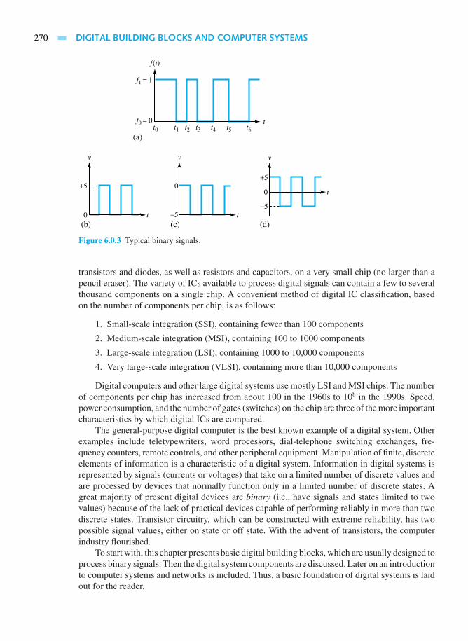
270 DIGITAL BUILDING BLOCKS AND COMPUTER SYSTEMS
f(t)
t
v
t
t1t0
f1 = 1
f0 = 0t5t2 t3 t4 t6
(a)
(b) (c) (d)
v
t
v
t0
0
0 −5−5
+5+5
Figure 6.0.3 Typical binary signals.
transistors and diodes, as well as resistors and capacitors, on a very small chip (no larger than apencil eraser). The variety of ICs available to process digital signals can contain a few to severalthousand components on a single chip. A convenient method of digital IC classification, basedon the number of components per chip, is as follows:
1. Small-scale integration (SSI), containing fewer than 100 components
2. Medium-scale integration (MSI), containing 100 to 1000 components
3. Large-scale integration (LSI), containing 1000 to 10,000 components
4. Very large-scale integration (VLSI), containing more than 10,000 components
Digital computers and other large digital systems use mostly LSI and MSI chips. The numberof components per chip has increased from about 100 in the 1960s to 108 in the 1990s. Speed,power consumption, and the number of gates (switches) on the chip are three of the more importantcharacteristics by which digital ICs are compared.
The general-purpose digital computer is the best known example of a digital system. Otherexamples include teletypewriters, word processors, dial-telephone switching exchanges, fre-quency counters, remote controls, and other peripheral equipment. Manipulation of finite, discreteelements of information is a characteristic of a digital system. Information in digital systems isrepresented by signals (currents or voltages) that take on a limited number of discrete values andare processed by devices that normally function only in a limited number of discrete states. Agreat majority of present digital devices are binary (i.e., have signals and states limited to twovalues) because of the lack of practical devices capable of performing reliably in more than twodiscrete states. Transistor circuitry, which can be constructed with extreme reliability, has twopossible signal values, either on state or off state. With the advent of transistors, the computerindustry flourished.
To start with, this chapter presents basic digital building blocks, which are usually designed toprocess binary signals. Then the digital system components are discussed. Later on an introductionto computer systems and networks is included. Thus, a basic foundation of digital systems is laidout for the reader.

6.1 DIGITAL BUILDING BLOCKS 271
6.1 DIGITAL BUILDING BLOCKS
The primary advantage of digital technology is the low cost, simplicity, and versatility of thedigital building blocks. Because digital signals have a finite number of discrete amplitudes at anygiven time, distinctive digital building blocks are developed to process them. Digital systems arebuilt by repeating a very few simple blocks. The approach becomes very powerful because theblocks (mass-produced in enormous numbers) are inexpensive in IC form and can be repeatedthousands of times.
The two-state nature of digital technology makes the binary number system its natural tool.In a binary system there are only two digits, namely, 0 and 1. The vast majority of present digitalcomputers use the binary system, which has two binary digits (bits), 0 and 1. Internal representationof information in a digital computer is in groups of bits. Besides the binary system (base 2), inthe digital world, the most commonly used number systems are octal (base 8) and hexadecimal(base 16).
EXAMPLE 6.1.1
A signal stands for 0110 with positive logic in which low stands for 0 and high stands for 1. Ifnegative logic (in which low stands for 1 and high stands for 0) is used, what digits are representedby the signal?
So l u t i on
The signal sequence reads: low–high–high–low. With negative logic, the signal stands for 1001.
EXAMPLE 6.1.2
If the time occupied in transmitting each binary digit is 1 µs, find the rate of informationtransmission if 1 baud is equal to 1 bit per second (bit/s).
So l u t i on
Since the time per digit is 1 × 10⁻⁶ s, one can transmit 106 digits per second. The informationrate is then 1× 106 bits, or 1 megabaud (M baud). Note that speeds of over 100 M baud are quitepossible.
Number Systems
A number system, in general, is an ordered set of symbols (digits) with relationships defined foraddition, subtraction, multiplication, and division. The base (radix) of the number system is thetotal number of digits in the system. For example, in our decimal system, the set of digits is 0, 1,2, 3, 4, 5, 6, 7, 8, 9 and hence the base (radix) is ten (10); in the binary system, the set of digits(bits) is 0, 1 and hence the base or radix is two (2).
There are two possible ways of writing a number in a given system: positional notation andpolynomial representation. For example, the number 2536.47 in our decimal system is representedin positional notation as (2536.47)10, whereas in polynomial form it is 2× 10³ + 5× 10² + 3×

272 DIGITAL BUILDING BLOCKS AND COMPUTER SYSTEMS
101+ 6× 100+ 4× 10⁻¹+ 7× 10⁻². The radix or base is 10, whereas the most significant digitor bit (MSB) is 2, the least significant digit or bit (LSB) is 7; the number of integer bits (digits)is 4, and the number of fractional bits (digits) is 2.
The binary number system has a base of 2 with two distinct digits (bits), 1 and 0. A binarynumber is expressed as a string of 0s and 1s, and a binary point if a fraction exists. To convertthe binary to the decimal system, the binary number is expressed in the polynomial form and theresulting polynomial is evaluated by using the decimal-system addition. For example,
(101101.101)2 = 1× 25 + 0× 24 + 1× 23 + 1× 22 + 0× 21 + 1× 20 + 1× 2−1
+ 0× 2−2 + 1× 2−3
= 32+ 0+ 8+ 4+ 0+ 1+ 0.5+ 0+ 0.125 = (45.625)10
For digital processing it is also often necessary to convert a decimal number into its equivalentbinary number. This is accomplished by using the following steps.
1. Repeatedly divide the integer part of the decimal number by 2. Use the remainder aftereach division to form the equivalent binary number. Continue this process until a zeroquotient is obtained. With the first remainder being the least significant bit, form the binarynumber by using the remainder after each division.
2. Repeatedly multiply the decimal fraction by 2. If 0 or 1 appears to the left of the decimalpoint of the product as a result of this multiplication, then add a 0 or 1 to the binary function.Continue this process until the fractional part of the product is zero or the desired numberof binary bits is reached.
For example, the decimal number (75)10 is converted into its binary equivalent:
Quotient Remainder
75 ÷ 2 = 37 1 LSB37 ÷ 2 = 18 118 ÷ 2 = 9 09 ÷ 2 = 4 14 ÷ 2 = 2 02 ÷ 2 = 1 01 ÷ 2 = 0 1 MSB
Stop
Thus, the binary number for (75)10 is given by:
(1001011)2
↑ ↑MSB LSB
Let us now convert the fractional decimal number (0.4375)10 into its binary equivalent:
↓MSB of binary fraction0.4375 × 2 = 0.87500.8750 × 2 = 1.75000.7500 × 2 = 1.50000.5000 × 2 = 1.0000
Stop↑ LSB of binary fraction
Thus, (0.4375)10 = (.0111)2.For representing binary data, octal and hexadecimal numbers are used. The octal number
system is a base-8 system and therefore has 8 distinct digits 0, 1, 2, 3, 4, 5, 6, 7. It is expressed

6.1 DIGITAL BUILDING BLOCKS 273
as a string of any combination of the 8 digits. In order to convert octal to decimal, one follows thesame procedure as for converting from binary to decimal, that is, by expressing the octal numberin its polynomial form and evaluating that polynomial by using decimal-system addition.
For converting from decimal to octal form, one follows the same procedure as for conversionfrom decimal to binary; but instead of dividing by 2 for the integer part, one divides by 8to obtain the octal equivalent. Also, instead of multiplying by 2 for the fractional part, onemultiplies by 8 to obtain the fractional octal equivalent of the decimal fraction. However, itis more common to convert from binary to octal and vice versa. Binary to octal conversionis accomplished by grouping the binary number into groups of 3 bits each, starting fromthe binary point and proceeding to the right as well as to the left; each group is then re-placed by its octal equivalent. For example, (100101111011.01011)2 is arranged as 100 101111 011 . 010 110
↑(note that a trailing 0 is added to complete the last group in the fractional
part). Replacing each group by its octal “decimal” equivalent, one obtains (4573.26)8. Theconversion from octal to binary is done by replacing each octal digit with its 3-bit binaryequivalent.
The hexadecimal number system is a base-16 system which has 16 distinct symbols in theset: 0, 1, 2, 3, 4, 5, 6, 7, 8, 9, A, B, C, D, E, F, where A is equivalent to 10, B to 11, , and F to 15.A hexadecimal number is therefore expressed as a string of any combination of the 16 symbols.To convert from hexadecimal to decimal, for example,
(2AB)16 = 2× 162 + A × 161 + B× 160 = 2× 162 + 10× 161 + 11× 160 = (683)10
(.F8)16 = F × 16−1 + 8× 16−2 = 15× 16−1 + 8× 16−2 = (0.96875)10
and
(2AB.F8)16 = (683.96875)10
The conversion from binary to hexadecimal is accomplished by grouping the binary number intogroups of 4 bits each, starting from the binary point and proceeding to the right as well as to theleft. Each group is then replaced by its hexadecimal equivalent. For example,
(11101110100100.100111)2 ⇒ 0011 1011 1010 0100 . 1001 1100 ⇒ (3BA4.9C)16
The conversion from hexadecimal to binary is achieved by reversing this process. Because theinternal structures of most digital computers manipulate data in groups of 4-bit packets, thehexadecimal system is used for representing binary data.
Since there is a need for decimal-to-binary conversion at the input of a digital device andfor binary-to-decimal conversion at the output of the device, from a user’s point of view, thebinary-coded-decimal (BCD) number system is developed for resolving the interface problem. Ina BCD number each of the decimal digits is coded in binary using 4 bits. For example,
(163.25)10 = (10100011.01)2 = (0001 0110 0011 . 0010 0101)BCD
Table 6.1.1 shows the first 20 numbers in the decimal, binary, octal, hexadecimal, and BCDsystems.
Logic Blocks
Boolean algebra, using Boolean variables (which are binary variables that can assume onlyone of two distinct values, true or false), is a mathematical system with logic notation used todescribe different interconnections of digital circuits. There are two basic types of digital building

274 DIGITAL BUILDING BLOCKS AND COMPUTER SYSTEMS
TABLE 6.1.1 Representation of Numbers in Different Systems
Base 10 Base 2 Base 8 Base 16(Decimal) (Binary) (Octal) (Hexadecimal) BCD
00 00000 00 00 0000 000001 00001 01 01 0000 000102 00010 02 02 0000 001003 00011 03 03 0000 001104 00100 04 04 0000 010005 00101 05 05 0000 010106 00110 06 06 0000 011007 00111 07 07 0000 011108 01000 10 08 0000 100009 01001 11 09 0000 100110 01010 12 0A 0001 000011 01011 13 0B 0001 000112 01100 14 0C 0001 001013 01101 15 0D 0001 001114 01110 16 0E 0001 010015 01111 17 0F 0001 010116 10000 20 10 0001 011017 10001 21 11 0001 011118 10010 22 12 0001 100019 10011 23 13 0001 1001
blocks: logic (combinational) blocks and sequential blocks (known as flip-flops). Logic blocksare electronic circuits that usually have several inputs and one output. The physical devices thatperform the basic Boolean operations are known as logic gates. The basic logic gates are OR,AND, and NOT, the interconnections of which form a logic network (also known as combinationalnetwork), which does not generally contain memory devices. The Boolean function describing acombinational network can be easily derived by systematically progressing from the input(s) tothe output on the logic gates.
The logic OR gate is an electronic circuit realization of the Boolean OR operation, which isrepresented by the symbol +. F = A + B, for example, is read as “F is equal to A OR B.” TheOR operation yields 1 if the value of any of its arguments is 1. Figure 6.1.1 shows a two-input ORgate along with its truth table (table of combinations for the gate) and an illustration of the ORoperation. A three-input OR gate with F = A+B+C would have a truth table with eight entries,which can be developed by the reader as an exercise.
The logic AND gate is an electronic circuit realization of the Boolean AND operation, whichis represented by the symbol · or by the absence of an operator. Thus, for example, F = A · B(also written simply as F = AB) is read as “F is equal to A AND B.” The AND operation yields 1if and only if the values of all its arguments are 1s. Figure 6.1.2 shows a two-input AND gate, itstruth table, and an illustration of the AND operation. A three-input AND gate with F = A ·B ·Cwould have a truth table with 23 = 8 possible entries, which can be developed by the reader as adesirable exercise.
The logic NOT gate is an electronic circuit realization of the Boolean NOT operation, whichis represented by a bar over the variable. F = A, for example, is read as “F equals NOT A.”This operation is also known as the complement operation. Because the NOT operation is a unaryoperation and simply inverts a switching variable, the NOT gate has only one input and oneoutput, and is also known as an inverter. Figure 6.1.3 shows a NOT gate and its truth table.
The AND operation followed by the NOT operation inverts the output coming out of theAND gate, and is known as NAND gate, which is typically shown in Figure 6.1.4 along with its

6.1 DIGITAL BUILDING BLOCKS 275
A
A
A B
0 00 11 01 1
F
0111
F
Off
Off
On
On
B
F = A + BF = 1 (light is on) if either A or B(or both) is equal to 1 (switch on)
BInput
(a) (b) (c)
Output
Inputs Output+
−
Figure 6.1.1 Two-input OR gate. (a) Symbol or physical representation. (b) Truth table. (c) Illustration ofOR operation.
A
A
A B
0 00 11 01 1
F
0001
F
Off (0) Off (0)
On (1) On (1)
B
F = A ⋅ B(also F = AB)B
Input
(a) (b) (c)
Output
Inputs Output +
−
F = 0 (light is off)F = 1 (light is on) if andonly if A = B = 1
Figure 6.1.2 Two-input AND gate. (a) Symbol or physical representation. (b) Truth table. (c) Illustrationof AND operation.
A
A
01
F
10F = A
Input
(a) (b)Output
Input Output Figure 6.1.3 NOT gate (complement).(a) Symbol or physical representation.(b) Truth table.
A
A B
1 01 01 11 1
F
1110
0 00 00 10 1
C
0101
0101
1111
F = A ⋅ B ⋅ CC
(a) (b)
Inputs Output
B
Figure 6.1.4 NAND gate.(a) Logic symbol. (b) Truth table.

276 DIGITAL BUILDING BLOCKS AND COMPUTER SYSTEMS
truth table. Similarly, the OR operation followed by the NOT operation is known as the NORoperation. Figure 6.1.5 shows a typical NOR gate with its truth table.
Two other logic blocks that are sometimes used are the EXCLUSIVE OR (XOR) andEXCLUSIVE NOR (COINCIDENCE) gates. Their conventional symbols together with theirtruth tables are shown in Figures 6.1.6 and 6.1.7, respectively. It is also possible to synthesizethese logic blocks by combining the basic OR, AND, as well as NOT logic gates.
The operations so far introduced are summarized in Table 6.1.2. Any Boolean function canbe transformed from an algebraic expression into a combinational network by using the basiclogic gates. It is always desirable, however, to implement a given Boolean function by using theminimum number of components, leading to a less complex and more economical network. Table6.1.3 gives the basic Boolean identities for which the truth tables for the expressions on eitherside of the equals sign are the same. The reader should note that, in general, it is improper to drawa diagram in which the outputs of any two blocks are connected together. Two outputs can becombined by using them as two inputs to another gate.
A
A B
1 01 01 11 1
F
0000
0 00 00 10 1
C
0101
0101
1000
F = A + B + CC
(a) (b)
Inputs Output
B
Figure 6.1.5 NOR gate. (a) Logicsymbol. (b) Truth table.
A
A B
0 00 11 01 1
F
0110F = A ⊕ B
F = A ⋅ B + A ⋅ BB
(a) (b)
Inputs Output
Figure 6.1.6 EXCLUSIVE OR gate (XOR) (also known as binarycomparator). (a) Logic symbol. (b) Truth table. NOTE: XOR operationyields 1 if the input A is 1 or B is 1, but yields 0 if both inputs A and Bare 1 or 0.
A
A B
0 00 11 01 1
F
1001F = A B
F = A ⋅ B + A ⋅ BB
(a) (b)
Inputs Output
Figure 6.1.7 EXCLUSIVE NOR gate (COINCIDENCE) (also knownas XNOR or EQUIVALENT gate). (a) Logic symbol. (b) Truth table.NOTE: XNOR operation yields 1 if both inputs A and B have the samevalue of either 0 or 1, but yields 0 if the input A is 1 or B is 1. Hence itis a complement of XOR gate.

6.1 DIGITAL BUILDING BLOCKS 277
TABLE 6.1.2 Logic Symbols and Truth Tables
The last two entries in Table 6.1.3 are known as DeMorgan’s theorems, whose importancestems from the fact that they offer a general technique for complementing Boolean expressions.They show that any logic function can be implemented using only OR and NOT gates, or usingonly AND and NOT gates. There exists a duality between AND and OR operations; any functioncan be realized by just one of the two basic operations, plus the complement operation. This givesrise to two families of logic functions: sum of products (SOP) and product of sums (POS). Anylogic expression can be reduced to either one of these.

278 DIGITAL BUILDING BLOCKS AND COMPUTER SYSTEMS
TABLE 6.1.3 Basic Boolean Identities
Identity Comments
1. X + 0 = X Identities 1–9 are basic to Boolean algebra2. X + 1 = 13. X +X = X
4. X + X = 15. X · 0 = 06. X · 1 = X
7. X ·X = X
8. X · X = 09. ¯X = X
10. X + Y = Y +X Commutative11. X · Y = Y ·X Commutative12. X + (Y + Z) = (X + Y )+ Z Associative13. X · (Y · Z) = (X · Y ) · Z Associative14. X · (Y + Z) = X · Y +X · Z Distributive
15. X + Y · Z = (X + Y ) · (X + Z)
16. X +X · Y = X Absorption17. X · (X + Y ) = X
18. X · Y + X · Z + Y · Z = X · Y + X · Z Consensus
19. X + Y + Z = X · Y · Z DeMorgan20. X · Y · Z = X + Y + Z DeMorgan
EXAMPLE 6.1.3
For the switching function F = A(A+ B
), draw a corresponding set of logic blocks and write
the truth table.
So l u t i on
A suitable connection of logic blocks is shown in Figure E6.1.3. Using the intermediate variables,the truth table is as follows.
A
B
AF = A (A + B)
A + B
Figure E6.1.3
A B A A + B F
0 0 1 1 00 1 1 1 01 0 0 0 01 1 0 1 1
EXAMPLE 6.1.4
Derive the Boolean function for the combinational network shown in Figure E6.1.4(a).

6.1 DIGITAL BUILDING BLOCKS 279
So l u t i on
The solution is given in Figure E6.1.4(b).
AF
C
B
(a)
Figure E6.1.4
A
A
B
A ⋅ C
F = A ⋅ B + A ⋅ C + B ⋅ C
A ⋅ B
B ⋅ C
FC
BC
(b)
EXAMPLE 6.1.5
Prove the Boolean identity A(B+C) = AB+AC, which is distributive, by comparing the truthtables of both sides.
So l u t i on
The truth tables with the necessary intermediate variables are as follows:
A B C B + C A(B + C) AB AC AB + AC
0 0 0 0 0 0 0 00 0 1 1 0 0 0 00 1 0 1 0 0 0 00 1 1 1 0 0 0 01 0 0 0 0 0 0 01 0 1 1 1 0 1 11 1 0 1 1 1 0 11 1 1 1 1 1 1 1
↑ Same ↑
Note: The direct representation of AB +AC would require three gates (two ANDs and oneOR). But two gates (one OR and one AND) can perform the same function, as seen from theidentity.

280 DIGITAL BUILDING BLOCKS AND COMPUTER SYSTEMS
EXAMPLE 6.1.6
(a) Express DeMorgan’s laws given by
X + Y = X · Y and X · Y = X + Y
in terms of logic gates.
(b) Express the sum of products given by (X · Y) + (W · Z) and the product of sums givenby (A + B) · (C + D) in terms of logic gates.
So l u t i on
(a) Figures E6.1.6(a) and (b) show the solution.
(b) Figures E6.1.6(c) and (d) show the solution.
Figure E6.1.6

6.1 DIGITAL BUILDING BLOCKS 281
Thus far we have shown how to find the truth table for a given combination of logic blocks.The inverse process, that of finding an interconnection of blocks to produce a given truth table,is known as logic synthesis. Even though the resulting circuit is not necessarily minimal (therebyassuming a minimum number of components), the truth table can be realized by the two standardforms: sum of products (SOP) and product of sums (POS). SOP can be implemented by usingtwo-level (AND–OR) networks, where each product term requires an AND gate (except for aterm with a single variable) and the logic sum of these terms is obtained by using an OR gate withinputs from the AND gates or the single variables. POS can be implemented by using two-level(OR–AND) networks, where each term requires an OR gate (except for a term with a singlevariable) and the product of these terms is obtained by using an AND gate with inputs from theOR gates or the single variables.
Figure 6.1.8 shows four possible gates with an output of 1 only. For example, the truth tableof Figure 6.1.9(a) can be realized by the interconnection of gates shown in Figure 6.1.9(b) withthe resulting Boolean expression F = AB + AB. The SOP or the POS method can be used torealize any truth table, but it is not efficient and minimal; usually other realizations with fewerblocks can be found. The realization can often be simplified by using the distributive law and thesimple theorem A + A = 1. For example, the expression F = AB + AB can be rewritten asF = (A+ A
)B by means of the distributive law, and can be simplified asF = B, since A+A = 1.
Finding minimal realizations with a minimum number of components is the challenge in logicdesign.
Addition of binary numbers is so common that a binary half-adder and a full-adder (FA)have become building blocks in their own right, and are available in IC form. The representationof the half-adder, which can add single-digit binary numbers, is shown in Figure 6.1.10(a) alongwith its truth table. N full adders are needed to add together two N-digit binary numbers. Figure6.1.11 illustrates the addition of 4-digit binary numbers.
A
Output 1 only if A = 1, B = 1(a) (b)
(c) (d)
Output 1 only if A = 1, B = 0
Output 1 only if A = 0, B = 1 Output 1 only if A = 0, B = 0
F
F
B
BF
A
BF
A
A
B
Figure 6.1.8 Four possible gates with an outputof 1 only.
A
1st level 2nd level
F = AB + AB
B
(a)
A B
0 00 11 01 1
F
0101
(b)
Figure 6.1.9 SOP realization of F = AB + AB. (a) Truth table. (b) Interconnection of gates.
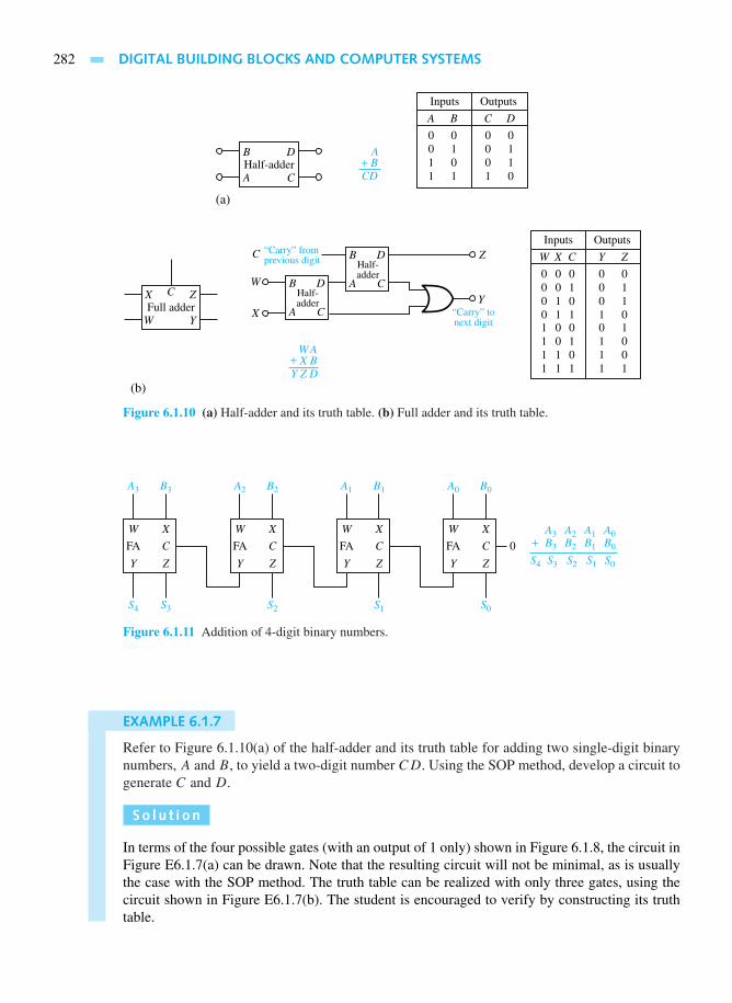
282 DIGITAL BUILDING BLOCKS AND COMPUTER SYSTEMS
B D A+ BCDA
Half-adderC
X C Z
WFull adder
Y
B D
A
Half-adder
C
BC
W
X
D
A
Half-adder
“Carry” fromprevious digit
“Carry” tonext digit
CY
Z
A B
0 00 11 01 1
C D
0 00 10 11 0
(a)
(b)
Inputs Outputs
W X
0 00 00 10 1
Y Z
0 00 10 11 0
1 01 01 11 1
C
01010101
0 11 01 01 1
Inputs Outputs
AWX BZY D
+
Figure 6.1.10 (a) Half-adder and its truth table. (b) Full adder and its truth table.
W X
Y
FA C
Z
A3 B3
S4 S3
W X
Y
FA C
Z
A2 B2
S2
W X
Y
FA 0 +C
Z
A1
A3
B1
S1
W X
Y
FA C
Z
A0 B0
S0
S4
A2
S3
A1
S2
A0B3 B2 B1 B0
S1 S0
Figure 6.1.11 Addition of 4-digit binary numbers.
EXAMPLE 6.1.7
Refer to Figure 6.1.10(a) of the half-adder and its truth table for adding two single-digit binarynumbers, A and B, to yield a two-digit number CD. Using the SOP method, develop a circuit togenerate C and D.
So l u t i on
In terms of the four possible gates (with an output of 1 only) shown in Figure 6.1.8, the circuit inFigure E6.1.7(a) can be drawn. Note that the resulting circuit will not be minimal, as is usuallythe case with the SOP method. The truth table can be realized with only three gates, using thecircuit shown in Figure E6.1.7(b). The student is encouraged to verify by constructing its truthtable.

6.1 DIGITAL BUILDING BLOCKS 283
A
D C
B
A
B
(a)
A
B
A
D
C
B
A
B
(b)
Figure E6.1.7
The basic logic gates described earlier are used to implement more advanced functions andare often combined to form logic blocks (or modules) which are available in compact IC packages.Although SSI packages were common basic units at one time, the trend now is to integration on aneven larger scale. Entire digital systems, such as those to be discussed later, are now available in ICform, and those ICs in turn become blocks for building even larger systems. The ICs are mountedin packages known as DIPs (dual in-line packages), each with 8, 14, or more wires (pins) meantto be plugged into corresponding pin sockets. The actual gates, with the same logic diagrams,can be made with several different kinds of internal construction, giving rise to different logicfamilies. In general blocks of one family are compatible with other blocks of the same family, butnot with those of other families.
Karnaugh Maps and Logic Design
Even though a truth table uniquely represents a logic function, it is clear that the same function mayappear in different algebraic forms. While the Boolean identities can be used for the simplificationof a given algebraic form, it is desirable to have a systematic process that guarantees the minimumform with a minimum number of components. The map method, known as the Karnaugh map or,simply, the K map, which is a modified form of the truth table, provides a convenient procedure forobtaining a minimum SOP or POS of a Boolean expression. The K maps are usually restricted toup to five variables, since they become too cumbersome to manipulate for a larger number of vari-ables. Before we get into the details of K maps, it is necessary to introduce minterm and maxterm.
When a product term contains each of the n variables of a function, it is called a minterm.For n variables, there are 2n possible minterms. The ith minterm of n variables is denoted by mi,where the subscript i, 0 ≤ i ≤ 2n − 1, represents the decimal equivalent of the binary numberobtained when a variable in minterm is replaced by 1 and its complement is replaced by 0.
When a sum term contains each of the n variables of a function, it is called a maxterm. Theith maxterm of n variables, denoted by Mi, is the complement of the ith minterm mi of the samen variables; that is to say, Mi = mi . Table 6.1.4 lists the eight possible maxterms and mintermsof the three variables A, B, and C.
Any Boolean function can be expressed, algebraically, as a sum (OR) of minterms. Anexpression of this form is known as a canonical sum of products. Given a truth table for a logic

284 DIGITAL BUILDING BLOCKS AND COMPUTER SYSTEMS
function, its SOP form can be obtained by taking the sum of the minterms that correspond to a 1in the output column of the table.
Any Boolean function can also be expressed, algebraically, as a product (AND) of maxterms.An expression of this form is known as a canonical product of sums. Given a truth table for a logicfunction, its POS form can be obtained by taking the product of the maxterms that correspond toa 0 (zero) in the output column of the table. Let us now consider an example to illustrate the useof minterms and maxterms.
TABLE 6.1.4 Minterms and Maxterms for Three Variables
A B C i Minterm mi Maxterm Mi
0 0 0 0 A · B · C A+ B + C
0 0 1 1 A · B · C A+ B + C
0 1 0 2 A · B · C A+ B + C
0 1 1 3 A · B · C A+ B + C
1 0 0 4 A · B · C A+ B + C
1 0 1 5 A · B · C A+ B + C
1 1 0 6 A · B · C A+ B + C
1 1 1 7 A · B · C A+ B + C
EXAMPLE 6.1.8
Given the truth table in Table E6.1.8 for an arbitrary Boolean function F, express F as a sum ofminterms and a product of maxterms.
TABLE E6.1.8
mi A B C F
m0 0 0 0 0m1 0 0 1 1m2 0 1 0 0m3 0 1 1 1m4 1 0 0 0m5 1 0 1 0m6 1 1 0 1m7 1 1 1 1
So l u t i on
Noting that F has an output of 1 that corresponds to minterms m1, m3, m6, and m7, F can beexpressed as
F(A,B,C) = m1 +m3 +m6 +m7
= A · B · C + A · B · C + A · B · C + A · B · Cor in a compact form as
F(A,B,C) =∑
mi(1, 3, 6, 7)
where∑
mi( ) means the sum of all the minterms whose subscript i is given inside the parentheses.
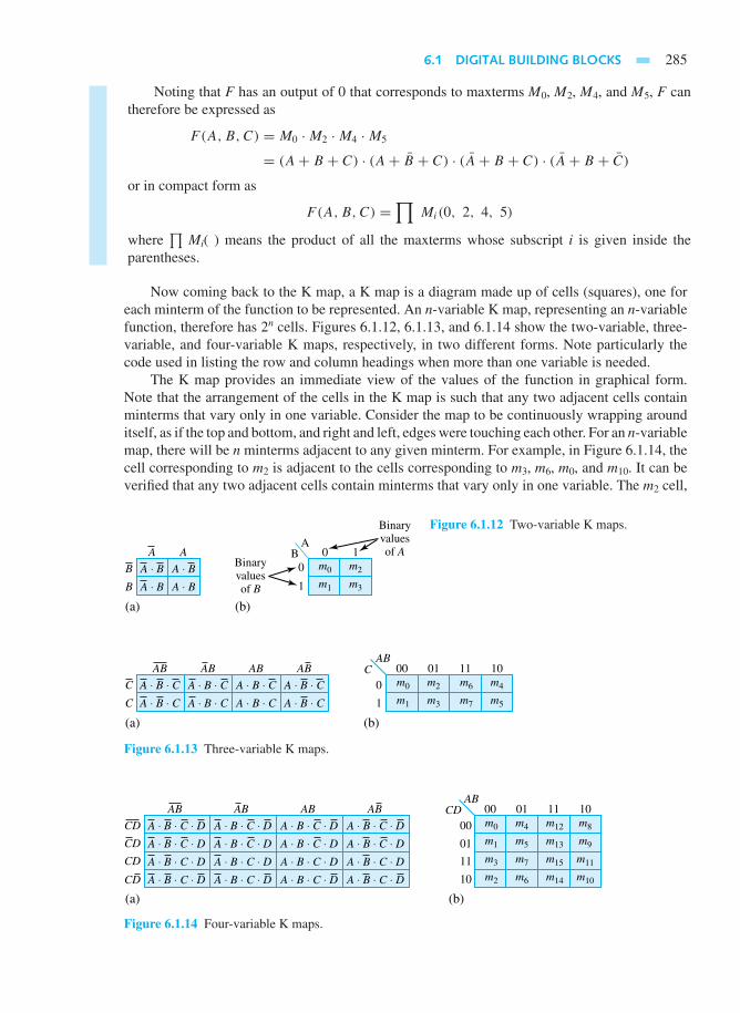
6.1 DIGITAL BUILDING BLOCKS 285
Noting that F has an output of 0 that corresponds to maxterms M0, M2, M4, and M5, F cantherefore be expressed as
F(A,B,C) = M0 ·M2 ·M4 ·M5
= (A+ B + C) · (A+ B + C) · (A+ B + C) · (A+ B + C)
or in compact form as
F(A,B,C) =∏
Mi(0, 2, 4, 5)
where∏
Mi( ) means the product of all the maxterms whose subscript i is given inside theparentheses.
Now coming back to the K map, a K map is a diagram made up of cells (squares), one foreach minterm of the function to be represented. An n-variable K map, representing an n-variablefunction, therefore has 2n cells. Figures 6.1.12, 6.1.13, and 6.1.14 show the two-variable, three-variable, and four-variable K maps, respectively, in two different forms. Note particularly thecode used in listing the row and column headings when more than one variable is needed.
The K map provides an immediate view of the values of the function in graphical form.Note that the arrangement of the cells in the K map is such that any two adjacent cells containminterms that vary only in one variable. Consider the map to be continuously wrapping arounditself, as if the top and bottom, and right and left, edges were touching each other. For an n-variablemap, there will be n minterms adjacent to any given minterm. For example, in Figure 6.1.14, thecell corresponding to m2 is adjacent to the cells corresponding to m3, m6, m0, and m10. It can beverified that any two adjacent cells contain minterms that vary only in one variable. The m2 cell,
A ⋅ B
(a) (b)
A A
Binaryvaluesof A
Binaryvaluesof B
00
BA
1
1
B
B A ⋅ B m2
m3
m0
m1A ⋅ B A ⋅ B
Figure 6.1.12 Two-variable K maps.
A ⋅ B ⋅ C
(a)
AB
C
C
A ⋅ B ⋅ CA ⋅ B ⋅ C
AB
A ⋅ B ⋅ CA ⋅ B ⋅ C
AB
A ⋅ B ⋅ CA ⋅ B ⋅ C
AB
A ⋅ B ⋅ C
(b)
1
0
110100AB
C 10m2
m3
m0
m1
m4
m5
m6
m7
Figure 6.1.13 Three-variable K maps.
A ⋅ B ⋅ C ⋅ D
(a)
AB
CD
CD
CD
CD
A ⋅ B ⋅ C ⋅ D
AB AB AB
A ⋅ B ⋅ C ⋅ DA ⋅ B ⋅ C ⋅ D
A ⋅ B ⋅ C ⋅ DA ⋅ B ⋅ C ⋅ DA ⋅ B ⋅ C ⋅ DA ⋅ B ⋅ C ⋅ D
A ⋅ B ⋅ C ⋅ DA ⋅ B ⋅ C ⋅ DA ⋅ B ⋅ C ⋅ DA ⋅ B ⋅ C ⋅ D
A ⋅ B ⋅ C ⋅ DA ⋅ B ⋅ C ⋅ DA ⋅ B ⋅ C ⋅ DA ⋅ B ⋅ C ⋅ D
(b)
01
00
10
11
110100AB
CD 10m4
m5
m0
m1
m8
m9
m12
m13
m7
m6
m3
m2
m11
m10
m15
m14
Figure 6.1.14 Four-variable K maps.

286 DIGITAL BUILDING BLOCKS AND COMPUTER SYSTEMS
for example, has an assignment of A · B · C · D (= 0 · 0 · 1 · 0), whereas the m3 cell has theassignment of A · B · C ·D(= 0 · 0 · 1 · 1), which differs only in the value of the variable D.
A function can be represented in a K map by simply entering 1s in the cells that correspondto the minterms of the function. This is best illustrated by an example.
EXAMPLE 6.1.9
Show the K-map representations of the following Boolean functions:
(a) F(A,B,C) =∑ mi(0, 2, 3, 5, 7)
(b) F(A,B,C,D) =∑ mi(1, 3, 5, 6, 9, 10, 13, 14)
So l u t i on
Figure E6.1.9 shows the K-map representations of the functions.
(a)
1
0
110100
F(A, B, C) = Σ mi(0, 2, 3, 5, 7)
ABC 10
1 1 1
11
(b)
01
11
10
00
110100
F(A, B, C, D) = Σ mi(1, 3, 5, 6, 9, 10, 13, 14)
ABCD 10
1 1 11
1 1 1
1
Figure E6.1.9
Simplification of an n-variable Boolean function by using a K map is achieved by groupingadjacent cells that contain 1s. The number of adjacent cells that may be grouped is always equalto 2m, for 0 ≤ m ≤ n, i.e., 1, 2, 4, 8, 16, 32, . . . cells. Such a group or set of 2m cells is called asubcube and is expressed by the product term containing only the variables that are common tothe adjacent cells. The larger the subcube is, the fewer variables are needed to express the productterm. This statement can be justified by using Boolean identities. For example, in a four-variableK map, the following possible subcubes can be formed.
• 1-cell subcube (having one minterm) expressed by a product term containing four, or n−m,variables; note that n = 4 and m = 0 for this case.
• 2-cell subcube (having two minterms) expressed by a product term containing three, orn−m, variables; note that n = 4 and m = 1 for this case.
• 4-cell subcube (having four minterms) expressed by a product term containing two, orn−m, variables; note that n = 4 and m = 2 for this case.
• 8-cell subcube (having eight minterms) expressed by a product term containing one or n−m
variables; note that n = 4 and m = 3 for this case.
• 16-cell subcube (having sixteen minterms) expressed by the logic 1; that is, the function isalways equal to 1.
Let us now present an example to illustrate the concepts related to subcubes.
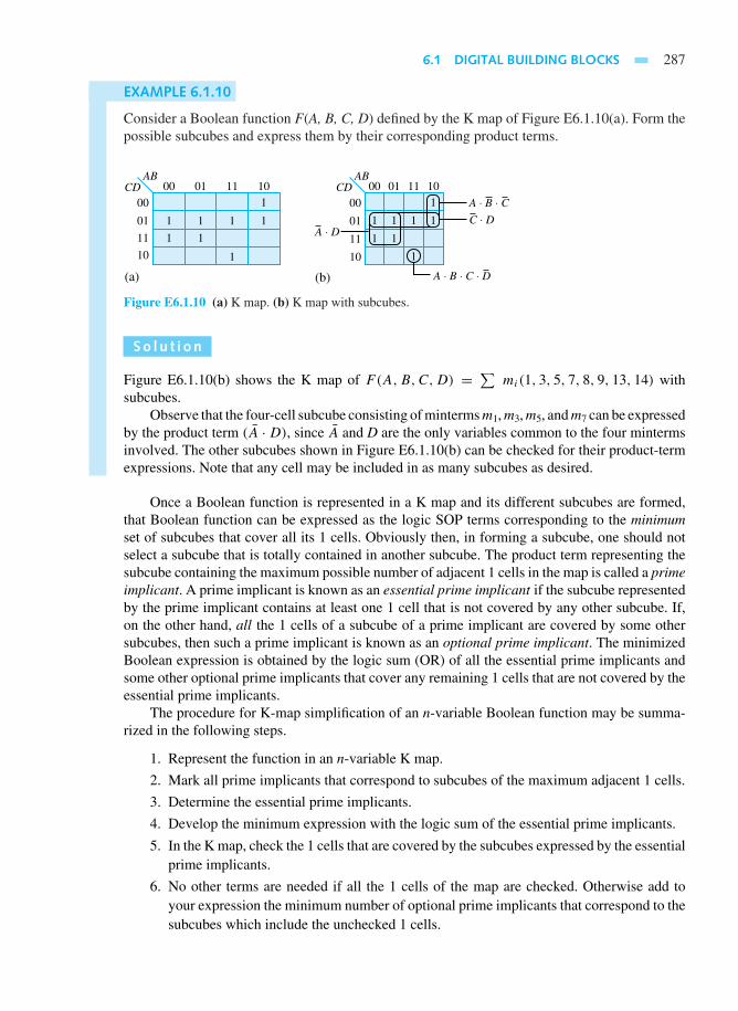
6.1 DIGITAL BUILDING BLOCKS 287
EXAMPLE 6.1.10
Consider a Boolean function F(A, B, C, D) defined by the K map of Figure E6.1.10(a). Form thepossible subcubes and express them by their corresponding product terms.
(a) (b)
01
11
10
00
A ⋅ D
A ⋅ B ⋅ C
A ⋅ B ⋅ C ⋅ D
C ⋅ D01
11
10
00
110100AB
CD 10 01 11 1000AB
CD
1 1 1
1
1
1
1
1
1 1 1 1
1 1
1
1
Figure E6.1.10 (a) K map. (b) K map with subcubes.
So l u t i on
Figure E6.1.10(b) shows the K map of F(A,B,C,D) = ∑mi(1, 3, 5, 7, 8, 9, 13, 14) with
subcubes.Observe that the four-cell subcube consisting of minterms m1, m3, m5, and m7 can be expressed
by the product term (A ·D), since A and D are the only variables common to the four mintermsinvolved. The other subcubes shown in Figure E6.1.10(b) can be checked for their product-termexpressions. Note that any cell may be included in as many subcubes as desired.
Once a Boolean function is represented in a K map and its different subcubes are formed,that Boolean function can be expressed as the logic SOP terms corresponding to the minimumset of subcubes that cover all its 1 cells. Obviously then, in forming a subcube, one should notselect a subcube that is totally contained in another subcube. The product term representing thesubcube containing the maximum possible number of adjacent 1 cells in the map is called a primeimplicant. A prime implicant is known as an essential prime implicant if the subcube representedby the prime implicant contains at least one 1 cell that is not covered by any other subcube. If,on the other hand, all the 1 cells of a subcube of a prime implicant are covered by some othersubcubes, then such a prime implicant is known as an optional prime implicant. The minimizedBoolean expression is obtained by the logic sum (OR) of all the essential prime implicants andsome other optional prime implicants that cover any remaining 1 cells that are not covered by theessential prime implicants.
The procedure for K-map simplification of an n-variable Boolean function may be summa-rized in the following steps.
1. Represent the function in an n-variable K map.
2. Mark all prime implicants that correspond to subcubes of the maximum adjacent 1 cells.
3. Determine the essential prime implicants.
4. Develop the minimum expression with the logic sum of the essential prime implicants.
5. In the K map, check the 1 cells that are covered by the subcubes expressed by the essentialprime implicants.
6. No other terms are needed if all the 1 cells of the map are checked. Otherwise add toyour expression the minimum number of optional prime implicants that correspond to thesubcubes which include the unchecked 1 cells.

288 DIGITAL BUILDING BLOCKS AND COMPUTER SYSTEMS
Let us now illustrate the application of this procedure in the following example.
EXAMPLE 6.1.11
Obtain a minimum Boolean expression for
F(A,B,C,D) =∑
mi(1, 3, 4, 5, 6, 7, 10, 12)
So l u t i on
1. The K map of F is shown in Figure E6.1.11(a).
(a) (b)
01
11
10
00A ⋅ D
A ⋅ B ⋅ C ⋅ D
A ⋅ B
01
11
10
00
110100AB
CD 10 01 11 1000AB
CD
1
1 1
1
1
1
1
1
1
B ⋅ C ⋅ D
1
1
1
1
1 1
1
Figure E6.1.11
2. The prime implicants, as depicted in Figure E6.1.11(b), are (A ·D), (A ·B), (B · C · D),and (A · B · C · D).
3. All prime implicants happen to be essential, since each of the subcubes contains at leastone 1 cell that is not covered by any other subcube.
4. F(A,B,C,D) = A ·D + A · B + B · C · D + A · B · C · D.
5. The 1 cells that are covered by the subcubes expressed by the essential prime implicantsare checked, as shown in Figure E6.1.11(b).
6. Since all the 1 cells have been checked, it follows that
F(A,B,C,D) = A ·D + A · B + B · C · D + A · B · C · D
The minimum POS expression for a Boolean function can be obtained easily by using Kmaps in a procedure very similar to that used for the minimum SOP expression. By using the 0sof the map and obtaining prime implicants again by using the 0 cells, this can be done. Since the0 cells represent the compliment of the function, complementing the minimum SOP expressionfor the 0s of the function yields the minimum POS form of the function. Even though the twoforms (POS and SOP) are completely equivalent, logically, one of the two forms may lead to arealization involving a smaller number of gates.
In designing a digital system, one often encounters a situation where the output cannot bespecified due to either physical or logical constraints. Figure 6.1.15 illustrates one such situation,where the input lines B and C to the black box of logic circuitry are physically connected together.For such a circuit, the input combination A = 0, B = 1, and C = 0 is not possible, and thereforethe output corresponding to this combination cannot be specified. Such an output is hence known

6.1 DIGITAL BUILDING BLOCKS 289
as a don’t-care output because of a physical constraint. As another example, Figure 6.1.16 showsthe logic circuitry in a black box with four input lines representing BCD data. For such a circuit,six of the input combinations (1010, 1011, 1100, 1101, 1110, and 1111) are not valid BCDs, andtherefore the output of this circuitry cannot be specified because of a logic constraint. Such outputsare hence labeled as don’t-care outputs. A don’t-care output or condition is generally representedby the letter d in the truth table and the K map.
The ds can be treated either as 0s or 1s when the subcubes are formed in the K map, dependingon which results in a greater simplification, thereby helping in the formation of the smallest numberof maximal subcubes. Note that some or all of the ds can be treated as 0s or 1s. However, oneshould not form a subcube that contains only ds.
ABlack box
(logic circuitry) F(A, B, C)BC
Figure 6.1.15 Physical constraint for a don’t-care condi-tion.
ABlack box
(logic circuitry)BCD data F(A, B, C, D)
BCD
Figure 6.1.16 Logic constraint for a don’t-care condition.
EXAMPLE 6.1.12
A Boolean function F(A, B, C, D) is specified by the truth table of Figure E6.1.12 (a). Obtain:(a) a minimum SOP expression, and (b) a minimum POS expression.
So l u t i on
The four-variable K map of F is shown in Figure E6.1.12(b).
(a) The prime implicants (with 1 cells) for F are marked in Figure E6.1.12(c). The minimumSOP expression is then given by
F = C · D + B · C
A B
0 00 00 00 0
F
1000
0 10 10 10
D
010101011
C
00110011
1100
1 01 01 01 0
10dd
1 11 11 11
010101011
00110011
dddd
(b)(a)
01
11
10
00
110100AB
CD 101 11 d
1 00 d
d
d
d
d
0
0
0
0
Figure E6.1.12
290 DIGITAL BUILDING BLOCKS AND COMPUTER SYSTEMS
(c)
01
11
10
00
110100AB
CD 10C D⋅1 11 d
1 d
d
d
d
d
B C⋅
A D⋅ (d)
01
11
10
00
110100AB
CD 10
C
d
d
d
d
d
d
0 0
0
0
0
0
B D⋅
Figure E6.1.12 Continued
(b) The prime implicants (with 0 cells) for the complement of F are marked in FigureE6.1.12(d). The minimum POS expression is then given by
F = C + B ·DComplementing both sides of this equation and using DeMorgan’s rules, one obtains
F = C · (B + D)
Note in particular that in Figures E6.1.12(c) and (d) we did not form subcubes that covered only ds.
Sequential Blocks
Neglecting propagation delays, which are measures of how long it takes the output of a gate torespond to a transition at the input of the gate, the output of a logic block at a given time dependsonly on the inputs at that same time. The output of a sequential block, on the other hand, dependsnot only on the present inputs but also on inputs at earlier times. Sequential blocks have thus akind of memory, and some of them are used as computer memories.
Most sequential blocks are of the kind known as multivibrators, which can be monostable(the switch remains in only one of its two positions), bistable (the switch will remain stable ineither of its two positions), and unstable (the switch changes its position continuously as a kindof oscillator, being unstable in both of its two states). The most common sequential block is theflip-flop, which is a bistable circuit that remembers a single binary digit according to instructions.Flip-flops are the basic sequential building blocks. Various types of flip-flops exist, such as theSR flip-flop (SRFF), D flip-flop (or latch), and JK flip-flop (JKFF), which differ from one anotherin the way instructions for storing information are applied.
SR FLIP-FLOP (SRFF)
The symbol for the SRFF is shown in Figure 6.1.17(a), in which S stands for “set,” R stands for“reset” on the input side, and there are two outputs, the normal output Q and the complementaryoutput Q. The operation of the SRFF can be understood by the following four basic rules.
1. If S = 1 and R = 0, then Q = 1 regardless of past history. This is known as the setcondition.
2. If S = 0 and R = 1, then Q = 0 regardless of past history. This is known as the resetcondition.
3. If S = 0 and R = 0, then Q does not change and stays at its previous value. This is ahighly stable input condition.
4. The inputs S = 1 and R = 1 are not allowed (i.e., forbidden) because QQ = 11; Q isno longer complementary to Q. This is an unacceptable output state. Such a meaningless
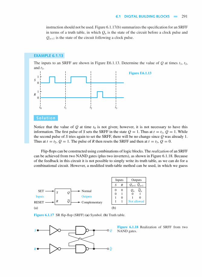
6.1 DIGITAL BUILDING BLOCKS 291
instruction should not be used. Figure 6.1.17(b) summarizes the specification for an SRFFin terms of a truth table, in which Qn is the state of the circuit before a clock pulse andQn+1 is the state of the circuit following a clock pulse.
EXAMPLE 6.1.13
The inputs to an SRFF are shown in Figure E6.1.13. Determine the value of Q at times t1, t2,and t3.
S
R
0
1
1
0
t0 t1 t2 t3
Figure E6.1.13
So l u t i on
Notice that the value of Q at time t0 is not given; however, it is not necessary to have thisinformation. The first pulse of S sets the SRFF in the state Q = 1. Thus at t = t1, Q = 1. Whilethe second pulse of S tries again to set the SRFF, there will be no change since Q was already 1.Thus at t = t2, Q = 1. The pulse of R then resets the SRFF and then at t = t3, Q = 0.
Flip-flops can be constructed using combinations of logic blocks. The realization of an SRFFcan be achieved from two NAND gates (plus two inverters), as shown in Figure 6.1.18. Becauseof the feedback in this circuit it is not possible to simply write its truth table, as we can do for acombinational circuit. However, a modified truth-table method can be used, in which we guess
S Q
R Q
S R
0 00 11 01 1
Qn+1 Qn+1
Qn Qn0 11 0
Not allowed
(a) (b)
Inputs
Normal
Complementary
Outputs
SET
RESET
Inputs
Outputs
Figure 6.1.17 SR flip-flop (SRFF) (a) Symbol. (b) Truth table.
Q
Q
S
R
Figure 6.1.18 Realization of SRFF from twoNAND gates.
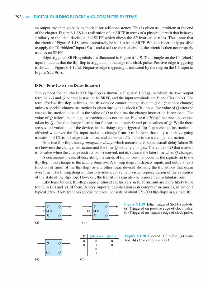
292 DIGITAL BUILDING BLOCKS AND COMPUTER SYSTEMS
an output and then go back to check it for self-consistency. This is given as a problem at the endof the chapter. Figure 6.1.18 is a realization of an SRFF in terms of a physical circuit that behavessimilarly to the ideal device called SRFF which obeys the SR instruction rules. Thus, note thatthe circuit of Figure 6.1.18 cannot accurately be said to be an SRFF. While it is certainly possibleto apply the “forbidden” input (S = 1 and R = 1) to the real circuit, the circuit is then not properlyused as an SRFF.
Edge triggered SRFF symbols are illustrated in Figure 6.1.19. The triangle on the Ck (clock)input indicates that the flip-flop is triggered on the edge of a clock pulse. Positive-edge triggeringis shown in Figure 6.1.19(a). Negative-edge triggering is indicated by the ring on the Ck input inFigure 6.1.19(b).
D FLIP-FLOP (LATCH OR DELAY ELEMENT)
The symbol for the clocked D flip-flop is shown in Figure 6.1.20(a), in which the two outputterminals Q and Q behave just as in the SRFF, and the input terminals are D and Ck (clock). Theterm clocked flip-flop indicates that this device cannot change its state (i.e., Q cannot change)unless a specific change instruction is given through the clock (Ck) input. The value of Q after thechange instruction is equal to the value of D at the time the change instruction is received. Thevalue of Q before the change instruction does not matter. Figure 6.1.20(b) illustrates the valuestaken by Q after the change instruction for various inputs D and prior values of Q. While thereare several variations of the device, in the rising-edge triggered flip-flop a change instruction iseffected whenever the Ck input makes a change from 0 to 1. Note that only a positive-goingtransition of Ck is a change instruction, and a constant Ck input is not a change instruction.
Note that flip-flops have propagation delay, which means that there is a small delay (about 20ns) between the change instruction and the time Q actually changes. The value of D that mattersis its value when the change instruction is received, not its value at the later time when Q changes.
A convenient means of describing the series of transitions that occur as the signals set to theflip-flop input change is the timing diagram. A timing diagram depicts inputs and outputs (as afunction of time) of the flip-flop (or any other logic device) showing the transitions that occurover time. The timing diagram thus provides a convenient visual representation of the evolutionof the state of the flip-flop. However, the transitions can also be represented in tabular form.
Like logic blocks, flip-flops appear almost exclusively in IC form, and are more likely to befound in LSI and VLSI form. A very important application is in computer memories, in which atypical 256k RAM (random access memory) consists of about 256,000 flip-flops in a single IC.
SCk
Q
R Q
(a) (b)
SCk
Q
R Q
Figure 6.1.19 Edge triggered SRFF symbols.(a) Triggered on positive edge of clock pulse.(b) Triggered on negative edge of clock pulse.
D Q
Ck Q
(a) (b)
D
0011
Q(before) Q(after)
0 01 00 11 1
Figure 6.1.20 Clocked D flip-flop. (a) Sym-bol. (b) Q for various inputs D.

6.1 DIGITAL BUILDING BLOCKS 293
EXAMPLE 6.1.14
The positive-edge triggered D flip-flop is given the inputs shown in Figure E6.1.14(a), with a zeroinitial value of Q. Draw the timing diagram.
D
Ck
0
1
1
0
Q1
0
D
Ck
0
(a)
(b)
1
1
0
Figure E6.1.14
So l u t i on
Q is illustrated in Figure E6.1.14(b) as a function of time.
In order to avoid the input condition SR = 11, an inverter is included, as shown in Figure6.1.21. SR can be either 01 or 10. For SR = 10, the flip-flop sets (i.e., QQ = 10) whereas forSR = 01 it resets (i.e., QQ = 01). Thus, the output replicates the input state, but with a delayequal to the time for information to propagate through the flip-flop.
Most commercially available flip-flops also include two extra control input signals known aspreset and clear. When activated, these input signals will set (Q = 1) or clear (Q = 0) the flip-flop, regardless of other input signals. Figure 6.1.22(a) shows the block diagram of a positive-edgetriggered D flip-flop with preset and clear control signals; Figure 6.1.22(b) gives the functionaltruth table for this device. Note that the clock is the synchronizing element in a digital system. Theparticular device described here is said to be positive-edge triggered, or leading-edge triggered,since the final output of the flip-flop is set on a positive-going clock transition.
Figure 6.1.23 shows a realization of the D flip-flop using six NAND gates, in which the outputpart is very similar to the SRFF of Figure 6.1.18 and the other four gates are used to translate theD-type control instructions into a form that the SRFF can use.
S Q
R
Data
Q
Figure 6.1.21 Flip-flop with inverter.

294 DIGITAL BUILDING BLOCKS AND COMPUTER SYSTEMS
Preset Clear Ck D Q Q
0 10 11 0
1 0Not allowed
(b)
Inputs Outputs
0 10 00 01 1
1 0d d
01
d d
d dD
CkClear
PresetQ
Q
(a)
Figure 6.1.22 Positive-edge triggeredD flip-flop with preset and clear. (a)Block diagram. (b) Truth table. NOTE:d stands for don’t-care condition. Thesymbol indicates the occurance of apositive transition in the clock timing.The symbol > (knife edge) drawn nextto the clock input in the block diagramindicates edge-triggered feature.
Q
Preset
Clear
Clock
D
Q
Figure 6.1.23 Realization of D flip-flop with six NAND gates.
JK FLIP-FLOP (JKFF)
The block diagram, truth table, and a practical realization of the JKFF are shown in Figure6.1.24. The JKFF differs from an SRFF in that output Q is fed back to the K-gate inputand Q to the J-gate input. Assuming QQ = 01, gate B is disabled by Q = 0 (i.e., F =1). The only way to make the circuit change over is for gate A to be enabled by makingJ = 1 and Q = 1 (which it is already). Then when Ck = 1, all inputs to gate A are 1and E goes to zero, which makes Q = 1. With Q and F both equal to 1, Q = 0, so theflip-flop has changed state. Note that the input condition JK = 11 is allowed, and in thiscondition, when the flip-flop is clocked, the output always changes state; thus it is said totoggle.
If the clock pulse is short enough to permit the flip-flop to change only once, the JKFFoperates well. However, with modern high-speed ICs a race is more likely to occur, which is acondition in which two pulses are intended to arrive at a destination gate in some specific order,but due to each one racing through different paths in the logic with a different number of gates,the propagation delays stack up differently and the timing order is lost. This can be eliminatedby introducing delays in the feedback paths between outputs (Q and Q) and inputs (J and K). Abetter solution to the problem is the master–slave JKFF.

6.2 DIGITAL SYSTEM COMPONENTS 295
D
CA
E
F
J
Ck
K B
Q
QJCk
Q
K Q
(a) (c)
J K
0 00 11 01 1
Qn+1 Qn+1
Qn Qn0 11 0
(b)
Inputs Outputs
Qn Qn
Figure 6.1.24 JK flip-flop. (a) Block diagram. (b) Truth table. (c) A realization.
MASTER–SLAVE JKFF
Figure 6.1.25 illustrates a master–slave JKFF, in which gates A, B, C, and D form the masterflip-flop and T, U, V, and W form the slave. The output of the master–slave JKFF can be predictedfor all combinations of J and K and for any duration of clock pulse. Thus it is the most versatileand universal type of flip-flop. SRFFs are also available in master–slave configuration.
Ck = 1 enables the master; Ck = 0 disables the slave. Let QQ = 10 and JK = 11 beforethe occurrence of a clock pulse. B is enabled by Q = 1 so that when the clock pulse arrives(i.e., Ck = 1), F goes to zero and QM to 1. Now with E = 1 and QM = 1, QM goes to zero sothat the master has been reset. However, the slave remains disabled until Ck goes to zero. Notethat the slave, at this stage, is essentially an SRFF with inputs S and R equal to QM and QM ,respectively. Thus, when Ck goes to zero, Ck goes to 1 and the slave is now reset by its inputsQMQM = 01. But the feedback to J and K cannot cause a race because, with Ck= 0, the masteris disabled.
W
V
U
T
B
AJ
K D
CE
F
Master Slave
Q
Q
Ck
Ck
QM
QM
Figure 6.1.25 Master–slave JK flip-flop.
6.2 DIGITAL SYSTEM COMPONENTS
The basic combinational and sequential building blocks were introduced in Section 6.1. Thereason that digital systems are so inexpensive and yet so powerful is that they consist of very

296 DIGITAL BUILDING BLOCKS AND COMPUTER SYSTEMS
large numbers of just a few building blocks, repeated in simple ways. In this section we shalldeal with some common digital system components, such as decoders, encoders, multiplexers,registers, counters, digital-to-analog (D/A) and analog-to-digital (A/D) converters, memory, anddisplay devices.
Decoders
An n-bit binary code is capable of encoding up to 2n distinct elements of information. Adecoder is a combinational network that decodes (converts) the n-bit binary-coded input tom outputs (m ≤ 2n). The block diagram of a 3-bit to 8-element decoder is shown in Figure6.2.1(a), wherein the three inputs are decoded into eight outputs, one for each combinationof the input variables. In the truth table shown in Figure 6.2.1(b), observe that for each in-put combination, there is only one output that is equal to 1 (i.e., each combination selectsonly one of the eight outputs). The logic diagram of the 3-to-8 decoder is shown in Figure6.2.1(c).
Decoding is so common in digital design that decoders are commercially available as MSI(medium-scale integration) packages in the form of 2-to-4, 3-to-8, and 4-to-10 decoders. Inte-grated circuits for decoders are available in different forms.
Encoders
Encoding is the process of forming an encoded representation of a set of inputs, and it is theconverse of the decoding operation. An encoder is a combinational network that generates ann-bit binary code that uniquely identifies the one out of m activated inputs (0 ≤ m ≤ 2n − 1).
Figure 6.2.2(a) shows the block diagram of an 8-element to 3-bit encoder. The truth table isgiven in Figure 6.2.2(b). Notice that only one of the eight inputs is allowed to be activated at anygiven time. The logic diagram for the 8-to-3 encoder is shown in Figure 6.2.2(c).
Multiplexers
A multiplexer is a data selector, whereas a demultiplexer is a data distributor. A multiplexeris a combinational network that selects one of several possible input signals and directs thatsignal to a single output terminal. The selection of a particular input is controlled by a set ofselection variables. A multiplexer with n selection variables can usually select one out of 2n inputsignals.
Figure 6.2.3(a) shows the block diagram of a 4-to-1 multiplexer. The truth table is given inFigure 6.2.3(b). Notice that each of the four inputs (I0, I1, I2, and I3) is selected by S1 and S0,and directed to the output Q. In general, only the input whose address is given by the select linesis directed to the output. The logic diagram is shown in Figure 6.2.3(c). 2-, 4-, 8-, and 16-to-1multiplexers are commercially available as MSI packages.
Registers
A register is a collection of flip flops (and some basic combinational gates to perform differentbinary arithmetic and logic operations), where each flip-flop is used to store 1 bit of information.Figure 6.2.4(a) shows the block diagram of a 4-bit shift-right register that uses D flip-flops. JKFFsand SRFFs are also used in shift-register construction. Observe in the timing diagram of Figure6.2.4(b) that each successive clock pulse transfers (or shifts) the data bit from one flip-flop to the

6.2 DIGITAL SYSTEM COMPONENTS 297
A0 A1
A0
A1
A2
1 01 01 11 1
A2
0101
0 00 00 10 1
0101
Q7
Q0Q1Q2Q3Q4Q5Q6Q7
Q6
0 00 00 11 0
Q5
0100
0 00 00 00 0
0000
Q4 Q3
1 00 00 00 0
Q2
0000
0 00 00 00 1
0010
Q1 Q0
0 00 00 00 0
0 11 00 00 0
A2 A1 A0
Q0
Q1
Q2
Q3
Q4
Q5
Q6
Q7
(b)
(c)
(a)
Figure 6.2.1 3-to-8 decoder. (a) Block diagram. (b) Truth table. (c) Logic diagram.
next one on the right. The waveforms also reveal that the data are read into the register seriallyand appear at the output in serial form. The shift register is then known as a serial-in serial-out(SISO) register.
PISO (parallel-in serial-out), SIPO (serial-in parallel-out), and PIPO (parallel-in parallel-out) registers are also often used to read in the input data and read out the output data in a

298 DIGITAL BUILDING BLOCKS AND COMPUTER SYSTEMS
n0
n1
n2
I7
I0
I7 I6 I5 I4 I3 I2 I1 I0
I1I2I3I4I5I6I7
I6
0 00 00 11 0
I5
0100
0 00 00 00 0
0000
I4 I3
1 00 00 00 0
I2
0000
0
Outputs
00 00 00 1
0010
I1 I0
0 00 00 00 0
0 11 00 00 0
n2
(b)(a)
(c)
n2 n1
1 01 01 11 1
n0
0101
0 00 00 10 1
0101
Inputs
n1
n0
Figure 6.2.2 8-to-3 encoder. (a) Block diagram. (b) Truth table. (c) Logic diagram.
convenient way that is needed for the operations involved. Right-shifting registers are employedin multiplication algorithms, whereas left-shifting registers are utilized in division algorithms.Registers that are capable of shifting the data to the left or right are known as bidirectionalshift registers. The register along with additional gates on a single chip forms an IC componentknown as the universal register, which usually includes the shift-left, shift-right, parallel-input,and no-change operations.
Counters
The shift register can be used as a counter because the data are shifted for each clock pulse. Acounter is a register that goes through a predetermined sequence of states when input pulses arereceived. Besides, computers, timers, frequency meters, and various other digital devices containcounters for counting events.
There are what are known as ripple (asynchronous), synchronous, and ring counters. Inripple counters, the output of each flip-flop activates the next flip-flop throughout the entiresequence of the counter’s states. In a synchronous counter, on the other hand, all flip-flopsare activated (triggered) simultaneously through a master clock connected to the clock inputsof all flip-flops. In a ring counter, as in a synchronous counter, all flip-flops are triggered

6.2 DIGITAL SYSTEM COMPONENTS 299
S1
S1 S0
S0I1
I0
I0
I1
I2
I3
I2
I3
0
Select Lines
Select Lines
Inputlines
Output
Output 00 11 01 1
I0I1I2I3
S1 S0
Q
(b)
(c)
(a)
Figure 6.2.3 4-to-1 multiplexer. (a) Block diagram. (b) Truth table. (c) Logic diagram.
simultaneously. However, the output of each flip-flop drives only an adjacent flip-flop. A singlepulse propagates through the ring in a ring counter, whereas all remaining flip-flops are at thezero state.
Figure 6.2.5(a) shows a block diagram of a 3-bit ripple counter using JKFFs. Notice from thetiming diagram shown in Figure 6.2.5(b) that the output Q0 of the leftmost flip-flop will changeits state at every clock pulse if the clear signal equals zero. The output Q1, controlled by Q0,will change its state every time Q0 changes from 0 to 1. Similarly Q2 is controlled by Q1. Figure6.2.5(c) shows the outputs for the first 8 clock pulses. Observe that a 3-bit counter will cyclethrough 8 states, 000 through 111. An n-bit ripple counter, in general, will cycle through 2n states;it is known as a divide-by-2n counter or modulo-2n binary counter. Taking the outputs from Q2 Q1
Q0, the counter becomes an up-counter; taking the outputs from Q2 Q1 Q0, the counter becomesa down-counter, which counts down from a preset number. Asynchronous ripple counters areavailable as MSI packages.

300 DIGITAL BUILDING BLOCKS AND COMPUTER SYSTEMS
D3
Ck
Clock
Data input
Preset
Data output
Clear
(a)
(b)
FF3
Pr
Clr
Y3 D2
Ck
FF2
Pr
Clr
Y2 D1
Ck
FF1
Pr
Clr
Y1 D0
Ck
FF0
Pr
Clr
Y0
Y3
Y2
Y1
Y0
1Pulse
Clock
Datainput
2
2TT 3T 4T 5T
2TT 4T 5T
6T
3T 4T 6T
4T 5T
2T 3T 5T 6T
5T 6T
3 4 5 6
Figure 6.2.4 4-bit shift-right SISO register. (a) Block diagram. (b) Timing diagram.
J0
k0
Clear
Clock
Logic 1(a)
Ck0
ClrQ0
Q0
J1
k1
Ck1
ClrQ1
Q1
J2
k2
Ck2
ClrQ2
Q2
Figure 6.2.5 3-bit ripplecounter. (a) Block diagram.(b) Timing diagram. (c) Out-puts for the first 8 clockpulses.

6.2 DIGITAL SYSTEM COMPONENTS 301
0
Clock Q2
00011110
0
Q1
01100110
0
Q0
10101010
T1
T2
T3
T4
T5
T6
T7
T8
(c)
1
ClockClear
1
1
(b)
1 1 1
1 1 1
0
0
0 0 0 0 0
0 0 0 0
0 0 0 01 1 1
T1
Q0
Q1
Q2
T2 T3 T4 T5 T6 T7 T8
Figure 6.2.5 Continued
The slow speed of operation, caused by the long time required for changes in state to ripplethrough the flip-flops, is a disadvantage of ripple counters. This problem is overcome by usingsynchronous converters. However, additional control logic is needed to determine which flip-flops, if any, must change state, since flip-flops are triggered simultaneously. Figure 6.2.6 showsthe logic diagram of a 3-bit binary synchronous converter using JKFFs. Synchronous counterscan be designed to cycle through any sequence of states. Various n-bit synchronous convertersare commercially available as MSI packages. Some counters are also programmable.
Figure 6.2.7(a) shows a 4-bit (modulo-4) ring counter using D flip-flops; its timing diagramis given in Figure 6.2.7(b). A modulo-n ring counter requires N flip-flops and no other gates,whereas modulo-N ripple and synchronous counters need only log2 N flip-flops. However, rippleand synchronous counters generally use more components than ring counters.
Clock
1 J2
k2
Ck2
Q2
Q2
J1
k1
Ck1
Q1
Q1
J0
k0
Ck0
Q0
Q0
Figure 6.2.6 3-bit binary synchronous converter using JKFFs.
D0
Clock(a)
Ck0
Q0
Q0
D1
Ck1
Q1
Q1
D2
Ck2
Q2
Q2
D3
Ck3
Q3
Q3
Figure 6.2.7 4-bit ring counter using D flip-flops. (a) Block diagram. (b) Timing diagram.

302 DIGITAL BUILDING BLOCKS AND COMPUTER SYSTEMS
Clock
(b)
0 0 0 0 0 0
00
0 0
0 0 0 0 0 0
0 0 0 0
0 0 0 0
1 1
11
1
1 1
1
T1
Q0
Q1
Q2
Q3
T2 T3 T4 T5 T6 T7 T8 T9 Figure 6.2.7 4-bit ring counter using Dflip-flops. (a) Block diagram. (b) Timingdiagram.
EXAMPLE 6.2.1
A table of minterms for three variables is as follows:
A B C i Minterm mi
0 0 0 0 A · B · C0 0 1 1 A · B · C0 1 0 2 A · B · C0 1 1 3 A · B · C1 0 0 4 A · B · C1 0 1 5 A · B · C1 1 0 6 A · B · C1 1 1 7 A · B · C
Implement the following Boolean functions by using one 3-to-8 decoder and three three-inputOR gates:
F1(A,B,C) =∑
mi(1, 2, 3) = A · B · C + A · B · C + A · B · CF2(A,B,C) =
∑mi(2, 4, 6) = A · B · C + A · B · C + A · B · C
F3(A,B,C) =∑
mi(3, 5, 7) = A · B · C + A · B · C + A · B · C
So l u t i on
The implementation is shown in Figure E6.2.1.
F1
F2
F3
A
B 3-to-8decoder
C
m0
m1
m2
m3
m4
m5
m6
m7
Figure E6.2.1

6.2 DIGITAL SYSTEM COMPONENTS 303
EXAMPLE 6.2.2
Show the logic diagram of an 8-to-1 multiplexer.
So l u t i on
The logic diagram is depicted in Figure E6.2.2.
A2 A1 A0
Q
I0
I1
I2
I3
I4
I5
I6
I7
Figure E6.2.2
EXAMPLE 6.2.3
Given the block diagram for a 4-bit shift-left register shown in Figure E6.2.3(a), draw the output(Q0, Q1, Q2, Q3, and data out) as a function of time for the clock, clear, and data-in signals givenin Figure E6.2.3(b).
Clr Clr Clr Clr
Clear
Q3
Clock
Data in
(a)
Ck3
D3
Q3
Data out Q2
Ck2
D2
Q2
Q1
Ck1
D1
Q1
Q0
Ck0
D0
Q0
Figure E6.2.3

304 DIGITAL BUILDING BLOCKS AND COMPUTER SYSTEMS
Clock
Clear
Data in
(b)
T1 T2 T3 T4 T5 T6 T7 T8 Figure E6.2.3 Continued
(c)
Clock
Clear
Data in
Q0
Q1
Q2
Q3
Data out
T1 T2 T3 T4 T5 T6 T7 T8
So l u t i on
The output is shown in Figure E6.2.3(c).
EXAMPLE 6.2.4
The block diagram for a 3-bit ripple counter is shown in Figure E6.2.4(a). Obtain a state table forthe number of pulses N = 0 to 8, and draw a state diagram to explain its operation.
FF1
LSB MSB
D
(a)
Ck
Q1
Q1
FF2
D
Ck
Q2
Q2
FF3
D
Ck
Q3
Q3
Figure E6.2.4 (a) Block diagram. (b) State table. (c) State diagram.

6.2 DIGITAL SYSTEM COMPONENTS 305
Figure E6.2.4 Continued
(c)
000111
110
101
100 011
010
001
So l u t i on
The state table and the state diagram are given in Figures E6.2.4(b) and (c). The horizontal arrowsindicate the times when clock inputs are applied to FF2 and FF3. These times are located bynoting that every time Q1 makes a transition from 1 to 0, FF2 is clocked, and when Q2 goes from1 to 0, FF3 is clocked.
In the state diagram, the eight states of the system are indicated by the values of the three-digitbinary number Q3 Q2 Q1.
EXAMPLE 6.2.5
Given the block diagram of a synchronous counter shown in Figure E6.2.5(a), draw the timingdiagram for the first input pulses, with Q1, Q2, and Q3 initially at 0.
So l u t i on
The timing diagram is shown in Figure E6.2.5(b). Corresponding to the rising transitions of theinput, FF1 operates such that Q1 can be drawn as a function of time, as shown in Figure E6.2.5(b).Because of the AND gate, FF2 can receive change instructions only when Q1= 1. Note that FF2

306 DIGITAL BUILDING BLOCKS AND COMPUTER SYSTEMS
does not receive the first change instruction, but it does receive the second one. At the time of thesecond change instruction, Q1 is still 1; it changes to 0 shortly afterward, but by that time FF2has already been triggered. Similarly, FF3 is triggered only when Q1 and Q2 are both equal to 1.Thus, from the timing diagram, the successive states of Q3 Q2 Q1 can be seen as 000, 001, 010,011, 100, 101, 110, 111, 000, 001, . . . , as required for a counter.
Note that in a synchronous counter, all the flip-flops change at the same time (unlike in aripple counter). The total delay is then the same as the propagation delay of a single flip-flop.
D
Ck
FF3FF2FF1
Q3
Q3
D
(a)
(b)
Ck
Q2
Q1
Q2
Q3
Q2
D
Ck
Input
Input
Q1
Q1
Figure E6.2.5 (a) Block diagram. (b) Timing diagram.
Digital-to-Analog (D/A) Converters
For the results of digital computations to be used in the analog world, it becomes necessary toconvert the digital values to proportional analog values. Figure 6.2.8 shows the block diagram ofa typical digital-to-analog (D/A) converter, which accepts an n-bit parallel digital code as inputand provides an analog current or voltage as output. For an ideal D/A converter, the analog outputfor an n-bit binary code is given by
Vo = −Vref(b0 + b1 × 2−1 + b2 × 2−2 + · · · + bn−1 × 2−n+1) (6.2.1)
where
Resistor andswitchingnetwork
Reference voltage
Digital input
Analog output
I
R
b0b1
Vobn-1
+−
Figure 6.2.8 Block diagram oftypical D/A converter.

6.2 DIGITAL SYSTEM COMPONENTS 307
V0 analog output voltage
Vref reference analog input voltage
b0 most significant bit of binary input code
bn−1 least significant bit of binary input code
In order to provide current-to-voltage conversion and/or buffering, an op amp is used at the output.However, in some high-speed applications where a limited output voltage range is acceptable, aresistor, instead of an op amp, is used for the current-to-voltage conversion, thereby eliminatingthe delay associated with the op amp.
WEIGHTED-RESISTOR D/A CONVERTER
Figure 6.2.9 shows a 4-bit weighted-resistor D/A converter which includes a reference voltagesource, a set of four electronically controlled switches, a set of four binary-weighted precisionresistors, and an op amp. Each binary bit of digital input code controls its own switch. The switchcloses with a bit value of 1, and the switch stays open with binary 0. The resistor connected tothe most significant bit (MSB), b0, has a value of R; b1 is connected to 2R, b2 to 4R, and b3 to 8R.Thus, each low-order bit is connected to a resistor that is higher by a factor of 2. For a 4-bit D/Aconverter, the binary input range is from 0000 to 1111.
An important design parameter of a D/A converter is the resolution, which is the smallestoutput voltage change, V , which for an n-bit D/A converter is given by
V = Vref
2n−1(6.2.2)
The range of resistor values becomes impractical for binary words longer than 4 bits. Also,the dynamic range of the op amp limits the selection of resistance values. To overcome theselimitations, the R–2R ladder D/A converter is developed.
R–2R LADDER D/A CONVERTER
Figure 6.2.10 shows a 4-bit R–2R ladder D/A converter, which contains a reference voltage source,a set of four switches, two resistors per bit, and an op amp. The analog output voltage can beshown to be
1 0 1 0 0 01 1
R
VoIin
Vref
I0
b0 b1 b2 b3
I1 I2 I3
2R 4R 8R
R
+−
Figure 6.2.9 4-bit weighted-resistor D/A converter.

308 DIGITAL BUILDING BLOCKS AND COMPUTER SYSTEMS
Vo = −Vref(b0 × 2−1 + b1 × 2−2 + · · · + bn−1 × 2−n) (6.2.3)
Because only two resistor values (R and 2R) are used, the R–2R ladder converter networks arerelatively simple to manufacture, fast, practical, and reliable. The commercially available AD558,which is an 8-bit R-2R D/A converter, is an example.
2n-R D/A CONVERTER
An n-bit 2n–R D/A converter needs 2n resistors of equal value R and (2n+1−2) analog switches. A3-bit 2n−R D/A converter is shown in Figure 6.2.11, which includes the eight resistors connectedin series to form a voltage divider providing eight analog voltage levels, as well as 14 analogswitches controlled by the digital input code such that each code creates a single path from thevoltage divider to the converter output. A unit-gain amplifier is connected to the output in orderto prevent loading of the voltage divider. 2n–R D/A converters are economically manufactured asLSI packages in spite of the large number of components needed.
Analog-to-Digital (A/D) Converters
An A/D converter converts analog input signals into digital output data in many areas such asprocess control, aircraft control, and telemetry. Being the interface between analog systems anddigital systems, it plays a key role in many industrial, commercial, and military systems. Severaltypes of A/D converters exist: counter-controlled, successive-approximation, and dual-ramp(dual-slope) converters. One should understand its basic operation because analog comparatorsform the basis of A/D converters. Figure 6.2.12 shows the block diagram of an analog comparator.The commercially available LM311 is an example that is widely used by designers.
COUNTER-CONTROLLED A/D CONVERTER
Figure 6.2.13 shows the block diagram of a counter-controlled A/D converter. Resetting the binarycounter to zero produces D/A output voltageV2 = 0 and initiates the analog-to-digital conversion.When the analog input V1 is larger than the DAC (D/A converter) output voltage, the comparatoroutput will be high, thereby enabling the AND gate and incrementing the counter. V2 is increased
1 0 1
MSB LSB
0 0 01 1
VoIin
Vref
b0 b1 b2 b3
2R
R R RX
2R 2R 2R 2R
R
+−
Figure 6.2.10 4-bit R–2R ladder D/A converter.

6.2 DIGITAL SYSTEM COMPONENTS 309
B2 B2 B1 B1 B0 B0
+−
Vref
Vo
R
R
R
R
R
R
R
R
1
2
3
4
5
6
7
Figure 6.2.11 3-bit 2n–R D/A converter.
+=−
V1
V2Vo
high
Discrete voltageoutput
Analog voltageinput signals
low
(logic 1)
(logic 0)
if V1 ≥ V2
if V1 < V2
Figure 6.2.12 Block diagram of analogcomparator.
as the counter gets incremented; when V2 is slightly greater than the analog input signal, thecomparator signal becomes low, thereby causing the AND gate to stop the counter. The counteroutput at this point becomes the digital representation of the analog input signal. The relativelylong conversion time needed to encode the analog input signal is the major disadvantage of thismethod.
SUCCESSIVE-APPROXIMATION A/D CONVERTER
This converter, shown in Figure 6.2.14, also contains a D/A converter, but the binary counteris replaced by a successive-approximation register (SAR), which makes the analog-to-digitalconversion much faster. The SAR sets the MSB to 1 and all other bits to 0, after a start-of-conversion pulse. If the comparator indicates the D/A converter output to be larger than the signal
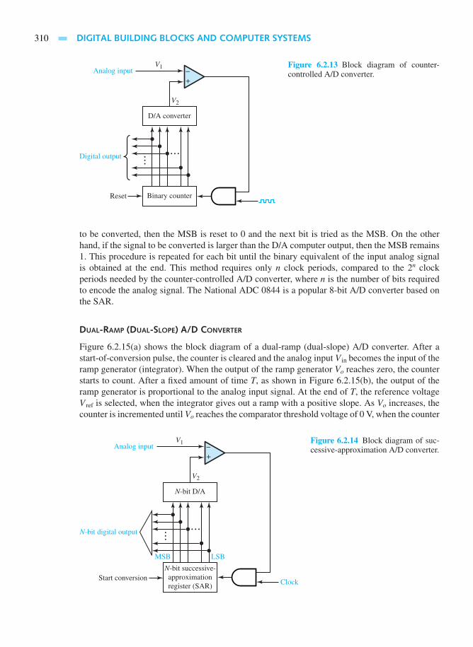
310 DIGITAL BUILDING BLOCKS AND COMPUTER SYSTEMS
+−
V1
V2
D/A converter
Reset
Digital output
Analog input
Binary counter
Figure 6.2.13 Block diagram of counter-controlled A/D converter.
to be converted, then the MSB is reset to 0 and the next bit is tried as the MSB. On the otherhand, if the signal to be converted is larger than the D/A computer output, then the MSB remains1. This procedure is repeated for each bit until the binary equivalent of the input analog signalis obtained at the end. This method requires only n clock periods, compared to the 2n clockperiods needed by the counter-controlled A/D converter, where n is the number of bits requiredto encode the analog signal. The National ADC 0844 is a popular 8-bit A/D converter based onthe SAR.
DUAL-RAMP (DUAL-SLOPE) A/D CONVERTER
Figure 6.2.15(a) shows the block diagram of a dual-ramp (dual-slope) A/D converter. After astart-of-conversion pulse, the counter is cleared and the analog input V in becomes the input of theramp generator (integrator). When the output of the ramp generator Vo reaches zero, the counterstarts to count. After a fixed amount of time T, as shown in Figure 6.2.15(b), the output of theramp generator is proportional to the analog input signal. At the end of T, the reference voltageV ref is selected, when the integrator gives out a ramp with a positive slope. As Vo increases, thecounter is incremented until Vo reaches the comparator threshold voltage of 0 V, when the counter
+−
V1
V2
N-bit D/A
Start conversion
N-bit digital output
Analog input
N-bit successive-approximationregister (SAR)
MSB LSB
Clock
Figure 6.2.14 Block diagram of suc-cessive-approximation A/D converter.
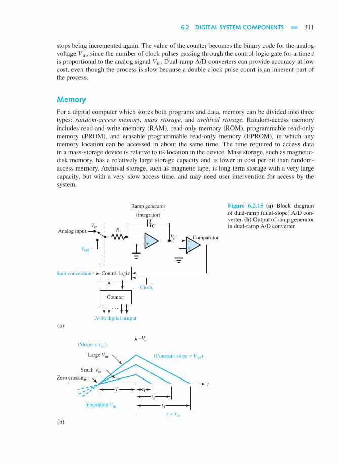
6.2 DIGITAL SYSTEM COMPONENTS 311
stops being incremented again. The value of the counter becomes the binary code for the analogvoltage V in, since the number of clock pulses passing through the control logic gate for a time tis proportional to the analog signal V in. Dual-ramp A/D converters can provide accuracy at lowcost, even though the process is slow because a double clock pulse count is an inherent part ofthe process.
Memory
For a digital computer which stores both programs and data, memory can be divided into threetypes: random-access memory, mass storage, and archival storage. Random-access memoryincludes read-and-write memory (RAM), read-only memory (ROM), programmable read-onlymemory (PROM), and erasable programmable read-only memory (EPROM), in which anymemory location can be accessed in about the same time. The time required to access datain a mass-storage device is relative to its location in the device. Mass storage, such as magnetic-disk memory, has a relatively large storage capacity and is lower in cost per bit than random-access memory. Archival storage, such as magnetic tape, is long-term storage with a very largecapacity, but with a very slow access time, and may need user intervention for access by thesystem.
Figure 6.2.15 (a) Block diagramof dual-ramp (dual-slope) A/D con-verter. (b) Output of ramp generatorin dual-ramp A/D converter.

312 DIGITAL BUILDING BLOCKS AND COMPUTER SYSTEMS
READ-AND-WRITE MEMORY (RAM)
Writing is the same as storing data into memory and reading is the same as retrieving the data later.RAM is said to be volatile because its contents are retained only as long as power is present. ARAM device is a collection of 2n addressable storage locations, each of which contains k bits. Itsblock diagram is shown in Figure 6.2.16, in which each cell may be a flip-flop or a capacitor, andn address lines are decoded to select k cells. A static RAM, in which each cell is a flip-flop, is theread-and-write memory that retains its data so long as the power is applied, without any furtheraction needed from the computer. Static RAM is used in microprocessor-based systems requiringsmall memory. Common static-RAM sizes are 2K× 8, 8K× 8, and 32K× 8, where K stands for210= 1024. A dynamic RAM, in which each cell is a capacitor (which leaks charges and thereforerequires continuous refreshing from the computer to maintain its value), is the read-and-writememory that is used in large memory systems due to its lower cost and greater density. Commondynamic-RAM packages are available in 16K-bit, 64K-bit, 256K-bit, and 1M-bit (where M standsfor mega = 220) sizes.
READ-ONLY MEMORY (ROM)
ROM is nonvolatile (because it maintains its contents even when its power is shut off) and isused to store data and programs that do not change during the operation of the system. Themask-programmed ROMs are read-only devices that are programmed for data storage during themanufacturing of the chip itself. These are generally less expensive devices for mass production.Character-font memory for laser printers is a good example. Programmable read-only memory(PROM) is a field-programmable memory that is fabricated by the manufacturer containing all 0sand is programmed irreversibly by the user by electrically changing appropriate 0s to 1s. PROMsare quite economical in small quantities. Erasable programmable read-only memory (EPROM)is nonvolatile and widely used in microprocessor systems for program storage. It can be erased byshining an ultraviolet light and reprogrammed if necessary. These are produced in low to moderatevolumes.
ELECTRICALLY ERASABLE PROGRAMMABLE ROM (EEPROM)
EEPROM is used for remote-area applications. The device is provided with special pins which,when activated electrically, alter the rewriting of selected memory locations.
MAGNETIC STORAGE DEVICES
Magnetic disk memory is nonvolatile and provides large storage capabilities with moderate accesstimes. The data are stored on one or more rigid aluminum circular disks coated with iron oxide. The
Enable
Read Write
k data lines
2n × k matrixof memory
cellsn address lines
Figure 6.2.16 Block diagram of 2n× k-bit RAM device.

6.2 DIGITAL SYSTEM COMPONENTS 313
most common disks have 11-in diameters and 200 tracks (concentric rings of data) per surface,numbered from 0 to 199, starting with the outside perimeter of the disk, with a typical trackpacking density of 4000 bits per inch. Disks are mounted on a common spindle, and all disksrotate at a typical speed of 3600 revolutions per minute (rpm). A typical disk has 17 sectors offixed size per track and 512 bytes (1 byte = 8 bits) of information per sector. Any desired sectorcan be quickly accessed.
Floppy disks, also known as flexible disks, are the low-cost, medium-capacity, nonvolatilememory devices made of soft flexible mylar plastic with magnetically sensitive iron-oxide coating.The original 8-in standard floppy is no longer in popular use. The 51/4-in minifloppy has a diskand a disk jacket covering the mylar media for protection, along with a write-protect notch andindex hole. The present-day minifloppy disks are either double-sided/double-density (DS/DD)with 9 sectors per track and 40 tracks per side or double-sided/quad-density (DS/QD) with 9 or15 sectors per track and 80 tracks per side. In a DS/DD minifloppy disk, about 720 kbytes of datacan be stored; whereas in a DS/QD mini-floppy disk, about 1–2 Mbytes of data can be stored.
The 31/2-in microfloppy disk, also known as a microdiskette, is enclosed in a rigid protectivecase and is provided with a write-protect notch. Microdiskettes are recorded in quad-densityformat with a capacity of 2 Mbytes; 4- to 16-Mbyte 31/2-in diskettes are being developed. Also,2-in diskettes are introduced in electronic cameras and portable personal computers.
Magnetic tapes are ideal devices for storing vast quantities of information inexpensively.However, the access time is slow because the entire tape must be read sequentially. The mostcommonly used tapes are ½-in wide, 2400 or 3600 ft long, and contained in a long 10½-in reel.Tape densities of 200, 556, 800, 1600, 6250, and 12,500 bits per inch (BPI) are standard.
In addition to these magnetic storage devices, two newer types of secondary storage havecome into use: winchester disks and videodisks (also known as optical disks). The former are sealedmodules that contain both the disk and the read/write mechanism, requiring little maintenance andallowing higher-density recording. The latter have been introduced recently, with high reliabilityand durability and a storage capacity of 1 Gbyte of data (equivalent to almost 400,000 typewrittenpages of information). A typical 14-in optical disk has 40,000 tracks and 25 sectors per track,with each sector holding up to 1 kbyte of information. While a write-once optical-disk drive iscurrently available, a read-and-write drive is being developed.
Display Devices
Display devices can be categorized as on/off indicators, numeric, alphanumeric, or graphicaldisplays. They may also be classified as active and passive devices. Active display devices emitlight, such as light-emitting diodes (LEDs), whereas passive display devices, such as liquid-crystaldisplays (LCDs), reflect or absorb light.
LIGHT-EMITTING DIODE (LED)
This is a reliable, rugged, and inexpensive semiconductor display device requiring about 10 mAof current flow for full illumination. An LED is shown in Figure 6.2.17. It is available in red,yellow, or green color, in common sizes of T-1 and T-13/4, where the number after the T denotesthe diameter of the lamp in units of eighths of an inch. Two-color LEDs are also available.
LIQUID-CRYSTAL DISPLAY (LCD)
This display needs only microwatts of power (over a thousand times less than a LED) and is usedin such devices as electronic wristwatches. With the application of an electric field the molecules

314 DIGITAL BUILDING BLOCKS AND COMPUTER SYSTEMS
On/Off
7404
+5 V
LED
R
Figure 6.2.17 Light-emitting diode (LED).
of the liquid-crystal material are straightened out, absorbing the light, and the display appearsblack. With no electric field applied, the display appears as a silver mirror because the light isreflected.
SEGMENT DISPLAYS
Seven-segment displays are the most commonly used numeric display devices, while 10- and16-segment (starburst) display devices are also available. Figure 6.2.18(a) depicts a common-cathode seven-segment LED display; Figure 6.2.18(b) shows its internal structure, consisting ofa single LED for each of the segments; and Figure 6.2.18(c) displays the digits by an appropriatecombination of lighted segments. The 16-segment display shown in Figure 6.2.18(d) is commonlyused for alphanumeric data.
(a)
(b)
(d)
(c)
a
a
g
d
f
e
b
c
b c d e f g
Figure 6.2.18 (a) Seven-segment display.(b) Internal structure of seven-segment dis-play. (c) Digits displayed by a seven-segmentdisplay. (d) 16-segment (starburst) display.
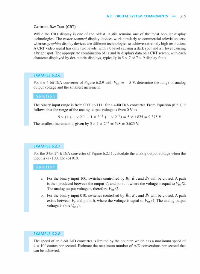
6.2 DIGITAL SYSTEM COMPONENTS 315
CATHODE-RAY TUBE (CRT)
While the CRT display is one of the oldest, it still remains one of the most popular displaytechnologies. The raster-scanned display devices work similarly to commercial television sets,whereas graphics display devices use different technologies to achieve extremely high resolution.A CRT video signal has only two levels, with a 0 level causing a dark spot and a 1 level causinga bright spot. The appropriate combination of 1s and 0s displays data on a CRT screen, with eachcharacter displayed by dot-matrix displays, typically in 5× 7 or 7× 9 display fonts.
EXAMPLE 6.2.6
For the 4-bit D/A converter of Figure 6.2.9 with Vref = −5 V, determine the range of analogoutput voltage and the smallest increment.
So l u t i on
The binary input range is from 0000 to 1111 for a 4-bit D/A converter. From Equation (6.2.1) itfollows that the range of the analog output voltage is from 0 V to
5× (1+ 1× 2−1 + 1× 2−2 + 1× 2−3) = 5× 1.875 = 9.375 V
The smallest increment is given by 5× 1× 2−3 = 5/8 = 0.625 V.
EXAMPLE 6.2.7
For the 3-bit 2n–R D/A converter of Figure 6.2.11, calculate the analog output voltage when theinput is (a) 100, and (b) 010.
So l u t i on
a. For the binary input 100, switches controlled by B0, B1, and B2 will be closed. A pathis then produced between the output Vo and point 4, where the voltage is equal to Vref /2.The analog output voltage is therefore Vref/2.
b. For the binary input 010, switches controlled by B0, B1, and B2 will be closed. A pathexists between Vo and point 6, where the voltage is equal to Vref/4. The analog outputvoltage is thus Vref/4.
EXAMPLE 6.2.8
The speed of an 8-bit A/D converter is limited by the counter, which has a maximum speed of4 × 107 counts per second. Estimate the maximum number of A/D conversions per second thatcan be achieved.

316 DIGITAL BUILDING BLOCKS AND COMPUTER SYSTEMS
So l u t i on
The rate of the clock will be constant, independent of the analog input. It must be slow enoughto allow the counter to count up to the highest possible input voltage. This will require 255(=27 + 26 + 25 + 24 + 23 + 22 + 21 + 20) counts, which will take 255/(40 × 106) = 6.375 µs.Thus, the process can be repeated 106/6.375 = 156,863 times per second.
EXAMPLE 6.2.9
If it is desired to store English-language writing with 1 byte representing each letter, find theminimum number of bits per byte that could be used.
So l u t i on
For the 26 letters in the English alphabet, we must have 2N ≥ 26, where N is the number of bitsper byte. N being an integer, the smallest possible value for N is 5. One can represent the letterA by 00000, B by 00001, and so on up to Z by 11001; the remaining six combinations could beused for representing punctuation marks or spaces. This is, in fact, the method by which lettersare represented in teletype systems.
If one wants to store capital English-language letters also, there will be 52 letters instead of26; in such a case 6-bit bytes would have to be used.
6.3 COMPUTER SYSTEMS
Digital computers, in general, are automatic machines that accept data and instructions, performpredefined operations very quickly on the data, and have the results available to the user invarious forms. They can be classified as microcomputers, minicomputers, mainframes, andsupercomputers.
Microcomputers have become a common part of everyday life. The cost ranging from afew hundred to about ten thousand dollars, today’s 16- and 32-bit microcomputer systems arealso dedicated for real-time applications in a distributed system. A microprocessor is an LSIdevice, which is a realization of the computer central-processor unit (CPU) in IC form. Themicroprocessor is the CPU of the microcomputer system.
Minicomputers, developed in the early 1960s, are high-performance, general-purpose multi-user computers. These are also designed for real-time dedicated applications. The PDP-11 seriesfrom Digital Equipment Corporation (DEC) have been the most prominent 16-bit minicomputers,and are now obsolete. The 32-bit minicomputers, known as superminis, were developed in the1970s, the most prominent one being the VAX 8600 from DEC, which was capable of executingabout 5 million instructions per second (MIPS). New VAX lines with larger MIPS have beendeveloped since.
Mainframes, capable of executing in excess of 53 MIPS, are high-performance, general-purpose computers supporting very large databases, ranging in price from one to ten milliondollars. These are used by many universities, large businesses, and government agencies, and aresupplied mainly by IBM. Examples include IBM 360, CDC 7600 of Control Data Corporation,and Texas Instrument Advanced Scientific Computer (TI–ASC).
Supercomputers, capable of executing in excess of one billion floating-point operations persecond (FLOPS), are very powerful, extremely high-performance computers for applications that

6.3 COMPUTER SYSTEMS 317
are beyond the reach of the mainframes, and cost more than ten million dollars. These are usedfor weather prediction, image processing, and nuclear-energy studies that require high-precisionprocessing of ordered data achieved by a speed advantage due to parallel processors. Cyber 205,Cray X-MP, and Cray 2 are some examples of supercomputers. In the 1980s, supercomputingcenters were developed at six American universities for high performance computing. By 1990 itwas possible to build chips with a million components; semiconductor memories became standardin all computers; widespread use of computer networks and workstations had occurred. Explosivegrowth of wide area networking took place with transmission rates of 45 million bits per second.
Organization
There are two principal components: hardware and software. The former refers to physicalcomponents such as memory unit (MU), arithmetic and logic unit (ALU), control unit (CU),input/output (I/O) devices, etc.; whereas the latter refers to the programs (collections of orderedinstructions) that direct the hardware operations.
Figure 6.3.1 illustrates the basic organization of a digital computer. The MU stores both dataand programs that are currently processed and executed. The ALU processes the data obtainedfrom the MU and/or input devices, and puts the processed data back into the MU and/or outputdevices. The CU coordinates the operations of the MU, ALU, and I/O units. While retrievinginstructions from programs resident in the MU, the CU decodes these instructions and directs theALU to perform the corresponding processing; it also oversees the I/O operations. Input devicesmay consist of card readers, keyboards, magnetic tape readers, and A/D converters; output devicesmay consist of line printers, plotters, and D/A converters. Devices such as terminals and magneticdisk drives have both input and output capabilities. For communicating with the external worldand for storing large quantities of data, a variety of I/O devices are used.
Software may be classified as system software and user software. The former refers to thecollection of programs provided by the computer system for the creation and execution of theuser programs, whereas the latter refers to the programs generated by various computer users forsolving their specific problems.
A program generally consists of a set of instructions and data specifying the solution ofa particular problem. Programs (and data) expressed in the binary system (using 0s and 1s)are known as machine-language programs. Writing programs in this form, which demands
Data
Control
Control
Address
ALU(arithmetric
andlogic unit)
CU(control unit)
CPU(central processing unit)
Data
Data
Data
Disk
Printer
Input
Terminal
MU(memory
unit)
I/O(Input/
output unit)
Figure 6.3.1 Typical organization of a computer.

318 DIGITAL BUILDING BLOCKS AND COMPUTER SYSTEMS
a detailed knowledge of the computer structure, is rather tedious and error-prone. Assembly-language programming is developed by using symbolic names, known as mnemonics, andmatching machine-language instructions on a more or less one-for-one basis. An assembleris then used to translate assembly-language programs into their equivalent machine-languageprograms. Because both assembly-language and machine-language programmings are specificto a particular computer, high-level languages (HLL) such as Fortran, Pascal, Basic, LISP, andC have been developed such that programs written by using them could be run on virtually anycomputer. Also, these are problem-oriented languages, which allow the user to write programs informs that are as close as possible to the human-oriented languages.
An interpreter translates each high-level-language statement into its equivalent set ofmachine-language instructions, which are then executed right away. Interpretive languages suchas Basic are very inefficient for programs with loops (repetitive instructions). The inefficiency iscorrected by a compiler, which translates the complete high-level language into machine language.Once the whole program is compiled, it can be executed as many times as desired without anyneed for recompilation. Examples of compiler languages are Fortran, Pascal, and C.
An operating system, such as DOS, VMS, or UNIX, consisting of a set of system programs,performs resource management and human-to-machine translation, supporting a given computerarchitecture. Operations such as starting and stopping the execution, as well as selecting a specificcompiler or assembler for translating a given program into machine language, are taken care of bythe operating system, which is unique for a given microcomputer, minicomputer, or mainframe.
Architecture
Replacing the ALU and CU (i.e., CPU) of Figure 6.3.1 by a microprocessor, and storinginstructions and data in the same memory, one arrives at a stored-program computer or amicrocomputer. A bus, which is a set of wires carrying address, data, and control signals, isemployed for interconnecting the major components of a microcomputer system. The address linesare unidirectional signals that specify the address of a memory location of an I/O device. With atypical 24-bit address bus, the microprocessor can access 224 (over 16 million) memory locations.Memory is generally organized in blocks of 8, 16, or 32 bits. The data bus is a bidirectional bus,varying in size from 8 to 32 bits, which carries data between the CPU, MU, and I/O units. Thecontrol bus provides signals to synchronize the memory and I/O operations, select either memoryor an I/O device, and request either the read or the write operation from the device selected.
While there are virtually countless variations in microprocessor circuit configurations, thesystem architecture of a typical microprocessor is shown in Figure 6.3.2. The arithmetic logicunit (ALU) accepts data from the data bus, processes the data as per program-storage instructionsand/or external control signals, and feeds the results into temporary storage, from which externalcontrol and actuator control functions can be performed. The accumulators are parallel storageregisters used for processing the work in progress, temporarily storing addresses and data, andhousekeeping functions. The stacks provide temporary data storage in a sequential order and areof use during the execution of subroutines. A subroutine is a group of instructions that appearsonly once in the program code, but can be executed from different points in the program. Theprogram counter is a register/counter that holds the address of the memory location containingthe next instruction to be executed. The status register contains condition-code bits or flags (setto logic 1 or logic 0, depending on the result of the previous instruction) that are used to makedecisions and redirect the program flow. The control unit (CU), which consists of the timingand data-routing circuits, decodes the instruction being processed and properly establishes datapaths among the various elements of the microprocessor. Interconnections may take the form of

6.3 COMPUTER SYSTEMS 319
gates that the control section enables or disables according to the program instructions. That isto say, programming at the machine-language level amounts to wiring with software instead ofhard-wired connections.
Microprocessors have instruction sets ranging from 20 to several hundred instructions,known as microprograms, which are stored in ROM to initiate the microprocessor routines.The instructions generally consist of a series of arithmetic and logic type operations, and alsoinclude directions for fetching and transferring data. Microprocessors are classified by word sizein bits, such as 1-, 4-, 8-, and 16-bit microprocessors; generally speaking, the larger the wordsize, the more powerful the processor. Three popular 8-bit microprocessors (µp) are Intel 8085,Zilog Z80, and Motorola MC6800; the 16-bit microprocessors dominating the market are Intel8086 and 80286, Motorola MC68000, and Zilog Z8000; the powerful 32-bit microprocessors atthe very high end of the market started with Intel 80386, Intel 80486, Motorola MC68020, andNational N532032. Still more powerful Intel Pentium processors such as Pentium II and III wereintroduced in the 1990’s, and even these are going to be replaced soon by Intel Itanium Processors.
A microprocessor system bus consists of three physical buses: the address bus, the databus, and the control bus. The types of circuits connected to microprocessor buses are registers,accumulators, or buffer circuits between the bus and the external memory or I/O devices.Multiplexing is usually used, which is to connect each register to a bus on a time-shared basis,only when it is being read. An operating bus is used to transfer various internal operationsand commands. An interface bus, such as the IEEE-488 (developed in 1975 by the Instituteof Electrical and Electronics Engineers) or the GPIB (general-purpose interface bus) provides the
Data bus
I/O databuffers
Instructionregistor
Addressgeneration
Programaddress register
Programstorage
Control
Actuatorcontrol
Controlunit
Control Clock
Address bus
Operand busSt
acks
Acc
umul
ator
Prog
ram
coun
ter
Tem
pora
ryre
gist
er
Stat
usre
gist
er
Arithmetric andlogic unit
Figure 6.3.2 Block diagram of typical microprocessor system architecture.

320 DIGITAL BUILDING BLOCKS AND COMPUTER SYSTEMS
means of communicating between the computer and the outside world with external devices suchas oscilloscopes, data collection devices, and display devices. Most present-day data acquisitionsystems are designed to be compatible with microprocessors for processing the measured data.A typical data acquisition and processing system is illustrated in Figure 6.3.3.
Amplification
Inpu
t sig
nals
Tra
nsdu
cers
Displays
Multiplexer
Reference
Analog-to-digitalconverter
DisplayStorageControlMainframecomputer
Micro-processor
Figure 6.3.3 Block diagram of typical data acquisition and processing system.
6.4 COMPUTER NETWORKS
Computer communications networks are the outcome of a combination of computers and telecom-munication products. An interconnected group of independent computers and peripheral devicesthat communicate with each other for the purpose of sharing software and hardware resourcesis known as a computer communications network. A local-area network (LAN) is any physicalnetwork technology that operates at high speed (usually tens of Mbits per second through severalGbits per second) over short distances (up to a few thousand meters). Examples include Ethernetand proNET-10. The stations, also known as nodes, within a LAN are physically linked witheach other through twisted pairs of copper wires, coaxial cables, or fiber-optic cables. A wide-area network (WAN, also known as long-haul network) is any physical network that spans largegeographic distances, usually operates at slower speeds, and has significantly higher delays thana LAN. Stations within a WAN communicate with each other through standard telephone lines,dedicated telephone lines, line-of-sight microwave systems, or fiber-optic links. Public-datanetwork (PDN) is network service offered by a common carrier, such as Telnet, Tymnet, andDataphone Digital Services of AT&T. ARPANET (Advanced Research Projects Agency of theU.S. Department of Defense) is an example of a private communications network. CYBERNETis an example of a remote-access communications network that provides access to huge databasesfor their users in different countries. The Internet is a collection of networks and gateways (special-purpose dedicated computers attached to various networks routing packets of information from oneto the other), including the Milnet (military network) and NSFNET (National Science Foundationnetwork), that function as a single, cooperative virtual network providing universal connectivityand application-level services such as the electronic mail. The Internet reaches many universities,government research labs, and military installations in several countries.
The future scope of the Internet, along with the World Wide Web (born in 1990), and thecommercialization of the Internet are bound to grow exponentially. In 1991, the U.S. Congresspassed the High Performance Computing Act to establish the National Research and EducationNetwork (NREN), which allows the electronic transfer of the entire Encyclopedia Britannica inone second. Computer networks worldwide will feature 3–D animated graphics, radio and cellularphone-links to portable computers, as well as fax, voice, and high-definition television. While theWeb is fast becoming a part of our everyday lives, the real Internet of the future may bear verylittle resemblance to today’s plans.

6.4 COMPUTER NETWORKS 321
Network Architecture
A protocol is a formal description of message formats and the rules two or more machinesmust follow to exchange those messages. Because TCP (transmission control protocol) and IP(Internet protocol) are the two most fundamental protocols, the entire protocol suite that is usedby the Internet is often referred to as TCP/IP. X.25 is the CCITT (Consultative Committee onInternational Telephony and Telegraphy) standard protocol employed by Telnet, and is mostpopular in Europe. Ethernet utilizes CSMA/CD (carrier sense multiple access with collisiondetection) protocol technology.
Computer network architecture refers to the convention used to define how the differentprotocols of the system interact with each other to support the end users. The most commonnetwork architecture model is the open-systems interconnections (OSI). Figure 6.4.1 showsthe ISO (International Standards Organization) seven-layer model for an OSI. Although not alllayers need be implemented, the more layers that are used, the more functionality and reliabilityare built into the system. Starting from the bottom layer, the functions of the layers are asfollows.
1. Physical—Defines the type of medium, the transmission method, and the transmissionrates available for the network; provides the means for transferring data across theinterconnection channel and controlling its use.
2. Data Link—Defines how the network medium is accessed, which protocols are used,
Layer 7: ApplicationLayer 7 protocol
Layer 6 protocol
Layer 5 protocol
Layer 4 protocol
Layer 3 protocol
Layer 2 protocol
Layer 1 protocol
Layer 6: Presentation
Layer 5: Session
Layer 4: Transport
Layer 3: Network
Layer 2: Data link
Layer 1: Physical
Interconnection channel
Layer 7: Application
Process A
Virtual communicationsshown by dashed lines
Physicalcommunicationsshown bysolid lines
Process B
Layer 6: Presentation
Layer 5: Session
Layer 4: Transport
Layer 3: Network
Layer 2: Data link
Layer 1: Physical
Figure 6.4.1 ISO 7-layer model for an OSI.

322 DIGITAL BUILDING BLOCKS AND COMPUTER SYSTEMS
the packeting/framing methods, and the virtual circuit/connection services; responsiblefor the transfer of data across the link; provides for the detection and correction of data-transmission errors.
3. Network—Standardizes the way in which addressing is accomplished between linkednetworks; performs networking functions and internetworking.
4. Transport—Handles the task of reliable message delivery and flow control betweenapplications on different stations; provides source-to-destination data integrity.
5. Session—Establishes two-way communication between applications running on differentstations on the network; provides the user interface into the transport layer.
6. Presentation—Translates data formats so that computers with different “languages” cancommunicate; provides the syntax (rules) of representation of data between devices.
7. Application—Interfaces directly with the application programs running on the stations;provides services such as file access and transfer, peer-to-peer communication amongapplications, and resource sharing; provides support to process end users’ applicationssuch as electronic mail, database management, and file management.
Note that the interconnection channel is not a part of the OSI specification.
Network Topology
This deals with the geometrical arrangement of nodes (endpoints consisting of physical devicessuch as terminals, printers, PCs, and mainframes) interconnected by links (transmission channels).Network topologies may be classified as bus topology (multidrop topology), star topology, ringtopology, tree topology, and distributed (mesh or hybrid) topology, as illustrated in Figure 6.4.2.Bus topology is used predominantly by LANs, whereas star topology is commonly used byprivate-branch exchange (PBX) systems. Ring topology may have centralized control (with onenode as the controller) or decentralized control (with all nodes having equal status). Tree topologyis used in most of the remote-access networks, whereas distributed topology is common in publicand modern communications networks. A fully distributed network allows every set of nodes tocommunicate directly with every other set through a single link and provides an alternative routebetween nodes.
The Internet is physically a collection of packet switching networks interconnected bygateways along with protocols that allow them to function logically as a single, large, virtualnetwork. Gateways (often called IP routers) route packets to other gateways until they canbe delivered to the final destination directly across one physical network. Figure 6.4.3 showsthe structure of physical networks and gateways that provide interconnection. Gateways do notprovide direct connections among all pairs of networks. The TCP/IP is designated to provide auniversal interconnection among machines, independent of the particular network to which theyare attached. Besides gateways that interconnect physical networks, as shown in Figure 6.4.3,Internet access software is needed on each host (any end-user computer system that connects toa network) to allow application programs to use the Internet as if it were a single, real physicalnetwork. Hosts may range in size from personal computers to supercomputers.
Transmission Media
These, also known as physical channels, can be either bounded or unbounded. Bounded media,in which signals representing data are confined to the physical media, are twisted pairs of wires,

6.4 COMPUTER NETWORKS 323
(a)
(b)
(c)
(d)
(e)
Figure 6.4.2 Network topologies. (a) Bus (multidrop)topology. (b) Star topology. (c) Ring topology. (d) Treetopology. (e) Distributed (mesh or hybrid) topology.
Hosts
Internet
Physicalnets
Gateways
Figure 6.4.3 Structure of typical TCP/IPInternet.
coaxial cables, and optical-fiber cables, used in most LANs. Unbounded media, such as theatmosphere, the ocean, and outer space in which the transmission is wireless, use infrared radiation,lasers, microwave radiation, radio waves, and satellites. Data are transmitted from one node toanother through various transmission media in computer communications networks.
Twisted pairs are used in low-performance and low-cost applications with a data rate of about1 Mbit per second (Mbps) for a transmission distance of about 1 km. Baseband coaxial cablesused for digital transmission are usually 50- cables with a data rate of about 10 Mbps over adistance of about 2 km. Broad-band coaxial cables used for analog transmission (cable TV) areusually 75- cables with a data rate of about 500 Mbps over a distance of about 10 km. Thelighter and cheaper fiber-optic cables support data transmission of about 1 Gbps over a distanceof about 100 km.

324 DIGITAL BUILDING BLOCKS AND COMPUTER SYSTEMS
Data Transmission and Modems
Data can be transferred between two stations in either serial or parallel transmission. Paralleldata transmission, in which a group of bits moves over several lines at the same time, is used whenthe two stations are close to each other (usually within a few meters), as in a computer–printerconfiguration. Serial data transmission, in which a stream of bits moves one by one over a singleline, is used over a long distance. Serial data transfer can be either asynchronous or synchronous.Asynchronous data communication is most commonly applied in low-speed terminals and smallcomputers. Large-scale integration (LSI) devices known as UARTs (universal asynchronous re-ceivers/transmitters) are commercially available for asynchronous data transfer. Synchronous datacommunication is used for transferring large amounts of data at high speed. USARTs (universalsynchronous/asynchronous receivers/transmitters) are commercially available LSI devices.
Frequency-division multiplexing (FDM) is a technique for data transmission widely usedin telephone, radio, and cable TV systems in which the transmission frequency spectrum (i.e.,bandwidth) is divided into smaller bands known as subchannels.
Data transmission between two stations can be achieved in either simplex, half-duplex, orfull-duplex mode. In a simplex mode, mainly used in radio and TV broadcasts, information travelsonly in one direction. This mode is rarely used in data communications. In half-duplex mode, usedby radio communications, information may travel in both directions, but only in one direction ata time. The transmitter becomes the receiver and vice versa. In a full-duplex mode, informationmay travel in both directions simultaneously. This mode, used in telephone systems, adopts twodifferent carrier frequencies.
A modem (modulator/demodulator) is an electronic device that takes digital data as a serialstream of bits and produces a modulated carrier signal as an output. That is to say, the digitalsignals are converted to an analog form with a relatively narrow bandwidth. The carrier signal isthen transmitted over the telephone line to a similar modem at the receiving end, where the carriersignal is demodulated back into its original serial stream of bits, as shown in Figure 6.4.4. Theserial digital data to be transmitted are modulated, filtered, and amplified for analog transmission;the analog data received at the receiving end are amplified, filtered, and demodulated to produceserial digital signals.
There are four different types of modems: half-duplex, full-duplex, synchronous, and asyn-chronous. With half-duplex modems data can be transmitted in only one direction at a time. Full-duplex modems transmit data in both directions at the same time; one modem is designated as theoriginating modem and the other as the answering modem, while transmitting and receiving dataare done at different frequencies. Asynchronous modems are low-data-rate modems transmittingserial data at a rate of about 1800 bits per second (bps). Synchronous modems are high-data-ratemodems transmitting serial data at a rate of about 10,800 bps.
Modems can also be classified as voice-band or wide-band modems. Voice-band modems arelow-to-high speed modems designed for use on dial-up, voice-grade, standard telephone lines up to
Modulated signal
Modem Modem
SourceDigital signal Digital signalDestination
Figure 6.4.4 Input/output signals of a modem.

6.6 PRACTICAL APPLICATION: A CASE STUDY 325
a rate of about 10,800 bps. Microprocessor-controlled modems are known as smart modems, suchas the Hayes modem, manufactured by Hayes Microcomputer Products. The portable acoustic-coupler device, which is a different type of voice-band modem, is a low-speed modem with arate of about 600 bps that is connected acoustically to a standard telephone. Wide-band modemsare very high-speed modems with rates of 19,200 bps and above, designed for use with dedicatedtelephone lines. These are currently used mostly on private communications systems.
6.5 LEARNING OBJECTIVES
The learning objectives of this chapter are summarized here, so that the student can check whetherhe or she has accomplished each of the following.
• Understanding continuous, discrete, and binary digital signals.
• Performing operations with binary, octal, hexadecimal, and binary-coded-decimal numbersystems.
• Logic symbols and truth tables for various gates.
• Designing simple combinational logic circuits using logic gates.
• Using Karnaugh maps to realize logic expressions.
• Sketching timing diagrams for sequential circuits based on flip-flops.
• Digital system components such as decoders, encoders, multiplexers, registers, counters,D/A and A/D converters, memory, and display devices.
• Basic understanding of computer systems.
• Basic notions about computer networks.
6.6 PRACTICAL APPLICATION: A CASE STUDY
Microcomputer-Controlled Breadmaking Machine
Figure 6.6.1 shows a simplified schematic diagram of a microcomputer-controlled breadmakingmachine. A microcomputer along with its timing circuit, keypad, and display unit controls theheating resistor, fan motor, and bread-ingredient mixing motor by means of digitally activatedswitches. An analog temperature sensor, through an A/D converter, provides the status oftemperature to the microcomputer. A digital timer circuit counts down, showing the time remainingin the process.
The control programs are stored in ROM and determine when and how long the machineshould mix the ingredients added to the bread pan, when and how long the heating resistor shouldbe turned on or off for various parts of the cycle, and when and how long the fan should be on tocool the loaf after baking is finished. The parameters such as light, medium, or dark bread crustare entered through the keypad into RAM.
According to the programs stored and the parameters entered, the machine initially mixesthe ingredients for several minutes. The heating resistor is turned on to warm the yeast, causingthe dough to rise while a temperature of about 90°F is maintained. The time remaining and thetemperature are continually checked until the baked loaf is cooled, and the finished bread is finallyready in about 4 hours.
Microprocessors and computers in various forms are used extensively in household appli-ances, automobiles, and industrial equipment.

326 DIGITAL BUILDING BLOCKS AND COMPUTER SYSTEMS
Timer
Microcomputer
Digitallyactivatedswitches
Breadingredientcontainer
Heatingresistor
Mixingmotor
Coolingfan
Fanmotor
To 120-V60-Hzsupply
Keypad Display
Temperaturesensor
ADC
Figure 6.6.1 Simplified schematic diagram of a microcomputer-controlled breadmaking machine.
PROBL EMS
6.1.1 Convert the following binary numbers into deci-mal numbers:
(a) (10110)2
(b) (101100)2
(c) (11010101)2
(d) (11101.101)2
(e) (.00101)2
6.1.2 Convert the following decimal numbers into bi-nary numbers:
(a) (255)10
(b) (999)10
(c) (1066)10
(d) (0.375)10
(e) (1259.00125)10
*6.1.3 Convert the following octal numbers into decimalnumbers:
(a) (257)8
(b) (367)8
(c) (0.321)8
(d) (367.240)8
(e) (2103.45)8
6.1.4 Convert the following decimal numbers into octalnumbers:
(a) (175)10
(b) (247)10
(c) (65,535)10
(d) (0.125)10
(e) (379.25)10
6.1.5 Convert the following octal numbers into binarynumbers:
(a) (3425)8
(b) (3651)8
(c) (.214)8
(d) (4125.016)8
(e) (4573.26)8
6.1.6 Convert the following binary numbers into octalnumbers:
(a) (011 100 010 101)2

PROBLEMS 327
(b) (1011010)2
(c) (.110101)2
(d) (100101111011.01011)2
(e) (1110110111.1011)2
6.1.7 Convert the following hexadecimal numbers intodecimal numbers:
(a) (6B)16
(b) (1F4)16
(c) (C59)16
(d) (256.72)16
(e) (.0E3)16
*6.1.8 Convert the following decimal numbers into hex-adecimal numbers:
(a) (97)10
(b) (864)10
(c) (5321)10
(d) (0.00125)10
(e) (449.375)10
6.1.9 Convert the following binary numbers into hex-adecimal numbers:
(a) (11101110100100.100111)2
(b) (1011011101)2
(c) (.11101)2
(d) (1101110001.11011110)2
(e) (.0000110111000101)2
6.1.10 Convert the following hexadecimal numbers intobinary numbers:
(a) (2ABF5)16
(b) (3BA4.9C)16
(c) (0.0DC5)16
(d) (15CE.FB3)16
(e) (2AB.F8)16
6.1.11 Convert the following decimal numbers into BCDnumbers:
(a) (567)10
(b) (1978)10
(c) (163.25)10
(d) (0.659)10
(e) (2153.436)10
6.1.12 Convert the following BCD numbers into decimalnumbers:
(a) (010101100111)BCD
(b) (.011001011001)BCD
(c) (.100110000100)BCD
(d) (10010010.00000001)BCD
(e) (0010000101010011.010000110110)BCD
*6.1.13 Obtain the truth table for the logic block shown inFigure P6.1.13.
6.1.14 Find the output function Y for the logic circuits ofFigure P6.1.14 (a) and (b).
6.1.15 An AOI (AND-OR-INVERT) gate is shown inFigure P6.1.15 with its two possible realizations.Obtain the output function Y and show that the twocircuits are equivalent.
6.1.16 Figure P6.1.16(a) shows the seven-segment arraythat is widely used to form the decimal digits 0 to 9in LED displays, as indicated in Figure P6.1.16(b).Let the inputs be the four binary digits used torepresent the decimal digits 0 to 9. (a) For thesegment Y1, (b) For the segment Y2, and (c) Forthe segment Y3 to be turned on, develop the logicexpression and find one possible logic circuit torealize the output in each case.
6.1.17 The DeMorgan’s theorems suggest that the basiclogic operations can be realized by use of invertersand NAND gates only. For the circuits shown inFigure P6.1.17, find the truth table, the type of gaterealized, and the expression for the logic output,in each case.
6.1.18 For the NOR and inverter realizations shown inFigure P6.1.18, find the truth table, the type of gaterealized, and the expression for the logic output,in each case.
*6.1.19 Obtain the Boolean expressions for the logic cir-cuits shown in Figure P6.1.19.
6.1.20 Draw the logic diagram for the following Booleanexpressions (without any simplification).
(a) Y = AB + BC
(b) Y = (A+ B)(A+ C)
(c) Y = A · B + B · C + A · B ·D + A · C ·D(d) Y = (A+ B) · (A+ C) · (B + C)
6.1.21 Obtain the Boolean expressions for the logic cir-cuits shown in Figure P6.1.21.
6.1.22 Using Boolean identities, simplify the following:
(a) Y = A+ A · B

328 DIGITAL BUILDING BLOCKS AND COMPUTER SYSTEMS
AF
B
Figure P6.1.13
A
B
Y
(a)
A
B
Y
(b)
Figure P6.1.14
A
B
Y
C
D D
A
B
C
(a)
Y
(b)
Figure P6.1.15
0 1 2 3 4 5 6 7 8 9
(a) (b)
Y5
Y4
Y1
Y2
Y3
Y6
Y7
Figure P6.1.16
B
A
B
A
Y
YY
B
A
Y
(a)
(b)
(c)
Figure P6.1.17

PROBLEMS 329
B
A
B
A
Y
Y
B
A
Y
(a)
(b)
(c)
Y
Figure P6.1.18
A
B
Y
(a)
A
B
C
Y
(b)
Figure P6.1.19
B
A
C
B
Y
(a)
B
A
C
Y
(b)
B
A
C
DY
(c)
Figure P6.1.21

330 DIGITAL BUILDING BLOCKS AND COMPUTER SYSTEMS
(b) Y = A · B + B · C + A · C ·D + A · B ·D(c) Y = (A+ B + C) · (A+ B + C) · C(d) Y = B · C + B · C + A · B · C
6.1.23 The truth table for F(A,B,C) = ∑mi(2, 3, 4,
5) is as follows:
A B C F
0 0 0 00 0 1 00 1 0 10 1 1 11 0 0 11 0 1 11 1 0 01 1 1 0
(a) Express F in a canonical sum-of-productsform.
(b) Minimize F in an SOP form, and obtain apossible realization.
*6.1.24 The truth table for F(A,B,C) = ∏Mi(0, 1, 6,
7) is as follows:
A B C F
0 0 0 00 0 1 00 1 0 10 1 1 11 0 0 11 0 1 11 1 0 01 1 1 0
(a) Express F in a canonical product-of-sumsform.
(b) Minimize F in a POS form and obtain a pos-sible realization.
6.1.25 Using K maps, simplify the following Booleanexpressions:
(a) F = A · B + A · B(b) F = A · C + C ·D + B · C ·D(c) F = A ·B · C+B ·C+A ·B ·D+B ·C ·D
6.1.26 Simplify the following Boolean functions intotheir minimum SOP form, by using K maps.
(a) F(A,B) =∑ mi(0, 1, 3)
(b) F(A,B,C) =∑ mi(0, 2, 3, 4, 5, 6)(c) F(A,B,C,D) = ∑
mi(0, 4, 5, 6, 7,12, 14)
(d) F(A,B) =∏ Mi(0, 2)
(e) F(A,B,C) =∏ Mi(0, 6)
(f) F(A,B,C,D) =∏ M i(1, 3, 11, 14, 15)
6.1.27 Given the following truth table, design the logiccircuit with the use of a K map by using only two-input gates.
A B C D y
0 0 0 0 10 0 0 1 10 0 1 0 10 0 1 1 00 1 0 0 00 1 0 1 10 1 1 0 00 1 1 1 01 0 0 0 11 0 0 1 11 0 1 0 01 0 1 1 11 1 0 0 01 1 0 1 11 1 1 0 01 1 1 1 1
6.1.28 For the logic circuit of Figure P6.1.28, construct atruth table and obtain the minimum SOP expres-sion.
*6.1.29 Simplify the logic circuit of Figure P6.1.29 byreducing the number of gates to a minimum.
6.1.30 Given the following truth table:
(a) Realize the function f by a K map using 0s.
(b) Realize the function f by a K map using 1s.
x y z f
0 0 0 00 0 1 10 1 0 10 1 1 11 0 0 11 0 1 11 1 0 01 1 1 0
6.1.31 Realize the logic function defined by the followingtruth table as the simplest POS form.

PROBLEMS 331
x
y
z
f
Figure P6.1.28
z
y
x
f
Figure P6.1.29
x y z f
0 0 0 10 0 1 00 1 0 10 1 1 01 0 0 11 0 1 01 1 0 01 1 1 0
6.1.32 With the use of a K map, simplify the followingBoolean expressions and draw the logic diagram.
(a) F1 = A · B + B · C + A · B ·D + A · C ·D(b) F2 = (X + Y ) · (X + Z) · (Y + Z)
(c) F3 = A · C + B · C + A · B · C
(d) F4 = (X + Y ) · (X + Z) · (Y + Z)
6.1.33 The K map of a logic function is shown in FigureP6.1.33.
(a) Obtain a POS expression and its correspond-ing realization.
(b) For the purpose of comparison, obtain thecorresponding SOP circuit, and comment onthe number of gates needed.
*6.1.34 Given the K map of a logic function as shownin Figure P6.1.34, in which ds denote don’t-careconditions, obtain the SOP expression.
6.1.35 The K map of a logic function is shown in FigureP6.1.35, in which ds denote don’t-care conditions.Obtain the SOP expressions.
6.1.36 Obtain a minimum two-level NAND–NANDrealization for the following Boolean expressions.
(a) F(A,B,C) =∑ mi(1, 6)+∑ di(2, 4, 5)
(b) F(A,B,C,D) = ∑mi(0, 4, 5, 7, 13) +∑
di(2, 6, 8, 10, 11)Note that
∑di( ) denotes the sum of minterms
corresponding to don’t-care outputs.
6.1.37 (a) Show the equivalent NOR realizations of thebasic NOT, OR, and AND gates.
(b) Show the equivalent NAND realization of thebasic NOT, AND, and OR gates.
6.1.38 Using a minimum number of NAND gates, realizethe following Boolean expression: F(A,B,C) =∑
mi(0, 3, 4, 5, 7).
6.1.39 Figure P6.1.39 shows a full adder with the idea ofadding Ci to the partial sum S ′, which is the samelogic process as addition with pencil and paper.
(a) Draw the truth table for the full adder.
(b) Add decimal numbers A = 7 and B = 3 inbinary form, showing the values of A,B, S ′,
AB
00
01
11
10
0100 11 10
00 0 0
00 0 0
10 0 0
00 1 0
CD
Figure P6.1.33
AB
00
01
11
10
0100 11 10
10 1 1
1d 0 d
01 0 d
00 1 d
CD
Figure P6.1.34
AB
00
01
11
10
0100 11 10
01 1 0
00 0 1
d0 d d
10 d d
CD
Figure P6.1.35

332 DIGITAL BUILDING BLOCKS AND COMPUTER SYSTEMS
C ′o, Ci, C′′o , and S for each pair of bits.
*6.1.40 Show that the circuit of Figure P6.1.40 is a NOR-gate realization of a flip-flop.
6.1.41 Consider a 1-bit version of the digital comparatorshown in Figure P6.1.41. Note that the operationof this circuit is such that whichever output is 1gives the desired magnitude comparison.
(a) Using NAND and INVERTER gates only, de-termine the number of gates required.
(b) Using NOR and INVERTER gates only, de-termine the number of gates required.
(c) Which realization requires the least numberof gates?
6.1.42 Draw the logic diagram of an SR latch using onlyNAND gates, and obtain the truth table for thatimplementation.
6.1.43 Complete the timing diagram of Figure P6.1.43 ofan SR latch.
6.1.44 You are to construct a modified truth table forthe circuit realization of the SRFF shown in Fig-ure 6.1.18. As indicated in the text, you guessan output and then go back to check it for self-consistency. In order to get you started, a part ofthe table is given:
S R Q (guess) Q (guess) Q Q
(a) 0 0 1 0(b) 0 0 0 1(c) 1 0 0 1(d) 1 0 1 0(e) 0 1 0 1(f) 1 1 1 1
For each row in the table, determine Q and Q, andcomment on the result.
*6.1.45 Let the circuit of Figure 6.1.18 be given the inputsshown in Figure P6.1.45, with the initial value ofQ being 1. Find the timing diagram (i.e., Q as afunction of time).
6.1.46 Consider the case of a positive-edge triggered Dflip-flop with preset and clear, as shown in Figure6.1.22 of the text. With the input signals shown inFigure P6.1.46, find the timing diagram (i.e., plotQ and Q as a function of time).
6.1.47 (a) Draw the logic diagram of the enabled D latchusing only NAND gates.
(b) Complete the timing diagram of FigureP6.1.47(a) of the D latch whose block diagramand truth table are given in Figure P6.1.47(b).
S
S′
SA
Half-adder
Full-adderB
A
B
Ci
Ci
Co
Co
Co′
Co′′
Half-adder
Figure P6.1.39
A
B
Y
Y
Figure P6.1.40
B
A
A
B
A
B
A
B
A
B
AB
AB = D
AB = C
(AB + AB) = E
(A < B)
(A = B)
(A > B)
AB
A
Figure P6.1.41

PROBLEMS 333
S
R
Figure P6.1.43
S0
1
R0
1
Figure P6.1.45
Ck
Clear
Preset
D
Figure P6.1.46
D
E
D
D
E
E
Q
Q
(b)
(a)
OutputsInputs
Qn Qn
Q Q
0
1 10011
d
E D
0
1
Figure P6.1.47
6.1.48 A JK flip-flop is shown in Figure P6.1.48(a).
(a) Modify it to operate like the D flip-flop ofFigure P6.1.48(b).
(b) Modify the JK flip-flop to operate like the Tflip-flop of Figure P6.1.48(c).
6.1.49 When the J and K inputs of a JKFF are tied tologic 1, this device is known as a divide-by-2counter. Complete the timing diagram shown inFigure P6.1.49 for this counter.
*6.1.50 An interesting application of the SRFF is as abuffer in overcoming contact bounce in mechan-ical switches. These switches, of the toggle type,may be used to change the logic state in a circuit.
However, they suffer from a major problem inthat their contacts do not close immediately butcontinue to make and break for some time after. Toavoid such an undesirable state (because it causesthe logic state of the circuit to fluctuate), an SRFFis placed between the switch and the circuit, asshown in Figure P6.1.50. Explain the operationas a buffer.
6.1.51 J and K are the external inputs to the JKFF shownin Figure P6.1.51. Note that gates 1 and 2 areenabled only when the clock pulse is high. Con-sider the four cases of operation and explain whathappens.

334 DIGITAL BUILDING BLOCKS AND COMPUTER SYSTEMS
J
K
Ck
Q
Q
D
Ck
Q
Q
T
(a) (b) (c)
Q
Q
OutputInput
Q Q
Qn Qn
Qn Qn
T
0
1
Figure P6.1.48
Ck
Q
Q
Figure P6.1.49
S
R
To logic circuit“High” switch
Q
Q
Figure P6.1.50
S
R
AJ
KB
Feedback loop
Feedback loop
1
Ck
2
Q
Q
Figure P6.1.51
(a) JK = 00
(b) JK = 10
(c) JK = 01
(d) JK = 11
6.1.52 Figure P6.1.52 shows the master–slave JKFF. As-suming that the output changes on the falling edgeof the clock pulse (i.e., when the clock pulse goesfrom high to low), discuss the operation of theflip-flop, and obtain a table indicating the state ofnormal output Q after the passage of one clockpulse for various combinations of the inputs JK.
6.2.1 A table for the direct 3-bit binary decoding isgiven. Show a block diagram for a 3-to-8 decoderand suggest a method for its implementation.
A B C Output = 1
0 0 0 F00 0 1 F10 1 0 F20 1 1 F31 0 0 F41 0 1 F51 1 0 F61 1 1 F7
*6.2.2 (a) Excess-3 code is a 4-bit binary code for the10 decimal digits and is found useful in digi-tal computer arithmetic. Each combination isfound by adding 3 to the decimal number be-ing coded and translating the result into direct

PROBLEMS 335
Ck
Master Slave
1 S1
R1
J
K
Q1
Q1
S2
R2
Q2
Q2
Q2
Q22
3
4
Figure P6.1.52
S1 S0
I
1 01 01 11 1
I
0101
0 00 00 10 1
0101
Q3Q0
Q1
Q2
Q3
S1 S0
Q2
0 00 10 01 0
Q1
0000
0 00 00 00 0
0001
Q0
0000
0100
Figure P6.2.9
binary form. Set up a table for the excess-3code for the 10 decimal digits.
(b) Set up a table for a 4-to-10 line excess-3 de-coding.
6.2.3 A common requirement is conversion from onedigital code to another. Develop a table of the BCDcode and the excess-3 code [see Problem 6.2.2(a)]to be derived from it, for the decimal digits 0 to 9.Show a block diagram for a BCD to excess-3 codeconverter.
6.2.4 Draw a block diagram for a 2-to-4 decoder. Obtainthe truth table, and develop a logic diagram.
6.2.5 Illustrate BCD-to-decimal decoding with a 4-to-16 decoder, and draw the corresponding truth ta-ble.
6.2.6 Based on the 8421 BCD code for decimal digits0 through 9, develop a block diagram for a BCDencoder and its implementation scheme.
*6.2.7 Implement the following Boolean functions byemploying 8-to-1 multiplexers (see Example 6.2.1in the text for a table of minterms).
(a) F1(A,B,C) =∑mi(0, 2, 4, 6)
(b) F2(A,B,C) =∑mi(1, 3, 7)
6.2.8 Using two 8-to-1 multiplexers and one 2-to-1 mul-tiplexer, show how a 16-to-1 multiplexer can beobtained in the form of a block diagram.
6.2.9 Given the block diagram and the truth table of ademultiplexer, as shown in Figure P6.2.9, obtainits implementation.
6.2.10 Use a 4-to-1 multiplexer to simulate the following:
(a) NAND logic function.
(b) EXCLUSIVE-OR logic function.
(c)∑
mi(1, 2, 4).
6.2.11 Show how a 16-to-1 multiplexer can be used toimplement the logic function described by thefollowing truth table.
A B C D Q
0 0 0 0 10 0 0 1 10 0 1 0 10 0 1 1 00 1 0 0 10 1 0 1 00 1 1 0 10 1 1 1 11 0 0 0 01 0 0 1 01 0 1 0 11 0 1 1 01 1 0 0 01 1 0 1 11 1 1 0 11 1 1 1 0

336 DIGITAL BUILDING BLOCKS AND COMPUTER SYSTEMS
*6.2.12 Show an arrangement for multiplexing 64-to-1 byusing four 16-to-1 multiplexers and one 4-to-1multiplexer.
6.2.13 Sketch the output waveforms for the register ofFigure 6.2.4(a) in the text if JKFFs are used inplace of D flip-flops.
6.2.14 Show a block diagram of a 4-bit, parallel-inputshift-right register and briefly explain its opera-tion.
6.2.15 Draw the timing diagram of Example 6.2.3 for a4-bit shift-right register.
6.2.16 Let the content of the register of Example 6.2.3 beinitially 0111. With data in being 101101, what isthe content of the register after six clock pulses?
6.2.17 A shift register can be used as a binary (a) divide-by-2, and (b) multiply-by-2 counter. Explain.
*6.2.18 Show a block diagram of a 4-bit shift-right registerusing JKFFs.
6.2.19 Obtain a block diagram of a shift-left/right registerusing D flip-flops.
6.2.20 Design a 4-bit universal shift register.
6.2.21 (a) Show a block diagram of an SRFF connectedto store 1 bit.
(b) Using 4 SRFFs obtain the block diagram foran SISO shift register.
(c) See what can be done to convert the SISOdevice to SIPO.
*6.2.22 Draw a block diagram of a 4-bit PIPO register andbriefly describe its operation.
6.2.23 Taking parallel data from a computer to be fedout over a single transmission line needs a PISOdevice. Develop a block diagram for such a shiftregister and briefly explain its operation.
6.2.24 Give a block diagram for a modulo-5 binary ripplecounter using JKFFs and draw its timing diagram.
6.2.25 (a) For a JKFF with JK = 11, the output changeson every clock pulse. The change will be co-incident with the clock pulse trailing edge andthe flip-flop is said to toggle, when T = 1, forthe T flip-flop. Show JKFF connected as a Tflip-flop and its timing diagram.
(b) Using T flip-flops, show the block diagram fora 3-bit ripple counter and its input and outputwaveforms.
6.2.26 Sketch the timing diagram for a 4-bit ripplecounter which uses T flip-flops. (See Problem6.2.25.)
*6.2.27 Counting to moduli other than 2n is a frequentrequirement, the most common being to countthrough the binary-coded decimal (BCD) 8421 se-quence. All that is required is a four-stage counterwhich, having counted from 0000 to 1001 (i.e.,decimal 0 to 9; ten states), resets to 0000 on thenext clock pulse. Develop a block diagram of anasynchronous decade counter and show its timingdiagram.
6.2.28 Consider the synchronous counter shown in Figure6.2.6 of the text.
(a) Draw its timing diagram.
(b) Show the implementation of the same syn-chronous counter using D flip-flops.
(c) Draw the timing diagram for part (b).
6.2.29 Consider a series-carry synchronous counter withT flip-flops shown in Figure P6.2.29 in which theAND gates carry forward the transitions of theflip-flops, thereby improving the speed. Sketch theoutput waveform for the synchronous counter.
6.2.30 Figure P6.2.30 shows the mod-8 counter whichcounts from 010 to 710 before resetting. Explainthe operation of the counter and sketch the timingdiagram.
6.2.31 Counters are used to realize various dividers inthe schematic representation of the digital clockshown in Figure P6.2.31. The blocks labeled“logic array” are logic gate combinations requiredto activate the corresponding segments in order todisplay the digits.
(a) Check to see that the six outputs (Y0 throughY5) display the number of hours, minutes, andseconds.
(b) If the date is also to be displayed, suggestadditional circuitry.
*6.2.32 Determine the bits required for a D/A converter todetect 1-V change when Vref = 15 V.

PROBLEMS 337
Input pulses
1 OutputT0
CkFF0
Y0 T1
CkFF1
Y1 T2
CkFF2
Y2
Figure P6.2.29
1
Clockinput line
J
Ck
FF1
A
A(LSB)
J
Ck
FF2
B
B
J
K K K
Ck
FF3
C
C Figure P6.2.30
100:1Divider
6 kHzclock
Logicarray
Y0 Y1 Y2 Y3 Y4 Y5
Logicarray
Output to 7-segment display elements
Logicarray
Logicarray
Logicarray
Logicarray
60:1Divider
10:1Divider
6:1Divider
10:1Divider
6:1Divider
10:1Divider
Figure P6.2.31
6.2.33 For the 4-bit D/A converter of Figure 6.2.9, calcu-late:
(a) The maximum analog output voltage.
(b) The minimum analog output voltage.
(c) The smallest detectable analog output voltagewhen Vref = −10 V.
6.2.34 For the 4-bit weighted-resistor D/A convertershown in Figure 6.2.9, prepare a table showingdecimal, binary equivalent, and current Iin in perunit, where 1 pu= Vref/R. Also sketch the analog
output waveform, i.e., Iin as a function of digitalbinary input.
6.2.35 For a 6-bit weighted-resistor D/A converter, if R isthe resistor connected to the MSB, find the otherresistor values needed, and calculate the maximumanalog output voltage, the minimum analog outputvoltage, and the smallest detectable analog outputvoltage if Vref = −15 V.
6.2.36 Analyze the 2-bit R–2R ladder-network D/A con-verter, and corresponding to binary 01, 10, and 11,obtain the equivalent circuits and determine the

338 DIGITAL BUILDING BLOCKS AND COMPUTER SYSTEMS
analog output voltage as a fraction of the referencevoltage.
*6.2.37 Consider the 4-bit R–2R ladder D/A converterwith Vref = −10 V. Determine the analog outputvoltage when the binary input code is 1100. Also,find what reference voltage is to be used in order toobtain the corresponding decimal output voltage.
6.2.38 For a 10-bit R–2R ladder-network D/A converterwith an MSB resistor value of 10 k, what is thevalue of the LSB resistor?
6.2.39 What is the basic difference between the weighted-resistor and the R–2R ladder D/A converters?
6.2.40 (a) Design a 6-bit R–2R ladder D/A converter.
(b) For Vref = 10 V, find the maximum outputvoltage.
(c) Determine the output voltage increment.
(d) If the output voltage is to indicate incrementsof 0.1 V, find the bits that must be used.
6.2.41 What is the basic difference between counter-controlled and successive-approximation A/Dconverters?
*6.2.42 Consider the dual-slope A/D converter of Figure6.2.15.
(a) Calculate the total charge on the integratordue to the input voltage V in during the signalintegration time T.
(b) Obtain an expression for the discharge time tdin terms of V in, V ref, and T.
6.2.43 An 8-bit A/D converter is driven by a 1-MHzclock. Estimate the maximum conversion time if:
(a) It is a counter-controlled A/D converter.
(b) It is a successive-approximation A/D con-verter.
6.2.44 How many 500-page books can be stored on a2400-ft, 1600-BPI magnetic tape if a typewrittenpage contains about 2500 bytes?
6.2.45 Suppose a ROM holds a total of 8192 bits.
(a) How many bits long would the individual ad-dresses have to be?
(b) If the bits are organized into 8-bit memorywords or bytes, how many words would therebe, and how many bits long would the ad-dresses have to be?
(c) How is such a ROM described?
(d) If each location requires its own word lineemanating from a decoder AND gate, howmany gates would the decoder for 1K-byteROM have to contain?
(e) Develop a two-dimensional addressing sys-tem using a 6-to-64 decoder, a 64-word×128-bit matrix, and 16-input multiplexers. Howmany gates would such a system require?
6.2.46 Show the schematic arrangement for: (a) one-dimensional addressing, and (b) two-dimensionaladdressing (see Problem 6.2.45), if a 32-kbit ROMis used to provide an 8-bit output word.
6.2.47 Repeat Problem 6.2.46 if a 64-kbit ROM is toprovide a 16-bit output word.
*6.2.48 Sketch a typical circuit for a 2-input, 4-outputdecoder.
6.2.49 Digital watches display time by turning on a cer-tain combination of the seven-segment displaydevice.
(a) Show a typical seven-segment display.
(b) Develop a truth table for turning on the seg-ments. The truth table should have inputs W,X, Y, and Z to represent the binary equiva-lents of the decimal integers, and outputs S0,S1, . . . , S7.
(c) Develop a typical circuit for one segment, S0.
(d) Show a schematic diagram of the seven-segment decoder/driver block (available in ICform).
6.2.50 Develop a schematic diagram of a system in whichthe D/A converter of Figure 6.2.13 can be em-ployed in a digital voltmeter.
7 Semiconductor Devices
7.1 Semiconductors
7.2 Diodes
7.3 Bipolar Junction Transistors
7.4 Field-Effect Transistors
7.5 Integrated Circuits
7.6 Learning Objectives
7.7 Practical Application: A Case Study—Electronic Photo Flash
Problems
Turning our attention to the internal structure of integrated-circuit (IC) building blocks, weencounter a new family of circuit elements known as semiconductor devices, which include diodesand transistors of various kinds. These circuit elements are nonlinear in their i–v characteristics.Nonlinearity complicates circuit analysis and calls for new methods of attack. However, thesemiconductor devices are extremely important for the electronic circuits.
Active circuits contain not only passive circuit elements (such as resistors, capacitors, orinductors) but also active elements such as transistors. All of the analog and digital blocksdiscussed in Chapters 5 and 6 are active circuits, and transistors are essential for their internalconstruction.
We shall present in this chapter the most important semiconductor devices, such as diodes,bipolar junction transistors, and field-effect transistors. Chapters 8 and 9 will deal with theirapplications in analog and digital circuits.
7.1 SEMICONDUCTORS
Semiconductors are crystalline solid materials whose resistivities have values between those ofconductors and insulators. Conductivity ranges from about 10−6 to about 105 S/m. Silicon is by farthe most important semiconductor material used today. The conductivity of pure silicon is about
339

340 SEMICONDUCTOR DEVICES
4.35 × 10⁻⁴ S/m. Good electrical characteristics and feasible fabrication technology have beenrequisites for the prevalence of silicon technology. Compound semiconductors, such as galliumarsenide, are being developed for microwave and photonic applications, while germanium is usedfor a few special purposes.
When unbound negatively charged electrons move through a crystal, as shown in Figure7.1.1(a), electrical conduction in semiconductors can take place with a direction of current oppositeto the direction of movement of the electrons. When a bound electron that should be present in thevalence bond is missing, the vacancy that arises is known as a hole. Holes are positively chargedparticles with a charge equal in magnitude to that of the electron. Mobile positively charged holescan also give rise to a current, as shown in Figure 7.1.1(b), with the direction of current in thesame direction as the movement of holes. Both holes and unbound electrons are known as chargecarriers, or simply carriers.
Pure semiconductors, known as intrinsic semiconductors, have very few charge carriersand may hence be classified as almost insulators or very poor electrical conductors. However,by adding (through a process known as doping) tiny controlled amounts of impurities (suchas boron, gallium, indium, antimony, phosphorus, or arsenic), a semiconductor can be made tocontain a desired number of either holes or free electrons and is then known as extrinsic (impure)material. A p-type semiconductor contains primarily holes, whereas an n-type semiconductorcontains primarily free electrons. While holes are the majority carriers in a p-type material, itis possible to inject electrons artificially into p-type material, in which case they become excessminority carriers. Minority carriers do play a vital role in certain devices. The doping substanceis called an acceptor when the extrinsic semiconductor is the p-type with holes forming themajority carriers and electrons forming the minority carriers. The doping substance is known asthe donor when the extrinsic semiconductor is the n-type with free electrons forming the majoritycarriers and holes forming the minority carriers. Both p- and n-type semiconductors are vitallyimportant in solid-state device technology. Diodes, transistors, and other devices depend on thecharacteristics of a pn-junction formed when the two materials are joined together as a singlecrystal.
−−−
−−−
−−−
Direction ofcurrent
Direction ofcurrent
(a)
+++
+++
+++
(b)
Figure 7.1.1 Electrical conduc-tion. (a) Electrons moving from leftto right give rise to a current di-rected from right to left. (b) Holesmoving from left to right give riseto a current directed from left toright.
7.2 DIODES
A single pn-junction with appropriate contacts for connecting the junction to external circuitsis called a semiconductor pn-junction diode. The fundamental building block upon which allsemiconductor devices are based is the pn-junction. The most common two-terminal nonlinearresistor is the semiconductor diode, whose symbol is shown in Figure 7.2.1(a). The terminalvoltage and current are denoted by vD and iD, respectively. The physical structure of the pn-junction is shown in Figure 7.2.1(b). The junction is made by doping the two sides of the crystalwith different impurities. Figure 7.2.1(c) shows the volt–ampere curve (or static characteristic)of the ideal (or perfect) diode. Note that when vD is zero, iD is not and vice versa, a condition

7.2 DIODES 341
corresponding to a switch. A diode acts like a switch that closes to allow current flow in theforward direction, but opens to prevent current flow in the reverse direction. The diode thus actslike a unilateral circuit element providing an on–off characteristic.
The physical operation of the junction can be described in terms of the charge-flow processes.Usually there is a greater concentration of holes in the p-region than in the n-region; similarly,the electron concentration in the n-region is greater than that in the p-region. The differences inconcentration establish a potential gradient across the junction, resulting in a diffusion of carriers,as indicated in Figure 7.2.2(a). Holes diffuse from the p-region to the n-region, electrons fromthe n-region to the p-region. The result of the diffusion is to produce immobile ions of oppositecharge on each side of the junction, as shown in Figure 7.2.2(b), and cause a depletion region (orspace-charge region) in which no mobile carriers exist.
The immobile ions (or space charge), being of opposite polarity on each side of the junction,establish an electric field because of which a potential barrier is formed and drift current isproduced. The drift current causes holes to move from the n- to the p-region and electrons tomove from the p- to the n- region, as shown in Figure 7.2.2(c). In equilibrium and with noexternal circuit, the drift and diffusion components of current are equal and oppositely directed.The potential barrier established across the depletion region prohibits the flow of carriers acrossthe junction without the application of energy from an external source.
pn-Junction under Bias
Let an external source be connected between the p- and n-regions, as shown in Figure 7.2.3(a).Figure 7.2.3(b) shows the circuit representation of the pn-junction or diode, and its externalcircuit. The voltage source V, called the bias, either decreases or increases the potential barrier,thereby controlling the flow of carriers across the junction. With V = 0, the barrier is unaffectedand the pn-junction has zero current. Positive values of V, known as forward biasing, decreasethe potential barrier, thereby increasing the number of electrons and holes diffusing across thejunction. The increased diffusion results in a net current, called the forward current, from thep- to the n-region. With increased V, the forward current further increases rapidly because thebarrier is reduced even further. Making V negative (reverse biasing), on the other hand, increasesthe potential barrier and reduces the number of carriers diffusing across the boundary. The driftcomponent produced by the electric field from the n- to the p-region causes a small current,called the reverse current (or saturation current) IS. The magnitude of the saturation currentdepends on the doping levels in the p- and n-type materials and on the physical size of the
+
−vD
p
anode
cathode
Practicaldevice
+
−vD
p
iD
iD
vD
Idealdiode
Metal(ohmic)contact
OnOff
0
(a)
p
n
(b) (c)
iD
Figure 7.2.1 pn-junction. (a) Circuit symbol for pn-junction diode. (b) Physical structure. (c) Volt–amperecharacteristic of an ideal (or perfect) diode.

342 SEMICONDUCTOR DEVICES
p nElectronsdiffuse
Holesdiffuse
(a)
(b)
(c)
p
p
n
n
x
x
x
Immobile ions
Depletion region
Donor
Space-charge density
Electric field
Electric field
Holes drift
Electrons drift
Potential
Acceptor
−−
−++
+
Figure 7.2.2 pn-junction diode with no externalvoltage source. (a) Hole and electron diffusion.(b) Depletion region. (c) Drift of electrons and holes.
junction. Increasing the reverse bias, however, does not affect the reverse current significantlyuntil breakdown occurs.
The static characteristic of a junction diode is shown in Figure 7.2.4(a), which describesthe dc behavior of the junction and relates the diode current I and the bias voltage V. Such acharacteristic is analytically expressed by the Boltzmann diode equation
I = IS(eV/ηVT − 1) (7.2.1)
(a)
p
I
V+ −
n
(b)
I
V+ −
Figure 7.2.3 pn-junction underbias. (a) Physical structure.(b) Semiconductor diode symbol.

7.2 DIODES 343
(a) (b)
0
Maximumspecifiedcurrent
Forwardbias
10
5
−0.05−0.1
0.05 0.1V, V
0
−IS
I, nA
(c)
10
5
−0.5−1.0 0.5 1.0V, V
0
I, µA
(d)
10
5
−5−10 5 10V, V
0
I, mA
Reversebias
(Breakdown voltage)−VB
Reversebreakdown
Burnout
Burnout
−IS
V
I
Figure 7.2.4 Typical static volt–ampere characteristic (dc behavior) of a pn-junction diode. (a) Showingreverse breakdown. (b), (c), (d) Omitting reverse breakdown (plotted on different scales).
in which η depends on the semiconductor used (2 for germanium and nearly 1 for silicon), andVT is the thermal voltage given by
VT = kT
q= T
11, 600(7.2.2)
where k is Boltzmann’s constant (= 1.381 × 10⁻²³ J/K), q is the magnitude of the electroniccharge (= 1.602× 10⁻¹⁹ C), and T is the junction temperature in kelvins (K= °C+ 273.15). Atroom temperature (T = 293 K), VT is about 0.025 V, or 25 mV. Using η = 1, Equation (7.2.1) isexpressed by
I = IS(e40V − 1) (7.2.3)
or by the following, observing that e4 >> 1 and e−4 << 1,
I =IS e
40V , V > 0.1 V
−IS, V < −0.1 V(7.2.4)
which brings out the difference between the forward-bias and reverse-bias behavior. The reversesaturation current is typically in the range of a few nanoamperes (10−9 A). In view of the

344 SEMICONDUCTOR DEVICES
exponential factor in Equation (7.2.3), the apparent shape of the I–V curve depends criticallyupon the scale of the voltage and current axes. Figures 7.2.4(b), (c), and (d) illustrate this point,taking IS = 1 nA = 10−9 A. A comparison of Figure 7.2.4(d) with Figure 7.2.1(c) suggests thatone can use the ideal diode as a model for a semiconductor diode whenever the forward voltagedrop and the reverse current of the semiconductor diode are unimportant.
Based on the ability of the junction to dissipate power in the form of heat, the maximumforward current rating is specified. Based on the maximum electric field that can exist in thedepletion region, the peak inverse voltage (maximum instantaneous value of the reverse-biasvoltage) rating is specified.
The most apparent difference between a real diode and the ideal diode is the nonzero voltagedrop when a real diode conducts in the forward direction. The finite voltage drop across the diodeis accounted for by Von, known as the offset or turn-on or cut-in or threshold voltage, as shownin the alternate representation of the junction diode in Figure 7.2.5(a). Typical values of Von are0.6 to 0.7 V for silicon devices and 0.2 to 0.3 V for germanium devices.
A closer approximation to the actual diode volt–ampere characteristic than that in Figure7.2.5(a) is depicted in Figure 7.2.5(b), which includes the effect of the forward (dynamic)resistance Rf, whose value is the reciprocal of the slope of the straight-line portion of theapproximate characteristic beyond the threshold voltage Von.
As an extension of the diode model of Figure 7.2.5(b), to allow for more realistic volt–amperecharacteristic slopes, the diode’s reverse resistance Rr for v < Von is included in the model ofFigure 7.2.6.
D
D
Figure 7.2.5 Forward-biased diode models. (a) With threshold voltage Von. (b) With threshold voltage Vonand forward resistance Rf.

7.2 DIODES 345
Slope = 1/Rr
Slope = 1/Rf
0 von
i
v
i
Idealdiode
Rf
RrvD
von
v
+
−
+
Figure 7.2.6 Piecewise-linear model of a diode, including the threshold voltage Von, forward resistance Rf,and reverse resistance Rr.
Two types of capacitors are associated with a pn-diode: the junction capacitance CJ (alsoknown as depletion capacitance or space-charge capacitance), which is dominant for a reverse-bias diode; and the diffusion capacitance CD, which is most significant for the forward-biascondition and is usually negligible for a reverse-biased diode. For applications where the diodecapacitance is important, the small-signal equivalent circuit under back (reverse)-biased operationincludes Rr in parallel with CJ, and the parallel combination of Rf, CJ, and CD for forward-biasedoperation.
Elementary Diode Circuits
Semiconductor diodes are used in a wide variety of applications. Their usage abounds in com-munication systems (limiters, gates, clippers, mixers), computers (clamps, clippers, logic gates),television (clamps, limiters, phase detectors), radar (power detectors, phase detectors, gain-controlcircuits, parametric amplifiers), and radio (mixers, automatic gain-control circuits, messagedetectors). Several simple diode circuits are presented in this section to serve only as examples.
In solving circuit problems with a nonlinear element, such as a diode, a useful techniqueemployed in many cases is a graphical approach. After plotting a nonlinear characteristic of theelement, such as the volt–ampere characteristic of a diode, one can superimpose a plot of thecircuit response (excluding the nonlinear element), which is the equation of a straight line in thei–v plane given by the loop equation for the network. Such an equation of the straight line isknown as the load line equation. The intersection of the load line with the characteristic of thenonlinear element in the i–v plane determines the quiescent (operating) point, which is the desiredsolution. Example 7.2.1 illustrates the procedure.
EXAMPLE 7.2.1
Determine whether the diode (considered to be ideal) in the circuit of Figure E7.2.1(a) isconducting.

346 SEMICONDUCTOR DEVICES
So l u t i on
For determining the condition of the ideal diode, let us initially assume that it does not conduct,and let us replace it with an open circuit, as shown in Figure E7.2.1(b). The voltage across the10- resistor can be calculated as 8 V by the voltage-divider rule. Then, applying KVL aroundthe right-hand loop, we get
8 = vD + 10 or vD = −2 V
That is to say, the diode is not conducting since vD < 0. This result is consistent with the initialassumption, and therefore the diode does not conduct.
The student is encouraged to reverse the initial assumption by presuming that the diode isconducting, and show the same result as obtained in the preceding.
10 V12 V 10 Ω
(a)
Ideal diode
5 Ω 12 ΩvD
−
+
+ −
10 V12 V 10 Ω
(b)
5 Ω 12 ΩvD
−
+
−
+8 V
−
+
+ −
Figure E7.2.1
EXAMPLE 7.2.2
Use the offset diode model with a threshold voltage of 0.6 V to determine the value of v1 forwhich the diode D will first conduct in the circuit of Figure E7.2.2(a).
So l u t i on
Figure E7.2.2(b) shows the circuit with the diode replaced by its circuit model. When v1 is zeroor negative, it is safe to assume that the diode is off. Assuming the diode to be initially off, nocurrent flows in the diode circuit. Then, applying KVL to each of the loops, we get
v1 = vD + 0.6+ 2 and v0 = 2

7.2 DIODES 347
Since vD = v1 − 2.6, the condition for the diode to conduct is v1 > 2.6 V.
v0600 Ω
(b)
Ideal diode
1.2 kΩ 0.6 VvD
D
−
+
+ − + −
2 Vv1 600 Ω
(a)
1.2 kΩ
−
+
2 V−
+
−
+
v1
−
+
Figure E7.2.2
EXAMPLE 7.2.3
We shall demonstrate load-line analysis to find the diode current and voltage, and then computethe total power output of the battery source in the circuit of Figure E7.2.3(a), given the diode i–vcharacteristic shown in Figure E7.2.3(b).
So l u t i on
The Thévenin equivalent circuit as seen by the diode is shown in Figure E7.2.3(c). The load-lineequation, obtained by the KVL, is the equation of a line with slope−1/RTh and ordinate interceptgiven by VTh/RTh,
iD = − 1
RThvD + 1
RThVTh
Superposition of the load line and the diode i–v curve is shown in Figure E7.2.3(d). From thesketch we see that the load line intersects the diode curve at approximately 0.67 V and 27.5 mA,given by the Q point (quiescent or operating point). The voltage across the 10- resistor of FigureE7.2.3(a) is then given by
V10 = 40IQ + VQ = 1.77 V
The current through the 10- resistor is thus 0.177 A, and the total amount out of the source istherefore given by 0.177 + 0.0275 = 0.2045 A. The total power supplied to the circuit by thebattery source is then
12× 0.2045 = 2.454 W
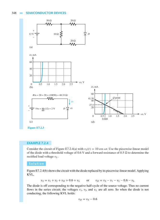
348 SEMICONDUCTOR DEVICES
D12 V
iD, mA
60
40
20
0.50 1.0 1.5 2.0 2.5(b)
vD, V
iD, mA
60
40
20
41.38
27.5
0.50 1.0 1.50.668
Q point
Load line2.0 2.5
(d)
vD, V
10 Ω
(a)
50 Ω 20 Ω
20 Ω−
+
−
+vD
iD
DVTh 10 (12) 2 V= =60
(c)
RTh 20 20 (10||50) 48.33= + + = Ω
Figure E7.2.3
EXAMPLE 7.2.4
Consider the circuit of Figure E7.2.4(a) with vS(t) = 10 cos ωt. Use the piecewise-linear modelof the diode with a threshold voltage of 0.6 V and a forward resistance of 0.5 to determine therectified load voltage vL.
So l u t i on
Figure E7.2.4(b) shows the circuit with the diode replaced by its piecewise-linear model. ApplyingKVL,
vS = v1 + v2 + vD + 0.6+ vL or vD = vS − v1 − v2 − 0.6− vL
The diode is off corresponding to the negative half-cycle of the source voltage. Thus no currentflows in the series circuit; the voltages v1, v2, and vL are all zero. So when the diode is notconducting, the following KVL holds:
vD = vS − 0.6

7.2 DIODES 349
When vD ≥ 0 or vS ≥ 0.6 V, the diode conducts. Once the diode conducts, the expression forthe load voltage can be obtained by the voltage divider rule, by considering that the ideal diodebehaves like a short circuit. The complete expression for the load voltage is therefore given by
vL = 10
10+ 1+ 0.5(vS − 0.6) = 8.7 cos ωt − 0.52, for vS ≥ 0.6 V
and vL = 0 for vS < 0.6 V. The source and load voltages are sketched in Figure E7.2.4(c).
vLvS
v, V
5
0
−5
−10
10
0.005 0.030 0.01 0.015 0.02 0.025(c)
t, s
10 Ω
(a)
1 Ω
−
+
+ −
−
+
vL
vS
vL10 Ω
(b)
1 Ω
−
+vS
v1 + −
0.5 Ω 0.6 V
Idealdiode
v2
+ +− −vD
−
+
Figure E7.2.4
EXAMPLE 7.2.5
Consider a forward-biased diode with a load resistance. Let the static volt–ampere characteristicof the diode be given by Equations (7.2.1) and (7.2.2), and typically represented by Figure7.2.4.
(a) For a dc bias voltage VB, obtain the load-line equation and the operating (quiescent) point

350 SEMICONDUCTOR DEVICES
(IQ, VQ) by graphical analysis. Extend the graphical analysis for different values of (i) loadresistance, and (ii) supply voltage.
(b) If, in addition to the constant potential VB, an alternating or time-varying potentialvS(t) =
√2 VS sin ωt is impressed across the circuit, discuss the dynamic (ac)
characteristics of the diode in terms of (i) small-signal current and voltage waveforms,and (ii) large-signal current and voltage waveforms.
So l u t i on
(a) The circuit of a forward-biased diode with a load resistance RL is shown in FigureE7.2.5(a). The KVL equation yields
VB = IRL + V or I = VB − V
RL
which is the load-line equation. The device equation (Boltzmann diode equation) andthe load-line equation involve two variables, I and V, whose values must satisfy bothequations simultaneously. As seen from Figure E7.2.5(b), Q is the only conditionsatisfying the restrictions imposed by both the diode and the external circuit. Theintersection Q of the two curves is called the quiescent or operating point, indicatedby the diode current IQ and the diode voltage VQ.
Extension of the graphical analysis for different values of load resistance anddifferent values of supply voltage is shown in Figures E7.2.5(c) and (d).
(b) The diode circuit with dc and ac sources is shown in Figure E7.2.5(e). The totalinstantaneous voltage impressed across the circuit is given by
vt = VB +√
2 VS sin ωt and vt = v + iRL
The maximum and minimum values of vt are (VB +√
2 VS) and (VB −√
2 VS),corresponding to the values of sin ωt equal to +1 and −1, respectively. The small-signal current and voltage waveforms, for values of VS much less than VB, are shownin Figure E7.2.5(f). The large-signal current and voltage waveforms, for values of VS
comparable to those of VB, are shown in Figure E7.2.5(g).
The motion of the load line traces the shaded area of the characteristics. The line segmentQ1Q2 is the locus of the position of the operating point Q. It is clear from the figures that thewaveforms of the diode voltage and current are functions of time. A point-by-point methodshould be used for plotting the waveforms. For the small-signal case, the diode can be consideredto behave linearly and the segment Q1Q2 is approximated by a straight line. For the large-signalcase, on the other hand, the behavior is nonlinear. The time-varying portion of the response is notdirectly proportional to vS(t), and a simple superposition of the direct and alternating responsesdoes not apply.

7.2 DIODES 351
(b)
(c)
VVBVo
RL1
Q1Q2Q3
Q4
RL1 < RL2 < RL3 < RL4
VBV
I
RL2
RL3
RL4
00
IQ
VB
Load lineI = (VB − V)/RLSlope = −1/RL
Device curve
Diodevoltage
Voltageacrossresistor
Load lines
0
Operating (quiescent) point
RL
I
RL
VB
V
I
(a)
+ −
+ −
Figure E7.2.5 (a) Circuit of forward-biased diode. (b) Graphical analysis of forward-biased diode with loadresistance. (c) Graphical analysis for different values of load resistance. (d) Graphical analysis for differentvalues of supply voltage. (e) Diode circuit with dc and ac sources. (f) Small-signal current and voltagewaveforms. (g) Large-signal current and voltage waveforms.

352 SEMICONDUCTOR DEVICES
(d)
(e)
(f)
Q5
Q4
Q2
Q3
Q1
Load lineslope = −1/RL
VB1 VB5VB3 VB4VB2V
I
0
RL
VB
v
i
Load linesDiode currentac componentvaries about IQ,the quiescent level
ωt
ωt
Q2
QQ1
VQ VB
IQ
i
+ −vS(t)+ −
vt+ −
+ −
VB − √2VS
v
Diode voltageac componentvaries about VQ,the quiescent level
VB + √2VS
Figure E7.2.5 Continued
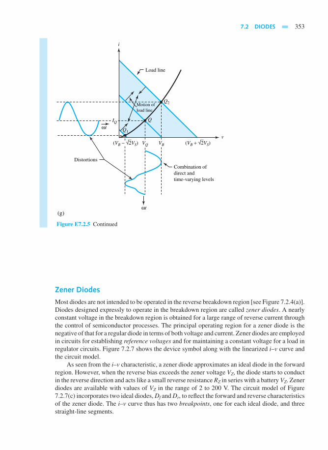
7.2 DIODES 353
(g)
Load line
Motion ofload line
ωt
Q2
Q
Q1
VQ VB
IQ
ωt
i
(VB + √2VS)v
Combination ofdirect andtime-varying levels
Distortions
(VB − √2VS)
Figure E7.2.5 Continued
Zener Diodes
Most diodes are not intended to be operated in the reverse breakdown region [see Figure 7.2.4(a)].Diodes designed expressly to operate in the breakdown region are called zener diodes. A nearlyconstant voltage in the breakdown region is obtained for a large range of reverse current throughthe control of semiconductor processes. The principal operating region for a zener diode is thenegative of that for a regular diode in terms of both voltage and current. Zener diodes are employedin circuits for establishing reference voltages and for maintaining a constant voltage for a load inregulator circuits. Figure 7.2.7 shows the device symbol along with the linearized i–v curve andthe circuit model.
As seen from the i–v characteristic, a zener diode approximates an ideal diode in the forwardregion. However, when the reverse bias exceeds the zener voltage VZ, the diode starts to conductin the reverse direction and acts like a small reverse resistance RZ in series with a battery VZ. Zenerdiodes are available with values of VZ in the range of 2 to 200 V. The circuit model of Figure7.2.7(c) incorporates two ideal diodes, Df and Dr, to reflect the forward and reverse characteristicsof the zener diode. The i–v curve thus has two breakpoints, one for each ideal diode, and threestraight-line segments.

354 SEMICONDUCTOR DEVICES
−VZ
VZ
Dr Df
RZ
RZ
i
v
1
0
Break pointsi
v v
i
(a) (c)
Idealdiode
Idealdiode
(b)
+
Figure 7.2.7 Zener diode. (a) Device symbol. (b) Linearized i–v curve. (c) Circuit model.
EXAMPLE 7.2.6
Consider a simple zener voltage regulator with the circuit diagram shown in Figure E7.2.6(a).
iZ
voutVS
RS
iout
(a)
+
−
voutVS
VZ
RZ
RS
iout
(b)
+
− +
−
Figure E7.2.6
(a) For a small reverse resistance RZ << RS and VS − RSiout > VZ , show that vout∼= VZ.
(b) For values of VS = 25 V, RS = 100 , VZ = 20 V, and RZ = 4 , find:
(i) vout for iout = 0 and iout = 50 mA.
(ii) The corresponding values of the reverse current iZ through the zener diode.
So l u t i on
(a) When VS − RSiout > VZ , the zener diode will be in reverse breakdown. The forwarddiode Df in our model of Figure 7.2.7(c) will be off while the reverse diode Dr is on. Theequivalent circuit is then given by Figure E7.2.6(b).
Straightforward circuit analysis yields

7.2 DIODES 355
vout = RS
RS + RZ
(VZ + RZ
RS
VS − RZiout
)For RZ << RS,RZ |VS/RS − iout| << VZ , in which case
vout ∼= VZ
Thus, the zener diode regulates vout by holding it at the fixed zener voltage VZ, in spiteof the possible variations of VS or iout.
(b) For iout = 0,
vout = 100
100+ 4
[20+ 4
100(25)
]= 100
104× 21 = 20.19 V
we have 20.19− 20 = 4iZ , or iZ = 0.19/4 = 47.5 mA.
For iout = 50 mA,
vout = 100
104
[20+ 4
100(25)− (4× 0.05)
]= 100
104× 20.8 = 20 V
we have 20− 20 = 4iZ , or iZ = 0.
Breakpoint Analysis
When a circuit consists of two or more ideal diodes, it will have several distinct operatingconditions resulting from the off and on states of the diodes. A systematic way of finding thoseoperating conditions is the method of breakpoint analysis. For a two-terminal network containingresistors, sources, and N ideal diodes, and driven by a source voltage v, the i–v characteristicwill in general consist of N + 1 straight-line segments with N breakpoints. The i–v curve can beconstructed by following these steps:
1. For v →∞, determine the states of all diodes, and write i in terms of v; do the same forv→−∞.
2. With one diode to be at its breakpoint (i.e., having zero voltage drop and zero current),find the resulting values of i and v at the terminals; do the same for each of the otherdiodes.
3. Plot the i–v breakpoints obtained from step 2; connect them with straight lines and addthe end lines found in step 1.
Note that in step 2, if two or more diodes are simultaneously at breakpoint conditions, thenumbers of breakpoints and line segments of the i–v curve are correspondingly reduced.
EXAMPLE 7.2.7
Determine the i–v characteristic of the network shown in Figure E7.2.7(a) by the use of breakpointanalysis.
So l u t i on
For v → ∞, D1 will be forward-biased while D2 will be reverse-biased (because v1 > 10 V).Hence, with D1 on and D2 off, v = 2i − 12+ 4i, or i = v/6+ 2.
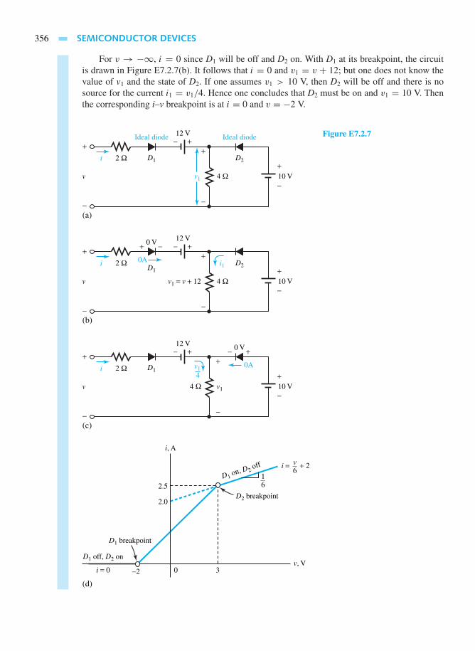
356 SEMICONDUCTOR DEVICES
For v → −∞, i = 0 since D1 will be off and D2 on. With D1 at its breakpoint, the circuitis drawn in Figure E7.2.7(b). It follows that i = 0 and v1 = v + 12; but one does not know thevalue of v1 and the state of D2. If one assumes v1 > 10 V, then D2 will be off and there is nosource for the current i1 = v1/4. Hence one concludes that D2 must be on and v1 = 10 V. Thenthe corresponding i–v breakpoint is at i = 0 and v = −2 V.
4 Ωv1
(a)
2 Ω
10 V−
+v
12 V
D1i
Ideal diode
D2
Ideal diode−+
−
+
−
+
4 Ωv1 = v + 12
(b)
2 Ω
10 V−
+v
12 V
D1i 0A
0 V
D2i1
−−+
−
++
0A
0 V +−
−
+
4 Ω v1
(c)
i, A
v, V
D1 breakpoint
D2 breakpoint
i = + 2
16
v6
D1 off, D2 on
D1 on, D2 o
ff
i = 0
2.5
2.0
0 3
(d)
−2
2 Ω
10 V−
+v
12 V
4D1i v1
−+
−
+
−
+
Figure E7.2.7

7.2 DIODES 357
With D2 at its breakpoint, the circuit is drawn in Figure E7.2.7(c). It follows that v1 = 10 Vand D1 must be on to carry i1 = v1/4 = 2.5 A. Thus, the second breakpoint is at i = 2.5 A andv = 3 V (because v = 2i − 12+ v1).
The complete i–v characteristic based on our results is shown in Figure E7.2.7(d). It can beseen that both D1 and D2 will be on over the middle region −2 < v < 3.
Rectifier Circuits
A simple half-wave rectifier using an ideal diode is shown in Figure 7.2.8(a). The sinusoidalsource voltage vS is shown in Figure 7.2.8(b). During the positive half-cycle of the source, theideal diode is forward-biased and closed so that the source voltage is directly connected acrossthe load. During the negative half-cycle of the source, the ideal diode is reverse-biased so that thesource voltage is disconnected from the load and the load voltage as well as the load current arezero. The load voltage and current are of one polarity and hence said to be rectified. The outputcurrent through the load resistance is shown in Figure 7.2.8(c).
In order to smooth out the pulsations (i.e., to eliminate the higher frequency harmonics) ofthe rectified current, a filter capacitor may be placed across the load resistor, as shown in Figure7.2.9(a). As the source voltage initially increases positively, the diode is forward-biased sincethe load voltage is zero and the source is directly connected across the load. Once the sourcereaches its maximum value VS and begins to decrease, while the load voltage and the capacitorvoltage are momentarily maintained at VS, the diode becomes reverse-biased and hence open-circuited. The capacitor then discharges over time interval t2 through RL until the source voltagevS(t) has increased to a value equal to the load voltage. Since the source voltage at this pointin time exceeds the capacitor voltage, the diode becomes once again forward-biased and henceclosed. The capacitor once again gets charged to VS. The output current of the rectifier with thefilter capacitor is shown in Figure 7.2.9(b), and the circuit configurations while the capacitor getscharged and discharged are shown in Figure 7.2.9(c). The smoothing effect of the filter can beimproved by increasing the time constant CRL so that the discharge rate is slowed and the outputcurrent more closely resembles a true dc current.
iL(k)vS vS(t) = VS sin ωt RL
vS iL
VSVSRL
Diodeclosed
Diodeclosed
Diodeopen
t t
Loadresistance
Ideal diode
(a)
(b)(c)
−
+
Figure 7.2.8 Simple half-waverectifier. (a) Circuit with idealdiode. (b) Input source voltage. (c)Output current through load resis-tance.

358 SEMICONDUCTOR DEVICES
iL(t)
vS(t) = VS sin ωt
vS(t) vS(t)
RLC
iL
VS
t2t1
RL
CRL
Capacitor chargesTimeconstant
Capacitordischarges
t
Loadresistance
Filtercapacitor
Ideal diode
(a)
(b)
−
+
RLC
Diode
0 ≤ t ≤ t1(c)
−
+RLC
Diode
t1 ≤ t ≤ t2 + t1
−
+
Figure 7.2.9 Rectifier with filter capacitor. (a) Circuit. (b) Output current of rectifier with filter capacitor.(c) Circuit configurations while capacitor gets charged and discharged.
The full-wave rectifier using ideal diodes is shown in Figure 7.2.10(a). Figure 7.2.10(b)shows circuit configurations for positive and negative half-cycles of the input source voltagevS(= VS sin ωt), and Figure 7.2.10(c) shows the rectified output voltage across the load resistanceRL. The full-wave rectification can be accomplished by using either a center-tapped transformerwith two diodes or a bridge rectifier circuit with four diodes.
7.3 BIPOLAR JUNCTION TRANSISTORS
The family of bipolar junction transistors has two members: the npn BJT and the pnp BJT. Bothtypes contain semiconductor junctions which operate with bipolar internal currents consisting ofholes and electrons. These are illustrated in Figure 7.3.1 along with their circuit symbols. Theemitter in the circuit symbol is identified by the lead having the arrowhead. The arrow pointsin the direction of conventional emitter current flow when the base–emitter junction is forwardbiased. A transistor can operate in three modes: cutoff, saturation, and active. In the active mode,for an npn BJT, the base–emitter junction (BEJ) is forward-biased by a voltage vBE, while thecollector–base junction (CBJ) is reverse-biased by a voltage vCB. Thus for an npn BJT, as shownin Figure 7.3.1(a), iB and iC are positive quantities such that iB + iC = iE . For a pnp BJT on theother hand, in the active region, the base–emitter and collector–base voltages are negative, and

7.3 BIPOLAR JUNCTION TRANSISTORS 359
vS(t) = VS sin ωt
(a)
Primary
Idealtransformer
Ideal diodeSecondary1:2
D1 D1
Ideal diode
D2D2
−
+RL
RL
vLvL(t)
vS
vS
++
+−
−
−
vS−
+
vS−
+
+−
vS > 0 (positive half-cycle)
(b)
RL
vL
vS−
+
vS−
+
+−
vS < 0 (negative half-cycle)
vL(t)
(c)
vS (t)
2π 3ππωt
VS
RL
vL
vS−
+
vS−
+
+−
Figure 7.2.10 Full-wave rectifier. (a) Circuit. (b) Circuit configurations for positive and negative half-cycles.(c) Rectified output voltage.
currents iB, iC, and iE are all negative quantities such that iE = iB + iC , that is to say, the biasvoltages as well as current directions are reversed compared to those of an npn BJT.
In an npn BJT, current flow is due to majority carriers at the forward-biased BEJ. While theelectrons diffuse into the base from the emitter and holes flow from the base to the emitter, theelectron flow is by far the more dominant part of the emitter current since the emitter is moreheavily doped than the base. Electrons become minority carriers in the base region, and these arequickly accelerated into the collector by action of the reverse bias on the CBJ because the base isvery thin. While the electrons are going through the base region, however, some are removed byrecombination with majority-carrier holes. The number lost through recombination is only 5% ofthe total or less. Due to the usual minority-carrier drift current at a reverse-biased pn junction, asmall current flow, on the order of a few microamperes, denoted by ICBO (collector current when

360 SEMICONDUCTOR DEVICES
n p n C(collector)
C (collector)
(a)E (emitter)
E(emitter)
B (base)
+
+−
−
(base)B
iC
iB
vCE
vBE
p n p C(collector)
C (collector)
(b)E (emitter)
E(emitter)
B (base)
+
+−
−
(base)B
iC
iE iE
iB
vCE
vBE
Figure 7.3.1 Bipolar junction transistors. (a) npn BJT structure and circuit symbol. (b) pnp BJT structureand circuit symbol.
emitter is open-circuited), called reverse saturation current, results. BJTs biased in the activeregion are shown in Figure 7.3.2.
It can be shown that the currents in a BJT are approximately given by
iE = ISE eVBE/VT = iB + iC = 1
αIC − 1
αICBO (7.3.1)
iC = iE + αICBO (7.3.2)
iB = (1− α)iE − ICBO = 1− α
αiC − 1
αICBO (7.3.3)
where ISE is the reverse saturation current of the BEJ, ICBO is the reverse saturation current ofthe CBJ, α (known as common-base current gain or forward-current transfer ratio, typicallyranging from about 0.9 to 0.998) is the fraction of iE that contributes to the collector current, andVT = kT /q is the thermal voltage (which is the voltage equivalent of temperature, having a valueof 25.861× 10⁻³ V when T = 300 K). Note that the symbol hFB is also used in place of α.
Another important BJT parameter is the common-emitter current gain, denoted by β (alsosymbolized by hFE), which is given by
β = α
1− α
(or α = β
1+ β
)(7.3.4)
which ranges typically from about 9 to 500, being very sensitive to changes in α. In terms of β,one can write
iC = βiB + ICBO
1− α= βiB + (β + 1)ICBO = βiB + ICEO (7.3.5)
where ICEO = (β + 1)ICBO is the collector cutoff current when the base is open-circuited (i.e.,iB = 0).
Figure 7.3.3 illustrates common-base static curves for a typical npn silicon BJT. In a common-emitter configuration in which transistors are most commonly used, where the input is to the baseand the output is from the collector, the input and output characteristics are shown in Figure 7.3.4.
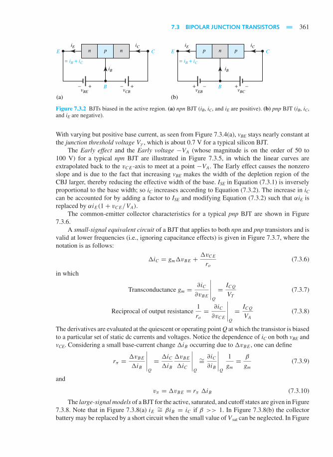
7.3 BIPOLAR JUNCTION TRANSISTORS 361
n p n C
(a)
EiE
vBE
iB
iC
= iB + iC = iB + iC
+−vCB
+−B
p n p C
(b)
EiE
vEB
iB
iC
−+vBC
−+B
Figure 7.3.2 BJTs biased in the active region. (a) npn BJT (iB, iC, and iE are positive). (b) pnp BJT (iB, iC,and iE are negative).
With varying but positive base current, as seen from Figure 7.3.4(a), vBE stays nearly constant atthe junction threshold voltage Vγ , which is about 0.7 V for a typical silicon BJT.
The Early effect and the Early voltage −VA (whose magnitude is on the order of 50 to100 V) for a typical npn BJT are illustrated in Figure 7.3.5, in which the linear curves areextrapolated back to the vCE-axis to meet at a point −VA. The Early effect causes the nonzeroslope and is due to the fact that increasing vBE makes the width of the depletion region of theCBJ larger, thereby reducing the effective width of the base. ISE in Equation (7.3.1) is inverselyproportional to the base width; so iC increases according to Equation (7.3.2). The increase in iCcan be accounted for by adding a factor to ISE and modifying Equation (7.3.2) such that αiE isreplaced by αiE(1+ vCE/VA).
The common-emitter collector characteristics for a typical pnp BJT are shown in Figure7.3.6.
A small-signal equivalent circuit of a BJT that applies to both npn and pnp transistors and isvalid at lower frequencies (i.e., ignoring capacitance effects) is given in Figure 7.3.7, where thenotation is as follows:
iC = gmvBE + vCE
ro(7.3.6)
in which
Transconductance gm = ∂iC
∂vBE
∣∣∣∣∣Q
= ICQ
VT
(7.3.7)
Reciprocal of output resistance1
ro= ∂iC
∂vCE
∣∣∣∣∣Q
= ICQ
VA
(7.3.8)
The derivatives are evaluated at the quiescent or operating point Q at which the transistor is biasedto a particular set of static dc currents and voltages. Notice the dependence of iC on both vBE andvCE. Considering a small base-current change iB occurring due to vBE , one can define
rπ = vBE
iB
∣∣∣∣∣Q
= iC
iB
vBE
iC
∣∣∣∣∣Q
∼= ∂iC
∂iB
∣∣∣∣∣Q
1
gm= β
gm(7.3.9)
and
vπ = vBE = rπ iB (7.3.10)
The large-signal models of a BJT for the active, saturated, and cutoff states are given in Figure7.3.8. Note that in Figure 7.3.8(a) iE ∼= βiB = iC if β >> 1. In Figure 7.3.8(b) the collectorbattery may be replaced by a short circuit when the small value of Vsat can be neglected. In Figure
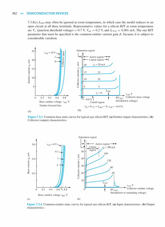
362 SEMICONDUCTOR DEVICES
7.3.8(c) ICEO may often be ignored at room temperature, in which case the model reduces to anopen circuit at all three terminals. Representative values for a silicon BJT at room temperatureare Vγ (junction threshold voltage) = 0.7 V, Vsat = 0.2 V, and ICEO = 0.001 mA. The one BJTparameter that must be specified is the common-emitter current gain β, because it is subject toconsiderable variation.
Figure 7.3.3 Common-base static curves for typical npn silicon BJT. (a) Emitter (input) characteristics. (b)Collector (output) characteristics.
V
Figure 7.3.4 Common-emitter static curves for typical npn silicon BJT. (a) Input characteristics. (b) Outputcharacteristics.

7.3 BIPOLAR JUNCTION TRANSISTORS 363
Collector current iC, mA
Saturation region
Linearactive region
Collector–emittervoltage vCE, V
Increasing vBE
Bre
akdo
wn
0.6 to 0.8 V−VA(Early voltage)
Figure 7.3.5 Early effect and Early voltage of typical npn silicon BJT.
Maximum
collector dissipation = 30 W
Saturation region
0 −10 −20 −30
−0.4
−0.8
−1.2
−1.6
−2.0−30
−25
−20
−15
−10
−5
−40 −50
(Cutoff) Base current = 0 mA
−60 −70 −80
Collector voltage, V
Col
lect
or c
urre
nt, A
Figure 7.3.6 Common-emitter collector characteristics for typical pnp BJT.
Despite the structural similarities, a pnp BJT has smaller current gain than a comparable npnBJT because holes are less mobile than electrons. Most applications of pnp BJTs involve pairingthem with npn BJTs to take advantage of complementary operation. The large-signal models ofFigure 7.3.8 also hold for pnp BJTs if all voltages, currents, and battery polarities are reversed.BJTs can provide the circuit properties of a controlled source or a switch.
+ −vπ= rπ ∆iB
gmvπ= β∆iB
∆iC∆iB
∆iE
ro
CB
E
rπ
Figure 7.3.7 Small-signal equivalent circuit of BJT.

364 SEMICONDUCTOR DEVICES
Current–controlledcurrentsource
(fixed)
iB > 0
iC = βiB
iE = iC + iB= (β + 1)iB
vCE > Vγ
vBE = Vγ
Vγ
−
−
+
+ +
E(a)
C
B
iB > 0
iC < βiB
vCE = Vsat
Vsat
vBE = Vγ
(fixed)Vγ
−
−
+
+ +
+
E(b)
C
B
iB = 0
iC = ICEO
vCE ≥ 0
vBE < Vγ −
−
+
+
E(c)
C
B
Figure 7.3.8 Large-signal models of npn BJT. (a) Linear circuit model in idealized active state. (b) Idealizedsaturated state. (c) Idealized cutoff state.
EXAMPLE 7.3.1
Consider the common-emitter BJT circuit shown in Figure E7.3.1(a). The static characteristics ofthe npn silicon BJT are given in Figure E7.3.1(b) along with the load line. Calculate iB for vS = 1V and 2 V. Then estimate the corresponding values of vCE and iC from the load line, and computethe voltage amplification Av = vCE/vS and the current amplification Ai = iC/iB .
So l u t i on
iB = 0 for vS < Vγ and iB = (vS − Vγ )/RB for vS > V . With varying but positive base current,vBE stays nearly constant at the junction threshold voltage Vγ , which is 0.7 V for a silicon BJT[see Figure 7.3.4(a)].
Then, IBQ1 = vS1 − 0.7
RB
= 1− 0.7
20,000= 15 µA, for vS1 = 0.7 V
Corresponding to 15-µA interpolated static curve and load line [see Fig. E7.3.1(b)], we getvCE1 = 9.4 V, and iC1 = 1.3 mA;
for vS2 = 2 V, IBQ2 = 2− 0.7
20,000= 1.3
20,000= 65 µA
+
−
C
(a)E
+
+
−
+
−−
BRB 20 k= Ω RC 2 k= Ω
VCC 12 V=
iC
iB
vS
vCE
vBE
Figure E7.3.1 (a) Circuit. (b) Staticcurves and load line.
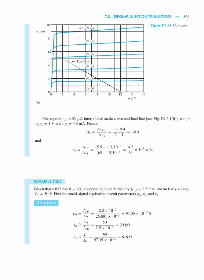
7.3 BIPOLAR JUNCTION TRANSISTORS 365
10
Load line
8
iC, mAiB 100 A= µ
80 Aµ
60 Aµ
40 Aµ
20 Aµ
iB 0=
vCE, V(b)
6
4
2
00 2 4 6 8 10 12 14 16
Figure E7.3.1 Continued
Corresponding to 65-µA interpolated static curve and load line [see Fig. E7.3.1(b)], we getvCE2 = 1 V and iC2 = 5.5 mA. Hence,
Av = vCE
vS= 1− 9.4
2− 1= −8.4
and
Ai = iC
iB= (5.5− 1.3)10−3
(65− 15)10−6= 4.2
50× 103 = 84
EXAMPLE 7.3.2
Given that a BJT has β = 60, an operating point defined by ICQ = 2.5 mA, and an Early voltageVA = 50 V. Find the small-signal equivalent circuit parameters gm, ro, and rπ .
So l u t i on
gm = ICQ
VT
= 2.5× 10⁻³
25.681× 10−3= 97.35× 10⁻³ S
ro ∼= VA
ICQ
= 50
2.5× 10−3= 20 k
rπ ∼= β
gm= 60
97.35× 10−3= 616

366 SEMICONDUCTOR DEVICES
EXAMPLE 7.3.3
Considering the circuit shown in Figure E7.3.3(a), find the state of operation and operating pointif the BJT has β = 80 and other typical values of a silicon BJT at room temperature.
(a)
(b)
E
B
C
+
+
+
−
−−
RB = 60 kΩ
RE = 4 kΩ
vBE
iB VCC = 20 V
iE
iC
vCE
E
B
C
+
+
+ − −−
60 kΩ
4 kΩ
vBE = 0.7 V
iB 20 V
iC =80 iB
iE =81 iB
vCE
Figure E7.3.3
So l u t i on
Let us check the state of operation through some preliminary calculations. Application of KVLyields
vBE = vCE − RBiB = VCC − REiE − RBiB
If we assume the saturated state, then vCE = Vsat and iB > 0, so that
vBE = Vsat − RBiB < 0.2
which is in violation of the saturation condition: vBE = Vγ = 0.7 V.If we assume the cutoff state, then iB = 0 and iE = iC = ICEO , so that
vBE = VCC − REICEO∼= 20 V
which is in violation of the cutoff condition: vBE < Vγ .Having thus eliminated saturation and cutoff, the active-state model is substituted, as shown
in Figure E7.3.3(b).The outer loop equation gives
20− 60iB − 0.7− 4× 81iB = 0
where iB is the base current in mA. Solving,

7.4 FIELD-EFFECT TRANSISTORS 367
iB = 19.3
384= 0.05 mA
iC = 80iB = 4 mA
Hence,
vCE = 20− 4× 81iB = 3.8 V
which does satisfy the active-state condition: vCE > Vγ .
7.4 FIELD-EFFECT TRANSISTORS
Field-effect transistors (FETs) may be classified as JFETs (junction field-effect transistors), de-pletion MOSFETs (metal-oxide-semiconductor field-effect transistors), and enhancement MOS-FETs. Each of these classifications features a semiconductor channel of either n-type or p-type,whose conduction is controlled by a field effect. Consequently, all FETs behave in a similarfashion. The FET classification is illustrated in Figure 7.4.1 along with the corresponding circuitsymbols. FETs have the useful property that very little current flows through their input (gate)terminals.
Junction FETs (JFETs)
The JFET is a three-terminal, voltage-controlled current device, whereas the BJT is principallya three-terminal, current-controlled current device. The advantages associated with JFETs aremuch higher input resistance (on the order of 107 to 1010 ), lower noise, easier fabrication, andin some cases even the ability to handle higher currents and powers. The disadvantages, on theother hand, are slower speeds in switching circuits and smaller bandwidth for a given gain in anamplifier.
Figure 7.4.2 shows the n-channel JFET and the p-channel JFET along with their circuitsymbols. The JFET, which is a three-terminal device, consists of a single junction embedded in asemiconductor sample. When the base semiconductor forming the channel is of a n-type material,the device is known as an n-channel JFET; otherwise it is a p-channel JFET when the channel is
FET
G : gate; D : drain; S : source
DepletionMOSFET
nchannel
pchannel
G
D
S
G
D
S
JFET
nchannel
pchannel
G
D
S
G
D
S
EnhancementMOSFET
nchannel
pchannel
G
D
S
G
D
S
Figure 7.4.1 FET classification.

368 SEMICONDUCTOR DEVICES
G(gate)
Gate
D (drain)
S (source) G(gate)
D (drain)
S (source)
Source
Metalcontact
Metalcontact
Conductingchannel
Depletionregion
(a)
Drain
Metalcontact
Gate
Source
Metalcontact
Metalcontact
Conductingchannel
Depletionregion
(b)
Drain
Metalcontactn
np
p
Figure 7.4.2 JFETs and their circuit symbols. (a) n-channel JFET. (b) p-channel JFET.
formed of a p-type semiconductor. The functions of source, drain, and gate are analogous to theemitter, collector, and base of the BJT. The gate provides the means to control the flow of chargesbetween source and drain.
The junction in the JFET is reverse-biased for normal operation. No gate current flows becauseof the reverse bias and all carriers flow from source to drain. The corresponding drain current isdependent on the resistance of the channel and the drain-to-source voltage vDS. As vDS is increasedfor a given value of vGS, the junction is more heavily reverse-biased, when the depletion regionextends further into the conducting channel. Increasing vDS will ultimately block or pinch off theconducting channel. After the pinch-off, the drain current iD will be constant, independent ofvDS. Changing vGS (gate-to-source voltage) controls where pinch-off occurs and what the valueof drain current is.
It is the active region beyond pinch-off that is useful for the controlled-source operation, sinceonly changes in vGS will produce changes in iD. Figure 7.4.3 illustrates the JFET characteristics.Part (a) shows the idealized static characteristics with two regions separated by the dashed line,indicating the ohmic (controlled-resistance or triode) region and the active (controlled-source)region beyond pinch-off. Note that iD is initially proportional to vDS in the ohmic region wherethe JFET behaves much like a voltage-variable resistance; iD depends on vGS for a given valueof vDS in the active region. In a practical JFET, however, the curves of iD versus vDS are notentirely flat in the active region but tend to increase slightly with vDS, as shown in Figure 7.4.3(b);when extended, these curves tend to intersect at a point of −VA on the vDS axis. Another usefulcharacteristic indicating the strength of the controlled source is the transfer characteristic, relatingthe drain current iD to the degree of the negative bias vGS applied between gate and source; a cutoffregion exists, indicated by the pinch-off voltage −VP , for which no drain current flows, becauseboth vGS and vDS act to eliminate the conducting channel completely.
Mathematically, the drain current in the active controlled-source region is approximatelygiven by [see Figure 7.4.3(a)]:
iD = IDSS
(1+ vGS
VP
)2
(7.4.1)
where IDSS, known as the drain–source saturation current, represents the value of iD whenvGS = 0.
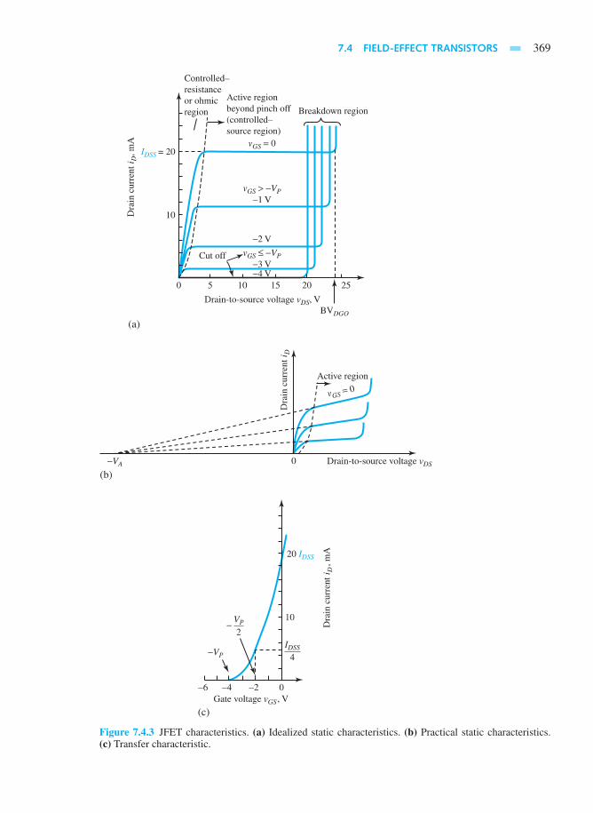
7.4 FIELD-EFFECT TRANSISTORS 369
Figure 7.4.3 JFET characteristics. (a) Idealized static characteristics. (b) Practical static characteristics.(c) Transfer characteristic.

370 SEMICONDUCTOR DEVICES
Also shown in Figure 7.4.3(a) is a breakdown voltage, denoted by BVDGO, at which breakdown inthe drain–gate junction occurs in the channel near the drain. For most JFETs, BVDGO ranges fromabout 20 to 50 V. The dependence of iD on vDS, as shown in Figure 7.4.3(b), can be accounted forby applying a first-order correction to Equation (7.4.1),
iD = IDSS
(1+ vGS
VP
)2 (1+ vDS
VA
)(7.4.2)
A small-signal equivalent circuit (valid at low frequencies where capacitances can beneglected) can now be developed based on Equation (7.4.2). Denoting the dc values at the operatingpoint by VGSQ, IDQ, and VDSQ, the small changes that occur can be expressed by
iD = ∂iD
∂vGS
∣∣∣∣∣Q
vGS + ∂iD
∂vDS
∣∣∣∣∣Q
vDS = gmvGS + 1
rovDS (7.4.3)
where
gm = ∂iD
∂vGS
∣∣∣∣∣Q
= 2IDSS
(1+ vGS
VP
)(1+ vDS
VA
)(1
VP
) ∣∣∣∣∣Q
= 2IDSS
VP
[(IDQ
IDSS
)(1+ VDSQ
VA
)]1/2 ∼=(
2
VP
) (IDSSIDQ
)1/2(7.4.4)
and
1
ro= ∂iD
∂vDS
∣∣∣∣∣Q
= IDSS
(1+ vGS
VP
)2 ( 1
VA
) ∣∣∣∣∣Q
= IDQ/VA
1+ (VDSQ/VA)∼= IDQ
VA
(7.4.5)
The small-signal equivalent circuit based on Equation (7.4.3) is shown in Figure 7.4.4.
DG
S
+
−
gm∆vGS∆vGS
∆iD
ro
Figure 7.4.4 JFET small-signal equiva-lent circuit for low frequencies.
EXAMPLE 7.4.1
Measurements made on the self-biased n-channel JFET shown in Figure E7.4.1 are VGS = −1V, ID = 4 mA; VGS = −0.5 V, ID = 6.25 mA; and VDD = 15 V.
(a) Determine VP and IDSS.
(b) Find RD and RS so that IDQ = 4 mA and VDS = 4 V.

7.4 FIELD-EFFECT TRANSISTORS 371
So l u t i on
(a) From Equation (7.4.1),
4× 10−3 = IDSS
(1+ −1
VP
)2
and
6.25× 10−3 = IDSS
(1+ −0.5
VP
)2
Simultaneous solution yields
IDSS = 9 mA and VP = 3 V
(b) For IDQ = 4 mA, VGS = −1 V,
RS = 1
4× 10−3= 250
The KVL equation for the drain loop is
− VDD + IDQRD + VDS + IDQRS = 0
or
− 15+ 4× 10⁻³RD + 4+ 4× 10−3 × 250 = 0
or
RD = 2.5 k
G
S
+ VDD
D
+
+
−
−vGS
RS
VDS
RD
RG
IG = 0
ID
VR = IGRG = 0
Figure E7.4.1
MOSFETs
The metal-oxide-semiconductor construction leads to the name MOSFET, which is also knownas insulated-gate FET or IGFET. One type of construction results in the depletion MOSFET, theother in the enhancement MOSFET. The names are derived from the way in which channelsare formed and operated. Both n-channel and p-channel MOSFETs are available in either type.
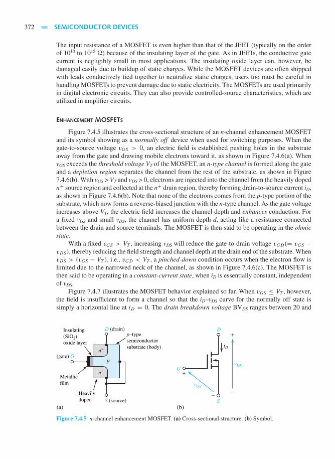
372 SEMICONDUCTOR DEVICES
The input resistance of a MOSFET is even higher than that of the JFET (typically on the orderof 1010 to 1015 ) because of the insulating layer of the gate. As in JFETs, the conductive gatecurrent is negligibly small in most applications. The insulating oxide layer can, however, bedamaged easily due to buildup of static charges. While the MOSFET devices are often shippedwith leads conductively tied together to neutralize static charges, users too must be careful inhandling MOSFETs to prevent damage due to static electricity. The MOSFETs are used primarilyin digital electronic circuits. They can also provide controlled-source characteristics, which areutilized in amplifier circuits.
ENHANCEMENT MOSFETS
Figure 7.4.5 illustrates the cross-sectional structure of an n-channel enhancement MOSFETand its symbol showing as a normally off device when used for switching purposes. When thegate-to-source voltage vGS > 0, an electric field is established pushing holes in the substrateaway from the gate and drawing mobile electrons toward it, as shown in Figure 7.4.6(a). WhenvGS exceeds the threshold voltage VT of the MOSFET, an n-type channel is formed along the gateand a depletion region separates the channel from the rest of the substrate, as shown in Figure7.4.6(b). With vGS > VT and vDS > 0, electrons are injected into the channel from the heavily dopedn+ source region and collected at the n+ drain region, thereby forming drain-to-source current iD,as shown in Figure 7.4.6(b). Note that none of the electrons comes from the p-type portion of thesubstrate, which now forms a reverse-biased junction with the n-type channel. As the gate voltageincreases above VT, the electric field increases the channel depth and enhances conduction. Fora fixed vGS and small vDS, the channel has uniform depth d, acting like a resistance connectedbetween the drain and source terminals. The MOSFET is then said to be operating in the ohmicstate.
With a fixed vGS > VT , increasing vDS will reduce the gate-to-drain voltage vGD(= vGS −vDS), thereby reducing the field strength and channel depth at the drain end of the substrate. WhenvDS > (vGS − VT ), i.e., vGD < VT , a pinched-down condition occurs when the electron flow islimited due to the narrowed neck of the channel, as shown in Figure 7.4.6(c). The MOSFET isthen said to be operating in a constant-current state, when iD is essentially constant, independentof vDS.
Figure 7.4.7 illustrates the MOSFET behavior explained so far. When vGS ≤ VT , however,the field is insufficient to form a channel so that the iD–vDS curve for the normally off state issimply a horizontal line at iD = 0. The drain breakdown voltage BVDS ranges between 20 and
D (drain)
S (source)
D
S
+
+
−−
(gate) G
G
vGS
vDS
iD
Insulating(SiO2)oxide layer
Metallicfilm
Heavilydoped
(a) (b)
p–typesemiconductorsubstrate (body)
p
n+
n+
Figure 7.4.5 n-channel enhancement MOSFET. (a) Cross-sectional structure. (b) Symbol.
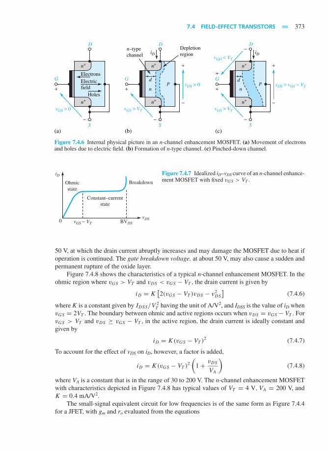
7.4 FIELD-EFFECT TRANSISTORS 373
D
S
+
+
−
−
G
vGS > 0
vDS > 0
iD
n+
n+
Electrons
Holes
(a)
Electricfield
Dn–typechannel
Depletionregion
S
+
−
G
vGS > VT
n+
n
n+
pd
(b)
+
−
vDS > vGS − VT
iD
D
S
+
+
−
−
G
vGS > VT
vGD < VT
n+
n
n+
pd
(c)
Figure 7.4.6 Internal physical picture in an n-channel enhancement MOSFET. (a) Movement of electronsand holes due to electric field. (b) Formation of n-type channel. (c) Pinched-down channel.
iD
vDSvGS − VT BVDS
Ohmicstate
Breakdown
Constant–currentstate
0
Figure 7.4.7 Idealized iD–vDS curve of an n-channel enhance-ment MOSFET with fixed vGS > VT .
50 V, at which the drain current abruptly increases and may damage the MOSFET due to heat ifoperation is continued. The gate breakdown voltage, at about 50 V, may also cause a sudden andpermanent rupture of the oxide layer.
Figure 7.4.8 shows the characteristics of a typical n-channel enhancement MOSFET. In theohmic region where vGS > VT and vDS < vGS − VT , the drain current is given by
iD = K[2(vGS − VT )vDS − v2
DS
](7.4.6)
where K is a constant given by IDSS/V2T having the unit of A/V2, and IDSS is the value of iD when
vGS = 2VT . The boundary between ohmic and active regions occurs when vDS = vGS − VT . ForvGS > VT and vDS ≥ vGS − VT , in the active region, the drain current is ideally constant andgiven by
iD = K(vGS − VT )2 (7.4.7)
To account for the effect of vDS on iD, however, a factor is added,
iD = K(vGS − VT )2
(1+ vDS
VA
)(7.4.8)
where VA is a constant that is in the range of 30 to 200 V. The n-channel enhancement MOSFETwith characteristics depicted in Figure 7.4.8 has typical values of VT = 4 V, VA = 200 V, andK = 0.4 mA/V2.
The small-signal equivalent circuit for low frequencies is of the same form as Figure 7.4.4for a JFET, with gm and ro evaluated from the equations

374 SEMICONDUCTOR DEVICES
vGS = VT = 4 V
vGS = 11 V
6 V
8 V
9 V
10 V
VT
25
20
Dra
in c
urre
nt i D
, mA
15
10
(a) (b)
Cutoffregion
25 Pinch-off or active region vGS > VT
vDS ≥ vGS − VT
vGS > VTOhmicregionvDS <
vGS − VT20
Dra
in c
urre
nt i D
, mA
15
10
5
0 128
Gate-to-source voltage vGS, V
4 0 128
Drain-to-source voltage vDS, V
4 16 2420
5
Figure 7.4.8 Characteristics of an n-channel enhancement MOSFET. (a) Transfer characteristic. (b) Staticcharacteristics.
gm = ∂iD
∂vGS
∣∣∣∣∣Q
= 2K(vGS − VT )
(1+ vDS
VA
) ∣∣∣∣∣Q
∼= 2√KIDQ (7.4.9)
and
ro =(
∂iD
∂vDS
∣∣∣∣∣Q
)−1
= VA
K(vGS − VT )2
∣∣∣∣∣Q
∼= VA
IDQ
(7.4.10)
in which all definitions are the same as those used previously for the JFET.
EXAMPLE 7.4.2
Consider the basic MOSFET circuit shown in Figure E7.4.2 with variable gate voltage. TheMOSFET is given to have very large VA, VT = 4 V, and IDSS = 8 mA. Determine iD and vDS forvGS = 1, 5, and 9 V.
+
−
D
S
+
+
−
G
vGS
vDS
RD = 5 kΩ
VDD = 20 V
iD
Figure E7.4.2

7.4 FIELD-EFFECT TRANSISTORS 375
So l u t i on
(a) For vGS = 1 V: Since it is less than VT, the MOSFET is in the cutoff region so thatiD = 0, which corresponds to the normally off state of the MOSFET,
vDS = VDD = 20 V
(b) For vGS = 5 V: The MOSFET operates in the active region,
iD = IDSS
V 2T
(vGS − VT )2 = IDSS
(vGS
VT
− 1
)2
= 8× 10⁻³
(5
4− 1
)2
= 0.5 mA
vDS = VDD − RDiD = 20− (5× 10³)(0.5× 10⁻³) = 17.5 V
The active MOSFET behaves like a nonlinear voltage-controlled current source.
(c) For vGS = 9 V: Since it is greater than 2VT so that iD increases while vDS decreases, theMOSFET is presumably in the linear ohmic state when
|vDS | ≤ 1
4(vGS − VT ) and vGS > VT
The theory for this case predicts that iD ∼= vDS/RDS , where RDS is the equivalent drain-to-sourceresistance given by
RDS = V 2T
2IDSS(vGS − VT )
Here the MOSFET acts as a voltage-controlled resistor. For our example,
RDS = 42
2(8× 10⁻³)(9− 4)= 200
Since this resistance appears in series with RD,
iD = VDD
RD + RDS
= 20
5000+ 200= 3.85 mA
and
vDS = RDSiD = 200× 3.85× 10−3 = 0.77 V
which is less than 1/4(9− 4) V.
Figure 7.4.9 shows a p-channel enhancement MOSFET which differs from an n-channeldevice in that the doping types are interchanged. Channel conduction now requires negative gate-to-source voltage or positive source-to-gate voltage. With vSG > VT and vSD > 0, iD flowsfrom source to drain, as shown in Figure 7.4.9(a). The p-channel and n-channel MOSFETs arecomplementary transistors, having the same general characteristics but opposite current directionand voltage polarities. By replacing vGS and vDS with vSG and vSD, respectively, the equations ofthe n-channel MOSFET apply to the p-channel MOSFET. However, a p-type channel does notconduct as well as an n-type channel of the same size because holes are less mobile than electrons.Consequently, smaller values of IDSS are typical of the p-channel MOSFETs.
DEPLETION MOSFETS
Figure 7.4.10 illustrates depletion MOSFETs and their symbols. Because the channel is builtin, no field effect is required for conduction between the drain and the source. The depletion
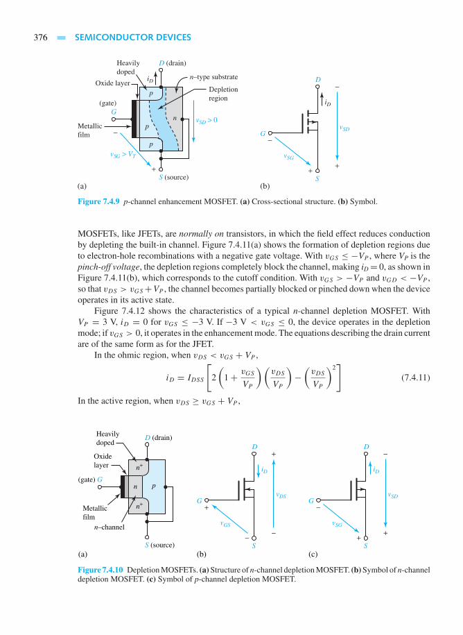
376 SEMICONDUCTOR DEVICES
Figure 7.4.9 p-channel enhancement MOSFET. (a) Cross-sectional structure. (b) Symbol.
MOSFETs, like JFETs, are normally on transistors, in which the field effect reduces conductionby depleting the built-in channel. Figure 7.4.11(a) shows the formation of depletion regions dueto electron-hole recombinations with a negative gate voltage. With vGS ≤ −VP , where VP is thepinch-off voltage, the depletion regions completely block the channel, making iD= 0, as shown inFigure 7.4.11(b), which corresponds to the cutoff condition. With vGS > −VP and vGD < −VP ,so that vDS > vGS+VP , the channel becomes partially blocked or pinched down when the deviceoperates in its active state.
Figure 7.4.12 shows the characteristics of a typical n-channel depletion MOSFET. WithVP = 3 V, iD = 0 for vGS ≤ −3 V. If −3 V < vGS ≤ 0, the device operates in the depletionmode; if vGS > 0, it operates in the enhancement mode. The equations describing the drain currentare of the same form as for the JFET.
In the ohmic region, when vDS < vGS + VP ,
iD = IDSS
[2
(1+ vGS
VP
)(vDS
VP
)−(vDS
VP
)2]
(7.4.11)
In the active region, when vDS ≥ vGS + VP ,
D (drain)
S (source)
D
S
+
+
−−
(gate) G
G
vGS
vDS
iD
Heavilydoped
Oxidelayer
Metallicfilm
(a) (b)
D
S
−
−
++
G
vSG
vSD
iD
(c)
n–channel
pn
n+
n+
Figure 7.4.10 Depletion MOSFETs. (a) Structure of n-channel depletion MOSFET. (b) Symbol of n-channeldepletion MOSFET. (c) Symbol of p-channel depletion MOSFET.

7.4 FIELD-EFFECT TRANSISTORS 377
iD = 0
S
+
−
G
vGS ≤ −VP
n+
n+ p
n+
n+ p
(b)
D
Depletionregions
S
G
vGS < 0
n+
n
n+
pd
(a)
vDS > vGS + VP
iD
S
G
vGS > −VP
vGD < −VP
(c)
d
D D
Figure 7.4.11 Internal physical picture in n-channel depletion MOSFET. (a) Formation of depletion regions.(b) Cutoff condition. (c) Active state.
Cut off vGS ≤ −VP
−VP
IDSS
25
20
Dra
in c
urre
nt i D
, mA
15
10
(a) (b)
25Ohmicregion
Active region
1 V
−1 V
−2 V
0 V
vDS < vGS + VPvDS ≥ vGS + VP
vGS = +2 V
vGS > −VP
20
Dra
in c
urre
nt i D
, mA
15
10
5
0 2−2
Gate-to-source voltage vGS, V
−4 0 64
Drain-to-source voltage vDS, V
2 8 1210
5
Figure 7.4.12 Characteristics of n-channel depletion MOSFET. (a) Transfer characteristic. (b) Staticcharacteristics.
iD = IDSS
(1+ vGS
VP
)2 (1+ vDS
VA
)(7.4.12)
where VA and IDSS are positive constants, and the factor (1 + vDS/VA) is added to accountapproximately for the nonzero slope of the iD–vDS curves of a practical device, as was done inEquation (7.4.2). The small-signal equivalent circuit for low frequencies is of the same form asFigure 7.4.4 for a JFET.
EXAMPLE 7.4.3
An n-channel depletion MOSFET, for which IDSS = 7 mA and VP = 4 V, is said to be operatingin the ohmic region with drain current iD = 1 mA when vDS = 0.8 V. Neglecting the effect ofvDS on iD, find vGS and check to make sure the operation is in the ohmic region.
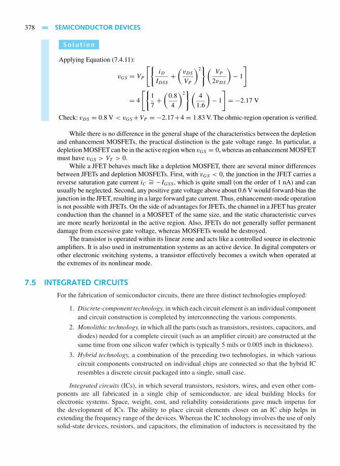
378 SEMICONDUCTOR DEVICES
So l u t i on
Applying Equation (7.4.11):
vGS = VP
[iD
IDSS
+(vDS
VP
)2(
VP
2vDS
)− 1
]
= 4
[1
7+(
0.8
4
)2(
4
1.6
)− 1
]= −2.17 V
Check: vDS = 0.8 V < vGS+VP = −2.17+4 = 1.83 V. The ohmic-region operation is verified.
While there is no difference in the general shape of the characteristics between the depletionand enhancement MOSFETs, the practical distinction is the gate voltage range. In particular, adepletion MOSFET can be in the active region when vGS = 0, whereas an enhancement MOSFETmust have vGS > VT > 0.
While a JFET behaves much like a depletion MOSFET, there are several minor differencesbetween JFETs and depletion MOSFETs. First, with vGS < 0, the junction in the JFET carries areverse saturation gate current iC ∼= −IGSS , which is quite small (on the order of 1 nA) and canusually be neglected. Second, any positive gate voltage above about 0.6 V would forward-bias thejunction in the JFET, resulting in a large forward gate current. Thus, enhancement-mode operationis not possible with JFETs. On the side of advantages for JFETs, the channel in a JFET has greaterconduction than the channel in a MOSFET of the same size, and the static characteristic curvesare more nearly horizontal in the active region. Also, JFETs do not generally suffer permanentdamage from excessive gate voltage, whereas MOSFETs would be destroyed.
The transistor is operated within its linear zone and acts like a controlled source in electronicamplifiers. It is also used in instrumentation systems as an active device. In digital computers orother electronic switching systems, a transistor effectively becomes a switch when operated atthe extremes of its nonlinear mode.
7.5 INTEGRATED CIRCUITS
For the fabrication of semiconductor circuits, there are three distinct technologies employed:
1. Discrete-component technology, in which each circuit element is an individual componentand circuit construction is completed by interconnecting the various components.
2. Monolithic technology, in which all the parts (such as transistors, resistors, capacitors, anddiodes) needed for a complete circuit (such as an amplifier circuit) are constructed at thesame time from one silicon wafer (which is typically 5 mils or 0.005 inch in thickness).
3. Hybrid technology, a combination of the preceding two technologies, in which variouscircuit components constructed on individual chips are connected so that the hybrid ICresembles a discrete circuit packaged into a single, small case.
Integrated circuits (ICs), in which several transistors, resistors, wires, and even other com-ponents are all fabricated in a single chip of semiconductor, are ideal building blocks forelectronic systems. Space, weight, cost, and reliability considerations gave much impetus forthe development of ICs. The ability to place circuit elements closer on an IC chip helps inextending the frequency range of the devices. Whereas the IC technology involves the use of onlysolid-state devices, resistors, and capacitors, the elimination of inductors is necessitated by the

7.6 LEARNING OBJECTIVES 379
fact that typical semiconductors do not exhibit the magnetic properties needed to realize practicalinductance values.
ICs are made by microfabrication technologies. The low cost of IC production is a result ofplanar processing in which fabrication begins with a very flat disc of silicon wafer, 5 to 10 cm indiameter and only 0.5 mm thick. The small electronic structures to be built on it are then producedphotographically. The technique is known as photolithography, in which a photosensitive lacquer(known as photoresist), which has the property of hardening when struck by light, is used. Thefabrication method requires a series of masks, photoetching, and diffusions.
MOSFET chips generally utilize either a p-channel or an n-channel device; hence, thesechips are known as PMOS and NMOS, respectively. Alternatively, both p-channel and n-channeldevices are used to form compound devices, in which case they are known as complementaryMOS (CMOS). Whereas the CMOS has the advantage of low power consumption, only a smallernumber of devices can be placed on the chip. MOS technologies are popularly used in computercircuits due to their higher packing densities. Bipolar technologies, however, are used in high-speed applications because they respond more quickly. The device fabrication methods are tooinvolved to be presented in this introductory text.
Small-scale integration (SSI) is used typically for a 20-component op amp, whereas large-scale integration (LSI) puts an entire microprocessor, typically with 10,000 components, on asingle chip. The chief benefits from integrating many components on an IC are low cost, smallsize, high reliability, and matched characteristics. Of the many IC packaging technologies, themost popular is the dual-in-line package (DIP), which consists of a rectangular plastic or ceramiccase enclosing the IC, with protruding pin terminals. While an op amp is commonly supplied inan 8-pin DIP for insertion into some larger circuit, a microprocessor may have a 40- to 64-pinDIP to accommodate the many external connections needed for an LSI chip.
7.6 LEARNING OBJECTIVES
The learning objectives of this chapter are summarized here so that the student can check whetherhe or she has accomplished each of the following.
• Understanding of electrical conduction in semiconductor materials.
• i–v characteristics of a semiconductor diode (or of a pn-junction).
• Diode modeling and analysis of elementary diode circuits.
• Zener diode, its circuit model, and simple applications.
• Breakpoint analysis of a circuit containing two or more ideal diodes.
• Half-wave and full-wave rectifier circuits.
• Basic operation of bipolar junction transistors, along with their input and output character-istics.
• Small-signal equivalent circuits and large-signal models of BJT.
• Recognizing the more common BJT configurations, and determining the voltage and currentgains.
• Basic operation of JFETs and their characteristics.
• JFET small-signal equivalent circuit (for low frequencies) and its applications for simplecircuit configurations.
• Basic operation of MOSFETs (enhancement and depletion types) and their characteristics.

380 SEMICONDUCTOR DEVICES
• MOSFET small-signal equivalent circuit (for low frequencies) and its application for simplecircuit configurations.
• Basic notions of integrated circuits.
7.7 PRACTICAL APPLICATION: A CASE STUDY
Electronic Photo Flash
A simplified schematic diagram of the electric circuit of an electronic photo flash typically usedon cameras is shown in Figure 7.7.1. By passing a high current through the flash tube, a brightflash of light is to be produced while the camera shutter is open. The power level is quite high,as much as 1 kW. The total energy delivered, however, is only on the order of 1 j, since the flashlasts less than 1 ms.
The electronic switch alternates between opening and closing approximately 10,000 timesper second. Energy is delivered by the battery over a period of several seconds and stored in thecapacitor. The stored energy is extracted from the capacitor whenever needed. The battery sourcecauses the current in the inductor to build up while the electronic switch is closed. Recall that thecurrent in an inductor cannot change instantaneously. When the switch opens, the inductor forcescurrent to go through the diode in one direction, charging the capacitor. Thus the diode allows thecapacitor to be charged whenever the electronic switch is open, and prevents the flow in the otherdirection when the electronic switch is closed. The voltage on the capacitor eventually reachesseveral hundred volts. When the camera shutter is opened, another switch is closed, enablingthe capacitor to discharge through the flash tube. Nowadays several practical electronic circuitsemploy diodes, BJTs, FETs, and integrated circuits.
FlashCElectronicswitch
Batterysource
Switch thatcloses whencamerashutteropens
LR Diode
Figure 7.7.1 Simplified schematic diagram of the electric circuit of an electronic photoflash.
PROBL EMS
7.2.1 Explain the action of a pn-junction with bias. Con-sider both the forward bias and the reverse bias,and use sketches wherever possible.
7.2.2 Assuming the diode to obey I = IS(eV/0.026− 1),
calculate the ratio V/I for an ideal diode with IS =10−13 A for the applied voltages of −2,−0.5,0.3, 0.5, 0.7, 1.0, and 1.5 V, in order to illustrate
that a diode is definitely not a resistor with aconstant ratio of V/I.
*7.2.3 A semiconductor diode with IS = 10µA and a1-k resistor in series is forward-biased with avoltage source to yield a current of 30 mA. Find thesource voltage if the diode I–V equation is givenby I = IS(e
40V − 1). Also find the source voltage
PROBLEMS 381
that would yield I = −8µA.
7.2.4 A silicon diode is forward-biased with V = 0.5V at a temperature of 293 K. If the diode currentis 10 mA, calculate the saturation current of thediode.
7.2.5 With V = 50 mV, a certain diode at room tem-perature is found to have I = 16 µA and satisfiesI = IS(e
40V − 1). Find the corresponding diffu-sion current.
7.2.6 A diode is connected in series with a voltagesource of 5 V and a resistance of 1 k. Thediode’s saturation current is given to be 10−12
A and the I–V curve is shown in Figure P7.2.6.Find the current through the diode in the circuitby graphical analysis.
7.2.7 For the circuit in Figure P7.2.7(a), determine thecurrent i, given the i–v curve of the diode shownin Figure P7.2.7(b).
7.2.8 A diode with the i–v characteristic shown in FigureP7.2.8 is used in series with a voltage source of 5V (forward bias) and a load resistance of 1 k.
(a) Determine the current and the voltage in theload resistance.
(b) Find the power dissipated by the diode.
(c) Compute the load current for different loadresistance values of 2, 5, 0.5, and 0.2 k.
*7.2.9 The diode of Problem 7.2.8 is connected in serieswith a forward-bias voltage of 10 V and a loadresistance of 2 k.
(a) Determine the load voltage and current.
(b) Calculate the power dissipated by the diode.
(c) Find the load current for different values ofsupply voltage of 2.5, 5.0, 15.0, and 20.0 V.
7.2.10 Consider a reverse-biased diode with a sourcevoltage VB in series with a load resistance RL.Write the KVL equation for the circuit.
7.2.11 Two identical junction diodes whose volt–ampererelation is given by Equation (7.2.1) in whichIS = 0.1 µA, VT = 25 mV, and η = 2, areconnected as shown in Figure P7.2.11. Determinethe current in the circuit and the voltage acrosseach diode.
7.2.12 Consider the diode of Problem 7.2.6 with Von =0.7 V and the model of Figure 7.2.5(a). Evaluatethe effect of Von on the answer.
*7.2.13 Consider the model of Figure 7.2.5(a). In the cir-cuit of Figure P7.2.13, the diode is given to haveVon = 0.7 V. Find i1 and i2 in the circuit.
7.2.14 For the circuit shown in Figure P7.2.14(a), deter-mine the diode current and voltage and the powerdelivered by the voltage source. The diode char-acteristic is given in Figure P7.2.14(b).
7.2.15 Let the diode of Problem 7.2.14, with its given v–icurve, be connected in a circuit with an operatingpoint ofVd = 0.6 V and Id = 2 mA. If the diode isto be represented by the model of Figure 7.2.5(b),determine Rf and Von.
7.2.16 Consider the circuit shown in Figure P7.2.16. De-termine the current in the diode by assuming:
(a) The diode is ideal.
(b) The diode is to be represented by the modelof Figure 7.2.5(a) with Von = 0.6 V, and
Device characteristic6
5
4
3
2
1
0 2 41 53 6
I, mA
V, V
Figure P7.2.6

382 SEMICONDUCTOR DEVICES
+
−1 mA
1
0.8
0.6
0.4
0.2
0.9
0.7
0.5
0.3
0.1
0(b)
(a)
1 20.5 2.51.5 3
id , mA
4 V 2 kΩ vd
+
−
id
2 kΩ 3 kΩ
vd , V
Figure P7.2.7
1
2
3
4
5
6
7
00.2 0.4 0.6 0.8
Diode voltage, V
Dio
de c
urre
nt, m
A
0.1 1.2 1.4 1.6
Figure P7.2.8
RL = 100 kΩSupply15 V
Diode A Diode B+
−
Figure P7.2.11

PROBLEMS 383
+
−500 kΩ
300 kΩ
i2
i1
10 V
Figure P7.2.13
−
+8 mA
1
2
3
4
5
0
(b)
(a)
0.2 0.4 0.6 0.8 1
id , mA
2 V 500 Ω vd
+
−
id
500 Ω
vd , V
Figure P7.2.14
(c) The diode is to be represented by the modelof Figure 7.2.5(b) with Von = 0.6 V andRf = 20 .
7.2.17 Sketch the output waveform of vo(t) in the circuitshown in Figure P7.2.17 for the interval 0 ≤ t ≤10 ms.
*7.2.18 Consider the circuit shown in Figure P7.2.18 withideal diodes in order to approximate a two-terminal nonlinear resistor whose v–i curve sat-isfies i = 0.001v2 in a piecewise-linear fashion.
(a) Find the values of R1, R2, and R3.
(b) Suppose that both diodes have Rf = 10
and Von = 0.5 V. Find the revised values ofthe resistors and voltage sources (v1 and v2) inorder to accomplish the same objective.
7.2.19 Consider the small-signal operation of a diodeas represented in the model of Figure 7.2.5(b)and the v–i curve given in Problem 7.2.14. Usingthe circuit shown in Figure P7.2.19, develop anapproximate equation for the diode current.

384 SEMICONDUCTOR DEVICES
+
−9 V 300 Ω 100 Ω
iD
600 Ω Diode
Figure P7.2.16
vo(t)v (t)
v (t)
t
600 Ω
6 V
0 10 mS
10 V200 Ω Ideal diode+
+
+
−−−
Figure P7.2.17
V2
R2
i
R3v = 5 V
3.5 V
+
+
− −V1
R1
2 V
+
−
Figure P7.2.18
5 V
vd = 5 + 0.01 sin ωt − RS id
idRS = 1000 ΩvS(t) = VS sin ωt
= 0.01 sin ωt
+
−
+
−
+
−
Figure P7.2.19
7.2.20 (a) In the circuit shown in Figure P7.2.20, thezener diode (with zero zener resistance) op-erates in its reverse breakdown region whilethe voltage across it is held constant at VZ
and the load current is held constant at VZ/RL,as the source voltage varies within the limitsVS,min < VS < VS,max. Find Imax and Imin
for the corresponding Rmin and Rmax, respec-tively.
(b) Assuming RS = 0 and the source voltageto vary between 120 and 75 V, for a loadresistance of 1000, determine the maximumvalue of the regulator resistor R if it is desiredto maintain the load voltage at 60 V. Also findthe required power rating of the zener.
7.2.21 For the zener diode regulator of Figure P7.2.20,assuming that VS varies between 40 and 60 V, withRS = 100 and RL = 1 k, select a zener diodeand its regulator resistor such that VL is maintainedat 30 V. You may assume zero zener resistance.
7.2.22 Choose R and find the smallest load resistanceallowed in Figure P7.2.20 when VZ = 12 V andthe source is 25 V ± 20% with RS = 0. Assumea maximum desired diode current of 20 mA and aminimum of 1 mA.
*7.2.23 Two zener diodes are connected as shown in Fig-ure P7.2.23. For each diode VZ = 5 V. Reversesaturation currents are 2 µA for D1 and 4 µA forD2. Calculate v1 and v2: (a) when VS = 4 V, and(b) if VS is raised to 8 V.

PROBLEMS 385
VS VZ RZ = 0 RLVL = VZ
VZ /RL
Source resistance Regulator resistor
DC source Regulator Load
RS RI+
−
++
−−
Figure P7.2.20
VS
D1
D2
v1500 kΩ
500 kΩ
+
−
+
−
v2
+
−
Figure P7.2.23
7.2.24 Consider the circuit of Figure P7.2.20 with VS =94 V, VZ = 12 V, R = 820 , RL = 220 ,RS = 0, and RZ = 25 . Assume the reversesaturation current of the zener diode to be zero.
(a) Find the load voltage, current, and power.
(b) Calculate the power dissipated in R and in thediode.
7.2.25 For the circuit of Example 7.2.7 let the directionof D2 be reversed. Find the i–v curve.
*7.2.26 Consider the periodic pulsating dc voltage pro-duced by a half-wave rectifier. Find the Fourierseries representation and the average dc value.
7.2.27 For the half-wave rectifier of Figure 7.2.8(a), letthe diode characteristic be the one given in FigureP7.2.14(b) instead of being an ideal one. For VS =2 V and RL = 500 , sketch vL(t).
7.2.28 Consider the circuit of Figure 7.2.9(a) with VS =10 V, ω = 2π × 103 rad/s, C = 10 µF, and RL =1000 . Sketch vL(t) and find the minimum valueof vL(t) at any time after steady-state operationhas been achieved.
7.2.29 For the rectifier circuit of Figure 7.2.9(a), sketchthe load current for C = 50 µF, R = 1 k, andvS(t) = 165 sin 377t V.
7.2.30 Consider the bridge rectifier shown in FigureP7.2.30. Describe its action as a full-wave rectifier,assuming the diodes to be ideal.
7.2.31 Consider a simple limiter circuit using idealdiodes, as shown in Figure P7.2.31. Analyze itsaction to restrict the variation of voltage withincertain limits.
7.3.1 A transistor has a base current iB = 25 µA,α = 0.985, and negligible ICBO. Find β, iE, andiC.
7.3.2 A particular BJT has a nominal value of α 0.99.Calculate the nominal β. If α can easily change±1%, compute the percentage changes that canoccur in β.
*7.3.3 A silicon BJT has an emitter current of 5 mA at 300K when the BEJ is forward-biased by vBE = 0.7V. Find the reverse saturation current of the BEJ.Neglecting ICBO, calculate iC,β, and iB ifα = 0.99.
7.3.4 The parameters of a BJT are given by α = 0.98,ICBO = 90 nA, and iC = 7.5 mA. Find β, iB, andiE.
7.3.5 For a BJT with vBE = 0.7 V, ICBO = 4 nA,iE = 1 mA, and iC = 0.9 mA, evaluate α, iB, iSE,and β.
7.3.6 Consider the circuit of Figure P7.3.6 in which thesilicon BJT has β = 85 and other typical valuesat room temperature. ICBO may be neglected.
(a) Compute iB, iC, and iE, and check whether thetransistor is in the active mode of operation.
(b) Check what happens if β is reduced by 10%.
(c) Check what happens if β is increased by 20%.

386 SEMICONDUCTOR DEVICES
D1
vL
RL
D3
D4
D2
vS(t) = VS sin ωt+ + −
−
Figure P7.2.30
vL(t)RL
V2
D2
−
+V1
RS
Source Limiter Load
D1
+
−
vS(t)+
−
+
−
Figure P7.2.31
E
B
C
+
−
430 kΩ 4.7 kΩ
12 V
Figure P7.3.6
*7.3.7 Using the small-signal equivalent circuit of a BJTwith gm = 0.03 S, β = 75, and VA = 65 V, a loadresistor RL is connected from the collector to theemitter, as shown in Figure P7.3.7. The transistoris biased to have a dc collector current of 6 mA.
(a) CalculatevL due to the small changevBE .
(b) Find the corresponding change iB in thebase current.
7.3.8 The common-emitter configuration shown in Fig-ure P7.3.8(a) for a pnp BJT is most frequently usedbecause the base current exerts a greater control onthe collector current than does the emitter current.The idealized collector characteristics of the pnptransistor are shown in Figure P7.3.8(b) along withthe load line.
The main power source VCC in conjunctionwith the base-bias source IBB is used to establishthe operating point Q in Figure P7.3.8(b). Let thecontrolling signal be ib =
√2 Ib sin ωt . Sketch
the sinusoidal variations of collector current iC,collector voltage vC, and base current iB, super-imposed on the direct values ICQ, VCQ, and IBQ,respectively, and calculate the current gain corre-sponding to a change in base current of 10 mA(peak value).
7.3.9 (a) A simple circuit using an npn BJT containingonly one supply is shown in Figure P7.3.9(a).Outline a procedure for determining the oper-ating point Q. The collector characteristics ofthe transistor are given in Figure P7.3.9(b).

PROBLEMS 387
+ −vπ
∆vBE = 0.05 V RL = 10 kΩ∆vL
0.03 vπ
ro
C
B
E
rπ
+
−
+
−
Figure P7.3.7
E
−2.0
−1.5
−1.0
−0.5
0
(b)
Load line
−5 −10 −15 −20
VCCiB = 0
iB = −40 mA
−35 mA
−30 mA
−25 mA
−20 mA
= −15 mA
−10 mA
−5 mA
Q IBQ
vC , V
i C, A
(a)
B
C
+−
+
−VCCib IBB
RLvC
iC
iB
Figure P7.3.8
(b) For VCC = 18 V, if the operating Q point isat a collector voltage of 10 V and a collectorcurrent of 16 mA, determine the RC and RB
needed to establish the operating point.
7.3.10 The two-transistor combination known as Dar-lington pair or Darlington compound transistor isoften used as a single three-terminal device, as
shown in Figure P7.3.10. Assuming the transistorsto be identical, neglecting ICBO of each BJT, findαC and βC of the combination.
*7.3.11 The circuit of Figure P7.3.11 uses a pnp BJTwhose characteristics are shown in Figure 7.3.6.The parameter values are RC = 30 ,RB =6 k,VCC = 60 V, and VBE = −0.7 V.
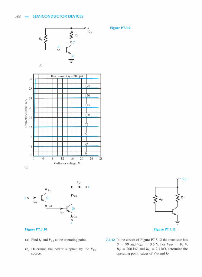
388 SEMICONDUCTOR DEVICES
Figure P7.3.9
Q2
iE2
iB2
e
iE1
Q1b
c
iC2
iCC
iC1
iB1
Figure P7.3.10
RBRC
−VCC
Figure P7.3.11
(a) Find IC and VCE at the operating point.
(b) Determine the power supplied by the VCC
source.
7.3.12 In the circuit of Figure P7.3.12 the transistor hasβ = 99 and VBE = 0.6 V. For VCC = 10 V,RF = 200 k, and RC = 2.7 k, determine theoperating point values of VCE and IC.

PROBLEMS 389
7.3.13 If the circuit of Example 7.3.1 is to switch fromcutoff to saturation, find the condition on vS, giventhat the transistor has β = 100.
7.3.14 Consider the circuit of Example 7.3.3. ForRE = 0and β = 50, find iE.
7.3.15 If the BJT in the circuit of Example 7.3.1 hasβ = 150, find iC and vCE when: (a) iB = 20 µA,and (b) iB = 60 µA. Specify the state of the BJTin each case.
7.3.16 The circuit shown in Figure P7.3.16 has a pnp BJTturned upside down. Find RB when vEC = 4 V andβ = 25.
7.3.17 Reconsider the circuit of Figure P7.3.16. Withβ = 25, find the condition on RB such that iC hasthe largest possible value.
7.4.1 Consider JFET characteristics shown in Figures7.4.3 (a) and (c).
(a) Write down the conditions for the operationto take place in the active region.
(b) Obtain an expression for the drain current iDin the active region, and for the value of iD forthe boundary between the ohmic and activeregions.
(c) Find the conditions for the linear ohmic op-eration and the equivalent drain-to-source re-sistance.
(d) Express the condition for operation in the cut-off region.
7.4.2 The JFET with parameters VP = 6 V and IDSS =18 mA is used in the circuit shown in Figure P7.4.2with a positive supply voltage. Find vGS, iD, andvDS. Note that the gate current is negligible for thearrangement shown.
*7.4.3 Consider the circuit of Figure P7.4.2 with thesame JFET parameters. Let RS be not specified.Determine vGS, vDS, and RS for active operation atiD = 2 mA.
7.4.4 A JFET with IDSS = 32 mA and VP = 5 V isbiased to produce iD = 27 mA at vDS = 4 V. Findthe region in which the device is operating.
RC
RF
VCC
+
Figure P7.3.12
C
B
E
+
+
−
+
−
−
RB
RC = 3 kΩ
vEB
vEE = 10 V
vEC
iC
Figure P7.3.16
D
S+
G RD = 1.5 kΩ
RS = 250 ΩVDD = 20 V
Figure P7.4.2

390 SEMICONDUCTOR DEVICES
7.4.5 For a p-channel JFET in its active region, specifythe polarities of voltages and the directions ofconventional currents.
7.4.6 Consider the common-source JFET circuit shownin Figure P7.4.6 with fixed bias. Sketch the si-nusoidal variations of drain current, drain volt-age, and gate voltage superimposed on the directvalues at the operating point. Assume reasonablecommon-source drain characteristics.
7.4.7 A self-biased n-channel JFET used in the circuitof Example 7.4.1 has the characteristics given inFigure P7.4.7 and a supply voltage VDD = 36V, RS = 1 k, and RD = 9 k. Determine theoperating point and the values of VGSQ, IDQ, andVDSQ.
*7.4.8 In the p-channel version of the circuit of Example7.4.1, with the JFET havingVP = 4 V and IDSS =−5 mA, find RD and RS to establish IDQ = −2mA and VDSQ = −4 V when VDD = −12 V.
7.4.9 An n-channel JFET in the circuit configurationshown in Example 7.4.1 is operating at IDQ =6 mA and VGSQ = −1 V when VDS = 5 V.Determine RS and VDD if: (a) RD = 2 k, and(b) RD = 4 k.
7.4.10 An n-channel JFET is given to have VP = 3 Vand IDSS = 6 mA.
(a) Find the smallest value of vDS when vGS = −2V if the operation is to be in the active region.
(b) Determine the corresponding iD for the small-est vDS.
7.4.11 Given that a silicon n-channel JFET has VP = 5V and IDSS = 12 mA, check whether the deviceis operating in the ohmic or active region whenvGS = −3.2 V and iD = 0.5 mA.
7.4.12 For an n-channel JFET with VA = 350 V, IDSS =10 mA, and VP = 3 V, find VDS that will causeiD = 11 mA when vGS = 0.
7.4.13 An n-channel JFET with VA = 300 V, VP = 2V, and IDSS = 10 mA is to be operated in theactive mode. Determine iD when vDS = 10 V andvGS = −0.5 V.
7.4.14 Sketch gm versus vGS for a JFET with IDSS = 10mA, VP = 3 V, VA = 100 V, and vDS = 10 V. Seewhat happens if VA → ∞. Also sketch ro versusvGS.
7.4.15 The drain current of a JFET in the ohmic region isapproximated by
iD = IDSS
[2
(1+ vGS
VP
)(vDS
VP
)−(vDS
VP
)2]
Assuming small vDS, find the channel resistancerDS for vGS = −2 V if the JFET’s parameters areIDSS = 25 mA and VP = 3 V.
7.4.16 An n-channel enhancement MOSFET operates inthe active region with very large VA, vGS = 6 V,VT = 4 V, and iD = 1 mA. Calculate K.
7.4.17 Consider the MOSFET circuit with variable volt-age shown in Example 7.4.2, with RD = 2 kand VDD = 12 V. The static characteristics ofthe n-channel enhancement MOSFET are givenin Figure P7.4.17.
(a) Draw the load line and find the operating pointif vGS = 4 V.
(b) Sketch the resulting transfer curves (i.e., iDand vDS as a function of vGS) showing cutoff,active, and saturation regions.
(c) For relatively undistorted amplification, theMOSFET circuit must be restricted to sig-nal variations within the active region. LetvGS(t) = 4 + 0.2 sin ωt V. Sketch iD(t)and vDS(t), and estimate the resulting voltageamplification Av.
(d) Let vGS(t) = 6 sin ωt , where ω is slowenough to satisfy the static condition. SketchiD(t) and vDS(t) obtained from the transfercurves. Comment on the action of the MOS-FET in the switching circuit.
7.4.18 Find idealized expressions for the active andohmic states and sketch the universal character-istics of an n-channel enhancement MOSFET op-erated below breakdown.
7.4.19 Let the circuit in Example 7.4.2 have VDD = 12 Vand RD = 2 k, and let the MOSFET have verylarge VA, VT = 2.5 V, and IDSS = 8.3 mA.
(a) Determine vGS and vDS when iD = 4 mA.
(b) Determine iD and vDS when the gate voltage is6 V.
7.4.20 Consider the MOSFET connected as a two-terminal device, as shown in Figure P7.4.20. Dis-cuss its states of operation.
7.4.21 Find the parameter values VT and IDSS for a p-channel MOSFET with iD = 0 when vGS ≤ −3V, and iD = 5 mA when vGS = vDS = −8 V. Youmay neglect the effect of vDS on iD.
7.4.22 In a depletion MOSFET for which VP = 3 V andIDSS = 11 mA, the drain current is 3 mA when vDS
is set at the largest value that will maintain ohmic-region operation. Find vGS if VA is very large.

PROBLEMS 391
+
+
+
+
−+−
GRD
iG = 0
iD
VDDVGG
vg = √2 Vg sin ωt vG
vD
Figure P7.4.6
ID , mA
VGS , V
VDS , V
VGS = 0 V
−0.5 V
−1 V
−2 V
−2.5 V
−3 V
−4 V
−1.5 V
ID , mA
0
0
10
8
6
4
2
00 28242016
(b)
(a)
1284 3632
−1−2−3−4−5
10
8
6
4
2
Figure P7.4.7 JFET characteristics. (a) Transfer characteristic. (b) Output characteristics.

392 SEMICONDUCTOR DEVICES
VDS , V
VGS ≤ 2.5 V
VGS = 5.0 V5.5 V
4.5 V
4.0 V
3.5 V
3.0 V
ID , mA
10
8
6
4
2
0 2 4 6 8 10 12 14 16
Figure P7.4.17
D
S
+
+
−−
G
vGS = v
v
iD0 A
iDFigure P7.4.20
*7.4.23 A depletion MOSFET is given to have large VA,VP = 2.8 V, IDSS = 4.3 mA, vDS = 4.5 V, andvGS = 1.2 V.
(a) Is the MOSFET operating in the active region?
(b) Find iD.
(c) Comment on whether the device is operatingin the depletion mode or in the enhancementmode.

8 Transistor Amplifiers
8.1 Biasing the BJT
8.2 Biasing the FET
8.3 BJT Amplifiers
8.4 FET Amplifiers
8.5 Frequency Response of Amplifiers
8.6 Learning Objectives
8.7 Practical Application: A Case Study—Mechatronics: Electronics Integrated with
Mechanical Systems
Problems
Amplifiers are circuits that produce an output signal which is larger than, but proportional to,an input signal. The input and output signals can be both voltages or currents, or one or theother, as in voltage-in current-out and current-in voltage-out amplifiers. The amplifier gain isjust the network’s transfer function, which is the ratio of output-to-input complex signals in thefrequency domain as found by complex analysis. Amplifiers find extensive use in instrumentationapplications. Sometimes, amplifiers are used for reasons other than gain alone. An amplifier maybe designed to have high input impedance so that it does not affect the output of a sensor while atthe same time giving a low output impedance so that it can drive large currents into its load, suchas a lamp or heating element. In some other applications, an amplifier with a low input impedancemight be desirable.
The first step in designing or analyzing any amplifier is to consider the biasing. The biasingnetwork consists of the power supply and the passive circuit elements surrounding the transistorthat provide the correct dc levels at the terminals. This is known as setting the Q point (quiescentor operating point) with no signal applied. A good bias circuit must not only establish the correctdc levels, but must maintain them in spite of changes in temperature, variations in transistorcharacteristics, or any other sources of variation.
393

394 TRANSISTOR AMPLIFIERS
Thus, a biasing signal (current or voltage), in the absence of any other signals, places thetransistor at an operating or quiescent point of its i–v characteristics. Time-varying signals areusually superimposed on dc biasing signals. Small variations of voltage and current about theoperating point are known as small-signal voltages and currents. While small-signal variationsare just a fraction of the power-supply voltage, the large-scale excursions of a power amplifier maybe comparable to the supply voltage. This chapter is devoted to the study of small-signal amplifiers,in which the relationships between small-signal variables are linear. Graphical solutions includingthe transistor’s general nonlinearity are not considered in this text.
A transistor model, having the same number of terminals as the transistor, is a collection ofideal linear elements designed to approximate the relationships between the transistor small-signal variables. While the small-signal model cannot be used to obtain information aboutbiasing, the ac device model considered in this chapter deals only with the response of thecircuit to small signals about the operating point. The transistor model is then substituted forthe transistor in the circuit in order to analyze an amplifier circuit. Under the assumption ofsmall-signal linear operation, the technique of superposition can be used effectively to simplifythe analysis.
Amplifier circuits can be treated conveniently as building blocks when analyzing largersystems. The amplifier block may be represented by a simple small-signal model. A multistageamplifier is a system obtained by connecting several amplifier blocks in sequence or cascade, inwhich the individual amplifier blocks are called stages. Input stages are designed to accept signalscoming from various sources; intermediate stages provide most of the amplification; output stagesdrive various loads. Most of these stages fall in the category of small-signal amplifiers.
The subject of amplifier frequency response has to do with the behavior of an amplifier asa function of signal frequency. Circuit capacitances and effects internal to the transistors imposelimits on the frequency response of an amplifier. Minimization of capacitive effects is a topic ofgreat interest in circuit design.
After discussing biasing the BJTs and FETs to establish the operating point, BJT and FETamplifiers are analyzed, and the frequency response of amplifiers is looked into. Advantages ofnegative feedback in amplifier circuits are also mentioned.
8.1 BIASING THE BJT
A simple method of biasing the BJT is shown in Figure 8.1.1. While no general biasing procedurethat will work in all cases can be outlined, a reasonable approach is to assign 1/2 VCC as the dropacross the transistor, 3/8 VCC as the drop across RC to allow an adequate ac voltage swing capabilityin the collector circuit, and 1/8 VCC as the drop across RE, so that RE is about 1/3 RC. With a specifiedsupply voltage VCC, biasing consists mainly of selecting values for VCEQ, ICQ, and IBQ = ICQ/β,which define the operating Q point. One can then select
+
−
+
−VCCVB
REI2
R1
R2
B
IBG E
RC
C
IEQ
VE
VCEG
ICC
Figure 8.1.1 Method of biasing the BJT.

8.2 BIASING THE FET 395
RC = 3VCC
8ICQ
(8.1.1)
RE = VCC
8(ICQ + IBQ)= VCCβ
8(1+ β)ICQ
(8.1.2)
Noting that VB = VE + VBE in Figure 8.1.1, or VB = (VCC/8) + 0.7 for silicon, and selectingI2 = 5IBQ, it follows then
R2∼= 0.7+ (VCC/8)
5IBQ
(8.1.3)
R1∼= VCC − VB
6IBQ
= (7 VCC/8)− 0.7
6IBQ
(8.1.4)
EXAMPLE 8.1.1
Apply the rule-of-thumb dc design presented in this section for a silicon npn BJT with β = 70when the operating Q point is defined by ICQ = 15 mA and IBQ = 0.3 mA, with a dc supplyvoltage VCC = 12 V, and find the resistor values of RC, RE, R1, and R2.
So l u t i on
Applying Equations (8.1.1) through (8.1.4), we get
RC = 3(12)
8(15× 10−3)= 300
RE = 12(70)
8(71)(15× 10−3)= 98.6
R1∼= [7(12)/8]− 0.7
6(0.3× 10⁻³)= 5444
R2∼= 0.7+ (12/8)
5(0.3× 10⁻³)= 1467
8.2 BIASING THE FET
Let us first consider biasing the JFET and then go on to biasing the MOSFET.
Biasing JFET
A practical method of biasing a JFET is shown in Figure 8.2.1. Neglecting the gate current, whichis usually very small for a JFET, we have
VG = VDDR2
R1 + R2(8.2.1)
The transfer characteristic of the JFET [see Figure 7.4.3(c)], neglecting the effect of vDS on iD, isgiven by
iD = IDSS
(1+ vGS
VP
)2
(8.2.2)

396 TRANSISTOR AMPLIFIERS
+
−VDDVG
R1
R2
GS
D
RS
RD
Figure 8.2.1 Method of biasing the JFET.
From Figure 8.2.1, applying the KVL to the loop containing R2 and RS , the load-line equation is
iD = VG − vGS
RS
(8.2.3)
The operating point Q is the intersection of the load line with the transfer characteristic, fromwhich IDQ and VGSQ can be read. While no systematic bias-point design procedure to serve allapplications exists, a simple procedure that will serve a good number of problems is outlinedhere. In establishing the operating point Q, compromising between high stability and high gain,one may choose
IDQ = IDSS
3(8.2.4)
Substituting this into Equation (8.2.2), we get
VGSQ =(
1−√3√3
)VP∼= −0.423VP (8.2.5)
Next, select VG to yield a reasonably low slope to the load line so that drain-current changes aresmall,
VG = 1.5VP (8.2.6)
The voltage drop across RS is then given by
VG − VGSQ∼= 1.5VP + 0.423VP = 1.923VP (8.2.7)
so that
RS = 1.923VP
IDQ
= 1.923VP
IDSS/3= 5.768VP
IDSS
(8.2.8)
Choosing R2 arbitrarily as
R2 = 100RS (8.2.9)
to maintain large resistance across the gate, R1 can be found,
R1 = R2(VDD − VG)
VG
= 100RS
(VDD
1.5VP
− 1
)(8.2.10)
Next, to find RD, choosing the transistor’s drop to be equal to that across RD plus the pinch-offvoltage necessary to maintain the active-mode operation,
VDD − IDQRS = VP + 2IDQRD (8.2.11)
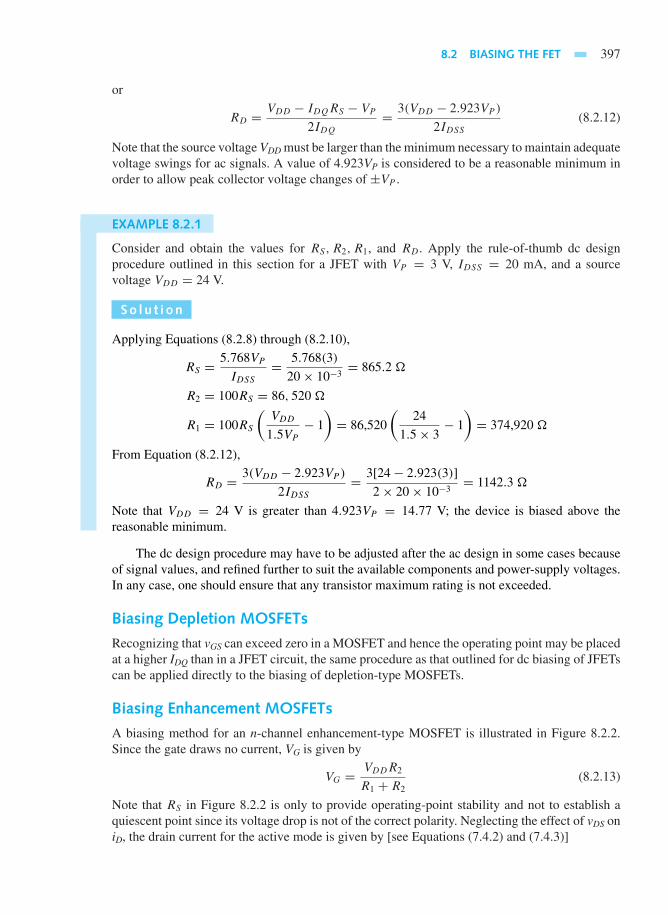
8.2 BIASING THE FET 397
or
RD = VDD − IDQRS − VP
2IDQ
= 3(VDD − 2.923VP )
2IDSS
(8.2.12)
Note that the source voltage VDD must be larger than the minimum necessary to maintain adequatevoltage swings for ac signals. A value of 4.923VP is considered to be a reasonable minimum inorder to allow peak collector voltage changes of ±VP .
EXAMPLE 8.2.1
Consider and obtain the values for RS,R2, R1, and RD . Apply the rule-of-thumb dc designprocedure outlined in this section for a JFET with VP = 3 V, IDSS = 20 mA, and a sourcevoltage VDD = 24 V.
So l u t i on
Applying Equations (8.2.8) through (8.2.10),
RS = 5.768VP
IDSS
= 5.768(3)
20× 10−3= 865.2
R2 = 100RS = 86, 520
R1 = 100RS
(VDD
1.5VP
− 1
)= 86,520
(24
1.5× 3− 1
)= 374,920
From Equation (8.2.12),
RD = 3(VDD − 2.923VP )
2IDSS
= 3[24− 2.923(3)]
2× 20× 10−3= 1142.3
Note that VDD = 24 V is greater than 4.923VP = 14.77 V; the device is biased above thereasonable minimum.
The dc design procedure may have to be adjusted after the ac design in some cases becauseof signal values, and refined further to suit the available components and power-supply voltages.In any case, one should ensure that any transistor maximum rating is not exceeded.
Biasing Depletion MOSFETs
Recognizing that vGS can exceed zero in a MOSFET and hence the operating point may be placedat a higher IDQ than in a JFET circuit, the same procedure as that outlined for dc biasing of JFETscan be applied directly to the biasing of depletion-type MOSFETs.
Biasing Enhancement MOSFETs
A biasing method for an n-channel enhancement-type MOSFET is illustrated in Figure 8.2.2.Since the gate draws no current, VG is given by
VG = VDDR2
R1 + R2(8.2.13)
Note that RS in Figure 8.2.2 is only to provide operating-point stability and not to establish aquiescent point since its voltage drop is not of the correct polarity. Neglecting the effect of vDS oniD, the drain current for the active mode is given by [see Equations (7.4.2) and (7.4.3)]

398 TRANSISTOR AMPLIFIERS
+
−VDDVG
R1
R2
G
S
D
RS
RD
Figure 8.2.2 Biasing an n-channel enhancementMOSFET.
iD = K(vGS − VT )2 (8.2.14)
in which VT and K are specified based on the transfer characteristic [Figure 7.4.8(a)] in themanufacturer’s data sheets.
The load-line equation is
iD = VG − vGS
RS
(8.2.15)
The required gate–source voltage VGSQ at the operating point is then
VGSQ = VT +√IDQ
K(8.2.16)
VDSQ can then be selected to yield a desired operating point on the ID–VDS static characteristics ofthe device. It follows then
RS + RD = VDD − VDSQ
IDQ
(8.2.17)
By trading off ac gain (larger RD) versus dc stability (larger RS), RD and RS need to be chosen.Once RS is chosen, then VG is set by
VG = VGSQ + IDQRS (8.2.18)
Finally, R1 and R2 can be selected arbitrarily to yield VG while keeping both large enough tomaintain a large gate impedance. The outlined approach is best illustrated by an example.
EXAMPLE 8.2.2
Given an n-channel enhancement MOSFET having VT = 4 V, K = 0.15 A/V2, IDQ = 0.5 A,VDSQ = 10 V, and VDD = 20 V. Using the dc design approach outlined in this section, determineVGSQ, VG, RD, RS, R1, and R2.
So l u t i on
Applying Equation (8.2.16),
VGSQ = VT +√IDQ
K= 4+
√0.5
0.15= 5.826 V

8.3 BJT AMPLIFIERS 399
Noting the supply voltage to be 20 V and the drop across the transistor 10 V, about 10 V can beallowed for ac swing across RD. Allowing some drop of, say, 3 V across RS for dc stability,
RD = 7
0.5= 14
RS = 4
0.5= 8
From Equation (8.2.18),
VG = VGSQ + IDQRS = 5.826+ 4 = 9.826 V
Selecting arbitrarily R2 = 10,000 to maintain a large gate impedance,
R1 = R2(VDD − VG)
VG
= 104(20− 9.826)
9.826= 10.354 k
One should also check to ensure that the voltage, current, and power ratings of the device are notexceeded.
Biasing methods using resistors have been presented for the sake of simplicity and ease ofunderstanding. However, nowadays biasing techniques for modern amplifiers utilize transistors.
8.3 BJT AMPLIFIERS
The purpose of electronic amplifiers is essentially to increase the amplitude and power of a signalso that either useful work is done or information processing is realized. The output signal powerbeing greater than the input signal power, the additional power is supplied by the bias supply.Thus, the amplifier action is one of energy conversion in which the bias power is converted tosignal power within the device.
A single-stage amplifier is one in which there is only one amplifying element. By combiningseveral single-stage amplifier circuits, a multistage amplifier is produced. Audio amplifiers aredesigned to amplify signals in the frequency range of 30 to 15,000 Hz perceptible to the humanear. A video amplifier is designed to amplify the signal frequencies needed for television imaging(see Chapter 15). An amplifier, in general, is then made up of a cascade of several stages. A stageusually consists of an elementary amplifier, which normally has only one transistor. The cascadeis formed by making the output of the first stage as the input of the second stage, the output ofthe second stage as the input of the third stage, and so on. This section is devoted to the study ofthree basic forms of amplifier stages which use a BJT.
Common-Emitter (CE) Configuration
The emitter part of a circuit being common to both the input and the output portions, Figure8.3.1(a) illustrates a common-emitter (CE) BJT amplifier. The resistors R1, R2, RC, and RE areprimarily set by biasing. The input ac source is represented by its Thévenin equivalent. Theamplified output ac voltage vL appears across the load resistor RL, which could represent theinput resistance of the next stage in a cascade. Capacitors CB, CC, and CE are so chosen that theyrepresent short circuits at the lowest frequency of interest. CE would be made large enough sothat 1/ωCE is small relative to RE in parallel with the impedance looking into the emitter at thesmallest ω of interest. Similarly, the reactances of CC and CB would be chosen small relative tothe resistances in their parts of the circuit. Capacitors CB and CC appear as short circuits to the acsignals, but block the dc voltages and currents out of one part of the circuit from coupling with

400 TRANSISTOR AMPLIFIERS
C
BE
CE
CC
+
−VCC
+
−VL
Ground
iS
+
−vS
RS
R2
R1
CB
RC
RE
RL
iL
v1
AC source
Amplifiedoutput
ac voltage
npn BJT
Loadresistor
Bypasscapacitor
(a)
Rin Ri
RB=R1||R2 RC RL
(b)
RS
+
−vS
+
−vπ rπ +
−vL = Av1 v1
gmvπ
E
C
ro
iS iL = AiiSB
GroundRin=RB||Ri Ri = rπ
v1 = vπ
Figure 8.3.1 Common-emitter (CE) BJT amplifier. (a) Circuit. (b) Small-signal ac equivalent circuit.
another part. Capacitor CE, known as the bypass capacitor, bypasses the ac current around RE sothat no significant ac voltage is generated across RE, and helps to increase the gain.
The small-signal ac equivalent circuit is shown in Figure 8.3.1(b), in which the small-signal model of Figure 7.3.7 for the transistor is used. While omitting the details of analysisand summarizing the results, we have
RB = R1
∥∥R2 = R1R2
R1 + R2(8.3.1)
Ri = resistance between
transistor base and ground(as seen looking into base)
= rπ (8.3.2)
v1 = vπ = vSRin
RS + Rin(8.3.3)

8.3 BJT AMPLIFIERS 401
where
Rin =[
total input resistance
seen by source
]= RB
∥∥Ri = RBrπ
RB + rπ(8.3.4)
Voltage and current gains are given by
Av1 =vL
v1= −gmRL[ro‖RC]
RL + [ro‖RC](8.3.5)
Ai = iL
iS= −gm(ro‖RC)(rπ‖RB)
RL + (ro‖RC)(8.3.6)
The CE configuration yields signal inversion since the gains can be seen to be negative.
EXAMPLE 8.3.1
Consider the transistor biased in Example 8.1.1. Given that RL = 500 and VA = 75 V for thetransistor, determine the ac voltage and current gains.
So l u t i on
Taking VT = 25.861× 10⁻³ V, as indicated in Section 7.3, and applying Equation (7.3.7),
gm = ICQ
VT
= 15× 10−3
25.861× 10−3= 0.58 S
By using Equation (7.3.8),
ro = VA
ICQ
= 75
15× 10−3= 5000
Taking RC = 300 from the solution of Example 8.1.1,
ro‖RC = 5000‖300 = 5000(300)
5000+ 300= 283
Applying Equation (8.3.5), one gets
Av1 =−0.58(500)(283)
(500+ 283)= −104.8
From Equation (7.3.9),
rπ = β
gm= 70
0.58= 120.7
and
Rin = R1‖R2‖rπ = 1
(1/R1)+ (1/R2)+ (1/rπ )= 1
(1/5444)+ (1/1467)+ (1/120.7)= 109.3
where values for R1 and R2 are taken from the solution of Example 8.1.1. From Equation (8.3.6),
Ai = −0.58(283)(109.3)
500+ 283= −22.9

402 TRANSISTOR AMPLIFIERS
Common-Collector (CC) Configuration
A common-collector (CC) amplifier is also known as an emitter follower (or a voltage follower)due to the fact that the output voltage “follows” the input by being approximately equal to theinput voltage. The amplifier is shown in Figure 8.3.2(a), in which the collector forms a commonterminal between the input and output circuits, and resistors R1, R2, and RE are determined bybiasing. Capacitors CB and CE are chosen large enough to appear as short circuits at the lowestfrequency of interest in the input signal vS. The output voltage vL is taken across the load resistorRL. The small-signal ac equivalent circuit of the amplifier is shown in Figure 8.3.2(b), whoseanalysis yields the following results:
RB = R1‖R2 = R1R2
R1 + R2(8.3.7)
CB
E CE
+
−VCC
+
−RL
Ground
iS
+
−vS
RS
R2
R1
CB
RE vL
IL
v1
AC source
Outputvoltage
npn BJT
Rin Ri
Loadresistor
(a)
R1||R2=RB
(b)
RS
+
−vS
gmvπ
E
C
rorπiS
i
iL
B
GroundRB||Ri=Rin Ri
v1
+
−RLRE vL
+
−vπ
Figure 8.3.2 Common-collector (CC) BJT amplifier. (a) Circuit. (b) Small-signal ac equivalent circuit.

8.3 BJT AMPLIFIERS 403
Rin = RB‖Ri = RBRi
RB + Ri
(8.3.8)
in which
Ri = rπ + RW(1+ gmrπ) (8.3.9)
where
RW = ro‖RE‖RL (8.3.10)
The voltage and current gains are given by
Av1 =vL
v1= RW(1+ gmrπ)
rπ + RW(1+ gmrπ)(8.3.11)
Ai = iL
iS= vLRin
v1RL
= Rin
RL
Av1 =RinRW(1+ gmrπ)
RL[rπ + RW(1+ gmrπ)](8.3.12)
ro is generally large enough so that the following results hold. For ro →∞,
Ri∼= rπ + (1+ gmrπ)(RE‖RL) (8.3.13)
Av1∼= (1+ gmrπ)(RE‖RL)
rπ + (1+ gmrπ)(RE‖RL)∼= 1 (8.3.14)
Ai∼= (1+ gmrπ)(RE‖RL)RB
RL[rπ + RB + (1+ gmrπ)(RE‖RL)](8.3.15)
Note that the voltage gain of the CC amplifier is about unity, but never exceeds unity. The currentgain, on the other hand, is large since Rin >> RL typically.
Common-Base (CB) Configuration
The common-base (CB) amplifier is shown in Figure 8.3.3(a), in which the base forms the commonterminal between the input and output circuits, and resistors R1, R2, RC, and RE are selected throughbiasing. Capacitors CB, CC, and CE are chosen large enough to act as short circuits at the lowestfrequency of interest in the input signal vS. The output voltage vL is taken from the collector acrossresistor RL. The small-signal ac equivalent circuit of the amplifier is shown in Figure 8.3.3(b),whose analysis yields the following results:
RH = RC‖RL = RCRL
RC + RL
(8.3.16)
Ri = rπ (ro + RH)
rπ + RH + ro(1+ gmrπ)(8.3.17)
Rin = RE‖Ri = RERi
RE + Ri
= (rπ‖RE)(ro + RH)
ro + RH + (rπ‖RE)(1+ gmro)(8.3.18)
The voltage and current gains are given by
Av1 =vL
v1= vL
−vπ =RH(1+ gmro)
RH + ro(8.3.19)
Ai = Rin
RL
Av1 =RH(rπ‖RE)(1+ gmro)
RL[ro + RH + (rπ‖RE)(1+ gmro)](8.3.20)
For ro →∞,

404 TRANSISTOR AMPLIFIERS
C
B
E
CE
CC
+
−VCC
+
−vL
Ground
R2
R1
CB
RC
RE
RL
iL
RS
iS
npn BJT
+
−vS
Rin
(a)
ACsource
Outputvoltage
v1
RC RL
+
−vL
+
−vS
gmvπ
E
C
rorπ
Ground
v1= −vπ
Ri
RE
RS
B
+
−vπ
Rm=REIIRi
IL
iS
(b)
Figure 8.3.3 Common-base (CB) BJT amplifier. (a) Circuit. (b) Small-signal ac equivalent circuit.
Ri∼= rπ
1+ gmrπ(8.3.21)
Rin∼= (rπ‖RE)
1+ gm(rπ‖RE)(8.3.22)
Av1∼= gm(RC‖RL) (8.3.23)
Ai∼= gm(RC‖RL)(rπ‖RE)
RL[1+ gm(rπ‖RE)](8.3.24)
Because of the low input resistance, the CB amplifier is often used as a current amplifier whichaccepts an input current into its low impedance and provides an output current into a highimpedance. That is why a CB amplifier is sometimes referred to as a current follower.

8.4 FET AMPLIFIERS 405
On comparing the CE, CC, and CB configurations one can come up with the followingobservations:
1. Ri and Rin are largest for the CC configuration, smallest for the CB, and in between thoseextremes for the CE.
2. While there is a sign inversion in the voltage-gain expression with the CE amplifier, aboutthe same magnitude of gain (which can be greater than unity) results for the CE and CBconfigurations. For the CC amplifier, however, the voltage gain cannot exceed unity.
3. Both CE and CB configurations can yield large current-gain magnitudes; the CB amplifierhas a current gain less than unity.
8.4 FET AMPLIFIERS
Just like the BJT amplifiers, FET amplifiers are constructed in common-source (CS, analogousto CE), common-drain (CD, analogous to CC), and common-gate (CG, analogous to CB)configuration. First we shall consider JFET amplifiers, then we show how the results are modifiedwith MOSFETs.
Common-Source (CS) JFET Amplifier
Figure 8.4.1(a) shows a CS JFET amplifier in which resistors R1, R2, RD, and RSS are selectedby the bias design, and capacitors CG, CD, and CS are chosen to be large enough that they act asshort circuits at the lowest frequency of interest in the input signal vS. Figure 8.4.1(b) gives itssmall-signal equivalent circuit. Noting that the input impedance of a JFET is very large, we have
Ri∼= ∞ (8.4.1)
Rin = R1‖R2 = R1R2
R1 + R2(8.4.2)
R1
R2
(a)
RS
+
−vS
Input ac source
CG
Outputvoltage
Rin
+
−VDD
Ri
RSS CS
GS
D
+
−
vL
CD
Ground
RL
n - ChannelJFET
iS
RD
iL
Figure 8.4.1 Common-source (CS) JFET amplifier. (a) Circuit. (b) Small-signal ac equivalent circuit.

406 TRANSISTOR AMPLIFIERS
R1 R2 RD RL
(b)
RS
+
−vS
+
−vGS
+
−vL
gmvGS
Output
Input
S
G D
roiS
iL
GroundRin = R1||R2 Ri −∞
v1
Figure 8.4.1 Continued
Further analysis yields
Av1 =−gmroRF
ro + RF
(8.4.3)
Ai = −gmroRFRin
RL(ro + RF )= Rin
RL
Av1 (8.4.4)
where
RF = RD‖RL = RDRL
RD + RL
(8.4.5)
The CS JFET amplifier is capable of large voltage and current gains.
EXAMPLE 8.4.1
A JFET for which VA = 80 V, VP = 4 V, and IDSS = 10 mA has a quiescent drain current of 3mA when used as a common-source amplifier for which RD = RSS = 1 k and RL = 3 k. Forthe case of fully bypassed RSS , find the amplifier’s voltage gain Av1 . Also determine the currentgain Ai if R1 = 300 k and R2 = 100 k.
So l u t i on
From Equations (7.4.5) and (7.4.4),
ro = VA
IDQ
= 80
3× 10−3= 26,666.7
gm = 2
VP
√IDSSIDQ = 2
4
√10× 10−3 × 3× 10−3 = 2.7386× 10⁻³ S
RF = RD‖RL = 1
(1/1000)+ (1/3000)= 750
Av1 =−gmroRF
ro + RF
= −2.7386(10−3)(26,666.7)750
26,666.7+ 750∼= −2

8.4 FET AMPLIFIERS 407
Rin = R1‖R2 = 300(100)
400= 75 k
Ai = Rin
RL
Av1 =75
3(−2) = −50
Common-Drain (CD) JFET Amplifier
Figure 8.4.2(a) shows a CD JFET amplifier in which resistors R1, R2, and RSS are selected by thebias design, and capacitors CG and CS are chosen to be large enough to act as short circuits atfrequencies in the band of interest (known as the midband). Figure 8.4.2(b) gives its small-signalac equivalent circuit. Analysis of this circuit yields
Ri∼= ∞ (8.4.6)
Rin = R1‖R2 = R1R2
R1 + R2(8.4.7)
Av1 =vL
v1= gmro(RSS‖RL)
ro + (RSS‖RL)(1+ gmro)(8.4.8)
Ai = iL
iS= gmro(RSS‖RL)(R1‖R2)
RL[ro + (RSS‖RL)(1+ gmro)](8.4.9)
In many cases Av1∼= 1 and vL = v1; that is to say the load voltage “follows” the input. Hence a
CD amplifier is often known as a source follower, which becomes an excellent buffer to couple ahigh-resistance source to a low-resistance load with nearly no loss in signal voltage. The currentgain, however, can be very large, leading to significant power gain.
Common-Gate (CG) JFET Amplifier
Figure 8.4.3(a) shows a CG JFET amplifier in which resistors R1, R2, RD, and RSS are selected bythe bias design, and capacitors CD and CS are chosen to be large enough to act as short circuits at
R1
R2
(a)
RS
+
−vS
Input ac source
CG
Outputvoltage
Rin
+
−VDD
Ri
RSS
GS
D
+
−vL
CS
Ground
RL
n-ChannelJFET
Figure 8.4.2 Common-drain (CD) JFET amplifier. (a) Circuit. (b) Small-signal ac equivalent circuit.
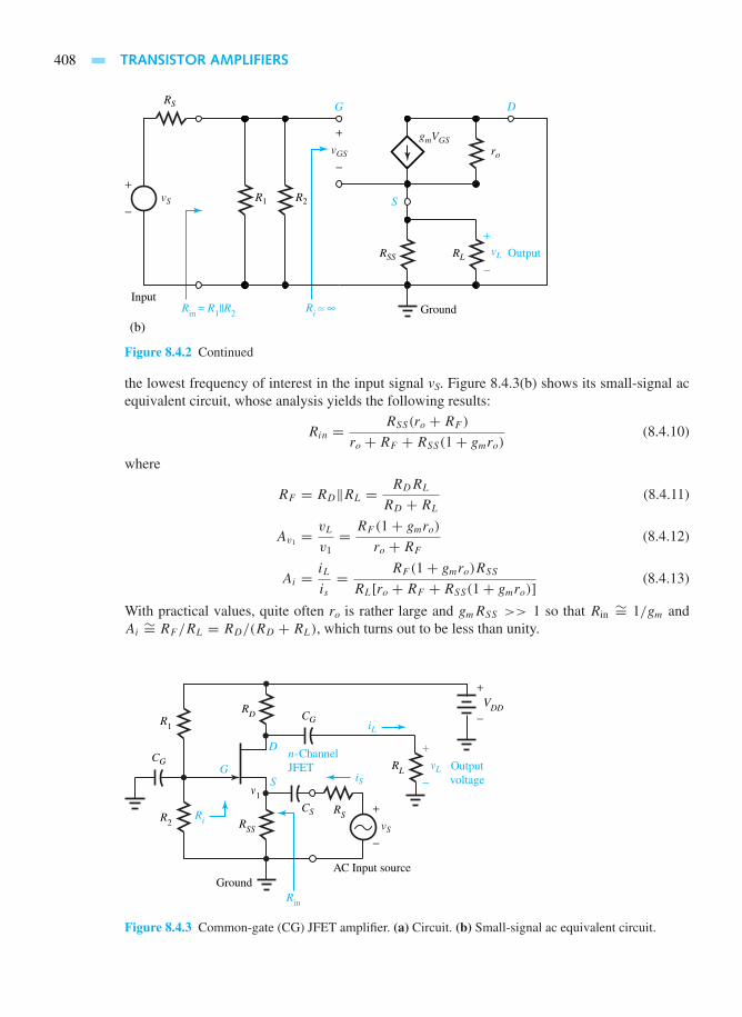
408 TRANSISTOR AMPLIFIERS
R1 R2
(b)
RS
+
−vS
+
−vGS
+
−vL
gmVGS
Output
Input
S
G D
ro
GroundRin = R1||R2 Ri − ∞
RSS RL
Figure 8.4.2 Continued
the lowest frequency of interest in the input signal vS. Figure 8.4.3(b) shows its small-signal acequivalent circuit, whose analysis yields the following results:
Rin = RSS(ro + RF )
ro + RF + RSS(1+ gmro)(8.4.10)
where
RF = RD‖RL = RDRL
RD + RL
(8.4.11)
Av1 =vL
v1= RF (1+ gmro)
ro + RF
(8.4.12)
Ai = iL
is= RF (1+ gmro)RSS
RL[ro + RF + RSS(1+ gmro)](8.4.13)
With practical values, quite often ro is rather large and gmRSS >> 1 so that Rin∼= 1/gm and
Ai∼= RF/RL = RD/(RD + RL), which turns out to be less than unity.
CG
CG
RSS
RD
R2Ri
R1
v1
GS
D
iL
RL
+
−vL Output
voltage
+
−vS
RSCS
Rin
AC Input source
+
−VDD
iS
Ground
n-ChannelJFET
Figure 8.4.3 Common-gate (CG) JFET amplifier. (a) Circuit. (b) Small-signal ac equivalent circuit.

8.5 FREQUENCY RESPONSE OF AMPLIFIERS 409
RS
+
−
iS vS
+
−vL
RSS
v1
Input
ro RD RLgmvGS
+
−vGS
G D iL
S
Output
(b)
Figure 8.4.3 Continued
On comparing the CS, CD, and CG configurations one can make the following observations:
1. For CS and CD configurations Rin = R1‖R2, which can be selected to be large duringthe bias design. For the CG configuration, however, Rin is not very large, on the order ofa few hundred ohms.
2. For the CD configuration the voltage gain is generally less than unity or near unity, whileit can exceed unity in the other configurations. The voltage gain of the CG configurationis slightly larger than that of the CS configuration.
3. For the CG configuration the current gain cannot be larger than unity. But for the CS andCD configurations it can be large by the choice of Rin.
MOSFET Amplifiers
Because the same small-signal equivalent circuits apply to both the JFET and the MOSFETs, allthe equations developed for the JFET amplifiers hold good for the MOSFET amplifiers, so longas gm and ro are computed properly. For the depletion MOSFET the equations for gm and ro, givenby Equations (7.4.4) and (7.4.5), are the same as for the JFET. For the enhancement MOSFET,they are given by Equations (7.4.9) and (7.4.10).
8.5 FREQUENCY RESPONSE OF AMPLIFIERS
All amplifiers exhibit variations of performance as the signal frequency is changed. The frequencyresponse of an amplifier may be defined as the functional dependence of output amplitude andphase upon frequency, for all frequencies. Invariably there is a maximum frequency above whichamplification does not occur. Depending on the design of the circuit, there may also be a lowerfrequency limit below which amplification disappears. The range of frequencies over whichsignificant amplification of the magnitude is obtained is known as the passband, which is boundedby the upper cutoff frequency and the lower cutoff frequency (if one exists). Dc-coupled amplifiers,in which the stages are coupled together for all frequencies down to zero, have no low-frequencylimit. On the other hand, circuits containing coupling capacitors that couple stages together for

410 TRANSISTOR AMPLIFIERS
Av0Magnitude
Mag
nitu
de o
f ga
in
Av0
2
Midband
W3dB
Phase angleof gain
Phase
0
Deteriorationdue tocoupling capacitorsand bypasscapacitor
0 ωL ωH ω
Deteriorationdue to capacitancesinternal to thetransistor
Bandwidth (passband)
Figure 8.5.1 Typical frequency response of a voltage amplifier.
ac while isolating them for dc are limited in their low-frequency response. The high-frequencydeterioration of the voltage gain is due to the effect of capacitances that are internal to the transistor.
Figure 8.5.1 shows a typical frequency response of a voltage amplifier. While most often themagnitude of the gain is discussed (because it defines the frequency range of useful gain), thephase response becomes important for transient calculations. The midband region is the range offrequencies where gain is nearly constant. Amplifiers are normally considered to operate in thisuseful midband region. The bandwidth of an amplifier is customarily defined as the band betweentwo frequencies, denoted by ωH and ωL, which corresponds to the gain falling to 3 dB below themidband constant gain. Thus,
W3dB = ωH − ωL (8.5.1)
which is shown in Figure 8.5.1. When both ωL and ωH have significant values, the amplifieris known as a bandpass amplifier. A narrow-bandpass amplifier is one in which W3dB is smallrelative to the center frequency of the midband region. In a low-pass unit (dc amplifier) there isno low 3-dB frequency.
The general problems of analyzing any given amplifier to determine ωL or ωH , and ofdesigning amplifiers with specific values of ωL and ωH , are extremely complex and well beyondthe scope of this text. Specific amplifier cases can, however, be considered in order to gain a senseof what is involved in determining the frequency response. Toward that end let us consider the CSJFET amplifier shown in Figure 8.4.1(a). The small-signal ac equivalent circuit for low frequenciesnear ωL is depicted in Figure 8.5.2(a), that for high frequencies near ωH in Figure 8.5.2(b).
Assuming ro to be large for convenience, the gain of the low-frequency circuit of Figure8.5.2(a) can be found to be
Av = vL
vs= Av0(jω)
2(ωZ + jω)
(ωL1 + jω)(ωL2 + jω)(ωL3 + jω)(8.5.2)

8.5 FREQUENCY RESPONSE OF AMPLIFIERS 411
R1 R2
Cs
RD RL
(a)
RS
+
−vS
+
−vGS
+
−vL
gm vGS
Outputvoltage
Input acsource
S
CG G DCD
RSS
ro
R1 R2 Cgs ro Cds RD RL
(b)
RS
+
−vS
+
−vGS
+
−vL
gmvGS Outputvoltage
Cgd
Input acsource
Figure 8.5.2 Small-signal equivalent circuits for CS JFET amplifier. (a) For low frequencies nearωL (includingcoupling capacitors and bypass capacitor). (b) For high frequencies near ωH (including parasitic capacitancesof transistor).
where
Av0 =−gmRGRDRL
(RS + RG)(RD + RL)(8.5.3)
RG = R1‖R2 = R1R2
R1 + R2(8.5.4)
ωZ = 1
RSSCS
(8.5.5)
ωL1 =1
RL1CS
(8.5.6)
ωL2 =1
RL2CD
(8.5.7)
ωL3 =1
RL3CG
(8.5.8)
RL1 =RSS
1+ gmRSS
(8.5.9)

412 TRANSISTOR AMPLIFIERS
RL2 = RD + RL (8.5.10)
RL3 = RS + RG (8.5.11)
The frequencies ωZ , ωL1 , ωL2 , and ωL3 are known as break frequencies, at which the behavior of|Av| changes. For ω above all break frequencies Av
∼= Av0 , which is the midband value of thegain. The largest break frequency is taken to be ωL, the low 3-dB frequency.
The amplifier gain at higher frequencies nearωH is found from the analysis of Figure 8.5.2(b).Neglecting the second-order term in ω2 in the denominator, the gain can be found to be
Av = vL
vs
∼= Av0ωH(ωZ − jω)
ωZ(ωH + jω)(8.5.12)
where
Av0 =−gmRGRDL
RS + RG
(8.5.13)
RDL = ro‖RD‖RL = roRDRL
roRD + roRL + RDRL
(8.5.14)
RG = R1‖R2 = R1R2
R1 + R2(8.5.15)
ωZ = gm
Cgd
(8.5.16)
ωH = 1
RA[Cgs + Cgd(1+ gmRDL + RDL/RA)](8.5.17)
RA = RS‖RG = RSRG
RS + RG
(8.5.18)
An illustrative example of both low- and high-frequency designs is worked out next.
EXAMPLE 8.5.1
Consider a CS JFET amplifier with the following parameters:R1 = 350 k;R2 = 100 k,RSS =1200 ,RD = 900 ,RL = 1000 ,RS = 2000 , ro = 15 k, gm = 6 × 10⁻³ S, Cgs = 3pF, Cgd = 1 pF, and ωL = 2π × 100 rad/s. Discuss the low- and high-frequency designs.
So l u t i on
For the low-frequency design,
RG = R1‖R2 = R1R2
R1 + R2= 350(100)
450= 77.78 k
RL1 =RSS
1+ gmRSS
= 1200
1+ (6× 10−3 × 1200)= 1200
8.2= 146.34
RL2 = RD + RL = 900+ 1000 = 1900
RL3 = RS + RG = 2000+ 77,780 = 79,780
Noting that RL1 is the smallest, from Equation (8.5.6),
CS = 1
RL1ωL
= 1
146.34(2π × 100)= 10.87 µF
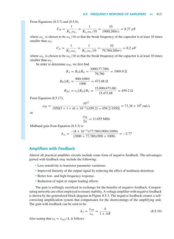
8.5 FREQUENCY RESPONSE OF AMPLIFIERS 413
From Equations (8.5.7) and (8.5.8),
CD = 1
RL2ωL2
= 1
RL2ωL/10= 10
1900(200π)= 8.37 µF
where ωL2 is chosen to be ωL/10 so that the break frequency of the capacitor is at least 10 timessmaller than ωL.
CG = 1
RL3ωL3
= 1
RL3ωL/10= 10
79,780(200π)= 0.2 µF
where ωL3 is chosen to be ωL/10 so that the break frequency of the capacitor is at least 10 timessmaller than ωL.
In order to determine ωH , we first find
RA = RS‖RG = 2000(77,780)
79,780= 1969.9
RD‖RL = 900(1000)
1900= 473.68
RDL = ro‖RD‖RL = 15,000(473.68)
15,473.68= 459.2
From Equation (8.5.17),
ωH = 1012
1950[3+ 1+ (6× 10⁻³)(459.2)+ 459.2/1950]= 73.26× 10⁶ rad/s
orωH
2π= 11.655 MHz
Midband gain from Equation (8.5.3) is
Av0 =−(6× 10⁻³)(77,780)(900)(1000)
(2000+ 77,780)(900+ 1000)= −2.77
Amplifiers with Feedback
Almost all practical amplifier circuits include some form of negative feedback. The advantagesgained with feedback may include the following:
• Less sensitivity to transistor parameter variations.
• Improved linearity of the output signal by reducing the effect of nonlinear distortion.
• Better low- and high-frequency response.
• Reduction of input or output loading effects.
The gain is willingly sacrificed in exchange for the benefits of negative feedback. Compen-sating networks are often employed to ensure stability. A voltage amplifier with negative feedbackis shown by the generalized block diagram in Figure 8.5.3. The negative feedback creates a self-correcting amplification system that compensates for the shortcomings of the amplifying unit.The gain with feedback can be seen to be
Af = vout
vin= A
1+ AB(8.5.19)
Also noting that vd = vout/A, it follows

414 TRANSISTOR AMPLIFIERS
+
−
vdvin
vout
A
B
Transistoramplifying unit with
gain A
Feedbackwith feedback factor B
vf
= vin − vf
= Bvout
= (AB)vd
vout = Avd = A(vin−vf)
= A(vin−Bvout)
Figure 8.5.3 Voltage amplifier with negative feedback.
vd
vin= 1
1+ AB(8.5.20)
The product AB is known as the loop gain because vf = B(Avd) = (AB)vd . In order to obtainnegative feedback, the loop gain must be positive. With AB > 0 in Equation (8.5.19) it followsthat |Af | < |A|. Thus, a negative feedback amplifier has always less gain than the amplifying unititself. With AB >> 1, Af remains essentially constant, thereby reducing the effect of transistorparameter variations in the amplifying unit. If the feedback unit has |B| < 1, one can still obtainuseful amplification since |Af | ∼= 1/|B| > 1.
The amplifiers discussed in Sections 8.3 and 8.4 as well as in this section are small-signallinear stages that use capacitance coupling. These are also known as RC amplifiers since theircircuits need only resistors and capacitors. There are of course other transistor amplifiers that donot have the small-signal limitation and are also not limited to the use of resistors and capacitorsin their circuits. For larger input signals the linear dependence of the current on the signal levelmay not be maintained.
8.6 LEARNING OBJECTIVES
The learning objectives of this chapter are summarized here so that the student can check whetherhe or she has accomplished each of the following.
• Biasing the BJTs and FETs.
• BJT and FET amplifier configurations, and their small-signal equivalent circuits, based onwhich voltage and current gains are computed.
• Frequency response of amplifiers, and low- and high-frequency designs.
• Advantages of negative feedback in amplifier circuits.
8.7 PRACTICAL APPLICATION: A CASE STUDY
Mechatronics: Electronics Integrated with Mechanical Systems
Electronic circuits have become so intimately integrated with mechanical systems that a new term,mechatronics, has been coined for the combination. Various subjects related to mechatronics arebeing developed at a number of universities in the United States, supported by major industrialsponsors. Too many engineers, at present, are not well equipped and trained to design mechatronic

PROBLEMS 415
products. Interdisciplinary experts who can blend many different technologies harmoniously arerather rare.
Let us think for a moment about various electronic and electric systems in an automobile oftoday. Only a few of those are listed here:
• Body electronics: Airbags, security and keyless entry, memory seats and mirrors
• Vehicle control: Antilock brakes, traction control, electronic navigation, adaptable suspen-sion systems
• Power train: Engine and transmission, cruise control, electronic ignition, four-wheel drive
• Instrumentation: Analog/digital dash, computerized performance evaluation and mainte-nance scheduling, tire inflation sensors
• Communications and entertainment: cellular phone, AM/FM radio, CD/tape player, digitalradio
• Alternative propulsion systems such as electric vehicles, advanced batteries, and hybridvehicles are being developed. Fiber-optics in communications and electrooptics, replacingthe conventional wire harness, are already in practice.
In recent years, the conventional electric ignition system has been replaced by electronicignition. Mechanically operated switches, or the so-called points, have been replaced by bipolarjunction transistors (BJTs). The advantages of transistorized ignition systems over the conven-tional mechanical ones are their greater reliability, durability, and ease of control. The transistorcycles between saturation (state in which it behaves as a closed switch) and cutoff (state inwhich it behaves as an open switch). The ignition spark is produced as a result of rapidlyswitching off current through the coil. Modern engine control systems employ electric sensorsto determine operating conditions, electronic circuits to process the sensor signals, and special-purpose computers to compute the optimum ignition timing.
Automotive electronics has made tremendous advances, and still continues to be one ofthe most dominating topics of interest to automotive engineers. Certainly, today’s mechanicalengineers have to be familiar with electronic circuit capabilities and limitations while they try tointegrate them with mechanical design and material science.
PROBL EMS
8.1.1 A silicon npn BJT is biased by the method shownin Figure 8.1.1, with RE = 240 , R2 = 3000 ,and VCC = 24 V. The operating point correspondsto VBEQ = 0.8 V, IBQ = 110 µA, VCEQ = 14 V,and ICQ = 11 mA. Determine RC and R1.
8.1.2 By using the rule-of-thumb procedure indicatedin the text, find values of all resistors in the biasmethod of Figure 8.1.1 with VCC = 10 V fora silicon npn BJT for which β = 100 and theoperating point is given by ICQ = 5 mA.
8.1.3 A fixed-bias method is illustrated in Figure P8.1.3.Assuming ICBO to be small compared to IBQ andICQ, find RB such that the operating point corre-
sponds to ICQ = 14 mA, VCEQ = 7 V, whenVCC = 12 V and the silicon BJT has a nominalβ = 70. Also determine RC.
*8.1.4 Consider the collector–base biasing methodshown in Figure P8.1.4. With the same data asin Problem 8.1.3, find RB and RC.
8.1.5 A BJT is biased by the method shown in FigureP8.1.5. If VBEQ = 0.7 V, β = 100, VCEQ = 10V, and ICQ = 5 mA, find I1, I2, and IEQ.
8.2.1 For the method of biasing a JFET shown in Figure8.2.1 of the text, use the design procedure outlinedthere to find VG, RS, RD, R2, and R1, given that
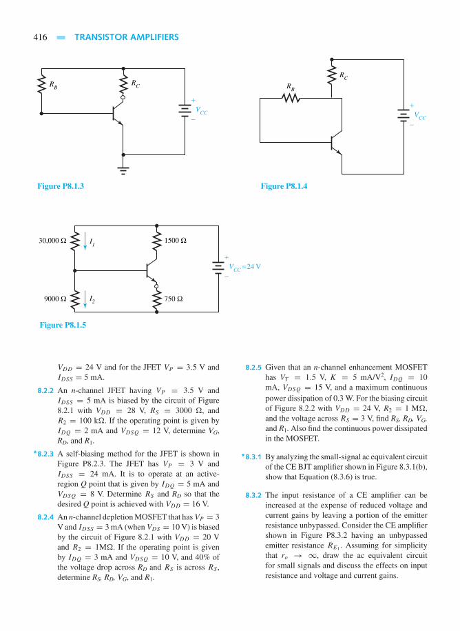
416 TRANSISTOR AMPLIFIERS
+
−VCC
RBRC
Figure P8.1.3
+
−VCC
RB
RC
Figure P8.1.4
+
−VCC
= 24 V
30,000 Ω
9000 Ω
I1
I2 750 Ω
1500 Ω
Figure P8.1.5
VDD = 24 V and for the JFET VP = 3.5 V andIDSS = 5 mA.
8.2.2 An n-channel JFET having VP = 3.5 V andIDSS = 5 mA is biased by the circuit of Figure8.2.1 with VDD = 28 V, RS = 3000 , andR2 = 100 k. If the operating point is given byIDQ = 2 mA and VDSQ = 12 V, determine VG,RD, and R1.
*8.2.3 A self-biasing method for the JFET is shown inFigure P8.2.3. The JFET has VP = 3 V andIDSS = 24 mA. It is to operate at an active-region Q point that is given by IDQ = 5 mA andVDSQ = 8 V. Determine RS and RD so that thedesired Q point is achieved with VDD = 16 V.
8.2.4 An n-channel depletion MOSFET that hasVP = 3V and IDSS = 3 mA (when VDS = 10 V) is biasedby the circuit of Figure 8.2.1 with VDD = 20 Vand R2 = 1M. If the operating point is givenby IDQ = 3 mA and VDSQ = 10 V, and 40% ofthe voltage drop across RD and RS is across RS ,determine RS, RD, VG, and R1.
8.2.5 Given that an n-channel enhancement MOSFEThas VT = 1.5 V, K = 5 mA/V2, IDQ = 10mA, VDSQ = 15 V, and a maximum continuouspower dissipation of 0.3 W. For the biasing circuitof Figure 8.2.2 with VDD = 24 V, R2 = 1 M,and the voltage across RS = 3 V, find RS, RD, VG,and R1. Also find the continuous power dissipatedin the MOSFET.
*8.3.1 By analyzing the small-signal ac equivalent circuitof the CE BJT amplifier shown in Figure 8.3.1(b),show that Equation (8.3.6) is true.
8.3.2 The input resistance of a CE amplifier can beincreased at the expense of reduced voltage andcurrent gains by leaving a portion of the emitterresistance unbypassed. Consider the CE amplifiershown in Figure P8.3.2 having an unbypassedemitter resistance RE1 . Assuming for simplicitythat ro → ∞, draw the ac equivalent circuitfor small signals and discuss the effects on inputresistance and voltage and current gains.

PROBLEMS 417
+
−VDD
RD
RSRG
Figure P8.2.3
CB
E
CE
CC
+
−VCC
+
−vL
Ground
iS
+
−vS
RS
R2
R1
CB
RC
RE1
RE2
RL
iLv1
Figure P8.3.2 CE amplifier having an unbypassed emitter resistance RE1 .
8.3.3 Consider the CE BJT amplifier of Figure 8.3.1(a)with R1 = 1600 , R2 = 400 , RC = 70 ,RE = 20 , and RL = 150 . The transistor hasβ = 70, VA = 50 V, and ICQ = 80 mA whenVCC = 15 V. Compute the amplifier’s voltage andcurrent gains. Take VT to be 25.861 mV.
8.3.4 Let the bypass capacitor CE be removed in Prob-lem 8.3.3. How would the gains be altered?
8.3.5 Let half of RE be unbypassed in Problem 8.3.3.How would the gains be altered?
*8.3.6 The CE BJT amplifier of Figure 8.3.1(a) has thefollowing parameters: R1 = 28,000 , R2 =8000 ,RC = 1400 ,RE = 700 ,RL =2000 ,VCC = 24 V, and ICQ = 5 mA whenβ = 100 and VA = 100 V. Calculate the voltageand current gains of the amplifier.
8.3.7 Let 200 of RE be not bypassed in Problem 8.3.6.How would the gains be altered?
8.3.8 Determine voltage and current gains for the CEBJT amplifier shown in Figure 8.3.1(a) with thefollowing parameters: R1 = 30,000 ,R2 =9000 ,RC = 750 ,RE = 250 ,RL =1000 ,VCC = 9 V; and ICQ = 5 mA whenβ = 150 and VA = 50 V.
8.3.9 Assuming that the bypass capacitor CE is removedin Problem 8.3.8, find the voltage and currentgains.
*8.3.10 Find an expression for the power gain AP for acommon-collector stage if the power gain of anamplifier stage is defined as the ratio of the loadpower vLiL to the power delivered by the sourcev1is. (See Figure 8.3.1 for notation.)

418 TRANSISTOR AMPLIFIERS
8.3.11 Starting from Equations (8.3.9), (8.3.11), and(8.3.12), show that equations (8.3.13) through(8.3.15) hold for ro →∞.
8.3.12 Consider the CC BJT amplifier circuit shown inFigure 8.3.2(a) with R1 = 150 k, R2 = 150 k,
RE = 2 k,RL = 3 k, and VCC = 10 V. TheBJT has β = 100, ICQ = 1.2 mA, and VA = 75V. Determine Ri, Rin, Av1 , and Ai.
8.3.13 Develop a formula for the power gain AP for acommon-collector stage if the power gain of anamplifier stage is defined as the ratio of the loadpower vLiL to the power delivered by the stage v1is.(See Figure 8.3.2 for notation.)
8.3.14 In the CC amplifier stage of Figure 8.3.2(a), let R1
= 32 k, R2= 22 k, RE= 400 , RL = 250 ,and VCC= 9 V. Given that VA= 70 V, β = 50, andICQ = 4 mA for the BJT, find Ri, Rin, Av1 , and Ai.
*8.3.15 Obtain an expression for the power gain AP fora common-base stage if the power gain of anamplifier stage is defined as the ratio of the loadpower vLiL to the power delivered by the sourcev1is. (See Figure 8.3.3 for notation.)
8.3.16 Show that Equation (8.3.17) holds for the circuitof Figure 8.3.3(b).
8.3.17 Consider the CB BJT amplifier circuit shown inFigure 8.3.3(a), with RC = 1 k,RL = 6 k,and Rin = 20 . The transistor parameters aregiven by β = 60, VA = 70 V, and gm = 0.03 S.Find Ri, RE, Av1 , and Ai.
8.3.18 Consider the CE BJT amplifier circuit shown inFigure P8.3.18. In order to make it into a common-base amplifier, terminals a and b are connected
together, and capacitor CE is disconnected fromground and used to couple a signal from a sourceto the emitter. Determine Ri, Rin, Av1 , and Ai.
8.4.1 For the CS JFET amplifier circuit of Figure8.4.1(a), RD = 2 k and RL = 3 k. The JFETwith ro = 15 k has a voltage gain Av1 = −4.5when the entire source resistance is bypassed. Findgm.
8.4.2 Considering the CS JFET amplifier circuit of Fig-ure 8.4.1(a), a portion of the source resistanceRSS in the JFET CS stage is sometimes left unby-passed. Let RSS = RSS1 + RSS2 in which RSS1 isthat portion ofRSS that is not bypassed andRSS2 isthat part of RSS that is bypassed. Find expressionsfor the amplifier voltage gain Av1 and the currentgain Ai. Comment on the results, particularly withreference to Equations (8.4.3) and (8.4.4).
8.4.3 The common-source amplifier of Figure 8.4.1(a)with RL = 300 ,RD = 150 , and RSS =100 (fully bypassed) has a JFET with VA = 80V, ro = 2 k, and VP = 4 V.
(a) Compute gm and IDSS if the voltage gain is−2.8.
(b) If the voltage gain is to be reduced to −1.4by leaving part of RSS unbypassed, find RSS1 ,which is that portion of RSS that is not by-passed.
*8.4.4 Consider Figure 8.4.1 (a) of a CS JFET ampli-fier with R1 = 330 k,R2 = 110 k,RD =1 k,RSS = 1 k,RL = 1 k, IDQ = 6 mA,VA = 90 V, VP = 4 V, and IDSS = 20 mA.Compute Rin, Av1 , and Ai.
C
E
Input 9000 Ω
30,000 Ω
CB
CE
B
250 Ω
750 ΩCC
1000 Ω
+
−9 V
ICQ = 5 mA
+
−vL
β = 150vA = 50 V
a
b
Figure P8.3.18

PROBLEMS 419
8.4.5 For the CD JFET amplifier of Figure 8.4.2(a),show that Equations (8.4.8) and (8.4.9) can berearranged as follows:
Av1 =gm(ro‖RSS‖RL)
1+ gm(ro‖RSS‖RL)
Ai = gm(ro‖RSS‖RL)(R1‖R2)
RL[1+ gm(ro‖RSS‖RL)]
8.4.6 In the source-follower circuit of Figure 8.4.2(a)the voltage gain is to be 0.7 when RSS = 300
and a JFET with ro = 5 k and gm = 0.025 S isused. Find the required load resistance.
8.4.7 Obtain an expression for the output resistance seenby the load when looking back into the ampli-fier between source and ground for the CD JFETsource-follower circuit of Figure 8.4.2(a).
8.4.8 If the circuit of Example 8.4.1 is converted to aCG amplifier having the same component values,compute the amplifier voltage gain Av1 , currentgain Ai, and Rin.
*8.4.9 Obtain an expression for Ri for the CG JFET am-plifier circuit of Figure 8.4.3(a).
8.4.10 Consider the CG JFET amplifier circuit of Figure8.4.3(a) with RL = 15k,RD = 7.5 k,RSS =5 k, ro = 100 k, and gm = 5 × 10⁻³ S.Evaluate Av1 , Ai, and Rin.
8.5.1 If the voltage gain of an amplifier is given by
Av = 20jω
(120π + jω)[1+ jω/(5π × 10−4)]
find ωH , ωL, and the midband gain.
8.5.2 Consider a CS JFET amplifier (Figure 8.5.2) withR1 = 520 k,R2 = 140 ,RD = 1 k, andRSS = 1.4 k. The FET parameters are gm =5 mS, ro = 20k, and Cgs = Cgd = 2 pF.The source resistance RS is 500 and the loadresistance RL is 2 k. For the low-frequency 3-dB angular frequency to be 40π rad/s, computeCS, CD, CG, Av0 , and ωH .
8.5.3 Determine RL, Cgs, andAv0 of a CS JFET amplifier(Figure 8.5.2), given thatRS = 1 kwhich can beconsidered to be much less than (R1‖R2), RL =RD,ωL << ωH ,ω3dB = 25 × 106 rad/s, andωZ/ωH = 75. The transistor parameters are gm =5 mS, ro >> (RD‖RL), and Cgs = Cgd .
8.5.4 (a) Let the nonlinear input–output relationship ofa transistor amplifying unit be given by vout =50(vd + 3v2
d). Plot the transfer characteristicand check for what range of vd the undistortedoutput results.
(b) Let a negative feedback loop be added suchthat vd = vin−Bvout. For values of B = 0.03and 0.08, investigate how the negative feed-back reduces nonlinear distortion, but reducesgain.
*8.5.5 (a) Consider the voltage amplifier with negativefeedback shown in Figure 8.5.3. For A =−100, find the feedback factor B in order toget Af = −20.
(b) With the value of B found in part (a), deter-mine the resulting range of Af if the transistorparameter variations cause A to vary between−50 and −200.
8.5.6 (a) Consider a BJT in the common-emitter con-figuration. The equations that describe the be-havior of the transistor in terms of the hybridh parameters are given by
vB = hieiB + hrevC
iC = hf eiB + hoevC
Develop the h-parameter equivalent circuit ofthe transistor in the common-emitter mode.
(b) Setting hre and hoe equal to zero, obtain the h-parameter approximate equivalent circuit ofthe common-emitter transistor.
(c) Figure P8.5.6(a) shows the small-signalequivalent circuit of a transistor amplifier inthe common-emitter mode. Find expressionsfor gains AI1 = IL/IB,AI2 = IL/IS, AV1 =VC/VB , and AV2 = VC/VS .
(d) Now consider the single-stage transistor am-plifier shown in Figure P8.5.6(b). The pa-rameters of the 2N104 transistor are hie =1.67 k,hf e = 44, and 1/hoe = 150 k.Evaluate the performance of the amplifier bycomputing current gain, voltage gain, powergain, input resistance as seen by the signalsource, and output resistance appearing at theoutput terminals.
(e) Next consider the two-stage transistor am-plifier depicted in Figure P8.5.6(c). Developthe h-parameter equivalent circuit of the two-stage amplifier and evaluate its performance.
(f) Then consider the linear model of thecommon-emitter BJT amplifier shown in Fig-ure P8.5.6(d) that is applicable to the midbandfrequency range. Find an expression for thecurrent gain AIm = I2/IS that remains in-variant with frequency. (Note the subscript m

420 TRANSISTOR AMPLIFIERS
denotes a reference to the midband frequencyrange.)
(g) The linear model of a common-emitter BJTamplifier shown in Figure P8.5.6(e) is appli-cable at low frequencies. Obtain an expressionfor the current gain AIl = I2/IS in terms ofAIm and ωl , where ωl corresponds to 0.707AIm
on the frequency response curve, and ωl iden-tifies the lower end of the useful bandwidth ofthe amplifier.
(h) The hybrid-π equivalent circuit for comput-ing the high-frequency performance of a BJT
RC-coupled amplifier is shown in FigureP8.5.6(f). Analyze the circuit (by representingin terms of isolated input and output sections)to find AIh = I2/IS in terms of AIm andωh, where ωh corresponds to 0.707AIm on thefrequency response curve, and denotes high-band frequencies.
(i) Sketch the frequency response curve of an RC-coupled amplifier by plotting the current gainas a function of frequency on semilogarithmicpaper and showing the bandwidth.
VB VCRB
RS
hie hoehfeIB
IBISIC
IL
RL
B C
E(a)
VS
Internalresistanceof source
Sourcesignal
+
−
Base biasequivalentresistance
Collectorloadresistance
Figure P8.5.6

PROBLEMS 421
B
C
E
−12 V
1 kΩ
25 mVrms
4.5 kΩ
55 kΩ 6 kΩ
25 µF 25 µF, 12 V
100 µF 50 µF
(c)
2.4 kΩ 0.24 kΩ
0.6 kΩ 0.1 kΩ
BJT2N104
BJT2N104
b
1.2 kΩ
a
First stage Second stage
RB hie hfeIB
IB
IL
RL
I2
R2IS
B C
E(d)
Useful output current of first stage(Input current of second stage)
Net input resistanceappearing at base terminalof second transistor
RB hie hfeIB
IBCCC
Couplingcapacitor
IL
RL
I2
R2IS
B
E(e)
VC
RB
CT IL
RL
I2
R2IS
B C
E(f)
RBB′Basespreadingresistor
RB′EForwardbiasedresistor
CDDiffusioncapacitor
IB ID
II ICITB ′
gmVB ′E = hfeIB
Transitioncapacitor
Figure P8.5.6 Continued

9 Digital Circuits
9.1 Transistor Switches
9.2 DTL and TTL Logic Circuits
9.3 CMOS and Other Logic Families
9.4 Learning Objectives
9.5 Practical Application: A Case Study—Cardiac Pacemaker, A Biomedical Engineering
Application
Problems
The use of nonlinear devices (BJT and FET) in constructing linear amplifiers has been studied inChapter 8. Although these devices are inherently nonlinear, their operation was confined to thelinear portions of their characteristics in order to produce linear amplification of a signal. Whenthese devices are operated in the nonlinear regions of their characteristics, the primary use lies inelectronic switches for use in computers and other digital systems. Digital electronic circuits arebecoming of increasing importance. Revolutionary advances in integrated-circuit (IC) technologyhave made it possible to place a large number of switches (gates) on a chip of very small size.Besides the advantage of utilizing less space, another significant advantage of digital systemsover analog systems is their inherent immunity to noise and interference.
Digital building blocks (made up of transistor circuits) and computer systems have beenpresented in Chapter 6. Digital circuits are almost always purchased as ready-made IC buildingblocks. However, users of digital hardware must decide which technology is best suited for eachcase because competing technologies known as logic families are available. Digital circuit designis of course of great interest to engineers in the IC industry for designing and building digitalblocks. The users of digital technology will certainly benefit from knowing what is inside theblocks they use.
A fundamental circuit of digital logic is the transistor switch, or inverter, which is consideredin Section 9.1. Basic logic circuits are developed in Section 9.2 using bipolar technology.Section 9.3 deals with other logic families, particularly the FET-based family known as CMOS(complementary metal-oxide semiconductor) technology.
422

9.1 TRANSISTOR SWITCHES 423
9.1 TRANSISTOR SWITCHES
The basic element of logic circuits is the transistor switch, a simplified model of which is shownin Figure 9.1.1. The control signal is the input voltage vin, which must lie in either the “low” rangeor the “high” range for a digital circuit. When vin is low, the switch may take either the open orthe closed position; when vin is high, the switch takes the other position. Looking at Figure 9.1.1,closing the switch makes vout zero, while opening the switch yields an output near VCC, assumingthat not much current flows through the output terminal. If VCC is chosen to lie in the high rangeand V = 0 is inside the low range, then allowed values of vin control the switch and give rise toallowed values of vout. A common special circuit in which a high input yields a low output, andvice versa, is known as an inverter, which performs the complement operation.
A typical inverter circuit using a bipolar transistor is shown in Figure 9.1.2(a), and theoperation of the BJT switch is illustrated in Figure 9.1.2(b). The KVL around the collector–emitter loop is given by
vCE = VCC − RCiC (9.1.1)
from which the load line may be drawn on the collector–emitter characteristic. The KVL aroundthe base–emitter loop is given by
vBE = Vi − RBiB (9.1.2)
and the corresponding load line may be drawn on the base–emitter characteristic.If the input is at zero volts, that is logic 0, then the base current is zero, and the operating
point is at ➀, as shown in Figure 9.1.2(b). The transistor is then said to be cut off, or simply off,when only a very small value of collector current (IC cutoff
∼= ICEO) flows. Thus, in the cutoff statethe output voltage is given by
Vo = VCE cutoff∼= VCC − RCICEO
∼= VCC = 5V (i.e., logic 1 level) (9.1.3)
If the input Vi changes to +5 V (logic 1 level), the base current is given by
IB sat = Vi − vBE
RB
(9.1.4)
where vBE∼= 0.7 V, which is the threshold voltage VT. Supposing that RB is chosen so as to drive
the transistor into saturation such that IB sat = 50 µA, the operating point switches to point ➁ onthe collector–emitter characteristic, when the transistor is said to be saturated, or simply on. Inthis saturated state VCE sat = Vsat, which is typically 0.2 to 0.3 V, depending on iB. The collectorcurrent in saturation is given by
IC sat = VCC − Vsat
RC
∼= VCC
RC
(9.1.5)
vout
vin
R
VCC Figure 9.1.1 Model of transistor switch.

424 DIGITAL CIRCUITS
VCC = 5 V
VT = 0.7
1
5
4
3
2
1
0.2 to 0.3 V
2 3 4 5
IB sat = 50
60 µA
50 µA
40 µA
30 µA
20 µA
10 µA
0.5
Saturation
Cutoff
1
Vi
Vi
VO = vCE
RC
RB
RB
vBE
vBE, V
iC
iB
iB, µA
vCE, V
iC, mA
(a)
(b)
Slope = −
− −
+−
+
+
vCE
−
+
+
1
1
2
2
VCE cutoff VCC
VCC
VCCRC
VCE sat = Vsat
IC cutoff = ICEOiB = 0
IC sat
Figure 9.1.2 BJT inverter switch. (a) Circuit with npn switching transistor.(b) Typical operation using load lines.
Thus, the transistor behaves like an ideal switch, as shown in Figure 9.1.3. It can be shown thatsaturation will occur when
Vi − VT
RB
>VCC − Vsat
β RC
or Vi > (VCC − Vsat)RB
β RC
+ VT (9.1.6)
The power dissipated in the transistorp = vCEiC+vBEiB ∼= vCEiC is very small or approximatelyzero in either cutoff or saturation. It should be noted, however, that power is expended in switchingfrom one state to the other, going through the linear or active region.

9.1 TRANSISTOR SWITCHES 425
RC
C
E
S Vo
+ VCC
+=
=
−
RC
E
C
S Vo
+ VCC
+
−
(a)
RC
CS
E
VoVsat
ICEO
+ VCC
+
−
+
−
RC
CS
E
Vo
+ VCC
+
−
(b)
Figure 9.1.3 BJT switch. (a) Off (cutoff) position.(b) On (saturation) position.
Cutoffregion
Activeregion
VT
Saturationregion
ViVCC
(VCC − Vsat) + VT
VCC
Vo
Vsat
0.7 VRB
βRC
Figure 9.1.4 Transfer characteristic of BJTswitch.
Figure 9.1.4 shows the transfer characteristic of a BJT switch relating Vi and Vo, whereasFigure 9.1.5 depicts a plot of a typical input-voltage waveform and the resulting output-voltagewaveform, illustrating the essential inherent inversion property of the switch, the waveformdistortion, propagation delays, and rise and fall times of the BJT switch. Note the followingtime parameters.

426 DIGITAL CIRCUITS
• Propagation delay td is a certain amount of delay for a change to occur. It is defined hereas the time to change from 0 to 10% of the final value. (Sometimes propagation delay isdefined as the time between the 50% level of Vi and the 50% level of Vo.) When Vi abruptlychanges from 0 to 5 V, note that the output voltage and collector current do not initiallychange during the propagation delay time.
• Rise time tr is the time needed to change from 10 to 90% of the final level.
• Propagation delay ts occurs when the input pulse returns to 0 V (i.e., logic level 0). This isa result of the time required to remove charge stored in the base region before the transistorbegins to switch out of saturation and is usually longer than td.
• Fall time tf is the time required for the output voltage and the collector current to changestate. That is the time required to switch through the active region from saturation to cutoff.
These times are influenced by the various capacitances inherent in the transistor and otherstray capacitances. In turn, the design of a digital switch is influenced by these propagationdelays, and the rise and fall times, which are grouped under the general category of switchingspeed.
5 V Cutoff
Saturation
5 V
Vo
tstr
td
tf
iC
Vi
t
t
t
Vsat
IC sat
IC cutoff = ICEO
0.9IC sat
0.1IC sat
0
Figure 9.1.5 Typical input-voltage waveform and resulting output-voltage waveform.

9.2 DTL AND TTL LOGIC CIRCUITS 427
EXAMPLE 9.1.1
For the circuit of Figure 9.1.2, given that VCC = 5 V, RC = 1 k,β = 100, and the high range is4 to 5 V, choose RB such that any high input will saturate the transistor with the base overdrivenby a factor of at least 5. Assume Vsat to be 0.2 V.
So l u t i on
Since iC ∼= βiB + ICEO , one must have (neglecting ICEO) IB sat > IC sat/β. But
IC sat = VCC − Vsat
RC
Hence,
IB sat >VCC − Vsat
βRC
With a factor of 5 included for the desired overdrive, one has
iB = 5VCC − Vsat
βRC
= 55− 0.2
100(1000)= 240 µA
When vi is in the high range, the emitter–base junction is forward-biased. The base current thatflows is given approximately by
iB = vi − 0.7
RB
or RB = vi − 0.7
iB
Setting vi = 4 V, which is the lowest value in the high range,
RB = 4− 0.7
2.4× 10−4= 13,750
One chooses the closest standard resistance smaller than 13,750 , since making RB smallerincreases the overdrive and hence improves the margin of safety.
9.2 DTL AND TTL LOGIC CIRCUITS
Bipolar transistors were the first solid-state switching devices commonly used to implement digitallogic circuits in the 1950s and 1960s. These circuits used diodes at the input of the gate for logicoperation followed by a transistor (BJT) output device for signal inversion. One of the bipolar logicfamilies that emerged was called DTL (diode–transistor logic). The TTL (transistor–transistorlogic) soon replaced DTL and then became the principal bipolar technology for the next twodecades. It is still often used today. In TTL circuits, the diodes used in DTL at the gate input arereplaced with a multiemitter transistor for increased performance. Primarily by reducing the sizeof the transistors and other components, speed and performance improvements have been madein TTL circuits.
Both DTL and TTL are called saturating logic families, because the BJTs in the circuitare biased into the saturated region to achieve the effect of a closed switch. The inherent slowswitching speed is a major difficulty with saturating logic because saturated BJTs store significantcharge and switch rather slowly. Schottky TTL is a nonsaturating logic family that was laterdeveloped to achieve higher speed performance by preventing the transistors from saturating.Another bipolar nonsaturating logic family is ECL (emitter-coupled logic), which has BJTs thatremain biased in the active region. These circuits consume more power, are less dense, but areextremely fast.

428 DIGITAL CIRCUITS
Using the transistor switch, logic gates can be constructed to perform the basic logic functionssuch as AND, OR, NAND, NOR, and NOT. Since the individual gates are available in the form ofsmall packages (such as the dual-in-line package, or DIP), it is generally not necessary to designindividual gates in order to design an overall digital system. However, the designer needs toobserve fan-out restrictions (i.e., the maximum number of gates that may be driven by the device),fan-in restrictions (i.e., the maximum number of gates that may drive the device), propagationdelays, proper supply voltage to the unit, and proper connections to perform the intended logicfunction. Gates of the same logic family can be interconnected since they have the same logicvoltage levels, impedance characteristics, and switching times. Some of the logic families arediscussed in this section.
DTL (Diode Transistor Logic) Gate
A circuit realization of a NAND gate will now be developed. By connecting NAND gates togetherin various ways, one can synthesize other gates and flip-flops. Thus in principle, a single NANDgate circuit, repeated many times, would be sufficient to build up digital systems.
One possible NAND gate circuit is shown in Figure 9.2.1, in which it can have as many inputsas desired (indicated by the dashed-line input C), and typical values of VCC = 5 V, RA = 2 k,RC = 5 k, and β = 50. We shall now consider the two inputs A and B that are quite adequate forour discussion, with the high range defined to be 4 to 5 V and the low range defined to be 0 to 0.5 V.
While the input voltages vA and vB are constrained to lie inside the high or low range ofthe allowed voltage ranges, the resulting output voltage vF is supposed to be inside the high orlow range as well. For different combinations of vA and vB, we need to find vF. Since the circuitconsists of no less than five nonlinear circuit elements (DA, DB, D1, D2, and T1), an approximationtechnique is used for analysis, while taking the voltage across a current-carrying forward-biasedpn junction to be 0.7 V. The reader may have realized that it is not obvious at the start whichdiodes are forward-biased and which are reverse-biased. Hence a guessing procedure is used inwhich a guess is made and checked for self-consistency.
Let us start by letting vA = vB = 0, in which case a probable current path is from VCC downthrough RA and through inputs A and B. Since this guess implies current flow through DA and DB inthe forward direction, we may guess that the voltage at X is 0.7 V. There is also a current path fromX down to ground through D1 and D2 and the base–emitter junction of the transistor. Even thoughthe sign of the guessed voltage is correct to forward-bias these three junctions, its magnitude of0.7 V is insufficient since 2.1 V (or 3 × 0.7) is needed to make current flow through this path.Then iB = 0; the transistor is cut off; and the output voltage vF = VCC = 5 V, assuming that
RA
DA
DC
A
C
X
VCC
RC iL
iB
T1D1 D2
F Output
Inputs
VCC
DB
B
Figure 9.2.1 DTL NAND gate.

9.2 DTL AND TTL LOGIC CIRCUITS 429
no load current flows through the output terminal. Thus in this case, DA and DB are conducting,whereas D1, D2, and T1 are not. This is illustrated by the first line in Table 9.2.1.
For the inputs indicated on the other lines of Table 9.2.1 the reader can reason out the othercolumns shown. In terms of the high and low ranges, the operation of the gate is illustrated in Table9.2.2. The truth table is given in Table 9.2.3 using the positive logic in which high is indicated by1 and low is indicated by 0. One can now see that the circuit does function as a NAND gate.
TABLE 9.2.1 Inputs and Outputs for NAND Gate of Figure 9.2.1
Volts Conduction Volts
vA vB vX DA DB D1D2T1 vF
0 0 0.7 YES YES NO 50 0.2 0.7 YES NO NO 50.3 4.6 1.0 YES NO NO 54.6 0.3 1.0 NO YES NO 54.8 4.1 2.1 NO NO YES 0.2 (= VCE sat)
TABLE 9.2.2 Operation of NAND gate of Figure 9.2.1
vA vB vF
LOW LOW HIGHLOW HIGH HIGHHIGH LOW HIGHHIGH HIGH LOW
TABLE 9.2.3 Truth Table using positive logic
A B F
0 0 10 1 11 0 11 1 0
EXAMPLE 9.2.1
What logic function does the circuit of Figure 9.2.1 perform if negative logic is used?
So l u t i on
Using negative logic, Table 9.2.2 can be translated into the following truth table. This can be seento be the logic function NOR.
A B F
1 1 01 0 00 1 00 0 1

430 DIGITAL CIRCUITS
The DTL NAND gate circuit shown in Figure 9.2.1 and others closely related to it belong tothe DTL logic family. Since all circuits in the same family have the same high and low ranges,they can be interconnected to build up digital systems. Although we have described the DTL gateas our first example for our convenience and easy understanding, the DTL technology is almostobsolete and is replaced by TTL.
TTL NAND Gate
The TTL logic family uses only transistors instead of a combination of transistors and diodes.TTL has the same high and low ranges as DTL. TTL is the most popular BJT logic family. Aprimary reason for the popularity of TTL over DTL is its higher speed. TTL has a typical fan-outof 10 or more, small propagation delays on the order of 2 to 10 ns, and a power consumptionof about 2 mW. By contrast, DTL has a typical fan-out of 8 to 10, a propagation delay onthe order of 30 to 90 ns, and a power consumption of around 15 mW. The noise margins andfan-out of DTL are generally better than those of RTL (resistor–transistor logic; see Problem9.2.8), but the switching speeds are about the same. The emitter-coupled logic (ECL) familyis also available with increased switching times, although not discussed here in any detail.The name arises from the common attachment of the emitters of the input transistors. Thepropagation delays are on the order of 1 ns, but the power consumption is quite high (on theorder of 25 mW per gate). Low power consumption combined with relatively small noise margins(< 0.3 V) has made TTL a popular choice and, in particular, the high-speed Schottky diodeTTL gates.
A typical TTL NAND gate is shown in Figure 9.2.2. Transistor T1 is a multiple-emittertransistor (npn BJT) which acts as an AND gate. Replacing the base–emitter and base–collectorjunctions with diodes, T1 can be represented as shown in Figure 9.2.3.
VA Vo
VCC = 5 V
X
YVBVC
R2
R1
T3T2T1
R3
F
Figure 9.2.2 TTL NAND gate.
VADA
DB
DC
Y
X
Base-collectordiode D
Base-emitter diodesVB
VC
Figure 9.2.3 Diode replacement of three-input transistor T1 ofFigure 9.2.2.
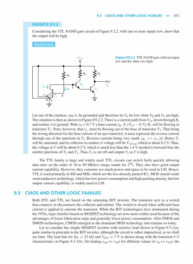
9.3 CMOS AND OTHER LOGIC FAMILIES 431
EXAMPLE 9.2.2
Considering the TTL NAND gate circuit of Figure 9.2.2, with one or more inputs low, show thatthe output will be high.
So l u t i on
Vo
VCC
X
Y
B
C
A
R2R1
iC1 iB1
T1
T3
T2
R3
F
Figure E9.2.2 TTL NAND gate with one inputlow and the other two high.
Let one of the emitters, say A, be grounded and therefore let VA be low while VB and VC are high.The situation is then as shown in Figure E9.2.2. There is a current path from VCC down through R1
and emitter A to ground. With vX= 0.7 V a base current iB1∼= (VCC − 0.7)/R1 will be flowing in
transistor T1. Note, however, that iC1 must be flowing out of the base of transistor T2. That beingthe wrong direction for the base current of an npn transistor, it must represent the reverse currentthrough one of the junctions in T2. Reverse currents being very small, iB1 >> iC1/β. Hence T1
will be saturated, and its collector-to-emitter A voltage will be VCE sat, which is about 0.2 V. Thus,the voltage at Y will be about 0.2 V, which is much less than the 1.4 V needed to forward-bias theemitter junctions of T2 and T3. Thus T3 is cut off and output Vo at F is high.
The TTL family is large and widely used. TTL circuits can switch fairly quickly allowingdata rates on the order of 10 to 40 Mbits/s (mega stands for 220). They also have good outputcurrent capability. However, they consume too much power and space to be used in LSI. Hence,TTL is used primarily in SSI and MSI, which are the less densely packed ICs. MOS (metal-oxidesemiconductor) technology, which has low power consumption and high packing density, but lowoutput current capability, is widely used in LSI.
9.3 CMOS AND OTHER LOGIC FAMILIES
Both DTL and TTL are based on the saturating BJT inverter. The transistor acts as a switchthat connects or disconnects the collector and emitter. The switch is closed when sufficient basecurrent is applied to saturate the transistor. While the BJT technologies have dominated duringthe 1970s, logic families based on MOSFET technology are now more widely used because of theadvantages of fewer fabrication steps and generally lower power consumption. After PMOS andNMOS technologies, CMOS emerged as the dominant MOS technology and remains so today.
Let us consider the simple MOSFET inverter with resistive load shown in Figure 9.3.1(a),quite similar in principle to the BJT inverter, although the circuit is rather impractical, as we shallsee later. The load line for RD = 23 k and VDD = 7 V is shown along with the transistor I–Vcharacteristics in Figure 9.3.1(b). On finding vout (= vDS) for different values of vin (= vGS), the
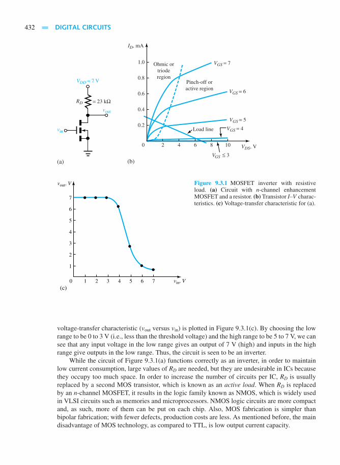
432 DIGITAL CIRCUITS
RD
VGS = 6
VGS = 7
VGS = 5
VGS ≤ 3
VGS = 4
VDS, V
ID, mA
vout
vin
VDD = 7 V
= 23 kΩ
Pinch-off oractive region
Load line
Ohmic ortrioderegion
1.0
0.8
0.6
0.4
0.2
0
(b)(a)
2 4 6 8 10
7
vout, V
vin, V
6
5
4
3
2
1
10 2 3 4(c)
5 6 7
Figure 9.3.1 MOSFET inverter with resistiveload. (a) Circuit with n-channel enhancementMOSFET and a resistor. (b) Transistor I–V charac-teristics. (c) Voltage-transfer characteristic for (a).
voltage-transfer characteristic (vout versus vin) is plotted in Figure 9.3.1(c). By choosing the lowrange to be 0 to 3 V (i.e., less than the threshold voltage) and the high range to be 5 to 7 V, we cansee that any input voltage in the low range gives an output of 7 V (high) and inputs in the highrange give outputs in the low range. Thus, the circuit is seen to be an inverter.
While the circuit of Figure 9.3.1(a) functions correctly as an inverter, in order to maintainlow current consumption, large values of RD are needed, but they are undesirable in ICs becausethey occupy too much space. In order to increase the number of circuits per IC, RD is usuallyreplaced by a second MOS transistor, which is known as an active load. When RD is replacedby an n-channel MOSFET, it results in the logic family known as NMOS, which is widely usedin VLSI circuits such as memories and microprocessors. NMOS logic circuits are more compactand, as such, more of them can be put on each chip. Also, MOS fabrication is simpler thanbipolar fabrication; with fewer defects, production costs are less. As mentioned before, the maindisadvantage of MOS technology, as compared to TTL, is low output current capacity.

9.3 CMOS AND OTHER LOGIC FAMILIES 433
FET switches offer significant advantages over BJT switches. An FET switch does not drawcurrent from a previous stage because the gate current of an FET is practically zero. Consequently,no significant power-loading effects are present, whereas BJTs, in contrast, do load down previousstages. Another advantage of FETs is that their logic voltage levels (typically, VDD = 15 V) arehigher than those of the BJTs (typically, VCC= 5 V). Thus, the FET logic circuits tend to toleratemore noise than the comparable BJT logic circuits. However, their switching speeds tend to besomewhat smaller than those for BJTs in view of the larger inherent capacitances of the FETs.
MOSFETs are preferred over JFETs for digital integrated circuits. Either PMOS (p-channelmetal-oxide semiconductor) or NMOS (n-channel metal-oxide semiconductor) logic circuits canbe constructed. Requiring only about 15% of the chip area of a BJT, MOSFETs offer very highpacking densities.
The usage of a p-channel MOSFET as the active load for an n-channel MOSFET leadsto a logic family known as complementary-symmetry MOS, or CMOS. CMOS technology hassignificant advantages and has become most popular. A basic CMOS inverter is shown in Figure9.3.2(a), in which both a p-channel and an n-channel enhancement MOSFET are used as asymmetrical pair, with each acting as load for the other.
When the input vin is low, the gate–source voltage of the NMOS is less than the thresholdvoltage and is cut off. The gate–source voltage of the PMOS, on the other hand, is −VSS , whereVSS, the supply voltage, is greater than the threshold voltage, VT . Then the PMOS is on, and thesupply voltage appears at the output vout. When the input vin is high (vin
∼= VSS), the PMOS turnsoff; the NMOS turns on. Then VSS appears across the drain–source terminals of the PMOS andthe output vout drops to zero. Thus, the circuit functions as an inverter. Figure 9.3.2(b) shows thesimplified circuit model of the CMOS inverter by depicting each transistor as either a short or anopen circuit, depending on its state.
Note that when the output is in the high state, the PMOS is on with the NMOS being off;when the output is in the low state, the NMOS is on with the PMOS being off. Virtually no currentis drawn from the power supply in either case. The CMOS has the advantage that it uses no powerexcept when it is actually switching. This property of virtually no power consumption, coupledwith the small chip surface needed, makes the CMOS very favorable for miniature and low-power applications such as wristwatches and calculators. Because of the poor switching speeds(compared to TTL), they are applied to low- to medium-speed devices. The principal disadvantageof the CMOS is a more complex fabrication procedure than that of the NMOS, leading to moredefects and higher cost.
Figure 9.3.2 CMOS inverter and circuit model.

434 DIGITAL CIRCUITS
vout
vin
VOL
VOL
VIL
NML
Transitionwidth
NMH
VIH VOH
VOH
Figure 9.3.3 Typical voltage-transfer character-istic of a CMOS logic circuit, showing noise mar-gins.
The switching action in the CMOS circuit is rather sharp, as compared with that of Figure9.3.1(c). A general voltage-transfer characteristic shown in Figure 9.3.3 illustrates this feature. Avery small change in vin is sufficient to produce a relatively large change in vout. The voltages VOH
and VOL, indicated in Figure 9.3.3, are, respectively, the nominal high and low output voltages ofthe circuit. VIL and VIH are the input voltages at which |dVout/dVin| = 1. These are seen to be theboundaries of the low and high ranges. The region between VIL and VIH is known as the transitionregion, and the transition width is given by VIH − VIL. The lower and upper noise margins aregiven by VIL − VOL ≡ NML and VOH − VIH ≡ NMH , respectively. The noise margins indicatethe largest random noise voltages that can be added to vin (when it is low) or subtracted from vin
(when it is high), without yielding an input in the forbidden transition region. A typical voltage-transfer characteristic and drain current ID1 versus input voltage vin for the CMOS inverter areshown in Figure 9.3.4. Note that when vin is inside either the low or the high states (and not inthe transition region), the drain current ID1 = −ID2
∼= 0. The maximum value of ID1 that occursduring transition is indeed very small.
EXAMPLE 9.3.1
For the CMOS inverter with characteristics shown in Figure 9.3.4, determine the noise margins.
So l u t i on
From Figure 9.3.4(a), VOH = 7 V and VOL = 0. From the location of the approximate pointswhere the absolute value of the slope is unity, VIL = 3.1 V and VIH = 3.9 V. Thus, noise marginsare given by
NML = VIL − VOL∼= 3.1− 0 = 3.1 V
NMH = VOH − VIH∼= 7− 3.9 = 3.1 V

9.3 CMOS AND OTHER LOGIC FAMILIES 435
7
vout, V
vin, V
6
5
4
3
2
1
10 2 3 4(a)
5 6 7
ID1, mA
vin, V
0.02
0.01
10 2 3 4(b)
5 6 7
Figure 9.3.4 Typical characteristics of a CMOSinverter. (a) Voltage-transfer characteristic. (b)Drain current versus input voltage.
CMOS NAND and NOR gates with two inputs are shown in Figure 9.3.5. For the NANDgate of Figure 9.3.5(a), if at least one input is in the low state, the associated PMOS device willbe on and the NMOS device will be off, thereby yielding a high output state. If, on the otherhand, both VA and VB are high, both PMOS devices will be off while both NMOS devices willbe on, thereby giving a low output Vout. Thus, the CMOS device of Figure 9.3.5(a) functions asa NAND gate.
For the NOR gate of Figure 9.3.5(b), when both inputs VA and VB are low, both NMOSdevices will be off with both PMOS devices on, and the output Vout is high around VSS. If, onthe other hand, one of the inputs goes to be high, the associated PMOS device turns off and thecorresponding NMOS device turns on, thereby yielding an output Vout to be low. Thus, the CMOSdevice of Figure 9.3.5(b) functions as a NOR gate. Note that neither gate in Figure 9.3.5 drawsvirtually any power-supply current, so that there is virtually no power consumption.
Another CMOS circuit that is conveniently built into CMOS technology is known as thetransmission gate, which is not strictly speaking a logic circuit. It is a switch controlled by a logicinput. In its circuit shown in Figure 9.3.6, the control signal C and its complement C determinewhether or not the input is connected to the output. When C is low (and C is high), neither gatecan induce a channel and the circuit acts as a high resistance between input and output. Thetransmission gate is then effectively an open circuit. On the other hand, when C is high (and C
is low), the transmission gate provides a low-resistance path between input and output for all

436 DIGITAL CIRCUITS
Figure 9.3.5 CMOS gates withtwo inputs. (a) NAND gate.(b) NOR gate.
allowed values of vin. The reader is encouraged to reason out these statements. Since the gateconducts well in either direction when the switch is on, the circuit is known to be reciprocal, inwhich case the labels “input” and “output” can be interchanged.
In addition to TTL, NMOS, and CMOS, several other logic families have been developedto suit various purposes. Emitter-coupled logic (ECL) is a high-speed bipolar technology withhigh power consumption. Transistors operate in the active mode and do not saturate in ECL;propagation delays per gate are as short as 1 ns. Besides high power consumption, the logic swing(which is the difference between high and low voltage levels) is small, being on the order of 1 V,which makes the ECL vulnerable to random noise voltages, thereby leading to errors.
The integrated-injection logic (IIL or I2L) is a compact, low-power bipolar technologycompetitive with MOS technology for LSI. This technology offers packing densities ten timeslarger than TTL: 100 to 200 gates per square millimeter as compared with probably 10 to 20 forTTL. Power consumption and delay time have a kind of trade-off relationship in IIL technology.
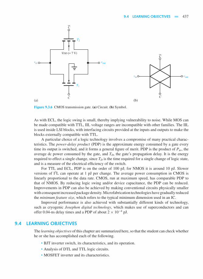
9.4 LEARNING OBJECTIVES 437
Figure 9.3.6 CMOS transmission gate. (a) Circuit. (b) Symbol.
As with ECL, the logic swing is small, thereby implying vulnerability to noise. While MOS canbe made compatible with TTL, IIL voltage ranges are incompatible with other families. The IILis used inside LSI blocks, with interfacing circuits provided at the inputs and outputs to make theblocks externally compatible with TTL.
A particular choice of a logic technology involves a compromise of many practical charac-teristics. The power-delay product (PDP) is the approximate energy consumed by a gate everytime its output is switched, and it forms a general figure of merit. PDP is the product of Pav, theaverage dc power consumed by the gate, and TD, the gate’s propagation delay. It is the energyrequired to effect a single change, since TD is the time required for a single change of logic state,and is a measure of the electrical efficiency of the switch.
For TTL and ECL, PDP is on the order of 100 pJ; for NMOS it is around 10 pJ. Slowerversions of I2L can operate at 1 pJ per change. The average power consumption in CMOS islinearly proportional to the data rate. CMOS, run at maximum speed, has comparable PDP tothat of NMOS. By reducing logic swing and/or device capacitance, the PDP can be reduced.Improvements in PDP can also be achieved by making conventional circuits physically smallerwith consequent increased package density. Microfabrication technologies have gradually reducedthe minimum feature size, which refers to the typical minimum dimension used in an IC.
Improved performance is also achieved with substantially different kinds of technology,such as cryogenic Josephon digital technology, which makes use of superconductors and canoffer 0.04-ns delay times and a PDP of about 2× 10⁻⁴ pJ.
9.4 LEARNING OBJECTIVES
The learning objectives of this chapter are summarized here, so that the student can check whetherhe or she has accomplished each of the following.
• BJT inverter switch, its characteristics, and its operation.
• Analysis of DTL and TTL logic circuits.
• MOSFET inverter and its characteristics.
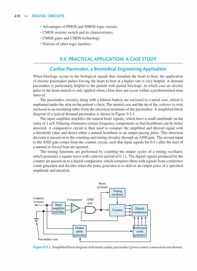
438 DIGITAL CIRCUITS
• Advantages of PMOS and NMOS logic circuits.
• CMOS inverter switch and its characteristics.
• CMOS gates and CMOS technology.
• Notions of other logic families.
9.5 PRACTICAL APPLICATION: A CASE STUDY
Cardiac Pacemaker, a Biomedical Engineering Application
When blockage occurs to the biological signals that stimulate the heart to beat, the applicationof electric pacemaker pulses forcing the heart to beat at a higher rate is very helpful. A demandpacemaker is particularly helpful to the patient with partial blockage, in which case an electricpulse to the heart muscle is only applied when a beat does not occur within a predetermined timeinterval.
The pacemaker circuitry along with a lithium battery are enclosed in a metal case, which isimplanted under the skin on the patient’s chest. The mental case and the tip of the catheter (a wireenclosed in an insulating tube) form the electrical terminals of the pacemaker. A simplified blockdiagram of a typical demand pacemaker is shown in Figure 9.5.1.
The input amplifier amplifies the natural heart signals, which have a small amplitude on theorder of 1 mV. Filtering eliminates certain frequency components so that heartbeats can be betterdetected. A comparative circuit is then used to compare the amplified and filtered signal witha threshold value and detect either a natural heartbeat or an output pacing pulse. This detectiondecision is passed on to the counting and timing circuitry through an AND gate. The second inputto the AND gate comes from the counter circuit, such that input signals for 0.4 s after the start ofa natural or forced beat are ignored.
The timing functions are performed by counting the output cycles of a timing oscillator,which generates a square wave with a precise period of 0.1 s. The digital signals produced by thecounter are passed on to a digital comparator, which compares them with signals from a referencecount generator and decides when the pulse generator is to deliver an output pulse of a specifiedamplitude and duration.
Inputamplifierand filter
Comparator ANDgate
Resetterminal
Pacemaker case
Catheterto heart
Digitalcomparator
Counter
Timingoscillator
Outputpulse
generator
Referencecount
generator
+−
Figure 9.5.1 Simplified block diagram of demand cardiac pacemaker (power source connections not shown).

PROBLEMS 439
Extremely low power consumption and high reliability become important criteria for allpacemaker designs. While electrical engineers can come up with better circuit designs, mechanicaland chemical engineers have to select better materials to produce the case and the catheter, andabove all, the physicians have to provide the pacemaker specifications. Thus, doctors and engineershave to work in teams in order to develop better biomedical products.
PROBL EMS
9.1.1 Show that saturation will occur when Equation(9.1.6) is satisfied.
*9.1.2 Consider a BJT switch connected to the next stage,as shown in Figure P9.1.2, in which iout is likelyto be negative when vout is high. Assume VCC = 5V, RC = 1k, and the high range to be 4 to 5 V.Find the largest |iout| that can be tolerated.
9.1.3 The transistor switch of Figure 9.1.2(a) is to bedesigned to operate in saturation and in cutoffwhen the pulse signal shown in Figure P9.1.3is applied to the input. Assume an ideal transis-tor with β = 100, VT = 0.7 V, Vsat = 0.2 V,and ICEO = 0.1 mA. Letting the supply voltageVCC = 5 V and RC = 500 , determine the min-imum value of RB, and sketch the output-voltagewaveform.
9.1.4 For the BJT switch described in Figure 9.1.2(a),let VCC = 5 V, VT = 0.7 V, Vsat = 0.2 V, andβ = 25. If Vl switches between 0 and 5 V andiB ≤ 0.1 mA, find the minimum values of RB andRC for proper operation.
9.1.5 Sketch the transfer characteristic for the BJTswitch described in Figure 9.1.2(a), given thatVCC = 5 V, Vsat = 0.2 V, VT = 0.7 V, RC =500 , RB = 10 k, and β = 100.
9.1.6 The transistor switch of Figure 9.1.2(a) withRB =10 k and RC = 750 employs a BJT which
has the characteristics shown in Figure P9.1.6(a).Sketch Vo as a function of time for the input signalgiven in Figure P9.1.6(b).
9.2.1 Considering Table 9.2.1, the first line has beenreasoned out in the text. Justify the other four lines.
*9.2.2 With vA = vB = 0 in Figure 9.2.1, show that aguess vX = 2.1 V would lead to a contradiction,and hence cannot be correct.
9.2.3 Consider the circuit of Figure 9.2.1 with vA = 0.4V and vB = 0.3 V. Find vX and vF.
9.2.4 With vA = 0.2 V and vB = 4.5 V in Figure 9.2.1,justify why vX = 0.7 V will be an incorrect guess.
9.2.5 Considering Figure 9.2.1 of the DTL NAND gatecircuit, inquire as to why D1 and D2 are used inthe circuit. (Hint: Consider the third line of Table9.2.1.)
9.2.6 Consider the DTL gate circuit shown in FigureP9.2.6. Assume diodes with VT = 0.7 V and thetransistor to have β = 35, VT = 0.7 V, ICEO = 0,and Vsat = 0.2 V.
(a) For inputsVA = 5 V andVB = 0 V, determineVo.
(b) For inputs VA = VB = 0 V, determine Vo.
(c) Is this a configuration of a DTL NOR gate?
RC
VCC
RB
VCC
Nextstage
vout
viniout
Figure P9.1.2
50 10t, µs
vi,V
5
15
Figure P9.1.3

440 DIGITAL CIRCUITS
ic, mA
vCE, V
iB = 0.12 mA
iB = 0
0.1 mA
0.08 mA
0.06 mA
0.04 mA
0.02 mA
8
7
6
5
4
1 2 3 40 5 6 7 8 9 10 11 12 13
vBE, V
iB, mA
1.61.41.210.80.60.40.2
0.1
0.08
0.06
0.04
0.02
0
3
2
1
(a)
B
C
E
vCEvBE
iC
iB +
+
− −
1 2 4(b)
t, ms
Vi, V
2
3
Figure P9.1.6
9.2.7 For the DTL gate shown in Figure P9.2.6, as-
sume ideal diodes, VT = 0.7 V, Vsat = 0.2 V,
RB = 10 k,RC = 500 , and VCC = 5 V. As-
suming β = 20 for the BJT and using reasonable
approximations, sketch the output Vo for the input
signals of Figure P9.2.7.
*9.2.8 A gate using resistor-transistor logic (RTL) isshown in Figure P9.2.8. Justify that this gate per-forms the NOR function.
9.2.9 Study the DTL gate circuit shown in Figure P9.2.9and state whether it behaves like a NOR gate or aNAND gate.
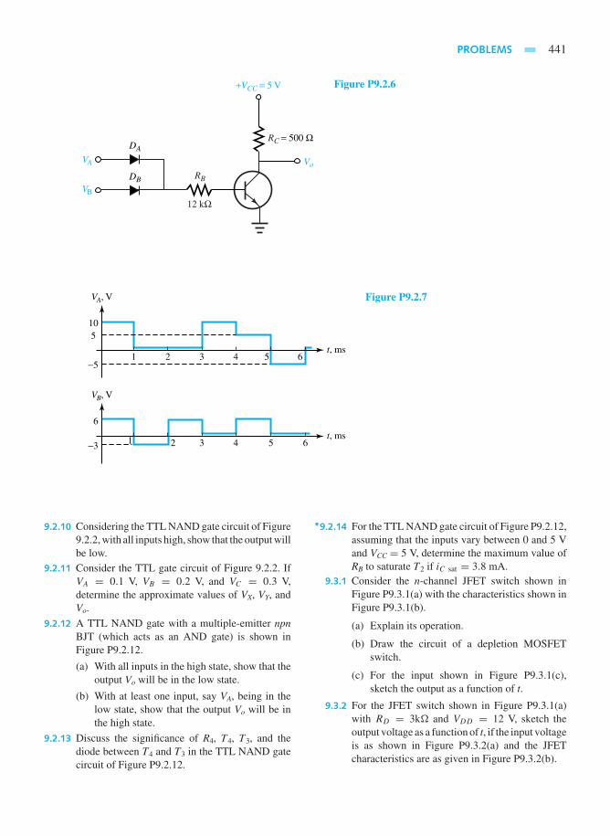
PROBLEMS 441
+VCC = 5 V
RB
RC = 500 Ω
Vo
DA
DB
12 kΩVB
VA
Figure P9.2.6
10
VA, V
t, ms
5
1 5 6432−5
6
VB, V
t, ms1 5 6432−3
Figure P9.2.7
9.2.10 Considering the TTL NAND gate circuit of Figure9.2.2, with all inputs high, show that the output willbe low.
9.2.11 Consider the TTL gate circuit of Figure 9.2.2. IfVA = 0.1 V, VB = 0.2 V, and VC = 0.3 V,determine the approximate values of VX, VY, andVo.
9.2.12 A TTL NAND gate with a multiple-emitter npnBJT (which acts as an AND gate) is shown inFigure P9.2.12.
(a) With all inputs in the high state, show that theoutput Vo will be in the low state.
(b) With at least one input, say VA, being in thelow state, show that the output Vo will be inthe high state.
9.2.13 Discuss the significance of R4, T4, T3, and thediode between T4 and T3 in the TTL NAND gatecircuit of Figure P9.2.12.
*9.2.14 For the TTL NAND gate circuit of Figure P9.2.12,assuming that the inputs vary between 0 and 5 Vand VCC = 5 V, determine the maximum value ofRB to saturate T2 if iC sat = 3.8 mA.
9.3.1 Consider the n-channel JFET switch shown inFigure P9.3.1(a) with the characteristics shown inFigure P9.3.1(b).
(a) Explain its operation.
(b) Draw the circuit of a depletion MOSFETswitch.
(c) For the input shown in Figure P9.3.1(c),sketch the output as a function of t.
9.3.2 For the JFET switch shown in Figure P9.3.1(a)with RD = 3k and VDD = 12 V, sketch theoutput voltage as a function of t, if the input voltageis as shown in Figure P9.3.2(a) and the JFETcharacteristics are as given in Figure P9.3.2(b).

442 DIGITAL CIRCUITS
+VCC
RC
Vo
RVA
RVB
RVC
T1
T2
T3
Figure P9.2.8
+VCC
RB RC
Vo
DA
VC D
VB
VA
Figure P9.2.9 DTL gate circuit.
9.3.3 FET logic circuits can be used with positivepulses by using enhancement-mode n-channelMOSFETs as switches. Figure P9.3.3(a) shows thecircuit and Figure P9.3.3(b) the MOSFET charac-teristics. For the input shown in Figure P9.3.3(c),sketch the output as a function of time.
*9.3.4 The complementary-symmetry MOSFET (CMOS)switch shown in Figure 9.3.2 has MOSFETs withVT = 5 V and Vsat = 1 V. If VSS = 20 V and vin asshown in Figure P9.3.4, sketch the output voltageas a function of time.
9.3.5 A typical CMOS inverter is shown in Figure
P9.3.5(a). The n-channel MOSFET T1 has thecharacteristics shown in Figure P9.3.5(b). T2 hasidentical characteristics except for the changes ofsign appropriate to a p-channel device.
(a) Outline a graphical procedure in order to findthe operating point of the CMOS inverterby superposing the I–V characteristics of T1
and T2.
(b) Sketch the resulting voltage-transfer charac-teristics (vout versus vin) and drain current ver-sus input voltage vin for the CMOS inverter.

PROBLEMS 443
VAVo
+VCC
VBVC
RB
T3
T4
T2
T1
R4
Figure P9.2.12 TTL NAND gate.
Figure P9.3.1 (a) n-channel JFET switch.(b) Characteristics (transfer characteristics;terminal characteristics and load line). (c) In-put.
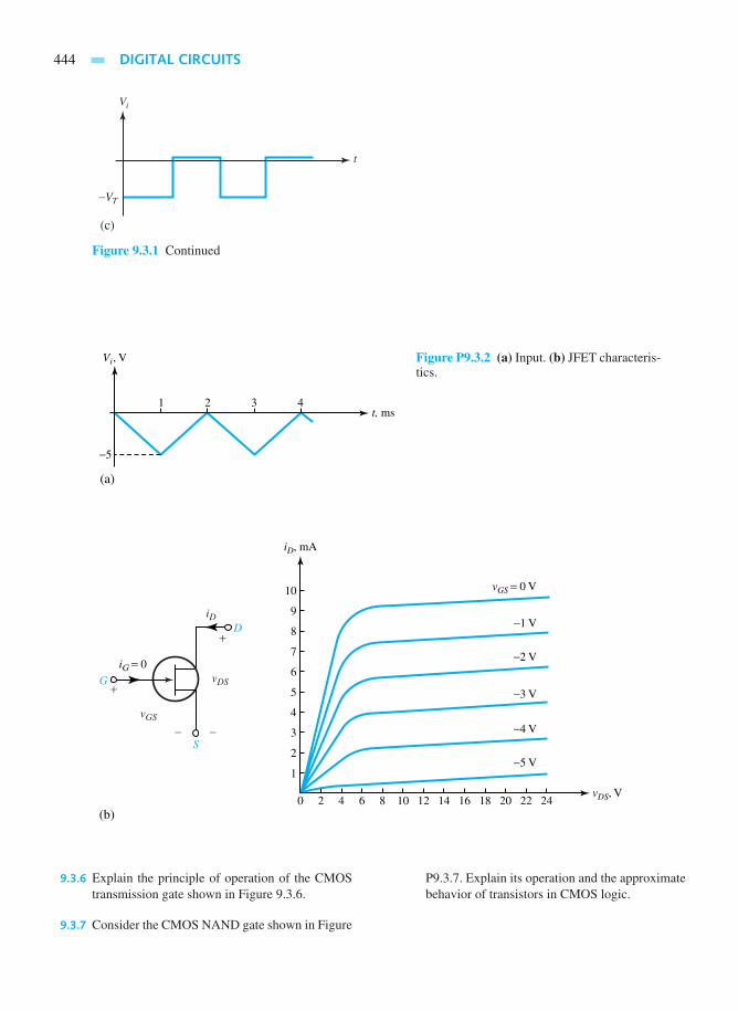
444 DIGITAL CIRCUITS
Figure 9.3.1 Continued
1 2 4
(a)
t, ms
Vi, V
−5
3
Figure P9.3.2 (a) Input. (b) JFET characteris-tics.
iD, mA
vDS, V
vGS = 0 V
−1 V
−2 V
−3 V
−4 V
−5 V
10
9
8
7
6
5
4
2 4 6 80 10 12 14 16 18(b)
20 22 24
3
2
1
S
iG = 0vDS
vGS
iDD
+
+
− −
G
9.3.6 Explain the principle of operation of the CMOStransmission gate shown in Figure 9.3.6.
9.3.7 Consider the CMOS NAND gate shown in Figure
P9.3.7. Explain its operation and the approximatebehavior of transistors in CMOS logic.

PROBLEMS 445
vGSVT
iD
vDS
iD
VDD
VDD
vGS = VT
vGS = Von
Vsat
RD
t
Vi
(c)
(b)
(a)
Saturation
Cutoff
4 V
3 V
2 V
1 V
D
S
Vi
Vo
RD
+VDD
G
Figure P9.3.3 (a) n-channel enhancement MOSFET switch. (b) Characteristics (transfer characteristics; terminalcharacteristics and load line). (c) Input.
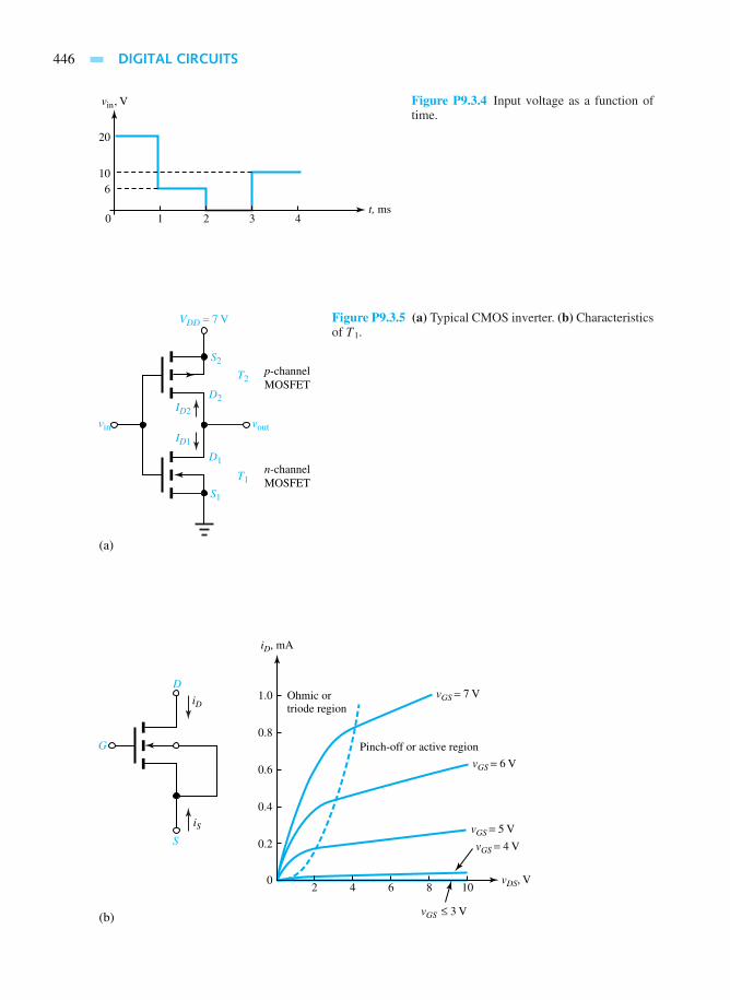
446 DIGITAL CIRCUITS
10 2 4t, ms
vin, V
106
20
3
Figure P9.3.4 Input voltage as a function oftime.
vout
VDD = 7 V
p-channelMOSFET
n-channelMOSFET
ID2
ID1
S2
S1
T1
T2
D2
D1
vin
(a)
Figure P9.3.5 (a) Typical CMOS inverter. (b) Characteristicsof T1.
vDS, V
iD, mA
108642
1.0 Ohmic ortriode region
(b)
Pinch-off or active region0.8
0.6
0.4
0.2
0
vGS = 7 V
vGS = 6 V
iS
iD
S
G
D
vGS = 5 V
vGS ≤ 3 V
vGS = 4 V

PROBLEMS 447
vout
VDD = 7 V
T3 T4
T2
T1
v1
v2
Figure P9.3.7 CMOS NAND gate.

This page intentionally left blank

PART
ENERGY SYSTEMSTHREE

This page intentionally left blank

10 AC Power Systems
10.1 Introduction to Power Systems
10.2 Single- and Three-Phase Systems
10.3 Power Transmission and Distribution
10.4 Learning Objectives
10.5 Practical Application: A Case Study—The Great Blackout of 1965
Problems
Electric power is indispensable for any modern society. Our use and demand for electric powergrows annually at the rate of 2 to 3%; our need nearly doubles about every 25 to 35 years. We, inthe United States, have become so accustomed to reliable and accessible electric power that wevirtually take it for granted.
Even though energy appears in many different forms, the vast majority of all energy deliveredfrom one point to another across the country is handled by ac power systems. Transportingelectric energy most efficiently from place to place becomes extremely important. Electric powergeneration, transmission, distribution, and utilization are the features of any practical powersystem.
In the United States power is generated by many generating stations interconnected in anoverall network, known as the power grid, which spans the entire country. The bulk of the systemis privately owned, whereas a part of the network is owned federally and a part municipally. Someutility companies in a given geographical area operate as power pools for reasons of economyand reliability.
The principal source of energy comes from the burning of fossil fuels such as coal and oilto generate steam, which drives steam turbines, which in turn drive electric generators. Otherimportant energy sources are hydroelectric and nuclear. In the former, electric generators aredriven by waterwheel (hydraulic) turbines near natural or human-made waterfalls; in the latter,nuclear reactions generate heat to drive the steam-turbine–generator chain. There are also otherless widely used sources of energy such as geothermal sources, wind, sun, and tides.
In this chapter, to start with, an introduction to power systems will be presented. Then weanalyze three-phase systems, a topic that was covered in part in Chapter 4. Finally, the components
451

452 AC POWER SYSTEMS
of an ac power network are identified, and topics related to power transmission and distributionare introduced.
10.1 INTRODUCTION TO POWER SYSTEMS
Thomas A. Edison’s work in 1878 on the electric light led to the concept of a centrally locatedpower station with distributed electric power for lighting in a surrounding area. The openingof the historic Pearl Street Station in New York City on September 4, 1882, with dc generators(dynamos) driven by steam engines, marked the beginning of the electric utility industry. Edison’sdc systems expanded with the development of three-wire 220-V dc systems. But as transmissiondistances and loads continued to grow, voltage problems were encountered. With the adventof William Stanley’s development of a commercially practical transformer in 1885, alternatingcurrent became more attractive than direct current because of the ability to transmit power at highvoltage with corresponding lower current and lower line-voltage drops. The first single-phase acline (21 km at 4 kV) in the United States operated in 1889 between Oregon City and Portland.
Nikola Tesla’s work in 1888 on electric machines made evident the advantages of polyphaseover single-phase systems. The first three-phase line (12 km at 2.3 kV) in the United Statesbecame operational in California during 1893. The three-phase induction motor conceived byTesla became the workhorse of the industry.
Most electric energy has been generated by steam-powered (accounting for about 85% ofU.S. generation) and by water-powered, or hydro, turbine plants (accounting for about 10% ofU.S. generation). Gas turbines are also used for short periods to meet peak loads. Steam plantsare fueled primarily by coal, gas, oil, and uranium. While coal is the most widely used fuel inthe United States, due to its abundance, nuclear units of 1280-MW steam-turbine capacity arein service today. However, rising construction costs, licensing delays, and public concerns havestopped the growth of nuclear capacity in the United States.
Other types of electric power generation are also prevalent, accounting for about 1% ofU.S. generation. These include wind-turbine generators, solar-cell arrays, tidal power plants, andgeothermal power plants, wherein energy in the form of steam or hot water is extracted from theearth’s upper crust. Substantial research now under way shows nuclear fusion energy to be themost promising technology for producing safe, pollution-free, and economical electric energy inthis century and beyond, since the needed fuel (deuterium) consumed in a nuclear fusion reactionis present in seawater abundantly.
Today the two standard frequencies for the generation, transmission, and distribution ofelectric power in the world are 60 Hz (in the United States, Canada, Japan, and Brazil) and 50 Hz(in Europe, the former Soviet Republics, South America except Brazil, India, and also Japan).Relatively speaking, the 60-Hz power-system apparatus is generally smaller in size and lighterin weight than the corresponding 50-Hz equipment with the same ratings. On the other hand,transmission lines and transformers have lower reactances at 50 Hz than at 60 Hz.
Along with increases in load growth, there have been continuing increases in the size ofgenerating units and in steam temperatures and pressure, leading to savings in fuel costs andoverall operating costs. Ac transmission voltages in the United States have also been risingsteadily: 115, 138, 161, 230, 345, 500, and now 765 kV. Ultrahigh voltages (UHV) above 1000kV are now being studied. Some of the reasons for increased transmission voltages are:
• Increases in transmission distance and capacity
• Smaller line-voltage drops
• Reduced line losses

10.1 INTRODUCTION TO POWER SYSTEMS 453
• Reduced right-of-way requirements
• Lower capital and operating costs.
In association with ac transmission, there have been other significant developments:
• Suspension insulator
• High-speed relay system
• High-speed, extra-high-voltage (EHV) circuit breakers
• EHV surge arrester to protect from lightning strokes and other surges
• Communications via power-line carrier, microwave, and fiber optics
• Energy control centers with supervisory control and data acquisition (SCADA) and withautomatic generation control (AGC)
• Extensive use of microprocessors for various tasks.
Along with ac transmission in the United States, there have been modern high-voltage dc(HVDC) transmission lines: the ±400-kV, 1360-km Pacific Intertie line between Oregon andCalifornia in 1970 as well as four other HVDC lines up to 400 kV and five back-to-back ac–dclinks as of 1991. A total of 30 HVDC lines up to 533 kV are in place worldwide. For an HVDC lineinterconnected with an ac system, solid-state converters at both ends of the dc line are needed tooperate as rectifiers and inverters. Studies in the United States have shown that overhead HVDCtransmission is economical for transmission distances longer than about 600 km. Also, HVDClinks seem to improve the overall system stability.
An interconnected system (in contrast with isolated systems) has many advantages:
• Better maintenance of continuity of service
• Increase in reliability and improved economy
• Reduction of reserve requirements
• Scheduling power transfers taking advantage of energy-cost differences in respective areas,load diversity, and seasonal conditions
• Shared ownership of larger and more efficient generating units.
Some of the disadvantages of interconnected operations are:
• Increased fault currents during short circuits
• Occasional domino effect leading to a regional blackout (such as the one that occurredin 1965 in the northern United States) due to an initial disturbance in some part of theinterconnected grid system.
Present and Future Trends
According to the Edison Electric Institute, electricity’s share of U.S. primary energy was almost36% in 1989, and it is likely to reach 46% by the year 2010. The growth rate in the use of electricenergy in the United States is projected to increase by about 2.4% per year for the near future,in spite of conservation practices, more efficient use of electricity, and a slackening populationgrowth. One should also be aware of large growth of power systems internationally.
Because of the large amount of U.S. coal reserves, there is the continuing shift away fromthe use of gas and oil and toward increasing use of coal. Unless the construction time and costper kW can be reduced significantly, no new nuclear units will be commissioned. Also, safety

454 AC POWER SYSTEMS
concerns seem to demand inherently safe reactor designs with standardized, modular constructionof nuclear units. Since the major U.S. hydroelectric sites (except in Alaska) have been fullydeveloped, one can foresee a trend for continuing percentage decline in hydroelectric energygeneration.
By the year 2000, the total U.S. generating capacity has reached 817 GW (1 GW= 1000 MW)and continues to grow. Current lead times of about a decade for the construction and licensing oflarge coal-fired units may cause insufficient reserve margins in some regions of the United States.
As of 1989, U.S. transmission systems consisted of about 146,600 circuit-miles of high-voltage transmission. During the 1990s, additions have totalled up to 13,350 circuit-miles, whichinclude 230-kV, 345-kV, and 500-kV lines. Because of the right-of-way costs, the possibility ofsix-phase transmission (instead of the current three-phase transmission) is being looked into.
U.S. distribution-network construction is expected to increase over the next decade. The older2.4-, 4.1-, and 5-kV distribution systems are being converted to 12 or 15 kV. Higher distributionvoltages such as 25 and 34.5 kV are also contemplated.
Recently some concern has surfaced about the effect of electromagnetic waves on the humanand animal environment. The result of this remains to be seen.
Computers in Power Systems
The control and stability of any electric power system is indeed extremely important, in particularwhen a system is expected to maintain uninterrupted continuity of service within set limitsof frequency and voltage, and to guarantee reliability of the system. Digital computers andmicroprocessors, along with highly developed software programs, have made their way intoplanning, designing, operating, and maintaining complex interconnected power systems. A largevolume of network data must also be acquired and accurately processed. Digital computerprograms in power-system engineering include power-flow, stability, short-circuit, and transientsprograms.
For a network under steady-state operating conditions, power-flow programs compute thevoltage magnitudes, phase angles, and transmission-line power flows. Today’s computers arecapable of handling networks with more than 2000 buses (nodes) and 2500 transmission linesin less than 1 minute power-flow solutions. Interactive power-flow programs have also beendeveloped along with CRT displays.
Stability programs are used to analyze power systems under various disturbances. Short-circuit programs compute fault currents and voltages under various fault conditions. These, inturn, will help in circuit-breaker selection, relay coordination, and overall system protection.
Transients programs yield the magnitudes and shapes of transient overvoltages and currentsthat may result from lightning strikes and other surges on the system. Based on the results of suchstudies, insulation coordination and surge-arrester selection are configured.
Planning and Research
Energy research worldwide is assuming top priority, in particular because of economic, en-vironmental, and resource constraints. DOE (Department of Energy) was established in theUnited States in 1977. A major private utility sponsored energy research organization, EPRI(Electric Power Research Institute) in Palo Alto, California, has been in existence since 1972.In addition, large utility companies, such as AEP (American Electric Power), have their ownresearch programs.
The major goals for the future are:

10.2 SINGLE- AND THREE-PHASE SYSTEMS 455
• New primary resources (such as nuclear fusion and solar energy) for electric bulk powergeneration
• Development of better means of generation (such as superconducting generators) andtransmission (such as six-phase)
• Emphasis on energy conservation (better utilization of electricity with less waste)
• Electric-energy storage facilities such as pumped storage, compressed gas, storage batteries,and superconducting magnetic coils.
10.2 SINGLE- AND THREE-PHASE SYSTEMS
It would be very helpful if the reader would review Section 3.1 on sinusoidal steady-state phasoranalysis and Chapter 4 on three-phase circuits before studying this section.
Ac power has significant practical advantages over dc power in generation, transmission,and distribution. One major drawback of the single-phase circuit is the oscillatory nature of theinstantaneous power flow p(t) as seen in Equation (3.1.36). The consequent shaft vibration andnoise in single-phase machinery are rather undesirable. A three-phase circuit, on the other hand,under balanced conditions has constant, nonpulsating (time invariant), instantaneous power, asseen from Equation (4.2.13); the pulsating strain on generating and load equipment is eliminated.Also for power transmission, a balanced three-phase system delivers more watts per kilogramof conductor than an equivalent single-phase system. For these reasons, almost all bulk electricpower generation and consumption take place in three-phase systems.
The majority of three-phase systems are four-wire, wye-connected systems, in which agrounded neutral conductor is used. Some three-phase systems such as delta-connected and three-wire wye-connected systems do not have a neutral conductor. Because the neutral current is nearlyzero under normal operating conditions, neutral conductors for transmission lines are typicallysmaller in size and current-carrying capacity than the phase conductors. Thus, the cost of aneutral conductor is substantially less than that of a phase conductor. The capital and operatingcosts of three-phase transmission and distribution systems, with or without neutral conductors,are comparatively much less than those of separate single-phase systems.
Ratings of three-phase equipment, such as generators, motors, transformers, and transmissionlines, are usually given as total three-phase real power in MW, or as total three-phase apparentpower in MVA, and as line-to-line voltage in kV.
Power
The essential concepts related to power have been presented in Sections 3.1 and 4.2. However,for better clarity and understanding, those concepts are revisited in a slightly different form.
The complex power S in a single-phase system is the complex sum of the real (P) and reactive(Q) power, expressed as follows:
S = P + jQ = V I ∗ = I I ∗Z = I 2Z θZ = V I θV − θI (10.2.1)
where θV is the angle associated with V (with respect to any chosen reference), θI is the angleassociated with I (with respect to the same reference chosen), θZ is the impedance angle, V isthe rms voltage phasor, I is the rms current phasor, and Z = R ± jX is the complex impedancewith a magnitude of Z. Note that ∗ stands for complex conjugate. If the voltage phasor V itself istaken to be the reference, θV = 0 and θI may be replaced by θ without any subscript.
The power factor PF is given by the ratio of the real power P (expressed in watts) to theapparent power S = √P 2 +Q2 expressed in volt-amperes,

456 AC POWER SYSTEMS
PF = P/S = cos θ (10.2.2)
where θ = tan−1 Q/P . Inductive loads cause current to lag voltage and are referred to as laggingpower factor loads. Conversely, capacitive loads cause current to lead voltage and are referred toas leading power factor loads.
For a case with lagging power factor, Figure 10.2.1(a) shows voltage and current phasors;Figure 10.2.1(b) depicts the real, reactive, and apparent powers; and Figure 10.2.1(c) gives thepower triangle. The corresponding diagrams with leading power factor are shown in Figure10.2.2. Loads on the electric power system are generally inductive, which will cause the phasecurrent to lag the corresponding applied phase voltage. The real power component representsthe components of voltage and current that are in phase, whereas the reactive power componentrepresents the components of voltage and current that are in quadrature (that is, 90° out of phase).
The convention used for positive power flow is described with the help of Figure 10.2.3, inwhich Figure 10.2.3 (a) applies to a generator (source), and Figure 10.2.3 (b) applies to a load(sink).
The power expressions for the three-phase case, in terms of the line quantities, are (seeSection 3.2)
S3φ = P3φ + jQ3φ (10.2.3)
Quadrant II Quadrant I
Quadrant III Quadrant IV
V
I
(Negative)
(Lagging)
θReference
(a)
Figure 10.2.1 Lagging power factor. (a) Voltage and currentphasors. (b) Real, reactive, and apparent powers. (c) Powertriangle.
Quadrant II Quadrant I
Quadrant III Quadrant IV
S
θ (Positive)
(b)
Qlagging PF
Plagging PF
−P
+Q
−Q
+P
S,VA
θ
(c)
P,W
Q,VAR

10.2 SINGLE- AND THREE-PHASE SYSTEMS 457
Quadrant II Quadrant I
Quadrant III Quadrant IV
V
I
(positive)
(leading)
θ
Reference
(a)
Figure 10.2.2 Leading power factor. (a) Voltage and currentphasors. (b) Real, reactive, and apparent powers. (c) Powertriangle.
Quadrant II Quadrant I
Quadrant III Quadrant IVS
(negative)θ
(b)
Qleading PF
Pleading PF−P
+Q
−Q
+P
S,VA
θ
(c)
P,W
Q,VAR
where
P3φ =√
3 VLIL cos θP (10.2.4)
Q3φ =√
3 VLIL sin θP (10.2.5)
S3φ =√
3 VLIL =√P 2
3φ +Q23φ (10.2.6)
+
−
I
V
S VI* P jQ= = +
(a)
+
−
I
V
S VI* P jQ= = +
(b)
Figure 10.2.3 Convention for positive power flow. (a) Generator case. If P is positive, then real power isdelivered. If Q is positive, then reactive power is delivered. If P is negative, then real power is absorbed. IfQ is negative, then reactive power is absorbed. (b) Load case. If P is positive, then real power is absorbed. IfQ is positive, then reactive power is absorbed. If P is negative, then real power is delivered. If Q is negative,then reactive power is delivered.

458 AC POWER SYSTEMS
in which θP is the phase angle between the voltage and the current of any particular phase, andcos θP is the power factor.
Under most normal operating conditions, the various components of the three-phase systemare characterized by complete phase symmetry. If such phase symmetry is assured throughoutthe power system, it is desirable to simplify the analytical efforts to a great extent by the use ofper-phase analysis. Also recall that three-phase systems are most often represented by single-line(one-line) diagrams.
The energy E associated with the instantaneous power over a period of time T seconds isgiven by
E = PT (10.2.7)
where E is the energy in joules that is transferred during the interval, and P is the average valueof the real-power component in joules per second. Note that the reactive-power component doesnot contribute to the energy that is dissipated in the load. The energy associated with the reactivepower component is transferred between the electric fields (which result from the application ofthe sinusoidal voltage between the phase conductors and ground) and the magnetic fields (whichresult from the flow of sinusoidal current through the phase conductors).
Many industrial loads have lagging power factors. Electric utilities may assess penalties forthe delivery of reactive power when the power factor of the customer’s load is below a minimumlevel, such as 90%. Capacitors are often used in conjunction with such loads for the purposeof power factor correction or improvement. An appropriate capacitor connected in parallel withan inductive load cancels out the reactive power and the combined load may have unity powerfactor, thereby minimizing the current drawn from the source. For problems and examples on thissubject, one may also refer to Sections 3.1 and 4.2.
EXAMPLE 10.2.1
A 60-Hz, three-phase motor draws 25 kVA at 0.707 lagging power factor from a 220-V source.It is desired to improve the power factor to 0.9 lagging by connecting a capacitor bank across theterminals of the motor.
(a) Determine the line current before and after the addition of the capacitor bank.
(b) Specify the required kVA (kVAR) rating of the capacitor bank. Also sketch a powertriangle depicting the power factor correction by using capacitors.
(c) If the motor and the capacitor bank are wye-connected in parallel, find the capacitanceper phase of the capacitor bank assuming that it is balanced.
(d) How would the result of part (c) change if the motor and the capacitor bank were to bedelta-connected in parallel?
So l u t i on
The real and reactive powers of the load (motor) are:
PM = 25× 0.707 = 17.68 kW
QM = 25 sin(cos−1 0.707) = 17.68 kVAR

10.2 SINGLE- AND THREE-PHASE SYSTEMS 459
(a) The line current of the motor, before the addition of the capacitor bank, is
IM = S3φ√3 VL
= 25,000√3× 220
= 65.6A
After the addition, the new value of line current is
Icorr = PM√3 VLPFcorr
= 17,680√3× 220× 0.9
= 51.55A
(b) The corrected new value of reactive power is
Qcorr = PM tan(cos−1 0.9) = 17.68 tan 25.8° = 8.56 kVAR
The kVA (kVAR ) rating of the capacitor bank needed to improve the power factor from0.707 to 0.9 lagging is then found as
Qcap = Qcorr −QM = 8.56− 17.68 = −9.12 kVAR
The power triangle is shown in Figure E10.2.1.
SM = 25 kVA
Scorr = 19.64
kVA
25.8°45°
PM = 17.68 kW
QM = 17.68 kVAR
Qcorr = 8.56 kVAR
Qcap = 9.12 kVAR
Figure E10.2.1 Power triangle
(c) Per-phase capacitive kVAR = 9.12/3 = 3.04 kVAR. With wye connection,
V 2LN
XC
=(
220/√
3)2
XC
= 3.04× 10³
or
XC =(
220/√
3)2
3.04× 103= 5.31
Hence,
C = 1
2π × 60× 5.31= 500 µF
(d) With delta connection,
V 2L
XC
= 2202
XC
= 3.04× 10³
or

460 AC POWER SYSTEMS
XC = 2202
3.04× 103= 15.92
Hence,
C = 1
2π × 60× 15.92= 166.6 µF
Note that Z = 3ZY (see Figure 4.2.1), or C = (13)CY , as it should be for a balanced case.
10.3 POWER TRANSMISSION AND DISTRIBUTION
The structure of a power system can be divided into generation (G), transmission, (T), anddistribution (D) facilities, as shown in Figure 10.3.1. An ac three-phase generating system providesthe electric energy; this energy is transported over a transmission network, designed to carry powerat high or extrahigh voltages over long distances from generators to bulk power substations andmajor load points; the subtransmission network is a medium to high-voltage network whosepurpose is to transport power over shorter distances from bulk power substations to distributionsubstations. The transmission and subtransmission systems are meshed networks with multiple-path structure so that more than one path exists from one point to another to increase the reliabilityof the transmission system.
The transmission system, in general, consists of overhead transmission lines (on transmissiontowers), transformers to step up or step down voltage levels, substations, and various protectivedevices such as circuit breakers, relays, and communication and control mechanisms.
Figure 10.3.2 shows a typical electric-power distribution system and its components. Be-low the subtransmission level, starting with the distribution substation, the distribution systemusually consists of distribution transformers, primary distribution lines or main feeders, lateral
G1
G2
To otherpool members
End user
End user
TransformerBus
End user
End user
To otherpool members
Generatingsystem
(13.8–24 kV)
Transmissionsystem
(138–765 kV)
Subtransmissionsystem
(34–138 kV)
Primarydistribution(4–34 kV)
Subtransmissiondistribution(120–600 v)
Figure 10.3.1 Typical power-system structure.
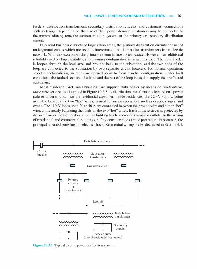
10.3 POWER TRANSMISSION AND DISTRIBUTION 461
feeders, distribution transformers, secondary distribution circuits, and customers’ connectionswith metering. Depending on the size of their power demand, customers may be connected tothe transmission system, the subtransmission system, or the primary or secondary distributioncircuit.
In central business districts of large urban areas, the primary distribution circuits consist ofunderground cables which are used to interconnect the distribution transformers in an electricnetwork. With this exception, the primary system is most often radial. However, for additionalreliability and backup capability, a loop-radial configuration is frequently used. The main feederis looped through the load area and brought back to the substation, and the two ends of theloop are connected to the substation by two separate circuit breakers. For normal operation,selected sectionalizing switches are opened so as to form a radial configuration. Under faultconditions, the faulted section is isolated and the rest of the loop is used to supply the unaffectedcustomers.
Most residences and small buildings are supplied with power by means of single-phase,three-wire service, as illustrated in Figure 10.3.3. A distribution transformer is located on a powerpole or underground, near the residential customer. Inside residences, the 220-V supply, beingavailable between the two “hot” wires, is used for major appliances such as dryers, ranges, andovens. The 110-V loads up to 20 to 40 A are connected between the ground wire and either “hot”wire, while nearly balancing the loads on the two “hot” wires. Each of these circuits, protected byits own fuse or circuit breaker, supplies lighting loads and/or convenience outlets. In the wiringof residential and commercial buildings, safety considerations are of paramount importance, theprincipal hazards being fire and electric shock. Residential wiring is also discussed in Section 4.4.
Circuitbreaker Substation
transformers
Circuit breakers
Primarycircuits
ormain feeders
Laterals
Distribution substation
Distributiontransformers
Secondarycircuits
Service entry(1 to 10 residential customers)
Figure 10.3.2 Typical electric power distribution system.

462 AC POWER SYSTEMS
( )
Figure 10.3.3 Single-phase, three-wire residential wiring circuit.
Power-System Loads
Figure 10.3.4 represents a one-line (single-line) diagram of a part of a typical three-phase powersystem. Notice the symbols that are used for generators, transformers, buses, lines, and loads.Recall that a bus is a nodal point.
Let us now consider the addition of a load bus to the operating power system. Serviceclassifications assigned by the electric utilities include residential, commercial, light industrial,and heavy industrial loads, as well as municipal electric company loads. Let us prepare a load-bus specification, which is a summary of the service requirements that must be provided by theelectric utility. Referring to the simple model of Figure 10.3.5, as an example, let the total newload connected to the system be 220 MVA at 0.8 power factor lagging; let the service be providedat the subtransmission level from a radial 115-kV circuit; let the 115-kV transmission line havea per-phase series impedance of 3+ j8.
The load-bus data (specifications), transmission line data, and source-bus data are given inTables 10.3.1, 10.3.2, and 10.3.3, respectively. The reader is encouraged to work out the details.
Looking at the load-bus data, the amount of reactive power that is needed to provide 100%compensation is 120 MVAR. Let us then add a three-phase shunt capacitor bank with a nominalvoltage rating of 115 kV and a reactive power rating of 120 MVAR. The per-phase reactance ofthe bank can be computed as X = V 2/Q = 1152/120 = 110.2 . The load-bus data with powerfactor correction are given in Table 10.3.4.
The transmission-system efficiency is defined as the ratio of the real power delivered to thereceiving-end bus to the real power transferred from the sending-end bus. This efficiency, whichis a measure of the real-power loss in the transmission line, comes out as 94.7% without powerfactor correction, and 96.5% with power factor correction.
The transmission-line voltage regulation (TLVR) is the ratio of the per-phase voltage dropbetween the sending-end and receiving-end buses to the receiving-end per-phase voltage (ornominal system per-phase voltage). It can also be expressed as
%TLVR = VRNL − VRFL
VRFL× 100 (10.3.1)

10.3 POWER TRANSMISSION AND DISTRIBUTION 463
G1 G2
To bus 6
To bus 7
Bus numbering 2
5
1
4
L6
L1
L7
L2
L3
L4 L5
3
Load
Generator
Transformer
Bus
Circuit breaker
Transmission line
Line numbering
Tie-line connectionwith neighboringsystem
Figure 10.3.4 One-line (single-line) diagram of part of a typical three-phase power system.
VS VR
Load
SS = PS + jQS SR = PR + jQR
Line impedance
Source bus(sending end)
Load bus(recieving end)
Figure 10.3.5 Simple model of part ofan operating power system.
where subscript R denotes receiving end, NL indicates no-load, and FL stands for full-load. TheTLVR for our example can be seen to be 12.8% prior to power factor improvement, and 10.2%after power factor improvement.
The two components of electric service are demand and energy. Demand is the maximumlevel of real power which the electric utility must supply to satisfy the load requirements of itscustomers. Energy is the cumulative use of electric power over a period of time. The demandcomponent of the electric-rate structure represents the capital investment needed by the utilityto provide the generation, transmission, and distribution facilities in order to meet the maximumcustomer demand. The energy component represents the operating costs, which include fuel andmaintenance that must be provided to meet the demand requirements over a period of time.
The load factor is the ratio of the actual energy usage to the rated maximum energy usage overa given period. A low load factor is indicative of a substantial period during which the capacity

464 AC POWER SYSTEMS
TABLE 10.3.1 Load-Bus Data
Quantity Symbol Value
Voltage V 115 kVCurrent I 1 kAApparent power S 220 MVAReal power P 160 MWReactive power Q 120 MVARPower factor cos θ 0.8 laggingPhase angle θ 36.9°Load impedance Z 66.1
Load resistance R 52.9
Load reactance XL 39.7
TABLE 10.3.2 Transmission-Line Data
Quantity Symbol Value
Resistance R 3
Inductive reactance XL 8
Series impedance Z 8.5
Series impedance angle θ 69.4°Real power loss Ploss 9 MWReactive power loss Qloss 24 MVARVoltage drop Vdrop 8.5 kV
TABLE 10.3.3 Source-Bus Data
Quantity Load Bus Line Source Bus
Voltage 115 8.5 127.7 kVReal power 160 9 169 MWReactive power 120 24 144 MVARApparent power 200 — 222 MVAAngle 36.9° — 40.4°
TABLE 10.3.4 Load-Bus Data with
Power-Factor Correction
Quantity Symbol Value
Voltage V 115 kVCurrent I 0.8 kAApparent power S 160 MVAReal power P 160 MWReactive power Q 0 MVARPower factor cos θ 1Phase angle θ 0°Load impedance Z 82.7
Load resistance R 82.7
Load reactance XL 0

10.3 POWER TRANSMISSION AND DISTRIBUTION 465
of the system is underutilized. Utilities often define load periods in terms of on-peak and off-peakhours. In order to level the demand by diverting a portion of the energy usage from the on-peakto the off-peak periods, economic incentives (such as lower electric rates for the sale of off-peak energy) are generally offered.
EXAMPLE 10.3.1
A three-phase, 34.5-kV, 60-Hz, 40-km transmission line has a per-phase series impedance of0.2+j0.5/km. The load at the receiving end absorbs 10 MVA at 33 kV. Calculate the following:
(a) Sending-end voltage at 0.9 PF lagging.
(b) Sending-end voltage at 0.9 PF leading.
(c) Transmission system efficiency and transmission-line voltage regulation correspondingto cases (a) and (b).
So l u t i on
The per-phase model of the transmission line is shown in Figure E10.3.1.
VS LN
IRIS = IR
R + jX8 + j20 Ω Load
+
−
+
−
VRLN =33√3− ∠0° kV
Figure E10.3.1 Per-phase model of transmission line (with only series impedance).
VR = 33,000√3
0° = 19,052 0° V
(a) IR = 10× 106
√3× 33× 103
− cos−1 0.9 = 175 − 25.8° A
VS LN = 19,052 0°+ (175 − 25.8°)(8+ j20) = 21, 983 6.6°VLN
VS LL = 21.983√
3 = 38.1 kV (line - to - line)
(b) IR = 10× 106
√3× 33× 103
+ cos−1 0.9 = 175 + 25.8° A
VS LN = 19,052 0°+ (175 + 25 .8°)(8+ j20) = 19,162 11.3° VLN
VS LL = 19.162√
3 = 33.2 kV (line - to - line)
(c) (i) 0.9 PF lagging:
PR = 10× 0.9 = 9 MW
PS =√
3× 38.1× 0.175 cos(25.8+ 6.6)° = 9.75 MW
466 AC POWER SYSTEMS
η = 9
9.75× 100 = 92.3%
TLVR = VR NL − VR FL
VR FL× 100 = 38.1− 33
33× 100 = 15.45%
Note: If there were no load, the sending-end voltage would appear at the receivingend.
(ii) 0.9 PF leading:
PR = 10× 0.9 = 9 MW
PS =√
3× 33.2× 0.175 cos(25.8− 11.3)° = 9.74 MW
η = 9
9.74× 100 = 92.4%
TLVR = 33.2− 33
33× 100 = 0.61%
10.4 LEARNING OBJECTIVES
The learning objectives of this chapter are summarized here, so that the student can check whetherhe or she has accomplished each of the following.
• Past, present, and future trends of power systems in the United States.• Three-phase power calculations and power factor improvement.• Basic notions of power transmission and distribution.• Working with load-bus data, transmission-line data, and source-bus data.• Simple transmission-line model and its circuit calculations.
10.5 PRACTICAL APPLICATION: A CASE STUDY
The Great Blackout of 1965
In the United States, electric utilities grew first as isolated systems. Gradually, however, neigh-boring utilities began to interconnect, which allowed utility companies to draw upon each others’generation reserves during time of need and to schedule power transfers that take advantageof energy-cost differences. Although overall system reliability and economy have improveddramatically through interconnection, there is a remote possibility that an initial disturbancemay lead to instability and a regional blackout.
The worst power failure in history occurred on Tuesday evening, November 9, 1965. Atthe height of the rush hour, complete darkness descended, and practically everything came to astandstill over an area of 83,000 square miles. About 30 million people were affected in eightstates and part of Canada. The system involved was the Canadian–United States eastern powercomplex (CANUSE).
Many guesses were offered as to the cause of the blackout, but most were far from correct.At first, little hope was held out for pinpointing the exact reason for the failure within a shorttime. However, on November 15 it was announced that the cause had been found. The failurewas attributed to a faulty relay at Sir Adam Beck Plant no. 2 at Queenston, Ontario (see Figure
R. McCaw, “The Great Blackout,” Power Engineering, Dec. 1965.

10.5 PRACTICAL APPLICATION: A CASE STUDY 467
10.5.1). This plant is part of the Ontario Hydro-Electric System on the Niagara River. Six linesrun into Ontario from the Beck plant, and the line controlled by the faulty relay was carrying 300MW. Failure of the relay dumped this load onto the other five lines. Even though these lines werenot overloaded, all five tripped out.
Total power flow on these lines had been 1600 MW into Ontario, including 500 MW beingimported from the Power Authority of the State of New York. All this power was suddenlydumped on the New York system. The resultant surge knocked out the Power Authority’smain east–west transmission line and shut down seven units that had been feeding the north-eastern grid. The resulting drain on systems to the south and east caused the whole system tocollapse.
New York City, for example, had been drawing about 300 MW from the network just beforethe failure. Loss of the upstate plants caused a sudden reversal of flow and placed a heavy drainon the City generators. The load was much greater than the plants still in service could supply,and the result was a complete collapse. Automatic equipment shut down the units to protect themfrom damage.
After the total failure the individual systems started up in sections, and most power wasrestored by a little after midnight. However, Manhattan, with the greatest concentration of load,was not fully restored unitl after six o’clock the following morning.
Only a rare combination of faults, however, will result in a cascading of tripouts and acomplete shutdown over an entire region. In order to avoid such large blackouts, stronger gridshave been planned and various techniques developed to operate large interconnected networks inparallel with a high degree of operating stability, and with increasing dependence on automated
Figure 10.5.1 Area affected by the blackout of 1965.

468 AC POWER SYSTEMS
controls. Pumped storage plants, which represent a large reserve that can be put into operation onshort notice, can help the situation.
The great blackout of 1965 had indeed been a sobering experience and possibly a neededwarning to reexamine some of our policies and plans. The warning will not have been wasted ifwe learn from it how to build a more reliable grid to suppply all the power that is needed in theyears ahead. After all, our whole economy is almost completely dependent on electric power.
PROBL EMS
10.2.1 Two ideal voltage sources are connected to eachother through a feeder with impedance Z =1.5 + j6 , as shown in Figure P10.2.1. LetE1 = 120 0° V and E2 = 110 45°.
(a) Determine the real power of each machine,and state whether the machine is supplyingor absorbing real power.
(b) Compute the reactive power of each ma-chine, and state whether each machine isdelivering or receiving reactive power.
(c) Find the real and reactive power associatedwith the feeder impedance, and state whetherit is supplied or absorbed.
*10.2.2 If the impedance between the voltage sources inProblem 10.2.1 is changed to Z = 1.5 − j6 ,redo parts (a) through (c) of Problem 10.2.1.
10.2.3 A single-phase industrial plant consists of twoloads in parallel:
P1 = 48kW PF1 = 0.60 lagging
P2 = 24kW PF2 = 0.96 leading
It is operated from a 500-V, 60-Hz source. Anadditional capacitor C is added in parallel toimprove the plant’s overall power factor to unity.Determine the value of C in µF. Also sketch thepower triangles before and after the addition ofC, and find the overall current drawn from thesupply.
10.2.4 A 230-V, single-phase, 60-Hz source suppliestwo loads in parallel. One draws 10 kVA at a
lagging power factor of 0.80 and the other draws6 kW at a lagging power factor of 0.90. Computethe source current.
10.2.5 A three-phase power system consists of a wye-connected ideal generator, supplying a wye-con-nected balanced load through a three-phasefeeder. The load has ZL = 20 30°/
phase, and the feeder has an impedance Zfdr =1.5 75° /phase. If the terminal voltage of theload is 4.16 kV, determine:
(a) The terminal voltage of the generator.
(b) The line current supplied by the generator.
10.2.6 A 345-kV, 60-Hz, three-phase transmission linedelivers 600 MVA at 0.866 power factor laggingto a three-phase load connected to its receiving-end terminals. Assuming that the voltage at thereceiving end is 345 kV and the load is wye-connected, find the following:
(a) Complex load impedance per phase ZL/ph.
(b) Line and phase currents.
(c) Real and reactive powers per phase.
(d) Total three-phase real and reactive powers.
*10.2.7 A three-phase load, connected to a 440-V bus,draws 120 kW at a power factor of 0.85 lagging.In parallel with this load is a three-phase capac-itor bank that is rated 50 kVAR . Determine theresultant line current and power factor.
E1 E2
I
−+
−+
z Figure P10.2.1

PROBLEMS 469
10.2.8 A balanced three-phase, wye-connected, 2400-V, 60-Hz source supplies two balanced wye-connected loads in parallel. The first draws 15kVA at 0.8 power factor lagging, and the secondneeds 20 kW at 0.9 power factor leading. Com-pute the following:
(a) Current supplied by the source.
(b) Total real and reactive power drawn by thecombined load.
(c) Overall power factor.
10.2.9 A three-phase, 60-Hz substation bus supplies twowye-connected loads that are connected in par-allel through a three-phase feeder that has a per-phase impedance of 0.5 + j2 . Load 1 draws50 kW at 0.866 lagging PF, and load 2 draws 36kVA at 0.9 leading PF. If the line-to-line voltageat the load terminals is 460 V, find the following:
(a) Total line current flowing through the feeder.
(b) Per-phase impedance of each load.
(c) Line-to-line voltage at the substation bus.
(d) Total real and reactive power delivered bythe bus.
10.2.10 A balanced delta-connected load has a per-phaseimpedance of 45 60° . It is connected to athree-phase, 208-V, 60-Hz supply by a three-phase feeder that has a per-phase impedance of1.2+ j1.6 .
(a) Determine the line-to-line voltage at the loadterminals.
(b) If a delta-connected capacitor bank, with aper-phase reactance of 60, is connected inparallel with the load at its terminals, com-pute the resulting line-to-line voltage at theload terminals.
*10.3.1 Consider a lossless transmission line with only aseries reactance X, as shown in Figure P10.3.1.
(a) Find an expression for the real power transfercapacity of the transmission system.
(b) What is Pmax (the theoretical steady-statelimit of a lossless line), which is the max-imum power that the line can deliver?
(c) How could the same expressions be used fora three-phase transmission line?
10.3.2 A 20-km, 34.5-kV, 60-Hz, three-phase transmis-sion line has a per-phase series impedance ofZ = 0.19+j0.34 /km. The load at the receiv-ing end absorbs 10 MVA at 33 kV. Calculate:
(a) The sending-end voltage for a load powerfactor of 0.9 lagging.
(b) The sending-end voltage for a load powerfactor of 0.9 leading.
(c) The transmission system efficiency for cases(a) and (b).
(d) The transmission-line voltage regulation(TLVR) for cases (a) and (b).
10.3.3 It is sometimes convenient to represent a trans-mission line by a two-port network, as shown inFigure P10.3.3. The relations between sending-end and receiving-end quantities are given by
VS = A VR + B IR and IS = C VR + D IR,
in which the generally complex parameters A,B, C, and D depend on the transmission-linemodels. For the model that includes only theseries impedance Z of the transmission line, findthe parameters A, B, C, and D and specify theirunits. Also evaluate (A D − B C).
10.3.4 For a transmission-line model that includes onlythe series impedance Z, sketch phasor diagramsfor:
(a) Lagging power factor load.
(b) Leading power factor load.
10.3.5 In terms of the parameters A, B, C, and D intro-duced in Problem 10.3.3, find an expression forVR at no load in terms of VS and the parameters.
*10.3.6 Consider an upgrade of a three-phase transmis-sion system in which the operating line-to-linevoltage is doubled, and the phase or line currentsare reduced to one-half the previous value, for thesame level of apparent power transfer. Discussthe consequent effects on the real and reactivepower losses, and on the voltage drop across theseries impedance of the transmission system.
10.3.7 Justify the entries made in Tables 10.3.1, 10.3.2,and 10.3.3 for load-bus data, transmission-linedata, and source-bus data, respectively, for theexample considered in the text.
10.3.8 Justify the entries made in Table 10.3.4 for load-bus data with power factor correction, and dis-cuss the effects of power factor correction onPloss, Qloss, and Vdrop of the transmission line.
10.3.9 Check the figures given in the text (for the ex-ample considered) regarding the transmission-system efficiencies and TLVR for the two cases,with and without power factor correction.

470 AC POWER SYSTEMS
IR
+
−
+
−
VR = VR ∠0°VS = VS ∠δ
IS Z = jX
Figure P10.3.1 Simple model of loss-less transmission line.
IR+
−
+
−
VR VS
IS
Two-portnetwork
Sending end Receiving end
Figure P10.3.3
10.3.10 On a per-phase basis, let v = √2 V cos ωt andi = √2 I cos (ωt − θ).
(a) Express the instantaneous power s(t) in termsof real power P and reactive power Q.
(b) Now consider the energy E associated withthe instantaneous power and show that E =Pt, where t is the duration of the time intervalin seconds.
10.3.11 A 60-Hz, three-phase transmission line has a totalper-phase series impedance of 35+ j140 . If itdelivers 40 MW at 220 kV and 0.9 power factorlagging, find:
(a) The voltage, current, and power factor at thesending end of the line.
(b) The voltage regulation and efficiency of theline.
10.3.12 A three-phase, 60-Hz transmission line has a totalseries impedance of 22.86 62.3° per phase. Itdelivers 2.5 MW at 13.8 kV to a load connectedto its receiving end. Compute the sending-endvoltage, current, real power, and reactive powerfor the following conditions:
(a) 0.8 power factor lagging.
(b) Unity power factor.
(c) 0.9 power factor leading.

11 Magnetic Circuits and Transformers
11.1 Magnetic Materials
11.2 Magnetic Circuits
11.3 Transformer Equivalent Circuits
11.4 Transformer Performance
11.5 Three-Phase Transformers
11.6 Autotransformers
11.7 Learning Objectives
11.8 Practical Application: A Case Study—Magnetic Bearings for Space Technology
Problems
A basic understanding of electromagnetism is essential to the study of electrical engineeringbecause it is the key to the operation of many electric apparatus found in industry and at home.Electric systems that generate, convert, or control huge amounts of energy almost always involvedevices whose operation depends on magnetic phenomena. Thus, we focus our attention hereon magnetic aspects as related to electric-power engineering. In this chapter we shall proceedfrom introductory magnetic-circuit concepts to relatively simple magnetic structures and then toa consideration of transformers.
The magnetic material determines the size of the equipment, its capabilities, and the lim-itations on its performance. The transformer, although not an energy-conversion device, is animportant auxiliary in the transfer and conversion of electric energy. Practically all transformersand electric machinery utilize magnetic material for shaping the magnetic fields which act as themedium for transferring and converting energy. Transformers are found in various applications,such as radio, television, and electric power transmission and distribution circuits. Other devices,such as circuit breakers, automatic switches, and relays, also require the presence of a confinedmagnetic field for their proper operation.
471
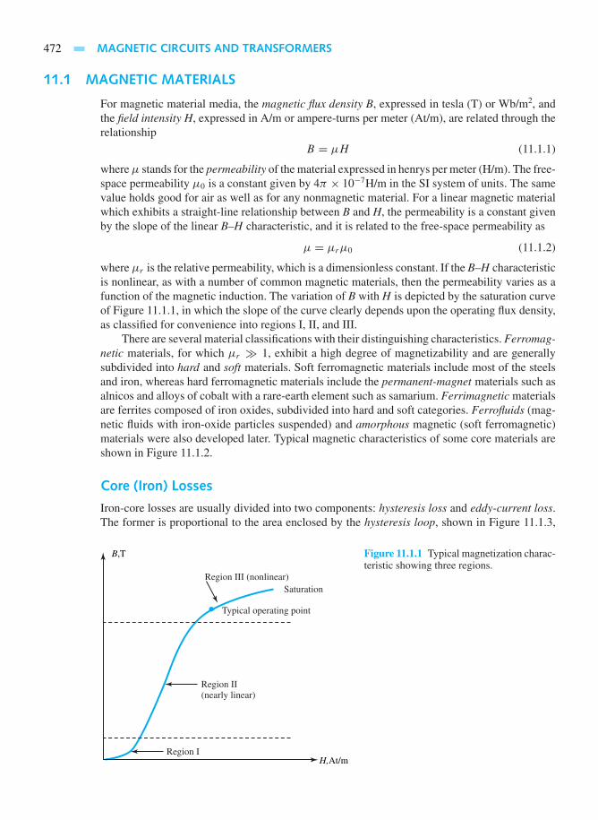
472 MAGNETIC CIRCUITS AND TRANSFORMERS
11.1 MAGNETIC MATERIALS
For magnetic material media, the magnetic flux density B, expressed in tesla (T) or Wb/m2, andthe field intensity H, expressed in A/m or ampere-turns per meter (At/m), are related through therelationship
B = µH (11.1.1)
whereµ stands for the permeability of the material expressed in henrys per meter (H/m). The free-space permeability µ0 is a constant given by 4π × 10−7H/m in the SI system of units. The samevalue holds good for air as well as for any nonmagnetic material. For a linear magnetic materialwhich exhibits a straight-line relationship between B and H, the permeability is a constant givenby the slope of the linear B–H characteristic, and it is related to the free-space permeability as
µ = µrµ0 (11.1.2)
where µr is the relative permeability, which is a dimensionless constant. If the B–H characteristicis nonlinear, as with a number of common magnetic materials, then the permeability varies as afunction of the magnetic induction. The variation of B with H is depicted by the saturation curveof Figure 11.1.1, in which the slope of the curve clearly depends upon the operating flux density,as classified for convenience into regions I, II, and III.
There are several material classifications with their distinguishing characteristics. Ferromag-netic materials, for which µr 1, exhibit a high degree of magnetizability and are generallysubdivided into hard and soft materials. Soft ferromagnetic materials include most of the steelsand iron, whereas hard ferromagnetic materials include the permanent-magnet materials such asalnicos and alloys of cobalt with a rare-earth element such as samarium. Ferrimagnetic materialsare ferrites composed of iron oxides, subdivided into hard and soft categories. Ferrofluids (mag-netic fluids with iron-oxide particles suspended) and amorphous magnetic (soft ferromagnetic)materials were also developed later. Typical magnetic characteristics of some core materials areshown in Figure 11.1.2.
Core (Iron) Losses
Iron-core losses are usually divided into two components: hysteresis loss and eddy-current loss.The former is proportional to the area enclosed by the hysteresis loop, shown in Figure 11.1.3,
B,T
Region II(nearly linear)
Region I
Region III (nonlinear)Saturation
Typical operating point
H,At/m
Figure 11.1.1 Typical magnetization charac-teristic showing three regions.
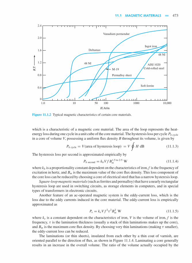
11.1 MAGNETIC MATERIALS 473
H,At/m
2.4
2.0
1.6
1.2
0.8
0.4
0
B,T
Vanadium permendur
DeltamaxIngot iron
48 NI
M-19
48 NI
Permalloy sheet
AISI 1020Cold-rolled steel
Soft ferrite
1.0 10 50 100 1000 10,000
Figure 11.1.2 Typical magnetic characteristics of certain core materials.
which is a characteristic of a magnetic core material. The area of the loop represents the heat-energy loss during one cycle in a unit cube of the core material. The hysteresis loss per cyclePh cycle
in a core of volume V, possessing a uniform flux density B throughout its volume, is given by
Ph cycle = V (area of hysteresis loop) = V
∮H dB (11.1.3)
The hysteresis loss per second is approximated empirically by
Ph second = khVfB1.5 to 2·5m W (11.1.4)
where kh is a proportionality constant dependent on the characteristics of iron, f is the frequency ofexcitation in hertz, and Bm is the maximum value of the core flux density. This loss component ofthe core loss can be reduced by choosing a core of electrical steel that has a narrow hysteresis loop.
Square-loop magnetic materials (such as ferrites and permalloy) that have a nearly rectangularhysteresis loop are used in switching circuits, as storage elements in computers, and in specialtypes of transformers in electronic circuits.
Another feature of an ac-operated magnetic system is the eddy-current loss, which is theloss due to the eddy currents induced in the core material. The eddy-current loss is empiricallyapproximated as
Pe = keVf2τ 2B2
m W (11.1.5)
where ke is a constant dependent on the characteristics of iron, V is the volume of iron, f is thefrequency, τ is the lamination thickness (usually a stack of thin laminations makes up the core),and Bm is the maximum core flux density. By choosing very thin laminations (making τ smaller),the eddy-current loss can be reduced.
The laminations (or thin sheets), insulated from each other by a thin coat of varnish, areoriented parallel to the direction of flux, as shown in Figure 11.1.4. Laminating a core generallyresults in an increase in the overall volume. The ratio of the volume actually occupied by the

474 MAGNETIC CIRCUITS AND TRANSFORMERS
B,T
H,At/m0
−0.2
−0.4
−0.6
−0.8
−1.0
0.6
0.4
1.0
0.8
0.2
50 100 150 200 250−250 −200 −100 −50
Figure 11.1.3 Typical hysteresis loop of a magnetic-core material.
Flux φ
Core
I
Figure 11.1.4 Part of a laminated core.
magnetic material to the total (gross) volume of the core is known as the stacking factor. Thethinner the lamination thickness, the lower the stacking factor. This factor usually ranges between0.5 and 0.95.
EXAMPLE 11.1.1
(a) Estimate the hysteresis loss at 60 Hz for a toroidal (doughnut-shaped) core of 300-mmmean diameter and a square cross section of 50 mm by 50 mm. The symmetrical hysteresisloop for the electric sheet steel (of which the torus is made) is given in Figure 11.1.3.
(b) Now suppose that all the linear dimensions of the core are doubled. How will the hysteresisloss differ?

11.2 MAGNETIC CIRCUITS 475
(c) Next, suppose that the torus (which was originally laminated for reducing the eddy-current losses) is redesigned so that it has half the original lamination thickness. Assumethe stacking factor to be unity in both cases. What would be the effect of such a changein design on the hysteresis loss?
(d) Suppose that the toroidal core of part (a) is to be used on 50-Hz supply. Estimate thechange in hysteresis loss if no other conditions of operation are changed.
So l u t i on
(a) Referring to Figure 11.1.3, the area of each square represents
(0.1 T)× (25 A/m) = 2.5Wb
m2× A
m= 2.5
V× s× A
m3= 2.5 J/m3
By counting, the number of squares in the upper half of the loop is found to be 43; thearea of the hysteresis loop is given by
2× 43× 2.5 = 215 J/m3
The toroidal volume is
π × 0.3× 0.052 = 2.36× 10⁻³m3
The hysteresis loss in the torus is then given by
2.36× 10−3 × 60× 215 = 30.44 W
(b) When all the linear dimensions of the core are doubled, its volume will be eight timesthe previous volume. Hence the new core hysteresis loss will be
8× 30.44 = 243.52 W
(c) The lamination thickness has no bearing on the hysteresis loss; it changes only the eddy-current loss. Hence, the hysteresis loss remains unchanged.
(d) Since the hysteresis loss is directly proportional to the frequency, the loss on the 50 Hzsupply will be
30.44× 50
60= 25.37 W
11.2 MAGNETIC CIRCUITS
A magnetic circuit provides a path for magnetic flux, just as an electric circuit provides a path forelectric current. Magnetic circuits are integral parts of transformers, electric machines, and manyother common devices such as doorbells. Analogous to voltage (electric potential difference) inthe electric circuit, in a magnetic circuit we have the magnetomotive force (mmf), or the magneticpotential difference which produces a magnetic field, and which has units of amperes or ampere-turns. The two sources of mmf in magnetic circuits are the electric current and the permanentmagnet (which stores energy and is capable of maintaining a magnetic field with no expenditure
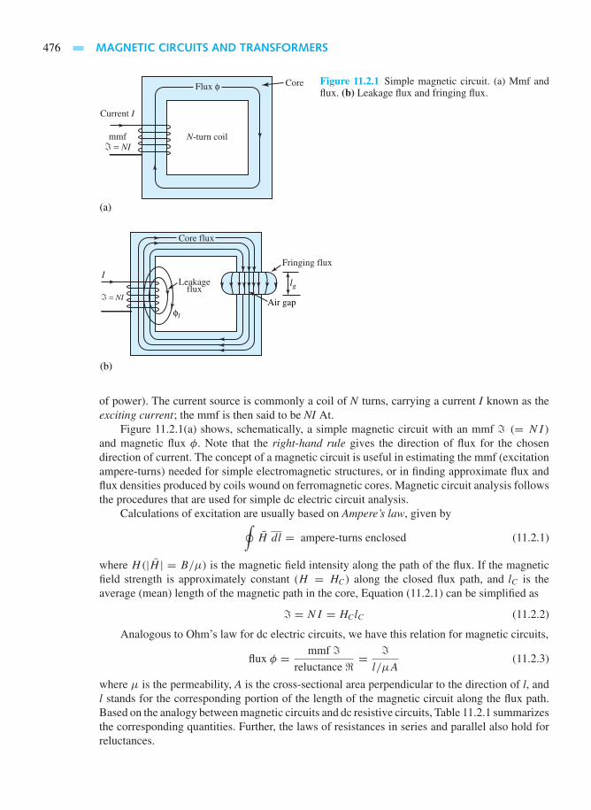
476 MAGNETIC CIRCUITS AND TRANSFORMERS
CoreFlux φ
N-turn coil
Current I
(a)
Figure 11.2.1 Simple magnetic circuit. (a) Mmf andflux. (b) Leakage flux and fringing flux.
Core flux
I
(b)
Leakageflux
Fringing flux
Air gap
lg
φl
of power). The current source is commonly a coil of N turns, carrying a current I known as theexciting current; the mmf is then said to be NI At.
Figure 11.2.1(a) shows, schematically, a simple magnetic circuit with an mmf (= NI)
and magnetic flux φ. Note that the right-hand rule gives the direction of flux for the chosendirection of current. The concept of a magnetic circuit is useful in estimating the mmf (excitationampere-turns) needed for simple electromagnetic structures, or in finding approximate flux andflux densities produced by coils wound on ferromagnetic cores. Magnetic circuit analysis followsthe procedures that are used for simple dc electric circuit analysis.
Calculations of excitation are usually based on Ampere’s law, given by∮H dl = ampere-turns enclosed (11.2.1)
where H(|H | = B/µ) is the magnetic field intensity along the path of the flux. If the magneticfield strength is approximately constant (H = HC) along the closed flux path, and lC is theaverage (mean) length of the magnetic path in the core, Equation (11.2.1) can be simplified as
= NI = HClC (11.2.2)
Analogous to Ohm’s law for dc electric circuits, we have this relation for magnetic circuits,
flux φ = mmf
reluctance =
l/µA(11.2.3)
where µ is the permeability, A is the cross-sectional area perpendicular to the direction of l, andl stands for the corresponding portion of the length of the magnetic circuit along the flux path.Based on the analogy between magnetic circuits and dc resistive circuits, Table 11.2.1 summarizesthe corresponding quantities. Further, the laws of resistances in series and parallel also hold forreluctances.

11.2 MAGNETIC CIRCUITS 477
TABLE 11.2.1 Analogy with dc Resistive Circuits
DC Resistive Circuit Magnetic Circuit
Current I (A) Flux φ (Wb)Voltage V (V) Magnetomotive force (mmf) (At)Resistance R = l/σA () Reluctance = l/µA (H−1)
Conductivity σ (S/m) Permeability µ( H/m)Conductance G = 1/R (S) Permeance P = 1/ (H)I = V/R φ = /Current density J = I/A (A/m2) Flux density B = φ/A (Wb/m2)
Analogous to KVL in electrical circuits, Ampere’s law applied to the analysis of a magneticcircuit leads to the statement that the algebraic sum of the magnetic potentials around any closedpath is zero. Series, parallel, and series–parallel magnetic circuits can be analyzed by means oftheir corresponding electric-circuit analogs. All methods of analysis that are valid for dc resistivecircuits can be effectively utilized in an analogous manner.
The following differences exist between a dc resistive circuit and a magnetic circuit
• Reluctance is not an energy-loss component like a resistance R (which leads to anI 2R loss). Energy must be supplied continuously when a direct current is established andmaintained in an electric circuit; but a similar situation does not prevail in the case of amagnetic circuit, in which a flux is established and maintained constant.
• Magnetic fluxes take leakage paths [as φl in Figure 11.2.1(b)]; but electric currents flowingthrough resistive networks do not.
• Fringing or bulging of flux lines [shown in Figure 11.2.1(b)] occurs in the air gaps ofmagnetic circuits; but such fringing of currents does not occur in electric circuits. Note thatfringing increases with the length of the air gap and increases the effective area of the airgap.
• There are no magnetic insulators similar to the electrical insulators.
In the case of ferromagnetic systems containing air gaps, a useful approximation for makingquick estimates is to consider the ferromagnetic material to have infinite permeability. The relativepermeability of iron is considered so high that practically all the ampere-turns of the winding areconsumed in the air gaps alone.
Calculating the mmf for simple magnetic circuits is rather straightforward, as shown in thefollowing examples. However, it is not so simple to determine the flux or flux density when themmf is given, because of the nonlinear characteristic of the ferromagnetic material.
EXAMPLE 11.2.1
Consider the magnetic circuit of Figure 11.2.1(b) with an air gap, while neglecting leakage flux.Correct for fringing by adding the length of the air gap lg = 0.1 mm to each of the other twodimensions of the core cross section AC = 2.5cm × 2.5cm. The mean length of the magneticpath in the core lC is given to be 10 cm. The core is made of 0.15- mm-thick laminations of M-19material whose magnetization characteristic is given in Figure 11.1.2. Assume the stacking factorto be 0.9. Determine the current in the exciting winding, which has 100 turns and produces a coreflux of 0.625 mWb.

478 MAGNETIC CIRCUITS AND TRANSFORMERS
So l u t i on
The net cross-sectional area of the core is 2.52 × 10−4 × 0.9 = 0.5625× 10⁻³ m2. Note that thestacking factor of 0.9 is applied for the laminated core. It does not, however, apply for the air-gapportion,
BC = φ
net area= 0.625× 10⁻³
0.5625× 10−3= 1.11 T
The corresponding HC from Figure 11.1.2 for M-19 is 130 A/m. Hence,
C = HClC = 130× 0.1 = 13 At
The cross-sectional area of the air gap, corrected for fringing, is given by
Ag = (2.5+ 0.01)(2.5+ 0.01)10−4 = 0.63× 10⁻³ m2
Bg = φ
Ag
= 0.625× 10⁻³
0.63× 10−3= 0.99 T
Hg = Bg
µ0= 0.99
4π × 10−7= 0.788× 10⁶ A/m
Hence,
g = Hglg = 0.788× 106 × 0.1× 10−3 = 78.8 At
For the entire magnetic circuit (see Figure E11.2.1)
NI = TOTAL = C + g = 13+ 78.8 = 91.8 At
Thus, the coil current
I = NI
N= 91.8
100= 0.92 A
+
−
φFigure E11.2.1 Equivalent magnetic circuit.
EXAMPLE 11.2.2
In the magnetic circuit shown in Figure E11.2.2(a) the coil of 500 turns carries a current of 4 A.The air-gap lengths are g1 = g2 = 0.25 cm and g3 = 0.4 cm. The cross-sectional areas are relatedsuch that A1 = A2 = 0.5A3. The permeability of iron may be assumed to be infinite. Determinethe flux densities B1, B2, and B3 in the gaps g1, g2, and g3, respectively. Neglect leakage andfringing.
So l u t i on
Noting that the reluctance of the iron is negligible, the equivalent magnetic circuit is shown inFigure E11.2.2(b).

11.3 TRANSFORMER EQUIVALENT CIRCUITS 479
Given = NI = 500 × 4 = 2000 At, g1 = g2 = 0.25 cm, and g3 = 0.4 cm; A1 = A2 =0.5A3; µ1 = µ2 = µ3 = µ0; φ3 = φ1 + φ2; and H1g1 +H3g3 = H2g2 +H3g3 = = 2000, wehave
H1g1 = H2g2 or H1 = H2
since g1 = g2. Thus, B1 = B2, since µ1 = µ2 = µ0. Because A1 = A2, it follows that φ1 = φ2
and φ3 = 2φ1. But B3 = φ3/2A1 = B1. Thus,
B1 = B2 = B3; H1 = H2 = H3
We had H1g1 +H3g3 = 2000, which is rewritten asB1
µ0(0.25× 10⁻²)+ B1
µ0(0.4× 10⁻²) = 2000
or,
B1 = 2000× 4π × 10−7
0.65× 10−2= 0.387 T = B2 = B3
g1 g3 g2
(a)
A3
A2A1
Figure E11.2.2
φ2φ1 φ3
(b)
A simple magnetic structure, similar to those examined in the previous examples, findscommon application in the so-called variable-reluctance position sensor, which, in turn, findswidespread application in a variety of configurations for the measurement of linear and angularposition and velocity.
For magnetic circuits with ac excitation, the concepts of inductance and energy storage comeinto play along with Faraday’s law of induction. Those concepts have been presented in somedetail in Section 1.2. The reader is encouraged to review that section, as that background will behelpful in solving some of the problems related to this section.
11.3 TRANSFORMER EQUIVALENT CIRCUITS
It would be appropriate for the reader to review the material on transformers in Section 1.2.Transformers come in various sizes, from very small, weighing only a few ounces, to verylarge, weighing hundreds of tons. The ratings of transformers cover a very wide range. Whereastransformers applied with electronic circuits and systems usually have ratings of 300 VA or less,power-system transformers used in transmission and distribution systems have the highest volt-ampere ratings (a few kVA to several MVA) as well as the highest continuous voltage ratings.Instrument transformers (potential transformers and current transformers) with very small volt-ampere ratings are used in instruments for sensing voltages or currents in power systems.

480 MAGNETIC CIRCUITS AND TRANSFORMERS
Transformers may be classified by their frequency range: power transformers, which usuallyoperate at a fixed frequency; audio and ultrahigh-frequency transformers; wide-band and narrow-band frequency transformers; and pulse transformers. Transformers employed in supplying powerto electronic systems are generally known as power transformers. In power-system applications,however, the term power transformer denotes transformers used to transmit power in ratingslarger than those associated with distribution transformers, usually more than 500 kVA at voltagelevels of 67 kV and above.
Conventional transformers have two windings, but others (known as autotransformers) haveonly one winding, and still others (known as multiwinding transformers) have more than twowindings. Transformers used in polyphase circuits are known as polyphase transformers. In themost popular three-phase system, the most common connections are the wye (star or Y) and thedelta (mesh or ) connections.
Figure 11.3.1 shows, schematically, a transformer having two windings withN1 andN2 turns,respectively, on a common magnetic circuit. The transformer is said to be ideal when:
• Its core is infinitely permeable.
• Its core is lossless.• It has no leakage fluxes.
• Its windings have no losses.
The mutual flux linking the N1-turn and N2-turn windings is φ. Due to a finite rate of changeof φ, according to Faraday’s law of induction, emf’s e1 and e2 are induced in the primary andsecondary windings, respectively. Thus, we have
e1 = N1dφ
dt; e2 = N2
dφ
dt; e1
e2= N1
N2(11.3.1)
The polarity of the induced voltage is such as to produce a current which opposes the flux change,according to Lenz’s law. For the ideal transformer, since e1 = v1 and e2 = v2, it follows that
v1
v2= e1
e2= N1
N2= a; V1
V2= E1
E2= N1
N2= a (11.3.2)
where V1, V2, E1, and E2 are the rms values of v1, v2, e1, and e2, respectively, and a stands for theturns ratio. When a passive external load circuit is connected to the secondary winding terminals,the terminal voltage v2 will cause a current i2 to flow, as shown in Figure 11.3.1. Further, we have
v1i1 = v2i2; i1
i2= v2
v1= N2
N1= 1
a; I1
I2= V2
V1= N2
N1= 1
a(11.3.3)
−
+
e1v1 e2 v2
Mean path of magnetic flux
−
+
−
+
i1 i2
Secondary(N2 turns)
Primary(N1 turns)
Ferromagnetic core
LoadZL
−
+
Mutual flux φ
Figure 11.3.1 Schematic of two-winding transformer.

11.3 TRANSFORMER EQUIVALENT CIRCUITS 481
in which I1 and I2 are the rms value of i1 and i2, respectively.If the flux varies sinusoidally, such that
φ = φmax sin ωt (11.3.4)
where φmax is the maximum value of the flux and ω = 2πf , f being the frequency, then theinduced voltages are given by
e1 = ωN1φmax cos ωt; e2 = ωN2φmax cos ωt (11.3.5)
Note that the induced emf leads the flux by 90°. The rms values of the induced emf’s are given by
E1 = ωN1φmax√2
= 4.44fN1φmax; E2 = ωN2φmax√2
= 4.44fN2φmax (11.3.6)
Equation (11.3.6) is known as the emf equation.From Equations (11.3.2) and (11.3.3) it can be shown that if an impedance ZL is connected
to the secondary, the impedance Z1 seen at the primary is given by
Z1 = a2ZL =(N1
N2
)2
ZL (11.3.7)
Major applications of transformers are in voltage, current, and impedance transformations,and in providing isolation while eliminating direct connections between electric circuits.
A nonideal (or practical) transformer, in contrast to an ideal transformer, has the followingcharacteristics, which have to be accounted for:
• Core losses (hysteresis and eddy-current losses)
• Resistive (I 2R) losses in its primary and secondary windings
• Finite permeability of the core requiring a finite mmf for its magnetization
• Leakage fluxes (associated with the primary and secondary windings) that do not link bothwindings simultaneously.
Now our goal is to develop an equivalent circuit of a practical transformer by including thenonideal effects. First, let us consider the simple magnetic circuit of Figure 11.2.1(a), excited byan ac mmf, and come up with its equivalent circuit. With no coil resistance and no core loss,but with a finite constant permeability of the core, the magnetic circuit along with the coil canbe represented just by an inductance Lm or, equivalently, by an inductive reactance Xm = ωLm,when the coil is excited by a sinusoidal ac voltage of frequency f = ω/2π . This reactance isknown as the magnetizing reactance. Thus, Figure 11.3.2(a) shows Xm (or impedance Z = jXm)across which the terminal voltage with an rms value of V1 (equal to the induced voltage E1)is applied.
Next, in order to include the core losses, since these depend directly upon the level of fluxdensity and hence the voltage V1, a resistance RC is added in parallel to jXm, as shown in Figure11.3.2(b). Then the resistance R1 of the coil itself and the leakage reactance X1, representingthe effect of leakage flux associated with the coil, are included in Figure 11.3.2(c) as a seriesimpedance given by R1 + jX1.
Finally, Figure 11.3.3 shows the equivalent circuit of a nonideal transformer as a combinationof an ideal transformer and of the nonideal effects of the primary winding, the core, and thesecondary winding. Note that the effects of distributed capacitances across and between thewindings are neglected here. The following notation is used:

482 MAGNETIC CIRCUITS AND TRANSFORMERS
+
−
Z = jXmV1 = E1
(a)
+
−
jXmV1 = E1 RC
(b)
+
−
jXmV1 RC
(c)
R1 jX1
E1
+
−
Figure 11.3.2 Equivalent circuits of an ironcore excited by an ac mmf.
+
−
jXmV1 RC
IC Im
I0R1 jX1 R2jX2
E1
+
−E2
+
−ZL
a : 1
+
−
V2
N1 N2(Ideal transformer)
I2I1
Figure 11.3.3 Equivalent circuit of a two-winding iron-core transformer as a combination of an idealtransformer and the nonideal effects.
a Turns ratio N1/N2
E1, E2 Induced voltage in primary and secondary
V1, V2 Terminal voltage of primary and secondary
I1, I2 Input and output current
I0 No-load primary exciting current
R1, R2 Winding resistance of primary and secondary
X1, X2 Leakage reactance of primary and secondary
Im, Xm Magnetizing current and reactance (referred to primary)
IC , RC Current and resistance accounting for core losses (referred to primary)
Yo Exciting admittance (referred to primary), which is the admittance of the parallelcombination of Xm and RC
ZL Load impedance = V2/I2

11.3 TRANSFORMER EQUIVALENT CIRCUITS 483
Note that phasor notation and rms values for all voltages and currents are used.It is generally more convenient to have the equivalent circuit entirely referred to either
primary or secondary by using the ideal-transformer relationships [Equations (11.3.2), (11.3.3),and (11.3.7)], thereby eliminating the need for the ideal transformer to appear in the equivalentcircuit. Figure 11.3.4 shows such circuits, which are very useful for determining the transformercharacteristics.
a2ZL
+
−
jXmV1 RC
IC Im
ja2X2 a2R2R1 jX1
−
Io
aV2
+
−
I2/aI1
(a)
ZL
+
−
jXm /a2V1/a RC /a
2
aIC aIm
jX2 R2
aI1
jX1/a2
−
aIo
V2
+
−
I2R1/a2
(b)
Figure 11.3.4 Equivalent circuits of a transformer. (a) Referred to primary. (b) Referred to secondary.
EXAMPLE 11.3.1
A single-phase, 50-kVA, 2400:240-V, 60-Hz distribution transformer has the following parame-ters:
Resistance of the 2400-V winding R1 = 0.75Resistance of the 240-V winding R2 = 0.0075Leakage reactance of the 2400-V winding X1 = 1
Leakage reactance of the 240-V winding X2 = 0.01
Exciting admittance on the 240-V side = 0.003− j0.02 S
Draw the equivalent circuits referred to the high-voltage side and to the low-voltage side. Labelthe impedances numerically.
So l u t i on
(a) The equivalent circuit referred to the high-voltage side is shown in Figure E11.3.1 (a). Thequantities, referred to the high-voltage side from the low-voltage side, are calculated as

484 MAGNETIC CIRCUITS AND TRANSFORMERS
R′2 = a2R2 =(
2400
240
)2
(0.0075) = 0.75
X′2 = a2X2 =(
2400
240
)2
(0.01) = 1.0
Note that the exciting admittance on the 240-V side is given. The exciting branchconductance and susceptance referred to the high-voltage side are given by
1
a2(0.003) or
1
100× 0.003 = 0.03× 10⁻³ S
and
1
a2(0.02) or
1
100× 0.02 = 0.2× 10⁻³ S
(b) The equivalent circuit referred to the low-voltage side is given in Figure E11.3.1 (b).Note the following points.
(i) The voltages specified on the nameplate of a transformer yield the turns ratio directly.The turns ratio in this problem is 2400:240, or 10:1.
(ii) Since admittance is the reciprocal of impedance, the reciprocal of the referring factorfor impedance must be used when referring admittance from one side to the other.
−jBm = −j0.2 × 10−3 S
jXm = jRC =
R1= 0.75 Ω jX1=j1 Ω R2 = a2R2 = 0.75 Ω jX2 = ja2X2 = j1 Ω
(a)
GC = 0.03 × 10⁻³ S
GC
13
105= Ω -jBm
12
104= Ω
or or
2400 : 240Ideal transformer(can be omitted)
′ ′
−j 0.02 S
jRC /a2
=
R1 = R1/a2 = 0.0075 Ω
jX1 = jX1/a2 = j 0.01 Ω
R2 = 0.0075 Ω
′
′ jX2 = j 0.01 Ω
(b)
a2GC = 0.003 S
31000
2100 = jXm /a
2ΩΩ
or or
2400 : 240Ideal transformer(can be omitted)
= −ja2Bm
Figure E11.3.1 Equivalent circuit. (a) Referred to high-voltage side. (b) Referred to low-voltage side.

11.3 TRANSFORMER EQUIVALENT CIRCUITS 485
The equivalent circuits shown in Figure 11.3.4 are often known as transformer T-circuitsin which winding capacitances have been neglected. Other modifications and simplificationsof this basic T-circuit are used in practice. Approximate circuits (referred to the primary)commonly used for the constant-frequency power-system transformer analysis are shown inFigure 11.3.5. By moving the parallel combination of RC and jXm from the middle to the left,as shown in Figure 11.3.5(a), computational labor can be reduced greatly with minimal error.The series impedance R1 + jX1 can be combined with a2R2 + ja2X2 to form an equivalentseries impedance, Zeq = Req + jXeq. Further simplification is gained by neglecting the excitingcurrent altogether, as shown in Figure 11.3.5(b), which represents the transformer by its equivalentseries impedance. When Req is small compared to Xeq, as in the case of large power-systemtransformers, Req may frequently be neglected for certain system studies. The transformer isthen modeled by its equivalent series reactance Xeq only, as shown in Figure 11.3.5(c). Thestudent should have no difficulty in drawing these approximate equivalent circuits referred to thesecondary.
The modeling of a circuit or system consisting of a transformer depends on the frequencyrange of operation. For variable-frequency transformers, the high-frequency-range equivalentcircuit with capacitances is usually considered, even though it is not further pursued here.
a2ZL
+
−
jXmV1 RC
IC Im
Req = R1 + a2R2 jXeq = j(X1 + a2X2)
−
Io
aV2
+
−
I1 I2/a
(a)
Figure 11.3.5 Approximate trans-former equivalent circuits referred toprimary.
a2ZL
+
−
V1
jXeq = j(X1 + a2X2)
−aV2
+
−
I1 = I2/a
(b)
Req = R1 + a2R2
I2/a
a2ZL
+
−
V1
jXeq = j(X1 + a2X2)
−aV2
+
−
I1 = I2/a
(c)
486 MAGNETIC CIRCUITS AND TRANSFORMERS
11.4 TRANSFORMER PERFORMANCE
The characteristics of most interest to power engineers are voltage regulation and efficiency. Thevoltage regulation of a transformer is a measure of the change in the magnitude of the secondaryvoltage as the current changes from no load to full load while the primary voltage is held fixed.This is defined as
% voltage regulation = V2 NL − V2 FL
V2 FL× 100 (11.4.1a)
which may also be expressed as
V1 − aV2
aV2× 100 (11.4.1b)
or
(V1/a)− V2
V2× 100 (11.4.1c)
The power efficiency (generally known as efficiency) of a transformer is defined as
η = real power output
real power input× 100% (11.4.2a)
= real power output
real power output + losses× 100% (11.4.2b)
= real power output
real power output + core loss + copper (I 2R) loss× 100% (11.4.2c)
in which the I 2R loss is obviously load-dependent, whereas the core loss is considered to beconstant and independent of the load. It can be shown that the core loss should be equal to thecopper loss for maximum operating efficiency at a given load.
The rated core loss can be approximated by the power input in the open-circuit test in whichone winding is open-circuited and rated voltage at rated frequency is applied to the other winding.The rated copper loss (at full load) can be approximated by the power input in the short-circuittest, in which one winding is short-circuited and a reduced voltage at rated frequency is appliedto the other winding such that the rated current results.
The energy efficiency generally taken over a 24-hour period, known as all-day efficiency, isalso of interest. It is given by
ηAD = energy output over 24 hours
energy input over 24 hours× 100% (11.4.3)
EXAMPLE 11.4.1
The transformer of Example 11.3.1 is supplying full load (i.e., rated load of 50 kVA) at a ratedsecondary voltage of 240 V and 0.8 power factor lagging. Neglecting the exciting current of thetransformer,
(a) Determine the percent voltage regulation of the transformer.
(b) Sketch the corresponding phasor diagram.
(c) If the transformer is used as a step-down transformer at the load end of a feeder whoseimpedance is 0.5+ j2.0 , find the voltage VS and the power factor at the sending endof the feeder.

11.4 TRANSFORMER PERFORMANCE 487
So l u t i on
(a) The equivalent circuit of the transformer, referred to the high-voltage (primary) side,neglecting the exciting current of the transformer, is shown below in Figure E11.4.1(a).Note that the voltage at the load terminals referred to the high-voltage side is 240×10 =2400 V. Further, the load current corresponding to the rated (full) load condition is50× 103/2400 = 20.8 A, referred to the high-voltage side. With a lagging power factorof 0.8,
I1 = I2/a = 20.8 − cos−1 0.8 = 20.8 − 36.9°
Using KVL,
V1 = 2400 0°+ (20.8 − 36.9°)(1.5+ j2.0) = 2450 0.34°
If there is no load, the load-terminal voltage will be 2450 V. Therefore, from Equation(11.4.1b),
% voltage regulation = V1 − aV2
aV2× 100 = 2450− 2400
2400× 100 = 2.08%
aV2 = 2400 ∠0° VV1
I1 = I2/a = 20.8∠−36.9° A+
−
+
−
Load
1.5 ΩReq
j 2.0 ΩjXeq
(a)
Figure E11.4.1
aV2 = 2400 ∠0° V0.34°
cos−1 0.8 = 36.9°
20.8∠−36.9° AI1 =
|I1Req| = 31.2 V
V1 = 2450 ∠0.34°
|j I1Xeq| = 41.6 V
(b)
VS
+
−
+
−
V1
I1 = I2/a = 20.8∠−36.9° A
+
−
aV2 = 2400 ∠0° Load
0.5 Ω j 2.0 Ω Req = 1.5 Ω j Xev = j2.0 Ω
(c)
Feeder

488 MAGNETIC CIRCUITS AND TRANSFORMERS
(b) The corresponding phasor diagram is shown in Figure E11.4.1(b).
(c) The equivalent circuit of the transformer, along with the feeder impedance, referred to thehigh-voltage side, neglecting the exciting current of the transformer, is shown in FigureE11.4.1(c). The total series impedance is (0.5+ j2.0)+ (1.5+ j2.0) = 2+ j4 . UsingKVL,
VS = 2400 0°+ (20.8 − 36.9°)(2+ j4) = 2483.5 0.96° V
The voltage at the sending end is then 2483.5 V. The power factor at the sending end isgiven by cos(36.9+ 0.96)° = 0.79 lagging.
EXAMPLE 11.4.2
Compute the efficiency of the transformer of Example 11.3.1 corresponding to (a) full load,0.8 power factor lagging, and (b) one-half load, 0.6 power factor lagging, given that the inputpower Poc in the open-circuit conducted at rated voltage is 173 W and the input power Psc in theshort-circuit test conducted at rated current is 650 W.
So l u t i on
(a) Corresponding to full load, 0.8 power factor lagging,
Output = 50,000× 0.8 = 40,000 W
The I 2R loss (or copper loss) at rated (full) load equals the real power measured in theshort-circuit test at rated current,
Copper loss = I 2HVReq HV = Psc = 650 W
where the subscript HV refers to the high-voltage side. The core loss, measured at ratedvoltage, is
Core loss = Poc = 173 W
Then
Total losses at full load = 650+ 173 = 823 W
Input = 40,000+ 823 = 40,823 W
The full-load efficiency of η at 0.8 power factor is then given by
η = output
input× 100 = 40,000
40,823× 100 = 98%
(b) Corresponding to one-half rated load, 0.6 power factor lagging,
Output = 1
2× 50,000× 0.6 = 15,000 W
Copper loss = 1
4× 650 = 162.5 W
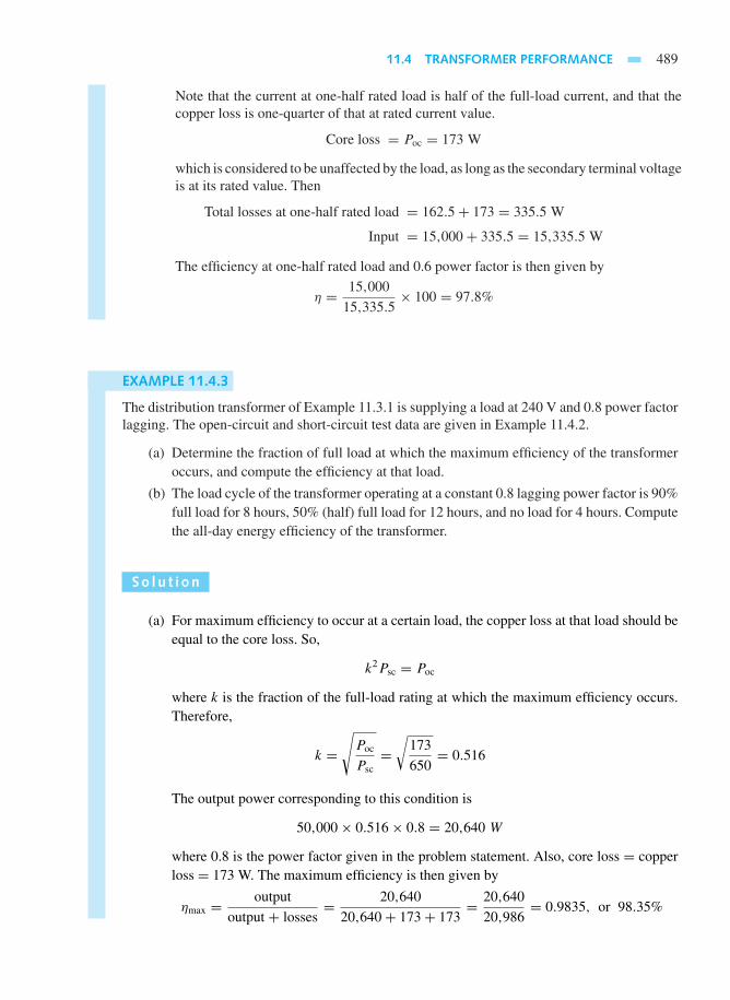
11.4 TRANSFORMER PERFORMANCE 489
Note that the current at one-half rated load is half of the full-load current, and that thecopper loss is one-quarter of that at rated current value.
Core loss = Poc = 173 W
which is considered to be unaffected by the load, as long as the secondary terminal voltageis at its rated value. Then
Total losses at one-half rated load = 162.5+ 173 = 335.5 W
Input = 15,000+ 335.5 = 15,335.5 W
The efficiency at one-half rated load and 0.6 power factor is then given by
η = 15,000
15,335.5× 100 = 97.8%
EXAMPLE 11.4.3
The distribution transformer of Example 11.3.1 is supplying a load at 240 V and 0.8 power factorlagging. The open-circuit and short-circuit test data are given in Example 11.4.2.
(a) Determine the fraction of full load at which the maximum efficiency of the transformeroccurs, and compute the efficiency at that load.
(b) The load cycle of the transformer operating at a constant 0.8 lagging power factor is 90%full load for 8 hours, 50% (half) full load for 12 hours, and no load for 4 hours. Computethe all-day energy efficiency of the transformer.
So l u t i on
(a) For maximum efficiency to occur at a certain load, the copper loss at that load should beequal to the core loss. So,
k2Psc = Poc
where k is the fraction of the full-load rating at which the maximum efficiency occurs.Therefore,
k =√Poc
Psc=√
173
650= 0.516
The output power corresponding to this condition is
50,000× 0.516× 0.8 = 20,640 W
where 0.8 is the power factor given in the problem statement. Also, core loss = copperloss = 173 W. The maximum efficiency is then given by
ηmax = output
output + losses= 20,640
20,640+ 173+ 173= 20,640
20,986= 0.9835, or 98.35%

490 MAGNETIC CIRCUITS AND TRANSFORMERS
(b) During 24 hours,
energy output = (8× 0.9× 50× 0.8)+ (12× 0.5× 50× 0.8) = 528 kWh
core loss = 24× 0.173 = 4.15 kWh
copper loss = (8× 0.92 × 0.65)+ (12× 0.52 × 0.65) = 6.16 kWh
The all-day (or energy) efficiency of the transformer is given by
ηAD = 528
528+ 4.15+ 6.16= 0.9808, or 98.08%
11.5 THREE-PHASE TRANSFORMERS
As we have seen in Chapter 10, three-phase transformers are used quite extensively in powersystems between generators and transmission systems, between transmission and subtransmissionsystems, and between subtransmission and distribution systems. Most commercial and industrialloads require three-phase transformers to transform the three-phase distribution voltage to theultimate utilization level.
Transformation in three-phase systems can be accomplished in either of two ways: (1)connecting three identical single-phase transformers to form a three-phase bank (each one willcarry one-third of the total three-phase load under balanced conditions); or (2) a three-phasetransformer manufactured for a given rating. A three-phase transformer, compared to a bank ofthree single-phase transformers, for a given rating will weigh less, cost less, require less floorspace, and have somewhat higher efficiency.
The windings of either core-type or shell-type three-phase transformers may be connectedin either wye or delta. Four possible combinations of connections for the three-phase, two-winding transformers are Y–,–Y, –, and Y–Y. These are shown in Figure 11.5.1 withthe transformers assumed to be ideal. The windings on the left are the primaries, those on theright are the secondaries, and a primary winding of the transformer is linked magnetically withthe secondary winding drawn parallel to it. With the per-phase primary-to-secondary turns ratio(N1/N2 = a), the resultant voltages and currents for balanced applied line-to-line voltages V andline currents I are marked in the figure.
As in the case of three-phase circuits under balanced conditions, only one phase needs tobe considered for circuit computations, because the conditions in the other two phases are thesame except for the phase displacements associated with a three-phase system. It is usuallyconvenient to carry out the analysis on a per-phase-of-Y (i.e., line-to-neutral) basis, and in sucha case the transformer series impedance can then be added in series with the transmission-lineseries impedance. In dealing with Y– and –Y connections, all quantities can be referred tothe Y-connected side. For – connections, it is convenient to replace the -connected seriesimpedances of the transformers with equivalent Y-connected impedances by using the relation
Zper phase of Y = 1
3Zper phase of (11.5.1)
It can be shown that to transfer the ohmic value of impedance from the voltage level on one sideof a three-phase transformer to the voltage level on the other side, the multiplying factor is thesquare of the ratio of line-to-line voltages, regardless of whether the transformer connection isY–Y, –Y, or –. In some cases, where Y–Y transformation is utilized in particular, it is quitecommon to incorporate a third winding, known as tertiary winding, connected in delta. Suchmultiwinding transformers with three or more windings are not considered in this text.
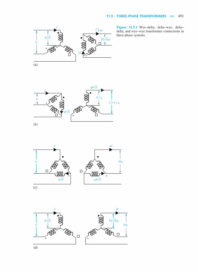
11.5 THREE-PHASE TRANSFORMERS 491
V
V/√3 V/(√3a)
−
+
I
+aI
√ 3 aI
(a)
Figure 11.5.1 Wye–delta, delta–wye, delta–delta, and wye–wye transformer connections inthree-phase systems.
V
+
I
(c)
I/√3 aI/√3
aI
+
V/a
V
V/√3 V/(√3a) V/a
+
I
(d)
aI
+

492 MAGNETIC CIRCUITS AND TRANSFORMERS
11.6 AUTOTRANSFORMERS
In contrast to a two-winding transformer, the autotransformer is a single-winding transformerhaving a tap brought out at an intermediate point. Thus, as shown in Figure 11.6.1, a–c is thesingle N1-turn winding wound on a laminated core, and b is the intermediate point where the tapis brought out such that b–c has N2 turns. The autotransformer may generally be used as eithera step-up or a step-down operation. Considering the step-down arrangement, as shown in Figure11.6.1, let the primary applied voltage be V1, resulting in a magnetizing current and a core flux φm.Voltage drops in the windings, exciting current, and small phase-angular differences are usuallyneglected for the analysis. Then it follows that
V1
V2= I2
I1= N1
N2= a (11.6.1)
in which a > 1 for step-down, a < 1 for step-up transformers.The input apparent power is S1 = V1I1, while the output apparent power is given by
S2 = V2I2. The apparent power transformed by electromagnetic induction (or transformer action)isSind = V2I3 = (V1−V2)I2. The output transferred by electrical conduction (because of the directelectrical connection between primary and secondary windings) is given byScond = V2I2−V2I3 =V2I1.
For the same output the autotransformer is smaller in size, weighing much less than a two-winding transformer, and has higher efficiency. An important disadvantage of the autotransformeris the direct copper connection (i.e., no electrical isolation) between the high- and low-voltagesides. A type of autotransformer commonly found in laboratories is the variable-ratio autotrans-former, in which the tapped point b (shown in Figure 11.6.1) is movable. It is known as the variac(variable ac). Although here, for the sake of simplicity, we have considered only the single-phaseautotransformer, three-phase autotransformers, which are available in practice, can be modeledon a per-phase basis and also analyzed just as the single-phase case.
V2
b
c
V1
+
−I3 = I2 − I1
I2
I1a
+
−
Figure 11.6.1 Single-phase step-down auto-transformer.
EXAMPLE 11.6.1
The single-phase, 50-kVA, 2400:240-V, 60-Hz, two-winding distribution transformer of Example11.3.1 is connected as a step-up autotransformer, as shown in Figure E11.6.1. Assume that the240-V winding is provided with sufficient insulation to withstand a voltage of 2640 V to ground.
(a) Find VH , VX, IH , IC , and IX corresponding to rated (full-load) conditions.
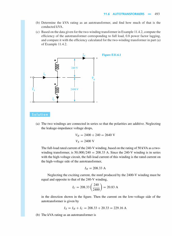
11.6 AUTOTRANSFORMERS 493
(b) Determine the kVA rating as an autotransformer, and find how much of that is theconducted kVA.
(c) Based on the data given for the two-winding transformer in Example 11.4.2, compute theefficiency of the autotransformer corresponding to full load, 0.8 power factor lagging,and compare it with the efficiency calculated for the two-winding transformer in part (a)of Example 11.4.2.
+
−
VH+
−
VX
IX
IC
240 V
2400 V
IH Figure E11.6.1
So l u t i on
(a) The two windings are connected in series so that the polarities are additive. Neglectingthe leakage-impedance voltage drops,
VH = 2400+ 240 = 2640 V
VX = 2400 V
The full-load rated current of the 240-V winding, based on the rating of 50 kVA as a two-winding transformer, is 50,000/240 = 208.33 A. Since the 240-V winding is in serieswith the high-voltage circuit, the full-load current of this winding is the rated current onthe high-voltage side of the autotransformer,
IH = 208.33 A
Neglecting the exciting current, the mmf produced by the 2400-V winding must beequal and opposite to that of the 240-V winding,
IC = 208.33
(240
2400
)= 20.83 A
in the direction shown in the figure. Then the current on the low-voltage side of theautotransformer is given by
IX = IH + IC = 208.33+ 20.33 = 229.16 A
(b) The kVA rating as an autotransformer is

494 MAGNETIC CIRCUITS AND TRANSFORMERS
VHIH
1000= 2640× 208.33
1000= 550 kVA
orVXIX
1000= 2400× 229.16
1000= 550 kVA
which is 11 times that of the two-winding transformer. The transformer must boost thecurrent IH of 208.33 A through a potential rise of 240 V. Thus the kVA transformed byelectromagnetic induction is given by
240× 208.33
1000= 50 kVA
The remaining 500 kVA is the conducted kVA.
(c) With the currents and voltages shown for the autotransformer connections, the lossesat full load will be 823 W, the same as in Example 11.4.2. However, the output as anautotransformer at 0.8 power factor is given by
550× 1000× 0.8 = 440,000 W
The efficiency of the autotransformer is then calculated as
η = 440,000
440,823= 0.9981, or 99.81%
whereas that of the two-winding transformer was calculated as 0.98 in Example 11.4.2.Because the only losses are those due to transforming 50 kVA, higher efficiency resultsfor the autotransformer configuration compared to that of the two-winding transformer.
11.7 LEARNING OBJECTIVES
The learning objectives of this chapter are summarized here, so that the student can check whetherhe or she has accomplished each of the following.
• Analysis and design of simple magnetic circuits.
• Equivalent circuits of transformers.
• Predicting transformer performance from equivalent circuits.
• Basic notions of three-phase transformers.
• Elementary autotransformer calculations and performance.
11.8 PRACTICAL APPLICATION: A CASE STUDY
Magnetic Bearings for Space Technology
The high magnetic energy stored in rare-earth-cobalt permanent magnets allows the design oflightweight motors and magnetic bearings for high-speed rotors. Magnetic bearings are not subjectto wear, and with the ability to operate under high vacuum conditions, they appear to be ideal forapplications requiring high rotational speeds, such as 100,000 r/min. Important applications arefor turbomolecular pumps, laser scanners, centrifuges, momentum rings for satellite stabilizations,and other uses in space technology.

PROBLEMS 495
Because of the absence of mechanical contact and lubricating fluids, magnetic bearingscan be operated in high vacuum at higher speeds with extremely low friction, low noise, andlonger operating life. With no risk of contamination by oil or gas, and with less heat dissipation,it is possible to ascertain clean, stable, and accurate operating conditions with reliability andrepeatability. In space technology the magnetic bearings are used successfully in reaction,momentum, and energy wheels, helium pumps, and telescope pointing. Terrestrial applicationsinclude scanners, high-vacuum pumps, beam choppers in high vacuum, energy storage wheels,and accurate smooth rotating machines. The magnetic bearings in a reaction wheel are shown inFigure 11.8.1.
The design of magnetic bearings involves the calculation of magnetic forces and stiffnessas part of designing an electromechanical servo system. In earlier days, the magnetic forceof a suspension block was calculated approximately, with reasonable accuracy, by assumingsimple straight flux paths. However, higher magnetic flux densities are increasingly used forreducing the weight and size of magnetic bearings, particularly in the case of a single-axis servoedmagnetic bearing which utilizes fringing rings. In such cases the nonlinear characteristics of theferromagnetic materials become quite significant; analytical techniques fail to yield sufficientlyaccurate results. Hence it becomes essential to take recourse to numerical analysis of the nonlinearmagnetic fields with the aid of a high-speed digital computer in order to determine more accuratelythe flux distribution corresponding to various conditions of operation, compute leakage, andevaluate forces at the air gap, so as to optimize the design of nonlinear magnetic bearings.
The strength of the electromagnet and/or the permanent magnet can easily be changed toobserve their effect on the leakage as well as the flux-density distribution, particularly at the air-gap level and fringing rings. The number of fringing rings and their location may also be easilychanged in order to evaluate their effects on the forces at the air-gap level.
Rotor
Motor
Bearing gap
SmCo magnet
Control coil
Figure 11.8.1 Magnetic bearings ina reaction wheel.
PROBL EMS
11.1.1 From the magnetic material characteristicsshown in Figure 11.1.2, estimate the relativepermeability µr at a flux density of 1 T for M-19
and AISI 1020 materials.
11.1.2 Determine the units for the area of the hysteresisloop of a ferromagnetic material.
496 MAGNETIC CIRCUITS AND TRANSFORMERS
11.1.3 In plotting a hysteresis loop the following scalesare used: 1 cm= 400 At/m and 1 cm= 0.3 T. Thearea of the loop for a certain magnetic materialis found to be 6.2 cm2. Calculate the hysteresisloss in joules per cycle for the specimen tested ifthe volume is 400 cm3.
11.1.4 A sample of iron having a volume of 20 cm3
is subjected to a magnetizing force varying sinu-soidally at a frequency of 400 Hz. The area of thehysteresis loop is found to be 80 cm2 with the fluxdensity plotted in Wb/m2 and the magnetizingforce in At/m. The scale factors used are 1 cm=0.03 T and 1 cm= 200 At/m. Find the hysteresisloss in watts.
11.1.5 The flux in a magnetic core is alternating sinu-soidally at a frequency of 500 Hz. The maximumflux density is 1 T. The eddy-current loss thenamounts to 15 W. Compute the eddy-current lossin this core when the frequency is 750 Hz and themaximum flux density is 0.8 T.
*11.1.6 The total core loss for a specimen of magneticsheet steel is found to be 1800 W at 60 Hz.When the supply frequency is increased to 90Hz, while keeping the flux density constant, thetotal core loss is found to be 3000 W. Determinethe hysteresis and eddy-current losses separatelyat both frequencies.
11.1.7 A magnetic circuit is found to have an ac hystere-sis loss of 10 W when the peak current is Im = 2A. Assuming the exponent of Bm to be 1.5 inEquation (11.1.4), estimate Ph for Im = 0.5 Aand 8 A.
11.1.8 Ac measurements with constant voltage ampli-tude reveal that the total core loss of a certainmagnetic circuit is 10 W at f = 50 Hz, and 13W at f = 60 Hz. Find the total core loss if thefrequency is increased to 400 Hz.
*11.2.1 Consider the magnetic circuit of Figure 11.2.1(a).Let the cross-sectional area AC of the core, be
16 cm2, the average length of the magnetic pathin the core lC be 40 cm, the number of turnsN of the excitation coil be 100 turns, and therelative permeability µr of the core be 50,000.For a magnetic flux density of 1.5 T in the core,determine:
(a) The flux φ
(b) Total flux linkage λ(= Nφ).
(c) The current required through the coil.
11.2.2 Now suppose an air gap 0.1 mm long is cutin the right leg of the core of Figure 11.2.1(a),making the magnetic circuit look like that ofFigure 11.2.1(b). Neglect leakage and fringing.With the new core configuration, repeat Problem11.2.1 for the same dimensions and values givenin that problem. See what a difference that smallair gap can make!
11.2.3 A toroid with a circular cross section is shown inFigure P11.2.3. It is made from cast steel with arelative permeability of 2500. The magnetic fluxdensity in the core is 1.25 T measured at the meandiameter of the toroid.
(a) Find the current that must be supplied to thecoil.
(b) Calculate the magnetic flux in the core.
(c) Now suppose a 10-mm air gap is cut acrossthe toroid. Determine the current that mustbe supplied to the coil to produce the samevalue of magnetic flux density as in part (a).You may neglect leakage and fringing.
11.2.4 For the magnetic circuit shown in Figure P11.2.4,neglecting leakage and fringing, determine themmf of the exciting coil required to produce aflux density of 1.6 T in the air gap. The material isM-19. The dimensions are lm1 = 60 cm, Am1 =24 cm2, lm2 = 10 cm, Am2 = 16 cm2, lg = 0.1cm, and Ag = 16 cm2.
8 cm
12 cm
N = 2500 turns
Figure P11.2.3 Toroid with circular cross section.
Am1
Coil
lm1
lm2
lm2 Am2
lg
Figure P11.2.4

PROBLEMS 497
11.2.5 Consider the toroid shown in Figure P11.2.5(a)made up of three ferromagnetic materials. Ma-terial a is nickel–iron alloy having a mean arclength la of 0.6 m; material b is medium sili-con steel having a mean arc length lb of 0.4 m;material c is cast steel having a mean arc lengthlc of 0.2 m. Each of the materials has a cross-sectional area of 0.002 m2. Find the mmf neededto establish a magnetic flux of φ = 1.2 mWb bymaking use of the magnetization curves given in
Figure P11.2.5(b).
11.2.6 The configuration of a magnetic circuit is given inFigure P11.2.6. Assume the permeability of theferromagnetic material to be µ = 1000µ0. Ne-glect leakage, but correct for fringing by increas-ing each linear dimension of the cross-sectionalarea by the length of the air gap. The magneticmaterial has a square cross-sectional area of 4cm2. Find the air-gap flux density, and the mag-netic field intensity in the air gap.
lb
lc
la
+V N
(a)
IR
Figure P11.2.5 (a) Toroid. (b) Magnetization curves oftypical ferromagnetic materials.
Soft
cast
steel
1.5
1.4
1.3
1.2
1.1
1.0
0.9
0.8
0.7
0.6
0.5
0.4
0.3
0.2
0.110 20 30 40 60 80 100 200 300 400 600 1000 2000 4000 10,000
Mag
netic
flu
x de
nsity
, T
Magnetic field intensity, At/m
Nickel–iron alloy
Med
iu
msil
icon sheet
steel
Cast i
ron

498 MAGNETIC CIRCUITS AND TRANSFORMERS
50 cm
50 cm50 cm
1000 turns1000 turns
5 A5 A
0.5 cm
Figure P11.2.6
*11.2.7 Consider the magnetic circuit shown in FigureP11.2.7. Assume the relative permeability of themagnetic material to be 1000 and the cross-sec-tional area to be the same throughout. Determinethe current needed in the coil to produce a fluxdensity of 1 T in the center limb, if the excitationcoil has 500 turns.
11.2.8 In the magnetic circuit shown in Figure P11.2.8the center leg has the same cross-sectional areaas each of the outer legs. The coil has 400 turns.The permeability of iron may be assumed to beinfinite. If the air-gap flux density in the left legis 1.2 T, find:
(a) The flux density in the air gap of the rightleg.
(b) The flux density in the center leg.
(c) The current needed in the coil.
11.2.9 Figure P11.2.9 shows the cross section of a rect-angular iron core with two air gaps g1 and g2.The ferromagnetic iron can be assumed to haveinfinite permeability. The coil has 500 turns.
(a) Gaps g1 and g2 are each equal to 0.1 cm,and a current of 1.83 A flows through the
winding. Compute the flux densities in thetwo air gaps, Bg1 in the center gap g1, andBg2 in the end gap g2.
(b) Let gap g2 now be closed by inserting aniron piece of the correct size and infinitepermeability so that only the center gap g1 =0.1 cm remains. If a flux density of 1.25 Tis needed in gap g1, find the current that isneeded in the winding.
11.2.10 Consider the magnetic circuit in Figure P11.2.10,in which all parts have the same cross section.The coil has 200 turns and carries a current of 5A. The air gaps are g1 = 0.4 cm and g2 = 0.5cm. Assuming the core has infinite permeability,compute the flux density in tesla in (a) gap g1,(b) gap g2, and (c) the left limb.
11.2.11 The magnetic circuit shown in Figure P11.2.11has an iron core which can be considered to beinfinitely permeable. The core dimensions areAC = 20 cm2, g = 2 mm, and lC = 100cm. The coil has 500 turns and draws a currentof 4 A from the source. Magnetic leakage andfringing may be neglected. Calculate the follow-ing:
30cm
25 cm25 cm
Figure P11.2.7
0.75cm
0.50cm
30cm
25 cm25 cm
Figure P11.2.8

PROBLEMS 499
g1
g2
Figure P11.2.9
30cm
20 cm20 cm
g1 g2
Figure P11.2.10
N gSource
Figure P11.2.11
(a) Total magnetic flux.
(b) Flux linkages of the coil.
(c) Coil inductance.
(d) Total stored magnetic energy.
*11.2.12 Repeat Problem 11.2.11 accounting for the core’srelative permeability of 2000.
11.2.13 Reconsider Problem 11.2.3. Calculate the coilinductance L and the total stored magnetic energybefore and after the air gap is cut.
11.3.1 A 10-kVA, 4800:240-V, 60-Hz, single-phasetransformer has an equivalent series impedanceof 120 + j300 referred to the primary high-voltage side. The exciting current of the trans-former may be neglected.
(a) Find the equivalent series impedance re-ferred to the secondary low-voltage side.
(b) Calculate the voltage at the primary high-voltage terminals if the secondary suppliesrated secondary current at 230 V and unitypower factor.
*11.3.2 A 25-kVA, 2300:230-V, 60-Hz, single-phasetransformer has the following parameters: re-sistance of high-voltage winding 1.5 , resis-tance of low-voltage winding 0.015 , leakagereactance of high-voltage winding 2.4 , andleakage reactance of low-voltage winding 0.024. Compute the following:
(a) Equivalent series impedance referred to thehigh-voltage side.
(b) Equivalent series impedance referred to thelow-voltage side.
(c) Terminal voltage on the high-voltage sidewhen the transformer is delivering full loadat 230 V and 0.866 power factor lagging.
11.3.3 A 100-kVA, 2300:230-V, 60-Hz, single-phasetransformer has the following parameters: R1 =0.30 , R2 = 0.003 , RC1 = 4.5 k, X1 =0.65 , X2 = 0.0065 , and Xm1 = 1.0 k,where subscripts 1 and 2 refer to high-voltage andlow-voltage sides, respectively. Set up the equiv-alent T-circuit of the transformer and determinethe input current, input voltage, input power, andpower factor when the transformer is delivering75 kW at 230 V and 0.85 lagging power factor.
11.3.4 A 150-kVA, 2400/240-V, 60-Hz, single-phasetransformer has the following parameters: R1 =0.2 , R2 = 0.002 , X1 = 0.45 , X2 =0.0045 , RC = 10 k, and Xm = 1.55 k,where the notation is that of Figure 11.3.4. Formthe equivalent T-circuit of the transformer re-ferred to the high-voltage side, and calculate thesupply voltage on the high-voltage side when thetransformer supplies rated (full) load at 240 Vand 0.8 lagging power factor.
11.3.5 For a single-phase, 60-Hz transformer rated 500
500 MAGNETIC CIRCUITS AND TRANSFORMERS
kVA, 2400:480 V, following the notation of Fig-ure 11.3.4, the equivalent circuit impedances inohms are R1 = 0.06, R2 = 0.003, RC = 2000,and X1 = 0.3, X2 = 0.012, Xm = 500. Theload connected across the low-voltage terminalsdraws rated current at 0.8 lagging power factorwith rated voltage at the terminals.
(a) Calculate the high-voltage winding terminalvoltage, current, and power factor.
(b) Determine the transformer series equivalentimpedance for the high-voltage and low-voltage sides, neglecting the exciting currentof the transformer.
(c) Considering the T-equivalent circuit, find theThévenin equivalent impedance of the trans-former under load as seen from the primaryhigh-voltage terminals.
11.3.6 A 20-kVA, 2200:220-V, 60-Hz, single-phasetransformer has these parameters:
Resistance of the 2200-V winding R1 = 2.50
Resistance of the 220-V winding R2 = 0.03
Leakage reactance of the 2200-V winding X1 =0.1
Leakage reactance of the 220-V winding X2 =0.1
Magnetizing reactance on the 2200-V sideXm =25,000
(a) Draw the equivalent circuits of the trans-former referred to the high-voltage and low-voltage sides. Label impedances numericallyin ohms.
(b) The transformer is supplying 15 kVA at 220V and a lagging power factor of 0.85. Deter-mine the required voltage at the high-voltageterminals of the transformer.
11.4.1 These data were obtained from tests carried outon a 10-kVA, 2300:230-V, 60-Hz distributiontransformer:
• Open-circuit test, with low-voltage winding ex-cited: applied voltage 230 V, current 0.45 A,input power 70 W
• Short-circuit test, with high-voltage windingexcited: applied voltage 120 V, current 4.35 A,input power 224 W
(a) Compute the efficiency of the transformerwhen it is delivering full load at 230 V and0.85 power factor lagging.
(b) Find the efficiency of the transformer whenit is delivering 7.5 kVA at 230 V and 0.85power factor lagging.
(c) Determine the fraction of rating at which thetransformer efficiency is a maximum, andcalculate the efficiency corresponding to thatload if the transformer is delivering the loadat 230 V and a power factor of 0.85.
(d) The transformer is operating at a constantload power factor of 0.85 on this load cycle:0.85 full load for 8 hours, 0.60 full load for 12hours, and no load for 4 hours. Compute thetransformer’s all-day (or energy) efficiency.
(e) If the transformer is supplying full load at230 V and 0.8 lagging power factor, de-termine the voltage regulation of the trans-former. Also, find the power factor at thehigh-voltage terminals.
*11.4.2 A 3-kVA, 220:110-V, 60-Hz, single-phase trans-former yields these test data:
• Open-circuit test: 200 V, 1.4 A, 50 W
• Short-circuit test: 4.5 V, 13.64 A, 30 W
Determine the efficiency when the transformerdelivers a load of 2 kVA at 0.85 power factorlagging.
11.4.3 A 75-kVA, 230/115-V, 60-Hz transformer wastested with these results:
• Open-circuit test: 115 V, 16.3 A, 750 W
• Short-circuit test: 9.5 V, 326 A, 1200 W
Determine:
(a) The equivalent impedance in high-voltageterms.
(b) The voltage regulation at rated load, 0.8power factor lagging.
(c) The efficiency at rated load, 0.8 power factorlagging, and at half-load, unity power factor.
(d) The maximum efficiency and the current atwhich it occurs.
11.4.4 A 300-kVA transformer has a core loss of 1.5 kWand a full-load copper loss of 4.5 kW.
(a) Calculate its efficiency corresponding to 25,50, 75, 100, and 125% loads at unity powerfactor.
(b) Repeat the efficiency calculations for the25% load at power factors of 0.8 and 0.6.

PROBLEMS 501
(c) Determine the fraction of load for whichthe efficiency is a maximum, and calculatethe corresponding efficiencies for the powerfactors of unity, 0.8, and 0.6.
11.4.5 Consider the solution of Example 11.4.1. Bymeans of a phasor diagram, determine the loadpower factor for which the regulation is maxi-mum (i.e., the poorest), and find the correspond-ing regulation.
11.4.6 A 10-kVA, 200:400-V, single-phase transformergave these test results:
• Open-circuit test (LV winding supplied): 200 V,3.2 A, 450 W
• Short-circuit test (HV winding supplied): 38 V,25 A, 600 W
Compute the efficiency when the transformerdelivers half its rated kVA at 0.85 power factorlagging.
*11.4.7 Find the percent voltage regulation and the effi-ciency of the transformer for the following cases:
(a) Problem 11.3.1(b).
(b) Problem 11.3.2(c).
11.4.8 The transformer of Problem 11.3.3 is delivering afull load of 100 kVA at a secondary load voltageof 230 V. Neglect the exciting current of thetransformer and determine the voltage regulationif:
(a) The load power factor is 0.8 lagging.
(b) The load power factor is 0.8 leading.
11.4.9 A 25-kVA, 2400/240-V, 60-Hz, single-phasetransformer has an equivalent series impedanceof 3.45+ j5.75 referred to the primary high-voltage side. The core loss is 120 W. When thetransformer is delivering rated kVA to a load atrated secondary voltage and a 0.85 lagging powerfactor, find the percent voltage regulation and theefficiency of the transformer.
11.4.10 A 25-kVA, 2200:220-V, 60-Hz, single-phasetransformer has an equivalent series impedanceof 3.5 + j4.0 referred to the primary high-voltage side.
(a) Determine the highest value of voltage regu-lation for full-load output at rated secondaryterminal voltage.
(b) At what power factor does it occur?
(c) Sketch the corresponding phasor diagram.
11.4.11 The following data were obtained on a 25-kVA, 2400:240-V, 60-Hz, single-phase distribu-tion transformer:
• Open-circuit test with meters on LV side: 240V, 3.2 A, 165 W
• Short-circuit test with meters on HV side: 55 V,10.4 A, 375 W
Compute the worst voltage regulation and thepower factor at which it occurs, when the trans-former is delivering rated output at rated sec-ondary terminal voltage of 240 V. Sketch thecorresponding phasor diagram.
*11.4.12 The efficiency of a 400-kVA, single-phase, 60-Hztransformer is 98.77% when delivering full-loadcurrent at 0.8 power factor, and 99.13% with half-rated current at unity power factor. Calculate:
(a) The iron loss.
(b) The full-load copper loss.
(c) The efficiency at 3/4 load, 0.9 power factor.
11.4.13 A transformer has its maximum efficiency of0.9800 when it delivers 15 kVA at unity powerfactor. During the day it is loaded as follows:12 hours 2 kW at power factor 0.5
6 hours 12 kW at power factor 0.86 hours 18 kW at power factor 0.9
Determine the all-day efficiency.
11.4.14 A single-phase, 3-kVA, 220:110-V, 60-Hz trans-former has a high-voltage winding resistance of0.3 , a low-voltage winding resistance of 0.06, a leakage reactance of 0.8 on its high-voltage side, and a leakage reactance of 0.2
on its low-voltage side. The core loss at ratedvoltage is 45 W, and the copper loss at ratedload is 100 W. Neglect the exciting current of thetransformer. Find the per-unit voltage regulationwhen the transformer is supplying full load at 110V and 0.9 lagging power factor.
11.4.15 The transformer of Problem 11.3.4 operates onthe following load cycle:12 hours full load, 0.8 power factor lagging
4 hours no load8 hours one-half full load, unity power
factorCompute the all-day energy efficiency.
11.4.16 A 75-kVA transformer has an iron loss of 1kW and a full-load copper loss of 1 kW. If thetransformer operates on the following load cycle,determine the all-day efficiency:

502 MAGNETIC CIRCUITS AND TRANSFORMERS
8 hours full load at unity power factor8 hours no load8 hours one-half full load at unity power
factor
*11.4.17 A 10-kVA transformer is known to have an ironloss of 150 W and a full-load copper loss of250 W. If the transformer has the following loadcycle, compute its all-day efficiency:
4 hours full load at 0.8 power factor8 hours 75% full load at 1.0 power factor
12 hours 50% full load at 0.6 power factor
11.4.18 Show polarity markings for a single-phase trans-former for (a) subtractive polarity, and (b) addi-tive polarity.
11.4.19 Two single-phase transformers, each rated 2400:120-V, are to be interconnected for (a) 4800:240-V operation, and (b) 2400:120-V operation.Draw circuit diagrams and show polarity mark-ings.
11.4.20 Two 1150:115-V transformers are to be inter-connected for (a) 2300:230-V operation, and (b)1150:230-V operation. Show the interconnec-tions and appropriate polarity markings.
11.5.1 A one-line diagram of a three-phase distributionsystem is given in Figure P11.5.1. Determinethe line-to-line voltage at the sending end of thehigh-voltage feeder when the transformer deliv-ers rated load at 240 V (line-to-line) and 0.8lagging power factor. Neglect the exciting currentof the transformer.
*11.5.2 A 5-MVA, 66:13.2 kV, three-phase transformersupplies a three-phase resistive load of 4500 kWat 13.2 kV. What is the load resistance in ohms asmeasured from line to neutral on the high-voltageside of the transformer, if it is:
(a) Connected in Y–Y?
(b) Reconnected in Y–, with the same high-tension voltage supplied and the same loadresistors connected?
11.5.3 A three-phase transformer bank consisting ofthree 10-kVA, 2300:230-V, 60-Hz, single-phasetransformers connected in Y– is used to stepdown the voltage. The loads are connected to thetransformers by means of a common three-phaselow-voltage feeder whose series impedance is0.005 + j0.01 per phase. The transform-ers themselves are supplied by means of athree-phase high-voltage feeder whose seriesimpedance is 0.5 + j5.0 per phase. Theequivalent series impedance of the single-phasetransformer referred to the low-voltage side is0.12+j0.24 . The star point on the primary sideof the transformer bank is grounded. The loadconsists of a heating load of 2 kW per phase anda three-phase induction-motor load of 20 kVAwith a lagging power factor of 0.8, supplied at230 V line-to-line.
(a) Draw a one-line diagram of this three-phasedistribution system.
(b) Neglecting the exciting current of the trans-former bank, draw the per-phase equivalentcircuit of the distribution system.
(c) Determine the line current and the line-to-line voltage at the sending end of the high-voltage feeder.
11.5.4 A single-line diagram of a three-phase trans-former bank connected to a load is given inFigure P11.5.4. Find the magnitudes of the line-to-line voltages, line currents, phase voltages,and phase currents on either side of the trans-former bank. Determine the primary to secondaryratio of the line-to-line voltages and the line cur-rents.
Load
3 single-phase transformerseach rated 50 kVA, 2400:240 V
identical with that of Example 11.4.1
3-phase low-voltage feederseries impedance0.00083 + j 0.0033 Ω/ph
3-phase high-voltage feederseries impedance0.25 + j 1.0 Ω/ph
Figure P11.5.1

PROBLEMS 503
Load2400 V 208 V
3 single-phase transformerseach rated 10 kVA, 2400:120 V, 60 Hz
30 kVA balanced
Figure P11.5.4
11.5.5 Three single-phase 100-kVA, 2400:240-V, 60-Hztransformers (each of which has an equivalent se-ries impedance of 0.045+j0.16 referred to itslow-voltage side) are connected to form a three-phase, 4160:240-V transformer bank, which inturn is connected to a three-phase feeder withan impedance of 0.5+ j1.5 /phase. When thethree-phase transformer bank delivers 250 kW at240 V and 0.866 lagging power factor, determine:
(a) The transformer winding currents.
(b) The sending-end voltage (line to line) at thesource.
11.5.6 Three single-phase, 10-kVA, 2400/120-V, 60-Hz transformers are connected to form a three-phase, 4160/208-V transformer bank. Each ofthe single-phase transformers has an equivalentseries impedance of 10 + j25 referred to thehigh-voltage side. The transformer bank is saidto deliver 27 kW at 208 V and 0.9 power factorleading.
(a) Draw a schematic diagram of transformerconnections, and develop a per-phase equiv-alent circuit.
(b) Determine the primary current, primary volt-age, and power factor.
(c) Compute the voltage regulation.
*11.5.7 A three-phase, 600-kVA, 2300:230-V, Y–Y trans-former bank has an iron loss of 4400 W and a full-load copper loss of 7600 W. Find the efficiencyof the transformer for 70% full load at 230 V and0.85 power factor.
11.5.8 Three identical single-phase transformers are tobe connected to form a three-phase bank rated at300 MVA, 230:34.5 kV. For the following con-figurations, determine the voltage, current, andkVA ratings of each single-phase transformer: (a)–, (b) Y–, (c) Y–Y, (d) –Y.
11.6.1 A single-phase, 10-kVA, 2300:230-V, 60-Hz,two-winding distribution transformer is con-nected as an autotransformer to step up the volt-age from 2300 V to 2530 V.
(a) Draw a schematic diagram of the arrange-ment showing all the voltages and currentswhile delivering full load.
(b) Find the permissible kVA rating of the auto-transformer if the winding currents are not toexceed those for full-load operation as a two-winding transformer. How much of that istransformed by electromagnetic induction?
(c) Based on the data given for the two-windingtransformer in Problem 11.4.1, computethe efficiency of the autotransformer corre-sponding to full load and 0.8 lagging powerfactor. Comment on why the efficiency ofthe autotransformer is higher than that of thetwo-winding transformer.
11.6.2 A two-winding, single-phase transformer rated3 kVA, 220:110 V, 60 Hz is connected as anautotransformer to transform a line input voltageof 330 V to a line output voltage of 110 V and todeliver a load of 2 kW at 0.8 lagging power factor.Draw the schematic diagram of the arrangement,label all the currents and voltages, and calculateall the quantities involved.
11.6.3 A two-winding, 15-kVA, 2300:115-V, 60-Hz,single-phase transformer, which is known to havea core loss of 75 W and a copper loss of 250 W, isconnected as an autotransformer to step up 2300V to 2415 V. With a load of 0.8 power factorlagging, what kVA load can be supplied withoutexceeding the current rating of any winding?Determine the efficiency at this load.
11.6.4 A single-phase, two-winding, 10-kVA, 440:110-V, 60-Hz transformer is to be connected as anautotransformer to supply a load at 550 V from a440-V supply. Draw a schematic diagram of theconnections and determine: (a) The maximumkVA rating as an autotransformer. (b) The maxi-mum apparent power transferred by conduction.(c) The maximum apparent power transferred byelectromagnetic induction.
*11.6.5 A 15-kVA, 2200:220-V, two-winding, single-phase transformer is connected as an autotrans-

504 MAGNETIC CIRCUITS AND TRANSFORMERS
former to step up voltage from 220 V to 2420V. Without exceeding the rated current of anywinding, determine the kVA rating of the auto-transformer, the kVA transformed by transformeraction, and the kVA conducted.
11.6.6 A 5-kVA, 480:120-V, two-winding, 60-Hz,single-phase transformer has an efficiency of95% while delivering rated load at rated voltageand 0.8 power factor lagging. This transformer
is to be connected as an autotransformer to stepdown a 600-V source to 480 V.
(a) Draw a schematic connection diagram as anautotransformer.
(b) Find the maximum kVA rating as an auto-transformer.
(c) Compute the efficiency as an autotrans-former delivering its rated kVA at 480 V and0.8 power factor lagging.
12 Electromechanics
12.1 Basic Principles of Electromechanical Energy Conversion
12.2 emf Produced by Windings
12.3 Rotating Magnetic Fields
12.4 Forces and Torques in Magnetic-Field Systems
12.5 Basic Aspects of Electromechanical Energy Converters
12.6 Learning Objectives
12.7 Practical Application: A Case Study—Sensors or Transducers
Problems
12.1 BASIC PRINCIPLES OF ELECTROMECHANICAL ENERGY CONVERSION
Energy available in many forms is often converted to and from electrical form because electricenergy can be transmitted and controlled simply, reliably, and efficiently. Among the energy-conversion devices, electromechanical energy converters are the most important. Electromechan-ical energy conversion involves the interchange of energy between an electric system and amechanical system, while using magnetic field as a means of conversion.
Devices that convert control signals from one form to another are known as transducers, mostof which have an output signal in the form of electric energy. For example, a potentiometer is usedto convert a mechanical position to an electric voltage, a tachometer generator converts a velocityinto a voltage (dc or ac), and a pressure transducer indicates a pressure drop (or rise) in termsof a corresponding drop (or rise) in electric potential. Thus, a transducer translates the commandsignal appropriately into an electrical form usable by the system, and forms an important partof control systems. Electromechanical transducers form a link between electric and mechanicalsystems.
When the energy is converted from electrical to mechanical form, the device is displayingmotor action. A generator action involves converting mechanical energy into electric energy. Theelectromechanical energy-conversion process can be expressed as
505

506 ELECTROMECHANICS
Electric energyMotor→←
Generator
Mechanical energy
Electromechanical energy converters, simply known as electric machines, embody three essentialfeatures: (1) an electric system, (2) a mechanical system, and (3) a coupling field. Figure 12.1.1is a schematic representation of an ideal electric machine (or a lossless electromechanical device)for which the following relations hold:
Electric input (or output) energy vit = mechanical output (or input) energy T ωmt
or
Electric input (or output) power vi = mechanical output (or input) power T ωm (12.1.1)
where v and i are the voltage and the current associated with the electrical port, and T and ωm arethe torque and the angular rotational velocity associated with the mechanical port.
The principle of conservation of energy may be stated as follows: Energy can be neithercreated nor destroyed, even though, within an isolated system, energy may be converted from oneform to another form, and transferred from an energy source to an energy sink. The total energyin the system is constant.
A practical electromechanical system with losses can be represented by adding on the lossyportion of the electric system and the lossy portion of the mechanical system modeled externally.Excluding all types of dissipation and losses makes the energy-conversion part to be lossless orconservative with a coupling field.
Both electric and magnetic fields store energy, from which useful mechanical forces andtorques can be derived. With a normal working electric field intensity of about 3× 10⁶ V/m, thestored electric-energy density is on the order of
1
2ε0E
2 = 1
2
10−9
36π(3× 10⁶)2 ∼= 40 J/m3
where ε0 is the permittivity of free space, given by 10−6/36π or 8.854 × 10⁻¹² F/m, and E isthe electric field intensity. This corresponds to a force density of 40 N/m2. The stored magneticenergy density in air, on the other hand, with a normal working magnetic flux density of about1.6 T, comes to
1
2
B2
µ0= 1
2
1.62
4π × 10−7∼= 1× 10⁶ J/m3
where µ0 is the permeability of free space, and B is the magnetic flux density. As this is nearly25,000 times as much as for the electric field, almost all industrial electric machines are magnetic
Losslesselectromechanical
devicewith coupling
field
Electricalport
Mechanicalport
Motor
Generator
i
v
v, i T, ωm
ωm, T
Figure 12.1.1 Schematic repre-sentation of a lossless electrome-chanical device.

12.1 BASIC PRINCIPLES OF ELECTROMECHANICAL ENERGY CONVERSION 507
in principle and are magnetic-field devices.Three basic principles associated with all electromagnetic devices are (1) induction, (2)
interaction, and (3) alignment.
Induction
The essentials for producing an emf by magnetic means are electric and magnetic circuits, mutuallyinterlinked. Figure 12.1.2(a) shows a load (or sink or motor) convention with the induced emf(or back emf) e directed in opposition to the positive current, in which case Faraday’s law ofinduction,
e = +dλ
dt= +N dφ
dt(12.1.2a)
applies, where λ is the flux linkages, N is the number of turns, and φ is the flux. On the otherhand, the induced emf e (or generated emf) acting in the direction of positive current, as shownin Figure 12.1.2(b) with a source (or generator) convention, satisfies Faraday’s law of induction,
e = −dλ
dt= −N dφ
dt(12.1.2b)
The change in flux linkage in a coil may occur in one of the following three ways:
1. The coil remaining stationary with respect to the flux, the flux varies in magnitude withtime. Since no motion is involved, no energy conversion takes place. Equation (12.1.2a)gives the transformer emf (or the pulsational emf ) as in the case of a transformer (seeChapter 11), in which a time-varying flux linking a stationary coil yields a time-varyingvoltage.
2. The flux remaining constant, the coil moves through it. A conductor or a coil movingthrough a magnetic field will have an induced voltage, known as the motional emf (orspeed emf ), given by
+
−
+
−
+
−
+
−
+
−
+
−
v
i R
e v
iR
+
−e
v = Ri + e = Ri + = Ri + Ndλdt
dφdt
(a)
v
i R
e v
iR
+
−e
v = e − iR = − − iR = −N − iRdλdt
dφdt
(b)
Figure 12.1.2 Circuit conven-tions. (a) Load (or sink or motor)convention. Note that the powerabsorbed by the circuit is posi-tive when v and i are positive, andwhen current flows in the direc-tion of voltage drop. (b) Source(or generator) convention. Notethat the power delivered by thiscircuit to the external circuit ispositive when v and i are posi-tive, and when current flows outof the positive terminal.

508 ELECTROMECHANICS
Motional emf e = BlU (12.1.3)
which is often called the cutting-of-flux equation, where B is the flux density of a non-time-varying, uniform magnetic field, l is the length of the conductor, U is the velocityof the conductor, and B, l, and U are mutually perpendicular in their directions. If themotion is rotary in nature, it is also known as rotational voltage. The direction for themotional emf can be worked out from the right-hand rule: if the thumb, first, and secondfingers of the right hand are extended so that they are mutually perpendicular to eachother, and if the thumb represents the direction of U and the first finger the direction ofB, the second finger will then represent the direction of the emf along l. This is depictedin Figure 12.1.3(a).
The generation of motional emf is further illustrated by a simple example, as shownin Figure 12.1.3(b), where a single-turn coil formed by the moving (or sliding) conductor(moving with velocity U), the two conducting rails, and the voltmeter are situated in amagnetic field of flux density B. The conductor moving with a velocity U, in a direction atright angles to both B and l, sweeps the area lU in 1 second. The flux per unit time in thisarea is BlU, which is also the flux linkage per unit time with the single-turn coil. Thus,the induced emf e is simply given by BlU. The motional emf (or speed emf) is alwaysassociated with the conversion of energy between the mechanical and electrical forms.
3. The coil may move through a time-varying flux; that is to say, both changes (1) and (2)may occur together. Usually one of the two phenomena is so predominant in a given devicethat the other may be neglected for the purposes of analysis.
Because magnetic poles occur in pairs (north and south) and the movement of a conductorthrough a natural north–south sequence induces an emf that changes direction in accordance withthe magnetic polarity (i.e., an alternating emf), the devices are inherently ac machines.
U
U
Figure 12.1.3 Generation of motional emf. (a) Right-hand rule. (b) Simple example.

12.1 BASIC PRINCIPLES OF ELECTROMECHANICAL ENERGY CONVERSION 509
Interaction
Current-carrying conductors, when placed in magnetic fields, experience mechanical force.Considering only the effect of the magnetic field, the Lorentz force equation gives the forceF as
F = BlI (12.1.4)
when a current-carrying conductor of length l is located in a uniform magnetic field of fluxdensity B, and the direction of the current in the conductor is perpendicular to the direction of themagnetic field. The direction of the force is orthogonal (perpendicular) to the directions of boththe current-carrying conductor and the magnetic field. Equation (12.1.4) is often used in electricmachine analysis.
The principle of interaction is illustrated in Figure 12.1.4, in which B is the flux density, Ithe current, and F the force. Shown in Figure 12.1.4(a) is the flux density B of an undisturbeduniform field, on which an additional field is imposed due to the introduction of a current-carryingconductor. For the case in which the current is directed into and perpendicular to the plane ofthe paper, the resultant flux distribution is depicted in Figure 12.1.4(b). It can be seen that in theneighborhood of the conductor the resultant flux density is greater than B on one side and lessthan B on the other side. The direction of the mechanical force developed is such that it tends torestore the field to its original undisturbed and uniform configuration. Figure 12.1.4(c) shows theconditions corresponding to the current being in the opposite direction to that of Figure 12.1.4(b).The force is always in such a direction that the energy stored in the magnetic field is minimized.Figure 12.1.5 shows a one-turn coil in a magnetic field and illustrates how torque is produced byforces caused by the interaction between current-carrying conductors and magnetic fields.
Alignment
Pieces of highly permeable material, such as iron, situated in ambient medium of low permeability,such as air, in which a magnetic field is established, experience mechanical forces that tend toalign them with the field direction in such a way that the reluctance of the system is minimized (orthe inductance of the system is maximized). Figure 12.1.6 illustrates this principle of alignment
B
(b)(a) (c)
FI
F
Figure 12.1.4 Principle of interaction.
F
F
I
Figure 12.1.5 Torque produced by forces caused by interaction ofcurrent-carrying conductors and magnetic fields.

510 ELECTROMECHANICS
Ferromagnetic pieces
Magentic flux lines
F
F
Figure 12.1.6 Principle of alignment.
and shows the direction of forces. The force is always in a direction that reduces the net magneticreluctance and shortens the magnetic flux path.
A mechanical force is exerted on ferromagnetic material, tending to align it with or bring itinto the position of the densest part of the magnetic field. This force is the familiar attraction of amagnet for pieces of iron in its field. In magnetic circuits, for example, definite forces are exertedon the iron at the air–iron boundary. Energy changes associated with a differential displacement ofthe iron cause the mechanical force. This force is the essential operating mechanism of many elec-tromagnetic devices, such as lifting magnets, magnetic clutches, chucks, brakes, switches (knownas contactors), and relays. Solenoid-operated (solenoid being another name for the operating coil)valves are common elements in piping systems. Actuators used in control systems operate due tothe mechanical force or torque converted from the electric, pneumatic, or hydraulic inputs.
In motor and generator action, the magnetic fields tend to line up, pole to pole. When theircomplete alignment is prevented by the need to furnish torque to a mechanical shaft load, motoraction results when electric to mechanical energy conversion takes place. On the other hand, whenthe alignment is prevented by the application of a mechanical torque to the rotor from a source ofmechanical energy, generator action results when mechanical to electric energy conversion takesplace.
EXAMPLE 12.1.1
A magnetic crane used for lifting weights can be modeled and analyzed as a simple magneticcircuit, as shown in Figure E12.1.1. Its configuration consists of two distinct pieces of the samemagnetic material with two air gaps. Obtain an expression for the total pulling force on the barin terms of the flux density B in the air-gap region and the cross-sectional area A perpendicularto the plane of paper, while making reasonable approximations.
So l u t i on
Reasonable approximations include infinite permeability of the magnetic material, as well asneglecting leakage and fringing. The magnetic energy stored in an incremental volume of theair-gap region is given by
dWm = 1
2B
(B
µ0
)dv
where B and H (= B/µ0) are in the same direction. Working with one pole of the magnetic circuit,in view of the symmetry, the incremental change in volume is dv = A dg. Hence,

12.1 BASIC PRINCIPLES OF ELECTROMECHANICAL ENERGY CONVERSION 511
dWm = 1
2
(B2
µ0
)A dg
The definition of work gives us
dW = Fdg
where F is the pulling force per pole on the bar. While a magnetic pull is exerted upon the bar,an energy dW equal to the magnetic energy dWm stored in the magnetic field is expended. Thus,
dWm = dW
or
1
2
(B2
µ0
)A dg = F dg
which yields the pulling force per pole on the bar as
F = 1
2
(B2
µ0
)A
The total pulling on the bar is then given by
Ftotal = 2F =(B2
µ0
)A
F
Bar
N turns
I
g
Core or yoke of uniformcross-sectional area A
g
Figure E12.1.1 Simple magnetic circuit for weightlifting.
EXAMPLE 12.1.2
Consider the arrangement shown in Figure E12.1.2. A conductor bar of length l is free to movealong a pair of conducting rails. The bar is driven by an external force at a constant velocity ofU m/s. A constant uniform magnetic field B is present, pointing into the paper of the book page.Neglect the resistance of the bar and rails, as well as the friction between the bar and the rails.
(a) Determine the expression for the motional voltage across terminals 1 and 2. Is terminal1 positive with respect to terminal 2?

512 ELECTROMECHANICS
(b) If an electric load resistance R is connected across the terminals, what are the current andpower dissipated in the load resistance? Show the direction of current on the figure.
(c) Find the magnetic-field force exerted on the moving bar, and the mechanical powerrequired to move the bar. How is the principle of energy conservation satisfied?
(d) Since the moving bar is not accelerating, the net force on the bar must be equal to zero.How can you justify this?
UB
(a)
2
1
Conductingrail
Conductingrail
Conducting bar
R
dl
l
Figure E12.1.2
UB
I
I
I
(b)
2
1dl
l
So l u t i on
(a) U, B, and l being perpendicular to each other, as per the right-hand rule, the motionalvoltage is e = BlU . 1 is positive with respect to 2, since the resulting current (when theswitch is closed) produces a flux opposing the original B, thereby satisfying Lenz’s law.
(b) I = BlU/R; P = I 2R = (BlU)2/R.
(c) The magnitude of the induced magnetic-field force exerted on the moving bar is BlI, andit opposes the direction of motion. The mechanical force is equal and opposite to theinduced field force. Hence the mechanical power required to move the bar is
(BlI )U = BlBlU
RU = (BlU)2
R
which is the same as the electric power dissipated in the resistor. Energy (from themechanical source) that is put in to move the conductor bar is expended (or trans-ferred) as heat in the resistor, thereby satisfying the principle of energy conserva-tion.
(d) In order to move the conductor bar at a constant velocity, it is necessary to impress amechanical force equal and opposite to the induced field force. Hence the net force onthe bar is equal to zero.

12.1 BASIC PRINCIPLES OF ELECTROMECHANICAL ENERGY CONVERSION 513
EXAMPLE 12.1.3
A loudspeaker is a common electrochemical transducer in which vibration is caused by changes inthe input current to a coil which, in turn, is coupled to a magnetic structure that can produce time-varying forces on the loudspeaker diaphragm. Figure E12.1.3(a) shows the schematic diagram ofa loudspeaker, Figure E12.1.3(b) is a simplified model, Figure E12.1.3(c) is a free-body diagramof the forces acting on the loudspeaker diaphragm, and Figure E12.1.3(d) is the electrical model.The force exerted on the coil is also exerted on the mass of the loudspeaker diaphragm.
S
N turns
N
N
Mass ofloudspeakerdiaphragm
Soundoutput
Electricinput
Permanentmagnet
v
Spring
Movingcoil
−
+k
dx
m
x
m
f = m
fkfe = Bli
fd
dudt
u = dxdt
u = dxdt
(b) (c)
(a)
−
+
−
+v e = Blu
RL
(d)
Figure E12.1.3 Loudspeaker.
Develop the equation of motion for the electrical and mechanical sides of the device anddetermine the frequency response U(jω)/V (jω) of the loudspeaker using phase analysis, andneglecting the coil inductance.
So l u t i on
The electrical side is described by
v = Ldi
dt+ Ri + e = L
di
dt+ Ri + Blu
where B is the flux density and l is the length of the coil given by 2πNr , in which N is the numberof coil turns and r the coil radius. Note that e is the emf generated by the motion of the coil in themagnetic field.
The mechanical side is described by

514 ELECTROMECHANICS
f = mdu
dt= fe − fd − fk = fe − du− kx = Bli − du− kx
where d represents the damping coefficient, k represents the spring constant, and fe is the magneticforce due to current flow in the coil. Using phasor techniques, we have
V (jω) = jωLI (jω)+ RI (jω)+ BlU(jω)
and
(jωm+ d)U(jω)+ k
jωU(jω) = BlI (jω)
Neglecting the coil inductance L, we get
I (jω) = V (jω)− BlU(jω)
R
The frequency response of the loudspeaker is then given byU(jω
V (jω)= Bl
Rm
jω
(jω)2 + jω(d/m+ B2l2/Rm)+ k/m
12.2 emf PRODUCED BY WINDINGS
The time variation of emf for a single conductor corresponds to the spatial variation of air-gap fluxdensity. By suitable winding design, the harmonics can be reduced appreciably, and the waveformof the generated emf can be made to approach a pure sine shape.
Figure 12.2.1 shows an elementary single-phase, two-pole synchronous machine. In al-most all cases, the armature winding of a synchronous machine is on the stator and the fieldwinding is on the rotor, because it is constructionally advantageous to have the low-powerfield winding on the rotating member. The field winding is excited by direct current, whichis supplied by a dc source connected to carbon brushes bearing on slip rings (or collectorrings). The armature windings, though distributed in the slots around the inner periphery ofthe stator in an actual machine, are shown in Figure 12.2.1(a) for simplicity as consistingof a single coil of N turns, indicated in cross section by the two sides a and −a placed indiametrically opposite narrow slots. The conductors forming these coil sides are placed inslots parallel to the machine shaft and connected in series by means of the end connections.The coil in Figure 12.2.1(a) spans 180° (or a complete pole pitch, which is the peripheraldistance from the centerline of a north pole to the centerline of an adjacent south pole) andis hence known as a full-pitch coil. For simplicity and convenience, Figure 12.2.1(a) showsonly a two-pole synchronous machine with salient-pole construction; the flux paths are shownby dashed lines. Figure 12.2.1(b) illustrates a nonsalient-pole or cylindrical-rotor construc-tion. The stator winding details are not shown and the flux paths are indicated by dashedlines.
The space distribution of the radial air-gap flux density around the air-gap periphery can bemade to approximate a sinusoidal distribution by properly shaping the rotor pole faces facing theair gap,
B = Bm cos β (12.2.1)
where Bm is the peak value at the rotor pole center and β is measured in electrical radians fromthe rotor pole axis (or the magnetic axis of the rotor), as shown in Figure 12.2.1. The air-gap fluxper pole is the integral of the flux density over the pole area. For a two-pole machine,

12.2 emf PRODUCED BY WINDINGS 515
−
+
N-turn coil on stator
Field winding
Magnetic flux path
Magnetic axisof stator coil
Magnetic axis of rotor
e
a
S
−a
N
+
+
+
θ = ωt; θ = ω
β
(a)
Figure 12.2.1 Elementary single-phase two-pole synchronous ma-chine. (a) Salient-pole machine.(b) Nonsalient-pole or cylindrical-rotor machine.
Air gap
(b)Cylindrical rotor field winding
Teeth of laminatedarmature core
Mean magneticflux path
Stator winding locatedin armature slots(not shown here)
++
++
++
+
S
N
φ =∫ +π/2
−π/2Bm cos β lr dβ = 2Bmlr (12.2.2)
and for a P-pole machine,
φ = 2
P2Bmlr (12.2.3)
where l is the axial length of the stator and r is the average radius at the air gap. For a P-polemachine, the pole area is 2/P times that of a two-pole machine of the same length and diameter.
The flux linkage with the stator coil is Nφ when the rotor poles are in line with the magneticaxis of the stator coil. If the rotor is turned at a constant speed ω by a source of mechanical powerconnected to its shaft, the flux linkage with the stator coil varies as the cosine of the angle betweenthe magnetic axes of the stator coil and the rotor,
λ = Nφ cos ωt (12.2.4)
where time t is arbitrarily taken as zero when the peak of the flux-density wave coincides withthe magnetic axis of the stator coil. By Faraday’s law, the voltage induced in the stator coil isgiven by

516 ELECTROMECHANICS
e = −dλ
dt= ωNφ sin ωt −N
dφ
dtcos ωt (12.2.5)
The minus sign associated with Faraday’s law in Equation (12.2.5) implies generator referencedirections, as explained earlier. Considering the right-hand side of Equation (12.2.5), the first termis a speed voltage caused by the relative motion of the field and the stator coil. The second termis a transformer voltage, which is negligible in most rotating machines under normal steady-stateoperation because the amplitude of the air-gap flux wave is fairly constant. The induced voltageis then given by the speed voltage itself,
e = ωNφ sin ωt (12.2.6)
Equation (12.2.6) may alternatively be obtained by the application of the cutting-of-flux conceptgiven by Equation (12.1.3), from which the motional emf is given by the product of Bcoil timesthe total active length of the conductors leff in the two coil sides times the linear velocity of theconductor relative to the field, provided that these three are mutually perpendicular. For the caseunder consideration, then,
e = Bcoilleffv = (Bm sin ωt)(2lN)(rωm)
or
e = (Bm sin ωt)(2lN)
(r2ω
P
)= ωN
2
P2Bmlr sin ωt (12.2.7)
which is the same as Equation (12.2.6) when the expression for φ, given by Equation (12.2.3), issubstituted.
The resulting coil voltage is thus a time function having the same sinusoidal waveform asthe spatial distribution B. The coil voltage passes through a complete cycle for each revolutionof the two-pole machine of Figure 12.2.1. So its frequency in hertz is the same as the speed ofthe rotor in revolutions per second (r/s); that is, the electrical frequency is synchronized with themechanical speed of rotation. Thus, a two-pole synchronous machine, under normal steady-stateconditions of operation, revolves at 60 r/s, or 3600 r/min, in order to produce 60-Hz voltage. Fora P-pole machine in general, however, the coil voltage passes through a complete cycle everytime a pair of poles sweeps, i.e., P/2 times in each revolution. The frequency of the voltage waveis then given by
f = P
2· n
60Hz (12.2.8)
where n is the mechanical speed of rotation in r/min. The synchronous speed in terms of thefrequency and the number of poles is given by
n = 120f
Pr/min (12.2.9)
The radian frequency ω of the voltage wave in terms of ωm, the mechanical speed in radians persecond (rad/s), is given by
ω = P
2ωm (12.2.10)
Figure 12.2.2 shows an elementary single-phase synchronous machine with four salient poles;the flux paths are shown by dashed lines. Two complete wavelengths (or cycles) exist in theflux distribution around the periphery, since the field coils are connected so as to form poles ofalternate north and south polarities. The armature winding now consists of two coils (a1,−a1)

12.2 emf PRODUCED BY WINDINGS 517
and (a2,−a2), connected in series by their end connections. The span of each coil is one-halfwavelength of flux, or 180 electrical degrees for the full-pitch coil. Since the generated voltagenow goes through two complete cycles per revolution of the rotor, the frequency is then twice thespeed in revolutions per second, consistent with Equation (12.2.8).
The field winding may be concentrated around the salient poles, as shown in Figures 12.2.1(a)and 12.2.2, or distributed in slots around the cylindrical rotor, as in Figure 12.2.1(b). By properlyshaping the pole faces in the former case, and by appropriately distributing the field winding inthe latter, an approximately sinusoidal field is produced in the air gap.
A salient-pole rotor construction is best suited mechanically for hydroelectric generatorsbecause hydroelectric turbines operate at relatively low speeds, and a relatively large numberof poles is required in order to produce the desired frequency (60 Hz in the United States),in accordance with Equation (12.2.9). Salient-pole construction is also employed for mostsynchronous motors.
The nonsalient-pole (smooth or cylindrical) rotor construction is preferred for high-speedturbine-driven alternators (known also as turbo alternators or turbine generators), which areusually of two or four poles driven by steam turbines or gas turbines. The rotors for such machinesmay be made either from a single steel forging or from several forgings shrunk together on theshaft.
Going back to Equation (12.2.6), the maximum value of the induced voltage is
Emax = ωNφ = 2πf Nφ (12.2.11)
and the rms value is
Erms = 2π√2f Nφ = 4.44 f Nφ (12.2.12)
which are identical in form to the corresponding emf equations for a transformer. The effect ofa time-varying flux in association with stationary transformer windings is the same as that of therelative motion of a coil and a constant-amplitude spatial flux-density wave in a rotating machine.The space distribution of flux density is transformed into a time variation of voltage because of thetime element introduced by mechanical rotation. The induced voltage is a single-phase voltagefor single-phase synchronous machines of the nature discussed so far. As pointed out earlier, toavoid the pulsating torque, the designer could employ polyphase windings and polyphase sourcesto develop constant power under balanced conditions of operation.
Magnetic flux path
++
++
S
S
NNa1
−a1
a2
−a2
Figure 12.2.2 Elementary single-phase, four-pole synchronous machine.

518 ELECTROMECHANICS
In fact, with very few exceptions, three-phase synchronous machines are most commonlyused for power generation. In general, three-phase ac power systems, including power generation,transmission, and usage, have grown most popular because of their economic advantages. Anelementary three-phase, two-pole synchronous machine with one coil per phase (chosen forsimplicity) is shown in Figure 12.2.3(a). The coils are displaced by 120 electrical degrees fromeach other in space so that the three-phase voltages of positive phase sequence a–b–c, displacedby 120 electrical degrees from each other in time, could be produced. Figure 12.2.3(b) showsan elementary three-phase, four-pole synchronous machine with one slot per pole per phase. Ithas 12 coil sides or six coils in all. Two coils belong to each phase, which may be connected inseries in either wye or delta, as shown in Figures 12.2.3(c) and (d). Equation (12.2.12) can beapplied to give the rms voltage per phase when N is treated as the total series turns per phase.The coils may also be connected in parallel to increase the current rating of the machine. Inactual ac machine windings, instead of concentrated full-pitch windings, distributed fractional-pitch armature windings are commonly used to make better use of iron and copper and to makewaveforms of the generated voltage (in time) and the armature mmf (in space) as nearly sinusoidalas possible. That is to say, the armature coils of each phase are distributed in a number of slots, andthe coil span may be shorter than a full pitch. In such cases, Equation (12.2.12) is modified to be
Erms = 4.44kW f Nphφ V/phase (12.2.13)
where kW is a winding factor (less than unity, usually about 0.85 to 0.95), and Nph is the numberof series turns per phase.
Special mechanical arrangements must be provided when making electrical connections tothe rotating member. Such connections are usually made through carbon brushes bearing on eithera slip ring or a commutator, mounted on—but insulated from—the rotor shaft and rotating withthe rotor. A slip ring is a continuous ring, usually made of brass, to which only one electricalconnection is made. For example, two slip rings are used to supply direct current to the fieldwinding on the rotor of a synchronous machine. A commutator, on the other hand, is a mechanicalswitch consisting of a cylinder formed of hard-drawn copper segments separated and insulatedfrom each other by mica.
In the conventional dc machine (with a closed continuous commutator winding on itsarmature), for example, full-wave rectification of the alternating voltage induced in individualarmature coils is achieved by means of a commutator, which makes a unidirectional voltageavailable to the external circuit through the stationary carbon brushes held against the commutatorsurface. The armature windings of dc machines are located on the rotor because of this necessity forcommutation and are of the closed continuous type, known as lap and wave windings. The simplexlap winding has as many parallel paths as there are poles, whereas the simplex wave windingalways has two parallel paths. The winding connected to the commutator, called the commutatorwinding, can be viewed as a pseudostationary winding because it produces a stationary flux whencarrying a direct current, as a stationary winding would. The direction of the flux axis is determinedby the position of the brushes. In a conventional dc machine, in fact, the flux axis correspondsto the brush axis (the line joining the two brushes). The brushes are located so that commutation(i.e., reversal of current in the commutated coil) occurs when the coil sides are in the neutralzone, midway between the field poles. The axis of the armature mmf is then in the quadratureaxis, whereas the stator mmf acts in the field (or direct) axis. Figure 12.2.4 shows schematicrepresentations of a dc machine. The commutator is thus a device for changing the connectionsbetween a rotating closed winding and an external circuit at the instants when the individualcoil-generated voltages reverse. In a dc machine, then, this arrangement enables a constant andunidirectional output voltage. The armature mmf axis is fixed in space because of the switching
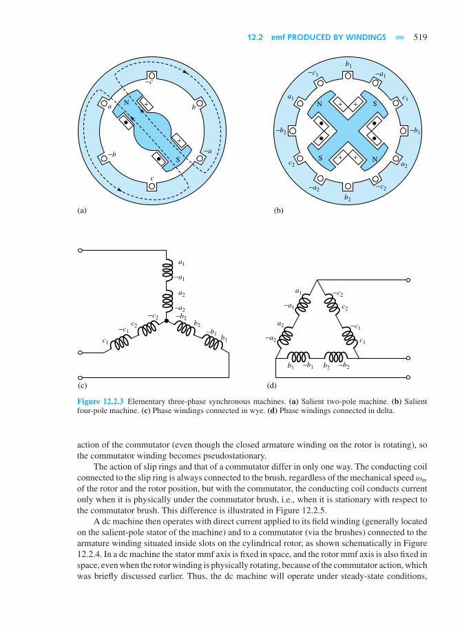
12.2 emf PRODUCED BY WINDINGS 519
S
Nb
c
−b
−c
a
(a) (b)
−a
+
+
b1
c1
−b1
−c1
a1
(c)
−a1
b2
c2
−b2
−c2
a2
−a2
+ +
++ N
N S
S
(d)
b1c1
−b1−c1
a1
−a1
b2c2
−b2−c2
a2
−a2
b1
c1
−b1
−c1
a1
−a1
b2
c2
−b2
−c2
a2
−a2
Figure 12.2.3 Elementary three-phase synchronous machines. (a) Salient two-pole machine. (b) Salientfour-pole machine. (c) Phase windings connected in wye. (d) Phase windings connected in delta.
action of the commutator (even though the closed armature winding on the rotor is rotating), sothe commutator winding becomes pseudostationary.
The action of slip rings and that of a commutator differ in only one way. The conducting coilconnected to the slip ring is always connected to the brush, regardless of the mechanical speed ωm
of the rotor and the rotor position, but with the commutator, the conducting coil conducts currentonly when it is physically under the commutator brush, i.e., when it is stationary with respect tothe commutator brush. This difference is illustrated in Figure 12.2.5.
A dc machine then operates with direct current applied to its field winding (generally locatedon the salient-pole stator of the machine) and to a commutator (via the brushes) connected to thearmature winding situated inside slots on the cylindrical rotor, as shown schematically in Figure12.2.4. In a dc machine the stator mmf axis is fixed in space, and the rotor mmf axis is also fixed inspace, even when the rotor winding is physically rotating, because of the commutator action, whichwas briefly discussed earlier. Thus, the dc machine will operate under steady-state conditions,

520 ELECTROMECHANICS
(a) (b)
+
++
++
++
ArmatureFieldcoil
Fieldstructure
Field
Brushes on commutator(not shown)
Quadrature axis,rotor mmf axis
Direct axis,stator mmfor field axis
Armature
Figure 12.2.4 Schematic representations of a dc machine. (a) Schematic arrangement. (b) Circuit represen-tation.
whatever the rotor speed ωm. The armature current in the armature winding is alternating. Theaction of the commutator is to change the armature current from a frequency governed by themechanical speed of rotation to zero frequency at the commutator brushes connected to theexternal circuit.
For the case of a dc machine with a flux per pole of φ, the total flux cut by one conductor inone revolution is given by φP , where P is the number of poles of the machine. If the speed ofrotation is n r/min, the emf generated in a single conductor is given by
e = φPn
60(12.2.14)
For an armature with Z conductors and α parallel paths, the total generated armature emf Ea isgiven by
Ea = PφnZ
60α(12.2.15)
Since the angular velocity ωm is given by 2πn/60, Equation (12.2.15) becomes
Ea = PZ
2παφωm = Kaφωm (12.2.16)
where Ka is the design constant given by PZ/2πα. The value obtained is the speed voltageappearing across the brush terminals in the quadrature axis (see Figure 12.2.4) due to the fieldexcitation producing φ in the direct axis. For this reason, in the schematic circuit representation ofa dc machine, the field axis and the brush axis are shown in quadrature, i.e., perpendicular to eachother. The generated voltage, as observed from the brushes, is the sum of the rectified voltages ofall the coils in series between brushes. If the number of coils is sufficiently large, the ripple in thewaveform of the armature voltage (as a function of time) becomes very small, thereby makingthe voltage direct or constant in magnitude.
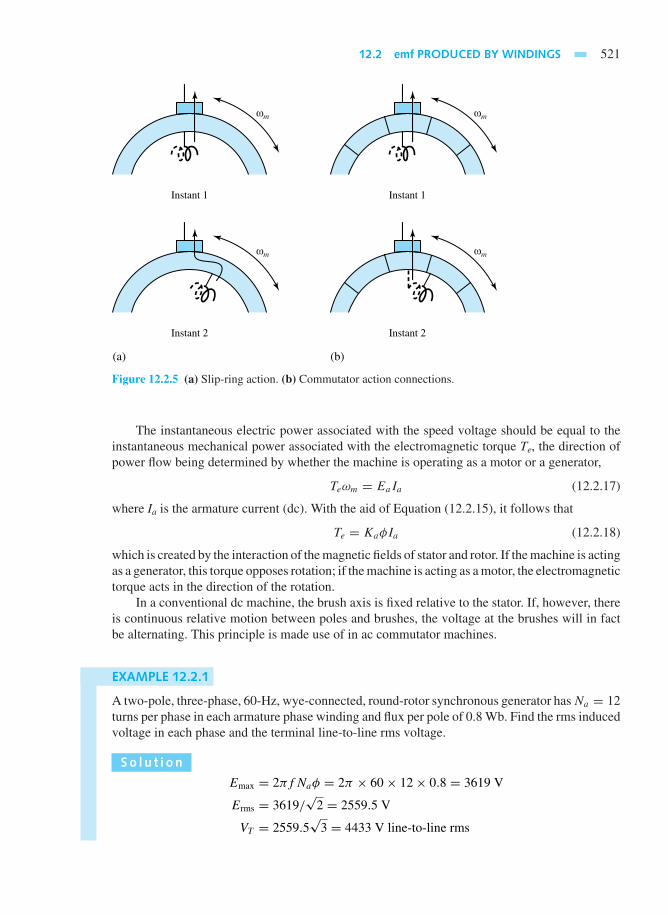
12.2 emf PRODUCED BY WINDINGS 521
Instant 1 Instant 1
ωm ωm
Instant 2 Instant 2
(a) (b)
ωm ωm
Figure 12.2.5 (a) Slip-ring action. (b) Commutator action connections.
The instantaneous electric power associated with the speed voltage should be equal to theinstantaneous mechanical power associated with the electromagnetic torque Te, the direction ofpower flow being determined by whether the machine is operating as a motor or a generator,
Teωm = EaIa (12.2.17)
where Ia is the armature current (dc). With the aid of Equation (12.2.15), it follows that
Te = KaφIa (12.2.18)
which is created by the interaction of the magnetic fields of stator and rotor. If the machine is actingas a generator, this torque opposes rotation; if the machine is acting as a motor, the electromagnetictorque acts in the direction of the rotation.
In a conventional dc machine, the brush axis is fixed relative to the stator. If, however, thereis continuous relative motion between poles and brushes, the voltage at the brushes will in factbe alternating. This principle is made use of in ac commutator machines.
EXAMPLE 12.2.1
A two-pole, three-phase, 60-Hz, wye-connected, round-rotor synchronous generator hasNa = 12turns per phase in each armature phase winding and flux per pole of 0.8 Wb. Find the rms inducedvoltage in each phase and the terminal line-to-line rms voltage.
So l u t i on
Emax = 2πfNaφ = 2π × 60× 12× 0.8 = 3619 V
Erms = 3619/√
2 = 2559.5 V
VT = 2559.5√
3 = 4433 V line-to-line rms

522 ELECTROMECHANICS
EXAMPLE 12.2.2
The armature of a four-pole dc machine has a simplex lap wound commutator winding (which hasthe number of parallel paths equal to the number of poles) with 120 two-turn coils. If the flux perpole is 0.02 Wb, calculate the dc voltage appearing across the brushes located on the quadratureaxis when the machine is running at 1800 r/min.
So l u t i on
This example can be solved by the direct application of Equation (12.2.15),
Ea = PφnZ
α × 60For our example, P = 4, φ = 0.02, n = 1800, the number of conductors Z = 120×2×2 = 480and the number of parallel paths α = 4 for the simplex lap winding (the same as the number ofpoles). Therefore,
Ea = 4× 0.02× 1800× 480
4× 60= 288 V dc
12.3 ROTATING MAGNETIC FIELDS
When a machine has more than two poles, only a single pair of poles needs to be consideredbecause the electric, magnetic, and mechanical conditions associated with every other pole pairare repetitions of those for the pole pair under consideration. The angle subtended by one pairof poles in a P-pole machine (or one cycle of flux distribution) is defined to be 360 electricaldegrees, or 2π electrical radians. So the relationship between the mechanical angle m and theangle in electrical units is given by
θ = P
2θm (12.3.1)
because one complete revolution has P/2 complete wavelengths (or cycles). In view of thisrelationship, for a two-pole machine, electrical degrees (or radians) will be the same as mechanicaldegrees (or radians).
In this section we set out to show that a rotating field of constant amplitude and sinusoidalspace distribution of mmf around a periphery of the stator is produced by a three-phase windinglocated on the stator and excited by balanced three-phase currents when the respective phasewindings are wound 2π/3 electrical radians (or 120 electrical degrees) apart in space. Let usconsider the two-pole, three-phase winding arrangement on the stator shown in Figure 12.3.1.The windings of the individual phases are displaced by 120 electrical degrees from each other inspace around the air-gap periphery. The reference directions are given for positive phase currents.The concentrated full-pitch coils, shown here for simplicity and convenience, do in fact representthe actual distributed windings producing sinusoidal mmf waves centered on the magnetic axesof the respective phases. Thus, these three sinusoidal mmf waves are displaced by 120 electricaldegrees from each other in space. Let a balanced three-phase excitation be applied with phasesequence a–b–c,
ia = I cos ωst; ib = I cos(ωst − 120°); ic = I cos(ωst − 240°) (12.3.2)
where I is the maximum value of the current, and the time t = 0 is chosen arbitrarily when thea-phase current is a positive maximum. Each phase current is an ac wave varying in magnitude
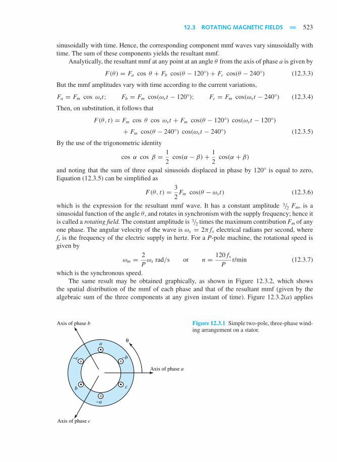
12.3 ROTATING MAGNETIC FIELDS 523
sinusoidally with time. Hence, the corresponding component mmf waves vary sinusoidally withtime. The sum of these components yields the resultant mmf.
Analytically, the resultant mmf at any point at an angle θ from the axis of phase a is given by
F(θ) = Fa cos θ + Fb cos(θ − 120°)+ Fc cos(θ − 240°) (12.3.3)
But the mmf amplitudes vary with time according to the current variations,
Fa = Fm cos ωst; Fb = Fm cos(ωst − 120°); Fc = Fm cos(ωst − 240°) (12.3.4)
Then, on substitution, it follows that
F(θ, t) = Fm cos θ cos ωst + Fm cos(θ − 120°) cos(ωst − 120°)
+ Fm cos(θ − 240°) cos(ωst − 240°) (12.3.5)
By the use of the trigonometric identity
cos α cos β = 1
2cos(α − β)+ 1
2cos(α + β)
and noting that the sum of three equal sinusoids displaced in phase by 120° is equal to zero,Equation (12.3.5) can be simplified as
F(θ, t) = 3
2Fm cos(θ − ωst) (12.3.6)
which is the expression for the resultant mmf wave. It has a constant amplitude 3/2 Fm, is asinusoidal function of the angle θ , and rotates in synchronism with the supply frequency; hence itis called a rotating field. The constant amplitude is 3/2 times the maximum contribution Fm of anyone phase. The angular velocity of the wave is ωs = 2πfs electrical radians per second, wherefs is the frequency of the electric supply in hertz. For a P-pole machine, the rotational speed isgiven by
ωm = 2
Pωs rad/s or n = 120fs
Pr/min (12.3.7)
which is the synchronous speed.The same result may be obtained graphically, as shown in Figure 12.3.2, which shows
the spatial distribution of the mmf of each phase and that of the resultant mmf (given by thealgebraic sum of the three components at any given instant of time). Figure 12.3.2(a) applies
Axis of phase a
Axis of phase c
Axis of phase b
+
+ +
θ
−a
a
−b
b
−c
c
Figure 12.3.1 Simple two-pole, three-phase wind-ing arrangement on a stator.

524 ELECTROMECHANICS
for that instant when the a-phase current is a positive maximum; Figure 12.3.2(b) refers to thatinstant when the b-phase current is a positive maximum; the intervening time corresponds to120 electrical degrees. It can be seen from Figure 12.3.2 that during this time interval, theresultant sinusoidal mmf waveform has traveled (or rotated through) 120 electrical degreesof the periphery of the stator structure carrying the three-phase winding. That is to say, theresultant mmf is rotating in synchronism with time variations in current, with its peak amplituderemaining constant at 3/2 times that of the maximum phase value. Note that the peak value ofthe resultant stator mmf wave coincides with the axis of a particular phase winding when thatphase winding carries its peak current. The graphical process can be continued for differentinstants of time to show that the resultant mmf is in fact rotating in synchronism with the supplyfrequency.
Although the analysis here is carried out only for a three-phase case, it holds good for any q-phase (q > 1; i.e., polyphase) winding excited by balanced q-phase currents when the respectivephases are wound 2π/q electrical radians apart in space. However, in a balanced two-phase case,note that the two phase windings are displaced 90 electrical degrees in space, and the phasecurrents in the two windings are phase-displaced by 90 electrical degrees in time. The constantamplitude of the resultant rotating mmf can be shown to be q/2 times the maximum contributionof any one phase. Neglecting the reluctance of the magnetic circuit, the corresponding flux densityin the air gap of the machine is then given by
Bg = µ0F
g(12.3.8)
where g is the length of the air gap.
Production of Rotating Fields from Single-Phase Windings
In this subsection we show that a single-phase winding carrying alternating current produces astationary pulsating flux that can be represented by two counterrotating fluxes of constant andequal magnitude.
Let us consider a single-phase winding, as shown in Figure 12.3.3(a), carrying alternatingcurrent i = I cos ωt . This winding will produce a flux-density distribution whose axis is fixedalong the axis of the winding and that pulsates sinusoidally in magnitude. The flux density alongthe coil axis is proportional to the current and is given by Bm cos ωt , where Bm is the peak fluxdensity along the coil axis.
Let the winding be on the stator of a rotating machine with uniform air gap, and let the fluxdensity be distributed sinusoidally around the air gap. Then the instantaneous flux density at anyposition θ from the coil axis can be expressed as
B(θ) = (Bm cos ωt) cos θ (12.3.9)
which may be rewritten by the use of the trigonometric identity following Equation (12.3.5) as
B(θ) = Bm
2cos(θ − ωt)+ Bm
2cos(θ + ωt) (12.3.10)
The sinusoidal flux-density distribution given by Equation (12.3.9) can be represented by avector Bm cos ωt of pulsating magnitude on the axis of the coil, as shown in Figure 12.3.3(a).Alternatively, as suggested by Equation (12.3.10), this stationary pulsating flux-density vector canbe represented by two counterrotating vectors of constant magnitude Bm/2, as shown in Figure12.3.3(b). While Equation (12.3.9) represents a standing space wave varying sinusoidally withtime, Equation (12.3.10) represents the two rotating components of constant and equal magnitude,
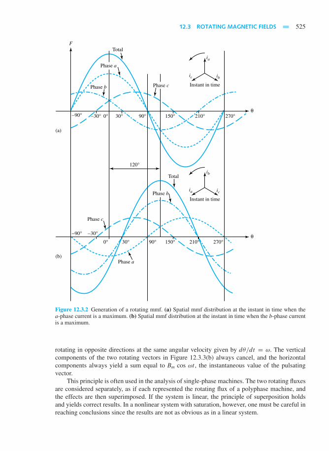
12.3 ROTATING MAGNETIC FIELDS 525
Phase a
Phase a
Phase b
Phase b
Phase c
Phase c
Total
(a)
(b)
Total
θ270°210°150°90°30°−30° 0°−90°
θ270°210°150°
120°
90°30°
−30°
0°
−90°
F
Instant in time
ia
ib
ic
Instant in time
ic
ia
ib
Figure 12.3.2 Generation of a rotating mmf. (a) Spatial mmf distribution at the instant in time when thea-phase current is a maximum. (b) Spatial mmf distribution at the instant in time when the b-phase currentis a maximum.
rotating in opposite directions at the same angular velocity given by dθ/dt = ω. The verticalcomponents of the two rotating vectors in Figure 12.3.3(b) always cancel, and the horizontalcomponents always yield a sum equal to Bm cos ωt , the instantaneous value of the pulsatingvector.
This principle is often used in the analysis of single-phase machines. The two rotating fluxesare considered separately, as if each represented the rotating flux of a polyphase machine, andthe effects are then superimposed. If the system is linear, the principle of superposition holdsand yields correct results. In a nonlinear system with saturation, however, one must be careful inreaching conclusions since the results are not as obvious as in a linear system.

526 ELECTROMECHANICS
ωt
(a) (b)
i = I cos ωtB = Bm cos ωt Bm cos ωt
ωt
ω
ω
Bm/2
Bm/2
Figure 12.3.3 Single-phase winding carrying alternating current, producing a stationary pulsating flux orequivalent rotating flux components.
12.4 FORCES AND TORQUES IN MAGNETIC-FIELD SYSTEMS
We mentioned earlier that the greater ease of storing energy in magnetic fields largely accountsfor the common use of electromagnetic devices for electromechanical energy conversion. In amagnetic circuit containing an air-gap region, the energy stored in the air-gap space is severaltimes greater than that stored in the iron portion, even though the volume of the air gap is only asmall fraction of that of the iron.
The energy-conversion process involves an interchange between electric and mechanicalenergy via the stored energy in the magnetic field. This stored energy, which can be determinedfor any configuration of the system, is a state function defined solely by functional relationshipsbetween variables and the final values of these variables. Thus, the energy method is a powerfultool for determining the coupling forces of electromechanics.
In a singly excited system, a change in flux density from a value of zero initial flux density toB requires an energy input to the field occupying a given volume,
Wm = vol∫ B1
0H dB (12.4.1)
which can also be expressed by
Wm =∫ λ1
0i(λ) dλ =
∫ φ1
0F(φ) dφ (12.4.2)
Note that the current i is a function of the flux linkages λ and that the mmf F is a function of theflux φ; their relations depend on the geometry of the coil, the magnetic circuit, and the magnetic
l Figure 12.4.1 Graphical interpretation of energyand coenergy in a singly excited nonlinear system.

12.4 FORCES AND TORQUES IN MAGNETIC-FIELD SYSTEMS 527
properties of the core material. Equations (12.4.1) and (12.4.2) may be interpreted graphically asthe area labeled energy in Figure 12.4.1. The other area, labeled coenergy in the figure, can beexpressed as
W ′m = vol
∫ H1
0B dH =
∫ i1
0λ(i) di =
∫ F1
0φ(F) dF (12.4.3)
For a linear system in which B and H, λ and i, or φ and F are proportional, it is easy to see thatthe energy and the coenergy are numerically equal. For a nonlinear system, on the other hand,the energy and the coenergy differ, as shown in Figure 12.4.1, but the sum of the energy and thecoenergy for a singly excited system is given by
Wm +W ′m = vol · B1H1 = λ1i1 = φ1 F1 (12.4.4)
The energy stored in a singly excited system can be expressed in terms of self-inductance,and that stored in a doubly excited system in terms of self and mutual inductances, for the circuit-analysis approach, as we pointed out earlier.
Let us now consider a model of an ideal (lossless) electromechanical energy converter thatis doubly excited, as shown in Figure 12.4.2, with two sets of electrical terminal pairs and onemechanical terminal, schematically representing a motor. Note that all types of losses have beenexcluded to form a conservative energy-conversion device that can be described by state functionsto yield the electromechanical coupling terms in electromechanics. A property of a conservativesystem is that its energy is a function of its state only, and is described by the same independentvariables that describe the state. State functions at a given instant of time depend solely on thestate of the system at that instant and not on past history; they are independent of how the systemis brought to that particular state.
We shall now obtain an expression for the electromagnetic torque Te from the principle ofconservation of energy, which, for the case of a sink of electric energy (such as an electric motor),may be expressed as
We = W +Wm
or in differential form as
dWe = dW + dWm (12.4.5)
where We stands for electric energy input from electrical sources, Wm represents the energy storedin the magnetic field of the two coils associated with the two electrical inputs, and W denotes themechanical energy output. We and W may further be written in their differential forms,
dWe = v1i1 dt + v2i2 dt (12.4.6)
i1
v1
i2
v2
Doubly excitedlossless electromechanicalenergy-conversion device
with conservative coupling fields
+
−
+ −
Te, θm = ωmt + θm(0)
Figure 12.4.2 Model of an ideal, doubly excited electromechanical energy converter.

528 ELECTROMECHANICS
dW = Te dθm (12.4.7)
where θm is expressed in electrical radians. Neglecting the winding resistances, the terminalvoltages are equal to the induced voltages given by
v1 = e1 = dλ1
dt(12.4.8)
v2 = e2 = dλ2
dt(12.4.9)
These are the volt-ampere equations, or the equations of motion, for the electrical side. Twovolt-ampere equations result because of the two sets of electrical terminals. Substituting theseinto Equation (12.4.6), one gets
dWe = i1 dλ1 + i2 dλ2 (12.4.10)
Substituting Equations (12.4.7) and (12.4.10) into the differential form of Equation (12.4.5), wehave
dWm = dWe − dW = i1 dλ1 + i2 dλ2 − Te dθm (12.4.11)
By specifying one independent variable for each of the terminal pairs, i.e., two electrical variables(flux linkages or currents) and one mechanical variable θm for rotary motion, we shall attempt toexpress Te in terms of the energy or the coenergy of the system.
Based on Equation (12.4.4) and the concepts of energy and coenergy, one has
Wm +W ′m = λ1i1 + λ 2i2 (12.4.12)
Expressing Equation (12.4.12) in differential form, the expression for the differential coenergyfunction dW ′
m is obtained as
dW ′m = d(λ1i1)+ d(λ2i2)− dWm
= λ1 di1 + i1 dλ1 + λ2 di2 + i2 dλ2 − dWm (12.4.13)
Substituting Equation (12.4.11) into Equation (12.4.13) and simplifying, one gets
dW ′m = λ1 di1 + λ2 di2 + Te dθm (12.4.14)
Expressing the coenergy as a function of the independent variables i1, i2, and θm,
W ′m = W ′
m(i1, i2, θm) (12.4.15)
the total differential of the coenergy function can be written as
dW ′m =
∂W ′m
∂i1di1 + ∂W ′
m
∂i2di2 + ∂W ′
m
∂θmdθm (12.4.16)
On comparing Equations (12.4.14) and (12.4.16) term by term, the expression for the electromag-netic torque Te is obtained as
Te = ∂W ′m(i1, i2, θm)
∂θm(12.4.17)
On the other hand, choosing the independent variables λ1, λ2, and θm, it can be shown that
Te = −∂Wm(λ1, λ2, θm)
∂θm(12.4.18)

12.4 FORCES AND TORQUES IN MAGNETIC-FIELD SYSTEMS 529
Depending on the convenience in a given situation, either Equation (12.4.17) or (12.4.18) can beused. For the case of a translational electromechanical system consisting of only one-dimensionalmotion, say, in the direction of the coordinate x, the torque Te and the angular displacement dθmare to be replaced by the force Fe and the linear displacement dx, respectively. Thus,
Fe = ∂W ′m(i1, i2, x)
∂x(12.4.19)
and
Fe = −∂Wm(λ1, λ2, x)
∂x(12.4.20)
For a linear magnetic system, however, the magnetic energy and the coenergy are alwaysequal in magnitude. Thus,
Wm = W ′m =
1
2λ1i1 + 1
2λ2i2 (12.4.21)
In linear electromagnetic systems, the relationships between flux linkage and currents (in a doublyexcited system) are given by
λ1 = L11i1 + L12i2 (12.4.22)
λ2 = L21i1 + L22i2 (12.4.23)
where L11 is the self-inductance of winding 1, L22 is the self-inductance of winding 2, andL12 = L21 = M is the mutual inductance between windings 1 and 2. All of these in-ductances are generally functions of the angle θm (mechanical or spatial variable) betweenthe magnetic axes of windings 1 and 2. Neglecting the iron-circuit reluctances, the electro-magnetic torque can be found from either the energy or the coenergy stored in the mag-netic field of the air-gap region by applying either Equation (12.4.17) or (12.4.18). For alinear system, the energy or the coenergy stored in a pair of mutually coupled inductors isgiven by
W ′m(i1, i2, θm) =
1
2L11i
21 + L12i1i2 + 1
2L22i
22 (12.4.24)
The instantaneous electromagnetic torque is then given by
Te = i21
2
dL11
dθm+ i1i2
dL12
dθm+ i2
2
2
dL22
dθm(12.4.25)
The first and third terms on the right-hand side of Equation (12.4.25), involving the angularrate of change of self-inductance, are the reluctance-torque terms; the middle term, involving theangular rate of change of mutual inductance, is the excitation torque caused by the interaction offields produced by the stator and rotor currents in an electric machine. It is this mutual inductancetorque (or excitation torque) that is most commonly exploited in practical rotating machines.Multiply excited systems with more than two sets of electrical terminals can be handled ina manner similar to that for two pairs by assigning additional independent variables to theterminals.
If none of the inductances is a function of the mechanical variable θm, no electromagnetictorque is developed. If, on the other hand, the self-inductances L11 and L22 are independent ofthe angle θm, the reluctance torque is zero and the torque is produced only by the mutual termL12(θm), as seen from Equation (12.4.25). Let us consider such a case in the following exampleon the basis of the coupled-circuit viewpoint (or coupled-coils approach).
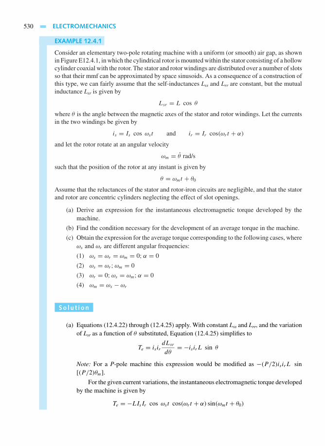
530 ELECTROMECHANICS
EXAMPLE 12.4.1
Consider an elementary two-pole rotating machine with a uniform (or smooth) air gap, as shownin Figure E12.4.1, in which the cylindrical rotor is mounted within the stator consisting of a hollowcylinder coaxial with the rotor. The stator and rotor windings are distributed over a number of slotsso that their mmf can be approximated by space sinusoids. As a consequence of a construction ofthis type, we can fairly assume that the self-inductances Lss and Lrr are constant, but the mutualinductance Lsr is given by
Lsr = L cos θ
where θ is the angle between the magnetic axes of the stator and rotor windings. Let the currentsin the two windings be given by
is = Is cos ωst and ir = Ir cos(ωr t + α)
and let the rotor rotate at an angular velocity
ωm = θ rad/s
such that the position of the rotor at any instant is given by
θ = ωmt + θ0
Assume that the reluctances of the stator and rotor-iron circuits are negligible, and that the statorand rotor are concentric cylinders neglecting the effect of slot openings.
(a) Derive an expression for the instantaneous electromagnetic torque developed by themachine.
(b) Find the condition necessary for the development of an average torque in the machine.
(c) Obtain the expression for the average torque corresponding to the following cases, whereωs and ωr are different angular frequencies:
(1) ωs = ωr = ωm = 0;α = 0
(2) ωs = ωr;ωm = 0
(3) ωr = 0;ωs = ωm;α = 0
(4) ωm = ωs − ωr
So l u t i on
(a) Equations (12.4.22) through (12.4.25) apply. With constant Lss and Lrr, and the variationof Lsr as a function of θ substituted, Equation (12.4.25) simplifies to
Te = is irdLsr
dθ= −is irL sin θ
Note: For a P-pole machine this expression would be modified as −(P/2)isirL sin[(P/2)θm].
For the given current variations, the instantaneous electromagnetic torque developedby the machine is given by
Te = −LIsIr cos ωst cos(ωr t + α) sin(ωmt + θ0)

12.4 FORCES AND TORQUES IN MAGNETIC-FIELD SYSTEMS 531
δr
δs
δ
++
+ + + + + + +
+ + +
Magnetic axisof stator
Magnetic axis of rotor
(a) (b)
Rotorwinding
Stator winding
++ −−
Stator coil
Rotor coil
θ
(c)
Fs sin δ = F sin δr
Fr sin δ = F sin δs
Fr
Fs
F
θ
Figure E12.4.1 Elementary two-pole rotating machine with uniform air gap. (a) Winding distribution.(b) Schematic representation. (c) Vector diagram of mmf waves.
Using trigonometric identities, the product of the three trigonometric terms in thisequation may be expressed to yield
Te = −LIsIr4
[sin [ωm + (ωs + ωr)] t + α + θ0+ sin [ωm − (ωs + ωr)] t − α + θ0+ sin [ωm + (ωs − ωr)] t − α + θ0+ sin [ωm − (ωs − ωr)] t + α + θ0]
(b) The average value of each of the sinusoidal terms in the previous equation is zero, unlessthe coefficient of t is zero in that term. That is, the average torque (Te)av developed bythe machine is zero unless
ωm = ±(ωs ± ωr)
which may also be expressed as
|ωm| = |ωs ± ωr |

532 ELECTROMECHANICS
(c) (1) The excitations are direct currents Is and Ir. For the given conditions of ωs = ωr =ωm = 0 and α = 0,
Te = −LIsIr sin θ0
which is a constant. Hence,
(Te)av = −LIsIr sin θ0
The machine operates as a dc rotary actuator, developing a constant torque againstany displacement θ0 produced by an external torque applied to the rotor shaft.
(2) With ωs = ωr , both excitations are alternating currents of the same frequency. Forthe conditions ωs = ωr and ωm = 0,
Te = −LIsIr
4[sin(2ωst + α + θ0)+ sin(−2ωst − α + θ0)+ sin(−α + θ0)
+ sin(α + θ0)]
The machine operates as an ac rotary actuator, and the developed torque is fluctu-ating. The average value of the torque is
(Te)av = −LIsIr
2sin θ0 cos α
Note that α becomes zero if the two windings are connected in series, in which casecos α becomes unity.
(3) With ωr = 0, the rotor excitation is a direct current Ir. For the conditions ωr =0, ωs = ωm, and α = 0,
Te = −LIsIr
4[sin(2ωst + θ0)+ sin θ0 + sin(2ωst + θ0)+ sin θ0]
or
Te = −LIsIr
2[sin(2ωst + θ0)+ sin θ0)]
The device operates as an idealized single-phase synchronous machine, and theinstantaneous torque is pulsating. The average value of the torque is
(Te)av = −LIsIr
2sin θ0
since the average value of the double-frequency sine term is zero. If the machineis brought up to synchronous speed (ωm = ωs), an average unidirectional torque isestablished. Continuous energy conversion takes place at synchronous speed. Notethat the machine is not self-starting, since an average unidirectional torque is notdeveloped at ωm = 0 with the specified electrical excitations.
(4) With ωm = ωs − ωr , the instantaneous torque is given by
Te = −LIsIr
4[sin(2ωst + α + θ0)+ sin(−2ωrt − α + θ0)
+ sin(2ωst − 2ωrt − α + θ0)+ sin(α + θ0)]

12.4 FORCES AND TORQUES IN MAGNETIC-FIELD SYSTEMS 533
The machine operates as a single-phase induction machine, and the instantaneoustorque is pulsating. The average value of the torque is
(Te)av = −LIsIr
4sin(α + θ0)
If the machine is brought up to a speed of ωm = ωs − ωr , an average unidirec-tional torque is established, and continuous energy conversion takes place at theasynchronous speed of ωm. Again, note that the machine is not self-starting, sincean average unidirectional torque is not developed at ωm = 0 with the specifiedelectrical excitations.
The pulsating torque, which may be acceptable in small machines, is, in general,an undesirable feature in a rotating machine working as either a generator or amotor, since it may result in speed fluctuation, vibration, noise, and a waste ofenergy. In magnetic-field systems excited by single-phase alternating sources, thetorque pulsates while the speed is relatively constant. Consequently, pulsating powerbecomes a feature. This calls for improvement; in fact, by employing polyphasewindings and polyphase sources, constant power is developed in a balanced system.
EXAMPLE 12.4.2
Consider an electromagnet, as shown in Figure E12.4.2, which is used to support a solid piece ofsteel and is excited by a coil of N = 1000 turns carrying a current i = 1.5 A. The cross-sectionalarea of the fixed magnetic core is A = 0.01 m2. Assume magnetic linearity, infinite permeabilityof the magnetic structure, and negligible fringing in the air gap.
(a) Develop a general expression for the force f acting to pull the bar toward the fixedmagnetic core, in terms of the stored energy, from the basic principle of conservation ofenergy.
(b) Determine the force that is required to support the weight from falling for x = 1.5 mm.
fe
Movable steel
N turns
i v
x
+ −
Fixed core
Figure E12.4.2 Electromagnet.

534 ELECTROMECHANICS
So l u t i on
(a) A change in the energy stored in the electromagnetic field dWm is equal to the sum ofthe incremental work done by the electric circuit and the incremental work done by themechanical system. Thus,
dWm = ei dt − fe dx = dλ
dti dt − fe dx = i dλ− fe dx
or
fe dx = i dλ− dWm
where e is the electromotive force across the coil and the negative sign is due to thesign convention shown in Figure E.12.4.2. Noting that the flux in the magnetic structuredepends on two independent variables, namely, the current i through the coil and thedisplacement x of the bar, one can rewrite the equation,
fe dx = i
(∂λ
∂idi + ∂λ
∂xdx
)−(∂Wm
∂idi + ∂Wm
∂xdx
)
where Wm is a function of i and x. Since i and x are independent variables, one gets
fe = i∂λ
∂x− ∂Wm
∂xand 0 = i
∂λ
∂i− ∂Wm
∂i
We can then see that
fe = ∂
∂x(iλ−Wm) = ∂
∂xW ′
m
where W ′m is the coenergy, which is equal to the energy Wm in structures that are
magnetically linear.
The force f acting to pull the bar toward the fixed magnet core is given by
f = −fe = −∂Wm
∂x
The stored energy in a linear magnetic structure is given by
Wm = φF2= φ2R (x)
2
where φ is the flux, F is the mmf, and R (x) is the reluctance, which is a function ofdisplacement. Finally, we get
f = −∂Wm
∂x= −φ2
2
dR (x)
dx
(b) The reluctance of the air gaps in the magnetic structure is given by
R (x) = 2x
µ0A= 2x
4π × 10−7 × 0.01= x
0.6285× 10⁻⁸
The magnitude of the force in the air gap is then given by

12.4 FORCES AND TORQUES IN MAGNETIC-FIELD SYSTEMS 535
|f | = φ2
2
dR (x)
dx= 1
2
(Ni
R
)2dRdx
= i2
2
N2
R 2
dRdx
= 1.52
210002 0.6285× 10−8
x2
For x = 1.5 mm = 1.5× 10⁻³ m,
|f | = 1.52
210002 0.6285× 10⁻⁸
(1.5× 10⁻³)2= 3142.5 N
The student should recognize the practical importance of force-generating capabilitiesof electromechanical transducers.
EXAMPLE 12.4.3
Solenoids find application in a variety of electrically controlled valves. The magnetic structureshown in Figure E12.4.3 is a simplified representation of a solenoid in which the flux in the airgap activates the motion of the iron plunger.
(a) Develop a general expression for the force exerted on the iron plunger and comment onits dependence on position x.
(b) Determine the current through the coil of N = 100 turns to pull the plunger to x = a,given that a = 1 cm, lg = 1 mm, and the spring constant is k = 1 N/m. Assume thepermeability of the magnetic structure to be infinite and neglect fringing.
Spring 1)
Nonmagneticbushing material
Movable ironplunger
N turns
i
2a
a
aa
x x = 0
lg
a
Fixed magneticcore structure
(µ ∞)
(µr
Figure E12.4.3 Simplified representation of asolenoid.

536 ELECTROMECHANICS
So l u t i on
(a) The force in the air gap can be expressed by
f = −1
2φ2 dR
dx
(See Example 12.4.2.) The gap reluctance, which in this case is due to the nonmagneticbushing, is given by
R = 2Rg = 2lgµ0ax
where the area ax is variable, depending on the position of the plunger, and lg is thethickness of the bushing on either side of the plunger. The air-gap magnetic flux is givenby
φ = FR= Ni
R= µ0Niax
2lg
Now,
dRdx
= d
dx
(2lgµ0ax
)= −2lg
µ0ax2
The force is then given by
f = −1
2φ2 dR
dx= −1
2
(µ0Niax
2lg
)2 ( −2lgµ0ax2
)or
f = 1
4
µ0a
lg(Ni)2
which is independent of the position x, and is a constant for a given exciting mmf andgeometry.
(b) For x = a = 1 cm = 0.01 m,
f = kx = 1× 0.01 = 1
4
4π × 10−7 × 0.01
0.001(100 i)2
or
i2 = 4× 0.001× 0.01
4π × 10−7 × 0.01
1
(100)2= 0.3182
or
i = 0.564 A
The student should recognize the practical importance of determining the approximatemmf or current requirements for electromechanical transducers.
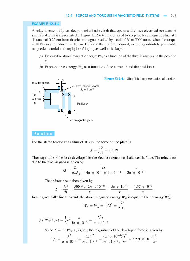
12.4 FORCES AND TORQUES IN MAGNETIC-FIELD SYSTEMS 537
EXAMPLE 12.4.4
A relay is essentially an electromechanical switch that opens and closes electrical contacts. Asimplified relay is represented in Figure E12.4.4. It is required to keep the fenomagnetic plate at adistance of 0.25 cm from the electromagnet excited by a coil of N = 5000 turns, when the torqueis 10 N · m at a radius r = 10 cm. Estimate the current required, assuming infinitely permeablemagnetic material and negligible fringing as well as leakage.
(a) Express the stored magnetic energyWm as a function of the flux linkage λ and the positionx.
(b) Express the coenergy W ′m as a function of the current i and the position x.
x = lg
i
Radius r
Cross–sectional areaAg = 1 cm2
Electromagnet
Ferromagnetic plate
N turns
Figure E12.4.4 Simplified representation of a relay.
So l u t i on
For the stated torque at a radius of 10 cm, the force on the plate is
f = 10
0.1= 100 N
The magnitude of the force developed by the electromagnet must balance this force. The reluctancedue to the two air gaps is given by
Q = 2x
µ0Ag
= 2x
4π × 10−7 × 1× 10−4= x
2π × 10−11
The inductance is then given by
L = N2
R= 50002 × 2π × 10−11
x= 5π × 10−4
x= 1.57× 10⁻³
x
In a magnetically linear circuit, the stored magnetic energy Wm is equal to the coenergy W ′m,
Wm = W ′m =
1
2Li2 = 1
2
λ2
L
(a) Wm(λ, x) = 1
2λ2 x
5π × 10−4= λ2x
π × 10−3
Since f = −∂Wm(λ, x)/∂x, the magnitude of the developed force is given by
|f | = λ2
π × 10−3= (Li)2
π × 10−3= (5π × 10−4)2i2
π × 10−3 × x2= 2.5 π × 10−4 i
2
x2
538 ELECTROMECHANICS
For x = 0.25 cm and |f | = 100 N,
i2 = 100(0.25× 10⁻²)2
2.5π × 10−4= 2.5
π= 0.795
or
i = 0.89 A
(b) W ′m(i, x) =
1
2Li2 = 1
2
5π × 10−4
xi2
Since f = ∂W ′m(i, x)/∂x, the magnitude of the developed force is given by
|f | = 1
2
5π × 10−4
x2i2
For x = 0.25 cm and |f | = 100 N,
i2 = 100× 2× (0.25× 10−2)2
5π × 10−4= 2.5
π= 0.795
or
i = 0.89 A
Such relays find common application in industrial practice to remotely switch largeindustrial loads. The student should recognize that a relatively low-level current can beused to operate the relay, which in turn controls the opening and closing of a circuit thatcarries large currents.
Starting with the flux linkages given by Equations (12.4.22) and (12.4.23), one can developthe volt–ampere equations for the stator and rotor circuits. While the voltage and torque equationsfor the idealized elementary machine of Example 12.4.1 with a uniform air gap are now obtainedfrom the coupled-circuit viewpoint, these can also be formulated from the magnetic-field viewpointbased on the interaction of the magnetic fields of the stator and rotor windings in the air gap.
Since the mmf waves of the stator and rotor are considered spatial sine waves, they can berepresented by the space vectors Fs and Fr , drawn along the magnetic axes of the stator androtor mmf waves, as in Figure E12.4.1, with the phase angle δ (in electrical units) between theirmagnetic axes. The resultant mmf F acting across the air gap is also a sine wave, given by thevector sum of Fs and Fr , so that
F 2 = F 2s + F 2
r + 2FsFr cos δ (12.4.26)
where F’s are the peak values of the mmf waves. Assuming the air-gap field to be entirely radial,the resultant H -field is a sinusoidal space wave whose peak is given by
Hpeak = F
g(12.4.27)
where g is the radial length of the air gap. Because of linearity, the coenergy is equal to the energy.The average coenergy density obtained by averaging over the volume of the air-gap region is
(w′)av = µ0
2(average value of H 2) = µ0
2
H 2peak
2= µ0
4
F 2
g2(12.4.28)
12.5 BASIC ASPECTS OF ELECTROMECHANICAL ENERGY CONVERTERS 539
since the average value of the square of a sine wave is one-half of the square of its peak value.The total coenergy for the air-gap region is then given by
W ′ = (w′)av(volume of air-gap region) = µ0
4
F 2
g2πDlg (12.4.29)
where D is the average diameter at the air gap and l is the axial length of the machine. Equation(12.4.29) may be rewritten as follows by using Equation (12.4.26):
W ′ = πDlµ0
4g(F 2
s + F 2r + 2FsFr cos δ) (12.4.30)
The torque in terms of the interacting magnetic fields is obtained by taking the partial derivativeof the field coenergy with respect to the angle δ. For a two-pole machine, such a torque is given by
Te = ∂W ′
∂δ= −πDlµ0
2gFsFr sin δ = −KFsFr sin δ (12.4.31)
in which K is a constant determined by the dimensions of the machine. The torque for a P-polecylindrical machine with a uniform air gap is then
Te = −P
2KFsFr sin δ (12.4.32)
Equations (12.4.31) and (12.4.32) have shown that the torque is proportional to the peak valuesof the interacting stator and rotor mmfs and also to the sine of the space-phase angle δ betweenthem (expressed in electrical units). The interpretation of the negative sign is the same as before, inthat the fields tend to align themselves by decreasing the displacement angle δ between the fields.
Equation (12.4.32) shows that it is possible to obtain a constant torque, varying neither withtime nor with rotor position, provided that the two mmf waves are of constant amplitude andhave constant angular displacement from each other. While it is easy to conceive of the two mmfwaves having constant amplitudes, the question would then be how to maintain a constant anglebetween the stator and rotor mmf axes if one winding is stationary and the other is rotating. Threepossible answers arise:
1. If the stator mmf axis is fixed in space, the rotor mmf must also be fixed in space, evenwhen the rotor winding is physically rotating, as is the case with a dc machine.
2. If the rotor mmf axis is fixed relative to the rotor, the stator mmf axis must rotate atthe rotor speed relative to the stationary stator windings, as is the case with a polyphasesynchronous machine.
3. The two mmf axes must rotate at such speeds relative to their windings that they remainstationary with respect to each other, as is the case with a polyphase induction machine(which we will explain later).
12.5 BASIC ASPECTS OF ELECTROMECHANICAL ENERGY CONVERTERS
Whereas detailed differences and particularly challenging problems emerge among various ma-chine types, this section briefly touches on the interrelated problems that are common to allmachine types, such as losses and efficiency, ventilation and cooling, machine ratings, magneticsaturation, leakage and harmonic fluxes, and machine applications. Various standards, developedby IEEE (Institute of Electrical and Electronics Engineers), NEMA (National Electrical Man-ufacturers Association), ANSI (American National Standards Institute), and IEC (InternationalElectrotechnical Commission), deal with machine ratings, insulation and allowable temperaturerise, testing methods, losses, and efficiency determination.

540 ELECTROMECHANICS
Besides the stator and rotor iron-core losses, friction and windage losses (which are generallyfunctions of machine speed, and are usually assumed to be practically constant for small speedvariations) are included in no-load rotational losses, which are effectively constant. Besidescopper losses (stator and rotor winding I2R losses), stray-load losses (which arise from variouscauses that are not usually accounted for, and are usually taken to be about 0.5 to 5% of themachine output) are included for the determination of efficiency (= output/input).
Much of the considerable progress made over the years in electric machinery is due to theimprovements in the quality and characteristics of steel and insulating materials, as well as toinnovative cooling methods. Modern large turbo alternators have direct water cooling (coolingwater circulated through hollow passages in their conductors, being in direct contact with thecopper conductors) in the stator (and the rotor in a few cases) and hydrogen cooling (withhydrogen under 1 to 5 atmospheres of pressure) in the rotor. With hydrogen under pressure,sealing the bearings appropriately needs particular attention for turbogenerators. For hydroelectricgenerators, on the other hand, designing the thrust bearings for vertical mounting becomes aprominent issue.
In general, every machine has a nameplate attached to the frame inscribed with relevantinformation regarding voltage, current, power, power factor, speed, frequency, phases, andallowable temperature rise. The nameplate rating is the continuous rating, unless otherwisespecified, such as short-time rating. Motors are rated in hp (horsepower); dc generators in kW;and alternators and transformers in terms of kVA rather than kW (because their losses and heatingare approximately determined by the voltage and current, regardless of the power factor). Thephysical size and cost of ac power-system apparatus are roughly proportional to the kVA rating.
In order to fully utilize the magnetic properties of the iron and optimize the machine design,the machine iron is worked at fairly saturated levels of flux density, such that the normal operatingpoint on the open circuit is near the knee of the open-circuit characteristic (or the no-loadsaturation curve, which is similar to the magnetization B–H characteristic). Magnetic saturationdoes influence the machine performance to a considerable degree. Leakage and harmonic fluxes,which exist in addition to the mutual flux (generally assumed to be sinusoidally distributed) andwhich may develop parasitic torques causing vibration and noise, also have to be considered.Accounting for, and including, these effects becomes too involved to be discussed here.
For motors the major consideration is the torque–speed characteristics. The requirementsof motor loads generally vary from one application to another. Some may need constant speedor horsepower, while some others may require adjustable varying speeds with different torquecapabilities. For any motor application, the starting torque, maximum torque, and runningcharacteristics (along with current requirements) should be looked into.
For generators it is the volt–ampere, or voltage–load, characteristics. For machines in general,it is also vital to know the limits between which characteristics can be varied and how to obtainsuch variations. Relevant economic features, such as efficiency, power factor, relative costs, andthe effect of losses on heating and machine rating, need to be investigated.
Finally, since a generator or a motor may only be one component of a complicated modernpower system, system-related dynamic applications and behavior (both steady-state and transient-state) and proper models to study such behavior become very important when designing electricmachines.
12.6 LEARNING OBJECTIVES
The learning objectives of this chapter are summarized here, so that the student can check whetherhe or she has accomplished each of the following.

12.7 PRACTICAL APPLICATION: A CASE STUDY 541
• Basic principles of electromechanical energy conversion, including induction, interaction,alignment, and torque production.
• Simplified analysis of electromechanical transducers, such as electromagnets, position andvelocity sensors, relays, solenoids, and loudspeakers, which convert electric signals tomechanical forces, or mechanical motion to electric signals.
• Calculating the emf produced in ac and dc machines.
• Generation of rotating magnetic fields.
• Evaluating forces and torques in magnetic-field systems, from the coupled-circuit viewpointand the magnetic-field viewpoint.
• Basic aspects of motors and generators.
12.7 PRACTICAL APPLICATION: A CASE STUDY
Sensors or Transducers
In almost all engineering applications there arises a need to measure some physical quantities, suchas positions, displacements, speeds, forces, torques, temperatures, pressures, or flows. Devicesknown as sensors or transducers convert a physical quantity to a more readily manipulatedelectrical quantity (such as voltage or current), such that changes in physical quantity usuallyproduce proportional changes in electrical quantity. The direct output of the sensor may oftenneed additional manipulation, known as signal conditioning, for the output to be in a usefulform free from noise and intereference. The conditioned sensor signal may then be sampled andconverted to digital form and stored in a computer for additional manipulation or display. Atypical computer-based measurement system using a sensor is represented in block diagram formin Figure 12.7.1. Table 12.7.1 lists various sensors and their uses.
TABLE 12.7.1 Sensors classified according to variable sensed
Variable Sensed Sensor or Transducer
Variations in dimensions due to motion Strain gaugeResistive potentiometerVariable reluctance sensorMoving-coil transducerSeismic sensor
Temperature ThermocoupleResistance temperature detectorRadiation detector
Force, torque, and pressure Capacitive sensorPiezoelectric transducer
Flow Magnetic flow meterTurbine flow meterHot-wire anemometerUltrasonic sensor
Light intensity Photoelectric sensor
Humidity Semiconductor transducer
Chemical composition Solid-state gas sensor
Liquid level Differential-pressure transducer

542 ELECTROMECHANICS
Data gathering with various sensors and data reduction have become much easier, automatic,and quite sophisticated due to the advent of the computer, since the computer can monitor manyinputs, process and record data, furnish displays, and produce control outputs.
Physicalphenomenonor stimulus
Outputdisplay
Digitalcomputer
with interface
Analog-to-digital
conversionSampling
Signalconditioning
Sensor ortransducer
Figure 12.7.1 Block diagram of measurement system using a sensor.
PROBL EMS
12.1.1 (a) Show by applying Ampere’s circuital lawthat the magnetic field associated with a longstraight, current-carrying wire is given byBφ = µ0I/(2πr), where the subscript φ de-notes the φ-component in the circular cylin-drical coordinate system,µ0 is the free-spacepermeability, I is the current carried by thewire, and r is the radius from the current-carrying wire. What is the net force on thewire due to the interaction of the B-field(produced by the current I) and the current I?
(b) A magnetic force exists between two adja-cent, parallel, current-carrying wires. Let I1
and I2 be the currents carried by the wiresand r the separation between them. Use theresult of part (a) to find the force between thewires. Discuss the nature of the force whenthe wires carry currents in the same direction,and in opposite directions.
*12.1.2 A rectangular loop is placed in the field of an in-finitely long straight conductor carrying a currentof I amperes, as shown in Figure P12.1.2. Find
an expression for the total flux linking the loop,assuming a medium of permeability µ.
12.1.3 Consider a conducting loop of length l and widthw, as shown in Figure P12.1.3, rotated about itsaxis (shown by the broken line) at a speed of ωm
rad/s under the influence of a magnetic field B.
(a) Obtain an expression for the induced emf,assuming the angle θm is zero at t = 0 andθm = ωmt .
(b) If a resistor R is connected across terminalsa–a′, explain what happens and how the prin-ciple of energy conservation is satisfied.
12.1.4 A coil is formed by connecting 15 conductingloops, or turns, in series. Each loop has lengthl = 2.5 m and width w = 10 cm. The 15-turncoil is rotated at a constant speed of 30 r/s (or1800 r/min) in a magnetic field of density B = 2T. The configuration of Figure P12.1.3 applies.
(a) Find the induced emf across the coil.
(b) Determine the average power delivered tothe resistor R = 500 , which is connectedbetween the terminals of the coil.
×××××××
r1
r2
r
B
l
I
×××××××
dr
×××××××
Figure P12.1.2

PROBLEMS 543
y
x
B
aa
a'a'
θm
ωm
ωm
y
z
l
w
B
Axis ofrotation
Figure P12.1.3 Rotating conducting loop.
(c) Calculate the average mechanical torqueneeded to turn the coil and generate powerfor the resistor. Identify the action of thedevice as that of a motor or a generator.
12.1.5 The machine of Problem 12.1.4 can be used as amotor. Let the terminals of the coil be connectedto a voltage source of 1 kV rms. If the motor runsat 1800 r/min and draws a current of 2 A, find thetorque supplied to the mechanical load.
12.1.6 The 50-turn coil in the configuration of FigureP12.1.3 is rotated at a constant speed of 300r/min. The axis of rotation is perpendicular toa uniform magnetic flux density of 0.1 T. Theloop has width w = 10 cm and length l = 1 m.Compute:
(a) The maximum flux passing through the coil.
(b) The flux linkage as a function of time.
(c) The maximum instantaneous voltage in-duced in the coil.
(d) The time-average value of the induced volt-age.
(e) The induced voltage when the plane of thecoil is 30° from the vertical.
*12.1.7 A 100-turn coil in the configuration of FigureP12.1.3 is rotated at a constant speed of 1200r/min in a magnetic field. The rms induced volt-age across the coil is 1 kV, and each turn has alength l = 112.5 cm and a width w = 10 cm.Determine the required value of the flux density.
12.1.8 A sectional view of a cylindrical iron-cladplunger magnet is shown in Figure P12.1.8. Thesmall air gap between the sides of the plungerand the iron shell is uniform and 0.25 mm long.Neglect leakage and fringing, and consider theiron to be infinitely permeable. The coil has 1000
turns and carries a direct current of 3 A. Computethe pull on the plunger for g = 1.25 cm.
12.1.9 Figure E12.1.1 can also be considered as a simplemodel of a magnetically operated relay that iscommonly used for the automatic control andprotection of electric equipment. Consider thecore and armature (shown as “Bar” in FigureE12.1.1) of the relay to be constructed out ofinfinitely permeable magnetic material. The corehas a circular cross section and is 1.25 cm indiameter, while the armature has a rectangularcross section. The armature is so supported thatthe two air gaps are always equal and of uniformlength over their areas. A spring (not shown inthe figure), whose force opposes the magneticpull, restrains the motion of the armature. If theoperating coil has 1800 turns carrying a currentof 1 A, and the gaps are set at 0.125 cm each, findthe pull that must be exerted by the spring. Youmay neglect leakage and fringing.
12.1.10 The coil is placed so that its axis of revolutionis perpendicular to a uniform field, as shown inFigure P12.1.10. If the flux per pole is 0.02 Wb,and the coil, consisting of 2 turns, is revolving at1800 r/min, compute the maximum value of thevoltage induced in the coil.
12.2.1 An elementary two-pole, single-phase, synchro-nous machine, as illustrated in Figure P12.2.1,has a field winding on its rotor and an armaturewinding on its stator, with Nf = 400 turns andNa = 50 turns, respectively. The uniform air gapis of length 1 mm, while the armature diameter is0.5 m, and the axial length of the machine is 1.5m. The field winding carries a current of 1 A (dc)and the rotor is driven at 3600 r/min. Determine:
(a) The frequency of the stator-induced voltage.
(b) The rms-induced voltage in the stator wind-ing.
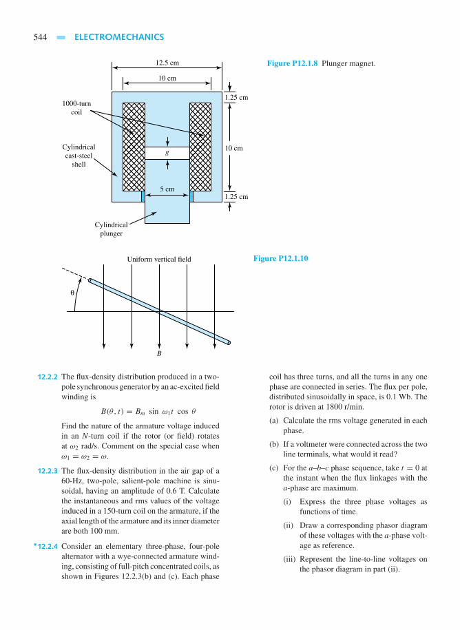
544 ELECTROMECHANICS
Cylindricalcast-steel
shell
1000-turncoil
Cylindricalplunger
12.5 cm
10 cm
1.25 cm
g
1.25 cm
10 cm
5 cm
Figure P12.1.8 Plunger magnet.
B
Uniform vertical field
θ
Figure P12.1.10
12.2.2 The flux-density distribution produced in a two-pole synchronous generator by an ac-excited fieldwinding is
B(θ, t) = Bm sin ω1t cos θ
Find the nature of the armature voltage inducedin an N-turn coil if the rotor (or field) rotatesat ω2 rad/s. Comment on the special case whenω1 = ω2 = ω.
12.2.3 The flux-density distribution in the air gap of a60-Hz, two-pole, salient-pole machine is sinu-soidal, having an amplitude of 0.6 T. Calculatethe instantaneous and rms values of the voltageinduced in a 150-turn coil on the armature, if theaxial length of the armature and its inner diameterare both 100 mm.
*12.2.4 Consider an elementary three-phase, four-polealternator with a wye-connected armature wind-ing, consisting of full-pitch concentrated coils, asshown in Figures 12.2.3(b) and (c). Each phase
coil has three turns, and all the turns in any onephase are connected in series. The flux per pole,distributed sinusoidally in space, is 0.1 Wb. Therotor is driven at 1800 r/min.
(a) Calculate the rms voltage generated in eachphase.
(b) If a voltmeter were connected across the twoline terminals, what would it read?
(c) For the a–b–c phase sequence, take t = 0 atthe instant when the flux linkages with thea-phase are maximum.
(i) Express the three phase voltages asfunctions of time.
(ii) Draw a corresponding phasor diagramof these voltages with the a-phase volt-age as reference.
(iii) Represent the line-to-line voltages onthe phasor diagram in part (ii).

PROBLEMS 545
ωm
θm
Stator magnetic axis
Rotormagnetic axis
Figure P12.2.1 Rotating machine with uniform airgap.
(iv) Obtain the time functions of the line-to-line voltages.
12.2.5 A wye-connected, three-phase, 50-Hz, six-polesynchronous alternator develops a voltage of1000 V rms between the lines when the rotor dcfield current is 3 A. If this alternator is to generate60-Hz voltages, find the new synchronous speed,and calculate the new terminal voltage for thesame field current.
12.2.6 Determine the synchronous speed in revolutionsper minute and the useful torque in newton-meters of a 200-hp, 60-Hz, six-pole synchronousmotor operating at its rated full load (1 hp∼= 746W).
12.2.7 From a three-phase, 60-Hz system, through amotor–generator set consisting of two directlycoupled synchronous machines, electric poweris supplied to a three-phase, 50-Hz system.
(a) Determine the minimum number of poles forthe motor.
(b) Determine the minimum number of poles forthe generator.
(c) With the number of poles decided, find thespeed in r/min at which the motor–generatorset will operate.
*12.2.8 Two coupled synchronous machines are used asa motor–generator set to link a 25-Hz system toa 60-Hz system. Find the three highest speeds atwhich this linkage would be possible.
12.2.9 A 10-turn square coil of side 200 mm is mountedon a cylinder 200 mm in diameter. If the cylinderrotates at 1800 r/min in a uniform 1.2-T field,determine the maximum value of the voltageinduced in the coil.
12.3.10 A four-pole dc machine with 728 active conduc-tors and 30 mWb flux per pole runs at 1800 r/min.
(a) If the armature winding is lap wound, findthe voltage induced in the armature, giventhat the number of parallel paths is equal tothe number of poles for lap windings.
(b) If the armature is wave wound, calculate thevoltage induced in the armature, given thatthe number of parallel paths is equal to 2 forwave windings.
(c) If the lap-wound armature is designed tocarry a maximum line current of 100 A, com-pute the maximum electromagnetic powerand torque developed by the machine.
(d) If the armature were to be reconnected aswave wound, while limiting per-path currentto the same maximum as in part (c), willeither the maximum developed power or thetorque be changed from that obtained in part(c)?
12.2.11 A four-pole, lap-wound armature has 144 slotswith two coil sides per slot, each coil havingtwo turns. If the flux per pole is 20 mWb andthe armature rotates at 720 r/min, calculate the
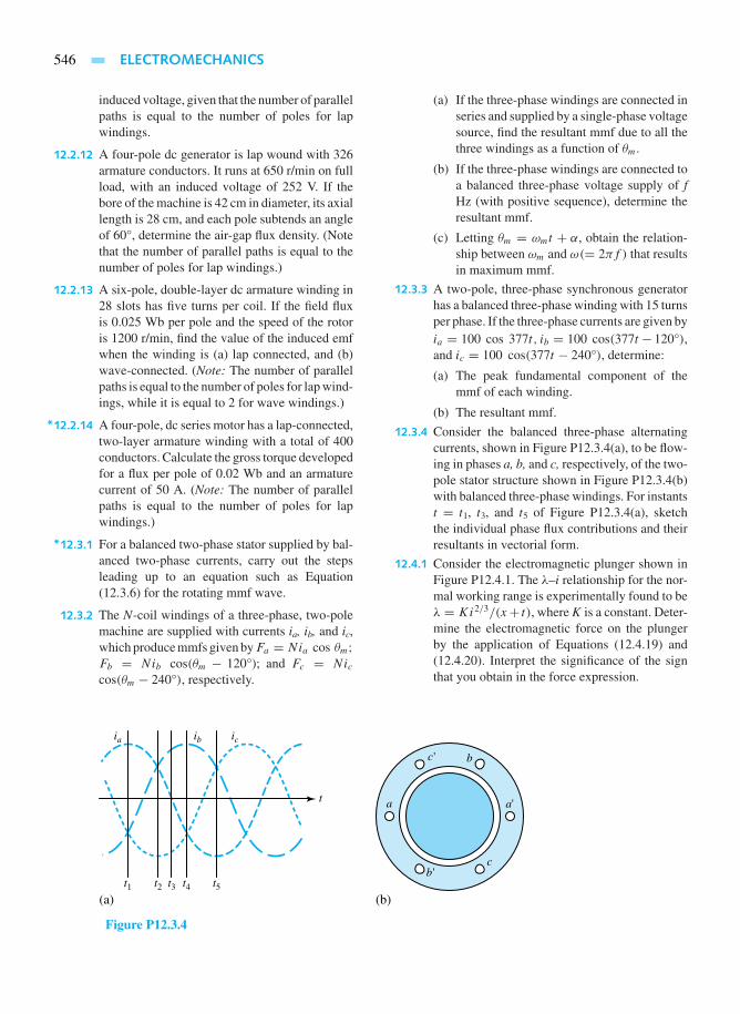
546 ELECTROMECHANICS
induced voltage, given that the number of parallelpaths is equal to the number of poles for lapwindings.
12.2.12 A four-pole dc generator is lap wound with 326armature conductors. It runs at 650 r/min on fullload, with an induced voltage of 252 V. If thebore of the machine is 42 cm in diameter, its axiallength is 28 cm, and each pole subtends an angleof 60°, determine the air-gap flux density. (Notethat the number of parallel paths is equal to thenumber of poles for lap windings.)
12.2.13 A six-pole, double-layer dc armature winding in28 slots has five turns per coil. If the field fluxis 0.025 Wb per pole and the speed of the rotoris 1200 r/min, find the value of the induced emfwhen the winding is (a) lap connected, and (b)wave-connected. (Note: The number of parallelpaths is equal to the number of poles for lap wind-ings, while it is equal to 2 for wave windings.)
*12.2.14 A four-pole, dc series motor has a lap-connected,two-layer armature winding with a total of 400conductors. Calculate the gross torque developedfor a flux per pole of 0.02 Wb and an armaturecurrent of 50 A. (Note: The number of parallelpaths is equal to the number of poles for lapwindings.)
*12.3.1 For a balanced two-phase stator supplied by bal-anced two-phase currents, carry out the stepsleading up to an equation such as Equation(12.3.6) for the rotating mmf wave.
12.3.2 The N-coil windings of a three-phase, two-polemachine are supplied with currents ia, ib, and ic,which produce mmfs given byFa = Nia cos θm;Fb = Nib cos(θm − 120°); and Fc = Niccos(θm − 240°), respectively.
(a) If the three-phase windings are connected inseries and supplied by a single-phase voltagesource, find the resultant mmf due to all thethree windings as a function of θm.
(b) If the three-phase windings are connected toa balanced three-phase voltage supply of fHz (with positive sequence), determine theresultant mmf.
(c) Letting θm = ωmt + α, obtain the relation-ship between ωm and ω(= 2πf ) that resultsin maximum mmf.
12.3.3 A two-pole, three-phase synchronous generatorhas a balanced three-phase winding with 15 turnsper phase. If the three-phase currents are given byia = 100 cos 377t, ib = 100 cos(377t − 120°),and ic = 100 cos(377t − 240°), determine:
(a) The peak fundamental component of themmf of each winding.
(b) The resultant mmf.
12.3.4 Consider the balanced three-phase alternatingcurrents, shown in Figure P12.3.4(a), to be flow-ing in phases a, b, and c, respectively, of the two-pole stator structure shown in Figure P12.3.4(b)with balanced three-phase windings. For instantst = t1, t3, and t5 of Figure P12.3.4(a), sketchthe individual phase flux contributions and theirresultants in vectorial form.
12.4.1 Consider the electromagnetic plunger shown inFigure P12.4.1. The λ–i relationship for the nor-mal working range is experimentally found to beλ = Ki2/3/(x+ t), where K is a constant. Deter-mine the electromagnetic force on the plungerby the application of Equations (12.4.19) and(12.4.20). Interpret the significance of the signthat you obtain in the force expression.
t
t1 t2 t3 t4 t5
ib icia
b
c
a
(a) (b)
b'
c'
a'
Figure P12.3.4

PROBLEMS 547
N turnsi
Cylindrical plunger
Spring
Nonmagneticcylindrical sleeve
t
tx0
x0: position of plunger when spring is relaxed
x
Figure P12.4.1
12.4.2 In Problem 12.4.1 neglect the saturation of thecore, leakage, and fringing. Neglect also the re-luctance of the ferromagnetic circuit. Assumingthat the cross-sectional area of the center legis twice the area of the outer legs, obtain ex-pressions for the inductance of the coil and theelectromagnetic force on the plunger.
*12.4.3 For the electromagnet shown in Figure P12.4.3,the λ–i relationship for the normal working rangeis given by i = aλ2 + bλ(x − d)2,where a and bare constants. Determine the force applied to theplunger by the electric system.
12.4.4 A solenoid of cylindrical geometry is shown inFigure P12.4.4.
(a) If the exciting coil carries a steady directcurrent I, derive an expression for the forceon the plunger.
(b) For the numerical values I = 10 A,N = 500turns, g = 5 mm, a = 20 mm, b = 2 mm,
and l = 40 mm, find the magnitude of theforce. Assume infinite permeability of thecore and neglect leakage.
12.4.5 Let the solenoid of Problem 12.4.4 carry an al-ternating current of 10 A (rms) at 60 Hz insteadof the direct current.
(a) Find an expression for the instantaneousforce.
(b) For the numerical values of N, g, a, b, andl given in Problem 12.4.4(b) compute theaverage force. Compare it to that of Problem12.4.4(b).
12.4.6 Consider the solenoid with a core of square crosssection shown in Figure P12.4.6.
(a) For a coil current I (dc), derive an expressionfor the force on the plunger.
(b) Given I = 10 A,N = 500 turns, g = 5 mm,a = 20 mm, and b = 2 mm, calculate themagnitude of the force.
Plunger
CoilCoil
Cylindrical magnetic shell
d
x
+ +
+ +
+ +
Figure P12.4.3
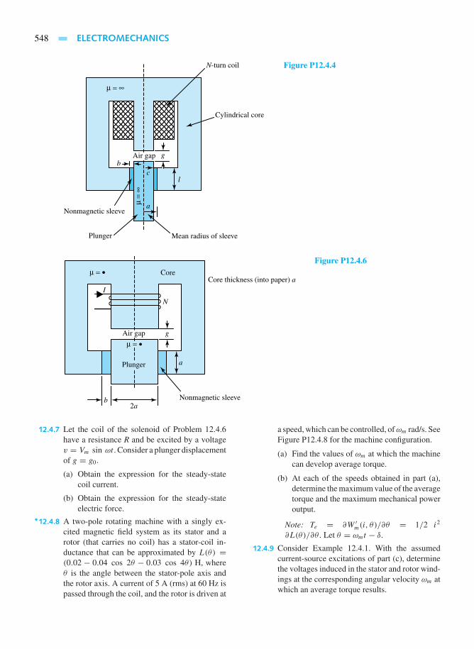
548 ELECTROMECHANICS
l
bAir gap
N-turn coil
Nonmagnetic sleeve
g
a
c
µ =
∞
µ = ∞
Cylindrical core
Mean radius of sleevePlunger
Figure P12.4.4
I
Nonmagnetic sleeve
Core thickness (into paper) aCore
N
b
Air gap
Plunger
g
a
2a
µ = •
µ = •
Figure P12.4.6
12.4.7 Let the coil of the solenoid of Problem 12.4.6have a resistance R and be excited by a voltagev = Vm sin ωt . Consider a plunger displacementof g = g0.
(a) Obtain the expression for the steady-statecoil current.
(b) Obtain the expression for the steady-stateelectric force.
*12.4.8 A two-pole rotating machine with a singly ex-cited magnetic field system as its stator and arotor (that carries no coil) has a stator-coil in-ductance that can be approximated by L(θ) =(0.02 − 0.04 cos 2θ − 0.03 cos 4θ) H, whereθ is the angle between the stator-pole axis andthe rotor axis. A current of 5 A (rms) at 60 Hz ispassed through the coil, and the rotor is driven at
a speed, which can be controlled, ofωm rad/s. SeeFigure P12.4.8 for the machine configuration.
(a) Find the values of ωm at which the machinecan develop average torque.
(b) At each of the speeds obtained in part (a),determine the maximum value of the averagetorque and the maximum mechanical poweroutput.
Note: Te = ∂W ′m(i, θ)/∂θ = 1/2 i2
∂L(θ)/∂θ. Let θ = ωmt − δ.
12.4.9 Consider Example 12.4.1. With the assumedcurrent-source excitations of part (c), determinethe voltages induced in the stator and rotor wind-ings at the corresponding angular velocity ωm atwhich an average torque results.

PROBLEMS 549
Ns turns
vs
is
+−
ωmRotor axis
Rotor
Stator pole axis
Stator
(d-axis ordirect axis)
Interpole axis(q-axis or
quadrature axis)
θ = ωmt − δ
θ
Figure P12.4.8
12.4.10 A two-winding system has its inductances givenby
L11 = k1
x= L22; L12 = L21 = k2
x
where k1 and k2 are constants. Neglecting thewinding resistances, derive an expression for theelectric force when both windings are connectedto the same voltage source v = Vm sin ωt .Comment on its dependence on x.
12.4.11 Two mutually coupled coils are shown in FigureP12.4.11. The inductances of the coils are L11 =A, L22 = B, and L12 = L21 = C cos θ . Find theelectric torque for:
(a) i1 = I0, i2 = 0.
(b) i1 = i2 = I0.
(c) i1 = Im sin ωt, i2 = I0.
(d) i1 = i2 = Im sin ωt.
(e) Coil 1 short-circuited and i2 = I0.
*12.4.12 Consider an elementary cylindrical-rotor two-phase synchronous machine with uniform airgap, as illustrated in the schematic diagram inFigure P12.4.12. It is similar to that of FigureE12.4.1, except that Figure P12.4.12 has twoidentical stator windings in quadrature insteadof one. The self-inductance of the rotor or fieldwinding is a constant given by Lff H; the self-inductance of each stator winding is a constant
given by Laa = Lbb. The mutual inductance be-tween the stator windings is zero since they are inspace quadrature; the mutual inductance betweena stator winding and the rotor winding dependson the angular position of the rotor,
Laf = L cos θ; Lbf = L sin θ
where L is the maximum value of the mutual in-ductance, and θ is the angle between the magneticaxes of the stator a-phase winding and the rotorfield winding.
(a) Let the instantaneous currents be ia, ib, and ifin the respective windings. Obtain a generalexpression for the electromagnetic torque Te
in terms of these currents, angle θ , and L.
(b) Let the stator windings carry balanced two-phase currents given by ia = Ia cos ωt , andib = Ia sin ωt , and let the rotor winding beexcited by a constant direct current If. Let therotor revolve at synchronous speed so that itsinstantaneous angular position θ is given byθ = ωt+δ. Derive the torque expression un-der these conditions and describe its nature.
(c) For conditions of part (b), neglect the re-sistance of the stator windings. Obtain thevolt–ampere equations at the terminals ofstator phases a and b, and identify the speed–voltage terms.
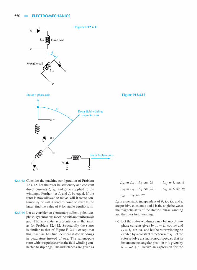
550 ELECTROMECHANICS
i1
L11
L22
θ
i2Movable coil
Fixed coil
Figure P12.4.11
Stator b-phase axis
θ
ia
ib
if
−
+
Stator a-phase axis
Rotor field windingmagnetic axis
+ −
Figure P12.4.12
12.4.13 Consider the machine configuration of Problem12.4.12. Let the rotor be stationary and constantdirect currents Ia, Ib, and If be supplied to thewindings. Further, let Ia and Ib be equal. If therotor is now allowed to move, will it rotate con-tinuously or will it tend to come to rest? If thelatter, find the value of θ for stable equilibrium.
12.4.14 Let us consider an elementary salient-pole, two-phase, synchronous machine with nonuniform airgap. The schematic representation is the sameas for Problem 12.4.12. Structurally the statoris similar to that of Figure E12.4.1 except thatthis machine has two identical stator windingsin quadrature instead of one. The salient-polerotor with two poles carries the field winding con-nected to slip rings. The inductances are given as
Laa = L0 + L2 cos 2θ; Laf = L cos θ
Lbb = L0 − L2 cos 2θ; Lbf = L sin θ;Lab = L2 sin 2θ
Lff is a constant, independent of θ ; L0, L2, and Lare positive constants; and θ is the angle betweenthe magnetic axes of the stator a-phase windingand the rotor field winding.
(a) Let the stator windings carry balanced two-phase currents given by ia = Ia cos ωt andib = Ia sin ωt , and let the rotor winding beexcited by a constant direct current If. Let therotor revolve at synchronous speed so that itsinstantaneous angular position θ is given byθ = ωt + δ. Derive an expression for the

PROBLEMS 551
torque under these conditions and describeits nature.
(b) Compare the torque with that of Problem12.4.12(b).
(c) Can the machine be operated as a motor? Asa generator? Explain.
(d) Suppose that the field current If is brought tozero. Will the machine continue to run?
12.4.15 Consider the analysis leading up to Equation(12.4.32) for the torque of an elementary cylin-drical machine with uniform air gap.
(a) Express the torque in terms of F, Fs, and δs,where δs is the angle between F and Fs .
(b) Express the torque in terms of F, Fr, and δr,where δr is the angle between F and Fr .
(c) Neglecting magnetic saturation, obtain thetorque in terms of B, Fr, and δr, where B isthe peak value of the resultant flux-densitywave.
(d) Let φ be the resultant flux per pole given bythe product of the average value of the fluxdensity over a pole and the pole area. Expressthe torque in terms ofφ, Fr, and δr, whereφ isthe resultant flux produced by the combinedeffect of the stator and rotor mmfs.
12.4.16 An electromagnetic structure is characterized bythe inductances L11 = L22 = 4 + 2 cos 2θand L12 = L21 = 2 + cos θ . Neglecting theresistances of the windings, find the torque as afunction of θ when both windings are connectedto the same ac voltage source such that
v1 = v2 = 220√
2 sin 314t
12.4.17 By using the concept of interaction between mag-netic fields, show that the electromagnetic torquecannot be obtained by using a four-pole rotor ina two-pole stator.
12.4.18 For each of the following devices, is a reluctancetorque produced when their coils carry directcurrent?
(a) Salient-pole stator carrying a coil, and asalient-pole rotor.
(b) Salient-pole rotor carrying a coil, and asalient-pole stator.
(c) Salient-pole stator carrying a coil, and acylindrical rotor.
(d) Salient-pole rotor carrying a coil, and a cylin-drical stator.
(e) Cylindrical stator carrying a coil, and a cylin-drical rotor.
(f) Cylindrical rotor carrying a coil, and a cylin-drical stator.
(g) Cylindrical stator carrying a coil, and asalient-pole rotor.
(h) Cylindrical rotor carrying a coil, and asalient-pole stator.
*12.4.19 An elementary two-pole rotating machine withuniform air gap, as shown in Figure E12.4.1, hasa stator-winding self-inductance Lss of 50 mH, arotor-winding self-inductance Lrr of 50 mH, anda maximum mutual inductance L of 45 mH. If thestator were excited from a 60-Hz source, and therotor were excited from a 25-Hz source, at whatspeed or speeds would the machine be capable ofconverting energy?
12.4.20 A rotating electric machine with uniform air gaphas a cylindrical rotor winding with inductanceL2= 1 H and a stator winding with inductance L1
= 3 H. The mutual inductance varies sinusoidallywith the angle θ between the winding axes, with amaximum of 2 H. Resistances of the windings arenegligible. Compute the mean torque if the statorcurrent is 10 A (rms), the rotor is short-circuited,and the angle between the winding axes is 45°.
12.4.21 The self and mutual inductances of a machinewith two windings are given by L11 = (1 +sin θ), L22 = 2(1 + sin θ), and L12 = L21 =M = (1−sin θ). Assuming θ = 45°, and lettingcoils 1 and 2 be supplied by constant currents I1
= 15 A and I2 = −4 A, respectively, find thefollowing:
(a) Magnitude and direction of the developedtorque.
(b) Amount of energy supplied by each source.
(c) Rms value of the current in coil 2, if thecurrent of coil 1 is changed to a sinusoidalcurrent of 10 A (rms) at 60 Hz and coil 2 isshort-circuited.
(d) Instantaneous torque produced in part (c).
(e) Average torque in part (c).
12.4.22 Consider the elementary two-pole rotating ma-chine with uniform air gap shown in FigureE12.4.1. Let Ns be the number of turns on thestator, Nr the number of turns on the rotor, l theaxial length of the machine, r the radius of therotor, and g the length of the air gap.

552 ELECTROMECHANICS
(a) Obtain expressions for self and mutual in-ductances, assuming infinite permeabilityfor the magnetic cores.
(b) Find the expression for the electromagnetictorque in terms of currents is and ir and angleθ .
(c) Show that the expression of part (b) is equiv-alent to
Te = −πµ0rl
gFsFr sin δ
12.5.1 A certain 10-hp, 230-V motor has a rotationalloss of 600 W, a stator copper loss of 350 W, arotor copper loss of 350 W, and a stray load lossof 50 W. It is not known whether the motor is aninduction, synchronous, or dc machine.
(a) Calculate the full-load efficiency.
(b) Compute the efficiency at one-half load, as-suming that the stray-loss and rotationallosses do not change with load.
12.5.2 A synchronous motor operates continuously onthe following duty cycle: 50 hp for 8 min, 100hp for 8 min, 150 hp for 10 min, 120 hp for 20min, and no load for 14 min. Specify the requiredcontinuous-rated hp of the motor. (Note: A motorrating is normally chosen on the basis of the rmsvalue given by
rms hp =√ ∑
(hp)2(time)
running time+ standstill time/k
where k is a constant accounting for reducedventilation at standstill.)

13 Rotating Machines
13.1 Elementary Concepts of Rotating Machines
13.2 Induction Machines
13.3 Synchronous Machines
13.4 Direct-Current Machines
13.5 Learning Objectives
13.6 Practical Application: A Case Study—Wind-Energy-Conversion Systems
Problems
The most widely used electromechanical device is a rotating machine, which utilizes the magneticfield to store energy. The main purpose of most rotating machines is to convert electromechanicalenergy, i.e., to convert energy between electrical and mechanical systems, either for electric powergeneration (as in generators or sources) or for the production of mechanical power to performuseful tasks (as in motors or sinks). Rotating machines range in size and capacity from small motorsthat consume only a fraction of a watt to large generators that produce several hundred megawatts.In spite of the wide variety of types, sizes, and methods of construction, all such machines operateon the same principle, namely, the tendency of two magnets to align themselves.
Most space is devoted to induction, synchronous, and direct-current machines. In spite of thedistinguishing features peculiar to each class of machines, there are several striking similaritiesamong the main kinds of machines.
13.1 ELEMENTARY CONCEPTS OF ROTATING MACHINES
Some of the basic features of conventional ac (particularly synchronous) and dc machines havebeen introduced in Chapter 12. More will be presented in this section. Three modes of operation ofa rotating electric machine—motoring, generating, and braking—are illustrated in Figure 13.1.1.
1. The motoring mode has electric power input and mechanical power output. The electro-magnetic torque Te drives the machine against the load torque T. The input voltage v drives thecurrent into the winding against the generated emf e.
553
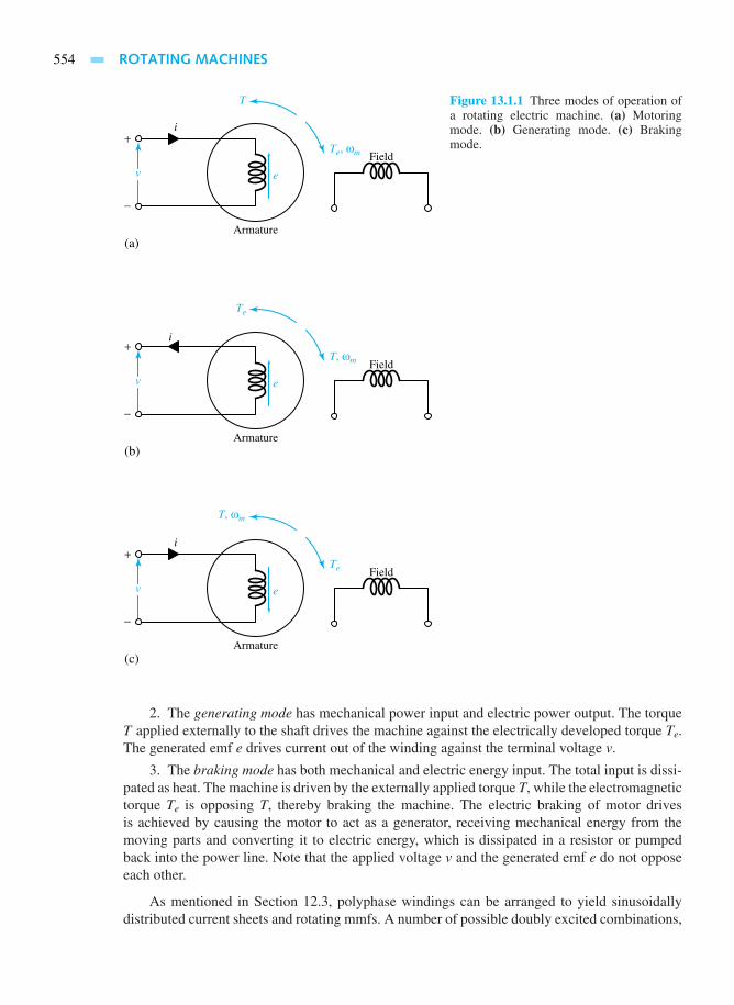
554 ROTATING MACHINES
e
T
Te, ωm
(a)
i+
−
vField
Armature
e
Te
T, ωm
(c)
i+
−
vField
Armature
e
Te
T, ωm
(b)
i+
−
vField
Armature
Figure 13.1.1 Three modes of operation ofa rotating electric machine. (a) Motoringmode. (b) Generating mode. (c) Brakingmode.
2. The generating mode has mechanical power input and electric power output. The torqueT applied externally to the shaft drives the machine against the electrically developed torque Te.The generated emf e drives current out of the winding against the terminal voltage v.
3. The braking mode has both mechanical and electric energy input. The total input is dissi-pated as heat. The machine is driven by the externally applied torque T, while the electromagnetictorque Te is opposing T, thereby braking the machine. The electric braking of motor drivesis achieved by causing the motor to act as a generator, receiving mechanical energy from themoving parts and converting it to electric energy, which is dissipated in a resistor or pumpedback into the power line. Note that the applied voltage v and the generated emf e do not opposeeach other.
As mentioned in Section 12.3, polyphase windings can be arranged to yield sinusoidallydistributed current sheets and rotating mmfs. A number of possible doubly excited combinations,

13.1 ELEMENTARY CONCEPTS OF ROTATING MACHINES 555
satisfying ωs = ωm ± ωr , which relates electrical and mechanical angular speeds, exist, givingrise to the names by which the machines are generally known, synchronous, induction, or dcmachines.
Elementary Synchronous Machines
The polyphase synchronous machine operates with direct current supplied to the field winding(assumed to be on the rotor, which is usually the case) through two slip rings and with polyphasealternating current supplied to the armature (assumed to be on the stator). The rotor mmf, which isobtained from a dc source, is stationary with respect to the rotor structure. When carrying balancedpolyphase currents, as shown in Section 12.3, the armature winding produces a magnetic field inthe air gap rotating at synchronous speed [Equation (12.2.9) or (12.2.10)], as determined by thesystem frequency and the number of poles in the machine. But the field produced by the dc rotorwinding revolves with the rotor. To produce a steady unidirectional torque, the rotating fields ofstator and rotor must be traveling at the same speed. Therefore, the rotor must turn precisely atthe synchronous speed. Such conditions satisfy the second possibility for the development of aconstant torque suggested in the discussion following Equation (12.4.32). The resulting physicalsystem is shown in Figure 13.1.2.
The polyphase synchronous machine is one in which the rotor rotates in synchronism withand in the same direction as the rotating mmf wave produced by the stator. Thus for synchronousmachines with polyphase stator winding, the following equation relating mechanical and electricalangular speeds is satisfied:
ωm = ωs = 2πf
P/2(13.1.1)
or alternatively, the steady-state speed at which the machine operates is known as the synchronousspeed, given by
Rotor
FsF
Fr
ωs
ωm = ωs
ωs
ωs
δr
δ
Axis of stator field
Axis of resultant field
S
S
N
N
Axis of rotor field
Air gap
Stator
Figure 13.1.2 Simplified two-polesynchronous machine with non-salient poles.

556 ROTATING MACHINES
Synchronous speed = 120f
Pr/min (13.1.2)
where f is the frequency of the system of which the machine is a part and P is the number of polesof the machine.
The electromagnetic torque, produced by the nonsalient-pole (or cylindrical-rotor) machine,can be expressed in terms of the resultant flux φ per pole produced by the combined effect of thestator and rotor mmfs (see Problem 12.4.15),
Te = Kφ Fr sin δr (13.1.3)
where K is a constant, Fr is the rotor mmf, and δr is the angle between the rotor mmf and theresultant flux or mmf axis. When the armature terminals are connected to a balanced polyphaseinfinite bus (which is a high-capacity, constant-voltage, constant-frequency system), the resultantair-gap flux φ is approximately constant, independent of the shaft load. Under normal operatingconditions the resultant air-gap flux φ, which is given by Equation (12.2.13) as
φ = terminal phase voltage
4.44 kWf Nph(13.1.4)
is essentially constant. The rotor mmf Fr determined by the direct field current is also a constantunder normal operating conditions. So, as seen from Equation (13.1.3), any variation in the torquerequirements of the load has to be accounted for entirely by variation of the angle δr , which iswhy δr is known as the torque angle (or load angle) of a synchronous machine. The effect ofsalient poles on the torque-angle characteristic is discussed in Section 13.3.
The torque-angle characteristic curve of a cylindrical-rotor synchronous machine is shownin Figure 13.1.3 as a function of the angle δr . For δr < 0, Te > 0, the developed torque is positiveand acts in the direction of the rotation; the machine operates as a motor. If, on the other hand,the machine is driven by a prime mover so that δr becomes positive, the torque is then negative,and the machine operates as a generator. Note that at standstill, i.e., when ωm = 0, no averageunidirectional torque is developed by the synchronous machine. Such a synchronous motor is notcapable of self-starting because it has no starting torque. The designer must provide a method forbringing the machine up to synchronous speed.
Torqueangle, δr
Te (or power)
Pull-out torque as a motor
Pull-out torque as a generator
Motor operation Generator operation
Te > 0 Te < 0
π−π π/2−π/2
Figure 13.1.3 Torque-angle char-acteristic curve of a cylindrical-rotor synchronous machine (for agiven field current and a fixed ter-minal voltage, i.e., for a constantresultant air-gap flux).

13.1 ELEMENTARY CONCEPTS OF ROTATING MACHINES 557
Figure 13.1.4 Sketch of damper bars located on salient-pole shoes of a synchronous machine.
Because a synchronous machine operates only at synchronous speed under steady-stateconditions, the machine cannot operate at synchronous speed during the load transition when theload on the synchronous machine is to be changed; the readjustment process is in fact dynamic.In the case of a generator connected to an infinite bus, an increase in the electric output power ofthe generator is brought about by increasing the mechanical input power supplied by the primemover. The speed of the rotor increases momentarily during the process, and the axis of the rotor-field mmf advances relative to the axes of both the armature mmf and the resultant air-gap mmf.The increase in torque angle results in an increase in electric power output. The machine thenlocks itself into synchronism and continues to rotate at synchronous speed until the load changesfurther. The same general argument can be made for the operation of a synchronous motor, exceptthat an increase in mechanical load decreases the speed of the rotor during the transition period,so that the axis of the rotor-field mmf falls behind that of the stator mmf or the resultant air-gapmmf by the required value of the load angle.
When the load on a synchronous machine changes, the load angle changes from one steadyvalue to another. During this transition, oscillations in the load angle and consequent associatedmechanical oscillations (known as hunting) occur. To damp out these oscillations, it is commonpractice to provide an additional short-circuited winding on the field structure, made out of copperor brass bars located in pole-face slots on the pole shoes of a salient-pole machine and connectedtogether at the ends of the machine. This additional winding (known as damper or amortisseurwinding) is shown in Figure 13.1.4. The winding is also useful in getting a synchronous motorstarted, as explained in the subsection on elementary induction machines. When the machineis operating under steady-state conditions at synchronous speed, however, this winding has noeffect. Because there is no rate of change of flux linkage, no voltage is induced in it.
As seen in Figure 13.1.3, when δr is±π/2 or 90°, the maximum torque or power (called pull-out torque or pull-out power) is reached for a fixed terminal voltage and a given field current. If theload requirements exceed this value, the motor slows down because of the excess shaft torque.Synchronous-motor action is lost because the rotor and stator fields are no longer stationarywith respect to each other. Any load requiring a torque greater than the maximum torque resultsin unstable operation of the machine; the machine pulls out of synchronism, known as pullingout of step or losing synchronism. The motor is usually disconnected from the electric supply byautomatic circuit breakers, and the machine comes to a standstill. Note that the pull-out torque canbe increased by increasing either the field current or the terminal voltage. In the case of a generatorconnected to an infinite bus, synchronism will be lost if the torque applied by the prime moverexceeds the maximum generator pull-out torque. The speed will then increase rapidly unless thequick-response governor action comes into play on the prime mover to control the speed.

558 ROTATING MACHINES
Elementary Induction Machines
In the discussion that followed Equation (12.4.32), the third possible method of producing constanttorque was to cause the mmf axes of stator and rotor to rotate at such speeds relative to theirwindings that they remain stationary with respect to each other. If the stator and rotor windingsare polyphase and carry polyphase alternating current, then both the stator mmf and the rotormmf axes may be caused to rotate relative to their windings. Such a machine will have polyphasestator ac excitation at ωs , polyphase rotor ac excitation at ωr , and the rotor speed ωm satisfying
ωm = ωs − ωr (13.1.5)
Let us consider the rotor speed given by Equation (13.1.5) and the same phase sequence ofsources. A rotating magnetic field of constant amplitude, rotating at ωs rad/s relative to thestator, is produced because of polyphase stator excitation. A rotating magnetic field of constantamplitude, rotating at ωs rad/s relative to the rotor, is also produced because of polyphase rotorexcitation. The speed of rotation of the rotor magnetic field relative to the stator is ωm + ωr , orωs , if the rotor is rotating with a positive speed of rotation ωm in the direction of the rotatingfields. If so, the condition for energy conversion at constant torque is satisfied. Such a situationis illustrated diagrammatically in Figure 13.1.5. Under these conditions the machine is operatingas a double-fed polyphase machine. Normally, in an induction machine with polyphase statorand rotor windings, only a source to excite the stator is employed, and the rotor excitation atthe appropriate frequency is induced from the stator winding. The device is thus known as aninduction machine.
In an induction machine, the stator winding is essentially the same as in a synchronousmachine. Equation (12.2.13) and the considerations leading to it hold here as in the case of asynchronous machine. When excited from a balanced polyphase source, the polyphase windingsproduce a magnetic field in the air gap rotating at a synchronous speed determined by the numberof poles and the applied stator frequency given by Equation (12.2.9). On the rotor, the winding iselectrically closed on itself (i.e., short-circuited) and often has no external terminals.
The induction machine rotor may be one of two types: the wound rotor or the squirrel-cagerotor. The wound rotor has a polyphase winding similar to and wound for the same number ofpoles as the stator winding. The terminals of the rotor winding (wye- or delta-connected, in thecase of three-phase machines) are brought to insulated slip rings mounted on the shaft. Carbonbrushes bearing on these slip rings make the rotor terminals available to the circuitry external to
Rotor
Fs Fr
ωs
ωm
ωm + ωr = ωs
δ
S
S
N
N
Stator
Figure 13.1.5 Mmf axes of an induction machine.

13.1 ELEMENTARY CONCEPTS OF ROTATING MACHINES 559
the motor. The rotor winding is usually short-circuited through external resistances that can bevaried. A squirrel-cage rotor has a winding consisting of conducting bars of copper or aluminumembedded in slots cut in the rotor iron and short-circuited at each end by conducting end rings.The squirrel-cage induction machine is the electromagnetic machine most widely used as a motorbecause of its extreme simplicity and ruggedness. Although the induction machine in the motormode is the most common of all motors, the induction machine has very rarely been used asa generator because its performance characteristics as a generator are not satisfactory for mostapplications; however, it has recently been used as a wind-power generator. The induction machinewith a wound rotor is also used as a frequency changer.
The polyphase induction motor operates with polyphase alternating current applied to theprimary winding, usually located on the stator of the polyphase machines. Three-phase motors aremost used commercially in practice, whereas two-phase motors are used in control systems. Theinduction machine has emf (and consequently current) induced in the short-circuited secondary(or rotor) winding by virtue of the primary rotating mmf. Such a machine is then singly excited.The induction machine may be regarded as a generalized transformer in which energy conversiontakes place, and electric power is transformed between the stator and the rotor along with a changeof frequency and a flow of mechanical power.
Let us assume that the rotor is turning at a steady speed of n r/min in the same direction asthe rotating stator field. Let the synchronous speed of the stator field be n1 r/min, as given byEquation (12.2.9), corresponding to the applied stator frequency fs Hz, orωs rad/s. It is convenientto introduce the concept of per-unit slip S given by
S = synchronous speed − actual rotor speed
synchronous speed= n1 − n
n1= ωs − ωm
ωs
(13.1.6)
The rotor is then traveling at a speed of n1 − n or n1S r/min in the backward direction withrespect to the stator field. The relative motion of the flux and rotor conductors induces voltagesof frequency Sfs, known as the slip frequency, in the rotor winding. Thus, the induction machineis similar to a transformer in its electrical behavior but with an additional feature of frequencychange. The frequency fr Hz of the secondary (or rotor) currents is then given by
fr = ωr
2π= Sfs (13.1.7)
At standstill, ωm = 0, so that the slip S= 1 and fr = fs ; that is, the machine then acts as a simpletransformer with an air gap and a short-circuited secondary winding. A steady starting torque isproduced because the condition for energy conversion at constant torque is satisfied; hence thepolyphase induction motor is self-starting. At synchronous speed, however, ωm = ωs , so that theslip S = 0 and fr = 0; no induction takes place because there is no relative motion between fluxand rotor conductors. Thus, at synchronous speed, the value of the secondary mmf is zero, andno torque is produced; that is, the induction motor cannot run at synchronous speed. The no-loadspeed of the induction motor is usually on the order of 99.5% of synchronous speed so that theno-load per-unit slip is about 0.005, and the full-load per-unit slip is on the order of 0.05. Thus,the polyphase induction motor is effectively a constant-speed machine.
An induction machine, connected to a polyphase exciting source on its stator side, can bemade to generate (i.e., with the power flow reversed compared to that of a motor) if its rotor isdriven mechanically by an external means at above synchronous speed, so that ωm > ωs andthe slip becomes negative. If the machine is driven mechanically in the direction opposite toits primary rotating mmf, then the slip is greater than unity and the machine acts as a brake. Forexample, let the machine be operating normally as a loaded motor; if two of the three phase supplylines to the stator are reversed, the direction of the stator rotating mmf will reverse. The rotor will

560 ROTATING MACHINES
then be rotating in the direction opposite that of the rotating mmf, so the machine will act as abrake and the speed will rapidly come to zero, at which time the electric supply can be removedfrom the machine. Such a reversal of two supply lines of the three-phase system, a useful methodof stopping the motor rapidly, is generally referred to as plugging or plug-braking. If the electricsupply is not removed at zero speed, however, the machine will reverse its direction of rotationbecause of the change of phase sequence of the supply resulting from the interchange of the twostator leads. The general form of the torque–speed curve (or torque–slip characteristic) for thepolyphase induction machine between rotor speed limits of −ωs ≤ ωm ≤ 2ωs , corresponding toa range of slips −1 ≤ S ≤ 2, is shown in Figure 13.1.6.
The torque that exists at any mechanical speed other than synchronous speed is known as anasynchronous torque. The induction machine is also known as an asynchronous machine, since notorque is produced at synchronous speed and the machine runs at a speed other than synchronousspeed. In fact, as a motor, the machine runs only at a speed that is less than synchronous speedwith positive slip. The factors influencing the general shape of the torque-speed characteristic(shown in Figure 13.1.6) can be appreciated in terms of the torque equation, Equation (13.1.3).Noting that the resultant air-gap flux φ is nearly constant when the stator-applied voltage andfrequency are constant, as seen by Equation (13.1.4), and that the rotor mmf Fr is proportional tothe rotor current ir, the torque may be expressed as
Te = K1ir sin δr (13.1.8)
where K1 is a constant and δr is the angle between the rotor mmf axis and the resultant flux or mmfaxis. The rotor current ir is determined by the rotor-induced voltage (proportional to slip) and therotor impedance. Since the slip is small under normal running conditions, as already mentioned,the rotor frequency fr = Sfs is very low (on the order of 3 Hz in 60-Hz motors with a per-unit slipof 0.05). Hence, in this range the rotor impedance is largely resistive, and the rotor current is verynearly proportional to and in phase with the rotor voltage; that is, the rotor current is very nearlyproportional to slip. An approximately linear torque–speed relationship can be observed in therange of low values of slip in Figure 13.1.6. Further, with the rotor-leakage reactance being verysmall compared with the rotor resistance, the rotor mmf wave lags approximately 90 electricaldegrees behind the resultant flux wave, and therefore sin δr is approximately equal to unity.
As slip increases, the rotor impedance increases because of the increasing effect of rotor-leakage inductance; the rotor current is then somewhat less than proportional to slip. The rotorcurrent lags further behind the induced voltage, and the rotor mmf wave lags further behind theresultant flux wave, so that sin δr decreases. The torque increases with increasing values of slipup to a point and then decreases, as shown in Figure 13.1.6 for the motor region. The maximumtorque that the machine can produce is sometimes referred to as the breakdown torque, because itlimits the short-time overload capability of the motor. Higher starting torque can be obtained byinserting external resistances in the rotor circuit, as is usually done in the case of the wound-rotorinduction motor. These resistances can be cut out for the normal running conditions in order tooperate the machine with a higher efficiency. Recall that a synchronous motor has no startingtorque. It is usually provided with a damper or amortisseur winding located in the rotor polefaces. Such a winding acts like a squirrel-cage winding to make the synchronous motor start as aninduction motor and come up almost to synchronous speed, with the dc field winding unexcited. Ifthe load and inertia are not too large, the motor will pull into synchronism and act as a synchronousmotor when the field winding is energized from a dc source.
So far the discussion of induction machines applies only to machines operating from apolyphase supply. Of particular interest is the single-phase induction machine, which is widelyused as a fractional-horsepower ac motor supplying the motive power for all kinds of equipment

13.1 ELEMENTARY CONCEPTS OF ROTATING MACHINES 561
Torque
−1012
−ωs ωs 2ωsRS
P0 Speed
Slip
Brakingregion
Motorregion
Generatorregion
Q
Figure 13.1.6 General form oftorque–speed curve (or torque–slip characteristic) for a poly-phase induction machine.
in the home, office, and factory. For the sake of simplicity, let us consider a single-phase inductionmotor with a squirrel-cage rotor and a stator carrying a single-phase winding, connected to a single-phase ac supply. The primary mmf cannot be rotating, but, in fact, it is pulsating in phase withthe variations in the single-phase primary current. It can be shown, however, that any pulsatingmmf can be resolved in terms of two rotating mmfs of equal magnitude, rotating in synchronismwith the supply frequency but in opposite directions (see Section 12.3). The wave rotating in thesame direction as the rotor is known as the forward-rotating wave, whereas the one rotating inthe opposite direction is the backward-rotating wave. Then the slip S of the machine with respectto the forward-rotating wave is given by
Sf = ωs − ωm
ωs
(13.1.9)
which is the same as Equation (13.1.6). The slip Sb of the machine with respect to the backward-rotating wave, however, is given by
Sb = −ωs − ωm
ωs
= 2− Sf (13.1.10)
Sf and Sb are known as forward (or positive-sequence) slip and backward (or negative-sequence)slip, respectively. Assuming that the two component mmfs exist separately, the frequency andmagnitude of the component emfs induced in the rotor by their presence will, in general, bedifferent because Sf is not equal to Sb. Then the machine can be thought of as producing a steadytotal torque as the algebraic sum of the component torques. The equivalent circuit based onthe revolving-field theory is pursued in Section 13.2. At standstill, however, ωm = 0 and thecomponent torques are equal and opposite; no starting torque is produced. Thus, it is clear thata single-phase induction motor is not capable of self-starting, but it will continue to rotate oncestarted in any direction. In practice, additional means are provided to get the machine started(usually as an asymmetrical two-phase motor) from a single-phase source, and the machine isthen run as a single-phase motor. An approximate shape of the torque–speed curve for the single-phase motor can readily be obtained from that of the three-phase machine shown in Figure 13.1.6.Corresponding to a positive slip of Sf= OP in Figure 13.1.6, the positive-sequence torque is PQ.Then, corresponding to Sb = 2 − Sf = OR, the negative-sequence torque is RS. The resultanttorque is given by PQ − RS. This procedure can be repeated for a range of slips 1 ≤ S ≤ 0to give the general form of the torque–speed characteristic of a single-phase induction motor, asshown in Figure 13.1.7.
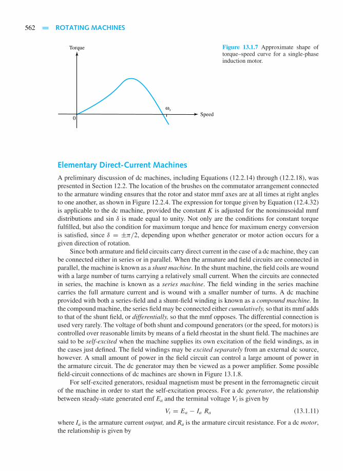
562 ROTATING MACHINES
Torque
0
ωsSpeed
Figure 13.1.7 Approximate shape oftorque–speed curve for a single-phaseinduction motor.
Elementary Direct-Current Machines
A preliminary discussion of dc machines, including Equations (12.2.14) through (12.2.18), waspresented in Section 12.2. The location of the brushes on the commutator arrangement connectedto the armature winding ensures that the rotor and stator mmf axes are at all times at right anglesto one another, as shown in Figure 12.2.4. The expression for torque given by Equation (12.4.32)is applicable to the dc machine, provided the constant K is adjusted for the nonsinusoidal mmfdistributions and sin δ is made equal to unity. Not only are the conditions for constant torquefulfilled, but also the condition for maximum torque and hence for maximum energy conversionis satisfied, since δ = ±π/2, depending upon whether generator or motor action occurs for agiven direction of rotation.
Since both armature and field circuits carry direct current in the case of a dc machine, they canbe connected either in series or in parallel. When the armature and field circuits are connected inparallel, the machine is known as a shunt machine. In the shunt machine, the field coils are woundwith a large number of turns carrying a relatively small current. When the circuits are connectedin series, the machine is known as a series machine. The field winding in the series machinecarries the full armature current and is wound with a smaller number of turns. A dc machineprovided with both a series-field and a shunt-field winding is known as a compound machine. Inthe compound machine, the series field may be connected either cumulatively, so that its mmf addsto that of the shunt field, or differentially, so that the mmf opposes. The differential connection isused very rarely. The voltage of both shunt and compound generators (or the speed, for motors) iscontrolled over reasonable limits by means of a field rheostat in the shunt field. The machines aresaid to be self-excited when the machine supplies its own excitation of the field windings, as inthe cases just defined. The field windings may be excited separately from an external dc source,however. A small amount of power in the field circuit can control a large amount of power inthe armature circuit. The dc generator may then be viewed as a power amplifier. Some possiblefield-circuit connections of dc machines are shown in Figure 13.1.8.
For self-excited generators, residual magnetism must be present in the ferromagnetic circuitof the machine in order to start the self-excitation process. For a dc generator, the relationshipbetween steady-state generated emf Ea and the terminal voltage Vt is given by
Vt = Ea − Ia Ra (13.1.11)
where Ia is the armature current output, and Ra is the armature circuit resistance. For a dc motor,the relationship is given by

13.2 INDUCTION MACHINES 563
Field
Shunt field
Series field
Fieldrheostat
Field rheostat
(a)
(c) (d)
(b)Dc source
Armature
Armature
Armature
Shunt fieldSeries field
Field rheostat
Armature
Figure 13.1.8 Field-circuit connections of dc machines. (a) Separately excited machine. (b) Shunt machine.(c) Series machine. (d) Compound machine.
Vt = Ea + Ia Ra (13.1.12)
where Ia is now the armature current input. Under steady-state conditions, volt–ampere charac-teristic curves are of interest for dc generators, and speed–torque characteristics are of interestfor dc motors. Depending on the method of excitation of the field windings, a wide variety ofoperating characteristics can be obtained. These possibilities make the dc machine both versatileand adaptable for control. More about dc machines is presented in Section 13.4.
13.2 INDUCTION MACHINES
We shall first consider polyphase induction motors and then single-phase induction motors. Thepolyphase induction motors used in industrial applications are almost without exception three-phase. The stator winding is connected to the ac source, and the rotor winding is either short-circuited, as in squirrel-cage machines, or closed through external resistances, as in wound-rotormachines. The cage machines are also known as brushless machines; the wound-rotor machinesare also called slip-ring machines.
A review of the subsection on elementary induction machines in Section 13.1 can be helpfulat this stage to recall the operating principle of polyphase induction machines.
Equivalent Circuit of a Polyphase Induction Machine
The induction machine may be regarded as a generalized transformer in which energy is convertedand electric power is transferred between stator and rotor, along with a change of frequency and a

564 ROTATING MACHINES
flow of mechanical power. At standstill, however, the machine acts as a simple transformer withan air gap and a short-circuited secondary winding. The frequency of the rotor-induced emf isthe same as the stator frequency at standstill. At any value of the slip under balanced steady-stateoperation, the rotor current reacts on the stator winding at the stator frequency because the rotatingmagnetic fields caused by the stator and rotor are stationary with respect to each other.
The induction machine may thus be viewed as a transformer with an air gap and variableresistance in the secondary; the stator of the induction machine corresponds to the transformerprimary, and the rotor corresponds to the secondary. For analysis of the balanced steady state, itis sufficient to proceed on a per-phase basis with some phasor concepts; so we will now developan equivalent circuit on a per-phase basis. Only machines with symmetrical polyphase windingsexcited by balanced polyphase voltages are considered. As in other discussions of polyphasedevices, let us think of three-phase machines as wye-connected, so that currents are always linevalues and voltages are always line-to-neutral values (on a per-phase basis).
The resultant air-gap flux is produced by the combined mmfs of the stator and rotor currents.For the sake of conceptual and analytical convenience, the total flux is divided into a mutual flux(linking both the stator and the rotor) and leakage fluxes, represented by appropriate reactances.
Considering the conditions in the stator, the synchronously rotating air-gap wave generatesbalanced polyphase counter emfs in the phases of the stator. The volt–ampere equation for thephase under consideration in phasor notation is given by
V1 = E1 + I1 (R1 + jXl 1) (13.2.1)
where V1 is the stator terminal voltage, E1 is the counter emf generated by the resultant air-gapflux, I1 is the stator current, R1 is the stator effective resistance, and Xl1 is the stator-leakagereactance.
As in a transformer, the stator (primary) current can be resolved into two components:a load component I ′2 (which produces an mmf that exactly counteracts the mmf of the rotorcurrent) and an excitation component I0 (required to create the resultant air-gap flux). Thisexcitation component itself can be resolved into a core-loss component Ic in phase with E1
+
−
+
−
V1 E1
R1jXl1
−jbm
Ic
gc
Im
I1
I0
I '2Figure 13.2.1 Equivalent circuit for the statorphase of a polyphase induction motor.
SE2
+
−
R2
jSXl2I2
Figure 13.2.2 Slip-frequency equivalent circuit for the rotorphase of a polyphase induction motor.

13.2 INDUCTION MACHINES 565
and a magnetizing component Im lagging E1 by 90°. A shunt branch formed by the core-lossconductance gc and magnetizing susceptance bm in parallel, connected across E1, will account forthe exciting current in the equivalent circuit, as shown in Figure 13.2.1, along with the positivedirections in a motor.
Thus far the equivalent circuit representing the stator phenomenon is exactly like that of thetransformer primary. Because of the air gap, however, the value of the magnetizing reactancetends to be relatively low compared to that of a transformer, and the leakage reactance is largerin proportion to the magnetizing reactance than it is in transformers. To complete the equivalentcircuit, the effects of the rotor must be incorporated, which we do by referring the rotor quantitiesto the stator.
Because the frequency of the rotor voltages and currents is the slip frequency, the magnitudeof the voltage induced in the rotor circuit is proportional to the slip. Also, in terms of the standstillper-phase rotor-leakage reactance Xl2, the leakage reactance at a slip S is given by SXl2. With R2
as the per-phase resistance of the rotor, the slip-frequency equivalent circuit for a rotor phase isshown in Figure 13.2.2, in which E2 is the per-phase voltage induced in the rotor at standstill. Therotor current I2 is given by
I2 = SE2√R2
2 + (SXl2)2(13.2.2)
which may be rewritten as
I2 = E2√(R2/S)2 +X2
l2
(13.2.3)
resulting in the alternate form of the per-phase rotor equivalent circuit shown in Figure 13.2.3.All rotor electrical phenomena, when viewed from the stator, become stator-frequency
phenomena because the stator winding sees the mmf and flux waves traveling at synchronous
+
−
E2
jXl2I2
R2
S
Figure 13.2.3 Alternate form of a per-phase rotor equivalentcircuit.
R2
S
+
+ +
− −
−
V1 E1
R1jXl1 jXl2
−jbmE2
Ic
gc
Im
I1
I0
I '2 I2
Figure 13.2.4 Per-phase equivalent coupled circuit of a polyphase induction motor.

566 ROTATING MACHINES
speed. Returning to the analogy of a transformer, and considering that the rotor is coupled to thestator in the same way the secondary of a transformer is coupled to its primary, we may draw theequivalent circuit as shown in Figure 13.2.4.
Referring the rotor quantities to the stator, we can now draw the per-phase equivalent circuitof the polyphase induction motor, as shown in Figure 13.2.5(a). The combined effect of the shaftload and the rotor resistance appears as a reflected resistance R′2/S, which is a function of slip andtherefore of the mechanical load. The quantity R′2/S may conveniently be split into two parts:
R′2S= R′2 +
R′2(1− S)S
(13.2.4)
R'2S
+
−
V1E1 = E '2
R1jXl1 jX 'l2
−jbm
R1
+
−
Ic
gc
Im
I1
I0
I '2
R'2 (1 − S)S
+
−
V1E1 = E '2
R '2jXl1 jX 'l2
−jbm
R1
+
−
Ic
gc
Im
I1
I0
I '2
R'2 (1 − S)S
+
−
V1
R '2jXl1 jX 'l2
−jbm
I1
I0
I '2
(a)
(b)
(c)
Figure 13.2.5 Per-phase equivalent circuits of a polyphase induction motor, referred to the stator.

13.2 INDUCTION MACHINES 567
and the equivalent circuit may be redrawn as in Figure 13.2.5(b). R′2 is the per-phase standstillrotor resistance referred to the stator, and R′2[(1− S)/S] is a dynamic resistance that depends onthe rotor speed and corresponds to the load on the motor. [See the discussion following Equation(13.2.6).]
When power aspects need to be emphasized, the equivalent circuit is frequently redrawn asin Figure 13.2.5(c), in which the shunt conductance gc is omitted. The core losses can be includedin efficiency calculations along with the friction, windage, and stray-load losses.
Recall that, in static transformer theory, analysis of the equivalent circuit is often simplifiedeither by neglecting the exciting shunt branch entirely, or by adopting the approximation of movingit out directly to the terminals. For the induction machine, however, such approximations mightnot be permissible under normal running conditions because the air gap leads to a much higherexciting current (30 to 50% of full-load current) and relatively higher leakage reactances.
The parameters of the equivalent circuit of an induction machine can be obtained from theno-load (in which the motor is allowed to run on no load) and blocked-rotor (in which the rotorof the induction motor is blocked so that the slip is equal to unity) tests. These tests correspondto the no-load and short-circuit tests on the transformer, and are very similar in detail.
Polyphase Induction Machine Performance
Some of the important steady-state performance characteristics of a polyphase induction motorinclude the variation of current, speed, and losses as the load–torque requirements change, and thestarting and maximum torque. Performance calculations can be made from the equivalent circuit.All calculations can be made on a per-phase basis, assuming balanced operation of the machine.Total quantities can be obtained by using an appropriate multiplying factor.
The equivalent circuit of Figure 13.2.5(c), redrawn for convenience in Figure 13.2.6, isusually employed for the analysis. The core losses, most of which occur in the stator, as well asfriction, windage, and stray-load losses, are included in the efficiency calculations. The power-flow diagram for an induction motor is given in Figure 13.2.7, in which m1 is the number of statorphases, φ1 is the power factor angle between V1 and I1, φ2 is the power factor angle between E1
and I ′2, T is the internal electromagnetic torque developed, ωs is the synchronous angular velocityin mechanical radians per second, and ωm is the actual mechanical rotor speed given by ωs(1−S).
The total power Pg transferred across the air gap from the stator is the difference between theelectric power input Pi and the stator copper loss. Pg is thus the total rotor input power, which isdissipated in the resistance R′2/S of each phase so that
Pg = m1(I′2)
2 R′2
S= T ωs (13.2.5)
Subtracting the total rotor copper loss, which is m1(I′2)
2 R′2 or SPg, from Equation (13.2.5) forPg, we get the internal mechanical power developed,
R1
R'2 (1 − S)S
+
−
V1
R '2jXl1 jX 'l2
jXm E1
I1
I0
I '2
Figure 13.2.6 Per-phase equivalentcircuit of a polyphase inductionmotor used for performancecalculations.

568 ROTATING MACHINES
Pm = Pg(1− S) = T ωm = m1(I′2)
2 R′2(1− S)
S(13.2.6)
This much power is absorbed by a resistance of R′2(1 − S)/S, which corresponds to the load.For this reason, the resistance term R′2/S has been split into two terms, as in Equation (13.2.4)and shown in the equivalent circuit of Figure 13.2.6. From Equation (13.2.6) we can see that ofthe total power delivered to the rotor, the fraction 1 − S is converted to mechanical power andthe fraction S is dissipated as rotor copper loss. We can then conclude that an induction motoroperating at high slip values will be inefficient.
The total rotational losses, including the core losses, can be subtracted from Pm to obtain themechanical power output Po that is available in mechanical form at the shaft for useful work,
Po = Pm − Prot = Toωm (13.2.7)
The per-unit efficiency of the induction motor is then given by
η = Po/Pi (13.2.8)
Let us now illustrate this procedure and the analysis of the equivalent circuit in the followingexample.
Electricpower input Pi
Mechanical poweroutput Po
= m1V1I1 cos φ1 = m1E1I '2 cos φ2= Tωs
Power transferredacross air gap Pg
= rotor input power= m1(I '2)2R'2/S
Mechanical powerdeveloped Pm= Pg(1 − S)= Tωm
Stator copper loss = m1I2
1R1
S1 − S
= m1(I '2)2R'2
Rotor copper loss = m1(I '2)2R'2= SPg
Rotational losses(core losses will beincluded here) Prot
= Pm − Prot = Toωm
Figure 13.2.7 Power flow in an induction motor.
EXAMPLE 13.2.1
The parameters of the equivalent circuit shown in Figure 13.2.6 for a three-phase, wye-connected,220-V, 10-hp, 60-Hz, six-pole induction motor are given in ohms per phase referred to the stator:R1 = 0.3, R′2 = 0.15, Xl1 = 0.5, X′12 = 0.2, and Xm = 15. The total friction, windage, and corelosses can be assumed to be constant at 400 W, independent of load. For a per-unit slip of 0.02,when the motor is operated at rated voltage and frequency, calculate the stator input current, thepower factor at the stator terminals, the rotor speed, output power, output torque, and efficiency.
So l u t i on
From the equivalent circuit of Figure 13.2.6, the total impedance per phase, as viewed from thestator input terminals, is given by

13.2 INDUCTION MACHINES 569
Zt = R1 + jXl1 +jXm
(R′2S+ jX′l2
)R′2S+ j (XM +X′l2)
= 0.3+ j0.5+ j15(7.5+ j0.2)
7.5+ j (15+ 0.2)
= (0.3+ j0.5)+ (5.87+ j3.10) = 6.17+ j3.60
= 7.14 30.26°
Phase voltage = 220/√
3 = 127 VStator input current = 127/7.14 = 17.79 APower factor = cos 30.26° = 0.864Synchronous speed = 120× 60/6 = 1200 r/minRotor speed = (1− 0.02)1200 = 1176 r/minTotal input power = √3× 220× 17.79× 0.864 = 5856.8 WStator copper loss = 3× 17.792 × 0.3 = 284.8 WPower transferred across air gap Pg = 5856.8− 284.8 = 5572 W
Pg can also be obtained as follows:
Pg = m1(I′2)
2R′2/S = m1I21 Rf
where Rf is the real part of the parallel combination of jXm and R′2/S+ jX′l2. Thus,
Pg = 3× 17.792 × 5.87 = 5573 W
Internal mechanical power developed = Pg(1− S) = 0.98× 5572 = 5460 WTotal mechanical power output = 5460− 400 = 5060 W, or 5060/745.7 = 6.8 hp
Total output torque = output powerωm
= output power(1−S)ωs
Since,
ωs = 4πf
poles= 4π × 60
6= 40π = 125.7 mechanical rad/s
it follows that
Total output torque = 5060
0.98× 125.7= 41.08 N ·m
Efficiency = 5060
5856.8= 0.864, or 86.4%
The efficiency may alternatively be calculated from the losses:Total stator copper loss = 284.8 WRotor copper loss = m1(I
′2)
2 R′2 = SPg = 0.02× 5572 = 111.4 WFriction, windage, and core losses = 400 WTotal losses = 284.8+ 111.4+ 400 = 796.2 WOutput = 5060 WInput = 5060+ 796.2 = 5856.2 W
Efficiency = 1− losses
input= 1− 796.2
5856.2= 1− 0.136 = 0.864, or 86.4%
Torque-Speed Characteristics of 3-Phase Induction Motors
Because the torque–slip characteristic is one of the most important aspects of the induction motor,we will now develop an expression for torque as a function of slip and other equivalent circuitparameters. Recalling Equation (13.2.8) and the equivalent circuit of Figure 13.2.6, we will obtain
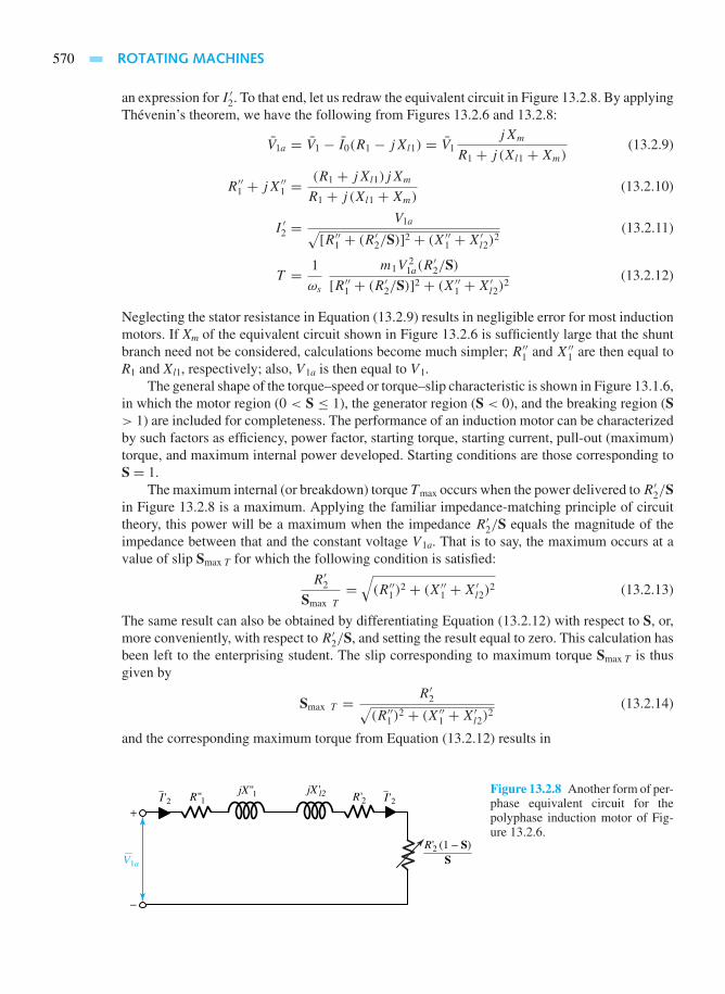
570 ROTATING MACHINES
an expression for I ′2. To that end, let us redraw the equivalent circuit in Figure 13.2.8. By applyingThévenin’s theorem, we have the following from Figures 13.2.6 and 13.2.8:
V1a = V1 − I0(R1 − jXl1) = V1jXm
R1 + j (Xl1 +Xm)(13.2.9)
R′′1 + jX′′1 =(R1 + jXl1)jXm
R1 + j (Xl1 +Xm)(13.2.10)
I ′2 =V1a√
[R′′1 + (R′2/S)]2 + (X′′1 +X′l2)2(13.2.11)
T = 1
ωs
m1V2
1a(R′2/S)
[R′′1 + (R′2/S)]2 + (X′′1 +X′l2)2(13.2.12)
Neglecting the stator resistance in Equation (13.2.9) results in negligible error for most inductionmotors. If Xm of the equivalent circuit shown in Figure 13.2.6 is sufficiently large that the shuntbranch need not be considered, calculations become much simpler; R′′1 and X′′1 are then equal toR1 and Xl1, respectively; also, V1a is then equal to V1.
The general shape of the torque–speed or torque–slip characteristic is shown in Figure 13.1.6,in which the motor region (0 < S ≤ 1), the generator region (S < 0), and the breaking region (S> 1) are included for completeness. The performance of an induction motor can be characterizedby such factors as efficiency, power factor, starting torque, starting current, pull-out (maximum)torque, and maximum internal power developed. Starting conditions are those corresponding toS = 1.
The maximum internal (or breakdown) torque Tmax occurs when the power delivered to R′2/Sin Figure 13.2.8 is a maximum. Applying the familiar impedance-matching principle of circuittheory, this power will be a maximum when the impedance R′2/S equals the magnitude of theimpedance between that and the constant voltage V1a. That is to say, the maximum occurs at avalue of slip Smax T for which the following condition is satisfied:
R′2Smax T
=√(R′′1 )2 + (X′′1 +X′l2)2 (13.2.13)
The same result can also be obtained by differentiating Equation (13.2.12) with respect to S, or,more conveniently, with respect to R′2/S, and setting the result equal to zero. This calculation hasbeen left to the enterprising student. The slip corresponding to maximum torque Smax T is thusgiven by
Smax T = R′2√(R′′1 )2 + (X′′1 +X′l2)2
(13.2.14)
and the corresponding maximum torque from Equation (13.2.12) results in
R ''1
R'2 (1 − S)S
+
−
V1a
R '2jX ''1 jX 'l2I '2 I '2
Figure 13.2.8 Another form of per-phase equivalent circuit for thepolyphase induction motor of Fig-ure 13.2.6.

13.2 INDUCTION MACHINES 571
Tmax = 1
ωs
0.5m1V2
1a
R′′1 +√(R′′1 )2 + (X′′1 +X′l2)2
(13.2.15)
which can be verified by the reader. Equation (13.2.15) shows that the maximum torque isindependent of the rotor resistance. The slip corresponding to the maximum torque is directlyproportional to the rotor resistance R′2, however, as seen from Equation (13.2.14). Thus, whenthe rotor resistance is increased by inserting external resistance in the rotor of a wound-rotorinduction motor, the maximum internal torque is unaffected, but the speed or slip at whichit occurs is increased, as shown in Figure 13.2.9. Also note that maximum torque and max-imum power do not occur at the same speed. The student is encouraged to work out thereason.
A conventional induction motor with a squirrel-cage rotor has about 5% drop in speed fromno load to full load, and is thus essentially a constant-speed motor. Employing a wound-rotormotor and inserting external resistance in the rotor circuit achieves speed variation but resultsin poor efficiency. Variations in the starting torque (at S = 1) with rotor-circuit resistance canalso be seen from Figure 13.2.9. As stated in Section 13.1, we can obtain a higher starting torqueby inserting external resistances in the rotor circuit and then cutting them out eventually forthe normal running conditions in order to operate the machine at a higher efficiency. Creatinga sufficiently large rotor-circuit resistance might make it possible to achieve an almost lineartorque–slip relationship for the slip range of 0 to 1. For instance, two-phase servo motors(used as output actuators in feedback control systems) are usually designed with very high rotorresistance to ensure a negative slope for the torque–speed characteristic over the entire operatingrange.
Since the stator resistance is quite low and has only a negligible influence, let us setR1 = R′′1 = 0, in which case, from Equations (13.2.12) and (13.2.15), we can show that
T
Tmax= 2
(S/Smax T )+ (Smax T /S)(13.2.16)
where S and Smax T are the slips corresponding to T and Tmax, respectively.
1.0
3.0
2.5
2.0
1.5
1.0
0.5
0
0.8 0.6 00.4 0.2
1.00.80.60 0.40.2 SpeedSynchronous speed
Slip
Load
Tmax
T/Tfull loadStable operatingregion for motor
with resistance (R '2)A
(R '2)D
(R '2)C
(R '2)B
(R '2)A
(R '2)D > (R '2)C > (R '2)B > (R '2)A
NA NB
NC
ND
Figure 13.2.9 Effect of changingrotor-circuit resistance on the torque–slip characteristic of a polyphase in-duction motor.

572 ROTATING MACHINES
EXAMPLE 13.2.2
For the motor specified in Example 13.2.1, compute the following:
(a) The load component I ′2 of the stator current, the internal torque T, and the internal powerPm for a slip of 0.02.
(b) The maximum internal torque, and the corresponding slip and speed.
(c) The internal starting torque and the corresponding stator load current I ′2.
So l u t i on
Let us first reduce the equivalent circuit of Figure 13.2.6 to its Thévenin-equivalent form shownin Figure 13.2.8. With the aid of Equations (13.2.9) and (13.2.10), we obtain
V1a = V1jXm
R1 + j (Xl1 +Xm)∼= V1
Xm
Xl1 +Xm
= 220√3
15
0.5+ 15 0° = 122.9 0° V
R′′1 + jX′′1 =(0.3+ j0.5)j15
0.3+ j (0.5+ 15)= 0.281+ j0.489
(a) Corresponding to a slip of 0.02, R′2/S = 0.15/0.02 = 7.5. From Equation (13.2.11), weget
I ′2 =122.9√
7.82 + 0.6892= 122.9
7.83= 15.7 A
The internal torque T can be calculated from either Equation (13.2.5) or (13.2.12),
T = 1
125.73× 15.72 × 7.5 = 5546
125.7= 44.12 N ·m
From Equation (13.2.6), the internal mechanical power is calculated as
Pm = 3× 15.72 × 7.5× 0.98 = 5435 W
which is also the same as T ωm = T ωs(1−S) = 44.12×125.7×0.98. In Example 13.2.1,this value is calculated as 5460 W; the small discrepancy is due to the approximations.
(b) From Equation (13.2.14) it follows that
Smax T = 0.15√0.2812 + 0.6892
= 0.15
0.744= 0.202
or the corresponding speed at Tmax is (1 − 0.202)1200 = 958 r/min. From Equation(13.2.15), the maximum torque can be calculated as
Tmax = 1
125.7
0.5× 3× 122.92
0.281+√0.2812 + 0.6892= 1
125.7
0.5× 3× 122.92
0.281+ 0.744= 175.8 N ·m
(c) Assuming the rotor-circuit resistance to be constant, with S= 1 at starting, from Equations(13.2.11) and (13.2.12) we get

13.2 INDUCTION MACHINES 573
I ′2 start =122.9√
(0.281+ 0.15)2 + (0.489+ 0.2)2= 122.9
0.813= 151.2 A
Tstart = 1
125.73× 151.22 × 0.15 = 81.8 N ·m
For such applications as fans and blowers, a motor needs to develop only a moderate startingtorque. Some loads, like conveyors, however, require a high starting torque to overcome highstatic torque and load inertia. The motor designer sometimes makes the starting torque equal tothe maximum torque by choosing the rotor-circuit resistance at startup to be
R′2 start =√(R′′1 )2 + (X′′1 +X′l2)2 (13.2.17)
which can easily be obtained from Equation (13.2.13) with Smax T = 1.
Speed and Torque Control of Polyphase Induction Motors
The induction motor is valuable in so many applications because it combines simplicity andruggedness. Although a good number of industrial drives run at substantially constant speed,quite a few applications need variable speed. Speed-control capability is essential in suchapplications as conveyors, hoists, and elevators. Because the induction motor is essentially aconstant-speed machine, designers have sought creative ways to easily and efficiently vary itsspeed continuously over a wide range of operating conditions. We only indicate the methods ofspeed control here.
The appropriate equation to be examined, based on Equation (13.1.8), is
n = (1− S)n1 = (1− S)120fs/P (13.2.18)
where n is the actual speed of the machine in revolutions per minute, S is the per-unit slip, fsis the supply frequency in hertz, P is the number of poles, and n1 is the synchronous speed inrevolutions per minute. Equation (13.2.18) suggests that the speed of the induction motor canbe varied by varying either the slip or the synchronous speed, which in turn can be varied bychanging either the number of poles or the supply frequency. Any method of speed control thatdepends on the variation of slip is inherently inefficient because the efficiency of the inductionmotor is approximately equal to 1 − S. On the other hand, if the supply frequency is constant,varying the number of poles results only in discrete and stepped variation in motor speed.Indeed, all methods of speed control require some degree of sacrifice in performance, cost,and simplicity. These disadvantages must be weighed carefully against the advantages of speedvariability.
The following are methods available for speed and torque control of induction motors.
• Pole-changing method
• Variable-frequency method
• Variable-line-voltage method
• Variable-rotor-resistance method
• Rotor-slip frequency control
• Rotor-slip energy recovery method
• Control by auxiliary devices (Kramer control, Scherbius control, Schrage motor)
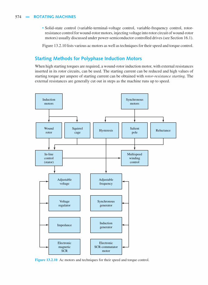
574 ROTATING MACHINES
• Solid-state control (variable-terminal-voltage control, variable-frequency control, rotor-resistance control for wound-rotor motors, injecting voltage into rotor circuit of wound-rotormotors) usually discussed under power-semiconductor controlled drives (see Section 16.1).
Figure 13.2.10 lists various ac motors as well as techniques for their speed and torque control.
Starting Methods for Polyphase Induction Motors
When high starting torques are required, a wound-rotor induction motor, with external resistancesinserted in its rotor circuits, can be used. The starting current can be reduced and high values ofstarting torque per ampere of starting current can be obtained with rotor-resistance starting. Theexternal resistances are generally cut out in steps as the machine runs up to speed.
Inductionmotors
Synchronousmotors
Multispeedwindingcontrol
Woundrotor
Squirrelcage
Hysteresis
Adjustablefrequency
Adjustablevoltage
Synchronousgenerator
Voltageregulator
Inductiongenerator
Impedance
ElectronicSCR-commutator
motor
Electronicmagnetic
SCR
Salientpole
Reluctance
In-linecontrol(stator)
Figure 13.2.10 Ac motors and techniques for their speed and torque control.

13.2 INDUCTION MACHINES 575
For squirrel-cage-rotor machines, the problem is to keep down the starting current whilemaintaining adequate starting torque. The input current, for example, can be no more than 6 timesthe full-load current, while the starting torque may be about 1.5 times the full-load torque. Depend-ing on the capacity of the available supply system, direct-on-line starting may be suitable onlyfor relatively small machines, up to 10-hp rating. Other starting methods include reduced-voltagestarting by means of wye–delta starting, autotransformer starting, or stator-impedance starting.
For employing the wye–delta starting method, a machine designed for delta operation isconnected in wye during the starting period. Because the impedance between line terminals forwye connection is three times that for delta connection for the same line voltage, the line currentat standstill for wye connection is reduced to one-third of the value for delta connection. Since thephase voltage is reduced by a factor of
√3 during starting, it follows that the starting torque will
be one-third of normal. For autotransformer starting, the setting of the autotransformer can bepredetermined to limit the starting current to any desired value. An autotransformer, which reducesthe voltage applied to the motor to x times the normal voltage, will reduce the starting current inthe supply system as well as the starting torque of the motor to x2 times the normal values.
Stator-impedance starting may be employed if the starting-torque requirement is not severe.Series resistances (or impedances) are inserted in the lines to limit the starting current. Theseresistances are short-circuited out when the motor gains speed. This method has the obviousdisadvantage of inefficiency caused by the extra losses in the external resistances.
EXAMPLE 13.2.3
An induction motor has a starting current that is 6 times the full-load current and a per-unit full-load slip of 0.04. The machine is to be provided with an autotransformer starter. If the minimumstarting torque must be 0.3 times the full-load torque, determine the required tapping on thetransformer and the per-unit supply-source line current at starting.
So l u t i on
From Equation (13.2.5), with slip at starting equal to 1, we have
Ts
Tf l=(Is
If l
)2
Sf l
where subscripts s and fl correspond to starting and full-load conditions.Substituting values, 0.3 = (Is/If l)
2 × 0.04, from which
Is/If l =√
0.03/0.04 = 2.74
or Is = 2.74 per unit, with Ifl taken as 1 per unit.The applied voltage to the motor must reduce the current from 6 per unit to 2.74 per unit,
i.e., the tapping must be sufficient to reduce the voltage to 2.74/6 = 0.456 of the full value.The supply-source line current will then be 2.74 × 0.456 = 1.25 per unit, where 0.456 is thesecondary-to-primary turns ratio.
Single-Phase Induction Motors
For reasons of simplicity and cost, a single-phase power supply is universally preferred forfractional-horsepower motors. It is also used widely for motors up to about 5 hp. Single-phase
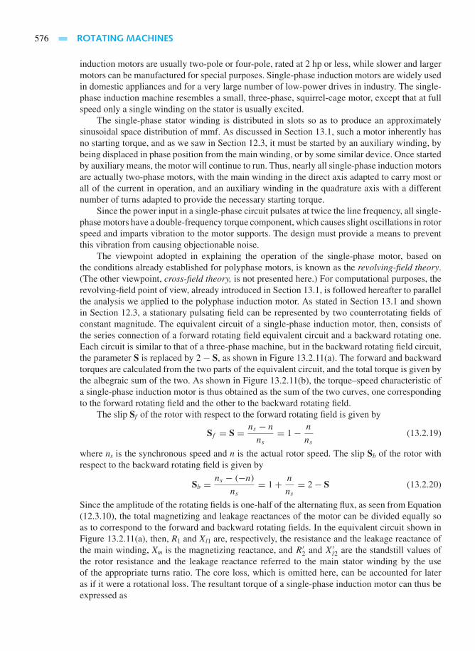
576 ROTATING MACHINES
induction motors are usually two-pole or four-pole, rated at 2 hp or less, while slower and largermotors can be manufactured for special purposes. Single-phase induction motors are widely usedin domestic appliances and for a very large number of low-power drives in industry. The single-phase induction machine resembles a small, three-phase, squirrel-cage motor, except that at fullspeed only a single winding on the stator is usually excited.
The single-phase stator winding is distributed in slots so as to produce an approximatelysinusoidal space distribution of mmf. As discussed in Section 13.1, such a motor inherently hasno starting torque, and as we saw in Section 12.3, it must be started by an auxiliary winding, bybeing displaced in phase position from the main winding, or by some similar device. Once startedby auxiliary means, the motor will continue to run. Thus, nearly all single-phase induction motorsare actually two-phase motors, with the main winding in the direct axis adapted to carry most orall of the current in operation, and an auxiliary winding in the quadrature axis with a differentnumber of turns adapted to provide the necessary starting torque.
Since the power input in a single-phase circuit pulsates at twice the line frequency, all single-phase motors have a double-frequency torque component, which causes slight oscillations in rotorspeed and imparts vibration to the motor supports. The design must provide a means to preventthis vibration from causing objectionable noise.
The viewpoint adopted in explaining the operation of the single-phase motor, based onthe conditions already established for polyphase motors, is known as the revolving-field theory.(The other viewpoint, cross-field theory, is not presented here.) For computational purposes, therevolving-field point of view, already introduced in Section 13.1, is followed hereafter to parallelthe analysis we applied to the polyphase induction motor. As stated in Section 13.1 and shownin Section 12.3, a stationary pulsating field can be represented by two counterrotating fields ofconstant magnitude. The equivalent circuit of a single-phase induction motor, then, consists ofthe series connection of a forward rotating field equivalent circuit and a backward rotating one.Each circuit is similar to that of a three-phase machine, but in the backward rotating field circuit,the parameter S is replaced by 2− S, as shown in Figure 13.2.11(a). The forward and backwardtorques are calculated from the two parts of the equivalent circuit, and the total torque is given bythe albegraic sum of the two. As shown in Figure 13.2.11(b), the torque–speed characteristic ofa single-phase induction motor is thus obtained as the sum of the two curves, one correspondingto the forward rotating field and the other to the backward rotating field.
The slip Sf of the rotor with respect to the forward rotating field is given by
Sf = S = ns − n
ns= 1− n
ns(13.2.19)
where ns is the synchronous speed and n is the actual rotor speed. The slip Sb of the rotor withrespect to the backward rotating field is given by
Sb = ns − (−n)ns
= 1+ n
ns= 2− S (13.2.20)
Since the amplitude of the rotating fields is one-half of the alternating flux, as seen from Equation(12.3.10), the total magnetizing and leakage reactances of the motor can be divided equally soas to correspond to the forward and backward rotating fields. In the equivalent circuit shown inFigure 13.2.11(a), then, R1 and Xl1 are, respectively, the resistance and the leakage reactance ofthe main winding, Xm is the magnetizing reactance, and R′2 and X′l2 are the standstill values ofthe rotor resistance and the leakage reactance referred to the main stator winding by the useof the appropriate turns ratio. The core loss, which is omitted here, can be accounted for lateras if it were a rotational loss. The resultant torque of a single-phase induction motor can thus beexpressed as

13.2 INDUCTION MACHINES 577
Te =I 2f (1− S)
ωmSR′2 −
I 2b (1− S)
ωm(2− S)R′2 (13.2.21)
The following example illustrates the usefulness of the equivalent circuit in evaluating themotor performance.
+
−
V
R1jXl1
j0.5Xm
j0.5X 'l2
j0.5Xm
(a)
(b)
Zf
Zb
If
Ib
I1
0.5R'2S
j0.5X 'l2
0.5R'22 − S
Torque
Speed
Torque due toforward rotating field
Torque due to backward rotating field
Resultant torque
Figure 13.2.11 Single-phase in-duction motor based on therevolving-field theory. (a) Equiva-lent circuit. (b) Torque–speed char-acteristics.
EXAMPLE 13.2.4
A 1/4-hp, 230-V, 60-Hz, four-pole, single-phase induction motor has the following parameters andlosses: R1 = 10 , Xl1 = X′l2 = 12.5 ,R′2 = 11.5 , and Xm = 250 . The core loss at 230 Vis 35 W and the friction and windage loss is 10 W. For a slip of 0.05, determine the stator current,

578 ROTATING MACHINES
power factor, developed power, shaft output power, speed, torque, and efficiency when the motoris running as a single-phase motor at rated voltage and frequency with its starting winding open.
So l u t i on
From the given data applied to the equivalent circuit of Figure 13.2.11, we see that
0.5R′2S
= 11.5
2× 0.05= 115
0.5R′22− S
= 11.5
2(2− 0.05)= 2.95
j0.5Xm = j125
j0.5X′l2 = j6.25
For the forward-field circuit, the impedance is
Zf = (115+ j6.25)j125
115+ j131.25= 59+ j57.65 = Rf + jXf
and for the backward-field circuit, the impedance is
Zb = (2.95+ j6.25)j125
2.95+ j131.25= 2.67+ j6.01 = Rb + jXb
The total series impedance Ze is then given by
Ze = Z1 + Zf + Zb = (10+ j12.5)+ (59+ j57.65)+ (2.67+ j6.01)
= 71.67+ j76.16 = 104.6 − 46.74°
The input stator current is
I1 = 230
104.6 46.74°= 2.2 − 46.74° A
also,Power factor = cos 46.74° = 0.685 lagging,Developed power Pd = I 2
1 Rf (1 − S) + I 21 Rb [1− (2− S)] = I 2
1 (Rf − Rb)(1 − S) =2.22(59− 2.67)(1− 0.05) = 259 WShaft-output power Po = Pd − Prot − Pcore = 259− 10− 35 = 214 W, or 0.287 hpSpeed = (1− S) synchronous speed = 0.95× 120× 60/4 = 1710 r/min, or 179 rad/sTorque = 214/179 = 1.2 N ·mEfficiency = output
input= 214
230× 2.2× 0.685= 214
346.6= 0.6174, or 61.74%
Starting Methods for Single-Phase Induction Motors
The various forms of a single-phase induction motor are grouped into three principal types,depending on how they are started.
1. Split-phase or resistance-split-phase motors: Split-phase motors have two stator windings(a main winding and an auxiliary winding) with their axes displaced 90 electrical degrees in space.As represented schematically in Figure 13.2.12(a), the auxiliary winding in this type of motorhas a higher resistance-to-reactance ratio than the main winding. The two currents are thus outof phase, as indicated in the phasor diagram of Figure 13.2.12(b). The motor is equivalent toan unbalanced two-phase motor. The rotating stator field produced by the unbalanced two-phase

13.2 INDUCTION MACHINES 579
winding currents causes the motor to start. The auxiliary winding is disconnected by a centrifugalswitch or relay when the motor comes up to about 75% of the synchronous speed. The torque–speedcharacteristic of the split-phase motor is of the form shown in Figure 13.2.12(c). A split-phasemotor can develop a higher starting torque if a series resistance is inserted in the starting auxiliarywinding. A similar effect can be obtained by inserting a series inductive reactance in the mainwinding; this additional reactance is short-circuited when the motor builds up speed.
2. Capacitor motors: Capacitor motors have a capacitor in series with the auxiliary windingand come in three varieties: capacitor start, two-value capacitor, and permanent-split capacitor.As their names imply, the first two use a centrifugal switch or relay to open the circuit or reducethe size of the starting capacitor when the motor comes up to speed. A two-value-capacitor motor,with one value for starting and one for running, can be designed for optimum starting and runningperformance; the starting capacitor is disconnected after the motor starts. The relevant schematicdiagrams and torque–speed characteristics are shown in Figures 13.2.13, 13.2.14, and 13.2.15.Motors in which the auxiliary winding and the capacitor are not cut out during the normal runningconditions operate, in effect, as unbalanced two-phase induction motors.
3. Shaded-pole motors: The least expensive of the fractional-horsepower motors, generallyrated up to 1/20 hp, they have salient stator poles, with one-coil-per-pole main windings. Theauxiliary winding consists of one (or rarely two) short-circuited copper straps wound on a portionof the pole and displaced from the center of each pole, as shown in Figure 13.2.16(a). The shaded-
(a)
+
−
Centrifugal switch
Cage rotor
Auxiliary winding
Torque, per unit
Torque during starting due to mainand auxiliary windings
Torque due to main winding only
Mainwinding
(c)
(b)
I
I
Im
Im
VV
Ia
Ia
4
3
2
1
S = 1(zero speed)
S = 0(synchronous speed)
Speed or slip
Switc
hing
spee
d
Figure 13.2.12 Split-phase motor. (a) Schematic diagram. (b) Phasor diagram at starting. (c) Typical torque–speed (or slip) characteristic.

580 ROTATING MACHINES
(a)
+
−
Centrifugal switch
Auxiliary winding
Torque, per unitTorque during starting due tomain and auxiliary windings
Torque due to main winding only(c)
(b)
I
I
Im
Im
VV
Ia
C
Ia
4
3
2
1
S = 1(zero speed)
S = 0(synchronous speed)
Speed or slip
Switc
hing
spee
d
Mainwinding
Figure 13.2.13 Capacitor-start motor. (a) Schematic diagram. (b) Phasor diagram at starting. (c) Typicaltorque–speed characteristic.
pole motor got its name from these shading bands. Induced currents in the shading coil cause theflux in the shaded portion of the pole to lag the flux in the other portion in time. The result isthen like a rotating field moving in the direction from the unshaded to the shaded portion of thepole. A low starting torque is produced. A typical torque-speed characteristic is shown in Figure13.2.16(b). Shaded-pole motors have a rather low efficiency.
Applications for Induction Motors
Before specifying a particular motor for a given application, the designer must know the loadcharacteristics, such as horsepower requirement, starting torque, acceleration capability, speedvariation, duty cycle, and the environment in which the motor is to operate. Typical speed–torquecurves for squirrel-cage induction motors with NEMA design classification A, B, C, and D areshown in Figure 13.2.17. Having selected the appropriate motor for a given application, the nextstep is to specify a controller for the motor to furnish proper starting, stopping, and reversingwithout damaging the motor, other connected loads, or the power system. The ranges of standardpower ratings given by NEMA for single-phase motors are listed in Table 13.2.1. Two-phaseinduction motors with high rotor resistance are employed as servomotors for control-systemapplications that usually require positive damping over the full speed range.

13.2 INDUCTION MACHINES 581
S = 1(zero speed)
S = 0(synchronous speed)
Torque, per unit
2
1
Speedor slip
(a) (b)
+
−
Auxiliary winding
Mainwinding
Figure 13.2.14 Permanent-split-capacitor motor. (a) Schematic diagram. (b) Typical torque–speedcharacteristic.
Centrifugalswitch
(a)
+
−
Auxiliary winding
Mainwinding
Torque, per unit
Starting capacitor
Running capacitor
(b)
3
2
1
S = 1(zero speed)
S = 0(synchronous speed)
Speedor slip
Switc
hing
spee
d
Figure 13.2.15 Two-value-capacitor motor. (a) Schematic diagram. (b) Typical torque–speed characteristic.
S = 1(zero speed)
S = 0(synchronous speed)
Torque, per unit
2
1
Speedor slip
(b)(a)
Cage rotor
Shading bandor coil
Figure 13.2.16 Shaded-pole motor. (a) Schematic diagram. (b) Typical torque–speed characteristic.

582 ROTATING MACHINES
TABLE 13.2.1 Ranges of Standard Power Ratings for Single-Phase Induction Motors
Motor Power Range
Capacitor start 1 mhp to 10 hpResistance start 1 mhp to 10 hpTwo-value capacitor 1 mhp to 10 hpPermanent-split capacitor 1 mhp to 1.5 hpShaded pole 1 mhp to 1.5 hp
Source: NEMA Standards Publication MG 1, Motors and Generators, New York, 1987.
300
200
100
20 40 60 80 1000Speed, % synchronous speed
A or B
C
D
Torq
ue, %
ful
l-lo
ad to
rque
Figure 13.2.17 Typical speed–torque curves forsquirrel-cage induction motors with NEMA designclassifications A, B, C, and D. (Adapted from NEMAStandards Publication MG 10, Energy ManagementGuide for Selection and Use of Polyphase Motors,New York, 1988.)
13.3 SYNCHRONOUS MACHINES
Large ac power networks operating at a constant frequency of 60 Hz in the United States (50 Hzin Europe) rely almost exclusively on synchronous generators to generate electric energy. Theycan also have synchronous compensators or condensers at key points for reactive power control.Generators are the largest single-unit electric machines in production, having power ratings inthe range of 1500 MVA, and we can expect machines of several thousand MVA to come intouse in future decades. Private, standby, and peak-load plants with diesel or gas-turbine primemovers also have alternators. Non-land-based synchronous plants can be found on oil rigs, onlarge aircraft with hydraulically driven alternators operating at 400 Hz, and on ships for variablefrequency supply to synchronous propeller motors. Synchronous motors provide constant speedindustrial drives with the possibility of power factor correction, although they are not often builtin small ratings, for which the induction motor is cheaper.
This section develops analytical methods of examining the steady-state performance ofsynchronous machines. We first consider cylindrical-rotor machines and discuss the effects ofsalient poles subsequently.

13.3 SYNCHRONOUS MACHINES 583
Equivalent Circuit of a Synchronous Machine
A review of the material about elementary synchronous machines presented in Section 13.1 isvery helpful at this stage to recall the principles of operation for synchronous machines.
To investigate the equivalent circuit of a synchronous machine, for the sake of simplicity, letus begin by considering an unsaturated cylindrical-rotor synchronous machine. Effects of saliencyand magnetic saturation can be considered later. Since for the present we are only concerned withthe steady-state behavior of the machine, circuit parameters of the field and damper windings neednot be considered. The effect of the field winding, however, is taken care of by the flux producedby the dc field excitation and the ac voltage generated by the field flux in the armature circuit.Thus, let Ef be the ac voltage, known as excitation voltage, generated by the field flux. As forthe armature winding, under balanced conditions of operation we will analyze it on a per-phasebasis. The armature winding obviously has a resistance Ra and a leakage reactance Xl of thearmature per phase.
The armature current Ia produces the armature reaction flux, the effect of which can berepresented by an inductive reactance Xφ , known as magnetizing reactance or armature reactionreactance. Thus Figure 13.3.1 shows the equivalent circuits in phasor notation, with all per-phasequantities, for a cylindrical-rotor synchronous machine working as either a generator or a motor.The sum of the armature leakage reactance and the armature reaction reactance is known as thesynchronous reactance,
Xs = Xφ +Xl (13.3.1)
and Ra + jXs is called the synchronous impedance Zs. Thus, the equivalent circuit for anunsaturated cylindrical-rotor synchronous machine under balanced polyphase conditions reducesto that shown in Figure 13.3.1(b), in which the machine is represented on a per-phase basis byits excitation voltage Ef in series with the synchronous impedance. Note that Vt is the terminalper-phase rms voltage, usually taken as reference.
In all but small machines, the armature resistance is usually neglected except for its effect onlosses (and hence the efficiency) and heating. With this simplification, Figure 13.3.2 shows thefour possible cases of operation of a round-rotor synchronous machine, in which the followingrelation holds:
Vt + j IaXs = Ef (13.3.2)
Observe that the motor armature current is taken in the direction opposite to that of the generator.The machine is said to be overexcited when the magnitude of the excitation voltage exceedsthat of the terminal voltage; otherwise it is said to be underexcited. The angle δ between theexcitation voltage Ef and the terminal voltage Vt is known as the torque angle or power angle of
+
−
+
−
−Er
(a)
+
−VtEf
jXφ jXl
Ia
Ra
Motor
IaGenerator
+
−(b)
+
−VtEf
jXs = j(Xφ + XI)
Ia
Ra
Motor
IaGenerator
Figure 13.3.1 Per-phase equivalent circuits of a cylindrical-rotor synchronous machine.

584 ROTATING MACHINES
(a)
jIaXs
Ia
Ef
Vtφ
δ
(b)
jIaXs
Ia
Ef
Vt
φ δ
(c)
jIaXs
−Ia
Ia Ef
Vt
φ
δ
(d )
jIaXs
−Ia
Ia
Ef
Vt
φ δ
Figure 13.3.2 Four possible cases of operation of a round-rotor synchronous machine with negligible armatureresistance. (a) Overexcited generator (power factor lagging), P > 0,Q > 0, δ > 0. (b) Underexcitedgenerator (power factor leading), P > 0,Q < 0, δ > 0. (c) Overexcited motor (power factor leading),P < 0,Q > 0, δ < 0. (d) Underexcited motor (power factor lagging), P < 0,Q < 0, δ < 0.
the synchronous machine. The power-angle performance characteristics are discussed later in thissection. The dc excitation can be provided by a self-excited dc generator, known as the exciter,mounted on the same shaft as the rotor of the synchronous machine.
The voltage regulation of a synchronous generator at a given load, power factor, and ratedspeed is defined as
% voltage regulation = Ef − Vt
Vt
× 100 (13.3.3)
where Vt is the terminal voltage on the load, and Ef is the no-load terminal voltage at rated speedwhen the load is removed without changing the field current.
EXAMPLE 13.3.1
The per-phase synchronous reactance of a three-phase, wye-connected, 2.5-MVA, 6.6-kV, 60-Hzturboalternator is 10 . Neglect the armature resistance and saturation. Calculate the voltageregulation when the generator is operating at full load with (a) 0.8 power factor lagging, and (b)0.8 power factor leading.

13.3 SYNCHRONOUS MACHINES 585
So l u t i on
Per-phase terminal voltage Vt = 6.6× 1000√3
= 3811 V
Full-load per-phase armature current Ia = 2.5× 10⁶
√3× 6.6× 1000
= 218.7 A
(a) Referring to Figure 13.3.2(a) for an overexcited generator operating at 0.8 power factorlagging, and applying Equation (13.3.2), we have
Ef = 3811+ j218.7(0.8− j0.6)(10) = 5414 tan−10.3415
% voltage regulation = 5414− 3811
3811× 100 = 0.042× 100 = 4.2%
(b) Referring to Figure 13.3.2(b) for an underexcited generator operating at 0.8 power factorleading, and applying Equation (13.3.2), we have
Ef = 3811+ j218.7(0.8+ j0.6)(10) = 3050 tan−10.7
% voltage regulation = 3050− 3811
3811× 100 = −0.2× 100 = −20%
As we have just seen, the voltage regulation for a synchronous generator can becomenegative.
Power Angle and Other Performance Characteristics
The real and reactive power delivered by a synchronous generator, or received by a synchronousmotor, can be expressed in terms of the terminal voltage Vt, the generated voltage Ef, thesynchronous impedance Zs, and the power angle or torque angle δ. Referring to Figure 13.3.2,it is convenient to adopt a convention that makes positive the real power P and the reactivepower Q delivered by an overexcited generator. Accordingly, the generator action correspondsto positive values of δ, whereas the motor action corresponds to negative values of δ. Withthe adopted notation it follows that P > 0 for generator operation, whereas P < 0 for motoroperation. Further, positive Q means delivering inductive VARs for a generator action, or receivinginductive VARs for a motor action; negative Q means delivering capacitive VARs for a generatoraction, or receiving capacitive VARs for a motor action. It can be observed from Figure 13.3.2that the power factor is lagging when P and Q have the same sign, and leading when P and Qhave opposite signs.
The complex power output of the generator in volt-amperes per phase is given by
S = P + jQ = Vt I∗a (13.3.4)
where Vt is the terminal voltage per phase, Ia is the armature current per phase, and * indicates acomplex conjugate. Referring to Figure 13.3.2(a), in which the effect of armature resistance hasbeen neglected, and taking the terminal voltage as reference, we have the terminal voltage,
Vt = Vt + j 0 (13.3.5)
the excitation voltage or generated voltage,
Ef = Ef (cos δ + j sin δ) (13.3.6)
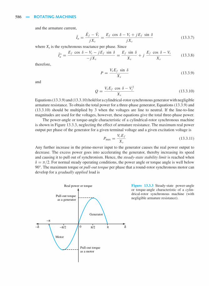
586 ROTATING MACHINES
and the armature current,
Ia = Ef − Vt
jXs
= Ef cos δ − Vt + jEf sin δ
jXs
(13.3.7)
where Xs is the synchronous reactance per phase. Since
I ∗a =Ef cos δ − Vt − jEf sin δ
−jXs
= Ef sin δ
Xs
+ jEf cos δ − Vt
Xs
(13.3.8)
therefore,
P = VtEf sin δ
Xs
(13.3.9)
and
Q = VtEf cos δ − V 2t
Xs
(13.3.10)
Equations (13.3.9) and (13.3.10) hold for a cylindrical-rotor synchronous generator with negligiblearmature resistance. To obtain the total power for a three-phase generator, Equations (13.3.9) and(13.3.10) should be multiplied by 3 when the voltages are line to neutral. If the line-to-linemagnitudes are used for the voltages, however, these equations give the total three-phase power.
The power-angle or torque-angle characteristic of a cylindrical-rotor synchronous machineis shown in Figure 13.3.3, neglecting the effect of armature resistance. The maximum real poweroutput per phase of the generator for a given terminal voltage and a given excitation voltage is
Pmax = VtEf
Xs
(13.3.11)
Any further increase in the prime-mover input to the generator causes the real power output todecrease. The excess power goes into accelerating the generator, thereby increasing its speedand causing it to pull out of synchronism. Hence, the steady-state stability limit is reached whenδ = π/2. For normal steady operating conditions, the power angle or torque angle is well below90°. The maximum torque or pull-out torque per phase that a round-rotor synchronous motor candevelop for a gradually applied load is
δ−δ
Real power or torque
Pull-out torqueas a generator
Generator
0
Pull-out torqueas a motor
Motor
π
−π
−π/2 π/2
Figure 13.3.3 Steady-state power-angleor torque-angle characteristic of a cylin-drical-rotor synchronous machine (withnegligible armature resistance).
13.3 SYNCHRONOUS MACHINES 587
Tmax = Pmax
ωm
= Pmax
2π ns/60(13.3.12)
where ns is the synchronous speed in r/min.In the steady-state theory of the synchronous machine, with known terminal bus voltage Vt
and a given synchronous reactance Xs, the six operating variables are P, Q, δ, φ, Ia, and Ef. Thesynchronous machine is said to have two degrees of freedom, because the selection of any two,such as φ and Ia, P and Q, or δ and Ef, determines the operating point and establishes the otherfour quantities.
The principal steady-state operating characteristics are the interrelations among terminalvoltage, field current, armature current, real power, reactive power, torque angle, power factor,and efficiency. These characteristics can be computed for application studies by means of phasordiagrams, such as those shown in Figure 13.3.2, corresponding to various conditions of operation.
The efficiency of a synchronous generator at a specified power output and power factor isdetermined by the ratio of the output to the input; the input power is given by adding the machinelosses to the power output. The efficiency is conventionally computed in accordance with a setof rules agreed upon by ANSI. Six losses are included in the computation:
• Armature winding copper loss for all phases, calculated after correcting the dc resistanceof each phase for an appropriate allowable temperature rise, depending on the class ofinsulation used.
• Field copper loss, based on the field current and measured field-winding dc resistance,corrected for temperature in the same way armature resistance is corrected. Note that thelosses in the field rheostats that are used to adjust the generated voltage are not charged tothe synchronous machine.
• Core loss, which is read from the open-circuit core-loss curve at a voltage equal to theinternal voltage behind the resistance of the machine.
• Friction and windage loss.
• Stray-load losses, which account for the fact that the effective ac resistance of the armatureis greater than the dc resistance because of the skin effect, and for the losses caused by thearmature leakage flux.
• Exciter loss, but only if the exciter is an integral component of the alternator, i.e., shares acommon shaft or is permanently coupled. Losses from a nonintegral exciter are not chargedto the alternator.
EXAMPLE 13.3.2
A 1000-hp, 2300-V, wye-connected, three-phase, 60-Hz, 20-pole synchronous motor, for whichcylindrical-rotor theory can be used and all losses can be neglected, has a synchronous reactanceof 5.00 /phase.
(a) The motor is operated from an infinite bus supplying rated voltage and rated frequency,and its field excitation is adjusted so that the power factor is unity when the shaft loadis such as to require an input of 750 kW. Compute the maximum torque that the motorcan deliver, given that the shaft load is increased slowly with the field excitation heldconstant.

588 ROTATING MACHINES
(b) Instead of an infinite bus as in part (a), let the power to the motor be supplied by a1000-kVA, 2300-V, wye-connected, three-phase, 60-Hz synchronous generator whosesynchronous reactance is also 5.00/phase. The generator is driven at rated speed, and thefield excitations of the generator and motor are adjusted so that the motor absorbs 750 kWat unity power factor and rated terminal voltage. If the field excitations of both machinesare then held constant, and the mechanical load on the synchronous motor is graduallyincreased, compute the maximum motor torque under the conditions. Also determine thearmature current, terminal voltage, and power factor at the terminals corresponding tothis maximum load.
(c) Calculate the maximum motor torque if, instead of remaining constant as in part (b), thefield currents of the generator and motor are gradually increased so as to always maintainrated terminal voltage and unity power factor while the shaft load is increased.
So l u t i on
The solution neglects reluctance torque because cylindrical-rotor theory is applied.
(a) The equivalent circuit and the corresponding phasor diagram for the given conditions areshown in Figure E13.3.2 (a), with the subscript m attached to the motor quantities,
Rated voltage per phase Vt = 2300√3= 1328 V line-to-neutral
Current per phase Iam = 750× 103
√3× 2300× 1.0
= 188.3 A
IamXsm = 188.3× 5 = 941.5 V
jXsmIam Iam
jIamXsm
−Iam+
−
+
−Vt
Vt
Efm
Efm
(a)
Iag = −Iam
jXsmjXsg Iag
Iam
jIamXsm
jIagXsg+
−
+
−Vt
Efm
+
−Efg
Efg
Efm
Vt
Iam
(b)
Figure E13.3.2

13.3 SYNCHRONOUS MACHINES 589
Efm =√
13282 + 941.52 = 1628 V
Pmax = EfmVt
Xsm
= 1628× 1328
5
= 432.4 kW per phase, or 1297.2 kW for three phases
Synchronous speed = 120× 60
20= 360 r/min, or 6 r/s
ωs = 2π × 6 = 37.7 rad/s
Tmax = 1297.2× 103
37.7= 34,408 N · m
(b) With the synchronous generator as the power source, the equivalent circuit and thecorresponding phasor diagram for the given conditions are shown in Figure E13.3.2(b),with subscript g attached to the generator quantities,
Efg = Efm = 1628 V
Pmax = EfgEfm
Xsg +Xsm
= 1628× 1628
10
= 265 kW per phase, or 795 kW for three phases
Tmax = 795× 103
37.7= 21,088 N · m
If a load torque greater than this amount were applied to the motor shaft, synchronismwould be lost; the motor would stall, the generator would tend to overspeed, and thecircuit would be opened by circuit-breaker action.
Corresponding to the maximum load, the angle between Efg and Efm is 90°. Fromthe phasor diagram it follows that
Vt = Efg√2= 1628√
2= 1151.3 V line-to-neutral, or 1994 V line-to-line
IagXsg = 1151.3 or Iag = 1151.3
5= 230 A
The power factor is unity at the terminals.
(c) Vt = 1328 V, and the angle between Efg and Efm is 90°. Hence it follows that
Efg = Efm = 1328√
2 = 1878 V
Pmax = EfgEfm
Xsg +Xsm
= 1878× 1878
10= 352.7 kW per phase, or 1058 kW for three phases
Tmax = 1058× 103
37.7= 28,064 N · m
Effects of Saliency and Saturation
Because of saliency, the reactance measured at the terminals of a salient-pole synchronous machineas opposed to a cylindrical-rotor machine (with uniform air gap) varies as a function of the rotor

590 ROTATING MACHINES
position. The effects of saliency are taken into account by the two-reactance theory, in whichthe armature current Ia is resolved into two components: Id in the direct or field axis, and Iq inthe quadrature or interpolar axis. Iq will be in the time phase with the excitation speed voltageEf , whereas Id will be in time quadrature with Ef . Direct- and quadrature-axis reactances (Xd
and Xq) are then introduced to model the machine in two axes. While this involved method ofanalysis is not pursued here any further, the steady-state power-angle characteristic of a salient-pole synchronous machine (with negligible armature resistance) is shown in Figure 13.3.4. Theresulting power has two terms: one due to field excitation and the other due to saliency. Themaximum torque that can be developed is somewhat greater because of the contribution due tosaliency.
Saturation factors and saturated reactances can be developed to account approximately forsaturation, or more involved field-plotting methods may be used if necessary. Such matters areobviously outside the scope of this text.
Parallel Operation of Interconnected Synchronous Generators
In order to assure continuity of the power supply within prescribed limits of frequency and voltageat all the load points scattered over the service area, it becomes necessary in any modern powersystem to operate several alternators in parallel, interconnected by various transmission lines, ina well-coordinated and optimized manner for the most economical operation. A generator can beparalleled with an infinite bus (or with another generator running at rated voltage and frequencysupplying the load) by driving it at synchronous speed corresponding to the system frequency andadjusting its field excitation so that its terminal voltage equals that of the bus. If the frequency ofthe incoming machine is not exactly equal to that of the system, the phase relation between itsvoltage and the bus voltage will vary at a frequency equal to the difference between the frequenciesof the machine and the bus voltages. In normal practice, this difference can usually be made quitesmall, to a fraction of a hertz; in polyphase systems, it is essential that the same phase sequence be
+δ
P
−P
Generator
0
Power due to saliency
Power due to field excitation
sin δ
−δ
Resultant power P
Motor
π−π
VtEf
Xd
sin 2δ−Vt
2
21Xq
1Xd
( )
−π/2 π/2
Figure 13.3.4 Steady-state power-angle characteristic of a salient-pole synchronous machine (with negli-gible armature resistance).
13.3 SYNCHRONOUS MACHINES 591
maintained on either side of the synchronizing switch. Thus, synchronizing requires the followingconditions of the incoming machine:
• Correct phase sequence• Phase voltages in phase with those of the system• Frequency almost exactly equal to that of the system• Machine terminal voltage approximately equal to the system voltage
A synchroscope is used for indicating the appropriate moment for synchronization. After themachine has been synchronized and is part of the system, it can be made to take its share of theactive and reactive power by appropriate adjustments of its prime-mover throttle and field rheostat.The system frequency and the division of active power among the generators are controlledby means of prime-mover throttles regulated by governors and automatic frequency regulators,whereas the terminal voltage and the reactive volt-ampere division among the generators arecontrolled by voltage regulators acting on the generator-field circuits and by transformers withautomatic tap-changing devices.
EXAMPLE 13.3.3
Two three-phase, 6.6-kV, wye-connected synchronous generators, operating in parallel, supply aload of 3000 kW at 0.8 power factor lagging. The synchronous impedance per phase of machine Ais 0.5+ j10 , and of machine B it is 0.4+ j12. The excitation of machine A is adjusted so thatit delivers 150 A at a lagging power factor, and the governors are set such that the load is sharedequally between the two machines. Determine the armature current, power factor, excitationvoltage, and power angle of each machine.
So l u t i on
One phase of each generator and one phase of the equivalent wye of the load are shown in FigureE13.3.3(a). The load current IL is calculated as
IL = 3, 000√3× 6.6× 0.8
− cos−1 0.8 = 328(0.8− j0.6) = 262.4− j196.8 A
For machine A,
cos φA = 1500√3× 6.6× 150
= 0.875 lagging; φA = 29°; sin φA = 0.485
IA = 150(0.874− j0.485) = 131.1− j72.75 A
For machine B,
IB = IL − IA = 131.3− j124 = 180.6 − cos
(131.3
180.6
)
cos φB = 131.3
180.6= 0.726 lagging
With the terminal voltage Vr as reference, we have
EfA = Vt + IAZA = (6.6/√
3)+ (131.1− j72.75)(0.5+ j10)× 10−3
= 4.6+ j1.27 kV per phase
Power angle δA = tan−1(1.27/4.6) = 15.4°

592 ROTATING MACHINES
The line-to-line excitation voltage for machine A is√
3√
4.62 + 1272 = 8.26 kV.
EfB = Vt + IBZB = (6.6/√
3)+ (131.1− j124)(0.4+ j12)× 10−3
= 5.35+ j1.52 kV per phase
Power angle δB = tan−1(1.52/5.35) = 15.9°
The line-to-line excitation voltage for machine B is√
3√
5.352 + 1.522 = 9.6 kV.The corresponding phasor diagram is sketched in Figure E13.3.3(b).
IA IB
ZA ZB
IL
+
−EfA
+
−EfB
+
−
Vt Load
(a)
Vt
(b)
δB
φB
δA
φA
IA
IAZA
IBZB
IB
EfA
EfB Figure E13.3.3
Steady-State Stability
The property of a power system that ensures that it will remain in equilibrium under both normaland abnormal conditions is known as power-system stability. Steady-state stability is concernedwith slow and gradual changes, whereas transient stability is concerned with severe disturbances,such as sudden changes in load or fault conditions. The largest possible flow of power througha particular point, without loss of stability, is known as the steady-state stability limit whenthe power is increased gradually, and as the transient-stability limit when a sudden disturbanceoccurs.
For a generator connected to a system that is very large compared to its own size, the systemin Figure 13.3.5 can be used. The power-angle equation (neglecting resistances) for the systemunder consideration becomes

13.3 SYNCHRONOUS MACHINES 593
Generator
Bus
Infinite busEs ∠ δs
jXe
Eg ∠ δg
Figure 13.3.5 Generator connected to an infinite bus.
P = EgEs
Xsin δgs (13.3.13)
where δgs is the angular difference between δg and δs , and X = Xd + Xe, with Xd being thedirect-axis reactance of the synchronous generator. The power angle characteristic given byEquation (13.3.13) is plotted in Figure 13.3.6. The peak of the power-angle curve, given byPmax, is known as the steady-state power limit (shown by point b in Figure 13.3.6), representingthe maximum power that can theoretically be transmitted in a stable manner. A machine isusually operated at less than the power limit (such as at point a in Figure 13.3.6), therebyleaving a steady-state margin, as otherwise even a slight increase in the angle δgs (such as atpoint c in Figure 13.3.6) would lead to instability. Installing parallel transmission lines [whicheffectively reduces X in Equation (13.3.13)] or adding series capacitors in lines raises the stabilitylimit.
Applications for Synchronous Motors
With constant-speed operation, power factor control, and high operating efficiency, three-phasesynchronous motors are employed in a wide range of applications. An overexcited synchronousmotor, known as a synchronous condenser, is used to improve the system power factor. Syn-chronous motors are used as prime movers of dc generators and variable-frequency ac generators.Typical applications include pumps, compressors, mills, mixers, and crushers.
Single-phase reluctance motors find application in such devices as clocks, electric shavers,electric clippers, vibrators, sandpapering machines, and engraving tools. A hysteresis motor isemployed for driving high-quality record players and tape recorders, electric clocks, and othertiming devices. The horsepower range is up to 1 hp for hysteresis motors, and up to 100 hp forreluctance motors.
δgs
P
Generator
90°
Motor
a
b
c
Pmax
Figure 13.3.6 Power-angle curve ofEquation (13.3.13).

594 ROTATING MACHINES
13.4 DIRECT-CURRENT MACHINES
Generally speaking, conventional dc generators are becoming obsolete and increasingly often arebeing replaced by solid-state rectifiers in most applications for which an ac supply is available.The same is not true for dc motors. The torque–speed characteristics of dc motors are what makesthem extremely valuable in many industrial applications. The significant features of the dc drivesinclude adjustable motor speed over wide ranges, constant mechanical power output or torque,rapid acceleration or deceleration, and responsiveness to feedback signals.
The dc commutator machines are built in a wide range of sizes, from small control deviceswith a 1-W power rating up to the enormous motors of 10,000 hp or more used in rolling-millapplications. The dc machines today are principally applied as industrial drive motors, particularlywhen high degrees of flexibility in controlling speed and torque are required. Such motors areused in steel and aluminum rolling mills, traction motors, overhead cranes, forklift trucks, electrictrains, and golf carts. Commutator machines are also used in portable tools supplied from batteries,in automobiles as starter motors, in blower motors, and in control applications as actuators andspeed-sensing or position-sensing devices.
In this section, we examine the steady-state performance characteristics of dc machines tohelp us understand their applications and limitations, illustrating the versatility of the dc machine.
Constructional Features of DC Machines
A dc generator or motor may have as many as four field windings, depending on the type and size ofthe machine and the kind of service intended. These field windings consist of two normal excitingfields, the shunt and series windings, and two fields that act in a corrective capacity to combatthe detrimental effects of armature reaction, called the commutating (compole or interpole) andcompensating windings, which are connected in series with the armature. The type of machine,whether shunt, series, or compound, is determined solely by the normal exciting-field circuitconnections, as shown in Figure 13.1.8. Figure 13.4.1 illustrates how various field windingsare arranged with respect to one another in part of a cross section of a dc machine, whereasFigure 13.4.2 shows the schematic connection diagram of a dc machine. The commutating andcompensating windings, their purpose, as well as the circuit connections are presented later inthis section.
Equivalent Circuit of a DC Machine
A review of the material presented with regard to elementary direct-current machines in Section13.1 can be helpful at this stage to recall the principles of operation for dc machines.
The circuit representations of a dc generator and a dc motor are shown in Figure 13.4.3.Under steady-state conditions the interrelationships between voltage and current are given by
Vf = If Rf (13.4.1)
and
Vt = Ea ± IaRa (13.4.2)
where the plus sign signifies a motor and the minus sign a generator. Vf is the voltage appliedto the field circuit, If is the field current, and Rf is the field-winding resistance. Vt is the terminalvoltage, Ea is the generated emf, Ia is the armature current, and Ra is the armature resistance. Thegenerated emf Ea is given by Equation (12.2.16) as

13.4 DIRECT-CURRENT MACHINES 595
Commutating pole (interpole)
Shunt fieldwinding
Series fieldwinding
Compensating field windinglocated in main-pole shoes
++
++ + +
+ ++
+
Mainpole
Mainpole
Armature witharmature winding
Commutating (interpole)field winding
Figure 13.4.1 Section of a dc machine illustrating the arrangement of various field windings.
Armature
Commutating(compole or interpole)
windingShunt field
Series fieldField rheostat
Compensating winding
Figure 13.4.2 Schematic con-nection diagram of a dc machine.
Ea = Kaφωm (13.4.3)
which is the speed (motional) voltage induced in the armature circuit due to the flux of thestator-field current. The electromagnetic torque Te is given by Equation (12.2.18) as
Te = KaφIa (13.4.4)
where Ka is the design constant. The product EaIa, known as the electromagnetic power beingconverted, is related to the electromagnetic torque by the relation
Pem = EaIa = Teωm (13.4.5)
For a motor, the terminal voltage is always greater than the generated emf, and the electromagnetictorque produces rotation against a load. For a generator, the terminal voltage is less than thegenerated emf, and the electromagnetic torque opposes that applied to the shaft by the primemover. If the magnetic circuit of the machine is not saturated, note that the flux φ in Equations(13.4.3) and (13.4.4) is proportional to the field current If producing the flux.
Commutator Action
As a consequence of the arrangement of the commutator and brushes, the currents in all conductorsunder the north pole are in one direction and the currents in all conductors under the south pole

596 ROTATING MACHINES
(a)
If
Ia+
−
+ −Vf
Vt
Rf Ra
Ea
(b)
If
Ia+
−
+
+
−
+
−−Vf
Vt
Rf Ra
Ea
Figure 13.4.3 (a) Circuit representation of a dc generator under steady-state conditions, Vf = Rf If andVt = Ea − IaRa . (b) Circuit representation of a dc motor under steady-state conditions, Vf = Rf If andVt = Ea + IaRa .
are in the opposite direction. Thus, the magnetic field of the armature currents is stationary inspace in spite of the rotation of the armature.
The process of reversal of currents in the coil is known as commutation. The current changesfrom +I to −I in time t . Ideally, the current in the coils being commutated should reverselinearly with time, as shown in Figure 13.4.4. Serious departure from linear commutation resultsin sparking at the brushes. Means for achieving sparkless commutation are touched upon later.As shown in Figure 13.4.4, with linear commutation, the waveform of the current in any coil asa function of time is trapezoidal.
Interpoles and Compensating Windings
The most generally used method for aiding commutation is by providing the machine with inter-poles, also known as commutating poles, or simply as compoles. These are small, narrow auxiliarypoles located between the main poles and centered on the interpolar gap. The commutating(interpole) winding is connected in series with the armature.
The demagnetizing effect of the armature mmf under pole faces can be compensated for, orneutralized, by providing a compensating (pole-face) winding, arranged in slots in the pole facein series with the armature, having a polarity opposite to that of the adjoining armature windingand having the same axis as that of the armature. Because they are costly, pole-face windings
Commutation
Coil current
−I
+I
t
∆t ∆t
Figure 13.4.4 Waveform of current in an armature coil undergoing linear commutation.

13.4 DIRECT-CURRENT MACHINES 597
are usually employed only in machines designed for heavy overload or rapidly changing loads,such as steel-mill motors subjected to reverse duty cycles or in motors intended to operate overwide speed ranges by shunt-field control. The schematic diagram of Figure 13.4.2 shows therelative positions of various windings, indicating that the commutating and compensating fieldsact along the armature axis (i.e., the quadrature axis), and the shunt as well as series fields actalong the axis of the main poles (i.e., the direct axis). It is thus possible to achieve rather completecontrol of the air-gap flux around the entire armature periphery, along with smooth sparklesscommutation.
DC Generator Characteristics
Figure 13.1.8 shows schematic diagrams of field-circuit connections for dc machines with-out including commutating pole or compensating windings. Shunt generators can be eitherseparately excited or self-excited, as shown in Figures 13.1.8 (a) and (b), respectively. Com-pound machines can be connected either long shunt, as in Figure 13.1.8(d), or short shunt, inwhich the shunt-field circuit is connected directly across the armature, without including theseries field.
In general, three characteristics specify the steady-state performance of a dc generator:
1. The open-circuit characteristic (abbreviated as OCC, and also known as no-load magne-tization curve), which gives the relationship between generated emf and field current atconstant speed.
2. The external characteristic, which gives the relationship between terminal voltage andload current at constant speed.
3. The load characteristic, which gives the relationship between terminal voltage and fieldcurrent, with constant armature current and speed.
All other characteristics depend on the form of the open-circuit characteristic, the load, and themethod of field connection. Under steady-state conditions, the currents being constant or, at most,varying slowly, voltage drops due to inductive effects are negligible.
As stated earlier and shown in Figure 13.4.3, the terminal voltage Vt of a dc generator isrelated to the armature current Ia and the generated emf Ea by
Vt = Ea − IaRa (13.4.6)
where Ra is the total internal armature resistance, including the resistance of interpole andcompensating windings as well as that of the brushes. The value of the generated emf Ea, byEquation (13.4.3), is governed by the direct-axis field flux (which is a function of the field currentand armature reaction) and the angular velocity ωm of the rotor.
The open-circuit and load characteristics of a separately excited dc generator, along withits schematic diagram of connections, are shown in Figures 13.4.5(a) and (b). It can be seenfrom the form of the external volt–ampere characteristic, shown in Figure 13.4.5(c), that theterminal voltage falls slightly as the load current increases. Voltage regulation is defined as thepercentage change in terminal voltage when full load is removed, so that, from Figure 13.4.5(c)it follows that
Voltage regulation = Ea − Vt
Vt
× 100% (13.4.7)

598 ROTATING MACHINES
Ia = IL
Vt
IaRa
IaRa
Ea
Ra
EaIf
+ −Vf
(a)
Field current If
Open circuitDrop due toarmature reaction
Load
Term
inal
vol
tage
Vt
Term
inal
vol
tage
Vt
Vt at rated full load
External characteristic
Drop due to armature reaction
Rated load
Load current IL
−
+
−
+
(b)
(c)
Figure 13.4.5 Open-circuit andload characteristics of a separatelyexcited dc generator. (a) Schematicdiagram of connections. (b) Termi-nal voltage versus field current rela-tionships. (c) External volt-amperecharacteristic.
Because the separately excited generator requires a separate dc field supply, its use is limited toapplications in which a wide range of controlled voltage is essential.
A shunt generator maintains approximately constant voltage on load. It finds wide applicationas an exciter for the field circuit of large ac generators. The shunt generator is also sometimesused as a tachogenerator when a signal proportional to the motor speed is required for control ordisplay purposes.

13.4 DIRECT-CURRENT MACHINES 599
IL = Ia
Vt = Ea − Ia(Ra + Rs)
+
−
Vt
Ra
EaSeries field Rs−
+
(a)
Diverter Ia(Ra + Rs)
A
B
C
Vol
tage
Vt
Ea
Load current
Residualvoltage
(b)
Figure 13.4.6 Dc series generator. (a) Schematic diagram of connections. (b) Volt–ampere characteristic atconstant speed.
The schematic diagram and the volt–ampere characteristic of a dc series generator at constantspeed are shown in Figure 13.4.6. The resistance of the series-field winding must be low forefficiency as well as for low voltage drop. The series generator was used in early constant-currentsystems by operating in the range B–C, where the terminal voltage fell off very rapidly withincreasing current.
The volt–ampere characteristics of dc compound generators at constant speeds are shown inFigure 13.4.7. Cumulatively compound generators, in which the series- and shunt-field windingmmfs are aiding, may be overcompounded, flat-compounded, or undercompounded, dependingon the strength of the series field. Overcompounding can be used to counteract the effect of adecrease in the prime-mover speed with increasing load, or to compensate for the line drop whenthe load is at a considerable distance from the generator. Differentially compounded generators, inwhich the series-winding mmf opposes that of the shunt-field winding, are used in applications inwhich wide variations in load voltage can be tolerated, and when the generator might be exposedto load conditions approaching short circuit.
Overcompounded
Flat compounded
Undercompounded
Differentiallycompounded
1.0 (rated value)
(rated value)1.0
Per-unitterminal voltage
Per-unit armature current
Figure 13.4.7 Volt–ampere characteristics of dc compound generatorsat constant speed.

600 ROTATING MACHINES
EXAMPLE 13.4.1
A 250-V, 50-kW short-shunt compound dc generator, whose schematic diagram is shown in FigureE13.4.1(a), has the following data: armature resistance 0.05 , series-field resistance 0.05 , andshunt-field resistance 130 . Determine the induced armature emf at rated load and terminalvoltage, while taking 2 V as the total brush-contact drop.
A1
A2
S1 S2F1 F2
(a)
Figure E13.4.1 Short-shunt com-pound generator. (a) Schematic dia-gram. (b) Equivalent circuit.
ERf = 130 Ω
RSe = 0.05 Ω
Ra = 0.05 Ω
+
+ +
−−
−
Vt = 250 V
Vf
If
Ia
It
(b)
So l u t i on
The equivalent circuit is shown in Figure E13.4.1(b).
It = 50× 103
250= 200 A
ItRSe = 200× 0.05 = 10 V
Vf = 250+ 10 = 260 V
If = 260
130= 2.0 A
Ia = 200+ 2 = 202 A
IaRa = 202× 0.05 = 10.1 V
E = 250+ 10.1+ 10+ 2 = 272.1 V

13.4 DIRECT-CURRENT MACHINES 601
DC Motor Characteristics
We gain an understanding of the speed–torque characteristics of a dc motor from Equations(13.4.2) through (13.4.4). In shunt motors, the field current can be simply controlled by theuse of a variable resistance in series with the field winding; the load current influences theflux only through armature reaction, and its effect is therefore relatively small. In series mo-tors, the flux is largely determined by the armature current, which is also the field current;it is somewhat difficult to control the armature and field currents independently. In the com-pound motor, the effect of the armature current on the flux depends on the degree of com-pounding. Most motors are designed to develop a given horsepower at a specified speed,and it follows from Equations (13.4.2) and (13.4.3) that the angular velocity ωm can be ex-pressed as
ωm = Vt − IaRa
Kaφ(13.4.8)
Thus, the speed of a dc motor depends on the values of the applied voltage Vt, the armature currentIa, the resistance Ra, and the field flux per pole φ.
Ra
Ia
IfIL = Ia + If
Ia = IL
Ea
−
+
+
−
Vt
Series field
Series field
Shunt field
Shunt field
Field rheostat
(a)
Diverter resistance
Ra
Ea
−
+
+
−
Vt
(b)
IfIL = Ia + If
Ra
Ia
Ea
−
+
+
−
Vt
(c)
Figure 13.4.8 Schematic diagrams of dc motors. (a) Shunt motor. (b) Series motor. (c) Cumulativelycompounded motor.

602 ROTATING MACHINES
The schematic arrangement of a shunt motor is shown in Figure 13.4.8(a). For a given appliedvoltage and field current, Equations (13.4.4) and (13.4.3) can be rewritten as
Te = KaφIa = KmIa (13.4.9)
Ea = Kaφωm = Kmωm (13.4.10)
Because Vt = Ea + IaRa , or Ia = (Vt − Ea)/Ra , it follows that
Te = KmVt
Ra
− K2mωm
Ra
(13.4.11)
Pem = EaIa = Teωm = VtKmωm
Ra
− K2mω
2m
Ra
(13.4.12)
The forms of the torque–armature current, speed–torque, and speed–power characteristics for ashunt-connected dc motor are illustrated in Figure 13.4.9.
The shunt motor is essentially a constant-speed machine with a low speed regulation. Asseen from Equation (13.4.8), the speed is inversely proportional to the field flux, and thus it canbe varied by controlling the field flux. When the motor operates at very low values of field flux,however, the speed will be high, and if the field becomes open-circuited, the speed will rise rapidlybeyond the permissible limit governed by the mechanical structure. In order to limit the speed toa safe value, when a shunt motor is to be designed to operate with a low value of shunt-field flux,it is usually fitted with a small cumulative series winding, known as a stabilizing winding.
The schematic diagram of a series motor is shown in Figure 13.4.8(b). The field flux is directlydetermined by the armature current so that
Te = Kaφ Ia = KI 2a (13.4.13)
and with negligible armature resistance,
Vt = Ea = Kaφωm = KIaωm (13.4.14)
Te = V 2t
Kω2m
(13.4.15)
Pem = ωmTe = V 2t
Kωm
(13.4.16)
and the speed–power curve is a rectangular hyperbola. The forms of the torque–armature current,speed–torque, and speed–power characteristics for a series-connected dc motor are also illustrated
ShuntShunt
Shunt
Series
Series
Series
Armature current
Torq
ue
Torque
Spee
d
Power
Spee
d
Compound
Figure 13.4.9 Characteristic curves for dc motors.

13.4 DIRECT-CURRENT MACHINES 603
in Figure 13.4.9. Note that the no-load speed is very high; care must be taken to ensure that themachine always operates on load. In practice, however, the series machine normally has a smallshunt-field winding to limit the no-load speed. The assumption that the flux is proportional tothe armature current is valid only on light load in the linear region of magnetization. In general,performance characteristics of the series motor must be obtained by using the magnetizationcurve. The series motor is ideally suited to traction, when large torques are required at low speedsand relatively low torques are needed at high speeds.
A schematic diagram for a cumulatively compounded dc motor is shown in Figure 13.4.8(c).The operating characteristics of such a machine lie between those of the shunt and series motors,as shown in Figure 13.4.9. (The differentially compounded motor has little application, sinceit is inherently unstable, particularly at high loads.) Figure 13.4.10 compares the speed–torquecharacteristics of various types of electric motors; 1.0 per unit represents rated values.
Synchronous motor
Induction motor
Shunt motor
Compound motorSeries dc motor
1.0 (rated value)
(rated value)1.0
Per-
unit
spee
d
Per-unit torque
Figure 13.4.10 Typical speed–torquecharacteristics of various electric motors.
EXAMPLE 13.4.2
A 200-V dc shunt motor has a field resistance of 200 and an armature resistance of 0.5 .On no load, the machine operates with full field flux at a speed of 1000 r/min with an armaturecurrent of 4 A. Neglect magnetic saturation and armature reaction.
(a) If the motor drives a load requiring a torque of 100 N · m, find the armature current andspeed of the motor.
(b) If the motor is required to develop 10 hp at 1200 r/min, compute the required value ofexternal series resistance in the field circuit.
So l u t i on
(a) Full field current If = 200/200 = 1 A. On no load,Ea = Vt−IaRa = 200−(4×0.5) =198 V. Since Ea = k1If ωm, where k1 is a constant,

604 ROTATING MACHINES
k1 = 198
1[(2π/60)× 1000]= 1.89
On load, Te = k1If Ia , or 100 = 1.89 × 1.0 × Ia . Therefore, the armature currentIa = 100/1.89 = 52.9 A. Now, Vt = Ea + IaRa , or Ea = 200− (52.9× 0.5) = 173.55V. Since Ea = k1If ωm, it follows that
ωm = 173.55
1.89× 1.0= 91.8 rad/s
That is, the load speed is 91.8× 60/2π = 876 r/min.
(b) For 10 hp at 1200 r/min,
Te = 10
(2π/60)× 1200= 59.34 N ·m
Then, 59.34 = 1.89If Ia, or If Ia = 31.4. Since Vt = Ea + IaRa, it follows that
200 = 1.89
(2π
60× 1200
)If + 0.5Ia
= 237.6If + 0.5Ia = 237.6If + 0.5× 31.4
If
Hence, If= 0.754 A or 0.088 A; and Ia= 31.4/If= 41.6 A or 356.8 A. Since the value ofIf = 0.088 A will produce very high armature currents, it will not be considered. Thus,with If = 0.754 A,
Rf = 200/0.754 = 265.25
The external resistance required is 265.25− 200 = 65.25 .
Speed Control of DC Motors
Equation (13.4.8) showed that the speed of a dc motor can be varied by control of the fieldflux, the armature resistance, and the armature applied voltage. The three most common speed-control methods are shunt-field rheostat control, armature circuit-resistance control, and armatureterminal-voltage control. The base speed of the machine is defined as the speed with rated armaturevoltage and normal armature resistance and field flux. Speed control above the base value canbe obtained by varying the field flux. By inserting a series resistance in the shunt-field circuitof a dc shunt motor (or a compound motor), we can achieve speed control over a wide rangeabove the base speed. It is important to note, however, that a reduction in the field flux causes acorresponding increase in speed, so that the generated emf does not change appreciably while thespeed is increased, but the machine torque is reduced as the field flux is reduced. The dc motorwith shunt-field rheostat speed control is accordingly referred to as a constant-horsepower drive.This method of speed control is suited to applications in which the load torque falls as the speedincreases. For a machine with a series field, speed control above the base value can be achievedby placing a diverter resistance in parallel with the series winding, so that the field current is lessthan the armature current.
When speed control below the base speed is required, the effective armature resistance can beincreased by inserting external resistance in series with the armature. This method can be appliedto shunt, series, or compound motors. It has the disadvantage, however, that the series resistance,carrying full armature current, will cause significant power loss with an associated reduction in

13.4 DIRECT-CURRENT MACHINES 605
overall efficiency. The speed of the machine is governed by the value of the voltage drop in theseries resistor and is therefore a function of the load on the machine. The application of this methodof control is thus limited. Because of its low initial cost, however, the series-resistance method,or a variation of it, is often attractive economically for short-time or intermittent slowdowns.
Unlike shunt-field control, armature-resistance control offers a constant-torque drive becauseboth flux and, to a first approximation, allowable armature current remain constant as speed varies.The shunted-armature method is a variation of this control scheme. This is illustrated in Figure13.4.11(a) as applied to a series motor, and in Figure 13.4.11(b) as applied to a shunt motor.Resistors R1 and R2 act as voltage dividers applying a reduced voltage to the armature. They offergreater flexibility in their adjustments to provide the desired performance.
The overall output limitations are as shown in Figure 13.4.12. With base speed defined as thefull-field speed of the motor at the normal armature voltage, speeds above base speed are obtainedby motor-field control at approximately constant horsepower, and speeds below base speed areobtained by armature-voltage control at approximately constant torque. The development of solid-state controlled rectifiers capable of handling many kilowatts has opened up a whole new field ofsolid-state dc motor drives with precise control of motor speed. The control resistors (in whichenergy is wasted) are eliminated through the development of power semiconductor devices and
R1
+
−
+
−
R2
Vt
Series field
(a)
Armature
R1
R2
Vt
Shunt field
(b)
Armature
Figure 13.4.11 Shunted-armature method of speed control. (a) As applied to a series motor. (b) As appliedto a shunt motor.
Approximateallowable
horsepower
Constant horsepowerConstant
torque
Basespeed
Maximumspeed
Armature voltagecontrol
Motor fieldcontrol
Approximateallowable
torque
Constant horsepowerConstant torque
Basespeed
Maximumspeed
Armature voltagecontrol
Motor fieldcontrol
Figure 13.4.12 Output limitations combining the armature voltage and field rheostat methods of speed control.
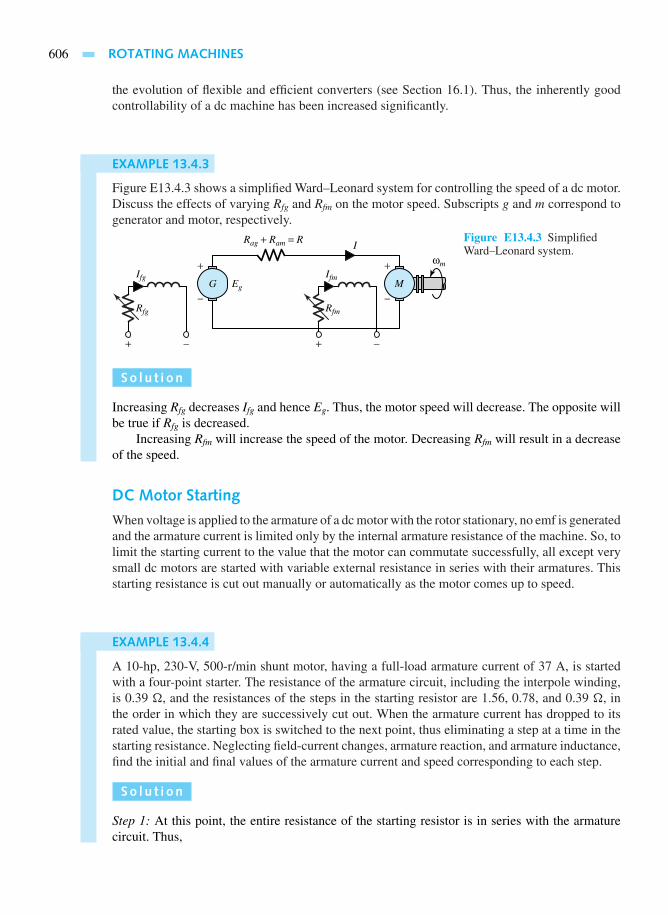
606 ROTATING MACHINES
the evolution of flexible and efficient converters (see Section 16.1). Thus, the inherently goodcontrollability of a dc machine has been increased significantly.
EXAMPLE 13.4.3
Figure E13.4.3 shows a simplified Ward–Leonard system for controlling the speed of a dc motor.Discuss the effects of varying Rfg and Rfm on the motor speed. Subscripts g and m correspond togenerator and motor, respectively.
+ −
Ifg
I
Rfg
+
+
−
−
+
−
Ifm
Rfm
ωm
Eg
Rag + Ram = R
MG
Figure E13.4.3 SimplifiedWard–Leonard system.
So l u t i on
Increasing Rfg decreases Ifg and hence Eg. Thus, the motor speed will decrease. The opposite willbe true if Rfg is decreased.
Increasing Rfm will increase the speed of the motor. Decreasing Rfm will result in a decreaseof the speed.
DC Motor Starting
When voltage is applied to the armature of a dc motor with the rotor stationary, no emf is generatedand the armature current is limited only by the internal armature resistance of the machine. So, tolimit the starting current to the value that the motor can commutate successfully, all except verysmall dc motors are started with variable external resistance in series with their armatures. Thisstarting resistance is cut out manually or automatically as the motor comes up to speed.
EXAMPLE 13.4.4
A 10-hp, 230-V, 500-r/min shunt motor, having a full-load armature current of 37 A, is startedwith a four-point starter. The resistance of the armature circuit, including the interpole winding,is 0.39 , and the resistances of the steps in the starting resistor are 1.56, 0.78, and 0.39 , inthe order in which they are successively cut out. When the armature current has dropped to itsrated value, the starting box is switched to the next point, thus eliminating a step at a time in thestarting resistance. Neglecting field-current changes, armature reaction, and armature inductance,find the initial and final values of the armature current and speed corresponding to each step.
So l u t i on
Step 1: At this point, the entire resistance of the starting resistor is in series with the armaturecircuit. Thus,

13.4 DIRECT-CURRENT MACHINES 607
RT 1 = 1.56+ 0.78+ 0.39+ 0.39 = 3.12
At starting, the counter emf is zero; the armature starting current is then
Ist = Vt
RT 1= 230
3.12= 73.7 A
By the time the armature current drops to its rated value of 37 A, the counter emf is
E = 230− 3× 12× 37 = 230− 115.44 = 215.57 V
The counter emf, when the motor is delivering rated load at a rated speed of 500 r/min with theseries starting resistor completely cut out, is
230− 0.39× 37 = 230− 14.43 = 215.57 V
The speed corresponding to the counter emf of 114.56 V is then given by
N = 114.56
215.57× 500 = 265.7 r/min
Step 2: The 1.56- step is cut out, leaving a total resistance of 3.12 − 1.56 = 1.56 in thearmature circuit. The initial motor speed at this step is 265.7 r/min, which means that the counteremf is still 114.56 V, if the effect of armature reaction is neglected. Accordingly, the resistancedrop in the armature circuit is still 115.44 V, so that
IaRT 2 = 115.44 or Ia = 115.44
1.56= 74A
That is, if the inductance of the armature is neglected, the initial current is 74 A. With the finalcurrent at 37 A, the counter emf is
E = 230− 37× 1.56 = 230− 57.72 = 172.28 V
corresponding to which the speed is
N = 172.28
215.57× 500 = 399.6 rpm
Step 3: The total resistance included in the armature circuit is 0.78 at the beginning of thisstep. The initial motor speed is 399.6 r/min, and the counter emf is 172.28 V. The initial armaturecurrent is then (230 − 172.28)/0.78 = 57.72/0.78 = 74 A. With the final current at 37 A, thecounter emf is
E = 230− 37× 0.78 = 230− 28.86 = 201.14 V
corresponding to which the speed is
N = 201.14
215.57× 500 = 466.5 r/min
Thus, we have the results shown in Table E13.4.4.
TABLE E13.4.4
StepCurrent (A) Speed (r/min)
Number Initial Final Initial Final
1 74 37 0 2662 74 37 266 4003 74 37 400 4674 74 37 467 500

608 ROTATING MACHINES
Efficiency
As is true for any other machine, the efficiency of a dc machine can be expressed as
Efficiency = output
input= input − losses
input= 1− losses
input(13.4.17)
The losses are made up of rotational losses (3 to 15%), armature-circuit copper losses (3 to 6%),and shunt-field copper losses (1 to 5%). Figure 13.4.13 shows the schematic diagram of a dcmachine, along with the power division in a generator and a motor. The resistance voltage drop,also known as arc drop, between brushes and commutator is generally assumed constant at 2V, and the brush-contact loss is therefore calculated as 2Ia. In such a case, the resistance of thearmature circuit should not include the resistance between brushes and commutator.
EXAMPLE 13.4.5
The following data apply to a 100-kW, 250-V, six-pole, 1000-r/min long-shunt compoundgenerator: no-load rotational losses 4000 W, armature resistance at 75°C = 0.015 , series-field resistance at 75°C = 0.005 , interpole field resistance at 75°C = 0.005 , and shunt-fieldcurrent 2.5 A. Assuming a stray-load loss of 1% of the output and a brush-contact resistance dropof 2 V, compute the rated-load efficiency.
So l u t i on
The total armature-circuit resistance (not including that of brushes) is
Ra = 0.015+ 0.005+ 0.005 = 0.025
Ia = IL + If = 100, 000
250+ 2.5 = 402.5 A
The losses are then computed as follows:
No-load rotational loss 4000 WArmature-circuit copper loss = 402.52 × 0.025 4050 WBrush-contact loss = 2Ia = 2 × 402.5 805 WShunt-field circuit copper loss = 250 × 2.5 625 WStray-load loss = 0.01 × 100,000 1000 WTotal losses 10,480 W
The efficiency at rated load is then given by
η = 1− 10,480
100,000+ 10,480= 1− 0.095 = 0.905, or 90.5%
It is usual to determine the efficiency by some method based on the measurement of losses,according to test codes and standards.
Applications for DC Machines
Dc motors find wide applications in which control of speed, voltage, or current is essential.Shunt motors with constant speed are used for centrifugal pumps, fans, blowers, and conveyors,whereas shunt motors with adjustable speed are employed in rolling mills and paper mills.Compound motors find their use for plunger pumps, crushers, punch presses, and hoists. Series

13.4 DIRECT-CURRENT MACHINES 609
Shunt field
Series fieldField rheostat
(a)
(b)
Input from Electromagnetic power
prime mover
Output power
= EaIa = Vt IL= VtaIa
Armature terminal power
No-load rotational loss(friction, windage, and core)
+ stray-load loss
Armature copper lossI2
a Ra+ brush-contact loss
Series-field loss I2s Rs
+ shunt-field loss I2fRf
IfIs
Ia (motor)Ia (generator)
Vta Vt
IL (motor)IL (generator)
−
+
−
+
Armature
(c)
Input powerfrom mains Armature terminal power
= Vt IL
Output available
= VtaIa at shaft= EaIa
Electromagnetic power
Shunt-field loss I2fRf
+ series-field loss I2s Rs
Brush-contact loss + armature loss I2
a Ra
No-load rotational loss+ stray-load loss
Figure 13.4.13 (a) Schematic diagram of a dc machine. (b) Power division in a dc generator. (c) Powerdivision in a dc motor.
motors (known as traction motors) are utilized for electric locomotives, cranes, and car dumpers.Universal motors, operating with either dc or ac excitation, are employed in vacuum cleaners,food processors, hand tools, and several other household applications. They are available in sizesof fractional horsepower up to, and well beyond, 1 hp, in speeds ranging between 2000 and 12,000r/min.
The dc shunt generators are often used as exciters to provide dc supply. The series generatoris employed as a voltage booster and also as a constant-current source in welding machines. Inapplications for which a constant dc voltage is essential, the cumulative-compound generatorfinds its use. The differential-compound generator is used in applications such as arc welding,where a large voltage drop is desirable when the current increases.

610 ROTATING MACHINES
13.5 LEARNING OBJECTIVES
The learning objectives of this chapter are summarized here, so that the student can check whetherhe or she has accomplished each of the following.
• Principles of operation of elementary synchronous, induction, and dc machines.
• Modeling a polyphase induction machine and evaluating its steady-state performance.
• Torque–speed characteristics of three-phase induction motors.
• Basic notions of speed and torque control of polyphase induction motors.
• Starting methods for polyphase induction motors.
• Analysis of single-phase induction motors by revolving-field theory.
• Starting methods for single-phase induction motors.
• Basic ideas about applications for induction motors.
• Modeling a polyphase synchronous machine and evaluating its steady-state performance.
• Parallel operation of interconnected synchronous generators.
• Basic notions about applications for synchronous motors.
• Modeling a dc machine and evaluating its steady-state performance as a motor and generator.
• Basic ideas about speed control of dc motors, dc motor starting, and applications for dcmachines.
13.6 PRACTICAL APPLICATION: A CASE STUDY
Wind-Energy-Conversion Systems
It has been well recognized that renewable energy sources would have to play a key role insolving the world energy problem. Wind energy with an estimated potential of 130 million MWfar exceeds the world’s hydraulic supply of about 3 million MW. Consequently, researchers havebeen looking into the economic utilization of wind energy on a large scale by developing cost-competitive and reliable wind-energy-conversion systems (WECSs) for various applications suchas electricity generation, agriculture, heating, and cooling.
The power coefficient Cp of wind turbines varies with the tip-speed ratio λ, as shown inFigure 13.6.1. Maximum power transfer is achieved by ensuing operation of λopt, where theturbine is most efficient. The mechanical power Pm available at the shaft of the wind turbine maybe expressed as a function of the wind speed v and the shaft speed w,
Pm(v,w) = C1vw2 + C2v
2w + C3v3 (13.6.1)
where C1, C2, and C3 are constants to be determined by curve-fitting techniques. Figure 13.6.2depicts typical wind-turbine characteristics of mechanical power versus wind speed for differentvalues of shaft speed. The two nonzero roots of the curves represent a lower limit for the cut-inwind speed vci and an upper limit for the cut-out wind speed vco. If the variable-speed operation isopted and the resulting system is able to follow the wind-speed variations, the operation at optimumtip-speed ratio can be ensured. In such a case, the power versus wind-speed characteristic will beas shown by the dashed line in Figure 13.6.2.
WECSs developed for the generation of electricity are generally classified as:

13.6 PRACTICAL APPLICATION: A CASE STUDY 611
Optimumoperating
point
Cp
Cp max
λλopt
Figure 13.6.1 Typical power coefficient versus tip-speedratio characteristic.
P/P
max
shaf
t pow
er
w = 10 rod/s
v, m/s
−0.2
0
0.5
1.0
Maximumshaft
power
302014 18 22 26
10
Figure 13.6.2 Typical mechan-ical power versus wind speedcharacteristics of a wind turbinefor various values of shaft speed.
• Constant-speed, constant-frequency (CSCF) systems
• Variable-speed, constant-frequency (VSCF) systems
• Variable-speed, variable-frequency (VSVF) systems
The generating units in these WECSs are commonly the induction and synchronous generators.Constant shaft-speed operation requires more complex and expensive mechanical and/or
hydraulic control systems for accurate control of the shaft speed. This is usually accomplished bycontrolling the turbine blades. Since the turbine operates with a low efficiency for wind speedsother than the rated speed, only a small portion of the available wind energy is extracted. Hencevariable-shaft-speed systems have been developed.
In variable-shaft-speed operation, the turbine is allowed to rotate at different speeds withthe varying wind speed. Optimum power transfer is possible, while the actual speed of rotationis determined by the torque–speed characteristics of both the turbine and the generator. In suchan operating mode, major control means are inevitably placed on the electrical side, since thecontrol of electric systems is easy to implement, more reliable, and less costly than the control ofmechanical systems.
Figure 13.6.3 illustrates a typical double-output induction generator (DOIG) scheme, in whichthe DOIG is equipped with two controlled converters to allow power flow in both directions. Power

612 ROTATING MACHINES
3 phase, 50-Hz supply
DC link
Converter 1 Converter 2
(both fully controlled)
sfs
fs
Inductiongenerator
Figure 13.6.3 Double-output induc-tion-generator scheme.
generation over a wide range of shaft speeds, in the slip range of −1 to +1, is possible. The netoutput power is maximized by varying the firing angles of both converters.
Induction generates are also employed nowadays for power generation in conjunction withhelical water turbines developed for operating in water streams.
PROBL EMS
13.1.1 A three-phase, 50-Hz induction motor has a full-load speed of 700 r/min and a no-load speed of740 r/min.
(a) How many poles does the machine have?
(b) Find the slip and the rotor frequency at fullload.
(c) What is the speed of the rotor field at fullload (i) with respect to the rotor? and (ii)with respect to the stator?
13.1.2 A three-phase, 60-Hz induction motor runs atalmost 1800 r/min at no load, and at 1710 r/minat full load.
(a) How many poles does the motor have?
(b) What is the per-unit slip at full load?
(c) What is the frequency of rotor voltages at fullload?
(d) At full load, find the speed of (i) the rotorfield with respect to the rotor, (ii) the rotorfield with respect to the stator, and (iii) therotor field with respect to the stator field.
*13.1.3 A four-pole, three-phase induction motor is ener-gized from a 60-Hz supply. It is running at a loadcondition for which the slip is 0.03. Determine:
(a) The rotor speed in r/min.
(b) The rotor current frequency in Hz.
(c) The speed of the rotor rotating magnetic fieldwith respect to the stator frame in r/min.
(d) The speed of the rotor rotating magnetic fieldwith respect to the stator rotating magneticfield in r/min.
13.1.4 Consider a three-phase induction motor with anormal torque–speed characteristic. Neglectingthe effects of stator resistance and leakage react-ance, discuss the approximate effect on the char-acteristic, if:
(a) The applied voltage and frequency arehalved.
(b) Only the applied voltage is halved, but thefrequency is at its normal value.
13.1.5 Induction motors are often braked rapidly bya technique known as plugging, which is thereversal of the phase sequence of the voltagesupplying the motor. Assume that a motor withfour poles is operating at 1750 r/min from aninfinite bus (a load-independent voltage supply)at 60 Hz. Two of the stator supply leads aresuddenly interchanged.
(a) Find the new slip.
(b) Calculate the new rotor current frequency.
13.1.6 A four-pole, three-phase, wound-rotor inductionmachine is to be used as a variable-frequency

PROBLEMS 613
supply. The frequency of the supply connectedto the stator is 60 Hz.
(a) Let the rotor be driven at 3600 r/min in eitherdirection by an auxiliary synchronous motor.If the slip-ring voltage is 20 V, what frequen-cies and voltages can be available at the sliprings when the rotor is at standstill?
(b) If the slip-ring voltage is 400 V, when therotor frequency is 120 Hz, at what speed mustthe rotor be driven in order to give 150 Hzat the slip-ring terminals? What will the slip-ring voltage be in this case?
*13.1.7 A three-phase, wound-rotor induction machine,with its shaft rigidly coupled to the shaft of athree-phase synchronous motor, is used to changebalanced 60-Hz voltages to other frequencies atthe wound-rotor terminals brought out throughslip rings. Both machines are electrically con-nected to the same balanced three-phase, 60-Hzsource. Let the synchronous motor, which hasfour poles, drive the interconnecting shaft in theclockwise direction, and let the eight-pole bal-anced three-phase stator winding of the induc-tion machine produce a counterclockwise rotat-ing field, i.e., opposite that of the synchronousmotor. Determine the frequency of the rotor volt-ages of the induction machine.
13.1.8 A synchronous generator has a rotor with sixpoles and operates at 60 Hz.
(a) Determine the speed of prime mover of thegenerator.
(b) Repeat part (a) if the generator has 12 poles.
(c) Repeat part (a) if the generator has 2 poles.
13.1.9 Repeat Problem 13.1.8 if the generator operatesat 50 Hz.
13.1.10 A three-phase ac motor, used to drive a draft fan,is connected to a 60-Hz voltage supply. At no-load, the speed is 1188 r/min; at full load, thespeed drops to 1128 r/min.
(a) Determine the number of poles of this acmotor.
(b) Comment on whether this motor is an induc-tion motor or a synchronous motor.
13.1.11 A dc shunt machine has an armature windingresistance of 0.12 and a shunt-field windingresistance of 50 . The machine may be run on250-V mains as either a generator or a motor.Find the ratio of the speed of the generator to the
speed of the motor when the total line current is80 A in both cases.
13.1.12 A 100-kW, dc shunt generator, connected to a220-V main, is belt-driven at 300 r/min, whenthe belt suddenly breaks and the machine con-tinues to run as a motor, taking 10 kW from themains. The armature winding resistance is 0.025, and the shunt field winding resistance is 60 .Determine the speed at which the machine runsas a motor.
*13.1.13 A dc shunt motor runs off a constant 200-Vsupply. The armature winding resistance is 0.4,and the field winding resistance is 100 . Whenthe motor develops rated torque, it draws a totalline current of 17.0 A.
(a) Determine the electromagnetic power devel-oped by the armature under these conditions,in watts and in horsepower.
(b) Find the total line current drawn by the motorwhen the developed torque is one-half therated value.
13.1.14 A dc machine, operating as a generator, develops400 V at its armature terminals, corresponding toa field current of 4 A, when the rotor is driven at1200 r/min and the armature current is zero.
(a) If the machine produces 20 kW of electro-magnetic power, find the corresponding ar-mature current and the electromagnetictorque produced.
(b) If the same machine is operated as a motorsupplied from a 400-V dc supply, and if themotor is delivering 30 hp to the mechanicalload, determine: (i) the current taken fromthe supply, (ii) the speed of the motor, and(iii) the electromagnetic torque, if the fieldcurrent is maintained at 4 A. Assume thatthe armature circuit resistance and the me-chanical losses are negligible.
(c) If this machine is operated from a 440-V dcsupply, determine the speed at which thismotor will run and the current taken fromthe supply, assuming no mechanical load, nofriction and windage losses, and that the fieldcurrent is maintained at 4 A.
13.1.15 Consider the operation of a dc shunt motor that isaffected by the following changes in its operatingconditions. Explain the corresponding approxi-mate changes in the armature current and speedof the machine for each change in operating con-ditions.

614 ROTATING MACHINES
(a) The field current is doubled, with the ar-mature terminal voltage and the load torqueremaining the same.
(b) The armature terminal voltage is halved,with the field current and load torque remain-ing the same.
(c) The field current and the armature terminalvoltage are halved, with the horsepower out-put remaining the same.
(d) The armature terminal voltage is halved,with the field current and horsepower outputremaining the same.
(e) The armature terminal voltage is halved andthe load torque varies as the square of thespeed, with the field current remaining thesame.
13.2.1 A balanced three-phase, 60-Hz voltage is appliedto a three-phase, two-pole induction motor. Cor-responding to a per-unit slip of 0.05, determinethe following:
(a) The speed of the rotating-stator magneticfield relative to the stator winding.
(b) The speed of the rotor field relative to therotor winding.
(c) The speed of the rotor field relative to thestator winding.
(d) The speed of the rotor field relative to thestator field.
(e) The frequency of the rotor currents.
(f) Neglecting stator resistance, leakage reac-tance, and all losses, if the stator-to-rotorturns ratio is 2:1 and the applied voltage is100 V, find the rotor-induced emf at standstilland at 0.05 slip.
13.2.2 No-load and blocked-rotor tests are conductedon a three-phase, wye-connected induction motorwith the following results. The line-to-line volt-age, line current, and total input power for theno-load test are 220 V, 20 A, and 1000 W; andfor the blocked-rotor test they are 30 V, 50 A, and1500 W. The stator resistance, as measured on adc test, is 0.1 per phase.
(a) Determine the parameters of the equivalentcircuit shown in Figure 13.2.5(c).
(b) Compute the no-load rotational losses.
*13.2.3 A three-phase, 5-hp, 220-V, six-pole, 60-Hz in-duction motor runs at a slip of 0.025 at full load.
Rotational and stray-load losses at full load are5% of the output power. Calculate the powertransferred across the air gap, the rotor copperloss at full load, and the electromagnetic torqueat full load in newton-meters.
13.2.4 The power transferred across the air gap of a two-pole induction motor is 24 kW. If the electromag-netic power developed is 22 kW, find the slip.Calculate the output torque if the rotational lossat this slip is 400 W.
13.2.5 The stator and rotor of a three-phase, 440-V,15-hp, 60-Hz, eight-pole, wound-rotor inductionmotor are both connected in wye and have thefollowing parameters per phase: R1 = 0.5 ,R2 = 0.1 , Xl1 = 1.25 , and Xl2 = 0.2 .The magnetizing impedance is 40 and the core-loss impedance is 360 , both referred to the sta-tor. The ratio of effective stator turns to effectiverotor turns is 2.5. The friction and windage lossestotal 200 W, and the stray-load loss is estimatedas 100 W. Using the equivalent circuit of Figure13.2.5(a), calculate the following values for aslip of 0.05 when the motor is operated at ratedvoltage and frequency applied to the stator, withthe rotor slip rings short-circuited: stator inputcurrent, power factor at the stator terminals, cur-rent in the rotor winding, output power, outputtorque, and efficiency.
13.2.6 Considering only the rotor equivalent circuitshown in Figure 13.2.2 or 13.2.3, find:
(a) The R2 for which the developed torque wouldbe a maximum.
(b) The slip corresponding to the maximumtorque.
(c) The maximum torque.
(d) R2 for the maximum starting torque.
*13.2.7 A three-phase induction motor, operating at itsrated voltage and frequency, develops a startingtorque of 1.6 times the full-load torque and amaximum torque of 2 times the full-load torque.Neglecting stator resistance and rotational losses,and assuming constant rotor resistance, deter-mine the slip at maximum torque and the slipat full load.
13.2.8 A three-phase, wye-connected, 400-V, four-pole,60-Hz induction motor has primary leakageimpedance of 1 + j2 and secondary leakageimpedance referred to the primary at standstill of1+ j2 . The magnetizing impedance is j40

PROBLEMS 615
and the core-loss impedance is 400 . Using theT-equivalent circuit of Figure 13.2.5(a):
(a) Calculate the input current and power (i) onthe no-load test (S∼= 0) at rated voltage, and(ii) on a blocked-rotor test (S = 1) at ratedvoltage.
(b) Corresponding to a slip of 0.05, computethe input current, torque, output power, andefficiency.
(c) Determine the starting torque and current;the maximum torque and the correspondingslip; and the maximum output power and thecorresponding slip.
For the following parts, use the approximateequivalent circuit obtained by transferring theshunt core loss/magnetizing branch to the inputterminals.
(d) Find the same values requested in part (b).
(e) When the machine is driven as an inductiongenerator with a slip of −0.05, calculate theprimary current, torque, mechanical powerinput, and electric power output.
(f) Compute the primary current and the brakingtorque at the instant of plugging (i.e., reversalof the phase sequence) if the slip immedi-ately before plugging is 0.05.
13.2.9 A 500-hp, wye-connected, wound-rotor induc-tion motor, when operated at rated voltage andfrequency, develops its rated full-load output ata slip of 0.02; maximum torque of 2 times thefull-load torque at a slip of 0.06, with a referredrotor current of 3 times that at full load; and 1.2times the full-load torque at a slip of 0.2, with areferred rotor current of 4 times that at full load.Neglect rotational and stray-load losses. If therotor-circuit resistance in all phases is increasedto 5 times the original resistance, determine thefollowing:
(a) The slip at which the motor will develop thesame full-load torque.
(b) The total rotor-circuit copper loss at full-loadtorque.
(c) The horsepower output at full-load torque.
(d) The slip at maximum torque.
(e) The rotor current at maximum torque.
(f) The starting torque.
(g) The rotor current at starting.
13.2.10 The per-phase equivalent circuit shown in Fig-ure 13.2.6 of a three-phase, 600-V, 60-Hz, four-pole, wye-connected, wound-rotor induction mo-tor has the following parameters: R1 = 0.75 ,R′2 = 0.80 , Xl1 = X′l2 = 2.0 , and Xm =50 . Neglect the core losses.
(a) Find the slip at which the maximum devel-oped torque occurs.
(b) Calculate the value of the maximum torquedeveloped.
(c) What is the range of speed for stable opera-tion of the motor?
(d) Determine the starting torque.
(e) Compute the per-phase referred value of theadditional resistance that must be insertedin the rotor circuit in order to obtain themaximum torque at starting.
13.2.11 A three-phase, wye-connected, 220-V, 10-hp, 60-Hz, six-pole induction motor (using Figure 13.2.6for notation) has the following parameters inohms per phase referred to the stator: R1 =0.294, R′2 = 0.144, Xl1 = 0.503, X′12 = 0.209,and Xm = 13.25. The total friction, windage,and core losses can be assumed to be constant at403 W, independent of load. For a slip of 2.00%,compute the speed, output torque and power, sta-tor current, power factor, and efficiency when themotor is operated at rated voltage and frequency.Neglect the impedance of the source.
*13.2.12 A squirrel-cage induction motor operates at a slipof 0.05 at full load. The rotor current at starting isfive times the rotor current at full load. Neglectingstator resistance and rotational and stray-loadlosses, and assuming constant rotor resistance,calculate the starting torque and the maximumtorque in per-unit of full-load torque, as well asthe slip at which the maximum torque occurs.
13.2.13 Using the approximate equivalent circuit inwhich the shunt branch is moved to the stator in-put terminals, show that the rotor current, torque,and electromagnetic power of a polyphase induc-tion motor vary almost directly as the slip, forsmall values of slip.
13.2.14 A three-phase, 50-hp, 440-V, 60-Hz, four-pole,wound-rotor induction motor operates at a slip of0.03 at full load, with its slip rings short-circuited.The motor is capable of developing a maximumtorque of two times the full-load torque at ratedvoltage and frequency. The rotor resistance per

616 ROTATING MACHINES
phase referred to the stator is 0.1 . Neglectthe stator resistance and rotational and stray-loadlosses. Find the rotor copper loss at full load andthe speed at maximum torque. Compute the valueof the per-phase rotor resistance (referred to thestator) that must be added in series to produce astarting torque equal to the maximum torque.
13.2.15 A three-phase, 220-V, 60-Hz, four-pole, wye-connected induction motor has a per-phase statorresistance of 0.5 . The following no-load andblocked rotor test data on the motor are given:
• No-load test: line-to-line voltage 220 V, totalinput power 600 W, of which 200 W is thefriction and windage loss, and line current 3 A
• Blocked-rotor test: line-to-line voltage 35 V,total input power 720 W, and line current 15 A
(a) Calculate the parameters of the equivalentcircuit shown in Figure 13.2.5(c).
(b) Compute the output power, output torque,and efficiency if the machine runs as a motorwith a slip of 0.05.
(c) Determine the slip at which maximum torqueis developed, and obtain the value of themaximum torque.
Note: It may help the student to solve Problems13.2.15 through 13.2.17 if the background givenin the solutions manual as part of the solution toProblem 13.2.15 is provided.
13.2.16 The synchronous speed of a wound-rotor induc-tion motor is 900 r/min. Under a blocked-rotorcondition, the input power to the motor is 45 kWat 193.6 A. The stator resistance per phase is 0.2, and the ratio of effective stator turns to effec-tive rotor turns is 2. The stator and rotor are bothwye-connected. Neglect the effect of the core-loss and magnetizing impedances. Calculate:
(a) The value in ohms of the rotor resistance perphase.
(b) The motor starting torque.
13.2.17 The no-load and blocked-rotor tests on a three-phase, wye-connected induction motor yield thefollowing results:
• No-load test: line-to-line voltage 400 V, inputpower 1770 W, input current 18.5 A, and fric-tion and windage loss 600 W
• Blocked-rotor test: line-to-line voltage 45 V,input power 2700 W, and input current 63 A
Determine the parameters of the equivalent cir-cuit of Figure 13.2.5(a), assuming R1 = R′2 andXl1 = X′l2.
*13.2.18 A three-phase induction motor has the per-phasecircuit parameters shown in Figure P13.2.18. Atwhat slip is the maximum power developed?
13.2.19 A large induction motor is usually started byapplying a reduced voltage across the motor; sucha voltage may be obtained from an autotrans-former. A motor is to be started on 50% of full-load torque, and the full-voltage starting currentis 5 times the full-load current. The full-load slipis 4%. Determine the percentage reduction in theapplied voltage (i.e., the percentage tap on theautotransformer).
13.2.20 A three-phase, 400-V, wye-connected inductionmotor takes the full-load current at 45 V with therotor blocked. The full-load slip is 4%. Calculatethe tappings k on a three-phase autotransformerto limit the starting current to 4 times the full-load current. For such a limitation, determine theratio of starting torque to full-load torque.
13.2.21 A three-phase, 2200-V, 60-Hz, delta-connected,squirrel-cage induction motor, when started atfull rated voltage, takes a starting current of 693A from the line and develops a starting torque of6250 N · m.
(a) Neglect the impedance and the exciting cur-rent of the compensator. Calculate the ra-tio of a starting compensator (i.e., an auto-transformer starter) such that the current sup-plied by the 2200-V line is 300 A. Computethe starting torque with the starting compen-sator.
+
−
V1 Xm = 20 Ω
R1 = 0.05 Ω
I '2
Xl1 + X 'l2 = 0.3 Ω
Ω=R'2S
0.05S
Figure P13.2.18
PROBLEMS 617
(b) If a wye–delta starting method is employed,find the starting current and the startingtorque.
*13.2.22 A three-phase, four-pole, 220-V, 60-Hz inductionmachine with a per-phase resistance of 0.5 isoperating at rated voltage as a generator at a slipof −0.04, delivering 12 A of line current and atotal output of 4000 W. The constant losses froma no-load run as a motor are given to be 220 W,of which 70 W represents friction and windagelosses. Calculate the efficiency of the inductiongenerator.
13.2.23 A 2200-V, 1000-hp, three-phase, 60-Hz, 16-pole,wye-connected, wound-rotor induction motor isconnected to a 2200-V, three-phase, 60-Hz busthat is supplied by synchronous generators. Theper-phase equivalent circuit of Figure 13.2.6 hasthe following parameters: R1 = 0.1 = R′2,Xl1 = 0.625 = X′l2, and Xm = 20 . If themachine is driven at a speed of 459 r/min to act asa generator of real power, find the rotor currentreferred to the stator and the real and reactivepower outputs of the induction machine.
13.2.24 A three-phase, 440-V, 60-Hz, four-pole inductionmotor operates at a slip of 0.025 at full load, withits rotor circuit short-circuited. This motor is tobe operated on a 50-Hz supply so that the air-gapflux wave has the same amplitude at the sametorque as on a 60-Hz supply. Determine the 50-Hz applied voltage and the slip at which the motorwill develop a torque equal to its 60-Hz full-loadvalue.
13.2.25 The rotor of a wound-rotor induction motor isrewound with twice the number of its originalturns, with a cross-sectional area of the conductorin each turn of one-half the original value. De-termine the ratio of the following in the rewoundmotor to the corresponding original quantities:
(a) Full-load current.
(b) Actual rotor resistance.
(c) Rotor resistance referred to the stator.Repeat the problem, given that the original rotoris rewound with the same number of turns asoriginally, but with one-half the original cross-section of the conductor. Neglect the changes inthe leakage flux.
13.2.26 A wound-rotor induction machine, driven by adc motor whose speed can be controlled, is op-erated as a frequency changer. The three-phase
stator winding of the induction machine is ex-cited from a 60-Hz supply, while the variable-frequency three-phase power is taken out of theslip rings. The output frequency range is to be120 to 420 Hz; the maximum speed is not toexceed 3000 r/min; and the maximum poweroutput at 420 Hz is to be 70 kW at 0.8 powerfactor. Assuming that the maximum-speed condi-tion determines the machine size, and neglectingexciting current, losses, and voltage drops in theinduction machine, calculate:
(a) The minimum number of poles for the induc-tion machine.
(b) The corresponding minimum and maximumspeeds.
(c) The kVA rating of the induction-machinestator winding.
(d) The horsepower rating of the dc machine.
13.2.27 A 1/4-hp, 110-V, 60-Hz, four-pole, capacitor-start, single-phase induction motor has the fol-lowing parameters and losses: R1 = 2 , Xl1 =2.8 , X′l2 = 2 , R′2 = 4 , Xm = 70 .The core loss at 110 V is 25 W, and friction andwindage is 12 W. For a slip of 0.05, computethe output current, power factor, power output,speed, torque, and efficiency when the motor isrunning at rated voltage and rated frequency withits starting winding open.
13.2.28 The no-load and blocked-rotor tests conductedon a 110-V, single-phase induction motor yieldthe following data:
• No-load test: input voltage 110 V, input current 3.7A, and input power 50 W
• Blocked-rotor test: input voltage 50 V and inputcurrent 5.6 A
Taking the stator resistance to be 2.0 , frictionand windage loss to be 7 W, and assuming Xl1 =X′l2, determine the parameters of the double-revolving-field equivalent circuit.
*13.2.29 The impedance of the main and auxiliary wind-ings of a 1/3-hp, 120-V, 60-Hz, capacitor-startmotor are given as Zm = 4.6 + j3.8 andZa = 9.6 + j3.6 . Determine the value of thestarting capacitance that will cause the main andauxiliary winding currents to be in quadrature atstarting.
*13.3.1 A three-phase, wye-connected, cylindrical-rotorsynchronous generator rated at 10 kVA and 230

618 ROTATING MACHINES
V has a synchronous reactance of 1.5 per phaseand an armature resistance of 0.5 per phase.
(a) Determine the voltage regulation at full loadwith: (i) 0.8 lagging power factor, and (ii) 0.8leading power factor.
(b) Calculate the power factor for which the volt-age regulation becomes zero on full load.
13.3.2 A three-phase, wye-connected, 2300-V, four-pole, 1000-kVA, 60-Hz synchronous machinehas a synchronous reactanceXs = 5, a field re-sistanceRf = 10 , and an approximately linearmagnetization characteristic (Ef versus If ) witha slope Kag = 200 . The machine is connectedto a balanced three-phase ac system and is usedas a generator. Determine the following:
(a) The rated stator current.
(b) The exciter settingVex = If Rf for operatingthe machine at rated conditions, at a powerfactor of (i) 0.866 lagging and (ii) 0.866leading.
(c) Vex in part (b) for unity power factor and thesame real power output as in part (b).
(d) The complex power delivered by the gener-ator to the system for parts (b) and (c).
13.3.3 The loss data for the synchronous generator ofProblem 13.3.2 are:
Open-circuit coreloss at 13.8 kV 70 kW
Short-circuit loadloss at 418 A, 75°C 50 kW
Friction and windageloss 80 kw
Field-winding resis-tance at 75°C 0.3
Stray-load loss atfull load 20 kW
Determine the efficiency of the generator at ratedload, rated voltage, and 0.8 power factor lagging.
13.3.4 A three-phase, six-pole, wye-connected syn-chronous generator is rated at 550 V and hasa synchronous reactance Xs = 2 . When thegenerator supplies 50 kVA at rated voltage anda power factor of 0.95 lagging, find the arma-ture current Ia and the excitation voltage Ef .Sketch the phasor diagram of Vt , Ia , and Ef .Also, determine the regulation corresponding tothe operating conditions.
13.3.5 The synchronous machine of Problem 13.3.2 isto be used as a motor. Determine the following:
(a) The exciter setting Vex for operation at ratedconditions and a power factor of (i) 0.866lagging, and (ii) 0.866 leading.
(b) Vex in part (a) for unity power factor and thesame real power input as in part (a).
(c) The complex power absorbed by the ma-chine in parts (a) and (b).
13.3.6 For a 45-kVA, three-phase, wye-connected, 220-V synchronous machine at rated armature cur-rent, the short-circuit load loss (total for threephases) is 1.80 kW at a temperature of 25°C. Thedc resistance of the armature at this temperatureis 0.0335 per phase. Compute the effectivearmature ac resistance in per unit and in ohmsper phase at 25°C.
*13.3.7 A 4000-V, 5000-hp, 60-Hz, 12-pole synchronousmotor, with a synchronous reactance of 4 perphase (based on cylindrical-rotor theory), is ex-cited to produce unity power factor at rated load.Neglect all losses.
(a) Find the rated and maximum torques.
(b) What is the armature current correspondingto the maximum torque?
13.3.8 A three-phase, wye-connected, four-pole, 400-V, 60-Hz, 15-hp synchronous motor has a syn-chronous reactance of 3 per phase and negligi-ble armature resistance. The data for its no-loadmagnetization curve follow:
Field current, A:2 3.5 4.4 6 8 10 12
Line-to-neutral voltage, V:100 175 200 232 260 280 295
(a) When the motor operates at full load at 0.8leading power factor, determine the powerangle and the field current. Neglect all losses.
(b) Compute the minimum line current for themotor operating at full load and the corre-sponding field current.
(c) When the motor runs with an excitation of 10A while taking an armature current of 25 A,calculate the power developed and the powerfactor.
(d) If the excitation is adjusted such that themagnitudes of the excitation voltage and theterminal voltage are equal, and if the motoris taking 20 A, find the torque developed.
13.3.9 A three-phase, wye-connected, 2300-V, 60-Hz,round-rotor synchronous motor has a syn-

PROBLEMS 619
chronous reactance of 2 per phase and neg-ligible armature resistance.
(a) If the motor takes a line current of 350 A op-erating at 0.8 power factor leading, calculatethe excitation voltage and the power angle.
(b) If the motor is operating on load with a powerangle of−20°, and the excitation is adjustedso that the excitation voltage is equal in mag-nitude to the terminal voltage, determine thearmature current and the power factor of themotor.
13.3.10 A 2300-V, three-phase, wye-connected, round-rotor synchronous motor has a synchronous reac-tance of 3 per phase and an armature resistanceof 0.25 per phase. The motor operates on loadwith a power angle of−15°, and the excitation isadjusted so that the internally induced voltageis equal in magnitude to the terminal voltage.Determine:
(a) The armature current.
(b) The power factor of the motor.Neglect the effect of armature resistance.
13.3.11 An induction motor takes 350 kW at 0.8 powerfactor lagging while driving a load. When anoverexcited synchronous motor taking 150 kWis connected in parallel with the induction mo-tor, the overall power factor is improved to 0.95lagging. Determine the kVA rating of the syn-chronous motor.
*13.3.12 An industrial plant consumes 500 kW at a laggingpower factor of 0.6.
(a) Find the required kVA rating of a syn-chronous capacitor to improve the powerfactor to 0.9.
(b) If a 500-hp, 90% efficient synchronous mo-tor, operating at full load and 0.8 leadingpower factor, is added instead of the capaci-tor in part (a), calculate the resulting powerfactor.
13.3.13 A three-phase, wye-connected, cylindrical-rotor,synchronous motor, with negligible armature re-sistance and a synchronous reactance of 1.27
per phase, is connected in parallel with a three-phase, wye-connected load taking 50 A at 0.707lagging power factor from a three-phase, 220-V,60-Hz source. If the power developed by the mo-tor is 33 kW at a power angle of 30°, determine:
(a) The overall power factor of the motor andthe load.
(b) The reactive power of the motor.
13.3.14 Two identical three-phase, 33-kV, wye-connected, synchronous generators operating inparallel share equally a total load of 12 MWat 0.8 lagging power factor. The synchronousreactance of each machine is 8 per phase, andthe armature resistance is negligible.
(a) If one of the machines has its field excita-tion adjusted such that it delivers 125 A lag-ging current, determine the armature current,power factor, excitation voltage, and powerangle of each machine.
(b) If the power factor of one of the machines is0.9 lagging, find the power factor and currentof the other machine.
13.3.15 A three-phase, wye-connected, round-rotor, 220-V, 60-Hz, synchronous motor, having a syn-chronous reactance of 1.27 per phase andnegligible armature resistance, is connected inparallel with a three-phase, wye-connected loadthat takes a current of 50 A at 0.707 laggingpower factor and 220 V line-to-line. At a powerangle of 30°, the power developed by the motor is33 kW. Determine the reactive kVA of the motor,and the overall power factor of the motor and theload.
13.3.16 A three-phase, wye-connected, 2500-kVA, 6600-V, 60-Hz turboalternator has a per-phase syn-chronous reactance and an armature resistanceof 10.4 and 0.071 , respectively. Compute thepower factor for zero voltage regulation on fullload.
13.4.1 A 100-kW, 250-V shunt generator has anarmature-circuit resistance of 0.05 and a field-circuit resistance of 60 . With the generatoroperating at rated voltage, determine the inducedvoltage at (a) full load, and (b) one-half full load.Neglect brush-contact drop.
13.4.2 A 100-kW, 230-V shunt generator has Ra =0.05 and Rf = 57.5 . If the generator oper-ates at rated voltage, calculate the induced volt-age at (a) full load, and (b) one-half full load.Neglect brush-contact drop.
*13.4.3 A 10-hp, 250-V shunt motor has an armature-circuit resistance of 0.5 and a field resistanceof 200 . At no load, rated voltage, and 1200r/min, the armature current is 3 A. At full loadand rated voltage, the line current is 40 A, and theflux is 5% less than its no-load value because ofarmature reaction. Compute the full-load speed.

620 ROTATING MACHINES
13.4.4 When delivering rated load a 10-kW, 230-V self-excited shunt generator has an armature-circuitvoltage drop that is 6% of the terminal voltageand a shunt-field current equal to 4% of the ratedload current. Calculate the resistance of the ar-mature circuit and the field circuit.
13.4.5 A 20-hp, 250-V shunt motor has a total armature-circuit resistance of 0.25 and a field-circuitresistance of 200. At no load and rated voltage,the speed is 1200 r/min, and the line current is4.5 A. At full load and rated voltage, the linecurrent is 65 A. Assume the field flux to bereduced by 6% from its value at no load, dueto the demagnetizing effect of armature reaction.Compute the full-load speed.
13.4.6 A dc series motor is connected to a load. Thetorque varies as the square of the speed. With thediverter-circuit open, the motor takes 20 A andruns at 500 r/min. Determine the motor currentand speed when the diverter-circuit resistance ismade equal to the series-field resistance. Neglectsaturation and the voltage drops across the series-field resistance as well as the armature resistance.
13.4.7 A 50-kW, 230-V compound generator has the fol-lowing data: armature-circuit resistance 0.05 ,series-field circuit resistance 0.05 , and shunt-field circuit resistance 125 . Assuming the totalbrush-contact drop to be 2 V, find the inducedarmature voltage at rated load and rated terminalvoltage for: (a) short-shunt, and (b) long-shuntcompound connection.
*13.4.8 A 50-kW, 250-V, short-shunt compound genera-tor has the following data: Ra = 0.06 , RS =0.04 , and Rf = 125 . Calculate the inducedarmature voltage at rated load and terminal volt-age. Take 2 V as the total brush-contact drop.
13.4.9 Repeat the calculations of Problem 13.4.8 for amachine that is a long-shunt compound genera-tor.
13.4.10 A 10-kW, 230-V shunt generator, with anarmature-circuit resistance of 0.1 and a field-circuit resistance of 230 , delivers full load atrated voltage and 1000 r/min. If the machine isrun as a motor while absorbing 10 kW from 230-V mains, find the speed of the motor. Neglect thebrush-contact drop.
13.4.11 The magnetization curve taken at 1000 r/min ona 200-V dc series motor has the following data:
Field current, A: 5 10 15 20 25 30Voltage, A: 80 160 202 222 236 244
The armature-circuit resistance is 0.25 and theseries-field resistance is 0.25 . Calculate thespeed of the motor (a) when the armature currentis 25 A, and (b) when the electromagnetic torqueis 36 N · m. Neglect the armature reaction.
*13.4.12 A dc series motor operates at 750 r/min witha line current of 100 A from the 250-V mains.Its armature-circuit resistance is 0.15 and itsseries-field resistance is 0.1 . Assuming thatthe flux corresponding to a current of 25 A is40% of that corresponding to a current of 100 A,determine the motor speed at a line current of 25A at 250 V.
13.4.13 A 7.5-hp, 250-V, 1800-r/min shunt motor, havinga full-load line current of 26 A, is started with afour-point starter. The resistance of the armaturecircuit, including the interpole winding, is 0.48; and the resistance of the shunt-field circuit,including the field rheostat, is 350 . The resis-tances of the steps in the starting resistor are 2.24,1.47, 0.95, 0.62, 0.40, and 0.26 , in the orderin which they are successively cut out. When thearmature current is dropped to its rated value,the starting box is switched to the next point,thus eliminating a step in the starting resistance.Neglecting field-current changes, armature reac-tion, and armature inductance, find the initial andfinal values of the armature current and speedcorresponding to each step.
13.4.14 Two shunt generators operate in parallel to supplya total load current of 3000 A. Each machine hasan armature resistance of 0.05 and a field resis-tance of 100 . If the generated emfs are 200 and210 V, respectively, determine the load voltageand the armature current of each machine.
13.4.15 Three dc generators are operating in parallel withexcitations such that their external characteristicsare almost straight lines over the working rangewith the following pairs of data points:
Terminal Voltage (V)
Load Current (A) Generator I Generator II Generator III
0 492.5 510 525
2000 482.5 470 475
Compute the terminal voltage and current of eachgenerator.
(a) When the total load current is 4350 A.

PROBLEMS 621
(b) When the load is completely removed with-out change of excitation currents.
13.4.16 The external-characteristics data of two shuntgenerators in parallel are given as follows:
Load Current, A: 0 5 10 15 20 25 30
Terminal voltage I, V: 270 263 254 240 222 200 175
Terminal voltage II, V: 280 277 270 263 253 243 228
Calculate the load current and terminal voltageof each machine.
(a) When the generators supply a load resistanceof 6 .
(b) When the generators supply a battery of emf300 V and resistance of 1.5 .
*13.4.17 A separately excited dc generator with anarmature-circuit resistance Ra is operating at aterminal voltage Vt, while delivering an armaturecurrent Ia, and has a constant loss Pc. Find thevalue of Ia for which the generator efficiency isa maximum.
13.4.18 A 100-kW, 230-V, dc shunt generator, with Ra =0.05 , and Rf = 57.5 has no-load rotationalloss (friction, windage, and core loss) of 1.8 kW.Compute:
(a) The generator efficiency at full load.
(b) The horsepower output from the primemover to drive the generator at this load.
13.4.19 A dc series motor, with a design constant Ka =40 and flux per pole of 46.15 mWb, operates at200 V while taking a current of 325 A. The totalseries-field and armature-circuit resistances are25 and 50 m, respectively. The core loss is 220W; friction and windage loss is 40 W. Determine:
(a) The electromagnetic torque developed.
(b) The motor speed.
(c) The mechanical power output.
(d) The motor efficiency.
13.4.20 A 230-V dc shunt motor delivers 30 hp at the shaftat 1120 r/min. If the motor has an efficiency of87% at this load, find:
(a) The total input power.
(b) The line current.
(c) If the torque lost due to friction and windageis 7% of the shaft torque, calculate the de-veloped torque.
13.4.21 A 10-kW, 250-V dc shunt generator, having anarmature resistance of 0.1 and a field resistanceof 250 , delivers full load at rated voltage and800 r/min. The machine is now run as a motorwhile taking 10 kW at 250 V. Neglect the brush-contact drop. Determine the speed of the motor.
13.4.22 A 10-hp, 230-V dc shunt motor takes a full-load line current of 40 A. The armature and fieldresistances are 0.25 and 230 , respectively. Thetotal brush-contact drop is 2 V, and the core androtational losses are 380 W. Assume that stray-load loss is 1% of output. Compute the efficiencyof the motor.

This page intentionally left blank

PART
INFORMATION SYSTEMSFOUR

This page intentionally left blank

14 Signal Processing
14.1 Signals and Spectral Analysis
14.2 Modulation, Sampling, and Multiplexing
14.3 Interference and Noise
14.4 Learning Objectives
14.5 Practical Application: A Case Study—Antinoise Systems—Noise Cancellation
Problems
The essential feature of communication, control, computation, and instrumentation systems isthe processing of information. Because of the relative ease and flexibility of processing andtransmitting electrical quantities, usually the information obtained from a nonelectrical source isconverted into electrical form. An electric signal is a voltage or current waveform whose time orfrequency variations correspond to the desired information. The information-bearing signals areprocessed either for purposes of measurement in an instrumentation system, or for transmittingover long distance in a communication system. All such systems, regardless of their particulardetails, share certain basic concepts and common problems.
Continuous signals (shown in Figure 6.0.1) are described by time functions which are definedfor all values of t (a continuous variable). Commercial broadcast systems, analog computers,and various control and instrumentation systems process continuous signals. The informationprocessed in analog systems is contained in the time function which defines the signal. Analogsystems are often thought of as performing signal processing in the frequency domain.
Discrete signals (shown in Figure 6.0.2), on the other hand, exist only at specific instancesof time, and as such, their functional description is valid only for discrete-time intervals. Dis-crete signals are invariably a sequence of pulses in which the information is contained in thepulse characteristics and the relation amidst the pulses in the sequence during a specified timeinterval. Digital computers, pulsed-communication systems (modern telephone and radar), andmicroprocessor-based control systems utilize discrete signals. Digital systems process digits, i.e.,pulse trains, in which the information is carried in the pulse sequence rather than the amplitude–time characterization of the pulses. Digital systems are often thought of as performing signalprocessing in the time domain. Because of the advantages of economy in time, low power
625

626 SIGNAL PROCESSING
consumption, accuracy, and reliability, digital communication systems are increasingly used fortransmitting information.
Foremost among signal concepts is spectral analysis (representation of signals in terms oftheir frequency components), a concept that serves as a unifying thread in signal processing andcommunication systems. Signals and spectral analysis are considered first in Section 14.1. Thenin Section 14.2, processing techniques such as equalization, filtering, sampling, modulation, andmultiplexing are presented, while topics on interference and noise are exposed in Section 14.3. Thecircuit functions required for time-domain processing parallel those needed for frequency-domainprocessing.
14.1 SIGNALS AND SPECTRAL ANALYSIS
Figure 14.1.1 shows the functional block diagram of a signal-processing system. The informationsource may be a speech (voice), an image (picture), or plain text in some language. The outputof a source that generates information may be described in probabilistic terms by a randomvariable, when the random or stochastic signal is defined by a probability density function. Theoutput of a source may not be deterministic, given by a real or complex number at any instant oftime. However, in view of the scope of this text, random signals and random processes are notdiscussed here.
A transducer is usually required to convert the output of a source into an electrical signalthat is suitable for transmission. Typical examples include a microphone converting an acousticspeech or a video camera converting an image into electric signals. A similar transducer is neededat the destination to convert the received electric signals into a form (such as voice, image, etc.)that is suitable for the user.
The heart of any communication system consists of three basic elements: transmitter, trans-mission medium or channel, and receiver. The transmitter (input processor) converts the electricsignal into a form that is suitable for transmission through the physical channel or transmis-sion medium. For example, in radio and TV broadcasts, since the FCC (Federal Communi-cations Commission) specifies the frequency range for each transmitting station, the trans-mitter must translate the information signal to be transmitted into the appropriate frequencyrange that matches the frequency allocation assigned to the transmitter. This process is calledmodulation, which usually involves the use of the information signal to vary systematicallythe amplitude, frequency, or phase of a sinusoidal carrier. Thus, in general, carrier modula-tion such as amplitude modulation (AM), frequency modulation (FM), or phase modulation
Informationsource
Inputtransducer
Input processor(transmitter)
Output signalat destination
Outputtransducer
Output processor(receiver)
Transmission medium(channel)Attenuation, distortion, interference, noise
Figure 14.1.1 Functional block diagram of a signal-processing system.

14.1 SIGNALS AND SPECTRAL ANALYSIS 627
(PM) is performed primarily at the transmitter. For example, for a radio station found at asetting of AM820, the carrier wave transmitted by the radio station is at the frequency of820 kHz.
The function of the receiver is to recover the message signal contained in the receivedsignal. If the message signal is transmitted by carrier modulation, the receiver performs carrierdemodulation to extract the message from the sinusoidal carrier.
The communication channel (transmission medium) is the physical medium that is utilized tosend the signal from the transmitter to the receiver. In wireless transmission, such as microwaveradio, the transmission medium is usually the atmosphere or free space. Telephone channels, onthe other hand, employ a variety of physical media such as wire lines and optical fiber cables.Irrespective of the type of physical medium for signal transmission, the essential feature is thatthe transmitted signal is corrupted in a random manner by a variety of possible mechanisms. Forsimplicity, the effects of these phenomena (attenuation, distortion, interference, noise, etc.) areshown at the center of Figure 14.1.1, since the transmission medium is often the most vulnerablepart of a communication system, particularly over long distances.
Attenuation, caused by losses within the system, reduces the size or strength of the signal,whereas distortion is any alteration of the waveshape itself due to energy storage and/or non-linearities. Contamination by extraneous signals causes interference, whereas noise emanatesfrom sources both internal and external to the system. To eliminate any one of these may pose achallenge to the design engineer.
Successful information recovery, while handling the aforementioned problems, invariablycalls for signal processing at the input and output. Common signal-processing operations includethe following:
• Amplification to compensate for attenuation
• Filtering to reduce interference and noise, and/or to obtain selected facets of information
• Equalization to correct some types of distortion
• Frequency translation or sampling to get a signal that better suits the system characteristics
• Multiplexing to permit one transmission system to handle two or more information-bearingsignals simultaneously
In addition, to enhance the quality of information recovery, several specialized techniques,such as linearizing, averaging, compressing, peak detecting, thresholding, counting, and timing,are used.
Analog signals in an analog communication system can be transmitted directly via carriermodulation over the communication channel and demodulated accordingly at the receiver. Alter-natively, an analog source output may be converted into a digital form and the message can betransmitted via digital modulation and demodulated as a digital signal at the receiver. Potentialadvantages in transmitting an analog signal by means of digital modulation are the following:
• Signal fidelity is better controlled through digital transmission than through analog trans-mission; effects of noise can be reduced significantly.
• Since the analog message signal may be highly redundant, with digital processing, redun-dancy may be removed prior to modulation.
• Digital communication systems are often more economical to implement.
Figure 14.1.2 illustrates the basic elements of a digital communication system. For eachfunction in the transmitting station, there is an inverse operation in the receiver. The analog input

628 SIGNAL PROCESSING
Digital messagesource
Digital messageoutput signal
Analog messagesource
Analog messageoutput signal
Digitalmodulator
Digitaldemodulator
Channelencoder
Channeldecoder
Sourceencoder
(transmitter side)
(receiver side)
Sourcedecoder
Analog-to-digitalconverter
Digital-to-analogconverter
ChannelNoise, interference
Figure 14.1.2 Basic elements of a digital communication system.
signal (such as an audio or video signal) must first be converted to a digital signal by an analog-to-digital (A/D) converter. If no analog message is involved, a digital signal (such as the outputof a teletype machine, which is discrete in time and has a finite number of output characters) canbe directly input.
Encoding is a critical function in all digital systems. The messages produced by the sourceare usually converted into a sequence of binary digits. The process of efficiently converting theoutput of either an analog or a digital source into a sequence of binary digits is called sourceencoding or data compression.
The sequence of binary digits from the source encoder, known as the information sequence,is passed on to the channel encoder. The purpose of the channel encoder is to introduce someredundancy in a controlled manner in the binary information sequence, so that the redundancycan be used at the receiver to overcome the effects of noise and interference encountered in thetransmission of the signal through the channel. Thus, redundancy in the information sequencehelps the receiver in decoding the desired information sequence, thereby increasing the reliabilityof the received data and improving the fidelity of the received signal.
The binary sequence at the output of the channel encoder is passed on to the digital modulator,which functions as the interface to the communication channel. The primary purpose of the digitalmodulator is to map the binary information sequence into signal waveforms, since nearly all thecommunication channels used in practice are capable of transmitting electric signals (waveforms).Because the message has only two amplitudes in a binary system, the modulation process is knownas keying. In amplitude-shift keying (ASK), a carrier’s amplitude is shifted or keyed between twolevels. Phase-shift keying (PSK) involves keying between two phase angles of the carrier, whereasfrequency-shift keying (FSK) consists of shifting a carrier’s frequency between two values. Manyother forms of modulation are also possible.
The functions of the receiver in Figure 14.1.2 are the inverse of those in the transmitter.At the receiving end of a digital communication system, the digital demodulator processes thechannel-corrupted transmitted waveform and reduces each waveform to a single number, whichrepresents an estimate of the transmitted data symbol. For example, when binary modulation is
14.1 SIGNALS AND SPECTRAL ANALYSIS 629
used, the demodulator may process the received waveform and decide on whether the transmittedbit is a 0 or 1. The source decoder accepts the output sequence from the channel decoder, andfrom the knowledge of the source encoding method used, attempts to reconstruct the originalsignal from the source. Errors due to noise, interference, and practical system imperfectionsdo occur. The digital-to-analog (D/A) converter reconstructs an analog message that is a closeapproximation to the original message. The difference, or some function of the difference, betweenthe original signal and the reconstructed signal is a measure of the distortion introduced by thedigital communication system.
The remainder of this chapter deals with basic methods for analyzing and processing analogsignals. A large number of building blocks in a communication system can be modeled by lineartime-invariant (LTI) systems. LTI systems provide good and accurate models for a large class ofcommunication channels. Some basic components of transmitters and receivers (such as filters,amplifiers, and equalizers) are LTI systems.
Periodic Signals and Fourier Series
In the study of analog systems, predicting the response of circuits to a general time-varying voltageor current waveform x(t) is a difficult task. However, if x(t) can be expressed as a sum of sinusoids,then the principle of superposition can be invoked on linear systems and the frequency responseof the circuit can be utilized to expedite calculations. Expressing a signal in terms of sinusoidalcomponents is known as spectral analysis. Let us begin here by considering the Fourier-seriesexpansion of periodic signals, which has been introduced in Section 3.1.
A periodic signal has the property that it repeats itself in time, and hence, it is sufficient tospecify the signal in the basic time interval called the period. A periodic signal x(t) satisfies theproperty
x(t + kT ) = x(t) (14.1.1)
for all t, all integers k, and some positive real number T, called the period of the signal. Fordiscrete-time periodic signals, it follows that
x(n+ kN) = x(n) (14.1.2)
for all integers n, all integers k, and a positive integer N, called the period. A signal that does notsatisfy the condition of periodicity is known as nonperiodic.
EXAMPLE 14.1.1
Consider the following signals, sketch each one of them and comment on the periodic nature:
(a) x(t) = A cos(2πf0t + θ), where A, f 0, and θ are the amplitude, frequency, and phase ofthe signal.
(b) x(t) = ej (2πf0t+θ), A > 0.
(c) Unit step signal u−1(t) defined by u−1(t) = 1, t > 0
1/2, t = 00, t < 0
.
(d) Discrete-time signal x[n] = A cos(2πf0n+ θ), where n is an integer.

630 SIGNAL PROCESSING
So l u t i on
(a) This is a continuous-time signal (called a sinusoidal signal) that is real and periodic withperiod T = 1/f0, as sketched in Figure E14.1.1(a).
(b) This is a complex periodic exponential signal. Its real part is
xr(t) = A cos(2πf0t + θ)
and its imaginary part is
xi(t) = A sin(2πf0t + θ)
This signal could also be described in terms of its modulus and phase. The absolute valueof x(t) is
|x(t)| =√x2r (t)+ x2
i (t) = A
and its phase is
x(t) = 2πf0t + θ
Sketches of these functions are shown in Figure E14.1.1(b). In addition, the followingrelations apply:
xr(t) = |x(t)| cos[ x(t)]
xi(t) = |x(t)| sin[ x(t)]
x(t) = arctanxi(t)
xr(t)
(c) The unit step signal is a nonperiodic signal, sketched in Figure E14.1.1(c).
(d) A sketch of this discrete-time signal is shown in Figure E14.1.1(d).
This is not periodic for all values of f 0. The condition for it to be periodic is
2πf0(n+ kN)+ θ = 2πf0n+ θ + 2mπ
x(t)
(a)
3
2
1
0
−1
−2
−3
t
Figure E14.1.1 (a) Sinusoidal signal. (b) Real–imaginary andmagnitude–phase graphs of the complex exponential signal. (c)Unit step signal. (d) Discrete sinusoidal signal.

14.1 SIGNALS AND SPECTRAL ANALYSIS 631
xr(t)
t
xi(t)
t
|x(t)|
t
∠x(t)
t
(b)2 4
1
−2 0−4
u−1(t)
(c)
1
12
t
x[n]
(d)
2.5
2
1
1.5
0
0.5
−1
−2
−2.5
−0.5
−1.5
n
Figure E14.1.1 Continued

632 SIGNAL PROCESSING
for all integers n and k, some positive integer N, and some integer m. From this it followsthat
2πf0kN = 2mπ or f0 = m/(kN)
that is, the discrete sinusoidal signal is periodic only for rational values of f 0.
Evenness and oddness are expressions of various types of symmetry present in signals. Asignal x(t) is even if it has a mirror symmetry with respect to the vertical axis. A signal is oddif it is symmetric with respect to the origin. The signal x(t) is even if and only if, for all t, itsatisfies
x(−t) = x(t) (14.1.3)
and is odd if and only if, for all t,
x(−t) = −x(t) (14.1.4)
Any signal x(t), in general, can be expressed as the sum of its even and odd parts,
x(t) = xe(t)+ x0(t) (14.1.5)
xe(t) = x(t)+ x(−t)2
(14.1.6)
xo(t) = x(t)− x(−t)2
(14.1.7)
The half-wave symmetry is expressed by
x
(t ± T
2
)= −x(t) (14.1.8)
EXAMPLE 14.1.2
Discuss the nature of evenness and oddness of:
(a) The sinusoidal signal x(t) = A cos(2πf0t + θ).
(b) The complex exponential signal x(t) = ej2πf0t .
So l u t i on
(a) The signal is, in general, neither even nor odd. However, for the special case of θ = 0,it is even; for the special case of θ = ±π/2, it is odd. In general,
x(t) = A cos θ cos 2πf0t − A sin θ sin 2πf0t
Since cos 2πf0t is even and sin 2πf0t is odd, it follows that
xe(t) = A cos θ cos 2πf0t
and
xo(t) = −A sin θ sin 2πf0t

14.1 SIGNALS AND SPECTRAL ANALYSIS 633
(b) From the sketches of Figure E14.1.1(b), for θ = 0, x(t) = Aej2πf0t , the real part andthe magnitude are even; the imaginary part and the phase are odd. Noting that a complexsignal x(t) is called hermitian if its real part is even and its imaginary part is odd, thesignal and symmetry are then said to be hermitian.
A signal x(t) is said to be causal if, for all t < 0, x(t) = 0; otherwise, the signal is noncausal.An anticausal signal is identically equal to zero for t > 0. A discrete-time signal is a causal signalif it is identically equal to zero for n < 0. Note that the unit step multiplied by any signal producesa causal version of the signal.
Signals can also be classified as energy-type and power-type signals based on the finitenessof their energy content and power content, respectively. A signal x(t) is an energy-type signal ifand only if the energy Ex of the signal,
Ex =∫ ∞
−∞|x(t)|2 dt = lim
T→∞
∫ T/2
−T/2|x(t)|2 dt (14.1.9)
is well defined and finite. A signal is a power-type signal if and only if the power Px of the signal,
Px = limT→∞
1
T
∫ T/2
−T/2|x(t)|2 dt (14.1.10)
is well defined and 0 ≤ Px <∞. For real signals, note that |x(t)|2 can be replaced by x2(t).
EXAMPLE 14.1.3
(a) Evaluate whether the sinusoidal signal x(t) = A cos (2πf0t + θ) is an energy-type or apower-type signal.
(b) Show that any periodic signal is not typically energy type, and the power content of anyperiodic signal is equal to the average power in one period.
So l u t i on
(a) Ex = limT→∞
∫ T/2
−T/2A2 cos2 (2πf0t + θ) dt = ∞
Therefore, the sinusoidal signal is not an energy-type signal. However, the power of thissignal is
Px = limT→∞
1
T
∫ T/2
−T/2A2 cos2(2πf0t + θ) dt
= limT→∞
1
T
∫ T/2
−T/2
A2
2[1+ cos(4πf0t + 2θ)] dt
= limT→∞
A2T
2T+[
A2
8πf0Tsin(4πf0t + 2θ)
]+T/2
−T/2
= A2
2<∞

634 SIGNAL PROCESSING
Hence, the given x(t) is a power-type signal with its power given by A2/2.
(b) For any periodic signal with period T0, the energy is given by
Ex = limT→∞
∫ +T/2
−T/2|x(t)|2 dt = lim
n→∞
∫ +nT0/2
−nT0/2|x(t)|2 dt
= limn→∞ n
∫ +T0/2
−T0/2|x(t)|2 dt = ∞
Therefore, periodic signals are not typically energy type. The power content of anyperiodic signal is
Px = limT→∞
1
T
∫ T/2
−T/2|x(t)|2 dt = lim
n→∞1
nT0
∫ nT0/2
−nT0/2|x(t)|2 dt
= limn→∞
n
nT0
∫ T0/2
−T0/2|x(t)|2 dt = 1
T0
∫ T0/2
−T0/2|x(t)|2 dt
which shows that the power content of a periodic signal is equal to the average power inone period.
The Fourier-series representation states that almost any periodic signal can be decomposedinto an infinite series of the form
x(t) = a0 +∞∑n=1
(an cos nωt + bn sin nωt) (14.1.11)
where a0, a1, b1, . . . are the Fourier coefficients, and ω is the fundamental angular frequencyrelated to the period T by ω = 2π/T = 2πf . The integer multiples of ω are known as harmonics:2ω being the second harmonic that is even, 3ω being the third harmonic that is odd, and so forth.The dc component is given by
a0 = 1
T
∫ T
0x(t)dt (14.1.12)
which is seen to be the average value of x(t). The remaining coefficients can be computed fromthe following integrals:
an = 2
T
∫ T
0x(t) cos nωt dt, for n = 1, 2, . . . (14.1.13)
bn = 2
T
∫ T
0x(t) sin nωt dt, for n = 1, 2, . . . (14.1.14)
It can be seen that bn= 0 for n= 1, 2, 3, . . . for even symmetry. Similarly, for odd symmetry,an = 0 for n = 0, 1, 2, 3, . . . . For half-wave symmetry, an = bn = 0 for n = 2, 4, 6, . . . so thatthe series contains only the odd-harmonic components. For relatively smooth signals, the higherharmonic components tend to be smaller than the lower ones. Discontinuous signals have moresignificant high-frequency content than continuous signals.

14.1 SIGNALS AND SPECTRAL ANALYSIS 635
EXAMPLE 14.1.4
Consider the following periodic waveforms shown in Figure E14.1.4:
A
tT0−T
A
tTD/20
A
−A
t−T T0
−T −D/2
−T/2 T/2
−T/2
T/2
−T/2 T/2
−T/2 T/2
A
−A
t−T T0
A
−A
t−T T0
(d)
(e)
(c)
(b)
(a)
Figure E14.1.4 Periodic waveforms.

636 SIGNAL PROCESSING
(a) Rectangular pulse train
(b) Triangular wave
(c) Sawtooth wave
(d) Square wave
(e) Half-rectified sine wave
Identify the waveform symmetry and find expressions for the Fourier coefficients.
So l u t i on
Waveform Symmetry a0 an or bn
(a) Rectangular pulse train EvenDA
Tan = 2A
πnsin
πDn
Tn = 1, 2, 3, . . .
(b) Triangular wave Even and half-wave 0 an = 8A
π2n2n = 1, 3, 5, . . .
(c) Sawtooth wave Odd 0 bn = 2A
πnn = 1, 2, 3, . . .
(d) Square wave Odd and half-wave 0 bn = 4A
πnn = 1, 3, 5, . . .
(e) Half-rectified sine wave NoneA
πb1 = A
2
an = − 2A
π(n2 − 1)n = 2, 4, 6, . . .
Spectral Analysis and Signal Bandwidth
Spectral analysis is based on the fact that a sinusoidal waveform is completely characterized bythree quantities: amplitude, phase, and frequency. By plotting amplitude and phase as a functionof frequency f (= ω/2π = 1/T ), the frequency-domain picture conveys all the information,including the signal’s bandwidth and other significant properties about the signal that consistsentirely of sinusoids. The two plots together (amplitude versus frequency and phase versusfrequency) constitute the line spectrum of the signal x(t).
If x(t) happens to be a periodic signal whose Fourier coefficients are known, Equation(14.1.11) can be rewritten as
x(t) = a0 +∞∑n=1
An cos(nωt + φn) (14.1.15)
where
An =√a2n + b2
n and φn = −arctan
(bn
an
)The phase angles are referenced to the cosine function, in agreement with our phasor notation.The corresponding phasor diagram of Fourier coefficients is shown in Figure 14.1.3.
Equation (14.1.15) reveals that the spectrum of a periodic signal contains lines at frequenciesof 0, f, 2f, and all higher harmonics of f, although some harmonics may be missing in particularcases. The zero-frequency or dc component represents the average value a0, the componentscorresponding to the first few harmonics represent relatively slow time variations, and the higherharmonics represent more rapid time variations.

14.1 SIGNALS AND SPECTRAL ANALYSIS 637
An
an
bn
φn
Figure 14.1.3 Phasor diagram of Fourier coefficients.
EXAMPLE 14.1.5
The rectangular pulse train of Figure E14.1.4(a) consists of pulses of height A and duration D.Such pulse trains are employed for timing purposes and to represent digital information. For aparticular pulse train, A = 3 and the duty cycle D/T = 1/3.
(a) Find the Fourier-series expansion of the pulse train.
(b) Sketch the line spectrum of the rectangular pulse train when T = 1 ms.
So l u t i on
(a) Using the solution of Example 14.1.4, we have for the particular pulse train:
a0 = DA
T= 1; an = 2A
πnsin
2Dn
T= 6
πnsin
πn
3; bn = 0
Thus, the Fourier-series expansion results,
x(t) = 1+ 1.65 cos ωt + 0.83 cos 2ωt − 0.41 cos 4 ωt − 0.33 cos 5 ωt + . . .
Note that the terms corresponding to 3ω, 6ω, . . . are missing because an = 0 for n = 3,6, . . . .
(b) T = 1 ms = 10−3 s and f = 103 Hz = 1 kHz. The line spectrum of the particularrectangular pulse train is shown in Figure E14.1.5. As seen from the spectrum, most ofthe time variation comes from the large-amplitude components below 6 kHz. The higherfrequency components have much smaller amplitudes, which account for the stepwisejumps in the pulse train.
0
Phase
Amplitude
0
−180°
1
1
2 3 4f, kHz
5 6 7 8 9
Figure E14.1.5

638 SIGNAL PROCESSING
A
t
(a) (b)
AD
1/D−D/2 D/2 2/D 3/Df
0
Amplitude
Figure 14.1.4 Nonperiodic signal and its spectrum. (a) Single rectangular pulse. (b) Continuous amplitudespectrum.
By letting T → ∞ for the rectangular pulse train of Figure E14.1.4(a), so that all pulsesvanish except the one centered at t = 0, we would obtain a single rectangular pulse, as shown inFigure 14.1.4(a). Because f = 1/T → 0 when T → ∞, intuitively, the amplitude lines willmerge to form a continuous plot, as shown in Figure 14.1.4(b). Spectral analysis of nonperiodicsignals involves Fourier transform theory, which goes beyond the scope of this text. Smoothcurves, such as one in Figure 14.1.4(b), suggest that the signal energy is spread over a continuousfrequency range, rather than being concentrated in discrete sinusoidal components. Note that theamplitude at f = 0 is equal to the net area DA of the nonperiodic signal.
When spectral peaks occur at or nearf = 0, and their amplitude spectra become progressivelysmaller as frequency increases, such waveforms are known as low-pass signals, for which thereexists a signal bandwidth W such that all significant frequency content falls within the range of0 ≤ f ≤ W . The concept of signal bandwidth plays a significant role in signal-processing andcommunication systems. Table 14.1.1 lists the nominal bandwidths of a few selected signals.
The approximate reciprocal relationship W ∼= 1/D conveys the salient point that long pulseshave small bandwidths while short pulses have large bandwidths. This agrees qualitatively withthe rectangular pulse spectrum of Figure 14.1.4(b), although it ignores the components abovef = 1/D. In order to preserve the square corners of the rectangular pulse shape, we would haveto take W >> 1/D.
Filtering, Distortion, and Equalization
Frequency response and filters were discussed in Section 3.4. Any undesired waveform alterationproduced by a frequency-selective network is known as linear distortion. It is so designated todistinguish it from the distortion caused by nonlinear elements. Let us now investigate filteringand linear distortion from the point of view of spectral analysis.
TABLE 14.1.1 Lowpass Signal Bandwidths of Selected Signals
Signal Type Bandwidth
Telephone-quality voice 3 kHzModerate-quality audio 5 kHzHigh-fidelity audio 20 kHzTelevision video 4 MHz

14.1 SIGNALS AND SPECTRAL ANALYSIS 639
Figure 14.1.5 shows a block diagram in which an arbitrary linear network characterized by itsac transfer function H(jω) has an input signal x(t) yielding an output signal y(t). Note that H(jω)is represented here in terms of the amplitude ratio and phase shift as a function of frequency fgiven by |H(f )| = |H(jω)| and θ(f ) = H(jω), respectively, where ω is related to f throughthe relation ω = 2πf .
If x(t) contains a sinusoidal component of magnitude A1 and phase φ1 at frequency f 1, thecorresponding output component of the linear network will have amplitude |H(f1)|A1 and phaseφ1 + θ(f1). If, on the other hand, the input should consist of several sinusoids given by
x(t) =∑n
An cos(2πfnt + θn) (14.1.16)
By superposition, the steady-state response at the output will be
y(t) =∑n
|H(fn)|An cos [2πfnt + φn + θ(fn)] (14.1.17)
By letting fn = nf 1 with n = 0, 1, 2, . . . , periodic steady-state response due to a periodic signalcan be obtained.
Whether periodic or nonperiodic, the output waveform signal is said to be undistorted if theoutput is of the form
y(t) = Kx(t − td) (14.1.18)
That is to say, the output has the same shape as the input scaled by a factor K and delayed in timeby td. For distortionless transmission through a network it follows then that
|H(f )| = K and θ(f ) = −360°(tdf ) (14.1.19)
which must hold for all frequencies in the input signal x(t). Thus, a distortionless network willhave a constant amplitude ratio and a negative linear phase shift over the frequency range inquestion.
When a low-pass signal having a bandwidth W is applied to a low-pass filter (see Section3.4) with bandwidth B, essentially distortionless output is obtained when B ≥ W . Figure 14.1.6illustrates the frequency-domain interpretation of distortionless transmission.
The preceding observation is of practical interest because many information-bearing wave-forms are low-pass signals, and transmission cables often behave like low-pass filters. Also noticethat unwanted components at f > W contained in a low-pass signal can be eliminated by low-passfiltering without distorting the filtered output waveform.
If |H(f )| = K , one of the conditions given by Equation (14.1.19) for distortionlesstransmission is not satisfied. Then the output suffers from amplitude or frequency distortion,i.e., the amplitudes of different frequency components are selectively increased or decreased.If θ(f ) does not satisfy the condition given in Equation (14.1.19), then the output suffers fromphase or delay distortion, i.e., different frequency components are delayed by different amountsof time. Both types of linear distortion usually occur together.
The linear distortion occurring in signal transmission can often be corrected or reduced byusing an equalizer network. The concept is illustrated in Figure 14.1.7, in which an equalizer isconnected at the output of the transmission medium, such that
|H(f )| ∣∣Heq(f )∣∣ = K and θ(f )+ θeq(f ) = −360°(tdf ) (14.1.20)
Linear network|H( f )| ∠θ( f )
x(t) y(t) Figure 14.1.5 Linear network with input and output signals.
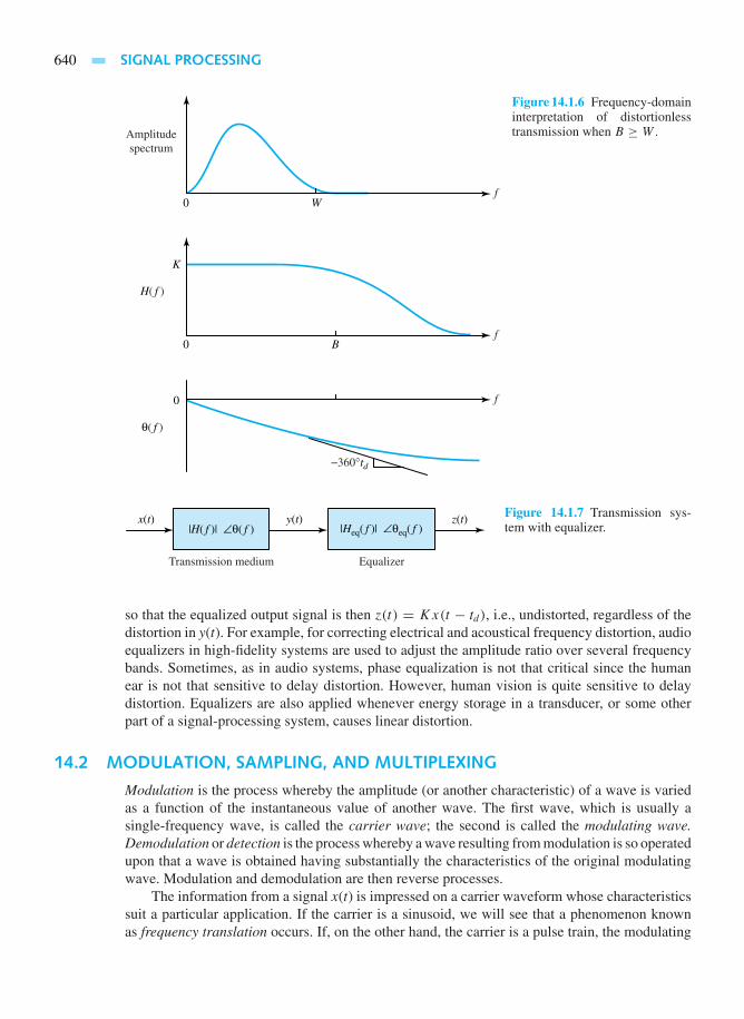
640 SIGNAL PROCESSING
f0 W
Amplitudespectrum
f0 B
H( f )
K
f
θ( f )
−360°td
0
Figure 14.1.6 Frequency-domaininterpretation of distortionlesstransmission when B ≥ W .
|H( f )| ∠θ( f )x(t) y(t)
|Heq( f )| ∠θeq( f )z(t)
Transmission medium Equalizer
Figure 14.1.7 Transmission sys-tem with equalizer.
so that the equalized output signal is then z(t) = Kx(t − td), i.e., undistorted, regardless of thedistortion in y(t). For example, for correcting electrical and acoustical frequency distortion, audioequalizers in high-fidelity systems are used to adjust the amplitude ratio over several frequencybands. Sometimes, as in audio systems, phase equalization is not that critical since the humanear is not that sensitive to delay distortion. However, human vision is quite sensitive to delaydistortion. Equalizers are also applied whenever energy storage in a transducer, or some otherpart of a signal-processing system, causes linear distortion.
14.2 MODULATION, SAMPLING, AND MULTIPLEXING
Modulation is the process whereby the amplitude (or another characteristic) of a wave is variedas a function of the instantaneous value of another wave. The first wave, which is usually asingle-frequency wave, is called the carrier wave; the second is called the modulating wave.Demodulation or detection is the process whereby a wave resulting from modulation is so operatedupon that a wave is obtained having substantially the characteristics of the original modulatingwave. Modulation and demodulation are then reverse processes.
The information from a signal x(t) is impressed on a carrier waveform whose characteristicssuit a particular application. If the carrier is a sinusoid, we will see that a phenomenon knownas frequency translation occurs. If, on the other hand, the carrier is a pulse train, the modulating

14.2 MODULATION, SAMPLING, AND MULTIPLEXING 641
signal needs to be sampled as part of the modulation process. Frequency translation and samplinghave extensive use in communication systems. Both of these lend to multiplexing, which permitsa transmission system to handle two or more information-bearing signals simultaneously.
Frequency Translation and Product Modulation
The basic operation needed to build modulators is the multiplication of two signals. Wheneversinusoids are multiplied, frequency translation takes place. Figure 14.2.1(a) shows a productmodulator, which multiplies the signal x(t) and a sinusoidal carrier wave at frequency fc to yield
xc(t) = x(t) cos 2πfct (14.2.1)
Choosing x(t) to be a low-pass signal with bandwidth W << fc, Figure 14.2.1(b) depicts therelationship between xc(t) and x(t). The modulated wave xc(t) can now be seen to have a bandpassspectrum resulting from frequency translation, which will be explained later.
If x(t) contains a sinusoidal component Am cos 2π fmt, multiplication by a sinusoidal carrierwave cos 2π fct with fc >> fm yields
(Am cos 2πfmt)× (cos 2πfct) = Am
2cos 2π(fc − fm)t + Am
2cos 2π(fc + fm)t (14.2.2)
Waveforms of the signal, the carrier wave, and the product, as well as their respective linespectra, are shown in Figure 14.2.2. Notice that the low frequency fm has been translated to thehigher frequencies fc ± fm.
Next, let us consider an arbitrary low-pass signal x(t) with the typical amplitude spectrumof Figure 14.2.3(a). The amplitude spectrum of the modulated wave xc(t) will now have twosidebands (lower and upper sidebands), each of width W on either side of fc, as illustrated inFigure 14.2.3(b). Thus, we have a signal that can be transmitted over a bandpass system with aminimum bandwidth of
B = 2W (14.2.3)
which is twice the bandwidth of the modulating signal. This process is then known as double-sideband modulation (DSB). Either the lower or the upper sideband may be removed by filtering soas to obtain single-sideband modulation (SSB) with B=W, if the bandwidth needs to be conserved.By choosing the carrier frequency fc at a value where the system has favorable characteristics,the frequency translation by product modulation helps in minimizing the distortion and otherproblems in system design.
xc(t)
xc(t)
cos 2πfct
t0
Idealmultiplier
Sinusoidalcarrierwave
Modulatedwave
Information-bearinginput signal
(a) (b)
x(t)
x(t)
1/fc
Figure 14.2.1 (a) Product modulator. (b) Waveforms.
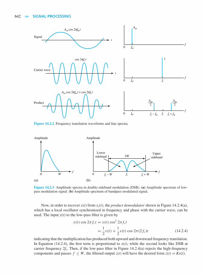
642 SIGNAL PROCESSING
Am cos 2πfmt
tSignal
cos 2πfc t
tCarrier wave
Am cos 2πfmt × cos 2πfc t
Product
0f
Am
fm
1
0f
fm fc
0f
fm fcfc − fm fc + fm
Am2
Am2
Figure 14.2.2 Frequency translation waveforms and line spectra.
0 Wf
fc fc + Wfc − W
Amplitude
(a)
0
2W
f
Amplitude
Lowersideband
Uppersideband
(b)
Figure 14.2.3 Amplitude spectra in double-sideband modulation (DSB). (a) Amplitude spectrum of low-pass modulation signal. (b) Amplitude spectrum of bandpass modulated signal.
Now, in order to recover x(t) from xc(t), the product demodulator shown in Figure 14.2.4(a),which has a local oscillator synchronized in frequency and phase with the carrier wave, can beused. The input y(t) to the low-pass filter is given by
x(t) cos 2πfct = x(t) cos2 2πfct
= 1
2x(t)+ 1
2x(t) cos 2π(2fc)t (14.2.4)
indicating that the multiplication has produced both upward and downward frequency translation.In Equation (14.2.4), the first term is proportional to x(t), while the second looks like DSB atcarrier frequency 2fc. Then, if the low-pass filter in Figure 14.2.4(a) rejects the high-frequencycomponents and passes f ≤ W , the filtered output z(t) will have the desired form z(t) = Kx(t).

14.2 MODULATION, SAMPLING, AND MULTIPLEXING 643
0 W 2fc(b)
f
y(t)
cos 2πfct
Oscillator
Synch
Low-passfilter
(a)
xc(t)z(t)
Figure 14.2.4 (a) Product demodula-tor. (b) Spectrum prior to low-pass fil-tering.
Sampling and Pulse Modulation
In most analog circuits, signals are processed in their entirety. However, in many modern electricsystems, especially those that convert waveforms for processing by digital circuits, such as digitalcomputers, only sample values of signals are utilized for processing. Sampling makes it possibleto convert an analog signal to discrete form, thereby permitting the use of discrete processingmethods. Also, it is possible to sample an electric signal, transmit only the sample values, and usethem to interpolate or reconstruct the entire waveform at the destination. Sampling of signals andsignal reconstruction from samples have widespread applications in communications and signalprocessing.
One of the most important results in the analysis of signals is the sampling theorem, whichis formally presented later. Many modern signal-processing techniques and the whole familyof digital communication methods are based on the validity of this theorem and the insight itprovides. The idea leading to the sampling theorem is rather simple and quite intuitive. Let usconsider a relatively smooth signal x1(t), which varies slowly and has its main frequency contentat low frequencies, as well as a rapidly changing signal x2(t) due to the presence of high-frequencycomponents. Suppose we are to approximate these signals with samples taken at regular intervals,so that linear interpolation of the sampled values can be used to obtain an approximation of theoriginal signals. It is obvious that the sampling interval for the signal x1(t) can be much largerthan the sampling interval necessary to reconstruct signal x2(t) with comparable distortion. Thisis simply a direct consequence of the smoothness of the signal x1(t) compared to x2(t). Therefore,the sampling interval for the signals of smaller bandwidths can be made larger, or the samplingfrequency can be made smaller. The sampling theorem is, in fact, a statement of this intuitivereasoning.
Let us now look from another point of view by considering a simple switching samplerand waveforms shown in Figure 14.2.5(a). Let the switch alternate between the two con-tacts at the sampling frequency fs = 1/Ts . The lower contact of the switch is grounded.
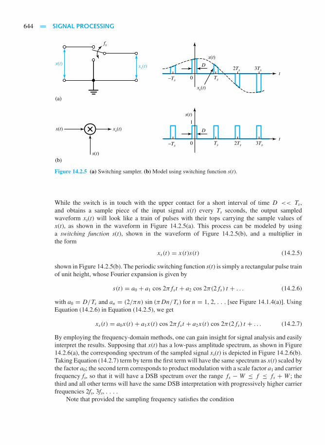
644 SIGNAL PROCESSING
xs(t)x(t)
xs(t)
xs(t)
x(t)
x(t)
s(t)
s(t)
fs
(a)
(b)
t−Ts Ts
D2Ts 3Ts
0
t−Ts Ts
D
2Ts 3Ts0
1
Figure 14.2.5 (a) Switching sampler. (b) Model using switching function s(t).
While the switch is in touch with the upper contact for a short interval of time D << Ts ,and obtains a sample piece of the input signal x(t) every Ts seconds, the output sampledwaveform xs(t) will look like a train of pulses with their tops carrying the sample values ofx(t), as shown in the waveform in Figure 14.2.5(a). This process can be modeled by usinga switching function s(t), shown in the waveform of Figure 14.2.5(b), and a multiplier inthe form
xs(t) = x(t)s(t) (14.2.5)
shown in Figure 14.2.5(b). The periodic switching function s(t) is simply a rectangular pulse trainof unit height, whose Fourier expansion is given by
s(t) = a0 + a1 cos 2πfst + a2 cos 2π(2fs) t + . . . (14.2.6)
with a0 = D/Ts and an = (2/πn) sin (πDn/Ts) for n = 1, 2, . . . [see Figure 14.1.4(a)]. UsingEquation (14.2.6) in Equation (14.2.5), we get
xs(t) = a0x(t)+ a1x(t) cos 2πfst + a2x(t) cos 2π(2fs) t + . . . (14.2.7)
By employing the frequency-domain methods, one can gain insight for signal analysis and easilyinterpret the results. Supposing that x(t) has a low-pass amplitude spectrum, as shown in Figure14.2.6(a), the corresponding spectrum of the sampled signal xs(t) is depicted in Figure 14.2.6(b).Taking Equation (14.2.7) term by term the first term will have the same spectrum as x(t) scaled bythe factor a0; the second term corresponds to product modulation with a scale factor a1 and carrierfrequency fs, so that it will have a DSB spectrum over the range fs − W ≤ f ≤ fs + W ; thethird and all other terms will have the same DSB interpretation with progressively higher carrierfrequencies 2fs, 3fs, . . . .
Note that provided the sampling frequency satisfies the condition
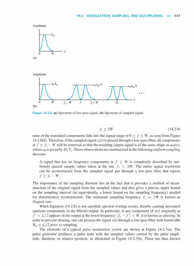
14.2 MODULATION, SAMPLING, AND MULTIPLEXING 645
0 W fs − W fs fs + W 2fs(b)
(a)
f
0 Wf
Amplitude
Amplitude
Am
a0Am a1Am/2 a2Am/2
Figure 14.2.6 (a) Spectrum of low-pass signal. (b) Spectrum of sampled signal.
fs ≥ 2W (14.2.8)
none of the translated components falls into the signal range of 0 ≤ f ≤ W , as seen from Figure14.2.6(b). Therefore, if the sampled signal xs(t) is passed through a low-pass filter, all componentsat f ≥ fs −W will be removed so that the resulting output signal is of the same shape as a0x(t),where a0 is given byD/Ts . These observations are summarized in the following uniform samplingtheorem:
A signal that has no frequency components at f ≥ W is completely described by uni-formly spaced sample values taken at the rate fs ≥ 2W . The entire signal waveformcan be reconstructed from the sampled signal put through a low-pass filter that rejectsf ≥ fs −W .
The importance of the sampling theorem lies in the fact that it provides a method of recon-struction of the original signal from the sampled values and also gives a precise upper boundon the sampling interval (or equivalently, a lower bound on the sampling frequency) neededfor distortionless reconstruction. The minimum sampling frequency fs = 2W is known asNyquist rate.
When Equation (14.2.8) is not satisfied, spectral overlap occurs, thereby causing unwantedspurious components in the filtered output. In particular, if any component of x(t) originally atf ′ > fs/2 appears in the output at the lower frequency
∣∣fs − f ′∣∣ < W , it is known as aliasing. In
order to prevent aliasing, one can process the signal x(t) through a low-pass filter with bandwidthBp ≤ fs/2 prior to sampling.
The elements of a typical pulse modulation system are shown in Figure 14.2.7(a). Thepulse generator produces a pulse train with the sampled values carried by the pulse ampli-tude, duration, or relative position, as illustrated in Figure 14.2.7(b). These are then known

646 SIGNAL PROCESSING
x(t)
(a)
(b)
x(t)
t
PAM
t
Ts 2Ts0 3Ts 4Ts 5Ts
Ts 2Ts 3Ts 4Ts 5Ts
0
PDM
t0
PPM
t0
Low-passfilter
Pulsegenerator
Transmissionmedium
Pulseconverter
Low-passfilter
Figure 14.2.7 (a) Typical pulse modulation system. (b) Waveforms.
as pulse amplitude modulation (PAM), pulse duration modulation or pulse width modula-tion (PDM or PWM), and pulse position modulation (PPM), respectively. At the output end,the modulated pulses are converted back to sample values for reconstruction by low-passfiltering.
EXAMPLE 14.2.1
In order to demonstrate aliasing, make a plot of the signal
x(t) = 3 cos 2π10t − cos 2π30t
which approximates a square wave with W = 30 Hz. If the sample points are taken at
t = 0,1
60,
2
60, . . . ,
6
60
corresponding to Ts = 1/(2W), you can see that x(t) could be recovered from those samples.However, if the sample points are taken at

14.2 MODULATION, SAMPLING, AND MULTIPLEXING 647
t = 0,1
40,
2
40, . . .
corresponding to Ts = 1/(2W) and fs < 2W , a smooth curve drawn through these points willshow the effect of aliasing.
So l u t i on
The waveforms are sketched in Figure E14.2.1.
x(t) Aliased waveform
t0
−2
2
160
140
340
=360
240
=660
440
260
460
560
Figure E14.2.1
Multiplexing Systems
A multiplexing system is one in which two or more signals are transmitted jointly over thesame transmission channel. There are two commonly used methods for signal multiplexing.In frequency-division multiplexing (FDM), various signals are translated to nonoverlappingfrequency bands. The signals are demultiplexed for individual recovery by bandpass filteringat the destination. FDM may be used with either analog or discrete signal transmission. Time-division multiplexing (TDM), on the other hand, makes use of the fact that a sampled signal isoff most of the time and the intervals between samples are available for the insertion of samplesfrom other signals. TDM is usually employed in the transmission of discrete information. Let usnow describe basic FDM and TDM systems.
Figure 14.2.8(a) shows a simple FDM system which is used in telephone communicationsystems. Each input is passed through a low-pass filter (LPF) so that all frequency componentsabove 3 kHz are eliminated. It is then modulated onto individual subcarriers with 4-kHz spacing.While all subcarriers are synthesized from a master oscillator, the modulation is achieved withsingle sideband (SSB). The multiplexed signal, with a typical spectrum as shown in Figure14.2.8(b), is formed by summing the SSB signals and a 60-kHz pilot carrier. The bandpass filters(BPFs) at the destination separate each SSB signal for product demodulation. Synchronization isachieved by obtaining the local oscillator waveforms from the pilot carrier. Telephone signals areoften multiplexed in this fashion.
A basic TDM system is illustrated in Figure 14.2.9(a). Let us assume for simplicity that allthree input signals have equal bandwidths W. A commutator or an electronic switch subsequentlyobtains a sample from each input every Ts seconds, thereby producing a multiplexed waveformwith interleaved samples, as shown in Figure 14.2.9(b). Another synchronized commutator at thedestination isolates and distributes the samples to a bank of low-pass filters (LPFs) for individualsignal reconstruction. More sophisticated TDM systems are available in which the sampled valuesare converted to pulse modulation prior to multiplexing and carrier modulation is included after

648 SIGNAL PROCESSING
x1(t)
x2(t)
x3(t)
x1(t)
x2(t)
x3(t)
Masteroscillator
Frequencysynthesizer
Transmissionmedium
Inputsignals
(a)
(b)
LPF
LPF
LPF
SSBmod
SSBmod
SSBmod
Σ
64 kHz
68 kHz
72 kHz
Frequencysynthesizer
Outputsignals
BPF
BPF
BPF
BPF
Demod
Demod
Demod
60-kHz pilot
Pilot
60–64 kHz
64–68 kHz
68–72 kHz
64 kHz
60-kHz pilot
68 kHz
72 kHz
f , kHz0 60 64 68 72
Figure 14.2.8 (a) Simple FDM system. (b) Typical spectrum of multiplexed signal with pilot.
multiplexing. Integrated switching circuits have made the TDM implementation much simplerthan FDM.
EXAMPLE 14.2.2
Find the transmission bandwidth required of a data telemetry system that is to handle three differentsignals with bandwidths W1 = 1 kHz, W2 = 2 kHz, and W3 = 3 kHz, by employing:
(a) FDM with DSB subcarrier modulation.
(b) TDM with pulse duration D = Ts/6.
So l u t i on
(a) B ≥ 2W1 + 2W2 + 2W3 = 12kHz.
(b) fs ≥ 2W3 = 6 kHz, so B ≥ 1/D = 6fs ≥ 36 kHz.

14.3 INTERFERENCE AND NOISE 649
x1
x2
x3
x1
x1s
x2x2s
x3x3s
fsfs
Transmissionmedium
Inputsignals
(a)
(b)
Outputsignals
LPF
LPF
LPFCommutator
LPF
LPF
LPFCommutator
x1(t)
t
Figure 14.2.9 (a) Basic TDM system. (b) Multiplexed waveform.
14.3 INTERFERENCE AND NOISE
An information-bearing signal often becomes contaminated by externally generated interferenceand noise and/or by internally generated noise. The demodulated message signal is generallydegraded to some extent by the presence of these distortions (attenuation, interference, andnoise) in the received signal. The fidelity of the received message signal is then a functionof the type of modulation, the strength of the additive noise, the type and strength of anyother additive interference, and the type of any nonadditive interference or noise. This sectiononly introduces some of the major causes of interference and noise, and touches upon somemethods of dealing with their effects in order to minimize the interference and suppress thenoise.
Interference may take several forms: ac hum, higher frequency pulses and “whistles,” orerratic waveforms commonly known as static. Interfering signals can be seen to enter the systemprimarily through the following mechanisms:
• Capacitive coupling, because of the stray capacitance between the system and an externalvoltage
• Magnetic coupling, because of the mutual inductance between the system and an externalcurrent
• Radiative coupling, because of electromagnetic radiation impinging on the system, partic-ularly in the channel
• Ground-loop coupling, because of the currents flowing between different ground points
To minimize coupling from the inevitable sources, all exposed elements are usually enclosedwithin conducting shields, which offer low-resistance paths to ground. When held at a commonpotential, these shields are quite effective in reducing most types of interference. However, low-frequency magnetic coupling can induce unwanted current flow through the shields themselves.Then the shield connection has to be interrupted to avoid a closed-loop current path. An additional

650 SIGNAL PROCESSING
layer of special magnetic shielding material may become necessary sometimes in extreme casesof magnetic-coupling interference. The grounding terminals, the equipment cases, and the shieldsare generally tied together at a single system ground point so as to prevent ground-loop current-coupling interference.
The transducer in some cases may have a local ground that cannot be disconnected. In sucha case, a separate ground strap (braided-wire straps used because of their low inductance) is usedto connect the local ground and the system ground point. The shield is also disconnected fromthe amplifier so as to prevent ground-loop current through the shield. Because the ground straphas nonzero resistance, any stray current through the strap will cause an interference voltage vcm
known as common-mode voltage since it appears at both the transducer and the shield terminals.vcm is generally quite small; however, when the information-bearing signal voltage itself is rathersmall, the common-mode voltage may pose a problem, which can be eliminated by using thedifferential amplifier, as shown in Figure 14.3.1. The analysis with the virtual-short model of theop-amp reveals that
vout = K(v2 − v1) (14.3.1)
amplifying the difference voltage v2−v1. With reasonable assumptions that Rs << R1 and Rt <<
R2, we have v1∼= vcm and v2
∼= x + vcm, so that
vout = K [(x + vcm)− vcm] = Kx (14.3.2)
in which vcm has been eliminated as desired. Such an op-amp circuit is also known as aninstrumentation or transducer amplifier.
Any interference at frequencies outside the signal band can be eliminated by appropriatefiltering. However, in order to combat interference within the signal band (after proper shieldingand grounding), a notch filter is sometimes used to avoid the bothersome interference at a singlefrequency f 0. Figure 14.3.2 illustrates the point: Part (a) shows the composite amplitude spectrumincluding the single-frequency interference; part (b) depicts the amplitude ratio of the notch filter.The notch-filtering technique does, of course, introduce some inevitable signal distortion, andsuch filtering should precede amplification to prevent possible saturation of the amplifier due tothe interference.
+
+
Shield
Transducer
Differentialamplifier
vcm
vout
v1
v2 R2
R1
RF = KR1
R3 = KR2
Rs
Rtx(t)
Model of a transducerwith common-mode voltage
+−
Figure 14.3.1 Differential amplifier to eliminate the common-mode voltage.
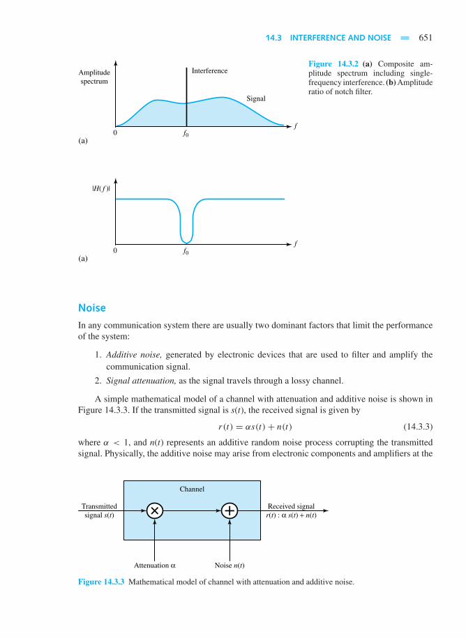
14.3 INTERFERENCE AND NOISE 651
Amplitudespectrum
Signal
Interference
ff0
(a)0
|H( f )|
ff0
(a)0
Figure 14.3.2 (a) Composite am-plitude spectrum including single-frequency interference. (b) Amplituderatio of notch filter.
Noise
In any communication system there are usually two dominant factors that limit the performanceof the system:
1. Additive noise, generated by electronic devices that are used to filter and amplify thecommunication signal.
2. Signal attenuation, as the signal travels through a lossy channel.
A simple mathematical model of a channel with attenuation and additive noise is shown inFigure 14.3.3. If the transmitted signal is s(t), the received signal is given by
r(t) = αs(t)+ n(t) (14.3.3)
where α < 1, and n(t) represents an additive random noise process corrupting the transmittedsignal. Physically, the additive noise may arise from electronic components and amplifiers at the
Channel
Noise n(t)
Transmittedsignal s(t)
Received signalr(t) : α s(t) + n(t)
Attenuation α
Figure 14.3.3 Mathematical model of channel with attenuation and additive noise.
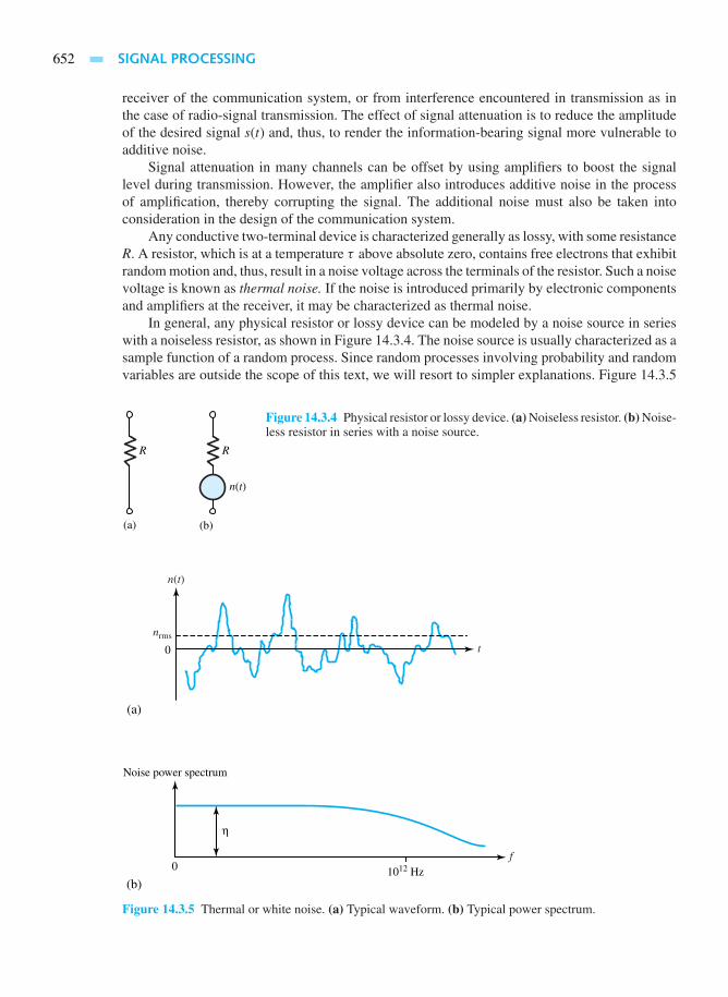
652 SIGNAL PROCESSING
receiver of the communication system, or from interference encountered in transmission as inthe case of radio-signal transmission. The effect of signal attenuation is to reduce the amplitudeof the desired signal s(t) and, thus, to render the information-bearing signal more vulnerable toadditive noise.
Signal attenuation in many channels can be offset by using amplifiers to boost the signallevel during transmission. However, the amplifier also introduces additive noise in the processof amplification, thereby corrupting the signal. The additional noise must also be taken intoconsideration in the design of the communication system.
Any conductive two-terminal device is characterized generally as lossy, with some resistanceR. A resistor, which is at a temperature τ above absolute zero, contains free electrons that exhibitrandom motion and, thus, result in a noise voltage across the terminals of the resistor. Such a noisevoltage is known as thermal noise. If the noise is introduced primarily by electronic componentsand amplifiers at the receiver, it may be characterized as thermal noise.
In general, any physical resistor or lossy device can be modeled by a noise source in serieswith a noiseless resistor, as shown in Figure 14.3.4. The noise source is usually characterized as asample function of a random process. Since random processes involving probability and randomvariables are outside the scope of this text, we will resort to simpler explanations. Figure 14.3.5
(b)(a)
R R
n(t)
Figure 14.3.4 Physical resistor or lossy device. (a) Noiseless resistor. (b) Noise-less resistor in series with a noise source.
n(t)
nrms
f0 1012 Hz
(a)
(b)
Noise power spectrum
η
t0
Figure 14.3.5 Thermal or white noise. (a) Typical waveform. (b) Typical power spectrum.

14.3 INTERFERENCE AND NOISE 653
(a) illustrates a typical thermal noise waveform n(t). In view of the unpredictable behavior, sincethe average value of n(t) may be equal to zero, a more useful quantity is the rms value nrms so thatthe average noise power is given by
N = n2rms/R, if nrms is noise voltage (14.3.4)
or
N = n2rmsR, if nrms is noise current (14.3.5)
The spectrum of thermal noise power is uniformly spread over frequency up to the infrared regionaround 1012 Hz, as shown in Figure 14.3.5(b). Such a distribution indicates that n(t) contains allelectrical frequencies in equal proportion, and an equal number of electrons is vibrating at everyfrequency. By analogy to white light, which contains all visible frequencies in equal proportion,thermal noise is also referred to as white noise.
The constant η in Figure 14.3.5(b) stands for the noise power spectral density, expressed interms of power per unit frequency (W/Hz). Statistical theory shows that
η = kT (14.3.6)
where k is the Boltzmann constant given by 1.381 × 10⁻²³ J/K and T is the source temperaturein kelvins. Equation (14.3.6) suggests that a hot resistance is noisier than a cool one, which iscompatible with our notion of thermally agitated electrons. At room temperature T0
∼= 290 K(17° C), η0 works out as 4× 10⁻²¹ W/Hz.
When we employ amplifiers in communication systems to boost the level of a signal, we arealso amplifying the noise corrupting the signal. Because any amplifier has some finite passband,we may model an amplifier as a filter with frequency response characteristic H(f ). Let us evaluatethe effect of the amplifier on an input thermal noise source.
Noiselessamplifier
nout(t)
NoutN
n(t)
G, B
RLR
Powerspectrum
BBandwidth
fl fu
(c)
0
η
N = ηB
Lowercutoff
Uppercutoff
Thermalnoisesource
AmplifierH( f )
Load
(b)
(a)MatchedMatched
Figure 14.3.6 Thermal noise converted to amplifier and load. (a) Matched block diagram. (b) Circuitrepresenting thermal noise at amplifier input. (c) Power spectrum.

654 SIGNAL PROCESSING
Figure 14.3.6(a), in block diagram form, illustrates a thermal noise source connected toa matched two-port network having frequency response H(f ) and the output of the networkconnected to a matched load. Figure 14.3.6(b) shows a thermal noise source represented by aresistance R connected to an amplifier with a matched input resistance. Presuming the amplifierto be noiseless, with power gain G and bandwidth B, the output noise power is
Nout = GN = GηB (14.3.7)
where N = ηB represents the source noise power [the area under the power-spectrum curvefalling within the passband, as shown in Figure 14.3.6(c)] accepted by the amplifier as input. Therms noise voltage for a thermal source connected to a matched resistance is then given by
ηrms =√RkT B (14.3.8)
The open-circuit voltage would be twice this value.Amplifier noise arises from both thermal sources (resistances) and nonthermal sources
(semiconductor devices). Although nonthermal noise is not related to physical temperature anddoes not necessarily have a uniform spectrum like that of thermal noise, one still refers to anamplifier’s noise temperature Ta, for convenience, as a measure of noisiness referred to the input.The model of a noisy amplifier is shown in Figure 14.3.7(a) with input noise N = ηB = kT B
from a source at temperature T, and the output power given by
Nout = GN +Na = GN +GkTaB = Gk(T + Ta)B (14.3.9)
where Na = GkTaB is the output noise power caused only by the amplifier, G is the power gainof the amplifier, and B is the bandwidth of the amplifier. Note that the amplifier noise Na is addedto the amplified source noise to yield the output power in Equation (14.3.9). If T = T0 (i.e., roomtemperature), then Nout
∼= Na , and the amplifier noise dominates the source noise, which is acommon occurrence. When Ta >> T0, the amplifier is very noisy, although not physically hot.
Figure 14.3.7(b) depicts the variation of noise temperature with frequency for a nonthermalsource. Several phenomena lumped together under the term one-over-f (1/f ) noise lead to thepronounced low-frequency rise in Figure 14.3.7(b). Such 1/f noise is produced by transistorsand certain transducers, such as photodiodes and optical sensors.
Signals in Noise
Let us now consider a weak information signal that is to be amplified by a noisy amplifier.The signal-to-noise ratio (SNR), usually expressed in decibels, becomes an important systemperformance measure. It is given by
Nout = GN + Na= Gk(T + Ta)B
G, B, Ta
Powerspectrum
N = kTB
f
noise1f
(b)(a)
Figure 14.3.7 (a) Model of a noisy amplifier. (b) Power spectrum of nonthermal noise.

14.3 INTERFERENCE AND NOISE 655
SNR = Pout
Nout= GPin
Gk(T + Ta)B= Pin
k(T + Ta)B(14.3.10)
where the amplified signal power is Pout = GPin in the numerator, which includes source andamplifier noise given by Equation (14.3.9); Pin is the average power of the input signal; and thedenominator Nout is the total output noise power given by Equation (14.3.9). Notice that the am-plifier’s power gain G does not appear in the final result of the SNR. A large SNR indicates that thesignal is strong enough to mask the noise and possibly make the noise inconsequential. For exam-ple, with SNR≥ 20 dB, intelligible voice communication results; otherwise, “static” in the voicesignal; with SNR ≥ 50 dB, noisefree television image results; otherwise, “snowy” TV picture.
For a good system performance, Equation (14.3.10) suggests a large value of Pin and/or smallvalues for T + Ta and B. However, one should be reminded here that the amplifier’s bandwidthB should not be less than the signal bandwidth W. That simply means that with large-bandwidthsignals, one would expect noise to be more troublesome.
Frequency translation can be used effectively to reduce the effect of 1/f noise by putting thesignal in a less noisy frequency band. Figure 14.3.8(a) shows the schematic implementation withproduct modulation and demodulation, whereas Figure 14.3.8(b) illustrates the noise reduction interms of the areas under the noise power curve. The two multipliers in Figure 14.3.8(a) are normallyimplemented by using a pair of synchronized switches. It turns out that the product modulationrequires bandwidth B = 2W , and the synchronized product demodulation doubles the final SNR.
Another way of improving the SNR is by preemphasis and deemphasis filtering. Generally,for low-frequency components of the message signal FM (frequency modulation) performs better,and for high-frequency components PM (phase modulation) is a better choice. Hence, if one candesign a system that performs FM for low-frequency components of the message signal, and
Powerspectrum
f
Amplifier with 1/f noise
fc
fc fc + WW fc − W0
Synchronizedswitches
(b)
Low-passfilter
(a)
Kx(t)
Figure 14.3.8 (a) Schematic arrangement with frequency translation to reducethe effect of 1/f noise. (b) Noise power spectrum.
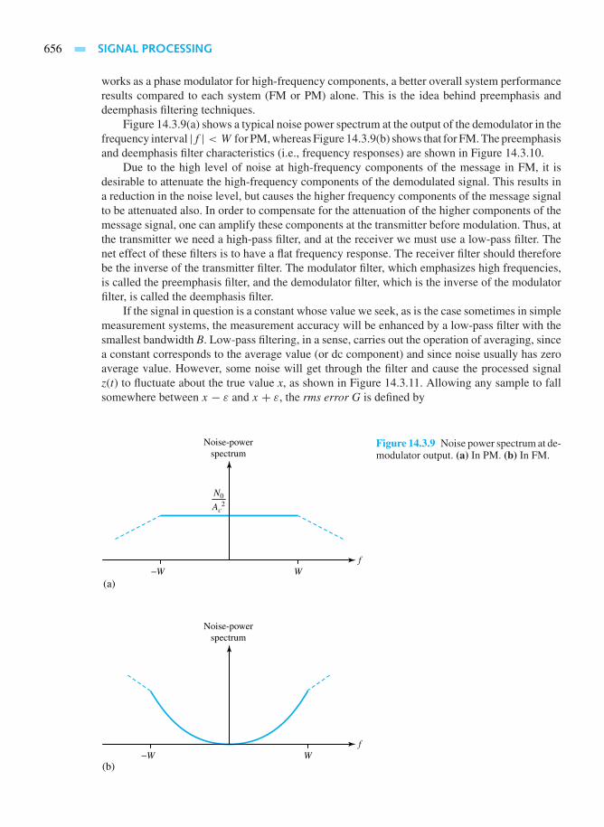
656 SIGNAL PROCESSING
works as a phase modulator for high-frequency components, a better overall system performanceresults compared to each system (FM or PM) alone. This is the idea behind preemphasis anddeemphasis filtering techniques.
Figure 14.3.9(a) shows a typical noise power spectrum at the output of the demodulator in thefrequency interval |f | < W for PM, whereas Figure 14.3.9(b) shows that for FM. The preemphasisand deemphasis filter characteristics (i.e., frequency responses) are shown in Figure 14.3.10.
Due to the high level of noise at high-frequency components of the message in FM, it isdesirable to attenuate the high-frequency components of the demodulated signal. This results ina reduction in the noise level, but causes the higher frequency components of the message signalto be attenuated also. In order to compensate for the attenuation of the higher components of themessage signal, one can amplify these components at the transmitter before modulation. Thus, atthe transmitter we need a high-pass filter, and at the receiver we must use a low-pass filter. Thenet effect of these filters is to have a flat frequency response. The receiver filter should thereforebe the inverse of the transmitter filter. The modulator filter, which emphasizes high frequencies,is called the preemphasis filter, and the demodulator filter, which is the inverse of the modulatorfilter, is called the deemphasis filter.
If the signal in question is a constant whose value we seek, as is the case sometimes in simplemeasurement systems, the measurement accuracy will be enhanced by a low-pass filter with thesmallest bandwidth B. Low-pass filtering, in a sense, carries out the operation of averaging, sincea constant corresponds to the average value (or dc component) and since noise usually has zeroaverage value. However, some noise will get through the filter and cause the processed signalz(t) to fluctuate about the true value x, as shown in Figure 14.3.11. Allowing any sample to fallsomewhere between x − ε and x + ε, the rms error G is defined by
Noise-powerspectrum
f
N0
Ac2
−W W
(b)
(a)
Noise-powerspectrum
f−W W
Figure 14.3.9 Noise power spectrum at de-modulator output. (a) In PM. (b) In FM.

14.3 INTERFERENCE AND NOISE 657
1
f5f04 f03f02f0f00−f0−2f0−3f0−4 f0−5f0
(a)
1 + f 2
f02|Hp( f )| =
1
1
f5f04 f03f02f0f00−f0−2f0−3f0−4 f0−5f0
(b)
1 + f 2
f02
|Hd ( f )| =
Figure 14.3.10 (a) Preemphasisfilter characteristic. (b) Deempha-sis filter characteristic.
z(t)
x + ε
x − ε
x
tt1 t2 t3
z(t1)
z(t2) z(t3)
Figure 14.3.11 Constant signal xwith noise fluctuations.
G = x√Pout/Nout
(14.3.11)
By taking M different samples of z(t), the arithmetic average can be seen to be
zav = 1
M(z1 + z2 + . . .+ zM) (14.3.12)
If the samples are spaced in time by at least 1/B seconds, then the noise-induced errors tend tocancel out and the rms error of zav becomes
εM = ε/√M (14.3.13)
This averaging method amounts to reducing the bandwidth to B/M .When the signal in question is a sinusoid whose amplitude is to be measured, averaging
techniques can also be used by utilizing a narrow bandpass filter, or a special processor known

658 SIGNAL PROCESSING
as a lock-in amplifier. For extracting information from signals deeply buried in noise, moresophisticated methods based on digital processing are available.
EXAMPLE 14.3.1
A low-noise transducer is connected to an instrumentation system by a cable that generates thermalnoise at room temperature. The information-bearing signal has a bandwidth of 6 kHz. The signalpower delivered is Pin = 120 pW. Evaluate the condition on the amplifier noise temperature Ta
such that the signal-to-noise ratio (SNR) is greater than or equal to 50 dB.
So l u t i on
Applying Equation (14.3.10) with T = T0,
SNR = Pout
Nout= Pin
k(T + Ta)B= Pin
kT0
(1+ Ta
T0
)B= 120× 10−12
4× 10⁻²¹(
1+ TaT0
)6× 10³
≥ 105
Hence,
Ta ≤ 49T0
This condition can easily be satisfied in the case of a well-designed amplifier.
14.4 LEARNING OBJECTIVES
The learning objectives of this chapter are summarized here so that the student can check whetherhe or she has accomplished each of the following.
• Basic ideas of analog and digital communication systems.
• Constructing the line spectrum of a periodic signal from its Fourier-series expansion.
• Conditions for distortionless transmission.
• Sketching spectra at various points in a system using product modulation and filtering.
• Conditions under which a signal can be sampled and then reconstructed from a pulse-modulated waveform.
• Basic notions of multiplexing systems.
• Causes of interference and noise, and techniques for minimizing their effects.
14.5 PRACTICAL APPLICATION: A CASE STUDY
Antinoise Systems—Noise Cancellation
Traditionally sound-absorbing materials have been used quite effectively to reduce noise levels inaircraft, amphitheaters, and other locations. An alternate way is to develop an electronic systemthat cancels the noise. Ear doctors and engineers have successfully developed ear devices thatwill nearly eliminate the bothersome and irritating noise (so-called tinnitus) experienced bypatients suffering from Meniere’s disease. For passengers in airplanes, helicopters, and otherflying equipment, a proper headgear is being developed in order to eliminate the annoying noise.

PROBLEMS 659
Applications could conceivably extend to people residing near airports and bothered by airplanetakeoffs and landings. For industrial workers who are likely to develop long-term ill effects dueto various noises they may be subjected to in their workplace, and even for persons who areirritated by the pedestrian noise levels in certain locations, antinoise systems that nearly eliminateor nullify noise become very desirable.
Figure 14.5.1 illustrates in block-diagram form the principle of noise cancellation as appliedto an aircraft carrying passengers. The electric signal resulting after sampling the noise at thenoise sources is passed through a filter whose transfer function is continuously adjusted by aspecial-purpose computer to match the transfer function of the sound path. An inverted versionof the signal is finally applied to loudspeakers, which project the sound waves out of phase withthose from the noise sources, nearly canceling the noise. Microphones on the headrests monitorthe sound experienced by the airline passengers so that the computer can determine the properfilter adjustments.
Signal processing, which is concerned with manipulating signals to extract information andto use that information to generate other useful electric signals, is indeed an important and far-reaching subject.
Adaptablefilter
Computer
Noisesource
Microphone nearsources of noise
such as engines and propellers(noise sampled before
entering passenger area)
Microphones(located on passenger headrests)
monitor sound level
Inverted signal versionof the transfer function
of the sound pathapplied to loudspeakers
Sound wavesnearly cancel thosefrom noise sources
Loudspeakerslocated inpassengercabin area
Figure 14.5.1 Block diagram of antinoise system to suppress the noise in an aircraft.
PROBL EMS
14.1.1 (a) A rectangular pulse is denoted by (t) anddefined as
(t) =
1, −1
2< t <
1
212 , t = ± 1
20, otherwise
Sketch the signal. Also express it in terms ofunit-step signals.
(b) The sinc signal is given by
sinc(t) =
sinπtπt
, t = 01, t = 0
Sketch the waveform and comment on itssalient features.
(c) The sign or signum signal is represented by

660 SIGNAL PROCESSING
sgn(t) =
1, t > 0−1 t < 00, t = 0
which can be expressed as the limit of thesignal xn(t) defined by
xn(t) =e−1/n, t > 0−e1/n, t < 00, t = 0
as n→∞. Sketch the waveform as the limitof xn(t).
*14.1.2 A large number of building blocks in a commu-nication system can be modeled by LTI (lineartime-invariant) systems, for which the impulseresponse completely characterizes the system.Consider the system described by
y(t) =∫ t
−∞x(τ) dτ
which is called an integrator. Investigate whetherthe system is LTI by finding its response to x(t −t0).
14.1.3 For a real periodic signal x(t) with period T0,three alternative ways to represent the Fourierseries expansion are:
x(t) =+∞∑−∞
xnej2π n
T0t
= a0
2+
∞∑n=1
[an cos
(2π
n
T0t
)
+ bn sin
(2π
n
T0t
)]
= x0 + 2∞∑n=1
|xn| cos
(2π
n
T0t + xn
)
where the corresponding coefficients areobtained from
xn = 1
T0
∫ α+T0
α
x(t)e−j2π n
T0tdt = an
2− j
bn
2
an = 2
T0
∫ α+T0
α
x(t) cos
(2π
n
T0t
)dt
bn = 2
T0
∫ α+T0
α
x(t) sin
(2π
n
T0t
)dt
|xn| = 1
2
√a2n + b2
n
xn = −arctan
(bn
an
)in which the parameter α in the limits of theintegral is arbitrarily chosen as α = 0 or α =−T0/2, for convenience.
(a) Show that the Fourier-series representationof an impulse train is given by
x(t) =+∞∑
n=−∞δ(t − nT0) = 1
T0
+∞∑n=−∞
ej2π n
T0t
Also sketch the impulse train.
(b) Obtain the Fourier-series expansion for thesignal x(t) sketched in Figure P14.1.3 withT0 = 2, by choosing α = −1/2.
14.1.4 (a) Show that the sum of two discrete periodicsignals is periodic.
(b) Show that the sum of two continuous peri-odic signals is not necessarily periodic; findthe condition under which the sum of twocontinuous periodic signals is periodic.
14.1.5 Classify the following signals into even and oddsignals:
(a)x1(t) =
e−t , t > 0−e−t , t < 00, t = 0
(b) x2(t) = e−|t |
1
−1
t−2
2−1
152−
52
32− 1
2−
12
32
Figure P14.1.3

PROBLEMS 661
(c)
x3(t) =
t|t | , t = 00, t = 0
*14.1.6 For the following neither even nor odd signals,find the even and odd parts of the signals.
(a)
x4(t) =t, t ≥ 00, t < 0
(b) x5(t) = sin t + cos t
14.1.7 Classify the following signals into energy-typeor power-type signals, and determine the energyor power content of the signal.
(a) x1(t) = e−t cos t u−1(t)
(b) x2(t) = e−t cos t
(c)
x3(t) = sgn(t) =
1, t > 0−1, t < 00, t = 0
Note:∫eax cos2 x dx = 1
4+a2 [(a cos2 x+sin 2x)+ 2
a]eax .
14.1.8 (a) Based on Example 14.1.3, comment onwhether x(t) = A cos 2π f 1t + B 2π f 2t isan energy- or a power-type signal.
(b) Find its energy or power content for f 1 = f 2
and f 1 = f 2.
14.1.9 For the power-type signals given, find the powercontent in each case.
(a) x(t) = Aej(2πf0t+θ).
(b) x(t) = u−1(t), the unit-step signal.
14.1.10 Show that the product of two even or two oddsignals is even, whereas the product of an evenand an odd signal is odd.
14.1.11 The triangular signal is given by
(t) =t + 1, −1 ≤ t ≤ 0−t + 1, 0 ≤ t ≤ 10, otherwise
(a) Sketch the triangular pulse.
(b) Sketch x(t) =∑+∞n=−∞ (t − 2n).
(c) Sketch x(t) =∑+∞n=−∞ (−1)n (t − n).
14.1.12 For real, even, and periodic functions with periodT0, the Fourier-series expansion can be expressedas
x(t) = a0
2+
∞∑n=1
an cos
(2π
n
T0t
)
where
an = 2
T0
∫ α+T0
α
x(t) cos
(2π
n
T0t
)dt
Determine an for the following signals:
(a) x(t) = |cos 2πf0t |, full wave rectifier out-put.
(b) x(t) = cos 2πf0t + |cos 2πf0t |, half-waverectifier output.
*14.1.13 For real x(t) given by Equation (14.1.11), identifythe even and odd parts of x(t).
14.1.14 Three alternative ways of representing a real peri-odic signal x(t) in terms of Fourier-series expan-sion are given in Problem 14.1.3. Determine theexpansion coefficients xn of each of the periodicsignals shown in Figure P14.1.14, and for eachsignal also determine the trigonometric Fourier-series coefficients an and bn.
14.1.15 Certain waveforms can be viewed as a combi-nation of some other waveforms for which theFourier coefficients are already known. Exam-ple 14.1.4 shows some periodic waveforms forwhich the coefficients a0, an, and bn are given byEquations (14.1.12) through (14.1.14), respec-tively. Use those to find the nonzero Fourier-series coefficients for the waveforms given inFigure P14.1.15.
14.1.16 Determine the bandwidth W from two criteria, (i)An < (An)max/10, for nf1 > W , and (ii) An <
(An)max/20, for nf1 > W , for the followingcases. (Note that A stands for amplitude.)
(a) Waveform of Figure E14.1.4(a), with A =π,D = 0.25 µs, and T = 0.5 µs.
(b) Waveform of Figure E14.1.4(b), with A =π2 and T = 2.5 µs.
(c) Waveform of Figure E14.1.4(d), withA = π
and T = 10 ms.
(d) Waveform of Figure E14.1.4(e), withA = π
and T = 800 µs.
14.1.17 Consider the rectangular pulse train x(t) of FigureE14.1.4(a), with A = 2 and D = T/2. Let v(t) =x(t) − 1.
(a) Sketch x(t) and v(t).
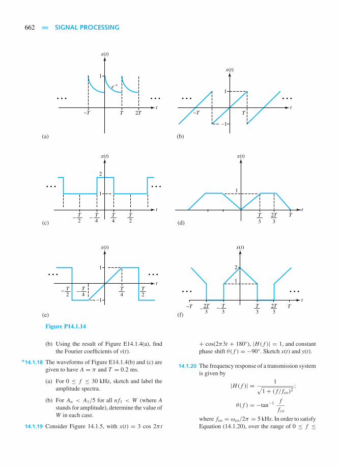
662 SIGNAL PROCESSING
x(t)
x(t)
T4
−T2
− T4
T2
(b)(a)
−T
e−t
Tt
2T
1
−T Tt
1
−1
x(t)
(c)
t
1
2
2T3
T
x(t)
(d)T3
t
1
T4
−−
T2
− T4
T2
x(t)
(e)
t
1
1T3
2
−−T T2T3
− T3
2T3
x(t)
(f)
t
1
Figure P14.1.14
(b) Using the result of Figure E14.1.4(a), findthe Fourier coefficients of v(t).
*14.1.18 The waveforms of Figure E14.1.4(b) and (c) aregiven to have A = π and T = 0.2 ms.
(a) For 0 ≤ f ≤ 30 kHz, sketch and label theamplitude spectra.
(b) For An < A1/5 for all nf1 < W (where Astands for amplitude), determine the value ofW in each case.
14.1.19 Consider Figure 14.1.5, with x(t) = 3 cos 2π t
+ cos(2π3t + 180°), |H(f )| = 1, and constantphase shift θ(f ) = −90°. Sketch x(t) and y(t).
14.1.20 The frequency response of a transmission systemis given by
|H(f )| = 1√1+ (f/fco)2
;
θ(f ) = −tan−1 f
fco
where fco = ωco/2π = 5 kHz. In order to satisfyEquation (14.1.20), over the range of 0 ≤ f ≤
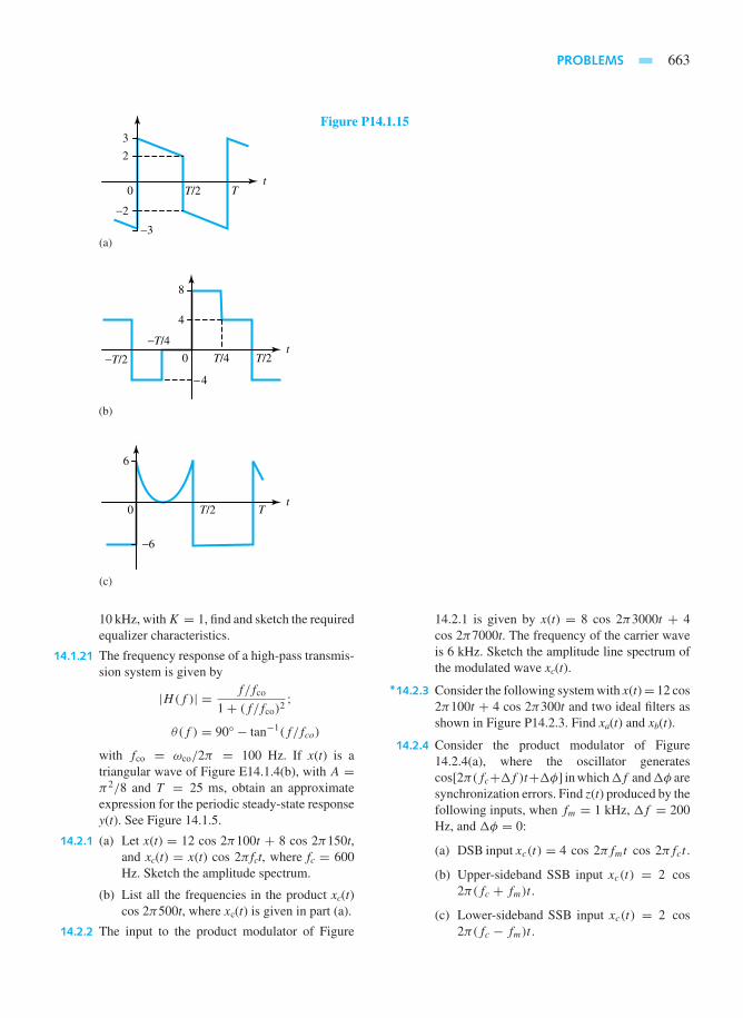
PROBLEMS 663
−3
tTT/2
T/4−T/2
−T/4
T/2
T/2
0
3
−2
(a)
2
t0
−4
(b)
4
8
t0 T
(c)
6
−6
Figure P14.1.15
10 kHz, with K = 1, find and sketch the requiredequalizer characteristics.
14.1.21 The frequency response of a high-pass transmis-sion system is given by
|H(f )| = f/fco
1+ (f/fco)2;
θ(f ) = 90°− tan−1(f/fco)
with fco = ωco/2π = 100 Hz. If x(t) is atriangular wave of Figure E14.1.4(b), with A =π2/8 and T = 25 ms, obtain an approximateexpression for the periodic steady-state responsey(t). See Figure 14.1.5.
14.2.1 (a) Let x(t) = 12 cos 2π100t + 8 cos 2π150t,and xc(t) = x(t) cos 2π fct, where fc = 600Hz. Sketch the amplitude spectrum.
(b) List all the frequencies in the product xc(t)cos 2π500t, where xc(t) is given in part (a).
14.2.2 The input to the product modulator of Figure
14.2.1 is given by x(t) = 8 cos 2π3000t + 4cos 2π7000t. The frequency of the carrier waveis 6 kHz. Sketch the amplitude line spectrum ofthe modulated wave xc(t).
*14.2.3 Consider the following system with x(t)= 12 cos2π100t + 4 cos 2π300t and two ideal filters asshown in Figure P14.2.3. Find xa(t) and xb(t).
14.2.4 Consider the product modulator of Figure14.2.4(a), where the oscillator generatescos[2π(fc+f )t+φ] in whichf andφ aresynchronization errors. Find z(t) produced by thefollowing inputs, when fm = 1 kHz, f = 200Hz, and φ = 0:
(a) DSB input xc(t) = 4 cos 2πfmt cos 2πfct .
(b) Upper-sideband SSB input xc(t) = 2 cos2π(fc + fm)t .
(c) Lower-sideband SSB input xc(t) = 2 cos2π(fc − fm)t .

664 SIGNAL PROCESSING
14.2.5 Repeat Problem 14.2.4 when fm = 1 kHz, f =0, and φ = 90°.
14.2.6 (a) Consider Figure 14.2.5, in which the signalto be sampled is x(t) = 18 cos 2π20t + 12cos 2π60t . With fs = 100 and D = Ts/2, for0 ≤ f ≤ 2fs , sketch the amplitude linespectrum of xs(t).
(b) Then find the signal y(t) that would be re-constructed by an ideal low-pass filter thatrejects all f > fs/2.
14.2.7 (a) The continuous amplitude spectrum of theinput to a switching sampler (Figure 14.2.5)is shown in Figure P14.2.7. For 0 ≤ f ≤100, with fs = 70 and D = Ts/4, sketch theresulting spectrum of xs(t).
(b) Suggest how x(t) can be reconstructed fromxs(t).
14.2.8 PDM and PPM (see Figure 14.2.7) have the ad-vantage of being immune to nonlinear distortion,because the pulse is either on or off. However, inexchange, the transmission bandwidth must beB ≥ 1/D >> W , which is needed to accommo-date pulses with duration D << Ts ≤ 1/(2W).Let D be the pulse duration of the PPM waveformin Figure 14.2.7. Let the maximum position shiftbe ±. For = 2D and fs = 20 kHz, find themaximum allowed value of D and the minimumrequired transmission bandwidth.
*14.2.9 The TDM system of Figure 14.2.9 has a trans-mission bandwidth B = 250 kHz.
(a) Find the maximum number of voice signalswith W = 4 kHz that can be multiplexed.
(b) Repeat part (a) with the additional constraintthat the TDM waveform be off for at least50% of the time.
14.3.1 An amplifier has a gain of 50 dB, a bandwidthof 9 MHz, and a noise temperature Ta = 25T0,where T0 is the room temperature, 290 K. Findthe output noise power and rms voltage across a100- load resistor when the source temperatureT = T0.
*14.3.2 If the signal in Example 14.3.1 has a bandwidth of600 kHz, determine Pout/Nout assuming a noise-less amplifier. Then check to see whether it ispossible to obtain Pout/Nout ≥ 105.
14.3.3 A simple RC filter yields |H(ω)|2 = 1/[1 +(ω/ωco)
2], whereas a more sophisticated and rel-atively more expensive Butterworth filter gives|H(ω)|2 = 1/[1 + (ω/ωco)
4]. Either of thesecan be used to reduce the hum amplitude. Letan information signal with significant frequencycontent for f ≤ 30 Hz be contaminated by achum at 120 Hz. The contaminated signal is thenapplied to a low-pass filter to reduce the humamplitude by a factor of α. For (i) α = 0.25,and (ii) α = 0.1, determine the required cutofffrequency f co for (a) the RC filter, and (b) theButterworth filter, and suggest the filter to be usedin each case.
cos 2πfat = cos 2π800t
Ideal filter Awhich rejects all
f < 800
Ideal filter Bwhich rejects all
f > 1200
x(t) xb(t)
cos 2πfbt = cos 2π1200t
Figure P14.2.3
Amplitude
0
20
f6040
Figure P14.2.7

PROBLEMS 665
14.3.4 (a) The transfer function of a notch filter is givenby H(jω) = (100+ jω−ω2)/(10+ jω)2.Sketch HdB versus ω.
(b) A notch filter centered at f0 = ω0/2π can beformed by using a resonant circuit arrangedsuch that
H(jω) = jQ(ω/ω0 − ω0/ω)
1+ jQ(ω/ω0 − ω0/ω)
Investigate |H(f )| at f = 0 and f = ∞;also at fl = f0(1− 1/(2Q), and fu= f 0(1+1/(2Q), for Q >> 1.
(c) With ω0 = 1/√LC and Q = (1/R)
√L/C,
show that a series RLC circuit can performas a notch filter when the output voltage istaken across L and C.
(d) For the purpose of rejecting 1-kHz interfer-ence, in order to get fl = 980 Hz and fu =1020 Hz, find the values of L and C of theseries RLC circuit with R = 50 .
(e) Now consider a tuned circuit in which R isconnected in series with a parallel combi-nation of L and C, and the output voltageis taken across R. With ω0 = 1/
√LC and
Q = R√C/L, show that the circuit can
perform as a notch filter.
(f) For the purpose of rejecting 60-Hz interfer-ence, in order to get fl = 58 Hz and fu = 62Hz, find the values of L and C of the circuitin part (e) with R = 1 k.
14.3.5 A noisy amplifier has Nout= 600 µW when T =T0; but Nout drops to 480 µW when the source isimmersed in liquid nitrogen at T = 80 K. Findthe amplifier’s noise temperature Ta.
14.3.6 Two noisy amplifiers (with noise temperaturesTa1 and Ta2) having the same bandwidth are con-nected in cascade so that the overall gain is G= G1G2. If the input noise to the first amplifieris N = kTB, determine the total output noisepower and the effective noise temperature Ta ofthe cascade, so that Nout = Gk(T + Ta)B.
*14.3.7 In order to measure the amplifier noise tempera-ture Ta, a thermal source at temperature T0 is con-nected and the corresponding Nout is observed;then the source temperature is increased to TR
when the corresponding Nout is doubled. Find Ta
in terms of TR and T0.
14.3.8 A signal (with P = 1 µW and B = 250 kHz)contaminated by white noise at noise temperatureT = 2T0 is applied to an amplifier. Obtain thecondition on Ta such that Pout/Nout ≥ 80.8 dB.
14.3.9 The noise figure of an amplifier is given by F =1 + Ta/T0. Express the output signal-to-noiseratio in terms of F, input noise power N, andinput noise temperature T. See how the result issimplified when T = T0.
14.3.10 A system for measuring the constant signal valuex has Pout/Nout = 40 dB and B = 8 Hz. In orderto obtain an accuracy of ±0.2%, how long mustthe output be observed?
14.3.11 An amplifier has a noise equivalent bandwidth B= 25 kHz and a maximum available power gainof G= 30 dB. If its output noise power is 108kT0,determine the effective noise temperature and thenoise figure (given by F = 1+ Ta/T0). Assumethe input noise source temperature to be T0.
*14.3.12 The overall noise figure of a cascade of K am-plifiers with gains Gk and corresponding noisefigures Fk, 1 ≤ k ≤ K , is
F = F1 + F2 − 1
G1+ F3 − 1
G1G2+ . . .
+ FK − 1
G1G2 . . . GK−1
If an amplifier is designed having three identicalstates, each of which has a gain of Gi = 5 and anoise figure of Fi = 6, i = 1, 2, 3, determinethe overall noise figure of the cascade of thethree stages. Looking at the result, justify thestatement that the front end of a receiver shouldhave a low noise figure and a high gain. (Notethat the noise figure of an amplifier is F =1+ Ta/T0.)
14.3.13 A radio antenna with a noise temperature of 60K is pointed in the direction of the sky. Theantenna feeds the received signal to the preampli-fier, which has a gain of 30 dB over a bandwidthof 10 MHz and a noise figure (F = 1 + Ta/T0)of 2 dB.
(a) Determine the effective noise temperature atthe input to the preamplifier.
(b) Determine the noise power at the output ofthe preamplifier.

15 Communication Systems
15.1 Waves, Transmission Lines, Waveguides, and Antenna Fundamentals
15.2 Analog Communication Systems
15.3 Digital Communication Systems
15.4 Learning Objectives
15.5 Practical Application: A Case Study—Global Positioning Systems
Problems
Even though most modern communication systems have only been invented and developed duringthe eighteenth and nineteenth centuries, it is difficult to imagine a world without telephones, radio,and television. After the invention of the electric battery by Alessandro Volta in 1799, SamuelMorse developed the electric telegraph and demonstrated it in 1837. Morse devised the variable-length binary code, in which letters of the English alphabet are represented by a sequence ofdots and dashes (code words). In this code, more frequently occurring letters are represented byshort code words, whereas letters occurring less frequently are represented by larger code words.Morse code (variable-length binary code), developed in 1837, became the precursor to variable-length source coding methods. Telegraphy, the earliest form of electrical communication, was abinary digital communication system in which the letters of the English alphabet were efficientlyencoded into corresponding variable-length code words having binary elements. In the baudoutcode, developed in 1875, the binary code elements were of equal length, and each letter wasencoded into fixed-length binary code words of length 5.
With the invention of the telephone, telephony came into being and the Bell TelephoneCompany was established in 1877. Transcontinental telephone transmission became operationalin 1915. Automatic switching was another important advance, and a digital switch was placed inservice in 1960. Numerous significant advances have taken place in telephone communicationsover the past four decades. For example, fiber-optic cables have replaced copper wire, andelectronic switches have come into use in place of electromechanical devices.
Marconi is credited with the development of wireless telegraphy in the late 1890s, afterMaxwell’s theory of electromagnetic radiation was verified experimentally by Hertz in 1887. The
666

Communication Systems 667
invention of the vacuum tube was particularly instrumental in the development of radio commu-nication systems. Amplitude modulation (AM) broadcast was initiated in 1920, while frequencymodulation (FM) broadcast was developed commercially by the end of World War II. Commercialtelevision broadcasting began in 1936 by the BBC (British Broadcasting Corporation), and theFCC (Federal Communications Commission) authorized television broadcasting five years laterin the United States.
The growth in communications over the past 60 years has been phenomenal. The invention ofthe transistor in 1947 and the integrated circuit and laser in 1958 have paved the way to satellitecommunication systems. Most of the wire-line communication systems are being replaced byfiber-optic cables (providing extremely high bandwidth), which makes the transmission of a widevariety of information sources (voice, data, and video) possible. High-speed communicationnetworks linking computers and the greater need for personal communication services are justthe beginning of the modern telecommunications era.
Today digital communication systems are in common use, carrying the bulk of our dailyinformation transmission through a variety of communication media, such as wire-line telephonechannels, microwave radio, fiber-optic channels, and satellite channels. Even the current analogAM and FM radio and television broadcasts will be replaced in the near future by digital transmis-sion systems. High-speed integrated circuits (ICs), programmable digital signal processing chips,microelectronic IC fabrication, and sophisticated digital modulation techniques have certainlyhelped digital communications as a means of transmitting information.
In spite of the general trend toward digital transmission of analog signals, a significant amountof analog signal transmission still takes place, especially in audio and video broadcasting. His-torically, analog communication systems were placed first, and then came digital communicationsystems.
In any communication system, the communication channel provides the connection betweenthe transmitter and the receiver. The physical channel (medium) may be any of the following:
• A pair of wires, which carry the electric signal
• Optical fiber, which carries the information on a modulated light beam
• An underwater ocean channel, in which the information is transmitted acoustically
• Free space, over which the information-bearing signal is radiated by using an antenna
• Data storage media, such as magnetic tape, magnetic disks, and optical disks.
The available channel bandwidth, as well as the noise and interference, limit the amount ofdata that can be transmitted reliably over any communication channel.
Figure 15.0.1 illustrates the various frequency bands of the electromagnetic spectrum (radioand optical portions) along with types of transmission media and typical applications.
Wire-line channels are used extensively by the telephone network for voice, data, and videotransmission. Twisted-pair wire lines (with a bandwidth of several hundred kHz) and coaxialcable (with a usable bandwidth of several MHz) are basically guided electromagnetic channels.
Fiber-optic channels offer a channel bandwidth that is several orders of magnitude larger thancoaxial cable channels. The transmitter or modulator in a fiber-optic communication system is alight source, such as a light-emitting diode (LED) or a laser, whose intensity is varied (modulated)with the message signal. The light propagates through the fiber as a light wave and is amplifiedperiodically along the transmission path to compensate for signal attenuation. At the receiverend, the light intensity is detected by a photodiode, whose output is an electric signal that varies

668 COMMUNICATION SYSTEMS
Designation Transmission media Applications
1015 Hz
1015 Hz
10−6 m
Ultraviolet
Visible lightExperimental
digitaltelecommunication
Opticalfibers
Laserbeams
Infrared
100 GHz
10 GHz
1 GHz
100 MHz
10 MHz
1 MHz
100 kHz
10 kHz
1 kHz
1 cm
10 cm
Millimeterwaves
Superhighfrequency
(SHF)
1 m
Ultrahighfrequency
(UHF)
10 m
Very highfrequency
(VHF)
100 m
Highfrequency
(HF)
1 km
Mediumfrequency
(MF)
10 km
Lowfrequency
(LF)
100 km
Very lowfrequency
(VLF)
Audioband
Experimental
Navigation
Satellite to satellite
Microwave relay
Earth to satellite
Radar
UHF TV
VHF TV and FM
Mobile, Aeronautical
Mobile radio
BusinessAmateur radioInternationalCitizens band
AM broadcasting
Aeronautics
Submarine cable
Navigation
Transoceanic radio
Telephone
Telegraph
Waveguide
Wav
elen
gth
Freq
uenc
y
Coaxialcable
Wire pairs
Microwaveradio
Long-waveradio
Short-waveradio
Figure 15.0.1 Frequency bands of the electromagnetic spectrum. (Source: A. Carlson,Communication Systems, 3rd ed., McGraw-Hill, New York, 1986.)
in direct proportion to the power of light striking on the photodiode. Optical fiber channels arereplacing nearly all wire-line channels in the telephone network.
Wireless electromagnetic channels are used in wireless communication systems, in whichthe electromagnetic energy is coupled to the propagation medium through an antenna that servesas a radiator. The physical size and configuration of the antenna depend mainly on the frequencyof operation. For example, a radio station transmitting AM frequency band of 1 MHz (witha corresponding wavelength of λ = c/fc = 300 m) requires an antenna of at least 30 m(approximately one-tenth of the wavelength).
The mode of propagation of electromagnetic waves in free space and atmosphere may besubdivided into three categories:

Communication Systems 669
• Ground-wave propagation
• Sky-wave propagation
• Line-of-sight (LOS) propagation.
In the frequency bands that are primarily used to provide navigational aids from shore toships around the world (VLF to LF to MF), the available channel bandwidths are relatively small,and hence the information that is transmitted through these channels is relatively slow speed andgenerally confined to digital transmission. Noise at these frequencies is caused by thunderstormactivity around the globe, whereas interference is caused by the many users.
For frequencies of 0.3 to 3 MHz, in the MF band, ground-wave (or surface-wave) propagation,illustrated in Figure 15.0.2, is the dominant mode used for AM broadcasting and maritime radiobroadcasting. Dominant disturbances include atmospheric noise, human-made noise, and thermalnoise from electronic components. The range is limited to about 100 miles for even the morepowerful radio stations.
In the ionosphere, the rarefied air becomes ionized, mainly due to ultraviolet sunlight. TheD-region, usually falling between 50 and 90 km in altitude, will reflect waves below 300 kHz orso, and attenuate higher frequency waves (300 kHz < f < 30 MHz), especially in the daytime.The D-region mostly disappears at night. The E-region (about 110 km in altitude) reflects highfrequencies (3 MHz < f < 30 MHz) during the daytime, and medium frequencies (300 kHz < f< 3 MHz) at night. The F1-region (about 175 to 250 km in altitude) is distinct from the F2-region(250 to 400 km in altitude) only during the day; at night they merge. Waves that penetrate theE-region usually go through the F1-region as well, with some attenuation being the primary effect.The F2-region provides the main means of long-distance, high-frequency (3 MHz < f < 30 MHz)communication by wave reflection. Sky-wave propagation is illustrated in Figure 15.0.3.
Signal multipath occurs with electromagnetic wave propagation via sky wave in the HFrange. When the transmitted signal reaches the receiver through multiple propagation paths withdifferent delays, signal fading may result. Both atmospheric noise and thermal noise become theadditive noise at high frequencies. It is possible to have ionospheric scatter propagation in thefrequency range of 30 to 60 MHz, and tropospheric scattering in the range of 40 to 300 MHz; butrelatively large antennas are needed with a large amount of transmitted power, because of largesignal propagation losses.
Frequencies above 30 MHz, propagating through the ionosphere with relatively little loss,make satellite and extraterrestrial communications possible. In the VHF band and higher, thedominant mode is line-of-sight (LOS) propagation, in which the transmitter and receiver antennasmust be in direct LOS with relatively little or no obstruction. That is why television stations
Ground or surfacewave
Earth
Troposphere(20 km aboveearth surface)
Figure 15.0.2 Illustration of ground-wave propagation in MFband.
Ionosphere (with D, E, F regions)
Sky waves
Earth
(50 to 600 kmabove earthsurface)
Figure 15.0.3 Illustration of sky-wave propaga-tion.

670 COMMUNICATION SYSTEMS
transmitting in the VHF and UHF bands have their antennas mounted on high towers to achieve abroad coverage area. A television antenna mounted on a tower of 1200 feet in height (= h) providesa coverage of about d = √2h ∼= 50 miles. Microwave radio relay systems (for telephone andvideo transmission at about 1 GHz) also have antennas mounted on tall towers.
In the VHF and UHF bands, thermal noise and cosmic noise, picked up by the antenna, becomepredominant. Above 10 GHz in the SHF band, atmospheric conditions (such as precipitation andheavy rains) play a major role in signal propagation. In the infrared and visible light regions ofthe electromagnetic spectrum, LOS optical communication in free space is being experimentedwith for satellite-to-satellite links.
A good understanding of a communication system can be achieved by studying electro-magnetic wave propagation (via transmission lines and antennas), and modulation as well asdemodulation involved in analog and digital communication systems. Toward that end, this chapteris divided into three sections. Since the wave concepts that apply to transmission lines are easilyunderstood, the first section deals with waves, transmission lines, and antenna fundamentals.Then we go on to discuss analog and digital communication systems in Sections 15.2 and 15.3,respectively.
15.1 WAVES, TRANSMISSION LINES, WAVEGUIDES, AND ANTENNAFUNDAMENTALS
In basic circuit theory we neglect the effects of the finite time of transit of changes in current andvoltage and the finite distances over which these changes occur. We assume that changes occursimultaneously at all points in the circuits. But there are situations in which we must consider thefinite time it takes for an electrical or magnetic wave to travel and the distance it will travel. It isin these situations that one must employ traveling-wave theory. Traveling-wave concepts mustbe used whenever the distance is so great or the frequency so high that it takes an appreciableportion of a cycle for the wave to travel the distance.
For sinusoidal signals, a wavelength λ is defined as the distance that a wave travels in onecycle or period. Since electric waves in free space travel at the velocity of light c(∼= 3×10⁸ m/s),the free-space wavelength is given by c/f. Table 15.1.1 shows some free-space wavelengths atselected frequencies. If the traveling-wave technique is to be employed for distances greater than1/10 wavelength, a distance of 3 mm at 10 GHz would require the use of this technique, whereasthe same distance at 100 MHz would not. On the other hand, a distance of 1 km is insignificantat power-line frequencies, but not in the broadcast band.
The connection of the high-power output of a transmitter located on a building to thetransmitting antenna on a tower is often made by special conductors called transmission lines,which guide the waves and usually consist of two or more parallel conductors, which are separatedby insulating (dielectric) materials. While transmission lines are available in many forms, Figure15.1.1 illustrates cross sections of some common types. The two-wire line of Figure 15.1.1(a) is
TABLE 15.1.1 Free-Space Wavelengths at Selected Frequencies
Application Frequency Wavelength
Power transmission 60 Hz 5000 kmVoice 1 kHz 300 kmBroadcast band 1 MHz 300 mFM, television 100 MHz 3 mX-band radar 10 GHz 3 cm

15.1 WAVES, TRANSMISSION LINES, WAVEGUIDES, AND ANTENNA FUNDAMENTALS 671
used to connect some television antennas. The coaxial cable of Figure 15.1.1(b) is the most widelyused of the many possible cable-type transmission lines. For printed-circuit and integrated-circuitapplications, transmission lines sketched in Figures 15.1.1(c) through (f) are commonly employed.
At higher frequencies, when power levels are large and attenuation in transmission lines issignificant, connections between system components are often made through waveguides, whichare usually hollow, closed, rigid conductor configurations (much like water pipes) through whichwaves propagate. The most common waveguides are either rectangular or circular in crosssection, as depicted in Figure 15.1.2, but other shapes and flexible varieties are also possible.
Coaxial transmission lines commonly operate in what is called the transverse electricmagnetic (TEM) mode, in which both the electric and the magnetic fields are perpendicular
Conductor
Conducting strip
Conductors
d
h
d
Dielectric εr
Dielectric εr
Dielectric εr Dielectric εr
Dielectricεr
(a)
(c)
(b)
W
W
h2 h
Hot lead
(e)
W
Conducting strip
hDielectric εr
Free space ε0
(d)
W
h
(f)
WS
Ground Hot lead Ground
S
D
Figure 15.1.1 Transmission lines (cross sections of some common types). (a) Two-wire line. (b) Coaxialline (cable). (c) Parallel strip line. (d) Microstrip line. (e) Strip line. (f) Coplanar waveguide.
b
a
(a)
a
(b)
Figure 15.1.2 Waveguides. (a) Rectangular. (b) Circular.

672 COMMUNICATION SYSTEMS
(transverse) to the direction of propagation, which is along the axial line. That is to say, noelectromagnetic field component exists in the axial direction. In the case of single-conductorhollow (pipelike) waveguides, either the TE (transverse electric) or the TM (transverse magnetic)mode can be energized. In the TE configuration, the electric field is transverse to the direction ofpropagation (which is along the axial line of the waveguide); that is to say, no electric field existsin the direction of propagation, while an axial component of the magnetic field is present. On theother hand, in the TM configuration, the magnetic field is transverse to the direction of propagation:i.e., no magnetic field exists in the axial direction, whereas an axial component of the electricfield is present. Within either grouping, a number of configurations or modes can exist, eitherseparately or simultaneously. However, we are generally concerned with the so-called dominantmode, which is defined as the lowest frequency mode that can exist in the waveguide. Whenoperating at a frequency above fc, known as the cutoff frequency, a wave propagates down thewaveguide and the mode is called propagation mode. When operating below the cutoff frequency,the field decays exponentially and there is no wave propagation.
Figure 15.1.3 represents a transmission line of length l connecting a signal source to a distantload. The line may be a two-wire line, a coaxial cable, or a hollow waveguide. The voltage v1(t)between the source-side (input) terminals of the transmission line gives rise to an electric field,while the current i1(t) produces a magnetic field. The characteristic impedance Z0 of the line isgiven by
Z0 = V1
I1(15.1.1)
which relates the voltage and current of the wave traveling along the line. Although Z0 in generalcould be complex, for distortionless transmission, Z0 (= R0) must be constant and resistive overthe frequency range of the signal. The signal-source voltage vS(t) is related to v1(t) by
vS(t) = v1(t)+ i1(t)RS (15.1.2)
where RS is the signal-source internal resistance. From Equations (15.1.1) and (15.1.2), we get
v1(t) = R0
RS + R0vS(t) (15.1.3)
i1(t) = 1
RS + R0vS(t) (15.1.4)
As the electromagnetic fields associated with v1(t) and i1(t) propagate down the line, they carryalong the associated voltages and currents that are no different from v1(t) and i1(t) except for adelay in time, because the charges (and therefore current) move down the line at finite velocityvg. Thus, at output terminals c and d in Figure 15.1.3, which are a distance l apart, the voltage
Transmissionline
Signalsource
Load
RS = Z0
Z0
a c
b d
RL = Z0vS (t)
i1(t)
x (t) = v1(t)
Pin Pout
y (t) = v2(t)
i2(t)
Figure 15.1.3 Transmission line (withmatched impedances).
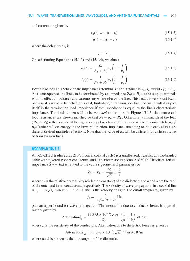
15.1 WAVES, TRANSMISSION LINES, WAVEGUIDES, AND ANTENNA FUNDAMENTALS 673
and current are given by
v2(t) = v1(t − tl) (15.1.5)
i2(t) = i1(t − tl) (15.1.6)
where the delay time tl is
tl = l/vg (15.1.7)
On substituting Equations (15.1.3) and (15.1.4), we obtain
v2(t) = R0
RS + R0vS
(t − l
vg
)(15.1.8)
i2(t) = 1
RS + R0vS
(t − l
vg
)(15.1.9)
Because of the line’s behavior, the impedance at terminals c and d, which is V2/I2, is still Z0(= R0).As a consequence, the line can be terminated by an impedance Z0(= R0) at the output terminalswith no effect on voltages and currents anywhere else on the line. This result is very significant,because if a wave is launched on a real, finite-length transmission line, the wave will dissipateitself in the terminating load impedance if that impedance is equal to the line’s characteristicimpedance. The load is then said to be matched to the line. In Figure 15.1.3, the source andload resistances are shown matched so that RS = R0 = RL. Otherwise, a mismatch at the load(RL = R0) reflects some of the signal energy back toward the source where any mismatch (RS =R0) further reflects energy in the forward direction. Impedance matching on both ends eliminatesthese undesired multiple reflections. Note that the value of R0 will be different for different typesof transmission lines.
EXAMPLE 15.1.1
An RG-213/U (radio guide 213/universal coaxial cable) is a small-sized, flexible, double-braidedcable with silvered-copper conductors, and a characteristic impedance of 50 . The characteristicimpedance Z0(= R0) is related to the cable’s geometrical parameters by
Z0 = R0 = 60√εr
lnb
a
where εr is the relative permittivity (dielectric constant) of the dielectric, and b and a are the radiiof the outer and inner conductors, respectively. The velocity of wave propagation in a coaxial lineis vg = c/
√εr , where c = 3× 10⁸ m/s is the velocity of light. The cutoff frequency, given by
fc = c
π√εr(a + b)
Hz
puts an upper bound for wave propagation. The attenuation due to conductor losses is approxi-mately given by
Attenuation∣∣c= (1.373× 10⁻³)
√ρf
Z0
(1
a+ 1
b
)dB/m
where ρ is the resistivity of the conductors. Attenuation due to dielectric losses is given by
Attenuation∣∣d= (9.096× 10⁻⁸)
√εr f tan δ dB/m
where tan δ is known as the loss tangent of the dielectric.

674 COMMUNICATION SYSTEMS
With a= 0.445 mm, b= 1.473 mm, εr = 2.26 for polyethylene dielectric, tan δ = 2×10⁻⁴,and ρ = 1.63×10⁻⁸ ·m, calculate the total line attenuation at 100 MHz, and check the value ofZ0(= R0) in the specification. If the cable connects an antenna to a receiver 30 m away, determinethe time delay of the cable, the velocity of wave propagation, and the cutoff frequency.
So l u t i on
Attenuation∣∣c= (1.373× 10⁻³)
√1.63× 10−8 × 108
50
(1
0.445× 10⁻³+ 1
1.473× 10⁻³
)∼= 0.103 dB/m
Attenuation∣∣d= (9.096× 10⁻⁸)
√2.26× 108 × 2× 10−4
∼= 0.00273 dB/m
Losses due to conductors obviously dominate.
Total attenuation = 0.103+ 0.00273 ∼= 0.106 dB/m
Z0 = R0 = 60√2.26
ln1.473
0.445∼= 50
Time delay = τ = l
vg= 30
√2.26
3× 10⁸∼= 0.15 µs
The velocity of wave propagation vg = c/√εr = c/
√2.26 = 0.665 times the speed of light, or
vg ∼= 2× 10⁸ m/s
Cutoff frequency fc = 3× 10⁸
π√
2.26(0.445+ 1.473)10−3
= 3× 10¹¹
π√
2.26× 1.918∼= 33 GHz
In practice, f < 0.95fc is usually maintained.
EXAMPLE 15.1.2
Unlike transmission lines, which operate at any frequency up to a cutoff value, waveguideshave both upper and lower cutoff frequencies. For rectangular air-filled waveguides [see Figure15.1.2(a)], the lower cutoff frequency (for propagation by the dominant mode) is given byfc = c/2a, where c is the speed of light. Since the upper limit cannot be larger than 2fc, practicalwaveguides are designed with b ∼= a/2 with a suggested frequency of 1.25fc ≤ f ≤ 1.9fc. For acircular air-filled waveguide [see Figure 15.1.2(b)] with inside radius a, the lower cutoff frequency(for propagation by the dominant mode) is fc = 0.293c/a. The operating band is usually fc < f< 1.307fc. The characteristic impedance Z0(= R0) in waveguides is not constant with frequency,as it is in transmission lines. For rectangular or circular air-filled waveguides, the expression forZ0(= R0) is given by
Z0 = R0 = 377√1− (fc/f )2

15.1 WAVES, TRANSMISSION LINES, WAVEGUIDES, AND ANTENNA FUNDAMENTALS 675
(a) For a rectangular air-filled waveguide with a = 4.8 cm and b = 2.4 cm, compute thecutoff frequency. If the operating frequency is 4 GHz, find the waveguide’s characteristicimpedance.
(b) Calculate the diameter of an air-filled circular waveguide that will have a lower cutofffrequency of 10 GHz.
So l u t i on
(a) fc = c
2a= 3× 10⁸
2× 4.8× 10−2= 3.125 GHz
Z0 = R0 = 377√1− (3.125/4)2
= 377√1− 0.8839
= 377
0.3407= 1106.5
(b) a = 0.293c
fc= 0.293× 3× 108
10× 109= 0.88 cm
Diameter = 2a = 1.76 cm
Now referring to Figure 15.1.3, assuming matched and distortionless conditions, with signalvoltage x(t) across the line input, the resulting output voltage y(t) is given by
y(t) = Kx(t − td) (15.1.10)
where K is the attenuation factor (less than unity) due to ohmic heating in the line dissipating partof the input signal energy and td is the delay time. Working with the average signal powers Pin
and Pout, the transmission loss L is defined as the power ratio
L = Pin/Pout (15.1.11)
where L = 1/K2 > 1 and Pout < Pin. Regardless of the type of transmission line, the transmissionloss increases exponentially with distance l such that
L = 10αl/10) (15.1.12)
where α is the attenuation coefficient of the line in decibels per unit length. Expressing L in dB,similar to power gain, we obtain
LdB = 10 logPin
Pout= αl (15.1.13)
Typical values of α range from 0.05 to 100 dB/km, depending on the type of transmission lineand the frequency. Rewriting Equation (15.1.13) as
Pout
Pin= 10−LdB/10 = 10−αl/10 (15.1.14)
Equation (15.1.14) reveals that Pout will be one-tenth of Pin when l = 10/α, showing therebyhow rapidly the output power falls off as the distance increases.
The transmission loss can be overcome with the aid of one or more amplifiers connectedin cascade with the transmission line. Figure 15.1.4 shows such a system with a preamplifier(transmitting amplifier) at the source, a receiving amplifier at the destination, and a repeater

676 COMMUNICATION SYSTEMS
Pin PoutG1
Preamplifier
L1α1
1
G2 G3
Repeater Receivingamplifier
L 2α2
2
Figure 15.1.4 Transmission system with preamplifier, repeater, and receiving amplifier.
(an additional amplifier) at some intermediate point in the line. All amplifiers will of course beimpedance-matched for maximum power transfer. The final output power Pout in Figure 15.1.4 isthen given by
Pout
Pin= G1G2G3
L1L2(15.1.15)
where the Gs are the power gains of the amplifiers, and the Ls are the transmission losses of thetwo parts of the line. Equation (15.1.15) reveals that we can compensate for the line loss and getPout≥ Pin if G1G2G3≥ L1L2. Noise considerations often call for a preamplifier to boost the signallevel before the noise becomes significant. As in the case of transcontinental telephone links,several repeaters are generally required for long-distance transmission.
EXAMPLE 15.1.3
From a source with Pin = 2.4 mW, we want to get Pout = 60 mW at a distance l = 20 km fromthe source. α for the transmission line is given to be 2.3 dB/km. The available amplifiers haveadjustable power gain, but are subject to two limitations: (i) the input signal power must be atleast 1 µW to overcome internal noise, and (ii) the output signal power must not be greater than1 W to avoid nonlinear distortion. Design an appropriate system.
So l u t i on
αl = 2.3× 20 = 46 dB
LdB = 46 or L = 1046/10 ∼= 40,000
Hence, we need a total gain of
Gtotal = L(Pout/Pin) = 40,000× (60/2.4) = 106, or 60 dB
We cannot put all the amplification at the destination, because the signal power at the outputof the line would be Pin/L = 2.4×10⁻³/(40×103) = 0.06 µ W, which falls below the amplifiernoise level. Nor can we put all amplification at the source, because the amplified source powerGPin = 106 × 2.4 × 10−3 = 2.4 kW would exceed the amplifier power rating. But we couldtry a preamplifier with G1 = 400, so as to get G1Pin = 400 × 2.4 × 10−3 = 0.96 W at theinput of the line, and G1Pin/L = 24 µ W at the output. The output amplifier should then haveG2 = Pout/(24 µW) = 60× 10−3/(24× 10−6) = 2500, and a repeater is not needed.
Antenna Fundamentals
We shall discuss here only the fundamental concepts needed to understand the role of an antenna asa power-coupling element of a system. Figure 15.1.5 illustrates the elements of a communication

15.1 WAVES, TRANSMISSION LINES, WAVEGUIDES, AND ANTENNA FUNDAMENTALS 677
system that involves antennas (with no conductors in the propagation medium) and the followingnomenclature:
Pt Power generated by the transmitter
Lt, Lr Transmitting-path loss (representing the power reduction caused by the transmission lineor waveguide that connects to the transmitting antenna) and receiving-path loss
Lta, Lra Transmitting antenna loss and receiving antenna loss
R Distance of separation between the antennas
S Signal power available at the lossless antenna output
Sr Signal power available at the receiver input
Radio transmission consists of antennas at the source and at the destination. It requires thesignal to be modulated on a high-frequency carrier, which usually is a sinusoid. Driven by anappropriate carrier, the transmitting antenna launches an electromagnetic wave that propagatesthrough space without the help of a transmission line. A portion of the radiated power is collectedat the receiving antenna.
The wavelength λ of the radio wave in air is related to the carrier frequency fc by
fcλ = c = 3× 10⁸ m/s (15.1.16)
The radio-transmission loss differs from that of a transmission line in two ways: (i) it increases asthe square of the separating distance instead of exponentially, and (ii) it can be partly compensatedby the antenna gains.
Antenna gain depends on both shape and size. Dipole antennas, commonly used at lowerradio frequencies, are made up of a rod or wire of length λ/10 to λ/2, and have an antenna-gainrange of 1.5 to 1.64 (1.8 to 2.1 dB). Horn antennas and parabolic dishes (so named after theirshapes) have much more gain at higher frequencies. A useful, although approximate, expressionfor gain is given by
TransmitterInformation-bearingsignal
Transmittingpath losses
Lt
Transmittingantenna loss
Receivingpath losses
Receivingantenna loss
Losslessantenna
Medium
LtaPt
ReceiverInformation-bearingsignal Lr Lra
Sr S
R
Figure 15.1.5 Communication system elements involving antennas.

678 COMMUNICATION SYSTEMS
G = 4πAe
λ2(15.1.17)
where λ is the wavelength being transmitted (or received), and Ae is the effective aperture oreffective area of the antenna. Power amplifiers are needed to overcome the radio-transmissionloss just as in a transmission-line system. Similar considerations hold for optical radiation, inwhich the electromagnetic wave takes the form of a coherent light beam.
Radio transmission is inherently a bandpass process with a limited bandwidth B nominallycentered at the carrier frequency fc. The fractional bandwidth B/fc is a key design factor witha general range of 1/100 ≤ B/fc ≤ 1/10. It is obvious then that large signal bandwidthsrequire high carrier frequencies to satisfy fc ≥ 10B. You can reason why television signalsare transmitted at fc of 100 MHz, whereas AM radio signals are transmitted at fc of 1 MHz.Since optical communication systems offer tremendous bandwidth potential on the order of 1012
Hz, and a corresponding high information rate, they have become topics of current researchinterest.
Antennas do not radiate power equally in all directions in space. The radiation intensitypattern describes the power intensity (which is power per unit solid angle, expressed in units ofwatts per steradian) in any spatial direction. Conceptually it is convenient to define an isotropicantenna as a lossless antenna that radiates its power uniformly in all directions. Although anisotropic antenna cannot be realized in practice, it serves as a reference for comparison with realantennas. The radiation intensity for such an antenna, with input power P, is a constant in anydirection, given by P/4π . The power gain G of a realistic antenna is a measure of the maximumradiation intensity of the antenna as compared with the intensity that would result from an isotropicantenna, with the same power input. G is then expressed as
G = maximum radiation intensity
radiation intensity of isotropic source (with the same power input)
= 4π (maximum radiation intensity)
P(15.1.18)
Referring to Figure 15.1.5, when a power Pt/Lt is applied to the transmitting antenna, let us findthe signal power Sr available to the receiver from the receiving antenna. An isotropic transmittingantenna would cause a radiation power density (power per unit area of a sphere) of
Power density = Pt
4πR2Lt
(15.1.19)
For a practical antenna that has power gain Gt and loss Lta relative to an isotropic antenna, Equation(15.1.19) would be modified as
Power density = PtGt
4πR2LtLta(15.1.20)
We shall assume that the transmitting and receiving antennas (reciprocal elements) point directlytoward each other, so that their gains are maximum. Letting Lch denote any losses incurred by thewave in the channel (medium), and Are be the effective area of the receiving antenna, the powerthat the receiving antenna is able to produce is given by
S = PtGtAre
4πR2LtLtaLch(15.1.21)
Accounting for the receiving antenna loss and receiving-path losses, a total system loss L can bedefined as

15.1 WAVES, TRANSMISSION LINES, WAVEGUIDES, AND ANTENNA FUNDAMENTALS 679
L = LtLtaLchLraLr (15.1.22)
Sr would then be given by
Sr = PtGtAre
4πR2L(15.1.23)
Using Equation (15.1.17) with Gr representing the receiving antenna gain, Equation (15.1.23)becomes
Sr = PtGtGrλ2
(4π)2R2L(15.1.24)
Quite often, for simplicity, in the case of LOS radio transmission illustrated in Figure 15.1.6,the transmission loss for a path of length R is given by
LTR = Pin
Pout= 1
GtGr
(4πR
λ
)2
(15.1.25)
which justifies the statements following Equation (15.1.16).
EXAMPLE 15.1.4
Let a LOS radio system and a transmission-line system both have L = 60 dB when the distanceR between transmitter and receiver is 15 km. Compute the loss of each when the distance isincreased to 30 km.
So l u t i on
R is doubled. LdB for the transmission line is proportional to the distance, as per Equation(15.1.13). Hence, LdB for the new transmission line = 2× 60 = 120 dB.
LTR for the LOS radio system is proportional to R2, as per Equation (15.1.25). Noting thatLdB = 10 log L and L = KR2, where K is a constant, it follows that
LdB = 20 log KR
When R is doubled,
LdB new = 20 log (K2R) = 20(log KR + log 2)
= 20 log KR + 20 log 2 = LdB old + 6
Hence, LdB for the new LOS radio system = 60 + 6 = 66 dB.
R
Pin Pout
Power gainGt
Power gainGr
Figure 15.1.6 Illustration of LOS radio trans-mission.

680 COMMUNICATION SYSTEMS
EXAMPLE 15.1.5
(a) Some antennas have a physical aperture area A that can be identified and is related tothe effective area Ae by Ae = ρaA, where ρa is known as the aperture efficiency. For acircular-aperture antenna with a diameter of 2 m and an aperture efficiency of 0.5 at 4GHz, calculate the power gain.
(b) Referring to Figure 15.1.5, let two such antennas be used for transmitting and receiving,while the two stations are separated by 50 km. Let the total loss over the link be 9 dB,while the transmitter generates 0.5 W. Find the available received power.
So l u t i on
(a) λ = c
f= 3× 10⁸
4× 109= 0.075 m. From Equation (15.1.17),
G = 4πAe
λ2= 4πρaA
λ2= 4π × 0.5× π
0.0752= 3509
(b) G = Gt = Gr = 3509; LdB = 10 log L, or L = 7.94. From Equation (15.1.24),
Sr = 0.5× 35092 × 0.0752
(4π)2 × 502 × 106 × 7.94∼= 1.1× 10⁻⁸ W
The variety and number of antennas are almost endless. However, for our introductorypurposes, they may be divided into the following types:
• Wire antennas, such as half-wavelength dipole, folded half-wave dipole, and helical antenna
• Array antennas, such as YAGI-UDA array
• Aperture antennas, such as pyramidal horn, conical horn, paraboloidal antenna, and Casse-grain antenna
• Lens-type antennas in radar and other applications.
Some of their geometries are illustrated in Figure 15.1.7.The radiation-intensity pattern describing the power intensity in any spatial direction is
an important antenna characteristic, since the antenna does not radiate power equally in alldirections in space. Such patterns are three-dimensional in nature. One normally chooses sphericalcoordinates centered on the antenna at A, and represents the power-intensity function P(θ, φ) atany distant point R as a magnitude P from A, which appears as a surface with a large main lobeand several side lobes (minor lobes), as shown in Figure 15.1.8.
Generally speaking, in most of the communication systems the transmitting and receivingantennas (reciprocal elements) face each other directly such that their large main lobes pointtoward each other, and the received-power output will be maximum. When scaled such thatthe maximum intensity is unity, the radiation-intensity pattern is commonly called the radiationpattern. In many problems in practice, the radiation pattern occurs with one dominant mainlobe, and as such, instead of considering the full three-dimensional picture, the behavior mayadequately and conveniently be described in two orthogonal planes containing the maximum ofthe main lobe. These are known as principal-plane patterns in terms of angles θ and φ. Figure15.1.9 illustrates one such pattern in polar and linear angle plots as a function of θ . The angularseparation between points on the radiation pattern that are 3 dB down from the maximum is called

15.1 WAVES, TRANSMISSION LINES, WAVEGUIDES, AND ANTENNA FUNDAMENTALS 681
Transmissionline
Transmission line
Active element(regular or folded dipole)
Throat
ApertureHornthroatReflector
(a)
(d) (e)
(g) (h)
(f)
Directors
(b) (c)
z
a
b
d
d
a
s
b
P
d
S
z
L
N turns
L2
λ4
=
L2
λ4
Transmissionline Transmission
line
λ2
=− −
y
x
z
L
z
z
y
f '
z
xy
A
B
y
zDfFocus
Focus f
Hyperbola(subreflector)Feeding
line
Parabola
ab
θ
φ
Figure 15.1.7 (a) Half-wave dipole. (b) Folded half-wave dipole. (c) Helical-beam antenna. (d) YAGI-UDAarray antenna. (e) Pyramidal horn. (f) Conical horn. (g) Paraboloidal antenna. (h) Cassegrain antenna (section).
the beamwidth, which is designated as θB or φB in the principal-plane patterns. Another useful,although approximate, expression for gain in terms of the beamwidths θB and φB of the pattern’smain lobe is given by
G = 4π
θBφB
(15.1.26)
when beamwidths are expressed in radians, or
G = 41.3× 10³
θBφB
(15.1.27)
when beamwidths are expressed in degrees.The antenna impedance, looking into the feed-point terminals of an antenna, will in general
have both resistive and reactive components. The antenna resistance is the combination of theradiation resistance (accounting for the power radiated by the antenna) and the loss resistance

682 COMMUNICATION SYSTEMS
x
z
y
A
(a) (b)
Sidelobes
Mainlobe
Direction of maximum
To R
Rθ
φ
x
A
z
y
Figure 15.1.8 (a) Spherical coordinates centered on the antenna at A. (b) Typical radiation-intensity patternwith main and side lobes (with all possible values of θ and φ considered).
(accounting for the power dissipated in the antenna itself as losses). Ideally, the antenna resistanceshould be equal (matched) to the characteristic impedance of the feeding line or guide to preventreflected power, and the antenna reactance should be zero.
Most antennas transmit only one polarization of electromagnetic wave. That is to say, theelectric field of the propagating wave is oriented with respect to the antenna in only one direction.The main lobe in most antennas is directed normal to the plane of the aperture. For phased-arrayantennas, however, the main lobe is electronically steered to other angles away from the so-calledbroadside. Figure 15.1.10 illustrates vertical, horizontal, and arbitrarily linear polarizations ofthe electric field. In Figure 15.1.10(a), with the electric field lying in the vertical plane, theradiation is said to be vertically polarized. With the electric field being in the horizontal plane,as in Figure 15.1.10(b), the radiation is said to be horizontally polarized. Since both vertical andhorizontal polarizations are simply special cases of linear polarization, the electric field, havingboth horizontal and vertical components (that are in time phase), can still be in a plane, as shownin Figure 15.1.10(c).
Some systems transmit simultaneously two linear orthogonal polarizations that are not intime phase. Elliptical polarization results when the two linear components have arbitrary relativeamplitudes and arbitrary time phase. Circular polarization (probably the most useful type) is aspecial case in which the horizontal and vertical electric fields are 90° out of time phase and haveequal magnitude. Left-hand circular polarization results when the horizontal radiation componentlags the vertical one by 90° and the resultant field appears to rotate counterclockwise in the xy-plane with time, as one located at the antenna views the wave leaving the antenna. If the horizontalcomponent leads the vertical one by 90°, right-hand circular polarization is said to take place.
Referring to Figure 15.1.7, the half-wave dipole is a relatively narrow-band antenna withits radiated wave linearly polarized. The dipole can be driven by a transmission line of 75-characteristic impedance. The folded half-wave dipole (a variation of the half-wave dipole) isused in television, broadcast FM, and other applications. This antenna is well suited for use with300- television cable. The helical antenna of Figure 15.1.7(c) yields a pencil-beam pattern inthe axis of the helix with circular wave polarization.
The YAGI-UDA array of Figure 15.1.7(d) is commonly used for television reception. It isusually seen with 3 to 12 elements, although even 40 elements are sometimes employed. Designfrequencies from 100 to 1000 MHz are typical. A half-wave or folded half-wave dipole is theactive element. The array consists of parallel dipoles, all lying in the same plane. The reflector,which reflects waves back toward the active element, enhances radiation in the axis of the array

15.1 WAVES, TRANSMISSION LINES, WAVEGUIDES, AND ANTENNA FUNDAMENTALS 683
(a) (b)
Mainlobe
Mainlobe
0
Relative radiationintensity (dB)
Side lobeSidelobes
Rel
ativ
e
radi
atio
n in
tens
ity
1.0
−0.5
z
x
θB θB
θθ
Figure 15.1.9 Typical radiation patternin one principal plane as a function ofθ . (a) Polar-coordinate plot. (b) Linear-coordinate plot.
(+z-direction). The radiation pattern, with linear polarization, exhibits a principal lobe in the+z-direction. The other elements, called directors, are designed to enhance radiation in the +zdirection. Gain increases with the number of elements and is often in the range of 10 to 20 dB.The bandwidth is usually small.
Both conical-horn and pyramidal-horn (aperture-type) antennas are mainly used as illumi-nators for large-aperture paraboloidal antennas, which are capable of generating very narrowbeamwidth patterns (with even less than 1° in angle-tracking radars). When a parabola is rotatedabout the z-axis [see Figure 15.1.17(g)], a surface of revolution known as a paraboloid results.With the source at the focus called the feed, the radiation pattern is mainly a dominant lobe inthe z-direction with smaller side lobes. Paraboloidal antennas have found wide use as antennasfor radar and communications. The Cassegrain antenna [shown in section in Figure 15.1.17(h)]is a variation of the paraboloid that gives improved system performance. The feed in this caseis moved to the rear of the antenna, and it illuminates a conducting surface (subreflector in theshape of a hyperboloid) placed near the focus.
Noise in receiving systems exists in two broad categories: (i) that originated external to thesystem (i.e., the one generated by the antenna in response to random waves from cosmic sourcesand atmospheric effects), and (ii) internally generated noise (i.e., the one generated within allcircuits making up the receiver, including transmission lines and amplifiers). It is common tomodel internal noise as having been generated by an external source.
Figure 15.1.11(a) shows a typical receiving system with noise. The antenna is a source of noisewith effective noise temperature Ta, known as the antenna temperature. Whatever receiving pathcomponents (such as transmission lines, waveguides, and filters) are present prior to the receiver’samplifier, their noise effect is represented by a noisy loss Lr (≥ 1) between points A and B, whilethe loss is assumed to have a physical temperature TL. The noisy receiver is supposed to operate ata nominal center frequency f 0, and have available power gain Ga(f ) as a function of the frequency,with Ga(f 0) as center-frequency power gain. Nao represents the total available output noise powerin Figure 15.1.11(a).
Figure 15.1.11(b) shows the noise-free model in a small frequency band df. Here k is theBoltzmann constant (see Section 14.3), and TR(f ) is the effective input noise temperature (to thenoise-free receiver).
Figure 15.1.11(c) gives the noise-free model with noise bandwidth BN (a rectangular passbandof width BN in hertz centered on f 0). The actual receiver is replaced by an idealized one with thesame nominal power gain Ga(f 0) and a constant (average) effective input noise temperature TR ,which is related to the average standard noise figure F0;
TR = 290(F0 − 1) (15.1.28)

684 COMMUNICATION SYSTEMS
(a) (b) (c)
xy
z
xy
z
xy
z
E−
E−
E−
Figure 15.1.10 Polarizations of the electric field. (a) Vertical polarization.(b) Horizontal polarization. (c) General linear polarization.
Noisy loss Lr
Antenna with antenna temperature Ta
Physical temperature TL
Nao
A
Available noise power kTsysBN
B Noisyreceiver
Available power gain Ga( f )
Center-frequency power gain Ga( f0)
Noise-free loss Lr
(a)
TL
dNao
A B Noise-freereceiver
Ga( f )kTR dfkTL( Lr − 1) df
(b)
(c)
Lr
Ga( f0)
ANoise-free
loss and receiver
Available power gain Ga( f0)/Lr
Noise bandwidth BN
Nao = kTsysBN
Figure 15.1.11 (a) Receivingsystem with noise. (b) Noise-free model in a small frequencyband df. (c) Noise-free modelwith noise bandwidth BN.
Note that both F0 and TR are measures of the noisiness of an amplifier. The noise figure F0 isusually available, whereas the temperature TR may not be given. In an ideal noise-free unit,F0 = 1and TR = 0.
The system noise temperature Tsys, which is the equivalent noise temperature of the antenna,can now be introduced such that
Tsys = Ta + TL(Lr − 1)+ TRLr (15.1.29)
and all available output noise power is emanating from the antenna, as illustrated in Figure15.1.11(c). Now the available system noise power becomes kTsysBN at point A; the noise-freereceiver has available power gain Ga(f0)/Lr with noise bandwidth BN; and the output noisepower is given by

15.2 ANALOG COMMUNICATION SYSTEMS 685
Nao = kTsysBNGa(f0)
Lr
(15.1.30)
The signal-to-noise power ratio at the system output is an excellent measure of performancefor many communication systems. The available signal power at point A in Figure 15.1.11(a) isgiven by
SA = PtGtGrλ2
(4π)2R2LtLtaLchLra(15.1.31)
based on Equation (15.1.24). The available noise power at point A is given by
NaA = kTsysBN (15.1.32)
Thus, the system performance with noise is measured by the signal-to-noise power ratio,(S
N
)A
= PtGtGrλ2
(4π)2R2LtLtaLchLrakTsysBN
(15.1.33)
15.2 ANALOG COMMUNICATION SYSTEMS
An analog message is a continuum of possible amplitudes at any given time, and analog signalsare continuous in time and in amplitude, such as audio and video signals. When the message tobe sent over a communication system is analog, we refer to the system as analog. The transmittedwaveform must be some function of the message so that the receiver could decipher the message.Usually the transmitted waveform is the result of varying either the amplitude, phase, or frequencyof a basic signal called a carrier. Combinations of amplitude, phase, and frequency variations arealso possible.
The carrier usually is sinusoidal of the formAc cos (ωct+φc), whereAc, φc, and fc = ωc/2πare the carrier’s amplitude, phase, and frequency, respectively. When A is varied as a linear functionof the message, amplitude modulation (AM) occurs. In phase modulation (PM) a phase term thatis a linear function of the message is added to the carrier. When the added phase is a linear functionof the integral of the message, the result is known as frequency modulation (FM). Note that thecarrier’s frequency in FM is a linear function of the message, because instantaneous angularfrequency is the time derivative of instantaneous phase. Thus, FM and PM are closely related.
Every communication system has a modulator at the transmitting station to structure thetransmitted waveform, and a demodulator (detector) at the receiving end to recover the messagefrom the received signal. Radio (AM and FM) and television broadcasting are the most familiarforms of communication through analog signal transmission. The FCC in the United Statesregulates the carrier-frequency assignments in order to minimize the interference between nearbystations. Commercial AM radio broadcasting utilizes the frequency band of 535 to 1605 kHz forthe transmission of voice and music. The carrier-frequency allocations range from 540 kHz to1600 kHz, with 10-kHz spacing. Each station can occupy a channel bandwidth of only 10 kHzcentered on its carrier. Even though the baseband message signal is limited to a bandwidth of about5 kHz, the AM broadcasting system adequately meets the need for low-cost mass communicationand general audio entertainment, in spite of lacking high-fidelity behavior.
Commercial FM radio broadcasting utilizes the frequency band of 88 to 108 MHz for thetransmission of music and voice signals. The carrier frequencies are separated by 200 kHz, and thepeak frequency deviation is fixed at 75 kHz. Each station (out of the possible 100) broadcasts ina channel bandwidth of 200 kHz centered on the carrier. The FM system is capable of presentinghigher quality audio to the user than AM because of the larger audio band allowed from 50 Hz to

686 COMMUNICATION SYSTEMS
15 kHz. Distortion at most stations is below 1%. Besides broadcast applications, FM is also usedin satellite links, aircraft altimetry, radars, amateur radio, and various two-way radio applications.Because of the larger bandwidth (up to 20 times more than in AM), an FM system has morefreedom from interference and better performance in noise than any AM station.
Commercial television broadcasting is allocated frequencies that fall in the VHF and UHFbands. Table 15.2.1 lists the television channel allocations in the United States, with the channelbandwidth of 6 MHz. In contrast to radio broadcasting, television signal-transmission standardsvary from country to country. The U.S. standard is set by the National Television Systems Com-mittee (NTSC). Commercial television broadcasting began as black-and-white (monochrome)picture transmission in London in 1936 by the British Broadcasting Corporation (BBC). Althoughcolor television was demonstrated a few years later, due to the high cost of color televisionreceivers, color television signal transmission was slow in its development. With the advent ofthe transistor and microelectronic components, the cost of color television receivers decreasedsignificantly, and by the middle 1960s, color television broadcasting was widely used by theindustry. The NTSC color system is compatible with monochrome receivers, so that the oldermonochrome receivers still function receiving black-and-white images out of the transmittedcolor signal.
Amplitude Modulation (AM)
In AM the message signal is impressed on the amplitude of the carrier signal. There are severaldifferent ways of amplitude modulating the carrier signal by the message signal, each of whichresults in different spectral characteristics for the transmitted signal. Four methods are:
• Conventional (standard) double-sideband AM
• Double-sideband suppressed-carrier AM
• Single-sideband AM
• Vestigial-sideband AM.
AM, as its name implies, carries the modulating signal x(t) in a time-varying amplitude ofthe form
a(t) = Ac[1+mAx(t)] (15.2.1)
where the constant Ac stands for the unmodulated carrier amplitude, and mA is the modulationindex. The resulting modulated wave is
xc(t) = a(t) cos(2πfct + φc)
= Ac cos(2πfct + φc)+ AcmAx(t) cos(2πfct + φc) (15.2.2)
TABLE 15.2.1 VHF and UHF Allocations forCommercial TV in the United States
Frequency BandChannel (6-MHz bandwidth/station)
VHF 2–4 54–72 MHzVHF 5–6 76–88 MHzVHF 7–13 174–216 MHzUHF 14–69 470–896 MHz

15.2 ANALOG COMMUNICATION SYSTEMS 687
whereas the sinusoidal carrier waveform is given by
c(t) = Ac cos(ωct + φc) = Ac cos(2πfct + φc)
Sometimes the standard AM signal is expressed in the form of
xc(t) = sAM(t) = [Ac + f (t)] cos(ωct + φc) (15.2.3)
in which the total amplitude of the carrier [Ac + f (t)] is a linear function of the message. Figure15.2.1 illustrates the AM waveforms.
If the maximum amplitude of f (t) in Equation (15.2.3) exceeds Ac, overmodulation is saidto occur. In order to prevent excessive distortion in the receiver, overmodulation is avoided instandard AM by requiring
|f (t)|max ≤ Ac (15.2.4)
such that the envelope of sAM(t) or xc(t) will never go negative and may at most become zero.The spectral behavior is depicted in Figure 15.2.2, assuming φ0 = 0 for simplicity. The spectralimpulses are due to the carrier and will always be present, even if the message were to disappear.The effect of AM is to shift half-amplitude replicas of the signal spectrum out to angularfrequencies ωc and −ωc. The band of frequencies above ωc or below −ωc is called the uppersideband (USB). The one on the opposing side is known as the lower sideband (LSB). Since AMtransmits both USB and LSB, it is known as double-sideband modulation. If the maximum circular(radian) frequency extent of f (t) is Wf rad/s, the frequency extent of the standard AM waveformis 2Wf. Thus, the low-pass signal is translated in frequency to the passband of the channel so thatthe spectrum of the transmitted bandpass signal will match the passband characteristics of thechannel.
There are several different methods for generating amplitude-modulated signals. Since theprocess of modulation involves the generation of new frequency components, modulators aregenerally characterized as nonlinear and/or time-variant systems, because a linear or a time-invariant system cannot create new frequencies other than those contained in its input signal.Figure 15.2.3 shows a block diagram of power-law modulation that is nonlinear. Let the voltageinput to such a device be the sum of the message signal and the carrier, as illustrated inFigure 15.2.3. The nonlinear device (that has an input–output characteristic of the form ofa square law) will generate a product of the message x(t) with the carrier, plus additionalterms. The desired modulated signal can be filtered out by passing the output of the nonlineardevice through a bandpass filter. The signal generated by this method is a conventional DSBAM signal.
t
x (t)
xc(t) Envelope |A(t)|
(a)
(b)
−Ac
Act
Figure 15.2.1 AM waveforms. (a) Information (message ormodulating) signal. (b) Modulated wave (corresponding stan-dard AM signal).

688 COMMUNICATION SYSTEMS
USB LSB USBLSB
Spectral impulsedue to carrier
Spectral impulsedue to carrier
Lower sideband (LSB)
Amplitude spectrum
Amplitude spectrum
Upper sideband (USB)
0 ω
0
12
ωωc−ωc
1
(a)
(b)
Figure 15.2.2 Spectral behavior. (a) Informa-tion-signal spectrum. (b) Corresponding AMsignal spectrum.
Ac cos 2π fc t
Nonlineardevice
such as aP–N diode
Bandpassfilter tuned
to fcx (t)
Message signal ConventionalDSB AM signal+
Figure 15.2.3 Block diagram of power-law modulation.
Let sAM(t) of Equation (15.2.3) be a voltage representing the wave that excites the transmittingstation’s antenna, which is assumed to represent a resistive impedance R0 to the transmitter thatfeeds it. The power in sAM(t) is found by
PAM = s2AM(t)
R0= Pc + Pf = 1
2R0
[A2
c + f 2(t)]
(15.2.5)
in which the overbar represents the time average, and f (t) is assumed to have no dc component,as is the usual case. Pc = A2
c/2R0 is the power in the carrier, and Pf = f 2(t)/2R0 is the addedpower caused by modulation. Pf is called the useful power, since only this power caused by themessage contributes toward message quality. Pc, the carrier power, is not useful power in thesense that it carries no information. However, it is important to the receiver’s ability to recoverthe message with low-cost circuitry. Modulation efficiency ηAM of the transmitted signal is definedas the ratio of the useful power to the total power,
ηAM = Pf
Pc + Pf= f 2(t)
A2c + f 2(t)
(15.2.6)
When f (t) is a square wave of peak amplitude Ac, the largest possible value of ηAM equal to 0.5,or 50%, occurs. When f (t) is a sinusoid, ηAM ≤ 1/3, as shown in Example 15.2.1. For practicalaudio (voice and music) messages, efficiency could be less than 1/3.

15.2 ANALOG COMMUNICATION SYSTEMS 689
EXAMPLE 15.2.1
Let f (t) be a sinusoid given by f (t) = Am cos ωmt with period Tm = 2π/ωm. Apply Equation(15.2.6) and obtain the value of ηAM.
So l u t i on
f 2(t) = 1
Tm
∫ Tm/2
−Tm/2A2
m cos2(ωmt) dt
= A2m
8π
∫ 2π
−2π(1+ cos x) dx = A2
m
2
ηAM = A2m
2A2c + A2
m
= (Am/Ac)2
2+ (Am/Ac)2
For no overmodulation, Am ≤ Ac, so that ηAM ≤ 1/3.
Suppressed-carrier AM, also known as double-sideband suppressed-carrier (DSB SC AM),results when the carrier term Ac in Equation (15.2.3) is eliminated. The DSB waveform is thengiven by
sDSB(t) = f (t) cos(ωct + φc) (15.2.7)
Figure 15.2.4(a) depicts the waveforms of the message signal and its amplitude spectrum; Figure15.2.4(b) shows the DSB waveform sDSB(t), and Figure 15.2.4(c) displays the amplitude spectrumof sDSB(t). From Equation (15.2.6) with Ac = 0, the efficiency of DSB SC AM comes out as 1.0,or 100%. While the power efficiency is increased, there will be added complexity, especially inthe demodulator.
f (t)
sDSB(t)
Amplitude spectrum of sDSB(t)
USBω
ωc−ωc
LSBLSB
0
USB
t
t
ω0 0
Message signal
Phase reversal when f (t) changes sign
(a)
(b)
(c)
USB
Amplitude spectrum
LSB
Figure 15.2.4 (a) Message signal and itsamplitude spectrum. (b) DSB SC sig-nal sDSB(t) corresponding to the message.(c) Corresponding SC AM signal spectrum.

690 COMMUNICATION SYSTEMS
A relatively simple method to generate a DSB SC AM signal is by employing two (identical)conventional AM modulators, such as two square-law AM modulators, arranged in the config-uration of Figure 15.2.5, which is known as a balanced modulator. φc = 0 is assumed here forsimplicity.
Single-sideband (SSB) AM is obtained by filtering one sideband of the DSB signal. As pointedout earlier, a DSB SC AM signal required a channel bandwidth of 2W for transmission, whereW is the bandwidth of the baseband signal. However, the two sidebands are redundant. Thetransmission of either sideband is sufficient to reconstruct the message signal at the receiver.Thus, the bandwidth of the transmitted signal is reduced to that of the baseband signal. Figure15.2.6 illustrates the generation of an SSB AM signal by filtering one of the sidebands (eitherUSB or LSB) of a DSB SC AM signal. SSB is popular with amateur radio operators because ofits high efficiency (ηSSB = 1) and bandwidth savings.
Vestigial-sideband (VSB) AM is a variation of SSB where a small portion (or vestige) ofthe filtered sideband is allowed to remain. The stringent frequency-response requirements on thesideband filter in an SSB AM system can be relaxed by allowing a part, known as a vestige, ofthe unwanted sideband to appear at the output of the modulator. Thus, the design of the sidebandfilter is simplified at the cost of a modest increase in the channel bandwidth required to transmitthe signal. Figure 15.2.7 illustrates the generation of a VSB AM signal. VSB is mainly used in the
Ac cos 2π fc t
Ac [1 + x (t)] cos 2π fc t
Ac [1 − x (t)] cos 2π fc t
2Ac x (t) cos 2π fc t
AMmodulator
AMmodulator
−x (t)
x (t)
Message signal
+
−
Figure 15.2.5 Block diagram ofa balanced modulator.
cos (ωct + φc)
Balancedmodulator
High-passfilter H(ω)
Gain = 2
00
2
0−ωc −ωc −ωcωc ωc ωc
f (t) sDSB(t)
SDSB(ω) SSSB(ω)H(ω)
ω ω ω
sSSB(t)
Messagesignal
Figure 15.2.6 Generation of a SSB AM signal by filtering one of the sidebands of aDSB SC AM signal.

15.2 ANALOG COMMUNICATION SYSTEMS 691
television broadcast system. The generation of VSB is similar to the generation of SSB, exceptthat the sideband-removal filter has a slightly different transfer function.
Message Demodulation
The major advantage of the conventional (standard) DSB AM signal transmission is the ease withwhich the signal can be demodulated. The message signal is received by passing the rectified signalthrough a low-pass filter whose bandwidth matches that of the message signal. The combination ofthe rectifier and the low-pass filter is known as an envelope detector, which is almost universallyused. A standard AM envelope detector consisting of a diode and an RC circuit (which is basicallya simple low-pass filter) and its response are shown in Figure 15.2.8.
During the positive half-cycle of the input signal, the diode is conducting and the capacitorcharges up to the peak value of the input signal. When the input falls below the voltage on thecapacitor, the diode becomes reverse-biased and the input becomes disconnected from the output.During this period, the capacitor discharges slowly through the load resistor R. On the next cycleof the carrier, the diode conducts again when the input signal exceeds the voltage across thecapacitor. The capacitor charges up again to the peak value of the input signal, and the process iscontinued. The time constant RC must be selected to follow the variations in the envelope of thecarrier-modulated signal. Generally, it is so chosen that
Ac cos 2π fc t
SidebandfilterH(ω)
x (t)
Messagesignal
Balancedmodulator
VSB AM signal×
Figure 15.2.7 Generation of a VSB AMsignal.
Voltage proportional to sAM(t)
Proportional toAc + f (t)
Ac
t
Envelope
Carrier
R sd (t)
sd (t)
(a)
(b)
C
Figure 15.2.8 Envelope detection of conventional (standard) AM signal.(a) Standard AM envelope detector. (b) Its response.

692 COMMUNICATION SYSTEMS
1
fc<< RC <<
1
W(15.2.8)
The simplicity of the demodulator has made conventional DSB AM a practical choice for AMradio broadcasting. A relatively inexpensive demodulator is very important in view of the severalbillions of radio receivers. With only a few broadcast transmitters and numerous receivers, thepower inefficiency of conventional AM is justified. Thus, it is cost-effective to construct powerfultransmitters and sacrifice power efficiency in order to have simpler signal demodulation at thereceivers.
Demodulation of DSB SC AM signals requires a synchronous demodulator, which is alsoknown as coherent or synchronous detector. That is, the demodulator must use a coherent phasereference. This is usually generated by means of a phase-locked loop (PLL), which forces thephase of the voltage-controlled oscillator to follow the phase of the reference signal, to demodulatethe received signal. The need for such a device is a chief disadvantage of the DSB SC scheme.
Figure 15.2.9 shows the general configuration. A PLL is utilized to generate a phase-coherentcarrier signal that is mixed with the received signal in a balanced modulator. The output of thebalanced modulator is fed into a low-pass filter of bandwidth W, which passes the desired signaland rejects all signal (and noise) components above W Hz.
Demodulation of SSB signals also requires the use of a phase-coherent reference. Figure15.2.10 shows the general configuration to demodulate the SSB signal. A small carrier component,which is transmitted along with the message, is inserted. A balanced modulator is used forfrequency conversion of the bandpass signal to low pass or baseband.
Demodulation of VSB signals generally uses a synchronous detector in the configuration ofFigure 15.2.10. In VSB, a carrier component is generally transmitted along with the messagesidebands. The existence of the carrier component makes it possible to extract a phase-coherentreference for demodulation in a balanced modulator. In some applications, such as televisionbroadcasting, however, a large carrier component is transmitted along with the message in theVSB signal, and in such a case it is possible to recover the message by passing the received signalthrough an envelope detector.
Balancedmodulator
Low-passfilter
Phase-lockedloop
sDSB(t)
Receivedsignal
x(t)
Messagesignal
Figure 15.2.9 Demodulator forthe DSB SC AM signal.
Balancedmodulator
Low-passfilter
Estimatecarrier
component
sSSB(t)
Receivedsignal
x(t)
Messagesignal
Figure 15.2.10 Demodulation ofSSB AM signal with a carriercomponent.

15.2 ANALOG COMMUNICATION SYSTEMS 693
From the noise performance point of view, all the AM systems yield the same performancefor the same messages and transmitted powers. Note, however, that the bandwidth of the DSBsystem is twice that of the SSB or VSB systems, so its input noise power is twice as large.
Frequency Modulation
So far we have considered AM of the carrier as a means for transmitting the message signal.AM methods are also known as linear modulation methods, although conventional AM is notlinear in the strict sense. Other classes of modulation methods are frequency modulation (FM)and phase modulation (PM). In FM systems the frequency of the carrier fc is changed by themessage signal, and in PM systems the phase of the carrier is changed according to the variationsof the message signal. FM and PM, which are quite nonlinear, are referred to as angle-modulationmethods. Angle modulation is more complex to implement and much more difficult to analyzebecause of its inherent nonlinearity. FM and PM systems generally expand the bandwidth suchthat the effective bandwidth of the modulated signal is usually many times the bandwidth of themessage signal. The major benefit of these systems is their high degree of noise immunity. Tradingoff bandwidth for high-noise immunity, the FM systems are widely used in high-fidelity musicbroadcasting and point-to-point communication systems where the transmitter power is ratherlimited.
A sinusoid is said to be frequency-modulated if its instantaneous angular frequency ωFM(t)
is a linear function of the message,
ωFM(t) = ωc + kFMf (t) (15.2.9)
where kFM is a constant with units of radians per second per volt when f (t) is a message-signalvoltage, and ωc is the carrier’s nominal angular frequency. Instantaneous phase being the integralof instantaneous angular frequency, the FM signal can be expressed as
SFM(t) = Ac cos
[ωct + φc + kFM
∫f (t) dt
](15.2.10)
where Ac is a constant amplitude and φc is an arbitrary constant phase angle. The maximumamount of deviation that ωFM(t) of Equation (15.2.9) can have from its nominal value is knownas peak frequency deviation, given by
ω = kFM |f (t)|max (15.2.11)
Because FM involves more than just direct frequency translation, spectral analysis and bandwidthcalculations are difficult in general, except for a few message forms. However, practical experienceindicates that the following relations hold for the FM transmission bandwidth:
WFM∼= 2(ω +Wf ) (15.2.12)
known as Carson’s rule for narrow-band FM with ω < Wf or
WFM∼= 2(ω + 2Wf ) (15.2.13)
for wide-band FM with ω >> Wf , where Wf is the spectral extent of f (t); i.e., the messagesignal has a low-pass bandwidth Wf. For example, commercial FM broadcasting utilizes Wf =2π(15× 103) rad/s (corresponding to 15 kHz) and ω = 5Wf such that ωFM = 14Wf . Becausethe performance of narrow-band FM with noise is roughly equivalent to that of AM systems, onlywide-band FM that exhibits a marked improvement will be considered here.
Figure 15.2.11 illustrates the close relationship between FM and PM. Phase modulatingthe integral of a message is equivalent to the frequency modulation of the original message,

694 COMMUNICATION SYSTEMS
FMmodulator
PMmodulator
f (t)
Messagesignal
Integratorf (t)
≡
PMmodulator
FMmodulator
f (t)Differentiator
f (t)≡
Figure 15.2.11 Close relationship between FM and PM.
and frequency modulating the derivative of a message is equivalent to phase modulation of themessage itself.
Generation of wide-band FM can be done by various means. However, only the most commonand conceptually the simplest one, known as the direct method, is considered here. It employsa voltage-controlled oscillator (VCO) as a modulator. A VCO is an oscillator whose oscillationfrequency is equal to the resonant frequency of a tuned circuit, as shown in Figure 15.2.12. Thefrequency can be varied if either the inductance or the capacitance is made voltage-sensitive tothe message signal f (t).
One approach to obtaining a voltage-variable reactance is through a varactor diode, whosecapacitance changes with the applied voltage, such as the junction capacitance of a reverse-biased diode, which depends on the amount of bias. Figure 15.2.13 illustrates the varactor-diodeimplementation of an angle modulator. The frequency of the tuned circuit and the oscillator willchange in accordance with the message signal f (t). Varactor-controlled VCOs can have a nearlylinear frequency–voltage characteristic, but often yield only small frequency deviations, i.e., smallω. Since any VCO is inherently unstable as its frequency is varied to produce FM, it becomesnecessary in many applications to stabilize the carrier’s frequency.
Demodulators for FM
Figure 15.2.14 shows a block diagram of a general FM demodulator, which is implemented bygenerating an AM signal whose amplitude is proportional to the instantaneous frequency of theFM signal, and then using an AM demodulator to recover the message signal. Transforming
Activeoscillator
circuit
Output proportional to cos ωt
where ω = 1√LC
Resonantcircuit
CL
Figure 15.2.12 Oscillator for usein a VCO.
Tooscillatorcircuit
. . .
. . .
C0f (t )
Cv
L+
−
Figure 15.2.13 Varactor-diode implementation of an anglemodulator.
15.2 ANALOG COMMUNICATION SYSTEMS 695
the FM signal into an AM signal can be achieved by passing the FM signal through an LTIsystem whose frequency response is nearly a straight line in the frequency band of the FMsignal.
FM demodulators mainly fall into two categories: frequency discriminators and locked-loopdemodulators. While both give the same performance for relatively high signal levels, locked-loop demodulators provide better performance than the discriminator when signal levels arelow and noise is a problem. The discriminator produces an output voltage proportional to thefrequency variations that occur in the FM signal at its input. Locked-loop demodulators are morecost-efficient when implemented in IC form.
A balanced discriminator with the corresponding frequency characteristics is depicted inFigure 15.2.15. The rising half of the frequency characteristic of a tuned circuit, shown in Figure15.2.15(b), may not have a wide enough linear region. In order to obtain a linear characteristicover a wider range of frequencies [see Figure 15.2.15(d)], usually two circuits tuned at twofrequencies f 1 and f 2 [with the frequency response shown in Figure 15.2.15(c)] are used in abalanced discriminator [Figure 15.2.15(a)].
Figure 15.2.16 shows a block diagram of an FM demodulator with feedback (FMFB), inwhich the FM discrimination is placed in a feedback system that uses a VCO path for feedback.The bandwidth of the discriminator and the subsequent low-pass filter is matched with that of themessage signal, which is the output of the low-pass filter.
An alternative to the FMFB demodulator is the use of a PLL, as shown in Figure 15.2.17,in which the phase of the VCO’s output signal is forced to follow (or lock to) the phase ofthe input FM waveform with small error. Since the VCO acts as an integrator, and phaseis the integral of frequency, the amplified error voltage appearing at the VCO input will beproportional to the message signal f (t). The filter is selected with a closed-loop bandwidth thatis wide enough to yield demodulation with minor distortion of f (t), and narrow enough to rejectnoise.
The signal and noise components, particularly at low SNRs, are so intermingled that onemay not be able to distinguish the signal from the noise. In such a case, a mutilation or thresholdeffect is said to be present. There exists a specific SNR at the input of the demodulator known asthe threshold SNR, beyond which signal mutilation occurs. The threshold effect then places anupper limit on the tradeoff between bandwidth and power in an FM system. Since the thresholdsfor locked loops are lower than for the discriminator, loop-type receivers, operating at smallersignal-power levels, find wide application in space communications where transmitter power isat a premium.
At the output of the discriminator in an FM receiver, higher frequency components of outputnoise power are accentuated. A low-pass filter, known as a deemphasis filter, is added so thatthe large-amplitude noise can be greatly reduced and the output SNR increased. Since the filteralso acts on the message, causing distortion, the message at the transmitter is passed througha compensating filter, called a preemphasis filter, before modulation occurs. It accentuates thehigher frequencies in the message so as to exactly compensate for the effect of the deemphasisfilter, so that there is no overall effect on the message (see also Section 14.3). The scheme isillustrated in Figure 15.2.18.
FM to AMconvertor
AMdemodulator
FM signal
input
Output
signal
AM signal Figure 15.2.14 Block diagram of a general FMdemodulator.
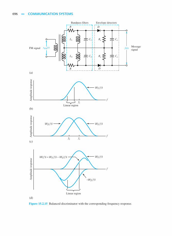
696 COMMUNICATION SYSTEMS
f (t)sFM(t)
R D
DR
L1
L2
Re
Messagesignal
FM signal
(a)
(b)
(c)
(d)
Am
plitu
de r
espo
nse
Linear region
Am
plitu
de r
espo
nse
Am
plitu
de r
espo
nse
Bandpass filters Envelope detectors
Re
Ce
Ce
C1
C2
f1
f1
f
f2
f
f
|H1( f )|
|H1( f )||H2( f )|
|H( f )| = |H1( f )| − |H2( f )| |H1( f )|
−|H2( f )|
Linear region
Figure 15.2.15 Balanced discriminator with the corresponding frequency response.
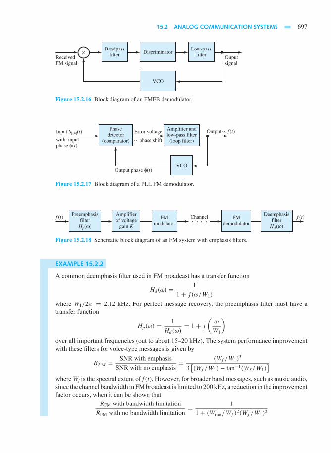
15.2 ANALOG COMMUNICATION SYSTEMS 697
Bandpassfilter Discriminator
VCO
Low-passfilterReceived
FM signalOuputsignal
×
Figure 15.2.16 Block diagram of an FMFB demodulator.
Amplifier andlow-pass filter
(loop filter)
Phasedetector
(comparator)
VCO
Input SFM(t)
with inputphase φ(t)
Error voltage
∝ phase shift
Output ∝ f (t)
Output phase φ(t)
Figure 15.2.17 Block diagram of a PLL FM demodulator.
Preemphasisfilter
Hp(ω)
Deemphasisfilter
Hd (ω)
Amplifierof voltage
gain K
FMmodulator
FMdemodulator
f (t) f (t)Channel. . . .
Figure 15.2.18 Schematic block diagram of an FM system with emphasis filters.
EXAMPLE 15.2.2
A common deemphasis filter used in FM broadcast has a transfer function
Hd(ω) = 1
1+ j (ω/W1)
where W1/2π = 2.12 kHz. For perfect message recovery, the preemphasis filter must have atransfer function
Hp(ω) = 1
Hd(ω)= 1+ j
(ω
W1
)over all important frequencies (out to about 15–20 kHz). The system performance improvementwith these filters for voice-type messages is given by
RFM = SNR with emphasis
SNR with no emphasis= (Wf /W1)
3
3[(Wf /W1)− tan−1(Wf /W1)
]where Wf is the spectral extent of f (t). However, for broader band messages, such as music audio,since the channel bandwidth in FM broadcast is limited to 200 kHz, a reduction in the improvementfactor occurs, when it can be shown that
RFM with bandwidth limitation
RFM with no bandwidth limitation= 1
1+ (Wrms/Wf )2(Wf /W1)2

698 COMMUNICATION SYSTEMS
where W rms is the rms bandwidth of f (t). Given W1/2π = 2.12 kHz, Wf /2π = 15 kHz, andWrms/2π = 4.25 kHz, determine RFM with and without bandwidth constraints.
So l u t i on
RFM(with no bandwidth constraint)
= (15/2.12)3
3[(15/2.12)− tan−1(15/2.12)
] ∼= 20.92, or 13.2 dB
RFM(with bandwidth limitation)
= 20.92
1+ (4.25/15)2(15/2.12)2∼= 4.17, or 6.2 dB
Thus, the bandwidth constraint has resulted in a loss in emphasis improvement of 13.2 − 6.2 =7 dB.
FM Stereo
Figure 15.2.19 shows the block diagram of an FM stereo transmitter and an FM stereo receiver.The following notation is used:
• fL(t), fR(t): Left and right messages that undergo preemphasis and are then added to yieldf 1(t) and differenced to give fd(t).
• f 2(t): Given by signal fd(t) when it DSB-modulates (with carrier suppressed) a 38-kHzsubcarrier.
• f 3(t): A low-level pilot carrier at 19 kHz that is included to aid in the receiver’s demodulationprocess.
• fs(t): Final composite message when f 1(t), f 2(t), f 3(t), and SCA (subsidiary communicationsauthorization) are all added up.
• SCA: A narrow-band FM waveform on a 67-kHz subcarrier with a total bandwidth of16 kHz. It is a special signal available to fee-paying customers who may desire to havebackground music free of commercials or nonaudio purposes such as paging.
• NBPF: Narrow-band band-pass filter.
• LPF, BPF, and NBPF: Appropriate filters that select the spectrum portions correspondingto f 1(t), f 2(t), and f 3(t), respectively.
The output signal-to-noise power ratio is smaller in FM stereo than in a monaural systemwith the same transmitted power, messages, and other parameters. With a loss as high as 22 dB,many FM stations can tolerate the loss because of the high power being transmitted.
Comparison of Analog-Modulation Systems
The comparison of analog modulation systems (conventional AM, DSB SC, SSB SC, VSB, FM,and PM) can be based on three practical criteria:
1. Bandwidth efficiency of the system.
2. Power efficiency of the system, as reflected in its performance in the presence of noise.The output SNR at a given received signal power is used as a criterion for comparing thepower efficiencies of various systems.
3. Ease of implementation of the system (transmitter and receiver).

15.2 ANALOG COMMUNICATION SYSTEMS 699
PreemphasisKHp(ω)
PreemphasisKHp(ω)
DSBmodulator
2
38-kHzoscillator
(a)
(b)
SCA
FMmodulator
19-kHz pilot
fL(t)
fR(t)
FM demodulator BPF Product LPF Deemphasis Hd (ω)
Deemphasis Hd (ω)
23–53 kHz 0–15 kHz
38-kHz subcarrier
Replaced by phase-locked loop
or
Local-carrier recovery
Synchronous detector
NBPF × 2 multiplier
19 kHz
LPF
0–15 kHz
sFM(t)
fd (t) f2(t)
f1(t)
f1(t)
f2(t)
f3(t)
fs(t)
fd (t)
2fR(t)
2fL(t)
A B
Phase detector LPF
÷ 2
38-kHz VCOA B
f4(t)
sFM(t)
f3(t)
Σ
Σ Σ
+
+
+ +
+
+
+−
Σ
Σ
++
+
−
Figure 15.2.19 (a) FM stereo transmitter. (b) FM stereo receiver.
The most bandwidth-efficient analog communication system is the SSB SC system with atransmission bandwidth equal to the signal bandwidth. In bandwidth-critical applications, suchas voice transmission over microwave and satellite links and some point-to-point communicationsystems in congested areas, this system is used widely. When transmission signals have asignificant dc component, such as image signals, SSB SC cannot be used because it cannoteffectively transmit direct current. A good compromise is the VSB system (with its bandwidthslightly larger than SSB and a capability for transmitting dc values), which is widely used intelevision broadcasting and some data-communication systems. When bandwidth is the major

700 COMMUNICATION SYSTEMS
concern, PM and particularly FM systems are least favorable. Only in terms of their high level ofnoise immunity, their usage may sometimes be justified.
FM, with its high level of noise immunity, and hence power efficiency, is widely usedon high-fidelity radio broadcasting and power-critical communication links such as point-to-point communication systems. It is also employed for satellite links and voice transmission onmicrowave LOS systems. When the transmitted power is a major concern, conventional AMand VSB (being the least power-efficient systems) are not used, unless their development can bejustified by the simplicity of the receiver structure.
From the viewpoint of ease of implementation, the simplest receiver structure is that ofconventional AM. Standard AM, VSB, and FM are widely used for AM, television, and high-fidelity FM broadcasting. The relative power inefficiency of the AM transmitter is compensatedfor by the extremely simple structure of several billions of receivers. The receiver structureis much more complicated for DSB SC and SSB SC systems, since they require synchronousdemodulation. These systems, therefore, are never used for broadcasting purposes. Note thatDSB SC also suffers from its relative bandwidth inefficiency.
Radio and Television Broadcasting
Radio (AM and FM) and television broadcasting are the most familiar forms of communicationvia analog transmission systems. The receiver most commonly used in AM radio broadcasting isthe superheterodyne receiver, shown in Figure 15.2.20, which consists of a radio-frequency (RF)tuned amplifier, mixer, local oscillator, intermediate frequency (IF) amplifier, envelope detector,audio-frequency amplifier, and a loudspeaker. Tuning at the desired radio frequency fc is achievedby a variable capacitor, which simultaneously tunes the RF amplifier and the frequency f LO of thelocal oscillator. Every AM radio signal, in a superheterodyne receiver, is converted to a common IFfrequency of fIF = |fc − fLO| = 455 kHz, which allows the use of a single tuned IF amplifier forsignals from any radio station in the frequency band. Matching the bandwidth of the transmittedsignal, the IF amplifier is set to have a bandwidth of 10 kHz.
The frequency conversion to IF is done by the combination of the RF amplifier and the mixer.The tuning range of the local oscillator is 955–2,055 kHz. f LO could be either higher or lower thanfc. If f LO is higher than fc, then fLO = fc+fIF. By tuning the RF amplifier to the frequency fc andmixing its output with the local oscillator frequency f LO, we obtain two signal components: onecentered at the difference frequency f IF; and the other centered at the sum frequency 2fc + fIF,known as the image frequency. Only the first component is passed on by the IF amplifier. The
RFamplifier Mixer
IFamplifier
Localoscillator
Common tuning
Automaticvolume control
Detector
Loud speaker
Audiofrequencyamplifier
Figure 15.2.20 Superheterodyne receiver.

15.2 ANALOG COMMUNICATION SYSTEMS 701
image response is suppressed by using the antenna and other RF-tuned circuits as a filter. Bylimiting the bandwidth of the RF amplifier to the range Bc < BRF < 2fIF, where Bc is thebandwidth of the AM radio signal (10 kHz), the radio signal transmitted at the image frequency(f ′c = fLO+ fIF) is rejected. A similar behavior occurs when f LO is lower than fc. Figure 15.2.21illustrates the AM station and image frequencies for a high-side and a low-side local oscillator,whereas Figure 15.2.22 depicts the frequency response characteristics of IF and RF amplifiers forthe case fLO > fc.
Amplifiers in the IF circuits provide most of the gain needed to raise the small antennasignal to a level sufficient to drive the envelope detector. The output of the detector contains adc component proportional to Ac and a component proportional to the audio message f (t), theamplified signal of which is used to drive the loudspeaker. The dc component is utilized in anautomatic volume control (AVC), otherwise known as automatic gain control (AGC), loop tocontrol the gain of RF and IF amplifiers by controlling their operating bias points. The loop actionis to maintain nearly a constant IF level at the detector’s input, even for large variations in antennavoltage.
The IF amplifier, with its narrow bandwidth, provides signal rejection from adjacent channels,and the RF amplifier provides signal rejection from image channels.
An FM radio superheterodyne receiver is shown in block diagram form in Figure 15.2.23.The part consisting of the antenna, RF amplifier, mixer, and local oscillator functions in a mannersimilar to that of an AM receiver, except that the frequencies involved are different. fIF = 10.7MHz in FM, so that the image is 21.4 MHz from the carrier frequency fc. The RF amplifier musteliminate the image-frequency band 2f IF away from the station to which the receiver is tuned.
The IF amplifier is generally divided into two parts. The higher level stage is set to limit ata proper level to drive the demodulator. More expensive FM receivers may have AGC added to
0 500 1000 1500
540 1600
AM station frequencies
RF-tuned circuit response
2000
(a)
(b)
f, kHz
fLO = fc + fIF
fLO = fc − fIF fc
fimage = fc + 2fIF
fimage = fc − 2fIF
fc
0 500 1000 1500
540 1600
AM station frequencies
2000f, kHz
Figure 15.2.21 AM radio stationand image frequencies. (a) High-side local oscillator, fLO > fc.(b) Low-side local oscillator,fLO < fc.
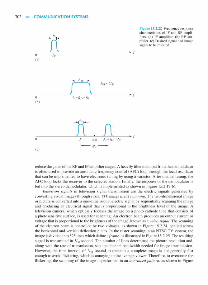
702 COMMUNICATION SYSTEMS
f
f
f
0
(b)
(c)
(a)fIF
Bc
0 fc = fLO − fIF
BRF < 2fIF
0 fLO
2fIF
f 'c = fLO + fIFfc
Bc
BRF
Figure 15.2.22 Frequency responsecharacteristics of IF and RF ampli-fiers. (a) IF amplifier. (b) RF am-plifier. (c) Desired signal and imagesignal to be rejected.
reduce the gains of the RF and IF amplifier stages. A heavily filtered output from the demodulatoris often used to provide an automatic frequency control (AFC) loop through the local oscillatorthat can be implemented to have electronic tuning by using a varactor. After manual tuning, theAFC loop locks the receiver to the selected station. Finally, the response of the demodulator isfed into the stereo demodulator, which is implemented as shown in Figure 15.2.19(b).
Television signals in television signal transmission are the electric signals generated byconverting visual images through raster (TV image area) scanning. The two-dimensional imageor picture is converted into a one-dimensional electric signal by sequentially scanning the imageand producing an electrical signal that is proportional to the brightness level of the image. Atelevision camera, which optically focuses the image on a photo cathode tube that consists ofa photosensitive surface, is used for scanning. An electron beam produces an output current orvoltage that is proportional to the brightness of the image, known as a video signal. The scanningof the electron beam is controlled by two voltages, as shown in Figure 15.2.24, applied acrossthe horizontal and vertical deflection plates. In the raster scanning in an NTSC TV system, theimage is divided into 525 lines which define a frame, as illustrated in Figure 15.2.25. The resultingsignal is transmitted in 1/30 second. The number of lines determines the picture resolution and,along with the rate of transmission, sets the channel bandwidth needed for image transmission.However, the time interval of 1/30 second to transmit a complete image is not generally fastenough to avoid flickering, which is annoying to the average viewer. Therefore, to overcome theflickering, the scanning of the image is performed in an interlaced pattern, as shown in Figure

15.2 ANALOG COMMUNICATION SYSTEMS 703
RFamplifier Mixer
Antenna
IFamplifier
fIF = 10.7 MHzBandwidth 210 kHz
Localoscillator
Frequency tuning
AGCdetector
AFC
FMdemodulator
Stereodemodulator
IFamplifierlimiter
Right loudspeaker
Left loudspeaker
Figure 15.2.23 Block diagram of a superheterodyne FM radio receiver.
15.2.26, consisting of two fields, each of 262.5 lines. Each field is transmitted in 1/60 second. Thefirst field begins at point a and terminates at point b, whereas the second field begins at point cand terminates at point d.
The image is scanned left to right and top to bottom in a system of closely spaced parallellines. When 242.5 lines are completed at the rate of 15,734.264 lines per second (63.556 µs perline), the raster’s visual area is scanned once; this scan is called a field. While the next 20 linesare not used for visual information, during that time of 1.27 ms special signals (testing, closedcaptions, etc.) are inserted and the beam is retraced vertically to begin a new field (shown as thesecond field in Figure 15.2.26). The raster (TV image area) has a standardized aspect ratio offour units of width for each three units of height. Good performance is achieved when the rasteris scanned with 525 lines at a rate of 29.97 frames per second.
The television waveform representing one scan is illustrated in Figure 15.2.27. A blankingpulse with a duration of 0.18 of the horizontal-sweep period Th is added to the visual voltagegenerated by the camera. While the blanking pulse turns off the electron beam in the receiver’spicture tube during the horizontal retrace time, an added sync (synchronization) pulse helps thereceiver to synchronize its horizontal scanning rate with that of the transmitter. Also, a burst ofat least 8 cycles of 3.579545 MHz, called the color burst, is added to the “back porch” of theblanking pulse for synchronizing the receiver’s color circuits. The visual information fluctuatesaccording to the image between the “black level” and the “white level” set at 70.3% and 12.5%,respectively, of the peak amplitude. An array of various sync pulses are added on top for bothhorizontal and vertical synchronization purposes.
If a filter is added to the television camera optics, so that only the red color passes through, thecamera’s voltage becomes proportional to the intensity of the amount of red in the image. Threesuch cameras, all synchronized and viewing the same image, are employed in color televisionto decompose the image into its primary color components of red R, green G, and blue B. Thecolor receiver utilizes a picture tube with three electron beams and a phosphor having R, G,and B components. While each beam excites one color of phosphor, at any spot in the imagethe three colors separately glow with proper intensities in response to the three transmitted colorsignals. The viewer’s eye effectively adds the three colors together to reproduce the original scenein color.
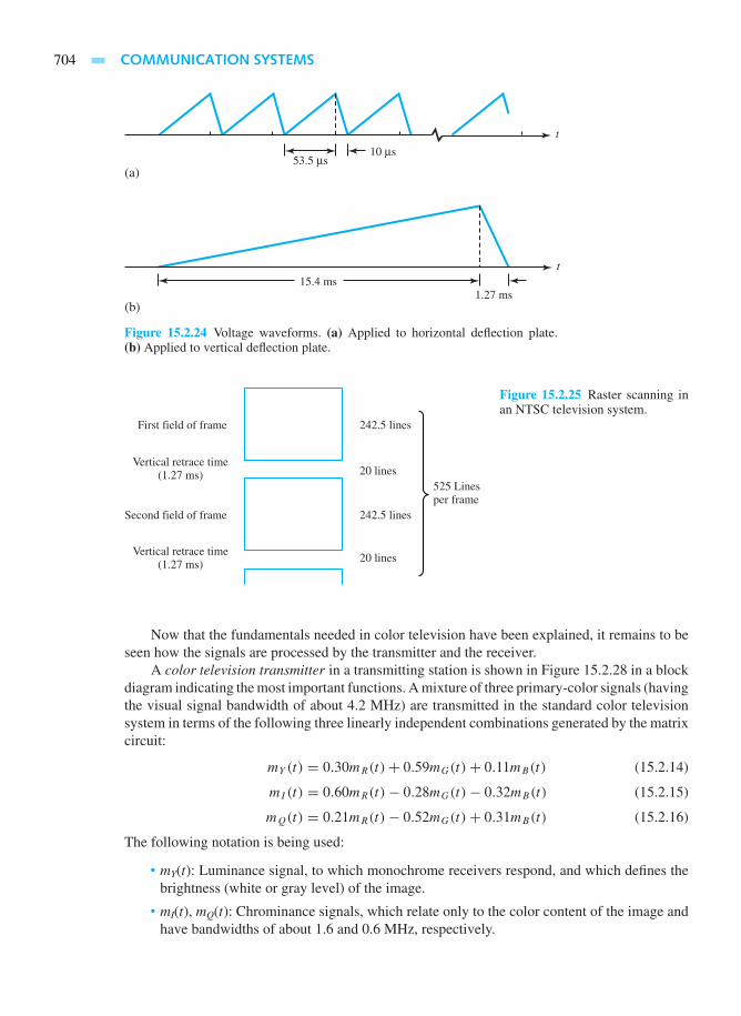
704 COMMUNICATION SYSTEMS
10 µs53.5 µs
15.4 ms1.27 ms
(a)
(b)
t
t
Figure 15.2.24 Voltage waveforms. (a) Applied to horizontal deflection plate.(b) Applied to vertical deflection plate.
First field of frame
Second field of frame
Vertical retrace time(1.27 ms)
Vertical retrace time(1.27 ms)
242.5 lines
20 lines525 Linesper frame
242.5 lines
20 lines
Figure 15.2.25 Raster scanning inan NTSC television system.
Now that the fundamentals needed in color television have been explained, it remains to beseen how the signals are processed by the transmitter and the receiver.
A color television transmitter in a transmitting station is shown in Figure 15.2.28 in a blockdiagram indicating the most important functions. A mixture of three primary-color signals (havingthe visual signal bandwidth of about 4.2 MHz) are transmitted in the standard color televisionsystem in terms of the following three linearly independent combinations generated by the matrixcircuit:
mY (t) = 0.30mR(t)+ 0.59mG(t)+ 0.11mB(t) (15.2.14)
mI(t) = 0.60mR(t)− 0.28mG(t)− 0.32mB(t) (15.2.15)
mQ(t) = 0.21mR(t)− 0.52mG(t)+ 0.31mB(t) (15.2.16)
The following notation is being used:
• mY(t): Luminance signal, to which monochrome receivers respond, and which defines thebrightness (white or gray level) of the image.
• mI(t), mQ(t): Chrominance signals, which relate only to the color content of the image andhave bandwidths of about 1.6 and 0.6 MHz, respectively.

15.2 ANALOG COMMUNICATION SYSTEMS 705
Beginning offirst field
Beginning ofsecond field
485 linesin picture
End ofsecond field
End offirst field
RetraceRetrace
a c
db
Figure 15.2.26 Interlaced scanningpattern to avoid flickering.
Color burst of 8 cyclesminimum of 3.579545 MHz
Peak carrier level (100%)
Blanking level (75%)Reference black level (70.3%)
Reference white level (12.5%)
Visual signal
Visual signal0.18Th
t
Th = 63.556 µs(one line)
Sync pulse
Figure 15.2.27 TV waveformrepresenting one horizontal lineof a raster scan.
• [m2I (t) + m2
Q(t)]1/2: Saturation or color intensity. A very deep red is saturated while red
diluted with white to give a light pink is nearly unsaturated.
• tan−1[mQ(t)/mI (t)]: Hue or tint.
• SI(t), SQ(t): Filtered chrominance signals of mI(t), mQ(t) by low-pass filters. SI(t) modulatesa color subcarrier at a frequency of 3.579545 MHz ± 10 Hz via DSB.
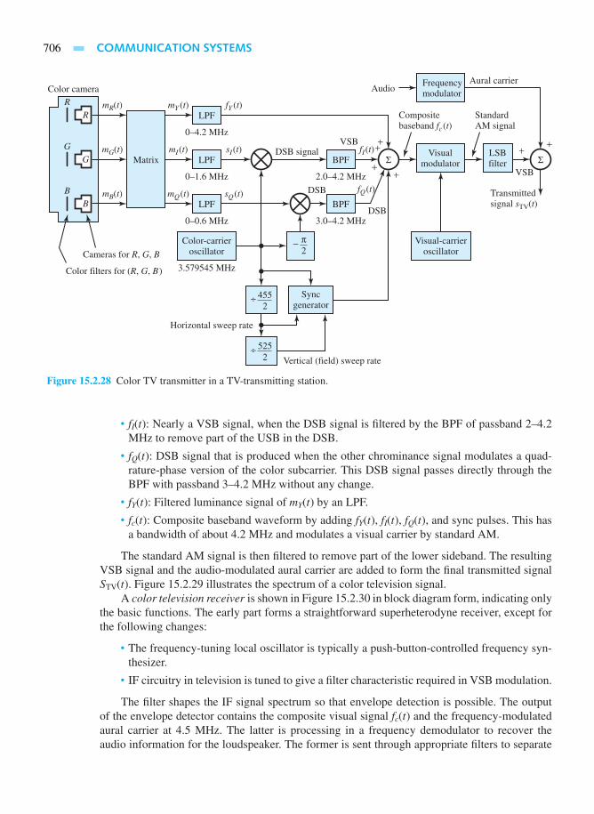
706 COMMUNICATION SYSTEMS
LPF
0–4.2 MHz
mY (t) fY (t)
LPFMatrix
Color camera
0–1.6 MHz 2.0–4.2 MHz
mI(t) sI(t) fI(t)
LPF BPF
BPF
B
G
R
B
G
R
0–0.6 MHz 3.0–4.2 MHz
Color-carrieroscillator
Visual-carrieroscillator
Horizontal sweep rate
Audio
Vertical (field) sweep rate
Aural carrier
Cameras for R, G, B
Color filters for (R, G, B)
Syncgenerator
Visualmodulator
Transmittedsignal sTV(t)
StandardAM signal
DSB signal
DSB
DSB
Compositebaseband fc(t)
Frequencymodulator
LSBfilter
VSB
VSB
2π−
2455÷
2525÷
3.579545 MHz
mQ(t)
mR(t)
mG(t)
mB(t) sQ(t) fQ(t)
Σ Σ
+
++
++ +
Figure 15.2.28 Color TV transmitter in a TV-transmitting station.
• fI(t): Nearly a VSB signal, when the DSB signal is filtered by the BPF of passband 2–4.2MHz to remove part of the USB in the DSB.
• fQ(t): DSB signal that is produced when the other chrominance signal modulates a quad-rature-phase version of the color subcarrier. This DSB signal passes directly through theBPF with passband 3–4.2 MHz without any change.
• fY(t): Filtered luminance signal of mY(t) by an LPF.
• fc(t): Composite baseband waveform by adding fY(t), fI(t), fQ(t), and sync pulses. This hasa bandwidth of about 4.2 MHz and modulates a visual carrier by standard AM.
The standard AM signal is then filtered to remove part of the lower sideband. The resultingVSB signal and the audio-modulated aural carrier are added to form the final transmitted signalSTV(t). Figure 15.2.29 illustrates the spectrum of a color television signal.
A color television receiver is shown in Figure 15.2.30 in block diagram form, indicating onlythe basic functions. The early part forms a straightforward superheterodyne receiver, except forthe following changes:
• The frequency-tuning local oscillator is typically a push-button-controlled frequency syn-thesizer.
• IF circuitry in television is tuned to give a filter characteristic required in VSB modulation.
The filter shapes the IF signal spectrum so that envelope detection is possible. The outputof the envelope detector contains the composite visual signal fc(t) and the frequency-modulatedaural carrier at 4.5 MHz. The latter is processing in a frequency demodulator to recover theaudio information for the loudspeaker. The former is sent through appropriate filters to separate
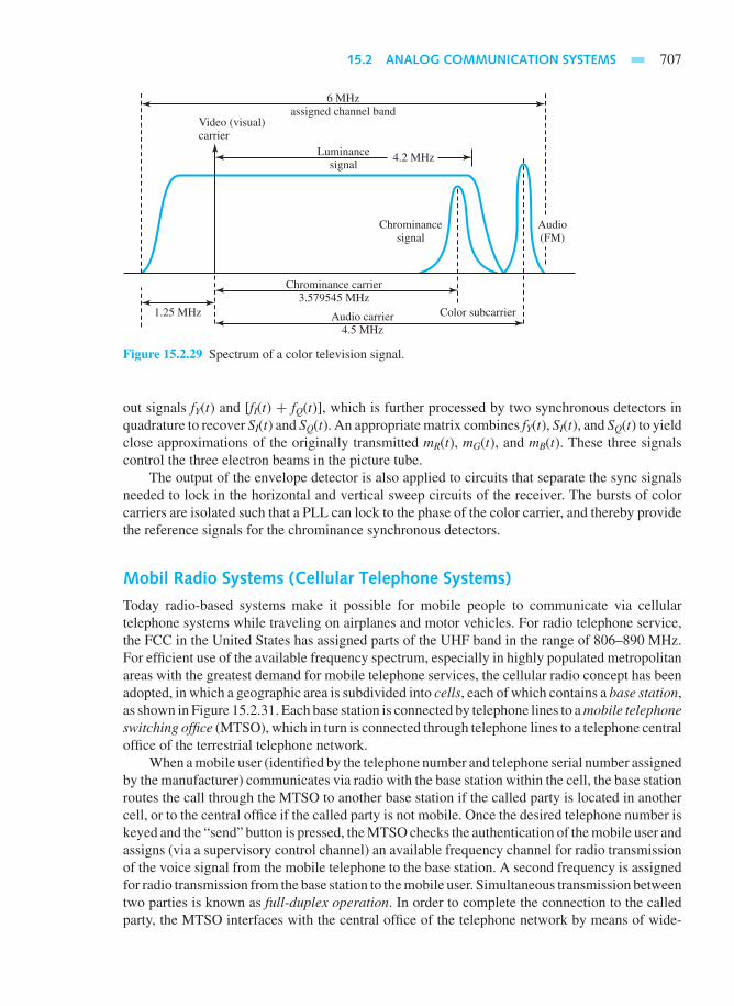
15.2 ANALOG COMMUNICATION SYSTEMS 707
6 MHzassigned channel band
Video (visual)carrier
Luminancesignal
4.2 MHz
Audio(FM)
Chrominancesignal
Chrominance carrier3.579545 MHz
Audio carrier4.5 MHz
Color subcarrier1.25 MHz
Figure 15.2.29 Spectrum of a color television signal.
out signals fY(t) and [fI(t) + fQ(t)], which is further processed by two synchronous detectors inquadrature to recover SI(t) and SQ(t). An appropriate matrix combines fY(t), SI(t), and SQ(t) to yieldclose approximations of the originally transmitted mR(t), mG(t), and mB(t). These three signalscontrol the three electron beams in the picture tube.
The output of the envelope detector is also applied to circuits that separate the sync signalsneeded to lock in the horizontal and vertical sweep circuits of the receiver. The bursts of colorcarriers are isolated such that a PLL can lock to the phase of the color carrier, and thereby providethe reference signals for the chrominance synchronous detectors.
Mobil Radio Systems (Cellular Telephone Systems)
Today radio-based systems make it possible for mobile people to communicate via cellulartelephone systems while traveling on airplanes and motor vehicles. For radio telephone service,the FCC in the United States has assigned parts of the UHF band in the range of 806–890 MHz.For efficient use of the available frequency spectrum, especially in highly populated metropolitanareas with the greatest demand for mobile telephone services, the cellular radio concept has beenadopted, in which a geographic area is subdivided into cells, each of which contains a base station,as shown in Figure 15.2.31. Each base station is connected by telephone lines to a mobile telephoneswitching office (MTSO), which in turn is connected through telephone lines to a telephone centraloffice of the terrestrial telephone network.
When a mobile user (identified by the telephone number and telephone serial number assignedby the manufacturer) communicates via radio with the base station within the cell, the base stationroutes the call through the MTSO to another base station if the called party is located in anothercell, or to the central office if the called party is not mobile. Once the desired telephone number iskeyed and the “send” button is pressed, the MTSO checks the authentication of the mobile user andassigns (via a supervisory control channel) an available frequency channel for radio transmissionof the voice signal from the mobile telephone to the base station. A second frequency is assignedfor radio transmission from the base station to the mobile user. Simultaneous transmission betweentwo parties is known as full-duplex operation. In order to complete the connection to the calledparty, the MTSO interfaces with the central office of the telephone network by means of wide-

708COMMUNICATIO
NSYSTEM
S
RFamplifier Mixer BPF
2.0–4.2 MHz
LPF
LPF VCO
Trap
4.2 MHz
LPF Matrix
Audio loud speaker
Picturetube
sQ(t)
fY(t)sI(t)
R
B
G
0–1.6 MHz
LPF
0–0.6 MHz
3.6 MHz
Aural IF FM demodulator
4.5 MHz
Gain adjust(color)
Antenna
IFamplifier
Envelopdetector
Color-burstgate
Horizontaloscillator
Phase-shiftadjust Hue (tint) control
Color-burst PLL
Verticaloscillator
Sweep tovertical yoke
Sweep tohorizontal yoke
Syncseparator
Localoscillator
Frequencytuning
IF passband41–47 MHz
2π−
Figure 15.2.30 Block diagram of a color television receiver.

15.2 ANALOG COMMUNICATION SYSTEMS 709
Cellwith base station
Telephonecentral office MTSO
Figure 15.2.31 Cellular telephone concept in mobile radio system.
band trunk lines, which carry speech signals from many users. When the two parties hang upupon completion of the telephone call, the radio channel then becomes available for another user.
During the telephone conversation, if the signal strength drops below a preset threshold, theMTSO monitors and finds a neighboring cell that receives a stronger signal and automaticallyswitches (in a fraction of a second) the mobile user to the base station of the adjacent cell. If amobile user is outside of the assigned service area, the mobile telephone may be placed in a roammode, which allows the user to initiate and receive calls.
In analog transmission between the base station and the mobile user, the 3-kHz wide audiosignal is transmitted via FM using a channel bandwidth of 30 kHz. Such a large bandwidthexpansion (by a factor of 10) is needed to obtain a sufficiently large SNR at the output ofthe FM demodulator. Since the use of FM is indeed wasteful of the radio frequency spectrum,cellular telephone systems based on digital transmission of digitized compressed speech are laterdeveloped. With the same available channel bandwidth, the system then accommodates a four-to tenfold increase in the number of simultaneous users.
Cellular systems employed cells with a radius in the range of 5–18 km. The base stationusually transmitted at a power level of 35 W or less, and the mobile users transmitted at a powerlevel of about 3 W, so that signals did not propagate beyond immediately adjacent cells. Bymaking the cells smaller and reducing the radiated power, frequency reuse, bandwidth efficiency,and the number of mobile users have been increased. With the advent of small and powerfulintegrated circuits (which consume very little power and are relatively inexpensive), the cellularradio concept has been extended to various types of personal communication services usinglow-power hand-held sets (radio transmitter and receivers).
With analog cellular, or AMPS (Advanced Mobile Phone System), calls are transmitted insound waves at 800 MHz to 900 MHz. This was the first mobile phone technology available inearly 1980s. Digital cellular, or D-AMPS (Digital AMPS), transmits calls in bits at the samefrequency as analog cellular, with improved sound quality and security. To send numerous callsat once, D-AMPS phones use either CDMA (Code Division Multiple Access) or TDMA (TimeDivision Multiple Access) technology; but CDMA phones won’t work in TDMA areas, and viceversa. A dual-mode unit can switch to analog transmission outside of the more limited digitalnetwork.
PCS (Personal Communications Service) phones transmit at 1800 MHz to 1900 MHz andare smaller and more energy efficient. To get around the limited coverage, a dual-band digitalphone (which switches to the lower digital frequency) and a trimode phone (which works in

710 COMMUNICATION SYSTEMS
AMPS, D-AMPS, or PCS areas) has been developed. The GSM (Global System for Messagingcommunications) is the most widely accepted transmission method for PCS phones.
The latest wireless communications technology is the personal satellite phone. The coverageis planetary and one can reach anywhere on earth. Examples include the Iridium satellite handsetdeveloped by Motorola and others from the Teledesic constellation. Special requirements, such assending and receiving data or faxes, can be handled by the new handheld computer-and-mobile-phone hybrids such as Nokia’s 9000i and the Ericsson DI27. Mobile phones with a Web browsercapability are also available. We have yet to see the more exciting new developments in thetelecommunications industry with computers, networking, and wireless technology.
15.3 DIGITAL COMMUNICATION SYSTEMS
A digital signal can be defined as having any one of a finite number of discrete amplitudes at anygiven time. The signal could be a voltage or current, or just a number such as 0 or 1. A signal forwhich only two amplitudes are possible is known as a binary digital signal, the type of which iscommonly used in computers and most digital communication systems. A communication systemthat is designed to process only digital signals (or messages) to convey information is said to bedigital. The recent trend is to make as much of the system digital as possible, because:
• Discrete data are efficiently processed.
• Analog messages can also be converted to digital form.
• Digital systems interface well with computers.
• Digital systems offer great reliability and yield high performance at low cost.
• Being flexible, digital systems can accommodate a variety of messages with ease.
• Security techniques are available to offer message privacy to users.
• Advanced signal-processing techniques can be added on.
However, the most serious disadvantages are the increased complexity needed for systemsynchronization and the need for larger bandwidths than in an equivalent analog system. Adigital system can directly interface with a source having only discrete messages, because ofthe inherent characteristic of the digital system. With suitable conversion methods, however,systems currently exist that can simultaneously transmit audio, television, and digital data overthe same channel. Figure 14.1.2 illustrates the basic elements of a digital communication system,which was introduced in Section 14.1.
Before we begin discussing digital systems, it is helpful to talk about the methods by whichanalog messages are converted into digital form. Sampling, quantization, and coding are the threeoperations needed for the transmission of an analog signal over a digital system.
Sampling
This method was introduced in Section 14.2. Sampling of an analog signal makes it discrete intime. A bandlimited signal can be recovered exactly from its samples, taken periodically in timeat a rate at least equal to twice the signal’s bandwidth. If a message f (t) has a spectral extent ofWf rad/s, the sampling rate fs (samples per second) must satisfy
fs ≥ Wf
π(15.3.1)
from the sampling theorem. The minimum rate Wf /π (samples per second) is known as theNyquist rate. If the exact message samples could be transmitted through the digital system, the

15.3 DIGITAL COMMUNICATION SYSTEMS 711
original f (t) could be exactly reconstructed at all times, with no error by the receiver. However,since the exact samples cannot be conveyed, they must be converted to discrete samples in aprocess known as quantization.
Quantization
Let Figure 15.3.1(a) illustrate a message f (t) with values between 0 and 7 V. A sequence ofexact samples taken at uniform intervals of time is shown: 1.60, 3.70, 4.75, 3.90, 3.45, and5.85 V. Quantization consists of rounding exact sample values to the nearest of a set of discreteamplitudes called quantum levels. Assuming the quantizer to have eight quantum levels (0, 1,2, . . . , 7 V), a sequence of quantized samples (2, 4, 5, 4, 3, and 6 V) is shown in Figure 15.3.1(a).Obviously, the scheme is not limited to messages with only nonnegative voltages. The quantizeris said to be uniform when the step size between any two adjacent quantum levels is a constant,denoted by δv volts. Quantizers with nonuniform step size are also designed for improved systemperformance. An L-level quantizer can have even or odd L. A quantizer is said to be saturated oroverloaded when
|f (t)| >(L− 2
2
)δv + δv = L
2δv (15.3.2)
Figure 15.3.2 shows the output quantum levels versus input voltage characteristic (stairstep inshape) of an L-level quantizer, when the message signal has both positive and negative amplitudesof the same maximum magnitude. Case (a) corresponds to L being an even integer, when themidriser can be observed; and case (b) corresponds to L being an odd integer, when the midtreadcan be seen.
V
t
t
f (t)
Ts 6Ts5Ts3Ts
Quantized samples
Binary code words (Nb = 3)
(a)
Polar format(b)
−A
A
2Ts 4Ts
2 4 5 4
00 0 0 0 00 001 11 1 11 1 1 1
3 6
5.85
3.45
3.903.70
1.601
0
2
3
4
5
6
7
4.75
Figure 15.3.1 (a) Analog message f (t) withexact and quantized samples. (b) Coding andwaveform formatting of quantized samples.

712 COMMUNICATION SYSTEMS
Output
Output
L − 12 )(
Midriser
(a)
(b)
Midtread
δv
L − 12 )( δv
≈
≈
≈
≈
≈ ≈
≈ ≈
L − 22
5 δv2
3 δv2
3 δv2
)( δv
L − 22 )( δv
−
L − 22 )( δv
L − 22 )( δv
−
L − 12 )( δv−
L − 12 )( δv−
−
5 δv
−δv
−2 δv
δv
2 δv
2−
L even
L odd
f (t)
f (t)
Figure 15.3.2 Uniform quantizercharacteristics. (a) Midriser witheven L. (b) Midtread with odd L.
EXAMPLE 15.3.1
A uniform quantizer is said to have 16 levels, and hence is called a midriser. The saturation levelsare to correspond to extreme values of the message of 1 V ≤ f (t) ≤ 17 V. Find the quantumlevels.
So l u t i on
The tread width is δv = (17 − 1)/16 = 1 V. The first quantum level is then given by1+ (δv/2) = 1.5 V. Other quantum levels, denoted by li, are given by
li = 1.5+ (i − 1)δv = 1.5+ (i − 1)1, i = 1, 2, . . . , 16

15.3 DIGITAL COMMUNICATION SYSTEMS 713
Quantization Error
Sampling followed by quantization is equivalent to quantization followed by sampling. Figure15.3.3 illustrates a message signal f (t) and its quantized version denoted by fq(t). The differencebetween fq(t) and f (t) is known as the quantization error εq(t),
εq(t) = fq(t)− f (t) (15.3.3)
Theoretically, fq(t) can be recovered in the receiver without error. The recovery of fq(t) canbe viewed as the recovery of f (t) with an error (or noise) εq(t) present. For a small δv with a largenumber of levels, it can be shown that the mean-squared value of εq(t) is given by
ε2q(t) =
(δv)2
12(15.3.4)
When a digital communication system transmits an analog signal processed by a uniformquantizer, the best SNR that can be attained is given by(
So
Nq
)= f 2(t)
ε2q(t)
= 12f 2(t)
(δv)2(15.3.5)
where S0 and Nq represent the average powers in f (t) and εq(t), respectively. When f (t) fluctu-ates symmetrically between equal-magnitude extremes, i.e., − |f (t)|max ≤ f (t) ≤ |f (t)|max,choosing a sufficiently large number of levels L, the step size δv comes out as
δv = 2 |f (t)|max
L(15.3.6)
and the SNR works out as (S0
Nq
)= 3L2f 2(t)
|f (t)|2max
(15.3.7)
By defining the message crest factor KCR as the ratio of peak amplitude to rms value,
K2CR =
|f (t)|2max
f 2(t)(15.3.8)
Equation (15.3.7) can be rewritten as
Quantizedmessage fq(t)
Quantizationerror εq(t)
Message f (t)
δv
δv
t
t
Figure 15.3.3 Message signal f (t), its quantizedversion fq(t), and quantization error εq(t).

714 COMMUNICATION SYSTEMS
(So
Nq
)= 3L2
K2CR
(15.3.9)
It can be seen that messages with large crest factors will lead to poor performance.
Companding
In order to lower the crest factor of a waveform, so as to produce better performance, a processknown as companding is used. It works like a compressor which progressively compresses thelarger amplitudes of a message when it is passed through a nonlinear network. The inverseoperation in the receiver is known as an expandor, when it restores the original message. Figure15.3.4 illustrates a typical set of input–output characteristics for a form of compandor. One can seethat the action of the compressor is to increase the rms–signal value for a given peak magnitude.
Source Encoding
After the quantization of message samples, the digital system will then code each quantizedsample into a sequence of binary digits (bits) 0 and 1. Using the natural binary code is a simpleapproach. For a code with Nb bits, integers N (from 0 to 2Nb − 1) are represented by a sequenceof digits, bNb
, bNb−1, . . . , b2, b1, such that
N = bNb(2Nb−1)+ . . .+ b2(2
1)+ b1(20) (15.3.10)
Note that b1 is known as the least significant bit (LSB), and bNbas the most significant bit (MSB).
Since a natural binary code of Nb bits can encode Lb = 2Nb levels, it follows that
|f (t)|max
|f (t)|max
|f (t)|max
|f (t)|maxInput
Input
No compressionWith compression
No expansionWith expansion
Output
Output
(a)
(b)
Figure 15.3.4 Compandor input–output character-istics. (a) Compressor. (b) Expandor.

15.3 DIGITAL COMMUNICATION SYSTEMS 715
L ≤ Lb = 2Nb (15.3.11)
if L levels span the message variations. For example, in Figure 15.3.1(b), Nb = 3 and L = 8;the binary code word 010 represents 0(23−1) + 1(21) + 0(20) = 2 V, and 110 represents1(23−1) + 1(21) + 0(20) = 6 V. Thus, binary code words with Nb = 3 are shown in Figure15.3.1(b).
EXAMPLE 15.3.2
A symmetrical fluctuating message, with |f (t)|max = 6.3 V and KCR = 3, is to be encoded byusing an encoder that employs an 8-bit natural binary code to encode 256 voltage levels from−7.65 V to +7.65 V in steps of δv = 0.06 V. Find L, f 2(t), and S0/Nq .
So l u t i on
From Equation (15.3.6),
L = 2 |f (t)|max
δv= 2× 6.3
0.06= 210
From Equation (15.3.8),
f 2(t) = |f (t)|2max
K2CR
= 6.32
9= 4.41 V2
From Equation (15.3.9),(S0
Nq
)= 3L2
K2CR
= 3× 2102
9= 14,700 or 41.67 dB
Digital Signal Formatting
After quantization and coding the samples of the message, a suitable waveform has to be chosento represent the bits. This waveform can then be transmitted directly over the channel (if no carriermodulation is involved), or used for carrier modulation. The waveform selection process is knownas formatting the digital sequence. Three kinds of waveforms are available:
1. Unipolar waveform, which assigns a pulse to code 1 and no pulse to code 0. The durationof a pulse is usually chosen to be equal to Tb, if binary digits occur each Tb seconds (thebit interval’s duration).
2. Polar waveform, which consists of a pulse of duration Tb for a binary 1 and a negativepulse of the same magnitude and duration for a 0. This yields better system performancein noise than the unipolar format, because of the wider distinction between the two values.
3. Manchester waveform, which transmits a pulse of duration Tb/2 followed by an equalmagnitude, but negative pulse of duration Tb/2 for each binary 1, and the negative of thistwo-pulse sequence for a binary 0. Even when a long string of 0s or 1s may occur in thedigital sequence, the advantage of this format is that it never contains a dc component.
Figure 15.3.5 illustrates these formats for a sequence of binary digits. Figure 15.3.1 (b) showsthe polar format corresponding to the coding in that case. Since it is important that a digital system

716 COMMUNICATION SYSTEMS
not lose track of polarity while processing polar or Manchester waveforms, a technique calleddifferential encoding (see Problem 15.3.9) is employed so as to remove the need to maintainpolarity.
Because the digits in a typical digital sequence fluctuate randomly between 0s and 1s withtime, the formatted waveform is then a randomly fluctuating set of pulses corresponding to theselected format. With such random waveforms, one uses the power spectral density (with units ofV2/Hz) to define the spectral content. On comparing the three waveform formats, the unipolar andpolar formats both have the same bandwidth and relative side-lobe level, whereas the Manchesterwaveform has no spectral component at direct current, but requires twice the bandwidth of theother two signals.
Pulse-Code Modulation (PCM)
PCM is the simplest and oldest waveform coding scheme for processing an analog signal bysampling, quantizing, and binary encoding. Figure 15.3.6 shows a functional block diagram ofa PCM system transmitter. In order to guarantee that the message is band-limited to the spectralextent for which the system is designed, a low-pass filter is introduced. The compressor is ratheroptional for better performance. Let us assume that the PCM signal is transmitted directly overthe baseband channel. Corrupted by the noise generated within the receiver, the PCM signal isshown as the input to the PCM reconstruction function in Figure 15.3.7, which depicts a blockdiagram of functions (including an optional expandor) needed to receive PCM. The operations ofthe receiver are basically the inverse of those in the transmitter. The first and most critical receiveroperation is to reconstruct the originally transmitted PCM signal as nearly as possible from thenoise-contaminated received waveform. The effect of noise is to be minimized through a carefulselection of circuit implementation.
The only knowledge required of the receiver to reconstruct the original PCM signal is whetherthe various transmitted bits are 0s and 1s, depending on the voltage levels transmitted, assumingthat the receiver is synchronized with the transmitter. The two levels associated with unipolar
0 1 1 1 0 1 0
(a)
(c)
(b)
(d)
TbA
t
t
t
A
A
−A
−A
0 1 0 1 1 0 0 Figure 15.3.5 Waveform formats for a binarydigital sequence. (a) Binary digital sequence bk.(b) Its unipolar format. (c) Its polar format. (d) ItsManchester format.

15.3 DIGITAL COMMUNICATION SYSTEMS 717
Analogmessage f (t)
Band-limited message
Presamplinglowpassfilter
SamplerA
Compressor(optional)
Uniformquantizer
Waveformformatter
Binary PCMto channel
Binaryencoder
Timingcontrol
Quantizedsamples
Figure 15.3.6 Block diagram of a PCM system transmitter.
PCM plusbroad-bandchannel noise
Original PCM plus errors Quantized samples plus noise
Expandor(optional)
PCMreconstruction
Binarydecoder
f (t) plus noise
Timing
Messagereconstruction
(low pass filter)
Figure 15.3.7 Block diagram of a PCM system receiver.
pulses of amplitude A are 0 and A, whereas those associated with polar pulses (of amplitudes±A)are A and−A. It is, of course, better for the receiver if the ratio of the pulse-caused voltage to thenoise rms voltage is the largest possible at the time of measurement. Figure 15.3.8 shows PCMreconstruction circuits for unipolar, polar, and Manchester waveforms. The following notation isused:
• VT: Preset threshold, which is zero for polar and Manchester PCM. In the unipolar system,it is equal to half the signal component of the integrator’s output level (A2Tb/2) at thesampling time when the input has a binary 1. (After the sample is taken, the integrator isdischarged to 0 V in preparation for integration over the next bit interval.)
• D: The difference between the integrator’s output and VT at the end of each bit interval ofduration Tb. If D ≥ 0, binary 1 is declared; if D < 0, a 0 is declared.
• Square-wave clock: Generates a voltage A for 0 < t < Tb/2 and −A for Tb/2 < t < Tb,with its fundamental frequency 1/Tb Hz. The product of the clock and the incoming
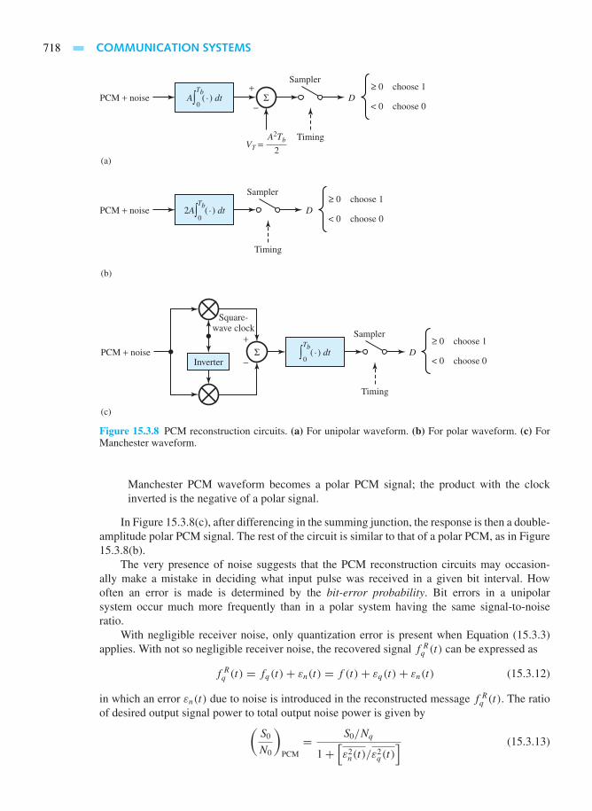
718 COMMUNICATION SYSTEMS
PCM + noise
Sampler
Timing
≥ 0 choose 1
< 0 choose 0
VT =A2Tb
2(a)
Σ+
−A∫ ( . ) dt D
Tb
Sampler
PCM + noise
Square-wave clock
Timing
≥ 0 choose 1
< 0 choose 0
(c)
Σ+
−∫ ( . ) dt D
PCM + noise
Sampler
Timing
≥ 0 choose 1
< 0 choose 0
(b)
2A∫ ( . ) dt D
Inverter
0
Tb
0
Tb
0
Figure 15.3.8 PCM reconstruction circuits. (a) For unipolar waveform. (b) For polar waveform. (c) ForManchester waveform.
Manchester PCM waveform becomes a polar PCM signal; the product with the clockinverted is the negative of a polar signal.
In Figure 15.3.8(c), after differencing in the summing junction, the response is then a double-amplitude polar PCM signal. The rest of the circuit is similar to that of a polar PCM, as in Figure15.3.8(b).
The very presence of noise suggests that the PCM reconstruction circuits may occasion-ally make a mistake in deciding what input pulse was received in a given bit interval. Howoften an error is made is determined by the bit-error probability. Bit errors in a unipolarsystem occur much more frequently than in a polar system having the same signal-to-noiseratio.
With negligible receiver noise, only quantization error is present when Equation (15.3.3)applies. With not so negligible receiver noise, the recovered signal f R
q (t) can be expressed as
f Rq (t) = fq(t)+ εn(t) = f (t)+ εq(t)+ εn(t) (15.3.12)
in which an error εn(t) due to noise is introduced in the reconstructed message f Rq (t). The ratio
of desired output signal power to total output noise power is given by(S0
N0
)PCM
= S0/Nq
1+[ε2n(t)/ε
2q(t)] (15.3.13)

15.3 DIGITAL COMMUNICATION SYSTEMS 719
where the numerator S0/Nq is given by Equation (15.3.5), or by Equation (15.3.9) when Equation(15.3.6) applies. If ε2
n(t) << ε2q(t), noise has no effect on performance; otherwise it has a
significant effect. Thus, εn(t) gives rise to a threshold effect in PCM.
Signal Multiplexing
Frequency-division multiplexing (FDM) and time-division multiplexing (TDM) systems wereintroduced in Section 14.2. When data from many sources in time are interlaced, the interlacingof data is called time multiplexing, in which case a single link can handle all sources. Figure15.3.9(a) illustrates time multiplexing soon after sampling for N similar messages. With properinterleaving of sampling pulses [see Figures 15.3.9(b) and (c) for individual message signalwaveforms], the train of samples can be added for the signal at point A in Figure 15.3.9(a), asshown in Figure 15.3.9(d). If we consider N similar messages of spectral extent Wf rad/s, thesampling interval Ts must satisfy
Ts ≤ π
Wf
(15.3.14)
based on the sampling theorem (see Section 14.2). A time slot is the time per sampling intervalthat is allowed per message. It is equal to the sum of the sampling-pulse duration τ and separationτg , called the guard time. Thus, we have
τ + τg = Ts
N≤ π
NWf
(15.3.15)
The time that is required to gather at least one sample of each message is known as a frame,which is Ts, as shown in Figure 15.3.9(d). Now, with a single composite source of the waveformshown in Figure 15.3.9(d) at point A of Figure 15.3.9(a), the time multiplexer of Figure 15.3.9(a)operates beyond A. For Nb-bit encoding, each time slot in the output PCM signal will have Nb bitsof duration,
Tb = Ts
NNb
(15.3.16)
It is assumed that all sample trains are derived from the same timing source, called a clock, andhence have the same frequency. Instead of using up all frame time for messages, some time isusually allocated for synchronization so that the receiver will know the start times of frames. TheAmerican Telephone and Telegraph Company (AT & T) employs a device known as a D3 channelbank, which is a synchronous multiplexer, whose characteristics are as follows:
• It multiplexes 24 telephone messages, each having an 8-kHz sampling rate so that Ts =1/(8×103) = 125 µs. The digital structure of each input message is determined by a singlemaster clock.
• Each sample uses 8-bit encoding, so that there are 8 × 24 = 192 message bits; one extrabit, known as a framing bit, of less than one time slot is allowed for frame synchronization.Thus, a total of 193 bits per frame, with a total bit rate of 193 × 8000 = 1.544 megabitsper second (Mbit/s), is available.
• The frame structure is illustrated in Figure 15.3.10.
• Bit robbing or bit stealing, which is the occasional borrowing of a message bit for purposesother than message information, is done for signaling, which refers to conveying informationconcerning telephone number dialed, dial tone, busy signal, ringing, and so on.

720 COMMUNICATION SYSTEMS
. . .
Σ+
++ CompressorSamplerLPFf2(t)
f1(t)
f2(t)
Ts
Ts
Ts
t
2Ts 3Ts
31
12
11
2Guard time τg
Time slot
Frame
2
2
N
τ
t
t
3Ts
3Ts
2Ts
2Ts
LPFfN (t)
Timing 2...
... ... ... ... ...
Sampler
Timing N
(a)
(b)
(c)
(d)
A Uniformquantizer
Binaryencoder
Binary PCM
Waveformformatter
LPFf1(t) Sampler
Timing 1
Figure 15.3.9 (a) Time multiplexing for N similar analog signals. (b) Waveform at point A for messagesignal 1. (c) Waveform at point A for message signal 2. (d) Full waveform at point A.
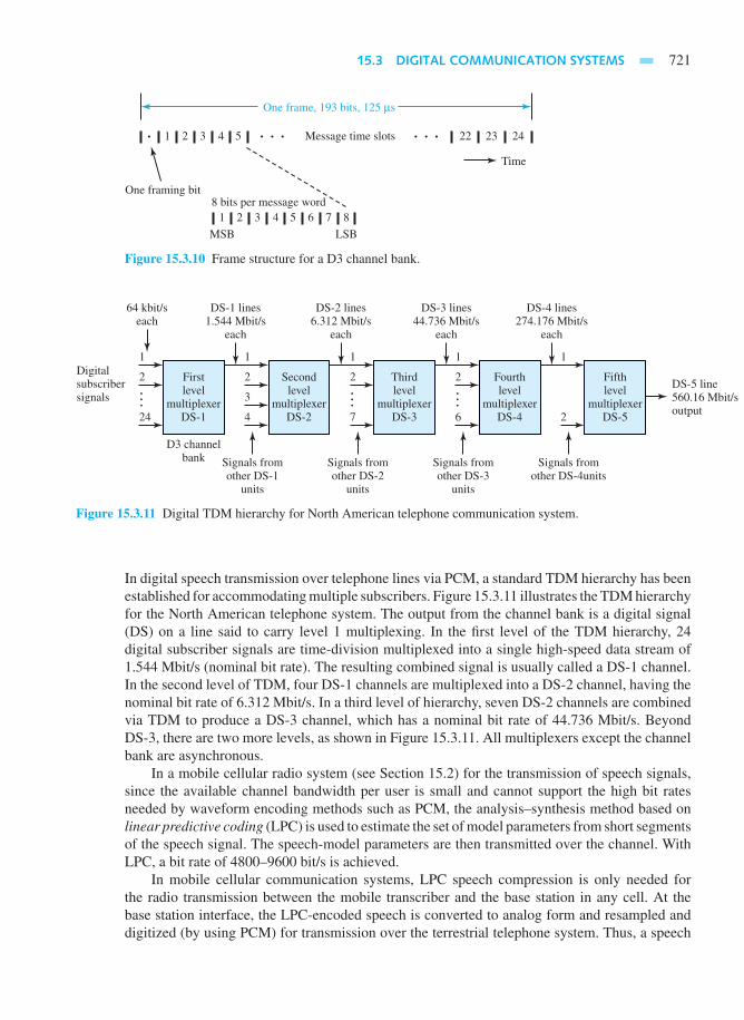
15.3 DIGITAL COMMUNICATION SYSTEMS 721
One frame, 193 bits, 125 µs
245432
One framing bit8 bits per message word
MSB LSB
1
54321 876
. . . . . . . 23
Time
22Message time slots
Figure 15.3.10 Frame structure for a D3 channel bank.
D3 channelbank
64 kbit/seach
Digitalsubscribersignals
1
2...24
...7
Secondlevel
multiplexerDS-2
Firstlevel
multiplexerDS-1
DS-1 lines1.544 Mbit/s
each
Signals fromother DS-1
units
1
2
3
4
Thirdlevel
multiplexerDS-3
DS-2 lines6.312 Mbit/s
each
Signals fromother DS-2
units
1
2...6
Fourthlevel
multiplexerDS-4
DS-3 lines44.736 Mbit/s
each
Signals fromother DS-3
units
1
2
2
Fifthlevel
multiplexerDS-5
DS-4 lines274.176 Mbit/s
each
DS-5 line560.16 Mbit/soutput
Signals fromother DS-4units
1
Figure 15.3.11 Digital TDM hierarchy for North American telephone communication system.
In digital speech transmission over telephone lines via PCM, a standard TDM hierarchy has beenestablished for accommodating multiple subscribers. Figure 15.3.11 illustrates the TDM hierarchyfor the North American telephone system. The output from the channel bank is a digital signal(DS) on a line said to carry level 1 multiplexing. In the first level of the TDM hierarchy, 24digital subscriber signals are time-division multiplexed into a single high-speed data stream of1.544 Mbit/s (nominal bit rate). The resulting combined signal is usually called a DS-1 channel.In the second level of TDM, four DS-1 channels are multiplexed into a DS-2 channel, having thenominal bit rate of 6.312 Mbit/s. In a third level of hierarchy, seven DS-2 channels are combinedvia TDM to produce a DS-3 channel, which has a nominal bit rate of 44.736 Mbit/s. BeyondDS-3, there are two more levels, as shown in Figure 15.3.11. All multiplexers except the channelbank are asynchronous.
In a mobile cellular radio system (see Section 15.2) for the transmission of speech signals,since the available channel bandwidth per user is small and cannot support the high bit ratesneeded by waveform encoding methods such as PCM, the analysis–synthesis method based onlinear predictive coding (LPC) is used to estimate the set of model parameters from short segmentsof the speech signal. The speech-model parameters are then transmitted over the channel. WithLPC, a bit rate of 4800–9600 bit/s is achieved.
In mobile cellular communication systems, LPC speech compression is only needed forthe radio transmission between the mobile transcriber and the base station in any cell. At thebase station interface, the LPC-encoded speech is converted to analog form and resampled anddigitized (by using PCM) for transmission over the terrestrial telephone system. Thus, a speech

722 COMMUNICATION SYSTEMS
signal transmitted from a mobile subscriber to a fixed subscriber will undergo two different typesof analog-to-digital (A/D) encoding, whereas speech-signal communication between two mobilesserviced by different base stations will undergo four translations between the analog and digitaldomains.
In the conversion of analog audio signals to digital form, with the development of the compactdisc (CD) player and the digital audio tape recorder, the most dramatic changes and benefitshave been experienced by the entertainment industry. The CD system, from a systems pointof view, embodies most of the elements of a modern digital communication system: A/D andD/A conversion, modulation/demodulation, and channel coding/decoding. Figure 15.3.12 showsa general block diagram of the elements of a CD digital audio system. The sampling rate in aCD system is chosen to be 44.1 kHz, which is compatible with the video recording equipmentcommonly used for digital recording of audio signals on magnetic tape. The samples of both the Land R signals are quantized using PCM with 16 bits per sample. While the D/A conversion of thetwo 16-bit signals at the 44.1-kHz sampling rate is relatively simple, the practical implementationof a 16-bit D/A converter is very expensive. Because inexpensive D/A converters with 12-bit (orless) precision are readily available, a method is to be devised for D/A conversion that employsa low precision (and hence a low-cost D/A converter), while maintaining the 16-bit precisionof the digital audio signal. Without going into details, the practical solution to this problem isto expand the bandwidth of the digital audio signal by oversampling through interpolation anddigital filtering prior to analog conversion.
Time-division multiple access (TDMA) is an important means by which each station on earthtimeshares the communication satellite in the sky, and broadcasts to all other stations during itsassigned time. Figure 15.3.13 shows the communication links of several (N) earth stations thatcommunicate with each other through satellite. All stations use the same up-link frequency, andall receive a single down-link frequency from the satellite.
Carrier Modulation by Digital Signals
Digitally modulated signals with low-pass spectral characteristics can be transmitted directlythrough baseband channels (having low-pass frequency-response characteristics) without theneed for frequency translation of the signal. However, there are many communication bandpasschannels (telephone, radio, and satellite channels) that pass signals within a band of frequencies(that is far removed from dc). Digital information may be transmitted through such channels byusing a sinusoidal carrier that is modulated by the information sequence in either amplitude, phase,or frequency, or some other combination of amplitude and phase. The effect of impressing the in-formation signal on one or more of the sinusoidal parameters is to shift the frequency content of thetransmitted signal to the appropriate frequency band that is passed by the channel. Thus, the signalis transmitted by carrier modulation. There are several carrier-modulation methods. However, weshall limit our discussion to the following, assuming only binary modulation in all cases:
• Amplitude-shift keying (ASK)• Phase-shift keying (PSK)• Differential phase-shift keying (DPSK)• Frequency-shift keying (FSK).
AMPLITUDE-SHIFT KEYING (ASK)
A carrier’s amplitude is keyed between two levels (binary 1 and 0) in binary ASK. Figure 15.3.14shows the functions of a coherent ASK communication system. Let us consider a bit interval from

15.3 DIGITAL COMMUNICATION SYSTEMS 723
Digitalrecorder
A/Dconverter
StudioL R
Modulator
Laserrecording
Master disc
Replication
Channel
1.25 m/s
Digitalcontroland displayinformation
Channelencoder
Up-samplingand
interpolation
D/Aconverter
L R
Demodulator
Compact disc
Channeldecoder
Figure 15.3.12 General block diagram ofa CD digital audio system.
Communicationsatellite
Earth
ReferencestationStation 2
Station 1Station N
. . .
Figure 15.3.13 Communication links of several earth stationscommunicating through a satellite.
t = 0 to t = Tb, since the operation of any other interval will be similar. The desired ASK signalis given by
sASK(t) =Ac cos(ωct + φc), 0 < t < Tb, for 10, 0 < t < Tb, for 0
(15.3.17)

724 COMMUNICATION SYSTEMS
where Ac, ωc, and φc are the peak amplitude, angular frequency, and phase angle of the mod-ulated carrier, respectively. Equation (15.3.17) can be viewed as a carrier Ac cos(ωct + φc)
modulated by a digital signal d(t) that is 0 or 1 in a given bit interval. The digital signal andproduct device shown in Figure 15.3.14 are then equivalent to the waveform formatter andmodulator. Assuming that the received signal sR(t) differs only in amplitude from sASK(t), onecan write
sR(t) =Ac cos(ωct + φc), 0 < t < Tb, for 10, 0 < t < Tb, for 0
(15.3.18)
The product device in the receiver’s demodulator acts like a synchronous detector thatremoves the input carrier. The major disadvantage of the coherent ASK is that the required localcarrier must be phase-connected with the input signal. The input to the integrator is a unipolarPCM signal, and the remainder of Figure 15.3.14 is a PCM receiver [see Figure 15.3.8(a)].
The noncoherent ASK system eliminates the need for a coherent local oscillator. Figure15.3.15 shows the demodulator and code generator for a noncoherent ASK system. A matchedfilter (that has its impulse response matched to have the same form as the carrier pulse at its input)and envelope detector take the place of the synchronous detector and integrator of Figure 15.3.14.
While ASK systems are not as widely used as other systems for various reasons, the ASKconcept remains significant, particularly as applied to modern optical communication systemswhich use intensity modulation of a light source.
Sampler
Sample at time Tb for bit interval 0 < t ≤ Tb
A cos (ωct + φc)(local carrier)
Ac cos (ωct + φc)
Broad-band system noise
Digitalsignal d(t) sR(t)sASK(t)
R ≥ 0 choose 1
< 0 choose 0
VT =A2Tb
4
ΣΣ+
+
+−
∫ ( . ) dt D
Demodulator and code generator of receiverChannelWaveform formatterand modulator
Tb
0
Figure 15.3.14 Functions of a coherent ASK communication system.
Sample at time Tb forbit interval 0 < t ≤ Tb
≥ 0 choose 1
< 0 choose 0
VT
A2Tb
sR(t) plus noise
4
Σ+
−
Envelopedetector
Matchedfilter DR
Figure 15.3.15 Demodulator and code generator for a noncoherent ASK system.

15.3 DIGITAL COMMUNICATION SYSTEMS 725
PHASE-SHIFT KEYING (PSK)
In PSK, the phase angle of a carrier is keyed between two values. When the values are separatedby π radians, it is known as phase-reversal keying (PRK). The PSK waveform in the bit intervalis given by
sPSK(t) =Ac cos(ωct + φc), 0 < t < Tb, for 1−Ac cos(ωct + φc), 0 < t < Tb, for 0
(15.3.19)
Equation (15.3.18) can be viewed as a carrier Ac cos(ωct + φc) modulated in amplitude bya digital signal d(t) with amplitudes of 1 when the binary digit in the bit interval is 1 and 0,respectively. Figure 15.3.16 illustrates the functions of a coherent PSK communication system,which is similar to the ASK system of Figure 15.3.14 with the following differences:
• The received signal is now given by
sR(t) =Ac cos(ωct + φc), 0 < t < Tb, for 1−Ac cos(ωct + φc), 0 < t < Tb, for 0
(15.3.20)
• A gain of 2 is assigned to the integrator.
• A threshold is absent when binary digits 0 and 1 occur with equal probability.
No truly noncoherent PSK version is possible because the PSK signal carries its informationin the carrier’s phase, whereas a noncoherent system purposely disregards phase and operatesonly on signal amplitude.
DIFFERENTIAL PHASE-SHIFT KEYING (DPSK)
In order to eliminate the need of a local carrier, DPSK has been developed in which the receiveruses the received signal to act as its own carrier. Figure 15.3.17 shows the functions of a DPSKsystem in which the leftmost product operation along with 1-bit delay is the differential encoder.The digital signal d(t) is a polar waveform of levels ±1, corresponding to binary digits 1 and0, respectively. The output signal a(t) from the differential encoder PSK-modulates a carrier toproduce the DPSK signal sDPSK(t). The product device followed by the wide-band low-pass filteracts as the coherent detector. The two inputs to the product device are obtained from the outputof a filter matched to the input pulse in a single bit interval. Note that the 1-bit delayed input tothe product device serves the purpose of the local oscillator for the coherent detector; that is to
Sampler
Sample at time Tb for bit interval 0 < t ≤ Tb
Demodulator and code generator of receiverChannelWaveform formatterand modulator
A cos (ωct + φc)(local oscillator)
Ac cos (ωct + φc)
Broad-band system noise
Digitalsignal d(t) sR(t)sPSK(t)
R ≥ 0 choose 1
< 0 choose 0Σ
+
+2 ( . ) dt D
Tb
0
Figure 15.3.16 Functions of a coherent PSK communication system.

726 COMMUNICATION SYSTEMS
Sampler
Sample at time Tb for bit interval 0 < t ≤ Tb
Demodulator and code generator of receiverChannelWaveform formatterand modulator
Ac cos (ωct + φc)
a(t − Tb)
Broad-band system noiseDifferential encoder
Digitalsignal d(t) sR(t)
si(t) + noise
sd(t) + noise
sDPSK(t)
a(t) R
If D ≥ 0 choose 1
If D < 0 choose 0
Σ. . .+
+Matched
filterWBLPF
Wide-bandlow-pass filter
Coherent detector
D
Delay TbDelay Tb
Figure 15.3.17 Functions of a DPSK system.
say, the DPSK waveform in a given bit interval serves as its own local-oscillator signal in thefollowing bit interval.
In Figure 15.3.17, si(t) is the signal component of the matched filter output, and sd(t) is thesignal component of the detector output. If the phases of both si(t) and si(t − Tb) are the same,sd(t) is then a positive voltage; if their phases differ by π radians, sd(t) will then be a negativevoltage. These voltages will have maximum amplitudes at the sample time at the end of the bitinterval. Because the sign of the voltage at the sampler depends upon the phase relationshipbetween si(t) and its delayed replica, and the sign of sd(t) is of the same form as d(t), theoriginal digital bit sequence can be determined by sampling to decide the sign of the detectoroutput.
Figure 15.3.18 illustrates an example sequence of message binary digits, modulator wave-forms in DPSK, and phase and polarity relationships as applied to DPSK message recovery.
FREQUENCY-SHIFT KEYING (FSK)
Digital transmission by FSK is a nonlinear modulation method that is appropriate for channelsthat lack the phase stability needed to perform carrier-phase estimation. Figure 15.3.19 showsthe functions of a coherent FSK system in which the transmitted signal sFSK(t) is generated byfrequency modulation of a voltage-controlled oscillator (VCO). The digital signal d(t) has a polarformat with amplitudes±1, corresponding to binary digits 1 and 0, respectively. Modulation keysthe VCO’s angular frequency between two values, such that
ω2 = ωc +ω when d(t) = 1 (15.3.21)
ω1 = ωc −ω when d(t) = −1 (15.3.22)
where ω is the frequency deviation from a nominal or carrier angular frequency ωc. In orderto conserve the bandwidth in the signal sFSK(t), ω is usually selected not much larger than theminimum allowable value given by
ω = π
Tb= ωb
2(15.3.23)

15.3 DIGITAL COMMUNICATION SYSTEMS 727
t
0
Digital signal d(t)
Phase of si(t)
(a)
(b)
0
0
π
−
+
π
Initial level
1 1 1 1 1 1 10 0 0 0 00Example digital bit sequence
1
−1
t
t
t
t
a(t − Tb)
Phase of si(t − Tb)
Sign of sd(t)
1
−1
t
a(t)1
−1
Figure 15.3.18 (a) Example sequenceof message binary digits and modulatorwaveforms in DPSK. (b) Phase and polar-ity relationships as applied to DPSK mes-sage recovery.
Sampler
Sample at time Tb for bit interval 0 < t ≤ TbA cos (ω1t + φ1)
A cos (ω2t + φ2) ≥ 0 choose 1
< 0 choose 0Σ
+
−Σ
+
+D
∫ ( . ) dt
∫ ( . ) dt
VCODigitalsignal d(t)
Broad-band system noise
Modulator Channel Demodulator and code generator of receiver
sFSK(t) sR(t)
R
Tb
0
Tb
0
Figure 15.3.19 Functions of a coherent FSK system.

728 COMMUNICATION SYSTEMS
When Equation (15.3.23) is satisfied, the bandwidth of the channel needed to support sFSK(t) isabout 2ωb rad/s. The transmitted signal in Figure 15.3.19 can be seen to be two unipolar ASKsignals in parallel, one at carrier frequency ω2 and the other at ω1. The receiver then becomes twocoherent ASK receivers in parallel (see Figure 15.3.14).
The noncoherent FSK version results when each product device and the following inte-grator in the receiver are replaced by a corresponding matched filter followed by an envelopedetector.
Comparison of Digital Communication Systems
The noise performances of different digital communication systems are usually compared on thebasis of their bit-error probabilities Pe. Keeping the ratio Eb/N0 as an independent parameter,where Eb represents the average signal energy per bit and N0 stands for the noise level, thefollowing expressions are given here with no derivation:
Pe =
12
[1+
√1
2π(Eb/N0)
]exp
(−Eb
2N0
)noncoherent ASK
12 exp
(−Eb
2N0
)noncoherent FSK
coherent ASK12 erfc
[√Eb
2No
]coherent FSK
unipolar PCM
12 exp
(−Eb
No
)DPSK
PSK12 erfc
[√Eb
No
]polar PCM
Manchester PCM
(15.3.24)
where
erfc(x) = 1− 2√π
∫ x
0e−ξ
2dξ (15.3.25)
is known as the complementary error function, which is equal to 1 at x = 0 and decreases to 0 asx →∞; its behavior may be approximated by
erfc(x) ∼= e−x2
x√π
when x > 2 (15.3.26)
and
erfc(−x) = 2− erfc(x) (15.3.27)
Figure 15.3.20 gives the plots of Equation (15.3.24). Of the PCM (noncarrier) systems, thepolar and Manchester-formatted systems are superior to the unipolar system, since no energy istransmitted during half the bits (on average) in the unipolar system. Of the carrier-modulatedsystems, coherent systems perform slightly better (by about 1 dB) than their correspondingnoncoherent versions. However, in practice, to avoid having to generate a local carrier in thereceiver, it may be worth the expense of 1 dB more in transmitted power. The PSK system canbe seen to be superior by about 3 dB for a given Pe to both FSK and ASK (which exhibit nearlythe same performance).

15.3 DIGITAL COMMUNICATION SYSTEMS 729
Pe
Eb
N0
100
ASK (noncoherent)FSK (noncoherent)
ASK (coherent)FSK (coherent)
PCM (unipolar)
PCM (polar)PCM (Manchester)PSK
DPSK
0 16128
10 log (dB)
4
10−1
10−2
10−3
10−4
10−5
10−6
10−7
Figure 15.3.20 Plots of Pe versus [Eb/N0]dB for variousdigital communication systems.
EXAMPLE 15.3.3
Let both coherent ASK and coherent PSK systems transmit the same average energy per bit intervaland operate on the same channel such that Eb/N0 = 18. Determine the bit-error probability Pe
for the two systems.
So l u t i on
From Equation (15.3.24) it follows for coherent ASK,
Pe = 1
2erfc
√Eb
2N0
= 1
2erfc
√18
2= 1
2erfc(3)
∼= 1
2
e−9
3√π
[from Equation (15.3.26)]
∼= 1.16× 10⁻⁵
and for coherent PSK,
Pe = 1
2erfc
√Eb
No
= 1
2erfc
√18 = 1
2erfc(4.243)

730 COMMUNICATION SYSTEMS
∼= 1
2
e−18
4.243√π
∼= 1.01× 10⁻⁹
The PSK system is clearly superior to the ASK system, based on equal values of Eb/N0.
Digital Transmission on Fading Multipath Channels
We have discussed thus far digital modulation and demodulation methods for the transmissionof information over two types of channels, namely, an additive noise channel and a linear filterchannel. While these channel models are appropriate for a large variety of physical channels, theybecome inadequate in characterizing signal transmission over radio channels whose transmissioncharacteristics vary with time. Time-varying behavior of the channel is exhibited by the following:
• Signal transmission via ionospheric propagation in the HF band (see Figure 15.0.3), inwhich signal fading is a result of multipath signal propagation that makes the signal arriveat the receiver via different propagation paths with different delays.
• Mobile cellular transmission, between a base station and a telephone-equipped automobile,in which the signal transmitted by the base station to the automobile is reflected fromsurrounding buildings, hills, and other obstructions.
• Line-of-sight microwave radio transmission, in which signals may be reflected from theground to the receiving antenna due to tall obstructions or hilly terrain in the path ofpropagation.
• Airplane-to-airplane radio communications, in which secondary signal components maybe received from ground reflections.
Such channels may be treated as linear systems with time-varying impulse response byadopting a statistical characterization. Models for time-variant multipath channels will not beconsidered here.
15.4 LEARNING OBJECTIVES
The learning objectives of this chapter are summarized here so that the student can check whetherhe or she has accomplished each of the following.
• Basic ideas about waveguides.
• Transmission line with matched impedances.
• Calculating the signal power at the output of a radio transmission system.
• Fundamentals of antennas.
• Signal-to-noise power ratio at the system output, as a measure of performance of thecommunication system.
• Amplitude modulation and message demodulation in analog communication systems.
• Frequency modulation and demodulation in analog communication systems.
• Block diagrams of superheterodyne radio receivers.
• Basic notions of television broadcasting.
• Cellular-telephone-system concepts.
• Sampling, quantization, and coding in digital communication systems.

15.5 PRACTICAL APPLICATION: A CASE STUDY 731
• Pulse-code modulation and demodulation for processing analog signals.
• Time-division multiplexing.
• Digital modulation and demodulation methods for the transmission of information and thecomparison of digital communication systems.
15.5 PRACTICAL APPLICATION: A CASE STUDY
Global Positioning Systems
Modern communication systems abound in practice: cellular phones, computer networks, tele-vision satellites, and optical links for telephone service. Communication with instruments hasbeen made possible between our planet, the earth, and Mars.
A global positioning system (GPS) is a modern and sophisticated system in which signals arebroadcast from a network of 24 satellites. A receiver, which contains a special-purpose computerto process the received signals and compare their phases, can establish its position quite accurately.Such receivers are used by flyers, boaters, and bikers. Various radio systems that utilize phaserelationships among signals received from several radio transmitters have been employed innavigation, surveying, and accurate time determination. An early system of this type, known asLORAN, was developed so that the receivers could determine their latitudes and longitudes.
Figure 15.5.1 illustrates in a simple way the working principle of LORAN, which consists ofthree transmitters (a master and two slaves) that periodically broadcast 10-cycle pulses of 100-kHzsine waves in a precise phase relationship. The signal received from each transmitter is phase-shifted in proportion to the distance from that transmitter to the receiver. A phase reference isestablished at the receiver by the signal from the master transmitter; then the receiver determinesthe differential time delay between the master and each of the two slaves. The difference intime delay between the master and a given slave yields a line of position (LOP), as shown inFigure 15.5.1.
If the time delays of the signals from the master and a given slave are equal (i.e., no differentialdelay), then the line of position is the perpendicular bisector of the line joining the master andthat particular slave. On the other hand, if the time delay from the master is smaller by a certainamount, the line of position happens to be a hyperbola situated toward and near the master, asillustrated by LOP for slave 1 in Figure 15.5.1, and LOP for slave 2, where the time delay fromslave 2 is smaller. The intersection of the LOPs for the two slaves determines the location of thereceiver.
LOP for slave 1
LOP for slave 2
Master transmitter
Position of receiver Slave 1
Slave 2
Figure 15.5.1 Working principle of LORAN.

732 COMMUNICATION SYSTEMS
The simple concept of relative phase relationships is exploited by engineers and scientists inseveral systems that are beneficial to the general public. For example, remote measurements ofthe height of Greenland’s ice cap (by using high-quality GPS receivers) are being made to assessthe possible effects of global warming.
PROBL EMS
15.1.1 A coaxial cable with polyethylene dielectric (εr =2.26) connects an antenna to a receiver 30 m away.Determine the velocity of wave propagation inthe cable and the delay of the cable. (Hint: SeeExample 15.1.1.)
15.1.2 If b and a are the radii of the outer and innerconductors, respectively, of a coaxial cable usinga polyethylene dielectric (εr = 2.26), what ratiob/a is needed for the cable to have a characteristicimpedance Z0 = R0 = (60/
√εr ) ln (b/a) of 50
?
*15.1.3 A rigid 50- coaxial transmission line has air asdielectric. If the radius of the outer conductor is 1cm, find the cutoff frequency
fc = c
π√εr (a + b)
Note that Z0 = R0 = (60/√εr ) ln (b/a).
15.1.4 If the line of Problem 15.1.3 is made of copperwhose resistivityρ = 1.72×10⁻⁸ ·m, determinethe maximum length that can be used if losses arenot to exceed 3 dB when f = 3 GHz. For theexpression of attenuation, see Example 15.1.1.
15.1.5 For an RG-290/U aluminum rectangular wave-guide, a = 58.42 cm and b = 29.21 cm. Computethe theoretical and practical frequency ranges ofoperation for the guide. (See Example 15.1.2.)
15.1.6 A rectangular air-filled RG-52/U is made of brass(ρ = 3.9 × 10⁻⁸ · m) and has dimensionsa = 22.86 mm and b = 10.16 mm.
(a) Determine Z0(= R0) at the limits of the prac-tical operating frequency range of the guide.(See Example 15.1.2.)
(b) Compute the attenuation given by
(0.458× 10⁻⁴)√fρ[1+ (2b/a)(fc/f )2
]b√
1− (fc/f )2dB
per unit length corresponding to those limitingfrequencies.
15.1.7 By using the expression for attenuation given inProblem 15.1.6(b), find the attenuation of the air-
filled waveguide of Problem 15.1.5 if ρaluminum =2.83 × 10⁻⁸ · m, at frequencies of 1.25fc and1.9fc.
*15.1.8 An RG-139/U rectangular waveguide is given tohave dimensions a = 0.8636 mm and b = 0.4318mm. Compute the theoretical and practical fre-quency ranges of operation for the guide. (SeeExample 15.1.2.)
15.1.9 Find the diameter of a circular waveguide that willhave a lower cutoff frequency of 10 GHz and alsospecify its largest usable frequency. (See Example15.1.2.)
15.1.10 It is desired to cut a λ/4 length of RG58A/U cable(εr = 2.3) at 150 MHz. What is the physical lengthof this cable?
15.1.11 A transmission line with air dielectric is 25 mlong. Find, in wavelengths, how long the line isat frequencies of 1 kHz, 10 MHz, and 100 MHz.
15.1.12 A transmission line with a dielectric (εr = 3.5) is100 m long. At a frequency of 10 GHz, how manywavelengths long is the line?
*15.1.13 Comment briefly on the following:
(a) Why are waveguides not used at low frequen-cies?
(b) Why are open-wire lines not generally used asguiding structures at very high frequencies?
(c) What is the velocity of wave propagation in aTeflon (εr = 2.1) coaxial transmission line?
15.1.14 (a) What is the difference between a TEM modeand a TE mode?
(b) Explain the terms “cutoff wavelength” and“dominant mode” as applied to waveguides.Find the cutoff wavelength for an air-filledrectangular waveguide for the propagation bythe dominant mode.
15.1.15 The cutoff frequency of a dominant mode in anair-filled rectangular waveguide is 3 GHz. Whatwould the cutoff frequency be if the same wave-guide were filled with a lossless dielectric havingan εr = 3.24?

PROBLEMS 733
15.1.16 A transmitter is connected to an antenna by atransmission line for which Z0 = R0 = 50 .The transmitter source impedance is matched tothe line, but the antenna is known to be unmatchedand has a reflection coefficient
L = RL − R0
RL + R0= 0.3
where RL (= ZL) is the load impedance. Thetransmitter produces a power of 15 kW in the inci-dent wave to the antenna and will be destroyed dueto overheat if the reflected wave’s power exceeds2 kW. Determine the antenna’s radiated power inthis case and comment on whether the transmitterwill survive.
*15.1.17 A source of impedance ZS = RS = 100 hasan open-circuit voltage vS(t) = 12.5 cos ωot anddrives a 75- transmission line terminated witha 75- load. Find the current and voltage at theinput terminals of the line.
15.1.18 The model of an elemental length of a lossy trans-mission line is shown in Figure P15.1.18(a),
along with its parameters, where R is series re-sistance per unit length, L is series inductanceper unit length, G is shunt conductance per unitlength, and C is shunt capacitance per unit length.The characteristic impedance Z0 of the line isgiven by
Z0 =√Z
Y=√
R + jωL
G+ jωC
The propagation constant V is given by
V =√Z Y = √(R + jωL)(G+ jωC)
= α + jβ
where α is the attenuation constant (nepers perunit length) and β is the phase constant (radi-ans per unit length). The ac steady-state solu-tion for the uniform line reveals the voltage on amatched line (ZL = Z0) to be E(x) = ESe
−γ x =ESe
−αxe−jβx , where ES is the sending-end volt-age and x is distance along the line from the send-ing end.
∆x
= 100 mi
ERES
L∆x
G ∆x
(a)
C ∆x
R∆xI−
I + ∆I−−
E + ∆EE−
−
+
−
+
−−
600 Ω
Eg = 10 ∠0° v RMS
(b)
ZR = Z0
IR−
IS−
−−+
−
−
−
+
+
−
−
−
Figure P15.1.18
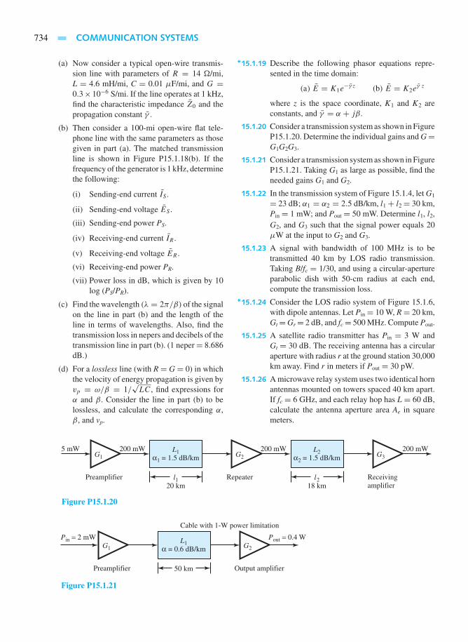
734 COMMUNICATION SYSTEMS
(a) Now consider a typical open-wire transmis-sion line with parameters of R = 14 /mi,L = 4.6 mH/mi, C = 0.01 µF/mi, and G =0.3×10⁻⁶ S/mi. If the line operates at 1 kHz,find the characteristic impedance Z0 and thepropagation constant γ .
(b) Then consider a 100-mi open-wire flat tele-phone line with the same parameters as thosegiven in part (a). The matched transmissionline is shown in Figure P15.1.18(b). If thefrequency of the generator is 1 kHz, determinethe following:
(i) Sending-end current IS .
(ii) Sending-end voltage ES .
(iii) Sending-end power PS.
(iv) Receiving-end current IR .
(v) Receiving-end voltage ER .
(vi) Receiving-end power PR.
(vii) Power loss in dB, which is given by 10log (PS/PR).
(c) Find the wavelength (λ = 2π/β) of the signalon the line in part (b) and the length of theline in terms of wavelengths. Also, find thetransmission loss in nepers and decibels of thetransmission line in part (b). (1 neper= 8.686dB.)
(d) For a lossless line (with R = G = 0) in whichthe velocity of energy propagation is given byvp = ω/β = 1/
√LC, find expressions for
α and β. Consider the line in part (b) to belossless, and calculate the corresponding α,β, and vp.
*15.1.19 Describe the following phasor equations repre-sented in the time domain:
(a) E = K1e−γ z (b) E = K2e
γ z
where z is the space coordinate, K1 and K2 areconstants, and γ = α + jβ.
15.1.20 Consider a transmission system as shown in FigureP15.1.20. Determine the individual gains and G=G1G2G3.
15.1.21 Consider a transmission system as shown in FigureP15.1.21. Taking G1 as large as possible, find theneeded gains G1 and G2.
15.1.22 In the transmission system of Figure 15.1.4, let G1
= 23 dB; α1 = α2 = 2.5 dB/km, l1+ l2= 30 km,Pin = 1 mW; and Pout = 50 mW. Determine l1, l2,G2, and G3 such that the signal power equals 20µW at the input to G2 and G3.
15.1.23 A signal with bandwidth of 100 MHz is to betransmitted 40 km by LOS radio transmission.Taking B/fc = 1/30, and using a circular-apertureparabolic dish with 50-cm radius at each end,compute the transmission loss.
*15.1.24 Consider the LOS radio system of Figure 15.1.6,with dipole antennas. Let Pin= 10 W, R= 20 km,Gt=Gr= 2 dB, and fc= 500 MHz. Compute Pout.
15.1.25 A satellite radio transmitter has Pin = 3 W andGt = 30 dB. The receiving antenna has a circularaperture with radius r at the ground station 30,000km away. Find r in meters if Pout = 30 pW.
15.1.26 A microwave relay system uses two identical hornantennas mounted on towers spaced 40 km apart.If fc = 6 GHz, and each relay hop has L = 60 dB,calculate the antenna aperture area Ae in squaremeters.
5 mW 200 mW200 mW
Preamplifier
G1L1
α1 = 1.5 dB/km
l120 km
200 mW
Repeater
G2
Receivingamplifier
G3L2
α2 = 1.5 dB/km
l218 km
Figure P15.1.20
Pin = 2 mW
Preamplifier
G1L1
α = 0.6 dB/km
50 km
Pout = 0.4 W
Cable with 1-W power limitation
Output amplifier
G2
Figure P15.1.21

PROBLEMS 735
15.1.27 An antenna has an aperture area of 10 m2, anaperture efficiency of 0.6, and negligible losses.If it is used at 5 GHz, find:
(a) Its power gain.
(b) The maximum power density that the antennacan generate at a distance of 20 km with aninput power of 2 kW.
15.1.28 The power gain of an antenna is 10,000. If its inputpower is 1 kW, calculate the maximum radiationintensity that it can generate.
*15.1.29 An antenna has beam widths of 3° and 10° inorthogonal planes and has a radiation efficiencyfactor of 0.6. Find the maximum radiation inten-sity if 1 kW is applied to the antenna.
15.1.30 The radiation pattern of a half-wave dipole an-tenna [see Figure 15.1.7(a)] is given by
P(θ, φ) = cos2 [(π/2) cos θ]
sin2θ
(a) Sketch the radiation pattern in the principalplane of xz containing angle θ .
(b) Determine the beam width between the −10-dB points of its radiation pattern as well as thehalf-power beamwidth.
15.1.31 The effective area of a dipole is given by Ae =0.13λ2. Find the effective area of a half-wavedipole at 3 GHz.
15.1.32 For a helical antenna [see Figure 15.1.7(c)], thehalf-power beamwidth and directive gain aregiven by
θB ∼= 52λ3/2
C√NS
where C = πD, N = L/S, and S = C tan α, inwhich α is called the pitch angle, and
GD∼= 12NC2S
λ3
The input impedance seen by the transmissionline at point P [Figure 15.1.7(c)] is almost purelyresistive, given by Za
∼= 140C/λ. Calculate the
antenna parameters of a 10-turn helix at f = 500MHz by assuming that C = λ and α = 14π/180.
15.1.33 For a pyramidal-horn antenna [Figure 15.1.7(e)],the maximum directive gain is given by
GD∼= 2.05πAB
λ2
occurring when the aperture dimensions are A ∼=√3λL andB ∼= 0.81A. The principal-plane beam-
widths for the optimum horn with maximum gainare given by θB ∼= 54λ/B in degrees in the yz-plane, and by φB
∼= 78λ/A in degrees in the xz-plane. For a pyramidal horn, with A = 6λ and B= 4.86λ, at 6 GHz, find GD, θB, and φB. Commenton whether this horn is optimum.
15.1.34 A conical horn [Figure 15.1.7(f)] has a side view asshown in Figure P15.1.34. The maximum value ofthe directive gain is given by GD
∼= 5.13(D/λ)2,whereD ∼= √3.33λL1 andL1 ∼= L/(1−d/D), inwhich d is the inside diameter of the waveguide.Beamwidths for the main beam directed along thez-axis are given by θB ∼= 60λ/D in degrees in theyz-plane, and byφB
∼= 70λ/D in degrees in the xz-plane. Let the circular waveguide, with a 2.5-cminside diameter, be expanded by adding a conicalflare to have an aperture with an inside diameterof 5.771λ at 8 GHz. For L1 = 10λ, find:
(a) The horn length L.
(b) The directive gain.
(c) The principal-plane beamwidths.
*15.1.35 A paraboloidal antenna [Figure 15.1.7(g)] has anaperture efficiency of 0.6 and a diameter D =100λ at 6 GHz. Illumination by the feed is suchthat the beamwidths of the principal-plane sec-ondary patterns are equal. Determine the antenna’spower gain and beamwidth. (Note that the ra-diation pattern of the feed is called the primarypattern, whereas that of the overall antenna is thesecondary pattern.)
15.1.36 Two stations, located on mountain tops 40 kmapart, communicate with each other using two
L1
L
ApertureApex
ThroatD
d
z
Figure P15.1.34

736 COMMUNICATION SYSTEMS
identical paraboloidal antennas with pencil beam-width of 1°, aperture efficiency of 0.8, and radi-ation efficiency of 0.85. The transmitting stationhas Pt= 60 W and Lt= 2 at 8 GHz. With Lr= 1.5and Lch = 2.5, find the diameter of the antennas andthe signal power available at the receiver input.
15.1.37 Two stations (using identical antennas, with di-ameters of 50λ and aperture efficiencies of 0.6 at35 GHz) are separated by 30 km. With negligibleantenna losses, antenna connection-path losses areLt = Lr = 1.33 at a physical temperature of 285K, while the antenna temperature is 85 K. The re-ceiver at either station has Ga(f 0)= 107, TR = 250K, and BN = 12 MHz. The rain attenuation andclear-air attenuation are given to be 3.9 dB/kmand 0.072 dB/km, respectively. Determine:
(a) The required output power to guarantee a sys-tem signal-to-noise power ratio of 45 dB whenheavy rain falls over a distance of 6 km.
(b) The available noise power occurring at thereceiver output.
(c) The output signal power occurring with andwithout rain, when the transmitted powerfound in part (a) is used.
15.1.38 If an antenna has an available noise power of1.6 × 10−15 W in a 1-MHz bandwidth, find theantenna temperature.
15.1.39 Determine the effective input noise temperatureof a long piece of waveguide (that connects anantenna to a receiver) with a loss of 3.4 dB at 12GHz and a physical temperature of 280 K.
*15.1.40 An antenna with an effective noise temperature of130 K couples through a waveguide that has a lossof 0.8 dB to a receiver. Find the effective noisetemperature presented by the waveguide output tothe receiver if the waveguide’s physical tempera-ture is 280 K.
15.1.41 If the antenna and waveguide of Problem 15.1.40feed a receiver for which BN= 10 MHz, Ga(f 0)=
1012, and TR = 300 K, determine the system noisetemperature and Nao at the receiver output.
15.1.42 (a) An amplifier with F0 = 3 or 4.77 dB, f 0 =4 GHz, and BN = 14 MHz is used with anantenna for which Ta= 200 K. The connectingpath loss is 1.45, or 1.61 dB at a physical tem-perature of 250 K. Find the available systemnoise power.
(b) If the antennas of Example 15.1.5 are usedwith the receiver of part (a), compute thesignal-to-noise ratio.
*15.2.1 Find the number of possible station frequencies inthe AM broadcast system in the United States.
15.2.2 Let a(t) = [1+mAx(t)] and x(t) = cos 2πfmt,fm << fc, and xc(t) = A(t) cos 2πfct .
(a) With mA= 1, sketch one full period of the AMwave and draw the envelope by connecting thepositive peaks of xc(t).
(b) Repeat part (a) with mA = 2, and notice thatthe carrier is overmodulated and the envelopedoes not have the same shape as x(t).
15.2.3 Figure P15.2.3 illustrates a way to generate anAM wave of the form of Equation (15.2.2), usinga nonlinear device and an appropriate bandpassfilter. Comment on the nature of the BPF to beused.
15.2.4 If the nonlinear device in Problem 15.2.3 pro-duces z = ay2, determine how the system mustbe augmented to obtain an AM wave in the formof Equation (15.2.2).
15.2.5 If the message has a spectrum
F(ω) =K cos πω
2Wf, −Wf ≤ ω ≤ Wf
0, elsewhere
where K and Wf are positive constants, sketch thespectrum of a standard AM signal that uses themessage. Comment on the physical significanceof K and Wf in the modulation process.
Ac cos 2π fc t
Nonlineardevice BPF
x (t) = Am cos 2π fmt z = y + ay2 xout(t)y+
Figure P15.2.3

PROBLEMS 737
*15.2.6 In a standard AM system, represented by Equation
(15.2.3), Ac = 200 V,∣∣∣f 2(t)
∣∣∣1/2 = 50 V, and
Z0 = R0 = 50 . Calculate ηAM, Pc, Pf, andPAM.
15.2.7 If a standard AM waveform [Equation (15.2.3)]of 1-kW average power is transmitted by an an-tenna with an input resistance of 75 , evaluatef 2(t), carrier power, and sideband power, giventhe efficiency to be 0.1.
15.2.8 In the envelope detector [Figure 15.2.8(a)] of astandard AM receiver, the product RC is chosento satisfy π/ωIF << RC < 1/ωm,max, whereωm,max/2π = 5 kHz in standard AM and ωIF =455 kHz. If R = 5000 , find the value of itscapacitor (by applying a factor of 10 to represent<<).
15.2.9 In an AM transmitter that transmits a total powerof 1 kW, the unmodulated carrier power is 850W. Compute the required value of (Si/Ni)AM at areceiver, if (S0/N0)AM = 2ηAM(Si/Ni)AM mustbe 103 for good performance.
15.2.10 At the transmitter in a standard AM system, Pf =50 W. In the receiver (S0/N0)AM = 250 when(Si/Ni)AM = 3000. Find the transmitter’s un-modulated carrier power and the total transmittedpower if (S0/N0)AM = 2ηAM(Si/Ni)AM.
*15.2.11 Determine the image frequency if an AM radioreceiver is tuned to a station at 1030 kHz and hasa high-side local oscillator.
15.2.12 Although the low side is not as good a choice asthe high-side local oscillator frequency, let an AMbroadcast receiver be designed with a low-sidelocal oscillator. As fc is varied from 540 to 1600kHz, find the values f LO and f image.
15.2.13 For a DSB system for which f (t) = Am cos ωmt,
ωc = 5ωm, and φc = 0, sketch the transmittedsignal.
15.2.14 One of the many types of product device to pro-duce suppressed-carrier AM is shown in FigureP15.2.14. Explain briefly how the device operates.
15.2.15 If the output signal from an AM modulator is givenby u(t) = 5 cos 1800 πt + 20 cos 2000 πt +5 cos 2200 πt , determine:
(a) The modulating signal m(t) and carrier c(t).
(b) The modulation index.
(c) The ratio of the power in sidebands to thepower in the carrier.
15.2.16 The signal m(t), whose frequency spectrum M(f )is shown in Figure P15.2.16, is to be transmittedfrom one station to another. Let the signal be nor-malized, i.e.,−1 ≤ m(t) ≤ 1. Find the bandwidthof the modulated signal:
(a) If USSB (upper single sideband) is employed.
(b) If DSB (double sideband) is employed.
(c) If an AM modulation scheme with a modula-tion index of 0.8 is used.
(d) If an FM signal with the frequency deviationconstant kf = 60 kHz is used.
*15.2.17 An FM signal, for which f (t)= 2 cos ωmt, is givenby
sFM(t) = 50 cos
185π(106)t + π
3
+ 6 sin[π(104)t
] Determine: Ac,ωc,φc,ωm, kFM, and the modulationindex βFM = ω/ωm.
15.2.18 A commercial FM station broadcasts a signal with180-kHz bandwidth when |f (t)|max = 2 V. FindkFM for the modulator if the spectral extent of f (t)is 30 kHz, by using Carson’s rule.
T1 T2
Q1
Q3
Q4
Q2
b
d
a
c
f (t) Outputcos ωct
+
Figure P15.2.14

738 COMMUNICATION SYSTEMS
M(f )
−10,000 10,000f
Figure P15.2.16
15.2.19 An FM station’s modulator has a sensitivity kFM =5π × 104 rad/s·V. A receiver uses a discriminatorthat has a gain constant of 10−5/π V·s/rad. Ne-glecting noise, determine the signal at the receiveroutput.
15.2.20 A voice message withWf = 2π(3×10³) rad/s andWrms = 2π(1 × 10³) rad/s is transmitted over anFM broadcast system with standard emphasis. SeeExample 15.2.2, and compare the improvementsdue to emphasis.
15.2.21 Show that the image frequency for an FM stationdoes not fall in the range of 88.1–107.9 MHz,regardless of the choice of high- or low-side localoscillator.
*15.2.22 Consider the signals given by Equations (15.2.12)through (15.2.14). Let them be normalized suchthat the red, green, and blue signals have a maxi-mum amplitude of unity. If mI(t) and mQ(t) are thereal and imaginary components of a color vector,defined by a magnitude [m2
I (t) + m2Q(t)]
1/2 andphase tan−1 [−mQ(t)/ml(t)], sketch points cor-responding to fully saturated R, G, and B colors.
15.2.23 If a television station operates on UHF channel20 (band 506–512 MHz), determine the station’svisual-carrier frequency.
15.2.24 For DSB and conventional AM, obtain expres-sions for the in-phase and quadrature componentsxd(t) and xq(t), and envelope and phase v(t) andφ(t).
15.2.25 The normalized signal xn(t) has a bandwidth of10 kHz and its power content is 0.5 W, while thecarrier Ac cos 2π fct has a power content of 200 W.Find the bandwidth and the power content of themodulated signal, if the modulation scheme is:
(a) Conventional AM with a modulation index
of 0.6 and a transmitted signal of Ac[1+mAx(t)] cos 2πfct .
(b) DSB SC with a transmitted signal of Acx(t)
cos 2πfct .(c) SSB with a transmitted signal of Acx(t)
cos 2πfct ∓Acx(t) sin 2πfct , where x(t) isa signal with a 90° phase shift in all frequencycomponents of x(t), and the upper − signcorresponds to the USSB signal, whereas thelower+ sign corresponds to the LSSB signal.
(d) FM with kf = 50 kHz.
15.2.26 Let the modulating signal m(t) be a sinusoid of theform m(t) = cos 2πfmt, fm << fc, and let thecarrier signal be cos(2πfct + φc).
(a) Determine the conventional AM signal, itsupper and lower sidebands, and its spectrumif the modulation index is α.
(b) Determine the DSB SC AM signal, its up-per and lower sidebands, and its spectrum form(t) = α cos 2πfmt, fm << fc.
(c) Determine the two possible SSB AM signalsand their spectra.
*15.2.27 Let the message signal m(t) = α cos (2πfmt)be used to either frequency-modulate or phase-modulate the carrierAc cos(2πfct). Find the mod-ulated signal in each case.
15.2.28 If an FM signal is given by sFM(t) = 100cos [2πfct+100
∫ t
−∞ m(τ) dτ ] and m(t) is givenin Figure P15.2.28, sketch the instantaneous fre-quency as a function of time and determine thepeak frequency deviation.
15.2.29 If m(t) of Figure P15.2.29 is fed into an FM modu-lator with peak frequency deviation kf= 25 Hz/V,plot the frequency deviation in hertz and the phasedeviation in radians.

PROBLEMS 739
m(t)
−1
−5
5
0 1 2 . . .
. . .t
Figure P15.2.28
m(t)
−1
−2
2
1
1 3 4 52 6t
Figure P15.2.29
15.2.30 An angle-modulated signal has the form u(t) =100 cos[2πfct+4 sin 2πfmt], where fc=10 MHzand fm = 1 kHz. Determine the modulation indexβf or βp and the transmitted signal bandwidth,with BFM = 2(βf +1)fm or BPM = 2(βp+1)fm,
(a) If this is an FM signal.
(b) If this is a PM signal.
15.2.31 Let m1(t) and m2(t) be two message signals, andlet u1(t) and u2(t) be the corresponding modulatedversions.
(a) When the combined message signal m1(t) +m2(t) DSB modulates a carrier Ac cos 2πfct ,show that the result is the sum of the two DSBAM signals u1(t) + u2(t). That is to say, AMsatisfies the superposition principle.
(b) If m1(t)+m2(t) frequency modulates a carrier,show that the modulated signal is not equal tou1(t) + u2(t). That is to say, FM does not sat-isfy the principle of superposition, and anglemodulation is not a linear modulation method.
15.2.32 Figure P15.2.32 shows an FM discriminator. As-sume the envelope detector to be ideal, with aninfinite input impedance. Choose the values for Land C if the discriminator is to be employed todemodulate an FM signal with a carrier frequencyfc = 80 MHz and a peak frequency deviation of 6MHz.
*15.2.33 Let a message signal m(t) have a bandwidth of 10kHz and a peak magnitude of 1 V. Estimate the
bandwidth, by using Carson’s rule, of the signalu(t) obtained when m(t) modulates a carrier witha peak frequency deviation of:
(a) fd = 10 Hz/V.
(b) 100 Hz/V.
(c) 1000 Hz/V.
15.2.34 The operating frequency range of a superhetero-dyne FM receiver is 88–108 MHz. The IF and LOfrequencies are so chosen that fIF < fLO. If theimage frequency f ′c must fall outside of the 88–108-MHz range, determine the minimum neededf IF and the corresponding range of f LO.
15.2.35 The television audio signal of Figure 15.2.29 isfrequency modulated with f = 25 kHz and hasWf
∼= 10 kHz. By using WFM ∼= 2(ω + 2Wf )
for ω >> Wf (for wide-band FM), find thepercentage of the channel bandwidth occupied bythe audio signal.
15.2.36 Suppose that a video signal, having W = 5 MHz,is transmitted via FM with f = 20 MHz. For1/100 ≤ B/fc ≤ 1/10, determine the bounds onthe carrier frequency. Use WFM ∼= 2(ω + 2Wf )
for ω >> Wf (for wide-band FM).
15.2.37 A TDM signal, like that of Figure 14.2.9(b), isformed by sampling 5 voice signals at fs= 8 kHz.The signal is then transmitted via FM on a radiochannel with 400-kHz bandwidth. Estimate themaximum allowable frequency deviation f [use

740 COMMUNICATION SYSTEMS
u(t)
L C
m(t)10 kΩEnvelopedetector
Figure P15.2.32
Equation (15.2.13) for wide-band FM if f ≥2W ).
*15.2.38 A radar system uses pulses of duration D to modu-late the amplitude of a radio carrier wave. The sys-tem can distinguish between targets spaced apartby a distance of d ≥ cD, where c is the velocityof light. In view of 1/100 ≤ B/fc ≤ 1/10, findthe minimum practical value of fc so that dmin =30 m.
15.2.39 A TDM signal of the type shown in Figure14.2.9(b) is formed by sampling M voice signals atfs = 8 kHz. If the TDM signal then modulates theamplitude of a 4-MHz carrier for radio transmis-sion, determine the upper limit on M that satisfies1/100 ≤ B/fc ≤ 1/10.
*15.3.1 Find the minimum rate of sampling that must beused to convert the message into digital form:
(a) If an audio message has a spectral extent of 3kHz.
(b) If a television signal has a spectral extent of4.5 MHz.
15.3.2 If an analog message that has a spectral extent of15 kHz is sampled at three times the Nyquist rate,determine the sampling rate.
15.3.3 The quantum levels of a quantizer are separatedby the step size δv = 0.2 V, with the lowest andhighest levels of−3.3 V and+3.3 V, respectively.A sequence of message samples is given by−2.15V, −0.53 V, 0.95 V, 0.17 V, and −0.76 V.
(a) List the quantum levels.
(b) Is the quantizer midriser or midtread?
(c) Find the corresponding sequence of the quan-tized samples.
(d) Determine the maximum amplitude that amessage can have if the quantizer is not tobe saturated.
15.3.4 When the quantum step size δv and the step size off (t) are the same as in Figure 15.3.2, the quantizeris said to have a gain of unity. If, on the other hand,
the quantizer has a gain of Kq > 1, what does thatimply?
15.3.5 A symmetrically fluctuating message that has acrest factor KCR = 3 and f 2(t) = 2.25 V2 isto be quantized such that the signal-to-noise ratioS0/Nq = 2700. If the quantizer is to use thesmallest number of levels that is a power of 2,find the following:
(a) The step size v.
(b) The binary number of levels Lb.
(c) The extreme quantum level voltages.
*15.3.6 A quantizer has 130 quantum levels that exactlyspan the extremes of a symmetrically fluctuatingmessage with step size δv = 0.04 V. Determinethe following:
(a) |f (t)|max.
(b) The largest crest factor the message can haveif S0/Nq must be at least 5500.
15.3.7 If a compressor in a system can change a mes-sage crest factor from 3.2 to 2, while maintainingits peak amplitude constant, find the decibels ofimprovement in signal-to-noise ratio that can beexpected in the system.
15.3.8 Determine the number of bits of a natural binaryencoder that works with the quantizer:
(a) If the extreme levels are ±3.1 V, with a stepsize of 0.2 V.
(b) If there are 128 quantum levels with δv =0.04 V.
15.3.9 A differential encoding scheme converts the orig-inal sequence of digits, denoted by bk, to a newsequence of digits, denoted by ak, by using thedifferential encoder shown in Figure P15.3.9. Theoutput digit in the kth interval is given by ak =ak−1⊕ bk , where⊕ represents modulo-2 addition(i.e., 0 ⊕ 0 = 0; 0 ⊕ 1 = 1; 1 ⊕ 0 = 1; and1⊕1 = 0). The new sequence is used in waveformformatting. For the input sequence bk given be-low, find the sequences ak and ak−1 by letting
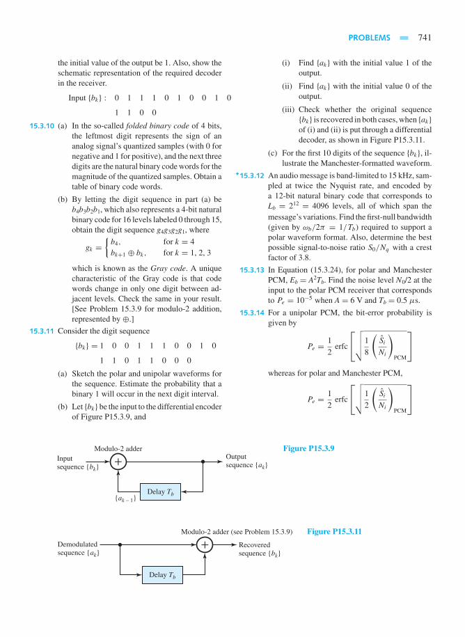
PROBLEMS 741
the initial value of the output be 1. Also, show theschematic representation of the required decoderin the receiver.
Input bk : 0 1 1 1 0 1 0 0 1 0
1 1 0 0
15.3.10 (a) In the so-called folded binary code of 4 bits,the leftmost digit represents the sign of ananalog signal’s quantized samples (with 0 fornegative and 1 for positive), and the next threedigits are the natural binary code words for themagnitude of the quantized samples. Obtain atable of binary code words.
(b) By letting the digit sequence in part (a) beb4b3b2b1, which also represents a 4-bit naturalbinary code for 16 levels labeled 0 through 15,obtain the digit sequence g4g3g2g1, where
gk =b4, for k = 4bk+1 ⊕ bk, for k = 1, 2, 3
which is known as the Gray code. A uniquecharacteristic of the Gray code is that codewords change in only one digit between ad-jacent levels. Check the same in your result.[See Problem 15.3.9 for modulo-2 addition,represented by ⊕.]
15.3.11 Consider the digit sequence
bk = 1 0 0 1 1 1 0 0 1 0
1 1 0 1 1 0 0 0
(a) Sketch the polar and unipolar waveforms forthe sequence. Estimate the probability that abinary 1 will occur in the next digit interval.
(b) Let bk be the input to the differential encoderof Figure P15.3.9, and
(i) Find ak with the initial value 1 of theoutput.
(ii) Find ak with the initial value 0 of theoutput.
(iii) Check whether the original sequencebk is recovered in both cases, when akof (i) and (ii) is put through a differentialdecoder, as shown in Figure P15.3.11.
(c) For the first 10 digits of the sequence bk, il-lustrate the Manchester-formatted waveform.
*15.3.12 An audio message is band-limited to 15 kHz, sam-pled at twice the Nyquist rate, and encoded bya 12-bit natural binary code that corresponds toLb = 212 = 4096 levels, all of which span themessage’s variations. Find the first-null bandwidth(given by ωb/2π = 1/Tb) required to support apolar waveform format. Also, determine the bestpossible signal-to-noise ratio S0/Nq with a crestfactor of 3.8.
15.3.13 In Equation (15.3.24), for polar and ManchesterPCM, Eb = A2Tb. Find the noise level N0/2 at theinput to the polar PCM receiver that correspondsto Pe = 10−5 when A = 6 V and Tb = 0.5 µs.
15.3.14 For a unipolar PCM, the bit-error probability isgiven by
Pe = 1
2erfc
√√√√1
8
(Si
Ni
)PCM
whereas for polar and Manchester PCM,
Pe = 1
2erfc
√√√√1
2
(Si
Ni
)PCM
+Inputsequence bk
ak − 1Delay Tb
Modulo-2 adderOutputsequence ak
Figure P15.3.9
+Demodulatedsequence ak
Delay Tb
Modulo-2 adder (see Problem 15.3.9)
Recoveredsequence bk
Figure P15.3.11

742 COMMUNICATION SYSTEMS
where Si/Ni is the ratio of the power in the signalpeak amplitude (at the integrator output at thesample time) to the average noise power at thesame point. For (Si/Ni)PCM = 32 at the sampler,find Pe for a unipolar and a polar system. In whichsystem will the bit errors occur more frequently?
15.3.15 For a Manchester PCM system, expressions for Eb
and Pe are given in Problems 15.3.13 and 15.3.14.Determine:
(a) The minimum value of (Si/Ni)PCM that isneeded to realize Pe = 10−4.
(b) The minimum input-pulse amplitude A re-quired if Pe = 10−4, N0 = 8 × 10⁻⁷ V2/Hz,and Tb = 0.4 µs.
15.3.16 For polar or Manchester PCM, Equation (15.3.13)is sometimes expressed as(
S0
N0
)PCM
= S0/Nq
1+ 22Nb+1 erfc
√√√√1
2
(Si
Ni
)PCM
where Si/Ni is the ratio of the power in the signalpeak amplitude (at the integrator output at the
sample time) to the average noise power at thesame point, and Nb is the number of bits in anatural binary code. In a polar PCM system, withNb = 8 and (Si/Ni)PCM = 20, find (S0/N0)PCM
for the message if its crest factor is 3. Assume thatall levels span the variations of the analog mes-sage. Comment on whether the system is operatingabove threshold.
*15.3.17 The expression given in Problem 15.3.16 for(S0/N0)PCM is plotted for a sinusoidal message inFigure P15.3.17 to show the performance curvesfor a PCM system using a polar waveform.
(a) Comment on the threshold effect.
(b) For the polar system of Problem 15.3.14, withNb = 8 and (Si/Ni)PCM = 32, determinewhether the system noise has significant effecton performance.
15.3.18 Four voice messages, each with 3-kHz bandwidth,are to be sampled at Nyquist rate, and time-multiplexed with samples taken at twice theNyquist rate from six analog monitoring signals,each with 0.5-kHz bandwidth. Determine the du-ration of the frame and suggest a sampling schemeindicating the timing of samples.
70
6 14
SiPCM, dBNi
S 0PC
M, d
BN
0
18 2610 22
Nb = 10
9
8
7
6
5
4
3
2
60
50
40
30
20
()
( )
10
0
^
Figure P15.3.17

PROBLEMS 743
15.3.19 By a simple time multiplexing of natural samplesover a single line, a large radar site transmits 85analog signals, each with 200-Hz bandwidth. Ifthe sampling is done at twice the Nyquist rate, onetime slot is used for synchronization, and the guardtime τg = 2τ , find the duration τ of the pulse.
15.3.20 Sketch an ASK signal for the binary sequence 1 01 1 0 0 1 0 0 1 if ωc = 3ωb = 6π/Tb.
15.3.21 In Equation (15.3.24), for coherent ASK, Eb =A2Tb/4, with A = 2.2 V, Tb = 2.6 µs, andN0 = 2×10⁻⁷ V2/Hz, find Pe for a coherent ASKsystem. Also, find Eb for a 1- impedance.
*15.3.22 In Figure 15.3.14, when the pulse of a carrier ofamplitude A during 0 < t ≤ Tb arrives at pointR, show that D ∼= A2Tb/4 at time Tb if noise isneglected and ωcTb >> 1.
15.3.23 If Eb/N0 = 20 in a coherent ASK system, find thevalue of Eb/N0 that is needed in a noncoherentASK system to yield the same value of Pe as thecoherent system.
15.3.24 To have the same value of Pe, show that Eb/N0 ina coherent-ASK system has to be twice that in acoherent PSK system.
15.3.25 In a DPSK system, when the received pulses are2 V in amplitude, Pe = 3 × 10⁻⁴. If the pulse
amplitude increases such that Pe = 2×10⁻⁶, findthe new amplitude.
15.3.26 Consider Figure 15.3.19, in which the receiverbecomes two coherent ASK receivers in parallel.Justify why the difference, rather than the sum,occurs.
15.3.27 Consider Figure 15.3.19, in which the input FSKpulse at point R is given by sR(t) = A cos(ω2t +φ2), 0 < t < Tb, and zero elsewhere in t, whenthe bit interval corresponds to a 1.
(a) Compute the outputs from the two integrators.
(b) If sR(t) changes in frequency and phase to ω1
andφ1, respectively, show that the two outputsof part (a) are reversed. (Assume ωcTb >> 1,and make suitable approximations.)
*15.3.28 Apply Equation (15.3.24) for various digital com-munication systems with Eb/N0 = 12, and usingPSK as the reference, compare their performances.
15.3.29 A communication system for a voice-band (3 kHz)channel is designed for a received SNR Eb/N0 atthe detector of 30 dB when the transmitter power isPs = −3 dBW. Find the value of Ps if it is desiredto increase the bandwidth of the system to 10 kHz,while maintaining the same SNR at the detector.

This page intentionally left blank

PART
CONTROL SYSTEMSFIVE

This page intentionally left blank

16 Basic Control Systems
16.1 Power Semiconductor-Controlled Drives
16.2 Feedback Control Systems
16.3 Digital Control Systems
16.4 Learning Objectives
16.5 Practical Application: A Case Study—Digital Process Control
Problems
Electric energy is widely used in practice, because of the ease with which the system and deviceperformance can be reliably controlled. One of the major areas of electrical engineering of interestto all engineers is control and instrumentation. Instrumentation is integrated throughout the book insections on electric circuits, electronic analog and digital systems, energy systems, and informationsystems. This final chapter serves to introduce a variety of methods by which the performanceof physical systems is controlled. By focusing on control aspects, the integration of many of theconcepts used in the preceding chapters is effected.
Systems is a term used in many fields of study: economics, ecology, social and physicalsciences. The catchword is used to describe an assemblage of components, subsystems, andinterfaces arranged or existing in such a fashion as to perform a function or functions in order toachieve a goal. Control refers to the function or purpose of the system we wish to discuss. Controlis almost always realized not by a single component, such as a transistor, resistor, or motor, butby an entire system of components and interfaces.
Control systems influence our everyday lives just as much as some of the other areas ofelectrical engineering. Examples abound in practice: household appliances, manufacturing andprocessing plants, and navigational and guidance systems, in which concepts of the analysisand design of control systems are utilized. A control system, in general, can be viewed as aninterconnection of components—electrical, mechanical, hydraulic, thermal, etc.—so as to obtaina desired function in an efficient and accurate manner. The control engineer is concerned withthe control of industrial processes and systems. The concepts of control engineering are notlimited to any particular branch of engineering. Hence, a basic understanding of control theory
747

748 BASIC CONTROL SYSTEMS
is essential to every engineer involved in the understanding of the dynamic behavior of varioussystems.
This chapter introduces different types of control systems, and some elementary methods forstudying their behavior. Three classes of control systems are presented:
1. Power semiconductor-controlled drives, in which the electrical input to a motor is adjustedto control performance.
2. Feedback control systems, in which a measure of the actual performance has to be knownin order to effect control.
3. Digital control systems, in which a digital processor becomes an essential element of thesystem, and the resulting processed output forms the basis for system control.
Many of the concepts and techniques used may be similar to those already developed earlierin the book. Indeed, any discussion of control methodology integrates much of the materialon circuits, electronic devices, and electromechanical energy-conversion devices. Such controltechniques are also employed in business, ecological, and social systems, as well as in problemareas related to inventory control, economic models, health-care delivery systems, and urbanplanning.
16.1 POWER SEMICONDUCTOR-CONTROLLED DRIVES
Power electronics deals with the applications of solid-state electronics for the control andconversion of electric power. Conversion techniques require switching power semiconductordevices on and off. The development of solid-state motor drive packages has progressed to thepoint at which they can be used to solve practically any power-control problem. This sectiondescribes fundamentals common to all electric drives: dc drives fed by controlled rectifiers andchoppers; squirrel-cage induction motor drives controlled by ac voltage controllers, inverters,and cycloconverters; slip-power-controlled wound-rotor induction motor drives; and inverter-controlled and cycloconverter-controlled synchronous motor drives, including brushless dc andac motor drives. Even though the detailed study of such power electronic circuits and componentswould require a book in itself, some familiarity becomes important to an understanding of modernmotor applications. This section is only a very modest introduction.
The essential components of an electric drive controlled by a power semiconductor converterare shown in the block diagram of Figure 16.1.1. The converter regulates the flow of power fromthe source to the motor in such a way that the motor speed–torque and speed–current characteristicsbecome compatible with the load requirements. The low-voltage control unit, which may consistof integrated transistorized circuits or a microprocessor, is electrically isolated from the converter-motor circuit and controls the converter. The sensing unit, required for closed-loop operation orprotection, or both, is used to sense the power circuit’s electrical parameters, such as convertercurrent, voltage, and motor speed. The command signal forms an input to the control unit, adjustingthe operating point of the drive. The complete electric drive system shown in Figure 16.1.1 mustbe treated as an integrated system.
A motor operates in two modes—motoring and braking. Supporting its motion, it convertselectric energy to mechanical energy while motoring. In braking, while opposing the motion, itworks as a generator converting mechanical energy to electric energy, which is consumed in somepart of the circuit. The motor can provide motoring and braking operations in both forward andreverse directions. Figure 16.1.2 illustrates the four-quadrant operation of drives. The continuousas well as the transient torque and power limitations of a drive in the four quadrants of operation

16.1 POWER SEMICONDUCTOR-CONTROLLED DRIVES 749
SourcePowersemiconductorconverter
Motor
Sensingunit
Controlunit
Commandsignal
LoadFigure 16.1.1 Essential components of anelectric drive.
0
Forwardbraking
Forwardmotoring
Reversebraking
Reversemotoring
III
Speed ωm
Torque T
IV
II I
Figure 16.1.2 Four-quadrant opera-tion of drives.
are shown in Figure 16.1.3 for speeds below and above base speed ωmb, which is the highest drivespeed at the rated flux.
Motors commonly used in variable-speed drives are induction motors, dc motors, andsynchronous motors. For the control of the motors, various types of converters are needed,as exemplified in Table 16.1.1. A variable-speed drive can use a single converter or morethan one. All converters have harmonics in their inputs and outputs. Some converters sufferfrom a poor power factor, particularly at low output voltages. The main advantages of con-verters are high efficiency, fast response, flexibility of control, easy maintenance, reliability,low weight and volume, less noise, and long life. The power semiconductor converters havevirtually replaced the conventional power controllers such as mercury-arc rectifiers and magneticamplifiers. Most of the drive specifications are governed by the load requirements, which inturn depend on normal running needs, transient operational needs, and needs related to locationand environment. Other specifications are governed by the available source and its capacity,as well as other aspects like harmonics, power factor, reactive power, regenerated power, andpeak current.

750 BASIC CONTROL SYSTEMS
0
Maximumcontinoustorque
Maximumtransienttorque
Maximumcontinuouspower
Maximumtransientpower
III
Speed ωm
Maximum speed
−ωmb
ωmb
Torque T
IV
II I
Figure 16.1.3 Continuous as well as transient torque and power limitations of a drive.
Power Semiconductor Devices
Since the advent of the first thyristor or silicon-controlled rectifier (SCR) in 1957, tremendousadvances have been made in power semiconductor devices during the past four decades. Thedevices can be divided broadly into four types:
• Power diodes
• Thyristors
• Power bipolar junction transistors (BJTs)
• Power MOSFETs (metal-oxide semiconductor field-effect transistors).
Thyristors can be subdivided into seven categories:
• Forced-commutated thyristor
• Line-commutated thyristor
• Gate turn-off thyristor (GTO)
• Reverse-conducting thyristor (RCT)
• Static-induction thyristor (SITH)
• Gate-assisted turn-off thyristor (GATT)
• Light-activated silicon-controlled rectifier (LASCR).
Typical ratings of these devices are given in Table 16.1.2. Whereas this comprehensive table,as of 1983, is given here for illustration purposes only, several new developments have takenplace since then: A single thyristor is currently available with the capability of blocking 6.5kV and controlling 1 kA. The 200-V Schottky barrier diodes are commercially available withratings of several hundred amperes, up to 1 kA, and with blocking voltages as high as 1–5 kV.

16.1 POWER SEMICONDUCTOR-CONTROLLED DRIVES 751
TABLE 16.1.1 Converters and Their Functions for the Control of Motors
Converter Conversion Function Applications
Controlled rectifiers Ac to variable dc Control of dc motors andsynchronous motors
Choppers Fixed voltage dc to variable voltagedc
Control of dc motors
Ac voltage controllers Fixed voltage ac to variable-voltageac at same frequency
Control of induction motors
Inverters (voltage source orcurrent source)
Dc to fixed or variable voltage andfrequency ac, voltage or currentsource
Control of induction motors andsynchronous motors
Cycloconverters Fixed voltage and frequency ac tovariable voltage and frequency ac
Induction motors and synchronousmotors
MOS-controlled thyristors (MCT) are rated for 3 kV, capable of interrupting around 300 A witha recovery time of 5 µs. Gate turn-off (GTO) thyristors can control 1 to 3 kA with a blockingvoltage capability of 6 to 8 kV. Table 16.1.3 gives the symbols and the v-i characteristics of thecommonly used power semiconductor devices.
Figure 16.1.4 illustrates the output voltages and control characteristics of some commonlyused power switching devices. The switching devices can be classified as follows:
TABLE 16.1.2 Typical Ratings of Power Semiconductor Devices
Voltage/Current Switching OnType Rating Time (µs) Voltage/Current*
Diodes General purposeHigh speedSchottky
3 kV/3.5 kA3 kV/1 kA40 V/60 A
2–50.23
1.6 V/10 kA3 V/3 kA
0.58 V/60 A
Forced-turned-offthyristors
Reverse blockingHigh speedReverse blockingReverse conductingGATTLight triggered
3 kV/1 kA1.2 kV/1.5 kA2.5 kV/400 A
2.5 kV/1 kA/R400 A1.2 kV/400 A6 kV/1.5 kA
4002040408
200–400
2.5 V/10 kA2.1 V/4.5 kA2.7 V/1.25 kA
2.1 V/1 kA2.8 V/1.25 kA2.4 V/4.5 kA
TRIACs 1.2 kV/300 A 1.5 V/420 A
Self-turned-offthyristors
GTOSITH
3.6 kV/600 A4 kV/2.2 kA
256.5
2.5 V/1 kA2.3 V/400 A
Power transistors Single
Darlington
400 V/250 A400 V/40 A630 V/50 A900 V/200 A
96
1.740
1 V/250 A1.5 V/49 A0.3 V/20 A
2 V
SITsPower MOSFETs
1.2 kV/10 A500 V/8.6 A1 kV/4.7 A500 V/10 A
0.550.70.90.6
1.2
0.6
2
0.4
Source: F. Harashima, “State of the Art on Power Electronics and Electrical Drives in Japan,” in Proc. 3rd IFAC Symposium on Control inPower Electronics and Electrical Drives (Lausanne, Switzerland, 1983), Tutorial Session and Survey Papers, pp. 23–33.* Note: On voltage is the on-state voltage drop of the device at a specified current.

752 BASIC CONTROL SYSTEMS
TABLE 16.1.3 Symbols and v–i Characteristics of Some Power Semiconductor Devices
DiodeA K
A K
VD
VG
ID
Device Symbol Characteristics
IDG+
−Thyristor
A K
IAG
GTO
A
BID
G
Gate triggered
TRIAC
G
C
E
A K
ID
LASCR
0
B
IBIC
IB
IE
IE
IC
NPN BJT
ID
PNP BJT
n-channelMOSFET
p-channelMOSFET
C
E
B
D
S
G
ID
VDS
VGS1VGS1 < VGSnVGSn
D
S
G
0 VDS
VGS1
ID
ID
ID
ID
ID
ID
ID
IC
IC
VGS1 > VGSnVGSn
0 VEC
IBnIBn > IB1IB1
IBnIBn > IB1IB1
0
0
0
0
0
0
VCE
VD
VD
VD
VD
Gate triggered
Gate triggered
Gate triggered
Gate triggered
VD
• Uncontrolled turn-on and turn-off (diode)
• Controlled turn-on and uncontrolled turn off (SCR)
• Controlled turn-on and turn-off (BJT, GTO, MOSFET)
• Continuous gate signal requirement (BJT, MOSFET)
• Pulse gate requirement (GTO, SCR)
• Bipolar voltage capability (SCR)
• Unipolar voltage capability (BJT, GTO, MOSFET)
• Bidirectional current capability (RCT, TRIAC)
• Unidirectional current capability (BJT, diode, GTO, MOSFET, SCR).

16.1 POWER SEMICONDUCTOR-CONTROLLED DRIVES 753
+VG
VsVs
t
t
vo
vG
voR
Thyristor
(a)
−1
1
−
+
+
−
−
+
VG
VsVs
t
t
vo
t1 T
t1 T
vG
voR
GTO
(b)
−1
1
0
−
+
+
−
−
t1 T
+
vB
VsVs
t
t
vo
vB
voR
(c)
1
0
−
+
+
−
−
t1 T
t1 T
Vs
t
t
vo
vGS
(d)
1
0
+
Vs
vo
vGS
R
D
S
G
−
+
+
−
−
Figure 16.1.4 Output voltages and control characteristics of some commonlyused power switching devices. (a) Thyristor switch. (b) GTO switch. (c) Transistorswitch. (d) MOSFET switch.
Power Electronic Circuits
These circuits can be classified as follows:
• Diode rectifiers
• Ac–dc converters (controlled rectifiers)

754 BASIC CONTROL SYSTEMS
• Ac–ac converters (ac voltage controllers)
• Dc–dc converters (dc choppers)
• Dc–ac converters (inverters)
• Static switches (contactors), supplied by either ac or dc.
Figure 16.1.5 shows a single-phase rectifier circuit converting ac voltage into a fixed dcvoltage. It can be extended to three-phase supply. Figure 16.1.6 shows a single-phase ac–dcconverter with two natural line-commutated thyristors. The average value of the output voltageis controlled by varying the conduction time of the thyristors. Three-phase input can also beconverted.
+
Diode D1
Diode D2
Acsupply
RVm
Vm
−Vm
π
π 2π
2π
vs
vs = Vm sin ωtLoad resistance
ωt
ωt
vo
vs
vo
(a) (b)
0
0
−+ +
−−
vs = Vm sin ωt
Figure 16.1.5 Single-phase rectifier circuit with diodes. (a) Circuit diagram. (b) Voltage waveforms.
+
Thyristor T1
Thyristor T2
Acsupply
RVm
Vm
−Vm
πα
π 2π
2π
vs
vs = Vm sin ωtLoad resistance
ωt
ωt
vo
vs
vo
(a) (b)
0
0
−+ +
−−
α
vs = Vm sin ωt
Figure 16.1.6 Single-phase ac–dc converter with two natural line-commutated thyristors. (a) Circuitdiagram. (b) Voltage waveforms.

16.1 POWER SEMICONDUCTOR-CONTROLLED DRIVES 755
+
TRIAC
Acsupply
Resistiveload R
VmG
Vm
−Vm
π
π2π
2π
vs = Vm sin ωtωt
ωt
vo
vo
vs
(a) (b)
0
0
−
+
− −Vm
α
vs = Vm sin ωt
α
Figure 16.1.7 Single-phase ac–ac converter with TRIAC. (a) Circuit diagram. (b) Voltage waveforms.
Figure 16.1.7 shows a single-phase ac–ac converter with a TRIAC to obtain a variable acoutput voltage from a fixed ac source. The output voltage is controlled by changing the conductiontime of the TRIAC.
Figure 16.1.8 shows a dc–dc converter in which the average output voltage is controlled bychanging the conduction time t1 of the transistor. The chopping period is T, the duty cycle of thechopper is δ, and the conduction time t1 is given by δT.
Figure 16.1.9 shows a single-phase dc–ac converter, known as an inverter, in which the outputvoltage is controlled by varying the conduction time of transistors. Note that the voltage is ofalternating form when transistors Q1 and Q2 conduct for one-half period and Q3 and Q4 conductfor the other half.
+
DCsupply
Transistor T1
Loa
d Vs
Vs
Dm
VBE
δ =
Vo = δVs
Tt1
t1
t
vo
vo
(a) (b)
0−
+
−+
−
T
T
t1t
VBE
0
1
Figure 16.1.8 A dc–dc converter. (a) Circuit diagram. (b) Voltage waveforms.
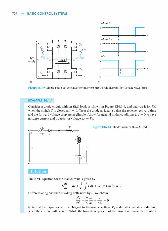
756 BASIC CONTROL SYSTEMS
+
+ +
+DC
supplyLoad Vs
VG3, VG4
−Vs
Vs
Q1
VG1 VG3
Q4
Q2
Q3
G
G
t
vo
(a) (b)
0
−
−− −
2T T
T
1
t
2T
VG1, VG2
T
1
0
0 t
2T
Figure 16.1.9 Single-phase dc–ac converter (inverter). (a) Circuit diagram. (b) Voltage waveforms.
EXAMPLE 16.1.1
Consider a diode circuit with an RLC load, as shown in Figure E16.1.1, and analyze it for i(t)when the switch S is closed at t = 0. Treat the diode as ideal, so that the reverse recovery timeand the forward voltage drop are negligible. Allow for general initial conditions at t = 0 to havenonzero current and a capacitor voltage vC = V0.
Vs
Vo
vC
S
Dt = 0
C
L
R
i+
−
+−
Figure E16.1.1 Diode circuit with RLC load.
So l u t i on
The KVL equation for the load current is given by
Ldi
dt+ Ri + 1
C
∫i dt + vC (at t = 0) = VS
Differentiating and then dividing both sides by L, we obtain
d2i
dt2+ R
L
di
dt+ i
LC= 0
Note that the capacitor will be charged to the source voltage VS under steady-state conditions,when the current will be zero. While the forced component of the current is zero in the solution

16.1 POWER SEMICONDUCTOR-CONTROLLED DRIVES 757
of the previous second-order homogeneous differential equation, we can solve for the naturalcomponent. The characteristic equation in the frequency domain is
s2 + R
Ls + 1
LC= 0
whose roots are given by
s1,2 = − R
2L±√(
R
2L
)2
− 1
LC
For the second-order circuit, the damping factor α and the resonant frequency ω0 are given by
α = R
2L; ω0 = 1√
LC
(Note: the ratio of α/ω0 is known as damping ratio δ.) Substituting, we get
s1,2 = −α ±√α2 − ω2
0
Three possible cases arise for the solution of the current, which will depend on the values ofα and ω0:Case 1—α = ω0: The roots are then equal, s1 = s2. The current is said to be critically damped.The solution of the current is of the form
i (t) = (A1 + A2t)es1t
Case 2—α > ω0: The roots are unequal and real. The circuit is said to be overdamped. Thesolution is then
i (t) = A1es1t + A2e
s2t
Case 3—α < ω0: the roots are complex. The circuit is underdamped. Let s1,2 = −α ± jωr ,
where ωr is known as the damped resonant frequency or ringing frequency, given by√ω2
0 − α2.The solution takes the form
i(t) = e−αt (A1 cos ωrt + A2 sin ωrt)
Observe that the current consists of a damped or decaying sinusoid. The constants A1 and A2 aredetermined from the initial conditions of the circuit.
The current waveform can be sketched, taking the conduction time of the diode into account.
Let us now consider a single-phase half-wave rectifier circuit as shown in Figure 16.1.10(a),with a purely resistive load R. We shall introduce and calculate the following quantities:
1. Efficiency
2. Form factor3. Ripple factor
4. Transformer utilization factor5. Peak inverse voltage (PIV) of diode
6. Displacement factor
7. Harmonic factor8. Input power factor.
During the positive half-cycle of the input voltage, the diode D conducts and the input voltageappears across the load. During the negative half-cycle of the input voltage, the output voltage is
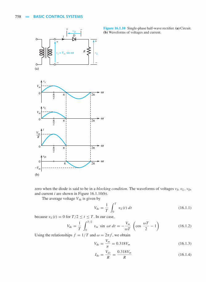
758 BASIC CONTROL SYSTEMS
vs = Vm sin ωt
(a)
vL
vD
i D
R
+
−
+
+
−
− Figure 16.1.10 Single-phase half-wave rectifier. (a) Circuit.(b) Waveforms of voltages and current.
Vm
−Vm
ωt
vs
(b)
0
2π π 2π
R
ωt
vD
0 π 2π
Vm
ωt
vL
0
2π π 2π
Vm
ωt
i
0
2π π 2π
zero when the diode is said to be in a blocking condition. The waveforms of voltages vS, vL, vD,and current i are shown in Figure 16.1.10(b).
The average voltage Vdc is given by
Vdc = 1
T
∫ T
0vL(t) dt (16.1.1)
because vL(t) = 0 for T/2 ≤ t ≤ T . In our case,
Vdc = 1
T
∫ T/2
0vm sin ωt dt = − Vm
ωT
(cos
ωT
2− 1
)(16.1.2)
Using the relationships f = 1/T and ω = 2πf , we obtain
Vdc = Vm
π= 0.318Vm (16.1.3)
Idc = Vdc
R= 0.318Vm
R(16.1.4)

16.1 POWER SEMICONDUCTOR-CONTROLLED DRIVES 759
The rms value of a periodic waveform is given by
Vrms =[
1
T
∫ T
0v2L(t) dt
]1/2
(16.1.5)
For a sinusoidal voltage vL(t) = Vm sin ωt for 0 ≤ t ≤ T/2, the rms value of the output voltage is
Vrms =[
1
T
∫ T/2
0(Vm sin ωt)2 dt
]1/2
= Vm
2= 0.5Vm (16.1.6)
Irms = Vrms
R= 0.5Vm
R(16.1.7)
The output dc power Pdc is given by
Pdc = VdcIdc = (0.318Vm)2
R(16.1.8)
The output average ac power Pac is given by
Pac = VrmsIrms = (0.5Vm)2
R(16.1.9)
The efficiency or the rectification ratio of the rectifier, which is a figure of merit used forcomparison, is then
Efficiency = η = Pdc
Pac
= (0.318Vm)2
(0.5Vm)2= 0.404, or 40.4% (16.1.10)
The form factor is FF = Vrms/Vdc, which gives a measure of the shape of the output voltage.In our case,
FF = Vrms
Vdc= 0.5Vm
0.318Vm
= 1.57, or 157% (16.1.11)
The ripple factor is RF = Vac/Vdc, which gives a measure of the ripple content. In our case,
RF = Vac
Vdc=√(
Vrms
Vdc
)2
− 1 =√
FF2 − 1 =√
1.572 − 1 = 1.21, or 121% (16.1.12)
The transformer utilization factor (TUF) is given by
TUF = Pdc
VsIs(16.1.13)
where Vs and Is are the rms voltage and rms current, respectively, of the transformer secondary.In our case, the rms voltage of the transformer secondary is
Vs =[
1
T
∫ T
0(Vm sin ωt)2 dt
]1/2
= Vm√2= 0.707Vm (16.1.14)
The rms value of the transformer secondary current is the same as that of the load,
Is = 0.5Vm
R(16.1.15)
Hence,
TUF = 0.3182
0.707× 0.5= 0.286 (16.1.16)
The peak inverse voltage (PIV), which is the peak reverse blocking voltage, is given by
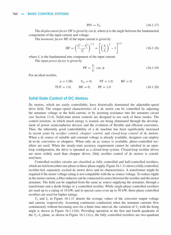
760 BASIC CONTROL SYSTEMS
PIV = Vm (16.1.17)
The displacement factor DF is given by cos φ, where φ is the angle between the fundamentalcomponents of the input current and voltage.
The harmonic factor HF of the input current is given by
HF =(I 2s − I 2
1
I 21
)1/2
=[(
Is
I1
)2
− 1
]1/2
(16.1.18)
where I1 is the fundamental rms component of the input current.The input power factor is given by
PF = I1
Iscos φ (16.1.19)
For an ideal rectifier,
η = 1.00; Vac = 0; FF = 1.0; RF = 0;TUF = 1.0; HF = 0; PF = 1.0 (16.1.20)
Solid-State Control of DC Motors
Dc motors, which are easily controllable, have historically dominated the adjustable-speeddrive field. The torque–speed characteristics of a dc motor can be controlled by adjustingthe armature voltage or the field current, or by inserting resistance into the armature circuit(see Section 13.4). Solid-state motor controls are designed to use each of these modes. Thecontrol resistors, in which much energy is wasted, are being eliminated through the develop-ment of power semiconductor devices and the evolution of flexible and efficient converters.Thus, the inherently good controllability of a dc machine has been significantly increasedin recent years by rectifier control, chopper control, and closed-loop control of dc motors.When a dc source of suitable and constant voltage is already available, designers can employdc-to-dc converters or choppers. When only an ac source is available, phase-controlled rec-tifiers are used. When the steady-state accuracy requirement cannot be satisfied in an open-loop configuration, the drive is operated as a closed-loop system. Closed-loop rectifier drivesare more widely used than chopper drives. Only rectifier control of dc motors is consid-ered here.
Controlled rectifier circuits are classified as fully controlled and half-controlled rectifiers,which are fed from either one-phase or three-phase supply. Figure 16.1.11 shows a fully controlled,rectifier-fed, separately excited dc motor drive and its characteristics. A transformer might berequired if the motor voltage rating is not compatible with the ac source voltage. To reduce ripplein the motor current, a filter inductor can be connected in series between the rectifier and the motorarmature. The field can be supplied from the same ac source supplying the armature, through atransformer and a diode bridge or a controlled rectifier. While single-phase controlled rectifiersare used up to a rating of 10 kW, and in special cases even up to 50 kW, three-phase controlledrectifiers are used for higher ratings.
Va and Ia in Figure 16.1.11 denote the average values of the converter output voltageand current, respectively. Assuming continuous conduction when the armature currents flowcontinuously without becoming zero for a finite time interval, the variation of Va with the firingangle is shown in Figure 16.1.11(b). Providing operation in the first and fourth quadrants ofthe Va–Ia plane, as shown in Figure 16.1.11(c), the fully controlled rectifiers are two-quadrant
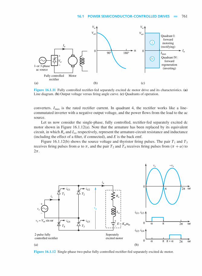
16.1 POWER SEMICONDUCTOR-CONTROLLED DRIVES 761
Vao
Va
(b)(a) (c)
α
Va
Ia
0
+
−
Vao
ImaxIa
Va
090° 180°
Fully controlledrectifier
1-or 3-phaseac source
Motor
I
Quadrant I:forward
motoring(rectifying)
Quadrant IV:forward
regeneration(inverting)
IV
Figure 16.1.11 Fully controlled rectifier-fed separately excited dc motor drive and its characteristics. (a)Line diagram. (b) Output voltage versus firing angle curve. (c) Quadrants of operation.
converters. Imax is the rated rectifier current. In quadrant 4, the rectifier works like a line-commutated inverter with a negative output voltage, and the power flows from the load to the acsource.
Let us now consider the single-phase, fully controlled, rectifier-fed separately excited dcmotor shown in Figure 16.1.12(a). Note that the armature has been replaced by its equivalentcircuit, in which Ra and La, respectively, represent the armature-circuit resistance and inductance(including the effect of a filter, if connected), and E is the back emf.
Figure 16.1.12(b) shows the source voltage and thyristor firing pulses. The pair T1 and T3
receives firing pulses from α to π , and the pair T2 and T4 receives firing pulses from (π + α) to2π .
iG1
T1
iG4
T4
vs
(b)(a)
is
+
−
+−
ωt
vs −vs
2π0
0
π
π
2-pulse fullycontrolled rectifier
Seperatelyexcited motor
ia
iG2
vs = Vm sin ωtE = Kmωm
vaLa
RaT2
iG3
T3ωtα 2π
0 π π + α ωtα 2π
iG1, iG3
iG2, iG4
Figure 16.1.12 Single-phase two-pulse fully controlled rectifier-fed separately excited dc motor.
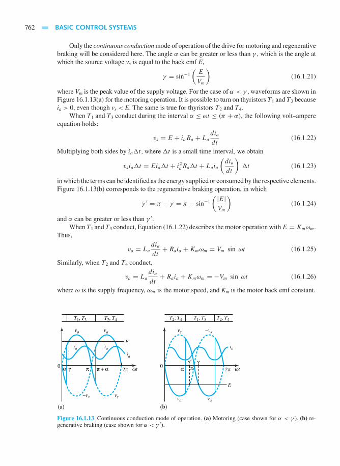
762 BASIC CONTROL SYSTEMS
Only the continuous conduction mode of operation of the drive for motoring and regenerativebraking will be considered here. The angle α can be greater or less than γ , which is the angle atwhich the source voltage vs is equal to the back emf E,
γ = sin−1
(E
Vm
)(16.1.21)
where Vm is the peak value of the supply voltage. For the case of α < γ , waveforms are shown inFigure 16.1.13(a) for the motoring operation. It is possible to turn on thyristors T1 and T3 becauseia > 0, even though vs < E. The same is true for thyristors T2 and T4.
When T1 and T3 conduct during the interval α ≤ ωt ≤ (π + α), the following volt–ampereequation holds:
vs = E + iaRa + La
dia
dt(16.1.22)
Multiplying both sides by iat , where t is a small time interval, we obtain
vsiat = Eiat + i2aRat + Laia
(dia
dt
)t (16.1.23)
in which the terms can be identified as the energy supplied or consumed by the respective elements.Figure 16.1.13(b) corresponds to the regenerative braking operation, in which
γ ′ = π − γ = π − sin−1
( |E|Vm
)(16.1.24)
and α can be greater or less than γ ′.When T1 and T3 conduct, Equation (16.1.22) describes the motor operation withE = Kmωm.
Thus,
va = La
dia
dt+ Raia +Kmωm = Vm sin ωt (16.1.25)
Similarly, when T2 and T4 conduct,
va = La
dia
dt+ Raia +Kmωm = −Vm sin ωt (16.1.26)
where ω is the supply frequency, ωm is the motor speed, and Km is the motor back emf constant.
(a)
ωt
va
T1, T3 T2, T4
E
va
ia iaia
vs−vs
2π0 π π + αγα
(b)
ωt
vs
T2, T4 T2, T4T1, T3
E
−vs
ia
vava
2π0γγ′
α π
Figure 16.1.13 Continuous conduction mode of operation. (a) Motoring (case shown for α < γ ). (b) re-generative braking (case shown for α < γ ′).

16.1 POWER SEMICONDUCTOR-CONTROLLED DRIVES 763
From α to π + α in the output voltage waveform of Figure 16.1.13(a), Equation (16.1.25)holds and its solution can be found as
ia(ωt) = Vm
zsin(ωt − ψ)− Kmωm
Ra
+K1e−t/τa , for α ≤ ωt ≤ π + α (16.1.27)
where
z = [R2a + (ωLa)
2]1/2
(16.1.28)
τa = La
Ra
(16.1.29)
ψ = tan−1
(ωLa
Ra
)(16.1.30)
and K1 is a constant.The first term on the right-hand side of Equation (16.1.27) is due to the ac source; the second
term is due to the back emf; and the third represents the combined transient component of the acsource and back emf. In the steady state, however,
ia(α) = ia(π + α) (16.1.31)
Subject to the constraint in Equation (16.1.31), the steady-state expression of current can beobtained. Flux being a constant, recall that the average motor torque depends only on the averagevalue or the dc component of the armature current, whereas the ac components produce onlypulsating torques with zero-average value. Thus, the motor torque is given by
Ta = KmIa (16.1.32)
To obtain the average value of Ia under steady state, we can use the following equation:
Average motor voltage Va = average voltage drop across Ra
+ average voltage drop across La
+ back emf (16.1.33)
in which
Va = 1
π
∫ π+α
α
Vm sin (ωt) d(ωt) = 2Vm
πcos α (16.1.34)
The rated motor voltage will be equal to the maximum average terminal voltage 2Vm/π .
Average drop across Ra = 1
π
∫ π+α
α
Raia(ωt) d(ωt) = Raia (16.1.35)
Average drop across La = 1
π
∫ π+α
α
La
(dia
dt
)d(ωt) = ω
π
∫ ia(π+α)
ia(α)
La dia
= ωLa
π[ia(π + α)− ia(α)] = 0 (16.1.36)
Substituting, we obtain
Va = IaRa +Kmωm (16.1.37)
for the steady-state operation of a dc motor fed by any converter. From Equations (16.1.34) and(16.1.37), it follows that

764 BASIC CONTROL SYSTEMS
Ia = (2Vm/π) cos α −Kmωm
Ra
(16.1.38)
Substituting in Equation (16.1.32), we get the following equation after rearranging terms:
ωm = 2Vm
πKm
cos α − Ra
K2m
Ta (16.1.39)
which is the relationship between speed and torque under steady state. The ideal no-load speedωm0 is obtained when Ia is equal to zero,
ωm0 = Vm
Km
, 0 ≤ α ≤ π
2(16.1.40)
ωm0 = Vm sin α
Km
,π
2≤ α ≤ π (16.1.41)
For torques less than the rated value, a low-power drive operates predominantly in the discontinu-ous conduction mode, for which a zero armature-current interval exists besides the duty interval.With continuous conduction, as seen from Equation (16.1.39), the speed–torque characteristicsare parallel straight lines whose slope depends on Ra, the armature circuit resistance. A filterinductor is sometimes included to reduce the discontinuous conduction zone, although such anaddition will lead to an increase in losses, armature circuit time constant, noise, cost, weight, andvolume of the drive.
EXAMPLE 16.1.2
Consider a 3-hp, 220-V, 1800-r/min separately excited dc motor controlled by a single-phase fullycontrolled rectifier with an ac source voltage of 230 V at 60 Hz. Assume that the full-load efficiencyof the motor is 88%, and enough filter inductance is added to ensure continuous conduction forany torque greater than 25% of rated torque. The armature circuit resistance is 1.5 .
(a) Determine the value of the firing angle to obtain rated torque at 1200 r/min.
(b) Compute the firing angle for the rated braking torque at −1800 r/min.
(c) With an armature circuit inductance of 30 mH, calculate the motor torque for α = 60°and 500 r/min, assuming that the motor operates in the continuous conduction mode.
(d) Find the firing angle corresponding to a torque of 35 N·m and a speed of 480 r/min,assuming continuous conduction.
So l u t i on
(a) Vm =√
2× 230 = 325.27 V
Ia = 3× 746
0.88× 220= 11.56 A
E = 220− (11.56× 1.5) = 220.66 V at rated speed of 1800 r/min
ωm = 1800× 2π
60= 188.57 rad/s
16.1 POWER SEMICONDUCTOR-CONTROLLED DRIVES 765
Km = E
ωm
= 202.66
188.57= 1.075
For continuous conduction, Equation (16.1.38) holds:2Vm
πcos α = IaRa +Kmωm = IaRa + E
At rated torque,
Ia = 11.56 A
Back emf at 1200 r/min = E1 = 1200
1800× 202.66 = 135.11
Substituting these values, one gets
2× 325.27
πcos α = 11.56× 1.5+ 135.11 = 152.45
or
cos α = 152.45× π
2× 325.27= 0.7365, or α = 42.6°
(b) At −1800 r/min,
E = −202.66 V
So it follows that
2× 325.27
πcos α = 11.56× 1.5− 202.66 = −185.32
or
cos α = −185.32× π
2× 325.27= −0.8953, or α = 153.5°
(c) From part (a), Km = 1.075. Corresponding to a speed of 500 r/min,
ωm = 500× 2π
60= 52.38 rad/s
From Equation (16.1.29), we have
52.38 = 2× 325.27
π × 1.075cos 60°− 1.5
1.0752Ta, or Ta = 33.82 N ·m
(d) From part (a), Km = 1.075. From Equation (16.1.39), we obtain
480× 2π
60= 2π × 325.27
π × 1.075cos α − 1.5
1.0752× 35
or,
cosα = 0.497 or α = 60.2°
The most widely used dc drive is the three-phase, fully controlled, six-pulse, bridge-rectifier-fed, separately excited dc motor drive shown in Figure 16.1.14. With a phase difference of

766 BASIC CONTROL SYSTEMS
60°, the firing of thyristors occurs in the same sequence as they are numbered. The linecommutation of an even-numbered thyristor takes place with the turning on of the next even-numbered thyristor, and similarly for odd-numbered thyristors. Thus, each thyristor conductsfor 120° and only two thyristors (one odd-numbered and one even-numbered) conduct ata time.
Considering the continuous conduction mode for the motoring operation, as shown in Figure16.1.15, for the converter output voltage cycle from ωt = α + π/3 to ωt = α + 2π/3,
iG1
T1
T4
iA
+
−
ωt2π0
0
π
π/3
6-pulse fully controlled rectifier Motor
ia
E = Kmωm
va
La
RaT5
T2
T3
T6
ωt2ππ
iG1
0 ωt2ππ
iG2
0 ωt2ππ
iG3
0 ωt2ππ
iG4
0 ωt2ππ
iG5
0 ωt2ππ
iG6
vABVm
vBC vCA
vBA
a
vCB vAC
A
B
C
N
Figure 16.1.14 Three-phase fullycontrolled six-pulse bridge-recti-fier-fed separately excited dc mo-tor.
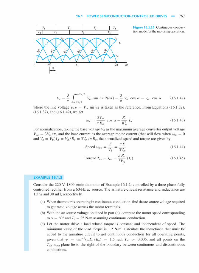
16.1 POWER SEMICONDUCTOR-CONTROLLED DRIVES 767
0 π/3 ωtα
T4 T6
va va
ia ia
T1T5 T5
T2
T3
T4
E
2ππ
AB AC BC BA CA
CB
Figure 16.1.15 Continuous conduc-tion mode for the motoring operation.
Va = 3
π
∫ α+2π/3
α+π/3Vm sin ωt d(ωt) = 3
πVm cos α = Vao cos α (16.1.42)
where the line voltage vAB = Vm sin ωt is taken as the reference. From Equations (16.1.32),(16.1.37), and (16.1.42), we get
ωm = 3Vm
πKm
cos α − Ra
K2m
Ta (16.1.43)
For normalization, taking the base voltage VB as the maximum average converter output voltageVao = 3Vm/π , and the base current as the average motor current (that will flow when ωm = 0and Va = VB)IB = VB/Ra = 3Vm/πRa , the normalized speed and torque are given by
Speed ωmn = E
VB
= πE
3Vm
(16.1.44)
Torque Tan = Ian = πRa
3Vm
(Ia) (16.1.45)
EXAMPLE 16.1.3
Consider the 220-V, 1800-r/min dc motor of Example 16.1.2, controlled by a three-phase fullycontrolled rectifier from a 60-Hz ac source. The armature-circuit resistance and inductance are1.5 and 30 mH, respectively.
(a) When the motor is operating in continuous conduction, find the ac source voltage requiredto get rated voltage across the motor terminals.
(b) With the ac source voltage obtained in part (a), compute the motor speed correspondingto α = 60° and Ta = 25 N·m assuming continuous conduction.
(c) Let the motor drive a load whose torque is constant and independent of speed. Theminimum value of the load torque is 1.2 N·m. Calculate the inductance that must beadded to the armature circuit to get continuous conduction for all operating points,given that ψ = tan−1(ωLa/Ra) = 1.5 rad, Tan > 0.006, and all points on theTan–ωmn plane lie to the right of the boundary between continuous and discontinuousconductions.
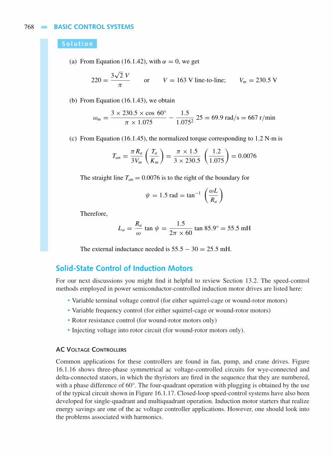
768 BASIC CONTROL SYSTEMS
So l u t i on
(a) From Equation (16.1.42), with α = 0, we get
220 = 3√
2 V
πor V = 163 V line-to-line; Vm = 230.5 V
(b) From Equation (16.1.43), we obtain
ωm = 3× 230.5× cos 60°
π × 1.075− 1.5
1.075225 = 69.9 rad/s = 667 r/min
(c) From Equation (16.1.45), the normalized torque corresponding to 1.2 N·m is
Tan = πRa
3Vm
(Ta
Km
)= π × 1.5
3× 230.5
(1.2
1.075
)= 0.0076
The straight line Tan = 0.0076 is to the right of the boundary for
ψ = 1.5 rad = tan−1
(ωL
Ra
)
Therefore,
La = Ra
ωtan ψ = 1.5
2π × 60tan 85.9° = 55.5 mH
The external inductance needed is 55.5− 30 = 25.5 mH.
Solid-State Control of Induction Motors
For our next discussions you might find it helpful to review Section 13.2. The speed-controlmethods employed in power semiconductor-controlled induction motor drives are listed here:
• Variable terminal voltage control (for either squirrel-cage or wound-rotor motors)
• Variable frequency control (for either squirrel-cage or wound-rotor motors)
• Rotor resistance control (for wound-rotor motors only)
• Injecting voltage into rotor circuit (for wound-rotor motors only).
AC VOLTAGE CONTROLLERS
Common applications for these controllers are found in fan, pump, and crane drives. Figure16.1.16 shows three-phase symmetrical ac voltage-controlled circuits for wye-connected anddelta-connected stators, in which the thyristors are fired in the sequence that they are numbered,with a phase difference of 60°. The four-quadrant operation with plugging is obtained by the useof the typical circuit shown in Figure 16.1.17. Closed-loop speed-control systems have also beendeveloped for single-quadrant and multiquadrant operation. Induction motor starters that realizeenergy savings are one of the ac voltage controller applications. However, one should look intothe problems associated with harmonics.

16.1 POWER SEMICONDUCTOR-CONTROLLED DRIVES 769
T1
T1T4
T4
AiA
T3
T3
T6
T6
B N B
A
C
T5
T2
T5T2
Statorwindings
C
Figure 16.1.16 Three-phase symmetrical ac voltage-controlled circuits.
A
B
C
A
B
C′
A′
Motor
C
Figure 16.1.17 Four-quadrant ac voltage controller.
FREQUENCY-CONTROLLED INDUCTION-MOTOR DRIVES
The converters employed for variable-frequency drives can be classified as:
• Voltage-source inverter (which is the only one considered here)
• Current-source inverters
• Cycloconverters, which allow a variable-frequency ac supply with voltage-source orcurrent-source characteristics obtained from a fixed-frequency voltage source.

770 BASIC CONTROL SYSTEMS
CS
Figure 16.1.18 Symbol of a self-commutated semiconductor switch.
A common symbol for the self-commutated semiconductor switch is shown in Figure 16.1.18.The control signal (either voltage or current) is denoted by CS, and the diode gives the directionin which the switch can conduct current. GTOs, power transistors, and MOSFETs are classifiedas self-commutated semiconductor devices because they can be turned off by their respectivecontrol signals: GTOs by a gate pulse, a power transistor by a base drive, and a MOSFET bya gate-to-source voltage. A thyristor, on the other hand, is a naturally commutated device thatcannot be turned off by its gate signal. A thyristor combined with a forced commutation circuitbehaves like a self-commutated semiconductor device, however. The self-commutation capabilitymakes its turnoff independent of the polarity of the source voltage, the load voltage, or the natureof load. Self-commutated semiconductor switches are suitable for applications for converters fedfrom a dc source, such as inverters and choppers.
Figure 16.1.19 shows a three-phase voltage-source inverter circuit, along with the corre-sponding voltage and current waveforms. The motor connected to terminals A, B, and C can havewye or delta connection. Operating as a six-step inverter, the inverter generates a cycle of lineor phase voltage in six steps. The following Fourier-series expressions describe the voltages vAB
and vAN:
vAB = 2√
3
πVd
[sin(ωt + π
6
)+ 1
5sin(
5ωt − π
6
)+ 1
7sin(
7ωt + π
6
)+ . . .
](16.1.46)
vAN = 2
πVd
[sin ωt + 1
5sin 5ωt + 1
7sin 7ωt + · · ·
](16.1.47)
The rms value of the fundamental component of the phase voltage vAN is given by
S4
iA AS1
iC1
VdO
+
−
(a)
iC4
D1
D4
S6
BS3
iC3
iC6
D3
D6
S2
CS5
iC5
iC2
D5
D2
Figure 16.1.19 Three-phase voltage-source inverter circuit with corresponding voltageand current waveforms.

16.1 POWER SEMICONDUCTOR-CONTROLLED DRIVES 771
(b)
0 π ωt2π 3π
iC1
0 ωt
iC2
0 ωt
iC3
0 ωt
iC4
0 ωt
iC5
0 ωt
iC6
0
π
ωt2π
3π
vABVd
0 π ωt2π
I
13
II III IV V VI I II III IV V Intervals
3π
vANiA iA
Vd23Vd
vAN
Figure 16.1.19 Continued
V1 =√
2
πVd (16.1.48)
From Figure 16.1.18(b), the rms value of the phase voltage is given by
V =[
1
π
∫ π3
0
(1
3Vd
)2
d(ωt)+∫ 2π/3
π/3
(2
3Vd
)2
d(ωt)
+∫ π
2π/3
(1
3Vd
)2
d(ωt)
]1/2
=√
2
3Vd (16.1.49)

772 BASIC CONTROL SYSTEMS
For a wye-connected stator, the waveform of the phase current is shown in Figure 16.1.19, which is
also the output current iA of the inverter. The output voltage of a six-step inverter can be controlled
by controlling either the dc input voltage or the ac output voltage with multiple inverters.
EXAMPLE 16.1.4
A 440-V, 60-Hz, six-pole, wye-connected, squirrel-cage induction motor with a full-load speedof 1170 r/min has the following parameters per phase referred to the stator: R1 = 0.2 , R′2 =0.1 , Xl1 = 0.75 , X′l2 = 0.7 , and Xm = 20 . (See Chapter 13, Figure 13.2.6,for the notation.) Consider the motor to be fed by a six-step inverter, which in turn is fed by asix-pulse, fully controlled rectifier.
(a) Let the rectifier be fed by an ac source of 440 V and 60 Hz. Find the rectifier firing anglethat will obtain rated fundamental voltage across the motor.
(b) Calculate the inverter frequency at 570 r/min and rated torque when the motor is operatedat a constant flux.
(c) Now let the drive be operated at a constant V/f ratio. Compute the inverter frequency at570 r/min and half the rated torque. Neglect the derating due to harmonics and use theapproximate equivalent circuit of Figure 13.2.6, with jXm shifted to the supply terminals.
So l u t i on
(a) From Equation (16.1.46), the fundamental rms line voltage of a six-step inverter is
VL =√
6
πVd
For a six-pulse rectifier, from Equation (16.1.42), Vd = (3/π)Vm cos α, where Vm is thepeak ac source line voltage. Thus,
VL = 3√
6
π2Vm cos α or cos α = VL
Vm
π2
3√
6
With VL = 440 V and Vm = 440√
2 V,
cos α = π2
3√
6√
2= 0.95 or α = 18.26°
(b) For a given torque, the motor operates at a fixed slip speed for all frequencies as long asthe flux is maintained constant. At rated torque, the slip speed NSl = 1200− 1170 = 30r/min. Hence, synchronous speed at 570 r/min is NS = N + NSl = 570 + 30 = 600r/min. Therefore, the inverter frequency is (600/1200)60 = 30 Hz.
(c) Based on the equivalent circuit, it can be shown that the torque for a constant V/f ratio is
T = 3
ωS
[V 2
rated
(R′2/S
)(R1 + R′2/S
)2 + (Xl1 +X′l2)2]
With a = f/frated,

16.1 POWER SEMICONDUCTOR-CONTROLLED DRIVES 773
T = 3
ωS
V 2
rated(R′2/aS)(
R1
a+ R′2
aS
)2
+ (Xl1 +X′l2)2
, a < 1
Here,
ωS = 120× 60
6× 2π
60= 40π = 125.66 rad/s
Vrated = 440√3= 254 V
S = 30
1200= 0.025
With a = 1,
Trated = 3
125.66
2542(0.1/0.025)(
0.2+ 0.1
0.025
)2
+ (0.75+ 0.7)2
= 312.11 N ·m
At half the rated torque,
0.5× 312.11 = 3
125.66
2542(0.1/aS)(
0.2
a+ 0.1
aS
)2
+ 1.452
or (0.2
a+ 0.1
aS
)2
+ 2.1 = 0.987
aS
Also,
S = aωS − ωm
aωS
or a = ωm
(1− S)ωS
= 59.7
(1− S)125.66= 0.457
1− S
(Note: ωm = 570× 2π/60 = 59.7 rad/s.)
Based on the last two equations, we can solve for a and S using an iterative procedure,
a = 0.4864; S = 0.0235
Therefore, frequency = 0.4864 × 60 = 29.2 Hz.
The inverter can also be operated as a pulse-width modulated (PWM) inverter. Figure 16.1.20shows the schemes when the supply is dc and when it is ac.
SLIP-POWER CONTROLLED WOUND-ROTOR INDUCTION-MOTOR DRIVES
Slip power is that portion of the air-gap power that is not converted into mechanical power. Themethods involving rotor-resistance control and voltage injection into the rotor circuit belong to this

774 BASIC CONTROL SYSTEMS
CL M
ML C
PWMinverter
Vd
PWMinverter
Filter
+
−
Filter
Dc link
(b)
(a)
Acsupply
Diodebridge
Figure 16.1.20 PWM inverter drives. (a) Supply is dc. (b) Supply is ac.
class of slip-power control. In order to implement these techniques using power semiconductordevices, some of the schemes are static rotor resistance control; the static Scherbius drive; andthe static Kramer drive, of which only the first is considered here.
The rotor circuit resistance can be smoothly varied statically (instead of mechanically) byusing the principles of a chopper. Figure 16.1.21 shows a scheme in which the slip-frequency acrotor voltages are converted into direct current by a three-phase diode bridge and applied to anexternal resistance R. The self-commutated semiconductor switch S, operating periodically witha period T, remains on for an interval ton in each period, with a duty ratio δ defined by ton/T.
The filter inductor helps to reduce the ripple in current Id and eliminate discontinuousconduction. Figure 16.1.22 shows input phase voltage waveforms of the diode bridge and asix-step rotor phase-current waveform, assuming ripple-free Id. For a period T of the switchoperation, the energy absorbed by resistance R is given by I 2
d R(T − ton), while the average powerconsumed by R is
R
S
Id
Vd
+
−
Ld, Rd
Wound-rotormotor
Diode bridge
3-phaseac supply
Figure 16.1.21 Static rotor resis-tance control of a wound-rotor in-duction motor.

16.1 POWER SEMICONDUCTOR-CONTROLLED DRIVES 775
0 π ωt2ππ/2
2π/3
3π/2
Phase voltage
Phase current
−Id
Id
Figure 16.1.22 Rotor voltage and current waveforms.
+
V1
I1
−
E1
R1 jXl1 jX ′l2
jXmR′a
R ′b
S
I ′2Figure 16.1.23 Per-phase funda-mental equivalent circuit of thedrive with static rotor resistancecontrol.
1
T
[I 2d R(T − ton)
]or I 2
d R(1− δ)
The effective value of resistance is then given by
R∗ = (1− δ)R (16.1.50)
The total resistance across the diode bridge is
Rt = R∗ + Rd = Rd + (1− δ)R (16.1.51)
The per-phase power absorbed by Rt is 1/3 I2d Rt , where Id is related to the rms value of the rotor
phase current,√
3/2Irms. Thus, the effective per-phase resistance Reff is given by
Reff = 0.5Rt (16.1.52)
From the Fourier analysis of the rotor phase current with quarter-wave symmetry, the fundamentalrotor current is (
√6/π)Id , or (3/π)Irms. It can be shown (as in Problem 16.1.14) that the per-phase
fundamental equivalent circuit of the drive referred to the stator is given by Figure 16.1.23, where
Ra = R2 + Reff (16.1.53)
and
Rb =(π2
9− 1
)Ra (16.1.54)
As in Chapter 13, the primed notation denotes referral to the stator, and R2 is the per-phaseresistance of the rotor. The resistance R′a/S accounts for the mechanical power developed andthe fundamental rotor copper loss, whereas the resistance R′b represents the effect of the rotorharmonic copper loss.
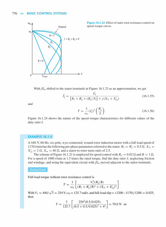
776 BASIC CONTROL SYSTEMS
0 T
ωs
ωm
Trated
δ = 0
δ = 11 > δ1 > δ2 > 0
δ2
δ1
Natural
Figure 16.1.24 Effect of static rotor resistance control onspeed–torque curves.
With jXm shifted to the stator terminals in Figure 16.1.23 as an approximation, we get
I ′2 =V1[
R1 + R′b + (R′a/S)]+ j (Xl1 +X′l2)
(16.1.55)
and
T = 3
ωs
(I ′2)2
(R′aS
)(16.1.56)
Figure 16.1.24 shows the nature of the speed–torque characteristics for different values of theduty ratio δ.
EXAMPLE 16.1.5
A 440-V, 60-Hz, six-pole, wye-connected, wound-rotor induction motor with a full-load speed of1170 r/min has the following per-phase parameters referred to the stator:R1 = R′2 = 0.5,Xl1 =X′l2 = 2 ,Xm = 40 , and a stator-to-rotor turns ratio of 2.5.
The scheme of Figure 16.1.21 is employed for speed control with Rd = 0.02 and R = 1 .For a speed of 1000 r/min at 1.5 times the rated torque, find the duty ratio δ, neglecting frictionand windage, and using the equivalent circuit with jXm moved adjacent to the stator terminals.
So l u t i on
Full-load torque without rotor resistance control is
T = 3
ωS
[V 2
1 (R′2/S)
(R1 + R′2/S)2 + (Xl1 +X′l2)2
]WithV1 = 440/
√3 = 254 V;ωS=125.7 rad/s, and full-load slip= (1200−1170)/1200 = 0.025,
then
T = 3
125.7
[2542(0.5/0.025)
(0.5+ 0.5/0.025)2 + 42
]= 70.6 N ·m

16.1 POWER SEMICONDUCTOR-CONTROLLED DRIVES 777
With rotor resistance control,
T = 3
ωS
[V 2
1 (R′a/S)(
R1 + R′b + R′a/S)2 + (Xl1 +X′l2)2
]
With R′b = (π2/9− 1)R′a = 0.0966R′a , and slip = (1200− 1000)/1200 = 0.167, we obtain
1.5× 70.6 = 3
125.7
[2542(R′a/0.167)(
0.5+ 0.0966R′a + R′a/0.167)2 + 42
]
Thus, R′2a − 2.18R′a + 0.44 = 0, or R′a = 0.225, or 1.955 . The value of 0.225 being less thanR′2 is not feasible; therefore R′a = 1.955 .
From Equation (16.1.53), Reff = (R′a −R′2)/(turns ratio)2 = (1.955− 0.5)/252 = 0.233 .From Equations (16.1.52) and (16.1.51), we calculate
(1− δ) = 2Reff − Rd
R= 2× 0.233− 0.22
1= 0.446, or δ = 0.554
Instead of wasting the slip power in the rotor circuit resistance, as was suggested by Scherbius,we can feed it back to the ac mains by using a scheme known as a static Scherbius drive. The slippower can be converted to mechanical power (with the aid of an auxiliary motor mounted on theinduction-motor shaft), which supplements the main motor power, thereby delivering the samepower to the load at different speeds, as in the Kramer drive.
Solid-State Control of Synchronous Motors
The speed of a synchronous motor can be controlled by changing its supply frequency. Withvariable-frequency control, two modes of operation are possible: true synchronous mode, em-ployed with voltage source inverters, in which the supply frequency is controlled from anindependent oscillator; and self-controlled mode, in which the armature supply frequency ischanged proportionally so that the armature field always rotates at the same speed as the rotor. Thetrue synchronous mode is used only in multiple synchronous-reluctance and permanent-magnetmotor drives, in applications such as paper mills, textile mills, and fiber-spinning mills, becauseof the problems associated with hunting and stability. Variable-speed synchronous-motor drives,commonly operated in the self-controlled mode, are superior to or competitive with induction-motor or dc-motor variable-speed drives.
Drives fed from a load-commutated current-source inverter or a cycloconverter find applica-tions in high-speed high-power drives such as compressors, conveyors, traction, steel mills, andship propulsion. The drives fed from a line-commutated cycloconverter are used in low-speedgearless drives for mine hoists and ball mills in cement production. Self-controlled permanent-magnet synchronous-motor drives are replacing the dc-motor drives in servo applications.
Self-control can be applied to all variable-frequency converters, whether they are voltage-source inverters, current-source inverters, current-controlled PWM inverters, or cycloconverters.Rotor position sensors, i.e., rotor position encoders with optical or magnetic sensors, or armatureterminal voltage sensors, are used for speed tracking. In the optical rotor position encoder shownin Figure 16.1.25 for a four-pole synchronous machine, the semiconductor switches are fired ata frequency proportional to the motor speed. A circular disk, with two slots S ′ and S ′′ on aninner radius and a large number of slots on the outer periphery, is mounted on the rotor shaft.Four stationary optical sensors P1 to P4 with the corresponding light-emitting diodes and phototransistors are placed as shown in Figure 16.1.25. Whenever the sensor faces a slot, an output

778 BASIC CONTROL SYSTEMS
results. Waveforms caused by the sensors are also shown in Figure 16.1.25. A detailed discussionof this kind of microprocessor control of current-fed synchronous-motor drives is outside thescope of this text.
0 180° 360° ωt
P1
0 120° 300° ωt
P2
0 60°
90°
90°
Slots
60°60°240° ωt
P3
P2
P4
P3
S″ S ′
P1
0 180°(b)
(a)
360° ωt
P4
Figure 16.1.25 Optical rotor position encoder and its output waveforms.
EXAMPLE 16.1.6
A 1500-hp, 6600-V, six-pole, 60-Hz, three-phase, wye-connected, synchronous motor, with asynchronous reactance of 36 , negligible armature resistance, and unity power factor at ratedpower, is controlled from a variable-frequency source with constant V/f ratio. Determine thearmature current, torque angle, and power factor at full-load torque, one-half rated speed, andrated field current. (Neglect friction, windage, and core loss.)
So l u t i on
The simplified per-phase equivalent circuits of the motor are shown in Figure E16.1.6. Phasevoltage V = 6600/
√3 = 3810.6 V, and
I ′m =V 0°
jXs
= 3810.6
36 90°= 105.9 − 90° A
With unity power factor at rated power, we obtain
1500× 746 = √3× 6600× Is
Hence, the rated armature current Is = 97.9 A. Then
I ′f = I ′m − I ′s = 105.9 − 90°− 97.9 0° = −97.9− j105.9 = 144.2 − 132.8° A
The synchronous speed is (120 × 60)/6 = 1200 rpm, or ωs = 125.7 rad/s. The rated torque isthen
Trated = 1500× 746
125.7= 8902 N ·m
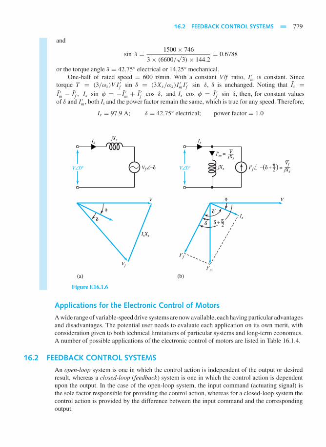
16.2 FEEDBACK CONTROL SYSTEMS 779
and
sin δ = 1500× 746
3× (6600/√
3)× 144.2= 0.6788
or the torque angle δ = 42.75° electrical or 14.25° mechanical.One-half of rated speed = 600 r/min. With a constant V/f ratio, I ′m is constant. Since
torque T = (3/ωs)V I ′f sin δ = (3Xs/ωs)I′mI
′f sin δ, δ is unchanged. Noting that Is =
I ′m − I ′f , Is sin φ = −I ′m + I ′f cos δ, and Is cos φ = I ′f sin δ, then, for constant valuesof δ and I ′m, both Is and the power factor remain the same, which is true for any speed. Therefore,
Is = 97.9 A; δ = 42.75° electrical; power factor = 1.0
V∠0°
V
Vf
Vf∠−δ jXs
Is
I ′m
I ′f
I ′f −(δ + ) =
δ
φ
δ δ + π2
δ′
φ
IsjXs
IsXs
V∠0°
Is
V
π2
(b)(a)
I ′m = VjXs
VfjXs
Figure E16.1.6
Applications for the Electronic Control of Motors
A wide range of variable-speed drive systems are now available, each having particular advantagesand disadvantages. The potential user needs to evaluate each application on its own merit, withconsideration given to both technical limitations of particular systems and long-term economics.A number of possible applications of the electronic control of motors are listed in Table 16.1.4.
16.2 FEEDBACK CONTROL SYSTEMS
An open-loop system is one in which the control action is independent of the output or desiredresult, whereas a closed-loop (feedback) system is one in which the control action is dependentupon the output. In the case of the open-loop system, the input command (actuating signal) isthe sole factor responsible for providing the control action, whereas for a closed-loop system thecontrol action is provided by the difference between the input command and the correspondingoutput.

780BASIC
CONTROLSYSTEM
S
TABLE 16.1.4 Applications for the Electronic Control of Motors
PracticalSpeed
Typical Range for aOutput One- or VariablesRange Two-Quadrant Governing
Converter Motor (kW) Drive Quadrants of Operation Supply Speed Applications
Dc Drives
Single-phaserectifier withcenter-tappedtransformer
Separately excitedor permanentmagnet dc
0–5 1:50 Quad 1 drivingQuad 2 dynamic or mechanical brakingReversal or armature connections or dual
converter for four-quadrant operation
120-V single-phase ac
Armatureterminal pd
Field current
Small variable-speeddrives in general
Single-phase fullycontrolledbridge rectifier
Separately excitedor permanentmagnet dc
0–10 1:50 Quad 1 drivingQuad 2 dynamic brakingReversal of armature connections or dual
converter for four-quadrant operation
240-V single-phase ac
Armatureterminal pd
Field current
Processing machinery,machine tools
Single-phasehalf-controlledbridge rectifier
Separately excitedor permanentmagnet dc
0–10 1:50 Quad 1 drivingQuad 2 dynamic brakingReversal of armature connections for
four-quadrant operation
240-V single-phase ac
Armatureterminal pd
Field current
Processing machinery,machine tools
Three-phasebridge rectifier
Separately excitedor permanentmagnet dc
10–200(10–50 forPM motor)
1:50 Quad 1 drivingQuad 2 dynamic brakingDual converter for regenerative braking
with four-quadrant operation
240-V to480-Vthree-phaseac
Armatureterminal pd
Field current
Hoists, machine tools,centrifuges,calender rollers
Three-phasebridge rectifier
Separately exciteddc
200–1000 1:50 Quad 1 drivingQuad 2 dynamic brakingDual converter for regenerative braking
with four-quadrant operation
460-V to600-Vthree-phaseac
Armatureterminal pd
Field current
Winders, rolling mills
Chopper (dc-to-dcconverter)
Separately exciteddc
1:50 Alternatives are quad 1 only; quads 1and 2; quads 1 and 4; all four
600-V to1000-V dc
Armatureterminal pd
Field current
Electric trains, rapidtransit streetcars,trolleys, buses,cranes
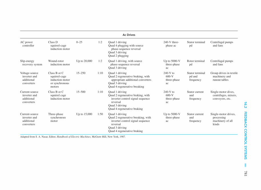
16.2FEED
BACKCONTROLSYSTEM
S781
Ac Drives
AC powercontroller
Class Dsquirrel-cageinduction motor
0–25 1:2 Quad 1 drivingQuad 4 plugging with source
phase-sequence reversalQuad 3 drivingQuad 2 plugging
240-V three-phase ac
Stator terminalpd
Centrifugal pumpsand fans
Slip-energyrecovery system
Wound-rotorinduction motor
Up to 20,000 1:2 Quad 1 driving, with sourcephase-sequence reversal
Quad 3 driving
Up to 5000-Vthree-phaseac
Rotor terminalpd
Centrifugal pumpsand fans
Voltage-sourceinverter andadditionalconverters
Class B or Csquirrel-cageinduction motoror synchronousmotors
15–250 1:10 Quad 1 drivingQuad 2 regenerative braking, with
appropriate additional convertersQuad 3 drivingQuad 4 regenerative breaking
240-V to600-Vthree-phaseac
Stator terminalpd andfrequency
Group drives in textilemachinery andrunout tables
Current-sourceinverter andadditionalconverters
Class B or Csquirrel cageinduction motor
15–500 1:10 Quad 1 drivingQuad 2 regenerative braking, with
inverter control signal sequencereversal
Quad 3 drivingQuad 4 regenerative braking
240-V to600-Vthree-phaseac
Stator currentandfrequency
Single-motor dives,centrifuges, mixers,conveyors, etc.
Current-sourceinverter andadditionalconverters
Three-phasesynchronousmotor
Up to 15,000 1:50 Quad 1 drivingQuad 2 regenerative breaking, with
inverter control signal sequencereversal
Quad 3 drivingQuad 4 regenerative braking
Up to 5000-Vthree-phaseac
Stator currentandfrequency
Single-motor drives,processingmachinery of allkinds
Adapted from S. A. Nasar, Editor, Handbook of Electric Machines, McGraw-Hill, New York, 1987.

782 BASIC CONTROL SYSTEMS
Activatingsignal u
Controlledvariable c
Referenceinput r
Controller Controlledprocess
Figure 16.2.1 Elements of an open-loop control system.
The elements of an open-loop control system may be divided into two parts: the controllerand the controlled process, as shown by the block diagram of Figure 16.2.1. An input signalor command r is applied to the controller, whose output acts as the actuating signal u. Theactuating signal then controls the controlled process such that the controlled variable c willperform according to some prescribed standards. The controller may be an amplifier, mechanicallinkage, or other basic control means in simple cases, whereas in more sophisticated electronicscontrol, it can be an electronic computer such as a microprocessor.
Feedback control systems can be classified in a number of ways, depending upon the purposeof the classification.
1. According to the method of analysis and design.
• Linear versus nonlinear control systems. Linear feedback control systems are idealizedmodels that are conceived by the analyst for the sake of simplicity of analysis anddesign. For the design and analysis of linear systems there exist a wealth of analyticaland graphical techniques. On the other hand, nonlinear systems are very difficult to treatmathematically, and there are no general methods that can be used for a broad class ofnonlinear systems.
• Time-invariant versus time-varying systems. When the parameters of a control system arestationary with respect to time during the operation of the system, the system is knownas a time-invariant system. Even though a time-varying system without nonlinearity isstill a linear system, the analysis and design of such a class of systems are generallymuch more complex than that of linear time-invariant systems.
2. According to the types of signal found in the system.
• Continuous-data and discrete-data systems. A continuous-data system is one in whichthe signals at various parts of the system are all functions of the continuous-time variablet. When one refers to an ac control system, it usually means that the signals in the systemare modulated by some kind of modulation scheme. On the other hand, a dc control systemimplies that the signals are unmodulated, but they are still ac signals according to theconventional definition. Typical components of a dc control system are potentiometers,dc amplifiers, dc motors, and dc tachometers; typical components of an ac control systemare synchros, ac amplifiers, ac motors, gyroscopes, and accelerometers.
• Sampled-data and digital control systems. These differ from the continuous-data systemsin that the signals at one or more points of the system are in the form of either a pulsetrain or a digital code. Sampled-data systems usually refer to a more general class ofsystems whose signals are in the form of pulse data, whereas a digital control systemrefers to the use of a digital computer or controller in the system. The term discrete-datacontrol system is used to describe both types of systems.

16.2 FEEDBACK CONTROL SYSTEMS 783
3. According to the type of system components.
• Electromechanical control systems.
• Hydraulic control systems.
• Pneumatic control systems.
• Biological control systems.
4. According to the main purpose of the system.
• Position control systems. Here the output position, such as the shaft position on a motor,exactly follow the variations of the input position.
• Velocity control systems.
• Regulators. Their function consists in keeping the output or controlled variable constantin spite of load variations and parameter changes. Speed control of a motor forms a goodexample. Feedback control systems used as regulators are said to be type 0 systems,which have a steady-state position error with a constant position input.
• Servomechanisms. Their inputs are time-varying and their function consists in providinga one-to-one correspondence between input and output. Position-control systems, includ-ing automobile power steering, form good examples. Servomechanisms are usually type1 or higher order systems. A type 1 system has no steady-state error with a constantposition input, but has a position error with a constant velocity input (the two shaftsrunning at the same velocity, but with an angular displacement between them).
Once the mathematical modeling of physical systems is done, while satisfying equations ofelectric networks and mechanical systems, as well as linearizing nonlinear systems wheneverpossible, feedback control systems can be analyzed by using various techniques and methods:transfer function approach, root locus techniques, state-variable analysis, time-domain analysis,and frequency-domain analysis. Although the primary purpose of the feedback is to reduce theerror between the reference input and the system output, feedback also has effects on such systemperformance characteristics as stability, bandwidth, overall gain, impedance, transient response,frequency response, effect of noise, and sensitivity, as we shall see later.
Transfer Functions and Block Diagrams
The transfer function is a means by which the dynamic characteristics of devices or systems aredescribed. The transfer function is a mathematical formulation that relates the output variable ofa device to the input variable. For linear devices, the transfer function is independent of the inputquantity and solely dependent on the parameters of the device together with any operations of time,such as differentiation and integration, that it may possess. To obtain the transfer function, oneusually goes through three steps: (i) determining the governing equation for the device, expressedin terms of the output and input variables, (ii) Laplace transforming the governing equation,assuming all initial conditions to be zero, and (iii) rearranging the equation to yield the ratio ofthe output to input variable. The properties of transfer functions are summarized as follows.
• A transfer function is defined only for a linear time-invariant system. It is meaningless fornonlinear systems.
• The transfer function between an input variable and an output variable of a system is definedas the ratio of the Laplace transform of the output to the Laplace transform of the input, or

784 BASIC CONTROL SYSTEMS
as the Laplace transform of the impulse response. The impulse response of a linear systemis defined as the output response of the system when the input is a unit impulse function.
• All initial conditions of the system are assumed to be zero.
• The transfer function is independent of the input.
The block diagram is a pictorial representation of the equations of the system. Each blockrepresents a mathematical operation, and the blocks are interconnected to satisfy the governingequations of the system. The block diagram thus provides a chart of the procedure to be followedin combining the simultaneous equations, from which useful information can often be obtainedwithout finding a complete analytical solution. The block-diagram technique has been highlydeveloped in connection with studies of feedback control systems, often leading to programminga problem for solution on an analog computer.
The simple configuration shown in Figure 16.2.2 is actually the basic building block of acomplex block diagram. The arrows on the diagram imply that the block diagram has a unilateralproperty; in other words, a signal can pass only in the direction of the arrows. A box is thesymbol for multiplication; the input quantity is multiplied by the function in the box to obtain theoutput. With circles indicating summing points (in an algebraic sense), and with boxes or blocksdenoting multiplication, any linear mathematical expression can be represented by block-diagramnotation, as in Figure 16.2.3 for an elementary feedback control system. The expression for theoutput quantity with negative feedback is given by
C = GE = G(R − B) = G(R −HC) (16.2.1)
or
C = G
1+HGR (16.2.2)
G(s)C(s) = G(s)R(s)
OutputR(s)Input
Figure 16.2.2 Basic building block of a block diagram.
R(s) reference variable (input signal)C(s) output signal (controlled variable)B(s) feedback signal, = H(s)C(s)E(s) actuating signal (error variable), = R(s) − B(s) G(s) forward path transfer function or open-loop transfer function, = C(s)/E(s) M(s) closed-loop transfer function, = C(s)/R(s) = G(s)/1 + G(s)H(s) H(s) feedback path transfer function
G(s)H(s) loop gain
Feedback elements (loop)
Controlled variable(output signal)
Feedforwardelements (loop)
Actuatingsignal
Reference variable(input signal)
Error detector(comparator)
Feedbacksignal
H(s)
G(s)C(s)c(t)
E(s)+− e(t)
R(s)r(t)
B(s)b(t)
Figure 16.2.3 Block diagram of an elementary feedback control system.
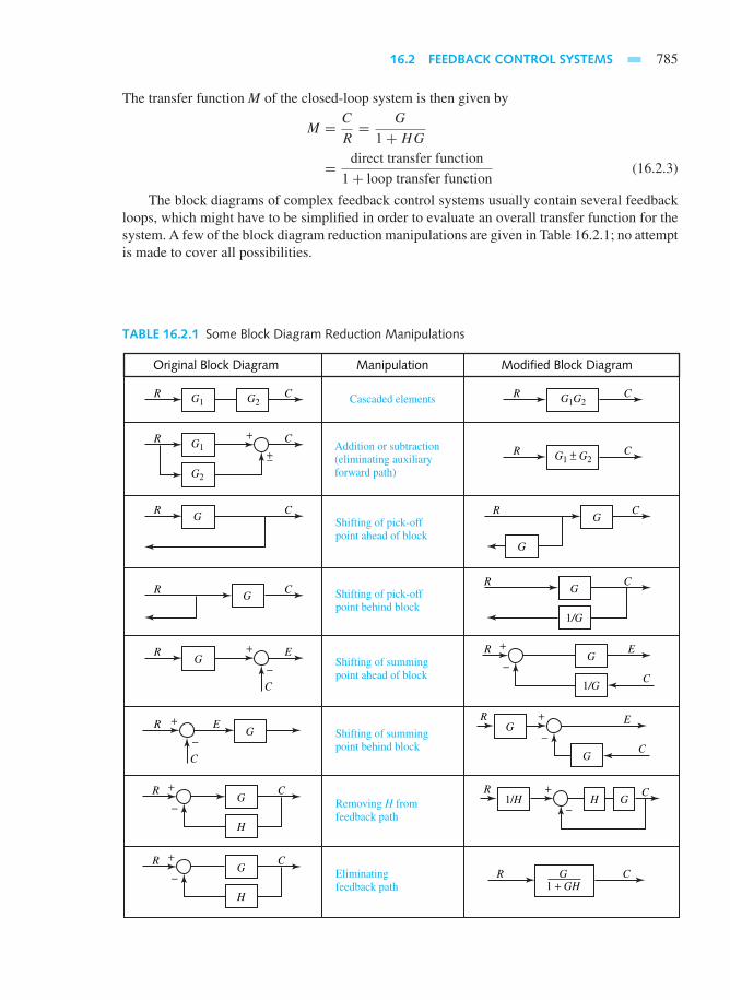
16.2 FEEDBACK CONTROL SYSTEMS 785
The transfer function M of the closed-loop system is then given by
M = C
R= G
1+HG
= direct transfer function
1+ loop transfer function(16.2.3)
The block diagrams of complex feedback control systems usually contain several feedbackloops, which might have to be simplified in order to evaluate an overall transfer function for thesystem. A few of the block diagram reduction manipulations are given in Table 16.2.1; no attemptis made to cover all possibilities.
TABLE 16.2.1 Some Block Diagram Reduction Manipulations
Original Block Diagram Modified Block DiagramManipulation
Cascaded elements
Addition or subtraction(eliminating auxiliaryforward path)
Shifting of pick-offpoint ahead of block
Shifting of pick-offpoint behind block
Shifting of summingpoint ahead of block
Shifting of summingpoint behind block
Removing H fromfeedback path
Eliminatingfeedback path
G1 G2R C
G1
G2
R C+
+−
G1G2CR
G1 + G2−CR
GR E
C
+
−
GR E
C
+
−
G
H
R C+
−H G1/H
R C+
−
G
G
R E
C
+
−
G
1/G
R E
C
+
−
G
1/G
R C
G
H
R C+
−
GR C
G1 + GH
R C
GR C
G
G
R C

786 BASIC CONTROL SYSTEMS
EFFECT OF FEEDBACK ON SENSITIVITY TO PARAMETER CHANGES
A good control system, in general, should be rather insensitive to parameter variations, while itis still able to follow the command quite responsively. It is apparent from Figure 16.2.1 that in anopen-loop system the gain of the system will respond in a one-to-one fashion to the variation inG. Let us now investigate what effect feedback has on the sensitivity to parameter variations.
The sensitivity S of a closed-loop system with Equation (16.2.3) to a parameter change p inthe direct transmission function G is defined as
SMp = per-unit change in closed-loop transmission
per-unit change in open-loop transmission
= ∂M/M
∂Gp/Gp
(16.2.4)
where Gp denotes that the derivative is to be taken with respect to the parameter p of the functionG. From Equation (16.2.3) it follows that
∂M = −HGp ∂Gp
(1+HGp)2+ ∂Gp
1+HGp
= ∂Gp
(1+HGp)2(16.2.5)
Substituting Equations (16.2.5) and (16.2.3) into Equation (16.2.4), one gets
SMp = ∂M/M
∂Gp/Gp
=[∂Gp/(1+HGp)
2] [(1+HGp)/Gp
]∂Gp/Gp
= 1
1+HGp
(16.2.6)
or
∂M
M=(
1
1+HGp
)∂Gp
Gp
(16.2.7)
Equation (16.2.6) shows that the sensitivity function can be made arbitrarily small by increasingHGp, provided that the system remains stable.
EFFECT OF FEEDBACK ON STABILITY
Let us consider the direct transfer function of the unstable first-order system of Figure 16.2.4(a).The transfer function is given by
G = C
E= K
1− pτ= −K/τ
p − 1/τ(16.2.8)
where p = d/dt is the differential operator. If a unit-step function is applied as the input quantityE, the output becomes
C(p) = −K/τ
p − 1/τE(p) = −K/τ
p(p − 1/τ)(16.2.9)
H
(b)(a)
R CE
−K
1 − pτG =
Note: p ≡
E C K1 − pτ
ddt
Figure 16.2.4 (a) Block-diagram representation of an unstable first-order system. (b) System of part (a)modified with a feedback path.

16.2 FEEDBACK CONTROL SYSTEMS 787
for which the corresponding time solution is given by
c(t) = K(1− et/τ ) (16.2.10)
which is clearly unstable, since the response increases without limit as time passes. By placing anegative feedback path H around the direct transfer function, as shown in Figure 16.2.4(b), theclosed-loop transfer function is then
M = C
R=
K
1− pτ
1+ KH
1− pτ
= K
1− pτ +HK(16.2.11)
By choosing H = ap and aK > τ , it follows that
M = K
1− pτ + paK(16.2.12)
and the corresponding time response of the closed-loop system, when subjected to a unit step,becomes
cf (t) = K(1− e−t/(aK−τ)) (16.2.13)
where cf(t) denotes response with feedback. The system is now clearly stable with aK > τ . Thus,the insertion of feedback causes the unstable direct transmission system of Figure 16.2.4(a) tobecome stable. Such a technique is often used to stabilize space rockets and vehicles, which areinherently unstable because of their large length-to-diameter ratios.
Note that the direct transfer function of Equation (16.2.8) has a pole located in the right halfp-plane at p = 1/τ , whereas the pole of the closed-loop transfer function of Equation (16.2.12)with aK > τ is located in the left half p-plane.
EFFECT OF FEEDBACK ON DYNAMIC RESPONSE AND BANDWIDTH
Let us consider the block-diagram representation of the open-loop system shown in Figure16.2.5(a), whose direct transfer function is given by
G = C
E= K
1+ pτ= K/τ
p + 1/τ(16.2.14)
corresponding to which, the transient solution of the system is of the form given by
c(t) = Ae−t/τ (16.2.15)
The transient in this system is seen to decay in accordance with a time constant of τ seconds. Byplacing a feedback path H around the direct transfer function, as shown in Figure 16.2.5(b), theclosed-loop transfer function is then
H
(b)(a)
R CE
−K
1 + pτG =
Note: p ≡
E C K1 + pτ
ddt
Figure 16.2.5 Block-diagram representation of system. (a) Without feedback. (b) With feedback.

788 BASIC CONTROL SYSTEMS
M = C
R=
K/τ
p + 1/τ
1+ HK/τ
p + 1/τ
= K/τ
p + 1+HK
τ
(16.2.16)
and the corresponding transient solution of the closed-loop system is of the form
cf (t) = Af e−[(1+HK)/τ ]t (16.2.17)
where cf(t) represents the transient response of the output variable with feedback. ComparingEquations (16.2.15) and (16.2.17), it is clear that the time constant with feedback is smaller bythe factor 1/(1+HK), and hence the transient decays faster.
By treating the differential operator p as the sinusoidal frequency variable jω, i.e., p = jω =j (1/τ), it follows from Equation (16.2.14) that the bandwidth of the open-loop system spreadsover a range from zero to a frequency of 1/τ rad/s. On the other hand, for the system with feedback,Equation (16.2.16) reveals that the bandwidth spreads from zero to (1+HK)/τ rad/s, showingthat the bandwidth has been augmented by increasing the upper frequency limit by 1+KH .
Dynamic Response of Control Systems
The existence of transients (and associated oscillations) is a characteristic of systems that possessenergy-storage elements and that are subjected to disturbances. Usually the complete solution ofthe differential equation provides maximum information about the system’s dynamic performance.Consequently, whenever it is convenient, an attempt is made to establish this solution first.Unfortunately, however, this is not easily accomplished for high-order systems. Hence we areforced to seek out other easier and more direct methods, such as the frequency-response methodof analysis.
Much of linear control theory is based on the frequency-response formulation of the sys-tem equations, and several quasi-graphical and algebraic techniques have been developed toanalyze and design linear control systems based on frequency-response methods. Althoughfrequency-response techniques are limited to relatively simple systems, and apply only to lin-ear systems in the rigorous mathematical sense, they are still most useful in system designand the stability analysis of practical systems and can give a great deal of information aboutthe relationships between system parameters (such as time constants and gains) and systemresponse.
Once the transfer function of Equation (16.2.3) is developed in terms of the complex frequencyvariable s, by letting s = jω, the frequency-response characteristic and the loop gain GH(jω) canbe determined. The Bode diagram, displaying the frequency response and root-locus techniques,can be used to study the stability analysis of feedback control systems. The dc steady-stateresponse, which becomes one component of the step response of the control system, can alsobe determined by allowing s to be zero in the transfer function. The step response, in turn, canbe used as a measure of the speed of response of the control system. Thus, the transfer functionobtained from the block diagram can be used to describe both the steady-state and the transientresponse of a feedback control system.
The matrix formulations associated with state-variable techniques have largely replacedthe block-diagram formulations. Computer software for solving a great variety of state-equationformulations is available on most computer systems today. However, in the state-variable for-mulation, much of the physical reality of any system is lost, including the relationships betweensystem response and system parameters.

16.2 FEEDBACK CONTROL SYSTEMS 789
With the development and widespread use of digital (discrete) control systems and the adventof relatively inexpensive digital computers, time-response methods have become more necessaryand available. These may be divided into two broad methodologies:
1. The actual simulation or modeling of the system differential equations by either analogor digital computers.
2. The state-variable formulation of the system state equations and their solution by a digitalcomputer. State-variable methods offer probably the most general approach to systemanalysis and are useful in the solution of both linear and nonlinear system equations.
The transient portion of the time response of a stable control system is that part which goes tozero as time increases and becomes sufficiently large. The transient behavior of a control systemis usually characterized by the use of a unit-step input. Typical performance criteria that are usedto characterize the transient response to a unit-step input include overshoot, delay time, rise time,and settling time. Figure 16.2.6 illustrates a typical unit-step response of a linear control system.The following four quantities give a direct measure of the transient characteristics of the stepresponse:
• Maximum (or peak) overshoot A is the largest deviation of the output over the step inputduring the transient state. It is used as a measure of the relative stability of the system. Thepercentage maximum overshoot is given by the ratio of maximum overshoot to final value,expressed in percent.
• Delay time td is defined as the time required for the step response to reach 90% of its finalvalue.
• Rise time tr is defined as the time needed for the step response to rise from 10% to 90% ofits final value.
c(t)Response
Rise time tr
Delaytime
td
Unit-step input
Maximumovershoot A
Decrement = A/B
Steady-stateerror
(t → ∞)
B
t00.10
0.50
1.000.950.90
1.05
Settling time ts
tmax
Figure 16.2.6 Typical unit-step response of a control system.

790 BASIC CONTROL SYSTEMS
• Settling time ts is the time required for the step response to decrease and stay within aspecified percentage (usually 5%) of its final value.
While these quantities are relatively easy to measure once a step response is plotted, theycannot easily be determined analytically, except for simple cases.
Steady-State Error of Linear Systems
If the steady-state response of the output does not agree exactly with the steady state of the input,the system is said to have a steady-state error. Steady-state errors in practical control systems arealmost unavoidable because of friction, other imperfections, and the nature of the system. Theobjective is then to keep the error to a minimum, or below a certain value. The steady-state erroris a measure of system accuracy when a specific type of input is applied to a control system.
Referring to Figure 16.2.3, assuming the input and output signals are of the same dimensionand are at the same level before subtraction, with a nonunity element H(s) incorporated in thefeedback path, the error of the feedback control system is defined as
e(t) = r(t)− b(t) or E(s) = R(s)− B(s) = R(s)−H(s)C(s)
or using Equation (16.2.2),
E(s) = R(s)
1+G(s)H(s)(16.2.18)
Applying the final-value theorem, the steady-state error of the system is
eSS = limt→∞ e(t) = lim
s→0sE(s) (16.2.19)
in which sE(s) is to have no poles that lie on the imaginary axis and in the right half of the s-plane.Substituting Equation (16.2.18) into Equation (16.2.19), we get
eSS = lims→0
sR(s)
1+G(s)H(s)(16.2.20)
which apparently depends on the reference input R(s) and the loop gain (loop transfer function)G(s)H(s).
The type of feedback control system is decided by the order of the pole of G(s)H(s) at s = 0.Thus, if the loop gain is expressed as
G(s)H(s) = KN(s)
sqD(s)= K(1+ T1s)(1+ T2s) · · · (1+ Tms)
sq(1+ Tas)(1+ Tbs) · · · (1+ Tns)(16.2.21)
where K and all of the T are constants, the exponent of s, i.e., q, in the denominator representsthe number of integrations in the open loop, and the exponent q defines the system type. With q= 0, 1, or 2, the system is classified as position, velocity, or acceleration system, respectively.Table 16.2.2 summarizes the error response for different unit inputs and three system types. Thedevelopment of these results is left as Problem 16.2.32 at the end of this chapter.
Classification of Feedback Control Systems by Control Action
A more common means of describing industrial and process controllers is by the way in whichthe error signal E(s) is used in the forward loop of Figure 16.2.3. The basic control elements are
• A proportional device, such as an amplifier
• A differentiating device, such as an inductor

16.2 FEEDBACK CONTROL SYSTEMS 791
TABLE 16.2.2 Steady-State Error Response for Unit Inputs
System Type Unit Step(1s
)Unit Ramp
(1
s2
)Unit Acceleration
(1
s3
)
0 Finite Infinite Infinite1 0 Finite Infinite2 0 0 Finite
• An integrating device, such as an operational amplifier with feedback.
Many industrial controllers utilize two or more of the basic control elements. The classificationby control action is summarized in Table 16.2.3.
Error-Rate Control, Output-Rate Control, and Integral-Error (Reset)Control
Let us consider a typical second-order servomechanism (containing two energy-storing elements)whose defining differential equation for obtaining the dynamic behavior of the system is givenby
Jd2c
dt2+ F
dc
dt+Kc + TL = Kr (16.2.22)
where J, F, and TL represent, respectively, effective inertia, equivalent viscous friction, andresultant load torque appearing at the motor shaft; K = KpKaKm, where Kp is the potentiometertransducer constant (V/rad), Ka is the amplifier gain factor (V/V), and Km is the motor-developedtorque constant (N·m/V) of the physical servomechanism shown in Figure 16.2.7; r is the inputcommand and c is the output displacement, both in radians.
The block diagram of the servomechanism of Figure 16.2.7 is given in Figure 16.2.8, inwhich the transfer function of each component is shown. Since the actuating signal is given byE = Kp(R − C), the block diagram may be simplified, as shown in Figure 16.2.9, in whichTL is assumed to be zero for simplicity. The direct transmission function (forward path transferfunction) for the system can be seen to be
G(s) = KpKaKm
Js2 + Fs= K
Js2 + Fs(16.2.23)
The corresponding closed-loop transfer function is given by
M(s) = C(s)
R(s)= G(s)
1+HG(s)= K/(J s2 + Fs)
1+K/(J s2 + Fs)= K
Js2 + Fs +K(16.2.24)
TABLE 16.2.3 Classification by Control Action
Control Action G(s)
Proportional Kp
Differential sKd
Integral Ki /sProportional and differential (PD) Kp + sKd
Proportional and integral (PI) Kp + Ki /sProportional and integral and differential (PID) Kp + Ki /s + sKd

792 BASIC CONTROL SYSTEMS
E
Feedbackpotentiometer
Inputpotentiometer
Servoamplifier
Gain factor Ka
Load
J, F, TL
cOutput
displacementMotor-developedtorque = e Ka Km
Direct connectionbetween servomotorand feedbackpotentiometeras well as load
Servomotor(torque constant
= Km)
Actuating signale = Kp(r − c)
ErEb
+
Figure 16.2.7 Second-order servomechanism.
Servomotor
Input potentiometer
Feedback potentiometer
Amplifier−Eb
−TL
Js2 + Fs1Er EaER(s) C (s)
Kp KaTdKm
Kp
Figure 16.2.8 Block diagram of the servomechanism of Figure 16.2.7.
H = 1
−Js2 + Fs
1R E CKpTdKa Km
Figure 16.2.9 Simplified blockdiagram of the servomechanismof Figure 16.2.7 (with zero loadtorque).
or
M(s) = C(s)
R(s)= K/J
s2 + (F/J )s +K/J(16.2.25)
or
C(s) = R(s)K/J
s2 + (F/J )s +K/J= R(s)
ω2n
s2 + 2ξωns + ω2n
(16.2.26)
where ωn ≡ √K/J is known as the system natural frequency, and
ξ ≡ F
2√KJ
= total damping
critical damping
is known as the damping ratio. ξ and ωn are the two figures of merit that describe the dynamicbehavior of any linear second-order system. The damping ratio ξ provides information aboutthe maximum overshoot (see Figure 16.2.6) in the system when it is excited by a step-forcing

16.2 FEEDBACK CONTROL SYSTEMS 793
function, whereas the natural frequency ωn of a system provides a measure of the settling time(see Figure 16.2.6). The settling time is no greater than ts = 3/ξωn for the response to a step inputto reach 95% of its steady-state value. For a 1% tolerance band, the settling time is no greater thants = 5/ξωn. Figure 16.2.10 depicts the percent maximum overshoot as a function of the dampingratio ξ for a linear second-order system. For two different systems having the same damping ratioξ , the one with the larger natural frequency will have the smaller settling time in responding toinput commands or load disturbances.
The particular form of the forced solution of Equation (16.2.26) depends upon the type offorcing function used. If a step input of magnitude r0 is applied, then R(s) = r0/s, so that thecomplete transformed solution becomes
C(s) =( r0
s
) ω2n
s2 + 2ξωns + ω2n
(16.2.27)
Note that the steady-state solution is generated by the pole associated with R(s), while the transientterms resulting from a partial-fraction expansion are associated with the poles of the denominator.
In order to meet the requirements for the steady-state performance, as well as dynamicperformance of the feedback control system of Figure 16.2.7, it becomes necessary to provideindependent control of both performances. Practical methods that have gained widespread accep-tance are
• Error-rate control
• Output-rate control
• Integral-error (or reset) control.
ERROR-RATE CONTROL
A system is said to possess error-rate damping when the generation of the output in some waydepends upon the rate of change of the actuating signal. For the system of Figure 16.2.7, if the
0.1
10
20
30
40
50
60
70
80
90
100
0.2 0.3 0.4 0.5 0.6 0.7
Perc
ent m
axim
um o
vers
hoot
Damping ratio ξ0.8 0.9 1.00
Figure 16.2.10 Plot of percent maxi-mum overshoot as a function of thedamping ratio for linear second-ordersystem.

794 BASIC CONTROL SYSTEMS
amplifier is so designed that it provides an output signal containing a term proportional to thederivative of the input, as well as one proportional to the input itself, error-rate damping will beintroduced. For the system that includes error rate, the only modification needed is in the transferfunction of the servoamplifier. Instead of the gain Ka, the new transfer function will be Ka+ sKe,where Ke denotes the error-rate gain factor of the amplifier. The complete block diagram is shownin Figure 16.2.11. In this case the direct transmission function becomes
G(s) = KpKm(Ka + sKe)
J s2 + Fs(16.2.28)
and the closed-loop transfer function is given by
M(s) = C(s)
R(s)= G(s)
1+HG(s)= K + sQe
J s2 + (F +Qe)s +K(16.2.29)
where K = KpKaKm and Qe = KpKeKm are known as the loop proportional gain factor and theloop error-rate gain factor, respectively.
Note that the steady-state solution for a step input r0 is the same whether or not error-ratedamping is present. The advantage of error-rate damping lies in the fact that it allows highergains to be used without adversely affecting the damping ratio, and thereby makes it possible tosatisfy the specifications for the damping ratio as well as for the steady-state performance. Also,the system’s natural frequency is increased, which in turn implies smaller settling times.
OUTPUT-RATE CONTROL
A system is said to have output-rate damping when the generation of the output quantity in someway is made to depend upon the rate at which the controlled variable is varying. Output-rate controloften involves the creation of an auxiliary loop, making the system multiloop. For the system ofFigure 16.2.7, output-rate damping can be obtained by means of a tachometer generator, drivenfrom the servomotor shaft. The complete block diagram of the servomechanism with output-ratedamping is depicted in Figure 16.2.12, where Ko is the output-rate gain factor (V·s/rad) and theoutput-rate signal is given by Ko(dc/dt). By applying the feedback relationship of Equation(16.2.3) to the minor (inner) loop, one gets
C(s)
E(s)=
KaKm
Js2 + sF
1+ sKoKaKm
Js2 + Fs
= KaKm
Js2 + (F +Qo)s(16.2.30)
where Qo = KoKaKm is known as the loop output-rate gain factor. Figure 16.2.12 may then besimplified, as shown in Figure 16.2.13. The closed-loop transfer function for the complete systemis then given by
AmplifierPotentiometer Servomotor−
Js2 + Fs1R E CKp Km
TdEaKa + sKe
Figure 16.2.11 Block diagram of servomechanism with error-rate damping.

16.2 FEEDBACK CONTROL SYSTEMS 795
Amplifier
Tachometer generatorOutput rate
Potentiometer Servomotor−
−Et
Js2 + Fs1R E CKp Ka Km
TdEa
sKo
Figure 16.2.12 Block diagram of servomechanism with output-rate damping.
M(s) = C(s)
R(s)=
K
Js2 + (F +Qo)s
1+ K
Js2 + (F +Qo)s
= K
Js2 + (F +Qo)s +K(16.2.31)
where K = KpKaKm is known as the loop proportional gain factor, as stated earlier.The manner in which output-rate damping effects in controlling the transient response are
most easily demonstrated is by assuming a step input applied to the system. The output-rate signalappears in opposition to the proportional signal, thereby removing the tendency for an excessivelyoscillatory response. With error-rate damping and output-rate damping, the damping ratio can beseen to be
ξ = F +Q
2√KJ
(16.2.32)
where Q = Qe or Qo, in which a term is added to the numerator, while the natural frequency isunchanged (as given by ωn = √K/J ). The damping ratio can then be adjusted independentlythrough Qe or Qo, while K can be used to meet accuracy requirements.
INTEGRAL-ERROR (OR RESET) CONTROL
A control system is said to possess integral-error control when the generation of the output insome way depends upon the integral of the actuating signal. By designing the servoamplifier suchthat it makes available an output voltage that contains an integral term and a proportional term,integral-error control can be obtained. By modifying the transfer function of the servoamplifier inthe block diagram, the complete block diagram of the servomechanism with integral-error controlis shown in Figure 16.2.14, where Ki is the proportionality factor of the integral-error component.The direct transmission function is then given by
G(s) = KpKm(Ki + sKa)
J s3 + Fs2(16.2.33)
and the corresponding closed-loop transfer function becomes
−Js2 + (F + Qo)s
KaKmR E CKp
Figure 16.2.13 Simplified block diagram of Figure 16.2.12.

796 BASIC CONTROL SYSTEMS
Potentiometer Servoamplifier Servomotor−
Js2 + Fs1R E CKp Ka + Ki
sKm
TdEa
Figure 16.2.14 Block diagram of servomechanism with integral-error control.
M(s) = C(s)
R(s)= Qi + sK
Js3 + Fs2 +Ks +Qi
(16.2.34)
where Qi = KiKpKm and K = KpKaKm, as defined earlier. Since the integral term stands alonewithout combining with the viscous-friction F term (as was the case with error-rate and output-ratecontrols), its influence on system performance differs basically from the previous compensationschemes. Also note that the order of the system is changed from second to third, because of theintegral-error compensation. The inclusion of the integral term implies that a third independentenergy-storing element is present. The position lag error, which exists with error-rate and output-rate control, disappears with integral-error control. This is a characteristic of integral controlwhich greatly improves steady-state performance and system accuracy. However, it may makethe dynamic behavior more difficult to cope with successfully.
Let us now present some illustrative examples.
EXAMPLE 16.2.1
Since dc motors of various types are used extensively in control systems, it is essential foranalytical purposes that we establish a mathematical model for the dc motor. Let us consider thecase of a separately excited dc motor with constant field excitation. The schematic representationof the model of a dc motor is shown in Figure E16.2.1(a). We will investigate how the speedof the motor responds to changes in the voltage applied to the armature terminals. The linearanalysis involves electrical transients in the armature circuit and the dynamics of the mechanicalload driven by the motor. At a constant motor field current If, the electromagnetic torque and thegenerated emf are given by
Te = Kmia (1)
ea = Kmωm (2)
where Km = kIf is a constant, which is also the ratio ea/ωm. In terms of the magnetization curve,ea is the generated emf corresponding to the field current If at the speed ωm. Let us now try to findthe transfer function that relates m(s) to Vt(s).
So l u t i on
The differential equation for the motor armature current ia is given by
vt = ea + La
dia
dt+ Raia (3)
or
Ra(1+ τap)ia = vt − ea (4)

16.2 FEEDBACK CONTROL SYSTEMS 797
−
−
−
+
+
−
−+
+Ra(1 + τas)
1B(1 + τms)
1Vt(s) +Te(s)
(b)
(a)
Ωm(s)Σ
TL(s)
ea
vt
vf
if
Lf
Rf
La
ωmTe
TL
ia
Ra
Ia(s)
Ea(s)
Km
Km
−
−+
Ra(1 + τas)1
TL
Kmea
Js1Vt(s) +Te(s)
(c)
(d)
Ωm(s)Σ
TL(s)
Ia(s)
Ea(s)
Km
Km
+
−
+
−
iavt ea
Ceq =
La Ra
K 2m
J
Geq =K 2
m
BZL =
Figure E16.2.1 (a) Model of a separately excited dc motor. (b) Block diagram representing Equations (8)and (9). (c) Block diagram representing Equation (11). (d) Analog electric circuit for a separately exciteddc motor.

798 BASIC CONTROL SYSTEMS
where vt is the terminal voltage applied to the motor, ea is the back emf given by Equation (2), Ra
and La include the series resistance and inductance of the armature circuit and electrical sourceput together, and τa = La/Ra is the electrical time constant of the armature circuit. Note that theoperator p stands for (d/dt). The electromagnetic torque is given by Equation (1), and from thedynamic equation for the mechanical system given by
Te = Jpωm + Bωm + TL (5)
the acceleration is then given by
(B + Jp)ωm = Te − TL (6)
or
B(1+ τmp)ωm = Te − TL (7)
where τm = J/B is the mechanical time constant. The load torque TL, in general, is a function ofspeed, J is the combined polar moment of inertia of the load and the rotor of the motor, and B isthe equivalent viscous friction constant of the load and the motor.
Laplace transforms of Equations (4) and (7) lead to the following:
Ia(s) = Vt(s)− Ea(s)
Ra(1+ τas)= Vt(s)−Kmm(s)
Ra(1+ τas)(8)
m(s) = [Te(s)− TL(s)]1
B
1
(1+ τms)(9)
The corresponding block diagram representing these operations is given in Figure E16.2.1(b) interms of the state variables Ia(s) and m(s), with Vt(s) as input.
The application of the closed-loop transfer function M(s), shown in Figure 16.2.3, to theblock diagram of Figure E16.2.1(b) yields the following transfer function relating m(s) andVt(s), with TL = 0:
m(s)
Vt (s)= Km/ [Ra(1+ τms)B(1+ τms)]
1+ [K2m/Ra(1+ τas)B(1+ τms)
] (10)
With mechanical damping B neglected, Equation (10) reduces tom(s)
Vt (s)= 1
Km [τis(τas + 1)+ 1](11)
where τi = JRa/K2m is the inertial time constant, and the corresponding block diagram is shown
in Figure E16.2.1(c). The transfer function relating speed to load torque with Vt = 0 can beobtained from Figure E16.2.1(c) by eliminating the feedback path as follows:
m(s)
TL(s)= − 1/J s
1+ (1/J s)[K2
m/Ra(1+ τas)] = − τas + 1
J s(1+ τas)+ (K2m/Ra)
(12)
Expressing the torque equation for the mechanical system as
Te = Kmia = Jpωm + Bωm + TL (13)
then dividing by Km, and substituting ωm = ea/Km, we obtain
ia = J
K2m
dea
dt+ B
K2m
ea + TL
Km
(14)
Equation (14) can be identified to be the node equation for a parallel Ceq–Geq–ZL circuit with
Ceq = J/K2m; Geq = B/K2
m; ZL = Kmea/TL (15)

16.2 FEEDBACK CONTROL SYSTEMS 799
and a common voltage ea. An analog electric circuit can then be drawn as in Figure E16.2.1(d) fora separately excited dc motor, in which the inertia is represented by a capacitance, the dampingby a shunt conductance, and the load–torque component of current is shown flowing through anequivalent impedance ZL. The time constants, τ i associated with inertia and τm associated with thedamping-type load torque that is proportional to speed (in terms of the analog-circuit notations),are given by
τi = RaCeq and τm = Ceq/Geq (16)
Note in the preceding analysis that Km is proportional to the constant motor field current If.The self-inductance of the armature can often be neglected except for a motor driving a load
that has rapid torque pulsations of appreciable magnitude.
EXAMPLE 16.2.2
A voltage amplifier without feedback has a nominal gain of 500. The gain, however, varies inthe range of 475 to 525 due to parameter variations. In order to reduce the per-unit change to0.02, while maintaining the original gain of 500, if the feedback is introduced, find the new directtransfer gain G and the feedback factor H.
So l u t i on
If G′ is the gain without feedback, it follows that
∂G′
G′= 525− 475
500= 0.1
From Equation (16.2.7),
∂M
M= ∂G
G
(1
1+HG
)= 0.02 (1)
where G stands for the new transmission gain with feedback. Also, from Equation (16.2.3),
M = G
1+HG= 500 (2)
From Equation (1),
1+HG = 0.1
0.02= 5 (3)
Substituting Equation (3) into Equation (2), one obtains
G = 500(1+HG) = 500(5) = 2500
and from Equation (3),
H = 5− 1
2500= 0.0016
EXAMPLE 16.2.3
The Ward–Leonard system, which is used in the control of large dc motors employed in rollingmills, is a highly flexible arrangement for effecting position and speed control of a separately

800 BASIC CONTROL SYSTEMS
excited dc motor. A simplified schematic diagram of such a system is shown in Figure E16.2.3(a),in which the tachometer, error detector, and amplifier are represented functionally rather than byelectric circuit connections. Assume the motor field current is held constant, the load torque isignored, and the generator speed is held constant under all conditions of operation.
Determine the transfer functions o/Eg and o/Ee, and develop a block diagram for thesystem.
(a)
(b)
ifia
ef
LfRf
Generatorfield
Constantfield
Tachometer
ωg = constant
Rag + Ram= Re
Lag + Lam= Le
+−
Speed
Referencevoltage er
efb = Kωω0Bm, Jm
Td
ee
eg emAmplifier
Ka
−(Ra + sLa) (Bm + sJm) + K 2
mRf + sLf
ΩKa
Kg Km
Kω
EgEe Ef
Efb
ER
ω0
Figure E16.2.3 (a) Schematic representation of a simplified Ward–Leonard dc motor control. (b) Blockdiagram of (a).
So l u t i on
For the dc generator with constant speed, we have
ef = if Rf + Lf
dif
dt
eg = Kgif
where Kg is a constant, andEg(s)
Ef (s)= Kg
Rf + sLf
The differential equation in the armature circuits is given by
eg = iaRe + Le
dia
dt+ em (1)
where
em = Kmωo (2)

16.2 FEEDBACK CONTROL SYSTEMS 801
for the constant field current, with Km a constant, and
Td = Kmia = Bmωo + Jmdωo
dt(3)
neglecting load torque. Transforming Equations (1), (2), and (3) and rearranging, we geto
Eg
= Km
(Ra + sLa)(Bm + sJm)+K2m
Accounting for the amplifier gain Ka, we haveo
Ee
= KaKgKm
(Rf + sLf )[(Ra + sLa)(Bm + sJm)+K2
m
]The block diagram, including the feedback loop due to the tachometer, is shown in FigureE16.2.3(b).
EXAMPLE 16.2.4
Consider an elementary feedback control system, as shown in Figure 16.2.3, with H = 1. Theoutput variable c and the input e to the direct transmission path are related by
d2c
dt2+ 8
dc
dt+ 12c = 68e
(a) Assuming the system to be initially at rest, for e = u(t), find the complete solution forc(t) when the system is operated in open-loop fashion without any feedback.
(b) With the feedback loop connected and with a forcing function of a unit step, i.e., R(s) =1/s, describe the nature of the dynamic response of the controlled variable by workingwith the differential equation for the closed-loop system, without obtaining a formalsolution for c(t).
(c) By working solely in terms of transfer functions, discuss the closed-loop behavior.
So l u t i on
(a) Laplace transforming the given equation with zero initial conditions, we have
s2C(s)+ 8sC(s)+ 12C(s) = 68
s(1)
or
C(s) = 68
s(s2 + 8s + 12)= 68
s(s + 2)(s + 6)= K0
s+ K1
s + 2+ K2
s + 6(2)
Evaluating the coefficients of the partial-fraction expansion, we get
C(s) = 17
3
(1
s
)− 17
2
(1
s + 2
)+ 17
6
(1
s + 6
)(3)
The corresponding time solution is then given by

802 BASIC CONTROL SYSTEMS
c(t) = 17
3− 17
2e−2t + 17
6e−6t (4)
(b) The differential equation describing the closed-loop system operation is
d2c
dt2+ 8
dc
dt+ 12c = 68(r − c) (5)
The output and input variables of the closed-loop system are related by
d2c
dt2+ 8
dc
dt+ 80c = 68r (6)
The two figures of merit, damping ratio ξ and natural frequency ωn, follow from thecharacteristic equation of the closed-loop system,
s2 + 8s + 80 = 0 (7)
(when the input is set equal to zero and the left side of Equation (6) is Laplace transformedwith zero initial conditions).
Identifying Equation (7) with the general form that applies to all linear second ordersystems,
s2 + 2ξωns + ω2n = 0 (8)
we obtain the following by comparing coefficients:
ωn =√
80 = 8.95 rad/s (9)
and
ξ = 8
2ωn
= 4
8.95= 0.448 (10)
Referring to Figure 16.2.10, the maximum overshoot can be seen to be 17%. Withξωn = 4, it follows that the controlled variable reaches within 1% of its steady-statevalue after the time elapse of
ts = 5
ξωn
= 5
4= 1.25 s
(c) The transfer function of the direct transmission path is given by
G(s) = C(s)
E(s)= 68
s2 + 8s + 12(11)
The closed-loop transfer function is
M(s) = C(s)
R(s)= G(s)
1+HG(s)=
68
s2 + 8s + 12
1+ 68
s2 + 8s + 12
(12)

16.2 FEEDBACK CONTROL SYSTEMS 803
orC(s)
R(s)= 68
s2 + 8s + 80(13)
Noting that the denominator of Equation (13) is the same as the left side of Equation (7),it follows that the damping ratio and the natural frequency will have the same values asfound in part (b). The oscillatory dynamic behavior can be described with the two figuresof merit ξ and ωn, along with percent maximum overshoot and settling time.
EXAMPLE 16.2.5
A feedback control system with the configuration of Figure 16.2.7 has the following parameters:Kp = 0.5 V/rad, Ka = 100 V/V, Km = 2.7 × 10⁻⁴ N·m/V, J = 1.5 × 10⁻⁵ kg·m2, andF = 2× 10⁻⁴ kg·m2/s.
(a) With an applied step-input command, describe the dynamic response of the system,assuming the system to be initially at rest.
(b) Find the position lag error in radians, if the load disturbance of 1.5×10⁻³ N·m is presenton the system when the step command is applied.
(c) In order that the position lag error of part (b) be no greater than 0.025 rad, determine thenew amplifier gain.
(d) Evaluate the damping ratio for the gain of part (c) and the corresponding percentmaximum overshoot.
(e) With the gain of part (c), in order to have the percent maximum overshoot not to exceed25%, find the value of the output-rate gain factor.
So l u t i on
(a) K = KpKaKm = 0.5× 100× 2.7× 10−4 = 0.0135 N·m/rad
ξ = F
2√KJ
= 2× 10⁻⁴
2√
0.0135× 1.5× 10−5= 10−4
0.45× 10−3= 0.222
From Figure 16.2.10, the percent maximum overshoot is 48%,
ωn =√K
J=√
0.0135
1.5× 10−5= 30 rad/s
The commanded value of the controlled variable reaches within 1% of its final value in
ts = 5
ξωn
= 5
0.222× 30= 0.75 s
The roots of the characteristic equation
s2 + F
Js + K
J= 0
804 BASIC CONTROL SYSTEMS
are
s1, 2 = − F
2J±√(
F
2J
)2
− K
J
The system is:
(i) Overdamped if
(F
2J
)2
>K
J
(ii) Underdamped if
(F
2J
)2
<K
J
(iii) Critically damped if
(F
2J
)2
= K
J
To make the servomechanism fast acting, the underdamped case is desirable. For theunderdamped situation, the roots are given by
s1, 2 = − F
2J± j
√K
J−(F
2J
)2
which can be expressed as
s1, 2 = −ξωn ± jωd
where ωd = ωn
√1− ξ 2 is known as damped frequency of oscillation. The damped
oscillations in our example occur at a frequency of
ωd = 30√
1− 0.2222 = 29.25 rad/s
(b) Starting from Equation (16.2.22), with a step command of magnitude r0 and a step changein load of magnitude TL, assuming the system to be initially at rest, one obtains
C(s) · (s2J + sF +K) = Kr0
s− TL
s
or
C(s) = (K/J )r0
s
(s2 + s
F
J+ K
J
) − TL/J
s
(s2 + s
F
J+ K
J
)
If TL= 0, at steady state, cSS = r0. In the presence of a fixed load torque, cSS = r0−TL/K .The position lag error for our example is given by
TL
K= 1.5× 10⁻³
0.0135= 0.111 rad
(c) The loop gain must be increased by a factor of 0.111/0.025 = 4.44. Hence the new valueof the amplifier gain is
K ′a = 4.44 Ka = 4.44× 100 = 444 V/V

16.3 DIGITAL CONTROL SYSTEMS 805
(d) Since ξ = F/2√KJ , it follows that
ξ ′ = ξ√4.44
= 0.4746ξ = 0.4746× 0.222 = 0.105
corresponding to which the percent maximum overshoot from Figure 16.2.10 is 72%.
(e) For a 25% overshoot, Figure 16.2.10 shows that ξ = 0.4. Then from Equation (16.2.32),ξ = (F +Qo)/2
√KJ , or
0.4 = 2× 10⁻⁴ +Qo
2√
0.0135× 1.5× 10−5= 2× 10⁻⁴ +Qo
2× 0.45× 10−3
Hence,
Qo = 0.36× 10⁻³ − 0.2× 10−3 = 0.16× 10⁻³
Then
Ko = Qo
K ′aKm
= 0.16× 10⁻³
444× 2.7× 10−4= 0.0013, or 1.3× 10⁻³ V·s/rad.
16.3 DIGITAL CONTROL SYSTEMS
Significant progress has been made in recent years in discrete-data and digital control systemsbecause of the advances made in digital computers and microcomputers, as well as the advantagesfound in working with digital signals. Discrete-data and digital control systems differ from thecontinuous-data or analog systems in that the signals in one or more parts of these systemsare in the form of either a pulse train or a numerical (digital) code. The terms, sampled-datasystems, discrete-data systems, discrete-time systems, and digital systems have been loosely usedin the control literature. However, sampled-data systems usually refer to a general class of systemswhose signals are in the form of pulse data; sampled data refers to signals that are pulse-amplitudemodulated, i.e., trains of pulses with signal information carried by the amplitudes. Digital controlsystems refers to the use of a digital computer or controller in the system; digital data usuallyrefers to signals that are generated by digital computers or digital transducers and are thus insome kind of coded form. A practical system such as an industrial process control is generallyof such complexity that it contains analog and sampled as well as digital data. Hence the termdiscrete-data systems is used in a broad sense to describe all systems in which some form ofdigital or sampled signals occur. When a microprocessor receives and outputs digital data, thesystem then becomes a typical discrete-data or digital control system.
Figure 16.3.1(a) illustrates the basic elements of a typical closed-loop control system withsampled data; Figure 16.3.1(b) shows the continuous-data input e(t) to the sampler, whereasFigure 16.3.1(c) depicts the discrete-data output e*(t) of the sampler. A continuous input signalr(t) is applied to the system. The continuous error signal is sampled by a sampling device, thesampler, and the output of the sampler is a sequence of pulses. The pulse train may be periodicor aperiodic, with no information transmitted between two consecutive pulses. The sampler inthe present case is assumed to have a uniform sampling rate, even though the rate may not beuniform in some other cases. The magnitudes of the pulses at the sampling instants representthe values of the input signal e(t) at the corresponding instants. Sampling schemes, in general,may have many variations: periodic, cyclic-rate, multirate, random, and pulse-width modulated
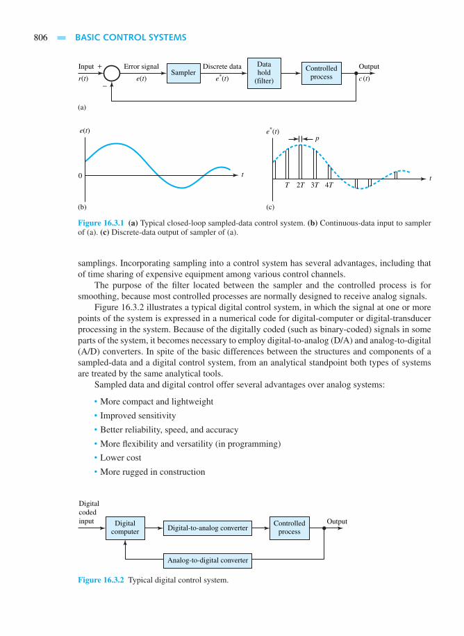
806 BASIC CONTROL SYSTEMS
(a)
(b) (c)
−
+Sampler
Input
r(t)
Error signal
e(t)
e(t)
Datahold
(filter)
Discrete data
e*(t)
e*(t)p
2T0
3TT 4T
t t
Output
c (t)Controlled
process
Figure 16.3.1 (a) Typical closed-loop sampled-data control system. (b) Continuous-data input to samplerof (a). (c) Discrete-data output of sampler of (a).
samplings. Incorporating sampling into a control system has several advantages, including thatof time sharing of expensive equipment among various control channels.
The purpose of the filter located between the sampler and the controlled process is forsmoothing, because most controlled processes are normally designed to receive analog signals.
Figure 16.3.2 illustrates a typical digital control system, in which the signal at one or morepoints of the system is expressed in a numerical code for digital-computer or digital-transducerprocessing in the system. Because of the digitally coded (such as binary-coded) signals in someparts of the system, it becomes necessary to employ digital-to-analog (D/A) and analog-to-digital(A/D) converters. In spite of the basic differences between the structures and components of asampled-data and a digital control system, from an analytical standpoint both types of systemsare treated by the same analytical tools.
Sampled data and digital control offer several advantages over analog systems:
• More compact and lightweight
• Improved sensitivity
• Better reliability, speed, and accuracy
• More flexibility and versatility (in programming)
• Lower cost
• More rugged in construction
Digitalcodedinput OutputDigital
computerControlled
processDigital-to-analog converter
Analog-to-digital converter
Figure 16.3.2 Typical digital control system.
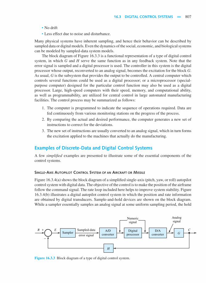
16.3 DIGITAL CONTROL SYSTEMS 807
• No drift
• Less effect due to noise and disturbance.
Many physical systems have inherent sampling, and hence their behavior can be described bysampled data or digital models. Even the dynamics of the social, economic, and biological systemscan be modeled by sampled-data system models.
The block diagram of Figure 16.3.3 is a functional representation of a type of digital controlsystem, in which G and H serve the same function as in any feedback system. Note that theerror signal is sampled and a digital processor is used. The controller in this system is the digitalprocessor whose output, reconverted to an analog signal, becomes the excitation for the block G.As usual, G is the subsystem that provides the output to be controlled. A central computer whichcontrols several functions could be used as a digital processor; or a microprocessor (special-purpose computer) designed for the particular control function may also be used as a digitalprocessor. Large, high-speed computers with their speed, memory, and computational ability,as well as programmability, are utilized for central control in large automated manufacturingfacilities. The control process may be summarized as follows:
1. The computer is programmed to indicate the sequence of operations required. Data arefed continuously from various monitoring stations on the progress of the process.
2. By comparing the actual and desired performance, the computer generates a new set ofinstructions to correct for the deviations.
3. The new set of instructions are usually converted to an analog signal, which in turn formsthe excitation applied to the machines that actually do the manufacturing.
Examples of Discrete-Data and Digital Control Systems
A few simplified examples are presented to illustrate some of the essential components of thecontrol systems.
SINGLE-AXIS AUTOPILOT CONTROL SYSTEM OF AN AIRCRAFT OR MISSILE
Figure 16.3.4(a) shows the block diagram of a simplified single-axis (pitch, yaw, or roll) autopilotcontrol system with digital data. The objective of the control is to make the position of the airframefollow the command signal. The rate loop included here helps to improve system stability. Figure16.3.4(b) illustrates a digital autopilot control system in which the position and rate informationare obtained by digital transducers. Sample-and-hold devices are shown on the block diagram.While a sampler essentially samples an analog signal at some uniform sampling period, the hold
−
+Sampler G
H
R E CSampled-data
error signalA/D
converterD/A
converter
Analogsignal
Numericsignal
Digitalprocessor
Figure 16.3.3 Block diagram of a type of digital control system.

808 BASIC CONTROL SYSTEMS
device simply holds the value of the signal until the next sample comes along. Two samplers withtwo different sampling periods (T1 and T2) are shown in Figure 16.3.4(b), which is known as amultirate sampled-data system. If the rate of variation of the signal in one loop is relatively muchless than that of the other loop, the sampling period of the sampler employed in the slower loopcan be larger. With sampling and multirate sampling, some of the expensive components of thesystem can be utilized on a time-sharing basis.
DIGITAL CONTROLLER FOR A STEAM-TURBINE DRIVEN GENERATOR
Figure 16.3.5 illustrates the basic elements of a minicomputer system in terms of a block diagramfor speed and voltage control (as well as data acquisition) of a turbine-generator unit. Typicaloutput variables of the generator are speed, rotor angle, terminal voltage, field (excitation) current,armature current, and real and reactive power. Some output variables are measured by digitaltransducers, whose outputs are then digitally multiplexed and sent back to the minicomputer.Some other output variables may be measured by analog transducers, whose outputs are processedthrough an analog multiplexer which performs a time-division multiplexing operation. The outputof the analog multiplexer is connected to a sample-and-hold device, which samples the outputof the multiplexer at a fixed time interval and then holds the signal level at its output until theA/D converter performs the analog-to-digital conversion. Thus, following the multiplexer, timesharing is done amid a number of signal channels.
MACHINE-TOOL PROCESS TO DRILL OR PUNCH HOLES (DIGITALLY CONTROLLED DRILL PRESS)
Figure 16.3.6 depicts an elementary system, including the input, digital processor, drill-positioningmechanism, and sampled-data position-control system. The process is controlled as follows:
1. The processor receives the input data and determines the sequence of operations, whilestoring both the sequence and the hole positions in its memory.
2. The sampled-data system helps in positioning the drill at the first hole location.
3. If the actual drill position agrees with the desired location stored in the memory, theprocessor sends a signal, thereby causing the drilling process to begin.
4. At the end of the first drilling operation, the process is continued until all the requiredholes are drilled.
To the basic system illustrated in Figure 16.3.6, additional controls such as speed control (toaccommodate different kinds of materials to be drilled) and timing control (to control the timeduration of the drilling process) can be added rather easily.
STEP-MOTOR CONTROL SYSTEM FOR READ–WRITE HEAD POSITIONING ON A DISK DRIVE
Figure 16.3.7 illustrates a system in which the prime mover used in the disk-drive system is astep motor driven by pulse commands. In response to each pulse input, the step motor moves bysome fixed displacement. This all-digital system does not need an A/D or D/A converter.
POSITION SERVO IN A RADAR SYSTEM
Figure 16.3.8 depicts the essential elements of a position servo system. In a radar system, anelectromagnetic pulse is radiated from an antenna into space. An echo pulse is received back
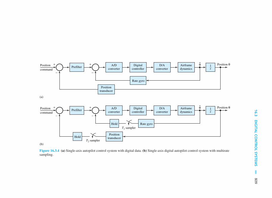
16.3DIGITA
LCONTROLSYSTEM
S809
−
+Prefilter s
−
+
Rate gyro
A/Dconverter
Positiontransducer
Positioncommand
(a)
θ Position θD/Aconverter
Airframedynamics
1Digitalcontroller
−
+Prefilter s
−
+
Rate gyro
Hold
Hold
A/Dconverter
Positiontransducer
T2 sampler
T1 sampler
Positioncommand
(b)
θ Position θD/Aconverter
Airframedynamics
1Digitalcontroller
Figure 16.3.4 (a) Single-axis autopilot control system with digital data. (b) Single-axis digital autopilot control system with multiratesampling.

810BASIC
CONTROLSYSTEM
S
Minicomputer Generator
OutputvariablesCoded
command
D/Aconverter
SteamturbineValve
D/Aconverter
Electrohydraulictransducer
Digitalmultiplexer
Digitaltransducers
Digital output
Digital output
(Voltage control)
(Speed control)
Analogtransducers
Analogmultiplexer
A/Dconverter
Sample-and-hold
(data aquisition)
From steamboiler
Exciter
Figure 16.3.5 Computer control of a turbogenerator unit.

16.3 DIGITAL CONTROL SYSTEMS 811
Memory andinstructions
Computer
Digitalprocessor
Drill-motordrive Drilling operation
Drill positionDrill
positionmechanism
Positionfeedbacknetwork
(Electromechanical drive)
Sampled-data position-control system
Inputnumericdata
Figure 16.3.6 Simplified block diagram of a digitally controlled drill press.
Digital computer Drive circuit Step motorSequencer
Digital positionencoder
Read–write head
Figure 16.3.7 Step-motor control system for read–write head positioning on a disk drive.
when a conductive surface, such as an airplane, appears in the signal path. While the antennais continuously rotated in search of a target, the antenna is stopped when the target is located.It is pointed toward the target by varying its angular direction until a maximum echo is heard.The position coordinate θ(t) of the antenna is usually controlled through a gear train by a dcservomotor. The motor torque is varied in both magnitude and direction by means of a controlvoltage obtained from the amplifier output. The control problem is then to command the motorsuch that the output θ (t) is nearly the same as the reference angular position θ r(t). The closedloop can be controlled by a digital controller.
Microprocessor Control
The microprocessor, which has rapidly become a key component in digital control systems, andits associated circuits function as the digital processor. It is often used as a dedicated computer
Transducer Controller(amplifier)
Motor andantenna
Transducer
Positioncommandθr(t)
Position θ(t)
Figure 16.3.8 Plant model of a position servo in a radar system.

812 BASIC CONTROL SYSTEMS
in which the chip itself is programmed to perform specific functions. Digital watches and autofuel-injection systems are examples. With microprocessor control, not only the same hardwarecan be used to perform a variety of tasks by reprogramming, but also distributed computation(which results in less expensive and more reliable operation than centralized control) is possiblewith interconnection and intercommunication of several microprocessors.
Figure 16.3.9 shows a block diagram of a microprocessor-controlled dc motor system, inwhich the controlled process consists of a dc motor, the load, and the power amplifier.
The block diagram of Figure 16.3.10 illustrates a typical microprocessor system used toimplement the digital PI controller. It would be simple to include the derivative operation toimplement the PID controller. While an analog timer is shown in Figure 16.3.10 to determinethe start of the next sampling period, a software timing loop can be used to keep track of whenT seconds have elapsed. The output pulse, once every T seconds, is applied to the interruptline of the microprocessor. This will cause the processor to execute the interrupt routine tooutput the next value of the control, u[(k + 1)T ], which is sent to the D/A converter, whoseoutput in turn controls the power amplifier. The timing pulse from the timer is also sent to the“sample” command line, thereby triggering the sample-and-hold circuitry; the motor velocityω(t) is sampled and held constant for one sampling period. The value of ω(kT) is then convertedto an N-bit binary number by the A/D circuitry. The microprocessor is signaled via “data ready”line (which may be attached to the interrupt line of the microprocessor) that the sampled datahave been converted. The second interrupt will cause the processor to read in the value of
D/Aconverter
Dc motor andpower amplifier
Feedback signalfrom motor
A/Dconverter
Microprocessor-based
controller
Output, updatedevery T seconds
Desiredsystemmotion
Sampler withsampling period T
Figure 16.3.9 Block diagram of a microprocessor-controlled dc motor system.
D/Aconverter
Poweramplifier
Inputport
Sample-and-hold
A/Dconverter
ω(t)
Accumulator (ac)
Data lines
Controlsignal
"Data ready" line
"Sample"command
line
Motor
Timer
Tachometer
Microprocessor
Outputport
Figure 16.3.10 Block diagram of discretized proportional and integral (PI) controller.

16.3 DIGITAL CONTROL SYSTEMS 813
ω(kT) and then compute the next value of control, u[(k + 1)T]. After calculation of the control,the microprocessor waits for another interrupt from the timer before it outputs the control att = (k + 1)T . An assembly-language program can be developed for the implementation of thePI controller.
The control of a dc motor can be achieved with a PI controller discretized for microprocessorprogramming. The starting point is that the PI controller is described by a differential equation.The latter is discretized at the sampling instants by one of the numerical approximation methods,and then is programmed in the microprocessor machine language.
Practical limitations of microprocessor-based control systems stem from the followingconsiderations:
• Finite-word-length characteristic, that is, an 8-bit word would only allow 28 = 256 levelsof resolution.
• Time delays encountered in executing the data handling, which may have a significant effecton the system response.
• Quantization effects, which affect accuracy and stability.
Adaptive Control
Another type of control system that makes use of the computer is known as adaptive control,which is functionally represented in Figure 16.3.11. While the block G provides the systemoutput for the system input, the feedback is provided by H and is converted to a digital signal.This digital signal is processed by the digital processor to effect the necessary control. Thecharacteristic feature of the adaptive control is that the characteristics of the block G arechanged with time so that, for a given input, the desired output is obtained. Based on theprediction of the performance of the system, the digital processor determines how G is to bechanged.
Figure 16.3.12 illustrates the adaptive control process as applied to a motor-speed controlsystem, which is based on adjustments of the armature resistance. Using all of the data inputs,the computer computes the optimum value of Ra such that the motor speed is appropriate tothe load. The signal corresponding to the computed value of Ra is in turn used to position thepotentiometer arm of the variable resistance. The actual armature resistance is then controlled bythe position of the potentiometer arm, which in turn may be controlled by a sampled-data versionof the position-control system.
The speed and power of the digital computer (in predicting the response to a wide range ofchanges that affect the system) are the main reasons for the use of adaptive systems in industrialcontrol. Large-scale systems may have multiple inputs applied simultaneously, and control issuccessfully achieved because the process of predicting the desired response, and comparingwith the actual response, can be accomplished in a relatively short time compared to the responsetime of the system to be controlled.
Digital processor
OutputInput
H
GFigure 16.3.11 Functional representation ofan adaptive control system.

814 BASIC CONTROL SYSTEMS
Positioncontrol
Variableresistance
Potentiometer arm
Computer
dc source
Data inputs:
Dc source Dcmotor
Load
ω
ω
++
−−
arm positiondesired performance
loadVm
Ia
Vm
Ra
Ia
Figure 16.3.12 Adaptive control process as applied to a motor-speed control system.
Methods of Analysis
Just as differential equations are used to represent systems with analog signals, differenceequations are used for systems with discrete or digital data. Difference equations are also usedto approximate differential equations, since the former are more easily programmed on a digitalcomputer, and are generally easier to solve.
One of the mathematical tools devised for the analysis and design of discrete-data systemsis the z-transform with z = eT s . The role of the z-transform for digital systems is similar to thatof the Laplace transform for continuous-data systems. While the Laplace transform can be usedto solve linear ordinary differential equations, for linear difference equations and linear systemswith discrete or digital data, the z-transform becomes more appropriate to use. Since it is not asimple matter to perform an inverse Laplace transform on transcendental functions which involveterms like e−kT s , the need arises to convert transcendental functions in s into algebraic ones inz. The development of z-transform methods of analysis are considered to be outside the scope ofthis book.
Various techniques and methods mentioned earlier, such as state-variable analysis, time-domain analysis, frequency-domain analysis, root-locus techniques, and Bode diagrams, areapplied to the analysis of digital control systems. Details of these are obviously outside thescope of this introductory text.
Finally, no one can be an expert in all areas discussed in this chapter, or indeed in the precedingchapters. Therefore, it is always good advice to consult with those who are. The basics you havebeen exposed to will help you to select such consultants, either in or out of house, who will providethe knowledge to solve the problem confronting you.
16.4 LEARNING OBJECTIVES
The learning objectives of this chapter are summarized here, so that the student can check whetherhe or she has accomplished each of the following.

16.5 PRACTICAL APPLICATION: A CASE STUDY 815
• Basic notions of power semiconductor devices and analysis of power electronic circuits.
• Solid-state control of dc motors.
• Solid-state control of induction motors.
• Solid-state control of synchronous motors.
• Transfer functions and block diagrams of feedback control systems.
• Dynamic response of control systems.
• Steady-state error of linear systems.
• Error-rate control, output-rate control, and integral-error control.
• Elementary concepts of digital control systems and their applications.
16.5 PRACTICAL APPLICATION: A CASE STUDY
Digital Process Control
Figure 16.5.1 shows a block diagram for microcomputer-based control of a physical process, suchas a chemical plant. A slight variation of the system can be used for automotive instrumentationin which sensors furnish various signals for speed, fuel reserve, battery voltage, oil pressure,engine temperature, and so on. The data are presented to the driver in one or more displays onthe dashboard. In a physical process on the other hand, based on the display information, anoperator can assess and direct the operation of the control process through a keyboard or otherinput devices to the microcomputer.
Various physical inputs, such as power and materials, are regulated by actuators, whichare in turn controlled by the microcomputer. Electric signals related to the controlled-processparameters, such as pressure and temperature, are produced by various sensors, which in turn
Analogsensors
A/Dconverter
D/Aconverter
Displayinformation
Operatorinputs
Microcomputer
Physical inputs
Acuators Contolledprocess Product output
Analog Digital
Digitalsensors
Figure 16.5.1 Block diagram for miocrocomputer-based control of a physical process.

816 BASIC CONTROL SYSTEMS
feed the information to the microcomputer. Actuators and sensors may be either analog or digital.Digital-to-analog (D/A) converters are used to convert the digital signals to analog form so as tosuit the analog actuators, where as analog-to-digital (A/D) converters are employed to convertthe analog sensor signals to digital form so as to suit the microcomputer.
One can think of so many systems in daily practice controlled or monitored by microcom-puters. Some examples include monitoring patients in intensive cardiac-care units of hospitals,nuclear-reactor controls, traffic signals, aircraft and automobile instrumentation, chemical plants,and various manufacturing processes.
PROBL EMS
16.1.1 (a) Consider a diode circuit with RC load asshown in Figure P16.1.1. With the switchclosed at t = 0 and with the initial conditionat t = 0 that vC = 0, obtain the functionalforms of i(t) and vC(t), and plot them.
(b) Then consider a diode circuit with an RL loadwith the initial condition at t = 0 that i = 0.With the switch closed at t = 0, obtain thefunctional forms of i(t) and vL(t).
(c) In part (b), if t >> L/R, describe what hap-pens. If an attempt is then made to open switchS, comment on what is likely to happen.
(d) Next consider a diode circuit with an LC loadwith the initial condition at t = 0 that i = 0and vC = 0. With the switch closed at t = 0,obtain the waveforms of i(t) and vC(t).
16.1.2 (a) Figure P16.1.2(a) contains a freewheelingdiode Dm, commonly connected across an in-ductive load to provide a path for the currentin the inductive load when the switch S isopened after time t (during which the switchwas closed). Consider the circuit operation intwo modes, with mode 1 beginning when theswitch is closed at t = 0, and mode 2 startingwhen the switch is opened after the current i
has reached its steady state in mode 1. Obtainthe waveforms of the currents i(t) and if(t).
(b) Consider the energy-recovery diode circuitshown in Figure P16.1.2(b), along with a feed-back winding. Assume the transformer to havea magnetizing inductance of Lm and an idealturns ratio of a = N2/N1. Let mode 1 beginwhen the switch S is closed at t = 0, and mode2 start at t = t1, when the switch is opened.Let t1 and t2 be the durations of modes 1 and 2,respectively. Develop the equivalent circuitsfor the two modes of operation, and obtainthe various waveforms for the currents andvoltages.
16.1.3 (a) Consider a full-wave rectifier circuit with acenter-tapped transformer, as shown in FigureP16.1.3, with a purely resistive load of R. Letvs = Vm sin ωt . Determine: (i) efficiency,(ii) form factor, (iii) ripple factor, (iv) TUF,and (v) PIV of diode D1. Compare the perfor-mance with that of a half-wave rectifier. (SeeExample 16.1.2.)
(b) Let the rectifier in part (a) have an RL load.Obtain expressions for output voltage vL(t)and load current iL(t) by using the Fourierseries.
t = 0
VS
vR
vC
R
C
+ +
−+
−−
SD I
Figure P16.1.1

PROBLEMS 817
t = 0
(a)
VSDm
if
R
L
+
−
SD i
(b)
VS
++
−
−
+−
S
D
i1v1
N1 : N2
v2
i2
Figure P16.1.2 (a) Diode circuit with freewheeling diode. (b) Energy-recovery diode circuit withfeedback winding.
vP
+
++
−
−
−
vD2
vD1
vs
+
−vs
vL
iL
D2
R
D1
Figure P16.1.3
*16.1.4 Consider a full-wave single-phase bridge rectifiercircuit with dc motor load, as shown in FigureP16.1.4(a). Let the transformer turns ratio be unity.Let the load be such that the motor draws a ripple-free armature current of Ia. Given the waveformsfor the input current and input voltage of the rec-tifier, as in Figure P16.1.4(b), determine: (i) har-monic factor HF of the input current, and (ii) inputpower factor PF of the rectifier.
16.1.5 (a) Consider a three-phase star or wye half-waverectifier with a purely resistive load R. Deter-mine: (i) efficiency, (ii) form factor, (iii) ripplefactor, (iv) TUF, and (v) PIV of each diode.
(b) Express the output voltage of the three-phaserectifier in Fourier series.
16.1.6 Consider a three-phase, full-wave bridge rectifier,as shown in Figure P16.1.6, with a purely resistiveload R. For each diode, determine: (i) efficiency,(ii) form factor, (iii) ripple factor, (iv) TUF, and(v) PIV.
16.1.7 Consider Example 16.1.2 in the text.
(a) Calculate the firing angle corresponding toa torque of 35 N·m and a speed of −1350r/min, assuming continuous conduction. What
is the quadrant of operation in the torque–speed relationship?
(b) Find the motor speed at the rated torque andα = 160° for the regenerative braking in thesecond quadrant.
16.1.8 For a three-phase, fully controlled, rectifier-fed,separately excited dc motor, corresponding toideal no-load operation, find the expression forthe no-load speeds. Comment on whether no-loadspeeds could be negative. Compared to the one-phase case, would you expect a considerable re-duction in the zone of discontinuous conduction?
*16.1.9 Consider the motor of Example 16.1.3 in the text.Calculate the motor speed for: (a) α = 120°,Ta = 25 N·m, and (b) α = 60°, Ta = 5 N·m.Assume continuous conduction in both cases.
16.1.10 Consider Example 16.1.4 in the text. For part (c),compute the corresponding rms fundamental sta-tor current.
16.1.11 A 60-Hz, six-pole, wye-connected, three-phaseinduction motor, with the parameters R1 = R′2 =0.025 and Xl1 = X′l2 = 0.125 , is controlledby variable-frequency control with constant V/fratio. Use the approximate equivalent circuit ofFigure 13.2.6, with jXm moved over to the supply

818 BASIC CONTROL SYSTEMS
vp
+
−
+
−vs
vsVm
Ia
−Vm
−Ia
π
π
2π
2π
ωt
ωt
0
0
Fundamentalcomponent
(a) (b)
i1
IL = Ia
D3
D2
D1
M
i1
D4
Figure P16.1.4 (a) Circuit diagram. (b) Waveforms.
vLR
+
−
ia
ic
iD1 iL
ib
vcn
van
vbn
a
ab
b
c
cD1
D4
D3
D6
D5
D2
Figure P16.1.6
terminals. For an operating frequency of 15 Hz,find:
(a) The maximum motoring torque as a ratio ofits value at the rated frequency.
(b) The starting torque and rotor current in termsof their values at the rated frequency.
16.1.12 Given that the motor of Problem 16.1.11 has afull-load slip of 0.05, compute the motor speedcorresponding to rated torque and a frequency of30 Hz.
16.1.13 Consider the motor of Example 16.1.4 in the text.Let the motor be controlled by variable frequencyat a constant flux of rated value. By using theequivalent circuit of Figure 13.2.6,
(a) Determine the motor speed and the stator cur-rent at one-half the rated torque and 30 Hz.
(b) Redo part (a), assuming the speed–torquecurves to be straight lines for S < Smax.
16.1.14 For the static rotor resistance control consideredin the text for an induction motor drive, developthe fundamental frequency equivalent circuit ofFigure 16.1.23.
*16.1.15 Consider the induction motor drive of Example16.1.5 in the text. Compute the motor speed cor-responding to δ = 0.65 and 1.5 times the ratedfull-load torque.
16.1.16 Let the simplified per-phase equivalent circuit ofan underexcited, cylindrical-rotor, synchronousmachine be given by a source Vf − δ in serieswith an impedance jXs. Let V 0° and Is − φ be

PROBLEMS 819
the applied voltage at the terminals and the currentdrawn by the motor, respectively.
(a) With V as reference, draw a phasor diagramfor the motor.
(b) Develop an equivalent circuit with a currentsource and draw the corresponding phasordiagram with V as reference.
(c) Obtain expressions for power and torque forparts (a) and (b).
(d) Now consider the variable-frequency opera-tion of the synchronous motor, with the per-unit frequency a to be f /f rated. Taking Vf asreference in the quadrature axis, draw the pha-sor diagram and comment on the effect of thevariable frequency.
16.1.17 Consider the motor of Example 16.1.6 in the text.
(a) Determine the armature current and powerfactor at one-half the rated speed, one-half therated torque, and rated field current.
(b) Find the torque and field current correspond-ing to rated armature current, 1.25 times therated speed, and unity power factor.
16.2.1 Consider the electrical transients on a linear ba-sis in a separately excited dc generator (whosemodel is shown in Figure P16.2.1), resulting fromchanges in excitation. Let the generator speed bea constant, so that the dynamics of the mechanicaldrive do not enter the problem. Obtain expressionsforEa(s)/Vf (s) and Ia(s)/Vf (s), and develop thecorresponding block diagrams. Let RL and LL bethe load resistance and load inductance, respec-tively.
16.2.2 A separately excited dc generator has the follow-ing parameters: Rf = 100 ,Lf = 20 H, Ra =0.1 ,La = 0.1 H, and Kg = 100 V per fieldampere at rated speed. The load connected to thegenerator has a resistance RL = 4.5 and aninductance LL = 2.2 H. Assume that the primemover is rotating at rated speed, the load switchis closed, and the generator is initially unexcited.Determine the armature current as a function oftime when a 230-V dc supply is suddenly appliedto the field winding, assuming the generator speedto be essentially constant.
16.2.3 A 5-hp, 220-V, separately excited dc motor hasthe following parameters: Ra = 0.5 , k = 2 H,
Rf = 220 , and Lf = 110 H. The armaturewinding inductance is negligible. The torque re-quired by the load is proportional to the speed,and the combined constants of the motor armatureand the load are J = 3 kg·m2 and B = 0.3kg·m2/s. Consider the armature-controlled dc mo-tor, whose speed is made to respond to variationsin the applied motor armature voltage vt. Let thefield current be maintained constant at 1 A.
(a) Develop a block diagram relating the motorspeed and the motor applied voltage, and findthe corresponding transfer function.
(b) Compute the steady-state speed correspond-ing to a step-applied armature voltage of 220V.
(c) How long does the motor take to reach 0.95of the steady-state speed of part (b)?
(d) Determine the value of the total effective vis-cous damping coefficient of the motor-loadconfiguration.
−
+
+
−
−+
ea
vt
vf
if
Lf
Rf
La
wmTe
Ts
ia
Ra Figure P16.2.1 Schematic representationof the model of a separately excited dc motor.

820 BASIC CONTROL SYSTEMS
*16.2.4 A separately excited dc generator has the follow-ing parameters:Field winding resistance Rf = 60
Field winding inductance Lf = 60 HArmature resistance Ra = 1
Armature inductance La = 0.4 HGenerated emf constant Kg = 120 V per field
ampere at rated speedThe armature terminals of the generator are con-nected to a low-pass filter with a series inductanceL = 1.6 H and a shunt resistance R = 1 .Determine the transfer function relating the outputvoltage Vt(s) across the shunt resistance R, and theinput voltage Vf(s) applied to the field winding.
16.2.5 A separately excited dc generator, running at con-stant speed, supplies a load having a 1- resistancein series with a 1-H inductance. The armatureresistance is 0.1 and its inductance is negligible.The field, having a resistance of 50 and an in-ductance of 5 H, is suddenly connected to a 100-Vsource. Determine the armature current buildup asa function of time, if the generator voltage constantKg = 50 V per field ampere at rated speed.
16.2.6 The following test data are taken on a 20-hp, 250-V, 600-r/min dc shunt motor: Rf = 150 , τf =0.5 s, Ra = 0.15 , and τa = 0.05 s. When themotor is driven at rated speed as a generator withno load, a field current of 2 A produces an armatureemf of 250 V. Determine the following:
(a) Lf, the self-inductance of the field circuit.
(b) La, the self-inductance of the armature circuit.
(c) The coefficient K relating the speed voltageto the field current.
(d) The friction coefficient BL of the load at ratedload and rated speed, assuming that the torquerequired by the load TL is proportional to thespeed.
16.2.7 A separately excited dc generator can be treated asa power amplifier when driven at constant angularvelocity ωm. If the armature circuit is connected toa load having a resistanceRL, obtain an expressionfor the voltage gain VL(s)/Vf (s). With Ra =0.1 ,Rf = 10 ,RL = 1 , and Kg = 100V per field ampere at rated speed, determine thevoltage gain and the power gain if the generator isoperating at steady state with 25 V applied acrossthe field.
16.2.8 Consider the motor of Problem 16.2.6 to be ini-tially running at constant speed with an impressed
armature voltage of 250 V, with the field separatelyexcited by a constant field current of 2 A. Letthe motor be driving a pure-inertia load with acombined polar moment of inertia of armature andload of 3 kg·m2. The rotational losses of the motorcan be neglected.
(a) Determine the speed.
(b) Neglecting the self-inductance of the arma-ture, obtain the expressions for the armaturecurrent and the speed as functions of time,if the applied armature voltage is suddenlyincreased from 250 V to 260 V.
(c) Repeat part (b), including the effect of thearmature self-inductance.
*16.2.9 A separately excited dc motor carries a load of300ωm + ωm N·m. The armature resistance is 1 and its inductance is negligible. If 100 V issuddenly applied across the armature while thefield current is constant, obtain an expression forthe motor speed buildup as a function of time,given a motor torque constant Km = 10 N·m/A.
16.2.10 Consider the motor of Problem 16.2.3 to be op-erated as a separately excited dc generator at aconstant speed of 900 r/min, with a constant fieldcurrent of 1.5 A. Let the load current be initiallyzero. Determine the armature current and the ar-mature terminal voltage as functions of time for asuddenly applied load impedance consisting of aresistance of 11.5 and an inductance of 0.1 H.
16.2.11 Consider a motor supplied by a generator, eachwith a separate and constant field excitation. As-sume the internal voltage E of the generator to beconstant, and neglect the armature reaction of bothmachines. With the motor running with no externalload, and the system being in steady state, let a loadtorque be suddenly increased from zero to T. Themachine parameters are as follows:Armature inductance of motor + generator, L =
0.008 HArmature resistance of motor + generator, R =
0.04
Internal voltage of the generator E = 400 VMoment of inertia of motor armature and load
J = 42 kg·m2
Motor constant Km = 4.25 N·m/ANo-load armature current i0 = 35 ASuddenly applied torque T = 2000 N·mDetermine the following:
(a) The undamped angular frequency of the tran-sient speed oscillations, and the damping ratioof the system.

PROBLEMS 821
(b) The initial speed, final speed, and the speeddrop in r/min.
16.2.12 Consider a separately excited dc motor havinga constant field current and a constant appliedarmature voltage. It is accelerating a pure-inertiaload from rest. Neglecting the armature inductanceand the rotational losses, show that by the time themotor reaches its final speed, the energy dissipatedin the armature resistance is equal to the energystored in the rotating parts.
16.2.13 Determine the parameters of the analog capacitivecircuit shown in Figure E16.2.1(d) for the motorin Problem 16.2.3 and its connected load. With theaid of the equivalent circuit, obtain the expressionfor the armature current, with a 3.5- startingresistance included in series with the armature tolimit the starting current.
*16.2.14 Neglecting the self-inductance of the armature cir-cuit, show that the time constant of the equivalentcapacitive circuit for a separately excited dc mo-tor with no load is RaReqCeq/(Ra + Req), whereReq = 1/Geq, as shown in Figure E16.2.1(d).
16.2.15 Consider the dc motor of Problem 16.2.3 to beoperating at rated voltage in steady state with afield current of 1 A, and with the starting resistancein series with the armature reduced to zero.
(a) Obtain the equivalent capacitive circuit ne-glecting the armature self-inductance and cal-culate the steady armature current.
(b) If the field current is suddenly reduced to 0.8 Awhile the armature applied voltage is constantat 220 V, compute the initial armature currentia(0) on the basis that the kinetic energy storedin the rotating parts cannot change instanta-neously.
(c) Determine the final armature current ia(∞) forthe condition of part (b).
(d) Obtain the time constant τ ′am of the armaturecurrent for the condition of part (b), and ex-
press the armature current as a function oftime on the basis that ia = ia(∞)+ [ia(0)−ia(∞)] e−t/τ ′am .
16.2.16 A separately excited dc motor, having a constantfield current, accelerates a pure inertia load fromrest. If the system is represented by an electricalequivalent circuit, with symbols as shown in Fig-ure P16.2.16, express R, L, and C in terms of themotor parameters.
16.2.17 Figure P16.2.17 represents the Ward–Leonard sys-tem for controlling the speed of the motor M.With the generator field voltage vfg as the inputand the motor speed ωm as the output, obtain anexpression for the transfer function for the system,assuming idealized machines. Let the load on themotor be given by J ωm + Bωm. The generatorruns at constant angular velocity ωg .
16.2.18 A separately excited dc generator has the follow-ing parameters:Rf = 100,Ra = 0.25,Lf =25 H, La = 0.02 H, and Kg = 100 V per fieldampere at rated speed.
(a) The generator is driven at rated speed, and afield circuit voltage ofVf = 200 V is suddenlyapplied to the field winding.
(i) Find the armature generated voltage as afunction of time.
(ii) Calculate the steady-state armature volt-age.
(iii) How much time is required for the arma-ture voltage to rise to 90% of its steady-state value?
(b) The generator is driven at rated speed, anda load consisting of RL = 1 and LL =0.15 H in series is connected to the armatureterminals. A field circuit voltage Vf = 200V is suddenly applied to the field winding.Determine the armature current as a functionof time.
J
If = constant
(b)(a)
La Ra ia iR L
Cve
ωm
+
−
v
+
−−
+
Figure P16.2.16
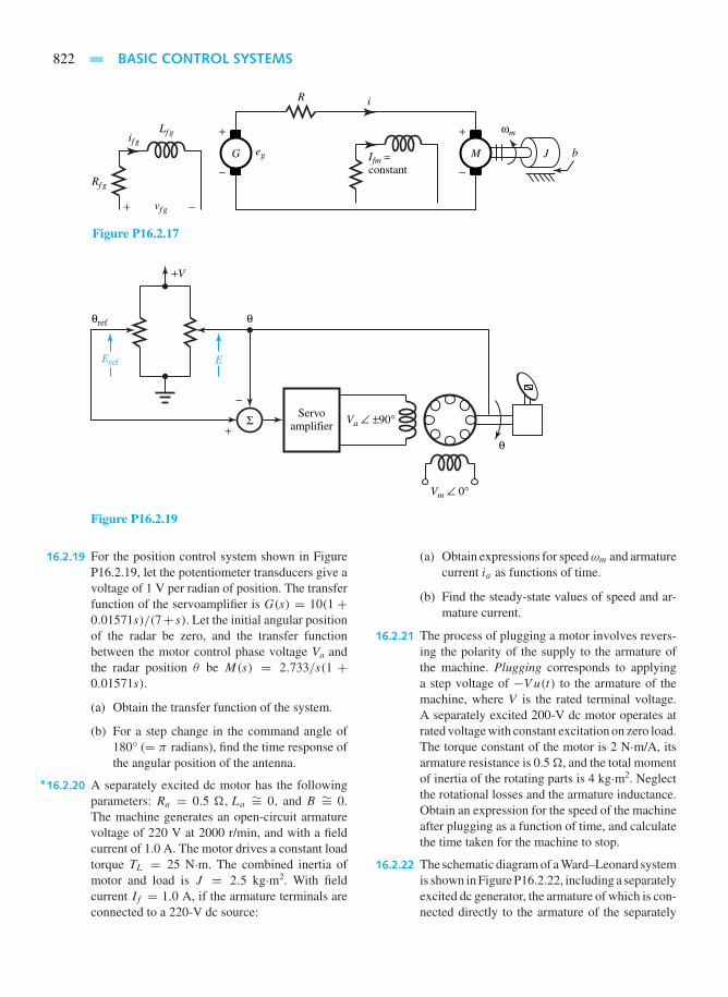
822 BASIC CONTROL SYSTEMS
Rfg
vfg
ifg
Lfg
Ifm =constant
eg
ωm
−+
R i
G
−
+
M J b
−
+
Figure P16.2.17
Servoamplifier
Va ∠ ±90°
Vm ∠ 0°
Σ+
−
Eref
θref θ
θ
E
+V
Figure P16.2.19
16.2.19 For the position control system shown in FigureP16.2.19, let the potentiometer transducers give avoltage of 1 V per radian of position. The transferfunction of the servoamplifier is G(s) = 10(1 +0.01571s)/(7+ s). Let the initial angular positionof the radar be zero, and the transfer functionbetween the motor control phase voltage Va andthe radar position θ be M(s) = 2.733/s(1 +0.01571s).
(a) Obtain the transfer function of the system.
(b) For a step change in the command angle of180° (= π radians), find the time response ofthe angular position of the antenna.
*16.2.20 A separately excited dc motor has the followingparameters: Ra = 0.5 ,La
∼= 0, and B ∼= 0.The machine generates an open-circuit armaturevoltage of 220 V at 2000 r/min, and with a fieldcurrent of 1.0 A. The motor drives a constant loadtorque TL = 25 N·m. The combined inertia ofmotor and load is J = 2.5 kg·m2. With fieldcurrent If = 1.0 A, if the armature terminals areconnected to a 220-V dc source:
(a) Obtain expressions for speedωm and armaturecurrent ia as functions of time.
(b) Find the steady-state values of speed and ar-mature current.
16.2.21 The process of plugging a motor involves revers-ing the polarity of the supply to the armature ofthe machine. Plugging corresponds to applyinga step voltage of −V u(t) to the armature of themachine, where V is the rated terminal voltage.A separately excited 200-V dc motor operates atrated voltage with constant excitation on zero load.The torque constant of the motor is 2 N·m/A, itsarmature resistance is 0.5 , and the total momentof inertia of the rotating parts is 4 kg·m2. Neglectthe rotational losses and the armature inductance.Obtain an expression for the speed of the machineafter plugging as a function of time, and calculatethe time taken for the machine to stop.
16.2.22 The schematic diagram of a Ward–Leonard systemis shown in Figure P16.2.22, including a separatelyexcited dc generator, the armature of which is con-nected directly to the armature of the separately
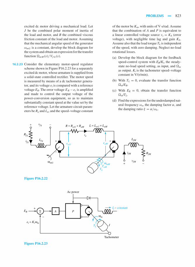
PROBLEMS 823
excited dc motor driving a mechanical load. LetJ be the combined polar moment of inertia ofthe load and motor, and B the combined viscousfriction constant of the load and motor. Assumingthat the mechanical angular speed of the generatorωmG is a constant, develop the block diagram forthe system and obtain an expression for the transferfunction mM(s)/VfG(s).
16.2.23 Consider the elementary motor-speed regulatorscheme shown in Figure P16.2.23 for a separatelyexcited dc motor, whose armature is supplied froma solid-state controlled rectifier. The motor speedis measured by means of a dc tachometer genera-tor, and its voltage et is compared with a referencevoltage ER. The error voltage ER− et is amplifiedand made to control the output voltage of thepower-conversion equipment, so as to maintainsubstantially constant speed at the value set by thereference voltage. Let the armature-circuit param-eters be Ra and La, and the speed–voltage constant
of the motor be Km, with units of V·s/rad. Assumethat the combination of A and P is equivalent toa linear controlled voltage source vs = KA (errorvoltage), with negligible time lag and gain KA.Assume also that the load torque TL is independentof the speed, with zero damping. Neglect no-loadrotational losses.
(a) Develop the block diagram for the feedbackspeed-control system with ER/Kt, the steady-state no-load speed setting, as input, and m
as output. Kt is the tachometer speed–voltageconstant in V/(r/min).
(b) With TL = 0, evaluate the transfer functionm/ER.
(c) With ER = 0, obtain the transfer functionm/TL.
(d) Find the expressions for the underdamped nat-ural frequency ωn, the damping factor α, andthe damping ratio ξ = α/ωn.
eaGeaM
ωmMTeM
TL
ifg
ifM
ωmG
Rfg
vfg
Lfg
−+ R = RaG + RaM L = LaG + LaM
LfM
vfM
RfM
ia
−
+
−
+
+ −
Figure P16.2.22
Σ A PER
If = constant
ωm
TL J
Ac power
Tachometer
et = Kt ωm
−
+
Figure P16.2.23

824 BASIC CONTROL SYSTEMS
(e) For a step input ER, obtain the final steady-state response ωm(∞), i.e., evaluateωm(∞)/ER .
(f) Evaluate ωm(∞)/TL for the step inputTL of a load torque.
16.2.24 Consider the motor of Problem 16.2.3 to be usedas a field-controlled dc machine. Let the armaturebe energized from a constant current source of 15A. Assume no saturation.
(a) Develop a block diagram relating the motorspeed and the applied field voltage.
(b) Determine the steady-state speed for a step-applied field voltage of 220 V.
(c) How long does the motor take to reach 0.95of the steady-state speed of part (b)?
*16.2.25 The output voltage of a 10-kW, 240-V dc generatoris regulated by means of the closed-loop systemshown in Figure P16.2.25. The generator parame-ters areRf = 150,Ra = 0.5,Lf = 75 H, andKE = 150 V per field ampere at 1200 r/min. Theself-inductance of the armature is negligible. Theamplifier has an amplification factor A = 10, andthe potentiometers are set such that a is unity andthe reference voltage vr is 250 V. The generator isdriven by an induction motor, the speed of whichis almost 1200 r/min when the generator output iszero, and 1140 r/min when the generator deliversan armature current of 42 A.
(a) Compute the steady-state armature terminalvoltage at no load, and when the generator isdelivering 42 A.
(b) Calculate the time constant for part (a).
(c) With the value of the field current as in part(a), for an armature current of 42 A, calculatethe steady-state armature voltage.
16.2.26 (a) A common analog control element is the dctachometer, which is basically a permanent
magnet generator, as illustrated schematicallyin Figure P16.2.26(a). Determine the transferfunction of this device, with speed as the inputand voltage as the output. See what happensto the transfer function if RL →∞.
(b) A dc servomotor is another common analogelement in control systems, shown schemat-ically in Figure P16.2.26(b). Obtain an ex-pression form(s)/Ei(s), assuming constant-field configuration and linear elements.
(c) Add load torque to the load on the servomotorof Figure P16.2.26(b). Develop a block dia-gram with a voltage signal that will serve as aspeed reference and a load torque as a secondinput (or load disturbance).
16.2.27 (a) Consider a single loop system of the con-figuration shown in Figure P16.2.27(a) withpositive feedback. Although positive feedbackgenerally results in instability, it is frequentlyemployed at low magnitudes or in portions ofa large control system, particularly in an innerloop. Obtain an expression for C(s)/R(s).
(b) Figure P16.2.27(b) illustrates a multiple-loopfeedback control system, where the arguments is omitted for simplicity. Reduce it to asingle-loop configuration.
16.2.28 Loop topography that is relatively common in con-trol systems is shown in Figure P16.2.28. Obtainits single-loop representation.
*16.2.29 A generalized two-input system is illustrated inFigure P16.2.29. Treating multiple inputs bymeans of the principle of superposition, whichholds in linear control systems, find the systemresponse C.
16.2.30 Simplify the loop topography shown in FigureP16.2.30 to that of a single-loop configuration.
16.2.31 Determine the steady-state error of a type 0 systemwith a unit-step reference input function for theWard–Leonard system of Figure E16.2.3(a).
vevfGain A
Amplifier
+ +++
+
−
RL
iL
vtavt
if
va
ava
Figure P16.2.25

PROBLEMS 825
ea
ea
Constant fieldor permanentmagnet
Constant fieldor permanentmagnet
(a)
Electronic instrumentsuch as dc millivoltmeterwith high impedance
vo RL
ωm
ωm
Ra Laia
ei
(b)
Ra LaJL , BL
ia
Figure P16.2.26
G(s)
H(s)
Loop 3
Loop 2
Loop 1
R(s)
(a)
C(s)+
+
G1 G2 G3 C
H1
R
(b)
+
−
H2
H3
+
+
−
Figure P16.2.27
16.2.32 Verify the error-response conclusions listed inTable 16.2.2.
16.2.33 (a) Determine the system type, the steady-stateerror for a unit-step reference function, andthe closed-loop time constant for the speed-control system of Figure P16.2.33(a), whichuses proportional control.
(b) Determine the system type, the steady-state
error for a unit-step reference function, andthe damping ratio for the speed-control sys-tem of Figure P16.2.33(b), which uses integralcontrol.
(c) Add proportional control to the system of part(b) by replacing Ki/s with Kp + Ki/s, andfind the new damping ratio.
*16.2.34 Consider the speed-control system shown in
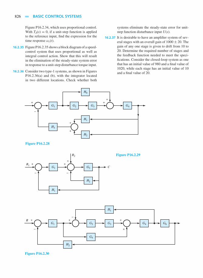
826 BASIC CONTROL SYSTEMS
Figure P16.2.34, which uses proportional control.With Td(s) = 0, if a unit-step function is appliedto the reference input, find the expression for thetime response ωc(t).
16.2.35 Figure P16.2.35 shows a block diagram of a speed-control system that uses proportional as well asintegral control action. Show that this will resultin the elimination of the steady-state system errorin response to a unit-step disturbance torque input.
16.2.36 Consider two type-1 systems, as shown in FiguresP16.2.36(a) and (b), with the integrator locatedin two different locations. Check whether both
systems eliminate the steady-state error for unit-step function disturbance input U(s).
16.2.37 It is desirable to have an amplifier system of sev-eral stages with an overall gain of 1000± 20. Thegain of any one stage is given to drift from 10 to20. Determine the required number of stages andthe feedback function needed to meet the speci-fications. Consider the closed-loop system as onethat has an initial value of 980 and a final value of1020, while each stage has an initial value of 10and a final value of 20.
G1 G2 G3 G4
+
+
+
++
−
H0
H1
H3
H2
Figure P16.2.28
G1 G2 CR1
R2
+ ++
− −
H2
H1
Figure P16.2.29
G1 G2 G3 G4 G6
R + +
+
+−
−
H1
G5
H2
Figure P16.2.30

PROBLEMS 827
−
+sJ + B
1ΩR(s) Ω0(s)E(s)
Controller
(a)
Turbine Load
Kp Kt
−+ sJ + B
1ΩR(s) Ω0(s)E(s)
(b)
sKi Kt
Figure P16.2.33
−
−+ +
Js1Ωr(s) Ωc(s)
Td (s)
Kp Kt
Figure P16.2.34
−
−+ +
Js1
sKi
Ωr(s) Ωc(s)
Td (s)
Kp + Kt
Figure P16.2.35
−
++
1 + τssKi
Kt
s(1 + τs)
Kt
R(s) C(s)
U(s)
(a)
−
++R(s) C(s)
U(s)
(b)
Kp
Figure P16.2.36
16.2.38 The parameters of the FET in a grounded-sourceamplifier are affected because aging causes a netper-unit decrease in gain of 25%. Each amplifiercircuit is designed to yield a gain (between theinput–output terminals) of 80, with the change atno time exceeding 0.1%.
(a) Find the minimum number of stages neededto meet the specification.
(b) Determine the corresponding feedback fac-tor H.
16.2.39 (a) A system has a direct transmission functiongiven by
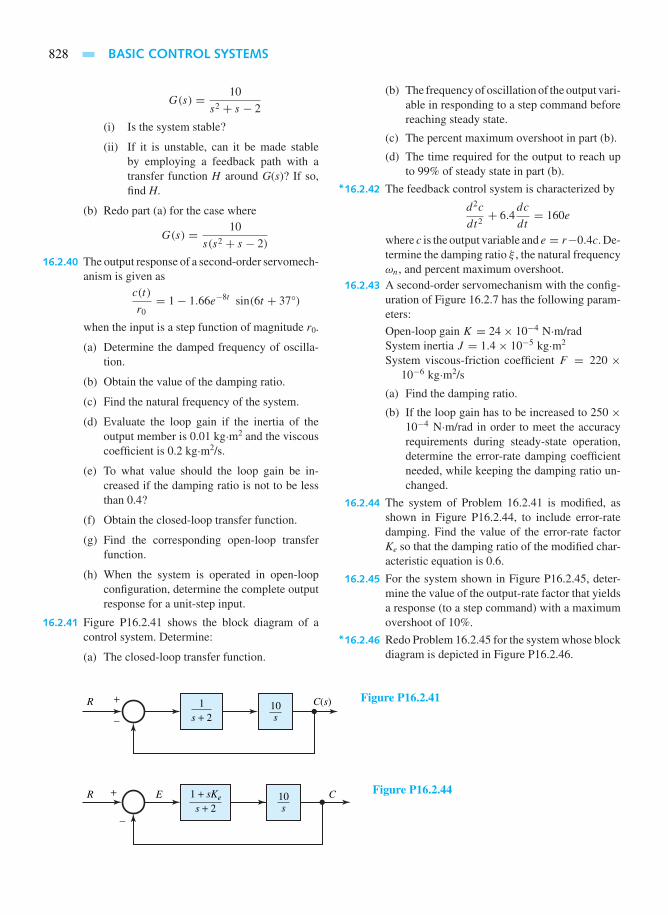
828 BASIC CONTROL SYSTEMS
G(s) = 10
s2 + s − 2
(i) Is the system stable?
(ii) If it is unstable, can it be made stableby employing a feedback path with atransfer function H around G(s)? If so,find H.
(b) Redo part (a) for the case where
G(s) = 10
s(s2 + s − 2)
16.2.40 The output response of a second-order servomech-anism is given as
c(t)
r0= 1− 1.66e−8t sin(6t + 37°)
when the input is a step function of magnitude r0.
(a) Determine the damped frequency of oscilla-tion.
(b) Obtain the value of the damping ratio.
(c) Find the natural frequency of the system.
(d) Evaluate the loop gain if the inertia of theoutput member is 0.01 kg·m2 and the viscouscoefficient is 0.2 kg·m2/s.
(e) To what value should the loop gain be in-creased if the damping ratio is not to be lessthan 0.4?
(f) Obtain the closed-loop transfer function.
(g) Find the corresponding open-loop transferfunction.
(h) When the system is operated in open-loopconfiguration, determine the complete outputresponse for a unit-step input.
16.2.41 Figure P16.2.41 shows the block diagram of acontrol system. Determine:
(a) The closed-loop transfer function.
(b) The frequency of oscillation of the output vari-able in responding to a step command beforereaching steady state.
(c) The percent maximum overshoot in part (b).
(d) The time required for the output to reach upto 99% of steady state in part (b).
*16.2.42 The feedback control system is characterized by
d2c
dt2+ 6.4
dc
dt= 160e
where c is the output variable and e = r−0.4c. De-termine the damping ratio ξ , the natural frequencyωn, and percent maximum overshoot.
16.2.43 A second-order servomechanism with the config-uration of Figure 16.2.7 has the following param-eters:
Open-loop gain K = 24× 10−4 N·m/radSystem inertia J = 1.4× 10⁻⁵ kg·m2
System viscous-friction coefficient F = 220 ×10−6 kg·m2/s
(a) Find the damping ratio.
(b) If the loop gain has to be increased to 250 ×10−4 N·m/rad in order to meet the accuracyrequirements during steady-state operation,determine the error-rate damping coefficientneeded, while keeping the damping ratio un-changed.
16.2.44 The system of Problem 16.2.41 is modified, asshown in Figure P16.2.44, to include error-ratedamping. Find the value of the error-rate factorKe so that the damping ratio of the modified char-acteristic equation is 0.6.
16.2.45 For the system shown in Figure P16.2.45, deter-mine the value of the output-rate factor that yieldsa response (to a step command) with a maximumovershoot of 10%.
*16.2.46 Redo Problem 16.2.45 for the system whose blockdiagram is depicted in Figure P16.2.46.
+
− s + 2 s101R C(s) Figure P16.2.41
+
−s + 2 s
101 + sKeR E C Figure P16.2.44

PROBLEMS 829
+
−
+
−s + 2
1s1
10
sK0
R C
Figure P16.2.45
+ +
−s + 2
1s2
5
sK0
R C
−
Figure P16.2.46

This page intentionally left blank

APPENDIX
A References
GENERAL ELECTRICAL ENGINEERING AND CIRCUITS
Bobrow, Fundamentals of Electrical Engineering, 2nd edition. Oxford University Press, New York, 1996DeCarlo and Lin, Linear Circuit Analysis, 2nd edition. Oxford University Press, New York, 2001Dorf and Svoboda, Introduction to Electric Circuits, Wiley, New York, 1999Franco, Electric Circuits Fundamentals, Oxford University Press, New York, 1994Irwin and Kerns, Introduction to Electrical Engineering, Prentice-Hall, Upper Saddle River, 1995Nasar, 3000 Solved Problems in Electric Circuits, McGraw-Hill, New York, 1992Pratap, Getting Started with MATLAB 5, Oxford University Press, New York, 1999Rizzoni, Principles and Applications of Electrical Engineering, 3rd edition. McGraw-Hill, New York, 2000Roberts and Sedra, SPICE, 2nd edition. Oxford University Press, New York, 1999Sadiku, Elements of Electromagnetics, 3rd edition. Oxford University Press, New York, 2001Sarma, Introduction to Electrical Engineering, Oxford University Press, New York, 2001Schwarz and Oldham, Electrical Engineering: An Introduction, 2nd edition. Oxford University Press, NewYork, 1993Schwarz, Electromagnetics for Engineers, Oxford University Press, New York, 1990Tuinenga, SPICE: A Guide to Circuit Simulation and Analysis Using PSpice, 3rd edition. Prentice-Hall,Upper Saddle River, 1995
INFORMATION AND COMMUNICATION SYSTEMS
Carlson, Communication Systems: An Introduction to Signals and Noise in Electrical Communication, 3rdedition. McGraw-Hill, NY, 1986Chen, Digital Signal Processing, Oxford University Press, New York, 2001Cooper and McGillem, Probabilistic Methods of Signal and System Analysis, 3rd edition. Oxford UniversityPress, New York, 1999Ingle and Proakis, Digital Signal Processing Using MATLAB, Version 4, 2nd edition. Brooks Cole, Monterey,1999Lathi, Modern Digital and Analog Communications Systems, 3rd edition. Oxford University Press, NewYork, 1998Proakis, Digital Communications, 3rd edition. McGraw-Hill, New York, 1995Proakis and Manolakis, Digital Signal Processing: Principles, Algorithms and Applications, 3rd edition.Prentice Hall, Upper Saddle River, 1995Stallings, Data and Computer Communications, 6th edition, Prentice-Hall, Upper Saddle River, 2000Stallings, Local and Metropolitan Area Networks, 6th edition, Prentice-Hall, Upper Saddle River, 2000Yariv, Optical Electronics in Modern Communications, 5th edition, Oxford University Press, New York,1997
ELECTRONIC SYSTEMS, DIGITAL AND ANALOG
Allen and Holberg, CMOS Analog Circuit Design, Oxford University Press, New York, 1987Campbell, The Science and Engineering of Microelectronic Fabrication, 2nd edition. Oxford UniversityPress, New York, 2001Dimitrijev, Understanding Semiconductor Devices, Oxford University Press, New York, 2000Franco, Design with Operational Amplifiers and Analog Integrated Circuits, 2nd edition. McGraw-Hill,New York, 1998Gray and Meyer, Analysis and Design of Analog Integrated Circuits, 3rd edition. Wiley, New York, 1992
831

832 APPENDIX A
Hansalman and Littlefield, Mastering MATLAB 5: A Comprehensive Tutorial and Reference, Prentice-Hall,Upper Saddle River, 1998Hodges and Jackson, Analysis and Design of Digital Integrated Circuits, 2nd edition. McGraw-Hill, NewYork, 1988Johns and Martin, Analog Integrated Circuit Design, Wiley, New York, 2000Martin, Digital Integrated Circuit Design, Oxford University Press, New York, 2000Razavi, Design of Analog CMOS Integrated Circuits, McGraw-Hill, New York, 2001Roulston, An Introduction to the Physics of Semiconductor Devices, Oxford University Press, New York,1999Roth, Fundamentals of Logic Design, 4th edition, Brooks Cole, Monterey, 1992Schaumann and Van Valkenburg, Design of Analog Filters, Oxford University Press, New York, 2001Sedra and Smith, Microelectronic Circuits, 4th edition, Oxford University Press, New York, 1998Van Valkenburg, Analog Filter Design, Oxford University Press, New York, 1982Wakerly, Digital Design: Principles and Practices, 3rd edition. Prentice-Hall, Upper Saddle River, 2000
CONTROL SYSTEMS
Bishop, Modern Control Systems Analysis and Design Using MATLAB and Simulink, Addison Wesley,Reading, 1997Chen, Linear System Theory and Design, 3rd edition. Oxford University Press, New York, 1999Dorf and Bishop, Modern Control Systems, 8th edition, Addison Wesley, Reading, 1997Franklin et. al., Digital Control of Dynamic Systems, 3rd edition. Addison Wesley, Reading, 1998Kuo, Automatic Control Systems,7th edition, Prentice-Hall, Upper Saddle River, 1994Kuo, Digital Control Systems, 3rd edition. Oxford University Press, New York, 1992Ogata, Modern Control Engineering, 3rd edition. Prentice-Hall, Upper Saddle River, 1997Stefani, Savant, Shahian, and Hostetter, Design of Feedback Control Systems, 4th edition, 2001
ELECTRIC POWER
Chapman, Electric Machinery Fundamentals, 3rd edition. McGraw-Hill, New York, 1998Guru and Hiziroglu, Electric Machinery & Transformers, 3rd edition. Oxford University Press, New York,2001Glover and Sarma, Power Systems Analysis and Design, 2nd edition. Brooks-Cole, Monterey, 1994Krein, Elements of Power Electronics, Oxford University Press, New York, 1998Nasar, Schaum’s Outline of Theory and Problems of Electric Machines and Electromechanics, 2nd edition.McGraw-Hill, New York, 1997Sen, Principles of Electric Machines and Power Electronics, 2nd edition. Wiley, New York, 1996Sarma, Electric Machines: Steady-State Theory and Dynamic Performance, 2nd edition. Brooks-Cole,Monterey, 1994

APPENDIX
B Brief Review of Fundamentals of Engineering (FE)Examination
Anyone who wishes to practice the engineering profession and offer professional services to thepublic must become registered as a professional engineer (PE). Boards in each of the 50 statesregulate the profession of engineering. The process of registering or licensing oneself as a PE isa multistep process.
Engineering programs accredited by the Engineering Accreditation Commission (EAC) ofthe Accreditation Board for Engineering and Technology (ABET) are acceptable to all boards asqualifying education. After obtaining the necessary education and applying to the board, one willbe allowed to take the Fundamentals of Engineering (FE) examination. The FE examination,formerly called the Engineer-in-Training (EIT) examination, is offered twice a year and isusually taken by engineering-college seniors or fresh graduates. After successfully passing theFE examination, one is known as an Engineer-Intern (EI), and is admitted to the preprofessionalstatus as a newly trained engineer. The EI must then obtain a minimum of four years of acceptableexperience before being qualified to take the Professional Engineering (PE) examination. Thistext should serve as an excellent reference to prepare for both of these examinations.
The FE examination consists of two parts, morning session and an afternoon session.Administered by the National Council of Examiners for Engineering and Surveying (NCEES),140 multiple-choice problems with 5 choices for each problem out of which one correct answeris to be selected are given in the morning session; 70 problems are given in the afternoon session.
Candidates for the FE examination are provided with a booklet called the Reference Hand-book, which contains relevant tables, formulas, and charts along with the question paper. Can-didates are not supposed to bring their own reference books to the examination. The electricengineering topics covered on the FE exam will now be outlined in this appendix, and the locationof these topics in this text will be identified to facilitate study and review.
FE EXAMINATION TOPICS
A combined topic and subtopic list for the morning and afternoon sessions of the FE examinationis given here, along with the relevant sections of this text.
1. DC circuitsElectrical quantities Section 1.1Resistor combinations and Ohm’s law Section 1.2Maximum power transfer Section 1.2Kirchhoff’s laws Section 1.3Node-voltage and mesh-current analyses Section 2.2Thévenin and Norton equivalent circuits Section 2.1Superposition and linearity Section 2.3
2. Capacitance and inductanceSeries and parallel combinations Section 1.2
833

834 APPENDIX B
Self and mutual inductance Section 1.2Stored energy Section 1.2
3. AC circuitsAverage and rms values Section 1.1Sinusoidal steady-state phasor analysis Section 3.1Impedance and admittance Section 3.1Complex power, power factor, and power-factor improvement Section 3.1Series and parallel resonance Section 3.4Quality factor and bandwidth Section 3.4
4. Three-phase circuitsWye and delta circuits Section 4.2Real and reactive power Section 4.2
5. Transients in circuitsTransients in RL and RC circuits Section 3.2Natural and forced responses of first and second-order circuits Section 3.2Effect of nonzero initial conditions Section 3.2Time constants in RL and RC circuits Section 3.2
6. Diode models and applicationsi–v characteristics of semiconductor diode Section 7.2Diode modeling and analysis of elementary diode circuits Section7.2Zener diode, its circuit model, and simple applications Section 7.2Half-wave and full-wave rectifier circuits Section 7.2
7. Operational amplifiersAmplifier block as a two-port device and its circuit model Section 5.1Ideal operational amplifier and its characteristics Section 5.2Analysis and design of simple amplifier circuits Section 5.2Applications of operational amplifiers Section 5.4
8. Electric and magnetic fieldsBasic concepts Section 1.1Capacitance and inductance Section 1.2Coupled circuits and ideal transformer Section 1.2Magnetic circuits Section 11.2Transformer equivalent circuits Section 11.3Transformer performance Section 11.4
9. Electromechanics and electric machinesBasic principles of electromechanical energy conversion Section 12.1EMF produced by windings Section 12.2Forces and torques in magnetic-field systems Section 12.4Elementary concepts of dc and ac machines Section 13.1
For additional and/or up-dated information regarding the FE examination, one may contactdirectly the NCEES, P.O. Box 1686, Clemson, SC 29633–1686.

APPENDIX
C Technical Terms, Units, Constants, andConversion Factors for the SI System
C.1 Physical Quantities
C.2 Prefixes
C.3 Physical Constants
C.4 Conversion Factors
TABLE C.1 Physical Quantities
Physical Quantity SI Unit Symbol
Length meter mmass kilogram kgtime second scurrent ampere A
admittance siemen (A/V) Sangle radian radangular acceleration radian per second squared rad/s2
angular velocity radian per second rad/sapparent power voltampere (VA) VAarea square meter m2
capacitance farad (C/V) Fcharge coulomb (As) Cconductance siemen (A/V) Selectric field intensity volt/meter V/melectric flux coulomb (As) Celectric flux density coulomb/square meter C/m2
energy joule (Nm) Jforce newton (kgm/s2) Nfrequency hertz (1/s) Hzimpedance ohm (V/A)
inductance henry (Wb/A) Hlinear acceleration meter per second squared m/s2
linear velocity meter per second m/smagnetic field intensity ampere per meter A/mmagnetic flux weber (Vs) Wbmagnetic flux density tesla (Wb/m2) Tmagnetomotive force ampere or ampere-turn A or Atmoment of inertia kilogram-meter squared kgm2
power watt (J/s) Wpressure pascal (N/m2) Pareactance ohm (V/A)
reactive power voltampere reactive varresistance ohm (V/A) ·mresistivity ohmmeter msusceptance siemen (A/V) Storque Newtonmeter Nmvoltage volt (W/A) Vvolume cubic meter m3
835

836 APPENDIX C
TABLE C.2 Prefixes
Prefix Symbol Meaning
exa E 1018
peta P 1015
tera T 1012
giga G 109
mega M 106
kilo k 103
hecto h 102
deka da 101
deci d 10–1
centi c 10–2
milli m 10–3
micro µ 10–6
nano n 10–9
pico p 10–12
femto f 10–15
alto a 10–18
TABLE C.3 Physical Constants
Quantity Symbol Value Unit
permeability constant µ0 1.257 × 10⁻⁶ H/mpermittivity constant ε0 8.854 × 10⁻¹² F/mgravitational acceleration constant g0 9.807 m/s2
speed of light in a vacuum c 0.2998 × 10⁹ m/scharge of an electron q -1.602 × 10⁻¹⁹ Celectron mass m 9.108 × 10⁻³¹ kgBoltzmann constant k 1.381 × 10⁻²³ J/K
TABLE C.4 Conversion Factors
Physical Quantity SI Unit Equivalents
length 1 meter (m) 3.281 feet (ft)39.37 inches (in)
angle 1 radian (rad) 57.30 degreesmass 1 kilogram (kg) 0.0685 slugs
2.205 pounds (lb)35.27 ounces (oz)
force 1 newton (N) 0.2248 pounds (lbf)7.233 poundals0.1 106 dynes102 grams
torque 1 newton-meter (Nm) 0.738 pound-feet (lbf-ft)141.7 oz-in10 106 dyne-centimeter10.2 103 gram-centimeter2
moment of inertia 1 kilogram-meter2 (kgm2) 0.738 slug-feet2
23.7 pound-feet2 (lb-ft2)54.6 103 ounce-inches2
10 106 gram-centimeter2 (g· cm2)

TECHNICAL TERMS, UNITS, CONSTANTS, AND CONVERSION FACTORS FOR THE SI SYSTEM 837
ContinuedTABLE C.4 Continued
energy 1 joule (J) 1 watt-second0.7376 foot-pounds (ft-lb)0.2778 10–6 kilowatt-hours (kWh)0.2388 calorie (cal)0.948 10–3 British Thermal Units (BTU)10 106 ergs
power 1 watt (W) 0.7376 foot-pounds/second1.341 10–3 horsepower (hp)
resistivity 1 ohm-meter (·m) 0.6015 109 ohm-circular mil/foot0.1 109 micro-ohm-centimeter
magnetic flux 1 weber (Wb) 0.1 109 maxwells or lines0.1 106 kilolines
magnetic flux density 1 tesla (T) 10 103 gauss64.52 kilolines/in2
magnetomotive force 1 ampere (A) or ampere-turn (At) 1.257 gilberts
magnetic field intensity 1 ampere/meter (A/m) 25.4 10–3 ampere/in12.57 10–3 oersted
temperature degree centigrade (°C) 59 (temperature, °F −32)(temperature, °K −273.18)

APPENDIX
D Mathematical Relations
D.1 Trigonometric Functions
D.2 Exponential and Logarithmic Functions
D.3 Derivatives and Integrals
D.4 Series Expansions and Finite Series
D.1 TRIGONOMETRIC FUNCTIONS
sin (x ± π
2) = ± cos (x)
cos (x ± π
2) = ∓ sin (x)
sin (x ± y) = sin (x) cos (y)± cos (x) sin (y)
cos (x ± y) = cos (x) cos (y)∓ sin (x) sin (y)
sin (2x) = 2 sin (x) cos (x)
cos (2x) = cos2 (x) − sin2 (x)
2j sin (x) = ejx − e−jx
2 cos (x) = ejx + e−jx
2 sin (x) sin (y) = cos (x − y)− cos (x + y)
2 sin (x) cos (y) = sin (x − y)+ sin (x + y)
2 cos (x) cos (y) = cos (x − y)+ cos (x + y)
sin2 (x)+ cos2 (x) = 1
2 sin2 (x) = 1− cos (2x)
2 cos2 (x) = 1+ cos (2x)
4 sin3 (x) = 3 sin (x)− sin (3x)
838

MATHEMATICAL RELATIONS 839
4 cos3 (x) = 3 cos (x)+ cos (3x)
8 sin4 (x) = 3− 4 cos (2x)+ cos (4x)
8 cos4 (x) = 3+ 4 cos (2x)+ cos (4x)
A cos (x)− B sin (x) = R cos (x + θ)
where, R =√A2 + B2
θ = tan−1 B
A
A = R cos θ
B = R sin θ
If x 1 , sin x ∼= x; cos x ∼= 1− x2
2
D.2 EXPONENTIAL AND LOGARITHMIC FUNCTIONS
e±jx = cos x ± j sin x
exey = e(x+y)
ex/ey = e(x−y)
log xy = log x + log y
logx
y= log x − log y
log xn = n log x
loga x = logb x/ logb a = (logb x)(loga b)
Base of natural (Naperian or hyperbolic) logarithms: e ∼= 2.71828
ln x = loge x = (loge 10)(log10 x) ∼= 2.3026 log10 x
log10 x = (log10 e)(loge x) = 0.4343 loge x = 0.4343 ln x
alneb = ab
If x 1 , ex ∼= 1+ x ; ln(1+ x) ∼= x

840 APPENDIX D
D.3 DERIVATIVES AND INTEGRALS
Derivatives:d
dx(a) = 0, where a is a fixed real number
d
dx(x) = 1
d
dx(au) = a
du
dx, where u is a function of x
d
dx(u± v) = du
dx± dv
dx, where u and v are functions of x
d
dx(uv) = u
dv
dx+ v
du
dx
d
dx(u
v) = v du
dx− udv
dx
v2= 1
v
du
dx− u
v2
dv
dx
d
dx(un) = nun−1 du
dx
d
dx[f (u)] = d
du[f (u)] · du
dx
d
dx(lnu) = 1
u
du
dx; ddx
(lnx) = 1
x
d
dx(loga u) = (loga e)
1
u
du
dx
d
dx(eu) = eu
du
dx; ddx
eax = aeax
d
dx( sin u) = du
dx( cos u) ; d
dxsin ax = a cos ax
d
dx( cos u) = −du
dx( sin u) ; d
dxcos ax = −a sin ax
Integrals: ∫(a + bx)ndx = (a + bx)n+1
(n+ 1)b, n = −1∫
dx
a + bx= 1
bln |a + bx|∫
dx
a2 + b2x2= 1
abtan−1 bx
a∫x dx
a2 + x2= 1
2ln(a2 + x2)∫
x2 dx
a2 + x2= x − atan−1 x
a∫dx
(a2 + x2)2= x
2a2(a2 + x2)+ 1
2a3tan−1 x
a∫x dx
(a2 + x2)2= −1
2(a2 + x2)

MATHEMATICAL RELATIONS 841
∫x2 dx
(a2 + x2)2= −x
2(a2 + x2)+ 1
2atan−1 x
a∫ln x dx = x ln x − x
∫eax dx = eax
a, a real or complex
∫xeax dx = eax(
x
a− 1
a2), a real or complex
∫x2eax dx = eax(
x2
a− 2x
a2+ 2
a3), a real or complex
∫x3eax dx = eax(
x3
a− 3x2
a2+ 6x
a3− 6
a4), a real or complex
∫eax sin (x) dx = eax
a2 + 1[a sin (x)− cos (x)]
∫eax cos (x) dx = eax
a2 + 1[a cos (x)+ sin (x)]
∫cos (x) dx = sin (x) ;
∫cos ax dx = 1
asin ax
∫x cos (x) dx = cos (x)+ x sin (x)
∫x2 cos (x) dx = 2x cos (x)+ (x2 − 2) sin (x)
∫sin (x) dx = − cos (x) ;
∫sin ax dx = −1
acos ax
∫x sin (x) dx = sin (x)− x cos (x)
∫x2 sin (x) dx = 2x sin (x)− (x2 − 2) cos (x)
∞∫−∞
e−a2x2+bx dx =
√π
aeb
2/(4a2) , a > 0
∞∫0
x2e−x2dx =
√π
4
∞∫0
Sa(x) dx =∞∫
0
sin (x)
xdx = π
2
∞∫0
Sa2(x) dx = π
2

842 APPENDIX D
D.4 SERIES EXPANSIONS AND FINITE SERIES
(1± x)n = 1± nx + n(n− 1)
2!x2 ± n(n− 1)(n− 2)
3!x3 ± . . . (x2 < 1) Binomial
(1± x)−n = 1∓ nx + n(n− 1)
2!x2 ∓ n(n+ 1)(n+ 2)
3!x3 ∓ . . . (x2 < 1) Binomial
ex = 1+ x + 1
2!x2 + . . . (all real values of x) Exponential
sin x = x − 1
3!x3 + 1
5!x5 − . . . (all real values of x) Trigonometric
cos x = 1− 1
2!x2 + 1
4!x4 − . . . (all real values of x) Trigonometric
f (x) = f (a)+ (x − a)f ′(a)+ (x − a)2
2!f ′′(a)+ (x − a)3
3!f ′ ′′(a)+ . . . Taylor
f (x + h) = f (x)+ hf ′(x)+ h2
2!f ′′(x)+ h3
3!f ′′′(x)+ . . .
= f (h)+ xf ′(h)+ x2
2!f ′′(h)+ x3
3!f ′′′(h)+ . . .
Taylor
Finite Series:N∑n=1
n = N(N + 1)
2N∑n=1
n2 = N(N + 1)(2N + 1)
6N∑n=1
n3 = N2(N + 1)2
4N∑n=0
xn = xN+1 − 1
x − 1N∑n=0
ej (θ+nφ) = sin [(N + 1)φ/2]
sin (φ/2)ej [θ+(Nφ/2)]

APPENDIX
E Solution of Simultaneous Equations
CRAMER’S RULE
Cramer’s rule provides an efficient organization for the work that is needed to solve a set ofsimultaneous linear algebraic equations. Here we develop formulae for the cases of two and threeunknowns. When there are more than three unknowns, the arithmetic becomes quite tedious; insuch cases, the solution is best carried out by a computer or calculator program.
Let us consider a pair of linear algebraic equations with two unknowns, x1 and x2, written inthe form
a11x1 + a12x2 = b1 (1a)
a21x1 + a22x2 = b2 (1b)
Cramer’s rule gives the solution for the unknowns as
x1 = D1/D (2a)
x2 = D2/D (2b)
where the Ds are the determinants given by
D =∣∣∣∣ a11 a12
a21 a22
∣∣∣∣ = a11a22 − a12a21 (3a)
D1 =∣∣∣∣ b1 a12
b2 a22
∣∣∣∣ = b1a22 − a12b2 (3b)
and
D2 =∣∣∣∣ a11 b1
a21 b2
∣∣∣∣ = a11b2 − b1a21 (3c)
The extension of Cramer’s rule to more than two equations is very similar to the resultsfor two equations, but is slightly more involved in the evaluation of the resulting determinants.For example, let us consider a set of three linear simultaneous algebraic equations with threeunknowns, x1, x2, and x3:
a11x1 + a12x2 + a13x3 = b1 (4a)
a21x1 + a22x2 + a23x3 = b2 (4b)
a31x1 + a32x2 + a33x3 = b3 (4c)
Cramer’s rule yields the solution for the three unknowns as
xk = Dk/D , k = 1 , 2 , 3 (5)
where
D =∣∣∣∣∣∣a11 a12 a13
a21 a22 a23
a31 a32 a33
∣∣∣∣∣∣ = a11
∣∣∣∣ a22 a23
a32 a33
∣∣∣∣− a12
∣∣∣∣ a21 a23
a31 a33
∣∣∣∣+ a13
∣∣∣∣ a21 a22
a31 a32
∣∣∣∣= a11(a22a33 − a23a32)− a12(a21a33 − a23a31)+ a13(a21a32 − a22a31) (6a)
843

844 APPENDIX E
D1 =∣∣∣∣∣∣b1 a12 a13
b2 a22 a23
b3 a32 a33
∣∣∣∣∣∣ = b1
∣∣∣∣ a22 a23
a32 a33
∣∣∣∣− a12
∣∣∣∣ b2 a23
b3 a33
∣∣∣∣+ a13
∣∣∣∣ b2 a22
b3 a32
∣∣∣∣= b1(a22a33 − a23a32)− a12(b2a33 − a23b3)+ a13(b2a32 − a22b3) (6b)
D2 =∣∣∣∣∣∣a11 b1 a13
a21 b2 a23
a31 b3 a33
∣∣∣∣∣∣ = a11
∣∣∣∣ b2 a23
b3 a33
∣∣∣∣− b1
∣∣∣∣ a21 a23
a31 a33
∣∣∣∣+ a13
∣∣∣∣ a21 b2
a31 b3
∣∣∣∣= a11(b2a33 − a23b3)− b1(a21a33 − a23a31)+ a13(a21b3 − b2a31) (6c)
D3 =∣∣∣∣∣∣a11 a21 b3
a21 a22 b2
a31 a32 b3
∣∣∣∣∣∣ = a11
∣∣∣∣ a22 a23
a32 a33
∣∣∣∣− a12
∣∣∣∣ a21 b2
a31 b3
∣∣∣∣+ b1
∣∣∣∣ a21 a22
a31 a32
∣∣∣∣= a11(a22b3 − b2a32)− a12(a21b3 − b2a31)+ b1(a21a32 − a22a31) (6d)
As an alternative approach to the solution of three simultaneous equations, typically givenby Equations (4a), (4b), and (4c), one can always use one of the equations to express an unknownin terms of the other two; substitution into the remaining two equations reduces the problem totwo equations with two unknowns. This method is most convenient when one does not need theunknown eliminated and one of the b-terms equals zero to simplify the elimination process.
GAUSS ELIMINATION
A simple technique, which is also used in digital computer methods, for solving linear simul-taneous algebraic equations is the method of Gauss elimination. The basic idea is to reduce theequations through manipulations to an equivalent form which is triangular; for example, theequation set of Equation (4) would be simplified to its equivalent in a triangular form giventypically by
c11x1 + c12x2 + c13x3 = d1 (7a)
c22x2 + c23x3 = d2 (7b)
c33x3 = d3 (7c)
The reduction of Equation (4) to that of Equation (7) is accomplished by the following tasks:
1. One can multiply any equation in the set by a nonzero number without changing thesolution.
2. One can also add or subtract any two equations and replace one of the two with the result.
Once the triangular form of Equation (7) is achieved, one can solve for the unknowns by backsubstitution:
From Equation (7c),
x3 = d3
c33(8a)
Substituting Equation (8a) in Equation (7b), one gets

SOLUTION OF SIMULTANEOUS EQUATIONS 845
c22x2 + c23d3
c33= d2
or x2 = 1
c22
[−c23
d3
c33+ d2
](8b)
Substituting Equations (8a) and (8b) into Equation (7a), one can solve for x1.
MATRIX METHOD
For those readers who have been introduced to matrix methods of analysis, the set of equationsin Equation (4) can be expressed as
AX = B (9)
where
coefficient matrix, A = a11 a12 a13
a21 a22 a23
a31 a32 a33
(10a)
column matrix of unknowns, X = x1
x2
x3
(10b)
and
column matrix, B = b1
b2
b3
(10c)
The solution is accomplished by
X = A−1B (11)
where A−1 is the inverse of the matrix A.One can find the inverse of a matrix by following the steps
1. Obtain the determinant of the matrix A as indicated in Equation (6a); it should be nonzerofor the inverse to exist.
2. Replace each element of the matrix by its cofactor. For example, the cofactor of a11 inEquation (10a) is given by
(−1)1+1
∣∣∣∣ a22 a23
a32 a33
∣∣∣∣ = (a22a33 − a23a32) ;the cofactor of a12 in Equation (10a) is given by
(−1)1+2
∣∣∣∣ a21 a23
a31 a33
∣∣∣∣ = − (a21a33 − a23a31)
3. Find the transpose of the resultant matrix in STEP 2 by interchanging its rows and columns.
4. Divide the resultant matrix in STEP 3 by the determinant found in STEP 1.
As a check, one can verify that the product AA−1 results in a unit matrix.

APPENDIX
F Complex Numbers
j = √−1 = 1 90 ;j 2 = −1 = 1 180 ;j 3 = −j = 1 270 = 1 − 90 ;j 4 = 1 0
e±jθ = cos θ ± j sin θ = 1 ± θ
ejθ + e−jθ = 2 cos θ
ejθ − e−jθ = j2 sin θ
If A = A θ = Aejθ = a + jb , then
a = A cos θ = ReA ; b = A sin θ = ImA
A =√a2 + b2 ;θ = tan−1(b/a)
(A)∗ = A − θ = Ae−jθ = a − jb
A+ (A)∗ = a + jb + a − jb = 2a = 2ReA
A(A)∗ = Aejθ × Ae−jθ = A2
If A1 = a1 + jb1 and A2 = a2 + jb2, it follows that
A1 ± A2 = (a1 + jb1)± (a2 + jb2) = (a1 ± a2)+ j (b1 ± b2)
ReA1 ± A2 = ReA1 ± ReA2
ImA1 ± A2 = ImA1 ± ImA2
A1A2 = (a1 + jb1)(a2 + jb2) = (a1a2 − b1b2)+ j (a1b2 + a2b1)
A1
A2= a1 + jb1
a2 + jb2= a1 + jb1
a2 + jb2× a2 − jb2
a2 − jb2= (a1a2 + b1b2)+ j (a2b1 − a1b2)
a22 + b2
2
IfA1 = A1ejθ1 = A1 θ1 and A2 = A2e
jθ2 = A2 θ2 , then
A1A2 = (A1ejθ1)(A2e
jθ2) = (A1 θ1)(A2 θ2) = A1A2ej (θ1+θ2) = A1A2 θ1 + θ2
A1
A2= A1e
jθ1
A2ejθ2= A1 θ1
A2 θ2= A1
A2ej (θ1−θ2) = A1
A2
θ1 − θ2
ASSOCIATIVE, COMMUTATIVE, AND DISTRIBUTIVE LAWS ARE SUMMARIZED
A+ (B + C) = (A+ B)+ C ;(A B)C = A(B C)
A+ B = B + A ;AB = BA
A(B + C) = AB + AC
846

APPENDIX
G Fourier Series
A periodic waveform f (t) = f (t+T ), which is said to be periodic with a period T , fundamentalfrequency f = 1/T , and fundamental radian frequency ω = 2π/T , can be expressed in terms ofan infinite series (known as the Fourier series) of sinusoidal signals. Expressed mathematically,we have
f (t) = a0
2+
∞∑n=1
(an cos nωt + bn sin nωt) (1)
where the coefficients an and bn are given by
an = 2
T
T/2∫−T/2
f (t) cos nωt dt = 2
T
T∫0
f (t) cos nωt dt , n = 0, 1, 2, 3, . . . (2)
bn = 2
T
T/2∫−T/2
f (t) sin nωt dt = 2
T
T∫0
f (t) sin nωt dt , n = 1, 2, 3, . . . (3)
The average value of f (t), which is also known as the dc component, is given by
a0
2= 1
T
T∫0
f (t) dt
COMPLEX (EXPONENTIAL) FOURIER SERIES
By making use of the trigonometric identities
cos t = 1
2(ejt + e−j t ) (4)
sin t = 1
2j(ejt − e−j t ) (5)
where j = √−1, one can express Equation (1) as follows in terms of complex Fourier series:
f (t) =∞∑
n=−∞cne
jnωt (6)
where the complex coefficients cn are given by
cn = 1
T
T/2∫−T/2
f (t) e−jnωt dt , n = 0, ±1, ±2, . . . (7)
The set of coefficients cn is often referred to as the Fourier spectrum. These coefficients arerelated to the coefficients an and bn of Equations (2) and (3) by
847

848 APPENDIX G
c0 = a0
2(8)
cn = 1
2(an − jbn) , n = 1, 2, . . . (9)
c−n = 1
2(an + jbn) = c∗n , n = 1, 2, . . . (10)
where the asterisk represents complex conjugation.The periodic function f (t) of Equation (1) can also be represented as
f (t) = a0
2+
∞∑n=1
2cn cos (nωt + φn) (11)
where the coefficients are related by
an = 2cn cos φn (12)
bn = −2cn sin φn (13)
cn = 1
2
√a2n + b2
n (14)
φn = arctan(−bn/an) (15)
The periodic waveform of Equation (1) can also be expressed as
f (t) = a0
2+
∞∑n=1
2cn sin (nωt + φn) (16)
where the coefficients are related by
an = 2cn sin φn (17)
bn = 2cn cos φn (18)
cn = 1
2
√a2n + b2
n (19)
φn = arctan(an/bn) (20)
note that the quadrant of φn is to be chosen so as to make the formulae for an, bn, and cn hold.
PROPERTIES OF FOURIER SERIES
Existence: If a bounded single-valued periodic function f (t) of period T has at most a finitenumber of maxima, minima, and jump discontinuities in any one period, then f (t) can berepresented over a complete period by a Fourier series of simple harmonic functions, thefrequencies of which are integral multiples of the fundamental frequency. This series will convergeto f (t) at all points where f (t) is continuous and to the average of the right- and left-hand limitsof f (t) at each point where f (t) is discontinuous.
Delay: If a periodic function f (t) is delayed by any multiple of its period T , the waveform isunchanged. That is to say
f (t − nT ) = f (t) , n = ±1, ±2, ±3, . . . (21)
Symmetry: A periodic waveform f (t) with even symmetry such that f (−t) = f (t) will have aFourier series with no sine terms; that is to say, all coefficients bn go to zero. If, on the other hand,

FOURIER SERIES 849
f (t) has odd symmetry such that f (−t) = −f (t), its Fourier series will have no cosine terms;that is to say, all an coefficients become zero.
Decomposition: An arbitrary periodic waveform f (t) can be expressed as
f (t) = fe(t)+ fo(t) (22)
where fe(t) represents a part with even symmetry, and fo(t) represents another part with oddsymmetry. These parts may be evaluated from the original signal by
fe(t) = 1
2[f (t)+ f (−t)] (23)
fo(t) = 1
2[f (t)− f (−t)] (24)
Integration: The integral of a periodic signal that has a valid Fourier series can be found bytermwise integration of the Fourier series of the signal.Differentiation: If a periodic function f (t) is continuous everywhere and its derivative has avalid Fourier series, then wherever it exists, the derivative of f (t) can be found by termwisedifferentiation of the Fourier series of f (t).
SOME USEFUL AUXILIARY FORMULAE FOR FOURIER SERIES
sinnπ
2= (j)n+1
2[(−1)n − 1] (25)
cosnπ
2= (j)n
2[(−1)n + 1] (26)
The following table of trigonometric functions will be helpful for developing Fourier series:
n n n n/2 n/2Function Any integer Even Odd Odd Even
sin nπ 0 0 0 0 0
cos nπ (−1)n 1 −1 1 1
sinnπ
20 (−1)(n−1)/2 0 0
cosnπ
2(−1)n/2 0 −1 1
sinnπ
4
√2
2(−1)(n
2+4n+11)/8 (−1)(n−2)/4 0
1 = 4
π[ sin
πt
k+ 1
3sin
3πt
k+ 1
5sin
5πt
k+ . . .] (0 < t < k) (27)
t = 2k
π[ sin
πt
k− 1
2sin
2πt
k+ 1
3sin
3πt
k+ . . .] (−k < t < k) (28)
t = k
2− 4k
π2[ cos
πt
k+ 1
32cos
3πt
k+ 1
52cos
5πt
k+ . . .] (0 < t < k) (29)
t2 = 2k2
π3
[(π2
1− 4
1) sin
πt
k− π2
2sin
2πt
k+ (
π2
3− 4
33) sin
3πt
k
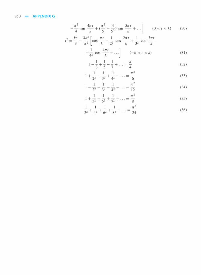
850 APPENDIX G
−π2
4sin
4πt
k+ (
π2
5− 4
53) sin
5πt
k+ . . .
](0 < t < k) (30)
t2 = k2
3− 4k2
π2
[cos
πt
k− 1
22cos
2πt
k+ 1
32cos
3πt
k
− 1
42cos
4πt
k+ . . .
](−k < t < k) (31)
1− 1
3+ 1
5− 1
7+ . . . = π
4(32)
1+ 1
22+ 1
32+ 1
42+ . . . = π2
6(33)
1− 1
22+ 1
32− 1
42+ . . . = π2
12(34)
1+ 1
32+ 1
52+ 1
72+ . . . = π2
8(35)
1
22+ 1
42+ 1
62+ 1
82+ . . . = π2
24(36)

APPENDIX
H Laplace Transforms
If f (t) is a piecewise continuous real-valued function of the real variable t (0 ≤ t < ∞), and|f (t)| < Meσt (t > T ;M,σ, T positive constants), then the Laplace transform of f (t), given by
La[f (t)] = F(s) =∞∫
0
e−stf (t) dt, (1)
exists in the half-plane of the complex variable s = σ + jω, for which the real part of s is greaterthan some fixed value s0, i.e., Re(s)s0.
The inverse transform is defined as
f (t =)La−1[F(s)] = 1
2πj
σ+j∞∫σ−j∞
F(s) est ds (2)
where σ > s0 is chosen to the right of any singularity of F(s).The property of Laplace transform given by
La[f (r)(t)
] = ∞∫0
e−st (drf
dtr) dt = srF (s)−
r−1∑n=0
sr−1−nf (n)(0+)
or
La[drf (t)
dtr
]= srF (s)− sr−1(0+)− sr−2 df
dt(0+)− . . .− dr−1f
dtr−1(0+) (3)
makes the Laplace transform very useful for solving linear differential equations with constantcoefficients, and many boundary value problems.
A summary of properties of Laplace transformation and a table of Laplace transform pairsare given below.
Summary of Properties of Laplace Transformation
Property Time Function Laplace Transform
Linearity a1f1(t)± a2f2(t) a1F1(s)± a2F2(s)
Differentiation f ′(t) sF (s)− f (0+)
f n(t) snF (s)− sn−1f (0+)− sn−2f ′(0+)− . . .− f n−1(0+)
Integration f−1(t) =t∫
0
f (τ) dτF (s)
s+ f−1(0+)
s
f−n(t)F (s)
sn+ f−1(0+)
sn+ f−2(0+)
sn−1+ . . .+ f n(0+)
s
851

852 APPENDIX H
t∫0
f (τ)g(t − τ) dτ F (s)G(s)
Multiplication by t
(frequency differentiation)tf (t) − d
ds[F(s)]
Division by t
(frequency integration)
1
tf (t)
∞∫s
F (s) ds
Time delay or shift f (t − T ) · u(t − T ) e−sT F (s)
Periodic functionf (t) = f (t + nT )
f (t) , 0 ≤ t ≤ T F(s)/[1− eT s ] , whereF(s) =T∫
0
f (t)e−st dt
Exponential translation(frequency shifting)
e−at f (t) F (s + a)
Change of scale(time scaling)
f (at) , a > 01
aF(
s
a)
Initial value f (0+) = limt→0
f (t) lims→∞ sF (s)
Final value f (∞) = limt→∞ f (t) , lim
s→0sF (s)
where limit exists [sF (s) has poles only inside the left half of the s-plane.]
Table of Laplace Transform Pairs
f (t) = La−1[F(s)] F(s) = La [f (t)]
δ(t) (unit impulse or delta function) 1
δ(t − T ) e−sT
aa
s
u(t) or 1 (unit step function)1
s
u(t − T )e−sT
s
t1
s2
(t − T ) u(t − T )e−sT
s2
tu(t − T )(1+ sT )e−sT
s2
tn, (n− integer)n!
sn+1
tn−1/(n− 1)!, n an integer1
sn
e−at1
s + a
te−at1
(s + a)2
e−at tnn!
(s + a)n+1
e−at − e−bt
b − a
1
(s + a)(s + b)
sin ωtω
s2 + ω2

LAPLACE TRANSFORMS 853
sin (ωt + θ)s sin θ + ω cos θ
(s2 + ω2)
cos ωts
s2 + ω2
cos (ωt + θ)s cos θ − ω sin θ
(s2 + ω2)
e−at sin ωtω
(s + a)2 + ω2
te−at sin ωt2ω(s + a)
[(s + a)2 + ω2]2
e−at cos ωts + a
(s + a)2 + ω2
te−at cos ωt[(s + a)2 − ω2]
[(s + a)2 + ω2]2
sinh ata
s2 − a2
cosh ats
s2 − a2
[k1e−at cos ωt + k2 − k1a
ωe−at sin ωt]
k1s + k2
(s + a)2 + ω2
ω√1− a2
e−aωt sin ω√
1− a2 tω2
s2 + 2aω + ω2
1
2ωt sin ωt
s
(s2 + ω2)2
1
2ω( sin ωt + ωt cos ωt)
s2
(s2 + ω2)2
Note that all f (t) should be thought of as being multiplied by u(t), i.e., f (t) = 0 for t < 0.

This page intentionally left blank

Index
A
ac ammeter, 48ac circuits:
power factor, 113power in, 112–21
ac generators, 199ac motors, speed and torque control,
574ac power, 112–21, 451–68
advantages over dc power, 455distribution, 460–62generation, 460Great Blackout of 1965, 466–68power-system loads, 462–66residential wiring, 212–15,
461–62transmission, 460
ac voltage controllers, 768–69ac voltmeter, 47Acceptor, 340Accumulators, 318Acoustic-coupler device, 325Active circuits, 339Active filters, 252–55Active load, 432Active mode, transistor, 358Active power, 113Active region, JFET, 368Adaptive control, 813–14Additive noise, 651, 669Additivity, 81Address bus, 318Admittance, 104–5Advanced Mobile Phone System
(AMPS), 709AGC. See Automatic gain controlAir gaps, 477Air-core transformers, 36Aircraft, autopilot control system,
807–8, 809Airplane-to-airplane radio
communication, 730Aliasing, 645Alignment, principle of, 509–10All-day efficiency, transformers,
486
Alternators, 199ALU. See Arithmetic logic unitAM. See Amplitude modulationAmmeter, 48Amorphous magnetic materials, 472Ampere (unit), 7, 29Ampere-turns per meter (unit), 472Ampere’s law, 476Ampere’s law of force, 7Amplification, 627Amplifier block, 224–29, 394Amplifier circuits, 223, 394Amplifier noise, 654Amplifiers, 393
BJT amplifiers, 399–405current-to-voltage amplifier,
248–49dc-coupled amplifiers, 409differential amplifier, 250–51,
650feedback amplifiers, 232FET amplifiers, 405–9frequency response of, 409–14IF amplifier, 700instrumentation amplifier, 650inverting amplifier, 244–45lock-in amplifier, 658MOSFET amplifiers, 409negative feedback, 413–14noninverting amplifier, 235,
245–46operational amplifiers, 229–56transducer amplifier, 650transistor amplifiers, 393–415voltage amplifier, 14, 799weighted differencing amplifier,
250Amplitude distortion, 639Amplitude modulation (AM),
626–27, 685, 686–93,698–99
single-sideband (SSB) AM, 641,690, 692, 698, 699
suppressed-carrier (SSB) AM,689
vestigial-sideband (VSB) AM,690–91, 692, 698, 699
Amplitude ratio, 155Amplitude-shift keying (ASK), 628,
722–24, 729, 730AMPS. See Advanced Mobile
Phone SystemAnalog building blocks, 223
amplifier block, 224–29application, 257–58operational amplifier, 229–56
Analog cellular phone calls, 709Analog circuits, 268Analog communication systems,
627, 667, 685–86amplitude modulation, 626–27,
685, 686–93, 698–99cellular phone systems, 707,
709–10demodulation, 627, 694–98FM stereo, 698, 699frequency modulation, 626–27,
685, 693–98, 699mobile radio systems, 707,
709–10, 721, 730radio broadcasting, 626, 677, 678,
685, 700–702TV broadcasting, 686, 702–7,
708Analog computers, 255–56Analog meters, 49Analog signals, 268, 627
antinoise systems, 658–59distortion, 638–39equalization, 639–40filtering, 638–39interference, 649–58modulation, 626, 640–47,
693–98, 699multiplexing, 627, 641, 647–49noise, 651–58periodic signals, 629–36sampling, 643–47signal bandwidth, 636–38spectral analysis, 626–40
Analog systems, 223, 268, 625Analog-to-digital (A/D) converters,
308–11, 628AND gate, 274, 275, 277
855

856 INDEX
Angle modulation, 693Antenna impedance, 681Antenna resistance, 681Antenna temperature, 683Antennas, communication systems,
676–85Antinoise system, 658–59Aperture antennas, 680Apparent power, 114Application layer, OSI model, 322Arc drop, 608Arithmetic logic unit (ALU), 318Armature circuit-resistance control,
604Armature current, 597Armature reaction reactance, 583Armature terminal-voltage control,
604Armature winding copper loss,
synchronous generators, 587ARPANET, 320Array antennas, 680, 682–83ASK. See Amplitude-shift keyingAssembler, 318Assembly-language programming,
318Asymptotic Bode diagram, 156,
158, 232Asynchronous counter, 298, 299,
300Asynchronous data communication,
324Asynchronous machine, 560Asynchronous modems, 324Asynchronous torque, 560Atmospheric noise, 669Attenuation coefficient, 675Automatic gain control (AGC), 701Automatic volume control (AVC),
701Automobiles:
ignition system, 178–79jump starting, 92–94odometer, 269power steering, 257–58speedometer, 269
Autopilot control system, 807–8,809
Autotransformers, 480, 492–94, 575Available power, 227AVC. See Automatic volume controlAverage noise figure, 683Average noise power, 653Average value, of periodic
waveform, 14
B
B-H characteristic, 472Back emf, 507Backward-rotating wave, 561Balanced discriminator, 695Balanced modulator, 690
Balanced three-phase loads:delta-connected load, 204–6power and, 206–8power measurement, 210, 211wye-connected load, 203–4
Bandpass channels, 722Bandpass filter, 175–76, 254Bandwidth, 410Bandwidth region, 155Base speed, 604Base-emitter junction (BEJ), 358Baseband channels, 722Baseband coaxial cable, 323BCD number system. See Binary-
coded-decimal numbersystem
BEJ. See Base-emitter junctionBias, 341Bias currents, op amp, 238Biasing, transistors, 394–99Biasing network, 235Bidirectional shift registers, 298Binary digital signal, 710Binary number system, 271, 272,
284Binary numbers, 274
addition of, 281converting decimal number to,
272converting to hexadecimal form,
273four-digit, 281, 282
Binary signals, 269Binary-coded-decimal (BCD)
number system, 273, 274Biot-Savart law, 10Bipolar junction transistors (BJT),
358–67biasing, 394–95BJT amplifiers, 399–405
Bistable sequential blocks, 290Bit robbing (bit stealing), 719Bit-error probability, 718BJT. See Bipolar junction transistorsBJT amplifiers, 399–405BJT inverter, 431BJT inverter switch, 424BJT switch, 425Block diagrams, 166–68, 784Bode diagram, 156Boltzmann diode equation, 342Boolean algebra, 273Bounded media, 322–23Braking mode, rotating machines,
554Branch, 12Break frequency, 157Breakdown voltage, 370Breakpoint analysis, diodes, 355–57Breakpoints, diodes, 353Broad-band coaxial cable, 323Brushless machines, 563Bus, 318
Bus topology, 322, 323Butterworth bandpass filter, 176
C
Canonical product of sums, 284Canonical sum of products, 283Capacitance, 24–26Capacitive coupling, 649Capacitive reactance, 109, 114Capacitive susceptance, 109Capacitor motors, 579, 581Capacitors, 16, 24–26Cardiac pacemaker, 438–39Carrier modulation, 626Carrier signal, 685Carrier wave, 640Carson’s rule, 693Case studies:
antinoise system, 658–59automobiles
ignition system, 178–79jump starting, 92–94power steering, 257–58
cardiac pacemaker, 438–39digital process control, 815–16electronic photo flash, 380global positioning system (GPS),
731–32Great Blackout of 1965, 466–68magnetic bearings for space
technology, 494–95mechatronics, 414–15microcomputer-controlled
breadmaking machine,326–27
physiological effects of electriccurrent, 216–17
resistance strain gauge, 53–54sensors, 541–42transducers, 541–42wind-energy-conversion systems,
610–12Cassegrain antenna, 683Cathode-ray tube. See CRTCB BJT amplifier. See Common-
base BJT amplifierCBJ. See Collector-base junctionCC BJT amplifier. See Common-
collector BJT amplifierCD JFET amplifier. See Common-
drain JFET amplifierCD player, 722, 723CDMA. See Code Division Multiple
AccessCE BJT amplifier. See Common-
emitter BJT amplifierCellular telephone system, 707,
709–10Central-processor unit. See CPUCG JFET amplifier. See Common-
gate JFET amplifierChannel decoder, 629

INDEX 857
Channel encoder, 628Characteristic impedance, 672Charge, 4Charge carriers, 340Charge-to-charge amplifier, 249Chrominance signal, 704Circuit analysis:
block diagrams, 166–68case studies, 92–94, 178–79computer-aided
frequency response, 171–73MATLAB, 88–92, 173–77Pspice and PROBE, 168–73SPICE, 85–87steady-state sinusoidal
analysis, 170–71transient analysis, 168–70
controlled sources, 79–81linearity, 81–83mesh-current method, 75–81nodal-voltage method, 71–75,
79–81superposition, 81–83, 629Thévenin and Norton equivalent
circuits, 67–71time-dependent, 102–3
application, 178–79computer-aided circuit
simulation, 168–77frequency response, 154–68Laplace transform, 102–3,
142–54phasor analysis, 102, 103–24transients, 124–42
wye-delta transformation, 83–84Circuit breakers, 213Circuits, 3
first-order, 133second-order, 133transients in, 125–42
Circular polarization, 682Clip-on ammeter, 49Clock, 719Clocked flip-flop, 292Closed-loop gain, 232Closed-loop rectifier drives, 760CMOS, 379, 435CMOS circuit, 434, 435–36CMOS inverter, 434CMRR. See Common-mode
rejection ratioCoaxial cable, 323Coaxial transmission lines, 671–72Code Division Multiple Access
(CDMA), 709Coefficient of coupling, 33–34Coenergy, magnetic field systems,
527Coil, flux linkage in, 507COINCIDENCE gate. See
EXCLUSIVE NOR gateCollector cutoff current, 360Collector-base junction (CBJ), 358
Color burst, 703Color television receiver, 706–7,
708Color television transmitter, 703,
704, 706Combinational blocks, 274Common-base (CB) BJT amplifier,
403–5Common-base current gain, 360Common-collector (CC) BJT
amplifier, 402–3Common-drain (CD) JFET
amplifier, 407, 409Common-emitter (CE) BJT
amplifier, 399–401Common-emitter current gain, 360Common-gate (CG) JFET amplifier,
407–9Common-mode input signal, 237Common-mode rejection ratio
(CMRR), 237Common-mode voltage, 650Common-source (CS) JFET
amplifier, 405–7, 408Communication systems, 666–70
analog, 667, 684–86amplitude modulation, 626–27,
685, 686–93, 698–99cellular phone systems, 707,
709–10, 721demodulation, 627, 640, 692,
694–98FM stereo, 698, 699frequency modulation, 626–27,
685, 693–98, 699mobile radio systems, 707,
709–10, 721, 730radio broadcasting, 626, 677,
678, 685, 700–702TV broadcasting, 686, 702–7,
708antennas, 676–85components, 626digital, 667, 710, 728–30
carrier modulation, 722–29companding, 714digital signal formatting,
715–16elements of, 627, 628fading multipath channels, 730multiplexing, 719–22pulse-code modulation (PCM),
716–19quantization, 711–13sampling, 643, 710–11source encoding, 714–15
fiber-optic communicationsystems, 667
frequency bands, 668–69global positioning systems,
731–32history of, 666–67LTI systems, 629
noise, 683–85, 693, 728satellite communication systems,
667, 722, 723signal processing, 626, 627transmission lines, 670–76waveguides, 671, 674waves, 670–71wireless communication systems,
668Communications networks, 320Commutating poles, 596Commutation, 596Commutator, 518, 521, 595–96, 647Commutator winding, 518Compact disk player, 722, 723Companding, 714Compensating winding, 596Compiler, 318Complement operation, 274, 277Complementary error function, 728Complementary transistors, 375Complementary-symmetry MOS.
See CMOSComplex poles, 145–46Complex power, 114, 455Compoles, 596Composition-type resistors, 17Compound machine, 562Compound semiconductors, 340Computer hardware, 317Computer networks, 320–25
architecture, 321–22data transmission, 324modems, 324–25topology, 322, 323transmission media, 322–23
Computer programs, 317–18Computer software, 317Computer systems, 316–20Computer-aided circuit analysis:
frequency response, 171–73MATLAB, 88–92, 173–77PSpice and PROBE, 168–73SPICE, 85–87steady-state sinusoidal analysis,
170–71transient analysis, 168–70
Computer-and-mobile phonehybrids, 710
Computers:disk drive control system, 808EEPROM, 312magnetic storage devices, 312–13memory, 311–13in power systems, 454RAM, 312ROM, 312
Conductance, 16Conductivity, 16, 339Conductors, 6–7, 17Conical-horn antennas, 683Conjugate complex poles, 145–46Conservation of energy, 506

858 INDEX
Constant-horsepower drive, 604Constant-torque drive, 605Constrained meshes, 78Constrained node, 74Continuous rating, 540Continuous signals, 625Continuous-state analog circuits,
268Continuous-state systems, 223Control bus, 318Control systems, 747–48
applications, 780–81digital control systems, 805–14
adaptive control, 813analysis of, 814block diagrams, 807components, 806examples, 807–11microprocessor control,
811–13process control, 815–16
feedback control systems, 779,782–83
block diagrams, 783–88classification of, 790–91dynamic response, 788–90error rate control, 793–94integral-error control, 795–96output-rate control, 794–95second-order servomechanism,
791–93steady-state error, 790transfer functions, 783–84
power networks, 454power semiconductor-controlled
drives, 748–49, 780–81dc motors, 760–68devices, 750–53induction motors, 768–77power electronic circuits,
753–60solid-state control, 760–79synchronous motors, 777–79
Control unit (CU), 318Controlled rectifier circuits, 760Controlled voltage sources, 13–14Copper, 6Copper losses, 587Core losses, 472–75, 587Cosinusoidal waveform, 14Coulomb’s law, 4Counter-controlled A/D converter,
308–9, 310Counters, 298–306Coupled-circuit viewpoint, 529Coupled-coils approach, 529CPU (central-processor unit), 316Crest factor, 713Critically damped system, 136, 138Cross-field theory, 576CRT (cathode-ray tube), 315CS JFET amplifier. See Common-
source JFET amplifier
CU. See Control unitCumulatively compound generators,
599Current, 7, 29, 48Current gain, 226Current transformer (CT), 48Current-to-voltage amplifier,
248–49Cut-in voltage, 344Cutoff frequency, 155Cutoff mode, transistor, 358Cutting-of-flux equation, 508CYBERNET, 320Cylindrical rotor synchronous
machine:equivalent circuit, 583–85interconnected, parallel operation,
590–92performance, 585–89power angle, 585
D
D3 channel bank, 719D flip-flop, 292–94D-AMPS. See Digital AMPSDamping ratio, 792Data bus, 318Data compression, 628Data link layer, OSI model, 321–22Data transmission, computers, 324Datum node, 71dc excitation, 584dc generator, 562, 597–600dc machines, 518–20, 562–63,
594–609applications, 608–9commutators, 518, 521, 595–96compensated windings, 596–97construction, 594dc generator, 562, 597–600efficiency, 608equivalent circuit, 594–95interpoles, 596mathematical model, 796–99solid-state control of, 760–68speed control, 604–6speed-torque characteristics,
601–4starting, 606–7
dc resistive circuit, compared tomagnetic circuit, 477
dc voltmeter, 47dc waveform, 15dc-coupled amplifiers, 409Decibel (unit), 156Decimal numbers, 274
converting to binary form, 272converting to octal form, 273
Decoders, 296, 297Deemphasis filter, 655, 695Delay distortion, 639Delayed unit step, 140
Delta, 199, 202Delta-connected load, balanced,
204–6Delta-connection, 199Demand, electric service, 463Demodulation, 627, 640, 692,
694–98Demodulator, 685DeMorgan’s theorems, 276–77Demultiplexer, 296Dependent voltage sources, 13–14Depletion capacitance, 345Depletion charge, 341Depletion MOSFETs, 371, 375–78,
397Detection, 640Detector, 685DF. See Displacement factorDielectric materials, 7Difference equations, 814Differential amplifier, 250–51, 650Differential encoding, 716Differential phase-shift keying
(DPSK), 725–26, 727Differential-mode input signal, 237Differentially compounded
generators, 599Differentiator, 252Diffusion capacitance, 345Digital AMPS (D-AMPS), 709Digital building blocks, 271–95
Karnaugh map, 283, 285–89logic blocks, 273–83logic design, 283–90number systems, 271–73sequential blocks, 290–95
Digital cellular phones, 709–10Digital circuits, 268, 422–39
application, 438–39CMOS, 431, 434–36DTL and TTL logic circuits,
427–31ECL, 427, 436IIL, 436–37MOSFETs, 431–33NMOS and PMOS, 433PDP, 437transistor switches, 423–27, 428
Digital communication systems,667, 710, 728–30
carrier modulation, 722–28companding, 714digital signal formatting, 715–16elements of, 627, 628fading multipath channels, 730multiplexing, 719–22pulse-code modulation (PCM),
716–19quantization, 711–12quantization error, 713–14sampling theorem, 643, 710–11source encoding, 714–15transmission, 627–28

INDEX 859
Digital computers, 255, 270, 317Digital control systems, 805–14
adaptive control, 813analysis of, 814black diagram, 807components, 806examples, 807–11microprocessor control, 811–13process control, 815–16
Digital demodulator, 628Digital meters, 49Digital modulator, 628Digital process control, 815–16Digital signal, 268Digital signal formatting, 715–16Digital system components, 295–96
analog-to-digital (A/D)converters, 308–11
counters, 298–306decoders, 296, 297digital-to-analog (D/A)
converters, 306–8display devices, 313–16encoders, 296, 298memory, 311–13multiplexers, 296, 299registers, 296–98
Digital systems, 268, 270, 625, 628Digital voltmeter (DVM), 269Digital-to-analog (D/A) converters,
306–8, 629Dimmer switch, 269Diode-transistor logic. See DTLDiodes, 340–41
Boltzmann diode equation, 342breakpoint analysis, 355–57diode circuits, 345–53forward-biased diode, 349–50LED, 313pn-junction under bias, 341–45rectifier circuits, 357–58semiconductors as, 340–58usage, 345varactor diode, 694Zener diodes, 353–55
DIP. See Dual-in-line packageDipole antennas, 677Direct-current machines. See dc
machinesDirect-on-line starting, 575Directors, 683Discrete signals, 625Discrete-component technology,
integrated circuits, 378Discrete-data systems, 805–14Discrete-state circuits, 268Discrete-state systems, 223Disk drive control system, 808Displacement factor (DF), 760Display devices, 313–15Distinct poles, 145Distortion, 629, 638–39Distributed topology, 322, 323
Divide-by-2n counter, 299Dominant mode, 672Don’t-care output, 289Doping, 340Dot convention, inductors, 34–35Double-sideband modulation
(DSB), 641Double-sideband suppressed-carrier
(DSB SC AM), 689, 692Double-sided/double-density
(DS/DD) floppy disks, 313Double-sided/quad-density
(DS/QD) floppy disks, 313Doubly excited system, 527Down-counter, 299DPSK. See Differential phase-shift
keyingDrain breakdown voltage, 372Drain-source saturation current,
368, 370Drift current, 341DS/DD floppy disks. See Double-
sided/double-density floppydisks
DS/QD floppy disks. See Double-sided/quad-density floppydisks
DSB. See Double-sidebandmodulation
DSB SC AM. See Double-sidebandsuppressed-carrier
DTL, 427DTL gate, 428–30Dual-band digital phone, 709Dual-in-line package (DIP), 379Dual-ramp (dual-slope) A/D
converter, 310–11Duality, 30, 31DVM. See Digital voltmeterDynamic resistance, 344Dynamic response, of control
systems, 788–90
E
Early effect, 361Early voltage, 361ECL, 427, 436Eddy-current loss, 472, 473–74EEPROM (electrically erasable
programmable ROM), 312Effective aperture, antenna, 678Effective area, antenna, 678Effective input noise temperature,
683Efficiency:
synchronous generator, 587transformers, 486
Electric charge. See ChargeElectric circuits, 3–4, 16
analogy between electrical andnonelectric systems, 50–52
analysis. See Circuit analysis
application, 53–54concepts, 3–53electrical quantities, 4–16Kirchhoff’s laws, 39–47lumped-circuit elements, 16–39measurements, 47–50meters, 47–50residential wiring, 212–15,
461–62three-phase circuits, 198–212
Electric current, physiologicaleffects of, 214, 216–17
Electric field intensity, 4–5, 8Electric potential, 10–11Electric power. See PowerElectric shocks, 216Electric signals. See SignalsElectrical appliances, grounding,
213Electrical engineering:
control systems, 747–816electric circuits
analysis. See Circuit analysisconcepts, 3–53residential wiring, 212–15,
461–62three-phase circuits, 198–212
electrical measurements. SeeElectrical measurements
electronic systems, 223amplifiers, 224–48analog building blocks, 224–58computer networks, 320–25computer systems, 316–20digital building blocks, 271–95digital circuits, 268, 422–39digital system components,
295–316semiconductor devices, 339–80transistor amplifiers, 393–415
energy systemsac power, 112–21, 451–68electromechanics, 505–42magnetic circuits, 475–79magnetic materials, 472–75rotating machines, 553–612transformers, 479–95
history of, xxiii–xxivinformation systems
communication systems,666–732
signal processing, 625–59Electrical measurements:
ammeter, 48analog meters, 49digital meters, 49instrument transformers, 48–49multimeters, 48ohmmeters, 48oscilloscope, 49sensors, 541–42voltmeter, 47–48, 269wattmeter, 208

860 INDEX
Wheatstone bridge, 49–50Electrical quantities, 4
conductors, 6–7current, 7electric potential, 10–11energy, 11insulators, 7power, 11source-load combination, 12–13voltage, 11waveforms, 14–15
Electrical radian (unit), 528Electrical time constant, 798Electrical-hydraulic analogs, 50, 51Electrical-mechanical analogs, 50,
51Electrical-thermal analogs, 51–52Electrically erasable programmable
read-only memory. SeeEEPROM
Electromagnetic spectrum,frequency bands of, 668
Electromagnetic torque, 527, 556Electromagnetic waves:
polarization of, 682propagation of, 668–70
Electromagnetism, 471application, 494–95autotransformers, 480, 492–94,
575iron-core losses, 472–75magnetic circuits, 475–79magnetic materials, 472–75three-phase transformers, 490–91transformer equivalent circuits,
479–85transformer performance, 486–90
Electromagnets, 533–35Electromechanical energy
conversion, 505–7alignment, 509–10applications, 541–42emf produced by windings,
514–22forces and torques, 526–39induction, 507–8interaction, 509problems, 540–41rotating machines, 553–612rotating magnetic fields, 522–26
Electromechanics, 505–42Electromotive force. See emfElectron, charge, 4Electronic mail, 320Electronic photo flash, 380Electronic systems, 223
amplifiers, 224–58analog building blocks, 224–58computer networks, 320–25computer systems, 316–20digital building blocks, 271–95digital circuits, 268, 422–39digital system components,
295–316semiconductor devices, 339–80transistor amplifiers, 393–415
Elementary loop, 75Elliptical polarization, 682emf, 11
back emf, 507induced, 507motional, 507, 508produced by windings, 514–22pulsational, 507speed emf, 507transformer, 507
emf equation, 481Emitter follower, 402Emitter-coupled logic. See ECLEncoders, 296, 298Energy, 11
conservation of, 506electric service, 463magnetic field systems, 527power and, 458in singly excited system, 526
Energy efficiency, transformers, 486Energy systems:
ac power, 451–68electromechanics, 505–42magnetic circuits, 475–79magnetic materials, 472–75rotating machines, 553–612transformers, 479–95
Energy-type signal, 633Enhancement MOSFETs, 371,
372–75, 397–98Envelope detector, 691EPROM (erasable programmable
read-only memory), 312Equalization, 627, 639–40Equations of motion, 528Equivalent circuit:
cylindrical rotor synchronousmachine, 583–85
dc machines, 594–95polyphase induction machines,
563–67small-signal equivalent circuit,
361Thévenin and Norton equivalent
circuits, 67–71transformers, 479–85
Erasable programmable read-onlymemory. See EPROM
Error-rate control, 793–94Essential prime implicant, 287Ethernet, 321Euler’s identity, 103Excitation torque, 529Excitation voltage, 583Exciter loss, synchronous generator,
587Exciting current, 476EXCLUSIVE NOR (COIN-
CIDENCE) gate, 276,
277EXCLUSIVE OR (XOR) gate, 276,
277Expandor, 714External frequency compensation,
op amp, 239Extrinsic semiconductors, 340
F
Fall time, 426Farad (unit), 224Faraday’s law of induction, 29–30,
479, 507FDM. See Frequency-division
multiplexingFeedback amplifiers, 232Feedback circuits, 232Feedback control systems, 779,
782–83block diagrams, 783–88classification of, 790–91dynamic response, 788–90error rate control, 793–94integral-error control, 795–96output-rate control, 794–95second-order servomechanism,
791–93steady-state error, 790transfer functions, 783–84
Ferrimagnetic materials, 472Ferrites, 473Ferrofluids, 472Ferromagnetic materials, 472, 510FET switches, 433FETs. See Field-effect transistorsFiber-optic cable, 323Fiber-optic channels, 667Fiber-optic communication systems,
667Field copper loss, synchronous
generator, 587Field intensity, 472Field-effect transistors (FETs), 367
biasing, 395–99FET amplifiers, 405–9FET switches, 433junction FETs, 367–71MOSFETs, 371–78
Filtered chrominance signal, 705Filtering, 627
analog signals, 638–39deemphasis filtering, 655, 695preemphasis filtering, 655, 695
Filters, 155, 252active filters, 252–55bandpass filter, 175–76, 254Butterworth bandpass filter, 176deemphasis filter, 655, 695inductorless filters, 252–55low-pass filters, 155, 252, 639notch filter, 650preemphasis filter, 655, 695

INDEX 861
First-order circuits, 133Flags, 318Flexible disks, 313Flip-flops, 274, 291
D flip-flop, 292–94JK flip-flop (JKFF), 294–95master-slave JKFF, 295SR flip-flop (SRFF), 290–92
Floppy disks, 313Flux linkage, 32–33FM. See Frequency modulationFM demodulator with feedback
(FMFB), 695, 697FM radio broadcasting, 685–86,
698, 699FM radio superheterodyne receiver,
700, 701, 703Folded half-wave dipole antenna,
682Forced response, 125Form factor, 759Forward biasing, 341Forward resistance, 344Forward-biased diode, 349–50Forward-current transfer ratio, 360Forward-rotating wave, 561Four-wire three-phase system, 199Fourier series:
periodic signal, 634phasor method, 121–24
Fractional bandwidth, 678Frame, 702Framing bit, 719Free-space permeability, 472Frequency, of waveform, 14Frequency bands, communication
systems, 668–69Frequency discriminators, 695Frequency distortion, 639Frequency modulation (FM),
626–27, 685, 693–98, 699Frequency response, 228, 229
of amplifiers, 409–14for circuit analysis, 154–68defined, 154op amp, 241with PSpice and PROBE, 171–72
Frequency translation, 627, 640,641–43
Frequency-controlled induction-motor drives, 769–73
Frequency-division multiplexing(FDM), 324, 647–48,719–22
Frequency-shift keying (FSK), 628,726–28
Friction losses, electromechanicaldevice, 540
Fringing, 477FSK. See Frequency-shift keyingFull-adder, 281Full-duplex mode, 324Full-duplex operation, 707
Full-pitch coil, 514Full-wave rectifier, 358
G
Gain-bandwidth product, 232Gallium arsenide, 340Gate breakdown voltage, 373Gate turn-off (GTO) thyristors, 751Gateways, 322General-purpose interface bus. See
GPIBGenerating mode, rotating machines,
554Generators, 540
ac generators, 199cumulatively compound
generators, 599dc generators, 562, 597–600differentially compounded
generators, 599digital controller for, 808, 810hydroelectric, 517self-excited, 562short-shunt compound dc
generator, 600shunt generators, 597, 598, 609synchronous generators, 582–90tachometer generator, 505
Germanium, 340GFCI (ground-fault circuit
interruption), 213–14Global positioning system (GPS),
731–32Global System for Messaging
communication (GSM), 710GPIB (general-purpose interface
bus), 319–20GPS. See Global positioning systemGreat Blackout of 1965, 466–68Ground connection, residential
wiring, 213Ground point, 11Ground strap, 650Ground-fault circuit interruption
(GFCI), 213–14Ground-loop coupling, 649Grounding, electrical appliances,
213GSM. See Global System for
MessagingGTO thyristors. See Gate turn-off
thyristorsGuard time, 719
H
h parameters, 164Half-adder, 281Half-duplex mode, 324Half-duplex modems, 324Half-power point, 155
Half-wave dipole antenna, 682Half-wave rectifier, 357Half-wave symmetry, 632Hard ferromagnetic materials, 472Hardware. See Computer hardwareHarmonic factor (HF), 760Heaviside, Oliver, 142Heaviside expansion theorem, 144Henry (unit), 29Henrys per meter (unit), 472Hexadecimal number system, 273,
274HF. See Harmonic factorHigh voltage windings, transformer,
36High-level languages (HLL), 318High-pass transfer function, 156High-voltage dc (HVDC)
transmission lines, 453HLL. See High-level languagesHole, semiconductors, 340Homogeneity, 81Horn antennas, 677, 683Hunting, 557HVDC transmission lines. See High-
voltage dc transmissionlines
Hybrid technology, integratedcircuits, 378
Hybrid topology, 322, 323Hydraulic-electrical analogs, 50, 51Hydroelectric generators, 517Hysteresis loop, 472–73
I
Ideal capacitor, 24Ideal current source, 13Ideal operational amplifier, 231–35Ideal resistor, 16Ideal transformer, 37, 480Ideal voltage source, 13IEEE, publications, xxii-xxiiiIF amplifier, 700IIL, 436–37Illuminators, 683Image frequency, 700Impedance, 104Impulse functions, 140Independent voltage sources, 13–14Induced emf, 507Inductance, 29–35Induction, 507–8Induction motors:
applications, 580–82polyphase induction machines
equivalent circuits, 563–67performance, 567–69speed and torque control,
573–74starting methods, 574–78
single-phase induction motors,578–80

862 INDEX
solid-state control of, 768–77standard ratings, 582starting methods, 574–80three-phase induction motors,
569–73torque- speed characteristics,
569–74Inductive reactance, 109, 114Inductive susceptance, 109Inductorless filters, 252–55Inductors, 29–35
dot convention, 34–35mutually coupled, 34series and parallel combinations,
31Inertial time constant, 798Infinite bus, 201, 556Information systems:
communication systems, 666–732signal processing, 625–59
Information sequence, 628Initial capacitor voltage, 24Input bias current, op amp, 238Input offset current, 238Input offset voltage, 237–38Input resistance, 224, 236Input voltage, 239Instantaneous power, 11Instrument transformers, 48–49Instrumentation amplifier, 650Insulating materials, 7Insulators, 7, 17Integral-error control, 795–96Integrated circuits (ICs), 269–70,
378–79Integrated-injection logic. See IILIntegrators, 251Interaction, principle of, 509Interface bus, 319Interference, 649–58Interlaced pattern, 702–3, 705Internal frequency compensation,
239Internet, 320, 322Internet protocol. See IPInterpoles, 596Interpreter, 318Intrinsic semiconductors, 340Inverse Laplace transform, 142Inverter, 274, 422, 423Inverting amplifier, 244–45Inverting integrator, 251Inverting op-amp stage, 232Inverting summing amplifier,
246–47IP (Internet protocol), 321IP routers, 322Iron losses, 472–75Isotropic antenna, 678
JBlankLineJK flip-flop (JKFF), 294–95
Josephon digital technology, 437Junction FETs (JFETs), 367–71,
395–97Junction threshold voltage, 361
K
Karnaugh maps (K maps), 283,285–89
Keying, 628Kirchhoff’s current law (KCL),
39–47Kirchhoff’s laws, 39–47Kirchhoff’s voltage law (KVL),
39–47
L
Lagging power factor, 113, 456LAN (local-area network), 320, 322Lap, 518Laplace, Pierre Simon, 142Laplace transform, 814
for circuit analysis, 102–3,142–54
inverse, 142properties of, 143–44single-sided, 142
Laplace transform pairs, 142, 143Large-scale integration (LSI), 270,
324, 379Large-signal models, 361LCD (liquid-crystal display),
313–14Leading power factor, 113Leakage, 477Leakage flux, 33, 481Leakage reactance, 481, 583LED (light-emitting diode), 313Lens-type antennas, 680Lenz’s law, 480Light-emitting diode. See LEDLine spectrum, 636Line-of-sight microwave radio
transmission, 730Linear circuit, 81Linear commutation, 596Linear current, 31Linear distortion, 638, 639Linear function, 81Linear modulation, 693Linear predictive coding (LPC), 721Linear resistors, 16Linear time-invariant (LTI) systems,
629Linearity, 81–83Links, 322Liquid-crystal display. See LCDLoad, 11, 12–14Load angle, 556Load bus, power system, 462, 464Load factor, 463–64
Load line equation, 345Load torque, 798Local-area network. See LANLock-in amplifier, 658Locked-loop demodulators, 695Logic blocks, 273–83Logic circuits, 427–37Logic families, 422Logic synthesis, 281Long-haul network, 320Loop error-rate gain factor, 794Loop proportional gain factor, 794Loop-current method, controlled
source, 79–80LORAN, 731Lorentz force equation, 8, 509LOS radio transmission, 679, 700Loss resistance, 681Losses, synchronous generators,
587Lossless electromechanical device,
506Loudspeaker, 513–14Low voltage windings, transformer,
36Low-pass filter, 155, 252, 639Low-pass signals, 638Low-pass transfer function, 156Lower sideband (LSB), 687LPC. See Linear predictive codingLSB. See Lower sidebandLSI. See Large-scale integrationLTI systems. See Linear time-
invariantLuminance signal, 704Lumped-circuit elements, 16
capacitance, 24–26inductance, 29–35maximum power transfer, 22–24resistance, 16–19transformer, 36–38
M
Machine-language programs,317–18
Machines, rotating machines,553–612
Magnetic bearings, for spacetechnology, 494–95
Magnetic circuits, 475–79Magnetic coupling, 649Magnetic disk memory, 312–13Magnetic field systems:
alignment, 509–10applications, 541–42emf produced by windings,
514–22forces and torques, 526–39induction, 507–8interaction, 509problems, 540–41rotating magnetic fields, 522–26

INDEX 863
Magnetic fields, 8rotating, 522–23
Magnetic flux, 29Magnetic flux density, 472Magnetic flux density vector, 8Magnetic forces, current and, 7–8Magnetic materials, 472–75Magnetic potential difference, 475Magnetic storage devices, 312–13Magnetic tapes, 313Magnetic-field viewpoint, 538Magnetizing reactance, 481, 583Magnetomotive force, 475Main panel, 213Mainframes, 316Majority carriers, 340Manchester waveform, 715Mask-programmed ROMs, 312Master-slave JKFF, 295MATLAB, 88–92, 173–74Maximum breakdown torque, 570Maximum common-mode input
voltage, 239Maximum differential input voltage,
239Maximum forward current, 344Maximum internal torque, 570Maximum power transfer, 22–24,
37, 114Maxterm, 283–84MCT. See MOS-controlled
thyristorsMechanical time constant, 798Mechanical-electrical analogs, 50,
51Mechatronics, 414–15Medium-scale integration (MSI),
270Memory, computer, 311–13Mesh, 75, 199, 202Mesh current, 75–76Mesh topology, 322, 323Mesh-current method, circuit
analysis, 75–81Metal-film resistors, 17Meters:
ammeter, 48analog meters, 49digital meters, 49instrument transformers, 48–49multimeters, 48ohmmeters, 48oscilloscope, 49voltmeter, 47–48, 269wattmeter, 208Wheatstone bridge, 49–50
Micro Sim Corp., SPICE-basedcircuit simulation, 85–86
Microcomputers, 316, 326–27Microdiskette, 313Microfabrication, 379Microprocessor control, 808, 811,
813
Microprocessors, 319Microprograms, 319Midband region, 410Miller integrator, 251Milnet, 320Minicomputers, 316Minority carriers, 340Minterm, 283–84Missiles, autopilot control system,
807–8, 809Mnemonics, 318Mobile radio systems, 707, 709–10,
721, 730Mobile telephone switching office,
707Modems, 324–25Modulating wave, 640Modulation:
AM, 626–27, 685, 686–93,698–99
analog signals, 626, 640–47angle modulation, 693carrier modulation, 626demodulation, 627, 640, 692,
694–98double-sideband modulation
(DSB), 641FM, 626–27, 685, 693–98, 699linear modulation, 693overmodulation, 687phase modulation (PM), 626–27,
685power-law modulation, 687, 688pulse amplitude modulation
(PAM), 646pulse duration modulation
(PDM), 646pulse width modulation (PWM),
646pulse-code modulation (PCM),
716–19single-sideband modulation
(SSB), 641Modulation efficiency, 688Modulation index, 686Modulator, 685Modulo-2n binary counter, 299Monolithic technology, integrated
circuits, 378Monostable sequential blocks, 290Morse code, 666MOS-controlled thyristors (MCT),
751MOSFET amplifiers, 409MOSFET inverter, 431MOSFETs, 371–78, 379
biasing, 397–98depletion MOSFETs, 371,
375–78digital circuits, 431–33enhancement MOSFETs, 371,
372–75MOSFET amplifiers, 409
MOSFET inverter, 431Motional emf, 507, 508Motoring mode, rotating electric
machine, 553Motors:
capacitor motors, 579, 581dc motors, 518–20, 562–63,
594–609applications, 608–9commutators, 518, 521, 595–96compensated windings, 596–97dc generator, 597–600efficiency, 608equivalent circuit, 594–95interpoles, 596mathematical model, 796–99solid state control of, 760–68speed control, 604–6speed-torque characteristics,
601–4starting, 606–7
induction motors, 563–82polyphase induction machines,
563–74single-phase induction motors,
578–80solid-state control of, 768–77three-phase induction motors,
569–73ratings, 540shaded-pole motors, 579–80, 581split-phase motors, 578–79starting
dc motors, 606direct-on-line starting, 575jump starting car motor, 92–94polyphase induction motor,
574–78rotor-resistance starting, 574single-phase induction motors,
578–80stator-impedance starting, 575
synchronous machines, 555–58,582–93
applications, 593cylindrical rotor synchronous
machine, 583–89equivalent circuit, 583salient-pole synchronous
machine, 589–90solid-state control of, 777–79steady-state stability, 592–93
traction motors, 609in variable-speed drives, 749
MSI. See Medium-scale integrationMultimeters, 48Multiple poles, 147–49Multiplexing:
analog signals, 627, 641, 647–49digital systems, 296, 299, 719–22frequency-division multiplexing,
324, 647–48, 719synchronous multiplexer, 719

864 INDEX
time multiplexing, 719time-division multiplexing,
647–48, 719–22Multirate sampled-data system, 808Multivibrators, 290Multiwinding transformers, 480Mutilation effect, 695Mutual inductance, 32, 34
N
NAND gate, 274–75, 277CMOS, 435DTL, 428–30TTL, 430–31
Narrow-band FM, 693National Research and Education
Network See NRENNatural response, 125Negative feedback, 234, 244, 257,
413–14Negative impedance converter,
249–50Negative phase sequence, 201Negative sequence, 199Network architecture, 321–22Network functions, 152Network layer, OSI model, 322Network topology, 322NMOS, 379, 432, 433No-load magnetization curve, 597No-load saturation curve, 540Nodal-voltage method, 71–75,
79–81Node-voltage method, controlled
source, 80–81Node-voltage variables, 71Nodes, 12, 320, 322Noise:
antenna receiving systems, 683communication systems, 651–58,
669, 693, 728–29op amp, 240
Noise bandwidth, 683Noise cancellation, 658–59Noise power spectral density, 653Noise temperature, 654Non-salient pole two-pole
synchronous machine, 555Noninverting amplifier, 235, 245–46Noninverting integrator, 251Noninverting op-amp stage, 232Noninverting summing amplifier,
247–48Nonsalient-pole rotor construction,
517NOR gate, 277, 435Norton equivalent circuits, 67–71NOT gate, 274, 275Notch filter, 650NREN (National Research and
Education Network), 320NSFNET, 320
Number systems, 271–83Numeric display devices, 314Nyquist rate, 645, 710
O
OCC. See Open-circuit characteristicOctal number system, 272–73, 274Offset voltage, 344Ohm (unit), 16, 163Ohmic region, JFET, 368Ohmmeters, 48Ohm’s law, 16One-line diagrams, 458Op amps. See Operational amplifiersOpen circuit, 22Open-circuit characteristic (OCC),
540, 597Open-circuit test, 486Open-circuit voltage, 23, 67Open-circuit voltage amplification,
224Open-loop bandwidth, 231–32Open-loop voltage gain, 236Open-systems interconnections
model. See OSI modelOperating point, 345Operating system, 318Operational amplifiers (op amps),
229–56analog computers, 255–56applications, 244–56charge-to-charge amplifier, 249current-to-voltage amplifier,
248–49differential amplifier, 250–51differentiator, 252ideal operational amplifier,
231–35inductorless filters, 252–55integrators, 251inverting amplifier, 244–45inverting summing amplifier,
246–47negative impedance converter,
249–50noninverting amplifier, 235,
245–46noninverting summing amplifier,
247–48properties, 235–44
Optical disks, 313Optional prime implicant, 287OR gate, 274, 275, 277Oscillator, 154Oscilloscope, 49OSI (open-systems interconnec-
tions) model, 321Output resistance, 224, 236Output voltage swing, op amp, 239Output-rate control, 794–95Overcompounding, 599Overdamped system, 136, 138
Overexcited machine, 583Overmodulation, 687
P
Packaged resistance arrays, 18PAM. See Pulse amplitude
modulationParabolic antennas, 677, 683Parallel data transmission, 324Parallel-in parallel-out (PIPO)
register, 297Parallel-in serial-out register
(PISO), 297Parasitic capacitance, 26Partial-fraction expansion, 144Passband, 409Passband region, 155PCM. See Pulse-code modulationPCS phones. See Personal
Communication Servicephones
PDM. See Pulse duration modulationPDN. See Public-data networkPDP. See Power-delay productPeak frequency deviation, 693Peak inverse voltage, 344Pencil-beam pattern, 682Per-phase analysis, 458Per-unit slip, 559Per-unit source frequency deviation,
161Period, of waveform, 14Periodic signal, 629, 634Periodic waveform, 14Permalloy, 473Permanent magnets, 472Permanent-split-capacitor motor,
581Permeability, 7Personal Communication Service
(PCS) phones, 709Phase distortion, 639Phase modulation (PM), 626–27,
685Phase sequence, three-phase
circuits, 201Phase shift, 155Phase symmetry, 458Phase-locked loop (PLL), 692, 695Phase-reversal keying (PRK), 725Phase-shift keying (PSK), 628, 725,
728, 729Phasor diagram, 110, 111–12Phasor method, 102, 103, 109–12
exponential excitations, 103–6forced response to sinusoidal
excitation, 106–9Fourier series, 121–24power and power factor in ac
circuits, 112–21Phasors, 110Photolithography, 379

INDEX 865
Photoresist, 379Physical channels, 322Physical layer, OSI model, 321Pinch-off voltage, 368PIPO. See Parallel-in parallel-out
registerPISO. See Parallel-in serial-out
registerPLL. See Phase-locked loopPM. See Phase modulationPMOS, 379, 432, 433pn-junction, 340–45pn-junction diode, 340Point charge, 4Polar waveform, 715Pole pitch, 514Pole-face winding, 596Polyphase induction machines:
equivalent circuits, 563–67performance, 567–69speed and torque control, 573–74starting methods, 574–78
Polyphase synchronous machines,555
Polyphase transformers, 480Port, 163POS. See Product of sumsPosition servo, radar system, 808,
811Positive feedback, 244Positive phase sequence, 201Positive sequence, 199Potential difference, 11Potential transformer (PT), 48Potentiometer, 18, 505Power, 11, 12
ac. See ac poweractive power, 113apparent power, 114available power, 227balanced three-phase circuits,
206–8complex power, 114, 455concepts, 455–60defined, 112dissipation, 228distribution, 460–62generation, 452–53, 460instantaneous power, 11power transfer, 22–23residential wiring, 212–15,
461–62safety codes, 214source loading, 23transmission, 198, 460, 462–63transmission lines, 453, 464in the U.S., 452–53
Power angle, 583, 585–87Power dissipation, 228Power distribution, ac power,
460–62Power efficiency, transformers, 486Power factor, 113, 455
Power factor correction, 458Power gain, 226, 678Power generation:
ac power, 460in the U.S., 452–53
Power grid, 451Power loss, residential wiring, 212Power measurement, 208–12Power semiconductor devices,
750–60Power semiconductor-controlled
drives, 748–49, 780–81devices, 750–53power electronic circuits, 753–60solid-state control, 760–68of dc motors, 760–68of induction motors, 768–77of synchronous motors, 777–79
Power spectral density, 716Power system loads, 462–66Power systems:
computers in, 454Great Blackout of 1965, 466–68history of, 452planning and research, 454–55power distribution, 460–62power generation, 452–53, 460power grid, 451power transmission, 198, 460,
462–63residential wiring, 212–15,
461–62single-phase power systems,
455–66three-phase power systems,
455–66transmission lines, 453, 464trends in, 453–54in the U.S., 452–53
Power transfer, 22–23Power transmission, 452–53
ac power, 460three-phase scheme, 198transmission lines, 453, 464
Power triangle, 114Power-delay product (PDP), 437Power-handling capacity, 228Power-law modulation, 687, 688Power-supply rejection ratio
(PSRR), 239Power-type signal, 633Preemphasis filtering, 655, 695Presentation layer, OSI model, 322Pressure transducer, 505Primary winding, transformer, 36Prime implicant, 287Principal-plane pattern, 680Principle of alignment, 509–10Principle of interaction, 509Principle of superposition, 81, 83,
629PRK. See Phase-reversal keyingPROBE, 86
Product demodulator, 642Product modulator, 641Product of sums (POS), 277, 281,
288Program counter, 318Programs. See Computer programsPropagation delay, 292, 426Propagation mode, 672Proportionality, 81Protocol, 321Proton, charge, 4PSK. See Phase-shift keyingPSpice, 86–88
frequency response with, 171–72steady-state sinusoidal analysis,
170–71transient analysis, 168–70
PSRR. See Power-supply rejectionratio
Public-data network (PDN), 320Pull-out power, 557Pull-out torque, 557Pulling out of step, 557Pulsational emf, 507Pulse amplitude modulation (PAM),
646Pulse duration modulation (PDM),
646Pulse modulation system, 645–46Pulse width modulation (PWM),
646Pulse-code modulation (PCM),
716–19Pure capacitor, 114Pure inductor, 113PWM. See Pulse width modulationPyramidal-horn antennas, 683
Q
Quality factor, 161Quantization, 268–69, 711–12Quantization error, digital
communication systems,713–14
Quantizers, 711Quiescent point, 345
R
R-2R ladder D/A converter, 307–8Radar system, position servo, 808,
811Radiation intensity pattern,
antennas, 678, 680Radiation pattern, antennas, 680Radiative coupling, 649Radio:
FM broadcasting, 685–86, 698,699
signal processing, 626

866 INDEX
transmission, 677, 678, 679, 685,700–702
RAM, 312Raster scanning, 702RC network, 155Reactive power, 114, 455Reactive volt-ampere (unit), 207Read-and-write memory. See RAMRead-only memory. See ROMReal poles, 145Real power, 113, 455Receiving antennas, 678Rectangular pulse, 140Rectification ratio, 759Rectifier circuits, 357–58Reference, of phasor diagram,
111–12Reference node, 71Reference point, 11Reflector, antenna, 682Registers, 296–98Relative permeability, 472Relay, 537Reluctance-torque terms, 529Reset, flip-flop, 293Reset control, 795–96Residential wiring, 212–15, 461–62Resistance, 16–19, 49, 583Resistance matching, 37Resistance strain gauge, 53–54Resistance voltage drop, 608Resistance-split-phase motors,
588–79Resistivity, 16, 17Resistor-transistor logic. See RTLResistors, 16–19
color-coded bands, 17–18power rating, 18series and parallel combinations,
19Resolution, 307Reverse current, 341Reverse resistance, 344Reverse saturation current, 360Revolving-field theory, 561, 576Right-hand circular polarization,
682Right-hand rule, 508Ring counter, 298Ring topology, 322, 323Ripple counter, 298, 299, 300Rise time, 426ROM, 312Rotating field, 523Rotating machines:
concepts, 553–63dc motors, 562–63, 594–609induction motors, 563–82synchronous machines, 555–58,
582–93wind-energy-conversion systems,
610–12Rotating magnetic fields, 522–23
Rotational voltage, 508Rotor-resistance starting, 574RTL, 430
S
Safety:electric shocks, 216GFCI, 213–14physiological effects of electric
current, 214, 216–17residential wiring, 212–15
Safety codes, electric power, 214Salient-pole rotor construction, 517Sampled-data signal, 268Sampled-data systems, 805, 806Sampling, 627, 643–47, 710–11Sampling frequency, 643Sampling theorem, 643Satellite communication systems,
667, 722, 723Saturating logic families, 427Saturation current, 341Saturation mode, transistor, 358SCA. See Subsidiary
communicationsauthorization
Scaling, 81Second-order circuits, 133Secondary winding, transformer, 36Segment displays, 314Self-excited generators, 562Self-inductance, 31Semiconductor devices, 339Semiconductors, 7, 339–40
application, 380bipolar junction transistors,
358–67compound semiconductors, 340defined, 339diodes, 340–58doping, 340field-effect transistors, 367–71integrated circuits, 378–79intrinsic semiconductors, 340MOSFETs, 371–78, 379n-type, 340p-type, 340resistivity, 17
Sensors, 541–42Sequential blocks, 274, 290–95Serial data transmission, 324Serial-in parallel-out (SIPO)
register, 297Serial-in serial-out (SISO) register,
297, 300Series machine, 562Series resonant frequency, 161Servomechanism, 791–93Session layer, OSI model, 322Set, flip-flop, 293Shaded-pole motors, 579–80, 581Shields, 649
Shift-right register, 296Short circuit, 22Short-circuit current, 23Short-circuit test, 486Short-shunt compound dc generator,
600Short-time rating, 540Shunt generators, 597, 598, 609Shunt machine, 562, 602Shunt-field rheostat control, 604Shunted-armature method, 605Siemens (unit), 16, 163Signal attenuation, 651, 652Signal bandwidth, spectral analysis
and, 636–38Signal multipath, 669Signal processing, 625–59
antinoise systems, 658–59communication systems, 626, 627distortion, 638–39encoding, 628equalization, 639–40filtering, 638–39interference, 649–58modulation, 626, 640–47multiplexing
analog signals, 627, 641,647–49
digital systems, 296, 299,719–22
noise, 651–58periodic signals, 629–36radio, 626, 678, 679, 685,
700–702sampling, 643–47, 710–11signal bandwidth, 636–38spectral analysis, 626–40TV, 626
Signal-to-noise ratio (SNR), 654Signals:
continuous, 625discrete, 625–26in noise, 654–58spectral analysis, 626–40
Silicon, conductivity, 339–40Simple poles, 145Single phase circuit, drawback of,
455Single-line diagrams, 458Single-phase four-pole synchronous
machine, 517Single-phase induction motors,
standard ratings, 582Single-phase power systems:
concepts, 455–60distribution, 460–62generation, 460power system loads, 462–66transmission, 460
Single-phase three-wire service,residential wiring, 461–62
Single-phase two-pole synchronousmachine, 514–15

INDEX 867
Single-phase windings, productionof rotating fields from,524–26
Single-pole double-throw (SPDT)switch, 214
Single-sideband modulation (SSB),641
Single-sideband (SSB) AM, 690,692, 698, 699
Single-sided Laplace transform, 142Single-sweep operation, 49Single-winding transformer, 492–94Singly excited system, energy in,
526Singularity functions, 140Sinusoidal excitation, 103, 106–9Sinusoidal steady state, 103Sinusoidal steady-state phasor
analysis, 102, 103–24Sinusoidal voltage source, 13Sinusoidal waveform, 14SIPO. See Serial-in parallel-out
registerSISO register. See Serial-in
serial-out registerSlew (slewing) rate, op amp, 239–40Slip frequency, 559Slip power, 773Slip ring, 518, 521Slip-power controlled wound-rotor
induction motor drives,773–76
Slip-ring machines, 563Small-scale integration (SSI), 270,
379Small-signal equivalent circuit, 361Smart modems, 325SNR. See Signal-to-noise ratioSoft ferromagnetic materials, 472Software. See Computer softwareSolenoids, 535–36Solid-state controlled rectifiers, 605Solid-state dc motor drives, 605SOP. See Sum of productsSource, 11, 12–14Source decoder, 629Source encoding, 628, 714–51Source loading, 23Source transformations, 67Source-load combination, 12–13Space technology, magnetic
bearings for, 494–95Space-charge capacitance, 345Space-charge region, 341SPDT switch (single-pole double-
throw switch), 214Spectral analysis, signals, 626–40Speed control, dc motors, 604–6Speed emf, 507SPICE-based analysis, 85–87Split-phase motors, 588–79Square-loop magnetic materials,
473
Squirrel-cage rotor, 558, 571, 582,585
SR flip-flop (SRFF), 290–92SSB. See Single-sideband
modulationSSB AM. See Suppressed-carrier
AMSSI. See Small-scale integrationStability, op amp, 240–41Staircase switch, 214Standard resistance, 49Star, 199, 202Star topology, 322, 323Starburst display, 314Static, 649Static characteristics, 368Stationary pulsating flux, 524Stator phase windings, 199Stator-impedance starting, 575Status register, 318Steady-state error, 690Steady-state phasor analysis, 102,
103–24Steady-state response, 125Steady-state sinusoidal analysis:
MATLAB, 173–74PSpice, 170–71
Steady-state stability, 592–93Steady-state stability limit, 592Steinmetz, Charles Proteus, 110Step functions, 140–41Step-down transformer, 36Step-up transformer, 36Stray-load loss, 540, 587Subsidiary communications
authorization (SCA), 698Successive approximation A/D
converter, 309, 310Successive approximation register
(SAR), 309Sum of products (SOP), 277, 281,
288Sum of sinusoids, 629Supercomputers, 316–17Superconductors, 437Superheterodyne receiver, 700, 701,
703Supermesh, 78Superminicomputers, 316Supernode, 74, 75Superposition, principle of, 81, 83,
629Suppressed-carrier AM, 689Switches:
dimmer switch, 269SPDT switch, 214staircase switch, 214three-way switch, 214toggle switch, 269transistor switches, 423–27, 428
Switching function, 644Switching speed, 426Synchronoscope, 591
Synchronous counter, 298Synchronous generators, 582–90,
592–93Synchronous impedance, 583Synchronous machines, 555–58,
582–93applications, 593cylindrical rotor synchronous
machineequivalent circuit, 583–85interconnected, parallel
operation, 590–92performance, 585–89power angle, 585
equivalent circuit, 583salient-pole synchronous
machine, reactance, 589–90solid-state control of, 777–79steady-state stability, 592–93
Synchronous modems, 324Synchronous multiplexer, 719Synchronous reactance, 583Synchronous speed, 555System architecture, 318–20System bus, 319System functions, 152System natural frequency, 792System noise temperature, 684System software, 317
T
T-circuits, 485Tachometer generator, 505TCP (transmission control protocol),
321TCP/IP, 321, 322TDM. See Time-division
multiplexingTDMA. See Time Division Multiple
AccessTelegraphy, 666Telephone transmission, history,
666Telephony, 666
cellular telephone system, 707,709–10
multiplexing, 719Television:
broadcasting, 686, 702–7, 708camera, 702–3color television receiver, 706–7,
708color television transmitter, 703,
704, 706signal processing, 626
TEM mode. See Transverse electricmagnetic mode
Tertiary winding, transformers, 490Tesla (unit), 472Thermal noise, 652, 669Thermal-electrical analogs, 51–52Thévenin equivalent circuits, 67–71

868 INDEX
Thévenin resistance, 131, 224, 228Thévenin voltage, 67, 224Three-phase bank, 490Three-phase circuits, 455
application, 216–17balanced three-phase loads,
202–6phase sequence, 199, 201–2power in, 206–8power measurement, 208–12residential wiring, 212–15source voltage, 199–201
Three-phase power systems:concepts, 455–60distribution, 460–62generation, 460power system loads, 462–66transmission, 460
Three-phase transformers, 490–91Three-phase two-pole synchronous
machine, 518, 519Three-phase wattmeter, 211Three-way switch, 214Three-wire three-phase system, 199Threshold effect, 695Threshold SNR, 695Threshold voltage, 344, 423Thyristors, 750, 751Time constant, 15Time Division Multiple Access
(TDMA), 709, 722Time multiplexing, 719Time slot, 719Time-dependent circuit analysis,
102–3application, 178–79computer-aided circuit simulation
frequency response, 171–73MATLAB, 173–77PSpice and PROBE, 168–73steady-sate sinusoidal analysis,
170–71transient analysis, 168–70
frequency response, 154–68Laplace transform, 102–3,
142–54phasor analysis, 102, 103–24transients, 125–42
Time-division multiplexing (TDM),647–48, 719–22
Timing diagram, 292TLVR. See Transmission-line
voltage regulationToggle, 294Toggle switch, 269Torque angle, 556, 583Torque-angle characteristic
curve, cylindrical-rotorsynchronous machine, 556
Torque-speed characteristics:dc motor, 601–4motors, 540
Total internal armature resistance,
597Total reactive power, 207Traction motors, 609Transducer amplifier, 650Transducers, 505, 541–42, 626Transfer functions, 152, 783Transformed networks, 105, 148Transformer emf, 507Transformer T-circuits, 485Transformer utilization factor
(TUF), 759Transformers, 36–38, 479–95
autotransformers, 480, 492–94,575
equivalent circuit, 479–85ideal, 480nonideal, 481three-phase transformers, 490–91turns ratio, 37, 480types, 480windings, 480
Transient analysis, PSpice, 168–70Transient response, 125Transient stability, 592Transient-stability limit, 592Transients, in circuits, 125–42Transistor amplifiers, 393–94
BJT amplifiers, 399–405FET amplifiers, 405–9MOSFET amplifiers, 409
Transistor circuitry, 270Transistor model, 394Transistor switches, 423–27, 428Transistor-transistor logic. See TTLTransistors:
biasing ofBJTs, 394–95FETs, 395–99
bipolar junction transistors (BJT),358–67, 394–95
complementary transistors, 375field-effect transistors (FETs),
367biasing, 395–99junction FETs, 367–71MOSFETs, 371–78, 379
transistor amplifiers, 393–415transistor switches, 423–27, 428
Transmission control protocol. SeeTCP
Transmission gate, CMOS circuit,435–36
Transmission lines:communication systems, 670–76power systems, 453, 464
Transmission loss, 675Transmission medium, 322–23, 627,
667–68Transmission-line voltage regulation
(TLVR), 462Transmission-system efficiency, 462Transmitting antennas, 678Transport layer, OSI model, 322
Transverse electric magnetic (TEM)mode, 671
Traveling-wave theory, 670Tree topology, 322, 323Trimode phone, 709–10Truth tables, 274–81TTL, 427, 430–31TUF. See Transformer utilization
factorTurbine generators, 517Turbo alternators, 517, 540Turn-on voltage, 344Turns ratio, transformer, 37, 480TV. See TelevisionTwisted pair cable, 323Two-pole synchronous machine,
555Two-port admittance, 163Two-port hybrid, 164Two-port impedance, 163Two-port network, 163Two-port parameters, 163–64Two-reactance theory, 590Two-value-capacitor motor, 581Two-wattmeter method, 208Two-winding core-type transformer,
36, 37Two-winding transformer, 480–90
UUARTs (universal asynchronous
receivers/transmitters), 324UHF band, 670Unbounded media, 323Underdamped system, 136, 138Underexcited machine, 583Uniform sampling theorem, 645Unipolar waveform, 715Unit-impulse function, 141Unit-step function, 140Universal asynchronous
receivers/transmitters.See UARTs
Universal registers, 298Universal resonance curve, 161–62Universal synchronous
receivers/transmitters.See USARTs
Unstable sequential blocks, 290Up-counter, 299Upper sideband (USB), 687USARTS (universal synchronous
receivers/transmitters), 324USB. See Upper sidebandUser software, 317
V
Varactor diode, 694Variable-ratio autotransformer,
492–94

INDEX 869
Variable-reluctance position sensor,479
Variac, 492VARs (unit), 207VCO. See Voltage-controlled
oscillatorVery large-scale integration (VLSI),
270Vestigial-sideband (VSB) AM,
690–91, 692, 698, 699VHF band, 669Video signal, 702Videodisks, 313Virtual ground, 245Virtual short circuit, 231VLSI. See Very large-scale
integrationVoice-band modems, 324–25Volt-ampere equations, 528Volt-amperes (unit), 455Volta, Alessandro, 666Voltage, 11Voltage amplifier, 14, 799Voltage drop, 12Voltage follower, 402Voltage regulation:
dc motor, 597transformers, 486
Voltage rise, 12Voltage sources, 11, 13Voltage-controlled oscillator
(VCO), 694, 726Voltage-current product, 11Voltage-load characteristics, 540Voltmeter, 47–48, 269
Vom, 48VSB AM. See Vestigial-sideband
AM
W
WAN (wide-area network), 320Ward-Leonard system, 799–801Wattmeter, 208Watts (unit), 455Wave windings, 518Waveforms, 14–15Waveguides, 671, 674Weber (unit), 29Weber-turns (unit), 29WECSs. See Wind-energy-
conversion systemsWeighted differencing amplifier,
250Weighted-resistor D/A converter,
307Wheatstone bridge, 49–50Wide-area network. See WANWide-band FM, 693, 694Wide-band modems, 325Winchester disks, 313Wind-energy-conversion systems
(WECSs), 610–12
Windage losses, electromechanicaldevice, 540
Windings:compensating winding, 596emf produced by, 514–22transformers, 490
wave windings, 518Wire antennas, 680Wire-line channels, 667Wire-wound resistors, 17Wireless communication systems,
668Wireless electromagnetic channels,
668World Wide Web, 320Wound rotor, 558Wye, 199, 202Wye-connected load, balanced,
203–4Wye-delta transformation, 83–84
X
X.25, 321XOR gate. See EXCLUSIVE OR
gate
Y
y parameters, 163Y-delta transformation. See
Wye-delta transformationYAGI-UDA array, 680, 682
Z
z parameters, 163–64 z-transform,814 Zener diodes, 353–55