Intrinsic defects and the D1 to D4 optical bands detected in plastically deformed Si
12
Intrinsic defects and the D1 to D4 optical bands detected in plastically deformed Si R. Jones, B. J. Coomer, J. P. Goss Department of Physics, University of Exeter, Exeter, EX4 4QL, United Kingdom S. ¨ Oberg Department of Mathematics, University of Lule˚ a, Lule˚ a S-97187, Sweden P. R. Briddon Department of Physics, The University of Newcastle upon Tyne, Newcastle upon Tyne NE1 7RU, United Kingdom (April 3, 2000) Abstract The properties of multi-vacancy and multi-interstitial defects that possess luminescent bands around 1 eV are reviewed. Prominent among these are the hexavacancy and tri- and tetra- self-interstitial defects. It is suggested that the formation of these defects on dislocation cores could lead to the D1 to D4 photoluminescent bands linked to dislocations in Si and SiGe. Typeset using REVT E X 1
-
Upload
independent -
Category
Documents
-
view
1 -
download
0
Transcript of Intrinsic defects and the D1 to D4 optical bands detected in plastically deformed Si
Intrinsic defects and the D1 to D4 optical bands detected inplastically deformed Si
R. Jones, B. J. Coomer, J. P. GossDepartment of Physics, University of Exeter, Exeter, EX4 4QL, United Kingdom
S. ObergDepartment of Mathematics, University of Lulea, Lulea S-97187, Sweden
P. R. BriddonDepartment of Physics, The University of Newcastle upon Tyne, Newcastle upon Tyne NE1 7RU,
United Kingdom(April 3, 2000)
Abstract
The properties of multi-vacancy and multi-interstitial defects that possessluminescent bands around 1 eV are reviewed. Prominent among these are thehexavacancy and tri- and tetra- self-interstitial defects. It is suggested thatthe formation of these defects on dislocation cores could lead to the D1 to D4photoluminescent bands linked to dislocations in Si and SiGe.
Typeset using REVTEX
1

I. INTRODUCTION
The origin of the photoluminescent bands D1 to D4 at 0.807, 0.870, 0.935 and 1.0 eVconnected with dislocations in silicon has been a major problem even after almost a quar-ter of century of investigation1. The recent observations2 of room temperature electro-luminescence from D1 and D2 has spurred further activity. Many experiments have beencarried out, and models advanced, but none has been universally accepted due in no smallway to the difficulty of identifying point defects clustered at the dislocation core. It doesseem likely that the reconstructed cores favoured by theory3 cannot lead to optical tran-sitions as low as around 0.8 eV. Thus models based on gettered impurities like transitionmetals4, oxygen5 or intrinsic defects like kinks and jogs6 have been proposed. The prevalenceof the bands – seen in FZ and Cz n-Si and p-Si as well as SiGe – gives doubt that impuritiesare primarily responsible while kink and jog densities are sensitive to annealing conditions.Instead we propose here, that multivacancy and/or self-interstitial clusters trapped at thecore may be responsible. Of course, such defects may arise from oxygen precipitation or fromthe growth of transition metal colonies and the origin of the luminescence misdiagnosed.
This hypothesis has grown out of recent investigations into optically active multi-interstitial and multi-vacancy point defects in Si. Our conclusion is that there are smallaggregates, stable to 500 ◦C, which are optically active giving luminescent and absorptionbands around 1 eV, and these results advance naturally the hypothesis that the D bands aredue to similar vacancy and interstitial clusters trapped at the dislocation core.
II. THE HEXAVACANCY
Our investigations began by analysing the electrical properties of the hexavacancy inSi. The ideal form of this defect contains, like other vacancy centres, dangling bonds whichhave a tendency to reconstruct in pairs. The best known example is the divacancy wherefour of the dangling bonds are paired yielding a defect with C2h symmetry and whoseelectrical activity largely emanates from the two remaining Si dangling bonds lying in themirror plane7. These dangling bonds give acceptor levels (−/0) and (=/−) at Ec − 0.43and Ec − 0.23 eV respectively. There is also a donor level at Ev + 0.19 eV. The V−2 defectis optically active and an absorption band is found at 0.34 eV due to transitions betweeninternal states8. There are no luminescence transitions around 1 eV. Further, there has beenno luminescence bands to our knowledge correlated with V3, V4 and V5. In all these defectsit is not possible to pair up all the dangling bonds and they all have deep gap-levels. Suchlevels can trap carriers and as such the S=1/2 charged defects can be detected in electronparamagnetic resonance (EPR). These vacancy defects may then be non-radiative centresand remain so when trapped at a dislocation core. Accordingly, they are unlikely to beresponsible for the D optical lines.
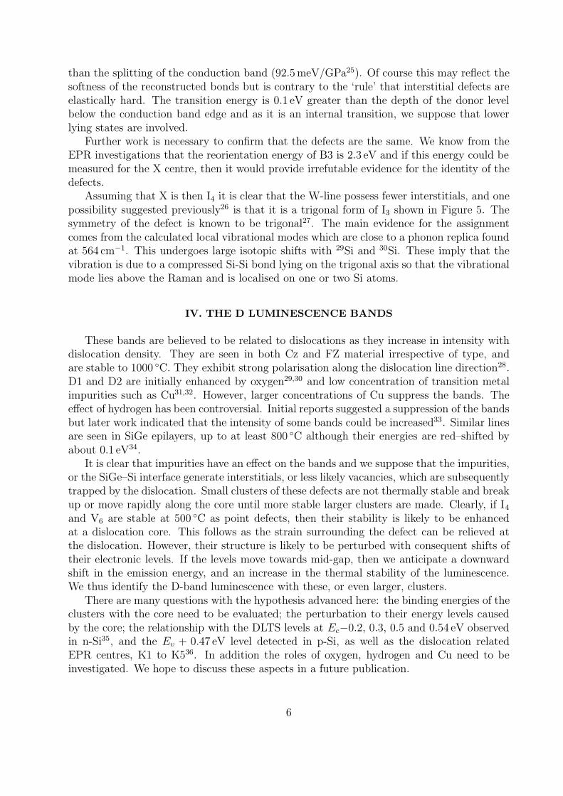
Consider now however V6. This then is the first vacancy defect which could luminesce inthe 1 eV region. This has six dangling bonds above and six below the hexagon of removedSi atoms (see Figure 1). In this case, all the bonds can be paired up and a defect madewhose electronic activity is minimal9–11. The reconstruction is symmetric and the resultingsymmetry of the centre is D3d. This reconstruction is of course similar to that occurring ata dislocation core.
2
Now, the question arises as to the electrical behaviour of the hexavacancy. This hasnow been answered but in an indirect way11. It has been found that neutron irradiatedSi containing ∼1016 cm−3 of hydrogen yields a number of photoluminescent lines linked tohydrogen12. Indeed these lines shift in mixtures of hydrogen and deuterium proving thatthese atoms are part of the optical centre of the defect. Moreover, the shifts of the linesdemonstrate that one of these centres, B41, contains two equivalent H atoms. What is theorigin of this line?
Careful annealing studies demonstrate that in neutron irradiated material a luminescenceband at 1.107 eV called the J-line occurs in a temperature range up to about 450 ◦C whenmultivacancy defects, including for example V5, are known to occur. This centre is believedto be intrinsic as its production increases with irradiation without saturation. The defectcan be aligned under stress in a similar manner to the divacancy suggesting it is a multi-vacancy centre. Moreover, the J-centre is not formed when hydrogen is present, but theother H-related PL centres are then detected. It seems then that hydrogen is reacting withthe J-centre leading to the hydrogen related defects.
A study of the effect of a magnetic field on the J-line has shown that the defect istrigonal13. Now a pair of equivalent atoms can only be added to a trigonal centre if thedefect possesses further symmetries such as inversion. The effective symmetry of the J-centre is then D3d and this is the same symmetry as the hexavacancy. No interstitialdefect has been constructed which has this symmetry and we conclude, that the J-line isdue to the hexavacancy. The calculations11 we have carried out support the view that astrong reconstruction occurs between the twelve dangling bonds of V6 and that only opticaltransitions in the vicinity of the band gap are possible.
In summary, the hexavacancy is the only vacancy aggregate known to be optically activein the 1 eV region but of course there are many interstitial defects known to luminescencein this energy region.
III. INTERSTITIAL CLUSTERS
From a theoretical viewpoint, analysing the structure of self-interstitial clusters has beena highly topical area. There are many papers dealing with possible structures but regrettablythere has been few serious attempts to try to relate the centres to observed defects. Herewe adopt a different strategy.
Most workers would agree that an interstitial defect whose dangling bonds can be re-constructed would be particularly stable. This is the case for the tetra-interstitial I4 defectbuilt out of four [100] split-interstitials10,14,15.
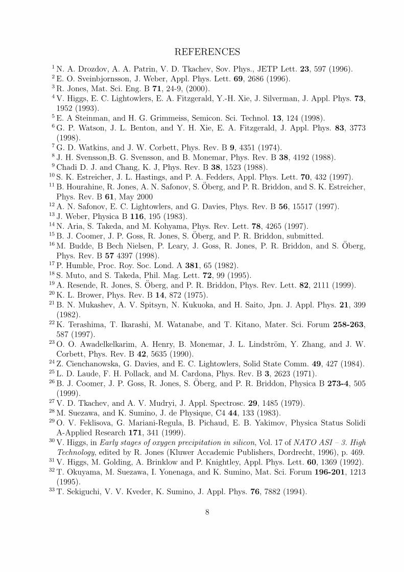
The split-interstitial shown in Figure 2 has two orthogonal p-orbitals which can be con-sidered as dangling bonds. These readily react with other defects. Indeed in Si we knowthat the interstitial complexes with hydrogen yielding a passive defect IH2
16. Thus, evenif the neutral interstitial I1 had a different structure, it is clear that IH2 is a perturbed[100] split-interstitial saturated with H. Now if we bring together two neighbouring split-interstitial defects as in Figure 3, then one pair of dangling bonds can be reconstructed. Thereconstructed bond bridges the two split-interstitials along [011].
We now show the other pair of dangling bonds along [011] can also be eliminated. Supposewe bring up another di-interstitial on a neighbouring (011) plane. This like the first will
3
possess two dangling bonds and one reconstructed bond. But placing then next to oneanother then allows us to pair up the four dangling bonds (aligned along [011]) formingaltogether four reconstructed bonds parallel to 〈011〉 as shown in Figure 4. Such a defecthas been suggested by Aria et al.14 as a low energy interstitial cluster in Si. However, thesame defect has been suggested many times and the earliest reference we are aware of is dueto Humble17 who argued it is a building block for an extended defect in diamond called theplatelet. Muto and Takeda18 have suggested that an extended (100) interstitial platelets inGe has the same structure.
It is clear that the stability of the defect arises from the elimination of dangling bonds andthis raises a crucial question. If there are no dangling bonds in the I4 defect, then surely,like reconstructed partials, there will be no gap states and the defect will be electrically,magnetically and optically inert. However, our calculations15 show that the defect is notinert and has a level deep donor level in the lower half of the band gap. The question nowarises is why should this occur.
To answer this, let us consider a tight binding model where an atomic orbital is coupledto neighbouring orbitals in a lattice of coordination z. If the Hamiltonian matrix elementsbetween neighbouring coupling atoms is V , then it is easy to show there is a band of statesstretching from −z|V | to z|V |. Now imagine an interstitial defect inserted in the middleof the lattice but having the same coordination as the bulk atoms. These bonds will becompressed and consequently the magnitude of |V | will be locally increased by a factor sayof f . It can be shown that the range for the energy eigenvalues is now increased to −zf |V |to zf |V |. Thus we expect states to move out of the valence band into the gap arising fromthese strengthened bonds. The same conclusion is reached if the effect of the interstitial isto locally increase the coordination z. In this way we can persuade ourselves that interstitialdefects can give rise to states in the lower half of the gap close to Ev. Of course, there aremany terms not considered in this simple tight binding Hamiltonian. There will be changesto bond angles and to the diagonal matrix elements and these will also cause a shift of thedefect levels. Nevertheless the best calculations we can do is to use an ab initio densityfunctional method to deduce the structure of the defect and then to evaluate its ionisationenergy. This is the energy necessary to remove a electron from the defective crystal. Ourcalculations showed that this is almost the same as the ionisation energy of the interstitialcarbon defect Ci. Thus we conclude19 that the defect must have a similar donor level as Ci
which is known from deep level transient spectroscopy (DLTS) studies to lie at Ev +0.28 eV.The implication is that I4 in p-Si should be present as as an ionised species I+
4 and thus EPRactive. We now ask whether an EPR signal has been found with properties expected of I4.
The B3 EPR centre (S=1/2) has been investigated by Brower20. This centre is detected inneutron irradiated p-type FZ-Si annealed between 170 to 500 ◦C. It possesses D2d symmetry– the same as I4. The defect is clearly very stable and not related to oxygen or carbonas 1016 cm−3 B3 centres can be formed – well above the concentrations of these elements.Brower makes the point that the unusual symmetry is not the result of motional averagingas in a Jahn-Teller distortion of a vacancy centre, but rather the symmetry is intrinsic.Hyperfine interactions on two atoms along the principal [100] axis have been resolved. Thisimplies that the core of the defect is empty for otherwise interaction with a unique atomwould have been detected. Of course, all these properties are expected of I4, although infact Brower suggests that the defect is a di-interstitial. The donor level has been placed at
4

Ev + 0.29 eV by Mukashev et al.21 who noted a correlation between B3 and the Ev + 0.29 eVlevel detected in DLTS. This agrees remarkable well with our estimate of the donor level.
Thus the properties of B3 are entirely in agreement with the calculations. But is thedefect optically active? We believe there is a link with a prominent optical centre called I3 orX (1.0398 eV). The notation I3 is unfortunate and may be confusing with the tri-interstitialI3 and so we shall refer to the optical centre as X.
The effect of annealing irradiated or implanted Si and following the evolution of photolu-minescent (PL) centres is instructive. Terashima et al.22 implanted Cz-Si with P and B ionsand subsequently annealed the samples between 200 and 700 ◦C. At 200 ◦C, a strong PL linecalled I1 or W at 1.018 eV was detected. Its intensity, relative to B-related bound exciton,first increased until about 200 ◦C and then decreased and the line disappeared by 500 ◦C.As the W signal diminished, the intensity of the X-line increased. This was not present at200 ◦C but became apparent at 300 ◦C, and its intensity increased until about around 450 ◦C.It subsequently decreased and vanished by 600 ◦C. These two lines dominated the spectrumbut there were less intense bands due to I2 at 1.080 eV – a trigonal defect containing two Batoms13 – and a line at 1.097 eV. Interestingly, annealing in an atmosphere containing Cu,led a similar spectrum but an additional band at 0.992 eV was detected which disappearedaround 550 ◦C.
Similar results were reported by Awadelkelkarim et al.23. Here, both Cz-Si and FZ-Siwere implanted with C and O and annealed to 500 ◦C. Besides the well known carbon andoxygen related lines: P (0.7671 eV), H (0.9254 eV), L (1.0038 eV), G (0.9694 eV), and C(0.7890 eV), the X and W lines were also detected. Moreover, in FZ-Si these, together withthe Y-line at 1.08 eV, were the principal emissions. Again the W-line although detected upto 350 ◦C, vanished at 400 ◦C while the X-line was observed from about 250 to 500 ◦C.
In summary, the annealing data in irradiated FZ-Si indicate that the W-centre is formedat an earlier stage than X and is stable until about 350 ◦C but as this disappears, the X-centre evolves and is stable until about 500 ◦C. Thus it is inferred that the W and X linesare related to intrinsic defects and the X centre is a larger aggregate than W. Both opticalsignals are seen in absorption as well as luminescence and represent transitions between gapstates. This distinguishes them from bound exciton transitions found, for example, in theJ-centre.
Now uniaxial stress measurements have been carried out on both of these centres . ForX, the line is split into two by 〈100〉 stress with one component being detected with anE field parallel to stress axis and the other perpendicular to it24. Similarly, the X-line issplit under 〈110〉 but not by 〈111〉 stress. It is clear that this behaviour is consistent withD2d symmetry if the optical transition occurs between either a1 and b2 or a2 and b1 states.Stressing along any 〈111〉 direction in Figure 4 would produce equivalent defects. However,the same stress pattern is found if the centre has Td symmetry, but in this case an electricdipole transition could only occur if one of the states had t2 symmetry. The effect of stressis then reflected in the splitting of the t2 manifold and one expects the vibronic structureto be associated with a t2 or e vibrational mode. However, there is no evidence that thesemodes are involved and thus the symmetry of the defect is is believed to be D2d.
Given the thermal stability of the X-defect and its symmetry it is tempting to identifyit with I4. However, one possible problem is that the stress sensitivity of the defect isanomalously large. Under [100] stress, the line splits by 117 meV/GPa which is greater
5
than the splitting of the conduction band (92.5 meV/GPa25). Of course this may reflect thesoftness of the reconstructed bonds but is contrary to the ‘rule’ that interstitial defects areelastically hard. The transition energy is 0.1 eV greater than the depth of the donor levelbelow the conduction band edge and as it is an internal transition, we suppose that lowerlying states are involved.
Further work is necessary to confirm that the defects are the same. We know from theEPR investigations that the reorientation energy of B3 is 2.3 eV and if this energy could bemeasured for the X centre, then it would provide irrefutable evidence for the identity of thedefects.
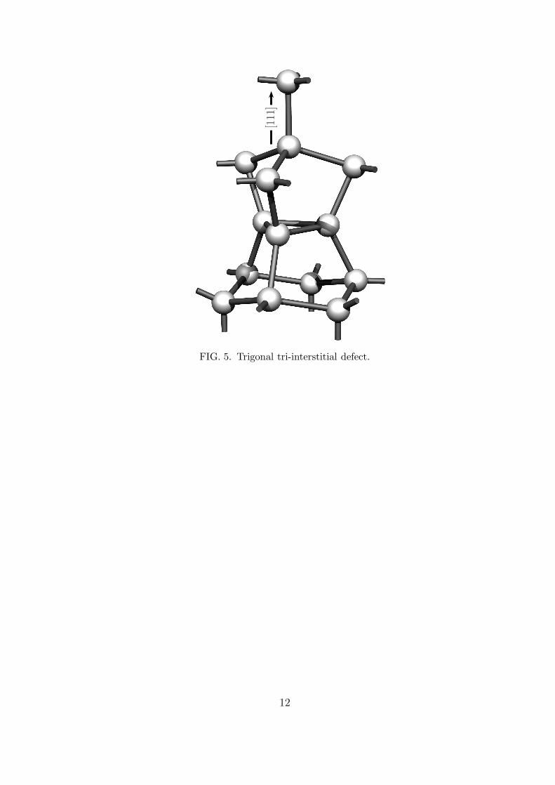
Assuming that X is then I4 it is clear that the W-line possess fewer interstitials, and onepossibility suggested previously26 is that it is a trigonal form of I3 shown in Figure 5. Thesymmetry of the defect is known to be trigonal27. The main evidence for the assignmentcomes from the calculated local vibrational modes which are close to a phonon replica foundat 564 cm−1. This undergoes large isotopic shifts with 29Si and 30Si. These imply that thevibration is due to a compressed Si-Si bond lying on the trigonal axis so that the vibrationalmode lies above the Raman and is localised on one or two Si atoms.
IV. THE D LUMINESCENCE BANDS
These bands are believed to be related to dislocations as they increase in intensity withdislocation density. They are seen in both Cz and FZ material irrespective of type, andare stable to 1000 ◦C. They exhibit strong polarisation along the dislocation line direction28.D1 and D2 are initially enhanced by oxygen29,30 and low concentration of transition metalimpurities such as Cu31,32. However, larger concentrations of Cu suppress the bands. Theeffect of hydrogen has been controversial. Initial reports suggested a suppression of the bandsbut later work indicated that the intensity of some bands could be increased33. Similar linesare seen in SiGe epilayers, up to at least 800 ◦C although their energies are red–shifted byabout 0.1 eV34.
It is clear that impurities have an effect on the bands and we suppose that the impurities,or the SiGe–Si interface generate interstitials, or less likely vacancies, which are subsequentlytrapped by the dislocation. Small clusters of these defects are not thermally stable and breakup or move rapidly along the core until more stable larger clusters are made. Clearly, if I4
and V6 are stable at 500 ◦C as point defects, then their stability is likely to be enhancedat a dislocation core. This follows as the strain surrounding the defect can be relieved atthe dislocation. However, their structure is likely to be perturbed with consequent shifts oftheir electronic levels. If the levels move towards mid-gap, then we anticipate a downwardshift in the emission energy, and an increase in the thermal stability of the luminescence.We thus identify the D-band luminescence with these, or even larger, clusters.
There are many questions with the hypothesis advanced here: the binding energies of theclusters with the core need to be evaluated; the perturbation to their energy levels causedby the core; the relationship with the DLTS levels at Ec−0.2, 0.3, 0.5 and 0.54 eV observedin n-Si35, and the Ev + 0.47 eV level detected in p-Si, as well as the dislocation relatedEPR centres, K1 to K536. In addition the roles of oxygen, hydrogen and Cu need to beinvestigated. We hope to discuss these aspects in a future publication.
6

ACKNOWLEDGEMENT
SO thanks NFR and TFR, and RJ thanks ENDEASD for financial support. We alsothank Gordon Davies for useful discussions.
7
REFERENCES
1 N. A. Drozdov, A. A. Patrin, V. D. Tkachev, Sov. Phys., JETP Lett. 23, 597 (1996).2 E. O. Sveinbjornsson, J. Weber, Appl. Phys. Lett. 69, 2686 (1996).3 R. Jones, Mat. Sci. Eng. B 71, 24-9, (2000).4 V. Higgs, E. C. Lightowlers, E. A. Fitzgerald, Y.-H. Xie, J. Silverman, J. Appl. Phys. 73,
1952 (1993).5 E. A Steinman, and H. G. Grimmeiss, Semicon. Sci. Technol. 13, 124 (1998).6 G. P. Watson, J. L. Benton, and Y. H. Xie, E. A. Fitzgerald, J. Appl. Phys. 83, 3773
(1998).7 G. D. Watkins, and J. W. Corbett, Phys. Rev. B 9, 4351 (1974).8 J. H. Svensson,B. G. Svensson, and B. Monemar, Phys. Rev. B 38, 4192 (1988).9 Chadi D. J. and Chang, K. J, Phys. Rev. B 38, 1523 (1988).
10 S. K. Estreicher, J. L. Hastings, and P. A. Fedders, Appl. Phys. Lett. 70, 432 (1997).11 B. Hourahine, R. Jones, A. N. Safonov, S. Oberg, and P. R. Briddon, and S. K. Estreicher,
Phys. Rev. B 61, May 200012 A. N. Safonov, E. C. Lightowlers, and G. Davies, Phys. Rev. B 56, 15517 (1997).13 J. Weber, Physica B 116, 195 (1983).14 N. Aria, S. Takeda, and M. Kohyama, Phys. Rev. Lett. 78, 4265 (1997).15 B. J. Coomer, J. P. Goss, R. Jones, S. Oberg, and P. R. Briddon, submitted.16 M. Budde, B Bech Nielsen, P. Leary, J. Goss, R. Jones, P. R. Briddon, and S. Oberg,
Phys. Rev. B 57 4397 (1998).17 P. Humble, Proc. Roy. Soc. Lond. A 381, 65 (1982).18 S. Muto, and S. Takeda, Phil. Mag. Lett. 72, 99 (1995).19 A. Resende, R. Jones, S. Oberg, and P. R. Briddon, Phys. Rev. Lett. 82, 2111 (1999).20 K. L. Brower, Phys. Rev. B 14, 872 (1975).21 B. N. Mukashev, A. V. Spitsyn, N. Kukuoka, and H. Saito, Jpn. J. Appl. Phys. 21, 399
(1982).22 K. Terashima, T. Ikarashi, M. Watanabe, and T. Kitano, Mater. Sci. Forum 258-263,
587 (1997).23 O. O. Awadelkelkarim, A. Henry, B. Monemar, J. L. Lindstrom, Y. Zhang, and J. W.
Corbett, Phys. Rev. B 42, 5635 (1990).24 Z. Cienchanowska, G. Davies, and E. C. Lightowlers, Solid State Comm. 49, 427 (1984).25 L. D. Laude, F. H. Pollack, and M. Cardona, Phys. Rev. B 3, 2623 (1971).26 B. J. Coomer, J. P. Goss, R. Jones, S. Oberg, and P. R. Briddon, Physica B 273-4, 505
(1999).27 V. D. Tkachev, and A. V. Mudryi, J. Appl. Spectrosc. 29, 1485 (1979).28 M. Suezawa, and K. Sumino, J. de Physique, C4 44, 133 (1983).29 O. V. Feklisova, G. Mariani-Regula, B. Pichaud, E. B. Yakimov, Physica Status Solidi
A-Applied Research 171, 341 (1999).30 V. Higgs, in Early stages of oxygen precipitation in silicon, Vol. 17 of NATO ASI – 3. High
Technology, edited by R. Jones (Kluwer Accademic Publishers, Dordrecht, 1996), p. 469.31 V. Higgs, M. Golding, A. Brinklow and P. Knightley, Appl. Phys. Lett. 60, 1369 (1992).32 T. Okuyama, M. Suezawa, I. Yonenaga, and K. Sumino, Mat. Sci. Forum 196-201, 1213
(1995).33 T. Sekiguchi, V. V. Kveder, K. Sumino, J. Appl. Phys. 76, 7882 (1994).
8
34 P. M. Mooney, and K. Shum, Mat. Sci. Forum 258-73, 151 (1997).35 P. Omling, E. R. Weber, L. Montelius, H. Alexander and J. Michel, Phys. Rev. B 32,
6571 (185).36 E. R. Weber, and H. Alexander, J. Phys. (Paris) Colloq. 44, C4-319 (1983).
9
FIGURES
x
x
FIG. 1. Ideal and reconstructed hexavacancy defects. The transparent spheres represent thevacancy sites.
FIG. 2. Schematic of the [100] split-interstitial. Also indicated are the two p-orbitals associatedwith the three-fold-coordinated atoms.
10
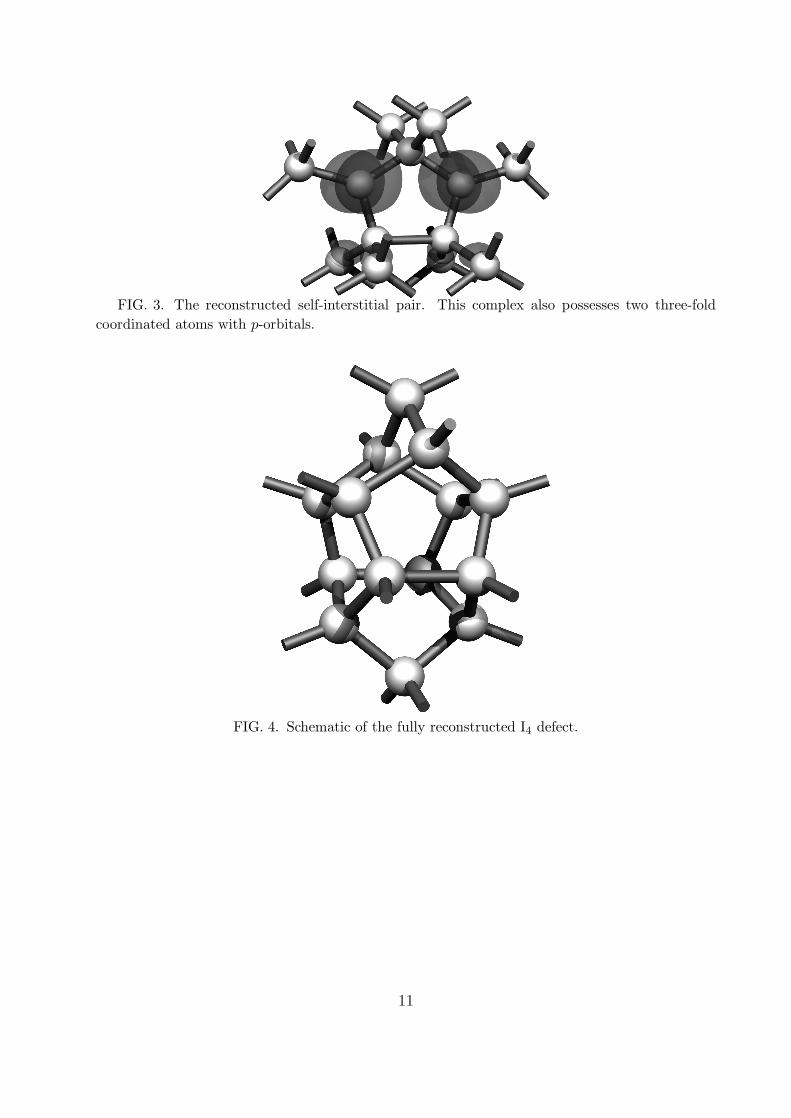
FIG. 3. The reconstructed self-interstitial pair. This complex also possesses two three-foldcoordinated atoms with p-orbitals.
FIG. 4. Schematic of the fully reconstructed I4 defect.
11
[111
]
x
x
FIG. 5. Trigonal tri-interstitial defect.
12

![D4 deRjd $ WRc^ ]Rhd W`c WcfZeWf] aRc]Vjd - Daily Pioneer](https://static.fdokumen.com/doc/165x107/631962a9c51d6b41aa0463ac/d4-derjd-wrc-rhd-wc-wcfzewf-arcvjd-daily-pioneer.jpg)