Interaction of Two-Dimensional Materials with Molecules ...
177
-
Upload
khangminh22 -
Category
Documents
-
view
4 -
download
0
Transcript of Interaction of Two-Dimensional Materials with Molecules ...

Copyright
Weibing Chen
2018

ABSTRACT
Interaction of Two-Dimensional Materials with Molecules, Cells, and Substrates
by
Weibing Chen
Two-dimensional (2D) materials have been widely explored in different
fields since 2004. More in-depth understanding of their interaction with the
environment becomes more and more vital in designing and implementing novel
biological devices. Knowing how to use them, how to evaluate their safety in the
human body, and how to prepare them cheaply are three critical questions in the
investigations of biomaterials. In this thesis, to cover these three questions, I will
examine two-dimensional materials in oxygen sensing, cytotoxicity evaluation,
friction tunability, substrate-controlled growth and protective layers in arbitrary
substrates. First, I will give a general review of the structure, synthesis, and
characterizations of two-dimensional materials used in this thesis. Second, I will
switch to the project of studying the interplay of MoS2 and oxygen molecules to
unveil the strong correlation between p-type doping and photoluminescence
enhancement due to the presence of oxygen. Next, to guarantee the safety of 2D
biosensor, I will reveal the tunable friction behaviors of MoS2 via the chemical
interface of self-assembled molecules which will be helpful in designing clogging-
free biosensors. Furthermore, the toxicity of MoS2 flakes and microparticles will be
evaluated via MTT without contaminations of samples during synthesis. The results

demonstrate the low toxicity of 2H type MoS2 to 6 six different kinds of human cells.
The interaction of 2D materials with substrates will be the focus of the last part of
this thesis, where I will demonstrate that patterned substrate controls the growth of
monolayer MoSe2 and the grown ultrathin h-BN on iron substrate protects the
covered substrate against strong acid very well. The extensive coverage in different
fields in this thesis provides us with some essential knowledge of these exciting 2D
materials in future biomedical applications.

Acknowledgments
Here I would like to thank my advisor Dr. Jun Lou for his patient and
insightful guidance and support on my Ph.D. program. My achievement cannot be
reached without his help. I also would like to thank Dr. Ming Tang and Dr. Angel
Marti for their constructive discussion on my researches and thoughtful feedback on
my thesis. My research projects spread different domains of science and many
experts in different areas offer their help generously. I am indebted to these
excellent collaborators including but not limited to Dr. Lidong Qin, Dr. Qunyang Li,
Dr. Weijin Qi, Dr. Xiaolong Zou, Dr. Ling Hao, Dr. Yingchao Yang, Dr. Dmitri V.
Voronine, Dr. Hua Guo, Dr. Sina Najmaei, Dr. Jing Zhang, Jiangtan Yuan, Zehua Jin,
and Shuai Jia.
I also want to express my sincere gratitude to my family. Without my
parents’ and my wife’s support, I can never achieve what I have today. Their
unconditional support and love are my best boost and strongest shield.

Contents
Acknowledgments ..................................................................................................... iv
Contents .................................................................................................................... v
List of Figures ............................................................................................................ ix
List of Tables .......................................................................................................... xviii
Nomenclature .......................................................................................................... xix
Overview ................................................................................................................... 1
Background and Introduction ..................................................................................... 3
2.1. Structures of 2D materials ....................................................................................... 4
2.2. Synthesis of 2D materials ......................................................................................... 7
2.2.1. Mechanical exfoliation ...................................................................................... 7
2.2.2. Liquid exfoliation ............................................................................................. 10
2.2.3. Chemical vapor deposition .............................................................................. 12
2.3. Characterizations, properties, and applications of 2D materials ........................... 17
2.3.1. Atomic force microscopy ................................................................................. 17
2.3.2. Raman and photoluminescence spectroscopy ................................................ 22
2.3.2.1. Raman scattering of 2D materials ............................................................. 24 2.3.2.2. PL of 2D materials ..................................................................................... 26 2.3.2.3. Second harmonic generation on 2D materials ......................................... 28
2.3.3. Field-effect transistor based on 2D materials ................................................. 29
2.3.4. Cytotoxicity evaluation of materials ................................................................ 35
2.3.5. XPS, SEM, and TEM .......................................................................................... 37
2.4. Summary ................................................................................................................ 39
2D Materials and Small Molecules: Quantitative correlation of photoluminescence
enhancement and doping level of monolayer transition metal dichalcogenides by
oxygen adsorption.................................................................................................... 40
3.1. Abstract .................................................................................................................. 40
3.2. Introduction ............................................................................................................ 41
3.3. Methods ................................................................................................................. 45
3.3.1. Materials and chemicals .................................................................................. 45

vi
3.3.2. MoS2 and WSe2 characterizations: .................................................................. 45
3.3.3. FET fabrications ............................................................................................... 46
3.4. Results and Discussions. ......................................................................................... 46
3.4.1. Characterization of grown MoS2 sample ......................................................... 46
3.4.2. PL investigation of MoS2 with oxygen adsorption ........................................... 48
3.4.3. Transport measurement of MoS2-based FET .................................................. 51
3.4.4. Decomposition of PL spectra and correlation with p-type doping of MoS2.... 53
3.4.5. Calculation of carrier density change from trion ratio .................................... 55
3.4.6. Oxygen adsorption on WSe2 and its effects .................................................... 56
3.5. Summary ................................................................................................................ 57
2D Materials and SAMs: Tunable friction of monolayer MoS2 by control of interfacial
chemistry ................................................................................................................. 60
4.1. Abstract .................................................................................................................. 60
4.2. Introduction ............................................................................................................ 61
4.3. Methods ................................................................................................................. 62
4.3.1. Growth of monolayer MoS2 on silicon wafer .................................................. 62
4.3.2. Preparation of MoS2 on SAMs ......................................................................... 63
4.3.3. Characterization and friction measurement ................................................... 64
4.3.3.1. Calibration of normal spring constant of the AFM probe ......................... 65 4.3.3.2. Calibration of lateral spring constant of the AFM probe .......................... 67
4.3.4. Simulations of charge transfer ........................................................................ 68
4.3.5. Kevin probe measurement .............................................................................. 69
4.4. Results and Discussion ........................................................................................... 69
4.4.1. Raman, PL and SEM characterizations ............................................................ 69
4.4.2. Friction measurement of MoS2 on SAMs ........................................................ 70
4.4.3. Charge transfer caused by SAMs ..................................................................... 73
4.4.4. Fermi level shift of monolayer MoS2 due to the presence of SAMs ............... 75
4.4.4.1. Optical, topographic and KPFM images of MoS2 across the boundary of APTS/MPTS and silicon ........................................................................................... 78
4.5. Summary ................................................................................................................ 81
2D Materials and Cells: Direct assessment of the toxicity of molybdenum disulfide
atomically thin film and microparticles via cytotoxicity and patch testing ................. 84

vii
5.1. Abstract .................................................................................................................. 84
5.2. Introduction ............................................................................................................ 85
5.3. Experimental Section ............................................................................................. 87
5.3.1. Preparation of MoS2 thin film and MoS2 microparticles ................................. 87
5.3.2. Cell culture and passage .................................................................................. 88
5.3.3. Cell viability evaluation .................................................................................... 90
5.3.4. Allergy testing on guinea pigs .......................................................................... 92
5.3.4.1. Pre-testing: ................................................................................................ 93 5.3.4.2. Patch testing and quartz plate testing: ..................................................... 94
5.4. Results and Discussion ........................................................................................... 95
5.4.1. Synthesis and Characterization of MoS2 film on quartz plate ......................... 95
5.4.2. Cytotoxicity results of MoS2 thin film .............................................................. 97
5.4.3. Cytotoxicity results of MoS2 microparticles .................................................. 101
5.4.4. Toxicity evaluation of MoS2 thin film and microparticles on animal skins ... 103
5.5. Summary .............................................................................................................. 106
2D Materials and Substrate I: Controllable growth of monolayer MoSe2 on nanoscale
pillar patterns ........................................................................................................ 107
6.1. Abstract ................................................................................................................ 107
6.2. Introduction .......................................................................................................... 108
6.3. Methods ............................................................................................................... 109
6.3.1. Chemicals and substrates .............................................................................. 109
6.3.2. CVD growth of monolayer MoSe2 ................................................................. 110
6.3.3. Characterizations ........................................................................................... 110
6.3.4. SHG measurement setup ............................................................................... 111
6.3.5. Simulation of CVD growth ............................................................................. 112
6.4. Results and Discussion ......................................................................................... 112
6.4.1. Characterization of grown MoSe2 ................................................................. 112
6.4.2. Evaluation the effect of pillars on Raman and PL .......................................... 116
6.4.3. Evaluation the effect of pillars on shape and orientation ............................. 117
6.4.4. Evaluation the effect of pillars on crystal orientation and edge type ........... 122
6.5. Summary .............................................................................................................. 125

viii
2D Materials and Substrates II: Growth of high-quality hexagonal boron nitride on
stainless steels as ultrathin protective films ............................................................ 126
7.1. Abstract ................................................................................................................ 126
7.2. Introduction .......................................................................................................... 127
7.3. Methods ............................................................................................................... 129
7.3.1. Chemicals ....................................................................................................... 129
7.3.2. Growth of h-BN .............................................................................................. 129
7.3.3. Characterizations ........................................................................................... 130
7.3.4. Evaluation of coating protection performance ............................................. 131
7.4. Results and Discussion ......................................................................................... 131
7.4.1. Characterization of compositions .................................................................. 131
7.4.2. Estimation of thickness of grown h-BN ......................................................... 134
7.4.3. Evaluation of proactive performance of h-BN ............................................... 136
7.5. Summary .............................................................................................................. 139
Summary and Outlook ............................................................................................ 140
References ............................................................................................................. 143

List of Figures
Figure 2.1 Top view of the ball-and-stick models of (a) graphene and (b) h-BN; (c) Side view and bird view of silicene; (d) Side view and bird view of 2H TMDs; (e) Top view of the ball-and-stick model of 2H TMDs; (f) Bird view of the primitive cell of 2H TMDs and the d-band splitting; (g) Top view of the ball-and-stick model of 1T TMDs; (h) Bird view of the primitive cell of 1T TMDs and the d-band splitting. ................................................................................................................ 5
Figure 2.2 Steps of ME of 2D materials. (a) Attach the tape to high-quality bulk layered crystals; (b) Peel off the Scotch tape from layered crystals; (c) Attach the Scotch tape to a new substrate; (d) Peel off the Scotch tape carefully from the new substrate. .................................................................................................................... 8
Figure 2.3 (a) Optical image of graphene sheet;[1] (b) AFM image of ultrathin MoS2 sheets;[35] (c) Optical image of MoS2 sheet of several layers; (d) Optical image of bilayer WSe2 nanosheet;[36] (e) Optical image of MoSe2 nanosheet, where dashed rectangle indicates the monolayer area (left) and bilayer area (right);[37] (f) Optical image of ultrathin SnS2 sheets.[38] ............................................ 9
Figure 2.4 Steps of LE. (a) Immerse MoS2 crystals or particles in butyllithium solution; (b) Lithium ions intercalate the MoS2 crystals; (c) Move the samples to water; (d) Reaction of lithium ions with water produces hydrogen gas which splits the layers of MoS2; (e) Surface of samples is modified with ions to stabilize them in solutions. ................................................................................................. 11
Figure 2.5 2D nanosheets obtained via LE. (a) TEM image of graphene, scar bar: 500 nm.[41](b) Atomic force microscope of MoS2 nanosheet. The inset shows the distribution of their diameters and thickness;[48] (c) TEM image of WS2 nanosheet.[45] .................................................................................................................. 12
Figure 2.6 Schematic of all-vapor CVD growth of 2D materials. (a) TMDs: different precursors used for Mo/W family TMDs are shown here. Blue rectangle represents furnace in CVD and carrying gas is pure nitrogen or mixture of nitrogen and hydrogen. (b) h-BN. The pump is used to maintain the low pressure of the quartz tube. ....................................................................................... 14
Figure 2.7 2D materials grown by all-vapor CVD. (a) Graphene;[93](b) MoS2;[73] (c) MoSe2;[53](d) h-BN.[94] ..................................................................................................... 16

x
Figure 2.8 Schematics of a typical AFM setup .............................................................. 18
Figure 2.9 Use AFM to indent 2D materials to acquire its Young’s module; (a) Transferred graphene on periodically circular holes. (b) AFM scanning image of graphene across the holes; (c) Depth-load data of graphene and fitted curve; (d) Schematics of indentation by AFM probe; (e) AFM scanning image of 2D materials across the holes after indentation; (f) Depth-load data of monolayer and bilayer MoS2 and fitted curves.[100,101] .................................................................... 20
Figure 2.10 (a) Lateral force of graphene as a function of lateral distance;[103] (b) Lateral force gap (friction) of monolayer and bilayer graphene as a function of displacement; [103] (c) Friction of monolayer and bilayer graphene as function of normal force; [103] (d) Atomic model of buckling effect of graphene when the tip slides over the surface;[104] (d) Schematic of proposed doping effect on the friction of MoS2.[111] ....................................................................... 22
Figure 2.11 a) Schematic of Raman process in vibration energy model (phonon band structure); (b) Schematic of PL process in electron band structure of semiconductors. See text for more information. ........................................................ 23
Figure 2.12 (a) Raman spectrum of graphene (top) and graphite (bottom);[112] (b) Intensity of D band and G band of graphene as functions of disorder length;[113] (c) Evolution of Raman spectra of few-layered MoS2 with thickness;[114] (d) Evolution of Raman peak positions of MoS2 with thickness;[114] (e) Evolution of Raman spectra of monolayer MoS2 with temperature;[115] (f) Raman peak position of monolayer MoS2 and WS2 at different temperature;[115] (g) The full width at half maximum of the A1g mode of monolayer MoS2 at different temperature;[116] (h) Mapping of Raman peak positions of different heterostructures.[117] ................................................................. 24
Figure 2.13 (a) Evolution of PL of MoS2 of different thickness obtained via ME;[34] (b) Calculated band structure of MoS2 of different thickness;[34] (c) Evolution of PL of MoS2 obtained via LE;[42] (d) Evolution of PL of MoS2 obtained via CVD;[120] (e) Evolution of PL of CVD-grown MoS2 with argon plasma;[121] (f) Evolution of PL of CVD-grown MoS2 with weaker oxygen plasma;[122] (g) PL of CVD-grown MoS2 transferred to different substrates;[92] (h) PL of ME MoS2 modified by bis(trifluoro-methane) sulfonimide.[123] ......... 27
Figure 2.14 (a) Schematic of SHG process in bilayer MoS2; (b) Dependence of SHG power on incident power; Inset: the dependence of SHG power on the
xi
rotation of sample;[155] (c) Optical image of stacked MoS2;[147] (d) SHG mapping of stacked MoS2. Stacking of MoS2 caused stronger SHG signal.132] ...................... 29
Figure 2.15 (a) Rendered model and schematic of back-gate FET of MoS2; (b) FET of graphene;[1] (c) Four electric remeasurement obtained from FET of graphene in (b): resistivity (A), conductivity (B) and Hall coefficient (C) of graphene as a function of gate voltage, carrier concentration as a function of temperature(D);[1] (d) Top-gated FET of MoS2 with HfO2 as dielectric layer;[156] (e) Dependence of source-drain current of monolayer MoS2 on back-gate voltage.Inset is the ISD – biased voltage curve. [156] ..................................................... 31
Figure 2.16 (a) Schematic of 1-nm channel of FET;[157] (b) Schematic of FET based on Cl-doped MoS2;[158] (c) Schematics of FET based on alloyed WSe2;[85] (d) Transmission curve of FET on h-BN sandwiched graphene;[159] (e) Transport response of FET on MoS2 at different atmosphere;[160] (f) Transport response of FET on MoS2 on Si3N4.[161] ............................................................................ 32
Figure 2.17 (a) Biosensor based on the change of dielectric coefficient of covering layer of monolayer MoS2;[17] (b) PL intensity of MoS2 controlled by back gate;[158] (c) Exciton concentration of MoSe2 controlled back gate;[37] (d) Source-drain current of FET of an electrically doping WS2 p-n junction as a function of bias gate;[171] (e) Schematic of a solar cell based on MoS2/p-Si heterostructure and its EQE specta;[172] (f) Photo detector based on FET of monolayer InSe and their photoresponse when samples is shed by lasers of different power;[173] (g) Light-emitting device based on the EL of MoS2 ;[174] (h) Absorption, PL and EL spectra of MoS2 FET;[174] (i) Strain induced shift of transport curve of FET of monolayer WSe2.[175] .......................................................... 33
Figure 2.18 Schematic of cytotoxicity of graphene and carbon nanotubes to neuronal PC12 cells. Inset: Mitochondrial toxicity evaluation;[179] (b) Cytotoxicity result of chemically exfoliated TMDs to human lung epithelial cells (A549).[180] ...................................................................................................................... 36
Figure 2.19 (a) XPS determination of nitrogen doping level in graphene at different temperatures;[183] (b) In-situ observation of CVD growth of graphene on a copper substrate;[184] (c) TEM modification of graphene to make freestanding graphene nanoribbon. [185] ....................................................................... 38
Figure 3.1 Optical, AFM, Raman and PL characterization of the monolayer MoS2. (a) Optical image of grown monolayer MoS2. The size is estimated to 50 µm; (b) Topological image of the sample by atomic force microscopy. The

xii
height profile shows that the thickness of as-grown samples is 0.62 nm; (c) Raman spectrum of the sample; inset is the zoom-in of two typical Raman peaks of monolayer MoS2, which corresponds to the 𝑬𝟐𝒈𝟏 and 𝑨𝟏𝒈 modes of 2D MoS2. Raman of Si is found (d) PL of the as-grown sample. The strong PL peak at 680 nm (labeled as Peak A) indicates the good quality of our as-grown sample. The Peak B is present due to the splitting of valence bands of 2D MoS2. Raman of Si is normalized to 1. ......................................................................................... 47
Figure 3.2 PL evolution of the monolayer MoS2 with oxygen levels. (a) PL of the as-grown monolayer MoS2 in pure oxygen and nitrogen environment. The intensity of PL in oxygen is about 40 times greater than that in nitrogen given the same power of the laser was used;(b) PL of the transferred monolayer MoS2 in pure oxygen and nitrogen environment. The PL intensity in oxygen is still much higher than that in nitrogen; (c) PL of the transferred monolayer MoS2 at different oxygen levels. As oxygen level decreases, the PL intensity decreases; (d) The relation between the position of the Peak A of PL and the oxygen levels. ........................................................................................................................... 50
Figure 3.3 Transfer characteristics evolution of the monolayer MoS2 sample. (a) Time-dependent transfer characteristics (source-drain current ISD vs. gate voltage Vg characteristics) of monolayer MoS2 FET in pure oxygen. After the purge of FET device in oxygen, the transfer characteristics gradually moves from left to right, indicating the increase of threshold voltage as oxygen adsorption rate on monolayer surface increases; (b) Time-dependent transfer characteristics of monolayer MoS2 FET after switched to pure nitrogen. Switching the gas from to oxygen to nitrogen means that decrease of oxygen level. Consequently, the transfer characteristics move from right to left, i.e., the decrease of the threshold voltage due to the desorption of oxygen from the sample; (c) Transfer characteristics at different oxygen levels. All data were obtained after 12 h purge. After saturation at the given oxygen levels for 12 h, the transfer characteristics shift from left to right, indicating the increase of the threshold voltage as oxygen level increases; (d) Threshold voltage versus oxygen levels; Inset is the linear fit of the peak position shift versus the threshold voltage shift. ........................................................................................................ 52
Figure 3.4 (a) The PL evolution of another monolayer MoS2 sample with oxygen levels and (b) the peak positions of the sample as oxygen level increases from 0 % to 100%; (c) The evolution of transfer characteristics and (d) the threshold voltage of the sample as oxygen level increases from 0% to 100%. (e) The correlation of the peak position shifts and threshold voltage

xiii
shifts (solid red line) and the linear fitting (green dashed line); (f) The evolution of the ratio of trion area to the total area of PL as the oxygen increases from 0% to 100%. All these results are consistent with that of Sample 1 in the main text. ................................................................................................... 53
Figure 3.5 Deconvolution of PL and the ratio of trion peak versus oxygen levels. (a) A typical deconvolution of PL of the monolayer MoS2 sample. Three peaks, including the A exciton, exciton B, and the trion, are used in the deconvolution; (b) The ratio of the area of trion peak to the total area of PL at different oxygen levels obtained from the deconvolution. The ratio decreases from 13% to 0% when oxygen level increases from 0 to 100%. ........................... 54
Figure 3.6 (a) Raman and PL of monolayer WSe2. The strong characteristic Raman peaks around 260 cm-1 and PL peak at 780 nm demonstrate the good quality of as-grown WSe2. ................................................................................................... 57
Figure 3.7 PL and transfer characteristics of p-type monolayer WSe2. (a) The normalized PL of monolayer WSe2 at different oxygen levels. As oxygen level increases from 0 to 100%, the PL intensity of p-type WSe2 decrease from 3.8 to 1.2; (b) The transfer characteristics of monolayer WSe2 at different oxygen levels. The right shifts of curves as oxygen level increases indicates a decrease of the threshold voltage. ...................................................................................................... 57
Figure 4.1 (a) Raman spectrum of the CVD-grown MoS2. The interval between the two vibrational modes of 20 cm-1 confirms that the sample is a monolayer; (b) PL of CVD-grown MoS2. The strong PL peak at 678 nm confirms the high quality of the samples. (c) Optical image of MoS2 on the SAMs stripes; (d) SEM image of MoS2 on the SAMs stripes, where the SAMs stripes are shown in darker. (e) Schematic of the sample preparation and friction measurements. Red stripes represent SAMs and triangles represents MoS2 samples. ................ 64
Figure 4.2 (a) Schematic of three-tip model used in the calibration of normal spring constant of AFM probe; (b) Schematic of DFLG method of determining lateral spring constant of AFM probe; (c) Typical damped oscillating data and the fitting curve of HOPG floating on top of four magnets; (d) Typical linear relationship between the displacement and the lateral signal of an AFM probe dragging HOPG away from the equilibrium point. ..................................................... 67
Figure 4.3 (a) AFM topography of monolayer MoS2 on APTS stripes. A dashed black line indicates the edge of MoS2. Inset: the profile line across the APTS stripe. The x-axis is displacement (unit: μm), and the y-axis is height (unit:

xiv
nm). (b) Friction image of MoS2 on APTS with black-white-sinusoidal color scale. Inset: lateral signals during the trace (red) and retrace (green) scans. The x-axis is displacement (unit: μm), and the y-axis is the lateral signal (unit: V). Vertical black lines show indicates the friction determined by the difference of the trace and retrace signals. (c) Friction image of the MoS2 sample on APTS with linear color scale. Inset: the average friction of MoS2 with APTS (red) and without APTS (blue). (d) AFM topography of MoS2 on MPTS. (e) Friction image of MoS2 with MPTS (red) and without MPTS (blue). All the scan area is 50 μm by 50 μm. (f) The normalized friction of monolayer MoS2 on APTS (red), MPTS (green) and bare Si wafer (blue). Reference friction is normalized to unity ........................................................................................................... 71
Figure 4.4. Ball-and-stick models of APTS (a) and MPTS (b). Red, cyan, white, blue and yellow balls indicate oxygen, silicon, carbon, hydrogen, nitrogen and sulfur atoms, respectively. (c) Top view (top) and side view (bottom) of MPTS over monolayer MoS2. The functional group is placed close to MoS2 in the model with 4x4x1 supercells of MoS2. The charge transfer between MoS2 and APTS (0.14 e) is larger than that of MoS2 on MPTS (0.05 e). ................................... 74
Figure 4.5 KPFM images and profile lines of (a) MoS2 on APTS; (b) MoS2 on SiO2; (c) MoS2 on MPTS; and (d) MoS2 on SiO2. The APTS beneath MoS2 is found to decrease the work function of monolayer MoS2 by 100 meV while MPTS does not decrease the work function of monolayer MoS2 significantly. The difference between (b) and (d) might be due to the different batch of MoS2 monolayers, and the dendrite pattern corresponds to the gaps between SAMs. ........................................................................................................................................... 78
Figure 4.6 (a) Optical image of the MoS2 flakes on the boundary of APTS area. (b) Optical image of the MoS2 flakes on the boundary of MPTS area. The red dashed lines indicate the boundary of the covered and exposed area andThe red arrows refer to the flakes scanned by AFM and KPFM. .................................... 80
Figure 4.7 (a) AFM and (b) KPFM images of a MoS2 flake at the boundary of the APTS. APTS covers the left side of the area. (c) (d) Topological and KPFM line profiles along the lines in (a) and 2(b). .......................................................................... 80
Figure 4.8 (a) AFM and (b) KPFM images of a MoS2 flake at the boundary of the APTS. MPTS covers the left side of the area. (c) (d) Topological and KPFM line profiles along the lines in (a) and 2(b). .......................................................................... 81
xv
Figure 5.1 Group 1 contains only MoS2 (1.6 g/mL) as a negative control and Group 2 only cells as positive control. Group 10 contains only culture media as none control. From 3 to 9, , the concentration of MoS2 decreases from 1.6 g/mL, 0.16 g/mL, 0.016 g/mL, 1.6 μg/mL, 0.16 μg/mL, 0.016 μg/mL, 1.6 ng/mL correspondingly. The outer holes contain 200 μL of PBS to slow down the evaporation of culture media. In each group, we used six holes. .......................... 92
Figure 5.2 (a) Optical image of a quartz plate with the left half covered by the MoS2 thin film. (b) Raman spectrum of MoS2 thin film. (c) HPDE cells in medium without quartz plate. (d) HPDE cells in medium with a quartz plate. (e) HPDE cells in medium with a quartz plate inside, half of which was covered by the MoS2 thin film. (f) HMLE cells at the boundary of quartz plate with and without MoS2 thin film. (g) Viabilities of different cells in medium with none, clean quartz plate, quartz plate fully covered by the MoS2 thin film. Scale bars in all pictures are 100 μm. .................................................................................................. 96
Figure 5.3 XPS of sulfurized MoS2 thin film on quartz. (a) referenced carbon 1s spectrum; (b) sulfur 2p spectrum; (c) molybdenum 3d spectrum. Three typical XPS spectra in Figure S3 shows the valence of sulfur is +2 according to the peak ranging from 161 to 163 eV. No 0 valence is present (164 eV), which means there is no sulfur element residual left in the grown samples. ............... 97
Figure 5.4 (a) Topography of MoS2 film on a quartz plate. The left part is the quartz plate, and the right part is a MoS2 film on the quartz plate. (b) 3D view of MoS2 thin film on a quartz plate. (c) Height profile of Line 1 in (a). The height of MoS2 thin film is estimated to be 3 nm here. .......................................... 100
Figure 5.5 The HPDE cells in normal media (a), with quartz plate (b), with MoS2-covered quartz plate (c), their respective identification of cell (d)(e)(f), and the distribution of round rates of cells (g)(h)(i). The round rate is defined as the ratio of the minor axis to the major axis of the elliptic shape of cells. 101
Figure 5.6 Cell morphologies in MoS2 suspensions (0.016 mg/mL). (a) 159; (b) dye-activated 231; (c) 293; (d) HDPE; (e) HMLE; (f) PANC1; (g) Viabilities of cells in the medium with MoS2 microparticles of different concentrations. Scale bars in all pictures are 100 μm. .......................................................................... 103
Figure 5.7 Examples of guinea pigs after two allergy testing. (a) After 1 hour; (b) After 24 hours; (c) After 48 hours. (d-f) Results of three guinea pigs after using quartz plate with MoS2 thin film as patch testing. ....................................... 105
xvi
Figure 6.1 (a) Top view and (b) bird view of the nanoscale pillars pattern (NPP) ; (c) Optical image, (d) SEM image, (e) Raman spectrum and (f) PL spectrum of the as-grown MoSe2 on the NPP; (g) Partial PL mapping image of as-grown MoSe2 on the NPP ............................................................................................ 114
Figure 6.2 Bird view of the as-grown MoSe2 on the NPP at different magnification (a) 5000 x ; (b) 15000 X; (c) 20000 X; (d) TEM image of the tiled MoSe2 pillars; (e) Atomic-resolution TEM image of MoSe2 pillars; (f) Selected electron diffraction pattern of selected area of the side of MoSe2 pillars. ...... 116
Figure 6.3 (a) Bird view of the transferred MoSe2 pillars. Note that some silicon pillars are left. (b) Zoom-in of (a) of the transferred MoSe2 pillars; (c) PL mapping of transferred MoSe2 with and without the support of silicon pillars. The inset shows the typical photoluminescence spectrum of MoSe2 with silicon pillars (purple) and without silicon pillars (green). ...................... 117
Figure 6.4 (a) SEM image of as-grown MoSe2 on NPP on a large area; (b) Zoom-in view of MoSe2 of the same orientation; (c) SEM image of the as-grown MoSe2 on silicon; (d) SEM image of the as-grown MoSe2 of different orientations. The side of the NPP substrate is not covered by pillars, which was utilized for the growth of MoSe2 on the flat silicon substrate. (e) The as-grown MoSe2 on pillars and the corresponding basis vectors of the hexagonal lattice of NPP; (f) Zoom-in view of the corner of the MoSe2 hexagon and the basis vectors. ...... 119
Figure 6.5 The coalignment of as-grown hexagonal MoSe2 and the hexagonal lattices of the NPP: (a) 10-µm-long edge; (b) 3-µm-long edge; (c) 1.5-µm-long edge; (d) Proposed growth model of MoSe2 on pillars; (e) Simulation result without silicon pillars; (f) Simulation result with pillars; The yellow part is the grown crystal after 1000 steps. ...................................................................................... 120
Figure 6.6 (a), (b) Zoom-in view of the yellow dashed rectangles in (c) the SEM image of infantile MoSe2, which are marked by the dashed circles. ................. 121
Figure 6.7 (a) Atomic model showing different kinds of terminating edges; (b) The SHG spectrum of the sample and the substrate; (c) Optical image of Sample 1 used for SHG spectrum measurement; (d) SHG intensity on the red spot of the sample in (c) as a function of crystal angle. The same polar coordination is used for (c) and (d). ............................................................................. 123
Figure 6.8 Optical image of Sample 2 and the SHG intensity as a function of the crystal angles at each marked location. ...................................................................... 125

xvii
Figure 7.1 Setup of CVD growth of h-BN on stainless steel. .................................. 130
Figure 7.2 (a) SEM image of a typical surface of Type 301 SLS. (b) EDX spectrum of the given area. ............................................................................................. 132
Figure 7.3 (a) Optical image of h-BN film on SSL; (b) Raman spectrum of the h-BN film on SLS; (c) XRD pattern of h-BN on SLS. ....................................................... 133
Figure 7.4 XPS spectra of elements in h-BN on SLS. (a) B 1s at 190 eV; (b) N 1s at 398 eV; (c) Fe 2p3/2t 708 eV. (d) Depth profile of h-BN film on SLS .............. 134
Figure 7.5 (a) SEM image of the h-BN/SLS. (b) The bird-view of the cross-section of h-BN/SLS. (c) Zoom in the cross-section. The thickness of h-BN is estimated to be 232 nm with the view angle considered...................................... 136
Figure 7.6 Protection performance evaluation of h-BN film on SLS in 20mL 1M HCl. (a) In the air; (b) 0 day; (c) 2 days; (d) 4 days; (e) 6 days; (f) 8 days. ...... 138
Figure 7.7 Evaluation of protection performance of the h-BN film on SLS in 20 mL 1M HCl at 90 °C. (a) 0 min; (b) 60 min (c) 180 min (d) 1440 min. .............. 139

List of Tables
Table 4.1 All data of normal spring constant of AFM cantilever ........................... 66
Table 5.1 Criterion for skin allergy. Occurring rate is defined as the number of animals of allergic reactions divided by the total number of animals ................ 94
Table 5.2Dose of MoS2 microparticles suspension and period in each group of guinea pigs ................................................................................................................................ 94
Table 5.3 Average and standard deviation (s. d.) of cell viabilities in different concentrations ........................................................................................................................ 98
Table 5.4 Results of guinea pigs patch testing. 0 means level none .................. 105
Table 7.1 Elemental analysis of type 301 SLS using EDX ...................................... 132

Nomenclature
2D two-dimensional
FET field-effect transistor
TMDs transition metal dichalcogenides
h-BN hexagonal boron nitride
HOPG highly ordered pyrolytic graphite
ME mechanical exfoliation/mechanically exfoliated
LE Liquid exfoliation
CVD chemical vapor deposition
PVD physical vapor deposition
PL photoluminescence
AFM atomic force microscope
CCD charge-coupled device
SLS stainless steels
FWHM full width at half maximum
EL electroluminescence
TEM transmission electron microscopy
SEM scanning electron microscopy
XPS X-ray photoelectron spectroscopy
SAMs self-assembled molecules
DFT density functional theory
NEMS nanoelectromechanical systems

xx
e-p coupling electron-phonon coupling
KPFM Kelvin probe force microscopy
CPD contact potential difference
SHG second harmonic generation
EDX energy dispersive X-ray spectroscopy
1
Chapter 1
Overview
Two-dimensional (2D) layered materials has been the most popular material in the
past decade due to its unique electric, photonic, optoelectric, and magnetic
properties. Different applications based their intriguing properties have been
proposed in different areas, such as flexible FET and photometers. One of the most
promising applications is biosensors which utilize the sensitivity of 2D materials to
the minimal concentration of molecules, low toxicity of 2D materials to most cells,
and the flexibility of 2D materials. However, many questions are still not answered
which impede better designs of biosensors. The scope of this thesis is to explore the
interaction between 2D materials and other materials including inorganic and
organic chemicals. An introduction of 2D materials will be given in Chapter 2. After
that, Chapter 3 focuses on the interplay of small molecules and 2D materials. In
Chapter 4, we will discuss how self-assembled organic molecules affect the
mechanical behaviors of 2D materials. The toxicity of 2D materials to cells will be

2
discussed in Chapter 5. The final part (Chapter 6 and Chapter 7) introduces the
effect substrates on the growth of 2D materials and how 2D materials protect
substrates.

3
Chapter 2
Background and Introduction
Since the birth of the graphene in 2004[1], two-dimensional (2D) materials
have been one of the most popular material family in academy and industry.
Subsequently, more 2D materials synthesized by different methods, such as
hexagonal boron nitride (h-BN), transition metal dichalcogenides (TMDs), silicene,
and 2D perovskites, are investigated in different aspects. Electronic,[2–5] optical,[6–8]
piezoelectric,[9–12] catalytic,[13–16] and biological[17,18] properties of 2D materials have
been widely explored by researchers, and different potential applications based on
these novel properties are proposed, designed and implemented. To meet
researchers’ high interests, in 2014, a new journal 2D Materials was created by
IOPPublishing specifically for new findings of these materials. All these findings are
inspired by the discovery of “impossible” 2D materials, which Laudau, Mermin, and
Imry[19–21] once predicted to be unstable. However, thanks to its crystal fluctuation
4
of at non-zero temperature as a quasi-2D material[22], graphene proves its existence
and Novoselov et al. opened the door to fantasy 2D materials for us. [23]
We will discuss the structures of 2D materials and the effects on their
properties first since structures of materials define everything else in materials
sciences. Then different synthesis methods of 2D materials will be discussed,
focusing on chemical vapor deposition, which we used for the synthesis of all 2D
materials in this thesis. Finally, properties of 2D materials and the corresponding
characterization methods will be reviewed along with potential applications based
on these attractive properties.
2.1. Structures of 2D materials
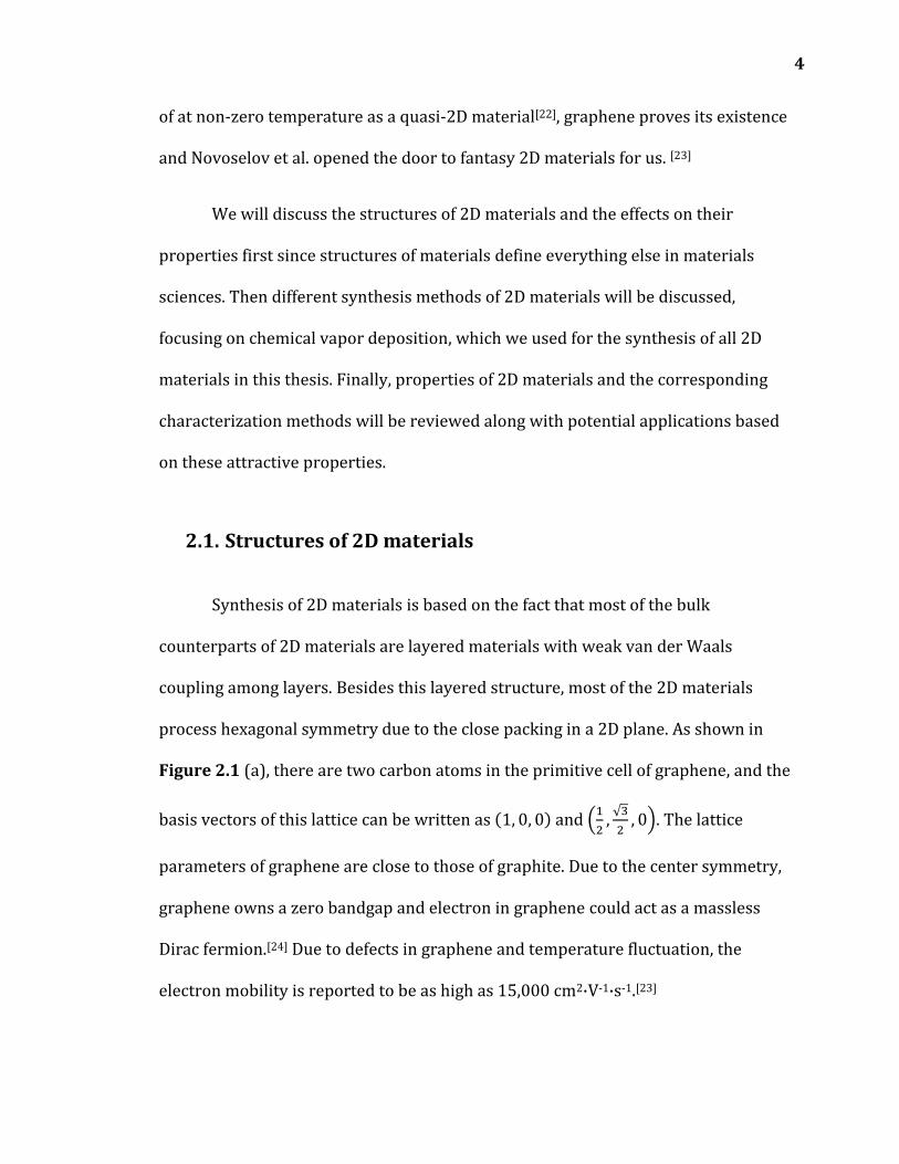
Synthesis of 2D materials is based on the fact that most of the bulk
counterparts of 2D materials are layered materials with weak van der Waals
coupling among layers. Besides this layered structure, most of the 2D materials
process hexagonal symmetry due to the close packing in a 2D plane. As shown in
Figure 2.1 (a), there are two carbon atoms in the primitive cell of graphene, and the
basis vectors of this lattice can be written as (1, 0, 0) and (12
, √32
, 0). The lattice
parameters of graphene are close to those of graphite. Due to the center symmetry,
graphene owns a zero bandgap and electron in graphene could act as a massless
Dirac fermion.[24] Due to defects in graphene and temperature fluctuation, the
electron mobility is reported to be as high as 15,000 cm2·V-1·s-1.[23]
5
Figure 2.1 Top view of the ball-and-stick models of (a) graphene and (b) h-BN; (c) Side view and bird view of silicene; (d) Side view and bird view of 2H
TMDs; (e) Top view of the ball-and-stick model of 2H TMDs; (f) Bird view of the primitive cell of 2H TMDs and the d-band splitting; (g) Top view of the ball-and-stick model of 1T TMDs; (h) Bird view of the primitive cell of 1T TMDs and
the d-band splitting.
Replacing carbon atoms in graphene with boron or nitrogen alternatively,
another interesting 2D material, hexagonal boron nitride (h-BN), can be found,
shown in Figure 2.1 (b). Due to the electron configurations of boron and nitrogen,
there is no dangling bond in h-BN. As a result, h-BN is an insulator with a band gap
of h-BN 5.87 eV[25] and show chemical inertness at different condition. Therefore,
the ultrathin h-BN protective coating is proposed.
Replacing carbon atoms in graphene by elements in the same group, for
instance, silicon, we can get silicene, shown in Figure 2.1 (c). Unlike the flat topology
of graphene, silicene has a periodic buckling topology, and the coupling among
layers is stronger, which makes it challenging to prepare via mechanical exfoliation.
a b c d
e f g hS
Mo Mo
S

6
Lalmi et al. and Aufray et al. in 2010 grew the silicene for the first time by depositing
silicon atoms on highly clean Ag(110) and Ag(111).[26,27] Similar to graphene,
silicene is a material with a small and tunable bandgap at different kinds of doping.
A silicene field-effect transistor (FET) was fabricated in 2015 to demonstrate its
capability in semiconductors industry.[28] However, the bandgap is smaller than
typical FET device (0.5 V), which limits its use as 2D semiconductors.
The most popular 2D semiconductors used in FET devices are transition
metal dichalcogenides (TMDs). It holds the same hexagonal symmetry as graphene
if viewed from the top. However, as shown in Figure 2.1 (d), unlike graphene, the
thickness of TMDs are greater since they are three sublayers thick with a sublayer of
transition metal atoms sandwiched by two sublayers of chalcogenides atoms.
However, two configurations of the three sublayers exist. The first one is ABA
stacking, where the chalcogenide layers overlap if viewed from the top, as shown in
Figure 2.1 (e). The primitive cell of such lattice is shown in Figure 2.1 (f), which
possesses a D3h symmetry. According to crystal field theory, such symmetry causes
the splitting of the d band of transition metal atom to three subbands: a1’, e’, e’’. The
low-energy band a1’ band is fully occupied by electrons while the left two bands are
empty, rendering this type of TMDs semiconducting. However, the other stacking,
ABC stacking, constructs a lattice with D3v-symmetry and its primitive cell is shown
in Figure 2.1(h). The Figure 2.1 (g) shows the top view of such lattice, and it is clear
that two chalcogenide layers mismatch. Such symmetry splits the d band of the
transition metal atom to two subbands: t2g and eg. The partial occupied t2g band
results in conducting TMDs. These two stacking are called 2H and 1T type

7
respectively in bulk TMDs, and researchers in 2D TMDs follow the nomenclature. In
summary, 2H TMDs are semiconducting, and 1T TMDs is conductive. Several reports
on simulations and controls of the phase transition between them have been
published. [29–31]
Structures of other 2D materials, such as black phosphorous (BP)[32] and
GaSe[33], are not discussed here. Please refer to literature for more details.
2.2. Synthesis of 2D materials
In this part, three main synthesis methods will be discussed. Other methods,
such as metal organic chemical vapor deposition, physical vapor deposition, and
atomic layer deposition will be mentioned briefly. For more details, please follow
the references.
2.2.1. Mechanical exfoliation
To obtain monolayer or few-layer materials, mechanical exfoliation (ME) of
bulk counterparts is a straightforward method since the birth of graphene in 2004[1]
and MoS2 in 2010[34]. It too simple to believe compared to other delicate methods in
nanomaterials when reported in 2004, which also demonstrates the authors’
courage and ambitions. Figure 2.2 shows the steps of ME method. Scotch tape was
used to obtain the first graphene, and it subsequently becomes the most popular
and cheapest tool in nanoscientists’ labs. Put a tape on high-quality crystals, such as
highly ordered pyrolytic graphite (HOPG) or bulk MoS2 flake, and peel it off to have

8
some ultrathin flakes on it. Only small parts of the flakes are thin enough to be
considered as 2D. Therefore, the tape is usually folded several times to tear the
flakes further down (not shown in Figure 2.2). After that, the tape is attached to a
new substrate, usually a silicon wafer with markers (which help locate the obtained
2D sheets). After several times of attaching and detaching the tape, some 2D flakes
can be found on the new substrate using an optical microscope. Figure 2.3 shows
some of the obtained samples.
Figure 2.2 Steps of ME of 2D materials. (a) Attach the tape to high-quality bulk layered crystals; (b) Peel off the Scotch tape from layered crystals; (c) Attach the Scotch tape to a new substrate; (d) Peel off the Scotch tape carefully from
the new substrate.

9
Figure 2.3 (a) Optical image of graphene sheet;[1] (b) AFM image of ultrathin MoS2 sheets;[35] (c) Optical image of MoS2 sheet of several layers; (d) Optical image of bilayer WSe2 nanosheet;[36] (e) Optical image of MoSe2 nanosheet,
where dashed rectangle indicates the monolayer area (left) and bilayer area (right);[37] (f) Optical image of ultrathin SnS2 sheets.[38]
The ME 2D materials usually possess high crystal quality due to the
prevention of possible chemical contaminations during their fabrication. (See
Chapter 3 for further discussions.) However, the size and thickness of flakes are
highly uncontrollable in this method, which thus prohibits it from large-scale
production of 2D materials. As we can see in Figure 3, the sizes of the flakes are
typically within 20 µm, and the actual monolayer area is even smaller. The
fabrication of devices based on such small areas requires e-beam lithography, which
is time-consuming and laborious to scale up. Ball milling, another kind of ME, has
been explored to scale up the preparation of h-BN[39], but the quality of samples is
ab c
df
e
5�µm
10
much worse. Therefore, samples obtained via ME are mostly used for fundamental
research of 2D materials.
2.2.2. Liquid exfoliation
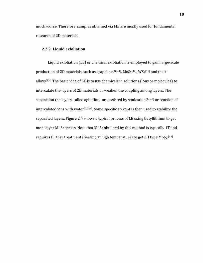
Liquid exfoliation (LE) or chemical exfoliation is employed to gain large-scale
production of 2D materials, such as graphene[40,41], MoS2[42], WS2[16] and their
alloys[43]. The basic idea of LE is to use chemicals in solutions (ions or molecules) to
intercalate the layers of 2D materials or weaken the coupling among layers. The
separation the layers, called agitation, are assisted by sonication[44,45] or reaction of
intercalated ions with water[42,46]. Some specific solvent is then used to stabilize the
separated layers. Figure 2.4 shows a typical process of LE using butyllithium to get
monolayer MoS2 sheets. Note that MoS2 obtained by this method is typically 1T and
requires further treatment (heating at high temperature) to get 2H type MoS2.[47]

11
Figure 2.4 Steps of LE. (a) Immerse MoS2 crystals or particles in butyllithium solution; (b) Lithium ions intercalate the MoS2 crystals; (c) Move the samples
to water; (d) Reaction of lithium ions with water produces hydrogen gas which splits the layers of MoS2; (e) Surface of samples is modified with ions to
stabilize them in solutions.
Although the mass of obtained 2D materials via LE are much greater than
those via ME, extrinsic defects and impurities are inevitably introduced to the
nanosheets in this method. The defeats and dopants not only degrade the lattice
structure but also change some of the intrinsic properties of 2D materials. Even
post-treatments may alleviate this problem, such as annealing in protecting gas[42],
the fragmented morphology and small sizes of samples still limits their applications.
Figure 2.5 shows the morphologies of several samples obtained by this method. As

12
we see, the sizes of samples are still limited, and the distribution of diameter and
thickness are broad.
Figure 2.5 2D nanosheets obtained via LE. (a) TEM image of graphene, scar bar: 500 nm.[41](b) Atomic force microscope of MoS2 nanosheet. The inset
shows the distribution of their diameters and thickness;[48] (c) TEM image of WS2 nanosheet.[45]
2.2.3. Chemical vapor deposition
Chemical vapor deposition (CVD) has proven to be a promising method of
growing large-scale and high-quality 2D materials compared to other methods.[49–51]
Although physical vapor deposition (PVD) of high-quality monolayer MoS2 was
achieved in 2013, the size was still limited, and the thickness was not uniform.[52]
This method also lacks flexibility because the tunable parameters in PVD are only
temperature and flow rate. On the contrary, tuning various parameters in CVD,
researchers are able to grow large-scale, high-quality graphene, MoS2 and h-BN [53–
57]. In this section, we will focus on the CVD growth of TMDs since CVD growth of
graphene and h-BN has been better developed and understood.[58,59] With different
13
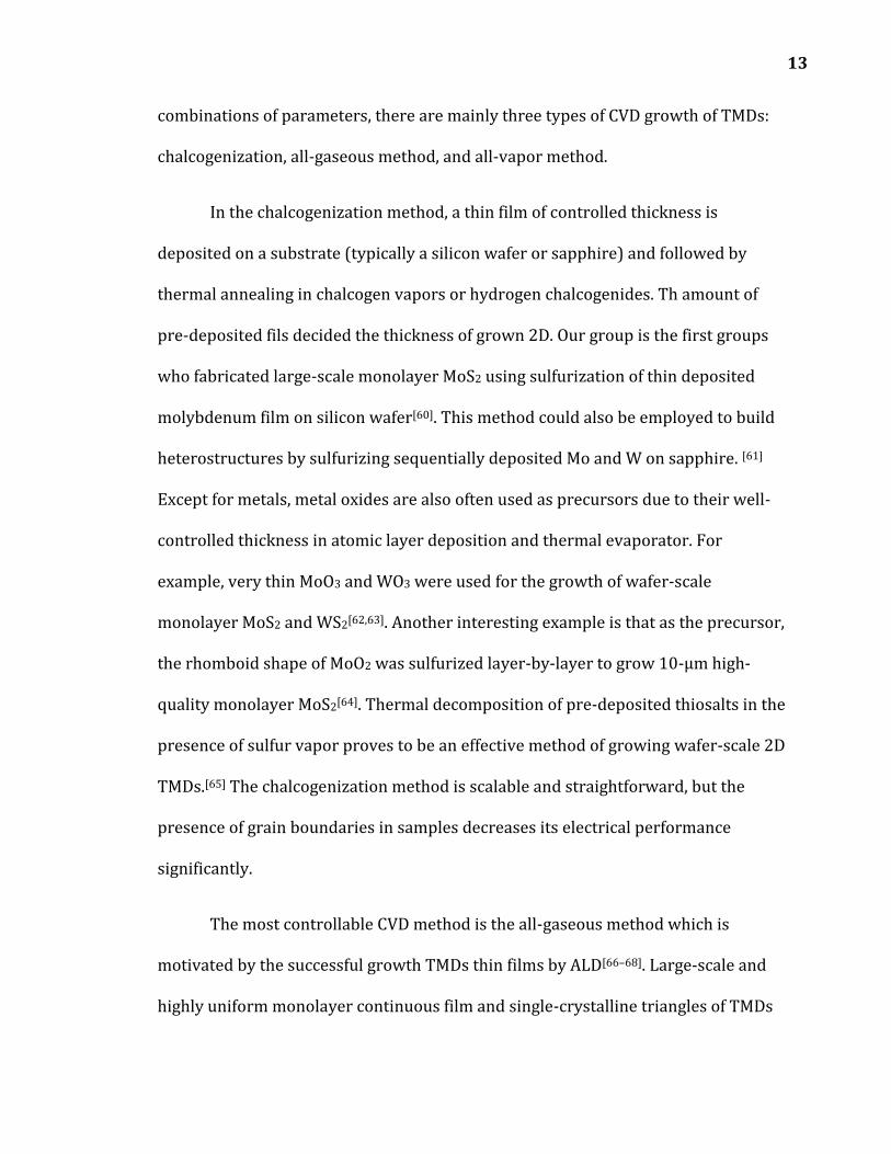
combinations of parameters, there are mainly three types of CVD growth of TMDs:
chalcogenization, all-gaseous method, and all-vapor method.
In the chalcogenization method, a thin film of controlled thickness is
deposited on a substrate (typically a silicon wafer or sapphire) and followed by
thermal annealing in chalcogen vapors or hydrogen chalcogenides. Th amount of
pre-deposited fils decided the thickness of grown 2D. Our group is the first groups
who fabricated large-scale monolayer MoS2 using sulfurization of thin deposited
molybdenum film on silicon wafer[60]. This method could also be employed to build
heterostructures by sulfurizing sequentially deposited Mo and W on sapphire. [61]
Except for metals, metal oxides are also often used as precursors due to their well-
controlled thickness in atomic layer deposition and thermal evaporator. For
example, very thin MoO3 and WO3 were used for the growth of wafer-scale
monolayer MoS2 and WS2[62,63]. Another interesting example is that as the precursor,
the rhomboid shape of MoO2 was sulfurized layer-by-layer to grow 10-μm high-
quality monolayer MoS2[64]. Thermal decomposition of pre-deposited thiosalts in the
presence of sulfur vapor proves to be an effective method of growing wafer-scale 2D
TMDs.[65] The chalcogenization method is scalable and straightforward, but the
presence of grain boundaries in samples decreases its electrical performance
significantly.
The most controllable CVD method is the all-gaseous method which is
motivated by the successful growth TMDs thin films by ALD[66–68]. Large-scale and
highly uniform monolayer continuous film and single-crystalline triangles of TMDs

14
have been successfully grown, such as MoS2, WS2, and WSe2[69–72]. The reaction
mechanism in this method is highly complicated but easy to test and improve thanks
to the maturely developed thermal models for gaseous reactions in metalorganic
chemical vapor deposition. However, due to the high toxicity and high prices of
precursors, this method is not widely adopted for the large-scale growth of 2D
materials.
Figure 2.6 Schematic of all-vapor CVD growth of 2D materials. (a) TMDs: different precursors used for Mo/W family TMDs are shown here. Blue
rectangle represents furnace in CVD and carrying gas is pure nitrogen or mixture of nitrogen and hydrogen. (b) h-BN. The pump is used to maintain the
low pressure of the quartz tube.
The most widely employed CVD method is the all-vapor method, which
utilizes the vapors of precursors at high temperature. Figure 2.6 shows the setup
schematics of growing TMDs and h-BN. This method has been intensively used and
studied since the first successful growth of monolayer MoS2 on the silicon wafer in
2013 due to its simplicity, versatility, and flexibility. In 2013 our group was the first
to obtain high-quality monolayer MoS2 without molecule seeding and studied the
electric effect of grain boundary in MoS2 [73]. Later, van der Zande et al. confirmed
the feasibility of CVD growth and found the shape of triangular MoS2 was an
Pressure�gauge
S/Se/Te
MoO3/WO3
Substrates
Carrying�gas
b

15
indicator of edge types of MoS2[74]. By replacing the MoO3 with MoCl5, Y. Yu et al.
obtained high-quality continuous monolayer MoS2 at a lower temperature[75]. Since
2013, many TMDs were grown by CVD, including WS2[76], MoSe2[77,78], WSe2[79],
MoTe2[80], WTe2[81], ReS2[82], NbS2[83], SnS2[84].
In the all-vapor method, types of precursors, evaporating temperature and
reaction temperature, ramp rate, reaction time, flow rate of carrying gases, seeding,
substrate morphology, and pressure of the whole chamber are tuned in a broad
range to grow 2D materials with desired properties. The quality of samples is
usually high. For example, the carrier mobility of CVD-grown WSe2 was as high as
200 cm2V-1s-1[85] which is comparable to that of ME samples. The intensity of
photoluminescence (PL) of CVD-grown 2D materials can be as high as that of ME
samples[57,86].
The flexibility of the all-vapor method is a double-edged knife, which not only
brings us more control options but also complicates the process. This complication
impedes the understanding of the reaction mechanism due to the scattering results
from different precursors, temperature programs, atmosphere, and reaction time. It
has been urged to investigate the growth process in this method to unveil the
leading parameters. Some results were reported in literature, including the
seeding[87], component of carrying gases[56,76], concentration of precursors[88],
substrates[55,74,89], and reaction temperature[79]. Recently, B. Li studied the growth
mechanism of MoSe2 and suggested to divide the growth process into three stages:
evaporation and reduction, condensation, and selenization[90]. The details of
16
nucleation are not yet well studied and recently J. Cain et al. unveiled a self-seeding
mechanism that the condensed metal oxides meta-particles were sulfurized to
fullerene core-shell nanoparticles and served as nucleus[91]. Substrates also play an
important role in all-vapor CVD. For example, monolayer MoS2 grown on a SrTiO3
substrate in CVD showed a 1.5D fractal-like morphology, which possessed s a high
edge-to-surface ratio and improved its electrocatalytic performance
dramatically.[89]. It was also found that MoS2 grown on the mica had different
helicity from that on the silicon wafer.[92] However, it is still unclear that how the
temperature, substrates, and precursors control the morphology of grown samples
in this method. It will be one goal in the next few years to understand and well
control the parameters.
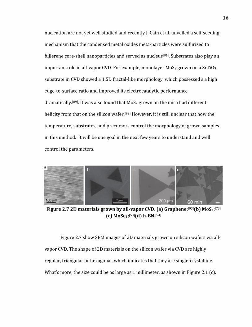
Figure 2.7 2D materials grown by all-vapor CVD. (a) Graphene;[93](b) MoS2;[73]
(c) MoSe2;[53](d) h-BN.[94]
Figure 2.7 show SEM images of 2D materials grown on silicon wafers via all-
vapor CVD. The shape of 2D materials on the silicon wafer via CVD are highly
regular, triangular or hexagonal, which indicates that they are single-crystalline.
What’s more, the size could be as large as 1 millimeter, as shown in Figure 2.1 (c).
b c d

17
CVD has been proven as a promising method of large-scale growth of 2D materials
and is used for the growth MoS2, MoSe2, and h-BN in this thesis.
2.3. Characterizations, properties, and applications of 2D
materials
This section is divided into five parts on the primary characterization
methods used in this thesis. I will give the principles of each method briefly and its
capability of characterizing properties of 2D materials. Furthermore, the potential
applications based on those the properties will be provided.
2.3.1. Atomic force microscopy
Since its birth in 1986[95], atomic force microscope (AFM) has been widely
used to characterize the surface of materials in different areas due to its high
sensitivity at vertical direction. Many variants of AFM were invented to visualize
more information on the material surface, such as chemical force microscopy[96] and
atomic force microscope infrared spectroscopy[97]. One of AFM variants used in this
thesis is called Kelvin probe force microscopy which is used to obtain the working
function of monolayer MoS2 with molecules (See Error! Reference source not f
ound. for more information). All the tools in the big family share a similar principle:
use a probe with a nanoscale tip to “touch” samples and record the feedback of the
probe caused by the interaction between the tip and the sample surface. Figure 2.8
shows a typical setup: a laser is shed on the back of a cantilever and reflected by its
back to a charge-coupled device (CCD). The signal collected by the CCD includes
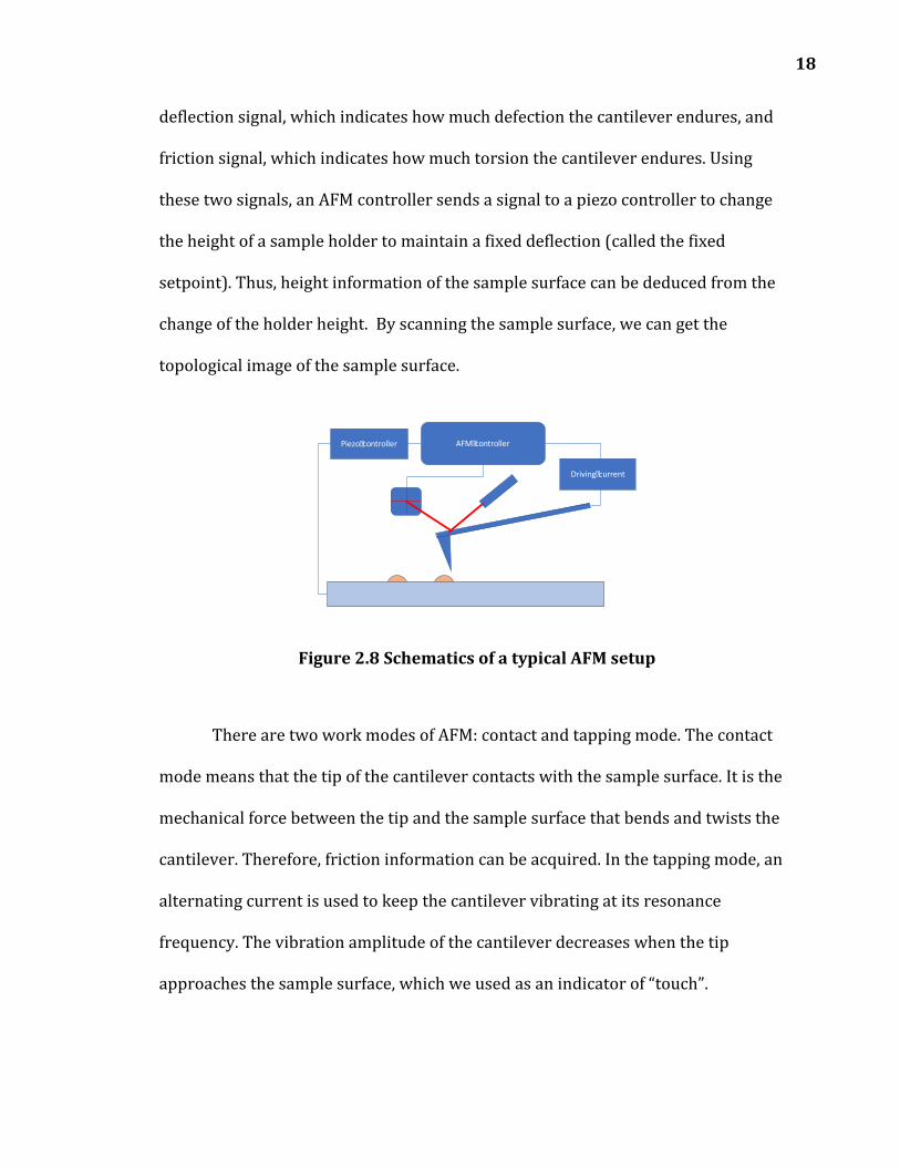
18
deflection signal, which indicates how much defection the cantilever endures, and
friction signal, which indicates how much torsion the cantilever endures. Using
these two signals, an AFM controller sends a signal to a piezo controller to change
the height of a sample holder to maintain a fixed deflection (called the fixed
setpoint). Thus, height information of the sample surface can be deduced from the
change of the holder height. By scanning the sample surface, we can get the
topological image of the sample surface.
Figure 2.8 Schematics of a typical AFM setup
There are two work modes of AFM: contact and tapping mode. The contact
mode means that the tip of the cantilever contacts with the sample surface. It is the
mechanical force between the tip and the sample surface that bends and twists the
cantilever. Therefore, friction information can be acquired. In the tapping mode, an
alternating current is used to keep the cantilever vibrating at its resonance
frequency. The vibration amplitude of the cantilever decreases when the tip
approaches the sample surface, which we used as an indicator of “touch”.
AFM�controller
Driving�current
Piezo�controller

19
Maintaining the same vibration amplitude by changing the holder height, AFM
provides the surface topography without damaging the sample surface.
As the thinnest materials, 2D materials challenge AFM to determine their
thickness accurately. Three facts conspire to make the measurement of graphene
hard to determine. First, the thickness of graphene is out of the resolution of most
AFM at room temperature. Second, the large roughness of metal substrates used in
the growth graphene prohibits the measurement. Finally, even using advanced AFM
at low temperature and transferring graphene to a clean silicon wafer, we are still
not able to determine the thickness of a graphene sheet on a hetero-surface because
that two kinds of the surface are present and their interactions with the tip are
different. At the edge of the graphene, the tip receives different kinds of feedback
when it crosses the edge, which renders the deduced thickness of graphene
meaningless. The situation holds for h-BN. For TMDs or other thicker 2D materials,
their thickness can be estimated from the AFM scanning, but it should be
interpreted carefully with the hetero-surface problem in mind. The thickness of
TMDs is estimated to from 0.6 nm to 1 nm according to AFM[56,98,99], which is
consistent with the thickness of layers in bulk materials. See Figure 2.3 (b) and
Figure 2.4 (b) for example.

20
Figure 2.9 Use AFM to indent 2D materials to acquire its Young’s module; (a) Transferred graphene on periodically circular holes. (b) AFM scanning image
of graphene across the holes; (c) Depth-load data of graphene and fitted curve; (d) Schematics of indentation by AFM probe; (e) AFM scanning image of 2D
materials across the holes after indentation; (f) Depth-load data of monolayer and bilayer MoS2 and fitted curves.[100,101]
Due to its information of force feedback from samples, we also use AFM for
the mechanical characterization of 2D materials. By indenting 2D materials across
holes by AFM probe and obtaining depth-load profiles of 2D materials, we can fit the
profiles to obtain Young’s modulus, as shown in Figure 2.9(a) (b) and (d) (e). Two
profiles of graphene and MoS2, are shown in Figure 2.9(c) and (f)[100,101]. The
Young’s moduli of graphene and MoS2 in these profiles are found to be 1.0 TPa and
270 GPa, greater than that of stainless steels (SLS). Most of the 2D materials have
extensive Young’s modules, for instance, Young’s modulus of h-BN is 1.16 TPa.[102]
a b
ed
c
f

21
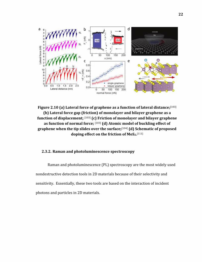
Friction behaviors and the adhesion of the 2D materials to substrates can
also be investigated via AFM. Measurements of frictions of 2D materials are
straightforward but accurate, and meaningful measurements are challenging since
2D materials are much more sensitive to the external environment than bulk
materials. Many factors not considered as significant roles in measuring friction of
bulk materials turn out to be important in friction measurement of 2D materials. For
example, as shown in Figure 2.10 (a), the friction of multilayer graphene depends on
how long the scanning distance of the tip move.[103] The longer it moves, the smaller
friction coefficient it perceives. Furthermore, the friction increases as the thickness
of graphene decreases, shown in Figure 2.10 (b) (c).[104] The scanning distance and
thickness were never considered as factors of friction in bulk materials. The effect of
thickness is widely investigated, and a widely accepted explanation is the buckling
of monolayer graphene shown in Figure 2.10(d). However, more and more novel
phenomenon is found[105–107], and theories and simulations are needed to
understand the bizarre 2D world[108–110] . How to control the friction becomes an
interesting topic in 2D materials. Cammarata et al. proposed that the Ti doping of
MoS2 is able to reduce the friction between layers, shown in Figure 2.10 (c).[110] In
this thesis, Error! Reference source not found. will investigate how electric d
oping affects the friction of 2D materials.
22
Figure 2.10 (a) Lateral force of graphene as a function of lateral distance;[103] (b) Lateral force gap (friction) of monolayer and bilayer graphene as a
function of displacement; [103] (c) Friction of monolayer and bilayer graphene as function of normal force; [103] (d) Atomic model of buckling effect of
graphene when the tip slides over the surface;[104] (d) Schematic of proposed doping effect on the friction of MoS2.[111]
2.3.2. Raman and photoluminescence spectroscopy
Raman and photoluminescence (PL) spectroscopy are the most widely used
nondestructive detection tools in 2D materials because of their selectivity and
sensitivity. Essentially, these two tools are based on the interaction of incident
photons and particles in 2D materials.
a b
c
d
e

23
Figure 2.11 a) Schematic of Raman process in vibration energy model (phonon
band structure); (b) Schematic of PL process in electron band structure of semiconductors. See text for more information.
In Raman spectroscopy, the interaction between photons and phonons in 2D
crystal excites the crystal to a virtual energy level, see Figure 2.11 (a). Although
mostly the crystal falls back to the same energy level and results in Rayleigh
scattering, it may fall to other energy levels according to the crystal symmetry,
resulting in Raman scattering. The energy difference between initial and final levels
is compensated by the change of the wavelength of photons, which is called Raman
shift in a unit of cm-1. The Raman spectrum provides us the information of the
crystal structure, vibration modes and the binding strength between atoms.
In photoluminescence, see Figure 2.11 (b), incident photons excite electrons
in valence band in semiconductors to the conduction band and leave holes in the
valence band. After relaxation, the electrons in conduction band fall to the
conduction band minimum, and the holes climb to the valence band maximum. The
interaction between them binds them to another kind of virtual particles called
excitons, whose recombination may emit photons. The photons are collected and
a b

24
analyzed to get PL spectrum of the samples, which provides precious information
about the crystal quality, electron structure, and behaviors of excitons. Defects can
be the non-radiative center of excitons which will reduce the PL intensity in bulk
semiconductors since fewer photons are emitted.
2.3.2.1. Raman scattering of 2D materials
Figure 2.12 (a) Raman spectrum of graphene (top) and graphite (bottom);[112] (b) Intensity of D band and G band of graphene as functions of disorder
length;[113] (c) Evolution of Raman spectra of few-layered MoS2 with thickness;[114] (d) Evolution of Raman peak positions of MoS2 with
thickness;[114] (e) Evolution of Raman spectra of monolayer MoS2 with temperature;[115] (f) Raman peak position of monolayer MoS2 and WS2 at
different temperature;[115] (g) The full width at half maximum of the A1g mode of monolayer MoS2 at different temperature;[116] (h) Mapping of Raman peak
positions of different heterostructures.[117]
As mentioned above, Raman has high selectivity and sensitivity, which help
determine if grown samples are 2D materials. As shown in Figure 2.12 (a), the D and
a
e f g h
b c d

25
G band are two typical peaks in the Raman spectrum of graphene. In graphene, the
intensity of the D band is minimal. The ratio of D band to G band is a good indicator
of graphene quality. As shown in Figure 2.12 (b), the ratio of D/G decreases as the
average disorder length LD increases. i.e., fewer defects exist in samples. [113]
For 2D TMDs, one of the primary feathers of their Raman scattering is the
softening of modes with decreasing thickness, and one of the examples, MoS2, is
shown in Figure 2.12 (c). First, the two peaks, A1g and E2g1, are the only two peaks in
ultrathin MoS2 due to the lower crystal symmetry. In bulk MoS2, we can observe
more peaks. This information helps us differentiate ultrathin MoS2 from thicker
MoS2. Second, the gap between the two modes decreases from 24 cm-1 to 20 cm-1
when the number of layers of ultrathin MoS2 decreases from 4 to 1. This trend exists
no matter what excitation is used (shown in Figure 2.12 (d)) and for other
TMDs.[114] With this features in mind, we can determine the thickness of as-grown
TMDs via Raman spectroscopy.
2D materials are very susceptible to circumstance, and their Raman
spectrum is affected by many factors, such as temperature, as shown in Figure 2.12
(e) (f). As temperature decreases from 623 K to 77 K, both of the A1g mode and E2g1
mode are hardened (blue shift). [115] This is used as a local thermometer at
nanoscale when we studied the thermoelectric properties of MoS2 and black.[118,119]
In Figure 2.12 (g), it shows that the full width at half maximum (FWHM) of A1g mode
of MoS2 decreases as temperature decreases, which can be used as
thermometers.[116] Different stacking orders in heterostructures also play a role on

26
the intensity of Raman peaks in 2D due to their couplings, which Zhou et al. in 2014
proposed to use as the fingerprint of heterostructures of 2D materials, shown in
Figure 2.12 (h). [117]
2.3.2.2. PL of 2D materials
PL requires the existence of band gap in materials, which excludes the
possibility of PL of graphene and other metallic materials. As semiconductors with
wide band gaps, 2D TMDs shows a strong PL from 500 nm to 900, which is not
surprised at first glance but later becomes interesting and complicated with further
studies.
Most bulk TMDs are indirect semiconductors, which means that the valence
band maximum does not align with the conduction band minimum in momentum
space. Therefore, the PL intensity of bulk TMDs is very weak due to the lack of
radiative recombination of excitons. However, as shown in Figure 2.13(a), as the
thickness of MoS2 decreases from bulk to monolayered, the PL intensity surges
around 680 nm.[34] This extraordinary phenomenon is explained the indirect to
direct transition in 2D materials due to quantum confinement of electrons in the z-
direction, shown in Figure 2.13 (b). The trend holds true for chemically exfoliated
and CVD-grown MoS2 and other TMDs, shown in Figure 2.13 (c) and (d). The
intensity of PL becomes an unparalleled indicator of monolayer TMDs. Derived from
the PL, the band gaps of all 2D materials are much greater than those of bulk
counterparts, which could also be understood by quantum confinement effect.

27
Figure 2.13 (a) Evolution of PL of MoS2 of different thickness obtained via ME;[34] (b) Calculated band structure of MoS2 of different thickness;[34] (c)
Evolution of PL of MoS2 obtained via LE;[42] (d) Evolution of PL of MoS2 obtained via CVD;[120] (e) Evolution of PL of CVD-grown MoS2 with argon plasma;[121] (f) Evolution of PL of CVD-grown MoS2 with weaker oxygen
plasma;[122] (g) PL of CVD-grown MoS2 transferred to different substrates;[92] (h) PL of ME MoS2 modified by bis(trifluoro-methane) sulfonimide.[123]
It is found later that PL of 2D materials is also tunable by different factors.
Defects are found to be a double-edged sword of PL in 2D materials. It is intuitive
that worse crystal impairs the PL intensity, as shown in Figure 2.13 (e), where high-
energy argon plasma was used to introduce defects in MoS2 and PL of MoS2 was
quenched. However, when low-energy oxygen plasma was used to introduce a small
number of defects, the PL intensity increased with the increasing dose, seen in
Figure 2.13 (f). Another example is substrates. As shown in Figure 2.13 (g), different
substrates were used to hold the transferred MoS2, and its PL was enhanced
dramatically only on mica.[92] Recently, different molecules have been used to
modify the surface of TMDs, and one of the astonishing results was reported by
4 3 2 1
a b c d
hgfe

28
Amani et al. in 2015 that unity quantum yield was achieved by use of
bis(trifluoromethane) sulfonimide molecules on ME MoS2.[123] Besides
defects[121,122,124–127], substrates[92,128–131], and molecules[57,123,132–135], other factors
are also widely studied, including doping[136–138], gating[139], covering[140], excitation
power of lasers,[141] strain,[142] and stacking orders[143]. The PL process shows a
delicate and complex nature, which requires more efforts to understand it. However,
various applications of 2D materials based on such sensitivity are proposed. For
example, due to its ultra-sensitivity of graphene to molecules, enhanced Raman
scatter of nitrogen-doping graphene was used as ultrasensitive molecular
sensors.[144] Huang et al. in 2014 also studied and proposed that PL could be used as
a probe of the interlayer coupling to twisted bilayer MoS2.[145]
2.3.2.3. Second harmonic generation on 2D materials
Unlike PL, second harmonic generation (SHG) is a process where two
photons are absorbed, and a single photon of higher energy is emitted, shown in
Figure 2.14 (a). As a nonlinear optical process, SHG provides more information
about structure symmetry and band structure. For example, as shown in Figure 2.14
(b), SHG power of monolayer MoS2 is dependent on the degree between the
polarization direction of incident laser and that of crystal orientation of samples,
which reveals a powerful tool of determining the type of edges of as-grown TMDs
without the need of TEM. [146] In Figure 2.14 (c) and (d), the SHG power mapping
could reveal the area of stacked MoS2 and their relative rotation.[147] The
significance of Figure 2.14 (b) should be emphasized here since dipolar SHG process
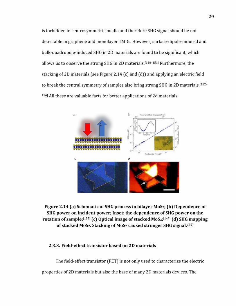
29
is forbidden in centrosymmetric media and therefore SHG signal should be not
detectable in graphene and monolayer TMDs. However, surface-dipole-induced and
bulk-quadrupole-induced SHG in 2D materials are found to be significant, which
allows us to observe the strong SHG in 2D materials.[148–151] Furthermore, the
stacking of 2D materials (see Figure 2.14 (c) and (d)) and applying an electric field
to break the central symmetry of samples also bring strong SHG in 2D materials.[152–
154] All these are valuable facts for better applications of 2d materials.
Figure 2.14 (a) Schematic of SHG process in bilayer MoS2; (b) Dependence of SHG power on incident power; Inset: the dependence of SHG power on the
rotation of sample;[155] (c) Optical image of stacked MoS2;[147] (d) SHG mapping of stacked MoS2. Stacking of MoS2 caused stronger SHG signal.132]
2.3.3. Field-effect transistor based on 2D materials
The field-effect transistor (FET) is not only used to characterize the electric
properties of 2D materials but also the base of many 2D materials devices. The
a b
c d
㻌2㻌

30
widely used FET is called back-gate FET, as shown in Figure 2.15 (a) and (b). 2D
materials are transferred to an insulating substrate, and two gold electrodes are
deposited on samples. In order to improve the contact between the gold electrodes
and samples, researchers used different strategies, one of which is to add an
ultrathin Ti or Cr layer between them. These two electrodes are called source and
drain. Another electrode is deposited on the back of the substrate, called gate. With
the gate voltage changing, the gate-dependent electricity properties of 2D materials
are measured. Typically, the dependence of source-drain current (ISD) on the gate
voltage (Vg) is obtained, and an “on/off” behavior is observed in semiconductors. ISD
increases when Vg increases. When the absolute value of Vg is less than a threshold
voltage, the increasing rate of ISD is small. However, when Vg surpasses the
threshold voltage, the increasing rate surges and this quick increase of ISD is called
“turn-on” of FET. The other popular FET is called top-gate FET, as shown in Figure
2.15 (d). The working principle is the same as back-gate FET except that a larger
gate voltage can be applied since high-dielectric materials are used to cover the
tested samples, such as h-BN or HfO2. The building of FET requires clean room,
lithography and e-beam deposition, which requires care.

31
Figure 2.15 (a) Rendered model and schematic of back-gate FET of MoS2; (b) FET of graphene;[1] (c) Four electric remeasurement obtained from FET of graphene in (b): resistivity (A), conductivity (B) and Hall coefficient (C) of
graphene as a function of gate voltage, carrier concentration as a function of temperature(D);[1] (d) Top-gated FET of MoS2 with HfO2 as dielectric layer;[156]
(e) Dependence of source-drain current of monolayer MoS2 on back-gate voltage.Inset is the ISD – biased voltage curve. [156]
At the birth of graphene, FET was already used to investigate its novel
behaviors, and the results are shown in Figure 2.15 (c). Since graphene is metallic,
the on/off was not expected, but the bipolar behavior was found. At a specific gate
voltage, the conductivity of samples has a sharp turn, at which electron behaves like
a massless fermion.[1] For MoS2, as shown in Figure 2.15 (e), an on/off can be found
easily. The on/off ratio is as high as 108, and the mobility of electron is 217 cm2V-1s-1.
[156]
S D
Gate
ad
c
e
b

32
Figure 2.16 (a) Schematic of 1-nm channel of FET;[157] (b) Schematic of FET based on Cl-doped MoS2;[158] (c) Schematics of FET based on alloyed WSe2;[85]
(d) Transmission curve of FET on h-BN sandwiched graphene;[159] (e) Transport response of FET on MoS2 at different atmosphere;[160] (f) Transport
response of FET on MoS2 on Si3N4.[161]
MoS2 is predicted to a good 2D semiconductor with an on/off ratio of
1010.[162] However, no experiment result reaches such value, and different strategies
have been employed to overcome the problems and measure different properties of
2D materials. For example, shorten the channel (the gap between source and drain)
reduces the size of samples and consequently the number of defects involved in
electron transport.[157,163,164] This should improve the electrical performance. One of
recent report is to utilize the carbon nanotube as the back gate whose electric field
could be as narrow as 1 nm, shown in Figure 2.16(a).[157] Improvement of the
contact between electrodes and samples is another direction since the Schottky
barrier between them requires a large threshold and causes a large threshold
voltage To achieve Ohmic contact, different methods have been tried, such chlorine
a cb
d fe

33
doping[158], alloying[85], phase transition[165] and h-BN[166]. Two of such methods are
shown in Figure 2.16 (b) (c) and the contact resistance can be as small as 0.3
k:·µm.[85] Another method is to protect 2D materials by others, such as ultrathin h-
BN, as shown in Figure 2.16 (d). By sandwiching graphene by h-BN, Quhe et al. not
only opened a 0.26 eV band gap in graphene but also increased the mobility of
electrons.[159] Molecules, as well as substrates, are found to affect the on/off
behaviors dramatically[160,161,167–170], and two of examples are given in Figure 2.16
(e)(f). Please refer to Chapter 3 for more information on this topic.
Figure 2.17 (a) Biosensor based on the change of dielectric coefficient of covering layer of monolayer MoS2;[17] (b) PL intensity of MoS2 controlled by
a b c
d e f
g h i
34
back gate;[158] (c) Exciton concentration of MoSe2 controlled back gate;[37] (d) Source-drain current of FET of an electrically doping WS2 p-n junction as a
function of bias gate;[171] (e) Schematic of a solar cell based on MoS2/p-Si heterostructure and its EQE specta;[172] (f) Photo detector based on FET of
monolayer InSe and their photoresponse when samples is shed by lasers of different power;[173] (g) Light-emitting device based on the EL of MoS2 ;[174] (h)
Absorption, PL and EL spectra of MoS2 FET;[174] (i) Strain induced shift of transport curve of FET of monolayer WSe2.[175]
Due to the sensitivity of 2D materials and interaction between electrons and
other particles, FET turns out to be the base of different applications of 2D materials.
Several applications based on 2D materials are shown in Figure 16. Molecular
sensor and biosensors are the most promising 2D devices resulted from its
sensitivity to molecules adsorption.[17,160,176,177] For example, as shown in Figure
2.17 (a), a label-free biomolecular sensor was proposed by Sarkar et al. in 2014.[17]
It based on the small change of dielectric coefficient of covering oxides of MoS2
when a biomolecule is adsorbed to the oxides surface. This small change leads to the
shift of threshold voltage of monolayer MoS2, which do not happen in bulk materials.
Another application is to use the back gate of FET to control the PL intensity and
exciton concentration of 2D materials, as shown in Figure 2.17 (b) and (c). [37,158] To
use 2D materials to harvest energy is another potential application. Pospischil et al.
designed a novel solar cell by introducing p-n junction in a single sheet of monolayer
WSe2 via electrical doping, shown in Figure 2.17 (d) and the efficient reached 0.5%.
In another solar cell application, 2D material MoS2 was used with traditional
semiconductor p-Si together to achieve a higher efficiency (5.23%), shown in Figure
2.17 (e).[172] Based on the avalanche effect of FET in monolayer InSe, Lei designed a
35
photodetector with high sensitivity, seen in Figure 2.17 (f).[173] FET of monolayer
MoS2 was also employed to build an electroluminescence (EL) device and the results
in Figure 2.17 (g) and (h) show that it works although the conversion efficiency is
just 0.01%. [174]Finally, the transport curve of 2D FET is also sensitive to strains
caused by bending of samples, which builds it as a suitable nanoscale strain
sensor.[175,178] One of such example is shown in Figure 2.17 (i) where the threshold
voltage of monolayer WSe2 shifts 0.2 V given 1% strain.[175]
2.3.4. Cytotoxicity evaluation of materials
For materials scientists, the evaluation of toxicity of 2D materials to cells
(called cytotoxicity) is straightforward on the surface: co-culture cells with 2D
materials on substrates or in solutions and after some period the viability of cells is
obtained through counting the cell density. Comparison of viabilities with and
without 2D materials gives the clue if 2D materials are dangerous to cells. However,
beneath the surface, selection of cells and solutions, reduce of counting errors, and
control of temperature according to standards, call for more care than materials
fabrication. What’s more, contamination of samples affects the results more
significantly on results from this evaluation than other inorganic properties, which
is discussed further in 0. Here I will review the general results of graphene and
other 2D materials briefly.

36
Figure 2.18 Schematic of cytotoxicity of graphene and carbon nanotubes to neuronal PC12 cells. Inset: Mitochondrial toxicity evaluation;[179] (b)
Cytotoxicity result of chemically exfoliated TMDs to human lung epithelial cells (A549).[180]
Due to its sp2 bonding, graphene is found to be dangerous to different cells in
vitro, as shown in Figure 2.18 (a). The neuronal PC12 cell was selected to test the
toxicity of carbon nanotubes and graphene and different activities of PC12 were
evaluated to characterize the effect of these two nanomaterials. The metabolic
activity of mitochondrion in PC12 cells are shown in the inset of Figure 2.18 (a) and
it is found that the carbon nanotubes and graphene both harm the PC12 cells since
the activity decreased quickly with concentration increased. [179]
Cytotoxicity results of TMDs are shown in Figure 2.18 (b), which shown
much weaker toxicity to human lung epithelial cells (A549).[180] However, the
exfoliated TMDs via LE are dominatingly 1T type due to the charge transfer of
intercalating ions and according to research[181], 1T-type of TMDs showed more and
more toxic when the thickness decreased. Another research also found that TMDs
were able to inhibit the activity of bacteria, which means toxic to these cell-like
a b

37
livings.[182] Overall, the toxicity of TMDs are not yet fully understood and no
conclusion could be made for now..
2.3.5. XPS, SEM, and TEM
As three basic characterization methods, these methods are used mostly for
auxiliary confirmation of chemical compositions, crystal structures and sample
morphology of 2D materials.
In X-ray photoelectron spectroscopy (XPS), a beam of high-energy x-ray is
shed on samples to power up valance electrons of elements to escape from the
surface of samples. The photoelectrons are collected, and their energies are
analyzed to get the binding energy of the valence electrons of elements. Due to the
high sensitivity of valence electrons to the binding of elements in crystals, XPS is a
potent tool of determining the surface composition of samples quantitatively and
the valence state of elements by deconvolution of XPS spectrum. XPS is helpful in
measuring the doping levels of 2D materials. One of example is shown in Figure 19
(a), where the doping levels of nitrogen in graphene at different temperature was
determined using XPS. [183]

38
Figure 2.19 (a) XPS determination of nitrogen doping level in graphene at different temperatures;[183] (b) In-situ observation of CVD growth of graphene
on a copper substrate;[184] (c) TEM modification of graphene to make freestanding graphene nanoribbon. [185]
Scanning electron microscopy (SEM) is used to see the morphology of 2D
materials at nanoscale under electron scattering. It usually requires high vacuum,
but environmental SEM (ESEM) allows a lower vacuum, which enables the in-situ
observation of chemical vapor growth of graphene on a copper substrate, shown in
Figure 19 (b).[184] The procedure of CVD process of 2D materials is not yet fully
understood, and such in-situ method provides valuable information about it.
Transmission electron microscopy (TEM) is usually to characterize the
atomic structure of 2D materials using high-energy electrons. However, it is also
a b
c

39
used to fabricate delicate nanomaterials by use of the high energy of electrons.
Figure 19 (c) shows one of example proposed by Rodriguez-Manzo in 2016. [185]
Using TEM, they were able to build high-quality and freestanding graphene
nanoribbons and measured electric properties of samples, which will facilitate the
better investigation of 2D materials without contaminations.
2.4. Summary
In this chapter, we go through the structures, characterization, properties,
and applications of 2D materials. In the following chapters, different aspects of 2D
materials will be studied in each project. In Chapter 3, we will discuss the
interaction of MoS2 with oxygen molecules, which can be used for in-vivo oxygen
flexible sensors. In Chapter 4, we will discuss the interaction of MoS2 with self-
assembled molecules, in which how to control the friction of 2D materials to prevent
clogging of 2D materials in the human body. In Chapter 5, we will discuss the
interaction of MoS2 will cells, which helps us understand the toxicity of MoS2 to the
human body. In Chapter 6, we discuss the interaction of 2D materials and substrates,
which is essential for the preparation of large-scale 2D materials to build advanced
biosensors. In Chapter 7, we discuss the interaction of 2D materials with a strong
acid, which is vital for the protection of 2D-material biosensors in different
conditions inside the human body. Finally, in Chapter 8, we give a summary of this
thesis and outlook.

40
Chapter 3
2D Materials and Small Molecules: Quantitative correlation of
photoluminescence enhancement and doping level of monolayer transition
metal dichalcogenides by oxygen adsorption
3.1. Abstract
In this chapter, we report the quantitative correlation of PL enhancement
and doping due to oxygen adsorption on monolayer TMDs. Further understanding of
this phenomenon could facilitate designs of oxygen sensors based on low-
dimensional materials. Previous studies on mechanically exfoliated TMDs
monolayer and nanoparticles proposed that adsorbed oxygen acts as p-type
dopants. However, understanding of their effects on physical properties of TMDs
41
remains incomplete. By incorporating PL and transport measurements of
monolayer MoS2 at different oxygen adsorption levels, we first observe the
quantitative correlation between PL intensity and doping: as the oxygen level
increases, monolayer TMDs become more and more p-type, and the intensities of
their PL are enhanced or quenched based on their intrinsic doping type. The
hypothesis that oxygen affects the PL of monolayer TMDs via p-type doping, i.e., the
change of carrier density is further supported by a match of the changes of carrier
density from the PL deconvolution and transport measurement. Furthermore, with
the presence of oxygen, the evolution of the PL of monolayer p-type WSe2 was
opposite to the that of n-type MoS2, which is consistent with the p-type doping
mechanism. This better understanding of the underlying principle of oxygen effects
on the PL of monolayer TMDs is expected to lead to better design of low-
dimensional molecule sensors
3.2. Introduction
For more than a decade, two-dimensional (2D) materials have been
extensively studied due to their attractive properties. Potential applications in
electrical,[2–5] optical,[6–8] catalytical,[13–16] and biological[17,18] fields have been
proposed, and this exploration of innovative designs based on 2D materials is still
highly active.
2D transition metal dichalcogenides (TMDs), one large family of 2D
materials, have been extensively explored since 2010 due to their unique
42
properties.[34] Different from the first-born 2D material graphene, 2D TMDs are
semiconductors with band gaps ranging from 1.5 to 2.0 eV, which paves a potential
road for the miniaturization of semiconductor devices. Unlike their bulk
counterparts, most of the TMDs monolayer show strong photoluminescence (PL) at
room temperature, due to their direct band gaps. The strong PL of TMDs has been
widely studied for the potential applications in sensors for gases,[167,176,177,186]
proteins,[187] and DNA[188]. As one of the first studied monolayer TMDs, mechanically
exfoliated (ME), monolayer MoS2 was obtained by A. Spleddiani et al. in 2010 and
showed an emerging PL peak at 680 nm.[34] This intriguing PL of monolayer MoS2
makes it a promising as a flexible optoelectronic material. To overcome the size
limitation in ME MoS2, researchers have widely adopted chemical vapor deposition
(CVD) for the growth of large-scale monolayer MoS2 for the fabrication of electronic
devices. However, CVD-grown MoS2 show weaker PL than ME MoS2 due to the
introduction of higher density of defects at elevated temperature. The weaker PL
intensity decreases the signal-to-noise ratio and thus limit the sensitivity of devices
built on CVD-grown TMDs, which necessitating methods to enhance the PL of CVD-
grown MoS2.
Molecules, such as oxygen and water, has been found to be able to increase
the PL of MoS2 but the mechanism of enhancement is still unclear. In 2013, S.
Tongay et al. were the first to study the effect of molecules on the PL of two-
dimensional (2D) materials.[189] They found that after high-temperature annealing,
the PL of mechanically exfoliated (ME) MoS2 increased in the ambient environment
by more than 100 times the PL in the vacuum. Such PL enhancement of MoS2 by

43
oxygen and water adsorption was attributed to the charge attraction of adsorbed
molecules from MoS2, i.e., p-type doping, which was supported by their density
functional calculations. In the same year, S. Mouri et al. doped ME MoS2 by a series of
organic molecules. Some of the molecules, such as F4TCNQ, enhanced the PL by
several factors while other molecules, such as NADH, decreased the PL of the
samples. The different charge transfer behaviors of these molecules were proposed
as the reason for such variance. However, no supporting measurement was
conducted in either report to confirm p-type doping, although theoretical results in
their reports suggested a high doping level (more than 97% decrease of free
electron density in monolayer MoS2). In 2014, H. Nan et al. found the same behavior
in ME MoS2 after high-temperature annealing; the intensity of PL at the cracks or
defects was much higher than that in the matrix. They attributed this enhancement
to the p-type doping and pointed out that such PL enhancement could be
reproduced by oxygen plasma irradiation without high-temperature annealing. In
doing so, they proved that the defect created during the annealing or irradiation was
the key to the molecule adsorption on MoS2.[122] Other molecules, such as H2O2 and
aromatic molecules,[133,135] were also employed to enhance the PL of ME MoS2; the p-
type doping of those molecules was considered as the cause of PL enhancement of
monolayer ME MoS2. However, none of these papers provided direct evidence of a
change of electric properties of MoS2 to support the p-type doping of adsorbed
molecules.
It is also under debate for the doping type induced by oxygen molecules on
monolayer MoS2. In 2013, W. Park et al. studied the passivation effect on monolayer

44
ME MoS2 and found that oxygen reduced the carrier density from 16.3 × 1015 cm-2
to 6.5 × 1015 cm-2, which indicates p-type doping. [160] Later, Y. Tong et al. showed
the same behavior in the monolayer MoS2 field-effect transistor; the threshold
voltage shifted to a positive direction when the device was exposed to an oxygen
atmosphere and remained almost unchanged when exposed to a nitrogen
atmosphere. Multiple-layer MoS2 was found to have the same behavior, i.e., p-type
doping by the oxygen, in the work of J. Jiang et al.[170] However, L. Qi et al. in 2016
pointed out that only physically adsorbed oxygen played a role of p-type doping and
that chemically adsorbed oxygen would result in n-type doping.[190] In summary,
there was no clear evidence linking the enhancement of PL and the p-type doping
caused by the physical adsorption of oxygen molecules on MoS2. Most of these
phenomena were observed in ME MoS2 but not in that grown by chemical vapor
deposition, which is the key for fabrication of large low-dimensional devices.
In this chapter, we report clear evidence demonstrating the link between the
PL enhancement and p-type doping induced by physical adsorption of oxygen on
monolayer MoS2 grown by CVD. The PL enhancement and p-type doping by oxygen
have been observed separately for a long time, but the link between them had not
been proven. Using PL and transport measurement on CVD-grown MoS2, we show a
linear relationship between the peak position shift and the threshold voltage shift.

45
3.3. Methods
3.3.1. Materials and chemicals
Monolayer MoS2 was grown by chemical vapor deposition, adapted from our
previous report.[191] In brief, the precursor MoO3 powder was put in a crucible in the
middle of a quartz tube in a furnace. An upside-down silicon wafer crossing the
crucible was used to catch the grown monolayer MoS2. Another crucible containing
sulfur powder was put at the upstream of the MoO3 crucible. Nitrogen of ultra-high
purity was employed as protecting gas and carrying gas. The whole quartz tube was
heated to 800 °C with the ramp rate of 50 °C/min and kept for 10 min. After that, the
furnace cooled down naturally in the air. All chemicals were bought from Sigma
Alpha and used as purchased. WSe2 was fabricated with the same procedure with
the source changed to Se and WO3, and the temperature was set at 900 °C.
3.3.2. MoS2 and WSe2 characterizations:
An InViaTM confocal Raman spectroscopy from Renishaw was employed to
characterize the Raman and photoluminescence of grown monolayer MoS2 and
WSe2. We used a 532-nm laser with 45 W (Model: RL532C50) as the excitation, and
5% power was used for Raman and PL characterization. The samples were put in a
sealed chamber with air inlet and outlet, which was purged by mixed gas with
desired oxygen levels.

46
3.3.3. FET fabrications
To measure the transport property of the grown monolayer MoS2, we first
built a FET structure with two deposited electrodes. Standard photolithography was
used to pattern the samples, and 5nm Ti and 45nm Au were deposited sequentially.
These two electrodes were used as the source and the drain. The heavily doped
silicon beneath the SiO2 was used as the back gate. The device was measured in a
probe station connected with Keithley 2634B.
3.4. Results and Discussions.
3.4.1. Characterization of grown MoS2 sample
We grew monolayer MoS2 by CVD and characterized the samples by AFM and
Raman spectroscopy. CVD has proven to be a promising method of growing large-
scale and high-quality 2D materials compared to other methods[49–51]. The typical
morphology of CVD-grown TMDs is triangular, indicating it is single-crystalline. One
typical sample of our CVD-grown MoS2 is shown in Figure 3.1(a), whose size was ~
35 µm. To confirm that the samples were monolayered, AFM was employed to
measure its thickness by scanning the edge of CVD-grown samples. A typical profile
line across the edge of this sample is shown in Figure 3.1(b), and the thickness of
this sample was estimated as 0.62 nm, which is consistent with the reported value of
monolayer TMDs[75]. Raman and PL spectra are two other widely used
characterization methods. Figure 3.1 (c) and (d) show the Raman and PL spectra of
this sample. The interval between the two typical Raman peaks of monolayer MoS2,

47
𝐸2𝑔1 and 𝐴1𝑔, was 21 cm-1 in our sample, which corresponds to that of monolayer
MoS2.[114,192] The strong PL of our sample was normalized to the Raman peak of SiO2
at 520 cm-1 , and it confirmed the high quality of our monolayer MoS2. Two peaks A
and B were found in our sample, due to the splitting of the valence band of
monolayer MoS2.[3] However, an trion peak convolute with the A peak, whose
intensity would be used to estimate the carrier density later in this report.
Figure 3.1 Optical, AFM, Raman and PL characterization of the monolayer MoS2. (a) Optical image of grown monolayer MoS2. The size is estimated to 50
µm; (b) Topological image of the sample by atomic force microscopy. The height profile shows that the thickness of as-grown samples is 0.62 nm; (c) Raman spectrum of the sample; inset is the zoom-in of two typical Raman
peaks of monolayer MoS2, which corresponds to the 𝑬𝟐𝒈𝟏 and 𝑨𝟏𝒈 modes of 2D
MoS2. Raman of Si is found (d) PL of the as-grown sample. The strong PL peak at 680 nm (labeled as Peak A) indicates the good quality of our as-grown

48
sample. The Peak B is present due to the splitting of valence bands of 2D MoS2. Raman of Si is normalized to 1.
3.4.2. PL investigation of MoS2 with oxygen adsorption
To study the effect of oxygen on the PL of monolayer MoS2, we first measured
its PL in the mixed gas of oxygen and nitrogen. Figure 3.2(a) shows the PL spectra of
as-grown monolayer MoS2 in pure oxygen and nitrogen. The intensity of the SiO2
Raman peak at 520 cm-1 is taken as reference and normalized to be one. The
normalized intensity of its PL peak in pure oxygen was 118, much higher than that
in nitrogen, which was 2~3. Due to the presence of oxygen, the intensity of PL
increased by about 40 times. To exclude the possibility of substrate effects, we
transferred the samples to a fresh new silicon wafer using the typical wet transfer
method.[191] The normalized PL spectra of the transferred sample are shown in
Figure 3.2 (b), which shows that the introduction of oxygen still enhanced the
intensity of PL. However, due to the transfer process, defects were inevitably
introduced to the monolayer MoS2, and thus the intensities of PL were less than that
of as-grown ones. In the next measurements, as-grown samples were used.
To further understand the effect of oxygen, we measured PL spectra of
monolayer MoS2 in atmospheres of different oxygen levels. Mixtures of oxygen and
nitrogen of ultra-high purity were used to achieve different oxygen levels. We began
with pure nitrogen and increased the oxygen level to 100% with a step of 20%. As
shown in Figure 3.2 (c), the intensity of normalized PL increased as the oxygen
levels increased from 0% to 100%, which is consistent with previous results.[189]

49
Note that the peak position of PL also had a blue shift as oxygen level increased. The
relationship between the oxygen levels and the positions of its PL peaks is shown in
Figure 3.2 (d), indicating that the peak position shifts from 1.830 to 1.848 eV as the
oxygen level increased from 0% to 100%. It saturates at a high level of oxygen,
which should be due to the total coverage of oxygen molecules on the surface of
monolayer MoS2. We will use the shift of peaks to estimate the change of free carrier
density after the transport measurement.

50
Figure 3.2 PL evolution of the monolayer MoS2 with oxygen levels. (a) PL of the as-grown monolayer MoS2 in pure oxygen and nitrogen environment. The
intensity of PL in oxygen is about 40 times greater than that in nitrogen given the same power of the laser was used;(b) PL of the transferred monolayer
MoS2 in pure oxygen and nitrogen environment. The PL intensity in oxygen is still much higher than that in nitrogen; (c) PL of the transferred monolayer MoS2 at different oxygen levels. As oxygen level decreases, the PL intensity
decreases; (d) The relation between the position of the Peak A of PL and the oxygen levels.
The effect of oxygen was attributed to the p-type doping of monolayer MoS2
in literature.[122,189] The intensity of PL depends on the number of excitons, each of
which is composed of an electron and a hole. Exciton may combine with another
electron to form a negative trion or a hole to form a positive trion. The
recombination of trion will not emit photons which is not directly related to PL. Due
to p-type doping by oxygen on monolayer MoS2, the generation of trions which
consumes excitons become more difficult because of fewer electrons in the 2D MoS2
as the as-grown 2D MoS2 is an n-type semiconductor. Thus, a higher concentration
51
of excitons was found when a laser was shed on p-type doped n-type MoS2. The
intensity of PL increases when more excitons are annihilated as electrons and holes
recombine.
3.4.3. Transport measurement of MoS2-based FET
We next confirmed this p-type doping by measuring the change of the
threshold voltage of the monolayer MoS2 FET. We conducted a transport
measurement of monolayer MoS2 FET in the atmosphere with different oxygen
levels. The same as-grown sample was used and kept in the vacuum for 24 h at the
beginning to get rid of all the adsorbed molecules. As shown in Figure 3.3 (a), the
source-drain current (ISD) of FET in the vacuum surged when the gate voltage was
greater than +35 V. This means our sample is an n-type semiconductor, and the
threshold voltage of this device is +35 V, which is consistent with the literature.[191].
As we introduced the oxygen for 0.2 hours to the chamber, the threshold increased
to 45 V. It saturated at 60 V after 24 hours. After that, nitrogen was introduced
slowly, and we observed the recovery of the threshold voltage. Therefore, the effect
of oxygen was p-type doping, which decreases the free carrier density and thus
increases the threshold voltage. This reversibility also confirmed that the oxygen
adsorption was physical since it recovered when nitrogen replaces oxygen in the
chamber. Figure 3.3(c) shows the shift of transport curve as a function of oxygen
level. It is clear that the threshold voltage increased gradually with oxygen level
increasing. This trend is plotted in Figure 3.3 (d). The shift of threshold voltage has
the same trend as the peak shift due to the oxygen. A linear relationship can be built

52
based on this firm correlation: Δ𝑉 = 0.40667𝑉/𝑚𝑒𝑉 Δ𝐸 + 0.067 𝑉, where Δ𝑉 = 𝑉 −
𝑉(0%) , V is the threshold voltage (V) at given oxygen level and V(0%) is that at 0%
oxygen; Δ𝐸 = 𝐸 − 𝐸(0%) where E is the peak position (meV) at given oxygen level
and E(0%) is the that at 0% oxygen. Another sample was measured as well, and the
same behaviors were observed. All the results are show in Figure 3.4
Figure 3.3 Transfer characteristics evolution of the monolayer MoS2 sample. (a) Time-dependent transfer characteristics (source-drain current ISD vs. gate
voltage Vg characteristics) of monolayer MoS2 FET in pure oxygen. After the purge of FET device in oxygen, the transfer characteristics gradually moves
from left to right, indicating the increase of threshold voltage as oxygen adsorption rate on monolayer surface increases; (b) Time-dependent transfer
characteristics of monolayer MoS2 FET after switched to pure nitrogen. Switching the gas from to oxygen to nitrogen means that decrease of oxygen level. Consequently, the transfer characteristics move from right to left, i.e.,
the decrease of the threshold voltage due to the desorption of oxygen from the sample; (c) Transfer characteristics at different oxygen levels. All data were
obtained after 12 h purge. After saturation at the given oxygen levels for 12 h, the transfer characteristics shift from left to right, indicating the increase of
the threshold voltage as oxygen level increases; (d) Threshold voltage versus
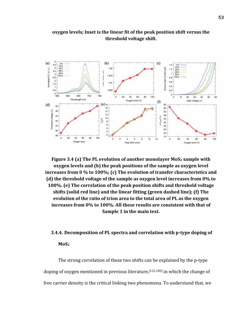
53
oxygen levels; Inset is the linear fit of the peak position shift versus the threshold voltage shift.
Figure 3.4 (a) The PL evolution of another monolayer MoS2 sample with oxygen levels and (b) the peak positions of the sample as oxygen level
increases from 0 % to 100%; (c) The evolution of transfer characteristics and (d) the threshold voltage of the sample as oxygen level increases from 0% to 100%. (e) The correlation of the peak position shifts and threshold voltage
shifts (solid red line) and the linear fitting (green dashed line); (f) The evolution of the ratio of trion area to the total area of PL as the oxygen
increases from 0% to 100%. All these results are consistent with that of Sample 1 in the main text.
3.4.4. Decomposition of PL spectra and correlation with p-type doping of
MoS2
The strong correlation of these two shifts can be explained by the p-type
doping of oxygen mentioned in previous literature,[122,189] in which the change of
free carrier density is the critical linking two phenomena. To understand that, we

54
estimated the change of free carrier density from these two measurements. For FET
measurements, the change of free carrier density when the oxygen level increased
from 0% to 100% was calculated by Δ𝐶 = Δ𝑉𝑡 𝐶𝑜𝑥/𝑒 = 8𝑉 × 12 𝑛𝐹/𝑐𝑚2 =
5.7 × 10¹¹/𝑐𝑚2.[193,194] For the PL results, the change of free carrier density could be
derived from the area ratio of the trion peak in the PL assuming a three-stage
excitation,[132] as shown in Figure 3.4 (a). By decomposing the whole PL spectrum
into three Laplacian-Gaussian peaks, representing A exciton, B exciton and a trion,
the carrier density could be estimated from the area ratio of trion peak. The ratio
was determined to be 13% at 0% oxygen and zero at 100% oxygen level, seen in
Figure 3.4 (b). Thus, the change of free carrier density due to the introduction of
oxygen can be estimated to be 7.7 × 10¹¹/𝑐𝑚2. (See Section 3.4.5). These two values
have a very good match, which provides strong support for the p-type doping
mechanism of oxygen on the PL enhancement of monolayer MoS2.
Figure 3.5 Deconvolution of PL and the ratio of trion peak versus oxygen levels. (a) A typical deconvolution of PL of the monolayer MoS2 sample. Three
peaks, including the A exciton, exciton B, and the trion, are used in the deconvolution; (b) The ratio of the area of trion peak to the total area of PL at

55
different oxygen levels obtained from the deconvolution. The ratio decreases from 13% to 0% when oxygen level increases from 0 to 100%.
3.4.5. Calculation of carrier density change from trion ratio
It is easy to have
𝐼𝐴−
𝐼𝑡𝑜𝑡𝑎𝑙= (
𝐼𝐴−
𝐼𝐴
1 + 𝐼𝐴−
𝐼𝐴
)
where 𝐼𝐴− is the intensity of trion peak, 𝐼𝐴 is the intensity of exciton peak, 𝐼𝑡𝑜𝑡𝑎𝑙 =
𝐼𝐴 + 𝐼𝐴− is the total intensity of PL.
According to mass action law[132,195], the ratio of the intensity of trion and the
exciton is:
𝐼𝐴−
𝐼𝐴=
𝛤𝐴−𝑁𝐴−
𝛤𝐴𝑁𝐴=
𝛤𝐴−
𝛤𝐴
1𝜅𝑒𝑓𝑓
𝜆 (𝜋ℏ2𝑚𝐴−
4𝑚𝐴𝑚𝑒)
1𝑘𝐵𝑇
𝑒− 𝐸𝑏𝑘𝐵𝑇 𝑛𝑒
where 𝛤𝐴− and 𝛤𝐴 are the radiative decay rete of trion and exciton, 𝜅𝑒𝑓𝑓 is the
effective SiO2 dielectric constant, 𝜆 is the power dependence[195], 𝑚𝐴− , 𝑚𝐴 and 𝑚𝑒
are the effective mass of trion, exciton and electron, 𝐸𝑏 is the binding energy of
trion, and 𝑛𝑒 is the carrier density. Take 𝛤𝐴− = 1.5, 𝛤𝐴 = 10, 𝑘𝑒𝑓𝑓 = 11.85, 𝜆 = −0.7,
𝑚𝑒 = 0.34 𝑚0, 𝑚𝐴 = 0.77 𝑚0, 𝑚𝐴− = 1.15, 𝐸𝑏 = 20 meV[132,195], we have
𝐼𝐴−
𝐼𝐴= 2 × 10⁻¹³𝑐𝑚2 𝑛𝑒
Therefore, we have
56
𝐼𝐴−
𝐼𝑡𝑜𝑡𝑎𝑙=
2 × 10⁻¹³𝑛𝑒
1 + 2 × 10⁻¹³𝑛𝑒
From this function, we can estimate the change of the carrier density to be
7.66 × 10¹¹/𝑐𝑚2
3.4.6. Oxygen adsorption on WSe2 and its effects
To confirm the effect of oxygen p-type doping on the PL intensity of TMDs,
we further employed the same setup to the monolayer WSe2, which is a p-type 2D
semiconductor according to the literature[79,85,196]. Figure 3.6 shows the Raman and
PL of grown WSe2. The strong PL confirms the excellent quality of our sample. Due
to more and more oxygen adsorbed on the surface of WSe2, more holes will be
present in WSe2 which eases the generation of positive trions. Therefore, the
intensity of its PL should decrease, and the PL peak should be redshift, a contrast to
the increase of PL intensity and the blue shift of n-type MoS2. As shown in Figure 3.7,
the trend of the intensity of PL and peak positions are consistent with what we
expect. The intensity of PL with 100% oxygen level is one-third of that without
oxygen present and the peak shifts towards higher wavelength. The FET
measurement also demonstrates the change of carrier density. With higher oxygen
level, the WSe2 sample had a greater threshold voltage, indicating p-type doping.
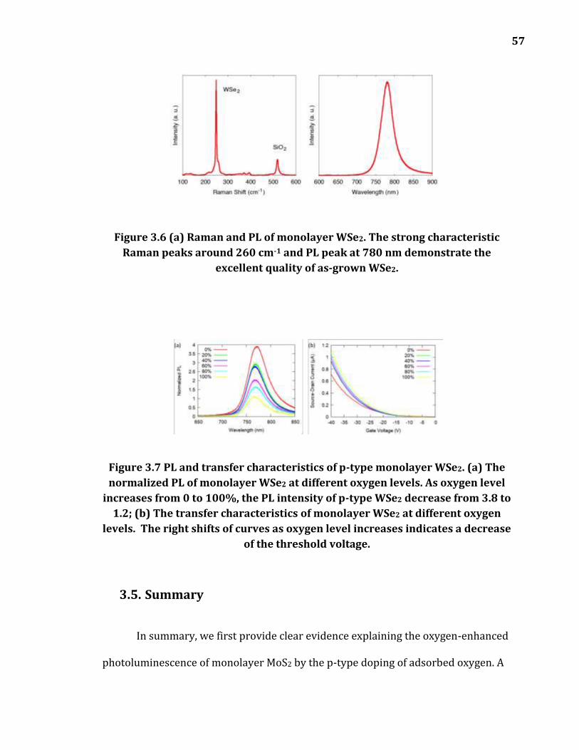
57
Figure 3.6 (a) Raman and PL of monolayer WSe2. The strong characteristic Raman peaks around 260 cm-1 and PL peak at 780 nm demonstrate the
excellent quality of as-grown WSe2.
Figure 3.7 PL and transfer characteristics of p-type monolayer WSe2. (a) The normalized PL of monolayer WSe2 at different oxygen levels. As oxygen level
increases from 0 to 100%, the PL intensity of p-type WSe2 decrease from 3.8 to 1.2; (b) The transfer characteristics of monolayer WSe2 at different oxygen
levels. The right shifts of curves as oxygen level increases indicates a decrease of the threshold voltage.
3.5. Summary
In summary, we first provide clear evidence explaining the oxygen-enhanced
photoluminescence of monolayer MoS2 by the p-type doping of adsorbed oxygen. A

58
linear relationship is observed between the peak positions of PL and threshold
voltages of MoS2 FET when the oxygen concentration is increased from 0% to 100%.
The threshold voltage is increased by 7 V after oxygen was introduced while the
area ratio of the trion peak in PL is decreased by 14%. The changes of carrier
density, which are estimated separately from the changes in threshold voltage and
the area ratio of the trion peak, are consistent with each other. This evidence and
the evolution of the PL of a p-type monolayer WSe2 sample also confirm the
underlying mechanism of oxygen-enhanced PL of monolayer TMDs and deepens our
understanding of the interaction of molecules and 2D materials. It will be helpful for
design of better molecules sensors or oximeters.

59
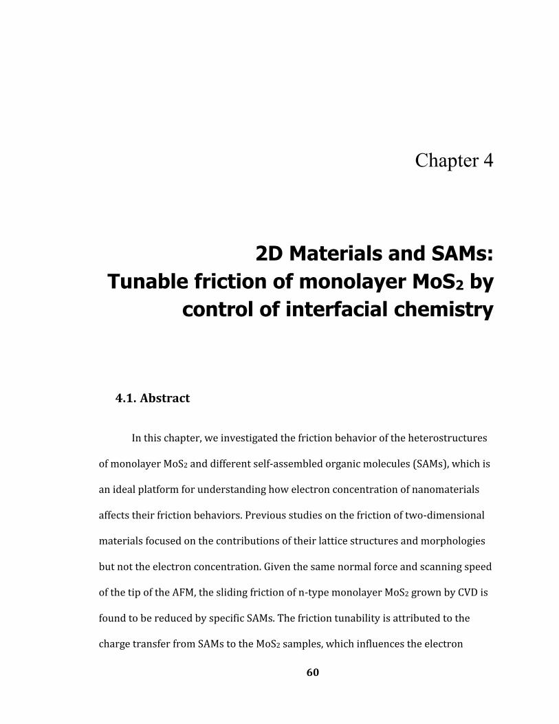
60
Chapter 4
2D Materials and SAMs: Tunable friction of monolayer MoS2 by
control of interfacial chemistry
4.1. Abstract
In this chapter, we investigated the friction behavior of the heterostructures
of monolayer MoS2 and different self-assembled organic molecules (SAMs), which is
an ideal platform for understanding how electron concentration of nanomaterials
affects their friction behaviors. Previous studies on the friction of two-dimensional
materials focused on the contributions of their lattice structures and morphologies
but not the electron concentration. Given the same normal force and scanning speed
of the tip of the AFM, the sliding friction of n-type monolayer MoS2 grown by CVD is
found to be reduced by specific SAMs. The friction tunability is attributed to the
charge transfer from SAMs to the MoS2 samples, which influences the electron

61
concentration and thus the carrier-mediated friction behaviors in 2D MoS2. ab initio
simulations and nanoscale mapping of work functions using Kelvin probe force
microscopy confirmed this hypothesis. These SAMs-based heterostructures provide
not only a tool of spatial controlling friction in low-dimensional materials but also a
new understanding of the contribution of electron-phonon coupling to friction at the
nanoscale.
4.2. Introduction
Nanotribology became available in 1995 when friction force microscopy
(FFM) was born.[197] As an important branch of tribology, nanotribology offers not
only more understanding of the origin of friction but also a better mean of
controlling the friction of nanoelectromechanical systems (NEMS).[198]. There
remain many important questions under debate[199] in this young branch, one of
which is the origin of friction, i.e., how energy dissipates during the friction process
and what factors affect this process. The main energy-dissipation sources are the
phonon-related properties of the matrix, such as phonon excitations[200] and
electron-phonon coupling[201]. Recently, electron-phonon coupling was found to be
an important kind of energy dissipations in nanomaterials.[202,203] For example,
silicon with different types of doping was found to have different friction
coefficients under the same normal force. One of the proposed mechanisms was
based on the different strength of electron-phonon coupling in two types of silicon,
i.e., energy was transferred from phonons to electrons and dissipated with different
efficiency.
62
2D materials, especially TMDs, provide a new platform to examine this
mechanism because their electron-phonon coupling (e-p coupling) can be more
easily tune due to their aextremely small thickness. For example, the carrier density
of monolayer MoS2 can be tuned by charge transfer of the adsorbed molecules, as
shown in Chapter 3, and this change of carrier density may affect the e-p coupling.
Although the e-p coupling is also strong in graphene, it is not as suitable as TMDs
because its thickness (~3.4 Å) is smaller than that of monolayer TMDs (~6 Å) and it
has a large plucking effect which dominates its friction behaviors.[204]
In this chapter, monolayer MoS2 was transferred onto the self-assembled
molecules (SAMs) with different functional groups to study the effect of carrier
density on the friction of monolayer MoS2 surface. AFM was used to measure the
single-asperity friction behavior of MoS2. We found that the significant charge
transfer from MoS2 to SAMs can decrease the friction of MoS2 by up to ~ 20%. This
phenomenon is explained by the decrease of the e-p coupling due to the decrease of
the carrier density in MoS2 in the presence of the SAMs. We employed ab initio
simulations and Kelvin probe force microscopy (KPFM) measurements to confirm
such change of the carrier density.
4.3. Methods
4.3.1. Growth of monolayer MoS2 on a silicon wafer
Triangular monolayer MoS2 samples were grown using CVD that we
previously developed[191]. Briefly, nitrogen was used as the carrying gas in a quartz
63
tube. 20 mg MoO3 in a ceramic crucible was used as the Mo precursor, and 50 mg
sulfur in the other crucible in the upstream direction was used as the S precursor. A
facing-down Si wafer with 300 nm SiO2 was put along the edge of the Mo crucible to
collect the grown monolayer MoS2. The furnace was heated from room temperature
to 750 °C at a rate of 50 °C/min and the dwelling time was 20 mins. After that, the
furnace was naturally cooled down to room temperature.
4.3.2. Preparation of MoS2 on SAMs
A clean Si/SiO2 wafer covered with S1813 stripes was prepared via standard
photolithography, and it was put into a chamber with volatile organic solutions for
24 h. Two kinds of organic solutions, 3-aminopropyltriethoxysilane (APTS) and 3-
mercaptopropyltrimethoxysilane (MPTS) in hexane, were used. These gaseous
monomers self-assembled themselves on the exposed silicon wafer. After acetone
removed the S1813 polymer, SAMs stripes on SiO2 could be found on the silicon
wafer. Monolayer MoS2 was transferred using poly(methyl methacrylate) (PMMA)
to the patterned wafer by the wet chemistry method.[191] Acetone was used to
remove the PMMA and leave MoS2 on the SAMs stripes. Figure 4.1 (e) shows the
whole process. The stripes enable the study of the friction behavior of monolayer
MoS2 with and without SAMs in the same single crystal flake.

64
Figure 4.1 (a) Raman spectrum of the CVD-grown MoS2. The interval between the two vibrational modes of 20 cm-1 confirms that the sample is a monolayer;
(b) PL of CVD-grown MoS2. The strong PL peak at 678 nm confirms the high quality of the samples. (c) Optical image of MoS2 on the SAMs stripes; (d) SEM
image of MoS2 on the SAMs stripes, where the SAMs stripes are shown in darker. (e) Schematic of the sample preparation and friction measurements.
Red stripes represent SAMs and triangles represents MoS2 samples.
4.3.3. Characterization and friction measurement
SEM (FEI Quanta 400) was used to confirm the patterns of organic molecules
and MoS2 on wafers. Raman spectroscopy (Renishaw inVia microscope) was used to
investigate the structure and thickness of the as-grown monolayer MoS2 using
514.5-nm laser excitation. Monolayer MoS2 thickness and topographical variations
were also measured using AFM (Agilent PicoScan 5500) in tapping mode.

65
To perform the friction measurements of monolayer MoS2 on SAMs stripes,
we calibrated a triangular cantilever (BRUKER CLCF model) in the AFM in the
contact mode using the three-tip method, in which the to-be-calibrated probe is
used to bend three rectangular cantilevers whose geometries and normal spring
constants were known. Then the normal spring constant of the AFM cantilever and
the conversion coefficient between the electric signal and normal force could be
obtained (see Section 4.3.3.1 for details).
To obtain the lateral spring constant of the AFM cantilever, we employed a
diamagnetic levitation system[205], in which four magnets levitated an HOPG flake as
a calibrator. By collecting the damped oscillating curve of HOPG, we derived its
lateral spring constant around the equilibrium point and used it to get the lateral
spring constant of the AFM cantilever when HOPG was dragged by the AFM probe
away from the equilibrium point (see Section 4.3.3.2 for more details).
After the AFM cantilever was calibrated, the prepared samples were placed
in a chamber filled with N2 to control its humidity level to be less than 5%. The
normal force was kept constant during the scanning of the samples, and the
topography and friction force were collected simultaneously.
4.3.3.1. Calibration of normal spring constant of the AFM probe
In a typical three-tip model[206], a Si sample with three well-calibrated
cantilevers is present. The to-be-calibrated AFM probe is used to bend the
cantilevers whose spring constants are the closest to that of this probe, as shown in

66
Figure 4.2 (a). Five points at different locations of the standard cantilevers are
chosen. Each bending test gives a deflection sensitivity which indicates the
deflection rate of the cantilever laser after it is in contact with the standard
cantilever. The following formula is used to obtain the normal spring constant K of
the AFM cantilever:
𝐾 = 𝐾𝑟𝑒𝑓 (𝑆𝑟𝑒𝑓
𝑆− 1) (
𝐿𝐿 − Δ𝐿
)3
where 𝐾𝑟𝑒𝑓 is the spring constant of the standard cantilever, 𝑆𝑟𝑒𝑓 is the deflection
sensitivity of AFM cantilever on silicon matrix, S is the deflection sensitivity of AFM
cantilever on a standard cantilever, L is the length of the standard cantilever and 𝐿 −
Δ𝐿 is the distance of the contact point from the edge of Si matrix. The data are
tabulated in Error! Reference source not found.. Using the intrinsic deflection s
ensitivity 108.23 nm/V of the AFM probe on the Si wafer, the normal spring
constant of the cantilever is 0.500±0.083 N/m and the normal force conversion
factor was decided as N = 0.055±0.009 μN/V, through which the AFM deflection
signal can be converted to normal force.
Table 4.1 All data of normal spring constant of AFM cantilever
𝐾𝑟𝑒𝑓(N/m) 𝑆𝑟𝑒𝑓 (nm/V)
𝐿 (𝜇𝑚) 𝐿 − Δ𝐿 (𝜇𝑚) 𝑆 (nm/V)
𝐾 (N/m)
0.126 267.5952 400 125.45327 307.847 0.614344 0.126 267.5952 400 181.15469 368.588 0.511934 0.126 267.5952 400 240.99829 471.906 0.439867 0.126 267.5952 400 342.3727 848.229 0.435991
Average - - - - - 0.50053

67
Std. Err. - - - - - 0.08352
Figure 4.2 (a) Schematic of three-tip model used in the calibration of normal spring constant of AFM probe; (b) Schematic of DFLG method of determining lateral spring constant of AFM probe; (c) Typical damped oscillating data and
the fitting curve of HOPG floating on top of four magnets; (d) Typical linear relationship between the displacement and the lateral signal of an AFM probe
dragging HOPG away from the equilibrium point.
4.3.3.2. Calibration of lateral spring constant of the AFM probe
As shown in Figure 4.2 (b), an HOPG flake was put in the magnetic trap
generated by four permanent magnets[207]. Due to its diamagnetism, HOPG is
levitated above the four magnets and trapped at the equilibrium point. When it is
perturbed a little away from the equilibrium point, it behaves like a damped
harmonic oscillator. A laser reflected by the HOPG flake was used to collect the
oscillating signal, which we fitted with:
𝐼(𝑡) = 𝐼0 + 𝐴e−𝛾𝑡sin(𝜔𝑡 + 𝜙)

68
where 𝜔 is the natural frequency of the magnetic field. Therefore, the spring
constant of the magnetic field around the equilibrium point can be obtained by k =
mω2 where m is the mass of HOPG. A typical fitting of data is shown in Figure 4.2(c).
The natural frequency is 33.156 s-1, and the mass of HOPG is 8.7 mg, which gives k =
9.56 pN/nm.
After k was obtained, the HOPG flake was put under AFM and dragged by the
probe of AFM. The normal force was so large that HOPG went with the probe
without sliding. The linear relationship between the displacement of the HOPG flake
and the lateral force applied to the probe was measured. The slope x then was used
to obtain the lateral spring constant via 𝛼𝐿 = 𝑘/𝑥, where k is the spring constant of
the magnetic field, and 𝛼𝐿 (nN/V) relates the electric signal to the lateral forces. The
data and fitting are shown in Figure 4.2 (d) and the slope is 7.84 ± 0.05 mV/μm.
Therefore, 𝛼𝐿= k/x = 1.196± 0.120 μN/V.
4.3.4. Simulations of charge transfer
We employed ab initio simulations to study the charge transfer between
SAMs and monolayer MoS2. We performed DFT calculations using the Vienna ab-
initio Simulation Package (VASP)[208] with the local density approximation (LDA)
and projector-augmented wave (PAW) potentials.[209,210] Adopting a 4 × 4 supercell
for MoS2, we chose a vacuum layer thickness greater than 10 Å to make the spurious
interactions negligible. The energy cutoff for the plane-wave basis set was 400 eV. 3
× 3 × 1 and 7 × 7 × 1 k-point meshes were selected for structural relaxation and self-
consistent calculations, respectively. All structures were fully relaxed until the force

69
on each atom was less than 0.01 eV/Å based on the plane-wave-based total energy
minimization.[211] We applied Bader analysis[212] to obtain the charge on each atom
and get the charge transfer from the molecules to monolayer MoS2.
4.3.5. Kevin probe measurement
We operated the AFM (Veeco Dimension Icon® with probe PFQNE-AL) in the
PeakForce KPFM mode to characterize both the morphology and the surface
potential of the same area. For each scan line, two passes of the probe were required
in total. During the first pass, the AFM works in the PeakForce TappingTM mode. By
intermittently tapping the sample at frequencies well below the cantilever
resonance frequency, the force-position curves at each point are measured so that
the height profile is obtained. At the end of the first pass, the probe was lifted to tens
of nanometers above the surface. Then it moved along the just-acquired height
contour at a constant lift height. During this second pass, the changes of the probe
resonance frequency or the phase, which were caused by the long-distant magnetic
or electric forces, are monitored. In the way, the AFM height image was recorded on
the first pass and the KPFM surface potential image is recorded on the second pass.
4.4. Results and Discussion
4.4.1. Raman, PL and SEM characterizations
To examine the quality and thickness of the CVD-grown MoS2, we utilized
Raman and PL spectroscopy. As shown in Figure 4.1 (a), the spacing between the A1g

70
and E2g vibrational modes was 20 cm-1, corresponding to that of the monolayer
MoS2[117,192]. Also, a strong peak around 678 nm was observed in the PL spectrum
(Figure 4.1 (b)), which is also a signature of the direct band gap of monolayer
MoS2.[92]
After MoS2 monolayers were transferred onto the silicon wafer with SAMs
stripes, we used optical microscopy and SEM to confirm the stacking structure of
MoS2 and SAMs. SAMs stripes are hardly visible in the optical image in Figure 4.1 (c).
However, a clear contrast between the transferred MoS2 and the SAMs stripes can
be seen in SEM shown in Figure 4.1 (d), which also shows that well-stacking
structure of MoS2.
4.4.2. Friction measurement of MoS2 on SAMs
Two types of SAMs with different dipole terminations were chosen for the
friction studies: 3-aminopropyltriethoxysilane (APTS) and 3-
mercaptopropyltrimethoxysilane (MPTS). Due to their same length of molecules and
similar structure, they have similar mechanically physical properties.[213] Due to
different functional groups, they are believed to induce different levels of doping in
the covering MoS2. Thus, they are suitable for the friction behaviors of monolayer
MoS2 with different carrier density. The scanning speed was fixed to be 25 μm/s,
and a chamber filled with N2 gas was used to minimize the effect of humidity.

71
Figure 4.3 (a) AFM topography of monolayer MoS2 on APTS stripes. A dashed black line indicates the edge of MoS2. Inset: the profile line across the APTS stripe. The x-axis is displacement (unit: μm), and the y-axis is height (unit: nm). (b) Friction image of MoS2 on APTS with black-white-sinusoidal color
scale. Inset: lateral signals during the trace (red) and retrace (green) scans. The x-axis is displacement (unit: μm), and the y-axis is the lateral signal (unit:
V). Vertical black lines show indicates the friction determined by the difference of the trace and retrace signals. (c) Friction image of the MoS2
sample on APTS with linear color scale. Inset: the average friction of MoS2 with APTS (red) and without APTS (blue). (d) AFM topography of MoS2 on
MPTS. (e) Friction image of MoS2 with MPTS (red) and without MPTS (blue). All the scan area is 50 μm by 50 μm. (f) The normalized friction of monolayer
MoS2 on APTS (red), MPTS (green) and bare Si wafer (blue). Reference friction is normalized to unity
The morphology of MoS2 on APTS stripes is shown in Figure 4.3 (a) and the
thickness of SAMs was estimated to be 1.5 nm. The contrast of the edge of APTS
stripe is significantly reduced in the region of MoS2 due to the coverage of MoS2.

72
Friction data were collected simultaneously with the AFM topography data of
these heterostructures to understand the mechanical behavior of the probe over the
MoS2 at different locations. The applied normal force of the contact probe was fixed
at 0.7 V, i.e., 38.5 nN. A typical friction signal is shown in Figure 4.3(b) inset. To
minimize the influence of the unleveled holder on the friction signals, we used the
average of the lateral forces during the trace and retrace scans as the friction of the
tip scanning over monolayer MoS2. To elucidate the little contrast of the friction
signal, we employed the black-and-white-sinusoidal color scale, which clarifies the
difference of the local contrast, as shown in Figure 4.3 (b). Note that the APTS on the
clean silicon wafer does not show any friction contrast in our AFM scanning. It can
be seen that MoS2 with APTS underneath shows different friction behavior
compared to MoS2 on the Si wafer. To obtain the friction difference between these
two areas, we averaged the area of MoS2 with and without APTS. The average
friction of MoS2 with APTS was 26.67 ± 2.48 nN and of MoS2 on the silicon wafer
was 33.75 ± 2.75 nN, as shown in the inset of Figure 4.3 (c). The presence of APTS
molecules reduces the friction of monolayer MoS2 by ~ 7 nN under the normal force
of 38.5 nN. i.e., ~20% friction reduction by this layer of molecules.
Next, we conducted the same measurements of the topography and friction
of MoS2 on MPTS stripes, and the results are shown in Figure 4.3 (d) and (e). In this
s, MoS2 with MPTS (red area) does not show any friction contrast compared to MoS2
without MPTS (blue area). We also measured the friction of different MoS2 crystals

73
on MPTS and did not observe any statistical difference from that of MoS2 on the Si
wafer. Note that the difference of the friction of MoS2/SiO2 in Figure 4.3 (b) and (e)
are caused by the sinusoidal color scale, which does not represent their real
difference.
We combined and normalized the friction data of these two stacking systems
in Figure 4.3 (e), in which the friction of MoS2 on the Si wafer is normalized to unity.
It can be seen that APTS reduces the friction of MoS2 by ~ 20% while MPTS does
not. Given the same scanning speed and normal force, the friction coefficient of the
AFM probe on monolayer MoS2 decreases by ~ 20% in the presence of APTS but
keeps the same with MPTS.
4.4.3. Charge transfer caused by SAMs
We now discuss the possible origin of this friction difference on different
types of SAMs. The structures of APTS and MPTS are shown in Figure 4.4 (a) and (b).
Their structures are very similar, both of which have four carbon atoms out of the
silicon wafer when assembled, making the height of these SAMs nearly the same.
Due to their similar structures, their stiffness and other mechanical properties could
not account for the different friction behavior of the covering monolayer MoS2.
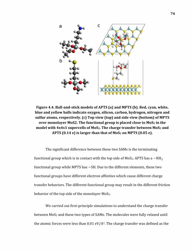
74
Figure 4.4. Ball-and-stick models of APTS (a) and MPTS (b). Red, cyan, white, blue and yellow balls indicate oxygen, silicon, carbon, hydrogen, nitrogen and sulfur atoms, respectively. (c) Top view (top) and side view (bottom) of MPTS
over monolayer MoS2. The functional group is placed close to MoS2 in the model with 4x4x1 supercells of MoS2. The charge transfer between MoS2 and
APTS (0.14 e) is larger than that of MoS2 on MPTS (0.05 e).
The significant difference between these two SAMs is the terminating
functional group which is in contact with the top side of MoS2. APTS has a −NH2
functional group while MPTS has −SH. Due to the different elements, these two
functional groups have different electron affinities which cause different charge
transfer behaviors. The different functional group may result in the different friction
behavior of the top side of the monolayer MoS2.
We carried out first-principle simulations to understand the charge transfer
between MoS2 and these two types of SAMs. The molecules were fully relaxed until
the atomic forces were less than 0.01 eV/A3. The charge transfer was defined as the
75
extra electrons in the molecules. From the simulation, we found that there were
0.14 extra electrons in one APTS molecule and 0.05 electrons in MPTS. It means that
0.14 electrons are transferring from MoS2 to APTS and 0.05 electrons to MPTS in
this supercell. These results are consistent with the FET measurement of these two
types of SAMs.[214] It is clear that APTS can extract more electrons from MoS2 than
MPTS.
In 2D semiconductors, the electron-phonon coupling is an important energy
dissipation path[201], and the strength of electron-phonon coupling in 2D materials is
proportional to their carrier density[109]. Therefore, the different friction behavior of
MoS2 with APTS and MPTS can be understood from the different carrier density due
to the SAMs underneath. CVD-grown monolayer MoS2 is an n-type
semiconductor[191,214],[215],. Due to the presence of APTS and MPTS, electrons
transfer from MoS2 to these SAMs decreasing the carrier density in monolayer MoS2.
More electrons happen in APTS than MPTS, and consequently, the strength of the
electron-phonon coupling decreases more and the energy-dissipation path becomes
suppressed more in MoS2/APTS than MoS2/MPTS. As a result, we observe the
reduction of friction in monolayer MoS2 when the amount of charge transfer is
significantly large, i.e., in monolayer MoS2 with APTS SAMs.
4.4.4. Fermi level shift of monolayer MoS2 due to the presence of SAMs
To confirm our hypothesis on the different doping levels due to different
SAMs, we used KPFM to inspect the work functions of the MoS2/APTS and
MoS2/MPTS heterostructures since the change of the carrier density correlates with
76
the shift of the Fermi level and thus the work functions in doped semiconductors. As
the carrier density decreases and the Fermi level shifts down towards the valence
band, the work function defined as the difference between the vacuum level and the
Fermi level in semiconductors increases. We expected that the MoS2/APTS had a
larger work function than MoS2/MPTS because the Fermi level in MoS2/APTS
moved more towards the valence band.
KPFM measures the contact potential difference VCPD, defined as[216]:
VCPD = ϕtip− ϕsample
e.
where ϕtip is the work function of the tip, and ϕsample is the work function of the
sample. To compare the work functions of these two systems, we used the APTS or
MPTS on SiO2 as the reference since it is the substrate in both systems. The CPD
difference of SAMs on SiO2 and clean SiO2 is trivial. (See 4.4.4.1 ) Therefore, we have:
ϕ(MoS2/APTS) = ϕRef − e(𝑉𝐶𝑃𝐷(MoS2/APTS) − VCPD(Ref))
ϕ(MoS2/MPTS) = ϕRef − e(VCPD (MoS2/MPTS) − VCPD (Ref))
where ϕ((MoS2)/Mol) and VCPD(MoS2/Mol) denote the work function and CPD of
MoS2 on SAMs, ϕRef and VCPD(Ref) denote the work function and CPD of the
reference. As shown below, ΔV = VCPD(MoS2/Mol) − VCPD(Ref) is negative,
therefore, the larger the absolute value of ΔV is, the larger the work function of the
systems is, which means lower Fermi level and heavier p-type doping.
77
We transferred the same batch of MoS2 to a Si wafer, half of which is covered
by SAMs. KPFM measurements were conducted together with simultaneous AFM
morphology measurements. Several samples were tested, and Figure 4.5 (a) and (b)
shows two representative samples with and without APTS. Two profile lines were
obtained in these two samples. It is found that ΔV = −300 meV with APTS and ΔV =
−200 meV without APTS. It indicates that the work function of MoS2 on APTS is 100
meV greater than that on the Si wafer. Therefore, the Fermi level shifts down by ~
100 meV with APTS presented, i.e., heavier p-type doping. On the contrary, as shown
in Figure 4.5 (c) and (d), the monolayer MoS2 on MPTS has almost the same Δ𝑉 as
that on Si wafer, which means that the work function of MoS2 was not significantly
affected by the MPTS. Therefore, the doping level induced by MPTS is not as
significant as that by APTS, which is consistent with what was expected.

78
Figure 4.5 KPFM images and profile lines of (a) MoS2 on APTS; (b) MoS2 on SiO2; (c) MoS2 on MPTS; and (d) MoS2 on SiO2. The APTS beneath MoS2 is
found to decrease the work function of monolayer MoS2 by 100 meV while MPTS does not decrease the work function of monolayer MoS2 significantly.
The difference between (b) and (d) might be due to the different batch of MoS2 monolayers, and the dendrite pattern corresponds to the gaps between
SAMs.
4.4.4.1. Optical, topographic and KPFM images of MoS2 across the boundary
of APTS/MPTS and silicon
Figure 4.6 shows the optical image of the MoS2 flakes on APTS and MPTS we
scanned by AFM and KPFM. In Figure 4.7, we show the AFM and KPFM images of the
MoS2 on the boundary of APTS. In Figure 4.7 (b), we can see that the area covered by
APTS is slightly higher than the exposed silicon substrate, and such a height
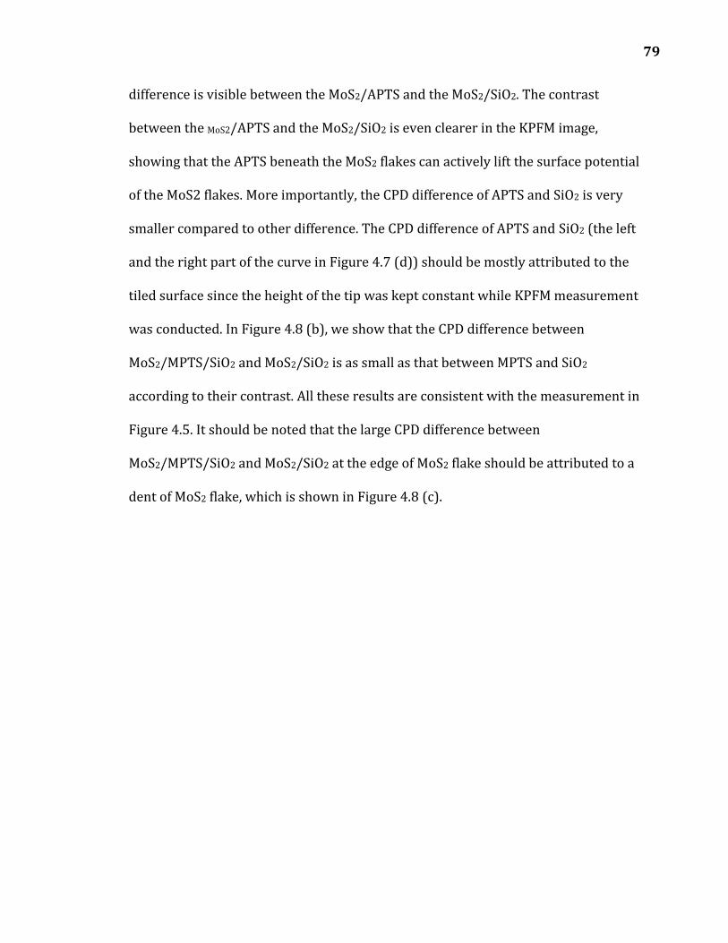
79
difference is visible between the MoS2/APTS and the MoS2/SiO2. The contrast
between the MoS2/APTS and the MoS2/SiO2 is even clearer in the KPFM image,
showing that the APTS beneath the MoS2 flakes can actively lift the surface potential
of the MoS2 flakes. More importantly, the CPD difference of APTS and SiO2 is very
smaller compared to other difference. The CPD difference of APTS and SiO2 (the left
and the right part of the curve in Figure 4.7 (d)) should be mostly attributed to the
tiled surface since the height of the tip was kept constant while KPFM measurement
was conducted. In Figure 4.8 (b), we show that the CPD difference between
MoS2/MPTS/SiO2 and MoS2/SiO2 is as small as that between MPTS and SiO2
according to their contrast. All these results are consistent with the measurement in
Figure 4.5. It should be noted that the large CPD difference between
MoS2/MPTS/SiO2 and MoS2/SiO2 at the edge of MoS2 flake should be attributed to a
dent of MoS2 flake, which is shown in Figure 4.8 (c).

80
Figure 4.6 (a) Optical image of the MoS2 flakes on the boundary of APTS area. (b) Optical image of the MoS2 flakes on the boundary of MPTS area. The red
dashed lines indicate the boundary of the covered and exposed area andThe red arrows refer to the flakes scanned by AFM and KPFM.
Figure 4.7 (a) AFM and (b) KPFM images of a MoS2 flake at the boundary of the APTS. APTS covers the left side of the area. (c) (d) Topological and KPFM line
profiles along the lines in (a) and 2(b).
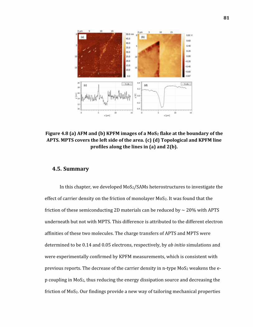
81
Figure 4.8 (a) AFM and (b) KPFM images of a MoS2 flake at the boundary of the APTS. MPTS covers the left side of the area. (c) (d) Topological and KPFM line
profiles along the lines in (a) and 2(b).
4.5. Summary
In this chapter, we developed MoS2/SAMs heterostructures to investigate the
effect of carrier density on the friction of monolayer MoS2. It was found that the
friction of these semiconducting 2D materials can be reduced by ~ 20% with APTS
underneath but not with MPTS. This difference is attributed to the different electron
affinities of these two molecules. The charge transfers of APTS and MPTS were
determined to be 0.14 and 0.05 electrons, respectively, by ab initio simulations and
were experimentally confirmed by KPFM measurements, which is consistent with
previous reports. The decrease of the carrier density in n-type MoS2 weakens the e-
p coupling in MoS2, thus reducing the energy dissipation source and decreasing the
friction of MoS2. Our findings provide a new way of tailoring mechanical properties

82
of low-dimensional materials and have potential applications in controlling the
friction of NEMS.

83
84
Chapter 5
2D Materials and Cells: Direct assessment of the toxicity of
molybdenum disulfide atomically thin film and microparticles via cytotoxicity
and patch testing
5.1. Abstract
The low toxicity of molybdenum disulfide (MoS2) atomically thin film and
microparticles is confirmed via cytotoxicity and patch testing in this report. The
toxicity of MoS2 thin film and microparticles has been extensively studied but is still
inconclusive due to potential organic contamination in the preparations of samples.
Such contamination is avoided here through preparing MoS2 atomically thin film via
direct sulfurization of molybdenum thin film on a quartz plate, which permits a
direct assessment of its toxicity without any contamination. Six different types of

85
cells, including normal, cancer and immortal cells, are cultured in the media
containing MoS2 thin film on quartz plates or dispersed MoS2 microparticles and
their viability are evaluated concerning the concentrations of samples. Detached
thin films from the quartz plates are also investigated to estimate the toxicity of
dispersed MoS2 in biological media. Allergy testing on the skin of guinea pigs is also
conducted to understand their effect on animal skins. By avoiding possible organic
contamination, we demonstrate the low toxicity of MoS2 atomically thin film and
microparticles to cells and animal skins, which paves the way for its applications in
flexible bio-sensing/bio-imaging devices and biocompatible coatings.
5.2. Introduction
As one of the most studied 2D materials, monolayer MoS2 has been
investigated in biological field enthusiastically due to its unique properties.
Compared to the gapless graphene, the 1.8 eV direct band gap of monolayer MoS2
builds the foundation for promising flexible nanoscale biological
electronics[188,217]and bio-sensing devices.[218] With more MoS2-based biological
devices being proposed, more and more concern on its toxicity to cells and live
tissues has been raised. Experiments and simulations on the interaction between
cells and 2D membranes were started to be explored to understand their effects.[219–
222]
It is well recognized that bulk TMDs have low toxicity,[223] but studies of their
nanoscale counterparts are still lacking and inconclusive. X. Yang et al. found that
86
different from graphene-based 2D materials, chemically exfoliated MoS2 was
antibacterial due to the production of reactive oxygen species.[182] J. Fan et al. also
demonstrated that single-layered exfoliated MoS2 nanosheet acted as an
antimicrobial material under the visible light because of the phase transition in
biological environments.[224] These antibacterial behaviors of monolayer MoS2 imply
that its toxicity cannot be overlooked. Furthermore, the study of the dependence of
toxicity on the number of layers of chemically exfoliated MoS2 showed that the
fewer layers exfoliated MoS2 sheets have, the more toxic they were, which was
attributed to its increased surface area.[181]
However, X. Wang et al. compared the toxicity of 2D and aggregated MoS2 for
cells in vitro and in the lung[225], and their results showed that aggregated MoS2
induced strong proinflammatory and profibrogenic response in vitro and acute lung
inflammation, while chemically exfoliated MoS2 did not. W. Z. Teo et al. claimed that
little toxicity of thin MoS2 and WS2 was found based on their cell assessments using
3-(4,5-Dimethyl-2-thiazolyl)-2,5-diphenyl-2H-tetrazolium bromide
Methylthiazolyldiphenyl-tetrazolium bromide (MTT) and water-soluble tetrazolium
salt (WST-8) assays on human lung carcinoma epithelial cells (A549).[180] The low
toxicity of MoS2 thin film was further supported by that no toxic effect was found
when 2D MoS2 nanosheets functionalized with polyethylene glycol of 3.5 mg/kg was
injected into mice.[226]
One of the possible reasons for the divergence in previous research on the
toxicity of MoS2 thin film compared to aggregated or bulk MoS2 is the residual

87
organic contents in its preparation and stabilization processes.[223] It has been a
hurdle for accurate assessment of its toxicity for a long time. However, it is difficult
to obtain MoS2 thin film without exfoliating chemicals. Mechanical exfoliation of
bulk MoS2 and chemical vapor deposition of precursors provide clean single
crystalline MoS2, but the obtained amount is less than enough for biological tests.
This chapter reports a direct assessment of the toxicity of MoS2 thin film
prepared by direct sulfurization of Mo thin film on quartz plates and microparticles
via cytotoxic MTT assay. The viabilities of six different cells in cytotoxic MTT assays
confirmed the low toxicity of MoS2 thin film and microparticles. We evaluate their
allergic impact on animal skin by allergy testing of MoS2 microparticles and thin
films on guinea pig skin. Our results support that MoS2 thin film and microparticles
are of little toxicity in the biological environment when the concentration is less
than 0.016 mg/mL.
5.3. Experimental Section
5.3.1. Preparation of MoS2 thin film and MoS2 microparticles
MoS2 atomically thin film was fabricated via direct sulfurization method.[60]
Thin Mo film (0.6 nm thick) was deposited onto clean quartz plates in an electron
beam evaporator. The quartz plates were placed in the middle of a quartz tube. N2
was used as the protecting gas (150 sccm), and the whole system was purged with
N2 for 15 min at room temperature. A ceramic boat filled with sulfur was placed
upstream to the quartz plates. The quartz plate was heated to 500 °C in 30 min and

88
kept for 90 min with the sulfur temperature being around 90 °C. Afterward, the
temperature of quartz plate was ramped to 750 °C in 10 min and kept for another
120 min to burn out all the sulfur. At this point, the temperature of sulfur increased
to around 120 °C. Finally, the furnace was cooled down naturally to room
temperature.
The mos2 powder was obtained from Sigma Aldrich and used as purchased.
After sonicated for 15 min, the powder in water was centrifuged (8000 rpm, 15
min). Finally, the supernatant liquid containing microscale powder of MoS2 was
dropped onto quartz plates and dried out naturally for biological tests. Solutions of
MoS2 microparticles of different concentrations are obtained by mixed the obtained
exfoliated MoS2 microparticles.
5.3.2. Cell culture and passage
Six kinds of cells were used to evaluate the toxicity of MoS2 of different
morphologies. Pancreatic cancer cell (PANC1), immortal Kidney epithelial cell (293),
pancreas cell (HPDE), immortal breast cell (HMLE), breast cancer cell (159) and
florescence-active breast cancer cell (231) were selected to understand how MoS2
affects various cell morphologies. All cells were purchased from ATCC and used as
purchased.
Different kinds of culture medium were used for different cells to maximize
their viabilities. For PANC1, 293, 159, and 231, we used a culture media composed
of Dulbecco's modified Eagle's medium (DMEM) with high glucose (500 mL), fetal

89
bovine serum (FBS, 50 mL) and of penicillin-streptomycin (PS, 5.5 mL). For HPDE,
Keratinocyte-serum free medium (SFM) including L-glutamine, epidermal growth
factor (EGF), pituitary extract bovine (PEB) and PS (5.0 mL) was purchased from
Gibco and used as the culture medium. HMLE cells were cultured in Mammary
epithelium basal medium (MEBM) bought from Lonza, where PS (5.0 mL) was
added to enhanced its performance.
We conducted cell passage as follows: the old culture media in the old dish
was removed, and the cells were rinsed with phosphate-buffered saline (PBS,
pH=7.4) before being transferred to a new dish. Trypsin (1 mL) was used to free all
kinds of cells except HMLE from the old dish walls. Trypsin neutralizing solution (1
mL) is for HMLE. The cells in the new dish were kept in the incubator at 37 °C for 3-
4 mins (8-10 min for HMLE) and then the corresponding culture medium (3 mL)
was added. The whole mixture was transferred to a new tube (10 mL) followed by
being pipetted to decrease the number of adherent cells on the walls. The mixture
was then centrifuged (1000 rpm, 3 min) to prohibit pancreatic enzyme activity. The
supernatant fluid was removed, and some new culture medium was added. The new
cells mixture was blown gently from the bottom with air to mix the cells uniformly.
Such mixture (200~300 µL) was transferred to another new dish with the culture
medium (10~15 ml) inside and then incubated in the atmosphere of CO2 (37 °C,
24~48 h). The cell passage finished here, and the cells were used as the next
generation.

90
Calcein-acetoxymethyl was used to dye florescence-active cells. The dyeing
solution was made of PBS (1 mL) and calcein-acetoxymethyl (1 µL, 4 M). With
supernatant fluid removed, the solution was mixed with the culture medium (2 mL).
After being gently blown by air, 1 mL of the solution was centrifuged (1000 rpm, 90
s). Removing the supernatant fluid again, we added 1 mL dyeing solution (1 mL) to
the solution and incubated it at 37 °C for 5 min. The mixture was centrifuged again,
and the supernatant fluid was removed. The cells were rinsed with PBS (1 mL).
5.3.3. Cell viability evaluation
After the cells were cultured in a medium with quartz plate (1.5 cm by 1.5
cm, covered or uncovered by the thin MoS2 film) for 24 hours, cell viability was
determined by manual counting of live cells. The quartz was rinsed with a culture
medium to free all cells from the dish wall, and the whole mixture was transferred
to a new tube. Trypsin (1 mL) was used to collect all the remaining cells in the dish
and added to the new tube. Extra trypsin (1 mL) was added to the tube solution and
incubated (37 °C, 3 min). The solution was then centrifuged (1500 rpm, 3 min) to
precipitate the cells. With the supernatant fluid removed and the culture medium (3
mL) added, the solution was blown gently to get cells well dispersed. Some of the
solution (20 μL) was mixed with the trypsin blue (20 µL) uniformly, and the mixture
was injected into the counter plate. The trypsin blue dyes the dead cells, which
provides a clue of differentiating live and dead cells. The viability was defined as the
number of live cells divided by the number of total cells.
91
A 96-well plate was used to assess the viability of cells exposed to MoS2
dispersed microparticles of different concentrations. 24~48 h before the seeding of
cells in wells, cell passage was done to increase the concentration of cells to around
65%. Each well was filled with cell solutions (180 µL, 5.0u104/mL) and cultured (37
°C, 12~16 h). PBS (20 µL) with dispersed MoS2 microparticles of different
concentrations was added to each well. The final concentration of cells in each well
was 8000~10000/200 µL. The concentration of MoS2 microparticles in PBS were 16
mg/mL, 1.6 mg/mL, 0.16 mg/mL, 0.016 mg/mL, and 1.6 µg/mL. Medium without
cells and MoS2 microparticles and a mixture of cells without MoS2 microparticles
were used as controls. After the MoS2 microparticles solution was added, the cell
solution was cultured (37 °C, 24 h). MTT in PBS (5 mg/mL) from Sigma was filtered
with 0.22-μm filter membranes to remove any contaminating cells and then injected
into each well. The cells were cultured (37 °C, 4 h). After that, the solution in each
well was centrifuged (3000 rpm, 10 min). The supernatant fluid was removed, and
methyl sulfone was added to dye the live cells. The plate was shaken (15 min) to mix
the solution. MTT turns purple in the presence of live cells, aiding in the calculation
of cell viability. The final plate is shown in Figure 5.1. Determinations of optical
density (OD) values of wells were conducted at 520 nm. Only live cells decrease the
OD values of the solution, which helps determine the viability.

92
Figure 5.1 Group 1 contains only MoS2 (1.6 g/mL) as a negative control and Group 2 only cells as positive control. Group 10 contains only culture media as
none control. From 3 to 9, , the concentration of MoS2 decreases from 1.6 g/mL, 0.16 g/mL, 0.016 g/mL, 1.6 μg/mL, 0.16 μg/mL, 0.016 μg/mL, 1.6 ng/mL
correspondingly. The outer holes contain 200 μL of PBS to slow down the evaporation of culture media. In each group, we used six holes.
5.3.4. Allergy testing on guinea pigs
Na2S was purchased from Tianjin Fengchuan Chemical Reagent Technologies
Co., LTD; PBS solution came from Thermo Fisher Scientific; JY92-2D ultrasonic cell
disruptor was supplied by Ningbo Scientz biotechnology Co. LTD. and RuiminTM
patching testing kit, which was produced by Sweden Chemotechnique Diagnostics,
and imported by Beijing Bioyoko Medical Technology Co., LTD. The IQ unit is made
of inert polyethylene plastic.

93
All the experiments with animals were performed in compliance with the
relevant laws and institutional guidelines and approved by the institution
committee. 26 guinea pigs (mature, female, and unpregnant) were employed in
patch testing and quartz plate testing. Their weights ranged from 250 to 350 g. An
area of fur (3cm by 3cm) was removed from the shoulder back area with razors and
then cleaned with a Na2S solution (8% mass). Two MoS2 microparticles suspension
(1.6 mg/mL and 0.16 mg/mL) were prepared by sonication of MoS2 powder in PBS
for 3 hours. For each IQ chamber from Chemotechnique MB, MoS2 suspension (25
µL) was injected for the patch testing. MoS2 thin films on quartz plates were also
employed as a patch in this test.
5.3.4.1. Pre-testing:
Two guinea pigs were randomly selected, and their exposed areas were
covered with a patch of the MoS2 suspension (0.16 mg/mL). One was covered for 24
hours and the other for 48 hours to secure the contact between MoS2 and the skin.
Degrees of erythema, ulceration and edema symptoms were measured at 1, 24, and
48 hours after the patches or quartz plates were removed. The levels of erythema
were classified as none, mild, moderate, severe and edematous erythema, and the
levels of edema are none, mild, moderate and severe. The criterion of allergy is
tabulated in Table 5.1.

94
Table 5.1 Criterion for skin allergy. The occurring rate is defined as the number of animals of allergic reactions divided by the total number of animals
Occurring rate/% Level Strength 0~8 I None
9~28 II Mild 29~64 III Moderate 65~80 IV Severe
81~100 V Extreme
5.3.4.2. Patch testing and quartz plate testing:
We divided 21 of the remaining 24 guinea pigs into four groups, which were
covered with patches of different concentrations of MoS2 suspension for different
periods of time. Measurements of erythema, ulceration and edema symptoms were
made at 1, 24, and 48 hours after patches were removed. The details of all groups
are listed in Table 5.2. The other three guinea pigs were covered with quartz plates
for 24 h to test the allergic effect of the MoS2 thin film.
Table 5.2Dose of MoS2 microparticles suspension and period in each group of guinea pigs
Group No. Covering time (h) Concentration (mg/mL) Volume (μL)
1 6 48 1.6 25 2 5 24 1.6 25 3 6 6 0.16 25
Control 4 24 None None
95
5.4. Results and Discussion
5.4.1. Synthesis and Characterization of MoS2 film on a quartz plate
MoS2 has been shown to be a highly promising 2D material in flexible
electronic and optoelectronic devices. To assess its prospects in biomedical devices,
such as in vivo biosensors and bio-functional coatings, here we studied the toxicity
of MoS2 of thin film morphology with care.
MoS2 atomically thin film was prepared via direct sulfurization of deposited
Mo film on quartz plates, which were biologically inert. Raman spectroscopy was
used to confirm the quality of the prepared MoS2 atomic layer. The mos2 thin film
has fewer peaks in its Raman spectrum than bulk MoS2 due to the fewer physical
constraints of low-dimensional materials. Figure 5.2 (a) shows an optical image of
sulfurized MoS2 thin film on a quartz plate which is 1.5cm by 1.5cm. The left half
covered by MoS2 thin film shows darker contrast compared to the right half without
MoS2 coating. Figure 5.2 (b) shows the Raman spectrum of the sulfurized MoS2 thin
film. The two peaks at 383 and 405 cm-1 are the typical peaks of few-layer MoS2.[73]
The gap of 22 cm-1 between the two peaks indicates the number of layers of MoS2
will be ~ 3 layers.[54] The high intensity of these two peaks also confirms the sound
quality of the MoS2 thin film. We believe no organic chemicals can survive at such
high temperature. After the 3-hour high-temperature reaction, only MoS2 inorganic
samples can sustain since the melting point of sulfur is 115.2 °C. This is further
confirmed by the XPS of the sample because no signal of the sulfur element whose
binding energy is 164 eV was found, as shown in Figure 5.3. The Raman spectrum in

96
Figure 5.2(a) also confirmed this since no Raman peaks (mainly at 218 cm-1 and 474
cm-1) of sulfur were found.[227]
Figure 5.2 (a) Optical image of a quartz plate with the left half covered by the MoS2 thin film. (b) Raman spectrum of MoS2 thin film. (c) HPDE cells in
medium without quartz plate. (d) HPDE cells in medium with a quartz plate. (e) HPDE cells in medium with a quartz plate inside, half of which was covered by the MoS2 thin film. (f) HMLE cells at the boundary of quartz plate with and without MoS2 thin film. (g) Viabilities of different cells in medium with none, clean quartz plate, quartz plate fully covered by the MoS2 thin film. Scale bars
in all pictures are 100 μm.

97
Figure 5.3 XPS of sulfurized MoS2 thin film on quartz. (a) referenced carbon 1s spectrum; (b) sulfur 2p spectrum; (c) molybdenum 3d spectrum. Three typical
XPS spectra in Figure S3 shows the valence of sulfur is +2 according to the peak ranging from 161 to 163 eV. No 0 valence is present (164 eV), which
means there is no sulfur element residual left in the grown samples.
5.4.2. Cytotoxicity results of the MoS2 thin film
The toxicity of these thin films was tested by co-culturing six kinds of cells in
corresponding media and the quartz plates with the MoS2 coating. The types of cells
include normal, cancer, and immortal cells, whose abbreviation are 159, 231, 293,
HMLE, HDPE, and PANC1 respectively in this report. 159 and 231 are widely used
breast cancer cells in toxicity evaluation because of their high success rate of cell
passage. The latter is fluorescent, which eases the difficulties associated with cell
counting and observation. HMLE (immortal breast cells) is selected to investigate
the effect of our nanomaterials on immortal cells in the same organ. To validate our
results in different organs, we selected the HDPE (normal pancreatic cells) and
PANC1 (pancreatic cancer cells). 293 cells are immortal kidney cells, which not just
provide information on the immortal cells but also provide a test platform in
another organ. The different morphologies and sensitivity of these cells provide a

98
comprehensive test platform for our samples. As controls, media with and without a
clean quartz plate were used to co-culture cells. After cultured in media for 24
hours, the number of live cells was estimated by manual counting to estimate
viability. More details are provided in methodology.
The morphologies of cells show no difference on quartz plates with and
without MoS2 thin film covered. For example, Figure 5.2 (c)-(e) are HDPE cells in
medium without a quartz plate, medium with a clear quartz plate and medium with
a MoS2-coated quartz plate, respectively. The differences in the shape of HPDE cells
are tiny in media, media with a quartz plate, and media with MoS2-covered quartz
plate. There is no obvious stretch in 1e, which could be demonstrated by the mean
and distribution of the round rates of the cells in Figure 5.5. The round rate is
defined as the ratio of the minor axis to the major axis of the elliptic shape of cells.
For normal media, it is 0.68 r 0.15; For quartz, 0.65 r 0.12; for quartz with MoS2,
0.69 r 0.14.
HMLE cells at the boundary of MoS2 on a quartz plate are shown in Figure 5.2
(f) as another example. HMLE cells do not show any preference towards MoS2 thin
film and the pure quartz plate. Some of the cells also cross the boundary between
MoS2-coated and clear quartz plate and thrive in both areas.
Table 5.3 Average and standard deviation (s. d.) of cell viabilities in different concentrations
159 231 293 HMLE HDPE PANC1 average average average average average average

99
160 60.42% 33.14% 51.48% 14.34% 40.93% 28.14% 16 85.58% 66.38% 62.83% 49.83% 56.34% 55.59% 1.6 91.94% 69.28% 63.28% 62.96% 62.15% 59.28%
0.16 94.54% 72.53% 69.79% 72.97% 73.03% 73.63% 0.016 98.41% 76.25% 76.02% 87.85% 74.97% 90.80%
0.0016 101.48% 85.37% 91.49% 111.79% 73.16% 88.72% cell 100.00% 100.00% 100.00% 100.00% 100.00% 100.00%
s. d. s. d. s. d. s. d. s. d. s. d.
160 12.31% 15.35% 13.29% 4.20% 5.85% 14.11% 16 7.39% 8.23% 12.83% 7.11% 2.73% 8.73% 1.6 3.28% 10.70% 12.77% 14.20% 5.45% 6.28%
0.16 3.89% 13.38% 8.80% 10.17% 7.76% 9.45% 0.016 13.55% 5.33% 7.58% 16.58% 4.91% 17.23%
0.0016 12.08% 14.73% 18.51% 19.92% 19.29% 14.62% cell 12.16% 20.67% 18.26% 18.78% 12.76% 19.00%
The viabilities of six types of cells are tabulated in Table 5.3 and shown in
Figure 5.2 (g). In this chart, the almost unchanged viabilities of all cells in different
media demonstrate that there are no statistically significant changes in cell viability
due to the introduction of MoS2 thin film on a quartz plate. It is noted that the
viabilities of some cells are higher than 100% but still lay within the confidence
interval. It is due to the error caused by manual counting and the proliferation of
cells during the test because highly active cancer and immortal cells were used. The
nominal concentration of MoS2 in media is estimated to be 1.4~2.8 µg/mL according
to the thickness of the thin film (2~4 nm, shown in Figure 5.4) and the volume of
media. However, the MoS2 thin films did aggregate on the quartz plate, so the local
concentration of MoS2 thin film around the quartz plate was much higher than the
nominal concentration.

100
Figure 5.4 (a) Topography of MoS2 film on a quartz plate. The left part is the quartz plate, and the right part is a MoS2 film on the quartz plate. (b) 3D view
of MoS2 thin film on a quartz plate. (c) Height profile of Line 1 in (a). The height of MoS2 thin film is estimated to be 3 nm here.
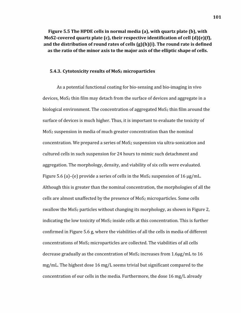
101
Figure 5.5 The HPDE cells in normal media (a), with quartz plate (b), with MoS2-covered quartz plate (c), their respective identification of cell (d)(e)(f), and the distribution of round rates of cells (g)(h)(i). The round rate is defined
as the ratio of the minor axis to the major axis of the elliptic shape of cells.
5.4.3. Cytotoxicity results of MoS2 microparticles
As a potential functional coating for bio-sensing and bio-imaging in vivo
devices, MoS2 thin film may detach from the surface of devices and aggregate in a
biological environment. The concentration of aggregated MoS2 thin film around the
surface of devices is much higher. Thus, it is important to evaluate the toxicity of
MoS2 suspension in media of much greater concentration than the nominal
concentration. We prepared a series of MoS2 suspension via ultra-sonication and
cultured cells in such suspension for 24 hours to mimic such detachment and
aggregation. The morphology, density, and viability of six cells were evaluated.
Figure 5.6 (a)–(e) provide a series of cells in the MoS2 suspension of 16 µg/mL.
Although this is greater than the nominal concentration, the morphologies of all the
cells are almost unaffected by the presence of MoS2 microparticles. Some cells
swallow the MoS2 particles without changing its morphology, as shown in Figure 2,
indicating the low toxicity of MoS2 inside cells at this concentration. This is further
confirmed in Figure 5.6 g, where the viabilities of all the cells in media of different
concentrations of MoS2 microparticles are collected. The viabilities of all cells
decrease gradually as the concentration of MoS2 increases from 1.6µg/mL to 16
mg/mL. The highest dose 16 mg/L seems trivial but significant compared to the
concentration of our cells in the media. Furthermore, the dose 16 mg/L already

102
shows some impact on the cells, which means higher concentration will inevitably
reduce the viability of cells. However, 159, HMLE and PANC1 cells do not have any
statistically significant decrease and 231, 293 and HDPE cells show little decrease in
their viability when the concentration is less than 0.016 mg/mL. The effect of MoS2
particles is even less when its concentration is around 0.0016 µg/mL, which is
around nominal concentrations in the MoS2 thin film tests. These experimental
results show that the detachment and aggregation of MoS2 film introduce minimal
adverse effects on the viabilities of cells. However, this critical value should be
specific for MoS2 thin film and microparticles here since it could be dependent on
the lateral size and edge types of nanomaterials. Further investigation of this needs
to be conducted in future.

103
Figure 5.6 Cell morphologies in MoS2 suspensions (0.016 mg/mL). (a) 159; (b) dye-activated 231; (c) 293; (d) HDPE; (e) HMLE; (f) PANC1; (g) Viabilities of cells in the medium with MoS2 microparticles of different concentrations.
Scale bars in all pictures are 100 μm.
5.4.4. Toxicity evaluation of MoS2 thin film and microparticles on animal
skins

104
To further investigate the biological effect of MoS2 microparticles and thin
film, skins of guinea pigs were tested for allergy. The guinea pig has a high level of
blood serum alexine, which can trigger an immune response easily when exposed to
a little amount of allergen. The surroundings easily influence the guinea pigs’
behaviors, so the temperature was kept at 25 ℃ and humidity is 60%. A diet of 50 g
cabbage per guinea pig per day was supplied. MoS2 microparticles suspensions of
medium of high concentrations (1.6 mg/mL and 0.16 mg/mL) were used for allergy
testing. After the allergen patches were removed, the exposed skins were recorded
at 1, 24, and 48 hours. Figure 5.7(a) – (c) shows three typical examples of these
guinea pigs after the patch testing. The skins are physically normal with no
erythema, edema or ulcers. Table 5.4 summarizes the observations of all guinea
pigs, which shows no allergic effect introduced by the MoS2 suspensions of 1.6
mg/mL and 0.16 mg/mL. Figure 5.7(d) – (f) shows the pictures of three guinea pig
examples after the quartz plate tests, in which shows the same effect of the solid
MoS2 thin film as that of microparticles suspensions. All the guinea pigs weighted
400-500 grams after patch testing and did not show any abnormal behaviors. The
patch testing data shows that the toxicity of MoS2 microparticles is very low at the
medium of high concentrations and that MoS2 thin film is a very safe material in
normal biological circumstance.
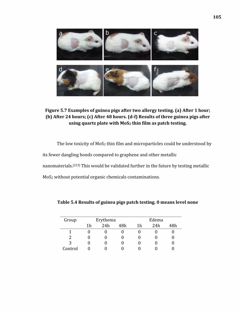
105
Figure 5.7 Examples of guinea pigs after two allergy testing. (a) After 1 hour; (b) After 24 hours; (c) After 48 hours. (d-f) Results of three guinea pigs after
using quartz plate with MoS2 thin film as patch testing.
The low toxicity of MoS2 thin film and microparticles could be understood by
its fewer dangling bonds compared to graphene and other metallic
nanomaterials.[223] This would be validated further in the future by testing metallic
MoS2 without potential organic chemicals contaminations.
Table 5.4 Results of guinea pigs patch testing. 0 means level none
Group Erythema Edema 1h 24h 48h 1h 24h 48h
1 0 0 0 0 0 0 2 0 0 0 0 0 0 3 0 0 0 0 0 0
Control 0 0 0 0 0 0

106
5.5. Summary
Using the MTT assay and patch testing, the toxicity of MoS2 thin film and
dispersed microparticles was directly assessed in vitro and on the skin. A large and
clean MoS2 thin film was synthesized by direct sulfurization of deposited
molybdenum thin film on quartz plates and used for cytotoxic tests of six different
types of cells. With a quartz plate half covered by the MoS2 thin film in the medium,
the viability of different cells did not show the statistical difference from the pure
medium and pure quartz plate, indicating the low toxicity of MoS2 thin film to these
cells. Our results of co-culturing cells in the medium of different concentration of
dispersed MoS2 microparticles show that the MoS2 microparticles did not induce
any toxic behaviors at the low concentration of 0.016 mg/mL, which supported that
aggregated MoS2 thin films even are safe to the cells in the case of film delamination.
The patch testing on guinea pigs further confirmed that there was little adverse
effect of MoS2 thin film and microparticles on the skin of animals. All these nontoxic
behaviors of MoS2 thin film and microparticles at low concentration would build the
foundation for MoS2-based devices in the biological environment.

107
Chapter 6
2D Materials and Substrate I: Controllable growth of monolayer
MoSe2 on nanoscale pillar patterns
6.1. Abstract
In this chapter, we developed a competitive growth method of high-quality
monolayer MoSe2 hexagons using the nanoscale silicon pillars. Development of
better large-scale synthesis methods of 2D materials are the bottleneck of their
further exploration and applications now, and no economical methods have been
found now. By incorporating substrates with nanoscale silicon pillars on top in CVD
growth, we found the interaction of the pillars and 2D materials provides a new
method of controlling the shape and the edge type of as-grown samples.
Confirmations of the quality of the grown samples were done with Raman, PL, and
TEM. The effect of the pillars on the monolayer MoSe2 is investigated by the PL

108
mapping, phase-field simulation, and SHG. This new understanding of the growth of
nanomaterials helps us to grow better nanomaterials by use of designed substrates.
6.2. Introduction
Different synthesis methods of 2D materials have been developed since the
birth of the graphene. The first-used and easiest method, mechanical exfoliation
(ME)[1,36,125,154,228,229] needs expensive and high-quality crystals, and it is incapable
of provides large-scale samples. Liquid exfoliation (LE)[41,44] can provide large-scale
samples, but the quality of samples is not as good as those via ME. Chemical vapor
deposition (CVD)[57,69,73,79,230–235] is widely used for different 2D materials, including
graphene, h-BN and TMDs. The quality of samples obtained through CVD is high, and
the sizes could reach millimeter scale.[236] However, large-scale samples are mostly
polycrystalline due to the random crystal orientation of the initial nucleus at the
beginning of the growth. Samples of uniform orientation have been found on
different special substrates, such as sapphire[76,237,238]. However, such substrates are
expensive, and their preparation could be the bottleneck of the applications of 2D
materials in future.
The uniform orientation of 2D materials on specific substrates is attributed
to their interaction with substrates.[76,237,238] It is reported that substrate crystal
orientation affects the orientation of 2D materials.[65,237,239,240] However, only flat
substrates were used, and the expensive materials such as sapphire were utilized.
Effective design the surface of regular substrates to control the growth of 2D
109
materials will provide a competitive growth method and improve our
understanding of the growth theory of nanomaterials.
Here we report an economical growth of high-quality monolayer
molybdenum disulfide (MoSe2) on nanoscale pillar pattern (NPP). With the help of
this NPP, hexagonal MoSe2 were successfully grown on the substrate in conformity
of silicon pillars. Different characterizations including Raman, PL, SEM, and TEM
confirms the high-quality of the as-grown MoSe2 crystals and its geometry shape.
Further investigations of the effect of silicon pillars on the MoSe2 were conducted in
the aspect of the photo-electronic property, geometry shape, crystalline quality and
edge types of the monolayer MoSe2. All the results improve our understanding of the
interaction between substrates and 2D materials.
6.3. Methods
6.3.1. Chemicals and substrates
All chemicals are purchased from Sigma-Aldrich and used as purchased.
Hexagonal-patterned silicon nanopillars are fabricated using the combination of
step-and-repeat nanoimprint lithography (NIL) and metal-catalyzed electroless
etching (MCEE) [241]. This approach is suitable for generating uniform Si
nanostructures of different dimensions and patterns.

110
6.3.2. CVD growth of monolayer MoSe2
Monolayer MoSe2 was grown by CVD, which was developed and reported
previously[73]. Briefly, a mixture of hydrogen and nitrogen (N2:H2 = 95:5 in volume)
is used as the carrying and catalysis gas. A face-down patterned Si wafer was put
across a ceramic crucible with precursor MoO3 inside. The crucible was placed in
the middle of a quartz tube with another crucible holding selenium powder in the
upstream. The flow rate of carrying gas was 80 sccm and reaction temperature was
800 °C with the heating rate of 50 °C/min. The dwelling time was 15 min at the
reaction temperature. After the reaction was done, the furnace was cooled down
naturally.
6.3.3. Characterizations
Raman spectroscopy (Renishaw inVia confocal microscope) was used to
characterize the as-grown samples. The power of laser w 2.25 W and the
wavelength was 532 nm. SEM (FEI Quanta 400) was employed to determine the
morphology and orientation of as-grown samples. It was also used to determine the
structure of NPP. TEM was carried out to study the morphology and crystal
structure of the samples at the nanoscale. It was performed on a JEOL 2100F
microscope operating at 200 kV. The diffraction pattern was obtained from the top
of the MoSe2 pillars using a selected-area aperture. Gatan microscopy suite software
was used to determine the crystal parameters of samples. XPS (PHI Quantera) was
performed on the samples using monochromatic Copper Kα X-rays, and the
obtained data were analyzed with the MultiPak.

111
To confirm the conformity of as-grown MoSe2, we used a wet transfer
method to transfer the grown samples to a new silicon substrate.[214] A 1.5-µm-thick
PMMA covered the as-grown sample via spin-coating and got heated at 185 °C for 1
min. The substrate was then floated on a 1M NaOH solution to dissolve the
underlying silicon. The floating PMMA film was picked up by a PVC piece and
transferred to a container full of water to remove the residual NaOH. This film was
picked up by a new wafer and heat at 80 °C to get dried out. Acetone was used to
dissolve the PMMA, and isopropyl alcohol was used to wash the final substrates. The
dry air dried the substrate.
6.3.4. SHG measurement setup
Second harmonic generation (SHG) spectroscopy was used to determine the
crystal orientation of as-grown samples. The excitation laser was linearly polarized
by a 900-1300 nm polarizing beamsplitter, and the polarization was rotated by
rotating an infrared half-wave plate. The pulse width was approximately 200 fs, and
the repetition rate was 80 MHz. A 50× near-IR objective lens was used to focus the
laser on the sample sitting on a continuous-flow liquid-nitrogen cryostat. A CCD
spectrometer was used to collect the generated SHG signal. To obtain SHG mapping
of the sample, we mounted a microscope object (Zeiss 50×; numerical aperture 0.55)
on piezo stage, which enables the mapping by moving the objective.

112
6.3.5. Simulation of CVD growth
Simulations of MoSe2 growth was implemented by multi-component phase-
field models, which is developed and reported previously.[90,242,243] Briefly, the
growth of crystal and the deposition, diffusion, and desorption of feedstock were
described by two fields which interacted with each other. Given the parameters
describing the growth rate, diffusion rate, and others, these two differential fields
equations were solved numerically using Fourier and Laplace transform. Hexagonal
patterns of pillars were generated on the substrate, and the effect of the pillars was
represented by the interaction between the growth of crystals and substrates, i.e.,
the slower growth rate was enforced in the area of pillars.
6.4. Results and Discussion
6.4.1. Characterization of grown MoSe2
We made the substrates via the combination of step-and-repeat nanoimprint
lithography (NIL) and metal-catalyzed electroless etching (MCEE), which was
developed and reported previously.[241] This method can generate wafer-scale
periodic silicon patterns at the nanoscale. The top view and bird view of the NPP are
shown in Figure 6.1 (a) (b), which shows that the height of the pillars is 300 nm, and
the diameter is 100 nm. The center distance of pillars is 200 nm, i.e., the interval
between two pillars is 100 nm. These pillars are highly uniform over the whole
substrate.
113
Hexagons samples were grown on the substrates by CVD, and Figure 6.1 (c)
and (d) shows a typical image and an SEM image of the as-grown samples. The edge
of as-grown hexagons is 100 µm long, which is much larger than the diameter of
pillars.
To confirm the as-grown samples are MoSe2, we collected the Raman and PL
spectrum of the as-grown samples, as shown in Figure 6.1 (e) and (f). The Raman
peak at 242 cm-1 and 284 cm-1 are consistent with the A1g and 𝐸2𝑔1 peaks of
monolayer MoSe2 in literature[233,244,245]. It should be noted that the strong peak at
250 cm-1 is not reported before, and it should be assigned to the multi-phonon
vibration (2 𝐸2𝑔1 at M) which is contributed from the MoSe2 grown along the side of
the pillars. This is the first report of a strong multi-phone vibration mode in
monolayer MoSe2. This strong intensity can be understood by that the direction
incident laser is parallel with the vibration direction of 𝐸2𝑔1 mode in MoSe2 on the
sides of pillars and this parallelism facilitates the involvement of multiple E12g
phonons in Raman scatter. The PL in Figure 6.1 (f) demonstrates the good quality of
as-grown MoSe2 where a strong PL peak is observed at 790 nm (1.57 eV). This peak
is consistent with literathe ture.[233,244,245] The PL mapping show in Figure 6.1 (g)
indicates that the strong PL is only observed on the MoSe2 on the pillars rather than
on the pillars.

114
Figure 6.1 (a) Top view and (b) bird view of the nanoscale pillars pattern (NPP) ; (c) Optical image, (d) SEM image, (e) Raman spectrum and (f) PL
spectrum of the as-grown MoSe2 on the NPP; (g) Partial PL mapping image of as-grown MoSe2 on the NPP
It is still inconclusive to determine the relative location of grown MoSe2
concerning the pillars from the top view in the optical and SEM images. The samples
could grow on the surface of the substrate and leave pillars uncovered, or cover the
top surface of the pillars and leave all other surfaces of the substrate uncovered, or
grow in conformity with pillars, i.e., cover the substrates and pillars. A bird view of
the samples helps us solve the problem. From a zoom-in view of the sample shown
in Figure 6.2 (a), we can conclude that the sample grows in conformity. A closer look
at Figure 2(b), the film of as-grown MoSe2 continues at the cross between the pillars
and the surface of the substrate, as shown in Figure 6.2 (c).
To further confirm the conformity and the crystal structure of the as-grown
samples, TEM was employed to characterize the samples at the nanoscale. A wet
2 µm 2 µm 200�µm 100�µm
20 µm
a b
g
dc
fe
115
transfer method was used to transfer the sample to copper grid carefully, and a TEM
image of a typical tiled pillar is shown in Figure 6.2 (d). As we can see, the sample
shows a perfectly hollow-pillar shape, and its geometry matches that of the pillar.
The atomic-resolution image of the sample is shown in Figure 6.2 (e), indicating the
good crystal quality. This is also demonstrated by the strong electron diffraction
pattern obtained by select-area electron diffraction in Figure 6.2 (f). From the
diffraction pattern, we can determine the crystal structure to be hexagonal lattice
and a = 0.330 nm, which is consistent with the literature.[246]
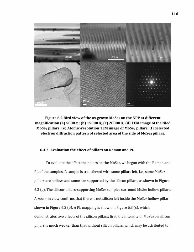
116
Figure 6.2 Bird view of the as-grown MoSe2 on the NPP at different magnification (a) 5000 x ; (b) 15000 X; (c) 20000 X; (d) TEM image of the tiled MoSe2 pillars; (e) Atomic-resolution TEM image of MoSe2 pillars; (f) Selected
electron diffraction pattern of selected area of the side of MoSe2 pillars.
6.4.2. Evaluation the effect of pillars on Raman and PL
To evaluate the effect the pillars on the MoSe2, we began with the Raman and
PL of the samples. A sample is transferred with some pillars left, i.e., some MoSe2
pillars are hollow, and some are supported by the silicon pillars, as shown in Figure
6.3 (a). The silicon-pillars-supporting MoSe2 samples surround MoSe2 hollow pillars.
A zoom-in view confirms that there is not silicon left inside the MoSe2 hollow pillar,
shown in Figure 6.3 (b). A PL mapping is shown in Figure 6.3 (c), which
demonstrates two effects of the silicon pillars: first, the intensity of MoSe2 on silicon
pillars is much weaker than that without silicon pillars, which may be attributed to
2�nm
20�µm 2�µm 1 µm
100�nm
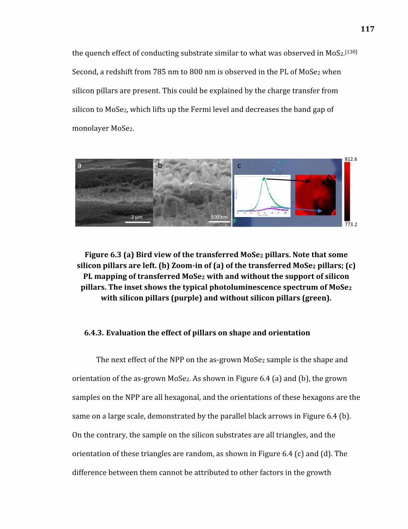
117
the quench effect of conducting substrate similar to what was observed in MoS2.[130]
Second, a redshift from 785 nm to 800 nm is observed in the PL of MoSe2 when
silicon pillars are present. This could be explained by the charge transfer from
silicon to MoSe2, which lifts up the Fermi level and decreases the band gap of
monolayer MoSe2.
Figure 6.3 (a) Bird view of the transferred MoSe2 pillars. Note that some silicon pillars are left. (b) Zoom-in of (a) of the transferred MoSe2 pillars; (c)
PL mapping of transferred MoSe2 with and without the support of silicon pillars. The inset shows the typical photoluminescence spectrum of MoSe2
with silicon pillars (purple) and without silicon pillars (green).
6.4.3. Evaluation the effect of pillars on shape and orientation
The next effect of the NPP on the as-grown MoSe2 sample is the shape and
orientation of the as-grown MoSe2. As shown in Figure 6.4 (a) and (b), the grown
samples on the NPP are all hexagonal, and the orientations of these hexagons are the
same on a large scale, demonstrated by the parallel black arrows in Figure 6.4 (b).
On the contrary, the sample on the silicon substrates are all triangles, and the
orientation of these triangles are random, as shown in Figure 6.4 (c) and (d). The
difference between them cannot be attributed to other factors in the growth
812.6
773.2
2 µm 500�nm
a b c

118
because these samples are on the same substrate in the same growth batch.
Obviously, the NPP controls the shape and the orientation of the samples. It is easy
to investigate the relationship between the orientation of silicon lattice of the NPP
and those of the samples. As shown in Figure 6.4 (e) and (f), the sides of hexagonal
samples are aligned with the close-packed directions of the hexagonal silicon pillars,
which means that pillars pin the boundary of MoSe2 crystal growth.

119
Figure 6.4 (a) SEM image of as-grown MoSe2 on NPP on a large area; (b) Zoom-in view of MoSe2 of the same orientation; (c) SEM image of the as-grown MoSe2 on silicon; (d) SEM image of the as-grown MoSe2 of different orientations. The side of the NPP substrate is not covered by pillars, which was utilized for the
growth of MoSe2 on the flat silicon substrate. (e) The as-grown MoSe2 on pillars and the corresponding basis vectors of the hexagonal lattice of NPP; (f)
Zoom-in view of the corner of the MoSe2 hexagon and the basis vectors.
The pinning effect of silicon pillars are further confirmed by the Figure 6.5
(a), (b) and (c). When the edge of the MoSe2 is greater than 1.5 µm, the hexagonal
samples align their edges correctly with the close-packed directions of the NPP. To
understand the pinning effect of the pillars, we employed a multi-component phase
filed model. Two fields describing the crystal and feedstock were solved numerically
on a substrate with and without pillars, see Figure 6.5 (d). The pinning effect of the
pillars was represented by the slower crystal growth rate in the two differential
equations. The results are shown in Figure 6.5 (e) and (f). The result is consistent
500�µm 100�µm 300�µm
300�µm 100�µm 5�µm
a b
d e
c
f

120
with the experiment fact that without pillars, the grown sample is primarily
triangular, and with pillars, it is primarily hexagonal.
Figure 6.5 The coalignment of as-grown hexagonal MoSe2 and the hexagonal lattices of the NPP: (a) 10-µm-long edge; (b) 3-µm-long edge; (c) 1.5-µm-long edge; (d) Proposed growth model of MoSe2 on pillars; (e) Simulation result
without silicon pillars; (f) Simulation result with pillars; The yellow part is the grown crystal after 1000 steps.
In the literature[65,73,247] and our simulation, the nucleus of the grown TMDs
should be dominatingly triangular or circular when their size is less than 100 nm
because the pinning effect of the pillars is trivial compared to the Wulff criteria of
TMDs. [248] This is confirmed by our further investigation of our SEM images on a
smaller scale. As shown in Figure 6.6, several triangular samples within the interval
of pillars can be found with a careful check. Furthermore, we also found a merging
system (see the large dashed red circle in Figure 6.6) which includes several close
5 µm10 µm 3 µm
a b
d e
c
f

121
triangular samples. A primitive hexagonal sample is emerging from this merge. This
confirms the growth steps of the hexagonal samples. In the beginning, triangular or
circular nucleus are formed in the intervals of the pillars or around the pillars. After
that, the nucleus grows or merges with others, and the pinning effect of the pinning
starts to play a role, i.e., impede the growth of the crystal. Such pinning effect causes
the edge of samples to align with the close-packed direction since the pinning effect
are the maximized here. With the size of the samples is large enough, the shape of
growing crystals is controlled to be hexagonal rather than triangular, and their
edges align with the silicon pillars.
Figure 6.6 (a), (b) Zoom-in view of the yellow dashed rectangles in (c) the SEM image of infantile MoSe2, which are marked by the dashed circles.
500 nm
1�µm 5 µm
a
b
c
122
6.4.4. Evaluation the effect of pillars on crystal orientation and edge type
In the literature, small grown TMD nuclear will rotate itself to adapt its
crystal orientation to a large one and forms a large single crystalline TMD. [243] It is
mentioned above that hexagonal samples are merged from small triangular samples,
which indicates that the hexagonal sample might be polycrystalline. The other
unsolved question is the kinds of the terminated edge of the hexagons. In the
triangular samples grown by CVD, the edge of TMDs is chalcogenide-terminating
due to its lowest free energy on the flat substrate.[249–252] For the hexagonal, no
conclusion is made yet. Here we will use SHG of TMDs to solve these two questions.
As a nonlinear optical phenomenon, SHG of TMDs has been studied
previously to understand the information it provides.[147,151,153,155,253,254] Due to the
broken of the symmetry in bulk TMDs from D6h to D3h, the SHG of TMDs can be
observed with a strong laser pump. The SHG signal of monolayer TMDs also shows
highly polarized property, i.e., the intensity of SHG signal is affected by crystal
orientations. Briefly, in TMDs, when the polarization of the incident laser aligns with
the direction of the zigzag edge, the intensity is minimized to 0; while the
polarization aligns with the direction of the armchair edge, its intensity is
maximized. The degree between the zigzag and armchair is 30° or 90° due to the
hexagonal symmetry of TMDs crystals, as shown in Figure 6.7 (a). Therefore, we can
observe the hexagonal ross-like spectrum when we rotate the TMD samples from 0
to 360°. This offers an opportunity to determine the crystal orientation of samples
without using TEM.

123
Figure 6.7 (a) Atomic model showing different kinds of terminating edges; (b) The SHG spectrum of the sample and the substrate; (c) Optical image of
Sample 1 used for SHG spectrum measurement; (d) SHG intensity on the red spot of the sample in (c) as a function of crystal angle. The same polar
coordination is used for (c) and (d).
Figure 6.7 (b) shows typical SHG spectra of MoSe2 and silicon. Due to the
two-photon excitation, an exciton with much larger energy (shorter wavelength)
could be observed at 520 nm. However, due to the high energy of the incident laser,
the silicon pillars also show a smaller SHG signal, which accounts for the non-zero
SHG minimum in Figure 6.7 (d). The investigated sample and the selected spot are
shown in Figure 6.7 (c), and the SHG intensity as a function of the crystal orientation
with the polarization of the laser fixed is shown in Figure 6.7 (d). With two auxiliary
parallel blues lines, it is easy to note that the direction of the edge close to the
selected spot is armchair since the intensity of SHG along this direction is
maximized. Due to the symmetry of the perfect hexagonal shape of this sample, all
Arm
chair
Zigzaga b
c d

124
its edges should be the armchair type. To check the grown samples are single
crystalline, we conducted an SHG measurement on another sample, which does not
show a perfect hexagonal shape, shown in Figure 6.8. As we can see in the optical
image of the sample, the two red lines, which indicates the edge of the sample, are
not entirely aligned at the angle of 120°. Four spots were measured for the SHG
signal, and the results are shown in the right part of Figure 6.8. As we can see, the
edges are still parallel to the corresponding directions to which maximum
intensities of SHG are obtained. Two conclusions could be made here: first, this
sample is polycrystalline since the crystal orientations at different locations are not
consistent; second, the edges of this sample are still armchair type despite that it is
polycrystalline. It is the first reported armchair-terminated edges in TMDs, which is
helpful in the potential applications in catalysis due to its higher free energy. The
NPP is not able to tune the crystal orientation but able to control the type of edges of
as-grown MoSe2.

125
Figure 6.8 Optical image of Sample 2 and the SHG intensity as a function of the
crystal angles at each marked location.
6.5. Summary
The growth of high-quality hexagonal monolayer MoSe2 was assisted by
nanoscale pillar pattern, which helps control the shape and edge types of the as-
grown samples. SEM image of MoSe2 hexagonal samples on the NPP confirms the
growth of MoSe2 in conformity with silicon pillars. Electron diffraction pattern
obtained by TEM estimates the lattice parameter of the crystal structure to be 0.33
nm which is consistent with the literature. Silicon pillars quench the PL of MoSe2 by
charge transfer, controls the shape of as-grown MoSe2, and forces the edge type to
be the armchair type, all of which are confirmed by PL mapping, phase-field
simulation, and SHG. This new knowledge of the effect of uneven substrates on the
growth of nanomaterials helps us develop better growth methods to obtain 2D
materials.
12
3 4
1
2
3
4

126
Chapter 7
2D Materials and Substrates II: Growth of high-quality hexagonal
boron nitride on stainless steels as ultrathin protective films
7.1. Abstract
In this chapter, we report an efficient growth of ultrathin h-BN on stainless
steels by low-pressure CVD as an effective protective coating. This provides a highly
suitable coating on iron-based industrial parts. Practical and cheap protective
coatings on industrial equipment have been pursued by researchers eagerly with
the rise of environmental concerns. Different strategies have been tried to use h-BN
on different metal substrates, but the stainless steels are not yet explored due to its
complicated compositions. We developed an easy growth of h-BN on the stainless
steel without ultrahigh vacuum and characterized the as-grown samples by Raman,

127
XRD, and XPS. The high-quality ultrathin h-BN film was demonstrated by its
extraordinarily protective performance on the stainless steel in strongly acidic
solution at elevated temperature. It provides an economically available and
environmentally acceptable protective coating on iron-based industrial parts at
extreme conditions.
7.2. Introduction
Corrosion is the most costing process in the industry. In 2002, it was one of
the largest single expenses in the US economy with the direct cost of $ 276 billion,
i.e., 3.1% of US GDP.[255] Design of an effective anti-corrosion scheme for industrial
materials has been the Holy Grail of material researchers and engineers for decades.
Besides the design of new materials, such as stainless steels, and corrosion
inhibitors, such as surfactants[256], protective coatings are the main direction of anti-
corrosion of materials. Such coatings should be environmentally acceptable,
economically available, and strongly adhesive to the surface of materials. Due to
these challenging requirements, researchers’ available options are limited and are
even less if extreme conditions are considered. One of such example is oil pipes
which suffer strong acidic condition at elevated temperature as high as 200 °C. Such
extreme environment requires the coatings to keep chemically inert under various
conditions to protect the covered industrial parts from corrosion. What’s more, the
thickness of the coating should be minimized to make good conformity on the parts.
h-BN is one of such materials, and it has been popularly studied recently due to its
low electric conductivity, high thermal conductivity, and chemical inertness even its

128
thickness goes to the nanoscale.[257–261] Even at the temperature as high as 1100 °C,
ultrathin h-BN films are impervious to oxygen diffusion and protects the nickel foil
from oxidation, which demonstrates the good protection performance of h-BN films
at high temperature.[262] Furthermore, raw h-BN is economically acceptable, and it is
also safe for the human body at the nanoscale.[263,264]
CVD has been employed to grow h-BN on Ni,[262,265,266] Cu,[267–269] Pt,[270–272]
Co,[234,273] Fe[102,274], alloys,[94,275] and even oxides[276]. However, stainless steels
(SLS), the widest used material in the industry, has not yet been tried to get covered
and tested in the extreme environment. The multiple elements in stainless steels
pose a more challenging problem than those single-element substrates. h-BN-mixed
polymer paint proved the effective enhancement of h-BN on polymers in metallic
corrosion resistance in simulated seawater media[277]. It was also reported to use
the segregation of doped boron and nitrogen in SLS to form a thin h-BN film on SLS
but the growth required ultrahigh vacuum and the concentration of dopants limited
the thickness of as-grown h-BN.[278–280]
In this chapter, we report an economical growth of the h-BN film on SLS by
low-pressure CVD. The h-BN films were characterized by Raman spectrum, XRD and
XPS and the results indicate a high-quality h-BN thin film formed on the iron
substrate. XPS was also used to obtain the depth-dependent chemical properties of
the grown films to determine its thickness to be hundreds of nanometers. The
thickness was further confirmed by the FIB/SEM cross-sectional view. The high-
quality h-BN/SLS samples were tested in the strong acid environment at the
129
different temperature, and the results demonstrate that h-BN well protects the
covered SLS from the chemical reaction with acids, which serves as a good
corrosion-inhibiting coating. This growth method of ultrathin h-BN films on SLS
opens the door to a cheap and environment-friendly coating in industry parts in the
extreme circumstance.
7.3. Methods
7.3.1. Chemicals
All the chemicals are purchased from Sigma-Aldrich and used as purchased
without any treatment. The furnace used was bought from MTI, and the quartz
tubes were from TechnicalGlass. The type 301 full hard stainless steel (FS-2) was
purchased from Trinity Brand Industry (TBI), and its thickness was 0.002 inch (51
µm).
7.3.2. Growth of h-BN
h-BN thin film was synthesized via an improved high-temperature low-
pressure CVD. Substrates were prepared by oxygen plasma cleaning or acid cleaning
for 5 - 10 min before they were placed on a supporting quart plate. Nickel foil (99%
and 0.001-in thick) was cleaned by acid for a few minutes and folded into an open
box. This box covers the substrate, and the height of the roof is a few millimeters.
We used hydrogen (99.99%, 200 sccm) as the carrying and catalytic gas. Ammonia
borane in a quartz boat was used as the precursor in the upstream of the substrates.

130
The reaction temperature of nickel and substrates was 1070 °C, and that of the
precursor is around 70 °C. The reaction time is 10 min. A pump is used to build the
low pressure inside the quartz tube. Figure 7.1 shows the setup of CVD growth of h-
BN.
Figure 7.1 Setup of CVD growth of h-BN on stainless steel.
7.3.3. Characterizations
Energy dispersive X-ray spectroscopy (EDX) in Quanta 400 F was used to
confirm the stoichiometry of the SLS. Raman spectroscopy (Renishaw inVia confocal
microscope) was used to investigate the structure and thickness of the as-grown h-
BN film on SLS using 532-nm laser as excitation. The laser power was 45 W, and a
static mode was used with 50 cycles to collect the signal. X-ray diffraction was
employed to confirm the structure of h-BN. Rigaku D/MAX-2100 diffractometer
with Cu kD radiation was used with power of 40 kV. XPS (PHI Quantera) was
conducted with the power of 5 kV. Depth profiling of samples was conducted using
argon ions to sputter an area of 2 mm by 2 mm with the power of 3 kV. The period
for each cycle is 1 min MultiPak software was used for the data analyses. FEI Helios

131
NanoLab™ 660 DualBeam SEM/FIB was employed to cut and see the cross-section
of the h-BN/SLS.
7.3.4. Evaluation of coating protection performance
The evaluation of the protection performance of h-BN/SLS was conducted by
comparing the etching rate of SLS with and without h-BN coating in strong acid
solution. 20 mL 1M HCl from Sigma-Aldrich was used as the acid. A piece of SLS was
cut from the covered substrate with a scissor, and an untreated SLS was used as a
control. A heater plate is used to control the chemical rate at the different
temperatures.
7.4. Results and Discussion
7.4.1. Characterization of compositions
Type 301 full hard stainless steel from TBI was used as the typical substrates.
These substrates were characterized by EDX to confirm the chemical compositions,
which is shown in Figure 7.2 and Table 7.1. The SEM image of SLS shows a rough
surface, and the stoichiometry of the SLS are consistent with the provided
information from TBI. Some trace elements in SLS, such as N and Mo, are
undetectable in our EDX, which is not tabulated in Table 7.1.

132
Figure 7.2 (a) SEM image of a typical surface of Type 301 SLS. (b) EDX spectrum of the given area.
Table 7.1 Elemental analysis of type 301 SLS using EDX
Element Cr Ni Mn Si S Fe
Conc. (%) 17.16 7.75 1.16 0.46 0.31 Balanced
The h-bn film was grown on the SLS by CVD at high temperature with the
help of nickel foil. The cleaning of SLS substrates by acid is essential for the
successful growth, and a typical optical image of the obtained h-BN/SLS is shown in
Figure 7.3 (a). Compared to the shining surface of an untreated SLS, the surface of h-
BN/SLS shows light yellow, which is caused by the coatings. The nonuniform yellow
color is caused merely by the different thickness of the films since all the following
characterizations show the same results in these areas except the intensity of
spectra.
20�µm
a b
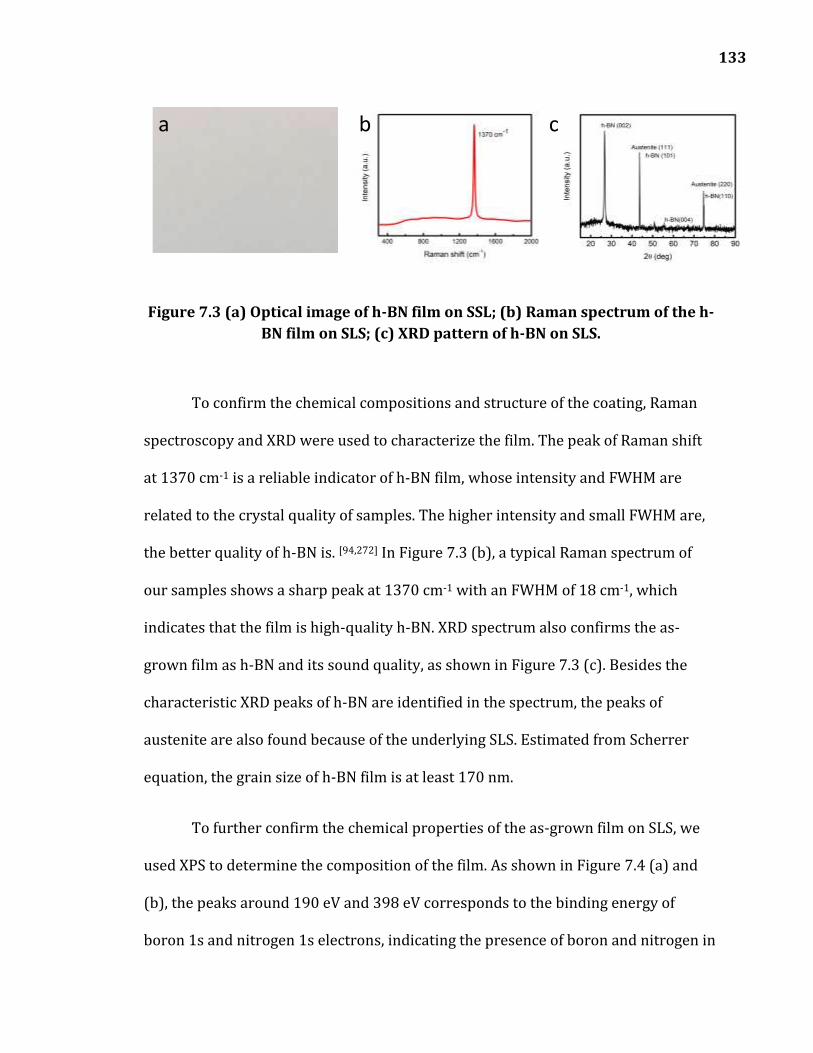
133
Figure 7.3 (a) Optical image of h-BN film on SSL; (b) Raman spectrum of the h-BN film on SLS; (c) XRD pattern of h-BN on SLS.
To confirm the chemical compositions and structure of the coating, Raman
spectroscopy and XRD were used to characterize the film. The peak of Raman shift
at 1370 cm-1 is a reliable indicator of h-BN film, whose intensity and FWHM are
related to the crystal quality of samples. The higher intensity and small FWHM are,
the better quality of h-BN is. [94,272] In Figure 7.3 (b), a typical Raman spectrum of
our samples shows a sharp peak at 1370 cm-1 with an FWHM of 18 cm-1, which
indicates that the film is high-quality h-BN. XRD spectrum also confirms the as-
grown film as h-BN and its sound quality, as shown in Figure 7.3 (c). Besides the
characteristic XRD peaks of h-BN are identified in the spectrum, the peaks of
austenite are also found because of the underlying SLS. Estimated from Scherrer
equation, the grain size of h-BN film is at least 170 nm.
To further confirm the chemical properties of the as-grown film on SLS, we
used XPS to determine the composition of the film. As shown in Figure 7.4 (a) and
(b), the peaks around 190 eV and 398 eV corresponds to the binding energy of
boron 1s and nitrogen 1s electrons, indicating the presence of boron and nitrogen in
a b c

134
the sample. The binding energies also mean the presence of boron-nitrogen binding
in the film.[281] The ratio of boron and nitrogen are determined to be 1.08:1, which is
consistent with the literature.[94] Combining all the information from Raman, XRD,
and XPS, it can be concluded that h-BN film was successfully grown on SLS.
Figure 7.4 XPS spectra of elements in h-BN on SLS. (a) B 1s at 190 eV; (b) N 1s at 398 eV; (c) Fe 2p3/2t 708 eV. (d) Depth profile of h-BN film on SLS
7.4.2. Estimation of thickness of grown h-BN
To estimate the thickness of the coating, we used XPS depth profile. The h-BN
film on SLS uniformly covered the whole SLS, which prohibits the application of
AFM to scan the edge of the film and determine its thickness. Because the hardness
of h-BN is greater than that of SLS, it is not easy to make a scratch on h-BN films
a b c
d

135
without damaging the SLS underneath, in which case an overestimate of the
thickness will be made. Therefore, XPS depth profile will be used. In this method,
XPS spectrum of a given area is collected each time after argon ions are used to
sputter away a layer of materials in the area. It provides the depth-dependent
chemical properties of the tested sample. Given a composite structure of our sample,
gradually decreasing peaks of B and N and a gradually increasing peak of Fe peaks
are expected. In Figure 7.4 (c), a typical XPS spectrum after long-time sputtering of
an area shows a strong peak of elemental iron.[281] The depth-dependent integrated
intensity of XPS peaks of B, N, and Fe are given in Figure 7.4 (d). As noted, the
intensities of B and N decreases and that of Fe increases as the cycles of argon
sputtering increases. This excludes the possibility of the alloying of h-BN and SLS
and demonstrates the composite structure of the sample. Given the depth
penetration capability of X-ray of 5 kV is limited to 5 nm[265] and that there is not Fe
signal at the beginning of the sputtering, we can conclude that the thickness of our
film is at least 5 nm. The depth of sputtering each cycle is estimated to be 15 nm by
experience, which means the thickness of h-BN could be hundreds of nanometers
since Fe signal became significant after several cycles.
To estimate the thickness of our coating more accurately, we used focused
ion beam (FIB) to create a cross-section of our sample and took an SEM image, as
shown in Figure 7.5. A typical SEM of the surface h-BN/SLS which is dramatically
different from the surface of untreated SLS in Figure 2 (a). Based on Figure 7.5 (b), it
is easy to estimate the thickness of the h-BN film is 0.2 µm given the view angle is
45°. Figure 7.5 (c) shows another bird view with higher magnification. The thickness

136
could be measured more accurately, and the result is 232 nm given the view angle is
52º. These results are consistent with the results in XPS profile.
Figure 7.5 (a) SEM image of the h-BN/SLS. (b) The bird-view of the cross-section of h-BN/SLS. (c) Zoom in the cross-section. The thickness of h-BN is
estimated to be 232 nm with the view angle considered.
7.4.3. Evaluation of proactive performance of h-BN
To demonstrate the protective performance of the h-BN thin film on SLS, we
used strong acid to etch the SLS. It is easy to understand that iron reacts with acid to
generate hydrogen slowly at room temperature and fast at elevated temperature,
which limits the use of SLS as containers of dilute acids and polymer coatings are
needed for most of the steel containers. As a highly inert chemical due to the
absence of dangling bonds, h-BN keeps inert at high temperature with all acids and
bases, which can protect the covered SLS. Since h-BN grows on both sides of the SLS,
it should protect it from the attack of acids and bases at the various circumstance.
Several pieces of the SLS with and without h-BN coating are immersed in 20 mL 1M
HCl solution, and the results are shown in Figure 7.6. As we can see, the h-BN
coating protects the SLS effectively. After eight days of reactions at room
2 µm
a b c
5�µm 5�µm
232�nm

137
temperature, the control was gone with only black residuals left (identified as Cr
dominating porous structure by SEM), and the one with h-BN coating was just
affected around the edges because of the little-exposed irons when the piece was cut
by the scissors. To estimate the performance of h-BN film in a longer period, we
used the elevated temperature to speed up the reaction rate, shown in Figure 7.7.
The solutions are heated to 90°C, and the reaction of HCl with the control is swift.
The control was gone totally in 180 minutes, and the coated sample was gone totally
after 1440 minutes etching. Therefore, it could be estimated that the h-BN could
protect the SLS as long as 64 days in a strong acid at ambient temperature. 1/8
etching rate of the uncoated one was achieved by the h-BN coating with exposed
edges. Without the exposed SLS edges, the etching rating is expected to be even
slower. The good protection performance of this h-BN coating is demonstrated well
here. This good protection also forbids the transfer of as-grown h-BN films to a new
substrate, which is the reason why the transfer technique was not adapted to
measure the thickness of as-grown films.[265]
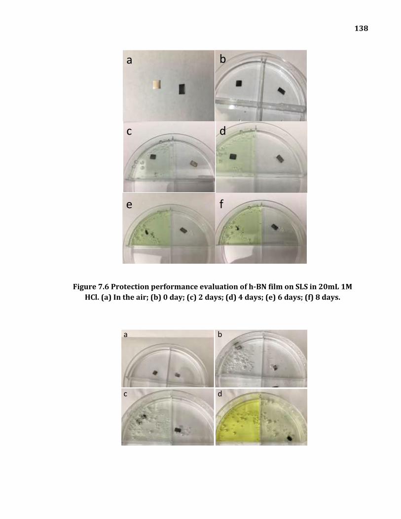
138
Figure 7.6 Protection performance evaluation of h-BN film on SLS in 20mL 1M HCl. (a) In the air; (b) 0 day; (c) 2 days; (d) 4 days; (e) 6 days; (f) 8 days.
a b
c d
e f
a b
c d

139
Figure 7.7 Evaluation of protection performance of the h-BN film on SLS in 20 mL 1M HCl at 90 °C. (a) 0 min; (b) 60 min (c) 180 min (d) 1440 min.
7.5. Summary
Using low-pressure CVD, we grew ultrathin h-BN films n on the surface of the
stainless steel without the need of the ultrahigh vacuum. The thickness of as-grown
h-BN films reaches hundreds of nanometers, which are supported by the
characterization of Raman, XRD, and XPS. The considerable intensity of peaks
indicates its high crystal quality. Their protection performance of covered stainless
steel in strong acidic condition at ambient and elevated temperature was
demonstrated. The ultrathin h-BN thin film was capable of protecting the SLS at
least 64 days in strongly acidic solution at ambient temperature. The large-scale and
high-quality h-BN thin film on stainless steels not just provides an effective anti-
corrosion coating but also advances the growth of chemically inert materials on
industrial substrates.

140
Chapter 8
Summary and Outlook
In this thesis, the interaction between 2D materials and different materials are
investigated, including MoS2 with oxygen, MoS2 with cells, MoS2 with self-assembled
molecules, MoSe2 with substrates with nanoscale pillars and h-BN with iron
substrates. With all these results, some conclusions and suggestions can be made:
1. As extremely thin materials, 2D materials will be evitably susceptible to the
environment than bulk materials, which build their advantage as biomedical
sensors of high sensitivity to molecules. Electricity of 2D materials has been
utilized in different areas, but other properties, such as Raman and PL,
should be considered since no built-in power supplier is needed in such
sensors.
2. MoS2 with tunable friction by electric doping is confirmed, and the effect
should be attributed to the extreme thinness of 2D materials. This might
provide a solution to the NEMS problem at the nanoscale which needs to
reduce frictions among their parts. Better NEMS devices are also essential for

141
large-scale applications of 2D materials since 2D materials need substrates to
support them. The electric doping level of 2D materials is still limited due to
the contaminated contact of 2D materials and electrodes, which might be
solved in the near future by in-situ growth and transfer of 2D materials in a
closed chamber.
3. 2H MoS2 are found to be quite safe for six different cells even at relatively
high concentration. However, more cells should be tested since there are
more than 200 kinds of cells in human body. Furthermore, few reports of the
in-vivo tests of 2D material have been reported. This will be an important
topic before the large-scale application of 2D materials.
4. Nanoscale pillars on silicon substrates are found to be able to offer a better
tool in CVD growth of 2D materials considering that the semiconductor
techniques used to fabricate such substrates are highly developed and
economically available. If we can fully control or affect the growth of 2D
materials via the interaction between substrates and materials, different
patterns and materials should be tried to find the best-patterned substrates
to grow 2D materials of desired properties.
5. h-BN can protect the underlying substrates very efficiently because of its
high stability in extreme conditions. With improved coverage on substrates,
the protection of this 2D material will perform better in anti-corrosion area.

142
h-BN should and will get more attention from industries than other 2D
materials
The applications of 2D materials are emerging as more 2D materials are being
synthesized and explored. However, the understanding of different aspects of
materials is far behind the accumulation of scientific facts. For example, no detailed
note has been made in the process of PL of 2D materials in different conditions, and
the growth process of 2D TMDs still lacks attention. The booming of 2D materials
already slows down, and it is time for us to analyze the facts that we have already
obtained a better and deeper understanding of 2D materials. The next boom of
nanomaterials will be fueled by the maturity of theories.
143
References
[1] K. S. Novoselov, A. K. Geim, S. V. Morozov, D. Jiang, Y. Zhang, S. V. Dubonos, I. V. Grigorieva, A. A. Firsov, Science (80-. ). 2004, 306, 666.
[2] L. Li, G. J. Ye, V. Tran, R. Fei, G. Chen, H. Wang, J. Wang, K. Watanabe, T. Taniguchi, L. Yang, X. H. Chen, Y. Zhang, Nat. Nanotechnol. 2015, 10, 608.
[3] X. Xu, W. Yao, D. Xiao, T. F. Heinz, Nat. Phys. 2014, 10, 343. [4] D. Wu, Z. Zhang, D. Lv, G. Yin, Z. Peng, C. Jin, Mater. Express 2016, 6, 198. [5] A. R. Kim, Y. Kim, J. Nam, H. S. Chung, D. J. Kim, J. D. Kwon, S. W. Park, J. Park, S.
Y. Choi, B. H. Lee, J. H. Park, K. H. Lee, D. H. Kim, S. M. Choi, P. M. Ajayan, M. G. Hahm, B. Cho, Nano Lett. 2016, 16, 1890.
[6] M. Ye, D. Winslow, D. Zhang, R. Pandey, Y. Yap, Photonics 2015, 2, 288. [7] C. Qin, Y. Gao, Z. Qiao, L. Xiao, S. Jia, Adv. Opt. Mater. 2016, 4, 1429. [8] H.-C. Kim, H. Kim, J.-U. Lee, H.-B. Lee, D.-H. Choi, J.-H. Lee, W. H. Lee, S. H. Jhang,
B. H. Park, H. Cheong, S.-W. Lee, H.-J. Chung, ACS Nano 2015, 9, 6854. [9] K. N. Duerloo, M. T. Ong, E. J. Reed, Environment 2012, 3, 2871. [10] H. Zhu, Y. Wang, J. Xiao, M. Liu, S. Xiong, Z. J. Wong, Z. Ye, Y. Ye, X. Yin, X. Zhang,
Nat. Nanotechnol. 2015, 10, 151. [11] W. Wu, L. Wang, Y. Li, F. Zhang, L. Lin, S. Niu, D. Chenet, X. Zhang, Y. Hao, T. F.
Heinz, J. Hone, Z. L. Wang, Nature 2014, 514, 470. [12] S. Manzeli, A. Allain, A. Ghadimi, A. Kis, Nano Lett. 2015, 15, 5330. [13] J. Shi, D. Ma, G.-F. Han, Y. Zhang, Q. Ji, T. Gao, J. Sun, C. Li, X.-Y. Lang, Y. Zhang, Z.
Liu, ACS 2014, 8, 10196. [14] D. Voiry, M. Salehi, R. Silva, T. Fujita, M. Chen, T. Asefa, V. B. Shenoy, G. Eda, M.
Chhowalla, Nano Lett. 2013, 13, 6222. [15] S. Wang, H. Ge, S. Sun, J. Zhang, F. Liu, X. Wen, X. Yu, L. Wang, Y. Zhang, H. Xu, J.
C. Neuefeind, Z. Qin, C. Chen, C. Jin, Y. Li, D. He, Y. Zhao, J. Am. Chem. Soc. 2015, 137, 4815.
[16] D. Voiry, H. Yamaguchi, J. Li, R. Silva, D. C. B. Alves, T. Fujita, M. Chen, T. Asefa, V. B. Shenoy, G. Eda, M. Chhowalla, Nat. Mater. 2013, 12, 850.
[17] D. Sarkar, W. Liu, X. Xie, A. C. Anselmo, S. Mitragotri, K. Banerjee, ACS Nano 2014, 8, 3992.
[18] S. Viswanathan, T. N. Narayanan, K. Aran, K. D. Fink, J. Paredes, P. M. Ajayan, S. Filipek, P. Miszta, H. C. Tekin, F. Inci, U. Demirci, P. Li, K. I. Bolotin, D. Liepmann, V. Renugopalakrishanan, Mater. Today 2015, 18, 513.
144
[19] Y. G. Spring, Statistical Physics, Perganmon, Oxford, 2004. [20] N. D. Mermin, Phys. Rev. 1968, 176, 250. [21] Y. Imry, L. Gunther, Phys. Rev. B 1971, 3, 3939. [22] J. C. Meyer, A. K. Geim, M. I. Katsnelson, K. S. Novoselov, T. J. Booth, S. Roth,
Nature 2007, 446, 60. [23] A. K. Geim, K. S. Novoselov, Nat. Mater. 2007, 6, 183. [24] A. H. C. Neto, F. Guinea, N. M. R. Peres, K. S. Novoselov, A. K. Geim, Rev. Mod.
Phys. 2007, 81, 109. [25] M. F. Khan, G. Nazir, V. M. Lermolenko, J. Eom, Sci. Technol. Adv. Mater. 2016,
17, 166. [26] B. Lalmi, H. Oughaddou, H. Enriquez, A. Kara, Ś. Vizzini, B. Ealet, B. Aufray,
Appl. Phys. Lett. 2010, 97, 2008. [27] B. Aufray, A. Kara, Ś. Vizzini, H. Oughaddou, C. Ĺandri, B. Ealet, G. Le Lay, Appl.
Phys. Lett. 2010, 96, 1. [28] L. Tao, E. Cinquanta, D. Chiappe, C. Grazianetti, M. Fanciulli, M. Dubey, A. Molle,
D. Akinwande, Nat. Nanotechnol. 2015, 10, 227. [29] K. A. N. Duerloo, Y. Li, E. J. Reed, Nat. Commun. 2014, 5, 1. [30] Y. Li, K. A. N. Duerloo, K. Wauson, E. J. Reed, Nat. Commun. 2016, 7, 1. [31] T. A. Empante, Y. Zhou, V. Klee, A. E. Nguyen, I. H. Lu, M. D. Valentin, S. A.
Naghibi Alvillar, E. Preciado, A. J. Berges, C. S. Merida, M. Gomez, S. Bobek, M. Isarraraz, E. J. Reed, L. Bartels, ACS Nano 2017, 11, 900.
[32] L. Li, Y. Yu, G. J. Ye, Q. Ge, X. Ou, H. Wu, D. Feng, X. H. Chen, Y. Zhang, Nat. Nanotechnol. 2014, 9, 372.
[33] S. Lei, L. Ge, Z. Liu, S. Najmaei, G. Shi, G. You, J. Lou, R. Vajtai, P. M. Ajayan, Nano Lett. 2013, 13, 2777.
[34] A. Splendiani, L. Sun, Y. Zhang, T. Li, J. Kim, C. Y. Chim, G. Galli, F. Wang, Nano Lett. 2010, 10, 1271.
[35] A. Ayari, E. Cobas, O. Ogundadegbe, M. S. Fuhrer, J. Appl. Phys. 2007, 101, 14507.
[36] H. Li, G. Lu, Y. Wang, Z. Yin, C. Cong, Q. He, L. Wang, F. Ding, T. Yu, H. Zhang, Small 2013, 9, 1974.
[37] J. S. Ross, S. Wu, H. Yu, N. J. Ghimire, A. M. Jones, G. Aivazian, J. Yan, D. G. Mandrus, D. Xiao, W. Yao, X. Xu, Nat. Commun. 2013, 4, 1474.
[38] Y. Huang, E. Sutter, J. T. Sadowski, M. Cotlet, O. L. A. Monti, D. A. Racke, M. R. Neupane, D. Wickramaratne, R. K. Lake, B. A. Parkinson, P. Sutter, ACS Nano 2014, 8, 10743.
[39] D. Lee, B. Lee, K. H. Park, H. J. Ryu, S. Jeon, S. H. Hong, Nano Lett. 2015, 15, 1238.

145
[40] N. Liu, F. Luo, H. Wu, Y. Liu, C. Zhang, J. Chen, Adv. Funct. Mater. 2008, 18, 1518.
[41] Y. Hernandez, V. Nicolosi, M. Lotya, F. M. Blighe, Z. Sun, S. De, I. T. McGovern, B. Holland, M. Byrne, Y. K. Gun’ko, J. J. Boland, P. Niraj, G. Duesberg, S. Krishnamurthy, R. Goodhue, J. Hutchison, V. Scardaci, A. C. Ferrari, J. N. Coleman, Nat. Nanotechnol. 2008, 3, 563.
[42] G. Eda, H. Yamaguchi, D. Voiry, T. Fujita, M. Chen, M. Chhowalla, Nano Lett. 2011, 11, 5111.
[43] A. Anto Jeffery, C. Nethravathi, M. Rajamathi, J. Phys. Chem. C 2014, 118, 1386. [44] J. N. Coleman, M. Lotya, A. O’Neill, S. D. Bergin, P. J. King, U. Khan, K. Young, A.
Gaucher, S. De, R. J. Smith, I. V. Shvets, S. K. Arora, G. Stanton, H. Y. Kim, K. Lee, G. T. Kim, G. S. Duesberg, T. Hallam, J. J. Boland, J. J. Wang, J. F. Donegan, J. C. Grunlan, G. Moriarty, A. Shmeliov, R. J. Nicholls, J. M. Perkins, E. M. Grieveson, K. Theuwissen, D. W. McComb, P. D. Nellist, V. Nicolosi, Science (80-. ). 2011, 331, 568.
[45] Y. Yong, L. Zhou, Z. Gu, L. Yan, G. Tian, X. Zheng, X. Liu, X. Zhang, J. Shi, W. Cong, W. Yin, Y. Zhao, Nanoscale 2014, 6, 10394.
[46] H. S. Mos, E. D. A. E. T. Al, ACS Nano 2012, 6, 7311. [47] D. Voiry, A. Mohite, M. Chhowalla, Chem. Soc. Rev. 2015, 44, 2702. [48] S. S. Chou, B. Kaehr, J. Kim, B. M. Foley, M. De, P. E. Hopkins, J. Huang, C. J.
Brinker, V. P. Dravid, Angew. Chemie - Int. Ed. 2013, 52, 4160. [49] Y. Shi, H. Li, L.-J. Li, Chem. Soc. Rev. 2015, 44, 2744. [50] M. Bosi, RSC Adv. 2015, 5, 75500. [51] Q. Ji, Y. Zhang, Y. Zhang, Z. Liu, Chem. Soc. Rev. 2015, 44, 2587. [52] S. Wu, C. Huang, G. Aivazian, J. S. Ross, D. H. Cobden, X. Xu, ACS Nano 2013, 7,
2768. [53] Y. Gong, G. Ye, S. Lei, G. Shi, Y. He, J. Lin, X. Zhang, R. Vajtai, S. T. Pantelides, W.
Zhou, B. Li, P. M. Ajayan, Adv. Funct. Mater. 2016, 26, 2009. [54] K. K. Liu, W. Zhang, Y. H. Lee, Y. C. Lin, M. T. Chang, C. Y. Su, C. S. Chang, H. Li, Y.
Shi, H. Zhang, C. S. Lai, L. J. Li, Nano Lett. 2012, 12, 1538. [55] J. H. Lee, E. K. Lee, W. J. Joo, Y. Jang, B. S. Kim, J. Y. Lim, S. H. Choi, S. J. Ahn, J. R.
Ahn, M. H. Park, C. W. Yang, B. L. Choi, S. W. Hwang, D. Whang, Science (80-. ). 2014, 344, 286.
[56] W. Chen, J. Zhao, J. Zhang, L. Gu, Z. Yang, X. Li, H. Yu, X. Zhu, R. Yang, D. Shi, X. Lin, J. Guo, X. Bai, G. Zhang, J. Am. Chem. Soc. 2015, 137, 15632.
[57] M. Amani, R. A. Burke, X. Ji, P. Zhao, D. H. Lien, P. Taheri, G. H. Ahn, D. Kirya, J. W. Ager, E. Yablonovitch, J. Kong, M. Dubey, A. Javey, ACS Nano 2016, 10, 6535.
[58] Y. Zhang, L. Zhang, C. Zhou, Acc. Chem. Res. 2013, 46, 2329.

146
[59] K. Zhang, Y. Feng, F. Wang, Z. Yang, J. Wang, J. Mater. Chem. C 2017, 5, 11992. [60] Y. Zhan, Z. Liu, S. Najmaei, P. M. Ajayan, J. Lou, Small 2012, 8, 966. [61] C. R. Wu, X. R. Chang, T. W. Chu, H. A. Chen, C. H. Wu, S. Y. Lin, Nano Lett. 2016,
16, 7093. [62] Y.-C. Lin, W. Zhang, J.-K. Huang, K.-K. Liu, Y.-H. Lee, C.-T. Liang, C.-W. Chu, L.-J.
Li, Nanoscale 2012, 4, 6637. [63] J. G. Song, J. Park, W. Lee, T. Choi, H. Jung, C. W. Lee, S. H. Hwang, J. M. Myoung,
J. H. Jung, S. H. Kim, C. Lansalot-Matras, H. Kim, ACS Nano 2013, 7, 11333. [64] X. Wang, H. Feng, Y. Wu, L. Jiao, J. Am. Chem. Soc. 2013, 135, 5304. [65] Y. Zhang, Q. Ji, J. Wen, J. Li, C. Li, J. Shi, X. Zhou, K. Shi, H. Chen, Y. Li, S. Deng, N.
Xu, Z. Liu, Y. Zhang, Adv. Funct. Mater. 2016, 26, 3299. [66] D. Seghete, G. B. Rayner, A. S. Cavanagh, V. R. Anderson, S. M. George, Chem.
Mater. 2011, 23, 1668. [67] R. Browning, P. Padigi, R. Solanki, D. J. Tweet, P. Schuele, D. Evans, Mater. Res.
Express 2015, 2, 35006. [68] N. D. Boscher, C. J. Carmalt, I. P. Parkin, J. Mater. Chem. 2006, 16, 122. [69] S. M. Eichfeld, L. Hossain, Y.-C. Lin, A. F. Piasecki, B. Kupp, A. G. Birdwell, R. A.
Burke, N. Lu, X. Peng, J. Li, A. Azcatl, S. McDonnell, R. M. Wallace, M. J. Kim, T. S. Mayer, J. M. Redwing, J. A. Robinson, ACS Nano 2015, 9, 2080.
[70] J. Park, W. Lee, T. Choi, S.-H. Hwang, J. M. Myoung, J.-H. Jung, S.-H. Kim, H. Kim, Nanoscale 2015, 7, 1308.
[71] V. Kranthi Kumar, S. Dhar, T. H. Choudhury, S. A. Shivashankar, S. Raghavan, Nanoscale 2015, 7, 7802.
[72] K. Kang, S. Xie, L. Huang, Y. Han, P. Y. Huang, K. F. Mak, C. J. Kim, D. Muller, J. Park, Nature 2015, 520, 656.
[73] S. Najmaei, Z. Liu, W. Zhou, X. Zou, G. Shi, S. Lei, B. I. Yakobson, J. C. Idrobo, P. M. Ajayan, J. Lou, Nat. Mater. 2013, 12, 754.
[74] A. M. Van Der Zande, P. Y. Huang, D. A. Chenet, T. C. Berkelbach, Y. You, G. H. Lee, T. F. Heinz, D. R. Reichman, D. A. Muller, J. C. Hone, Nat. Mater. 2013, 12, 554.
[75] Y. Yu, C. Li, Y. Liu, L. Su, Y. Zhang, L. Cao, Sci. Rep. 2013, 3, 1866. [76] Y. Zhang, Y. Zhang, Q. Ji, J. Ju, H. Yuan, J. Shi, T. Gao, D. Ma, M. Liu, Y. Chen, X.
Song, H. Y. Hwang, Y. Cui, Z. Liu, ACS Nano 2013, 7, 8963. [77] J. C. Shaw, H. Zhou, Y. Chen, N. O. Weiss, Y. Liu, Y. Huang, X. Duan, X. Wang, Y.
Gong, G. Shi, W. L. Chow, K. Keyshar, G. Ye, R. Vajtai, J. Lou, Z. Liu, E. Ringe, B. K. Tay, P. M. Ajayan, ACS Nano 2014, 8, 5125.
[78] J. C. Shaw, H. Zhou, Y. Chen, N. O. Weiss, Y. Liu, Y. Huang, X. Duan, Nano Res. 2014, 7, 511.
[79] B. Liu, M. Fathi, L. Chen, A. Abbas, Y. Ma, C. Zhou, ACS Nano 2015, 9, 6119.

147
[80] C. H. Naylor, W. M. Parkin, J. Ping, Z. Gao, Y. R. Zhou, Y. Kim, F. Streller, R. W. Carpick, A. M. Rappe, M. Drndić, J. M. Kikkawa, A. T. C. Johnson, Nano Lett. 2016, 16, 4297.
[81] J. Zhou, F. Liu, J. Lin, X. Huang, J. Xia, B. Zhang, Q. Zeng, H. Wang, C. Zhu, L. Niu, X. Wang, W. Fu, P. Yu, T. R. Chang, C. H. Hsu, D. Wu, H. T. Jeng, Y. Huang, H. Lin, Z. Shen, C. Yang, L. Lu, K. Suenaga, W. Zhou, S. T. Pantelides, G. Liu, Z. Liu, Adv. Mater. 2017, 29, DOI 10.1002/adma.201603471.
[82] K. Keyshar, Y. Gong, G. Ye, G. Brunetto, W. Zhou, D. P. Cole, K. Hackenberg, Y. He, L. Machado, M. Kabbani, A. H. C. Hart, B. Li, D. S. Galvao, A. George, R. Vajtai, C. S. Tiwary, P. M. Ajayan, Adv. Mater. 2015, 27, 4640.
[83] S. Zhao, T. Hotta, T. Koretsune, K. Watanabe, T. Taniguchi, K. Sugawara, T. Takahashi, H. Shinohara, R. Kitaura, 2D Mater. 2016, 3, 9.
[84] G. Su, V. G. Hadjiev, P. E. Loya, J. Zhang, S. Lei, S. Maharjan, P. Dong, P. M. Ajayan, J. Lou, H. Peng, Nano Lett. 2015, 15, 506.
[85] H. J. Chuang, B. Chamlagain, M. Koehler, M. M. Perera, J. Yan, D. Mandrus, D. Tománek, Z. Zhou, Nano Lett. 2016, 16, 1896.
[86] K. M. McCreary, A. T. Hanbicki, G. G. Jernigan, J. C. Culbertson, B. T. Jonker, Sci. Rep. 2016, 6, 19159.
[87] X. Ling, Y.-H. Lee, Y. Lin, W. Fang, L. Yu, M. S. Dresselhaus, J. Kong, Nano Lett. 2014, 14, 464.
[88] D. Kong, H. Wang, J. J. Cha, M. Pasta, K. J. Koski, J. Yao, Y. Cui, Nano Lett. 2013, 13, 1341.
[89] Y. Zhang, Q. Ji, G. Han, J. Ju, J. Shi, D. Ma, J. Sun, ACS Nano 2014, 8, 8617. [90] B. Li, Y. Gong, Z. Hu, G. Brunetto, Y. Yang, G. Ye, Z. Zhang, S. Lei, Z. Jin, E. Bianco,
X. Zhang, W. Wang, J. Lou, D. S. Galvão, M. Tang, B. I. Yakobson, R. Vajtai, P. M. Ajayan, Angew. Chemie - Int. Ed. 2016, 55, 10656.
[91] J. D. Cain, F. Shi, J. Wu, V. P. Dravid, ACS Nano 2016, 10, 5440. [92] Q. Ji, Y. Zhang, T. Gao, Y. Zhang, D. Ma, M. Liu, Y. Chen, X. Qiao, P. H. Tan, M.
Kan, J. Feng, Q. Sun, Z. Liu, Nano Lett. 2013, 13, 3870. [93] X. Li, W. Cai, J. An, S. Kim, J. Nah, D. Yang, R. Piner, A. Velamakanni, I. Jung, E.
Tutuc, S. K. Banerjee, L. Colombo, R. S. Ruoff, Science (80-. ). 2009, 324, 1312. [94] G. Lu, T. Wu, Q. Yuan, H. Wang, H. Wang, F. Ding, X. Xie, M. Jiang, Nat. Commun.
2015, 6, 1. [95] G. Binnig, C. F. Quate, Phys. Rev. Lett. 1986, 56, 930. [96] C. D. Frisbie, L. F. Rozsnyai, A. Noy, M. S. Wrighton, C. M. Lieber, Science (80-. ).
1994, 265, 2071. [97] A. Hammiche, H. M. Pollock, M. Reading, M. Claybourn, P. H. Turner, K. Jewkes,
Appl. Spectrosc. 1999, 53, 810. [98] P. Hu, J. Ye, X. He, K. Du, K. K. Zhang, X. Wang, Q. Xiong, Z. Liu, H. Jiang, C. Kloc,
148
Sci. Rep. 2016, 6, 24105. [99] H. Chen, X. Wen, J. Zhang, T. Wu, Y. Gong, X. Zhang, J. Yuan, C. Yi, J. Lou, P. M.
Ajayan, W. Zhuang, G. Zhang, J. Zheng, Nat. Commun. 2016, 7, 12512. [100] C. Lee, X. Wei, J. W. Kysar, J. Hone, Science (80-. ). 2008, 321, 385. [101] S. Bertolazzi, J. Brivio, A. Kis, ACS Nano 2011, 5, 9703. [102] S. M. Kim, A. Hsu, M. H. Park, S. H. Chae, S. J. Yun, J. S. Lee, D. H. Cho, W. Fang, C.
Lee, T. Palacios, M. Dresselhaus, K. K. Kim, Y. H. Lee, J. Kong, Nat. Commun. 2015, 6, 8662.
[103] S. Li, Q. Li, R. W. Carpick, P. Gumbsch, X. Z. Liu, X. Ding, J. Sun, J. Li, Nature 2016, 539, 541.
[104] T. Filleter, J. L. McChesney, A. Bostwick, E. Rotenberg, K. V. Emtsev, T. Seyller, K. Horn, R. Bennewitz, Phys. Rev. Lett. 2009, 102, 86102.
[105] E. Gnecco, R. Bennewitz, T. Gyalog, E. Meyer, J. Phys. Condens. Matter 2001, 13. [106] R. Bennewitz, Mater. Today 2005, 8, 42. [107] X. Guo, N. Mei, J. Food Drug Anal. 2014, 22, 105. [108] H. Gao, Y. Dong, A. Martini, Tribol. Int. 2014, 74, 57. [109] Y. Dong, J. Phys. D. Appl. Phys. 2014, 47, 55305. [110] A. Cammarata, T. Polcar, RSC Adv. 2015, 5, 106809. [111] A. Cammarata, T. Polcar, Inorg. Chem. 2015, 54, 5739. [112] A. C. Ferrari, D. M. Basko, Nat. Nanotechnol. 2013, 8, 235. [113] A. Jorio, E. H. M. Ferreira, M. V. O. Moutinho, F. Stavale, C. A. Achete, R. B.
Capaz, Phys. Status Solidi Basic Res. 2010, 247, 2980. [114] H. Li, Q. Zhang, C. C. R. Yap, B. K. Tay, T. H. T. Edwin, A. Olivier, D. Baillargeat,
Adv. Funct. Mater. 2012, 22, 1385. [115] N. A. Lanzillo, A. Glen Birdwell, M. Amani, F. J. Crowne, P. B. Shah, S. Najmaei, Z.
Liu, P. M. Ajayan, J. Lou, M. Dubey, S. K. Nayak, T. P. O’Regan, Appl. Phys. Lett. 2013, 103, DOI 10.1063/1.4819337.
[116] S. Sahoo, A. P. S. Gaur, M. Ahmadi, M. J. F. Guinel, R. S. Katiyar, J. Phys. Chem. C 2013, 117, 9042.
[117] K. G. Zhou, F. Withers, Y. Cao, S. Hu, G. Yu, C. Casiraghi, ACS Nano 2014, 8, 9914.
[118] M. Kayyalha, J. Maassen, M. Lundstrom, L. Shi, Y. P. Chen, J. Appl. Phys. 2016, 120, 134305.
[119] B. Smith, B. Vermeersch, J. Carrete, E. Ou, J. Kim, N. Mingo, D. Akinwande, L. Shi, Adv. Mater. 2017, 29.
[120] Y. Zhu, J. Yang, S. Zhang, S. Mokhtar, J. Pei, X. Wang, Y. Lu, Nanotechnology 2016, 27, 135706.
[121] M. S. Kim, G. Nam, S. Park, H. Kim, G. H. Han, J. Lee, K. P. Dhakal, J.-Y. Leem, Y.
149
H. Lee, J. Kim, Thin Solid Films 2015, 590, 318. [122] H. Nan, Z. Wang, W. Wang, Z. Liang, Y. Lu, Q. Chen, D. He, P. Tan, F. Miao, X.
Wang, J. Wang, Z. Ni, ACS Nano 2014, 8, 5738. [123] M. Amani, D. H. Lien, D. Kiriya, J. Xiao, A. Azcatl, J. Noh, S. R. Madhvapathy, R.
Addou, K. C. Santosh, M. Dubey, K. Cho, R. M. Wallace, S. C. Lee, J. H. He, J. W. Ager, X. Zhang, E. Yablonovitch, A. Javey, Science (80-. ). 2015, 350, 1065.
[124] S. Tongay, J. Suh, C. Ataca, W. Fan, A. Luce, J. S. Kang, J. Liu, C. Ko, R. Raghunathanan, J. Zhou, F. Ogletree, J. Li, J. C. Grossman, J. Wu, Sci. Rep. 2013, 3, 2657.
[125] P. K. Chow, R. B. Jacobs-Gedrim, J. Gao, T. M. Lu, B. Yu, H. Terrones, N. Koratkar, ACS Nano 2015, 9, 1520.
[126] N. Kang, H. P. Paudel, M. N. Leuenberger, L. Tetard, S. I. Khondaker, J. Phys. Chem. C 2014, 118, 21258.
[127] W. Su, L. Jin, X. Qu, D. Huo, L. Yang, Phys. Chem. Chem. Phys. 2016, 18, 14001. [128] Y. Li, Z. Qi, M. Liu, Y. Wang, X. Cheng, G. Zhang, L. Sheng, Nanoscale 2014, 6,
15248. [129] N. Scheuschner, O. Ochedowski, A. M. Kaulitz, R. Gillen, M. Schleberger, J.
Maultzsch, Phys. Rev. B - Condens. Matter Mater. Phys. 2014, 89, 2. [130] U. Bhanu, M. R. Islam, L. Tetard, S. I. Khondaker, Sci. Rep. 2015, 4, 5575. [131] J. Hou, X. Wang, D. Fu, C. Ko, Y. Chen, Y. Sun, S. Lee, K. X. Wang, K. Dong, Y. Sun,
S. Tongay, L. Jiao, J. Yao, K. Liu, J. Wu, Small 2016, 3976. [132] S. Mouri, Y. Miyauchi, K. Matsuda, Nano Lett. 2013, 13, 5944. [133] W. Su, H. Dou, D. Huo, N. Dai, L. Yang, Chem. Phys. Lett. 2015, 635, 40. [134] H. M. Oh, G. H. Han, H. Kim, M. S. Jeong, Curr. Appl. Phys. 2016, 16, 1223. [135] Y. Cheng, J. Z. Wang, X. X. Wei, D. Guo, B. Wu, L. W. Yu, X. R. Wang, Y. Shi,
Chinese Phys. Lett. 2015, 32, 117801. [136] W. Su, N. Kumar, S. J. Spencer, N. Dai, D. Roy, Nano Res. 2015, 8, 3878. [137] H. V. Han, A. Y. Lu, L. S. Lu, J. K. Huang, H. Li, C. L. Hsu, Y. C. Lin, M. H. Chiu, K.
Suenaga, C. W. Chu, H. C. Kuo, W. H. Chang, L. J. Li, Y. Shi, ACS Nano 2016, 10, 1454.
[138] G. Bai, S. Yuan, Y. Zhao, Z. Yang, S. Y. Choi, Y. Chai, S. F. Yu, S. P. Lau, J. Hao, Adv. Mater. 2016, 7472.
[139] Z. Li, S.-W. Chang, C.-C. Chen, S. B. Cronin, Nano Res. 2014, 7, 973. [140] G. Plechinger, F. X. Schrettenbrunner, J. Eroms, D. Weiss, C. Schüller, T. Korn,
Phys. Status Solidi - Rapid Res. Lett. 2012, 6, 126. [141] D. Kaplan, K. Mills, J. Lee, S. Torrel, V. Swaminathan, J. Appl. Phys. 2016, 119,
214301. [142] L. Yang, X. Cui, J. Zhang, K. Wang, M. Shen, S. Zeng, S. A. Dayeh, L. Feng, B.
150
Xiang, Sci. Rep. 2015, 4, 5649. [143] M. Dichalcogenides, J. Yuan, S. Najmaei, Z. Zhang, J. Zhang, S. Lei, P. M. Ajayan,
ACS Nano 2015, 9, 555. [144] S. Feng, M. C. Dos Santos, B. R. Carvalho, R. Lv, Q. Li, K. Fujisawa, A. L. Elías, Y.
Lei, N. Perea-López, M. Endo, M. Pan, M. A. Pimenta, M. Terrones, Sci. Adv. 2016, 2, e1600322.
[145] C. Huang, S. Wu, A. M. Sanchez, J. J. P. Peters, R. Beanland, J. S. Ross, P. Rivera, W. Yao, D. H. Cobden, X. Xu, Nat. Mater. 2014, 13, 1096.
[146] A. Kumar, P. K. Ahluwalia, Phys. B Condens. Matter 2013, 419, 66. [147] W. T. Hsu, Z. A. Zhao, L. J. Li, C. H. Chen, M. H. Chiu, P. S. Chang, Y. C. Chou, W. H.
Chang, ACS Nano 2014, 8, 2951. [148] J. J. Dean, H. M. Van Driel, Phys. Rev. B - Condens. Matter Mater. Phys. 2010, 82,
1. [149] S. J. Brun, T. G. Pedersen, Phys. Rev. B - Condens. Matter Mater. Phys. 2015, 91,
1. [150] J. L. Cheng, N. Vermeulen, J. E. Sipe, Sci. Rep. 2017, 7, 1. [151] G. A. Wagoner, P. D. Persans, E. A. Van Wagenen, G. M. Korenowski, J. Opt. Soc.
Am. B 1998, 15, 1017. [152] C. Janisch, Y. Wang, D. Ma, N. Mehta, A. L. Elías, N. Perea-López, M. Terrones, V.
Crespi, Z. Liu, Sci. Rep. 2014, 4, 1. [153] L. M. Malard, T. V. Alencar, A. P. M. Barboza, K. F. Mak, A. M. De Paula, Phys.
Rev. B - Condens. Matter Mater. Phys. 2013, 87, 1. [154] Y. Wang, J. Xiao, H. Zhu, Y. Li, Y. Alsaid, K. Y. Fong, Y. Zhou, S. Wang, W. Shi, Y.
Wang, A. Zettl, E. J. Reed, X. Zhang, Nature 2017, 550, 487. [155] N. Kumar, S. Najmaei, Q. Cui, F. Ceballos, P. M. Ajayan, J. Lou, H. Zhao, Phys. Rev.
B - Condens. Matter Mater. Phys. 2013, 87, 161403. [156] B. Radisavljevic, A. Radenovic, J. Brivio, V. Giacometti, A. Kis, Nat. Nanotechnol.
2011, 6, 147. [157] S. B. Desai, S. R. Madhvapathy, A. B. Sachid, J. P. Llinas, Q. Wang, G. H. Ahn, G.
Pitner, M. J. Kim, J. Bokor, C. Hu, H. S. P. Wong, A. Javey, Science (80-. ). 2016, 354, 99.
[158] L. Yang, K. Majumdar, H. Liu, Y. Du, H. Wu, M. Hatzistergos, P. Y. Hung, R. Tieckelmann, W. Tsai, C. Hobbs, P. D. Ye, Nano Lett. 2014, 14, 6275.
[159] R. Quhe, J. Zheng, G. Luo, Q. Liu, R. Qin, J. Zhou, D. Yu, S. Nagase, W. N. Mei, Z. Gao, J. Lu, NPG Asia Mater. 2012, 4, e16.
[160] W. Park, J. Park, J. Jang, H. Lee, H. Jeong, K. Cho, S. Hong, T. Lee, Nanotechnology 2013, 24, 95202.
[161] A. Sanne, R. Ghosh, A. Rai, H. C. P. Movva, A. Sharma, R. Rao, L. Mathew, S. K. Banerjee, Appl. Phys. Lett. 2015, 106.

151
[162] Y. Yoon, K. Ganapathi, S. Salahuddin, Nano Lett. 2011, 11, 3768. [163] Y. Liu, J. Guo, Y. Wu, E. Zhu, N. O. Weiss, Q. He, H. Wu, H. C. Cheng, Y. Xu, I.
Shakir, Y. Huang, X. Duan, Nano Lett. 2016, 16, 6337. [164] A. Nourbakhsh, A. Zubair, R. N. Sajjad, A. Tavakkoli K. G., W. Chen, S. Fang, X.
Ling, J. Kong, M. S. Dresselhaus, E. Kaxiras, K. K. Berggren, D. Antoniadis, T. Palacios, Nano Lett. 2016, acs. nanolett.6b03999.
[165] R. Kappera, D. Voiry, S. E. Yalcin, W. Jen, M. Acerce, S. Torrel, B. Branch, S. Lei, W. Chen, S. Najmaei, J. Lou, P. M. Ajayan, G. Gupta, A. D. Mohite, M. Chhowalla, APL Mater. 2014, 2.
[166] J. Wang, Q. Yao, C. W. Huang, X. Zou, L. Liao, S. Chen, Z. Fan, K. Zhang, W. Wu, X. Xiao, C. Jiang, W. W. Wu, Adv. Mater. 2016, 8302.
[167] Y. Tong, Z. Lin, J. T. L. Thong, D. S. H. Chan, C. Zhu, Appl. Phys. Lett. 2015, 107, 123105.
[168] Y. Du, H. Liu, A. T. Neal, M. Si, P. D. Ye, IEEE Electron Device Lett. 2013, 34, 1328.
[169] S. Wang, W. Zhao, F. Giustiniano, G. Eda, Phys. Chem. Chem. Phys. 2016, 18, 4304.
[170] J. Jiang, S. Dhar, Phys. Chem. Chem. Phys. 2016, 18, 685. [171] A. Pospischil, M. M. Furchi, T. Mueller, Nat. Nanotechnol. 2014, 9, 257. [172] M. L. Tsai, S. H. Su, J. K. Chang, D. S. Tsai, C. H. Chen, C. I. Wu, L. J. Li, L. J. Chen, J.
H. He, ACS Nano 2014, 8, 8317. [173] S. Lei, F. Wen, L. Ge, S. Najmaei, A. George, Y. Gong, W. Gao, Z. Jin, B. Li, J. Lou, J.
Kono, R. Vajtai, P. Ajayan, N. J. Halas, Nano Lett. 2015, 15, 3048. [174] R. S. Sundaram, M. Engel, A. Lombardo, R. Krupke, A. C. Ferrari, P. Avouris, M.
Steiner, Nano Lett. 2013, 13, 1416. [175] T. Shen, A. V. Penumatcha, J. Appenzeller, ACS Nano 2016, 10, 4712. [176] Q. He, Z. Zeng, Z. Yin, H. Li, S. Wu, X. Huang, H. Zhang, Small 2012, 8, 2994. [177] D. J. Late, Y. K. Huang, B. Liu, J. Acharya, S. N. Shirodkar, J. Luo, A. Yan, D.
Charles, U. V. Waghmare, V. P. Dravid, C. N. R. Rao, ACS Nano 2013, 7, 4879. [178] X. Liu, C. Tang, X. Du, S. Xiong, S. Xi, Y. Liu, X. Shen, Q. Zheng, Z. Wang, Y. Wu, A.
Horner, J.-K. Kim, Mater. Horizons 2017, 4, 477. [179] Y. Zhang, S. F. Ali, E. Dervishi, Y. Xu, Z. Li, D. Casciano, A. S. Biris, ACS Nano
2010, 4, 3181. [180] W. Z. Teo, E. L. K. Chng, Z. Sofer, M. Pumera, Chem. - A Eur. J. 2014, 20, 9627. [181] E. L. K. Chng, Z. Sofer, M. Pumera, Nanoscale 2014, 6, 14412. [182] X. Yang, J. Li, T. Liang, C. Ma, Y. Zhang, H. Chen, N. Hanagata, H. Su, M. Xu,
Nanoscale 2014, 6, 10126. [183] J. Wu, L. Ma, R. M. Yadav, Y. Yang, X. Zhang, R. Vajtai, J. Lou, P. M. Ajayan, ACS
152
Appl. Mater. Interfaces 2015, 7, 14763. [184] Z.-J. Wang, G. Weinberg, Q. Zhang, T. Lunkenbein, A. Klein-Hoffmann, M.
Kurnatowska, M. Plodinec, Q. Li, L. Chi, R. Schloegl, M.-G. Willinger, ACS Nano 2015, 9, 1506.
[185] J. A. Rodríguez-Manzo, Z. J. Qi, A. Crook, J.-H. Ahn, A. T. C. Johnson, M. Drndić, ACS Nano 2016, 10, 4004.
[186] F. K. Perkins, A. L. Friedman, E. Cobas, P. M. Campbell, G. G. Jernigan, B. T. Jonker, Nano Lett. 2013, 13, 668.
[187] P. T. K. Loan, W. Zhang, C. Te Lin, K. H. Wei, L. J. Li, C. H. Chen, Adv. Mater. 2014, 26, 4838.
[188] C. Zhu, Z. Zeng, H. Li, F. Li, C. Fan, H. Zhang, J. Am. Chem. Soc. 2013, 135, 5998. [189] S. Tongay, J. Zhou, C. Ataca, J. Liu, J. S. Kang, T. S. Matthews, L. You, J. Li, J. C.
Grossman, J. Wu, Nano Lett. 2013, 13, 2831. [190] L. Qi, Y. Wang, L. Shen, Y. Wu, Appl. Phys. Lett. 2016, 108, 63103. [191] S. Najmaei, Z. Liu, W. Zhou, X. Zou, G. Shi, S. Lei, B. I. Yakobson, J. C. Idrobo, P.
M. Ajayan, J. Lou, Nat. Mater. 2013, 12, 754. [192] C. Lee, H. Yan, L. E. Brus, T. F. Heinz, J. Hone, S. Ryu, ACS Nano 2010, 4, 2695. [193] M. M. Perera, M. W. Lin, H. J. Chuang, B. P. Chamlagain, C. Wang, X. Tan, M. M. C.
Cheng, D. Tománek, Z. Zhou, ACS Nano 2013, 7, 4449. [194] B. W. H. Baugher, H. O. H. Churchill, Y. Yang, P. Jarillo-Herrero, Nano Lett.
2013, 13, 4212. [195] Y. Lin, X. Ling, L. Yu, S. Huang, A. L. Hsu, Y. H. Lee, J. Kong, M. S. Dresselhaus, T.
Palacios, Nano Lett. 2014, 14, 5569. [196] S. H. El‐Mahalawy, B. L. Evans, Phys. Status Solidi 1977, 79, 713. [197] C. M. Mate, G. M. McClelland, R. Erlandsson, S. Chiang, Phys. Rev. Lett. 1987, 59,
1942. [198] N. Tayebi, A. A. Polycarpou, J. Appl. Phys. 2005, 98, 73528. [199] I. Szlufarska, M. Chandross, R. W. Carpick, J. Phys. D. Appl. Phys. 2008, 41,
123001. [200] a. Buldum, D. Leitner, S. Ciraci, Phys. Rev. B 1999, 59, 16042. [201] V. Popov, ZAMM - J. Appl. Math. Mech. / Zeitschrift für Angew. Math. und Mech.
2000, 80, 65. [202] J. Y. Park, D. F. Ogletree, P. A. Thiel, M. Salmeron, Science (80-. ). 2006, 313,
186. [203] Y. Qi, J. Y. Park, B. L. M. Hendriksen, D. F. Ogletree, M. Salmeron, Phys. Rev. B -
Condens. Matter Mater. Phys. 2008, 77, 1. [204] C. Lee, Q. Li, W. Kalb, X. Z. Liu, H. Berger, R. W. Carpick, J. Hone, Science (80-. ).
2010, 328, 76.
153
[205] Q. Li, K. S. Kim, A. Rydberg, Rev. Sci. Instrum. 2006, 77, 65105. [206] J. Hutter, J. Bechhoefer, Rev. Sci. Instrum. 1993, 64, 1868. [207] Q. Li, K. S. Kim, A. Rydberg, Rev. Sci. Instrum. 2006, 77, 1. [208] G. Kresse, J. Furthmüller, Phys. Rev. B 1996, 54, 11169. [209] G. Kresse, D. Joubert, Phys. Rev. B 1999, 59, 1758. [210] P. E. Blöchl, Phys. Rev. B 1994, 50, 17953. [211] J. Ihm, A. Zunger, M. L. Cohen, J. Phys. C Solid State Phys. 1979, 12, 4409. [212] G. Henkelman, A. Arnaldsson, H. Jónsson, Comput. Mater. Sci. 2006, 36, 354. [213] C. Celle, C. Suspène, M. Ternisien, S. Lenfant, D. Guérin, K. Smaali, K. Lmimouni,
J. P. Simonato, D. Vuillaume, Org. Electron. physics, Mater. Appl. 2014, 15, 729. [214] S. Najmaei, X. Zou, D. Er, J. Li, Z. Jin, W. Gao, Q. Zhang, S. Park, L. Ge, S. Lei, J.
Kono, V. B. Shenoy, B. I. Yakobson, A. George, P. M. Ajayan, J. Lou, Nano Lett. 2014, 14, 1354.
[215] A. K. M. Newaz, D. Prasai, J. I. Ziegler, D. Caudel, S. Robinson, R. F. Haglund, K. I. Bolotin, Solid State Commun. 2013, 155, 49.
[216] W. Melitz, J. Shen, A. C. Kummel, S. Lee, Surf. Sci. Rep. 2011, 66, 1. [217] H. Li, Z. Yin, Q. He, H. Li, X. Huang, G. Lu, D. W. H. Fam, A. I. Y. Tok, Q. Zhang, H.
Zhang, Small 2012, 8, 63. [218] P. M. Ajayan, J. M. Tour, Nature 2007, 447, 1066. [219] Y. Tu, M. Lv, P. Xiu, T. Huynh, M. Zhang, M. Castelli, Z. Liu, Q. Huang, C. Fan, H.
Fang, R. Zhou, Nat. Nanotechnol. 2013, 8, 594. [220] J. Mao, R. Guo, L. T. Yan, Biomaterials 2014, 35, 6069. [221] J. Mao, P. Chen, J. Liang, R. Guo, L. T. Yan, ACS Nano 2016, 10, 1493. [222] P. Chen, Z. Huang, J. Liang, T. Cui, X. Zhang, B. Miao, L. T. Yan, ACS Nano 2016,
10, 11541. [223] K. Kalantar-zadeh, J. Z. Ou, T. Daeneke, M. S. Strano, M. Pumera, S. L. Gras, Adv.
Funct. Mater. 2015, 25, 5086. [224] J. Fan, Y. Li, H. N. Nguyen, Y. Yao, D. F. Rodrigues, Environ. Sci. Nano 2015, 2,
370. [225] X. Wang, N. D. Mansukhani, L. M. Guiney, Z. Ji, C. H. Chang, M. Wang, Y. P. Liao,
T. Bin Song, B. Sun, R. Li, T. Xia, M. C. Hersam, A. E. Nel, Small 2015, 11, 5079. [226] T. Liu, C. Wang, X. Gu, H. Gong, L. Cheng, X. Shi, L. Feng, B. Sun, Z. Liu, Adv.
Mater. 2014, 26, 3433. [227] A. T. Ward, J. Phys. Chem. 1968, 72, 4133. [228] Y. Ohno, K. Maehashi, Y. Yamashiro, K. Matsumoto, Nano Lett. 2009, 9, 3318. [229] C. Ruppert, O. B. Aslan, T. F. Heinz, Nano Lett. 2014, 14, 6231. [230] Y. Kim, H. Bark, G. H. Ryu, Z. Lee, C. Lee, J. Phys. Condens. Matter 2016, 28,

154
184002. [231] M. Okada, T. Sawazaki, K. Watanabe, T. Taniguch, H. Hibino, H. Shinohara, R.
Kitaura, ACS Nano 2014, 8, 8273. [232] Z. Zhang, X. Ji, J. Shi, X. Zhou, S. Zhang, Y. Hou, Y. Qi, Q. Fang, Q. Ji, Y. Zhang, M.
Hong, P. Yang, X. Liu, Q. Zhang, L. Liao, C. Jin, Z. Liu, Y. Zhang, ACS Nano 2017, 11, 4328.
[233] J. Chen, X. Zhao, S. J. R. Tan, H. Xu, B. Wu, B. Liu, D. Fu, W. Fu, D. Geng, Y. Liu, W. Liu, W. Tang, L. Li, W. Zhou, T. C. Sum, K. P. Loh, J. Am. Chem. Soc. 2017, 139, 1073.
[234] C. M. Orofeo, S. Suzuki, H. Hibino, J. Phys. Chem. C 2014, 118, 3340. [235] L. Chen, B. Liu, A. N. Abbas, Y. Ma, X. Fang, Y. Liu, C. Zhou, ACS Nano 2014, 8,
11543. [236] Y. Gong, G. Ye, S. Lei, G. Shi, Y. He, J. Lin, X. Zhang, R. Vajtai, S. T. Pantelides, W.
Zhou, B. Li, P. M. Ajayan, Adv. Funct. Mater. 2016, 26, 2009. [237] Q. Ji, M. Kan, Y. Zhang, Y. Guo, D. Ma, J. Shi, Q. Sun, Q. Chen, Y. Zhang, Z. Liu,
Nano Lett. 2015, 15, 198. [238] L. Chen, B. Liu, M. Ge, Y. Ma, A. N. Abbas, C. Zhou, ACS Nano 2015, 9, 8368. [239] T. Yanase, S. Watanabe, M. Weng, M. Wakeshima, Y. Hinatsu, T. Nagahama, T.
Shimada, Cryst. Growth Des. 2016, 16, 4467. [240] W. Ge, K. Kawahara, M. Tsuji, H. Ago, Nanoscale 2013, 5, 5773. [241] J. W. Ho, Q. Wee, J. Dumond, A. Tay, S. J. Chua, Nanoscale Res. Lett. 2013, 8, 1. [242] I. Steinbach, F. Pezzolla, Phys. D Nonlinear Phenom. 1999, 134, 385. [243] V. I. Artyukhov, Z. Hu, Z. Zhang, B. I. Yakobson, Nano Lett. 2016, 16, 3696. [244] Y. Yang, X. Li, M. Wen, E. Hacopian, W. Chen, Y. Gong, J. Zhang, B. Li, W. Zhou, P.
M. Ajayan, Q. Chen, T. Zhu, J. Lou, Adv. Mater. 2017, 29, 1. [245] Y. He, A. Sobhani, S. Lei, Z. Zhang, Y. Gong, Z. Jin, W. Zhou, Y. Yang, Y. Zhang, X.
Wang, B. Yakobson, R. Vajtai, N. J. Halas, B. Li, E. Xie, P. Ajayan, Adv. Mater. 2016, 28, 5126.
[246] S. H. El-Mahalawy, B. L. Evans, J. Appl. Crystallogr. 1976, 9, 403. [247] D. Dumcenco, D. Ovchinnikov, K. Marinov, P. Lazić, M. Gibertini, N. Marzari, O.
L. Sanchez, Y. C. Kung, D. Krasnozhon, M. W. Chen, S. Bertolazzi, P. Gillet, A. Fontcuberta I Morral, A. Radenovic, A. Kis, ACS Nano 2015, 9, 4611.
[248] D. Cao, T. Shen, P. Liang, X. Chen, H. Shu, J. Phys. Chem. C 2015, 119, 4294. [249] J. A. G. Sheneve Z. Butler, Shawna M. Hollen, Linyou Cao, Yi Cui, ACS Nano
2013, 7, 2898. [250] M. Xu, T. Liang, M. Shi, H. Chen, Chem. Rev. 2013, 113, 3766. [251] X. Mao, Y. Xu, Q. Xue, W. Wang, D. Gao, Nanoscale Res. Lett. 2013, 8, 1. [252] G. Ye, Y. Gong, J. Lin, B. Li, Y. He, S. T. Pantelides, W. Zhou, R. Vajtai, P. M.

155
Ajayan, Nano Lett. 2016, 16, 1097. [253] D. H. Kim, D. Lim, J. Korean Phys. Soc. 2015, 66, 816. [254] R. W. Boyd, Nonlinear Optics, Academinc, San Diego, 2008. [255] R. M. Chiles, Agric. Human Values 2013, 30, 511. [256] M. A. Malik, M. A. Hashim, F. Nabi, S. A. AL-Thabaiti, Z. Khan, Int. J. Electrochem.
Sci. 2011, 6, 1927. [257] S. Vandana, V. Kochat, J. Lee, V. Varshney, S. Yazdi, J. Shen, S. Kosolwattana, S.
Vinod, R. Vajtai, A. K. Roy, C. S. Tiwary, P. M. Ajayan, J. Phys. D. Appl. Phys. 2017, 50.
[258] A. F. Khan, D. A. C. Brownson, C. W. Foster, G. C. Smith, C. E. Banks, Analyst 2017, 142, 1756.
[259] G. H. Lee, Y. J. Yu, X. Cui, N. Petrone, C. H. Lee, M. S. Choi, D. Y. Lee, C. Lee, W. J. Yoo, K. Watanabe, T. Taniguchi, C. Nuckolls, P. Kim, J. Hone, ACS Nano 2013, 7, 7931.
[260] M. K. L. Man, S. Deckoff-Jones, A. Winchester, G. Shi, G. Gupta, A. D. Mohite, S. Kar, E. Kioupakis, S. Talapatra, K. M. Dani, Sci. Rep. 2016, 6, 9.
[261] A. Yan, J. Velasco, S. Kahn, K. Watanabe, T. Taniguchi, F. Wang, M. F. Crommie, A. Zettl, Nano Lett. 2015, 15, 6324.
[262] Z. Liu, Y. Gong, W. Zhou, L. Ma, J. Yu, J. C. Idrobo, J. Jung, A. H. Macdonald, R. Vajtai, J. Lou, P. M. Ajayan, Nat. Commun. 2013, 4, 2541.
[263] X. Chen, P. Wu, M. Rousseas, D. Okawa, Z. Gartner, A. Zettl, C. R. Bertozzi, J. Am. Chem. Soc. 2009, 131, 890.
[264] M. A. I. Rasel, T. Li, T. D. Nguyen, Y. T. Gu, in 7th WACBE World Congr. Bioeng. 2015, 2015, pp. 31–34.
[265] Y. Shi, C. Hamsen, X. Jia, K. K. Kim, A. Reina, M. Hofmann, A. L. Hsu, K. Zhang, H. Li, Z. Y. Juang, M. S. Dresselhaus, L. J. Li, J. Kong, Nano Lett. 2010, 10, 4134.
[266] Y.-H. Lee, K.-K. Liu, A.-Y. Lu, C.-Y. Wu, C.-T. Lin, W. Zhang, C.-Y. Su, C.-L. Hsu, T.-W. Lin, K.-H. Wei, Y. Shi, L.-J. Li, RSC Adv. 2012, 2, 111.
[267] K. K. Kim, A. Hsu, X. Jia, S. M. Kim, Y. Shi, M. Hofmann, D. Nezich, J. F. Rodriguez-Nieva, M. Dresselhaus, T. Palacios, J. Kong, Nano Lett. 2012, 12, 161.
[268] L. Song, L. Ci, H. Lu, P. B. Sorokin, C. Jin, J. Ni, A. G. Kvashnin, D. G. Kvashnin, J. Lou, B. I. Yakobson, P. M. Ajayan, Nano Lett. 2010, 10, 3209.
[269] J. Han, J. Y. Lee, H. Kwon, J. S. Yeo, Nanotechnology 2014, 25, 145604. [270] G. Kim, A. R. Jang, H. Y. Jeong, Z. Lee, D. J. Kang, H. S. Shin, Nano Lett. 2013, 13,
1834. [271] Y. Gao, W. Ren, T. Ma, Z. Liu, Y. Zhang, W. Bin Liu, L. P. Ma, X. Ma, H. M. Cheng,
ACS Nano 2013, 7, 5199. [272] J. H. Park, J. C. Park, S. J. Yun, H. Kim, D. H. Luong, S. M. Kim, S. H. Choi, W. Yang,
156
J. Kong, K. K. Kim, Y. H. Lee, ACS Nano 2014, 8, 8520. [273] C. M. Orofeo, S. Suzuki, H. Kageshima, H. Hibino, Nano Res. 2013, 6, 335. [274] S. Caneva, R. S. Weatherup, B. C. Bayer, B. Brennan, S. J. Spencer, K. Mingard, A.
Cabrero-Vilatela, C. Baehtz, A. J. Pollard, S. Hofmann, Nano Lett. 2015, 15, 1867.
[275] G. Lu, T. Wu, P. Yang, Y. Yang, Z. Jin, W. Chen, S. Jia, H. Wang, G. Zhang, J. Sun, P. M. Ajayan, J. Lou, X. Xie, M. Jiang, Adv. Sci. 2017, 4.
[276] S. Behura, P. Nguyen, S. Che, R. Debbarma, V. Berry, J. Am. Chem. Soc. 2015, 137, 13060.
[277] E. Husain, T. N. Narayanan, J. J. Taha-Tijerina, S. Vinod, R. Vajtai, P. M. Ajayan, ACS Appl. Mater. Interfaces 2013, 5, 4129.
[278] R. H. Stulen, J. Vac. Sci. Technol. 1979, 16, 940. [279] T. Takahashi, H. Itoh, A. Takeuchi, J. Cryst. Growth 1979, 47, 245. [280] D. Fujita, J. Vac. Sci. Technol. A Vacuum, Surfaces, Film. 1988, 6, 230. [281] J. F. Moulder, W. F. Stickle, P. E. Sobol, K. D. Bomben, The Handbook of X-Ray
Photoelectron Spectroscopy, Physical Electronics, Inc., Eden Prairie, 1995.