Innovative and Useful Laboratory Experiments of Electrical ...
165
Vinicius Silva Angelo Rezek Carlos Camacho Innovative and Useful Laboratory Experiments of Electrical Machines Electrical Machines Controls and Operations Innovative and Useful Laboratory Experiments of Electrical Machines This work consists of simple and innovative experiments at the beginning and, as work advances, the experiments become themselves bigger and with more details. The last topics show the analysis of induction and synchronous generators in parallel operation mode and their transients. This work intends to present some innovative and relevant experiments and concepts to electrical machines applications. All chapters show innovations and they are interconnected so that the readers have a wide understanding about these new ways of electrical machines control and operation. Vinicius Zimmermann Silva graduated in Electrical Engineering at EFEI, Brazil, in 1998. He obtained MSc degree at UNIFEI in 2004 and MBA degree at FGV in 2011. He worked at ALSTOM for six years and at FURNAS for almost one year. Zimmermann who has been working at PETROBRAS since 2005 is in the final stage of his doctorate degree at UNIFEI. 978-620-2-31727-6 Electrical Machines Controls Silva, Rezek, Camacho
-
Upload
khangminh22 -
Category
Documents
-
view
1 -
download
0
Transcript of Innovative and Useful Laboratory Experiments of Electrical ...

Vinicius SilvaAngelo RezekCarlos Camacho
Innovative and UsefulLaboratory Experiments ofElectrical MachinesElectrical Machines Controls and Operations
Innovative and Useful Laboratory Experimentsof Electrical MachinesThis work consists of simple and innovative experiments at thebeginning and, as work advances, the experiments become themselvesbigger and with more details. The last topics show the analysis ofinduction and synchronous generators in parallel operation mode andtheir transients. This work intends to present some innovative andrelevant experiments and concepts to electrical machines applications.All chapters show innovations and they are interconnected so that thereaders have a wide understanding about these new ways of electricalmachines control and operation.
Vinicius Zimmermann Silva graduated in ElectricalEngineering at EFEI, Brazil, in 1998. He obtainedMSc degree at UNIFEI in 2004 and MBA degree atFGV in 2011. He worked at ALSTOM for six yearsand at FURNAS for almost one year. Zimmermannwho has been working at PETROBRAS since 2005is in the final stage of his doctorate degree atUNIFEI.
978-620-2-31727-6
Electrical Mach
ines C
on
trols
Silva, Rezek, Camacho

������������
����������
�������������
�������������������������������� !"������������ �������
#�������


������������ ����������
�������������
������������������������������� !"������������ ��������#�������
��������#��������������������$"��������
���������� ����������

������������������������� ������������������������������������������������������� ����� ��� ������ ���������� ��� ���� ��������� ��� ������������������ ��� ������ ��� ������� �������� ���� ���� ��� ����� ������ ��������������������������������� ����������� ������������������������� �������������������������������������������������������������������������� �������� ��� ������� ��� ������������ ��� ��� ���� ��� �������� ������� ����������������������������������������������������
��������������������������
���������!�������"� �������������������#�������������$����%������!�������&������������'��!��� ��� ���������(��� )*�%�����!�������$����$������*)+,-��%�������� ������������������� ������� �����������������
�� �������.�/��������!�������������0�1������������������� ������� .� 2,)3� #������������� $���� %������ !������� &���� ����� ��'��!��� ��� ����������(���

Innovative and Useful LaboratoryExperiments of Electrical Machines
Vinicius Zimmermann Silva
Angelo José Junqueira RezekCarlos Alexandre Pereira Camacho

Acknowledgements
I owe my most sincere and deepest thanks to God due to the grace of our lives, to
my professor adviser and friend Angelo José Junqueira Rezek who always motivated and
helped me as well as to my parents Maria das Graças Zimmermann Silva and Jose Carlos
Ferreira da Silva who have always been on my side.
I also thank my friend and university co-worker Christel Enock Ghislain Ogoulola
for assistance in conversion to LATEX of this work.
Finally, I thank the UNIFEI technicians José Airton de Freitas, Adair Salvado
Junior and Jorge Wilson Rosa for assistance in my workbench at laboratory of research
development of electrical didactic laboratory of Federal University of Itajubá.

"You don’t start out writing good stuff. You start out writing crap and thinking it is good
stuff, and then gradually you get better at it.
That’s why I say one of the most valuable traits is persistence.”
(Octavia E. Butler)

Abstract
This work aims to present new contributions for electrical machines application studies,
mainly about analysis of induction and synchronous generators in parallel operation mode.
Then, in summary, the main topics presented in this work are: an analysis of induction
and synchronous generators in parallel operation mode and studies of load and generation
transients. All of this main subject are supported by appendixes that contributes with
practical and original studies related to each subsystem that is part of main experiments
such as: (i) voltage and current regulators for DC machines, (ii) firing circuit, (iii) voltage
regulators to synchronous generators, (iv) four-quadrant Driven System for DC Machine
and (v) analogical and digital control boards.
Key-words: Asynchronous Generator, Closed loop Control, Induction Generator, Iso-
lated Electric System, Generators in Parallel, Synchronous Generator.

List of Figures
Figure 1.1 – Electric Scheme . . . . . . . . . . . . . . . . . . . . . . . . . . . . . . . 24
Figure 1.2 – MP 410T in Speed Control loop . . . . . . . . . . . . . . . . . . . . . . 25
Figure 1.3 – MP 410T in Voltage Control loop . . . . . . . . . . . . . . . . . . . . . 25
Figure 1.4 – Speed Control Loop . . . . . . . . . . . . . . . . . . . . . . . . . . . . 28
Figure 1.5 – Field Voltage Control Loop . . . . . . . . . . . . . . . . . . . . . . . . 28
Figure 1.6 – Converter Configuration used for control Operational Scenarios . . . . 28
Figure 1.7 – Electronic Board MP410T and Connections . . . . . . . . . . . . . . . 29
Figure 1.8 – Circuit boards MP410T used to implement the Control Loops . . . . . 29
Figure 1.9 – Laboratory assembly in the laboratory of research development of elec-
trical didactic laboratory of Federal University of Itajubá . . . . . . . . 35
Figure 1.10–Synchronous and Induction Generators in parallel Operation Mode
with Steady Armature Voltage for DCMIG (Variation of DCMIG field
flux by field Rheostat) . . . . . . . . . . . . . . . . . . . . . . . . . . . 36
Figure 1.11–Synchronous and Induction Generators in Parallel Operation mode
with Variable Armature Voltage for DCMIG (DCMIG Steady field flux) 36
Figure 1.12–Synchronous and Induction Generators in Parallel Operation mode
with Variable Armature Voltage for DCMIG and an Induction Motor
as Load (DCMIG Steady field flux) . . . . . . . . . . . . . . . . . . . . 37
Figure 1.13–Conjugate vs rpm - Induction Motor and Generator . . . . . . . . . . . 37
Figure 1.14–PIG vs PSG with DCMIG Field Variation and V aDCMIG kept Constant 42
Figure 1.15–PIG vs PSG with V aDCMIG Variation and Field flux kept Constant
(Only resistive load) . . . . . . . . . . . . . . . . . . . . . . . . . . . . 43
Figure 1.16–PIG vs PSG with V aDCMIG Variation and Field Flux kept Constant
(Resistive load & IM) . . . . . . . . . . . . . . . . . . . . . . . . . . . . 43
Figure 1.17–PDCMIG vs PDCMSG with DCMIG Field Flux Variation and V aDCMIG
Kept Constant . . . . . . . . . . . . . . . . . . . . . . . . . . . . . . . 44
Figure 1.18–VSG (Synchronous generator voltage) x fSG (Synchronous generator fre-
quency) x Iload (Load current) . . . . . . . . . . . . . . . . . . . . . . . 44
Figure 1.19–PDCMIG vs PDCMSG with V aDCMIG Variation and Field Flux Kept
Constant (Only resistive load) . . . . . . . . . . . . . . . . . . . . . . 45
Figure 1.20–PDCMIG vs PDCMSG with V aDCMIG Variation and Field Flux Kept
Constant (Resistive load plus IM) . . . . . . . . . . . . . . . . . . . . 45
Figure 1.21–nIG vs nSG with DCMIG Field Flux Variation and V aDCMIG Kept
Constant . . . . . . . . . . . . . . . . . . . . . . . . . . . . . . . . . . 46
Figure 1.22–nIG vs nSG with V aDCMIG Variation and Field Flux kept Constant
(Only resistive load) . . . . . . . . . . . . . . . . . . . . . . . . . . . . 46
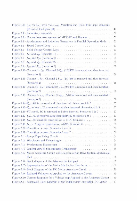
Figure 1.23–nIG vs nSG with V aDCMIG Variation and Field Flux kept Constant
(Resistive load plus IM) . . . . . . . . . . . . . . . . . . . . . . . . . . 47
Figure 2.1 – Laboratory Assembly . . . . . . . . . . . . . . . . . . . . . . . . . . . 52
Figure 2.2 – Connections Arrangement of MP410T and Devices . . . . . . . . . . . 52
Figure 2.3 – Synchronous and Induction Generators in Parallel Operation Mode . . 53
Figure 2.4 – Speed Control Loop . . . . . . . . . . . . . . . . . . . . . . . . . . . . 53
Figure 2.5 – Field Voltage Control Loop . . . . . . . . . . . . . . . . . . . . . . . . 53
Figure 2.6 – IIG and Vpn (Scenario 1) . . . . . . . . . . . . . . . . . . . . . . . . . . 55
Figure 2.7 – ISG and Vpn (Scenario 1) . . . . . . . . . . . . . . . . . . . . . . . . . . 55
Figure 2.8 – IIG and Vpn (Scenario 2) . . . . . . . . . . . . . . . . . . . . . . . . . . 55
Figure 2.9 – ISG and Vpn (Scenario 2) . . . . . . . . . . . . . . . . . . . . . . . . . . 55
Figure 2.10–Channel 1- ISG, Channel 2-Vpn. (2/3 kW is removed and then inserted)
(Scenario 2) . . . . . . . . . . . . . . . . . . . . . . . . . . . . . . . . . 56
Figure 2.11–Channel 1-IIG, Channel 2-Vpn. (2/3 kW is removed and then inserted)
(Scenario 2) . . . . . . . . . . . . . . . . . . . . . . . . . . . . . . . . . 56
Figure 2.12–Channel 1- nSG, Channel 2- IIG. (2/3 kW is removed and then inserted.)
(Scenario 2) . . . . . . . . . . . . . . . . . . . . . . . . . . . . . . . . . 56
Figure 2.13–Channel 1- nSG, Channel 2- ISG. (2/3 kW is removed and then inserted.)
(Scenario 2) . . . . . . . . . . . . . . . . . . . . . . . . . . . . . . . . . 56
Figure 2.14–Vpn, SG is removed and then inserted. Scenarios 4 & 5 . . . . . . . . . 57
Figure 2.15–Vpn in load. IG is removed and then inserted. Scenarios 4 & 5 . . . . . 57
Figure 2.16–SG speed. IG is removed and then inserted. Scenarios 6 & 7 . . . . . . 57
Figure 2.17–ISG, IG is removed and then inserted. Scenarios 6 & 7 . . . . . . . . . 57
Figure 2.18–ISG. SG smallest contribution = 0.4A. Scenario 3 . . . . . . . . . . . . 58
Figure 2.19–IIG, IG biggest contribution =6.9A. Scenario 3 . . . . . . . . . . . . . 58
Figure 2.20–Transition between Scenarios 4 and 5 . . . . . . . . . . . . . . . . . . . 58
Figure 2.21–Transition between Scenarios 6 and 7 . . . . . . . . . . . . . . . . . . . 58
Figure A.1–Ramp Type Firing Circuit . . . . . . . . . . . . . . . . . . . . . . . . . 64
Figure A.2–Waveforms and Firing Angle . . . . . . . . . . . . . . . . . . . . . . . . 64
Figure A.3–Synchronism Transformer . . . . . . . . . . . . . . . . . . . . . . . . . 65
Figure A.4–General view of Synchronism Transformer . . . . . . . . . . . . . . . . 65
Figure A.5–Motor Armature Circuit and Diagram of the Drive System Mechanical
Part . . . . . . . . . . . . . . . . . . . . . . . . . . . . . . . . . . . . . 66
Figure A.6–Block diagram of the drive mechanical part . . . . . . . . . . . . . . . 67
Figure A.7–Representation of the Motor Mechanical Part in pu . . . . . . . . . . . 68
Figure A.8–Block Diagram of the DC Motor Armature Circuit . . . . . . . . . . . 70
Figure A.9–Reduced Voltage step Applied to the Armature Circuit . . . . . . . . . 70
Figure A.10–Current Response for a Voltage step Applied to the Armature Circuit . 70
Figure A.11–Schematic Block Diagram of the Independent Excitation DC Motor . . 71
Figure A.12–Complete Block Diagram of Controlled Drive . . . . . . . . . . . . . . 72
Figure A.13–Current Regulation Loop . . . . . . . . . . . . . . . . . . . . . . . . . . 73
Figure A.14–Current Transducer . . . . . . . . . . . . . . . . . . . . . . . . . . . . . 74
Figure A.15–Implementation of Current Regulator . . . . . . . . . . . . . . . . . . . 78
Figure A.16–Speed Regulation Loop . . . . . . . . . . . . . . . . . . . . . . . . . . . 80
Figure A.17–Implementation of Speed Regulator . . . . . . . . . . . . . . . . . . . 82
Figure A.18–General Diagram . . . . . . . . . . . . . . . . . . . . . . . . . . . . . . 85
Figure A.19–Speed and Current Waveforms . . . . . . . . . . . . . . . . . . . . . . 86
Figure A.20–DCM coupled with SG and a Resistive Load . . . . . . . . . . . . . . 87
Figure B.1 – Basic Organization of Control Circuit. . . . . . . . . . . . . . . . . . . 91
Figure B.2 – Blocks Diagram of Control Circuit using the TCA 785 and 555. . . . . 92
Figure B.3 – Internal Diagram of TCA 785. . . . . . . . . . . . . . . . . . . . . . . . 94
Figure B.4 – Waveforms Diagram for TCA 785. [1] . . . . . . . . . . . . . . . . . . . 95
Figure B.5 – TCA 785 Wrapping and Pins . . . . . . . . . . . . . . . . . . . . . . . 95
Figure B.6 – CI 555 as Monostable . . . . . . . . . . . . . . . . . . . . . . . . . . . . 98
Figure B.7 – Monostable with Adjustable output Pulse Width. . . . . . . . . . . . . 99
Figure B.8 – Internal Diagram of TIL111. . . . . . . . . . . . . . . . . . . . . . . . . 99
Figure B.9 – Attack stage circuit. . . . . . . . . . . . . . . . . . . . . . . . . . . . . 100
Figure B.10–Control Voltage Circuit. . . . . . . . . . . . . . . . . . . . . . . . . . . 101
Figure B.11–Block Diagram of Complete Control Circuit . . . . . . . . . . . . . . . 101
Figure B.12–Firing Circuit Diagram . . . . . . . . . . . . . . . . . . . . . . . . . . . 102
Figure B.13–Voltage Sources for Firing Circuit Diagram . . . . . . . . . . . . . . . . 102
Figure C.1 – Auxiliary Circuit Mounted in the Laboratory . . . . . . . . . . . . . . 105
Figure C.2 – Generator Time Constant Determination . . . . . . . . . . . . . . . . . 106
Figure C.3 – Simplified Block Diagram of Voltage Regulation . . . . . . . . . . . . . 107
Figure C.4 – Full Wave Three-phase Rectifier with thyristor [2] . . . . . . . . . . . 107
Figure C.5 – Full Blocks Diagram of Voltage Regulation System . . . . . . . . . . . 108
Figure C.6 – Value of τgs and Relation between the large and the Small Time Con-
stants . . . . . . . . . . . . . . . . . . . . . . . . . . . . . . . . . . . . 110
Figure C.7 – Graetz Bridge with Thyristor and 220 V Grid Voltage . . . . . . . . . . 112
Figure C.8 – Voltage regulator . . . . . . . . . . . . . . . . . . . . . . . . . . . . . . 114
Figure C.9 – Voltage Regulator Topology with “T” Filter in the Reference Channel . 114
Figure C.10–Voltage Regulator Topology . . . . . . . . . . . . . . . . . . . . . . . . 117
Figure C.11–Voltage Regulator System for Synchronous Machine . . . . . . . . . . 117
Figure D.1–Full Blocks Diagram of DC Machine . . . . . . . . . . . . . . . . . . . 120
Figure D.2– Implemented Drive System . . . . . . . . . . . . . . . . . . . . . . . . . 121
Figure D.3–Control Circuit . . . . . . . . . . . . . . . . . . . . . . . . . . . . . . . 122
Figure D.4–Conjugate (t) versus Speed (n) Diagram . . . . . . . . . . . . . . . . . 122
Figure D.5–Closing of Converters I and II . . . . . . . . . . . . . . . . . . . . . . . 123
Figure D.6–Commutation Switch S1 . . . . . . . . . . . . . . . . . . . . . . . . . . 123
Figure D.7–Control Circuit . . . . . . . . . . . . . . . . . . . . . . . . . . . . . . . 124
Figure D.8–Resistance to Energy Dissipation in Machine Field Circuit . . . . . . . 125
Figure D.9–Rotation Inversion using the Armature Current Inversion . . . . . . . . 126
Figure D.10–Rotation Inversion using the Field Current Inversion . . . . . . . . . . 126
Figure E.1 – No load test and locked rotor test circuit . . . . . . . . . . . . . . . . . 127
Figure E.2 – Induction Motor Equivalent Circuit . . . . . . . . . . . . . . . . . . . . 127
Figure E.3 – Results of no-Load Test: W1+W2 vs Voltage Applied . . . . . . . . . . 128
Figure E.4 – Equivalent Circuit – No-Load Test . . . . . . . . . . . . . . . . . . . . 129
Figure E.5 – Equivalent Circuit Locked Rotor Test . . . . . . . . . . . . . . . . . . . 130
Figure E.6 – IM Winding Connection . . . . . . . . . . . . . . . . . . . . . . . . . . 130
Figure E.7 – Magnetization branch power factor . . . . . . . . . . . . . . . . . . . . 134
Figure E.8 – Parameters of Induction Motor . . . . . . . . . . . . . . . . . . . . . . 135
Figure E.9 – Resistors bank and IM currents in scenarios C as Table 1.10 . . . . . . 139
Figure F.1 – Scenario 1B . . . . . . . . . . . . . . . . . . . . . . . . . . . . . . . . . 142
Figure F.2 – Scenario 2B . . . . . . . . . . . . . . . . . . . . . . . . . . . . . . . . . 142
Figure F.3 – Scenario 3B . . . . . . . . . . . . . . . . . . . . . . . . . . . . . . . . . 143
Figure F.4 – Scenario 1C . . . . . . . . . . . . . . . . . . . . . . . . . . . . . . . . . 143
Figure F.5 – Scenario 2C . . . . . . . . . . . . . . . . . . . . . . . . . . . . . . . . . 143
Figure F.6 – Scenario 3C . . . . . . . . . . . . . . . . . . . . . . . . . . . . . . . . . 144
Figure G.1–Proportional device with adjustable gain . . . . . . . . . . . . . . . . . 145
Figure G.2–Circuit to determination of variable a . . . . . . . . . . . . . . . . . . . 146
Figure G.3–Simplified circuit . . . . . . . . . . . . . . . . . . . . . . . . . . . . . . 147

List of Tables
Table 1.1 – Terminal Descriptions of SEMIKRON MP410T Electronic Board . . . . 26
Table 1.2 – Electronic Control Board Configuration . . . . . . . . . . . . . . . . . . 27
Table 1.3 – DCMIG (Direct Current Motor coupled with induction generator) Data
plate . . . . . . . . . . . . . . . . . . . . . . . . . . . . . . . . . . . . . 29
Table 1.4 – DCMSG (Direct current motor coupled with synchronous generator)
Data plate . . . . . . . . . . . . . . . . . . . . . . . . . . . . . . . . . . 30
Table 1.5 – IG (Induction Generator) Data plate . . . . . . . . . . . . . . . . . . . 30
Table 1.6 – SG (Synchronous Generator) Data plate . . . . . . . . . . . . . . . . . 30
Table 1.7 – Load Data plate . . . . . . . . . . . . . . . . . . . . . . . . . . . . . . . 30
Table 1.8 – Load Data plate . . . . . . . . . . . . . . . . . . . . . . . . . . . . . . . 30
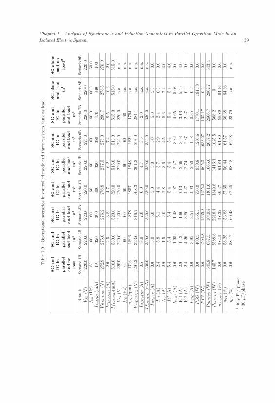
Table 1.9 – Operational scenarios in controlled mode and three resistors bank as load 39
Table 1.10–Operational scenarios in controlled mode and three resistors bank and
induction motor as load . . . . . . . . . . . . . . . . . . . . . . . . . . . 40
Table 1.11–Operational scenarios in controlled mode and a resistor bank . . . . . . 41
Table 2.1 – Scenarios and Transitions . . . . . . . . . . . . . . . . . . . . . . . . . . 54
Table A.1–DC Motor Data . . . . . . . . . . . . . . . . . . . . . . . . . . . . . . . 73
Table A.2–Current Regulator Parameters . . . . . . . . . . . . . . . . . . . . . . . 77
Table A.3–Complementary Current Regulator Data . . . . . . . . . . . . . . . . . . 79
Table A.4–Speed Regulator Parameters . . . . . . . . . . . . . . . . . . . . . . . . 82
Table A.5–Speed Regulator Parameters . . . . . . . . . . . . . . . . . . . . . . . . 84
Table B.1 – Pulse width from pins 14 and 15 related to capacitor C12 values, [3] . . 97
Table C.1 – Excitation Parameters of Salient Poles Synchronous Generator . . . . . 106
Table C.2 – Excitation Parameters of Salient Poles Synchronous Generator . . . . . 109
Table C.3 – Excitation Parameters of Salient Poles Synchronous Generator . . . . . 109
Table C.4 – Regulator Parameters Adjustments and Optimization [4]. . . . . . . . . 112
Table C.5 – Optimized Voltage Regulator Parameters . . . . . . . . . . . . . . . . . 113
Table C.6 – Voltage Regulator Adjustments . . . . . . . . . . . . . . . . . . . . . . . 117
Table D.1–Motor Data . . . . . . . . . . . . . . . . . . . . . . . . . . . . . . . . . . 121
Table D.2–Speed Regulator Parameters . . . . . . . . . . . . . . . . . . . . . . . . 121
Table D.3–Current Regulator Parameters . . . . . . . . . . . . . . . . . . . . . . . 121
Table D.4–Cause and Effect Matrix . . . . . . . . . . . . . . . . . . . . . . . . . . 124
Table E.1 – No load Test . . . . . . . . . . . . . . . . . . . . . . . . . . . . . . . . . 128
Table E.2 – Current Regulator Parameters . . . . . . . . . . . . . . . . . . . . . . . 129
Table E.3 – Average Resistance . . . . . . . . . . . . . . . . . . . . . . . . . . . . . . 130

List of abbreviations and acronyms
BL Ballast load 59
CT Current transformer 73
DCGSG Direct current generator coupled with synchronous generator 59
DCM Direct Current Motor 20
DCM Direct current motor 44
DCMIG Direct Current Motor coupled with induction generator 9
DCMSG Direct current motor coupled with synchronous generator 9
E DC supply voltage 75
EDCM Direct current motor voltage 66
EN Rated voltage 69
ESGf Synchronous generator field terminal voltage 107
Epp Phase-phase voltage 111
FPSO Floating production storage and offloading 21
IG Induction Generator 9
IG Gate current 92
IM Induction motor 34
IAK Locked rotor current 71
IC Capacitor current 33
IIG Induction generator current 33
IN Rated Current 69
ISG Synchronous generator current 33
Ia Armature current 66
Icc Generator field circuit current 104
Iexc excitation current 111
IfDCMIG Field current of direct current motor coupled with induction generator 21
Iload Load current 5
Im Magnetization Current 128
Irm Magnetization branch current across resistance 134
Ixm Magnetization branch current across inductor 134
IaDCMIG Direct current motor induction generator armature current 42
Ic1 Capacitor current 1 33
Ic2 Capacitor current 2 33
IdwMT Induction motor reactive current 33
In Rated Current 86
IwIG Induction generator active current 33
IwMT Induction motor active current 33
IwSG Synchronous generator active current 33
IwloadR R Load Active current 33
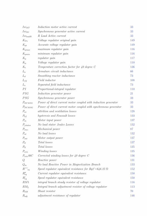
KP o Voltage regulator original gain 149
Kpe Accurate voltage regulator gain 149
Kpmax maximum regulator gain 116
Kpmin minimum regulator gain 116
Kp regulator gain 117
Kp Voltage regulator gain 110
Kt Temperature correction factor for 40 degree C 136
La Armature circuit inductance 66
Ld Smoothing reactor inductance 73
Lfd Field inductor 108
Ls Separated field inductance 73
PI Proportional-integral regulator 110
PIG Induction generator power 21
PSG Synchronous generator power 33
PDCMIG Power of direct current motor coupled with induction generator 33
PDCMSG Power of direct current motor coupled with synchronous generator 33
Pav attrition and ventilation losses 128
Phf hysteresis and Foucault losses 133
Pin Motor input power 137
Pjstator No load stator Joules Losses 132
Pmec Mechanical power 87
Pnl No load losses 132
Pout Motor output power 137
Ptl Total losses 137
Ptl Total losses 135
Pwin Winding losses 135
Pwin40C Corrected winding losses for 40 degree C 136
Q Reactive power 131
Qm No load Reactive Power in Magnetization Branch 133
R””eq Speed regulator equivalent resistance for Rq2’=646.25 Ω 152
R′′
eq Current regulator equivalent resistance 150
R′
eq Speed regulator equivalent resistance 150
RM1 integral branch steady resistor of voltage regulator 116
RM2 Integral branch adjustment resistor of voltage regulator 113
RSH Shunt resistor 70
Radj adjustment resistance of regulator 146
Raj adjustment resistance of voltage regulator 115
Ra Armature circuit resistance 66
Requ Equivalent resistance 146
Req Voltage regulator equivalent resistance 150
Rfd Field resistor 107
Rfdmed Measured field electrical resistance 104
Rq1 Proportional branch adjustment resistor of voltage regulator 113
Rti total resistor value of integral branch 116
Rtot Total resistance 146
Rtp total resistor value of proportional branch 115
Rd Phase resistance in delta connection 129
Rm Motor Average Measured Resistance 129
Ry Phase resistance in star connection 129
SG Synchronous Generator 9
SM Synchronous machine 65
SV Synchronous voltage 92
SW Interconnection switch 37
Tc Load torque 66
Tfr Friction torque 66
Tm Motor torque 86
Tn Motor rated torque 86
U2 AC supply voltage 75
V ′′
Ro Current regulator original gain 147
V ′
Ro Speed regulator original gain 148
V 1 Sawtooth voltage 92
V 2 Rectangular pulse 92
V 3 Rectangular wave 92
V 4 Rectangular pulses train 92
V 5 Amplified rectangular pulses train 92
V C Control voltage 92
V L Load voltage 92
VIG Induction generator voltage 55
VRa Total regulator gain 147
VRie Accurate current regulator gain 150
VRi Gain of the current regulator 72
VRne2 Accurate speed regulator gain for Rq2’=646.25 Ω 153
VRne Accurate speed regulator gain 150
VRn Gain of the speed regulator 71
VRo Regulator original gain 146
VSG Synchronous generator voltage 5
Vcc Control voltage of thyristor firing system 64
Vdc Direct current voltage 42
Vfd Generator field terminal voltage 104
Vi Motor current amplification factor 69
Vi Gain of machine electric part 72
Vpn Phase neutral voltage 55
Vpp Phase-phase voltage 55
Vref Reference Voltage 106
Vsa Generator output voltage 107
Vs Gain of the static converter 72
Vt Transducer output voltage 107
V aDCMIG DCM armature voltage coupled with IG 21
Θ0 Magnetization Branch Power Factor Angle 134
βRM2 adjustable resistor of integral branch 114
ηIG IG efficiency 33
ηSG SG efficiency 33
ηgroup Group efficiency 33
τH Accelerating time constant 67
τa Inductor circuit or armature time constant 68
τe Equivalent time constant 80
τgi Filter time constant of the current transducer 72
τgn Filter time constant of the speed transducer 72
τgs1 Filter time constant of the reference channel of the speed loop 71
τgs2 Filter time constant of the reference channel of the current loop 71
τgs Smoothing time constant 108
τi Current regulator time constant 72
τn Time constant of the speed regulator 72
τss Firing circuit time constant 72
fSG Synchronous generator frequency 5
ia Armature current in pu 68
m Motor torque in pu 68
n.a. Not applicable 38
nIG Induction generator speed 34
nREF Reference speed 72
nSG Synchronous generator speed 55
nu Speed in pu 72
r1 Stator winding resistance 130
r140C Corrected stator winding resistance for 40 degree C 136
r2’ Rotor winding resistance referred to stator winding 131
r′
240C Corrected rotor winding resistance referred to stator for 40 degree C 136
rm Magnetization branch resistance 134
tc Load torque in pu 72
vi Signal from the current transducer 73
x1 Stator winding reactance 131
x2’ Rotor winding reactance referred to stator winding 131
xm Magnetization branch reactance 135
R””aje Accurate adjustment resistance of Appendix D speed regulator 152
R′
aje Accurate adjustment resistance of speed regulator 148
RM ′′
2 Integral branch adjustment resistor of current regulator 78
RM ′
2 Integral branch adjustment resistor of speed regulator 82
R′′
aje Accurate adjustment resistance of current regulator 147
Raje Accurate adjustment resistance of voltage regulator 148
R′′
aj adjustment resistance of current regulator 78
R′
aj adjustment resistance of speed regulator 83
R′′
q1 Proportional branch adjustment resistor of current regulator 78
R′
q1 Proportional branch adjustment resistor of speed regulator 82
R′′
q2 Proportional branch steady resistor of current regulator 79
R′
q2 Proportional branch steady resistor of speed regulator 83
V 1′ Rectangular pulse 93
V 2′ Wider Rectangular pulse 93
V 3′ Wider Rectangular pulse 93
V 4′ Wider Rectangular pulse 93
τ ′ Generator field time constant 104
τ ′
i Regulator time constant 108
MHPP Micro-Hydro Power Plants 20
List of symbols
B Resultant torque 66
F (s) Transfer function 110
J Inertia moment, motor plus load 66
M Torque 66
Mn Rated torque 67
Nn Rated speed 86
U Counter electromotive force 66
ΔV Voltage error signal 107
Θmed Measured winding temperature 105
Θref Reference temperature resistance 105
α thyristor firing angle 74
αu Value in pu of the thyristor firing angle 75
η motor efficiency 87
μ Overlap angle 75
φ Machine flux 42
σ Sum of small time constant 109
k Proportionality constant 0 87
n0 No load speed 66
t Time 86
w Rotation rads
66
σ′ Sum of small time constant of speed regulator 80
k′′′′ Proportionality constant 4 88
k′′′ Proportionality constant 3 87
k′′ Proportionality constant 2 87
k′ Proportionality constant 1 87
n Speed 66
Contents
1 ANALYSIS OF SYNCHRONOUS AND INDUCTION GENERA-
TORS IN PARALLEL OPERATION MODE IN AN ISOLATED
ELECTRIC SYSTEM . . . . . . . . . . . . . . . . . . . . . . . . . . 23
1.1 Introduction . . . . . . . . . . . . . . . . . . . . . . . . . . . . . . . . . 23
1.2 Isolated Electric System . . . . . . . . . . . . . . . . . . . . . . . . . . 24
1.3 Digital Control Board . . . . . . . . . . . . . . . . . . . . . . . . . . . 25
1.3.1 MP410T Electronic Board Parameterization . . . . . . . . . . . . . . . . 26
1.3.2 Voltage and Speed Control Loops . . . . . . . . . . . . . . . . . . . . . . 27
1.3.3 Arrangement . . . . . . . . . . . . . . . . . . . . . . . . . . . . . . . . . 28
1.4 Data Plate . . . . . . . . . . . . . . . . . . . . . . . . . . . . . . . . . . 29
1.5 Equations - Part I . . . . . . . . . . . . . . . . . . . . . . . . . . . . . 30
1.5.1 Capacitor Bank Sizing . . . . . . . . . . . . . . . . . . . . . . . . . . . . 31
1.5.2 Resistive Divider Sizing . . . . . . . . . . . . . . . . . . . . . . . . . . . 31
1.6 Equations - Part II . . . . . . . . . . . . . . . . . . . . . . . . . . . . . 32
1.7 Equations - Part III . . . . . . . . . . . . . . . . . . . . . . . . . . . . 34
1.8 The Experiment and Schemes . . . . . . . . . . . . . . . . . . . . . . 34
1.8.1 Methods of IG Connection into the Electric System . . . . . . . . . . . . . 35
1.8.2 Experiment Data . . . . . . . . . . . . . . . . . . . . . . . . . . . . . . . 38
1.9 Results . . . . . . . . . . . . . . . . . . . . . . . . . . . . . . . . . . . . 42
1.10 Conclusion . . . . . . . . . . . . . . . . . . . . . . . . . . . . . . . . . . 47
2 LOAD AND GENERATION TRANSIENTS OF SYNCHRONOUS
AND INDUCTION GENERATORS IN PARALLEL OPERATION
MODE IN AN ISOLATED ELECTRIC SYSTEM . . . . . . . . . . . 49
2.1 Introduction . . . . . . . . . . . . . . . . . . . . . . . . . . . . . . . . . 49
2.2 Isolated Electric System . . . . . . . . . . . . . . . . . . . . . . . . . . 50
2.3 Data Plate . . . . . . . . . . . . . . . . . . . . . . . . . . . . . . . . . . 50
2.4 Equation - Part I . . . . . . . . . . . . . . . . . . . . . . . . . . . . . . 50
2.5 Equation - Part II . . . . . . . . . . . . . . . . . . . . . . . . . . . . . 50
2.6 Experiment and Schemes . . . . . . . . . . . . . . . . . . . . . . . . . 51
2.7 Voltage and Speed Control Loops . . . . . . . . . . . . . . . . . . . . 52
2.8 Experimental Data . . . . . . . . . . . . . . . . . . . . . . . . . . . . . 53
2.9 Results . . . . . . . . . . . . . . . . . . . . . . . . . . . . . . . . . . . . 55
2.10 Conclusion . . . . . . . . . . . . . . . . . . . . . . . . . . . . . . . . . . 59
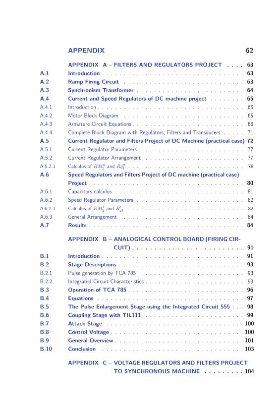
APPENDIX 62
APPENDIX A – FILTERS AND REGULATORS PROJECT . . . . 63
A.1 Introduction . . . . . . . . . . . . . . . . . . . . . . . . . . . . . . . . . 63
A.2 Ramp Firing Circuit . . . . . . . . . . . . . . . . . . . . . . . . . . . . 63
A.3 Synchronism Transformer . . . . . . . . . . . . . . . . . . . . . . . . . 64
A.4 Current and Speed Regulators of DC machine project . . . . . . . . 65
A.4.1 Introduction . . . . . . . . . . . . . . . . . . . . . . . . . . . . . . . . . . 65
A.4.2 Motor Block Diagram . . . . . . . . . . . . . . . . . . . . . . . . . . . . 65
A.4.3 Armature Circuit Equations . . . . . . . . . . . . . . . . . . . . . . . . . . 68
A.4.4 Complete Block Diagram with Regulators, Filters and Transducers . . . . . 71
A.5 Current Regulator and Filters Project of DC Machine (practical case) 72
A.5.1 Current Regulator Parameters . . . . . . . . . . . . . . . . . . . . . . . . 77
A.5.2 Current Regulator Arrangement . . . . . . . . . . . . . . . . . . . . . . . 77
A.5.2.1 Calculus of RM ′′
2 and Rq′′
1 . . . . . . . . . . . . . . . . . . . . . . . . . . . 78
A.6 Speed Regulators and Filters Project of DC machine (practical case)
Project . . . . . . . . . . . . . . . . . . . . . . . . . . . . . . . . . . . . 80
A.6.1 Capacitors calculus . . . . . . . . . . . . . . . . . . . . . . . . . . . . . . 81
A.6.2 Speed Regulator Parameters . . . . . . . . . . . . . . . . . . . . . . . . . 82
A.6.2.1 Calculus of RM ′
2 and R′
q1 . . . . . . . . . . . . . . . . . . . . . . . . . . . 82
A.6.3 General Arrangement . . . . . . . . . . . . . . . . . . . . . . . . . . . . 84
A.7 Results . . . . . . . . . . . . . . . . . . . . . . . . . . . . . . . . . . . . 84
APPENDIX B – ANALOGICAL CONTROL BOARD (FIRING CIR-
CUIT) . . . . . . . . . . . . . . . . . . . . . . . . . 91
B.1 Introduction . . . . . . . . . . . . . . . . . . . . . . . . . . . . . . . . . 91
B.2 Stage Descriptions . . . . . . . . . . . . . . . . . . . . . . . . . . . . 93
B.2.1 Pulse generation by TCA 785 . . . . . . . . . . . . . . . . . . . . . . . . 93
B.2.2 Integrated Circuit Characteristics . . . . . . . . . . . . . . . . . . . . . . . 93
B.3 Operation of TCA 785 . . . . . . . . . . . . . . . . . . . . . . . . . . . 96
B.4 Equations . . . . . . . . . . . . . . . . . . . . . . . . . . . . . . . . . . 97
B.5 The Pulse Enlargement Stage using the Integrated Circuit 555 . . . 98
B.6 Coupling Stage with TIL111 . . . . . . . . . . . . . . . . . . . . . . . 99
B.7 Attack Stage . . . . . . . . . . . . . . . . . . . . . . . . . . . . . . . . 100
B.8 Control Voltage . . . . . . . . . . . . . . . . . . . . . . . . . . . . . . . 100
B.9 General Overview . . . . . . . . . . . . . . . . . . . . . . . . . . . . . . 101
B.10 Conclusion . . . . . . . . . . . . . . . . . . . . . . . . . . . . . . . . . 103
APPENDIX C – VOLTAGE REGULATORS AND FILTERS PROJECT
TO SYNCHRONOUS MACHINE . . . . . . . . . 104
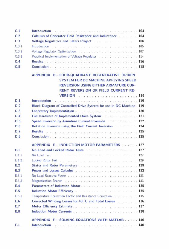
C.1 Introduction . . . . . . . . . . . . . . . . . . . . . . . . . . . . . . . . . 104
C.2 Calculus of Generator Field Resistance and Inductance . . . . . . . . 104
C.3 Voltage Regulators and Filters Project . . . . . . . . . . . . . . . . . 106
C.3.1 Introduction . . . . . . . . . . . . . . . . . . . . . . . . . . . . . . . . . 106
C.3.2 Voltage Regulator Optimization . . . . . . . . . . . . . . . . . . . . . . . 107
C.3.3 Practical Implementation of Voltage Regulator . . . . . . . . . . . . . . . 114
C.4 Results . . . . . . . . . . . . . . . . . . . . . . . . . . . . . . . . . . . . 116
C.5 Conclusion . . . . . . . . . . . . . . . . . . . . . . . . . . . . . . . . . . 118
APPENDIX D – FOUR-QUADRANT REGENERATIVE DRIVEN
SYSTEM FOR DC MACHINE APPLYING SPEED
REVERSION USING EITHER ARMATURE CUR-
RENT REVERSION OR FIELD CURRENT RE-
VERSION . . . . . . . . . . . . . . . . . . . . . . 119
D.1 Introduction . . . . . . . . . . . . . . . . . . . . . . . . . . . . . . . . . 119
D.2 Block Diagram of Controlled Drive System for use in DC Machine . 119
D.3 Laboratory Implementation . . . . . . . . . . . . . . . . . . . . . . . . 120
D.4 Full Hardware of Implemented Drive System . . . . . . . . . . . . . 121
D.5 Speed Inversion by Armature Current Inversion . . . . . . . . . . . . 122
D.6 Rotation Inversion using the Field Current Inversion . . . . . . . . . 124
D.7 Results . . . . . . . . . . . . . . . . . . . . . . . . . . . . . . . . . . . 125
D.8 Conclusion . . . . . . . . . . . . . . . . . . . . . . . . . . . . . . . . . . 125
APPENDIX E – INDUCTION MOTOR PARAMETERS . . . . . . 127
E.1 No Load and Locked Rotor Tests . . . . . . . . . . . . . . . . . . . . 127
E.1.1 No Load Test . . . . . . . . . . . . . . . . . . . . . . . . . . . . . . . . 127
E.1.2 Locked Rotor Test . . . . . . . . . . . . . . . . . . . . . . . . . . . . . . 129
E.2 Stator and Rotor Parameters . . . . . . . . . . . . . . . . . . . . . . . 129
E.3 Power and Losses Calculus . . . . . . . . . . . . . . . . . . . . . . . . 132
E.3.1 No Load Reactive Power . . . . . . . . . . . . . . . . . . . . . . . . . . . 133
E.3.2 Magnetization Branch . . . . . . . . . . . . . . . . . . . . . . . . . . . . 133
E.4 Parameters of Induction Motor . . . . . . . . . . . . . . . . . . . . . . 135
E.5 Induction Motor Efficiency . . . . . . . . . . . . . . . . . . . . . . . . 135
E.5.1 Temperature Correction Factor and Resistance Correction . . . . . . . . . . 136
E.6 Corrected Winding Losses for 40 ◦C and Total Losses . . . . . . . . 136
E.7 Motor Efficiency Estimate . . . . . . . . . . . . . . . . . . . . . . . . . 137
E.8 Induction Motor Currents . . . . . . . . . . . . . . . . . . . . . . . . . 138
APPENDIX F – SOLVING EQUATIONS WITH MATLAB . . . . . 140
F.1 Introduction . . . . . . . . . . . . . . . . . . . . . . . . . . . . . . . . . 140
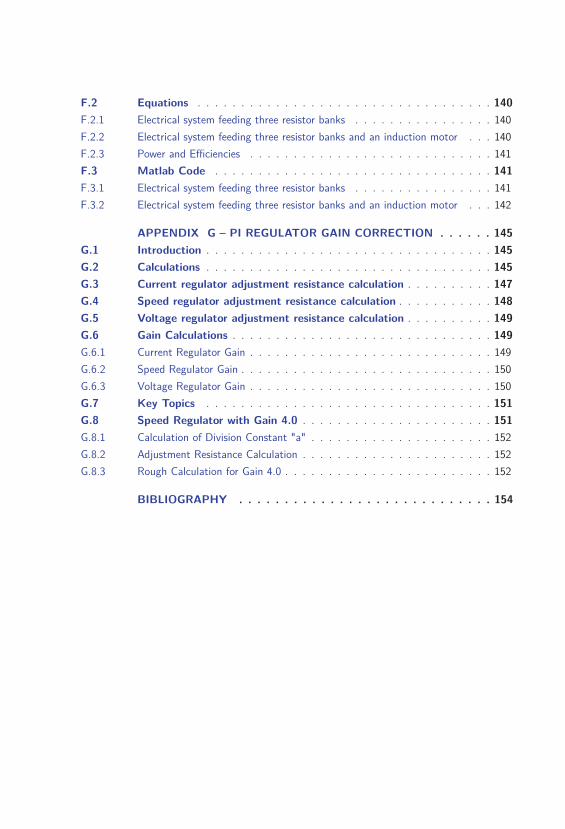
F.2 Equations . . . . . . . . . . . . . . . . . . . . . . . . . . . . . . . . . . 140
F.2.1 Electrical system feeding three resistor banks . . . . . . . . . . . . . . . . 140
F.2.2 Electrical system feeding three resistor banks and an induction motor . . . 140
F.2.3 Power and Efficiencies . . . . . . . . . . . . . . . . . . . . . . . . . . . . 141
F.3 Matlab Code . . . . . . . . . . . . . . . . . . . . . . . . . . . . . . . . 141
F.3.1 Electrical system feeding three resistor banks . . . . . . . . . . . . . . . . 141
F.3.2 Electrical system feeding three resistor banks and an induction motor . . . 142
APPENDIX G – PI REGULATOR GAIN CORRECTION . . . . . . 145
G.1 Introduction . . . . . . . . . . . . . . . . . . . . . . . . . . . . . . . . . 145
G.2 Calculations . . . . . . . . . . . . . . . . . . . . . . . . . . . . . . . . . 145
G.3 Current regulator adjustment resistance calculation . . . . . . . . . . 147
G.4 Speed regulator adjustment resistance calculation . . . . . . . . . . . 148
G.5 Voltage regulator adjustment resistance calculation . . . . . . . . . . 149
G.6 Gain Calculations . . . . . . . . . . . . . . . . . . . . . . . . . . . . . . 149
G.6.1 Current Regulator Gain . . . . . . . . . . . . . . . . . . . . . . . . . . . . 149
G.6.2 Speed Regulator Gain . . . . . . . . . . . . . . . . . . . . . . . . . . . . . 150
G.6.3 Voltage Regulator Gain . . . . . . . . . . . . . . . . . . . . . . . . . . . . 150
G.7 Key Topics . . . . . . . . . . . . . . . . . . . . . . . . . . . . . . . . . 151
G.8 Speed Regulator with Gain 4.0 . . . . . . . . . . . . . . . . . . . . . . 151
G.8.1 Calculation of Division Constant "a" . . . . . . . . . . . . . . . . . . . . . 152
G.8.2 Adjustment Resistance Calculation . . . . . . . . . . . . . . . . . . . . . . 152
G.8.3 Rough Calculation for Gain 4.0 . . . . . . . . . . . . . . . . . . . . . . . . 152
BIBLIOGRAPHY . . . . . . . . . . . . . . . . . . . . . . . . . . . . 154
20
Introduction
In recent years, self-excited induction generators have been employed as suitable
isolated power sources in MHPP (Micro-Hydro Power Plants) and wind energy applica-
tions [5, 6, 7, 8, 9, 10, 11]. In wind power generating systems, the physical size of the
individual machines operating at maximum efficiency and dealing with regular routine
maintenance related to necessary interruptions, future growth and reliability are reasons
for them to be operated in parallel [12, 13, 14].
The studies related to IG and SG in parallel operation mode [15, 16, 17, 18, 19,
20, 21, 22] show a newer knowledge border, that show the results and behavior of this
kind of generation topology, including simulation results for an MHPP. Overall, one of
the main contributions of this work is the use of actual control loops in practical experi-
ments involving SG and IG in parallel operation and their optimization and adjustments
[4]. These control loops and experiments were mounted in the Laboratory of research
development of electrical didactic laboratory of Federal University of Itajubá.
This work is focused on the operational behavior of two different kinds of genera-
tors operating in parallel mode, their roles within the electric system, their controls and
characteristics of each generator, some transients and their effects, as well as studies and
implementations of control alternatives in order to avoid the undesirable transient effects.
As basis of the target study, this work presents various experiments accomplished
in this cited laboratory, which are related to DCM (Direct Current Motor) and their
speed and current control loops. The DCM are used as primary machine to SG and
IG. Then, it is essential that DCMSG has speed control loop and DCMIG can be driven
manually due to their functional characteristics.
The SG requires synchronous speed rotation in its shaft regardless to load tran-
sients or any other disturbs on going in the electric system. On the contrary, the SG does
not operate. The SG shaft speed is sensible to disturbs and any other changes on going
in the electric system. It means that, speed regulation or speed control loop is required
for the SG primary machine or DCMSG in order to keep its shaft synchronous speed.
On the other hand, IG has different functional characteristics that make it able to
supply active power taking only into account its shaft speed be higher than synchronous
speed. As IG shaft speed increases above the synchronous speed, the supply power is
higher. The other characteristic is that, regardless of load changes or disturbs on going
in the electric system, its shaft speed and power supply is the same for the IG. Then,
these functional characteristics do not require any IG shaft automatic speed regulation.
It means that its primary machine or DCMIG, in the case of these experiments studied in
Introduction 21
this work, do not need automatic speed regulation or any speed control loop. From these
cited reasons, the DCMIG speed is not automatically controlled, differently of the DCMSG
speed that is automatically controlled. The control of DCMIG speed is done manually by
open control loop. The two methods used to change the DCMIG speed are: the V aDCMIG
(DCM armature voltage coupled with IG) method and the field flux or IfDCMIG (Field
current of direct current motor coupled with induction generator) method.
In general, the generators used in the industry are driven by gas or steam turbines.
One of the main characteristics of these turbines is the availability of keeping the machine
shaft speed even in adverse conditions as in load transients. The cited turbine speed
variation does not overcome ten percent independently of electrical system transients,
[23]. Then, in order to do the DCMIG closer to turbine behavior in the experiment
implemented in laboratory, two methods of DCMIG speed elevation were studied in order
to rise the PIG (Induction generator power) supplied. First, the machine field flux is
decreased and, the second, the DCMIG armature voltage V aDCMIG is increased. The
increase of V aDCMIG has better results than decrease of machine field flux.
In the experiments of this work, the wound rotor machine was used instead of
squirrel cage rotor machine. The wound rotor machine can have an extra advantage that
is the high startup torque due to resistors that can be connected at the induction machine
rotor circuit [24]. In this way, the induction machine can start directly as motor and it can
turn a IG by increase of speed up to this speed exceeds the synchronous speed as detailed
in chapter 1. Besides of likely higher wound rotor machine cost, the unique technical
considerable difference between the two machines considered in this work is that the
wound rotor machine can have a higher startup torque and then it permits an additional
option of synchronism between the IG and SG, that is the method of direct startup as
mentioned in chapter 1. Then, except that mentioned difference, the results obtained with
wound rotor machine can be also considered identical to results with squirrel cage rotor
machine. Considering that explanation, the results of this work are valid to as wound
rotor machine as squirrel cage rotor machine.
One of the potential motivations for this study is to identify a potential alternative
capable of optimizing the main electric system currently adopted in oil platforms or FPSO
(Floating production storage and offloading), making them cheaper, simpler, lighter and
more efficient. The oil platforms use traditionally three of four SGs in parallel operation
mode.
Analysis of a generator’s power balance and its interactions is presented in this
work in various operational scenarios. The results enable comparisons of the two methods
of induction generator speed control, by either the autotransformer method or the field
flux variation method. The former results in a larger range of speed and power from
the induction generator. Therefore, it has more desirable features for actual operational
Introduction 22
conditions.
In addition, this work is based on thesis [25] and shows six appendixes to the
chapters 1 and 2, as follow: the appendix A says about Filter and Regulator Project
for direct current motor, DC motor, appendix B says about Analogical Control Board
for current and voltage control loops, appendix C says about Voltage Regulators Project
to Synchronous Machine, appendix D shows studies about a practical case using DCM
controls for driving in four quadrants [26], appendix E calculates the induction motor
parameters used in one of the experiments of chapter 1, appendix F shows the Matlab
codes used to solve the equation system indicated in chapters 1 and 2 and appendix G
shows the more accurate method for the regulator parameter adjustments. Thus, these
additional studies provide the basis of knowledge [27] for the analysis of synchronous
and induction generators in parallel operation mode in an isolated electric system. These
generators feed either a resistive load or a resistive load and an induction motor together.

23
1 Analysis of Synchronous and Induction
Generators in Parallel Operation Mode in
an Isolated Electric System
1.1 Introduction
This work is composed of analysis over an electric system that includes an induction
motor, a resistive load and an autotransformer connected to a diodes bridge to feed the
DCMIG armature, what permits to increase manually the IG electric power limits, [28],
[29] with better efficiency [30]. Therefore, this work shows the IG supplying more active
power than it was shown in [28] and an induction motor inserted in experiment what
enables an wider analysis of the system behavior.
Two methods of DCMIG speed elevation were studied in order to rise the PIG
supplied. First, the machine field flux is decreased and, the second, the DCMIG armature
voltage V aDCMIG is increased. The increase of V aDCMIG has better results than decrease
of machine field flux.
This work presents results that show additional remarkable characteristics by op-
eration in parallel mode between one SG and one IG. Some characteristics, such as re-
duced weight and size, easier maintenance, and shorter manufacturing and delivery time
are more associated with induction generators and are relevant to MHPP as demonstrated
in general introduction and they could also be to oil platforms. Besides, it has absence of
dc supply for excitation and better transient performances [20], [8].
In this chapter, the three different methods of IG connection into the electric
system were studied as follow: (i) direct startup as a motor and rising the induction
motor speed up to induction motor turns IG, (ii) synchronism of self-excited IG with the
electric system and (iii) adjustment of IG speed at synchronous speed and IG connection
into the system;
In the experiments of this chapter, the wound rotor machine was used instead of
squirrel cage rotor machine. The wound rotor machine can have an extra advantage that
is the high startup torque due to resistors that can be connected at the induction machine
rotor circuit [24]. For this work, the unique differential advantage by the use of this kind
of machine is making the first method of IG connection into the electric system available,
(i) direct startup as a motor and rising the induction motor speed up to it turns IG.
A potential application of this cited generator topology is in MHPP, which has
Chapter 1. Analysis of Synchronous and Induction Generators in Parallel Operation Mode in an
Isolated Electric System 24
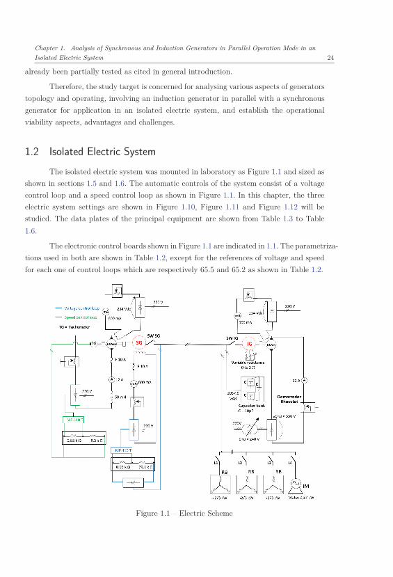
already�been�partially�tested�as�cited� in�general� introduction.
Therefore,�the�study�target�is�concerned�for�analysing�various�aspects�of�generators�
topology�and�operating,� involving�an� induction�generator� in�parallel�with�a� synchronous�
generator� for� application� in� an� isolated� electric� system,� and� establish� the� operational�
viability�aspects,�advantages�and�challenges.
1.2� Isolated�Electric�System
The�isolated�electric�system�was�mounted�in�laboratory�as�Figure�1.1�and�sized�as�
shown� in� sections�1.5�and�1.6.�The�automatic�controls�of� the� system�consist�of�a�voltage�
control� loop�and�a� speed� control� loop�as� shown� in�Figure�1.1.� In� this� chapter,� the� three�
electric� system� settings� are� shown� in� Figure� 1.10,� Figure� 1.11� and� Figure� 1.12� will� be�
studied.�The�data�plates� of� the�principal� equipment� are� shown� from�Table� 1.3� to�Table�
1.6.
The�electronic�control�boards�shown�in�Figure�1.1�are�indicated�in�1.1.�The�parametriza-
tions�used� in�both�are�shown� in�Table�1.2,�except� for�the�references�of�voltage�and�speed�
for�each�one�of�control� loops�which�are�respectively�65.5�and�65.2�as�shown� in�Table�1.2.
Figure 1.1 – Electric Scheme

Chapter 1. Analysis of Synchronous and Induction Generators in Parallel Operation Mode in an
Isolated Electric System 25
1.3 Digital Control Board
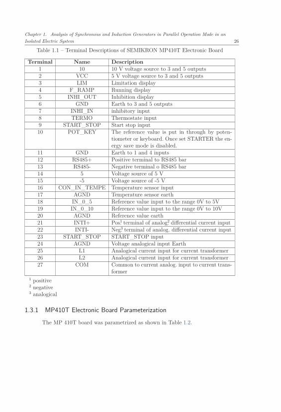
The digital control board MP 410T aims to control the three-phase thyristor bridge
firing angle. After the correct connections between the thyristors bridge and the electronic
board, the MP 410T board can be set as shown in Table 1.1, so that all firing gates from
thyristors bridge operate properly. It means that all firing angle turn itself controlled by
the MP 410T electronic board. All reference signals from control loops are connected to
MP 410T such as speed and field voltage references. This kind of electronic board are
inserted in the circuit as part of speed and voltage control loops as shown in Figures
1.2 and 1.3. The correct connections and electronic board configuration are necessary to
proper operation of MP 410T. The terminal descriptions of electronic boards MP 410T
follow in the Table 1.1.
Figure 1.2 – MP 410T in Speed Control loop
Figure 1.3 – MP 410T in Voltage Control loop
Chapter 1. Analysis of Synchronous and Induction Generators in Parallel Operation Mode in an
Isolated Electric System 26
Table 1.1 – Terminal Descriptions of SEMIKRON MP410T Electronic Board
Terminal Name Description1 10 10 V voltage source to 3 and 5 outputs2 VCC 5 V voltage source to 3 and 5 outputs3 LIM Limitation display4 F_RAMP Running display5 INHI_OUT Inhibition display6 GND Earth to 3 and 5 outputs7 INHI_IN inhibitory input8 TERMO Thermostate input9 START_STOP Start stop input10 POT_KEY The reference value is put in through by poten-
tiometer or keyboard. Once set STARTER the en-ergy save mode is disabled.
11 GND Earth to 1 and 4 inputs12 RS485+ Positive terminal to RS485 bar13 RS485- Negative terminal o RS485 bar14 5 Voltage source of 5 V15 -5 Voltage source of -5 V16 CON_IN_TEMPE Temperature sensor input17 AGND Temperature sensor earth18 IN_0_5 Reference value input to the range 0V to 5V19 IN_0_10 Reference value input to the range 0V to 10V20 AGND Reference value earth21 INTI+ Pos1. terminal of analog2. differential current input22 INTI- Neg3. terminal of analog. differential current input23 START_STOP START_STOP input24 AGND Voltage analogical input Earth25 L1 Analogical current input for current transformer26 L2 Analogical current input for current transformer27 COM Common to current analog. input to current trans-
former1 positive2 negative3 analogical
1.3.1 MP410T Electronic Board Parameterization
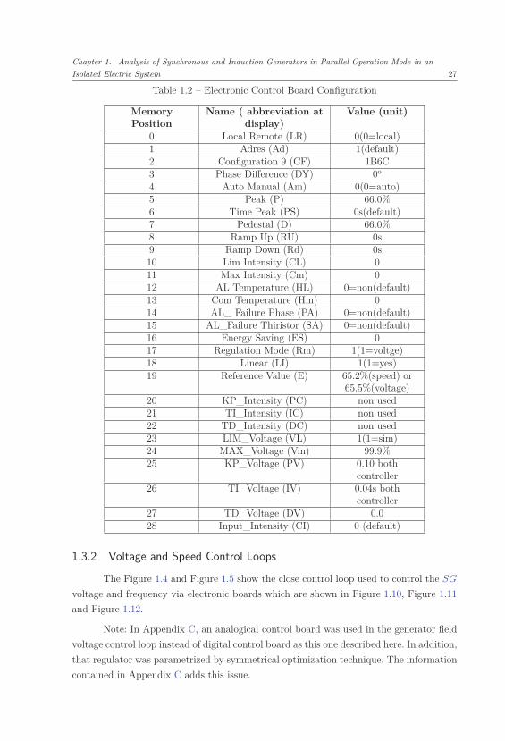
The MP 410T board was parametrized as shown in Table 1.2.
Chapter 1. Analysis of Synchronous and Induction Generators in Parallel Operation Mode in an
Isolated Electric System 27
Table 1.2 – Electronic Control Board Configuration
MemoryPosition
Name ( abbreviation atdisplay)
Value (unit)
0 Local Remote (LR) 0(0=local)1 Adres (Ad) 1(default)2 Configuration 9 (CF) 1B6C3 Phase Difference (DY) 0o
4 Auto Manual (Am) 0(0=auto)5 Peak (P) 66.0%6 Time Peak (PS) 0s(default)7 Pedestal (D) 66.0%8 Ramp Up (RU) 0s9 Ramp Down (Rd) 0s10 Lim Intensity (CL) 011 Max Intensity (Cm) 012 AL Temperature (HL) 0=non(default)13 Com Temperature (Hm) 014 AL_ Failure Phase (PA) 0=non(default)15 AL_Failure Thiristor (SA) 0=non(default)16 Energy Saving (ES) 017 Regulation Mode (Rm) 1(1=voltge)18 Linear (LI) 1(1=yes)19 Reference Value (E) 65.2%(speed) or
65.5%(voltage)20 KP_Intensity (PC) non used21 TI_Intensity (IC) non used22 TD_Intensity (DC) non used23 LIM_Voltage (VL) 1(1=sim)24 MAX_Voltage (Vm) 99.9%25 KP_Voltage (PV) 0.10 both
controller26 TI_Voltage (IV) 0.04s both
controller27 TD_Voltage (DV) 0.028 Input_Intensity (CI) 0 (default)
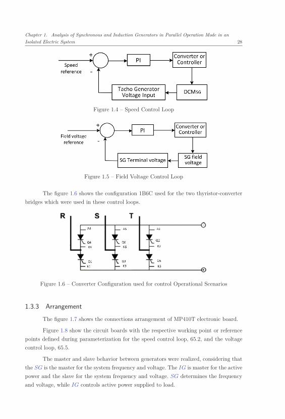
1.3.2 Voltage and Speed Control Loops
The Figure 1.4 and Figure 1.5 show the close control loop used to control the SG
voltage and frequency via electronic boards which are shown in Figure 1.10, Figure 1.11
and Figure 1.12.
Note: In Appendix C, an analogical control board was used in the generator field
voltage control loop instead of digital control board as this one described here. In addition,
that regulator was parametrized by symmetrical optimization technique. The information
contained in Appendix C adds this issue.
Chapter 1. Analysis of Synchronous and Induction Generators in Parallel Operation Mode in an
Isolated Electric System 28
Figure 1.4 – Speed Control Loop
Figure 1.5 – Field Voltage Control Loop
The figure 1.6 shows the configuration 1B6C used for the two thyristor-converter
bridges which were used in these control loops.
Figure 1.6 – Converter Configuration used for control Operational Scenarios
1.3.3 Arrangement
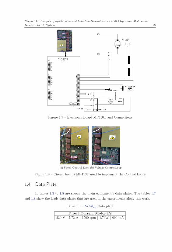
The figure 1.7 shows the connections arrangement of MP410T electronic board.
Figure 1.8 show the circuit boards with the respective working point or reference
points defined during parameterization for the speed control loop, 65.2, and the voltage
control loop, 65.5.
The master and slave behavior between generators were realized, considering that
the SG is the master for the system frequency and voltage. The IG is master for the active
power and the slave for the system frequency and voltage. SG determines the frequency
and voltage, while IG controls active power supplied to load.
Chapter 1. Analysis of Synchronous and Induction Generators in Parallel Operation Mode in an
Isolated Electric System 29
Figure 1.7 – Electronic Board MP410T and Connections
(a) Speed Control Loop (b) Voltage Control Loop
Figure 1.8 – Circuit boards MP410T used to implement the Control Loops
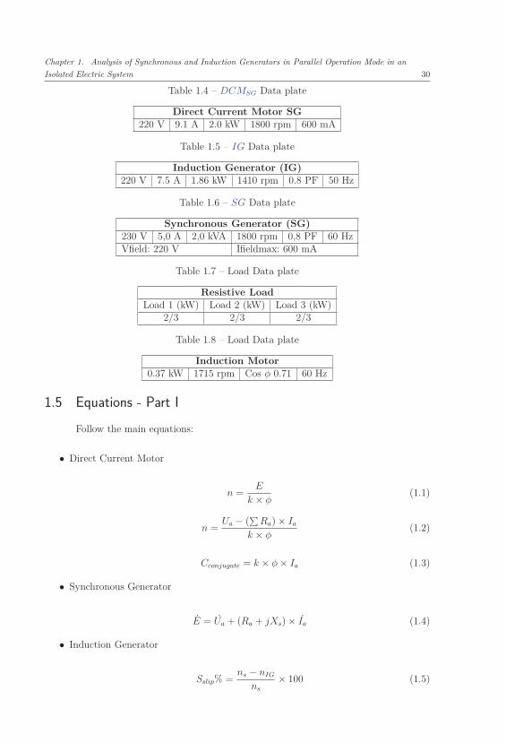
1.4 Data Plate
In tables 1.3 to 1.8 are shown the main equipment’s data plates. The tables 1.7
and 1.8 show the loads data plates that are used in the experiments along this work.
Table 1.3 – DCMIG Data plate
Direct Current Motor IG220 V 7.72 A 1500 rpm 1.7kW 600 mA
Chapter 1. Analysis of Synchronous and Induction Generators in Parallel Operation Mode in an
Isolated Electric System 30
Table 1.4 – DCMSG Data plate
Direct Current Motor SG220 V 9.1 A 2.0 kW 1800 rpm 600 mA
Table 1.5 – IG Data plate
Induction Generator (IG)220 V 7.5 A 1.86 kW 1410 rpm 0.8 PF 50 Hz
Table 1.6 – SG Data plate
Synchronous Generator (SG)230 V 5,0 A 2,0 kVA 1800 rpm 0,8 PF 60 HzVfield: 220 V Ifieldmax: 600 mA
Table 1.7 – Load Data plate
Resistive LoadLoad 1 (kW) Load 2 (kW) Load 3 (kW)
2/3 2/3 2/3
Table 1.8 – Load Data plate
Induction Motor0.37 kW 1715 rpm Cos φ 0.71 60 Hz
1.5 Equations - Part I
Follow the main equations:
• Direct Current Motor
n =E
k × φ(1.1)
n =Ua − (
∑Ra) × Ia
k × φ(1.2)
Cconjugate = k × φ × Ia (1.3)
• Synchronous Generator
E = Ua + (Ra + jXs) × Ia (1.4)
• Induction Generator
Sslip% =ns − nIG
ns
× 100 (1.5)
Chapter 1. Analysis of Synchronous and Induction Generators in Parallel Operation Mode in an
Isolated Electric System 31
ns =120 × fSG
Pnumberofpoles
(1.6)
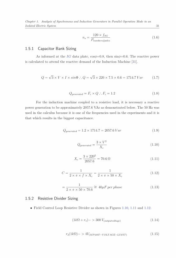
1.5.1 Capacitor Bank Sizing
As informed at the IG data plate, cosφ=0.8, then sinφ=0.6. The reactive power
is calculated to attend the reactive demand of the Induction Machine [31].
Q =√
3 × V × I × sinΦ ∴ Q =√
3 × 220 × 7.5 × 0.6 = 1714.7 V ar (1.7)
Qgenerated = Fc × Q ∴ Fc = 1.2 (1.8)
For the induction machine coupled to a resistive load, it is necessary a reactive
power generation to be approximately 2057.6 VAr as demonstrated below. The 50 Hz was
used in the calculus because it is one of the frequencies used in the experiments and it is
that which results in the biggest capacitance.
Qgenerated = 1.2 × 1714.7 = 2057.6 V ar (1.9)
Qgenerated =3 × V 2
Xc
(1.10)
Xc =3 × 2202
2057.6= 70.6 Ω (1.11)
C =1
2 × π × f × Xc
=1
2 × π × 50 × Xc
(1.12)
=1
2 × π × 50 × 70.6∼= 40μF per phase (1.13)
1.5.2 Resistive Divider Sizing
• Field Control Loop Resistive Divider as shown in Figures 1.10, 1.11 and 1.12.
(1kΩ + r1)− > 300 V(outputvoltage) (1.14)
r2(1kΩ)− > 4V(MP 410T −V OLT AGE−LIMIT ) (1.15)
Chapter 1. Analysis of Synchronous and Induction Generators in Parallel Operation Mode in an
Isolated Electric System 32
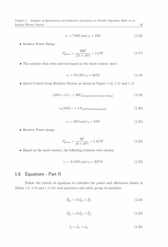
r1 = 74kΩ and r2 = 1kΩ (1.16)
• Resistor Power Sizing:
Ppower =3002
(75 × 103)= 1.2 W (1.17)
• The resistors that were selected based on the sized resistor, were:
r1 = 79.1kΩ r2 = 947Ω (1.18)
• Speed Control Loop Resistive Divisor as shown in Figure 1.10, 1.11 and 1.12.
(1kΩ + r1)− > 36V(tachogeneratoroutputvoltage) (1.19)
r2(1kΩ)− > 4 V(MP T 410voltagelimit) (1.20)
r1 = 8kΩ and r2 = 1kΩ (1.21)
• Resistor Power sizing:
Ppower =362
(9 × 10³)= 1.14 W (1.22)
• Based on the sized resistor, the following resistors were chosen:
r1 = 8.3 kΩ and r2 = 947 Ω (1.23)
1.6 Equations - Part II
Follow the system of equations to calculate the power and efficiencies shown in
Tables 1.9, 1.10 and 1.11 for each generator and entire group of machines.
I2SG = Iw2
SG + I2c1 (1.24)
I2IG = Iw2
IG + I2c2 (1.25)
Ic = Ic1 + Ic2 (1.26)
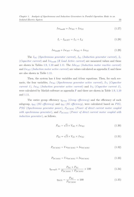
Chapter 1. Analysis of Synchronous and Induction Generators in Parallel Operation Mode in an
Isolated Electric System 33
IwloadR = IwSG + IwIG (1.27)
Ic − IdwMT = Ic1 + Ic2 (1.28)
IwloadR + IwMT = IwSG + IwIG (1.29)
The ISG (Synchronous generator current), IIG (Induction generator current), IC
(Capacitor current) and IwloadR (R Load Active current) are measured values and these
are shown in Tables 1.9, 1.10 and 1.11. The IdwMT (Induction motor reactive current)
and IwMT (Induction motor active current) are values calculated as appendix E and these
are also shown in Table 1.11.
Then, the system has 4 four variables and 4-four equations. Then, for each sce-
nario, the four variables, IwSG (Synchronous generator active current), Ic1 (Capacitor
current 1 ), IwIG (Induction generator active current) and Ic2 (Capacitor current 2 ),
were calculated by Matlab software as appendix F and these are shown in Table 1.9, 1.10
and 1.11.
The entire group efficiency ηgroup (Group efficiency) and the efficiency of each
subgroup, ηSG (SG efficiency) and ηIG (IG efficiency), were calculated based on PIG,
PSG (Synchronous generator power), PDCMSG (Power of direct current motor coupled
with synchronous generator), and PDCMIG (Power of direct current motor coupled with
induction generator), as follows.
PSG =√
3 × VSG × IwSG (1.30)
PIG =√
3 × VIG × IwIG (1.31)
PDCMSG = V aDCMSG × IaDCMSG (1.32)
PDCMIG = V aDCMIG × IaDCMIG (1.33)
ηgroup% =PSG + PIG
PDCMSG + PDCMIG
× 100 (1.34)
ηSG% =PSG
PDCMSG
× 100 (1.35)
Chapter 1. Analysis of Synchronous and Induction Generators in Parallel Operation Mode in an
Isolated Electric System 34
ηIG% =PIG
PDCMIG
× 100 (1.36)
1.7 Equations - Part III
The equations e calculus used to determine the IM (Induction motor) parameters
and IM equivalent circuit such as the primary and secondary impedances and also the
primary and secondary currents are showed in Appendix E.
1.8 The Experiment and Schemes
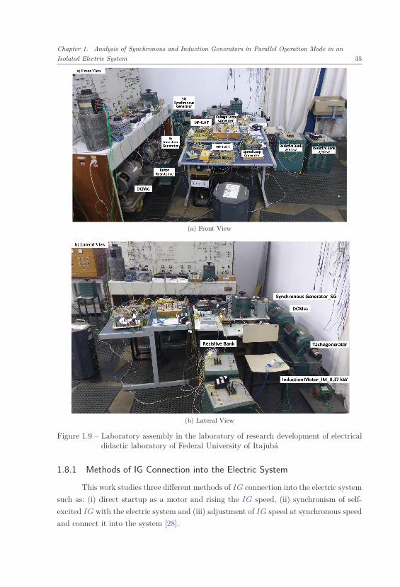
The experiment was mounted in the laboratory as shown in Figure 1.9 a) and b).
The detailed circuit is shown in Figures 1.10, 1.11 and 1.12.
Figure 1.9 b) shows another experiment view, including the taco generator and its
connections. The detailed circuits are shown in Figures 1.10, 1.11 and 1.12.
The power from IG, PIG, was limited because the IfDCMIG reached the maximum
value in accordance with DCMIG current specifications. This limited speed from DCMIG
was a challenge because the low speed resulted in low contribution from PIG. Then, it
was necessary to elevate the DCMIG speed, nIG (Induction generator speed).
Then, the methodology consists of implementing the comparative analysis of the
power and efficiencies, starting with an analysis between the PIG from the scheme in
Figure 1.10 and PIG from the schemes in Figure 1.11 and Figure 1.12, covering the
scenarios shown in Table 1.11, Table 1.9 and Table 1.10 respectively.
Finally, a comparative efficiency analysis was conducted for two subgroups, one
composed of IG and a DCMIG and the other composed of SG and a DCMSG. These
analyses are done over the scenarios related to the scheme in Figure 1.10, the scheme in
Figure 1.11 and the scheme in Figure 1.12.
Thus, the increase of DCMIG speed results in increase of the PIG contributions
and IG subgroup efficiencies such as they are shown in the results.
The Figure 1.11 and Figure 1.12 show the schemes implemented in the laboratory
to overcome the challenge related to limitation of IG speed [28] such as bringing the
experiment closer to actual conditions and taking into advantages of IG power capacity.
It was used as an autotransformer connected to a diodes bridge to vary the voltage applied
on the DCMIG armature circuit and obtain a higher speed and PIG.
Chapter 1. Analysis of Synchronous and Induction Generators in Parallel Operation Mode in an
Isolated Electric System 35
(a) Front View
(b) Lateral View
Figure 1.9 – Laboratory assembly in the laboratory of research development of electricaldidactic laboratory of Federal University of Itajubá
1.8.1 Methods of IG Connection into the Electric System
This work studies three different methods of IG connection into the electric system
such as: (i) direct startup as a motor and rising the IG speed, (ii) synchronism of self-
excited IG with the electric system and (iii) adjustment of IG speed at synchronous speed
and connect it into the system [28].
Chapter 1. Analysis of Synchronous and Induction Generators in Parallel Operation Mode in an
Isolated Electric System 36
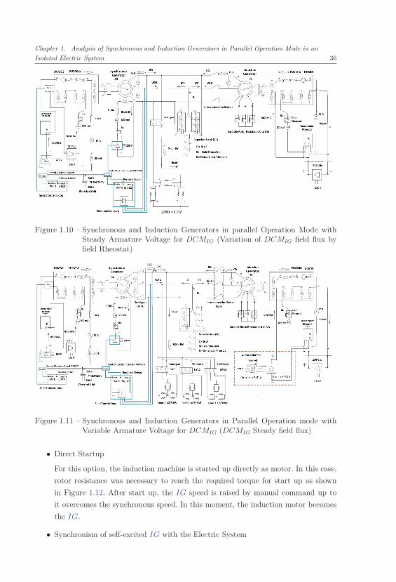
Figure 1.10 – Synchronous and Induction Generators in parallel Operation Mode withSteady Armature Voltage for DCMIG (Variation of DCMIG field flux byfield Rheostat)
Figure 1.11 – Synchronous and Induction Generators in Parallel Operation mode withVariable Armature Voltage for DCMIG (DCMIG Steady field flux)
• Direct Startup
For this option, the induction machine is started up directly as motor. In this case,
rotor resistance was necessary to reach the required torque for start up as shown
in Figure 1.12. After start up, the IG speed is raised by manual command up to
it overcomes the synchronous speed. In this moment, the induction motor becomes
the IG.
• Synchronism of self-excited IG with the Electric System

Chapter 1. Analysis of Synchronous and Induction Generators in Parallel Operation Mode in an
Isolated Electric System 37
Figure 1.12 – Synchronous and Induction Generators in Parallel Operation mode withVariable Armature Voltage for DCMIG and an Induction Motor as Load(DCMIG Steady field flux)
For this option, the induction generator is auto-excited and the capacitor bank is
required and connected in the IG directly as well as the interconnection switch,
SW (Interconnection switch), is placed beside of capacitor bank as shown in Figure
1.12 by green arrow. For this option, it was used a synchroscope for closing the
interconnection switch.
Figure 1.13 – Conjugate vs rpm - Induction Motor and Generator
• Adjustment of IG Speed at Synchronous Speed
Considering the scheme shown in the Figure 1.12, the IG speed was led to close and
below the fluctuation point, it means some value close to point where the torque or

Chapter 1. Analysis of Synchronous and Induction Generators in Parallel Operation Mode in an
Isolated Electric System 38
conjugate is null as it can be seen in Figure 1.13 bellow. The fluctuation point is
at the intersection with rpm axis. The interconnection switch shown in Figure 1.12
was closed when the Induction motor speed is in the fluctuation area. From this IG
speed, the DCMIG speed should be raised up to overcome the fluctuation point to
become the induction motor an induction generator.
For this option, the IG is not auto-excited, the reactive is obtained from the grid.
1.8.2 Experiment Data
The experimental data obtained in the laboratory are shown in Table 1.11, Table
1.9 and Table 1.10. The Table 1.9 shows the data obtained from the scheme in Figure 1.11,
Table 1.10 shows the data obtained from the scheme in Figure 1.12 and Table 1.11 shows
the data obtained from the scheme in Figure 1.10. The unique difference between Figure
1.11 and Figure 1.12 is the presence of IM in Figure 1.12 as additional load. The difference
between the Figure 1.10 and the others is basically the presence of an autotransformer in
the DCMIG field circuit and an additional motor as load in Figure 1.12.
The autotransformer is responsible for applying a voltage range directly on the
DCMIG armature to obtain a larger speed range of the DCMIG and to push more power
to the IG, keeping the DCMIG parameters into the rated values. Hence, the elevation
of IG speed and power depend on DCMIG armature voltage, V aDCMIG. It means that
the DCMIG speed control method used for the scheme in Figure 1.10 is different of the
method used in the Figures 1.11 and 1.12. The IG speed of scheme shown in Figure 1.10
depends on just the DCMIG field flux because V aDCMIG is steady. The DCMIG field flux
is adjusted manually and V aDCMIG as well.
In summary, the Table 1.11 shows the data obtained from the scheme shown in
Figure 1.10 that has the 234 Vdc steady source; Table 1.9 and Table 1.10 show respectively
the data obtained from the schemes shown in Figure 1.11 and Figure 1.12. These schemes
have an autotransformer and a diodes bridge as substitute of the 234 Vdc steady source
shown in Figure 1.10. The difference between Figures 1.11 and 1.12 is the induction motor
that is inserted as additional load in Figure 1.12.
Then, from these three schemes, the data obtained from each operation scenario
into a same scheme are analyzed and compared among themselves. The generators per-
formances between different schemes are analyzed and compared considering the similar
operational scenarios under tests and the respective schemes’ differences. The results are
shown along this work.
Note: The abbreviations n.a. (Not applicable) shown in scenarios 1, 1C and 1B of
tables 1.9, 1.10 and 1.11 refer to values not used in SG and IG power graphics. The cited
graphics are based on the scenarios 2 onwards.
Chapter 1. Analysis of Synchronous and Induction Generators in Parallel Operation Mode in an
Isolated Electric System 39T
able
1.9
–O
pera
tion
alsc
enar
ios
inco
ntro
lled
mod
ean
dth
ree
resi
stor
sba
nkas
load
SG
an
d
IGin
parall
el
an
dn
o
load
SG
an
d
IGin
parall
el
an
dlo
ad
in1
SG
an
d
IGin
parall
el
an
dlo
ad
in1
SG
an
d
IGin
parall
el
an
dlo
ad
in1
SG
an
d
IGin
parall
el
an
dlo
ad
in1
SG
an
d
IGin
parall
el
an
dlo
ad
in1
SG
an
d
IGin
parall
el
an
dlo
ad
in1
SG
alo
ne
an
dlo
ad
in1
SG
alo
ne
an
dn
o
load
2
Res
ults
Sce
nari
o1B
Sce
nari
o2B
Sce
nari
o3B
Sce
nari
o4B
Sce
nari
o5B
Sce
nari
o6B
Sce
nari
o7B
Sce
nari
o8B
Sce
nari
o9B
VS
G(V
)22
0.0
220.
022
0.0
220.
022
0.0
220.
022
0.0
220.
022
0.0
fS
G(H
z)60
6060
6060
6060
.060
.060
.0I f
ield
SG
(mA
)19
032
030
030
032
035
037
034
010
0V
aD
CM
SG
(V)
272.
927
5.0
276.
227
6.8
277.
527
8.0
280.
727
8.5
270.
0Ia
DC
MS
G(A
)2.
02.
53.
84.
76.
27.
49.
510
.62.
0If
DC
MS
G(m
A)
510.
053
0.0
520.
052
0.0
515.
051
0.0
515.
051
5.0
515.
0V
IG
(V)
220.
022
0.0
220.
022
0.0
220.
022
0.0
220.
0n.
a.n.
a.f
IG
(Hz)
6060
6060
6060
60n.
a.n.
a.n
IG
(rpm
)17
9318
9618
7818
5718
4818
2117
94n.
a.n.
a.V
aD
CM
IG
(V)
291.
332
3.6
316.
730
8.3
301.
329
3.0
284.
1n.
a.n.
a.Ia
DC
MIG
(A)
0.5
8.0
7.0
6.0
4.7
3.5
2.0
n.a.
n.a.
If
DC
MIG
(mA
)33
0.0
330.
033
0.0
330.
033
0.0
330.
033
0.0
n.a.
n.a.
Iw
loa
dR
(A)
0.0
5.0
5.0
5.0
5.0
5.0
5.0
5.0
0.0
I IG
(A)
2.4
5.8
5.1
4.4
3.7
2.9
2.4
0.0
0.0
I SG
(A)
2.9
1.5
2.0
2.8
3.6
4.5
5.6
7.4
4.0
IC
(A)
5.4
5.4
5.4
5.4
5.4
5.4
5.4
5.4
4.0
I WS
G(A
)0.
01.
051.
481.
972.
473.
324.
655.
030.
0IC
1(A
)2.
91.
131.
602.
132.
663.
033.
135.
404.
0IC
2(A
)2.
44.
263.
803.
272.
742.
372.
270.
00.
0I W
IG
(A)
0.0
3.95
3.51
3.03
2.53
1.68
0.35
0.0
0.0
PS
G(W
)0.
040
0.5
565.
575
0.0
939.
812
66.6
1770
.119
15.8
0.0
PIG
(W)
0.0
1504
.813
35.8
1155
.396
5.5
638.
6713
5.17
0.0
0.0
PD
CM
SG
(W)
545.
868
7.5
1049
.613
01.0
1665
.020
57.2
2666
.729
62.7
543.
4P
DC
MIG
(W)
145.
725
88.8
2216
.918
49.8
1416
.110
25.5
568.
20
0.0
ηG
RO
UP
(%)
0.0
58.1
558
.33
60.4
761
.84
61.8
058
.89
64.6
60.
0η
SG
(%)
0.0
58.2
553
.88
57.6
556
.44
61.5
766
.38
64.6
60.
0η
IG
(%)
0.0
58.1
260
.43
62.4
568
.18
62.2
823
.79
n.a.
n.a.
140
μF
/ph
ase
230
μF
/pha
se
Chapter 1. Analysis of Synchronous and Induction Generators in Parallel Operation Mode in an
Isolated Electric System 40
Tab
le1.
10–
Ope
rati
onal
scen
ario
sin
cont
rolle
dm
ode
and
thre
ere
sist
ors
bank
and
indu
ctio
nm
otor
aslo
ad
SG
an
d
IGin
parall
el
an
dn
oR
load
.1
SG
an
d
IGin
parall
el
mo
de
an
d
load
in.1
SG
an
d
IGin
parall
el
mo
de
an
d
load
in.1
SG
an
d
IGin
parall
el
mo
de
an
d
load
in.1
SG
an
d
IGin
parall
el
mo
de
an
d
load
in.1
SG
an
d
IGin
parall
el
mo
de
an
d
load
in.1
SG
an
d
IGin
parall
el
mo
de
an
d
load
in.1
SG
alo
ne
an
dlo
ad
in.1
SG
alo
ne
an
dn
o
load
.2
Res
ults
Sce
nari
o1C
Sce
nari
o2C
Sce
nari
o3C
Sce
nari
o4C
Sce
nari
o5C
Sce
nari
o6C
Sce
nari
o7C
Sce
nari
o8C
Sce
nari
o9C
VS
G(V
)22
0.0
220.
022
0.0
220.
022
0.0
220.
022
0.0
220
220.
0f
SG
(Hz)
6060
6060
6060
6060
60I f
ield
SG
(mA
)17
042
041
040
040
043
047
539
010
0V
aD
CM
SG
(V)
278.
927
7.0
277.
528
0.5
281.
028
1.1
282.
927
9.2
271.
7Ia
DC
MS
G(A
)2.
02.
94.
05.
06.
37.
69.
610
.52.
0If
DC
MS
G(m
A)
530.
053
0.0
530.
053
0.0
530.
052
0.0
520.
052
0.0
515.
0V
IG
(V)
220.
022
0.0
220.
022
0.0
220.
022
0.0
220.
00.
0n.
a.f
IG
(Hz)
6060
6060
6060
600.
0n.
a.n
IG
(rpm
)18
0318
9318
6818
5718
4318
2117
930.
0n.
a.V
aD
CM
IG
(V)
288.
933
0.0
318.
031
0.0
302.
329
5.2
285.
90.
0n.
a.Ia
DC
MIG
(A)
1.0
8.0
7.0
6.0
4.7
3.5
2.0
0.0
n.a.
If
DC
MIG
(mA
)33
0.0
330.
033
0.0
330.
033
0.0
330.
033
0.0
0.0
n.a.
Iw
loa
dR
(A)
0.0
5.0
5.0
5.0
5.0
5.0
5.0
5.0
0.0
Iw
MT
(A)
0.2
0.2
0.2
0.2
0.2
0.2
0.2
0.2
0.0
Idw
MT
(A)
1.23
1.23
1.23
1.23
1.23
1.23
1.23
1.23
0.0
I IG
(A)
2.3
6.0
5.0
4.4
3.6
2.9
2.3
0.0
0.0
I SG
(A)
2.8
0.7
1.6
2.3
3.3
4.1
5.3
6.7
4.0
IC
(A)
5.4
5.4
5.4
5.4
5.4
5.4
5.4
5.4
4.0
I WS
G(A
)1.
550.
651.
291.
993.
043.
744.
955.
230.
0IC
1(A
)2.
330.
281.
031.
171.
291.
661.
884.
24.
0IC
2(A
)1.
853.
913.
143.
002.
882.
512.
290.
00.
0I W
IG
(A)
-1.3
74.
553.
913.
222.
161.
450.
250.
00.
0P
SG
(W)
591.
224
7.97
490.
3475
3.80
1156
.914
28.7
1887
.819
91.7
0.0
PIG
(W)
-521
.117
33.5
1491
.112
27.7
824.
5255
2.74
93.6
80.
00.
0P
DC
MS
G(W
)55
7.8
803.
3011
10.0
1402
.517
70.3
2136
.427
15.8
2931
.662
4.5
PD
CM
IG
(W)
288.
926
40.0
2226
.018
60.0
1420
.810
33.2
571.
80.
00.
0η
GR
OU
P(%
)0.
057
.55
59.4
060
.73
62.0
962
.52
60.2
767
.59
0.0
ηS
G(%
)0.
030
.87
44.1
753
.75
65.3
566
.88
69.5
167
.59
0.0
ηIG
(%)
0.0
65.6
666
.99
66.0
058
.03
53.5
016
.38
0.0
n.a.
140
μF
/ph
ase
230
μF
/pha
se
Chapter 1. Analysis of Synchronous and Induction Generators in Parallel Operation Mode in an
Isolated Electric System 41T
able
1.11
–O
pera
tion
alsc
enar
ios
inco
ntro
lled
mod
ean
da
resi
stor
bank
SG
an
d
IGin
parall
el
mo
de
an
d
no
load
.1
SG
an
d
IGin
parall
el
mo
de
I IG
=5
.3A
.1
SG
an
d
IGin
parall
el
mo
de
I IG
=4
.5A
.1
SG
an
d
IGin
parall
el
mo
de
I IG
=4
.0A
.1
SG
an
d
IGin
parall
el
mo
de
I IG
=3
.5A
1
SG
an
d
IGin
parall
el
mo
de
I IG
=3
.2A
1
SG
alo
ne
an
dlo
ad
in1
SG
alo
ne
an
dn
o
load
1
Res
ults
Scen
ario
1Sc
enar
io2
Scen
ario
3Sc
enar
io4
Scen
ario
5Sc
enar
io6
Scen
ario
7Sc
enar
io8
VS
G(V
)22
8.0
228.
022
8.0
228.
022
8.0
228.
022
8.0
228.
0f
SG
(Hz)
5555
5555
5555
5555
I fie
ldS
G(m
A)
380
510
500
500
510
580
400
100
Va
DC
MS
G(V
)23
2.1
234.
023
7.6
239.
523
9.4
243.
023
9.0
232.
4Ia
DC
MS
G(A
)0.
04.
76.
88.
09.
512
.012
.02.
0If
DC
MS
G(m
A)
450
420
450
440
440
440
420
420
VIG
(V)
228.
022
8.0
228.
022
8.0
228.
022
8.0
0.0
0.0
fIG
(Hz)
5555
5555
5555
0.0
0.0
nIG
(rpm
)16
7917
2017
0716
9316
8316
630
0V
aD
CM
IG
(V)
232.
122
5.4
226.
822
8.2
229.
823
1.2
0.0
0.0
Ia
DC
MIG
(A)
0.0
9.8
7.4
6.0
4.2
2.3
0.0
0.0
If
DC
MIG
(mA
)25
010
020
022
024
531
00.
00.
0I l
oa
d(A
)0.
05.
05.
05.
05.
05.
05.
00.
0I I
G(A
)3.
55.
34.
54.
03.
53.
20.
00.
0I S
G(A
)1.
92.
23.
03.
54.
35.
37.
35.
2IC
(A)
5.2
5.2
5.2
5.2
5.2
5.2
5.2
5.2
I WS
G(A
)n.
a.2.
052.
683.
063.
864.
915.
000.
00IC
1(A
)n.
a.0.
791.
341.
701.
892.
005.
205.
2IC
2(A
)n.
a.4.
403.
863.
503.
313.
200.
000.
00I W
IG
(A)
n.a.
2.94
2.32
1.94
1.14
0.10
0.00
0.00
PS
G(W
)n.
a.80
9.9
1059
.512
07.5
1525
.319
38.1
1998
.40.
0P
IG
(W)
n.a.
1.16
4.7
915.
0476
7.07
449.
2736
.48
0.00
0.0
PD
CM
SG
(W)
n.a.
1099
.816
15.7
1916
.022
74.3
2916
.028
68.0
464.
8P
DC
MIG
(W)
n.a.
2208
.916
78.3
1369
.296
5.2
531.
80.
00.
0η
GR
OU
P(%
)n.
a.59
.68
59.9
460
.10
60.9
557
.27
68.8
5n.
a.η
SG
(%)
n.a.
73.6
465
.58
63.0
267
.07
66.4
668
.85
n.a.
ηIG
(%)
n.a.
52.7
354
.52
56.0
246
.55
6.9
n.a.
n.a.
140
μF
/ph
ase
Chapter 1. Analysis of Synchronous and Induction Generators in Parallel Operation Mode in an
Isolated Electric System 42
1.9 Results
The results show graphs, analysis of configurations presented in Figure 1.10, Figure
1.11 and Figure 1.12 and analysis of contribution from each generator for each arrangement
of load, that is ether a resistive bank or three resistive banks added with an induction
motor.
All graphs obtained from scheme in Figure 1.10 [28] are based on a system fre-
quency of 55 Hz. For the others experiments from Figures 1.11 and Figure 1.12, the system
frequency is 60 Hz. Then, the synchronous speed for the experiments from Figure 1.10 is
1650 rpm, see the equation 1.6, and 1800 rpm for the other experiments.
In order to highlight the contributions from autotransformer and Diodes Bridge
to the experiments, it will be presented some analysis based on graphs and experiment
results.
Figure 1.14 shows that the PIG was limited to 1164 W in scenario 2 from Table
1.11 because the over current of IaDCMIG (Direct current motor induction generator arma-
ture current) 9.8 A, that is a value greater than the rated IaDCMIG of 7.72 A as Table 1.3.
To overcome this barrier, an autotransformer and a diodes bridge were installed to widen
the voltage range applied over the DCMIG armature, as shown in Figure 1.11 and Figure
1.12. The armature voltage range with the autotransformer and diodes bridge can vary
from 0 to 336 Vdc (Direct current voltage). This range is bigger than the previous case with
V aDCMIG of 234 Vdc. As the DCMIG speed, nIG, is directly proportional to V aDCMIG,
1.2, the nIG is elevated proportionally with the V aDCMIG, as shown in scenarios 2 to 8
from Table 1.9 and Table 1.10. Then, in this latter method, IaDCMIG variation depends
on the load conjugate variation only, whereas the DCMIG flux, φ, remains constant as
1.3.
Figure 1.14 – PIG vs PSG with DCMIG Field Variation and V aDCMIG kept Constant
Figure 1.15 and Figure 1.16 shows that the power range supplied from IG, PIG,
Chapter 1. Analysis of Synchronous and Induction Generators in Parallel Operation Mode in an
Isolated Electric System 43
through the autotransformer method, is greater than PIG of 234 Vdc steady source
method. Consequently, the PSG supplied from this autotransformer method is lower
than the PSG supplied from 234 Vdc steady source method. Both methods feed the entire
resistive load as shown in Figure 1.14 and Figure 1.15, and the resistive and motor load
as shown in Figure 1.16.
Figure 1.15 – PIG vs PSG with V aDCMIG Variation and Field flux kept Constant (Onlyresistive load)
Figure 1.16 – PIG vs PSG with V aDCMIG Variation and Field Flux kept Constant (Re-sistive load & IM)
In Figure 1.17, Figure 1.19 and Figure 1.20 show the comparative results of IG and
SG primary machine output power, PDCMIG vs PDCMSG. These performances are similar
to PIG and PSG performances shown in Figure 1.14, Figure 1.15 and Figure 1.16. The
PDCMIG in Figure 1.17 elevates because a field flux decreases and V aDCMIG kept constant.
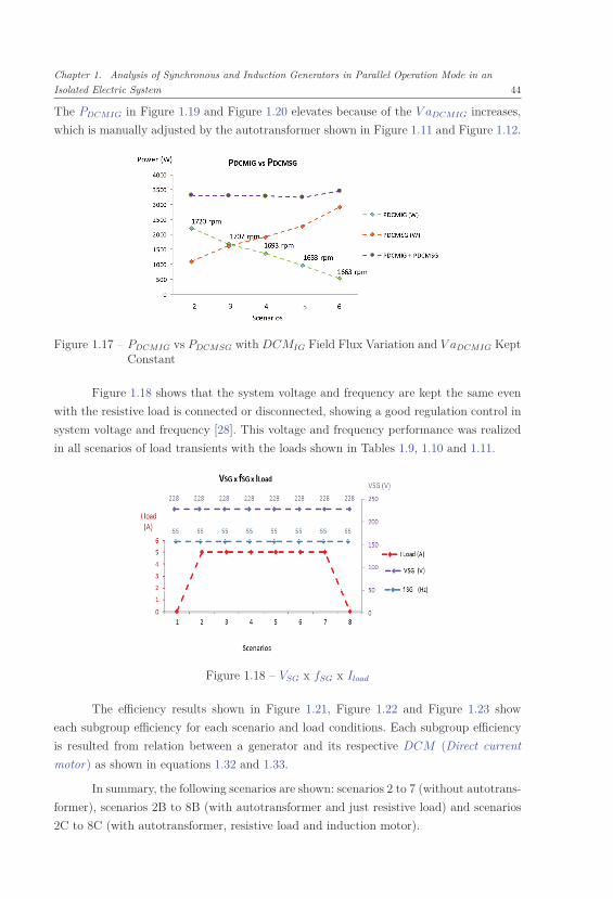
Chapter 1. Analysis of Synchronous and Induction Generators in Parallel Operation Mode in an
Isolated Electric System 44
The PDCMIG in Figure 1.19 and Figure 1.20 elevates because of the V aDCMIG increases,
which is manually adjusted by the autotransformer shown in Figure 1.11 and Figure 1.12.
Figure 1.17 – PDCMIG vs PDCMSG with DCMIG Field Flux Variation and V aDCMIG KeptConstant
Figure 1.18 shows that the system voltage and frequency are kept the same even
with the resistive load is connected or disconnected, showing a good regulation control in
system voltage and frequency [28]. This voltage and frequency performance was realized
in all scenarios of load transients with the loads shown in Tables 1.9, 1.10 and 1.11.
Figure 1.18 – VSG x fSG x Iload
The efficiency results shown in Figure 1.21, Figure 1.22 and Figure 1.23 show
each subgroup efficiency for each scenario and load conditions. Each subgroup efficiency
is resulted from relation between a generator and its respective DCM (Direct current
motor) as shown in equations 1.32 and 1.33.
In summary, the following scenarios are shown: scenarios 2 to 7 (without autotrans-
former), scenarios 2B to 8B (with autotransformer and just resistive load) and scenarios
2C to 8C (with autotransformer, resistive load and induction motor).
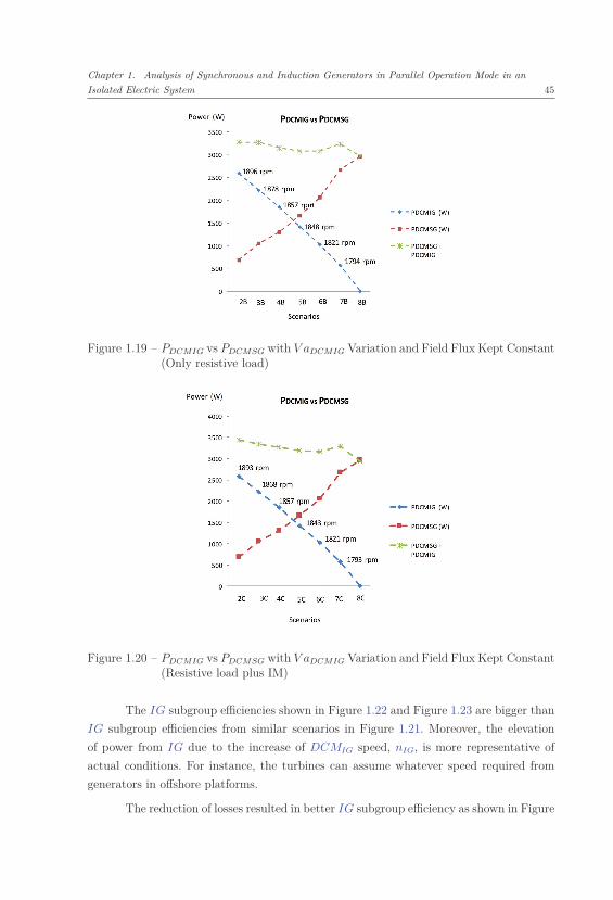
Chapter 1. Analysis of Synchronous and Induction Generators in Parallel Operation Mode in an
Isolated Electric System 45
Figure 1.19 – PDCMIG vs PDCMSG with V aDCMIG Variation and Field Flux Kept Constant(Only resistive load)
Figure 1.20 – PDCMIG vs PDCMSG with V aDCMIG Variation and Field Flux Kept Constant(Resistive load plus IM)
The IG subgroup efficiencies shown in Figure 1.22 and Figure 1.23 are bigger than
IG subgroup efficiencies from similar scenarios in Figure 1.21. Moreover, the elevation
of power from IG due to the increase of DCMIG speed, nIG, is more representative of
actual conditions. For instance, the turbines can assume whatever speed required from
generators in offshore platforms.
The reduction of losses resulted in better IG subgroup efficiency as shown in Figure
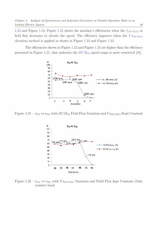
Chapter 1. Analysis of Synchronous and Induction Generators in Parallel Operation Mode in an
Isolated Electric System 46
1.22 and Figure 1.23. Figure 1.21 shows the machine’s efficiencies when the IfDCMIG or
field flux decreases to elevate the speed. The efficiency improves when the V aDCMIG
elevation method is applied as shown in Figure 1.22 and Figure 1.23.
The efficiencies shown in Figure 1.22 and Figure 1.23 are higher than the efficiency
presented in Figure 1.21, that indicates the DCMIG speed range is more restricted [28].
Figure 1.21 – nIG vs nSG with DCMIG Field Flux Variation and V aDCMIG Kept Constant
Figure 1.22 – nIG vs nSG with V aDCMIG Variation and Field Flux kept Constant (Onlyresistive load)

Chapter 1. Analysis of Synchronous and Induction Generators in Parallel Operation Mode in an
Isolated Electric System 47
Figure 1.23 – nIG vs nSG with V aDCMIG Variation and Field Flux kept Constant (Resis-tive load plus IM)
1.10 Conclusion
The cited electric system shows voltage and frequency regulation for each scenario
transition as demonstrated in Figure 1.18, tables 1.9, 1.10 and 1.11 and respective analysis.
SG presented the master behavior for the system frequency and voltage as [28].
IG did the master behaviour for the active power and slave behavior for the system
frequency and voltage. SG controls the system voltage and frequency and IG follows the
voltage and frequency defined by SG. The IG establishes the active power supplied to
the system and the SG complements the rest of active power and reactive power required.
The PSG depends on the IG shaft speed imposed by DCMIG. The PSG and the system
voltage and frequency are controlled respectively by field voltage and speed control loops
presented in Figure 1.10, Figure 1.11 and Figure 1.12.
It was realized a bigger PIG range in the scenarios shown in Table 1.9 and in
Table 1.10, than the scenarios shown in Table 1.11 due to V aDCMIG elevation method.
The PSG fulfilled the load power automatically from the PIG manually adjusted by
autotransformer.
The field flux variation method of DCMIG, [28], does not result in PDCMIG in-
crease, whereas the V aDCMIG elevation method results in increase of PDCMIG, PIG and
IG subgroup efficiency. The increase of PIG is resulted from IG speed increase, nIG, that
was obtained by elevation of V aDCMIG as shown in Figure 1.15, Figure 1.16, Figure 1.19
and Figure 1.20.
The use of V aDCMIG method, instead of Vdc steady source or flux (IfDCMIG)
reduction method, enables to reach the IaDCMIG limit of 8.0 A and 1893 rpm of DCMIG
shaft speed. It is higher than the DCMIG speed from Vdc steady source, see Figure 1.21.
The efficiencies from the V aDCMIG elevation method were greater than those from

Chapter 1. Analysis of Synchronous and Induction Generators in Parallel Operation Mode in an
Isolated Electric System 48
the scheme with Vdc steady source [28], as shown in Figure 1.22 and Figure 1.23. V aDCMIG
elevation method does not have the additional current losses that the Vdc steady source
method have.
The Vdc steady source method consist of reduction of field flux φ, IfDCMIG, and
increasing of IaDCMIG as 1.3. Then, the IG speed, nIG, is increased as equation 1.2.
The main losses for the Vdc steady source method are related to higher IaDCMIG
elevation, P(w) = Ra∗Ia2DCMIG, than the IaDCMIG elevation caused by V aDCMIG elevation
method. Then, by use of Vdc steady source method, the IaDCMIG is elevated due to
reduction of IfDCMIG. The higher IaDCMIG is, the higher losses are. Then, as the losses
of V aDCMIG elevation method are lower, the efficiencies are higher.
As shown in power performance graphs related to V aDCMIG elevation method,
Figure 1.15, Figure 1.16, Figure 1.19 and Figure 1.20, the PIG and PDCMIG are more
representative of actual operation conditions.
All of the followings three different methods of IG connection into the electric
system were implemented and the results were satisfactory: (i) direct startup as a motor
and rising the induction motor speed up to it turns IG, (ii) synchronism of self-excited
IG with the electric system and (iii) adjustment of IG speed at synchronous speed and
IG connection into the system;
49
2 Load and Generation Transients of Syn-
chronous and Induction Generators in Par-
allel Operation Mode in an Isolated Electric
System
2.1 Introduction
This section presents an analysis of load and generation transients in an isolated
electric system with a parallel connection of one synchronous generator and induction
generator, each one coupled to a dc machine or primary machine as well as to a capacitor
bank. A resistive load is connected to the system. Changes in the load were intentionally
provoked. Then, each generator was removed, one at a time, and reconnected. The results
are shown here and the respective curves are analysed.
The results show the performance and responses of the cited system regarded to
either transients from load changes or from partial generation withdrawal [32].
Differently of scheme shown in Figure 1.10, the schemes shown in Figures 1.11,
1.12 and in the Figure 2.3 have an autotransformer for actuating directly in V aDCMIG in
order to permit a greater speed elevation range and, then, a higher power contribution
from the IG. Furthermore, the current resistor bank consists of three individual bank
resistors connected in parallel, as presented in Figure 2.3 [28].
In the experiments of this chapter, the first method of IG connection into the
electric system was implemented, (i) direct startup as a motor and rising the induction
motor speed up to it turns IG. As the wound rotor machine was used instead of squirrel
cage rotor machine, that first method can be used to the experiments described here.
As already informed in general introduction and in chapter 1, the wound rotor machine
can have an extra advantage that is the high startup torque due to resistors that can be
connected at the induction machine rotor circuit [24].
One of the motivations of this study is related to the main advantages of in-
duction generators over synchronous generators which are: brushless construction with
squirrel-cage rotor, reduced size and weight, absence of DC supply for excitation, reduced
maintenance cost, and better transient performance [8]. As previously informed, the use
of wound rotor machine does not make invalid the results obtained in this work for squir-
rel cage rotor machine because the functioning of both machines is the same, except the
Chapter 2. Load and Generation Transients of Synchronous and Induction Generators in Parallel
Operation Mode in an Isolated Electric System 50
possibility of increasing of wound rotor startup torque.
Then, this work presents conclusions about the system performance regarding to
load and generation transients.
2.2 Isolated Electric System
The isolated electric system was sized as shown by the equations and data given
in the following paragraphs. The equations are based on calculations in [33].
The system automatism consists of a voltage control loop and a speed control loop.
Both are inserted in the SG scheme, as shown in Figure 2.3.
The data plates of the principal equipment are shown in Tables 1.3 to Table 1.7.
The speed and voltage control loops are presented respectively in Figure 2.4 and
Figure 2.5.
The voltage and speed electronic control boards are shown in Figure 2.1, Figure
2.2 and Figure 2.3.
The parametrization used in both electronic control boards was shown in chapter
1, except de reference values of voltage and speed. The references of voltage and speed
control loops are respectively 68.6 and 60.1.
2.3 Data Plate
The equipment’s data plates are shown in tables 1.3 to 1.8. The tables 1.7 and 1.8
show the loads data plates that are used in the experiments along this work.
2.4 Equation - Part I
The equations of this section are the same used in the previous chapter as shown
in section 1.5.
2.5 Equation - Part II
The equations 2.1, 2.2, 2.3 and 2.4 together with the equations 2.5 to 2.11 were em-
ployed to calculate the power and efficiencies as shown in the Table 2.1 for each generator
and the entire group of machines.
I2SG = Iw2
SG + I2c1 (2.1)
Chapter 2. Load and Generation Transients of Synchronous and Induction Generators in Parallel
Operation Mode in an Isolated Electric System 51
I2IG = Iw2
IG + I2c2 (2.2)
Ic = Ic1 + Ic2 (2.3)
Iload = IwloadR = IwSG + IwIG (2.4)
As ISG, IIG, IC and IwloadR are measured values, (see Table 2.1), the system has
four variables and four equations. Then, for each scenario, the four variables IwSG, Ic1,
IwIG and Ic2 were calculated by Matlab software as appendix F and result in values
shown in Table 2.1.
The entire group efficiency and the efficiency of each subgroup were calculated
based on PIG, PSG, PDCMSG, and PDCMIG as follows.
PSG =√
3 × VSG × IwSG (2.5)
PIG =√
3 × VIG × IwIG (2.6)
PDCMSG = V aDCMSG × IaDCMSG (2.7)
PDCMIG = V aDCMIG × IaDCMIG (2.8)
ηgroup% =PSG + PIG
PDCMSG + PDCMIG
× 100 (2.9)
ηSG% =PSG
PDCMSG
× 100 (2.10)
ηIG% =PIG
PDCMIG
× 100 (2.11)
2.6 Experiment and Schemes
The experiment was mounted in the laboratory as shown in Figures 2.1, 2.2 and
2.3.
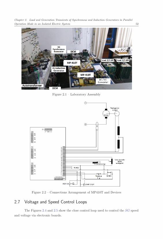
Chapter 2. Load and Generation Transients of Synchronous and Induction Generators in Parallel
Operation Mode in an Isolated Electric System 52
Figure 2.1 – Laboratory Assembly
Figure 2.2 – Connections Arrangement of MP410T and Devices
2.7 Voltage and Speed Control Loops
The Figures 2.4 and 2.5 show the close control loop used to control the SG speed
and voltage via electronic boards.

Chapter 2. Load and Generation Transients of Synchronous and Induction Generators in Parallel
Operation Mode in an Isolated Electric System 53
Figure 2.3 – Synchronous and Induction Generators in Parallel Operation Mode
Figure 2.4 – Speed Control Loop
Figure 2.5 – Field Voltage Control Loop
The master and slave behavior of the generators (SG is the master and IG is the
slave for the system frequency and voltage) as well as the IG is the master for the active
power supply as verified and detailed in chapter 1 of this work. The frequency and voltage
are determined by SG, while the active power consumed at load is supplied by the IG
and complemented by SG.
2.8 Experimental Data
The laboratorial data are shown in Table 2.1.
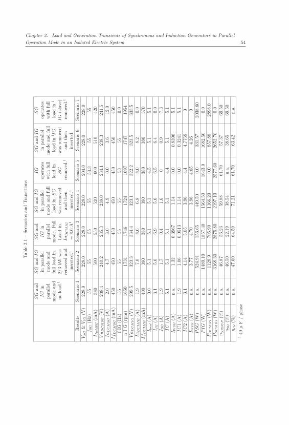
Chapter 2. Load and Generation Transients of Synchronous and Induction Generators in Parallel
Operation Mode in an Isolated Electric System 54
Tab
le2.
1–
Scen
ario
san
dT
rans
itio
ns
SG
and
IG
inpa
ralle
lm
ode
and
nolo
ad.1
SG
and
IG
inpa
ralle
lm
ode
and
full
load
in.
2/3
kWw
asre
mov
edan
din
sert
ed.1
SG
and
IG
inpa
ralle
lm
ode.
Full
Loa
din
.Ia
DC
MIG
=8.
6A
1
SG
and
IG
inpa
ralle
lm
ode
and
full
load
in.
SG
was
rem
oved
and
then
inse
rted
.1
IG
oper
ates
wit
hfu
lllo
adin
.S
G
rem
oved
.1
SG
and
IG
inpa
ralle
lm
ode
and
full
load
in.1 I
G
was
rem
oved
and
then
inse
rted
.
SG
oper
ates
wit
hfu
lllo
adin
.1
IG
(sla
ve)
rem
oved
.1
Res
ults
Scen
ario
1Sc
enar
io2
Scen
ario
3Sc
enar
io4
Scen
ario
5Sc
enar
io6
Scen
ario
7V
SG
&V
IG
(V)
228.
022
8.0
228.
022
8.0
204.
022
8.0
228.
0f
SG
(Hz)
5555
5555
53.3
5555
I fie
ldS
G(m
A)
380
500
550
520
600
510
420
Va
DC
MS
G(V
)23
8.4
240.
223
5.3
238.
023
4.1
238.
324
1.5
Ia
DC
MS
G(A
)2.
04.
73.
04.
90.
03.
612
.0If
DC
MS
G(m
A)
450
450
450
450
450
450
450
fIG
(Hz)
5555
5555
5355
0.0
nI
G(r
pm)
1650
1731
1746
1724
1697
1747
1954
Va
DC
MIG
(V)
299.
532
3.3
334.
432
3.1
322.
232
3.5
333.
5Ia
DC
MIG
(A)
1.9
7.0
8.6
6.8
8.0
8.2
0.0
If
DC
MIG
(mA
)40
038
038
038
038
038
037
0I l
oa
d(A
)0.
05.
15.
15.
14.
55.
15.
1I I
G(A
)3.
15.
66.
95.
66.
56.
40.
0I S
G(A
)1.
91.
70.
41.
60
0.9
7.3
IC
(A)
5.1
5.1
5.1
5.1
4.4
5.1
5.1
I WS
G(A
)n.
a.1.
320.
3967
1.14
0.0
0.83
965.
1IC
1(A
)1.
91.
060.
0513
1.14
0.0
0.32
415.
1IC
2(A
)3.
14.
145.
053.
964.
44.
7759
0I W
IG
(A)
n.a.
3.77
4.70
3.96
4.65
4.26
0P
SG
(W)
n.a.
524.
9115
6.65
449.
500.
033
1.57
2038
.60
PIG
(W)
n.a.
1489
.10
1857
.40
1564
.50
1643
.016
82.5
00.
0P
DC
MS
G(W
)n.
a.11
28.9
705.
9011
66.2
00.
085
7.88
2898
.0P
DC
MIG
(W)
n.a.
3168
.30
2875
.80
2197
.10
2577
.60
2652
.70
0.0
ηG
RO
UP
(%)
n.a.
46.8
756
.23
59.8
861
.70
57.3
769
.50
ηS
G(%
)n.
a.46
.50
22.1
938
.54
n.a.
38.6
569
.50
ηIG
(%)
n.a.
47.0
064
.59
71.2
161
.70
63.4
2n.
a.1
40μ
F/
phas
e
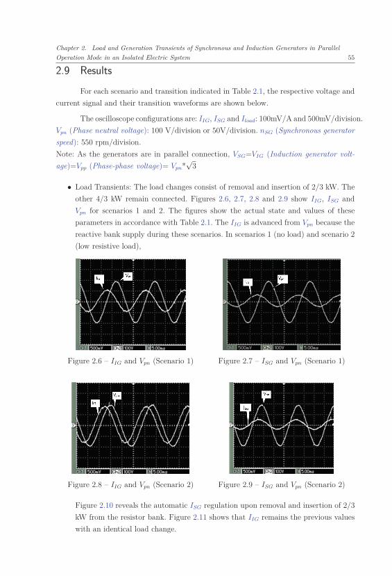
Chapter 2. Load and Generation Transients of Synchronous and Induction Generators in Parallel
Operation Mode in an Isolated Electric System 55
2.9 Results
For each scenario and transition indicated in Table 2.1, the respective voltage and
current signal and their transition waveforms are shown below.
The oscilloscope configurations are: IIG, ISG and Iload: 100mV/A and 500mV/division.
Vpn (Phase neutral voltage): 100 V/division or 50V/division. nSG (Synchronous generator
speed): 550 rpm/division.
Note: As the generators are in parallel connection, VSG=VIG (Induction generator volt-
age)=Vpp (Phase-phase voltage)= Vpn*√
3
• Load Transients: The load changes consist of removal and insertion of 2/3 kW. The
other 4/3 kW remain connected. Figures 2.6, 2.7, 2.8 and 2.9 show IIG, ISG and
Vpn for scenarios 1 and 2. The figures show the actual state and values of these
parameters in accordance with Table 2.1. The IIG is advanced from Vpn because the
reactive bank supply during these scenarios. In scenarios 1 (no load) and scenario 2
(low resistive load),
Figure 2.6 – IIG and Vpn (Scenario 1) Figure 2.7 – ISG and Vpn (Scenario 1)
Figure 2.8 – IIG and Vpn (Scenario 2) Figure 2.9 – ISG and Vpn (Scenario 2)
Figure 2.10 reveals the automatic ISG regulation upon removal and insertion of 2/3
kW from the resistor bank. Figure 2.11 shows that IIG remains the previous values
with an identical load change.
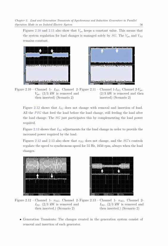
Chapter 2. Load and Generation Transients of Synchronous and Induction Generators in Parallel
Operation Mode in an Isolated Electric System 56
Figures 2.10 and 2.11 also show that Vpn keeps a constant value. This means that
the system regulation for load changes is managed solely by SG. The Vpn and VIG
remains constant.
Figure 2.10 – Channel 1- ISG, Channel 2-Vpn. (2/3 kW is removed andthen inserted) (Scenario 2)
Figure 2.11 – Channel 1-IIG, Channel 2-Vpn.(2/3 kW is removed and theninserted) (Scenario 2)
Figure 2.12 shows that IIG does not change with removal and insertion of load.
All the PIG that feed the load before the load change, still feeding the load after
the load change. The SG just participates this by complementing the load power
required.
Figure 2.13 shows that ISG adjustments for the load change in order to provide the
increased power required by the load.
Figures 2.12 and 2.13 also show that nSG does not change, and the SG’s controls
regulate the speed to synchronous speed for 55 Hz, 1650 rpm, always when the load
changes.
Figure 2.12 – Channel 1- nSG, Channel 2-IIG. (2/3 kW is removed andthen inserted.) (Scenario 2)
Figure 2.13 – Channel 1- nSG, Channel 2-ISG. (2/3 kW is removed andthen inserted.) (Scenario 2)
• Generation Transients: The changes created in the generation system consist of
removal and insertion of each generator.
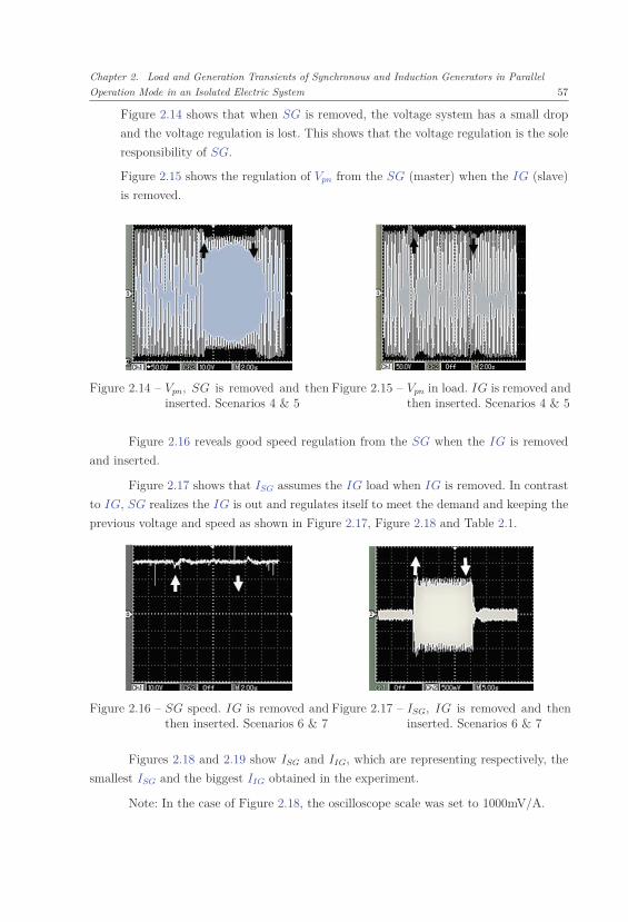
Chapter 2. Load and Generation Transients of Synchronous and Induction Generators in Parallel
Operation Mode in an Isolated Electric System 57
Figure 2.14 shows that when SG is removed, the voltage system has a small drop
and the voltage regulation is lost. This shows that the voltage regulation is the sole
responsibility of SG.
Figure 2.15 shows the regulation of Vpn from the SG (master) when the IG (slave)
is removed.
Figure 2.14 – Vpn, SG is removed and theninserted. Scenarios 4 & 5
Figure 2.15 – Vpn in load. IG is removed andthen inserted. Scenarios 4 & 5
Figure 2.16 reveals good speed regulation from the SG when the IG is removed
and inserted.
Figure 2.17 shows that ISG assumes the IG load when IG is removed. In contrast
to IG, SG realizes the IG is out and regulates itself to meet the demand and keeping the
previous voltage and speed as shown in Figure 2.17, Figure 2.18 and Table 2.1.
Figure 2.16 – SG speed. IG is removed andthen inserted. Scenarios 6 & 7
Figure 2.17 – ISG, IG is removed and theninserted. Scenarios 6 & 7
Figures 2.18 and 2.19 show ISG and IIG, which are representing respectively, the
smallest ISG and the biggest IIG obtained in the experiment.
Note: In the case of Figure 2.18, the oscilloscope scale was set to 1000mV/A.
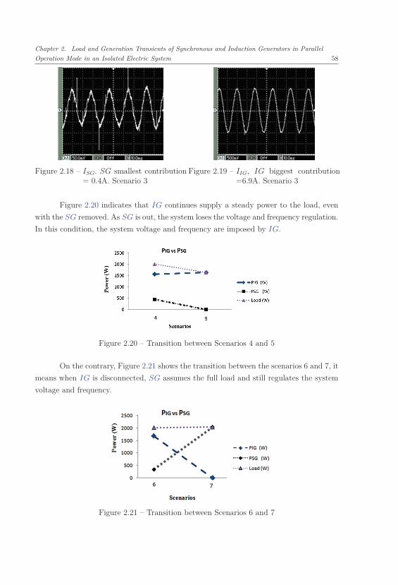
Chapter 2. Load and Generation Transients of Synchronous and Induction Generators in Parallel
Operation Mode in an Isolated Electric System 58
Figure 2.18 – ISG. SG smallest contribution= 0.4A. Scenario 3
Figure 2.19 – IIG, IG biggest contribution=6.9A. Scenario 3
Figure 2.20 indicates that IG continues supply a steady power to the load, even
with the SG removed. As SG is out, the system loses the voltage and frequency regulation.
In this condition, the system voltage and frequency are imposed by IG.
Figure 2.20 – Transition between Scenarios 4 and 5
On the contrary, Figure 2.21 shows the transition between the scenarios 6 and 7, it
means when IG is disconnected, SG assumes the full load and still regulates the system
voltage and frequency.
Figure 2.21 – Transition between Scenarios 6 and 7

Chapter 2. Load and Generation Transients of Synchronous and Induction Generators in Parallel
Operation Mode in an Isolated Electric System 59
2.10 Conclusion
Regarding to load changes, with removal and insertion of load, the SG can regulate
the system voltage and frequency. The ISG adjustments to the new load demand, while
the IIG keeps the previous values during transients. IG continues to supply the same
power previously set for.
Regarding to IG transients, IG removed or inserted, SG and its system can reg-
ulate the system voltage and frequency. This is running even if the IG is fully loaded or
IG is removed abruptly.
Regarding to SG transients, SG removed or inserted, IG is not capable of main-
taining the system voltage and frequency, because IG does not have the voltage and
frequency controls as the SG has. In this situation, the system frequency falls slightly as
well as the system voltage.
In addition, when the system has no load or has only 2/3 kW and the two machines
operating in parallel, when PDCMIG is elevated to a value bigger than 600 W, the system
frequency exceeds 55 Hz. Then, the IG and DCMIG group motorizes the SG, and the
DCMSG operates as a no load DCGSG (Direct current generator coupled with synchronous
generator). As it is shown in the scheme shown in Figure 2.3, there is not no other way
besides the load for receiving the generated power. Moreover, as the converter is operating
as rectifier instead of inverter, the generated energy does not have another way to be
regenerated or dissipated, then, the system frequency increases. When the system has 2/3
kW or 2kW connected, it is realized that the frequency does not exceed the rated value.
In this case, all generated power is being consumed by loads. It consists of scenarios two
to seven as shown in Table 2.1. Therefore, when PDCMIG is adjusted to a value bigger
than load power, the system frequency exceeds 55 Hz.
In [34] is shown two systems capable to regulate the system frequency in an electric
system, the one of them is able to regulate the system frequency in an isolated electric
that uses BL (Ballast load) (energy dissipation) and the other uses energy regeneration
to the grid. It requires interconnected system. This latter serves as a didactic alternative
only.
60
Conclusion
After the studies of DC machines regulators project (appendix A), thyristor fir-
ing circuit (appendix B), voltage regulators and filters project to synchronous machine
(appendix C) and four-quadrant operations for DC machines (appendix D) was possible
implement the target experiment of this work which consist of laboratorial scheme of
induction and Synchronous generators in parallel operation mode feeding inductive and
resistive loads. This experiment was target of analysis and studies of generation and load
transients and specific contingencies for this kind of generators topology.
The main conclusions about the experiments are:
1. The SG presents a master behavior for the system frequency and voltage. IG does
a master behavior for the active power supply and slave behavior for the system
frequency and voltage. SG controls the system voltage and frequency and IG es-
tablishes the active power supplied to the system and SG complements the rest of
active power and reactive power required;
2. The V aDCMIG elevation method resulted in increase of PDCMIG, PIG and higher
IG subgroup efficiency than the IfDCMIG reduction method [28]. The increase of
PDCMIG and PIG are consequences of IG speed increase, nIG, that was obtained
by elevation of V aDCMIG.
3. When the IG generates more than the load demand, the system frequency grows up
and stays out of rated system frequency. The IG motorizes synchronous machine
and DCMSG operates as a no load DCGSG;
4. In the scenario "IG out and IG in", SG and its system can regulate the system
voltage and frequency and SG keeps running even if the IG is fully loaded and
is removed abruptly. On the contrary, when the SG is disconnected, the system
voltage and frequency go out of control.
5. Voltage and speed control loops were implemented in lab to control the parallel
operation of synchronous and induction generators.
6. Three different methods of IG connection into the electric system were studied as
follow: (i) direct startup as a motor and rising the speed up to it turns IG, (ii)
synchronism of self-excited IG with the electric system and (iii) adjustment of IG
speed at synchronous speed and connection into the system;
Conclusion 61
7. It was used an original method to find power and efficiencies values of different
equipment in different scenarios as demonstrated in chapters 1, 2 and complemented
by appendix F;
8. The frequency elevation was checked when load transients happen in specific sce-
narios or PIG is bigger than load demand as indicated in chapter 2;
Based on the results obtained, the operation in parallel of induction and syn-
chronous generators in an isolated electric system is technically viable in MHPP and it
should be economic advantageous for MHPP and other applications due to some reasons
such as: the IG final price is so lower than SG final price even to big machines 25 MW
(information has obtained from Brazil traditional machine supplier), IG maintenance is
simpler and consequently cheaper and IG is lighter than SG. Beyond, The IG’s reply for
short circuit events is better than SG’s one because the IG contributes less than SG to
short circuit power, [20]. Otherwise, mainly for greater applications as oil platforms and
FPSO, there are other equipment and accessories that may be required, such as capacitor
bank, switches and filters which should be also considered for a more deeper economic
and technical evaluation.

Appendix
63
APPENDIX A – Filters and Regulators
Project
A.1 Introduction
In this appendix. two kinds of analogical filters and regulators for a DC motor
will be studied. namely a speed regulator that is composed of a speed control loop and
current regulators [35]. Both loops. the current control loop and speed control loop aim
to control the DC motor speed as shown in [34].
These loops will be used in primary machines that will serve as the primary drives
of induction and synchronous generators. The primary machines used in the experiments
are independent excitation ones. They are proper to speed control because their speed is
basically controlled by armature current or field flux variation.
Initially, in this appendix will be present some devices required in DC motor
controllers such as a ramp type firing circuit and synchronism transformer.
And then, it will be followed by practical cases and instructions of how design the
analogical speed and current DC machine regulators and how define filters, capacitors,
resistors and others necessary devices to implement the regulators. In add, all of the time
constants and gains values will be estimated or calculated and the experiments will be
didactically presented.
All the issues studied in this appendix are based on original and practical-case
projects carried out and tested in the Laboratory of research development of electrical
didactic laboratory of Federal University of Itajubá.
The analogical voltage regulator will be shown in appendix C.
The speed and current regulators used in chapters 1 and 2 are digital ones, other-
wise, these can be replaced by analogical ones as those described here and in appendixes
C and G.
A.2 Ramp Firing Circuit
The ramp-type firing system are used in all the experiments accomplished in this
work and its functioning shown in Figure A.1 was implemented either with an analogical
circuit detailed in appendix B or inside of the electronic board MP 410T algorithm used
in chapters 1 and 2:
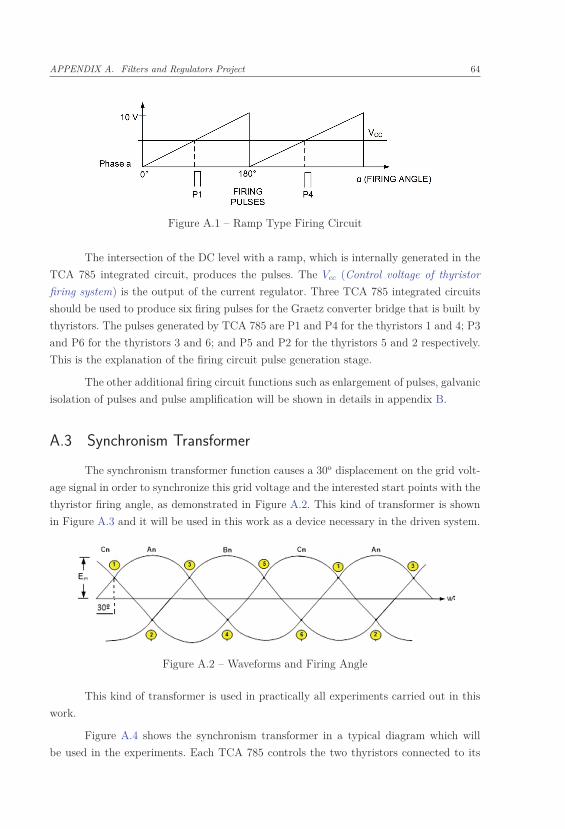
APPENDIX A. Filters and Regulators Project 64
Figure A.1 – Ramp Type Firing Circuit
The intersection of the DC level with a ramp, which is internally generated in the
TCA 785 integrated circuit, produces the pulses. The Vcc (Control voltage of thyristor
firing system) is the output of the current regulator. Three TCA 785 integrated circuits
should be used to produce six firing pulses for the Graetz converter bridge that is built by
thyristors. The pulses generated by TCA 785 are P1 and P4 for the thyristors 1 and 4; P3
and P6 for the thyristors 3 and 6; and P5 and P2 for the thyristors 5 and 2 respectively.
This is the explanation of the firing circuit pulse generation stage.
The other additional firing circuit functions such as enlargement of pulses, galvanic
isolation of pulses and pulse amplification will be shown in details in appendix B.
A.3 Synchronism Transformer
The synchronism transformer function causes a 30o displacement on the grid volt-
age signal in order to synchronize this grid voltage and the interested start points with the
thyristor firing angle, as demonstrated in Figure A.2. This kind of transformer is shown
in Figure A.3 and it will be used in this work as a device necessary in the driven system.
Figure A.2 – Waveforms and Firing Angle
This kind of transformer is used in practically all experiments carried out in this
work.
Figure A.4 shows the synchronism transformer in a typical diagram which will
be used in the experiments. Each TCA 785 controls the two thyristors connected to its
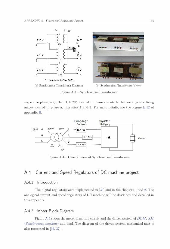
APPENDIX A. Filters and Regulators Project 65
(a) Synchronism Transformer Diagram (b) Synchronism Transformer Views
Figure A.3 – Synchronism Transformer
respective phase, e.g., the TCA 785 located in phase a controls the two thyristor firing
angles located in phase a, thyristors 1 and 4. For more details, see the Figure B.12 of
appendix B.
Figure A.4 – General view of Synchronism Transformer
A.4 Current and Speed Regulators of DC machine project
A.4.1 Introduction
The digital regulators were implemented in [36] and in the chapters 1 and 2. The
analogical current and speed regulators of DC machine will be described and detailed in
this appendix.
A.4.2 Motor Block Diagram
Figure A.5 shows the motor armature circuit and the driven system of DCM , SM
(Synchronous machine) and load. The diagram of the driven system mechanical part is
also presented in [36, 37].
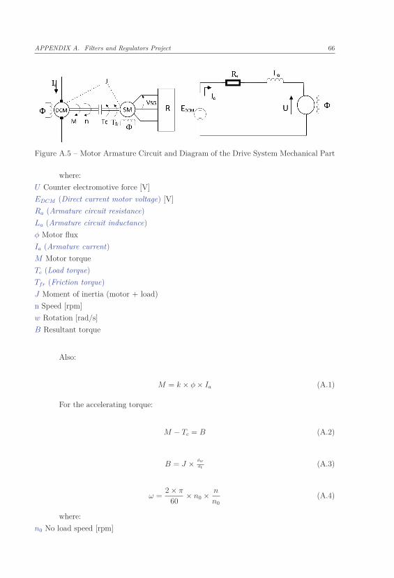
APPENDIX A. Filters and Regulators Project 66
Figure A.5 – Motor Armature Circuit and Diagram of the Drive System Mechanical Part
where:
U Counter electromotive force [V]
EDCM (Direct current motor voltage) [V]
Ra (Armature circuit resistance)
La (Armature circuit inductance)
φ Motor flux
Ia (Armature current)
M Motor torque
Tc (Load torque)
Tfr (Friction torque)
J Moment of inertia (motor + load)
n Speed [rpm]
w Rotation [rad/s]
B Resultant torque
Also:
M = k × φ × Ia (A.1)
For the accelerating torque:
M − Tc = B (A.2)
B = J × dw
dt(A.3)
ω =2 × π
60× n0 × n
n0
(A.4)
where:
n0 No load speed [rpm]
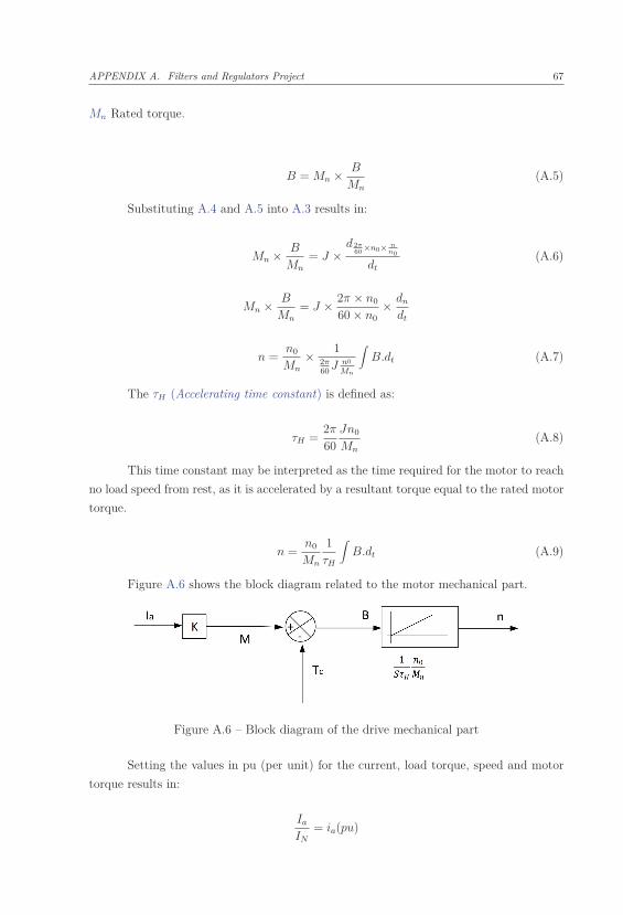
APPENDIX A. Filters and Regulators Project 67
Mn Rated torque.
B = Mn × B
Mn
(A.5)
Substituting A.4 and A.5 into A.3 results in:
Mn × B
Mn
= J ×d 2π
60×n0×
nn0
dt
(A.6)
Mn × B
Mn
= J × 2π × n0
60 × n0
× dn
dt
n =n0
Mn
× 12π60
J n0
Mn
∫B.dt (A.7)
The τH (Accelerating time constant) is defined as:
τH =2π
60Jn0
Mn
(A.8)
This time constant may be interpreted as the time required for the motor to reach
no load speed from rest, as it is accelerated by a resultant torque equal to the rated motor
torque.
n =n0
Mn
1τH
∫B.dt (A.9)
Figure A.6 shows the block diagram related to the motor mechanical part.
Figure A.6 – Block diagram of the drive mechanical part
Setting the values in pu (per unit) for the current, load torque, speed and motor
torque results in:
Ia
IN
= ia(pu)

APPENDIX A. Filters and Regulators Project 68
Tc
Mn
= tc(pu)
B
Mn
= b(pu)
n
n0
= nu(pu)
M
Mn
= m(pu)
The mechanical block diagram of Figure A.6 can be represented in pu as shown in
Figure A.7.
Figure A.7 – Representation of the Motor Mechanical Part in pu
Notes: 1- All variables from Figure A.6 are shown in Figure A.7 in per unit mode
and lower-case letters. 2- The variables ia (Armature current in pu) and m (Motor torque
in pu) are equal.
A.4.3 Armature Circuit Equations
In order to define the τa (Inductor circuit or armature time constant) and the
block diagram, the calculus are shown in the following.
EDCM = RaIa + La
dIa
dt
+ U (A.10)
Applying the Laplace transform results in:
EDCM = RaIa(S) + SLaIa(S) + U(S)
EDCM = U(S) = Ia(S)[Ra + SLa]
APPENDIX A. Filters and Regulators Project 69
ia(S) =EDCM(S) − U(S)
Ra + SLa
(A.11)
Defining τa:
τa =La
Ra
(A.12)
Ia(S) =EDCM(S) − U(S)
1 + Sτa
× 1Ra
(A.13)
Ia
IN
× IN =EDCM − U
Ra
× EN
EN
× 11 + Sτa
Ia
IN
=EDCM − U
ENRa
× EN
IN
× 11 + Sτa
Ia
IN
=EDCM − U
EN
× EN
RaIN
× 11 + Sτa
The armature current Ia seems to be normalized by the current IN (Rated Cur-
rent). Voltages EDCM and U are also normalized by the voltage EN (Rated voltage). The
normalized values are set as:
Ia =Ia
IN
(A.14)
e =EDCM
EN
(A.15)
u =U
EN
(A.16)
Vi =EN
RaIN
(A.17)
where Vi (Motor current amplification factor).
The block diagram of the DC motor armature circuit is shown in Fig. A.8.
The factor Vi
1+Sτacan be considered a delay element of the 1st order. The time
constant τa can be determined in one of two alternative ways:
a) Measuring La and Ra;
b) Applying a reduced voltage step in the armature circuit at the moment that
the rotor of the motor is blocked.
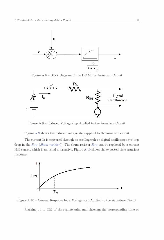
APPENDIX A. Filters and Regulators Project 70
Figure A.8 – Block Diagram of the DC Motor Armature Circuit
Figure A.9 – Reduced Voltage step Applied to the Armature Circuit
Figure A.9 shows the reduced voltage step applied to the armature circuit.
The current Ia is captured through an oscillograph or digital oscilloscope (voltage
drop in the RSH (Shunt resistor)). The shunt resistor RSH can be replaced by a current
Hall sensor, which is an usual alternative. Figure A.10 shows the expected time transient
response.
Figure A.10 – Current Response for a Voltage step Applied to the Armature Circuit
Marking up to 63% of the regime value and checking the corresponding time on
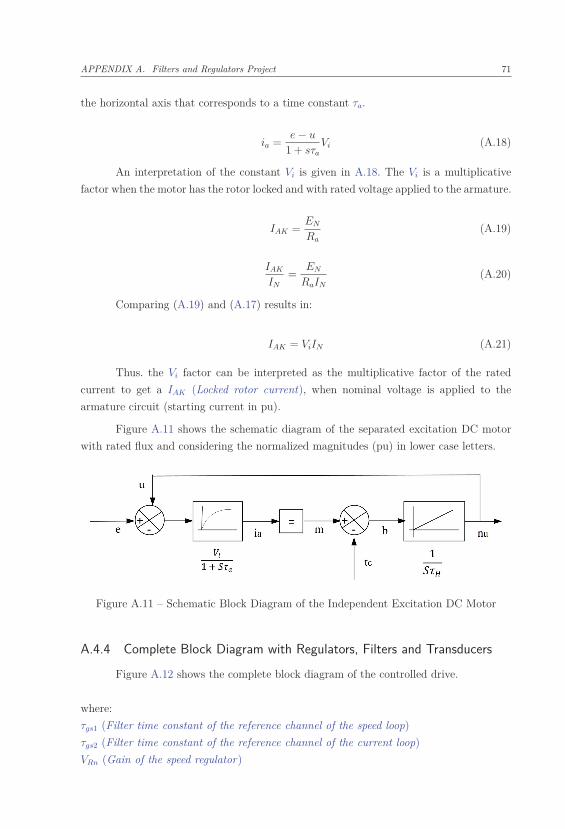
APPENDIX A. Filters and Regulators Project 71
the horizontal axis that corresponds to a time constant τa.
ia =e − u
1 + sτa
Vi (A.18)
An interpretation of the constant Vi is given in A.18. The Vi is a multiplicative
factor when the motor has the rotor locked and with rated voltage applied to the armature.
IAK =EN
Ra
(A.19)
IAK
IN
=EN
RaIN
(A.20)
Comparing (A.19) and (A.17) results in:
IAK = ViIN (A.21)
Thus. the Vi factor can be interpreted as the multiplicative factor of the rated
current to get a IAK (Locked rotor current), when nominal voltage is applied to the
armature circuit (starting current in pu).
Figure A.11 shows the schematic diagram of the separated excitation DC motor
with rated flux and considering the normalized magnitudes (pu) in lower case letters.
Figure A.11 – Schematic Block Diagram of the Independent Excitation DC Motor
A.4.4 Complete Block Diagram with Regulators, Filters and Transducers
Figure A.12 shows the complete block diagram of the controlled drive.
where:
τgs1 (Filter time constant of the reference channel of the speed loop)
τgs2 (Filter time constant of the reference channel of the current loop)
VRn (Gain of the speed regulator)

APPENDIX A. Filters and Regulators Project 72
Figure A.12 – Complete Block Diagram of Controlled Drive
VRi (Gain of the current regulator)
τn (Time constant of the speed regulator )
τi (Current regulator time constant)
τgn (Filter time constant of the speed transducer )
τgi (Filter time constant of the current transducer)
τss (Firing circuit time constant )
Vs (Gain of the static converter)
τa Inductor circuit or armature time constant
Vi (Gain of machine electric part)
Vcc Control voltage of thyristor firing circuit
ia Armature current in pu
tc (Load torque in pu)
nu (Speed in pu)
nREF (Reference speed)
The regulators shown in Fig. A.12 were considered as PI (proportional integral) and
their parameters will be determined by the design procedure in this work.
A.5 Current Regulator and Filters Project of DC Machine (practi-
cal case)
In this appendix will be described the current control loop with current regulators and
filters parameters project [37].
Figure A.13 shows the current regulation loop and Table A.1 shows the DC motor data.
The current transducer is a diode bridge connected between a resistor and the
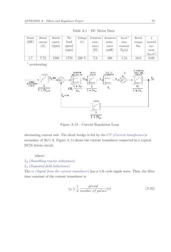
APPENDIX A. Filters and Regulators Project 73
Table A.1 – DC Motor Data
Power
(kW)Rated
current
(A)
Rated
speed
(rpm)
Noload
speed(rpm)
Voltage
(V)
Armature
resis-
tance
(Ω)
Armature
induc-
tance
(mH)
Accel.1
time
constant
TH(s)
Rated
torque
Nm
J
inertial
mo-
ment
(kg.m2)
1.7 7.72 1500 1770 220 V 7.0 490 1.54 10.8 0.09
1 accelerating
Figure A.13 – Current Regulation Loop
alternating current side. The diode bridge is fed by the CT (Current transformer)s
secondary of 30/5 A. Figure A.14 shows the current transducer connected in a typical
DCM driven circuit.
where:
Ld (Smoothing reactor inductance)
Ls (Separated field inductance)
The vi (Signal from the current transducer) has a 1/6 cycle ripple wave. Thus, the filter
time constant of the current transducer is:
τgi ≤ 12
period
number of pulses(s) (A.22)

APPENDIX A. Filters and Regulators Project 74
Figure A.14 – Current Transducer
τgi ≤ 12
× 16.7 × 10−3
6(s) ∴ τgi ≤ 1.39 ms
For 60 Hz, a period of 16.7 ms and a six-pulse bridge, the filter time constant of
the current transducer is then adopted as:
τgi ≤ 1.39 ms (A.23)
The firing circuit cannot instantly respond to the change in the firing angle α.
This time constant can vary in the range of zero to one sixth of a cycle. Thus, the time
constant of the firing circuit τss = 2.5 ms is defined.
From the armature resistance Ra and armature inductance La, the inductor circuit
time constant τa was obtained measuring La and Ra and calculated as demonstrated
below.
τa =La
Ra
=490 × 10−3
7(A.24)
τa =La
Ra
= 70 ms (A.25)
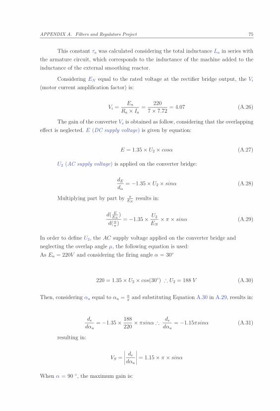
APPENDIX A. Filters and Regulators Project 75
This constant τa was calculated considering the total inductance La in series with
the armature circuit, which corresponds to the inductance of the machine added to the
inductance of the external smoothing reactor.
Considering EN equal to the rated voltage at the rectifier bridge output, the Vi
(motor current amplification factor) is:
Vi =En
Ra × Ia
=220
7 × 7.72= 4.07 (A.26)
The gain of the converter Vs is obtained as follow, considering that the overlapping
effect is neglected. E (DC supply voltage) is given by equation:
E = 1.35 × U2 × cosα (A.27)
U2 (AC supply voltage) is applied on the converter bridge:
dE
dα
= −1.35 × U2 × sinα (A.28)
Multiplying part by part by πEN
results in:
d( EEN
)
d(απ)
= −1.35 × U2
EN
× π × sinα (A.29)
In order to define U2, the AC supply voltage applied on the converter bridge and
neglecting the overlap angle μ, the following equation is used:
As En = 220V and considering the firing angle α = 30◦
220 = 1.35 × U2 × cos(30◦) ∴ U2 = 188 V (A.30)
Then, considering αu equal to αu = απ
and substituting Equation A.30 in A.29, results in:
de
dαu
= −1.35 × 188220
× πsinα ∴
de
dαu
= −1.15πsinα (A.31)
resulting in:
VS =
∣∣∣∣∣ de
dαu
∣∣∣∣∣ = 1.15 × π × sinα
When α = 90 ◦, the maximum gain is:
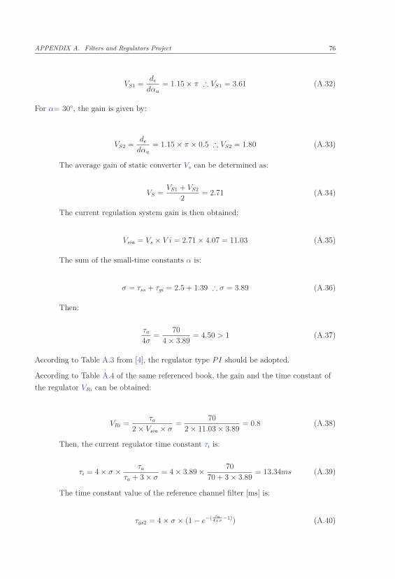
APPENDIX A. Filters and Regulators Project 76
VS1 =de
dαu
= 1.15 × π ∴ VS1 = 3.61 (A.32)
For α= 30◦, the gain is given by:
VS2 =de
dαu
= 1.15 × π × 0.5 ∴ VS2 = 1.80 (A.33)
The average gain of static converter Vs can be determined as:
VS =VS1 + VS2
2= 2.71 (A.34)
The current regulation system gain is then obtained:
Vsia = Vs × V i = 2.71 × 4.07 = 11.03 (A.35)
The sum of the small-time constants α is:
σ = τss + τgi = 2.5 + 1.39 ∴ σ = 3.89 (A.36)
Then:
τa
4σ=
704 × 3.89
= 4.50 > 1 (A.37)
According to Table A.3 from [4], the regulator type PI should be adopted.
According to Table A.4 of the same referenced book, the gain and the time constant of
the regulator VRi can be obtained:
VRi =τa
2 × Vsia × σ=
702 × 11.03 × 3.89
= 0.8 (A.38)
Then, the current regulator time constant τi is:
τi = 4 × σ × τa
τa + 3 × σ= 4 × 3.89 × 70
70 + 3 × 3.89= 13.34ms (A.39)
The time constant value of the reference channel filter [ms] is:
τgs2 = 4 × σ × (1 − e−( τa4×σ
−1)) (A.40)
APPENDIX A. Filters and Regulators Project 77
τgs2 = 4 × 3.89 × (1 − e−( 70
4×3.89−1)) = 15.09ms (A.41)
Capacitors Calculus
- Reference value filter:
Cs =RS1 + RS2
RS1 × RS2
∗ τgs2 (A.42)
Cs =22 + 2222 × 22
× 15.09 μF = 1.37 μF (A.43)
- Current transducer filter
Ci =Ri1 + Ri2
Ri1 × Ri2
∗ τgi (A.44)
Ci =15 + 1515 × 15
× 1.39 ∴ Ci = 0.19μF (A.45)
The closest and chosen capacitors values were Cs= 1.22 μF and Ci= 0.22 μF as
shown in Fig. A.15.
A.5.1 Current Regulator Parameters
In summary, the current regulator parameters are shown in Table A.2:
Table A.2 – Current Regulator Parameters
Type Gain(VRi)
TimeConstant
(τi)
Reference channelFilter time constant
(τgs2)
Feedback channelfilter time constant
(τgi)PI 0.8 13.34 15.09 1.39
A.5.2 Current Regulator Arrangement
Figure A.15 shows the current regulator. Its inner current loop structure was pro-
posed by [4].
APPENDIX A. Filters and Regulators Project 78
Figure A.15 – Implementation of Current Regulator
A.5.2.1 Calculus of RM ′′
2 and Rq′′
1
In order to make the adjustment of RM ′′
2 (Integral branch adjustment resistor of current
regulator) and R′′
q1 (Proportional branch adjustment resistor of current regulator), the
specific values of each one of these resistors will be calculated.
RM ′′
2 was obtained as:
τn = (RM ′′
1 + RM ′′
2 ) × CF ′′ (A.46)
RM ′′
1 + RM ′′
2 =τi
CF ′′=
(13.34 × 10⁻³
8.8 × 10⁻⁶
)= 1.52 kΩ (A.47)
RM ′′
2 =τi
CF ′′− RM ′′
1 = 1520 − 470 = 1.05kΩ (A.48)
The R′′
aj (adjustment resistance of current regulator) was calculated as:
R′′
aj =
(R′′
F × (R′′
q1 + R′′
q2))
(VRi × (R′′
i1 + R′′
i2))(A.49)
R′′
aj =(10 × (4.7 + 0.47)(0.8 × (15 + 15))
× 103 (A.50)
R′′
aj = 2.15kΩ (A.51)
APPENDIX A. Filters and Regulators Project 79
Then, as R′′
q2 (Proportional branch steady resistor of current regulator)=470 Ω
R′′
q1 + R′′
q2 = 2150 Ω (A.52)
R′′
q1 = 2150 − 470 Ω (A.53)
R′′
q1 = 1.68 kΩ (A.54)
Adopting the VRi as the variable in evidence, it will be possible to find the VRi limits by
just changing R′′
aj as follows.
Equation A.49 and isolating the variable VRi, it results in:
VRi =
(R′′
F × (R′′
q1 + R′′
q2))
(R′′
aj × (R′′
i1 + R′′
i2)) (A.55)
For the minimum R′′
aj=0.47 k Ω, the maximum VRi is:
VRimax =(10 × (4.7 + 0.47)(0.47 × (15 + 15))
= 3.6 (A.56)
For the maximum R′′
aj= 4.8 k Ω, the minimum VRi is:
VRimin =(10 × (5.17 + 0.47)(4.8 × (15 + 15))
= 0.33 (A.57)
Thus, as the defined resistors, the VRi can vary from 0.33 to 3.6.
The current regulator data are given in Table A.3.
Table A.3 – Complementary Current Regulator Data
OptimizedR′′
aj
R′′
q1 RM ′′
2 Optimizedgain (VRi)
Minimumgain
(VRimin)
Maximumgain
(VRimax)2.15 k Ω 1.68 kΩ 1.05 kΩ 0.8 0.33 3.6
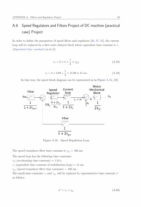
APPENDIX A. Filters and Regulators Project 80
A.6 Speed Regulators and Filters Project of DC machine (practical
case) Project
In order to define the parameters of speed filters and regulators [36, 37, 35], the current
loop will be replaced by a first order delayed block whose equivalent time constant is τe
(Equivalent time constant) as in [4]:
τe = 2 × σ +12
× τgs2 (A.58)
τe = 2 × 3.89 +12
× 15.09 ≈ 15 ms (A.59)
In that way, the speed block diagram can be represented as in Figure A.16, [38]:
Figure A.16 – Speed Regulation Loop
The speed transducer filter time constant is τgn = 100 ms.
The speed loop has the following time constants:
τH (accelerating time constant) = 1.54 s
τe (equivalent time constant of stabilization loop) = 15 ms
τgn (speed transducer filter time constant) = 100 ms
The small-time constants τe and τgn will be replaced by representative time constant σ′
as follows:
σ′ = τe + τgn (A.60)

APPENDIX A. Filters and Regulators Project 81
σ′ = 15 + 100 = 115 ms (A.61)
As the division τH
4×σ′= 1.54
4×0.115= 3.34 > 1, then, in accordance with Table 6.3 from [4], a
proportional-integral regulator (PI) should be used.
From Table 6.4 from [4], the optimized gain and time constant of the regulator are:
VRN =τH
2 × σ′=
1.542 × 0.115
= 6.7 (A.62)
τn = 4 × σ′ = 460 ms (A.63)
The speed transducer is a tachogenerator coupled with the DC motor shaft. The filter
was used to reduce the high wave that was part of the tachogenerator output voltage.
The considered time constant was:
τgn = 100 ms (A.64)
The reference channel filter has the following time constant:
τgs1 = 4 × σ′ × (1 − e−(
τH4×σ′
−1)) = 416 ms (A.65)
A.6.1 Capacitors calculus
Adopting the resistances R′
s1= R′
s2= 100 k Ω as part of the reference value filter and
R′
i1= R′
i2= 100 kΩ as part of the speed transducer filter, it results in:
- Reference value filter capacitor:
Cn =R′
S1 + R′
S2
R′
S1 × R′
S2
∗ τgs1 = 8.32 μF (A.66)
The closest capacitor value was got by four capacitors 2.2 μF in parallel, resulting in 8.8
μF .
- Speed transducer filter capacitor:
CL =R′
i1 + R′
i2
R′
i1 × R′
i2
∗ τgn = 2.2 μF (A.67)
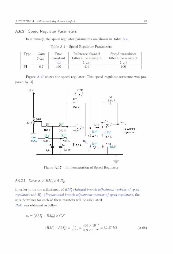
APPENDIX A. Filters and Regulators Project 82
A.6.2 Speed Regulator Parameters
In summary, the speed regulator parameters are shown in Table A.4.
Table A.4 – Speed Regulator Parameters
Type Gain(VRN)
TimeConstant
(τn)
Reference channelFilter time constant
(τgs1)
Speed transducerfilter time constant
(τgn)PI 6.7 460 416 100
Figure A.17 shows the speed regulator. This speed regulator structure was pro-
posed by [4]
Figure A.17 – Implementation of Speed Regulator
A.6.2.1 Calculus of RM ′
2 and R′
q1
In order to do the adjustment of RM ′
2 (Integral branch adjustment resistor of speed
regulator) and R′
q1 (Proportional branch adjustment resistor of speed regulator), the
specific values for each of these resistors will be calculated.
RM ′
2 was obtained as follow:
τn = (RM ′
1 + RM ′
2) × CF ′
(RM ′
1 + RM ′
2) =τn
CF ′=
460 × 10−3
8.8 × 10−6= 52.27 kΩ (A.68)
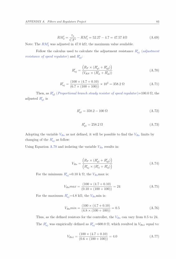
APPENDIX A. Filters and Regulators Project 83
RM ′
2 =τn
CF ′− RM ′
1 = 52.27 − 4.7 = 47.57 kΩ (A.69)
Note: The RM ′
2 was adjusted in 47.0 kΩ, the maximum value available.
Follow the calculus used to calculate the adjustment resistance R′
aj (adjustment
resistance of speed regulator) and R′
q1:
R′
aj =
(RF × (R′
q1 + R′
q2))
(VRN × (R′
i1 + R′
i2))(A.70)
R′
aj =(100 × (4.7 + 0.10)(6.7 × (100 + 100))
× 103 = 358.2 Ω (A.71)
Then, as R′
q2 (Proportional branch steady resistor of speed regulator)=100.0 Ω, the
adjusted R′
q1 is
R′
q1 = 358.2 − 100 Ω (A.72)
R′
q1 = 258.2 Ω (A.73)
Adopting the variable VRn as not defined, it will be possible to find the VRn limits by
changing of the R′
aj as follow:
Using Equation A.70 and isolating the variable VRn results in:
VRn =
(RF × (R′
q1 + R′
q2))
(R′
aj × (R′
i1 + R′
i2)) (A.74)
For the minimum R′
aj=0.10 k Ω, the VRnmax is:
VRnmax =(100 × (4.7 + 0.10)
(0.10 × (100 + 100))= 24 (A.75)
For the maximum R′
aj=4.8 kΩ, the VRnmin is:
VRnmin =(100 × (4.7 + 0.10)(4.8 × (100 + 100))
= 0.5 (A.76)
Thus, as the defined resistors for the controller, the VRn can vary from 0.5 to 24.
The R′
aj was empirically defined as R′
aj=600.0 Ω, which resulted in VRn1 equal to:
VRn1 =(100 × (4.7 + 0.10)(0.6 × (100 + 100))
= 4.0 (A.77)

APPENDIX A. Filters and Regulators Project 84
Then, instead of considering the optimized value VRn= 6.7, (A.62), VRn1=4.0 was
considered for this practical experiment and the results are shown below.
The speed regulator data follow in Table A.5.
Table A.5 – Speed Regulator Parameters
OptimizedR′
aj
R′
q1 RM ′
2 Optimizedgain VRn
Minimumgain
(VRnmin)
Maximumgain
(VRnmax)358.2 Ω 258.2 Ω 47.57 k Ω 6.7 0.5 24
A.6.3 General Arrangement
Figure A.18 shows the general diagram including all the module interconnections
[36], [37].
Notes:
1- The P1 value (the maximum speed adjustment) was empirically adjusted as shown in
Fig. A.18.
2- By means of P2 shown in Fig. A.18; increasing the gain of Q6, the limit current
of main circuit is decreased; in other way, when the gain is decreased, the limit current is
increased, see the block diagram in Fig. A.12.
A.7 Results
Although the optimized gain VRn of 6.7 has been calculated, the gain was empiri-
cally adjusted to 4.0 with the R′
aj equal to 600 Ω.
The motor speed and current waveforms for the gain of 4.0 are shown in Fig. A.19
at the moment when the motor is driven by the control system from its rest position.
The gain was empirically adjusted to 4.0 with the R′
aj equal to 600 Ω, which resulted in
a satisfactory dynamic response to the current and speed startup transitory, as shown in
Fig. A.19, (yellow curve: current and blue curve: speed).
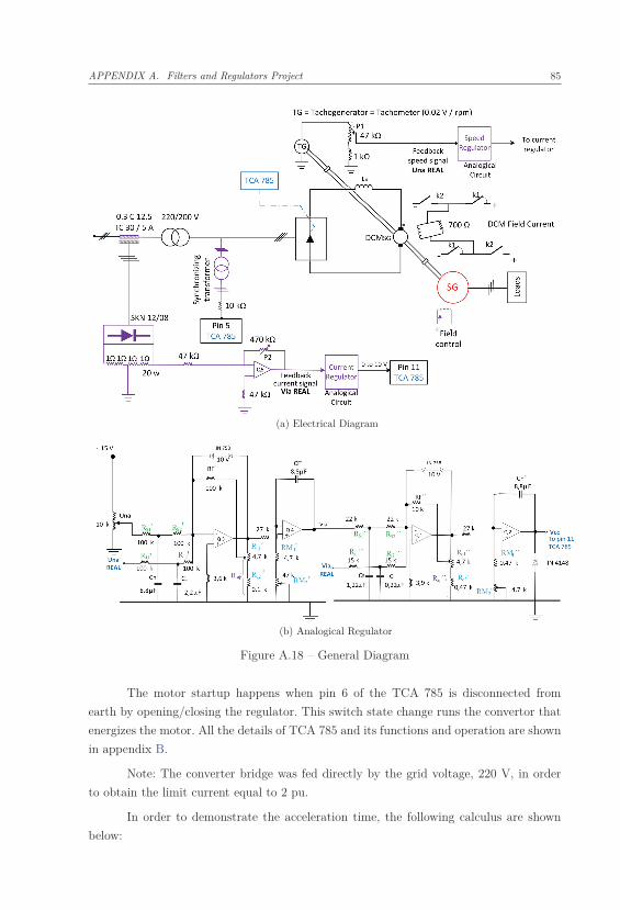
APPENDIX A. Filters and Regulators Project 85
(a) Electrical Diagram
(b) Analogical Regulator
Figure A.18 – General Diagram
The motor startup happens when pin 6 of the TCA 785 is disconnected from
earth by opening/closing the regulator. This switch state change runs the convertor that
energizes the motor. All the details of TCA 785 and its functions and operation are shown
in appendix B.
Note: The converter bridge was fed directly by the grid voltage, 220 V, in order
to obtain the limit current equal to 2 pu.
In order to demonstrate the acceleration time, the following calculus are shown
below:
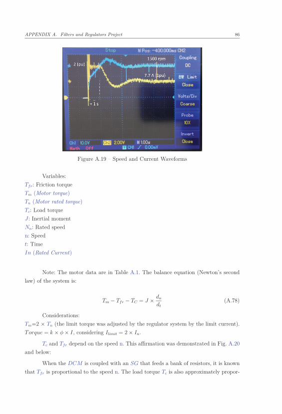
APPENDIX A. Filters and Regulators Project 86
Figure A.19 – Speed and Current Waveforms
Variables:
Tfr: Friction torque
Tm (Motor torque)
Tn (Motor rated torque)
Tc: Load torque
J : Inertial moment
Nn: Rated speed
n: Speed
t: Time
In (Rated Current)
Note: The motor data are in Table A.1. The balance equation (Newton’s second
law) of the system is:
Tm − Tfr − TC = J × dn
dt
(A.78)
Considerations:
Tm=2 × Tn (the limit torque was adjusted by the regulator system by the limit current).
Torque = k × φ × I, considering Ilimit = 2 × In.
Tc and Tfr depend on the speed n. This affirmation was demonstrated in Fig. A.20
and below:
When the DCM is coupled with an SG that feeds a bank of resistors, it is known
that Tfr is proportional to the speed n. The load torque Tc is also approximately propor-
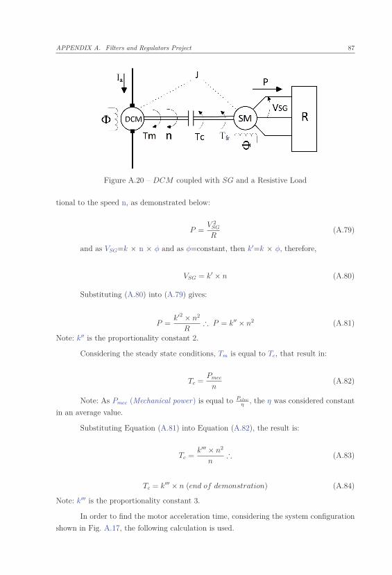
APPENDIX A. Filters and Regulators Project 87
Figure A.20 – DCM coupled with SG and a Resistive Load
tional to the speed n, as demonstrated below:
P =V 2
SG
R(A.79)
and as VSG=k × n × φ and as φ=constant, then k′=k × φ, therefore,
VSG = k′ × n (A.80)
Substituting (A.80) into (A.79) gives:
P =k′2 × n2
R∴ P = k′′ × n2 (A.81)
Note: k′′ is the proportionality constant 2.
Considering the steady state conditions, Tm is equal to Tc, that result in:
Tc =Pmec
n(A.82)
Note: As Pmec (Mechanical power) is equal to Pelec
η, the η was considered constant
in an average value.
Substituting Equation (A.81) into Equation (A.82), the result is:
Tc =k′′′ × n2
n∴ (A.83)
Tc = k′′′ × n (end of demonstration) (A.84)
Note: k′′′ is the proportionality constant 3.
In order to find the motor acceleration time, considering the system configuration
shown in Fig. A.17, the following calculation is used.
APPENDIX A. Filters and Regulators Project 88
Substituting Tm=2 × Tn into Equation (A.78) results in:
2 × Tn − Tfr − Tc = J × dn
dt
(A.85)
As the magnetic field φ is constant, then Tfr+Tc=(k1 + k2)× n, or, in summary:
Tfr + Tc = k′′′′ × n (A.86)
Note: k′′′′ is the proportionality constant 4.
Substituting Equation (A.86) into Equation (A.85) gives:
2 × Tn − k′′′′ × n = J × dn
dt
(A.87)
From Table A.1, Tn=10.8 Nm.
J × dn
dt
+ k′′′′ × n = 2 × 10.8 (A.88)
dn
dt
+k′′′′
J× n =
21.6J
(A.89)
For k′′′′ definition, the motor speed is in rated speed as described below:
Tn = k′′′′ × 2 × π
60× 1500 (A.90)
k′′′′ =60 × 10.8
2 × π × 1500∴ (A.91)
k′′′′ =64.8
300 × π= 0.069
Nmrad
s
(A.92)
Getting J of motor plus load from Table A.1 and substituting k′′′′ from (A.92 into
Equation (A.89) gives:
dn
dt
+0.0690.09
× n =21.60.09
(A.93)
Linear differential equation:
dn
dt
+ 0.77 × n = 240 (A.94)
APPENDIX A. Filters and Regulators Project 89
Considering [39], the solution for (A.94) is:
n = e−
∫P dt ×
[∫Q × e
∫P dtdt + C
](A.95)
Considering [39] and Equation (A.94), P= 0.77 and Q= 240, then:
n = e−
∫0.77dt ×
[∫240 × e
∫0.77dtdt + C
](A.96)
n = e−0.77t ×[∫
240 × e0.77tdt + C
](A.97)
n = e−0.77t ×[∫ 240 × e0.77t
0.77+ C
](A.98)
n = e−0.77t ×[311.68 × e0.77t + C
](A.99)
In order to find the constant C, the boundary condition is used:
Fort = 0, n = 0 (A.100)
Substituting (A.100) into (A.99) gives:
0 = 1 × [311.68 + C] (A.101)
C = −311.68 (A.102)
Substituting (A.102) into (A.99) gives:
n = e−0.77t ×[311.68 × e0.77t − 311.68
] rad
s(A.103)
Converting rads
to rpm results in:
n = e−0.77t ×[311.68 × e0.77t − 311.68
]× 60
2 × πrpm (A.104)
n = 2976.32e−0.77t ×[e0.77t − 1
]rpm (A.105)
For n=1500 rpm, it gives:
1500 = 2976.32e−0.77t ×[e0.77t − 1
](A.106)

APPENDIX A. Filters and Regulators Project 90
1500 = 2976.32 ×[1 − e−0.77t
](A.107)
Solving the equation (A.107) by the iterative method results in:
t = 0.91s (A.108)

91
APPENDIX B – Analogical Control Board
(Firing Circuit)
B.1 Introduction
This appendix presents the concepts of operation and functioning of firing circuit
to control the three-phase thyristor bridge firing angle using the integrated circuit TCA
785 and other components, The TCA 785 was developed by ICOTRON-SIEMENS. This
firing circuit was implemented and tested in the Laboratory of research development of
electrical didactic laboratory of Federal University of Itajubá [40], [41], [3].
This electronic circuit generates all the logic of the command signals that will
control the thyristors operation. The aim of the device is to drive the thyristors by using
the necessary gate current.
This firing circuit was developed to control the firing angle of thyristors, transistors,
and TRIACs continually in the 0◦ to 180◦ range. It has a large number of configurations
and few external components.
In the first part of this appendix is shown the firing circuit logic and, in the second
part, the functions are shown. The most contribution of this appendix is the presentation
of a complete firing circuit with all details that becomes possible an easy implementation.
This kind of control board is used in the primary machine of the synchronous
generator in order to control the primary machine speed that drives the SG.
Figure B.1 shows the basic organization of the control circuit in block diagram.
Figure B.1 – Basic Organization of Control Circuit.
Legend
1: Function of synchronism and sawtooth wave generation
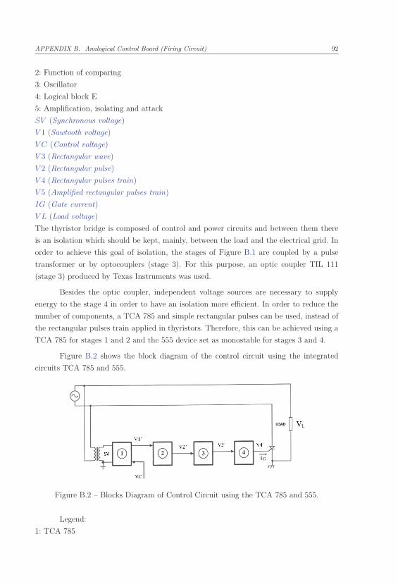
APPENDIX B. Analogical Control Board (Firing Circuit) 92
2: Function of comparing
3: Oscillator
4: Logical block E
5: Amplification, isolating and attack
SV (Synchronous voltage)
V 1 (Sawtooth voltage)
V C (Control voltage)
V 3 (Rectangular wave)
V 2 (Rectangular pulse)
V 4 (Rectangular pulses train)
V 5 (Amplified rectangular pulses train)
IG (Gate current)
V L (Load voltage)
The thyristor bridge is composed of control and power circuits and between them there
is an isolation which should be kept, mainly, between the load and the electrical grid. In
order to achieve this goal of isolation, the stages of Figure B.1 are coupled by a pulse
transformer or by optocouplers (stage 3). For this purpose, an optic coupler TIL 111
(stage 3) produced by Texas Instruments was used.
Besides the optic coupler, independent voltage sources are necessary to supply
energy to the stage 4 in order to have an isolation more efficient. In order to reduce the
number of components, a TCA 785 and simple rectangular pulses can be used, instead of
the rectangular pulses train applied in thyristors. Therefore, this can be achieved using a
TCA 785 for stages 1 and 2 and the 555 device set as monostable for stages 3 and 4.
Figure B.2 shows the block diagram of the control circuit using the integrated
circuits TCA 785 and 555.
Figure B.2 – Blocks Diagram of Control Circuit using the TCA 785 and 555.
Legend:
1: TCA 785
APPENDIX B. Analogical Control Board (Firing Circuit) 93
2: Monostable 555
3: Optic coupler TIL 111
4: Amplification, isolating and attack
SV : Synchronous voltage
V 1′ (Rectangular pulse)
V 2′ (Wider Rectangular pulse), V 3′ (Wider Rectangular pulse) and V 4′ (Wider Rectan-
gular pulse)
V L: Load voltage
B.2 Stage Descriptions
This section will show the main characteristics of the integrated circuit TCA 785
and its functions.
B.2.1 Pulse generation by TCA 785
The main TCA 785 function is to control the firing angle of thyristors, TRIACs
and transistors continually in the range from 0◦ to 180◦. Its configuration options enable
a simplified selection of external devices for connections and disconnections. This keeps
the final circuit simpler and smaller than other available options.
B.2.2 Integrated Circuit Characteristics
The main characteristics of this integrated circuit are:
• Internal required current: 5 mA;
• Digital logic is highly immune to interference;
• Two main outputs with 55 mA current and two other outputs with open collector
pins rated to 1.5 mA current;
• Three TCA 785 are needed for a three-phase system;
• The period of the output pulse is defined by the external capacitor;
• The output voltage is adjusted at 3.1 V;
• Simultaneous inhibition of all outputs is possible;
• One output is for TRIACs control.
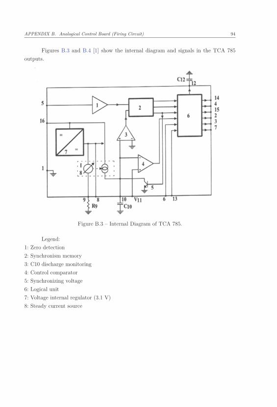
APPENDIX B. Analogical Control Board (Firing Circuit) 94
Figures B.3 and B.4 [1] show the internal diagram and signals in the TCA 785
outputs.
Figure B.3 – Internal Diagram of TCA 785.
Legend:
1: Zero detection
2: Synchronism memory
3: C10 discharge monitoring
4: Control comparator
5: Synchronizing voltage
6: Logical unit
7: Voltage internal regulator (3.1 V)
8: Steady current source
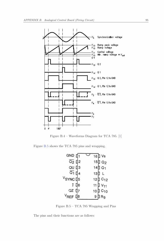
APPENDIX B. Analogical Control Board (Firing Circuit) 95
Figure B.4 – Waveforms Diagram for TCA 785. [1]
Figure B.5 shows the TCA 785 pins and wrapping.
Figure B.5 – TCA 785 Wrapping and Pins
The pins and their functions are as follows:
APPENDIX B. Analogical Control Board (Firing Circuit) 96
01 Ground
02 Pin 15 complementary output with open collector
03 Positive pulse output with open collector
04 Pin 14 complementary output with open collector
05 Synchronism input (antiparallel diodes)
06 Inhibits all outputs when they are grounded
07 Open collector output to activate TRIACs
08 Steady supply 3.1 V
09 Potentiometer to ramp adjustment (20 < R9 < 500kΩ)
10 Capacitor to generate the ramp (C10≤ 0.5μF )
11 Controls voltage input (DC)
12 Controls the output pulse width of 14 and 15
13 Controls the output pulse width of 02 and 04
14 Positive pulse output in the positive half wave
15 Positive pulse output in the negative half wave
16 DC supply; it is not guaranteed for stabilization
B.3 Operation of TCA 785
The integrated circuit (IC) feed is done by pin 16 referenced to the ground terminal
(pin 1) with a voltage range between 8 V and 18 V. Internally, the IC is fed by a regulated
voltage of 3.1 V, regardless of the possible changes in its external feed. The synchronism
is obtained by a zero detector (pin 5), which is connected to a synchronism transformer.
The ramp generator, whose control is located in the logical unit, consists of a steady
current source that charges an external capacitor C10. The charge current is set by an
external resistance R9 in order to adjust the ramp amplitude, which goes to zero whenever
the synchronism voltage exceeds zero. Then, the group R9 and C10 determine the ramp
inclination.
The control comparator compares the ramp voltage and control voltage and when
they are equal to each other, the comparator sends pulses to the output through the
logical unit. Then, positive pulses appear in the positive half-wave in the synchronism
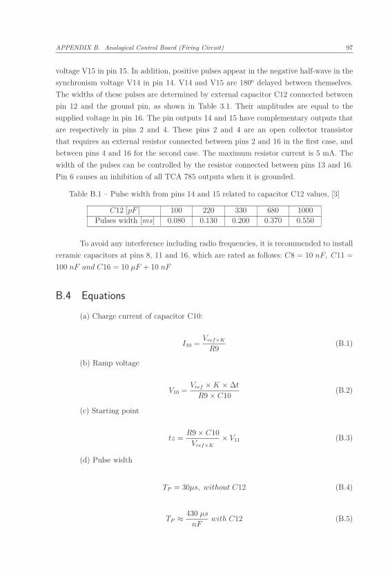
APPENDIX B. Analogical Control Board (Firing Circuit) 97
voltage V15 in pin 15. In addition, positive pulses appear in the negative half-wave in the
synchronism voltage V14 in pin 14. V14 and V15 are 180o delayed between themselves.
The widths of these pulses are determined by external capacitor C12 connected between
pin 12 and the ground pin, as shown in Table 3.1. Their amplitudes are equal to the
supplied voltage in pin 16. The pin outputs 14 and 15 have complementary outputs that
are respectively in pins 2 and 4. These pins 2 and 4 are an open collector transistor
that requires an external resistor connected between pins 2 and 16 in the first case, and
between pins 4 and 16 for the second case. The maximum resistor current is 5 mA. The
width of the pulses can be controlled by the resistor connected between pins 13 and 16.
Pin 6 causes an inhibition of all TCA 785 outputs when it is grounded.
Table B.1 – Pulse width from pins 14 and 15 related to capacitor C12 values, [3]
C12 [pF ] 100 220 330 680 1000Pulses width [ms] 0.080 0.130 0.200 0.370 0.550
To avoid any interference including radio frequencies, it is recommended to install
ceramic capacitors at pins 8, 11 and 16, which are rated as follows: C8 = 10 nF, C11 =
100 nF and C16 = 10 μF + 10 nF
B.4 Equations
(a) Charge current of capacitor C10:
I10 =Vref×K
R9(B.1)
(b) Ramp voltage
V10 =Vref × K × Δt
R9 × C10(B.2)
(c) Starting point
tz =R9 × C10
Vref×K
× V11 (B.3)
(d) Pulse width
TP = 30μs, without C12 (B.4)
TP ≈ 430 μs
nFwith C12 (B.5)
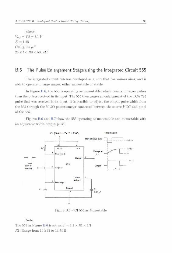
APPENDIX B. Analogical Control Board (Firing Circuit) 98
where:
Vref = V 8 = 3.1 V
K = 1.25
C10 ≤ 0.5 μF
25 kΩ < R9 < 500 kΩ
B.5 The Pulse Enlargement Stage using the Integrated Circuit 555
The integrated circuit 555 was developed as a unit that has various aims, and is
able to operate in large ranges, either monostable or stable.
In Figure B.6, the 555 is operating as monostable, which results in larger pulses
than the pulses received in its input. The 555 then causes an enlargement of the TCA 785
pulse that was received in its input. It is possible to adjust the output pulse width from
the 555 through the 50 kΩ potentiometer connected between the source V CC and pin 6
of the 555.
Figures B.6 and B.7 show the 555 operating as monostable and monostable with
an adjustable width output pulse.
Figure B.6 – CI 555 as Monostable
Note:
The 555 in Figure B.6 is set as: T = 1.1 × R1 × C1
R1: Range from 10 k Ω to 14 M Ω
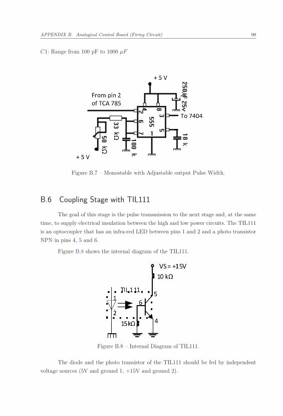
APPENDIX B. Analogical Control Board (Firing Circuit) 99
C1: Range from 100 pF to 1000 μF
Figure B.7 – Monostable with Adjustable output Pulse Width.
B.6 Coupling Stage with TIL111
The goal of this stage is the pulse transmission to the next stage and, at the same
time, to supply electrical insulation between the high and low power circuits. The TIL111
is an optocoupler that has an infra-red LED between pins 1 and 2 and a photo transistor
NPN in pins 4, 5 and 6.
Figure B.8 shows the internal diagram of the TIL111.
Figure B.8 – Internal Diagram of TIL111.
The diode and the photo transistor of the TIL111 should be fed by independent
voltage sources (5V and ground 1, +15V and ground 2).
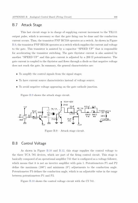
APPENDIX B. Analogical Control Board (Firing Circuit) 100
B.7 Attack Stage
This last circuit stage is in charge of supplying current increment to the TIL111
output pulse, which is necessary so that the gate firing can be done and the conduction
current occurs. Thus, the transistor PNP BC558 operates as a switch. As shown in Figure
B.9, the transistor PNP BD136 operates as a switch which supplies the current and voltage
to the gate. This transistor is assisted by a capacitor “SPEED UP” that is responsible
for accelerating the transistor switching. The gate thyristor current is also assisted by
another “SPEED UP” and this gate current is adjusted by a 200 Ω potentiometer. The
gate current is coupled to the thyristor and flows through a diode so that negative voltage
does not reach the gate. In summary, the general characteristics are:
• To amplify the control signals from the signal stages;
• To have current source characteristics instead of voltage source;
• To avoid negative voltage appearing on the gate cathode junction.
Figure B.9 shows the attack stage circuit.
Figure B.9 – Attack stage circuit.
B.8 Control Voltage
As shown in Figure B.10 and B.12, this stage supplies the control voltage to
the three TCA 785 devices, which are part of the firing control circuit. This stage is
basically composed of an operational amplifier 741 that is configured as a voltage follower,
which means that it is not an inverter amplifier with gain 1. Potentiometers P1 and P2
define the maximum (180◦) and minimum (0◦) adjustments to the conduction angle.
Potentiometer P3 defines the conduction angle, which is an adjustable value in the range
between potentiometers P1 and P2.
Figure B.10 shows the control voltage circuit with the CI 741.

APPENDIX B. Analogical Control Board (Firing Circuit) 101
Figure B.10 – Control Voltage Circuit.
B.9 General Overview
Figure B.11 shows the block diagram.
Figure B.11 – Block Diagram of Complete Control Circuit
Figure B.12 shows the electrical diagram of the firing circuit of the thyristor bridge
[42], [43], [44]. Figure B.13 also shows the electrical diagrams used for the 6 voltage sources
that are shown in Figure B.12.
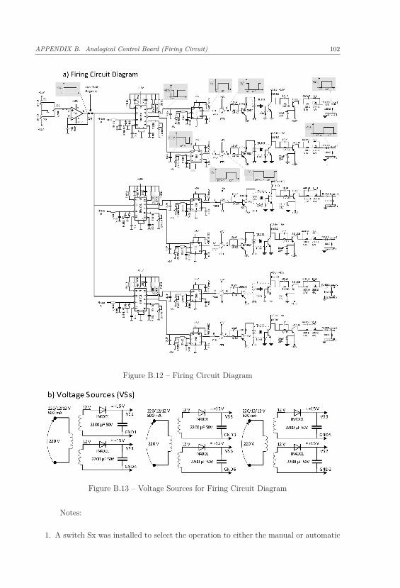
APPENDIX B. Analogical Control Board (Firing Circuit) 102
Figure B.12 – Firing Circuit Diagram
Figure B.13 – Voltage Sources for Firing Circuit Diagram
Notes:
1. A switch Sx was installed to select the operation to either the manual or automatic
APPENDIX B. Analogical Control Board (Firing Circuit) 103
position between pin 3 of buffer 741 and potentiometers P1 and P3. Sx is in the
manual position as demonstrated in Figure B.12. When Sx is in the automatic
position, the signal comes from the regulator output instead of potentiometers P1
and P3.
2. P1 serves to adjust the maximum alpha conduction angle and P2 serves to adjust
the minimum alpha conduction angle.
3. The integrated circuit TCA 785 is a current version of TCA 780. Both have the
same functions and pins.
B.10 Conclusion
This appendix presented the concepts of operation and functioning of firing circuit
to control the three-phase thyristor bridge firing angle using the integrated circuit TCA
785.
This electronic circuit generates all the logic of the command signals that will
control the thyristors operation. The aim of the device is to drive the thyristors by using
the necessary gate current.
This firing circuit was developed to control the firing angle of thyristors, transistors,
and TRIACs continually in the 0◦ to 180◦ range. It has a large number of configurations
and few external components as demonstrated in this appendix.
The firing circuit logic and functioning algorithm were shown, as well as, the
firing circuit and parts of this firing circuit. The most contribution of this appendix is
the presentation of complete firing circuit tested and implemented in the Laboratory of
research development of electrical didactic laboratory of Federal University of Itajubá
with all details that becomes possible a new assembly that can be done for anyone using
these same components.
104
APPENDIX C – Voltage Regulators and
Filters Project to Synchronous Machine
C.1 Introduction
Generator frequency and voltage regulation means to enable the generator to re-
spond the load disturbances and electrical system variation in a way that the system
frequency and voltage can be maintained constant and within the acceptable limits.
This chapter will show a new technique named symmetrical optimization to carry
out adjustments of the voltage regulator parameters as shown in [45]. This new technique
has already been applied in the speed regulator of a DCM . Otherwise, there is nothing
about it in the scientific community related to use this technique over generator voltage
regulator. Then, this one is the original contribution of this appendix.
This appendix presents theory concepts and practical experiment about the de-
velopment of analogical automatic voltage regulator applied on the SG terminals, which
operates in an isolated electric system. Moreover, this kind of voltage regulator and its
parameters, such as gain and regulator time constant will be defined and adjusted by this
cited technique [4, 45].
The methodology shows here serves to establish the first approximation of the
voltage regulator parameters for SG voltage regulator, such as gain and regulator time
constant. The final adjustments are always done experimentally (fine adjustment at the
workbench).
The voltage regulator used in chapters 1 and 2 are digital ones, otherwise, these
can be replaced by analogical ones as those described here and in appendix G.
C.2 Calculus of Generator Field Resistance and Inductance
Figure C.1 shows the auxiliary circuit mounted in the laboratory to determine the
generator field resistance and τ ′ (Generator field time constant). As shown in Figure C.1,
dividing the Vfd (Generator field terminal voltage) , by the Icc (Generator field circuit
current), the Rfdmed (Measured field electrical resistance) is given below:
Rfdmed =116.3V
0.42A≈ 277 Ω (C.1)
As additional information and to calculate the reference temperature resistance,

APPENDIX C. Voltage Regulators and Filters Project to Synchronous Machine 105
Figure C.1 – Auxiliary Circuit Mounted in the Laboratory
[46], to 40 ◦C, Θref , for the temperature rise test [47, 48], the equation indicated in C.2
is used:
Rfdref = Rfdmed × 234.5 + Θref
234.5 + Θmed
(C.2)
considering:
Rfdmed : Measured field electrical resistance
Θref : Reference temperature resistance
Θmed : Measured winding temperature
The 277 Ω resistance measured during the experiment was obtained for Θmed =
22.0 ◦C. Otherwise, the reference field resistance for 40 ◦C is calculated in Equation C.3:
Rfdref = 277 × 234.5 + 40.0234.5 + 22.0
= 296.4 Ω (C.3)
Note: The field winding is made of copper.
Figure C.2 shows the current Icc during the field energization transitory.
From Figure C.2, it is found τ ′= 160 ms, that corresponds to time interval to
current Icc, reaches 63 % of steady state current, that is equal to 0.42 A. Once the field
resistance and the generator time constant have been defined by Equation C.4, the field
inductance is calculated:
τ ′ =Lfd
Rfd
(C.4)
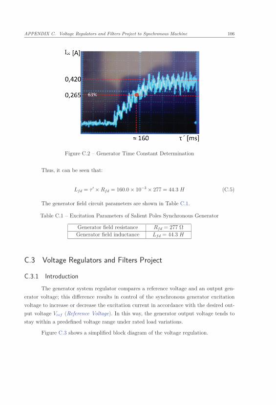
APPENDIX C. Voltage Regulators and Filters Project to Synchronous Machine 106
Figure C.2 – Generator Time Constant Determination
Thus, it can be seen that:
Lfd = τ ′ × Rfd = 160.0 × 10−3 × 277 = 44.3 H (C.5)
The generator field circuit parameters are shown in Table C.1.
Table C.1 – Excitation Parameters of Salient Poles Synchronous Generator
Generator field resistance Rfd = 277 ΩGenerator field inductance Lfd = 44.3 H
C.3 Voltage Regulators and Filters Project
C.3.1 Introduction
The generator system regulator compares a reference voltage and an output gen-
erator voltage; this difference results in control of the synchronous generator excitation
voltage to increase or decrease the excitation current in accordance with the desired out-
put voltage Vref (Reference Voltage). In this way, the generator output voltage tends to
stay within a predefined voltage range under rated load variations.
Figure C.3 shows a simplified block diagram of the voltage regulation.
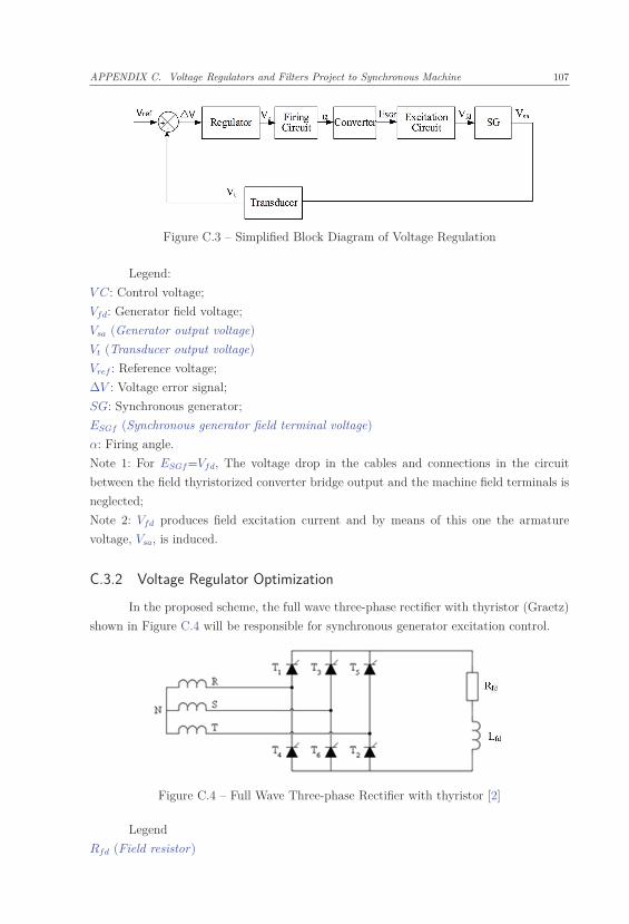
APPENDIX C. Voltage Regulators and Filters Project to Synchronous Machine 107
Figure C.3 – Simplified Block Diagram of Voltage Regulation
Legend:
V C: Control voltage;
Vfd: Generator field voltage;
Vsa (Generator output voltage)
Vt (Transducer output voltage)
Vref : Reference voltage;
ΔV : Voltage error signal;
SG: Synchronous generator;
ESGf (Synchronous generator field terminal voltage)
α: Firing angle.
Note 1: For ESGf=Vfd, The voltage drop in the cables and connections in the circuit
between the field thyristorized converter bridge output and the machine field terminals is
neglected;
Note 2: Vfd produces field excitation current and by means of this one the armature
voltage, Vsa, is induced.
C.3.2 Voltage Regulator Optimization
In the proposed scheme, the full wave three-phase rectifier with thyristor (Graetz)
shown in Figure C.4 will be responsible for synchronous generator excitation control.
Figure C.4 – Full Wave Three-phase Rectifier with thyristor [2]
Legend
Rfd (Field resistor)
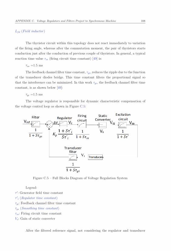
APPENDIX C. Voltage Regulators and Filters Project to Synchronous Machine 108
Lfd (Field inductor)
The thyristor circuit within this topology does not react immediately to variation
of the firing angle, whereas after the commutation moment, the pair of thyristors starts
conduction just after the conduction of previous couple of thyristors. In general, a typical
reaction time value τss (firing circuit time constant) [49] is:
τss =1.5 ms
The feedback channel filter time constant, τgi, reduces the ripple due to the function
of the transducer diodes bridge. This time constant filters the proportional signal so
that the interference can be minimized. In this work τgi, the feedback channel filter time
constant, is as shown below [49]:
τgi =1.5 ms
The voltage regulator is responsible for dynamic characteristic compensation of
the voltage control loop as shown in Figure C.5:
Figure C.5 – Full Blocks Diagram of Voltage Regulation System
Legend:
τ ′: Generator field time constant
τ ′
i (Regulator time constant)
τgi: Feedback channel filter time constant
τgs (Smoothing time constant)
τss: Firing circuit time constant
Vs: Gain of static converter
After the filtered reference signal, not considering the regulator and transducer
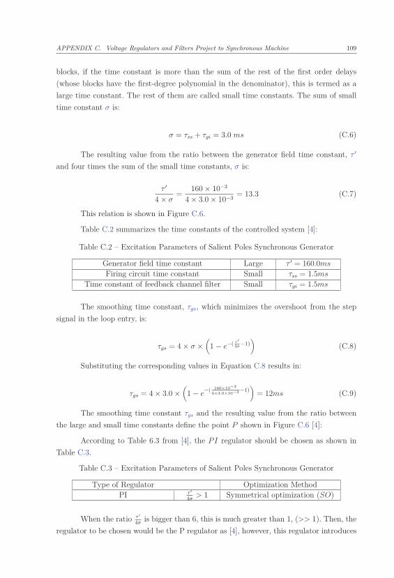
APPENDIX C. Voltage Regulators and Filters Project to Synchronous Machine 109
blocks, if the time constant is more than the sum of the rest of the first order delays
(whose blocks have the first-degree polynomial in the denominator), this is termed as a
large time constant. The rest of them are called small time constants. The sum of small
time constant σ is:
σ = τss + τgi = 3.0 ms (C.6)
The resulting value from the ratio between the generator field time constant, τ ′
and four times the sum of the small time constants, σ is:
τ ′
4 × σ=
160 × 10−3
4 × 3.0 × 10−3= 13.3 (C.7)
This relation is shown in Figure C.6.
Table C.2 summarizes the time constants of the controlled system [4]:
Table C.2 – Excitation Parameters of Salient Poles Synchronous Generator
Generator field time constant Large τ ′ = 160.0ms
Firing circuit time constant Small τss = 1.5ms
Time constant of feedback channel filter Small τgi = 1.5ms
The smoothing time constant, τgs, which minimizes the overshoot from the step
signal in the loop entry, is:
τgs = 4 × σ ×(
1 − e−( τ ′
4σ−1)
)(C.8)
Substituting the corresponding values in Equation C.8 results in:
τgs = 4 × 3.0 ×(
1 − e−( 160×10
−3
4×3.0×10−3−1)
)= 12ms (C.9)
The smoothing time constant τgs and the resulting value from the ratio between
the large and small time constants define the point P shown in Figure C.6 [4]:
According to Table 6.3 from [4], the PI regulator should be chosen as shown in
Table C.3.
Table C.3 – Excitation Parameters of Salient Poles Synchronous Generator
Type of Regulator Optimization MethodPI τ ′
4σ> 1 Symmetrical optimization (SO)
When the ratio τ ′
4σis bigger than 6, this is much greater than 1, (>> 1). Then, the
regulator to be chosen would be the P regulator as [4], however, this regulator introduces
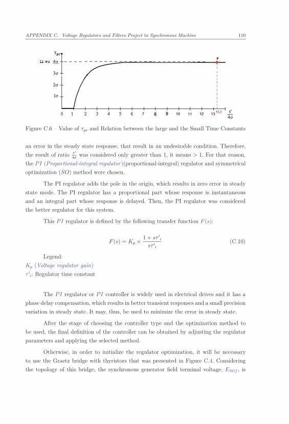
APPENDIX C. Voltage Regulators and Filters Project to Synchronous Machine 110
Figure C.6 – Value of τgs and Relation between the large and the Small Time Constants
an error in the steady state response, that result in an undesirable condition. Therefore,
the result of ratio τ ′
4σwas considered only greater than 1, it means > 1. For that reason,
the PI (Proportional-integral regulator)(proportional-integral) regulator and symmetrical
optimization (SO) method were chosen.
The PI regulator adds the pole in the origin, which results in zero error in steady
state mode. The PI regulator has a proportional part whose response is instantaneous
and an integral part whose response is delayed. Then, the PI regulator was considered
the better regulator for this system.
This PI regulator is defined by the following transfer function F (s):
F (s) = Kp × 1 + sτ ′
i
sτ ′i
(C.10)
Legend:
Kp (Voltage regulator gain)
τ ′
i: Regulator time constant
The PI regulator or PI controller is widely used in electrical drives and it has a
phase delay compensation, which results in better transient responses and a small precision
variation in steady state. It may, thus, be used to minimize the error in steady state.
After the stage of choosing the controller type and the optimization method to
be used, the final definition of the controller can be obtained by adjusting the regulator
parameters and applying the selected method.
Otherwise, in order to initialize the regulator optimization, it will be necessary
to use the Graetz bridge with thyristors that was presented in Figure C.4. Considering
the topology of this bridge, the synchronous generator field terminal voltage, ESGf , is
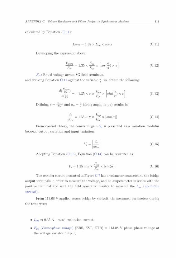
APPENDIX C. Voltage Regulators and Filters Project to Synchronous Machine 111
calculated by Equation (C.11):
ESGf = 1.35 × Epp × cosα (C.11)
Developing the expression above:
ESGf
EN
= 1.35 × Epp
EN
×[cos(
α
π) × π
](C.12)
EN : Rated voltage across SG field terminals.
and deriving Equation C.11 against the variable απ, we obtain the following:
d(ESGf
EN)
d(απ)
= −1.35 × π × Epp
EN
×[sin(
α
π) × π
](C.13)
Defining e = ESGf
ENand αu = α
π(firing angle, in pu) results in:
de
dαu
= 1.35 × π × Epp
EN
× [sin(α)] (C.14)
From control theory, the converter gain Vs is presented as a variation modulus
between output variation and input variation:
Vs =
∣∣∣∣∣ de
dαu
∣∣∣∣∣ (C.15)
Adopting Equation (C.15), Equation (C.14) can be rewritten as:
Vs = 1.35 × π × Epp
EN
× [sin(α)] (C.16)
The rectifier circuit presented in Figure C.7 has a voltmeter connected to the bridge
output terminals in order to measure the voltage, and an amperemeter in series with the
positive terminal and with the field generator resistor to measure the Iexc (excitation
current):
From 113.08 V applied across bridge by varivolt, the measured parameters during
the tests were:
• Iexc ≈ 0.35 A - rated excitation current;
• Epp (Phase-phase voltage) (ERS, EST, ETR) = 113.08 V phase–phase voltage at
the voltage variator output;
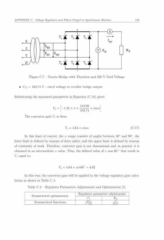
APPENDIX C. Voltage Regulators and Filters Project to Synchronous Machine 112
Figure C.7 – Graetz Bridge with Thyristor and 220 V Grid Voltage
• EN = 103.74 V - rated voltage at rectifier bridge output.
Substituting the measured parameters in Equation (C.16) gives:
Vs =∣∣∣∣−1.35 × π × 113.08
103.74× sinα
∣∣∣∣The convertor gain Vs is then:
Vs = 4.64 × sinα (C.17)
In this kind of control, the α range consists of angles between 30◦ and 90◦, the
lower limit is defined by reasons of drive safety, and the upper limit is defined by reasons
of continuity of work. Therefore, converter gain is not dimensional and, in general, it is
obtained at an intermediate α value. Thus, the defined value of α was 60 ◦ that result in
Vs equal to:
Vs = 4.64 × sin60◦ = 4.02
In this way, the convertor gain will be applied to the voltage regulator gain calcu-
lation as shown in Table C.4:
Table C.4 – Regulator Parameters Adjustments and Optimization [4].
Symmetrical optimizationRegulator parameter adjustments
τ ′
i Kp
Symmetrical functions 4στ ′
τ ′+3στ ′
2Vsσ
APPENDIX C. Voltage Regulators and Filters Project to Synchronous Machine 113
Table C.5 – Optimized Voltage Regulator Parameters
Parameters Proportional-IntegralVoltage regulator optimized gain Kp = 6.63
Regulator time constant τ ′
i = 7.7 ms
Referring to Table C.4, the regulator gain Kp can be calculated as the following
equation:
Kp =τ ′
2 × Vs × σ(C.18)
Kp =160 × 10−3
2 × 4.02 × 3.0 × 10−3= 6.63
Referring again to Table C.4, the voltage regulator time constant, τ ′
i, is calculated
as in the following equation:
τ ′
i =4 × σ × τ ′
τ ′ + 3 × σ(C.19)
τ ′
i =4 × 3.0 × 160160 + 3 × 3.0
× 10−3 = 7.7 ms
Table C.5 summarizes the classification and optimization parameters needed for
the voltage regulator implementation at the workbench.
Considering these results, Rq1 (Proportional branch adjustment resistor of voltage
regulator) and RM2 (Integral branch adjustment resistor of voltage regulator) adjustments
will be calculated over the voltage regulators implemented in the laboratory, as shown in
Figure C.8.
Note: This cited methodology was developed to analogical regulators. Otherwise,
the digital regulators, MP 410T produced by Semikron have parameters adjusted man-
ually, by the use of control keys. In other words, electronic board MP 410T does not
require the resistor adjustments Rq1 and RM2 as shown in this cited methodology of this
appendix.
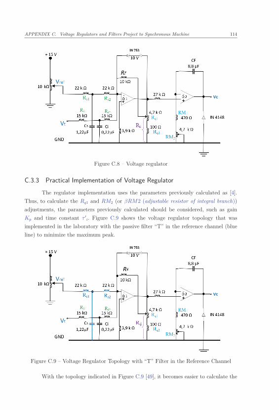
APPENDIX C. Voltage Regulators and Filters Project to Synchronous Machine 114
Figure C.8 – Voltage regulator
C.3.3 Practical Implementation of Voltage Regulator
The regulator implementation uses the parameters previously calculated as [4].
Thus, to calculate the Rq1 and RM2 (or βRM2 (adjustable resistor of integral branch))
adjustments, the parameters previously calculated should be considered, such as gain
Kp and time constant τ ′
i. Figure C.9 shows the voltage regulator topology that was
implemented in the laboratory with the passive filter “T” in the reference channel (blue
line) to minimize the maximum peak.
Figure C.9 – Voltage Regulator Topology with “T” Filter in the Reference Channel
With the topology indicated in Figure C.9 [49], it becomes easier to calculate the
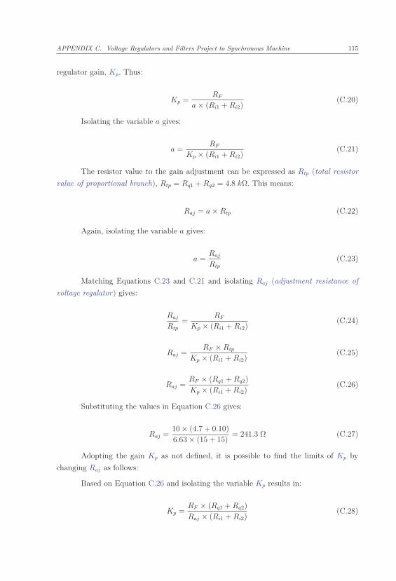
APPENDIX C. Voltage Regulators and Filters Project to Synchronous Machine 115
regulator gain, Kp. Thus:
Kp =RF
a × (Ri1 + Ri2)(C.20)
Isolating the variable a gives:
a =RF
Kp × (Ri1 + Ri2)(C.21)
The resistor value to the gain adjustment can be expressed as Rtp (total resistor
value of proportional branch), Rtp = Rq1 + Rq2 = 4.8 kΩ. This means:
Raj = a × Rtp (C.22)
Again, isolating the variable a gives:
a =Raj
Rtp
(C.23)
Matching Equations C.23 and C.21 and isolating Raj (adjustment resistance of
voltage regulator) gives:
Raj
Rtp
=RF
Kp × (Ri1 + Ri2)(C.24)
Raj =RF × Rtp
Kp × (Ri1 + Ri2)(C.25)
Raj =RF × (Rq1 + Rq2)Kp × (Ri1 + Ri2)
(C.26)
Substituting the values in Equation C.26 gives:
Raj =10 × (4.7 + 0.10)6.63 × (15 + 15)
= 241.3 Ω (C.27)
Adopting the gain Kp as not defined, it is possible to find the limits of Kp by
changing Raj as follows:
Based on Equation C.26 and isolating the variable Kp results in:
Kp =RF × (Rq1 + Rq2)Raj × (Ri1 + Ri2)
(C.28)
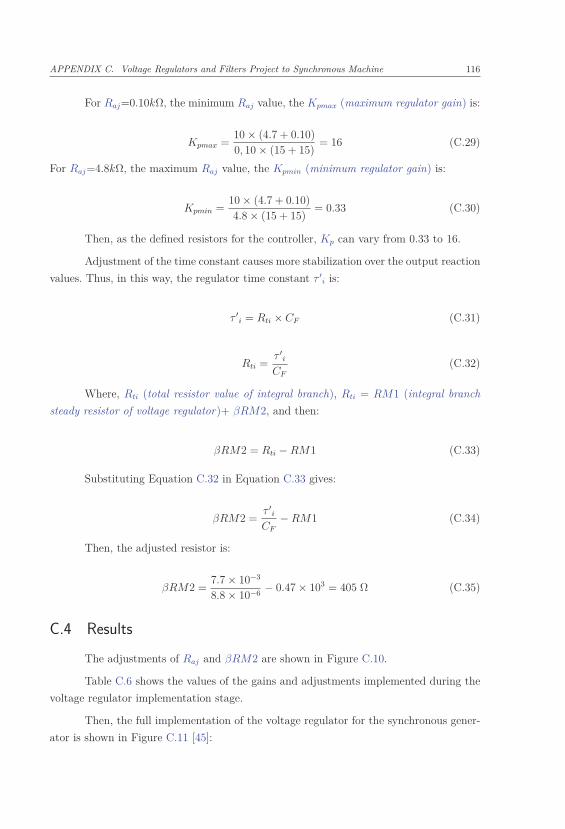
APPENDIX C. Voltage Regulators and Filters Project to Synchronous Machine 116
For Raj=0.10kΩ, the minimum Raj value, the Kpmax (maximum regulator gain) is:
Kpmax =10 × (4.7 + 0.10)0, 10 × (15 + 15)
= 16 (C.29)
For Raj=4.8kΩ, the maximum Raj value, the Kpmin (minimum regulator gain) is:
Kpmin =10 × (4.7 + 0.10)4.8 × (15 + 15)
= 0.33 (C.30)
Then, as the defined resistors for the controller, Kp can vary from 0.33 to 16.
Adjustment of the time constant causes more stabilization over the output reaction
values. Thus, in this way, the regulator time constant τ ′
i is:
τ ′
i = Rti × CF (C.31)
Rti =τ ′
i
CF
(C.32)
Where, Rti (total resistor value of integral branch), Rti = RM1 (integral branch
steady resistor of voltage regulator)+ βRM2, and then:
βRM2 = Rti − RM1 (C.33)
Substituting Equation C.32 in Equation C.33 gives:
βRM2 =τ ′
i
CF
− RM1 (C.34)
Then, the adjusted resistor is:
βRM2 =7.7 × 10⁻³
8.8 × 10⁻⁶− 0.47 × 103 = 405 Ω (C.35)
C.4 Results
The adjustments of Raj and βRM2 are shown in Figure C.10.
Table C.6 shows the values of the gains and adjustments implemented during the
voltage regulator implementation stage.
Then, the full implementation of the voltage regulator for the synchronous gener-
ator is shown in Figure C.11 [45]:
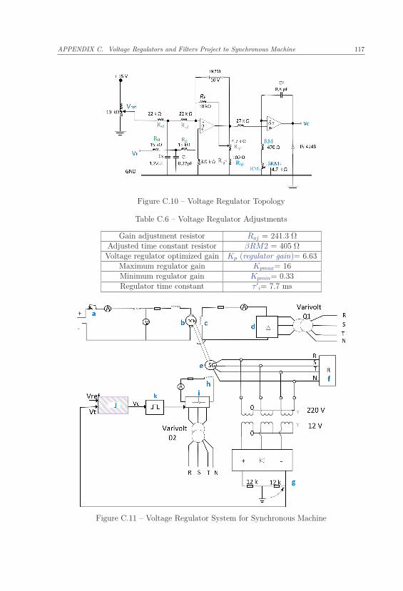
APPENDIX C. Voltage Regulators and Filters Project to Synchronous Machine 117
Figure C.10 – Voltage Regulator Topology
Table C.6 – Voltage Regulator Adjustments
Gain adjustment resistor Raj = 241.3 ΩAdjusted time constant resistor βRM2 = 405 Ω
Voltage regulator optimized gain Kp (regulator gain)= 6.63Maximum regulator gain Kpmax= 16Minimum regulator gain Kpmin= 0.33Regulator time constant τ ′
i= 7.7 ms
Figure C.11 – Voltage Regulator System for Synchronous Machine

APPENDIX C. Voltage Regulators and Filters Project to Synchronous Machine 118
Legend:
a Rheostat f Three-phase load
b DC motor armature g Voltage transducer
c DC motor field h Synchronous generator field
d Diodes bridge i Thyristors bridge
e Synchronous generator j Voltage regulator
k Firing Circuit
C.5 Conclusion
This appendix presented theory concepts and practical experiment mounted in
laboratory about the development of an analogical automatic voltage regulator applied
on the SG terminals, which operates in an isolated electric system. Moreover, the kind
of voltage regulator was defined and its parameters as gain and regulator time constant
were estimated or calculated using the symmetrical optimization technique [4, 45].
119
APPENDIX D – Four-quadrant Regenerative
Driven System for DC Machine applying
Speed Reversion using either Armature
Current Reversion or Field Current Reversion
D.1 Introduction
A regenerative driven system for DC machines in four quadrants was implemented
in the laboratory of research development of electrical didactic laboratory of Federal Uni-
versity of Itajubá, [26]. The speed reversion was done using two distinct methods: the first
consisted of armature DC current inversion through the use of two converters, whereas,
the second, consisted of inversion of the field current through the use of one converter.
The results of both methods are presented, discussed and compared. The symmetrical
optimization method [4] was chosen to adjust the regulator parameters.
The controlled drive system for DC machines is widely used in industry, [35, 36,
49, 26]. Speed reversion is needed in many industrial processes. In order to achieve this
aim, this work will present the use of the two cited methods to return regenerative energy
to the grid during the braking process [26, 38].
D.2 Block Diagram of Controlled Drive System for use in DC Ma-
chine
Figure D.1 shows the full block diagram of the DC machine:
APPENDIX D. Four-quadrant Regenerative Driven System for DC Machine applying Speed Reversion
using either Armature Current Reversion or Field Current Reversion 120
Figure D.1 – Full Blocks Diagram of DC Machine
Legend:
τgs1 Filter time constant of the reference channel of the speed loop
τgs2 Filter time constant of the reference channel of the current loop
VRn Gain of the speed regulator
VRi Gain of the current regulator
τn Time constant of the speed regulator
τi Current regulator time constant
τgn Filter time constant of the speed transducer
τgi Filter time constant of the current transducer
τss Time constant of the firing circuit
Vs Gain of the static converter
τa Armature circuit time constant
Vi Gain of machine electric part
Vcc Control voltage of thyristor firing system
Note: Figure D.1 shows the PI regulators of DC machine. The motor regulator
parameters were obtained by the symmetrical optimization method [4].
D.3 Laboratory Implementation
In order to implement the system in the laboratory, the following data plates were
shown in D.1 to D.3 [38].
Note: All these values were obtained as described in [38] and in appendix A.
APPENDIX D. Four-quadrant Regenerative Driven System for DC Machine applying Speed Reversion
using either Armature Current Reversion or Field Current Reversion 121
Table D.1 – Motor Data
Power Current Ratedspeed
No loadspeed
Ratedvoltage
Armatureresistance (
∑Ra)
1.7 kW 7.72 A 1500 rpm 1770 rpm 220 V 7.0 Ω
Table D.2 – Speed Regulator Parameters
Type Gain(VRn)
Timeconstant (τn)
Reference channelfilter time
constant (τgs1)
Speed transducerfilter time
constant (τgn)PI 6.7 460 ms 416 ms 100 ms
Table D.3 – Current Regulator Parameters
Type Gain(VRi)
Timeconstant (τi)
Reference valuefilter (τgs2)
Feedbackcurrent filter
(τgi)PI 0.8 13.34 ms 15.43 ms 1.39 ms
D.4 Full Hardware of Implemented Drive System
Figure D.2 shows the implemented drive system and Figure D.3 shows the full
hardware of the control system [4], including the control switches.
Figure D.2 – Implemented Drive System
APPENDIX D. Four-quadrant Regenerative Driven System for DC Machine applying Speed Reversion
using either Armature Current Reversion or Field Current Reversion 122
Figure D.3 – Control Circuit
D.5 Speed Inversion by Armature Current Inversion
Considering the diagram shown in Figure D.4, after the switch S1” turns from
negative to positive, the operations occur as shown in quadrants I, II and III. When the
switch S1” turns from positive to negative, the operations occur as shown in quadrants
III, IV and I.
Figure D.4 – Conjugate (t) versus Speed (n) Diagram
In order to clarify Figure D.2, the switch S2 is closed and then converter I and
converter II are running one at a time. This system is known as a dual converter, without
circulation current.
In this way, if converter I is running, the switch S1 shown in Figure D.3 is close
and switches S1’ are open. On the contrary, if converter II is running, the switches S1’
are closed and S1 is open. The switch S1” enables the speed inversion. The switch S1”’
will promote the blockage of the converter pulses I and unblock the converter pulses II
as shown in Figure D.5. There is a period of about some milliseconds in which both
converters are blocked and, thus, they are not running. Figure D.5 shows this sequence:
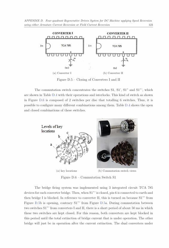
APPENDIX D. Four-quadrant Regenerative Driven System for DC Machine applying Speed Reversion
using either Armature Current Reversion or Field Current Reversion 123
(a) Converter I (b) Converter II
Figure D.5 – Closing of Converters I and II
The commutation switch concentrates the switches S1, S1’, S1” and S1”’, which
are shown in Table D.4 with their operations and interlocks. This kind of switch as shown
in Figure D.6 is composed of 2 switches per disc that totalling 6 switches. Thus, it is
possible to configure many different combinations among them. Table D.4 shows the open
and closed combinations of these switches.
(a) key locations (b) Commutation switch views
Figure D.6 – Commutation Switch S1
The bridge firing system was implemented using 3 integrated circuit TCA 785
devices for each converter bridge. Then, when S1”’ is closed, pin 6 is connected to earth and
then bridge I is blocked. In reference to converter II, this is turned on because S1”’ from
Figure D.5b is opening, contrary S1”’ from Figure D.5a. During commutation between
two switches S1”’ from converters I and II, there is a short period of about 50 ms in which
these two switches are kept closed. For this reason, both converters are kept blocked in
this period until the total extinction of bridge current that is under operation. The other
bridge will just be in operation after the current extinction. The dual converters under
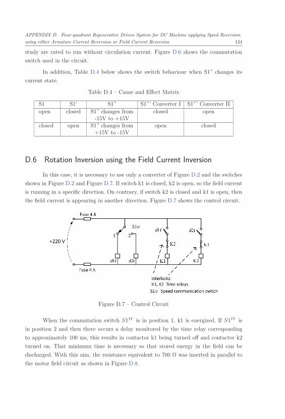
APPENDIX D. Four-quadrant Regenerative Driven System for DC Machine applying Speed Reversion
using either Armature Current Reversion or Field Current Reversion 124
study are rated to run without circulation current. Figure D.6 shows the commutation
switch used in the circuit.
In addition, Table D.4 below shows the switch behaviour when S1” changes its
current state.
Table D.4 – Cause and Effect Matrix
S1 S1’ S1” S1”’ Converter I S1”’ Converter IIopen closed S1” changes from
-15V to +15Vclosed open
closed open S1” changes from+15V to -15V
open closed
D.6 Rotation Inversion using the Field Current Inversion
In this case, it is necessary to use only a converter of Figure D.2 and the switches
shown in Figure D.2 and Figure D.7. If switch k1 is closed, k2 is open, so the field current
is running in a specific direction. On contrary, if switch k2 is closed and k1 is open, then
the field current is appearing in another direction. Figure D.7 shows the control circuit.
Figure D.7 – Control Circuit
When the commutation switch S1IV is in position 1, k1 is energized. If S1IV is
in position 2 and then there occurs a delay monitored by the time relay corresponding
to approximately 100 ms, this results in contactor k1 being turned off and contactor k2
turned on. That minimum time is necessary so that stored energy in the field can be
discharged. With this aim, the resistance equivalent to 700 Ω was inserted in parallel to
the motor field circuit as shown in Figure D.8.
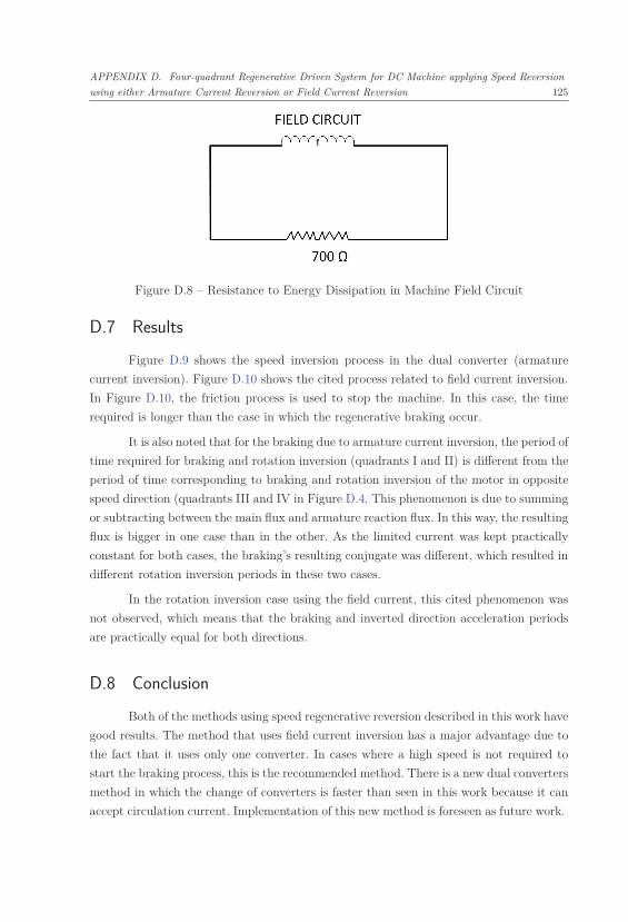
APPENDIX D. Four-quadrant Regenerative Driven System for DC Machine applying Speed Reversion
using either Armature Current Reversion or Field Current Reversion 125
Figure D.8 – Resistance to Energy Dissipation in Machine Field Circuit
D.7 Results
Figure D.9 shows the speed inversion process in the dual converter (armature
current inversion). Figure D.10 shows the cited process related to field current inversion.
In Figure D.10, the friction process is used to stop the machine. In this case, the time
required is longer than the case in which the regenerative braking occur.
It is also noted that for the braking due to armature current inversion, the period of
time required for braking and rotation inversion (quadrants I and II) is different from the
period of time corresponding to braking and rotation inversion of the motor in opposite
speed direction (quadrants III and IV in Figure D.4. This phenomenon is due to summing
or subtracting between the main flux and armature reaction flux. In this way, the resulting
flux is bigger in one case than in the other. As the limited current was kept practically
constant for both cases, the braking’s resulting conjugate was different, which resulted in
different rotation inversion periods in these two cases.
In the rotation inversion case using the field current, this cited phenomenon was
not observed, which means that the braking and inverted direction acceleration periods
are practically equal for both directions.
D.8 Conclusion
Both of the methods using speed regenerative reversion described in this work have
good results. The method that uses field current inversion has a major advantage due to
the fact that it uses only one converter. In cases where a high speed is not required to
start the braking process, this is the recommended method. There is a new dual converters
method in which the change of converters is faster than seen in this work because it can
accept circulation current. Implementation of this new method is foreseen as future work.
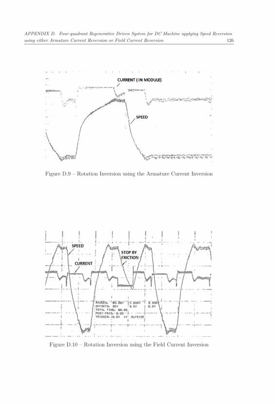
APPENDIX D. Four-quadrant Regenerative Driven System for DC Machine applying Speed Reversion
using either Armature Current Reversion or Field Current Reversion 126
Figure D.9 – Rotation Inversion using the Armature Current Inversion
Figure D.10 – Rotation Inversion using the Field Current Inversion
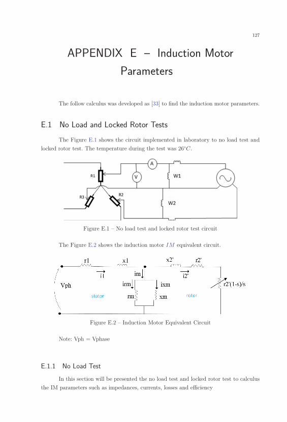
127
APPENDIX E – Induction Motor
Parameters
The follow calculus was developed as [33] to find the induction motor parameters.
E.1 No Load and Locked Rotor Tests
The Figure E.1 shows the circuit implemented in laboratory to no load test and
locked rotor test. The temperature during the test was 26◦C.
Figure E.1 – No load test and locked rotor test circuit
The Figure E.2 shows the induction motor IM equivalent circuit.
Figure E.2 – Induction Motor Equivalent Circuit
Note: Vph = Vphase
E.1.1 No Load Test
In this section will be presented the no load test and locked rotor test to calculus
the IM parameters such as impedances, currents, losses and efficiency
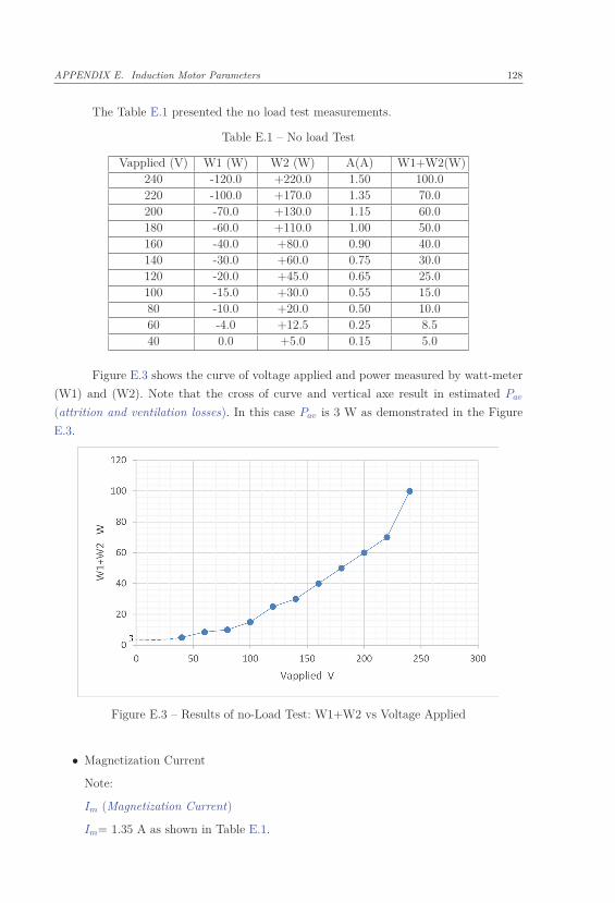
APPENDIX E. Induction Motor Parameters 128
The Table E.1 presented the no load test measurements.
Table E.1 – No load Test
Vapplied (V) W1 (W) W2 (W) A(A) W1+W2(W)240 -120.0 +220.0 1.50 100.0220 -100.0 +170.0 1.35 70.0200 -70.0 +130.0 1.15 60.0180 -60.0 +110.0 1.00 50.0160 -40.0 +80.0 0.90 40.0140 -30.0 +60.0 0.75 30.0120 -20.0 +45.0 0.65 25.0100 -15.0 +30.0 0.55 15.080 -10.0 +20.0 0.50 10.060 -4.0 +12.5 0.25 8.540 0.0 +5.0 0.15 5.0
Figure E.3 shows the curve of voltage applied and power measured by watt-meter
(W1) and (W2). Note that the cross of curve and vertical axe result in estimated Pav
(attrition and ventilation losses). In this case Pav is 3 W as demonstrated in the Figure
E.3.
Figure E.3 – Results of no-Load Test: W1+W2 vs Voltage Applied
• Magnetization Current
Note:
Im (Magnetization Current)
Im= 1.35 A as shown in Table E.1.
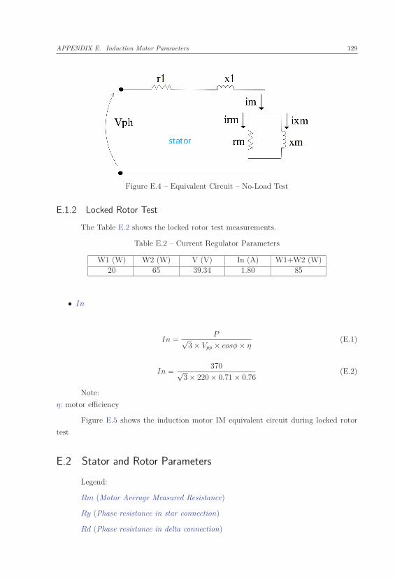
APPENDIX E. Induction Motor Parameters 129
Figure E.4 – Equivalent Circuit – No-Load Test
E.1.2 Locked Rotor Test
The Table E.2 shows the locked rotor test measurements.
Table E.2 – Current Regulator Parameters
W1 (W) W2 (W) V (V) In (A) W1+W2 (W)20 65 39.34 1.80 85
• In
In =P√
3 × Vpp × cosφ × η(E.1)
In =370√
3 × 220 × 0.71 × 0.76(E.2)
Note:
η: motor efficiency
Figure E.5 shows the induction motor IM equivalent circuit during locked rotor
test
E.2 Stator and Rotor Parameters
Legend:
Rm (Motor Average Measured Resistance)
Ry (Phase resistance in star connection)
Rd (Phase resistance in delta connection)
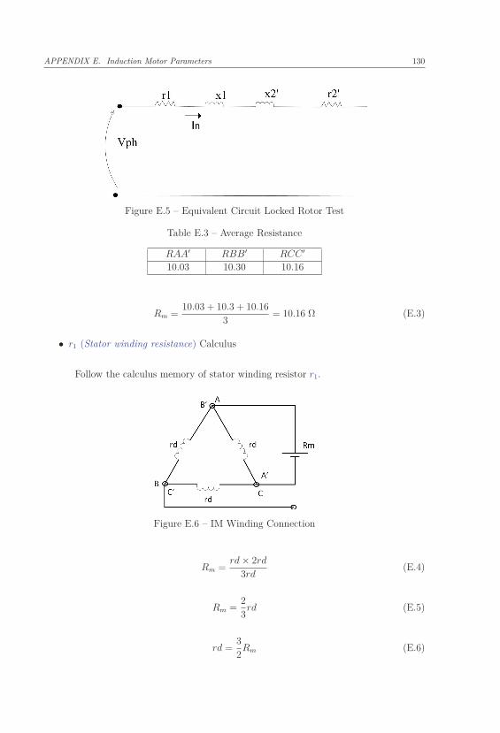
APPENDIX E. Induction Motor Parameters 130
Figure E.5 – Equivalent Circuit Locked Rotor Test
Table E.3 – Average Resistance
RAA′ RBB′ RCC ′
10.03 10.30 10.16
Rm =10.03 + 10.3 + 10.16
3= 10.16 Ω (E.3)
• r1 (Stator winding resistance) Calculus
Follow the calculus memory of stator winding resistor r1.
Figure E.6 – IM Winding Connection
Rm =rd × 2rd
3rd(E.4)
Rm =23
rd (E.5)
rd =32
Rm (E.6)
APPENDIX E. Induction Motor Parameters 131
As ry =13
rd (E.7)
And putting (E.6) into (E.7), it has
ry =Rm
2=
10.162
ry = r1 = 5.08 Ω (E.8)
• r2’ (Rotor winding resistance referred to stator winding) Calculus
From Table E.2, W1+W2=85 W
W1 + W2 = 3 × (r1 + r2′) × in2 (E.9)
853 × 1.82
= 5.08 + r2′
r2′ = 3.66 Ω (E.10)
• Q (Reactive power)
Q =√
3 × (W2 − W1) (E.11)
From Table E.2, W2-W1=45
Q =√
3 × (65 − 20) = 77.94 V ar (E.12)
Q = 3 × (x1 + x2′) × In2 (E.13)
• x1 (Stator winding reactance) and x2’ (Rotor winding reactance referred to stator
winding)
doing (E.13) and (E.2) in (E.14)
77.94 = 3 × (x1 + x2′) × 1.82 (E.14)
APPENDIX E. Induction Motor Parameters 132
(x1 + x2′) = 8.01 Ω (E.15)
⎡⎣x1 �→ x2′
r1 �→ r2′
⎤⎦ (E.16)
doing (E.8) and (E.10) in (E.16)
⎡⎣ x1 �→ x2′
5.08 �→ 3.66
⎤⎦
x1 =r1 × x2′
r2(E.17)
x1 =5.08 × x2′
3.66(E.18)
From (E.15) and (E.18), result in
5.08 × x2′ + x2′ × 3.66 = 29.32 (E.19)
x2′ × 8.74 = 29.32 (E.20)
x2′ = 3.35 Ω (E.21)
doing (E.21) in (E.18), result in
x1 =5.08 × 3.35
3.66(E.22)
x1 = 4.65 Ω (E.23)
E.3 Power and Losses Calculus
The Pav was defined in Figure E.3 and consist in 3 W. Pnl (No load losses) is
obtained from no load test for 220 V, it resulted in 70 W (W1 +W2).
• Pjstator (No load stator Joules Losses)
APPENDIX E. Induction Motor Parameters 133
Pjstator26◦ = 3 × r1 × im2 (E.24)
Pjstator26◦ = 3 × 5.08 × 1.352 (E.25)
Pjstator26◦ = 27.77 W (E.26)
• Phf (hysteresis and Foucault losses)
Phf = (W1 + W2) − 3 × r1 × im2 − Pav (E.27)
Phf = 70 − 3 × 5.08 × 1.352 − 3 (E.28)
Phf = 39.23 W (E.29)
E.3.1 No Load Reactive Power
Q0 =√
3 × (W2 − W1) (E.30)
From Table E.1, W2-W1=270 W
Q0 =√
3 × 270 V ar
Q0 = 467.65 V ar (E.31)
E.3.2 Magnetization Branch
• Qm (No load Reactive Power in Magnetization Branch)
Qm = Q0 − 3 × x1 × I20 (E.32)
Qm = 467.65 − 3 × 4.65 × 1.352 (E.33)
Qm = 442.23V ar (E.34)
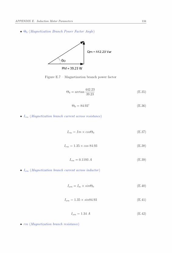
APPENDIX E. Induction Motor Parameters 134
• Θ0 (Magnetization Branch Power Factor Angle)
Figure E.7 – Magnetization branch power factor
Θ0 = arctan442.2339.23
(E.35)
Θ0 = 84.93◦ (E.36)
• Irm (Magnetization branch current across resistance)
Irm = Im × cosΘ0 (E.37)
Irm = 1.35 × cos 84.93 (E.38)
Irm = 0.1193 A (E.39)
• Ixm (Magnetization branch current across inductor)
Ixm = Im × sinΘ0 (E.40)
Ixm = 1.35 × sin84.93 (E.41)
Ixm = 1.34 A (E.42)
• rm (Magnetization branch resistance)
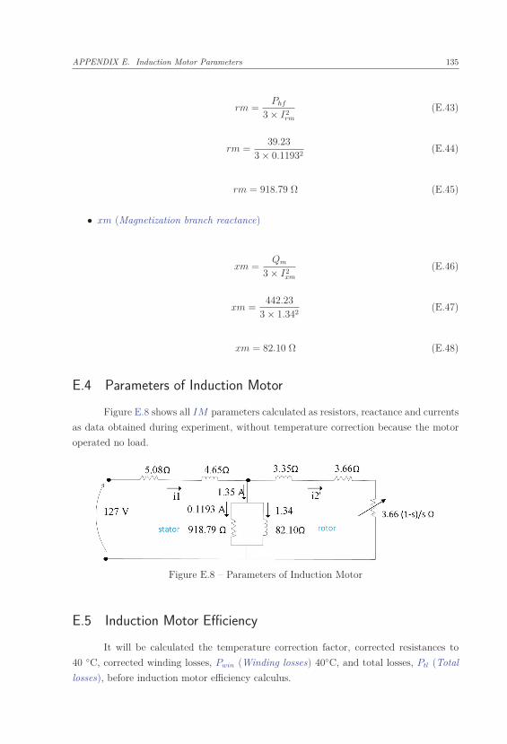
APPENDIX E. Induction Motor Parameters 135
rm =Phf
3 × I2rm
(E.43)
rm =39.23
3 × 0.11932(E.44)
rm = 918.79 Ω (E.45)
• xm (Magnetization branch reactance)
xm =Qm
3 × I2xm
(E.46)
xm =442.23
3 × 1.342(E.47)
xm = 82.10 Ω (E.48)
E.4 Parameters of Induction Motor
Figure E.8 shows all IM parameters calculated as resistors, reactance and currents
as data obtained during experiment, without temperature correction because the motor
operated no load.
Figure E.8 – Parameters of Induction Motor
E.5 Induction Motor Efficiency
It will be calculated the temperature correction factor, corrected resistances to
40 ◦C, corrected winding losses, Pwin (Winding losses) 40◦C, and total losses, Ptl (Total
losses), before induction motor efficiency calculus.
APPENDIX E. Induction Motor Parameters 136
E.5.1 Temperature Correction Factor and Resistance Correction
The temperature correction factor is used in order to attend the IEC standard,[47,
48], that requires the resistances correction to lead to the starting reference resistance for
the temperature rise tests, [48].
• Kt (Temperature correction factor for 40 degree C )
Kt 40◦C =234.5 + 40234.5 + 26
(E.49)
Kt 40◦C = 1.054 for r1 and r′
2 (E.50)
• r140C (Corrected stator winding resistance for 40 degree C )
r1 40◦C = r1 26◦ × 1.054 (E.51)
r1 40◦C = 5.08 × 1.054 (E.52)
r1 40◦C = 5.35 Ω (E.53)
• r′
240C (Corrected rotor winding resistance referred to stator for 40 degree C )
r′
2 40◦C = r2 26◦ × 1.054 (E.54)
r′
2 40◦C = 3.66 × 1.054 (E.55)
r′
2 40◦C = 3.86 Ω (E.56)
E.6 Corrected Winding Losses for 40 ◦C and Total Losses
• Pwin40C (Corrected winding losses for 40 degree C )

APPENDIX E. Induction Motor Parameters 137
The Pwin measured in locked rotor test, Table E.2, need to be corrected for 40 ◦C.
Follow the corrected winding losses for 40 ◦C.
Pwin 40◦C = Kt × Pwin26◦C (E.57)
Pwin 40◦C = 1.054 × 85 W (E.58)
Pwin 40◦C = 89.59 W (E.59)
• Ptl (Total losses)
The Ptl calculus:
Ptl = Phf + Pav + Pwin40◦C (E.60)
Ptl = 39.23 W + 3 W + 89.59 W (E.61)
Ptl = 131.82 W (E.62)
E.7 Motor Efficiency Estimate
• Pout (Motor output power)
• Pin (Motor input power)
Note: (Motor data plate is shown in Table 1.8)
η =Pout
Pin
(E.63)
Pin = Pout + Ptl (E.64)
Pin = 370 + 131.82 W (E.65)
Pin = 501.82 W (E.66)

APPENDIX E. Induction Motor Parameters 138
η =370
501.82(E.67)
η = 73.73 % (E.68)
E.8 Induction Motor Currents
Follow the calculus of IdwMT and IwMT . These values are shown in Table 1.10 for
all scenarios tested.
• IdwMT
Q =√
3 × 220 × IdwMT =√
3 × (W2 − W1) (E.69)
Q =√
3 × 220 × IdwMT = 467.65 (E.70)
IdwMT = 1.23 A ∗ ∗ (E.71)
Note **: The difference between IdwMT and Ixm is perfectly acceptable. The dif-
ference close to 0.1 A between expected and found values is due to small measurements
errors and instruments precision and accuracy errors. It does not affect the presented
modelling. Therefore, the results and modelling continue valid.
• IwMT
P = (W1 + W2) = 70.0 W (E.72)
Q =√
3 × (W2 − W1) = 467.6 W (E.73)
S =√
70.02 + 467.62 = 472.86 V A (E.74)
cosφ =P
S=
70472.86
(E.75)

APPENDIX E. Induction Motor Parameters 139
cosφ = 0.148 (E.76)
IwMT = I0 × cosφ = 1.35 × 0.148 (E.77)
IwMT = 0.20 A (E.78)
In Figure E.9 is shown the resistor banks current and the no load IM current.
Figure E.9 – Resistors bank and IM currents in scenarios C as Table 1.10
140
APPENDIX F – Solving Equations with
Matlab
F.1 Introduction
This appendix demonstrates how the equations indicated in chapter 1 are solved.
There will be presented the Matlab code for equation solution used in two typical schemes
mounted in laboratory. The first one is focused on electrical system scheme mounted in
laboratory for feeding three resistor banks as shown in Figure 1.11. The second is focused
on the scheme for feeding three resistor banks and an induction motor together as shown
in figure 1.12. In the equation system, there are four known variables and four unknown
variables that will be found.
F.2 Equations
F.2.1 Electrical system feeding three resistor banks
Based on Figure 1.11, the equations below are formulated to calculated the currents
IwSG, Ic1, IwIG, Ic2.
I2SG = Iw2
SG + I2c1 (F.1)
I2IG = Iw2
IG + I2c2 (F.2)
Ic = Ic1 + Ic2 (F.3)
IwloadR = IwSG + IwIG (F.4)
F.2.2 Electrical system feeding three resistor banks and an induction motor
Based on Figure 1.12, the equations below are formulated to calculated the currents
IwSG, Ic1, IwIG, Ic2. The currents IdwMT and IwMT are given values and these were
calculated as appendix E.
I2SG = Iw2
SG + I2c1 (F.5)
APPENDIX F. Solving Equations with Matlab 141
I2IG = Iw2
IG + I2c2 (F.6)
Ic − IdwMT = Ic1 + Ic2 (F.7)
IwloadR + IwMT = IwSG + IwIG (F.8)
F.2.3 Power and Efficiencies
From the results of previous equations, the power of PSG, PIG, PDCMSG, PDCMIG
and the efficiencies ηgroup, ηSG, ηIG were calculated as equations below.
PSG =√
3 × VSG × IwSG (F.9)
PIG =√
3 × VIG × IwIG (F.10)
PDCMSG = V aDCMSG × IaDCMSG (F.11)
PDCMIG = V aDCMIG × IaDCMIG (F.12)
ηgroup% =PSG + PIG
PDCMSG + PDCMIG
× 100 (F.13)
ηSG% =PSG
PDCMSG
× 100 (F.14)
ηIG% =PIG
PDCMIG
× 100 (F.15)
F.3 Matlab Code
F.3.1 Electrical system feeding three resistor banks
This section shows the Matlab code used to solve the equations formulated for
each scenario. Not make sense to show all scenarios because it would be repetitive and
not effective. Then, in order to obtain the results, the new entering data IwSG, Ic1, IwIG,
Ic2 from Table 1.9 should be inserted in line 9 of Matlab code, Figures F.1, F.2 or F.3,
this code should be run and the viable result should be considered.
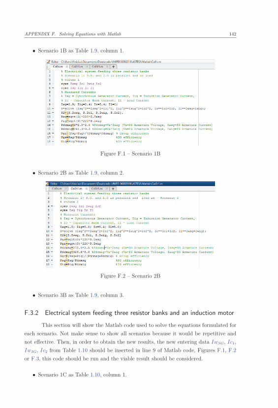
APPENDIX F. Solving Equations with Matlab 142
• Scenario 1B as Table 1.9, column 1.
Figure F.1 – Scenario 1B
• Scenario 2B as Table 1.9, column 2.
Figure F.2 – Scenario 2B
• Scenario 3B as Table 1.9, column 3.
F.3.2 Electrical system feeding three resistor banks and an induction motor
This section will show the Matlab code used to solve the equations formulated for
each scenario. Not make sense to show all scenarios because it would be repetitive and
not effective. Then, in order to obtain the new results, the new entering data IwSG, Ic1,
IwIG, Ic2 from Table 1.10 should be inserted in line 9 of Matlab code, Figures F.1, F.2
or F.3, this code should be run and the viable result should be considered.
• Scenario 1C as Table 1.10, column 1.

APPENDIX F. Solving Equations with Matlab 143
Figure F.3 – Scenario 3B
Figure F.4 – Scenario 1C
• Scenario 2C as Table 1.10, column 2.
Figure F.5 – Scenario 2C
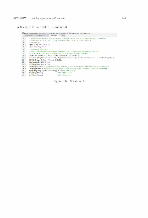
APPENDIX F. Solving Equations with Matlab 144
• Scenario 3C as Table 1.10, column 3.
Figure F.6 – Scenario 3C
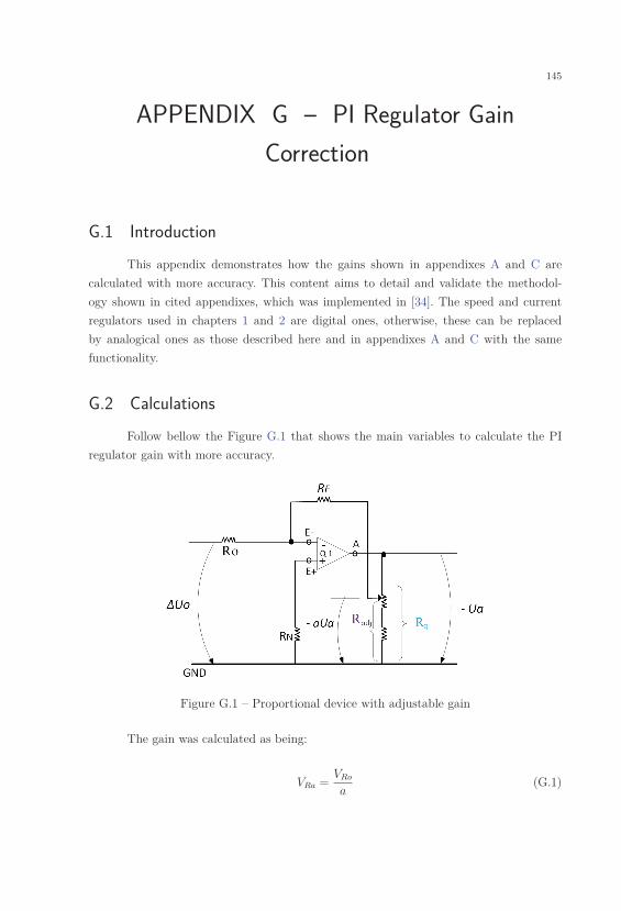
145
APPENDIX G – PI Regulator Gain
Correction
G.1 Introduction
This appendix demonstrates how the gains shown in appendixes A and C are
calculated with more accuracy. This content aims to detail and validate the methodol-
ogy shown in cited appendixes, which was implemented in [34]. The speed and current
regulators used in chapters 1 and 2 are digital ones, otherwise, these can be replaced
by analogical ones as those described here and in appendixes A and C with the same
functionality.
G.2 Calculations
Follow bellow the Figure G.1 that shows the main variables to calculate the PI
regulator gain with more accuracy.
Figure G.1 – Proportional device with adjustable gain
The gain was calculated as being:
VRa =VRo
a(G.1)
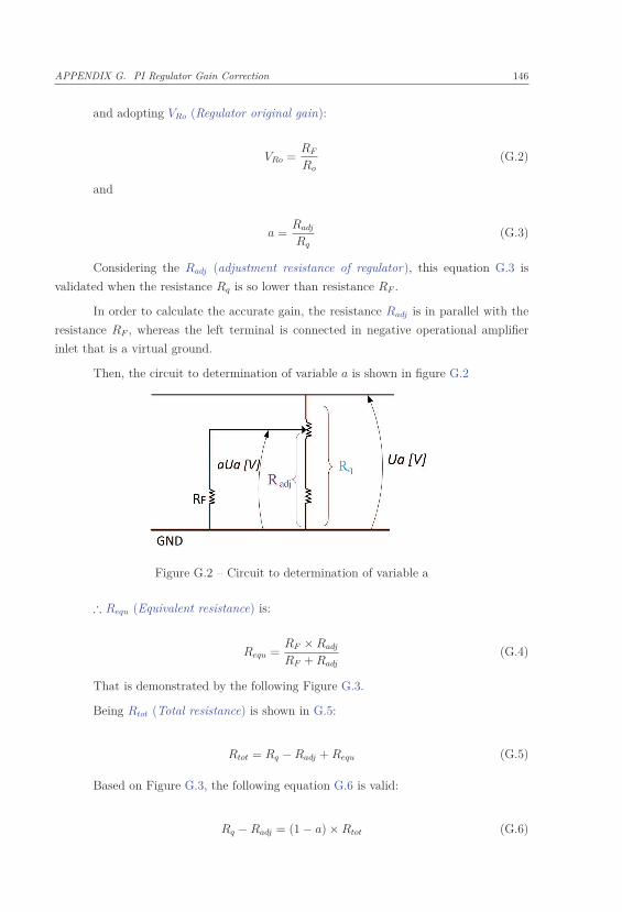
APPENDIX G. PI Regulator Gain Correction 146
and adopting VRo (Regulator original gain):
VRo =RF
Ro
(G.2)
and
a =Radj
Rq
(G.3)
Considering the Radj (adjustment resistance of regulator), this equation G.3 is
validated when the resistance Rq is so lower than resistance RF .
In order to calculate the accurate gain, the resistance Radj is in parallel with the
resistance RF , whereas the left terminal is connected in negative operational amplifier
inlet that is a virtual ground.
Then, the circuit to determination of variable a is shown in figure G.2
Figure G.2 – Circuit to determination of variable a
∴ Requ (Equivalent resistance) is:
Requ =RF × Radj
RF + Radj
(G.4)
That is demonstrated by the following Figure G.3.
Being Rtot (Total resistance) is shown in G.5:
Rtot = Rq − Radj + Requ (G.5)
Based on Figure G.3, the following equation G.6 is valid:
Rq − Radj = (1 − a) × Rtot (G.6)
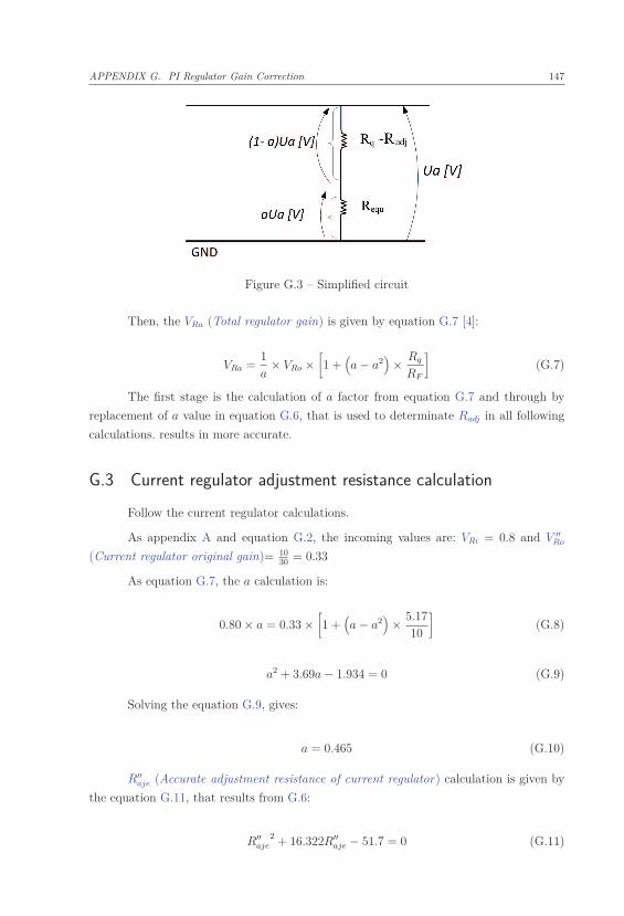
APPENDIX G. PI Regulator Gain Correction 147
Figure G.3 – Simplified circuit
Then, the VRa (Total regulator gain) is given by equation G.7 [4]:
VRa =1a
× VRo ×[1 +
(a − a2
)× Rq
RF
](G.7)
The first stage is the calculation of a factor from equation G.7 and through by
replacement of a value in equation G.6, that is used to determinate Radj in all following
calculations. results in more accurate.
G.3 Current regulator adjustment resistance calculation
Follow the current regulator calculations.
As appendix A and equation G.2, the incoming values are: VRi = 0.8 and V ′′
Ro
(Current regulator original gain)= 1030
= 0.33
As equation G.7, the a calculation is:
0.80 × a = 0.33 ×[1 +
(a − a2
)× 5.17
10
](G.8)
a2 + 3.69a − 1.934 = 0 (G.9)
Solving the equation G.9, gives:
a = 0.465 (G.10)
R′′
aje (Accurate adjustment resistance of current regulator) calculation is given by
the equation G.11, that results from G.6:
R′′
aje2 + 16.322R′′
aje − 51.7 = 0 (G.11)

APPENDIX G. PI Regulator Gain Correction 148
∴ R′′
aje = 2.716 kΩ (G.12)
As the resulting value from equation A.51 using the approximated value method
is the R′′
aj=2.15 k Ω, it means that the R′′
aje = 2.716 k Ω, which was calculated by this
more accurate method, is so close.
G.4 Speed regulator adjustment resistance calculation
Follow the speed regulator calculations.
As appendix A and equation G.2, the incoming values are: VRn = 6.7 and V ′
Ro
(Speed regulator original gain)= 100200
= 0.5
As equation G.7, the a calculation is:
6.7 =1a
× 0.5 ×[1 +
(a − a2
)× 4.8
100
](G.13)
6.7 × a = 0.5 ×[
100 + (a − a2) × 4.8100
](G.14)
Solving the equation G.14, gives:
a2 + 278.167a − 20.833 = 0 (G.15)
Solving the equation G.15, gives:
a = 0.07486 (G.16)
The R′
aje (Accurate adjustment resistance of speed regulator) calculation is given
by the equation G.17, that results from G.6:
R′
aje2 + 1328.53R′
aje − 480 = 0 (G.17)
∴ R′
aje = 0.3612 kΩ (G.18)
As the resulting value from equation A.71 using the approximated value method
is the R′
aj=358.2 Ω, it means that the R′
aje value, which was calculated by this more
accurate method, Raje (Accurate adjustment resistance of voltage regulator) = 361.2 Ω,
is so close.

APPENDIX G. PI Regulator Gain Correction 149
G.5 Voltage regulator adjustment resistance calculation
Follow the speed regulator calculations.
As Figure C.8, appendix A and equation G.2, the incoming values are: Kpe (Accu-
rate voltage regulator gain) = 6.63 and KP o (Voltage regulator original gain)= 1030
= 0.33
As equation G.7, the a calculation is:
6.63 × a = 0.33 ×[
10 + (a − a2) × 4.810
](G.19)
Solving the equation G.19, gives:
a2 + 40.856a − 2.083 = 0 (G.20)
Solving the equation G.20, gives:
a = 0.0509 (G.21)
The Raje calculation is given by the equation G.22, that results from G.6:
Raje2 + 191.67Raje − 48 = 0 (G.22)
∴ Raje = 0.25 kΩ (G.23)
As the resulting value from equation A.71 using the approximated value method
is the Raj=241.3 Ω, it means that the Raje = 250.0 Ω, which was calculated by this more
accurate method, is so close.
G.6 Gain Calculations
The adjustment resistances calculated in appendixes A and C by the rough calcula-
tion method result in R′′
aje=2.15 k Ω for current regulator; R′
aje=358.2 for speed regulator
and Raje=241.3 for voltage regulator.
Then, for these cited adjustment resistances, the respective gains will be calculated
by the more accurate method as follow below.
G.6.1 Current Regulator Gain
Regarding to current regulator shown in Figure A.15, follow the calculations in
order to obtain the accurate current regulator gain.
APPENDIX G. PI Regulator Gain Correction 150
From the equation G.4, the R′′
eq (Current regulator equivalent resistance) is:
R′′
eq =2.15 × 102.15 + 10
= 1.77 kΩ (G.24)
From the equation G.3, the variable "a" is:
a =1.775.17
= 0.342 (G.25)
Then, as the equation G.7, the gain VRie (Accurate current regulator gain) is:
VRie =0.3330.342
×[1 +
(0.342 − 0.3422
)× 5.17
10
]= 1.087 (G.26)
∴ This gain VRie= 1.087 is so close to VRi=0.80 that was used the rough calculation
method in appendix A.
G.6.2 Speed Regulator Gain
Regarding to speed regulator shown in Figure A.17, follow the calculations in order
to obtain the accurate speed regulator gain.
From the equation G.4, the R′
eq (Speed regulator equivalent resistance) is:
R′
eq =0.3582 × 100
100.3582= 0.3569 kΩ (G.27)
From the equation G.3, the variable "a" is:
a =0.3569
4.8= 0.07435 (G.28)
Then, as the equation G.7, the gain VRne (Accurate speed regulator gain) is:
VRne =0.5
0.07435×
[1 +
(0.07435 − 0.074352
)× 4.8
100
]= 6.7472 (G.29)
∴ This gain VRne= 6.7472 is so much close to VRn=6.7 that was used the rough
calculation method in appendix A.
G.6.3 Voltage Regulator Gain
Regarding to speed regulator shown in Figure C.8, follow the calculations in order
to obtain the accurate speed regulator gain.
From the equation G.4, the Req (Voltage regulator equivalent resistance) is:
Req =0.2413 × 10
10.2413= 0.2356 kΩ (G.30)
APPENDIX G. PI Regulator Gain Correction 151
From the equation G.3, the variable "a" is:
a =0.2356
4.8= 0.04908 (G.31)
Then, as the equation G.7, the gain Kpe is:
Kpe =0.333
0.04908×
[1 +
(0.04908 − 0.049082
)× 4.8
10
]= 6.9368 (G.32)
∴ This gain Kpe= 6.9368 is so close to Kp=6.63 that was used the rough calculation
method in appendix C.
G.7 Key Topics
The speed and current PI regulators for general control applications are imple-
mented in Laboratory of research development of electrical didactic laboratory of Federal
University of Itajubá (UNIFEI) and these are located in wooden box shown in Figure 1.9.
The current regulator shows in appendix A and that regulator implemented in [34]
have identical topology.
The speed regulator shows in appendix A and that regulator implemented in [34]
are similar. The unique difference is that has a fixed resistance 470 Ω located in R′
q1
branch,[34], instead of 100 Ω shows in appendix A methodology. Related to gain 6.7
calculated in appendix A by rough method, the speed regulator with fixed resistance 470 Ω
would not be viable, whereas the maximum gain, VRn, obtained through by this regulator
would be a bit upper 5.55. For this reason, the speed regulator with fixed resistance of R′
q1
branch was defined as 100 Ω, that became possible to show all adjustment methodology
for this regulator in appendixes A and in this appendix G.
Otherwise, for the experiments that use speed regulator whose gain is 4.0 as D
and [26], the speed regulator with fixed resistance 470 Ω is enough. The gain 4.0 is lower
than maximum gain 5.55 cited in previous paragraph.
In order to support the experiments show in D and illustrate the concepts described
here, the section G.8 will show the calculations to set the speed regulator with gain 4.0.
G.8 Speed Regulator with Gain 4.0
For the adjustment of speed Regulator with gain 4.0, it has:
APPENDIX G. PI Regulator Gain Correction 152
G.8.1 Calculation of Division Constant "a"
From the equation G.7, the gain VRne is:
VRne =0.5a
×[1 +
(a − a2
)× 5.17
100
]= 4.0 (G.33)
Then,
800a = 100 + 5.17a − 5.17a2 (G.34)
∴ a = 0.1257 (G.35)
G.8.2 Adjustment Resistance Calculation
The R””aje (Accurate adjustment resistance of Appendix D speed regulator) calcu-
lation is given by the equation G.36, that results from G.6:
R””aje2 + 790.37R””aje − 517 = 0 (G.36)
∴ R””aje = 0.6535 kΩ (G.37)
G.8.3 Rough Calculation for Gain 4.0
The gain for resistance calculated by the rough method is as follow:
From the equation G.1, the variable "a" is:
4.0 =0.5a
∴ a = 0.125 (G.38)
From the equation G.4, the R””eq (Speed regulator equivalent resistance for Rq2’=646.25
Ω ) is calculated as follow:
Rq2′ = 0.125 × 5.17 = 0.64625 kΩ (G.39)
Rq2′ = 646.25 Ω (G.40)
Using the accurate method, it results in
R””eq =0.64625 × 100
100.64625= 0.6421 kΩ (G.41)

APPENDIX G. PI Regulator Gain Correction 153
a =0.64215.17
= 0.1242 (G.42)
Then, the gain VRne2 (Accurate speed regulator gain for Rq2’=646.25 Ω) is:
VRne2 =0.5
0.1242−
[1 +
(0.1242 − 0.12422
)× 5.17
100
](G.43)
VRne2 =0.5
0.1242× 1.005624 (G.44)
VRne2 = 4.048 (G.45)
Therefore, the VRne2 is close to the adjusted gain 4.0.
154
Bibliography
1 ARCHIVE., D. TCA 785 Application Notes – SIEMENS. 2019. Disponível em: <https://www.datasheetarchive.com/TCA%20785%20application%20note-datasheet.html>. 7,94, 95
2 MOHAN, N.; UNDELAND, T. M.; ROBBINS, W. P. Power electronics: converters,applications, and design. [S.l.]: John wiley & sons, 2003. 7, 107
3 LANDER, C. W. Eletrônica industrial: teoria e aplicações. [S.l.]: McGraw-Hill, 1988.9, 91, 97
4 FRÖHR, F.; ORTTENBURGUER, F. Introduction to electronic control (in spanish).Marcombo SA, Siemens Aktiengesellschaft, 1986. 9, 20, 76, 77, 80, 81, 82, 104, 109, 112,114, 118, 119, 120, 121, 147
5 HAQUE, M. Self-excited single-phase and three-phase induction generators in remoteareas. In: IEEE. 2008 International Conference on Electrical and Computer Engineering.[S.l.], 2008. p. 38–42. 20
6 IBRAHIM, K.; LEIDHOLD, R. Variable frequency converter based voltage and fre-quency regulation of induction generator for stand-alone system application. In: IEEE.AFRICON 2015. [S.l.], 2015. p. 1–5. 20
7 TOUTI, E. et al. Asynchronous generator model for autonomous operating mode.In: IEEE. Proceedings of the International Conference on Electronics, Computers andArtificial Intelligence-ECAI 2013. [S.l.], 2013. p. 1–6. 20
8 MACEDO, D. M. The use of pumps operating as turbines and induction generatorsin electric power generation" (in portuguese). Master in Science Dissertation, FederalUniversity of Itajubá, UNIFEI. 2004. 20, 23, 49
9 Braga, A. V. et al. Isolated induction generator in a rural brazilian area: Field perfor-mance tests, doi:10.1016/ j. renene. 2015.05.057. Renewable Energy Journal, 2015. 20
10 SIMÕES, M. G.; FARRET, F. A. Renewable energy systems: design and analysis withinduction generators. [S.l.]: CRC press, 2004. 20
11 DEMETRIADES, G. M. The use of induction generators for small-scale hydroelectricschemes in remote areas. In: IEEE. 2000 10th Mediterranean Electrotechnical Conference.Information Technology and Electrotechnology for the Mediterranean Countries. Proceed-ings. MeleCon 2000 (Cat. No. 00CH37099). [S.l.], 2000. v. 3, p. 1055–1058. 20
12 LEE, C.-H.; WANG, L. A novel analysis of parallel operated self-excited inductiongenerators. IEEE Transactions on Energy Conversion, IEEE, v. 13, n. 2, p. 117–123, 1998.20
13 WANG, L.; LEE, C.-H. Dynamic analyses of parallel operated self-excited inductiongenerators feeding an induction motor load. IEEE Transactions on Energy Conversion,IEEE, v. 14, n. 3, p. 479–485, 1999. 20
Bibliography 155
14 CHAKRABORTY, C. et al. Performance of parallel-operated self-excited inductiongenerators with the variation of machine parameters. In: IEEE. Proceedings of the IEEE1999 International Conference on Power Electronics and Drive Systems. PEDS’99 (Cat.No. 99TH8475). [S.l.], 1999. v. 1, p. 86–91. 20
15 GAWANDE, S. et al. Synchronization of synchronous generator and induction gen-erator for voltage & frequency stability using statcom. In: IEEE. 2010 3rd InternationalConference on Emerging Trends in Engineering and Technology. [S.l.], 2010. p. 407–412.20
16 ION, C.; MARINESCU, C. Control of parallel operating micro hydro power plants. In:IEEE. 2010 12th International Conference on Optimization of Electrical and ElectronicEquipment. [S.l.], 2010. p. 1204–1209. 20
17 REDDY, P. J.; SINGH, S. Voltage and frequency control of parallel operated syn-chronous and induction generators in micro hydro scheme. In: IEEE. 2014 InternationalConference on Computation of Power, Energy, Information and Communication (IC-CPEIC). [S.l.], 2014. p. 124–129. 20
18 VANCO, W. E. et al. Experimental analysis of a self-excited induction generatorsoperating in parallel with synchronous generators applied to isolated load generation.IEEE Latin America Transactions, IEEE, v. 14, n. 4, p. 1730–1736, 2016. 20
19 MAGALHÃES, A. S. et al. Parallel operation repowering of synchronous and induc-tion generator. In: IEEE. 2016 IEEE 16th International Conference on Environment andElectrical Engineering (EEEIC). [S.l.], 2016. p. 1–6. 20
20 MELLO, F. P. Induction generators with inherent var generation capabilities an alter-native to synchronous generators. XIII Symposium of Specialists in Electric OperationalExpansion Planning, Foz do Iguaçu, Brazil. 2014. 20, 23, 61
21 WIJAYA, F. D.; GAJAYANA, L. N.; WIJAYA, H. P. Parallel operation synchronousand induction generator on microgrid testbed. In: IEEE. 2017 9th International Confer-ence on Information Technology and Electrical Engineering (ICITEE). [S.l.], 2017. p. 1–5.20
22 GAWANDE, S.; PORATE, K. Review of parallel operation of synchronous generatorand induction generator for stability. In: IEEE. 2009 Second International Conference onEmerging Trends in Engineering & Technology. [S.l.], 2009. p. 716–721. 20
23 GÜLEN, S. C. Gas Turbines for Electric Power Generation. [S.l.]: Cambridge Uni-versity Press, 2019. 21
24 FITZGERALD, A. E. et al. Electric machinery. [S.l.]: McGraw-Hill New York, 2003.v. 5. 21, 23, 49
25 SILVA, V. Z. Dynamic emulation and analysis of synchronous and induction genera-tors in parallel operation mode in an isolated electric system. In: FEDERAL UNIVER-SITY OF ITAJUBA, UNIFEI. [S.l.], 2020. p. 1–172. Doctorate thesis. 22
26 REZEK, Â. J. J. et al. A four quadrant regenerative dc drive by speed reversal usingarmature current inverting and by means of field current inverter - a comparative analysis(in portuguese). IEEE - INDUSCON/96, São Paulo-SP. INDUSCON/96 Annals. 1996. 22,119, 151
Bibliography 156
27 REZEK, Â. J. J. Fundamentos básicos de máquinas elétricas: teoria e ensaios. Syn-ergia, Rio de Janeiro-RJ and ACTA, Itajubá-MG, 2011. 22
28 SILVA, V. Z.; REZEK, Â. J. J.; CORRÊA, R. D. L. Analysis of synchronous andinduction generators in parallel operation mode in an isolated electric system, doi:10.1109/pedg.2017.7972459. In: IEEE. 2017 IEEE 8th International Symposium on PowerElectronics for Distributed Generation Systems (PEDG). [S.l.], 2017. p. 1–8. 23, 34, 35,42, 44, 46, 47, 48, 49, 60
29 SILVA, Â. J. J. R. V. Z.; CORRÊA, R. L. Analysis of synchronous and inductiongenerators in parallel operation mode in an isolated electric system using a ballast load asa regulation system under transient conditions, doi: 10.22270/ijesar.v4i2.112. In: IJESAR.[S.l.], 2018. p. 22–37. 23
30 SILVA, V. Z.; REZEK, Â. J. J.; CORRÊA, R. D. L. Novel analysis of synchronousand induction generators in parallel operation mode in an isolated electric system, doi:10.25046/aj020625. ASTES journal, 2017. 23
31 CHAPALLAZ, J.-M.; EICHENBERGER, P.; FISCHER, G. Manual on pumps usedas turbines. [S.l.]: Vieweg Braunschweig, Germany, 1992. 31
32 SILVA, V. Z.; REZEK, Â. J. J.; CORRÊA, R. D. L. Transients analysis of syn-chronous and induction generators in parallel operation mode in an isolated electric sys-tem, doi:10.1109/cobep.2017.8257236. In: IEEE. 2017 Brazilian Power Electronics Con-ference (COBEP). [S.l.], 2017. 49
33 OLIVEIRA, J. C.; COGO, J. R.; ABREU, J. P. G. Transformadores, teoria e ensaios.editora edgard blücher ltda. São Paulo, SP, 1984. 50, 127
34 SILVA, V. Z.; JUNQUEIRA, R. A. J.; OGOULOLA, C. E. G. Alternatives to controlthe frequency increase in an electric system with synchronous and induction generatorsin parallel operation mode, doi: 10.1016/j.epsr.2019.106136. Electric Power Systems Re-search, Elsevier, v. 180, 2020. 59, 63, 145, 151
35 MORAES, G. G.; FERREIRA, D. C. G.; JÚNIOR, G. S. F. Speed control of dcmachine (in portuguese). Electrical engineering final course report, Federal University ofItajuba. 2013. 63, 80, 119
36 REZEK, Â. J. J. et al. Modelling and implementation of a series dc motor drivesystem, doi: 105772/59814. https://www.intechopen.com, INTECH, 2015. 65, 80, 84, 119
37 REZEK, Â. J. J. Permanent and transitory state analysis of an ac/dc electrical energyconversion (in portuguese). Master in Science Dissertation, EFEI. 1986. 65, 72, 80, 84
38 REZEK, Â. J. J. et al. Project and simulation of a controlled drive system to directcurrent machines (in portuguese). Annals of II Internation Seminary of Electrical Motorsand regulatory drives, II SIMEAR, Vol III pages 141-160 – EPUSP, ABINEE TEC/91.1991. 80, 119, 120
39 SPIEGEL, M. R. Mathematical handbook of formulas and tables. McGraw-Hill, 1968.89

Bibliography 157
40 MENDONÇA, G. R. S.; REZEK, Â. J. J. Electronic circuit to firing angle command ofa three-phase thyristor bridge (in portuguese). Electrical engineering final course report,UNIFEI. 2002. 91
41 MALVINO, A. P.; BATES, D. J. Eletrônica-Vol. 1-8a Edição. [S.l.]: McGraw HillBrasil, 2016. v. 2. 91
42 GUIMARÃES, C. A. M. A point-on-wave switching system based on microcomputer(in portuguese). Master in Science Dissertation, UFSC, Florianópolis-SC, Brazil. 1986.101
43 COGO, J. R. Project and implementation of dc transmission system simulator (inportuguese). EFEI/FINEP agreement. 1985. 101
44 PINHEIRO, C. A. M.; COGO, J. R. Firing circuit of thyristors in three-phase grid(in portuguese). EFEI. 1985. 101
45 CAMACHO, C. A. P.; REZEK, Â. J. J. Use of symmetrical optimization techniqueto voltage adjust applied on synchronous generator (in portuguese). Master dissertation,Federal University of Itajubá, UNIFEI. 2007. 104, 116, 118
46 ALMEIDA, A. T. L. d. Máquinas síncronas. Grupo de Estudo em Manutenção Eletro-Eletrônica e Instalações, Universidade Federal de Itajubá, 2000. 105
47 IEC (Ed.). IEC 60034-2-1 Rotating electrical machines, Standard methods for deter-mining losses and efficiency from tests. 105, 136
48 IEC (Ed.). IEC 60034-1 Rotating electrical machines, Rating and performance. 105,136
49 REZEK, Â. J. J. et al. The modulus optimum (mo) method applied to voltage regu-lation systems: modeling, tuning and implementation. In: Proc. International Conferenceon Power System Transients, IPST. [S.l.: s.n.], 2001. v. 1, p. 24–28. 108, 114, 119


KS OmniScriptum Publishing
Brivibas gatve 197
LV-1039 Riga, Latvia
Telefax: +371 686 204 55
www.omniscriptum.com
Buy your books fast and straightforward online - at one of world’s
fastest growing online book stores! Environmentally sound due to
Print-on-Demand technologies.
Buy your books online at
www.morebooks.shop
Kaufen Sie Ihre Bücher schnell und unkompliziert online – auf einer
der am schnellsten wachsenden Buchhandelsplattformen weltweit!
Dank Print-On-Demand umwelt- und ressourcenschonend produzi
ert.
Bücher schneller online kaufen
www.morebooks.shop