Influence of Size Effect on the Electronic and Elastic Properties of Diamond Films with Nanometer...
16
The influence of size effect on the electronic and elastic properties of diamond films with nanometer thickness Leonid A. Chernozatonskii † , Pavel B. Sorokin †,‡,§ , Alexander A. Kuzubov ‡ , Boris P. Sorokin # , Alexander G. Kvashnin ‡ , Dmitry G. Kvashnin ‡ , Pavel V. Avramov ‡,††,⊥ and Boris I. Yakobson § Emanuel Institute of Biochemical Physics, Russian Academy of Sciences, 4 Kosigina st., Moscow, 119334, Russian Federation Siberian Federal University, 79 Svobodny av., Krasnoyarsk, 660041 Russian Federation Department of Mechanical Engineering & Material Science and Department of Chemistry, Rice University, Houston, Texas 77251, USA Technological Institute of Superhard and Novel Carbon Materials, 7a Centralnaya Street, Troitsk, Moscow region, 142190, Russia Kirensky Institute of Physics, Russian Academy of Sciences, Akademgorodok, Krasnoyarsk, 660036 Russian Federation Advanced Science Research Center, Japan Atomic Energy Agency, Tokai, Ibaraki319-1195, Japan † Emanuel Institute of Biochemical Physics ‡ Siberian Federal University § Rice University # Technological Institute of Superhard and Novel Carbon Materials †† Kirensky Institute of Physics ⊥ Advanced Science Research Center [email protected] Corresponding author. E.mail: [email protected] 1
Transcript of Influence of Size Effect on the Electronic and Elastic Properties of Diamond Films with Nanometer...

The influence of size effect on the electronic and elastic
properties of diamond films with nanometer thickness
Leonid A. Chernozatonskii†, Pavel B. Sorokin†,‡,§, Alexander A. Kuzubov‡, Boris P. Sorokin#,
Alexander G. Kvashnin‡, Dmitry G. Kvashnin‡, Pavel V. Avramov‡,††,⊥ and Boris I. Yakobson§
Emanuel Institute of Biochemical Physics, Russian Academy of Sciences, 4 Kosigina st., Moscow,
119334, Russian Federation
Siberian Federal University, 79 Svobodny av., Krasnoyarsk, 660041 Russian Federation
Department of Mechanical Engineering & Material Science and Department of Chemistry, Rice
University, Houston, Texas 77251, USA
Technological Institute of Superhard and Novel Carbon Materials, 7a Centralnaya Street, Troitsk,
Moscow region, 142190, Russia
Kirensky Institute of Physics, Russian Academy of Sciences, Akademgorodok, Krasnoyarsk, 660036
Russian Federation
Advanced Science Research Center, Japan Atomic Energy Agency, Tokai, Ibaraki319-1195, Japan
† Emanuel Institute of Biochemical Physics
‡ Siberian Federal University
§ Rice University
# Technological Institute of Superhard and Novel Carbon Materials
†† Kirensky Institute of Physics ⊥ Advanced Science Research Center
Corresponding author. E.mail: [email protected]
1
The atomic structure and physical properties of few-layered 111 oriented diamond nanocrystals (diamanes), covered by
hydrogen atoms from both sides are studied using electronic band structure calculations. It was shown that energy stability
linear increases upon increasing of the thickness of proposed structures. All 2D carbon films display direct dielectric band
gaps with nonlinear quantum confinement response upon the thickness. Elastic properties of diamanes reveal complex
dependence upon increasing of the number of 111 layers. All theoretical results were compared with available
experimental data.
Introduction
The graphene as two-dimensional material has attracted attention from the scientific community long
before experimental fabrication. The first theoretical study of graphene is dated 1946, when the
remarkable band structure of “Dirac cones” has been studied 1. First experimental observation of free
standing graphene 2 in 2004 initiated the comprehensive study of this material. Ballistic conductivity,
pseudo-chiral Dirac’s nature of carriers, anomalous Hall effect 3 makes graphene the most promising
material for science and future technology.
Hydrogenation of graphene enlarges its potential application in nanoelectronics. Regular adsorption
of hydrogen atoms changes graphene electronic structure and opens the band gap depending upon the
distance between hydrogen regions 4-8. Total hydrogenation of graphene changes the nature of
electronic states due to changing of sp2 hybridization of C-C bonds to sp3 one and opens the dielectric
band gap. 9,10 Such two-dimensional insulator was called as graphane. 10 The theoretical prediction was
generally confirmed experimentally by Elias et. al 11.
Graphane is an offspring of graphene along with graphene nanoribbons and carbon nanotubes. The
other type of carbon bonding opens a new way for developing of two-dimensional carbon based
materials.
Graphane is the first member in a series of sp3 bonded diamond films consist of a number of adjusted
111 oriented layers which display unique physical properties. For the first time diamane structures
were proposed by Chernozatonskii et. al. 12 in 2009. Recently 13 similar C2H structure was also
considered.
Usually diamond films prepared by CVD method with micrometer thickness. 14 Also the diamond
quantum wells obtained in the bulk structures of superlattices. 15 The consequent study of graphene,
graphane and proposed diamanes can be considered as bottom-up nanotechnological approach opposite
to ordinary top-down paradigm. The main goal of this work is to study diamane physical properties. As
against to Ref. 12 we consider diamanes with different thickness, we investigate their stability and
compare them with known data for sp3-hybridized hydrocarbon clusters. We study the elastic properties
2
of the structures and obtain phonon dispersion, wave velocities and elastic constants. Finally we discuss
possible ways to synthesize the structures.
Method and model
The plane wave DFT PBE 16 electronic structure calculations of 2D carbon nanostructures were
performed using Ultrasoft Vanderbilt pseudopotentials 17 and a plane-wave energy cutoff equal to 30 Ry
by PWSCF code 18. To calculate equilibrium atomic structures, the Brillouin zone was sampled
according to the Monkhorst–Pack 19 scheme with a 16×16×1 k-point convergence grid. To avoid
interactions between the species, neighboring planes were separated at least by 10 Å in the hexagonal
supercells. During the atomic structure minimization, structural relaxation was performed until the
change in total energy was less than 3×10⁻⁷ eV. Phonons calculations were performed within density
functional perturbation theory. 20 All the values given above were carefully tested and found optimal.
Results and discussion
Atomic structures of graphene and graphane are presented in Fig. 1a and 1b, respectively. Both
structures display hexagonal symmetry with essentially different lattice parameters (2.468 and 2.540 Å,
respectively) because of different nature of chemical bonding. In contrast to flat sp2-hybridized
graphene, crimped sp3 graphane is characterized by two terminal layers of hydrogen atoms from both
sides of the sheet. Surface hydrogen atoms of graphane at least from one side can be replaced by one
more layer of sp3 carbon atoms forming a diamane structure. Since chemical bonding between carbon
layers in diamanes is also realized by sp3 hybridization, the lattice parameters of studied diamanes are
close to each other (a = 2.53 Å).
Hydration of graphene completely changes the nature of the material which can be considered as the
thinnest possible diamond. The diamond films with smallest thickness obviously succeed the properties
of the graphane with consistent approaching to the bulk diamond limit. Diamond films or diamanes
under study fill the gap between two-dimensional graphane and crystalline diamond.
3

Fig. 1. The atomic geometry of studied quasi two-dimensional carbon nanofilms a) graphene; b) graphane; c)
diamane D(AB) with AB stacking of two layers; d) diamane D(ABC) with ABC stacking of three layers. Carbon
atoms are marked by yellow (light gray), hydrogen are marked by blue (gray). For each diamane possible stacking
sequences of carbon layers are presented.
The atomic geometry of the diamane consists of stacking covalently bounded monoatomic carbon
layers (Fig. 1b-d). The changing of the stacking sequence allows constructing different diamane
polytypes. According to this fact diamanes can be compactly classified as D(ijk…l) where i, j, k, l are
positions layer types which can be equal to A, B or C. For example, two and three layered diamanes
with natural diamond stacking sequence (ABCABC…) are denoted as D(AB) and D(ABC); two and
three layered diamanes with lonsdaleite stacking sequence (AAA…) are denoted as D(AA) and
D(AAA). In the left part of the Fig. 1c-d the D(AB) and D(ABC) structures are presented whereas on
the right possible stacking sequences of carbon layers in corresponding diamanes are shown. In general,
graphane can be named as D(A) but we suppose that graphane is the intermediate structure between
graphene and diamane due to the structure does not contain any diamond like cells.
Formation energy (eV/atom) of studied structures was calculated according to the following
equation 21,22: ( ) ( )222
+−−= nEnEEE Hgraphenestrform , where Egraphene is energy of graphene per carbon
atom (-9.30 eV/atom), is energy of hydrogen molecule (-2.99 eV/atom) and n is number of carbon
atoms in the unit cell.
2HE
4

0.0 0.2 0.4 0.6 0.8 1.0-0.3
-0.2
-0.1
0.0
0.1
3.0
C H
Diamond
atomic H
H2
Methane
AdamantaneDiamantane
TriamantaneGraphane
D(AB)D(AA)
D(ABC) D(AAC)D(AAA)
Graphene
E (e
V/a
tom
)fo
rm
C1-x xH Fig. 2. a) Formation energy of different hydrocarbon structures as a function of hydrogen content. One can see three
groups of structures marked by rectangles. The first group consists of sp3-hybridized CH4 molecule. The next group
consists of several members of diamondoid family (adamantane, diamantine and triamantane 23). The last group
consists of 2D nanoclusters of graphane and diamanes D(ij) and D(ijk).
For the sake of comparison the formation energies of a set of hydrocarbon structures were calculated
using the same PBC DFT method. Studied structures can be divided on three groups. The first group
(molecules) contains one member, CH4 molecule which has the lowest formation energy (-
0.25 eV/atom). The next group consists of diamondoids and contains three smallest members of the
family: adamantane, diamantine and triamantane. 23 And the third group (two-dimensional diamond-
like nanothick films) contains graphane and diamanes.
The energies of the studied structures tend nearly linear to the energy of bulk diamond (Fig. 2a) upon
the hydrogen content. The diamanes with diamond type layer stacking (AB and ABC types) display the
lowest energy per atom in comparison with corresponding structures with other stacking sequences but
the difference in the energy of diamanes with diamond and other stacking sequences is smaller than
0.02 eV/atom which justifies the possible existence of diamanes with any stacking types. Two layered
diamanes D(ij) are less favorable than graphane but are more favorable than graphene. The stability of
the D(ij) is also proved by the high energy of 0.74 eV/atom of separation of D(AB) to two isolated
carbon layers hydrogenated from one side.
5

Fig. 2a allows to estimate the possible way of preparation of diamanes. The formation energy of
three-layered diamanes is positive (in the assumption of zeros temperature and pressure) if graphene
and H2 are used as source species of carbon and hydrogen atoms, respectively. The changing of source
of hydrogen from molecular H2 to atomic H leads to different sign of the formation energy from
positive to negative which means that all studied diamane series become energy favorable. It should be
noted that the graphane-like structure was synthesized experimentally using by atomic hydrogen. 11 In
the case of diamanes, passivating hydrogen layers display only hexagonal symmetry as against
graphane on which surface hydrogen can be arranged in various manners. 9,10,24
6

C1-x xH0.0 0.2 0.4 0.6 0.8 1.0
2
3
4
5
69
10
C H
Diamond
Methane
AdamantaneDiamantane
Triamantane
GraphaneD(AB)D(AA)D(ABC)
D(AAC)D(AAA)
E (e
V)ba
nd g
ap
5
0
-5
-10
-15
5
0
-5
-10
-15
M Г K M
5
0
-5
-10
-15
E(k
)(eV
)E
(k)(
eV)
E(k)
(eV)
a)
b)
c)
d)5
0
-5
-10
-15
E(k
)(eV
)
e)
Fig. 3. Evolution of the band structures of 2D carbon nanostructures: a) graphane; b) D(AB); c) D(ABC) and d) in
the limit of infinite number of layers (bulk diamond with the same orientation of reciprocal vectors ). Fermi level is
marked by horizontal blue line; e) band gap width of different hydrocarbon structures as a function of hydrogen
content. One can see three groups of structures marked by rectangles. The first group consists of sp3-hybridized CH4
molecule. The next group consists of several members of diamondoid family (adamantane, diamantine and
triamantane 23). The last group consists of 2D nanoclusters of graphane and diamanes D(ij) and D(ijk).
7

Let us consider the electronic properties of the studied structures. Band structures of graphane and
diamanes are similar and display dielectric behavior and direct band gap (Fig. 3). For the sake of
comparison, the electronic structure of methane and diamondoid clusters was also calculated. The band
gap of studied structures should tend to the band gap of bulk diamond (Fig. 3e) upon the decrease of
hydrogen content (and increase of thickness of the structure). In the case of diamondoid clusters similar
results were obtain in Ref. 25. The diamane band gap widths are lower than the gap of graphane
(3.4 eV) which evidence of the existence of minimum in the dependence of band gap value upon the
number of layers because calculated band gap of diamond (diamane with infinite index) is 4.5 eV. The
nonlinear effect of the studied films can be explained by surface states and quantum confinement effect.
During the increasing of diamane film thickness the contribution of electrons from the bulk increases
and electronic properties of the diamanes tends to the properties of diamond.
The phonon band structures of graphane, D(AB) and D(ABC) are presented in Fig. 4 (a, b and c,
respectively). The energy splitting of the graphane highest active modes in Raman spectrum (2856 cm-1
and 2896 cm -1, reference values 10 are 2842 cm-1 and 2919 cm-1) is equal to 40 cm-1 whereas diamanes
display smaller energy splitting of the modes (2865 cm-1 and 2875 cm-1 for D(AB), and 2874 cm-1 and
2882 cm-1 for D(ABC), respectively), see group VI in Table 1. The increasing of the number of modes
in the frequency region around 1332 cm-1 (diamond fingerprints) can be an indication of diamane films
due to linear increase of line intensities upon thickness of the diamond-like film 26 (group V in Table 1).
Another characteristic feature of diamanes is appearance of the vibrational modes at 664 cm-1 and
848 cm-1 in the cases of D(AB) and D(ABC), respectively (group III in Table 1). Near 500 cm-1
frequency region one can see two (for D(AB)) and five (for D(ABC)) optical modes bunched in one and
two groups, respectively (groups I and II in Table 1).
Three acoustic branches of graphane and diamanes correspond to in-plane (two branches, linear
dependence ω(k)) and out-plane (one branch, quadratic dependence ω(k)) vibrations of the 2D
structure. 27 The increasing of the thickness of the film leads to gradual transformation of the quadratic
branch to linear one of transverse mode typical for the crystal.
8

Table 1. Phonon frequencies (cm-1) at Г-point region and velocities of transverse and longitudinal acoustic in-plane
modes (103 m/s)
ωopt groups
I II III IV V VI vTA, vLA,
Graphane - - - 1123, 1123
1159, 1162, 1162, 1328, 1328
2856, 2896
12.0 17.7
D(AB) 401, 401 664
1131, 1131, 1133, 1133
1201, 1249, 1260, 1260, 1313, 1313
2865, 2875
12.1 17.8
D(ABC) 291, 291 467, 483, 483
848
1132, 1132, 1133, 1133
1211, 1224, 1224, 1248, 1282, 1287, 1287, 1308, 1308
2874 2882
12.2 18.0
Diamond (experiment 28)
12.4 18.3
Velocities of longitudinal and transverse acoustic in-plane modes (Table 1) were obtained from
phonon spectra (Fig. 4). For comparison the longitudinal and transverse velocities were calculated for
diamond in hexagonal orientation based on experimental value of elastic constants 28 (see Appendix for
details). It is clearly seen that the velocities are gradually increased with increasing of the thickness of
the films due to the augmentation of stiffness of the structures and tend to the diamond values.
9

M Г K M
0.0
500
1000
1500
ω (c
m)
-1ω
(cm
)-1
ω (c
m)
-1
a)
b)
c)
3000
0.0
500
1000
1500
3000
0.0
500
1000
1500
3000
Fig. 4. Phonon band structures of 2D carbon nanostructures: a) graphane; b) D(AB); c) D(ABC).
Based on the velocities, elastic constants of graphene, graphane, D(AB) and D(ABC) were calculated
and compared with experimental data for graphite 29 and theoretical data for graphene 30,31 and
graphane. 32 Due to 2D nature of the objects under study, the elastic constants were calculated using
equations and , where ρ2D is formal density (kg/m2 units) in which
ambiguous thickness of 2D material is neglected. To compare the calculated data and experimental
values of elastic constants of bulk graphite from Ref.
DLAvC 22
11 ρ= DTAvCC 22
1112 2 ρ−=
29, the theoretical data of graphene from Ref. 31
were multiplied by formal value 3.35 Å (the distance between graphene layers in graphite).
10
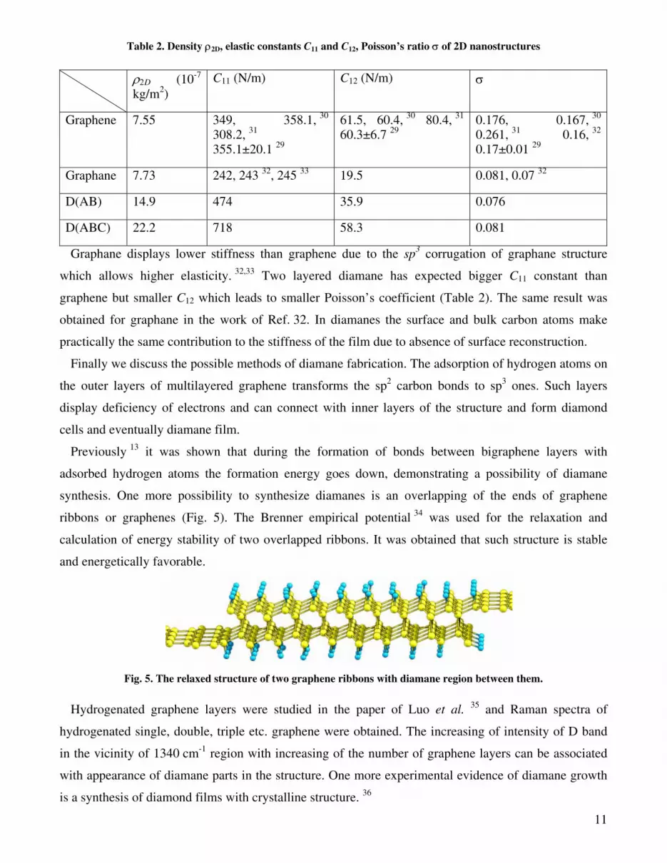
Table 2. Density ρ2D, elastic constants C11 and C12, Poisson’s ratio σ of 2D nanostructures
ρ2D (10-7 kg/m2)
C11 (N/m) C12 (N/m) σ
Graphene 7.55 349, 358.1, 30 308.2, 31 355.1±20.1 29
61.5, 60.4, 30 80.4, 31 60.3±6.7 29
0.176, 0.167, 30 0.261, 31 0.16, 32 0.17±0.01 29
Graphane 7.73 242, 243 32, 245 33 19.5 0.081, 0.07 32
D(AB) 14.9 474 35.9 0.076
D(ABC) 22.2 718 58.3 0.081
Graphane displays lower stiffness than graphene due to the sp3 corrugation of graphane structure
which allows higher elasticity. 32,33 Two layered diamane has expected bigger C11 constant than
graphene but smaller C12 which leads to smaller Poisson’s coefficient (Table 2). The same result was
obtained for graphane in the work of Ref. 32. In diamanes the surface and bulk carbon atoms make
practically the same contribution to the stiffness of the film due to absence of surface reconstruction.
Finally we discuss the possible methods of diamane fabrication. The adsorption of hydrogen atoms on
the outer layers of multilayered graphene transforms the sp2 carbon bonds to sp3 ones. Such layers
display deficiency of electrons and can connect with inner layers of the structure and form diamond
cells and eventually diamane film.
Previously 13 it was shown that during the formation of bonds between bigraphene layers with
adsorbed hydrogen atoms the formation energy goes down, demonstrating a possibility of diamane
synthesis. One more possibility to synthesize diamanes is an overlapping of the ends of graphene
ribbons or graphenes (Fig. 5). The Brenner empirical potential 34 was used for the relaxation and
calculation of energy stability of two overlapped ribbons. It was obtained that such structure is stable
and energetically favorable.
Fig. 5. The relaxed structure of two graphene ribbons with diamane region between them.
Hydrogenated graphene layers were studied in the paper of Luo et al. 35 and Raman spectra of
hydrogenated single, double, triple etc. graphene were obtained. The increasing of intensity of D band
in the vicinity of 1340 cm-1 region with increasing of the number of graphene layers can be associated
with appearance of diamane parts in the structure. One more experimental evidence of diamane growth
is a synthesis of diamond films with crystalline structure. 36
11
The electronic structure calculations directly demonstrate complex dependence of the physical
properties of diamanes upon their thickness. Controllable variation of the number of 111 layers and
sequence order leads to tunable variation of electronic properties of diamanes. Diamanes can be applied
in nanoelectronics and nanooptics e.g. as active laser medium within lasers. The increasing number of
layers in diamane will lead to transition of direct band gap to indirect one (diamond) therefore only thin
films can be used for this purpose. Diamanes can be used as optical planar waveguides and as very thin
dielectric hard films in nanocapasitors or as chemical nanosensors (e.g. it was obtained that
hydrogenated diamond surface changes their electrical conductivity by adsorption of H3O+ species 37) or
as mechanically stiff nanothick elements in nanoelectronics.
Acknowledgements
L.A.C. was supported by the Russian Academy of Sciences, program No. 21 and by the Russian
Foundation for Basic Research (project no. 08-02-01096). P.B.S. and B.I.Y. acknowledge support by
the Office of Naval Research (MURI project). P.V.A. and P.B.S. also acknowledge the collaborative
RFBR-JSPS grant No. 09-02-92107-ЯΦ. We are grateful to the Joint Supercomputer Center of the
Russian Academy of Sciences for the possibility of using a cluster computer for quantum chemical
calculations. The geometry of all presented structures was visualized by commercial ChemCraft
software
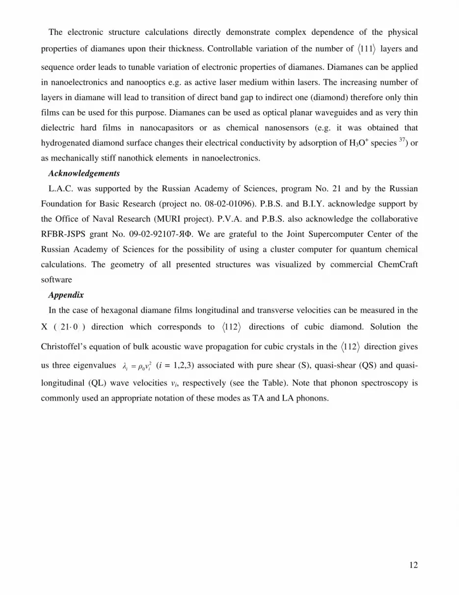
Appendix
In the case of hexagonal diamane films longitudinal and transverse velocities can be measured in the
X ( 021⋅ ) direction which corresponds to 112 directions of cubic diamond. Solution the
Christoffel’s equation of bulk acoustic wave propagation for cubic crystals in the 112 direction gives
us three eigenvalues (i = 1,2,3) associated with pure shear (S), quasi-shear (QS) and quasi-
longitudinal (QL) wave velocities vi, respectively (see the Table). Note that phonon spectroscopy is
commonly used an appropriate notation of these modes as TA and LA phonons.
20 ii vρλ =
12
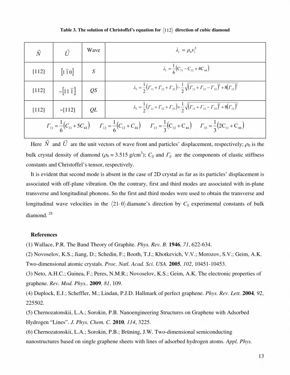
Table 3. The solution of Christoffel’s equation for 112 direction of cubic diamond
Nr
Ur
Wave 2
0 ii vρλ =
[112] [ ]011 S ( )4412111 C4CC61
+−= λ
[112] ~ [ ]111 QS ( ) ( ) ( )213
23312113312112 8
21
21 ΓΓΓΓΓΓΓ λ +−+−++=
[112] ~[112] QL ( ) ( ) ( )213
23312113312113 8
21
21 ΓΓΓΓΓΓΓ λ +−++++=
( )441111 561 CCΓ += ( )441213 CC
31
+=Γ ( )441133 CC231
+=Γ ( )441212 61 CCΓ +=
Here Nr
and Ur
are the unit vectors of wave front and particles’ displacement, respectively; ρ0 is the
bulk crystal density of diamond (ρ0 = 3.515 g/cm3); Cij and Γij are the components of elastic stiffness
constants and Christoffel’s tensor, respectively.
It is evident that second mode is absent in the case of 2D crystal as far as its particles’ displacement is
associated with off-plane vibration. On the contrary, first and third modes are associated with in-plane
transverse and longitudinal phonons. So the first and third modes were used to obtain the transverse and
longitudinal wave velocities in the 021⋅ diamane’s direction by Cij experimental constants of bulk
diamond. 28
References
(1) Wallace, P.R. The Band Theory of Graphite. Phys. Rev. B. 1946, 71, 622-634.
(2) Novoselov, K.S.; Jiang, D.; Schedin, F.; Booth, T.J.; Khotkevich, V.V.; Morozov, S.V.; Geim, A.K.
Two-dimensional atomic crystals. Proc. Natl. Acad. Sci. USA. 2005, 102, 10451-10453.
(3) Neto, A.H.C.; Guinea, F.; Peres, N.M.R.; Novoselov, K.S.; Geim, A.K. The electronic properties of
graphene. Rev. Mod. Phys.. 2009, 81, 109.
(4) Duplock, E.J.; Scheffler, M.; Lindan, P.J.D. Hallmark of perfect graphene. Phys. Rev. Lett. 2004, 92,
225502.
(5) Chernozatonskii, L.A.; Sorokin, P.B. Nanoengineering Structures on Graphene with Adsorbed
Hydrogen “Lines”. J. Phys. Chem. C. 2010, 114, 3225.
(6) Chernozatonskii, L.A.; Sorokin, P.B.; Brüning, J.W. Two-dimensional semiconducting
nanostructures based on single graphene sheets with lines of adsorbed hydrogen atoms. Appl. Phys.
13

Lett.. 2007, 91, 183103.
(7) Singh, A.K.; Yakobson, B.I. Electronics and Magnetism of Patterned Graphene Nanoroads. Nano
Lett. 2009, 9, 1540-1543.
(8) Balog, R.; Jørgensen, B.; Nilsson, L.; Andersen, M.; Rienks, E.; Bianchi, M.; Fanetti, M.;
Lægsgaard, E.; Baraldi, A.; Lizzit, S.; Sljivancanin, Z.; Besenbacher, F.; Hammer, B.; Pedersen, T.G.;
Hornekær, P.H.&.; Liv Bandgap opening in graphene induced by patterned hydrogen adsorption. Nat.
Mater.. 2010, 9, 315-319.
(9) Sluiter, M.H.F.; Kawazoe, Y. Cluster expansion method for adsorption: Application to hydrogen
chemisorption on graphene. Phys. Rev. B. 2003, 68, 085410.
(10) Sofo, J.O.; Chaudhari, A.S.; Barber, G.D. Graphane: a two-dimensional hydrocarbon. Phys. Rev. B.
2007, 75, 153401.
(11) Elias, D.C.; Nair, R.R.; Mohiuddin, T.M.G.; Morozov, S.V.; Blake, P.; Halsall, M.P.; Ferrari, A.C.;
Boukhvalov, D.W.; Katsnelson, M.I.; Geim, A.K. Control of Graphene's Properties by Reversible
Hydrogenation: Evidence for Graphane. Science. 2009, 323, 610.
(12) Chernozatonskii, L.A.; Sorokin, P.B.; Kvashnin, A.G.; Kvashnin, D.G. Diamond-like C 2 H
nanolayer, diamane: Simulation of the structure and properties. JETP Letters. 2009, 90, 134-138.
(13) Leenaerts, O.; Partoens, B.; Peeters, F.M. Hydrogenation of bilayer graphene and the formation of
bilayer graphane from first principles. Phys. Rev. B. 2009, 80, 245422.
(14) Ashfold, M.N.R.; May, P.W.; Rego, C.A.; Everitt, N.M. Thin film diamond by chemical vapour
deposition methods. Chem. Soc. Rev.. 1994, 23, 21-30.
(15) Silva, S.R.P.; Amaratunga, G.A.J.; Haq, S.; Salje, E.K. Optical quantum size effects in diamond-
like carbon superlattice structures. Thin solid films. 1994, 253, 20-24.
(16) Perdew, J.P.; Burke, K.; Ernzerhof, M. Generalized gradient approximation made simple. Phys.
Rev. Lett. 1996, 77, 3865-3868.
(17) Vanderbilt, D. Soft self-consistent pseudopotentials in a generalized eigenvalue formalism. Phys.
Rev. B. 1990, 41, 7892-7895.
(18) Giannozzi, P.; Baroni, S.; Bonini, N.; Calandra, M.; Car, R.; Cavazzoni, C.; Ceresoli, D.; Chiarotti,
G.L.; Cococcioni, M.; Dabo, I.; Corso, A.D.; de Gironcoli, S.; Fabris, S.; Fratesi, G.; Gebauer, R.;
Gerstmann, U.; Gougoussis, C.; Kokalj, A.; Lazzeri, M.; Martin-Samos, L.; Marzari, N.; Mauri, F.;
Mazzarello, R.; Paolini, S.; Pasquarello, A.; Paulatto, L.; Sbraccia, C.; Scandolo, S.; Sclauzero, G.;
Seitsonen, A.P.; Smogunov, A.; Umari, P.; Wentzcovitch, R.M. QUANTUM ESPRESSO: a modular
and open-source software project for quantum simulations of materials. J. Phys.: Cond. Mat.. 2009, 21,
395502.
(19) Monkhorst, H.J.; Pack, J.D. Special points for Brillouin-zone integrations. Phys. Rev. B. 1976, 13,
5188-5192.
14

(20) Baroni, S.; de Gironcoli, S.; Dal Corso, A.; Giannozzi, P. Phonons and related crystal properties
from density-functional perturbation theory. Rev. Mod. Phys.. 2001, 73, 515-562.
(21) Dumitrica, T.; Hua, M.; Yakobson, B.I. Endohedral silicon nanotubes as thinnest silicide wires.
Phys. Rev. B. 2004, 70, 241303(R).
(22) Sorokin, P.B.; Chernozatonskii, L.A.; Avramov, P.V.; Yakobson, B.I. Magnesium Boride
Nanotubes: Relative Stability and Atomic and Electronic Structure. J. Phys. Chem. C. 2010, 114, 4852-
4856.
(23) Dahl, J.E.; Liu, S.G.; Carlson, R.M.K. Isolation and Structure of Higher Diamondoids, Nanometer-
Sized Diamond Molecules. Science. 2003, 299, 96-99.
(24) Artyukhov, V.I.; Chernozatonskii, L.A. Structure and layer interaction in carbon monofluoride and
graphane: a comparative computational study. J. Phys. Chem. C. 2010, 114, 5389-5396.
(25) Landt, L.; Klünder, K.; Dahl, J.E.; Carlson, R.M.K.; Möller, T.; Bostedt, C. Optical response of
diamond nanocrystals as a function of particle size, shape, and symmetry. Phys. Rev. Lett. 2009, 103,
047402.
(26) Knight, D.S.; White, W.B. Characterization of diamond films by Raman spectroscopy. J. Mat.
Res.. 1989, 4, 385-393.
(27) Saito, R.; Dresselhaus, G.; Dresselhaus, M.S. Physical Properties of Carbon Nanotubes, 1 ed.;
Imperial College Press: London, 1998; pp 259.
(28) McSkimin, H.J.; Andreatch, P. Elastic Moduli of Diamond as a Function of Pressure and
Temperature. J. Appl. Phys.. 1972, 43, 2944.
(29) Blakslee, O.L.; Proctor, D.G.; Seldin, E.J.; Spence, G.B.; Weng, T. Elastic Constants of
Compression Annealed Pyrolytic Graphite. J. Appl. Phys.. 1970, 41, 3373.
(30) Wei, X.; Fragneaud, B.; Marianetti, C.A.; Kysar, J.W. Nonlinear elastic behavior of graphene: Ab
initio calculations to continuum description. Phys. Rev. B. 2009, 80, 205407.
(31) Falkovsky, L. Phonon dispersion in graphene. JETP. 2007, 105, 397-403.
(32) Topsakal, M.; Cahangirov, S.; Ciraci, S. Strain induced modifications on the properties of
graphane. Appl. Phys. Lett.. 2010, 96, 091912.
(33) Muñoz, E.; Singh, A.K.; Ribas, M.A.; Penev, E.S.; Yakobson, B.I. The ultimate diamond slab:
GraphAne versus graphEne. Diamond & Related Materials. 2010, 19, 368-373.
(34) Brenner, D.W.; Shenderova, O.A.; Harrison, J.A.; Stuart, S.J.; Ni, B.; Sinnott, S.B. A second-
generation reactive empirical bond order (REBO) potential energy expression for hydrocarbons. J.
Phys.: Cond. Mat.. 2002, 14, 783-802.
(35) Luo, Z.; Yu, T.; Kim, K.; Ni, Z.; You, Y.; Lim, S.; Shen, Z.; Wang, S.; Lin, J. Thickness-
Dependent Reversible Hydrogenation of Graphene Layers. ACS Nano. 2009, 3, 1781-1788.
15

(36) Tsugawa, K.; Ishihara, M.; Kim, J.; Koga, Y.; Hasegawa, M. Nucleation Enhancement of
Nanocrystalline Diamond Growth at Low Substrate Temperatures by Adamantane Seeding. J. Phys.
Chem. C. 2010, 114, 3822-3824.
(37) Andriotis, A.N.; Mpourmpakis, G.; Richter, E.; Menon, M. Surface conductivity of hydrogenated
diamond films. Phys Rev Lett. 2008, 100, 106801.
16