Inductive link design for medical implants
6
2009 IEEE Symposium on Industrial Electronics and Applications (ISIEA 2009), October 4-6, 2009, Kuala Lumpur, Malaysia Inductive Link Design for Medical Implants Hussnain Ali, Student Member IEEE, Talha J Ahmad, Shoab A Khan Biomedical Engineering Department Center for Advanced Research in Engineering Islamabad, Pakistan [email protected], [email protected], [email protected] Abstract— This paper describes design principles to design and develop a transcutaneous link for medical implants using inductively coupled coils. Parameters which optimize link efficiency have been discussed in the light of previous studies and a simple design methodology to find optimized parameters for Class E amplifier and inductive coils is outlined. Paper also describes design of an indigenously developed transcutaneous link from commercial off-the- shelf components to demonstrate the design process. Simulation and practical results of the link developed at 2.5MHz for 100mW output power are provided. We were able to achieve 40% link efficiency with data rate of 128kbps from laboratory-based discrete electronic components. Keywords — Inductive Link; Medical Implants; Class E Amplifier I. INTRODUCTION Wireless transmission of data and power has emerged as a popular and essential characteristic of implantable medical devices such as cardiac pacemakers, implantable cardioverter defibrillators, recording devices, neuromuscular stimulators, prosthetic devices such as cochlear and retinal implants to name a few. Inductive coupling is most popular and effective means to realize transcutaneous link for biomedical devices because a single pair of coil can be used both for data as well as power transmission to the implanted circuitry. In addition to this, design of an inductive link using a power amplifier is fully customizable with full control on variables like operating frequency, range, form-factor and output power for an ‘application specific’ design. Design requirements of an inductive link for medical implants demand careful consideration of (i) bandwidth for supporting high data rates; (ii) efficiency for minimum power drop across the link; (iii) coupling insensitivity to coil misalignments; iv) form factor and v) biocompatibility. Data and power transmission have conflicting requirements in terms of efficiency. Wider bandwidth and high data rates are better supported at higher frequency. On the contrary, efficient power transfer is achieved using low operating frequency. This is due to the fact that human body is penetrable to magnetic fields at lower frequencies [1]. In addition to this, degradation of power transmission efficiency at higher frequency results from more power absorption in the tissue and more power dissipation in the external and internal power conditioning blocks [2,3]. One solution to this problem is to use separate coils for data and power transfer when no compromise between efficiency and data bandwidth is required, approach used by [1,3]. However, using separate coils has its own disadvantages such as increased form factor and electromagnetic interference which increases system complexity such as incorporation of wide range of frequencies and complex modulation techniques, to minimize interference, and use of CRC to remove BER etc. Second option is to establish a tradeoff between the requirements and use a single coil for both the tasks by optimizing design parameters for efficiency and high data rates as reported in [4,5]. As far as RF data and power transmission is concerned, efficient power transfer is a major bottle neck in RF links, not efficient data transfer [4]. Therefore, optimization of efficiency for power transfer is highly desirable due to low coupling in practical implants [6]. First step in the design and analysis of an inductive link requires simplified circuit representation of the inductive link to compute link response at the operating frequency. Incorporation of resonating impedances at primary and secondary side has been widely reported to improve the link performance. Circuit component values derived for an optimum link topology are presented in Section I. Second step involves coil design, which plays a critical role in optimum data and power transmission. This includes optimization of coil geometry, coil dimensions, inductor losses, type of wire used and number of turns in windings to mention a few. All these factors are comprehensively discussed in Section III and a heuristic design methodology has been outlined to design coils in laboratory. Final step involves design of power amplifier. Wireless transmission through inductive coupling requires an AC excitation which makes the power driver essentially a DC to AC inverter. Furthermore, considering the fact that high voltage level is usually required by the primary coil and batteries produce a much lower voltage, the driver should also have the ability of amplifying the battery voltage [3]. Therefore, two essential characteristics of the required power amplifier are efficient DC to AC inversion and voltage amplification for energizing the primary coil. Class E Amplifiers not only meet above requirements but are characterized by 100% theoretical efficiency and are thus, most preferable designer choice. In Section IV, Class E Amplifier design with reference to the transcutaneous link is comprehensively discussed. Section V describes design of our developed transcutaneous link on the discussed design principles followed by simulation and practical results in Section VI. Finally, conclusions derived from the design process are presented in Section VII. 978-1-4244-4683-4/09/$25.00 ©2009 IEEE 694
-
Upload
independent -
Category
Documents
-
view
3 -
download
0
Transcript of Inductive link design for medical implants
2009 IEEE Symposium on Industrial Electronics and Applications (ISIEA 2009), October 4-6, 2009, Kuala Lumpur, Malaysia
Inductive Link Design for Medical Implants
Hussnain Ali, Student Member IEEE, Talha J Ahmad, Shoab A Khan Biomedical Engineering Department
Center for Advanced Research in Engineering Islamabad, Pakistan
[email protected], [email protected], [email protected]
Abstract— This paper describes design principles to design and develop a transcutaneous link for medical implants using inductively coupled coils. Parameters which optimize link efficiency have been discussed in the light of previous studies and a simple design methodology to find optimized parameters for Class E amplifier and inductive coils is outlined. Paper also describes design of an indigenously developed transcutaneous link from commercial off-the-shelf components to demonstrate the design process. Simulation and practical results of the link developed at 2.5MHz for 100mW output power are provided. We were able to achieve 40% link efficiency with data rate of 128kbps from laboratory-based discrete electronic components.
Keywords — Inductive Link; Medical Implants; Class E Amplifier
I. INTRODUCTION Wireless transmission of data and power has emerged
as a popular and essential characteristic of implantable medical devices such as cardiac pacemakers, implantable cardioverter defibrillators, recording devices, neuromuscular stimulators, prosthetic devices such as cochlear and retinal implants to name a few. Inductive coupling is most popular and effective means to realize transcutaneous link for biomedical devices because a single pair of coil can be used both for data as well as power transmission to the implanted circuitry. In addition to this, design of an inductive link using a power amplifier is fully customizable with full control on variables like operating frequency, range, form-factor and output power for an ‘application specific’ design.
Design requirements of an inductive link for medical implants demand careful consideration of (i) bandwidth for supporting high data rates; (ii) efficiency for minimum power drop across the link; (iii) coupling insensitivity to coil misalignments; iv) form factor and v) biocompatibility. Data and power transmission have conflicting requirements in terms of efficiency. Wider bandwidth and high data rates are better supported at higher frequency. On the contrary, efficient power transfer is achieved using low operating frequency. This is due to the fact that human body is penetrable to magnetic fields at lower frequencies [1]. In addition to this, degradation of power transmission efficiency at higher frequency results from more power absorption in the tissue and more power dissipation in the external and internal power conditioning blocks [2,3]. One solution to this problem is to use separate coils for data and power transfer when no compromise between efficiency and data bandwidth is
required, approach used by [1,3]. However, using separate coils has its own disadvantages such as increased form factor and electromagnetic interference which increases system complexity such as incorporation of wide range of frequencies and complex modulation techniques, to minimize interference, and use of CRC to remove BER etc. Second option is to establish a tradeoff between the requirements and use a single coil for both the tasks by optimizing design parameters for efficiency and high data rates as reported in [4,5]. As far as RF data and power transmission is concerned, efficient power transfer is a major bottle neck in RF links, not efficient data transfer [4]. Therefore, optimization of efficiency for power transfer is highly desirable due to low coupling in practical implants [6].
First step in the design and analysis of an inductive link requires simplified circuit representation of the inductive link to compute link response at the operating frequency. Incorporation of resonating impedances at primary and secondary side has been widely reported to improve the link performance. Circuit component values derived for an optimum link topology are presented in Section I.
Second step involves coil design, which plays a critical role in optimum data and power transmission. This includes optimization of coil geometry, coil dimensions, inductor losses, type of wire used and number of turns in windings to mention a few. All these factors are comprehensively discussed in Section III and a heuristic design methodology has been outlined to design coils in laboratory.
Final step involves design of power amplifier. Wireless transmission through inductive coupling requires an AC excitation which makes the power driver essentially a DC to AC inverter. Furthermore, considering the fact that high voltage level is usually required by the primary coil and batteries produce a much lower voltage, the driver should also have the ability of amplifying the battery voltage [3]. Therefore, two essential characteristics of the required power amplifier are efficient DC to AC inversion and voltage amplification for energizing the primary coil. Class E Amplifiers not only meet above requirements but are characterized by 100% theoretical efficiency and are thus, most preferable designer choice. In Section IV, Class E Amplifier design with reference to the transcutaneous link is comprehensively discussed. Section V describes design of our developed transcutaneous link on the discussed design principles followed by simulation and practical results in Section VI. Finally, conclusions derived from the design process are presented in Section VII.
978-1-4244-4683-4/09/$25.00 ©2009 IEEE 694
2009 IEEE Symposium on Industrial Electronics and Applications (ISIEA 2009), October 4-6, 2009, Kuala Lumpur, Malaysia
Figure 1: Inductive link topology with series tuned primary side and parallel tuned secondary side
II. INDUCTIVE LINK Inductive link for wireless transmission of data and
power is essentially an air-core transformer which works on the principle of mutual coupling. This section presents mathematical modeling of the link for optimizing link efficiency and voltage gain.
Primary circuit tuned in series resonance and secondary tuned in parallel resonance as shown in Fig. 1 is an ideal combination due to its close resemblance with the actual link if a power amplifier is used at the primary side. Additionally, a series-resonant primary network requires lower voltage swings at its input because the phase of the inductor and capacitor voltage cancel at resonance [4]. Efficiency and Voltage gain profiles for this topology may be described mathematically by (1) and (2) respectively.
. . . (1)
.. . . (2)
where 2
In the practically experienced coupling ranges, this
model produces best results if circuit is resonated at resonance condition 1⁄ . Efficiency and voltage gain profiles for this topology are given in Fig. 2.
III. COIL DESIGN Following sections describe coil design parameters
which should be tuned for optimum results.
A. Coupling Coefficient Coupling factor or coupling coefficient ‘ ’ is described
as:
(3)
where is mutual inductance between and . Physically, the coupling coefficient equals the fraction of magnetic flux generated by the primary coil which flows through the secondary coil and ranges from 0 to 1. Maximum coupling is desirable for transmission efficiency but in practically designed links is typically
Figure 2. (a) Efficiency (b) Voltage gain profiles for the inductive link topology shown in Fig. 1.
less than 0.4 [5]. A low coupling between coils demands a high current in the primary side for transferring the necessary energy which results in higher losses. The transformer, therefore, must be designed for optimizing coupling.
B. Quality Factor Quality Factor ‘ ’ of an inductor having inductance
and self resistance at angular frequency is mathematically described as:
(4)
It is desirable to use as large a circuit as possible. High may be achieved by using low loss, high coils with sufficiently low. At low frequencies,
may be approximated as the dc resistance of the coil windings, however at higher frequencies the ac resistance due to the electromagnetic skin effect and proximity effect become prominent [3]. is used to estimate coil losses and can better be computed by a finite element analysis (FEA) software for particular frequency and coil geometry [7] .
In addition to this, coils generally have better at higher frequency as skin-effect resistive losses scale proportional to √ while their reactance scales proportional to . A large operating frequency, however, results in more sensitivity to parasitics, increased tissue absorption, increased losses and/or increased power in the Class-E drivers that require better timing precision at higher operating frequencies [4]. All these factors contribute in decreasing the overall net efficiency with increase in operating frequency.
C. Coil Geometry Zierhofer and Hochmair et al. have described a
geometric approach in [8] for enhancing the coupling between two magnetically coupled coils. This enhancement is achieved by distributing the turns of the coils across the radii instead of concentrating them at the outer circumferences i.e. to shape coils in the form of planar circular coils (pancake arrangement) rather than solenoids. However this scheme uses more wire resulting in higher ohmic resistance which, in turn implies reduction in . On the other hand, for the same planar geometry, [6] has demonstrated that there exists an optimum number of turns for maximum net efficiency as discussed in section E.
D. Coil Dimensions and Number of Turns Dimensions of the coils also play a critical role in
enhancing or suppressing mutual coupling. Increasing diameter of the coil, increases mutual coupling. Fernández et al. [7] reports that coupling is optimized if the outer
695

2009 IEEE Symposium on Industrial Electronics and Applications (ISIEA 2009), October 4-6, 2009, Kuala Lumpur, Malaysia
diameter of the primary coil is kept larger than outer diameter of secondary coil, and if inner diameter of primary coil is kept smaller than inner diameter of secondary coil. As a general guideline, dimensions of implantable (secondary) coil should be considered first. It should be designed as large as the implant allows [3]. Next, primary coil should be designed such that it is neither too small and neither unwieldy large. If the diameter of the primary coil is too small, the field strength would drop off quickly with axial displacement [9].
Theoretical equations suggest that the coupling coefficient should not be a strong function of total number of turns ‘ ’ in ideal circular coils since by increasing , both numerator and denominator of (3) increase at almost the same rate. However, results in [8] and [3] indicate that coupling coefficient is maximum for a particular number turns with ratio of coil’s internal to external radii ( ⁄ nearly equal to 0.4 . A heuristic design process as discussed in section F should be undertaken to design the coils.
E. Coil Losses Major coil losses arise from the net resistive nature of
the coil windings. essentially comprises of dc resistance of the wire and resistance due to the skin effect and proximity effect. Use of Litz wire for coil winding substantially reduces the later two. Loss in the primary coil and secondary coil is given by (5) and (6) respectively.
(5)
, (6)
where is the voltage induced at secondary side and is the voltage drop across the load at secondary side.
One obvious deduction which can be drawn from (5) and (6) is to keep as small as possible. Beside this, above equations indicate that the loss is inversely proportional to both the operating frequency and self inductances. Generally, decreasing frequency favors efficiency [10]. However, loss will continue to decrease with increasing inductance until the current in inductor or is comparable to the load current. Beyond this point, loss in the secondary coil will increase due to the dominating load current [3].
F. Design Methodology Coil coordinates are first calculated in MATLAB which
are then passed on to a Finite Element Analysis (FEA) software such as Fast Henry to compute frequency-dependent self and mutual inductances, as well as parasitic resistances, of generic three-dimensional conductive structures in the form of matrix. Extracted parameters are again passed to a MATLAB code to compute value of . Finally, SPICE is used to simulate the inductive link on extracted value of . Depending on the output of spice, coil parameters are changed until optimal
is extracted [3].
IV. CLASS E POWER AMPLIFIER “Class E” refers to a tuned power amplifier (PA)
composed of a single-pole switch and a load network [11]. It is also known as switched mode PA because the active device or transistor acts as a switch [9]. On the other hand,
TABLE I. AMPLIFIER CLASSES AND THEIR EFFICIENCY
Amplifier Type Maximum Efficiency Conduction Angle Θ Class A 50% 360 Class B 78.5% 180 Class AB <78.5% 180-360 Class C Up to 90% 120.6 Class D 80-95% - Class E 100% theoretical Optimum 50%
Classes A, B and C refer to amplifiers in which the transistor acts as a current source [11]. Use of active device as switch instead of a high-impedance current source remarkably improves efficiency. In addition to this, Class E PA has capability to drive relatively high AC current through the transmitter coil for a relatively low DC input current and voltage with high efficiency. This is a consequence of an impedance transformation inherent to the Class E circuit [12]. Table I shows maximum achievable efficiencies from different amplifier classes. It is evident from the table that Class E is a preferable designer’s choice due to 100% theoretical efficiency.
A. Basic Principle In Class-E, the transistor operates as an on/off switch
and the load network shapes the voltage and current waveforms in such a way that simultaneous high voltage and high current in the transistor are avoided. Since power is equal to the product of voltage and current at each point in time during the RF period, integrated and averaged over the RF period ( 1⁄ ); keeping current and voltage out of phase drastically minimizes power dissipation, especially during the switching transitions. On the contrary, in most amplifiers the largest power dissipation is in the power transistor. The true Class E Operation is achieved when the transistor is operated at optimum conditions. Optimum conditions for an amplifier containing a switch and an appropriate load network as described by Raab et al. [11] and Sokal et al. [13], [14] are:
(i) The Voltage rise across the transistor at turn-off should be delayed until after the transistor is off such that the current has reduced to zero.
(ii) The transistor voltage ( for MOSFET or for BJT) should be brought back to zero at the time of transistor turn-on, i.e. before the current begins to rise.
(iii) First derivative (slope) of the transistor voltage i.e. d dt VDS for MOSFET or d dt VCE for BJT should be zero at the time of turn on.
An amplifier containing a switch and a load network, but not meeting these three criteria may still be called Class E but is usually referred as “suboptimum Class E” [11]. To fulfill the above conditions, appropriate load network should be used to ensure minimum voltage-current product during the switching transitions.
B. Operation The operation of Class-E circuits has been exhaustively
discussed in the literature [1], [3], [5], [11-19]. Circuit operation is determined by the transistor when it is on, and by the transient response of the load network when the transistor is off (Fig. 3). RF choke acts as current source when the switch is off. It charges the resonant network and creates a transient voltage across the
696

2009 IEEE Symposium on Industrial Electronics and Applications (ISIEA 2009), October 4-6, 2009, Kuala Lumpur, Malaysia
Figure 3. Class E topology
transistor. When the switch is on, its current rises smoothly until the switch is off again. Current and voltage in the branch are nearly sinusoidal at the resonant frequency of the tank circuit, a condition strictly true for high coils. The RF output amplitude is almost linearly proportional to the dc supply voltage. Parasitic shunt capacitances are absorbed into Cshunt [15].
C. Analysis Analysis of class E amplifier is straightforward but
quite tedious as all the parameters are interrelated [11]. Different analysis methodologies to describe Class E circuit have been reported in literature [11], [13-19]. The approach for determining the component values is to either solve the exact differential equation or make some approximations that will help simplify the equations and make the solution easy to arrive at [3], [1]. Raab et al. [11] has derived basic circuit equations for the idealized Class E PA using Fourier series techniques by assuming high quality factor, perfect choke and perfect switch. Time domain analysis considering similar assumptions has been carried out by Hmida et al. in [5]. Gaudo et al. [16] has devised a method for the exact analysis and design of a very simple class E network to check suitability of a transistor for the amplifier design. A more generalized analysis of the differential equations is performed by Avratoglou et al. [17] that takes into account most important parameters which affect the amplifier performance namely, dc-feed inductance, factor of the series-tuned circuit and the switching device ON resistance. Design and performance curves are given and discussed for the finite dc-feed inductance, shunt-capacitor, and series-tuned configuration. Troyk et al. [18] has simplified the differential equations in closed-form solution by assuming high and low duty-cycle switch driver. This approach is well applicable for low coupling coefficients but not for circuits that involve a low value. Kazimierczuk et al. [19] has provided tables that can be used for specific values of but for different pulse source duty-cycles. Sokal et al. [14], [13] has provided explicit design equations in the form of continuous mathematical functions that yield the low-order lumped-element Class-E circuit where the pulse driver for the active device has a 50% duty-cycle. Conditions provided by Sokal assume zero on resistance and perfect choke inductance that acts as ideal current source, however a tuning method for bringing the Class-E from off-nominal conditions back to the nominal conditions has also been described. Beside complex derivations of component values, Class E amplifier is fully designable [14].
V. COMPLETE LINK DESIGN A complete inductive link based on the described
principles was designed using off-the shelf laboratory components at an operating frequency of 2.5MHz. This section discusses technical details of the developed transcutaneous module.
A. Coil Design Circular planar coils were designed using the design
principles described in Section IV. Table II lists design parameters of the indigenously designed coils. Nylon bobbins were machined using a CNC machine as shown in Fig. 4. 30 AWGN wire was used for coil windings, which has a maximum current handling of 142mA.
B. Amplifier Design We employed Single Ended Class E configuration with
multi-frequency load network topology as shown in Fig. 3 to develop Class E Amplifier. Advantage of using single-ended configuration is the ease of inclusion of parasitic drain-source capacitance of the switch transistor into the design optimization as compared to Class D or Class C amplifiers [5], [15].
C. Switch Selection One of the difficult design processes is appropriate
switch selection. MOSFET is a usual design choice in high frequency switching applications [20]. An important figure of merit for Class E operation is low ON resistance
. However, reducing MOSFET’s ON resistance usually results in an increase in gate capacitance (especially in high switching applications) as well as an increase in gate voltage which makes switching with TTL levels difficult due to high gate charge and higher gate threshold voltage . On the contrary, decreasing gate capacitance increases rise and fall times. Two solutions to the above problem are an appropriate gate drive or a tradeoff between parameters for appropriate MOSFET selection.
D. Component Values For the switch we chose Fairchild’s 2N7000 from easily
available COTS, with rise and fall times between 10 to 20ns, input capacitance of 20pF and a respectable RDS(ON). Component values for the circuit given in Fig 6 based on Sokal’s explicit design equations are given in Table III.
E. Difficulties: Beside many advantages, there are many problems
associated with Class E amplifiers as well. One of the major problems with Class E circuits is maintaining operation at the precise Class-E frequency because Class E mode of operation is very sensitive to changes in the frequency at which the switch is driven [21]. If the driving frequency is either up or down, there will be a
TABLE II. COIL PARAMETERS AT PRIMARY AND SECONDARY SIDE
Primary Secondary L=80µH L=8µH Reffective=2.5Ω Reffective=1.4Ω Qunloaded=350 Qunloaded=89 N=45 N=24 Rexternal=13.5mm Rexternal=6.3mm Rinternal=6.5mm Rinternal=2.8mm
697

2009 IEEE Symposium on Industrial Ele
Figure 4: Designed coils
nonzero switch voltage during switchswitch losses. Overall average powesubstantial due to high currents or spikecause switch damage [12]. Therefore, only one combination of operating freqand coil that will produce the oconditions [22]. Moreover, the Class-Eto the problem of switch capacitanfrequency range since it can be absorbecapacitance Cshunt [3], [1].
In addition to this, the design proceassumptions such as ideal choke, isinusoidal current in load network (anvalid for high ). For example, not acdesign equations results in considerexpected output power for low circuitself, involves a trade-off among opeharmonic content of the output power the parasitic resistances of the load-ne
makes circuit band limited and incdue to parasitic resistances. Finally, clavery sensitive to the parasitic cinductance of the circuit board. Thesmore evident with increase in opecausing high-frequency noise, particlevel. In practice, manual tweaking of component values is often required (whlaboratory components) to optimize thClass E behavior.
VI. SIMULATIONS AND RFig. 5 depicts link simulation of the o
link topology in SPICE. The inductive band pass filter at the central frequeincreases with increase in couplingIncorporating resonance impedances results in more and more dependence on
Fig. 6 illustrates the complete transmASK modulator, Class E Amplifier and
Fig.7 illustrates the receiver end of th
TABLE III. CLASS E PARAMETERS
Operating Frequency Designed for Output Power Supply Voltage Inductance – Transmitter Coil Parallel Capacitor (Cshunt) Series Resonant Capacitance (Cseries) RF choke (Lchoke) Rload
ectronics and Applications (ISIEA 2009), October 4-6, 2009
h closure causing er losses may be es which can even every circuit has
quency, duty-cycle optimum Class E E driver is immune nce, limiting the ed into the parallel
ess involves many ideal switch, and n assumption only ccounting for in rable decrease in uits. Choice of , erating bandwidth, and power loss in etwork [14]. High creases power loss ass E circuit is also capacitances and se effects become erating frequency cularly in ground
the circuit for the hen using discrete he circuit for true
RESULTS optimum inductive
link behaves as a ency. Band-width g coefficient .
into the design n the frequency. mitter design with Gate driver.
he transcutaneous
2.5MHz 100mW 5V 80µH 81pF 66pF 400µH 127Ω
Figure 5. Inductive Link Simulation peak at 2.5MHz wile y axi
link with ASK demodulator, pofilter. Demodulator is essenti(ASK demodulation).
Class E waveforms are swaveform is that of the gate siand 2.5MHz switching frequgraph shows the drain to sotransistor. Waveforms show trzero voltage at drain when thecurrent product at any time inzero which results in approefficiency. Fig. 9c and 9d primary coil which is nearly 40
Fig. 10 depicts the voltage wside. 6V regulated DC output vsecondary side. Data rate up with 36mW output power, efficiency.
VII. CONC
Design techniques and optiminductive link for maximizincoupling ranges have been preamplifier and an inductive linkvariables and parameters are intried to integrate design cotechniques presented in previoto develop link with thoroughvariables involved in the desigoptimizing process is to maxiand , minimize losses, achiand optimize the coil design These design principles are
Z
R1
Ro
cos(2πfst)
ASK modulator
Gat
-Vs
-Vs
Signal Source (Data)
Figure 6. Transm
L2
Ra
RCtune
Bridge Rectifier ASK de(Envelop
Figure 7. Recei
9, Kuala Lumpur, Malaysia
(x axis shows frequencies with s shows voltage gain)
ower rectifier and low pass ally an envelope detector
shown in Fig. 9. Upper ignal with 50% duty cycle
uency, whereas the lower ource voltage, VDS of the rue Class E operation with e switch is closed. Voltage, n complete cycle is nearly ximately 100% amplifier show voltage across the
0Vpp at high state. waveforms at the secondary voltage was acquired at the to 128kbps was achieved which implies 36% link
CLUSION mization process to develop ng link efficiency at low esented. Design of a power k is quite tedious as many nter-related. This paper has oncepts and optimization us studies to aid designers
h understanding of various gn process. Essence of the imize coupling coefficient eve true Class E behavior for maximum efficiency.
e supplemented with an
R2
Lchock
Cp
Cs
Lcoil
Reffective
Vd
te Drive
Class E PA
mitter Design
R1C1
R2
C2
R3
RG
modulator pe detector)
Lowpass filter Saturation
Data out
Power out
ver Design
698
2009 IEEE Symposium on Industrial Electronics and Applications (ISIEA 2009), October 4-6, 2009, Kuala Lumpur, Malaysia
(a)
(b)
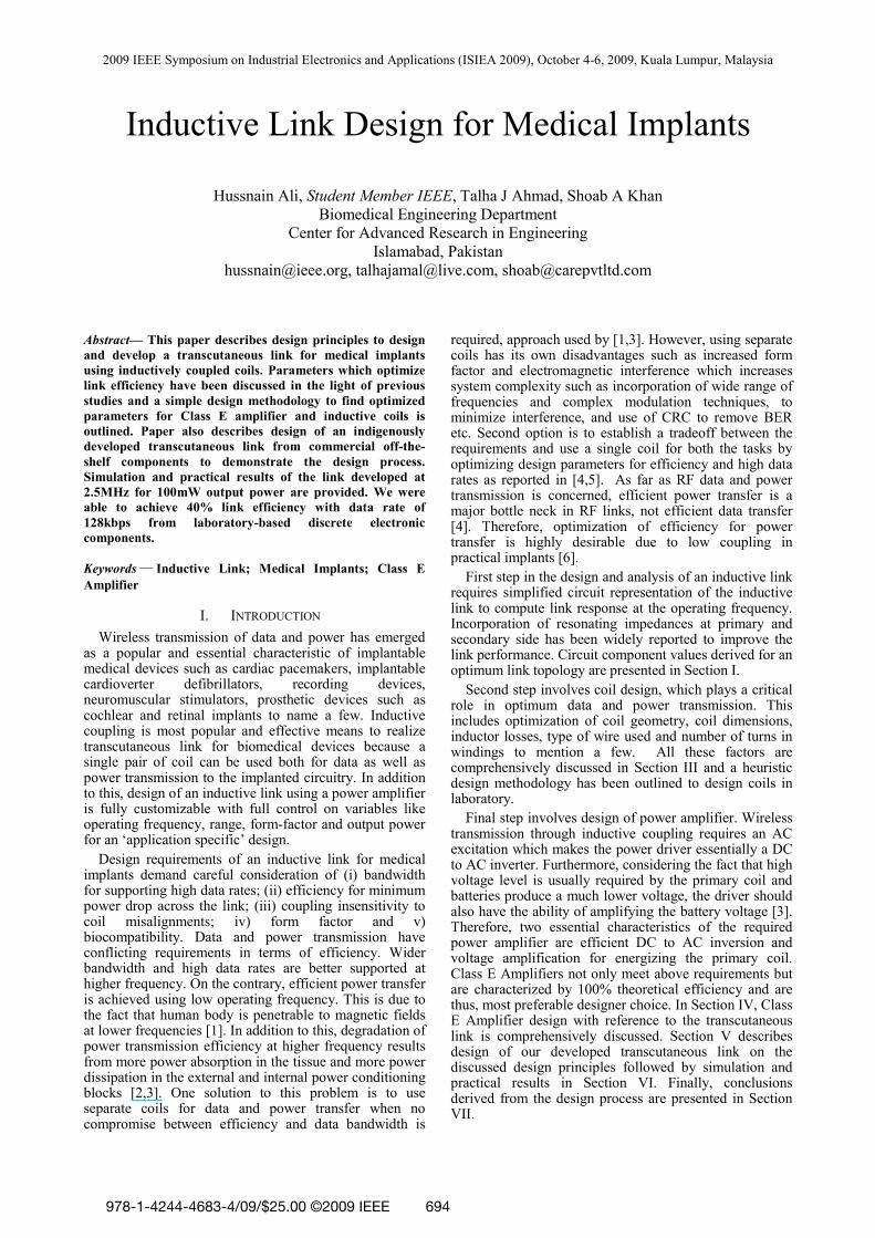
(c) (d) Fig. 8. Class E Waveforms. (a) Vgate (b) drain to source voltage VDS (c)Data signal at the gate (x6) and voltage across primary coil (bursts of sinusoids) (d)Voltage across primary coil in high state= 40 VPP, time scale = 1.4us
indigenously developed inductive link powered by a Class E amplifier. Results are very satisfactory for a laboratory-based design using discrete electronic components. Final link efficiency was 40% with 40mW output power and 128kbps data transfer rate.
REFERENCES [1] B. S. Pundi, "Class E Power Amplifier Design and Back-
Telemetry Communication for Retinal Prosthesis," PhD Thesis, North Carolina State University, Raleigh, North Carolina, 2002.
[2] J. C. Lin and A. W. Guy, "Power Deposition in a Spherical Model of Man Exposed to I-20-MHz Electromagnetic Fields," IEEE Transactions on Microwave Theory and Techniques, vol. 21, no. 12, pp. 791-797, Dec. 1973.
[3] S. Atluri, "A Wideband Power efficient inductive link for implantable biomedical devices using multiple carrier frequencies," PhD Thesis, North Carolina State University, Raleigh, North Carolina, 2006.
[4] M. W. Baker and R. Sarpeshkar, "Feedback Analysis and Design of RF Power Links for Low-Power Bionic Systems," IEEE Transactions on Biomedical Circuits and Systems, vol. 1, no. 1, pp. 28-38, Mar. 2007.
[5] G. B. Hmida, H. Ghariani, and M. Samet, "Design of Wireless Power and Data Transmission Circuits for Implantable Biomicrosystem," Biotechnology, vol. 6, no. 2, pp. 153-164, 2007.
[6] C. M. Zierhofer and E. S. Hochmair, "Coil design for improved power transfer efficiency in inductive links," in Proceedings of the 18th Annual International Conference of the IEEE Engineering in Medicine and Biology Society, Bridging Disciplines for Biomedicine, Nov 1996, pp. 1538-1539.
[7] C. Fernandez, "Design issues of a core-less transformer for a contact-less application," in Seventeenth Annual IEEE Applied Power Electronics Conference and Exposition, APEC, 2002, pp. 339-345.
[8] C. M. Zierhofer and E. S. Hochmair, "Geometric Approach for Coupling Enhancement of Magnetically Coupled Coils," IEEE Transactions on Biomedical Engineering, vol. 43, no. 7, pp. 708-714, Jul. 1996.
[9] S. K. Kelly, "A System for Efficient Neural Stimulation with Energy Recovery," PhD Thesis, Massachusetts Institute of Technology, Massachusetts, Cambridge, 2003.
[10] N. D. Donaldson and A. T. Perkins, "Analysis of resonant coupled coils in the design of radio frequency transcutaneous links," Medical and Biological Engineering, vol. 21, no. 5, pp. 612-627, Sep. 1983.
[11] F. H. Raab, "Idealized operation of the Class E Tuned Power Amplifier," IEEE Transactions on Circuits and Systems, vol. 24, no. 12, pp. 725-735, Dec. 1977.
[12] M. A. K. Schwan and P. R. Troyk, "High efficiency driver for transcutaneously coupled coils," in Proceedings of the Annual International Conference of the IEEE Engineering in Engineering, Medicine and Biology Society, Images of the Twenty-First Century, 1989, pp. 1403-1404.
[13] N. O. Sokal and D. A. Sokal, "Class-E A new class of high
(a)
(b)
(c)
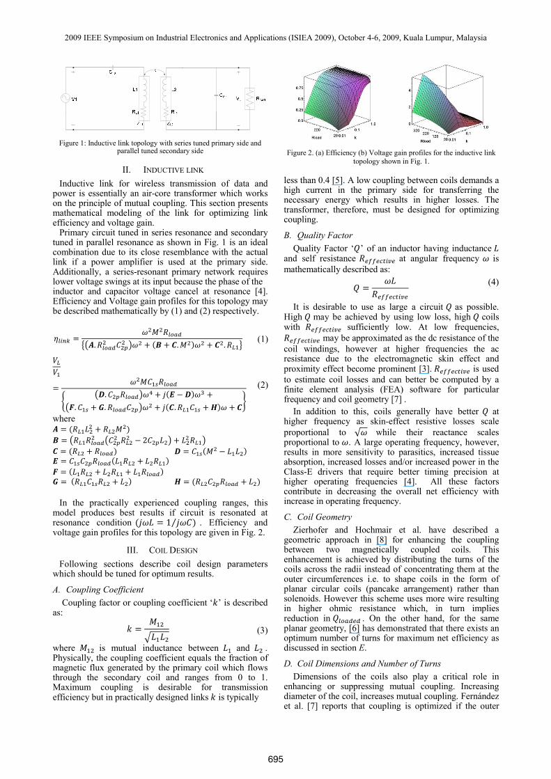
(d) Figure 9. Waveforms at the secondary side. (a) Voltage at receiver coil, across tuning capacitor, (b)Data output at the demodulator, (c) Comparison of data-IN (primary side) and data-OUT (secondary side), (d) Rectified, regulated output voltage at the secondary side = 6V dc.
efficiency tuned single-ended switching power amplifiers," IEEE Journal of Solid-State Circuits, vol. 10, pp. 168-176, 1975.
[14] N. O. Sokal, "Class-E RF Power Amplifiers," WA1HQC of Design Automation, Inc ARRL Technical Advisor, Jan/Feb 2001.
[15] M. Kazimierczuk, "Collector amplitude modulation of the class E tuned power amplifier," IEEE Transactions on Circuits and Systems, vol. 31, no. 6, pp. 543-549, Jun. 1984.
[16] P. M. Gaudo, C. Bernal, and A. Mediano, "Exact analysis of a simple class E circuit version for device characterization purposes," IEEE MTT-S International Microwave Symposium Digest, vol. 3, pp. 1737-1740, Jun. 2003.
[17] C. P. Avratoglou, N. C. Voulgaris, and F. I. Ioannidou, "Analysis and design of a generalized class E tuned power amplifier," IEEE Transactions on Circuits and Systems, vol. 36, no. 8, pp. 1068-1079, Aug. 1989.
[18] P. R. Troyk and M. A. K. Schwan, "Closed-loop class E transcutaneous power and data link for MicroImplants," IEEE Trans. on Biom. Eng., vol. 39, no. 6, pp. 589-599, Jun. 1992.
[19] M. Kazimierczuk and K. Puczko, "Exact analysis of class E tuned power amplifier at any Q and switch duty cycle," IEEE Transactions on Circuits and Systems, vol. 34, no. 2, pp. 149-159, Feb. 1987.
[20] L. Balogh. Design and Application Guide For High Speed MOSFET Gate Drive Circuits. www.ti.com.
[21] P. R. Troyk and G. A. DeMichele, "Inductively-Coupled Power and Data Link for Neural Prostheses using a Class-E Oscillator and FSK Modulation," in Proceedings of the International Conference of the IEEE EMBS, Cancum, Mexico, September, 2003, pp. 3376-3379.
[22] K. H. Wen, L. P. Sheau, and F. D. F. Cliff, "Design of radio-frequency powered coils for implant instruments ," Medical and Biological Engineering and Computing, vol. 15, no. 6, pp. 634-640, Nov. 1977.
[23] T. Xie, "Design and Development of Class E RF Power Amplifier Prototype by using a Power MOSFET," University of Kansas, Kansas, Technical Report, 2007.
[24] C. M. Zierhofer and E. S. Hochmair, "The Class-E Concept For Efficient Wide-Band Coupling-Insensitive Transdermal Power And Data Transfer," in Proceedings of the Annual International Conference of the IEEE Engineering in Medicine and Biology Society, 1992, pp. 382-383.
[25] C. M. Zierhofer and E. S. Hochmair, "High-efficiency coupling-insensitive transcutaneous power and data transmission via an inductive link," IEEE Transactions on Biomedical Engineering, vol. 37, no. 7, pp. 716-722, Jul. 1990.
[26] C. Fernandez, O. Garcia, J. A. Cobos, and J. Uceda, "A simple dc-dc converter for the power supply of a cochlear implant," in IEEE 43rd Annual Power Electronics Specialist Conference, PESC, 2003, pp. 1965-1970.
699