Implementation of Snubber Circuits in a PV-Based Off-Grid ...
12
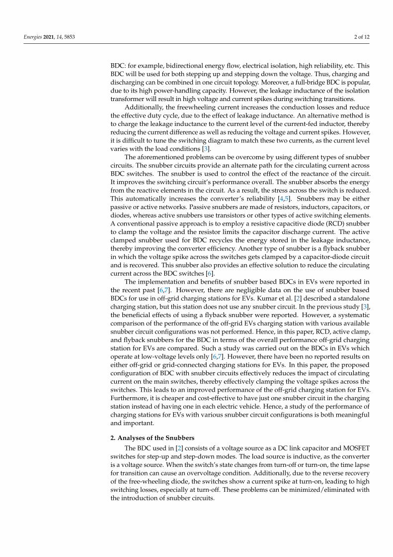
energies Article Implementation of Snubber Circuits in a PV-Based Off-Grid Electric Vehicle Charging Station—Comparative Case Studies Divya Krishnan Nair *, Krishnamachar Prasad and Tek Tjing Lie Citation: Krishnan Nair, D.; Prasad, K.; Lie, T.T. Implementation of Snubber Circuits in a PV-Based Off-Grid Electric Vehicle Charging Station—Comparative Case Studies. Energies 2021, 14, 5853. https:// doi.org/10.3390/en14185853 Academic Editors: Islam Safak Bayram and Enrique Romero-Cadaval Received: 26 June 2021 Accepted: 14 September 2021 Published: 16 September 2021 Publisher’s Note: MDPI stays neutral with regard to jurisdictional claims in published maps and institutional affil- iations. Copyright: © 2021 by the authors. Licensee MDPI, Basel, Switzerland. This article is an open access article distributed under the terms and conditions of the Creative Commons Attribution (CC BY) license (https:// creativecommons.org/licenses/by/ 4.0/). School of Engineering, Computer and Mathematical Sciences, Auckland University of Technology, 1010 Auckland, New Zealand; [email protected] (K.P.); [email protected] (T.T.L.) * Correspondence: [email protected] Abstract: With the penetration of electric vehicles (EVs), there have been paradigm shifts in the transportation sector. EVs are ideally considered to be clean and eco-friendly, but they can overload the existing grid infrastructure and significantly contribute towards carbon emissions depending on the source of charging. The ideal solution is to develop a charging infrastructure for EVs that is integrated with solar energy technology. This paper presents the design of a zero-voltage switching snubber-based bidirectional converter for an off-grid charging station for EVs. The proposed system includes a solar array with a boost converter, a bidirectional converter with snubber circuits and an energy storage unit. A comprehensive comparison between various types of snubbers, such as the resistive capacitive diode snubber, active clamp snubber and flyback snubber, is presented. This type of system configuration clamps the rail voltage, due to the difference in current between leakage inductance and low voltage side-fed inductor currents, resulting in reduced current spikes at the converter’s switches. Such a converter, therefore, leads to higher efficiency of the charging station for EVs. The design of a snubber-based off-grid charging station for EVs is formulated and validated in the MATLAB/Simulink environment. Keywords: resistive capacitive diode snubber; active clamp snubber; flyback snubber; bidirectional converter; off-grid charging station 1. Introduction Electric vehicles (EVs) are more environmentally friendly than the current inter- nal combustion engine (ICE) vehicles, as they have the potential to dramatically reduce greenhouse gases and global warming. The electrification of transport sector promotes sustainable energy development. Even though EVs may not emit CO 2 or other noxious gases when in use, they create a burden on the grid. Therefore, the coupling between the photovoltaics (PV) and charging stations for EVs is beneficial, as it allows greater usage of both EVs and solar energy without interrupting the grid’s capacity and provides better power quality. The solar-based charging station is primarily applicable on highways and remote locations to successfully charge EVs [1]. Kumar et al. [2] proposed a PV-based off-grid charging station in which the solar source is coupled with an energy storage unit (ESU) efficiently for variable irradiance conditions. The system enhances the reliability of the off-grid charging station for EVs. However, they used a non-isolated bidirectional converter with no capability of attaining zero-voltage switching (ZVS) characteristics. This is likely to result in a decrease in the overall efficiency of the charging station. Therefore, in this paper, we present a bidirectional DC–DC converter (BDC) with snubber circuits and demonstrate that a near ZVS across BDC switches is achieved for an off-grid charging station for EVs. This is expected to yield a higher efficiency PV-based charging station for EVs. Since EVs are operated at low voltage levels, there is a need for an interface between the BDC and the charging station. Isolated BDC offers many advantages over non-isolated Energies 2021, 14, 5853. https://doi.org/10.3390/en14185853 https://www.mdpi.com/journal/energies
-
Upload
khangminh22 -
Category
Documents
-
view
3 -
download
0
Transcript of Implementation of Snubber Circuits in a PV-Based Off-Grid ...
energies
Article
Implementation of Snubber Circuits in a PV-Based Off-GridElectric Vehicle Charging Station—Comparative Case Studies
Divya Krishnan Nair *, Krishnamachar Prasad and Tek Tjing Lie
�����������������
Citation: Krishnan Nair, D.;
Prasad, K.; Lie, T.T. Implementation
of Snubber Circuits in a PV-Based
Off-Grid Electric Vehicle Charging
Station—Comparative Case Studies.
Energies 2021, 14, 5853. https://
doi.org/10.3390/en14185853
Academic Editors: Islam
Safak Bayram and
Enrique Romero-Cadaval
Received: 26 June 2021
Accepted: 14 September 2021
Published: 16 September 2021
Publisher’s Note: MDPI stays neutral
with regard to jurisdictional claims in
published maps and institutional affil-
iations.
Copyright: © 2021 by the authors.
Licensee MDPI, Basel, Switzerland.
This article is an open access article
distributed under the terms and
conditions of the Creative Commons
Attribution (CC BY) license (https://
creativecommons.org/licenses/by/
4.0/).
School of Engineering, Computer and Mathematical Sciences, Auckland University of Technology,1010 Auckland, New Zealand; [email protected] (K.P.); [email protected] (T.T.L.)* Correspondence: [email protected]
Abstract: With the penetration of electric vehicles (EVs), there have been paradigm shifts in thetransportation sector. EVs are ideally considered to be clean and eco-friendly, but they can overloadthe existing grid infrastructure and significantly contribute towards carbon emissions dependingon the source of charging. The ideal solution is to develop a charging infrastructure for EVs that isintegrated with solar energy technology. This paper presents the design of a zero-voltage switchingsnubber-based bidirectional converter for an off-grid charging station for EVs. The proposed systemincludes a solar array with a boost converter, a bidirectional converter with snubber circuits and anenergy storage unit. A comprehensive comparison between various types of snubbers, such as theresistive capacitive diode snubber, active clamp snubber and flyback snubber, is presented. This typeof system configuration clamps the rail voltage, due to the difference in current between leakageinductance and low voltage side-fed inductor currents, resulting in reduced current spikes at theconverter’s switches. Such a converter, therefore, leads to higher efficiency of the charging station forEVs. The design of a snubber-based off-grid charging station for EVs is formulated and validated inthe MATLAB/Simulink environment.
Keywords: resistive capacitive diode snubber; active clamp snubber; flyback snubber; bidirectionalconverter; off-grid charging station
1. Introduction
Electric vehicles (EVs) are more environmentally friendly than the current inter-nal combustion engine (ICE) vehicles, as they have the potential to dramatically reducegreenhouse gases and global warming. The electrification of transport sector promotessustainable energy development. Even though EVs may not emit CO2 or other noxiousgases when in use, they create a burden on the grid. Therefore, the coupling between thephotovoltaics (PV) and charging stations for EVs is beneficial, as it allows greater usageof both EVs and solar energy without interrupting the grid’s capacity and provides betterpower quality. The solar-based charging station is primarily applicable on highways andremote locations to successfully charge EVs [1]. Kumar et al. [2] proposed a PV-basedoff-grid charging station in which the solar source is coupled with an energy storage unit(ESU) efficiently for variable irradiance conditions. The system enhances the reliabilityof the off-grid charging station for EVs. However, they used a non-isolated bidirectionalconverter with no capability of attaining zero-voltage switching (ZVS) characteristics. Thisis likely to result in a decrease in the overall efficiency of the charging station. Therefore,in this paper, we present a bidirectional DC–DC converter (BDC) with snubber circuitsand demonstrate that a near ZVS across BDC switches is achieved for an off-grid chargingstation for EVs. This is expected to yield a higher efficiency PV-based charging stationfor EVs.
Since EVs are operated at low voltage levels, there is a need for an interface betweenthe BDC and the charging station. Isolated BDC offers many advantages over non-isolated
Energies 2021, 14, 5853. https://doi.org/10.3390/en14185853 https://www.mdpi.com/journal/energies
Energies 2021, 14, 5853 2 of 12
BDC: for example, bidirectional energy flow, electrical isolation, high reliability, etc. ThisBDC will be used for both stepping up and stepping down the voltage. Thus, charging anddischarging can be combined in one circuit topology. Moreover, a full-bridge BDC is popular,due to its high power-handling capacity. However, the leakage inductance of the isolationtransformer will result in high voltage and current spikes during switching transitions.
Additionally, the freewheeling current increases the conduction losses and reducethe effective duty cycle, due to the effect of leakage inductance. An alternative method isto charge the leakage inductance to the current level of the current-fed inductor, therebyreducing the current difference as well as reducing the voltage and current spikes. However,it is difficult to tune the switching diagram to match these two currents, as the current levelvaries with the load conditions [3].
The aforementioned problems can be overcome by using different types of snubbercircuits. The snubber circuits provide an alternate path for the circulating current acrossBDC switches. The snubber is used to control the effect of the reactance of the circuit.It improves the switching circuit’s performance overall. The snubber absorbs the energyfrom the reactive elements in the circuit. As a result, the stress across the switch is reduced.This automatically increases the converter’s reliability [4,5]. Snubbers may be eitherpassive or active networks. Passive snubbers are made of resistors, inductors, capacitors, ordiodes, whereas active snubbers use transistors or other types of active switching elements.A conventional passive approach is to employ a resistive capacitive diode (RCD) snubberto clamp the voltage and the resistor limits the capacitor discharge current. The activeclamped snubber used for BDC recycles the energy stored in the leakage inductance,thereby improving the converter efficiency. Another type of snubber is a flyback snubberin which the voltage spike across the switches gets clamped by a capacitor-diode circuitand is recovered. This snubber also provides an effective solution to reduce the circulatingcurrent across the BDC switches [6].
The implementation and benefits of snubber based BDCs in EVs were reported inthe recent past [6,7]. However, there are negligible data on the use of snubber basedBDCs for use in off-grid charging stations for EVs. Kumar et al. [2] described a standalonecharging station, but this station does not use any snubber circuit. In the previous study [3],the beneficial effects of using a flyback snubber were reported. However, a systematiccomparison of the performance of the off-grid EVs charging station with various availablesnubber circuit configurations was not performed. Hence, in this paper, RCD, active clamp,and flyback snubbers for the BDC in terms of the overall performance off-grid chargingstation for EVs are compared. Such a study was carried out on the BDCs in EVs whichoperate at low-voltage levels only [6,7]. However, there have been no reported results oneither off-grid or grid-connected charging stations for EVs. In this paper, the proposedconfiguration of BDC with snubber circuits effectively reduces the impact of circulatingcurrent on the main switches, thereby effectively clamping the voltage spikes across theswitches. This leads to an improved performance of the off-grid charging station for EVs.Furthermore, it is cheaper and cost-effective to have just one snubber circuit in the chargingstation instead of having one in each electric vehicle. Hence, a study of the performance ofcharging stations for EVs with various snubber circuit configurations is both meaningfuland important.
2. Analyses of the Snubbers
The BDC used in [2] consists of a voltage source as a DC link capacitor and MOSFETswitches for step-up and step-down modes. The load source is inductive, as the converteris a voltage source. When the switch’s state changes from turn-off or turn-on, the time lapsefor transition can cause an overvoltage condition. Additionally, due to the reverse recoveryof the free-wheeling diode, the switches show a current spike at turn-on, leading to highswitching losses, especially at turn-off. These problems can be minimized/eliminated withthe introduction of snubber circuits.
Energies 2021, 14, 5853 3 of 12
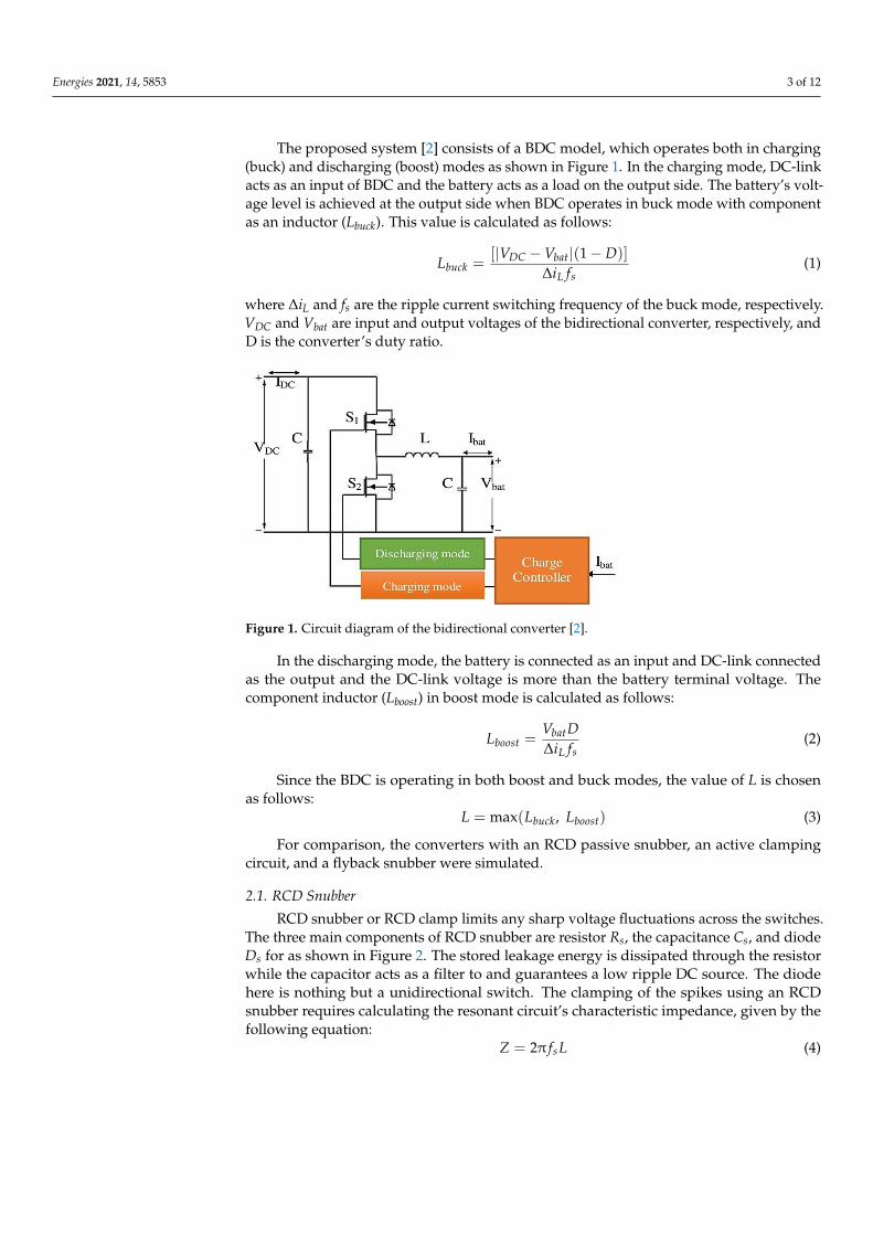
The proposed system [2] consists of a BDC model, which operates both in charging(buck) and discharging (boost) modes as shown in Figure 1. In the charging mode, DC-linkacts as an input of BDC and the battery acts as a load on the output side. The battery’s volt-age level is achieved at the output side when BDC operates in buck mode with componentas an inductor (Lbuck). This value is calculated as follows:
Lbuck =[|VDC −Vbat|(1− D)]
∆iL fs(1)
where ∆iL and fs are the ripple current switching frequency of the buck mode, respectively.VDC and Vbat are input and output voltages of the bidirectional converter, respectively, andD is the converter’s duty ratio.
Energies 2021, 14, x FOR PEER REVIEW 3 of 12
to high switching losses, especially at turn-off. These problems can be minimized/elimi-nated with the introduction of snubber circuits.
The proposed system [2] consists of a BDC model, which operates both in charging (buck) and discharging (boost) modes as shown in Figure 1. In the charging mode, DC-link acts as an input of BDC and the battery acts as a load on the output side. The battery’s voltage level is achieved at the output side when BDC operates in buck mode with com-ponent as an inductor (Lbuck). This value is calculated as follows: 𝐿 = |𝑉 𝑉 |(1 𝐷)
∆i 𝑓 (1)
where ∆iL and fs are the ripple current switching frequency of the buck mode, respectively. VDC and Vbat are input and output voltages of the bidirectional converter, respectively, and D is the converter’s duty ratio.
In the discharging mode, the battery is connected as an input and DC-link connected as the output and the DC-link voltage is more than the battery terminal voltage. The com-ponent inductor (Lboost) in boost mode is calculated as follows: 𝐿 = 𝑉 𝐷
∆i 𝑓 (2)
Since the BDC is operating in both boost and buck modes, the value of L is chosen as follows: 𝐿 = max (𝐿 , 𝐿 ) (3)
For comparison, the converters with an RCD passive snubber, an active clamping circuit, and a flyback snubber were simulated.
Figure 1. Circuit diagram of the bidirectional converter [2].
2.1. RCD Snubber RCD snubber or RCD clamp limits any sharp voltage fluctuations across the switches.
The three main components of RCD snubber are resistor Rs, the capacitance Cs, and diode Ds for as shown in Figure 2. The stored leakage energy is dissipated through the resistor while the capacitor acts as a filter to and guarantees a low ripple DC source. The diode here is nothing but a unidirectional switch. The clamping of the spikes using an RCD snubber requires calculating the resonant circuit’s characteristic impedance, given by the following equation: 𝑍 = 2π𝑓 𝐿 (4)
If the snubber resistor value is equal to the characteristic impedance, the ringing ef-fect is reduced. Therefore, to select the resistor, the following equation is used:
Figure 1. Circuit diagram of the bidirectional converter [2].
In the discharging mode, the battery is connected as an input and DC-link connectedas the output and the DC-link voltage is more than the battery terminal voltage. Thecomponent inductor (Lboost) in boost mode is calculated as follows:
Lboost =VbatD∆iL fs
(2)
Since the BDC is operating in both boost and buck modes, the value of L is chosenas follows:
L = max(Lbuck, Lboost) (3)
For comparison, the converters with an RCD passive snubber, an active clampingcircuit, and a flyback snubber were simulated.
2.1. RCD Snubber
RCD snubber or RCD clamp limits any sharp voltage fluctuations across the switches.The three main components of RCD snubber are resistor Rs, the capacitance Cs, and diodeDs for as shown in Figure 2. The stored leakage energy is dissipated through the resistorwhile the capacitor acts as a filter to and guarantees a low ripple DC source. The diodehere is nothing but a unidirectional switch. The clamping of the spikes using an RCDsnubber requires calculating the resonant circuit’s characteristic impedance, given by thefollowing equation:
Z = 2π fsL (4)
Energies 2021, 14, 5853 4 of 12
Energies 2021, 14, x FOR PEER REVIEW 4 of 12
𝑅 = 𝑍 (5)
The snubber capacitor, Cs, allows the resistor to be most effective at the ringing fre-quency by reducing the dissipation to a minimum at the switching frequency. The capac-itor is designed so that the impedance of the capacitor at the clamping frequency is con-sidered equal to the resistor, as shown in the following equation: 𝐶 = 12𝜋𝑓 𝑅 (6)
where fs is the switching frequency of the converter. The RCD snubber works by absorbing the inductor’s current when the switch’s drain
voltage exceeds the clamp capacitor voltage. The relatively large capacitor used in the circuit manages to keep the voltage constant over a switching cycle. By using a larger capacitor value, the peak power will increase while the switching loss will decrease [8].
Figure 2. Circuit diagram of the RCD snubber [8].
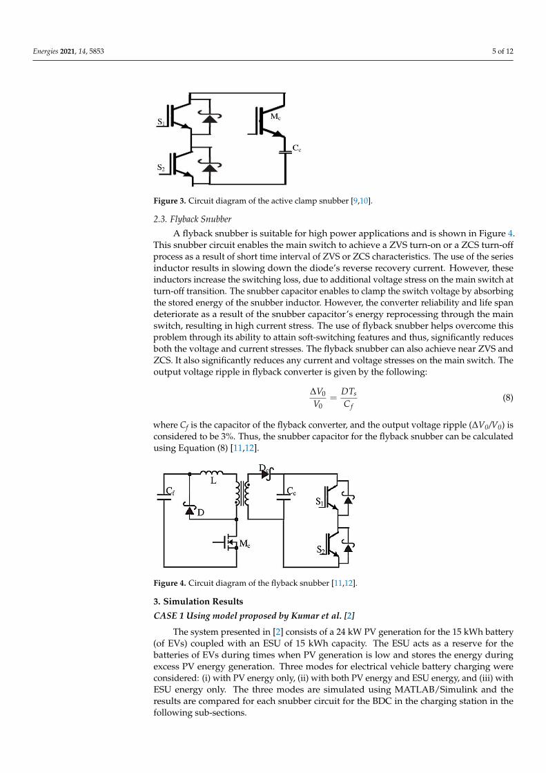
2.2. Active Clamp Snubber An active clamp for the BDC’s higher power applications is a good choice. It limits
the overshoot of the bridge switch’s turn-off voltage, thus enabling the energy stored for ZVS. The output diode’s reverse-recovery problem can partly be overcome by utilizing an appropriate design for the leakage inductance. However, the switches in these converters work under hard switching conditions. The active clamp circuit replaces the role of the passive lossless clamp circuit. The primary and the clamp switches turn ON under the ZVS condition, and the use of parallel capacitors help significantly reduce the turn OFF losses.
As shown in Figure 3, the coupled inductor included in the topology is used to recy-cle the leakage inductance energy and achieve the ZVS condition for the main and clamp switches. The switches and diodes’ voltage stresses are lower than the output voltage. Thus, by using an active clamp circuit with an active switch Mc, and a capacitor, Cc,, con-duction losses and cost can be significantly reduced.
The design is based on the resonant tank circuit formed by the clamping capacitor Cc and the leakage inductance Lk. Resonance occurs during the off-stage of the boost mode operation. The criterion to select Cc is such that the following holds: 𝐶 ≥ (𝑇 /4𝝅)𝐿 (7)
where Ts is the period of the driving signal for each bridge switch of the converter [9,10].
Figure 2. Circuit diagram of the RCD snubber [8].
If the snubber resistor value is equal to the characteristic impedance, the ringing effectis reduced. Therefore, to select the resistor, the following equation is used:
Rs = Z (5)
The snubber capacitor, Cs, allows the resistor to be most effective at the ringingfrequency by reducing the dissipation to a minimum at the switching frequency. Thecapacitor is designed so that the impedance of the capacitor at the clamping frequency isconsidered equal to the resistor, as shown in the following equation:
Cs =1
2π fsR(6)
where fs is the switching frequency of the converter.The RCD snubber works by absorbing the inductor’s current when the switch’s drain
voltage exceeds the clamp capacitor voltage. The relatively large capacitor used in thecircuit manages to keep the voltage constant over a switching cycle. By using a largercapacitor value, the peak power will increase while the switching loss will decrease [8].
2.2. Active Clamp Snubber
An active clamp for the BDC’s higher power applications is a good choice. It limitsthe overshoot of the bridge switch’s turn-off voltage, thus enabling the energy stored forZVS. The output diode’s reverse-recovery problem can partly be overcome by utilizing anappropriate design for the leakage inductance. However, the switches in these converterswork under hard switching conditions. The active clamp circuit replaces the role of thepassive lossless clamp circuit. The primary and the clamp switches turn ON under the ZVScondition, and the use of parallel capacitors help significantly reduce the turn OFF losses.
As shown in Figure 3, the coupled inductor included in the topology is used to recyclethe leakage inductance energy and achieve the ZVS condition for the main and clampswitches. The switches and diodes’ voltage stresses are lower than the output voltage. Thus,by using an active clamp circuit with an active switch Mc, and a capacitor, Cc
„ conductionlosses and cost can be significantly reduced.
The design is based on the resonant tank circuit formed by the clamping capacitor Ccand the leakage inductance Lk. Resonance occurs during the off-stage of the boost modeoperation. The criterion to select Cc is such that the following holds:
Cc ≥(Ts/4π)2
Lk(7)
where Ts is the period of the driving signal for each bridge switch of the converter [9,10].
Energies 2021, 14, 5853 5 of 12Energies 2021, 14, x FOR PEER REVIEW 5 of 12
Figure 3. Circuit diagram of the active clamp snubber [9,10].
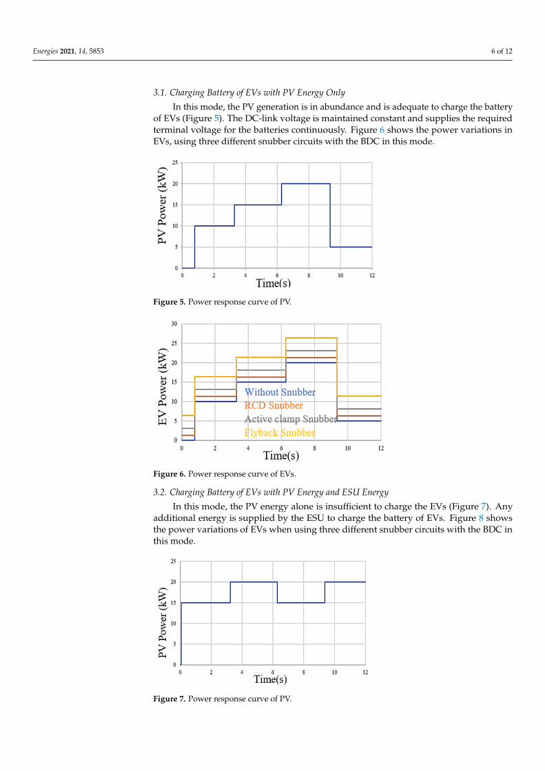
2.3. Flyback Snubber A flyback snubber is suitable for high power applications and is shown in Figure 4.
This snubber circuit enables the main switch to achieve a ZVS turn-on or a ZCS turn-off process as a result of short time interval of ZVS or ZCS characteristics. The use of the series inductor results in slowing down the diode’s reverse recovery current. However, these inductors increase the switching loss, due to additional voltage stress on the main switch at turn-off transition. The snubber capacitor enables to clamp the switch voltage by ab-sorbing the stored energy of the snubber inductor. However, the converter reliability and life span deteriorate as a result of the snubber capacitor’s energy reprocessing through the main switch, resulting in high current stress. The use of flyback snubber helps overcome this problem through its ability to attain soft-switching features and thus, significantly reduces both the voltage and current stresses. The flyback snubber can also achieve near ZVS and ZCS. It also significantly reduces any current and voltage stresses on the main switch. The output voltage ripple in flyback converter is given by the following: ∆𝑉𝑉 = 𝐷𝑇𝐶 (8)
where Cf is the capacitor of the flyback converter, and the output voltage ripple (∆V0/V0) is considered to be 3%. Thus, the snubber capacitor for the flyback snubber can be calcu-lated using Equation (8) [11,12].
Figure 4. Circuit diagram of the flyback snubber [11,12].
3. Simulation Results CASE 1 Using model proposed by Kumar et al. [2]
The system presented in [2] consists of a 24 kW PV generation for the 15 kWh battery (of EVs) coupled with an ESU of 15 kWh capacity. The ESU acts as a reserve for the bat-teries of EVs during times when PV generation is low and stores the energy during excess PV energy generation. Three modes for electrical vehicle battery charging were consid-ered: (i) with PV energy only, (ii) with both PV energy and ESU energy, and (iii) with ESU energy only. The three modes are simulated using MATLAB/Simulink and the results are
Figure 3. Circuit diagram of the active clamp snubber [9,10].
2.3. Flyback Snubber
A flyback snubber is suitable for high power applications and is shown in Figure 4.This snubber circuit enables the main switch to achieve a ZVS turn-on or a ZCS turn-offprocess as a result of short time interval of ZVS or ZCS characteristics. The use of the seriesinductor results in slowing down the diode’s reverse recovery current. However, theseinductors increase the switching loss, due to additional voltage stress on the main switch atturn-off transition. The snubber capacitor enables to clamp the switch voltage by absorbingthe stored energy of the snubber inductor. However, the converter reliability and life spandeteriorate as a result of the snubber capacitor’s energy reprocessing through the mainswitch, resulting in high current stress. The use of flyback snubber helps overcome thisproblem through its ability to attain soft-switching features and thus, significantly reducesboth the voltage and current stresses. The flyback snubber can also achieve near ZVS andZCS. It also significantly reduces any current and voltage stresses on the main switch. Theoutput voltage ripple in flyback converter is given by the following:
∆V0
V0=
DTs
C f(8)
where Cf is the capacitor of the flyback converter, and the output voltage ripple (∆V0/V0) isconsidered to be 3%. Thus, the snubber capacitor for the flyback snubber can be calculatedusing Equation (8) [11,12].
Energies 2021, 14, x FOR PEER REVIEW 5 of 12
Figure 3. Circuit diagram of the active clamp snubber [9,10].
2.3. Flyback Snubber A flyback snubber is suitable for high power applications and is shown in Figure 4.
This snubber circuit enables the main switch to achieve a ZVS turn-on or a ZCS turn-off process as a result of short time interval of ZVS or ZCS characteristics. The use of the series inductor results in slowing down the diode’s reverse recovery current. However, these inductors increase the switching loss, due to additional voltage stress on the main switch at turn-off transition. The snubber capacitor enables to clamp the switch voltage by ab-sorbing the stored energy of the snubber inductor. However, the converter reliability and life span deteriorate as a result of the snubber capacitor’s energy reprocessing through the main switch, resulting in high current stress. The use of flyback snubber helps overcome this problem through its ability to attain soft-switching features and thus, significantly reduces both the voltage and current stresses. The flyback snubber can also achieve near ZVS and ZCS. It also significantly reduces any current and voltage stresses on the main switch. The output voltage ripple in flyback converter is given by the following: ∆𝑉𝑉 = 𝐷𝑇𝐶 (8)
where Cf is the capacitor of the flyback converter, and the output voltage ripple (∆V0/V0) is considered to be 3%. Thus, the snubber capacitor for the flyback snubber can be calcu-lated using Equation (8) [11,12].
Figure 4. Circuit diagram of the flyback snubber [11,12].
3. Simulation Results CASE 1 Using model proposed by Kumar et al. [2]
The system presented in [2] consists of a 24 kW PV generation for the 15 kWh battery (of EVs) coupled with an ESU of 15 kWh capacity. The ESU acts as a reserve for the bat-teries of EVs during times when PV generation is low and stores the energy during excess PV energy generation. Three modes for electrical vehicle battery charging were consid-ered: (i) with PV energy only, (ii) with both PV energy and ESU energy, and (iii) with ESU energy only. The three modes are simulated using MATLAB/Simulink and the results are
Figure 4. Circuit diagram of the flyback snubber [11,12].
3. Simulation Results
CASE 1 Using model proposed by Kumar et al. [2]
The system presented in [2] consists of a 24 kW PV generation for the 15 kWh battery(of EVs) coupled with an ESU of 15 kWh capacity. The ESU acts as a reserve for thebatteries of EVs during times when PV generation is low and stores the energy duringexcess PV energy generation. Three modes for electrical vehicle battery charging wereconsidered: (i) with PV energy only, (ii) with both PV energy and ESU energy, and (iii) withESU energy only. The three modes are simulated using MATLAB/Simulink and theresults are compared for each snubber circuit for the BDC in the charging station in thefollowing sub-sections.
Energies 2021, 14, 5853 6 of 12
3.1. Charging Battery of EVs with PV Energy Only
In this mode, the PV generation is in abundance and is adequate to charge the batteryof EVs (Figure 5). The DC-link voltage is maintained constant and supplies the requiredterminal voltage for the batteries continuously. Figure 6 shows the power variations inEVs, using three different snubber circuits with the BDC in this mode.
Energies 2021, 14, x FOR PEER REVIEW 6 of 12
compared for each snubber circuit for the BDC in the charging station in the following sub-sections.
3.1. Charging Battery of EVs with PV Energy Only In this mode, the PV generation is in abundance and is adequate to charge the battery
of EVs (Figure 5). The DC-link voltage is maintained constant and supplies the required terminal voltage for the batteries continuously. Figure 6 shows the power variations in EVs, using three different snubber circuits with the BDC in this mode.
Figure 5. Power response curve of PV
Figure 6. Power response curve of EVs.
3.2. Charging Battery of EVs with PV Energy and ESU Energy In this mode, the PV energy alone is insufficient to charge the EVs (Figure 7). Any
additional energy is supplied by the ESU to charge the battery of EVs. Figure 8 shows the power variations of EVs when using three different snubber circuits with the BDC in this mode.
Figure 7. Power response curve of PV.
Figure 5. Power response curve of PV.
Energies 2021, 14, x FOR PEER REVIEW 6 of 12
compared for each snubber circuit for the BDC in the charging station in the following sub-sections.
3.1. Charging Battery of EVs with PV Energy Only In this mode, the PV generation is in abundance and is adequate to charge the battery
of EVs (Figure 5). The DC-link voltage is maintained constant and supplies the required terminal voltage for the batteries continuously. Figure 6 shows the power variations in EVs, using three different snubber circuits with the BDC in this mode.
Figure 5. Power response curve of PV
Figure 6. Power response curve of EVs.
3.2. Charging Battery of EVs with PV Energy and ESU Energy In this mode, the PV energy alone is insufficient to charge the EVs (Figure 7). Any
additional energy is supplied by the ESU to charge the battery of EVs. Figure 8 shows the power variations of EVs when using three different snubber circuits with the BDC in this mode.
Figure 7. Power response curve of PV.
Figure 6. Power response curve of EVs.
3.2. Charging Battery of EVs with PV Energy and ESU Energy
In this mode, the PV energy alone is insufficient to charge the EVs (Figure 7). Anyadditional energy is supplied by the ESU to charge the battery of EVs. Figure 8 showsthe power variations of EVs when using three different snubber circuits with the BDC inthis mode.
Energies 2021, 14, x FOR PEER REVIEW 6 of 12
compared for each snubber circuit for the BDC in the charging station in the following sub-sections.
3.1. Charging Battery of EVs with PV Energy Only In this mode, the PV generation is in abundance and is adequate to charge the battery
of EVs (Figure 5). The DC-link voltage is maintained constant and supplies the required terminal voltage for the batteries continuously. Figure 6 shows the power variations in EVs, using three different snubber circuits with the BDC in this mode.
Figure 5. Power response curve of PV
Figure 6. Power response curve of EVs.
3.2. Charging Battery of EVs with PV Energy and ESU Energy In this mode, the PV energy alone is insufficient to charge the EVs (Figure 7). Any
additional energy is supplied by the ESU to charge the battery of EVs. Figure 8 shows the power variations of EVs when using three different snubber circuits with the BDC in this mode.
Figure 7. Power response curve of PV. Figure 7. Power response curve of PV.
Energies 2021, 14, 5853 7 of 12Energies 2021, 14, x FOR PEER REVIEW 7 of 12
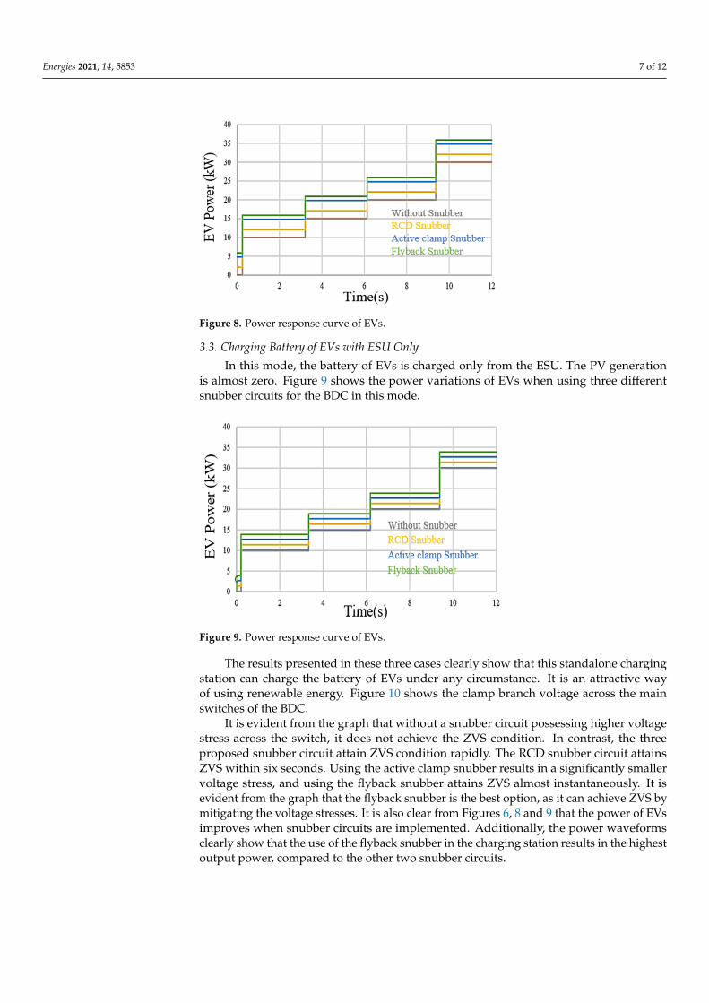
Figure 8. Power response curve of EVs
3.3. Charging Battery of EVs with ESU Only In this mode, the battery of EVs is charged only from the ESU. The PV generation is
almost zero. Figure 9 shows the power variations of EVs when using three different snub-ber circuits for the BDC in this mode.
Figure 9. Power response curve of EVs.
The results presented in these three cases clearly show that this standalone charging station can charge the battery of EVs under any circumstance. It is an attractive way of using renewable energy. Figure 10 shows the clamp branch voltage across the main switches of the BDC.
It is evident from the graph that without a snubber circuit possessing higher voltage stress across the switch, it does not achieve the ZVS condition. In contrast, the three pro-posed snubber circuit attain ZVS condition rapidly. The RCD snubber circuit attains ZVS within six seconds. Using the active clamp snubber results in a significantly smaller volt-age stress, and using the flyback snubber attains ZVS almost instantaneously. It is evident from the graph that the flyback snubber is the best option, as it can achieve ZVS by miti-gating the voltage stresses. It is also clear from Figures 6, 8 and 9 that the power of EVs improves when snubber circuits are implemented. Additionally, the power waveforms clearly show that the use of the flyback snubber in the charging station results in the high-est output power, compared to the other two snubber circuits.
Figure 8. Power response curve of EVs.
3.3. Charging Battery of EVs with ESU Only
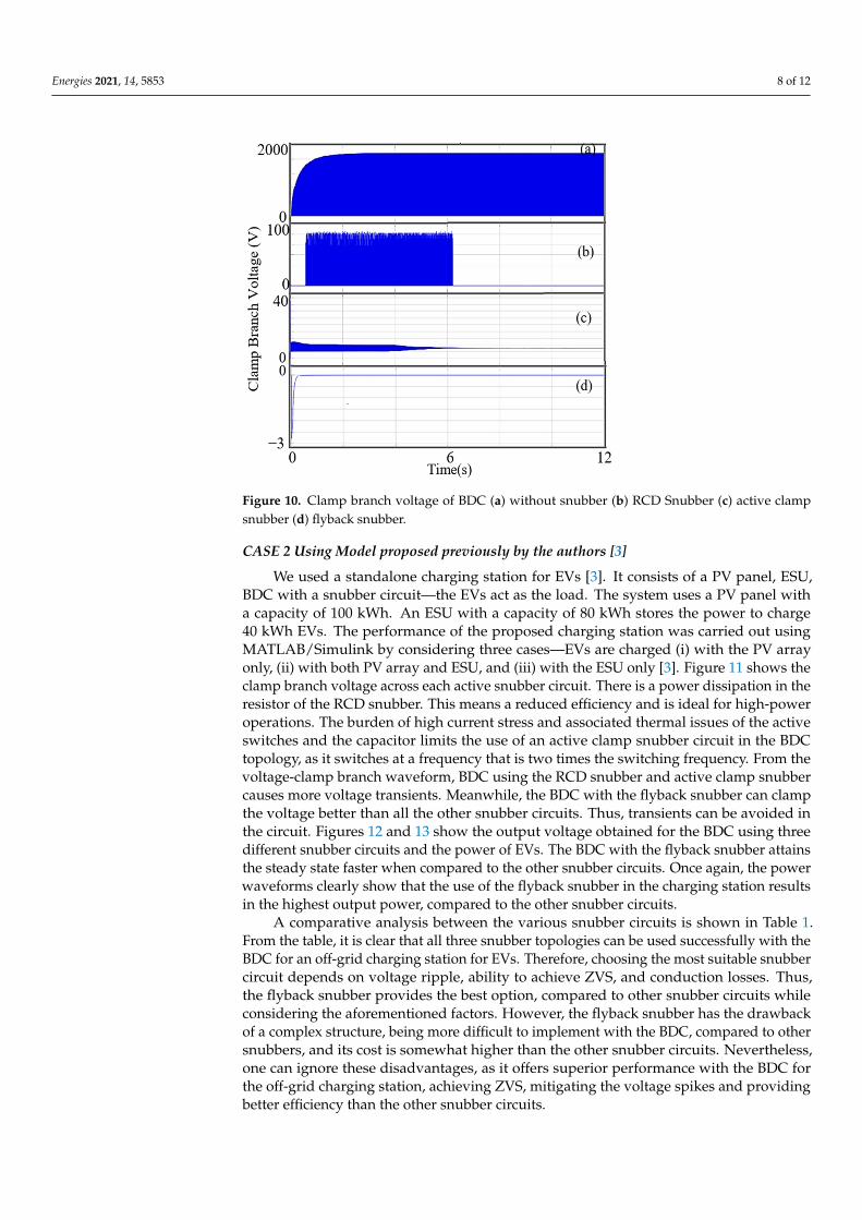
In this mode, the battery of EVs is charged only from the ESU. The PV generationis almost zero. Figure 9 shows the power variations of EVs when using three differentsnubber circuits for the BDC in this mode.
Energies 2021, 14, x FOR PEER REVIEW 7 of 12
Figure 8. Power response curve of EVs
3.3. Charging Battery of EVs with ESU Only In this mode, the battery of EVs is charged only from the ESU. The PV generation is
almost zero. Figure 9 shows the power variations of EVs when using three different snub-ber circuits for the BDC in this mode.
Figure 9. Power response curve of EVs.
The results presented in these three cases clearly show that this standalone charging station can charge the battery of EVs under any circumstance. It is an attractive way of using renewable energy. Figure 10 shows the clamp branch voltage across the main switches of the BDC.
It is evident from the graph that without a snubber circuit possessing higher voltage stress across the switch, it does not achieve the ZVS condition. In contrast, the three pro-posed snubber circuit attain ZVS condition rapidly. The RCD snubber circuit attains ZVS within six seconds. Using the active clamp snubber results in a significantly smaller volt-age stress, and using the flyback snubber attains ZVS almost instantaneously. It is evident from the graph that the flyback snubber is the best option, as it can achieve ZVS by miti-gating the voltage stresses. It is also clear from Figures 6, 8 and 9 that the power of EVs improves when snubber circuits are implemented. Additionally, the power waveforms clearly show that the use of the flyback snubber in the charging station results in the high-est output power, compared to the other two snubber circuits.
Figure 9. Power response curve of EVs.
The results presented in these three cases clearly show that this standalone chargingstation can charge the battery of EVs under any circumstance. It is an attractive wayof using renewable energy. Figure 10 shows the clamp branch voltage across the mainswitches of the BDC.
It is evident from the graph that without a snubber circuit possessing higher voltagestress across the switch, it does not achieve the ZVS condition. In contrast, the threeproposed snubber circuit attain ZVS condition rapidly. The RCD snubber circuit attainsZVS within six seconds. Using the active clamp snubber results in a significantly smallervoltage stress, and using the flyback snubber attains ZVS almost instantaneously. It isevident from the graph that the flyback snubber is the best option, as it can achieve ZVS bymitigating the voltage stresses. It is also clear from Figures 6, 8 and 9 that the power of EVsimproves when snubber circuits are implemented. Additionally, the power waveformsclearly show that the use of the flyback snubber in the charging station results in the highestoutput power, compared to the other two snubber circuits.
Energies 2021, 14, 5853 8 of 12Energies 2021, 14, x FOR PEER REVIEW 8 of 12
Figure 10. Clamp branch voltage of BDC (a) without snubber (b) RCD Snubber (c) active clamp snubber (d) flyback snubber.
CASE 2 Using Model proposed previously by the authors [3] We used a standalone charging station for EVs [3]. It consists of a PV panel, ESU,
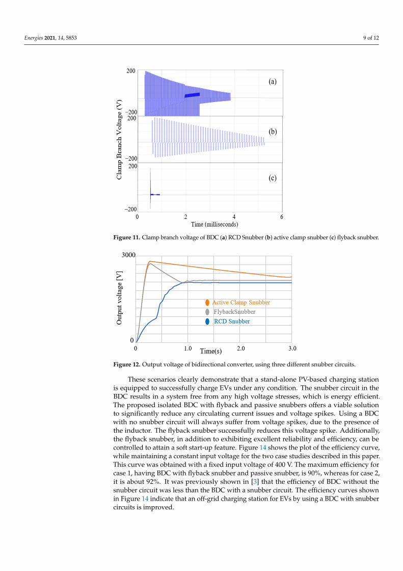
BDC with a snubber circuit—the EVs act as the load. The system uses a PV panel with a capacity of 100 kWh. An ESU with a capacity of 80 kWh stores the power to charge 40 kWh EVs. The performance of the proposed charging station was carried out using MATLAB/Simulink by considering three cases—EVs are charged (i) with the PV array only, (ii) with both PV array and ESU, and (iii) with the ESU only [3]. Figure 11 shows the clamp branch voltage across each active snubber circuit. There is a power dissipation in the resistor of the RCD snubber. This means a reduced efficiency and is ideal for high-power operations. The burden of high current stress and associated thermal issues of the active switches and the capacitor limits the use of an active clamp snubber circuit in the BDC topology, as it switches at a frequency that is two times the switching frequency. From the voltage-clamp branch waveform, BDC using the RCD snubber and active clamp snubber causes more voltage transients. Meanwhile, the BDC with the flyback snubber can clamp the voltage better than all the other snubber circuits. Thus, transients can be avoided in the circuit. Figures 12 and 13 show the output voltage obtained for the BDC using three different snubber circuits and the power of EVs. The BDC with the flyback snubber attains the steady state faster when compared to the other snubber circuits. Once again, the power waveforms clearly show that the use of the flyback snubber in the charg-ing station results in the highest output power, compared to the other snubber circuits.
A comparative analysis between the various snubber circuits is shown in Table 1. From the table, it is clear that all three snubber topologies can be used successfully with the BDC for an off-grid charging station for EVs. Therefore, choosing the most suitable snubber circuit depends on voltage ripple, ability to achieve ZVS, and conduction losses. Thus, the flyback snubber provides the best option, compared to other snubber circuits while considering the aforementioned factors. However, the flyback snubber has the drawback of a complex structure, being more difficult to implement with the BDC, com-pared to other snubbers, and its cost is somewhat higher than the other snubber circuits. Nevertheless, one can ignore these disadvantages, as it offers superior performance with the BDC for the off-grid charging station, achieving ZVS, mitigating the voltage spikes and providing better efficiency than the other snubber circuits.
Figure 10. Clamp branch voltage of BDC (a) without snubber (b) RCD Snubber (c) active clampsnubber (d) flyback snubber.
CASE 2 Using Model proposed previously by the authors [3]
We used a standalone charging station for EVs [3]. It consists of a PV panel, ESU,BDC with a snubber circuit—the EVs act as the load. The system uses a PV panel witha capacity of 100 kWh. An ESU with a capacity of 80 kWh stores the power to charge40 kWh EVs. The performance of the proposed charging station was carried out usingMATLAB/Simulink by considering three cases—EVs are charged (i) with the PV arrayonly, (ii) with both PV array and ESU, and (iii) with the ESU only [3]. Figure 11 shows theclamp branch voltage across each active snubber circuit. There is a power dissipation in theresistor of the RCD snubber. This means a reduced efficiency and is ideal for high-poweroperations. The burden of high current stress and associated thermal issues of the activeswitches and the capacitor limits the use of an active clamp snubber circuit in the BDCtopology, as it switches at a frequency that is two times the switching frequency. From thevoltage-clamp branch waveform, BDC using the RCD snubber and active clamp snubbercauses more voltage transients. Meanwhile, the BDC with the flyback snubber can clampthe voltage better than all the other snubber circuits. Thus, transients can be avoided inthe circuit. Figures 12 and 13 show the output voltage obtained for the BDC using threedifferent snubber circuits and the power of EVs. The BDC with the flyback snubber attainsthe steady state faster when compared to the other snubber circuits. Once again, the powerwaveforms clearly show that the use of the flyback snubber in the charging station resultsin the highest output power, compared to the other snubber circuits.
A comparative analysis between the various snubber circuits is shown in Table 1.From the table, it is clear that all three snubber topologies can be used successfully with theBDC for an off-grid charging station for EVs. Therefore, choosing the most suitable snubbercircuit depends on voltage ripple, ability to achieve ZVS, and conduction losses. Thus,the flyback snubber provides the best option, compared to other snubber circuits whileconsidering the aforementioned factors. However, the flyback snubber has the drawbackof a complex structure, being more difficult to implement with the BDC, compared to othersnubbers, and its cost is somewhat higher than the other snubber circuits. Nevertheless,one can ignore these disadvantages, as it offers superior performance with the BDC forthe off-grid charging station, achieving ZVS, mitigating the voltage spikes and providingbetter efficiency than the other snubber circuits.
Energies 2021, 14, 5853 9 of 12Energies 2021, 14, x FOR PEER REVIEW 9 of 12
Figure 11. Clamp branch voltage of BDC (a) RCD Snubber (b) active clamp snubber (c) flyback snubber.
Figure 12. Output voltage of bidirectional converter, using three different snubber circuits.
Figure 11. Clamp branch voltage of BDC (a) RCD Snubber (b) active clamp snubber (c) flyback snubber.
Energies 2021, 14, x FOR PEER REVIEW 9 of 12
Figure 11. Clamp branch voltage of BDC (a) RCD Snubber (b) active clamp snubber (c) flyback snubber.
Figure 12. Output voltage of bidirectional converter, using three different snubber circuits. Figure 12. Output voltage of bidirectional converter, using three different snubber circuits.
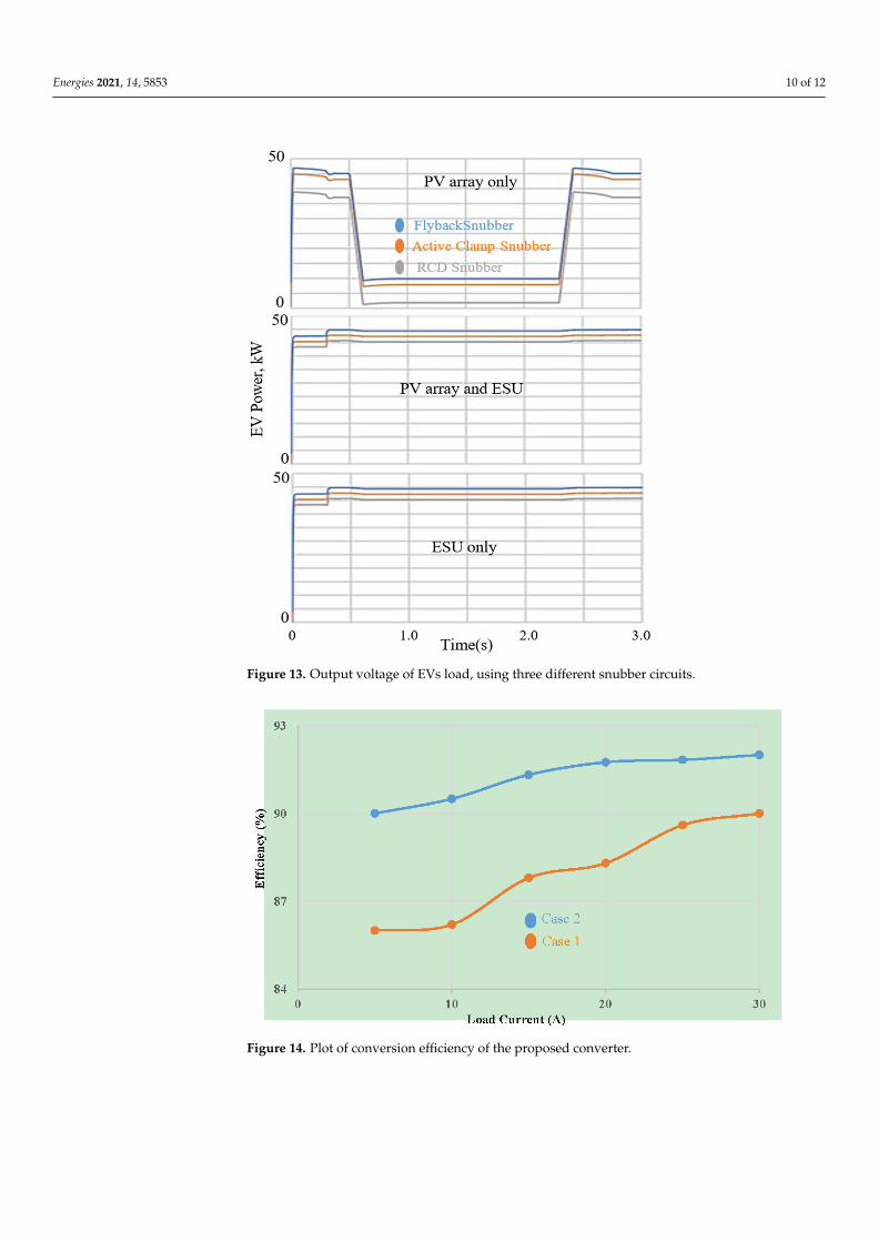
These scenarios clearly demonstrate that a stand-alone PV-based charging stationis equipped to successfully charge EVs under any condition. The snubber circuit in theBDC results in a system free from any high voltage stresses, which is energy efficient.The proposed isolated BDC with flyback and passive snubbers offers a viable solutionto significantly reduce any circulating current issues and voltage spikes. Using a BDCwith no snubber circuit will always suffer from voltage spikes, due to the presence ofthe inductor. The flyback snubber successfully reduces this voltage spike. Additionally,the flyback snubber, in addition to exhibiting excellent reliability and efficiency, can becontrolled to attain a soft start-up feature. Figure 14 shows the plot of the efficiency curve,while maintaining a constant input voltage for the two case studies described in this paper.This curve was obtained with a fixed input voltage of 400 V. The maximum efficiency forcase 1, having BDC with flyback snubber and passive snubber, is 90%, whereas for case 2,it is about 92%. It was previously shown in [3] that the efficiency of BDC without thesnubber circuit was less than the BDC with a snubber circuit. The efficiency curves shownin Figure 14 indicate that an off-grid charging station for EVs by using a BDC with snubbercircuits is improved.
Energies 2021, 14, 5853 10 of 12Energies 2021, 14, x FOR PEER REVIEW 10 of 12
Figure 13. Output voltage of EVs load, using three different snubber circuits.
Table 1. Comparative analysis of various snubber circuits.
Parameters RCD Snubber Active CLAMPING
SNUBBER Flyback Snubber
Number of switches/diodes/capacitors 0/1/1 1/0/1 1/1/2 Conduction loss Moderate Low Very low Voltage ripple Moderate Low Negligible
Attaining speed of ZVS Very slow Slow Fast Ease of implementation in BDC Much easier Easy Difficult
Complexity Smooth Bit complex Complex Cost Inexpensive Reasonable Bit expensive
Efficiency Low Moderate High
These scenarios clearly demonstrate that a stand-alone PV-based charging station is equipped to successfully charge EVs under any condition. The snubber circuit in the BDC results in a system free from any high voltage stresses, which is energy efficient. The pro-posed isolated BDC with flyback and passive snubbers offers a viable solution to signifi-cantly reduce any circulating current issues and voltage spikes. Using a BDC with no snubber circuit will always suffer from voltage spikes, due to the presence of the inductor. The flyback snubber successfully reduces this voltage spike. Additionally, the flyback snubber, in addition to exhibiting excellent reliability and efficiency, can be controlled to attain a soft start-up feature. Figure 14 shows the plot of the efficiency curve, while main-taining a constant input voltage for the two case studies described in this paper. This curve was obtained with a fixed input voltage of 400 V. The maximum efficiency for case 1,
Figure 13. Output voltage of EVs load, using three different snubber circuits.
Energies 2021, 14, x FOR PEER REVIEW 11 of 12
having BDC with flyback snubber and passive snubber, is 90%, whereas for case 2, it is about 92%. It was previously shown in [3] that the efficiency of BDC without the snubber circuit was less than the BDC with a snubber circuit. The efficiency curves shown in Figure 14 indicate that an off-grid charging station for EVs by using a BDC with snubber circuits is improved.
Figure 14. Plot of conversion efficiency of the proposed converter.
4. Conclusions In this paper, various snubber circuits for the BDC of two different models of an off-
grid solar-based charging station for EVs were implemented and studied. A performance comparison of the charging station was carried out. The use of PV to charge EVs in an off-grid charging station will help to achieve clean energy generation and reduce the grid burden. Thus, the use of EVs in remote locations can be significantly increased. An ESU is coupled with the system to work under any circumstances. The proposed BDC incorpo-rates either RCD snubber or active clamp snubber or flyback snubber to reduce the voltage spike caused by the current fed inductor. The proposed station’s design using various snubber circuits was explained and validated in MATLAB/Simulink. It was successfully tested on two independent models, thus making the method both credible and robust. The efficiency of the proposed converter with the snubber circuits in both the cases is higher, compared to the converter without snubbers. The converter can achieve ZVS con-ditions more rapidly than a converter without the snubber. Thus, the use of an appropriate snubber enhances the system reliability efficiency. In both the models reported here, the flyback snubber consistently offered the best possible results.
Author Contributions: Conceptualization, D.K. and K.P.; methodology, D.K.; software, D.K.; vali-dation, D.K., K.P. and T.T.L.; formal analysis, D.K.; investigation, D.K.; resources, D.K.; data cura-tion, D.K.; writing—original draft preparation, D.K..; writing—review and editing, D.K. and K.P.; visualization, D.K.; supervision, K.P. and T.T.L.; project administration, K.P. and T.T.L.;. All authors have read and agreed to the published version of the manuscript.
Funding: This research received no external funding.
Conflicts of Interest: The authors declare no conflict of interest.
Figure 14. Plot of conversion efficiency of the proposed converter.

Energies 2021, 14, 5853 11 of 12
Table 1. Comparative analysis of various snubber circuits.
Parameters RCD Snubber Active CLAMPING SNUBBER Flyback Snubber
Number of switches/diodes/capacitors 0/1/1 1/0/1 1/1/2
Conduction loss Moderate Low Very low
Voltage ripple Moderate Low Negligible
Attaining speed of ZVS Very slow Slow Fast
Ease of implementation in BDC Much easier Easy Difficult
Complexity Smooth Bit complex Complex
Cost Inexpensive Reasonable Bit expensive
Efficiency Low Moderate High
4. Conclusions
In this paper, various snubber circuits for the BDC of two different models of an off-grid solar-based charging station for EVs were implemented and studied. A performancecomparison of the charging station was carried out. The use of PV to charge EVs in anoff-grid charging station will help to achieve clean energy generation and reduce the gridburden. Thus, the use of EVs in remote locations can be significantly increased. An ESU iscoupled with the system to work under any circumstances. The proposed BDC incorporateseither RCD snubber or active clamp snubber or flyback snubber to reduce the voltage spikecaused by the current fed inductor. The proposed station’s design using various snubbercircuits was explained and validated in MATLAB/Simulink. It was successfully tested ontwo independent models, thus making the method both credible and robust. The efficiencyof the proposed converter with the snubber circuits in both the cases is higher, comparedto the converter without snubbers. The converter can achieve ZVS conditions more rapidlythan a converter without the snubber. Thus, the use of an appropriate snubber enhancesthe system reliability efficiency. In both the models reported here, the flyback snubberconsistently offered the best possible results.
Author Contributions: Conceptualization, D.K.N. and K.P.; methodology, D.K.N.; software, D.K.N.;validation, D.K.N., K.P. and T.T.L.; formal analysis, D.K.N.; investigation, D.K.N.; resources, D.K.N.;data curation, D.K.N.; writing—original draft preparation, D.K.N.; writing—review and editing,D.K.N. and K.P.; visualization, D.K.N.; supervision, K.P. and T.T.L.; project administration, K.P. andT.T.L. All authors have read and agreed to the published version of the manuscript.
Funding: This research received no external funding.
Conflicts of Interest: The authors declare no conflict of interest.
References1. Shariff, S.M.; Alam, M.S.; Ahmad, F.; Rafat, Y.; Asghar, M.S.J.; Khan, S. System Design and Realization of a Solar-Powered Electric
Vehicle Charging Station. IEEE Syst. J. 2020, 14, 2748–2758. [CrossRef]2. Kumar, V.; Teja, V.R.; Singh, M.; Mishra, S. PV Based Off-Grid Charging Station for Electric Vehicle. IFAC-PapersOnLine 2019, 52,
276–281. [CrossRef]3. Nair, D.K.; Prasad, K.; Lie, T.T. Standalone electric vehicle charging station using an isolated bidirectional converter with snubber.
Energy Storage 2021, e255. [CrossRef]4. Sharon, P.; Sathiyan, P.S. Design and simulation of bidirectional converter with flyback and capacitor diode snubbers. In Proceedings of
the 2015 International Conference on Innovations in Information, Embedded and Communication Systems (ICIIECS), Coimbatore,India, 19–20 March 2015; pp. 1–5.
5. Todd, P.C. Snubber Theory, Design Circuits and Application. Available online: https://www.ee.bgu.ac.il/~dcdc/notes/Additional_2012/Snubbers.pdf (accessed on 13 September 2021).
6. Bhatt, K.; Gupta, R.A.; Gupta, N. Design and development of isolated snubber based bidirectional DC–DC converter for electricvehicle applications. IET Power Electron. 2019, 12, 3378–3388. [CrossRef]
7. Wu, T.-F.; Chen, Y.-C.; Yang, J.-G.; Kuo, C.-L. Isolated Bidirectional Full-Bridge DC–DC Converter With a Flyback Snubber.IEEE Trans. Power Electron. 2010, 25, 1915–1922. [CrossRef]

Energies 2021, 14, 5853 12 of 12
8. Vaz, A.R.; Tofoli, F.L. In-depth analysis of an RCD snubber applied to a DC-DC boost converter. Int. J. Circuit Theory Appl. 2021,49, 283–305. [CrossRef]
9. Yoo, J.S.; Ahn, T.; Yu, G.; Lee, J.; Lee, J. A study on novel active clamp snubber applied DC-DC quasi resonant flyback converterto effectively reduce switch voltage surge. In Proceedings of the 2017 20th International Conference on Electrical Machines andSystems (ICEMS), Sydney, Australia, 11–14 August 2017; pp. 1–5. [CrossRef]
10. Yan, Z.; Zeng, J.; Liu, J.; Lin, W. A Novel Soft-Switching Bidirectional DC-DC Converter with High Voltage-Gain for Grid-Connected Energy Storage System. In Proceedings of the 2019 4th IEEE Workshop on the Electronic Grid (eGRID), Xiamen, China,11–14 November 2019; pp. 1–6. [CrossRef]
11. Balbayev, G.; Nussibaliyeva, A.; Tultaev, B.; Dzhunusbekov, E.; Yestemessova, G.; Yelemanova, A. A novel regenerative snubbercircuit for flyback topology converters. J. Vibroengineering 2020, 22, 983–992. [CrossRef]
12. Tadvin, S.M.; Bin Shah, S.R.; Hossain, M.R.T. A Brief Review of Snubber Circuits for Flyback Converter. In Proceedings of the2018 3rd International Conference for Convergence in Technology (I2CT), Pune, India, 6–7 April 2018; pp. 1–5. [CrossRef]