Global comparisons of volcanic-associated massive sulphide ...
Upload
northwesternCategory
view
3download
0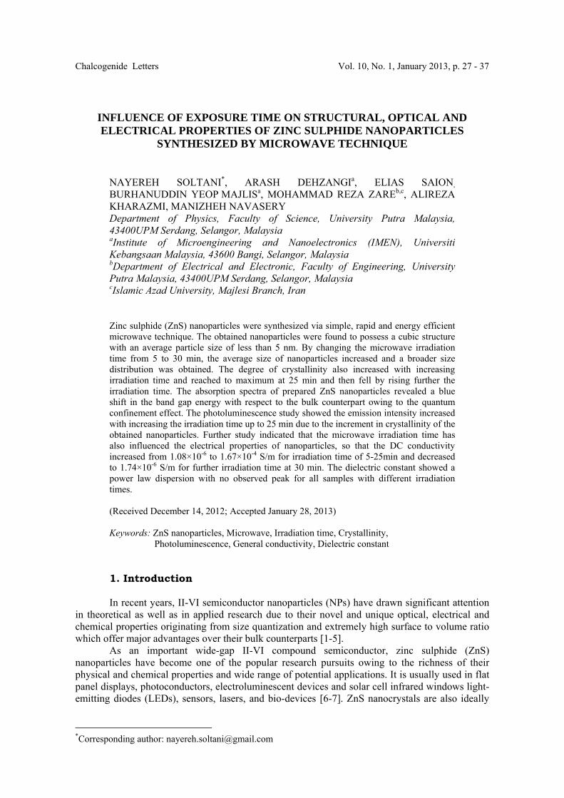
Chalcogenide Letters Vol. 10, No. 1, January 2013, p. 27 - 37
INFLUENCE OF EXPOSURE TIME ON STRUCTURAL, OPTICAL AND ELECTRICAL PROPERTIES OF ZINC SULPHIDE NANOPARTICLES
SYNTHESIZED BY MICROWAVE TECHNIQUE
NAYEREH SOLTANI*, ARASH DEHZANGIa, ELIAS SAION, BURHANUDDIN YEOP MAJLISa, MOHAMMAD REZA ZAREb,c, ALIREZA KHARAZMI, MANIZHEH NAVASERY Department of Physics, Faculty of Science, University Putra Malaysia, 43400UPM Serdang, Selangor, Malaysia aInstitute of Microengineering and Nanoelectronics (IMEN), Universiti Kebangsaan Malaysia, 43600 Bangi, Selangor, Malaysia bDepartment of Electrical and Electronic, Faculty of Engineering, University Putra Malaysia, 43400UPM Serdang, Selangor, Malaysia cIslamic Azad University, Majlesi Branch, Iran
Zinc sulphide (ZnS) nanoparticles were synthesized via simple, rapid and energy efficient microwave technique. The obtained nanoparticles were found to possess a cubic structure with an average particle size of less than 5 nm. By changing the microwave irradiation time from 5 to 30 min, the average size of nanoparticles increased and a broader size distribution was obtained. The degree of crystallinity also increased with increasing irradiation time and reached to maximum at 25 min and then fell by rising further the irradiation time. The absorption spectra of prepared ZnS nanoparticles revealed a blue shift in the band gap energy with respect to the bulk counterpart owing to the quantum confinement effect. The photoluminescence study showed the emission intensity increased with increasing the irradiation time up to 25 min due to the increment in crystallinity of the obtained nanoparticles. Further study indicated that the microwave irradiation time has also influenced the electrical properties of nanoparticles, so that the DC conductivity increased from 1.08×10⁻⁶ to 1.67×10⁻⁴ S/m for irradiation time of 5-25min and decreased to 1.74×10⁻⁶ S/m for further irradiation time at 30 min. The dielectric constant showed a power law dispersion with no observed peak for all samples with different irradiation times. (Received December 14, 2012; Accepted January 28, 2013) Keywords: ZnS nanoparticles, Microwave, Irradiation time, Crystallinity, Photoluminescence, General conductivity, Dielectric constant
1. Introduction In recent years, II-VI semiconductor nanoparticles (NPs) have drawn significant attention
in theoretical as well as in applied research due to their novel and unique optical, electrical and chemical properties originating from size quantization and extremely high surface to volume ratio which offer major advantages over their bulk counterparts [1-5].
As an important wide-gap II-VI compound semiconductor, zinc sulphide (ZnS) nanoparticles have become one of the popular research pursuits owing to the richness of their physical and chemical properties and wide range of potential applications. It is usually used in flat panel displays, photoconductors, electroluminescent devices and solar cell infrared windows light-emitting diodes (LEDs), sensors, lasers, and bio-devices [6-7]. ZnS nanocrystals are also ideally
*Corresponding author: [email protected]

28 suited for applications in biological labelling and diagnostics, due to less toxicity as compared to other II–VI semiconductor NPs [8].
As the properties of nanocrystals are highly dependent on their structure, particle size, size distribution, and morphology, a burst of research activities has been emerged in the synthesis and characterization of semiconductor NPs [7-8]. To synthesize ZnS nanocrystals, various techniques have been employed, including the chemical methods [9], solid-state reactions [10], sol-gel processes [11], sonochemical preparation [12], microwave [13-14] and γ-irradiation route [15]. Among the aforementioned methods, the microwave assisted route is one of the more recent methods and is a rapidly developing area of research. It is simple, rapid and energy efficient. A major advantage of the microwave synthesis method is that it provides homogenous internal and volumetric heating at rapid rates without sharp thermal gradient effects and thereby is capable of producing small particles with a narrow particle size distribution and high purity [16-18].
In our previous work, the influence of irradiation time on microwave-hydrothermal and microwave-polyol method for the synthesis of ZnS NPs was reported and compared together [13]. In this work, based on the previous knowledge of researches we try to give deeper view of the structural, optical and electrical properties of ZnS NPs synthesized by polyol method in order to improve prior achievements and lead for future research.
2. Experimental In a typical synthesis, 5 mM of zinc acetate (Zn(CH3COO)2.2H2O) and 6 mM of
Thioacetamide (CH3CSNH2) were dissolved completely in 20 ml of ethylene glycol (C2H6O2). The mixture were placed in a high power microwave oven (1100W) operated using a pulse regime with 20% power. The reactions were carried out by changing irradiation time at 5, 10, 15, 20, 25 and 30 min. The white precipitate gradually appeared during the reaction. The precipitates were centrifuged (3500 rpm, 10 min) and washed several times with distilled water and absolute ethanol and dried in air at 60oC for 24 h under control environment.
The products were characterized by X-ray diffraction (XRD) at a scanning rate of 5o/min in the 2θrange 20–70o using a Philips X-ray diffractometer (7602 EA Almelo) with Cu Kα radiation (λ = 0.1542 nm). The particle size and size distribution were determined from the transmission electron microscopy (TEM) micrographs (HTACHI H-7100 TEM). The optical properties of ZnS NPs were characterized using UV–visible absorption spectroscopy (UV-1650PC SHIMADZU) and photoluminescence (PL) spectroscopy (Perkin Elmer, LS-55: fluorescence spectrometer). The dielectric properties of the ZnS NPs were measured using Precision LRC meter (Agilent-4284A) in the frequency range from 20 Hz to 1 MHz at room temperature. Samples were characterized in shape of pellet with the dimension of 0.53 mm and 10.8 mm as thickness and diameter respectively.
3. Results and discussions XRD patterns of ZnS nanocrystalline synthesized at different irradiation times are shown
in Figure 1. All spectra have three major peaks, which are observed at 2θ values of 28.5, 47.4, and 56.3o and matching perfectly with the (111), (220) and (311) crystalline planes of the face centred cubic structure of ZnS reported in ICDD PDF 65-1691 with the lattice parameter of 5.41 Ao and cell volume of 158.4 Ao3. Increasing the irradiation time results the appearance of two low intensity peaks at about 69.4oand 76.7o at 10 min exposure time and a shoulder around 33.1o at 15 min which correspond to (400), (331) and (200) crystalline planes of the reference pattern. No extra peaks corresponding to any other crystallographic phase or unreacted ingredient was detected, indicating the products at high purity.
The broadening of XRD peaks (FWHM) decreases with increasing irradiation time indicates that the mean crystalline size of ZnS nanocrystalline is smaller for lower irradiation time [13]. The crystalline size of the ZnS nanoparticles were calculated using (111) reflection of the XRD patterns based on the Scherrer equation [16, 19]:
29
D = kλ/ βcos θ (1)
where D is the average crystallite size, k is particle shape factor, λ is the X-ray wavelength used (0.1542 nm), β is the angular line width of half-maximum intensity and θ is the Bragg’s angle in degree. The estimated sizes are listed in Table 1.
Fig. 1. XRD pattern of ZnS nanocrystals synthesized in different irradiation times.
The intensity of XRD peaks increases with increasing irradiation time and reaches the
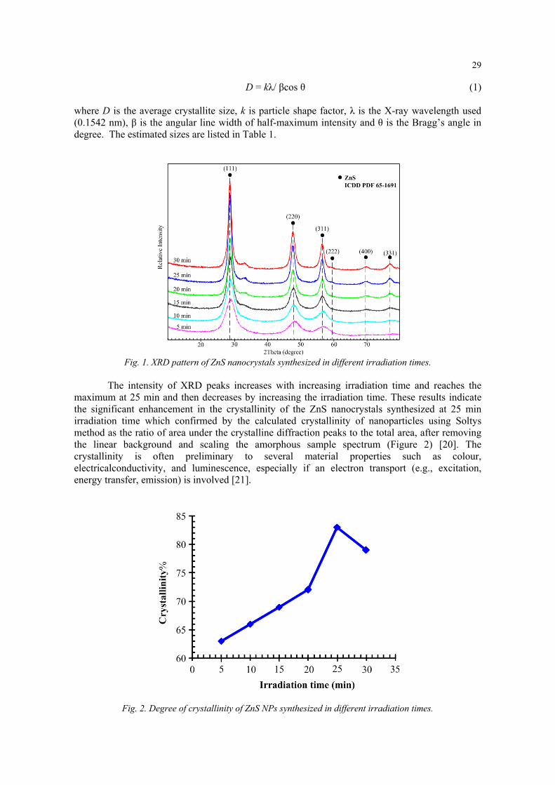
maximum at 25 min and then decreases by increasing the irradiation time. These results indicate the significant enhancement in the crystallinity of the ZnS nanocrystals synthesized at 25 min irradiation time which confirmed by the calculated crystallinity of nanoparticles using Soltys method as the ratio of area under the crystalline diffraction peaks to the total area, after removing the linear background and scaling the amorphous sample spectrum (Figure 2) [20]. The crystallinity is often preliminary to several material properties such as colour, electricalconductivity, and luminescence, especially if an electron transport (e.g., excitation, energy transfer, emission) is involved [21].
Fig. 2. Degree of crystallinity of ZnS NPs synthesized in different irradiation times.
30
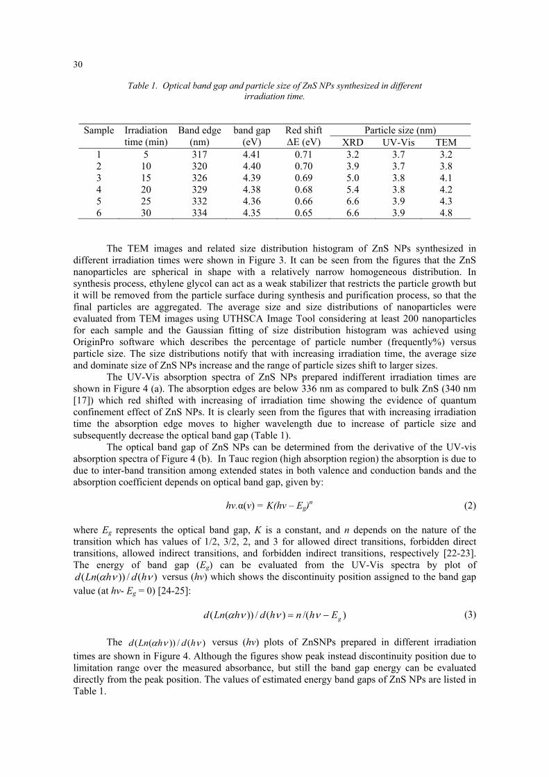
Table 1. Optical band gap and particle size of ZnS NPs synthesized in different irradiation time.
Sample Irradiation time (min)
Band edge (nm)
band gap (eV)
Red shift ΔE (eV)
Particle size (nm) XRD UV-Vis TEM
1 5 317 4.41 0.71 3.2 3.7 3.2 2 10 320 4.40 0.70 3.9 3.7 3.8 3 15 326 4.39 0.69 5.0 3.8 4.1 4 20 329 4.38 0.68 5.4 3.8 4.2 5 25 332 4.36 0.66 6.6 3.9 4.3 6 30 334 4.35 0.65 6.6 3.9 4.8
The TEM images and related size distribution histogram of ZnS NPs synthesized in different irradiation times were shown in Figure 3. It can be seen from the figures that the ZnS nanoparticles are spherical in shape with a relatively narrow homogeneous distribution. In synthesis process, ethylene glycol can act as a weak stabilizer that restricts the particle growth but it will be removed from the particle surface during synthesis and purification process, so that the final particles are aggregated. The average size and size distributions of nanoparticles were evaluated from TEM images using UTHSCA Image Tool considering at least 200 nanoparticles for each sample and the Gaussian fitting of size distribution histogram was achieved using OriginPro software which describes the percentage of particle number (frequently%) versus particle size. The size distributions notify that with increasing irradiation time, the average size and dominate size of ZnS NPs increase and the range of particle sizes shift to larger sizes.
The UV-Vis absorption spectra of ZnS NPs prepared indifferent irradiation times are shown in Figure 4 (a). The absorption edges are below 336 nm as compared to bulk ZnS (340 nm [17]) which red shifted with increasing of irradiation time showing the evidence of quantum confinement effect of ZnS NPs. It is clearly seen from the figures that with increasing irradiation time the absorption edge moves to higher wavelength due to increase of particle size and subsequently decrease the optical band gap (Table 1).
The optical band gap of ZnS NPs can be determined from the derivative of the UV-vis absorption spectra of Figure 4 (b). In Tauc region (high absorption region) the absorption is due to due to inter-band transition among extended states in both valence and conduction bands and the absorption coefficient depends on optical band gap, given by:
hv.α(v) = K(hv – Eg)n (2)
where Eg represents the optical band gap, K is a constant, and n depends on the nature of the transition which has values of 1/2, 3/2, 2, and 3 for allowed direct transitions, forbidden direct transitions, allowed indirect transitions, and forbidden indirect transitions, respectively [22-23]. The energy of band gap (Eg) can be evaluated from the UV-Vis spectra by plot of
)(/))(( hdhLnd versus (hv) which shows the discontinuity position assigned to the band gap value (at hv- Eg = 0) [24-25]:
)/()(/))(( gEhnhdhLnd (3)
The )(/))(( hdhLnd versus (hv) plots of ZnSNPs prepared in different irradiation
times are shown in Figure 4. Although the figures show peak instead discontinuity position due to limitation range over the measured absorbance, but still the band gap energy can be evaluated directly from the peak position. The values of estimated energy band gaps of ZnS NPs are listed in Table 1.

31
Fig. 3. TEM images and size distribution histograms of ZnS NPs synthesized in different irradiation times

32
Fig. 4.UV-Visible spectra and d(Ln(αhѵ))/d(hυ) vs. hѵ plots of the ZnSNPs synthesized in (a) 5, (b) 10, (c) 15, (d) 20, (e) 25 and (f) 30 min irradiation time
From the band gap values, the particle sizes could be calculated using Brus equation [26-
28]:
r
e
mmrE
rhe
0
2
**2
22
4
8.111
2
(4)
where ΔE is the blue shift of the band gap, me* is the effective mass of electron, mh
* is the effective mass of hole, r is the radius of the particle, εr is the dielectric constant and εo is the permittivity of free space. The first term indicates the confinement effect and the second term being the Coulomb term. In a strong confinement, as in the present case, the second term is small and can be neglected. The computed particle sizes are listed in Table 1and compare with those determined from TEM images.
Luminescence-based analytical techniques are very sensitive to detect discrete electronic states and can provide experimental evidence of electronic defects. In this work, the evolution of photoluminescence (PL) spectra was utilized for the characterization of defects and crystal quality of ZnS NPs. In microcrystals charge carriers are trapped at defect sites. However, in nanoparticles, these traps are most likely located at the surface because of an enhanced surface-to-volume ratio. Therefore, the surface defect states play important roles in the luminescence properties of nanoparticles, which act as radiative or nonradiative centres in nanoparticles. With the increase in degree of crystallinity, the concentration of defects that act as sites for nonradiative recombination of electron–hole pairs decreases and the emission intensity increases [8]. In semiconductors like ZnS, there are several kinds of native electronic defects include zinc vacancies (VZn) and interstitials (Zni), sulfur vacancies (VS) and interstitials (Si), and anti-sites such as zinc atom in a sulphur lattice site (ZnS). Sulphur vacancies and zinc interstitials create donor levels close to the conduction band and zinc vacancies and sulfur interstitials act as acceptors with defect levels close to the valence band (Figure 5) [29].
(a) (b)

33
Fig. 5. Schematic energy level diagram showing the emission mechanism in the ZnS
The PL spectra of ZnS NPs synthesized in different irradiation time were recorded at the room temperature under 270 nm excitation. As revealed in Figure 6, PL spectra for the ZnS nanocrystals synthesized in 5 and 10 min shows a broad emission spreading from~370 nm to 500 nm essentially resulting from the compounded effect of ethylene glycol and the energy states present between the valence and conduction bands. These broad peaks consist of three less prominent sub bands at ~419, 445 and 485 nm. The first and third peaks are attributed to the recombination of electron-hole pairs in sulphur and zinc vacancies respectively. These two individual components (blue emissions centred at ~419 and 485 nm) are clearly observed in PL spectra of ZnS nanocrystals synthesized at higher irradiation time. The second peak is probably due to surface states arising from capping function of ethylene glycol. With increasing irradiation time and reduce of ethylene glycol capping function on the surfaces of nanoparticles, the second peak is disappeared. The PL intensities show an enhancement with increasing irradiation time and reach to their maximum in 25 min irradiation time which correspond to the maximum degree of crystallinity.
Fig. 6. PL spectra of the ZnSNPs synthesized in (a) 5, (b) 10, (c) 15, (d) 20, (e) 25 and
(f) 30 min irradiation time
34
irradia
seen frand thefor irracases, after acrystal
appearincreasorigin providcarrierhigher
temperto1MHzero fr0 (Z’ a
conducdispersof the which
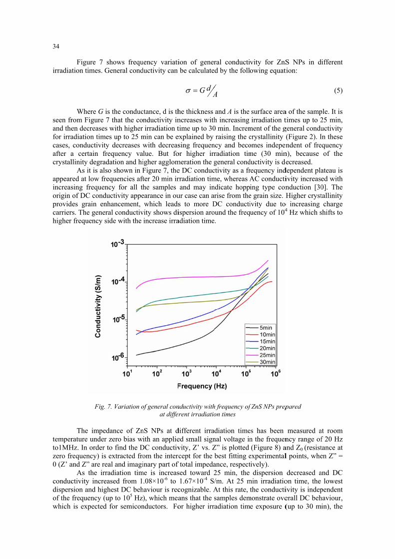
Figure 7 sation times. G
Where G irom Figure 7en decreasesadiation timeconductivity
a certain frllinity degrad
As it is alsred at low fresing frequenof DC condu
des grain enrs. The generr frequency s
Fig.
The impedrature under
Hz. In order trequency) is and Z” are re
As the irrctivity increasion and highfrequency (uis expected
shows frequGeneral cond
s the conduc7 that the cos with higheres up to 25 my decreases requency vadation and hiso shown in Fequencies aftncy for all thuctivity appehancement, ral conductivide with the
7. Variation o
dance of Znzero bias w
to find the Dextracted fro
eal and imagiradiation timased from 1hest DC behup to 105 Hzfor semicon
uency variatiductivity can
ctance, d is thnductivity inirradiation t
min can be ewith decreas
alue. But foigher agglomFigure 7, the
fter 20 min irhe samples earance in ouwhich leads
vity shows diincrease irra
of general conat differ
nS NPs at dith an applie
DC conductivom the intercinary part of
me is increas.08×10-6 to
haviour is rec), which meanductors. Fo
ion of generbe calculate
AdG
he thickness ncreases withtime up to 30explained by sing frequen
or higher irrmeration the ge DC conducrradiation timand may in
ur case can as to more Dispersion aroadiation time
nductivity withrent irradiatio
different irraed small signvity, Z’ vs. Zcept for the
f total impedased toward 21.67×10⁻⁴ S/cognizable. Aans that the sor higher irr
ral conductied by the foll
A
and A is the h increasing 0 min. Incremraising the c
ncy and becoradiation timgeneral condctivity as a frme, whereas Andicate hopprise from the
DC conductiound the freqe.
h frequency ofon times
diation timenal voltage inZ” is plotted best fitting eance, respect25 min, the /m. At 25 mAt this rate, samples dem
radiation tim
vity for ZnSowing equat
surface areairradiation t
ment of the gcrystallinity omes indepenme (30 minductivity is derequency indAC conductiing type cone grain size. Hivity due to
quency of 104
f ZnS NPs prep
es has been n the frequen(Figure 8) a
experimentaltively).
dispersion min irradiatiothe conducti
monstrate ovee exposure (
S NPs in dtion:
a of the samptimes up to 2general condu(Figure 2). Indent of fre
n), because decreased. dependent plaivity increasenduction [30Higher cryst
o increasing 4 Hz which s
pared
measured ancy range of
and Z0 (resistl points, whe
decreased aon time, the ivity is indeperall DC beh(up to 30 m
ifferent
(5)
ple. It is 25 min, uctivity In these equency
of the
ateau is ed with 0]. The tallinity charge
shifts to
at room f 20 Hz tance at en Z” =
and DC lowest
pendent haviour, in), the
35
crystallinity is degraded and DC conductivity is expected to decrease. The basic observation in ZnS NPs is that the general conductivity is increasing function of frequency.
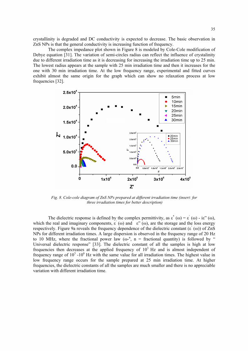
The complex impedance plot shown in Figure 8 is modeled by Cole-Cole modification of Debye equation [31]. The variation of semi-circles radius can reflect the influence of crystalinity due to different irradiation time as it is decreasing for increasing the irradiation time up to 25 min. The lowest radius appears at the sample with 25 min irradiation time and then it increases for the one with 30 min irradiation time. At the low frequency range, experimental and fitted curves exhibit almost the same origin for the graph which can show no relaxation process at low frequencies [32].
Fig. 8. Cole-cole diagram of ZnS NPs prepared at different irradiation time (insert: for three irradiation times for better description)
The dielectric response is defined by the complex permittivity, as ε* (ω) = ε’ (ω) - iε” (ω), which the real and imaginary components, ε’ (ω) and ε” (ω), are the storage and the loss energy respectively. Figure 9a reveals the frequency dependence of the dielectric constant (ε’ (ω)) of ZnS NPs for different irradiation times. A large dispersion is observed in the frequency range of 20 Hz to 10 MHz, where the fractional power law (ω-n, n = fractional quantity) is followed by “ Universal dielectric response” [33]. The dielectric constant of all the samples is high at low frequencies then decreases at the applied frequency of 103 Hz and is almost independent of frequency range of 103 -106 Hz with the same value for all irradiation times. The highest value in low frequency range occurs for the sample prepared at 25 min irradiation time. At higher frequencies, the dielectric constants of all the samples are much smaller and there is no appreciable variation with different irradiation time.

36
Fig. 9. Variation of dielectric constant (a) and dielectric loss (b) with frequency of ZnS NPs prepared at
different irradiation time
The high observed value of the dielectric constant at low frequency range can be due to the interfacial effect of the electrodes and the sample [34]. It is seen that the dielectric constant (ε’), for the low frequency values of ε’, is increasing when the particle size increases due to rising of the irradiation time (Table 1) and more crystalinity. It is worth noting that the interfacial polarization in crystalline defects can be the origin of the dielectric constant variation for different ZnS NPs samples. In the crystalline defects, charge carriers, such as the free charge, cavities and polar groups can affect the dielectric constant [35].
The frequency dependence of the dielectric loss for prepared ZnS NPs in different irradiation times (Figure9b), indicates a power law dispersion for ε” (ω) with no observed peak. It is found that the dielectric loss of the NPs sharply decreases with increasing frequency over a range of 10 – 105 Hz and keeps stabilization over a range of 105 - 106 Hz. The high value of the dielectric loss can be due to motion of free charge carriers in samples [34]. Moreover, the dielectric loss increases with raising the irradiation time, which shows the highest value for the sample with the best crystallinity at 25 min irradiation time. This may due to more charge carriers and polar groups in this particular sample which can increase the dielectric loss.
4. Conclusions This paper presented the influence of microwave irradiation time on structural, optical and
electrical properties of ZnS nanoparticles synthesized using microwave technique. The obtained nanoparticles showed highly pure cubic structure of an average size of less than 5 nm with narrow size distribution. It was found that an increment of the microwave irradiation time from 5 to 30 min results an increase in the average particle size and subsequently a decrease in the optical band gap due to quantum confinement effect.
The PL intensity and DC conductivity of the synthesized ZnS nanoparticles were found to increase with increasing irradiation time and reached the maximum values at 25 min of irradiation time. We assign these observed effects to the crystallinity of the nanoparticles and a correlation between the degrees of structural disorder. The crystallinity showed a dominant influence on dielectric response of the ZnS NPs.
Acknowledgment This work was supported by the Ministry of Higher Education of Malaysia under the
FRGS and RUGS grants. The authors would also like to thank staff of the Faculty of Science and the Bioscience Institute of University Putra Malaysia, who had contributed to this work.
(a) (b)

37
References [1] A.R. Loukanov, C.D. Dushkin, K.I. Papazova, A.V. Kirov, M.V. Abrashev, E. Adachi, Colloid. Surf. A. 245, 9 (2004). [2] M. Molaei, E.S. Iranizad, M. Marandi, N. Taghavinia and R. Amrollahi, Appl. Surf. Sci. 257, 9796 (2011). [3] S. Sadhu, P. Saha Chowdhury and A. Patra, J. Lumin. 128, 1235 (2008). [4] C. Bi, L. Pan, M. Xu, J. Yin, L. Qin, J. Liu, H. Zhu and J.Q. Xiao, Mater. Chem. Phys. 116, 363 (2009 ). [5] L. Cao and S. Huang, J. Lumin. 114, 293 (2005). [6] M. Mall and L. Kumar, J. Lumin. 130, 660 (2010). [7] G. Ghosh, M. Kanti Naskar, A. Patra and M. Chatterjee, Opt. Mater. 28, 1047 (2006). [8] Z. Li, J. Wang, X. Xu and X. Ye, Mater. Lett. 62, 3862 (2008). [9] Q. Zhao, L. Hou and R. Huang, Inorg. Chem. Commun. 6, 971 (2003). [10] L. Wang, X. Xu and X. Yuan, J. Lumin. 130, 137 (2010). [11] M.M. Biggs, O.M. Ntwaeaborwa, J.J. Terblans and H.C. Swart, Physica. B. 404, 4470 (2009). [12] S.S. Lee, K.-T. Byun, J.P. Park, S.K. Kim, J.C. Lee, S.-K. Chang, H.-Y. Kwak I.-W. Shim, Chem. Eng. J. 139, 194 (2008). [13] N. Soltani, E. Saion, M.Z. Hussein, A. Bahrami, K. Naghavi and R.B. Yunus, Chalcogenide. Lett. 9, 265 (2012). [14] M. Marandi, G. Hajisalem, N. Taghavinia and M. Houshiar, J. Lumin. 131, 721 (2011). [15] Y. Zhao, W. Shi, M. Gong, F. Yu and T. Chen, Mater. Chem. Phys. 94, 292 (2005). [16] R. He, X.-f. Qian, J. Yin, H.-a. Xi, L.-j. Bian and Z.-k. Zhu, Colloid. Surface. A. 220, 151 (2003). [17] Y. Ni, G. Yin, J. Hong and Z. Xu, Mater. Res. Bull. 39, 1967 (2004). [18] D. Han, C. Song and X. Li, Mater. Chem. Phys. 116, 41 (2009). [19] J. Li, Y. Xu, Y. Liu, D. Wu and Y. Sun, China. Particuology. 2, 266 (2004). [20] P. Bansal, M. Hall, M.J. Realff, J.H. Lee and A.S. Bommarius, Bioresource. Technol. 101, 4461 (2010). [21] C. Feldmann, Solid. State. Sci. 7, 868 (2005). [22] X. Xu, R. Lu, X. Zhao, S. Xu, X. Lei, F. Zhang and D.G. Evans, Appl. Catal. B. 102, 147 (2011). [23] R.S. Singh, S. Bhushan, A.K. Singh and S.R. Deo, Dig. J. Nanomater. Bios. 6, 403 (2011). [24] S. Kar and S. Chaudhuri, 1-D zinc sulfide nanostructurs: synthesis and charactrization, in Focus on nanomaterials researchB.M. Caruta, Editor. 2006, Nova Science Publisher: New York. p. 47-76. [25] S. Kar and S. Chaudhuri, Chem. Phys. Lett. 414, 40 (2005). [26] S. Phoka, P. Laokul, E. Swatsitang, V. Promarak, S. Seraphin and S. Maensiri, Mater. Chem. Phys. 115, 423 (2009). [27] M. Pattabi, B. Saraswathi Amma, K. Manzoor and S. Ganesh, Sol. Energ. Mat. Sol. C. 91, 1403 (2007). [28] P. Verma, G.S. Manoj and A.C. Pandey, Physica. B. 405, 1253 (2010). [29] J.S. McCloy, Properties and processing of chemical vapor deposited zinc sulfide, in Materials Science & Engineering. 2008, The University of Arizona. [30] S. Chisca, V.E. Musteata, I. Sava and M. Bruma, Eur. Polym. J. 47, 1186 (2011). [31] K.S. Cole and R.H. Cole, J. Chem. Phys. 9, 341 (1941). [32] N. Bouropoulos, G. Psarras, N. Moustakas, A. Chrissanthopoulos and S. Baskoutas, physica status. solid. A. 205, 2033 (2008). [33] A.K. Jonscher, Nature. 267, 673 (1977). [34] P. Dutta, S. Biswas and S.K. De, Mater. Res. Bull. 37, 193 (2002). [35] W. Wan, D. Yu, Y. Xie, X. Guo, Z. Mao and L. Huang. Effects of Nanoparticle Surface Treatment on the Crystalline Morphology and Dielectric Property of Polypropylene/Calcium Carbonate Nanocomposites. 2006: IEEE.
Copyright © 2022 FDOKUMEN