
IECD DIPLOMA EE 6TH SEM - IITM Group Of Institution
210
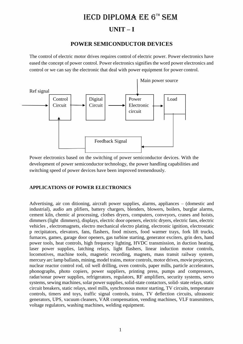
IECD DIPLOMA EE 6 TH SEM 1 Feedback Signal UNIT – I POWER SEMICONDUCTOR DEVICES The control of electric motor drives requires control of electric power. Power electronics have eased the concept of power control. Power electronics signifies the word power electronics and control or we can say the electronic that deal with power equipment for power control. Main power source Ref signal Power electronics based on the switching of power semiconductor devices. With the development of power semiconductor technology, the power handling capabilities and switching speed of power devices have been improved tremendously. APPLICATIONS OF POWER ELECTRONICS Advertising, air con ditioning, aircraft power supplies, alarms, appliances – (domestic and industrial), audio am plifiers, battery chargers, blenders, blowers, boilers, burglar alarms, cement kiln, chemic al processing, clothes dryers, computers, conveyors, cranes and hoists, dimmers (light dimmers), displays, electric door openers, electric dryers, electric fans, electric vehicles , electromagnets, electro mechanical electro plating, electronic ignition, electrostatic p recipitators, elevators, fans, flashers, food mixers, food warmer trays, fork lift trucks, furnaces, games, garage door openers, gas turbine starting, generator exciters, grin ders, hand power tools, heat controls, high frequency lighting, HVDC transmission, in duction heating, laser power supplies, latching relays, light flashers, linear induction motor controls, locomotives, machine tools, magnetic recording, magnets, mass transit railway system, mercury arc lamp ballasts, mining, model trains, motor controls, motor drives, movie projectors, nuclear reactor control rod, oil well drilling, oven controls, paper mills, particle accelerators, phonographs, photo copiers, power suppliers, printing press, pumps and compressors, radar/sonar power supplies, refrigerators, regulators, RF amplifiers, security systems, servo systems, sewing machines, solar power supplies, solid-state contactors, solid- state relays, static circuit breakers, static relays, steel mills, synchronous motor starting, TV circuits, temperature controls, timers and toys, traffic signal controls, trains, TV deflection circuits, ultrasonic generators, UPS, vacuum cleaners, VAR compensation, vending machines, VLF transmitters, voltage regulators, washing machines, welding equipment. Control Digital Power Load Circuit Circuit Electronic circuit
-
Upload
khangminh22 -
Category
Documents
-
view
2 -
download
0
Transcript of IECD DIPLOMA EE 6TH SEM - IITM Group Of Institution
IECD DIPLOMA EE 6TH SEM
1
Feedback Signal
UNIT – I
POWER SEMICONDUCTOR DEVICES
The control of electric motor drives requires control of electric power. Power electronics have
eased the concept of power control. Power electronics signifies the word power electronics and
control or we can say the electronic that deal with power equipment for power control.
Main power source
Ref signal
Power electronics based on the switching of power semiconductor devices. With the
development of power semiconductor technology, the power handling capabilities and
switching speed of power devices have been improved tremendously.
APPLICATIONS OF POWER ELECTRONICS
Advertising, air con ditioning, aircraft power supplies, alarms, appliances – (domestic and
industrial), audio am plifiers, battery chargers, blenders, blowers, boilers, burglar alarms,
cement kiln, chemic al processing, clothes dryers, computers, conveyors, cranes and hoists,
dimmers (light dimmers), displays, electric door openers, electric dryers, electric fans, electric
vehicles , electromagnets, electro mechanical electro plating, electronic ignition, electrostatic
p recipitators, elevators, fans, flashers, food mixers, food warmer trays, fork lift trucks,
furnaces, games, garage door openers, gas turbine starting, generator exciters, grin ders, hand
power tools, heat controls, high frequency lighting, HVDC transmission, in duction heating,
laser power supplies, latching relays, light flashers, linear induction motor controls,
locomotives, machine tools, magnetic recording, magnets, mass transit railway system,
mercury arc lamp ballasts, mining, model trains, motor controls, motor drives, movie projectors,
nuclear reactor control rod, oil well drilling, oven controls, paper mills, particle accelerators,
phonographs, photo copiers, power suppliers, printing press, pumps and compressors,
radar/sonar power supplies, refrigerators, regulators, RF amplifiers, security systems, servo
systems, sewing machines, solar power supplies, solid-state contactors, solid- state relays, static
circuit breakers, static relays, steel mills, synchronous motor starting, TV circuits, temperature
controls, timers and toys, traffic signal controls, trains, TV deflection circuits, ultrasonic
generators, UPS, vacuum cleaners, VAR compensation, vending machines, VLF transmitters,
voltage regulators, washing machines, welding equipment.
Control Digital Power Load
Circuit Circuit
Electronic
circuit

IECD DIPLOMA EE 6TH SEM
2
POWER ELECTRONIC APPLICATIONS
COMMERCIAL APPLICATIONS
Heating Systems Ventilating, Air Conditioners, Central Refrigeration, Lighting, Computers
and Office equipments, Uninterruptible Power Supplies (UPS), Elevators, and Emergency
Lamps.
DOMESTIC APPLICATIONS
Cooking Equipments, Lighting, Heating, Air Conditioners, Refrigerators & Freezers, Personal
Computers, Entertainment Equipments, UPS.
INDUSTRIAL APPLICATIONS
Pumps, compressors, blowers and fans. Machine tools, arc furnaces, induction furnaces,
lighting control circuits, industrial lasers, induction heating, welding equipments.
AEROSPACE APPLICATIONS
Space shuttle power supply systems, satellite power systems, aircraft power systems.
TELECOMMUNICATIONS
Battery chargers, power supplies (DC and UPS), mobile cell phone battery chargers.
TRANSPORTATION
Traction control of electric vehicles, battery chargers for electric vehicles, electric locomotives,
street cars, trolley buses, automobile electronics including engine controls.
UTILITY SYSTEMS
High voltage DC transmission (HVDC), static VAR compensation (SVC), Alternative energy
sources (wind, photovoltaic), fuel cells, energy storage systems, induced draft fans and boiler
feed water pumps.
POWER SEMICONDUCTOR DEVICES
Power Diodes.
Power Transistors (BJT’s).
Power MOSFETS.
IGBT’s.
Thyristors
Thyristors are a family of p-n-p-n structured power semiconductor switching devices
SCR’s (Silicon Controlled Rectifier)
The silicon controlled rectifier is the most commonly and widely used member of the
thyristor family. The family of thyristor devices include SCR’s, Diacs, Triacs, SCS, SUS,
LASCR’s and so on.
POWER SEMICONDUCTOR DEVICES USED IN POWER ELECTRONICS
The first thyristor or the SCR was developed in 1957. The conventional Thyristors (SCR’s)
were exclusively used for power control in industrial applications until 1970. After 1970,
various types of power semiconductor devices were developed and became commercially
available. The power semiconductor devices can be divided broadly into five types
Power Diodes.
Thyristors.
IECD DIPLOMA EE 6TH SEM
3
Power BJT’s.
Power MOSFET’s.
Insulated Gate Bipolar Transistors (IGBT’s).
Static Induction Transistors (SIT’s).
The Thyristors can be subdivided into different types
Forced-commutated Thyristors (Inverter grade Thyristors)
Line-commutated Thyristors (converter-grade Thyristors)
Gate-turn off Thyristors (GTO).
Reverse conducting Thyristors (RCT’s).
Static Induction Thyristors (SITH).
Gate assisted turn-off Thyristors (GATT).
Light activated silicon controlled rectifier (LASCR) or Photo SCR’s.
MOS-Controlled Thyristors (MCT’s).
Time required for emitter current to diffuse across the base region into the collector
region once the base emitter junction is forward biased. The turn on time ton
ranges
from 10 to 300 ns. Base current is normally more than the minimum required to saturate
the transistor. As a result excess minority carrier charge is stored in the base region.
When the input voltage is reversed from VB1 to VB 2 the base current also abruptly changes
but the collector current remains constant for a short time interval tS called the storage time.
The reverse base current helps to discharge the minority charge carries in the base region and to remove the excess stored charge form the base region. Once the excess stored charge is
removed the baser region the base current begins to fall towards zero. The fall-time t f is the
time taken for the collector current to fall from 90% to 10% of ICsat . The turn off time toff is
the sum of storage time and the fall time. toff ts t f
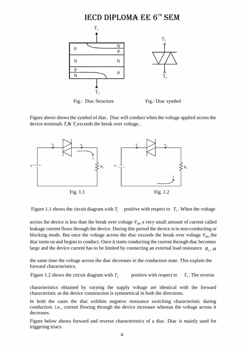
DIAC
A diac is a two terminal five layer semi-conductor bi-directional switching device. It can
conduct in both directions. The device consists of two p-n-p-n sections in anti parallel as shown
in figure. T1 and T2 are the two terminals of the device.
IECD DIPLOMA EE 6TH SEM
4
T1
T1
T2
T2
Fig.: Diac Structure Fig.: Diac symbol
Figure above shows the symbol of diac. Diac will conduct when the voltage applied across the
device terminals T1 & T2 exceeds the break over voltage..
V RL
Fig. 1.1 Fig. 1.2
Figure 1.1 shows the circuit diagram with T1 positive with respect to T2 . When the voltage
across the device is less than the break over voltage VB01 a very small amount of current called
leakage current flows through the device. During this period the device is in non-conducting or
blocking mode. But once the voltage across the diac exceeds the break over voltage VB01 the
diac turns on and begins to conduct. Once it starts conducting the current through diac becomes
large and the device current has to be limited by connecting an external load resistance RL , at
the same time the voltage across the diac decreases in the conduction state. This explain the
forward characteristics.
Figure 1.2 shows the circuit diagram with T2 positive with respect to T1 . The reverse
characteristics obtained by varying the supply voltage are identical with the forward
characteristic as the device construction is symmetrical in both the directions.
In both the cases the diac exhibits negative resistance switching characteristic during
conduction. i.e., current flowing through the device increases whereas the voltage across it
decreases.
Figure below shows forward and reverse characteristics of a diac. Diac is mainly used for
triggering triacs.
P N
P
N N
P P
N
IECD DIPLOMA EE 6TH SEM
5
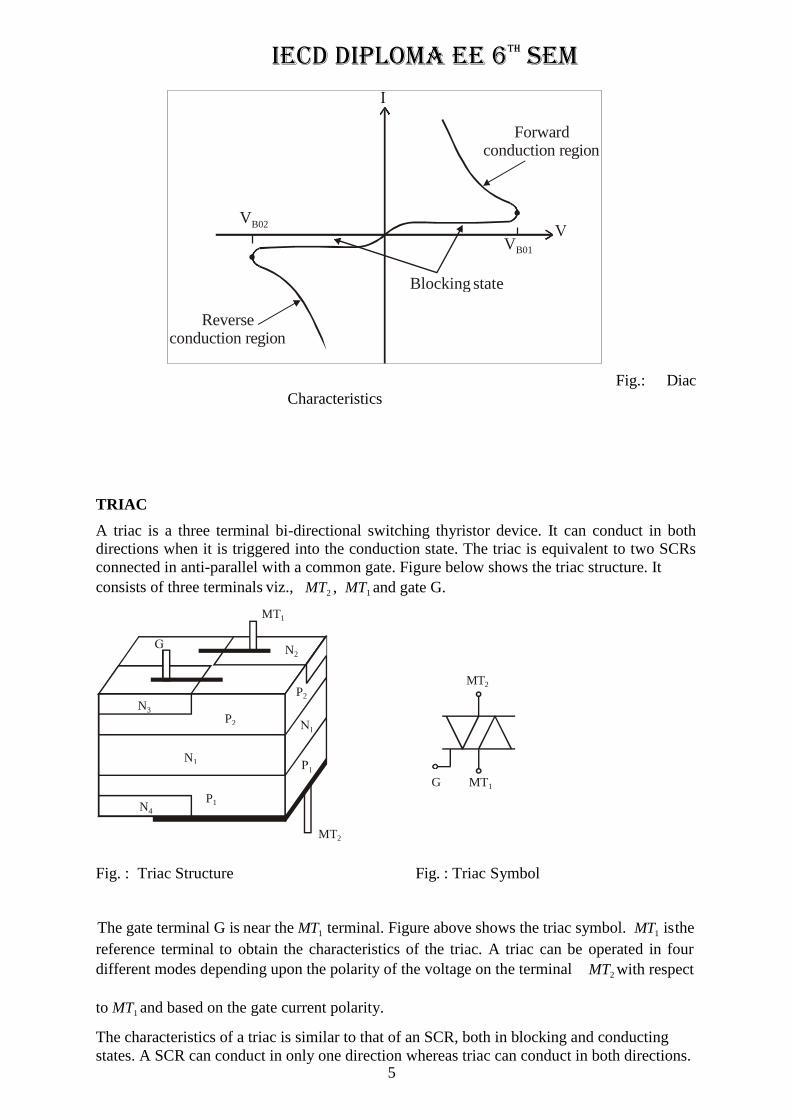
Fig.: Diac
Characteristics
TRIAC
A triac is a three terminal bi-directional switching thyristor device. It can conduct in both
directions when it is triggered into the conduction state. The triac is equivalent to two SCRs
connected in anti-parallel with a common gate. Figure below shows the triac structure. It
consists of three terminals viz.,
MT1
MT2 , MT1 and gate G.
MT2
G MT1
Fig. : Triac Structure Fig. : Triac Symbol
The gate terminal G is near the MT1 terminal. Figure above shows the triac symbol. MT1 is the
reference terminal to obtain the characteristics of the triac. A triac can be operated in four
different modes depending upon the polarity of the voltage on the terminal MT2 with respect
to MT1 and based on the gate current polarity.
The characteristics of a triac is similar to that of an SCR, both in blocking and conducting
states. A SCR can conduct in only one direction whereas triac can conduct in both directions.
Forward conduction region
VB02
VB01
Blocking state
Reverse conduction region
N2
P2
N3
P2
N1
N4 P1
MT2
IECD DIPLOMA EE 6TH SEM
6
2
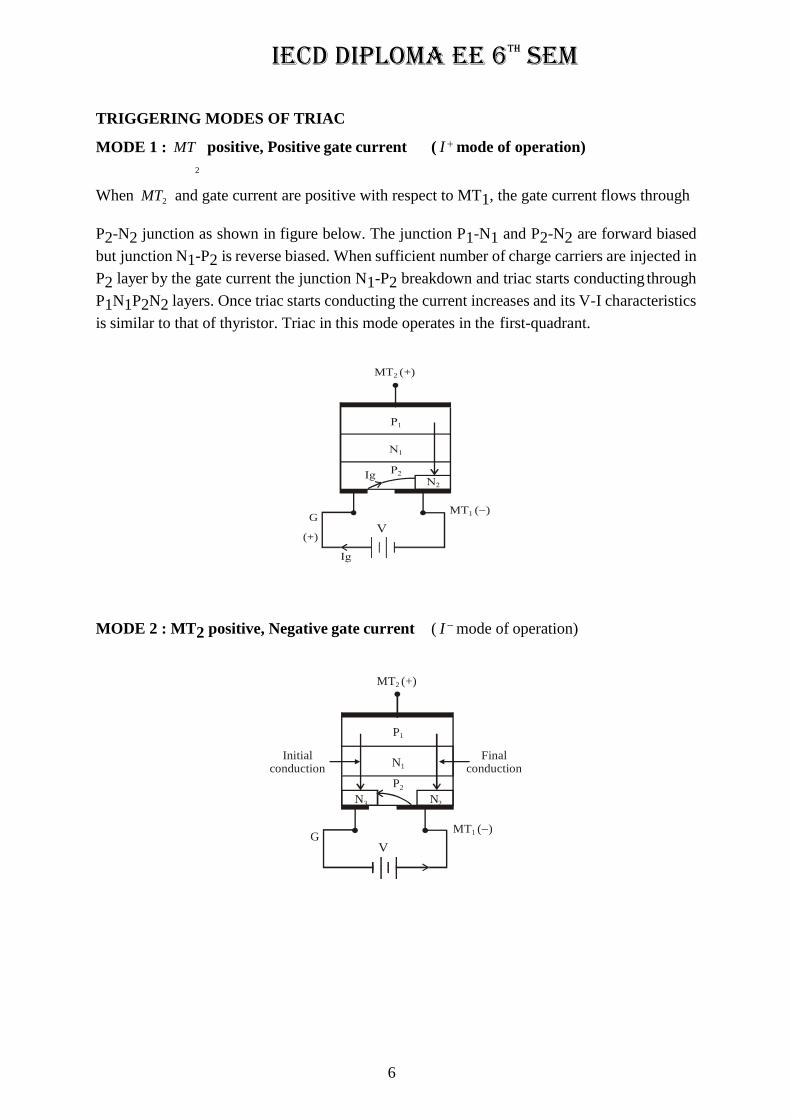
TRIGGERING MODES OF TRIAC
MODE 1 : MT positive, Positive gate current ( I mode of operation)
When MT2 and gate current are positive with respect to MT1, the gate current flows through
P2-N2 junction as shown in figure below. The junction P1-N1 and P2-N2 are forward biased
but junction N1-P2 is reverse biased. When sufficient number of charge carriers are injected in
P2 layer by the gate current the junction N1-P2 breakdown and triac starts conducting through
P1N1P2N2 layers. Once triac starts conducting the current increases and its V-I characteristics
is similar to that of thyristor. Triac in this mode operates in the first-quadrant.
MT2 (+)
G
(+)
MT1 ()
MODE 2 : MT2 positive, Negative gate current ( I mode of operation)
MT2 (+)
Initial conduction
G
P1
N1
P2
N3 N2
V
Final conduction
MT1 ()
IECD DIPLOMA EE 6TH SEM
7
Ig
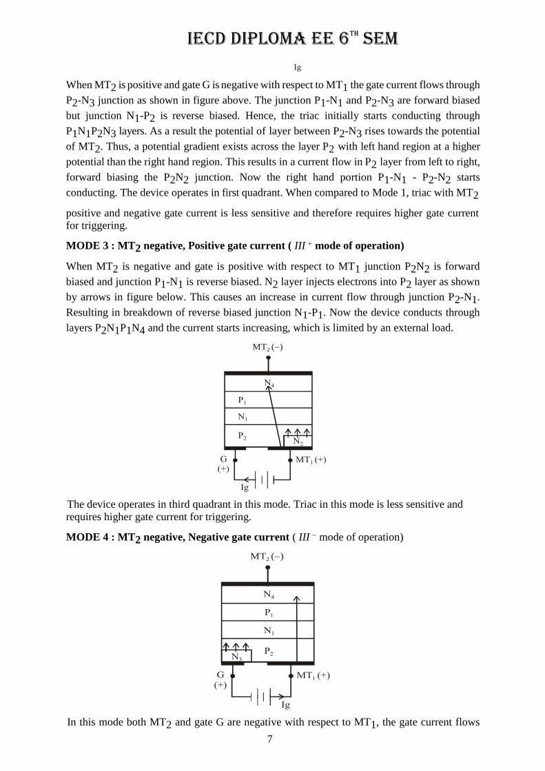
When MT2 is positive and gate G is negative with respect to MT1 the gate current flows through
P2-N3 junction as shown in figure above. The junction P1-N1 and P2-N3 are forward biased
but junction N1-P2 is reverse biased. Hence, the triac initially starts conducting through
P1N1P2N3 layers. As a result the potential of layer between P2-N3 rises towards the potential
of MT2. Thus, a potential gradient exists across the layer P2 with left hand region at a higher
potential than the right hand region. This results in a current flow in P2 layer from left to right,
forward biasing the P2N2 junction. Now the right hand portion P1-N1 - P2-N2 starts
conducting. The device operates in first quadrant. When compared to Mode 1, triac with MT2
positive and negative gate current is less sensitive and therefore requires higher gate current for triggering.
MODE 3 : MT2 negative, Positive gate current ( III mode of operation)
When MT2 is negative and gate is positive with respect to MT1 junction P2N2 is forward
biased and junction P1-N1 is reverse biased. N2 layer injects electrons into P2 layer as shown
by arrows in figure below. This causes an increase in current flow through junction P2-N1.
Resulting in breakdown of reverse biased junction N1-P1. Now the device conducts through
layers P2N1P1N4 and the current starts increasing, which is limited by an external load.
MT2 ()
The device operates in third quadrant in this mode. Triac in this mode is less sensitive and
requires higher gate current for triggering.
MODE 4 : MT2 negative, Negative gate current ( III mode of operation)
MT2 ()
In this mode both MT2 and gate G are negative with respect to MT1, the gate current flows

IECD DIPLOMA EE 6TH SEM
8
through P2N3 junction as shown in figure above. Layer N3 injects electrons as shown by arrows
into P2 layer. This results in increase in current flow across P1N1 and the device will turn ON
due to increased current in layer N1. The current flows through layers P2N1P1N4. Triac is more
sensitive in this mode compared to turn ON with positive gate current. (Mode 3).
Triac sensitivity is greatest in the first quadrant when turned ON with positive gate current and
also in third quadrant when turned ON with negative gate current. when MT2 is positive with
respect to MT1 it is recommended to turn on the triac by a positive gate current. When MT2 is
IECD DIPLOMA EE 6TH SEM
9
negative with respect to MT1 it is recommended to turn on the triac by negative gate current.
Therefore Mode 1 and Mode 4 are the preferred modes of operation of a triac ( I mode and
III mode of operation are normally used).
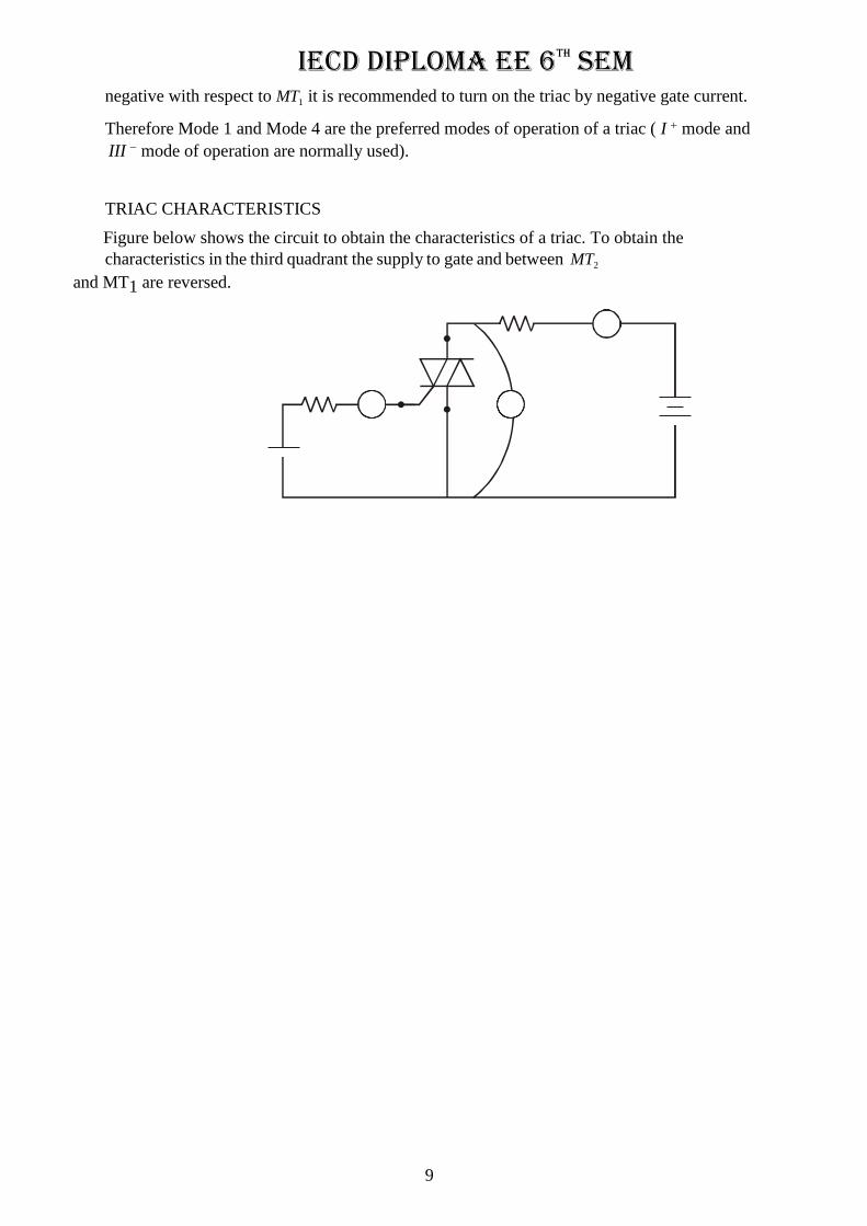
TRIAC CHARACTERISTICS
Figure below shows the circuit to obtain the characteristics of a triac. To obtain the
characteristics in the third quadrant the supply to gate and between MT2
and MT1 are reversed.
IECD DIPLOMA EE 6TH SEM
10
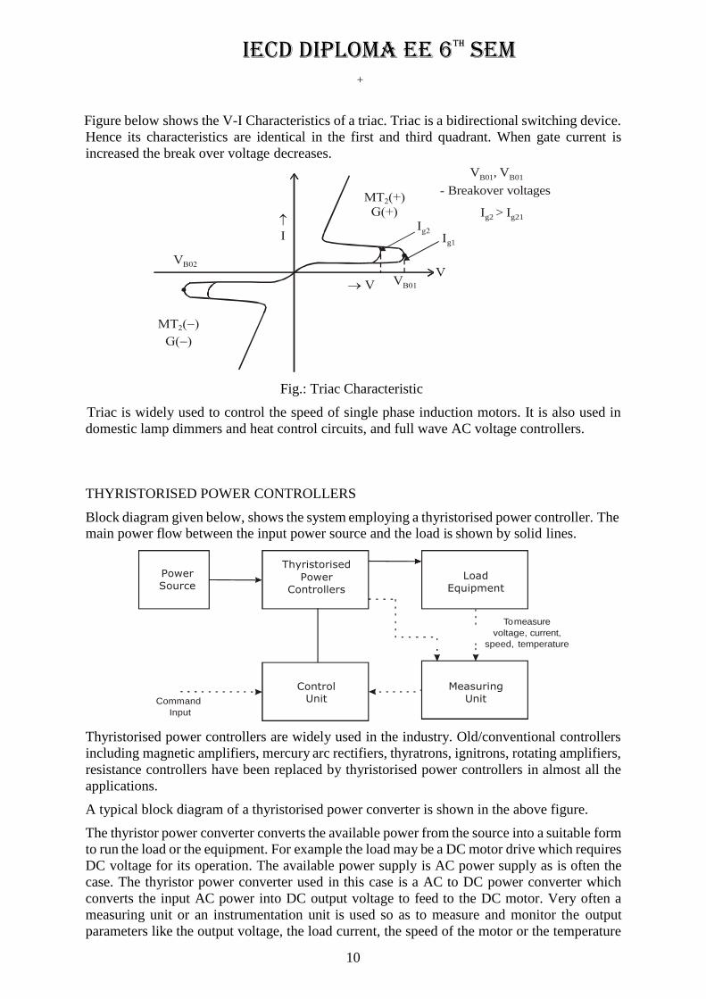
+
Figure below shows the V-I Characteristics of a triac. Triac is a bidirectional switching device.
Hence its characteristics are identical in the first and third quadrant. When gate current is
increased the break over voltage decreases.
VB01
, VB01
Breakover voltages
Ig2 > Ig21
g1
Fig.: Triac Characteristic
Triac is widely used to control the speed of single phase induction motors. It is also used in
domestic lamp dimmers and heat control circuits, and full wave AC voltage controllers.
THYRISTORISED POWER CONTROLLERS
Block diagram given below, shows the system employing a thyristorised power controller. The main power flow between the input power source and the load is shown by solid lines.
To measure
voltage, current,
speed, temperature
Command
Input
Thyristorised power controllers are widely used in the industry. Old/conventional controllers
including magnetic amplifiers, mercury arc rectifiers, thyratrons, ignitrons, rotating amplifiers,
resistance controllers have been replaced by thyristorised power controllers in almost all the
applications.
A typical block diagram of a thyristorised power converter is shown in the above figure.
The thyristor power converter converts the available power from the source into a suitable form
to run the load or the equipment. For example the load may be a DC motor drive which requires
DC voltage for its operation. The available power supply is AC power supply as is often the
case. The thyristor power converter used in this case is a AC to DC power converter which
converts the input AC power into DC output voltage to feed to the DC motor. Very often a
measuring unit or an instrumentation unit is used so as to measure and monitor the output
parameters like the output voltage, the load current, the speed of the motor or the temperature
Power
Source
Thyristorised
Power
Controllers
Load
Equipment
Control
Unit

IECD DIPLOMA EE 6TH SEM
11
etc. The measuring unit will be provided with meters and display devices so that the output
parameters can be seen and noted. The control unit is employed to control the output of the
thyristorised power converter so as to adjust the output voltage / current to the desired value to
obtain optimum performance of the load or equipment. The signal from the control unit is used
to adjust the phase angle / trigger angle of the Thyristors in the power controller so as to vary
the output voltage to the desired value.
SOME IMPORTANT APPLICATIONS OF THYRISTORISED POWER
CONTROLLERS
Control of AC and DC motor drives in rolling mills, paper and textile mills, traction
vehicles, mine winders, cranes, excavators, rotary kilns, ventilation fans, compression etc.
Uninterruptible and stand by power supplies for critical loads such as computers, special high tech power supplies for aircraft and space applications.
Power control in metallurgical and chemical processes using arc welding, induction heating, melting, resistance heating, arc melting, electrolysis, etc.
Static power compensators, transformer tap changers and static contactors for industrial power systems.
Power conversion at the terminals of a HVDC transmission systems.
High voltage supplies for electrostatic precipitators and x-ray generators.
Illumination/light control for lighting in stages, theaters, homes and studios.
Solid state power controllers for home/domestic appliances.
IECD DIPLOMA EE 6TH SEM
12
ADVANTAGES OF THYRISTORISED POWER CONTROLLERS
High efficiency due to low losses in the Thyristors.
Long life and reduced/minimal maintenance due to the absence of mechanical wear.
Control equipments using Thyristors are compact in size.
Easy and flexibility in operation due to digital controls.
Faster dynamic response compared to the electro mechanical converters.
Lower acoustic noise when compared to electro magnetic controllers, relays and
contactors.
DISADVANTAGES OF THYRISTORISED POWER CONTROLLERS
All the thyristorised power controllers generate harmonics (unwanted frequency
components) due to the switching ON and OFF of the thyristors. These harmionics
adversely affect the performance of the load connected to them. For example when the
load are motors, there are additional power losses (harmonic power loss) torque
harmonics, and increase in acoustic noise.
The generated harmonics are injected into the supply lines and thus adversely affect the
other loads/equipments connected to the supply lines.
In some applications example: traction, there is interference with the commutation
circuits due to the power supply line harmonics and due to electromagnetic radiation.
The thyristorised AC to DC converters and AC to AC converters can operate at low
power factor under some conditions.
Special steps are then taken for correcting the line supply power factor (by installing PF improvement apparatus).
The thyristorised power controllers have no short time over loading capacity and therefore they must be rated for maximum loading conditions. This leads to an increase
in the cost of the equipment.
Special protection circuits must be employed in thyristorised power controllers in order
to protect and safe guard the expensive thyristor devices. This again adds to the system
cost.
TYPES OF POWER CONVERTERS or THYRISTORISED POWER CONTROLLERS
For the control of electric power supplied to the load or the equipment/machinery or for
power conditioning the conversion of electric power from one form to other is necessary and
the switching characteristic of power semiconductor devices (Thyristors) facilitate these
conversions
The thyristorised power converters are referred to as the static power converters and
they perform the function of power conversion by converting the available input power supply
in to output power of desired form.
The different types of thyristor power converters are
Diode rectifiers (uncontrolled rectifiers).
Line commutated converters or AC to DC converters (controlled rectifiers)
AC voltage (RMS voltage) controllers (AC to AC converters).
IECD DIPLOMA EE 6TH SEM
13
Cyclo converters (AC to AC converters at low output frequency).
DC choppers (DC to DC converters).
Inverters (DC to AC converters).
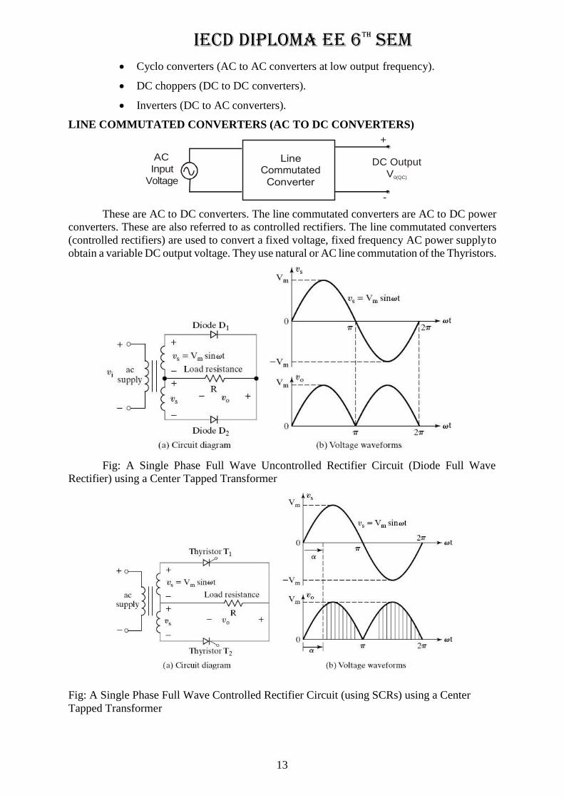
LINE COMMUTATED CONVERTERS (AC TO DC CONVERTERS)
+
AC
Input
Voltage
DC Output
V0(QC)
-
These are AC to DC converters. The line commutated converters are AC to DC power
converters. These are also referred to as controlled rectifiers. The line commutated converters
(controlled rectifiers) are used to convert a fixed voltage, fixed frequency AC power supply to
obtain a variable DC output voltage. They use natural or AC line commutation of the Thyristors.
Fig: A Single Phase Full Wave Uncontrolled Rectifier Circuit (Diode Full Wave
Rectifier) using a Center Tapped Transformer
Fig: A Single Phase Full Wave Controlled Rectifier Circuit (using SCRs) using a Center
Tapped Transformer
IECD DIPLOMA EE 6TH SEM
14
Different types of line commutated AC to DC converters circuits are
Diode rectifiers – Uncontrolled Rectifiers
Controlled rectifiers using SCR’s.
o Single phase controlled rectifier.
o Three phase controlled rectifiers.
Applications of Line Commutated Converters
AC to DC power converters are widely used in
Speed control of DC motor in DC drives.
UPS.
HVDC transmission.
Battery Chargers.
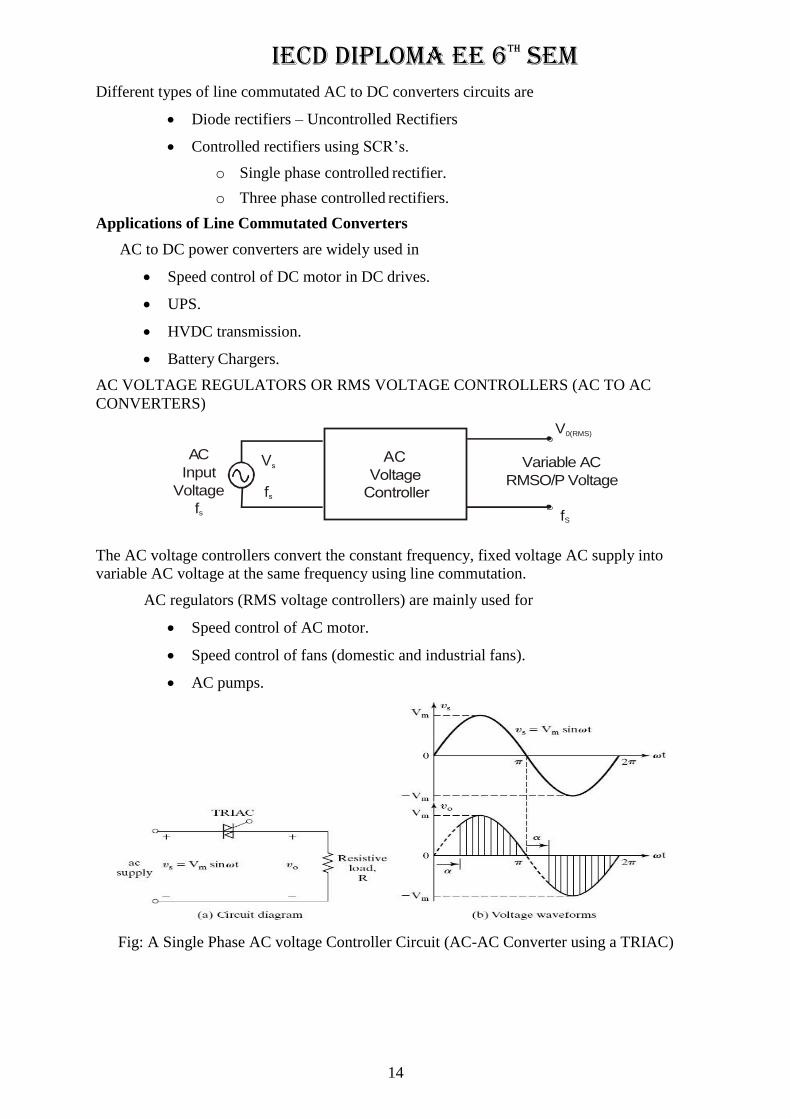
AC VOLTAGE REGULATORS OR RMS VOLTAGE CONTROLLERS (AC TO AC
CONVERTERS)
AC
Input
Voltage
fs
V0(RMS)
Variable AC
RMSO/P Voltage
fS
The AC voltage controllers convert the constant frequency, fixed voltage AC supply into
variable AC voltage at the same frequency using line commutation.
AC regulators (RMS voltage controllers) are mainly used for
Speed control of AC motor.
Speed control of fans (domestic and industrial fans).
AC pumps.
Fig: A Single Phase AC voltage Controller Circuit (AC-AC Converter using a TRIAC)
IECD DIPLOMA EE 6TH SEM
15
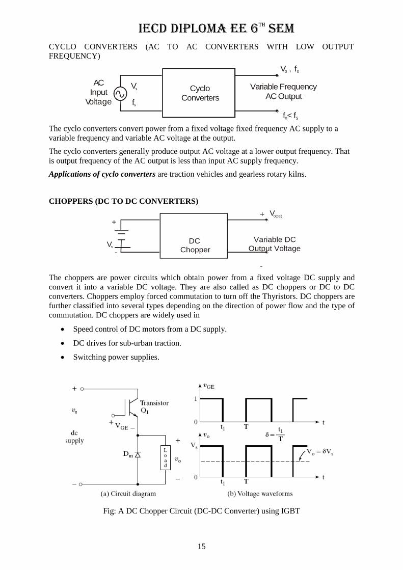
CYCLO CONVERTERS (AC TO AC CONVERTERS WITH LOW OUTPUT
FREQUENCY)
AC V
Input s
Voltage fs
V0 , f0
Variable Frequency
AC Output
f0< fS
The cyclo converters convert power from a fixed voltage fixed frequency AC supply to a
variable frequency and variable AC voltage at the output.
The cyclo converters generally produce output AC voltage at a lower output frequency. That
is output frequency of the AC output is less than input AC supply frequency.
Applications of cyclo converters are traction vehicles and gearless rotary kilns.
CHOPPERS (DC TO DC CONVERTERS)
+
+ V0(d c)
Vs -
DC
Chopper
Variable DC
Output Voltage
-
The choppers are power circuits which obtain power from a fixed voltage DC supply and
convert it into a variable DC voltage. They are also called as DC choppers or DC to DC
converters. Choppers employ forced commutation to turn off the Thyristors. DC choppers are
further classified into several types depending on the direction of power flow and the type of
commutation. DC choppers are widely used in
Speed control of DC motors from a DC supply.
DC drives for sub-urban traction.
Switching power supplies.
Fig: A DC Chopper Circuit (DC-DC Converter) using IGBT
Cyclo
Converters
IECD DIPLOMA EE 6TH SEM
16
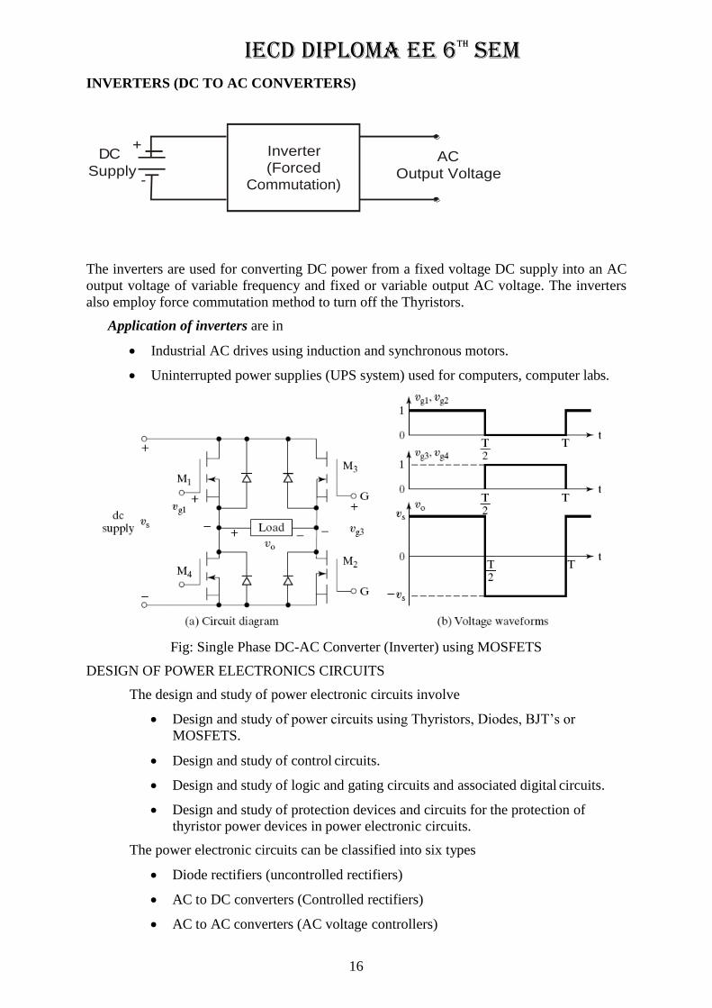
INVERTERS (DC TO AC CONVERTERS)
DC +
Supply -
Inverter (Forced
Commutation)
AC
Output Voltage
The inverters are used for converting DC power from a fixed voltage DC supply into an AC
output voltage of variable frequency and fixed or variable output AC voltage. The inverters
also employ force commutation method to turn off the Thyristors.
Application of inverters are in
Industrial AC drives using induction and synchronous motors.
Uninterrupted power supplies (UPS system) used for computers, computer labs.
Fig: Single Phase DC-AC Converter (Inverter) using MOSFETS
DESIGN OF POWER ELECTRONICS CIRCUITS
The design and study of power electronic circuits involve
Design and study of power circuits using Thyristors, Diodes, BJT’s or
MOSFETS.
Design and study of control circuits.
Design and study of logic and gating circuits and associated digital circuits.
Design and study of protection devices and circuits for the protection of
thyristor power devices in power electronic circuits.
The power electronic circuits can be classified into six types
Diode rectifiers (uncontrolled rectifiers)
AC to DC converters (Controlled rectifiers)
AC to AC converters (AC voltage controllers)
IECD DIPLOMA EE 6TH SEM
17
DC to DC converters (DC choppers)
DC to AC converters (Inverters)
Static Switches (Thyristorized contactors)
THYRISTORS
A thyristor is the most important type of power semiconductor devices. They are extensively
used in power electronic circuits. They are operated as bi-stable switches from non-conducting
to conducting state.
A thyristor is a four layer, semiconductor of p-n-p-n structure with three p-n junctions. It has
three terminals, the anode, cathode and the gate.
The word thyristor is coined from thyratron and transistor. It was invented in the year 1957 at
Bell Labs. The Different types of Thyristors are
Silicon Controlled Rectifier (SCR).
TRIAC
DIAC
Gate Turn Off Thyristor (GTO)
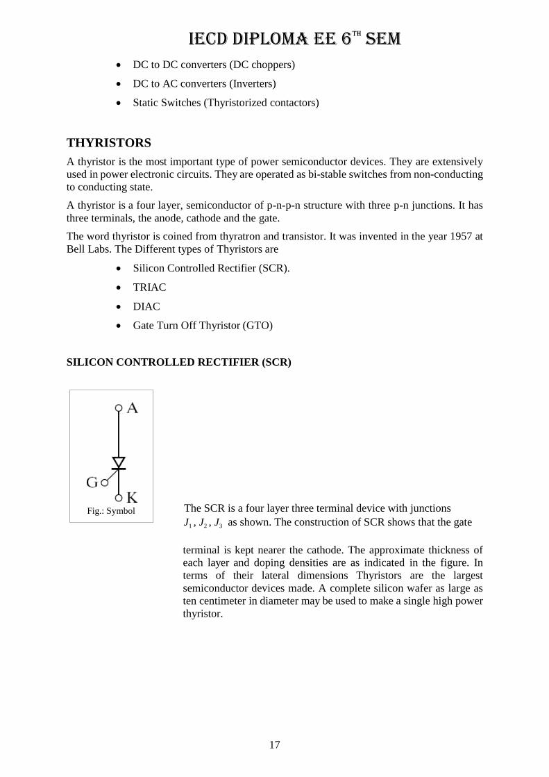
SILICON CONTROLLED RECTIFIER (SCR)
The SCR is a four layer three terminal device with junctions
J1 , J2 , J3 as shown. The construction of SCR shows that the gate
terminal is kept nearer the cathode. The approximate thickness of
each layer and doping densities are as indicated in the figure. In
terms of their lateral dimensions Thyristors are the largest
semiconductor devices made. A complete silicon wafer as large as
ten centimeter in diameter may be used to make a single high power
thyristor.
Fig.: Symbol
IECD DIPLOMA EE 6TH SEM
18
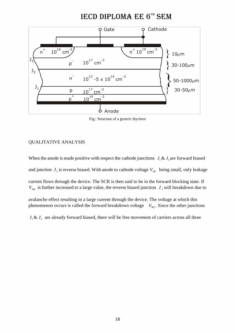
Fig.: Structure of a generic thyristor
QUALITATIVE ANALYSIS
When the anode is made positive with respect the cathode junctions J1 & J3 are forward biased
and junction J 2 is reverse biased. With anode to cathode voltage VAK being small, only leakage
current flows through the device. The SCR is then said to be in the forward blocking state. If
VAK
is further increased to a large value, the reverse biased junction J 2 will breakdown due to
avalanche effect resulting in a large current through the device. The voltage at which this
phenomenon occurs is called the forward breakdown voltage VBO . Since the other junctions
J1 & J3 are already forward biased, there will be free movement of carriers across all three
Gate Cathode
n+
J3
J2
1019
cm-3
p-
n+
1019
cm-3
10m
10 cm 17 -3
n–
1013
-5 x 10¹⁴
cm-3
J1
10 cm 17 -3 30-50m
10 cm
19 -3
Anode
IECD DIPLOMA EE 6TH SEM
19
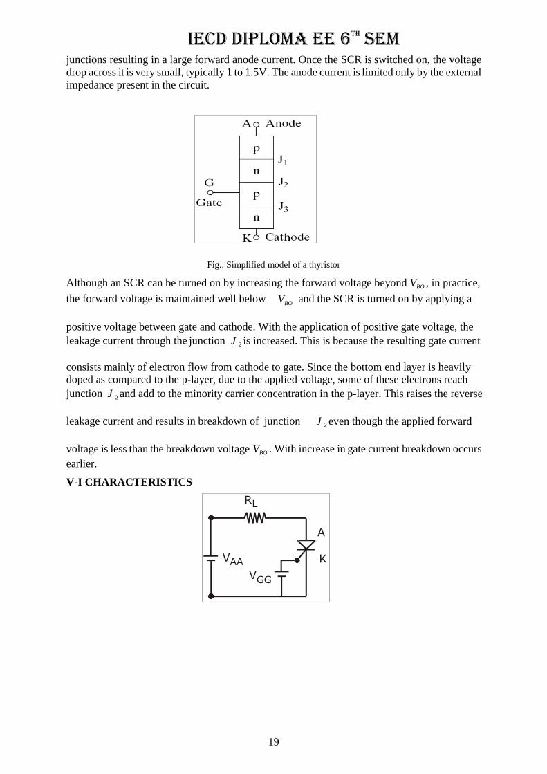
junctions resulting in a large forward anode current. Once the SCR is switched on, the voltage
drop across it is very small, typically 1 to 1.5V. The anode current is limited only by the external
impedance present in the circuit.
Fig.: Simplified model of a thyristor
Although an SCR can be turned on by increasing the forward voltage beyond VBO , in practice,
the forward voltage is maintained well below VBO
and the SCR is turned on by applying a
positive voltage between gate and cathode. With the application of positive gate voltage, the
leakage current through the junction J 2 is increased. This is because the resulting gate current
consists mainly of electron flow from cathode to gate. Since the bottom end layer is heavily doped as compared to the p-layer, due to the applied voltage, some of these electrons reach
junction J 2 and add to the minority carrier concentration in the p-layer. This raises the reverse
leakage current and results in breakdown of junction J 2 even though the applied forward
voltage is less than the breakdown voltage VBO . With increase in gate current breakdown occurs
earlier.
V-I CHARACTERISTICS
RL
VAA
VGG
IECD DIPLOMA EE 6TH SEM
20
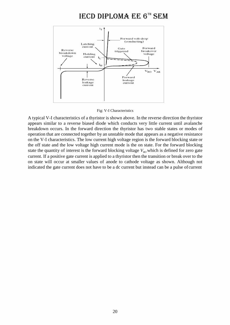
Fig: V-I Characteristics
A typical V-I characteristics of a thyristor is shown above. In the reverse direction the thyristor
appears similar to a reverse biased diode which conducts very little current until avalanche
breakdown occurs. In the forward direction the thyristor has two stable states or modes of
operation that are connected together by an unstable mode that appears as a negative resistance
on the V-I characteristics. The low current high voltage region is the forward blocking state or
the off state and the low voltage high current mode is the on state. For the forward blocking
state the quantity of interest is the forward blocking voltage VBO which is defined for zero gate
current. If a positive gate current is applied to a thyristor then the transition or break over to the
on state will occur at smaller values of anode to cathode voltage as shown. Although not
indicated the gate current does not have to be a dc current but instead can be a pulse of current
IECD DIPLOMA EE 6TH SEM
21
having some minimum time duration. This ability to switch the thyristor by means of a current
pulse is the reason for wide spread applications of the device.
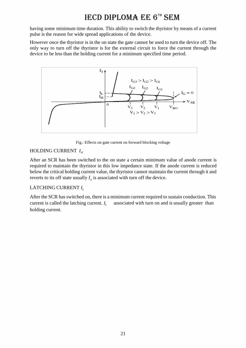
However once the thyristor is in the on state the gate cannot be used to turn the device off. The
only way to turn off the thyristor is for the external circuit to force the current through the
device to be less than the holding current for a minimum specified time period.
Fig.: Effects on gate current on forward blocking voltage
HOLDING CURRENT IH
After an SCR has been switched to the on state a certain minimum value of anode current is
required to maintain the thyristor in this low impedance state. If the anode current is reduced
below the critical holding current value, the thyristor cannot maintain the current through it and
reverts to its off state usually I is associated with turn off the device.
LATCHING CURRENT IL
After the SCR has switched on, there is a minimum current required to sustain conduction. This
current is called the latching current. IL
holding current.
associated with turn on and is usually greater than
IECD DIPLOMA EE 6TH SEM
22
1 1 1 1
2 2 2
1 2
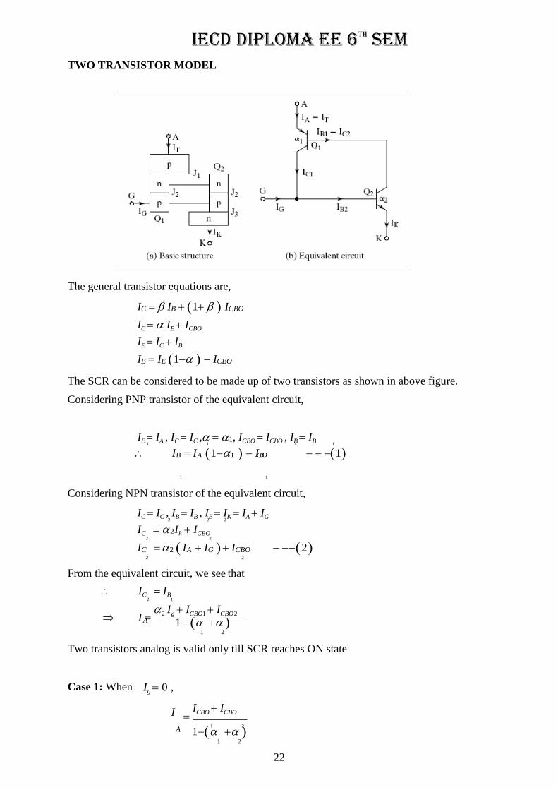
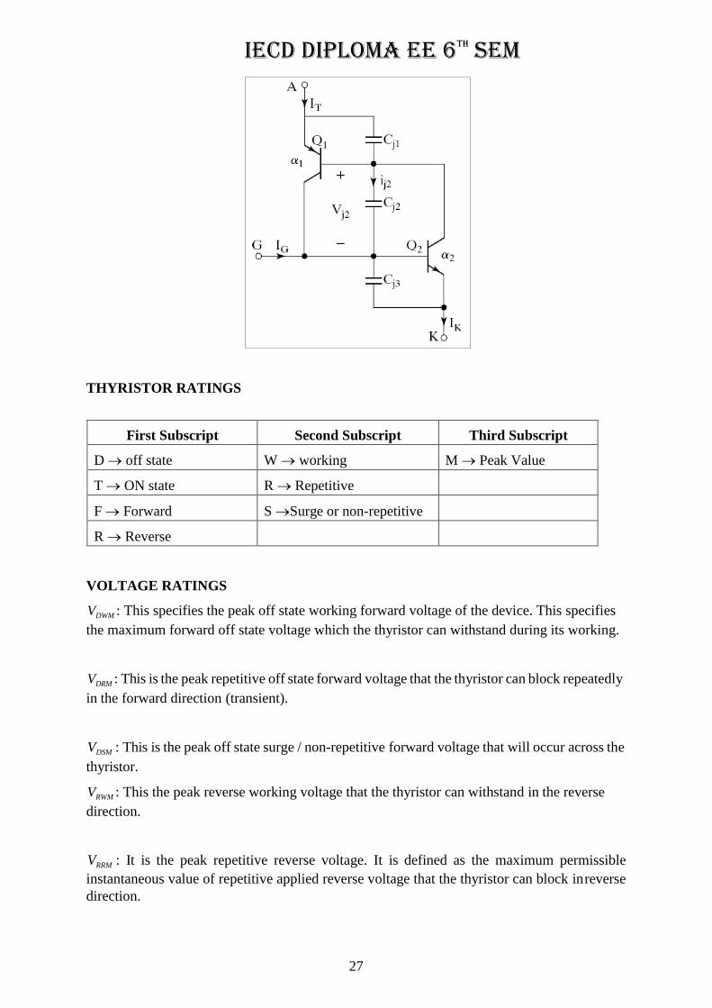
TWO TRANSISTOR MODEL
The general transistor equations are,
IC IB 1 ICBO
IC IE ICBO
IE IC IB
IB IE 1 ICBO
The SCR can be considered to be made up of two transistors as shown in above figure.
Considering PNP transistor of the equivalent circuit,
IE IA , IC IC , 1, ICBO ICBO , IB IB
IB IA 11 ICBO 1
1 1
Considering NPN transistor of the equivalent circuit,
IC IC , IB IB , IE IK IA IG
IC 2Ik ICBO 2 2
IC 2 IA IG ICBO 2 2 2
From the equivalent circuit, we see that
IC IB 2 1
I 2 Ig ICBO1 ICBO 2
A 1 1 2
Two transistors analog is valid only till SCR reaches ON state
Case 1: When Ig 0 ,
I
ICBO ICBO
A 1 1 2
IECD DIPLOMA EE 6TH SEM
23
B g
The gain 1 of transistor T1 varies with its emitter current IE IA . Similarly varies with
IE IA Ig IK . In this case, with Ig 0 , 2 varies only with I A . Initially when the applied
forward voltage is small, 1 2 1.
If however the reverse leakage current is increased by increasing the applied forward voltage,
the gains of the transistor increase, resulting in 1 2 1.
From the equation, it is seen that when 1 2 1, the anode current I A tends towards .
This explains the increase in anode current for the break over voltage VB 0 .
Case 2: With gate current Ig applied.
When sufficient gate drive is applied, we see that I I is established. This in turn results in 2
a current through transistor T2 , this increases 2 ofT2 . But with the existence of
IC 2I 2Ig , a current through T, is established. Therefore, 2 2
IC 1IB 12IB 12Ig . This current in turn is connected to the base of T2 . Thus the base
1 1 2
drive of T2 is increased which in turn increases the base drive of T1 , therefore regenerative
feedback or positive feedback is established between the two transistors. This causes 1 2 to tend to unity therefore the anode current begins to grow towards a large value. This
regeneration continues even if Ig is removed this characteristic of SCR makes it suitable for
pulse triggering; SCR is also called a Lathing Device.
SWITCHING CHARACTERISTICS (DYNAMIC CHARACTERISTICS)
THYRISTOR TURN-ON CHARACTERISTICS
When the SCR is turned on with the application of the gate signal, the SCR does not conduct
fully at the instant of application of the gate trigger pulse. In the beginning, there is no
appreciable increase in the SCR anode current, which is because, only a small portion of the
silicon pellet in the immediate vicinity of the gate electrode starts conducting. The duration
between 90% of the peak gate trigger pulse and the instant the forward voltage has fallen to
90% of its initial value is called the gate controlled / trigger delay time tgd . It is also defined as
the duration between 90% of the gate trigger pulse and the instant at which the anode current
rises to 10% of its peak value. tgd is usually in the range of 1sec.
IECD DIPLOMA EE 6TH SEM
24
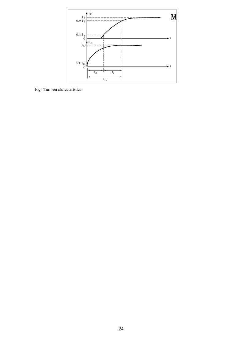
Fig.: Turn-on characteristics
IECD DIPLOMA EE 6TH SEM
25
Once tgd has lapsed, the current starts rising towards the peak value. The period during which
the anode current rises from 10% to 90% of its peak value is called the rise time. It is also defined as the time for which the anode voltage falls from 90% to 10% of its peak value. The
summation of tgd and tr gives the turn on time ton of the thyristor.
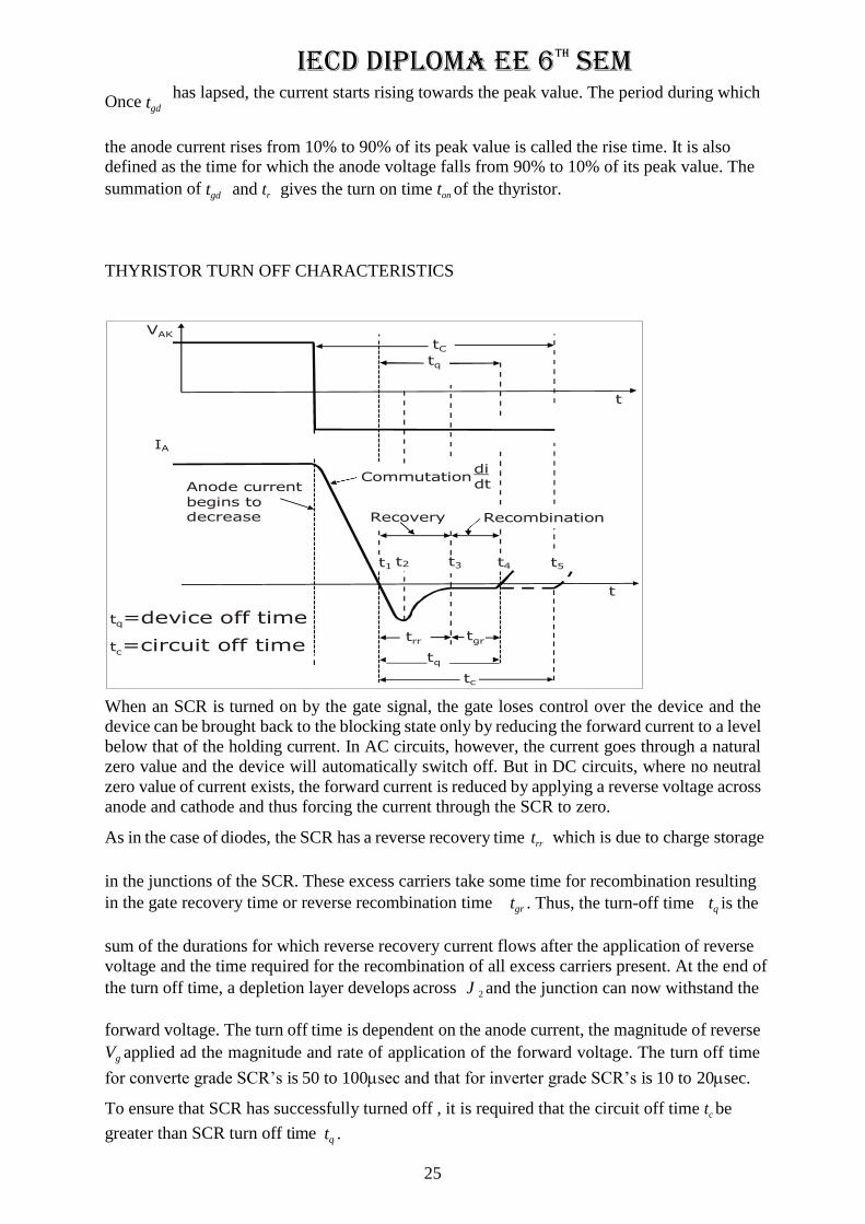
THYRISTOR TURN OFF CHARACTERISTICS
When an SCR is turned on by the gate signal, the gate loses control over the device and the
device can be brought back to the blocking state only by reducing the forward current to a level
below that of the holding current. In AC circuits, however, the current goes through a natural
zero value and the device will automatically switch off. But in DC circuits, where no neutral
zero value of current exists, the forward current is reduced by applying a reverse voltage across
anode and cathode and thus forcing the current through the SCR to zero.
As in the case of diodes, the SCR has a reverse recovery time trr which is due to charge storage
in the junctions of the SCR. These excess carriers take some time for recombination resulting
in the gate recovery time or reverse recombination time tgr . Thus, the turn-off time tq is the
sum of the durations for which reverse recovery current flows after the application of reverse
voltage and the time required for the recombination of all excess carriers present. At the end of
the turn off time, a depletion layer develops across J 2 and the junction can now withstand the
forward voltage. The turn off time is dependent on the anode current, the magnitude of reverse
Vg applied ad the magnitude and rate of application of the forward voltage. The turn off time
for converte grade SCR’s is 50 to 100sec and that for inverter grade SCR’s is 10 to 20sec.
To ensure that SCR has successfully turned off , it is required that the circuit off time tc be
greater than SCR turn off time tq .
IECD DIPLOMA EE 6TH SEM
26
j
j j
j
THYRISTOR TURN ON
Thermal Turn on: If the temperature of the thyristor is high, there will be an increase
in charge carriers which would increase the leakage current. This would cause an
increase in 1 & 2 and the thyristor may turn on. This type of turn on many cause
thermal run away and is usually avoided.
Light: If light be allowed to fall on the junctions of a thyristor, charge carrier concentration would increase which may turn on the SCR.
LASCR: Light activated SCRs are turned on by allowing light to strike the silicon
wafer.
High Voltage Triggering: This is triggering without application of gate voltage with
only application of a large voltage across the anode-cathode such that it is greater than
the forward breakdown voltageVBO . This type of turn on is destructive and should be
avoided.
Gate Triggering: Gate triggering is the method practically employed to turn-on the thyristor. Gate triggering will be discussed in detail later.
dv dt
Triggering: Under transient conditions, the capacitances of the p-n junction will
influence the characteristics of a thyristor. If the thyristor is in the blocking state, a
rapidly rising voltage applied across the device would cause a high current to flow
through the device resulting in turn-on. If i is the current throught the junction 2
j2 and
C is the junction capacitance and V is the voltage across 2 2
j2 , then
i dq2
d C V
C j2 dVJ 2
V dC
2
j 2 dt dt j2
j2
dt j2 dt
From the above equation, we see that if dv
dt
is large, 1
2
will be large. A high value of charging
current may damage the thyristor and the device must be protected against high dv
. The dt
manufacturers specify the allowable dv
. dt
j
IECD DIPLOMA EE 6TH SEM
27
THYRISTOR RATINGS
First Subscript Second Subscript Third Subscript
D off state W working M Peak Value
T ON state R Repetitive
F Forward S Surge or non-repetitive
R Reverse
VOLTAGE RATINGS
VDWM : This specifies the peak off state working forward voltage of the device. This specifies
the maximum forward off state voltage which the thyristor can withstand during its working.
VDRM : This is the peak repetitive off state forward voltage that the thyristor can block repeatedly
in the forward direction (transient).
VDSM : This is the peak off state surge / non-repetitive forward voltage that will occur across the
thyristor.
VRWM : This the peak reverse working voltage that the thyristor can withstand in the reverse
direction.
VRRM : It is the peak repetitive reverse voltage. It is defined as the maximum permissible
instantaneous value of repetitive applied reverse voltage that the thyristor can block in reverse
direction.
IECD DIPLOMA EE 6TH SEM
28
VRSM : Peak surge reverse voltage. This rating occurs for transient conditions for a specified
time duration.
VT : On state voltage drop and is dependent on junction temperature.
VTM : Peak on state voltage. This is specified for a particular anode current and junction
temperature.
dv rating: This is the maximum rate of rise of anode voltage that the SCR has to withstand
dt
and which will not trigger the device without gate signal (refer dv
dt
triggering).
CURRENT RATING
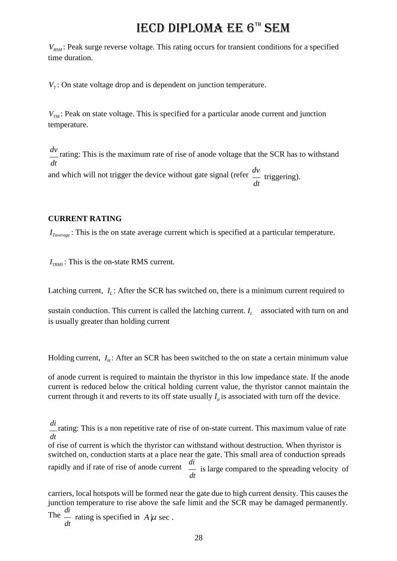
ITaverage : This is the on state average current which is specified at a particular temperature.
ITRMS : This is the on-state RMS current.
Latching current, IL : After the SCR has switched on, there is a minimum current required to
sustain conduction. This current is called the latching current. IL
is usually greater than holding current
associated with turn on and
Holding current, IH : After an SCR has been switched to the on state a certain minimum value
of anode current is required to maintain the thyristor in this low impedance state. If the anode
current is reduced below the critical holding current value, the thyristor cannot maintain the
current through it and reverts to its off state usually I is associated with turn off the device.
di rating: This is a non repetitive rate of rise of on-state current. This maximum value of rate
dt of rise of current is which the thyristor can withstand without destruction. When thyristor is
switched on, conduction starts at a place near the gate. This small area of conduction spreads
rapidly and if rate of rise of anode current di
dt
is large compared to the spreading velocity of
carriers, local hotspots will be formed near the gate due to high current density. This causes the
junction temperature to rise above the safe limit and the SCR may be damaged permanently.
The di
dt
rating is specified in A sec .
PE
29
44
GATE SPECIFICATIONS
IGT : This is the required gate current to trigger the SCR. This is usually specified as a DC value.
VGT : This is the specified value of gate voltage to turn on the SCR (dc value).
VGD : This is the value of gate voltage, to switch from off state to on state. A value below this
will keep the SCR in off state.
QRR : Amount of charge carriers which have to be recovered during the turn off process.
Rthjc : Thermal resistance between junction and outer case of the device.
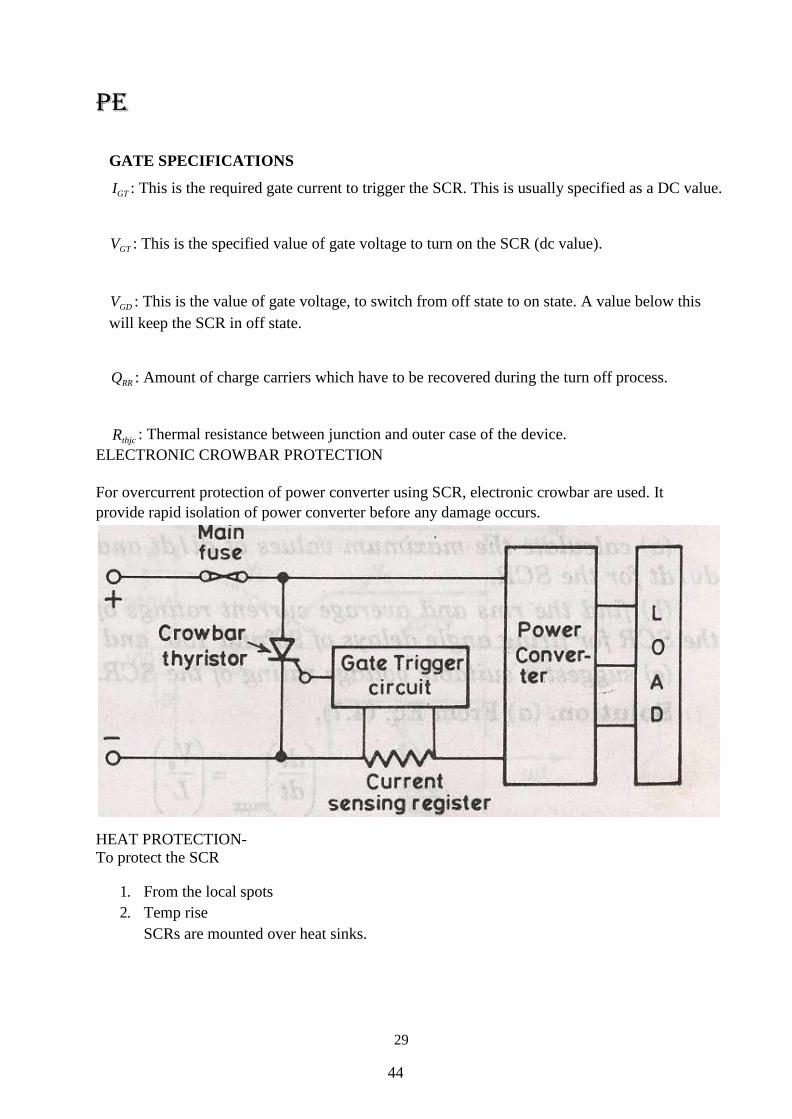
ELECTRONIC CROWBAR PROTECTION
For overcurrent protection of power converter using SCR, electronic crowbar are used. It
provide rapid isolation of power converter before any damage occurs.
HEAT PROTECTION-
To protect the SCR
1. From the local spots
2. Temp rise
SCRs are mounted over heat sinks.
PE
30
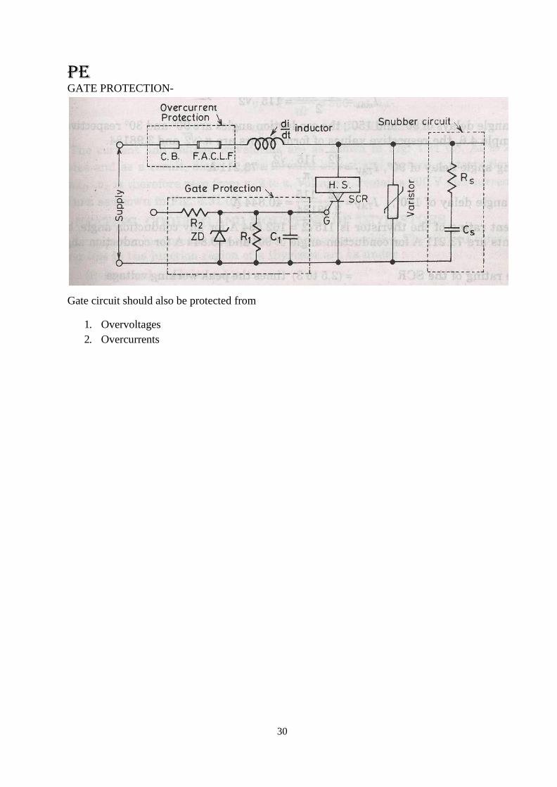
GATE PROTECTION-
Gate circuit should also be protected from
1. Overvoltages
2. Overcurrents
PE
31
Overvoltage across the gate circuit causes the false triggering of SCR
GATE TRIGGERING METHODS
Types
The different methods of gate triggering are the following
R-triggering.
RC triggering.
UJT triggering.
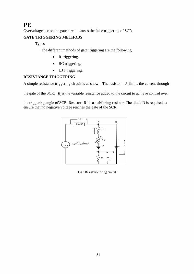
RESISTANCE TRIGGERING
A simple resistance triggering circuit is as shown. The resistor R1 limits the current through
the gate of the SCR. R2 is the variable resistance added to the circuit to achieve control over
the triggering angle of SCR. Resistor ‘R’ is a stabilizing resistor. The diode D is required to
ensure that no negative voltage reaches the gate of the SCR.
vO
a b LOAD
i R1
R2
vS=Vmsint D VT
R Vg
Fig.: Resistance firing circuit
PE
32
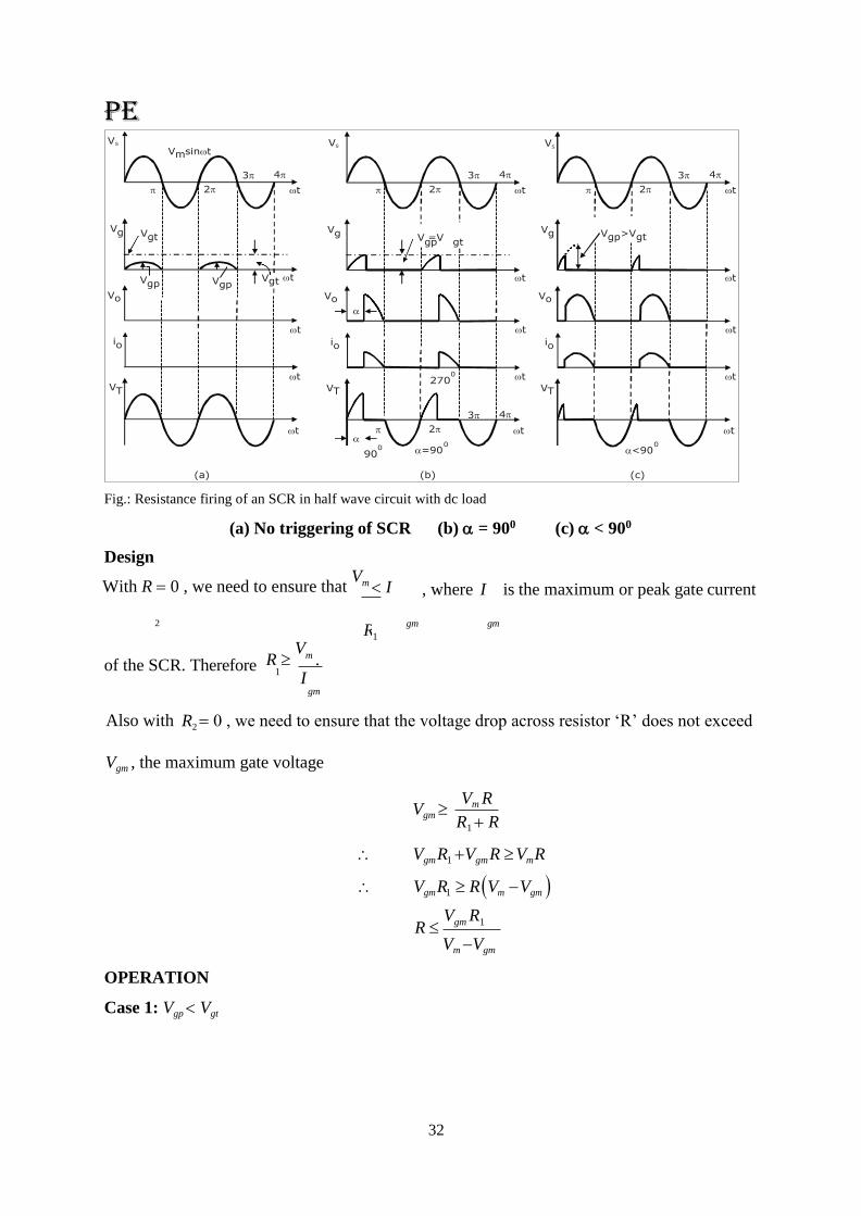
Fig.: Resistance firing of an SCR in half wave circuit with dc load
(a) No triggering of SCR (b) = 900 (c) < 900
Design
With R 0 , we need to ensure that Vm I
, where I is the maximum or peak gate current
2
of the SCR. Therefore
gm gm
1
R V
m . 1
I
Also with
gm
R2 0 , we need to ensure that the voltage drop across resistor ‘R’ does not exceed
Vgm , the maximum gate voltage
Vgm
Vm R
R1 R
Vgm R1 Vgm R Vm R
Vgm R1 R Vm Vgm
OPERATION
Case 1: Vgp Vgt
R Vgm R1
Vm Vgm
R
PE
33
gp
gt
Vgp , the peak gate voltage is less then Vgt since R2 is very large. Therefore, current ‘I’ flowing
through the gate is very small. SCR will not turn on and therefore the load voltage is zero and
vscr is equal to Vs . This is because we are using only a resistive network. Therefore, output will
be in phase with input.
ase 2: Vgp Vgt , R2 optimum value.
When R is set to an optimum value such that V V , we see that the SCR is triggered at 900 2 gp gt
(since V reaches its peak at 900 only). The waveforms shows that the load voltage is zero till
900 and the voltage across the SCR is the same as input voltage till it is triggered at 900 .
Case 3: Vgp Vgt , R2 small value.
The triggering value V is reached much earlier than 900 . Hence the SCR turns on earlier than
VS reaches its peak value. The waveforms as shown with respect to Vs Vm sin t .
At
Therefore
t ,VS Vgt ,Vm Vgp
sin1 Vgt
Vgt Vgp sin
V
gp
But V
Vm R
R1 R2 R
Therefore sin1 Vgt R1 R2 R
V
m R
Since Vgt , R1, R are constants R2
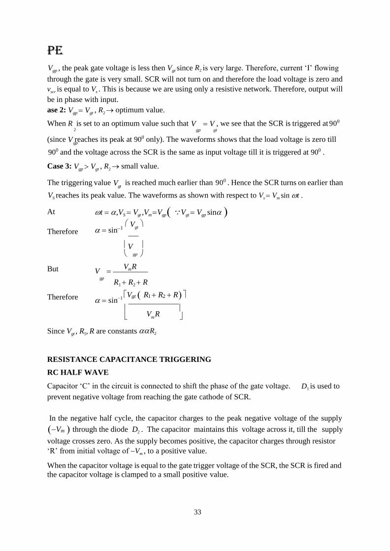
RESISTANCE CAPACITANCE TRIGGERING
RC HALF WAVE
Capacitor ‘C’ in the circuit is connected to shift the phase of the gate voltage.
prevent negative voltage from reaching the gate cathode of SCR.
D1 is used to
In the negative half cycle, the capacitor charges to the peak negative voltage of the supply
Vm through the diode D2 . The capacitor maintains this voltage across it, till the supply
voltage crosses zero. As the supply becomes positive, the capacitor charges through resistor
‘R’ from initial voltage of Vm , to a positive value.
When the capacitor voltage is equal to the gate trigger voltage of the SCR, the SCR is fired and
the capacitor voltage is clamped to a small positive value.
gp
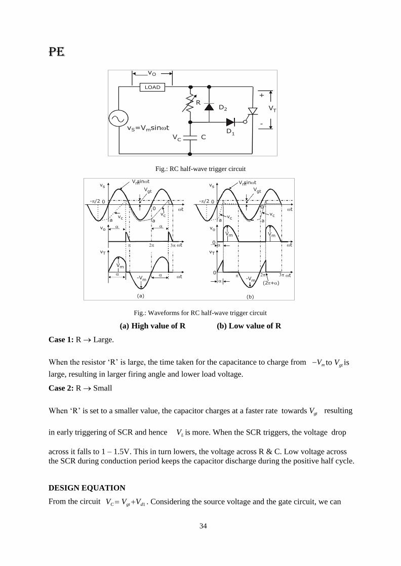
PE
34
Fig.: RC half-wave trigger circuit
Case 1: R Large.
Fig.: Waveforms for RC half-wave trigger circuit
(a) High value of R (b) Low value of R
When the resistor ‘R’ is large, the time taken for the capacitance to charge from
large, resulting in larger firing angle and lower load voltage.
Case 2: R Small
Vm to Vgt is
When ‘R’ is set to a smaller value, the capacitor charges at a faster rate towards Vgt resulting
in early triggering of SCR and hence VL is more. When the SCR triggers, the voltage drop
across it falls to 1 – 1.5V. This in turn lowers, the voltage across R & C. Low voltage across
the SCR during conduction period keeps the capacitor discharge during the positive half cycle.
DESIGN EQUATION
From the circuit VC Vgt Vd1 . Considering the source voltage and the gate circuit, we can

PE
35
write

PE
36
vs Igt R VC . SCR fires when
PE
37
2
vs Igt R VCthat isvS Ig R Vgt Vd1 . Therefore
R vs Vgt Vd1
. The RC time constant for zero output voltage that is maximum firing angle Igt
for power frequencies is empirically gives as RC 1.3 T
.
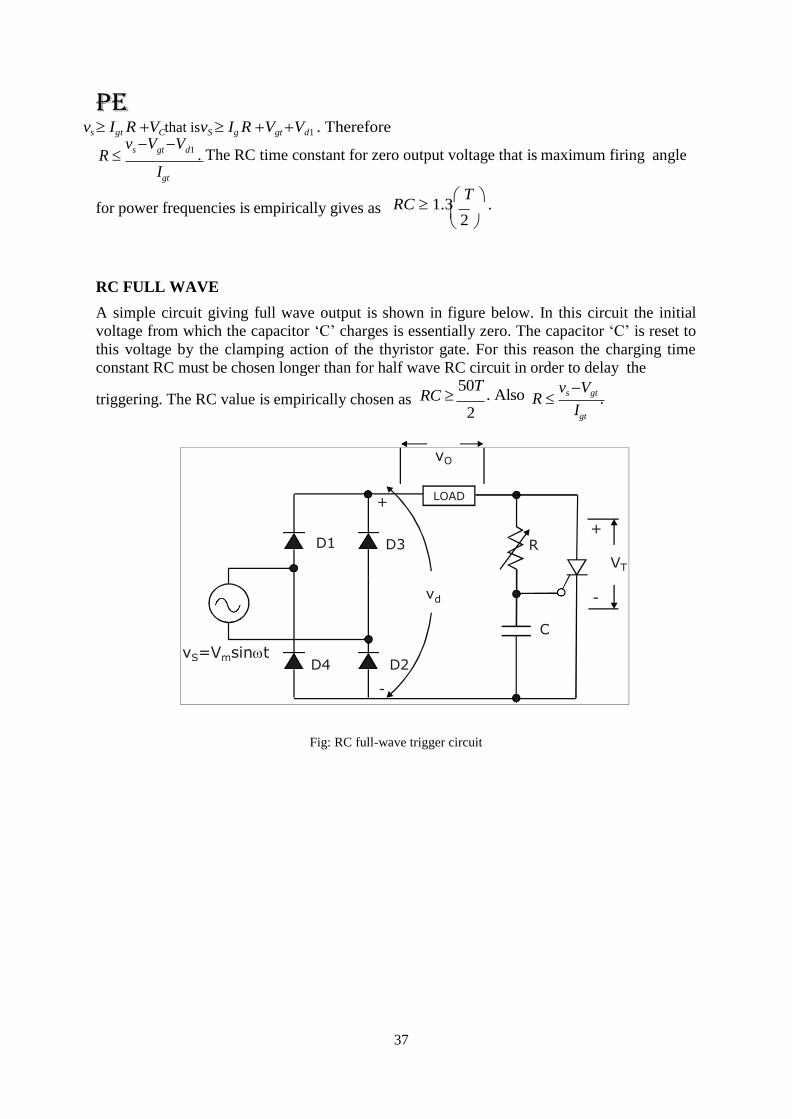
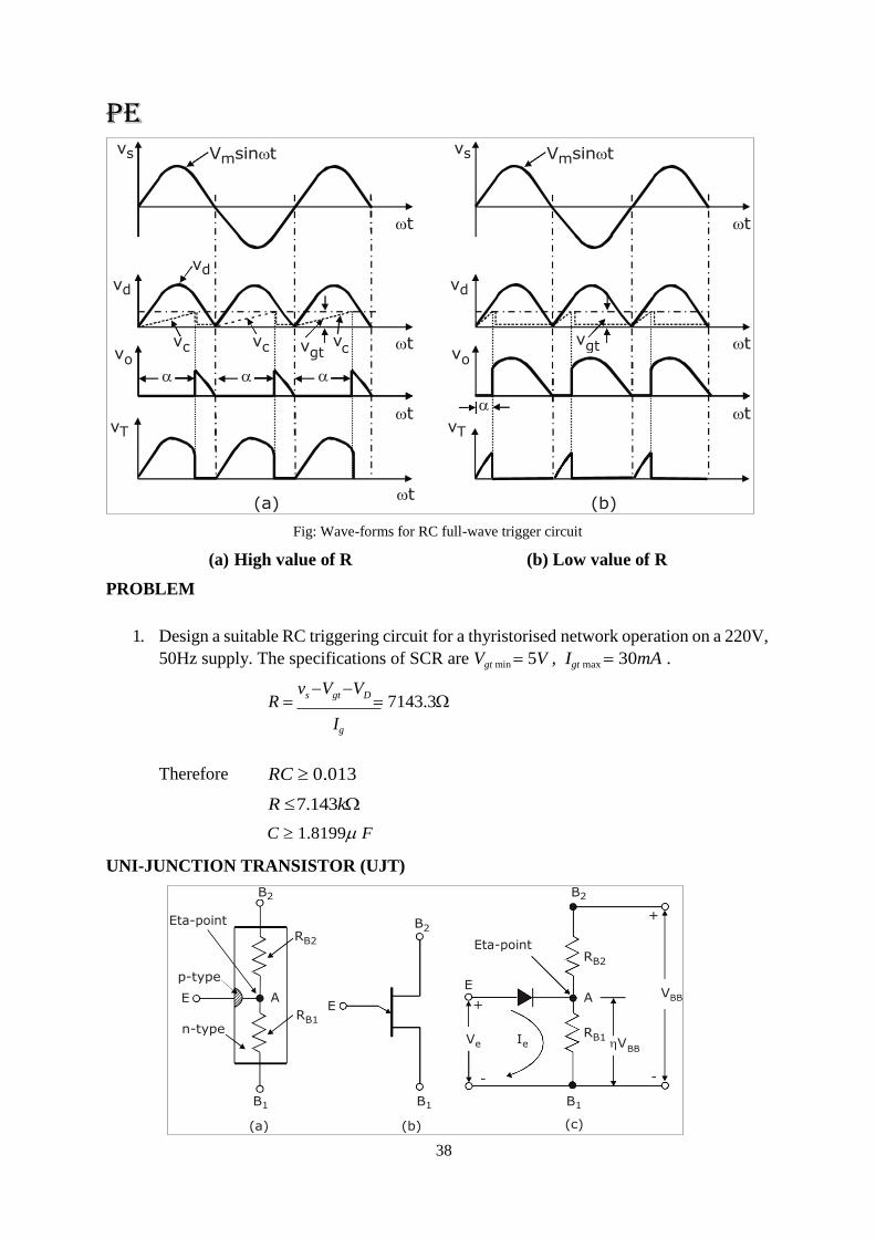
RC FULL WAVE
A simple circuit giving full wave output is shown in figure below. In this circuit the initial
voltage from which the capacitor ‘C’ charges is essentially zero. The capacitor ‘C’ is reset to
this voltage by the clamping action of the thyristor gate. For this reason the charging time
constant RC must be chosen longer than for half wave RC circuit in order to delay the
triggering. The RC value is empirically chosen as RC 50T
. Also 2
R vs Vgt
.
Igt
vO
+ LOAD
+ D1 D3 R
VT
vd -
C
vS=Vmsint D4 D2
-
Fig: RC full-wave trigger circuit
PE
38
PROBLEM
Fig: Wave-forms for RC full-wave trigger circuit
(a) High value of R (b) Low value of R
1. Design a suitable RC triggering circuit for a thyristorised network operation on a 220V,
50Hz supply. The specifications of SCR are Vgt min 5V ,
R vs Vgt VD
7143.3
Ig
Igt max 30mA .
Therefore RC 0.013
R 7.143k
C 1.8199 F
UNI-JUNCTION TRANSISTOR (UJT)
vs vs
vd
vd
vd
o
vc vc vgt vc
vgt
o
vT
vT
Eta-point
Eta-point
PE
39
Fig.: (a) Basic structure of UJT (b) Symbolic representation (c) Equivalent circuit
UJT is an n-type silicon bar in which p-type emitter is embedded. It has three terminals base1,
base2 and emitter ‘E’. Between B1 and B2 UJT behaves like ordinary resistor and the internal
resistances are given as RB1 and RB 2 with emitter open RBB
RB1
RB 2
. Usually the p-region
is heavily doped and n-region is lightly doped. The equivalent circuit of UJT is as shown. When
VBB
is applied across B1 and B2 , we find that potential at A is
V VBB RB1 V
RB1
AB1
R R BB R R
B1 B 2 B1 B 2
is intrinsic stand off ratio of UJT and ranges between 0.51 and 0.82. Resistor RB 2
5 to 10K.
is between
OPERATION
When voltage VBB
is applied between emitter ‘E’ with base 1
B1 as reference and the emitter
voltage VE is less than VD VBE the UJT does not conduct. VD VBB
is designated as VP
which is the value of voltage required to turn on the UJT. Once VE
then UJT is forward biased and it conducts.
is equal to VP VBE VD ,
The peak point is the point at which peak current IP flows and the peak voltage VP is across
the UJT. After peak point the current increases but voltage across device drops, this is due to
the fact that emitter starts to inject holes into the lower doped n-region. Since p-region is heavily
doped compared to n-region. Also holes have a longer life time, therefore number of
carriers in the base region increases rapidly. Thus potential at ‘A’ falls but current IE increases
rapidly. RB1 acts as a decreasing resistance.
The negative resistance region of UJT is between peak point and valley point. After valley
point, the device acts as a normal diode since the base region is saturated and
decrease again.
RB1
does not
PE
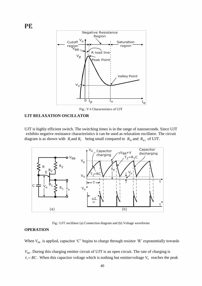
40
Capacitor
discharging
Fig.: V-I Characteristics of UJT
UJT RELAXATION OSCILLATOR
UJT is highly efficient switch. The switching times is in the range of nanoseconds. Since UJT
exhibits negative resistance characteristics it can be used as relaxation oscillator. The circuit
diagram is as shown with R1 and R2 being small compared to RB1 and RB 2
of UJT.
1
OPERATION
Fig.: UJT oscillator (a) Connection diagram and (b) Voltage waveforms
When VBB is applied, capacitor ‘C’ begins to charge through resistor ‘R’ exponentially towards
VBB . During this charging emitter circuit of UJT is an open circuit. The rate of charging is
1 RC . When this capacitor voltage which is nothing but emitter voltage VE reaches the peak

PE
41
point VP VBB VD , the emitter base junction is forward biased and UJT turns on. Capacitor

PE
42
‘C’ rapidly discharges through load resistance

PE
43
R1 with time constant 2 R1C 2

PE
44
1 . When
emitter voltage decreases to valley point Vv , UJT turns off. Once again the capacitor will charge
towards VBB and the cycle continues. The rate of charging of the capacitor will be determined
by the resistor R in the circuit. If R is small the capacitor charges faster towards VBB and thus
reaches VP faster and the SCR is triggered at a smaller firing angle. If R is large the capacitor
takes a longer time to charge towards VP
cases is as shown below.
the firing angle is delayed. The waveform for both
PE
45
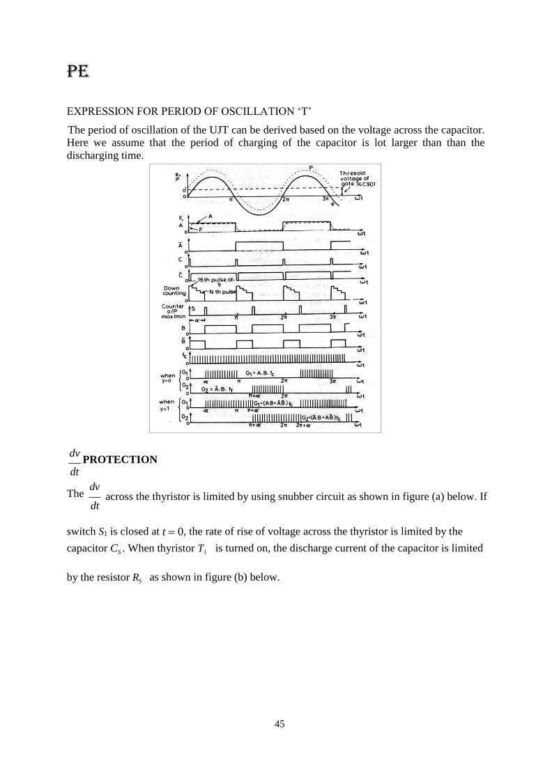
EXPRESSION FOR PERIOD OF OSCILLATION ‘T’
The period of oscillation of the UJT can be derived based on the voltage across the capacitor.
Here we assume that the period of charging of the capacitor is lot larger than than the
discharging time.
dv PROTECTION
dt
The dv
dt
across the thyristor is limited by using snubber circuit as shown in figure (a) below. If
switch S1 is closed at t 0, the rate of rise of voltage across the thyristor is limited by the
capacitor CS . When thyristor T1 is turned on, the discharge current of the capacitor is limited
by the resistor RS as shown in figure (b) below.
PE
46
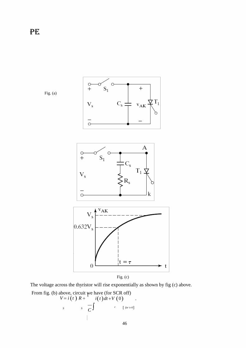
Fig. (a)
ig. (b)
Fig. (c)
The voltage across the thyristor will rise exponentially as shown by fig (c) above.
From fig. (b) above, circuit we have (for SCR off) V i t R
1 i t dt V 0 .
S S C
c for t0
PE
47
Therefore
i t VS e
t s , where R C
Also
RS
VT t VS i t RS
s S S
V t V VS e
t R
s
T S S
Therefore V t V V e s V
1 e
t t s
At t = 0,
At t s ,
Therefore
T S S S
VT 0 0
VT s 0.632VS
dv
VT s VT 0
0.632VS
dt s RSCS
PE
48
And R VS .
S I
I
TD
TD
is the discharge current of the capacitor.
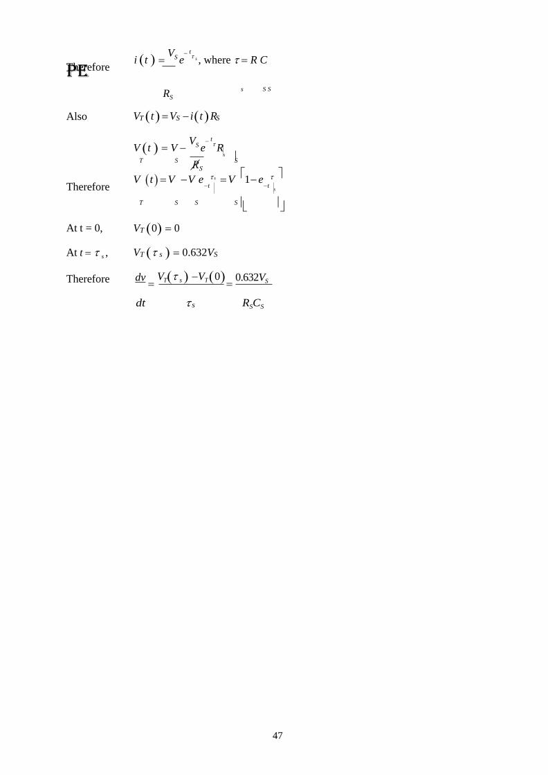
It is possible to use more than one resistor for dv
dt
and discharging as shown in the
figure (d) below. The dv
is limited by R and C . R R limits the discharging current such
that
ITD
dt
VS
R1 R2
1 S 1 2
Fig. (d)
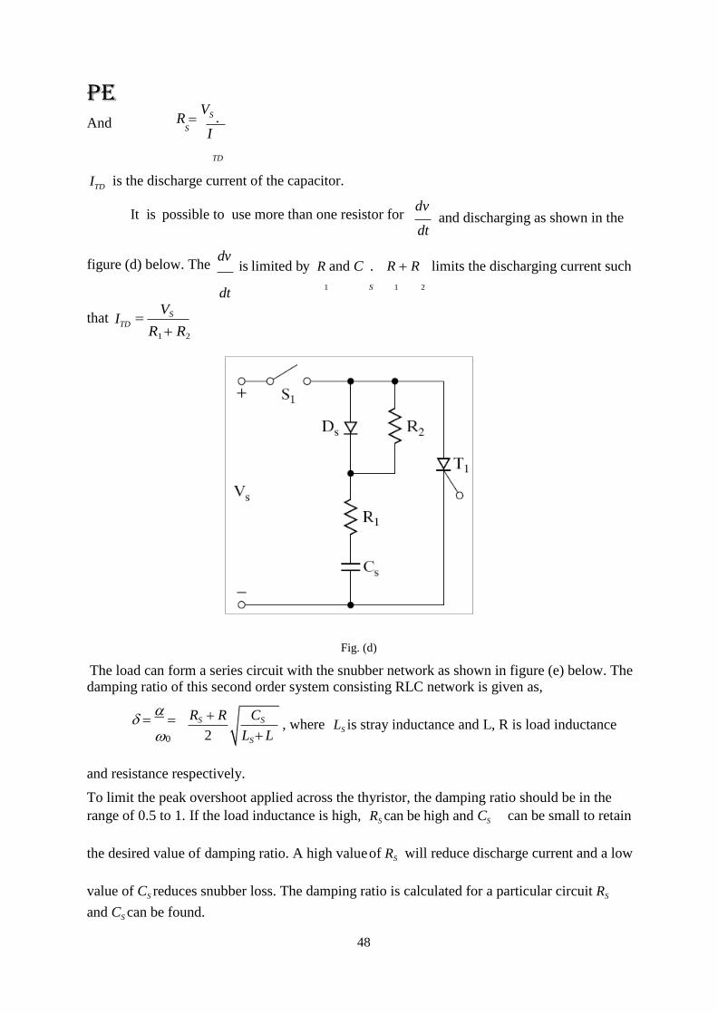
The load can form a series circuit with the snubber network as shown in figure (e) below. The damping ratio of this second order system consisting RLC network is given as,
0
, where
LS is stray inductance and L, R is load inductance
and resistance respectively.
To limit the peak overshoot applied across the thyristor, the damping ratio should be in the
range of 0.5 to 1. If the load inductance is high, RS can be high and CS can be small to retain
the desired value of damping ratio. A high value of RS will reduce discharge current and a low
value of CS reduces snubber loss. The damping ratio is calculated for a particular circuit RS
and CS can be found.
RS R CS
2 LS L
PE
49
Fig. (e)
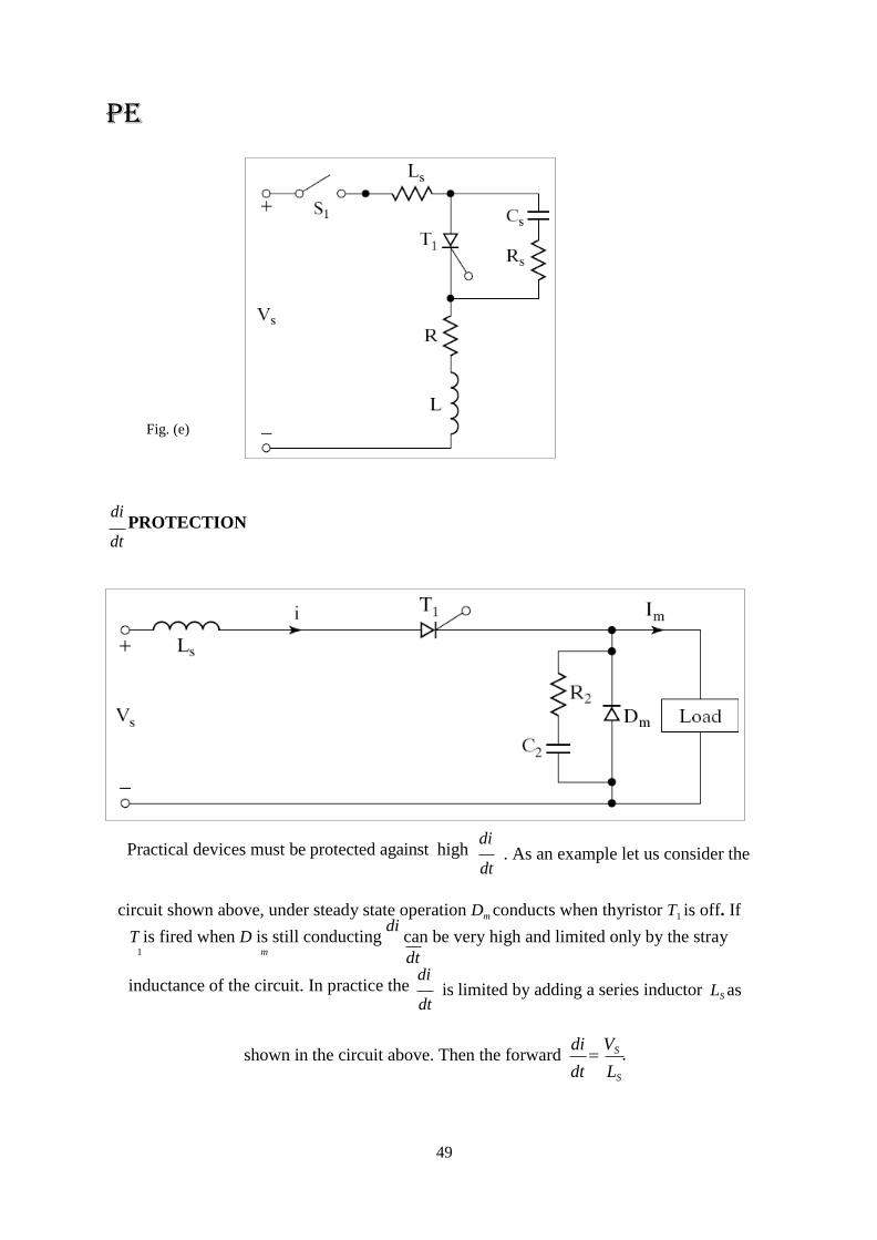
di PROTECTION
dt
Practical devices must be protected against high di
dt
. As an example let us consider the
circuit shown above, under steady state operation Dm conducts when thyristor T1 is off. If
T is fired when D is still conducting di
can be very high and limited only by the stray
1 m dt
inductance of the circuit. In practice the di
dt
is limited by adding a series inductor LS as
shown in the circuit above. Then the forward di
VS .
dt LS

PE
50
SERIES AND PARALLEL OPERATION
SCR ratings have improved considerably since its introduction in 1957. Presently, SCRs with
voltage and current rating of 10kV and 3kA are available. However, for some industrial
applications, the demand for voltage and current ratings is so high that a single SCR cannot
fulfill such requirements. In such cases, SCRs are connected in series in order to meet the high
voltage demand and in parallel for fulfilling high current demand.
The string efficiency that is a term used for measuring the degree of utilization of SCRs in a
string.
String efficiency = Actual voltage / current rating
ns , no. of SCRs voltage / current rating of one SCR
Usually the above ratio is less than one. Since SCRs of same ratings and specifications do not
have identical characteristics unequal voltage / current sharing is bound to occur for all SCRs
in a string. Therefore the string efficiency can never be equal to one.
DERATING FACTOR (DRF)
The use of an extra unit will improve the reliability of a string. A measure of the reliability of the string is given by a factor called derating factor defined as
DRF = 1 - String efficiency
SERIES OPERATION OF SCRS
For high voltage applications two or more Thyristors can be connected in series to provide the
required voltage rating. However due to production spread the characteristics of Thyristors of
the same type are not identical.
STATIC EQUALIZATION
As seen from V-I characteristics, two identical Thyristors to be used in a string do not have the
same off state current for same off-state voltages. If these SCRs are used in a string as such,
unequal voltage distribution would occur. In order to overcome this, we could connect resistors
across individual SCRs to meet the requirement of equal off state currents for the same off state
voltage. But this is not practical therefore we use the same resistor ‘R’ across each SCR to get
fairly uniform voltage distribution.

PE
51
We see that, equal resistors ‘R’ are connected across individual SCR’s which are connected in
series. Let ns be the number of SCRs connected. Let IT be the total current that the string carries
and individual SCRs have leakage currents ID1
, ID 2...............
, IDn
.
As seen from the V-I characteristics, even though the voltage across each SCR is the same, the
leakage current in the off state differ. Let ID1 ID 2 . Since SCR1 has lower leakage current
compared to other SCRs, it will block a higher voltage compared to other SCRs.
Let the leakage current of other SCRs, be such that ID2 ID3 , IDn . Therefore
ID1 IT I1 ................... 1
ID2 IT I2 ................ 2
If VD1 is the voltage across SCR1, then VD1 I1R , and voltage across the rest of the SCRs is
ns 1 I2R .
Therefore total voltage across the string = Vs I1R ns 1 I2R .
But from equation (2) VS I1R ns 1IT ID2
But from equation (1) IT ID1 I1
Therefore

PE
52
VS I1R ns 1ID1 I1 ID2 R
VS VD1 ns 1 I1R ns 1ID1 ID2 R

PE
53
But ID1 ID 2 , VS VD1 ns 1 I1R ns 1ID2 ID1 R
ID 2 ID1 ID = difference between leakage currents of SCR1 and the rest of the SCRs.
Therefore VS VD1 ns 1VD1 nS 1IDR
VS nsVD1 ns 1 IDR ...3
Also R nsVD1 VS
ns 1 ID
VD1max
From equation (3), considering the worst case condition of
VS ns 1 RID2
ns
ID1 0 ,
PE
54
GATE TURN-OFF THYRISTORS
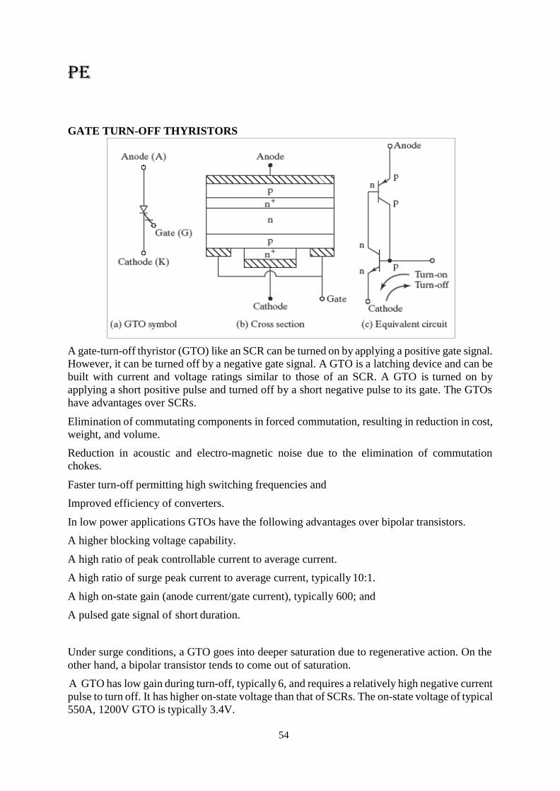
A gate-turn-off thyristor (GTO) like an SCR can be turned on by applying a positive gate signal.
However, it can be turned off by a negative gate signal. A GTO is a latching device and can be
built with current and voltage ratings similar to those of an SCR. A GTO is turned on by
applying a short positive pulse and turned off by a short negative pulse to its gate. The GTOs
have advantages over SCRs.
Elimination of commutating components in forced commutation, resulting in reduction in cost,
weight, and volume.
Reduction in acoustic and electro-magnetic noise due to the elimination of commutation
chokes.
Faster turn-off permitting high switching frequencies and
Improved efficiency of converters.
In low power applications GTOs have the following advantages over bipolar transistors.
A higher blocking voltage capability.
A high ratio of peak controllable current to average current.
A high ratio of surge peak current to average current, typically 10:1.
A high on-state gain (anode current/gate current), typically 600; and
A pulsed gate signal of short duration.
Under surge conditions, a GTO goes into deeper saturation due to regenerative action. On the
other hand, a bipolar transistor tends to come out of saturation.
A GTO has low gain during turn-off, typically 6, and requires a relatively high negative current
pulse to turn off. It has higher on-state voltage than that of SCRs. The on-state voltage of typical
550A, 1200V GTO is typically 3.4V.

PE
55
Controllable peak on-state current ITGQ is the peak value of on-state current which can be
turned off by gate control. The off state voltage is reapplied immediately after turn-off and the
reapplied dv dt is only limited by the snubber capacitance. Once a GTO is turned off, the load
PE
56
current IL , which is diverted through and charges the snubber capacitor, determines the
reapplied dv dt .
Where Cs
is the snubber capacitance
dv
IL
dt Cs
BIDIRECTIONAL TRIODE THYRISTORS
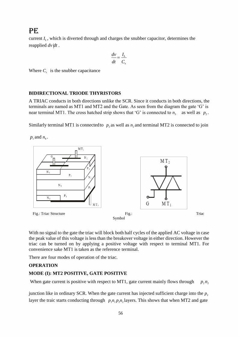
A TRIAC conducts in both directions unlike the SCR. Since it conducts in both directions, the
terminals are named as MT1 and MT2 and the Gate. As seen from the diagram the gate ‘G’ is
near terminal MT1. The cross hatched strip shows that ‘G’ is connected to n3 as well as p2 .
Similarly terminal MT1 is connected to p2 as well as n2 and terminal MT2 is connected to join
p1 and n4 .
Fig.: Triac Structure Fig.: Triac
Symbol
With no signal to the gate the triac will block both half cycles of the applied AC voltage in case
the peak value of this voltage is less than the breakover voltage in either direction. However the
triac can be turned on by applying a positive voltage with respect to terminal MT1. For
convenience sake MT1 is taken as the reference terminal.
There are four modes of operation of the triac.
OPERATION
MODE (I): MT2 POSITIVE, GATE POSITIVE
When gate current is positive with respect to MT1, gate current mainly flows through p2 n2
junction like in ordinary SCR. When the gate current has injected sufficient charge into the p2
layer the traic starts conducting through p1n1 p2n2 layers. This shows that when MT2 and gate

PE
57
are positive with respect to MT1 triac acts like a conventional thyristor. The quadrant of operation is the first quadrant
PE
58
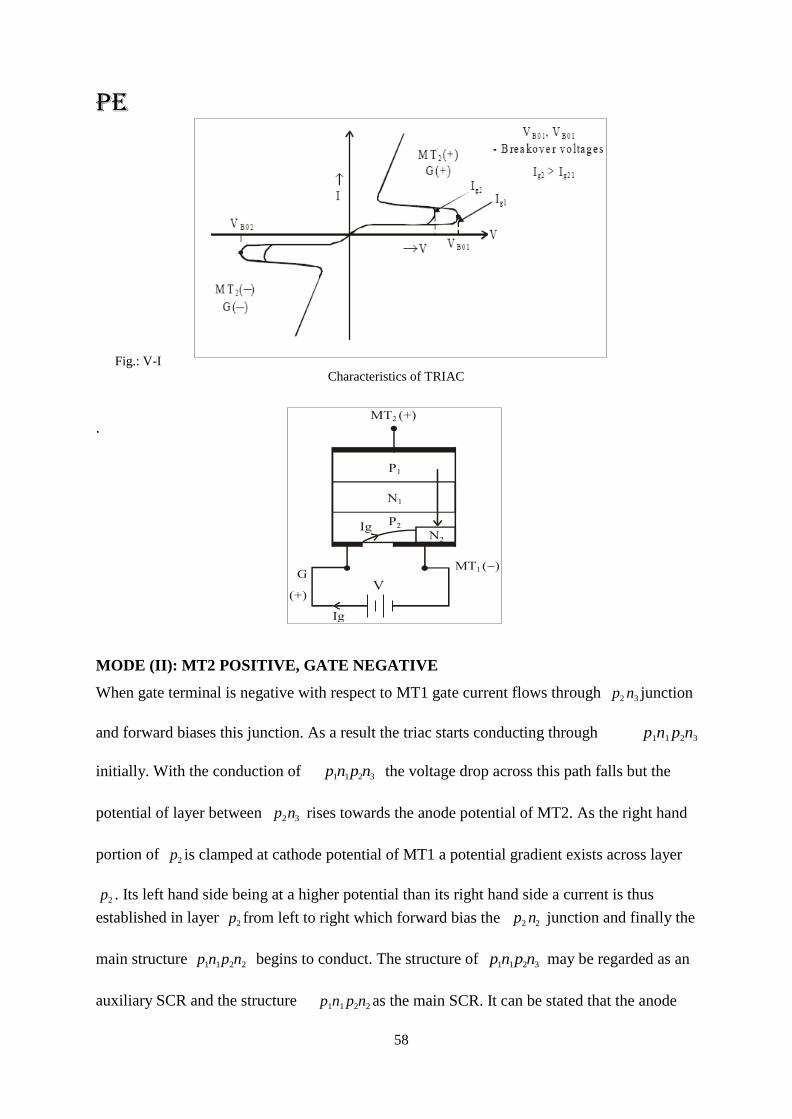
Fig.: V-I
Characteristics of TRIAC
.
MODE (II): MT2 POSITIVE, GATE NEGATIVE
When gate terminal is negative with respect to MT1 gate current flows through
p2 n3 junction
and forward biases this junction. As a result the triac starts conducting through p1n1 p2n3
initially. With the conduction of p1n1 p2n3 the voltage drop across this path falls but the
potential of layer between p2 n3 rises towards the anode potential of MT2. As the right hand
portion of p2 is clamped at cathode potential of MT1 a potential gradient exists across layer
p2 . Its left hand side being at a higher potential than its right hand side a current is thus
established in layer p2 from left to right which forward bias the p2 n2 junction and finally the
main structure p1n1 p2n2 begins to conduct. The structure of p1n1 p2n3 may be regarded as an
auxiliary SCR and the structure p1n1 p2n2 as the main SCR. It can be stated that the anode

PE
59
current of the auxiliary SCR serves as the gate current of the main SCR. This mode of operation
is less sensitive as compared to the previous mode since more gate current is required.
PE
60
2
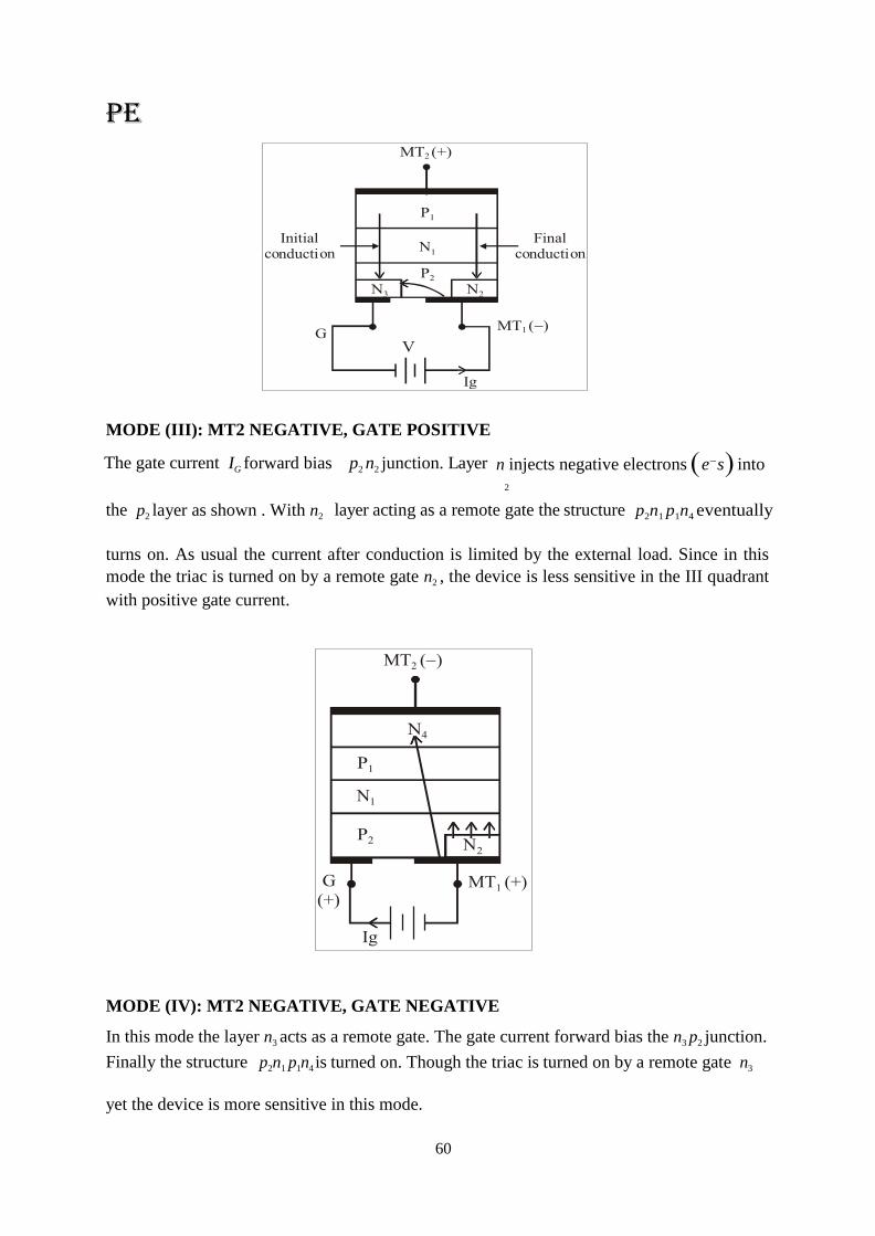
MODE (III): MT2 NEGATIVE, GATE POSITIVE
The gate current IG forward bias p2 n2 junction. Layer n injects negative electrons es into
the p2 layer as shown . With n2 layer acting as a remote gate the structure p2n1 p1n4 eventually
turns on. As usual the current after conduction is limited by the external load. Since in this
mode the triac is turned on by a remote gate n2 , the device is less sensitive in the III quadrant
with positive gate current.
MODE (IV): MT2 NEGATIVE, GATE NEGATIVE
In this mode the layer n3 acts as a remote gate. The gate current forward bias the n3 p2 junction.
Finally the structure p2n1 p1n4 is turned on. Though the triac is turned on by a remote gate n3
yet the device is more sensitive in this mode.
PE
61
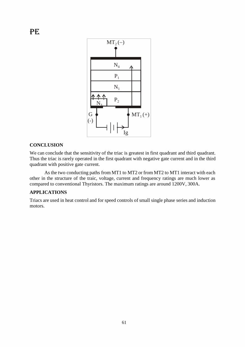
CONCLUSION
We can conclude that the sensitivity of the triac is greatest in first quadrant and third quadrant.
Thus the triac is rarely operated in the first quadrant with negative gate current and in the third
quadrant with positive gate current.
As the two conducting paths from MT1 to MT2 or from MT2 to MT1 interact with each
other in the structure of the traic, voltage, current and frequency ratings are much lower as
compared to conventional Thyristors. The maximum ratings are around 1200V, 300A.
APPLICATIONS
Triacs are used in heat control and for speed controls of small single phase series and induction
motors.
MT2 ()
N4
P1
N1
N3 P2
G (-)
MT1 (+)
Ig

PE
62

PE
63
UNIT-II
Phase control technique – Single phase Line commutated converters
Unlike diode rectifiers, PCRs or phase controlled rectifiers has an advantage of regulating the
output voltage. The diode rectifiers are termed as uncontrolled rectifiers. When these diodes are
switched with Thyristors, then it becomes phase control rectifier. The o/p voltage can be regulated
by changing the firing angle of the Thyristors. The main application of these rectifiers is involved
in speed control of DC motor.
What is a Phase Controlled Rectifier?
The term PCR or Phase controlled rectifier is a one type of rectifier circuit in which the diodes are
switched by Thyristors or SCRs (Silicon Controlled Rectifiers). Whereas the diodes offer no
control over the o/p voltage, the Thyristors can be used to differ the output voltage by adjusting
the firing angle or delay. A phase control Thyristor is activated by applying a short pulse to its gate
terminal and it is deactivated due to line communication or natural. In case of heavy inductive
load, it is deactivated by firing another Thyristor of the rectifier during the negative half cycle of
i/p voltage.
Types of Phase Controlled Rectifier
The phase controlled rectifier is classified into two types based on the type of i/p power supply.
And each kind includes a semi, full and dual converter.
Figure: 2.1. Classification of rectifiers

PE
64
Single-phase Controlled Rectifier
This type of rectifier which works from single phase AC i/p power
supply Single Phase Controlled Rectifiers are classified into
different types
Half wave Controlled Rectifier: This type of rectifier uses a single Thyristor device to provide
o/p control only in one half cycle of input AC supply, and it offers low DC output.
Full wave Controlled Rectifier: This type of rectifier provides higher DC output
Full wave controlled rectifier with a center tapped transformer requires two Thyristors.
Full wave bridge controlled rectifiers do not need a center tapped transformer
Three-phase Controlled Rectifier
This type of rectifier which works from three phase AC i/p power supply
A semi converter is a one quadrant converter that has one polarity of o/p voltage and current.
A full converter is a a two quadrants converter that has polarity of o/p voltage can be either +ve or –ve
but, the current can have only one polarity that is either +ve or -ve.
Dual converter works in four quadrants – both o/p voltage and o/p current can have both the polarities.
Operation of Phase Controlled Rectifier
The basic working principle of a PCR circuit is explained using a single phase half wave PCR
circuit with a RL load resistive shown in the following circuit.
A single phase half wave Thyristor converter circuit is used to convert AC to DC power
conversion. The i/p AC supply is attained from a transformer to offer the required AC supply
voltage to the Thyristor converter based on the o/p DC voltage required. In the above circuit, the
primary and secondary AC supply voltages are denoted with VP and VS.

PE
65
Figure: 2.2. Single phase half wave rectifier circuit
During the +ve half cycle of i/p supply when the upper end of the transformer secondary winding
is at a + ve potential with respect to the lower end, the Thyristor is in a forward biased state.
The thyristor is activated at a delay angle of ωt =α, by applying an appropriate gate trigger pulse
to the gate terminal of thyristor. When the thyristor is activated at a delay angle of ωt =α, the
thyristor behaviors and assuming a perfect thyristor. The thyristor acts as a closed switch and the
i/p supply voltage acts across the load when it conducts from ωt =α to π radians For a purely
resistive load, the load current io that flows when the thyristor T1 is on, is given by the expression.
Io= vo/ RL, for α≤ ωt ≤ π
Applications of Phase Controlled Rectifier
Phase controlled rectifier applications include paper mills, textile mills using DC motor drives and
DC motor control in steel mills.
AC fed traction system using a DC traction motor.
Electro-metallurgical and Electrochemical processes.
Reactor controls.
Magnet power supplies.
Portable hand instrument drives.
2 | P a g e
PE
66
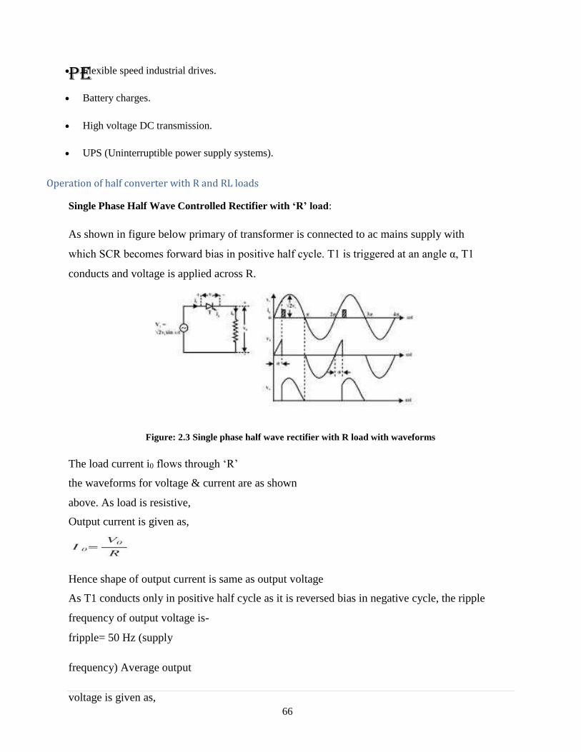
Flexible speed industrial drives.
Battery charges.
High voltage DC transmission.
UPS (Uninterruptible power supply systems).
Operation of half converter with R and RL loads
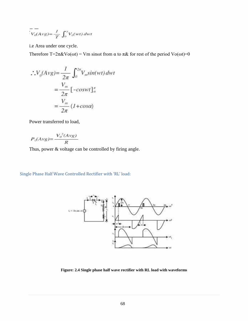
Single Phase Half Wave Controlled Rectifier with ‘R’ load:
As shown in figure below primary of transformer is connected to ac mains supply with
which SCR becomes forward bias in positive half cycle. T1 is triggered at an angle α, T1
conducts and voltage is applied across R.
Figure: 2.3 Single phase half wave rectifier with R load with waveforms
The load current i0 flows through ‘R’
the waveforms for voltage & current are as shown
above. As load is resistive,
Output current is given as,
Hence shape of output current is same as output voltage
As T1 conducts only in positive half cycle as it is reversed bias in negative cycle, the ripple
frequency of output voltage is-
fripple= 50 Hz (supply
frequency) Average output
voltage is given as,

PE
67
PE
68
i.e Area under one cycle.
Therefore T=2π&Vo(ωt) = Vm sinωt from α to π& for rest of the period Vo(ωt)=0
Power transferred to load,
Thus, power & voltage can be controlled by firing angle.
Single Phase Half Wave Controlled Rectifier with ‘RL’ load:
Figure: 2.4 Single phase half wave rectifier with RL load with waveforms

PE
69
Figure above shows the single phase half wave rectifier with RL Load.
Normally motors are inductive loads
L= armature of field coil inductance
R= Resistance of coil.
In positive half cycle, SCR starts conduction at firing angle “α”.
Drop across SCR is small & neglected so output voltage is equal to supply voltage.
Due to ‘RL’ load, current through SCR increases slowly.
At ‘π’, supply voltage is at zero where load current is at its max value.
In positive half cycle, inductor stores energy & that generates the voltage.
In negative half cycle, the voltage developed across inductor, forward biases SCR & maintains its
conduction.
Basically with the property of inductance it opposes change in current.
Output current & supply current flows in same loop, so all the time io=is.
After π the energy of inductor is given to mains & there is flow of ‘io’. The energy reduces as if gets
consumed by circuit so current also reduces.
At ‘β’ energy stored in inductance is finished, hence ‘io’ becomes zero & ‘T1’ turns off.
‘io’ becomes zero from ‘β’ to ‘2π+α’ hence it is discontinuous conduction.

PE
70
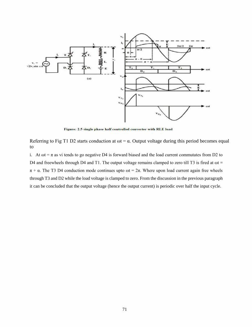
Single phase half controlled converter with RLE load
The diode D2 and D4 conducts for the positive and negative half cycle of the input voltage
waveform respectively. On the other hand T1 starts conduction when it is fired in the positive half
cycle of the input voltage waveform and continuous conduction till T3 is fired in the negative half
cycle. Fig. shows the circuit diagram and the waveforms of a single phase half controlled converter
supplying an R – L – E
load.
PE
71
Referring to Fig T1 D2 starts conduction at ωt = α. Output voltage during this period becomes equal
to
i. At ωt = π as vi tends to go negative D4 is forward biased and the load current commutates from D2 to
D4 and freewheels through D4 and T1. The output voltage remains clamped to zero till T3 is fired at ωt =
π + α. The T3 D4 conduction mode continues upto ωt = 2π. Where upon load current again free wheels
through T3 and D2 while the load voltage is clamped to zero. From the discussion in the previous paragraph
it can be concluded that the output voltage (hence the output current) is periodic over half the input cycle.
PE
72
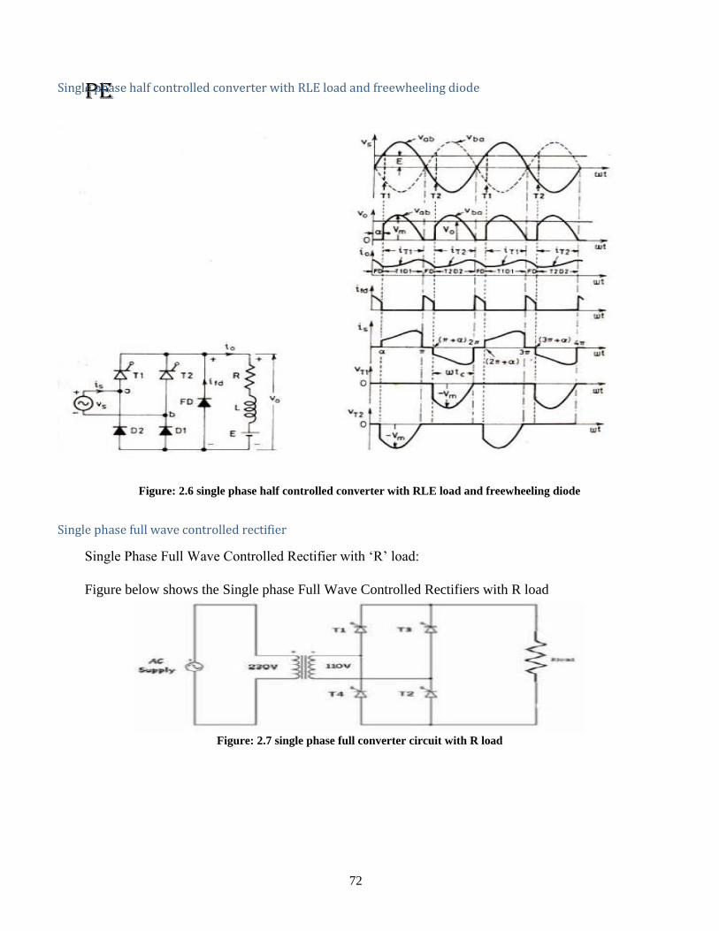
Single phase half controlled converter with RLE load and freewheeling diode
Figure: 2.6 single phase half controlled converter with RLE load and freewheeling diode
Single phase full wave controlled rectifier
Single Phase Full Wave Controlled Rectifier with ‘R’ load:
Figure below shows the Single phase Full Wave Controlled Rectifiers with R load
Figure: 2.7 single phase full converter circuit with R load
PE
73
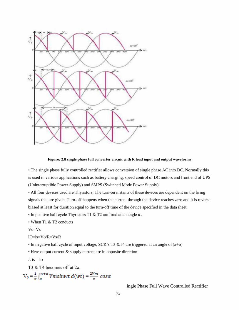
Figure: 2.8 single phase full converter circuit with R load input and output waveforms
• The single phase fully controlled rectifier allows conversion of single phase AC into DC. Normally this
is used in various applications such as battery charging, speed control of DC motors and front end of UPS
(Uninterruptible Power Supply) and SMPS (Switched Mode Power Supply).
• All four devices used are Thyristors. The turn-on instants of these devices are dependent on the firing
signals that are given. Turn-off happens when the current through the device reaches zero and it is reverse
biased at least for duration equal to the turn-off time of the device specified in the data sheet.
• In positive half cycle Thyristors T1 & T2 are fired at an angle α .
• When T1 & T2 conducts
Vo=Vs
IO=is=Vo/R=Vs/R
• In negative half cycle of input voltage, SCR’s T3 &T4 are triggered at an angle of (π+α)
• Here output current & supply current are in opposite direction
∴ is=-io
T3 & T4 becomes off at 2π.
ingle Phase Full Wave Controlled Rectifier
PE
74
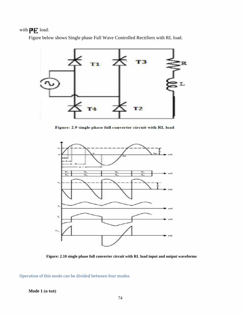
with ‘RL’ load:
Figure below shows Single phase Full Wave Controlled Rectifiers with RL load.
Figure: 2.10 single phase full converter circuit with RL load input and output waveforms
Operation of this mode can be divided between four modes
Mode 1 (α toπ)

PE
75
• In positive half cycle of applied ac signal, SCR’s T1 & T2 are forward bias & can be turned on at an
angle α.
• Load voltage is equal to positive instantaneous ac supply voltage. The load current is positive, ripple
free, constant and equal to Io.
• Due to positive polarity of load voltage & load current, load inductance will store energy.
Mode 2 (π toπ+α)
• At wt=π, input supply is equal to zero & after π it becomes negative. But inductance opposes any
change through it.
• In order to maintain a constant load current & also in same direction. A self inducedemf appears across
‘L’ as shown.
• Due to this induced voltage, SCR’s T1 & T2 are forward bais in spite the negative supply voltage.
• The load voltage is negative & equal to instantaneous ac supply voltage whereas load current is positive.
• Thus, load acts as source & stored energy in inductance is returned back to the ac supply.
Mode 3 (π+α to 2π)
• At wt=π+α SCR’s T3 & T4 are turned on & T1, T2 are reversed bias.
• Thus , process of conduction is transferred from T1,T2 to T3,T4.
• Load voltage again becomes positive & energy is stored in inductor
• T3, T4 conduct in negative half cycle from (π+α) to 2π
• With positive load voltage & load current energy gets stored
Mode 4 (2π to 2π+α)
• At wt=2π, input voltage passes through zero.
• Inductive load will try to oppose any change in current if in order to maintain load current constant & in
the same direction.
• Induced emf is positive & maintains conducting SCR’s T3 & T4 with reverse polarity also.
• Thus VL is negative & equal to instantaneous ac supply voltage. Whereas load current continues to be
positive.
• Thus load acts as source & stored energy in inductance is returned back to ac supply
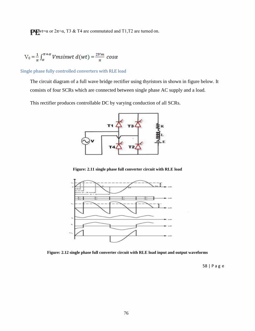
PE
76
• At wt=α or 2π+α, T3 & T4 are commutated and T1,T2 are turned on.
Single phase fully controlled converters with RLE load
The circuit diagram of a full wave bridge rectifier using thyristors in shown in figure below. It
consists of four SCRs which are connected between single phase AC supply and a load.
This rectifier produces controllable DC by varying conduction of all SCRs.
Figure: 2.11 single phase full converter circuit with RLE load
Figure: 2.12 single phase full converter circuit with RLE load input and output waveforms
58 | P a g e

PE
77
In positive half-cycle of the input, Thyristors T1 and T2 are forward biased while T3 and T4 are
reverse biased. Thyristors T1 and T2 are triggered simultaneously at some firing angle in the
positive half cycle, and T3 and T4 are triggered in the negative half cycle.
The load current starts flowing through them when they are in conduction state. The
load for this converter can be RL or RLE depending on the application.
By varying the conduction of each thyristor in the bridge, the average output of this converter
gets controlled. The average value of the output voltage is twice that of half-wave rectifier.
The average output voltage is
Line commutated converters
For single phase half wave converter
PE
78
PE
79
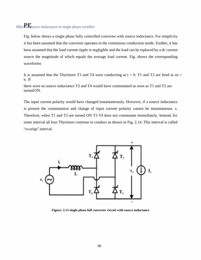
PE
80
Effect of source inductance in single phase rectifier
Fig. below shows a single phase fully controlled converter with source inductance. For simplicity
it has been assumed that the converter operates in the continuous conduction mode. Further, it has
been assumed that the load current ripple is negligible and the load can be replaced by a dc current
source the magnitude of which equals the average load current. Fig. shows the corresponding
waveforms
It is assumed that the Thyristors T3 and T4 were conducting at t = 0. T1 and T2 are fired at ωt =
α. If
there were no source inductance T3 and T4 would have commutated as soon as T1 and T2 are
turned ON.
The input current polarity would have changed instantaneously. However, if a source inductance
is present the commutation and change of input current polarity cannot be instantaneous. s.
Therefore, when T1 and T2 are turned ON T3 T4 does not commutate immediately. Instead, for
some interval all four Thyristors continue to conduct as shown in Fig. 2.14. This interval is called
“overlap” interval.
Figure: 2.13 single phase full converter circuit with source inductance
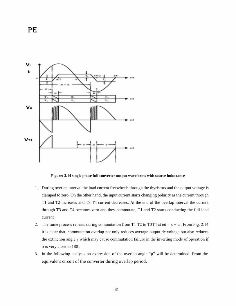
PE
81
Figure: 2.14 single phase full converter output waveforms with source inductance
1. During overlap interval the load current freewheels through the thyristors and the output voltage is
clamped to zero. On the other hand, the input current starts changing polarity as the current through
T1 and T2 increases and T3 T4 current decreases. At the end of the overlap interval the current
through T3 and T4 becomes zero and they commutate, T1 and T2 starts conducting the full load
current
2. The same process repeats during commutation from T1 T2 to T3T4 at ωt = π + α . From Fig. 2.14
it is clear that, commutation overlap not only reduces average output dc voltage but also reduces
the extinction angle γ which may cause commutation failure in the inverting mode of operation if
α is very close to 180º.
3. In the following analysis an expression of the overlap angle “μ” will be determined. From the
equivalent circuit of the converter during overlap period.
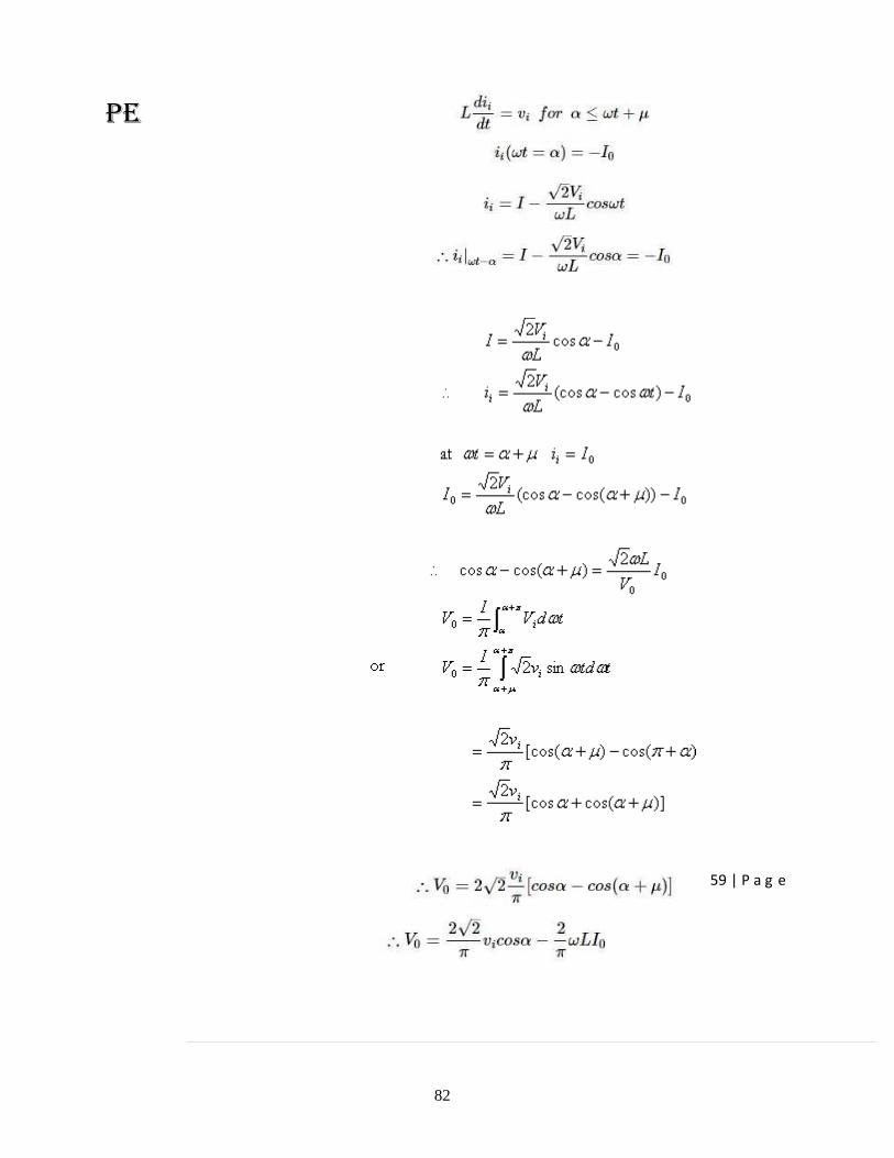
PE
82
59 | P a g e
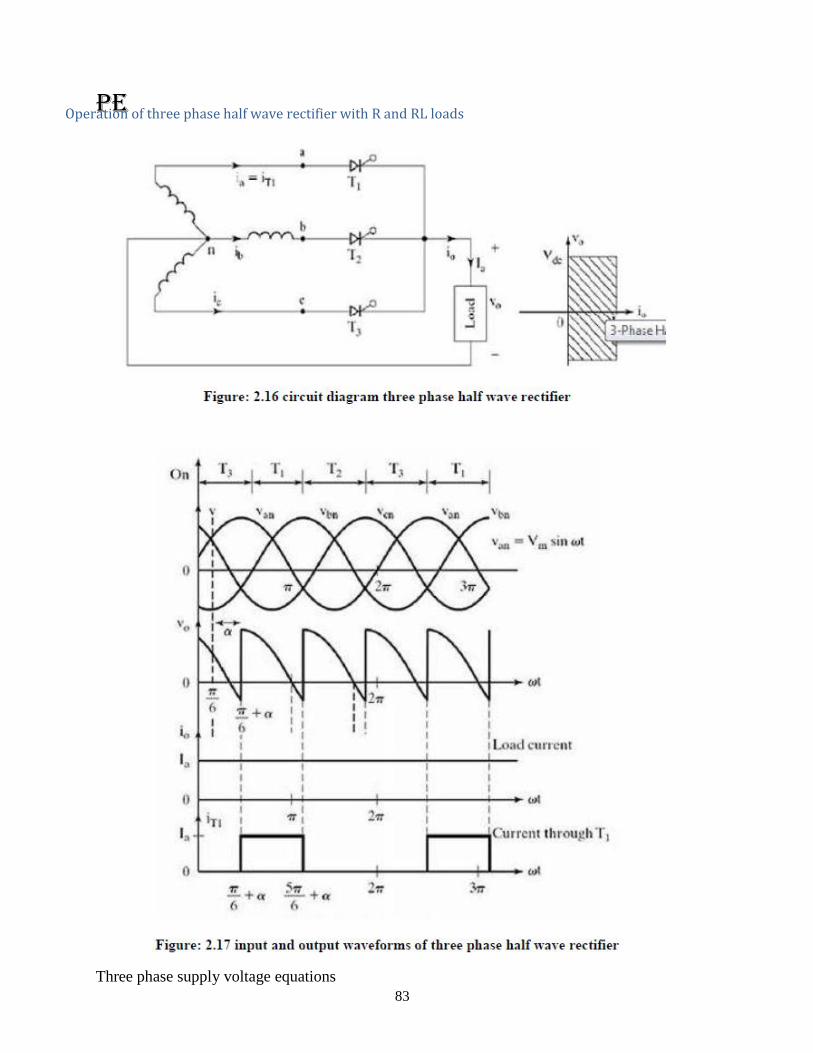
PE
83
Operation of three phase half wave rectifier with R and RL loads
Three phase supply voltage equations
PE
84
The 3-phase half wave converter combines three single phase half wave controlled
rectifiers in one single circuit feeding a common load. The thyristor T 1 in series with one of
the supply phase windings 'a-n' acts as one half wave controlled rectifier The second thyristor
T 2 in series with the supply phase winding 'b-n' acts
as the second half wave controlled rectifier. The third thyristor T3in series with the supply
phase winding acts as the third half wave controlled rectifier. cathode point.
When the thyristor T1 is triggered at ωt=(∏/6 + α)=(30° + α) , the phase voltage Van appears
across the load when T1 conducts. The load current flows through the supply phase winding
'a- n' and through thyristor T1 as long as T1 conducts.
When thyristor T2 is triggered at ωt=(5∏/6α), T1 becomes reverse biased and turns-off. The
load current flows through the thyristor and through the supply phase winding 'b-
n' . When T2 conducts the phase voltage vbn appears across the load until the thyristor T3
is triggered .
When the thyristor T3 is triggered at ωt=(3∏/2 + α)=(270°+α) , T2 is reversed biased and hence
T2turns-off. The phase voltage Van appears across the load when T3 conducts.
The 3-phase input supply is applied through the star connected supply transformer as shown
in the figure. The common neutral point of the supply is connected to one end of the load
while the other end of the load connected to the common
When T1 is triggered again at the beginning of the next input cycle the thyristor T 3 turns off
as it is reverse biased naturally as soon as T1 is triggered. The figure shows the 3-phase
input supply voltages, the output voltage which appears across the load, and the load current
assuming a constant and ripple free load current for a highly inductive load and the current
through the thyristor T1.
For a purely resistive load where the load inductance ‘L = 0’ and the trigger angle α >(∏/6) ,
the load current appears as discontinuous load current and each thyristor is naturally
commutated when the polarity of the corresponding phase supply voltage reverses. The
PE
85
frequency of output
ripple frequency for a 3-phase half wave converter is fs, where fs is the input supply frequency. 3
The 3-phase half wave converter is not normally used in practical converter systems because
of the disadvantage that the supply current waveforms contain dc components (i.e., the
supply current waveforms have an average or dc value).
To derive an expression for the average output voltage of a 3-phase half wave converter for continuous
load current
The reference phase voltage is vRN=van=Vmsinωt. The trigger angle is measured from the
cross over points of the 3-phase supply voltage waveforms. When the phase supply voltage
Van begins its positive half cycle at ωt=0 , the first cross over point appears at
ωt=(∏/6)radians 30°.
The trigger angle α for the thyristor T1 is measured from the cross over point at . The
thyristor T1 is forward biased during the period ωt=30° to 150° , when the phase supply
voltage van has higher amplitude than the other phase supply voltages. Hence T1 can be
triggered between 30° to 150°. When the thyristor T1 is triggered at a trigger angle α, the
average or dc output voltage for continuous load current is calculated using the equation
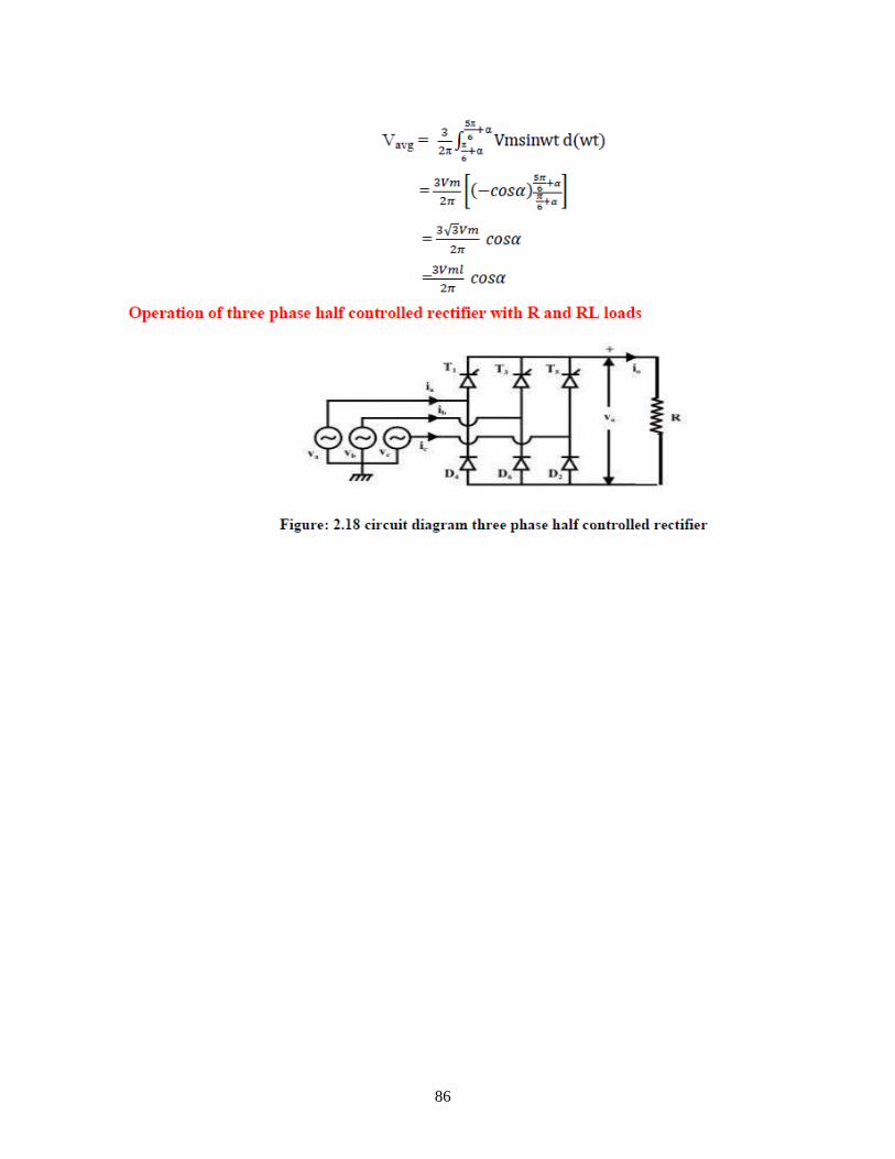
PE
86
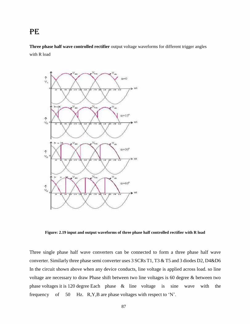
PE
87
Three phase half wave controlled rectifier output voltage waveforms for different trigger angles
with R load
Figure: 2.19 input and output waveforms of three phase half controlled rectifier with R load
Three single phase half wave converters can be connected to form a three phase half wave
converter. Similarly three phase semi converter uses 3 SCRs T1, T3 & T5 and 3 diodes D2, D4&D6
In the circuit shown above when any device conducts, line voltage is applied across load. so line
voltage are necessary to draw Phase shift between two line voltages is 60 degree & between two
phase voltages it is 120 degree Each phase & line voltage is sine wave with the
frequency of 50 Hz. R,Y,B are phase voltages with respect to ‘N’.
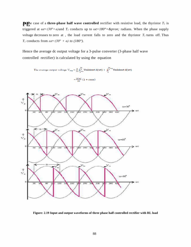
PE
88
In the case of a three-phase half wave controlled rectifier with resistive load, the thyristor T1 is
triggered at ωt=(30°+α)and T1 conducts up to ωt=180°=&pron; radians. When the phase supply
voltage decreases to zero at , the load current falls to zero and the thyristor T1 turns off. Thus
T1 conducts from ωt=(30° + α) to (180°).
Hence the average dc output voltage for a 3-pulse converter (3-phase half wave
controlled rectifier) is calculated by using the equation
=
Figure: 2.19 Input and output waveforms of three phase half controlled rectifier with RL load
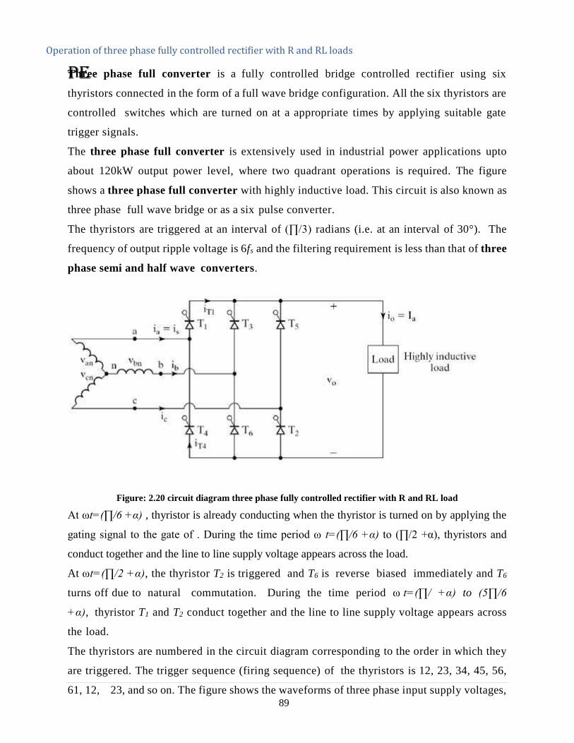
PE
89
Operation of three phase fully controlled rectifier with R and RL loads
Three phase full converter is a fully controlled bridge controlled rectifier using six
thyristors connected in the form of a full wave bridge configuration. All the six thyristors are
controlled switches which are turned on at a appropriate times by applying suitable gate
trigger signals.
The three phase full converter is extensively used in industrial power applications upto
about 120kW output power level, where two quadrant operations is required. The figure
shows a three phase full converter with highly inductive load. This circuit is also known as
three phase full wave bridge or as a six pulse converter.
The thyristors are triggered at an interval of (∏/3) radians (i.e. at an interval of 30°). The
frequency of output ripple voltage is 6fs and the filtering requirement is less than that of three
phase semi and half wave converters.
Figure: 2.20 circuit diagram three phase fully controlled rectifier with R and RL load
At ωt=(∏/6 +α) , thyristor is already conducting when the thyristor is turned on by applying the
gating signal to the gate of . During the time period ω t=(∏/6 +α) to (∏/2 +α), thyristors and
conduct together and the line to line supply voltage appears across the load.
At ωt=(∏/2 +α), the thyristor T2 is triggered and T6 is reverse biased immediately and T6
turns off due to natural commutation. During the time period ω t=(∏/ +α) to (5∏/6
+α), thyristor T1 and T2 conduct together and the line to line supply voltage appears across
the load.
The thyristors are numbered in the circuit diagram corresponding to the order in which they
are triggered. The trigger sequence (firing sequence) of the thyristors is 12, 23, 34, 45, 56,
61, 12, 23, and so on. The figure shows the waveforms of three phase input supply voltages,

PE
90
output voltage, the thyristor current through T1 and T4, the supply current through the line
‘a’.
We define three line neutral voltages (3 phase voltages) as
follows VRN
To derive an expression for the average output voltage of three phase full converter with highly
inductive load assuming continuous and constant load current
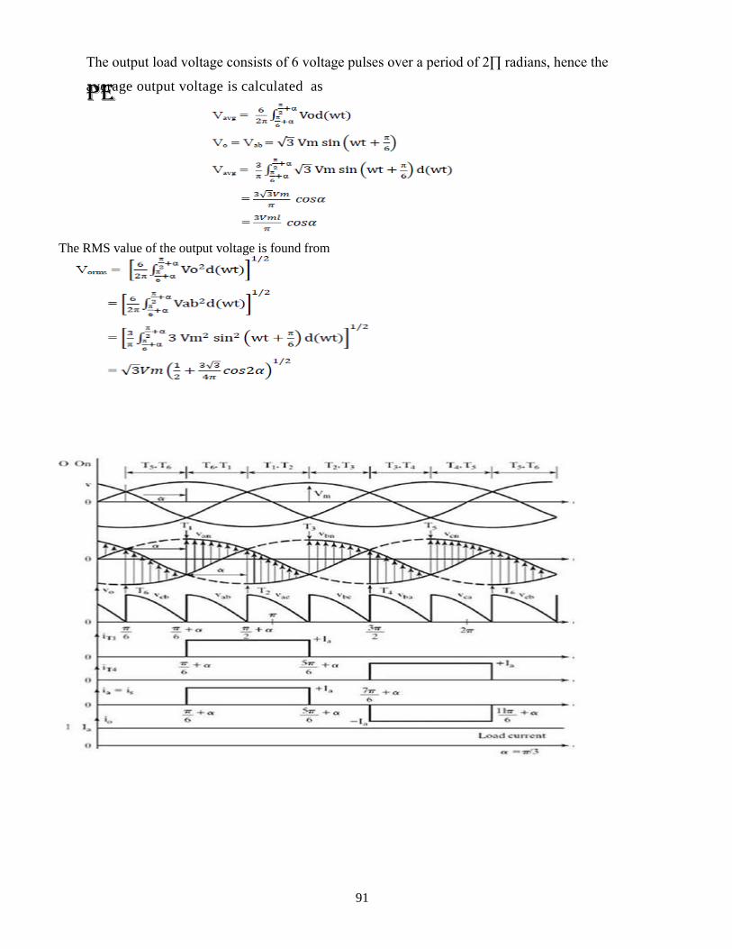
PE
91
The output load voltage consists of 6 voltage pulses over a period of 2∏ radians, hence the
average output voltage is calculated as
The RMS value of the output voltage is found from
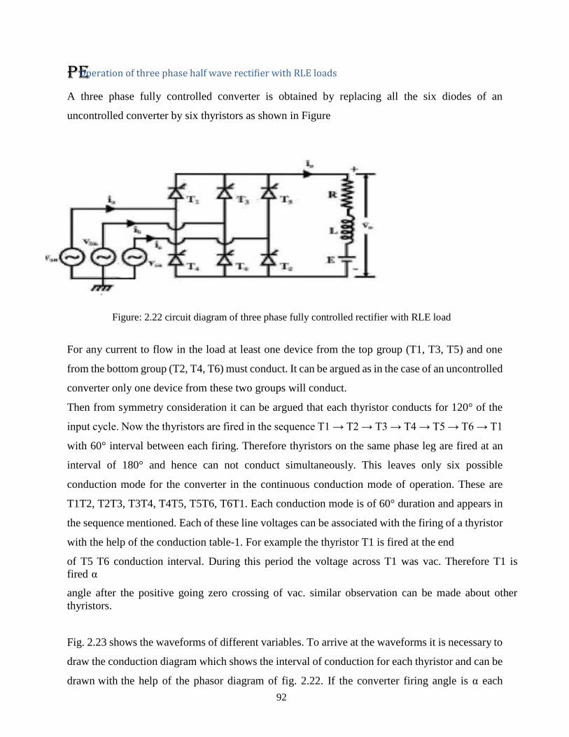
PE
92
Operation of three phase half wave rectifier with RLE loads
A three phase fully controlled converter is obtained by replacing all the six diodes of an
uncontrolled converter by six thyristors as shown in Figure
Figure: 2.22 circuit diagram of three phase fully controlled rectifier with RLE load
For any current to flow in the load at least one device from the top group (T1, T3, T5) and one
from the bottom group (T2, T4, T6) must conduct. It can be argued as in the case of an uncontrolled
converter only one device from these two groups will conduct.
Then from symmetry consideration it can be argued that each thyristor conducts for 120° of the
input cycle. Now the thyristors are fired in the sequence T1 → T2 → T3 → T4 → T5 → T6 → T1
with 60° interval between each firing. Therefore thyristors on the same phase leg are fired at an
interval of 180° and hence can not conduct simultaneously. This leaves only six possible
conduction mode for the converter in the continuous conduction mode of operation. These are
T1T2, T2T3, T3T4, T4T5, T5T6, T6T1. Each conduction mode is of 60° duration and appears in
the sequence mentioned. Each of these line voltages can be associated with the firing of a thyristor
with the help of the conduction table-1. For example the thyristor T1 is fired at the end
of T5 T6 conduction interval. During this period the voltage across T1 was vac. Therefore T1 is
fired α
angle after the positive going zero crossing of vac. similar observation can be made about other
thyristors.
Fig. 2.23 shows the waveforms of different variables. To arrive at the waveforms it is necessary to
draw the conduction diagram which shows the interval of conduction for each thyristor and can be
drawn with the help of the phasor diagram of fig. 2.22. If the converter firing angle is α each
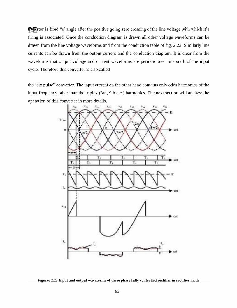
PE
93
thyristor is fired “α”angle after the positive going zero crossing of the line voltage with which it’s
firing is associated. Once the conduction diagram is drawn all other voltage waveforms can be
drawn from the line voltage waveforms and from the conduction table of fig. 2.22. Similarly line
currents can be drawn from the output current and the conduction diagram. It is clear from the
waveforms that output voltage and current waveforms are periodic over one sixth of the input
cycle. Therefore this converter is also called
the “six pulse” converter. The input current on the other hand contains only odds harmonics of the
input frequency other than the triplex (3rd, 9th etc.) harmonics. The next section will analyze the
operation of this converter in more details.
Figure: 2.23 Input and output waveforms of three phase fully controlled rectifier in rectifier mode

PE
94
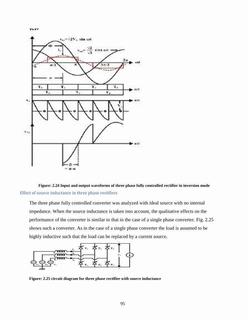
PE
95
Figure: 2.24 Input and output waveforms of three phase fully controlled rectifier in inversion mode
Effect of source inductance in three phase rectifiers
The three phase fully controlled converter was analyzed with ideal source with no internal
impedance. When the source inductance is taken into account, the qualitative effects on the
performance of the converter is similar to that in the case of a single phase converter. Fig. 2.25
shows such a converter. As in the case of a single phase converter the load is assumed to be
highly inductive such that the load can be replaced by a current source.
Figure: 2.25 circuit diagram for three phase rectifier with source inductance
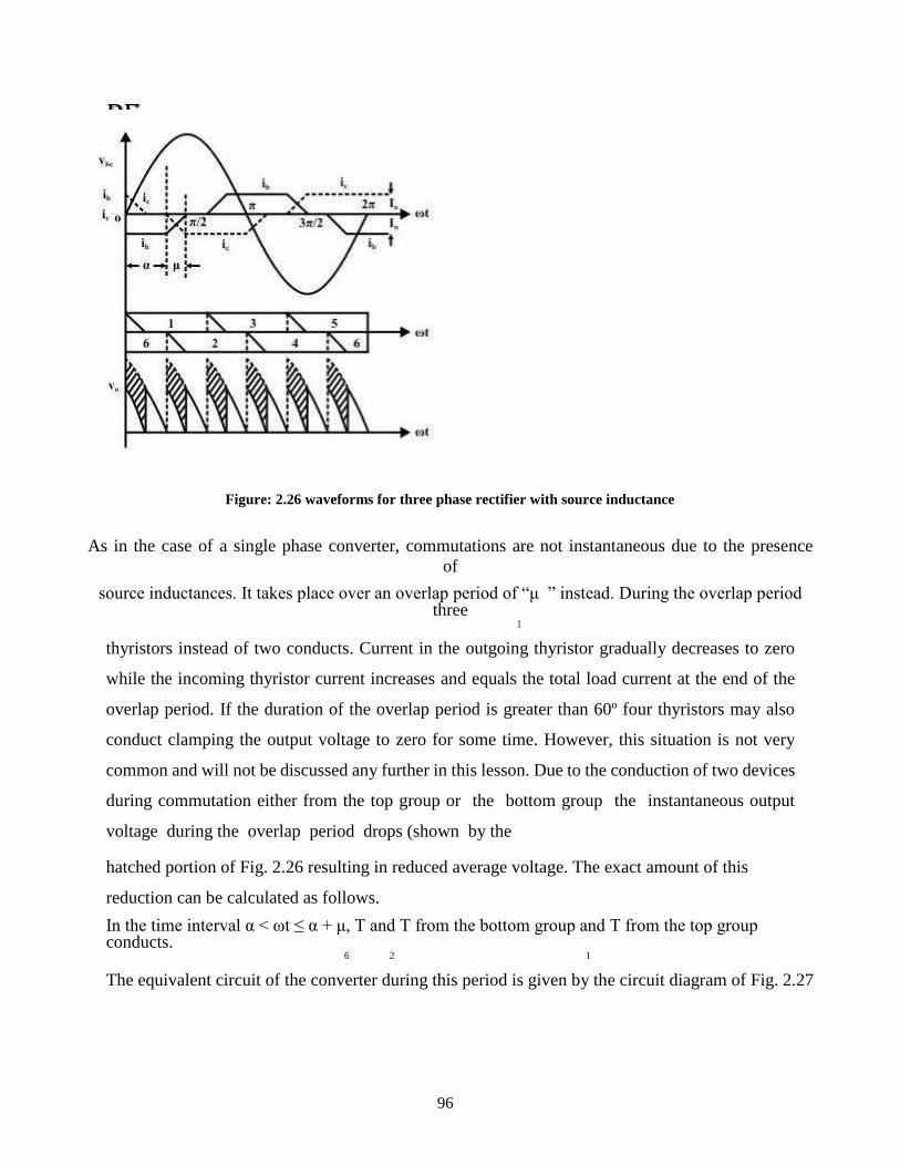
PE
96
Figure: 2.26 waveforms for three phase rectifier with source inductance
As in the case of a single phase converter, commutations are not instantaneous due to the presence
of
source inductances. It takes place over an overlap period of “μ ” instead. During the overlap period three
1
thyristors instead of two conducts. Current in the outgoing thyristor gradually decreases to zero
while the incoming thyristor current increases and equals the total load current at the end of the
overlap period. If the duration of the overlap period is greater than 60º four thyristors may also
conduct clamping the output voltage to zero for some time. However, this situation is not very
common and will not be discussed any further in this lesson. Due to the conduction of two devices
during commutation either from the top group or the bottom group the instantaneous output
voltage during the overlap period drops (shown by the
hatched portion of Fig. 2.26 resulting in reduced average voltage. The exact amount of this
reduction can be calculated as follows.
In the time interval α < ωt ≤ α + μ, T and T from the bottom group and T from the top group conducts.
6 2 1
The equivalent circuit of the converter during this period is given by the circuit diagram of Fig. 2.27
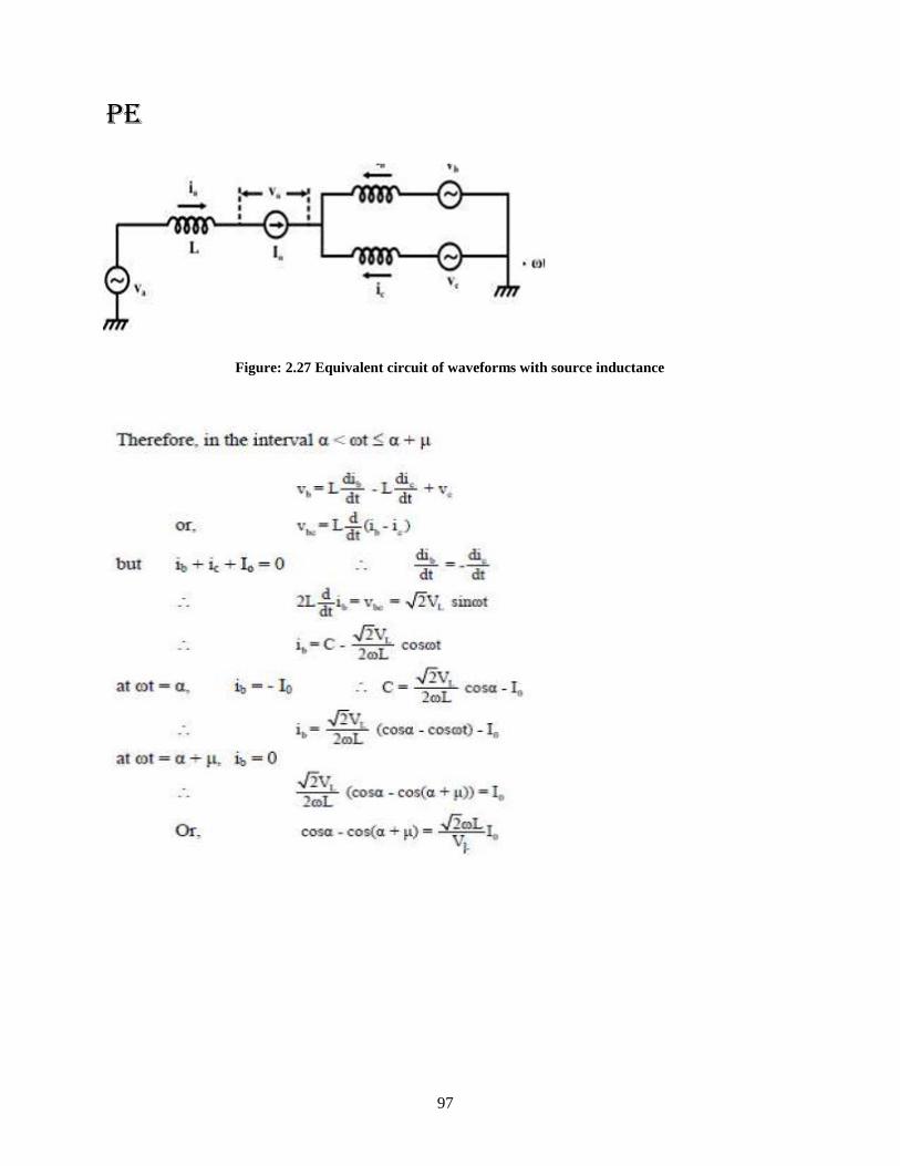
PE
97
Figure: 2.27 Equivalent circuit of waveforms with source inductance
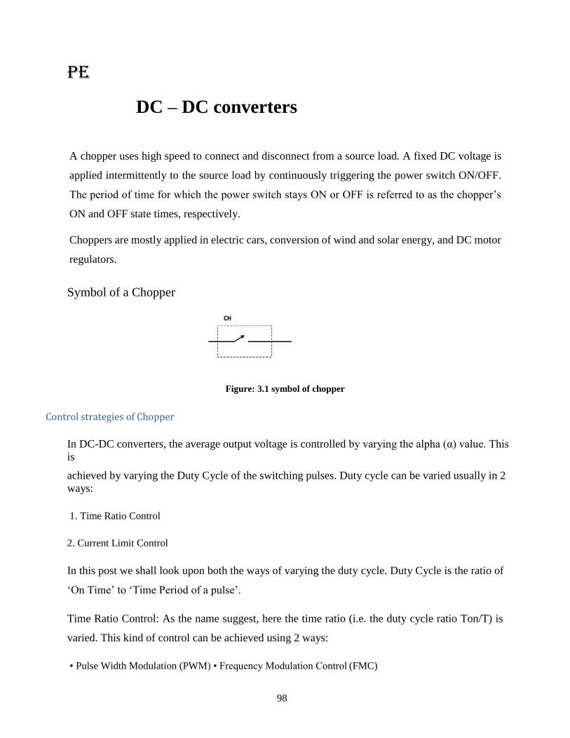
PE
98
DC – DC converters
A chopper uses high speed to connect and disconnect from a source load. A fixed DC voltage is
applied intermittently to the source load by continuously triggering the power switch ON/OFF.
The period of time for which the power switch stays ON or OFF is referred to as the chopper’s
ON and OFF state times, respectively.
Choppers are mostly applied in electric cars, conversion of wind and solar energy, and DC motor
regulators.
Symbol of a Chopper
Figure: 3.1 symbol of chopper
Control strategies of Chopper
In DC-DC converters, the average output voltage is controlled by varying the alpha (α) value. This
is
achieved by varying the Duty Cycle of the switching pulses. Duty cycle can be varied usually in 2
ways:
1. Time Ratio Control
2. Current Limit Control
In this post we shall look upon both the ways of varying the duty cycle. Duty Cycle is the ratio of
‘On Time’ to ‘Time Period of a pulse’.
Time Ratio Control: As the name suggest, here the time ratio (i.e. the duty cycle ratio Ton/T) is
varied. This kind of control can be achieved using 2 ways:
• Pulse Width Modulation (PWM) • Frequency Modulation Control (FMC)
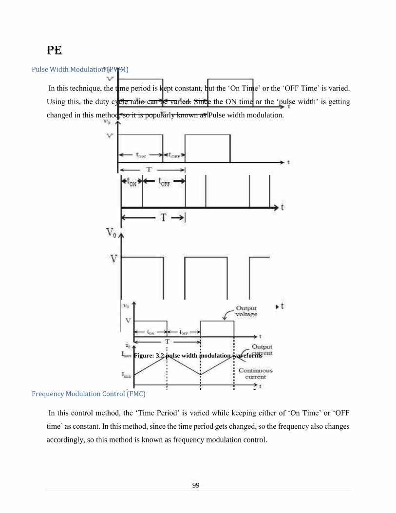
PE
99
Pulse Width Modulation (PWM)
In this technique, the time period is kept constant, but the ‘On Time’ or the ‘OFF Time’ is varied.
Using this, the duty cycle ratio can be varied. Since the ON time or the ‘pulse width’ is getting
changed in this method, so it is popularly known as Pulse width modulation.
Figure: 3.2 pulse width modulation waveforms
Frequency Modulation Control (FMC)
In this control method, the ‘Time Period’ is varied while keeping either of ‘On Time’ or ‘OFF
time’ as constant. In this method, since the time period gets changed, so the frequency also changes
accordingly, so this method is known as frequency modulation control.

PE
100
Figure: 3.3 Frequency modulation waveforms
Current Limit Control:
As is obvious from its name, in this control strategy, a specific limit is applied on the current
variation.
In this method, current is allowed to fluctuate or change only between 2 values i.e. maximum
current (I max) and minimum current (I min). When the current is at minimum value, the chopper
is switched ON. After this instance, the current starts increasing, and when it reaches up to
maximum value, the chopper is switched off allowing the current to fall back to minimum value.
This cycle continues again and again.
Figure: 3.4 current limit control waveforms
Classification of Choppers
Depending on the voltage output, choppers are classified as −

PE
101
1. Step Up chopper (boost converter)
2. Step Down Chopper(Buck converter)
3. Step Up/Down Chopper (Buck-boost converter)
Depending upon the direction of the output current and voltage, the converters can be classified into
five classes namely
1. Class A [One-quadrant Operation]
2. Class B [One-quadrant Operation]
3. Class C [Two-quadrant Operation]
4. Class D Chopper [Two-quadrant Operation]
5. Class E Chopper [Four-quadrant Operation]
Step Down Chopper
This is also known as a buck converter. In this chopper, the average voltage output VO is less
than the input voltage VS. When the chopper is ON, VO = VS and when the chopper is off, VO =
0
When the chopper is ON −
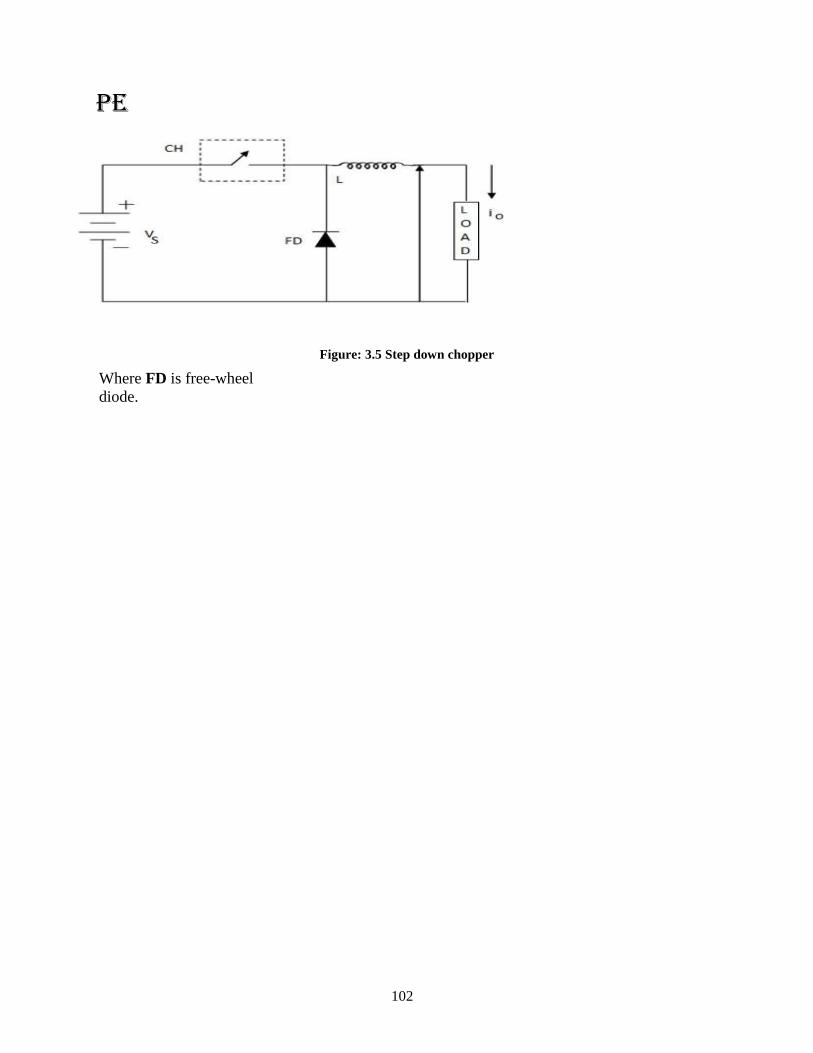
PE
102
Where FD is free-wheel
diode.
Figure: 3.5 Step down chopper
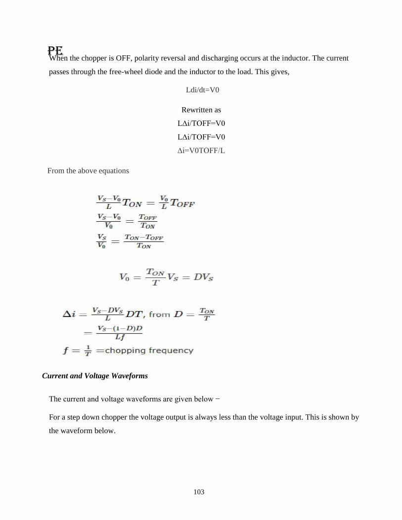
PE
103
When the chopper is OFF, polarity reversal and discharging occurs at the inductor. The current
passes through the free-wheel diode and the inductor to the load. This gives,
Ldi/dt=V0
Rewritten as
LΔi/TOFF=V0
LΔi/TOFF=V0
Δi=V0TOFF/L
From the above equations
Current and Voltage Waveforms
The current and voltage waveforms are given below −
For a step down chopper the voltage output is always less than the voltage input. This is shown by
the waveform below.
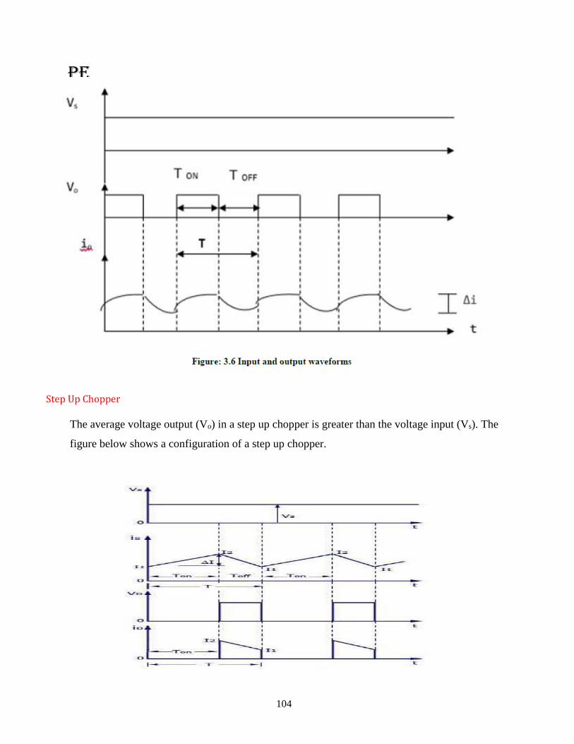
PE
104
Step Up Chopper
The average voltage output (Vo) in a step up chopper is greater than the voltage input (Vs). The
figure below shows a configuration of a step up chopper.
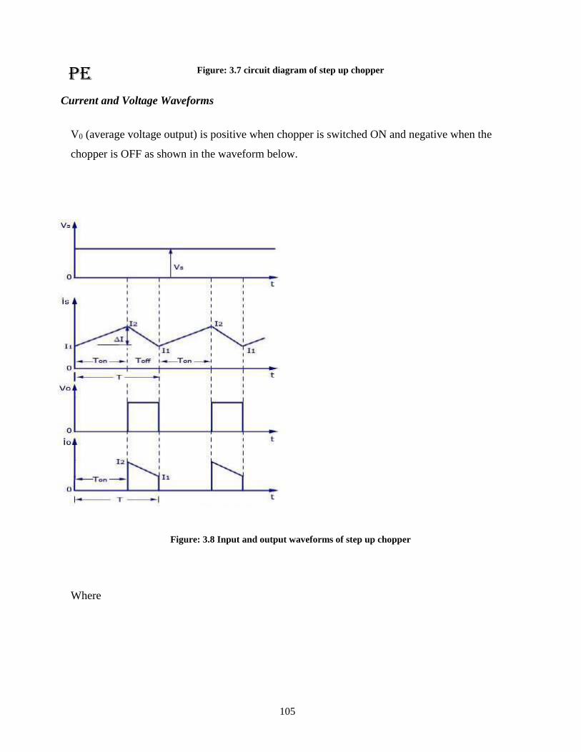
PE
105
Figure: 3.7 circuit diagram of step up chopper
Current and Voltage Waveforms
V0 (average voltage output) is positive when chopper is switched ON and negative when the
chopper is OFF as shown in the waveform below.
Figure: 3.8 Input and output waveforms of step up chopper
Where
PE
106
,
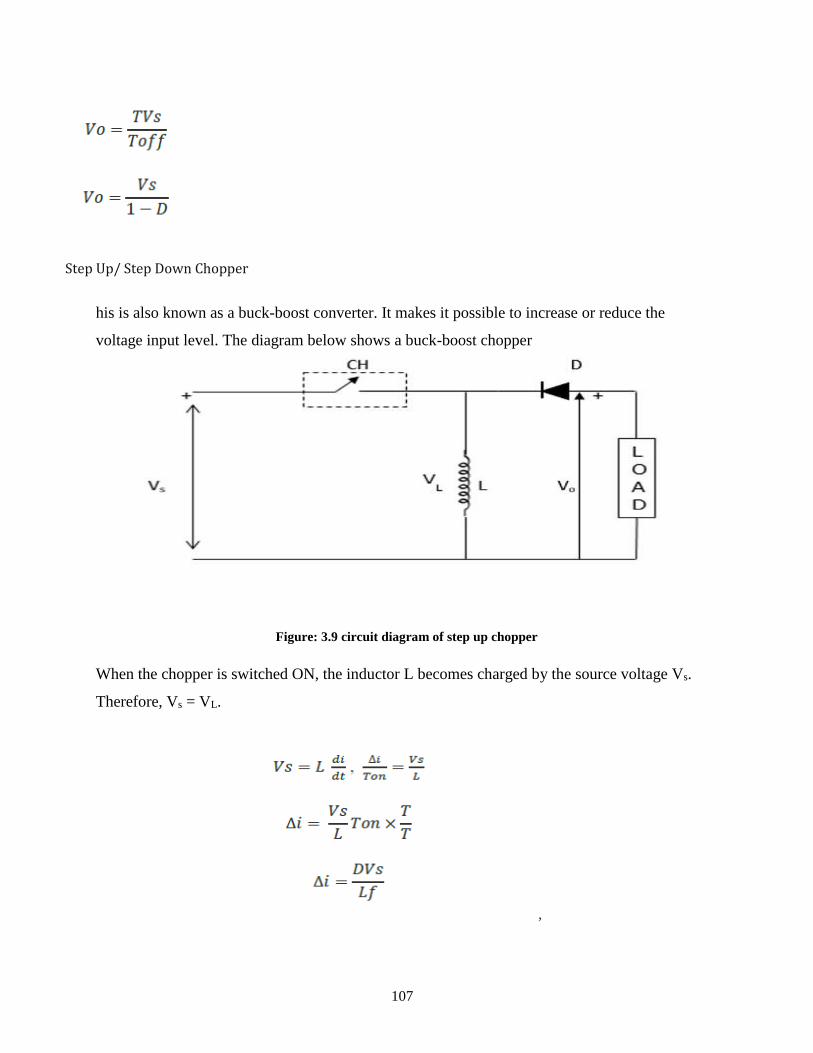
PE
107
Step Up/ Step Down Chopper
his is also known as a buck-boost converter. It makes it possible to increase or reduce the
voltage input level. The diagram below shows a buck-boost chopper
Figure: 3.9 circuit diagram of step up chopper
When the chopper is switched ON, the inductor L becomes charged by the source voltage Vs.
Therefore, Vs = VL.
,

PE
108
When the chopper is switched OFF, the inductor’s polarity reverses and this causes it to discharge
through the diode and the load.
Principle of operation of class A chopper
Class A Chopper is a first quadrant chopper
• When chopper is ON, supply voltage V is connected across the load.
• When chopper is OFF, vO = 0 and the load current continues to flow in the same direction through the
FWD.
• The average values of output voltage and current are always positive. Class A Chopper is a first
quadrant chopper
• When chopper is ON, supply voltage V is connected across the load.
• When chopper is OFF, vO = 0 and the load current continues to flow in the same direction through the
FWD.
• The average values of output voltage and current are always positive.
• Class A Chopper is a step-down chopper in which power always flows form source to load.
• It is used to control the speed of dc motor.
• The output current equations obtained in step down chopper with R-L load can be used to study the
performance of Class A Chopper.
79 | P a g e
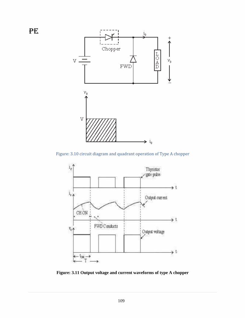
PE
109
Figure: 3.10 circuit diagram and quadrant operation of Type A chopper
Figure: 3.11 Output voltage and current waveforms of type A chopper
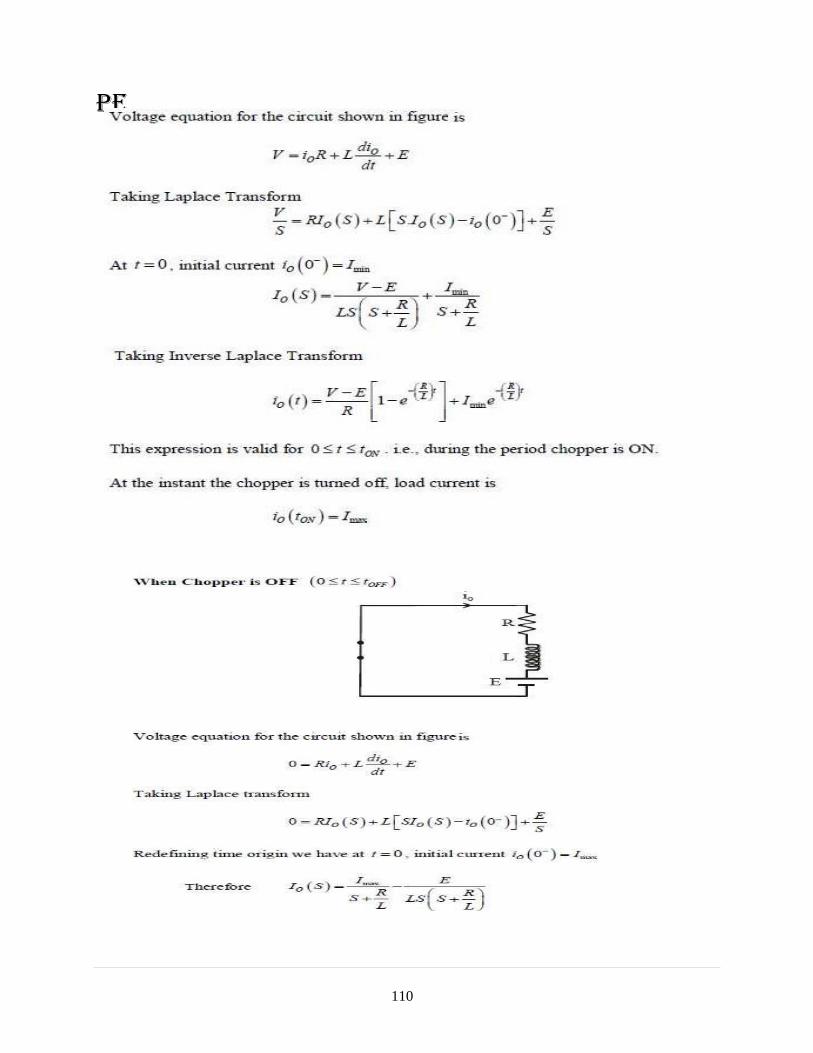
PE
110
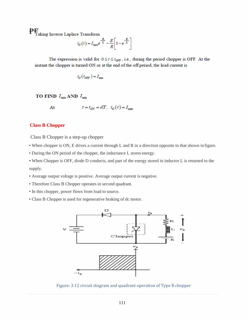
PE
111
Class B Chopper
Class B Chopper is a step-up chopper
• When chopper is ON, E drives a current through L and R in a direction opposite to that shown in figure.
• During the ON period of the chopper, the inductance L stores energy.
• When Chopper is OFF, diode D conducts, and part of the energy stored in inductor L is returned to the
supply.
• Average output voltage is positive. Average output current is negative.
• Therefore Class B Chopper operates in second quadrant.
• In this chopper, power flows from load to source.
• Class B Chopper is used for regenerative braking of dc motor.
Figure: 3.12 circuit diagram and quadrant operation of Type B chopper
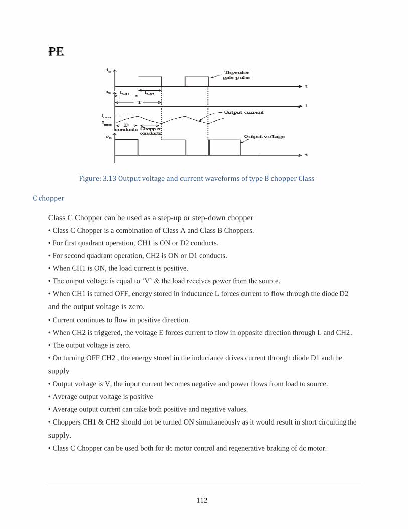
PE
112
Figure: 3.13 Output voltage and current waveforms of type B chopper Class
C chopper
Class C Chopper can be used as a step-up or step-down chopper
• Class C Chopper is a combination of Class A and Class B Choppers.
• For first quadrant operation, CH1 is ON or D2 conducts.
• For second quadrant operation, CH2 is ON or D1 conducts.
• When CH1 is ON, the load current is positive.
• The output voltage is equal to ‘V’ & the load receives power from the source.
• When CH1 is turned OFF, energy stored in inductance L forces current to flow through the diode D2
and the output voltage is zero.
• Current continues to flow in positive direction.
• When CH2 is triggered, the voltage E forces current to flow in opposite direction through L and CH2 .
• The output voltage is zero.
• On turning OFF CH2 , the energy stored in the inductance drives current through diode D1 and the
supply
• Output voltage is V, the input current becomes negative and power flows from load to source.
• Average output voltage is positive
• Average output current can take both positive and negative values.
• Choppers CH1 & CH2 should not be turned ON simultaneously as it would result in short circuiting the
supply.
• Class C Chopper can be used both for dc motor control and regenerative braking of dc motor.
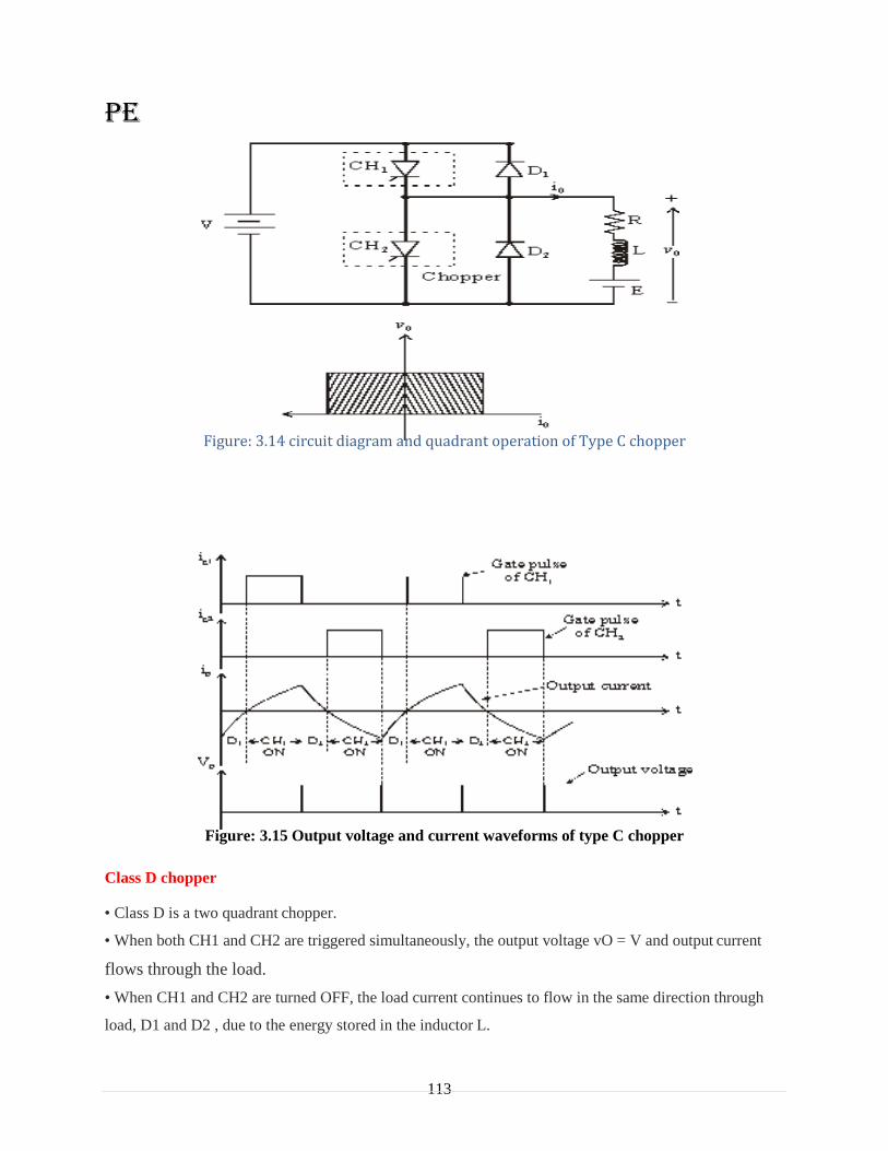
PE
113
Figure: 3.14 circuit diagram and quadrant operation of Type C chopper
Figure: 3.15 Output voltage and current waveforms of type C chopper
Class D chopper
• Class D is a two quadrant chopper.
• When both CH1 and CH2 are triggered simultaneously, the output voltage vO = V and output current
flows through the load.
• When CH1 and CH2 are turned OFF, the load current continues to flow in the same direction through
load, D1 and D2 , due to the energy stored in the inductor L.
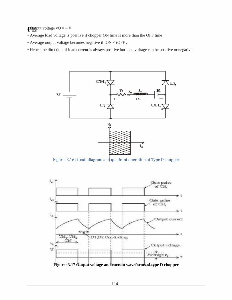
PE
114
• Output voltage vO = – V.
• Average load voltage is positive if chopper ON time is more than the OFF time
• Average output voltage becomes negative if tON < tOFF .
• Hence the direction of load current is always positive but load voltage can be positive or negative.
Figure: 3.16 circuit diagram and quadrant operation of Type D chopper
Figure: 3.17 Output voltage and current waveforms of type D chopper
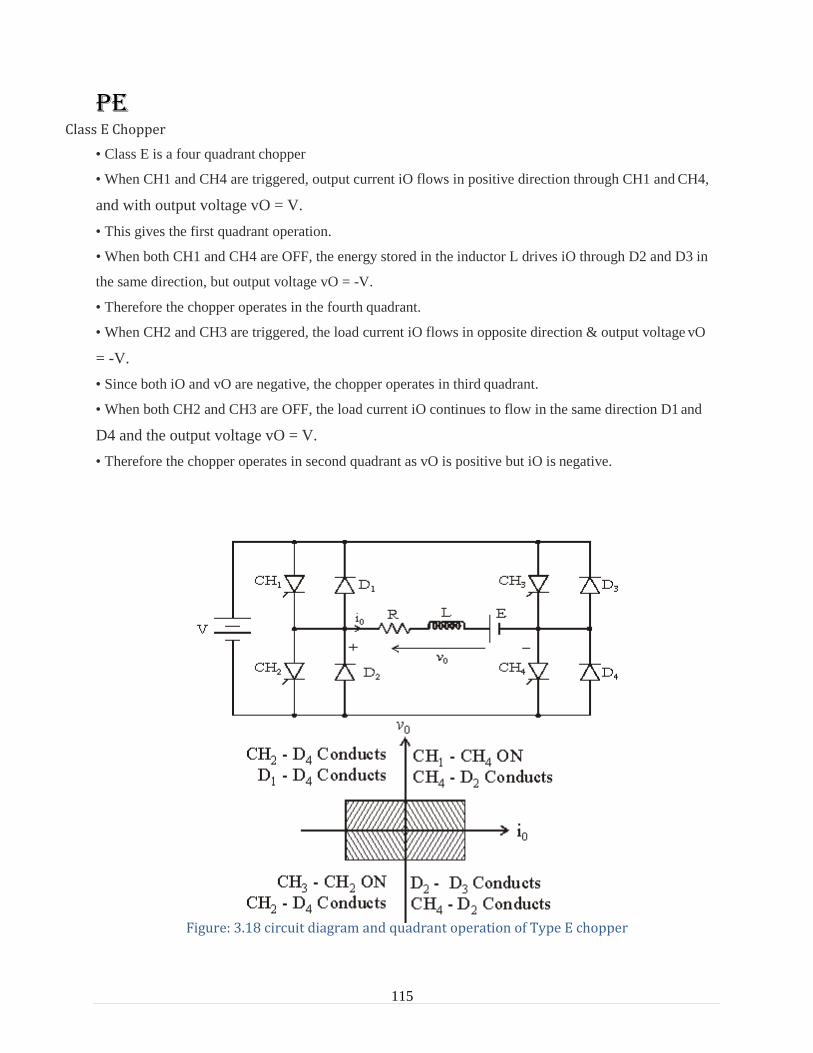
PE
115
Class E Chopper
• Class E is a four quadrant chopper
• When CH1 and CH4 are triggered, output current iO flows in positive direction through CH1 and CH4,
and with output voltage vO = V.
• This gives the first quadrant operation.
• When both CH1 and CH4 are OFF, the energy stored in the inductor L drives iO through D2 and D3 in
the same direction, but output voltage vO = -V.
• Therefore the chopper operates in the fourth quadrant.
• When CH2 and CH3 are triggered, the load current iO flows in opposite direction & output voltage vO
= -V.
• Since both iO and vO are negative, the chopper operates in third quadrant.
• When both CH2 and CH3 are OFF, the load current iO continues to flow in the same direction D1 and
D4 and the output voltage vO = V.
• Therefore the chopper operates in second quadrant as vO is positive but iO is negative.
Figure: 3.18 circuit diagram and quadrant operation of Type E chopper
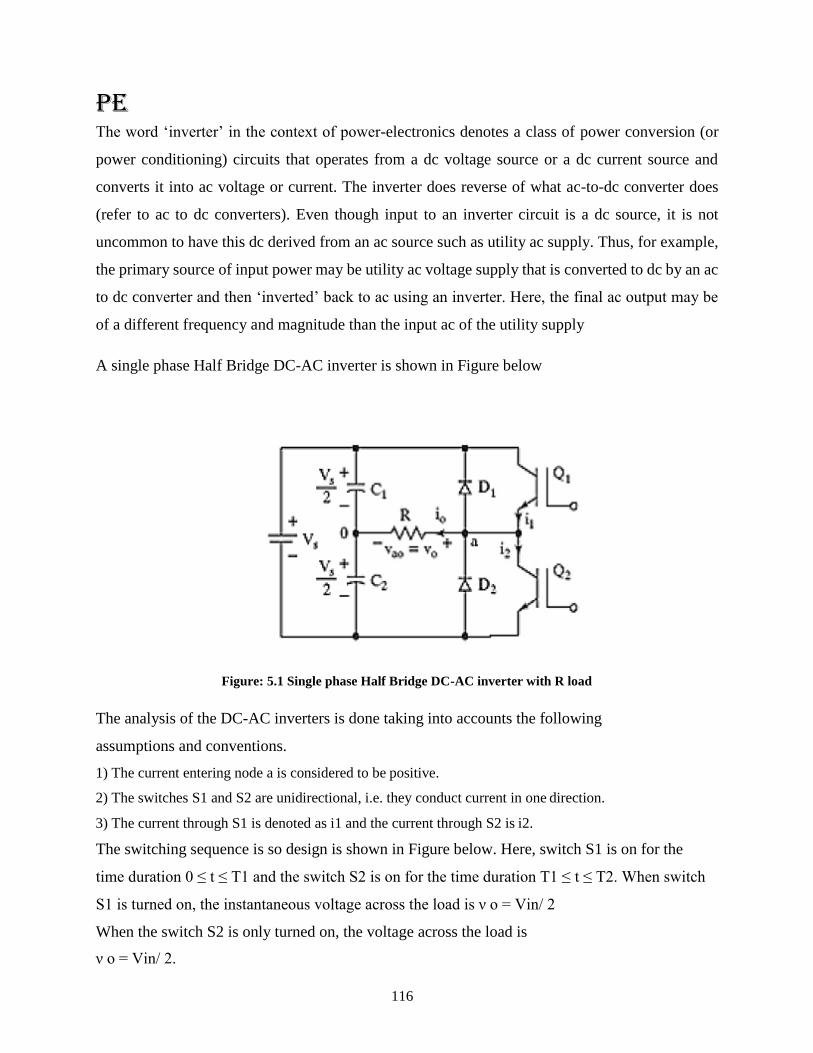
PE
116
The word ‘inverter’ in the context of power-electronics denotes a class of power conversion (or
power conditioning) circuits that operates from a dc voltage source or a dc current source and
converts it into ac voltage or current. The inverter does reverse of what ac-to-dc converter does
(refer to ac to dc converters). Even though input to an inverter circuit is a dc source, it is not
uncommon to have this dc derived from an ac source such as utility ac supply. Thus, for example,
the primary source of input power may be utility ac voltage supply that is converted to dc by an ac
to dc converter and then ‘inverted’ back to ac using an inverter. Here, the final ac output may be
of a different frequency and magnitude than the input ac of the utility supply
A single phase Half Bridge DC-AC inverter is shown in Figure below
Figure: 5.1 Single phase Half Bridge DC-AC inverter with R load
The analysis of the DC-AC inverters is done taking into accounts the following
assumptions and conventions.
1) The current entering node a is considered to be positive.
2) The switches S1 and S2 are unidirectional, i.e. they conduct current in one direction.
3) The current through S1 is denoted as i1 and the current through S2 is i2.
The switching sequence is so design is shown in Figure below. Here, switch S1 is on for the
time duration 0 ≤ t ≤ T1 and the switch S2 is on for the time duration T1 ≤ t ≤ T2. When switch
S1 is turned on, the instantaneous voltage across the load is ν o = Vin/ 2
When the switch S2 is only turned on, the voltage across the load is
ν o = Vin/ 2.
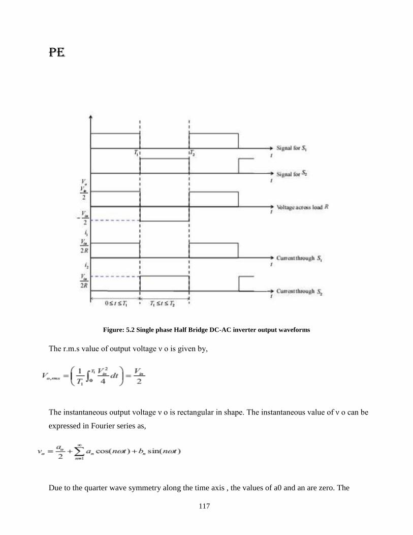
PE
117
Figure: 5.2 Single phase Half Bridge DC-AC inverter output waveforms
The r.m.s value of output voltage ν o is given by,
The instantaneous output voltage ν o is rectangular in shape. The instantaneous value of ν o can be
expressed in Fourier series as,
Due to the quarter wave symmetry along the time axis , the values of a0 and an are zero. The
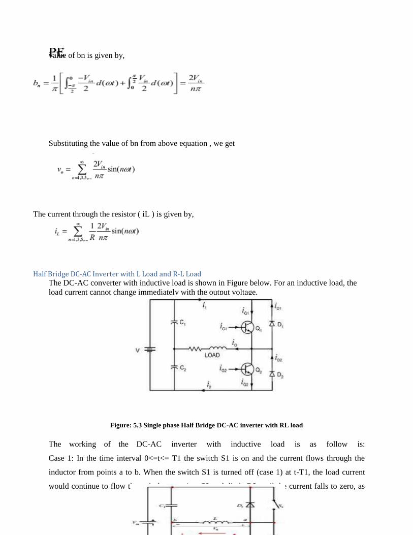
PE
118
value of bn is given by,
Substituting the value of bn from above equation , we get
The current through the resistor ( iL ) is given by,
Half Bridge DC-AC Inverter with L Load and R-L Load
The DC-AC converter with inductive load is shown in Figure below. For an inductive load, the
load current cannot change immediately with the output voltage.
Figure: 5.3 Single phase Half Bridge DC-AC inverter with RL load
The working of the DC-AC inverter with inductive load is as follow is:
Case 1: In the time interval 0<=t<= T1 the switch S1 is on and the current flows through the
inductor from points a to b. When the switch S1 is turned off (case 1) at t-T1, the load current
would continue to flow through the capacitor C2 and diode D2 until the current falls to zero, as

PE
119
shown in Figure below.
Figure: 5.4 Single phase Half Bridge DC-AC inverter with L load
Case 2: Similarly, when S2 is turned off at t = T1 , the load current flows through the diode D1
and capacitor C1until the current falls to zero, as shown in Figure below.
Figure: 5.5 Single phase Half Bridge DC-AC inverter with L load
When the diodes D1 and D2 conduct, energy is feedback to the dc source and these diodes are
known as feedback diodes. These diodes are also known as freewheeling diodes. The current for
purely inductive load is given by,
Similarly, for the R – L load. The instantaneous load current is obtained as,
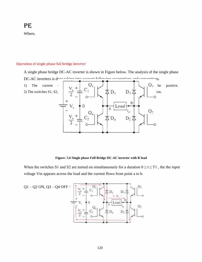
PE
120
Where,
Operation of single phase full bridge inverter
A single phase bridge DC-AC inverter is shown in Figure below. The analysis of the single phase
DC-AC inverters is done taking into account following assumptions and conventions.
1) The current entering node a in Figure 8 is considered to be positive.
2) The switches S1, S2, S3 and S4 are unidirectional, i.e. they conduct current in one direction.
Figure: 5.6 Single phase Full Bridge DC-AC inverter with R load
When the switches S1 and S2 are turned on simultaneously for a duration 0 ≤ t ≤ T1 , the the input
voltage Vin appears across the load and the current flows from point a to b.
Q1 – Q2 ON, Q3 – Q4 OFF ==> ν o = Vs
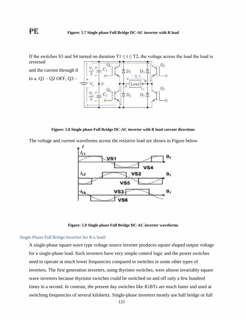
PE
121
Figure: 5.7 Single phase Full Bridge DC-AC inverter with R load
If the switches S3 and S4 turned on duration T1 ≤ t ≤ T2, the voltage across the load the load is
reversed
and the current through the load flows from point b
to a. Q1 – Q2 OFF, Q3 – Q4 ON ==> ν o = -Vs
Figure: 5.8 Single phase Full Bridge DC-AC inverter with R load current directions
The voltage and current waveforms across the resistive load are shown in Figure below
Figure: 5.9 Single phase Full Bridge DC-AC inverter waveforms
Single Phase Full Bridge Inverter for R-L load:
A single-phase square wave type voltage source inverter produces square shaped output voltage
for a single-phase load. Such inverters have very simple control logic and the power switches
need to operate at much lower frequencies compared to switches in some other types of
inverters. The first generation inverters, using thyristor switches, were almost invariably square
wave inverters because thyristor switches could be switched on and off only a few hundred
times in a second. In contrast, the present day switches like IGBTs are much faster and used at
switching frequencies of several kilohertz. Single-phase inverters mostly use half bridge or full
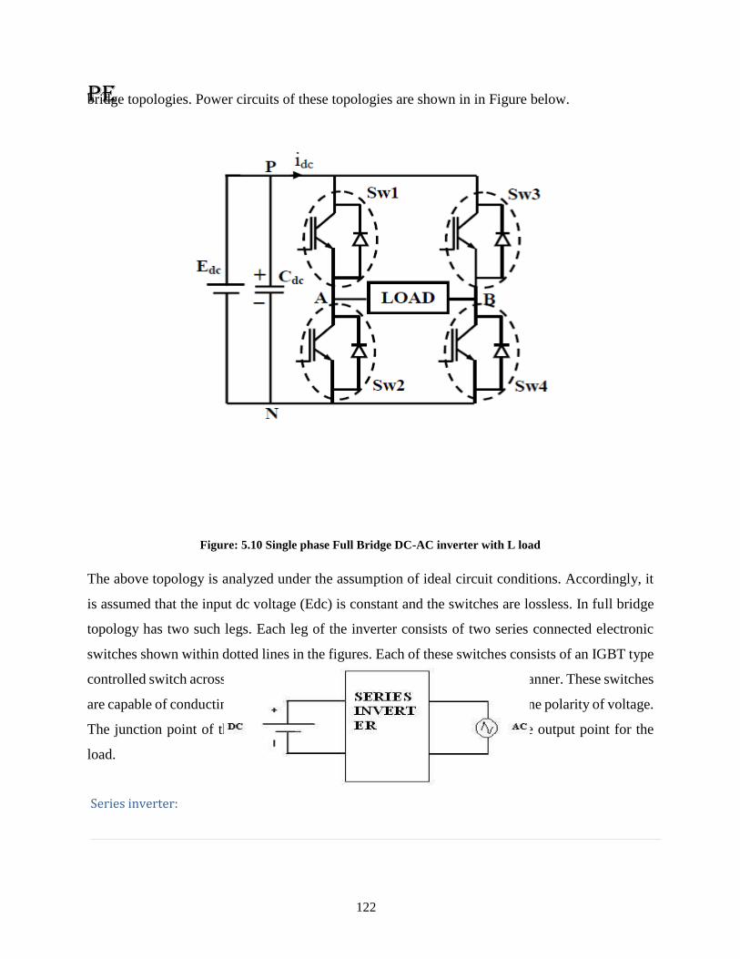
PE
122
bridge topologies. Power circuits of these topologies are shown in in Figure below.
Figure: 5.10 Single phase Full Bridge DC-AC inverter with L load
The above topology is analyzed under the assumption of ideal circuit conditions. Accordingly, it
is assumed that the input dc voltage (Edc) is constant and the switches are lossless. In full bridge
topology has two such legs. Each leg of the inverter consists of two series connected electronic
switches shown within dotted lines in the figures. Each of these switches consists of an IGBT type
controlled switch across which an uncontrolled diode is put in anti-parallel manner. These switches
are capable of conducting bi-directional current but they need to block only one polarity of voltage.
The junction point of the switches in each leg of the inverter serves as one output point for the
load.
Series inverter:
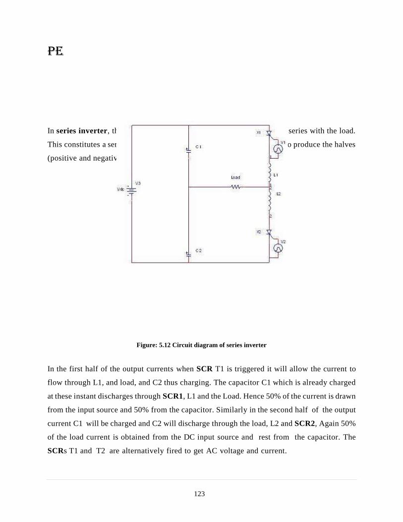
PE
123
In series inverter, the commutating elements L and C are connected in series with the load.
This constitutes a series RLC resonant circuit. The Two SCRs are used to produce the halves
(positive and negative half cycle) in the output.
Figure: 5.12 Circuit diagram of series inverter
In the first half of the output currents when SCR T1 is triggered it will allow the current to
flow through L1, and load, and C2 thus charging. The capacitor C1 which is already charged
at these instant discharges through SCR1, L1 and the Load. Hence 50% of the current is drawn
from the input source and 50% from the capacitor. Similarly in the second half of the output
current C1 will be charged and C2 will discharge through the load, L2 and SCR2, Again 50%
of the load current is obtained from the DC input source and rest from the capacitor. The
SCRs T1 and T2 are alternatively fired to get AC voltage and current.
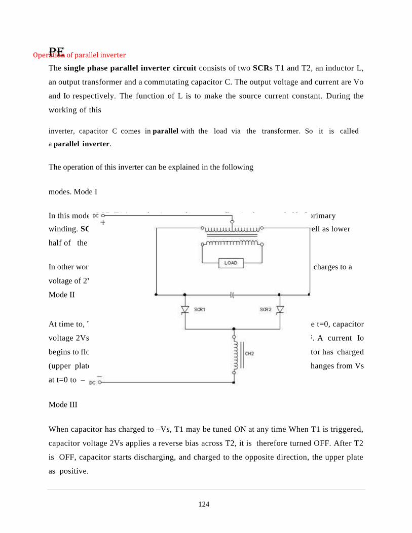
PE
124
Operation of parallel inverter
The single phase parallel inverter circuit consists of two SCRs T1 and T2, an inductor L,
an output transformer and a commutating capacitor C. The output voltage and current are Vo
and Io respectively. The function of L is to make the source current constant. During the
working of this
inverter, capacitor C comes in parallel with the load via the transformer. So it is called
a parallel inverter.
The operation of this inverter can be explained in the following
modes. Mode I
In this mode, SCR T1 is conducting and a current flow in the upper half of primary
winding. SCR T2 is OFF. As a result an emf Vs is induced across upper as well as lower
half of the primary winding.
In other words total voltage across primary winding is 2 Vs. Now the capacitor C charges to a
voltage of 2Vs with upper plate as positive.
Mode II
At time to, T2 is turned ON by applying a trigger pulse to its gate. At this time t=0, capacitor
voltage 2Vs appears as a reverse bias across T1, it is therefore turned OFF. A current Io
begins to flow through T2 and lower half of primary winding. Now the capacitor has charged
(upper plate as negative) from +2Vs to -2Vs at time t=t1. Load voltage also changes from Vs
at t=0 to – Vs at t=t1.
Mode III
When capacitor has charged to –Vs, T1 may be tuned ON at any time When T1 is triggered,
capacitor voltage 2Vs applies a reverse bias across T2, it is therefore turned OFF. After T2
is OFF, capacitor starts discharging, and charged to the opposite direction, the upper plate
as positive.

PE
125
Paralleled Commutated Inverter
Fig 1: is a schematic of the classical parallel commutated square wave inverter bridge. It
is being included here for illustrative purposes since most other circuits utilize this circuit or
a variation there of. The waveform generated and supplied to the load is basically a square
wave having a peak to peak amplitude of twice the DC supply voltage and a period that is
determined by the relate at which SCRs 1 through 4 are gated on. The SCRs are turned on
in pairs by simultaneously applying signals to the gate terminals of SCRs 1 and 4 or SCRs 2
and 3. If SCRs 1 and 4 happen to be the first two switched on a current will flow from the
positive terminal of the source through negative terminal of the source. This will establish a
left to right, plus to minus voltage relationship on the load.
Simultaneously, the left terminal of capacitor C1 will be charged positively with respect to
the right negative terminal. The steady-state load current through the various components is
determined nearly completely by the impedance of the load. Chokes 1 and 2 and SCRs 1 and
4 present very low steady-state drops and therefore nearly all the source voltage appears
across the load. Conduction of SCRs 1 and 4 will continue to the end of the half cycle, at
which point the gates are removed from SCRs 1 and 4 remain in conduction along with SCRs
2 and 3 that have now been turned on. If it were not for chokes 1 and 2, the action of
turning on the second set of SCRs would place very low impedance and therefore
momentarily prevent the source from being short-circuited.Capacitor C1 now discharges
with a current which flows into the cathode of SCR 1 through SCR 2 in a forward
direction back to the negative terminal of the capacitor. This direction of current flow causes
SCR 1 to become non-conductive provided that the reverse current through the SCR is of
sufficient duration for the SCR to again become blocking. C1 simultaneously discharges
through SCR 3 in a forward direction and through SCR 4 in a reverse direction. This will
cause SCR 4 to become non-conductive just the same SCR 1. This entire sequence is referred
to as commutation and typically in a modern inverter would occur in a period of time less
than 50 microseconds. During this interval, chokes 1and 2 must have sufficient transient
impedance to prevent a significant increase in current from the DC source.
Diodes 1, 2, 3 and 4 serve two functions. The first is to return any stored energy that may be
"kicked back" from the load to the source. They also serve to prevent the choke from
generating a high transient voltage immediately after commutation.
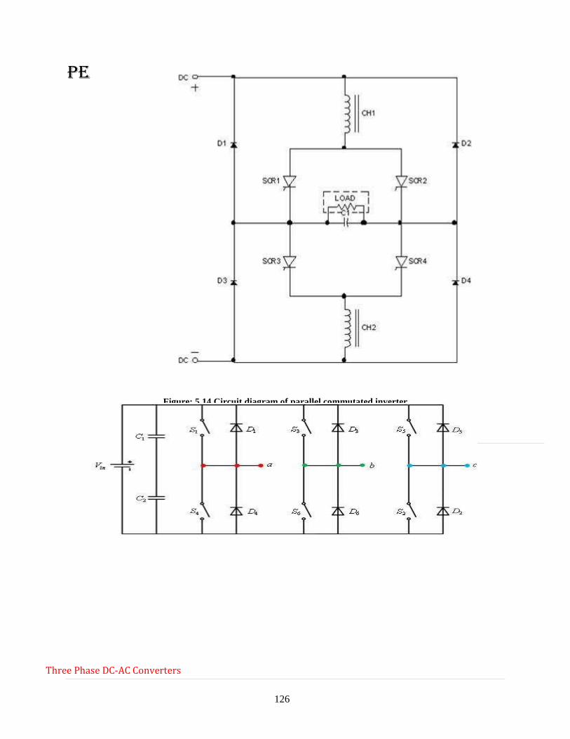
PE
126
Figure: 5.14 Circuit diagram of parallel commutated inverter
Three Phase DC-AC Converters

PE
127
Three phase inverters are normally used for high power applications. The advantages of a three
phase inverter are:
• The frequency of the output voltage waveform depends on the switching rate of the swtiches and hence
can be varied over a wide range.
• The direction of rotation of the motor can be reversed by changing the output phase sequence of the
inverter.
• The ac output voltage can be controlled by varying the dc link voltage.
The general configuration of a three phase DC-AC inverter is shown in Figure Two types of
control signals can be applied to the switches:
• 180° conduction
• 120° conduction
Figure: 5.15 Circuit diagram of three phase bridge inverter
180-Degree Conduction with Star Connected Resistive Load
The configuration of the three phase inverter with star connected resistive load is shown in Figure.
The following convention is followed:
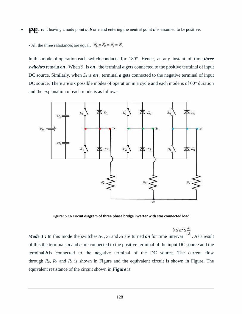
PE
128
• A current leaving a node point a, b or c and entering the neutral point n is assumed to be positive.
• All the three resistances are equal, .
In this mode of operation each switch conducts for 180°. Hence, at any instant of time three
switches remain on . When S1 is on , the terminal a gets connected to the positive terminal of input
DC source. Similarly, when S4 is on , terminal a gets connected to the negative terminal of input
DC source. There are six possible modes of operation in a cycle and each mode is of 60° duration
and the explanation of each mode is as follows:
Figure: 5.16 Circuit diagram of three phase bridge inverter with star connected load
Mode 1 : In this mode the switches S5 , S6 and S1 are turned on for time interval . As a result
of this the terminals a and c are connected to the positive terminal of the input DC source and the
terminal b is connected to the negative terminal of the DC source. The current flow
through Ra, Rb and Rc is shown in Figure and the equivalent circuit is shown in Figure. The
equivalent resistance of the circuit shown in Figure is

PE
129
(1)
The current i delivered by the DC input source is
(2)
The currents ia and ib are
(3)
Keeping the current convention in mind, the current ib is
(4)
Having determined the currents through each branch, the voltage across each branch is
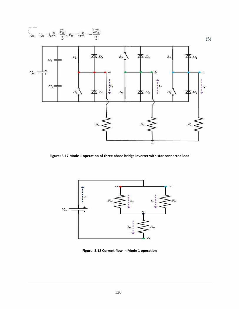
PE
130
(5)
Figure: 5.17 Mode 1 operation of three phase bridge inverter with star connected load
Figure: 5.18 Current flow in Mode 1 operation
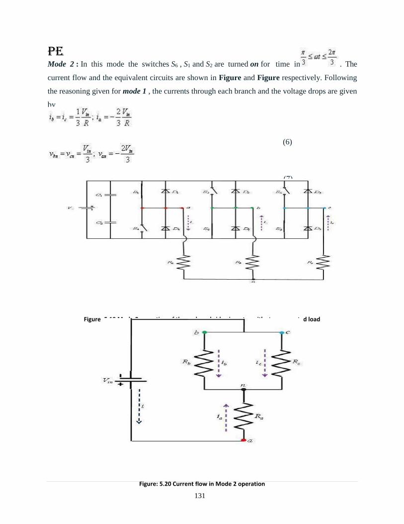
PE
131
Mode 2 : In this mode the switches S6 , S1 and S2 are turned on for time interval . The
current flow and the equivalent circuits are shown in Figure and Figure respectively. Following
the reasoning given for mode 1 , the currents through each branch and the voltage drops are given
by
(6)
(7)
Figure: 5.19 Mode 2 operation of three phase bridge inverter with star connected load
Figure: 5.20 Current flow in Mode 2 operation
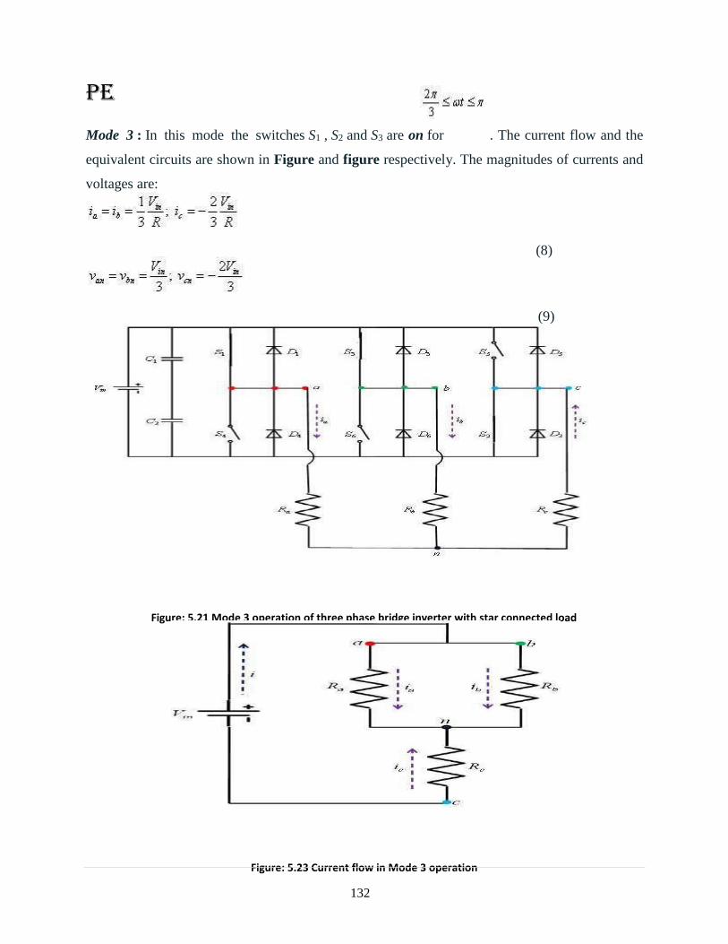
PE
132
Mode 3 : In this mode the switches S1 , S2 and S3 are on for . The current flow and the
equivalent circuits are shown in Figure and figure respectively. The magnitudes of currents and
voltages are:
(8)
(9)
Figure: 5.21 Mode 3 operation of three phase bridge inverter with star connected load
Figure: 5.23 Current flow in Mode 3 operation

PE
133

PE
134
For modes 4, 5 and 6 the equivalent circuits will be same as modes 1, 2 and 3 respectively. The
voltages and currents for each mode are:
for mode 4 (10)
for mode5 (11)
for mode 6 (12)
The plots of the phase voltages (van, vbn and vcn) and the currents ( ia, ib and ic) are shown in Figure
Having known the phase voltages, the line voltages can also be determined as:
(13)
The plots of line voltages are also shown in Figure and the phase and line voltages can be
expressed in terms of Fourier series as:
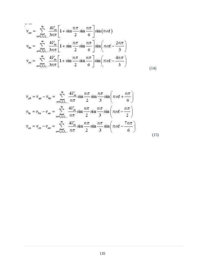
PE
135
(14)
(15)
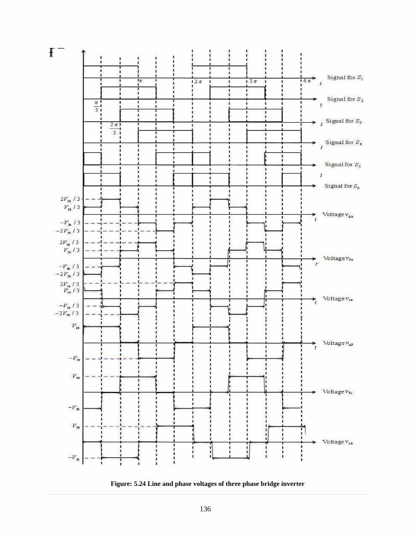
PE
136
Figure: 5.24 Line and phase voltages of three phase bridge inverter
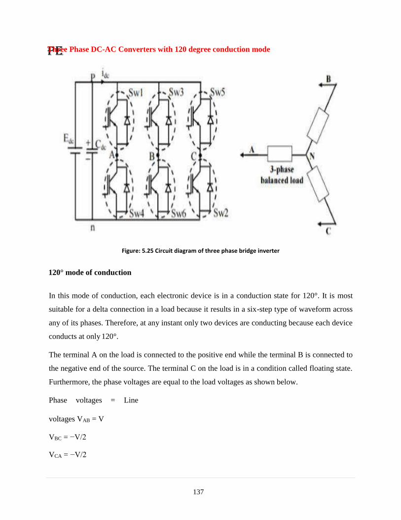
PE
137
Three Phase DC-AC Converters with 120 degree conduction mode
Figure: 5.25 Circuit diagram of three phase bridge inverter
120° mode of conduction
In this mode of conduction, each electronic device is in a conduction state for 120°. It is most
suitable for a delta connection in a load because it results in a six-step type of waveform across
any of its phases. Therefore, at any instant only two devices are conducting because each device
conducts at only 120°.
The terminal A on the load is connected to the positive end while the terminal B is connected to
the negative end of the source. The terminal C on the load is in a condition called floating state.
Furthermore, the phase voltages are equal to the load voltages as shown below.
Phase voltages = Line
voltages VAB = V
VBC = −V/2
VCA = −V/2

PE
138
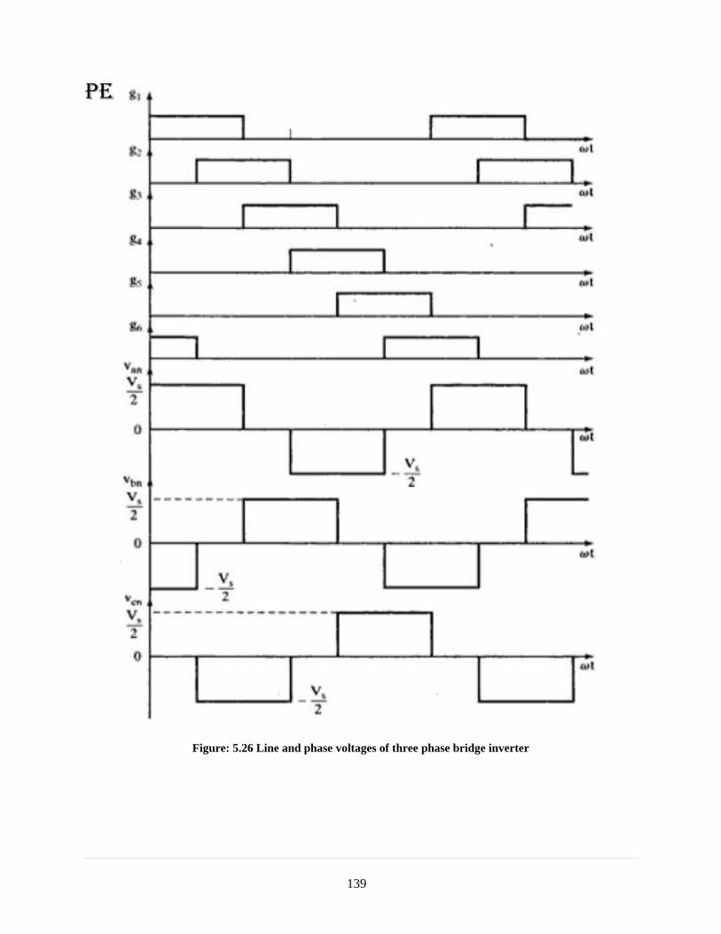
PE
139
Figure: 5.26 Line and phase voltages of three phase bridge inverter
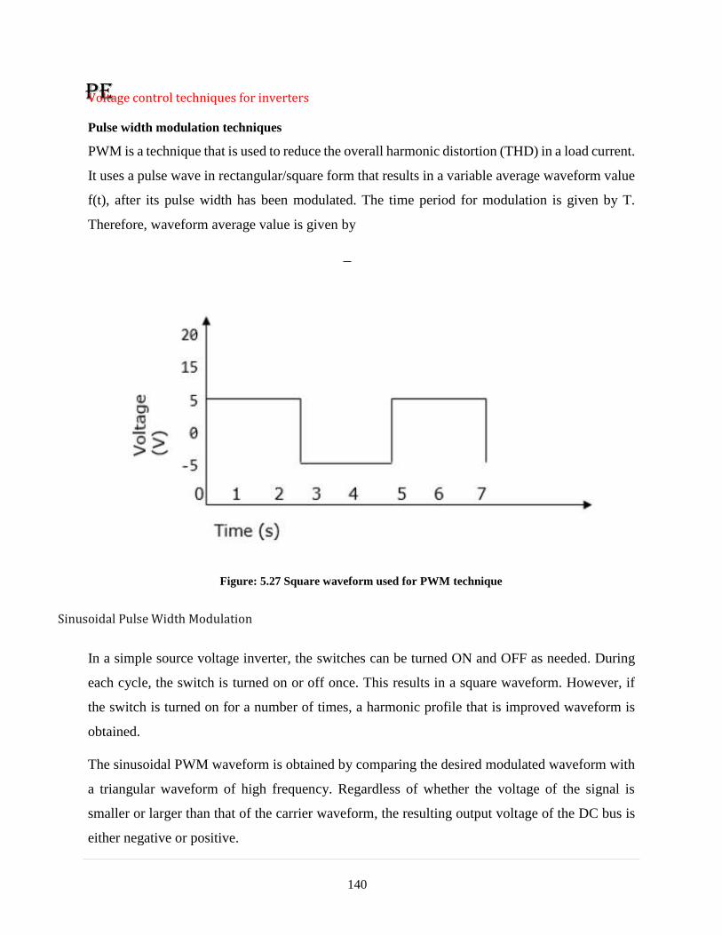
PE
140
Voltage control techniques for inverters
Pulse width modulation techniques
PWM is a technique that is used to reduce the overall harmonic distortion (THD) in a load current.
It uses a pulse wave in rectangular/square form that results in a variable average waveform value
f(t), after its pulse width has been modulated. The time period for modulation is given by T.
Therefore, waveform average value is given by
Figure: 5.27 Square waveform used for PWM technique
Sinusoidal Pulse Width Modulation
In a simple source voltage inverter, the switches can be turned ON and OFF as needed. During
each cycle, the switch is turned on or off once. This results in a square waveform. However, if
the switch is turned on for a number of times, a harmonic profile that is improved waveform is
obtained.
The sinusoidal PWM waveform is obtained by comparing the desired modulated waveform with
a triangular waveform of high frequency. Regardless of whether the voltage of the signal is
smaller or larger than that of the carrier waveform, the resulting output voltage of the DC bus is
either negative or positive.

PE
141
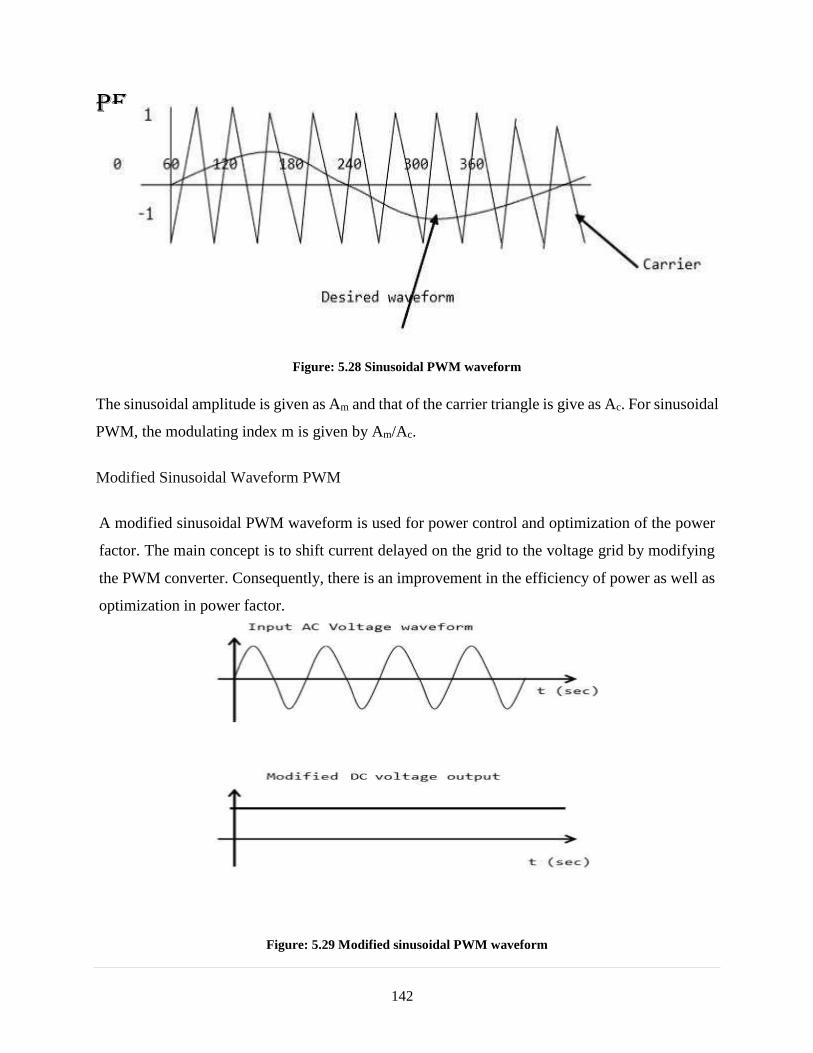
PE
142
Figure: 5.28 Sinusoidal PWM waveform
The sinusoidal amplitude is given as Am and that of the carrier triangle is give as Ac. For sinusoidal
PWM, the modulating index m is given by Am/Ac.
Modified Sinusoidal Waveform PWM
A modified sinusoidal PWM waveform is used for power control and optimization of the power
factor. The main concept is to shift current delayed on the grid to the voltage grid by modifying
the PWM converter. Consequently, there is an improvement in the efficiency of power as well as
optimization in power factor.
Figure: 5.29 Modified sinusoidal PWM waveform
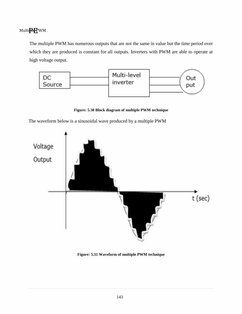
PE
143
Multiple PWM
The multiple PWM has numerous outputs that are not the same in value but the time period over
which they are produced is constant for all outputs. Inverters with PWM are able to operate at
high voltage output.
Figure: 5.30 Block diagram of multiple PWM technique
The waveform below is a sinusoidal wave produced by a multiple PWM
Figure: 5.31 Waveform of multiple PWM technique
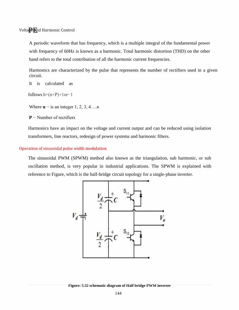
PE
144
Voltage and Harmonic Control
A periodic waveform that has frequency, which is a multiple integral of the fundamental power
with frequency of 60Hz is known as a harmonic. Total harmonic distortion (THD) on the other
hand refers to the total contribution of all the harmonic current frequencies.
Harmonics are characterized by the pulse that represents the number of rectifiers used in a given
circuit.
It is calculated as
follows h=(n×P)+1or−1
Where n − is an integer 1, 2, 3, 4….n
P − Number of rectifiers
Harmonics have an impact on the voltage and current output and can be reduced using isolation
transformers, line reactors, redesign of power systems and harmonic filters.
Operation of sinusoidal pulse width modulation
The sinusoidal PWM (SPWM) method also known as the triangulation, sub harmonic, or sub
oscillation method, is very popular in industrial applications. The SPWM is explained with
reference to Figure, which is the half-bridge circuit topology for a single-phase inverter.
Figure: 5.32 schematic diagram of Half bridge PWM inverter

PE
145
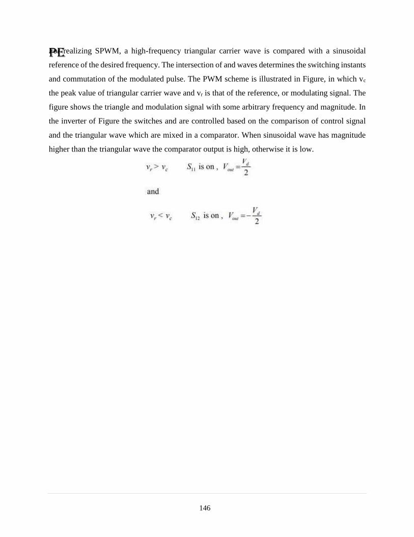
PE
146
For realizing SPWM, a high-frequency triangular carrier wave is compared with a sinusoidal
reference of the desired frequency. The intersection of and waves determines the switching instants
and commutation of the modulated pulse. The PWM scheme is illustrated in Figure, in which vc
the peak value of triangular carrier wave and vr is that of the reference, or modulating signal. The
figure shows the triangle and modulation signal with some arbitrary frequency and magnitude. In
the inverter of Figure the switches and are controlled based on the comparison of control signal
and the triangular wave which are mixed in a comparator. When sinusoidal wave has magnitude
higher than the triangular wave the comparator output is high, otherwise it is low.
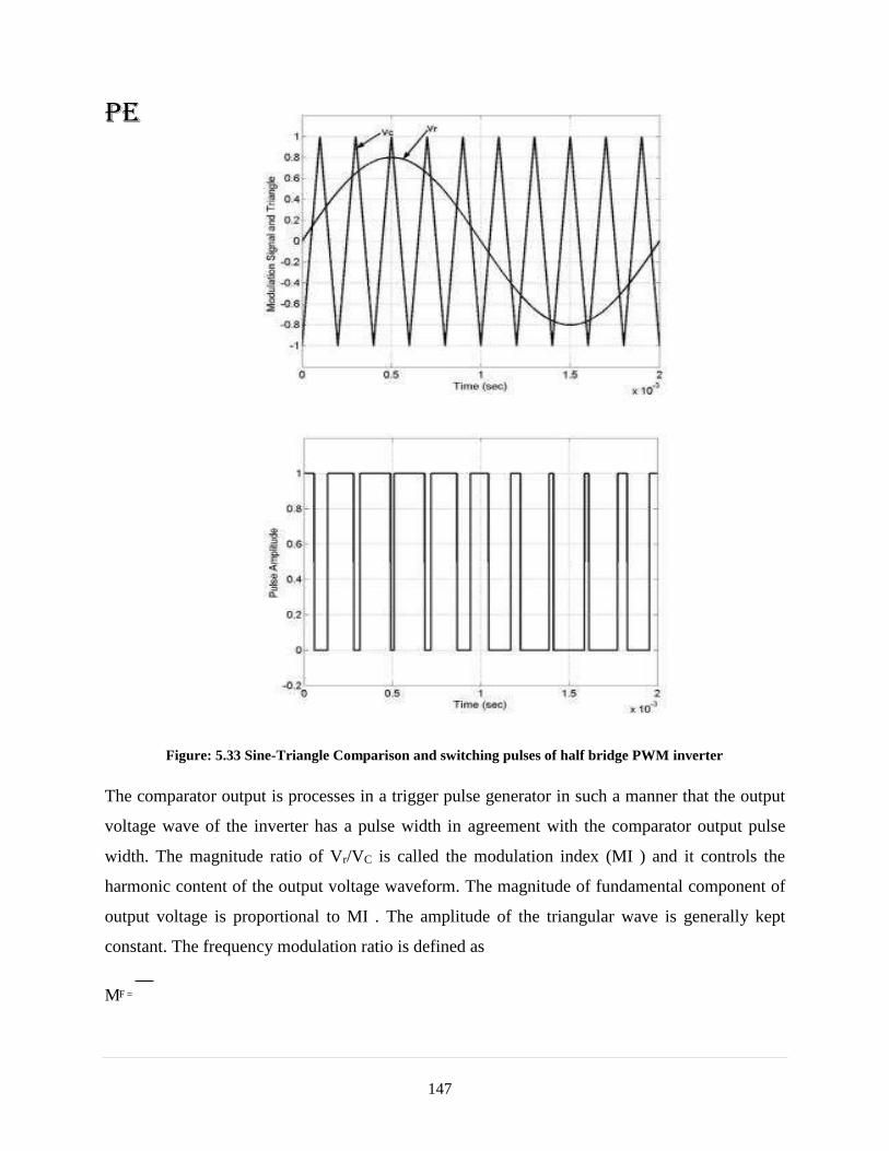
PE
147
Figure: 5.33 Sine-Triangle Comparison and switching pulses of half bridge PWM inverter
The comparator output is processes in a trigger pulse generator in such a manner that the output
voltage wave of the inverter has a pulse width in agreement with the comparator output pulse
width. The magnitude ratio of Vr/VC is called the modulation index (MI ) and it controls the
harmonic content of the output voltage waveform. The magnitude of fundamental component of
output voltage is proportional to MI . The amplitude of the triangular wave is generally kept
constant. The frequency modulation ratio is defined as
F =
M
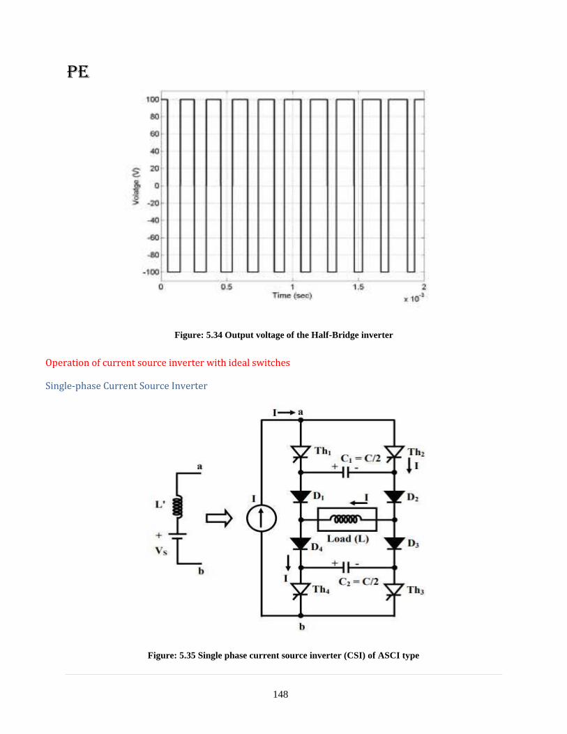
PE
148
Figure: 5.34 Output voltage of the Half-Bridge inverter
Operation of current source inverter with ideal switches
Single-phase Current Source Inverter
Figure: 5.35 Single phase current source inverter (CSI) of ASCI type
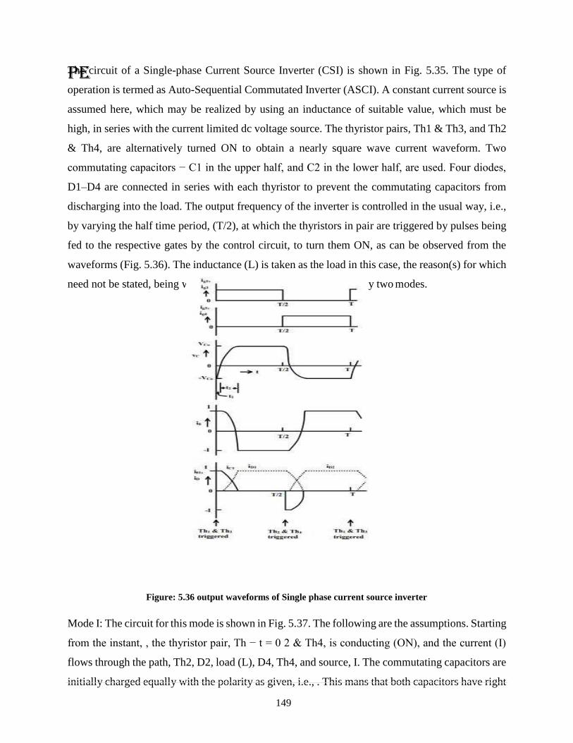
PE
149
The circuit of a Single-phase Current Source Inverter (CSI) is shown in Fig. 5.35. The type of
operation is termed as Auto-Sequential Commutated Inverter (ASCI). A constant current source is
assumed here, which may be realized by using an inductance of suitable value, which must be
high, in series with the current limited dc voltage source. The thyristor pairs, Th1 & Th3, and Th2
& Th4, are alternatively turned ON to obtain a nearly square wave current waveform. Two
commutating capacitors − C1 in the upper half, and C2 in the lower half, are used. Four diodes,
D1–D4 are connected in series with each thyristor to prevent the commutating capacitors from
discharging into the load. The output frequency of the inverter is controlled in the usual way, i.e.,
by varying the half time period, (T/2), at which the thyristors in pair are triggered by pulses being
fed to the respective gates by the control circuit, to turn them ON, as can be observed from the
waveforms (Fig. 5.36). The inductance (L) is taken as the load in this case, the reason(s) for which
need not be stated, being well known. The operation is explained by two modes.
Figure: 5.36 output waveforms of Single phase current source inverter
Mode I: The circuit for this mode is shown in Fig. 5.37. The following are the assumptions. Starting
from the instant, , the thyristor pair, Th − t = 0 2 & Th4, is conducting (ON), and the current (I)
flows through the path, Th2, D2, load (L), D4, Th4, and source, I. The commutating capacitors are
initially charged equally with the polarity as given, i.e., . This mans that both capacitors have right

PE
150
hand plate positive and left hand plate negative. If two capacitors are not charged initially, they
have to pre-charge.
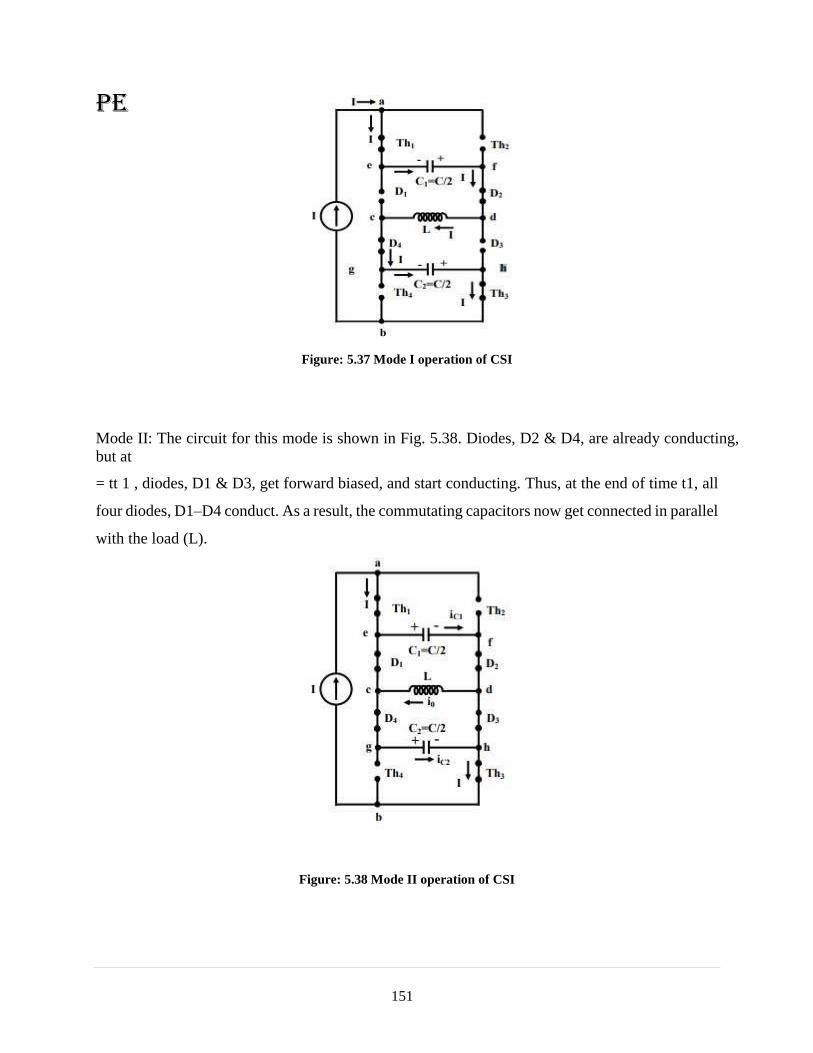
PE
151
Figure: 5.37 Mode I operation of CSI
Mode II: The circuit for this mode is shown in Fig. 5.38. Diodes, D2 & D4, are already conducting,
but at
= tt 1 , diodes, D1 & D3, get forward biased, and start conducting. Thus, at the end of time t1, all
four diodes, D1–D4 conduct. As a result, the commutating capacitors now get connected in parallel
with the load (L).
Figure: 5.38 Mode II operation of CSI
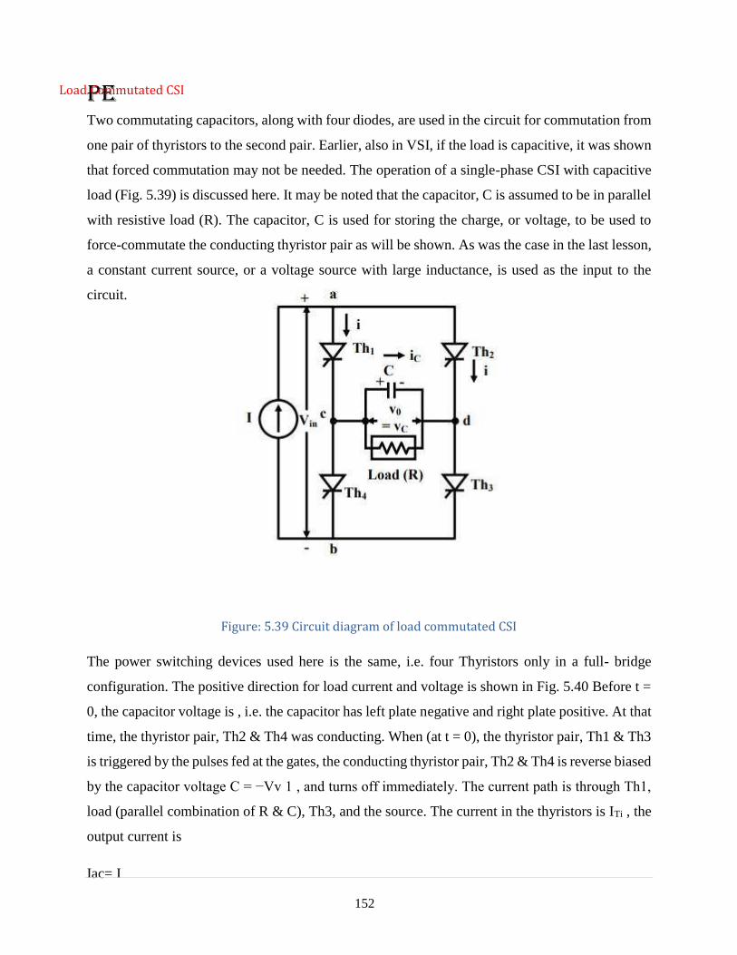
PE
152
Load Commutated CSI
Two commutating capacitors, along with four diodes, are used in the circuit for commutation from
one pair of thyristors to the second pair. Earlier, also in VSI, if the load is capacitive, it was shown
that forced commutation may not be needed. The operation of a single-phase CSI with capacitive
load (Fig. 5.39) is discussed here. It may be noted that the capacitor, C is assumed to be in parallel
with resistive load (R). The capacitor, C is used for storing the charge, or voltage, to be used to
force-commutate the conducting thyristor pair as will be shown. As was the case in the last lesson,
a constant current source, or a voltage source with large inductance, is used as the input to the
circuit.
Figure: 5.39 Circuit diagram of load commutated CSI
The power switching devices used here is the same, i.e. four Thyristors only in a full- bridge
configuration. The positive direction for load current and voltage is shown in Fig. 5.40 Before t =
0, the capacitor voltage is , i.e. the capacitor has left plate negative and right plate positive. At that
time, the thyristor pair, Th2 & Th4 was conducting. When (at t = 0), the thyristor pair, Th1 & Th3
is triggered by the pulses fed at the gates, the conducting thyristor pair, Th2 & Th4 is reverse biased
by the capacitor voltage C = −Vv 1 , and turns off immediately. The current path is through Th1,
load (parallel combination of R & C), Th3, and the source. The current in the thyristors is ITi , the
output current is
Iac= I

PE
153
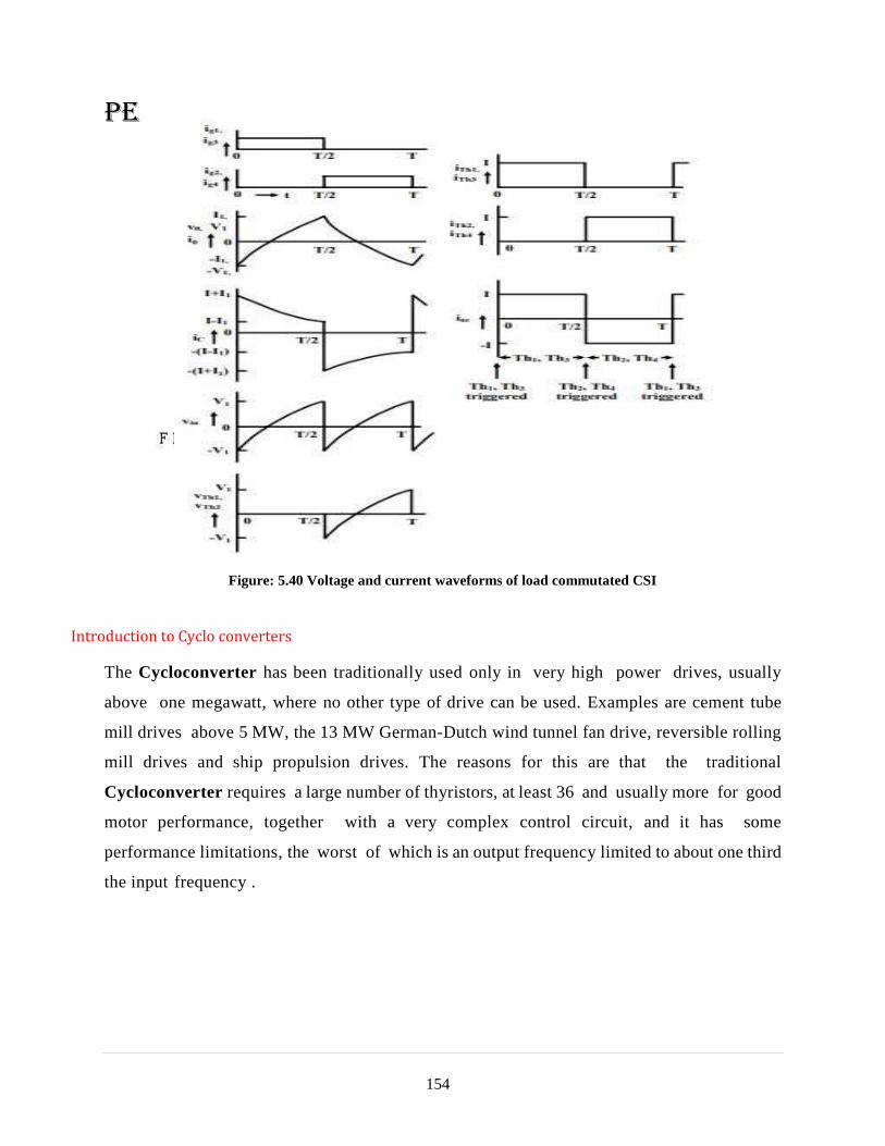
PE
154
Figure: 5.40 Voltage and current waveforms of load commutated CSI
Introduction to Cyclo converters
The Cycloconverter has been traditionally used only in very high power drives, usually
above one megawatt, where no other type of drive can be used. Examples are cement tube
mill drives above 5 MW, the 13 MW German-Dutch wind tunnel fan drive, reversible rolling
mill drives and ship propulsion drives. The reasons for this are that the traditional
Cycloconverter requires a large number of thyristors, at least 36 and usually more for good
motor performance, together with a very complex control circuit, and it has some
performance limitations, the worst of which is an output frequency limited to about one third
the input frequency .
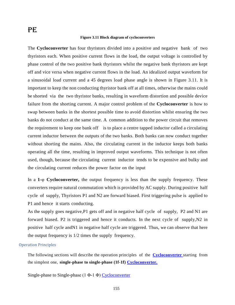
PE
155
Figure 3.11 Block diagram of cycloconverters
The Cycloconverter has four thyristors divided into a positive and negative bank of two
thyristors each. When positive current flows in the load, the output voltage is controlled by
phase control of the two positive bank thyristors whilst the negative bank thyristors are kept
off and vice versa when negative current flows in the load. An idealized output waveform for
a sinusoidal load current and a 45 degrees load phase angle is shown in Figure 3.11. It is
important to keep the non conducting thyristor bank off at all times, otherwise the mains could
be shorted via the two thyristor banks, resulting in waveform distortion and possible device
failure from the shorting current. A major control problem of the Cycloconverter is how to
swap between banks in the shortest possible time to avoid distortion whilst ensuring the two
banks do not conduct at the same time. A common addition to the power circuit that removes
the requirement to keep one bank off is to place a centre tapped inductor called a circulating
current inductor between the outputs of the two banks. Both banks can now conduct together
without shorting the mains. Also, the circulating current in the inductor keeps both banks
operating all the time, resulting in improved output waveforms. This technique is not often
used, though, because the circulating current inductor tends to be expensive and bulky and
the circulating current reduces the power factor on the input
In a 1-φ Cycloconverter, the output frequency is less than the supply frequency. These
converters require natural commutation which is provided by AC supply. During positive half
cycle of supply, Thyristors P1 and N2 are forward biased. First triggering pulse is applied to
P1 and hence it starts conducting.
As the supply goes negative,P1 gets off and in negative half cycle of supply, P2 and N1 are
forward biased. P2 is triggered and hence it conducts. In the next cycle of supply,N2 in
positive half cycle andN1 in negative half cycle are triggered. Thus, we can observe that here
the output frequency is 1/2 times the supply frequency.
Operation Principles
The following sections will describe the operation principles of the Cycloconverter starting from
the simplest one, single-phase to single-phase (1f-1f) Cycloconverter.
Single-phase to Single-phase (1 Φ-1 Φ) Cycloconverter
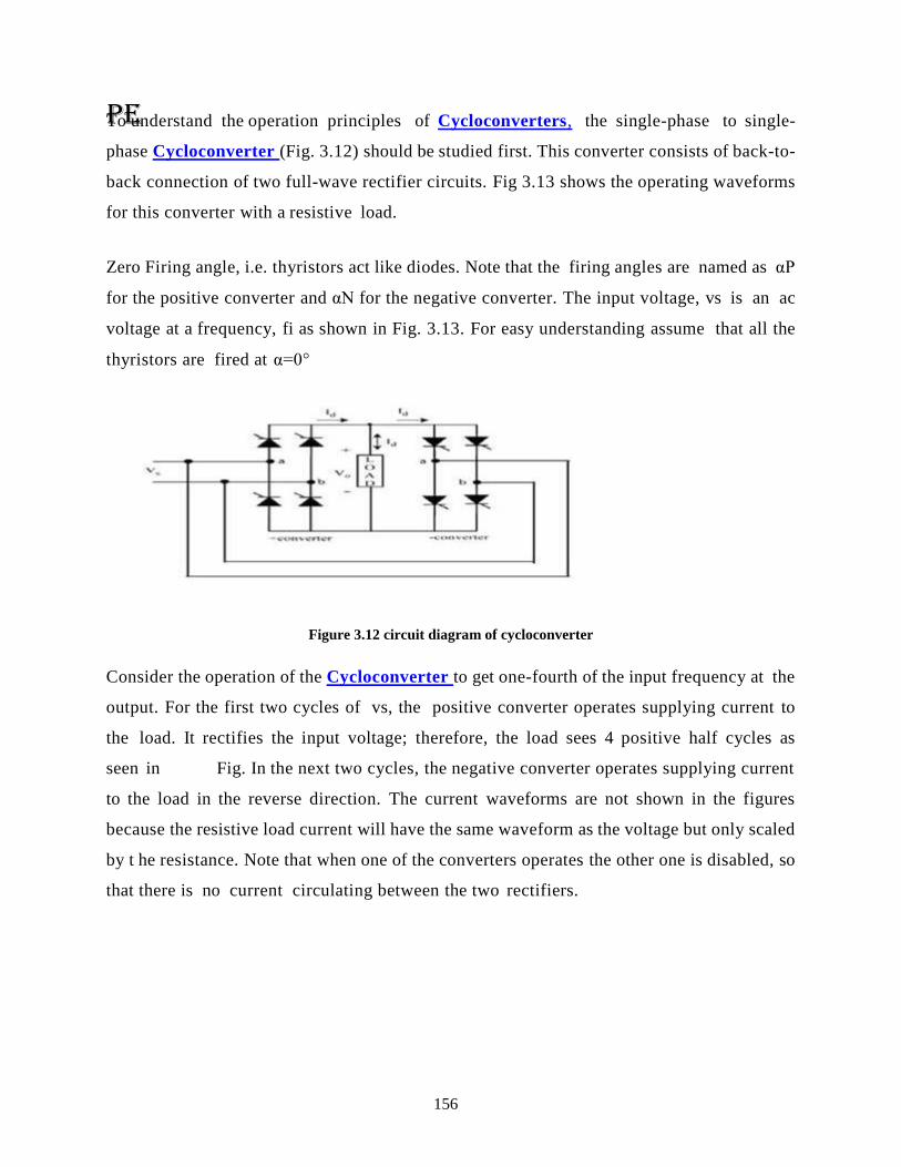
PE
156
To understand the operation principles of Cycloconverters, the single-phase to single-
phase Cycloconverter (Fig. 3.12) should be studied first. This converter consists of back-to-
back connection of two full-wave rectifier circuits. Fig 3.13 shows the operating waveforms
for this converter with a resistive load.
Zero Firing angle, i.e. thyristors act like diodes. Note that the firing angles are named as αP
for the positive converter and αN for the negative converter. The input voltage, vs is an ac
voltage at a frequency, fi as shown in Fig. 3.13. For easy understanding assume that all the
thyristors are fired at α=0°
Figure 3.12 circuit diagram of cycloconverter
Consider the operation of the Cycloconverter to get one-fourth of the input frequency at the
output. For the first two cycles of vs, the positive converter operates supplying current to
the load. It rectifies the input voltage; therefore, the load sees 4 positive half cycles as
seen in Fig. In the next two cycles, the negative converter operates supplying current
to the load in the reverse direction. The current waveforms are not shown in the figures
because the resistive load current will have the same waveform as the voltage but only scaled
by t he resistance. Note that when one of the converters operates the other one is disabled, so
that there is no current circulating between the two rectifiers.
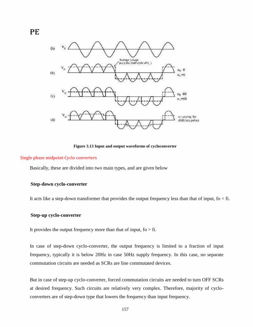
PE
157
Figure 3.13 Input and output waveforms of cycloconverter
Single phase midpoint Cyclo converters
Basically, these are divided into two main types, and are given below
Step-down cyclo-converter
It acts like a step-down transformer that provides the output frequency less than that of input, fo < fi.
Step-up cyclo-converter
It provides the output frequency more than that of input, fo > fi.
In case of step-down cyclo-converter, the output frequency is limited to a fraction of input
frequency, typically it is below 20Hz in case 50Hz supply frequency. In this case, no separate
commutation circuits are needed as SCRs are line commutated devices.
But in case of step-up cyclo-converter, forced commutation circuits are needed to turn OFF SCRs
at desired frequency. Such circuits are relatively very complex. Therefore, majority of cyclo-
converters are of step-down type that lowers the frequency than input frequency.
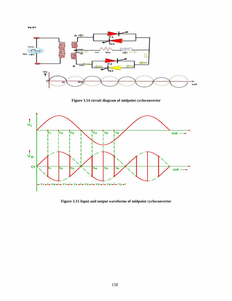
PE
158
Figure 3.14 circuit diagram of midpoint cycloconverter
Figure 3.15 Input and output waveforms of midpoint cycloconverter
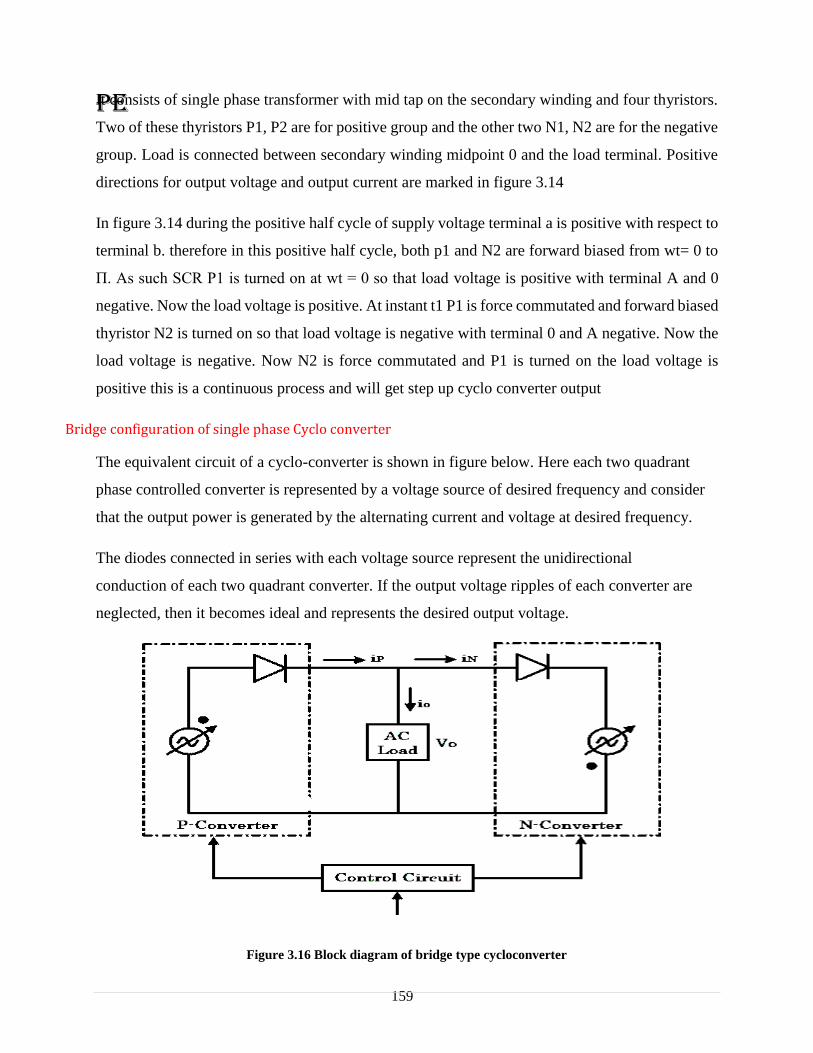
PE
159
It consists of single phase transformer with mid tap on the secondary winding and four thyristors.
Two of these thyristors P1, P2 are for positive group and the other two N1, N2 are for the negative
group. Load is connected between secondary winding midpoint 0 and the load terminal. Positive
directions for output voltage and output current are marked in figure 3.14
In figure 3.14 during the positive half cycle of supply voltage terminal a is positive with respect to
terminal b. therefore in this positive half cycle, both p1 and N2 are forward biased from wt= 0 to
Π. As such SCR P1 is turned on at wt = 0 so that load voltage is positive with terminal A and 0
negative. Now the load voltage is positive. At instant t1 P1 is force commutated and forward biased
thyristor N2 is turned on so that load voltage is negative with terminal 0 and A negative. Now the
load voltage is negative. Now N2 is force commutated and P1 is turned on the load voltage is
positive this is a continuous process and will get step up cyclo converter output
Bridge configuration of single phase Cyclo converter
The equivalent circuit of a cyclo-converter is shown in figure below. Here each two quadrant
phase controlled converter is represented by a voltage source of desired frequency and consider
that the output power is generated by the alternating current and voltage at desired frequency.
The diodes connected in series with each voltage source represent the unidirectional
conduction of each two quadrant converter. If the output voltage ripples of each converter are
neglected, then it becomes ideal and represents the desired output voltage.
Figure 3.16 Block diagram of bridge type cycloconverter

PE
160
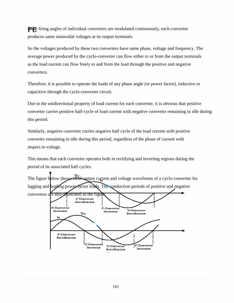
PE
161
If the firing angles of individual converters are modulated continuously, each converter
produces same sinusoidal voltages at its output terminals.
So the voltages produced by these two converters have same phase, voltage and frequency. The
average power produced by the cyclo-converter can flow either to or from the output terminals
as the load current can flow freely to and from the load through the positive and negative
converters.
Therefore, it is possible to operate the loads of any phase angle (or power factor), inductive or
capacitive through the cyclo-converter circuit.
Due to the unidirectional property of load current for each converter, it is obvious that positive
converter carries positive half-cycle of load current with negative converter remaining in idle during
this period.
Similarly, negative converter carries negative half cycle of the load current with positive
converter remaining in idle during this period, regardless of the phase of current with
respect to voltage.
This means that each converter operates both in rectifying and inverting regions during the
period of its associated half cycles.
The figure below shows ideal output current and voltage waveforms of a cyclo-converter for
lagging and leading power factor loads. The conduction periods of positive and negative
converters are also illustrated in the figure.

PE
162
Figure 3.17 cycloconverter waveforms
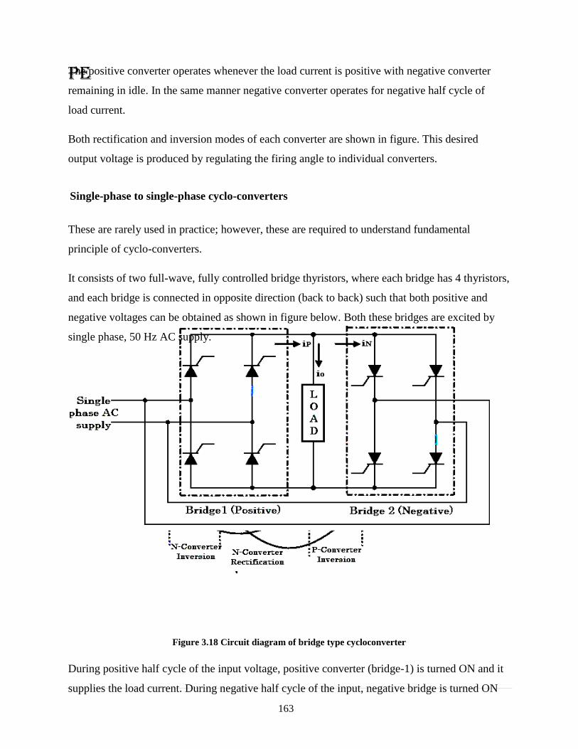
PE
163
The positive converter operates whenever the load current is positive with negative converter
remaining in idle. In the same manner negative converter operates for negative half cycle of
load current.
Both rectification and inversion modes of each converter are shown in figure. This desired
output voltage is produced by regulating the firing angle to individual converters.
Single-phase to single-phase cyclo-converters
These are rarely used in practice; however, these are required to understand fundamental
principle of cyclo-converters.
It consists of two full-wave, fully controlled bridge thyristors, where each bridge has 4 thyristors,
and each bridge is connected in opposite direction (back to back) such that both positive and
negative voltages can be obtained as shown in figure below. Both these bridges are excited by
single phase, 50 Hz AC supply.
Figure 3.18 Circuit diagram of bridge type cycloconverter
During positive half cycle of the input voltage, positive converter (bridge-1) is turned ON and it
supplies the load current. During negative half cycle of the input, negative bridge is turned ON

PE
164
and it supplies load current. Both converters should not conduct together that cause short circuit
at the input.
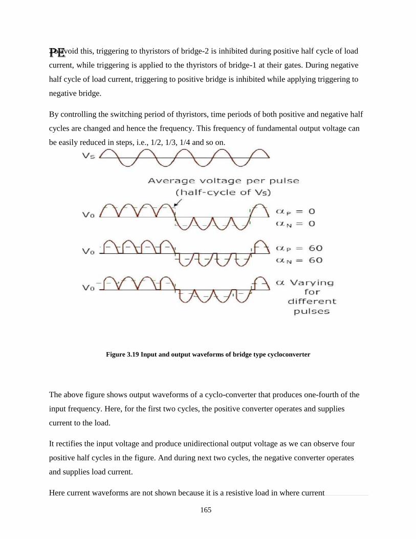
PE
165
To avoid this, triggering to thyristors of bridge-2 is inhibited during positive half cycle of load
current, while triggering is applied to the thyristors of bridge-1 at their gates. During negative
half cycle of load current, triggering to positive bridge is inhibited while applying triggering to
negative bridge.
By controlling the switching period of thyristors, time periods of both positive and negative half
cycles are changed and hence the frequency. This frequency of fundamental output voltage can
be easily reduced in steps, i.e., 1/2, 1/3, 1/4 and so on.
Figure 3.19 Input and output waveforms of bridge type cycloconverter
The above figure shows output waveforms of a cyclo-converter that produces one-fourth of the
input frequency. Here, for the first two cycles, the positive converter operates and supplies
current to the load.
It rectifies the input voltage and produce unidirectional output voltage as we can observe four
positive half cycles in the figure. And during next two cycles, the negative converter operates
and supplies load current.
Here current waveforms are not shown because it is a resistive load in where current

PE
166
(with less magnitude) exactly follows the voltage.
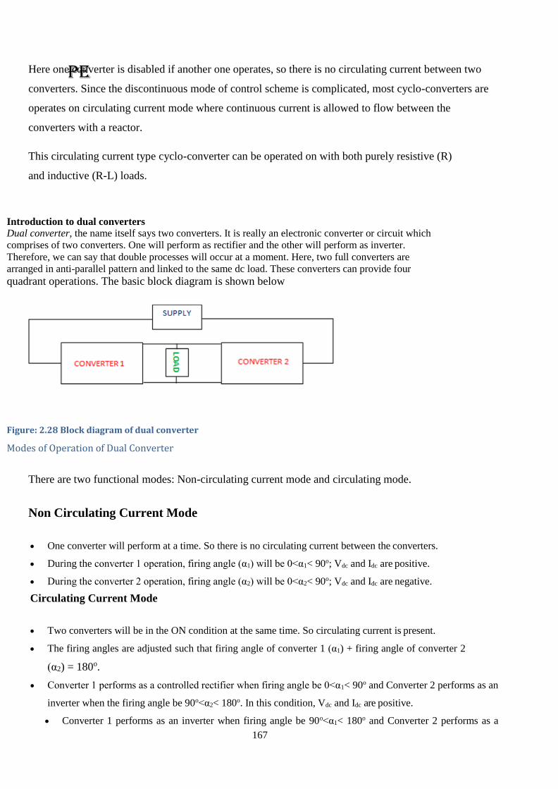
PE
167
Here one converter is disabled if another one operates, so there is no circulating current between two
converters. Since the discontinuous mode of control scheme is complicated, most cyclo-converters are
operates on circulating current mode where continuous current is allowed to flow between the
converters with a reactor.
This circulating current type cyclo-converter can be operated on with both purely resistive (R)
and inductive (R-L) loads.
Introduction to dual converters
Dual converter, the name itself says two converters. It is really an electronic converter or circuit which
comprises of two converters. One will perform as rectifier and the other will perform as inverter.
Therefore, we can say that double processes will occur at a moment. Here, two full converters are
arranged in anti-parallel pattern and linked to the same dc load. These converters can provide four
quadrant operations. The basic block diagram is shown below
Figure: 2.28 Block diagram of dual converter
Modes of Operation of Dual Converter
There are two functional modes: Non-circulating current mode and circulating mode.
Non Circulating Current Mode
One converter will perform at a time. So there is no circulating current between the converters.
During the converter 1 operation, firing angle (α1) will be 0<α1< 90o; Vdc and Idc are positive.
During the converter 2 operation, firing angle (α2) will be 0<α2< 90o; Vdc and Idc are negative.
Circulating Current Mode
Two converters will be in the ON condition at the same time. So circulating current is present.
The firing angles are adjusted such that firing angle of converter 1 (α1) + firing angle of converter 2
(α2) = 180o.
Converter 1 performs as a controlled rectifier when firing angle be 0<α1< 90o and Converter 2 performs as an
inverter when the firing angle be 90o<α2< 180o. In this condition, Vdc and Idc are positive.
Converter 1 performs as an inverter when firing angle be 90o<α1< 180o and Converter 2 performs as a
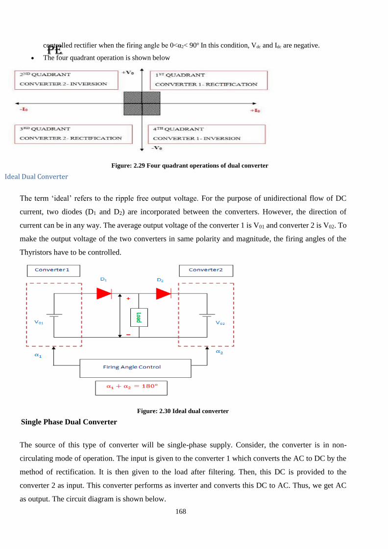
PE
168
controlled rectifier when the firing angle be 0<α2< 90o In this condition, Vdc and Idc are negative.
The four quadrant operation is shown below
Figure: 2.29 Four quadrant operations of dual converter
Ideal Dual Converter
The term ‘ideal’ refers to the ripple free output voltage. For the purpose of unidirectional flow of DC
current, two diodes (D1 and D2) are incorporated between the converters. However, the direction of
current can be in any way. The average output voltage of the converter 1 is V01 and converter 2 is V02. To
make the output voltage of the two converters in same polarity and magnitude, the firing angles of the
Thyristors have to be controlled.
Figure: 2.30 Ideal dual converter
Single Phase Dual Converter
The source of this type of converter will be single-phase supply. Consider, the converter is in non-
circulating mode of operation. The input is given to the converter 1 which converts the AC to DC by the
method of rectification. It is then given to the load after filtering. Then, this DC is provided to the
converter 2 as input. This converter performs as inverter and converts this DC to AC. Thus, we get AC
as output. The circuit diagram is shown below.
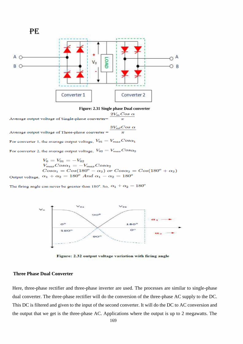
PE
169
Figure: 2.31 Single phase Dual converter
Three Phase Dual Converter
Here, three-phase rectifier and three-phase inverter are used. The processes are similar to single-phase
dual converter. The three-phase rectifier will do the conversion of the three-phase AC supply to the DC.
This DC is filtered and given to the input of the second converter. It will do the DC to AC conversion and
the output that we get is the three-phase AC. Applications where the output is up to 2 megawatts. The
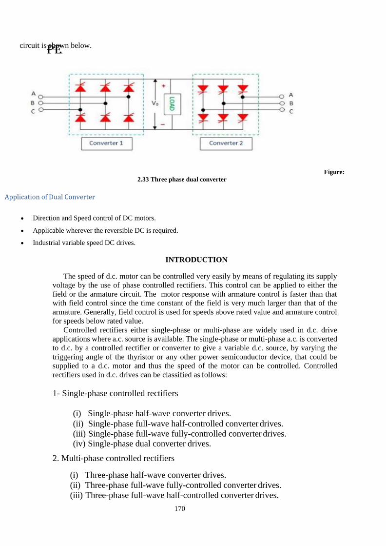
PE
170
circuit is shown below.
Figure:
2.33 Three phase dual converter
Application of Dual Converter
Direction and Speed control of DC motors.
Applicable wherever the reversible DC is required.
Industrial variable speed DC drives.
INTRODUCTION
The speed of d.c. motor can be controlled very easily by means of regulating its supply
voltage by the use of phase controlled rectifiers. This control can be applied to either the
field or the armature circuit. The motor response with armature control is faster than that
with field control since the time constant of the field is very much larger than that of the
armature. Generally, field control is used for speeds above rated value and armature control
for speeds below rated value.
Controlled rectifiers either single-phase or multi-phase are widely used in d.c. drive
applications where a.c. source is available. The single-phase or multi-phase a.c. is converted
to d.c. by a controlled rectifier or converter to give a variable d.c. source, by varying the
triggering angle of the thyristor or any other power semiconductor device, that could be
supplied to a d.c. motor and thus the speed of the motor can be controlled. Controlled
rectifiers used in d.c. drives can be classified as follows:
1- Single-phase controlled rectifiers
(i) Single-phase half-wave converter drives.
(ii) Single-phase full-wave half-controlled converter drives.
(iii) Single-phase full-wave fully-controlled converter drives. (iv) Single-phase dual converter drives.
2. Multi-phase controlled rectifiers
(i) Three-phase half-wave converter drives.
(ii) Three-phase full-wave fully-controlled converter drives.
(iii) Three-phase full-wave half-controlled converter drives.
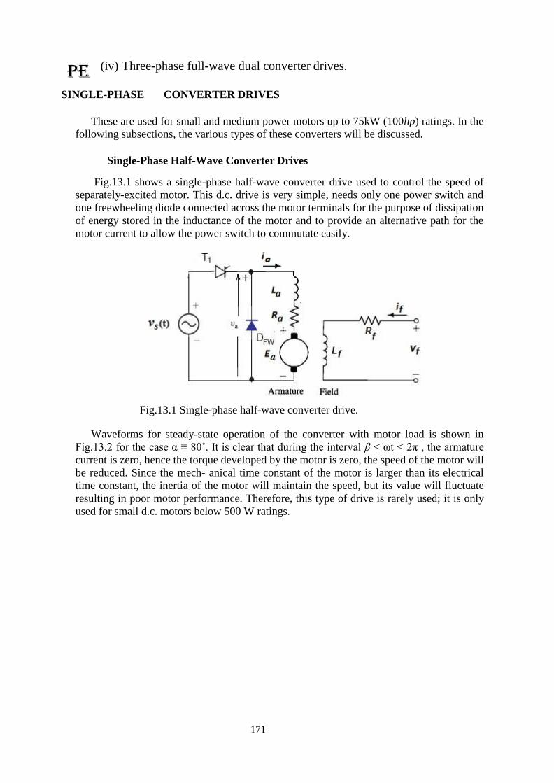
PE
171
(iv) Three-phase full-wave dual converter drives.
SINGLE-PHASE CONVERTER DRIVES
These are used for small and medium power motors up to 75kW (100hp) ratings. In the
following subsections, the various types of these converters will be discussed.
Single-Phase Half-Wave Converter Drives
Fig.13.1 shows a single-phase half-wave converter drive used to control the speed of
separately-excited motor. This d.c. drive is very simple, needs only one power switch and
one freewheeling diode connected across the motor terminals for the purpose of dissipation
of energy stored in the inductance of the motor and to provide an alternative path for the
motor current to allow the power switch to commutate easily.
Fig.13.1 Single-phase half-wave converter drive.
Waveforms for steady-state operation of the converter with motor load is shown in
Fig.13.2 for the case α ≡ 80˚. It is clear that during the interval β < ωt < 2π , the armature
current is zero, hence the torque developed by the motor is zero, the speed of the motor will
be reduced. Since the mech- anical time constant of the motor is larger than its electrical
time constant, the inertia of the motor will maintain the speed, but its value will fluctuate
resulting in poor motor performance. Therefore, this type of drive is rarely used; it is only
used for small d.c. motors below 500 W ratings.
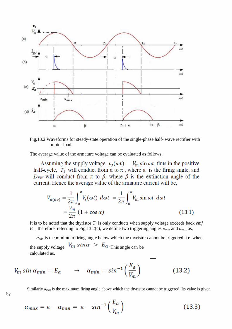
PE
172
Fig.13.2 Waveforms for steady-state operation of the single-phase half- wave rectifier with
motor load.
The average value of the armature voltage can be evaluated as follows:
It is to be noted that the thyristor T1 is only conducts when supply voltage exceeds back emf
Ea , therefore, referring to Fig.13.2(c), we define two triggering angles αmin and αmax as,
αmin is the minimum firing angle below which the thyristor cannot be triggered. i.e. when
the supply voltage This angle can be
calculated as,
Similarly αmax is the maximum firing angle above which the thyristor cannot be triggered. Its value is given
by

PE
173
The speed of the motor can be calculated from the general equation of the speed of d.c.
motor as,
The starting torque can also be calculated from Eq.(13.4) or Eq.(13.5) by setting n or ω equal
zero and calculate the torque, (using Eq.(13.5) for example), as
Single-Phase Semiconverter with Separately-Excited d.c. Motor Load
The circuit diagram of a single-phase full-wave half-controlled (semiconverter) drive for
controlling a separately-excited d.c. motor is depicted in Fig.13.4. Here a full wave rectifier
bridge is supplies the field circuit, and a half-controlled bridge supplies the armature circuit.
The vast majority of shunt motors are controlled in this manner.
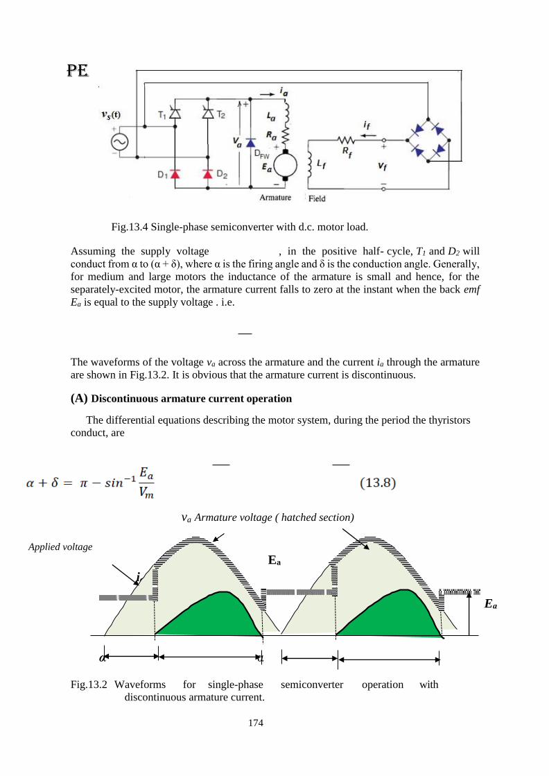
PE
174
Fig.13.4 Single-phase semiconverter with d.c. motor load.
Assuming the supply voltage , in the positive half- cycle, T1 and D2 will
conduct from α to (α + δ), where α is the firing angle and δ is the conduction angle. Generally,
for medium and large motors the inductance of the armature is small and hence, for the
separately-excited motor, the armature current falls to zero at the instant when the back emf
Ea is equal to the supply voltage . i.e.
The waveforms of the voltage va across the armature and the current ia through the armature
are shown in Fig.13.2. It is obvious that the armature current is discontinuous.
(A) Discontinuous armature current operation
The differential equations describing the motor system, during the period the thyristors
conduct, are
va Armature voltage ( hatched section)
Applied voltage
Ea
ia
Ea
α α
Fig.13.2 Waveforms for single-phase semiconverter operation with
discontinuous armature current.
PE
175
If we assume that the inertia of the rotating system is large then speed fluctuations will
be negligible. If each term of is integrated from α to (α + δ) and then divided by π , the
instantaneous voltage, current and speed will be converted to their respective average values,
where
[ ]
and the average voltage across is zero.
(B) Analysis with Continuous Armature Current Operation
If the armature inductance is large then conduction will continue, even after the supply
voltage has reversed, for which typical waveforms are shown in Fig.13.6. Hence assume
continuous current operation, the average value of the armature voltage is:
PE
176
series with the armature and hence the armature current becomes continuous, using D1 or D2 as
freewheeling diodes whenever the supply voltage reverses. Two modes of operation are
possible. In one mode current flows through T1 and D2 (or T2 and D1) and the supply voltage
appears across the motor. In the second mode T1 and D1 (or T2 and D2) conduct and the motor
voltage is zero. The motor equations are:
PE
177
Single-Phase Full-Wave Fully-
Controlled Rectifier Drives
The circuit diagram of a single-phase full-wave fully-controlled converter drive for
controlling a separately-excited d.c. motor is depicted in Fig.13.8.
Fig. 13.8 Single-phase full-converter with d.c. motor load.
PE
178
Here a full-wave rectifier bridge is supplies the field circuit, while the full-converter supplies
the armature circuit. The converter has four thyristors that need alternate switching of the
pairs of these thyristors T1 , T2 or T3 , T4 . The converter provides + Va or – Va depending on
the value of the triggering angle α of the thyristors, thus two quadrant operation is possible.
Armature current remains unidirectional due to the converter configuration. The vast majority
of shunt motors are also controlled in this manner.
(C) Single-phase full-converter operation with continuous motor current
The waveforms of voltage va across the armature and the current ia through the armature
are shown in Fig. 13.9 for continuous current mode of operation.
Fig.13.9 Waveforms of the armature voltage and the current for contin- uous current
operating mode.
In any case it is obvious that the thyristor only conducts when supply voltage exceeds
the back emf , i.e. .

PE
179
When thyristors T1 and T2 triggered at ωt = α , T3 and T4 must be turned off. When thyristors
T3 and T4 are triggered at ωt = α + π negative voltage is applied across T1 and T2 causes them
to commutate naturally. The average value of the armature voltage, as can be deduced from
Fig.13.9 is
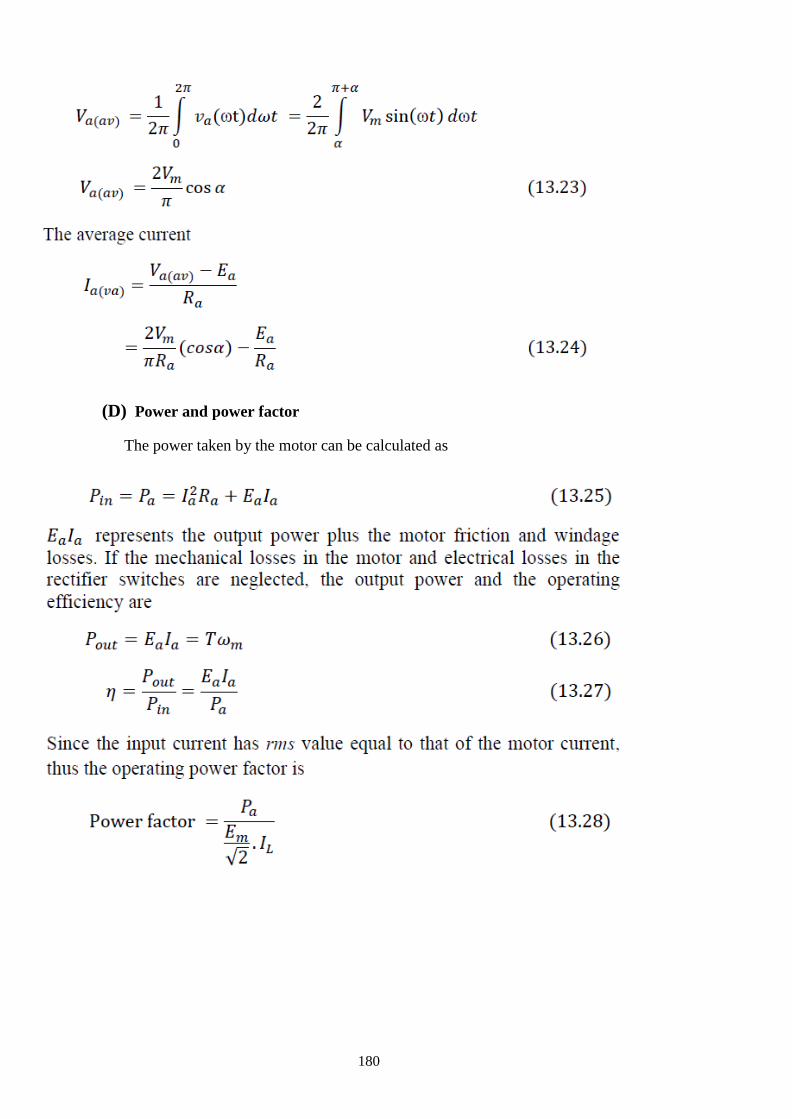
PE
180
(D) Power and power factor
The power taken by the motor can be calculated as
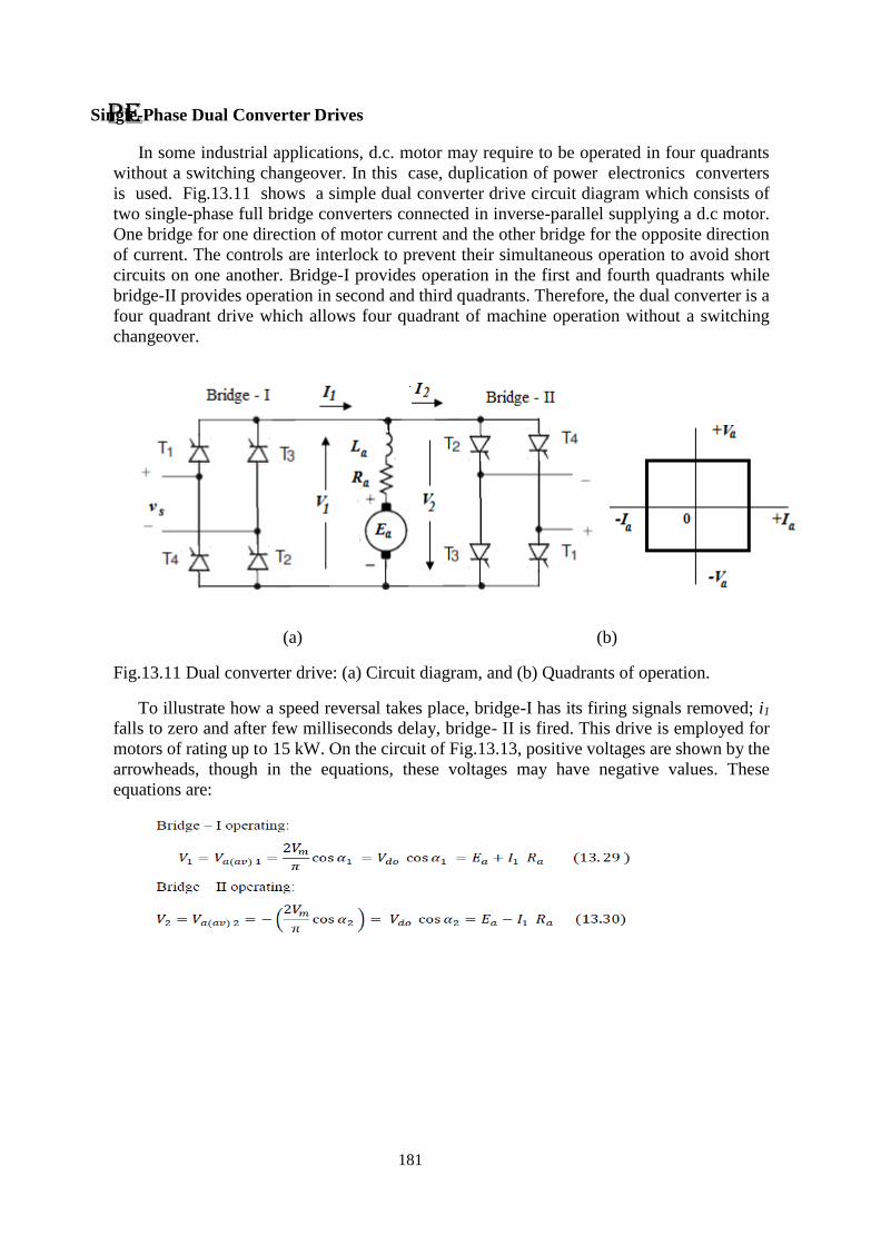
PE
181
Single-Phase Dual Converter Drives
In some industrial applications, d.c. motor may require to be operated in four quadrants
without a switching changeover. In this case, duplication of power electronics converters
is used. Fig.13.11 shows a simple dual converter drive circuit diagram which consists of
two single-phase full bridge converters connected in inverse-parallel supplying a d.c motor.
One bridge for one direction of motor current and the other bridge for the opposite direction
of current. The controls are interlock to prevent their simultaneous operation to avoid short
circuits on one another. Bridge-I provides operation in the first and fourth quadrants while
bridge-II provides operation in second and third quadrants. Therefore, the dual converter is a
four quadrant drive which allows four quadrant of machine operation without a switching
changeover.
(a) (b)
Fig.13.11 Dual converter drive: (a) Circuit diagram, and (b) Quadrants of operation.
To illustrate how a speed reversal takes place, bridge-I has its firing signals removed; i1
falls to zero and after few milliseconds delay, bridge- II is fired. This drive is employed for
motors of rating up to 15 kW. On the circuit of Fig.13.13, positive voltages are shown by the
arrowheads, though in the equations, these voltages may have negative values. These
equations are:
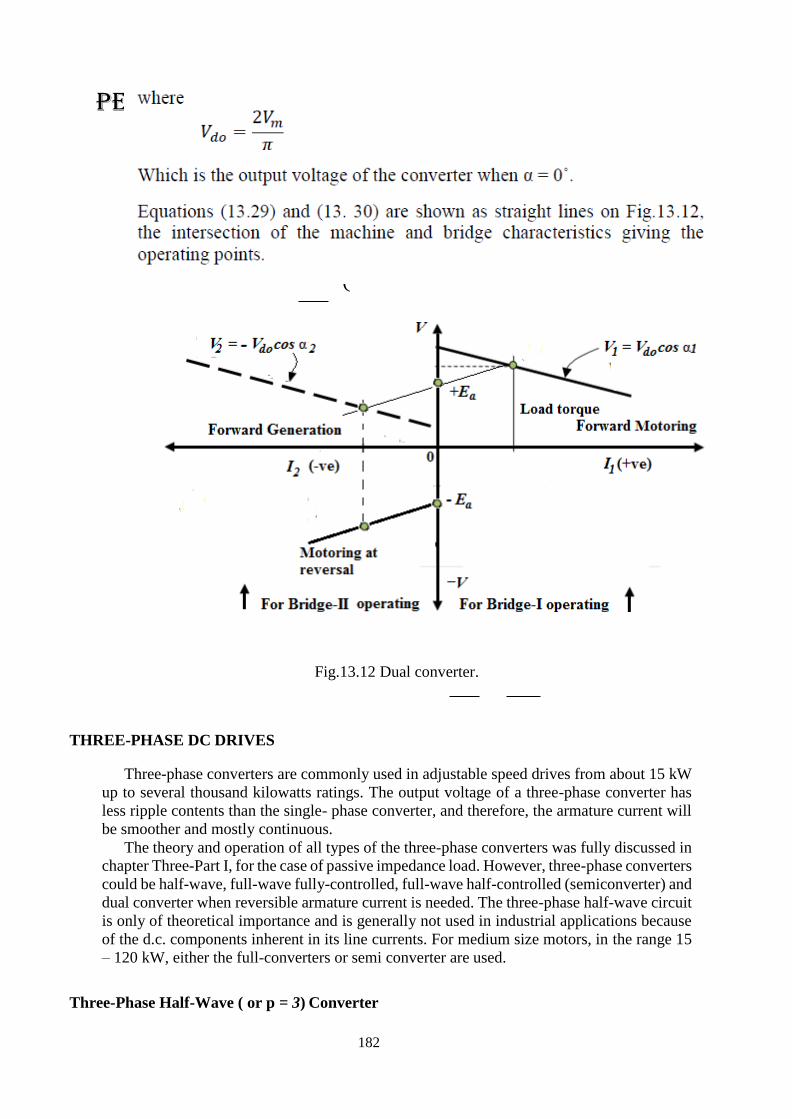
PE
182
(
Fig.13.12 Dual converter.
THREE-PHASE DC DRIVES
Three-phase converters are commonly used in adjustable speed drives from about 15 kW
up to several thousand kilowatts ratings. The output voltage of a three-phase converter has
less ripple contents than the single- phase converter, and therefore, the armature current will
be smoother and mostly continuous. The theory and operation of all types of the three-phase converters was fully discussed in
chapter Three-Part I, for the case of passive impedance load. However, three-phase converters
could be half-wave, full-wave fully-controlled, full-wave half-controlled (semiconverter) and
dual converter when reversible armature current is needed. The three-phase half-wave circuit
is only of theoretical importance and is generally not used in industrial applications because
of the d.c. components inherent in its line currents. For medium size motors, in the range 15
– 120 kW, either the full-converters or semi converter are used.
Three-Phase Half-Wave ( or p = 3) Converter
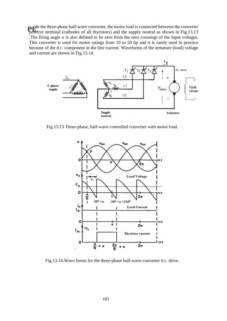
PE
183
In the three-phase half-wave converter, the motor load is connected between the converter
positive terminal (cathodes of all thyristors) and the supply neutral as shown in Fig.13.13
.The firing angle α is also defined to be zero from the zero crossings of the input voltages.
This converter is used for motor ratings from 10 to 50 hp and it is rarely used in practice
because of the d.c. component in the line current. Waveforms of the armature (load) voltage
and current are shown in Fig.13.14.
Fig.13.13 Three-phase, half-wave controlled converter with motor load.
Fig.13.14.Wave forms for the three-phase half-wave converter d.c. drive.
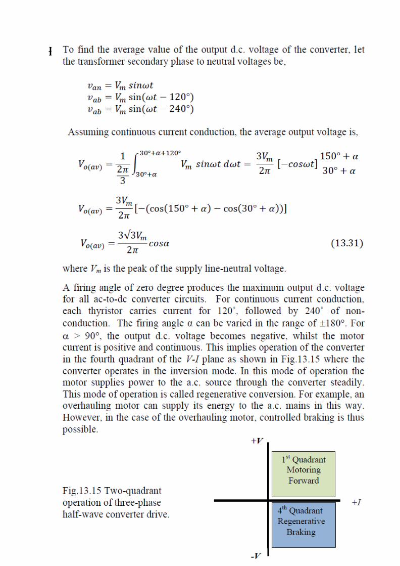
PE
184
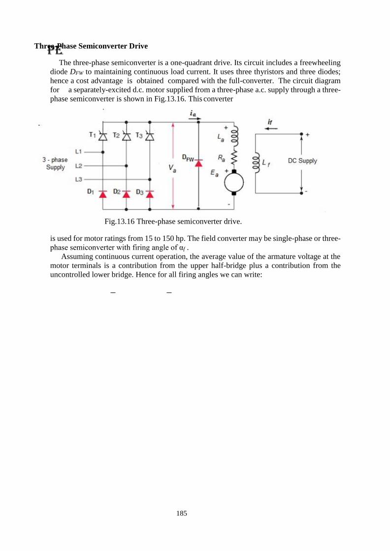
PE
185
Three-Phase Semiconverter Drive
The three-phase semiconverter is a one-quadrant drive. Its circuit includes a freewheeling
diode DFW to maintaining continuous load current. It uses three thyristors and three diodes;
hence a cost advantage is obtained compared with the full-converter. The circuit diagram
for a separately-excited d.c. motor supplied from a three-phase a.c. supply through a three-
phase semiconverter is shown in Fig.13.16. This converter
Fig.13.16 Three-phase semiconverter drive.
is used for motor ratings from 15 to 150 hp. The field converter may be single-phase or three-
phase semiconverter with firing angle of αf .
Assuming continuous current operation, the average value of the armature voltage at the
motor terminals is a contribution from the upper half-bridge plus a contribution from the
uncontrolled lower bridge. Hence for all firing angles we can write:
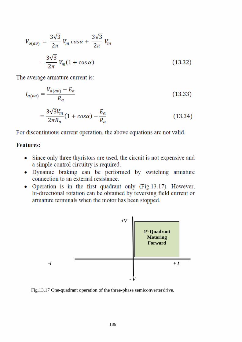
PE
186
-I + I
- V
Fig.13.17 One-quadrant operation of the three-phase semiconverter drive.
+V
1st Quadrant
Motoring
Forward
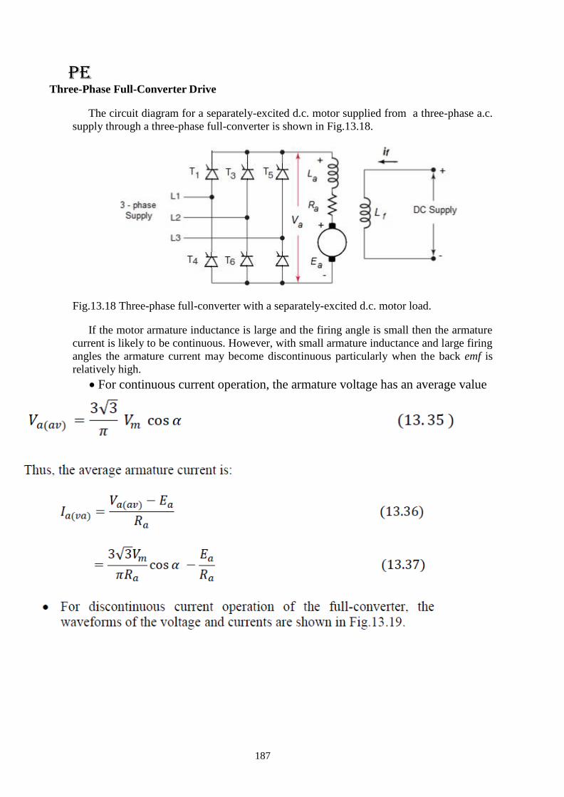
PE
187
Three-Phase Full-Converter Drive
The circuit diagram for a separately-excited d.c. motor supplied from a three-phase a.c.
supply through a three-phase full-converter is shown in Fig.13.18.
Fig.13.18 Three-phase full-converter with a separately-excited d.c. motor load.
If the motor armature inductance is large and the firing angle is small then the armature
current is likely to be continuous. However, with small armature inductance and large firing
angles the armature current may become discontinuous particularly when the back emf is
relatively high.
For continuous current operation, the armature voltage has an average value
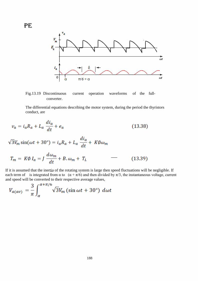
PE
188
Fig.13.19 Discontinuous current operation waveforms of the full-
converter.
The differential equations describing the motor system, during the period the thyristors
conduct, are
If it is assumed that the inertia of the rotating system is large then speed fluctuations will be negligible. If
each term of is integrated from α to (α + π/6) and then divided by π/3, the instantaneous voltage, current
and speed will be converted to their respective average values,
PE
189
Three-Phase Dual Converter Drive
Four-quadrant operation of a medium and large size d.c. motor drive (200-2000 hp)
can be obtained by the three-phase dual converter shown in Fig.13.20. The average motor
voltage is required to be equal for both converters, which required that the firing angles
of the two sets of the thyristors should sum to 180˚.
The armature voltage supplied by converter-1 (for continuous current operation) is
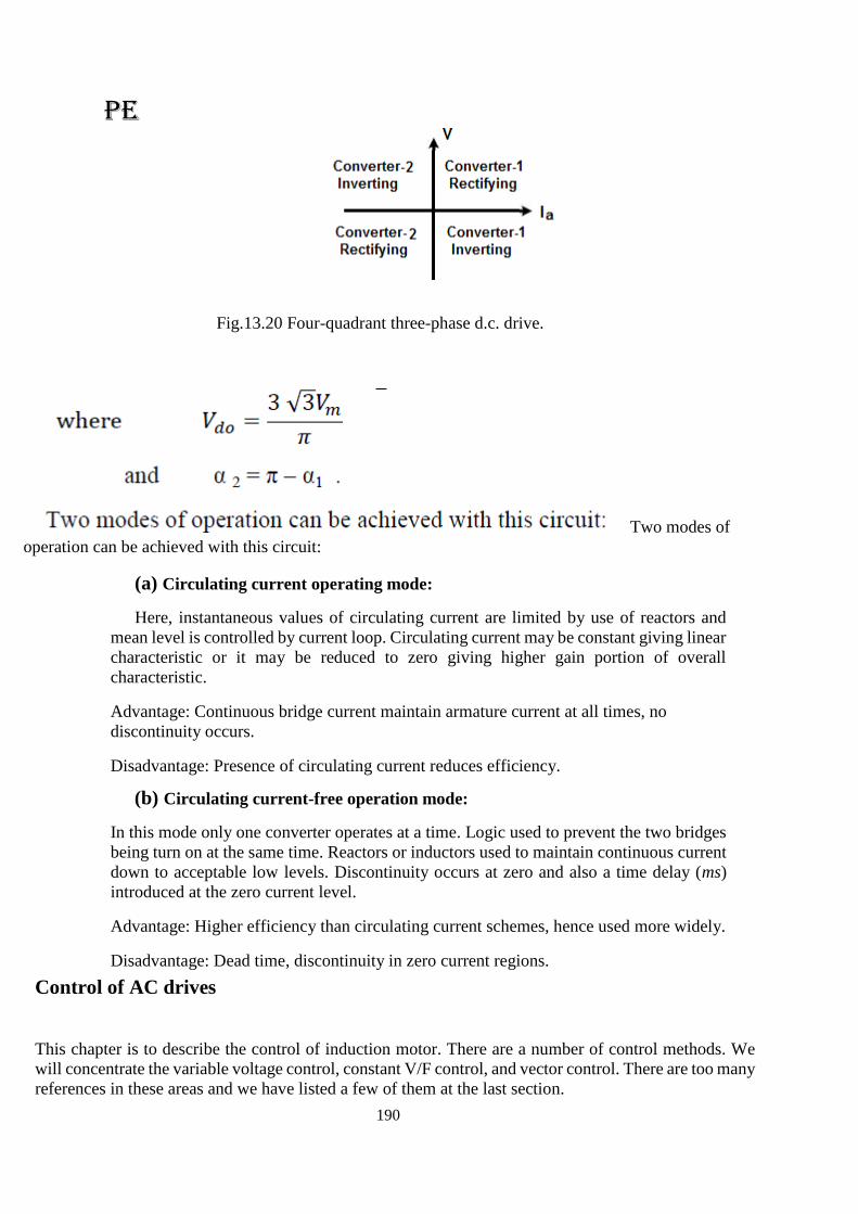
PE
190
Fig.13.20 Four-quadrant three-phase d.c. drive.
Two modes of
operation can be achieved with this circuit:
(a) Circulating current operating mode:
Here, instantaneous values of circulating current are limited by use of reactors and
mean level is controlled by current loop. Circulating current may be constant giving linear
characteristic or it may be reduced to zero giving higher gain portion of overall
characteristic.
Advantage: Continuous bridge current maintain armature current at all times, no
discontinuity occurs.
Disadvantage: Presence of circulating current reduces efficiency.
(b) Circulating current-free operation mode:
In this mode only one converter operates at a time. Logic used to prevent the two bridges
being turn on at the same time. Reactors or inductors used to maintain continuous current
down to acceptable low levels. Discontinuity occurs at zero and also a time delay (ms)
introduced at the zero current level.
Advantage: Higher efficiency than circulating current schemes, hence used more widely.
Disadvantage: Dead time, discontinuity in zero current regions.
Control of AC drives
This chapter is to describe the control of induction motor. There are a number of control methods. We
will concentrate the variable voltage control, constant V/F control, and vector control. There are too many
references in these areas and we have listed a few of them at the last section.
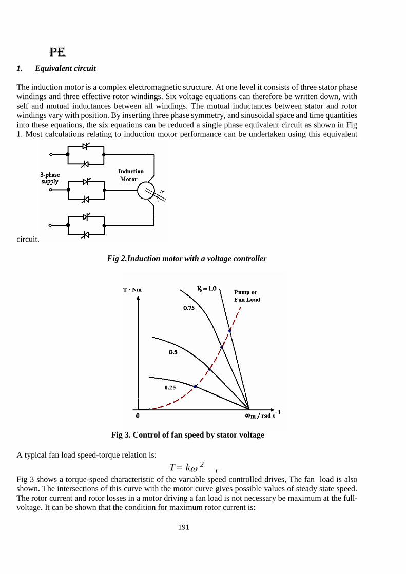
PE
191
1. Equivalent circuit
The induction motor is a complex electromagnetic structure. At one level it consists of three stator phase
windings and three effective rotor windings. Six voltage equations can therefore be written down, with
self and mutual inductances between all windings. The mutual inductances between stator and rotor
windings vary with position. By inserting three phase symmetry, and sinusoidal space and time quantities
into these equations, the six equations can be reduced a single phase equivalent circuit as shown in Fig
1. Most calculations relating to induction motor performance can be undertaken using this equivalent
circuit.
Fig 2.Induction motor with a voltage controller
Fig 3. Control of fan speed by stator voltage
A typical fan load speed-torque relation is:
T= k 2
Fig 3 shows a torque-speed characteristic of the variable speed controlled drives, The fan load is also
shown. The intersections of this curve with the motor curve gives possible values of steady state speed.
The rotor current and rotor losses in a motor driving a fan load is not necessary be maximum at the full-
voltage. It can be shown that the condition for maximum rotor current is:
r
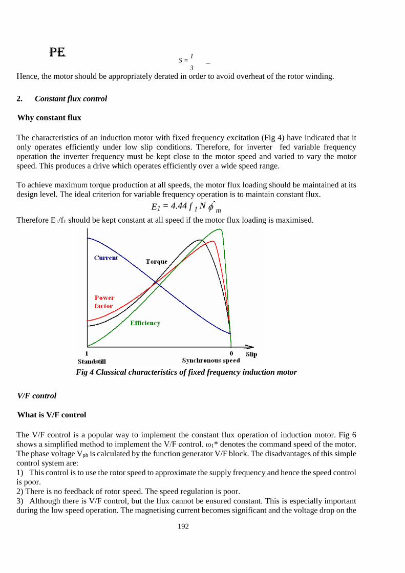
PE
192
S = 1
3
Hence, the motor should be appropriately derated in order to avoid overheat of the rotor winding.
2. Constant flux control
Why constant flux
The characteristics of an induction motor with fixed frequency excitation (Fig 4) have indicated that it
only operates efficiently under low slip conditions. Therefore, for inverter fed variable frequency
operation the inverter frequency must be kept close to the motor speed and varied to vary the motor
speed. This produces a drive which operates efficiently over a wide speed range.
To achieve maximum torque production at all speeds, the motor flux loading should be maintained at its
design level. The ideal criterion for variable frequency operation is to maintain constant flux.
E1 = 4.44 f 1 N ˆm
Therefore E1/f1 should be kept constant at all speed if the motor flux loading is maximised.
Fig 4 Classical characteristics of fixed frequency induction motor
V/F control
What is V/F control
The V/F control is a popular way to implement the constant flux operation of induction motor. Fig 6
shows a simplified method to implement the V/F control. ω1* denotes the command speed of the motor.
The phase voltage Vph is calculated by the function generator V/F block. The disadvantages of this simple
control system are:
1) This control is to use the rotor speed to approximate the supply frequency and hence the speed control
is poor.
2) There is no feedback of rotor speed. The speed regulation is poor.
3) Although there is V/F control, but the flux cannot be ensured constant. This is especially important
during the low speed operation. The magnetising current becomes significant and the voltage drop on the
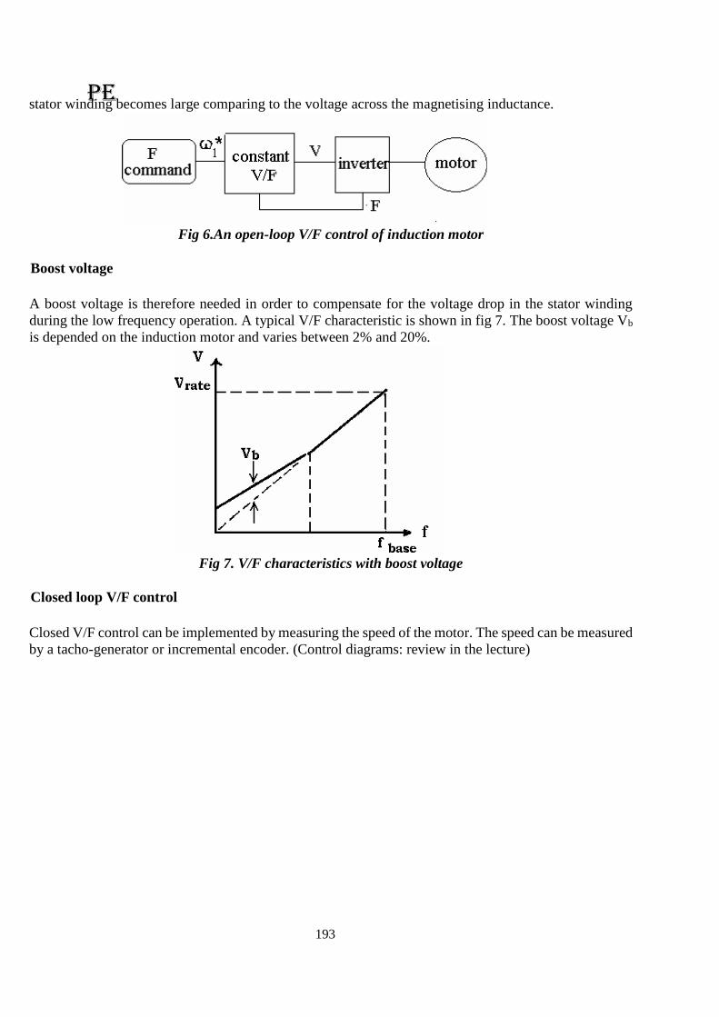
PE
193
stator winding becomes large comparing to the voltage across the magnetising inductance.
Fig 6.An open-loop V/F control of induction motor
Boost voltage
A boost voltage is therefore needed in order to compensate for the voltage drop in the stator winding
during the low frequency operation. A typical V/F characteristic is shown in fig 7. The boost voltage Vb
is depended on the induction motor and varies between 2% and 20%.
Fig 7. V/F characteristics with boost voltage
Closed loop V/F control
Closed V/F control can be implemented by measuring the speed of the motor. The speed can be measured
by a tacho-generator or incremental encoder. (Control diagrams: review in the lecture)
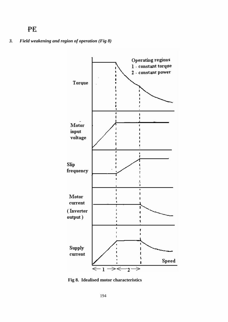
PE
194
3. Field weakening and region of operation (Fig 8)
Fig 8. Idealised motor characteristics

PE
195

PE
196
Region of operation
Region 1. Constant torque region:
This is the constant volts/frequency ratio region, apart from the voltage boost needed at low speed to
overcome stator voltage drop. Ideally, this results in constant flux in the air-gap; hence with constant
rotor current and slip frequency, constant torque is achieved.
Region 2. Constant power region
Once the motor speed is increased beyond its base speed, there is no further voltage increase available
because it will exceed the rated voltage. Further increase of the motor speed is achieved by weakening
the field.
The function generation of the V/F control diagram can now be modified such that the voltage is hold
constant at the rated voltage beyond base speed. Further increase in speed will cause the motor to operate
in field weakening region.
Plugging, Motoring and Regenerative braking
Motoring - The source frequency of the motor can be adjusted by changing the frequency demand of the
inverter (the PWM pulse width equation). It should be noted that using PWM inverter, the frequency can
be positive or negative in order to control the motor in forward or reverse rotation.
Plugging - The rotor rotates in the opposite direction to that of the air gap flux, ie S >
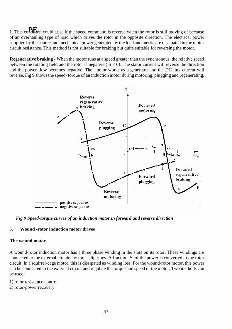
PE
197
1. This condition could arise if the speed command is reverse when the rotor is still moving or because
of an overhauling type of load which drives the rotor in the opposite direction. The electrical power
supplied by the source and mechanical power generated by the load and inertia are dissipated in the motor
circuit resistance. This method is not suitable for braking but quite suitable for reversing the motor.
Regenerative braking - When the motor runs at a speed greater than the synchronous, the relative speed
between the rotating field and the rotor is negative ( S < 0). The stator current will reverse the direction
and the power flow becomes negative. The motor works as a generator and the DC link current will
reverse. Fig 9 shows the speed- torque of an induction motor during motoring, plugging and regenerating.
Fig 9 Speed-torque curves of an induction motor in forward and reverse direction
5. Wound -rotor induction motor drives
The wound motor
A wound-rotor induction motor has a three phase winding in the slots on its rotor. These windings are
connected to the external circuits by three slip rings. A fraction, S, of the power is converted to the rotor
circuit. In a squirrel-cage motor, this is dissipated as winding loss. For the wound-rotor motor, this power
can be connected to the external circuit and regulate the torque and speed of the motor. Two methods can
be used:
1) rotor resistance control
2) rotor-power recovery
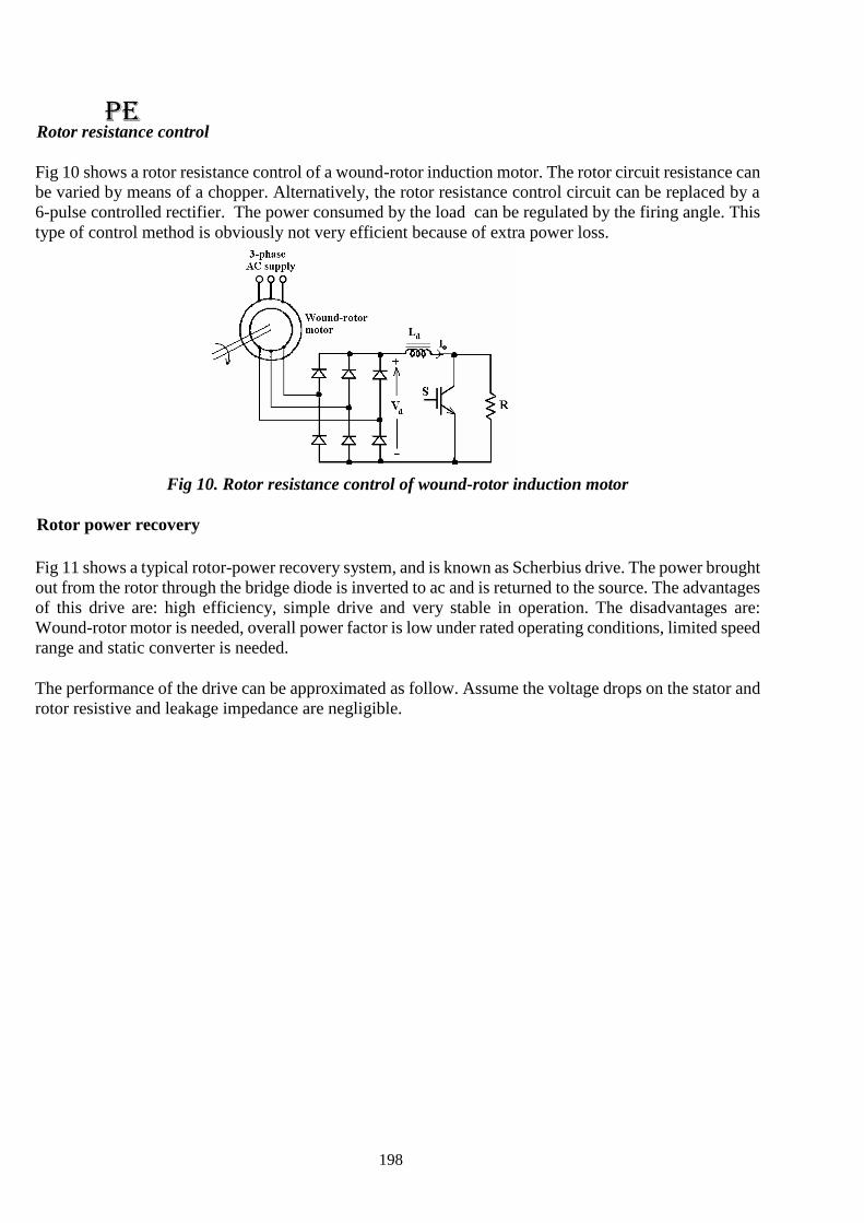
PE
198
Rotor resistance control
Fig 10 shows a rotor resistance control of a wound-rotor induction motor. The rotor circuit resistance can
be varied by means of a chopper. Alternatively, the rotor resistance control circuit can be replaced by a
6-pulse controlled rectifier. The power consumed by the load can be regulated by the firing angle. This
type of control method is obviously not very efficient because of extra power loss.
Fig 10. Rotor resistance control of wound-rotor induction motor
Rotor power recovery
Fig 11 shows a typical rotor-power recovery system, and is known as Scherbius drive. The power brought
out from the rotor through the bridge diode is inverted to ac and is returned to the source. The advantages
of this drive are: high efficiency, simple drive and very stable in operation. The disadvantages are:
Wound-rotor motor is needed, overall power factor is low under rated operating conditions, limited speed
range and static converter is needed.
The performance of the drive can be approximated as follow. Assume the voltage drops on the stator and
rotor resistive and leakage impedance are negligible.
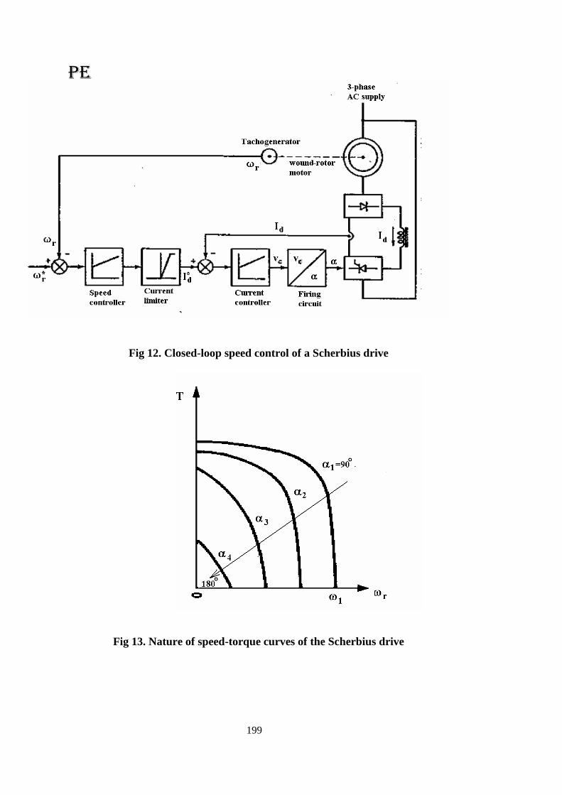
PE
199
Fig 12. Closed-loop speed control of a Scherbius drive
Fig 13. Nature of speed-torque curves of the Scherbius drive
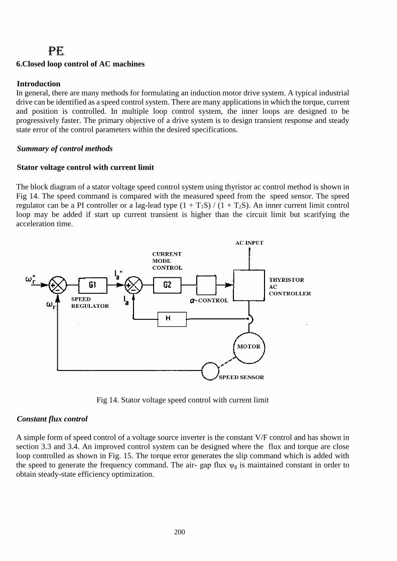
PE
200
6.Closed loop control of AC machines
Introduction
In general, there are many methods for formulating an induction motor drive system. A typical industrial
drive can be identified as a speed control system. There are many applications in which the torque, current
and position is controlled. In multiple loop control system, the inner loops are designed to be
progressively faster. The primary objective of a drive system is to design transient response and steady
state error of the control parameters within the desired specifications.
Summary of control methods
Stator voltage control with current limit
The block diagram of a stator voltage speed control system using thyristor ac control method is shown in
Fig 14. The speed command is compared with the measured speed from the speed sensor. The speed
regulator can be a PI controller or a lag-lead type (1 + T1S) / (1 + T2S). An inner current limit control
loop may be added if start up current transient is higher than the circuit limit but scarifying the
acceleration time.
Fig 14. Stator voltage speed control with current limit
Constant flux control
A simple form of speed control of a voltage source inverter is the constant V/F control and has shown in
section 3.3 and 3.4. An improved control system can be designed where the flux and torque are close
loop controlled as shown in Fig. 15. The torque error generates the slip command which is added with
the speed to generate the frequency command. The air- gap flux ψg is maintained constant in order to
obtain steady-state efficiency optimization.
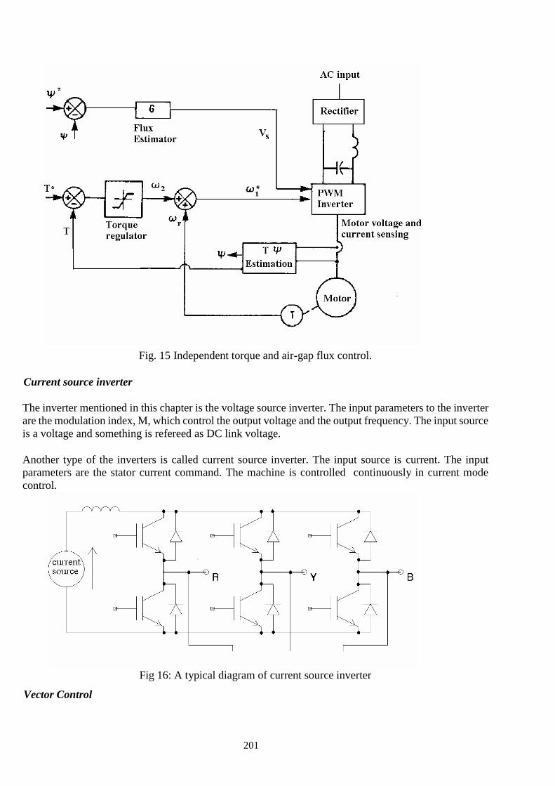
PE
201
Fig. 15 Independent torque and air-gap flux control.
Current source inverter
The inverter mentioned in this chapter is the voltage source inverter. The input parameters to the inverter
are the modulation index, M, which control the output voltage and the output frequency. The input source
is a voltage and something is refereed as DC link voltage.
Another type of the inverters is called current source inverter. The input source is current. The input
parameters are the stator current command. The machine is controlled continuously in current mode
control.
Fig 16: A typical diagram of current source inverter
Vector Control
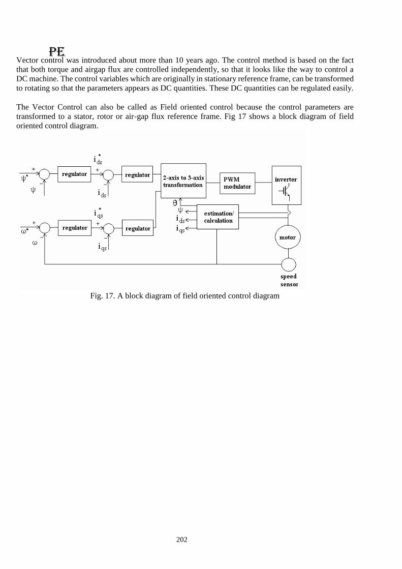
PE
202
Vector control was introduced about more than 10 years ago. The control method is based on the fact
that both torque and airgap flux are controlled independently, so that it looks like the way to control a
DC machine. The control variables which are originally in stationary reference frame, can be transformed
to rotating so that the parameters appears as DC quantities. These DC quantities can be regulated easily.
The Vector Control can also be called as Field oriented control because the control parameters are
transformed to a stator, rotor or air-gap flux reference frame. Fig 17 shows a block diagram of field
oriented control diagram.
Fig. 17. A block diagram of field oriented control diagram

PE
203
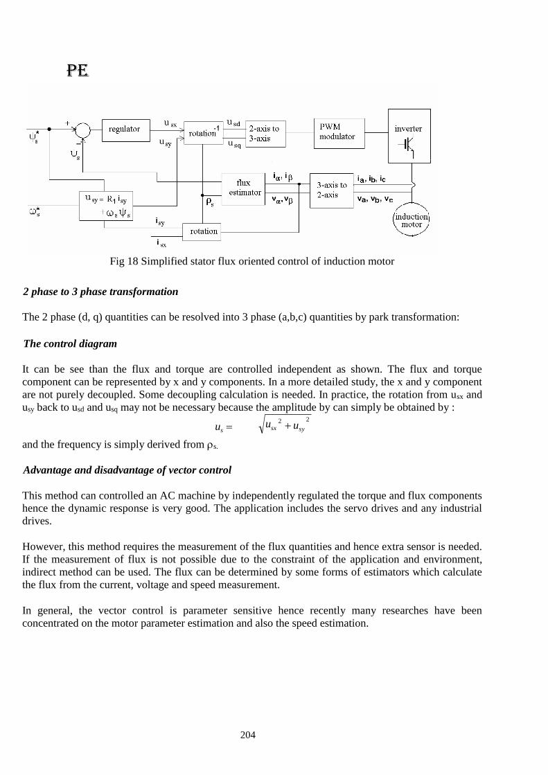
PE
204
Fig 18 Simplified stator flux oriented control of induction motor
2 phase to 3 phase transformation
The 2 phase (d, q) quantities can be resolved into 3 phase (a,b,c) quantities by park transformation:
The control diagram
It can be see than the flux and torque are controlled independent as shown. The flux and torque
component can be represented by x and y components. In a more detailed study, the x and y component
are not purely decoupled. Some decoupling calculation is needed. In practice, the rotation from usx and
usy back to usd and usq may not be necessary because the amplitude by can simply be obtained by :
us
and the frequency is simply derived from s.
Advantage and disadvantage of vector control
This method can controlled an AC machine by independently regulated the torque and flux components
hence the dynamic response is very good. The application includes the servo drives and any industrial
drives.
However, this method requires the measurement of the flux quantities and hence extra sensor is needed.
If the measurement of flux is not possible due to the constraint of the application and environment,
indirect method can be used. The flux can be determined by some forms of estimators which calculate
the flux from the current, voltage and speed measurement.
In general, the vector control is parameter sensitive hence recently many researches have been
concentrated on the motor parameter estimation and also the speed estimation.
usx 2
usy
2

PE
205
7. Comparison of AC drives
Stator voltage
control
Square-wave
inverter
PWM
inverter
Speed range Limited low speed medium to high
speed (10:1)
ratio
Very wide
speed
range, up
to very low
speed
Harmonics Rich harmonics
in line and
machine.
Problem in
motor
heating
relative lower
in low
frequency
harmonics
Very low in
harmonics
especially
the
switching
frequency
is high
Torque
pulsation
High pulsating
torque
frequency
Problem at low
speed
Minimal
Power
factor
Poor in line
power factor
because of the
phase control
low line power
factor because
of phase
control
High power
factor
Efficiency Poor Medium but
improves with
better transistors
Good and
improves
with better
transistors
Cost Low cost because
simple in control
circuit
Moderate
ly but
improvin
g
Moderate
ly
because
of the
control
circuits
but
improvin
g
Application Low to medium
power blower
and pump drives.
Low power
appliance
General
purpose
drives.
Low to
medium
power
General
purpose
drive,
medium to
high power
application,
servo drives

PE
206
Gen
eral
com
men
ts
Application is
limited
Usually for
open loop
control. May
have stability
problem at low
speed.
Fast
transien
t
respons
e.
popular
drive
Most of us take the mains ac supply for granted and use it almost casually without giving the slightest thought to its
inherent shortcomings and the danger posed to sophisticated and sensitive electronic instruments/equipments. For
ordinary household appliances such as incandencent lamps, tubes, fans, TV and fridge, the mains ac supply does not
make much difference, but when used for computers, medical equipments and telecommunication systems, a clean,
stable interruption free power supply is of the utmost importance. Of the myriad of devices, processes and systems
which rely on ac power, computers are probably the most sensitive to power disturbances and failures. Interruptions in
power supply may cause the contents of a memory to be lost or corrupted, the entire system to malfunction or fail, or
even variety of components failures to occur, all of which not only result in inconvenience but also loss of money.
As more and more PCs, word processors and data terminals find their way into small business, UPS systems that meet
the power requirements and price range needs of even the small business organizations and offices are being
manufactured.
Uninterruptible Power Supply Systems.
There are three distinct types of uninterrupted power supplies, namely, (£) on-line UPS (ii) off-line UPS, and (Hi)
electronic generators. In the on-line UPS, whether the mains power is on or off, the battery operated inverter is on all
the time and supplies the ac output voltage. When the mains power supply goes off, the UPS will be on only until the
battery gets discharged. When the main power resumes, the battery will get charged again. In off-line UPS and electronic
generators, ther inverter is off when the mains power is present and the output voltage derived directly from the mains
is the same as the mains supply voltage. The inverter turns on only when the mains supply goes off.
The block diagrams of on-line UPS, off-line UPS and electronic generators are given in figs The ever increasing
importance of computers in industry and commerce will increase the need for quality, high stability and interruption
free power supplies.
A clean ac power source is the fundamental to the operation of most sensitive electronic equipment, and many new and
sophisticated circuits are designed to overcome the effects of disturbances normally found in the mains ac supply.
In order to protect a sensitive system from power losses and blackouts, an alternative power source is required that can
switch into operation immediately when disruption occurs. An interruptible power supply (UPS) is just such an
alternative source. A UPS generally consists of a rectifier, battery charger, a battery bank and inverter circuit which
converts the commercial ac input into dc suitable for input to the battery bank and the inverter. The rectifier should have
its input protected and should be capable of supplying power to the inverter when the commercial supply is either slightly
below the normal voltage or slightly above.
Online UPS:

PE
207
In case of On-line UPS, the battery operated inverter works continuously whether the mains supply is present or not.
Triac T1 is on for all the times while Triac T2 has been provided to bypass the UPS inverter, only when a fault
develops in the UPS inverter. When the mains supply fails, the UPS supplies power only until the batteries get
discharged. However, once the mains power resumes, the batteries will get charged again. The switching times of these
supplies is considered to be zero. Usually sealed maintenance free batteries are used and the running time of the inverter is
low (approximately 10 to 30 minutes).
Off Line UPS:
In the case of Off-Line UPS, the inverter is off when the mains power is on and the output voltage is derived directly
from the mains. The inverter turns on only when the mains supply fails. Its switching time is less than 5 ms. These
UPS are generally used with PCs or computers or other appliances where a small duration (5 ms or less) interruption
in power supply can be tolerated. Usually, sealed batteries or lead-acid batteries are used. The running time of
these supplies is also low (about 10 to 30 minutes).
Electronic Generators:
Offline UPS Block Diagram
Online UPS Block Diagram

PE
208
An electronic generator is the same as the off-line UPS system except for one difference that switching time from the
mains supply to battery driven inverter supply will not be small (over 10 ms) for the electronic generator. Also, the
electronic generators will run for longer time (1 to 4 hours) than off-line UPS systems because, usually large size lead-
acid batteries are used with/electronic generators. These are meant for household applications to run fans, coolers, fridge,
lights, TV and VCR.
The demand is the highest for the electronic generators meant for house hold applications, followed by the off-line UPS,
and then the on-line UPS systems. The off-line or online UPS systems are mainly used in places where PCs or computers
are used. The demand for on- line UPS systems is less than for off-line UPS systems because the price of the on-line
UPS systems is higher.
Switched Mode Power Supply (SMPS)
Like a linear power supply, the switched mode power supply too converts the available unregulated ac or dc input
voltage to a regulated dc output voltage. However in case of SMPS with input supply drawn from the ac mains, the
input voltage is first rectified and filtered using a capacitor at the rectifier output. The unregulated dc voltage across
the capacitor is then fed to a high frequency dc-to-dc converter. Most of the dc-to-dc converters used in SMPS circuits
have an intermediate high frequency ac conversion stage to facilitate the use of a high frequency transformer for
voltage scaling and isolation. In contrast, in linear power supplies with input voltage drawn from ac mains, the mains
voltage is first stepped down (and isolated) to the desired magnitude using a mains frequency transformer, followed
by rectification and filtering. The high frequency transformer used in a SMPS circuit is much smaller in size and
weight compared to the low frequency transformer of the linear power supply circuit.
The ‘Switched Mode Power Supply’ owes its name to the dc-to-dc switching converter for conversion from
unregulated dc input voltage to regulated dc output voltage. The switch employed is turned ‘ON’ and ‘OFF’ (referred
as switching) at a high frequency. During ‘ON’ mode the switch is in saturation mode with negligible voltage drop
across the collector and emitter terminals of the switch where as in ‘OFF’ mode the switch is in cut-off mode with
negligible current through the collector and emitter terminals. On the contrary the voltage- regulating switch, in a
linear regulator circuit, always remains in the active region.
Details of some popular SMPS circuits, with provisions for incorporating high frequency transformer for voltage
scaling and isolation, have been discussed in next few lessons. In this lesson a simplified schematic switching
arrangement is described that omits the transformer action. In fact there are several other switched mode dc-to-dc
converter circuits that do not use a high frequency transformer. In such SMPS circuits the unregulated input dc voltage
is fed to a high frequency voltage chopping circuit such that when the chopping circuit (often called dc to dc chopper)
is in ON state, the unregulated voltage is applied to the output circuit that includes the load and some filtering circuit.
When the chopper is in OFF state, zero magnitude of voltage is applied to the output side. The ON and OFF durations
are suitably controlled such that the average dc voltage applied to the output circuit equals the desired magnitude of
output voltage. The ratio of ON time to cycle time (ON + OFF time) is known as duty ratio of the chopper circuit. A
high switching frequency (of the order of 100 KHz) and a fast control over the duty ratio results in application of the
desired mean voltage along with ripple voltage of a very high frequency to the output side, consisting of a low pass
Electronic Generator

PE
209
filter circuit followed by the load. The high frequency ripple in voltage is effectively filtered using small values of
filter capacitors and inductors.
SMPS versus linear power supply
As discussed above, in a linear regulator circuit the excess voltage from the unregulated dc input supply drops across
a series element (and hence there is power loss in proportion to this voltage drop) whereas in switched mode circuit
the unregulated portion of the voltage is removed by modulating the switch duty ratio. The switching losses in modern
switches (like: MOSFETs) are much less compared to the loss in the linear element.
In most of the switched mode power supplies it is possible to insert a high frequency transformer to isolate the output
and to scale the output voltage magnitude. In linear power supply the isolation and voltage-scaling transformer can
be put only across the low frequency utility supply. The low frequency transformer is very heavy and bulky in
comparison to the high frequency transformer of similar VA rating. Similarly the output voltage filtering circuit, in
case of low frequency ripples is much bulkier than if the ripple is of high frequency. The switched mode circuit
produces ripple of high frequency that can be filtered easily using smaller volume of filtering elements.
Linear power supply though more bulky and less efficient has some advantages too when compared with the switched
mode power supply. Generally the control of the linear power supply circuit is much simpler than that of SMPS
circuit. Since there is no high frequency switching, the switching related electro-magnetic interference (EMI) is
practically absent in linear power supplies but is of some concern in SMPS circuits. Also, as far as output voltage
regulation is concerned the linear power supplies are superior to SMPS. One can more easily meet tighter
specifications on output voltage ripples by using linear power supplies.
Hybrid (SMPS followed by linear) power supply
A comparison of linear and switched mode power supplies tells about the advantages and disadvantages of the two.
Linear power supply is highly inefficient if it has to work over large variations in input voltage, is more bulky because
of the use of low frequency transformer and filter elements (inductors and capacitors). On the other hand linear power
supplies give better output voltage regulation. It may sometimes be required to have output voltage regulation similar
to the one provided by linear supplies and compactness and better efficiency of a switched mode supply. For this, the
linear power supply may be put in tandem with a switched mode supply. Let us consider a case where one needs an
isolated and well-regulated 5 volts output while input power is drawn from utility supply that has large voltage
fluctuation. In such a situation one may generate an isolated 7.5 volts from an SMPS and follow it by a 5 volts linear
power supply set to work with 7.5 volts input. The input to linear power supply must be few volts more than the
required output (for proper biasing of the switches) and hence SMPS tries to maintain around 7.5 volts input. It can
be seen that the linear power supply now does not have large input voltage variation in spite of large variations in the
utility rms voltage. The SMPS portion of the power supply efficiently performs the job of voltage isolation and
conversion from widely varying utility voltage to fairly regulated 7.5 volts dc. Under the given condition it may not
be difficult to see that the overall efficiency of this hybrid power supply will lie between that of a SMPS and a linear
supply. The overall cost may or may not increase even though two supplies in tandem are used. It is to be kept in mind
that to achieve the same output voltage specification by an SMPS circuit alone, the control and filtering circuit may
become more costly and complex (than the one used in the hybrid power supply unit). Similarly if the linear supply
has to be designed for larger fluctuation in input voltage the component ratings, including heat-sink ratings, will be
higher and may cost as much as the hybrid unit.
Multiple output SMPS
A single power supply unit may need to output several different voltages. The individual output voltages may have
different ratings in terms of output current, voltage regulation and ripple voltages. These outputs may need isolation
between them. Generally a common high frequency transformer links the input and output windings and in spite of
output voltage feedback all the outputs can not have same regulation because of different loads connected to different
outputs and hence different ohmic (resistive) drops in the output windings (loads are generally variable and user
dependent). Also the coupling between the different secondary windings and the primary winding may not be same
causing different voltage drops across the respective leakage inductances. Barring this mismatch in the voltage drops
across the resistances and leakage inductances of the secondary windings their output voltages are in proportional to
their turns ratios. The turns ratios are properly chosen to give fairly regulated individual output voltages (even if only
one output voltage feedback is used for SMPS switch control). The output that needs to have tighter voltage regulation

PE
210
may be used for output voltage feedback. In case another output needs to have similarly tight regulation then that
particular output may be passed through an additional linear regulator circuit as in the case of hybrid power supply
circuit discussed in the previous section (Sec. 21.5).
Resonant Mode Power Supplies
Resonant mode power supplies are a variation over SMPS circuits where the switching losses are significantly reduced
by adapting zero-voltage or zero-current switching techniques. In non- resonant mode SMPS circuits the switches are
subjected to hard switching (during hard- switching, both the voltage and current in the switch are of considerable
magnitude resulting in large instantaneous switching power loss). Efficiency of resonant mode power supplies is
generally higher than non-resonant mode supplies.
Power supply specifications
Power supplies may have several specifications to be met, including their voltage and current ratings. There may be
short time ratings of higher magnitudes of current and continuous ratings of somewhat lower magnitudes. One needs
to specify the tolerable limits on the ripple voltages, short-circuit protection level of current (if any) and the nature of
output volt-current curve during over-current or short circuit (the output voltage magnitude should reduce or fold back
towards zero, gradually, depending on the severity of over-current). The fuse requirement (if any) on the input and
the output side may need to be specified. One needs to specify the type of input supply (whether ac or dc) or whether
the power supply can work both from ac or dc input voltages. Acceptable range of variation in input voltage
magnitude, supply frequency (in case of ac input) are also to be specified. Efficiency, weight and volume are some
other important specifications. Some applications require the electro-magnetic compatibility standards to be met. By
electromagnetic compatibility it is meant that the level of EMI generation by power supply should be within tolerable
limits and at the same time the power supply should have the ability to work satisfactorily in a limited noisy
environment. It is quite common to have output voltage isolation and it is specified in terms of isolation breakdown
voltage. In case of multiple power supplies it needs to be specified whether all the outputs need to be isolated or not
and what should be the acceptable ripple voltage range for each.
In majority of the cases the available source of input power is the alternating type utility voltage of 50 or 60 Hz. The
voltage levels commonly used are 115V (common in countries like, USA) and 230 volts (common in India and many
of the European countries). Most utility (mains) power supplies are expected to have 10% voltage regulation but for
additional precaution the SMPS circuits must work even if input voltages have 20% variation. Now-a-days universal
power supplies that work satisfactorily and efficiently both on 115 V and 230 V input are quite popular. These power
supplies are very convenient for international travelers who can simply plug-on their equipments, like laptop computer
and shaving machine, without having to pay much attention on the exact voltage and frequency levels of the utility
supply. In contrast some of the other power supplies have a selector switch and the user is required to adjust the switch
position to match the utility voltage. In case user forgets to keep the selector switch at correct position, the equipment
attached may get damaged.
Some common types of SMPS circuits
There are several different topologies for the switched mode power supply circuits. Some popular ones are: fly-back,
forward, push-pull, half bridge and H-bridge circuits. Some of these configurations will be discussed in the coming
lessons. A particular topology may be more suitable than others on the basis of one or more performance
criterions like cost,
efficiency, overall weight and size, output power, output regulation, voltage ripple etc. All the topologies listed above
are capable of providing isolated voltages by incorporating a high frequency transformer in the circuit. There are
many commercially available power supply controller ICs that can readily be used to control the duty ratio of the
SMPS switches so that the final output is well regulated. Most of these ICs are capable of driving MOSFET type of
switches. They also provide features like under voltage lock-out, output over-current protection etc.