Two-Photon Polymerization of Hybrid Sol-Gel Materials for Photonics Applications
Upload
khangminh22Category
view
4download
0
Progress in Materials Science
Volume 99 Pages 27-105
DOI: 10.1016/j.pmatsci.2018.08.001
HYBRID SPINTRONIC MATERIALS: GROWTH, STRUCTURE AND PROPERTIES Wenqing Liu,1,2 ,* Ping Kwan Johnny Wong,3,4 ,* and Yongbing Xu1,4 , | |
1 York-Nanjing Joint Center (YNJC) for Spintronics and Nanoengineering, School of Electronics Science and Engineering, Nanjing University, Nanjing 210093, China 2 Department of Electronic Engineering, Royal Holloway University of London, Egham TW20 0EX, United Kingdom 3 Centre for Advanced 2D Materials and Graphene Research Centre, National University of Singapore, 6 Science Drive 2, Singapore 117546, Singapore
4 Spintronics and Nanodevice Laboratory, Department of Electronics, University of York, York YO10 5DD, United Kingdom || Author to whom correspondence should be addressed. Email: [email protected] * These authors contribute equally to this review article.
Abstract
Spintronics is an emergent interdisciplinary topic for the studies of spin-based, other than or in addition to charge-only-based physical phenomena. Since the discovery of giant magnetoresistance (GMR) effect in metallic multilayers, the first-generation spintronics has generated huge impact to the mass data storage industries. The second-generation spintronics, on the other hand, focuses on the integration of the magnetic and semiconductor materials and so to add new capabilities to the electronic devices. While spin phenomena have long been investigated within the context of conventional ferromagnetic materials, the study of spin generation, relaxation, and spin-orbit coupling in non-magnetic materials took off only recently with the advent of hybrid spintronics and it is here many novel materials and architectures can find their greatest potentials in both science and technology. This article reviews recent progress of the research on a selection of hybrid spintronic systems including those based on ferromagnetic metal (FM) and alloys, half-metallic materials, and two-dimensional (2D) materials. FM and alloys have spontaneous magnetization and usually high Curie temperature (Tc), half-metallic materials possess high spin polarization near the Fermi level (EF), and the 2D materials have unique band structures such as the Fermi Dirac cone and valley degree of freedom of the charge carriers. Enormous progress has been achieved in terms of synthesising the epitaxial hybrid spintronic materials and revealing their new structures and properties emerging from the atomic dimensions and the hetero-interfaces. Apart from the group-IV, III-V, and II-VI semiconductors and their nanostructures, spin injection and detection with 2D materials such as graphene, transition-metal dichalcogenides (TMDs) and topological insulators (TIs) has become a new trend and a particularly interesting topic due to either the long spin lifetime or strong spin-orbit coupling induced spin-momentum locking, which potentially leads to dissipationless electronic transport.

LIST OF CONTENTS
1 INTRODUCTION 1
2 THE DEVELOPMENT OF SPINTRONICS 3
2.1 GMR IN METALLIC MULTILAYERS: THE FIRST GENERATION SPINTRONICS 3
2.2 HYBRID SPINTRONIC SYSTEMS: THE SECOND GENERATION SPINTRONICS 4
3 SEMICONDUCTOR HYBRID STRUCTURES WITH FERROMAGNETIC
METALS AND ALLOYS 6
3.1 METAL-BASED STRUCTURES 7
3.1.1 FERROMAGNETIC FE ON GAAS, ALGAAS AND INAS 7 3.1.2 METASTABLE FERROMAGNETIC CO AND NI ON GAAS 15
3.2 ALLOY-BASED STRUCTURES 18
3.2.1 AMORPHOUS FERROMAGNETIC COFEB ON GAAS AND INAS 19 3.2.2 INTERMETALLIC FE3SI ON GAAS, SI, AND GE 20 3.2.3 PERPENDICULAR MNXGA ON GAAS 29
4 SPINTRONIC HYBRID STRUCTURES WITH HALF-METALLIC MATERIALS
38
4.1 HALF METALLICITY 38
4.2 SPINTRONIC HYBRID STRUCTURES WITH HALF-METALLIC MATERIALS 40
4.2.1 MAGNETITE ON GAAS, INAS, AND GAN 40 4.2.2 HEUSLER ALLOYS ON GAAS, INAS, AND (GAMN)AS 49
5 HYBRID SPINTRONIC STRUCTURES WITH 2D MATERIALS 54
5.1 GRAPHENE-BASED SPINTRONIC STRUCTURES 55
5.1.1 GRAPHENE IN PROXIMITY TO FMS 55 5.1.2 GRAPHENE IN PROXIMITY TO FMIS 62
5.2 TMD-BASED SPINTRONIC STRUCTURES 64

5.2.1 THEORETICAL FM/TMD INTERFACES 65 5.2.2 EXPERIMENTAL FM/TMD INTERFACES 67
5.3 TOPOLOGICAL INSULATOR (TI)-BASED STRUCTURES 69
5.3.1 MAGNETICALLY DOPED TIS 69 5.3.2 TI IN PROXIMITY TO FMS AND FMIS 72
6 SPIN INJECTION/DETECTION IN HYBRID SPINTRONIC DEVICES 74
6.1 SPIN-FIELD-EFFECT TRANSISTOR (SPIN-FET) AND CONDUCTIVITY MISMATCH 74
6.2 SPINTRONIC DEVICES WITH SEMICONDUCTING MATERIALS 78
6.2.1 WITH GAAS 78 6.2.2 WITH INAS 86 6.2.3 WITH GAN 87 6.2.4 WITH SI 88 6.2.5 WITH GE 91 6.2.6 RELIABILITY AND COMPLICATIONS OF THE THREE-TERMINAL HANLE GEOMETRY 93
6.3 SPINTRONIC DEVICES WITH NANOWIRES 93
6.4 SPINTRONIC DEVICES WITH 2D MATERIALS 95
6.4.1 WITH GRAPHENE 95 6.4.2 WITH TMDS 103 6.4.3 WITH TIS 104
7 SUMMARY AND OUTLOOK 108

1
1 Introduction
Spintronics, also known as spin electronics, is an exciting topic of physics and electronics. It
studies spin-based, other than or in addition to charge-only-based physical phenomena, which
promises not only new capabilities of electronic devices, but also interesting science [1-5].
Since the middle 20th century, the semiconductor (SC) based electronics industry has
followed the famous Moore’s law that the number of transistors per square inch increases
exponentially, i.e., doubles every eighteen months [6]. However, this trend is about to hit a
limit within the next decade when the computing units enter the regime of nanometer scale
and the quantum mechanism starts to dominate. One of the uppermost problems that restrict
further device minimization is the electron tunnelling effect. When the length of gate is scaled
down to about 3 nm, which can be predicated if the Moore’s law applies, considerable
leakage current from the source to drain can occur. Another issue is the growing power
density in circuits, leading to the ever-increasing operation temperature. This heating effect
has serious consequences for the reliability and controllability of the shrinking transistors. To
engineer new transistors and electronic circuits that can break through the physical limitations
has been the major challenge of the contemporary IT industry. Spintronics is involved in this
subject by offering novel material/structure candidates, where the spin of electrons can be
utilized as an extra degree of freedom for data processing. The progress of the electronics
technology from the vacuum tube, to Si-based transistors and then the spintronics is
illustrated in Figure 1. Such spin-based devices are expected to present abundant desirable
properties including high processing speed, low power consumption and non-volatile memory
storage capabilities.
Meanwhile, the spin-based or related phenomena themselves are valuable subjects for
fundamental physics and material science. Spin has been generally accepted as an intrinsic
form of angular momentum carried by elementary particles, composite particles, and atomic
nuclei. However, a comprehensive description of spin, spintronics and their related
phenomena, such as spin scattering, spin transfer, spin wave and spin-orbital interactions, is
still physically and mathematically subtle. Much research effort in this field has been inspired
by the earliest proposed spin-field-effect transistor (spin-FET) by Datta and Das in 1990 [7].
Such a prototype ferromagnet (FM)/SC hybrid device exhibits magnetic source and drain for
injecting and detecting spin-polarized electrons. Transport of electron spins is confined in a
non-magnet channel where, on one hand, a gate voltage can be applied to lead to spin
precession via the Rashba-type spin-orbit interaction [8], and, on the other hand, the relative
magnetization directions in the source and drain provides another means to dominate the
conductivity in the device when there is no bias from the gate. This three-terminal spin

2
transistor is extremely intriguing in the sense that it relies on the mainstream SC technology
and is structurally similar to that of a conventional transistor but has a very different working
mechanism� which will be discussed in the following sections. Here the fabrication of well-
defined FM/SC hybrid interfaces with controllable magnetic properties for the spin
injection/detection processes is generally regarded as one of the most crucial and challenging
steps to realize functional spintronic devices.
Given their fundamental and technological importance, this article aims to serve as a
comprehensive review covering the key aspects, i.e. growth, structure and properties, and
most updated progress of the field of hybrid spintronic materials. The rest of this article is
organized as below. Section 2 gives an overview of the emergence and history of spintronics.
Various representative SC-based hybrid structures with FM metals and alloys are presented in
section 3, and those with half-metallic materials including magnetite and Heusler alloys in
section 4. Section 5 is devoted to more exotic hybrid spintronic structures with two-
dimensional (2D) materials covering graphene, transition-metal dichalcogenides (TMDs) as
well as topological insulators (TIs). The concepts of spin-FET and conductivity mismatch,
and recent experimental realization of spin devices with conventional SC and 2D materials
are presented in section 6. Finally, we conclude the essential issues of this fast-expanding
field and give an outlook of the future research in section 7.
Figure 1 Evolution of electronic technology.

3
2 The Development of Spintronics
2.1 GMR in metallic multilayers: the first generation spintronics
The rise of spintronics can be marked by the discovery of the giant magnetoresistive (GMR)
effect in 1988 by A. Fert [9] and P. Grünberg [10] (who shared the 2007 Noble Prize of
Physics). In their pioneering experiment, the MR effect as high as 50% at low temperature of
Fe/Cr multilayers was observed and that the FM Fe layers are antiferromagnetically coupled
through the non-magnetic Cr interlayers as shown in Figure 2. Later Parkin et al. found that
the interlayer coupling between the magnetic layers can oscillate between ferromagnetic and
antiferromagnetic exchange depending on the thickness of the non-magnetic layers [11].
Although the earliest GMR effect had been demonstrated in the current-in-plane (CIP)
geometry, it was later suggested by Valet and Fert that longer spin diffusion length and even
stronger effect could be realized in current-perpendicular-to-plane (CPP) geometry [12].
Figure 2 The experimental diagram of the GMR effect of three Fe/Cr superlattices at 4.2 K in CIP geometry. Image adapted from Ref. [9].
The GMR effect has been demonstrated on a successive FM/non-magnetic metal
(NM)/FM trilayer structure, known as a spin-valve, in which the two FM layers have
distinctly different magnetic coercive fields (Hc). Due to the shape anisotropy, the
magnetization lies in the plane of the FM layer which gives rise to two possible magnetic
configurations of the spin-valve. One of the FM layers is magnetically hard, such that
relatively large magnetic fields are required to switch its magnetization, whilst the other layer
is magnetically soft, requiring much smaller magnetic fields to change its magnetization
direction [13]. Considering an increasing magnetic field applied to the spin valve, initially the
field is only large enough to saturate the soft layer and thus at this moment the two FM layers
have antiparallel magnetization. And when the field is sufficient to re-orientate both the soft
and the hard layers, the two are aligned in parallel. This alignment of the magnetization of the

4
two FM layers relative to each other changes the electrical resistance between two values in
the spin-valve.
The underlying principle of the spin-valve can be qualitatively interpreted by the
Mott’s two current model, which was proposed as early as 1936 to explain the sudden
increase in resistivity of FM metals as they are heated above the Curie temperature (Tc) [14].
Mott’s s-d scattering model assumes that the electrical conductivity in metals can be
described in terms of two independent conducting channels, corresponding to the spin-up and
spin-down electrons, respectively. It also assumes that the two spin channels do not mix over
long distances and thus the electrical conduction of them occurs simultaneously. In spin-
valve, for the parallel-aligned FM layers, the spin-up electrons pass through the structure
almost without scattering while the spin-down electrons are scattered strongly within both FM
layers. On the contrary, both the spin-up and spin-down electrons are scattered strongly
within one of the FM layers for the antiparallel-aligned trilayer. The different spin scattering
rate between the spin-up and spin-down channels is proportional to the asymmetry of the
density-of-states (DOS) near the Fermi level EF. In the magnetized FM layers, the DOS differ
between the spin-up and spin-down electrons and hence have more states available to one
spin orientation than another. When a bias voltage is placed across the FM/NM/FM trilayer,
electrons will pass through depending on the availability of free states for its spin
direction. If two magnetic layers are parallel, majority electrons in one will find many states
of similar orientation in the other, causing a large current or a low overall resistance. On the
other hand, if they are antiparallel, both spin directions will encounter a bottleneck in either of
the two plates, resulting in a higher total resistance.
Shortly after the successful demonstration of the GMR effect, such device was
quickly implemented by IBM in the form of a GMR read head for hard disk divers (HDD) in
1991, which had increased the HDD areal recording density by three orders of magnitude
within ten years. Furthermore in 1995, by replacing the NM spacer layer of the spin-valve
with a thin non-magnetic insulator, magnetic tunnel junctions (MTJs) emerged [15] and were
then applied to Magnetic Random Access Memory (MRAM).
2.2 Hybrid spintronic systems: the second generation spintronics
The great success of the GMR and its derivatives in metal-based devices (usually classified as
the first generation spintronics) have not only boosted the research and technology of spin-
based phenomena, but also encouraged people to take an even more ambitious step, i.e. spin

5
injection, a process to create spin polarization into NM or paramagnetic SC. FM/SC hybrid
spintronic systems naturally combine the desirable properties of both SC and FM, and could
provide new types of control over conduction in electronic devices. Using SCs for spintronic
applications bears several distinguished advantages over the aforementioned metal-based
GMR devices. Unlimited to the context of spintronics, SCs have the ability to amplify signal
and serve as a multi-functional device [16]. The integration between spintronics and SCs,
along with major advances in nanotechnology, is expected to not only ensure continued
adherence to the Moore’s law but also nourish many revolutionary new concepts that are very
often termed “more than Moore”. With this respect, second generation spintronic devices,
which focus on integrating magnetic materials with versatile and active SC devices, have ever
since constituted a research theme of immense importance.
Figure 3 Schematic of the proposed spin-FET by Datta and Das. The device consists of FM source and drain. The electrons are injected into the transport channel with a population of spin. Under the effect of spin-orbit interaction, the spin will process about the effective magnetic field originated from the gate electric field. The device current will be determined by the projection of electron spin onto the magnetization direction of the drain. Image adapted from [7].
There are several attracting points that persuade the electronics community to believe
that active control and manipulation of spins in SCs in the second-generation spintronic
devices could be complimentary to the mainstream electronic industry. Not to mention the
overwhelming role played by SCs in contemporary electronic devices, it amplifies signal,
which is not possible in the case of metal-based devices. Spin-orbit coupling in SCs provides
a means to manipulate electron spins [8]. Long spin relaxation time and coherence length
over micron-sized distances have been unambiguously evidenced in SCs [17, 18]. This also
means that any information carried by the electron spin can be efficiently transferred in a
given SC transport channel. Controllable SC properties by impurity doping are extremely
beneficial for tailoring specific device functionalities. Most importantly, easy integration with
the current SC fabrication technologies in combination with flexible design concepts have
rendered SC spintronics highly technological relevant.

6
A large portion of the research work reported to date in the hybrid spintronics
community was very much stimulated by the novel idea of Datta and Das [7], who proposed
the spin FET – an analogy of the conventional FETs as illustrated in Figure 3. With spin-
polarized electrons injected from a FM source into a SC and detected using a FM drain
electrode, spin-FET integrates the functionality of passive thin film devices and active SCs
structures, which is a fundamental goal for which many researchers are pursuing today. Spin-
FET is structurally similar to the conventional FETs, e.g. the metal-oxide-semiconductor-FET
(MOSFET) but functions with a remarkably different mechanism. Since only a small energy
and a short period of time are needed to change the spins precession compared to that
required in a MOSFET where the channel needs to be under inversion, spin-FETs are
expected to present high computing speed but low power consumption [7, 19-21]. To be
elaborated in latter sections, such spin-FET architecture is highly unique as it can combine
not only with conventional SCs but also with various emerging low-dimensional structures
and materials that exhibit novel spin properties. This design flexibility is advantageous
particularly in situation where tailor-made device functionality is to be achieved for specific
applications.
3 Semiconductor hybrid structures with ferromagnetic metals and alloys
A well-ordered high-quality FM/SC interface is the most critical element for robust spin
injection/detection in the spintronic devices. As such, section 3 will be devoted to reviewing
the epitaxial growth, structure and properties of several representative FM/SC hybrid systems
with fundamental and technological relevance to the development of the second-generation
spintronics. This include FMs, namely Fe, Co, Ni, and FM-alloy based hybrid materials,
namely magnetic amorphous alloy CoFeB, intermetallic Fe3Si and perpendicular
magnetization MnxGa on III-V semiconductors as well as on Si and Ge. There exist a few
topical reviews on the FM epitaxial growth and in-situ characterization on GaAs [22] and on
the Heusler alloy-based hybrid structures with SCs [23], which are closely related to the
present topic. Here we will give an overall picture of the 30-years research progress on the
epitaxial FM/SC interfaces and their impact on spin injection.

7
3.1 Metal-based structures
3.1.1 Ferromagnetic Fe on GaAs, AlGaAs and InAs
Epitaxial growth, film and interface structures
The growth of epitaxial FM/SC hybrid structures was first demonstrated in Fe/GaAs by
Prinz’s group in Naval Research Laboratory [24]. This is possible in part due to the fact that
the lattice constant of bcc Fe (2.866 Å) is almost exactly half that of GaAs (5.654 Å). Over
the years, Fe/GaAs continues to be a model system for the epitaxial growth of FM metals on
SCs. The Fe/InAs hybrid structure is another interesting system, as metals on narrow gap
SCs, such as InAs which has a direct bandgap as small as 0.36 eV at room temperature (RT),
form low resistance contacts [25]. Though the lattice mismatch of Fe and InAs (6.058 Å) at
5.4% is much larger than that of Fe/GaAs (1.3%), high-quality bcc Fe has been demonstrated
on InAs(001) by Xu et al. [26]. On the other hand, exceptional cases exist for Co and Ni, as
their metastable bcc phases can be stabilized on GaAs and InAs in the atomic/nanometer
thickness range.
Molecular-beam epitaxy (MBE) is the most commonly used growth technique to
synthesize high-quality hybrid FM/SC structures. It is highly crucial to have a clean and well-
ordered SC substrate prior to the growth. For the FM/SC systems to be discussed below,
typical substrate cleaning procedures may include ex-situ chemical cleaning, followed by in-
situ thermal annealing with or without argon ion sputtering. Alternatively, to have well-
ordered surface with a specific reconstruction, it is also common to use substrates with an As
capping layer, and in this case the surface reconstructions are mainly controlled by the
annealing temperatures [27]. In many earlier studies, the FM layers were grown at elevated
temperatures of around 470–500 K, and such high temperature growth usually ended up with
the formation of a magnetic dead layer at the hybrid interface. In order to reduce or even
eliminate the intermixing of Fe with Ga, In, or As at the interface, Xu et al. eventually
demonstrated the epitaxial growth at RT.

8
Figure 4 LEED patterns of the GaAs(001)-(4 ´ 6) substrate after As desorption and after Fe deposition at RT. Image adapted from Ref. [28].
The growth processes are usually be monitored in-situ by either reflection high-
energy electron diffraction (RHEED) or low-energy electron diffraction (LEED). Figure 4
shows the LEED patterns of Fe/GaAs(001) following the deposition of Fe at RT [28]. These
LEED observations demonstrate that the Fe grows epitaxially on GaAs(001) at RT with an
epitaxial relationship of Fe(001)<100>||GaAs(001)<100>, and that the lack of Fe LEED
patterns for the first 4 monolayer (ML) suggests a 3D Volmer-Weber growth mode. The
epitaxial growth of Fe/InAs, as monitored by LEED, indicates an epitaxial relationship of
Fe(001)<001>||InAs(001)<001>, similar to that of the Fe/GaAs(001) [29]. The most
distinctive feature of a clean SC surface is the formation of a variety of reconstructions and
associated atomic scale structures [30-32]. To demonstrate how these atomic scale structures
effect the lattice relaxation, the epitaxial growth in Fe/InAs(001)-(4 ´ 2) has been studied in
details with dynamic RHEED by Xu et al. [29].
Figure 5 shows the relative changes of the peak separations compared to that of the
InAs(001) substrate as a function of Fe coverage for the [011] and [0 1] directions. The
growth could be divided into three stages. Region I (0–5 ML): in this pseudomorphic growth
stage below a critical thickness dc = 5 ML the films have the same lattice constant as that of
the substrate and are highly strained. Region II (5–25 ML): this is a transition region between
pseudomorphic growth and full relaxation. The films begin to relax after about 5 ML along
�
1

9
both directions. However, the relaxation along the [0 1] direction is significantly faster than
that along the [011] direction. Region II could then roughly be divided into two sub-regions,
(i) 5–10 ML and (ii) 15–25 ML. In sub-region (i), the lattice constant along the [0 1]
direction changes rather sharply with increasing thickness and approaches the bulk value
around 10 ML, while the lattice constant along the [011] direction changes much more slowly
and levels off around 25 ML in region (ii), showing the anisotropic lattice relaxation.
According to a simplified model [33, 34], the thickness dependence of the strain
relaxation in equilibrium can be described as e = h(1–dc/d) for d > dc, where e is strain, h is
the lattice mismatch, dc is the critical thickness, and d is the thickness of the overlayer. The
fitted curve is shown by the dotted line with a critical thickness of 5 ML. However, these
theoretical results disagree with the experimental data in both directions. A modified
phenomenological model can explain “the anisotropic lattice relaxation” using an modified
expression for the strain as e = h[1–(dc/d)n]. Here a new parameter n is to characterize the
thickness dependence of the lattice relaxation. While the critical thickness was approximately
the same of dc = 5.0 ± 0.3 ML for both directions, it has been found that n = 3.0 ± 0.2 for the
[0 1] direction and n = 1.5 ± 0.1 for the [011] directions, suggesting different energy
barriers along these two directions.
Figure 5 (a) Relative changes of the RHEED strip distances compared with that of InAs(001) substrate as a function of Fe coverage, (b) STM image of the InAs(100)-(4 ´ 2) substrate, and inset, enlarged image showing clearly the In rows, and (c) a 3D schematic atomic model. Image adapted from Ref. [29].
With scanning tunnelling microscopy (STM), Xu et al. further studied the mechanism
of different lattice relaxation along the [011] and [0 1] directions, which are equivalent in
the bulk counterpart. On an InAs(001)-(4 ´ 2) surface, a 4 ´ periodicity with a repeat distance
of 17 Å along [011] can be observed. The height of the bright rows is about 3 Å, which agrees
with the height of the corrugation between the first and the third In dimers. The In dimer rows
�
1
�
1
�
1
�
1

10
along the [011] direction is expected to present an additional energy barrier to the motion of
the interfacial dislocations along [011] direction. This “anisotropic energy barrier” will
therefore lead to different thickness dependences of the lattice relaxation along two <011>
directions.
As we shall see in section 6, the abruptness and properties of FM/SC interfaces
largely determine the spin injection/detection efficiency of spin devices. In this sense, it is
very crucial to establish relevant knowledge on the interface formation mechanism down to
the atomic scale. Zega et al. compared the atomic structures of two types of Fe/AlGaAs
interface by high-resolution transmission electron microscopy (TEM) (see Figure 6): one for
an as-grown interface that showed an injected spin polarization of 18% in a full spin-light-
emitting-diode (spin-LED) device structure, and the other for an annealed one exhibited an
improved spin polarization of 26% [35]. An interfacial region of ~0.7 nm thick with some
disorders was identified for the as-grown sample, whereas the annealed interface was thinner
(~0.5 nm) without any distinguishable disorder. Further measurements by high-angle annular-
dark-field microscopy indicated the existence of an atomic layer of intermixed Fe and As for
the annealed interface. Through density functional theory (DFT) calculations, it was
suggested that the mild annealing step could sharpen the Fe/GaAs interface, attributed to a
restructuring of the interface into a lower-energy state, thereby reducing the degree of the
mixing. LeBeau et al. [36] and Fleet et al. [37-39] also reported several other types of
interfacial atomic structures for the Fe/GaAs system. Some consisted of a single partially
occupied phase inserted between Fe film and As-terminated GaAs [36], while the others
possessed different structures coexisted in the same film [37-39]. An example for the latter
scenario has been illustrated in Figure 7, in which structures I and II can coexist in the same
Fe film, but with the former being the majority, thus leading to an abrupt Fe/GaAs interface;
since structure II is partially mixed in nature, it tends to roughen the interface [39]. In general,
these TEM results can have several implications: (i) the formation of various interface
structures may be related to different surface reconstructions of GaAs(001) used in these
studies, prior to Fe deposition. For fair comparisons, the exact surface conditions of the GaAs
must be known. (ii) This might also partly account for the experimentally measured values for
the Fe/GaAs Schottky barrier height, which have been quite wide-ranging so far (0.2 to 0.8
eV) [40, 41]. In particular, for systems with different interfacial structures, a distribution of
barrier heights should be expected. This would in turn provide preferential regions that
dominate transport properties, as well as strong temperature dependence of device behavior,
which have indeed been observed [42, 43].

11
Figure 6 High-resolution TEM images of an Fe/AlGaAs spin-LED structure. (a) As-grown, and (b) post-annealed at 500 K for 10 min. Scale bar is 1.0 nm. Image adapted from Ref. [35].
Figure 7 Two types of atomic structures existing at an Fe/GaAs interface after a mild post-annealing at 500 K for 10 min. Structure I shows an abrupt interface, while structure II results in a rough, mixed interface. Image adapted from Ref. [39].
Magnetic and magnetoelastic properties
In the artificially engineered FM/SC layered structures, substantial spin accumulation and
transport can occur at the FM/SC interface, which is decisive for spin injection. For the
proposed spin-FET [7], spin-LED [44-47] and their derivatives, the best opportunity for
achieving optimal spin injection and transport could only be obtained when no magnetic dead
layer exists at the hybrid interface.
Many researchers have reported on the epitaxial growth of Fe on GaAs, among which
there exist the long lasting debate over the presence of magnetic dead layer at the Fe/GaAs
interface [48]. This detrimental effect used to be attributed to the formation of
antiferromagnetic Fe2As [49] and half-magnetized Fe3Ga2xAsx [48] in the vicinity of the
interface, until a bulk-like magnetic moment of RT grown Fe on GaAs(001)-(4 × 6) and its

12
corresponding magnetic phase evolution [28] (see Figure 8) were demonstrated. The former
result was further confirmed with unambiguous X-ray magnetic circular dichroism (XMCD)
down to the ML regime [50]. By contrast, Monchesky et al. suggested a FM dead layer in
Co/GaAs system associated with the formation of interfacial Co2GaAs for Co thickness less
than 3.4 ML [51]. In addition, the evolution of interface properties of electrodeposited Ni film
on GaAs upon annealing revealed a significant enhancement of As out-diffusion,
accompanying by an increased Schottky barrier height which has been attributed to the Ni-
Ga-As compound formation [52]. More recent attempts to incorporate magnetic thin films
with TIs have, for instance, shown a ~1.2 nm magnetic dead layer of Co on Bi2Se3 [53]. All
these studies clearly uncover the high risks of modifying the magnetic ordering near a region
of the surface or interface of FM/SC due to interdiffusion, termination and hybridization; and
controversial reports make this issue rather complex. Whether a deposited FM on SC is
magnetically ordered at the interface is a must-addressed issue before any functional
spintronic devices can be practically developed.
Figure 8 Evolution of the magnetic phase of Fe/GaAs corresponding to the growth morphology. Image adapted from Ref. [28].
Another open issue over almost two decades is the origin of an uniaxial magnetic
anisotropy (UMA), unexpected from the crystal symmetry of bcc Fe and first observed in the
Fe/GaAs(001). The evolutions of the hysteresis loops of Fe/GaAs(001)-(4 ´ 2) and
Fe/InAs(001)-(4 ´ 2) are shown in Figure 9 [54]. The Fe films grown on both substrates show
the existence of UMA, dominating the global magnetic anisotropy in the ultrathin regions.
However, above the critical thicknesses of about 50 ML for Fe/GaAs and 16 ML for Fe/InAs,
the cubic anisotropy takes over. There are four possible mechanisms responsible for the UMA
observed in Fe/GaAs and Fe/InAs: (i) shape anisotropy as the films show 3D island growth;
(ii) if a nearly half-magnetized phase exists at the interface, then this may be partly
responsible for the UMA; (iii) intrinsic anisotropy due to the unidirectional nature of Fe-As,

13
Fe-Ga and Fe-In bonds; (iv) magnetoelastic interactions due to strain in the ultrathin epitaxial
films caused by lattice mismatch. STM study shows no evidences of shape anisotropy due to
the 3D island growth [29]. The so-called nearly half-magnetized phase at the interface could
also be excluded, as this phase does not exist in the samples grown at RT [28]. It is now
generally believed that the atomic scale structure related to the SC surface is responsible for
this UMA.
Figure 9 Magneto-optical Kerr effect (MOKE) hysteresis loops of Fe/GaAs(001)-(4 ´ 2) (left panel) in the thickness range of 5–140 ML grown at RT with the magnetic field applied along four major axes, and that of Fe/InAs(001)-(4 ´ 2) (right panel). Image adapted from Ref. [54].
By examining the magnetic anisotropy of the Fe films deposited on GaAs substrates
with different reconstructions, Kneedler et al. proposed that the unidirectional nature of Fe-As
or Fe-Ga bonds is responsible for the UMA [55]. This might be understood as a “chemical”
effect, in which the electronic structure of the Fe atoms near the interface differs distinctly
from “normal” bcc Fe. Measurements of the thickness dependence of the anisotropies in
Fe/GaAs by Brockmann et al. demonstrated that the UMA is a pure interface term originating
exclusively from the Fe/GaAs interface. This favours the picture of “unidirectional chemical
bonding” at the interface [56]. In another study, Tivakornsasithorn et al. reported the epitaxial
Fe films on GaAs, ZnSe, and Ge; and their results tend to suggest that by controlling surface
reconstructions of the semiconductor substrates, one may engineer the magnetic anisotropy in
the magnetic overlayers [57].

14
Figure 10 Effective fourfold in-plane magnetic anisotropy constant K1eff (triangles) and effective
uniaxial in-plane anisotropy constant KUeff (squares) versus inverse film thickness for Fe34Co66 films on
GaAs(001), determined from MOKE loops. Image adapted from Ref. [58].
Another picture accounting for the origin of the UMA is the uniaxial magnetoelastic
coupling due to anisotropic lattice relaxation [29, 59]. The magnetoelastic energy can be
expressed as . Here and are the
magnetostrictions along the [011] and [0-11] directions respectively; and and
are the stress. The magnetoelastic effect occurs as a direct consequence of the compression or
expansion of the Fe film for lattice matching with GaAs or InAs. In these specific cases,
Ahmad et al. found that the magnetoelastic constants of a 10 ML Fe film on GaAs could be
20 times larger than that of bulk Fe as illustrated in Figure 11, thereby revealing the great
importance of magnetoelastic coupling in magnetic ultrathin films [60, 61].
Figure 11 Magnetostriction constants of Fe films on GaAs(001) and Ga0.8In0.2As(001) substrates as a function of Fe film thickness. The solid black line is the magnetostriction constant of bulk Fe in the [110] direction, and the dashed line is proportional to the inverse thickness, and is a guide for the eye. Image adapted from Ref. [61].
�
Eσ
�
Eσ = −3/2(λ[011]σ [011] − λ[0−11]σ[0−11])
�
λ[011]
�
λ[0−11]
�
σ[011]
�
σ[0−11]

15
Claydon et al. have observed UMA in the lattice-matched system Fe/In0.2Ga0.8As as
well [27]. While not being explained by magnetoelastically induced uniaxial anisotropy, this
result would seem to support the “chemical” effect proposed by Kneedler et al., in which the
UMA is derived from the unidirectional nature of Fe-As or Fe-Ga bonds [55]. It is noteworthy
that the magnetic properties and interface structure of Fe films on MgO buffered GaAs(001)
have been reported by Choi et al. [62]. A two-fold UMA in the Fe can still be observed but
cannot be related to the bonding between the Fe and the GaAs. In this case, the uniaxial
chemical bonding can readily be ruled out, and the UMA can be regarded as a uniaxial
structural property. While all these studies demonstrated the impotence of the interface
structures to the magnetic anisotropies, the atomic scale mechanism of the UMA is still far
from conclusive.
3.1.2 Metastable ferromagnetic Co and Ni on GaAs
Co is another 3d FM that can be grown epitaxially on GaAs(001) [63-68] and GaAs(011) [63,
69-73]. The lattice parameter of Co is about 2.82 Å and that of GaAs is about 5.65 Å, almost
perfectly double of Co. Therefore, bcc phase of Co on GaAs is intuitively expected, even
though it is not a naturally occurred phase. Prinz et al. in their pioneering paper in 1985
indeed reported MBE growth of bcc Co on GaAs(001) [63], but theory however showed that
such a bcc phase is rather a forced structure stabilized by the interaction with the GaAs
substrate [69]. Other authors have claimed that epitaxial Co grown on the GaAs(001) could
possess a hcp structure [65], which has been evidenced by an observed combination of bcc
and hcp phases, in which the hcp Co islands form at the free surface of bcc Co at a thickness
of 14.5 nm [69]. Figure 12 shows the RHEED patterns of the GaAs substrate along the [110]
and [100] directions with a 3.0 nm thick bcc and 20.0 nm thick hcp Co film [69].

16
Figure 12 RHEED patterns at various thickness points in the Co film deposition on GaAs. Image adapted from Ref. [69].
As emphasized earlier, 3d FMs and any other metallic thin films grown on bare GaAs
substrates may suffer from issues such as segregation of substrate atoms, which could result
in intermixing of SC atoms with metallic atoms or formation of complicated interface. In
order to avoid these complications, experiments using seed [74, 75] and passivation layers
have been investigated [63, 76, 77]. The first approach relies on using a seed layer as a
physical barrier to block possible out-diffusion of atoms from the substrates. Thin Fe layers
have been employed as such a barrier on GaAs(001), on top of which bcc Co could be grown
epitaxially [74]. Fundamentally relevant to the use of a seed layer, the passivation layer
approach aims at treating the GaAs surface with materials that acts as a field barrier, so that
electron loss from the GaAs and diffusion of SC atoms into a metallic overlayer can be
avoided. S and Sb have been used in this case [78, 79].
Epitaxial growth of bcc Ni on GaAs(001) constitutes an interesting hybrid FM/SC
system in its own right, since for Ni the bcc structure does not naturally exist. The MBE
growth of this particular heterostructure was first demonstrated by Tang et al. [80]. By
depositing at RT, the bcc phase of Ni was shown to exist up to 2.5 nm, exhibiting a fourfold
in-plane magnetic anisotropy with its easy axes along the <100> directions. The fcc phase
was observed to set in beyond a Ni thickness of 2.5 nm, contributing a UMA to the global
anisotropy of the film. Later it was found that growing the Ni film at 170 K rather than at RT
offers two advantages: (i) the stable bcc thickness can be extended up to 3.5 nm [81]; and (ii)
there exists no magnetic dead layer at the Ni/GaAs interface. The magnetization of the bcc
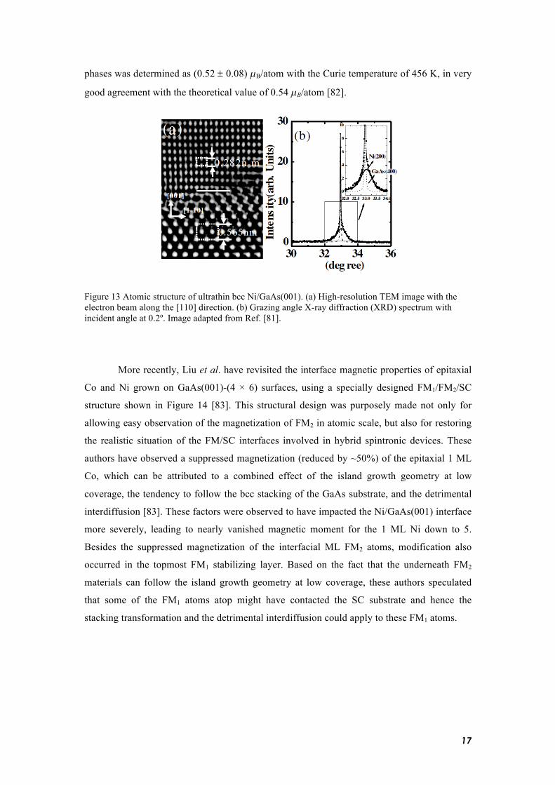
17
phases was determined as (0.52 ± 0.08) µB/atom with the Curie temperature of 456 K, in very
good agreement with the theoretical value of 0.54 µB/atom [82].
Figure 13 Atomic structure of ultrathin bcc Ni/GaAs(001). (a) High-resolution TEM image with the electron beam along the [110] direction. (b) Grazing angle X-ray diffraction (XRD) spectrum with incident angle at 0.2º. Image adapted from Ref. [81].
More recently, Liu et al. have revisited the interface magnetic properties of epitaxial
Co and Ni grown on GaAs(001)-(4 × 6) surfaces, using a specially designed FM1/FM2/SC
structure shown in Figure 14 [83]. This structural design was purposely made not only for
allowing easy observation of the magnetization of FM2 in atomic scale, but also for restoring
the realistic situation of the FM/SC interfaces involved in hybrid spintronic devices. These
authors have observed a suppressed magnetization (reduced by ~50%) of the epitaxial 1 ML
Co, which can be attributed to a combined effect of the island growth geometry at low
coverage, the tendency to follow the bcc stacking of the GaAs substrate, and the detrimental
interdiffusion [83]. These factors were observed to have impacted the Ni/GaAs(001) interface
more severely, leading to nearly vanished magnetic moment for the 1 ML Ni down to 5.
Besides the suppressed magnetization of the interfacial ML FM2 atoms, modification also
occurred in the topmost FM1 stabilizing layer. Based on the fact that the underneath FM2
materials can follow the island growth geometry at low coverage, these authors speculated
that some of the FM1 atoms atop might have contacted the SC substrate and hence the
stacking transformation and the detrimental interdiffusion could apply to these FM1 atoms.

18
Figure 14 (a) Schematic illustration of the FM1/FM2/SC structure (right) retrieving the FM2/SC structure (left). (b) Co/GaAs and Ni/GaAs interfaces versus the distance along the (100) direction. The distance is normalized to the lattice constant of GaAs. The colored spheres at the bottom indicate the position of each atomic layer. The dashed lines indicate the interfacial or the FM2 region. Image adapted from Ref. [83].
3.2 Alloy-based structures
As the most established base for both fundamental research and technological applications in
second generation spintronics, the impact of metal-based 3d FM/SC hybrid interfaces is
clearly undisputed. However, because of the growing demands on robustness, stability, and
reduced physical dimension, this field is currently transforming into a new stage where more
exotic hybrid interfaces beyond those conventional ones are needed. We will in this respect
introduce three types of alloy-based FM/SC hybrid systems that include CoFeB/GaAs, Fe3Si
on GaAs, Si, and Ge, and MnxGa/GaAs. These have been particularly chosen, in response to
(i) the puzzling issues on the UMA in 3d FM/GaAs(001) hybrid structures as discussed in the
previous sub-section and (ii) the strategic requirement of a perpendicular magnetic anisotropy
(PMA) in spintronic devices for high-density and current-controlled applications as discussed
in section 6. For ease of comparison, the growth conditions and magnetic properties of the
metal-based as well as the alloy-based structures reviewed by this article have been
summarized in Table 1.
b

19
3.2.1 Amorphous ferromagnetic CoFeB on GaAs and InAs
The commonly observed UMA in the epitaxial ultrathin films of Fe on GaAs(001) and
InAs(001) are believed to stem from two main mechanisms, i.e. interfacial bonding
interaction and magnetocrystalline anisotropy [28, 29, 54, 84] as discussed in the previous
sub-section. Separating these magnetic contributions is technically challenging but yet not
impossible when using a magnetic material without an intrinsic magnetocrytalline anisotropy.
Amorphous FM alloys are one such group of materials. In fact, CoFeB, a representative alloy
in this group, has now become an indispensable constituting material for several viable non-
volatile magnetic storage applications related to the giant tunnelling magnetoresistance
(TMR) effect [85, 86], current–induced spin-transfer torque (STT) [87, 88], MRAM and spin
transport devices. Hindmarch et al. were able to explicitly separate the interface-induced and
intrinsic magnetic anisotropies in 3d FM/III-V(001) hybrid systems when using the
amorphous alloy [89, 90]. Interestingly it was observed that a much stronger UMA can be
attained in their sputter-deposited Co40Fe40B20 film on GaAs than on AlGaAs/GaAs. The
mechanism of the UMA was explained in terms of a "bond-orientational" anisotropy model,
in which a long-range microstructural anisotropy arises due to local anisotropic coordination
polyhedra [90]. Tu et al. took a step further to investigate the UMA in Co56Fe24B20 films
grown on the different surface orientations of GaAs [91]. A strong UMA of ~270 Oe was
achieved on the (001) face, but only a weak one of less than 20 Oe for both (011) and (111)
surfaces as shown in figure 15. The angular dependence of the UMA revealed quite
distinctive behavior on the different GaAs surfaces, which could be related to different
surface morphology of the FM films. In a very recent attempt to correlate UMA and atomic
scale interface magnetism by XMCD, Yan et al. quantified the orbital to spin magnetic
moment ratio of the Co and Fe atoms in CoFeB/GaAs(001) and observed an remarkable
enhancement of the ratio by more than 300% [92]. Such an enhanced orbital moment relative
to the bulk counterpart was higher for the Co atoms, leading to a possible link between the
presence of the UMA and the large spin-orbit coupling in the ultrathin films on GaAs.

20
Figure 15 Magnetic hysteresis loops along the easy- and hard-axes of CoFeB films deposited on (a) (001), (b) (011), and (111)-oriented GaAs substrates, respectively. Image adapted from Ref. [91].
3.2.2 Intermetallic Fe3Si on GaAs, Si, and Ge
Lattice structure
Due to the ease of overlayer/substrate intermixing, high-quality hybrid interfaces between III-
V SCs and 3d FM metals are restricted to be grown at rather low temperatures, mostly not
exceeding RT [1, 28, 84]. This thermal instability issue, which is expected to limit these
interfaces for robust and high-temperature applications, has led to an exploration for
alternative FMs that possess comparable or even higher spin polarization along with better
stability on III-V SCs. Intermetallic Fe3Si is one such candidate, exhibiting a high Curie
temperature of 803 K [93]. Ordered Fe3Si crystallizes in a D03 lattice structure [94, 95], and
can be regarded as a magnetic Heusler alloy (note that we purposely separated this part from
section 4, because Fe3Si is a half-metal), taking the notation of Fe(A, C)2Fe(B)Si(D). As
illustrated in Figure 16, the four penetrating fcc sub-lattices A, B, C, and D are at the
coordinates of (0, 0, 0), (0.25, 0.25, 0.25) and (0.5, 0.5, 0.5), and (0.75, 0.75, 0.75),
respectively, rendering two chemically and magnetically non-equivalent types of Fe atoms
[94, 96]. The Fe(A, C) atoms have 4 Fe(B) atoms and 4 Si(D) atoms as first-nearest neighbors

21
and are characterized by a magnetic moment of 1.35 µB. The Fe(B) atoms, on the other hand,
carry a moment of 2.2 µB, having 8 Fe(A, C) atoms as first-nearest neighbors [94, 96]. Falling
into the group of Heusler alloys though, half-metallic behavior is not expected for Fe3Si.
According to the bulk electronic structure calculations [97-100], the DOS close to the Fermi
level exhibits a dip for the minority spins and the spin polarization should therefore be
roughly of the same order of magnitude as that for Fe, i.e. ~43% [101]. Such a value has in
fact been verified by point contact Andreev reflection spectroscopy for MBE-grown Fe3Si
epitaxial films on GaAs(001) [102].
As far as epitaxial growth is concerned, Fe1-xSix binary alloys can exist in the fcc
phase within a wide range of Si concentration between x = 0–0.265; but to obtain an ordered
D03 structure, the Si content should be confined within 9.5–26% [103]. It was demonstrated
that realistic epitaxial growth of Fe3Si (5.64 Å) could be largely facilitated by its good lattice-
match with various SCs including GaAs(001) and (113)A (5.65 Å) [102, 104-111], Si(111)
(5.43 Å) [112-115], and Ge(111) (5.65 Å) [116-119]. When compared with Fe/GaAs(001)
[55, 120], those Fe3Si-based hybrid interfaces are generally more thermally stable with
respect to post-growth annealing [121, 122].
Figure 16 D03 lattice structure of bulk Fe3Si with Fe atoms on non-equivalent A, C and B sub-lattice sites. Image adapted from Ref. [111].
Epitaxial growth and magnetic properties
Liou et al. have reported one of the first experimental demonstrations of epitaxial
Fe3Si/GaAs(001) by MBE [104]. Within a wide range of substrate temperatures of 550–800
K, the epitaxy of stoichiometric Fe3Si down to 2 MLs was practically achievable. Not
mentioned in this pilot study though, one might speculate, from the experimental procedures,
the use of an As-terminated GaAs surface for such epitaxial growth [104, 123]. This starting

22
growth front is very crucial from the growth perspective, because in many cases it largely
determines the exact growth mode to be involved, as for the metal-based 3d FM/SC hybrid
systems. For instance, Herfort et al. has shown that an As-rich (2 ´ 1) surface of GaAs(001)
enables a layer-by-layer growth of Fe3Si [105], but, on a Ga-rich (4 ´ 6) surface, a 3D growth
has been observed instead [124]. These results have also been consistently found in other
studies [102, 107]. As a side note, the speculation that we made for the GaAs surfaces used in
Ref. [104] is in fact in good agreement with their observation of a sharp RHEED pattern just
after a ML of Fe3Si deposition; such a pattern would have been absent in the case of 3D
growth due to surface roughness. Later Herfort et al. [105] optimized the growth temperature
range (150–250 °C), within which Fe3Si/GaAs(001) with better structural and magnetic
properties, in comparison to those in Ref. [104], can be achieved. In particular, higher
magnetic moments of ~1050 emu/cm3 (at RT) were obtained in the optimized films than the
values, i.e. ~1000 emu/cm3 (at 10 K) in Ref. [104].
The rationale behind the use of an optimized (low) growth temperature for
Fe3Si/GaAs(001) in Ref. [105] as well as in other related works [102, 107-109, 124] is two-
fold: to promote a long-range atomic order but simultaneously limit short-ranged disorder
originated from possible intermixing of Fe/Si with Ga/As. Indeed, Figure 17 shows the cross-
sectional TEM images obtained for two nearly stoichiometric Fe3Si films grown on As-rich (2
´ 1)-GaAs(001) at 550 and 700 K, respectively [108]. It is apparent that a superior interface
can be fabricated at the lower temperature. More importantly, there is no sign of an
intermixed layer over the sample area of several microns. This is in contrast to the growth at
higher temperature, where an extended and rough reaction layer is detected that consists of
flat precipitates of various crystalline phases. Coupling the TEM results with the data
separately extracted from glazing incidence XRD [108, 109], the authors concluded that 70%
of the Fe3Si films grown at 550 K possesses a high degree of long-range atomic order, while
the remaining 30% might be defective, due to the mixing of the D-site Si atoms with the A-
and C-site Fe atoms [108]. A two-step growth strategy for the epitaxial Fe3Si/GaAs(001) was
alternatively proposed by Hsu et al. [110]. This method relies on an initial growth of a 2 nm
thick Fe3Si at 450 K in order to minimize possible interfacial reactions, followed by ramping
up of the substrate temperature to 550 K. Even though an intermixed layer of 2–3 MLs was
detected by x-ray photoelectron spectroscopy (XPS), an ultra-sharp Fe3Si/GaAs interface can
be achieved with this strategy. Further, in view of the seemingly insurmountable issue on the
interface intermixing even at the growth temperature as low as 450 K, Makarov et al. have
developed to employ a MgO buffer layer as a physical diffusion barrier in between Fe3Si and
GaAs [125]. With a 3.0 nm MgO, the thermally induced interdiffusion at the hybrid interface
was reduced dramatically.

23
Figure 17 Cross-sectional TEM images of two stoichiometric Fe3Si/GaAs(001) hybrid structures grown at (a) 550 K and (b) 700 K. The thicknesses of the films are ~50 nm. Image adapted from Ref. [108].
The magnetic moments in epitaxial Fe3Si/GaAs have been mainly studied by bulk
measurements and are found to be ranged between 660–1050 emu/cm3 [102, 104, 105, 110,
126], with the highest being obtained from samples grown at an optimized temperature range
[105]. To access the atomic scale magnetism, which is directly correlated to the electronic
structure of the alloy films, both element-specific XMCD as well as polarized neutron
reflectometry (PNR) have been employed. PNR characterizations performed by Ionescu et al.
have simultaneously revealed the atomic magnetic moment and interface roughness of Fe3Si
film on Ga-rich (4 ´ 6) surface [102]. The former parameter has been quantitatively found as
(1.107 ± 0.014) µB/atom at RT, close to the bulk value of 1.175 µB/atom at 6.5 K [94, 95],
while the interface roughness was about 2.3 ± 0.1 nm. On the other hand, via XMCD,
Krumme et al. directly compared the magnetic moments of Fe3Si films on different surfaces
including MgO(001), Ga-rich (4 ´ 6) and As-rich (2 ´ 2) of GaAs(001) [124]. Figure 18
shows the X-ray absorption (XAS) and XMCD spectra at the Fe L2,3 edges of those grown on
MgO and Ga-rich (4 ´ 6) surface. Concurrently the maximum of the absorption signal at the
L3 edge decreases by ~8% for Fe3Si on MgO and by ~17% on Ga-rich (4 ´ 6). Additionally, a
shoulder occurs 2 eV above the L3 edge in the Fe3Si XAS. However, at the L2 edge, the
absorption intensity is nearly unchanged. The broadening as well as the shoulder has been
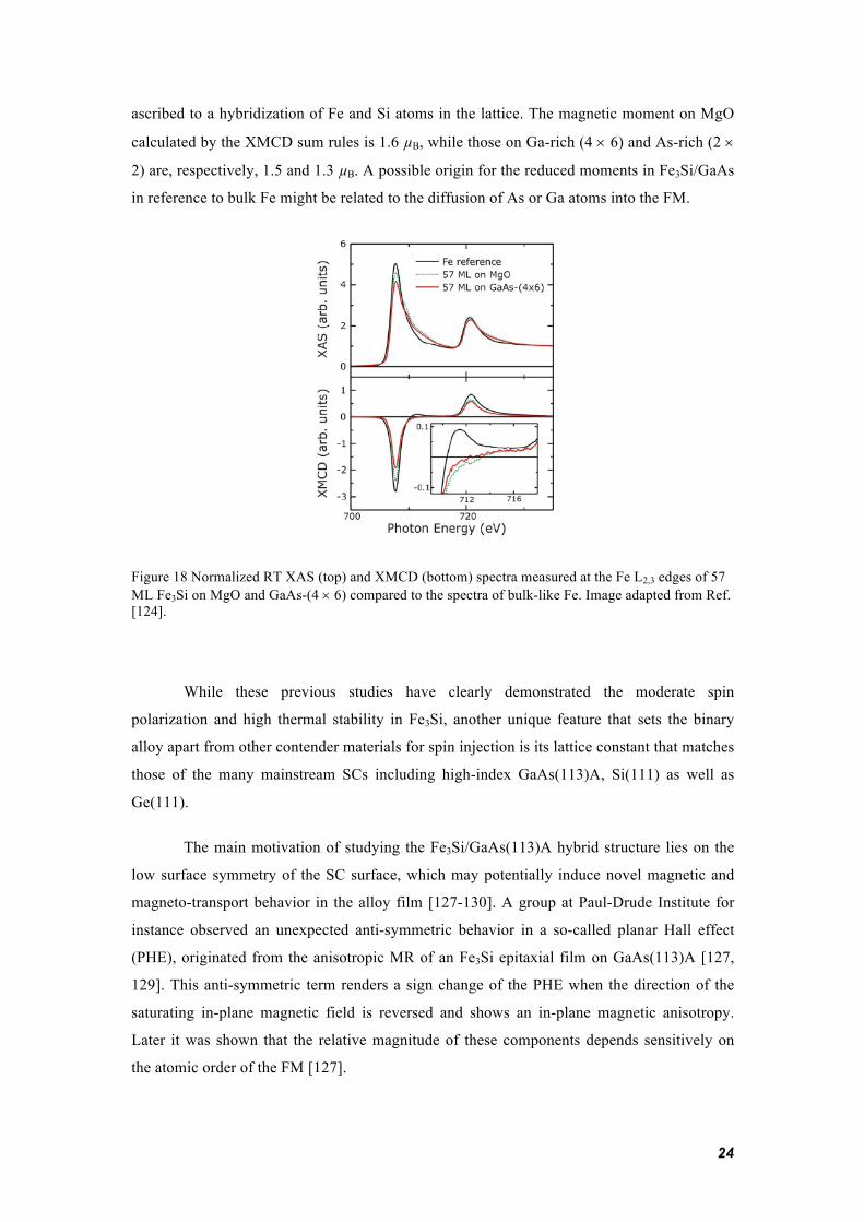
24
ascribed to a hybridization of Fe and Si atoms in the lattice. The magnetic moment on MgO
calculated by the XMCD sum rules is 1.6 µB, while those on Ga-rich (4 ´ 6) and As-rich (2 ´
2) are, respectively, 1.5 and 1.3 µB. A possible origin for the reduced moments in Fe3Si/GaAs
in reference to bulk Fe might be related to the diffusion of As or Ga atoms into the FM.
Figure 18 Normalized RT XAS (top) and XMCD (bottom) spectra measured at the Fe L2,3 edges of 57 ML Fe3Si on MgO and GaAs-(4 ´ 6) compared to the spectra of bulk-like Fe. Image adapted from Ref. [124].
While these previous studies have clearly demonstrated the moderate spin
polarization and high thermal stability in Fe3Si, another unique feature that sets the binary
alloy apart from other contender materials for spin injection is its lattice constant that matches
those of the many mainstream SCs including high-index GaAs(113)A, Si(111) as well as
Ge(111).
The main motivation of studying the Fe3Si/GaAs(113)A hybrid structure lies on the
low surface symmetry of the SC surface, which may potentially induce novel magnetic and
magneto-transport behavior in the alloy film [127-130]. A group at Paul-Drude Institute for
instance observed an unexpected anti-symmetric behavior in a so-called planar Hall effect
(PHE), originated from the anisotropic MR of an Fe3Si epitaxial film on GaAs(113)A [127,
129]. This anti-symmetric term renders a sign change of the PHE when the direction of the
saturating in-plane magnetic field is reversed and shows an in-plane magnetic anisotropy.
Later it was shown that the relative magnitude of these components depends sensitively on
the atomic order of the FM [127].

25
Ordered Fe3Si has a slight lattice mismatch of 4.2% with Si, thus providing an
opportunity for establishing an epitaxy between the two materials [112-115]. Generally
speaking, the main challenge for such an epitaxial growth concerns a strong tendency for the
Fe atoms of Fe3Si to diffuse into the substrate and form silicides. Accordingly, low
temperature growth, as in the case of Fe3Si/GaAs [102, 104-111], is mandatory. Yakovlev et
al. have succeeded in fabricating epitaxial Fe3Si films on Si(111)-(7 ´ 7) surfaces at 450 K by
MBE [115], resulting in an epitaxial relationship of Fe3Si(111)||Si(111). At RT, those films
are magnetic with a weak uniaxial magnetic anisotropy of 26 Oe and a relatively narrow
ferromagnetic resonance linewidth of 11.57 Oe. Yoshitake et al. also reported a RT growth of
epitaxial Fe3Si/Si(111) with an extremely smooth surface morphology by DC sputtering
[113]. Relative to MBE, this technique generates atoms or molecules with kinetic energies of
several eV when reaching the substrate surface. This can promote epitaxial growth at a lower
temperature. However, it should be noted that such fabricated FM films were found to possess
a B2 structure. In this phase, the Si atoms are not expected to arrange in an ordered manner.
Nevertheless, those films have shown a saturation magnetization of 960 emu/cm3, which is
slightly lower than the bulk D03 counterpart. Nakane et al. developed a preparation technique
for both stoichiometric and off-stoichiometric D03-Fe3+xSi1-x thin films with a strong texture
using silicon-on-insulator (SOI) [112]. The FM films were synthesized by thermally activated
silicidation reaction between an ultrathin SOI layer and a pre-deposited Fe layer at an
annealing temperature from 920–1080 K. The film composition in this case is mainly
controlled by the relative SOI/Fe thickness ratio.
The nearly perfect lattice-match between Fe3Si (5.64 Å) and Ge (5.65 Å) makes this
combination particularly promising for Ge-based spin devices. Electrical injection/detection
of spin-polarized electrons in Ge has already been demonstrated using FM Fe3Si contacts
(also see section 6) [131-133]. The epitaxial growth of Fe3Si on various Ge surface
orientations was pioneered by a group at Kyushu University [116-118]. At a substrate
temperature of 360 K, Fe3Si with a D03 lattice structure can be grown epitaxially by MBE on
both Ge(110) and Ge(111), while a polycrystalline film is formed on the (001) surface [117],
as illustrated in Figure 19. The alloy film grown on Ge(111) features an atomically sharp
interface, while that on Ge(110) is slightly rougher (~3 nm). Structurally quite different
though, both Fe3Si/Ge(100) and Fe3Si/Ge(111) have a saturation magnetization value of ~1 ´
106 A/m, which is almost identical to the bulk counterpart. However, in terms of magnetic
switching behavior, the Fe3Si film on Ge(111) has a smaller coercivity and weaker in-plane
angular dependence than on Ge(100), which might be related to the lesser amount of
structural defects in the former case, that can act as pinning sites for magnetic domains [117].
Maeda et al. have carried out an experimental study focusing on two particular issues: (i)

26
epitaxial growth of Fe3Si/Ge(111) at a wide range of substrate temperature (360–700 K), and
(ii) thermal stability of stoichiometric and off-stoichiometric Fe3Si/Ge(111) with respect to
post-growth annealing [116]. For the first issue, the authors extracted the depth profiles of Fe
and Ge concentrations and atomic order in Fe3Si/Ge(111) prepared at a series of substrate
temperatures. By Rutherford backscattering spectroscopy and TEM, an optimal temperature
range was determined to be below 430 K; for higher temperatures, a very rough interface was
observed, consisting of both FeGe and Fe3Si originating from atomic interdiffusion. In
addition, the authors have concluded that stoichiometric Fe3Si are more thermally stable than
the off-stoichiometric one. For instance, after post-annealing at 700 K, off-stoichiometric
Fe4Si/Ge(111) was found to possess the impurity FeGe phase, whilst purely stoichiometric
sample could maintain its D03 ordered structure and high crystallinity even after being post-
annealed at 750 K for 120 min [116].

27
Figure 19 Cross-sectional TEM images and selected area electron diffraction patterns of 50 nm thick Fe3Si films grown on various Ge surface orientations at 360 K. Image adapted from Ref. [117].

28
Figure 20 High-resolution TEM images and selected area electron diffraction patterns of Fe3Si/Ge(111) grown at (a) 360 and (b) 700 K. The latter shows the coexistence of cubic FeGe epitaxially grown in Fe3Si. Image adapted from Ref. [116].
The magnetic properties of epitaxial Fe3Si/Ge(111) films particularly grown at 430 K
have been characterized by Ando et al [118]. The hybrid structures fabricated at such
temperature exhibit atomically flat interfaces. An unexpected in-plane uniaxial magnetic
anisotropy was observed in all samples in the as-grown state, but the direction of the uniaxial
easy axis appeared to be random. By post-growth annealing at 400–700 K, such a random
behavior of the uniaxial easy axis can be greatly reduced as a consequence of an alignment of
the magnetic easy axis along the [ ] direction. This observation was also accompanied
with a reduction in the sample saturation magnetization. These authors argued that the
thermal effect on the Fe3Si/Ge magnetic properties might be associated with an increased
fraction of the ordered D03 phase in the FM film [118]. For the first time, Yamada et al.
demonstrated MBE growth of D03-Fe3Si on Ge(111) at RT [119]. Figure 21 shows the
saturation magnetization at RT and the degree of local D03 ordering for 25 nm Fe3Si films as
a function of growth temperature. The magnetization values are insensitive to the growth
temperature from RT to 600 K, but reduces considerably when going beyond 600 K, possibly
due to magnetic dead layer formation near the hybrid interface. This is in good agreement
with the local phase ordering extracted by Mössbauer spectroscopy [119].
�
01 1

29
Figure 21 The saturation magnetization at RT and the degree of D03 phase of 25 nm thick Fe3Si grown at a temperature range between RT and 700 K. Image adapted from Ref. [119].
3.2.3 Perpendicular MnxGa on GaAs
Lattice structure
Magnetic materials with PMA, be it intrinsic in nature or extrinsically-induced, have rapidly
become a core group of materials in second generation spintronics. On one hand, these
materials are highly essential for realization of high recording density non-volatile memory
[134-136] by using the so-called STT effect in perpendicularly magnetized MTJs [88]. In
these key devices, the magnetization direction can be manipulated by applying an electric
current, thus making possible the technology of STT-MRAM that has many unique features
including non-volatility, scalability, high speed, and low consumption power [137, 138]. On
the other hand, materials exhibiting PMA are fundamentally very intriguing, because of the
many physical phenomenona like remanent spin injection in spin-FET and spin-LEDs (also
see section 6), giant anomalous Hall effect (AHE), and long-lived ultrafast spin procession,
etc [139-146].
Previous theoretical calculations have suggested that MnxGa alloys could be a game-
changer for the advanced MRAM industry, with its thermodynamically stable L10 phase
possessing large perpendicular anisotropy of 26 Merg/cm3, moderate magnetization of 2.51
µB/Mn atom, and large magnetic energy product of 28.2 MG Oe [145, 147-149]. For these
reasons, we will focus on various aspects from lattice structure to epitaxial growth and to
tailoring of PMA in MnxGa/GaAs(001) hybrid structure.
The binary Mn–Ga phase diagram shown in Figure 22 indicates several ordered
phases in MnxGa [150, 151]; yet for spintronics, two particular tetragonal phases are of most

30
relevance due to strong magnetism and high Curie temperature: L10 ferromagnetic phase for
0.76 £ x £ 1.8 [152, 153], and D022 ferrimagnetic phase for 2 £ x < 3 [145, 154-156]. The L10-
MnxGa has lattice parameters of a = 3.88–3.90 Å and c = 3.64–3.69 Å [152, 153]. Each Mn
atom in L10-MnGa is expected to contribute a moment of 2.51 µB [148, 149]. For bulk D022-
MnxGa, the lattice constants are a = 3.90–3.94 Å and c = 7.10–7.17 Å [154-156]. As
mentioned just above, MnxGa alloys have been predicted to have strong PMA along with high
spin polarization and Curie temperature as well as low magnetic damping constant [145]. For
accessing these properties in practice, reliable growth of the alloys films constitutes a key
prerequisite, which will be reviewed in some details below.
Figure 22 (a) Phase diagram of binary Mn-Ga system; (b) Unit cells of two ordered magnetic phases (L10 and D022) of MnxGa alloys. Image adapted from Ref. [147].
Epitaxial growth and perpendicular magnetic anisotropy
Over recent years, several groups have successfully accomplished the growth of L10- and
D022-MnxGa films by either magnetron sputtering or MBE. First studies were done in the 90s
when Krishnan, and Tanaka et al. respectively confirmed square and perpendicular hysteresis
of MnxGa (1.2 < x < 1.5) grown on GaAs(001) by magneto-optical, magnetic and transport
measurements [142, 143]. Since then, various substrates based on SCs and insulating oxides
have been studied for the growth [157-162]. However, only GaAs and MgO substrates can

31
lead to appreciable PMA. In most cases, D022-MnxGa films were fabricated on MgO(001)
[139, 140, 146, 156, 157, 163]. Wu et al. for instance reported magnetic and magneto-
transport properties of 5 nm thick Mn2Ga and Mn2.5Ga epitaxial films with PMA on Cr
buffered MgO(001) [139, 146]. Kurt et al. further prepared stoichiometric D022-Mn3Ga films
with an out-of-plane magnetic easy axis on MgO, Pt-MgO and Cr-MgO, and extracted a spin
polarization of 40–58% in Mn2Ga and Mn3Ga by point-contact Andreev reflection [156, 163].
Despite these efforts, the theoretically predicted magnetic properties in MnxGa [148, 149],
ideal for MRAM and STT applications, were seemingly unreachable, until the major
breakthrough by Zhu et al [164]. In that particular work, the authors demonstrated for the first
time pronounced magnetic properties in homogeneous L10-Mn1.5Ga epitaxial films on
GaAs(001) including perpendicular Hc tunable from 8.1 to 42.8 kOe, PMA with a maximum
of 21.7 Merg/cm3, energy product up to 2.6 MGOe, squareness exceeding 0.94, and
magnetization controllable from 27.3 to 270.5 emu/cm3 at RT [164]. By various
characterization methods, the MBE-grown Mn1.5Ga films were found to possess good epitaxy
for growth temperatures below 600 K. Going beyond 650 K could however lead to impurity
phases, possibly due to intermixing between Mn and GaAs. Figure 23 shows the typical
perpendicular and in-plane magnetic hysteresis loops of Mn1.5Ga film grown at 400 K
reported in the pioneering work of Zhu et al [164], which indicates a high squareness and
strong PMA as high as 42.8 kOe. These features also hold for films grown between 400 and
600 K. Generally speaking, these results are on one hand quite different from other reports for
films grown on other substrates [158, 160, 162], and on the other hand still lower than the
calculated values for stoichiometric L10-MnGa [148]. Both strains within the films [149] and
marginal off-stoichiometry could be responsible for such disparity. In particular, it has been
predicted that excessive Mn atoms in a MnxGa will align antiparallel to the rest of the
magnetic atoms, in turn resulting in spin compensation [148].

32
Figure 23 Perpendicular and in-plane magnetic hysteresis loops of L10-Mn1.5Ga film on GaAs grown at (a) 400 K, and (b) various substrate temperatures. (c) Remanent magnetization, (d) saturation magnetization, and (e) Hc as a function of substrate temperature. Image adapted from Ref. [164].
There exist three different proposals aiming at optimizing these non-ideal magnetic
properties as well as controlling the PMA of MnxGa films for specific spintronic applications.
The first involves composition tuning and post-growth annealing. Inspired by the studies on
the composition-dependence of magnetic properties of bulk MnxGa polycrystals [145, 153],
Zhu et al. performed a systematic investigation on using both composition and post-growth
annealing to tailor the magnetism in their MBE-grown MnxGa epitaxial films on GaAs(001)
[152]. They found that epitaxial films could be obtained under two conditions: (i) Within a
composition range from x = 0.76 to 2.6; and (ii) annealing temperatures up to ~650 K [152].
A prolonged annealing at 750 K would otherwise significantly deteriorate the magnetic
behavior of Mn0.76Ga films, owing to Mn2As formation. The second approach is strain
engineering. The magnetic properties, especially the PMA, of MnxGa are strongly growth-
and substrate-dependent [143, 156, 160-162, 165-167]. For instance, MnxGa films grown on
GaSb(111) behaved like a hard FM, whereas on Al2O3(0001), similar films were magnetically
soft [162]. Such strong substrate-dependent magnetic properties, which largely originate from
strain, have motivated Al-Aqtash and Sabirianov to examine the variation of the PMA in
MnGa as functions of Mn concentration and applied elastic strain [168]. Using DFT theory,
these authors have demonstrated that a large PMA can exist in MnGa and be effectively tuned
for a wide range of concentrations and compressive/tensile strains. The third approach relies
on interfacial exchange interaction in a FM/MnxGa bilayer structure, which was developed by
a group at Tohoku University, with the ultimate goal on enhancing the MR effect in MTJs

33
[169-173]. Kubota et al. and Ma et al. have respectively reported perpendicularly magnetized
MTJs based on L10-Mn62Ga38 and thin CoFeB electrodes with a MgO tunnel barrier. In those
studies, either a thin Fe or Co layer was introduced between the MnGa layer and the MgO
barrier layer to investigate interfacial effect on the device’s magnetic and transport properties.
For Fe insertion, a maximum TMR ratio of 24% was observed in MTJs with a Fe thickness of
1.1 nm at RT [173], whilst a much higher ratio of 40% for Co insertion with a comparable
thickness [170]. Such a disparity in device performance has been explained by the difference
in exchange coupling at the FM/MnGa interfaces, with Fe and Co exhibiting an opposite
coupling with the magnetization of the MnGa. In the ultrathin limit, Fe tends to couple
ferromagnetically with MnGa, whereas Co prefers an anti-FM coupling [170, 171, 173-175].
In particular, the latter type of coupling leads to an unusual four low-resistance states in
Mn62Ga38/Co/Mg/MgO/CoFeB devices rather than two in conventional ones (see Figure 24).
An abrupt transition of the interfacial exchange coupling from FM and anti-FM is further
observed by Ma et al. in L10-MnGa/Fe1-xCox epitaxial bilayers when x is around 25% [171].
By considering the band structure of the MnGa alloy (see Figure 25), the authors have
accounted for this transition by the spin-polarization reversal of Fe1-xCox due to the rise of the
Fermi level as the Co content increases. In another relevant study, Xiao et al. have
additionally revealed that the exchange coupling between L10-Mn1.5Ga (15 nm) and Co (2–12
MLs) can change from FM to anti-FM coupling simply by a thermal annealing step at 600 K
[174]. By first-principles calculations, it is evidenced that such transition might involve a
thermodynamical process, in which a FM coupled Co/Mn-terminated MnGa bilayer
transforms into an anti-FM coupled Co/Ga-terminated structure, given the more stable Co-Ga
bond than the Co-Mn one.

34
Figure 24 TMR and four low-resistance states of Mn62Ga38/Co/Mg/MgO/CoFeB junctions at (a) 300 K and (b) 5 K. Image adapted from Ref. [170].
Figure 25 (a) Band structure of bcc Fe1-xCox and L10-MnGa alloys. (b) Spin-resolved density of states. Image adapted from Ref. [171].

35
System Ref. Structure Substrate
reconstruction Thickness
(nm) mspin
(µB/atom) morb
(µB/atom) Temperature
(K) Growth rate
(Å/min) Growth
technique
Fe/GaAs(001) [28] bcc (4 ´ 6) 1.1 2.03 ± 0.14 0.26 ± 0.03 300 1.43 MBE
[28] bcc (4 ´ 6) 4.7 2.07 ± 0.14 0.12 ± 0.02 300 1.43 MBE
[50] bcc (4 ´ 6) 0.04 1.96 ± 0.5 1.23 ± 0.1 300 1.43 MBE
[50] bcc (4 ´ 6) 0.07 1.84 ± 0.21 0.25 ± 0.05 300 1.43 MBE
[50] bcc (4 ´ 6) 0.14 1.84 ± 0.11 0.23 ± 0.04 300 1.43 MBE
[55] bcc (2 ´ 4)/ c(4 ´ 4) MBE
Fe/InAs(001) [84] bcc (4 ´ 2) 1.1 1.22 ± 0.12 0.22 ± 0.03 448 1.43 MBE
[84] bcc (4 ´ 2) 3.6 1.90 ± 0.15 0.16 ± 0.01 448 1.43 MBE
[176] bcc c(8 ´ 2)/(4 ´ 2) 3.9 MS: 1.2 ´103 emu/cm3 300 1.3–1.5 MBE
[177] bcc 40 300/448 3 MBE
Fe/GaN(001) [178] bcc (1 ´ 1) 65 300 10 MBE
Fe/GaN(0001) [179] bcc (1 ´ 1) 5–50 300 11 MBE
[180] bcc (1 ´ 1) 5–70 300/523 0.17/0.26 MBE
[179] bcc (7 ´ 7) 5 300 2 MBE
[181] bcc 37.4 MS: 1.48 ´103 emu/cm3 (as-grown) 300–950 < 1.43 MBE
Co/GaAs(011) [63] bcc 35.7 mspin+orb: 1.53 448–498 3.3 MBE
Co/GaAs(001) [66] bcc (2 ´ 2) 20.2 mspin+orb: 1.3–1.4 448–498 3.3 MBE
[66] bcc (2 ´ 2) 21.6 mspin+orb: 1.3–1.4 448–498 3.3 MBE
[68] bcc (4 ´ 2) 0.8–2.0 423 2 MBE
[68] bcc/hcp (4 ´ 2) 2.0–6.0 423 2 MBE
[64] bcc (2 ´ 4) 3.0/8.0 mspin+orb: 1.2/1.7 423 0.16 MBE
[69] bcc 3.0–15 448–498 MBE

36
[69] bcc/hcp 15–50 448–498 MBE
[182] bcc c(4 ´ 4) 5.6 263–498 0.71 MBE
[65] bcc (4 ´ 6) 5.0, 15 413 1 MBE
[183] bcc (4 ´ 6) 1.1 MS: 0.71 ´103 emu/cm3 MBE
[183] bcc/hcp (4 ´ 6) 1.6 MS: 1.19 ´103 emu/cm3 MBE
[183] bcc/hcp (4 ´ 6) 5.0 MS: 1.31 ´103 emu/cm3 MBE
[183] bcc/hcp (4 ´ 6) 7.0 MS: 1.37 ´103 emu/cm3 MBE
[184] bcc/hcp 50, 560 300 MBE
Co/InAs(111) [185] (111)A-(2 ´ 2) 0.07–0.28 300 0.71 MBE
[185] (111)B-(1 ´ 1) 0.07–0.28 300 0.71 MBE
Ni/GaAs(001) [80] bcc 0.2–2.5 2.0 MBE
[80] bcc/fcc 2.5–6.0 2.0 MBE
[52] fcc 5.0 MS: 387 emu/cm3 300 Electrodeposit
[52] fcc >10 MS: 484 emu/cm3 300 Electrodeposit
[81] bcc (4 ´ 6) <3.5 mspin+orb: 0.52 ± 0.08 170 MBE
Co40Fe40B20/GaAs(001) [89] 3.5 Fe (Co) morb/mspin: 0.45 (0.38) 300 DC sputtering
Co40Fe40B20/AlGaAs(001) [89] 3.5 Fe (Co) morb/mspin: 0.34 (0.19) 300 DC sputtering
Co56Fe24B20/GaAs(001) [92] 3.5 Fe: 1.17 ± 0.03 Fe: 0.03 ± 0.03 300 DC sputtering
[92] Co: 1.53 ± 0.03 Co: 0.56 ± 0.03 300 DC sputtering
Mn0.6Ga0.4/GaAs(001) [142] L10 30 MS: 460 emu/cm3 at 35 K 475 11.5 MBE
Mn1.5Ga/GaAs(001) [164] L10 48 MS: 27.3–270.5 e mu/cm3
400–600 MBE
MnxGa/GaAs(001) [152] L10 MS: 52 (x = 2.6)–445 (x = 0.76) emu/cm3;
post-annealed at 750 K 550 MBE
Mn0.6Ga0.4/GaAs(001) [143] L10 c(4 ´ 4) 10 M at remanence: 225 emu/cm3 450–500 8.3 MBE

37
Table 1 A summary of the growth conditions and magnetic properties of the FM/SC hybrid structures that have been discussed in section 3.
MnGax/GaAs(111)B [186] L10 (1 ´ 1) 5.0 MS: 300 (x = 0.6)–650 (x = 0.53) emu/cm3;
post-annealed at 700 K 300–550 2.0 MBE
MnxGa1-x/GaN(0001) [187] L10 (1 ´ 1) 30–50 MS: 100 (x = 0.5)–371 (x = 0.42) emu/cm3 550 MBE
[160] L10 (1 ´ 1) 150 MS: 120 (x = 0.67)–400 (x = 0.49) emu/cm3 550 MBE
Fe3Si/GaAs(001) [104] D03 0.56–60 MS: 1000 emu/cm3 at 10 K 550–800 3.0 MBE
[105] D03 (2 ´ 1) 30–40 MS: 1050 emu/cm3 450–550 0.4 MBE
[102] D03 (4 ´ 6) 21 mspin+orb: 1.107 ± 0.014 600 0.36 MBE
[110] D03 (4 ´ 6) 14 MS: 600 emu/cm3 450–600 1.17 MBE
[111] D03 (1 ´ 1) 10–200 MS: 700 emu/cm3 580–650 2.0 MBE
Fe3Si/GaAs(113)A [130] D03 35–50 MS: 600 ± 50 emu/cm3 550 0.13 MBE
Fe3Si/GaAs(111)A [126] D03 (2 ´ 2) 7.5 MS: 990 emu/cm3 550 0.45 MBE
Fe3Si/Si(111) [113] B2 110 MS: 960 emu/cm3; grown at 300 K 300–800 1.1 Sputtering
[115] D03 (7 ´ 7) MS: ~1059 emu/cm3 450 MBE
Fe3Si/Ge(111) [119] D03 25 MS: 400 (grown at 700 K)–
970 (grown at 300 K) emu/cm3 300–700 MBE
[116] D03 35 360–700 MBE
[118] D03 50 430 MBE [117] D03 50 360 MBE

38
4 Spintronic hybrid structures with half-metallic materials
As originally envisaged, the Datta-Das spin-FET should involve Ohmic FM/SC interfaces [7],
so that the total device impedance could be kept as low as possible to avoid slow dynamical
response and large power dissipation at steady bias. As we shall further explain in section 6,
these transparent contacts generally suffer from the so-called conductivity mismatch problem,
originating from the fact that the conductivities of 3d FM metals are several orders of
magnitude larger than those in conventional SCs. This fundamental issue, which rendered
rather low spin injection efficiency in many previous attempts, has led to intensive efforts on
developing two categories of special magnetic materials as viable solutions—half-metallic
oxides and alloys with 100% spin polarization P as to be introduced in this section.
4.1 Half metallicity
Half-metals are ferro- or ferri-magnetic materials that act as conductors to electrons of one
spin orientation, but as insulators or SCs to those of the opposite orientation [188, 189].
Figure 26 presents a schematic diagram of the partial DOS near EF of paramagnetic,
ferromagnetic and half-metallic materials, respectively. DOS of spin-up and spin-down
electrons are identical in numbers in paramagnetic materials leading to P = 0, while these spin
sub-bands show an imbalance in FMs resulting in 0 < P < 1. Half-metals represent an extreme
case where either the spin-up or the spin-down states are empty at the EF, giving P = 1. The
discovery of half-metallicity originates from the early studies of Heusler alloys, some of
which yield the properties of metals as well as insulators simultaneously in the same material,
depending on the spin direction. By performing electronic structure calculations in the
Heusler alloy, NiMnSb, such property was identified as half-metallic magnetism by de Groot
et al. in 1983 and since then the exploration of half-metals has received a strong boost [188,
189].
Figure 26 A schematic diagram of the partial DOS near EF of paramagnetic, ferromagnetic and half-metal materials. DOS of spin-up and spin-down electrons are identical in numbers in paramagnetic materials leading to P = 0, while these spin sub-bands show an imbalance in FMs resulting in 0 < P < 1. Half-metals represent an extreme case where either the spin-up or the spin-down states are empty at

39
the EF, giving P = 1.
Half-metallic magnetism has been previously probed by spin-resolved positron
annihilation spectroscopy—a dedicated technique used in the study of polarized band
structures of FMs [190]. Due to the experimental complications, the number of
experimentally established half-metals remains a puzzle and electronic structure calculations
continue playing a leading role in the search for new half-metals. Formally the expected
100% spin polarization of charge carriers in a half- metallic FM is a hypothetical situation
that can be approached only in the limit of vanishing temperature and by neglecting spin-orbit
interactions. However, at low temperatures (as compared with the high Tc, which exceeds
1000 K for typical half-metals and minor spin-orbit interactions), a half-metal deviates so
markedly from a normal material that the treatment as a special category of materials is
justified.
Figure 27 Spin polarization and Tc of a list of selected magnetic materials found in the literature. The triangles refer to the Tc of the materials and the bars indicate the spin polarization. Image adapted from Ref. [191].
To date, a diverse collection of materials including Heusler alloys [23, 188, 189, 192-
202], chromium dioxides [101, 203-206], manganite [207-212], and magnetite (Fe3O4) [203,
213-219] have been found to carry half-metallicity. The overwhelming high spin
polarization makes half-metals ideal spin sources in the proposed hybrid spintronic devices.
Some of these materials offer a mixture of the desired properties for spintronics applications,
e.g. high Tc that are well in excess of RT as well as half-metallicity. This promises their

40
applications at finite temperature, since many of the depolarization mechanisms scale with the
reduced temperature T/Tc. Figure 27 presents a survey of the P and Tc of some of the
aforementioned materials which might be of potential use in spintronics applications, from
which the clear advantages of half-metals can be seen. The following sub-sections review the
research development of two selected high-Tc half-metallic spintronic materials that are of
primary interest, i.e. magnetite and Heusler alloys.
4.2 Spintronic hybrid structures with half-metallic materials
4.2.1 Magnetite on GaAs, InAs, and GaN
Lattice structure
Fe3O4 is one of the most widespread natural iron compounds and the most ancient magnetic
material being known to date (discovered more than 2,500 years ago!). The experimentally
true half-metallic state was first reported by Dedkov et al. by means of spin- and angle-
resolved photoemission spectroscopy, from which P = –(80 ± 5)% was obtained near EF,
consistent with the spin-split band energies from DFT calculations [220]. Fascinating
properties of spin transport have also been presented in Fe3O4, i.e. spin-Seebeck effect [221],
spin-filter effect [222], gate voltage-induced phase transition [223], and spin-valve effect of
Fe3O4/MgO/Fe3O4 junctions [224]. Yet at the meantime, many fundamental properties of
magnetite such as the half-metallicity, spin and orbital ordering, Verwey transition
mechanism and the coupling mechanism between different sites have long been open issues.
The famous transition of magnetite was discovered by Verwey as early as 1939 that
at Tv 120 K magnetite undergoes a first-order metal–insulator phase transition, called
Verwey transition [225, 226]. When the temperature is lowered through Tv the electrical
resistivity increases by two orders of magnitude. Typically, such an abrupt change of
crystallographic structure at Tv is accompanied by further anomalies in a series of related
parameters controlling the magnetic, thermodynamic, electric and mechanical interactions in
the solids. When integrating with SCs, beyond Tv, magnetite has the advantage in having less
conductivity mismatch that exists in FM/SC heterostructures and hence can be used as
efficient spin injectors in the diffusive transport regime [227]. Even today the origin of this
abnormal transition and the low-temperature phase of magnetite are still the subject of
numerous investigations and the controversial reports furthermore question the fundamental
theories.

41
The rather complicated magnetic structure of magnetite was partly proposed by
Verwey and Haayman in 1941 [228] and the total structure was proposed by Néel in 1948
[229], and then confirmed three years later by neutron scattering [230]. Magnetite has a cubic
inverse spinel structure with fcc unit cells where oxygen ions are placed regularly in cubic
close packed positions along the [111] axis. Its unit cell is comprised of 56 atoms: 32 O2−
anions, 16 Fe3+ cations and 8 Fe2+ cations. Three non-equivalent sites for the cations exist and
their arrangements are such that 8 Fe3+ occupy the tetrahedral sites (A-sites) and 8 Fe3+ and
another 8 Fe2+ cations occupy the octahedral site (B-sites). Two important types of super-
exchange interactions, namely super-exchange (SE) and double-exchange (DE), occur in
magnetite, whose strength and sign depend on the angle between the ions and on the filling of
the orbitals. The 90º indirect super-exchange interactions of the Fe ions in A- and B-sites as
mediated via the O anions lead to an anti-parallel alignment of spins on the A- and B sub-
lattices. Such coupling is substantially weaker than the 125º DE, in which electrons hop
between ferromagnetically coupled 28 B-site Fe2+ and Fe3+ ions, resulting in an average
charge of Fe2.5+. Because the spin of the extra electron of Fe2+ is oppositely directed to the
electrons of Fe3+, electron transfer is only possible when both ions are aligned
ferromagnetically. The DE then increases the bandwidth or delocalization of the extra
electron, thereby decreasing its kinetic energy and favoring a ferromagnetic alignment.
Taking into account all these exchange mechanisms, the net magnetic moments of 4 µB/f.u of
magnetite are imparted from the B-site Fe2+ ions.
Complexities also exist in the theoretical model of magnetite due to the narrow 3d
band and thus strongly correlated effects in the oxide. To this day the debate continues
whether magnetite can be described by band theory or whether the size of the correlation
effects requires other methods, such as the LDA+U (the local density approximation
explicitly including the on-site Coulomb interactions) [231, 232] or even multiplet schemes.
LDA calculations have suggested high spin configuration, which yields an exchange splitting
of 3.5 eV that is larger than the eg−t2g splitting [233]. Band theory finds that magnetite is
metallic because the EF falls at the bottom of the minority spin band on the octahedral sites,
which is of t2g character. However, below the Tv , magnetite is known to be an insulator, not
the predicted metal.
Epitaxial growth and properties
There are two practical approaches to the preparation of Fe oxide samples starting with
metallic Fe. The first one is the growth of Fe in an oxygen environment, with suitable

42
substrate temperature [215, 234-236]. In this case, the incident Fe atoms are oxidized before
they reach the surface and are deposited. This method generates a homogeneous chemical
composition throughout the film. However, there are some problems related to this method.
First the oxidation of the substrate surface, for example, the GaAs(001) surface, is a problem.
In the oxygen-rich environment, which should be constructed prior to the Fe oxide growth,
the GaAs(001) itself might be oxidized before the Fe oxide deposition. This incurs a
GaAs(001) oxide interface between the bulk GaAs and the Fe oxide. Secondly, possible
chemical stoichiometric variation occurs depending on the oxidizing agent and substrate
temperature, etc. Thirdly, the growth of Fe oxide on the Fe oxide is found to induce a high
density of anti-phase boundaries (APBs) in the film, which can be treated as defects and act as
scattering centres for spin-polarized electrons [215, 234, 235].
The second approach is post-growth oxidation, in which an Fe film is first deposited
on a given substrate, and then oxidized by some oxidizing agent to form Fe oxide. In our
present discussion on hybrid spintronic structures, the Fe has been epitaxially grown on
GaAs(001) and other SC substrates with or without a MgO interlayer, prior to oxidation [237-
244]. This approach leads to ultrathin Fe oxide films of high-quality owing to the oxidation
mechanism applied here. It is known that in the oxidation process of a thick Fe film, the
electrons migrate from the inner atomic Fe/oxide interface to the oxide/oxygen surface and
combine with oxygen, to form O2- anions [245]. The Fe oxides, from the Fe side to the
oxygen side, range from FeO, Fe3O4 to Fe2O3. Due to the nature of oxide themselves, the
thickness ratio of each oxide relies on their so-called “potential energy” provided there is
plenty of Fe. If the Fe film is ultrathin, such as a few nanometres, then the composition
dependence on depth disappears and a uniform stoichiometry can be achieved. Apart from the
growth the Fe3O4 films using the MBE systems as mentioned above, the pulsed laser
deposition (PLD) techniques have also been extensively used to synthesize Fe3O4 thin films,
whose magnetic properties can be tuned by the oxygen pressure [246].
Open issues still exist, regarding the fundamental magnetic properties of magnetite
thin films such as the half-metallicity, spin and orbital ordering, quantum confinement,
Verwey transition mechanism and the coupling mechanism between different ionic sites.
With the thickness going down to nanometer scale, these issues become even more
sophisticated. For instance, with ferromagnetic proximity polarization effect and MOKE, Yan
et al. [247] reported oscillations of the Faraday signals from both techniques as a function of
Fe3O4 film thickness on GaAs(001) and attributed this behaviour to the formation of spin-
polarized quantum-well states in the t2g band of the Fe3O4 films. Liu et al. [248, 249],
observed a significantly unquenched orbital magnetic moment in Fe3O4/MgO/GaAs(001) and

43
in Fe3O4/MgO(100). The magnetic moment was estimated from the integrated XAS and
XMCD spectra as shown in Figure 28. The unquenched orbital moment universally presences
in Fe3O4 regardless the different film stoichiometry, oxygen-defects, APBs, and substrates
and could represent an intrinsic property of ferromagnetic metal-oxides. This has strong
implications for realizing spintronic operations as a high spin-orbit coupling is essential for
the ultrafast switching of spin polarization by electric field and circularly polarized light.
Moreover, unlike the reported reduced values of the magnetic moment of Fe3O4 ultrathin
films [250, 251], these authors found that the Fe3O4/MgO/GaAs(001) heterostructure retains a
large total moments of 83% of the bulk value down to nanometer scale.
Figure 28. Typical XAS and XMCD spectra of a stoichiometric Fe3O4 and their integrations for the calculation of magnetic moment. Image adapted from ref. [248].
System Ref. Lattice mismatch UMA Easy axis of KU
Fe3O4/GaAs(001) [237] 4.8% Yes [0-11]
Au/Fe3O4/GaAs(001) [252] Au/Fe3O4: 3.0% Yes [0-11]
Fe3O4/MgO/GaAs(001) [241] Fe3O4/MgO: –0.33% MgO/GaAs: 25.5% Yes [011]
Fe3O4/InAs(001) [244] 1.9% Yes [011] Fe3O4/GaN(0001) [239] –6.5% No
Fe3O4/MgO/Si(001) [242] MgO/Si: –0.33% No Fe/GaAs(001) [28] 1.3% Yes [011] Fe/InAs(001) [54] 5.4% Yes [0-11]
Table 2 An overview of different Fe3O4-based hybrid structures being fabricated and characterized to date. Note that the crystallographic directions of the UMA in this table have already taken into account the differing notations being used in the cited works.

44
The stoichiometry of the thin Fe3O4 films is of paramount importance in controlling
the electric and magnetic properties for ferrite–based MR devices, as the coexistence of small
amounts of other phases of iron oxide, such as FeO and Fe2O3 could result on a quenching of
the high spin polarization. Previous studies on bulk crystals have shown that small deviation
from the ideal stoichiometry strongly influences the Verwey transition temperature [253]. The
stoichiometry of magnetite has been efficiently obtained by various techniques, like
conversion electron Mössbauer spectroscopy and XMCD [254]. Furthermore, the physical
properties of magnetite films would be significantly influenced by strain. A comparable study
of the microstructure and magnetic properties of magnetite thin films deposited on (001)-
oriented MgO and SrTiO3 (STO) substrates has recently revealed an obvious difference in
magnetic properties of the two films [255]. Compared to Fe3O4/MgO, a larger domain
structure and significant out-of-plane magnetization components were observed in Fe3O4/STO
as a consequence of the in-plane compressive strain. It has also been shown that the change in
the lattice mismatch from –0.3% for Fe3O4/MgO structure to 4% for the Fe3O4/MgAl2O4
structure has increased the fraction of the film that is relaxed to 40% and this consecutively
broadened out the Verwey transition [256]. Obtaining a magnetite thin film on semiconductor
substrates with properties suitable for the spintronic applications is thus a significant
challenge.
The metallicity of magnetite also suffers from various problems, such as the APB-
type of structural defects, deviation from the ideal stoichiometry, and strain arising from
epitaxial growth, that could quench the expected high spin polarization. APBs have been
observed in the epitaxial thin films regardless of the substrates or the growth techniques being
employed [215, 234, 235, 237, 257]. In the thin film regime, these APBs can cause
significant distortions in the film properties from that of the bulk single-crystal of Fe3O4. For
example, in contrast with the single-crystal, the magnetization of the thin films cannot be
saturated at strong magnetic fields [215, 234, 235], epitaxial ultrathin magnetite films of less
than 3.2 nm thick were found to show a superparamagnetic behavior [258], the modified
exchange interaction at the APB results in an exchange bias on the neighboring FM domains
[235], and the magneto-transport measurements show a large linear MR at high fields which
is not seen in the bulk [215, 234, 235].
Progress has been made on integrating half-metallic Fe3O4 with various mainstream
SCs including GaAs(001) [237, 258], InAs(001) [243, 244], GaN(0001) [239, 259, 260] and
MgO-buffered Si(001) [242], which are made possible by the post-annealing oxidation as
introduced in the preceding paragraphs. As developed by Lu et al. [237], the recipe involved
in those fabrications can be generalized as the following two steps: (i) Epitaxial growth of Fe

45
ultrathin film on the SC substrate of interest, followed by (ii) exposure to molecular oxygen
with a partial pressure of 5 × 10⁻⁵ to 8 × 10⁻⁴ mbar at a substrate temperature of 500 K. Figure
29 shows as an example the RHEED patterns for Fe3O4/GaAs(001). Similar to the discussion
of Fe on GaAs(001) substrate, the ferrite exhibits a fourfold symmetry in the film plane,
giving rise to the same RHEED patterns with the electron beams along the [011] and [0-11]
directions and an epitaxial relationship of Fe3O4(001)<011>||GaAs(001)<010> with the unit
cell of Fe3O4 rotated by 45° to match that of the GaAs.
Both XPS and XMCD were typically employed as the most direct characterization
tools to determine the chemical phase and stoichiometry of those Fe3O4-based hybrid
structures on different SCs. In particular, the latter technique is able to probe the magnetic
coupling in the ferrite by separating the magnetic signal from different Fe cations. Fe3O4
features an inverse spinel structure in which the tetrahedral sites are entirely occupied by
Fetd3+ cations but the octahedral sites are equally filled up by Feoh
2+ and Feoh3+ cations.
Although the same amount of Fe3+ cations in tetrahedral sites and octahedral sites are
ferrimagnetically coupled, they cannot cancel out each other in the dichroism due to their
different chemical environments [261]. The characteristic contributions from different ionic
sites of Fetd3+, Feoh
2+ and Feoh3+ in ultrathin Fe3O4 films on GaAs(100) are determined from
the XAS and XMCD spectra [237, 262]. The strong peak of Feoh2+ excludes the composition
of γ-Fe2O3, which does not contain any Feoh2+. The macroscopic magnetization comes from
the octahedral Feoh2+ cations, which have different photon energy in the XMCD spectrum
relative to the octahedral Feoh3+ cations and tetrahedral Fetd
3+ cations. To minimize the
possible interdiffusion between Fe and GaAs, Lee et al. has grown the initial Fe film at the
low temperatures of 95 K, and then oxidized the film into Fe3O4 [263].
Figure 29 (Left) RHEED patterns along three crystallographic directions of GaAs(001) substrate after oxidation of 6.0 nm Fe. The directions along which the electron beam incident are noted in the right column. The high voltage has been set to 10.0 kV. (Right) Schematic diagram of Fe3O4 unit cell and GaAs(001) surface. The Fe3O4 cell has been rotated by 45° to match that of the GaAs. Image adapted from Ref. [237].

46
Another striking property of the Fe3O4-based hybrid spintronic structures lies on the
presence of a substrate-dependent UMA, unexpected from the cubic symmetry of the ferrite,
as that found in Fe/GaAs. For instance, Lu et al. [237] and Zhang et al. [241] reported
thickness-dependent MOKE measurements of Fe3O4/GaAs(001) along the major
crystallographic directions of the GaAs and observed a predominant UMA in the 2.0 nm thick
film (see
Figure 30). As the film thickness increases from 2.0 nm to 6.0 nm, the global easy
axis sequentially rotates from [0-11] to [001], as a consequence of the increase in the ratio of
K1/Ku, whose quantitative values have been independently extracted by ferromagnetic
resonance (FMR) [243, 264-266]. We summarized in Table 2 the lattice mismatch and the
existence and magnetic easy axis of the UMA observed in different Fe3O4/SC hybrid systems.
Comparing these information, we can immediate conclude that the UMA is strongly
substrate-dependent and only appears on cubic surfaces. This is true considering the absence
of the UMA in Fe3O4/GaN(0001) hybrid system with a hexagonal symmetry [239]. An
exception does exist for Fe3O4/MgO/Si(001) as reported in Ref. [242]. However, because the
UMA is strictly an interface effect, the 10 nm thick MgO interlayer used in that particular
study, with the original purposes as a diffusion barrier as well as a buffer layer for relieving
strain/stress, readily excludes, if any, the influence of the Si substrate. On the other hand, it is
impossible to establish a direct correlation between the lattice mismatch and the UMA. If one
nevertheless singles out Fe3O4/GaAs(001) [237] and Fe3O4/InAs(001) [244], the magnetic
easy axes of the UMA in these cases have been observed to differ by 90°, exactly identical to
that for Fe/GaAs(001) [28] versus Fe/InAs(001) [54]. Such an observation is highly crucial
because it tentatively suggests that the UMA in these Fe3O4-based hybrid structures might be
directly stemmed from their parent Fe-based systems. This argument appears to be fairly
reasonable due to the post-annealing oxidation involved in those cases. For this reason, the
mechanisms of “unidirectional interfacial bonding” and “anisotropic lattice relaxation”, which
are generally accepted for explaining the UMA in the Fe/III-V SC(001) systems [28, 29],
might still be valid for the Fe3O4-based structures. Zhang et al. have indeed provided an
insight into this issue by studying the evolution of the UMA in Fe3O4/GaAs(001) as a
function of an MgO interlayer thickness [240, 241, 267]. Interestingly, immediately after the
MgO insertion, the UMA changes sign, corresponding to a 90° rotation of its magnetic easy
axis. In addition, the strength of the UMA was observed to decrease as the interlayer
thickness increases. By separating the surface and volume contributions to the UMA, one can
conclude that the existence of the UMA in Fe3O4/GaAs and Fe3O4/MgO/GaAs is
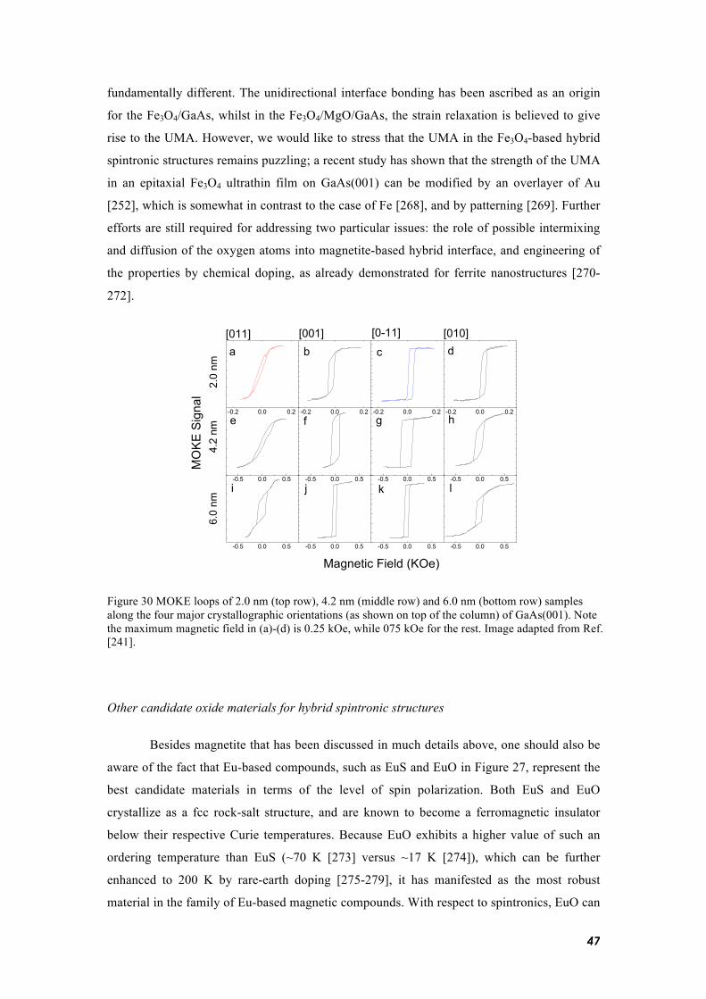
47
fundamentally different. The unidirectional interface bonding has been ascribed as an origin
for the Fe3O4/GaAs, whilst in the Fe3O4/MgO/GaAs, the strain relaxation is believed to give
rise to the UMA. However, we would like to stress that the UMA in the Fe3O4-based hybrid
spintronic structures remains puzzling; a recent study has shown that the strength of the UMA
in an epitaxial Fe3O4 ultrathin film on GaAs(001) can be modified by an overlayer of Au
[252], which is somewhat in contrast to the case of Fe [268], and by patterning [269]. Further
efforts are still required for addressing two particular issues: the role of possible intermixing
and diffusion of the oxygen atoms into magnetite-based hybrid interface, and engineering of
the properties by chemical doping, as already demonstrated for ferrite nanostructures [270-
272].
Figure 30 MOKE loops of 2.0 nm (top row), 4.2 nm (middle row) and 6.0 nm (bottom row) samples along the four major crystallographic orientations (as shown on top of the column) of GaAs(001). Note the maximum magnetic field in (a)-(d) is 0.25 kOe, while 075 kOe for the rest. Image adapted from Ref. [241].
Other candidate oxide materials for hybrid spintronic structures
Besides magnetite that has been discussed in much details above, one should also be
aware of the fact that Eu-based compounds, such as EuS and EuO in Figure 27, represent the
best candidate materials in terms of the level of spin polarization. Both EuS and EuO
crystallize as a fcc rock-salt structure, and are known to become a ferromagnetic insulator
below their respective Curie temperatures. Because EuO exhibits a higher value of such an
ordering temperature than EuS (~70 K [273] versus ~17 K [274]), which can be further
enhanced to 200 K by rare-earth doping [275-279], it has manifested as the most robust
material in the family of Eu-based magnetic compounds. With respect to spintronics, EuO can
-0.2 0.0 0.2
lkji
hgfe
dcba
4.2
nm
-0.2 0.0 0.2
-0.2 0.0 0.2
-0.2 0.0 0.2
-0.5 0.0 0.5
6.0
nm
-0.5 0.0 0.5
-0.5 0.0 0.5
-0.5 0.0 0.5
-0.5 0.0 0.5
-0.5 0.0 0.5
2.0
nm
[010][001] [0-11][011]
Magnetic Field (KOe)
MO
KE S
igna
l
-0.5 0.0 0.5
-0.5 0.0 0.5

48
offer three fundamentally interesting aspects. The first aspect refers to its rather high
magnetic moment of 7 µB per Eu atom, originating from the half-filled 4f-states [280], and
large magneto-optic response [281]. The second aspect is the nearly perfect spin polarization
of EuO (and EuS) at cryogenic temperatures, as determined directly by superconducting
Meservey-Tedrow technique [273, 274, 282], point contact Andreev reflection [101, 279], or
indirectly by tunnelling magnetoresistance measurements [283-286]. The third and perhaps
the most unique aspect of EuO concerns its ability to serve as a ferromagnetic tunnel barrier
for spin-filter tunnelling, a phenomenon being extensively researched by Moodera et al, and
relying on the exchange splitting of the conduction band of the ferromagnetic insulator (FMI),
which creates two different tunnel barrier heights for spin-up and spin-down electrons [15,
273, 274, 283-285, 287, 288]. As for hybrid spintronic devices, such a spin-selective
tunnelling mechanism is most relevant, providing an alternative to the conductivity-mismatch
problem [227], with an added merit of high efficient spin injection and detection.
Despite the tremendous potential of EuO for spintronics, the accessibility of high-
quality EuO films and its heteroepitaxy with conventional semiconductors have been largely
limited by the instability of the oxide. As reported previously, EuO is metastable actually, that
tends to convert to the more thermodynamically stable, non-magnetic Eu2O3 [289]. Oxygen-
deficiency in EuO, possibly originating from improper growth conditions, can otherwise lead
to conductive ferromagnetic phases [279], in turn destroying the intrinsic spin-filter tunnelling
functionality of EuO. To date, most of the experimental studies reported employ the so-called
adsorption-controlled or distillation growth mode by reactive MBE for the epitaxial growth of
EuO thin films [279, 290-300]. In this mode, an Eu-rich environment is maintained around a
heated substrate (usually above 720 K), so that any excess Eu atoms not being oxidized will
re-evaporate off the substrate surface, thus preventing over-oxidation of the EuO into Eu2O3
and Eu3O4. While quite efficient for growth on oxide surfaces, including YSZ [292, 293],
YAlO3 [279, 301], and MgO [293, 298], this specific strategy by itself is insufficient for
semiconductor substrates, owing to interdiffusion issue. A physical diffusion barrier that
simultaneously allows for the heteroepitaxy has been demonstrated as a possible solution [279,
293, 298]. Yet, a major downside of this is the existence of an additional tunnel barrier to the
EuO/semiconductor contact, even though this added barrier is only several nanometers thick.
Only recently has seen the development of another solution specific to Si. This route involves
passivation or, equivalently, termination of Si surfaces by atomic species, such as H, Eu [297],
or Sr [296], prior to the EuO growth. The effectiveness and impacts of those various interface
treatments toward spin-based applications remain to be tested using practical devices.

49
To end this sub-section, we would like to briefly highlight an emerging area
particularly focusing on 2D oxide interfaces. Example of which include LaAlO3/STO [302,
303], LaAlO3/EuO [304, 305], and others [306-309]. Due to their multitude of properties,
such as superconductivity, magnetism, high charge mobility, quantum confinement, etc.,
these interfaces are believed to be an interesting platform for gate-controlled spin transport in
a lateral geometry [310-312].
4.2.2 Heusler alloys on GaAs, InAs, and (GaMn)As
Lattice Structure
Heusler alloys are intermetallic compounds with particular composition and crystal structure
as included in Figure 31 [313]. They can be categorized into two distinct classes: the half
Heuslers with the form XYZ (referred as C1b structure) and full Heuslers with the form X2YZ
(referred as L21 structure) where X and Y atoms are transition-metals, while Z atom is either a
SC or a non-magnetic metal. The unit cell of the L21 structure consists of four fcc sub-lattices,
while that of the C1b structure is formed by removing one of the X sites. Heusler alloys are
ferromagnetic as a result of the DE mechanism between neighboring magnetic ions. Both half
and full Heusler alloys show the Slater-Pauling behavior of the binary transition-metal alloys,
i.e. the total number of valence electrons per f.u. determines the total magnetic moment per
f.u., and this behavior enables one to tailor the magnetic properties of new compounds by
substituting the Y atoms with the different transition-metals.
Figure 31 Major combinations of Heusler alloy formation.
H He
Li Be B C N O F Ne
Na Mg Al Si P S Cl Ar
K Ca Sc Ti V Cr Mn Fe Co Ni Cu Zn Ga Ge As Se Br Kr
Rb Sr Y Zr Nb Mo Tc Ru Rh Pd Ag Cd In Sn Sb Te I Xe
Cs Ba Hf Ta W Re Os Ir Pt Au Hg Tl Pd Bi Po At Rn
Fr Ra
La Ce Pr Nd Pm Sm Eu Gd Tb Dy Ho Er Tm Yb Lu
Ac Th Pa U Np Pu Am Cm Bk Cf Es Fm Md No Lr
Y X
Z
50
The term ‘Heusler phase’ was named after Friedrich Heusler, who discovered a
mysterious FM behavior in a ternary alloy formed from non-FM constituents as early as 1903
[188]. The Heusler alloys have been the subjects of a large number of studies over more than
a century and especially since 1983, when Heusler alloys were predicted to possess a half-
metallic character [188]. NiMnSb, as the first predicted half-metallic Heusler alloy, was hotly
investigated at the early stage. Although the bulk single-crystals have shown ~100% spin
polarization at the EF by means of spin-polarized positron annihilation [314], the thin films
NiMnSb has only shown 28% at 0.4 K by TMR [315] and ~58% with Andreev reflection
[101]. Later on, the focus of the research on Heusler alloys shifted toward the Co-based
Heusler alloys with the formula Co2YZ, which were found to have half-metallicity [316, 317]
and high Tc (for example in Co2FeSi, Tc =1120 K). Up to 317% TMR ratio has been obtained
at 4 K from Co2Cr0.6Fe0.4Al [318]. This achievement was followed by even larger TMR ratios
from MTJs with different Co-based Heusler alloys electrodes such as Co2FeAl [319],
Co2MnSi [320], Co2Cr1−xFexAl [321], and Co2FeSi [316]. While Co2MnSi has shown a giant
low temperature TMR ratio of about 570% which corresponds to a spin polarization of 89%,
this ratio has tremendously reduced to 90% at RT.
Epitaxial growth and properties
A number of Heusler alloys have been grown epitaxially on SCs including NiMnSb [193],
Ni2MnGa[322], Ni2MnGe [195], Ni2MnAl [323], Co2MnSi [324], Co2 (Cr, Fe)Al [325],
Co2MnGe [198] on GaAs(001), Ni2MnIn [197] on InAs(001), and Cu2MnAl and Co2MnSi on
Si. Co-sputtering, PLD and MBE are the three main deposition methods that have been used
so far. The Ni-based half Heusler Alloy, namely epitaxial NiMnSb has been the grown both
by co-sputtering [326], and by MBE [315] techniques. Although the bulk single crystal
NiMnSb exhibited 100% spin polarization [314], these thin films showed much smaller
values of spin polarization, a maximum of ~60% [101]. Atomic disorders at the empty sites
are pointed out to be the reason for this large difference from the bulk value of polarization
[327]. Epitaxial NiMnSb(001) thin films are reported to be grown both on GaAs(001) [193],
and GaAs(111)B [328] substrates. The surface spin polarizations are predicted to depend
upon the terminated layers for such growth. For the NiMnSb(001) surface, the Ni-terminated
surface compresses the distance between the surface Ni and subsurface of MnSb layer by 10%
and corresponds to a surface polarization of 42%. On the other hand, the MnSb-terminated
surface reduces the distance between the surface Mn and subsurface of Ni layers by 3.5% and
expands that between the surface of Sb and sub-surface of Ni layers by 7.3% with a surface
polarisation of 84% [329]. Similar effect is predicted for NiMnSb(111) surfaces [330]. On the

51
contrary, epitaxial NiMgSb(001) films grown on MgO(111) substrate with Mo(001)-buffer
layers exhibited 68%–100% spin polarization at the MnSb terminated surface [331]. The
effect of surface termination on the spin polarization has also been predicted for other half
Heusler alloys, such as PtMnSb [332], and CoMnSb [333]. Co-based full Heusler alloys are
also been investigated. Single-crystalline Co2MnSi Heusler alloy films have been grown on
GaAs(001) substrates by PLD. High quality Co2MnSi films on GaAs has been achieved after
deposition at 450 K [324] as indicated by the sparking RHEED pattern shown in Figure 32.
The L21 order polycrystalline Co2CrAl and epitaxial Co2FeAl thin films were grown onto
GaAs(001) substrates at 673 K using MBE. The Co2FeAl films, exhibited almost single phase
with the crystalline relationship of Co2FeAl(001)<110>//GaAs(001)<110> [325].
Figure 32 RHEED patterns of a clean GaAs(001), b 60-Å-thick Co2MnSi film, left-hand side panels along [110] GaAs and right panels along [1-10] GaAs, c line profiles of GaAs top and Co2MnSi bottom RHEED patterns taken along [110] GaAs achieved at a substrate temperature of 450 K. Image adapted from Ref. [324].
Heusler alloys exhibit structural similarity to the zinc-blende structure adopted by
binary SCs like GaAs, InAs and ZnS [322, 334], and large bandgap at EF in general, which
could facilitate their use in devices such as spin-FET and spin-LED (see section 6). However,
disadvantages exist in Heusler alloys because of their fragile half-metallicity against atomic
disorder. For the L21 structure, when X atoms remain ordered while full disorder occurs
52
between Y and Z sites, the alloy transforms into the B2 structure. And if disorder occurs
between one X site and either Y or Z sites, the atomic arrangement may lead eventually to the
A2 structure. Such disorders result in suppression of the inversion centers that is present in the
ordered Heusler alloys, which have important consequences for the half-metallic bandgaps. It
was reported that more than 7% of atomic disorder is enough to vanish the energy gap for the
minority spins at EF. The earlier mentioned discrepancy of spin polarization in NiMnSb thin
films, compared with that in bulk NiMnSb is a typical example [327].
The understanding of the interface and magnetic moments of ultrathin Heusler alloy
films on semiconductor surfaces are important for high efficient spin injection. Previously
Grabis et al. [335] found that the reduced magnetization of Co2MnGe thin films was due to a
reduction of the Mn moments. Claydon et al. [336] carried out a detailed XMCD study of the
element specific magnetic properties of Co2MnGa/GaAs(001) hybrid structure at RT, and
observed a considerable reduction in the magnetic moments by as large as 50% in the
ultrathin films, as summarized in Table 3. This observation was attributed to possible Mn
defects that reside on Co sites, causing an anti-ferromagnetic coupling. Later on, this
particular type of Heusler-based hybrid spintronic structure was incorporated into a spin-LED
with an aim to study electrical spin injection [337, 338]. With an off-stoichiometric
Co2.4Mn1.6Ga, a rather low spin injection efficiency of 13% was observed and in addition the
polarization signal disappeared above 20 K. With Co2MnGa, this efficiency could be boosted
to 22% [338]. But even for stoichiometric Co2MnGe that is known to be almost half-metallic,
only an efficiency of 27% could be attained [339]. In general, these results point to possible
interfacial defects that on one hand can limit device performance and on the other hand urge
for utilization of advanced characterization techniques such as XMCD to probe specifically
the hybrid interface properties which are otherwise difficult to observe by bulk methods.
In addition to the local moments, the magnetic anisotropies of ultrathin Heusler alloy
films can also be affected by the semiconductor surfaces. As discussed in section 3, UMA has
been observed in several ferromagnetic metals and alloys such as Fe, Co, CoFeB on various
semiconductor substrates. A recent study of single-crystalline full-Heusler alloy films on
GaAs again observed UMA in its ultrathin region [340]. As shown in Figure 33, these authors
have prepared the Co2MnAl films with the thickness varying from 3nm to 12 nm on GaAs
(100) using MBE, and obtained a significant Ku of nearly 4 x 10³ erg/cm3 at 3 nm, which was
attributed to the interfacial stress. Such strong UMA can be utilised to design the
magnetization switching of the spin injectors and detectors in the spin-FET.

53
Table 3 The sum of orbital and spin moments with error bars in uB/atom for the Co and Mn components as obtained from XMCD measurements on three different film structures of CoxMnyGa indicated by the x/y ratio with three different thicknesses. Data obtained from Ref. [336]
Figure 33 (a) The RHEED pattern of CMA film. (b) DCXRD pattern of 12-nm-thick CMA film. (c) Normalized in-plane hysteresis loops of CMA films with varying thickness, and the field is applied along [110] direction. (d) Normalized in-plane hysteresis loops of CMA films with the field applied along [1–10] direction. Image adapted from Ref. [340].
More recent research is directed to exploring the magnetic proximity effect between
Heusler alloys and diluted magnetic semiconductors (DMSs) [341-343]. In such a magnetic
bilayer system, the exchange coupling from a Heusler alloy is utilized to enhance the Tc in a
DMS [344-347]. Nie et al. reported the magnetic proximity effect in Co2FeAl/(Ga,Mn)As
bilayers [348]. A significantly enhanced Tc (above RT) was demonstrated by XMCD in the
epitaxial Co2FeAl/(Ga,Mn)As bi-layer structure. As shown in Figure 34, the elemental

54
specific hysteresis loops of Fe, Co and Mn, respectively, exhibit clear FM behaviors and
identical Hc, proving a robust magnetic Mn-Fe-Co coupling. Unlike the anti-parallel
alignment, which has been reported in the Fe/(Ga,Mn)As systems [349-351], their results
suggest a FM coupling between the Fe, Co and the Mn. This observation was also later on
confirmed by the ab initio density functional calculations on both the ordered L21 and
disordered B2 phases for the Co2FeAl.
Figure 34 The elemental specific XMCD hysteresis loops of the Fe, Co, and Mn, respectively in Co2FeAl/(Ga,Mn)As bilayers probed with elemental specific XMCD. Image adapted from Ref. [348].
5 Hybrid spintronic structures with 2D materials
2D systems have become one of the most exciting new classes of materials due to the wealth
of exceptional physical properties that occur when charge, spin and heat transport are
confined to a plane. Their unique 2D electron gas (2DEG)-like behaviors not only enrich the
world of low-dimensional physics, but also provide a platform for transformative technical
innovations. Magnetism is not common for the elements consisting Van der Waals 2D
materials; however, spin polarization in these materials can still be induced by defects, edge
states, magnetic dopants and/or via the proximity to an adjunct magnetic source etc.
Compared to FM, they generally have less robust magnetism, but significantly longer spin
lifetime or spin coherence length, which are eagerly desired in spintronics. Furthermore, their
capacity of integration with FM offers a promising direction toward the development of
hybrid devices that can perform logic, communications, and storage within the same material
technology.

55
5.1 Graphene-based spintronic structures
The revolutionary nature of graphene [352-354] makes it a prime candidate for the spintronics
applications, in which the generation and tuning of spin-polarized currents are prerequisites
[2]. In its pristine state, graphene exhibits no sign of conventional spin polarization, and so far
no experimental signature shows a FM phase of graphene. This gap is now filling up by
combined efforts in multi-disciplinary research. The FM metal/graphene heterojunction is one
of the most promising avenues to realize efficient spin injection into graphene [355] and other
carbon-based organic systems [356-360]. Perfect spin-filtering for lattice-matched interfaces
of graphite with Ni or Co has been predicted, which is insensitive to interface roughness due
to the intrinsically ordered nature of graphite [361]. Fascinating properties of spin transport
phenomena have presented in the Co/graphene system [362, 363], though theoretical
calculations show that the atomic magnetic moment of Co can be reduced by more than 50%
when absorbing on graphene surface [364]. As a non-magnetic interlayer, vertical spin-valve
devices have also been successfully demonstrated, featuring FM/graphene interfaces [365-
370], in which the signal could be enhanced by doubling the number of graphene layers in
some specific cases [365]. Being a tunnel barrier with a low out-of-plane conductivity,
graphene sheet has been shown to drastically improve the spin-injection efficiency for FM/Si
interfaces [371].
Despite the above positive findings, current understanding of magnetic properties in
the hybrid FM/graphene structures remains very limited, largely because of a number of non-
trivial interface problems. Those interface issues, which include but are not limited to
interface disorders, magnetic dead layer, and electronic orbital hybridizations, must be
understood before any functional graphene-based spintronic devices can be developed. This
section will be devoted to discussing these aspects by highlighting the main progress on the
growth, structures and interface magnetism of graphene-based hybrid structures with FMs.
5.1.1 Graphene in proximity to FMs
“Graphene on top”
As one can imagine, two types of basic hybrid structures between graphene and FMs are
technically possible, according to the conventional spin-valve architecture. One is with
graphene on top of a FM, and the other with graphene at the bottom. Due to both historical
56
[372, 373] and technical reasons (see latter paragraphs), the “graphene on top” structure has
been most studied, and is relatively easier to achieve than the “graphene at the bottom”
structure. Previous fabrication of the former hybrid structure was overwhelmingly done by
thermal cracking of hydrogen gases, a self-limiting process, on lattice-matched crystalline
FMs [374-384]. Both Ni(111) and Co(0001) have been the primary FMs of interest,
considering a nearly perfect lattice-match characterized by only a marginal mismatch of ~1.3%
between graphene and Ni/Co. Graphene usually exhibits a hexagonal (1 ´ 1) structure on both
FM surfaces [374, 375, 377, 379], but exceptions do exist for growth under slightly non-
optimal conditions for which other differently oriented domains co-exist with the (1 ´ 1)
atomic structure, forming a moiré-derived pattern in graphene [381, 382]. A rather extreme
case has also been reported recently, involving graphene growth on Fe(110) surface [385].
Although the shortest Fe-Fe distance (2.48 Å) is close to the lattice constant in graphene (2.46
Å), the Fe(110) surface features a distorted hexagonal symmetry, which in turn induces a
short-ranged periodic wavy pattern in graphene.
Both the graphene/Ni(111) and graphene/Co(0001) hybrid interfaces are covalently
bonded systems, characterized by strong interfacial hybridization between the graphene p and
FM 3d valence-band states. Such substantial interface effects should provide new
opportunities for spintronic applications. On the one hand, a robust spin-filtering effect has
been predicted in those interfaces [361]. On the other hand, the orbital hybridization may
serve as a viable means to induce magnetism in graphene, which has proven to be non-trivial
in many earlier attempts [386-390]. For instance, a partial charge transfer of spin-polarized
electrons from the FMs to graphene was previously observed to occur, inducing an effective
magnetic moment and thus carbon K-edge XMCD [377, 378]. For the particular case of the
graphene/Ni(111) interface, the XMCD dichroic signal was reported to be as high as –12% at
RT and coupled antiparallel to the spin moments of the Ni 3d states at the Fermi level [374].
Further enhancement of the K-edge XMCD by a factor of ~2.7 was also demonstrated via
intercalation of a thin layer (1 ML) of Fe into the graphene/Ni interface [378]. For electrical
spin injection into graphene from FMs, the DOS in the vicinity of the Fermi level are most
relevant. Previous angle-resolved photoelectron spectroscopy (ARPES) measurements have
shown very interesting distortion of the valence band of graphene with the presence of Ni(111)
and Co(0001). For both hybrid interfaces, the π states of graphene are essentially shifted away
from the Fermi level due to orbital hybridization with the FM d bands [379-382, 384, 391],
but a new spin-polarized cone-like interface band has observed to set in near the Fermi level
[379, 381, 391] (see Figure 36). The existence of such spin-polarized interface band may be
employed as a spin source and/or as a spin-filter for spin injection.
57
Figure 35 XMCD spectra of Fe-intercalated graphene/Ni(111) hybrid structures at the (a) Ni L2,3, (b) Fe L2,3, and (c) C K-edges. Image adapted from Ref. [378].
Figure 36 ARPES measurements of well-oriented graphene/Co interface at RT. Images adapted from Ref. [379].
“Graphene at the bottom”
Due to their large difference in surface energy, 3d FMs usually form nanoscale clusters on
graphene/graphite [392-394]. This explains the technical challenge on why the “graphene at
the bottom” (FM/graphene) structure is more difficult to achieve. Experimental efforts are
nevertheless underway, trying to come up with novel solutions to overcome this challenge.

58
From the fundamental science perspective, the FM/graphene hybrid interface presents a
promising platform for studying atomic-scale magnetism and magnetic anisotropy in low-
dimension. Liu et al. have recently carried out a systematic study on the interfacial magnetism
in Fe/graphene heterojunction using a combined method of XMCD and DFT calculations
[395]. The experiment has been performed using a specially designed FM1/FM2/graphene
structure that to a large extent restores the realistic case of the proposed graphene-based
transistors [83]. As shown in Figure 37, these authors have quantitatively observed a reduced
but still sizable magnetic moments of the epitaxial Fe ML on graphene, which is well
resembled by simulationsand can be attributed to the strong hybridization between the Fe 3dz2
and the C2pz orbitals and the sp-orbital-like behavior of the Fe 3d electrons due to the
presence of graphene. The calculated magnetic moments of Fe for the three different
configurations as well as those derived from the experimental measurements were gathered in
Table 4. Generically, an enhancement of morb of Fe can be attributed to the symmetry
breaking of the ultrathin film, for which the electrons are more localized, leading to an orbital
degeneracy lifting as reported in Fe/GaAs [50] and Fe/InAs [84]. A further factor of influence
is the modified chemical environment due to the underneath graphene. Interfacial mspin can be
induced in the π-conjugated states of several carbon-based systems by adjacent FM as
observed in C60/Fe3O4(001) [359, 360], C60/Fe(001) [356, 358], and graphene/Ni(111) [377,
378], due to the intensive spin and charge transfer between the FM and C atoms. The stacking
of the topmost FM with respect to graphene is another noteworthy question. Possibilities exist
that in such FM/graphene heterojunctions, FM atoms may be incorporated into the graphene
defects, or diffuse through the graphene to form metallic layers in-between the graphene and
the substrate. A very recent LEED analysis on FM intercalation underneath graphene sheets
shows that for 1-2 ML Fe deposited on graphene/Ni(111), the Fe atoms tends to intercalate
between the graphene and Ni surface, forming a favorable Ni/Fe/graphene stacking and that
Fe in between of graphene and Ni tends to follow the fcc stacking of the Ni(111) substrate
and the graphene has the same registry as for Ni(111) [375, 378, 396]. In terms of the
occupation sites, the best agreement between experiment and theory of the Fe/graphene
heterojunction points to a coexistence of two types of domains, namely top-fcc and bridge-top
domains [397].

59
Figure 37 The theoretical model of Fe/grapheme bilayer. (a) Illustration of the three non-equivalent allocations of Fe on graphene, namely top (blue), bridge (green) and hollow (red), and their calculated equilibrium distance (d0) and system free energy (E), referenced to Fetop/graphene. The unit cell is shown as the gold-colored parallelogram. (b) Spin-resolved band structures for a freestanding Fe ML (left column) and the ML Fetop/graphene (right column), respectively, together with their corresponding partial DOS. Image adapted from Ref. [395].
System Ref. Method stacking mspin (µB/atom) morb (µB/atom) Fe/graphene [395] XMCD 1.06 ± 0.1 0.18 ± 0.02
Fetop/graphene [395] DFT fcc 1.23 Febridge/graphene [395] DFT fcc 0.67 Fehollow/graphene [395] DFT fcc 2.57
freestanding ML Fe [395] DFT fcc 2.76 Fe/InAs [84] XMCD bcc 1.22 ± 0.12 0.22 ± 0.03 Fe/GaAs [50] XMCD bcc 1.84 ± 0.21 0.25 ± 0.05
bulk-like Fe [395] DFT bcc 2.15 bulk-like Fe [398] XMCD bcc 1.98 0.086
Table 4 The experimentally measured and calculated magnetic moments of Fe in various graphene-based configurations in comparison with those on InAs and GaAs [395].
60
The strong orbital hybridization in FM/graphene hybrid structures is known to be
capable of influencing the magnetic ground state of FM adatoms, which in turn can control
magnetic anisotropy. A relevant study has been reported for nanometer-thick Co films
intercalated between graphene and Ir(111) [399]. PMA originated from the hybridization
between the graphene and the Co electronic orbitals was observed in this intercalated system,
which could be manipulated further by adjusting the Co thickness [400]. For a Co thickness
of 13 ML or less, the magnetization of the intercalated structure is purely out-of-plane. Above
15 ML, in-plane anisotropy starts emerging and increases with the Co thickness (see Figure
38). By engineering a stacking structure with multiple Co/graphene interfaces, it has been
proposed that a giant PMA more than 20-times larger than conventional multilayers may be
possible [400].
Figure 38 (a-b) Thickness dependent effective magnetic anisotropy for bare Co film, one surface of Co film coated by graphene, both surfaces of Co film coated by graphene, respectively. (c) Out-of-plane and in-plane contrast of SPLEEM images of Co/Ir(111) and graphene/Co/Ir(111) structures with different Co thicknesses. Image adapted from Ref. [400].
The perfect spin-filtering effect due to k-vector conservation at lattice-matched
FM/graphene interfaces relies on the fact that the only states available at the Fermi energy of
graphene are located or close to the K-points, where there are only minority-spin states of the
said FMs [361]. However, a key question is how one can realize such an epitaxial FM
electrode on top of graphene. Here we highlight two notable approaches [376, 401] that may
shed light onto this challenging issue.

61
The first approach concerns the growth of Fe3O4 ultrathin films on graphene/Ni(111)
[376]. The central idea behind this approach involves the use of half-metallic Fe3O4 as a top
FM contact on graphene, for which the fully spin-polarized bands of Fe3O4 at the Fermi level
may relieve the stringent requirement on a perfect crystallographic matching at the
FM/graphene interface. Being an oxide, Fe3O4 has an added advantage on limiting interfacial
electronic interaction with graphene, which should then preserve the intrinsic Dirac electronic
structure of the 2D material. To fabricate an abrupt interface, the authors adapted an
“oxidation and post-annealing” procedure, by which the dispersion of the graphene π states
can still be observed by ARPES [376].
A radically different approach has been demonstrated by Wong et al., based on solid
phase epitaxy of amorphous CoFeB at elevated temperatures [401]. The atomic arrangement
of the practical heterostructure has been depicted in Figure 39 where the best registry is
obtained by fitting seven parts of the hexagonal carbon lattice to six parts of CoFe(110). This
configuration is clearly less ideal than the case of (111) Co or Ni on graphene, where a
hexagon-on-hexagon registry is possible, and may therefore induce a symmetry-lowering
factor, which is likely to deteriorate the robustness of the proposed spin-filtering effect. The
degree of such effect has also been considered in terms of the band matching. The spin-
resolved Fermi surfaces of bcc-Co projected onto the (110) plane, where an imbalance of
minority- versus majority-spin states at the N-point in the reciprocal space of Co(110) can be
observed in Figure 39. Further taking into account the presence of Fe in the alloy, which
features a complicated structure of majority- and minority-spin states at the Fermi level, the
spin-filtering effect and thus the difference in conductance between the parallel and anti-
parallel cases in a sandwich structure involving the CoFe(110)/graphene interfaces is
estimated to be finite, albeit small. This approach nevertheless remains in the race of
achieving the predicted spin-filtering effect [361], as boron accumulation that would
otherwise break the favorable conditions for the spin-filtering effect was not observed at the
CoFe/graphene hybrid interface [401]. In addition, CoFeB with a higher Co/Fe compositional
ratio is expected to crystallize into an fcc phase, which therefore should lead to a better lattice
registry with graphene.
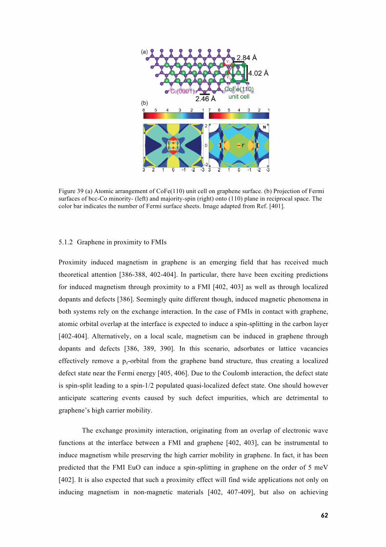
62
Figure 39 (a) Atomic arrangement of CoFe(110) unit cell on graphene surface. (b) Projection of Fermi surfaces of bcc-Co minority- (left) and majority-spin (right) onto (110) plane in reciprocal space. The color bar indicates the number of Fermi surface sheets. Image adapted from Ref. [401].
5.1.2 Graphene in proximity to FMIs
Proximity induced magnetism in graphene is an emerging field that has received much
theoretical attention [386-388, 402-404]. In particular, there have been exciting predictions
for induced magnetism through proximity to a FMI [402, 403] as well as through localized
dopants and defects [386]. Seemingly quite different though, induced magnetic phenomena in
both systems rely on the exchange interaction. In the case of FMIs in contact with graphene,
atomic orbital overlap at the interface is expected to induce a spin-splitting in the carbon layer
[402-404]. Alternatively, on a local scale, magnetism can be induced in graphene through
dopants and defects [386, 389, 390]. In this scenario, adsorbates or lattice vacancies
effectively remove a pz-orbital from the graphene band structure, thus creating a localized
defect state near the Fermi energy [405, 406]. Due to the Coulomb interaction, the defect state
is spin-split leading to a spin-1/2 populated quasi-localized defect state. One should however
anticipate scattering events caused by such defect impurities, which are detrimental to
graphene’s high carrier mobility.
The exchange proximity interaction, originating from an overlap of electronic wave
functions at the interface between a FMI and graphene [402, 403], can be instrumental to
induce magnetism while preserving the high carrier mobility in graphene. In fact, it has been
predicted that the FMI EuO can induce a spin-splitting in graphene on the order of 5 meV
[402]. It is also expected that such a proximity effect will find wide applications not only on
inducing magnetism in non-magnetic materials [402, 407-409], but also on achieving

63
controllable MR [402, 410, 411], gate tunable manipulation of spin transport [403, 412] and
exchange bias [413], and STT [414], as well as the quantized AHE in graphene [415, 416].
The induced magnetism in graphene by the proximity coupling to a magnetic
substrate has been demonstrated experimentally for graphene on Au/Ni(111) substrates [417].
By spin-ARPES, it has been observed that electronic orbital hybridization of graphene p
states with Au 5d states could result in a giant Rashba-type spin splitting as large as ~100
meV in graphene p band [417]. But to probe the induced magnetism in graphene by transport
devices, magnetic insulators rather than metals are mandatory. Along this line, Swartz et al.
have explored the epitaxial growth of EuO on graphene, and discussed several possible
scenarios for realizing exchange splitting with this magnetic insulator. While their graphene
devices exhibit clearly the integer quantum Hall effect, no signature of magnetism in the form
of AHE due to the proximity interaction with EuO could be observed [294, 418]. On the other
hand, these authors have also investigated the properties of the magnetic moments in
graphene originating from localized pz-orbital defects created by adsorbed hydrogen atoms.
The behavior of these moments has been studied using non-local spin transport to directly
probe the spin-degree of freedom of the defect-induced states. More recently, Hallal et al
[419] calculated the proximity induced magnetism in graphene on four different magnetic
insulators, namely EuO, EuS, yttrium iron garnet (YIG) and cobalt ferrite (CFO). As shown
in, the results indicate that induced exchange-splitting in graphene can vary from tens to
hundreds of meV by selecting different FMIs.
Figure 40 Band structures of graphene on (a) EuO, (b) CoFe2O4, (c) EuS and (d) Y3Fe5O12. Blue (green) and red (black) represent spin up and spin down bands of graphene (magnetic insulators), respectively. Image adapted from Ref [419].

64
A convincing evidence of proximity-induced magnetism in graphene was reported by
Wang et al [420], using an atomically flat YIG thin film. Their results indicated not only a
large exchange interaction and ferromagnetism in graphene/YIG, but also an enhanced spin-
orbit coupling which inherently weak in pristine graphene. In their devices, a large AHE
resistivity could only be observed far away from the Dirac point as included in Figure 41.
However, when using magnetic and insulating LaMnO3, Cheng et al [421] acquired a
considerable AHE signal nearby or at the Dirac point.
Figure 41 The gate voltage dependence of the device conductivity, quantum Hall effect, and non-linear AHE resistivity of transferred graphene/YIG device. Image adapted from Ref. [420].
5.2 TMD-based spintronic structures
TMDs, whose structures are arranged in a layered fashion like graphene, have recently
attracted widespread interest [422-428]. In the atomically thin regime, TMDs possess three
unique fundamental properties that are believed to be superior to those of graphene. Firstly,
there are almost 40 different types of TMDs being known to date. Depending on different
combinations of chalcogen and transition-metal elements, TMDs can exhibit metallic, half-
metallic, semiconducting, superconducting, and magnetic properties [424, 429-432]. This
diversity makes the TMD family more sought-after in many applications than graphene.
Secondly, inversion symmetry is broken in group-VI semiconducting TMD MLs, such as
MoS2, WSe2, which in turn activates the valley degree of freedom for charge carriers [426,
65
428, 433]. This is distinct from the indiscriminative K-valleys of graphene, and provides a
fascinating playground for valleytronics. With the strong spin-orbit coupling originated from
the heavy transition-metal atoms, the spin degree of freedom in ML TMDs can be further
coupled with the valley degree of freedom, leading to the dual use of both spin and valley in
spin-valleytronics for information processing [427]. Thirdly, while strong spin-orbit coupling
usually results in short spin lifetimes, the case of the group-VI semiconducting ML TMDs is
expected to be very different because of the giant spin-orbit spitting in its valence band edge,
that can suppress spin relaxation to produce longer spin lifetimes [427]. This unusual
behavior has indeed been observed in polarization-resolved photoluminescence measurements,
reporting a lower bound on the spin lifetime of 1 ns [433]. Optical Kerr spectroscopy has
further revealed that electron spins in n-type MoS2 and WS2 MLs are long-lived, with spin
lifetimes exceeding 3 ns at 5 K. This value is two to three orders of magnitude longer than
typical exciton recombination times [434]. These two particular works based on optical
characterizations strongly suggest that semiconducting ML TMDs could outpace graphene in
terms of spin lifetimes.
While we are aware of an increasing amount of theoretical and experimental studies
on 2D DMSs, a recent topic where researchers attempt to create magnetism in non-magnetic
TMD MLs by transition-metal dopants (mainly group-VI semiconducting TMDs) [435-440],
we will rather restrict our discussion on the hybrid systems involving FMs and TMDs, which
are the main scopes of this review article. On the other hand, the general background and
(spin-unrelated) properties of low-dimensional TMDs have already been reviewed in much
detail in Ref. [423, 424, 429].
5.2.1 Theoretical FM/TMD interfaces
Currently available studies on FM/ML TMD hybrid interfaces remain scarce to date [441-
446], but yet are already sufficiently convincing to show its exciting prospect for spintronics.
Down to the fundamentals, its uniqueness as a 2D material comes with the fact that higher
binding energies generally exist between 3d FMs and ML TMDs (from Fe to Ni on MoS2:
2.5–3.4 eV [441-443]) than with graphene (Co on graphene: 1.6 eV [447]), despite the
structural similarity of TMDs and graphene [441-443]. On the one hand and in the case of ML
MoS2, such disparity in the surface binding energies can be explained by the coexistence of
Mo 4d and S 3p orbitals at the band edges, in contrast to the relatively “flat” electron cloud
due to the sp2 network of graphene. On the other hand, this difference suggests better wetting
of 3d FMs on ML TMDs and thus higher chances of achieving epitaxy [393, 394]. In fact,

66
Chen et al. have predicted such feasibility for the particular case of Co/ML MoS2 hybrid
interface [443]. Their calculations have indicated stable adsorption and high diffusion barrier
for Co atoms on ML MoS2 for establishing a long-ranged structural order, and also heavy
overlapping among the Co 3d, Mo 4d and S p electronic orbitals, as a consequence of
interface hybridization. This latter electronic effect is particularly promising because a large
spin-splitting near the Fermi level is expected, simultaneously leading to a net local moment
as high as 0.93 µB in the Co atom and half-metallicity at the Co/ML MoS2 interface, which
could play an important role in defining the spin injection mechanism via such novel interface
[443] (see Figure 42).
By means of first-principles calculations, Dolui et al. have also predicted a giant MR
effect in vertical Fe/MoS2/Fe junctions with a maximum MR of ~300% [444]. Such a vertical
spin-valve device is highly interesting because of its structural similarity to conventional
MTJs, but yet with a low-resistance non-magnetic TMD layer. The working principle of the
Fe/MoS2/Fe junctions is actually comparable with the proposal for FM/graphene-based spin
filters by Karpan et al [361]. A main criterion on obtaining a large MR is on band symmetry.
For instance, when MoS2 is employed as a spacer material, the FM should possess electronic
states of one spin at the Fermi level at the center of the TMD Brillouin zone, while the other
spin states should preferentially reside away from the G point. Provided such symmetry,
conducting channels exist only for one spin type, while the opposite spin electrons will be
selectively scattered, thus not contributing to a device current. As we shall see in section 6, a
finite MR value has indeed been observed in relevant vertical structures based on
NiFe/MoS2/NiFe [448]. That particular experimental work has not only verified the main
findings of this theoretical study, but also substantiated the robustness of FM/ML TMD
hybrid interfaces for spintronic devices.

67
Figure 42 (a-b) DFT simulated atomic structure of ML Co atoms on ML MoS2. (c-d) Charge and spin density difference profiles, respectively. (e) Spin-resolved partial-DOS of the hybrid interface. Image adapted from Ref. [443].
5.2.2 Experimental FM/TMD interfaces
The coupled spin- and valley degrees of freedom in low-dimensional group-VI
semiconducting TMDs (such as MoS2 and WSe2) has enabled the recent experimental
observations of coexistence of spin-Hall and valley-Hall effects [427], long-lived electron
spin in the nanosecond range due to strong spin-valley locking [434], and optical and
electrical controls of valley polarization [428, 433, 449]. A possible route to better utilize and
even expand these novel physical phenomena is to integrate the ML TMDs with spin devices.
A spin-FET with a ML TMD transport channel is one potential example. However, exploring
this as well as those previously proposed by theories [443, 444] will have to build on the
ability to fabricate well-defined FM/ML TMD hybrid interfaces, which by far has proven to
be very challenging [445, 446, 450].
Because of its semiconducting character, group-VI ML TMDs tend to form Schottky
barriers with metal contacts. Such interfacial barriers in most cases dominate any measured
transport properties of a given device [451]. In the context of spintronics, understanding the
role of the contacts is key for realizing efficient spin injection from FM electrodes into the

68
ML TMD materials. Chen et al. were the first to look into the Schottky barrier formation at
Co/ML MoS2 interface, and observed a barrier height of ~60 meV [445]. This value could be
improved by as much as 84% with an inserted MgO thin barrier. Further control over the
barrier height was also demonstrated by a back electrostatic gate, which is effective due to the
2D nature of ML MoS2. A large Schottky barrier resistance was also observed by Dankert et
al. for Co/few-layer MoS2 interface, which could be reduced similarly by introducing a thin
TiO2 tunnel barrier [446] as shown in Figure 43. This approach not only results in an
enhancement of the transistor on-state current by two orders of magnitude and the field-effect
mobility by a factor of 6, but also enables the contact resistance of the Co/few-layer MoS2
interface to lie within the optimum range for realistic observation of a large two-terminal MR
[452]. A further insight into the Schottky barrier formation at the 3d FM/TMD hybrid
interfaces can be obtained by comparing these two studies with another work reported by
Wang et al. for NiFe/MoS2 interfaces [450]. A particularly interesting observation in the latter
was an Ohmic behavior between multilayer MoS2 and NiFe, but a Schottky character for NiFe
and ML MoS2. At this point, one can conclude that the Schottky barriers formed at 3d
FM/TMD interfaces are very sensitive to both the FM of interest and the TMD thickness. We
speculate that the relative energetics between the materials are governing the barrier
formation, and can only be characterized in an unambiguous manner by (i) state-of-the-art
surface science approaches, such as in-situ XPS and ultraviolet photoelectron spectroscopy,
and (ii) contamination-free hybrid interfaces. In this regard, the recent major advancements
on MBE growth of several epitaxial ML TMDs will largely facilitate such potential studies
[431, 432].
Figure 43 Contact resistance for observation of MR. Calculated two-terminal MR as a function of (a) the contact resistance-area product in a MoS2-based spin-valve structure, and (b) gate voltage and contact resistance. Image adapted from Ref. [446].

69
5.3 Topological insulator (TI)-based structures
As a newly discovered class of matters with eccentric electronic phase, the spin-orbit induced
TIs have a very short history but large attractions to the community of condensed matter
physicists. Since they were first theorized in 2005 [453] and later experimentally produced in
2007 [454], TIs, with their ability to insulate on the inside and conduct on the outside, have
presented new possibilities for the future spintronics applications.
The past ten-years has been a rapid developing time for TIs, during which both 2D
and 3D versions of these materials have been theoretically predicted and subsequently
produced in laboratories. The first experimental signature of TIs was the observation of the
2D quantum spin Hall effect sandwiched by layers of HgxCd1–xTe, reported by König et al. in
2007 [454]. They performed transport measurement of this trilayer device and observed the
predicted 2e2/h conductance, which is independent of the width of the sample as expected for
a conductance resulting only from edge states. The 3D TI was demonstrated in 2008, by
Hsieh et al., who mapped out the surface states of bismuth antimonite (BixSb1–x) [455].
However, those surface states observed were more complicated than one initially thought,
which eventually prompted the community to search for other classes of materials that might
exhibit a simpler electronic structure. This search indeed led to the discovery of binary Bi2Se3
and Bi2Te3 alloys, which are the prototype 3D TIs nowadays. 3D TIs feature novel phases of
quantum matter characterized by sharp changes in electronic structure at their very surfaces,
i.e. with insulating bulk band gap and gapless Dirac-like band dispersion surface state (SS).
While such a phase offers unique opportunities for fundamental research, it is equally
important to break the time-reversal symmetry of TIs to realize novel physical phenomena
and quantum-computing applications. The newly demonstrated QAH effect [456-458],
abnormal proximity effect [459, 460], giant MOKE [461], magnetic monopole [462], and
chiral conduction channels [463, 464] are some of the fascinating examples.
5.3.1 Magnetically doped TIs
Amongst the rich physical phenomena that can possibly be found in TIs, the effect of
magnetic perturbation is particularly crucial, due to its potential utilization in spintronics
applications. Efforts to dope tetradymite family materials with magnetic impurities were
made before the discovery of their topological characteristics. The discussions of such
magnetic doped materials at that time had been limited to the scope of conventional DMSs,
despite that the doping concentration did go far beyond the “dilute” regime [465]. In

70
magnetically doped TI systems, FM moments can be developed through two major
mechanisms: the van Vleck mechanism from the large spin susceptibility of the valence
electrons in TI materials [458], and the RKKY interaction between neighboring magnetic
ions, which are mediated by either the bulk itinerant carriers or the TI surface Dirac-
fermions. These two magnetic mechanisms have been independently observed in Mn-doped
Bi2Te2Se1 and Cr-doped (BiSb)2Te3 systems, respectively [466, 467].
Figure 44 The ARPES map of Fe-doped Bi2Se3 with various concentrations: (c) 0%; (d) 10%, (g) 12%; (h) 16%. (a)-(b) Non-magnetically doped TI with a Dirac point connecting the upper and lower Dirac cones as in the undoped case. Image adapted from Ref. [468].
Within the growing family of TIs, ferromagnetism has been reported in V-, Cr-, and
Mn-doped single crystals of Sb2Te3 [469, 470], Fe- and Mn-doped single crystals of Bi2Te3
[471, 472], and Fe-doped single crystals of Bi2Se3 [468]. Both ferro- [473] and antiferro-
magnetism [474] have been reported in Cr-doped Bi2Se3, and for Fe-doped Bi2Se3
observations are rather controversial. Zhang et al. studied the effect of magnetic doping of a
series of 3d transition metals in Bi2Se3 using first-principles calculations and found that Cr
and Fe doping preserves the insulating nature of the host TI in the bulk and Cr-doped Bi2Se3
is likely to be ferromagnetic [475]. Apart from transition metals, rare-earth metals such as Gd
[476], Dy [477], and Sm [478] have also been explored as an effective dopant to induce long-
range magnetic ordering in Bi2Se3 or Bi2Te3.
For the electronic and magnetic ground state of the magnetically doped TIs, evidence
from the experimental observations including magneto-transport measurements, global
magnetometry [468, 473], and core-level spectroscopies [479-481] are so far inconclusive.

71
Magnetic studies on epitaxial, Cr-doped Bi2Se3 using superconducting quantum interference
device [473] and PNR [482] universally reported a magnetic moment of no more than 2
µB/atom, remarkably lower than the Hund’s rule of 3 µB/atom of substitutional Cr3+ on Bi
sites. Significant mismatch also exists in Mn- and Fe-doped Bi2Se3, who typically show
global magnetic moments of 1.5 µB/atom and 3µB/atom [468], while their Hund’s rule is 5
µB/atom. It has been proposed that in magnetic TIs, ferromagnetic moments can be developed
not only through the s-d exchange interaction such as in DMSs [344, 483-486], but also
through the van Vleck mechanism, by which magnetic ions are directly coupled through the
local valance elecrons [458]. Both types of mechanism have been observed independently in
Mn-doped Bi2(TeSe)3 [467] and Cr-doped (BiSb)2Te3 [466] thin films. According to the
pioneering work by Haazen et al. the magnetic moment of Bi2-xCrxSe3 decreases with
increasing doping concentration and sharply drops beyond 10% [473]. This is well
resembled by Liu et al. [465] using a combined approach of XMCD and DFT calculation, as
summarized in Figure 45 and the reduced moment was found to be contributed by the AFM
dimmers.
Figure 45 A summary of the experimentally measured and the DFT-calculated dependence of (a) magnetic moment and (b) the fraction of the three predominant defects CrI
3+, CrBi0, and (CrBi-CrI)3+, as
a function of the chemical potential of Cr (µCr) in Bi2-xCrxSe3. Image adapted from Ref. [465].

72
5.3.2 TI in proximity to FMs and FMIs
Similar to that of DMS, the low Tc is also a major obstacle towards the RT applications of
magnetically doped TIs. Pioneering theoretical work suggests that suitable FMIs have the
potential to achieve a strong and uniform exchange coupling in contact with TIs without
significant spin-dependent random scattering of helical carriers on magnetic atoms. Lou et al.
identified several FMIs with compatible magnetic structure and relatively good lattice
matching with TIs, including Bi2Se3, Bi2Te3, and Sb2Te3, and found that MnSe can be a good
candidate to open a sizable bandgap at the surface of the TI [487]. Eremeev et al. studied the
magnetic proximity effect at the interface of the Bi2Se3/MnSe(111) system using DFT
calculations and demonstrated gapped states in both the immediate region of the interface and
the deeper atomic layers of the TI [488]. Men’shov et al. employed a continual approach
based on the k·p Hamiltonian and estimated the possibility to manage the Dirac helical state
in TIs [489]. Semenov et al. proposed electrostatic control of the magnetic anisotropy in
FMI/TI hybrid architectures and illustrated that surface electrons can induce out-of-plane
magnetic anisotropy of the system [490]. Recently, theoretical calculations on the MR effect
in TI/FMI heterostructures found that the induced exchange splitting in the TI will generate
an electric conductivity, depending on the magnetization orientation, but in different forms
from the anisotropic MR and the spin Hall MR [491]. Progress has also been made
experimentally in various FMI/TI heterostructures. Kandala et al. performed electrical
transport measurement of GdN/Bi2Se3, finding that a GdN overlayer results in suppression of
weak anti-localization at the top surface of Bi2Se3 [492]. Similar observation of the
suppressed weak antilocalization in Bi2Se3 proximity coupled to antiferromagnetic NiO was
reported by Bhowmick et al. [493]. By demonstrating the MR effect, Yang et al. [494] and
Wei et al. [492] observed proximity-induced ferromagnetism at the interface of EuS/Bi2Se3
prepared via both PLD and MBE deposition techniques respectively, although the effect
observed is limited to low temperature (< 22 K) due to the low Tc of EuS. Nevertheless,
theoretical and experimental reports so far all point to a promising performance of FMI/TI
heterostructures.
The interface magnetism of (anti-)FM/TI heterostructures, such as Fe/Bi2Se3 [495-
497], Co/Bi2Se3 [53, 489], and Cr/Bi2Se3 [498] has also been investigated. Remarkably,
Vobornik et al. demonstrated that long-range FM at ambient temperature can be induced in
Bi2-xMnxTe3 by an Fe overlayer [499], as shown in Figure 46. This result has enlightened the
RT use of TIs with the assistance of the magnetic proximity effect as a pathway. However, in
the presence of a metallic layer, the non-trivial surface states of the TI can be significantly
altered due to their hybridization with the bulk states of the (anti-)FM in contact. Besides, the

73
metallic layer naturally short circuits the TI layer and therefore fundamentally restrict the
device design. In view of this shortcoming, Liu et al. instead performed a study of enhancing
the magnetic ordering in a model magnetically doped TI, Bi2-xCrxSe3, via the proximity effect
using a high-Tc FMI, which provides the TI with a source of exchange interaction yet without
breaking its non-trivial surface state [460]. By performing the magneto-transport and
elemental specific XMCD measurements, these authors have unequivocally observed an
enhanced Tc of 50 K in this magnetically doped TI/FMI heterostructure, as shown in Figure
47. They have also found a large and fast decreasing penetration depth compared to that of
DMS, which could indicate a novel mechanism for the interaction between FMIs and the non-
trivial TIs surface.
Figure 46 Mn- and Fe XMCD hysteresis loops versus temperature in Fe/Bi2-xMnxTe3 bilayer. Image adapted from Ref. [499].

74
Figure 47 Magneto-transport measurement of the Bi2-xCrxSe3/YIG bilayer. (A) Typical hall bar device used in the experiment. (B) AHE of the Bi1.89Cr0.11Se3/YIG thin film versus magnetic field at 20−90 K. (C) Comparison of the AHE versus temperature of the Bi1.89Cr0.11Se3 thin films grown on YIG (111) and Si (111), respectively. (D) The Hc of Bi1.89Cr0.11Se3/YIG versus temperature. Image adapted from Ref. [460].
6 Spin injection/detection in hybrid spintronic devices
6.1 Spin-field-effect transistor (spin-FET) and conductivity mismatch
The transport and the manipulation of carrier spins represent two key elements of SC
spintronics. The electron spin relaxation time in SCs is found to be several orders of
magnitude longer than the electron momentum and energy relaxation times [17]. Further
experimental signatures indicate that, in the case of GaAs, electrons can be dragged over a
distance of 100 µm without losing their spin coherence using an electric field [18]. These
observations suggest that spin information could be transported efficiently in certain SC
channels. Another benefit exists in the feasibility of varying carrier doping profiles in the
SCs, which not only allows the tailoring of specific purposes in the spintronic devices design,
but also opens up opportunities for realizing novel physical phenomena.

75
Figure 48 Illustration of spin-FET in operation. The spin orientations of electrons at different regions of the channel are shown with arrows when the transistor is switched “on” (upper raw) and “off” (lower raw), respectively, by the gate voltage. Precession of electron spin about this Rashba magnetic field generates current modulation and transistor action.
A typical spin-FET device has two magnetic contacts as source and drain for
electrical spin injection and detection, respectively. Its transport channel can in principle
involve a wide variety of spin hosting materials, and those to be discussed in latter sub-
sections include conventional SCs and derived nanowires, and 2D materials. To elucidate its
working principle, Figure 48 shows a schematic spin-FET in operation. In this geometry, two
FM contacts are magnetized in a mutually parallel manner along the channel. Assuming the
transistor is biased in the common source configuration, when biased by a source-drain
voltage, the source contact, formed by one of those FM contacts, will inject electron spins
into the channel along the direction of the magnetization of the source and travel to the drain
contact constituted by the other FM. The spin-FET operation lies in the gate control of such
spin-polarized current. When an electrostatic potential is applied between the “gate” terminal
and ground, an electric field transverse to the channel along the vertical direction and starts to
set in. The electrostatic field induces an effective magnetic field for spin manipulation via the
Rashba spin-orbit interaction. The orientation of such magnetic field is mutually
perpendicular to the current flow and the electrostatic field from the gate.
The realization of the spin-FET is limited by the fact that a FM metal has a
conductivity typically several orders of magnitude larger than that of a SC. Schmidt et al.
were the first to arouse broad attention to this fundamental “conductivity mismatch problem”
76
[227]. This issue can be clarified with a simplified model based on spin-dependent
electrochemical potential µ described by Ohm’s law and the diffusion equation [227, 500],
Equation 1
Equation 2
Here j is the particle current, e is the electron charge, s is the conductivity, D is the
diffusion coefficient and tsf is the spin-flip time. The arrows indicate the spin direction based
on the two current model [14]. Using the boundary condition of continuous electrochemical
potential across the interface, the potential in different regions of the device can be calculated.
The simplified model for spin injection into a SC and its corresponding electrochemical
potential are shown in Figure 49. There, when the magnetizations in the injector and detector
are parallel to each other, the slope of the electrochemical potential for different spin channels
in the SC is different. Since the conductivity of the non-magnetic SC for both spin channels is
equal, this allows different currents flow, leading to spin polarization. When the
magnetizations of the two contacts are anti-parallel to each other, the slope is the same for
different spin channels, which indicates an unpolarized current due to the same conductivity.
However, the total resistance of the device at these two different configurations is only
slightly different due to the dominant spin independent SC resistance in comparison to the
metal resistance. Instead of a complicated mathematical calculation, a simplified equivalent
circuit is also shown for clarity.
�
∂µ↑↓
∂x=ej↑↓σ↑↓
�
µ↑ −µ↓
τ sf=D∂ 2(µ↑ −µ↓ )
∂x 2

77
Figure 49 Simplified circuit and electrochemical potential across a FM/SC/FM junction. Image adapted from Ref. [227].
Since the resistance of the SC is much larger than that in the FM, the total resistance
of the junction is mainly determined by the SC, thus leading to negligible MR effect. This
situation can be quantitatively described by the following expression for a single FM/SC
interface [501],
Equation 3
Where g, Psc and b are the interface conductivity polarization, injected polarization in SC and
spin polarization of FM. r*b, rsc and rF are respectively resistance of the interface contact, SC
and FM. For a perfect Ohmic contact, i.e. r*b ® 0, and a typical value in practice for sFM/sSC
= 103, one can immediately realize that Psc is substantially attenuated and merely nil.
In order to deal with such a disparity between the DOS in FM and in SC, two
different types of solutions have been developed accordingly. The first type still concerns a
direct intimate FM/SC contact, but now with a FM of similar electron density to that of SC.
DMS is one such candidate as we have briefly mentioned in section 4. However, it remains a
�
Psc = rb*γ + rFβ
rb* + rsc + rF
≈ rFβrsc + rF

78
great challenge to improve the quality and in particular to enhance their magnetic ordering
and Curie temperatures of DMSs [344-347]. In fact, a resistive half-metallic material such as
Fe3O4 with 100% spin polarization as also discussed in section 4 can serve as an alternative,
which, according to Equation 3, shall lead to 50% injected polarization. On the other hand,
the second type of solutions is to engineer a resistive barrier that takes over the total
resistance of the FM/SC interface [452, 502]. In practice, this strategy has been implemented
using two approaches. The first approach is tunnelling through a native Schottky barrier,
which can be achieved by inserting a heavily doped thin SC layer at the vicinity of the
interface. By such approach, Hanbicki et al. have reported 30% electrical spin injection
efficiency up to 200 K [45]. The second approach is the use of an insulator tunnel barrier such
as Al2O3 and MgO inserted between FM and SC [503-506]. For instance, with a MgO
barrier, Jiang et al. have demonstrated up to 30% spin injection efficiency at RT [506].
Nevertheless, be it of the Schottky- or insulator-type, an optimal barrier profile for efficient
spin injection has to be sufficiently narrow, so as to satisfy the Rowell criteria for single-step
tunnelling [503]. It is also noteworthy that, well before those spin injection studies, the basic
concept of a FM/insulator/SC structure for injection of spin-polarized electrons was readily
demonstrated by Alvarado and Renaud using scanning tunnelling microscope (STM) with a
FM tip [507].
Below we highlight the major progress and representative results on hybrid spintronic
devices. This section has been grouped according to the types of non-magnetic spin hosting
materials within which spin accumulation is to be created.
6.2 Spintronic devices with semiconducting materials
6.2.1 With GaAs
Early studies on creation of non-equilibrium spin by optical means [508-510] have uniquely
promoted the use of direct bandgap SCs such as GaAs, as prototype materials for explicit
demonstrations of electrical spin injection from magnetic contacts. From a purely
fundamental science perspective, two device geometries have been established, that
correspond to either an optical or an electrical scheme for detecting spin accumulation. The
development of both schemes has been regarded as a major step toward the realization of
spintronic devices.

79
Vertical devices
Spin-LEDs, which adopt a vertical geometry as illustrated in Figure 50, are arguably the
earliest SC-based proof-of-concept devices developed in the context of second generation
spintronics. A typical spin-LED operates based on a competition between the electrical
creation of non-equilibrium spin by a magnetic contact and carrier recombination and spin
relaxation in the device. The recombination in this case occurs between the photoexcited spin-
polarized electrons and the unpolarized holes and is accompanied by a partially circularly
polarized luminescence [511]. Because the inter-band transition probabilities for the polarized
electrons follow the optical selection rule, quantities such as spin relaxation time,
recombination time and spin orientation can be obtained by analyzing such
electroluminescence. With the spin-LED structure, Zhu et al. demonstrated for the first time
in 2001 with the use of a FM Schottky tunnel junction to inject spin-polarized electrons from
Fe into a GaAs/(In,Ga)As quantum well (QW) structure [44]. Over the years, this optical
scheme has been routinely used as a detection methodology for measuring spin injection
efficiency, as it is less ambiguous than those based on (two-terminal, local) resistance
measurements and allows angle resolved studies [46, 47, 512]. One of the most striking
results at that time was reported by Jonker et al., who demonstrated a spin injection efficiency
of 30%, corresponding to an injected spin polarization from the Fe electrode of approximately
13%, using a reverse-biased Fe/AlGaAs Schottky diode [513]. Since then, various
combinations of spin injector contacts and QW structures have been studied [45, 505, 506,
514-522], resulting in three further topics that are currently being explored. The first concerns
the use of half-metallic materials as highly spin-polarized contacts for improving the spin
injection efficiency in spin-LEDs. While current progress has been hampered by the presence
of interface disorders with the Heusler alloys [339, 523] and magnetite [524], which in turn
limits the device performance at low temperature, recent demonstrations involving interface
engineering have shed some light onto such issue [525, 526]. The second topic relates to the
development of new spin-LED architectures, well demonstrated by a recent work that shows
spin injection into Si-based QWs up to 500 K using Al2O3 and SiO2 tunnel contacts with Fe
[527, 528]. The third topic involves the utilization of spin injectors with PMA for zero field
operation of spin-LEDs [529, 530]. It is noteworthy that the particular topic is largely
motivated by (i) the measurement constraint imposed by the Faraday geometry requiring an
alignment between the spin momentum axis and the light emitted direction, which is
commonly achieved using strong external magnetic fields; (ii) the possibility to realize
electrical switching of the injector magnetization via the STT effect [88, 531, 532].

80
Figure 50 Schematics diagram of a reverse-biased spin-LED using a magnetic material as a spin injector and an AlGaAs/GaAs QW as a detector. Image adapted from Ref. [511].
Another type of vertical devices has been demonstrated by Wong et al., consisting of
two in-situ grown Fe magnetic contacts sandwiching a thin GaAs membrane down to a
thickness of 50 nm [533]. These devices, which are structurally similar to traditional spin-
valves [9, 10, 12] but with non-magnetic SC interlayers, have a number of major merits such
as strong compatibility with modern electronic applications relative to multi-terminal (lateral)
devices (see next sub-section), and capability of high-density 3D integration with SC
technology. Such two-terminal spin device displayed non-linear and asymmetric current-
voltage characteristics due to electron tunnelling via the two Fe/n-GaAs Schottky contacts
with different barrier heights (0.77 and 0.80 eV). At low temperature down to 5 K, the device
exhibited a small but clear MR signal of 0.46% corresponding to the relative magnetization
alignment of the Fe contacts rather than possible spurious effects [534-536]. It was suggested
that the subtle balance between the energetics of the back-to-back Fe/GaAs Schottky barriers
involved in the spin-valve plays an important role in determining the strong bias dependence
of the observed MR [533] (Figure 51). There exists an experimental work reporting a highly
relevant and comparable device structure to that in Ref. [533], but the device response therein
is entirely different [537].

81
Figure 51 Bias dependence of MR signal and band diagrams of vertical Fe/GaAs/Fe device. Image adapted from Ref. [533].
Lateral devices
Spin-FET represents an all-electrical design compared with the optical pumping or detecting
of spin in spin-LED. A notable advancement has been the electrical detection of spin
accumulation and diffusion in the non-local device geometry achieved by Lou et al. [42, 43].
As schematically depicted in Figure 52, electron spins are injected into the n-GaAs channel
with a Fe/AlGaAs Schottky tunnel barrier (contact 3). Due to spin accumulation under the
injector contact, a fraction of the spins will diffuse in the opposite direction from the charge
current. The voltage measured at the second Fe contact (contact 4) corresponds to the local
electrochemical potential relative to that under a remote contact (contact 1) far away from the
injector, and depends on the relative magnetization orientation of the two Fe contacts (contact
3 and 4), thus leading to the electrical spin detection. Using the Hanle effect [538-542], which
induces the precession and dephasing of the spin accumulation under an external magnetic
field perpendicular or oblique to the lateral device, one can quantitatively determine the spin
lifetime and spin diffusion constant. In reality, the FM/SC interface mixing, magnetic dead
layer, and conductivity mismatch are however the major obstacles for the electrical spin
injection, which limit the efficiency generally below ~10% at RT (ambiguity may exist here
due to the different definitions) [38, 39, 43, 543, 544]. This situation was later partly relieved
by efforts of either inserting spin-dependent tunnelling barriers [545, 546] or including mild
post-growth thermal treatments [35, 36, 39]. On the other hand, advanced microscopy
techniques have been developed and revealed some interesting phenomena unique to the non-
local devices [547, 548]. By optical Kerr microscopy, Crooker et al. [547] have for instance
directly mapped out a polarization mechanism of accumulated spins by reflection from a FM

82
drain contact, which verified the earlier theoretical work by Ciuti et al. [549]. Via a spatially
resolved magneto-optic Kerr microscope, Kotissek et al. have reported for the first time the
ability to measure the 2D spin density distributions, arising from either lateral or vertical
charge transport in a cross-section of a FM/SC contact [548]. Such a mapping tool enabled
these authors to separate the contributions from spin diffusion and electron drift in their
devices, which is technically challenging for other techniques.
Figure 52 Schematic diagram of the nonlocal experiment. Electron spins are injected into the GaAs with a Fe/AlGaAs Schottky tunnel barrier (contact 3). The voltage measured at the second Fe contact (contact 4) is dependent on the relative magnetization orientation of the two Fe contacts (contact 3 and 4), leading to the electrical spin detection. Image adapted from Ref. [43].
Following these pilot demonstrations that are static in nature, tremendous efforts have
been made to establish dynamical approaches for spin injection and detection, aiming at
overcoming some technical limitations imposed by the original method. One such limitation
is that spin detection based on the Hanle effect strictly relies on the dephasing of spin
accumulation by an applied magnetic field, which can render ineffective when the spin
lifetimes of a given SC-based system becomes shortened at high temperatures. With respect
to this, a dynamical detection based on ferromagnetic resonance (FMR) has been introduced
very recently [550]. This technique has been proven very robust, utilizing the precession of
the magnetization under FMR conditions to detect spin accumulation, rather than monitoring
only the Larmor precession in conventional Hanle measurements. A schematic diagram of
such FMR measurement geometry has been shown in Figure 53, by which the authors in Ref.
[550] have been able to push the detection limit in the case of n-GaAs up to RT, which in the
past was inaccessible by the Hanle and derived techniques [38, 39, 42, 43, 543, 551].

83
Figure 53 The schematic FMR-based setup for detecting spin relaxation in n-GaAs at RT. Any spin signal measured by such technique will lead to a decrease in device voltage. Image adapted from Ref. [550].
Another major dynamical approach concerns the so-called spin-pumping technique
that makes it possible to inject electron spin via a low-resistivity FM/SC contact [552], in
contrast to the fundamental issue on “conductivity mismatch” between FMs and SCs [227].
As shown in Figure 54, Ando et al. have developed this spin-pumping approach, allowing for
spin injection in GaAs via an Ohmic interface with NiFe [552]. This technique is in many
ways similar to the FMR-based dynamic spin detection [550]. It involves forcing the
magnetization of a FM injector to precess in a radio-frequency field provided by a microwave
source, but the detection mechanism here relies on the inverse spin-Hall effect that translates
the microwave-generated spin current into an electrical voltage. The impact of this approach
is rapidly wide-spreading. Besides GaAs, spin injection into many other SCs and non-
magnetic materials have been accomplished by this powerful dynamical approach [364, 553-
557].

84
Figure 54 The schematic setup for dynamic spin injection and inverse spin-Hall effect in NiFe/GaAs hybrid structure that features a low-resistive Ohmic contact. Image adapted from Ref. [552].
In terms of the recent advances on spin injector materials, major progress has been
reported for integrating highly spin-polarized materials, including half-metallic Heusler alloys
and magnetic transition-metal oxides, with GaAs and related lateral devices [525, 526, 558-
560]. As discussed in section 4, half-metallic materials are highly promising for electrical spin
injection due to their large spin polarization at the Fermi level, but many device studies have
mostly resulted in pessimistic performances attributed to interface mixing and/or conductivity
mismatch. Only recently with proper interface engineering, evidence of appreciable spin
injection efficiency has been practically demonstrated up to RT for some specific systems
[525, 558, 560]. It can be summarized from those successful studies that a diffusion barrier
which can be a tunnel barrier oxide or even an ultrathin FM might be required to avoid
elemental migration from the Heusler alloys into GaAs [525]; while for magnetite (and as
well for Fe [546]), a high-quality MgO barrier which can be epitaxially grown between Fe3O4
and GaAs is mandatory for preserving the high spin polarization of the magnetic oxide and
simultaneously for achieving abrupt interfaces for efficient spin injection at RT [560].
The lateral device geometry being investigated for the context of spintronics
resembles the original Datta-Das spin-FET structure [7]. However, there is a major difference
between the two in the injected spin orientation in the device channel for electric and/or

85
magnetic field modulation. So far, most of the electrical spin injection experiments have been
performed with an in-plane magnetized spin injector/detector, whereas, in the Datta-Das spin-
FET, an out-off-plane effective magnetic field either applied externally or created by a gate
voltage via the Rashba effect is preferred for efficient spin manipulation [7]. In practice, the
latter can be realized by using a perpendicularly magnetized spin injector that offers two
additional advantages. Firstly, it allows for a reduced contact size than an in-plane one for
three-terminal Hanle measurements [311, 545, 561-567], owing to a strong uniaxial magnetic
anisotropy. Secondly, zero-magnetic-field operation is possible for optical detection scheme,
as well as for current-induced magnetization manipulation of FM injector and detection
contacts by STT [88, 531, 532, 568, 569]. The former possibility is built on the Faraday
optical selection rule in which only the perpendicular component of the electron spin angular
momentum can contribute to circular polarization. In this regard, Ohsugi et al. utilized an
ordered L10-FePt/MgO/n-GaAs hybrid structure [570, 571] as one such perpendicular spin
injector contact for quantitative and direct comparisons of the spin lifetimes in the same
device obtained independently by optical and electrical means [571] as shown in Figure 55.
This particular work has crucially revealed an underestimation of such spin quantity by the
three-terminal Hanle measurements. In most cases, the spin accumulation under an injector
contact has been probed instead [566, 572-575].
Figure 55 Lateral device and measurement configurations of L10-FePt/MgO/GaAs hybrid structure. Image adapted from Ref. [571].

86
6.2.2 With InAs
Due to its intrinsically strong spin-orbit interaction along with the ability of possessing high
electron mobility in 2DEG structure, narrow bandgap InAs has been regarded as an appealing
channel material for the Datta-Das spin-FET [7]. However, previous observations on
electrical spin injection and detection in InAs have been controversial [534-536], mainly
related to the use of electrically transparent ohmic FM/InAs contacts that fail the interface
conditions necessary for achieving efficient spin injection [227, 452, 502]. Among all the
experimental results reported to date for the FM/InAs system, only those obtained by either a
spin-LED structure [177, 576-578] or non-local/Hanle geometry [21, 579, 580] can serve as
an explicit proof of the presence of any injection and detection phenomena. In some specific
structures involving doped-InAs, it is practically feasible to obtain a Schottky barrier with a
3d FM metal, as demonstrated recently in CoFe/In0.75Ga0.25As [581] and
NiFe/In0.53Ga0.47As/InAs [579] QWs. But this type of Schottky interfaces fall short as the spin
injection efficiency obtained remains relatively low, which can be a consequence of non-ideal
interface resistance originating from the low Schottky barrier height at these injector contacts.
This appears plausible particularly because a better efficiency can be obtained in other
experiments where a tunnel barrier has been employed [582, 583].
Electric-field manipulation of spin orientation via the Rashba effect constitutes one of
the most unique functionalities in the Datta-Das spin-FET [7]. While progress on spin
injection and detection has been relatively successful for GaAs, it remains a challenging task
to establish concrete knowledge of field-induced operation. Instead, taking advantage of the
stronger intrinsic spin-orbit interaction in InAs, Koo et al. provided evidence of gate voltage
modulation of spin precession in high-mobility InAs heterostructure, first with in-plane NiFe
electrodes [21] and later with perpendicularly magnetized TbFeCo/CoFeB contacts [580]. In
those studies, an intrinsic electric field stemmed from the structural asymmetry in the InAs
channel leads to a transverse Rashba field to the directions of the traveling carriers. Such
Rashba field was shown to depend on a gate voltage, so that the spin precession rate can be
electrically modulated (see Figure 56). The authors in Ref. [580] have also provided evidence
of three-terminal Hanle signals in their lateral InAs device without a resistive barrier. It is
from the authors’ view that the interface properties of the FM/InAs should be revisited, as it
remains not known whether any spin-polarized interface states actually exist, that may serve
as a source of spin polarization for spin injection even in the absence of a Schottky or tunnel
barrier. So far, this situation has not been considered by the presently available theoretical

87
frameworks [227, 452, 502]. In fact, it has been suggested that a very robust spin polarization
should be expected for an Ohmic FM/InAs interface [584].
Figure 56 Gate voltage modulation of spin precession in high-mobility InAs heterostructure with perpendicularly magnetized TbFeCo/CoFeB electrodes at 1.4 K. Image adapted from Ref. [580].
6.2.3 With GaN
Previous time-resolved Kerr rotation and time-resolved Faraday rotation measurements on
bulk n-doped GaN [585, 586] and multi-terminal Hanle measurements of low-defect GaN
nanowires [587] have generally suggested a spin lifetime of 35–100 ps and a spin diffusion
length of ~260 nm at RT. Bulk GaN grown by metal-organic chemical vapor deposition
(MOCVD), which is most common for industrial applications, has also shown comparable
values of 37–44 ps and 175 nm at RT, as extracted from relevant devices with Hanle
geometry and ferromagnetic MnAs/AlAs or CoFe/MgO tunnel contacts [587, 588] as
included in Figure 57. These literature values are expected to be the lower bound for defect-
free GaN; currently available synthetic GaN epilayers possess rather high densities of
dislocations caused by strain relaxation during epitaxial growth on lattice-mismatched
substrates. Accordingly, whether GaN will become a prime candidate in the race of practical
spintronic applications seems to rely strongly on the future advances of III-V nitride SC
growth technologies [589, 590].

88
Figure 57 Schematic bulk GaN-based heterostructure with MnAs/AlAs tunnel contact and three-terminal Hanle measurement scheme. Image adapted from Ref. [587].
6.2.4 With Si
Si spintronics by itself constitutes an intensive topic of research, and by no means this review
article aimed to cover all aspects of this topic. Rather we would refer interested readers to the
in-depth review articles in the literature [591-593]. The main drive behind using Si for
spintronics is its small intrinsic spin-orbit interaction compared with those in III-V SCs.
Indeed, a large spin lifetime was measured for electrons in undoped Si, amounting to 500–
1000 ns at 60 K and reducing to ~70 ns at 150 K [594, 595]. With carrier doping, this quantity
was found to reduce to a few ns at RT, due to impurity scattering [596-599].
The contact resistances of FM/Si heterostructures were previously found to be
dictated by Schottky barrier formation, but not by any oxide tunnel barriers being inserted at
their interfaces [600]. Such Schottky-type interfaces not only result in contact resistances way
higher than the narrow resistance window needed for efficient spin injection [452], but also
introduce three complications that are fundamentally different from the conductivity
mismatch issue [227]. Firstly, according to the Fert and Jaffrès model for two-terminal
FM/SC/FM sandwich structures [452], a large contact resistance will cause an exceedingly
long electron dwell time in the SC channel relative to the spin relaxation time, under which

89
condition any spin accumulation that builds up in the channel will vanish. Secondly, from an
application point of view, a large contact resistance prevents any high-frequency operation.
Thirdly, charge transport across a wide Schottky barrier would probably occur by thermionic
emission, instead of by tunnelling, thus rendering inefficient spin injection [601]. For these
reasons, developing viable methods for suppressing carrier depletion due to the Schottky
barrier formations at FM/Si interfaces has been regarded as a non-trivial step in the general Si
spintronics research over the last decade. As such, the first major breakthrough came from
Min et al. who demonstrated spin-tunnel contacts on Si free from carrier depletion [600] as
included in Figure 58. By using low work function FMs such as Gd, these authors were able
to reduce and even tune the contact resistance of FM/Al2O3/Si heterostructure over eight
orders of magnitude and achieve the conditions required for observing two-terminal MR
effect [452]. Years after, the same group further demonstrated another breakthrough, using a
three-terminal Hanle geometry for electrically injecting, manipulating and detecting spin
polarization in Si up to RT [561] as in Figure 59. There, the authors specifically adopted
Ni80Fe20/Al2O3 tunnel contacts with highly n- and p-doped Si so as to prevent carrier depletion
at the contact interfaces.
Figure 58 Tunable resistances of FM/I/Si spin-tunnel contacts, using low work-function rare-earth material, Gd. Image adapted from Ref. [600].

90
Figure 59 Electrical injection and detection of a large spin accumulation in n-type Si at RT, measured by Hanle effect. Image adapted from Ref. [561].
Despite those advances, the very first injection of spin-polarized electrons into Si was
actually realized by a Fe/Al2O3 injector in the spin-LED geometry [527]. An injected electron
spin polarization of ~30% at 5 K was estimated in the Si layer, which could persist up to at
least 125 K. The spin accumulation created by this particular injector contact was further
verified by Hanle measurements [602]. In addition to the popular dielectrics (AlOx and MgO),
ultrathin SiO2 as a spin-dependent tunnel barrier has been found to be very robust, boosting
the electrical signals to temperatures as high as 500 K [528]. Highly significant though, nearly
all these tunnel contacts suffers from being too resistive than the optimal range necessary for
efficient spin injection [452]. As shown in Figure 60, a single-layer graphene serves as a
viable solution to this problem, providing a contact resistance close to such optimum [371].

91
Figure 60 The normalized zero bias resistance, and current-voltage curves and corresponding resistance-area products for NiFe contacts on Si with and without graphene. Image adapted from Ref. [371].
A radically different approach to inject spin into Si, i.e. by heat transport, has been
established quite recently [603]. A temperature gradient across a MTJ on a SC has been
shown to produce a spin flow from the FM into the SC. Such a thermal spin current depends
sensitively on the Seebeck coefficient of the junction, and can be switched off or even
inverted in sign by using a bias voltage [604]. Since it is not accompanied by a charge current,
this new strategy could pave the way towards a new class of energy-efficient spintronic
devices operating with a pure spin current.
6.2.5 With Ge
Compared to Si, the higher spin-orbit coupling in Ge potentially provides a better prospect for
realizing gate voltage control of spin precession in the Datta-Das spin-FET [7]. Progress on
electrical spin injection in Ge has been promising. Experimental demonstrations, using
Fe/MgO- and NiFe/Al2O3-based tunnel contacts, have generally achieved clear spin signals
due to spin accumulation in bulk n-Ge up to ~220 K [563, 605], and in one specific case, at
RT [606]. The spin relaxation in Ge is governed by the Elliot-Yafet mechanism. Comparing
those studies and relative to those with MgO [605, 606], the Al2O3-based contacts [563]
feature higher interface roughness with Ge, but fall short in two non-negligible aspects. First,
strongly inverted Hanle effect due to random stray magnetic fields arising from the interface
roughness [567]. Second, sequential tunnelling via interface states within the Al2O3/Ge
interface region, which could severely depolarize spins. In view of these issues, two types of
magnetic materials have been explored, aiming at improving spin injection and interface

92
abruptness. The first type is binary Heusler alloy Fe3Si, the crystal structure and general
magnetic properties of which have been discussed in section 3. Due to its nearly perfect
lattice match with Ge(111), high-quality Fe3Si with structurally and chemically abrupt
interfaces can be epitaxially grown on the SC by MBE [116-119]. In combination with highly
doped n-Ge surface layer fabricated by Sb delta-doping, Fe3Si was found to form a Schottky
tunnel contact, enabling electrical spin accumulation signals up to ~200 K [607] as shown in
Figure 61. However, this particular work has suffered from the interface resistance being too
sensitive to temperature due to non-uniformity of carrier density over the highly doped Ge
layer. Mn5Ge3 is another magnetic material that can be grown epitaxially on Ge(111) by
solid-phase epitaxy of an ultrathin Mn overlayer [608]. Both Hanle and inverted Hanle signals
were observed up to 200 K, and more strikingly, the spin voltage in this case was several
orders of magnitude larger than theoretical predictions [452]. Remaining to be understood
still, the latter observation has been speculated as a possible consequence of individual Mn
atoms present at the Mn5Ge3/Ge interface, that in turn may act as deep energy trapping centers
in the bandgap of the Ge [608].
Figure 61 Three-terminal and non-local device geometries with Fe3Si/n+-Ge contacts for electrical spin injection and detection in Ge. Image adapted from Ref. [607].

93
6.2.6 Reliability and complications of the three-terminal Hanle geometry
As reviewed above, a vast majority of studies are in place, demonstrating the three-terminal
geometry for detecting spin accumulation [311, 545, 560-567, 571, 573, 575, 587, 606-611].
This geometry, first reported in Ref. [545], uses a single FM contact as both spin injector and
detector. While offering the apparent advantage of simplified device fabrication, this
geometry comes with a number of consequences evidenced to complicate the interpretation of
the measured Hanle or spin voltage signals [566, 572, 574, 575, 612-614]. First, because the
FM contact itself is biased, the three-terminal geometry is more prone to spurious effects,
such as Hall, anisotropic MR, or anisotropic TMR effects [615-617]. Second, the spin
voltages detected by the three-terminal geometry are orders of magnitude (i.e. mV versus µV)
larger than expected from calculations [452] and observed by the non-local technique [311,
545, 560-567, 571, 573, 575, 587, 606-610]. This unphysical voltage signal cannot be
explained by an imbalance in the chemical potential caused by injected spin polarization, but
rather has now been considered as the contributions from inelastic tunnelling via localized
states in the tunnel contact [545, 566, 572, 574, 575, 610, 618]. Spin accumulation in
localized states was first proposed and modeled by Tran et al. who explained the enhanced
spin voltages in Co/Al2O3/GaAs devices [545]. Later on, Song and Dery [572] and Yue et al.
[614] put forth two independent but complementary models, relating the Hanle-like signals to
modulation of the tunnelling current via localized states. Due to Pauli-blockade and/or
coupling of the Zeeman levels in the FM contact, such modulation shows a small magnetic
field dependence, as also observed in previous experiments. It is also worth mentioning that
this proposed modulation can further be generalized to systems even without a FM contact
[575]. The magnetoresistance effect is then entirely driven by multistep tunnelling via a
higher density of localized states in the tunnel barrier, which indeed has been observed in
some specific studies [310, 312, 575]. Overall, even with those models, the interpretation of
the data obtained by the three-terminal Hanle geometry remains non-trivial at this stage. For
future work, proper control experiments and special measure (see, for example, Ref. [573])
appear mandatory.
6.3 Spintronic devices with nanowires
Low-dimensional SC nanostructures have been attracting considerable interest because of
their unique physical properties for carrier and spin transport, relative to their bulk

94
counterparts. Interested readers are referred to a recent review by Tang et al., who
summarized in great detail the latest progress and challenges in SC nanowire spintronics
[619].
Enhanced spin lifetimes have been generally observed in various SC nanowires, made
possible by strong suppression of phonon scattering due to reduced DOS in the nanostructures
[609, 620-623]. The realization of electrical spin injection and detection in SC nanowires can
be achieved similarly as in the bulks, i.e. using either Schottky or tunnel contacts, but
additional challenges are expected, considering the cylindrical shape and small diameter of
the nanowires. Here, we categorize these challenges based on two main aspects. The first
concerns the detection scheme specific to nanowire devices. Unlike bulk devices, contact
areas in nanowire devices are typically much smaller, rendering the three-terminal Hanle
signal far too small for detection in practice. Also, the spin precession in an ideally 1D
channel should be confined to the nanowire axis, which could make the non-local Hanle
signal difficult to observe. While these are generally true for several SC nanowires, including
Ge [620], Si [622], and InN [623], where non-local spin-valve signals have been observed, an
exception does exist for GaN nanowires with FeCo/MgO tunnel contacts, in which Hanle
signals could be acquired in the same geometry [609]. Another challenging aspect is the
fabrication of high-quality FM contacts on nanowire devices. Due to the cylindrical shape of
nanowires, the epitaxial growth of direct FM contacts on the 1D structure is technically non-
trivial. Alternatively, a more convenient contact fabrication method has been established for
Si and Ge nanowires, based on silicide/germanide Schottky contact formations with FM
metals. These approaches offers several unique merits: (i) the formed silicide/germanide
contacts are typically single-crystalline [621, 624, 625], and exhibit atomically clean
interfaces with the nanowires, even in the presence of a large interfacial lattice mismatch. (ii)
The atomically clean interfaces so produced partly alleviate Fermi level pinning typically
observed in conventional metal/SC contacts, and should facilitate device transport properties.
(iii) The channel lengths of the nanowire devices, which can be controlled by annealing
temperature and time, are scalable down to the sub-tens nanometer regime [621, 625].
With the abovementioned approach, Lin et al. reported the formation of single-
crystalline MnSi/Si/MnSi nanowire heterostructures, and negative MR signals up to 1.8% at
low temperature [621]. A similar heterostructure based on Ge nanowire, with Mn5Ge3
electrodes that exhibit a Tc (300 K) higher than that of FM silicides, has been demonstrated by
Tang et al. [625]. Such Mn5Ge3/p-type Ge-based nanowire devices possessed a spin diffusion
length of 480 nm and a spin lifetime exceeding 244 ps at 10 K. Both of these values appear
significantly larger than those in bulk Ge [620]. Meanwhile, tunnelling spin injection into Si

95
and Ge nanowires has also been demonstrated [622, 626, 627]. For instance, Zhang et al.
reported all-electrical spin injection, transport, and detection in heavily n-doped Si nanowires,
using Co/Al2O3 injector contacts. Spin injection efficiencies as high as 30% and long spin
diffusion lengths up to 6 µm have been achieved [622]. In 2010 and 2014, respectively, two
research groups have consistently accomplished lateral spin injection and detection in Ge
nanowires with MgO tunnel barriers [626, 627] as shown in Figure 62. A record long spin
diffusion length observed in those works was >100 µm at 4.2 K, which is much larger than
those in bulk Ge with a similar doping concentration.
Figure 62 Non-local spin-valve measurements and cross-section TEM image of Ge nanowire with Fe/MgO spin injector contacts. Image adapted from Ref. [627].
6.4 Spintronic devices with 2D materials
6.4.1 With Graphene
Since its successful synthesis by mechanical exfoliation from graphite in 2004 [628],
graphene has attracted enormous attention. As a prototypical 2D quantum system, graphene
displays a combination of exceptional properties including large charge carrier mobility
(200,000 cm2 V-1s-1) due to its peculiar Dirac band structure [629, 630], high thermal
conductivity (5300 W/mK) [631], strong mechanical strength [632], as well as excellent
optical characteristics [633]. In particular, the low spin-orbit interaction in graphene is very
attractive for spin-based applications, because it potentially offers long spin lifetimes [352-
354, 634-636]. The spin transport in single- or a few-layer graphene has become the subject
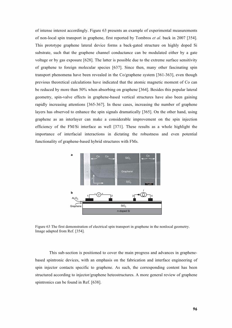
96
of intense interest accordingly. Figure 63 presents an example of experimental measurements
of non-local spin transport in graphene, first reported by Tombros et al. back in 2007 [354].
This prototype graphene lateral device forms a back-gated structure on highly doped Si
substrate, such that the graphene channel conductance can be modulated either by a gate
voltage or by gas exposure [628]. The latter is possible due to the extreme surface sensitivity
of graphene to foreign molecular species [637]. Since then, many other fascinating spin
transport phenomena have been revealed in the Co/graphene system [361-363], even though
previous theoretical calculations have indicated that the atomic magnetic moment of Co can
be reduced by more than 50% when absorbing on graphene [364]. Besides this popular lateral
geometry, spin-valve effects in graphene-based vertical structures have also been gaining
rapidly increasing attentions [365-367]. In these cases, increasing the number of graphene
layers has observed to enhance the spin signals dramatically [365]. On the other hand, using
graphene as an interlayer can make a considerable improvement on the spin injection
efficiency of the FM/Si interface as well [371]. These results as a whole highlight the
importance of interfacial interactions in dictating the robustness and even potential
functionality of graphene-based hybrid structures with FMs.
Figure 63 The first demonstration of electrical spin transport in graphene in the nonlocal geometry. Image adapted from Ref. [354].
This sub-section is positioned to cover the main progress and advances in graphene-
based spintronic devices, with an emphasis on the fabrication and interface engineering of
spin injector contacts specific to graphene. As such, the corresponding content has been
structured according to injector/graphene heteostructures. A more general review of graphene
spintronics can be found in Ref. [638].
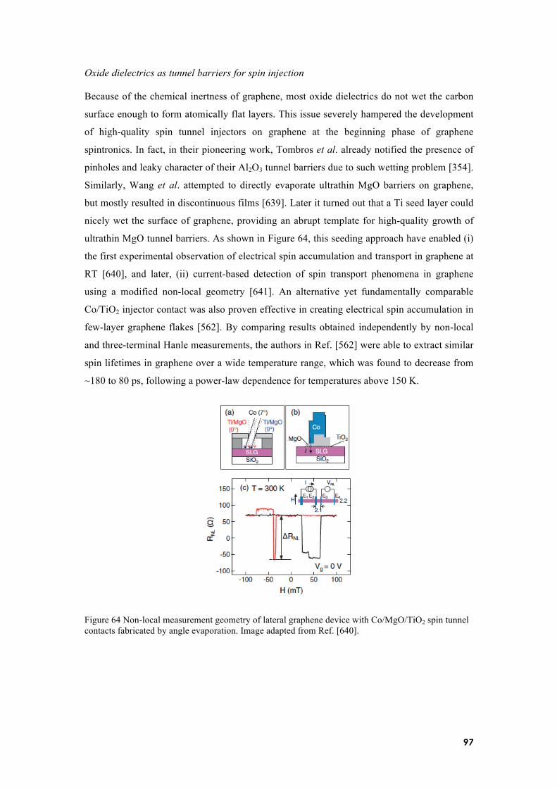
97
Oxide dielectrics as tunnel barriers for spin injection
Because of the chemical inertness of graphene, most oxide dielectrics do not wet the carbon
surface enough to form atomically flat layers. This issue severely hampered the development
of high-quality spin tunnel injectors on graphene at the beginning phase of graphene
spintronics. In fact, in their pioneering work, Tombros et al. already notified the presence of
pinholes and leaky character of their Al2O3 tunnel barriers due to such wetting problem [354].
Similarly, Wang et al. attempted to directly evaporate ultrathin MgO barriers on graphene,
but mostly resulted in discontinuous films [639]. Later it turned out that a Ti seed layer could
nicely wet the surface of graphene, providing an abrupt template for high-quality growth of
ultrathin MgO tunnel barriers. As shown in Figure 64, this seeding approach have enabled (i)
the first experimental observation of electrical spin accumulation and transport in graphene at
RT [640], and later, (ii) current-based detection of spin transport phenomena in graphene
using a modified non-local geometry [641]. An alternative yet fundamentally comparable
Co/TiO2 injector contact was also proven effective in creating electrical spin accumulation in
few-layer graphene flakes [562]. By comparing results obtained independently by non-local
and three-terminal Hanle measurements, the authors in Ref. [562] were able to extract similar
spin lifetimes in graphene over a wide temperature range, which was found to decrease from
~180 to 80 ps, following a power-law dependence for temperatures above 150 K.
Figure 64 Non-local measurement geometry of lateral graphene device with Co/MgO/TiO2 spin tunnel contacts fabricated by angle evaporation. Image adapted from Ref. [640].
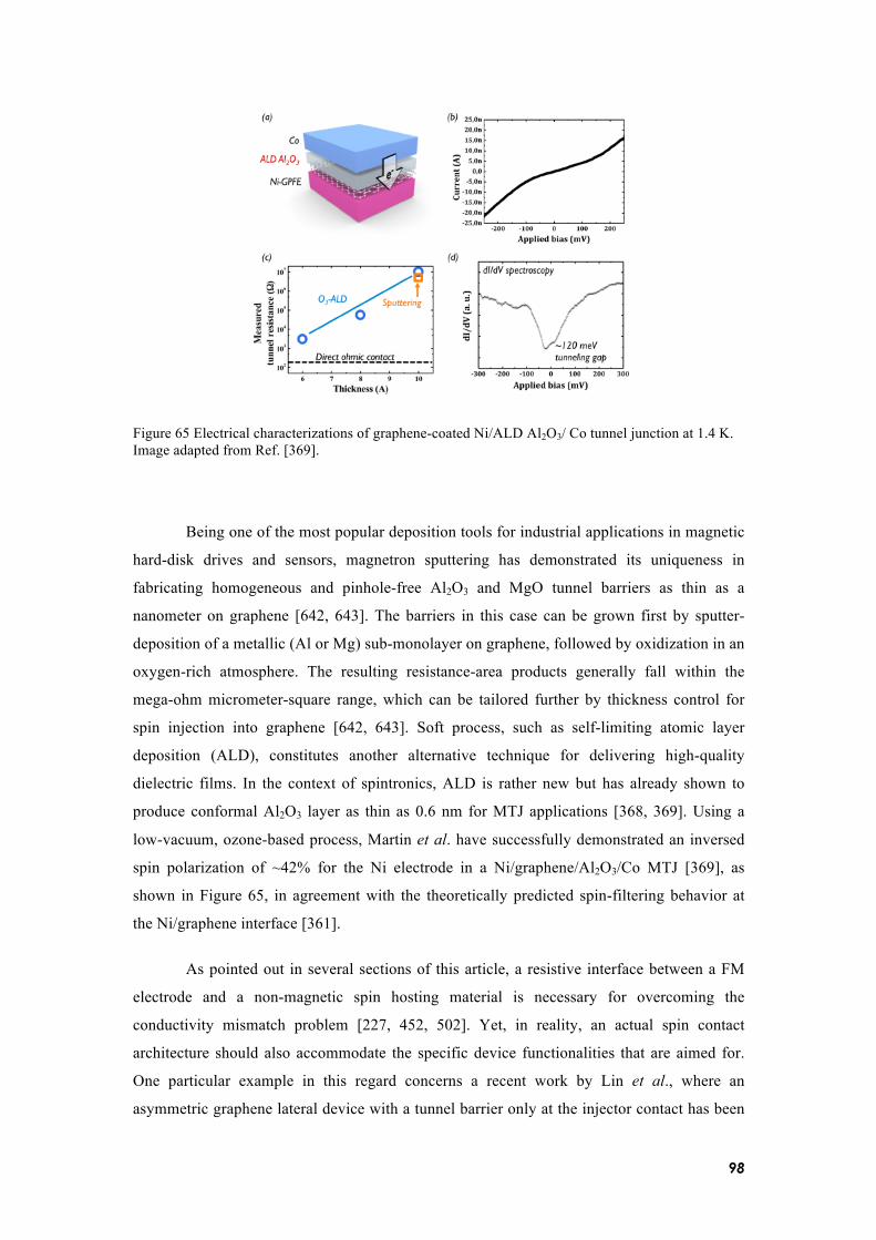
98
Figure 65 Electrical characterizations of graphene-coated Ni/ALD Al2O3/ Co tunnel junction at 1.4 K. Image adapted from Ref. [369].
Being one of the most popular deposition tools for industrial applications in magnetic
hard-disk drives and sensors, magnetron sputtering has demonstrated its uniqueness in
fabricating homogeneous and pinhole-free Al2O3 and MgO tunnel barriers as thin as a
nanometer on graphene [642, 643]. The barriers in this case can be grown first by sputter-
deposition of a metallic (Al or Mg) sub-monolayer on graphene, followed by oxidization in an
oxygen-rich atmosphere. The resulting resistance-area products generally fall within the
mega-ohm micrometer-square range, which can be tailored further by thickness control for
spin injection into graphene [642, 643]. Soft process, such as self-limiting atomic layer
deposition (ALD), constitutes another alternative technique for delivering high-quality
dielectric films. In the context of spintronics, ALD is rather new but has already shown to
produce conformal Al2O3 layer as thin as 0.6 nm for MTJ applications [368, 369]. Using a
low-vacuum, ozone-based process, Martin et al. have successfully demonstrated an inversed
spin polarization of ~42% for the Ni electrode in a Ni/graphene/Al2O3/Co MTJ [369], as
shown in Figure 65, in agreement with the theoretically predicted spin-filtering behavior at
the Ni/graphene interface [361].
As pointed out in several sections of this article, a resistive interface between a FM
electrode and a non-magnetic spin hosting material is necessary for overcoming the
conductivity mismatch problem [227, 452, 502]. Yet, in reality, an actual spin contact
architecture should also accommodate the specific device functionalities that are aimed for.
One particular example in this regard concerns a recent work by Lin et al., where an
asymmetric graphene lateral device with a tunnel barrier only at the injector contact has been
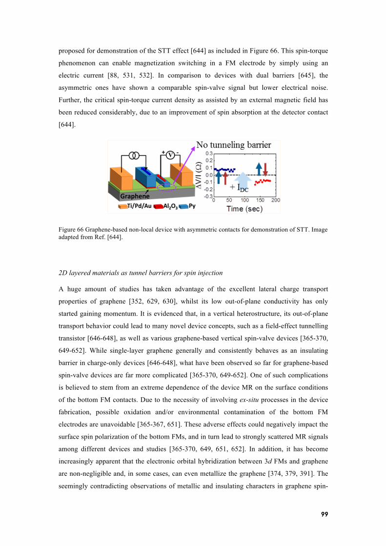
99
proposed for demonstration of the STT effect [644] as included in Figure 66. This spin-torque
phenomenon can enable magnetization switching in a FM electrode by simply using an
electric current [88, 531, 532]. In comparison to devices with dual barriers [645], the
asymmetric ones have shown a comparable spin-valve signal but lower electrical noise.
Further, the critical spin-torque current density as assisted by an external magnetic field has
been reduced considerably, due to an improvement of spin absorption at the detector contact
[644].
Figure 66 Graphene-based non-local device with asymmetric contacts for demonstration of STT. Image adapted from Ref. [644].
2D layered materials as tunnel barriers for spin injection
A huge amount of studies has taken advantage of the excellent lateral charge transport
properties of graphene [352, 629, 630], whilst its low out-of-plane conductivity has only
started gaining momentum. It is evidenced that, in a vertical heterostructure, its out-of-plane
transport behavior could lead to many novel device concepts, such as a field-effect tunnelling
transistor [646-648], as well as various graphene-based vertical spin-valve devices [365-370,
649-652]. While single-layer graphene generally and consistently behaves as an insulating
barrier in charge-only devices [646-648], what have been observed so far for graphene-based
spin-valve devices are far more complicated [365-370, 649-652]. One of such complications
is believed to stem from an extreme dependence of the device MR on the surface conditions
of the bottom FM contacts. Due to the necessity of involving ex-situ processes in the device
fabrication, possible oxidation and/or environmental contamination of the bottom FM
electrodes are unavoidable [365-367, 651]. These adverse effects could negatively impact the
surface spin polarization of the bottom FMs, and in turn lead to strongly scattered MR signals
among different devices and studies [365-370, 649, 651, 652]. In addition, it has become
increasingly apparent that the electronic orbital hybridization between 3d FMs and graphene
are non-negligible and, in some cases, can even metallize the graphene [374, 379, 391]. The
seemingly contradicting observations of metallic and insulating characters in graphene spin-

100
valves therefore seem to suggest the varying hybridization strength at those interfaces [365,
366, 650]. Two different device fabrication approaches, namely, “flip-transfer” method [650]
and direct CVD growth of graphene/Ni heterostructures [368-370], have been proposed to
better define the bottom FM/graphene interfaces. The latter approach might have a better
prospect for spintronics, since it allows for direct growth of graphene on Ni thin film, which
naturally forms a lattice-matched graphene/Ni spin-filtering interface as predicted by Karpan
et al. [361]. Vertical spin-valve devices with such CVD-grown graphene/Ni interfaces have
resulted in large negative MR [368-370], in tentative agreement with a dominant transport of
minority spin electrons through the graphene layer [361]. However, it should be noted that the
origin of such negative MR remains an open question and can only be properly addressed by
employing devices with both top and bottom epitaxial FM/graphene interfaces. Potential
fabrication methods for the top FM/graphene contacts have been discussed in section 5 [376,
401].
Hexagonal boron nitride (h-BN), an insulating isomorph of graphene with a large
bandgap of ~6 eV, has manifested itself as a promising candidate for being a high-resistance,
pinhole-free tunnel barrier with well-defined layer thickness for spin injection into other 2D
materials [653-659]. It has been suggested that a large MR can be achieved by incorporating
h-BN as the tunnel barrier in MTJs due to interfacial spin filtering [660-662]. On the
experimental side, lateral graphene spin transport devices with h-BN tunnel barriers have
been reported [655-658]. In the first attempt, Yamaguchi et al. used exfoliated single-layer h-
BN for electrical spin injection into bilayer graphene from NiFe contacts, acquiring a spin
signal of a few milliohms (spin polarization of less than 2%) and spin lifetime of ~50 ps
[658]. These parameters were however quite similar to that observed for transparent contacts,
thereby indicating no improvement by inserting the h-BN. By contrast, when utilizing large-
area h-BN grown by CVD, Kamalakar et al. achieved reliable and reproducible tunnelling
behavior in their lateral devices. Significant spin transport over micrometer-scale distances
and spin signal of 0.46 ns at 100 K have also been observed [655, 656]. The same group
further revealed an inversion of spin signal in devices with asymmetric contact resistances by
using different h-BN thicknesses [657] as shown in Figure 67. The presence of large and
negative spin polarization in high resistance Co/few-layer h-BN contacts provides
experimental evidence of existence of the spin filtering effect predicted by previous
theoretical calculations [661]. However, it is reasonable to expect that the spin-filtering effect
(if any) in these earlier studies should not be robust, because the FMs/h-BN contacts would
naturally suffer from a similar wetting problem as previously seen for FMs on graphene [393,
394]. Accordingly, before one can harness the true potential of h-BN, a primary task is to
come up with viable means to accomplish structurally and electronically well-defined FM/h-

101
BN interfaces. Along this direction, Piquemal-Banci et al. have developed a low pressure
CVD technique to grow h-BN directly on Fe [654] as shown in Figure 68. It has been shown
that a clear tunnelling MR response up to 6%, corresponding to a spin polarization of 17%,
could be attained in a full MTJ structure. These values are considered much larger than the
best-obtained value from MTJs with exfoliated h-BN [653], highlighting the immense
importance of interface ordering.
Figure 67 Comparison of inverted and normal spin valve signals on graphene-based devices with different combinations of Co/h-BN spin injector and detector contacts. Image adapted from Ref. [657].
Figure 68 Direct growth of h-BN on Fe by low pressure CVD, and resistance mapping by conductive tip AFM with different thicknesses of the grown h-BN. Image adapted from Ref. [654].
102
Since 2014, Friedman et al. at the Naval Research Laboratory have been developing
homoepitaxial tunnel barriers for spin injection in graphene. Their works underlines the use of
graphene as both a tunnel barrier as well as a high-mobility transport channel [663, 664]. In
practice, this has been done by chemical functionalization of the top layer of a graphene
bilayer, so that it decouples from and serves as a monolayer tunnel barrier for charge and spin
injection into the lower graphene channel. For fluorinated barriers fabricated by exposing
graphene to XeF2 gas, a tunnelling spin polarization as high as ~63% has been achieved at
low bias. This is much larger than the highest values reported to date (26–30%) for devices
with Al2O3 or MgO tunnel barriers [354, 634, 640]. Hydrogenated graphene tunnel barriers
have also been fabricated successfully [663]. While acting as effective barriers up to RT, the
overall spin lifetime values in this case have been found significantly less than those devices
with fluorinated barriers, possibly due to the presence of magnetic scatters in the
hydrogenated graphene [665].
Besides the above notable progress on implementing novel tunnel barriers for
electrical spin injection into graphene, a distinct route is currently being explored, involving
the potential use of TIs [666, 667] as an electrically controlled spin source [668-670]. For 3D
TIs, such as Bi-based chalcogenides, the ability to generate spin-polarized currents arises
from the strong spin-orbit coupling and the spin-momentum locked topological surface states
of the materials. According to relevant theoretical studies, combining a 3D TI with an
appropriate 2D material, such as graphene, could enable the transfer of topological insulator
properties across the interface [670]. Experimentally, Zhang et al. [671] and Vaklinova et al.
[668] have independently realized such 3D TI/graphene heterostructure. The former group of
authors have observed exotic gate-tunable tunnelling resistance and quantum oscillations due
to quantized Landau levels in both graphene and the surface states of Bi2Se3 under strong
external magnetic fields in vertical Bi2Se3 nanoplate/graphene heterojunctions [671], while
the latter group of researchers have demonstrated injection of spin-polarized current in CVD-
grown Bi2Te2Se/graphene heterostructure [668]. The device operation of the latter experiment
can be better illustrated with the aid of Figure 69. With the multi-terminal non-local
geometry, the net spin-polarized current generated in Bi2Te2Se is injected into the graphene
channel in a direction that depends on the polarity of the applied bias. The Co magnetic
contact on the graphene serves as a spin detector, measuring the non-local spin-valve signal
due to the incoming spin current from the TI. An important finding from the hybrid device
has been the sign reversal of the non-local signal according to the direction of the applied
current. While this sign change has been commonly regarded as a signature of current-
induced helical spin polarization in the TI- and derived heterostructures [668, 669, 672-678],

103
recent concern arises questioning the validity of such an observation and even the electrical
measurement geometry involved [612, 679]. In fact, it has been shown that spurious effects,
such as magnetic stray fields from the FM contacts on a TI could mimic both the sign change
as well as its dependence on the driving current direction [679].
Figure 69 Electrical detection of spin-polarized current in graphene injected from Bi2Te2Se. Image adapted from Ref. [668].
6.4.2 With TMDs
Vertical spin-valves employing semiconducting TMD MLs (such as MoS2 and WS2) as non-
magnetic spacers have generally shown MR signals in the order of 0.1% close to RT [448,
680]. Yet the metallic transport in those devices is radically different from the Schottky-type
behavior in the lateral geometry [445, 446, 450]. Fundamentally, this disparity is related to
the strong orbital hybridization between TMDs and 3d FMs, as suggested by first-principle
calculations [444]. In fact, that theoretical framework has predicted an even larger MR effect
than the experimental values which are likely limited by factors such as the crystallinity of
FM electrodes, interface disorders, etc. It is apparent that most of the FM/TMD interfaces and
devices being characterized so far have been fabricated from exfoliated TMDs. While
exfoliated TMDs can provide a significant degree of flexibility on achieving a wide range of
hybrid structures, large-scale fabrication and lattice-matched interfaces are very unlikely. Wu
et al. have recently attempted to fabricate well-defined MoS2/Fe3O4 interface by direct
sulfurization of pre-deposited Mo film on Fe3O4 at elevated temperatures [681], and observed
a clear MR signal up to 200 K. A corresponding theoretical modeling of this interface, as
included in Figure 70, has surprisingly indicated a nearly fully spin-polarized electron band at

104
the Fermi level, i.e. an almost undistorted half-metallic character of Fe3O4 in the presence of
an electronically hybridized MoS2 layer [681]. However, a recent study of spin injection into
a graphene-WS2 heterostructure indicated that the WS2 actually induces additional dephasing
of the spin into the graphene [682]. All these studies should encourage further theoretical and
experimental investigations into such TMD-based spintronic interfaces.
Figure 70 Calculated electronic structure of Fe3O4/MoS2/Fe3O4 junctions. Image adapted from Ref. [681].
6.4.3 With TIs
The conservation of time-reversal symmetry in the surface states of TIs gives rise to the
iconic property of spin-momentum locking [666, 667, 683]. Depending on charge carrier
density, spin and momemtum of the surface states are directly coupled in a perpendicularly
right-handed or left-handed orientation. Such helical spin texture should conceptually enable
an unpolarized charge current to create a net spin polarization without the use of a FM
material [666, 667, 683]. Direct electrical detection and manipulation in this regard will
provide valuable insight into both fundamental and applied aspects of the spin-momentum
physics in TIs. So far, salient features of the existence of spin-momentum locking in 3D TIs

105
have been investigated electrically by measurements of three main kinds: (i) spin-pumping
[555, 684, 685], (ii) spin-orbit torque [686, 687], and (iii) potentiometric method [672-678].
We will introduce the working principles of these approaches and review recent results as
below.
Spin-pumping, a versatile technique previously employed for various materials in the
context of spin injection, has been utilized by Shiomi et al. for the first demonstration of spin-
charge conversion effect in the surface states of bulk-insulating TIs, Bi1.5Sb0.5Te1.7Se1.3 and
Sn-doped Bi2Te2Se [684] as shown in Figure 71. This technique relies on the magnetization
precession in a FM excited by FMR, such that non-equilibrium spins can be generated and
pumped into a non-magnetic material of interest. Following the experimental geometry in
Ref. [684] and in other related works [555, 685], the spin accumulation produced induces a
charge current along a direction parallel to (z ´ s), where s is the spin polarization axis and z
is the unit vector perpendicular to the plane. Due to the 2D nature of the surfaces states, the
induced charge current also possesses a 2D character, which is fundamentally different from
the current governed by the inverse spin Hall effect in 3D systems [364, 552]. However, in
reality, imperfect insulation of bulk states due to, for instance, small bulk bandgaps as of 0.35
eV for the prototypical Bi2Se3, and unintentional doping from crystalline defects can
unfavorably impact the electrical characterization of spin-momentum locking in two major
ways, namely, mixing of the respective contributions from spin-charge conversion and
inverse spin Hall effect [555], and quenching of the spin-charge conversion efficiency. For
the latter, the authors in Ref. [684] estimated an efficiency of merely 10-4 for bulk insulating
TIs, corresponding to 15% of injected spins that contribute to the spin-charge conversion. On
the other hand, Jamali et al. proposed the dynamical spin-pumping mechanism in
CoFeB/Bi2Se3 bilayer [555]. By combining theoretical modeling and experimental
measurements of angle-dependent spin-charge conversion, it is speculated that the pumped
spin current should first be enhanced by the spin-orbit coupling of the surface states and then
converted into a voltage signal by the inverse spin Hall effect due to the bulk component of
3D Bi2Se3.
More advanced dynamical measurements have been demonstrated further by Baker et
al. combining FMR and time-resolved XMCD for studying the spin-pumping dynamics in
CoFe/Bi2Se3/NiFe heterostructures [685]. Remarkably different from a conventional pumping
experiment, time-resolved XMCD allows for element-specific detection of magnetization
precession within each FM layer through polarization dependence of X-ray absorption at the
FM L2,3 edges. Technically, in Ref. [685], those authors were able to achieve a resolution of
several ps through synchronization of X-ray bunch arrival with the RF driving precession.

106
Their experimental work has pointed out a strong tendency of a TI interlayer to act as a spin
sink during FMR excitation, in turn dramatically increasing the Gilbert damping of
magnetodynamics in the FM layers. However, there is no convincing evidence of spin
transport through the TI to a second FM. This observation may be related to either dynamic
exchange or a short-range coupling between the surface states [685].
Figure 71 Spin-charge conversion of surfaces states in a 3D TI characterized by spin pumping in a NiFe/TI bilayer structure. Image adapted from Ref. [684].
Recent experiments on TI-based magnetic heterostructures have intriguingly revealed
a spin-orbit torque [686-688] much higher than for any source of spin-torque measured to
date [689-692]. The physical mechanism underlining such a phenomenon in TIs remains to be
understood, but is believed to stem from the spin-momentum locking of the topological
surface states. Fischer et al. for instance explored this issue by modeling TI-based bilayers
involving FM metal (TI/FM) and magnetically doped TIs (TI/magnetic TI), respectively
[693]. It is suggested that the exchange interaction couples the spins of the two layers, thereby
enabling the transfer to occur. On the experimental side, Mellnik et al. [686] and Fan et al.
[687] have both reported giant spin-orbit torques in TI-based bilayer structures by
measurements of spin-torque-FMR and the AHE, respectively. Essentially, from these
pioneering studies, FMs with a low Gilbert damping will facilitate the spin torque
phenomena, since a smaller torque from a TI is required to generate an appreciable
magnetization precession in the FM layer. As such, an even more exciting result on electric-
field control of the spin-orbit torque in semiconducting Cr-doped TI has been demonstrated

107
very recently. Such an electrical means will pave the way towards an ultimate control of
current-induced magnetization switching in magnetic TIs by electrostatic gating [694].
As elucidated elsewhere in this article, FM materials can function as a sensing probe
for spin-dependent electrochemical potentials due to spin accumulation in non-magnetic
materials [42, 43, 310-312, 354, 362, 371, 561-566, 575, 606, 626, 634, 636, 640, 641, 655-
658, 663, 664, 668, 695-698]. This notion has been employed by Li et al. [673], and
subsequently by others [672, 674-678] to investigate the charge-current-induced spin
polarization arising from spin-momentum locking in 3D TIs. While differing in
configurations of the FM probes, the device concepts involved in those works are essentially
comparable. Following the scheme in Ref. [673] as shown in Figure 72, the magnetization
direction of a FM contact provides an initially defined spin axis for the detection, and this
contact measures the electrical voltage that is proportional to the projection of the TI spin
polarization onto the detection axis. When a pure charge current established between two
non-magnetic remote electrodes is at 90º with the magnetization of the FM detector contact,
the TI spin is parallel to the magnetization, and a spin-related voltage is detected at the FM
contact proportional to the magnitude of the charge current. Such measured voltage will
change sign, when the charge current polarity is reversed. Similarly, as the contact
magnetization is switched to an opposite direction by an in-plane field, the measured spin
voltage will follow the hysteresis loop of the contact. However, no spin voltage is expected
when the in-plane contact magnetization is in 90º orientation, relative to the TI spin
polarization.
Figure 72 Device configuration for probing the current-induced spin polarization in Bi2Se3 using FM contacts. Image adapted from Ref. [673].

108
With the above strategy and using both Fe/Al2O3- and Co/MgO/graphene tunnel
contacts, Li et al. have first observed a net spin polarization via the spin-momentum locking
in MBE-grown Bi2Se3 films [673], and then the helical spin texture in p-type TI Sb2Te3 [672].
Besides electrical voltage, Tian et al. have further demonstrated probing of the current-
induced spin polarization in TIs as MR signals in a spin-valve geometry [674]. An asymmetry
in the device MR with its polarity following the applied current has been observed, providing
experimental evidence for the spin helical current of the surface states in the Bi2Se3 [674].
Subsequent studies, which also rely on the above single- and two-terminal FM configurations,
have focused on more bulk-insulated TIs, including (Bi0.53Sb0.47)2Te3 [676], Bi1.5Sb0.5Te1.7Se1.3
[677] and Bi2Te2Se [675].
A record high spin resistance of 70 mΩ at RT has been reported by Dankert et al. for
exfoliated Bi2Se3 [678]. Being the largest reported thus far, this value has been ascribed to the
use of a TiO2 tunnel barrier that is known to grow more uniformly on layered materials than
other oxide-based dielectrics [446]. However, recent concerns arose questioning the
interpretation of the quantities extracted from the abovementioned electrical measurements
[612, 679]. In particular, different from the claim on current-induced spin polarization of the
surface states charge carriers, de Vries et al. have indicated the possibility of fringe-field-
induced Hall effect in causing the observed electrical voltage [679]. It is also shown in
another control study that topologically trivial metallic Au thin film devices could reproduce
nominally identical voltage hysteresis seen with the Tis [612], thus calling for alternative
transport methods for identifying, if any, the true signature of helical current-induced spin
polarization in TI surface states.
7 Summary and Outlook
The miniaturization of charge-based electronic devices together with the huge demands for
higher processing speed, lower energy dissipation and denser storage medium in digital
devices have completely changed our scientific and engineering mindsets — it is not just
about putting more electronic components onto a chip; rather it is about how wisely those
components can be used and developed. This notion has ever since nourished and reinforced
the rapid growth of spintronics, a new technology that can integrate, improve, or even replace
the charge-based electronics.
The strategic combinations of magnetic materials with non-magnetic spin hosting
materials as hybrid spintronic structures play a pivotal role in both defining spin

109
injection/detection efficiency and creating unprecedented spin-based phenomena. Among the
hybrid structures reviewed in this article, those forming 3d FM/SC interfaces have been the
prime candidates for many studies due to their long history and well-known electronic and
magnetic properties and high Curie temperatures in excess of RT. In terms of the epitaxy, it is
generally accepted that a low temperature growth is mostly preferred, so that interface
imperfections due to intermixing, magnetic dead layers, etc. can be largely eliminated. Also
highlighted in this article is an alternative route on searching for FM alloys with a higher
thermal stability on SCs. Existing studies have readily identified quite a number of such
alloys which are highly interesting for being a spin source for spintronic devices as well as for
providing unique properties such as PMA for zero-field and STT applications. It has long
been a challenging issue to boost spin injection efficiency in FM/SC-based devices. While the
fundamental concepts and theoretical models on the conductivity mismatch have enhanced
our understanding of the physics of spin transport across the FM/SC interfaces, the
performances of existing devices with either a Schottky or a tunnel barrier remain undesirable
for actual applications at RT. As pointed out in this article, creating a resistive interface that
takes over the overall resistance of a FM/SC junction is simply not sufficient; instead, the
interface resistance should lie within a narrow window defined by a number of important
parameters as considered by the Fert and Jaffrès model. And this is exactly one of the most
elusive tasks to be tackled in the field. Using a single-layer graphene as a tunnelling barrier
constitutes a milestone achievement in this regard, but the impact of this finding on future
spin injection devices would certainly depend on the advent of new fabrication technique that
can allow for direct growth of large-scale graphene on SC and oxide dielectrics, which is
currently not so well-established. Setting aside the technical difficulties of interface
engineering, adapting either a highly spin-polarized materials or a magnetic semiconductor is
in principle a possible way out of the conductivity mismatch problem. Both of these exotic
materials have been hotly investigated over the last decades, and have contributed a wealth of
exciting knowledge and phenomena in materials science and condensed matter physics. As
elaborated in this article, magnetite and Heusler alloys are theoretical half-metallic materials
with fully spin-polarized bands at the Fermi level. These materials, even with the mismatch
problem settling in, are expected to create an injected spin polarization of 50% in a SC.
However, in the literature, the experimentally measured results are in most cases way lower
than this expectation. And these results are possibly related to the complex details involved in
the epitaxial growth including substrate termination, oxidation mechanism, intermixing, and
off-stoichiometry, etc. As far as these issues are concerned, we have not recognized any
collective research efforts that take all these into account in a systematic manner, and
accordingly this may form an exciting opportunity to overcome such a bottleneck in the half-
metallic materials. By contrast, magnetic semiconductors such as DMSs, which are not

110
covered in this article but have been intensively studied in the past, naturally avoid the
difficulties of integration without conventional SCs; however great challenges remain to
improve their crystallinity and in particular their Curie temperatures. Magnetic proximity
effect is a promising pathway not only for DMSs but also for graphene and the newly
discovered magnetic TIs. We expect that this technique based on interface orbital
hybridization will continue to be playing a fascinating role in uncovering the magnetism in
low-dimensional systems, especially those based on the emerging 2D materials.
2D materials, in particular, graphene and TMDs, are gaining strong momentum in
spintronics research. Their outstanding mechanical, electronic and optical properties as well
as the highly desired long spin lifetimes in low-dimension make them a competitive group of
emerging materials for the construction of the Datta-Das spin-FET. However, the most unique
features really setting them apart from other non-magnetic spin hosting materials such as
conventional SCs and organic molecular materials are the unprecedented spin-based
phenomena that can exist in their interfaces with 3d FMs. In some specific cases, these hybrid
interfaces have been predicted to act as tunnelling barriers, spin-filters and even half-metallic
spin sources for highly efficient spin injection. While intriguing, many of these exceptional
effects so far exist only in theory and proof-of-concept studies will necessitate practical
means to fabricate epitaxial interfaces between 3d FMs and 2D materials. Admittedly, the
latter aspect challenges the existing technologies in both spintronics and 2D materials,
because radically new approaches for epitaxial growth have to be developed for the weakly
interacting van der Waal surfaces of the layered materials. A very limited number of attempts
does exist in this regard and we anticipate such challenging tasks to become an intensive topic
that will unify research efforts from both spintronics and 2D materials.
In the original Datta-Das spin-FET proposal, the gate-modulated spin transport in a
channel relies on the spin-orbit interaction and thus the Rashba effect of that channel material.
When choosing an appropriate channel material, there is always a tradeoff between spin
lifetime and modulation efficiency. On the other hand, for materials being made of light
elements, especially graphene, Si, and their derived nanostructures, that exhibit weak spin-
orbit interaction, the Rashba-type modulation is mostly ineffective and other viable concepts
have to be established accordingly.
The significance of hybrid spintronic materials is undisputed. The exciting progress
and milestone achievements reviewed by this article demonstrate many challenges as well as
opportunities in the design and fabrication of spin-based electronic materials and devices.
Given the strongly multi-disciplinary nature of this field, the family of hybrid spintronic

111
materials will certainly keep expanding, which in turn will lead to more impact to material
science and electronics technology.
Acknowledgements
This work is supported by the National Basic Research Program of China
(No.2014CB921101, 2016YFA0300803), the National Natural Science Foundation of China
(No.61427812 and 11774160), Jiangsu Shuangchuang Programme, Jiangsu NSF
(No.BK20140054) and EPSRC UK (EP/G010064/1).

112
References
[1] Xu YB, Thompson SM. Spintronic Materials and Technology. London: Taylor and Francis Group; 2006.
[2] Prinz GA. Device physics - Magnetoelectronics. Science. 1998;282:1660-3.
[3] Wolf SA, Awschalom DD, Buhrman RA, Daughton JM, von Molnar S, Roukes ML, et al. Spintronics: A spin-based electronics vision for the future. Science. 2001;294:1488-95.
[4] Zutic I, Fabian J, Das Sarma S. Spintronics: Fundamentals and applications. Rev Mod Phys. 2004;76:323-410.
[5] Fabian J, Matos-Abiague A, Ertler C, Stano P, Zutic I. Semiconductor spintronics. Acta Physica Slovaca. 2007;57:565-907.
[6] Moore GE. Cramming more components onto integrated circuits (Reprinted from Electronics, pg 114-117, April 19, 1965). Proc IEEE. 1998;86:82-5.
[7] Datta S, Das B. ELECTRONIC ANALOG OF THE ELECTROOPTIC MODULATOR. Appl Phys Lett. 1990;56:665-7.
[8] Bychkov YA, Rashba EI. PROPERTIES OF A 2D ELECTRON-GAS WITH LIFTED SPECTRAL DEGENERACY. Jetp Lett. 1984;39:78-81.
[9] Baibich MN, Broto JM, Fert A, Vandau FN, Petroff F, Eitenne P, et al. GIANT MAGNETORESISTANCE OF (001)FE/(001) CR MAGNETIC SUPERLATTICES. Phys Rev Lett. 1988;61:2472-5.
[10] Binasch G, Grunberg P, Saurenbach F, Zinn W. ENHANCED MAGNETORESISTANCE IN LAYERED MAGNETIC-STRUCTURES WITH ANTIFERROMAGNETIC INTERLAYER EXCHANGE. Phys Rev B. 1989;39:4828-30.
[11] Parkin SSP, More N, Roche KP. OSCILLATIONS IN EXCHANGE COUPLING AND MAGNETORESISTANCE IN METALLIC SUPERLATTICE STRUCTURES - CO/RU, CO/CR, AND FE/CR. Phys Rev Lett. 1990;64:2304-7.
[12] Valet T, Fert A. THEORY OF THE PERPENDICULAR MAGNETORESISTANCE IN MAGNETIC MULTILAYERS. Phys Rev B. 1993;48:7099-113.
[13] Dieny B, Speriosu VS, Parkin SSP, Gurney BA, Wilhoit DR, Mauri D. GIANT MAGNETORESISTANCE IN SOFT FERROMAGNETIC MULTILAYERS. Phys Rev B. 1991;43:1297-300.
[14] Mott NF. The electrical conductivity of transition metals. Proceedings of The Royal Society A. 1936;153:699-717.
[15] Moodera JS, Kinder LR, Wong TM, Meservey R. LARGE MAGNETORESISTANCE AT ROOM-TEMPERATURE IN FERROMAGNETIC THIN-FILM TUNNEL-JUNCTIONS. Phys Rev Lett. 1995;74:3273-6.
[16] Zorpette G. The quest for spin transistor. IEEE Spectr. 2001;38:30-5.
[17] Kikkawa JM, Awschalom DD. Resonant spin amplification in n-type GaAs. Phys Rev Lett. 1998;80:4313-6.
[18] Kikkawa JM, Awschalom DD. Lateral drag of spin coherence in gallium arsenide. Nature. 1999;397:139-41.

113
[19] Sugahara S, Tanaka M. A spin metal-oxide-semiconductor field-effect transistor using half-metallic-ferromagnet contacts for the source and drain. Appl Phys Lett. 2004;84:2307-9.
[20] Hall KC, Flatte ME. Performance of a spin-based insulated gate field effect transistor. Appl Phys Lett. 2006;88:162503.
[21] Koo HC, Kwon JH, Eom J, Chang J, Han SH, Johnson M. Control of Spin Precession in a Spin-Injected Field Effect Transistor. Science. 2009;325:1515-8.
[22] Xu YB , Wong J, Liu W, Niu D, Zhang W, Lu Y, Hassan S, Yan Y, and Will I, Magnetic/III-V Semiconductor Based Hybrid Structures, Chapter 8 Handbook of Spintronics, ISBN 978-94-007-6893-2. Springer Dordrecht Heidelberg New York London DOI 10.1007/978-94-007-6892-5.
[23] Hirohata A, Kikuchi A, Tezuka N, Inomata K, Claydon JS, Xu YB, et al. Heusler alloy/semiconductor hybrid structures. Curr Opin Solid State Mat Sci. 2006;10:93-107.
[24] Krebs JJ, Jonker BT, Prinz GA. PROPERTIES OF FE SINGLE-CRYSTAL FILMS GROWN ON (100)GAAS BY MOLECULAR-BEAM EPITAXY. J Appl Phys. 1987;61:2596-9.
[25] Rhoderick EH, Williams RH. Metal-semiconductor contacts. Oxford: Oxford University Press; 1988.
[26] Xu YB, Kernohan ETM, Tselepi M, Bland JAC, Holmes S. Single crystal Fe films grown on InAs(100) by molecular beam epitaxy. Appl Phys Lett. 1998;73:399-401.
[27] Claydon JS, Niu DX, Xu YB, Telling ND, Kirkman IW, van der Laan G. Spin and orbital moments of ultra-thin Fe films on various semiconductor surfaces. IEEE Trans Magn. 2005;41:3325-7.
[28] Xu YB, Kernohan ETM, Freeland DJ, Ercole A, Tselepi M, Bland JAC. Evolution of the ferromagnetic phase of ultrathin Fe films grown on GaAs(100)-4x6. Phys Rev B. 1998;58:890-6.
[29] Xu YB, Freeland DJ, Tselepi M, Bland JAC. Anisotropic lattice relaxation and uniaxial magnetic anisotropy in Fe/InAs(100)-4x2. Phys Rev B. 2000;62:1167-70.
[30] Xue QK, Hashizume T, Zhou JM, Sakata T, Ohno T, Sakurai T. STRUCTURES OF THE GA-RICH 4X2 AND 4X6 RECONSTRUCTIONS OF THE GAAS(001) SURFACE. Phys Rev Lett. 1995;74:3177-80.
[31] Kendrick C, LeLay G, Kahn A. Bias-dependent imaging of the in-terminated InAs(001) (4x2)/c(8x2) surface by STM: Reconstruction and transitional defect. Phys Rev B. 1996;54:17877-83.
[32] Qin XR, Lagally MG. Adatom pairing structures for Ge on Si(100): The initial stage of island formation. Science. 1997;278:1444-7.
[33] Matthews JW, Crawford JL. ACCOMMODATION OF MISFIT BETWEEN SINGLE-CRYSTAL FILMS OF NICKEL AND COPPER. Thin Solid Films. 1970;5:187-98.
[34] Fassbender J, Guntherodt G, Mathieu C, Hillebrands B, Jungblut R, Kohlhepp J, et al. Correlation between structure and magnetic anisotropies of Co on Cu(110). Phys Rev B. 1998;57:5870-8.
[35] Zega TJ, Hanbicki AT, Erwin SC, Zutic I, Kioseoglou G, Li CH, et al. Determination of interface atomic structure and its impact on spin transport using Z-contrast microscopy and density-functional theory. Phys Rev Lett. 2006;96:196101.
[36] LeBeau JM, Hu QO, Palmstrom CJ, Stemmer S. Atomic structure of postgrowth annealed epitaxial Fe/(001) GaAs interfaces. Appl Phys Lett. 2008;93:121909.
[37] Fleet LR, Kobayashi H, Ohno Y, Hirohata A. Atomic Interfacial Structures in Fe/GaAs Films. IEEE Trans Magn. 2011;47:2756-9.

114
[38] Fleet LR, Kobayashi H, Ohno Y, Kim JY, Barnes CHW, Hirohata A. Interfacial structure and transport properties of Fe/GaAs(001). J Appl Phys. 2011;109:07C504.
[39] Fleet LR, Yoshida K, Kobayashi H, Kaneko Y, Matsuzaka S, Ohno Y, et al. Correlating the interface structure to spin injection in abrupt Fe/GaAs(001) films. Phys Rev B. 2013;87:024401.
[40] Jonker BT, Kneedler EM, Thibado P, Glembocki OJ, Whitman LJ, Bennett BR. Schottky barrier formation for Fe on GaAs(001) and the role of interfacial structure. J Appl Phys. 1997;81:4362.
[41] Kurebayashi H, Steinmuller SJ, Laloe JB, Trypiniotis T, Easton S, Ionescu A, et al. Initial/final state selection of the spin polarization in electron tunnelling across an epitaxial Fe/GaAs(001) interface. Appl Phys Lett. 2007;91:102114.
[42] Lou X, Adelmann C, Furis M, Crooker SA, Palmstrom CJ, Crowell PA. Electrical detection of spin accumulation at a ferromagnet-semiconductor interface. Phys Rev Lett. 2006;96:176603.
[43] Lou XH, Adelmann C, Crooker SA, Garlid ES, Zhang J, Reddy KSM, et al. Electrical detection of spin transport in lateral ferromagnet-semiconductor devices. Nat Phys. 2007;3:197-202.
[44] Zhu HJ, Ramsteiner M, Kostial H, Wassermeier M, Schonherr HP, Ploog KH. Room-temperature spin injection from Fe into GaAs. Phys Rev Lett. 2001;87:016601.
[45] Hanbicki AT, Jonker BT, Itskos G, Kioseoglou G, Petrou A. Efficient electrical spin injection from a magnetic metal/tunnel barrier contact into a semiconductor. Appl Phys Lett. 2002;80:1240-2.
[46] Fiederling R, Keim M, Reuscher G, Ossau W, Schmidt G, Waag A, et al. Injection and detection of a spin-polarized current in a light-emitting diode. Nature. 1999;402:787-90.
[47] Ohno Y, Young DK, Beschoten B, Matsukura F, Ohno H, Awschalom DD. Electrical spin injection in a ferromagnetic semiconductor heterostructure. Nature. 1999;402:790-2.
[48] Filipe A, Schuhl A, Galtier P. Structure and magnetism of the Fe/GaAs interface. Appl Phys Lett. 1997;70:129-31.
[49] Prinz GA, Rado GT, Krebs JJ. MAGNETIC-PROPERTIES OF SINGLE-CRYSTAL (110) IRON FILMS GROWN ON GAAS BY MOLECULAR-BEAM EPITAXY (INVITED). J Appl Phys. 1982;53:2087-91.
[50] Claydon JS, Xu YB, Tselepi M, Bland JAC, van der Laan G. Direct observation of a bulklike spin moment at the Fe/GaAs(100)-4x6 interface. Phys Rev Lett. 2004;93:037206.
[51] Monchesky TL, Unguris J. Magnetic properties of Co/GaAs(110). Phys Rev B. 2006;74:241301.
[52] Scheck C, Evans P, Zangari G, Schad R. Sharp ferromagnet/semiconductor interfaces by electrodeposition of Ni thin films onto n-GaAs(001) substrates. Appl Phys Lett. 2003;82:2853-5.
[53] Li J, Wang ZY, Tan A, Glans PA, Arenholz E, Hwang C, et al. Magnetic dead layer at the interface between a Co film and the topological insulator Bi2Se3. Phys Rev B. 2012;86:054430.
[54] Xu YB, Freeland DJ, Tselepi M, Bland JAC. Uniaxial magnetic anisotropy of epitaxial Fe films on InAs(100)-4 x 2 and GaAs(100)-4 x 2. J Appl Phys. 2000;87:6110-2.
[55] Kneedler EM, Jonker BT, Thibado PM, Wagner RJ, Shanabrook BV, Whitman LJ. Influence of substrate surface reconstruction on the growth and magnetic properties of Fe on GaAs(001). Phys Rev B. 1997;56:8163-8.
[56] Brockmann M, Zolfl M, Miethaner S, Bayreuther G. In-plane volume and interface magnetic anisotropies in epitaxial Fe films on GaAs(001). J Magn Magn Mater. 1999;198-99:384-6.

115
[57] Tivakornsasithorn K, Liu X, Li X, Dobrowolska M, Furdyna JK. Magnetic anisotropy in ultrathin Fe films on GaAs, ZnSe, and Ge (001) substrates. J Appl Phys. 2014;116:043915.
[58] Dumm M, Zolfl M, Moosbuhler R, Brockmann M, Schmidt T, Bayreuther G. Magnetism of ultrathin FeCo (001) films on GaAs(001). J Appl Phys. 2000;87:5457-9.
[59] Xu YB, Greig D, Seddon EA, Matthew JAD. Element specific spin-resolved densities of states in amorphous Fe75B25 probed with a synchrotron radiation source. J Appl Phys. 2000;87:7136-8.
[60] Ahmad E, Will IG, Lu YX, Xu YB, Morley NA, Gibbs MRJ. Hysteretic properties of epitaxial Fe/GaAs(100) ultrathin films under external uniaxial strain. J Appl Phys. 2004;95:6555-7.
[61] Morley NA, Tang SL, Gibbs MRJ, Ahmad E, Will IG, Xu YB. Magnetocrystalline anisotropies and magnetostriction of ultrathin Fe films on GaAs with Cr overlayers. J Appl Phys. 2005;97:10H501.
[62] Choi JW, Kim HJ, Kim KH, Scholl A, Chang J. Uniaxial magnetic anisotropy in epitaxial Fe/MgO films on GaAs(001). J Magn Magn Mater. 2014;360:109-12.
[63] Prinz GA. STABILIZATION OF BCC CO VIA EPITAXIAL-GROWTH ON GAAS. Phys Rev Lett. 1985;54:1051-4.
[64] Blundell SJ, Gester M, Bland JAC, Daboo C, Gu E, Baird MJ, et al. STRUCTURE INDUCED MAGNETIC-ANISOTROPY BEHAVIOR IN CO/GAAS(001) FILMS. J Appl Phys. 1993;73:5948-50.
[65] Gu E, Gester M, Hicken RJ, Daboo C, Tselepi M, Gray SJ, et al. FOURFOLD ANISOTROPY AND STRUCTURAL BEHAVIOR OF EPITAXIAL HCP CO/GAAS(001) THIN-FILMS. Phys Rev B. 1995;52:14704-8.
[66] Subramanian S, Liu X, Stamps RL, Sooryakumar R, Prinz GA. MAGNETIC ANISOTROPIES IN BODY-CENTERED-CUBIC COBALT FILMS. Phys Rev B. 1995;52:10194-201.
[67] Liu X, Stamps RL, Sooryakumar R, Prinz GA. Magnetic anisotropies in thick body centered cubic Co. J Appl Phys. 1996;79:5387-9.
[68] Wu YZ, Ding HF, Jing C, Wu D, Liu GL, Gordon V, et al. In-plane magnetic anisotropy of bcc Co on GaAs(001). Phys Rev B. 1998;57:11935-8.
[69] Mangan MA, Spanos G, Ambrose T, Prinz GA. Transmission electron microscopy investigation of Co thin films on GaAs(001). Appl Phys Lett. 1999;75:346-8.
[70] Xu F, Joyce JJ, Ruckman MW, Chen HW, Boscherini F, Hill DM, et al. EPITAXY, OVERLAYER GROWTH, AND SURFACE SEGREGATION FOR CO/GAAS(110) AND CO/GAAS(100)-C(8X2). Phys Rev B. 1987;35:2375-84.
[71] Idzerda YU, Elam WT, Jonker BT, Prinz GA. STRUCTURE DETERMINATION OF METASTABLE COBALT FILMS. Phys Rev Lett. 1989;62:2480-3.
[72] Izquierdo M, Davila ME, Avila J, Ascolani H, Teodorescu CM, Martin MG, et al. Epitaxy and magnetic properties of surfactant-mediated growth of bcc cobalt. Phys Rev Lett. 2005;94:187601.
[73] Liu AY, Singh DJ. ELASTIC INSTABILITY OF BCC COBALT. Phys Rev B. 1993;47:8515-7.
[74] Wieldraaijer H, Kohlhepp JT, LeClair P, Ha K, de Jonge WJM. Growth of epitaxial bcc Co(001) electrodes for magnetoresistive devices. Phys Rev B. 2003;67:224430.
[75] Idzerda YU, Jonker BT, Elam WT, Prinz GA. STRUCTURE DETERMINATION OF METASTABLE COBALT FILMS DEPOSITED ON GAAS. J Vac Sci Technol A-Vac Surf Films. 1990;8:1572-6.

116
[76] Nath KG, Maeda F, Suzuki S, Watanabe Y. Passivation-mediated growth of Co on Se, S and O rich GaAs surfaces: A potential approach to control interface crystallinity and magnetic continuity. J Appl Phys. 2002;91:3943-5.
[77] Zhang FP, Xu PS, Zhu CG, Lu ED, Guo HZ, Xu FQ, et al. Studies of interface formation between Co with GaAs(100) and S-passivated GaAs(100). J Electron Spectrosc Relat Phenom. 1999;101:485-8.
[78] Anderson GW, Hanf MC, Norton PR. GROWTH AND MAGNETIC-PROPERTIES OF EPITAXIAL FE(100) ON S-PASSIVATED GAAS(100). Phys Rev Lett. 1995;74:2764-7.
[79] Nath KG, Maeda F, Suzuki S, Watanabe Y. Epitaxy, modification of electronic structures, overlayer-substrate reaction and segregation in ferromagnetic Co films on Se-treated GaAs(001) surface. Jpn J Appl Phys Part 1 - Regul Pap Short Notes Rev Pap. 2000;39:4571-4.
[80] Tang WX, Qian D, Wu D, Wu YZ, Dong GS, Jin XF, et al. Growth and magnetism of Ni films on GaAs(001). J Magn Magn Mater. 2002;240:404-6.
[81] Tian CS, Qian D, Wu D, He RH, Wu YZ, Tang WX, et al. Body-centered-cubic Ni and its magnetic properties. Phys Rev Lett. 2005;94:137210.
[82] Guo GY, Wang HH. Gradient-corrected density functional calculation of elastic constants of Fe, Co and Ni in bcc, fcc and hcp structures. Chin J Phys. 2000;38:949-61.
[83] Liu WQ, Zhou QH, Chen Q, Niu DX, Zhou Y, Xu YB, et al. Probing the Buried Magnetic Interfaces. ACS Appl Mater Interfaces. 2016;8:5752-7.
[84] Xu YB, Tselepi M, Wu J, Wang S, Bland JAC, Huttel Y, et al. Interface magnetic properties of epitaxial Fe-InAs heterostructures. IEEE Trans Magn. 2002;38:2652-4.
[85] Djayaprawira DD, Tsunekawa K, Nagai M, Maehara H, Yamagata S, Watanabe N, et al. 230% room-temperature magnetoresistance in CoFeB/MgO/CoFeB magnetic tunnel junctions. Appl Phys Lett. 2005;86:092502.
[86] Heyne L, Klaui M, Backes D, Mohrke P, Moore TA, Kimling JG, et al. Direct imaging of current-induced domain wall motion in CoFeB structures. J Appl Phys. 2008;103:07D928.
[87] Kubota H, Fukushima A, Yakushiji K, Nagahama T, Yuasa S, Ando K, et al. Quantitative measurement of voltage dependence of spin-transfer torque in MgO-based magnetic tunnel junctions. Nat Phys. 2008;4:37-41.
[88] Mangin S, Ravelosona D, Katine JA, Carey MJ, Terris BD, Fullerton EE. Current-induced magnetization reversal in nanopillars with perpendicular anisotropy. Nat Mater. 2006;5:210-5.
[89] Hindmarch AT, Kinane CJ, MacKenzie M, Chapman JN, Henini M, Taylor D, et al. Interface induced uniaxial magnetic anisotropy in amorphous CoFeB films on AlGaAs(001). Phys Rev Lett. 2008;100:117201.
[90] Hindmarch AT, Rushforth AW, Campion RP, Marrows CH, Gallagher BL. Origin of in-plane uniaxial magnetic anisotropy in CoFeB amorphous ferromagnetic thin films. Phys Rev B. 2011;83:212404.
[91] Tu HQ, You B, Zhang YQ, Gao Y, Xu YB, Du J. Uniaxial Magnetic Anisotropy in Amorphous CoFeB Films on Different Orientational GaAs Substrates. IEEE Trans Magn. 2015;51:1-4.
[92] Yan Y, Lu C, Tu H, Lu X, Liu W, Wang J, et al. Element specific spin and orbital moments of nanoscale CoFeB amorphous thin films on GaAs(100). AIP Adv. 2016;6:095011.

117
[93] Niculescu VA, Burch TJ, Budnick JI. A LOCAL ENVIRONMENT DESCRIPTION OF HYPERFINE FIELDS AND ATOMIC MOMENTS IN FE3-XTXSI ALLOYS. J Magn Magn Mater. 1983;39:223-67.
[94] Hines WA, Menotti AH, Budnick JI, Burch TJ, Litrenta T, Niculescu V, et al. MAGNETIZATION STUDIES OF BINARY AND TERNARY ALLOYS BASED ON FE3SI. Phys Rev B. 1976;13:4060-8.
[95] Niculescu V, Raj K, Budnick JI, Burch TJ, Hines WA, Menotti AH. RELATING STRUCTURAL, MAGNETIZATION, AND HYPERFINE FIELD STUDIES TO A LOCAL ENVIRONMENT MODEL IN FE3-XVXSI AND FE3-XMNXSI. Phys Rev B. 1976;14:4160-76.
[96] Kulikov NI, Fristot D, Hugel J, Postnikov AV. Interrelation between structural ordering and magnetic properties in bcc Fe-Si alloys. Phys Rev B. 2002;66:014206.
[97] Bansil A, Kaprzyk S, Mijnarends PE, Tobola J. Electronic structure and magnetism of Fe3-xVxX (X=Si, Ga, and Al) alloys by the KKR-CPA method. Phys Rev B. 1999;60:13396-412.
[98] Fujii S, Ishida S, Asano S. A HALF-METALLIC BAND-STRUCTURE AND FE(2)MNZ (Z=AL, SI, P). Journal of the Physical Society of Japan. 1995;64:185-91.
[99] Kudrnovsky J, Christensen NE, Andersen OK. ELECTRONIC-STRUCTURES AND MAGNETIC-MOMENTS OF FE3+YSI1-Y AND FE3-XVXSI ALLOYS WITH DO3-DERIVED STRUCTURE. Phys Rev B. 1991;43:5924-33.
[100] Moroni EG, Wolf W, Hafner J, Podloucky R. Cohesive, structural, and electronic properties of Fe-Si compounds. Phys Rev B. 1999;59:12860-71.
[101] Soulen RJ, Byers JM, Osofsky MS, Nadgorny B, Ambrose T, Cheng SF, et al. Measuring the spin polarization of a metal with a superconducting point contact. Science. 1998;282:85-8.
[102] Ionescu A, Vaz CAF, Trypiniotis T, Gurtler CA, Garcia-Miquel H, Bland JAC, et al. Structural, magnetic, electronic, and spin transport properties of epitaxial Fe3Si/GaAs(001). Phys Rev B. 2005;71:094401.
[103] Hansen M, Anderko K, Salzberg H. Constitution of binary alloys. Journal of the Electrochemical Society. 1958;105:260C-1C.
[104] Liou SH, Malhotra SS, Shen JX, Hong M, Kwo J, Chen HS, et al. MAGNETIC-PROPERTIES OF EPITAXIAL SINGLE-CRYSTAL ULTRATHIN FE3SI FILMS ON GAAS (001). J Appl Phys. 1993;73:6766-8.
[105] Herfort J, Schonherr HP, Ploog KH. Epitaxial growth of Fe3Si/GaAs(001) hybrid structures. Appl Phys Lett. 2003;83:3912-4.
[106] Lenz K, Kosubek E, Baberschke K, Wende H, Herfort J, Schonherr HP, et al. Magnetic properties of Fe3Si/GaAs(001) hybrid structures. Phys Rev B. 2005;72:144411.
[107] Jenichen B, Kaganer VM, Braun W, Herfort J, Shayduk R, Ploog KH. Layer-by-layer growth of thin epitaxial Fe3Si films on GaAs(001). Thin Solid Films. 2007;515:5611-4.
[108] Herfort J, Jenichen B, Kaganer V, Trampert A, Schonherr HP, Ploog KH. Epitaxial Heusler alloy Fe3Si films on GaAs(001) substrates. Physica E-Low-Dimensional Systems & Nanostructures. 2006;32:371-4.
[109] Jenichen B, Kaganer VM, Herfort J, Satapathy DK, Schonherr HP, Braun W, et al. Long-range order in thin epitaxial Fe3Si films grown on GaAs(001). Phys Rev B. 2005;72:075329.

118
[110] Hsu YL, Lee YJ, Chang YH, Huang ML, Chiu YN, Ho CC, et al. Structural and magnetic properties of epitaxial Fe3Si/GaAs heterostructures. J Cryst Growth. 2007;301:588-91.
[111] Thomas J, Schumann J, Vinzelberg H, Arushanov E, Engelhard R, Schmidt OG, et al. Epitaxial Fe3Si films on GaAs(100) substrates by means of electron beam evaporation. Nanotechnology. 2009;20:235604.
[112] Nakane R, Tanaka M, Sugahara S. Preparation and characterization of ferromagnetic DO3-phase Fe3Si thin films on silicon-on-insulator substrates for Si-based spin-electronic device applications. Appl Phys Lett. 2006;89:192503.
[113] Yoshitake T, Nakagauchi D, Ogawa T, Itakura M, Kuwano N, Tomokiyo Y, et al. Room-temperature epitaxial growth of ferromagnetic Fe3Si films on Si(111) by facing target direct-current sputtering. Appl Phys Lett. 2005;86:262505.
[114] Miyao M, Ueda K, Ando Y-i, Kumano M, Sadoh T, Narumi K, et al. Atomically controlled hetero-epitaxy of Fe3Si/SiGe for spintronics application. Thin Solid Films. 2008;517:181-3.
[115] Yakovlev IA, Varnakov SN, Belyaev BA, Zharkov SM, Molokeev MS, Tarasov IA, et al. Study of the structural and magnetic characteristics of epitaxial Fe3Si/Si(111) films. Jetp Lett. 2014;99:527-30.
[116] Maeda Y, Jonishi T, Narumi K, Ando Y-I, Ueda K, Kumano M, et al. Axial orientation of molecular-beam-epitaxy-grown Fe3Si/Ge hybrid structures and its degradation. Appl Phys Lett. 2007;91:171910.
[117] Sadoh T, Kumano M, Kizuka R, Ueda K, Kenjo A, Miyao M. Atomically controlled molecular beam epitaxy of ferromagnetic silicide Fe3Si on Ge. Appl Phys Lett. 2006;89:182511.
[118] Ando Y, Hamaya K, Kasahara K, Ueda K, Nozaki Y, Sadoh T, et al. Magnetic properties of epitaxially grown Fe3Si/Ge(111) layers with atomically flat heterointerfaces. J Appl Phys. 2009;105:07B102.
[119] Yamada S, Sagar J, Honda S, Lari L, Takemoto G, Itoh H, et al. Room-temperature structural ordering of a Heusler compound Fe3Si. Phys Rev B. 2012;86:174406.
[120] Wedler G, Wassermann B, Notzel R, Koch R. Stress evolution during Fe(001) epitaxy on GaAs(001). Appl Phys Lett. 2001;78:1270-2.
[121] Herfort J, Schonherr HP, Kawaharazuka A, Ramsteiner M, Ploog KH. Epitaxial growth of Fe3Si/GaAs(001) hybrid structures for spintronic application. J Cryst Growth. 2005;278:666-70.
[122] Noh DY, Hwu Y, Je JH, Hong M, Mannaerts JP. Strain relaxation in Fe-3(Al,Si)/GaAs: An x-ray scattering study. Appl Phys Lett. 1996;68:1528-30.
[123] Hong M, Chen HS, Kwo J, Kortan AR, Mannaerts JP, Weir BE, et al. MBE GROWTH AND PROPERTIES OF FE3(AL,SI) ON GAAS(100). J Cryst Growth. 1991;111:984-8.
[124] Krumme B, Weis C, Herper HC, Stromberg F, Antoniak C, Warland A, et al. Local atomic order and element-specific magnetic moments of Fe3Si thin films on MgO(001) and GaAs(001) substrates. Phys Rev B. 2009;80:144403.
[125] Makarov SI, Krumme B, Stromberg F, Weis C, Keune W, Wende H. Improved interfacial local structural ordering of epitaxial Fe3Si(001) thin films on GaAs(001) by a MgO(001) tunnelling barrier. Appl Phys Lett. 2011;99:141910.
[126] Liu YC, Chen YW, Tseng SC, Chang MT, Lo SC, Lin YH, et al. Epitaxial ferromagnetic Fe3Si on GaAs(111)A with atomically smooth surface and interface. Appl Phys Lett. 2015;107:122402.

119
[127] Muduli PK, Friedland KJ, Herfort J, Schoenherr HP, Ploog KH. Investigation of magnetic anisotropy and magnetization reversal by planar Hall effect in Fe3Si and Fe films grown on GaAs(113)A substrates. J Phys-Condes Matter. 2006;18:9453-62.
[128] Muduli PK, Friedland KJ, Herfort J, Schoenherr HP, Ploog KH. Composition dependent properties of Fe3Si films grown on GaAs(113)A substrates. J Appl Phys. 2009;105:07B104.
[129] Muduli PK, Friedland KJ, Herfort J, Schonherr HP, Ploog KH. Antisymmetric contribution to the planar Hall effect of Fe3Si films grown on GaAs(113)A substrates. Phys Rev B. 2005;72:104430.
[130] Herfort J, Muduli PK, Friedland KJ, Schoenherr HP, Ploog KN. Magnetic anisotropy in Heusler alloy Fe3Si films on GaAs(113)A. J Magn Magn Mater. 2007;310:2228-30.
[131] Hamaya K, Ueda K, Kishi Y, Ando Y, Sadoh T, Miyao M. Epitaxial ferromagnetic Fe(3)Si/Si(111) structures with high-quality heterointerfaces. Appl Phys Lett. 2008;93:132117.
[132] Hamaya K, Hashimoto N, Oki S, Yamada S, Miyao M, Kimura T. Estimation of the spin polarization for Heusler-compound thin films by means of nonlocal spin-valve measurements: Comparison of Co2FeSi and Fe3Si. Phys Rev B. 2012;85:100404.
[133] Hamaya K, Takemoto G, Baba Y, Kasahara K, Yamada S, Sawano K, et al. Room-temperature electrical creation of spin accumulation in n-Ge using highly resistive Fe3Si/n(+)-Ge Schottky-tunnel contacts. Thin Solid Films. 2014;557:382-5.
[134] McCallum AT, Krone P, Springer F, Brombacher C, Albrecht M, Dobisz E, et al. L1(0) FePt based exchange coupled composite bit patterned films. Appl Phys Lett. 2011;98:242503.
[135] Challener WA, Peng CB, Itagi AV, Karns D, Peng W, Peng YY, et al. Heat-assisted magnetic recording by a near-field transducer with efficient optical energy transfer. Nat Photonics. 2009;3:220-4.
[136] Weisheit M, Fahler S, Marty A, Souche Y, Poinsignon C, Givord D. Electric field-induced modification of magnetism in thin-film ferromagnets. Science. 2007;315:349-51.
[137] Kishi T, Yoda H, Kai T, Nagase T, Kitagawa E, Yoshikawa M, et al. Lower-current and Fast switching of A Perpendicular TMR for High Speed and High density Spin-Transfer-Torque MRAM. New York: Ieee; 2008.
[138] Kent AD, Worledge DC. A new spin on magnetic memories. Nat Nanotechnol. 2015;10:187-91.
[139] Wu F, Sajitha EP, Mizukami S, Watanabe D, Miyazaki T, Naganuma H, et al. Electrical transport properties of perpendicular magnetized Mn-Ga epitaxial films. Appl Phys Lett. 2010;96:042505.
[140] Mizukami S, Wu F, Sakuma A, Walowski J, Watanabe D, Kubota T, et al. Long-Lived Ultrafast Spin Precession in Manganese Alloys Films with a Large Perpendicular Magnetic Anisotropy. Phys Rev Lett. 2011;106:117201.
[141] Houssameddine D, Ebels U, Delaet B, Rodmacq B, Firastrau I, Ponthenier F, et al. Spin-torque oscillator using a perpendicular polarizer and a planar free layer. Nat Mater. 2007;6:447-53.
[142] Krishnan KM. FERROMAGNETIC DELTA-MN1-XGAX THIN-FILMS WITH PERPENDICULAR ANISOTROPY. Appl Phys Lett. 1992;61:2365-7.
[143] Tanaka M, Harbison JP, Deboeck J, Sands T, Philips B, Cheeks TL, et al. EPITAXIAL-GROWTH OF FERROMAGNETIC ULTRATHIN MNGA FILMS WITH PERPENDICULAR MAGNETIZATION ON GAAS. Appl Phys Lett. 1993;62:1565-7.
[144] Balke B, Fecher GH, Winterlik J, Felser C. Mn3Ga, a compensated ferrimagnet with high Curie temperature and low magnetic moment for spin torque transfer applications. Appl Phys Lett. 2007;90:152504.

120
[145] Winterlik J, Balke B, Fecher GH, Felser C, Alves MCM, Bernardi F, et al. Structural, electronic, and magnetic properties of tetragonal Mn(3-x)Ga: Experiments and first-principles calculations. Phys Rev B. 2008;77:054406.
[146] Wu F, Mizukami S, Watanabe D, Naganuma H, Oogane M, Ando Y, et al. Epitaxial Mn2.5Ga thin films with giant perpendicular magnetic anisotropy for spintronic devices. Appl Phys Lett. 2009;94:122503.
[147] Zhu LJ, Nie SH, Zhao JH. Recent progress in perpendicularly magnetized Mn-based binary alloy films. Chin Phys B. 2013;22:118505.
[148] Sakuma A. Electronic structures and magnetism of CuAu-type MnNi and MnGa. J Magn Magn Mater. 1998;187:105-12.
[149] Yang ZX, Li J, Wang DS, Zhang KM, Xie X. Electronic structure and magnetic properties of delta-MnGa. J Magn Magn Mater. 1998;182:369-74.
[150] Meissner HG, Schubert K. ZUM AUFBAU EINIGER ZU T5-GA HOMOLOGER UND QUASIHOMOLOGER SYSTEME .2. DIE SYSTEME CHROM-GALLIUM MANGAN-GALLIUM UND EISEN-GALLIUM SOWIE EINIGE BEMERKUNGEN ZUM AUFBAU DER SYSTEME VANADIUM-ANTIMON UND VANADIUM-ARSEN. Z Metallk. 1965;56:523.
[151] Wu JS, Kuo KH. Decagonal quasicrystal and related crystalline phases in Mn-Ga alloys with 52 to 63 a/o Ga. Metall Mater Trans A-Phys Metall Mater Sci. 1997;28:729-42.
[152] Zhu LJ, Pan D, Nie SH, Lu J, Zhao JH. Tailoring magnetism of multifunctional MnxGa films with giant perpendicular anisotropy. Appl Phys Lett. 2013;102:132403.
[153] Bither TA, Cloud WH. MAGNETIC TETRAGONAL DELTA PHASE IN MN-GA BINARY. J Appl Phys. 1965;36:1501-2.
[154] Kren E, Kadar G. NEUTRON DIFFRACTION STUDY OF MN3GA. Solid State Commun. 1970;8:1653-5.
[155] Niida H, Hori T, Onodera H, Yamaguchi Y, Nakagawa Y. Magnetization and coercivity of Mn3-delta Ga alloys with a D0(22)-type structure. J Appl Phys. 1996;79:5946-8.
[156] Kurt H, Rode K, Venkatesan M, Stamenov P, Coey JMD. Mn3-xGa (0 <= x <= 1): Multifunctional thin film materials for spintronics and magnetic recording. Phys Status Solidi B-Basic Solid State Phys. 2011;248:2338-44.
[157] Mizukami S, Kubota T, Wu F, Zhang X, Miyazaki T, Naganuma H, et al. Composition dependence of magnetic properties in perpendicularly magnetized epitaxial thin films of Mn-Ga alloys. Phys Rev B. 2012;85:014416.
[158] Lu ED, Ingram DC, Smith AR, Knepper JW, Yang FY. Reconstruction control of magnetic properties during epitaxial growth of ferromagnetic Mn3-delta Ga on wurtzite GaN(0001). Phys Rev Lett. 2006;97:146101.
[159] Wang KK, Chinchore A, Lin WL, Ingram DC, Smith AR, Hauser AJ, et al. Epitaxial growth of ferromagnetic delta-phase manganese gallium on semiconducting scandium nitride (001). J Cryst Growth. 2009;311:2265-8.
[160] Bedoya-Pinto A, Zube C, Malindretos J, Urban A, Rizzi A. Epitaxial delta-MnxGa1-x layers on GaN(0001): Structural, magnetic, and electrical transport properties. Phys Rev B. 2011;84:104424.
[161] Wang KK, Lu ED, Knepper JW, Yang FY, Smith AR. Structural controlled magnetic anisotropy in Heusler L1(0)-MnGa epitaxial thin films. Appl Phys Lett. 2011;98:162507.
121
[162] Feng W, Thiet DV, Dung DD, Shin Y, Cho S. Substrate-modified ferrimagnetism in MnGa films. J Appl Phys. 2010;108:113903.
[163] Kurt H, Rode K, Venkatesan M, Stamenov P, Coey JMD. High spin polarization in epitaxial films of ferrimagnetic Mn3Ga. Phys Rev B. 2011;83:020405.
[164] Zhu LJ, Nie SH, Meng KK, Pan D, Zhao JH, Zheng HZ. Multifunctional L1(0)-Mn1.5Ga Films with Ultrahigh Coercivity, Giant Perpendicular Magnetocrystalline Anisotropy and Large Magnetic Energy Product. Adv Mater. 2012;24:4547-51.
[165] Tanaka M. EPITAXIAL FERROMAGNETIC THIN-FILMS AND SUPERLATTICES OF MN-BASED METALLIC COMPOUNDS ON GAAS. Mater Sci Eng B-Solid State Mater Adv Technol. 1995;31:117-25.
[166] Tanaka M, Harbison JP, Sands T, Philips B, Cheeks TL, Deboeck J, et al. EPITAXIAL MNGA/NIGA MAGNETIC MULTILAYERS ON GAAS. Appl Phys Lett. 1993;63:696-8.
[167] Zha CL, Dumas RK, Lau JW, Mohseni SM, Sani SR, Golosovsky IV, et al. Nanostructured MnGa films on Si/SiO2 with 20.5 kOe room temperature coercivity. J Appl Phys. 2011;110:093902.
[168] Al-Aqtash N, Sabirianov R. Strain control of magnetocrystalline anisotropy and energy product of MnGa alloys. J Magn Magn Mater. 2015;391:26-33.
[169] Ma QL, Iihama S, Zhang XM, Miyazaki T, Mizukami S. Spin dynamics induced by ultrafast heating with ferromagnetic/antiferromagnetic interfacial exchange in perpendicularly magnetized hard/soft bilayers. Appl Phys Lett. 2015;107:222404.
[170] Ma QL, Kubota T, Mizukami S, Zhang XM, Naganuma H, Oogane M, et al. Magnetoresistance effect in L1(0)-MnGa/MgO/CoFeB perpendicular magnetic tunnel junctions with Co interlayer. Appl Phys Lett. 2012;101:032402.
[171] Ma QL, Mizukami S, Kubota T, Zhang XM, Ando Y, Miyazaki T. Abrupt Transition from Ferromagnetic to Antiferromagnetic of Interfacial Exchange in Perpendicularly Magnetized L1(0)- MnGa/FeCo Tuned by Fermi Level Position. Phys Rev Lett. 2014;112:157202.
[172] Mizukami S, Kubota T, Iihama S, Ranjbar R, Ma Q, Zhang X, et al. Magnetization dynamics for L1(0) MnGa/Fe exchange coupled bilayers. J Appl Phys. 2014;115:17C119.
[173] Kubota T, Ma QL, Mizukami S, Zhang XM, Naganuma H, Oogane M, et al. Dependence of Tunnel Magnetoresistance Effect on Fe Thickness of Perpendicularly Magnetized L1(0)-Mn62Ga38/Fe/MgO/CoFe Junctions. Appl Phys Express. 2012;5:043003.
[174] Xiao JX, Lu J, Liu WQ, Zhang YW, Wang HL, Zhu LJ, et al. Tailoring the interfacial exchange coupling of perpendicularly magnetized Co/L1(0)-Mn1.5Ga bilayers. J Phys D-Appl Phys. 2016;49:245003.
[175] Kim DY, Vitos L. Tuned Magnetic Properties of L1(0)-MnGa/Co(001) Films by Epitaxial Strain. Sci Rep. 2016;6:19508.
[176] Ruppel L, Witte G, Woll C, Last T, Fischer SF, Kunze U. Structural, chemical, and magnetic properties of Fe films grown on InAs(100). Phys Rev B. 2002;66:245307.
[177] Yoh K, Ohno H, Katano Y, Mukasa K, Ramsteiner M. Spin injection from a ferromagnetic electrode into InAs surface inversion layer. J Cryst Growth. 2003;251:337-41.
[178] Lallaizon C, Schieffer P, Lepine B, Guivarc'h A, Abel F, Cohen C, et al. Epitaxial growth of Fe films on cubic GaN(001). J Cryst Growth. 2002;240:236-40.

122
[179] Calarco R, Meijers R, Kaluza N, Guzenko VA, Thillosen N, Schapers T, et al. Epitaxial growth of Fe on GaN(0001): structural and magnetic properties. Phys Status Solidi A-Appl Mat. 2005;202:754-7.
[180] Meijers R, Calarco R, Kaluza N, Hardtdegen H, Ahe MVD, Bay HL, et al. Epitaxial growth and characterization of Fe thin films on wurtzite GaN(0001). J Cryst Growth. 2005;283:500-7.
[181] Gao CX, Brandt O, Schonherr HP, Jahn U, Herfort J, Jenichen B. Thermal stability of epitaxial Fe films on GaN(0001). Appl Phys Lett. 2009;95:111906.
[182] Ludge K, Schultz BD, Vogt P, Evans MMR, Braun W, Palmstrom CJ, et al. Structure and interface composition of Co layers grown on As-rich GaAs(001) c(4X4) surfaces. J Vac Sci Technol B. 2002;20:1591-9.
[183] Madami M, Tacchi S, Gubbiotti G, Carlotti G, Socino G. Thickness dependence of magnetic anisotropy in ultrathin Co/GaAs(001) films. Surf Sci. 2004;566:246-51.
[184] Ding Z, Thibado PM, Awo-Affouda C, LaBella VP. Electron-beam evaporated cobalt films on molecular beam epitaxy prepared GaAs(001). J Vac Sci Technol B. 2004;22:2068-72.
[185] Palmgren P, Szamota-Leandersson K, Weissenrieder J, Claessan T, Tjernberg O, Karlsson UO, et al. Chemical reaction and interface formation on InAs(111)-Co surfaces. Surf Sci. 2005;574:181-92.
[186] Arins AW, Jurca HF, Zarpellon J, Varalda J, Graff IL, de Oliveira AJA, et al. Tetragonal zinc-blende MnGa ultra-thin films with high magnetization directly grown on epi-ready GaAs(111) substrates. Appl Phys Lett. 2013;102:102408.
[187] Mandru AO, Corbett JP, Lucy JM, Richard AL, Yang FY, Ingram DC, et al. Structure and magnetism in Ga-rich MnGa/GaN thin films and unexpected giant perpendicular anisotropy in the ultra-thin film limit. Appl Surf Sci. 2016;367:312-9.
[188] Degroot RA, Mueller FM, Vanengen PG, Buschow KHJ. NEW CLASS OF MATERIALS - HALF-METALLIC FERROMAGNETS. Phys Rev Lett. 1983;50:2024-7.
[189] Pickett WE, Moodera JS. Half metallic magnets. Physics Today. 2001;54:39-44.
[190] Kawasuso A, Fukaya Y, Maekawa M, Mochizuki I, Zhang H. Spin-polarized positron annihilation spectroscopy for spintronics applications. In: Alam A, Coleman P, Dugdale S, Roussenova M, editors. 16th International Conference on Positron Annihilation. Bristol: Iop Publishing Ltd; 2013.
[191] Wong PKJ. Fabrication and Characterization of Hybrid Magnetic Semiconductor Materials and Devices: The University of York; 2009.
[192] Heusler F, Take E. The nature of the Heusler alloys. Physikalische Zeitschrift. 1912;13:897-908.
[193] Van Roy W, De Boeck J, Brijs B, Borghs G. Epitaxial NiMnSb films on GaAs(001). Appl Phys Lett. 2000;77:4190-2.
[194] Girgis E, Bach P, Ruster C, Gould C, Schmidt G, Molenkamp LW. Giant magnetoresistance in an epitaxial NiMnSb/Cu/CoFe multilayer. Appl Phys Lett. 2005;86:142503.
[195] Dong JW, Chen LC, Xie JQ, Muller TAR, Carr DM, Palmstrom CJ, et al. Epitaxial growth of ferromagnetic Ni2MnGa on GaAs(001) using NiGa interlayers. J Appl Phys. 2000;88:7357-9.
[196] Lund MS, Dong JW, Lu J, Dong XY, Palmstrom CJ, Leighton C. Anomalous magnetotransport properties of epitaxial full Heusler alloys. Appl Phys Lett. 2002;80:4798-800.
[197] Dong JW, Lu J, Xie JQ, Chen LC, James RD, McKernan S, et al. MBE growth of ferromagnetic single crystal Heusler alloys on (001)Ga1-xInxAs. Physica E. 2001;10:428-32.

123
[198] Ambrose T, Krebs JJ, Prinz GA. Epitaxial growth and magnetic properties of single-crystal Co2MnGe Heusler alloy films on GaAs (001). Appl Phys Lett. 2000;76:3280-2.
[199] Geiersbach U, Bergmann A, Westerholt K. Preparation and structural properties of thin films and multilayers of the Heusler compounds Cu2MnAl, Co2MnSn, Co2MnSi and Co2MnGe. Thin Solid Films. 2003;425:225-32.
[200] Raphael MP, Ravel B, Willard MA, Cheng SF, Das BN, Stroud RM, et al. Magnetic, structural, and transport properties of thin film and single crystal Co2MnSi. Appl Phys Lett. 2001;79:4396-8.
[201] Singh LJ, Barber ZH, Miyoshi Y, Bugoslavsky Y, Branford WR, Cohen LF. Structural, magnetic, and transport properties of thin films of the Heusler alloy Co2MnSi. Appl Phys Lett. 2004;84:2367-9.
[202] Singh LJ, Barber ZH, Kohn A, Petford-Long AK, Miyoshi Y, Bugoslavsky Y, et al. Interface effects in highly oriented films of the Heusler alloy Co2MnSi on GaAs(001). J Appl Phys. 2006;99:013904.
[203] Chambers SA. Epitaxial growth and properties of thin film oxides. Surf Sci Rep. 2000;39:105-80.
[204] Ji Y, Strijkers GJ, Yang FY, Chien CL, Byers JM, Anguelouch A, et al. Determination of the spin polarization of half-metallic CrO2 by point contact Andreev reflection. Phys Rev Lett. 2001;86:5585-8.
[205] Coey JMD, Venkatesan M. Half-metallic ferromagnetism: Example of CrO2 (invited). J Appl Phys. 2002;91:8345-50.
[206] Ishibashi S, Namikawa T, Satou M. EPITAXIAL-GROWTH OF FERROMAGNETIC CRO2 FILMS IN AIR. Mater Res Bull. 1979;14:51-7.
[207] Coey JMD, Sanvito S. Magnetic semiconductors and half-metals. J Phys D-Appl Phys. 2004;37:988-93.
[208] Volger J. FURTHER EXPERIMENTAL INVESTIGATIONS ON SOME FERROMAGNETIC OXIDIC COMPOUNDS OF MANGANESE WITH PEROVSKITE STRUCTURE. Physica. 1954;20:49-66.
[209] Vonhelmolt R, Wecker J, Holzapfel B, Schultz L, Samwer K. GIANT NEGATIVE MAGNETORESISTANCE IN PEROVSKITELIKE LA2/3BA1/3MNOX FERROMAGNETIC-FILMS. Phys Rev Lett. 1993;71:2331-3.
[210] McCormack M, Jin S, Tiefel TH, Fleming RM, Phillips JM, Ramesh R. VERY LARGE MAGNETORESISTANCE IN PEROVSKITE-LIKE LA-CA-MN-O THIN-FILMS. Appl Phys Lett. 1994;64:3045-7.
[211] Park JH, Vescovo E, Kim HJ, Kwon C, Ramesh R, Venkatesan T. Direct evidence for a half-metallic ferromagnet. Nature. 1998;392:794-6.
[212] Nadgorny B, Mazin, II, Osofsky M, Soulen RJ, Broussard P, Stroud RM, et al. Origin of high transport spin polarization in La0.7Sr0.3MnO3: Direct evidence for minority spin states. Phys Rev B. 2001;63:184433.
[213] Weiss W, Ritter M. Metal oxide heteroepitaxy: Stranski-Krastanov growth for iron oxides on Pt(111). Phys Rev B. 1999;59:5201-13.
[214] Gao Y, Kim YJ, Chambers SA, Bai G. Synthesis of epitaxial films of Fe3O4 and alpha-Fe2O3 with various low-index orientations by oxygen-plasma-assisted molecular beam epitaxy. J Vac Sci Technol A. 1997;15:332-9.

124
[215] Margulies DT, Parker FT, Spada FE, Goldman RS, Li J, Sinclair R, et al. Anomalous moment and anisotropy behavior in Fe3O4 films. Phys Rev B. 1996;53:9175-87.
[216] Voogt FC, Fujii T, Smulders PJM, Niesen L, James MA, Hibma T. NO2-assisted molecular-beam epitaxy of Fe3O4, Fe3-delta O4, and gamma-Fe2O3 thin films on MgO(100). Phys Rev B. 1999;60:11193-206.
[217] Ruby C, Humbert B, Fusy J. Surface and interface properties of epitaxial iron oxide thin films deposited on MgO(001) studied by XPS and Raman spectroscopy. Surf Interface Anal. 2000;29:377-80.
[218] Kim HJ, Park JH, Vescovo E. Oxidation of the Fe(110) surface: An Fe3O4(111)/Fe(110) bilayer. Phys Rev B. 2000;61:15284-7.
[219] Kim HJ, Park JH, Vescovo E. Fe3O4(111)/Fe(110) magnetic bilayer: Electronic and magnetic properties at the surface and interface. Phys Rev B. 2000;61:15288-93.
[220] Dedkov YS, Rudiger U, Guntherodt G. Evidence for the half-metallic ferromagnetic state of Fe3O4 by spin-resolved photoelectron spectroscopy. Phys Rev B. 2002;65:064417.
[221] Ramos R, Kikkawa T, Uchida K, Adachi H, Lucas I, Aguirre MH, et al. Observation of the spin Seebeck effect in epitaxial Fe3O4 thin films. Appl Phys Lett. 2013;102:072413.
[222] Liao ZM, Li YD, Xu J, Zhang JM, Xia K, Yu DP. Spin-filter effect in magnetite nanowire. Nano Lett. 2006;6:1087-91.
[223] Gooth J, Zierold R, Gluschke JG, Boehnert T, Edinger S, Barth S, et al. Gate voltage induced phase transition in magnetite nanowires. Appl Phys Lett. 2013;102:073112.
[224] Hu G, Suzuki Y. Negative spin polarization of Fe3O4 in magnetite/manganite-based junctions. Phys Rev Lett. 2002;89:276601.
[225] Verwey EJW. Electronic conduction of magnetite (Fe3O4) and its transition point at low temperatures. Nature. 1939;144:327-8.
[226] Walz F. The Verwey transition - a topical review. J Phys-Condes Matter. 2002;14:R285-R340.
[227] Schmidt G, Ferrand D, Molenkamp LW, Filip AT, van Wees BJ. Fundamental obstacle for electrical spin injection from a ferromagnetic metal into a diffusive semiconductor. Phys Rev B. 2000;62:R4790-R3.
[228] Verwey EJW, Haayman PW. Electronic conductivity and transition point of magnetite ("Fe-3 O-4"). Physica. 1941;8:979-87.
[229] Neel L. *PROPRIETES MAGNETIQUES DES FERRITES - FERRIMAGNETISME ET ANTIFERROMAGNETISME. Ann Phys-Paris. 1948;3:137-98.
[230] Gunnarsson O, Schonhammer K. ELECTRON SPECTROSCOPIES FOR CE COMPOUNDS IN THE IMPURITY MODEL. Phys Rev B. 1983;28:4315-41.
[231] Jeng HT, Guo GY, Huang DJ. Charge-orbital ordering and verwey transition in magnetite. Phys Rev Lett. 2004;93:156403.
[232] Huang DJ, Chang CF, Jeng HT, Guo GY, Lin HJ, Wu WB, et al. Spin and orbital magnetic moments of Fe3O4. Phys Rev Lett. 2004;93:077204.
[233] Zhang Z, Satpathy S. ELECTRON-STATES, MAGNETISM, AND THE VERWEY TRANSITION IN MAGNETITE. Phys Rev B. 1991;44:13319-31.
125
[234] Eerenstein W, Palstra TTM, Hibma T, Celotto S. Origin of the increased resistivity in epitaxial Fe3O4 films. Phys Rev B. 2002;66:201101.
[235] Eerenstein W, Palstra TTM, Saxena SS, Hibma T. Spin-polarized transport across sharp antiferromagnetic boundaries. Phys Rev Lett. 2002;88:247204.
[236] Boothman C, Sanchez AM, van Dijken S. Structural, magnetic, and transport properties of Fe3O4/Si(111) and Fe3O4/Si(001). J Appl Phys. 2007;101:123903.
[237] Lu YX, Claydon JS, Xu YB, Thompson SM, Wilson K, van der Laan G. Epitaxial growth and magnetic properties of half-metallic Fe3O4 on GaAs(100). Phys Rev B. 2004;70:233304.
[238] Xu YB, Hassan SSA, Wong PKJ, Wu J, Claydon JS, Lu YX, et al. Hybrid Spintronic Structures With Magnetic Oxides and Heusler Alloys. IEEE Trans Magn. 2008;44:2959-65.
[239] Wong PKJ, Zhang W, Cui XG, Xu YB, Wu J, Tao ZK, et al. Ultrathin Fe3O4 epitaxial films on wide bandgap GaN(0001). Phys Rev B. 2010;81:035419.
[240] Wong PKJ, Zhang W, Xu YB. Interface electrical properties of Fe3O4/MgO/GaAs(100) epitaxial spin contacts. Phys Status Solidi A-Appl Mat. 2011;208:2344-7.
[241] Zhang W, Zhang JZ, Wong PKJ, Huang ZC, Sun L, Liao JL, et al. In-plane uniaxial magnetic anisotropy in epitaxial Fe3O4-based hybrid structures on GaAs(100). Phys Rev B. 2011;84:104451.
[242] Hassan SSA, Xu YB, Wu J, Thompson SM. Epitaxial Growth and Magnetic Properties of Half-Metallic Fe3O4 on Si(100) Using MgO Buffer Layer. IEEE Trans Magn. 2009;45:4357-9.
[243] Huang ZC, Hu XF, Xu YX, Zhai Y, Xu YB, Wu J, et al. Magnetic properties of ultrathin single crystal Fe3O4 film on InAs(100) by ferromagnetic resonance. J Appl Phys. 2012;111:07C108.
[244] Huang ZC, Zhai Y, Xu YB, Wu J, Thompson SM, Holmes SN. Growth and magnetic properties of ultrathin single crystal Fe3O4 film on InAs(100). Phys Status Solidi A-Appl Mat. 2011;208:2377-9.
[245] Kubaschewski O, Hopkins BE. Oxidation of metals and alloys. London: Butterworths Scientific Publications; 1954.
[246] Zhang JR, Liu WQ, Zhang MH, Zhang XQ, Niu W, Gao M, et al. Oxygen pressure-tuned epitaxy and magnetic properties of magnetite thin films. J Magn Magn Mater. 2017;432:472-6.
[247] Li Y, Han W, Swartz AG, Pi K, Wong JJI, Mack S, et al. Oscillatory Spin Polarization and Magneto-Optical Kerr Effect in Fe3O4 Thin Films on GaAs(001). Phys Rev Lett. 2010;105:167203.
[248] Liu WQ, Xu YB, Wong PKJ, Maltby NJ, Li SP, Wang XF, et al. Spin and orbital moments of nanoscale Fe3O4 epitaxial thin film on MgO/GaAs(100). Appl Phys Lett. 2014;104:142407.
[249] Liu WQ, Song MY, Maltby NJ, Li SP, Lin JG, Samant MG, et al. X-ray magnetic circular dichroism study of epitaxial magnetite ultrathin film on MgO(100). J Appl Phys. 2015;117:17E121.
[250] Babu VH, Govind RK, Schindler KM, Welke M, Denecke R. Epitaxial growth and magnetic properties of ultrathin iron oxide films on BaTiO3(001). J Appl Phys. 2013;114:113901.
[251] Orna J, Algarabel PA, Morellon L, Pardo JA, de Teresa JM, Anton RL, et al. Origin of the giant magnetic moment in epitaxial Fe3O4 thin films. Phys Rev B. 2010;81:144420.
[252] Liu E, Zhang JZ, Zhang W, Wong PKJ, Lv LY, Zhai Y, et al. Influence of Au capping layer on the magnetic properties of ultrathin epitaxial Fe3O4/GaAs(001) film. J Appl Phys. 2011;109:07C121.

126
[253] Shepherd JP, Koenitzer JW, Aragon R, Spalek J, Honig JM. HEAT-CAPACITY AND ENTROPY OF NONSTOICHIOMETRIC MAGNETITE FE3(1-DELTA)O4 - THE THERMODYNAMIC NATURE OF THE VERWEY TRANSITION. Phys Rev B. 1991;43:8461-71.
[254] Morrall P, Schedin F, Case GS, Thomas MF, Dudzik E, van der Laan G, et al. Stoichiometry of Fe3-delta O4(111) ultrathin films on Pt(111). Phys Rev B. 2003;67:214408.
[255] Chen YZ, Sun JR, Han YN, Xie XY, Shen J, Rong CB, et al. Microstructure and magnetic properties of strained Fe3O4 films. J Appl Phys. 2008;103:07D703.
[256] Chapline MG, Wang SX. Observation of the Verwey transition in thin magnetite films. J Appl Phys. 2005;97:123901.
[257] Hassan SSA, Xu YB, Ahmad E, Lu YX. Transport and magneto-transport characteristics of Fe3O4/GaAs hybrid structure. IEEE Trans Magn. 2007;43:2875-7.
[258] Lu YX, Claydon JS, Xu YB, Schofield DM, Thompson SM. Magnetic properties of ultrathin Fe3O4 on GaAs(100). J Appl Phys. 2004;95:7228-30.
[259] Zou X, Wu J, Wong PKJ, Xu YB, Zhang R, Zhai Y, et al. Damping in magnetization dynamics of single-crystal Fe3O4/GaN thin films. J Appl Phys. 2011;109:07D341.
[260] Wong PKJ, Zhang W, Cui XG, Will I, Xu YB, Tao ZK, et al. Growth evolution and superparamagnetism of ultrathin Fe films grown on GaN(0001) surfaces. Phys Status Solidi A-Appl Mat. 2011;208:2348-51.
[261] Lam NQ. ION-BOMBARDMENT EFFECTS ON THE NEAR-SURFACE COMPOSITION DURING SPUTTER PROFILING. Surf Interface Anal. 1988;12:65-77.
[262] Sigmund P. MECHANISMS AND THEORY OF PHYSICAL SPUTTERING BY PARTICLE IMPACT. Nucl Instrum Methods Phys Res Sect B-Beam Interact Mater Atoms. 1987;27:1-20.
[263] Lee JM, Cho DY, Kim Y, Noh DY, Park BG, Kim JY, et al. Characterization of Fe3O4/GaAs(100) ultrathin films prepared by oxidizing kinetically-stabilized Fe layers. Thin Solid Films. 2012;526:47-9.
[264] Huang ZC, Zhai Y, Lu YX, Li GD, Wong PKJ, Xu YB, et al. The interface effect of the magnetic anisotropy in ultrathin epitaxial Fe(3)O(4) film. Appl Phys Lett. 2008;92:113105.
[265] Zhai Y, Huang ZC, Fu Y, Ni C, Lu YX, Xu YB, et al. Anisotropy of ultrathin epitaxial Fe3O4 films on GaAs(100). J Appl Phys. 2007;101:09D126.
[266] Zhai Y, Sun L, Huang ZC, Lu YX, Li GD, Li Q, et al. Thickness dependence of the molecular magnetic moment of single crystal Fe3O4 films on GaAs (100). J Appl Phys. 2010;107:09B110.
[267] Wong PKJ, Zhang W, Xu YB, Hassan S, Thompson SM. Magnetic and Structural Properties of Fully Epitaxial Fe3O4/MgO/GaAs(100) for Spin Injection. IEEE Trans Magn. 2008;44:2640-2.
[268] Wong PKJ, Fu Y, Zhang W, Zhai Y, Xu YB, Huang ZC, et al. Influence of Capping Layers on Magnetic Anisotropy in Fe/MgO/GaAs(100) Ultrathin Films. IEEE Trans Magn. 2008;44:2907-10.
[269] Zhang W, Wong PKJ, Zhang D, Yuan SJ, Huang ZC, Zhai Y, et al. Magnetic anisotropies in epitaxial Fe3O4/GaAs(100) patterned structures. AIP Adv. 2014;4:107111.
[270] Kou ZX, Zhang W, Wang YK, Wong PKJ, Huang HB, Ji C, et al. One-dimensional zinc ferrite nano-chains synthesis by chemical self-assembly assistant by magnetic field. J Appl Phys. 2014;115:17B524.

127
[271] Yuan HL, Liu E, Yin YL, Zhang W, Wong PKJ, Zheng JG, et al. Enhancement of magnetic moment in ZnxFe3-xO4 thin films with dilute Zn substitution. Appl Phys Lett. 2016;108:232403.
[272] Zhang W, Wong PKJ, Zhang D, Yue JJ, Kou ZX, van der Laan G, et al. XMCD and XMCD-PEEM Studies on Magnetic-Field-Assisted Self-Assembled 1D Nanochains of Spherical Ferrite Particles. Adv Funct Mater. 2017;27:1701265.
[273] Santos TS, Moodera JS. Observation of spin filtering with a ferromagnetic EuO tunnel barrier. Phys Rev B. 2004;69:241203.
[274] Moodera JS, Hao X, Gibson GA, Meservey R. ELECTRON-SPIN POLARIZATION IN TUNNEL-JUNCTIONS IN ZERO APPLIED FIELD WITH FERROMAGNETIC EUS BARRIERS. Phys Rev Lett. 1988;61:637-40.
[275] Miyazaki H, Im HJ, Terashima K, Yagi S, Kato M, Soda K, et al. La-doped EuO: A rare earth ferromagnetic semiconductor with the highest Curie temperature. Appl Phys Lett. 2010;96:232503.
[276] Molnar SV, Shafer MW. TRANSPORT IN GD-DOPED EUO. J Appl Phys. 1970;41:1093-4.
[277] Ott H, Heise SJ, Sutarto R, Hu Z, Chang CF, Hsieh HH, et al. Soft X-ray magnetic circular dichroism study on Gd-doped EuO thin films. Phys Rev B. 2006;73:094407.
[278] Shafer MW, McGuire TR. STUDIES OF CURIE-POINT INCREASES IN EUO. J Appl Phys. 1968;39:588-&.
[279] Schmehl A, Vaithyanathan V, Herrnberger A, Thiel S, Richter C, Liberati M, et al. Epitaxial integration of the highly spin-polarized ferromagnetic semiconductor EuO with silicon and GaN. Nat Mater. 2007;6:882-7.
[280] Mauger A, Godart C. THE MAGNETIC, OPTICAL, AND TRANSPORT-PROPERTIES OF REPRESENTATIVES OF A CLASS OF MAGNETIC SEMICONDUCTORS - THE EUROPIUM CHALCOGENIDES. Phys Rep-Rev Sec Phys Lett. 1986;141:51-176.
[281] Ahn KY, Shafer MW. RELATIONSHIP BETWEEN STOICHIOMETRY AND PROPERTIES OF EUO FILMS. J Appl Phys. 1970;41:1260-2.
[282] Hao X, Moodera JS, Meservey R. SPIN-FILTER EFFECT OF FERROMAGNETIC EUROPIUM SULFIDE TUNNEL BARRIERS. Phys Rev B. 1990;42:8235-43.
[283] LeClair P, Ha JK, Swagten HJM, Kohlhepp JT, van de Vin CH, de Jonge WJM. Large magnetoresistance using hybrid spin filter devices. Appl Phys Lett. 2002;80:625-7.
[284] Miao GX, Moodera JS. Magnetic tunnel junctions with MgO-EuO composite tunnel barriers. Phys Rev B. 2012;85:144424.
[285] Miao GX, Muller M, Moodera JS. Magnetoresistance in Double Spin Filter Tunnel Junctions with Nonmagnetic Electrodes and its Unconventional Bias Dependence. Phys Rev Lett. 2009;102:076601.
[286] Nagahama T, Santos TS, Moodera JS. Enhanced magnetotransport at high bias in quasimagnetic tunnel junctions with EuS spin-filter barriers. Phys Rev Lett. 2007;99:016602.
[287] Moodera JS, Santos TS, Nagahama T. The phenomena of spin-filter tunnelling. J Phys-Condes Matter. 2007;19:165202.
[288] Santos TS, Lee JS, Migdal P, Lekshmi IC, Satpati B, Moodera JS. Room-temperature tunnel magnetoresistance and spin-polarized tunnelling through an organic semiconductor barrier. Phys Rev Lett. 2007;98:016601.
128
[289] Samsonov GV. The Oxide Handbook. 2nd ed. New York: IFI/Plenum; 1982.
[290] Altendorf SG, Efimenko A, Oliana V, Kierspel H, Rata AD, Tjeng LH. Oxygen off-stoichiometry and phase separation in EuO thin films. Phys Rev B. 2011;84:155442.
[291] Steeneken PG, Tjeng LH, Elfimov I, Sawatzky GA, Ghiringhelli G, Brookes NB, et al. Exchange splitting and charge carrier spin polarization in EuO. Phys Rev Lett. 2002;88:047201.
[292] Sutarto R, Altendorf SG, Coloru B, Moretti Sala M, Haupricht T, Chang CF, et al. Epitaxial and layer-by-layer growth of EuO thin films on yttria-stabilized cubic zirconia (001) using MBE distillation. Phys Rev B. 2009;79:205318.
[293] Swartz AG, Ciraldo J, Wong JJI, Li Y, Han W, Lin T, et al. Epitaxial EuO thin films on GaAs. Appl Phys Lett. 2010;97:112509.
[294] Swartz AG, Odenthal PM, Hao YF, Ruoff RS, Kawakami RK. Integration of the Ferromagnetic Insulator EuO onto Graphene. ACS Nano. 2012;6:10063-9.
[295] Averyanov DV, Karateeva CG, Karateev IA, Tokmachev AM, Vasiliev AL, Zolotarev SI, et al. Atomic-Scale Engineering of Abrupt Interface for Direct Spin Contact of Ferromagnetic Semiconductor with Silicon. Sci Rep. 2016;6:22841.
[296] Averyanov DV, Sadofyev YG, Tokmachev AM, Primenko AE, Likhachev IA, Storchak VG. Direct Epitaxial Integration of the Ferromagnetic Semiconductor EuO with Silicon for Spintronic Applications. ACS Appl Mater Interfaces. 2015;7:6146-52.
[297] Caspers C, Gloskovskii A, Gorgoi M, Besson C, Luysberg M, Rushchanskii KZ, et al. Interface Engineering to Create a Strong Spin Filter Contact to Silicon. Sci Rep. 2016;6:22912.
[298] Caspers C, Gloskovskij A, Drube W, Schneider CM, Muller M. Heteroepitaxy and ferromagnetism of EuO/MgO (001): A route towards combined spin- and symmetry-filter tunnelling. Phys Rev B. 2013;88:235302.
[299] Caspers C, Muller M, Gray AX, Kaiser AM, Gloskovskii A, Fadley CS, et al. Chemical stability of the magnetic oxide EuO directly on silicon observed by hard x-ray photoemission spectroscopy. Phys Rev B. 2011;84:205217.
[300] Ulbricht RW, Schmehl A, Heeg T, Schubert J, Schlom DG. Adsorption-controlled growth of EuO by molecular-beam epitaxy. Appl Phys Lett. 2008;93:102105.
[301] Melville A, Mairoser T, Schmehl A, Shai DE, Monkman EJ, Harter JW, et al. Lutetium-doped EuO films grown by molecular-beam epitaxy. Appl Phys Lett. 2012;100:222101.
[302] Burton JD, Velev JP, Tsymbal EY. Oxide tunnel junctions supporting a two-dimensional electron gas. Phys Rev B. 2009;80:115408.
[303] Mannhart J, Blank DHA, Hwang HY, Millis AJ, Triscone JM. Two-Dimensional Electron Gases at Oxide Interfaces. MRS Bull. 2008;33:1027-34.
[304] Lee J, Sai N, Demkov AA. Spin-polarized two-dimensional electron gas through electrostatic doping in LaAlO3/EuO heterostructures. Phys Rev B. 2010;82:235305.
[305] Wang Y, Niranjan MK, Burton JD, An JM, Belashchenko KD, Tsymbal EY. Prediction of a spin-polarized two-dimensional electron gas at the LaAlO3/EuO(001) interface. Phys Rev B. 2009;79:212408.
[306] Betancourt J, Paudel TR, Tsymbal EY, Velev JP. Spin-polarized two-dimensional electron gas at GdTiO3/SrTiO3 interfaces: Insight from first-principles calculations. Phys Rev B. 2017;96:045113.

129
[307] Lu HS, Cai TY, Ju S, Gong CD. Half-Metallic p-Type LaAlO3/EuTiO3 Heterointerface from Density-Functional Theory. Physical Review Applied. 2015;3:034011.
[308] Hou F, Cai TY, Ju S, Shen MR. Half-Metallic Ferromagnetism via the Interface Electronic Reconstruction in LaAlO3/SrMnO3 Nanosheet Superlattices. ACS Nano. 2012;6:8552-62.
[309] Burton JD, Tsymbal EY. Highly Spin-Polarized Conducting State at the Interface between Nonmagnetic Band Insulators: LaAlO3/FeS2 (001). Phys Rev Lett. 2011;107:166601.
[310] Inoue H, Swartz AG, Harmon NJ, Tachikawa T, Hikita Y, Flatte ME, et al. Origin of the Magnetoresistance in Oxide Tunnel Junctions Determined through Electric Polarization Control of the Interface. Phys Rev X. 2015;5:041023.
[311] Reyren N, Bibes M, Lesne E, George JM, Deranlot C, Collin S, et al. Gate-Controlled Spin Injection at LaAlO3/SrTiO3 Interfaces. Phys Rev Lett. 2012;108:186802.
[312] Swartz AG, Harashima S, Xie YW, Lu D, Kim B, Bell C, et al. Spin-dependent transport across Co/LaAlO3/SrTiO3 heterojunctions. Appl Phys Lett. 2014;105:032406.
[313] Webster HPJ, Ziebeck KRA. Alloys and compounds of d-elements with main group elements: Springer-Verlag; 1988.
[314] Hanssen K, Mijnarends PE, Rabou L, Buschow KHJ. POSITRON-ANNIHILATION STUDY OF THE HALF-METALLIC FERROMAGNET NIMNSB - EXPERIMENT. Phys Rev B. 1990;42:1533-40.
[315] Tanaka CT, Nowak J, Moodera JS. Spin-polarized tunnelling in a half-metallic ferromagnet. J Appl Phys. 1999;86:6239-42.
[316] Wurmehl S, Fecher GH, Kandpal HC, Ksenofontov V, Felser C, Lin HJ, et al. Geometric, electronic, and magnetic structure of Co2FeSi: Curie temperature and magnetic moment measurements and calculations. Phys Rev B. 2005;72:184434.
[317] Gercsi Z, Hono K. Ab initio predictions for the effect of disorder and quarternary alloying on the half-metallic properties of selected Co2Fe-based Heusler alloys. J Phys-Condes Matter. 2007;19:326216.
[318] Marukame T, Ishikawa T, Matsuda KI, Uemura T, Yamamoto M. High tunnel magnetoresistance in fully epitaxial magnetic tunnel junctions with a full-Heusler alloy Co2Cr0.6Fe0.4Al thin film. Appl Phys Lett. 2006;88:262503.
[319] Okamura S, Miyazaki A, Sugimoto S, Tezuka N, Inomata K. Large tunnel magnetoresistance at room temperature with a Co2FeAl full-Heusler alloy electrode. Appl Phys Lett. 2005;86:232503.
[320] Sakuraba Y, Nakata J, Oogane M, Ando Y, Kato H, Sakuma A, et al. Magnetic tunnel junctions using B2-ordered Co2MnAl Heusler alloy epitaxial electrode. Appl Phys Lett. 2006;88:022503.
[321] Inomata K, Okamura S, Miyazaki A, Kikuchi M, Tezuka N, Wojcik M, et al. Structural and magnetic properties and tunnel magnetoresistance for Co-2(Cr,Fe)Al and Co2FeSi full-Heusler alloys. J Phys D-Appl Phys. 2006;39:816-23.
[322] Dong JW, Chen LC, Palmstrom CJ, James RD, McKernan S. Molecular beam epitaxy growth of ferromagnetic single crystal (001) Ni2MnGa on (001) GaAs. Appl Phys Lett. 1999;75:1443-5.
[323] Dong XY, Dong JW, Xie JQ, Shih TC, McKernan S, Leighton C, et al. Growth temperature controlled magnetism in molecular beam epitaxially grown Ni2MnAl Heusler alloy. J Cryst Growth. 2003;254:384-9.
130
[324] Wang WH, Przybylski M, Kuch W, Chelaru LI, Wang J, Lu YF, et al. Magnetic properties and spin polarization of Co2MnSi Heusler alloy thin films epitaxially grown on GaAs(001). Phys Rev B. 2005;71:144416.
[325] Hirohata A, Kurebayashi H, Kamura S, Masaki T, Nozaki T, Kikuchi M. Magnetic properties of L2(1)-structured Co-2(Cr,Fe)Al films grown on GaAs(001) substrates. J Appl Phys. 2005;97:10C308.
[326] Mancoff FB, Bobo JF, Richter OE, Bessho K, Johnson PR, Sinclair R, et al. Growth and characterization of epitaxial NiMnSb/PtMnSb C1(b) Heusler alloy superlattices. J Mater Res. 1999;14:1560-9.
[327] Orgassa D, Fujiwara H, Schulthess TC, Butler WH. First-principles calculation of the effect of atomic disorder on the electronic structure of the half-metallic ferromagnet NiMnSb. Phys Rev B. 1999;60:13237-40.
[328] Van Roy W, Wojcik M, Jedryka E, Nadolski S, Jalabert D, Brijs B, et al. Very low chemical disorder in epitaxial NiMnSb films on GaAs(111)B. Appl Phys Lett. 2003;83:4214-6.
[329] Lezaic M, Galanakis I, Bihlmayer G, Blugel S. Structural and magnetic properties of the (001) and (111) surfaces of the half-metal NiMnSb. J Phys-Condes Matter. 2005;17:3121-36.
[330] Galanakis I, Lezaic M, Bihlmayer G, Blugel S. Interface properties of NiMnSb/InP and NiMnSb/GaAs contacts. Phys Rev B. 2005;71:214431.
[331] Ristoiu D, Nozieres JP, Borca CN, Komesu T, Jeong HK, Dowben PA. The surface composition and spin polarization of NiMnSb epitaxial thin films. Europhys Lett. 2000;49:624-30.
[332] Galanakis I. Surface properties of the half- and full-Heusler alloys. J Phys-Condes Matter. 2002;14:6329-40.
[333] Vanengen PG, Buschow KHJ, Jongebreur R, Erman M. PTMNSB, A MATERIAL WITH VERY HIGH MAGNETO-OPTICAL KERR EFFECT. Appl Phys Lett. 1983;42:202-4.
[334] Xie JQ, Dong JW, Lu J, Palmstrom CJ, McKernan S. Epitaxial growth of ferromagnetic Ni2MnIn on (001) InAs. Appl Phys Lett. 2001;79:1003-5.
[335] Grabis J, Bergmann A, Nefedov A, Westerholt K, Zabel H. Element-specific x-ray circular magnetic dichroism of Co2MnGe Heusler thin films. Phys Rev B. 2005;72:024437.
[336] Claydon JS, Hassan S, Damsgaard CD, Hansen JB, Jacobsen CS, Xu YBB, et al. Element specific investigation of ultrathin Co2MnGa/GaAs heterostructures. J Appl Phys. 2007;101:09J506.
[337] Hickey MC, Damsgaard CD, Farrer I, Holmes SN, Husmann A, Hansen JB, et al. Spin injection between epitaxial Co2.4Mn1.6Ga and an InGaAs quantum well. Appl Phys Lett. 2005;86:252106.
[338] Hickey MC, Damsgaard CD, Holmes SN, Farrer I, Jones GAC, Ritchie DA, et al. Spin injection from Co(2)MnGa into an InGaAs quantum well. Appl Phys Lett. 2008;92:232101.
[339] Dong XY, Adelmann C, Xie JQ, Palmstrom CJ, Lou X, Strand J, et al. Spin injection from the Heusler alloy CO2MnGe into Al0.1Ga0.9As/GaAs heterostructures. Appl Phys Lett. 2005;86:102107.
[340] Meng K, Miao J, Xu X, Zhao J, Jiang Y. Thickness dependence of magnetic anisotropy and intrinsic anomalous Hall effect in epitaxial Co 2 MnAl film. Physics Letters A. 2017;381:1202-6.
[341] Ohno H. Making nonmagnetic semiconductors ferromagnetic. Science. 1998;281:951-6.
[342] Ohno H, Shen A, Matsukura F, Oiwa A, Endo A, Katsumoto S, et al. (Ga,Mn)As: A new diluted magnetic semiconductor based on GaAs. Appl Phys Lett. 1996;69:363-5.

131
[343] Furdyna JK, Kossut J. Diluted magnetic semiconductors. Boston: Academic Press; 1988.
[344] Edmonds KW, van der Laan G, Farley NRS, Campion RP, Gallagher BL, Foxon CT, et al. Magnetic Linear Dichroism in the Angular Dependence of Core-Level Photoemission from (Ga,Mn)As Using Hard X Rays. Phys Rev Lett. 2011;107:5.
[345] Edmonds KW, Wang KY, Campion RP, Neumann AC, Farley NRS, Gallagher BL, et al. High-Curie-temperature Ga1-xMnxAs obtained by resistance-monitored annealing. Appl Phys Lett. 2002;81:4991-3.
[346] Wang M, Campion RP, Rushforth AW, Edmonds KW, Foxon CT, Gallagher BL. Achieving high Curie temperature in (Ga, Mn)As. Appl Phys Lett. 2008;93:132103.
[347] Wang M, Marshall RA, Edmonds KW, Rushforth AW, Campion RP, Gallagher BL. Determining Curie temperatures in dilute ferromagnetic semiconductors: High Curie temperature (Ga, Mn)As. Appl Phys Lett. 2014;104:132406.
[348] Nie SH, Chin YY, Liu WQ, Tung JC, Lu J, Lin HJ, et al. Ferromagnetic Interfacial Interaction and the Proximity Effect in a Co2FeAl/(Ga,Mn)As Bilayer. Phys Rev Lett. 2013;111:027203.
[349] Maccherozzi F, Sperl M, Panaccione G, Minar J, Polesya S, Ebert H, et al. Evidence for a Magnetic Proximity Effect up to Room Temperature at Fe/(Ga,Mn)As Interfaces. Phys Rev Lett. 2008;101:267201.
[350] Olejnik K, Wadley P, Haigh JA, Edmonds KW, Campion RP, Rushforth AW, et al. Exchange bias in a ferromagnetic semiconductor induced by a ferromagnetic metal: Fe/(Ga,Mn)As bilayer films studied by XMCD measurements and SQUID magnetometry. Phys Rev B. 2010;81:104402.
[351] Sperl M, Maccherozzi F, Borgatti F, Verna A, Rossi G, Soda M, et al. Identifying the character of ferromagnetic Mn in epitaxial Fe/(Ga,Mn)As heterostructures. Phys Rev B. 2010;81:035211.
[352] Geim AK, Novoselov KS. The rise of graphene. Nat Mater. 2007;6:183-91.
[353] Min H, Hill JE, Sinitsyn NA, Sahu BR, Kleinman L, MacDonald AH. Intrinsic and Rashba spin-orbit interactions in graphene sheets. Phys Rev B. 2006;74:165310.
[354] Tombros N, Jozsa C, Popinciuc M, Jonkman HT, van Wees BJ. Electronic spin transport and spin precession in single graphene layers at room temperature. Nature. 2007;448:571-4.
[355] Tsukagoshi K, Alphenaar BW, Ago H. Coherent transport of electron spin in a ferromagnetically contacted carbon nanotube. Nature. 1999;401:572-4.
[356] Tran TLA, Wong PKJ, de Jong MP, van der Wiel WG, Zhan YQ, Fahlman M. Hybridization-induced oscillatory magnetic polarization of C-60 orbitals at the C-60/Fe(001) interface. Appl Phys Lett. 2011;98:222505.
[357] Tran TLA, Cakir D, Wong PKJ, Preobrajenski AB, Brocks G, van der Wiel WG, et al. Magnetic Properties of bcc-Fe(001)/C-60 Interfaces for Organic Spintronics. ACS Appl Mater Interfaces. 2013;5:837-41.
[358] Wong PKJ, Tran TLA, Brinks P, van der Wiel WG, Huijben M, de Jong MP. Highly ordered C-60 films on epitaxial Fe/MgO(001) surfaces for organic spintronics. Org Electron. 2013;14:451-6.
[359] Wong PKJ, Zhang W, Wang K, van der Laan G, Xu YB, van der Wiel WG, et al. Electronic and magnetic structure of C-60/Fe3O4(001): a hybrid interface for organic spintronics. J Mater Chem C. 2013;1:1197-202.
[360] Wong PKJ, Zhang W, van der Laan G, de Jong MP. Hybridization-induced charge rebalancing at the weakly interactive C-60/Fe3O4(001) spinterface. Org Electron. 2016;29:39-43.

132
[361] Karpan VM, Giovannetti G, Khomyakov PA, Talanana M, Starikov AA, Zwierzycki M, et al. Graphite and graphene as perfect spin filters. Phys Rev Lett. 2007;99:176602.
[362] Han W, Kawakami RK. Spin Relaxation in Single-Layer and Bilayer Graphene. Phys Rev Lett. 2011;107:047207.
[363] Ohishi M, Shiraishi M, Nouchi R, Nozaki T, Shinjo T, Suzuki Y. Spin injection into a graphene thin film at room temperature. Jpn J Appl Phys Part 2 - Lett Express Lett. 2007;46:L605-L7.
[364] Ando K, Saitoh E. Inverse spin-Hall effect in palladium at room temperature. J Appl Phys. 2010;108:4.
[365] Iqbal MZ, Iqbal MW, Lee JH, Kim YS, Chun SH, Eom J. Spin valve effect of NiFe/graphene/NiFe junctions. Nano Res. 2013;6:373-80.
[366] Meng J, Chen JJ, Yan Y, Yu DP, Liao ZM. Vertical graphene spin valve with Ohmic contacts. Nanoscale. 2013;5:8894-8.
[367] Liao ZM, Wu HC, Wang JJ, Cross GLW, Kumar S, Shvets IV, et al. Magnetoresistance of Fe3O4-graphene-Fe3O4 junctions. Appl Phys Lett. 2011;98:052511.
[368] Martin MB, Dlubak B, Weatherup RS, Piquemal-Banci M, Yang H, Blume R, et al. Protecting nickel with graphene spin-filtering membranes: A single layer is enough. Appl Phys Lett. 2015;107:012408.
[369] Martin MB, Dlubak B, Weatherup RS, Yang H, Deranlot C, Bouzehouane K, et al. Sub-nanometer Atomic Layer Deposition for Spintronics in Magnetic Tunnel Junctions Based on Graphene Spin-Filtering Membranes. ACS Nano. 2014;8:7890-5.
[370] Dlubak B, Martin MB, Weatherup RS, Yang H, Deranlot C, Blume R, et al. Graphene-Passivated Nickel as an Oxidation-Resistant Electrode for Spintronics. ACS Nano. 2012;6:10930-4.
[371] van 't Erve OMJ, Friedman AL, Cobas E, Li CH, Robinson JT, Jonker BT. Low-resistance spin injection into silicon using graphene tunnel barriers. Nat Nanotechnol. 2012;7:737-42.
[372] Gamo Y, Nagashima A, Wakabayashi M, Terai M, Oshima C. Atomic structure of monolayer graphite formed on Ni(111). Surf Sci. 1997;374:61-4.
[373] Hu ZP, Ogletree DF, Vanhove MA, Somorjai GA. LEED THEORY FOR INCOMMENSURATE OVERLAYERS - APPLICATION TO GRAPHITE ON PT(111). Surf Sci. 1987;180:433-59.
[374] Dedkov YS, Fonin M. Electronic and magnetic properties of the graphene-ferromagnet interface. New J Phys. 2010;12:125004.
[375] Dedkov YS, Fonin M, Rudiger U, Laubschat C. Graphene-protected iron layer on Ni(111). Appl Phys Lett. 2008;93:022509.
[376] Dedkov YS, Generalov A, Voloshina EN, Fonin M. Structural and electronic properties of Fe3O4/graphene/Ni(111) junctions. Phys Status Solidi-Rapid Res Lett. 2011;5:226-8.
[377] Weser M, Rehder Y, Horn K, Sicot M, Fonin M, Preobrajenski AB, et al. Induced magnetism of carbon atoms at the graphene/Ni(111) interface. Appl Phys Lett. 2010;96:012504.
[378] Weser M, Voloshina EN, Horn K, Dedkov YS. Electronic structure and magnetic properties of the graphene/Fe/Ni(111) intercalation-like system. Phys Chem Chem Phys. 2011;13:7534-9.
[379] Usachov D, Fedorov A, Otrokov MM, Chikina A, Vilkov O, Petukhov A, et al. Observation of Single-Spin Dirac Fermions at the Graphene/Ferromagnet Interface. Nano Lett. 2015;15:2396-401.

133
[380] Eom D, Prezzi D, Rim KT, Zhou H, Lefenfeld M, Xiao S, et al. Structure and Electronic Properties of Graphene Nanoislands on Co(0001). Nano Lett. 2009;9:2844-8.
[381] Varykhalov A, Marchenko D, Sanchez-Barriga J, Scholz MR, Verberck B, Trauzettel B, et al. Intact Dirac Cones at Broken Sublattice Symmetry: Photoemission Study of Graphene on Ni and Co. Phys Rev X. 2012;2:041017.
[382] Varykhalov A, Rader O. Graphene grown on Co(0001) films and islands: Electronic structure and its precise magnetization dependence. Phys Rev B. 2009;80:035437.
[383] Varykhalov A, Sanchez-Barriga J, Shikin AM, Biswas C, Vescovo E, Rybkin A, et al. Electronic and Magnetic Properties of Quasifreestanding Graphene on Ni. Phys Rev Lett. 2008;101:157601.
[384] Pacile D, Lisi S, Di Bernardo I, Papagno M, Ferrari L, Pisarra M, et al. Electronic structure of graphene/Co interfaces. Phys Rev B. 2014;90:195446.
[385] Vinogradov NA, Zakharov AA, Kocevski V, Rusz J, Simonov KA, Eriksson O, et al. Formation and Structure of Graphene Waves on Fe(110). Phys Rev Lett. 2012;109:026101.
[386] Yazyev OV. Emergence of magnetism in graphene materials and nanostructures. Rep Prog Phys. 2010;73:056501.
[387] Yazyev OV, Helm L. Defect-induced magnetism in graphene. Phys Rev B. 2007;75:125408.
[388] Palacios JJ, Fernandez-Rossier J, Brey L. Vacancy-induced magnetism in graphene and graphene ribbons. Phys Rev B. 2008;77:195428.
[389] Nair RR, Sepioni M, Tsai IL, Lehtinen O, Keinonen J, Krasheninnikov AV, et al. Spin-half paramagnetism in graphene induced by point defects. Nat Phys. 2012;8:199-202.
[390] McCreary KM, Swartz AG, Han W, Fabian J, Kawakami RK. Magnetic Moment Formation in Graphene Detected by Scattering of Pure Spin Currents. Phys Rev Lett. 2012;109:186604.
[391] Marchenko D, Varykhalov A, Sanchez-Barriga J, Rader O, Carbone C, Bihlmayer G. Highly spin-polarized Dirac fermions at the graphene/Co interface. Phys Rev B. 2015;91:235431.
[392] Baumer M, Libuda J, Freund HJ. THE TEMPERATURE-DEPENDENT GROWTH MODE OF NICKEL ON THE BASAL-PLANE OF GRAPHITE. Surf Sci. 1995;327:321-9.
[393] Poon SW, Pan JS, Tok ES. Nucleation and growth of cobalt nanostructures on highly oriented pyrolytic graphite. Phys Chem Chem Phys. 2006;8:3326-34.
[394] Wong PKJ, de Jong MP, Leonardus L, Siekman MH, van der Wiel WG. Growth mechanism and interface magnetic properties of Co nanostructures on graphite. Phys Rev B. 2011;84:054420.
[395] Liu WQ, Wang WY, Wang JJ, Wang FQ, Lu C, Jin F, et al. Atomic-Scale Interfacial Magnetism in Fe/Graphene Heterojunction. Sci Rep. 2015;5:11911.
[396] Sun X, Pratt A, Yamauchi Y. First-principles study of the structural and magnetic properties of graphene on a Fe/Ni(111) surface. J Phys D-Appl Phys. 2010;43:385002.
[397] Soares EA, Abreu GJP, Carara SS, Paniago R, de Carvalho VE, Chacham H. Graphene-protected Fe layers atop Ni(111): Evidence for strong Fe-graphene interaction and structural bistability. Phys Rev B. 2013;88:165410.
[398] Chen CT, Idzerda YU, Lin HJ, Smith NV, Meigs G, Chaban E, et al. EXPERIMENTAL CONFIRMATION OF THE X-RAY MAGNETIC CIRCULAR-DICHROISM SUM-RULES FOR IRON AND COBALT. Phys Rev Lett. 1995;75:152-5.

134
[399] Rougemaille N, N'Diaye AT, Coraux J, Vo-Van C, Fruchart O, Schmid AK. Perpendicular magnetic anisotropy of cobalt films intercalated under graphene. Appl Phys Lett. 2012;101:142403.
[400] Yang HX, Vu AD, Hallal A, Rougemaille N, Coraux J, Chen G, et al. Anatomy and Giant Enhancement of the Perpendicular Magnetic Anisotropy of Cobalt-Graphene Heterostructures. Nano Lett. 2016;16:145-51.
[401] Wong PKJ, van Geijn E, Zhang W, Starikov AA, Tran TLA, Sanderink JGM, et al. Crystalline CoFeB/Graphite Interfaces for Carbon Spintronics Fabricated by Solid Phase Epitaxy. Adv Funct Mater. 2013;23:4933-40.
[402] Haugen H, Huertas-Hernando D, Brataas A. Spin transport in proximity-induced ferromagnetic graphene. Phys Rev B. 2008;77:115406.
[403] Semenov YG, Kim KW, Zavada JM. Spin field effect transistor with a graphene channel. Appl Phys Lett. 2007;91:153105.
[404] Yang HX, Hallal A, Terrade D, Waintal X, Roche S, Chshiev M. Proximity Effects Induced in Graphene by Magnetic Insulators: First-Principles Calculations on Spin Filtering and Exchange-Splitting Gaps. Phys Rev Lett. 2013;110:046603.
[405] Pereira VM, Guinea F, dos Santos J, Peres NMR, Castro Neto AH. Disorder induced localized states in graphene. Phys Rev Lett. 2006;96:036801.
[406] Huang WM, Tang JM, Lin HH. Power-law singularity in the local density of states due to the point defect in graphene. Phys Rev B. 2009;80:121404.
[407] Yokoyama T. Controllable spin transport in ferromagnetic graphene junctions. Phys Rev B. 2008;77:073413.
[408] Soodchornshom B, Tang IM, Hoonsawat R. Quantum modulation effect in a graphene-based magnetic tunnel junction. Phys Lett A. 2008;372:5054-8.
[409] Dell'Anna L, De Martino A. Wave-vector-dependent spin filtering and spin transport through magnetic barriers in graphene. Phys Rev B. 2009;80:155416.
[410] Semenov YG, Zavada JM, Kim KW. Magnetoresistance in bilayer graphene via ferromagnet proximity effects. Phys Rev B. 2008;77:235415.
[411] Yu Y, Liang QF, Dong JM. Controllable spin filter composed of ferromagnetic AB-stacking bilayer graphenes. Phys Lett A. 2011;375:2858-62.
[412] Michetti P, Recher P, Iannaccone G. Electric Field Control of Spin Rotation in Bilayer Graphene. Nano Lett. 2010;10:4463-9.
[413] Semenov YG, Zavada JM, Kim KW. Electrical control of exchange bias mediated by graphene. Phys Rev Lett. 2008;101:147206.
[414] Yokoyama T, Linder J. Anomalous magnetic transport in ferromagnetic graphene junctions. Phys Rev B. 2011;83:081418.
[415] Qiao ZH, Yang SYA, Feng WX, Tse WK, Ding J, Yao YG, et al. Quantum anomalous Hall effect in graphene from Rashba and exchange effects. Phys Rev B. 2010;82:161414.
[416] Tse WK, Qiao ZH, Yao YG, MacDonald AH, Niu Q. Quantum anomalous Hall effect in single-layer and bilayer graphene. Phys Rev B. 2011;83:155447.
[417] Marchenko D, Varykhalov A, Scholz MR, Bihlmayer G, Rashba EI, Rybkin A, et al. Giant Rashba splitting in graphene due to hybridization with gold. Nat Commun. 2012;3:1232.

135
[418] Swartz AG, McCreary KM, Han W, Wong JJI, Odenthal PM, Wen H, et al. Integrating MBE materials with graphene to induce novel spin-based phenomena. J Vac Sci Technol B. 2013;31:04D105.
[419] Hallal A, Ibrahim F, Yang H, Roche S, Chshiev M. Tailoring magnetic insulator proximity effects in graphene: first-principles calculations. 2D Materials. 2017;4:025074.
[420] Wang ZY, Tang C, Sachs R, Barlas Y, Shi J. Proximity-Induced Ferromagnetism in Graphene Revealed by the Anomalous Hall Effect. Phys Rev Lett. 2015;114:016603.
[421] Cheng GH, Wei LM, Cheng L, Liang HX, Zhang XQ, Li H, et al. Graphene in proximity to magnetic insulating LaMnO3. Appl Phys Lett. 2014;105:133111.
[422] Novoselov KS, Jiang D, Schedin F, Booth TJ, Khotkevich VV, Morozov SV, et al. Two-dimensional atomic crystals. Proc Natl Acad Sci U S A. 2005;102:10451-3.
[423] Wang QH, Kalantar-Zadeh K, Kis A, Coleman JN, Strano MS. Electronics and optoelectronics of two-dimensional transition metal dichalcogenides. Nat Nanotechnol. 2012;7:699-712.
[424] Chhowalla M, Shin HS, Eda G, Li LJ, Loh KP, Zhang H. The chemistry of two-dimensional layered transition metal dichalcogenide nanosheets. Nat Chem. 2013;5:263-75.
[425] Radisavljevic B, Radenovic A, Brivio J, Giacometti V, Kis A. Single-layer MoS2 transistors. Nat Nanotechnol. 2011;6:147-50.
[426] Mak KF, Lee C, Hone J, Shan J, Heinz TF. Atomically Thin MoS2: A New Direct-Gap Semiconductor. Phys Rev Lett. 2010;105:136805.
[427] Xiao D, Liu GB, Feng WX, Xu XD, Yao W. Coupled Spin and Valley Physics in Monolayers of MoS2 and Other Group-VI Dichalcogenides. Phys Rev Lett. 2012;108:196802.
[428] Zeng HL, Dai JF, Yao W, Xiao D, Cui XD. Valley polarization in MoS2 monolayers by optical pumping. Nat Nanotechnol. 2012;7:490-3.
[429] Butler SZ, Hollen SM, Cao LY, Cui Y, Gupta JA, Gutierrez HR, et al. Progress, Challenges, and Opportunities in Two-Dimensional Materials Beyond Graphene. ACS Nano. 2013;7:2898-926.
[430] Ma YD, Dai Y, Guo M, Niu CW, Zhu YT, Huang BB. Evidence of the Existence of Magnetism in Pristine VX2 Monolayers (X = S, Se) and Their Strain-Induced Tunable Magnetic Properties. ACS Nano. 2012;6:1695-701.
[431] Zhang Y, Chang TR, Zhou B, Cui YT, Yan H, Liu ZK, et al. Direct observation of the transition from indirect to direct bandgap in atomically thin epitaxial MoSe2. Nat Nanotechnol. 2014;9:111-5.
[432] Ugeda MM, Bradley AJ, Zhang Y, Onishi S, Chen Y, Ruan W, et al. Characterization of collective ground states in single-layer NbSe2. Nat Phys. 2016;12:92-7.
[433] Mak KF, He KL, Shan J, Heinz TF. Control of valley polarization in monolayer MoS2 by optical helicity. Nat Nanotechnol. 2012;7:494-8.
[434] Yang LY, Sinitsyn NA, Chen WB, Yuan JT, Zhang J, Lou J, et al. Long-lived nanosecond spin relaxation and spin coherence of electrons in monolayer MoS2 and WS2. Nat Phys. 2015;11:830-4.
[435] Wang YR, Li SA, Yi JB. Electronic and magnetic properties of Co doped MoS2 monolayer. Sci Rep. 2016;6:24153.
[436] Yue Q, Chang SL, Qin SQ, Li JB. Functionalization of monolayer MoS2 by substitutional doping: A first-principles study. Phys Lett A. 2013;377:1362-7.

136
[437] Shu HB, Luo PF, Liang P, Cao D, Chen XS. Layer-Dependent Dopant Stability and Magnetic Exchange Coupling of Iron-Doped MoS2 Nanosheets. ACS Appl Mater Interfaces. 2015;7:7534-41.
[438] Fan XL, An YR, Guo WJ. Ferromagnetism in Transitional Metal-Doped MoS2 Monolayer. Nanoscale Res Lett. 2016;11:154.
[439] Ramasubramaniam A, Naveh D. Mn-doped monolayer MoS2: An atomically thin dilute magnetic semiconductor. Phys Rev B. 2013;87:195201.
[440] Cheng YC, Zhang QY, Schwingenschlogl U. Valley polarization in magnetically doped single-layer transition-metal dichalcogenides. Phys Rev B. 2014;89:155429.
[441] Saidi WA. Trends in the Adsorption and Growth Morphology of Metals on the MoS2(001) Surface. Cryst Growth Des. 2015;15:3190-200.
[442] Ataca C, Ciraci S. Functionalization of Single-Layer MoS2 Honeycomb Structures. J Phys Chem C. 2011;115:13303-11.
[443] Chen Q, Ouyang YX, Yuan SJ, Li RZ, Wang JL. Uniformly Wetting Deposition of Co Atoms on MoS2 Monolayer: A Promising Two-Dimensional Robust Half-Metallic Ferromagnet. ACS Appl Mater Interfaces. 2014;6:16835-40.
[444] Dolui K, Narayan A, Rungger I, Sanvito S. Efficient spin injection and giant magnetoresistance in Fe/MoS2/Fe junctions. Phys Rev B. 2014;90:041401.
[445] Chen JR, Odenthal PM, Swartz AG, Floyd GC, Wen H, Luo KY, et al. Control of Schottky Barriers in Single Layer MoS2 Transistors with Ferromagnetic Contacts. Nano Lett. 2013;13:3106-10.
[446] Dankert A, Langouche L, Kamalakar MV, Dash SP. High-Performance Molybdenum Disulfide Field-Effect Transistors with Spin Tunnel Contacts. ACS Nano. 2014;8:476-82.
[447] Yazyev OV, Pasquarello A. Metal adatoms on graphene and hexagonal boron nitride: Towards rational design of self-assembly templates. Phys Rev B. 2010;82:045407.
[448] Wang WY, Narayan A, Tang L, Dolui K, Liu YW, Yuan X, et al. Spin-Valve Effect in NiFe/MoS2/NiFe Junctions. Nano Lett. 2015;15:5261-7.
[449] Ye Y, Xiao J, Wang HL, Ye ZL, Zhu HY, Zhao M, et al. Electrical generation and control of the valley carriers in a monolayer transition metal dichalcogenide. Nat Nanotechnol. 2016;11:597-602.
[450] Wang WY, Liu YW, Tang L, Jin YB, Zhao TT, Xiu FX. Controllable Schottky Barriers between MoS2 and Permalloy. Sci Rep. 2014;4:6928.
[451] Sze SM. Physics of semiconductor devices. New York: John Wiley and Sons; 1981.
[452] Fert A, Jaffres H. Conditions for efficient spin injection from a ferromagnetic metal into a semiconductor. Phys Rev B. 2001;64:9.
[453] Kane CL, Mele EJ. Z(2) Topological order and the quantum spin Hall effect. Phys Rev Lett. 2005;95:146802.
[454] Konig M, Wiedmann S, Brune C, Roth A, Buhmann H, Molenkamp LW, et al. Quantum spin hall insulator state in HgTe quantum wells. Science. 2007;318:766-70.
[455] Hsieh D, Qian D, Wray L, Xia Y, Hor YS, Cava RJ, et al. A topological Dirac insulator in a quantum spin Hall phase. Nature. 2008;452:970-4.
[456] Chang CZ, Zhang JS, Feng X, Shen J, Zhang ZC, Guo MH, et al. Experimental Observation of the Quantum Anomalous Hall Effect in a Magnetic Topological Insulator. Science. 2013;340:167-70.

137
[457] Liu CX, Qi XL, Dai X, Fang Z, Zhang SC. Quantum anomalous Hall effect in Hg1-yMnyTe quantum wells. Phys Rev Lett. 2008;101:146802.
[458] Yu R, Zhang W, Zhang HJ, Zhang SC, Dai X, Fang Z. Quantized Anomalous Hall Effect in Magnetic Topological Insulators. Science. 2010;329:61-4.
[459] Qin W, Zhang ZY. Persistent Ferromagnetism and Topological Phase Transition at the Interface of a Superconductor and a Topological Insulator. Phys Rev Lett. 2014;113:266806.
[460] Liu WQ, He L, Xu YB, Murata K, Onbasli MC, Lang MR, et al. Enhancing Magnetic Ordering in Cr-Doped Bi2Se3 Using High-T-C Ferrimagnetic Insulator. Nano Lett. 2015;15:764-9.
[461] Tse WK, MacDonald AH. Giant Magneto-Optical Kerr Effect and Universal Faraday Effect in Thin-Film Topological Insulators. Phys Rev Lett. 2010;105:057401.
[462] Qi XL, Li RD, Zang JD, Zhang SC. Inducing a Magnetic Monopole with Topological Surface States. Science. 2009;323:1184-7.
[463] Qi XL, Hughes TL, Zhang SC. Topological field theory of time-reversal invariant insulators. Phys Rev B. 2008;78:195424.
[464] Tserkovnyak Y, Loss D. Thin-Film Magnetization Dynamics on the Surface of a Topological Insulator. Phys Rev Lett. 2012;108:187201.
[465] Liu W, West D, He L, Xu Y, Liu J, Wang K, et al. Atomic-Scale Magnetism of Cr-Doped Bi2Se3 Thin Film Topological Insulators. ACS Nano. 2015;9:10237-43.
[466] Chang CZ, Zhang JS, Liu MH, Zhang ZC, Feng X, Li K, et al. Thin Films of Magnetically Doped Topological Insulator with Carrier-Independent Long-Range Ferromagnetic Order. Adv Mater. 2013;25:1065-70.
[467] Checkelsky JG, Ye JT, Onose Y, Iwasa Y, Tokura Y. Dirac-fermion-mediated ferromagnetism in a topological insulator. Nat Phys. 2012;8:729-33.
[468] Chen YL, Chu JH, Analytis JG, Liu ZK, Igarashi K, Kuo HH, et al. Massive Dirac Fermion on the Surface of a Magnetically Doped Topological Insulator. Science. 2010;329:659-62.
[469] Dyck JS, Drasar C, Lost'ak P, Uher C. Low-temperature ferromagnetic properties of the diluted magnetic semiconductor Sb2-xCrxTe3. Phys Rev B. 2005;71:115214.
[470] Dyck JS, Hajek P, Losit'ak P, Uher C. Diluted magnetic semiconductors based on Sb2-xVxTe3 (0.01 <= x <= 0.03). Phys Rev B. 2002;65:115212.
[471] Hor YS, Roushan P, Beidenkopf H, Seo J, Qu D, Checkelsky JG, et al. Development of ferromagnetism in the doped topological insulator Bi2-xMnxTe3. Phys Rev B. 2010;81:195203.
[472] Kulbachinskii VA, Kaminskii AY, Kindo K, Narumi Y, Suga K, Lostak P, et al. Ferromagnetism in new diluted magnetic semiconductor Bi2-xFexTe3. Physica B. 2002;311:292-7.
[473] Haazen PPJ, Laloe JB, Nummy TJ, Swagten HJM, Jarillo-Herrero P, Heiman D, et al. Ferromagnetism in thin-film Cr-doped topological insulator Bi2Se3. Appl Phys Lett. 2012;100:082404.
[474] Choi YH, Jo NH, Lee KJ, Yoon JB, You CY, Jung MH. Transport and magnetic properties of Cr-, Fe-, Cu-doped topological insulators. J Appl Phys. 2011;109:07E312.
[475] Zhang JM, Zhu WG, Zhang Y, Xiao D, Yao YG. Tailoring Magnetic Doping in the Topological Insulator Bi2Se3. Phys Rev Lett. 2012;109:266405.

138
[476] Song YR, Yang F, Yao MY, Zhu FF, Miao L, Xu JP, et al. Large magnetic moment of gadolinium substituted topological insulator: Bi1.98Gd0.02Se3. Appl Phys Lett. 2012;100:242403.
[477] Harrison SE, Collins-McIntyre LJ, Zhang SL, Baker AA, Figueroa AI, Kellock AJ, et al. Study of Dy-doped Bi2Te3: thin film growth and magnetic properties. J Phys-Condes Matter. 2015;27.
[478] Chen TS, Liu WQ, Zheng FB, Gao M, Pan XC, van der Laan G, et al. High-Mobility Sm-Doped Bi2Se3 Ferromagnetic Topological Insulators and Robust Exchange Coupling. Adv Mater. 2015;27:4823-9.
[479] Figueroa AI, van der Laan G, Collins-McIntyre LJ, Zhang SL, Baker AA, Harrison SE, et al. Magnetic Cr doping of Bi2Se3: Evidence for divalent Cr from x-ray spectroscopy. Phys Rev B. 2014;90:134402.
[480] Collins-McIntyre LJ, Watson MD, Baker AA, Zhang SL, Coldea AI, Harrison SE, et al. X-ray magnetic spectroscopy of MBE-grown Mn-doped Bi2Se3 thin films. AIP Adv. 2014;4:127136.
[481] Watson MD, Collins-McIntyre LJ, Shelford LR, Coldea AI, Prabhakaran D, Speller SC, et al. Study of the structural, electric and magnetic properties of Mn-doped Bi2Te3 single crystals. New J Phys. 2013;15:103016.
[482] Collins-McIntyre LJ, Harrison SE, Schonherr P, Steinke NJ, Kinane CJ, Charlton TR, et al. Magnetic ordering in Cr-doped Bi2Se3 thin films. Epl. 2014;107:57009.
[483] Ruderman MA, Kittel C. INDIRECT EXCHANGE COUPLING OF NUCLEAR MAGNETIC MOMENTS BY CONDUCTION ELECTRONS. Physical Review. 1954;96:99-102.
[484] Yosida K. MAGNETIC PROPERTIES OF CU-MN ALLOYS. Physical Review. 1957;106:893-8.
[485] Jungwirth T, Sinova J, Masek J, Kucera J, MacDonald AH. Theory of ferromagnetic (III,Mn)V semiconductors. Rev Mod Phys. 2006;78:809-64.
[486] Hong NH, Sakai J, Poirot N, Brize V. Room-temperature ferromagnetism observed in undoped semiconducting and insulating oxide thin films. Phys Rev B. 2006;73:132404.
[487] Luo WD, Qi XL. Massive Dirac surface states in topological insulator/magnetic insulator heterostructures. Phys Rev B. 2013;87:085431.
[488] Eremeev SV, Men'shov VN, Tugushev VV, Echenique PM, Chulkov EV. Magnetic proximity effect at the three-dimensional topological insulator/magnetic insulator interface. Phys Rev B. 2013;88:144430.
[489] Men'shov VN, Tugushev VV, Eremeev SV, Echenique PM, Chulkov EV. Magnetic proximity effect in the three-dimensional topological insulator/ferromagnetic insulator heterostructure. Phys Rev B. 2013;88:224401.
[490] Semenov YG, Duan XP, Kim KW. Electrically controlled magnetization in ferromagnet-topological insulator heterostructures. Phys Rev B. 2012;86:161406.
[491] Chiba T, Takahashi S, Bauer GEW. Magnetic-proximity-induced magnetoresistance on topological insulators. Phys Rev B. 2017;95:094428.
[492] Kandala A, Richardella A, Rench DW, Zhang DM, Flanagan TC, Samarth N. Growth and characterization of hybrid insulating ferromagnet-topological insulator heterostructure devices. Appl Phys Lett. 2013;103:202409.

139
[493] Bhowmick T, Jerng S-K, Jeon JH, Roy SB, Kim YH, Seo J, et al. Suppressed weak antilocalization in the topological insulator Bi 2 Se 3 proximity coupled to antiferromagnetic NiO. Nanoscale. 2017;9:844-9.
[494] Yang QI, Dolev M, Zhang L, Zhao JF, Fried AD, Schemm E, et al. Emerging weak localization effects on a topological insulator-insulating ferromagnet (Bi2Se3-EuS) interface. Phys Rev B. 2013;88:081407.
[495] Honolka J, Khajetoorians AA, Sessi V, Wehling TO, Stepanow S, Mi JL, et al. In-Plane Magnetic Anisotropy of Fe Atoms on Bi2Se3(111). Phys Rev Lett. 2012;108:256811.
[496] Wray LA, Xu SY, Xia YQ, Hsieh D, Fedorov AV, Hor YS, et al. A topological insulator surface under strong Coulomb, magnetic and disorder perturbations. Nat Phys. 2011;7:32-7.
[497] West D, Sun YY, Zhang SB, Zhang T, Ma XC, Cheng P, et al. Identification of magnetic dopants on the surfaces of topological insulators: Experiment and theory for Fe on Bi2Te3(111). Phys Rev B. 2012;85:081305.
[498] Zhao X, Dai XQ, Zhao B, Wang N, Ji YY. Cr adsorption induced magnetism in Bi2Se3 film by proximity effects. Physica E-Low-Dimensional Systems & Nanostructures. 2014;55:9-12.
[499] Vobornik I, Manju U, Fujii J, Borgatti F, Torelli P, Krizmancic D, et al. Magnetic Proximity Effect as a Pathway to Spintronic Applications of Topological Insulators. Nano Lett. 2011;11:4079-82.
[500] Vanson PC, Vankempen H, Wyder P. BOUNDARY RESISTANCE OF THE FERROMAGNETIC-NONFERROMAGNETIC METAL INTERFACE. Phys Rev Lett. 1987;58:2271-3.
[501] Albrecht JD, Smith DL. Electron spin injection at a Schottky contact. Phys Rev B. 2002;66:113303.
[502] Rashba EI. Theory of electrical spin injection: Tunnel contacts as a solution of the conductivity mismatch problem. Phys Rev B. 2000;62:R16267-R70.
[503] Ikeda S, Miura K, Yamamoto H, Mizunuma K, Gan HD, Endo M, et al. A perpendicular-anisotropy CoFeB-MgO magnetic tunnel junction. Nat Mater. 2010;9:721-4.
[504] Wang WG, Li MG, Hageman S, Chien CL. Electric-field-assisted switching in magnetic tunnel junctions. Nat Mater. 2012;11:64-8.
[505] Motsnyi VF, Van Dorpe P, Van Roy W, Goovaerts E, Safarov VI, Borghs G, et al. Optical investigation of electrical spin injection into semiconductors. Phys Rev B. 2003;68:245319.
[506] Jiang X, Wang R, Shelby RM, Macfarlane RM, Bank SR, Harris JS, et al. Highly spin-polarized room-temperature tunnel injector for semiconductor spintronics using MgO(100). Phys Rev Lett. 2005;94:056601.
[507] Alvarado SF, Renaud P. OBSERVATION OF SPIN-POLARIZED-ELECTRON TUNNELLING FROM A FERROMAGNET INTO GAAS. Phys Rev Lett. 1992;68:1387-90.
[508] Lampel G. NUCLEAR DYNAMIC POLARIZATION BY OPTICAL ELECTRONIC SATURATION AND OPTICAL PUMPING IN SEMICONDUCTORS. Phys Rev Lett. 1968;20:491-3.
[509] Parsons RR. BAND-TO-BAND OPTICAL PUMPING IN SOLIDS AND POLARIZED PHOTOLUMINESCENCE. Phys Rev Lett. 1969;23:1152-4.
[510] Clark WG, Feher G. Nuclear polarization in InSb by a dc current. Phys Rev Lett. 1963;10:134-8.

140
[511] Zutic I, Fabian J, Das Sarma S. Spin injection through the depletion layer: A theory of spin-polarized p-n junctions and solar cells. Phys Rev B. 2001;64:121201.
[512] Oestreich M, Hubner J, Hagele D, Klar PJ, Heimbrodt W, Ruhle WW, et al. Spin injection into semiconductors. Appl Phys Lett. 1999;74:1251-3.
[513] Jonker BT, Park YD, Bennett BR, Cheong HD, Kioseoglou G, Petrou A. Robust electrical spin injection into a semiconductor heterostructure. Phys Rev B. 2000;62:8180-3.
[514] Kawaharazuka A, Ramsteiner M, Herfort J, Schonherr HP, Kostial H, Ploog KH. Spin injection from Fe3Si into GaAs. Appl Phys Lett. 2004;85:3492-4.
[515] Motsnyi VF, De Boeck J, Das J, Van Roy W, Borghs G, Goovaerts E, et al. Electrical spin injection in a ferromagnet/tunnel barrier/semiconductor heterostructure. Appl Phys Lett. 2002;81:265-7.
[516] Hanbicki AT, van 't Erve OMJ, Magno R, Kioseoglou G, Li CH, Jonker BT, et al. Analysis of the transport process providing spin injection through an Fe/AlGaAs Schottky barrier. Appl Phys Lett. 2003;82:4092-4.
[517] van 't Erve OMJ, Kioseoglou G, Hanbicki AT, Li CH, Jonker BT, Mallory R, et al. Comparison of Fe/Schottky and Fe/Al2O3 tunnel barrier contacts for electrical spin injection into GaAs. Appl Phys Lett. 2004;84:4334-6.
[518] Wang R, Jiang X, Shelby RM, Macfarlane RM, Parkin SSP, Bank SR, et al. Increase in spin injection efficiency of a CoFe/MgO(100) tunnel spin injector with thermal annealing. Appl Phys Lett. 2005;86:052901.
[519] Mansell R, Laloe JB, Holmes SN, Petrou A, Farrer I, Jones GAC, et al. InGaAs spin light emitting diodes measured in the Faraday and oblique Hanle geometries. J Phys D-Appl Phys. 2016;49:165103.
[520] Mansell R, Laloe JB, Holmes SN, Wong PKJ, Xu YB, Farrer I, et al. Spin-injection device prospects for half-metallic Fe3O4:Al0.1Ga0.9As interfaces. J Appl Phys. 2010;108:034507.
[521] Yokota N, Aoshima Y, Ikeda K, Nishizawa N, Munekata H, Kawaguchi H. Room temperature spin injection into (110) GaAs quantum wells using Fe/x-AlOx contacts in the regime of current density comparable to laser oscillation. J Appl Phys. 2015;118:163905.
[522] Mattana R, George JM, Jaffres H, Van Dau FN, Fert A, Lepine B, et al. Electrical detection of spin accumulation in a p-type GaAs quantum well. Phys Rev Lett. 2003;90:166601.
[523] Damsgaard CD, Hickey MC, Holmes SN, Feidenhans'l R, Mariager SO, Jacobsen CS, et al. Interfacial, electrical, and spin-injection properties of epitaxial Co2MnGa grown on GaAs(100). J Appl Phys. 2009;105:124502.
[524] Wada E, Watanabe K, Shirahata Y, Itoh M, Yamaguchi M, Taniyama T. Efficient spin injection into GaAs quantum well across Fe3O4 spin filter. Appl Phys Lett. 2010;96:102510.
[525] Ebina Y, Akiho T, Liu HX, Yamamoto M, Uemura T. Effect of CoFe insertion in Co2MnSi/CoFe/n-GaAs junctions on spin injection properties. Appl Phys Lett. 2014;104:172405.
[526] Bruski P, Manzke Y, Farshchi R, Brandt O, Herfort J, Ramsteiner M. All-electrical spin injection and detection in the Co2FeSi/GaAs hybrid system in the local and non-local configuration. Appl Phys Lett. 2013;103:052406.
[527] Jonker BT, Kioseoglou G, Hanbicki AT, Li CH, Thompson PE. Electrical spin-injection into silicon from a ferromagnetic metal/tunnel barrier contact. Nat Phys. 2007;3:542-6.

141
[528] Li CH, van't Erve OMJ, Jonker BT. Electrical injection and detection of spin accumulation in silicon at 500 K with magnetic metal/silicon dioxide contacts. Nat Commun. 2011;2:245.
[529] Liang SH, Zhang TT, Barate P, Frougier J, Vidal M, Renucci P, et al. Large and robust electrical spin injection into GaAs at zero magnetic field using an ultrathin CoFeB/MgO injector. Phys Rev B. 2014;90:085310.
[530] Tao BS, Barate P, Frougier J, Renucci P, Xu B, Djeffal A, et al. Electrical spin injection into GaAs based light emitting diodes using perpendicular magnetic tunnel junction-type spin injector. Appl Phys Lett. 2016;108:152404.
[531] Kiselev SI, Sankey JC, Krivorotov IN, Emley NC, Schoelkopf RJ, Buhrman RA, et al. Microwave oscillations of a nanomagnet driven by a spin-polarized current. Nature. 2003;425:380-3.
[532] Ralph DC, Stiles MD. Spin transfer torques. J Magn Magn Mater. 2008;320:1190-216.
[533] Wong PKJ, Zhang W, Wu J, Will IG, Xu YB, Xia K, et al. Spin-Dependent Transport in Fe/GaAs(100)/Fe Vertical Spin-Valves. Sci Rep. 2016;6:29845.
[534] Monzon FG, Roukes ML. Spin injection and the local Hall effect in InAs quantum wells. J Magn Magn Mater. 1999;198-99:632-5.
[535] Gardelis S, Smith CG, Barnes CHW, Linfield EH, Ritchie DA. Spin-valve effects in a semiconductor field-effect transistor: A spintronic device. Phys Rev B. 1999;60:7764-7.
[536] Hammar PR, Bennett BR, Yang MJ, Johnson M. Observation of spin injection at a ferromagnet-semiconductor interface. Phys Rev Lett. 1999;83:203-6.
[537] Ahmad E, Valavanis A, Claydon JS, Lu YX, Xu YB. Vertical spinal electronic device with large room temperature magnetoresistance. IEEE Trans Magn. 2005;41:2592-4.
[538] Johnson M, Silsbee RH. INTERFACIAL CHARGE-SPIN COUPLING - INJECTION AND DETECTION OF SPIN MAGNETIZATION IN METALS. Phys Rev Lett. 1985;55:1790-3.
[539] Johnson M, Silsbee RH. SPIN-INJECTION EXPERIMENT. Phys Rev B. 1988;37:5326-35.
[540] Johnson M, Silsbee RH. ELECTRON-SPIN INJECTION AND DETECTION AT A FERROMAGNETIC-PARAMAGNETIC INTERFACE. J Appl Phys. 1988;63:3934-9.
[541] Johnson M, Silsbee RH. NONLOCAL RESISTANCE AND MAGNETORESISTANCE IN BULK METALS. Phys Rev B. 1989;39:8169-74.
[542] Jedema FJ, Heersche HB, Filip AT, Baselmans JJA, van Wees BJ. Electrical detection of spin precession in a metallic mesoscopic spin valve. Nature. 2002;416:713-6.
[543] Salis G, Alvarado SF, Fuhrer A. Spin-injection spectra of CoFe/GaAs contacts: Dependence on Fe concentration, interface, and annealing conditions. Phys Rev B. 2011;84:041307.
[544] Liefeith LK, Tholapi R, Hanze M, Hartmann R, Slobodskyy T, Hansen W. Influence of thermal annealing on the spin injection and spin detection through Fe/GaAs interfaces. Appl Phys Lett. 2016;108:212404.
[545] Tran M, Jaffres H, Deranlot C, George JM, Fert A, Miard A, et al. Enhancement of the Spin Accumulation at the Interface between a Spin-Polarized Tunnel Junction and a Semiconductor. Phys Rev Lett. 2009;102:036601.
[546] Shim SH, Kim HJ, Koo HC, Lee YH, Chang J. Electrical spin injection in modulation-doped GaAs from an in situ gerown Fe/MgO layer. Appl Phys Lett. 2015;107:102407.

142
[547] Crooker SA, Furis M, Lou X, Adelmann C, Smith DL, Palmstrom CJ, et al. Imaging spin transport in lateral ferromagnet/semiconductor structures. Science. 2005;309:2191-5.
[548] Kotissek P, Bailleul M, Sperl M, Spitzer A, Schuh D, Wegscheider W, et al. Cross-sectional imaging of spin injection into a semiconductor. Nat Phys. 2007;3:872-7.
[549] Ciuti C, McGuire JP, Sham LJ. Spin polarization of semiconductor carriers by reflection off a ferromagnet. Phys Rev Lett. 2002;89:156601.
[550] Liu CJ, Patel SJ, Peterson TA, Geppert CC, Christie KD, Stecklein G, et al. Dynamic detection of electron spin accumulation in ferromagnet-semiconductor devices by ferromagnetic resonance. Nat Commun. 2016;7:10296.
[551] Salis G, Fuhrer A, Schlittler RR, Gross L, Alvarado SF. Temperature dependence of the nonlocal voltage in an Fe/GaAs electrical spin-injection device. Phys Rev B. 2010;81:205323.
[552] Ando K, Takahashi S, Ieda J, Kurebayashi H, Trypiniotis T, Barnes CHW, et al. Electrically tunable spin injector free from the impedance mismatch problem. Nat Mater. 2011;10:655-9.
[553] Ando Y, Kasahara K, Yamane K, Baba Y, Maeda Y, Hoshi Y, et al. Bias current dependence of spin accumulation signals in a silicon channel detected by a Schottky tunnel contact. Appl Phys Lett. 2011;99:012113.
[554] Ando Y, Maeda Y, Kasahara K, Yamada S, Masaki K, Hoshi Y, et al. Electric-field control of spin accumulation signals in silicon at room temperature. Appl Phys Lett. 2011;99:132511.
[555] Jamali M, Lee JS, Jeong JS, Mahfouzi F, Lv Y, Zhao ZY, et al. Giant Spin Pumping and Inverse Spin Hall Effect in the Presence of Surface and Bulk Spin-Orbit Coupling of Topological Insulator Bi2Se3. Nano Lett. 2015;15:7126-32.
[556] Patra AK, Singh S, Barin B, Lee Y, Ahn JH, del Barco E, et al. Dynamic spin injection into chemical vapor deposited graphene. Appl Phys Lett. 2012;101:162407.
[557] Heinrich B, Burrowes C, Montoya E, Kardasz B, Girt E, Song YY, et al. Spin Pumping at the Magnetic Insulator (YIG)/Normal Metal (Au) Interfaces. Phys Rev Lett. 2011;107:066604.
[558] Saito T, Tezuka N, Matsuura M, Sugimoto S. Spin Injection, Transport, and Detection at Room Temperature in a Lateral Spin Transport Device with Co2FeAl0.5Si0.5/n-GaAs Schottky Tunnel Junctions. Appl Phys Express. 2013;6:103006.
[559] Saito T, Tezuka N, Sugimoto S. Electrical Transport Properties and Spin Injection in Co2FeAl0.5Si0.5/GaAs Junctions. IEEE Trans Magn. 2011;47:2447-50.
[560] Bhat SG, Kumar PSA. Room temperature electrical spin injection into GaAs by an oxide spin injector. Sci Rep. 2014;4:5588.
[561] Dash SP, Sharma S, Patel RS, de Jong MP, Jansen R. Electrical creation of spin polarization in silicon at room temperature. Nature. 2009;462:491-4.
[562] Dankert A, Kamalakar MV, Bergsten J, Dash SP. Spin transport and precession in graphene measured by nonlocal and three-terminal methods. Appl Phys Lett. 2014;104:192403.
[563] Jain A, Louahadj L, Peiro J, Le Breton JC, Vergnaud C, Barski A, et al. Electrical spin injection and detection at Al2O3/n-type germanium interface using three terminal geometry. Appl Phys Lett. 2011;99:162102.
[564] Jain A, Rojas-Sanchez JC, Cubukcu M, Peiro J, Le Breton JC, Prestat E, et al. Crossover from Spin Accumulation into Interface States to Spin Injection in the Germanium Conduction Band. Phys Rev Lett. 2012;109:106603.

143
[565] Jain A, Vergnaud C, Peiro J, Le Breton JC, Prestat E, Louahadj L, et al. Electrical and thermal spin accumulation in germanium. Appl Phys Lett. 2012;101:022402.
[566] Txoperena O, Gobbi M, Bedoya-Pinto A, Golmar F, Sun XN, Hueso LE, et al. How reliable are Hanle measurements in metals in a three-terminal geometry? Appl Phys Lett. 2013;102:192406.
[567] Dash SP, Sharma S, Le Breton JC, Peiro J, Jaffres H, George JM, et al. Spin precession and inverted Hanle effect in a semiconductor near a finite-roughness ferromagnetic interface. Phys Rev B. 2011;84:054410.
[568] Hu XF, Wu J, Niu DX, Chen L, Morton SA, Scholl A, et al. Discontinuous properties of current-induced magnetic domain wall depinning. Sci Rep. 2013;3:3080.
[569] Zhang W, Wong PKJ, Yan P, Wu J, Morton SA, Wang XR, et al. Observation of current-driven oscillatory domain wall motion in Ni80Fe20/Co bilayer nanowire. Appl Phys Lett. 2013;103:042403.
[570] Ohsugi R, Kunihashi Y, Sanada H, Kohda M, Gotoh H, Sogawa T, et al. Bias dependence of spin injection/transport properties of a perpendicularly magnetized FePt/MgO/GaAs structure. Appl Phys Express. 2016;9:043002.
[571] Ohsugi R, Shiogai J, Kunihashi Y, Kohda M, Sanada H, Seki T, et al. Comparison of electrical and optical detection of spin injection in L1(0)-FePt/MgO/GaAs hybrid structures. J Phys D-Appl Phys. 2015;48:164003.
[572] Song Y, Dery H. Magnetic-Field-Modulated Resonant Tunnelling in Ferromagnetic-Insulator-Nonmagnetic Junctions. Phys Rev Lett. 2014;113:047205.
[573] Tinkey HN, Li PK, Appelbaum I. Inelastic electron tunnelling spectroscopy of local "spin accumulation" devices. Appl Phys Lett. 2014;104:232410.
[574] Txoperena O, Casanova F. Spin injection and local magnetoresistance effects in three-terminal devices. J Phys D-Appl Phys. 2016;49:133001.
[575] Txoperena O, Song Y, Qing L, Gobbi M, Hueso LE, Dery H, et al. Impurity-Assisted Tunnelling Magnetoresistance under a Weak Magnetic Field. Phys Rev Lett. 2014;113:146601.
[576] Li CH, Kioseoglou G, Hanbicki AT, Goswami R, Hellberg CS, Jonker BT, et al. Electrical spin injection into the InAs/GaAs wetting layer. Appl Phys Lett. 2007;91:262504.
[577] Stier AV, Meining CJ, McCombe BD, Chado I, Grabs P, Schmidt G, et al. Electrical spin injection and optical detection in InAs based light emitting diodes. Appl Phys Lett. 2008;93:081112.
[578] Meining CJ, Stier AV, Whiteside VR, McCombe BD, Chado L, Grabs A, et al. Magneto-optical studies of spin injection in Cd1-xMnxSe/InAs structures. International Journal of Modern Physics B. 2007;21:1347-9.
[579] Koo HC, Yi H, Ko JB, Chang J, Han SH, Jung D, et al. Electrical spin injection and detection in an InAs quantum well. Appl Phys Lett. 2007;90:022101.
[580] Kim JH, Bae J, Min BC, Kim HJ, Chang J, Koo HC. All-electric spin transistor using perpendicular spins. J Magn Magn Mater. 2016;403:77-80.
[581] Hidaka S, Akabori M, Yamada S. High-Efficiency Long-Spin-Coherence Electrical Spin Injection in CoFe/InGaAs Two-Dimensional Electron Gas Lateral Spin-Valve Devices. Appl Phys Express. 2012;5:113001.
[582] Zhu L, Yua ET. Influence of surface treatment and interface layers on electrical spin injection efficiency and transport in InAs. J Vac Sci Technol B. 2010;28:1164-8.

144
[583] Ishikura T, Liefeith LK, Cui ZX, Konishi K, Yoh K, Uemura T. Electrical spin injection from ferromagnet into an InAs quantum well through a MgO tunnel barrier. Appl Phys Express. 2014;7:073001.
[584] Zwierzycki M, Xia K, Kelly PJ, Bauer GEW, Turek I. Spin injection through an Fe/InAs interface. Phys Rev B. 2003;67:092401.
[585] Beschoten B, Johnston-Halperin E, Young DK, Poggio M, Grimaldi JE, Keller S, et al. Spin coherence and dephasing in GaN. Phys Rev B. 2001;63:121202.
[586] Buss JH, Rudolph J, Natali F, Semond F, Hagele D. Temperature dependence of electron spin relaxation in bulk GaN. Phys Rev B. 2010;81:155216.
[587] Jahangir S, Dogan F, Kum H, Manchon A, Bhattacharya P. Spin diffusion in bulk GaN measured with MnAs spin injector. Phys Rev B. 2012;86:035315.
[588] Bhattacharya A, Baten MZ, Bhattacharya P. Electrical spin injection and detection of spin precession in room temperature bulk GaN lateral spin valves. Appl Phys Lett. 2016;108:042406.
[589] Amano H, Sawaki N, Akasaki I, Toyoda Y. METALORGANIC VAPOR-PHASE EPITAXIAL-GROWTH OF A HIGH-QUALITY GAN FILM USING AN AIN BUFFER LAYER. Appl Phys Lett. 1986;48:353-5.
[590] Jain SC, Willander M, Narayan J, Van Overstraeten R. III-nitrides: Growth, characterization, and properties. J Appl Phys. 2000;87:965-1006.
[591] Jansen R. Silicon spintronics. Nat Mater. 2012;11:400-8.
[592] Sverdlov V, Selberherr S. Silicon spintronics: Progress and challenges. Phys Rep-Rev Sec Phys Lett. 2015;585:1-40.
[593] Jansen R, Dash SP, Sharma S, Min BC. Silicon spintronics with ferromagnetic tunnel devices. Semiconductor Science and Technology. 2012;27:083001.
[594] Huang B, Monsma DJ, Appelbaum I. Coherent spin transport through a 350 micron thick silicon wafer. Phys Rev Lett. 2007;99:177209.
[595] Appelbaum I, Huang BQ, Monsma DJ. Electronic measurement and control of spin transport in silicon. Nature. 2007;447:295-8.
[596] Pifer JH. MICROWAVE CONDUCTIVITY AND CONDUCTION-ELECTRON SPIN-RESONANCE LINEWIDTH OF HEAVILY DOPED SI=P AND SI=AS. Phys Rev B. 1975;12:4391-402.
[597] Ochiai Y, Matsuura E. ESR IN HEAVILY DOPED N-TYPE SILICON NEAR A METAL - NONMETAL TRANSITION. Physica Status Solidi a-Applied Research. 1976;38:243-52.
[598] Zarifis V, Castner TG. Observation of the conduction-electron spin resonance from metallic antimony-doped silicon. Phys Rev B. 1998;57:14600-2.
[599] Hilton DJ, Tang CL. Optical orientation and femtosecond relaxation of spin-polarized holes in GaAs. Phys Rev Lett. 2002;89:146601.
[600] Min BC, Motohashi K, Lodder C, Jansen R. Tunable spin-tunnel contacts to silicon using low-work-function ferromagnets. Nat Mater. 2006;5:817-22.
[601] Hirohata A, Xu YB, Guertler CM, Bland JAC, Holmes SN. Spin-polarized electron transport in ferromagnet/semiconductor hybrid structures induced by photon excitation. Phys Rev B. 2001;63:4.
145
[602] van't Erve OMJ, Hanbicki AT, Holub M, Li CH, Awo-Affouda C, Thompson PE, et al. Electrical injection and detection of spin-polarized carriers in silicon in a lateral transport geometry. Appl Phys Lett. 2007;91:3.
[603] Le Breton JC, Sharma S, Saito H, Yuasa S, Jansen R. Thermal spin current from a ferromagnet to silicon by Seebeck spin tunnelling. Nature. 2011;475:82-5.
[604] Jeon KR, Min BC, Spiesser A, Saito H, Shin SC, Yuasa S, et al. Voltage tuning of thermal spin current in ferromagnetic tunnel contacts to semiconductors. Nat Mater. 2014;13:360-6.
[605] Zhou Y, Han W, Chang LT, Xiu FX, Wang MS, Oehme M, et al. Electrical spin injection and transport in germanium. Phys Rev B. 2011;84:125323.
[606] Hanbicki AT, Cheng SF, Goswami R, van 't Erve OMJ, Jonker BT. Electrical injection and detection of spin accumulation in Ge at room temperature. Solid State Commun. 2012;152:244-8.
[607] Hamaya K, Baba Y, Takemoto G, Kasahara K, Yamada S, Sawano K, et al. Qualitative study of temperature-dependent spin signals in n-Ge-based lateral devices with Fe3Si/n(+)-Ge Schottky-tunnel contacts. J Appl Phys. 2013;113:183713.
[608] Spiesser A, Saito H, Jansen R, Yuasa S, Ando K. Large spin accumulation voltages in epitaxial Mn5Ge3 contacts on Ge without an oxide tunnel barrier. Phys Rev B. 2014;90:205213.
[609] Kum H, Heo J, Jahangir S, Banerjee A, Guo W, Bhattacharya P. Room temperature single GaN nanowire spin valves with FeCo/MgO tunnel contacts. Appl Phys Lett. 2012;100:182407.
[610] Sharma S, Spiesser A, Dash SP, Iba S, Watanabe S, van Wees BJ, et al. Anomalous scaling of spin accumulation in ferromagnetic tunnel devices with silicon and germanium. Phys Rev B. 2014;89:075301.
[611] Aoki Y, Kameno M, Ando Y, Shikoh E, Suzuki Y, Shinjo T, et al. Investigation of the inverted Hanle effect in highly doped Si. Phys Rev B. 2012;86:081201.
[612] Li PK, Appelbaum I. Interpreting current-induced spin polarization in topological insulator surface states. Phys Rev B. 2016;93:220404.
[613] Appelbaum I, Tinkey HN, Li PK. Self-consistent model of spin accumulation magnetoresistance in ferromagnet/insulator/semiconductor tunnel junctions. Phys Rev B. 2014;90:220402.
[614] Yue Z, Prestgard MC, Tiwari A, Raikh ME. Resonant magnetotunnelling between normal and ferromagnetic electrodes in relation to the three-terminal spin transport. Phys Rev B. 2015;91:195316.
[615] Gould C, Ruster C, Jungwirth T, Girgis E, Schott GM, Giraud R, et al. Tunnelling anisotropic magnetoresistance: A spin-valve-like tunnel magnetoresistance using a single magnetic layer. Phys Rev Lett. 2004;93:117203.
[616] Grunewald M, Gockeritz R, Homonnay N, Wurthner F, Molenkamp LW, Schmidt G. Vertical organic spin valves in perpendicular magnetic fields. Phys Rev B. 2013;88:085319.
[617] Moser J, Matos-Abiague A, Schuh D, Wegscheider W, Fabian J, Weiss D. Tunnelling anisotropic magnetoresistance and spin-orbit coupling in Fe/GaAs/Au tunnel junctions. Phys Rev Lett. 2007;99:056601.
[618] Jansen R, Deac AM, Saito H, Yuasa S. Injection and detection of spin in a semiconductor by tunnelling via interface states. Phys Rev B. 2012;85:134420.
[619] Tang JS, Wang KL. Electrical spin injection and transport in semiconductor nanowires: challenges, progress and perspectives. Nanoscale. 2015;7:4325-37.

146
[620] Tang JS, Wang CY, Chang LT, Fan YB, Nie TX, Chan M, et al. Electrical Spin Injection and Detection in Mn5Ge3/Ge/Mn5Ge3 Nanowire Transistors. Nano Lett. 2013;13:4036-43.
[621] Lin YC, Chen Y, Shaios A, Huang Y. Detection of Spin Polarized Carrier in Silicon Nanowire with Single Crystal MnSi as Magnetic Contacts. Nano Lett. 2010;10:2281-7.
[622] Zhang SX, Dayeh SA, Li Y, Crooker SA, Smith DL, Picraux ST. Electrical Spin Injection and Detection in Silicon Nanowires through Oxide Tunnel Barriers. Nano Lett. 2013;13:430-5.
[623] Heedt S, Morgan C, Weis K, Burgler DE, Calarco R, Hardtdegen H, et al. Electrical Spin Injection into InN Semiconductor Nanowires. Nano Lett. 2012;12:4437-43.
[624] Wu Y, Xiang J, Yang C, Lu W, Lieber CM. Single-crystal metallic nanowires and metal/semiconductor nanowire heterostructures. Nature. 2004;430:61-5.
[625] Tang JS, Wang CY, Hung MH, Jiang XW, Chang LT, He L, et al. Ferromagnetic Germanide in Ge Nanowire Transistors for Spintronics Application. ACS Nano. 2012;6:5710-7.
[626] Liu ES, Nah J, Varahramyan KM, Tutuc E. Lateral Spin Injection in Germanium Nanowires. Nano Lett. 2010;10:3297-301.
[627] Tang JS, Nie TX, Wang KL. Spin Transport in Ge Nanowires for Diluted Magnetic Semiconductor-based Nonvolatile Transpinor. In: Harame D, Caymax M, Heyns M, Masini G, Miyazaki S, Niu G, et al., editors. Sige, Ge, and Related Compounds 6: Materials, Processing, and Devices. Pennington: Electrochemical Soc Inc; 2014. p. 613-23.
[628] Novoselov KS, Geim AK, Morozov SV, Jiang D, Zhang Y, Dubonos SV, et al. Electric field effect in atomically thin carbon films. Science. 2004;306:666-9.
[629] Bolotin KI, Sikes KJ, Jiang Z, Klima M, Fudenberg G, Hone J, et al. Ultrahigh electron mobility in suspended graphene. Solid State Commun. 2008;146:351-5.
[630] Castro Neto AH, Guinea F, Peres NMR, Novoselov KS, Geim AK. The electronic properties of graphene. Rev Mod Phys. 2009;81:109-62.
[631] Balandin AA, Ghosh S, Bao WZ, Calizo I, Teweldebrhan D, Miao F, et al. Superior thermal conductivity of single-layer graphene. Nano Lett. 2008;8:902-7.
[632] Vadukumpully S, Paul J, Mahanta N, Valiyaveettil S. Flexible conductive graphene/poly(vinyl chloride) composite thin films with high mechanical strength and thermal stability. Carbon. 2011;49:198-205.
[633] Zheng QB, Ip WH, Lin XY, Yousefi N, Yeung KK, Li ZG, et al. Transparent Conductive Films Consisting of Ultra large Graphene Sheets Produced by Langmuir-Blodgett Assembly. ACS Nano. 2011;5:6039-51.
[634] Dlubak B, Martin MB, Deranlot C, Servet B, Xavier S, Mattana R, et al. Highly efficient spin transport in epitaxial graphene on SiC. Nat Phys. 2012;8:557-61.
[635] Drogeler M, Franzen C, Volmer F, Pohlmann T, Banszerus L, Wolter M, et al. Spin Lifetimes Exceeding 12 ns in Graphene Nonlocal Spin Valve Devices. Nano Lett. 2016;16:3533-9.
[636] Kamalakar MV, Groenveld C, Dankert A, Dash SP. Long distance spin communication in chemical vapour deposited graphene. Nat Commun. 2015;6:6766.
[637] Schedin F, Geim AK, Morozov SV, Hill EW, Blake P, Katsnelson MI, et al. Detection of individual gas molecules adsorbed on graphene. Nat Mater. 2007;6:652-5.

147
[638] Han W, Kawakami RK, Gmitra M, Fabian J. Graphene spintronics. Nat Nanotechnol. 2014;9:794-807.
[639] Wang WH, Han W, Pi K, McCreary KM, Miao F, Bao W, et al. Growth of atomically smooth MgO films on graphene by molecular beam epitaxy. Appl Phys Lett. 2008;93:183107.
[640] Han W, Pi K, McCreary KM, Li Y, Wong JJI, Swartz AG, et al. Tunnelling Spin Injection into Single Layer Graphene. Phys Rev Lett. 2010;105:167202.
[641] Wen H, Zhu TC, Luo YQ, Amamou W, Kawakami RK. Current-based detection of nonlocal spin transport in graphene for spin-based logic applications. J Appl Phys. 2014;115:17B741.
[642] Dlubak B, Martin MB, Deranlot C, Bouzehouane K, Fusil S, Mattana R, et al. Homogeneous pinhole free 1 nm Al2O3 tunnel barriers on graphene. Appl Phys Lett. 2012;101:203104.
[643] Cubukcu M, Martin MB, Laczkowski P, Vergnaud C, Marty A, Attane JP, et al. Ferromagnetic tunnel contacts to graphene: Contact resistance and spin signal. J Appl Phys. 2015;117:083909.
[644] Lin CC, Gao YF, Penumatcha AV, Diep VQ, Appenzeller J, Chen ZH. Improvement of Spin Transfer Torque in Asymmetric Graphene Devices. ACS Nano. 2014;8:3807-12.
[645] Lin CC, Penumatcha AV, Gao YF, Diep VQ, Appenzeller J, Chen ZH. Spin Transfer Torque in a Graphene Lateral Spin Valve Assisted by an External Magnetic Field. Nano Lett. 2013;13:5177-81.
[646] Britnell L, Gorbachev RV, Geim AK, Ponomarenko LA, Mishchenko A, Greenaway MT, et al. Resonant tunnelling and negative differential conductance in graphene transistors. Nat Commun. 2013;4:1794.
[647] Britnell L, Gorbachev RV, Jalil R, Belle BD, Schedin F, Katsnelson MI, et al. Electron Tunnelling through Ultrathin Boron Nitride Crystalline Barriers. Nano Lett. 2012;12:1707-10.
[648] Britnell L, Gorbachev RV, Jalil R, Belle BD, Schedin F, Mishchenko A, et al. Field-Effect Tunnelling Transistor Based on Vertical Graphene Heterostructures. Science. 2012;335:947-50.
[649] Chen JJ, Meng J, Zhou YB, Wu HC, Bie YQ, Liao ZM, et al. Layer-by-layer assembly of vertically conducting graphene devices. Nat Commun. 2013;4:1921.
[650] Park JH, Lee HJ. Out-of-plane magnetoresistance in ferromagnet/graphene/ferromagnet spin-valve junctions. Phys Rev B. 2014;89:165417.
[651] Singh AK, Eom J. Negative Magnetoresistance in a Vertical Single-Layer Graphene Spin Valve at Room Temperature. ACS Appl Mater Interfaces. 2014;6:2493-6.
[652] Cobas E, Friedman AL, van't Erve OMJ, Robinson JT, Jonker BT. Graphene As a Tunnel Barrier: Graphene-Based Magnetic Tunnel Junctions. Nano Lett. 2012;12:3000-4.
[653] Dankert A, Kamalakar MV, Wajid A, Patel RS, Dash SP. Tunnel magnetoresistance with atomically thin two-dimensional hexagonal boron nitride barriers. Nano Res. 2015;8:1357-64.
[654] Piquemal-Banci M, Galceran R, Caneva S, Martin MB, Weatherup RS, Kidambi PR, et al. Magnetic tunnel junctions with monolayer hexagonal boron nitride tunnel barriers. Appl Phys Lett. 2016;108:102404.
[655] Kamalakar MV, Dankert A, Bergsten J, Ive T, Dash SP. Spintronics with graphene-hexagonal boron nitride van der Waals heterostructures. Appl Phys Lett. 2014;105:212405.
[656] Kamalakar MV, Dankert A, Bergsten J, Ive T, Dash SP. Enhanced Tunnel Spin Injection into Graphene using Chemical Vapor Deposited Hexagonal Boron Nitride. Sci Rep. 2014;4:6146.

148
[657] Kamalakar MV, Dankert A, Kelly PJ, Dash SP. Inversion of Spin Signal and Spin Filtering in Ferromagnet vertical bar Hexagonal Boron Nitride-Graphene van der Waals Heterostructures. Sci Rep. 2016;6:21168.
[658] Yamaguchi T, Inoue Y, Masubuchi S, Morikawa S, Onuki M, Watanabe K, et al. Electrical Spin Injection into Graphene through Monolayer Hexagonal Boron Nitride. Appl Phys Express. 2013;6:073001.
[659] Iqbal MZ, Siddique S, Hussain G, Iqbal MW. Room temperature spin valve effect in the NiFe/Gr-hBN/Co magnetic tunnel junction. J Mater Chem C. 2016;4:8711-5.
[660] Yazyev OV, Pasquarello A. Magnetoresistive junctions based on epitaxial graphene and hexagonal boron nitride. Phys Rev B. 2009;80:035408.
[661] Karpan VM, Khomyakov PA, Giovannetti G, Starikov AA, Kelly PJ. Ni(111)/graphene/h-BN junctions as ideal spin injectors. Phys Rev B. 2011;84:153406.
[662] Hu ML, Yu ZZ, Zhang KW, Sun LZ, Zhong JX. Tunnelling Magnetoresistance of Bilayer Hexagonal Boron Nitride and Its Linear Response to External Uniaxial Strain. J Phys Chem C. 2011;115:8260-4.
[663] Friedman AL, van 't Erve OMJ, Robinson JT, Whitener KE, Jonker BT. Hydrogenated Graphene as a Homoepitaxial Tunnel Barrier for Spin and Charge Transport in Graphene. ACS Nano. 2015;9:6747-55.
[664] Friedman AL, van't Erve OMJ, Li CH, Robinson JT, Jonker BT. Homoepitaxial tunnel barriers with functionalized graphene-on-graphene for charge and spin transport. Nat Commun. 2014;5:3161.
[665] Lee WK, Whitener KE, Robinson JT, Sheehan PE. Patterning Magnetic Regions in Hydrogenated Graphene Via E-Beam Irradiation. Adv Mater. 2015;27:1774-8.
[666] Hasan MZ, Kane CL. Colloquium: Topological insulators. Rev Mod Phys. 2010;82:3045-67.
[667] Qi XL, Zhang SC. Topological insulators and superconductors. Rev Mod Phys. 2011;83:1057-110.
[668] Vaklinova K, Hoyer A, Burghard M, Kern K. Current-Induced Spin Polarization in Topological Insulator-Graphene Heterostructures. Nano Lett. 2016;16:2595-602.
[669] Tian J, Chung T-F, Miotkowski I, Chen YP. Electrical spin injection into graphene from a topological insulator in a van der Waals heterostructure. arXiv preprint arXiv:160702651. 2016.
[670] Aseev PP, Artemenko SN. Spin injection from topological insulator into metal leads. Physica B. 2015;460:222-6.
[671] Zhang L, Yan Y, Wu HC, Yu DP, Liao ZM. Gate-Tunable Tunnelling Resistance in Graphene/Topological Insulator Vertical Junctions. ACS Nano. 2016;10:3816-22.
[672] Li CH, van 't Erve OMJ, Li YY, Li L, Jonker BT. Electrical Detection of the Helical Spin Texture in a p-type Topological Insulator Sb2Te3. Sci Rep. 2016;6:29533.
[673] Li CH, van 't Erve OMJ, Robinson JT, Liu Y, Li L, Jonker BT. Electrical detection of charge-current-induced spin polarization due to spin-momentum locking in Bi2Se3. Nat Nanotechnol. 2014;9:218-24.
[674] Tian JF, Childres I, Cao HL, Shen T, Miotkowski I, Chen YP. Topological insulator based spin valve devices: Evidence for spin polarized transport of spin-momentum-locked topological surface states. Solid State Commun. 2014;191:1-5.

149
[675] Tian JF, Miotkowski I, Hong S, Chen YP. Electrical injection and detection of spin-polarized currents in topological insulator Bi2Te2Se. Sci Rep. 2015;5:14293.
[676] Tang JS, Chang LT, Kou XF, Murata K, Choi ES, Lang MR, et al. Electrical Detection of Spin-Polarized Surface States Conduction in (Bi0.5Sb0.47)(2)Te-3 Topological Insulator. Nano Lett. 2014;14:5423-9.
[677] Ando Y, Hamasaki T, Kurokawa T, Ichiba K, Yang F, Novak M, et al. Electrical Detection of the Spin Polarization Due to Charge Flow in the Surface State of the Topological Insulator Bi1.5Sb0.5Te1.7Se1.3. Nano Lett. 2014;14:6226-30.
[678] Dankert A, Geurs J, Kamalakar MV, Charpentier S, Dash SP. Room Temperature Electrical Detection of Spin Polarized Currents in Topological Insulators. Nano Lett. 2015;15:7976-81.
[679] de Vries EK, Kamerbeek AM, Koirala N, Brahlek M, Salehi M, Oh S, et al. Towards the understanding of the origin of charge-current-induced spin voltage signals in the topological insulator Bi2Se3. Phys Rev B. 2015;92:201102.
[680] Iqbal MZ, Iqbal MW, Siddique S, Khan MF, Ramay SM. Room temperature spin valve effect in NiFe/WS2/Co junctions. Sci Rep. 2016;6:21038.
[681] Wu HC, Coileain CO, Abid M, Mauit O, Syrlybekov A, Khalid A, et al. Spin-dependent transport properties of Fe3O4/MoS2/Fe3O4 junctions. Sci Rep. 2015;5:15984.
[682] Omar S, van Wees BJ. Graphene-WS2 heterostructures for tunable spin injection and spin transport. Phys Rev B. 2017;95:081404.
[683] Moore JE. The birth of topological insulators. Nature. 2010;464:194-8.
[684] Shiomi Y, Nomura K, Kajiwara Y, Eto K, Novak M, Segawa K, et al. Spin-Electricity Conversion Induced by Spin Injection into Topological Insulators. Phys Rev Lett. 2014;113:196601.
[685] Baker AA, Figueroa AI, Collins-McIntyre LJ, van der Laan G, Hesjedal T. Spin pumping in Ferromagnet-Topological Insulator-Ferromagnet Heterostructures. Sci Rep. 2015;5:7907.
[686] Mellnik AR, Lee JS, Richardella A, Grab JL, Mintun PJ, Fischer MH, et al. Spin-transfer torque generated by a topological insulator. Nature. 2014;511:449-51.
[687] Fan YB, Upadhyaya P, Kou XF, Lang MR, Takei S, Wang ZX, et al. Magnetization switching through giant spin-orbit torque in a magnetically doped topological insulator heterostructure. Nat Mater. 2014;13:699-704.
[688] Wang Y, Deorani P, Banerjee K, Koirala N, Brahlek M, Oh S, et al. Topological Surface States Originated Spin-Orbit Torques in Bi2Se3. Phys Rev Lett. 2015;114:257202.
[689] Liu LQ, Pai CF, Li Y, Tseng HW, Ralph DC, Buhrman RA. Spin-Torque Switching with the Giant Spin Hall Effect of Tantalum. Science. 2012;336:555-8.
[690] Miron IM, Garello K, Gaudin G, Zermatten PJ, Costache MV, Auffret S, et al. Perpendicular switching of a single ferromagnetic layer induced by in-plane current injection. Nature. 2011;476:189-93.
[691] Miron IM, Gaudin G, Auffret S, Rodmacq B, Schuhl A, Pizzini S, et al. Current-driven spin torque induced by the Rashba effect in a ferromagnetic metal layer. Nat Mater. 2010;9:230-4.
[692] Liu LQ, Moriyama T, Ralph DC, Buhrman RA. Spin-Torque Ferromagnetic Resonance Induced by the Spin Hall Effect. Phys Rev Lett. 2011;106:036601.

150
[693] Fischer MH, Vaezi A, Manchon A, Kim EA. Spin-torque generation in topological insulator based heterostructures. Phys Rev B. 2016;93:125303.
[694] Fan YB, Kou XF, Upadhyaya P, Shao QM, Pan L, Lang MR, et al. Electric-field control of spin-orbit torque in a magnetically doped topological insulator. Nat Nanotechnol. 2016;11:352-9.
[695] van't Erve OMJ, Friedman AL, Li CH, Robinson JT, Connell J, Lauhon LJ, et al. Spin transport and Hanle effect in silicon nanowires using graphene tunnel barriers. Nat Commun. 2015;6:7541.
[696] Han W, Wang WH, Pi K, McCreary KM, Bao W, Li Y, et al. Electron-Hole Asymmetry of Spin Injection and Transport in Single-Layer Graphene. Phys Rev Lett. 2009;102:137205.
[697] Kamalakar MV, Madhushankar BN, Dankert A, Dash SP. Low Schottky Barrier Black Phosphorus Field-Effect Devices with Ferromagnetic Tunnel Contacts. Small. 2015;11:2209-16.
[698] Han W, Jiang X, Kajdos A, Yang SH, Stemmer S, Parkin SSP. Spin injection and detection in lanthanum- and niobium-doped SrTiO3 using the Hanle technique. Nat Commun. 2013;4:2134.
Copyright © 2022 FDOKUMEN