HP-3320AB-Manual.pdf - The Hewlett Packard Archive
179
HP Archive This vintage Hewlett Packard document was preserved and distributed by www. hparchive.com Please visit us on the web ! On-line curator: Louis Taber
-
Upload
khangminh22 -
Category
Documents
-
view
0 -
download
0
Transcript of HP-3320AB-Manual.pdf - The Hewlett Packard Archive

HP Archive
This vintage Hewlett Packard document was preserved and distributed by
www. hparchive.com Please visit us on the web !
On-line curator: Louis Taber
..-.;;lNMM0.:I:
OPERATING AND SERVICE MANUAL
o o
FREQUENCYSYNTHESIZER
3320A/B
o
...... -.-- •
_C::oO__
.",", .2.··11 e
0----
.....-
--•. - -@- -.---------
o HEWLETTiii PACKARD :I:
..'"'"~'"

.....----HEWLETTifJPACKARD---......
CERTIFICATION
The Hewlett-Packard Company certifies that this instrument wasthoroughly tested and inspected and found to meet its publishedspecifications when it was shipped from the factory. The HewlettPackard Company further certifies that its calibration measurements are traceable to the U.s. National Bureau of Standards tothe extent allowed by the Bureau's calibration facility.
WARRANTY AND ASSISTANCE
All Hewlett-Packard products are warranted against defects inmaterials and workmanship. This warranty applies for one yearfrom the date of delivery, or, in the case of certain major components listed in the operating manual, for the specified period. Wewill repair or replace products which prove to be defective duringthe warranty period provided they are returned to HewlettPackard. No other warranty is expressed or implied. We are notliable for consequential damages.
Service contracts or customer assistance agreements are availablefor Hewlett-Packard products that require maintenance and repair on-site.
For any assistance, contact your nearest Hewlett-Packard Sales andService Office. Addresses are provided at the back of this manual.
W.J. FORD SURPLUS ENTERPRISESA DIVISION OF 3125661 CANADA INC.
21 MARKET ST. N. (corner Market 8r William)P.O. Box 606. SMITHS FALLS, ONT. K7A 4T6
TELEPHONE (613)~195 FAX (613) 283-0637
OPERATING AND SERVICE MANUAL
Manual Part No. 03320-90001Microfiche Part No. 03320-90051
MODEL 3320A/B
FREQUENCY SYNTHESIZER
The main body of this instruction manual applies to
Serial Number 1 I38A-00276 (Model 3320A)1319A-00691 (Model 3320B)
and higher. Any changes made in instruments havingserial numbers higher than the above number will befound in a "Manual Changes" supplement suppliedwith this manual. Be sure to examine this supplementfor any changes which apply to your instrument andrecord these changes in the manual. Backdatinginformation for instruments with lower serial numbers will be found in Section VIII.
Copyright Hewlett-Packard Company 1971P.O. Box 301, Loveland, Colorado, 80537 U.S.A.
Printed: August 1973

Model 3320A/B
TABLE OF CONTENTS
Table of Contents
SectionI. GE
I-I.1-3.1-6.1-9.1-12.1-14.1-16.
PageERAL I FORMATION I-I
Introduction .. _ _ 1-1Specifications _..... . I-IDescription..... . I-IOptions _ 1-3Accessories Supplied 1-3Accessories Available 1-3Instrument and Manual Identification 1-3
Section4-15.4-17.4-19.4-41.4-49.4-56.4-62.4-63.4-70.
PageReference Section _ 4-2
Functional Block Description __4-2Controller Section 4-2Frequency Section ...........•..... 4-7Amplitude Section ...........•..... 4-7Reference Section _4-9
Unique Circuits ...............•.... 4-103320B Thermopile Circuitry ....•.... 4-10The'" N Counter ............•.... 4-11
Section PageII. INSTALLATION .............• _•......... 2-1
2-1. Introduction ...........•.•......... 2-12-3. Initial Inspection. . . . . . . •......... 2-12-5. Power Requirements 2-12-7. Grounding Requirements 2-12-10. Environmental Requirements 2-22-12. Repackaging for Shipment 2-22-16. Power Cords and Receptacles 2-22-18. Interfacing......... . 2-22-19. Remote BCD Options. . . . . 2-22-22. Remote GPIB Option. . . . 2-2
Section PageIll. Operating Instructions 3-1
3-1. Introduction... . 3-13-3. Controls, Indicators and Connectors 3-13-5. Front Panel Operation 3-13-7. Frequency 3-13-9. Amplitude ..................•.... 3-13-12. Leveling ..................•...... 3-13-14. Remote BCD Programming .....•...... 3-13-16. Remote Enable 3-13-18. 3320B Amplitude ...........•...... 3-23-20. Frequency ..........•............ 3-33-22. Vernier 3-33-24. Range _......•..... 3-33-26. Leveling...... . . . 3-33-28. Delay and Response ........•.•..... 3-33-34. Remote GPIB Programming ......•..... 3-43-48. Handshake ...............•....... 3-63-52. Delay Flag 3-73-56. End Output ............•.•....... 3-93-58. Reference Crystal Oven .......•.•..... 3-9
Section PageIV. THEORY OF OPERATION 4-1
4-1. Introduction . 4-14-3. General Description ...........•.•.... 4-14-6. Simplified Block Diagram .....•..•.... 4-14-7. introduction 4-14·9. Controller Section ..........•.•.... 4-14-11. Frequency Section .....•......•.... 4-24-13. Amplitude Section 4-2
Section PageV. MAINTENANCE. . . ..........•...... 5-1
5-1. Introduction ......•......•...... 5-15-3. Test Equipment 5-15-5. Performance Tests. . . . . 5-15-7. Frequency Accuracy, Vernier Out 5-15-9. Frequency Accuracy, Vernier In 5-15-11. Harmonic Distortion 5-35-13. Spurious............ .. 5-45-15. Signal to Phase Noise 5-45-17. Amplitude Accuracy, Absolute 5-65-19. 3320A Frequency Response, 0.0 I Hz-
13 MHz. 3320B Frequency Response,0.01 Hz - 10 Hz 5-6
5-21. 3320B Frequency Response,10 Hz - 13 MHz 5-7
5-23. 3320B Attenuator Accuracy, 10kHz 5-75-25. 3320B Attenuator Frequency Response .. 5-85-27. Adjustment Procedures 5-115-29. Power Supply. . . . . . . 5-115-31. Reference Oscillator .....•....•.... 5-115-33. VTO Linearity 5-115-35. Vernier 5-115-37. Amplitude Reference, 3320B 5-125-39. Carrier Balance 5-125-41. Amplitude 5-125-43. Harmonics,3320B ...........•.... 5-135-45. Leveling,3320B 5-135-47. Transient Response, 3320B 5-145-49. General Maintenance Information 5-145-51. Front Panel Removal 5-145-53. Front Panel Disassembly 5-155-55. Front Panel Assembly 5-165-57. Impedance Cam Settings 5-16
Section PageVI. REPLACEABLE PARTS ......•...•........ 6-1
6-1. Introduction ............•.......... 6-16-4. Ordering Information .....•.......... 6-16-6. Non-Listed Parts .......•............ 6-1
iiI

TableofContents
SectionPageVII.CIRCUITDIAGRAMSAND
TROUBLESHOOTING.......•.•.........7-17-1.Introduction7-17-3.Troubleshooting.•...•.........7-17~.SchematicDiagrams..........•.......7-1
SectionPageVIII.BACKDATING..............8-1
8-1.Introduction.8-18-3.InstrumentSerialNumberSequence.....8-18-5.ChangeI,forSerialumbers1121A-
00II0andBelow(3320A),II22A-00120andBelow(3320B)..8-1
8-7.Change2,3320B8-28-9.Change3,3320B8-28-11.Change4,forSerialNumbers1138A-
00135andBelow(3320A),II39A-00200andBelow(3320B)....8-2
Model3320A/B
SectionPage8-13.Change5,forSerialNumbersII38A-
00135andBelow(3320A),II39A-00250andBelow(3320B)...8-2
8-15.Change6,forSerialNumbers1139A-00340andBelow(3320B)8-2
8-17.Change7,forSerialNumbers1l38A-00185andBelow(3320A).1139A-00540andBelow(3320B)....8-2
8-19.Change8,forSerialNumbers1139A-00590andBelow(3320B)8-2
8-21.Change9,forSerialNumbers1138A-00275andBelow(3320A),1319A-00690andBelow(3320B)....8-3
APPENDICESA.CODELISTOFMANUFACTURERSB.SALESANDSERVICEOFFICES
LISTOFTABLESTablePageI-I.Specifications.I-I1-2.GeneralInformation1-2/1-31-3.AccessoriesSupplied.......•......1-31-4.AccessoriesAvailable....•..........1-32-1.GPIBBusCables2-33-1.FrequencyControlSertings....3-13-2.AmplitudeandFrequencySertlingTimes3-43-3.AddressingCodes3-43-4.GPIBBusSignalMnemonics3-53-5.ASCIIProgrammingCodes3-53-6.GPIBProgramming.............•.•.......3-63-7.SertlingTimes3-74-1.3320A!BRanges4-24-2.GPIBBusSignalMnemonics..........•.....4-44-3.FrequencySertingvs.~NNumber4-124-4.PresetNumber4-145-1.TestEquipmentRequired5-25-2.3320AFrequencyResponse(0.01Hz-13MHz).5-65-3.3320BFrequencyResponse(0.01Hz-lOHz)..5-75-4.3320BFrequencyResponse(10Hz-13MHz)..5-75-5.OutputArtenuator5-95-6.3320BFrequencyResponse5-95-7.ReadoutDisksPositions.......•.•........5-168-1.SerialNumberIndex.............•.•......8-1
iv

Model 3320AjB
LIST OF ILLUSTRATIONS
Table of Contents
7-2.
7-1.
6-1.6-2.6-3.
Figure Page2-1. Power Module ...........•.•........... 2-12-2. Power Receptacles ............•........... 2-22-3. BCD Remote Connector .....•........•.... 2-22-4. GPiB Remote Connector ............•...... 2-32-5. Typical GP[B Bus System 2-33-1. Controls, Indicators, and Connectors 3-03-2. BCD Input Connector 3-23-3. BCD Timing Sequence ..............•...... 3-43-4. GPiB Input Connector ........•.•.......... 3-53-5. Programming Example ........•............ 3-73-6. Handshake Timing Diagram 3-83-7. Option 002 Circuit Diagram ..........•..... 3-94-1. Simplified 3320A!B Block Diagram .....•..... 4-14-2. Frequency Generation 4-24-3. Reference Sources ..................•..... 4-34-4. 3320A Standard Controller ...........•..... 4-34-5. 3320B Standard Controller .........•.•..... 4-34-6. 3320A BCD Controller ............•....... 4-34-7. 3320B BCD Controller ............•....... 4-34-8. Typical GPIB Bus System 4-44-9. GPIB Can troller 4-54-10. VTO and Phase Lock Loop 4-64-11. Range Dividers 4-74-12. 3320A Amplitude Section. . . 4-84-13. 3320B Amplitude Section .............•.... 4-84-14. Simplified Amplitude Reference ......•...... 4-94-15. Reference Section 4-94-16. Vernier Oscillator 4-104-17. AC/OC Converter in the Amplitude Section 4-114-18. AC/OC Converter with Overload Circuits 4-[ 14-19 . .,. N Control Logic Diagram 4-135-1. Harmonic Distortion 5-35-2. 3320 Output Section ..............•.•..... 5-45-3. Spurious 5-55-4. Signal to Phase Noise 5-55-5. 3320B Frequency Response (i 0 Hz - 13 MHz) .. 5-75-6. 3320B Attenuator Accuracy 5-85-7. 50 Ohm to 75 Ohm Adapter 5-105-8. Chassis Mounted Components .........•.... 5-135-9. Front Panel and Vernier Control
Mechanical Parts .................•.... 5-17External Mechanical Parts 6-33Internal Mechanical Parts 6-34Front Panel and Vernier Control
Mechanical Parts 6-35System Component Isolation and
GPiB Troubleshooting Tree 7-3/7-4Reference Frequency Troubleshooting Tree .7-5/7-6
Figure Page7-3. Frequency Generating Section
Troubleshooting Tree 7-7/7-87-4. Amplitude Section Troubleshooting Tree .. 7-9/7-107-5. Controller Functional Block Diagram 7-11/7-127-6. Controller Configurations 7-13/7-147-7. Analog Functional Block Diagram 7-15/7-167-8. Common Assemblies, Top and
Bottom View 7,17/7-187-9. Panel Interface A20. 3320A Standard,
Options 001, 002, 006 .. 7-19/7-207-10. Panel Interface A21. 3320B Standard,
Options 001, 002, 006 7-21/7-227-11. BCD Frequency Control. p/o A23, 3320A
Option 003, 3320B Option 004 7-23/7-247-12. BCD Frequency Control. p/o A23, 3320A
Option 003, 3320B Option 004 7-25/7-26
7-13. BCD Amplitude Control A24B. 3320BOption 004 7-27
7-14. GPIB Input A37 and GPIB Controller A38,3320B Option 007 7-29/7-30
7-15. GPIB Latches A25, 3320B Option 007 7-31/7-327-16. GPIB Frequency Control. p/o A23,
3320B Option 007 7-33/7-347-17. GPIB Frequency Control. p/o An,
3320B Option 007 7-35/7-367-18. GPIB Amplitude Control A24B,
3320B Option 007 . 7-37/7-387-19. VTO A3 . . . . . . . . . . . . . . 7-39/7-407-20. ~ N Counter A2 7-41/7-427-21. Range Divider A4 7-43/7-447-22. Range Divider A5, 3320AjB Standard. Range
Divider A6, 3320AjB Option 006· 7-45/7-467-23. Mixer Preamp AIO. . 7-47/7-487-24. Power Amplifier AI2A, 3320A . . . . . .. 7-49/7-507-25. Power Amplifier A14, Attenuator A15;
3320B .7-51/7-527-26. Modulator A9A, 3320A 7-53/7-547-27. Modulator A9B, 3320B . . . . . . . . . .. . .. 7-55/7-567-28. Detector AI2B, 3320B ..7-57/7-587-29. Amplitude Reference All, 3320B 7-59/7-607-30. 20 MHz Reference Oscillator A8,
Reference Phase Lock. p/o A7 .7-61/7-627-31. Vernier Reference Oscillator AI,
Reference Ph"e Lock. p/o A7 7-f,3/7-647-32. Power Supplies; AI6A, AI7A 3320A.
AI6B, AI7B 3320B 7-65/7-667-33. Wiring Diagram .. . 7-67/7-68
v

Model 3320A/B
SEeTIO N IGENERAL INFORMATION
Section I
I-I. INTRODUCTION.
1-2. This section contains general information about theModel 3320A/B Frequency Synthesizer. A general description plus information on specifications, accessories, andinstrument identification is given.
1-3. SPECIFICATIONS.
1-4. Table I-I is a complete list of the Model 3320A/Bcritical specifications that are governed by tolerances. Table1-2 contains general information that describes the operating characteristics of the 3320A/B.
1~5. Any change in the specifications due to manufacturing, design, or traceability to the U.S.National Bureau ofStandards will be covered by revised pages in this manual.This manual supercedes all previous information concerningspecifications of the 3320.
1·6. DESCRIPTION.
1-7. The Hewlett-Packard Model 3320A/B FrequencySynthesizer provides accurate and stable frequencies from0.001 Hz to 12.9999 MHz. Frequency selection is by threecontrols that provide three digits of resolution plus an
Table '·1. Specifications.
Frequency accuracyVernier Out: ± 0.001% of setting for 6 mo. OoC to 5SoC.Vernier In: ± 0.01% of range for 6 mo, OoC to 5SoC.
Frequency stabilityLong term: ± 10 parts in 106 of setting per year (Vernier Out)
with ambient temperature reference. Optional high stabilitycrystal reference oven available (Option 002).
Signal to phase noise (integrated>. > 40 dB in 30 kHz band,excluding ± 1 Hz, centered on carrjer.l0 MHz range, VernierOut. Improves on lower frequency ranges.
Spurious: > 60 dB down.
Harmonic distortion: with output frequencies> 0.1% of range atfull output amplitude any harmonically related signal wilt be lessthan the following specified levels.
- BOdB with output from 5 Hz to 100 kHz.- 50dB with output from 100 kHz to 1 MHz.- 40 dB with output from 1 MHz to 13 MHz.
3320A AMPLITUDE SECTION
Amplitude: maximum 2 V rms ± 10% open circuit.maximum 1 V rms ± 10% into 50!1.
Frequency response: ± 2 dB over total range.
33208 AMPLITUDE SECTION
Amplitude accural;Y (absolute): ± 0.05 dB at 10 kHz and+26.99 dBm (20°C to 30°CI.
Attenuator accuracy (l0 kHz reference): ± 0.02 dB/l0 dB step.
Frequency response (10 kHz reference):
33208 ATTENUATOR SETTINGS IdBml
Standard Option 001
+ 26.99 to + 24.99 to
3.00 5.00
3.01 to 5.01 to
- 23.00 - 25.00
- 23.01 to - 25.01 to
- 53.00 - 55.00
- 53.01 to - 55.01 to
- 69.99* - 69.99**
SPECIFICATION IdB)
LEVELING OFF LEVELING ON (> 10 Hz)
± 0.5 ± 0.05
± 0.5 ± 0.1
± 0.5 ± 0.2
± 0.5 ± 0.4
* - 73.00 dBm, remote control.** - 75.00 dBm, remote control.
I-I

SectionI
Table1-2.GeneralInformation.
Model3320AjB
Frequencyrange:Frequencyranges:
0.01Hzto13MHzin7ranges.10MHz
1000kHz100kHz
10kHz1000Hz
100HZ}10HzOptional
30%overrangeonallranges.
Powerrequirements:115Vor230V±10%,48Hzto63Hz,<110W,(400Hzoperationonspecialbasisl.
Weight3320A:45lb.(20,4kg).
Shipping:59Ib(26,7kg).3320B:471b.(21,3kg).
Shipping:61lb.(27,5kg).
Outlinedrawing:
Frequencyresolution:
RangeVernierOutVernierInVernierIn
(localorremotel(local)(remote)
10MHz10kHz10Hz1kHz1000kHz1kHz1Hz100Hz
100kHz100Hz0.1Hz10Hz10kHz10Hz0.01Hz1Hz
1000Hz1Hz1mHz0.1Hz100Hz0.1Hz0.1mHz0.01Hz10Hz0.01Hz0.01mHz0.001HzOPTIONS
Internalfrequencystandard:20MHzambIenttemperaturE;crystal.Optional5MHzreferencecrystalovenavailable(Option002).
Phaselocking:the3320A/Bmaybephaselockedwitha200mVto2Vrmssignalthatisanysubharmonicof20MHzfrom1MHzthrough10MHz(e.g.,1MHz,2MHz,2.5MHz,5MHz.10MHz).BNCfemaleconnector.
Rearpaneloutput:frontorrearpaneloutputisavailable.CanbeeasilychangedbyroutinginternalcabletofrontorrearfemaleBNCconnectors.Nodegradationofperformanceforrearpaneloutput.
AuxiliaryoutputsTrackingoutput:20MHzto33MHzoffsetsignal.Tracksmain
outputwith20MHzoffset.RearpanelfemaleBNG,>100mVrms/50n.
MHzreferenceoutput:sinewave,rearpanelfemaleBNG.>220mVrms/50n(>0dBm/50nl.
Lowleveloutput:samefrequencyasmainoutputbutremainsbetween50mVrmsand158mVrms(into50n)dependingonmainoutputlevelsetting.Maybeusedascounteroutputifwanted.RearpanelfemaleBNG.sinewave.
3320AAMPLITUDESECTION
Amplituderange:0dBmto+13dBmrangethrough3/4turnfrontpanelcontrol(notprogrammablel.
Outputimpedance:50n.
33208AMPLITUDESECTiON
Amplituderange:+26.99dBm(1/2watt)to-69.99dBmC·73.00dBmunderremotecontrailinto50n,(+26.99dBm=
5VrmsintoSOn).
Amplituderesolution:0.01dB.
Outputimpedance:50n.
GENERAL3320A/B
Operatingtemperature:OoCto550C.
Storagetemperature:-400Cto+JOoC.
J·2
75OhmOutputImpedanceOption0013320A!B
Attenuationandoutputreferencedto75rl.Amplituderange(3320Bonly):+24.99dBmto-69.99dBm
(-75.00dBmunderremotecontrol)into75n.(3320Aonly):-2dBmto+11dBminto75n.
ReferenceCrystalOven*Option0023320A/B
5MHzcrystalintemperaturestabilizedoven.longtermstability:±1partinlOS/day.
±1partin107/mo.Frequencyaccuracy:±1partin107ofsettingpermonth.ForfieldinstallationorderaccessorykitHP11237A.
ParallelBCDRemoteControl*Option0033320AOnly
Allowsdigitalremotecontroloffrequencyonlyon3320A.Digitalcontrolofoutputlevelisnotavailableon3320A.ThemostsignificantdigitoftheVerniermaybeprogrammedthusgivingfourdigits,plus30%overrange,controloffrequencyinsevenranges(twoareoptionall.Controllinesrequired:24plusremoteline.logiclevels:TTL,"1"statelow,non-isolated.Frequencyswitchingandsettlingtime:±0.01%range,15ms,
±0.001%range,60ms.ForfieldinstallationorderaccessorykitHP11238A.
ParallelBCDRemoteControl*Option0043320BOnly
Allowsfulldigitalremotecontroloffrequencyandamplitude.G)Fourdigitsoffrequency,overrange,frequencyrange,VernierIn/Out.fourdigitsofamplitude,andlevelingloopresponsetimesareallcontrolleddigitally.Allfrontpanelcontrols,exceptlineswitCh,aredisabledinremote.
Controllinesrequired:40plusremoteline.logiclevels:TTL,"1"statelow,non-isolated.Frequencyswitchingandsettlingtime:±0.01%range,15ms;
±0.001%range,60ms.Amplitudeswitchingandsettlingtime:<1.5storatedaccuracy.ForfieldinstallationorderaccessorykitHP112388.

Model 3320A/B
GPIB Remote Control*Option 007 33208 Only
Section I
Table 1·2. General Information (cant'd).
Logic Level Requirements for All Digital Remote Control Options.
100 Hz and 10 Hz Ranges·Option 006 3320A/B
"High" (logical "0") + 2.4 V to + 5 V or removal ofcontact closure to ground.
o V to 0.4 V (5 rnA max.) or"Low" (logical "1") contact closure to ground
through < 80 ohms.
Allows bit~rallel word-serial digital remote control of allfunctions. (..!) A 33208 with this option will recognize an addressand then accept instructions in a serial fashion. Instructions are in a7-bit parallel ASCII code. Due to the addressing feature. up to ten3320B's (with this option) may be programmed from one programmer. The HP 3260A Marked Card Programmer may be used as aprogrammer for this option.
This option requires 8 digital input lines for full control.(!) sevenof the eight are programming input lines and one is a data commandline.
State Requirements
Full digital isolation is standard with this option.
Timing: max of 5 J,l5 per word required to input program data.
Logic level requirements: (same as parallel BCD remote). Switchingand settling times for frequency and amplitude are the same as withthe parallel BCD remote option. For field installation, orderaccessory kit HP 11239B.
overrange digit, and a vernier control that provides twodigits of resolution. A range control provides five ranges of1000 Hz, 10 kHz, 100kHz, 1000 kHz, and 10 MHz. Theoutput frequencies are derived from a precision singlefrequency source by an indirect synthesis technique.
1-8. In the 3320A, the output amplitude is selected by a0-13 dBm continuous potentiometer. Maximum outputvoltage is I V rms into 50 fl. The 3320B has a range of+26.99 dBm to -{)9.99 dBm with a resolution of 0.01 dB.The output amplitude can be selected in steps of 0.0 I dB,0.1 dB, 1.0 dB, or 10 dB. Maximwn output voltage of the3320B is 5 V rms into 50 fl.
1-9. OPTIONS.
Adds two lower frequency ranges, 100.0 Hz and 10.00 Hz, yieldinggreater resolution for low frequency outputs (see resolution sectionof specifications). These two ranges are fully programmable if digitalremote options are installed.F.or field installation order accessory kit HP 11240A.
·Field installable.
Q) Except last vernier digit and line switch.
1-12. ACCESSORIES SUPPLIED.
1-13. Accessories supplied with the 3320A/B are listed inTable 1-3.
Table 1~3 Accessories SupDlied.
~p·Model <ltv Descriptionor Part No.
03320-84401 1 Rack Mounting Kit11235A 1 GPI B Adapter
1·14. ACCESSORIES AVAILABLE.
1·15. Accessories available for the 3320A/B are listed inTable 1-4.
Table 14. Accessories Available.
1-10. The 3320A/B series of instruments include a total ofnine options. These options are as follows:
001 001 75 fl Output Impedance002 002 Reference Crystal Oven003 004 Parallel BCD Remote Control006 006 100 Hz and 10 Hz Ranges
007 GPI B Remote Control
1·11. The 3320B Option 007, GPIB (General PurposeInterface Bus) Remote Control utilizes a seven line databus, a three line transfer bus,and four additional control buslines to manage the flow of information over the data busand the transfer bus. Data information is transferred in anASCII (American Standard Code for Information Interchange) code. For more information concerning this andother options, refer to Table 1-2, Section III, or your localSales and Service Office.
3320AOptions
3320BOptions
Description
-hp. Model Descriptionor Part No.
3260A Marked Card Programmer11237A Option 002 Kit11238A Option 003 Kit (A only)112388 Option 004 Kit IB only)112398 Option 007 Kit (B only)11240A Option 006 Kit11048C 50 n Feedthrough110948 75 n Feedthrough (Opt. 001 only)
1-16. INSTRUMENT AND MANUAL IDENTIFICATION.1-17. TIlls manual applies to instruments with the serialnumber prefix shown on the title page. If changes havebeen made in the instrument since this manual was printed,a "Manual Changes" supplement supplied with the manualwill define these changes. Be sure to record these changes inyour manual. Backdating information in Section VIIIad;lpts the manual to instruments with serial numberprefIxes lower than those shown on the title page. Partnumbers for the manual and the microfIche copy of themanual are also shown on the title page.
1·3

Model 3320A/B
2-1. INTROOUCTION.
Section II
SECTION IIINSTAllATION
grounds the instrument. The offset pin on the power cableis the ground wire.
2-2. This section contains information and instructionsnecessary for the installation and shipping of the Model3320A/B Frequency Synthesizer. [neluded are initialinspection procedures, power and grounding requiremen ts,environmental information, power cord information, interfacing and instructions for repackaging for shipment.
2-3. INITIAL INSPECTION.
2-4. This instrument was carefully inspected both mechanically and electrically before shipment. It should be free ofmars or scratches and in perfect electrical order uponreceipt. To confum this, the instrument should be inspected for physical damage in transit. and the electricalperformance should be tested using the procedure outlinedin Paragraph 5-7. [f there is damage or deficiency, see thewarranty inside the front cover of this manual.
2-5. POWER REQUIREMENTS.
2-6. The 3320 can be operated from any source of 115 V± 10% at 48 to 66 Hz. The power receptacle on the rearpanel contains the switch for selecting 115 V or 230 Voperation and the input power fuse. The instrument leavesthe manufacturer with the 115 V/230 V switch in the115 V position. It is necessary to set the switch in the230 V position when operating from a 230 V source. Usethe following procedure and Figure 2-1 for setting the115 V/230 V switch:
a. Disconnect power cord and slide the cover to the leftto gain access to the fuse compartment (Figure 2-1a).
b. Remove the Line Fuse by pulling outward on theFuse Puller (Figure 2-1 b).
c. With the Fuse Puller positioned as shown (Figure2-1c), set the 115 V/230 V Selector Switch to the positionthat corresponds with the line voltage to be used.
d. Replace the Line Fuse using a 3 A, 250 V for 115 Voperation or a 1.5 A, 250 V for 230 V operation.
2·7. GROUNDING REllUIREMENTS.
2-8. To protect operating personnel, the National ElectricalManufacturer's Association (NEMA) recommends that theinstrument panel and cabinet be grounded. The Model3320A/B is equipped with a three-<:onductor power cablewhich, when plugged into an appropriate receptacle,
2-9. To preserve the protection feature when operating theinstrument from a two-contact outlet, use a three-prong totwo-prong adapter and connect the pigtail on the adapter topower line ground.
2·1a.
!IM ,~ "- 1~1111J11~{ --,!ij~~Ji IL..J ~ -
7~·,,1;t:111/ F J:; c. 2 II "' I f ·...lst.
III2-1b.
2-10.
1. POWER CORO RECEPTACLE
2. FUSE COMPARTMENT COVER
3. 115 V/230 V SELECTOR SWITCH
4. FUSE PULLER
5. LINE FUSE
Figure 2·1. Power Module.
2-1

SectionIIModel3320A/B
numberfora3320powercordeqUippedwiththeappropriatematingplugforthatreceptacle.Iftheappropriatepowercordisnotincludedwiththeinstrument,"notifythenearest-hp-SalesandServiceOfficeandareplacementcordwillbeprovided.The3320powercord,powerinputreceptacleandmatingconnectorsmeetthesafetystandardssetforthbytheInternationalElectrotechnicalCommission(lEC).
Figure2·2.PowerReceptacles.
2-18.INTERFACING.
8120-1348 8120-1351 8120·1369 8120-1689
2-19.RemoteBCDOptions.
2-12.REPACKAGINGFORSHIPMENT.
2-13.Thefollowingparagraphscontainageneralguideforrepackagingtheinstrumentforshipment.RefertoParagraph2-14iftheoriginalcontaineristobeused;2-15ifitisnot.Ifyouhaveanyquestions,contactyournearest-hpSalesandServiceOffice(SeeAppendixBforofficelocations).
2-10.ENVIRONMENTALREQUIREMENTS.
2-11.TheModel3320A/Bisequippedwithacoolingfanmountedontherearpanel.Theinstrumentshouldnotbemountedinanymannerwhichwouldobstructtheflowofairintotherearpanelandouttheperforatedcovers.Thefiltersforthecoolingfancanberemovedandreplacedorflushedwithsoapywater.Twoextramtersarefurnishedasspares.TheModel3320A/Bshouldnotbeoperatedwheretheambienttemperaturerangeexceeds0°Cto55°C(32°Fto131°F)orstoredwheretheambienttemperaturerangeexceeds-40°Cto70°C(-40°Fto158°F).
2-14.Placetheinstrumentintheoriginalcontainerwithappropriatepackingmaterialandsealwellwithstrongtapeormetalbands.
2-15.Iftheoriginalcontainerisnottobeused,proceedasfollows:
2-20.The3320AOption003andthe3320BOption004aredesignedforremoteprogrammingfromanexternalBCDsource.Theremoteinput/outputconnectorisshowninFigure2-3.Acompletedescriptionoftheinput/outputsignalsandlogiclevelsisgiveninSectionIII.
a.Wraptheinstrumentinheavypaperorplasticbeforeplacinginaninnercontainer.
b.Placepackingmaterialaroundallsidesoftheinstrumentandprotectthepanelfacewithcardboardstrips.
C.Placetheinstrumentandtheinnercontainerinaheavycartonorwoodenboxandsealwithstrongtapeormetalbands.
d.Marktheshippingcontainer"DEUCATEINSTRUMENT"."FRAGILE".etc.
NOTE
IftheinstrumentistobeshippedtoHewlettPackardforserviceorrepair,attachatagtotheinstrumentidentifyingtheownerandindicatingtheserviceorrepairtobeaccomplished.In·cludethemodelnumberandfullserialnumberoftheinstrument.Inanycorrespondence,identifytheinstrumentbymodelnumberandfullserialnumber.
2-21.Aninterfacingconnector(-hp-PartNumber1251-3056)andtwoconnectorcovers(-hp-PartNumber10513-4001)aresuppliedforexternalconnections.Thisconnectorcanbewiredtocontributetotheuser'sapplication.Afieldinstallationkit(-hp-PartNumber11238Aforthe3320A,or11238Bforthe3320B)isavailableforconvertingastandard3320Aor3320BtoaBCDremotecontrolledoption.Installationinstructionsaresuppliedwiththekit.
,.. .....,........Figure2-3.BCDRemoteConnector.
2-22.RemoteGPIBOption.
2-16.POWERCORDSANDRECEPTACLES.
2-17.Figure2-2illustratesthestandardpowerreceptaele(walloutlet)configurationsthatareusedthroughouttheUnitedStatesandinothercountries.The-hp-partnumbershowndirectlyaboveeachreceptacledrawingisthepart
2-23.The3320BOption007isdesignedforremoteprogrammingfromanexternalGPlB(GeneralPurposeInterfaceBus,seeParagraphI-II)source.Theremoteinput/outputconnectorisshowninFigure2-4.Acompletedescriptionoftheinput/outputsignalsandlogiclevelsrequiredisgiveninSectionIII.
2-2

Model 3320A/B
"....".-..,.Figure 2-4. GPIB Remote Connector.
2-24. Remote programming sources for the 3320B Option007 include the -hp- Model 3260A Marked CardProgrammer, the -hp- 9800 series Calculators, and the -hp2100 series computers. The -hp- 11235A Adapter must beused to interface all -hp- GPIB SOurces to the 3320B remoteinput.
2-25. There are three GPIB bus cables available (See Table2-1). Up to 15 instruments may be connected in parallelusing these cables; however, the following two restrictionsmust be observed.
1. When more than two instruments are connected tothe bus, the cable length added for each additionalinstrument cannot exceed six feet per unit.
2. The total cable length to all units cannot exceed51 feet.
The cables are listed with their respective lengths, in Table2-1. A typical bus system is shown in Figure 2-5.
Table 2·1. GPI B Bus Cables.
Accessory Number Length
10631 A 3ft.106318 6 ft.10631C 12 ft.
2-26. The -hp- Model 3260A Marked Card Reader suppliesits own interface cable. If the card reader cable is -hp- PartNo. 03260-61607, an 11235A Adapter must be used tointerface the card reader to the 3320B. If the card readercable is -hp- Part No. 0326Q-61605, the 11235A Adapter is
Section 11
not required. However, the following card reader cablemodification must be performed for proper operation.
3260A CABLE (03260-61605) MODIFICATION
(For use with 3320B Option 007)
1. Remove the four Screws holding the cover on theinterface card on the end of the WI Cable.
2. Move the violet wire to pin 8.
3. Move the white wire to pin 18.
4. Move the key from pin J to pin T.
5. Replace the screws and covers.
6. The modification is complete.
2-27. The -hp- 9800 series Calculators can be interfaced tothe 3320B using the -hp- 1I144A Interface Card, a1063IA/B/C GPIB bus cable, and the 11235A Adapter.
2-28. The -hp- Model 2114,2115,2116 or 2100 computerscan be interfaced using the -hp- Model 59310 Interface Kit.The 59310 kit includes an interface cable, a computer I/Ocard, and computer programming instructions. An -hp11235A Adapter must be used to interface the cablesupplied with the 59310 kit to the 3320B.
9820,01,CAI..CUI..ATOR 3490A
" ""3260,01, lTAL~ERIMARKED CARD (LISTENERlPROGRAMMER
<CONTROLLER)
(2 FT. MAX.)'~ ~
GPIB.us
CABLES
r-- 6 FT. MAX. ----
FREQUENCY 33208COUNTER FREQUENCY(TALKER) SYNTMESIZER(LISTENER) ( LISTENER)
".0.,.••·»'·
Figure 2-5. Typical GPIB Bus System.
2-3

SectionIIIModel3320A/B
:53208FReQUENCYSYNTHESIZERMt*..<f'•••n••o
••won
CD00
@
CD
OUTI'UT
@
.:
@@
~I'-"
CD@@@@
LEvELING
•...09........"""......
LINE
Frequencycontrolformostsignificantdigitofoutputfrequency.Alsocontrolsoverrangedigit(Paragraph3·7).
Rearoutput:Sameoutputasfrontpaneloutputjack.Mustmovecableconnectortorearjackfromfrontjack.
(SeeSectionVIII,ManualBackdating)
o
CDCD
CDCD
Frequencycontrolsforsecondandthirdsignificantdigitofoutputfrequency(Paragraph3·71.
Vernier:Controlstwoleastsignificantdigitsoffrequency(Paragraph3·7).
VERNIN/VERNOUT:Turnsvernieroscillatoronoroff(ParagraphJ.71.
RANGE:Controlsrangeoffrequency.5rangesinstandardinstrument~1()()()Hz,10kHz,100kHz,1000kHz,10MHz(Paragraph3-7).
LINE:Poweron/offcontrol.
LEVELING:Controlstheamplitudestability.Shortloopfor<10Hz.Longloopfor>10Hz(ParagraphJ.121.
AMPLITUDE:Setsoutputamplitudefrom+26.99dBmto-69.99dBm(ParagraphJ.91.
Outputjack:3320A=1Vrmsinto50ohms.0~13dBcontinuousadjustment.3320B=5Vrmsinto50ohms_+26.99dBm=-69.99dBm,0.01dBresolution.
@
@
@
®
®
@@
LOWLEVELOUTPUT:Comesthrough30dBpadfromoutputamplifier.Amplitudefollowselectronicattenuatar5etting(9.99dB).
2~33MHz:OutputfromMixerboar-d.IndicatesselectedfrequencyoutofFrequencyGeneratingportionofSynthe~
sizer(tracksfrontpanelwith20MHzoffset).
1MHz:OividedoutputofReferenceOscillatoroutofReferencePhaseLockboard.
Remoteinputconnectorforoptions003.004,and007(BCDandGPIB)(Paragraphs3·14,3·17),
ExternalPhaseLock:InputforReference5MHzExternalOvenorExternalPhaseLockSignal.
Acpowerinput:Includesinputpowerassembly.
Option002ReferenceOscillator.5MHzcrystaloscillatoroutputandadjustments.
Figure3-1.Controls,Indicators,andConnectors.
3-0

Model 3320A/B Section III
SECTI 0 N III
OPERATING INSTRUCTIONS
3·1. INTRODUCTION.
3-2. This section contains information necessary for operation of the ·hp- Model 3320A/B Frequency Synthesizer.Included are descriptions and identification of front andrear panel controls, indicators and connectors, operatinginstructions, and remote programming information.
3·3. CONTROLS. INDICATORS and CONNECTORS.
34. A brief description of each control, indicator andconnector is given in Figure 3-1. Controls, indicators andconnectors requiring additional information are referencedto descriptive paragraphs within this section.
3·5. FRONT PANEL OPERATION.
3-6. The following paragraphs contain information forsetting frequency, amplitude and leveling. Also included isinformation on remote programming and input/outputconnectors.
3·7. Frequency.
3-8. The 3320A/B provides five digits of frequency resolution plus an overrange digit. The frequency is determinedby the position of the RANGE control, the two Verniercontrols (VERN IN/VERN OUT and vernier frequency).and the three FREQUENCY controls. Thc three FREQUENCY controls set the three most significant digits andthe overrange digit. The RANGE control places the decimalpoint. The vernier controls allow the operator to adjust twoadditional digits of frequency from 00 to 99. When thevernier control is in the VERN OUT position. theseadditional digits are always 00. Table 3-1 shows the controlsettings for maximum output in each of the five rangepositions.
0-13 dB porentiometer. Maximum output voltage for the3320A is I V rms into 50 ohms or 2 V rms open circuit.
3-1 I. The 3320B output amplitude is adjusted by fourfront panel AMPLITUDE controls. Output levels from+26.99 dBm to -69.99 dBm with a resolution of 0.01 dBare obtainable. Each amplitude control operates independently, allowing changes of 0.01 dB. 0.1 dB, I dB or 10 dBin the output level. Maximum output voltage is 5 V rmsinto 50 ohms or 10 V nTIS open circuit.
3-12. Leveling.
3-13. The 3320B frequency response is determined by theposition of the LEVELING control. For frequencies below10Hz, the LEVELING control should be in the OFFposition. This prevents the thermopile in the leveling loopfrom responding to the instantaneous value of the outputsinewave. For frequencies above 10Hz, the thermopile willrespond only to the true rros value of the output frequency,therefore, the LEVELING control should be in the ON(> 10Hz) position.
3-14. REMOTE BCD PROGRAMMING.
3-15. The 3320A Option 003 and 3320B Option 004 canbe remotely programmed with an 8-4-2-1 BCD code. Allfunctions of the 3320A can be programmed with theexception of amplitude, the last vernier digit, and thepower switch. All functions of the 3320B can be programmed with the exception of the last vernier digit and thepower switch. There is no internal storage capability,therefore, the program lines must be held until the programis changed. Figure 3-2 shows the BCD input connector andthe signal inputs for each pin. Paragraphs 3-16 through 3-33explain each input/output signal. logiC levels for the BCDinput/outputs are as follows:
3-16. Remote Enable.3-17. The signal input labeled REN controls the remote/local mode of operation (REN LOW = remote, REN HIGH= local). When the 3320A/B is programmed to the remotemode, the front panel controls have no effect.
Table 3-1. Frequency Control Settings_
Range Frequency Digits Verniet'" Digits(MAX) (MAX)
Hz 1299. 99kHz 12.99 99kHz 129.9 99kHz 1299. 99MHz 12.99 99
3-9. Amplitude.
3-10. The 3320A output amplitude is adjusted by a
State
L LOW (logical" I ")
H HIGH (logical "0")
Requirements
oV to 0.4 V (5 rnAmax.) or contact closure to ground through<80 ohms.
+ 2.4 V to + 5 V or removal of contact closure to ground.
3·1

SectionIII
AWOO
A200D
ABOO
A20a
A80
A20
AS
A2
VF'
VF1
V,"
Rl
f1
"FlO
F40
FlOO
F<OO
F800
tRefDela.,Flag
Ground
0'
02
03
O'
0'
0'
07
08
09
0100
~
"~~012z.
~
013~ou015
016
011
0"
0"020
011
022
013
02'
075
028
013
018
A
Ground0I
A."02
AlOUD03
A400O'
Al000'
A400'
'"07
AI08
'"09
LDelayFlag010~~~
0125; uO~.
013U
LDelayIn,llale0"V-015
Le~eling016
02011
"0"
"0"
RI020
F102>
'"022
FlO013
F800"FlOO0"
FlOOD028
•Rri013HDelay1000"lt018
Figure3-2.BCDInputConnector.
Model3320AjB
F•FrtqlllllCY
A'Amplitude
IN·lo·nvV'Vim",INfOUT-OUT:Hi',5V
v••Vffn,e.Frequency
REN'Rem011Enable••Hi••5V
Asign•Pola,i'yoIArnp-.-loaOV
•Rei'•15V10'-hp.40bitard(.RetDelayFlag)
D'Orlay,np"'l$
•AtlDelayFllog·FlagforeompulrI.hefOrlayh)$21tledIhp·40bitufd)
LDelayFlag'FlagforwmpulelallerDetayhISsenled(othercardsl
LDelayInHialt'In,t,aluthtDelayStQuence
HOela.,In'llatl'InItIates,heDelaySl!qutOCI
33201\-B-2565A
3·18.33208Amplitude.
3-19.TI,e16signalinputsprefacedAcontrolthefouramplitudedigitsandthesignoftheamplitude.Theinputsrepresentingeachdigitareasfollows:
AIOOO}A2000A4000
Asign
mostsignificantdigitofamplitude
polarityofamplitude
Al
}A2A4A8
AIO
}A20MOA80
AIOO
}A200MOOA800
3·2
leastsignificantdigitofamplitude
secondsignificantdigitofamplitude
thirdsignificantdigitofamplitude
Eachdigitisprogrammedbyapplyingan8-4-2-1BCDcoderepresentingthedigitdesired.Thethreeleastsignificantdigitscanbeselectedfrom0to9.Themostsignificantdigitcanbeselectedfrom0to7.TheAsigninputdeterminesthepolarityoftheamplitude.Fora+dBmtheinputlevelmustbeHIGH.Fora·dBmtheinputlevelmustbeLOW.
Whenremoteprogrammingisused,theminimumoutputis·73.00dBm(·75.00dBmOption001).Ifthe3320Bisprogrammedforalowerlevel,theoutputvoltageincreases.

Model 3320A/B Section I1J
Example amplitude program:
3-20. Frequency.
3-21. The 13 signal inputs prefaced F control the threemost significant frequency digits plus the overrange digit.The inputs representing each digit are as follows:
Each digit is programmed by applying an 8-4-2-1 BCD coderepresenting the digit desired. All frequency digits Can beselected from 0 to 9. The overrange digit can be either a 0or a I. NOTE:Although the maximum frequency of the3320A/B is specified as 12. 99 MHz. it is possible toprogram a higher frequency. However, the response is notspecified and will deteriorate.
Overrange
FIOOO ; L3 rd MSD
FIOO HF200 LF400 HF800 H
3-25. The three signal inputs prefaced R control theposition of the range switch. Each position is designated bya number. There are five range positions available (seven inthe 3320A/B Option 006). Programming is accomplishedby applying a 4-2-1 BCD code representing the number forthe range position desired. The following list identifies therange position by number and respective range:
3-27. The signal input labeled Leveling controls the levelingmode of operation (leveling HIGH; ON (> 10Hz), levelingLOW = OFF). The programmed frequency (or group offrequencies) must be considered when selecting the levelingmode. If a frequency of 10 Hz or Jess is programmed, theleveling should be programmed OFF. This will eliminateany distortion of the 3320B output caused by the levelingloop (see Paragraph 3-12). If a frequency greater than10Hz is programmed, the leveling should be programmedON (> 10 Hz).
3-23. The signal input prefaced V and the four signalinputs prefaced VF control the vernier in/out and thevernier frequency. Programming conditions for vernierin/out are HIGH; out and LOW; in. Only the firstvernier digit can be remotely programmed. Programming isaccomplished by applying an 8-4-2-1 BCD code representing the digit desired.
3-22. Vernier.
3-26. leveling.
* MHz RANGE programmed (See Paragraph 3-24).
3-24. Range.
0; 10 HZ}I; 100 Hz Option 006
2; 1000 Hz3; 10kHz4; 100 kHz5; 1000 kHz6; 10 MHz
3-28. Delay and Response.
most significant digit of frequency
least significant digit of frequency
overrange digit
second significant digit of frequency
FI }F2F4F8
FlO }F20F40F80
FIOO
}F200F400F800
FIOOO
desired amplitude - 12.34 dBm
LSD 2 nd SD
Al H AIO LA2 H A20 LA4 L A40 HA8 H A80 H
3 rdSD MSD and Sign
AIOO - H AIOOO LA200 L A2000 HMOO H MOOO HA800 H A sign L
Example frequency Program:
desired frequency
LSDFI ; HF2; HF4 LF8 H
12.34 MHz *
2 nd SDFlO; LF20 LF40 HF80 H
3-29. The two signal inputs prefaced D and the signalinput/outputs labeled Delay Flag, L Delay Initiate, H DelayInitiate, + Ref. and + Ref. Delay Flag control the delay andresponse time of the 3320A/B.
3-30. The delay is simply an internal clock which countsfor the time interval programmed by the Oland D2 inputs.During the count sequence, the clock outputs a flag to the
3-3

SectionIII
externalcontroller.Thistlagcanbemonitoredtodeterminetheaccuracywhichthe3320A/Bfrequencyandthe3320Bamplitudehassertled.Table3-2liststhedelaycodes,theclocktimeintervalandthetolerancestowhichthefrequencyandamplitudehavesertled.Figure3-3showsthetimingsequenceofrhedelay.
3-31.ThedelaysequenceisstartedbyprogrammingaDelayInitiate(datastrobe).TwoDelayInitiateinputsareavailable.IfthestrobeoutputfromtheexternalcontrollerisHIGHtrue,theHDelayInitiateinputmustbeused.IfthestrobeoutputfromthecontrollerisLOWtrue,theLDelayInitiateinputmustbeused.
NOTE
TheHDelayIniateinputisnotTTLcompatible.Itmayrequireaminimumof+4Vappliedtothisinputtoinitiatethedelaysequence.
3-32.Therearealsotwodelayflag(HoldoffFlag)outputsavailable.TheLDelayFlagoutputisstandardLOWtrueTTLlogic.WhenitisnecessarytohaveaHIGHtruedelayflag,thepositivereferencevoltagefromtheexternalcontroller(suchasthe-hp-I2556A40bitBCDInterfaceCard)canbeappliedtothe+Ref.input.The+Ref.DelayFlagwillbeheldatthe+Ref.potentialwhilethedelaysequenceisinprogress.Whenthedelaysequenceiscompleted,the+Ref.DelayFlagwillgoLOW.
3-33.Whenthe3320Bisprogrammedforalowfrequency(below1000Hz)andthelevelingisON(>10Hz),theoutputcanbecomedistortedduetotheresponseofthe3320Bamplitudesection.Thisresponsecanbeslowedtoeliminatethedistortion.Thisisaccomplishedbyprogrammingadelaycodeof3.Withallotherdelaycodes,theresponseisinthefastmode.Whenthe3320Bisinthelocalmode,theresponseisalwaysintheslowmode.
NOTE
Whengoingfromlocaltoremote,theresponseisautomaticallysettothefastmode(delaycode0)Therefore,iflowfrequellciesareprogrammed,theresponseshouldbesettotheslowmode(delaycode3).
~1'DELAYFLAG 0.L...J
~~Ef---------
o+REFDELAYFLAG
- DELAYTIMEVARIABLE(SeelaDle~·2)
Figure3-3.BCDTimingSequence.
34
Model3320A/B
Table3-2.AmplitudeandFrequencySettlingTimes.
DelayTime%ofRangeAmplitudeCodeIntervalFrequencyTolerance
Tolerance
015ms.01--1GOms.001--2300ms-
~
i%•31500ms--withinrated
accuracy
..Responseinslowmode(SeeParagraph3·33).
3-34.REMOTEGPIBPROGRAMMING.
3-35.TheGPIB(GeneralPurposeInterfaceBus)remotecontroloptionpermitstheModel332GBtooperateonasingledata/controlbuswithseveralotherinstruments.AtypicalGPIBbussystemisshowninFigure4-8.Eachbuscontainseightdatalinesandsevencontrollines.TheASCII(AmericanStandardCodeforInformationInterchange)codeformatisusedtotransferdataontheeightdatalines.
3-36.Atotalof15instrumentsmaybeconnectedinparalleltothebus.Eachinstrumentonthebusisassignedanaddress(oraddresses)sothatitcanbeselectedindividuallybyanexternalcontroller.Thisenablestheexternalcontrollertodeterminewhichinstrumentswillbecommunicatingonthebusatanygiventime.Aninstrumentwillhavealistenaddressifitcanreceivedata,atalkaddressifitcantransmitdata,orbothalistenandatalkaddressifitcanbothreceiveandtransmitdata.Forexample,the3320BGPIBoptionhasonlyalistenaddress,whichallowsthecontrollinginstrumenttoinstructthe3320Btoreceiveprogramminginformationasoutlinedinthefollowingparagraphs.
Table3-3.AddressingCodes.
Addressl4020I10421
40100000411000014210001043100011441001004510010146100110471001115010100051101001521010105310101154101100551011015610111057101111601100006111000162110010631100116411010065110101661101106711011170111000711110017211101073111011741111007511110176111110

Model 3320A/B Section 1II
Character Octal Binary
Table 3-5. ASCII Programming Codes.
Digits for address·;amplitude, frequency,
vernier, etc.
·Address clearAmplitude prefaceCommand (initiates delay)
Delay code preface
Frequency prefaceVernier "IN"
Vernier "OUT"Range preface
Vernier preface
Polarity of amplitudePolarity of amplitude
a 10 Hz
~optional
1 100 Hz (A6 assembly)2 1000 Hz3 10 kHz4 100 kHz5 1000 kHz6 10 MHz
Range CodesCharacter Range
?
a1
23456789
+
A
CDFKMR
V
077 0111111101 1000001
103 1000011
104 1000100
106 1000110113 1001011115 1001101
122 1010010
126 1010110
053 0101011055 0101101
060 0110000061 0110001
062 0110010
063 0110011
064 0110100065 0110101
066 0110110
067 0110111
070 0111000071 0111001054 0101100 Function execute
I 111 1001001 local enable
• Address and clear must be accompanied by an MAE. On the3260A Card Reader, MRE = 200 (address"" -267, clear = 277).
Mnemonic Signal Name
DAC Data AcceptedDAV Data ValidMRE Multiple Response EnableREN Remote EnableRFD Ready For Data
SRO Service RequestEQP End OutputDialDI02DI03
DI04 Data Input/OutputDI05 bits 1 through 8.
DI06
D'07DI08
Table 3-4. GPIB Bus Signal Mnemonics.
3-39. For convemence and brevity, each GPIB bus signalline is identified by a mnemonic, which is an abbreviationof the signal name. Table 3-4 lists the seven control linesand eight data lines used on the GPIB bus.
3-38. A principal advantage of the GPIB bus system is thatall information is routed over the same 15 lines. For thisreason standard cables are used to connect each instrumentto the bus. Section II lists the GPIB bus cables available.
3-37. The listen address for the 3320B is normally theASCII character 3, octal code 063, but may be changed bymeans of internal jumper wires on the GPIB InputAssembly (A37). Instructions for changing the address aregiven in Note 2, Figure 7-14. Table 3-3 lists the differentaddresses which can be assigned.
3-40. An H preceding a mnemonic indicates that the signalis HIGH true, L indicates LOW is true. For example, LDAV indicates that a LOW true signal is required for a dataValid signal. All GPIB lines are LOW true except H RFDand H DAC, which are HIGH true. Table 1-2 lists the signallevels required.
NOTE
In the 3320B the Data Input/Output bit 8(DI08) and Service Request (SRQ) are not used(no connections).
GND(ll eala InpUI Bil 2III Dilla InpUI Bit .(III Dilla Input Bit 6
(ll Dati ValidIHl Ready For DalatLl End Output
CIRCUIT SIO£IOOTTOM
B0_DBDC00DEOFOHOJOKOL0.ONOPOROsOTOUOV
GNDIII Dalil Input Bit 1III Dilil Input Bil 3III Oil. Input Bit 5III Data Input Bill(ll Remote Enable(til Oil' Acupled
III Multiple Rap,)n5:\!Enable
III Delay Flag
COMPONENT SlOE,~ _
010203040505010'0'DID011012013014015018011o 1B
3-41. All 3320B front panel functions are programmablewith the exception of the last vernier digit and the line.Table 3-5 lists each of the functions and the octal codes,the ASCII character for each code, and the seven bit binarycode for each octal code. The binary code is applied to theseven Data Input lines on the remote input/output connectar. Figure 3-4 shows the remote connector pin numbersand the input/output signals for each pin.
Figure 3-4. GPIB Input Connector.
3-42. The first step in GPIB programming is to address the3320B. Addressing is accomplished by applying the addresscode to the data line, setting the MRE (Multiple ResponseEnable) LOW, and setting DAV (Data Valid) LOW. Anexample program is listed in Table 3-6. The 3320B does not
3-5

SectionIII
havetobeintheremotemodetobeaddressed.Conversely.itmustbeaddressedbeforeitcanbeputintotheremotemode.
NOTE
Whenpowerisinitiallyappliedthe3320Bmayormaynotbeaddressed.Thisiswhythe"AddressClear"command(ASCI!?)isrecommendedpriortoaddressinganyinstrument(5)ontheGPIBBus.
3-43.Toputthe3320Bintotheremotemode(afterithasbeenaddressed)settheREN(RemoteEnable)LOW,MREHIGH,applytheFunctionExecutecode(ASCIIcomma)tothedatalines,andsetDAVLOW.TheRENcanbesetLOWatanytimepriortotheFunctionExecute(ie.,whileaddressing)butthe3320BwillnotgointotheremotemodeuntiltheFunctionExecuteandLDAVisapplied.TheFunctionExecutecanbeappliedduringthefunctionprogrammingsequence(SeeNotes,Table3-<i).
Table3-6.GPIBProgramming.
Example:5.0kHzfrequencyVernierOut,-5.00dBmAmplitude60msdelay.
InstructionStateorBinaryCodes
OctalCode~<0"'..MN
:; 000000
is0isisisisis
100402010421
MRElOWClear077""0111111Address0630110011RENlOWMREHIGHR122101001040640110100
'..0540101100F10610001105065011010100600110000
0540101100m1151001101A1011000001
0550101101506501101010060011000000600110000
05401011000104100010010610110001
0540101100C1031000011
""EachcodeappliedtothedatalinesmustbefollowedbyaDAVlOW.
"·Instrumentgoestoremotemodeatthistime.
3-44.Whenpowerisinitiallyapplied,the3320Bmaygototheremotemodeforafewseconds,thentothelocalmodeevenifRENisheldLOW.ItwillremaininthelocalmodeuntiltheaddressandaFunctionExecuteisprogrammed.
3-6
Model3320AjB
3-45.Whenprogrammedtotheremotemode,theconditionofthe3320BoutputdependsonthepositionofajumperwireontheA38assembly(SeeFigure7-14).IfthereisajumperwirebetweenpointsAandBontheA38assembly,the3320Bwillgototheconditionslistedbelow:
FREQUENCY800HzRANGE........•......•.......1000HzM.1PLITUDE....•...........-69.00dBmVERNIEROUTIOHzDELAy1500msLEVELINGON(>10Hz)
IfthereisnojumperbetweenpointsAandBontheA38assembly,the3320Bwillgotothepreviouslyremoteprogrammedconditionswhenprogrammedtotheremotemode.The3320Bleavesthefactorywithnojumper.
346.ThesecondstepinGPIBprogrammingisthefunctionprogramming.ThisisaccomplishedbyapplyingtheASCIIcode,representingtheinformationdesired,tothesevendatalinesandstrobingtheinformationintothe3320B.TheLDAVisthestrobepulse.EachsevenbitcodeappliedtothedatalinesmustbeaccompaniedbyanLDAV.Theprogramminginformationforeach3320Bfunctionisappliedintwoparts,theprefacecommandrepresentingthefunction(ie.,VforVernier)andthedesireddigitsforthatfunction(ie.,99foraVerniersettingof99).Aftereachprefacecommandandthedigitshavebeenstrobedintothe3320B,theymustbefollowedbyaFunctionExecute.
3-47.Ifallfunctionshavebeenprogrammedanditisdesiredtoreprogramaspecificfunction,itisonlynecessarytoreprogramthatfunction.Whenfrequencyoramplitudeisprogrammedtheinstrumentassumesth~leadjngzeros.
Loadingsequenceofthedigitsprogrammedarefromrighttoleft.Ifanamplitudepolarityisnotprogrammed,theinstrumentassumesa+polarity.Figure3-5showsanexampleprogramusingamarkedcardforthe3260AMarkedCardProgrammer.The3260Adoesnothandshake.ThestrobemarksontherightedgeofthecardrepresenttheDAV.The200bitonthecardrepresentstheMRE.
3·48.Handshake.
3-49.TheDataValid(DAV),ReadyforData(RFD),andDataAccepted(DAC)signalsforma"handshake"sequence,controllingthehmingfordatatransferontheDatalines.Whenanaddresscodeoraprogramminginstructionisappliedtothesevendatalines,theexternalcontrollermustsettheDAVLOW.Thisindicatestothe3320Bthatdataisavailableonthedatalines.Ifthe3320Bisnotprocessingpreviousdata,theRFDwillbeHIGHandtheDACwiIJbeLOW.ApproximatelythreemicrosecondsaftertheDAVissetLOWbytheexternalcontroller,the3320BwillsetDACHIGHandRFDLOW.TheDACindicatestothecontrollerthatthe3320Bhasacceptedthedataandisprocessingit.TheRFDsignalindicatestotheexternalcontrollerthatthe3320Bisnotreadyformoredata.Whenthe3320Bhasset

Model 3320A/B Section III
Figure 3-5. Programming Example.
RFD LOW and DAC HIGH, the external controller canremove the DAV and the data from the data lines andreplace it with new data. The cycle repeals until allprogramming is completed. Figure 3-6 shows the timingrelationship between the DAV, RFD, and DAC signals.
,- Function Execute
D - delay prefaceI - dclay code (60 ms)
C - Delay Initiate
ASCII
Programming
Characters
Example: To program a delay of 60 ms,
3-52. Delay Flag.
3-51. The RFD line is also controlled by the delayprogrammed (See Paragraph 3-52). As soon as a DelayInitiate code (Octal code I OJ) is programmed, the RFD willremain LOW for the length of time programmed by thedelay. If the RFD Signal is monitored, the user can be surethe 3320B amplitude and frequency has settled to thedesired tolerance when the RFD goes HIGH.
3-50. It is not necessary for the external controller tomonitor the RFD or DAC signals. However, if these signalsare not monitored, the external controller must waitapproximately three microseconds before removing theLDAV and the data from the data lines and applying newdata, and approximately two microseconds before settingDAV LOW again. This ensures the 3320B has had time toaccept and process the previous data.
3-53. The delay is generated by an internal clock whichcounts for the time internal programmed on the data lines.At the end of the count sequence, the clock outputs a flagto the external controller (delay flag or RFD). This flag canbe monitored to determine the accuracy which the 3320Bfrequency and amplitude has settled. Table 3-7 lists thedelay codes, the clock time interval, and the toleranceswhich the frequency and amplitude have settled. Theprogrammed delay code must be followed by a DelayInitiate (ASCII character C). This code initiates the delaysequence. The Delay Initiate code does not have to befollowed by a Function Execute code.
It~ ~~;t"A"~."~ NO o~I""E
~ ~.. '00' '00 ,co, .(1 " .: . , ,-, Clu, • 0:_ • -:- • • -, • ~:- • oio • • -, 0 -:.-. • oio • 0 -· • 0 0:_ • 0:_ 0 0 -, 0 0:_ 0 -:- 0 0 -• , 0 -:= 0 0:_ • 0 -, , 0 0:_ • 0:_ 0 • -• 0 ~ c:_ • O:D 0 0, 0 t::l:_ 0 -:- 0 0 -• 0 _:0 0 -:- 0 • -"" 0 .: 0 0 CJ:Cl 0 • -• -" 0 0: • 0 -:- 0 •"
, 0 0: • • 0:_ 0 • --", 0 0, • • 0'0 0 0
", 0 0: • • 0:0 0 0 -
" 0 0:_ 0 -:- 0 0
" 0_ :0
00: _
0 0 -0
" , 0 0;_ • O:D 0 • -" 0 0:_ 0 -:- 0 0
" , 0 _:0 0 O:Cl • •" 0 0:0 0 0:0 0 0 -" 0 0:0 0 Cl:Cl 0 0
" 0 0'0 0 O:D 0 0 -" 0 t::l:o 0 0:0 0 0
" 0 0:0 0 Cl:O 0 0 -" 0 0'0 0 oio 0 0
" 0 Cl:Cl 0 Cl:= 0 0
" 0 Cl:O 0 0:= 0 0
" 0 0'0 0 0'0 0 0
00 0 0:0 0 Cl:O 0 0
" 0 0;0 0 0:0 0 0
" 0 °io 0 0:0 0 0
, uS>: SO"' P(NC«~ no NOt ....P" IN SHADED "PU <TOP,
J. [USE CO"~l('fU'
• 'NYO' lH'S "OE UP._._. "P ••""."."" "'._..,
Ampli'u<lO·· 5 <18m
vom;'" -out
Dollly ·00 ....
AOOrtsS·263
Table 3·7. Settling Times.
Remote Control 3320 Operation
FrequencyFrequency of Delay Leveling Settling Tolerance Amplitude
Operation Code Mode Time (% of Range) Tolerance
~1000 Hz 0 On 15 ms .011 On 60 ms .00'2 On 300 ms ,%
10Hz ~ f ~ 1000 Hz 3' On 1500 ms "
~10 Hz 4 Off 15 ms .0'5 Off 60 ms .00'6 Off 300 ms ,%7 Off 150p ms "
* Use delay code 3 to eliminate distortion caused by low frequency and leveling on.** Denotes amplitude within rated accuracy.
3-7

SectionIIIModel3320AjB
ONEINSTRUMENTONLINE
DATALINES,II II
II III
DAVIII
II I
IMIN.OFIMIN.OFI I
Il:::3lJsecI::::l2IlUCIIIIIII
RFD,II ,I
I,IIIIIII III DAC*II
UNADDRESSED1II
--------r-"t"-,,I,III
DACI;IIADDRESSEDI,I
I,III,III
To~T,T,1T5
•DACgoesLOWwheninstrumentisaddressed.
T2-T3'"DeterminedbyhowfastcontrollersetsDAVHIGH.
T2•T4'"Determinedbydelayifprogrammed.
RFDLINES::;I'II
~ToRFDT,INSf.I----===",==~,=i=i="-....--l,------~-,,-
::~IL_~'
lNST.2-----i---+l==~:i="=~=Li--J_~:,+__-'/--===t=j'==l~=~~~~t},=,~---J INST.3
INST.4,I
II
DACLINESIII,,,
I--.--'---i--!--,------.J:l'-.J
To'"Fastestinstrumentisreadyfordata.
~GPIB~BUS
3-8
T3'"Slowestinstrumenthasaccepteddataandthedatacanberemoved.
T4'"Fastestinstrumenthasaccepteddata.
T9=Slowestinstrumenthasprocesseddataandnewdatacanbeprogrammed.
Alllineswireor'edmeansaIowanline.1or2or3or4willholdoutputlow.
Figure3·6.HandshakeTimingDiagram.

Model 3320A/B Section III
Figure 3-7. Option 002 Circuit Diagram.
3·58. REFERENCE CRYSTAL OVEN.
5 Ml'tl Oul
';'1~\1 "'-
'OK L.~
"-5MHI
T'OK, vcxo
'OK'-' ,
-I~V ,nlO~ ·8·l
3-60. For operation, connect a short jumper cable betweenthe 5 MHz OUT and EXT FREQ REF (both on rear panel).A circuit diagram for the Option 002 is shown in Figure3-7.
To XAI7-H
To X.c.17-9 ,'s
'"
To XAI7-J
3-59. The 3320A/B Option 002 is a standard instrumentwith an oven controlled, 5 MHz, reference crystal oscillator.The signal from the 5 MHz oscillator is applied to thereference phase lock assembly to phase lock the 20 MHzVCXO. The result is an increase in 3320A/B outputfrequency accuracy and stability (See Table 1-2). AnOption 002 Field Installation Kit is obtainable by orderingAccessory Kit 11237A.
3-57. The End Output (EOP) signal allows the externalcontroller to terminate all activity on the GPIB bus lines.When this line is set low by the controller, the 3320B andall other instruments paralleled to the bus lines, will set alldata lines, MRE, DAV, RFD, and DAC HIGH.
3·56. End 0utput.
3-55. The delay code programmed also controls the leveling mode of operation (Delay Codes 0-3, LEVELING ON(> 10Hz), Delay Code 4-7, LEVELING OFF). 11,eprogrammed frequency (or group of frequencies) must beconsidered when selecting the leveling mode. If a frequencyof 10Hz or less is programmed, the leveling should beprogrammed OFF. This will eliminate any distortion of the33206 output caused by the leveling loop (See Paragraph3-12). If a frequency greater than 10 Hz is programmed, theleveling should be programmed ON (> 10Hz).
3-54. When the 3320B is programmed for a low frequency(below 1000 Hz) and the leveling is ON (> 10Hz), theoutput can become distorted due to the response time ofthe ampLi tude section. The response can be slowed toeliminate this distortion by programming a delay code of 3.With all other delay codes the response is in the fast mode.
3-9

Model 3320A/B Section IV
SECTION IV
THEORY OF OPERATION
4-1. INTRODUCTION.
4-2. This section contains the theory of operation for the3320A/B. Included is a general description, a simplifiedblock description. a functional block description, and basiccircuit theory on unique circuits.
4-3. GENERAL DESCRIPTION.
to a crystal oscillator in the reference se~tion. In the3320B. both frequency and amplitude are t:olltrolled byBCD signals from the controller sectioll. In the 3320A. thefrequency only is cOIHrolled by BCD signals from theCOl1lroUer. The amplitude of the 3320A is controlled by a0-13 dBm fronl panel potentiometer. The BCD sign31sfrom the controller are. in turn. cOIHrollcd by front panelswitch settings or GPI B remote programming.
4-9. Controller Section.4-4. The -hp- Model 3320A/B Frequency Synlhesizerprovides a wide range of accurate and stable frequencieswith variable amplitude settings. The frequency range isfrom 0.001 Hz 10 12.9999 MHz. Five digits of frequencyresolution plus an overrange is provided in five ranges. The3320A amplitude is variable from 0 dBm to 13 dBm intoSO ohms by a fronl panel potentiomeler. The 3320Bamplitude is variable from +26.99 dBm 10 -69.99 dBm intoSO ohms in steps of 0.01 dB, 0.1 dB. 1 dB or 10 dB.
~-IO. The controller section of the 33~OA/B processesinformation from the front panel controls or the remoteinputs into BCD codes for controUing the frequency in the3320A/B and amplitude in the 3320B. As shown in theController Configuration diagram (Figure 7-6). the complexity of the controller section varies with rhe 3320 Modeland Options. Refer to Paragraph 4-19 for a detailed blockdiscussion of each t:ontroUer type.
4-6. SIMPLIFIED BLOCK DIAGRAM.
4-7. Introduction.
4-5. Options available whieh increase the flexibility of the3320A/B are as follows:
The discussion on theory in this section will include theseoptions where applicable.
FRONTPANEL
CONTRZLS RE!OTE
I CONTROLLEoII SECJ10N I FRONT
PANEL....PLITUDE
'332T ONLY)BCD BCD(33208
ONLY)o Hz TOIFREQUENCY I 2ONHz: TO 32.99MHz I AMPLITUDE~~HZ
SECTION r 1 SECTION OUTPUT
10kHZ,18MHz LREFERENCEI2NHz 20MHz
IOSCILLAlOR I .SECTION
Figure 4·1. Simplified 3320AlB Block Diagram.
75 ohm OUlput
A high stability reference oscillator.(Increases frequency stability and accuracy.)
BCD remole programming.Two eXLra ranges (100 Hi. and 10 Hz) 10
increase the low frequency resolution100.00001 Hz.
GPI B remote programming.
DESCRIPTION
007
003,004006
4-8. The 3320A/B can be divided into four basic sections:controller, frequency, amplitude, and reference (see Figure4-1). The signal out of the 3320A/B is developed in Ihefrequency section and applied to the amplitude sectionwhere it is translated down in frequency and the level isdetermined. Both frequency and amplitude are referenced
OPTION
001002
4-1

SectionIV
Tobie4·1.3320A/BRonges.
Range-IRangeDividersFrequencyAppliedto
PositionU",dAmplitudeSection
10MHza20MHzto32.99MHz1000kHz120MHzto21.299MHz100kHz220MHzto20.1299MHz10kHz320MHzto20.01299MHz1000Hz420MHzto20.001299MHz100HZ}Option520MHzto20.0001299MHz10Hz006onty620MHzto20.00001299MHz
4·11.FrequencySection.
4-12.The3320A/Bsignalisdevelopedinthefrequencysectionbyanindirectsynthesistechnique.Thismethodusesavoltagetunedoscillator(VTO)phase-lockedtoastandardreferenceoscillator(seeFigure4-2).TheVTOfrequencythenbecomesasstableandaccurateastherefercnceoscillator.TheoutputoftheVTO(20MHzto32.99MHz)isappliedtoarangeswitch.IftherangeswitchisintheMHzposition,theVTOoutputisapplieddirectlytotheamplitudesection.(ftherangeswitchisinanypositionotherthantheMHzposition,theoutputoftheVTOisappliedtoaseriesofrangedividers.Table4-1liststherangepositions.thenumberofrangedividersusedoneachrangeswitchposition,andtheoutputfrequenciesofeachrangedivider.Eachrangedividerusesadivideandmixtechniquetoincreasetheresolutionwhiledecreasingthemaximumoutputfrequencyofthe3320A/B.
4·13.AmplitudeSection.
Model3320A/B
4-14.The3320Aamplitudeandthethreeleastsignificantdigitsofthe3320Bamplitudearecontrolledbyamplitude~'(:dulatinga20MHzsignalfromthereferenceoscillator.thissignalismixedwiththesignalfromthefrequencysection.The3320Balsohasa10dB/stepattenuatorattheoutputfor90dBoflevelcontrol.
4-15.ReferenceSection.
4-16.Therearetwofrequencyreferencesinthe3320A/B;the20MHzReferenceOscillatorandtheVernierOscillator(seeFigure4-3).WhentheVERNIN/OUTcontrolisintheVERNINposition,theVernierOscillatoristhesourcefortheVTOandphase-lockcircuitry.The20MHzReferenceOscillatoristhesourcefortherangedividersandthe3320A!Bamplitudesection.TIlisallowstheoperatortoadjustthelasttwodigitsofthe3320A/BoutputfrequencybyadjustingthefrequencyoftheVernierOscillator.WhentheVERNIN/OUTcontrolisintheVERNOUTposition,the20MHzReferenceOscillatoristhesourceforall3320A/Bcircuits.
4·17.FUNCTIONALBLOCKOESCRIPTION.
4-18.Thefunctionalblockdescriptionisbrokenintofourparts:frequencysection,amplitudesection,controllersection,andreferencesection.Forillustrationassistance,refertotheFunctionalBlockDiagrams(Figures7-5and7-7),theControllerConfiguration(Figure7-6),andtheschematicsinSectionVII.
4-19.ControllerSection.
4-20.Thefollowingisafunctionalblockdescriptionofthevariouscontrollersectionsusedinthe3320A/Bsynthesizers.Thecontrollerprocessesinformationfromthefrontpanelorremoteinput,intoaBCDformatforcontrollingthefrequencyandamplitudesectionsasshowninFigure4-1.Thecomplexityofthecontrollersectionincreasesfromfrontpanelcontrolonly,asinthe3320Astandard,to
~~~~-1 BCDDIGITALTORANGETOMIXERCONTROLLERANALOGVTODIVIDERS
~----INAMPLITUDE
REMOTE-CONVERTOR10MHzSECTIONRANGESWITCH
20-32.99MHz
pHASE
-LOCK
110kHzFROM
REFERENCESECTION3320AIB-B-3511
Figure4-2.FrequencyGeneration.
4-2

Model 3320AjB
~FERENCE -,I SECTION
II"'"''' e:: ""'" 10kHz II FREQUENCY OSCILLATOR
ICIRCUITRY
I I VTOI
I I10 kH: PHASE
LOCK
I'Ok", I rI 20 "1Hz
REFERENCE 18 MHZ I ISMH. RANGE
I OSCILLATORZ MHz I DIVIDERS
CIRCUITR Y
I II I 2 MHr, 20 MH. ~PLITUOE
SECTION
L .-J nzo.v...·)~,~
Figure 4-3. Reference Sources.
GPIB control, as in the 3320B Option 007. The various3320A!B controller sections are shown in the controllerConfiguration diagram, Figure 7-6. Each conrroller isdiscussed in the following paragraphs.
4-21. 3320A Standard Controller. The controller for thestandard Model 3320A is shown in Figure 4-4. The BCDcodes representing the front panel frequency, range, levelingand vernier in/out settings are converted in the AlOassembly and applird to the frequency section. Theamplitude setting is controlled manually by the amplitudepotentiometer on the front panel.
CONTROLLER
PANELfRONT~
INTERFACE~
FREaUENCYPANEL ICOOE SECTION
CONTROL TRANSFORMATION) (SEE SCHEMATIC 1
FOR CODES
AMPLITUDESECTION
n20A/8-8'3~09
Figure 4-4. 3320A Standard Controller.
4-22. 3320B Standard Controller. The controller for thestandard Model 3320B consists of rhe front panel and thepanel interface assembly as shown in Figure 4-5. The BCDdata representing the front panel frequency setting isconverted in the panel interface block and applied to thefrequency sections. The BCD data representing the frontpanel amplitude setting is added to a preset BCD number inthe panel in terface assembly. This addition provides theproper BCD code for controlling the amplitude section.Since the 3320B output is calibrated in dBm, the magnitude of the preset BCD number depends on the outputimpedance of the 3320B.
4-23. 3320A BCD Option 003. The 3320A Option 003controller is shown in Figure 4-6. Option 003 can be
Section IV
controlled from the front panel or remotely with parallelBCD lines as outlined in Section III of this manual. In localcontrol (front panel) the BCD code representing thefrequency, range, and vernier in/out setting are converted inthe BCD control circuits. The converted BCD code fromthe BCD control circuits is applied to the frequency sectionthrough the An Cable Board. In remote control mode theBCD information from the remote lines is converted in theBCD control circuits and applied to the frequency section.The Delay Flag shown in Figure 4-6 remains low for theamount of delay time programmed per Section III. Theamplitude setting for Model 3320A Option 003 is con~
trolled manually by the front panel potentiometer.
CONTROLLER
PANELINTERFACE
(CODETRAIII$FORMATION)
Figure 4-5. 3320B Standard Controller.
CONTROLLERCABLE60ARD
; A22
II 8CO '" n
FROtH CONTROL lieD I I I FREQUENCY IPANEL CIRCUITS
1\ l' I "",,,AI3 II 'r_ A238A24A .... J
REMOTE {'" I SEE SCHE......TlCS
INPUTfDUTPUT DELAY FLAG FOR CODES
,nO"I-I· ""
Figure 4-6. 3320A BCD Controller.
CONTROLLER CABLE,80ARO
IFRONT 'CO FREOUEOlCY 'CO
,.. ... 06.2:2:.PANEL I FREOUENCY I." I I COI<iTROL
1\#SECTION
A23
i----j '"""'"tl\,~ '""'"'' I
""'" { COI<iTROL SECTIO"l
'COA24B
INPUTIOUTPut OELAY FLAG SEE SCHEMATICS
fOR COOES ........_._ ..'.
Figure 4-7. 3320B BCD Controller.
4-24. 3320B BCD Option 004. The 3320B Option 004controller is shown in Figure 4-7. Option 004 can becontrolled from the front panel or remotely with parallelBCD lines as outlined in Section III of this manual. In localcontrol the BCD data from the front panel is processed byA23 and A24B assemblies", shown in Figure 4-7. Inremme control mode the BCD data from the remote inputlines is processed by A23 and A24B.
4-25. The frequency control block (A23) converts the BCDcodes representing frequency, range, leveling, and vernierin/out settings into appropriate BCD codes for controllingthe frequency and amplitude leveling. The BCD datarepresenting the amplitude setting is added to a preset BCDnumber in the amplitude control block (A24). This
4-3

SectionIV
additionprovidestheproperBCDcodeforcontrollingtheamplitudesections.Sincethe3320BoutputiscalibratedindBm,themagnitudeofthepresetBCDnumberdependsontheoutputimpedanceofthe3320B.ThedelayflagshowninFigure4-7remainslowfortheamountofdelaytimeprogrammed.Althoughthedelayflag(s)comesfromtheA24Bassembly,theactualtimingisperformedbytheA23assemblyasindicatedbythedottedlineinFigure4-7.
4-26.3320BGPIBOption007.TheGPIB(GeneralPurposeInterfaceBus)remotecontroloptionpermitstheModel3320Btooperateonasingledata/controlbuswithseveralotherinstruments.AtypicalGPIBbussystemisshowninFigure4-8.Atotalof15instrumentsmaybeconnectedinparalleltothebus.Eachinstrumentonthebusisassignedanaddress(oraddresses)sothatitcanbeselectedindividuallybyanexternalcontroller.Thisenablestheexternalcontrollertodeterminewhichinstrumentswillbecommunicatingonthebusatanygiventime.Aninstrumentwillhavealistenaddressifitcanreceivedata,atalkaddressifitcantransmitdata,orbothalistenandatalkaddressifitcanbothreceiveandtransmitdata.Forexample,the3320BGPlBoptionhasonlyalistenaddress,whichallowsthecontrollinginstrumenttoinstructthe3320BtoreceiveprogramminginformationasoutlinedinParagraph3-34.Thelistenaddressforthe3320BisnormallytheASCIIcharacter3,octalcode063,butmaybechangedasoutlinedinSectionIII.The3320BGPIBoptionisdirectlycompatiblewiththe-hp-9800seriescalculators.The-hp-3260AMarkedCardProgrammermayalsobeusedastheremotecontroller.
4-27.GPIBBusConnections.AprincipaladvantageoftheGPIBbussystemisthatallinformationisroutedoverthe
Model3320A/B
same15lines.Forthisreasonstandardcables(whichmaybevariouslengths)areusedtoconnecteachinstrumenttothebus.Thecablecontainseightdatalinesandsevencontrollines.SectionIIIofthismanualdescribesthefunctionofeachGPIBbusline.SectionIIliststheGPIBbuscablesavailable.
4-28.Forconvenienceandbrevity,eachGPIBbussignallineisidentifiedbyamnemonic,whichisanabbreviationofthesignalname.Table4-2liststhesevencontrollinesandeightdatalinesusedontheGPIBbus.
Table4·2.GPIBBusSignalMnemonics.
MnemonicSignalName
DACDataAcceptedDAVDataValidMREMultipleResponseEnableRENRemoteEnableRFDReadyForDataSROServiceRequestEO?EndOutputDIOl'0102DI03DI04Data1nput/Output0105bits1throughB.01060107DI08,
4-29.AnHprecedingamnemonicindicatesthatthesignalisHIGHtrue,LindicatesLOWistrue.Forexample,LDAVindicatesthataLOWtruesignalisrequiredforadataValidsignal.AllGPIBlinesareLOWtrueexceptHRFD
9820.0.CALCULATOR3490.0.
ORDVM3260.0.(TALKER)
MARKEDCARD(LISTENER)PROGRAMMER(CONTROLLER)
D12FT.MAX.7=tjGPIBBUS
CABLES
"---6FT.MAX.~
r..,FREQUENCY33208
COUNTERFREQUENCY(TALKER)SYNTHESIZER(LISTENER)(LISTENER)
lnO.J!II·"~
Figure4·8.TypicalGPIBBusSystem.
44

Model 3320A/B
and H DAC, which are HIGH true. Table 1-2 lists the signallevels required.
NOTE
In the 3320B the Data Input/Output bit 8(DI08) and Service Request (SRQ) are not used(no connections).
4·30. GPIB Basic Theory and Operation. The 3320B GPIBcircuits employ both combinational and sequential logic toconvert the ASClI data input into parallel BCD data forcontrolling the various settings of frequency and amplitude.A black diagram of the GPIB circuits is shown in Figure4-9.
4-31. By means of the GPIB control lines, each appropriateASCII character on the data lines is accepted by the InputCircuit. As each data character is accepted, a Data AcceptedSignal (H DAC) is supplied back to the remote controller toindicate that the data has been accepted. After a datacharacter has been processed, RFD is allowed to go HIGH,indicating to the remote controller that the 33208 is readyfor new data.
4·32. To provide isolation, each ASCII character andvarious control data is transferred to the controller blockby means of pulse transformers or photo-couplers. Thecontroller decodes the ASCII character into a "PrefaceCommand" or "Numerical Data". For example, if theASC II characters A, I, 2, 3 and 4 were accepted by theInput Circuit in sequence, the first character A would bedecoded in the controller and applied to the Latches(storage registers) as an Amplitude Preface Command. Thenext four ASCII characters, being numerals. would bedecoded as numerical data and applied to the Latchesprefaced by the earlier Amplitude Preface Command.
4-33. The Latches and associated circuits function primarily as a series to parallel converter. It converts the prefacecommands and the serial numerical data from the controllerinto stored parallel BCD data.
4-34. The main function of the BCD Circuits is to processthe BCD format used for controlling the frequency andamplitude sections.
4-35. The BCD data for the frequency setting is convertedto 9's complement and applied directly to the frequencysection of the 3320B. The 9's complement of a number is a
Section IV
number which, when added to the first number, equalsnine. For example, the 9's complement of a BCD 2 is aBCD 7 since 2 + 7 = 9. The BCD data for the amplitudesettings is added to a preset BCD number in the BCDCircuits. This BCD addition provides the proper BCDnumbers for controlling the amplitude reference and 10 dBIstep attenuator in the amplitude section of the 3320B.Since the 3320B output is calibrated in dBm, the magnitude of the preset BCD number depends on the outputimpedance of the 3320B.
4-36. In addition to processing the amplitude and frequency data, the BCD circuit also processes the remainingprogrammable parameters such as vernier frequency, leveling and delay. The delay flag shown in Figure 4-9 holdsthe GPIB RFD LOW for the amount of delay timeprogrammed.
NOTE
A more detailed functional block diagram ofallthe assemblies IA37, A 38, A25, A23 andA24B) used in the GPIB controller is shown inFigure 7·5.
4·37. Reset Conditions. When power is first appUed to the3320B, Reset and Clear signals from the controller blockreset the latches to the turn on conditions given in SectionIII. However, the Resel signal also clears the RemoteFlip-Flop, forcing the 3320B into local (front panel)control. LocaJ control is automatic when power is initiallyapplied even if the RE is held LOW.
4·3B. Addressing the 33208. When the MRE is LOW, thelnput Circuit waits for the DAV 10 go LOW indicating thatthe data information is valid. When L DAV !s received, theinformation on the dala lines, LOla 1 through LDI07, arecompared to the 3320B address. If they match, the 3320Bis addressed and the DAC signal is allowed to go HIGH toindicate that the address has been accepted.
NOTE
When power is initially applied the 3320B mayor may not be addressed. This is why the"Address Clear" command (ASCII 1) is recommended prior to addressing any inslrumetll(s)on the GPIB Bus.
4-39. Remote Programming. After the 3320B has been
BCD LINESFROM FRONT PANEL
TOCONTROLLER I-- LATCHES BCD BCD AMPLITUDE AND
JCIRCUITS FREQUENCY
GPiB A38 f---- A25 A23 ANOA24E1 SECTIONS
DATA L1NES---' I N PUT
GPIB , ___ A37 DELAY FLAGCONTROL LINES~ :n~O"'/a-8-'508
Figure 4-9. GPIB Controller.
4-5

SectionIV
addressedtolisten,itmaybeplacedintotheremotecontrolmode.RemotecontrolisselectedbyRENandapplyinga"FunctionExecute"command(ASCIIcomma)tothedatalines.The33208willnotgointoremotemodebysimplyholdingRENLOW.The3320BwillremaininlocalmodeuntilaFunctionExecutecommand(ASCIIcomma)isreceivedonthedatalines.ThisFunctionExecutecommandmustfollowtheprogrammingofeachprefacecommand(parameter)asdiscussedinSectionIII.ThefirstFunctionExecuteinaprogrammingsequencesetstheRemoteFlip-FloptotheremotemodelandtransfersanyprefaceddatatotheLatches.AnyfollowingFunctionExecutecommandsimplytransferstheprefaceddatatotheLatches.
NOTE
The3320BlIlustbeaddressedbeforeitcal!beplacedinremotecOlltrol.
Model3320A/B
4-40.LocalControl.Inlocalcontrol,theBCDcircuitsprocesstheBCDdatacomingfromthefrontpanelsettings(switchclosurestoground).Theinput,controllerandlatchcircuitshavenofunctionduringlocalcontrol.The33208GPIBoptionmaybeputintolocalcontrolbyoneofthefollowingmethods:
I.Initiallyapplyingpower.
2.Bygivinga"LocalEnable"command(ASCIICharacterI)duringremotecontrol.
3.BycontrollingtheREN.
NOTE
Some"special"3320BinstmmentshaveafrontpanelswitchLacontroltheRENandforcelocalcontrol.Formoreinformation,seenotesonSchematicNo.6.
dePRETUNE20TO32.99MHzTO
VTO-RANGEDIVIDERS
D/AdeERRORSIGNAL
PHASEtOkHzCOMPARATORFROM
REFERENCESECTION
BCD10kHz
CONTROL
OVERANGE1000
800
MOST1400SIGNIFICANT?nn•N DIGIT100•
80COUNTER
SECOND140SIGNIFICANT203320"/8'8-3507
DtGIT'A8
LEAST14SIGNIFICANT2DIGITI
Figure4-'O.VTOandPhaseLockLoop.
4-6

Model 3320AjB Section IV
4-41. Frequency Section.
442. The frequency section of the 3320AjB is composedof a BCD controlled voltage tuned oscillator (VTO), phaselocked to a 10 kHz reference signal, and six range dividers,including Option 006 (see Figure 4-2).
4-43. The output frequency of the frequency section isvariable from 20 MHz to 32.99 MHz with the vernier in/outcontrol in the vernier out position. With the vernier in/outcontrol in the vernier in position, two more additionaldigits are variable via the vernier oscillator making theoutput frequenc)' of the frequency section 20 MHz to32.9999 MHz. In the following discussion. the frequenciesgiven are considered to be with the vernier in/out in thevernier out position. Refer to Paragraph 4-60 for adiscussion of the vernier oscillator.
4·44. VTO, Phase-Lock Circuitry. The BCD signal, fromthe controller section. for the ovcrrange digit and the twomost significant digits of 3320AjB output frequency, isapplied to a 0/A converter on the VTO assembly (secFigure 4-10). The D/A converter converts the BCD signal toa de voltage which is applied to the VTO as a pretuncvoltage. This sets the VTO close to the desired frequency.
4-45. Precise frequency control is achieved by phaselocking the output of the VTO to a 10kHz reference signalfrom the reference oscillator. This is accomplished byapplying the output of the VTO to a -0- N counter. The -0- Nnumber is controlled by the same BCD signal whichpretuned the VTO plus the BCD signal for the remainder ofthe frequency digits. This signal sets the -:- N coumer insuch a manner that the counter will divide the output ofthe VTO to 10 kHz (refer to Paragraph 4-70 for a detaileddiscussion on the -0- N counter). The 10 kHz output fromthe -:- N counter is applied to a phase comparator where itis compared to <l 10kHz signal from the referenceoscillator. Any difference in phase between the two signalswill be developed as a de voltage. This de voltage is appliedto the VTa to correct its frequency.
4-46. Range Dividers. The output signal of the VTO isapplied either to the amplitude section or to a series ofrange dividers, depending on the position of the rangecontrol. Seven ranges are available on the 3320AjB,including Option 006. Table 4-1 lists the range positions,the number of range dividers used for each position, andthe output frequency of each range divider.
4-47. With the range control in the 10 MHz position, theoutput of the VTO (20 MHz to 32.99 MHz) is applieddirectly to the amplitude section. In the amplitude section,the Signal is mixed with 20 MHz and the differencefrequency (0 Hz to 12.99 MHz) is available at the 3320A/Boutput jack.
448. With the range switch in any position other than theMHz position, the output of the VTO is applied to one ormore of the range dividers. Each divider uses a divide andmjx technique to increase the resolution of the Outputsignal by one decade while decreasing the maximumfrequency by one decade (see Figure 4-1 I). For example, ifthe range control is placed in the 1000 kHz position. theVTO output (20 MHz to 32.99 MHz) is divided by 10(2 MHz to 3.299 MHz) and mixed with 18 MHz from thereference section. The sum of these two signals (20 MHz to21.299 MHz) is applied to the amplitude section. Thissignal is mixed with 20 MHz in the amplitude section, andthe difference frequency (0 Hz to 1299 kHz) is available atthe 3320A/B Output jack.
4-49. Amplitude Section.
4-50. 3320A Amplitude. The 3320A output signal isvariable from 0 dBm to 13 dBm, into SO ohms, by a frontpanel potentiometer. The potentiometer applies a devoltage to a modulator to amplitude modulate a 20 MHzsignal from the reference section (sec Figure 4-12). Theleveled (amplitude modulated) 20 MHz is applied to amixer where it is mixed with the 20 MHz to 32.99 MHzfrom the frequency section. The difference frequency outof the mixer (0 HI to 12.99 MHz) is amplified, filtered, andamplified again before it is applied to the 3320A output.
20 TO 21.299MHzleMHz 3320AJ9· B-!!)l!)
SIGNAL TOAMPLITUDESECTION
100kHzRANGEPOSITION
~-c,.....,tr-- SIGNAL TONEXT RANGEDIVIDER
leMHz
1000 kHzRANGEPOSITION
2 TO 3.299MHz
10MHzRANGEPOSITION
SIGNALFROM _-",,-1\_-1VTO
Figure 4-11. Range Dividers.
4-7

SectionIVModel3320A/B
LEVELED20·32.99MHzIMIXER10HZTO12.'39MHzIAMP1.IFI[R3320A
~~~r~EQlLNCYI,---,_.JII,-__.J~WMS
LEVELED20MHz
20MHzIMOOUUTOII11-''''_.-0IrIFRONTPAIt£L
~~~~I~itEREHCEL-__.JE-JAMPLITUDE
......./11•••".".
Figure4·12.3320AAmplitudeSeelion.
4-51.33208Amplitude.The3320Boutputsignalisvariablefrom+26.99dBmto-69.99dBm(.73.00dBminremotemode)into50ohms.Thethreeleastsignificantdigitsarecontrolledbyamplitudemodulatingthe20MHzfromthereferencesectionwithadevoltageandapplyingthemodulated20MHztotheoutputmixer(seeFigure4-13).Themostsignificantdigitiscontrolledbya10dB/stepattenuatoratthe3320Boutput.
4-52.Thedevoltageusedtomodulatethe20MHzsignaloriginatesintheD/Aconverterassembly(All).TheD/Aconverterconsistsofacounter.clockedwitha2MHzsignal
fromtheReferenceOscillator,andaseriesofFETswitchescontrollingthechargeanddischargeofacapacitor(seeFigure4-14).TheBCDsignalfromthecontrollersectiondeterminesthelengthoftimethecountercounts.AtTo,switchAisclosedallowingC1tochargeto10V.SwitchAisopenedandswitchBisclosedallowingC1todischargethroughR1.WhenthecounterhascouotedthelengthoftimeallowedbytheBCDsignal,switchBisopenedandswitchCisclosed.ThedevoltageremainingonC,istransferredtoholdingcapacitor,C,.FromC"thedelevelisappliedtotheModulatorasapretunedc,andtheLevelingassembly.
4-53.TheLevelingassemblyconsistsofathermopilecircuitandacomparator(seeFigure4-13).ThesignalappliedtothethermopilecircuitisdeterminedbythepositionoftheLEVEUNGcontrol.WhentheLEVELINGcontrolisintheONposition,the3320Boutputisappliedtothethermopilecircuit.WhentheLEVEUNGcontrolisintheOFFposition,the20MHzfromthemodulatoris\'ppliedtothethermopilecircuit.Thethermopilecircuitdetectsthesignalandappliesthedetothecomparator.ThisdeiscomparedtothedefromtheD/Aconverter.Anydifferenceinthetwodelevelsisappliedtothemodulator
FROMCONTROLLERSECTION
BUT
OHMS
1_4BCDLINES
LEVELED332020-32.99MHzoHzTO12.99MHzIOdS/STEPOUTPFROMFREQUENCY
MIXERAMPLIFIERATTENUATORSO
SECTIONON(10Hz)OFF
LEVELING
LEVELED20MHzQe/c1c
CONVERTER
dedeSUMMING
20MHzPOINT
MODULATORCOMPARATORREFERENCE FROMREFERENCE
SECTIONde
PRETUNEde
2MHzAMPLITUDE
FROMREFERENCEREFERENCESECTION
T12BCDLINES
FROMCONTROLLER
3320A/I-S-3506SECTION
Figure4·13.33208AmplitudeSeelion.
4-8

Model 3320AjB
C
,A Rl
erei :
f11/1, ~~~. .,IQV-=.. I ~
l I I To Tl
W I I CI :
" II I II I I
12 BCD Lines~ JF,omCont,ol,., ~
2MHz
Section IV
To Leveling AssemblyAnd Modulotor Assembly
Switches A,B,aCAre Fet Switches
B20A/B-B- )!>02
Figure 4-14. Simplified Amplitude Reference.
to correct the amplitude of the leveled 20 MHz. SeeParagraph ~3 for a detailed discussion of the thermopilecircuitry.
4-54. The leveled 20 MHz is applied to a mixer where it ismixed with the 20 MHz to 32.99 MHz from the frequencysection. The difference frequency out of the mixer (0 Hz to12.99 MHz) is amplified, filtered, and amplified againbefore it is applied to a BCD controlled 10 dB/stepattenuata! assembly.
4-55. The 10 dB/step altenuator is capable of switching inup to 90 dB of attenuation in 10 dB steps. The leveled20 MHz is capable of applying 9.99 dB of attenuation in0.01 dB, 0.1 dB, or I dB steps. These two altenuators workin conjunction to cover the 3320B range of +26.99 to
-69.99 dBm. At +26.99 dBm, both attenuators are applyingodB of altenuation. When altenuation is added, the first9.99 dB is from the leveled 20 MHz. Then at +16.99 dBm,the 10 dB/step altenuator will supply 10 dB of attenuationand the leveled 20 MHz is back to 0 dB of altenuation. Thisoperation continues through the attenuation range to-69.99 dBm. The switching points of the 10 dB/step altenuator below 0 dBm is -3.01 dBm, -13.01 dBm, -23.01 dBm,etc.
4-56. Reference Section.
4-57. The reference section of the 3320AjB consists of twovoltage controlled crystal oscillators; a vernier oscillator,which is switched in and out with the vernier .control, and a
EXTERNALRfFERENCEINPUT
TO20 MODULATOR IN
~~------""'-------------"M:::H:",~·:~t-h~DE
TO).--<. CO:~::;TOR 20Mttz MIXER ~ ;;'8:;.,.RANGE
VCXO MHz DIVIDERS
1- 7 10
TO
1---. ....,.~2_-N IN"H AMPLITUDE,..., .t SECTION
Figure 4-15. Reference Section.
.• 2
TOREAR
~_,.!Ic...PANElMHz I MHz
OUT
TO
~_",I",.VERN IERMHz ~~~~JOL
4-9

SectionIV
20MHzosciUator.Thevernieroscillatorcanbeusedtovarythelasttwodigitsofthe3320A/Boutputfrequency.The20MHzoscillatorcanbephase-lockedtoanexternalreferencesource.
4-58.20MHzReferenceOscillator.Therearefourfrequenciessuppliedbythe20MHzReferenceOscillator;20MHz,18MHz,2MHz,and1MHz(seeFigure4-15).The20MHzsignalisappliedtotheamplitudesectionlevelcontrolmodulatordirectlyfromthe20MHzoscillator.The20MHzsignalisalsoappliedtoa.;.10circuitandamixercircuitonthe20MHzReferenceOscillatorassembly.The2MHzsignaloutofthe.;.lOisappliedtothemixerandmixedwiththe20MHzsignal.Thedifferencefrequencyof18MHzisappliedtotherangedividersinthefrequencygeneratingsection.The2MHzfromthe-;-10circuitisalsoappliedtothe~NVariableModulusCounterintheamplitudesectionandtotwo-;-2circuitsonthe20MHzReferenceOscillatorassembly.TheIMHzfromoneofthe.;.2circuitsisappliedtotherearpanelIMHzOUTjack.TheIMHzfromthesecond.;.2circuitisappliedtotheVERNIlOUTcontrol.WiththeVERNIN/OUTcontrolintheVERNOUTposition,theIMHzisappliedtoa-;-100circuitontheVernierOscillatorassembly.The10KHzfromthe.;.100circuitisappliedtothephase-lockloopinthefrequencygeneratingsection.
4-59.Aphase-lockcircuitisprovidedforphaselockinganexternalfrequencyreferencetothe20MHzoscillator.Theexternalfrequencyreference,suchasthe5MHzovenstabilizedreferenceoscillator(Option002)isappliedtoaphasecomparatoronthePhase-Lockassembly.Here,itiscomparedtoaportionofthe20MHzoutput.Anydifferenceinphasebetweenthetwosignalswillcreateadcvoltagewhichisappliedtothe20MHzoscillatortochangeitsoutputfrequency.
4-60.VernierOscillator.TheVernierOscillatorisa10MHzvoltagecontrolledcrystaloscillator.Theoutputoftheoscillatorisappliedtoa.;.10circuit(seeFigure4-16).TheIMHzfromthe.;.10circuitisappliedtotheVERIN/OUTcontrol.WiththeVERNIN/OUTcontrolintheVERNINposition,theIMHzfromthe.;.10circuitisappliedtoa.;.100circuit.The10KHzfromthe.;.100circuitisappliedtothephase-lockloopinthefrequencygeneratingsection.
Model3320A/B
10kHzreferencewillvarythelasttwodigitsofthe3320A/Boutputfrequency(Vernierdigits)from00to99.Remoteprogrammingallowsthemostsignificantofthesetwodigitstobevariedfrom0to9.RemoteprogrammingcanbeaccomplishedbytheBCDremoteprogrammingOption003forthe3320AmodelorbytheBCDremoteprogrammingOption004orASCIIremoteprogrammingOption007inthe3320B.Withallprogrammingoptions,aBCD8-4-2-1signalisappliedtoaD/AconverterontheVernierOscillatorassembly.ThedevoltagefromtheD/Aisappliedtotheoscillatortovaryitsoutputfrequency.
4-62.UNIUUECIRCUITS.
4-63.3320BThermopileCircuitry.
4-64.Whenthe3320BLEVELINGis0(>10Hz),theAC/DCconvertermonitorstheoutputofthepoweramplifier(seeFigure4-13).Theconverterconvertsthissignaltoadcvoltagewhichiscomparedtoadcamplitudereference.Theresultingdifferencevoltageisamplifiedbythecomparator.Thecomparatoroutputchangesthelevelofthe20MHzoutputoftheModulator.This,inturn,changestheleveloutofthemixerandthepoweramplifier.Thelevelchangeoutofthepoweramplifierismonitoredbytheconverterandallowstheconverteroutputtoapproachtheamplitudereferencelevel.
4-65.Whenthe3320BLEVELINGcircuitisoff,theAC/DCconvertermonitorsthe20MHzoutputoftheModulator(seeFigure4-13).TheAC/DCconverterconvertsthissignaltoadcvoltagewhichiscomparedtoadcamplitudereference.Theresultingdifferencevoltageisamplifiedbythecomparatorandusedtoadjustthe20MHzoutputoftheModulator.WhentheLEVELINGcircuitisoff,theMixerandPowerAmplifierarenotincludedintheamplitudelevelingloop.
4-66.AC/DCConverter.AsimplifieddiagramoftheAC/DCconverterisshowninFigure4-17.TheconverterutilizesathermopileandrespondstotheRMSvalueoftheinputSignal.Theinputsignaldrivesaresistiveloadwhichistheheaterelementforthethermopile.Theextremelyflatfrequencyresponseofthethermopileallowsthelevelinglooptofunctioneffectivelyoveraverybroadfrequencyrange.
4-61.TheVernierOscillatorcanbetunedbyeitherafrontpanelverniercontrolorbyremoteprogramming.Thefrontpanelcontrolallowsthe10MHzfromtheoscillatortobevariedwhichinturnvariesthe10kHzreferencetothephase-lockloopinthefrequencysection.Varyingthe
Figure4-16.VernierOscillator.
vERNIERFREQUENCT
'''1'1.1 "ON
""." REFERENCEOSCILLATORm<a/.·.·._
4-67.Anincreasedsignallevelintotheconvertercausespoint2togomarcpositivewhichwillcausepoint3togomorepositive.Thisincreasedvoltageat3increasesthevoltageat4.Thiscausespoint4toapproachthesamevoltageaspoint2.Sincethethermopilesarematched,theRMSvoltageatpointIisverynearlyequaltothedelevelatpoint3(Jvoltacatpoint1yields1voltdeatpoint3).
4·68.ProtectionCircuits.AsimplifieddiagramoftheAC/DCconverterandtheassociatedprotectioncircuitsareshowninFigure4-18.TheprotectioncircuitsaredesignedtoprotectthethermopileandOutputAmplifierfromovervoltagecauscdbyinstrumentmalfunctionorbyaccidentalapplicationofvoltagetotheoutputterminals.Ifthe
4-10

Model 3320A/B Section IV
Q3 (RESPONSECONTROL)
+v
r--+--~~---/_---,
cIc OUTPUT TOCOMPARATOR
IC2
t---T----i~~PO"'R.4.
IC ISIGNAL '/1J)1r - 1® ®I ,, ,- - '\ " 'EE'BACK :
THERMOPILE------:.. •THE THERMOPILE IS A SOUARE-LOWDEVICE THAT CONSISTS OF SEVERALntlN FILM THERMOCOJPLES IN SERIES.THE TWO HALVES OF THE THERMOPILEHAVE CLOSELY MATCHED CHARACTERISTICS.(I VOLT AT POINTeD PRODUCES ABOUT 70rrH
Of de AT POINT ® I
Figure 4-17. AC/DC Converter In The Amplitude Section.
031RESPONSE CONTROL)
ONt>+OHt I
de OUTPUT-r-- TO MODULATOR
T '09(RESPON$Et ¢. CONTROLl
QB IIREsflONSECONTROL)
r----j+ COW'ARATOR
o IOtRESFONSE CONTROL)>.,...--t--i.-~--_/
'<5
aCldeCONVERTER
i--(2IIIt +5V,L_
FROM<lIITPUTAMPLIFIERFROM _
t.lOOULATQR OFF
OVERLOADSIGNAL
(gz~~OLST--i.-_ATTENJATOR)
-1!lV
deREfERENCE R53FROM AMPLITUOE·-------'M.-------'SECTION
Figure 4-18. AC/DC Converter With Overload Circuits.
the response to be remotely programmed to FAST. FASTresponse requires these four switches to be open.
4-70. The.,. N Counter.
4-71. Refer to Figure 4-10 for the block diagram of theVTO Phase Lock Loop containing the .,. N Counter. Thepurpose of the VTO Phase Lock Loop is to provide anoutput frequency to the amplitude section. The range ofthe output frequency from the VTO depends on theposition of the vernier control switch:
voltage at TP2 exceeds about +2.5 volts, IC5 sets theMonostable Flip-Flop. This causes K2 to close shorting theconverter input to ground and the output attenuator toprovide at least 40 dB of attenuation. While the MonostableFlip-Flop is set, the voltage at TP2 approaches 0 volts. Atthe end of 5 seconds, the Monostable returns to its normalstate. If the overload condition still exists, the Monostableis set again. The resistor and diode between the output ofQI J and the de reference pulls the dc reference linenegative during overload. This reduces the 20 MHz signalout of the Modulator.
4-{j9. The response is set to SLOW for the standard 3320B.TItis requires the four response control switches shown inFigure 4-18 to be closed. Options 003. 004 and 007 allow
Vernier
InOut
VTO Output
20 to 32.9999 MHz20 to 32.99 MHz
4-11

SeclionIV
Theactualoutputfrequencydependsonthefrequencysettingselected.
NOTE
Forthefollowingdiscussion,thevernierin/outcontrolisconsideredtobeintheoutposition.
4-72.Thefunctionofthe.;-NCounterintheVIOPhaseLockLoopistodividetheoutputoftheVIa(20to32.99MHz)bysomenumberN.ThenumberNisdeterminedbytheBCDcontroltinesfromthecontroller.Theoutputofthe-;-NCounteriscomparedwiththe10kHzreferencesignalfromthefrequencyreferencesection.Iftheoutputofthe.;-NCounterisnotequaltothe10kHzreferencesignal,anerrorsignalisgeneratedtotunetheVTatotheproperfrequency.Whentheoutputofthe.;-Nisexactly10kHz,theLoopisphaselockedtothe10kHzreferenceandtheVIawillbetunedtothecorrectfrequency.Whenanewfrequencyisselected,adifferent.;-NnumberissetbytheBCDcontrollines.Atthesametime,theDIAconverterprelunestheVTatoafrequencyclosetotherequiredoutputandthenthePhaseLockLooptunestheVTatotherequiredfrequency.Whentheloopisphaselocked,theoutputofthe.;-Ncounteris10kHzandthefrequencyoftheVTaisgivenbythefollowingformula:
VTafrequency=Nx10kHz
WhereN=.;-Nnumberbetween2000and3299
Sincethe3320A/BusesRangeDividerstoprovideadditionalresolution,theoutputoftheVTOalwaysvariesbetween20MHzand3299MHzindependentofRANGEsetting.The.;-Nnumbervariesbetween2000and3299ateachrangesettingasshowninTable4-3.
4-73.The.;-NCounterutilizesthreepreseHabledecadecountersandthecontrolcircuitsshowninFigure4-19.ThepresettablecountersandtheAFlip-Floparesettoa"preset"numberbytheBCDcontrollines.ThecounterstartscountingtheVTacyclesstartingwiththepreset
Model3320A/B
number.The-;-NCountercountsuptoamaximumnumberof3999(SenseNo.).Eachtimethe3999numberisreached,acompletedpulseissuppliedtothePhaseComparator.
Thebasicsequenceofoperationforthe-;-NCounteris:
1)LoadPresetNumber(fromBCDcontrollines).
2)CountVTafrequencyuntilcounterreaches3999(maximumcount).
3)ProvideoutputpulsetoPhaseComparator.
4)Repeatcycle.
Sincethemaximumnumberthatthecountercanachieveis3999,thepresetnumbermaybedeterminedbysubtractingtheNnumberfrom3999(preset=3999-N),forexample:
Maximumfrequency(anyrange)VTa=32.99MHzN=3299PresetNumber=07003999-3299
Minimumfrequency(0Hz)VTa=20.00MHzN~2000PresetNumber~1999~3999-2000
IftheVTafrequencyisunknown,proceedasfollows:
I.TodeterminetheVTafrequency,add20MHztothedesiredoutputfrequency.
2.TodeterminetheNnumber,dividetheVIafrequencyby10kHz.Thisnumberisalwaysbetween2000and3299.
3.Todeterminethepresetnumber,subtracttheNnumberfrom3999.Thisnumberisalwaysbetween0700and1999.
Table4·3.FrequencySettingvs.-;-NNumber.
FREQUENCYRANGE/SETTINGFVTO
-;-N
10MHz1000kHz100kHz10kHz1000Hz(A3TP31Number
aH,aH,aH,aH,aH,20MH,20005MH,500kHz50kH,5kH,500Hz25MH,2500
10MH,1000kHztookH,10kH,10000Hz30MH,300012.99MHz1299kHz129.9kHz12.99kHz1299Hz32.99MHz3299
4-12

Model 3320A/B Section IV
BCD CONTROL LINES,.. 10'· 100" IOrOKNERANGE)LOADPRESETNO.
VTO I I~
FREQUENCY
--:J (I~'Z)PRESETTABLE I
,. , ,. ,(CLOCK) PRESETTABLE PRESETTABLE ,
t---- '(Ie 3) (IC4)OECA6~Cc1)uNTER I A 8
DECADE COUNTER DECADE COUNTER (IC6 ) (ICGl~ , ,
4, , ,
,(1~2:1 +5v
,.-J, , , ,., , ,,. FL-- F·F
), C 0 E( 1e7) ( Ice) (ICBl IO~Hz, , , , , , , OUTPUT TO
TRIPLE INPUT ---K C PHASEJ-K FLlP- FLOP COMPARATOR
L.
."0./.·.·....
Counting Flip-Flops Presettable Decade Counters Flip-Flops Gates
Sequence B A IC5 IC4 IC3 C D E F G Remarks
BCD BCD2 1
Preset 0, , · · · 0 0 0 Enabled Disabled Start of Cycle
Number
Preset + 1 t t t t t t
3990 1 1 9 9 0 0 Enabled Gate G Enabled
1 1 9 9 0 1
11 1 9 9 1 0
3993 1 1 9 9 1 1 0 0 0 Enabled Enaoled
3994 0 · · · · · 1 0 0 Disabled Disabled Counters and F·F 1 arepreset. F·F S, is cleared
3995 0 · · · · · 1 1 0
3996 0 · · · · · 1 1 1 Output to phasecomparator goes high
3997 0 • · · · · 0 1 1
3998 0 · · · · · 0 0 1 Disabled
3999 0 · · · · · 0 0 0 Enabled Disabled Output to phasecomparator goes lowand cycle repeats
Set to preset numbert Preset number + 1
Figure 4-19. -;- N Control Logic Diagram.
4-13

SectionIV
AnexampleofhowthepresetnumberisdeterminedbytheBCDcontrollinesisshowninTable4-4.
4-74.ThetableinFigure4-19showsthecountingsequenceforthe.;-NCounter.Whenthecounterreaches3990,Gate
Model3320A/B
Gisenabled.At3993,allthreeJinputsatFlip-FlopCarehigh.At3994,GateFisdisabledbutthecountcontinuesbyclockingFlip-FlopsC,D,andEuntil3999isreached.At3996,theoutputtothephasecomparatorgoeshighandremainshighuntil3999isreached.
Table4·4.PresetNumber.
Most2ndMost3rdMostTitleOverrangeSignificantSignificantSignificant
DigitDigitDigitDigit
FrequencyControl1265Digits
BCDCodeof1001001100101FrequencyControl
Digits
Codeto-:-NCounter10111*DOll·0100·
PresetNumber0734
·Therequiredpresetnumberisthe9'scomplimentofthecorrespondingFrequencyControlDigits
Summationoftable:N~3999-734~3265VTQFrequency=3265x10kHz·32.650000MHz
4-14

Model 3320A/B Section V
SECTION VMAINTENANCE
NF__R2000 FO
XN MIxER
FR2000 FR
FR 20MHz-;. 2000 REFERENCE
OSCILLATOR
The XN cirCUitry is controlled by a phase lock loop. Ifeither the 7 2 K or the XN number is incorrect, the loopwill not lock. The following formula can be used to deriveFO:
5-4. The tcst equipment required for the majntenance ofthe 3320A/B is listed in Table 5-1. If the recommendedmodel is not available, use a substitute that meets therequired characteristics.
5-3. TEST EQUIPMENT.
5-1. INTRODUCTION.
5-2. This section contains the information necessary formaintenance of the Model 3320A/B Frequency Synthesizer. Included is a list of test equipment required,in-cabinet performance tests for standard and options,adjustment procedures for standard and options, and frontpanel disassembly procedures.
NOTE
To insure proper stabilization of all circuitry,allow a 30-minu te warmup period before begin·ning any performance tests or adjustment procedures.
5-5. PERFORMANCE TESTS.
5-6. The following performance tests compare the3320A/B performance with the list of specifications givenin Table 1-1. These tests may be used for incominginspection, periodic maintenance. or to verify specificationsafter repair. A Performance Test Card is provided at the endof this section for recording the performance of theinstrument during the performance tests. The card may beremoved from the manual as a permanent record. If theinstrument fails to meet any of its specifications, performthe adjustment procedures outlined in Paragraph 5-27.During the performance test, periodically vary the linevoltage ± 10% with a power line transformer to insureproper operation at various ac line voltages. When checkingthe performance of Option 001, use a 75 ohm to 50 ohmadapter on the output of the 3320A/B (excluding Paragraphs 5-17 and 5-21). Refer to Figure 5-7 for part numbersand diagram of 75 ohm to 50 ohm adapter.
5-7. Frequency Accuracy. Vernier Out.
5-8. This performance test insures the 3320A/B meets theFrequency Accuracy performance specifications listed inTable 1-1 when the vernier control is in the out position.The output frequency of the 3320A/B is derived from the20 MHz Oscillator as follows:
=FR(N- 2000) =FR (K)
2000
If FO = FR(K) and if the phase lock loop is locked up,any frequency error in FO must be due to FR (20 MHz).This performance test measures the accuracy of the 20 MHzReference Oscillator and the output of the 3320A/B toinsure phase lockup. The Frequency Accuracy specificationlisted in Table I-I with the Vernier out·is ± 0.001% ofselling.
a. Connect an electronic counter to the 1 MHz outputjack on the 3320A/B rear panel. The counter indicationshould be 1.000000 MHz ± 10 Hz.
b. Connect the counler to the 3320A/B front panelOUTI'UT jack.
c. Set the 3320A/B RANGE to MHz and FREQUENCYto 12.22. Set VERN IN/OUT to VERN OUT. The counterindication should be 12.220000 MHz ± 122 Hz.
d. Set the 3320A/B FREQUENCY to 1.10. The counterindication should be 1.100000 MHz ± II Hz.
e. Set the 3320A/B FREQUENCY to 00.01. Set thecounter TIME BASE to .1 IlS and FUNCTION to PERIODAVERAGE 10K. The counter indication should be100.00000 IlS ± 1 ns.
5-9. Frequency Accuracy. Vernier In.
5·10. The 3320A/B uses two unrelated reference oscillatorsto derive the output frequency when the vernier control is
5-1

SectionV
Table5-1.TestEquipmentRequired.
Model3320A/B
5-2
InstrumentTypeRequiredCharacteristicsRecommendedModel
ElectronicCounterFrequency:deto33MHz-hp·Model5245LTimeBase:.1}Jsecto10secwith5261APeriodAverage:ltolQOKplug·inOutput:100kHz,1MHz,10MHz
(rearpanel)10MHz(frontpanel)
Sensitivity:1mV
WaveAnalyzerFrequency:20Hzto16MHz-hp-Models312AAmplitude:100IlVto30Vand3590A(with
B.W.:10Hz3593Aplug-in)Outputs:RecorderDynamicRange:>70dB
.0VoltmeterRange:7.000mV±70jJ.Vto.hp-Model3450A5V±25mV
Frequency:50Hzto100kHz
acVoltmeterDynamicRange:100dS.hp-Model403AB.W.:1Hz
OscilloscopeDualchannel(Ch.B.Trigger);-hp-Modell80A(withFrequency:deto13MHz1801Aand1820AAccuracy:±.1%ofsettingplug-ins.)
dcVoltmeterVoltageRange:100mVto30V-hp-Model3450AAccuracy:±0.05%
SpectrumAnalyzerFrequency:10MHzto48MHz-hp-Model8553B/8552AResponse:±0.5dB(in141Sdisplay)
AttenuatorAttenuation:20dBin10dBsteps-hp-Model3550withknownerror
Accuracy:±0.01dB
AttenuatorAttenuator:10dBin1dBsteps-hp·Model355C
ThermocoupleInput:3Vrms-hp-Model11049AOutput:7.0mVdc-hp-Model11049-H01InputImpedance:50ohms
and75ohms(forOption001)
DoubleBalancedMixerFrequency:100kHzto13MHz-hp-Model10534A
LowPassFilterFrequency:150kHzSeeFigure5-4
LowPassFilterFrequency:15kHzSeeFigure5-5
FeedthruTerminationImpedance:50ohms±02%-hp-Model11048C75ohms:I:02%-hp-Model11094C
Resistors10ohm(2each)-hp-PartNo.0757-0489100ohm(1each)-hp-PartNo.0757.Q17810kilohm(1each)-hp-PartNo.0757.Q340
Capacitors.0068~F(1each)-hp-PartNo.0160-01591300pF(1each)-hp-PartNo.0160·2221.012J,lF(1each)-hp-PartNo.0160-03011600pF(1each)-hp-PartNo.0160-2223
Coil150~h(1each)-hp-PartNo.9100-1639
OscillatorSignaltoNoiseRatio:>GOdS·hp·105A/Sdown
Spurious:>80dBdownFrequency:5MHzand1MHz
FrequencyDoublerFrequency:5MHz-hp-Model10515AImpedance:50ohms

Model 3320A/B PERFORMANCE TESTS Section V
in the I position. This performance test insures theinstrument meets the Frequency Accuracy specificationslisted in Table I-I. The specification is 0.01% of range.
3. Connect an electronic counter to the 3320A!B frontpanel OUlFUT jack.
b. Set the 3320A/B RANGE to MHz, VERN IN/OUTto VERN IN, and FREQUENCY to 00.0150. The counterindication should be 15.000 kHz ± 1.0 kHz.
c. Set the 3320A/B FREQUENCY to 12.9999. Thecounter indication should be 12.9999 MHz ± 1.0 kHz.
d. Step the RANGE to each of the lower positions. Thecounter indication in Step c should be divided by 10 witheach step.
5-11. Harmonic Distortion.
5-12. Tltis performance test insures the 3320A/B meets theHarmonic Distortion specification listed in Table 1-1. Thespecification is divided into three frequency ranges: - 60 dBfrom 5 Hz to 100 kHz, - 50 dB from 100 kHz to I MHz,and - 40 dB from I MHz to 13 MHz.
3320A:
a. Connect the equipment as shown in Figure 5-].
b. Set the 3320A front panel controls as follows:
AMPLITUDE .......•.•......... Full CWVERN IN/OUT VERN INRANGE. . . 100 kHzFREQUENCY... . 010.0
c. Set the 355D to J0 dB, the 355C to 3 dB, and adjustthe wave analyzer for a 0 dBm meter indication at 10 kHz.
d. Tune the wave analyzer to the second, third, andfourth harmonics of the 10kHz signal. Harmonic levelsshould be at least 60 dB below the reference level set inStep c.
e. Repeat Steps c and d for the following FREQUENCYand RANGE settings:
RANGE FREOUENCY Specifications
100 kHz 129.9 ·50 dB1000 kHz 0150 -50dB1000 kHz 1299 -40dB
10 MHz 04.00 -40dB
f. Exchange the wave analyzer with a spectrum analyzer.
g. Set the 3320A FREQUENCY to 7.00. Adjust thespectrum analyzer to display the 7.00 MHz reference signaland the second, third, and fourth harmonics.
h. The harmonic signals should be at least 40 dB belowthe 7.00 MHz reference.
WAVE ANALYZERhp 312A
I~IFREQUENCY SYNTHESIZER
hp 3320B 10DB/STEP I DB/STE PATTENUATOR ATTENUATOR @ @ @ @ ~© © © © © hp 355D hp 355C
©©©© SHORT @ SHo::,r @ SHORT 0 @ @ @ 0.. " Co> CABLE CABLE CABLE =@ ~ 0 @ @ @,HIGH
FREOUENCYRANGES
}32:0A-B-2:575A
WAVE ANALYZER
hp 3590A hp "".
I~L! I I I10
@ • 0 • @ @l> @
@ @ @T@<i> <) <i>: @> <i> <i> . <i>
LOWFREOuENCY
RANGES
Figure 5-1. Harmonic Distortion.
5-3

SectionVPERFORMANCETESTSModel3320A/B
i.RepeatStepsgandhforthefrequencyof12.99MHz.
3320B:
a.Usesameprocedureas3320Awiththefollowingexceptions:
(1)InStepb,setAMPLITUDEto+26.99dBm(+24.99,Option001)andLEVELINGtoOFF.
(2)InStepc,set355Dto20dBand355Cto7dB.
5-13.Spurious.
5-14.Thisperformancetestinsuresthe3320A/BmeetstheSpurious(shorttermstability)specificationlistedinTableI-I.Thespecificationis>60dBbelowtheselectedOUtpuIor-110dBminto50ohms,whicheverisgreater.Awaveanalyzerisusedtocheckrandomspuriousand2,Ispurious.The2,Ispuriousisgeneratedbythemixingactionusedtodevelopthe3320A/Boutputfrequency(SeeFigure5-2).The2,Ispuriousisequalto2F,-Fl'Forexample,ifthe3320A/BisprogrammedforanoUlputfrequencyof8MHz,F1=28MHzand2F,-F1=40MHz-28MHz=12MHz=2,1spurious.10kHzand60Hzsidebandsarecheckedat10MHzbymixingthe3320A/Boutputfrequencyto100kHzand10kHzandmonitoringthesidebandswithawaveanalyzer.
3320A/BOUTPUTMIXER
F1~3320AtBOUTPUT20-33MH,10-13MH,
F22QMHz))20"/1-11-))'0
Figure5-2.3320OutputSection.
a.Connectawaveanalyzertothe3320A/BfrontpanelOUTPUTjack.The3590Awaveanalyzerwiththe3593Aor3594Aplug-inwillcoverthelowerfrequenciesofthe3320A/B.The3I2Awaveanalyzerwillcovertheupperfrequencies.
b.SettheLEVELINGON(>10Hz)(3320B)andadjustthe3320A/BAMPLITUDEandthewaveanalyzerforaconvenientreferencelevelonthewaveanalyzermeter.
C.Tunethewaveanalyzerthroughtheentirefrequencyrangeofthe3320A/B.Thewaveanalyzermeterindicationshouldbe>60dBbelowthereferencesetinStepbor-I10dBm,whicheverisgreater.
NOTE
The2,ispuriousfora3320A/Boutputfrequencyofi3MHzis7MHz(40MHz-33MHz).InStepcabove,besuretocheckat7MHzwiththewaveanalyzer.
5-4
d.ConnecttheequipmentasshowninFigure5-3(insurethe5MHzosciJIatorisat5,000,000.0Hz).
DONOTEXCEEDTHERATEDiNPUTOFMiXER.
e.Setthe3320A/BRANGEto10MHzandFREQUECYto10.10.In3320B,setLEVELINGto0(>10Hz).
f.Adjusttheamplitudeofthe3320A/Bandthewaveanalyzerto0.1Vmeterindicationat100kHz.
g.Tunethewaveanalyzerto90kHz,80kHz,70kHz,and60kHz.Meterindicationsfor10kHzsidebandsshouldbe>60dBbelowthereferencesetinStepfor-I10dBm,wh.icheverisgreater.
h.Setthe3320A/BFREQUENCYto10mandrepeatStepffor10kHz.
i.Tunethewaveanalyzerto10.060kHz,10.120kHz,10.240kHz,and10.300kHz.Meterindicationsforthe60Hzsidebandsshouldbe>60dBbelowthereferencesetinStepfor-110dBm,whicheverisgreater.
5-15.SignalToPhaseNoise.
5-16.Thisperformancelestinsuresthe3320A/BmeetstheSignaltoPhaseNoisespecificationslistedinTableI-I.Thespecificationforsignaltophasenoiseis>40dBdownina30kHzband,excluding±IHzcenteredoncarrier.Thistestusesa5MHzoscillator,withafrequencydoubler,asar<ferencefrequency.Theoutputofthe3320A/Bandthereferencefrequencyaremixedandthedifferencesignalisappliedtoawidebandacvoltmeter.Whenthe5MHzoscillatoristunedslightlyofffrequency,thephaseofthe3320A/Boutputsignalwilldriftslightly.Asthe3320A/Boutputandthereferenceoscillatordriftthroughphasequadrature,theacvoltmeterwillpeak.Thispeakvalueisthemaximumphasenoise.
3.Connectthe5MHzoscillatortoacounterandadjustthefrequencyfor5,000,000.0Hz.
b.ConnecttheequipmentasshowninFigure5-4.
DONOTEXCEEDTHERATEDINPUTOFMIXER.

Model 3320A/B PERFORMANCE TESTS Section V
QUARTZ OSCILLATORFREQUENCY SYNTHESIZER hp 105A/8
hp 33208
I g ~ • 0 ~ o~9 • <j>0l£l '~
@ '" '" EXT REF IN
a .. '" '<:1 '" '" '1'FREQUENCY
MIXER OOU8L[R
\ , hplO534 hPlO515A. ,=
WAVE ANALYZERhp 3590A hp 3594A
1~lol I0
I I
>0 ' 0 . @ @l> @
150KHz LPF ~ @ @ 1@r----------, OJ " ® : lil @) @ - @,
" " ,~, '00 "0 ,~
r: CI C3 U.0068 C2 .012
I 1300pF '\ & I3$20"'8·8' 260110 L _________ .J
Figure &-3. Spurious.
c. Set the 3320A/B RANGE to 10 MHz, FREQUENCYto 1O.Ql, and VERN IN/VERN OUT to OUT. Adjust the3320A/B amplitude for a convenient reference level on theac voltmeter.
d. Set the oscilloscope DISPLAY to ALT B Trigger andadjust for a convenient display of both channels. Thechannel A signal will not lock.
e. Set the 3320A/B FREQUENCY to 10.00. Adjust thefrequency of the 5 MHz oscillator until the channel Adisplay on the oscilloscope is drifting very slowly.
f. Ground the Channel B input terminal on the oscilloscope and adjust the display for a convenient reference. Setthe input terminal to de.
g. Disconnect Channel B of the oscilloscope from pointA (Figure 5-4) and connect to point B.
h. The oscilloscope display on Channel B should driftthrough 0 Vdc when the 3320A/B signal and the referenceoscillator signal are in phase quadrature. The indication onthe ac voltmeter, when the Channel B oscilloscope displayis at 0 Vdc, should be> 40 dB below the reference set inStep c.
50MHzOSCILLOSCOPE PLUG IN
hp 180A hPl80lA
FREQUENCY SYNTHE SIZERhp 33208 QUARTZ OSCILLATOR
hp 105A/8
a
A fREOUEHCYOOU8LEJthp IOS15A
15KHz LPFr- --,I RI I. ""
•150KHz LPFr- --- -- - ---,I AI U I
__ I 100 150 I
T '.L" CiW'I 'T'.00&8 C2 .01 2 I
I W 1300pr IL J
r AC VOLTMETERIL-""'-"-"""'-""-' +- -1 ho403A
[g@@ ;
".~• • HOl
Figure &-4. Signal to Phase Noise.
5-5

SectionVPERFORMANCETESTSModel3320A/B
5-17.AmplitudeAccuracy,Absolute.
5-18.Thisperformancetestinsuresthe3320A/BmeetstheabsoluteamplitudeaccuracyspecificationslistedinTableI-I.Thespecificationsare:
3320AStandardandOption001:IVrms±10%into50ohms(75ohms,Option001).2Vrms±10%opencircuit.
3320BStandard:5.0Vrms±0.5%into50ohms.10.0Vrms±0.5%opencircuit.
3320BOption001:4.86Vrms±0.5%into75ohms9.73Vrms±0.5%opencircuit.
3320A:
a.Connectanacvoltmetertothe3320AfrontpanelOUTPUTjackthrougha50ohmload(75ohmload,Option001).
b.SettheAMPLITUDEfullclockwise.Theacvoltmeterindicationshouldbe1Vrms±0.1Vrms.
c.Removethe50ohmload(75ohmload,Option001).Theacvoltmeterindicationshouldbe2Vrms±0.2Vrms.
3320B:
a.Setthe3320Bfrontpanelcontrolsasfollows:
AMPLITUDE(3320BStandard)...+26.99dBm(3320B,Option001).+24.99dBm
VERNIN/OUTVERNOUTRANGE10kHzFREQUENCY...•...................IO.OOLEVELINGON(>10Hz)
b.Connectanacvoltmetertothe3320BfrontpanelOUTPUTjackthrougha50ohmload(75ohmload,Option001).Theacvoltmeterindicationshouldbe5.000Vrms±0.025Vrms(4.863Vrms±0.024Vrms,Option001).
c.Removethe50ohmload(75ohmload,Option001).Theacvoltmeterindicationshouldbe10.000Vrms±0.05Vrms(9.726Vrms±0.048Vrms,Option001).
5-19.3320AFrequencyResponse,0.01Hz-13MHz.33208FrequencyResponse,0.01Hz-10Hz.
5-20.Thisperformancetestinsuresthe3320AmeetstheFrequencyResponsespecificationlistedinTableI-loveritsentirefrequencyrange.Thistestalsoinsuresthe3320BmeetstheFrequencyResponsespecificationlistedinTableI-IfromomHzto10Hz.Thespecificationforthe
5-6
3320Ais±2dB.Thespecificationforthe3320Bis±0.5dB(referencedto10kHz).Thetotalfrequencyresponsespecificationforthe3320Bcoversallfrequenciesatallsettingsofthe10dBoutputlevelattenuator.Totesttotalfrequencyresponseofthe3320Bperformthistest;FrequencyResponse,10Hz-13MHz,Paragraph5-21;and3320BOutputAttenuatorFrequencyResponse,Paragraph5-25.
3320A:
a.Connectanoscilloscopetothe3320AfrontpanelOUTPUTjack.
b.Setthe3320AAMPLITUDEfullCW,VERNIN/OUTtoVERNOUT,RANGEto10kHz,andFREQUENCYto10.00.
c.GroundtheinputterminaloftheosciJIoscopeandadjusttheverticalpositioncontroltopositionthesweepatcenter.Settheinputterminaltodeandadjusttheverticalgainfor8emdisplay.
d.SettheosciJIoscopeverticalpositioncontrolsothepositivepeaksofthedisplayareonthecenterline.
e.Setthe3320AfrontpanelcontrolstothepositionslistedinTable5-2.ThepeaksontheoscilloscopedisplayshouldnotvarymorethanIempositiveand0.8emnegative.
Table5-2.3320AFrequencyResponse(0.01Hz-13MHz).
RANGEFREOUENCYVERNIN/OUT
10MHz12.99OUT10MHz00.01OUT
1000kHz1299.OUT1000kHz0001.OUT
lOakHz129.9OUT100kHz000.1OUT
10kHz12.99OUT10kHz00.01OUT
1000Hz1299.OUT1000Hz0001.OUT1000Hz0000.99IN1000Hz0000.50IN1000Hz0000.10IN
3320B:
a.Connectanoscilloscopetothe3320BfrontpanelOUTPUTjack.
b.Setthe3320Bfrontpanelcontrolsasfollows:
AMPLITUDE(Standard)...._.+26.99dBm(Option001)"__+24.99dBm
VERNIN/OUT__VERNINRANGE_..10kHzFREQUENCY10.00LEVELINGOFF

Model 3320A/B PERFORMANCE TESTS Section V
c. Perform Steps c and d of the 3320A section of thisperformance check.
d. Set the 3320B FREQUENCY, RANGE, and Vernierto the positions listed in Table 5-3. The peaks on theoscilloscope should not vary mOre than ± 0.2 em.
Table 5-3. 3320B Frequency Response <0.01 Hz - 10 Hz),
d. Set the 3320B RANGE and FREQUENCY to thepositions listed in Table 5-4. The de voltmeter indicationshould not vary more than ± 70 IlV. Multiply the devoltmeter indications by 71.5 to transpose the errors to mVindications. Record these adjusted indications. These readings will be used in the 3320B Output Altenuator Frequency Response performance test.
Table 5·4. 3320B Frequency Response (10 Hz - 13 MHz),
RANGE FREQUENCY Vernier
1000 Hz 0010 00
1000 Hz 0005 00
1000 Hz 0001 001000 Hz 0000 99
1000 Hz 0000 551000 Hz 0000 10
1000 Hz 0000 01
!i-21. 3320B Frequency Response. 10 Hz ·13 MHz.
RANGE FREQUENCY
10 MHz 12.9910MHz 00.01
1000 kHz 12991000 kHz 0001
100 kHz 129.9100 kHz 000.1
10 kHz 12.9910 kHz 00.01
1000 Hz 12991000 Hz 00'0
!i-23. 3320B Attenuator Accuracy. 10 kHz.5-22. This performance test insures the 3320B meets theFrequency Response specifications listed in Table I-I withthe 10 dB altenuator in the straight through position. Thespecification is ± 0.05 dB (referenced to 10kHz).
a. Set the 3320B front panel controls as follows:
AMPLITUDE (Standard) + 26.99 dBm(Option 001) + 24.99 dBm
VERN IN/OUT VERN OUTRANGE.. . 10 kHzFREQUENCY 10.00LEVELING ON (> 10Hz)
5-24. This performance test insures the 3320B meets theattenuator accuracy specification listed in Table I-I. Thespecification is ± 0.02 dB/IO dB step, 10 kHz, referencedto the straight-through position of the output attenuator.This specification is accumulative as attenuation is added tothe output. The tolerance for each added step is equal tothe tolerance of the previous step plus 0.02 dB. The outputof the 3320B is applied to a wave analyzer through acalibrated attenuator. The wave analyzer detects the 3320Boutput signal and applies ,he detected signal to a devoltmeter. The dc voltmeter indications are recorded forlater use in determining the 3320B output attenuatorfrequency response.
b. Connect the equipment as shown in Figure 5-5.a. Connect the equipment as shown in Figure 5--6.
c. Adjust the AMPLITUDE of the 3320B for a7.000 mV ± 10 IlV indication on the de voltmeter. NOTE
NOTE
Do not change the setting of the 3320B 10 dBattenuatar.
This performance rest uses a 355A 10 dBattenuatar with a known accuracy on the 0 dBand 10 dB settings. The error in the attenuacormust be considered in determining the error ofthe 3320B.
FREOUENCY SYNTHESIZERhp 3320B MULTI-FUNCTION METER
hp 3450A
FOR OPTION 001 USE lip II049A ,OPTION HOI
© © © © ©
~ THERMAL CONVERTER [~ ~ ~ ~~';Jll hp II049A ~Jl~
H2o.... I-nn... NOTE L-----~=):I===================::::::jCONNECT DIRECTLY TO 33206OR USE SHORT CABLE.
Figure !i-5. 3320B Frequency Response (10 Hz - 13 MHz).
5-7

SectionVPERFORMANCETESTSModel3320A/B
WAVEANALYZERhp312A
FREQUENCYSYNTHESIZERI~Ihp3320B0
10DB/STEPlOB/STEP.<e)@-©@@AThENUATORAT"hENUATOR~@@@Q}.
@II'II'@P3550P355C
••'"
SHORT<.)
SHORT\!,?SHORT0@@@<)
CABLECABLECABLE='"-
@@
'"'"RECORDEROUTPUT
MULTI-FUNCTIONMETERhp3450A
ITIJ[I]~
ITIJ[I]~.: i•0[I](I
SJlO..·.·llO..
Figure5-6.3320BAttenuatorAccurll:Y.
5-25.3320BAttenuatorFrequencyResponse.
h.Specificationsforeachpositionoftheoutputattenuatarareasfollows:
5-26.Thisperformancetestinsuresthe3320BmeetstheFrequencyResponsespecificationslistedinTableI-Iatallpositionsofthe3320B10dBoutputattenuator.Allspecificationsarereferencedto10kHz.ThespecificationsarelistedagaininTable5.Q.Thelastthreedigitsofamplitude(i.e.6.99digitsin+26.99dBm)arecontrolledbyelectronicattenuationinthe3320BOutputSection.FrequencyResponseisnotaffectedbythisattenuation,therefore,thisperformancetestevaluatesonlythemostsignificantdigit(10dBattenuator).Eachstepoftheattenuatorismeasuredandthemeasurementrecordedforaspecificfrequency,usingthepreviousstepasareference,untilallstepshavebeenmeasuredatthatfrequency.Thentheprocedureisrepeatedatanotherfrequency.Whenallstepshavebeenmeasuredatalldesiredfrequencies,therecordedinformationisusedinconjunctionwiththerecordedinformationinParagraph5-21and5-23todeterminethefrequencyresponseoftheIOdBattenuator.
Attenuatar(dBm)
•2•4•6•8 <10
•12.14.16.18
Specification(mVI
(accumulative)
+14.00+4.00•6.DO-16.00-26.00·36.00·46.00·56.00·66.00
+15.00+5.00•5.DO-15.00·25.00·35.DO·45.00-55.00·65.00
StandardOption001
b.Setthe3320Bfrontpanelcontrolsasfollows:
e.Setthe355Dto10dBanddownrangethewaveanalyzcr10dB.Adjustthe355Candthcwaveanalyzerfora1.000Vdcindicationonthedcvoltmeter.
AMPLITUDE(Standard)+25.00dBm(Option001)+24.00dBm
VERNIN/OUTVERNOUTRANGE10kHzFREQUENCY.....•..............IO.OOLEVELINGON(>10Hz)
LSetthe3320BAMPLITUDEto+5.00dBm(+4.00dBm,Option001)andsetthe355Dto0dB.AlgebraicallyaddandrecordthedifferencebetweenthedcvoltmeterindicationandthereferencesetinStepetothedifferencerecordedinStepd.
c.Setthe355Dto10dBandadjustthe355Candthewaveanalyzerfora1.000Vdcindicationonthedcvoltmeter.
d.Setthe3320BAMPLITUDEto+15.00dBm(+14.00dBm,Option001).Setthe3550to0dBandrecordthedifferencebetweenthedcvoltmeterindicationandthereferencesetinStepc.
g.RepeatStepseandffortheremainingattenuatorsettingslistedinTable5-5.InStepf,algebraicallyaddtothepreviouslyrecordeddifferenceinstcadofthedifferencerecordedinStepd.
5-8

Model 3320A/B PERFORMANCE TESTS
Table 5-5_ Output Attenuator.
33208 Attenuatar (dBml 3550ldBI Wave Analyzer (dBm)
Standard Option 001
+ 25.00 (Ref) + 24.00 (Ref) '0 + 10+ 15.00 + 14.00 0 Record de Voltmeter Indication+ 15.00 (Ref) + 14.00 (Ref) '0 0+ 5.00 + 4.00 0 Record de Voltmeter Indication+ 5.00 IRef) + 4.00 IRef! '0 - 10
5.00 6.00 0 Record de Voltmeter Indication5.00 IRef) 6.00 (Ref) '0 - 20
15.00 - '6.00 0 Record de Voltmeter Indication'5.00IRef! - 16.00 IRef! '0 -3025.00 - 26.00 0 Record de Voltmeter Indication
- 25.00 IRef! - 26.00 (Ref! 10 -40- 35.00 - 36.00 0 Record de Voltmeter Indication. 35.00 (Ref) . 36.00 (Ref) 10 - 50- 45.00 - 46.00 0 Record de Voltmeter Indication- 45.00IRef! - 46.00 IRef) 10 - 60- 55.00 - 56.00 0 Record de Voltmeter Indication- 55.00 IRef! - 56.00 (Ref) '0 - 70. 65.00 - 66.00 0 Record de Voltmeter Indication
Section V
3. Connect the equipment as shown in Figure 5-6.
NOTE
This performance lesl uses a 355D 10 dBatlenualOr with a known accuracy on the 0 dBand 10 dB settings. The error in the at tenuatorshould be used in delermining Ihe error of Ihe3320B.
b. Set the 3320B front panel controls as follows:
AMPLITUDE (Standard) .. + 25.00 dBm(Option 001) + 24.00 dBm
VERN IN/OUT VERN OUTRANGE 10 kHzFREQUENCY 10.00LEVELING . . . _..ON (> 10 Hz)
c. Set the 355D to 10 dB and adjust the 355C and waveanalyzer for a 1.000 V de indication on the de voltmeter.
d. Set the 3320B AMPLITUDE fa + 15.00 dBm(+ 14.00 dBm, Option 001). Set the 355D to 0 dB andrecord the difference between the dc voltmeter indicationand the reference set in Step c.
Table 5·6. 3320B Frequency Response.
3320B ATTENUATOR SETTINGS (dBm) SPECIFICATION IdBl
Standard Option 001 LEVELING OFF LEVELING ON I> '0 H,)
+ 26.99 to + 24.99 to± 0.5 :!:. 0.05
3.00 5.00
3.01 to - 5.01 to± 0.5 ± 0.1
- 23.00 ·25.00
- 23.01 to . 25.01 to± 0.5 ± 0.2
·53.00 - 55.00
. 53.01 to - 55.01 to1: 0.5 1: 0.4
. 69.99· . 69.99 ...
.. - 73.00 dBm, remote control ..... - 75.00 dBm, remote control.
5-9

SectionVPERFORMANCETESTSModel3320A/B
e.RepeatStepscanddforseltingslistedinTable5-5.
NOTE
TheAttenuatorsettingsmarkedRefinTable5-5arethesettingsusedinStepc.
f.RepeatStepsc,d.andeforfrequencieslistedinTable5-4.
NOTE
Thereferencefrequencyforthefrequencyresponsespecificationis10kHz.DuetotheamountoferrOTinthetestequipmentused,thefrequencyresponseofaspecificattenuatarstepcannotbedeterminedbycomparingdi·rectlyto10kHzonthatstep(SeeStepg).
g.Todeterminethefrequencyresponseofeachstep.therecordedindicationsofStepdarecomparedasfollows:
(I)Forthe+15.00dBm(+14.00,Option001)stepfrequencyresponse,usethefollowingformula:
A=B+C-0where
A=Therelationshipoftherecordederror(Stepd),measuredataspecificfrequency,to10kHz.
B=Therecordederror(Stepd)
C=TheadjustederroratthesamefrequencyasBrecordedinParagraph5-21,Stepd.
D=Therecordederrorat10kHzmeasuredonthe+15.00dBmattenuatorstepinParagraph5-23,Stepd.
beencalculated,itmustbeusedintheformula,A=B+C-D,forC.Theprocedure(Stepg(I»willthenberepeatedforthe+5.00dBmattenuatorstep.
(3)Repeattheprocedure(Stepg(I»foreachoftheremainingstepsoftheattenuatorusingthecalculationsofthepreceedingstepsforCintheformula.
(4)Thefrequencyresponsespecificationsareasfollows:
33208AttenuatarSettings(dBm)SpecificationStandardOption001LEVELINGON(>10Hz)
+26.99to+24.99to5mV
3.005.00±
-3.015.01to:!:12mV
·23.00.25.00
•23.01to-25.01to±23mV
-53.00-55.00
-53.01.55.01±45mV
-69.99•-69.99....
..73.00dBm,remotecontrol...75.00dBm,remotecontrol.
h.RepeatstepsbthroughewiththeLEVELINGOFF,FREQUENCY00.05,andRANGE1000Hz.Thespecificationis±60mYonallattenuatorsettings.
750CONNECTOR-hp-PARTNO.11048-27603
c::--Example:
B=TherecordederroratIMHz(Stepd)=+2mY.
C=TheadjustederroratIMHzrecordedinParagraph5-21,Stepd=-1mY.
0=Therecordederrorat10kHzmeasuredonthe+15.00dBm(+14.00,Option001)attenuatorstepinParagraph5-23,Stepd=-ImY.
A=2mV+(-ImY)-(-ImY)=2mV-ImV+ImV=2mY.IndicatesIMHzis2mVpositiveinrespectto10kHzonthe+15.00dBmattenuatorstep.
RI43.201/aw
-hp-PARTNO.0757-0392
500
RI24.9n1%I/BW
-lip-PARTNO.0757-0291
R286.6nI/eW
-hp·PARTNO.0698-4398
c;:-THREADEDSLEEVE
-hp-PARTNO.11048-27604
(2)Oncethefrequencyresponseforthe+15.00dBm(+14.00,Option001)attenuatorstephas
5-10
Figure5-7.50OhmTo75OhmAdapter.

Model 3320A!B ADJUSTMENT PROCEDURES Section V
5-27. ADJUSTMENT PROCEDURES.
5-28. The following is a complete adjustment procedurefor the 3320A/B. This procedure should be conducted onlyif the 3320A/B has failed the performance tests. If properperformance cannot be achieved by the adjustment procedures, refer to the troubleshooting procedures, Section VII.
5-29. Power Supply.
5-30. This adjustment procedure sets the + 15 V de supplyand checks the voltages of the - 15 V dc, ± 5 V dc, and± 30 V de supplies.
3. Connect a de voltmeter between AI? pin L(+ 15 V de) and AI7 pin 10 (ground).
b. Adjust AI7R23 (+ 15 V adjust) for 14.950 V de to15.050 V de.
c. Connect the de voltmeter to the following pins andinsure each voltage is within the tolerances shown.
AI7pin 14 5.000t05.300AI7 pin p 5.000 to 5.300AI7 pin 7 ·4.850 to - 5.370AI7pin8.......... . .. -14.8to-15.2
d. Connect the de voltmeter ground to A 17 pin 4.Check the following voltages to insure they are within thetolerances shown.
b. Connect the oscilloscope to A7TPl. Connect the rearpanel output of the counter to the EXT FREQ REF inputon the rear panel of the 3320A/B.
c. Set the counter rear panel MODE to I T STD FREQand OUTPUT STD FREQ to 10 MHz.
d. Adjust A8C4 (20 MHz ADJUST) until the display onthe oscilloscope is a sinewave > 6 V p-p.
e. Ground the oscilloscope input and adjust trace forcenter of display. Set oscilloscope input to de and readjustA8C4 for 0 V de with no sinewave on oscilloscope display.
f. Connect the counter to the I MHz OUT on the rearpanel of the 3320A/B. Counter indication should be I MHz± I Hz.
5-33. VTO Linearity.
5·34. This adjustment procedure sets the VTO for a linearoutput over the 3320A!B frequency range.
a. Connect the de voltmeter to A3TP2. Set the3320A/B FREQUENCY to 12.99 and adjust A3R38(PRETU E ADJUST) for a voltmeter indication of- 10 V de ± 0.3 V de.
b. Connect the de voltmeter to A3TPI. Set the3320A/B FREQUENCY from 00.99 to 12.99 in I MHzsteps. The de voltmeter indication should not be morenegative than - 4V de on each frequency setting.
AI7pinBAI7pinC
. . . . . . . . . . . . . . 29.125 to 30.875. . ·28.800 to . 31.200
5-35. Vernier.
5-31. Reference Oscillator.
5-32. This adjustment procedure sets the 20 MHz Reference Oscillator by monitoring the I MHz output on the rearpanel of the 3320A/B. It also sets the External ReferencePhase Lock circuitry.
NOTE
If Ihe 3320A/B being adjusted is an Option002, steps band c of Ihis performance lest donot need to be performed. If the 3320A/Bbeing adjusted is not an Option 002, step a ofthis performance test does not need to beperformed.
a. Disconnect the short cable between the EXT FREQREF and the 5 MHz OUT on the 3320A/B rear panel.Connect the electronic counter to the 5 MHz OUT andadjust the COURSE and FINE adjustments on the 3320A/Brear panel for 5,000,000 Hz. Reconnect the short cablebetween the EXT FREQ REF and the 5 MHz OUT.Connect the oscilloscope to A7TP I
5-36. This adjustment procedure sets the Vernier Oscillatorfor a 10kHz swing (VTO output) on the front panelVernier.
a. Set the 3320A/B FREQUENCY TO 12.99, RANGEto 10 MHz, VERN IN/VERN OUT to VERN IN.
b. Connect the de voltmeter to AITPI. Adjust AIRI(DC REF ADJ) for a de voltmeter indication of· 6.06 V de± 0.02 V de.
c. Connect the counter to the 3320A/B rear panel L.a.OUTPUT (20-33 MHz). Set the 3320A/B FREQUENCY to0000, adjust Al R50 for 20 MHz ± 100 Hz.
d. Connect the oscilloscope to AITP2 through a 6.8 pFcapacitor. Adjust AIC3 (10 MHz LEVEL ADJUST) formaximum signal on oscilloscope display. Display should be> 250 mV pop.
e. Set the 3320A/B Vernier to 99. Adjust AIR34(10 kHz ADJUST) for 20,010,000 Hz to 20,010,075 Hzindication on the counter.
f. Set the 3320A/B Vernier to 50. Adjust AI R50(5 kHz ADJUST) for 20,004,950 Hz to 20,005,050 Hzindication on the counter.
5·11

SectionVADJUSTMENTPROCEDURESModel3320A/B
g.Setthe3320A/BVernierto00.AdjustAIC6(0HzADJUST)for19,999,950Hzto20,000,000Hzindicationonthecounter.
h.Repeatstepse,f,andguntilalllimitsaremet.
I.Setthe3320A/BVernierro99,FREQUENCYto12.99.IfnecessaryreadjustAIR34(10kHzADJUST)for33,000,000Hzto33,000,100Hzindicationonthecounter.
5·37.AmplitudeReference,3320B.
5-38.ThisadjustmentproceduresetsthereferencedelevelfromtheDIAConverter.
a.ConnectthedevoltmetertoAIITPI.
b.Setthe3320BAMPLITUDEto16.99dBm(-5.01dBm,Option001).AdjustAllRIO(REFERENCEADJUST)for10.0000Vde±0.0005Vde(9.729Vde±0.005mVdc,Option001)indicationonthedevoltmeter.
c.Setthe3320BAMPLITUDEto17.00dBm(-5.00dBm,Option001).AdjustAIIRI6(DECAYADJUST)for3.1659Vde±0.0002Vde(3.0801Vde±0.002Vdc,Option001)indicationonthedevoltmeter.
5-39.CarrierBalance.
540.ThisadjustmentproceduresetstheoutputoftheMixerforminimumcarriersignalfeedthruandmaximumcommonmoderejection.
a.Setthe3320A/BFREQUENCYto0100,RANGEto1000Hz,andLEVELINGtoOFF(3320B).
b.ConnecttheacvoltmetertoAIOTPI.AdjustAIOR37(ACSIGNALNULL)foranullindicationontheacvoltmeter«100mVac).
c.RemovethebrowncablefromthePre-AmpoutputontheAI0assembly.Movethegreencablefromthe20-30MHzoutontheAIDassemblytothePre-Ampoutputjack.
d.Connectthespectrumanalyzerthroughthe355Dattenuatortothe3320A/BrearpanelL.O.OUTPUT(20-33MHz).
NOTE
Set355Dattenuatarta20dBbeforeconnectingto3320A/B.
e.Setthe3320A/BFREQUENCYto12.99andRANGEto10MHz.
5-12
f.AdjustAIOR31(CARRIERNULL)forminimumamplitudeofthe32.99MHzsignalonthespectrumanalyzerdisplay.
g.Returnthegreencabletothe20-33MHzjackontheAIDassembly.ReplacethebrowncabletothePre-AmpoutputontheAIDassembly.
5-41.Amplitude.
542.Thisadjustmentproceduresetstheamplitudesectionofthe3320A/Bforminimumtemperaturedrift,minimumdeoffset,andproperoutputvoltagelevel.
3320B:
a.Setthe3320BFREQUENCYto10.00,RANGEto10K,andAMPLITUDEto+17.00dBm(+15.00dBm,Option001).Removetheredcablefromthe20MHzinputontheAI2Bassembly.Removetheclearcablefromthe0-13MHzinputontheAI2Bassembly.ShortAI2BTP2togroundwithajumpercable.
b.Usingjumpercablesconnecta5ohmresistor(two10ohmresistorsinparallel)betweenA12BTPIandground.ConnectChannelAinputoftheoscilloscopeacrossthe5ohmresistor.
c.SettheoscilloscopeINPUTtodeandVOLTS/DIVto.1(.0Iif10:1dividerprobeisused).Adjustoscilloscopedisplayforaconvenientreference.
d.AdjustAI2BRI0(OFFSETADJUST)untilthereisanoticeable(approximately1.5em)delevelshift(eitherupordown)ontheoscilloscopedisplaythenreadjustA12BRI0intheoppositedirectionuntilth~delevelontheoscilloscopedisplayisonthethresholdofshiftingback.
e.Removethe5ohmresistorandalljumpercables.Replacetheredcabletothe20MHzinputandtheclearcabletothe0-13MHzinputontheAI2Bassembly.
f.Connectthedevoltmetertothe3320Bfrontpaneloutputjack.
g.Setthe3320BAMPLITUDEto+26.99dBm(+24.99dBm,OptionDOl).
h.AdjustAIOR45(DCOFFSET)fora0Vde±2mVdcindicationonthedcvoltmeter.
i.Connecttheacvoltmeterthrougha50ohmload(75ohmload,OptionDOl)tothe3320Bfrontpaneloutputjack.
j.Setthe3320BFREQUENCYto10.00,RANGEto10kHz,AMPLITUDEto+26.99dBm(+24.99dBm,Option001),andLEVELINGtoON(>10Hz).

Model 3320A!B ADJUSTMENT PROCEDURES Section V
k. Adjust AI2BR30 (+ 5 V ADJ) for 5.000V ac± 0.001 V ac (4.8646 V ac ± 0.0012 V ac, Option 001)indication on the ac voltmeter. If AI2BR30 does not haveenough range remove AIBAR2 (thermocouple), rotate it180
0, and replace it back on the AI2B assembly. Repeat
adjustment of A12BR30.
e. Connect the ac voltmeter through a 50 ohm load (75ohm load, Option 001) to the 3320A front panel outputjack.
f. Adjust A9AR52 (AMPLITUDE ADJUST) for1.000 V ac ± 0.1 V ac indication on the ac voltmeter.
l. Set the 3320B AMPLITUDE to + 17.00 dBm(+ 15.00 dBm, Option 001) and adjust A12BR34 (1.583 VADJ) for 1.583 V ac ± 0.001 V ac (1.540 V ac ± 0.002 Vac, Option 001) indication on the ac voltmeter.
3320A:
5-43. Harmonies, 33208.
544. This adjustment procedure sets the harmonic level ofthe 3320B output signal to a minimum.
a. Connect the spectrum analyzer through the 355D(set to 40 dB) attenuator to the 3320B front panel outputjack.
a. Connect the de voltmeter to the 3320A front paneloutput jack. Set the 3320A AMPLITUDE Full C W.
b. Set the 3320B FREQUENCY to 12.99, RANGE to10 MHz, AMPLITUDE to + 26.99 dBm (+ 24.99 dBm,Option 001), and LEVELING to ON (> 10 Hz).
b. Remove the brown cable from the input of the A12Aassembly. Connect a jumper cable between AI2A 11 andground.
c. Adjust AI2ARII (DC OFFSET) for 0 V de ± 2 mVde indication on the de voltmeter.
c. Adjust AI4R55 (BIAS ADJUST) until the thirdharmonic of the 12.99 MHz signal is approximately 42 dBbelow the 12.99 MHz funuamental on the spectrumanalyzer display.
5-45. Leveling, 33208.
d. Remove the shorting cable from A12A 11 andreplace the brown cable. Adjust AIOR45 (DC OFFSET) fora 0 V de ± 2 mV de indication on the de voltmeter.
546. This adjustment procedure sets the 3320B outputsignal for equal ae levels when switching from LEVELINGOFF to LEVELING ON (> 10Hz).
AC Power Module A39Pl, A28Pl(includes F1J (ASCII) (BCD)
~ MI~ Lr[]1A2S. n'o.IA39
Al5 i i RI
i ! .rtrnc" ~,XA17 '2
...J w w w
AI9
I I
~b'-"." <, ':-'
U IlJ iii 1U LI 1lJ. .Al3
I,
"'" '"!,
[~LLJ 'LILI, § Ml €
'- -_01-1~ I;! ~~~~4:
-I ~ 7 ; IIIII1 AI.
:nl l:0~ rIDJIII'--;::;-Ir,. ! ~ A22 ~ h ..~
;; ~~ ~
~~ :;;0 ro
~0 ~
« « « « « ;;. ;;
J=.J'
;--" • U • I • u
CRCR2CR3
04aS0203
R23+ 15 V a
+5
""
Rev. A
Figure 5-8. Chassis Mounted Components.
5-13

SectionVGENERALMAINTENANCEINFORMATIONModel3320A!B
a.Connecttheacvoltmetertothe3320Bfrontpaneloutputjack.
b.Setthe3320BFREQUENCYto10.00,RANGEto10kHz,AMPLITUDEto+16.99dBm(+14.99dBm,Option001),andLEVELINGtoON(>10Hz).Recordtheacvoltmeterindication.
c.Setthe3320BLEVELINGtoOFFandadjustA9BC24(LEVELINGOFFADJUST)tothesameacvoltmeterindicationasrecordedinstepb±10mVac.
5-47.TransientResponse,33208.
548.Thisadjustmentproceduresetsthe3320BLevelinglooptransientresponse.
a.ConnectthedevoltmetertoAI2BTP3.
b.Setthe3320BFREQUENCYto10.00,RANGEto10kHz,andAMPLITUDEto+16.99dBm(+14.99dBm,Option001).Recorddevoltmeterindication.
c.Set3320BAMPLITUDEto+17.99dBm(+15.99dBm,Option001).AdjustA9BR27(PRETUNEADJUST)forthesamedevoltmeterindicationasrecordedinstepb.
d.AdjustingA9BR27effectsthevoltageindicationat+16.99dBm.Repeatstepsbandcuntilthetwoindicationsarewithin±200mVde.
GENERALMAINTENANCEINFORMATION
5-49.GENERALMAINTENANCEINFORMATION.
5-50.ThefollowingparagraphscOhtaininformationonfrontpanelremoval,frontpaneldisassemblyandfrontpanelassembly.Alsoincludedisacampositioninginfom1alionfor50ohmand75ohminstruments.
5-51.FrontPanelRemoval.
5-52.Thefollowingprocedureprovidesinformationforremovingthe3320A!Bfrontpanel.
StepA
Removetopandboltomcovers,MP21andMP25.
5-14
StepB
RemovefourScrewsholdingfrontpaneltosidecastings.
StepC
............_-""- Turninstrumentupsidedownandremovetheoutputcable
atJ9.

Model 3320A/B GENERAL MAINTENANCE INFORMATION Section V
MP60
MP55, MP58 - 2 each,
NOTE
MP54. MP55. MP59 and MP61 Readout Diskshave cams mounted on them. Do not loosen theAllen screws on the cams.
",l,
Step C
Remove Readout DisksMP59 - 3 each, MP60).
Remove the six screws holding the front panel to the AI3Switch Assembly. Unsolder decimal indicator wires (Notewire colors and destinations).
<• '.• • : :..
Remove the ribbon cable from the A13 Switch Assemblyand remove the front panel.
5-53. Front Panel Disassembly.
5-54. The following procedure provides information fordisassembling the 3320A/B front panel. This will allowreplacement of the switch wafers on the AI3 SwitchAssembly. On earlier 3320A/B instruments the switchwafers were not replaceable. Refer to the backdatingSection VIII for serial number breakdown for the earlierin~truments.
Step A
StepD---".,
Remove front panel knobs and leveling switch.Step B
Step D
•'!{t;) 't •
•..,.--•
MP19/
Remove mounting nuts holding AI3 Switch Assembly toMPI9.
5-15

SectionVGENERALMAINTENANCEINFORMATIONModel3320A/B
5-55.FrontPanelAssembly.Table5-7.ReadoutDisksPositions.
5-56.Thefollowingprocedureprovidesinformationforassemblingthe3320A/Bfrontpanel.
StepA
ReplaceMPI9withlockingnuts.(SecParagraph5-54,StepD).SlideReadoutDisksontoswitchshafts.(DonottightenAllenscrews).Replaceandfastenfrontpanel.(SeeParagraph5-54,StepB).
ReadoutDiskNumberInFrontPanelWindow
Overrange,MSFD..122ndSFD0LSFD0Range3rdK(nexttoM)MSAD+23rdSAD02ndSAD0LSAD0
StepB
OVERRANGE
MSFO'"
..OnMSFOandoverrangedigit,rotatetheReadoutDiskuntilthecamtripstheoverrangeflagfora1intheoverrangewindow.ContinuetorotatetheReadoutDiskuntila2appearsintheMSFDwindow.
//./\ MSAO'"3rdSAD2ndSADLSAD
..Mostsignificantfrequencydigit.**Mostsignificantamplitudedigit.
Setthefrequency,Rangeandamplitudeswitchesasfollows:
MSFDCW2ndSFD,LSFD,3rdSAD,2ndSAD,LSAD.....gapinrotorbladeisup.
(SeeFigurebelow).MSADCWRangeCW,thenCCWoneposition.
HoldReadoutDisksinpositionslistedinTable5-7andtightenAllenscrews.
5-57.ImpedanceCamSettings.
5-58.Thefollowingproceduresindicatetheproperpositioningoftheimpedancecams.Thesecamsarelocatedonthe2ndSADReadoutDisk(SeeParagraph5-56,StepB).ProperpositioningofthiscampreventstheamplitudecontrolsfrombeingsethigherthanthemaximumoutputdBm.Themaximumoutputforthestandard3320Bis+26.99dBm.Themaximumoutputforthe3320BOption001is+24.99dBm.
Standard3320B:
LoosenAllenscrewsoncam,positioncamasshownabove,tightenAllenscrews.
NOTE
3320BOption001:
•
.....;; ,
.'
Maintainapproximately1/16inchclearancebetweenReadoutDiskandfrontpanel.Thi!iwillpreventscratchingofReadoutDiskswhentheyarerotated.
TOPOFASSEMBLY
R07BL~:EG:P...... .I...M..
..••
"LoosenAllenscrewsoncam,positioncamasshownabove,tightenAllenscrews.
5-16

Model 3320AjBSection V
CAMS and COLLARS (See Note)
MP62
MP62
f.. ~-"'---•
..:~·.~Ll1 ,=-i@;~
r~: 7tl~11 12 dQ~~13
.A? '\ 14
~'" 8~ 1516
~ 17~(MP54)
NOTE: Cams and collars (parts 17, 18. 19, 20) fit on ReadoutDisks noted in parenthesis).
Figure 5-9. Front Panel and Vernier Control Mechanical Parts.
5-17

Hewlett-Packard Model 3320AlBFrequency Synthesizer
Serial No. _
Frequency Accuracy
Vernier Out
1 MHz12.22 MHz
1.10MHz00.01 MHz
Vernier In
00.0150 MHz12.9999 MHz
1000 kHz Range100 kHz Range
10 kHz Range1000 Hz Range
Harmonic Distortion
10 kHz129.9 kHz
150 kHz1299 kHz
4MHz7 MHz
12.99 MHz
Spurious
Signal to Phase Noise
3320A Amplitude Accuracy
50 Ohm loadOpen circuit
33208 Amplitude Accuracy
50 Ohm loadOpen circuit
Frequency Response
3320A
3320B, 0.01 Hz-l0 Hz
3320B, 10 Hz-13 MHz
Adjusted Errors:
PERFORMANCE TEST CARD
.9999990 MH'12.219878 MH,
1.099989 MHz
99.99900 '"
14.000 kHz12.9989 MHz
0.9 V rms1.8Vrms
4.975 V rms9.95 V rms
·0.8 em
- 0.2 em
6930 ~N de
Test Performed By _
Date _
1.0000010 MH,12.220122 MHz
1.1000'1 MHz100.00100 JlS
16.000 kHz13.0009 MHz
> - 60 dB>·50 dB> - 50 dB>·40 dB> - 40 dB> -40 dB>·40 dB
>·60dBor·110dBm
> -40 dB
1.1Vrms2.2 V rms
5.025 V rms10.05 V rms
+ 1 em
+0.2em
7070 IlV de
12.99 MHz .01 MHz 1299 kHz 1 kHz 129.9 kHz .1 kHz 12.99 kHz .01 kHz 1299 Hz 10 Hz

Attenuator Accuraey, 33208
+ 15.00 d8m+ 5.oodBm- 5.00 dBm- 15.oodBm- 25.00dBm- 35.oodBm- 45.00 dBm. 55.00 dBm- 65.00 dBm
Attenuator Frequency Response, 33208
0.998 V de0.996 V de0.994 V de0.992 V de0.990 V de0.988 V de0.986 V de0.984 V de0.9B2 V de
1.002 V de1.004 Vdc1.006 V de1.008 V de1.010Vdc1.012Vdc1.014 V de1.016Vdc1.018Vdc
Record Readings (Step d):
12.99 MHz I .01 MHz 11299 kHz 11 kHz I1299kHz 1.1 kHz I 12.99 kHz 1.01 kHz
+15
+ 5
- 5
- 15
- 25
-35
- 45
- 55
-65
•Calculated Error (Step g):
1299 Hz I 10 Hz
+15
+ 5
- 5
- 15
-25
- 35
-45
-55
-65
12.99 MHz .01 MHz 1299 kHz 1 kHz 129.9 kHz .1 kHz 12.99 kHz .01 kHz 12.99 Hz 10 Hz Specification
--- -- --- -- • 5mV
--- -- --- --- -- • 5 mV
--- -- --- -- ± 12 mV
--- -- --- -- ± 12 mV
--- -- --- -- ± 23mV
--- -- --- -- ± 23mV
--- -- --- -- ± 23mV
-- --- -- ± 45 mV
--- -- --- -- ± 45 mV

Model 3320A/B Section VI
SECTIO N VI
REPLACEABLE PARTS
6-1. INTROOUCTION. 6-3. Miscellaneous parts are listed at the end of Table 6-1.
6-2. TItis section contains infonnation for ordering replacement parts. Table 6-1 lists parts in alphameric order of theirreference designators and indicates the -hp- part number ofeach part, with any applicable notes, and provides thefollowing:
a. Total quantity used in the instrument (TQ column).The total quantity of a part is given the fIrst time the partnumber appears.
b. Description of the part. See list of abbreviationsbelow.
c. Typical manufacturer of the part in a fIve-digit code.See Appendix A for a list of manufacturers.
d. Manufacturer's part number.
6-4. OROERING INFORMATION.
6-5. To obtain replacement parts, address order or inquiryto your local Hewlett·Packard Field OffIce. See Appendix Bfor a list of offIce locations. Identify parts by theirHewlett-Packard part numbers. Rebuilt boards can bepurchased at a reduced price on an exchange basis. See Page6-31 for a list of 3320A/B rebuilt boards and their partnumbers. For more information contact your localHewlett-Packard Field OffIce.
6-6. NON-L1STEO PARTS.
6-7. To obtain a part that is not listed, include:
a. Instrument model number.b. Instrument serial number.c. Description of the part.d. Function and location of the part.
F ..•.•..........•....•.••••••• .1 ....-1('11FET field eflect fr~sinor
hd . . ..flxed
Ag .............•.......•..•.•..• ~IYff
AI . • munumA. . 1I~bl
Au. _ _•.. lJOld
.II/ide... single~eOWl*·throw
..... single"i)Ole single'ltvow
........ .optimum value ....cted.t f.,tory._. V"1Ii! showrt (pan "'IV be omitt«ll
. no~d type number~selected or special type
® Dupont de Nemours
W alllsiwI Wilhwlv orking in rse voltll9fl..10 . . without
...........................i..-ound
..SPOTSPST.
• •.............. resistor.rt>odium
. rOOt-me..->-$ClUilfe••..•• ~lIry
Ta. . •••••••.••••.•.Utlulum. ... ohm(sI TC . • .•....... 1ftnperItur. coetticient
........ ordil'r by deteJ"iption T"r02 titanium dio"ide...outside di__ 1011 .•.••.•••••••• toggle
tol. .. 101er_
P • . • .•.. peak trim . • •.................. trimmerpA. • •.•.........~etsl TSTA IrlinsiSlorpc .......•.•............ printed circuitpF • • .••.•. picof.adls) 10'·12 tilfads V. . .•.•..•.•.voltlslpiv. . .•..... pe in vallllge VilCW ••••• IIlternalir.g CUITent wvorking vOIi•plo part 01 v. . . vlltiablepos . . .•..•........ position lsi vdc... . direct cur",nt working voltagepoly . polystyrenepot •.•.......•........... pollntiometerPi' peak·lo-peakppm ..p;vts pe< millionprec:. . •.... prKision (temperah"l1 caefl""t.
long Urm stability andlor toler8llC1l1
R.,..rms..ro..
".....DO• .•....... kilohrnlsl _ 10+3 ohms•........ kilohertz _ 10+ 3 hertz
nA. . •.... ~.lsl.IO·g.mperesNC nor 'V dOlled Se .......................•.•.•seleniumN., • • .nf!Of> 3Kt. • . t1CtionlslNO ...•.•.••.••.......... normally~ 5i.............. • .silicon
DECIMAL MULTIPl.IERS
ABBREVIATIONSH2 hertz (cyclels! per SllCOtIdl NPO •..•..•.••.•.•.. nell"liwe posili lero
I,ero temper.lur. coeffieieflllns R3f\OSKOtKl(s) • 10"9 secondsnsr . not separel2ly rltpl_~
rnA ... miliiamPf!l"elsl • 1()"3 amperesMHZ ...•.•..•..... ml!g.llhertz - 10...e hertzM!1. . ....megohm(s)· 10+6 ohmsmet 11m .•....•................meu,1 filmmlr .....••.•...' .•..... manuflCtur....ms.. . .millise«>nd
~~ ::: ·..:.ili;~l~isi '•.~:~p:F .• • •••.••............ microhwillHsIJ.Is _ •.••.••••.••••.••.••microsecondlslIN. . micrO¥Ottlsl- 10-6 valls"'" _ Mvl-@
•.............. henryliesl. .....••• mercury
. ...~ted.. doubl..·polll double·thro..
..•... double·poI1 "ngll·thro..
..................... Ilectrolytic.................•encipsullited
10 . •• ,irt1idOl! (tillmeterimpg •..•.••.••••........... impngnallKlincd. • .••.........j~t
•....................•. CIlPk'10< ins. • in..l,tionl«l1•.. .c.......,
_ coefficient kil..•............common kHz.
. •......... oomposition• CQnMCtion l.. . induclor
lin .......................••• Ii Ufl«log. . .. looprithmic taper
H.H!I_.
GaAs __ . gallium affenidlGHz ...•. gi9OJhertz· 10.9 herUgd • • .•.................•. ~...dled)Ge. .gltrmaniumgnd ..............•. . ... groundledl
elcctencap
c.~.
~.._.
00_.conn.
.....OPOT .DesT
Pr"i. 5ymbob MUltipli. Pr.li. Symbols Multiplier
terl T 10'2 centi < 10.2
gill" G ", milli m 10.3- MorM"ll ,,. micro ",,~
kilo If: ark ,0' "~O " 10·g
0.<<0 , ..' pico , 1O.t2..... .. ,. femlo , 1()"IS
""'. d ,.., .n. • 1O.t8
TS . • •............ terminal mil:lU microcircuitV vacuum tube. MOlt bulb,photClClell. etc.W •••••••••••.•..•.•. .cableX _. • .••.•••••••••.• .JIOCketxes llmplloIderXF fu.holderY. • ... cry~tal
Z . . .......•.. network
DESIGNATORS...............filt.... Q . . ••• transistor
..................at.... OCR. • transistor-diodf!. •.••.......... inMgl"ated circuit R. . . . . . . . . . .. . •• . ff!'Sinor
.••.••.•.••.••.••. jact< RT . thermistor.• ''''IV S _ •.••••switch
...•.•.. inductor T. . trandorn-_....•. m'n.... TB terminal board
........ mechlnical part TC. . thermocoupl.,. . plug TP. . lISt poiM
'C.HR
"., .K.'-M ..........•.
M',.
A. . ..-mblv8 .•. molorBT. . ••..................•.•. batteryC . •• capacitorCR ..........•.• diodeDl. .•.•..•.•.••........... wlay lineOS. • .IampE • mise electronic panF fum
6-1

SectionVI
Table6·1.ReplaceableParts.
Model3320AIe
ReferenceHPPartNumberOtyDescriptionMfrMfrPartNumber DesignationCode
"03320-665011BOARDASSY:VERNIEROSCILLATOR2848003320-66501
AICIC160-2009•
C:FXDMICA820PF5~300VOCW00853ROM15FA2tJ3CAIC20140-0193,C:FXDMICA82PF
"2848C0140-{ll93
AIC30121-04362C:VARAIR2.4-24.5PF14910189-509-105AICft0150-009312'C:FXDCER0.01UF+80-20~100VOCW72982501-K600011
AICS0150-0e93C:FXQCER0.01UF+80-20~100VOCW72982!lOI-KeOOOllAIC60121-04322C:VAR'lR1.1-14.1PF7497C189-505-105AIC70150-0e93C:FX0CEP,0.01UF+80-20~IGOVOCW72982801-K800011AIC80180-114629C:FXQELECT15UF10%20VOCW284800180-1746A1C90190-1746C:FXOELECT15UF10120vacw284800180-1746AlCl00180·1746c:FXOELECT15UF10%20VOCW284800180·1746
tAICII0150-00463C:FXO.68PF78488T~peGAAIe120180--1746C:FXOHECT15
"'10120VOCW284800180-1746
AIC130180-1746C:fXDELECT15OF10120VDCW2848e0180-1746A1C140150-0093C:FXOCER0.01Uf+80-20%100VOCW72982801-KeOOOllAICIS0180-1746C:FXOELECT15Uf10120VOCW2848C0180-1746
A1CR11901-004057OIOOE:SILICON30MA30WVC7263FOGl0e8AICR20122-0059,OIOOE:VOLTAGEVARIABLECAPACITANCE284800122-0059AICR31901-0040OIOOE:SILICON30MA30WV01263FOG10G8AllC11826-004327IC:L1NEAROPERATIONALAMPLIFIER284801826-C043AlIC21826-0043IC:LINEAROPERATIONALAMPLIFIER284801826-0043
AllC31826-0043IC:LINEAROPERATIONALAMPLIFIER284801826-0043Alle41820-05842'IC:TTlQUAO2-INPTNORGATE284801820-(584AllC51820-07516IC:OIGITAL012'l5SN741'i6NAliCe1820-0584IC:TTLQUAD2-INPTNORGATE284801820-0584AllC71820-0151JC:OIGITAL01295SN741'i6N
Allca1820-0151IC:OIGITAL01295SN74196NAllC91826-0043IC:LINEAROPERATIONALAMPLIFIER284801826-0043AILl9\40-01801COJL/CHOKE2.70UHlOt284809140-0180AIL2'l100-1621,COll/CHCH18UH,0<284809100-1621A1L39140-0107,COIL:FXORF27UH10~9'l8001840-38
A1l59140-0107COIL:FXORF27UH,0<998001840-38AU69140-0107CQIL:fXORF21UHlOt998001840-38A1L79140-01C1COJl:fXORF27UH10%Q9aOOJ840-38AI'll1853-002010TSTR:SIPNPISELECTEOFROM21'137021284801853-0020AI'l21853-0020TSTR:SIPNPISElECTEOFROM2N37021284801853-0020
AIQ31853-0020TSTR:SIPNPISELECTEOFRO....2"131021284801653-('020AI'l418'33-0020TSTR:SIPNPtSELECTEDFROM2N37021284801853-(\020A1'l51853-0020TSTR:StPNPISELECTEOFROM2N37021264801853-0C20Al,;)61854-001916TSTR:SJN"284801854-0019AI'l71854-0019TSTR:SINPN284801854-0019
AI'l81854-0019TSTR:SINPN284801854-('019AIQ91854-040421TSTR:SIN"284801854-0404AI'lI01853-0020TSTR:SIPNPtSELECTEDFROM2N37021284801853-0020A1'll11854-0404TSTR:SINPN284801854-('404AIRI2100-24891R:VARFlM5KOHM10~LIN1/2w284802100-2489
A1R20698·3382,,'"NETFl"5.49KOHM1%1/8W19701MF4C·T-O
AIR30698-327916,f<ONETFlM4990OHM111/8101284800698-3279AIR40757-04521,'"
NETFLM27.4KOHM"
1/8101284800757-0452A1R.50757-04411,'"
MHFLM8.25KOHM111/8W284800757-0441AIR60757-02893,fXONETFlM13.3KOHM1~1/8W284800757-0289
AIR70757-044212,'"NETfLN10.0KOHMII1/8W284800757-"442
AIRS0698-3279,'"
NETflN4990OHM111/8W284800698-3279AIR90757-028310,'"
NETflN2.00KOHM111/8101284800757-0283AllUOC6<;&-44793,fXOflN14KOHM111/8W284600698-4479AIRI20698-32595,'"
fLN1.87KOHMa1/8W284800698-3259
A1R1306<;8-3259,'"flN7.87KOHMU1/8W284800698-3259
AIR140757-0283,"0MHFlM2.00KOHMIt1/8101284800757-C283AIR15':6<;8-4479,'"
fLNi'tKOHM1%1/8W284800698-4479AIR160698-44602,'"
NETFlM15.8KOHMII1/8101284800698-4480AIR17C6<)8-4480,f<ONETFLM15.8KOHM1~118101284800698-4480
AlII.180757-0283,'"METflN2.00KOHMIt1/8W284800751-C28~
AIR1906S8-4479,'"fLN14KOHM111/8101284800698-4419
AIR200698-31603,'"METflNH.6KOHMIt1/8w264800698-3160
A1R21C6<;8-3160,fXOMHflN31.6KOHMU1/8101284800698-3160AIR230698-35582,f<ONETfLN4.02KOHM111/8W284800698-3558
AIR24C6<)8-44891,'"fLN26KOHMIS1/8W284800698-4489
AIR250757-04602,f<ONETfLN61.9KOHMU:1/8W284800757-0460AIR260157-0460,'"
NETFLM61.9KOHM1~1/8W284800751-0460AIR210698-44133,"0FLIoi8.06K'HN
"1/8W264800698-4473 AIR280751-04592,'"
NETfLM56.2KOHMIt1/8101284800157-0459
AIR290757-0442,fXONETfLN10.0KOHMl~1/8W28"'800757-0442AIR-300757-0442,'"
NETfLN1O.0KOHM111/8W284800757-0442 A1R320698-35191,'"NETfLN12.4KOHMIt1/8'11284800698-3519
A1R33C6'18-3219,'"METFlM4990OHM1~1/8W284800698-3279
AIR342100-31032,'"CERMET10K'HM101TYPEP3/4W264802100-3103
tSeeSectionVIII,ManualBackdatinll.
6-2

Model 3320A/B
Table 6·1. Replaceable Parts (cont'd)
Section VI
Reference HP Part Number Qty Description MfrMfr Part NumberDesignation Code
AlOl35 0698-3279 R:FXO MET FLM 4990 OHM It 1/8W 28./080 06"8-3219A1R36 C6<;8-3219 R:FXO "T FLM ./0"90 OHM It 1/8W 28"80 0698-321"AIR31 0157-0283 R:fXO MET FLM 2.00K OHM It l/AW 284110 0151-0283AIR]8 (151-0401 4 R:fXO MET FLM 100 OHM It 1/8W 28480 C151-0401A1R19 0157-0./042 R:fXD MET FLM 10.OK OHM U; 1/8W 28./080 0751-0./0./02
A1R./oO 0757-0./0)0 2 R:FXD MET FLM 2.21K OHM It 1/8W 28480 0757-Oft30Alit41 0757-0442 R:fXO MET FLM 10.OK OHM It 1/8W 28./080 0751-0./olt2AUt42 0698-3279 R:FXO MET FLM 4990 OHM 11: 1/8W 28480 0698-3279A1R43 0698-4./086 1 R:FXO MET FLM 2./o.9K OHM It 1/8W 28.. 80 0698-./0./086AIR44 C757-0459 R:fXD MET FlM 56.2K OHM 1% 1/8W 28480 0751-O't59
AU45 0698-4./013 R: fXO Fl' 8.06K OHM U: 1/8W 28./oS0 0698-4./013A1it46 C151-0401 ;l:fXD MET flM 100 OHM It I/SW 28./080 0151-0401A1R41 0151-0401 R:fXD MET FLM 100 OHM " 1/8W 28 .. 80 0151-0401AIR48 0698-3219 R: flCO MET FLM 4"90 OHM 11: 1/SW 28480 06"8-321"AIR49 0151-0290 2 R:fXO MET FLM 6.19K OHM " 1/8W 2S480 C151-02"0
AIR50 210~3103 R:VAR CERMET 10K OHM lOt TYPE P 3/4'11 28480 2100-3103AUI;l 0698-4435 2 R:FXO fUI 2.49K OHH " 1/8W 28480 0698-4435AIRS] 0157-0./olt2 R:flCO MET flM 10.0K OHM 11: 1/8W 28480 0151-04"2AIRS4 0157-0283 R:fXD MET FLM 2.00K OHM It 1/8W 28480 0157-0283A1R55 0757-C283 R:FXO MET fLM 2.00K OHM It I/SII 28 .. 80 0151-0283
A1l1..56 0684-1051 3 R:fXO COMP If1EGOHM 10" 114W 01121 C8 1051A1R51 C157-0280 10 R:fXO MET fLM 1K OHM 11 1/8W 28480 0151-028':1I A1R58 UNASSIGNED
A1R59 0614·1051 R:fXD COMP IMEGOHM 11lll/4W 01121 C8 1051AlR60 068....-.3321 4 R:fXO CQMP 3300 OHM lOt 1/4W 01121 C 8 33'21
A1R61 C6<;S-3279 R:FXO MET flM 4990 OH!'t 11: 1/8'" 28480 0698-327"JAHPI 0844)-00041 4 TEST POINT 28480 084it3-000"1AlTP2 08443-00041 TEST POINT 28480 08443-00041AIYl Oit 10-0it31 1 CRYSTAL:QUARTI 28it80 0410-0it31
" 03320-t:6502 1 BOARD ASSY:N- SAMPLER 28it80 03320-66502
A2: 1 018~1702 1 C:FXD ELECT 180 UF 201 61/0CW 56289 1500187XOOC6R2-DYSA2C2 0150-0093 C: fXO CEil. 0.01 UF +80-2a1 100l/DCW 12"JS2 801-K800011A2C3 0150-0C93 C:fJCO CEil. 0.01 UF +80-201 100VOCW 12982 801-K800011A2Cl,; 0150-00'l3 C:FXO CEil. 0.01 UF +80-201 100l/DCW 12"82 801-K8eOOllA2C5 0150-0C"3 C:fXO CER 0.01 Uf +80-201 100VOC'" 12"JS2 801-K800011
A2C6 0150-00<;) C:FXO tEA 0.01 UF +80-Z= 100VDCII 12982 801-K80oo11A2C7 01S0-0e"J3 C:fXO tEA 0.01 UF +80-20t 100VOCW 12982 801-K800011m, 0ISO-OC"J3 C: fXO CEil. 0.01 UF +80-Z01 100VOC'" 12"J82 801-K800011A2C9 0150-0093 C:fXO CEil. 0.01 UF +80-Z01 100VOCW 12982 801-)(800011A2Cli 0180-174b C:FXO ELECT 15 UF 10% 20VDCW 28480 0180-11..b
AlC 12 0150-0C84 21 C:FJCD CE~ 0.1 UF +eD-20Z 100VDCW 56289 HC4185-COHA2C13 0180-01"J4 1 C:fXO TA 150 Uf 10> 15VDCW 5628"J 1500157X9015S2-0YSA2C14 0150-0084 C:Fll:O CER 0.1 UF +to-20t 100VOCW 5628"J HC41B5-COHA2C15 0150-0C84 C:FXO CEil. 0.1 UF +eO-201 100l/DCW 5628" llC4185-COHA2C16 0160-01"J4 I C: FXO MY 0.015 Uf 10> 56289 192PI53"2-PTS
A2el1 0160-222" 1 C :fXD MICA 3000 PF 51 Z8480 016fl-2229A2C 18 0160-2199 3 C:FXO MICA 30 PF 5t )aOVOC'" 28480 0160-21"9A2e19 0160-2291 1 C:fXO MY 0.18 UF 10> BOI/DCW 56289 192P18491l8-PTSA2C21 0150-0C84 C: FXO CER 0.1 Uf +80-20Z 100l/DCW 5b289 33C4185-COHA2C22 0180-1746 C:fXD ELECT 15 UF lot 20l/DCw 28480 OlBO-1146
A2C23 OlB~1146 C:FJCO ELECT 15 UF 101 20VDCW 284S0 0180-1746A2C24 0150-00"3 C:fXO CEil. 0.01 UF +8~ZOI 100Voc.W 72"J82 801-K800011A2(Z5 0110-0040 1 C:FXQ MY 0.047 UF lOt 200VDCW 562S"J I<J2P473<J2-PTSA2C26 0150-00") C:fXO CER 0.01 Uf +8~2al 100VOCW 12982 801-K80oo11
I AlCRl l"Jl 0-001 6 OIOOE:GER 50 lilA 60 WIV 93332 0236 I
t A2CR2 1910-0016 DIODE :GER 50 MA 60 WIV 93332 02361t A2CR3 1910·0016 01 OOE: GER 50 MA 60 WIV 93332 02361t A2Cit4 1910-0016 DJOOE:GERSOMA SOWIV 93332 02361
A2CR5 l"JOI-0040 Dl00E:SILICON 30MA )OWY 07263 fOGI088A2C.t6 1"01-0050 , DIOOE:SI 200 MA AT IV 01263 fDA 6308
A2eR7 1901-0053 3 0100E:SILICON 30VOCW 01263 FD3it./o4A2Cil.8 1901-0050 OIODE:SI 200 MA AT 11/ 07263 fDA 6308A2CR9 1901-0053 OIOOE:SILICON 30YDCW 07263 FD3444A2CRll 1"JOI-0040 OIODE:SILICON 30MA 30'111/ 0126) fOG1088A2C1U2 1901-0050 DIODE:SI 200 MA AT IV 07263 fOA 6308
A2CRl) 1901-0040 OIOOE:SILICON lOMA 30WV 012b3 FDGIOS8A2CRI4 1"01-0050 01 DOE: S I 200 MA AT IV 07263 fDA 6308A21 Cl 1820-0370 1 IC:TTL QUAD 2-INPT HAND GATE O12"J5 SN4418
t A21C2 1820-0686 1 IC:TTL TRIPLE 3-INPT AND GATE 01295 SNZ4654A2IC) 1820-0151 IC:OJGlTAL 012"J5 SH74196N
A21C4 182~0151 It DIGIT AL 01Z"J5 5N74196NA21tS 1820-0151 It DIGITAL 012"J5 SN14196NA21C6 1820-0752 1 It DIGITAl. TTL 01295 5N33586A21C7 1820-0469 1 It DIGITAL TTl HI-SPEED FlF 012"J5 SN19234
t A2Ica 1820-0695 1 It DIGIT AI.. TTL DUAL .)-K FF Q4.1l3 SC9150PK
t SeeSectJon Viii, Manual Backdlillng
6-3

SeCtionVI
Table6-1.ReplaceableParts(cont·d).
Model3320A/B
ReferenceHPPartNumberQtyDescriptionMfrMfrPartNumber DesignationCode
A21C91826-00661IC:LINEAR07263Sl22486A2Ll9100-16188COIL:HOLOEDCHOKE5.60UH284809101)-1618
tA2L2NOTASSIGNEOA2L39100-1618COIL:MOLOEDCHOKE5.60UH284809100-1b13A2L.'HOO-16293COIL/CHOKE47.0UH5%284809100-1629
A2L59140·01371CHOKE/COIL:FXD1000UH5%284809140·0137A2Ql1854-0019TSTR:SINPN284801854-{)O19A2Q31854-0354,rSTR:SIN"284801854-0354A2Q2U!53-0203
"rSTR:SIPtlP284801853-0203
A2Q51854-0404TSTR:SINPN28480185.-0404
A2Q41854-0404TSTR:SIN"284801854-0..04A2Q61854-0404TSTR:SIN"284801854-0',04A2Rl0683-27151R:FXOCOMPnoOHM5%1/4W01121C82715A2R20683-3315,R:FXDCD~P330OHM,.1/4\0101121C8331~;
A2R30683-512517R:FXDCOMP510001:11".5t1/41101121CB5125
A2R.0683-5125R:FXOCOMP5100OHN"
II'tW01121C85125A2R50683-2025
"R:FXOcaMP2000OHN,.1/4W01121CB2025
A2R60683-2025R:FXOCOfllP2000OHN"
1/4W01121CB202~;
A2R70683-2025R:FXOCOMP2000OHN"
1/41101121CB202~;
tA2R8NOTASSIGNED
tA2R90683-101516R:FXOCOMP100OHM"
1/4W01121CB101jA2Rli0683-1535,R:FXDcaMP",OHN
"1I4W01121C81535
A2R120683-2C25R:FXDCOMP2000OHN"
1/4W01121CB2025A2R130683-10154R:FXDCOMP100OHM
"1/4W01121C,101~;
A2RI4C683-2C25R:fXOCOMP2000OHN"
1/41101121C8202~;
A2R150698-67451R:FXDFLlo!22OHM"
1I8W284800698-6·'45A2R160751-0280R:fXONETHNIKOHM
"1/8W284800757-C280
A2RI70151-0280R:FXDNETHN"
OHN"
1/8W284800751-0;'80A2lU80698-4123,R:FXONETHI<'.499OHI<'.
"1/8W284800698-4123
A2R190151-04.2R:fXDNETHN10.0KDHM
"1/8W284800751-D442
A2R21C757-0442R:FXO""
FLN1O.0KOHM"
1/810284800157-0',42A2R2l0151-03468R:FXON"FLN10OHN
"1/8W28.800751-0346
A2R230751-0346R:fXO""
FLN10OHNit1/8W284800757-C346A2R2.0757-0H6R:fXO
""FLN10OHM
"1/810284800751-03....6
A2R.250757-0346R:fXON"FLN10OHMIt1/810284800751-0346
A2R.260151-04388R:fXDN"FLN5.IlKOHN1%1/8W284800757-0'.38A2R270757-0442R:fXDNETFLN10.OKOHN
"1/810284800757-0',42
A2~280698-34';71R:FXDHN6.04KOHM"
1/8W284800698-3',91A2R290751-0442R:fXON"FLN10.0l';OHN
"1/8101284800157-0'.42
A2R310751-0438R:FXO""
FlM5.11KOHN"
1/810284800751-0438
A2R320757-0438R:FXON"FLN5.11KOHMit1/8W284800757-0',38A2R330157-0438R:FXO."FL.5.11KOHM1%1/8W284800151·04:18A2R340157-0438R:fXDN"FLN5.1ll';OHM
"1I8W284600157-0..38
A2R350757·0442R;FXDMETFLM10KOHM1%1/8w19701MF4CT-OA2Tl9100-13931TRANSfORMER:TOROID284809100-1293
"03320·66503180ARDASSY:VTO2848003320-66503
A3Cl0180-029121C:fXDELECT1.0UF10'35VOCW56289150DI05X9035A2-DYSA3C20160-01571C:FXOMYLAR4700PF10%200vOCW56289192P47292·PTSA3C30140·02002C:FXDMICA390Pf
"30DVDew00853RDMlSF39lJ3S
A3C.0160-02073C:fXOMYLARO.OIUf5t200VOCW284800160-0207A3C50160-0207C:FXDMYLARO.OlUf
"2covoew28.800160-0201
A3e60170-00631C:FXDMY0.020UFlOX4DOVoew56289148P17()A-PUM A3C80180-1746C:fXDfLECTISUflOX20VDCW284800160-1146A3C90150-0093e:fXOCER0.01Uf+80-20t100VOCW72982SDI-K8000ll A3el00180-1746C:fXOELECTISUFlOX20VOCW28480011lO-l"f46 A3C12e160-2199C:FXOMICA30PF51300voew284800160-2]99
A3C130160-2199C:FXDMICA30PF,.300VDCW284800160-2]99 A3C140150-0093C:FXOCEIl.0.01Uf+80-20t100VDCW12982801-K800011 A3C150150-0093C:FXDCEil.0.01UF+80-20t100VOCW72982801-K8()OO11 A3C160150-0093C:fXOCEil.0.01UF+80-201100VOCW12982801-K800011 A3CI1OlSO-0093C:fXOCEil.0.01UF+80-201100vDCW72982801-K80001l
A3C180150-0093C:FXOCER0.01UF+80-201100VOCW72982801-K80001l A3C190150-0093C:FXOC'R0.01UF+80-20%100VDCW72982801-K800011 A3C200lSo-OG93C:fXOCEil.0.01UF+80-201100VDCW72982801-K800011 A3C210150-0C84C:FXDCER0.1Uf+80-20%100VOCW5628933C41B5-COH A3C210150-0C8.t,C:fXOCEil.0.1UF+80-201100VDCW5628933C416S-COH
A3C230180-0314,C:fXOTANT•10UFlOX20vOCW562!!91500106X9020B2-0YS A3C2.0180-0374C;fXDTANT•10Uf10120VDCW562691500106X9020B2-0YS A3C2501SO-0093C;FXDCEil.0.01UF+80-20%100VQCW72982801-K800011 A3C260150·0093C:FXDCER0_01UF+80-20%l00VDCW284800150-009:1 A3CRl1901-05182DIODE:HOTCARRIER284801901·0518 A3CR21901.Q518DIODE:HOTCARRIER284801901-0513 A3CR30122-0059OIODE;vOLTAGEvARIABLECAPACITANCE284800122-0059 A3CR40122-0059OIOOE:VOLTAGEVARIA8LECAPACITANCE284800122-0059 A31C11826-0043IC:lINEAROPERATIONALAMPLIfiER284801826-0043 A31C21820-03061INTEGRATEOCIRCUIT284801820-0306 A31C31826-00.t,3IC:lINEAROPERATIONALAMPLIfiER26480182tl-OCl43
tSeeSectionVIII,ManualBackdatmg•
.-,

Model 3320A/B
Table 6-1. Replaceable Parts (cont·d)
section VI
Reference HP Part Number Qty Description Mfr Mfr Part NumberDesignation Code
A31C~ 1826-00~3 IC;lINEAR OPERATIONAL AMPLIFIER 28~80 1826-0043Alli' C;14~OM6 , COll;FltO RF 1 U" 28480 9140-0096A]l4 9140-0179 2 COIl/CHCKE 22.0 UH .01 28480 91~C-0179A3U 914~0098 2 COil :FltO RF 2.2 UH 28~80 9HO-0098AllS 9100-1629 COlllCHOKE 41.0 UH " 28480 9100-1629
A3l6 9100-1629 COILICHOKE ~1.0 UH 51 28480 '1100-1629AlP 1 1250-1314 , CONNECTOR:RF COAlt,CENTER CONTACT 98291 52-054-0000A]Ql 185~-0404 TSTR:SI ">N 28480 1854-0404A1Q2 1854-0~O4 TSTR:SI ">N 28~80 1854-04O'tA]Ql 1854-O't04 TSTR:$( NPN 28480 1854-0404
A)04 1854-0404 TSTR:Sl N>N 2M80 1854-O't04A]Q5 185lo-0lo04 TSTR:SI N>N 28480 1854-0loOitA306 18'5'0-0404 TSTR:SI NPN 28480 18H-Qlo04A)07 1854-0404 TSTR:SI NPN 28480 1854-Qlo04A)08 18';4-0"00"0 TSTR:SI NPH 28"080 1854-O't04
A]Q9 1854-0404 TSTR:SI NPN 28480 1854- GH)4A)010 1853-0010 10 TSTR:SI PNPI SelECTED FRO" 2N32511 28480 1853-0010A3011 1854-0345 6 TSTR:SI ",N 80131 2N5179A3012 18~4-0345 TSTR:SI NPN 80131 2"l51HA3Q13 1854-0345 TSTR:SI N>N 80131 2"'5119
A]014 1854-0404 TSTR:SI NPN 28480 1854-O't04A3015 1854-040-4 TSTR:St NPN 28480 1854-0-404AlQI6 1'l54-0~0~ TSTRtSI NPN 28~80 1854-04OitA3017 1853-0010 TSTR:St PNP1SElECTED fRO" 2N3251) 28480 1853-0010A3il.l 0683-6825 11 RtFltO CO"P 6800 OH" 51 1""" 01121 CB 6825
A3R2 068)-7535 10 R:FltO COMP 15K OHM 51 I/~W 01121 " 75)5A1R3 0683-51~5 Z R:FltO CO,",P 510K OHM 51 1/411 01121 " SiloSA3R-4 0683-5145 R:FltO COMP 510K OH" 51 I/~II 01121 " 5145A)R5 0681-6825 R :FXO CO"P 6800 OH" 51 1/4W 01121 C8 b825A3R6 0883·7535 5 R:FltO COMP15KOHM5~114W 01121 C81535
A)R 1 0683-2045 1 R:FltO CO,"P 200K OHM 51 1/4W 01121 " 2045A3R8 0683-)0~5 1 11.: FXD COMP 300K OHM 5S I/IoW 01121 co 3045A3R9 0683-6825 R:FltO CaMP 6800 OHM 5t 1/4'" 01121 C8 6825URI0 0683-15'35 11.: FXD COMP 15K OHM 5S 1/4W 01121 C' 1535A3il.l2 0683-1045 6 R;FXD CO"P lOOK OHMS 51 1/4... 01121 C8 10~5
A3R13 0683-1545 , R:FXD CO,..P 150K OH" 5S I/~W 01121 C8 15~5
A1RI4 0681-6825 R:FXO CO,"P 6800 OhM ss: 1/411 01121 C8 6825AlR15 0683-1535 R: FXO COMP 15K OH~ 51 I/~W 01121 C8 1535.0... 16 0157-04065 2 R:FltD "ET FLM lOOK OHM 11 1I8W 28~l!O 0151-()Io65A)Rl1 0151-0465 RtFltO MET FlM lOOK OHM 11 1/8... 28~80 0151-0465
A)~18 068]-6825 RtFXO COMP 6800 OH" 51 1/4011I 01121 C8 6825A3R19 0683-1535 R:FXO CO"P 15K OH~ 51 1/4W 01121 C8 7535A3R20 069 8-322 8 , R: FXO "ET FLM ~9.9K OHM 11 1/811I 2840 eo 0698-3228A3R22 10698-3228 R:FltO MET FlM 49.9K OHM 11 1/8W 28480 0698-3228A3~23 0683-6825 R:FXO CaMP 6800 OH" 51 IH... 01121 ce 6825
A3R24 (683-7535 R:FltO CCMP 15K OHM 51 1/4W 01121 ce 1515A3R25 0751-0-449 9 R t no fL~ 20K OH" 11 1/811I 28480 0151-Qlo49A3R26 0157-0453 2 R: FltO "ET Fl" 3O.IK OHM IS 1/8W 28~80 0751-0453A3R27 0683-6825 RtFXD CCMP 6800 (JiM 51 1/4>'1 01121 C8 6825A)R28 0683-7535 R:FltO CO"P 15K OH" 51 1/4W 01121 C8 7535
AlR29 0157-04~2 R:FltD "ET FlM 10.oK OH" IS 1/8'1 28~80 0151-0442A3R30 0157-0446 R:FXO MET FlM 15.0K OHM 11 1/8'" 28480 0151-04406
A)R12 0683-6825 R:FXO CO"P 6800 OHM 51 I/~w 01121 ce 6825A3RJ) 0683-1535 R: FXO CaMP 15K OHM 51 1/'0'11I 01121 C8 1535
A1R34 C157-0~42 R:FXO NET FlM 10.OK OHX It 1/8... 28~80 0151-0442A3R35 0157-040402 RtFltD '" fL" 10.0K OHM " 1/8" 28~80 0151-04402A3R36 C698- 3162 1 R:FXO OET FlM 406.4X OHMU 1/8W 19101 MF4C T·OA3~Jl 0751-0H'j 1 R:FXD "0 IlK (Ii" IS 1/8W 284080 0151-0445A3R)8 2100-2521 2 R:VAR "0 2oaO OHM lOt lIN 1/2.. 28~80 2100-2521
A3~19 0683-6825 R: FXO CO"P 6800 OHM ss: 1/4... 01121 C8 6825A3R40 0683-2215 1 R: FltD CO"P 220 OH" 51 1/411I 01121 C8 2215A3R41 0683-1015 R:FXO CO"P 100 OHM 51 IHV 01121 C8 1015A3R"o2 0151·0213 R;FXO MET HoM 3.0\ K OHM '" 1/8 W 151J42 CEA T·OAlR43 0151-0283 R:FXO MET FLM 2.001<. OH" 11 1/8W 284eo 0151-0283
A3R44 0683-6825 R:FXO CO"P b800 OHM 51 1/4.. 01121 C8 6825A3~45 0157-0431 2 R:FXO MET Fl" ~750 OH" 11 1/8.. 28480 0757-Dlt31A1R46 0757-0420 1 R:FXO MET FlM 150 OH" II 1/8.. 28480 0151-0420A3R47 0757-0410 1 R:FXO "ET FlM )01 OHM 11 1/8... 284080 015T-DltlOA3R48 0157-1094 2 R:FXO MET fLM 1.~lK OHM 11 1/8'" 28480 0157-1094
A3it49 0157-109-4 R:FXO MET FL" 1.471( OH" 11 1I8W 28480 0757-109~A1R50 0683-5105 R:FXO CDMP 51 OH" 51 I/~W 01121 C8 5105A3~52. RSJ 0757-04-49 R:FltO FUI 20K "'0 " 1/8W 28-480 0157-O't~9A3R54 0157- 0-4~9 R:FltD FlM 20K OHM 11 1/8W 28480 0151-Qlo-49AlR55 0757-0447 , R:FXD FLM 16.2K OHM 1% 1/8W 284llO CMf·)/lO·32 T ,

SecUonVI
Table6·1.ReplaceableParts(contd).
Model3320AIE
ReferenceHPPartNumberQtyDescriptionMfrMfrPartNumber DesignationCode
A3l'560757·0442R:FXOFUt',I11KOHM1%I/SW91637CMF·111032T·1A3R57C683-2025R:FXOCOMP2000OHM5t:1/411I01121CB2025A3R580683-6825R:FXOCOMP6BOOOHM5t:1/4W01121C86825A3R590683-5105R:FXOCOMP51OHM5~l/4W01121CB5105A3R500683-39152R:FXOCOMP390OHM5~1/411I01121e63915
A3R620683-3915R:FXOCOMP390OHM5~1/4WOll21CB3915A3R630683-33258R:FXOCOMP33000HM5%1/4W01121C83325A3R640683-102556R:FXQCaMP1000OHM5t:1/4W01121e81025A3R650683-2')25R:FXQeo,,"p2000OHM5t:1/4..01121e82025A3R660683-5105R:FXOCDMP51OHM5t1/4W01121CB5105
A3R670683-3315R:FXOeDMP330OHM"
1/4W01121e83315A3R680683-16251R:FXOCOMP1600OHM5t:1/4W01121e81625A3R690683-4325
•R:FXOCO,,"P4300OHM5%1/4W01121C84325A3R100683-5105R:FXOCOMP51OHM5~1/411I01121e85105A3R710683-5115HR:FXDCD"'P510OHM5t:1/4W01121C85115
A3R720683-5115Fl.:FXQeOMP510OHM5t:11'oW01121e8susA3R730683-5105R:FXDCOMP51OHM5t:1/411I01121e85105A3R740683-62251R:FXDCOMP6200OHM5t:1/4W01121e86225A3R750683-3025R:FXDCO"P3000OHM5t:1/4W01121C83025A3R760683-1025R:FXDCaMP1000OHM5~1/4W01121CB1025
A3R770683-24257R;FXQeOMP2400OHM5~1/4W01121e82425A3R780683-20158R:FXOCOMP200OHM5~1/4W01121CB2015A3R190157-0444R:FXOMETFLMl2.1KOHM1%1/8W284800757-0444A3R800151-04511R:FXDMETfLM24.3KOHM1~1/8W284800151-0451A3RlH0698-4473R:FXOfLM8.06KOHMa1/8W284800698-4473
A3R820683-1025R:fXDeOMP1000OHMst:1/4W01121C81025A3R830757-0449R:FXDFL,,"20KOHM1~1/8W284800151-(449A3R840751-0449R:FXDFlM2:0KOHMl~1/8W284800151-0449A3R850757·0447R:fXDfLM16.2KOHM1%1I8W~8480I0757·0447M03320-66504160ARDASSY:RNGDIV28480,0332:0-66504A4A103320·627011FILTEAASSY284800332:0·62:701A4A20332D-621022FILTERASSY2848003320-62702A4Cl015D-OC50
"e:FXOCEil.1000Pf+8D-20'lCOOVDCW5628<;COb7BI02EIC2lS26-COH
A4e201SO-0C'l3C:FXOeER0.01UF"'80-20%10DVDCW72982801-K800011A4C3015D-0050e:FXOCEil.1000PF+80-20~1000voew56289C0678102E1021S26-eOHA4C..0160-093'l2C:FXOMICA430Pf5t:300",,;,284800160-0939
Aloes016D-0'l38,eFXOMICA1000PF5t:72136ROM15EI02:JICA4C60160-20352eFXOMICA750PF5~300voew00853POl'l15F75IHSA4e70160-0939eFXDMICA430Pf5~300VOCW284800160-0939A4e801SO-0093eFXOCEll.0.01UF+80-20t:100VOC..72982801-K800011A4C90150-0093CFXOCER0.01Uf+80-2:0t100VDCW72982801-K,800011
A4CI00150-0093e'<DeER0.01u,+SD-20t:100VOCIII72982SCl-KSOOOllA4C1101'50-0050e'<DeER1000p,+80-20~IOOOVOCW56289COb78102EI02l526-COHA4C120150-0093e'<DeER0.01u,+8D-20t:100VOCW72982801-K,800011Aloe1301SD-0050e'<DCE'1000PF+80-20~1000VOCW56289C0678102EI02l526-COHA4CI401SO-0050e"0e,.1000PF+S0-20~looovoew56289C0676102EI02l526-COH
A4C150150-0050e"0e,.1000PF+80-20t1000VOCW56289e0678102EI02l526-CDHA4C160150~0050e"0e,.1000PF+8D-20t:looovoew56289CC618102EI02ZS26-CDHA4C170150-0093e"0eER0.01u,+80-20t:100VDCW72982801-K800011A4C180150-0050e"0e,.1000PF+80-20t:1000VOCW56280;e0678102EI02lS26-CDHA4e190150-0050e"0e,.1000PF+80-20~1000VOC..56289C0678102EI02lS26-COH
A4C2001SO-0050e"0e,.1000PF+8a-20t:1000VDCW56289CQ67BI02EI02l526-COHA4e210150-0093e"0e,.0.01u,+80-20~100VDCW72982801-K800011A4C220150-0093e"0e,.0.01u,+8D-20t:100VQCW72982BOI-K8POOIlA4C230150-0050e"0e,.1000PF+SO-20t:1000voew56289C0678102EI02lS26-COHA4C240150-0050e"0e,.1000PF+80-20~1000VOCW56289C061BI02EI02l526-COH
AltC250150-0050C"0e,.1000PF+80-20~1000VOCW56289C0678l02fl02lS26-eDHA4e260150-0C93e"0e,.0.01u,+80-20t:100VOCIII72982801-K,800011A4C270150-0050e"0e,.1000PF+80-20%1000VDCW56289C0678102EI02l526-COH A4e280160-2009e"0MICA820PF5~300VOC..00853RDM15F821J3CA4C290160-0938e"0MreA1000PF5~72136ROl'l15EI02JIC
A4C300160-0'ill8e"0MICA1000Pf5t:72136ROM15EI02JICA4C310150-0C93e"0CEll.0.01UF+SO-20t100VOCW12982801-K,800011A4C320150-0C93e"0CER0.01UF+8a-20t:100VOCW72982801~K800011AltC330150-0093e"0CEil.0.01UF+BO-20t:100VDCW72982801-K800011A4C3401SO-0C50e"0CER1000PF+8D-2ot1000voew56289C0618102EI02ZS26-COH
A4C350150-0(193e"0e,.0.01u,"'80-20~100VOCW72982801-K800011 A4C360150-0050e"0e,.1000PF+80-2ot1000VOCW56289e0678102EI02Z526-COH A4C310150-0050e''0eER1000PF-t80-20~1000VOCW56289C0678l02El02lS26-eOHA4e380150-0050e"0e,.1000PF+80-20t:1000VOCW56289e0678102EI02lS26-COHA4C390150-0050e"0e,.1000PF+80-20t:1000voew56289C0678102EI02ZS26-CDH
A4C4001SO-0093efXDCEil.0.01U,-t80-2~100VOCW72982BCI-K800011A4C410150-0050eFXOCEil.1000PF-t80-20~1000VOCW56289C0678102fl02Z526-COHA4C4201SO-0050eFJ(OCEa1000PF+80-20t1000VDCW5628'lC0678102El02lS26-CDH A4e430150-0050eFXQCEil.1000PF+80-20S1000VDCW56289C0678102EI02l526-COHA4C....015O-00'l3eFXDCER0.01U,+80-2~100VOC)f72982801-K800011
6-0

Model 3320A/B
Table 6-1. Replaceable Parts (cont'd).
Section VI
Reference HP Part Number Qty Description MfrMfr Part NumberDesignation Code
A4C",5 0150-0093 C:FXO CUI 0.01 UF +S~201: 100VOCIII 72982 SOl-KSOOOHA4C46 015~0050 C:FXD CER 1000 " +SO-20t 1000VOCIII 56289 C0678102EI02ZS26-COHA4CH 0150-0050 C:FXD ceo 1000 " +SO-21); 1000VDCW ';62S9 C0678102EI02lS26-COHA4C4S 0180-1746 C:FXD ELECT 15 UF lOt 20VDCw 28480 0180-1746A4Clt9 0180-1746 C:FXD ELECT 15 UF lOt 20VOCIII 2S480 0180-1146
AltlC 1 182(1·(1450 5 IC: DIGITAL 183H N829(1AA4IC2 1820·0427 5 IC:lINEAR MOOUlE 04713 SC8232GKA41C3 1826-0058 • IC:lINEAR VIDEO AMPLIFIER 18)24 HE SOIAA4IC .. 1826-005 e IC:lINEAR VTDEO AMPLIFIER 18324 NE 50104A41C5 1820-0450 • IC:DIGITAL TTl 1832<to N8290A
A<tolC6 h20·0427 IC: LINEAR MODULE 04713 SC8232GKA<toIO 1826-0058 IC:LINEAA VIDEO AMPLIFIER 18324 "IE 501AA41C8 1826-0058 IC:lINEAR VIDEO AMPLIFIER 18324 NE SOIAhU 'H0D-32<to8 2 COIL:FXD 10 UH 28480 q 100- 32:48Alol2 9100-3248 CDIL:FXD 10 IJH 28480 9100-3248
A4L 3 9100-3241 3 COIL:FXO 15 U" 28480 'H00-3247A4L4 9100-1618 COIL:HOLOED CHO<.E 5.60 UH 28480 9100-161SA4L5 9100-1618 COIL:HOLOEO CHOKE 5.60 UH 28480 QI00-1619A4l6THRULll 9170·0016 FERRITE 8EAOS 28480 9110·0016A4Pl 1250·1314 CONNECTOR: RFCOAX, CENTER CONTACT 98291 52·054·0000A4Ql 1853-0203 TSTR: SI PNP 28480 1853·0203,1,41;12 1853-02'J3 TSTll.:SI PHP 28480 L853-0203A403 185"0-0009 6 TSTR:SI HPH 80l)1 2"ll09A4Q4 1854-0071 18 TSTR:SI "lPNI SELECTED FROM 2N31041 28480 1854-0071A405 185<to-OC71 TSTR:SI "lPNISELECTED FAOM 2N31041 28480 185't-0071A406 1853-0010 TSTR:SI PNPI SELECTED FROM 2N32511 28480 18';3-0011)
A4Ql 1854-0071 TSTR:SI NPNISElECTEO FROM 2N31041 284S0 1854-0071A4Q8 1853-0203 TSTR:SI PHP 28480 1853-0203A41;19 1853-0203 TSTR:SI PHP 28480 1853-0203A4Ql0 1854-0009 TSTR ;SI HPH 80131 2"ll09A4011 1854- 0071 TSTR:SI NP"llSELECTfO FROM 2N3704) 28480 1854-0011
A4Q12 1854-0011 TSTR:SI NPNISELECTEO FROM 2N3704 , 28480 1854-0011A4013 1853-0010 TSTR:S I PNPISHECTEO FROM 2N32511 28480 1853-0010A4014 1854-0071 TSTR:SI NPNISELECTEO FADM 2N31041 28480 1854-0011A4A1 0683-0215 '" R:FXO CO"P 620 OHM 51 114M 01121 C8 6215A4RZ 0683-5625 10 R:FXO COMP 5600 OHM 51 114M 01121 C8 5625
,1,41'3 0683-5625 R:FXO COMP 5600 OHM 51: 1/4111 01121 C8 5625A4R~ 0683-6215 R:fXO CO,,"P 620 OHM 51: 1/4111 01121 C8 6215A4R5 0683-6215 R:FXO COMP 620 OHM 51: 114111 01121 C8 6215A4A6 0683-1025 R;fXO COMP 1000 CHI' 51 1/4'1 01121 C8 1025A4Rl C683-2015 R: FXO COMP 200 OHM 51 114M 01121 C8 2015
"4;1,8 0683-8215 II: FXO COMP 820 OHM 5% 1/4 W 01121 C8 bZ15A4R9 0683·4115 II: FXQ COMP 470 OHM 5% 1/4 W 01121 C8 6215A4RI0 Ob83-5105 A:fXD caMP 51 OHM 51 1/4111 01121 co 5105A41111 0683-6815 1 R:FXO COMP 680 OHM 51: 1/4111 01121 C8 6815A4R12 0683-7505 1 R:FXO COMP 15 l)-iM " 1/4111 01121 C8 7505
AIHl13 Ob83-2225 • A:FXO CO"P 2.2K OHM 51 1/4111 01121 C8 2225A4;1,14 0683-5105 R: FXD COMP 51 C»iM 51 1/4111 01121 C8 5105A4Rl5 0683-1125 10 R:FXO COMP 1100 OH" 51 114'1 01121 C8 1l2SA4R16 0683-1615 1 R:FXO COMP 360 /JHI4 5t 114M 01121 C8 3615AIHl17 0683-1025 R:FXO caMP 1000 OH~ 5t 1/4111 01121 C8 1025
A4R18 0683-1315 , R: FXO CaMP 130 OHM 51 114M 01121 C8 1315A4R19 0683-1025 R:FXO COMP 1000 OHM 51: 1/4111 01l4'l C8 1025A4RZO 0683-4115 5 R:FXD caMP 4TO OHM 51 1/4111 01121 C8 4115A4R21 0683-1315 R:FXO COMP 130 OHM 51 114M 01l4'l C8 1315A4;1,23 0683-]325 13 R:fXO caMP 3]00 OHM 51 114M 01121 C8 3325
A4R24 0683-)025 • "0 COMP 3000 OHM 51 1/4M 01121 C8 )025A4R25 0683-1025 • "0 COMP 1000 OHM 51 114M 01121 C8 1025"411.26 0683-1025 • FXO caMP 1000 OHM 5t 114M 01121 <. 1025"4R21 0683-4735 6 • FXO COMP 47K C»iM 51 1/ ...111 01121 <. 4735,1,411.28 0683-6835 • • FXD CO"P 68K OHM ';t 1/4111 01121 <. 6835
A4R29 0683-1125 • FXO COJIIP 1100 OHM 51 1/4'" 01121 C8 1125A4R30 0683-6215 , FXD CO"P 620 OH" 5t 1/4111 01121 <. 6215"4R3! 0683-1045 • "0 CaMP lOOK OHMS 5t 1/4111 01121 <. 1045A4A32 06U-2735 , • FXD COMP 27K OHM 51: 1/4111 01121 <. 2735A4RB 0683-1525 1 • FXO COMP 7500 otiH 51 1/4111 01121 <. 152';
A4R34 0683-5125 • FXO COfllP 5100 OHM 5t 114M 01121 <. 51250441135 0683-6215 • FXO COMP 620 OHM 51 114M 01121 C8 0215"4R36 0683-5625 • fXO COMP 5600 OHM 51 1/'" 01121 <. 5625A4R31 0683-5625 • FXO COMP 5600 otiM 51 1/4111 01121 <. 5f>25A41U8 0683-6215 • FXO CO"P 620 OH" 51 1/411 01121 <. 6215
A411.39 0683-6215 • FXO CaMP 620 DiM 5t 1/4'1 01121 <. 62l".)A4R40 0683-102'; • fXD COMP 1000 OHM 51 1/4111 01121 C8 1025AltR4l 0683-2015 • FXO CaMP 200 OHl'l 5t 1/4111 01121 <. 2015A4R42 0683-6215 • FXD CaMP 620 OHM 5t lI<tolll 01121 <. 621';A411.43 0683-6215 • FXO COMP 620 OHM 51 1/4111 01121 <. 6215
t See Section VIII, Manual Backdatin9
6.'

SectionVI
Table6-1.ReplaceableParts(cont"d).
Model3320A/B
ReferenceHPPartNumberQtyDescriptionMfrMfrPartNumber DesignationCode
AItRItIt0683-5105R:FXDcaMP51OHM5;1/4W01121CBSID!>A4R450683-91153R;FxaCOMP910OHM5;1/4W01121CB<H15A4Rlt60683-11153R:FXOCaMP110OHM5;IHW01121CB1115A4R480683-5105R:FX0CaMP51OHM5;1/4..01121CB5105A4R~70683-4325R:FXOCOMP4300OHM5;1/4W01121CB432!>
A4R490683-1125R:FXOCOMP1100OHM5;1/410101121CB1125A'oR500683-15154R:FXOCOfl!P150OHM5;1/4W01121CB1515A'oR510683-1025R:FXDCaMP1000OHM5;1/4W01121CB1025A4R520683-1315R:FXDCOMP130OHM5;1/410101121CB1315A4R530683-2425R:FXOCaMP2..00OHM5:C1/4'101121CB2425
A4R540683-82155R:FXDCOMP620OHM5;1/4W01121CB8215A4R550683-1315R:FXDcaMP130OHM5;1/410101121CB1315A'oR570683-3325R:FXOCOMP3300OHM5;1I4W01121CB3325A4R580683-3025R:FXOCQMP3000OHM5;1/410101121CB3025A4R590683-1025R:FXOCO,",P1000OHM
"1/410101121CB1025
A4R600683-1025R:FX0COMP1000OHM511/410101121CB1025A4R610663-4135R:FXDCOJIIP47KOHM
"1/40101121C84735
A4R620683-6835R:fXOCaMP68KOHH5;1/4W01121CB6835A4R630683-1125R:FXOceMP1100OHM
"1/4W01121CBIl2S
A4R640683-6215R:FxOcaMP620OHM5;1/4W01121CB6215
A4R650663-1045R:FXDCOMPlOOKOHMS
"1/4W01121CB1045
A4R&60683-2135R:FXOCOMP27KOHM5;1I4W01121CB2135A4R&70683-1525R:FXOCOMP7500OHM
"1/410101121CB1525
A4R&80683-5125R:FXOCOMP5100OHM5;1/410101121C85125A503320-66505180AROASS":RNG01V2848003320-66505
A5A1.A203320-62102FILTERASSY2848003320-62102A5C10150-0050C:FXOCEil.1000
"+80-20;1000VOCW5628"C0618102ElOllS26-cOH
A5C20150-0C,"3C:FXOCEil.0.01UF.80-20;100VOC'ol12982801-K800011A5C30150-0050C:FXOCER1000PF+80-20;1000VOCW56289C0618102EI021S26-COHA5C..NOTASSIGNED
A5C70160-0<;38C:FXO/IIICA1000PF"
12136RO~15E1C2JICA5C50160-20C9C:FXO!".ICli820PF5;300VOCW0085:1RO.'ol15F621J3CA5C60160-0"38C:fXDMICA1000PF5;72136RO~15EI02JICA5C801~0-()050C:FXOcee1000PF+80-20;1000vDCW56289C0618102EI02ZS26-COHA5C'I0150-')0<;13C:FXOCEil.0.01UF+80-20'100VOCW12962801-K600011
A5C100150-0C0;3C:FXOCER0.01UF+80-201:100VOCW12982801-K800011ASCII0150-0C50C:fXOCER1000PF+80-20Z1000VOCW5628'1C0618102E102ZS26-COHA5C120150-0093C:FXDCER0.01UF+80-20t100VOCW72982801-K800011A5C130150-0050C:FXOCER1000PF+80-20;1000VOCW56289C0618102EI02ZS26-COH ASCII,.0150-0050C:FXO
'"1000PF+80-20;1000VOCw5628"C0678102EI021S26-COH
A5C15C150-0050C:FXOcee1000PF+60-20;1000VOCW56289CQ618102E102ZS26-COH A5C160150-00"3C:FXOCER0.01UF+80-20;100VOCW12982801-K800011 A5Cl10150-0C50C:FXOCER1000PF+60-20;1000vOCw5628"C0618102EI021S26-COH A5C1801SO-0050C:FXOCEil.1000"
+80-20;1000VOCW56289C06781v2EI021S26-COH A5(190150-0093C:FXOCEil0.01Uf.80-201100VOCW72"82801-K600011 A5C200150·0050C:FxOCER1000PF+80·20%1000vocw56289C0678102E1022S26·(DH A5C210150-0093C:fXDCEil0.01UF.80-20;100vocw72982801·K8001l11 A5C220150-0050C:FXOCEil1000PF+80-20;1000VOCW56289C0678102E102ZS26·COH A5C2301SO-0050C:FXOCEil.1000PF+60-20;1000VOC'oI56289C0616102EI02IS26-COH A5e240150-0050C:FXOCER1000PF+80-20;1000VOCW56289C0618102E102ZSZ6-COH A5C250150-0093C:FXOCEil.0.01UF+80-Z0;100VOCW72982aOl-1<800011 A5C260150·0050C:FXDCEA1000PF'80'0%1000VOCW56289C067810,E1022S26·COH A5CZ70160·2009C:FXOMICA820PF5%300VDCW00853ROM15F821J3C A5C280160-0<;38C:FXQMICA1000PF
"72136ROM15EI02JIC A5C2'.l0160-0938C:FXOMICA1000PF5:172136ROM15E1C2JIC A5C300150-0093C:FxOCEil0.01Uf+80-Z0;100VOCW72982801-K800011 A5C310150-0050C:FXOCEil.1000PF+aO-20t;1000VOC'oI56289C0618102E102ZS26-CDH
A5C320150-0C93C:FXO'"
0.01"'
+80-2ot100VOCW12982aOl-K8C'0011 A5C330150-0C93C:FXOcee0.01UF+80-20;100VOCW12982801-KaOOOll A5e3401~0-OC50C:fXO'"
1000PF+80-20;1000VOCW56289C06181e2EI02lS26-COH A5C350150-00"3C:FXOcee0.01UF+80-20;100VOCW12"82801-K800011 A5C360150-0C50C:FXOCER1000PF+80-20;1000VOCw562a"C0618102E1021S26-COHA5C31e150-0050C:FXOcee1000PF.80-20;1000VOCw56289C0618102EI021SZ6-COH A5C380150-0050C:FXOCEil.1000PF+80-20;1000vOCw5626"C0618102E102IS26-COH A5C390150-01193C:FXOCERO.OlUF+80·20%100VOCW72982801-K801l011
A5C400150-0050C:FXOCEil.1000"
.80-201:1000VOCW56289C0618102EI021S26-COH ASC'tl0150-0050C:FXDCEil.1000PF+60-20;1000vOCW56289C0618102EI02ZS26-COH A5C420150-0C93C;FXOCER0.01UF+80-20;100VOCW1298280l-K8000ll A5C430150-0050C:FXOCEil.1000PF+80-20;1000VOCwS626QC0618102E102lS26-COH A5C'o40150-0093C:FXOCER0.01UF+80-201:100VOCW12"82e01-K8000llA5C450150-0C50C:FXOCEil.1000
"+80-20;1000VOCW56289C0678102EI021SZ6-COH A5C"601SO-0050C:FXOCEil1000PF+60-201:1000VOCW56289C0618102E10ZZS26-COH A5C4701811-1746c:FXDELECT15UF10%20VOCWZ84800180·1746 A5C4801811·1746C:FXDELECT15UF10%211VOCw284800180·1746 A51CI1820·0450IC:DIGITALTTL18324N8290A A51C21820·0427IC:LINEARMODULE04713SC8232GI< A51C31826·0058IC:LINEARVIDEOAMPLIFIER18324NESOIA
!:i-I::I

Model 3320A/B
Table 6-1. Replaceable Parts (cont'd)
Section VI
Reference HP Part Number Oty Description MfrMfr Part NumberDesignation Code
A51C4 1826-0lj58 IC:LINEAR VIDEO AMPLIFIER 1832:4 HE 50lAA51C5 1820-0450 IC:OIGITAL TTL 1832-\ H8290AASIC6 1820·0421 IC:LINEAA MOOULE 04113 SC8232G K1.510 I826-o05e IC:LINEAR VIDEO AMPLIFIER 18324 HE SOIAASIC8 1826-0058 IC:LIHEAR VIDEO AMPLIFIER 18324 HE SOIA
ASll 9100-3Z47 COIL:FXD IS UH 28480 9100-3247A5L2 9100-3247 COIL:FXO 15 UH 28480 9100-3247ASll 9100-1618 COIL:MOLOEO CHCJI(,E 5.60 UH 28480 9100-1618A5L" 9100-1618 COIL:MOLOEO CHOKE 5.60 UH 28480 9100-1618A5L6THRUL11 '110·0016 7 BEAD: MAGNETIC SHielDING 02114 56·S'O.fi5138ASPI 1250·1314 CONNECTOR; Rf COAX, CENTER CONTACT '82'1 ~\'~)~:%~033A5Ql 1853-0203 TSTR:SI PHP 284801.502 1853-0203 TSTR:SI PHP 28480 1853-02031.503 1854-0009 TSTR:SI HPH 80131 2N7091.50" 1854-0071 TSTR:SI NPNI SELECTED FROM 2N31041 28480 1854-00711.505 leS4-0071 TSTR:SI NPNlSElECTEO FROM 2N37041 28480 1854-C071
1.501. 1853-0010 TSTR:SI PNPI SELECTED FROM 2N325lJ 28480 1853-0')101.501 1854-CC11 TSTR:SI NPNISElECTEO FROM 2N31041 2848C' 18510-0071A5Q8 1853-0203 TSTR:SI PHP 28480 1853-0203A5Q9 1853-0203 TS TR:S I PHP 28480 1853-0203'5010 1854-0009 TSTR:SI HPH 80131 2H709
A5Ql1 1854-0C71 TSTR:S I NPNISElECTEO FROM 2N37041 28480 1854-00711.5:;112 1854-0011 TSTR:SI NPN( SelECTED FROM 2N310"1 28480 1854-00111.5'113 1853-0010 TSTR:SI PNPISElECTEO FROM 2N32S11 28480 1853-00101.5014 185it-007l TSTR:SI NPNISELECTEO FROM 2N37041 28480 1854-0011ASRI 0683-6215 R:FXO CQMP 620 OHM 5Z 1/.. 01121 C8 6215
A5A.2 0683-5625 R: fXO COMP 5600 CliM 5l I/ltW 01121 C8 5625ASR3 (683-5625 R:fXD COMP 5600 OHM 5l 1/4W 01121 C8 5625
A5R4 06e3-6215 R: FXO CaMP 620 OHM 5Z 1/ltW 01121 C8 62151.510.5 0683-6215 R=FXO COMP 620 OHM 5l 1/4'01' 01121 C8 6215
ASR6 0683-1025 R:fXO COMP 1000 OHM 5Z 1/4W 01121 C8 1025A5R7 0683-2015 R: FXO CGMP 200 0liH " 1/4W 01121 C8 2015A5R8 0683-6215 R:fXO COMP 620 OHM 5Z 1/4W 01121 C8 6215"5R9 0683-6215 R:FXO CQMP 620 OHM. 5l 1/4'01' 01121 C8 6215A5RI0 0683-5105 R:fXO CaMP " OHM 5Z 114 .. 01121 C8 5105
"510.11 0683-9115 R:FXO COMP 910 OHM 5l 1/4'01' 01121 C8 9115ASR. 12 0683-1115 R: FXO COMP 110 OHM 5Z 1/4W 01121 C8 1115,0,510.13 0683-4325 R: FXO COMP 4300 OHM Sl 1/4" 01121 C8 "325A5R14 0633-5105 Fl.: F)(O COMP 51 OHM SZ 1/4W 01121 C8 51051.510.15 0683-1125 R:FXO COMP 1100 CliM SZ 1/4W 01121 C8 1125
1.510.16 0683-7515 R:FXO COMP 750 OHM 5l 1/4W 01121 C8 7515ASR 17 0683-1025 R:FXO CO,,"P 1000 OHM 5l 1/4W 01121 co 1025ASU8 0683-1l15 R:FXO COMP 110 OHM 5Z 1/4'01' 01121 C8 1315,0,510.19 0683-2425 R:FXO COMP 2400 CliM SZ 114'01' 01121 C8 2425A51l20 0683-8215 R:FXO COMP 820 OHM SZ 1/4W 01121 C8 8215
A51l11 0683-1315 R :FXO CO~P 130 OHM 5Z 1/4W 01121 C8 1315A5R.23 0683- 3325 R: FXD COMP 3300 OHM 5~ 1/4W 01121 C8 3325A5R24 0683-3025 R: FXO CO"'P 3000 OHM 5l 1/4W 01121 C8 30251.510.25 0683-1025 R:FXO COMP 1000 OHM 5l 1/4W 01121 C8 1025A5R26 0683-1025 R:F)(O COMP 1000 OHM 5l 11.. 01121 C8 1025
A5R27 C683-4135 R:fXO COMP HK OHM 5Z 1/4W 01111 C8 4735A5U8 0683-6835 R:FXO CaMP 68K OHM 5l 114'1 01121 C8 6835A5R29 0683-1125 R:FXD COMP 1100 OHM 5'l: 1/4'1 01121 C8 1125,0,510.30 0683-6215 R:fXO COMP 1.20 OHM 5l 1/4W 01121 C8 6215ASR.31 0683-1045 R:FXO CaMP lOOK OHMS 5l 114w 01121 C8 1045
A5U2 0683-2735 R:fXD CO,,"P 21K CliM 5Z 114W 0112l C8 21351.510.)) 0683-7525 R:FXO COMP 7500 OHM SZ 1/4.. 01121 C8 7525ASIl.34 0683-5125 R:FXO caMP 5100 CliM 5Z 114'1 01121 C8 5125A5R35 0683-6215 R:fXO caMP 620 OHM 5Z 1/4'01' 01121 C8 6215ASUb 0683-5625 R:FXO caMP 5600 (0)4 5l 1/4'1 01121 C8 5615
ASR31 0683-5625 R:FXD COMP 5600 OHM Sl 1/4'1 01111 C8 5625
A5R38 0683-6215 R:FXO COMP 620 OHM SZ 1/4'1 01121 C8 6215A5R39 0683-6215 R:FXO CaMP 620 OHM. SZ 1/4W 01121 C8 6215A5HO 0683-1025 R:FXO COMP 1000 OHM 5Z 1/4'01' 01121 C8 1025
ASRlt! 0683-2015 • FXO COJtP 200 CliM 5Z 114W 01121 C8 2015ASII.42 0683-6215 • FXD CaMP 620 OHM SZ 1/4'01' 01121 C8 6215"5R."3 0683-6215 • FXO COMP 620 OHM 5Z 1I4W 01121 C8 6215"SR."4 0683-5105 • FXO COMP 51 OHM '5l 1/4W 01121 C8 5105A5R./05 0683-9115 • FXO COMP 910 OHM 5l I/ltW 01121 C8 9115
1.511.46 0683-1115 • ,"0 COMP 110 OHM 5Z I/ltW 01121 C8 1115"510.107 0683-4325 • ,"0 caMP 4300 OHM 51: 1/4W 01121 C8 43251.510.48 0683-5105 • ,"0 COMP 51 OHM 5l 1/4" 01121 C8 5105A5Rlt9 0683-1125 • '"0 CaMP lIDO OHM 51 lIltw 01121 C8 1125ASR50 0683-1515 • '"0 CQ"P 750 Otvl 5Z 1/4'01' 01121 C8 7515
'·9

SectionVI
Table6-1.ReplaceableParts(conl'd).
Model3320A/B
ReferenceHPPartNumberOtyDescriptionMfrMfrPartNumber DesignationCode
A5R5106e3-1025R:fXDCOIIP1000OH"51:1/(0"01121C81025A5R520683-1315R:fXOCOJIIP130OHM51:1/(0"01111C81315ASR530683-2(025R:fXOCO,"PHODOHM5:1:1/(01101121C82".2SA5RH0683-8215R:fXDCO"P820llHft5:1:1"'''01121C88215ASRSS0683-1315R:fXOCOfItP1300",,"51:1/0W01121C81315
A5R570683-3325R:fXOCOl"PnoD(liM,.1",."01121C83325A5RS80683-302SR:fXDCOMP3000OHM5:1:1""1101121C83025A5R590683-1025R:fXDCOI!P1000OHM
"lIlt"01121C81025
ASR600683-1025R:fXOCO,"P1000OHM51:'I'''
01121C81025A5R610683-(0735R:fXDCOJIIPlt7K.CJiI'l
"1/ltll01121
"(0735
ASR620683-6835R:fXOCOMP68K.OHM51:1",."01121C86835ASR630683-1125R:fXDCOMP1100OHM5t:1/..W01121C81125A5R6"0683-6215R:fXDCO...P620OHM51:1/.."01121C86215Asa6S0683-10lt5R:fXOCOJIIPlOOK.OHMS5:1:1/(01101121C810"SASR66068:3-2135R:fXDCO"P21K.OHMS:I:1/~01121C82735
ASll.670683-7525R:fXOCOMP7500OHM5&l/ltil01121C8752SASR680683-5125R:fxOCOMP5100OHM5%l/~01121C85125
A6lDPTlOH006103320·66505IDENTICALTO.1.5.REfEFITOASPARTSLIST.2848003320·68505
A703320·86501PCASSEM8LY:PHASELOCK.2848003320·66501
AICI018O·1148•c,no15UF10%20VDCW582891500158X902082-0YS
.1.7C2014001901C,FXDMICA39PF5%12138AOM15E390J3CA7C301600163IC,FXOMICA5PF10"12138RDM15C050K5S.1.7C4,C5015000939C,FXD.01UF"80'll0·20%100VOcw914187A,bdA7C601400200C,fXO390PF5"00853RDM15F391J35
.1.7C7,ea01500093CFXD,01UF•811llo-20%100VOCW91418TA,bd
.1.7C901600205IC,FXOMICA10PF5%12136ROM15CIOOJ55
.1.7C11,C1201500093C,FXD.01UFt80%·2~100VDCW91418T',bdA7C14,CI501500093C,FXD.01UF•8~-20%100VOCW91418T',Od.1.7C160180-0291IC:FXO1UF10%35VOCW562891500105X9035.1.2-0YSA1C17014{)-O190C:FXO39PF5'l1.72316RDM15E390J3CA7C20,C210180-1746C:FXD15UFlCt1fo20VDCW562891500156X902082·0Y5A7cn0150-0093CFXO.01UF-80%-20"100VOCW91418TA""d A7C230170-0066IC:FXDMYLAR10".027UF200VOCw56289192P27392-PlSA7C240160-0155Ic:FXO.0033UF200VDCW562895CI3C-CIAL,bdA1C25.C260160·22211c:FXOMICA1300PF5"72136ADM19F132J3C
A7C270180·1746C:FXO15UF10%20VOCw562891500156X9020B2·0YSA7CR1THRUCA61901·00406DIODE:5150~'A2PF2NS30v07263FOG10BBAllC11820·092319IIC:DUAD2lNPUTNORGATE047135C7521PKAlIC2.IC3IB26·00431Ie:llNEAROP.AMP12040Sll2795Al1C41820·0595,IC:DUALDIGITAL12040DM74L7:iN
AHI91003314ICOIL:MOLDED284809100·3314AH2THRUl491400179
•COIL:MOLDEDCHOKE2848091400119All691003315ICOil:MOLDED284809100-3315AlL791400179COIL:MOLDEDCHOKE284809140·0119.1.7L891003313ICOil:MOLDED284809100·3313
A7Jl,J21250-I1951CONNECTOR:R.f.9829152·053·0000.1.10118530203ITSTR:SIPNP04113555651A70218540009ITSTR04113SS7316KAl0318540019ITSTR:51NPN041135·6516Al04THRU0618540071,TSTR:SINPH01295SKAIl2l
A1RIOli83·1525IRfXOCOMP150005"1/4W01121C81525 A1R20683·1025,RFXDCOMP100005"1(4W01121CB1025 A7R30683·1315IRFXDCOMP130n5"1f4W01121C81315 A7R406834315IRFXOCOMP430n5%1f4W01121C84315 A7RS,Rli068320151RFXDCOMP20005"1f4W01121C82015
A7Rl06835I151RFXDCOMPSIDOHM5%1f4W01121C85115 A7R8.Ri0683·151518fXDCOMI'150OHM5%1(4W0112'C81515 A7R12.RI3068327251RFXOCOMP2700OHM5"1/4W01121C82125 .1.1RU,R150683·12351RFXDCOMp12KOHM510114W01121C8123S A7RI606832025•
RFXDCOMP2000OHM5%1/4W01121CB2025
.1.7RI106835125,RFXOCOMP5100OHM5%1/4W01121CB512S .1.7R200683·10351RFXOCOMp10KOHM5"1/4W01121C8103S A7R210683-1025RFXOCOMp1000OHM5%1/4W01121CBI025 .1.1R220683·1805IRFXOCaMP18OHM5"1/4W01121CB1805 .1.7fl230683-1045IRFXOCOMp100It:OHM5%1f4W01121CB'04SAlA2406835125RFXOCOMp5100OHM5%1/4W01121C85125 A7R2506832035IRfXOCaMP20KOHM5%l/4W01121C82035 Alfl260683-1625IRFXOCaMP1600OHM5"1/4W01121CB1625 A7R2106832025RFXOCaMP2000OHM5%1f4W01121CB2025 AlR2806839115IRFXOCaMP910OHM5"1/4W01121CB9115
A7R29068336051RfXOCOMP36OHM5"1/4W01121CB3605 A7R3006832025RFXOCOMP2000OHM5"1f4W01121CB2025 A7R310683-1025RFXOCOMP1000OHM5%1/4W01121C81025 .1.7R3206833325IRFXOCaMP3300OHM5%1/4W01121CB3325 .1.1R3306830275IRFXDCOMP2.7OHM5%1/4W01121CB27G5
tSeeSectionVIII,ManvalBackdating
6-10

Model 3320A1B
Table 6.1. Replaceable Parts (cont'd).
section VI
ReferenceHP Part Number Oty Description Mfr Mfr Part NumberDesignation Code
A7 R34 0683· 1025 R, FXO COMP 1000 OHM 5% 1/4 W 01121 C81025A7 R35,R3S 068 J. 1055 2 R, FXO COMP 1 MEGOH/A 5% 1/4 W 01121 C81055A7 R31 0683 4325 I R, FXD COMP 4JOO OHM 5% 114 W 01121 C84325A7 R38 0683 2225 I R, FXO COMP 2200 OHM 5% 114 W 01121 C82225A7 RJ9 0683 5125 R, FXO COMP 5100 OHM 5% 114 W 01121 C85125
A7 R40 OS8 3· 1035 R, FXO COMP 10 k OHM 5% 1I4W 01\21 C81035A1 R41 0683· 1025 R, FXO COMP 1000 OHM 5% 1f4 W 01121 C81025A1 RU 0683 2025 R, FXQ COMP 2000 OHM 5% 1/4 W 01121 C82025A1 RU 0683 J005 I R' FXQ COMP30 OHM 5% l(4W 01121 CB3005A1 TI 91 DO· 1362 2 TRANSFORMER: TORDIO 28480 9100·1362
A7 T2 9100· 1361 I TRANSFORMER: TOROID 28480 9100-1361A7 T3 9100· 1362 TRANSFORMER: TOROID 28480 9100·1362
AS 03320-66508 1 8QAIl.O ASST~Il.EFEIl.ENCE OSC ILL ATOll. 28~80 0)310-66508
A8Cl 0150-0122 7 C:FXO CEil. ZOOO PF 201: 500VOCW 1'2982 801-000-Y5S-202MABC2 ot 80-1 74b C:fXQ ELECT 15 UF lOt 20Voew 28480 0180-110\61..80 0160-0181 1 C;FXD MICA )OPF 51 300VOCW 14&55 ROMI5ElODJ3SA8C4 0121-04)6 C:VAR AIR 2.4-24.5 PF 1',970 189-50Q-I05A8C5 01bo-n22 1 C;FXO MICA 18 PF 51 100VOCW C085) 1l.0M15C 180Jl 5
A8CIl 0150-009) C:FXO CEil. 0.01 UF +80-201 100Voew 12982 801-";800011A8C7 0160-220) 1 C: FXD HICA 91 PF 51 72136 ROMI5f910.J3CA8C8 01 SO-0093 C;FXO CEil: 0.01 Uf +80-2OS 100voew 1'2982 801-K800011A8C9 0150-009) C:fXO CEil. 0.01 Uf +80-201: l00VOCW 72982 801-K800011A8CI0 0ISO-009) C:FXQ CEil: 0.01 Uf .80-201: 100VOCw 1'2982 801-K800011
A8Cll 016~2C09 C:fXO MICA 820 PF 5t 300VOCW 0085) RDMI5f821J3CA8CI2 0140-017<1 , C: Flt:O MICA 1000 PF 2t 28480 01lo0-0179A8C 13 0140-0179 C: FllO MICA tODD PF Zt 28480 0140-0179A8CI4 015O-00'H C:FllO CER 0.01 UF +80-Z01: 100Voew 72982 801-";800011ABC15 0150-0093 C: FXO CEil. 0.01 UF +80-201 100VOCW 72982 S(II-KSOO01l
A8CI6 0150-0C93 C:FllO CEil. 0.01 UF +80-20t 100Voew 72962 801-1(,600011ASC17 0150-0Cq3 C:FXO CEil. 0.01 UF +80-20t 100VOCW 72982 801-K800011ASCL8 0IltC-0222 , C:fXO MICA ''00 " 11 300VOCW 28480 0140-0222I..8CI9 0150-0122 C:FXO CER 2000 PF 20", 500VOCw 72982 8~1-000-Y5S-202"ASC20 01so-oe93 c:no CEFt 0.01 UF +80-20~ 100Voew 72962 8CI-K800011
A8C2t 0150-0C'J3 C:FllO CER 0.01 UF +80-20t 100Voew 12982 801-K800011A8C22 0150-0122 C:fllO CER 2000 " ,., 500VOCW 72'J82 8CI-000-Y5S-202MA8C23 0150-0122 C:FllO CER 2000 " 20", '.iOOVOCw 72982 801-000-'t'55-202MA8CH 0140-0222 C:FXO MICA ''00 " 11: 300VOCW 28480 0140-0222A8C25 0lSo-OC93 C:FXD CEil. 0.01 UF +80-201: 100VOCW 72982 801-K800011
A8C26 01S0-0C93 C;FXD CEil. 0.01 UF +80-20t 10OVoc.W 7298Z 801-K800011A8C21 0140-0222 C; FXO MICA 2ltO " 11 300VDCW 2SltSO 0140-0222A8CZ8 01SO-0122 C:fXO CEil. 2000 " 20S 500Voew 12982 80t-DOO-Y5S-202MA8C29 0150-0122 C:FXO CEFt 2000 PF ZO", 500VOCW 72982 801-00~-Y5S-202"ASC30 0ISO-0122 C;FXO CER 2000 " 201: '.iOOVOCW 72982 801-000-Y5S-202H
A8C.lL OHo-0210 1 C:FXO MICA 270 PF 51: 28480 OHO-0210A8Cll 0160-2225 1 C:FXO MlCA 2000 Pf 51 300Voew 12136 ROH19F202J3CA8C33 D150-0C93 C;FXO CER 0.01 UF .80-201: 100voeW 72982 801-1(,800')11A80lt 0150-0093 C:FllO CEFt 0.01 UF +80-ZOS 100Voc.W 72982 801-K800011A8C35 e15e-0093 C:FXO CER 0.01 UF +80-20"' 10evoew 72982 SOl-K800011
A8C30 0150-0093 C;FXD CER 0.01 UF +80-201 100Voew 12982 801-K800011A807 0150-0e93 C;FXD CER 0.01 UF +80-20t 100Voc.W 12982 801-K800011ASCla 01SO-0093 C:FXD CER 0.01 UF ... SD-2OS 100Voew 12982 801-K800011A8C)9 015O-0C93 C:fXO CE' 0.01 UF +80-201 100VOCW 729S2 801-K800011A8CIo0 0ISO-00'J3 C:FXO CER 0.01 UF +80-201 100VOCW 12982 801-K80oo11
t ASC41 UNASSIGNEOt ASC42 UNASSIGNEDt A8Clt] UNASSIGNEDt A8CIolo UNASSIGNEOt ASCIo5 UNASSIGNEO
t ASClo6 UNASSIGNED1..8(47 D18o-17lt6 C:FXO ELECT " UF 10"' 20Vacw 28480 0180-1746ASClt8 0180-1146 C:FXO ELECT 15 UF lOt zovoew 284S0 0180-IH6A8Clt9 0150-0093 C:FXO CEil. 0.01 UF +80-20t 100VoeW 72982 801-K800011A8C50 0180-1746 C;FllO ELECT 15 UF lOt 20Voew 28480 0180-1746
A8CRI 01Z2-0059 OIOOE:VOLTAGE VARIA8LE CAPAC IT ANCE 28480 0122-0059A81Cl 1820-0450 IC :0 IG iT AL TTL 1832'i N8290AA8IC2 1820·0427 IC:LINEAR MODULE 04113 SC8232Gkt A8Pl UNASSIGNEOA8L 1 9140-0179 COIL/CHOKE 22.0 UH I.' 2848C 9140-0179
f See SectIon VIII, Manual B~ckdalmg.
6-11

SectionVI
Table6-1.ReplaceableParts(contd)
Model3320A/e
ReferenceHPPartNumberOtyDescriptionMfrMfrPartNumber DesignationCode
ASLl9100-16203COll;~OLDEDCHOKE15.0UK102:284809100-1620ASL39140-006S4COIL;Rf0.33UH52:95265N6-0.31PSA6L.9140-0086COIL:Rf0.33UH52:95265N8-0.37PSASL59140-0066COIL;RF0.33UK5%95265N8-0.37PSABLb91.0-0essCOll:Rf0.33UH52:95265N8-0.37PS
tABL7UNASSIGNEDASL89140-0107COIL:fXORF27UH10l998001840-38A8L99140-0107COIL:FXORf27UH10l998001640-36ASL109140-0107COIL:FXORF27UH10l99800IS40-36A6Ui9100-161SCOIL:MDLOEOCHOKE5.60UM2S.80'HOO-lb16
AS'll185lo-0C19TSTR;SINeN2f!460165.-0C19A8021854-0019TSTR:SINeN28480lS54-C019A8Q31853-0203TSTR:SIPNP264801653-0203A8041653-0203TSTR:SIPNP284801853-0203A8Q51854-0009TSTR:SINPN601312N709
MQ61654-0009TSTR:SINeN801312N709A8011654-0019TSTR:SINPN26480IS5..-0019ABQS1654-0019TSTR:SINPN264601654-0019A6~916~3-0203TSTR:SIPNP264801653-0203ABQI01~53-0203TSTR:SIPNP264801653-0203
ABQil1853-0203TSTR:SIPNP264801853-0203A80i21853-0203TSTR:SIPNP264801653-0203
tA6013UNASSIGNEDtASQ14UNASSIGNED
A8H0683-5125R:FXDCO~P5100OHI'I52:1/....01121C65125
A8R20757·0442R:FXOMETFLM10.0KOHM1%118W2S4600757-0142ASR30757·0453R:FXDMETFLM30.1K0HM1%1/8W284800757-0153A8R4C698-34992R:FXQFLM40.2KOHM1%1/6W28.80069S-3499A8R50&83-4715R:FXDCOMP470OHM51:1/4W01121C84715A6R60683-1535R:FXDcaMP15KOHM51:1/4W01121C81535
A6R70683-30352R:FXDCOMP30'OM'"
1/4W01121C63035A8R80683-3035R:FXOCOMP3o,0",
"1/4W01121C83035
A6R90683-4715R:FXOCOplP..70OHM
"1/4W01121C647i5
A8RI00683-1025R:FXOCOMP\000OHI'I
"l/"tW01121C61025
A8R\10683-2025R:FXOcaMP2000OHI'I,.1/4W01121C62025
ABR120683-102511.:FXOCOMP10000","
1/41010112\C61025ASR130683-5625fUFXOCO/liP56000"',.1/4W01121C65625A8R140&83-5625R:FXDCOI'IP5600OHM52:1/4W01121C65625A8Rl50683-6215R:FXDCC,.P620OHM52:1/41001121C66215A8R160683-6215R:FXQCOMP620OH~5:1:1/410101121C66215
A8R170683-1025R:FXDCO,.P1000OHM5%1/4W01121C61025A6RlS0683-2015R:FXDCQI'IP200OHM5:1:1/410101121C62015ASF.19C683-3315R:FXDCO,.P330OHM52:1/"tW01121C63315A8R200663-10355R:fXDCCI'IP10KOHM5:1:1/410101121C61035A8R210683-2025R:FXDCOMP2000OHI'I52:1/4W01121C62025
A8R220683-6215R:FXDCDI'IP620OHI'I52:1/41401121C66215A6R230663-&215,''0CC,.P620OHM52:1/..W01121C66215A6R240683-1015RFXDCOMP10'OHM5%1/4W01121C61015ASR250683-91251RfXOCO,.P9100OHM52:1/4W01121C89125A8R260683-3025RFXOCOI'IP3000OHM51:1/4W01121C83025
A8l'270663-3025R"0COl'P3000OHM51:1/41401121C83025A8R260683-5105RFXCCOI'IP51OHM5%1/..10101121C85105 A8R29C683-51C5R"0CO"P51OHM52:1/4W01121C85105A8R300683-1315R"0COMP130OHM5%1/4W01121C81315A8R310683-7525R"0ca,.p7500OHM52:1/4W01121C87525
A8R320683-3315R"0COMP330OHM52:1/4W01121C83315A8R330683-3315R"0COl'P330OHM5%I/"tW01121CB3315 A8R340&83-47059R"0COMP47OHM52:1I4W01121C64705A8R350683-4705RFXCCaMP41OHM52:11410101121C84705 A8R360683-3315R"0COMP330OHM52:1/4W01121C83315
A8R370683-2225R"0COl'P2.2KOHM52:lI..W01121C'2225 ASR3806e3-1015R'"
COMP100OHM52:11410101121C61015 A8R390683-2225R"0CO,.P2.2KOHM5:1:1/4W01121C62225 A8R400&83-4705,FXCCOMP..1OHM52:1/4W01121C8..705 A8R41068.3-1035RFXCCOIl.P10KOHM52:1/4W01121C81035
A6R420663-1035RFXOCOMP10KOHM52:1/4W01121C81035 A81h30683-3315RFXDCOMP330OHM52:1/410101121C83315 A8R440683-1025RFXOCOMP1000OHM52:1/4W01121C81025 A8R45068.3-6215RFXOcoro.P620OHM52:1/4W01121C86215 A6R460683-4705,fXDCOMP47OHM52:1/4W01121C84705
A8R't70&83-..715RFXCCOMP410OHM52:11"tW01121C64715 A6R.80683-5125R"0COI'IP5100OHM52:1/4W01121C85125 A6R490683-5125RFXCCOMP5100OHM52:1/4W01121C65125 A8R500663-4705R"0CaMP47OHM5:1:1/410101121C84705 A8R510683-5125R'"
COMP5100OHM5J:1/4W01121C85125
tSeeSectionVlll,ManualBackdating.
6-12

Model 3320A!B
ReferenceDesignation HP Part Number
Table 6.1 Replaceable Parts(Cant'd)
Description MfrCode
Section VI
Mfr Part Number
A8R52A8R53ASR5"A8R55"'8R56
ASil51"'8il.58"'Sil.59"'8R1oOA8R61
t A8R62t A8R63f ASR!>"f 1.81'65f A8Rb6
t A81161THIIU 1111
t ABT 1ABYlA9A (332M ONLY)
A9Cl THRU A9C12A9C24A9C32A9C3SA91Cl THRU A91Ci1.901 THIIU 1.905A9RI THIIU A9112~
A9R43A9R441.91145
A9R41
A91151A9R521.98 (33208 ONLYA9CIA9C2
A9C3A9C4A9C5A9C6A9C1
A9C8A9C9A9Cl0A9CliA9CI3
A9C14A9C15A9C16A9C11A9C18
A9CI9A9C20A9C21A9C22A9C23
A9C24A9C25A9C26A9C21A9C28
A9C29A9C30A9C31A9C32A9C33
A9C34, A9C35A9CIIlA9CR2A91ClA91C2
A91C3A91C4,.,91C5A9rC6A9Jl
0683-20150683-10250683-6215068J-'HOS0683-~115
06e3-S1250683- 512 50683-.to1050683-51250683-2015
0410·043803320·66533
0180,1146
069835510683331506984448
0698·35102100-24898103320·665090180·03140180·1135
0180·1135018003740180031301801743OlliO 0154
016001540180-11430160·01590180·11430150 0093
0150 0093015000930160·2201015000930140·0191
0150·00930150·00930180·11460150·00930150·0093
0121·04320160·09580160-21500160·03180160·2202
0160·01960160·22020160·03180180·114601801146
0150·00931901-00401901·00401826·004318260043
1826 00431826 00431826 00431821·00011250,1195
R:FXQ COMP zoo OHM 5~ 1/"'WR:FXO COMP 1000 OHM 5l II"''''R:FXO COMP 620 OHM 51 1/"'wR:fXO COMP "'1 OHM 5~ 1/4WR:FxO caMP 470 OHM 51 1/4W
R:FXD ceMP 5100 OHM 51 1/~\II
R:FXO CO,"P 5100 OHM 51 1/4\11R:FXQ CaMP '01 OHM 51 1/4WR:fXQ COMP 5100 (JiM 51 1/0'0\11R:FXD COMP 200 OHM 51 11,",
UNASSIGNEDUNASSIGNEDUNASSIGNEDUNASSIGNEDUNASSIGNED
UNASSIGNED
UNASSIGNEDCRYSTAL: OUARTZPC ASSY: MODULATOR
A9A IS IOENTICAL TO A9S WITH THEFOLLOWING EXCEPTIONS:
NOT ASSIGNEDNOT ASSIGNEONOT ASSIGNEDC: FXO HECT 15 Uf 10" 20 VDCWNOT ASSIGNEDNOT ASSIGNEONOT ASSIGNEO
R: FXO FLM 806 OHM 1% H8 WR: FXD COMP 330 OHM 5% 1/4 WRo FX,O FLM 294 OHM I'll, 1/8 W
NOT ASSIGNED
R: FXD FLM 453 OHM I'll. 1/8 WR:VAR CQMP 51( OHM 10'l' 112WPC ASSY: MOOULATORC: FXO TANT. 10 UF 10" 20 vocwC: FXO elECT 0.22 UF 10" 35 Vocw
C: FXO ELECT 0.22 UF 10% 35 VDCWC: FXO TArn.l0 UF 10% 20 VOCWC· FXO ELECT 0_68 UF 10% 35 VOCWC: FXO ELECT 0.1 UF 10% 35 VDCWC: FXO MICA MY 0.0022 UF 10% 200 vocw
c: FXO MICA MY 0.0022 UF 10" 200 VOCWC: FXO HECT 0.1 UF 10" 35 VOCWC: FXO MY 0_0068 Uf 10% 200 VocwC: FXO elECT 0.1 UF 10'11: 35 VOCWC: FXD CER 0.01 Uf. 80·20" 100 VDCW
C: FXD CER 0.01 UF • 80·20" 100 VOCWC: FXO CER 0.01 UF t 811· 20" 1110 VOCWC FXO MICA 51 PF 5"C: FXD CER 0.01 UF ~ 80·20" 100 VOCWC: FXD MICA 56 PF 5" 300 VOCW
C: fXD CER 0.01 UF. 80·20" 100 VOCWC: FXD CER 0.01 UF. 80 20" 100 vocwC: FXO ELECT 15 UF 10" 20 VDCWC: FXO CER 0.01 UF;. 80·20" 100 VOCWC: FXD CER 0.01 UF. 80· 211% 100 VDCW
C: VAR AIR 1.7·14.1 PFC· FXO MICA 390 PF 5% 31111 VOCWC:FXDMICA33PFS'1loC: FXO MICA 21 PF 5"C: FXO MICA 15PF 5%
C: FXO MICA 24 PF 5" 300 VDCWC: FXO MICA 15 PF 5"C: FXO MICA 21 PF 5%C: FXO HECT 15 UF 10" 20 vocwC: FXO ELECT 15 UF 10" 20 VDCW
C:FXOCERD.01UF +80·20%100VOCWOIOoE: SILICON 30 MA 30WVOIOOE: SILICON 30 MA 30 WVIC: LINEAR OPERATIONAL AMPLIFIERlC: LINEAR OPERATIONAL AMPLIFIER
IC: lINEAII OPERATIONAL AMPLIFIERIC: LINEAR OPEIIATIONAL AMPLIFIERIC: LINEAR OPERATIONAL AMPLIFIERTRANSISTOR ARIIAY: SI rlPNCONNECTOR: RF SU8·MINII\TURE SERIES
01121011210112101121O1l21
0112101121011210112101121
2848028480
56289
146140112114614
12136284BO284805628928480
2848056289562895628956289
5628956289562895628912982
1298212982121361298219101
1298212982284801298212982
1491000853284801213628480
0406228480721362848028480
1298201263012632848028480
2B48028480284800213598291
ca 2015ca 1025ca 6215ce 4705ce 1+115
CB 5125CB 5125CB "'105CB 5125ce 2015
0410·043B03320·66533
1500 156X90 1082· OYS
cn·o obdca3315C41·0 obd
MF4C T·O obd2100248903320·665091500 106X90 I082·0 YS0180·1135
0180·11351500106X902082·0YS1500 684X9035A2-0 YS15001 04X9035A2·0 YS192P22292·PTS
192P22292·PTS15001 04X9035A2·0 YS192P61282·PTS15001 04X9015A2·o YS80H,BOOOIl
801-1';800011801·1';800011ROM15E510J1C801-1';800011ROM15E560Jl00V
801·K800011801-K8000110180-1146801·K80DOII801·K800011
189·505·105RDM15F391J3S0160-2150ROM15E270J5S0160·2202
ROM15C240J3S0160·2202ROMI5E270J5S0180·11460180·1146
801·K800011fOG1088FOG10881826·00431826~043
1826·00431826-00431826·0043CA304652-053·0000
I See Section VIII, Manual Backdating.
6-13

SectionVI
ReferenceDesignation
A9L1A9L2A9L3A9L4A9l5
A9L6A9L7A9L8A901A902
A90)A904A905A906A907
A90SA909A9010A9RlA9R2
A9A)A9A4A9A5A9A6A9R7
A9RSA9A9,MR10A9R11A9A12.A9R13A9R14
A9A15A9R16,A9R17A9RlSA9R19A9R20
A9R21A9R22A9R2)A9R24A9A25
A9A26A9RHA9A2SA9R29A9R30
A9R31A9R32A9R33A9R34A9R35
A9R36A9R3SA9R39A9R40A9R41
A9R42A9A43A9A44A9R45A9R46
A9A47A9R48
AI>AIOCIAIOC2AIOC3
AIOC...Aloe;AIOC6Aloe7Aloe8
AlOCIOAIOCllAl0e12AlOClltAIOC15
AIOCl6Aloel7
6-14
HPPartNumber
9140009591400096914001079140009691400111
914001129140011191400107lS54007118530020
IS54·00711855·00S1185500S1lS53006618540019
1854001918540019185300660698351806983518
0757·0463075702S0075704440598430706984482
0698325906832735068347550683273506834755
0683273506983518075704630757028007570444
0598430706984482069832590683472506983493
0757·03492100·2521075102130698412306984123
069841230157·043806984416069844150757·0280
0757·02000757·02810583·4705075102800683·4705
0757039707570416075703460757041507570384
0757039801510277
03320-665100160-220001"00-02020140-0146
0150-00930150-00930150-00930150-009301SO-0093
0150-0C930150-00930150-0C930150-00930150-0093
0180-02910180-0197
Qty
13
113
5
Table6-1.ReplaceableParts(cont'd).
Description
COIL:FXOAF1UHCOIL:FXORF1UHCOIL'FXQRf27UH10%COIL:FXORF1UHCOIL:FXQRF3.3UH
COIL:FXDRF4.1UHCOIL:FXQRF3.3UHCOIL:FXORf27UH10%TSTR:SINPN(SELECTEDfROM2N3704)TSTR:SIPNP(SELECTEDFROM2N3702)
TSTR:SINPN(S~I~Cl~dfrom2N3704)TSTA:SifETTSTRSIFETTSTR:SIPNPTSTA:SINPN
TSTR:SINPNTSTR:SINPNTSTR:SIPNPR'FXDfLM7.32KOHM1%J/8WAFXDflM7.32KOHM1%1/8W
A:FXOMETflM82_5KOHM1%1/8WR:FXOMETFLM1KOHM1%1/8WA'FXOMETFLM12,1KOHM1%1/8WR:FXOFlM14,3KOHM1%1/8WA'FXQFLM11.4KOHMI'll.1/8W
A:FXOFlM7.87KOHM1%1/8WR:FXOCOMP27KOHM5%1/4WR:FXQCOMP4.7MEGOHM5%1/4WR:FXOCOMP27KOHM5%1!4WR:FXOCOMP4.7MEGOHM5%1/4W
A'FXOCOMP27KOHM5%1/4WR'FXOfLM7_32KOHM1%1I8WA:FXOMETFlM82.5KOHM1%l/SWA:FXOMETflM1KOHM1%1I8WR:FXOMETFLM12.1KOHM1%lISW
R:FXOFlM14.3KOHM1%1/SWR:FXOFlM17.4KOHM1%1/8WR'fXOFLM7.S7KOHM1%1/8WR:FXOCOMP4700OHM5%1/4WA:FXOFlM4.12KOHMl%I/SW
R:FXOMETFlM22.6KOf-iM1%1/8WR:VARFlM2000OHM\0%LIN1/2WR:FXOMETFlM3.01KOHM1%1/8WRFXOMETFU/,499OHM1%1/8WA:FXOMETHM499OHM1%1/8W
A'FXOMETFlM499Of-iM1%l/SWA:FXOMETFLM5_11KOHM1%1/8WR:FXOFLM10.2KOHM1%1/8WR:FXOFLM165OHMJ%1/8WR'FXOMETFlM1KOHM1%1/8W
R:FXOMETFLM5.62KOHM1%1/8WR:FXOMETFlM2,14KOHM1%1{6WR:FXOCOMP47OHM5%1/4WR:FXOMETFLM1KOHM1%1/8WR:FXOCOti,P47OHM5%1/4W
RFXOMETFlM68.1OHM1%lISWRFXOFlM1.3KOHM1%liSWR:FXDMETfLM10OHM1%I/SWR'FXOMETFlM475OHM1%1/8WR:FXOFlM'20OHM1%1/8W
R:FXOMETFlM75OHM1%1/8WA:FXDMETFlM49.90HM1%1/8W
BOARDASSY:A"PC:fXD"ICA~3PF5%C:FXD"ICA15PF5%500VDCWC:FXO"ICA82PF5%300VOCW
C:FXOCER0.01UF+80-20%100VOCWC:FXOCER0.01UF+80-20%100VOCWC:FXOCER0.01UF+80-201100VOCWC:FXOCER0.01UF+80-201lOOVOCWC:FXOCER0.01UF+80-20%100VDCW
C:FXOCEll.0.01UF+80-20%100VDCWC:FXOCEll.0.01UF+80-201100VOCWC:FXQCEll.0.01UF+80-201100VDCwC:FXDCEll.0.01UF+80-Z01100VDCWC:FXDCEll.0.01UF+80-20%100VOCW
C:FXOELECT1.0UFlot35VDCwC:FXOELECT2.2UF10120VDew
MfrCode
2848018480998001848028480
2848028480998002848028480
2848080131801318013128480
2848028480801312848028480
2848028480284802848028480
2848001121011210112101121
0112128480284802848028480
2848028480284800112128480
2848028480284802848028480
2848028480284802848028480
2848028480011212848001121
2848028480284802848028480
2848028480
Z8~8a
7213628~80
1~655
1298272982729821298272982
7298272982729827298272982
5628956289
Model3320AlB
MfrPartNumber
9140·00969140·00961840·389140·00969140·0111
9140-01129140·01121840-381854-00711853-0020
1853·00712N52452N52452N42501854-0019
1854·00191854·00192N42500698-35180698·3518
0757·04630757-02800751-04440698·43070698·4482
0698·3259C82735e8475~
C82135C84755
C82735069S-35180757-04630151-02800751-0444
0698-43070698-44820698·3259C847250698-3493
0757·03492100-25210751·02730698·41230698·4123
0698·41230757·0438069S-44760698·44150157·0280
015J.02000757-0281C8410~
0157·0280C84705
0757-03970151·04260757·03460151·04150757-0334
0157·03'l80757-0271
03320-66510RO"15E430J3C01~a-0202
RD"15E820J3S
801-K800011801-Ka00011801-K800011801-1(,800011801-K600011
801-K800011801-KEOOOH801-K800011801-K800011801-KFOOOll
150010;X9035A2-DYS1500225X9020A2-0YS

Model 3320A!B
Table 6-1. Replaceable Parts (cont"d).
Section VI
Reference HP Part Number Qty Description MfrMfr Part NumberDesignation Code
AlOC18 0150-0093 C:FXO CER 0.01 UF +80-201 100Voew lZ982 801-1l800011AI0C20 CI60-0157 3 C:FXO ~Y 0.00.7 UF 101 200VOCW 56289 192P4lZ9Z-PTSAI0CH 0150-0093 C:FXO CER 0.01 UF +80-2OS 10DVoe .. lZ982 801-K800011Al0e22 0150-0093 C:fXO CER 0.01 UF +80-201 100Voe .. lZ982 8DI-K800011AI0eB 0180-0197 C:FXO ELECT 2.2 UF 101 20VOC.. 56289 ISOO22SX9020A2-DYSAlOCH 0150-00.2 1 C:FXD Tl •• 1 PF 51 500VOC.. 78488 TYPE GAAIOC25 0160-0.88 1 C:FXO CER 10 PF 21; 500VOC .. 71471 CN-lAIO:26 0160-3306 1 C:FXO JIlICA 2S+I-0. S PF 100VOCW 00853 IWJllISC2S001e
Al0C2? 0160·0205 1 C:FXD MICA 10PF 5% 28480 0160·0205AI0C28 0180-0291 C:FXO ELECT 1.0 UF 10' 3SVDC.. 56289 150010SX9035A2-DYSAI000 0160-2009 C:FXD JIlleA 820 PF SI 300VOC.. 008S) ROMISF821 J)CAlDOl 0180-0291 C:FXO ELECT 1.0 UF 10' 35VOCIoI 56<' 89 150010SX90l5A2-DVSAIOC32 018')-0291 C:fXO ELECT 1.0 UF 101 )SVDCW 56289 ISOOI05X9035A2-0YS
AIOC33 0140-0176 3 C:FXO MICA 100 PF 21 2M80 0140-0176AI0CH 0160--01S7 C: F XO MY 0.0047 UF 10' 200VDC.. 56289 192P47292-PTSAlOC35 01'0(1-0198 1 C:FXD tHCA ZOO PF " 72136 RD!415F201J3CAI0(36 0160-0174 1 C:FXO CER 0.47 Uf +80-201 25VOCW 56289 5CIIB1S-CJIllAI008 0150-0ce4 C:fXO CER 0.1 UF +80-201 100VOC.. 56289 'BC.IB5-COH
AI0C39 0150-0(84 C: FXO CER 0.1 UF +80-201 100VOC.. 56289 33C4185-CDtiAIOC40 0180-0291 C:fXD ELECT 1.0 Vf 10> 3SVOC.. 56289 150DI05X90)SA2-DYSAI0C41 0180-0291 C:fXO ELECT 1.0 UF 101 3SVDC.. 56289 lS0DIOSX90)SA2-DYSAlOC.2 0180-1746 C :FXD ELECT IS UF 101 20VOC" 28.80 0180-11.6AI0:H 0180-0197 C:fXD ELECT 2.2 UF 101 20VOC .. 56289 IS00225X9020A2-DYS
Al;:lCH 0180-1146 C:fXO ELECT 15 Uf 101 20VOC.. 28.80 0180-1146AIOCoCo5 0180-0197 C:FXD elECT 2.2 UF 101 20VDC.. 56289 1500225X902~A2-DYSAI0CRI 1901-0044 , 010DE:SILICCN 20JllA/IV 2848C 1901-0040C0AIOCR2 1901-0044 OIOOE:SILICON 20JllA/IV 28460 1901-0044AIOCR] 1901-001010 OIOOE:SllICON 20MA/IV 28480 1901-(10104
AI01CI 1858-001S 1 Ie: HEX LIMITER 28480 1858-0015AIOJe2 1826-0062 1 1(: HEX MIXER 28480 1826-0062AI01C] 1826-0043 IC:LINEAR OPERATIONAL AMPl I f IER 2848C 1826- 0043AIOIC4 1826-0043 IC:lINEAR OPERATIONAL AMPLIFIER 28480 1826-00431.101 C5 1826-004] IC:lINEAR OPERATIONAL AMPLIfIER 28480 1826-0043
AIOJ 1 1250-1195 CDNNECTQR:Rf SUB-MINIATURE SERIES 98291 52-053-0000AIOJ2 1250-1195 CONNECTOR:RF SUA-JIlINIATURE SERIES 98291 52-053-0000AIOLl 9140-0106 2 COll:FXO 0.oCo7 UH 28480 9l1tO-Ol06AIOl2 9140-G098 COIl:FXD RF 2.2 UH 28480 9litO-0098AIOl] 9HO-OI06 COIL:FXO 0.47 UH 28480 9140-0106
AIOL4 9lito-OU4 • CoIL:FXD RF 10 UH 28480 9140-0114AIOlS 9100-1620 COIL:HOLOED CHOKE 15.0 UH 10~ 28480 9100-1620AlOl6 9100-3316 1 COIL:fXD 5.6 UH 281080 91(10-3316AIOll 9100-3311 1 COIl:FXO 6.0 UH 28480 9100-3311AI0l8 911t0-01l4 COIl:fXD Rf 10 UH 28480 9140--01110
AIOl9 9HO-01loCo COIL:FXO RF 10 UH 28480 9140-01110A 10LlO 9 lIto-O I lit COlL :FXO RF 10 UH 281080 9140-0114AlOLlI 9100-1620 COll:HOLDED CHOKE 15.0 VH lin 284110 9100-1620AtOPI 125D-I3IoCo CONNECTOR:Rf COAX,CENTER CONTACT 98291 52-0S"-0000AI0:U 1854-0019 TSTR:SI ",H 28480 1854-0019
AI0Q2 1854-0019 TSTR:SI HPH 28"80 1854-0019AlOH 1854-0404 TSTR:SI HPH 28480 1854-0404AI004 1854-0457 1 TSTR:SI HPH 28"80 1854-0'057
AI0Q6 1853-0203 TSTR:SI PHP 28480 1853-0203
A1D07 1854-0404 TSTR:SI NPN 28480 1854-0404AI008 1854-0019 TSTR:SI HPH 28480 18S"-0019AI009 1853-0203 TSTR:SI PHP 28480 1853-0203A10RI 06<;!l-3279 R: FXO MET FlM 4990 OHH U 1/8W 28480 0698-3219AIORZ 0751-0407 1 R:FXO MET Fl~ 200 OHM " 1/8.. 28480 0757-0401
AlOR3 06')8-3498 1 R FXO MET FLM 8.66K OHM " 1/8W 28480 0698-3498AI0~4 0157-0398 R fXO "T flM 15 OHM " 1/8W 28480 0751-C398AIOR5 0157-0388 1 , fXO fLH 30.1 OHM 1~ 1/811 28480 0757-0388AIOll.6 0698-]4]4 1 R FXC HET FlJll 34.8 OHM " lI8.. <'8480 0698-'343.410R7 0698-10420 1 R fXO fLH 226 OHM U 1/8.. 28480 0698-..... 20
AIOR8 0698-0C0406 1 R fXD fl' 115 OHM " 1/8.. 280C080 0698-"406AIOil,9 0698- ..43] 1 , fXD FLM <'260 OHM II 1/8.. 280C080 0698-44))AICiUO 0698-1t4"S 1 R fXO FL' 5.161( (liM 11 1/8.. 28480 0698-4""5AIORll 0698-3512 1 R fXD FLM 1180 OHH II 1/8W 281080 0698-3512AI0R12 0698-101052 • R fXO FL' 3110 OHJIl 11 1/8" 28480 D698-0C04S2
AIOR13 0698-"123 R fXO RET FlM 499 OHM 11 1/811 28480 0698-4123A10rU4 0698-4452 , fXO FL' 37 ... (liM 11 1/8.. 28480 0698-4452AlORI6 0757-0277 R fXO RET FlJll 0C09.9 OHl" U 1/8.. 28480 0151-0217AIO~17 0757-0277 R fXO 'ET FLJIl 49.9 OHM U 1/811 28480 0151-0277AI0RI8 C757-0434 1 , fXO 'ET FlM 3.651( OHJIl I~ 1/811 28.. 80 0151-04]4
AI0R19 0698-348lt 1 , fXD FL' 6650 OHM U 1/8W 28480 0698-]OCOS"AIOR20 C6QS-4474 3 R fXD FLR 8.50 OH" 11 1/8W 28480 0698-4474AI0UI 0157-0289 R fXO 'ET FLJIl 13.3K OHM 11 1/8.. 28480 0751-0289A lOR22 C698-4435 R fXO FL' 2."91( OHM U 1/8W 28480 0698-4oCo35AI0R2] 0757-0421 2 , FXO 'ET FlJll 1.51( OHM 11 118" 28"80 0751-0421
6-15

sectionVIModel3320AIB
Table6-1ReplaceableParts(cont-d)
ReferenceDesignation
AIOU~
AI0R2SAIOil.2t>AIOR27AI0~28
AIOR29AIO~JO
AI0R31AIOR3ZAI0R3~
AIORHAI0R3t>AlOin7AIOR3SAIOAl9
AI0R40AIOil.41AlOil;42AlOI!;...,.AlO1l4S
AIOR4t>A10il,l.7Al:lR4SAI0.=1.49AIORSO
AI0R51A10R52AlOR53AIORS4AIO~SS
AIORS6AIOR57AIO~59
AIOjl,60AI0R61
Al:)ito2AI0il.63AlORt>4AIOR65AIOR66
AIOR67AIOR68AlOR69AIORTOAIORT2
AlOAnAlORHAIORT5AIOTIAI012AllAll(Option0011AllCIAllC2AllClAUClt
Alle5Al1C6AUC8AUe.9AllC10
AllCUAIlC12AUCRIAllCR2AUCR3
AllCR4.lUCASAlIlCIAUIC2All10
AlllC4AIlIC5AIllC6AUtOAl11CS
6-16
HPPartNumber
0757-0lt080157·04050757-04050757-02890157-0281
0757-02810751-03171l00-25740698-4lt260151-0291
1810-00780157-04492100-31540157-0449C151-0291
0151-04180151-0442069S-3219C68't-HIl2100-3054
0698-42110698-4S0aIH51-02180698-32680698-....57
0157-02770151-043S0151-02770757-02800698-3151
0698-43690698-31510151-04140757-0438C698-3558
0157-04420151-04420684-564101'51-04310751-0277
0684-56110751-02770757-02710698-412]C698-3262
069S-32620698-41230751-02119l00-13629100-136103320-6651103]20-665400160-01570160-02070160-04960150-0C84
0170-0055C180-IH601S0-lllo60150-00930150-00'H
C180-17lo60150-00931901-00lo01901-00401902-00loS
1902-06921901-00loO18W-OS831820-07031820-0103
1820-070l1820-05951820-02011820-02011826-0043
Qty
1128
2
•2
11J
7
•
Description
R:FXOHETFLH2lo3OHMII1/8WR:FXOFLM162OHM111/8WR:FXOFLM162OHM1~1/8WR:FXOMETFLM13.3KOHM111/8WR:FXOMETFLM2.14KOHM11I/aW
R:FXOMETFLM2.74KOHM111/8WR:FXOMETFLM1.33KOHMII1/8WR:VARCERMET500O~M10lLIN1/2WR:FxOFLM1580OHMnI/SWR:FXOFLM24.9OHM111/8W
RESISTIVENETWORKR:FXOFLK20KOHMU1I8WR:VARIKOHM101LINR:fXOFLM20KCHMII1/8WR:fXOFLH24.9OHM11118W
R:FXOKETFLM5.IIKOHMII1/8WR:fXOMETFLM10.OKOHMII1/8WR:FXOKEfFlH4990OHK111/8WR:FXOCOMP390OHMlOll/loWR:VARceRMET50KOHMlal3/4W
R:FXOFLM15SKOHK111/8WR:FXOFL~18.1KOHM111/8101R:FXOMETFLM1.18KOHM111/8WR:FXDFU'11.5KaiMl'I/SWR:FXDFLM516OHM11I/SW
R:FXOMETFLM49.9OHM1.If8WR:FXOMETFLM5.11KOHM111/8WR:FKOMETFLM49.9OHM1~1/8101R:FXOKETFLMlKOHM111/8WR:FXOMETFLM2.81KOHMII1/8W
R:FXOFLM23.2OHM111/8WR:FXDMETFLM2.81KOHM111/8WR:FXOFLM432OHM111/8WR:FXOMETFLM5.11KOHM111/8101R:FXOMETFLMlo.02KOHMII1/8W
R:FXOMETFLM10.OKOHM111/8WR:FXOMETFLM10.OKOHMIII/SWR:FXOCO~PS60KOHM1011/4WR:FXOMETFLM4750OHMIII/SWA:FXOMETFLMlo9.9OHKI~1/8101
R:fXOCOHP560OHM10'1/4~
R:FXOMETFLMlo9.9OHM111/8WR:FXOMETFLM49.9OHMIII/SWR:FXDMETHililo99OHM111/8WR:FXOMETFUt40.2OHM1l1I8W
R:FXOMETFLM40.2OHM111/8WR:FXOMETFLM499OHMII1/8WA:FXOMETFLM49.9OHM11l/SwTRANSfORMER:TOROIOTRANSFORMER:TOROIOBOAROASSY:O/ACONVERTER80AROASSY:O/ACONVERTERC:FXDMY0.0047UF101200VOCwc:FXOMYlAR0.01UF5%200vocwC:FXOMICA22000PF11100VOCWC:FXOCEA0.1UF+80-201100VOCW
C:FXOMYO.lUF201200VOCWC:FXOELECTISUF10120VD(WC:FXOELECT15UF10120VOCWC:FXOCER0.01UF+80-201100VOCWC:FXOCER0.01UF+80-201IOOVOCW
C:FXOELECTISUf10~20VOCWc:FXOCEA0.01UF+80·20l.100VOCWDIooe:SllICON30MA30WVOIOOE:SILlCQH30MA30WV0IOOE:8REAKOOWN6.81V51
OIOOE:TCAEFERENCE6.3V11DlOOE:SILICOH30MA30WVIC:TTLQUAO2-!NPTNANDGATEIC:DIGITAlTTLoeCADECOUNTERIC:OIGITALTTLOECADECOUNTER
ICOIGITALTTLDECADeCOUNTERICTTLDUALJ-KHASTEASLAVEF/FICTTLMONOSTA8LEMUlTIVI8RATORICTTLMONOSTA8LEMULTIVIBRATORICliNEAROPERATIONALAMPLIFIER
MfrCode
28480197011970128lo802Blo80
28480284802848028lo8028480
2Slo80284f!0284802SloS028480
284802848028lo800112128lo8C
2848028lof!0284802848028480
2848C28480284eo2848028480
2848028loeo284802848028480
28lo80284S001121284802S480
0112128lo8028lo802Slo802S480
2848028loS028lo8028480284802848028480562S9284800085356289
56289284802848012982129S2
284S072982012630726304113
284800126328loS028lo802S480
28480284S028loS02848028480
MfrPartNumber
0757-Clte8MF4CT·0MF4CT·O01S7-C2890151-11281
0757-02810157-03172l00-~S7lt
069S-442607S7-C291
18l0-OC7!!0157-Clo492100-315lo0751-04490151-0291
0757-043S0157-04420698-~279
CB39112100-:054
0698-lo2110698-45080751-02780698-]2680698-4457
0151-(2710751'-('4380151-(2710151'-02800698-H51
0698-43690698-11510151-041407S7-(lt380698-3558
0151-Clo420151'-(442C856lo10757-(437.,151-(271
CS56110751-(2710157-C271069S-lo1230698-3262
('698-32620698-41230757-02719100-13629100-136103320-5551103320-66540192P41292-PTS0160·0207ROM30F223FIC33C4165-COM
192PI0lt020180-17lo60180-11lo6801-KeOOOll801-K8000H
01SO-1146801-K800011FOGI088FOGI088Sll0939-IH
1902-0692FOGI0881820-0Ul1820-07031820-0703
1820-070]1820-0595lS20-0l01IS20-0l011826-00)43

Model 3320A/B
Table 6-1. Replaceable Parts (cont"d)
Section VI
Reference HP Part Number Oty Description MfrMfr Part NumberDesignation Code
AllJC9 1626-0043 IC:LINEAR OPERATIONAL AMPLIFIER 26'060 1826-COlo3AllJCIO 1826-00'03 lC:LINEAR OPERATIONAL AfltPlI F I Ell. 28'080 1826-COlo3Al1Ll. L2 914().()137 2 COIL:FXO RF H)OO UH 5" 2ll48O 9140-0137All12 91'00-003 f COIL :5Hti 99846 35000-15-502AllL3 9100-1616 COIL:HOLOED CHOKE 5.60 UH 28.to80 910')-1618
All01 1853-0020 TSTR:5l PNPI SELECTED FRO" 2143102) 26480 la'S"I-0020All~2 185.to-0351 , TSTR:SI "'" 0.t0713 2"13904AllQ3 185S-0326 , T5TR:FET N.-<HANNEl 80131 2,..392AUOlt 1854-0.toOlt T5TR:51 "'" 28480 185lo-040.t0Al1~5 1853-0010 T5TR:51 PNPISHECTEO FRO" 2143251 ) 28480 1853-0010
A1106 1853-0020 TSTII.:51 PNPI5ElECTED FROM 2N 37021 28lt80 18S3-0020All~7 18 ~.to-03'51 TS T!l,: 5 I "," 04713 21430;04All 08 1855-C3e6 T5TR:FET N-CHANNEL 80131 2"14392AIIQ9 lan-0020 T5TR:51 PNPC SElECTED FROM 21437021 28'080 1853-0020AllQI0 l65~-0351 T5TR:SI "," 04713 2N3904
A11Q11 1655-0366 T5TR:fET "I-CHANNel 60131 2N.to392A1111. 1 015"7-C4.to9 Il.:FXD FLM 20K OHM Il 1/8W 28'080 0157-0'049AllR2 0751-04'09 R:FXD FLM 20K OHM II 1/8W 28480 0151-0449AllR3 0683-.to125 R:FXQ CO"P 4100 OHH 5l I/.tow ~1121 C8 '0125AIU4 0683-1525 51 R:FXO CO/OP 1500 OH'l 5t 1/.toW 01121 C8 1525
,1,1111.5 0683-2225 R:nD COM' 2.2K OHM 51: Illtll 01121 C8 2225AI1R6 0683-1035 ll.:fXD CaMP 10K GiM SI: 1/411 01121 C8 1035AllR.8 0157-02H 1 R:FXD HET FL" 1.21K OHM II: 1/8W 28480 0757-C274AIU9 0698-8026 1 R:fXO FlM 1.61K OHM 0.5" 1I8W 28480 0698-8026AllRil (Option DOl) 0698 -3202 1 11.: FXO MET FLM 1.14K OHM I'll. 118 W 28480 0698-3202AllRl0 2100 -3095 1 11.: VAil. CERMET 200 OHM 10'" TYPE P 3/4W 28480 2100-3095AllRll 0698-6670 1 R:fXO MET FLM 11( OHM 0.51: 1/8W 28480 0698-6670A 1111.12 0683-333S 1 11.: fXO COMP 33 I( DH!'I 51 1/01011 01121 C8 3335Allill3 0683-1025 R:FXO CO/,,:P 1000 OHH 51: 1/4W 01121 C8 1025AlliU5 0698-8027 1 R:FXO FLM 19.3K OHM O.Sl 1/8W 28.to80 0698-6027AllR 16 2100-315'0 II. :VAR IK OHM 10~ LIN 28480 2100-315'0
AllR17 C683-2225 R: FXO COMP 2.21( OHM 51 1/4W 01121 CB 2225AllR18 0698-oltoltB4 2 R:FXO FLM 19.1K CH" U 1f8W 28480 0698-4484A1111. 19 0683-2225 R: FXO CO/OP 2.21( OHM 51: I/loW DIl21 C8 2225AI1R20 0683-1035 R:FXD CO/oP 10K OHM 51 1/4W 01121 CB 103SAllR21 0683-2225 ll.:FXO COMP 2.21( OHM 51 1/.toli 01121 C8 2225
AllR22 0698-.toolt8olt R;FlO Flt~ 19.IK QHM U 1/811 28480 06098-4.to84AllR24 0683- 2225 R:FXO CaMP 2.21( OHM ,. 1/.tow 01121 C8 2225AllR25 0683-1525 R:FXD CC,,"P 1500 OHM " 1/411 01121 C8 1525Allil.26 0683-5635 1 R:FXQ CCMP 56K OHMS " l/loV 01121 C8 5635A111t21 0683-102S R:fXO CCMP 1000 OHM " 1/.toW 01121 C8 1025
AllR28 06e3-1025 R:FXO COMP 1000 OHM 5l 1/4W 01121 C8 1!l2SAllR29 0683-2235 1 11.: FXO CO,,"P 22K OHM 5l 1/oltV 01121 C8 223SA1IR30 C698-3228 R:FXO MET FLM .to9.91( OHM I~ 1/8W 28480 0698- 3228AllR)1 0698-010'059 1 R:FKO FLM 63'0 OHM U 1/8W 28480 0696-4459A12A lJ320A ONLYl 03320.66518 1 AMPLIfiER ASSY 28480 03320-66518
A12 C1 0160-2198 , C:FXO MICA 20 PF 5~ 72136 ROH15C200J3CA12 cz 01'00-0176 C:fXD MICA 100 PF 21: 28480 0140-0176A12 C, 0160-3691 1 C: FXD MICA 75 Pf U 100VDCW 12136 ROMISE150FlSA12 C, 0140-0218 2 C: FXO MICA 160 PF ,. 28.to80 0140-0218A12 C, 0160-0205 2 C:FXD MICA lO PF " 28480 0160-0205
A12 C. 010100-0228 2 C:FXQ MICA 360 PF 11: 300VOCW 28.to80 0140-0228'12 C7 0140-0226 2 C:FXD MICA 320 PF " 2801080 0140-0226A12 C8 0160-2198 C:FXO MICA 20 PF 51: 72136 ll.OMI5C200J3C
'" C. 0140-0220 2 C:FXO MICA 200 PF n 300VOCW 28480 0140-0220
'" CIO 0160-2009 C:FXO MICA 820 PF " 300VOCII 00853 ROM15F821J3C
All Cll 0150-0eq) C:FXQ CEO 0.01 UF +-80-201: 100VOCW 72982 801-K80COllAll C13 0150-0C8lo C:FXO CEO 0.1 Of +80-201 lOOVDCW 56289 )3CH8S--COHA12 ct, 01SO-OC8.to C:FXO CEO 0.1 UF +80-201: 100VOCW 56289 33C.toIBS-COHAll CIS 01 SO-0093 C:FXO CEO 0.01 UF +80-2ot 100VOCII 72982 801-K800011All Cto 0150-0093 C:FXO CEO 0.01 UF +-80-201: 100VOC" 72982 801-K80001l
'" 017 0180-2398 2 C:FXO ELECT 600 UF +-75-101 15vocw 56289 390607G015E14All C18 0150-0C84 C: FXO CEll. 0.1 UF -+-60-201 100VOCII 56289 33C4185-CDHAll Cl9 0150-0CB.to C:FXQ CEil. 0.1 UF +80-201 100VOCW 56289 33C4185-COHAll CZO 0150-0093 C: FlO CEil. 0.01 UF +8D-201: 100VOCW 12982 80l-K800011All C22 0150-0093 C: FlO CEil. 0.01 Uf +80-201: 100VOCW 72982 801-K800011
All m 0180- 2398 C:FKO elECT 600 UF +75-lot 15 Vocw 56269 '3906 07G015E 14
'" CZ; 0150·0121 2 C:FlO CEil. 0.1 UF + 80·20" 50 voew 5628<0 5C5081-CMI
'" C25 0150·0121 C:FXQ CEil. 0.1 Uf + 80·20" 50 VDew 5628<0 5C5081-CMI
'" C2. 0180-1146 C:FXO ELECT 15 UF 101 lOVecw 28480 0180-1146All CRt 1901-000100 OIOOE:SILICON 30MA 30WV 07263 FOGI088
All CRZ 1901-0040 Dlooe S ILICOH 30l"lA """ 01263 FOGI098All CR3 1901-0040 DIODE SILICON 30MA 3lll1V 01263 FOGI088All C" 1901-0040 OIOOE SIUCON 30.... 3lll1V 07263 FOGI088All CRS 1901-0040 DIOOE SILICON 30MA 3lll1V 01263 FOGI088All CR' 1901-0040 DIODE S IUCON 30 .... 3lll1V 072&3 FOGI088
6-17

SectionVI
ReferenceDesignation
A12CR7A12CRaA12CR9A12CRI0A12f1
A12J1A12J2A12J3A12LlA12L2A12L3A12L4A12L5A12L0A12L7A12LB,L9
A12QlA12Q2A12Q3A12Q4AllQ5
A12QoA12Q7A12QBA12RlA12R2
HPPartNumber
1901-00501902-05541901-00501902-055to2110-0027
1251-29691251-2':1691251-2'l6':1':I100-331'l'll00-33189100-33189170-0016'l110-00169170-00169170-0016'll40-0180
1854-03to51854-03451853-020311:54-00191854-0053
1854-03451853-02031853-00120151-0378(6<;8-435to
Qty
2
•
Table6·1.ReplaceableParts(cont'd)
Description
OIOOE:SI200MAATIVOIOOE8REAKOOWN:I0V1..OIOOE:SI200MAATIVOIOOEBREAKOQWN:IOVlWFUSE:0.125A250V
CONNECTOR:PHOOO,SINGLEJACKCONNECTOR:PHONO.SINGLEJACKCONNECTOR:PHONO.SINGLEJACKeOIl:FXO0.74UHCOIL:FXO0.58UHCOIL:FXD0,58UHBEAD:MAGNETICSHIELDINGBEAO:MAGNETICSHIELDINGBEAO:MAGNETICSHIELOINGBEAD:MAGNETICSHIELDINGCOIL:F)(O!If2.7UH10%
TSTR:SINPNTSTR:SlNPNTSTIl:SIPNPTSTR:SJNPNTSTR:SINPN
TSTR:51NPNTSTR:SIPNPTSTR:SIPNPR:FXOHETFlM11.0OHMI:1/811ll.:FXOFlM11.8OHMIt1/8W
MfrCode
0726328~80
012632848075915
21264212642126"28411028~80
284800211402114021140211499800
8013180131284802848080131
80131284BO801312848028480
Model3320AIE
MfrPartNumber
FDA63081902-0554fOAb3081':102-0554312.125
15-24-050115-24-050115-24-05019100-33199100-33189100-331856·590·65A113856-590-65/3856-590-6513656·590-65A1/381537-22
2N51792N51791853-02031854-00192N2218
2N51791853-02032N2904A0157-03780698-4354
R:FXOMETFlM215OHMl'118Wll.:FXOHETFLM56.2OHM111/8WR:FXOMETfLM309OHMII1/8WR:FXOFLM45.3OHM11118"fI:VARCERMET10OHM2~LIN112W
R:FXOFLM45.3OHM1%118WR:FXllCO,,"P470HM10%1/4WR:FXOMETFLMI.OOKOHMII1/411R:FXOMETFLM1.02KOHM111/8WR:FXDCOMP82OHM10%1/4W
A12R3A12R4A1211.5A12Rr:.A12R.7
A12R8A12Rl0A12R11A12R12A12R133
A12RltoA12R15A1211.10A12R17A12R18
0698-34410751-C3950696-44490698·438021002583
069843800684-47010757-0338C6<;8-41950684-8201
0698-00620684-41010698-4452e757-02840151-0389
112
214
R:fXOR:FXOR:FXDR:FXOR:FXO
~ETFLMceMP47FLM374METFLMFLM33.2
464OHMIt1/8..OHM1011/4WOHM11liB"150OHM11:I/BII
OHM11:1/811
2848C28480916379163728480
9163701121284802B~80
01121
2848001121284802848019701
0698·34"10"157-0395CMF-l.'IO-32T-lCMF·l/10·32T·l2100-2583
CMF-1I10-32T-lC8470107S7-0H80698-4195caB201
0698-')082C841010696-44520757-0284MF4CT'O
.bd.bd
A12R19A12R20A1211.21
0757-03460757-03460151-0389
R:FXOHETflMR:FXOHETFLMR:fXOFLM33.2
10OHMU1161110OHM1t1/8..
OHMItlIBW
28~8C
2848019701
0757-034b0757-0346MF4CT·0
A12ll.22
A12R23A12ll.24A12ll.25A12ll.20A12R27
A12R28A12R29A12R3DAI2R31A12IU2A12R33OPTION001A12R33(SldlAI2f1HAI2fl35,R36A12R31,fl38
A12a(33208ONLYAI2A1A12A2AI2ClA12C2A12C3AI2CtoA12C5
AI2C6A12C1A12C8A12C9AI2CI0
AI2ellA12C12A12C13A12CI4A12C15
6-18
C698-4447
0757-0284C6'l8-44520684-41010698-444906':18-325':1
06'l8-44110684-4101C698-44650684-47210684-47210757-07100698-32280698-44280684·47010684·1001
03320·6651203320·667010853·00170180-02910180--02910160--01820160-02':1801b0-3183
0170-00790160-01610160-016101bo-01610180-0374
0160·30770160·30770160-01610160--26110160-0161
2
2
R:FXOMETfLM280OHM111/8W
ll.:FXOMETFLM150OHM111/BIIR:FXOFLM374OHMII1/8..R:FXOCOMP47OHM10:1/411!I:FXOFLM309OHMI:1/811R:fXOFLM7.B7KOHMIt1/8..
R:FXOFlM7.15KOHM11:1/8..R:fXOCOMP47OHM1011/~"
R:FXOFLM931OHMII1/8..ll.:FXOCOMP~100OHM101:1/~w
R:FXOCOMP~700OHM1011/411R:fXDfLM73.2DHM1%1/4WR:FXDFLM49.9OHM1%l!BWR:FXDFLM1.69KOHM1%118WR:FXQCOMP47OHM10%114WR:FXDCOMP10OHM10%114W
aOARUASSY:DETECTORTRANSISTORASSYTHERI,lOCOUPLE
eFXDELECT1.0UF101:35voe..CFXOELECT1.0UF10135VOC..CFXDIUCA41PF51:300VOCWeFXOMY0.0015UF101:200VDC..CFXOMY0.41UF201:50VOC..
CFXDMY0.047UF201:50YOCWCFXOMY0.01UF101:200vaCWCFXDMY0.01UF10:200VDC..CFXOMY0.01UF10:200VDCWCFXOTANT.10UF10:20YDC..
CFXOMYLAfI.021UFIIl%I00YDCWCFXOMYLAR.027UF10%100VOCWCfXOMY0.01UF101200VDC"CfXDMY1UF10:50VOC..CFXDMY0.01UF10:200VOCW
28480
2848028480011212848028480
284800112128480011210112101295284809J6310112101121
2848028460284605628956289146555628984411
844115b289562895628956289
5628956289562898441156289
0757-02840699-4452C8470106'l8-44490698-3259
0696·4471C8470106':18-4465C64721C84121MC60T-l0698-3228CMF·11I0-32T-lobdC64701CB1001
03320-6651203320·667010853·00111500105X9035A2-0YS1500105X'l035A2-0YSROMI5E410J3S192P152'l2-PTSHEW101
STYLE3TYPE601PE192PI0392-PTS192PI0392-PTS192PI0392-PTS1500106X902082-0YS
225P2739WBl-PWM225P2739W8J-PWM192PI0392-PTSHE"101192PI0392-PTS

Model 3320A!B Section VI
Table 6-1 Replaceable Parts. (cont'd).
Reference HP Part Number Qty Description MfrMfr Part NumberDesignation Code
A12 Clb 01bO-2611 C:FXO MY , UF lOt 50VOCW 84411 HEW 101A12 C17 0180-01'n C:FXO ELECT 2.2 UF lOt 20VOCW 5628.. 150D225x9020A2-QYSA12 C18 0180-0060 1 C:FXO Al ELECT 200 UF +75-101 3'10CW 56289 300207G003CC2-0SMA12C19 0160-2322 C,FXD MICA 18 PF 5% 100VDCVI 00853 RDM15C18OJ15A12CR1. CR2 1901-(l040 DIDDE:SILlCDN 30MA 30WV 07263 FDG1088
A12 CR3 1901-00ltO OIODE:SllICON 30l'lA 30W'I 07263 FOGI088A12 C", 1902-00lt" 3 OIODE:8REAKOOWN 6.19'1 51 04713 Sll0939-122A12 CRS 1901-0053 OIOOE:SllICON 30VOCW 07263 f03444All CRO 1901-0040 OIOOE:SIlICON 30MA 30101'1 07263 FOGI088A12 CR7 1902-0049 OIODE:8REAKOOWN 6.19V St 04713 SZ10939-122
A12 CRa 1901-0040 OIOOE:SILICON 30MA 30W'I 01263 FDCI088A12 CRO 1901-0040 DIODE:SILlCON 30MA 30WV 07263 fOGI088All CRI0 1901-0040 OIOOE:SILICON 30M A 30WV 01263 fOGI088All ICl 1826-0043 IC:LINEAR OPERATIONAL AMPLIFIER 28480 1826-0043All lC2 1826-0043 IC:LINEAR OPE~ATtO~Al AMPLIFIER 28480 1826-0043
All Ie3 1826-0043 IC:LINEAR OPERATIONAL AMPLIFIER 28480 1826-0043All Ie4 1820-020T tC:TTL MONOSTA8LE ~ULTIVI8RATOR 28480 1820-0201All lC5 1826-0043 IC:LINEAR OPERATIONAL AMPLIFIER 28480 1826-0043All Jl, J2 1251·2969 2 CONNECTOR: PHor~o 27264 15·24·0501All K1 0490·0963 6 RELAY' MULTI-REED 28480 0490-ll963A12 K2 0490·1015 , RELAY, REED COIL 10 VA 250 V 15636 R2731·2All Ql 1854-0404 TSTR:SI NPN 28480 1854-0404All Q2 18~3-0012 TSTR: SI PNP 80131 2N2904AAll Q3 1855-0368 4 TSTR:FET 51 NPN N-CHANNEL 28480 1855-0368
All OS 1854-0210 4 T5TR:5I NPN 80131 2N22:22
All 06 1854-0210 TSTR:SI "N 80131 2N2222All 07 1854-0404 TSTR:SI NPN 28480 1854-C404All O' 1855-0368 TSTR:FET SI NPN N-CHANIlEL 28480 1855-0368All 0' 1855-0366 TSTR:FET SI NPN N-CHANflEL 28480 16~3-C368All 010 1855-0368 T5TR:FET SI NPN N-CHANIlEL 28480 1855-068
All 011 1854-0210 TSTR:51 NPN 80111 2N2222All Oll 1854-0210 TSTR:51 NPN 80131 21'12222All Ri 0684-4121 R:FXO COMP 4100 OHM lOt 1/4W 01121 e8 ... 721All R2 0684-2231 2 ~:FKO COMP 22K OHM "" 1/411 01121 C6 2231All R3 0684-2231 R~FXO COMP 22K OHM "" 1/411 01121 C8 22:31
All R4 0684-4131 4 • F" COMP 47< ,"M 10' 1/411 01121 " 4731All R5 0664-4151 • • "0 eeMP 4.7 MEGOHM lOt 1/411 01121 " 4751All .6 068"'-2251 • "0 COMP 2.2 MEGOHM "" 1/4101 01121 e6 2251All • 7 0698-44.... 1 • "0 FLM 54.9K OHM 1% 1/811 28480 0698-4499All •• 01><;8-8004 2 • "0 FLM 200K OHM O.I~ 1/8101 28480 06"8-8004
All RiD 2100-3056 2 • 'A' CERMET 5K OHM '" TYPE P 3/411 28480 210Q---3()56A12 '12 0698-8004 • "0 FlM 200K OHM 0.1% 1/811 28480 0698-8004All '13 0757-0412 2 • "0 MET FU\ 200K OHM It 1/8W 28460 0157-0472All '14 0151-0412 • "0 MET FLM 200K OHM It 1/6W 28480 0751-0472All '15 0684-4731 • "0 COMP 47K OHM lot 1/411 01121 C8 4131
All '17 0698-4530 1 • "0 FLM 232K OHM It 1/8101 28480 0698-4530All .18 0157-0446 • "0 ME7 eLM lS.0K OHM Il 1/8101 28460 0751-0446All .iO 0151-0280 • "0 ME7 eLM lK OHM n 1/8W 28480 0751-C28QAll '20 0698-4462 1 • "0 FLM 768 OHM It 1/8W 28480 0698-4462All '21 0751-0128 1 • ''0 ME7 FLM 619 OHM It 1/4W 28480 0757-0728
All '22 0757-0428 3 • ''0 MET FLM 1.62K OHM 11 1/8W 28480 0157-0428All .23 0757-0427 • ''0 MET fLM 1.5K OHM 11 1/8101 28480 0157-C427All .24 0684-3331 1 • FXO COMP 13K OHM '0' 1/4W 01121 C8 3331All '25 01>';8-8005 , • F" FLM 15 OHM .001t 1/8W 28480 06<J8-80C5All R27 0698-3228 • ''0 MET FLM 49.9 K OHM 11 1/811 19701 MF4CT·0 "dAll '28 0157-0270 3 • ''0 ME7 FLM 24..K OHM 1% 1/8W 26480 0157-0270All .29 06"8-8007 1 • '" FLM 7.054K OHM .0011 1/8W 28480 06<;8-8007All '" 2100-3122 1 • 'A' CERMET 100 OHM lOt 3/411 28480 2100-3122All '31 06'>8-8006 1 • '" FLM 1.772K OHM .0011 1/8W 28480 0698-8006All "2 0698-3262 • ''0 MET FLM 40.2 OHM 1% 1/8W 28480 0698-3262
All .33 06"8-3562 1 • F" MET FLM 41.2K OHM 11 1/8W 28480 0698-3582All .34 2100-3054 • 'A' CERMET 50K OH!'! lot 3/4W 28480 2100-3054All .35 0684-1221 1 • ''0 COMP 12 K OHM 101 1/4W 01121 C6 1221All '36 068"'-1061 • F" CaMP 10 MEGOHM lot 1/4101 01121 CB 1061All "7 0684-4151 • ''0 CaMP 4.7 MEGOHM 10% 1/4101 01121 C8 4751
All '38 0684-4751 • F" COMP 4.7 MEGOHM lOt 1/4W 01121 " 4751All R3' 01>84-1021 2 • F" COMP 1000 OHM 10% 1/4101 01121 C8 1021All .40 06'>8-3228 • ''0 MET FLM 49.9K OHM 11 1/8'" 28480 0698-3228All .41 0698-34"9 • F" HM 'oO.2K OHM " 118101 28480 0698-3499All '42 0684-4151 • '" COMP 4.7 MEGOHM 10l l/'oW OIl21 C8 4751
A12 '43 C684-6811 , • '" COMP 680 OHM 10' 1/4W 01121 " 6811All '44 0684-3311 , • ''0 COMP 330 OHM '''' 1/4'" 01121 " 3311All '45 0664-3321 • "0 COMP :HOO OHM '" 1/4W 01121 " 3321All '46 0684-4731 • "0 COMP 41K OHM "" 1/4W 01121 " 4131All '47 0684-1021 • FXO COMP 1000 OHM lOt 1/411 01121 C8 1021A12 '48 0698-3160 , FXD MET FLM 31.6 K OHM lXoll8W 28480 0698·3160A12 ". 0698·3226 R FXO MET FLM 6.49 K OHM 190 I!SW 28480 0698·3226All RSO 06S4·6821 , , FXO MET COMP 6.S K OHM 1090 1/4 W 01121 C86821
6-19

SectionVI
Table6-1.ReplaceablePartslCant'dl
Model3320A/B
ReferenceHPPartNumberQtyDescriptionMfr
MfrPartNumber DesignationCodeA12R5106844731R,FXOCOMP47KOHM10%1!4W01121C84731A12R5206841051R,FXDCOMP1MEGOHM10%1/4W01121C81051A12R5307570270R·FXOMETFlM249KOHM1%1!8W284800757·0270A12R540684·10011RFXOcaMP10OHM10%1/4W01121C81001A12R55,06841001R,FxacaMP10OHM10%1/4W01121CB1001
A13A(3320AONLYl03320·619021PCASSY:SWITCH28480A13R10698·4416R:FXDFLM169OHM1%1/8w91637CMF1/1032T·1obd
3130·0471MSFD;WAFER284803130,04713130-0473MSFO:DETENT284803130-04733130·04722NDSFD:WAFER284803130·0472
3130-04772NDSFD:DETENT284803130·04773130·0472LSFD:WAFER284803130-04723130-0477LSFD,DETENT284803130-04773130-0474RANGE·TOPWAFER284803130·04743130·0475RANGE:BOTTOMWAFER284803130·04753130-0478RANGE:DETENT284803130-0478
A13B(33208ONLYf03320·619011PCASSY:SWITCH2848003320·61901A13Rl0698·4416R:FXDFLM1690HM1%1/8W91637CMF1/1032T·lobd
3130·0471MSFD:WAFER284803130·04713130-0473MSFll:DETENT284803130·04733130·04722NDSFD:WAFER284803130-0472
3130-04772NDSFD:DETENT284803130·04773130·0472LSFD:WAFER284803130-04723130·0477lSFD:DETENT284803130·04773130-0476MSADW....FER284803130,04763130·0479MSAD:DETENT284803130-0479
3130·04723RDSADWAFER284803130-04723130-04773RDSAD:DETENT284803130-04773130·04722NDSAD:WAFER284803130·04723130·04772NDSAD:DETENT284803130-04773130·0472LSAD:WAFER284803130-0472
3130-0477LSAD:DETENT284803130·04773130-0474RANGE'TOPWAFER284803130-04743130·0475RANGE:80TTOMWAFER284803130·04753130-0478RANGE:DETENT284803130·0478
A14(3320BONLYI03320·665141BOARDASSY:POWERAMPLIFIER2848003320·66514
A14C10160-21<18CFXOMICA20PF
"12136Il.OM15C200J3C A14C20160-03361CFXOMICA100
"U284800160-0336 A14C30160-35201CFXOMICA75PFU100VOC..,7213t:ROM15E750FIC
A14C40140-0218CFXOMICA160PF2~284800140-0218 A14C50160-0205CFXOMICA10PF
"284800160-0205
A14C60140-0228CFXOMICA360PFIt300VDCW284800140-0228 A1<tC70140-0226C'XOMICA320PFIt284800140-0126 A14C80160-21<18CFXOMICA20PF5~72136ROI'I1SC200J3C AI4C<I0140-0220C'XOMICA200PFU300VOCW284800140-0220 A14CI00140-0176CFXOMICA100PF2%284800140-0176
6-20

Model 3320AlB
Table 6.1. Replaceable Parts(Cant'dl
Section VI
ReferenceHP Part Number Qty Description Mfr
Mfr Part NumberDesignation CodeAlofoCll 0160-2228 1 C:fllO MICA 2100 Pf S~ 28~80 0160-2228AlltC12 0180-0291 C:fXD EUCT 1.0 Uf 10~ 35voew 56289 150010SX903SA2-DYSAltte13 0150-0093 C:fXD eER 0.01 Uf +80-20~ 100VOCW 12982 801-K8000 11Al1oel1o 0180-18106 2 C:fXO elECT 2.2 Uf 101 35VOCW 56289 lS0022SX903582-0YSAHClS 0180-0291 C:fXO elECT 1.0 Uf 101 35VOCW 56289 15001CSX9035A2-0YS
AHCt6 OBo-Oe8lt e:fXO CER 0.1 Uf +80-20~ 100VDCW 56289 BClt18S-CDH, AlltC17 NOT ASSIGNEDA14C18 0180-0291 C:FIlD ELECT 1.0 Uf 101 3SVDCW 56289 150DI0S1l9035A2-0YSA14C19 0150·0015 C: FXD TI DIDX 2.2 PF 10% 500VDCW 78488 TYPE GAA14C20 0150·0084 C: FXD CEA 0.1 UF +80-20% l00VQCW 56289 33C41 B5-CDH
A14eZl 0180-0116 2 C:fXO ELECT 6.8 Uf 1" 35VOCW 56289 15C0685X903582-0YSAl4e 2l 0150-0C84 C:FXO CER 0.1 UF +80-201 100vacw 56289 33C41BS-COHA14C23 0180-0291 C:FXO elECT 1.0 Uf 101 HVQCW Sb289 15001C51l9035A2-0YSAlofoC24 0180-0376 , C:FIlO elECT 0.47 UF 101 )SVDCW 56289 lS004141l9035A2-0YSAHC25 0180-0316 C;FXO elECT 0.47 UF 101 )SVOCW 56289 lS004141l9035AZ-DYS
A14C26 0190-0291 C:FIlO elECT 1.0 UF 10' 15VOCW 56289 150DI051l9035AZ-OYSAl1oC27 0150-0CI!Io C:fXO CER 0.1 UF +80-20'l 100VOCW 5628'> 33C418S-COti, A14C28 NOT ASSIGNEDA14C29 0180-18'06 C:FXO ELECT 2.2 UF 10' 35VOCW 56289 15C0225X903582-0YSAl4(;30 0180-0291 C:FIlO elECT 1.0 Uf 10~ 35VOCW 56289 lS00105X9035A2-0YS
A14C32 0150·0022 C:fXQ TI OIOX 3.3 PF 10% 500VDCW 78488 TYPE GAA14C33 01500084 C:FXD CER 0.1 UF +80-20% l00'lDCW 56289 33C41 B5-CDHA14C34 ')180-0291 C:fIlD ELECT 1.0 UF 10' 3SVOCW ~628'> 15001CSX9015A2-0YSA14C35 elSO-OC84 C:fxD CER 0.1 UF +80-20~ 100VOCW 56289 33C4165-COHAl0f0C36 0180-0116 C:FxO ELECT 6.8 UF 10' 3SVOCW 56289 1500h85X903S6Z-0YS
Al4t31 0180-02en C: FXO ELECT 1.0 "' 10' 35VOCW 56269 1500105X9035A2-0YSA1406 0180-0291 C:FIlD ELECT 1.0 UF 10' )5VOCW 5628'> 150010SX903SA2-0YSAl4C39 0180-0291 C:FXD ELECT \.0 "' '0' 3SVOCW 56269 150010SX9035A2-DYSAl~C40 0180-0291 C:FIlO ELECT 1.0 Uf 10~ 3SVOCW 56289 1500105X903SA2-0YSA14:41 019~0)76 C:FXO ELECT 0.41 UF 10' )I)VDCW S6289 150D41'oX9035A2-0YSA14 C42 0160·3011 C: FXO MYLAR .021 UF 1(1% 100 'IOCN 56289 225P2139W61·PWMA14CRl 1902-3205 , DIODE BREAKOCWN:lS.OV 5~ 2848C 1902-3201)A14C R2 1902-3105 DIODE 6REAKODWN:15.DV 5~ 28460 1902-3205A14CI\3 1902-0556 2 0100E:BREAKOt\lN 20.0V 5~ 1W 28480 1902-0556AHCR4 1901-0044 010DE:SILICON 20MA/IV 28480 1901-C044Al4CRS 1901-0044 OIODE:$ILICON 20MA/1V 2846C 1901-00'0'0
Al4CRh 1901-0040 OIODE:SIL1CON 30MA JOWV 0126) fOGI088AHCR 7 1901-00100 OIOOE:SILlCClN 30MA 30WV 01263 FOGI088AltteR8 1901-00100 OIOOE:SILICOH 30MA ,OW, 01263 FOGI0S8A14CR9 1901-0040 OIODE:$ll1COH 30"' 30WV 01263 fDGI066Al4tR10 19D!-00"'0 OIOOE:SIUCON 30MA 30WV 0126) FOGI088
Al"'CRll 1901-0040 OIOOE:SlliCOH 30MA ,OW, 01263 FOGI088Al4CR12 1901-00'00 OIOOE:SILICOH 30KA 30WV 07263 FDGI088A14CR14 1901-00~4 OIOOE:S ILlCCN 20MAI1 V 28"'80 1901-0044Al/oCR15 1901-0044 01 OOE:S IUCON 20MA/IV 26480 1901-0044A14CRlb 1901-0040 OIOOE:$ IUCON 30/'\A 30JjV 01263 FDGI088
A14CR17 1901-0040 OIODE:SILICON 30MA 30WV 01263 FDGI088A14CR18 1901-0040 DIOOE:$ ILICON }OMA 30WV 01263 FDGI088A14CRl9 1901-0OS0 OIOOE:SI 200 MA AT IV 011.63 FDA 6108AlloCR20 1902-0202 2 DIODE BREAKOOWN:1S.0V " 1. 28480 1902-0202AhCR22 1901-0050 OIOOE:Sl 200 MA AT IV C12lo3 FOA 6)08
A14CI\Z3 1902-0202 OIOOE BREAKOOWN:lS.0V " ,. 28480 1902-020ZA10f0CJ<Z4 1902-0556 DIOOE:6REAKOOWH 20.0V " 1. 28480 1902-0556Al0f0CRZ5 1901-00ltlt DIOOE:SILICON ZOMA/IV 28480 1901-0044AlloCR26 1901-0044 OIOOE:SILICON 20MA/IV 28"'80 1901-0044A14IC1 1820-020) I lC:OPERATICNAL AMPLIfiER 01263 SL8940
1 See Section VIII, Manual Oackdating
6·21

SectionVI
Table6-1.ReplaceableParts(cont'd).
Model3320A/B
ReferenceHPPartNumberOtyDescriptionMfrMfrPartNumber DesignationCode
AlltJl1251·2969CONNECTOR:PHOND,SINGLEJACK2726415·24·:l501AlltJ31251-2969CONNECTOR;PHCNO.SINGlEJACK212M,15-2"-0501AI4J41251-2969CQNNeCTQR:PHONO.SINGLEJACK2126415-24-0501A1'oLI9100-331<;1COIl:FXD0.7~UH284809100-3319
Al4l29100-3318caIl:FXD0.58UH28...809100-3318Al'tll9100-3318COIL:FXO0.58UH28...80<;1100-3318AIltl'"9100-16191COIL:MOLOEOCHOKE6.8UH10~28~80'H00-1619Al4L5lHRUL89170·00168EAD:MAGNETICSHielDING284809170·0016A14LB9170·0016BEAD:MAGNETICSHIELDING284BO9170·0016A14J21250·1195CON,'1EClOR:RFSUB·MINIATURESERIES9829152·053·0000
tA14Q15080·9041TSlR:SELECTED284805080·9041tA14025080·9041lSlR:SELECTED284805080·9041
A14031853·0010lSlR'SIPNP(SELECTEOFRDM2N3251)284BO1853·0010A14041853·(13122lSlRSIPNP(1471J2N5160A14Q51854·05312ISlR'SINPN284801854·0531A14061854·0351ISlR:SINPN047132N3904
Althl1185"'-0039•
TSTR:SlH"801312N3053AI..0818S...-03081TSIR:SIHPH801312N35S3
tA14095080·90422lSIR:SelECTED2848050809042A14~101854-0351lSTR:SIHPH0...7132N3<;101tAlltQll18540-0531TSTIUSIHPH28...801854-(,531A140121853·0312TSTIi:SIPHP047132N51&1I
Al'oQ131853-03131lSTR:SIPHP0~713MM4019U..Ql'"1853-0010TSIR:SIPHPISELECTEOFROM2H325112h801853-0010Al4~151853-00512lSTR:SlPHP801312N"'037
tA140165080·S042TSTR:SELECTED284805080·9042AI4R1OH7·0277R:FXOMETFlM49.9OHMI"1/8W284800151·0277A14R20151·0442R:FXDMETFlM10.0"OHMI"1/8W2848001510442Al..R30151-0......2R:FKOMETFLM10.0KOHMIt1/8W284800151-0....2AlloR...0757-0210R:FXOMETFLM2491(OHMIl1/8W28"'800751-C210AllWt5C157-0280R:FXDMETFL"lKOHMIl1/8W28...800757-0280AlltR6068"'-15212R:FKOCO"P1500OHM10l1/4'11'01121C81~21AHR7068"'-1521R;FXOCOMP1500OHM1011/''''11'01121C81521
Al"R80698-3518R:FXQHM7.32KOHM111/8'11'28...800698-3518AHR90698-....271R:FX0FLM1650OHMU1/8\1128...800698--4"'27AURiO0683-0685•R:FKOCO"P6.8OHM5lI/"oW01121C868G5Al..Rll0683-0685R:FXOCOMP6.8OHM5~1/4'11'01121CI'~8G5Al4R12NOTASSIGtlEO
AlIoR130757-03943•"0"ETFLM51.1OHMIl1/8'11'284800757-039't
AIlWt1...0757-0283•"0ME'FLM2.00KOHM1~1/8W28...ao0757·0283
AI..RI50757-0......2•"0METFlM10.0KOHMI~l/aw284800751-0"'42
AHiU60751-038lt•"0FL.20OHM
l'1/8W28...800757-038"
A14R170157-0291•"0FL.24.9OHMU1/811284800757-0291
Al4R180757-07"'72•"0FL~SilOOHl1U1/4W284800157-07"7Al..RI90757-0428
•"D.ETFLM1.62KOHM1~1/81128"'800157-0"'28AIlWt200698-"'1351•"0H:;:TFLM8.87KOHMI.O~1/2W284800698-"'135Al...R210757-0271
•FXOHETFlM4<;1.9OHMU1/8'11'284800757-0211
tAI4R2201S1·0217•FXOFLM49.9OHM'"1I8W2848001510211
Al...R2306..&-......710•"0FlM8...50OHMI~I/aw2848006<;18-.....74
Al~2"0698-35352•"0METfLM1650OH"1.0%1/2'11'28...8006<;18-]535AlltR250687-10012•"0caMP10OHM10~1/2'11'01121E8ICOIAllWt260698-19852•"0FlM2DiM5l114\112848006<;18-7985AUR270698-00012•"0COMP...7OHM5~112\101121E8HG5
Al...l2a0698-0001•"0CaMP....70...
"112\1101121E8""G5
Al'tR290684-3321R"0COMP3300OHM10~II"'"01121(8n21A14R300757-0338R"0MElFlH1.00KOHM1~1/"'\11284800757-0338A14R3206<;18-79<;10,R"0METFLM200OHM.OU1/2\11284800698-7990AllWt330698-1<;190R"0METFLM200OHM.Ol~II2W28..800698-7990
AlIoR3406'>8-7<;190R"0.ETFL.200OHM.on1/2'11'28"'800698-7990A14R350698-1990R"0METFL"200OHH.Ol~1/211284800698-1990AtltR360698-80081R"0FL"351OHM284800698-80C8AtltR370698-4"'26R"0FL.1580OHMU1/8W284800698-~"'26Al'Hl.380698-80091R"0FL.95OHM2848006"8-8009
AI...R390757-039'"R"0METHM51.1OHMII1/8W28"'800757-03<;14A14R400684-3321RFROCOMP3300OHM101114'11'01121C83321AI4R410151-0283RFROMETFlM2.00KGlM111/8W28"'800157-0283A14R"'20757-0442R"0METFlM10.0KOHMn1/8N284800751-0442A14RIo307'j1-03<;1...RFROMETFLM51.1OHMI~1/8\11284800757-0394
AI"'R440683-0685R"0COMP6.8OHM5l1/4W01121C868G5Al..R...5068]-06@5RFRO(CMP6.8OHl15l114NOU2lC868G5 Al4R..60757-038'"RFROFl"20OHM1%1/8N28..800757-038't AI........70151-02<;11RFROFlM2....9OHM1l1/8\11284800151-C291Atlta.480757-01"t7RFROFl"5110OHHUI/...W284800751-01"07
A14R490751-0283R"0.ETFL.2.ooKOHMI~1/8\1128...800757-0283A14R500757-0......2RFROME'FL"10.0KOHMII118'11'28"'800757-04"'2A14R5207'57-0<fo28RFRO.ETFL.1.62KOHMn1/81128...800757-0428 AlloR530757-0211RFROME'FL."'<;1.9OHM1l1/811284800757-0271AlItR552100-198..1RV'"FL.100OHM10%LIN1/21128...802100·198...
tA14R560751·0211RFXOFLM49.9OHM1"1/8W2848007510211 AlItR570757-0211RFxOHETFlM"'9.9OHMI~1/8W28...800751-0271A14...580698-7985RFXOHM2OHM5~I/"W2848006<;18-7985Al..R5906<;8-3535RFKOMElFLM1650OHM1.0l1/2W28~800698-3535Al..R600698-.....7~RFXOFl~8~50OHMU1/81128...eo0698-.....1...
tSeeSectionVIII.ManualBackdating
6·22

Model 3320AlB
Table 6·1. Replaceable Parts (cont'd).
Section VI
Reference HP Part Number Qty Description MfrMfr Part NumberDesignation Code
AlloR61 0687-1001 R:FXO COHP 10 OHM 101 1I2W 01121 EB 1001AlloR 62 0698-7520 2 R:FXO FLM 3.01 OHM " 11411 28480 0698-7520Al4~63 0698-7520 R: FXO FLM 3.01 OHM 11 1/1tW 28480 OM8-7520A!4il.64 0757-0414 R:FXO FLM 432 OHM 11 1/8., 28480 0757-041"AU RS5 0&98,8010 1 R; FXO FlIII 1.3 OHM 5" 1/4 W 28480 0698-8010Id513320BONLYl 03320·66515 1 BOARO ASSY: ATHNUATOR 28480 03320·66515AI5101'Iian DOll 03320·66556 1 BOARO ASSY:ATTENUATOR 284BO 03320·66556A15C 1 0180·0229 2 C:FXD ElECT 33 UF 10" 10VOCW 2B480 o lBO·0229A15C2-C5 0150·0093 C:FXO CER 0.01 UF ·SU·2J" ICOVOCW 12982 SOI·KlOOOIl
AI5C6 016Q.3622 C:fXD MICA.1 UF 5" 72136 AOMI5El02J1CAlSCRI 1901-0040 OIOOE:SILlCON 3011" 30liV 07263 FOGI088Al5CR2 1901-0040 OIOOE:SILICON 30"" ",.IV 07263 FOGI08BAl5CR3 1901-0040 OJOOE:SILICON 30MA 3011V 01263 FOGI088U5CR4 1901-0040 OJOOE:SILICON 30MA 30WV 07263 FOGI088
U51Cl 1820-0586 • IC :OIGITAL TTL HEX C()IolVERTER 28480 1 B20-0586AJ5JC2 1820-0256 1 IC:OTL OUAO 2-INPUT pallER GATE 04113 f'IlC858PAl5JI 1250-1195 CONNECTOR:RF SUB-MINIATURE SERIES 98291 52-053-0000A15 J2 1250-1339 CONNECTOR: RF SUB·MINIATURE SERIES 98291 52·051·0000A15KI.1I:2 0490-0963 RELAY:KUlTI-REEO 28480 0490-0963
A15K3 0... 90-0963 RELAY:MUlTI-REEO 2801lt80 0"'90-0963AI5K... 0"'90-0<;63 RElAY:KULTI-REEO 2B480 0... 90-0963AI5K5 C490-0'iI63 RElAY:MULTI-REEO 28480 0490-09631.15';11 185"'-0354 TSTR:SI "PH 28480 1854-0354AJ.5Q2 I 854-03501lt TSTR:SJ NPH 28480 1854-0354
1.15:13 185olo-0354 TSTR:SI HPH 28olo80 185"'-0354Al5Q4 1854-0354 TSTR:SI HPN 28480 1854-0354A15Rl 0684-3911 R:FXO ceMP ,., OH' Ul, 114W 01121 C8 3911AI5R2 0684-3911 R:FXO COMP 390 0", 10. 114W 01121 C8 3911A15il.3 0684-3911 RIFXO COl"P 390 OH' ,0> 11411 01121 CB 3911
USR4 0684-1811 , R:fll.O caMP 180 OHH '" 114M OIl21 C8 1811A15R5 06<;8-7<;84 • RIFll.O FLM 61.1 OHM .01~ 112W 28480 0698-7984A15R6 0698·8258 4 R:FXD PREC fLM 247.5 OHM .1% 1!4W 01738 CMF·60·1.T9A15R7 0698·7984 R:FXD FLM 61.1 OHM .01% 1{2W 28480 0698·7984A15R8 0698·8390 1 R:FXO FI.M 96.25 OHM 0.1% 1I4W 28480 0698·8390
AI5B 0698-7982 , R:Fll.O FLM 71.16 OHM o.a 114111 28480 0698-7982A15R1Q 0698-8390 R:FXO FI.M 96.25 OHM 0.1% 1 '4W 28480 0698·8390A15R12 0698-1984 R:FXD FLI" 61.1 OHM .on 1/211 28480 069'3-1984A15R 13 0698·8258 R:FXD PREC FlM 241.5 OHM .1% 1f4W 01138 CMF·60·1, T9A1511 14 069B-7984 R:fXO fLM 61.1 OHM .on, 112w 28480 0698·7984
A15R 15 0698·1984 R:fXO fLM 61.1 OHM .01% 112w 284BO 089B·7984A15R16 089B·8258 R:fXO PREC FlM 247.5 OHM .1" 1{4W 01738 CMf·60·1. T9AI5RI1, II 18 0698· 7984 R:fXO fLM 61.1 OHM .0Uli II2W 28480 069B·7984AI5R19 0698·8258 lI:fXO PREC FlM 247.5 OHM .1% 1/4W 01138 CMF·60·1. T9
Al5it20 06<;S-7981t R: fXD flM 61.1 OHM .01" 112 W 28480 0698-7984Al5R2110PTlON 001 069B-B011 1 R: fXO FlM 25 OHM 0.1" 1/4 \I 280\80 0698- 8011A16A (33201. ONLY! 03320-66534 PC ASSY: fiLTeR 28480 03320·66534A16CI 0180·2395 C: ~XU ~Ut;1 3000 Uf ·10. 15'Jlo40 voew 56289 390300A16C2 01BO·2395 C: FXD ELECT 300J UF . 10. 75'Jlo ,t:) VOCW 562S9 390300A 16R 1 0681·1231 R: FXO COMP 12 K OHM 10'" 1/2 W 01121 EBIZ31A 1611 2 0681·1231 R: FXO COMP 12 II: OHM 10" 1/2 W 01121 EB 12311.168 (33208 ONLY) 03320-~6S16 1 BOARD ASSY:F!LTEII 28480 03320-66518A16Cl 0180-2395 2 C:FXD AL ELECT 3000 UF +75-101: 40..,oe., 56289 3<;0300AI6C2 0180-2395 C:FKO AL ELECT 3000 UF +75-101: 40VOClll 56289 390300
Al6C3 0180-2396 2 C:FXO AL ElECT 1000 UF +15-101 15VOC., 56289 39DI08G015JP4A16C4 0180-2396 C:fXO AL ElECT 1000 UF +75-.1.01: 7SVOCW 56289 390108G015JP4A16Rl 0681-1231 2 RIFXO COMP 12< 0..- 1O. 1/2111 01121 E8 1231AI6R2 0687-1231 R:FxO CON' 12K OHM 10. 112W 01121 E8 1231Al6R3 0687-2231 2 R:FXQ CO/lllP 22K OHM 101: 1/2., 01121 E8 22'31
A16R4 0687-2231 R:FxO COMP 22X ll't/lll 10l 112., OJI21 fa 2231AI1A (3320A ONlY! 03320·66535 1 PC ASSY: POWER SUPPLY 28480 03320·66535
AI1A IS 10 ENTlCAl TO AI18 WITHTHE FOllOWING EXCEPTIOIl4S:
Al1C4 NOT ASSIGNEOAl1C9 THRU C13 NOT ASSIGNEDAI11C3 NOT ASSIGNEDA1102 NOT ASSIGNEDAl101 THRU 013 NOT ASSIGNEOAI1111STHIIU 1111 NOT ASSIGN EOAI11133,1I34 NOT ASSIGNEDAI1R39THIIU 1150 NOT ASSIGNED
AllB (3320B ONLY) 03320-66511 1 BOARO ASSy:paWER SUPPLY 28480 03320-66517AI1C 1 0160-029'3 , C:FXO I'IY 1800 PF 101: 200voe1ll 56289 192P18292-PTSA17C2 0180-03H C:FXO TANT • 10 UF 101 20Voc.lif 56289 1500106X9020B2-0YSAllC3 0180-0309 1 C:FXQ ElECT 4.7 UF 20l 10Voc.lif 56289 150~75 1l.0010A2-0YSAI1C4 0180-0374 C:FXO T"NT. 10 UF 101 20YOClif 56289 1500106 X902D8 2-0Y SAI1C5 0180-0291 C:FXO ElECT 1.0 UF 101 35VOCW 56289 150010S11.9035A2-0YS1.17'6 0J.80-0229 C:FXD ELECT 33 Uf 101 10VOClif 28480 0180-0229AI7C7 0180-1974 2 C:FXO TA 10 UF 101: 35VOCII 56289 1500ID6X903SR2-0YSA17C8 0180-19H C:FXO TA 10 UF 101 35VOClll 56289 1500106X9D35~2-0YSA17C9 0180-0091 2 CIFXD ELECT 10 UF +50-101: 100VOClif 56289 300106FIOOOC2-0SMAllCI0 0160-22O"t 2 C:Fxa MICA 100PF 51 72136 ll.OIU5FI01J3C
6·23

Se<:lion\/1
Table6-1.ReplaceableParts(cent'd)
Model3320Al8
ReferenceHPPartNumberQtyDescriptionMfrMfrPartNumber DesignationCode"'11(.12O160-22C4C:FXO.ueAlOOPF
"12136RDHI5FIOIJ3C
1.11(130180-0091C:FXDELECT10UF+50-10:1100VOCW5628930DI06FIOOOC2-0SMAllCIt!1901-0040DlOOE:S1LICON30MA30WV01263FDGIOR8.1.11(11.21902-3104,DIOOE:BRE"'KDOWN5.62'115:104113Sll09:!9-110AllCR31884-00681THRIsrOR284801884-C068"'I1CIi.'.1901-0040DJODE:SILlcaN30M'"30WV01263FOGla!!@:AllCR51901-0040aloaE:SILICON30MAlOWV01263FOGIOf8...I1CR61902-0049DIOOE:BREAKDOWN6.19V5~04713Sl1093<;1-122
"'11CR11901-0040OIOOE:SILIeCN30HA30WV01263fOGIOeeAlleR81<;101-0040DIDDE:SILICON30MA30WV07263FOGI068Al1CR91902-06861DIODE8REAKDOWN:6.2V2104713IN825AlleRI01902-3205DIODE8REAKDOWN:15.0V5:1284801902-3205AllCR121901-0040DIODE:5ILlcaN30MA30WV01263FDGl088
A11CRI31902-C519,OlaOE8REAKOOWN:5.11V284801902-(519...I1CR141901-05272DIODE:CURRENTREGUlATOR284801901-0521All(R151<;102-3114,DIODE8RE"'KOOWN:6.19V
"284801902-3114
A17CRI61901-0527OIOOE:CURRENTREG\A.ATOII.28't801901-0521AI1ICI1826-0043IC:LINEAROPERATIONALAMPLIFIER28-4801826-C043
A17I(21826-0043IC:lINE...ROPE~"'TIONAlAMPLifIER28-480I826-C0-4]"'lnC)1826-0043IC:LINEAROPER"'TIONAlAMPLIFIER28"801826-0043A17IC41826-00-43IC:LINEAROPERATIONALAMPLIFIER284801826-C0-43...171(51826-00-43IC:LINEAROPERATIONAL...MPLIfIER2848C1826-00"3...17IH185-4-0C39TSTR:51HPH801312N]053
.1.11021854-0039TSTII.:51..H801312N30'j]All:l318~"-0039TSTR:51HPH801312N3053"'I1Q418H-OC111TSTR:GE",PN801312N1304.1.11\151853-0051T5TR:SJPHP801112N-4C"31...11061850-0C621TSTR:GEALLOYJUNCTION01295
"'" .1.110118!:-4-04082T5TR:51H"28480185-4-0408"'1108185-4-0071T5TR:51NPNISELECTEOfROM2N3104128480185-4-COll...110<;1l854-040eTSTR:51NPH284801854-0408.1.110101853-0238,TSTR:51PHP284801853-0238AJ1;lll1853-0010T5TR:51PNPISELECTEDFROH2N32511284801853-0010
.1.170121853-0238lSTR:SlPHP284801853-C238AI7Q13I8~3-0238TSTR:51PHP284801853-0238AllRI0684-1821ZR:FXOCO~P1800OHM10:1114WC112ICB1821AI1R206<;18-3219R:fXOMETflM4990OHM
"1/8W284800698-3279
.1.1111.30151-0429,R,fXOMETfLM1.82KOHM111/8W284800151-C429
AI7R40698-3219,".NETFLM'0990OHMU1/8W284800698-3279
A17RSC698-3219,".METflM'0990OHHII1/8W28480069l!-3279AllR6068"-10411,".CaMPlOOK(JiM
'0'1/4W01121C81041
A17R10151-028",FXDHelflM150OHM1:11/8W284800151-028"A17R80811-12002•fXOWW0.10OHM1012w28-4800811-1200
"'11R90811-1200,".WW0.10.HHI.'2.284800811-1200
.1.1111.100757-0-401,".METHM100OHM
"1/8W28'0800757-0401
AI1R12C151-0429•".HETFLH1.82KOHM1:11/8W28'0800751-C'o29
A11RI30698-31S4,,".!'lETFLH4.22K(JiM
"I/ew19101Mf4CT·O
"'11Rl'o0751-0-430,".METHM2.21KOHMn1I8W28'0800751-0430
"'l1R150151-0-429,".METFLM1.82KOHM
"I/SW284800157-0429
.1.1111.16068"-1821,".CO~P1800OHM101I/..W01121C81821AI1Rl10683-0215,•".COl',P2.7OHM5:1114W01121C82165 .1.1111.180811-30502,".Will0.15OHM51IW28-4800811-3050AI1R190698-]700Z•""
HI',115OHM
"I/8W28'080Q6Q8-)100
A17R2006Q8-4307,".fUI14.3KOHMU1/8W2848006<;18-4301A11R210157-0213,".
HETfLM3.01KOHHU1/8W284800757-0213AI1R220698-4411,,".METFLM10.5KOHM111/8W284800698--4411Al1R232100-2633,,YARCERMETIKOHM101LIN1I2w28-4802100-2633 A11R2406<;;8-4471
•".HI".7.15KOHM111/8W284800698-441l
AI1R250698-3279,".METflM4Q90OHMU11811284800698-3219 A17R26C698-3219,".HETfLM'0990OHMU1/8W28-4800698-3219 .1.1111.270751-0426,".Fe>1.3KOHMU1/8W28"6e0157-0'026 .1.1111.280811-3050,".IIW0.15OHM51lW284800811-3050 Aln290698-3100,".fl"115OHM
"1/8W284800698-l700
"'1111.300698-4307,".FLH14.lKOHMn1/8W28-4800698-4301 .1.1111.320751-0273,".METFLM3.0lKOHMII1/8W284800151-0273 AI1R330698-6618
•,,x.METFlM15KOHM0.511/8W284800698-6678 .1.1111.3-40698-6618•
FX.HETflM15kO~0.511/8W284800698-6!l18 AllR350683-7525,FX.COMP1500OHM5:11/4W01121C81525
.1.1111.360687-3301,,FX.COMP33.....''''
1/2W01121E83301 "'1111.370687-27012•,x.caMP21OHM10:11/211101121E82701 "'l1R380681-2701•
FX.COMP21OHM,ot112w01121E82701 .1.1711.390683-03352•FX.ceMP3..3OHH51
"...01121C80335 AI1R400683-0215•,x.COMP2.7OHM511/'0"01121C821G5
A11R42069&-41511,FX.FlM10KOHM0.111/8111284800698-4151 "'11R430698-3151•,x.HETFLM2.87K(JiM1:11/8111284800698-)151 ...I1R....40698--46-41,•
FX.FLM3240OHMII1/-4W284800698-4MI A17R450757-04-46•,x.METFLM15.0KOHM1:11/8111284800157-O't46 AllR460683-1525•
FX.caMP1500OHM511/41101121C81525 .1.1711.....1C698-6618,,x.METFLM15KOHM0.511/81128"800698-6618 .1.1111.480698-6678,".HETflM15KOHM0..511/8W2848006<;18-6616
6·24

Model 3320A/B
ReferenceDesignation
AllR49AllHOAITTPIAlTTP2AIS
AlO
Al9XAIA19U2AUXA3AI9XA4A19x.A5
AI'iX.A1, A8A19U9A19XAJOA19x.AllAI9XA12
A19XA20ISTD 332llA ONLY)
A19XA21ISTO 332t1B ONLY)
A19XA2213320A.IBOPT. 003 THRUOO71
A20(STO 3mA ONLY)
A20 IC 1AZOICZA201C3AZOIC ...A201C5
A20lUA20RlAlOjBA20R4A21
(STO 3320B ONLY)A211ClAlll C2A211C3A21IC ...A211C5
A211C6AlllC 1A211C8A211C9AlllC12
A2UCI)A21ICI'"A2HCISA21QIA21Q2
A1IQ3A21Q4AZUlAllR2A2U3
A2lil4A2lil.5A2U6Allil.1Allil6
A2U9A21RIOA2UI2A21RIlA2UI4
A21RI5A2!RlbA2UllA1IRI8A21RI9A2U2aA21R21
A22(OPT. 003, 004, 001)
A221C1A23
(OPT. 003, 004, O(l7)A23ClA23C2A2lC3AllC4A2llCI
HP Part Number
C683-021S0683-033508443-0004108443-00041
oJ320- ~6519
1251-2(;351251-20351251·20351251-16331251-1633
1251-16331251-20351251-16331251-203512~1-1633
12511365
1251·1365
1251·1365
03320·665l0
1820-05861820-0598182o-0S871820-05861820-0171
1810-0041181D-00410683-27250683-2125
03320·665211820-05861820-05861820-05861820-07661820-0766
1820-01661820-01661820-05981820-05841820-0587
1820-058611120-05831820·07111853-020311155-0081
1853-020311I54-0Cl11810-00411810-004111110-0041
1810-0C411810-0041181O-C0410683-153506U-1535
0683-1I250683-20350683-82150683-24250(8)-1325
0683-18150683-10250683-20250683-27250683-27250683-15450683-5125
03320-665221820-0717
Q332Q.665230160-093801110-02100180-01950150-00931820-0S90
Qty
8
33
14
6
3
3
17
Table 6-1. Replaceable Parts (coot'd),
Description
R:fXQ CO"P 2.7 OHM 5' I/IoWR:FXO CC~P 3.3 OH" 51: 1/411TEST POINTTEST POINTNOT ASSIGNEO
BOARD ASSY:"OTHER
CONN:PC JOl2Xl51 CONTACTSCONN:PC JOl2XI51 CONTAC1SCONN:PC 30(lXI5ICONTACTSCONN: PC 0.15)15 CONTACTCONNECTOR: PC 11 .15)15 CONTACT
CONNECTOR: PC 11 .15115 CONTACTCONN: PC 30 12 xiS) CONTACTSCONNECTOR:PC 11 x15)15 CONTACTCONN:PC 3012XI51 CONTACTSCONNECTOR:P(;tl X 151 15 CON1ACT
CONNECTOR; PC 12X22J CONTACTS
CONN: PC U (2X22J CONTACTS
CONN; PC 44/2X22) CONTACTS
BOARO ASSY; INTERFACE A
IC:OIGITAl TTL HEX CONVERTERIC:OIGITAl T1L QUAD 2-INPT EXCl OR GATEIC:TTL TRIPLE 3-INPT NAND GATElC:OlGITAL TTL HEx CO~VERTER
IC: DIGITAL
R:NETwap.K,8 RES. 2.7K OHM 51R:NETWORK,8 RES. 2.7K OHM 51R:FXO CC~P 2100 OHM 51 1/4WR:FXO ceNP 2700 OHM 51 1/4W
80ARa ASSY: INTERFACE BIC:OIGITAL TTL HEX CONVERTERIC:OIGITAl TTL HEX CO~VERTER
IC:OIGITAL TTL HEX CONVERTERIC: MOSIe: NOS
IC: 1405Ie: 1405IC:OIGITAl TTL QUAD 2-1NI'T EXCL OR GATE"IC:TTl QUAD 2-INPT NOR GATEIC:TTl TRIPLE 3-INPT NAND GATE
IC:DIGITAl TTL HEX CCNVERTERIC:TTl QUAD 2-INPT NANO GATEIC; DIGITALTSTR:SI PNPTSTR:SI FET
TSTR:SI PHPTSTR:SI NPNISELECTEO FRO~ 2N3704'R:NETWORK.8 RES. 2.1K OHM 51R: NETWORK,S RES. 2.7K DHJ1 51R:NETWORK.8 RES. 2.7K OHM 51:
R:HETIIORK,8 RES. 2.11( OHM 51R:HETIIORI<.8 RES. 2.1K OH'" 51R:NETWORK,8 RES. 2.1K O~~ 51R:FXQ CO"P 15«. ClH"I 5' 11411R:FXO co~p 75K OHM 51 1/4'"
R:FXO CO"'P 1I00 ()Hfl ~ 1/4111R: FXO CONP 20K OHM 5' 1/ .....R:FXQ CO"P 1120 OHM 51 1/4111R:FXO COMP 2400 OHM 5' 1/4WR:FXQ CO"P 1300 OH" 51 1I4W
R:fXO ceMP 180 OM" 51 1/4\1Rlfxa COItP 1000 {JiM 51 1/4111R:fXQ COMP 2000 OM" 5Z 1/4WR:FXO CO~P 2100 OHM ~ 1I4WR:fXO CO"P 2700 OHM 5Z 114MR:FXO co"p 1501: {Ji" 51 1/4WR:fXO COMP 5100 OM" 5Z 1/4111
BOARD ASSY; CABLEIC: DIGITAL
BOARD ASSY;FREQUENCY
C:FXD "ICA 1000 PF 5'C:FXO elECT 3.3 UF 201: 15YOCWC:FXD ELECT 0.33 UF 201: 3SYOCWC:FXD CER 0.01 UF +8D-20l 100VOC'"IC;OIG(TAl TTL DUAL 2-WIDE.INPT AND/OR
MfrCode
01121011212848028480
28480
7653016530165301118511185
111 8516530111851653011185
11185
11185
28480
2848028480284802848001295
2810802848C0112101121
284802848028480284802848028480
2848028480284802848028"080
2848028480012952848080131
284802114110211"0802848C28480
2848C2848028"0800112101121
0112101121011210112101121
01121011210112101121011210112101121
2848001295
28480
72136562695628q7298228480
Section VI
Mfr Part Number
C8 21G5C8 033508443-00041011443-00041
03320-66519
65-116065-116065·1160252·15030·310252·15·30·310
252·15·30·31065·H60252·15·30·31065-n6D252-15-30-310
25222·30·300
252·22·30·300
03320·66520
1820-0S861820-05981820-05671820-05865"121819
1810-00411810-0041C8 2125C8 2725
03320·665211820-05861820-05861820-058611l20-01661820-0766
1820-01661820-01661820-059111820-058411120-05117
1820-05861820-0583SN218191853-02012N5245
1853-02031854-00711810-00411810-00411810-0041
1810-00411810-DOlti1810-0041C8 1535C8 1535
C8 1125C8 2035C8 8215C8 2415C8 1325
Ct. 1815C8 1025C8 20ZSC8 2725C8 2125C8 1545C8 5125
03320-66522$N21819
00320-66523ROH15EI02JIC1500335XOOISA2-0YSlSOD334X003SA2-0YS601-1(,8000111820-0590

SectionVI
ReferenceDesignationA231e2A2310A231e4A23IC5A231C6
A231C7A23IC8A231e9A231el0A231Cll
A231C12A231e13A231(HA231C15A231C16
A231e11A231C18A231e19A231C20A231C21
A23Q1A23Rl.2311.2
tA23R3,R4
A23~5
A23R6A23R7A23R81,2311.9
A231"-10.2311.11
A24A(3320AOPT.003ONLY)
A241ClA24R1
A24R2A24R3A24R4
A246(33206OPT.004,007ONLY)1,24(1A24C2A24C3A2ICI1,21(21,241(31,241'4
1,241(5A21C6A21C7A241C8A241C9
AZ"'IC101,241(11A241C121,2..."13A241CI4
1,241(15A24QlAZ'tQ2A2'tQ31,2411.1
AZ'tRZAZ4R31,2...11.4AZ"'R5A2'tR6
AZ"'R7.4,Z4R81,2411.9AZ...RI01,2411.12
1,2411.13A24Rl'tAZ4R15A2'tR16AZRI71,211.181,2411.19A24R53A25
(3320~OPT.007ONLY)1,25(1
HPPartNumber
182~0590
1820-0590182~0590
1820-0590182~OS90
182G-05901820-05901820-0590182~0586
1820-05"8
1820-058't1820-05841820-06001820-06001820-0583
18Z0-058't1820-02071820-05871820-05831820·0595
1854-00711810-0041181~0041
0683·2725
0683-39252100-30560683-12350683-10Z50683-5125
0683-182501>83-Z025
03320-66536
182004110683·5115
068351150683·18150683·1535
03320·6652401SO-0C93015O-0C93
0ISO-00"31820-05901620-05901820-059018Z0-0590
l820-059018Z0-05901820-05901820-0S90182~0166
1820-0761>1820-016618Z0-076618Z0-05831820-0S84
1820-04711853-02031855-008118S3-02031810-0041
1810-00411810-00411810-00410683-15350683-S125
0683-15450683-1535C683-11250683-18150683-2't25
0683-82150683-20350683-51150683-51150683-18150683-10250683-20250683-1535
03320·665250140-0232
Oty
2
Table6-1.ReplaceableParts(Conl'd)
Description
IC:OIGITALTTLDUAL2-WIOE,INPTAND/ORIC:DIGITALTTLDUAL2-wI0E.INPTANDIORIC:DJGITALTTLDUAL2-WIDE,INPTANO/ORIC:DIGJTALTTLDUAL2-WIDE,INPTAND/ORIC;DJGITALTTLDUAL2-WIOE.INPTAND/OR
IC;OIGITALTTLDUAL2-WIOE,INPTAND/ORIC:OIGITALTTLOUAL2-W1DE,INPTAND/ORle;DIGITALTTLDUAL2-WIDE.INPTANO/OR1C:DIGITALTTLHEXCONVERTERIC:DIGITALTTLQUAD2-INPTEXCLORGATE
IC:TTLQUAD2-INPTNORGATEIC;TTLQUAD2-INPTNORGATElC:DIGITALTTLDECADECOUNTERIC;D1GITALTTLDECADECOUNTERIC:TTLQUADZ-JNPTNANDGATE
IC:TTLQUAD2-INPTNORGATE1C:TTLMONOSTABLEMULTIVI8RATORIC;TTLTRIPLE3-INPTNANDGATEIC:TTLQUAO2-INPTNANDGATEIC:TTLDUALj-KMASTERSLAVEF/F
TSTR:SJNPNISELECTEOFROM2N37041R;NETWORK,8RES.2.7KOHM5%R:NETWORK,8RES.2.1KOHM5%R:FXDCOMP2700OHM5%1/4W
R:FXOCO,",P3900OHM51;1/4WR:VARCERMET5KOHM101;TYPEP3/'tWR:FXO'O"P12KOHM5;1/4101R;FXDCO"P1000OHM5t1/4WR;FXOCO,",P5100OHM51:1/4101
R;FXDCOMP1800OHM51:1/4WR:FXDeot'p2000OHM5%1/...101
PCASSY:INVERTER
IC:TTLHEXINVERTERRFXOCOMP510OHM5%1/4W
A:FXOCOMP510OHM5%1/4WR:FXDCDMP180OHM5%1/4WR·FXDCOMP15KOHM5%lf4W
BOARDASSY:AMPLITUDECONTROLC:FXDCEI<.0.01UF+80-20%100VOCWC:FKDCEI<.0.01UF+80-20%100VOCW':;FXOCEil0.01UF+80-201;100VOCWIC:OIGtTALTTLQUAL2-WIOE,INPTAND/ORIC;DIG1TALTTLDUAL2-WIDE,INPTAND/OR1C;DIGITALTTLDUAL2-WIDE.INPTANDIORJC;DIGHALTTLDUAL2-W1DE,INPTAND/OR
IC:DIGITALTTL~AL2-WIDE.INPTAND/OR1C:DIGJTALTTLDUAL2-WIOE.INPTAND/ORIC:DIGITALTTLDUALZ-WIDE.INPTAND/ORle:DIGITALTTLDUAL2-WIOE,INPTAND/ORIC:MOS
IC:MOSIC:MOSIe;HOSlC:TTLQUAD2-INPTNANDGATEIC:TTLQUAD2-{NPTNORGATE
IC:TTLHEXINVERTERTSTR:SIPNPTSTR:SIFEYTSTR:SIPNPIl:NETWORK.8RES.2.7KOHM51;
R:NETWORK,8RES.2.7KOHM5%R:NETWORK,8RES.2.1KOHM51;R:NETWORK,8RES.2.1KOHM51;R:FXOCOMP15KOHM51;I/...WR:FXOCO,.P5100OHM5%1/4W
R:FXOCO"P150KOHM51;1/4WR:FKOCO,.P15KOHM51;114WR:FXOCOMP1100OHM51;1/4WR:FXOCOIIP180OHM51;1/4WR:FXDCO~P2400OHM51;1/4W
R:FXDCO"P820OHM5%1/4WR;FXOCaMP20KOHM5~1/4WR:FXOCOt'P510OHM5%1/4WR:FXDCOMP510OHM5~1/4WR;FXDCOt'P180OHM51;1/4WR:FXOCOMP1000OHM51;1/4WR:FXOCOMP2000OHM51;1/4WR:FXOCDMP15KOHM51;1/4W
PCASSV;LATCHC:FXOHICA460PFU300VOCW
MfrCode28480284802848028...8028480
Z848028480284802848028480
2848028480284802846028480
2848C28480284802848028480
28480284802848001121
01121264M011210112101121
0112101121
28480
0129501121
011210112101121
28480072'18272..8212"82284802848028....8028480
2848028480284802848028480
2848028480284802848028480
2848028480601312848028480
284802848028't800l1Z101121
0112101121011210112101121
0112101121011Z10112101121011210112101121
2848028480
Model3320A/B
MfrPartNumber
1820-059018Z0-05901820-05901820-05901820-0590
1820-05901820-05901820-05901820-05861820-0598
1820-05841820-058't1820-06001820-06001820-0583
1820-05841820-02011820-05811820-05831820-0595
1854-00111810-00411810-0041CB272S
CB39252100-3056CB1235C81025CB5125
CB1825CB2025
00320-66536
SN19235CB5115
OB5115CB1815CB1535
03320-66524~....801-K800011801-K800011801-K8000111820-05901820-(15901820-05901820-1;590
1820-05901820-05"01820-0590l820-05901820-0166
1820-016618Z0-07661820-07661820-05831820-0584
1820-04111853-02032N52451853-02031810-0041
1810-C0411810-00411810-0041CB1535C65125
e81545CB1535C81125C61815CB2425
C68215C82035CB5115C85115C81815C61025C82025CB1535
03320-665250140-0232
tSeeSectionVIII,MartualBackdal;rtg.

Model 3320A/B
Table 6.1. Replaceable Parts(Cant'd)
Section VI
ReferenceDesignation
A25t2A25t)A251ClA25IClA251C)
A251C4A251C5A251Ct>A251C7A251C8, C9
Al51CI0Al51CllA251 C12A251C13A251CI4
A251 C 15
A251C17A251CI8A251C 19
A25IC20A251C21Al51C22A251C23A251Cl5
A251C2t>A251C21A251Cl8Al5RIA25R2A25R3
A28(OPT. 003, 004 ONLY)
A28QI
Al8RIA28R2A28R3A28R4A28RSA28RBA28 R1
A28R8A2aR9A28Rl0A28R 11A28R12
A28R13A28R14A28R 15A28RI6A28R 11
A28R18A28R19A28R20A28R21A28R22
A28R2JA28R24A28R27A28R28A28R29
A28R30A28R31A28RJ2A28RJJA28R34
A28R35A28R36A28R31A28R38A28R39
A28R40A28R41A28R42A28R43A2BR44
A2SR45A28R46A28R47A2BR48A2BR49
HP Part Number
0IltO-Ol<)90160-03631820-05841820-058'"1820-0595
1820-05951820-05<)51820-05831820-05841820-0491
1820-04<)11820-0 ...n1820-0595182:0-0583182:0-0583
1820-0583
1820-058...1820-06561820-065t>
1820-0656182:0-0656182:0-0656I 820-065t>1820-0656
1820-06561820-06561820-0656068)-10250683-1025(68)-1025
C3320-66526185010-0071
C683-15250683-1525
0683·3925068339250683·15250683·15250683·3925
0683 39250683·15250683·1525061339250683 3925
0683·15250683·15250683.39150683·39250683·1525
0683·152506833925068339250683·15250683·1525
0683·39250683·39250683·15250683·152506833925
068339250683·15250683·15250683 39250683 3925
068315250683 39250683 15250683 15250683 3925
0683·39250683·15250683,15250683·39250683·3925
0683 1 SlSOB83·15250683 3925068339250683·1525
Oty
10
Description
C;FXO I'IICA 2""0 PF 5tC;FXO 1'I1CA 620PF 5tlC:TTL QUAO 2-INPT NOR GATEIC:TTL QUAD 2-INPT NOR GATEIC ;TTL DUAL J-K MASTER SI.AVE F/F
IC;TTl DUAL J-K MASTER S\.AVE F/FIC:TTL DUAL J-K MASTER S\.AVE F/FIC:TTl QUAD 2-INPT NAND GATEIC: TTL OUAO NOR GATEIC;DIGITAL 4-BIT RIGHT/LEFT
IC;OIGITAL 4-8IT RIGHT/LEFTIC:DIGITAL 4-BIT RIGHT/lEFTI(:TTL DUAL J-K MASTER SLAVE F/FI(:TTL QUAD 2-INPT NANO GATElC:TTL QUAD 2-INPT NAND GATE
IC:TTL QUAD 2-INPT NANO GATE
IC:TTL OUAO 2- INPT NDR GATEIC:OIGITAL TTL 4-BIT DATA SELECTORIC;OIGITAl TTL "'-SIT DATA SELECTOR
IC:OIGITAL TTL 4-8IT DATA SELECTORIC:OIGITAl TTL 4-BIT DATA SELECTOKlC:OIGITAL TTL 4-81T DATA SELECTORIC:OICITAL TTL "'-8IT DATA SELECTORIC;OIGITAL TTL "'-8IT OATA SELECTOR
IC:OIGITAL TTL 4-BIT DATA SELECfORIe lOIGITAL TTL "-SIT DATA SELECTORIC:OIGITAL TTL 4-81T OATA SELECTORR:FKO COl'1' 1000 OHM 5t: 1/4'11R: FXO caMP 1000 OHM 5t: 1/ ......R:FXO CO"I' 1000 OHM 5t: 1/4..
80AR.O ASSY:PAIl LGCTSTR.:51 NPNISELECTED FROM 2"1)1041
R:FXD CCI'IP 1500 OHM 5& 1/ ......R:FXD CCI'.I' 1500 OHM 5& 1/4..R: FXD eOMP 3900 OHM S,," 1/4WR: FXO eOMP 3900 OHM 5,," 1/4 WR: FXO CaMP 1500 OHM 5% 1/4 WR: FXO CaMP 1500 OHM 5% 1/4 WR: FXO COMP 3900 OHM 5" 1/4 W
R; FXO eOMP 3900 OHM 5" 1/4 WR FXO eOMP 1500 OHM 5,," 1(4 WR' FXO eOMP 1500 OHM 5" 1(4 WR: FXO COMP 3900 OHM 5" 114 WR: FXO COMP 3900 OHM 5'" 114 W
R: FXO COMP 1500 OHM 5" 1/4 WR: FXO COMP 1500 OHM 5% 1/4 WR' FXO COMP 3900 OHM 5" 114 WR: FXO COMP 3900 OHM 5% 1/4 WR: FXD COMP 1500 OHM 5'" 1/4 W
R: FXD COMP 1500 OHM 5" 1(4 WR: FXD COMP 3900 OHM 5" 1/4 WR: FXO COMP 3900 OHM 5" 114 WR: FXO COMP 1500 OHM 5" 1/4 WR' FXD COMP 1500 OHM 5" 1/4 W
R: FXD COMP 3900 OHM 5" 1/4 WR: FXD COMP 3900 OHM 5~ 1/4 WR: FXD COMP 1500 OHM 5% 1/4 WR: FXD COMP 1500 OHM 5% 1/4 WR: FXD COMP 3900 OHM 5" 1/4 W
R: FXO CaMP 3900 OHM 5" 1/4 WR: FXO COMP 1500 OHM 5" 1/4WR: FXD COMP 1500 OHM 5'" 1I4WR: FXD COMP 3900 OHM 5" 1(4 WR: FXO COMP 3900 OHM 5" 1/4 W
R; FXD COMP 1500 OHM 5" 114 WR; FXD COMP 39DO OHM 5" 114 WR; FXD COMP 1500 OHM 5" lf4 WR. FXD COMP 1500 OHM 5" 114 WR: FXO COMP 3900 OHM 5" 114 W
R FXD COMP 3900 OHM 5" 1/4 WR FXO COMP 1500 OHM 5" 1/4 '1\'R FXD COMP 1500 OHM 5'" 114 '1\'R FXD COMP 3900 OHM 5" 1/4 '1\'R FXO CaMP 3900 OHM 5'" 1/4 W
R FXO COMP 1500 OHM 5" 1/4 WR FXO COMP 1500 OHM 5'" 1/4 WR fXO CaMP 3900 OHM 5" 1/4 WR fXO COMP 3900 OHM S'" 1/4 WR FXQ COMP 1500 OHM 5'll. 1/4 W
MfrCode
284802848028480l8 ...802S480
28480284130284802848001295
01295012<)528 ... 802848028480
28480
2848001295012<)5
012950129501295OlZQ5012<)5
0129501l<)5012<)5011210112101121
28'08028'080
01121011210112101121011210112101121
0112101121011210112101121
0112101121011210112101121
0112101121011210112101121
0112101121011210112101121
0112101121011210112101121
0112101121011210112101121
0112101121011210112101121
0112101121011210112101121
Mfr Part Number
0140-019<J0160-03631820-05841820-05841820-05<)5
1820-05951820-05Q51820-05831820·05845N199<)5
5NI9995SNIQ9951820-05951820-05831820-0581
182(\-0581
1820-058'tSN1""266S,.14266
SN14266SIH ...266SNI4266SN1"'266SHI4266
SN142665"114266SNI"'266CB 1025C8 1025C8 1025
03320-665281854-C011
ce 1525ce 1525ce3925C83925e8152Se81525e83925
e83925e81525C81525e8392SC8392S
C81525C8152SC83925C83925C81525
ce152SCB3925e83925C81525eB 1525
CB3925CB3925CB 1525CB152~
eB3925
C83925C81525C81525e83925C83925
C81S25C83925eB1525e81525C83925
C8392Se81525C81525C83925e63925
e81525C81525C83925C83925CS1525
6·27

SectionVI
Table6-1.ReplaceablePartslCant'dl
Model3320Ai8
ReferenceHPPartNumberQtyDescriptionMfrMfrPartNumber DesignationCode
A28R500583·IS25R,FXOCOMP1500OHM5"114W01121C81525A28R5106833925RFXOCOMP3900OHM5"1/4W01121C83925A28R5206833925R,FXDCOMP3900OHM5"1/4W01121C83925A28R530683·1525RFXOCOMP1500OHM5"1/"W01I21C81525A28R540683-1525R,FXDCOMP1500OHM5"1/4W01121C81525
A28R5506833925R,FXOCaMP3900OHM5%114WOil21C63925A28A5606833925A,FXDCaMP3900OHM5%1/4W01121C83925A28A580683·1525A,FXDCaMP1500OHM5%1/4W01121C81525A28A590683-1525R,FXOCOMP1500OHM5%1/4W01121C81525A28R6006833925R,FXOCOIM3900OHM5%1/4W01121C83925
A28R6106833925A,FXOCOMP3900OHM5"1/4W01121C83925A28R620683·1525R,FXQCOMP1500OHM5"1/4W01121C81525A28R630683·1525R,FXOCOMP1500OHM5"114W01121C81525A28R6406833925R,FXOCOMP3900OHM5%If"W01121C83925A28R6506833925R,FXDCOMP3900OHM5"1f4W01121C83925
A28R660683·1525R,FXOCOMP1500OHM5"1/4W01121C81525A28A610683·1525R,FXOCOMP1500OHM5"114W01121C81525A28R6806833925R,FXOCOMP3900OHM5%1/4W01121C83925A28A6906833925R,FXOCOMP3900OHM5"1/4W01121C83925A28Rl00683-1525R,FXOCOMP1500OHM5'41/4W01121C81525
A28Rl111683·1525R,FXOCOMP1500OHM5"1/4W01121C81525A28R1206833925R,FXOCOMP3900OHM5'41/4W01121C83925A28A1306833925R,FXOCOMP3900OHM5"1/..W01121C83925A28R140683·1525R,FXOCOMP1500OHM5"1/"W01121C81525A28R1506833925R,FXDCOMP3900OHM5"1/..W01121C83925
A28R160683·1525R,FXOCOMP1500OHM5"1/..W01121C81525A28R1106833925R,FXOCOMP3900OHM5"1/4W01121C83925A28R180683·1525R·FXOCOMP1500OHM5"1/4Wall21C81525A28R1906833925R,FXOCOMP3900OHM5"1/4W01121C63925A28R8o06833925R,FXOCOMP3900OHM5"114W01121C83925
A28A810683·1325A,FXOCOMP1300OHM5%114W01121C81325A28A820683·1525R,FXOCOMP1500OHM5%II"W01121C81525A28A8306833925A,FXOCOMP3900OHM5%1/4W01121C83925A28R840683-I525AFXOCOMP1500OHM5%1/4W01121C81525A28R8506833925R,FXOCOMP3900OHM5%1/4W01121C83925
A28R860683·I525R,FXOCOMP1500OHM5%114W01121C81525A28118106833925R,FXOCOMP3900OHM5"1/4W01121C83925A2811880683·1525R,FXOCOMP1500OHM5"1/4W01121C81525A28R8906833925R,FXOCOMP3900OHM5"1f4W01121C83925A28R9105831515R,FXOCOMP150OHM5"1/4W01121C81515
A28XA231251·1365CONN·PC4412X221CONTACTS11185252·22·3]·300A28XA241251·1365CONN:1>CU!2X221CONTACTS11185252·22·3J.300
A3703320·66531GPIBINPUT2848003320·66531 !3J20BOPT.007ONLVIA31CI0160-0990CFXCMICA100llF2"300VOCW12136080 A31C20160·0363CFXCMICA620pF5%300VOCw12136OBDA31C30160·0938C,FXCMICA1000pF5"300VOCW12136080 A31C401600938CFXDMICA1000pF5'4300VOCw12136080 A31C50140·0198C,FXDMICA200pF5'412136080
A31C60180·010"C,FXDALELECT200UF-10%+15%16VOCW56289300201GO160F2-0SM A31Cl0180·0104C,FXDALELECT200UF-HI"+75%16VOCW56289300201GO160F2·0SM A31C80150-0012C:FXOCER0.01UF20"1000VOCW56289C023A102J103MS38·C0II A31CRI1910·00160100E:GE100MA14433G118 A31CR21910·0016DIODE:GE100MA14433G118
A31CR31910·0016DIODE:GE100MA1..433G118 A31CR41910·0016DIODE:GE100MA14433G118 A31CR51910·0016DIODE:GE100MA'''433G118 A31CR61910·0016DIODE:GE100MAIU33G1l8 A31CRl1910·00160100E·GE100MAIU33G1l8
A31CR81910·0016DIODE:GE100MA14433G1l8 A31CR91901·0158DIODE:51.15A200V04113SR135t-·3 A31CR101901·01580100E:51.15A200V04113SR135(,·3 A31CRll1901-0158DIODE:SI.15A200V04113SR135(,·3 A31CRI21901·0158DIODE:SI.l:;A200V04113SR135t-·3
A311Cl1820·0583INTEGRATEDCIRCUIT:DIGITALQUAD2·INPUTGATE120405012951 A311C21820·0583INTEGRATEDCIRCUIT:DIGITALOUAD2·INPUTGATE12040501295:; A311C31820-0588INTEGRATEDCIRCUIT:DIGITALDUAL4·INPUTGATE120405012981 A3UC41820·0588INTEGRATEDCIRCUIT:DIGITALOUAL4·INPUTGATE12040S012981 A311C51820-0584INTEGRATEDCIRCUIT:DIGITALnUAO2·INPUTNORGATE12040OM14L02N
A311C61820·0584INTEGRATEDCIRCUIT:DIGITALQUAD2·INPUTNORGATE12040OMl4LU2N
6·28

Model 3320AlB Section VI
Table 6-1 Replaceable PortslConl'dJ
ReferenceHP Part Number Qty Description Mfr
Designation Code Mfr Part Number
A371C7 1820-0584 INTEGRATED CIRCUIT: DIGITAL QUAD 2· INPUT NORGATE 12040 DM74L02NA37ICB 1820·0583 INTEGRATED CIRCUIT: DIGliAL QUAD 2 ·INPUT NANDGATE 12040 SO 12955A371C9 1820-0586 INTEGRATED CIRCUIT: DIGITAL HEX INVERTEP. 12040 OM74L04NA37ICl0 1990·0312 PHOTO ISOLATOR 01295 OBO
A371C 11 1990·0312 PHOTO ISOLATOR 01295 OBOA37DI 1854·0354 TSTR; SI NPN 04713 SS2011A37Q2 1854·0354 TSTR' SI NPN 04713 5S2011A37D3 1854·0009 TSTR: SI NPN 2N 709 04713 SS3761(A37D4 1853-0203 TSTR: SI PNP 04713 SS5651
A37Q5 1854-0354 TSTR: SI NPN 04713 SS2011A37R I 1810·0136 '0 NETWORK FLM 91637 080A37R2 0683·5115 '0 fXD COMP 510 OHM 50 114 YI 01121 CB 5115A37R3 0683·5115 , fXD COMP 510 OHM 50 If4 VI 01 I 21 CB 51 15A37R4 0683·5115 '0 FXO COMP 510 OHM 50 114 '1/ 01121 CB 51 15
A37R5 0683·5115 , 0 "0 CDMP 510 OHM 50 "4 ~I 01 I 21 ca 5115A37R6 06a3·5115 , 0 "0 COMP 510 OHM 50 1'4 VI 01121 Ca5115A37R7 06B3·51 15 , 0 "0 COMP 510 OHM 50 1'4 VI 01 I 21 CB5115A37R8 0683-5115 , '<0 COMP 510 OHM 50 114 VI 01 I 21 ca 5115A37R9 068J.3025 , 0 "0 COMP 3 K OH M 50 1/4 VI 01 I 21 ca 3025
A37R10 068J.6225 R: rxo COMP 62000HM 5" 1/4W 01 I 21 ca 6225A37R11 NOT ASSIGNEDA37R12 0683-3025 R: rxa COMP 3 K OHM 5" 1/4 YI 01121 CB 3025A37R13 0683-6225 R: fXD COMP 6200 OHM 5'" 114 W 01 I 21 CB 6225A37RU 0683·9115 R: fXD COMP 910 OHM 5" "4 \1 01121 CB 9115
A37RI5 0583·6215 '0 "0 COMP5200HM 5" 1/4W 01 I 21 ca 6215A37RI6 0683·1025 '0 "0 COMP I K OHM 5'1. I/HI 01121 CB 1025A37R17 0683-6215 '0 "0 COMP 6200HM 5" 1/4W 01121 CB 5215A37R18 0683·5115 '0 "0 COMP 510 OHM 5" 1I41Y 01 I 21 C85115A37R-19 0683·1325 , "0 COMP 1300 OHM 5" 114W 01121 C81325
A37A20 0683-1325 , fXO COMP 1300 OHM 5 ~ \14 W 01 I 21 CB 1325A37R 21 0683·1025 , 0 fXO COMP 1 K OHM 5" 1/4\'1 01121 CB 1025A37A22 0683·1535 R: rxo COMP 15KOHM 5% 1I4W 01121 CB 1535A37A23 NOT ASSIGNEDA37R24 0683-1025 R: FXD CDMP 1 KOHM 5'" 1f41Y 01121 CB 1025
A31A25 0683-1535 '0 "0 caMP 15K5~ 1/41Y 01121 CB 1535A37A26 06833615 '0 "0 COMP UoOHM 5" 1I4\V 01121 C83615A37RH 0683·1025 ,. "0 caMP 1 I( OHM 5" 1/4\Y 01121 CB 1025A37R28 0683·1035 '0 "0 COMP 10 K OHM 5" 1I4W 01121 ce 1035A31R29 0683·1025 '0 "0 COMP I I( OHM 5" 1I4\Y 01121 CB 1025
A37R30 0683·1535 '0 "0 COMP 15K 5" ,'4W 01121 ca1535A37R31 0683-3025 '0 "0 CaMP 3KaHM5%1/4W 01121 CB 3025A37R32 0683-6225 ,. "0 CaMP 62000HM 5~ 1/4W 01121 CB 6225A37R33 0683·3615 , ,<0 COMP 3600HM 5% 114W 01 I 21 CB3615A37R34 0683·1035 , 0 '<0 CoMP 10KOHM 5% 1I4W 01121 CB 1035
A37R35 0683·1025 ,. "0 COMP I K OHM 5" 1/4W 01121 C81025A37R36 0683-3005 '0 "0 caMP 300tlM 5'" 1/4 ....' 01121 ell 3005
A37T1 9100·1238 XfMR: PULSE 90095 2 WEMAA37T2 9100-1238 XfMR: PULSE 90095 2 WEMAA3713 9100·1238 XfMR: PULSE 90095 2 WEMAA37T4 9100-1238 XfMR: PU LSE 90095 2 WEMAA37T5 9100-123B XfMR: PULSE 90095 2 WEMA
A37T6 9100·1238 XfMR: PULSE 90095 2 WEMAA37T7 9100-1238 XfM R: PU LSE 90095 2 WEMAA31T8 9100·1238 XfM R: PU LSE 90095 2 WEMA
AJa13320B OPT. 007 ONLYl 03320·66538 GPIB CONTROL 28480 03320·66538
A3BC I 0160·0938 C: fXO MICA 1000 pf 5" 300 VOCW 72136 DBOA3BC2 01BO·0291 C: fXO TA 1 Uf 10" 35 VOCW 56289 1500 I05X 9035A2·0 YSA3BC3 0160·0938 C: fXO MICA 1000 pF 5" 300 VOCW 72136 080A38C4 0160·2201 C: Fxe MICA 300 pf 5" 300 VOCW 72136 DBO
A3BCS 0180·1746 Co 'XO TA 15 ur 10" 20 VOCW 56289 1500156X9020B2·DYSA38C6 0160·2207 C: fXO MICA 300pF 5" 300VDCW 72136 080A3BCR 1 1910·0016 DIODE: GE 100 MA 14433 G718A38CR2 1910·0016 DIODE: GE 100 MA 14433 G718A381CI 1820·05B4 INTEGRATED CIRCUIT: DIGITAL QUAD , . INPUT NOR
GATE 12040 DM74L02N
A38!C2 1820·0584 INTEGHATED CIRCUIT" DIGITAL QUAD 2 ·INPUT NORGATE 12040 DM74L02N
A381C3 1820·0584 INTEGAATED CIRCUIT: DIGITAL DUAO , . INPUT NORGATE 12040 DM74L02N
A3BIC4 1820·05B4 INTEGRATED CIRCUIT; alGITAL QUAD 2 ·INPUT NORGATE 12040 DM74L02N
A381CS NOT ASSIGNEDA311C6 1820·0584 INTEGRATED CIRCUIT: DIGITAL QUAa 2· INPUT NOR
GATE 12040 DM14L02N
A381C7 1820·0584 INTEGRATED CIRCUIT: DIGITAL QUAa 2 - INPUT NORGATE 12040 OM74L02N
A381CB 1820·0584 INTEGRATED CIRCUIT: DIGITAL QUAa 2 ·ltlPUT NORGATE 12040 OM74L02N
6·29

SectionVI
Table6.1.ReplaceablePartslCanl'dl
Model3320Ala
ReferenceHPPartNumberOtyDescriptionMfr
MfrPartNumber DesignationCode
A381C91820·0583INTEGRATEDCIRCUIT:DIGITALDUAD2-INPUTNANDGATE12040so12955
A381Cl01820·0595INTEGRATEDCIRCUIT:DIGITALDUALFllp·FlDP12040DM74LJ3NA381Cl11820-0584INTEGRATEDCIRCUIT:DIGITALQUAD2·INPUTNOR12040DM7H02N
GATEA381C121820·0777INTEGRATEDCIRCUIT:DIGITAL01295SN21819A381C131820-0777INTEGRATEDCIRCUIT:DIGITAL01295SN21819A381C141820·0711INTEGRATEDCIRCUIT:DIGITAL01295SN21819A38ICI51820·0586INTEGRATEDCIRCUIT:DIGITALHEXINVERTER12040DM14l04NA381CI61820-0584INTEGRATEDCIRCUIT:DIGITALQUAD2-INPUTNO'
GATE12040DM74l02N
AUIC171820·0586INTEGI'ATEDCIRCUIT,DIGITAL
""INVERTER12040DM74104N
1,38011853-0086UTR:SIPNP04713SPU3Z1A38RI0683·9115R:FXDCDrAP9100HM5%1I4W01121C89115A38R2068H215,FXOcorAP620OHM5"1I4W01121C86215A38R30683·1025R:FXDCOlAP1KOHM5"1I4W01121CB10:15
A38R40683·:1035,,FXCCOMP:10K5"1/4W01121CB:1035A38R50683·1025,"0CDIAP1KOHM5"1/4W01121C81025A38R60683-9115
""0COPAP910OHM5"1/4W01121C89115
A38R70683·6215,,"0cor.p620OHMS"1/4W01121CB6215A38R80683-1025
""0CaMP1KOHM5"lf4W01121C8102S
A38R90683·10:15"
"0CaMP1KOHM..I/.W01111C8102SA38Rl00683·1025
"FXCCOMP1KOHM..1/4W01121C810:15
A39(3320BOPT.007ONLY)03320·66539IPCASS(:MOTHER2848003320·56539
A39XA231251·1365CONN:PC4412X221CONTACTS71785252·22·30·300A39XA241251·1365CONN:PC44(2X22)CONTACTS71785252·22·30·300A39XA2512512035CONN:PC30(2XI5)CONTACTS7653065·7160A39XA3712512035CONN:PC30(2XI5)CONTACTS7653065·7160A39XA381251·2035CONN:PC30(2X151CONTACTS7653065·7160
CHASSISMOUNTEDCOMPONENTS
CI0180·2397IC:FXO18000UFCRI.CR21901·05263ASSY:OIOOE8RlOGESI100PIV51,CR3'1901-05:16ASSY:DIODEBRIDGESl100PIVSAFl(11QVac)2110·0312IFUSE:lA250VSLOnoFI(230Vac)211Q.0202IFUSE:0.50A250V510BlO75915313.5005F22110·0055IFUSE:411.250VNORMALno
J1THAUJ51250-1194CONNECTOA:RF(SUBMIN)J'1250·0252CONNECTOR:AFJ713320AONLYI1250.()102CONNECTOR:RFJ6125O.()252CONNECTOR:RFJ'1250-1194CONNECTOR:RF(SUBMIN)J10(3320BONLY)1250{)102CONNECTOR:RFJIIPIO03320-61618CABLEASSYJI2,J13125().0252JI'AEM:1I0.IA28.OPT.000,0041(A39.OPT.0011JIS1250-0118CONNECTOR:RFLEOITHRUlE0403320·68101OECIMA,lINOICATORASSEMBLYMI3160·0248IFAN:TUBAXIAL011854-0063ITSTR:51NPN2N3055Q218SHIOn2TSTR:SINPN2N3054OJ1853-00522TSTR:SIi'NP2N3140 ...1854-oonTSTR,SINPHiN305405'185UOS2TSTR:SIi'NP2N3140
'I0684-.4711R:FXDCOMP410OHMIlJ'1,I'.WR22100·2211IR:VAR...:....lII',0KOHM~3WRJ2101).3167IR:VAR25KOilM13320AONlYI513101-(1896ISWITCH,TOGGLE(POWER)523100-2125ISWITCH:ROT.RY(VERNIERI
".3101·111gISWITCH:TOGGLE(lEVElING)TI9101).32].4ITRANSFORME"'C:POWER
CA8LEASSEMBLIESWI033204;1601IFLATCASlEASSEMBLY13320A/BSTDAND
OPTIONS001,002.006)W2033204;1602IFLATCABLEASSEMBLY(3320A/8OPTIONS
003THRUOOlONLY)03320·61603ICABLEA,SSEMILYA(BROWNI03320·616G4ICABLEASSEM8LY8IRED)0332(1.61605ICAllEASSEM8LYC{A12TO1,14
8MOOELDNlYI
03320·61606ICA8LEASSEMILY0(HONO.TOPOWERSWITCH)
03320-61607ICA8lEASSEMILYE(TOFRONTPANELOUTPUll03320·61608ICABLEASSEMBLYF(ORANGE)
03321)·61610ICABLEASSEMBLYH(GREEN)03320·61611ICA,UEASSEM8LYI(BLUE)03320·61612ICAUEASSEMBLYJ(VIOLETJ03320·61613ICABLEASSEMBLYK(WHITE) (')INDICATESPARTON03320·61614ICA.8LEASSEMBLYL(FROMA,151
8MOOElONLY.0332Q.61618ICABLEA5SEMBlY(ALTERNATEOUTPUT)2848003320-6161B
6·30

Model 3320AlB
Table 6.1. Replaceable Parts(Cant'd)
Section VI
ReferenceHP Part Number Qty Description Mfr
Mfr Part NumberDesignation CodeMISCELLANEOUS
504Q.5S32 , COVER: MAIN POWER SWITCH10513-4001 ,
COVER: 18 PIN CONNECTOR (OPTION 013)05216-4008 , GUARD: SOCKET (REMOTE CONHOL)5001-1449 , HINGE1400-0008 , HOLDER: FUSE (F2)
05216-4007 ,HOUSING: CONNECTOR (REMOTE CONTROL I
5040·0702 1 INSULATOR: CONNECTOR (FOR Jdl03320·84401 ,
KIT: ACCESSORY ·INCLUOES THE FOLLOWING:5020·7621 , SRACt:ET5020-1622 1 SRACt:ET03320·66530 , EXTENDER: PCSIM0-5615 , FILLER STRIP0332Q.62103 1 FILTERASSY: FAN11332G-9OOllO ,
MANUAl: OPERATING AND SERVICEOptioa 1102 Gilly
03320·6IS01 1 8RU ASSY: TERM CONSISTS OF " .OJJ2l).QI209 , S Rn: TERM ....0157·04~2 1 R: FXO FLM 10K OHM 1% I!aw 19101 MF~C T·O .bd2100·2~88
, R: VAil COMP lOt: OHM 20'" 112w 01121 Typ. W096D.Q154 , CRYSTAL: OVEN OSCillATOR 7537810502·6001 , CABLE: EXTERNAL PULSE ·hp·1251·3056 56 PIN CONNECTOR (OPT. 003, roll
, MECHANICAL PARTS (REFER TO FIGURES 5-1 THRU 6·3)"Pl 5060-8505 COVER: TOP
"" 03320·00202 (3320A) ,PANEL: REAR
11332G-00101 (331OBI , PANEl: REAR.PJ 0332Q.IM115 I COVER: OVEN.04 3160-0249 1 GRILLE: FAN." 31~221
,FILTER: FAN
.P6 3151).{1228 ,SCREEN: fILTER
"P1 5000-8521 1 COVER, REAR (RIGHT SIOEl"P6 5060.8131 1 RETAINER: HANDLE
"" 5060.0222 1 ASSY: HANDLEMP10 5000-8525 1 COVER: FRONTStOE
MP11 5000-0051 1 PLATE, FLUTEDMP12 0490·0030 ,
STAND: TILTMP13 5060·0157 ,
ASSY; FOOTMrl4 033lO·2~901 1 fRAME: SIDEMP15 0332G-01202 ,
BRACKET: PANEL (RIGHT SIDEI
MPI5 0332Q.24707 1 SPACER: BARMPH OJJzo.2~108 1 SPACER: ROOMPI8 SCJ6G.8513 1 COVER'SOTTOMMP19 03320-64301 ,
PLATE: SWITCHMP20 MP20. Front PaOlI Assembly Inclod~ A13 S....itch Assembly.
03320-60302 ,PANEL: FRONT 3320A
03320·60304 ,PANEL: FRONT 3320A (OPTION DOn
03320·60301 ,PANEL: FRONT 3320S"
03320·60303 ,PANEL: FRONT 3320S (OPTION 0011"
MP21 5020·6856 ,TRIM: BOTTOM
MP22 0310·2257 8 t:NOB: RND
.m 0310·1092 ,KNOll. 1/2 RNO
MP24 0310·1126 ,t:NOB: CONCENTRIC.", S020·&865 I TRtM: TOP
IIIP26 0332lH11203 ,BRACt:ET: PANEL (LEFT SIOEI.m ....531 I COVER: REAR (LEFT S10EI.". 0332lH11206 I 8RACt:ET: RECTIFIER
t MP29 03320~120S , 8RACt:ET: POWERSUPf'LY
"PJ' 0332().()1208 ,STRAP: RETAINER
t Mp), 03320·69536 ,REAR OECt: ASSEMIflY INCLUDES:
03320·60112 , DECK: POWER SUPPLY03320·51204 , BRACt:ET: RIGHT03320-61210 , SRACt:ET: CONTROL FRONT03320·61211 , SRACt:ET: CONTROL REAR
MP32 113320-OO104 , DECK: AMP AND ATTENIIlP33 03320·60101 ,
ASSY: GUSSET.OJ. 113320.oo101 ,DECK: CARD NEST.PJ' 03320-00601 ,SHIELD
.P36 03320·25501 " EXTRU: CARD NEST (A1THRU All)IIIP31 03320~1201 (3320A1 , ASS¥: TSTR BRACt:ET
0332O~1202 (332OBI 1 ASSY: TSTR BRACt:ET
.P38 (13320·04101 ,COVER: CARD NEST (AI)
"OJ' 113320·Q4102 ,COVER: CARD NEST (A2)
MP40 03320·04103 ,COVER, CARD NEST (1.3)
MP41 03320·04104 ,COVER: CAAD NEST (A4)
MP42 03320·04105 ,COVER: CARD NEST (AS)
MP43 03320..()4106 ,COVER: CARD NEST (A61
MP44 03320.04101 ,COVER: CARD NEST (All
MP45 OJ31O.04108 1 COVER: CARD NEST (A81.... 03320-64109 1 COVER: CARD NEST lA91IIIP41 03320-04110 I COVER: CARD NEST lAIDl
.m 03320-64111 (33208) , COVER: CARD NEST (AlIIMP~9 03320·041 19 13320A) 1 COVER: CARD NEST (Alii
"'" 03320-42301 1 EXTRU: CARD NEST (AI21.", 11332O·241tl5 , SUPPORT, FLAG.'" 5040·5882 1 ASSY: FLAG
1 See Section VIII. M~nu~1 Backdatmg,
6·31

SectionVI
MfCHAIIIC:AL'AATSIQlIlt'lil
Model3320AlB
ReferenceHPPartNumberQtyDescriptionMfrMfrPartNumber DesignationCode
M'5303320·29101ISPRINGMPS'5040-5885IDISK:READOUTMPSS504CJ.5886IDISK:READOUT"MP5603320·24704
•SPACER
MPSINOTASSIGNED
MP585040-58842DISK:READOUTMP59.MP605040·58873DISK:REAoourMP615040·5883IDISK:READOUTMP6203320·61401IASSY:VERNIERDRIVf
ISEEFIGURE6·31
I03320·235{)1ISUPPORT:GfAR2311)0.2725,SWITCH:ROTARY303320·23702ISHAFT:DRIVEGEAR
•143lH17571GEAR:DRIVES5060-59911GfAR:i>OT,29SQ.OOOIINUT:HEX318BRS72190-0016IWASMER:LOCKINT.I03320·220«117GEAR:3EVEl
•2100-22171R:VARWNLIN10KOHM53W
ID1140-00531COUNHR11ISJO.I638IPOINTER121430.07411GEAR:CfNHRSPUR130332(1.24706ISPACER:GEARU2190-03782WASHER:s.s_1503320·23101ISHAFT:BEVELGEAR
"219lHlB192WASHER:NYlON
17504(}.58781CAM284805040-5878180332(}.262021COLLAR284800332(}'26202195040-59461CAM284805040-59462003320·262011COLLAR2848003320-2ii201
REBUILTASSEMBLIES
"03320-69501
"0332CJ.695{)2
A30332CJ.69503A'Cl3320-69504AS03320-695{)SA703320·695ll7AI03320-69S08AOI03320·695ll9AIDCl3320-69510All03320·69511A12B03320-69512AU03320-69514AIS03320-69515A17103320-69517A12A03320-69518A2103320·69521A2303320-69523A2<03320-69524A250332CJ.69525A2603320-69526A2103320-69527A9A03320-69533A17A03320.69535
6-32

MP1~
'" w w
"T1 ~·I
MP
26
'I'M
P25
~ m x :: :; !!!. s: m n :r .. " [ ~
MP
15
MP
14
12
MP
11
MP
12
MP
10
MP
9
MP
6MP~
~HO"'-O-!,ee'"
;:: o 0 g. W W ~ 2: '" !f <::
". o " :5

0-
W...
.".c'S..C(l!"o;;::;!!!.;;:..n=
r"".,'!!!.;f~,.
~
3'2
0_
-8-l'8
17~-,r::---..:Ji../
tS
eeA
ppendixC
.M
anualB
ackdating.
Rev.
A•
Fo
rIn
slrum
en
tS
erialN
um
be
rs:3
32
0A
-1121
A.
00
11
1a
nd
ab
ove
.3
32
08
-11
22
A·
00
12
1a
nd
ab
ove
.
~M
P34
MP
32
•
~g,o;S;;::o0
g.
Ww::5~""

Model 3320A/B Section VI
CAMS and COLLARS (See Note)
•
MP62
9
f•
MP20
8
It\""'. ;•~ . 3
~(~.~ 4
7/ r;;n ~ ~ 7~P c/ifP7 I""""') 6
11 12 ~ 5
~~~ 13
~~\ 14
rf/~ 8~ 15
16
~ 17~(MP54)
NOTE: Cams and collars (parts 17. 18. 19. 20) fit on ReadoutDisks noted in parenthesis).
Figure 6-3. Front Panel and Vernier Control Mechanical Parts.
6-35

Model 3320A/B Section VII
SECTION VIICIRCUIT DIAGRAMS
7-1. INTROOUCTION. NOTE
7-2. This section of the manual contains troubleshootinginformation and ciruit diagrams for the 3320AjB Automatic Synthesizer. Included are troubleshooting trees,functional block diagrams, schematic diagrams and component location diagrams.
7·3. TROUBLESHOOTING.
74. The following troubleshooting information is designedto eliminate needless unrelated checks in locating instrument malfunctions. It should first be determined that amalfunction does exist and that it does not exist external tothe 3320AjB. Before troubleshooting the 3320AjB, become familiar with the principles of operation (Section III)and the functional composition (Section IV) of theinstrument.
7-5. To isolate the malfunction to an assembly, use theBlock Diagrams (Figures 7-5, 7-6, 7-7) and/or the troubleshooting trees (Figures 7-1 through 74). To further isolatethe malfunction to a component, use the schematicdiagrams (Figures 7-9 through 7-32).
Use the troubleshooting trees in the sequence inwhich they appear in the manual with oneexception. The first rroub/eshooting tree. (Figure 7-1, System Component Isolation and GPfBTroubleshooting Tree) should be used for Option 007 (GPfB) 3320B instruments only. Forstandard instruments start the troubleshootingwith Figure 7-2, Reference Frequency Troubleshooting Tree.
7-6. SCHEMATIC OIAGRAMS.
7-7, The schematic diagrams (Figure 7-9 through Figure7-32) contained in this section show the detailed circuits ofthe 3320AjB. Components marked with an asterisk arethose that are critical in value. The value of thesecomponents may vary from one instrument to another. Theoptimum value is selected at the factory. All optionsavailable with the 3320AjB are shown.
REFERENCE DESIGNATIONSASSElflLY
ASSEMBLY PART NUIIBERNA!,E (INCLUOES AZA! SL8ASSEMBLY)
----A2
ASSEMBLYREFERENCEDESIGNATION~
JACK XAZ IS MOUNTED ONCHASSIS OR ANOTHER ASSEMBLY'-r-.,
-\. ,.-vfJfr./t 'fsr~:[lgo~NRCS£a~Pt~r'rdisiG~kR IS AZPI) I
~ z ~P'-'_-, I'.' I R3 TEST VOLTAG£~ IPI IS NOT MOUNTED _ " 01
ON AZ ASSEMBLY : I +2..92V 't--_...:p-,,~/.)",2 2(COMPLETE DESIGNATOR IS PI} I \:~ ,
~ : I R4~COMP1.CTE DESIGNATOR /S AZR4 I; ( ,I i SUBASSEMBLY OF AZ DENOTES S£EMAT/C---*".' '/'-'~,;'.'--...l." "",COMPlETE DESIGNATOR IS AZAI) ON WHICH CONNECTION
~" " I ISMADE
-..i(~ I~NUMBER INDICATES AI IPIN OF XAZ AND PI ~MOTO-CHOPPER 05C-1
,lli, : • I I .) ,g
;J I ~ I fRI fR2 I IfJ4LE STAND~ r--FCMALE PINWIRE COLOR: COLOR CODE IS THE SAME I ~ I PIN CONNECTOR CONNECTOR ONAS THE RESISTOR COLOR CODE. FIRST EYELET OR STAND- MAY OR MAY ~ A WHT/RED WIRENUMBER INDICATES BASE COLOR SECOND I OFF TERMINAL, MAY OR NOT 8E NUMBERED otU-..........NlMBER INDENT/FIES W/DER STRIP, AND I MAY NOT BE NUMBERED I COMPLETE I '" ~THE THIRD INDICATES THE NARROWER / AfY IV' DESIGNATOR l'~STRIP. (~DENOTES WHT/RED/YEL WIRE)I. @J I IS AZAIRI I ~
PARTIAL REFERENCE DESIGNATIONS ARE SHOWN: PREFIX WITH ASSEMBLY OR SUBASSEMBLYDESIGNATIOMSI OR BOTH FOR COMPLETE DESIGNATION
STo·e·2192
7-1

SectionVII
..--------sCHEMATICNOTES--------,
I.PARTIALREFERENCEDESIGNATIONSARESHOWN.PREFIXWITHASSBfBLYORSUBASSEMBLYDESIGNATIO(S)ORBOTHFORCOMPLETEDESIG·NATJON.
2.COMPONENTVALVESARESHOWNASFOLLOWSUNLESSOTHERWISENOTED.
RESiSTANCEINOHMSCAPACITACEINMICROFARADSINDUCTANCEINr-.IICROHENRVS
3.\7DENOTESFLOATABLECIRCUITGROUND.
4.WDENOTESASSEMBLYCIRCUITGROUND.
5......DENOTESCHASSISCIRCUITGROUND.
6.~DENOTESPOWERLINEGROUND,
7.~DENOTESSCREWDRIVERGRQUND.
8.DENOTESASSEMBLY.
9.2DENOTESSIGNALDESTINATION.
10.IDENOTESFRONTPANELMARKING.
11.[:====:JDENOTESSlDEANDREARPANELMARKING.
Model3320A/B
12.DENOTESSCREWDRIVERADJUST.
7-2
13.~DENOTESWIRECOLOR;COLORCODESAMEASRESISTORCOLORCODE.FIRSTNUMBERIDENTIFIESBASECOLOR..,SECONDNUMBERIDENTIFIESwlDERSTRIP,THIRDNUMBERIDENTlFlESNARROWERSTRIP.
(e.g.~:::WHITE,RED,YELLOW.)
14.·AVERAGEVALUESHOWN,OPTIMUMVALUESELECTEDATFACTORY.
15.SCHEMATICDIAGRAMSINCLUDEALLOPTIONS.

IIIIIIIIIII
III
m~~InnE U'~It:lj'~. n" '00' 200 100: ~ " 10 : ~ , ,, 0 0,0 0 D10 0 0
f--!-.1267
, 0 0:0 0 0:0 0 0-0:_ -01_ --f-, 0 0'0 0 CJ:o 0 0, A 101 0 _:0 0 0:0 0 -· · 053 0 0:_ 0 _:0 --, 2 062 0 0;_ -0:0 -0
· • 066 0 0:_ -0:_ -0
· • 071 0 0:_ --:= 0 -· • 071 0 0:_ --:= 0 -" 064 0 0;_ 0 -:- 0 0
" R 122 0 _:c:J -0:= -0
" 3 063 0 0:_ -0:0 --.. 064 0 0:_ 0 -'- 0 0
" F 106 0_ :0
00; _ -0.. 1 061 0 0:_ -0'0 0 -" 0 060 0 0;_ -D:D 0 0.. • 71 0 0:_ -_:0 0 -.. 071 0 0;_ -_ :0
0 -" 064 0 0:_ 0 -:- 0 0
" M 115 0 _:0 0 -1- 0 -" 064 0 =:- 0 -:- 0 0
" 0 104 0_ '0
00: _
0 0.. 3 063 0 0:_ -D:D --" 064 0 0:_ 0 -:- 0 0
" C 103 0 _'0 0 CJlD --" 0 0:0 0 OlD 0 0
" 0 0'0 0 0'0 0 0
" 0 0'0 0 Clr D 0 0
" 0 CJ:D 0 CJ1CJ 0 0
" 0 c:qo 0 CJ:D 0 0
~ 0 clio 0 CJ:D 0 0
1. IIX 50FT 'fJICl\1. 00 1101' IIoUIK 11II IKoADlO AlIIU (Tot')
J. lA.UI: COWUTUT_. IM$DT lHIS SlOl ......- ...............-
m=... ~~mu Di~$licC.d4
~. SH' '00' '00 100: .0 " .: , , ,, 0 -,- --:- --, 0 -:- --:- --, 0 -:- --:- --· 0 -'- --:- --, 0 -;- --:- --· 0 -:- --:- --, 0 -:- --:- -•· 0 -:- -.:. --· 0 -:- --:- --· ~ -:- --:- --" 0 -:- --:- --"
~ -:- --:- --"~ -:- --:- --.. 0 -:- --:- -•
" 0 -:- --:- --" 0 OrO 0 0'0 0 0
" 0 0:0 0 0:= 0 0.. 0 010 0 0:= 0 0.. 0 CJlD 0 oro 0 0
" 0 D:D 0 DID 0 0
" CJ:CJ 0 0:0 0 0
" 0 0:0 0 0:0 0 -" 0 ~'o 0 olo ~ 0
" 0 0:0 0 0:0 ~ 0
" 0 OlD 0 oro 0 0
" 0 0'0 0 oro 0 0
" 0 OlD 0 0'0 0 0
" 0 0'0 0 0'0 0 0
" 0 CJl° 0 0:= 0 0
" 0 D:D 0 oro 0 0
" 0 Dr D 0 Dr D 0 0
~ 0 OlD 0 DID 0 0
I. UK $On I'£NOl2. 00 MOl IUIIIt 1M stW)(o .uu. (T0l')
S. [U5£ COIlPl£IUY_. ItI5UT THlS SIM: Ul'.- ........,. ........-- -
• This card is marked for .:kIrl'$ling <II" in$U1Jment ofaddress 67.lf ttw: address of yOlK instrument i$differ·ent, you $hould change the Iddrtu on the card$ tomltch your instruments inter",1 IddrlU.
m=~CAllO NO. 2~~I"'" p''liI 'icC, d 2
~ m, ,- '00 100: 40 " .: , , ,, 0 0,0 0 O:D 0 0,'" 0:= 0 O:D 0 0, 0 D:= 0 olD 0 0
· 2.7 -0'_ -D:_ --, 0 =;= 0 O:D 0 0· A 10' '" -;= 0 0:0 0 -, OS, 0 =:- 0 -:- 0 -· • 066 0 c::_ -0:_ 0 -· • 071 0 0:_ --:= 0 -· • 066 0 D:_ -0:_ -0
" • 0 ,--,:- -D;_ - 0
" 054 0 0:_ 0 -:- 0 0
" R 122 0 _:0 -D:a -0.. 4 064 0 0:_ -0'_ 0 0" 064 0 0:_ 0
_:_ CJ ci-.. F 106 0
_ :00
0' _ -'"" 7 067 0 CJ;_ -01_ --" • 066 0 D:_ -D:_ -0
" • 066 00' _ -0:_ -0
'0 064 0 0:_ 0 -:- 0 0
" K 113 0 _:0 0 _:0 --~ V 126 0 _:0 -0:_ -0
"- 8 070 0 0'_ -_:0 0 0
" 064 0 0:_ 0 -:- 0 0
" 0 0 _:0 0 0;_ 0 0
" 4 064 0 0'_ -0;_ 0 0
" 064 0 0:_ 0 -'- 0 0
" C 103 0 -:= 0 D:O --" 0 0:= 0 0'0 0 0
" 0 0:= 0 0'0 0 '"" 0 CJ:O 0 0:0 0 '"~ '" 0:0 0 0:0 0 '"
I. ua son I'alOI.2. 00 IIOT _ ... SH.IOUlAIIU <to"
3. lUX COWlan'4,lM!DI'I"lHISSIOE~- --.._-
&J:WI
C...RO NO. .~;I"'" ,agnortic C...d 5
~. m, '00' '00 100: 40 " .: . , ,, 0 0;0 0 0'0 0 0, 0 0:0 0 0:0 0 0, 0 ""':0 0 0 0 0 0
0 0'0 0 0:0 0 0
· 0 0:'--' '" 0;0 0 0
· 267 -0:_ -0:_ --, 0 o:c 0 0:0 0 0· A 101 0 _:0 '" 0:0 0 -· · OS3 0 =:- 0 _:0 --· 2 062 0 =:- -0:0 -0
" • 0 =:- -0:_ -0
" 0 =:- -0;_ -0
" • I~ 0 0:_ -CJ;_ -0.. 054 0 0;_ 0 -'- 0 0
" F 0
_ :00
0: _ -0
" • 0 0:_ -_:0 0 0
" 0 060 0 0:_ -.0;0 0 0
" 0 060 0 0:_ -0:0 0 0.. 064 0 0:_ 0 -:- 0 0
" R 122 0 _10 -0:0 -0
" 3 063 '"0;_ -0:0 --" 064 0 =;- 0 -r- 0 0
" K 113 0 -:= 0 _:0 -0
" V 126 0 -:= -0:_ -0
" 7 067 0 0;_ -0:_ --" 064 0 CJ:_ 0 -:- 0 '"" 0 104 0 _:0 0 0'_ 0 0
" 4 064 0 0'_ -0'_ 0 0
" 4 0 0:_ 0 -'- 0 0
'0 C 103 0 _:0 0 =:0 --" 0 :::J;o 0 0:0 0 0
~ 0 O;D 0 OlD 0 0
1. u~ son I'lHCll
2. 00 IIOT """II: 1M 5H.'O£O UItA (TOI'I
:S.lllI.U COIIJ'l.£I'U'... .soT tHIS SlOE ~.- ........._-... -
-m=- ~ 3 o>~I!!II<O~icC.d3
~ n" ,- '00 100: 40 " " . , ,, 0 0,0 0 0'0 0 0, 0 0:= 0 0:0 0 0, 0 D:O 0 0'0 0 0
· 267 -0:_ -0;_ --· '" 0:0 0 0;0 0 0
· 0 0:0 0 010 0 '", 0 D:O 0 0:0 0 '"· 0 o:CJ 0 010 0 0· 0 D:= 0 0 0 0 0· 0 0:0 0 0'0 0 0
" 0 o:CJ 0 0;0 0 0
" 0 0:0 0 °lc 0 0
" 0 0:= 0 o:CJ 0 0
" 113 0 _:0 0 _'0 --" 0 0:0 0 0:0 0 0.. 0 0:0 0 0'0 0 0
" 0 0:0 0 010 0 0
" 0 0:0 0 0:0 0 0
" 0 =:0 0 0:0 0 0
10 0 OlD 0 0:0 0 0
" 0 0:0 0 0:0 0 0
" 0 0,0 0 0:0 0 0
~0 0'0 0 0:0 0 0
" V 12. 0 _:0 -0:_ -0r,;- 7 067 0 0:_ -0:_ --" 0 0'0 0 0:0 '" 0
" 064 0 0:_ 0 -'- 0 0
" 0 0'0 0 0'0 0 0
" 0 0'0 0 0'0 0 0
" --- OS. 0 0'_ 0 -'- 0 -" 0 OlD 0 0:0 0 0
~ 0 0'0 0 0'0 0 0
I.uason~l
2. 00 IIOT _ iii $HADU) AIIU (TI)lI')
3. u.ur COII"l-Pn'4."'" YMII 510£ ~- -.. - -
m~ ~6~
I"'" Oi!!l'!OSlic c.d 6
~ n" ,- '00 100: 40 " .: . , ,, 0 0:0 0 0'0 0 0, 0 0:0 0 0:0 0 0, 0 0:0 0 0 0 0 0
· 0 0'0 0 0:0 0 0, 0 -:- --:- --· 0 =:= 0 010 0 0, 0 0:0 0 0;0 0 0· 0 0:0 0 0;0 0 0· 0 0:"'" 0 0:0 0 ~
· 0 0:= 0 0:0 0 0
" 0 0:= 0 0:0 0 0
" 0 0:= 0 0;0 0 0
" 0 0:0 0 0;0 0 0.. 0 0:0 0 0'0 0 0
" 0 0:0 0 0'0 0 0
" 0 -:- --'- --" 0 0:0 0 Dlo 0 0
" 0 0:0 0 0:0 0 0
" 0 010 0 0:= 0 0
" 0 OlD 0 0:0 0 0
" 0 0:0 0 0:0 0 0
" '" 0;0 0 0;0 0 0
" 0 ,--,:= 0 0:0 0 0
" ~ 0;= 0 0;0 0 '"" 0 o:CJ 0 0'0 0 0
" 0 0'0 0 0:0 0 0
" 0 0;0 0 0'0 0 0
" 0 0:0 0 0'0 0 0
" 0 0:0 0 0'0 0 0
" 0 0:0 0 0'0 0 0
" 0 0:0 0 0:0 0 0
~ 0 0:0 '" 0:0 0 0
.1. USE son I'(HCllz. 00 IIOT _II: Iff SH.IOUl AIIU (TOI'I
1. utA.S( cowtLJU'4_lIl$IUITlHISSlOI:~
.- --.._-

UIU 1; "If STATES ON XAZ§A AND XAZSB AFTER INSERTING DIAGNOSTIC CARD 11I0. 1.
1 HIGH VOL TAGE . LIGHT ONolOW VOLTAGE· LIGHT Off
TABLE 2; PIN STATES ON XA2SA AND XA2SB AFTER INSERTING DIAGNOSTIC CARD NO.2.
I HIGH VOL TAGE LIGHT ONoLOW VOLTAGE . LIGHT OFF
lOGIC DEFINITIONS (For Tilblts 3 thru M EXAMPLE TABLE 5: PIN STATES ON Xli AFTER INSERTING DIAGNOSTIC CARD NO. \.
1 z lighl ON [high VIlltilgl'l
o~ lighl OFF (lowVIlltagr'
b • Burs! 01 pulses (light blinking r.pidlyl
Cod. 1-0 1
I) -I· MUM lhat before U1rd IS in5lrl.d loglt probelight IsDN.
21 .0- Means ttyt $Omtllmt during Ihe time thl CardRuder IS running the light gots OFF.
31 I· TIM light comes back ON. This I'niIV occurbelOl'I or illter Iht Card Rtilder $lops runnIng
SHOULD THI~ TEST FAilREPLACE All:.
lOGIC TROUBLESHOOTING PROCEDURE
AJ Con~t logit probt 10 toMetlor pin dtsIg~ted
in loglt Troubll5hoo1lng Tilbl. fT.tllts 3 thru 51being used.
BI Using the logic DeliMtnM li5trd ilbo'tt. note thlinitial logit S1i1tl inditilled by tht logIC probeThis st.te should coHtspond wllh the Irr5t dlg.1 ofIItt 3-digit codt 10 be checked ---
Cl \vtJilt observing the legit probe IndtUlllDn. In5lrlthl ilpprOPflille teu card In tht Card Ruder
OJ Whilth. Card Reader is running, the Iogit probeIndit.iluon should cOlTtspond with thl sewnddigll of the code btlngthec:ked. --
El ....'hen the Card Ruder 11M 5l0Pped running. th.loglt probt Indiution should cornepond Wllh theIhird digll of the code ~ng thttked.
F) If the logiC probe mdlCillton iSI!lCorrttt lor ilny or~I digits 01 iI g~ coM replate the boiIrdtndlQlld in the Logic Troubl~o[ing T.ble.
TABlE 6. ALL PINS ARE ON XA37.
Connett 1000t probt 10 XA37 pin 9 Insert OiilljnoSIlt Cilld No 6 ilnd note the number 0111rnt11M probe hghl bhnks ilfIer lhe tilfd IS 11l5tl'1ed_ RepNI thIS 5IquttlU WIth the logic ~robe
connettrd to eilth of Ihr other ptn~ hSled on the lable In tilCh tiISt. tilt light should bf ONIn;llillly ~d blink Ihrn times ilfler the card is InSffitl! Ttrr only IllttPllOnS are pin \0 "tIhichshould blink rapIdly dUling Ihr te51 and pin 11 WhKh IS ~""'ays 10...· whtn the wd ruder JII)WeI'
SMIth IsON
PINS TO BE CHECKED AS INDICATED ABOVE
3 5 6 7 B 9 10 11
TAnE]; "III nATES ON XAJ1IEFORE. DURING AND AFTER INSERTING DIAGNOSTIC CARD NO.4.
SHOULD THIS TEST ·FAILREPLACE A37.
TABLE 4: PIN STATES ON Xli BEFORE. DURING AiiO AFTER INSERTING DIAGNOSTIC CARD NO.3.
SHOULD THIS TEST FAILREPLACE A38
TABLE 7: PIN STATES ON XA25 AFTER INSERTING DIAGNOSTIC CARD NO. s.
TABLE 8: PIN STATES ON XA38 AFTERINSERTING DIAGNOSTIC CARD NO.1.

Replace A24 if output amplitude only is incorrect.Replace A23 if output frequency only is incorrect.Replace A23 and A24 if both output frequencyand output amplitude are incorrect.
II
b. If the unit fails any test, replace the boardindicated for that test. If the unit passes thetests, proceed to Steps c thru e.
Insert Diagnostic Card No.5.
3320A-D-2958
a. Perform the tests outlined in Tables 3 through5.
d. !nsert Card No.1. The logic code should bel·b·' at XA37 pin 12 and O-b-O at XA37 pin13. If the unit fails this test, replace A37.
e. If the unit passes all tests, replace A25.
13
NO
f------o~--------;~ c. ~~~~~g~Cia~On~:t~~o~~~d b~oi_ktt,f~~7c~~e ~~not correct, replace A23. If the code iscorrect, go to Step d.
Are pin states as shown inTable 2?
b Insert Diagnostic Card No.1.
a. Connect logic probe to XA37 pin L.
b. Check pins listed in Table 2 with logic probe.
a. Insert Diagnostic Card No.2.
RepiaceA37Is XA36 pin 15 high?lsXA24 pin Y high?
b. Check pins listed in Table 1 with logic probe.
a. Insert Diagnostic Card NO.1.
Go to 3260A Troubleshooting Trees.
a. Disconnect the Card Reader from the 3320B.Check the following pins on XA37 ; theyshould all be high: 3,4,5,6,7,8,9,10,11,R. If they are all high, go to Step b. If theyare not all high, replace A37.
b. Reconnect the 3260A Card Reader to the3320B. Using the logic probe and Table 6,determine if the Card Reader is functioningproperly.
26
Enter here.
Figure 7-1. System Component Isolation And GPI B Troubleshooting Tree.
7-3/7-4

~~ ~B2~1~~;, ~S2~~~~U~~: _N_O ..,~_--------- REMOVE A9 BOARD fROMPlITUOE • 840 mV p.p, DC UNIT.OffSET' + 1.25 VOLTS?
GO TO fREOUENCY GENER·ATiNG SECTION, TROUBLE·SHOOTING.
LAT AB PIN 3' (20 MHz). ISfREOUENCY' 20 MHz± 200 Hz, AMPLITUDE = 1 Vp.p, DC OffSET =1.25VOLTS.
r-REPLACE AB WITH NEWBOARD.
REPLACE A9 WITH NEWBOARD.
LDETERMINE fAULTYBOARD AND REPLACE A4OR AS.
Yes
1... 10 kHz SIGNALSCOPE SETIINGST1NE/OIV = 50.s/CMVOLTS/OIV' 0.05 VOLTS/OIVVERT. INPUT . OC COUPLEDSLOPE +ACfINTERNAL TRIGGER
@Al PIN M (10 kHz)
r
LREPLACE Al WITH NEWBOARD.
REPLACE AT WITH NEWBOARD.
REPLACE All WITH NEWBOARD.
REPLACE AS WITH NEWBOARD.
LAT AT PIN 10' (2 MHzI,lSa. fREQUENCY = 2 MHz
REMOVE All fROM 3320B.--.~--- ± 20 Hz?b. AS IN fiGURE 3, BUT4.2 V pop?
REPLACE Al WITH NEWBOARD.
rAT AS PIN 14",IS fREQUEN·CY := 18 MHz ± 180 Hz. AM·PLITUDE := 260 mV p.p, DCOfFSET = 0 VOLTS'
REPLACE AB WITH NEWBOARD.
rREPLACE Al WITH NEWBOARD.
REPLACE A2 WITH NEWBOARD.
LAT AT PIN IS' 11 MHz). IS No ~11N~L PIN 15' 11 MHz) IS
~.IG1N:~Z'± 10 Hz? ~""--..;~--- REMOVE Al FROM UNIT. ---1~_-- a. 1 MHz ± 10 Hz?
b. AS IN fIGURE2' ~O~~~~.:~GURE2 ONLY 3.9
""'",L· t"_Y_e_s-l~ ~g_NI~~~z)SCOPE TO AT PIN _-I~_-- ~'. S~GR~':iU~SNI~/IG=Uf~~; :6~~~CE AT WITH NEW
± 20 Hz' tNo jYes
AT AT PIN 10" (2 MHz), IS
REMOVE AT fROM SIGNAL3320A/3320B. --I~--- a. 2 MHz ± 20 Hz?
b. AS IN fiGURE 3, BUT4.2 V p-p?
LAT Al PIN M-1l0 kHz)a. ODES F VARY fROM
_-I~__- 10.000 kHz TO AT LEAST10.003 kHz?b. IS SIGNAL AS IN fiGURE11
~~ ~5tiNM~4;,;SI~~~~,U~~ No ~PlITUOE 400 mV p.p, DCOffSET=OVOLTS'
SET VERN INIVERN OUT TOVERN IN. TURN VERNIERTHROUGH fULL RANGEWHILE MONITERING fRE·OUENCY AT PIN M. ODESFREQUENCY VARY fROM10.000 kHz TO AT LEAST10.003 kHz.?
REMOVE A2 fROM3320A/3320B.
No
No
ENTER HERE Yes
AT Al PIN M'(10 kHz). ODES
~~NN:g S~~~~ T?N7J:~~ __~_-- ~OlUn~T~~PL~gO~ ~~Ol:;'OUT TO VERN OUT. fiGURE 11
2 MHz SIGNALSCOPE SETTINGSTIME/DIVISION = 0.2.s10IVVOLTS/DIVISION = 0.05 VO LTS/OIVVERT. INPUT . DC COUPLEDMODE· AUTOSLOPE +ACfINTERNAL TRIGGER
2." 1 MHz SIGNALTIME/DIVISION = 0.5",/OIVVOLTS/DIVISION = 0.05 VOLTS/OIVVERT. INPUT· DC COUPLEDMODE· AUTOSLOPE +ACfINTERNAL TRIGGER
3."
oVOLTS
"AT PIN 15( 1 MHz)
3320A- 0 - 2564
@ATPIN 10 (2 MHz)
...All made with.;. 10 probe.
'If THERE IS AN ASTERISKBY A PIN NUMBER, THEMEASUREMENT IS TO BEMADE ON THE MOTHERBOARD (AI9) .
Figure 7-2. Reference Frequency Troubleshooting Tree.
7-5/7-6

I
III
TABLE 1: RANGE SWITCH lOGIC.
(AVAILABLE ON MOTHER 80ARD)
FREOUENCYR2 R3 " AS R6
SETTING
1222 Hz 0 1 1 1 1
'"1DOll Hz OV 3.5 V 35V BV 35VA....
1.I1 ..HI 1 0 1 1 1
'"lOtH,A.....
11.1kHz 1 1 0 1 1
"122.2 kHzon 100 kHzA.....
111.00 kHz 1 1 1 0 1
'"1000 kHzRamI!
TABLE 2: PRETUNE D/A AND COUNTER INPUTS.
(AVAILABLE ON MOTHER BOARD)
From Panfl USED ON A2 AND A3 USED ONLY ON A2Frequencv
40 120Selllny !DOG 800 400 200 100 80 10 8 4 2 I
0111 1 1 0 0 0 1 o I 0 0 1 0 0 0Any Range 3.5 V 3.5 V OV OV
1222 0 0 1 1 1 0 1 1 1 0 1 1 1Any Range I
TAlllE ]: fREQUENCY SWITCH lOGIC.
(ALL PIN NUMBERS ARE LOCATED ON W2).
FREQUENCY PINS ON W2
SETTING 12 14 " 18 20 I 3 I , 1 , I 11 13 " 11 21 19 23
17.701"" '"' 'P'" '"' gnd I open '"' '"' .., .., ""
,,,, 'P'" 'P'" '"'kH, 0l'en
888'P'" 'P'" '"' open I gnd open '"' .., '"'kH, 'PO" open 'P~ 'PO" 'PO" 'PO" 'PO"
12.00
'"' I I IMH.
TABLE 4
INSTRUCTIONS:
A..lf you art TroublfShODling the JJ211B Dplion 001, you do nothave A21 in the uni!.
B. If you ..rived at this point via palh Q) .replaa A23 with Inew board.
C. II yeu ifrivtd at this point vi~ p~th CD , check. the pinnumben in Tallie alter selling the appropriate frequencies.
1I1ht unit PfSSI!S lhese lau, rtPlacl All.
If the unit fails lhese lem, ffPlK. A23.

REPLACE A2 AND A3 WITHNEW BOARDS.
REPLACE A2 WITH NEWBOARD.
NORMAL OPERATION
+YESIS THERE A SEARCH WAVE·
---....-- FORM {SEE FIGURE 1) AT A2PIN S·.
SET fREQUENCY'" 100 Hz.
tYES
AT A2 PIN S·, IS THERE A~CONSTANT DC VOLTAGE BE
TWEEN+1SVAND·6V?
REPLACE A2 WITH NEWBOARD.
A. DISCONNECT EXTERri'ALOCSUPPLY.
B. REMOVE A3.
C. PUT A2BACK IN UNIT.
REPLACE A2 WITH NEWBOARD.
YES
JD. CONNECT 20MHz FROMA7PIN1·TOA2PINA~.
E. SET FREQUENCY"00.000 MHz.
F. CONNECT SCOPE A2PIN S·.
REPLACE A3 WITH NEWBOARD.
REPLACE A3 WITH NEWBOARD.
NO
tYES I tYESA. PUT A3 BACK IN UNIT. ----........... AAS",,,','A'",',S, 1',.0 A2 AND A3~ REMOVE BOTH A2 AND A3. ----II------ ARE INPUTS TO A2 AND A3B. REMOVE A2 FROM UNIT. " AS IN TABLE 2?
A. REMOVE A2.
B. SET EXTERNAL DC SUP·PLYTO ·6VOLTS
C. CONNECT THE EXTERNAL DC SUPPLY TO A2PIN S~. AT OUTPUT IS:
FREQUENCY..; 13.00MHzO. SET FREQUENCY ~ WHEN EXTERNAL POWER12.99 MHz. -----.....-- SUPPLY IS AT -6VOLTS.
>14.00 MHz WHEN EX·TERNAL POWER SUPPLY ISAT+6VOLTS.tNO
E. RECORD 3320 OUTPUTF REOUENCY WITH EX·TERNAL POWER SUPPL Y SETTO -6 V.
F. RECORD 3320 OUTPUTFREQUENCY WITH EXTERNAL POWER SUPPLY SETTO +6V
NEWREPLACE A21 WITHBOARD. SEE NOTE 1.
tYES
A. TURN LINE ON/OFF TOOFF.
PROBLEM IN FLEXIBLECABLE ORA13.
USE THIS PATH IF BOTH AMPLiTUDE AND FREQUENCYARE BAD.
B, REMOVE THE CONTROLLER END OF THE FLEXIBLEPLASTIC CABLE (W2) WHICHCONNECTS THE FRONT PANEL TO THE CONTROLLER.
CD C.USE LOGIC PROSE OR
....---;__- g~~~~~~R C~~S~REE~SU~~GROUND FOR EACH FREOUENCY SETTING AND PINNUMBER IN TABLE 3. MAKEMEASUREMENTS BETWEENCHASSIS GROUND AND THEAPPROPRIATE PIN ON THECONNECTOR
D. ARE SWITCH CLOSURESASSHOWN lNTABLE 3?
tNO
NO
REPLACE A4 WITH NEWBOARD.
REPLACE A3 WITH NEWBOARD.
REPLACE AS WITH NEWBOARD.
tYES
CHECK SWITCH LOGIC ON
----~....- tnE~~r~~~O~ONAI~OTA~~~\?
REPLACE AS WITH NEWBOARD.
REPLACE A3 WITH NEWBOARD.
REPLACE A4 WITH NEWBQARD.
SET FREQUENCY ~ 11.1 kHz.
t>-- .~-----tNO
j tYES +YESTYES
AT OUTPUT ODES COUNTER NO ~~~C~Oi~~TRCHBO~OR~.C A~~~ REMOVE A4 FROM 3320A! __..-__ ~~~C~O~~~CHBO~OR~.CA~~ NOREAD 90.090jAS! Ins? ------- LEVELS AS SHOWN IN TABLE 3320B lEVELS AS SHOWN IN TABLE -----.
1? P
SET F R E QUE N C Y ~
111.0QKHz
ISET FREOUENCY" 11.1 KHz.
LsAT OUTPUT ODES COUNTER NO ~~iC~oi~~~CHBO~OR~.C A~~ _N_~_ R'MOV' A5 FROM 3310A/READ 900.901 jJS! ails? -+-- LEVELS AS SHOWN IN TABLE -------- 33208.
\?
GO TO AMPLITUDE SECTIONTROUBLESHOOTING TREE
tYES
AT OUTPUT DOES COUNTER ~ ~~iC~O~~~~CHBO~OR~.C A~~ ~ REMOVE A3 FROM 3320A/ ~~~C~Oi~~~CH80~OR~CA~~ NO
READ 1.11 MHz" 11 Hz? LEVELS AS SHOWN IN TABLE 3320B. LEVELS AS SHOWN IN TABLE ------.....-...1? 1?
ISET FREQUENCY"1.11 MHz REPLACE A4 WITH NEW REPLACE A4 WITH NEW
j 'OARO. +YES 'OARO. +YES
TYESAT OUTPUT DOES COUNTER NO ~~~C~O~~~~CHBO~QRGri.C A~~~ REMOVE A4 FROM 3320A! _ ___.-- ~~~C~Oi~~~CHBO~ORGri.CA~~ NOREAD 111.00 KHz ± 1.0 Hz? ----+--- LEVELS AS SHOWN IN TABLE 3320B. LEVELS AS SHOWN IN TABLE -'-'---;--~
11 1?
~~~g:: t06A~~DI~~~CSEL6~:~ GO TO AMPLITUDE SECTIONNOTE: SIGNAL MUST BE AM TROUBLESHOOTING TREE.
PLlFIEO BEFORE COUNTERCAN READ IT. USE 461 WITH40dB GAINAT A6Jl,IS:
F R E QUE N C YONC 0 U N T E R20.001222 MHz
AMPLITUDE 100 mV TO800mV p.p DC OFFSET'"oVOLTS
ENTER HERE
SET FREOUENCY= 1.11 KHz
1YESF REO U E N C Y f1222,00 Hz
VERN OUTNERN IN TO ---------- ~~20U~~~.j3~~~~On~~TERVERN OUT.
AMP LIT U 0 E+20.00dBm.
SET 3320A{3320B CONTROLSTO:
NOTE1. IF YOU ARE TROUBLE
SHOOTiNG 3320B OPTION007, GO TO TABLE4
3320A-D~2570
REPLACE A3 WITH NEWBOARD.
PROBLEM IN FLEXIBLECABLE OR A13.
AT A2PIN A·IS:
A2 FROM~1~~:~iTU~.E2~4~Oe;L\sb~~:~~~~CE A2 WITH NEW
OFFSET
REPLACE A3 WITH NEWBOARD
REPLACE A 10 WITH NEWBOARD.
AT A6Jl IS:F R E QUE N C YON
FROM~~0.~Ol~2~H~ E R " --......-- :~~:~~:lStITCHLOGICAS_Nc:;O,--..~ .,AMPLITUDE'" 200 mV TO
900 mV p.p WITH + 0.5 VOLTSDC OFFSET
REPLACE A21 WITH NEWBOARD. SEE NOTE 1
tYES
A. TURN LINE ON/OFF TOOFf.
REPLACE A4 WITH NEW B. REMOVE THE CONTROL.BOARD. LER END OF THE FLEXIBLE
+PLASTIC CABLE (W2) WHICHCONNECTS THE FRONT PAN
YES EL TO THE CONTROLLER
~3'20:/~j20tS BACK IN CHECK SWITCH LOGIC ON NO CD C. USE LOGIC PROBE OR CD~t~~E~~r~~~O~ONAI~OTA~~~ -..----------------_---;~___.~- g~~~~~~R C~~SUMRE:SSU~~ - .......>--------------1--------------------
B. REMOVE A4 FROM 1? GROUND FOR EACH FRE3320A/3320B. QUENCY SETTING AND PIN
NUMBER IN TABLE 3. MAKEMEASUREMENTS BETWEENCHASSIS GROUND AND THEAPPROPRIATE PIN ON THECONNECTOR
D. ARE SWITCH CLOSURESAS SHOWN IN TABLE 3?tNO
REM 0 V E AID3320A!3320B
REPLACE A3 WITH NEWBOARD
REPLACE AS WITH NEWBOARD REPLACE AS WITH NEW
+YES BOARD. +YES
AT A4PINB'IS'FREQUENCY ON COUNT NO CHECK SWITCH lOGIC ON
AS FROM ---o~-ER"'32.22MHz±122Hz _----<~__ A19 MOTHER BOARD. AREAMPLITUDE"'200mV TO LEVELS AS SHOWN IN
1.4V p.p WITH +2.4VOLTS TABLEl?DC OffSET?
REPLACE A4 WITH NEWBOARD.
tYES
AT A3PIN 3·IS:FREQUENCY ON CDUN
A 4 FRO M _-..~_- TE:;p3l21·n~El~~~~ mV TO
800 mV p.p WITH + 10 VOLTSOCOFFSET?
REMOVE3320A!3320B.
NO
J
NO
REPLACE A3 WITH NEWBOARD.
tYES
REMOVE A3 FROM 3320A! __....__ ~~iC~o~~~~C~O~~~I.CA~~ ~Nc:0:..-------------------------------------------------__..I3320B. LEVELS AS SHOWN IN
TABLE 1?
fES
SET FREQUENCY 1222 Hz,
tAT A4P1N 3"IS: AT AS PIN 3" IS:
FREQUENCY ON COUNT FREQUENCY ON COUNT
ERA"'M3#l~i~~~; 11ll~~. TO --'.:YE:.::Se,~~- ERA~~~ii~6~ ~~~O±~~.2 ~~400mV p-p WITH +9.6 VOLTS B[)O mV Pop WITHDC OFFSET? + 2.40 VOLTS DC OFFSET?
oVOlTS
AT A6JlIS:FREOUENCY '" 32.22 MHz
~2E2~ M~z~ E QUE N C Y '" ------.......--! ~~~~iTUOE '" 100 mV TO
500 mV p.p WITH 0 VOLTS DCOFfSET?
SEARCH WAVEFORM
"MADE WITH.;. 10 PROBE.
~IF THERE IS AN· BY APINNUMBER, THE MEASUREMENT IS TO BE MADE ONA19(MOTHER BOARD)
1·· VOLTS/DlV·0,2INPUT ·D.C. COUPLEDSWEEPMOOE·AUTOSYNC SOURCE . INTERNALTIME/DIV - 1 MSEC
Figure 7-3. Frequency Generating Section Troubleshooting Tree.
7-7/7-8

III
III
II
IIIII
TABLE 1: lOGIC WEIGHTS FOR All ON MOTHER BOARD.
AMPLITUDE I lOGIC WEIGHTS
SETTING I 800 400 I 200 100 80 140 I 20 10 8 I 4 2 1
·2500 dBm SV 2SV 2SV .2SV .25 V 2SV 2SV 2SV .25 V .25 V .25 V .25 V1 0 0 0 0 0 0 0 0 0 0 0
·25.99 dBm 1 0 0 1 I 1 0 0 0 1 0 0 1
- 2366 dBm I 0 1 , 1 0 0 1 I 1 1 0 I 1 1 0
TABlE 2: lOGIC fOR A15l0GIC CONNECTOR.
AMPLITUDElOGIC WEIGHTS I
SETTING4 2 2 1 I
• 2500 dam ·JVlo·5V 'JVto-5V +)Vto+SV -JVto·5V1 1 1 1
6500 dBmDVIO·.6v QV10·.6V OVlo·.6V OVlo·O.6V
0 0 , 0 0
UBlE 3. AMPLITUDE SWITCH lOGIC.
(All PIN NUMBERS ARE LOCATED ON Wll.
AMPLITUDE PINS ON W2
SETTING I 21 28 " lO 11 J2 33 J4 3S 36 J) 38 39 40 41 42
-11.17 open open ,,' "" ", ", "" ", ,,' ,,' "" ,,' ,,' ", open ,,'"m. 6UB I gnd '"' open ,,' "" "" ", "" optn open ,,' open open open '"' open

NORMAL OPERATION.
j
LREPLACE All WITH NEWBOARO.
r__--1~--- ~MS~UTPUT : 3.41 VOLTS
LSET AMPLITUOE+23.66 dBm.
o__--1~~--- ~MS~UTPUT : 5.00 VOLTS __--1..~--- REMOVE All FROM 3320B. __.~--- ~:~L~~~IC LEVELS AS INSET AMPLITUOE
+ 26.99 dBm.
r
REPLACE A10 WITH NEWBOARO.
REPLACE A9 WITH NEWBOARO.
AT A9 PIN J IS,
REMOVE A10 FROM 3320B. __.~_-_ FREOUENCY = 20 MHz± 100 Hz;AMPlITUOE = 504 mV p.p?
NOTE1. IF THE UNIT YOU ARE
TROUBLESHOOTING IS3320B OPTION 007 (GPIB) ,YOU 00 NOT HAVE A21. RE·PLACE A24 WITH NEWBOARO.
IOISCO NECT BROWN WIREATTO OF A10.
NOTE, BE SURE TO CON· AT SELECTRO ON TQP OFN E C T S COP E ---1~"""--AlO, PERIOO : 100", ± 1 ns;g~~~~g/~lOMETAL AMPlITUOE: 2.6 V p.p?
L rREPLACE AlO WITH NEWBOARO.
REPLACE A14 WITH NEWBOARO.
YES
A9 PIN J IS'FREQUENCY 200 MHz
_Y_E-lS~-"'--4~- ~~~~~tOE: 225 mV pp'
NOTE, BE SURE TOGROUNO SCOPEA10 PIN 1.
r
REPLACE A2l WITH NEWBOARO. SEE NOTE 1.
PROBLEM IS IN FRONT PAN·EL SWITCHES (A13) OR INFLEXIBLE CABLE.
rREPLACE A12 WITH NEWBOARO.
AT A12TP3 IS VOLTAGE: 0 VOC TO· 1 V OC?
REPLACE A12 WITH NEWBOARO.
USE THIS PATH IF OUTPUT AT A12TP3 IS THE VOLTAGEIS LESS THAN 5.0 VOLTS ---4~~-- GREATER THAN 5.5 VOLTSRMS. DC?
USE THIS PATH IF OUTPUT YESIS GREATER THAN 5.0 ~
VOLTS RMS.IS VOLTAGE AT Al1TPl +7.9VOLTS OC?
A. TERMINATE OUTPUT IN50 OHMS.B. CONNECT OC VOLTMETER TO OUTPUT.C SET AMPlITUOE :+ 26.99 dBm.O. RECONNECT ALL A12SELECTRO CABLES.
YES
REPLACE A9 WITH NEWBOARO.
REPLACE A15 WITH NEWBOARO.
A. TURN LINE ON OFF TOOFF.B. REMOVE THE CONTROL·LER ENO OF THE FLEXIBLEPLASTIC CABLE IW2) WHICHCONNECTS THE FRONT PAN·
CHECK THE LOGIC LEVELS EL TO THE CONTROllER.ON THE CONNECTOR FROM 0 C. USE LOGIC PROBE OR
--~~__ WHICH A15 WAS REMOVEO. --._...._~_ OHM METER TO MEASURE ---l"~-- ARE LOGIC LEVELS AS INARE THEY AS SHOWN IN CONTACT CLOSURES TO TABLE 3'TABLE 2' GROUND FOR EACH AMPlI·
TUOE SETTING ANO PINNUMBER IN TABLE 3. MAKEMEASUREMENTS BETWEEMCHASSIS GROUNO ANO THEAPPROPRIATE PIN OF w2CONNECTOR.
L
r
PUT A9 BACK IN 3320B. --..~---
REPLACE A15 WITH NEWBOARO.
REMOVE A15 BOARO FROMLOGIC CONNECTOR.
CHECK THE LOGIC LEVELSON THE CONNECTOR TO
-~~~--WHICH A15 IS CONNECTEO.ARE THEY AS SHOWN INTABLE 2'
o
LSET AMPLITUOE·65.00 dBm.
_Y_E--IS""",,__ ~g~~~CE All WITH NEW
________tLo
rSET AMPLITUOE
+ 25.00 dBm.
REMOVE All FROM 3320B.
ARE LOGIC LEVELS AS INTABLE 1?
--...-- IS OUTPUT .0039 V RMS'
YES
YES
j
Lr
CHECK THE LOGIC LEVELSON THE CONNECTOR TO 0
IS SIGNAL 24B mV RMS' --------1---....---.-- WHICH A15 IS CONNECTEO. ~ARE THEY AS SHOWN INTABLE 2?
ISVOLTAGE+ 7.9 VOLTS' --_-------j--------------------------------------'_--..
CONNECT DC Vm to Al1TPl.
CONNECT AC VOLTMETERTO REAR.
OC· 13 MHzLOW LEVEL OUTPUT.
IS VOLTAGE AT OUTPUT 3.97VOLTS RMS?
SET AMPLITUOE·35.00 dBm.
r,",,"" "'. '""''' L,~32g~SCONNECT ALL SELEC- --;~......--ISAllTP1:+ 7.9 V OC' _Y_E_S_~~-_ PUT A12 BACK IN 3320B. --..~_-- ISAllTPl + 7.9V OC?TRO CABLES INTO A12.C. REMOVE A9 FROM 3320B.
ENTER HERE
SET, AMPlITUOE TO 25.00dBm.FREQUENCY TO10.00 kHz. --.~---LEVELING ON.CONNECT 50 OHMLOAO TO OUTPUT.
REPLACE A12 WITH NEWBOARO.
3320A- 0-2568
'IF THERE IS AN ASTERISKBY A PIN NUMBER, THEMEASUREMENT IS TO BEMAOE ON THE MOTHERBOARO (A191.
Fig~re 7-4. Amplitude Section Troubleshooting Tree.
7-9/7-10

III
I
IIIII
IIII
Table 1. Data Bit Decoder.
ASCII INPUT' OUTPUT orCharacter b7 b6 b5 b4 b3 b2 bl Preface Commands
0 0 1 1 X" X X X1 0 1 1 - - - -2 0 1 1 - - - -3 0 1 1 - - - -4 0 1 1 - - - - H Numerical No. Enable5 0 1 1 - - - - (lC8 pin 1)6 0 1 1 - - - -
7 0 1 1 - - - -8 0 1 1 - - - -
9 0 1 1 - - - -
0 1 0 1 1 0 0 H Function Execute(XA 38 pin 61
0 1 0 1 1 0 1 H - dBm (XA38 pin 7)A 1 0 0 0 0 0 1 L Amplitude (XA38 pin C)C 1 0 0 0 0 1 1 L Delay Initiate IXA38 pin SI0 1 0 0 0 1 0 0 L Delay (XA38 pin 5)F 1 0 0 0 1 1 0 L Frequency (XA38 pin 3)I 1 0 0 1 0 0 1 H Local Enable {lCll pin 101K 1 0 0 0 0 1 1 H Vernier In (XA38 pin 01M 1 0 0 1 1 0 1 H Vernier Out (XA38 pin 4)R 1 0 1 0 0 1 0 L RANGE (XA38 pin E)V 1 0 1 0 1 1 0 L Vernier Digit (XA38 pin B)
* Positive True.** X = Don't Care.
NOTE
This is a Functional Block Diagram of the GPI B and BCDController. The logic symbology shown is functional and may notagree with the conventional Logic shown on schematics. Two ormore Logic gates may be combined into one gate on this diagram.The circlets) on the inputs of the IC's indicates the logic levelrequired not necessarily inversion. The circle "0" indicates a lowlogic level (0 V) required to perform the gate function.

4 LINESTO AIS(I0dBAMPLITUDE)
8 LINES TO A313 LINES TO A2
TO A3, A4, AS.A6, OPTION 006
fA22TCABLEf-----=--l BOA RD
I,
CARRY ICONTROL01- 03
ICI3-ICIS
ICI-IC8
IIII
I BCD INPUT NOo2
II A......__::.B.J, ~AMPLITUDE
REMOTE DATA NFORMATlON)
DATA ~~~iCR~O".i
I
...-BCD INPUTlOUTPUT3320~IOPTION 00333206
1
OPTION 004
REMOT£CONTROL
L REN
I FRONTTO A37 _ P NELFOR GPIB~~I 0 TAOPTION 007 I I I
~-'-+--tO<ICISII
I BCD CODESI lLOW TRUE)I 40 LINES
60
300
ISOO
4
DATASELECTOR!
STORAGEREGISTERSIC18-23IC24-28
(LATCHES)
I 100
I 20
o
LEVELING
o
I
CLOCKCONTROL
AND CLOCKSREGISTERS
ICI3ICIS
FREOUENCY AND
II
--- --- -- - -- ~TO AI
@~~FREO-U-E-N-C-Y-C-O-NrnOL--I-L-I-N-E~E~N'-E-R-'-N-I-O-U-T - - -------1 1""."OR 'I
I@AND ® .- ....:I....:L=.:I.:.:N=-E....:l-"D....:4-'-)-=L=-EV.:.:E"'L"":.:NG"--- '- - - - -- - - - - --- TO AI2B
! DATA 1---_'_'13C-L_IN_E_S_-I1 COM,i~tENT r-_13_L_'N_E_S_F_R_E_0_U_E_N_C_Y I 1I
REMOTE..... SELECTORI I CIRCUITRY IDATA INVERTOR I
ICI-IC9 3 LINES I I 311~~~7L1NJ 7 LINES I
r-----t-7:1~'f:R:~ii!~r:fTl~..ArA~---B-yt-------------"'--'=='-"------_-_---~I-l1D~CODER RANGE II
~ - - - AMPLITUDE CONTROL - ---- - - ----
~~ I L'1~ h I LINE VERNIER REMOTE ENABLE iI ~Vi)(>+---------------------------'I'---- - ----I TO AI
I : I
I12 LINES H ITHRUH 800 I 12 LINES TO,- -=-c==__'--__--=.c:--'-'-'_---'_ - '_ ~~-el'r~ttmIdB
A
BDCDDER JJ L 1000 I - - - - - - - _1-
l ~g~~~~~R 12L1NES Z ~gg~' I LL..:I:C:9.:::-.::'C~12~-------t::.:2,..::4,.:::8.:,.tO::.2::.:,=:2,.J41 I I
BCD INPUT NO.2)-1 ~ IlPRESET NUMBER) I IH DELAY FLAG, I LI NE , L
+L.¢, IC 14 L 400014OdBI: _
PIO ~~ I FREOUENCY CONTROL -- "4'OR-®- I I I'::!J I OVERLOAD L FROM
+REF DELAY FLAG(S),BCD OPTION ,.~E~~Y rl -- --j I AI2B
r ----'D"'E"'L"'A:.:Y....:I:.:N-'-IT'-'I.=A:.:T=-E..'..l"-ST.:.:A"'R-'-T'-'S"--'C"'L"'O"'C:.:K:.:)-------LII-+------lS CLOCK OI---+_01J CLOCK I Q··I S II CO N/FROL I It 18 VERN~-o-~N IN I
IC21 I 71381 ~~ I :
CDJD2 I _ [LR ..JQ~ ~~~rG I L r i,_! 1
1
-=--=--=--=--=-----1-,-: :1
1
~- CIRCUIT JI ( I
~I- --- ---/-- II L__ J: :DELAY CODE TIMING ---- ~=~~~~)--f.!,!;~~--.J II, T CLEAR L
01 02 7 DELAYlrns) I 4 20 100 _ _ _
o 0 I IS I DELAY TIMEI COUNTER _ I I
~ICI4,ICIS I LINE RESPONSE CONTROL jl I
DI+D2 LOW~ SLOW RESPONSE .L TO A9B________________--=-:...:...:=-=-====...c...:=-=--= ..J - - - - - - - - AND TO
__ __ I __~ AI2B
PULSEGENERATOR
lell, R3.C3
nSETS REGISTERS TO 0AND SIGN FF TO +
)
© © © ©,,"' "'''''' 'I -l -l I ©'-'-_~'_o_"_"_'O_"_'-_~' II~-=--=:_-_-_"__:I~~~:::_'_"-:..:.-=--_'-'_./" . "AMPLITUDE
....-----1---j----r-,i-----"
~C13' IF-SELECTSIC 14, STORAGE
Ol---......-t ICISIC3-5
CLEAR
K CLOCK
IC6,RI,R2
FUNCTIONEXECUTE
)o+-----jJ
,H STROBE
I PREFACEI ,~OMMAND
!~LOCKO,CUT71-----<f/-'-'~c.:9:.:Jc.:I:::3---+-<~
~I
IH NO. STROBE
/" DELAY INITIATE ENABLE, I C CODE 103)
_-ICB PIN I
~ H NUMERALNO. ENAtlLE
1060-071- CODES)
I IC 16
..------1f------1'----I IC 17
+;;V
I-...::...;=:.=..:... T--<TPi-3__----;-~~?2_-_5 G_P_1B_L_A_T_CH_E_S__----j~~~~~~~~~~~~~~~~~~~~:'-'-="-'-''"'''''----------~---lI \LI DATA SELECT CONTROL
TURN-ON L RESET
CI~,U/~~Y I1C17,IC9 L CLEAR I
!'r'" ""'~'" ~. iDATA BIT f------.L ~ LOCAL ENABLE I
S~~~:C~ I r-_+-'-'PR"'E"'~.=A"'C=_E....:C"'OM=M"'_A.::.N:.:D:::S"_lS",E",E=--.:.T",A",BL",E=.o..1,-I__1__--\IICI
-JIC2
DELAYEDSTROBE
CLOCK REGISTERS NUMERICAL>--+------'==-"==="'----------1 DATASHIFT
I REGISTERS _ DATA II 'C'J,.N'~I' (PARALLEJLII SIGN OUTPUT)
/l-__!-_+__+-+------------;---------------Ir_---------'(=.S=-E'"RIc.A:.:L'-'.'IN.::.P..=U-,T-')_--i FFLbl-Lb4 I ICI2NUMERICAL 1--- -T-------------~=:'-:::-=:-'----DATA
FUNCTION EXECUTE1-c.:(-=C-=0_'_'M-=M-=A'------=C.:.OD.:.E:....:0-=S-=4-=)_,i.__-I REMOTE L REN
J FF 0 IICIOl- .- ---jK I
LOCAL ENABLE ~ CLEAR ClOCK II I CODE III) I
,A- ENABLE'"' LINE
MONOSTABLEFF
IC8,le17,RI. R2
RIO. CI, C6
M0"o~NT-r:RY Hb 1- Hb7
STORAGE
IC~-~C4 I--I
i iII
TP6
--l• I
I i1 I
i I
02 ~
STROBE
L DELAY FLAG
I /' DELAYED DAV (HIGH TRUE)~ -::::2.81'5 AFTER L DAV
ICB PIN II
I
~o T;~S JI
IC6 I
~ 01 _
I RFD DELAY
I
II ,.-~-~~~,1<======== I~====-===.d
I DACII
IC8ICS
T~ISOLATOR
T8
TP3
o
ICB
Ho ADDRESS
ICS
______n DAV PULSE
, IC7 PIN 10
PHOTO
ISOi:JOR 1--------....-:'-----------1OS ~
INVERTORICII,04
2f'SECIC9 PI N 10 DELAY
L---.r--f"'----'-"'-=-i---!..IIC8, RI9R20, C3,C4
,---;S
HADDRESS
}--,C",L=E:::A",R_-\ R
13
IC B
IC 3, IC7
ADDRESSCLEAR
DECDDERIC4,IC9,IC2
.-----, L ADDRESSCLEAR
,ADDRESS DATA
ADDRESSJUMPERS
LL'Jl/~ ADDRESS
DECODER !-_----'H"--=A"'D"'OR"'E"'S"'S'---_-'o
,..--H DELAY FLAG
~
~0 TPI ~----+---<Jr-,4
IC6IC6 )I~:>3_-t~---------------------+-------r_-----.--q
+-------<:1
RI6
r
I TP21,-
I
L DAV
L MRE
L EOP I
L DATAL1NES(?)
.~
JIC7
+----:------t------------q
E::~C~~~'t"~ROTE~L::~ ~--------------------------------~--------------------:III
II ® L DELAY FLAG I IFROM A24 II TRANSFORMER DELAY TIMING CIRCUIT I
COUPLED PROGRAMMING DATA DATA BITS b I THRU b 7 17 LINES)
I I C I ISOLATORIC 2 ,..,
TI-T7
L RENI PHOTO ,(SEE SCHEMATIC'L
ISO~~TOR I- _'_'A~ 8
INVERTOR
____________ICIO,03 __ _ _ ___~ L _II
______ J3320A/B-J-3260 COPYRIGHT 1973 BY HEWLETT- PACKARD COMPANY
Figure 7-5. Controller Functional Block Diagram.
7-11/7-12
CONTROLLER
3320AlB-J- 3262
3320B OPTION 007ASC II
"~=============== CONTROLLER ================-
ASC IIINPUT/OUTPUT
3320A OPTION 003BCD
3320B OPTION 004BCD
BCDINPUT/OUTPUT~--~L--__---'
~/========CONTROLLER==========
BCDINPUT/OUTPUT--.....----<~
'-------'
CONTROLLER
3320B STANDARD,OPTIONS 001, 002OR 006
3320A STANDARD,OPTIONS 001,002OR 006
~/=======CONTROLLER======~
Figure 7-6. Controller Configurations.
7-13/7-14

III NOTE 1: Circled number indicates schematic number for circuit
shown.
NOTE 2: RESPONSE CONTROL: In local mode of operation,response is always in "slow" mode (switches closed). In remotemode response is in "fast" mode (switches open) unless pro·grammed for "slow" mode. See Section III.* Troubleshooting Points For Functional Block Diagram
A1TP2 10 to 10.004 MHz; VERN at "00" (full ccw)"'9999.9 MHz; VERN at "99" '" 10003.0 MHz.
FREQUENCY RANGE/SETTINGA3TP3
10MHz 1000 kHz 100 kHz 10 kHz 1000 Hz
0 Hz 0 Hz 0 Hz 0 Hz o Hz 20 MHz5 MHz 500 kHz 50 kHz 5 kHz 500 Hz 25 MHz
10 MHz 1000 kHz 100 kHz 10 kHz 1000 Hz 30 MHz
III
IIIIIII
A2TP1
A3TP3
A7TP1
ABTP1
ASTP5
A11TP1
A12TP3
20-33 MHz Out(Rear Panel)
Low Level Out(Rear Panel)
1 MHz Out(Rear Panel)
10 kHz; see waveform:
/l /T]v PodOd:j U L IOO}'uc:
The VTO frequency varies between 20 MHzand 32.99 MHz depending on frequency set·ling.
NOTE
Use a 10: 1 probe and a counter with highsensitivity (-hp- 5245L with 5261 AI whenmeasuring frequency at A3TP3.
> 6 V p-p when unlocked, see Reference Oscil·lator Adjustment procedure. section V.
20 MHz, 1.7 V pop.
18 MHz, 2 V pop.
+ 10.000 V dc at + 16.99 dBm setting.+3.1659 V dc at + 17.00dBm setting. For3320B with 50 n output only.
On properly adjusted unit, typically + 2 V debut must remain within ± .2 V with any amplitude change with LEVELING ON.
Tracks output frequency, 20 MHz plus frontpanel frequency setting. > 100 mV rms into50 n.
Same frequency as main output, between50 mV and 158 mV rms into 50 n dependingon amplitude level setting.
> 220 mV rms into 50 n.

OPTION 5m8~fD,~ (001'002'D06
m It Ai)2~'CONTRa.LER "-- ®FUNCTIONAL
BLOCKDIAGRAM
iLEVELING
OFFDON()oIOHz)
4 BCDLINES
'----
IAi5'ls:;;ODEL' rREAR PANEL-i
~ ONLY I :0-ALTERNATEO II PltlCJrommobl. I L _;_ o~' JI IOdB POI I I
STEPI ATTENUATOR I II I 00,6"&'L ...J ~
CAUTICH:DC COUPLEO
_.::A"::;P,:;:L1.::'U:::O:;.E ..l!+;;z::l-I--')~
~
BCD SIGNAL BCD SIGNALFOR OPTIONS FOR STANDARD,004,007 :\ (OPTICNS 001, 002, 006
~~~ I f A21IcooiiiOLLffiV "-- BCDFU~~~L ADDERS
DIAGRAM CD
Tl6.99 d..... ' OVTPUT i
- - - - - - .---+--------,
ION(>IOHz) I
--,IIIIIIIIIIII____ ...J
tOVERLOADSIGNAL TO
CONTROLLER
't>:' MODEL ONLY
Fr--l [AiZ"Al u
-,
® I I ® I OUTPUTf--.4--_o I r-, ,---0
I 1 I IL J L J
'-'=====================:!J 3320A/B-J-3263
,..-------t-----------------<>"
AMPLIFIERAND
FILTER(20 MHz BP)
dBm161
BCD SIGNALFOR OPTIONS004,007 \
A22 t~.T~~R../FUNCTIONAL
BLOCKDIAGRAM
+ 26.99 dBm MAX OUTPUT
II,
~MHZ
~-;:P~-,IIIIIIIIII
MIXER
COPYRIGHT 1973 BY HEWLETT-PACKARD COMPANY
i""MOOELoNLYCSE~'MODEL-BELOW) - - -, 1@2BJ'~MODElONLY - --
I Z RESPONSE
: :__ i~~E~6:~~~~AMPLIFIER I 1/r---'1~/-, t-"~f1
S G - AND -- I / C15' j
~Up~~~~ FILTERS I ' ", T RMS
\ I /~ DETECTOR f-LEVEL ; I> ~ I L_ _ THERMCFlLEI
CONTROL >-o--......-<).~ SEE NOTE I 1----,.--;I·+-<~,OIFFERENTlAlMODULATOR I~ , , AMPLIFlER
I"~,- r~LONLY -:C~E:Y- - - -~-- -:, / i-- AM:;;~'ER __ ,/: :~S~'GTN:A:LROR ~I VARiABLE AND I
r + ~2-"M~H::Z~--""'--;"_-1 ~"" 20MHz' FILTERS, I II
MIODULUS ,--------"AMPLEMOLD BUFFERCOUNTER CAPACITOR 1 I II I I
I CIRCUITRY I DCREFERENCE L. - - - - - - -I - , _...J L _
L . J L..:V"'O"'L"-TA:::.G"'E=- + --,:'-'...._--;f-- -+' --1
'~CD (OdB TO 9.99 dB L - __ ~ _ _ .J
LINES IN 1,.1 OR .01 dB REMOTE RESPONSEBCD SIGNAL FOR STEPS) CONTROL ~
IiSTANDARD, OPTIONS OPTIONS ~001,002,006 ONLY 004,007 ONLY
A21BCD
ADDERS
®
2MHz 2MHz';'10
L i~r-
20 MHz TTREFERENCE 20MHzCRYSTAL
OSCILLATORIVCXO)
r.7-'~
@
L ~
------1II
L10KHz
.;. N 20MHz TOVARIABLE 32.99 MHz
MODULUS I+---~-----~COUNTER
PHASECOMPARATOR
L _
13 BCD LINES
1,1
[Ai-I- - - - -- -----: - - - - - - - - -- - -I IREARPANELI
I @ 10MHz LL I I 0-~'t,~, II e- DlA REFERENCE ';'10 _ ';'100 I L_ - -- - J
CONVERTER O~rSTAL i - J - - - - -- - - - - - - -I ~~~~OR I A7 @@
:LOCAL REMOTE REMOTE ILOCAL lOUT I ~ I I~ ~ r-----,
J~ - - -_T- ------_0 }> I MHz -'\:' - - -. - - - ~ - - - - - - - - -. - _1 0 ~ 2 t----.-----c;----c------400e------l
L _ _ _ _ _ J II I MHz I
1---------;----' 7 2
"'-REMOTE STANDJD OPTIONS I 'ENABLE OPTIONS 001 L.. 003004 I 20 MHz I
~~? ffi 00;iz~;06 ;RZ''n /I if-' :~ ~_T,PI::\V CONTROLLER
\ FUNCTIONAL I PHASE DC I~ BLOCK r- ::-VAMPLIFIER COMPARATOR 7MPLIFIER:>,1--;-1--:-1--1
'----l+_~ DIAGRAM
19,! t I L.....::C:::':'::':"....J
'--==c;o--- "'RN OU'7.1'%VERN '" --==.,-----' I IVERNIER 00 ~ X> VERNIER JUMPER CABLEFREOUENCY IN/OUT ~~~~~ES~~~EN~ L J
OSCILLATOR ~ 0-e:XT FREO REf
<OPTION 002) FtNEFREO ADJ
5101Hz OUT6RSE
G
4A22 BCDSEE LINES
CONTROlLERI---===-FUNCTIONAL
BLOCKDIAGRAM
A20,A21 'REAR-PANEL l.----<-1f'U"h0'i:j�,P~~M~T ~~~,~J2~,~f~I~NS I AT J ®~~E-;;O~ ,- - - - - - - - - - - - - -, L~E~:H~O-.J .~®,O-1- - - - - - - - - - - - ~- - -: i A14 "Jifu MOOELONLYiSE[oA~OOEi:BELOw) ~Od~ --I
CIRCUITRY I J ~~D B~D I PRE TUNE ~ 4i3 I Y T1 ~ i'-... I ~ PAD I~ LINES LINES I D/A SIGNAL VTO BUUEA 1 20 MHz TO 32.99 MHz : 1 '" ._..:::::-... I I 13MHz POWE~ I
(>~-=------==--1'===--I=-lcoNVERTER 20T~HZ f------- AMPLI:/!; I '--~A~~i 'I LIMITER MIXER O.OHz TO AM'r'FI~>---'I--I'-l Flt:ri:R -- AMF'CI~ 10V 1m, TO'" 50n 1
m ~g~ ~;~,~~S I 32099 MHZ./ r I 12.99MHZ V V I I / 3.162V 1m' ICONTROLLE< 003 D04 007 '- t J L - - - - - - - - - - - - - - - - I- - - J L - - - - ....JFU;;::~~AL " - - - - - - - - - - - - - - - - - - - - ,- - I ~L....J - - - - - - 1000-;H:- - - - - - - - - - ,;;~I G,=:l- - - - - - ~ ~z - - - - - - - - - - l~o~H:-l ~OPTtON 006 ONlY) - ~O-;;: - - - - - - - - - - ~ ;;; -l LEVELED
DIAGRAM i -@A
z
2-'-----ll:I@)NGE'NGE I ~ ,NGE ,NGE I I@VNGEVNGEyMHzI!\.. I AMPLIFIER AMPLIFIER I AMPLIFIER AMPLIFIER I I AMPLIFIER AMPLIFIER
fMP~~'ER\ i ~ ~~~ -----t'~~'-~- +~~ ~'_,~J~ __ ~~g f",,-,-_ ~~~ -- f'_,~'_J_L_ +N,~ {,>_'-~ ~~g /~OI I I II FILTER(BP) FILTER(BP} I I FILTER(BP) FILTER (BP) I I FILTER(BP) FILTER(BP)*, AND AND' AND AND I I AND AND
, ~~JA~LENCE <~XER AM~FIER <$>'XER AMP~FIER i i <$?'XER AMP~'FIER <2>IXER AMPL~FIER::~<$?'XER>-__A_M_P-,L1,FIER ,<;?'XER>-__A_M_~..JIFIER
~20MHz TO 20 MHz TO I I 20 MHz TO 20 MHz TO I I 20MHz TO 20MHz TO21.299 MHz 20.1299MHz I: 20.01299MHz 20.001299MHz I I 20.0001299MHz 20.00001299 MHz
IB MHz IB MHz , I IB MHz 18 MHz I I 18MHz 18MHz
______________________~~L-----------------------JL ~
7 BCD LINESRANGE
::lEE' A20,A21 ~ mA 3 BCD LINES 3 LINE ~ CONTROLLEF~ CD TO ® (FUNCTIONAL
7 LINE BLOCKDECODER DIAGRAM
STANDARD OPTIONS 003,OPTIONS 004, 007001,002,006
FREQLJ(NCY
Figure 7-7. Analog Functional Block Diagram.
7-15/7-16

AI3Ahp Port No. 03320-61902
FRONT PANEL SWITCH ASSEM BLY
3320A/[-B-3257
08°800)8888
3320A/5-B-2356
AI3Bhp Po rt No. 03320- 61901
FRONT PANEL SWITCH ASSEMBLY

c::n=:::JPOWER
IN
22 II IZ STD 3320A xA20A •
STD3320B XA21AASCII 8 BCO, 3320A/B X A2ZA (OPTION 003,004 B 007 !
AI
A
XA2
I A
XA3
A
XA4
I
XA5I
XASI
XA7I
XAaI
XA9I A
XAIOI
XAlf XAl2I A I
s 15 S 'S "S IS 15 IS IS S IS
AI9hp Port No. 03320- 66519
Rev B
MOTHER BOARD
3320A/B-8-3259

., ~C
OM
PO)o
lEN
T
<C
IRC
UIT
a;C
OM
PO
NE
NT
z "C ~t>
,. N '"C
IRC
UIT
BC
DIN
PU
T
,. '!'
"1J
o ... -:;,
"'b
:;:r
,---
.....'
N o ,. \ .. '".. '"~
l>
-R
7-
-R
5-
--R
36
--
R3
5--
-R
S-
-R
6-
-R
II-
·-R
9
-R
I2-
-RIO
·--R
IS--
--R
I3
--R
I6
--A
I4··
--R
I9-'
--R
I7-
R2
0-R
18
.-R
23
--
R2
1-
--R
24
'--
R2
2··
-R
29
----
R2
7-
-H.j
O-·
R2S
-R
34
'-R
32
--
R~\.
\•
-R3
1-
N N
X 1> ~ 1>
N N
~
-R
80
-Q
-R
81
-V
-R
82
-
-R
61
---
R5
9-
'-R
64
--
R6
2-
--R
bO-
RS
8-
-R
55
--R
54
--
R5
5-
-R
53
--
R5
2-
-R
50
.--R
51
--R~9-'
-_.
R4
8--
A4
6-A
47
--fl4
5-
-f<
44
--R
42
--R
43
--R
41
--R
40
--R
38
-R
39
--
R3
7-
R6
5--
-R6~
.R
68
----
A6
(;
-H
69
-·-
R5
7-
-R
r5--
-R
l4-
-R7
7"'
--R
76
-.-
R7
2--
--.
R7
0
-R7
3--
R7
1-.
..R
79
--R
7$
·
-RA
9-
-R
88
--
R8
5-
--R
84
--R
81
--R
B6
~R$3-
-R
82
-R
3---R
I--
-R
4-
-R
2-
DODD
DDDD
DDDD
DDD~
OOOO
OODU
DDDO
X 1> N OJ
1>
"'ll
o ,
a o .t>aJ n o ;s: ~.g-
I ~ tIl a
zii::o~»
O~@N
OJ>
(jJ(X
)"'
llN
--i
?-
Ol
aO
lZ
(J1
Na
OJ
a "" ~
x t> '"~ 1>
t>
,-'-
"'r-
-lu
;
~L-'-
",r-
-Iu
;
x l> '"(Xl l>
X l> N UO l>
Po
L-
1-
",r-
-Iu
;
",r-
-Iu
;
x l> tv .j> l>
Nil'" N
x t> '" '"l>
Nil'" '"
):>
()J
<.0
iii: ~ :l: ~ m
z~
:00
:0C1
0
o<
0•
l>(J
J
o(J
J~
N-l
0(5
~Z
(j)
o()\
o(J
J...
,jIi
)
X l> N '" rn
).
,.
J>1
.-.-
1-
t>
,-'-
PL
-'-
I :g~
CO
MP
ON
EN
T
l>l>
CIR
CU
IT"'.
...
x~
X>0
""<0
Iot
i;C
OM
PO
NE
NT
~~
CIR
ClJ
IT
TO
XA
28

Ml@ LJ-=I :' T1 '
~I A2B, A16 l
A39
~ ~ U,A15 I
1I : : ~Jl.
I~ nr' ~r(~i~
(~ :'~ ..., i"l"" :'¥ .......~_ ....
XA17 F2
I r.-J w u U
A19
! I
- ~ ~ ~) C-'
u II 81 • II u , uA13
••••• U
AC Power Module A39Pl. A28PlOncludes Fl} (ASCII) (BCD)
'"0.40.5
Rev. A
TOP VIEW BOTTOM VIEW
RIGHT SIDE VIEW
Figure 7-8. Common Assemblies, Top And Bottom View.
7-17/7-18

I
22Z
RevA
NOTE 2: (Cont'd)
NOTE 3: BCD Low true logic, switch contact{s) to Ground is truestate.
TO XA 20AA20
hp Part No. 03320-66520
COMPONENTA CIRCUIT
INPUT DECIMAL OUTPUT
12 13 14 15 1 2 3 4 5 6 7 9 10 11
L L L L L H H H H H H H H HCODE
L L L '0 H , H H H H H H H H Digit 1 2L L H L H H , H H H H H H H
4 8L L H H H H H L H H H H H H
L H L L H H H H L H H H H H0 0 0 0 0
L H L H H H H H H L H H H H 1 1 0 0 0L H H L H H H H H H L H H H 2 0 1 0 0L H H H H H H H H H H L H H
3 1 1 0 0H L L L H H H H H H H H L H 4 0 0 1 0H L L H H H H H H H H H H LH L H L H H H H H H H H H H 5 1 0 1 0H L H H H H H H H H H H H H 6 0 1 1 0
H H L L H H H H H H H H H H 7 1 1 1 0H H L H H H H H H H H H H H 8 0 0 0 1H H H L H H H H H H H H H HH H H H H H H H H H H H H H 9 1 0 0 1
n = 12= 34=
I = a =
0I - == .. a: =
= a:
U=en I =
0 =N = -<{ = = ...,x 8 a = -
= = ~0
n =I- = = 0
= a = >- I-
= = z= "'10= I = z ~
G::J '"N = 0 =>a: 0-
'-- a: = :> uI
U= 0
a:
= u u== 4748= 4950A
0000000000000000000000 3320A-B-3084
I
NOTE 2: On A20lC5, input at pin 12 is hard wired low,and outputpins9,10,and 11 are not used IN/Cl.
NOTE 1: 9'5 Complement Circuitry:
INPUT 9's COMPLEMENT
Digit 1 2 4 8 1 2 4 8
0 H H H H H L L H
1 L H H H L L L H
2 H L H H H H H L
3 L L H H L H H L
4 H H L H H L H L
5 L H L H L L H L
6 H L L H H H L L
7 L L L H L H L L
8 H H H L H L L L
9 L H H L L L L L
I
I
II
I
I
II
I
I
IIIII
II
I

fYOA20 PANeL ~N~E-R-FA-C-E-"A::- ~3-32-0---6-6-52~ - ----.....-A-I-9-.-M-0-T-H-E-R--- --1(STANDARD, OPTIONS 001,002 AND 006, "A" MODEL ONLY) g~t2RO~66519
9's COMPLEMENT CIRCUITRY
(SEE NOTE I FOR INPUT/OUTPUT LOGIC LEVELS),
1000
F~O~T---'PANEL I
03320-61902 II
SEE NOTE 3FOR SWITCHINGTRUTH TABLE
+5V
!RIBWIJI 2.7K
W'I 15f(--.--------------------'-1---7) U~TO XA2 PIN D 12
I I +5V I ::1: :: 1
FREQUENCY I WIJ2 I I :1mr:~13 12 IT >:1TOXA2PINF 12
'"~II: I I: : 4 1
0-----) 17 I II ) 17 >---r--- TO XA2 PI N C 12
I 4 ::: I I :I I I
I I I I 16~TO XA2 PIN E 12
, i '[ T~~\, I i: 10 I I I 9 ~(-~IO---------------------'-IO"---') S >--+-TO XA2 PIN J 12
I I +5V I 1:1
I ::: RIFFREQUENCY I I 1 2.7K1[;:~'I~+5V 10 20,Rrr-
1
1
+8~~~~:~~lr,: 0-----) 53>---i1 :1 IIII ; ~~~K"~o-y-'--'~ j ,,,' !'...'Jf'-"'---------...:.4.:.0~)I'rigm::: ~ if
L----;=-__~--l---_+_< 3 80 14>---t- ig ~~~ ~:~ ~ :T80 I +f5:
2Gil2.7K
I 100 14( - 100) P >---t-ig ~~nll~ N If
'"'g~\'" i I( '1;~1' I :~14~oo20 9 ICI X1'- -'2,,0"'0'-'> N >--+-- TO XA2 PIN R 12
I I I
I: TO XA3 PIN 13 II0-----)20 I +5v
'"--~;_r'___418~ R2EI 2.7K 400 ) 13)---1- TO XA2 PIN M 12
, ~16 18 I 1:
1
TO XA3 PIN 10 IIQVERRANGE 400 I I I
~12 I I
I ::I I 800 12)---L--- TO XA2 PIN P 12
L...-8~0~0-----+-+-----L-<' I6~-__-----"-j I TO XA3 PIN 12 II
I +5V :
12 ( f ~~~K 1000) v~ TO XA2 PIN B 12 JL ----- ~~:='~_
P/oAI3A
COPYRIGHT 1971 BY HEWLETT-PACKARD COMPANY

24 FROM XAI7 PIN B
24 FROM XAI7 PIN 7
IPlOAI3AI F~~N;\ IP/OA20~A~E~ -I-N-T-ER-F-A~ -:'A" 03326-~6-;2-0---- - A19 MOTHER - -lPANEL I (STANDARD, OPTIONS 001,002 AND006,"A
N
MODEL ONLY) g~t2~~66519
[REMOTE I tel )50)rW,ir-J2 Wf-(.!.-+I_W-+:J~1(50f- NO CONNECTION, I I :: I +5V +5V--718~~OXAI PIN J 23os~ I + 5V I :: I + 5,~ I :1
'I SEE NOTE 3 I :FOR SWITCHING ' : 21 " 3 TLiONE 1-'-"'O"-",M!lH,,--,R,,,A!lNG,,,E~~,,,, 1, TO XA3 PIN R 11TRUTH TABLE , I r--;-
RANGE : O;~~~R f-"-6"IOO=0-"K!lH,,---,R,,,A,,NG,,,E'-~L >-+TO XA4 PIN' 13~-<"""'~-~21 )-,--------'-' 1 r,--"IOO=K",H=-,-,-R,-=A"N=-GE=-~IO>-+TO XA4 PIN ~3
>-r--------=~--+---!:'--«19~----<l>---_"_l '0 " IC5 f-'-_,-,IO:;:K"H=-,..:;Rc:A"N=-GE=-~K>-+TO XA5 PIN 14
ISEE 3 I OH, RANGE >--7- 14
: N~TE I-I-:=:'~O:O~H'~~R~A;N;GE~=~ 9~TO XA5 PIN 14I I 10PT 006 ONLY) J'ITO XA6 PIN
I' Li-I--l-'-<23 12" 1-'-----;::::',:O,-,:H',-::R,-,:'"NG",E7---7 8)__+_TO XA5 PIN 2 14'I +5V-m-Ea>--O-,------' 128 (OPT 006 ONLY) I I::
'59 I DS2=IOMHz,IOKHz or 10Hz RANGE LIGHT IOS3;IOOKHz or 100Hz RANGE LIGHT
: DS4:IOOOKHz or 1000Hz RANGE LIGHT I J !
I"~,,, ,,, I I I ·l;~" iIVERNIER~I ,6)>-"W+I,J:.::2 -fCVL
.>-'-.::,Wlc'-'<JI( E-E 1--2..3~4 :;. >--:-TO XAI PIN C 23r ' ,6 'C4 >'---------------7 X I TO XA7 PIN 14 23: : I I :
R2~ )180» : I (IOE )19)---t-TOXAI PINF 23~ :;. . :' (a E )W>--+-TO XAI PIN H 23
Vi~R! +5V
fi---7:2; i ~:2gE+5V p:~;+:::: :'1:: ~;
FREQUENCY )' ( '--L 23IFRONT PANELI 'L 22
46) 1 24 Y/iTO XAI PIN 7
. l (26 Z )--+-TO XA' PIN 9 23
- -~ 902 XA20a I I24 FROM XAI7 PIN R ~ : ( 4 ~+5V :
NO CONNECTION I ( 5~ I: I
NO CONNECTION r i ~:~ ,
cili : (11~-15V L' I~ I <2~-5V -.-J
L- - - - - - - -3320A-E-2552A
1Figure 7-9. Panel Interface A20; 3320A Standard, Options 001, 002, 006.
7-19/7-20

IIIIII
NOTE 1: 9'5 Complement Circuitry:
INPUT g's COMPLEMENT
Digit 1 2 4 8 1 2 4 8
0 H H H H H L L H
1 L H H H L L L H
2 H L H H H H H L
3 L L H H L H H L
4 H H L H H L H L
5 L H L H L L H L
6 H L L H H H L L
7 L L L H L H L L
8 H H H L H L L Lg L H H L L L L L
NOTE 2: On A211C15, input at pin 12 is hard wired low, andoutput pins g, 10, and 11 are not used IN/C).
NOTE 3: BCD Low true logic, switch contact(s) to Ground is truestate.
CODE
Digit 1 2 4 8
0 0 0 0 01 1 0 0 02 0 1 0 03 1 1 0 04 0 0 1 05 1 0 1 06 0 1 1 07 1 1 1 08 0 0 0 1g 1 0 0 1
,eoINPUT ~'?;.'..._".
IC7 Jumpered for BCD 7IC6 Jumpered for BCD 5
3320B OPTION 001,75.11 Impedance
The Complement /D/ input controls the BCD output ID1, D2, D4,D8!. With the Complement /D/ input high I'" +5 V) the direct BCDsum of inputs #1 and #2 are applied to the BCD Output. With theComplement /D/ input low ('" - 5 V) the g's complement of the twoinputs is applied to the BCD Output. The BCD Output lines haveinternal pull-up res;stors.
eo,,,,P-"T'<Q.,
IPRESET>
IC7 Jumpered for BCD 7IC6 Jumpered for BCD 3
NOTE 4: 1C4, 5, 6, or 7 operate as a BCD Adder. The two BCDInputs 1#1 and #2) are summed together and applied to the BCDOutput. The BCD inputs and output lines are high true logic. A truesignal on the A Sign input indicates a negative amplitude numberO.e., -10.00 dBm). The BCD Input #2 is a "hard wired" input,preset by means of jumper wires on the pc assembly. See Note 5.
3320B STANDARD, 50.11 Impedance
Transistor 01 inhibits a Carry-In signal to IC4 when the AmplitudeSign is positive. Transistors Q2, Q3 and IC8 control the level of theComplement /D/ input.
NOTE 5: Jumpers on the A21 Assembly for IC6 and IC7 are presetat the factory:
,,'o-[r,,---+++--+'-'IL../
INPUT DECIMAL OUTPUT
12 13 14 15 1 2 3 4 5 6 7 9 10 11
L L L L L H H H H H H H H H
L L L H H L H H H H H H H H
L L H L H H L H H H H H H H
L L H H H H H L H H H H H H
L H L L H H H H L H H H H H
L H L H H H H H H L H H H H
L H H L H H H H H H L H H H
L H H H H H H H H H H L H H
H L L L H H H H H H H H L H
H L L H H H H H H H H H H L
H L H L H H H H H H H H H H
H L H H H H H H H H H H H H
H H L L H H H H H H H H H H
H H L H H H H H H H H H H H
H H H L H H H H H H H H H H
H H H H H H H H H H H H H H
I
I
I
I
I
II
II
III

= 12= 34======= ..,~ i=~ 0= .... ~= z= !oJ
~~= '"= 0= '-'=c:::::::::3 4748= 4950
~~GG! I c=== R2::::=::::J
®a I I I I"',::,::: ~ r:;;;-I®
a::c:::a::Q:~6 III I
I I I tQ.j\ r;;--I(Dll)0'!"J ~
~~~~RI===.JSBA
~JUMPERS FOR 1(7b-:'E_R_S_F_O_R_IC_6 -,
00001 billo ®-... o
c::J c:J nn1
!
c::J D Uu~~EJ=
10=
lEI
NoctX
~
33:20& !I 3ioo

12
12
SEE NOTE 3
FOR SWITCHING
TRUTH TABLE
L 'I,+5V RI I
--~---"COPYRIGHT 1971 BYHEWLETT - PACKARDCOMPANY
IA'OAI3B~N~ ~A~EL PIOA 21 INTERFACE =-S':- o~5~1(lJt~~At,Q·~·~~~:SL ~~L~72 A 19 MOTHER- -~9'5 COMPLEMENT CIRCUITRYISEE NOTE I) BOARD
ON>IQHz 03320-61901 03320-66519
I_ r--7'I,)WIJZ ~2.1 WIJI(44( 3~4 LEVELING ) •~ TO XAI2S PlNIO 20
ILEVErTIW " I : I V'~ I : I
====';-~-------7) .)>--------.....;--;...,'(. ( , 103· "RNIE. 'N""" ) ,)-;--TO XA' P'N C 23 I
~R 'Nil I I .5
f:
4F
I ,: TO XA1 P'N '4 23
IVERN~2.1K
I,..-----t--T-K"( - )U>+-TOXA2P'NO 12
I ;: : I +5V I ::FREQUENCY :: :
~,:s~::~'I' ITT, TO XA2 P'N F 12
I I >--:---------l :::, ~~ )":>-+-TOXA2 P'NC 12
'( ':: i j' I !
:: : liT ',·T:1
TO XA2 PIN E
+15
: 1•2.7K
,-_--"'O'--_-"-L---c-< 9 ( _ to ) S~TO XA2 PIN J
I+5V I
FREQUENCY I :: : ~TO XA2 PIN L 12
~'~SO :~I' 20 '" i I::::::':::~I I I I I 40 ) l!l~ TO XA3 PIN 7 II
I'~ <0 ::! (I' I : 12I I I _ : I TO XA2 PIN K
I eo :: '4~TO)(A3PIN8 II
r '!;'l. I i ,ro..","" 12'00 ( I '00 ) '~TO XA3 PIN" I I
'I ,: "I' +5V I IFREQUENCY I I: : r TO XA2 PIN R 12MS~'4 >-r-----J ~ZO 200 N~TO XA3 PIN 13 II
'0------7'O~ ":1 I :,'>----7"r:---, ',' : ITO XA2 PIN M 12
O--O~V[~.""~Ab~--" i:ll'~:~J '::.'I::=:;; ;;; ;;~: :~
. I 'l;~, I~m ..",", 12'--__--"'0"'0"-0_+-1_-7-< I" ( +5V '000) ~04 TO XA3 PIN 6 II
:: I XA21A
>-'-----'---....,...+:-+<:<21 3~b""E 1 IOMHz RANGE II>-+-rO XA3 PINR II
L"',' ,I 7 LINE 1000KHz RANGE L '------L.......,: TO XA4 PIN I 13
DECODER r-.---: : 100KHz RANGE 10>-+-TO XA4 PJN2 13I I 19 ICI5 K~TO XA5 PINI 14
ISEE NOTE 9 >-+-TO XA5 PIN 2 14 I
~;:K 2 J ~TO XA6 PIN t 14 JOS2<'OMH, '" '----(23 "" IC' .)-l-TO XA6 P'N2 1410KHz RANGE LIGHT L "---lOS 3 a 100 KHz RANGE LIGHT054 "'IOOOKHzorIDOOHz - - --- - - --- - - --- -- - - -----
RANGE LIGHT
2Figure 7-10. Panel Interface A21; 33208 Standard, Options 001, 002, 006.
7-21/7-22Part 1

SEESCI"£MATIC 17FOR LOGICTRUTH TABLE
21212\21
3320AlB-J-3265
H 800
H200
-ISV I"'IAf.!...++ ..!:HC!C'O""'O'-__---) F>-t--TO XAII PIN 6
7~TD XAII PIN 7
f.'-++ ~_-'H'"''''OO''---__---) 2>-+--TO XAII PIN F
4>+--TO XAII PIN H
H QV,RCOAO I :,.-_--!!..J!:!.=~'- ~ t'-,,:.,:::: ~ :0 1
)o!-'-_----"L~''''00,,0''________710)X:2:II~ ~ TO XAI5 PIN 6 17
I !+- -'L=''''O=OO'---_____79~ TO XAIS PIN S 17
I:, 17>"------"L"'.'o;00'"0'- 78~ TO XAI5 PIN 4
I :r-------------- ---'L~''''OO'''O'_____::::-___77~ TO XAtS PIN 3 17
~k6 I : 97 24-IOV~ 1 ~-ISV FROM XAI7 PIN 8
t~~7 I;- sv --------j 2:) :...2Q1., FROM XAI7 PIN 7 24+5V---,..-..74) :..!Qbo FROM XAI7 PINR24
Y 5) I~ TOXAI5 PIN I 17r--?6~TOXAI5 PIN2 17
_~-----JI~----- - -I _
AMPLITUDE
SEE NOTE 3
FOR SWITCHING
TRUTH TABLE
IP/oAI3sr;;0~,";"~ IPloA2Q INTERFA-e; ~:-6;'~N;;-A;D~0~-;;N-D-- - - --- - - --- - - --- - -~R-;O~~-~61'9VERNIER I 006, 'B
1MODEL ONLY) ~
FREOUENCY WIJZ ~J, WIJI XA21A 2IFRONT"'NELI~ ) '0) (,o( I )">+-TO XAI PIN F 3'..R2~ )8), I,':, (8(. )W>+-TOXAIPINH 23
10K i eE'C), '-' <'IO~ N~~~NNECTION I ::; :~_.~ -1 +5V
1-~ ~I-;j OSI t :39 O~TO XAII PIN2 2 I
P/oAI3B FRONT PANEL I H2 '~TOXAII PIN3 21AMPLITUDE H4 E~TO XAII PIN4 21
tELSD
39~ ~42 HB 6~TOXAIIP'N5 21I 42~ :!:I +,v I :I I I tC4 +5V I
40~ ~! ~ SEE R21 I
I 41~ ~40 NOTE 5.IK ~20>+--TOXAI PIN 6 23: : I 4 QI 2I>-+-- TO XAI PIN B 23:VK 'I' >-+-- TO XAI PIN 7 23
L----'---!--i--.-<" R20 '>-+--TO XAI PIN 9 23ISDK I ;
I+5V------718 >+--REMOTE ENABLE TO XAI PIN J 23+5v----7 Hqro XAI2B PINI4 20
'0 " I i, TOXA9BPlNA 19
'I : : I I BCDAMPLlTUOE I I : ADDE~ : :
tE'~SO ::~381 ,e, i~'6>+------, ::: SEE H'O I , 21( >-i----,~ NOTE 4~TO XAlt PINe
'17
I I I I 3
1
5 4 H20 C~TO XAII PINe 21: :: : H40 3~TOXAIIPIND 21
, I :: HaD Br-:--rOXAIl PINE 21I : 80 I I 36 I
: +5V WIJI WI
: 49~ NO CONNECTION
: 100 31 I
i I
~'~so "~~'I'
3 <I>+---------J :::I I I I I
:~32~ <100 :: : ./ ----'-
,,>+-----, ~32,,;;:
: : I ' IL-_--""o"'o'---_..--+-<,,~----<-----'-
I,.-_,-"0",0,,-0_+-..---"-(,,,~----<---4
, I " : II I I 1 1
AMPLlTUOE 1 :: :
tE"~O Z9~ ~'I"~----"1
28~ :::
I C>--7,0~ !:!I >+-----.~
'I' '000::: '1°" '
~I"G+~.L"_ :: : Z7<C------4_---'j
!: : I+5V------1') : I ('~+5V: :: I' I II I I
P ::S: Ii ~:9'0 : ~6
I
L I L _2
Figure 7-10. Panel Interface A21; 33208 Standard, Options 001, 002, 006.
7-21/7-22

CJT~JTS
II'; F'~ - 5,-----------
INPUT 9's COMPLEMENT
Digit 1 2 4 8 1 2 4 8
a L L L L H L L H1 H L L L L L L H2 L H L L H H H L3 H H L L L H H L4 L L H L H L H L5 H L H L L L H L6 L H H L H H L L7 H H H L L H L L8 L L L H H L L L9 H L L H L L L L
INPUT DECIMAL OUTPUT
12 13 14 15 1 2 3 4 5 6 7 9 10 11
L L L L L H H H H H H H H H
L L L H H L H H H H H H H H
L L H L H H L H H H H H H H
L L H H H H H L H H H H H H
L H L L H H H H L H H H H H
L H L H H H H H H L H H H H
L H H L H H H H H H L H H H
L H H H H H H H H H H L H H
H L L L H H H H H H H H L H
H L L H H H H H H H H H H L
H L H L H H H H H H H H H H
H L H H H H H H H H H H H H
H H L L H H H H H H H H H H
H H L H H H H H H H H H H H
H H H L H H H H H H H H H H
H H H H H H H H H H H H H H
NOTE 5: On A221C1, input at pin 12 is hard wired low, and outputpins9, 1a,and 11 are not used IN/C).
NOTE 4: 9's Complement Circuitry:
CODEDigit 1 2 4 8
a a a a a1 1 a a a2 a 1 a a3 1 1 a a4 a a 1 a5 1 a 1 a6 a 1 1 a7 1 1 1 a8 a a a 19 1 a a 1
H +5 VL a V
H Delay Flag - indicates the delay flag line should be + 5 Vwhen a delay flag signal is present.
POSITIVE LOGIC I)'· (IA'18"le) + (ID'IE'IF)Zf ' (2A.28) + i 2C.20)
2 A 28 2C
L Data Valid - indicates the data valid line should be 0 V whena data valid signal is present.
L
NOTE 3: BCD Low true logic, switch contact(s) to ground is truestate.
In Local Mode (A Low, B High) the input on pins 9 and 10 isinverted and applied to pin 8. The input on pin 5 is inverted andapplied to pin 6.
NOTE 2: In Remote Mode IA High, B Low) the input on pins 12and 13 is inverted and applied to pin 8. The input on pin 3 isinverted and applied to pin 6.
Example:
NOTE 1: Logic signal levels are shown by the letters H or Lpreceding the name of the line. The Hand L indicates the true state(signal present). Voltage levels for the Hand L are:
I
I
I
I
I
II
III
III
I
II
I
II

DDDODDDDDDDDDDD~OOUOODODODDD
w ~C
OM
PO
NE
NT
-1
1'8
0-rQ
I\-R
81
-V
-R
82
---
R6
1-
-R5
9-R
64
-R
62
-RW
---
R5
S-
.R
5-6-
-R~4
--R
55
--R'5~~-
-R5
2-
-A
50
--R
51
--R
49
--R
48
--R
46
~-·
R4
7--
1'l
45
-R
44
--R
42
.--R
'43
--R
'lI-
R4
0--R
38
-R
39
'-'
--R
3r
--F
Hi5
--R
63
-R
6B
--R
6€
-
-R
69
--
R6
7-R
75
-·--
R7
4-
-R
n--R
l6
--A
72
--R
70
-R
73
--R
71
-
-R
r9R
lB-~eg.--RBB-
··-R
8S
--R
B4
-R
87
--R
BE
>-A
::8
3--
R8
2-
,"-R
3--R
I-
-R4-~
R2
r-~on
=-0
c:::
::::
::J~
:!::
=~
=-0
='Z
=:i
=~--j
=0
~=;:
=N
~c.
.= = = = = = ~I"~
="'
..,
=""
0",
~R!:':t
-CI_
-C
3-
-P
g-
-R
8-
Q.D
l-C
2-
-R
l-·
-(;4
-
o0W
o@@
i
o8~
~ ~oA
§~ :l
J
1:10
0~:lJ "I
®~~@
=ill=0
=o
_"'"
-f>()
1
II
ill@
B= = = = = = = = = = = =
,.= = = = = = = = = =
NN
N""-0 :lJi
<
".. Co ::j~ Z -l
--j o x :I- '" '" :I-
~ ~ "tI
0
::0:::
...
z:X
>'"
0N
w·
OJ
0 \>l
()l '"0 , en en (}1 '"()l
TOX
A22
B
0000
0000
00
~ ~
-1
'l1
-
-R'
-R
36
-
-R
35
--R
8"
RO
-11
'11
-
-R
9-
·RI;
'
-R
IO--
-RI~-~
-R
I3
-R
lfi-
-HI4
---1
1'1
9--
-R
I7
-
-R
20
--R
I8
-
-R2)~
-R
21
-
~'R24-
R?<
'-F
1'2
9--
-F~2:7--
-R3
0-R
28
-~R34-·
··"R
32
-
R3.~--
-F
L'j.I
-
~
x .. '¢; ..
BC
DIN
PU
T.. N I»
CIR
CU
IT
x r;; '"..
o o .l>w o o ;:: ~">
:I
:""
'""
:ll
0
OJ
~~;U?l>
a~8N
~p~(D
-4?
-m
om
;;!.
(J< N
om
o '" ~
-=noo
onnnO
OOOO
DDOO
OODo
nnooo
"=0 3:=
~£
CO
MP
ON
EN
TN
~=
~~=
...
./:1G
IRG
UIT
~=
TO
XA
28
"tI
=
El0 ~
=..
.-l
=::0
z:x
>0
~~
NX
=..
:I-~NI;;
= =0
1N
=N
I>0
=I
=en a>
=(.
II
=N
='"
= = =N
~Ic:
:::J

12
II
MOTHER -----,BOARD I03320 -66519
I
II
, ', ,I I
H F800
H FIOO ) 32)
I IH F20030)
I I0
H F4QO) 27) I
XA28 W3
>r,
IaI IIII
) " F2 ) 38)
II) " F4 )35
) " RI ---7 '7 IS3 LINE
ITO
7 LINE
DECODER
) H R2 I ) 22 ICI
XA22A)1>-r TO XA2 PIN D 12
I)1~ TO XA2 PIN F 12
)---'----.l-J----,-<>----------7'7>-f TO XA2 PIN C I 2
IIII
III
)>-+------,,-"-,-,FB'------7)I nm .., eH 12
I)f I )r~TO XA2 PIN J 12
>--+--"--'-""--7 )>-T---,--.;-----,r------~R )--+' TO XA2 PIN L 12'j I I :TO XA3 PIN 9 II
>---"----"--'=--Cr-7) 31 )--+----f-+----,<~-----____7 '5>-fig m~:~ ~ IfII,I,,I
)>----l.__,,"-'.F"'B"'O__)') 29r-r---+--T-----r~------_? '4~~ ~~§ ~\~,,I,,)I~ t8 m~:~ N : f
>N" ,TO XA2 PI N R 12>-,----,-'-----,-0----------7 [: TO XA3 PIN 13 II
>---r--'-r------.-o---------1) 13>---; ig m ~',~ ~ :f,,II,,
) 25)>---,----+-'----,-0---------7),(1ii :1\ .:: r, :f
)>--r_--'L"'F"""'DO"'O'----7)42)>---'--,-,------,-0---------7) V>-+ TO XA2 PIN 8 12 II.x. 'TO XA3 PIN 6 II IL
A22A
---lIOH, RANG: -1:2~-
I ~PTf~~ OO~ ONLY) B>+ TO XA6 PIN 2 142 (OPTION 006 ONLY) J >+ TO XA6 PIN I 143 1000Hz RANGE 9>-+ TO XA5 PIN 2 144 10 kHz RANGE K>-+ TO XA5 PIN I 14
SEE NOTE 5100KHz RAfo.G[ 10~ TO XA4 PIN2 136 1000KHz RANGE l ~ TO XA4 PIN 1 137 10 MHz ~NGE 11>-4- TO XA3 PIN R II
12 L TRUE OUTPUTS_ _I XA22A
" R4 ) '9 r-'----+:J'------.<>--l--~ ~-----
I
)
) H FlO
) H F20
) " F4D
)
,'---'~2Z81T 6
)r12,13 DATA
SELECTOR/4
B tLOCALlREMOTE SELECT+5V INVERTER IICI A SEE SCHEMATIC 4
RI~~ R2C ...!.!.- c2.7K 2.7K SEE NOTE/ 5 2
--'- If---<9,10 8 5
R2~rlRIC- ICII 4 0
62.7K 2.7K
5~~" 910 DATA
6,SELECTOOIINVERTER r!-I--
IC2
:5 SEE NOTEr!!-
~'/
rL-2 I-- 6 ICI2 4 :3 lelO 4 :3L 1213 8
-,r---
613 ICIO '22 BIT 3
12,13 DATA 4
ISELECTOR/
r--+5V INVERTER r!-I--
R2~~ R2EIC3
2.7K 2.7K r'-'- 4/ 5 SEE NOTE
I2 t-L-I--910 , 2
'---ICII 3 F+5v
R2~f R2H,
2.7K 2.7K5~r!-
910DATA
6
SELECTOR/INVERTER r!-I--
IC4r'-'-
~":3 SEE NOTE, 2 t--'- I--- lCI2 13 5 tCIQ 6 9
1213 8,~ 12
1213~ ,II ICIQ 10 5, DATA
r'---I
, SELECTORI+5V INVERTER t-'- I---
R2~f RIEIC5
r'2--- " 62.7K 2.7K /I9 '0 SEE NOTEP- I--5
2
"6,'--- ICII II
" 7+5V
RI~f RIB 12
2.7K 2.7K910""'---- 4
2811 ~
/ 5 DATA 8SELECTOO
f-INVERTER r-!-t-IC6
r"--6 12
"1213 SEE NOTEP- ICI3 J2 I-- 4
89 ICl3 10 IIICI3
I,
6~ 5
1213r--e q; ICIO " 82 81 T, DATA~
SELECTORt+5V INVERTER r-!- I--
R2~i RIGIC7
2.7K 2.7K ~9,10 SEE NOTE
r2--2 I--5 6 L
+5V~
IRI~f RIH2.7K 2.7K5-, 8, 2 BIT
9,10 DATA~SELECTORI
INVERTER t-'- I---ICB
, ~SEE NOTE
r'-----12.13
28 9
~
13
I
7
I
15
18
17
~
!1P,OAI3~~s-IFR-0-NT--P~N:L--I- - - ---:2- :1" FREQUENCY .W2J3'M I ~: (14
'I!' MSD "4~ I :~ I (20
I SEE NOTE 3 t------<+-~20): ?OO ::: IFOR SWITCHING 18~ : 400 I I ITRUTH TABLE ---....r I v 7 I I I I I
I /16) : BOO LI+:-'C--;'~(~'B
I ~~'2~ I ~: ;, (','2I' _-_- ~ ~-_-~ I_l_!_~'-----------------------------,-< 20
W
XA~3A II
,----------------------------+I~(19
I /
'-----------------------------,'-<2
XA~3A I,
,---------------------------+--<.22
J)__________________________________-'-- .;;<2'p~7!.. ~Y~T.:.P~C~M~A!!Y--- .J. _
-----------------~-----------------
BCD MOTHER BOARD 03320-6652B YOA23 FREQ CONTROL 03320-66523
"A" MODEL, OPT ION 003 , oj 2 9'5 COMPLEMENT CIRCUITRYISEE NOTE4 FOR LOGIC LEVEL)"B" MODEL, OPT ION 004 XA23A
s
A28
I
Jl4 I 'EMOTEI
+5V'::T~~ E-----------
I R37 R38t'OAI3A/sIFRONT PAN:l
,1.5K 1.5K
" :1 FREQUENCY ~ ;1 W2J'~I i (,
R39 R40 +5V I' F§~"~" I ' , I, I SEE NOTE 3 13 I 2 , , ,, 3.9K 3.9K IFOR SWITCHING ,0----------7) : ' I I, R41 R42 TRUTH TABLE I C>----) I I) I 4I ,
II , " 17 1.5K 1.5K
II I
,
:' 0----------7'7~I ,
I ~" iI/'
~_____ J , :
I,
R43 R44,, 3.9K 3.9K, ------ - ----- -------
I, ,17 ,17 /,,
, ,I , ,,
, ' /I ,
I /I I
II +5V, ~-----------,
R45 R46,1.5K 1.5K
OOAI3A/S!FRONTPAN~~ W,2,
W2JI,
:~" 'I FREQUENCY ~r 1" FE'~"" I
I,
R47 R48 +5V I I: 20 , I I,SEE NOTE 3 C>----) 7 ) I, 3.9K 3.9K II FOR SWITCHING 'C>----» : 40
, , II R49 R50 I , I, ,17 , 17 1.5K 1.5K TRUTH TABLE. 5 i
II I
" '0----------73~, I I
I
i~" I I
I ~_____J ~ _!
II R51 R52, 3.9K 3.9KI
,17 , -- ---- ---- -- -----I
I I
I, ,,
L PI 20B
L F2 2lA
I
L FlO 228
L F20 23A
rRl2:0
I
L F4Q 238
L F80 24A
II
+5V
I R53 R541.5K 1.5K
L FIOO /248
LF200 25A
I'! R55 R56 +5V3.9K 3.9K
R58 R59, \ '17 1.5K 1.5K
LF40D 25BI
"L F800 26B~
I iR60 R61
3.9K 3.9K
I I ,17 '17, I,I
+5V
R62 R631.5K 1.5K
L FlOOD 26A "-2
L RI 20A
IR64 R65 +5V
3.9K 3.9KR66 R671.5K 1.5K
L R2 198
L R4 19A
I R68 R693.9K 3.9K
L F4 ZIB
L FB 22A
(SEE
C
33320A-E-2560AIBCD Frequency Control PIa A23; 3320A Option 003, 3320B Option 004.Figure 7-11.
7-23/7-24

OliTPuT PI~12 CON~£·:'[D
TO 'NPl" T PI~ I fOR B'DCOUNT
POS,TlvE"::lGIC
~TES
II~ • SIT TIIIIEBEFOR£CLOCK PULSE
l.'" +lotliT TIlliE AFTERCI.OCK PULSE:
~_ Q ~ On "'EANS ()JTPUTS 00 NOT CHANGESTATES WITH CLOCK PULSE
4.a.Qn~EANS OUTPUTS CHANGE ST4T"ESWITH C~OCK PULSE
22Z
LOW INPUT TO Cl£A1l SfTSO TO LOGICAL 0CLEAR IS INDEPENO(NT OF CLOC'"
Local mode A Low, B HighRemote mode A High, BLow
NOTE 4: Local/Remote select lines from A24 Assembly:
NOTE 5: Logic Diagram of IC is shown below.
I COMPONENT 47492 CIRCUIT 4850
0000000000000000000000000
1 COMPONENTA CIRCUIT
33Z0"-8-Z8~
[:~<I~: I [>~ ~I: :I l:1~I:S:! [::I~ I?: l [: !C:I:O: [ [: :<1:: I [::I~?:[
(: <1:4: I [: !C:1:: I [:)~~6:1 [:lC»:1 [:1:<7: :1 t:)~ ~ :l [::1~~:1
t: :C:l~:l t:'~:2~:1 [::I~~:l [:~i'? :l [::<S::1 [:)s~:1 [: :lsi:l-RII- ® A-RIO-
0000000000000000000000
POSITIVE LOGIC 'Y'{IAo'8°tC)+(IOO
R3+ R4+2.7K 2.7K
9,10 - 6 LEVELING L ON(>lOHz) HOFF2 BIT
105 DATA 8 VERNIER LOUT, H IN
I,71~~~ RESPONSE CONTROL L FAST, H SLOW
A B ,K
~ ~/
IC9
~ +5V
SEECLOCK PULSEzl5ms
~DELAY
3 NOTE ADJUST
"- 2 R6'-12,13 M~NO- [;:
5KPULSE GENERATOR
~i
, . STABLEMULTI- R7 1
<rRIO
IBRATOR 2K I1.8K 12
~'3 ~ICI8 ll.......
S££ 11112RS
NOTE 3.9K 8 9 10 II ICI7 C24 RII 2,3 2,3 1, ' ICI7 3.3
~A;JICIS ICI4 '!..I'CI8 II2K DECADE DECADE 14 CI
~B COUNTER COUNTER l'OOO~-
~7 SEE NOTE 3 14 II SEE NOTE 3 ';'1 PF
VOUTPUT
CLOCK - I~II 9 +SV SEE
INPUT
~NOTE I
~4S I
';-20 7-100 74 R8roTC ~PUT ~OUTPUT IK~J O~3~ 10
9 IC20 8 3 IC21
a 1310~ -KII 8 CLOCK CLEAR
/
~'pICI9 I 2
9J ~
~ ~"'''," ,." "'1 IICI7 IIIC20 I
4 I 2ICI7
312
6 21IC20
13 4 +SV
ICI6 " 9,10 ICI 8 IC2012 S 6
13I
ICI912
2 I
/
-- -- - - -- -- ---
P
R72 R733.9K 3.9K
R91750
fREF 27A
.l5 FROM W2J2
5 FROM W2J2
T 5 TO W2J2
I 'r
I :IIIII1+5V
I R741.5K
W2 W2JIPIN 46 -Ft--t--< 46
PIN47tt-+-< 47
I 'PIN48~48
DELAY)lFLAG
II
XA23A IL 01 18A ~r-+--------i-'-(
L 02 17A(-i---+-----!--< 13
IR773.9K
+5VsEE NOTE I R78
/. 1.5KL DELAY INITIATE 14A~J------+--""'--<
+SV
R76I.SK
R7S3.9K
~ - -;'REOUENCY CONT;;;~03320-66S23 - - ~28 BCD MOTHER BOAR IPlOA22J-;;ABLE BOARD~ \::', ~gg~t g~~',~~ ~~;\ 03320-66S28 03320-66522
W2JI +SV)--<f---------------.j'----+-----,A---+--< ~E-<±h<:4------------------------------------------------------------------------------------~~M) Xf3A ) 2 ,.>-XA-:,c-2_B--jVf~?,__+__,,__o------____o» 4 /~22B +SV FROM XAI7 PIN R 24
.>--r -.--_-H---!---<::~:f~v +sv )zil ~ 49f j r: i =r -' 3~26
' 5
1
0, :: " ~O-:;H-;:R BOARD)--.---------_--t---H-'--< ': I ~~~320- 66519
I I I I II I B MODEL ONLY)I: : XA22A INC- A MODEll 20
I ( 6 ) ) I ) :: I a ) I>-+=- TO XAI2B PIN I
>-'--------;:::::::::::;;:=:-::-::===:j..I=~(44 ) )40) : : a ) X~ TO XAI PINC 23
BCD-MOTHERBOiiRo-~ ) ) 20),' I I:L TO XA7 PIN 14 2303320-66528 I
I 1 '- ~ TOXA98 PINA 19'J 14 +5V +5V I : 7 HI / ; ---- TO XAI2B PIN 1420
'r.---, R70 R71 I I I IBMODELONLY)~~§~T<j!01J 1.51< 1.5K : I I INC -A MODEll
04 (LEVELING) 16A7i'r-------_1~-I-"X:..:A.;:.23::cA_'<.N : I :1 I
VERNIERIN/oUT 15A7ir---------I--I-<~-+--<12 , I(L IN,H OUT) : ' I
fREF DELAY FLAG 27B~'--~----I--I-t_-'--<Y : I
1I II I, I, II I
: IIIIIIIIIII
+ SEE SECTION VIII, BACKDATING
IP/OAI3A18r~f~fl 5 TO W2J2 PIN 22
IVERNIER OUT I SI 5 TO W2J2 PIN 4I W2J3I I +5V---7 4
[VERNIER INJ 1 22
I 24
I26
I 5 TO W2J2 PIN 2610NI>IOHz)1
152 I 5 TO W2J2 PIN 24
'j' 16)
~ I 'B'MODELONLY )44)I LEVELING I 'A'MODEL-NC_~W2J3,P1N41 A28
('B' MODEL ONLY)
I1
I2341) a ) 20)--t- TO XAI PIN6
4S) I 1-0 ) Y)-+-- TO XAI PIN 7 23I 1)21>+-43) I
23I TOXAI PIN8
L. I2347) 1 ) z)-'-- TO XAI PIN9
I 1
II l-__I
3320A-J-2399A
4
COPYRIGHT 1971 BY HEWLETT- PACKARD COMPANY
+ SV +SV +SV +SVR82 R84 R86 R881.5K I.SK I.SK I.SK
R811.3K
R803.9K
L VF/ 158~f_----'-----------+--I_-+--I_------------------------------------------------------------------------------------------~
VF2 178~,____--------------+----<~-+--t_-------------------------------------------------------------------------------------------)
VF4 168~---------------+-____i--+-____i--------------------------------------------------------------------------------------------7
L VF8 18B~'----------------+R:-:8::3,--t-R::-8::-S:-+::R-=8::-7-1.,R::-8:-:9,------------------------------------------------------------------------------------------------......,~
I 3.9K 3.9K 3.9K 3.9K
~---
DELAY INITIATE 28A ~!--"M~-<J'---H
Figurll 7-12. BCD Frequency Control PIO A23; 3320A Option 003, 3320B Option 004.
7-25/7-26

I
~~- .~"BCD
"PU~ ~,7.;..• ,.)"
NOTE 5: Jumpers on the A24B Assembly for ICll and IC12 arepreset at the factory:
IC12 Jumpered for BCD 7ICll Jumpered for BCD 3
The Complement /D/ input controls the BCD output (Dl, D2, D4,D8l. With the Complement /D/ input high (""+5 V), the direct BCDsum of inputs #1 and #2 are applied to the BCD Output. With theComplement /0/ input low (~-5 V). the 9's complement of the twoinputs is applied to the BCD Output. The BCD Output lines haveinternal pull-up resistors.
3320B STANDARD, 50 n Impedance(Preset No. 73)
r FOR IC II FOR ICI2
~ ~1(+5Y)
o ONE TEN 1 jQr-8~08l ~ a ~O(GNO)
3320A/B 8 3~~B
Transistor 01 inhibits a Carry·ln signal to ICg when the AmplitudeSign is positive. Transistors 02, 03 and associated circuits (IC13, 14and 15) control the level of the Complement ID/ input.
3320B OPTION 001,75 n Impedance(Preset No. 75)
IC12 Jumpered for BCD 7ICll Jumpered for BCD 5
NOTE 4: IC9,lO,ll or 120perateasa BCD Adder. The two BCDInputs (#1 and #2) are summed together and applied to the BCDOutput. The BCD inputs and output lines are high true logic. A truesignal on the A Sign input indicates a negative amplitude number(i.e .. -10.00 dBml. The BCD Input #2 is a "hard wired" input,preset by means of jumper wires on the pc assembly. See Note 5.
GNC
the input on pins 9 and 10 is~nput on pin 5 is inverted and
CODEDigit 1 2 4 8
a a a a a1 1 a a a2 a 1 a a3 1 1 a a4 a a 1 a5 1 a 1 a6 a 1 1 a7 1 1 1 aB a a a 1
9 1 a a 1
2A 28 2C 20
POSITIVE LOGIC IY 0 (IA' IS"IC) + i ,C' I~"F iZ'f. 12A.2Bl + I 2(·2D1
NOTE 3: BCD Low true logic, switch contact(s) to ground is truestate.
L Data Valid - indicates the data valid line should be 0 V whena data valid signal is present.
In Local Mode (A Low, B High)inverted and applied to pin 8. Theapplied to pin 6.
H +5VL a v
NOTE 2: In Remote Mode (A High, B Low) the input on pins 12and 13 is inverted and applied to pin 8. The input on pin 3 isinverted and applied to pin 6.
Example:
H Delay Flag - indicates the delay flag line should be + 5 Vwhen a delay flag signal is present.
NOTE 1: Logic signal levels are shown by the letters H or Lpreceding the name of the line. The Hand L indicates the true state(signal present). Voltage levels for the Hand L are:
II
II
I
II
II
III

two BCDthe BCDic. A true~ number:I" input,:>te 5.
,D2, D4,rect BCDWith the
f the twoines have
mplitude[IC13,14
IA24AFE;T~R 0332Q-6~5~6:+5V +5V I
Rt R2 I510 510
L F~~~OTJI4ENAp81~E9A ;(A24\ Y 5 lei <; 12 K )XA24
A ¥F:~IE~H~~A~~~,~~/:lAI9
II XA248 B~7~TO XA238 PIN 47
>O"-"'h----'jso>---- TO LED I THRU AI3
+5V I
IR4f : 46~TO XA23B PIN 46 A15K ~ I
L TgEL~~4FL#11\ IOA------<Z ( - 4~348>--FROM XA23B PIN48
I I Xli 4[\FRO~ VERNIER FREQUENCY XA246(10 ( ) II~TO XAI PIN F THRU A2B,A22 6 AI9
POT R2 THRU AI3 ------< 8 ( ) L)----m XAI PIN H THRU A2B, A22 8 AI9
f~~J~~~.~:~7 PIN R X,",24
"'(I3~ +5V +5v------7 4 )XA24
b TO XA238 PIN 4
I ~?2>--TO XA23B PIN 22
GROUND THRU XA28A PIN 49,~---./ / ~24'- -TD XA238 PIN 24XA22B PIN 3 ~ r, ~I r-L__ 17 ~6>--TG XA238 PIN 26
33204- B - 2498
TO W2J2I COMPONENT 4749
2 CIRCUIT 4850o
0000000000000000000000000
IC12 are <rI
I I I.. N '"<r <r <rI I I
(+5VI
A
(GNOI 0000000000000000000000
0000000000000000000000000
0000000000000000000000
-RIO--RI7--RI6--RI5-
B~
GGG
-R53-
n<r
U
332.04-8-30'022Z
-C3-- R7 -
I COM PONENTA CIRCUIT
TO XA24A A24Alip Part No. 03320-66536
Rev AICOMPONENT TOW2J2 47492 CIRCUIT 4850
-RIB-
o
-R13-e-CZ --RI2- Q3 -RI9-®-RI4- -R6 - 01 "---R4==:)-RS - e -RS - '---
-.~ CJ c:J~~
G 0 c:::J~U
I COMPONENTA CIRCUIT
TOXA24A A248lip Part No.03320-66524
Rev A
22Z
33201,-8-3078

21
21
21
21
21
21
21
21
23
23
23
MOTH-ERiBOARO03320-
66519
II
PIN 4 4
PIN 22 4
PIN 24 4
PIN 26 4
NO CONNECTION
BNC MOTH:lRBOARD
03320-66S2BII
I xA2a W~, I XA22A1" )>--'----c~~<>-----~1 0~ TO XA II PI N 2
1")' 15~TOXA" PIN 3
1'6): 1 E)-;-- TO XAII PIN 4T· >;>-,--mm ""
A28
R'O1.5K
+SV
R91.5K
L DELAYFLAG
REMOTEENABLE
IA28 ['00 ~,;,; ;;;;;;;;-;;,;;,:;;;;;- u --- - - --- - - --- - - ---T""A-2-4-8""'-A-M-P-C-0-N;R;'L---03;2~--6-6S-2-4- - +-fSV-~:-7A-K-- - - --- - - --- - - --- - - --- - - --- - - --- - - --- - - --- --
("B" MODEL .OPTION 004 ONLY) +r +SV
XA:4~22~<_- '--"'''''OCj~ B IRS5K f~~KJ14 / 5 DATA II I \ ,,01
IREMOTEI r-------------------------'-( 2' " SELECTeRl~ '-='~~+~ ~-----------------~ .{Sl. ~~~ +1:
9~-~---~.~~7-~------------------------------------~DiT~,
1
1/ i '.SR~ ~~K ! r::AI38IFRONT -;'A~~ w.?, W~J2~391/ 2~j~f f~~~K I SEE NOTE -"!"-f-- f2.7K -----!!- BCD .; 5) : H2
LAI SA I I AMPC~);UDE I W2J~ I :;:,: I 2 1-"6_+_+--~-----_+_~_________"_--,-":.j ADDER 5 E) H4
/ I' ~'D---739~ : : (',2 '-2- ~ /6) HB~?~E LA2 'OBI i: 3.~~ ~~KR5 t5V R6 'I ~~~ "!!.i!c;' : '2) : • I:::, RIDrlRlc - +1:3G ~ IC9 ~ +r
LAB 88~':---....:.,f7---.:f7--I·-S-K._+'-.S-K-_, " TRUTH TABLE : D---7J:~~ I [, J, ': (4.0,~,_-_2-.7-K ....f-ft-2-._7_K.--','-l~I-".-+-+---...f2-.7-K----+->->--------"-__!2:~-lSEE4NOTE r5~K ~~~TK 9 ICI3 •
L A4 9B~'~------+_+---' . I I· ( . I 3 DATA r1!---1--- '-~Nv--f+j 02 '0 ~ RIO
I i 3.~J ~~9K I! _-_-_-_-_-_-_-_-_-_- ~_-.J ~~~~~~/~r_ +;~;7HK I " ".-;; f~K ' ICI4 ' ; ICI3 6 :: ICI3 II 9 ,CIS • ~>c",-".;.8,,0---749) WfJ2 W~I ' ,17 ,17 L-------------------------r-<:20~E-------.-~''-lSEE NOTE 1-"6_+_+--_4----J , II L-------------------------i-','-</ E 9,'0 2 -2- +SV +fSV +SV--7')>-+-c-7"--FROM W2JI
'--- +f5V CARRY ~k~ p22) FROM W2JIXA24A R4H 24) FROM W2JI
2.7K Q~ J 2~'1K 26) FROM W2JIr---------------------------'-'-< '9~E----------"-j' ~1-"·-+-+---4~-~1 ~
.-------------------'-<WE 9'0 DATA -"-r_ +'fSV " "~-..-+-..--\-... RI4 Irr:--- - -- ---=-.l ~~+S.V~ ~~~~~W:~ ~ - T- ~ L _ _+~~--,.!:,-1 BCD COM"L£,~~~20TKPloAI381FRONT~A-N~ W} W2J2 2~~~ ~~~K 'SE~::TE 1--"-~:__1f-__1---4-----_+~--l.J :
LA20 7Bh---<~+_------' I I AMPLlTUOE I W2J3._ I :', (" j 2 ILAID 7A~,---I-+---------' '. ~ !")~2'OO I r, I (3
1
, 'P- : :: ADDER ADDER OUTPUT XA2'AH
,O , 91 )XA,28 W3
I ' RII RI2 +SV I . +SV '--- +. fSV ," ICIO 7 .) , 7 .. -, 1'~TOXAII PIN BI 3.9K 3.9K I SEE NOTE 3 I 38 I I ~f J~ R4F""'--- I •: ~~b I~J~ ~.';K I~~~TCHING : 36) 140 :: I 2';;~ ~~~K 2.7K ~ SEE NOTE
4C): H20 )12)>--:--+-L:-'->------j)C)-+--lOXAIiPINC
LABO 6B~::_--.::-~--._+--_, : I TRUTH TABLE ' 37~ I i j : ~: +---- -+_I----:'-l~~f-"-.!!.~-l--f---4_-----+-+---"'::-1 • : 1 :»>--r'-':"':"':-----7; ,:;:~===~~!:~::=========:; :~:~ ::',', ::: ~LA40 6A~,~------+--+-, J 1·t:----- --·~'-j~~b£~WR'~ +. f5V II
: 3.~~ ~~~K I' _-_-~_-_- ~ +S~S3 IC4 ~ ~~EK I "...-- +sv 11) 1.6) 1'9)-;----TOXAI PINF
: ,',17 XA2'A,a ISK 'SEENOTEI-"6_l_l---4~---J ~:3 L): L 1.a) 1 W)__TOXAIPINHI : ,2 ~-l-----..-----H---__1----+--1_4--.-++--------------------~------------7<); VERNIER ENABLE 1.0) >,a>-7--ToxAI PIN J
I I vt:--+--------«''''l'o'---P- vA 8/ CARRY ~W~ - --- - - - ~ -=.,- ---V~;NIER I'J~/+-----------------------------------+<Z,~....-~'~~~·-------++--------~~---~---~~~N~-~H~.~F-ftJIPIN4B4~~I~$~~~,
" - y ). " W2J3 < ~~----~....:.......:-_i1 C--I • I LJ~ a" , ' B ; I 10K.--------------------------t-,-<I7(,E'-----------"l' 2 BIT ~_l_l-----q--~-I SEE !!l '- '0)' " : ~oE II 910 DATA r!!.- R3C NOTE U , ~8 : 4 I I II ~/-------·-"9SELECTORI +t
V,2.7K ~ • ,,,, ....- '--747~- TO w2JI PIN 47 I
+SV "+SV - - , " '4 '5V~ ~
I r--------~----------~ R2B!SlR2
A 'NV~~~ER~ R3D +sv L_l_+_+_-L--'1 .6>-c----+-+ATO W2JI PIN46: ~~ :I~~~ r.'~K I r= 31 - - ...... I 2.7Kf f2.7K 'u .. 27K ...,,4.lJ" ,-- 50)' :_' ('0 ( -l I >- 20
f-i---t-+-----..J I 1 PillA 138 FRONT PANEL W:_~ W2!J2
S
' ' SEE NOTEI-'-6_l_l---·-----_l_+-T-~-=-~-'9'" BCD 7 L- '--__-=--==::.. __ _ _ "'00 , '7 M FROM XAI2B PlNIS 21LA200 5B I AMPLITUDE ~2J' i I ; I 2 g '6 ADDER >-'-_+_+_-+_-I_--------------------------------~F)>--+-"-=---~7'B''>--'-+_;.-J-'-<>-----~F)__TOXA'' PIN 6 I
/_<-__+-+--------.J I ,~.~ ,TOO ", <•• /-----....-----"''_1 c..L- l : ." ILAIOO 5AIl;: RI9 R20 +5V I:~~~NOTE3 FEi:0"--7:~) 200 If: : ~ ~ +5V L...-
1 r~:: ICII ~''-+_I__+-+---------------------------------~7) H200 )15'>-~+_:-:-_<>_-----~'7>__:____lOXAll PIN7 21I 3.9K 3.9~2' R22 ISWITCHING' "j'1 +!:3E C'; ,~ , H'OO 5 2~TO XAII PIN F 21J,f7 17 I.SK I.SK TRUTH TABLE : 32) , '00 I :: : .. t_3_~.....f-+_f~.-2,C-K---"_1.-2B'T • f 2.7K ~ SEE NOTE 1-6L-+-1_-I-~-----_----------------------------7' A)>--+-'"O!a"'0""0-----3l1 B''>-"'-l--''-r-'.<>-----~'A)__TO_ XA_'_'PIN H_2_1
/-i---~-=--- ......+--~ ,,~ I , '~'2 1-'-_l_l---4~---_l_+_+_-=---"'1 7
LABOO 'B, I .! i' :" 1, DATA f-!.!- 12 • fJb -sv--l..-C-,-~1I'2) '1' 2~x~y/~,~M7 24LA40D 4A,f-!-:------R-2-3+-+R-2-4--, I L J ') 1f-----~---~-1~~~~m~f-!W T " I ' , I
! i +sv 3.9K'I7'17
3
•
9K C----~------------X~~E---------_"1' SE:::OTE:~:.!:-I-I--_ .....f~-;-rK-..J1 ~>-- 1 '*' ,,,,--f"-~-:-'-7T T ; .: I"j;=;;~';:": ~;91
E: f~~~ !: ;,T:
5
,: ,~ ,.~ '!;:& -, 11 -""'_-<o--.-_~~"'kB__-_-f..s-~O-I-~/~) • 1 ~ : : ';>--x~,nf,il~ 24
I : 3~§~T .- ......!-<~ ,~>_!_._l_l----_o~ SEE CARRY R~d +:61 ~N~'O:: I, .i ¢ r-------------------------'--{s ..E--------'9"",0 SE~:~~OR/-"- R4J l NgTE .~ W WI: wL-.:;.,o; , T /::>---TOXAIS PIN 217 W: +sv ~ - - - - - - - - --- - -~ R2~~+S'V~!R2G '~~R;"R ~ +lV 2.
7Kt ~-+~+-+~~9~ 7 B) L1000 12' ' , 7~TO XAIS PIN 317I R27 R28 ...1 - -:l ....!-- R4C +5V 2 '8 ~ /'0) H OVERLOAD '\2S'" I I ': I.SK I.SK I I PillA1381 FRONT PANEL W_2 W2J2 2.7K 2.7K 2.7K;:;:; 9 BCD ~ / 'r"-
LA2000 'BP,---<~+------..J I I AMP~~6UDE .W2J3'MO I r l: : S29~---....-t_I-·--"'_1SE~NOTEI-"6-l--f-~------+-++-,~-'74ADDER' :1 ICI4 ):>"'----------------------7H) L'OOO 12') 1'O>--TOXAIS PIN617
LA/OOO 3A~'---I-.....--+-sv----' II ~29~ I ': : <B, '~ 2-. +C~V ~ B IC'4 '0 , I I ',:: ' I " ~~~Zg:;IMATICIT: R29 R30 1}~NOTE 3 : 28) 2000 :: I I +5V ~ 16 lel2 9 I TRUTH TABLE
,3.9K 3.9~31 R32 'SWITCHING ' '000 I ,I ~f'f R4B H ,--;: &GI '\7 ~ 1.5K 1.5K : : TRUTH TABl.E : 2';07)~ ;', S'GN :_,: Li.<1:,.':/ 2~?~ ~~7EK 2.7K ~ SEE NOTE I
SIGN 2AH/'----.::-~--<~+_--_, ) . ~. L..,..-(, ,~. ~ '0 • ",CI4" ICI3' 1J) L2000 126) : 0 1a)__TOXAIS PIN 417(H=+, L=-) I ~---""-+--I-·--'--1. DATA f-!!-------. ~ 4 II 2 I I I I I
L A4000 2af-J'-------I_.....-, I L _ 2 SELECJ~ +Tsv
12 6 ) L2000 1 ) J 0 19>--TO XAIS plN-sl7
I 3~~~ ~::K L::=::==::~ ---J 'NW~ER~_ ~~~ I, ~ ~9 J23 : I,b "\D ~!:l SEE NOTE 6 r-:--AMPLlTUO£ L
I 5 '0 2 ~ f~G;OSlrIVE NUMBER IL .,..:-</,. ( ~ 'L X~ .. __L-- H_'_N~A:V_E_NU_M_B_E_R_C~Y_R_IG_H_T_'_97~B!_H_E_W_L_ET_T:.P~CK_A_R_D_C_O_MP~N~ ~ _ _ _ _ _ _ _ _ --.J3320-J-2559A
5Figure 7-13. BCD Amplitude Control A24B, 3320B Option 004; Invertor A24A, 3320A Option 003.
7-27

NOTE 1: LDgic signal levels are shown by the letters H or Lpreceding the name of the line. The Hand L indicates the true state(signal present). Voltage levels for the Hand L are:
H = +5VL = OV
Example:
H Delay Flag - indicates the delay flag line should be + 5 Vwhen a delay flag signal is present.
L Data Valid - indicates the data valid line should be 0 V whena data valid signal is present.
NOTE 2: LDcation of jumpers on A37 Assembly indicates GPIBAddress of instrument. Instruments are shipped from factory withAddress 63, jumpered in as shown on schematic. To change Address,move jumpers to desired number according to the following table:
BIT WEIGHT
b1 1b2 2b3 4b4 10b5 20
Note: b6 (40 weight) is "hard-wired".b7 (80 weight) is "hard-wired".
NOTE 3: Instruments are shipped from factory with jumper A-B onA37 Assembly connected. The jumper wire can be removed and aground connected to B to inhibit remote enable.
If it is desired to control local or remote mode of the instrumentwith a switch, connect the switch to the S.W. REMOTE ENABLEpoint on the A39 Assembly. Grounding the S.W. REMOTEENABLE point forces local mode. No connection (switch open) tothe S.W. REMOTE ENABLE point will allow the instrument to beremotely programmed, as outlined in Section III, if jumper A-B isconnected.
NOTE 4: Instruments are shipped from factory with jumper A-B onA38 Assembly removed (disconnected). With the jumper disconnected, the last remote program for amplitude, frequency, etc., isretained when changing from remote to local and then back toremote. If it is not desired to retain the last remote program,connect a jumper between points A and B. This will enabte the DataSelector/Storage Registers on the A25 Assembly to be reset by theLocal Enable Command to the initial remote turn-on conditionlisted below.
Frequency 800 HzRange 1000 HzAmplitude -69.00 dBmVernier out/O HzDelay 1500 msLeveling ........................• ON (>10 Hz)
7-28
NOTE 5: The Logic diagram for a 4 Line to 10 Line Decoder isshown below. IC12, 13, 14 along with NOR gates IC6, 7,11 andInverter IC15 constitute a "data bit decoder". See Figure 7-5 for rtruth table.
INPUT DECIMAL OUTPUT
12 13 14 15 1 2 3 4 5 6 7 9 10 11
L L L L L H H H H H H H H HL L L H H L H H H H H H H HL L H L H H L H H H H H H HL L H H H H H L fi H H H H H
L H L L H H H H L H H H H HL H L H H H H H H L H H H HL H H L H H H H H H L H H HL H H H H H H H H H H L H H
H L L L H H H H H H H H L HH L L H H H H H H H H H H LH L H L H H H H H H H H H HH L H H H H H H H H H H H H
H H L L H H H H H H H H H HH H L H H H H H H H H H H HH H H L H H H H H H H H H HH H H H H H H H H H H H H H
NOTE 6: Logic diagram of IC is shown below.
POSITIvElOGIC
'1'1 'n +1J K Q
o 0 Ono I 0I I
I I anNOTES:Un • BIT TIME BEFORE
CLOCK PULSE2.11'1 +-,= BIT TIME AFTER
CLOCK PULSE3. a-an MEANS OUTPUTS DO NOT CHANGE
STATES WITH CLOCK PULSE4.0·On MEANS OUTPUTS CHANGE STATES
WITH CLOCK PULSE
Low i.,ut to Clo., .ot. Q to 10,leel O.
Cloor I. In_pon4lont of Cloc:k.

IIIIIIIIII
~!
c:':J!
OOCCCOCCOOOOOCCI CO"'PONENTA CIRCUIT
A37 TO XA37A
hp Port No. 03320-66537
Rev A
ASCII
INPUT-,--~ ---,
2- _
;0
XA39
IIIIIIIII
COMPO_ENTA CI~C U'~
A38 TO XA38A
hp Perl No, 03320-66538
RevA
A39hp Port No. 03320-66539
RevA
ASCII MOTHER BOARD, OPTION 007

7
7
7
,>- ~os;~ggg_F.7
>-- H No. STROBETO xA25B- 2
'--'---- L RES£TTTO XA258-B
>-- H VERNIER INTO XA2SB-0
A39 ~~~H;R-B;;;l03320-66S39 I
~i38 _ L AMPLITUDE 7 I~ TO XA25B-C I
,
~~OD~~~~B_S 7
>+- ~ov~~~~~~40UT 7,,
>+- ~o-::;'S8-" 7,>-;- TO XA2SB-10 7)-+-- TO xA2SB- L 7~ TO XA2SB-9 7>+- TO XA2SB -K 7
DELAY
>- ~6N~~~~:I I 9
71>-;-L VERNIER DIGIT7 I
I TO XA25B- B I
FUNCTION
>--;- ~/:m~c..6,
" L FREOUENCYr-:-- TO XA25B - 3,
>---' L RANGETO XA25B-E
~IOOOPFIK
>--- ~OC;~~:B_JI '
+SV~' )-;--+SV I~gt· ~ I~A>-'w I
____________________________l "'.jPIN 14' +511
P 7'W
457ICI-IC9
, r--
dV' 15 "LINE TO Z,
'3 o~~~~ , ~IC7'\..1 "10 ~ c~ I~
, ,,~
lel2 Jle7'\. 13 , ICI · 5II /13'2 ./
"SEE I,~ NOTE 1 ,
~4.. 5
8J le7 '0 'ICI · ,·" I~,o
~ ·5J le7. , lOS · / E
,- I, ~ 21ICII"13
1C15 " •~t
13 4 LINE TO10 LINE JL--.!.!
DECODER 5 ,~
z IC6"'\..' •~II le2 13 ICl3 I• •~
WICS'IO.. SEE
I /I,_ NOTE ·~. I leI 2 02 5 ,'--- ~. 1
~L DATA INPUT BIT I I
JBIT 2
( KBIT 3
~BIT 4
( l
· M
~JICll' 4 " IIC9 " S
~ "II IC3 13 •~ ~
.j'CIIY-I~ '" LINE TO FUNCTION, 10 LINE • ~
~£X£CUrE
~.14 DECOOER ,
5 "L5F)J ICI4II ) IC6../ Il 0
~. ,SEE
LOCAL1 J Cor!-
~"• NOTE
~IO " 5 ~ ENA8L£_
ICIO'--- S<E
10 NOTE 6 _ 8
~ T~II 13~
~ i 7uM£R'CAL
~, -'~.~CR2
2 ,2~ "6 IC4 4 3 ICI6 13 2
"MONOSTABLE F F. 3 1C1 4
I, ,
\
" RI ,~t3
910
" IC;'> FR2
~620
~TURN-ON
A SEE CIRCUIT
CI == INOTE ! ,RIO 4
510pFt IK . ,3~~9 ~IK 9 IC9 8 "
C6
'":~R7
I¢300PF620
R6 JC4--l QI 910 ~300PF IC2 +
~II
7~Ie POWER AND ,IGROUND CONNECT
R3 R4A'":IIC9' •
IK 20KCI-IC9, S105-ICI7, PIN 14' "'511 , ' ./ICII P1N7' W RS -lC3
I14
I
H STROBE
H REMOTE ENABLE:r------7 s>--,- AC FROM TI 24
eRIO ACR'2
+SV
R2 "9'"SID
t5V 3
R3 "9'"'SID
+5V 3.~(),",
T3
R4SID
t5V 3
"~vRS +S~ ,CR4SID
R6 "9'"'SID
+5V 3
R7 "Q'"'SID
+5V :5
RB "QSID II ,CR7
2 _
• IC2,p'-·-------/---<Hf---H----1HHHH----------------------------~w.---'
'3 lei ./P""------------1I---<H----1HHHH----------------------------~w.---'~
, ICI /P"-'--------------t-1--t--t----------------------------~w.---'~
I, _
I,
I,
12~
~ ICI ;):>'-.---------------t-.-----------------------------w-.---'
U IC2'P'-'-----~t_t-Hf---HHH--t--t--t-----------------------------w.---', ./
'0 ICI ,p.:-----------t--..-+--+--+-+-----------------------------...;Ai;---'..--L-_"./
REMOTECONTROl.
JI42 f(-j-------T-<
I
L END OUTPUT
L MULTIPLERESPONSE ENABLE
L DATA VALID
SEEf"'NOTE I
L DATA INPUT BIT I
L REMOTE ENABLE
,..",.", ""r, om ,..., ""r, om ,...,.". 'I (
, om '0,",'''' i~(7--------C-<
L DATA INPUT BIT 6 D~(-+------~-<
IL DATA INPUT BIT 7 5~(-;--------ir<
6Figure 7-14. GPIB Input A37 And GPIB Controller A38, 3320B Option 007.
7-29/7-30

I
Example:
H Oelay Flag - indicates the delay flag line should be + 5 Vwhen a delay flag signal is present.
NOTE 1: Logic signal levels are shown by the letters H or Lpreceding the name of the line. The Hand L indicates the true state(signal present), Voltage levels for the Hand L are:
III
HL
+5VOV
BCDIC PINS WIRED OUTPUT
IC28 2 +5V - 63,5,12 t
IC4 Clear VERN OUT
Input Data A2, 82, C2, and D2 is numerical data from shift registersIC8-IC11.
III
L Data Valid - indicates the data valid line should be 0 V whena data valid signal is present.
NOTE 2: IC8-IC11 are 4-bit Shift Registers. The mode ofoperation is controlled by the voltage level on mode control line,pin 6. When the mode control line is high (~+5 VI, the registers arereset by parallel loading of Inputs A, B, C and O. Inputs A, B, C andD are hard-wired to +5 V. When the mode control line is low(;::::;:0 V) the Serial Input, pin 1, is enabled. These IC's are connectedfor serial-ta-parallel conversion of the numerical data bits, bl-b4.
The "A" output of each Ie represents the least significant digit. The"0" output of each IC represents the most significant digit.
POSITIVE_OG:C
,,o,, ,
NOTESI. ln'81TTIMEBEFORE
CLOCK PULSE2"0 +1'8IT TIME AFTER
CLOCI( PULSE3, ':'.00 MEANS OUTPUTS DO NOT CHANGE
STATES WITH CLOCK PULSE4,Q'Qo MEANS OUTPUTS (HANGE STATES
Wn.. C_OCI<: PULSE
Low input to Cloar sets Q to logical O.
Clear i. independent of Clock
NOTE 4: Logic diagram of IC is shown below.
J MCJ( C_JCKI~PUT CONTRO·~
BCDIC PINS WIRED OUTPUT
IC18 5,12 +5V 32,3 W
IC19 2,5,12 +5 V 23 t
IC20-IC22 2,3,5,12 +5V 0IC23 2,3,5 +5V 8
12 tIC25-IC26 2,3,5,12 +5 V 0IC27 3,5 +5V 9
2,12 t
Input data A1, 81, C1, and Dl is hardwired, as listed below, for the"initial turn on conditions" listed in Section III.
All inputs and outputs are low true.
NOTE 3: IC18-IC23, and IC25-IC28 are 4-bit Data Selectors/Storage Registers (latches). All inputs and outputs are BCD, lowtrue. When L Clear IOata Seiectl input is low (""0 VI, input dataAl, 81, Cl, and D1 is applied to the respective outputs QA. QS'QC' and QO' When Data Select input is high, input data A2, B2, C2ana 02 is applied to the respective outputs. The selected input datais shifted to the output terminals on the negative-going edge ofclock pulse.
I
II
I
IIII
I
.1

BCDJTPUT
- 6
,RN OUT
m shift registers
~
G G B 0 B 0 8I
J,,.l,~~.!.2. EJ ~ 0 G B B'f Y~~'f~
G [::'~~7::1 a t: :~2:< :J G~ a
EJ G G GEJ G000000000000000 0000000000000001 TOXA25B 15 COMPONENT 1 TO XA25A 15A S CI RCUIT A S
A B33Z0A-B-3111
A25hp Par! No. 03320- 66525
Rev A
~FTER
PUTS DO NOT CHANGEXK PULSEPUTS CHANGE STATES,e

77-15. GPIB Latches A25, 3320B Option 007.Figure
6
6
I16H
16I
6
I16
6II
66
Fr~,~,;ci:O~~;O;::~:~:;:~c:O"'~:":':~~~~~~~~~~~~~~~~~~~~~~~~~~~d-;ro:,----,-.~-JII' 6 DELAY FROM XA'5.. ~~f-E 4 ' L CLEAR(DlJTA SELECT) 6
1
iTO XA23A PIN 12 :1
XA38 PIN 5~ 51 leI 10 7 J IC3 Q 9 4 ICI3 6 10 IC13 8 CLOCK(O£LAY) IO~9 1
9 ----.JCLDCKCLEAR 6 9 6 n~,T,~~~115 L 01 H >---+-'TO XA23A PIN P 9
CLEAR FROM~ J ~, 0 ~ IJ~i: :: ~ ~; ; S-i-~g ~:~;: ~:~ ~ ~XA38 PIN 8: " I U : I
RANGE FROM-"--< E " ~~ f-L- IXA38 PIN E I ~CI 13 14 oJ Q 12 4 STORAGE 15 L RI 9>--- TO XA23A PIN 158
II die 3 12 & 6 REGISTER 14 L R2 8 I~ , ICI9 " L J>----- TO XA23A PIN R 8 I
: 6H FUNCTION EXECUTE--< 6 3, 0 ,ICI3 3 ~" CLOCK (RANGEJ '0 ;~~E R4 1'>--'- w ..~ :'" I~A22~"~"O ~i'~\::':]DXA38 PIN 6 I ~ ::== I 0332E?6-522 0332066519
6 L VERNIER FRDM--<. • ,----, SELDAE~ f-L- 1_XA38 PIN 8 I ~IC2~'O " J 0 " .------,,~ L VFI • XA25~ )XA29. W-2 " ,>XA22A PIN 62~1
' ~, 4 SlORAGE 15 II >--:--741 . ' j 0 7 20 TO XAII I ClOC~C~ 2 ~2 6FjcS~oS 14 L VF2 12>---+---7 45) : I ) Y~TO XAI PIN 7~ I
H STROBE FROM-+--< F 3..L- 0 • , '3 "ICI4" ~. CLOCK(VERNIER) ,~ ;~~E :: ~ ~:: ~ H:~5 ' ; ,° 5~'~~g ~:: ~~ :23
XA3BPINF' , ~ '--- I -~ IH VERNIER IN FROM_L/ 0 T J IC4 ° ~ L- _ _ _
XA38 PIN 01"""" ~~l.DCK CLEAR lei lei I S£~~/~
: I ~~ "0 8 4 J~?:r~ I~ L FI K ) XA,25ATO XA23A PIN 586 H VERNIER OUT FROM-+--<: 4 4 I • IC21 '4 L ~; L >-,--TO XA23A PIN T 8
1 6 XA38 PIN 4: I , s~~:~ ~ FB 10)--+-TO XA23A PIN 168
L Ri~~J ~~NO~-,--< B --!Q~ M >--TO XA23A PIN U 8
I 6 L FREOUENCY FROM~ ~ , • ---;;;;r;;-~ I
""
XA38 PIN 3 -----.. P-V ' " " SElL010'"~ 0 8I ::5 IC2 ,J Q 4 STORAGE 15 L FI t I >--10 XA23A PIN 17
~~C~'AR~' ~ 'W~~14 L FlO N>--TOXA23APINV8
( SEE NorE I : 3 , '0 ~ 3 B " CLOCK(FREOUENCY) ,:2 ',~ ~ ::~ ~~~g ~:~;: ~:~ ~ ~
I' 6 L AMPLITUDE FROM--< 1 " ~ ~,:-STL}£!~ ~" L "00 I 8XA38 PIN C ':, I ~C2 13 T 9 tB ~~ 'I3>-!--TO XA23A PIN 19
8" ~JIC5 Q 6 5 ICI5 6 10 CL OCK(AMPL I TUDE) 1 Rfcl~T3 14 L F200 R>-+TOXA23APINXQ.OCK eLE 9 I C15 8 4 SEE 13 L F400 14 )--+-TO XA23A PIN 208
10 K 5 6 N~TE II L Feoo S)--!-TO XA23A PIN218
+5V ---+-< I f- +5V PREFACE COMMANO I C 14 6 '---~ :
~A~ VLOCK-OI.IT 4 "
No. STROBE FROML! '0 IC7. 9 2" IC 7 " PULSE GENERATOR I~~Ic~, 0 ,XA38 PIN 2~ 5 ICI4 3! II~\ I
9 10 SHIFT REGISTER Rt 6 IC2 4 I. • 11,12
1
3 K
T013 L FIOOO 15>-,--TO XA23A PIN 228
IC6 RESET STROBE , IK , ,-SEE
,( R3 NOTE 43 IC6 +~kPF R2 ICI7 3 IK• ' w ~~. IK RESET(MOOECONTROLJ 4 1C17".
L--'---"<>·~<IC6;~2C40h' i~~OPF '-----'~f-L-I 13 2W 6~ 10 4 ~~~ 15 L Al 5 >-,--TO XA24A PIN 2210I ICG 11 PF CLOCK REGISTERS 1 RE~~~T~~ !2 6 tC25 14 L A2 E >--TO XA24A PIN 2110
L />4: I~ ~ tC8 ::5 1 ,fatE 13 L A4 0 )--1-TO XA24A PIN X 106 FROM XA38 PIN M -+-< K '~ '0~ J" L AB 4
1
~TO XA24A PIN 2010
, I ,--,-- 'O~ 9I 6 RG,HHTIli,F 13 ~SELE.~,~oFT L_+ -+_-""lSTOAAGE " L A'O c >--TO XA24A PIN W 10
I ~~GISTERS 12 I REGISTERS 14 L A20 18I .........!!. IsCEE9 '0 IC26 L A40 '>--TO XA24A PIN 19 "
L />3 I " 4 SEE 13 B >--TO XA24A PIN V IFROM XA38 PIN L~ 9 I N~TE ~ 6 N~TE " L ARO 2 >--TO XA24A PIN 1810
,:1: I '--- ~ I6 R(>HTIUfl 13 ~t----t-::1 s 1FT IZ ~SELE~m..L
~Fl"Jr'o" • ..i~~TAEGE I' L A'OO A )--+-TO XA24A PIN U 10 ,L b2 ~ ~~iE 10 : IC27 :: ~ A200 I) XA~5BTO XA24A PIN 1710 I
FROM XA38 PIN K -'--< L ~ r-L- , ..'ME " L ::: S)--+-'-'TO XA24A PIN T 10: I - ~ OS>-,--TO XA24A PIN 16 10: ....-!-~13 ~ I:I ----!. ~~~TT~S ',0, L.....!£- ~~tik~~ L AIOOO I
L : 6 I~E~I REGISTE. L A2000 <: R~TO XA24A PIN 5 10hI , NOTE 9 , IC28 '4 '4~TOXA24APINI510
FROM XA38 PIN J -T< '0 I~ ~ : ;~~E :~ ~ :4~i~~' 13 >--TO XA24A PIN 14 10
: I ...-v--.--!O~ I 3, I JP )--L-TO XA24A PIN R 10
H-dBm , ~'~L~
~:~~ ;::~;~ ;~;L- - ----- - - --- -- ---- ----- - - ---- --~-P: -------------------------------------------------------- iCOPYRIGHT 1971 BY HEWLETT-PACKARD COMPANY ~
L.. - - ---- - - --- - - ---- - - --- - - --- - - --- - - --- - - --- - - ---- - - --- - - ---- - - --- - - ---- - - --- - - --- - - --- - - --- - - --- - ---- - - --- - - 3320A.E.239::5A
7-31/7-32

I
Example:
L Data Valid - indicates the data valid line should be 0 V whena data valid signal is present.
H Delay Flag - indicates the delay flag line should be + 5 Vwhen a delaY flag signal is present.
NOTE 1: Logic signal levels are shown by the letters H or Lpreceding the name of the line. The Hand L indicates the true state(signal present). Voltage levels for the Hand L are:
INPUT 9's COMPLEMENTDigit 1 2 4 8 1 2 4 8
0 L L L L H L L H1 H L L L L L L H2 L H L L H H H L3 H H L L L H H L4 L L H L H L H L5 H L H L L L H L6 L H H L H H L L7 H H H L L H L L8 L L L H H L L L9 H L L H L L L L
NOTE 4: 9's Complement Circuitry:
+5VOV
HLI
I
I
IIIIIIIII
NOTE 2: In Remote Mode (A High, B Low) the input on pins 12and 13 is inverted and applied to pin 8. The input on pin 3 isinverted and applied to pin 6.
In Local Mode (A Low, B High) the input on pins 9 and 10 isinverted and applied to pin 8. The input on pin 5 is inverted andapplied to pin 6.
Ve c Ie IB
2A 28 2C 2J
POSITIVE LOGIC 'Y',IAO'S"IC\+(IO'IE'IFI2'r. (2A'28l + (2e.2D)
NOTE 5: On A221C1, input at pin 12 is hard wired low, and outputpins9,10,and 11 are not used (NtCI.
INPUT DECIMAL OUTPUT
12 13 14 15 1 2 3 4 5 6 7 9 10 11
L L L L L H H H H H H H H HL L L H H L H H H H H H H H
L L H L H H L H H H H H H H
L L H H H H H L H H H H H H
L H L L H H H H L H H H H H
L H L H H H H H H L H H H H
L H H L H H H H H H L H H HL H H H H H H H H H H L H H
H L L L H H H H H H H H L HH L L H H H H H H H H H H LH L H L H H H H H H H H H HH L H H H H H H H H H H H H
H H L L H H H H H H H H H HH H L H H H H H H H H H H H
H H H L H H H H H H H H H H
H H H H H H H H H H H H H H
IIII
NOTE 3: BCD Low true logic, switch contact(s) to ground is truestate.
CODEDigit 1 2 4 8
0 0 0 o 01 1 0 o 02 0 1 o 03 1 1 o 04 0 0 1 05 1 0 1 06 0 1 1 07 1 1 1 08 0 0 o 19 1 0 0 1
I

A
~~~~~~~~~~~~~~~~~~~~~~
MPLEMENT4 8
L HL HH LH LH LH LL LL LL LL L
~d low, and output
,==
co=gj=~c::::JB
0=>--=
=='0=
I COMPONENTA CIRCUIT
TO XA22A
A22fJp Part No. 03320-66522
Rev A
TOW2JI
22Z
I COMPONENT 47492 CIRCUIT 4850
OOOO~~~~~OO~~~~OOO~~~~O~~T7 9 10 11
H H H HH H H HH H H HH H H H
H H H HH H H HL H H HH L H H
H H L HH H H LH H H HH H H H
H H H HH H H HH H H HH H H H
[:~<'?:l [:'2~'::1
[><':4:1 t:~C:'::1
t:~c:'~:l [>~:2~:l-RII- rQi\-RIO- 0
l::c>:e:l [::'~'~:l [:~C:'?:[
[:~~~6;1 [::c>~:l [:':<7::][:;'si:l [:~S'?:l [:~C:~:l
A
[:i<'::l [::'2!:1
[::'~; :l [::'?~ :l
[:~?U [::'S i: 1
~~~~~~~~~~~~~~~~~DDDDDI COMPON ENTA CIRCUIT
22Z
3320A-S-287!iTO XA23A
A23fJp Part No. 03320-66523
Rev B

1414141413
13
II
PIN 2
PIN I
PlN 2
PIN I
PIN 2
PIN I
PIN R
MOTHERBOARD03320-66519
" 3 LINETO
7 LINEDECOO£RICI
SEE NOTE5
"12
,) H FIOO )32)
I I.) H F20C )30)
I I7) H F400 )27)
>---1----'---'----~-------)~p>--r tg m~:~ N:~
I~--.-.J-----<>-------7 '-.J. TO XA2 PIN R 121:TO XA3 PIN
13 1 I
>-.---"--r-----().--------') ,,>--{ tg ~~~ ~',~ ~I~I
I
1
1
I
I
)>--;---'!.H--,F-'!B",OO"---7 )>--7'---+-.L-----o---------7 ~TC XA2 PIN P 12J 25 12 r-;TO XA3 PIN 12 I I
I
II
......-+--+--------"~' ICIOJ;><>"0'--------------7
RIG2.7K
910
+,v
RIH2.7K
2 BIT910 DATA
SELECTORIIINVERTER
Ica
SEE NOTE 212 13 2
+5V
RID RIB2.7K 2"7K
L FlOOD
XA25A PIN P
SEE NOTE I
7 FROM XA25A PIN
7 FROM XA25A PI N a
7 FROM XA25A PIN 15
7 FROM XA25A PIN 9
17 FROM17 FROM
7 FROM
7 FROM
A39 GPIB MOTH~; B~33~;-66539 - - --- - - --- --~;C~N~3;2;-~ - - --- - - --- - - --- - -
f-"":"='="...J "B" MODEL OPTION 007 ONLY "".~ 9', COWLEMENT CIRCUITRYIS~E NOTE 4 FOR LOGIC LEVELS)
7 L FI XApA( XA23A )(A39 W3 XA22AFROM XA25A PIN X I 5 f---------"-J 2 BIT f-!-----------'-j'ICIOIX>-'----------------7 2 )>-i---,H,--,-,F1'---7) '9)>---e----L--...,----o--------)7 u >-iTO XA2 PIN 0 12
7 FROM XA25A PIN L L F2 : ( T ~---_-------"::2,'1"SE~:~:'ORJ1--'--'--- ABn I 1:'
I ':
)
r==- --- --- ------------, +5V INVEomR J §~~A}c'~t~.?~~ 1.ELECT
!FAI3BfON"T-PA-NELI yt2 W:JI( I 2~~~ ~~~K , SEE':~TE C,) HF2 )'18): )T1>-t:TO XA2 PIN F 12
I : FREW5NCY I~ [1 j ("f__------<i>----~.,""lO 2
II~~..~ r:>:, ::: ("I 1-"---1-+----+---'--\\ D) H,F4 )35) ) '7~, TO XA2 PIN C 12swrrt~rNG I : 4 I I ITRUTH TABLE C>--------7 I I ) :: I I
: : '17~ i j i ~:~f__------<i>-------""""-IO ~A~: :
I' _-_--==-_-_-~ ~ %~~, i7 FROM XA25A PIN 10 .:L-'F"'A----'---------------------_,--«I.~--------"-ISEE NOTE 2 E )>-i__-'H-'F'-'B'--_7)")>---L---L..l------O--------)~I.>__+TOXA2 PIN E 12
7 FROM XA25A PIN M L F8 : ( u 12," 2 :
XA~3A I :7 FROM XA25A PIN" L .F10 : ( 17 f---------"-J 2 BIT f-2--+-+-------'-'''-I' ICIOJ.><>'...2------------~, )>--J---,H"-,-F,,,,10'---7),.)...-,--'-'-------<>--------'7) 5 ~TO XA2 PIN J 12
7 FROM XA25A PIN N L .F20 ~ +5V 12," DATA I I I irr:~I~B~~;EL I ------w_~:vl 2~% ~~iK ~~~~;~I r-----------~------_7A) H.F20 )34)>-...,,--:-:-------<>-------~)R>__+TOXA2~:~§12I I FREQUENCY. W2J3" I :! (9 ~---.....-j---2.jSEE NOTE 2 I I I I TO XA3 I III fE2~SD9~ ~: (7 9to 2I-"_+--+- .....--''-\,~-..... :
IISEE NOTE' ' )' 20 1 I +5V r-----+------~F) H F40 )" )>---;---+-+-----0---------'7) 15>--{tg mPIN H 12SWlft~~G : :) : 40 : R2G R2H , PIN 7 IITRUTH TABLE:: 1 2.7K 2.7K 1
: i '~ i (: f-----4--f---.-,"'-l0 ~A~~T :
J (I SELECTOR I
II ----~--------------.J INV~~~ER I I
XA25A PIN 12 L FAD ( 18 f---------"'-lSEE NOTE 2 H )>--"---"H...;F",B:::0--7) 29)>--r---'-T------O--------)~14 ~~ ~~~ ~:~ ~ 12,!"L-'F~BO~ ~( w 12 " 2 II
XAr3A 1
XA25A PIN 13 -'L"""'FIOO""- -+I--«t9~---------'-"2..,'''_l3 2 BIT
XA25A PIN R L F200 : (. ~---------"_1 OAT A~ SElEC
I
I !PlOA~3-B-IFR'ONi-F-R-0-NT--PA~ --,- - - --- :2- W2,"" IAI IN'1~1ER, I ~_. ; 1 ~ 910 SEE NOTEFREQUENCY . W2J3 ,M I ~ I
I I MSD 14~ ~ ~ : (ZOf__-----<>-----"-I 2 1-"-+-+-----4---'~\
ISEE NOTE 3 20) 200 : I
FOR • ISWITCHING 18; : Aoo ITRUTH TABLE , I I
I ,16) : BOO 1...1+;-+-:--i-'-<~'8f------4~f---"'.""O-l2 BITI I QVERRANGE)--l---JQQQ-, I I : OAT A
I 12. I 1 : (I.II _-_--:=:::-_-_-~ :~i_ ~ ~~1H~ I
7 FROM XA25A PIN 14 L .F400 i (ZO,f__+---------""""""-ISEE NOTE 2
7 FROM XA25A PIN S "L-"'F8"'00"- ,.:--«21 2
'+A I: <22 f__+---------"-'""'''-I
Il-"--jf---l--------'4ICIOC)o"---------------7 8 )>--i-__
L"-!:.2
F1"OO"'O'-----7)A2)>---"--,--i----~-------)~V >--f ~g m~:~ ~ 11 21 J'
L'RI C"'-'''-----------------------L{I5f-+--------'-j
IlffOAI~~[F;;ON-FH-ON-T--~N-E:-1- ---- -- "22A_ _ __
I I RANGE W2J3 W2 ~AI I 21): RI ,-, IOH,RANGE I:
ISEE NOTE' 19" R2 f i ......-+--+---------------------------7 L )>--T----'H"-'R'-"---)~ 17 (OPr:,~N:: 0NIr) 8>--7 TO XA6
FOR : I 1 fOP TION 006 ONLYl J '---.l. TO XA6SWITCHING i}-;""----"R"A ~'.,J'., / :TRUTH TABLE ] 1000Hz RANGE 9>-+ TO X A5
I I 19~---""'-1-------"_1 1-"--t-t------------------------_7 8 ) H .R2 ) 22 >-+--+-.-----"-0---'=1 r4,--,IO=K""",--",RA"N",G",c,-_~.>--T TO XA5I I , lOOKHz RANGE '---.J..II +5V R ' B 1-"--===-==~-7IOr-; TO XA4L- 16~ I 6 1000KHz RANGE '---.J..- - -- - - g~~:~'gKH~~fo8'H'?~lN~~NL~HlfGHT f"--====="--'7l r-;- TO XA4
L R2 -. - -- ~~~R~~w.ttT t-7,--,'c:0-""';:;,"::.'-,,":::A;:;,N,,,GC'-...-7 I Ir-+ TO XA3
: (R ~ IL RA L TRUE OUTpunS"--'=-----------------------+:-«I4~-------.="t_.=_~f..!_---------- ~ 9) H RA ) 19 )--"--+::1-----;-<>--'
L..- ~ - - --- - - ._A2_'_A........1 =aJlit!I ~7L Ill....tlEl\'l.T~~~W' ---J'L.- ----J L- _
Figure 7-16. GPIB Frequency Control PIO A23, 3320B Option 007. 87-33/7-34

CONNE~TED
FO~ BCD
o 0 0
o 0oo
OU"'PU~" , ,
o I I
o 0 0o 0
COU~T I,
~C5;~:vE
• C~IC
:-'~
~·~-I:·~"!Ll1; , ~',
- ,;,. ~
NOTESI t n 'BIT T1MEBEFCFlE
CLOCK PULSE2 '0 +:' BIT TIME AFTER~LOCK PULSE
3. Q-'~" \1EAriS OUTP'F5 DO ~OT ~r;ANG(
STATES ',,"'ITH CLOCK P~LSE
4. Q' On MEANS OUTPLTS ~hAi'.GE STATES....,.~'"' CLCC~ P'JLSE
~~~~DECADECOUNTER
NC OUTPUTI.cIOI
Low input to Clt.r •• " Qt. lotlc.1 O.Cltor is indoponde"t of Clock
OUTPUT:C 21
1;2
Local mode A Low, B HighRemote mode A High, BLow
I
[1::Y:LCCK~T
wo
NOTE 5: Logic Diagram of Ie is shown below.
NOTE 4: Local/Remote select lines from A24 Assembly:
NOTE 3: (CONrO.)
TO XA23A
A23lip Par! No. 03320-66523
Rey B
I COMPON ENT 22A CIRCUIT Z
cunur2D 2i'
3320A-B- 281!i
[: ':<,~: I [:'? ~': :1 I: :C>:a:1 [:~< ': :1 [::'?!:1[::'s'~: l [: ~c>:o: 1[:<':4:] [:!C:'~: 1 [:)~;6:1 [:1c»:] [: ~C:7: :] 1: ~s ~ :l L:'~~:1
LC:'~:l [>2 :2~:1 [: :'S ~ :1 [:~S'~ :l [: ~<~ :1 [:)sU [::'si:l-RII- ® A-RIO-
0000000000000000000000
IA 2A 28 2C
~~
c:::::POSITIVE LOGIC iY_(IA·IS·IC)+:ID·IE·IF)
zy < (ZA.2B) + ( 2C.20)
L Data Valid - indicates the data valid line should be 0 V whena data valid signal is present.
H Delay Flag - indicates the delay flag line should be + 5 Vwhen a delay flag signal is present.
H = +5 VL ~ 0 V
TOW2JII COMPONENT 4749:2 CIRCUIT 4850
0000000000000000000000000
In Local Mode (A Low, B High) the input on pins 9 and 10 isinverted and applied to pin 8. The input on pin 5 is inverted andapplied to pin 6.
IC 18 IF 1£ 10 IY
NOTE 3: Logic diagram of IC is shown below.
Example.:
NOTE 2: In Remote Mode (A High, B Lowl the input on pins 12and 13 is inverted and applied to pin 8. The input on pin 3 isinverted and applied to pin 6.
NOTE 1: Logic signal levels are shown by the letters H or Lpreceding the name of the line. The H and L indicates the true state(signal present). Voltage levels for the Hand L are:
I
I
I
I
IIIIIIIIIIIIIII

20
2323
PINIQ
PINC
PIN 14
MOTHER BOARD03320-665'9AI9
A39
C23.3
,,II,I
: 1II, ,, ,, ,,
I,II,i : ,, I ': 'I : I
RESPONSE CONTROL H SLOW, L FAST) K )>-.1.----------7) 20)>-.1.-*'~-'------:--oo------~)H )---1-----TO XA9B PIN A 19 I
I L : TOXA'2B PIN 14 20 I___J __~ __ I _
+5V
="""",c-r - FREOUENCY cONTROL 03320 - 66523t-:;,=.--,I'B'MOOEL OPTION 007 ONLY)
PIN 46
PIN48
PIN 47
NO CONNECT ION
TO W2J2
7FROM XA25A P'N H
7 FROM XA25A P'N 7
10 FROM W2J2
10 FROM W2J2
10
7 FROM XA25A PIN F
I 7 FROM XA25A PIN 6
I
1f SEE SECTION v III, BAC K DATING
~
ION I >IOH,I IILEVELlNcJ
~~~HER BO~R~l IP/oA22 J~~~6-~~~~203320-66539
{
w2.JI ~+=-------__--------_-------__~-------- ---------__- ~)M)~~~A-2-3-A------~;2{7~ 0 '4~+~~~~NR~
10 ~~:~~~ ::,: ::~-l-~~--------------------------------------------------------------------------------------~ZI) ~: ::~>-:-ilr--+l-T!-:--'----<:==J ;. 3
1:~
I "TO W2J2 PI N 26 I : I
I~BBI~T~i I :+5V----7 4 +5V +5V i
I ,
I 22 I::,
IR3 f R4 f I
IVERNIER OUT I SI 24 2.7K 2.7K I
~ 26 I '[VERNIER IN I I I : I
I 910 r--- 6 LEVELING L ON(>IOHz). HOFF " ' I XA22AI 6 )>-------------« 6 f----4--I---'"'-"'-l 2 BIT f!'----------------------------------------------------====::-~===~:..:....:=-------------~ 10 )~+----------7) , )~--',-!-:1-,-+----'-<>-------7) '>--t----- TO XAJ2B
,---'---,,---+------744>-- ---<44 5 SE~:~~:""'--,f'8'------------------------------------------ ::V£:.:R.::N.::/.::.E.::R_..::L"O;::IJ::T-',,,H:...:.:./N'- -------7 , ) ) 40) , ) <>tcTO XA,
: ~ __~ I A 2 'NVERTER8B I i TOXA7
S2 r"""'AC:3=9"-GPIB MOTHER BOARD__ : >-=- 'C9 :
03320-66539 I ........'- SEE II +5V I :NOTE CLOCK PVLS£~/~ms DELAY
XA23A 2 810
r;:--14 E RA6DJU;,t I~N/LD4 3 ~,~ I
t-< 12 ,,~~Z~~E~T '2,13 '-- ;T~~OL~ ON 5K
...:.-.< y ~----+-'-_ RIO MULTI- ~:
i 1 ~t 1.8K ~ ....::12'-{--..." ~VI~~:;OR~.. N~~~ lr-112 3~~K B ~J9 II) lel7 »)':>3 -+ ICI8
j4 Ril 1-;-'CC~'5;-f52'23---l~2,J,3~ ICl4 '-..JVo...----+1-'::'9-l~ 2 3 lel8
--<46 f--A 2K DECADE DECODE '4
1,k C,o'OO 4 L----,!.!..-
COUNTER COUNTER 1-----------.--<47 f--B ~17 SEE NOTE 3 ..'..:.4__..:.''-j' SEE NOTE3 PF
r ~ ourPUT
--<48 /H~~:'r' CLOCK 'I 12. II 9 +5V
T m~T~- 5 ~,
: 720oor~ ~o O</rpur /74 O</rf'Ur ctl~C196 R8 4
ISEE - 3~ ': 'C20 B 'K ~ J IC21 :L'~":-1f--------------'
NOr< I L- +-+-"'0'j '--=- K or
~p~L~/"o~/-+-1~~-,~3~~------------+4------------------1I-+~~~~IC'9 8 ~c~
! I ~6 :~~,k
: '3 8 ~'x>4'-1>-+-+------------------+--j--'-l2I,C20 3 4
, ICI6 II 10 ICI6s.:>c'Y-"~>------+-+-------------------+-' 5 lC20 6---t--< 13 L 02 12 13
I I 12: 2 IC 19,
b L L OELAy'-/-N-/T-,A-r-'p-----------------------------
3320A-J-2.4~SA FROM ~A~ PIN 5 __ t,l _
COPYRtGHT 1971 8Y HEWLETT-PACKARD COMPANY
9Figure 7-17. GPIB Frequency Control Pia A23, 33208 Option 007.
7-35/7-36

IIIIIIIIIIIIIIII1I'I
NOTE 1: Logic signal levels are shown by the letters H or Lpreceding the name of the line. The Hand L indicates the true state(signal present). Voltage levels for the Hand L are:
H ~ +5 VL ~ a V
Example:
H Delay Flag - indicates the delay flag line should be + 5 Vwhen a delay flag signal is present.
L Data Valid - indicates the data valid line should be a V whena data valid signal is present.
NOTE 2: In Remote Mode (A High, B Low) the input on pins 12and 13 is inverted and applied to pin 8. The input on pin 3 isinverted and applied to pin 6.
In Local Mode (A Low, B High) the input on pins 9 and 10 isinverted and applied to pin 8. The input on pin 5 is inverted andapplied to pin 6. Vee Ie IF 10 O~T';UT
1./10 2A 28 2C 20
POSITIVE LOGIC IY' (IA' IS'le) + ( W'IE 'IF)£'( - (2A.281 + (2C.20)
NOTE 3: BCD Low true logic, switch contaet(s) to ground is truestate,
CODEDigit 1 2 4 S
a a a a a1 1 a a a2 a 1 a a3 1 1 a a4 a a 1 a5 1 a 1 a6 a 1 1 a7 1 1 1 as a a a 19 1 a a 1
NOTE 4: 1C9, la, 11 or 12 operate as a BCD Adder. The two BCDInputs (#I and #2) are summed together and applied to the BCDOutput, The BCD inputs and output lines are high true logic. A truesignal on the A Sign input indicates a negative amplitude number(I.e., -10.00 dBm). The BCD Input #2 is a "hard wired" input,preset by means of jumper wires on the pc assembly. See Note 5.
The Complement /0/ input controls the BCD output (01,02,04,DBl. With the Complement /0/ input high ("" +5 V), the direct BCDsum of inputs #I and #2 are applied to the BCD Output. With theComplement /0/ input low ("" -5 V). the 9's complement of the twoinputs is appiied to the BCD Output. The BCD Output lines haveinternal pull-up resistors.
Transistor 01 inhibits a Carry-In signal to 1C9 when the AmplitudeSign is positive. Transistors 02, 03 and associated circuits (IC13, 14and 15) control the level of the Complement /0/ input.
NOTE 5: Jumpers on the A24B Assembly for IC11 and IC12 arepreset at the factory:
r FOR IGII FOR IGI2
~~1(+5V)
° ONE TEN .:=fr0r-'sljEOel ~ ~ ~O(GNO)
3320A/B B 3558
3320B STANDARD, 50 n Impedance(Preset No. 73)
IC12 Jumpered for BCD 7IC11 Jumpered for BCD 3
3320B OPTION 001,75 n Impedance(Preset No. 751
IC12 Jumpered for BCD 7IC11 Jumpered for BCD 5

0000000000000000000000000
hp Part No.03320-66524
Rev A
II -
7 FROM
1
7 FROM E
6 TC
I, 7 FROM
17 FROM
7 'COlFRO~
7 FRO'I M W
II 7 ~:
FRO~ '
7 FRO,.,..M W
II
I
3320A-B-3C78
47494850
22Z
TO W2J2
A24B
I COMPONENT2 CIRCUIT
I COMPONENTACIRCUIT
TOXA24A
11 and IC12 are
er. The two BCD)Iied to the BCDtrue logic. A truenplitude number-d wired" input.'. See Note 5.
!n the Amplitude:ireuits OC13, 14put.
ICI2....__11+5Vl
JO~G~D:
Jut (01, 02,04,), the direct BCDOutput. With the~ment of the two)utput lines have
)A/B B 3~!>8
ee
ce
II
17 FROM
I 7 FROM.
I,6 FROM
7 FROM)
7 FROM >II
I
II 7 FROM;
17FROMt

SEESCI:tEMATICFORLOGICTRUTHTABLE
21
21
21
21
23
23
231
17
17
17
17
17
21
21
21
21
MOTHER-iBOARD03320
66519
II
ND CONNECTION
7 FROM XA25A PIN 2
7 FROM XA25A PIN B
6
GPIB ~-E-R-B-OA-RO- ;33-2-0---6-6-53; - --- - - --- - - ---"A-2-4-8""'T--A-M-P-C~N-T-R-0-L-0-3;2~--6-65-2-4- - +-;V--- - - --- - - --- - - --- - - --- - - --- - - --- - - --- - - --- - - -----r-:A-3-9-,--:~.",.~B'TOBHAERRO l1- ..1 'B' MODEL OPTION 007 ONLY 'e'MOOEl OPTION 007 ONLY ~R3A +~v! +5V 03320-66539 ,
XA24A / r-- r2.7K R5 ~~K'7 FROM kA25A PIN S ~L2-AI~ --«(22~----------"""°'-j 2 BIT .....·-----<~--_,I 15K ,
'7 FROM .02SA PIN E ~ A2 (2' / , SE~t~~ f-- ~' I I
I~E~I- ~A-13-8~ONT~EL I --------~ It+ SV ~~~R~ +~S:3B '~~1_+ ~"oiAr~ ~~~'~r_9-+W-~~~_-_--~~0!rA roUIIPIN2
I r;:; W2 W2J2 I 2~~~ ~~~K SEE ~f___ 2.7K -----!- BCD r4'-----t---------------------------------------~/5)>--:---"H<.2----_...7',,) 1 "S~TOXAII PIN3, - ( NOTE '-".6-+-+---<>------t-I_---'.'-l 7 I 7 / [ -
I I I AMP~D;UDE ~ ~ (39" , 2 ~ ~ ADDER I-''---t---------------------------------------~ E)~--T----"H"-4-----...7~ '6) I0 ~ E>-+--- TO XAII PIN 4
II II ~~~ NOTE'P§'0 ~ ::) , 2 ; '(42
1
,(5V - +!:3G :==;: IC9 6 +1~9 ~ 6) HB )1") '- ,0 ~ i~TOXAIl PIN S
~;~TTCHHI:AGBLE I 0-------740
)>-r,..:4'-----, L-_~2_~7_'~~(fO_+~-~~-K--'__l,'----2BIT 8 f2.7K ~ NS:T~ ~ ~(.IK 'J '
: II 41~ t (:~' , DATA t--f-"--=-,,-+f___-+---<O------HI-----"jl~'-i 4 r5~K 10 ICI3 8
J ( SELECTORI +f5V " ~-vw-t+-l 02 13 ~ RIOII ~ INVERTER f-!b!l R8 W2J2 W2
Ir:::-:::: 75"'} II 9 e. IC IS '>C>"2~I""B"'0 ~49> ' -
SEE NOTE I --........ _-_-~_-_-__ _ _ _ ~~~ ~t- ~~7HK 2} 22 1'\ ICI4 I 6 12 ICI3 ICI5 .;' I . ::7 FROM kA25A PIN 4 L A8 (20~--------~.'_i N~TE ....=-6-+-+---<0_----' 2 ; ICI3 : :
7 A4 ( '.'0 2 +5V +T5V
+5V-"4) :: FROM W2JI PIN 4 9FROM XA25A PIN D x ~---------"=-t ~ ~~ t5V CARRY RI3 ~ :\ 9
I I - ~ 820 C 22) FROM W2JI PIN 22
I XA24A t~~rK O~ J ~24)>--,-~'-'--FRCM W2.'; PIN 2 4 9
1
7 FROM XA25A PIN 3 L A20 ( '9 / • ~1_'8__j__jI_--0----_, <:.../ 2~'~K ~I7H26)>-"~~<"'-,;--FROM W2JI PIN 26 9
7 FROM XA2SA PIN C L AIO ( W~---_----'."'.''''_I0 SE~:~OR/f-'.C--+-- I ~. " \ Ir=1 ---r:---~~~----------~ RIEtvRIE INV,~;ER~f- +b~4G 8 - ~6~ TI Ip/oA138 FRONT PANEL W2 W2J2 2.7Kf 2.7K , SEE r·7K
o------ii- BCD -SV,
IAMPliTUDE ~ ~'S" N02TE f-'-6-11-1--_0_-----+-H_---"'-j ADDER I
. COMPLEMENTI I 2~SD 35 W2J3 10 i (38 J ~ ~ ADDER OUTPUT I I
IIn~ NOTD ,0-------7'8) 20 I +5V '--- +~5~4F ~ IC10 1 " 4 )X42
4"",O ~ 9 )XA39 W_, 10 ~ 4>,~22A TO XAII PIN B
SWITCHING I 36~C RIH~ RIG 2.7K ~ SEE 4 C)>--''-'H'''''''O----~ >---i--+---:.o-----~TRUTH TABLE 2.7Kf 2.7K _ '0 NOTE ~ 12) ,0 ~ C)-!---ro XAII PIN C
, I 0-------737~ L-- --<'6 20:~: .....8-1-1----------+-+----"',,'--1 4 5 ) ,) H40 ~ 7) 1'0 ~,)-+--mXAIl PIN D
J ~ j7 , SELECTOR -"--f- 6 ) H80 " ) 0 \ B'--'------,' TO XA II PIN EI I I tSV INVERTER~ +f5V t 8 7
10 I 7 ~II _-_-~_-_- ~ RS3 ~~:"'!-f___ ~~7EK I ..--- +SV ~") ~46)~--H-I;<'0-----7~19>+--mXAI PINF
:<A,A ISK , ~Ig /L>-~ L ~48)~---;-i--.>-------7~W>_+__TOXAIPINHL_ 4('8~__j-------~~~~61~~==~~=~--~~---~---~~-~~~~~------- ~)-~V~E~RaNISE~R~E~N~02y~4)~ ~ ~~~roXAI~NJ
L A40 ( " '.10L----~ -A B)' CARR' ~W~ - --- - - 4 ~-13-8- -, - - - V~R:IER I ITOXA37 PINN hL-'O"'E"'Ll'A'!...!:FhLA"'G'- -+-«z, • ICIS' 48) (, FROMW2JI PIN 48 fYO I pFREOUENCY ,
I !:! --7 e) 1 : 1 ~ 8~~o2K (FRONT PANEL)
7 L A200 ( • -2BIT ~" I 'FROM XA2SA PIN I "--""''''------------------------( If it I NSJf'E !!1 ---7'0)::: : ('0 I ;
7 FROM XA2SA PIN A L AIOO ( U '.10 E~E~~~R/-'"-f--- +SV 2~~~ +SV l. "'do ~47>-+-----;-;-8 10 W2JI PIN 47 i4\ I I I
:l +5V INVERTER-!ill ~I '1.!L- - ~ '4 +5V ?:Jr- ------ ----- ----- -- .1 ICS. R30 +sv I 46~ATOW2JI PIN46: I */" DSI I :I r.;;;-A138 FRONT -PANEL! W2 W2J2 / 2~~~f ~;A SEE --"-f___ 2.7K ~ 17 BCD r---7 S0) , _' (50 IREMOTE LIGHT) M>+FROM XOl2B PIN IS 20
, AMPLITUDE I~r-------(~j' ' NO,TE 6 • ADDER 1 L-- - - --- - - ----=-: : =-=== ----- -- F) H'OO ~18 F >+--TO XAII PIN 6 21
'II
I
SSF~W~,TNCOHT,NEG' ~';SO::~~2J342:'oCo (,4
1
/ R2~~+SVR2C '-~ +I:3E £ ICII : ?) :~: ~; 7>-i--TOXAII PIN 7 21
TR\JTHTABLE : ~</ 2.7K 2.7K _ f2.7K ~8~ ;~;E 6 / H800 7 2)--;---roXAIl PIN F 21
" II 33~ (~/ , 2BIT 8 ---<> '0 4 A) ~ B AF==!0_X':.II_P..:I..:N..:H"-_~2::;1'_'
J.! (N ' SEL~~~I ~f- '2 m; -SV '2) ~ 4 ~-SV FROM 24I I I IN"'RTER -!ill T " +:61 I +sv I 2,. i ::~ :::~:_-_-_==__-_- ---l ,S~~ "'!-f- t~;!K I ".,...-;;~ 9 17 ~ 4,~ XAI7 PIN R 24
7 FROM XA2SB PIN IS L A800 :<A27"('6' NO,TE 6 If_G- -sv 10 'I' : 2
1sl>r:,' t&ys ~7N I 17
7 FROM XA2SB PIN S MOO ( T • '0 ~ +~~,S CARR' ~.Ol
6 L REMOTE ENABLE I" - ISla CARRY -IOV ~k8 M) ~ ~-15V FROM 24FROM XA38 PIN R ('I' • ICIS 6 RI~i lC2 -,'5V I 7 61 'I~ XAI7 PIN 8
7 FROM XA2SB PIN 14 L A2oo0 (s,,'~ 8 ~t I SEE 2K T·OI ~N1>-----r-r---749 ,> ; w7 FROM XA258 PIN R L AIOOO (5 910 SELECTOR/-I- R4D 1TE 17 W W~50 6)-t-rOXAI5 PIN 2
! !p/OAI;~Fi PA~:L1------W: -w:l :j~rV ~~tK INV~:ER;f___ +;;~iK2.7:sv ~l<>: ~.~~;: ~ /:; H~:OROLOAO ;:: TiTOXAIS PIN 3
I , AMPLITUDE ~ ~29" N~TE I l ' M' ~H) L4000 ~24)~----'--;--,;OO------')~10>+_TOXAISPIN 6
II~~ NOTE,~M:O ::)W2J32::~ (28
1
+5V ' -~ +f5~4B ~ ICI2 : ICI4 '0 '~ I I I i,
SWITCHING 'O~ 4000 R2Fl R2E ~. SEE ~ ITRUTH TABLE I I. 2.7Kf 2.7K _ 2.7K ~ - v-- NOTE
, 1 27) S'GN '_' ~'--<'O/ 281T 8 - '0 4 " ICI4" ICI3 ' J) L 2000 ~ 26) ,0 ) 8r--m XAIS PIN 4, I 'I 27 " DATA It ~ 4 II I 1 I I :
II ~~==--~~--------J ~~!{f~~r- +~~~'k I~o "_ 6 ~;9),L
2000 J~23) :0 ~91)--'---TOXAIS PINS
7 FROM XA2SB PIN P A SIGN ( R • NOTE 6 ---AMPLI rUOE SIGN L~F: XA2SB PIN 13 L A4QQQ ( 4 / '." 2 e-L- L' POSITIVE NUMBER :
____________________________x~ ~ ~G~/:E~ COPYRI(;HT.J91t~I~J~-~CDMP~~.L. _ _ _ _---.J
10Figure 7-18. GPIB Amplitude Control A24B, 3320B Option 007.
7-37/7-38

Logic level low (false) Base ~ -1.19 VdcCollector ~ -5.93 Vdc
0.64 Vdc2.64 Vdc
"5I COMPONENTA CIRCUIT
TO XA3 A3hp Par! No. 03320-66503
Rev C
CCCC~OOOCDODDOD
Logic level high (true) BaseCollector
NOTE 3: DC voltage levels on the base and collector of transistorsQ1 thru 08 depend on logic level of base signal. Voltage levelsversus logic levels are as follows:
NOTE 2: Logic levels are high true (+ 5 V)(9's complement of front panel settings)
SCHEMATIC CONNECTOR INSTRUMENT TYPENUMBER NUMBER
1 XA20A "A" Model - Standard,Options 001 ,002,006
2 XA21A "B" Model - Standard,Options 001,002,006
3 XA22A "A" Model - Option 003"B" Model - Option 004
8 XA22A "B" Model - Option 007
NOTE 1: The following table lists the schematic number andconnector "'Imber versus instrument type for controller boardinterfacing:
II
I
I
II
I
II
II
IIIIIIII

R63303K
R(j2390
500
1 20-32.99 MH,t-=====-'--'='---------.:...P:<;'FJ1'--+--TO AIOJI 15
(OUTPUT MiXER)
BUFFER AMPLIFIER
R60390
+15V
VTO FREQuENCy SEE F'lGC/RE 7-7 I(
.3 V P-P (MAXIMUM FRE()(JENCr ANY RANGE)
.~ V p.p (MAX/MUN FREQuENCy ANY RANGr£_J ...:~..:£.:::£O:.:'::.:'::;CK+- __-7 3)--1- ~g-x3;~~I~H~ 12TP3 • IC2 • R64 I (f N COUNTER I
CI4 IK.01
R6651
MHI RAM;E z 0.8! loth
AI' eTHER RANGE S 0.19 Vd. "
CI330
CI230
R57 -15V2K
-!>.2J~m
~56
10K
-ISV
.90Vdc
VTO20-32.99MHz
ClOT15 'it/
L I'I
-IOV
'(l.8( VdI:' MAX" FqEO ANY RANGE JTO
- '.64 Vdc {MIN FR£O ANY RANGE,
R3713K
R3646.4K
RS300K
+IDV
R7200K
-15V
R4510K
RI3ISOK
+IOV
tlQV
R3510K
XA20A R27 +IOV.A2IA PIN 12 -,H...:8..:0.:.0_-r-« 12 (-_--=6".S"K:-f!"'_+-J I~~~
XA22A I R35 R7Q10K ~~6 T:6~ ~6TT 51
XA20A -15V W w r<hXA21A PIN V ~:;ORANGE~ 6 (-------------"""~f='-_H 17 I
~:~ L -_'5_V 'O_MH~ :AN_'G_E_SW_'_TC~ ..J
fROM
.A20A R9 tlQVH80 6.8KfROM XA21A PIN 14 (8
XAZ2A
IRI7
lOOK
XA20A -15V RI4HIQO
("6.8K
FROM XA21A PlN P
XA22A
R22 -15V49.9K
XAZOA RIS -IOVH200 (13
6.SKfROM XAZIA PIN N
.A22A
I
R2630.IK
.A20A-15V R23
H400 6.8KfROM XA21A PIN 13 (10
XA22A troy
R29-15V10K R30
15K
FROM
fROM
~0~3~0~- - --- - - --- - - --- - - --- - - --- - - --- - - --TP-'- - - --- - - --- - - --- - - --- - - --- - - --- - - --- - - --- - - --- - -lI C5 C4 II .01 .01 R44 I
XA3 I Elt ~bT 4~i;K 6.8K II 2 FROM XA2 PIN 5~ 4 ROR VOLTAGE FROM PHASE COMPARATOR ~~ XA3
I C2 R43 R83 +IQV 14'-----.L- tt5VT4700 2K ~
:: TP2 WPF20K I
-IOV
II
23 TO XAI PIN K-4--< I ~--~o--------':P~:"~,,~.:::UN':::'::O,:,~.:::~E~~:::1:;==;;:~£:"R'-----------i----------------,I 'III
SEE NOTE J I\ I
" SEE IX A20A NorE 2 I 6~~K
fROM • A21A PIN R H20 I ( 9 f----::w"'-~"'--+_i
XA22A IXA20A -15V 6~~K.A2IA PIN 15 ...:H:04,,,0_-I.--<( 7 f--------------:w-~"'-+_J
XA22A
~--------------------------------------------------------------------~
A 19 MOTHER BOARD 03320-66519 II
I II
I
XA20AIOMH~ RANGE
~E_~;::'ON:~~~~A~:~~-T-,N-G-'-=_:..::::_.:.:_...:_.:.:_:::_..:_"-_-_-_-_-_-_-_-_-~-_-_-~~~~~~-_-_-_- _~-_-_-_-_-_-_-_-_-_-_-~-_-_-~~~~~~-_-_-_-_-_-_-_-~-_-_-~~~~~~-_-_-_-_-_-_-_-_--_-_-_-~~~~~-_-_-_-_-_-_-_-_-_-_- _-_-_-_-_-_--_-_-_-_-_-_-_-~-_-_-_-_-_-_-_-_-_-_-_-_-_-_-_-_--_-_-~~~~~~-_-_-_-_~-_-_-_-_-_-_-_-_-_-_-~-_-_-~~~~~~-_-_-_-_-_-_- -_..J_ ---..=== __J3320A-J-Z"OO
11Figure 7-19. VTO A3.
7-39/7-40

POS~TIVE
LOGIC
~ i ~ : ~'
I ~ i ~""OTESI.JoJI·J2·J32.K~nK2·K3
~""~BIT T'ME eUORECLOCK PUlSE.
4.'".1~ BIT TIME AFTER
CLOCK PULSE.5.Q·Qo"'EANS OUTPUTS DO NOT
CHANGE STATES wiTH CLOCKPULSE,
6.Q_Q" IIEANS OUTPUTS Cl'IANGESTATES wiTH CLOCK PULSE.
3320"'-8-3085
~ I ~D:: 10 crI ~ 1
I I'"NU
I
TPIo
OM'" DU~U"-lI"'£ PACKAGEITOP VIEWI
CLOCKVee PRESET n K2 KI Q
He CLEAR JI J2 J3 (l "NO
..-'
I
LOW INPUT TO PRESET SETS Q TO LOGlCAcLOW IN~UT TO CLEAR SETS" TO LOGICAl 0PRESET .lND ~LEAR ARE INDEPENDE NT OF ClOC'
I I I"' ....ii:ira::I I I
155
NOTE 3: Logic diagram of IC is shown below.
NOTE 2: (CONT'D.l
I 1 I", .. '"ii:ii:iXI I 1
~~~
A2
I I......0:0:
I I
~~ I0:0:
1 I u
Part No. 03320-66502
Rev C
N
UI
-C6-
-C7-
TO XA2
hp
I'"-'I
our pur 0ACO....EtTEO
o CLOC~ 2 '''PUT
COUO"T IQo 0L~-'~, , ", , : ,, , ",,, " ,,. , , ,," , "
ASY"CHRO ..QUS OUTPUTLOW '''PUT TO ClEAR
S£TSOA"BOCOO LOW
I COMPONENTA CIRCUIT
I I-u ..,
I I000000000000000
-C8-
-C5-
G
I I I
- I "CD'"a:: No::. - 0::
I I I 0 I
C~OC~,
- C26-
-RB--C3-
-C4-
I IN - N ~...J ....J a:: a:::I I I I
~OAOArA ' .. PUTS
cou..TI ~
~OAO C
SCHEMATIC CONNECTOR INSTRUMENT TYPENUMSER NUMSER
1 XA20A "A" Model - Standard.Options 001. 002, 006
2 XA21A "S" Model - Standard.Options 001,002,006
3 XA22A "A" Model - Option 003"S" Model - Option 004
8 XA22A "B" Model - Option 007
NOTE 2: IC3. IC4 and IC5 are programmable decade counters. Theoutputs are preset to any state (number) by placing a low on theCount/Load input and parallel loading the desired data (number) onthe Data Inputs. The outputs will change to agree with the DataInputs independently of the state of the clocks.
NOTE 1: The following table lists the schematic number andconnector number versus instrument type for controller boardinterfacing:
II
II
II
II
II
IIIIIII
II

GROUND PINS1,3,4,5,6,7,8,9,10,12.14
PHASECOMPARATOR
---------------------------------l
CR4
~£:! >
z z ---z---0: 0: 0:5 .. .. .. .. .. .. ..
'" 0 0 '"'" ~ '" N ~ '" N '".. .. .. .. .. ..x x x x x x x x
" " "0 0 0l>: l>: l>:... ... ...
CR3
..o~x
zz----0:.. ~N '".. ..x x
CR2
+5V
LOAD PRESET NO.
1-"------------..---<~--t------..-~--yR~7-+5V
2K
<J) l>: !!? ~z z z z z0: 0: 0: 0: 0:.. .. .. 5
.. .. 5 .. .. .. .. .. .. .. ..N '" 0 '" 0 '" 0 N '" 0 N '" 0
~ '" '" '" '" '" '" '" '" '" '" '".. .. .. .. .. .. .. .. .. .. .. .. .. ..x x x x x x x x x x x x x x x
" " " " "0 0 0 0 0l>: l>: l>: l>: l>:... ... ... ... ...
+5V
X02-1- --1- ---} ---1- ---*----*----*----*----*----*----*----x--{~C~U~TER 03320-:'6-6;;;;- - - 0 --- F --- C --- E --- J --- L --- H --- K --- 0" --- o' -- : --: -t,' --- ----- ----- ----- ----- ----- ----- ----- ------ ----- --~
I r ~ ~ ~ i ~ ~ ~ i ~ ~ ~LOGIC LEVELS HI TRtlE("$V)~(9 's COMPLEMENT OF FRONTPANEL SE TrINGS)
+5V
RI270 R2
330
+ CI~IBO
20-32.99 MHz XA2II FROM XA3 PIN 3 --< 0 ~f--1~t-i
(VTO FREOUENCY) I C2.01
,1
R335.IIK
2.50 Vdc( .OHr, any rang.JTO
-3.36 VdcfJ2.99,onyrang_)TP3
1IIIIII
IIIIIII ERROR DC
>'......-------+-~ s~TO XA3 PIN 4 II,
I ': II :
DC AMPLIFIER
J1J11-.j 100" SEC f.-
(
+15V
R2110K
RIB499
RI3100
-15V
CII
15;P
+15V+5V
t N VARIABLE MODULus COUNTER
X02 RI6 C25 R29--< 10KH, REF I K .047 .g:~T:)j~ -15V 10K C24 R350.43 W .Ol~ 10KL :d_' -15: -~5_V ~
-f SEE SECTION VIII, BACKDATI NG
L _COPYRIGHT 1971 BY HEWLETT-PACKARD COMPANY -----------------~33Z0A ·J-2556A
Figure 7-20.12
N Counter A2.
7-41/7-42

G il I I I I I I , I" I~ I I ., 121,-r'-~::4:7~1I Ie I ~~ ~ ~ U) t; Q~~~ @N<D 1
'" II I I Y I a:: I era:: ~ ii: 0'¢ I I I I. • I Uu t::\~~ -Ll- -L2- I
I\V1~ -CII- -CIO- 'I I I I I I I I I I I I I I -cr~-I W~ffiC~8-I ul~~~gh~Nu' ~~~ NU~ ~~ Be3 ~:!t ~ N~;t')N~~~~~9:!~~~~~ ~ 2 0
......................... .......... ........ uu a:: a::a::a::!Qa:o::a::a::cruUa::U~Da:::a::: u U lD~ I I , I I I , I I '" I I , ' I I II III I II I I I I I I I I I 0
I I I I I I " " , '" I I I EJ I I I I I II II I I I I I I 1" I '~o'"\OO-l"-\Da)(D1()I() _1()a)(1'> II) N_ Ill,... If') I()CO.....""1001')_Q)1() N .....aI>¢O'lNID 1"1
IN.,..,.,.,I"lft)rt')I")N rt).,.¢.,. ..,1()1f) IC7 ,.,,,, I() Ifll,l")I,P(,l)\DU)(Q!'pu;I¢ .:til) .,.lI1lD'It ¢
ua:a:a::a:.a::a::a::u ua::a::a:: u a:: a:: Uu a:: a::a::a::a::a::a::a::a::a::U va: 0: 00::0:::1' Y N
~ WID'I " I~®'I , ' I I I ~c~~- I I I I I I I I I I I I ' I I I-,'t: :~=i5I Q (,1l N 8 -l3 - -C33-1o 0 ';' I I I I I " I I I " 10. I II EJ ~~~~ g) ~$~ ~~~ A2 .! Ica5 a::a::O:::a::o u Ocra:a:: ~a::u ••~ Ie 11111 '1 1 11.-.11 f
I 00000 000 0000-00-0--- ~~~ L&J
IIIIIIII
15TOXA4 A4hp Perl No· 03320- 66504
Rev A
H20A-B-3O'W9
IIIIIII
NOTE 1: The following table lists the schematic number andoonnector number versus instrument type for controller boardinterfacing:
SCHEMATIC CONNECTORNUMBER NUMBER INSTRUMENT TYPE
1 XA20A "A·· Model - Standard.Options 001. 002. 006
2 XA21A "B·' Model - Standard.Options 001. 002. 006
3 XA22A ··A·· Model - Option 003"B'· Model - Option 004
8 XA22A ··B·· Model - Option 007
DC voltages on Ql. 02. Q3 measured with 3320A/B in1000 kHz range position using high input resistance, lowcapacitance voltmeter (-I1p- 412Al.
Top voltage measured with 3320A/B in 1000 kHz rangeposition.Bottom voltage measured with 3320A/B in any other rangeposition.
DC voltages on Q8. 09. Ql0 measured with 3320A/B in100 kHz range position using high input reSistance, lowcapacitance voltmeter (-I1p- 412Al.
Top voltage measured with 3320A/B in 100 kHz rangeposition.Bottom voltage measured with 3320A/B in any other rangeposition .
.7 to .9 V pop on 1000 kHz or 100 kHz range position.

II
1
~320A-J-2551
1PI J2
t-----+-,-<E(..,.:------------ TO AIOPl 15.f'p ::;;:1
11
X~4 XA20A)--i-- FROM XA2lA PIN L ....... See I
Note
XA22A(1000KHz RANGE)
\
R65lOOK
R31lOOK
+15V
R63l.rK
R29I.IK
5Vdc20mVdc,
C44T .O~ 5Vd,\l7 ~ 20mVdc
/
+ I5V
2Q-21.299MHz~~
20 20.1299MHz
C21
~.~
ROOIK
R26IK
+15V
R59IK
R25IK
100 KHz RANGE SWITCHI
1000KHz RANGE SWITCH
------------1
~1.7Vdc--.OVdc
+15V
~ 1.2Vdc~ O.2Vdc
R573.3K
R233.3K
C42
~.OOI
F======~======="
-15V
R583K
R24 CI93K ~.00l
-15V
+15V
15Vdc ~2.7rVd:.::'_~___.
I
C40~.Ol
C41.001
12
CI61.01
W CIB.001'2
R55130
R21130
+5V
+5V
II
4.2Vdc I3.8vdc
R64 XA4
H-=----.-----<~_6""2""'0____lr_------~ 2~ FROM ~~~&A PIN 10
Ii XA22A "-I (100KHz RANGE) " See Note
: III1,,,i,,,,,,,1
+-----------r---------------~Br 20-20.1299MHz 14
*\ TO XA5 PIN3
R68 4 15Vd, J (10kHz 6 1000Hz RANGE DIVIDER)5.IK &7Vdc
TIOV
----------- -------- -- ---------------
C38.001
R54B20
C6
20-21.299MHz
FILTER AND AMPLIFIERI
C4
-------------
A4A2r-----------------,
I
I....- ---J
A4AIr---------------------,
f=============~==============',
C33.01
CIO.01
R50750
RI6750
R49I.IK
+15V
------------
IC6
IC2
'--......-----4----t'JVv--.---15V
.:r. C31
W·OI
RII910
L~~====~==jQWV---15V10
-------------- -- -------------
MIXER
MIXERI
L8
R4451
\ NOTE:Ground pins3,4,5,7,10, II
C301000PFJ
+5V
RI8130
I
• \ 5iJr\NOTE:
Ground pins3,4,5,7,10,11
L3 C2915 1000PF
r==
,f'================~=================\\ FILTER AND AMPLIFIER
R375.6K
R35.6K
R365.6K
R25.6K
R5620
AMPLIFIER and 710I
AMPLI FIER and 710
R7200
03320 - 665 04
R35 R38 .A R39620 620 W C27 620
+--,,,",,,~,,,",,-._Oj,O_I__~
Z.BVdc
RI620
C25.001
C26.01.J;
C2.Ol~
F==========!============.,
03320 - 66519
II R53IBMH I ..--.2VP-P
FROM XA~ -----+-<' 14 .:- f-~,-L_ _=_2.,,4~K'-__I
PIN 14 :'II
22
F4 RANGE D~:ERXA4
II
+15V~" ~ +15VII I
-15V~12~-15VIIII1I
I RI9 CI422 F~p9r~r +<14 E(__~c:",-_·_2_V_P_-_p ",2~OOI
,IIIIIIIIIII
IIIIII
20-32.99 MHz I
FROM XA3 -+< 3 E( ~)I--2.:..::8-"W:::.'__H
PIN F I .81,1
! I L4I 5.6
+5V -----T<5
1
~~C48+5V,
I 15IIII II I
II
~H-;R-BOARO
II
II
I~~: I 4,6,7,9,
I 10,13,15I
I : L5I 5.6
I ...~i~:..L CUPYRIGHT 1971 BY HEWLETT-,P'"'A"'C"K"'"A=R=D""'COMPAN·."Y-----
4' SEE SECTI~~'II, BACKDATING
Figure 7-21. Range Divider A4.
7-43/7-4413

I
NOTE 1: The following table lists the schematic number andconnector number versus instrument type for controller boardinterfacing:
AI
I
~-r~T:-]_____________ -c 14-§ -CI7-
BIII,"'tl!,I'lt;.. 111"1Q5\
IC3 =~ ~N~~~~~N~~N~~1t)l%J NO v::.::Ju(,) a:::a::a::a:a:a::cm::a:::a::uua:u'!!!Ju~~~ c:cl1'1111111111'111 l'lll~
15
A5 or A6No.03320-66505
Rev A
, '0I I I· •
,.l..ON~§.'Ua:a:cr le2 ~6t I I I· -0::-• ·jY
-C8- -C9-
II I I I II")-It') N CE~
~ii:~ u a:a:I I I I I I
,isI
hP P or t
TO XAS/XA6
.7 to .9 V pop on 10 kHz and 1000 Hz ranges (100 Hz and10Hz ranges for A6, Option 006).
DC voltages on Ql, Q2, Q3 measured with 3320A!B in10 kHz (l00 Hz for A6, Option 006) range position usinghigh input resistance, low capacitance voltmeter (-hp- 412A).
Top voltage measured with 3320A!B in 10kHz range(l00 Hz range for A6, Option 006) position.Bottom voltage measured with 3320A/B in any other range.
Top voltage measured with 3320A!B in 1000 Hz range(10 Hz range for A6, Option 006) position.Bottom voltage measured with 3320A/B in any other rangeposition .
DC voltages on 08, 09, Ql0 measured with 3320A!B in1000 Hz (10 Hz for A6, Option 006) range position usinghigh input resistance, low capacitance voltmeter (-hp412A).
SCHEMATIC CONNECTORNUMBER NUMBER INSTRUMENT TYPE
1 XA20A "A" Model - Standard,Options 001,002,006
2 XA21A "B" Model - Standard,Options 001. 002. 006
3 XA22A "A" Model - Option 003"B" Model - Option 004
B XA22A "B" Model - Option 007
IIIIII1I1 till J II EJ I I 11'111111'111<1 t III l@~~;~~~~~ ~ ~~~~~;;:; le7 ~~~~:gtD~~g:"J~~:;:r;;~Q N(7)~~~~uo::a:a:a::a::a:::a: u u a:::a:::a::: u a::a: u u a:: a:: a:a::Q:a:::a::a:::a:::a::u ua:::u~ 3l2a::u u ~111111111 I II f I II I t I I I IIIIII1I III I III I ~
1QV\tQ9\ ~ f68\ g -O'-_C32_1 I-C40- @
~'J ICI II I I I ~ ~ ~c1~ ~6,h "-1' EJCB~ ~~~ ~ u:~:.~iQ~ A2 .~IIIIJ liiti •• 11
o000000ODD DO 0-00--- ~~~E ~
Ia>
"uI
I'"-'
II".....I
~III! ~~f ~~ , I I I
I @9@)@l.H.!.~~J,J,~Ua::: a: a::: a::: a::cra:u'I III III '
I
II
I
II
I
I
II
I
I
II
II
I
II
1AIOPI 15
1
~':>':UA -J - 22~
FOR OPTION 006
~ 4.2VdcW 3.8Vdc
\
R31lOOK
R65t lOOK
+15V
R63I.IK
R29I.IK
~Vdc
20mVdc,
C42
~.Ol* 5Vdc
4 20mVdc
/
XA20A
I FROM XA21A PIN KXA22A "
XA5 10kHz RANGE (A5) '"Hf----=.--.--:;M~-I----!----~I >-l-- See I
Note
I XA20A /FROM XA21 A PIN J
XA22A100Hz RANGE (A6)
\
+15V
IR26~ IK
R59IK
R25IK
10kHz RANGE SWITCH (A5)100Hz RANGE SWITCH (A6 )
+15V
R60IK
I+15V I
20-20.01299MH, IAOi / 1)J4~ 20-20.0001299MHz lAG) PI J3
~ 20-20.001299MHz (AS) +----+,~~;>-t-,-------------- TO20 - 20.00001299MHz JAG)"",- I \ (OUTPUT"r7Q MIXER)
1000 Hz RANGE SWITCH (A5) W T10 Hz RANGE SWITCH (A6)
I
+15V
~ f.2Vdc~ O.2Vdc
R57303K
R233.3K
C41.f,.001
I
-15V
-15V
R583K
15Vdc '*"2.7 We
i?~\Ii' CI7
.001
\
12
R55130
R21130
C39i .01
\Ii' C409 12 .001
+5Vz
C37.001
R54820
4.2Vdc I XA20A3.BYdc FROM XA21 A PIN 9
R64 ~5 looO~~2~tNGE(A5~Hf-'---._..-~6"'2"'0-1_-------~2 >+- See Note
: XA20A / I
If FROM ~m~ PIN B
i 10Hz RANGE (A6)
I,III,I
:III
+---------,.--------------------~8r NO CONNECTION (STANDARD)
J20-20.001299MHz FROM 14
~~K A5 TO XA6 PIN 3 (OPT 006)
+ISV
----------------------------------------- -----
20-20.()(X)t299MHz (AG)
------------ ----- --------------- ----------
FILTER AND AMPLIFIERI
FILTER AND AMPLIFIER
20-20.01299 MHz (AS)
C2 C4 C6
18WP~12
VPF
C5
18PF
C7470 T L2 410T L3 430T
PFw PFW PF
W
A5A2A6A2r---------------,
L- ~
A5AIA6AI~------------------l
p============!::::============,
/
C33.01
R49I.IK
R50750
CIO.01
RI5I.IK
RI6750
-t15V
\
IC6
IC2
L..:=~===~=::j;rfNv~-I5V.1:. C30\y .01
RII
1090
-15V'---------------'
MIXERI
MIXER!
L8
C31.x..001 \y
R4451
C291000PFJ.
\NOTE;Ground pins3,4,5,7,10,11
\ NOTE:Ground pins3,4,5,7,10,11
"'5V
R2130
L2 C2B15 1000PF
+5V
R52p=. 130
I
\
'''''\
rJ 10'b~PF RI2
1-;';';'-=-=rl~~"'-----1E--:-=-r1=~----l.r-~=$==~~---:l----r--.J110L,.,.,..-....,....J
R375.6K
R365.6K
R25.6K
+5V.
+5Vz
R39620
AMPLIFIER and .;. 10
R41200
+5Vz
R38620
03320-66505
03320-66505
O.6Vdc
R35620
2J]Vdc
RI620
C24.001
C25
.Ol~
OPTION 006
RANGE 01 VIDER
03320 - 66519
XA5XA6 (OPT 006)
1
""5V~1I ~ +15VII I
- 15V-t-<12~-15VIIIIIII
IB MHz : ~.2V p.p 2R1
£K .'661FRp~~ ,";tB --7-<'4 (O('----------"~::::--------------------~-~~
I22
~H-;R-BOARD
I1
IIIII
20-20.1299MHz i $:c13 FR~~8X~~) --:<' ~(-----ld,f----+===-t--l
20 - 20.001299 MHz : I .00114 FROM XA5 I
PIN8 (A6) : L3I 5.6
... 5V --;....( 5~"'5V,: I' ....lC47I t 15III1I,,1,II11II
18MHz : .....-.2 v p.p 2~~~ .'b1li2 2 FRO~'Nx~: --t<14?-----j--j---~=-------------------------.:.OW~-If_-~
I AMPLIFIER and ';'10
:IIIIII,,I1III
:IIII1II
i I~~
I 1\4,6,7,9,1 10,13,15
I : L4
I "'---"<I~i"L COPYRIGHT 1971 BY HEWLETT-PACKARD COMPAN-Y------
---
Figure 7-22. Range Divider A5, 3320A!B Standard; Range Divider A6, 3320A!B Option 006.
7-45/7-4614

7
9
12
e
1310
.3 to .9 V pop varies with range setting.
16
13
3
16
TOXA(l AIQ IS
hp Pari NO. 03320-66510Rev e
4
For 3320B with 50 n output voltage varies from ~ .1 V Pi>at + 17.00 dBm to ~ .3 V pop at + 16.99 dBm. NOTE: toprevent oscillations, make measure on bottom side of motherboard with A10 in place.
o Hz to 12.99 MHz. For 3320B with 50 n output, 3 V Pi> at+ 17 .00 dBm. 5 V pop at + 16.99 dBm. NOTE: with BRN(PRE AMP OUT) cable disconnected.
NOTE 1: lel is a high frequency transistor array consisting of 4transistors for use as a limiter. Circuit diagram is shown below.
NOTE 2: IC2 is a high frequency transistor array consisting of 6transistors for use as a mixer. Circuit diagram is shown below.
I
I
I
I
I
II
I
I
I
IIII
II

IA'91 "''''-';'-R-O--- - --- -- --- - - ----- --- -- ---- - --- ----- - - --- - - --- - - --- - - --- -- --- - ~----- --- -- ---- - --- ----- - - ---- ----- - --- --------------1r----,---- - - --- - - --- - -
AIO MIXER PREAMP 03320-66510+15V MiXER
IPRE-AMPLIFIER
.) ,
T
I
I
•~ /~ COL,."_,,~ TO AI~JI 17(B'MOOELl
'; TI
PINS tO,II,12, 13 and 15
R7549.9
C39.1
C3B.1
tlSV
R6310K
R6210K
R614.02K
R605.11 K
C32-0.2 'de I
R59432
O~8 Vdc
-15V2
+15V
R54I K
+15V
C244.7PF
R5149.9
C27*
~~PF
+ISV
R50576
C22.01
R49R47 11.5K + C2378.7K ~2.2,R4B1.7BK
l515
C20R3B R35B T.0047I. 20K 500 \l7,
IC2
R34 R35AI 24.9 500
R36AC
TPIHEX
SIGNALRI6 RI7 20K JULl
49.9 49.9 MIXERR37
IK
R222.49K
R2200
L410
"HEX I.RB
LIMITER
115 6 II
ICI
LII15
LID10
~rY>-v-,..-""---15V2C44
+~'5
LBXAIO '0
+15V~7~+15Vii' ++~;2: r6 \173
-15V ---'-< 9 ~.-fi-""_-.-__ - 15 V,
I
1II FROM
13 FROM
14 FROM
14 FROM
III I
1 I" R23
('A' MOOE Ll 1.5K-15V,
: 8 20MHFzRJ~PUT --7<' ( T2 :6'1 7g "
",,,;;, ",.,,,~ ! ;~;1 le;, .,,'I I LIMITER .01 162
LR27 R2B R29 R21
13.3K 2.74K 2.74K 13.3K
___________________________________ ..:-1':V_'_2 2_~ ~
L-_____ ICOPYRIGHT 1971 BY HEWLETT-PACKARD COMPANY - - --- - - --- - - --- - - --- - - --- - - --- - - --- - - --- - - --- - - --- - - --- - - --- - - --- - - --- - - --- - - --- - - --- - - --- - - --- - - --- - - --- - - --- - - --- - -~3320A·J-2397
15Figure 7·23. Mixer Preamp A 10
7-47/7-48

-@- 1 1 *1 j I -R33-
000000000000000I AI2A _TOXAI2
hp Port No 03320-66518Rev A

IA12AI OUTPUT- - --- -<';" Model Only)AMPLIFIER 03320-66518
+15V
I J7
J3~~IOOTPUTI: : 500
I
FOR 750 OU~~~'ct~~~~~RR3
fHA •
4~~~ FI
"2vrms 10O.43V rms
~-- - - ---moA~O:-2555
L82.7
+15V
Rt7150
-15V
CR'
CR5CR2
Ct3 CR6CR3 .1
R22CR4280
R26309
R2947
-ISV
Cl2 R27'Ol~ 7.87
9Vdc
+15V
R34'.69K
I C3
I 10~2pF 75PF ~I R4
1~~~~~R2~56'.2 OOVVd~~C~11.8 R3
OHZTOIOMHZ~ 21515 FROM AIO J2 ~
II
1
I~IA~M~P~L~I~T~U~D~E:!.I -tQf7,,z'P:i2'7)"1!'i
2 r- ++~T fr2~~bL""'___ Y \Ii'
AI • """;'-M"" I03320-66519
XAI2
18 TO XA9 PIN R-t< ~ is?? +15V
+15V--+< 9 ~(~-l-'--~~-lT~c:>244
I I ~.,'I : L=6 ~ -15V
-15V-« 7(0 lc25
I '~~V _' Wj .._"" ""' 5 6 __ _ _ _ _3,4, t , . __L 11.12,13 __ _ _
- - -T1971 8; H-EWLETT-PACKARD C"iiMPANy- -COPYRIGH
Figure 7-24.16
Power Amplifier A12A, 3320A.
749/7-50

@
-RI9-
-C4- -C5-
-C6-
-CR3- -CR4~R3- -R4-
-RI6-
158 mV50 mV
158 mV50 mV
158 mV50 mV
158 mV50 mV
158 mV
LOW LEVEL OUT
RELAY CONTACTS AS VIEWED FROM TOP(K2-K5IDENTICAL TO KI)
TOXAI5'AI5
hp Po,' No. 03320-66515(STANDARDj03320- 66556 (OPTION 001)Rev D
+ 26.99+ 17 .00+ 16.99+ 7.00+ 6.99
3.003.01
13.0013.01
-CR- -C'i:2_RI_ -R2-
6) -=-~~=@
NOTE 3: To prevent oscillations on A 14 Assembly I measure devoltage levels with high input resistance, low capacitance voltmeter(·hp· 412Al.
NOTE 2: (CONT'D.)
AMPLITUDE
transistor(s) OF F
Table 1. Output Attenuatar.
*For Standard 3320B (50 n output)H = + 5 V, L = 0 V, - = transistor(s) ON, X
LOW signals (0 V) at inputs (pins 3, 4, 5, and 6) puts in attenuation by de-energizing respective reedrelay(s). This attenuator provides 0 dB of attenuation when amplitude is set for maximum output(+ 26.99 for 50 n, + 24.99 for 75 n). Switching occurs in 10 dB steps down from maximum output. Atruth table for various amplitude settings is listed below:
AMPLITUDE* INPUT LINES (LOW true) ATTENUATION TRANSISTORSSETTING 4000 2000 2000 1000 (thru A 15) Ql Q2 Q3 Q4
+ 26.99 H H H H odB - - - -
+ 16.99 H H H L 10 dB - X - -
+ 6.99 H L H H 20 dB X - - -· 3.01 H L H L 30 dB X X - -
13.01 H L L H 40 dB X - X -
· 23.01 H L L L 50 dB X X X -
33.01 L L H H 60 dB X - - X· 43.01 L L H L 70 dB X X - X
53.01 L L L H 80 dB X - X X63.01 L L L L 90 dB X X X X
SCHEMATIC CONNECTORNUMBER NUMBER INSTRUMENT TYPE
2 XA21A "B" Model - Standard,Options 001,002,006
5 XA22B "B" Model - Option 004
10 XA22B "B" Model - Option 007
AI4hp Port :"10.03320-66514
Rev. A
NOTE 1: The following table lists the schematic number andconnector number versus instrument type for controller boardinterfacing:
NOTE 2: The Low Level Out varies with settings of amplitudecontrols. At maximum output (+ 26.99 dBm for 50 n, + 24.99 dBmfor 75 n), the output is 158 mV. At all levels in 10 dB steps downfrom maximum output, the Low Level Out is 158 mV. See outputlevel for standard (50 n) unit listed below.
I
I
I
I
II
I
II
II
II
I
II
II
II

II
I+5V~ I ~+5VFROM XA21B PIN5
C,.l.·1 : ~ XA22B
33~2! / SEE NOTE 1
:90
IT2~ FROM XA2IB PIN 6
XA22B
C6 I.IJ. II 2 I
3320A-J-2395A
_1, ,K5 :,,,
17Figure 7-25. Power Amplifier A 14, Attenuator A 15; 3320B.
+5V+5V+5V
•
+5V
ICI
OUTPUT ATTENUATOR 03320-66515 ('B' STANDARD)03320-66556('B' OPTION 00 I IAI5
SEE NOTE I
/FROM ~~gBB PIN 7~ 3 ~_1,-=0,-=0-=0'---'-1---1
: IFROM ~~~kBB PIN B 4-<4 ~--,2,-,0,-,OO=-_4---1
8: IFROM ~~I:B PIN 9~ 5 ~-'-=--"+--1
B .: 1 400CFROM ~~kB PIN 10-=-<: 6~ 9
ISEE TABLE I Lrc:--....,..J
"+5V
II
BOV
R293.3K
CR2015V IOV rms to
3.162Vrms
R30IK R32
200
CR22~5~R34200
R35200
R40 CR23 R363.3K 15V 357
-30V R37 R3B1.58K 95
R5B2 R39
51.1
R262
t---'--1>-" TP2
CRIO
CRI I
25Wc
CRI2
-2.1.5 Vdc
-25Vde
1.0 Vdc
-1.OVde
R5749.9
CRI6
CRI7
CRIB
-30V
-t-30V
---------
-30V
+30V
R241.65K
R59 R601.65K B.45K
CRI4
R23B.45K
02'3.3 PF
.R22f
49.9/.7Vdc
+C25 CRI5.47
POWER AMPLIFIER!
-30V
-t-30V
R5010K
CR5
CR4
-30V
CR25
+30V-30V
R6 R71.5K 1.5K
13 MHz L P FILTERCR6
'"'~15V CR7BIAS
RI R2
ADJUST
1R20 R55
49.9 10K B.B7K 100
CIO100PF
R9 CRB
R64 1.65K432
L4+30V CR9
6.B ;12 R4R3 -1.7
10K I 249K We
CI20PF
r-----r--- - - -- - - ------- - - --- - - --------------A 14 POWER AMPLIFIER 03320-66514 (f! MOOEL ONLY)
II
15 0Hzto 13MHz ~,f~J'_-t--.r;.y;.'---""""'_fi~_"' .....-.J~,---+--.--=':'-:Jf::~_~:':;'::'::--+-':;;"~-+--.:l
FROM AIOJ2 L.i.<~
T
-30V
-26.5Vde
R47 CR2624.9
-28.5Vdc R48
5.IIK
II
-~
7-51/7-52

-C)5-
-C'lO- -C31-
-C26-
-C25- - R46-
-C27-
~L5~
-C28- -C29-
TQXA9 A9Ahp Port No. 03320-66533
Rev A
-CI3-
-CI4-
IIIIIIIIIIIIIIIIII
II

1
l
3320A-O- 2~54
--------,I
I
XA9--, ,>-r-+5V
PINS: +5Vr-----, ~'B,C,D,H,K.M,P 2.3,4,
~: ~'. 9',11,12,14,15
GROUND
20 MHz FILTER
C31 L7 XA9 N 4 15R48 C29 L6 27PF 3.3 J >--;--TO XAIO PI49.9 3\~ 24~~ : LEVELS 20MHz-p
B -lC30 I TO OUTPUT IC~8 T75PF I MIXER I27PF f 75PF \l7 :
L8 I
-15V~II)--L---'5V
':In'' .--J
t5V
R44330
R45294
R43806
OVdc
-9.7 Vdc
R30499
-15V-15V
II
LII
L --COMPANY- - ---HEWLETT-PACKARDCOPYRIGHT 1971 BY
~- ;OARO 03320-66519A 19 MOTHER
-- -------~3;;;."MOdeIOnIY)
IA
9
A I,,'"CO,," omo ~ ,,",co,,"" "Or_DU_L_A-<Tr-o_R~_-j(-i-:;~\J
..... 20MHz INPUT~ I ~( _2T" ..,,,", ! II
I
1 :16 FROM XAI2A PIN 2---t..<",
ERROR de....
i i
Figure 7-26.18
Modulator A9A, 3320A.
7-53/7-54

Example:
_II 8_
-C·-
-C2-
TaXA. A98lip Pari No.03320-66509
RewA
-(ZI- _"2"__ a_ -11'0-u- -11,1- -11'--\."- :~~ -'I" :-~~~~ -:~~-
_l~~21- t~:::f ;'="CI--CllI··CU IG)':. 1120_ 1l2--~IIii- -II,'!l- -"S--cn- . - . -(;3-
-C30--CJI- -C3.S-
-L7- -\..11--ClO-
A _IIU_
l!!.J _(.2'_
I CO.-"OII(II T.. ('''CUll
000000000000000
+5VOV
L Data Valid - indicates the data valid line should be a v whena data valid signal is present.
Top voltage for Response Slow.Bottom voltage for Response Fast.NOTE: In local mode response is always slow.
H Delay Flag - indicates the delay flag line should be + 5 Vwhen a delay flag signal is present.
HL
SCHEMATIC CONNECTORNUMBER NUMBER INSTRUMENT TYPE
2 XA21A "B" Model - Standard,Options DOl , 002,006
4 XA22A "8" Model - Option 004
9 XA22A "8" Model - Option 007
NOTE 2: The following table lists the schematic number andconnector number versus instrument type for controller boardinterfacing:
NOTE 1: Logic signal levels are shown by the letters H or Lpreceding the name of the line. The Hand L indicates the true state(signal present). Voltage levels for the Hand L are:
I
I
I
II
I
I
I
I
II
I
I

~--
I
MOTHER BOARD 03320-66519-- - - --------,
15
20J1 1.,p-TOAI2BJ2
: LEVELED 20 MHzTO THERMOPILE
IDETECTOR
C29 L6 C31 L724PF 4.7 27PF 3.3 ~
L.....-1f-~""'"'------.--j~~J /--,--- TO XAIO PIN 4
B lC30 : LEVELED 20MHz
t~25~F t75PF TO OUTPUT
I MIXERIIII
+15V I I ) 7)-!-+15V+ C32 C20 I I~15 ~.Ol :
I
-15V~IO>-;---15V
c341 lC33 27 'I I.0'f~'5 :
GROUND PINS: ...s--~ ~C,O,H,K,M,N, 0/ I: \!7;:~1}2~144:1;~8, +sv--7 5~+5V
I
20 MHz ,FILTER
L327
+5V
C26L4 33PF
I
C25 R48R46 390
t
49.9 L520 PF 3.3
C2727PF
CI5 T.01 W
R3B2.74K
R40IK
-15V -15V
R3310.2K
-15V
R30499
-15V
LII
R29499
-15V-15V
R31499
CI4.01
PRETUNEADJUST
~
R2622.6K
-15V
+15V
CII
.I~
R2217.4K
R717.4K
R23
t:~ 7.B7K
RBC4 7.B7K
~IO
RI327K
CRI
CR2
RI5 427K W
-14. 2 Vdc-15V -/4.8Vdc
R2114.3K
R614.3K
R2012.IK
R512.IK
R4IK
RI9IK
RI77.32K
R27.32K
RI67.32K
RI7032K
SEE NOTE 2
/
I.9B I. "",,,;,; =",;,~.;,-'-n-Iy-j-- - - --- - - --- - - --- - - --- - - --- - -
, RESPONSE, FILTERS F========L=E=V=EL=C=O=N=T=R:!O=L=M=O=D=U=LA=T=O=R=========1
20MHz INPUT 322 FROM XAB PIN 31' I
I III
+15VA).!.l /4.2Vdc+ 15VR9 /4.8Vdc
27K RIOA 27K~680mVdc
/65mVdcRESPONSE CONTROL R24L FAST, HSLOW 4.7K
FROM XA21A PIN H+< A f----t--.::.,;.;:-::-===-'---------"""'------'--tiXA22A I '--- SEE NOTE I
20FROM XAI2B PIN 2-i--< R
ERROR de : I: II I
IIIIIIIII
: IFROM XAII PIN 15-l....( B~--------------------------~-t~~
21 PRETUNE de IREFERENCEVOLTAGE
L . _------- -~-- --- - - --- ------------- --- -- ---- - --------- - - -----II
L----:C'::O'::PC;Y::cR7':IG:-:HT 19iiBYHEWLETT-PACKARD- COMPANY - - --- -- - - -- - - -- - - -- - - -- - - -- - - -- - - -- - - -- - - -- - - -- - - -- - - -- - - -,;;oA-E-2'~'3A;-----
19Figure 7-27. Modulator A9B, 3320B.
7-55/7-56

I Al28 TO XAI e!
hp PorI No. 03320-66512Re~ A
IIIIIIIIIII
II
NOTE 1: The following table lists the schematic number andconnector number versus instrument type for controller boardinterfacing:
SCHEMATIC CONNECTORNUMBER NUMBER INSTRUMENT TYPE
2 XA21A "B" Model - Standard.Options 001, 002, 006
4.5 XA22A "B" Model - Option 004
9,10 XA22A "B" Model - Option 007
NOTE 2: Logic signal levels are shown by the letters H or Lpreceding the name of the line. The Hand L indicate the true state(signal present). Voltage levels for the Hand L are:
H =+5VL=OV
Example:
H Delay Flag - indicates the delay flag line should be + 5Vwhen a delay flag signal is present.
L Data Valid - indicates the data valid line should be 0 V whena data valid signal is present.
"
NOTE 3: 1C4 is connected to function as a Monostable Flip-flopwith negative edge triggering. The Q output will remain high forapproximately 5 seconds. This IC is identical to Fairchild 9601.
Top voltage for Response Slow.Bottom voltage for Response FastNote: in local mode response is always slow
Top voltaoe measured with BCD Inputs on A11 Assembly~ (Schematic 21 ) at 999%~ Bottom voltage measured With BCD J"puts on A 11 Assembty
at 000.See Schematic 21 , Note 2.
A Top voltage. Leveling ON.}.!.( Bottom voltage, Leveling OFF.
Top voltage, normal operation.*Bottom voltage, overload condition.
A. Typically + 2 V de but must remain within ±.2 V dc with).!.( any change in amplitude setting with Leveling ON.

.~~ - - - - - - - - - - - - - - - - - - - - - - - - --- - - - - - - - - - - - - - - - - - - - - - -- - - - - - -~A19 MOTHER BOAR D 03320- 66519 I
R384.7M
v:'>'~-- .....--_t_--_7 2~TO XA9B PIN R 191
I: DC ERROR I
1 IIII
R4049.9K
CI6I
CI5.01
R39I K
R351.2K
R3610M
-56mVdc
2..5V*
R37 -15V4.7M
R297054
+15V+15V
1:-/0 Vdc"-
3 Vdc
-15V
'--------~rb1>° ~bh
R31~ +5V1772 ADJ
_2.5 Vdc
1.5B3V... +15VADJ --..-
~5~ S--""RN3""341.2K
RI9IK
III1
I f
GND fiNS 3,',5,6 ,-7 ~~ I I
GNU PINS 12,13 r-7 :\l7, I Iril'
-----------------~
R231.5K
R221.62K
R2749.9K
TP2 2 .. IVdC",*O.6Vdc
V
R2076B
R21619
CR3
CR2
--,I
--l
R4B31.6K
P--t---V>N-.- +15V
CI2.027
RI2200KRI4
200K
C6.047
RI7232K
RIO5K
-15V
RI547K
RI3200K
PIO AI2 AI
I 2
R8200K
+5V
R4647K
C5.47
C4.0015
R453.3K
C347PF
IIIIIII
K21 A'~ ~
/4,6Vdc .A480mVdc W
81mVdc740mVdc
14 .. 9 Vdc
_/4. 9 Vtk
+15V
CR9
R506.BK
eR6
CR5
R52R51 1M + CI7 R53
47K~2.2
249)(
-15V 3
-15V
+15V
+5V
LEVELINGON(>/OHz) KI
R222K
CRIOR43680
T19 FROM A9BPI
LEVELED20MHz
0-13MHz 1FROM POWERAMPLiFIER
~ ~JI17 FROM AI4J3 ~;
DC REFERENCEVOL TAGE
~VELI~0:66512 (Mode~"~"~ - - ---- - - ---- - ---- - - --- - - --- - - --- - - --- - - --- - - --- - - --- - - ---- - - -----II R54
XAI2 10+15V---+<:9~+15V
I' +1.- Cl
: I R55 ~'I 10
-15V--+<:7~_-15V
[ I ~~2+5V---+< 8 f-- +5"
IIII
(SEE NOTE/: RI
FROM XA21A PIN H ----'-< "f-__4",.7",K-P-H
XA22A 65m~c6861/1vtlc
1}
(SEE NOTE / I
R44XAI2 330
FRCfol XA21A PIN I~IO~--~-'VV~J;-ti
XA22A ", I A O.2Vdc~ O.8Vdc
TO XA21A PIN M----r<'5f----------------t------------'XA22A I I
(SEE NOTE / :
II
i I21 FROM XAII PIN 15 --'-< I (------_-------------
~HT19~EW[(i'T::·PACKAR-DC"OMPANY- --- - - --- - - --- - - --- - - --- - - ---- - - ---
LEVELINGL ON(>/OH4,H OFF
"-SEE NOTE 2
~H OVERl.OAO
RESPONSE: CONTROLH SLOW, L FAST
'--- SEE NOTE 2
+ SEE SECTION VIII, BACKDATING _______J-- ---- - --- -- --- - - ------ --- - - --- - - --- -- ---------- --------- - ---'---------- - --- - - -- - - -- - - ------
20Figure 7-28. Detector A128,33208.
7-57/7-58

Capacitor, C3, discharges from + 10 V to+ 3.165 V at 9.99 dB down from maximumoutput. Or, any time the BCD INPUTS toAll ~ 000.
Amplitude BCD CapacitorSetting INPUTS Discharge
+ 26.99 999 + 10 V+16.99 999 + 10 V+ 6.99 999 + 10 V
3.01 999 + 10 V13.01
2.~
Bottom voltage with BCD INPUTS = 000 amplitude settingof + 17.00 d Bm for 3320B with 50 n output.
Amount of capacitor, C3, discharge (Delay) varies withamplitude setting and may be observed with an oscilloscope:
1. At maximum amplitude setting and at all levels 10 dBdown from maximum amplitude, there 'is no dischargeand the capacitor remains at + 10 V. Examples for 3320Bwith 50 n output:
For 3320B with 50 n output:+ 10.000 V dc ± .002 Vat + 16.99 dBm+ 3.1659 V dc ± .0006 V at + 17.00 dBm
Top voltage with BCD INPUTS ~ 999. amplitude setting of+ 16.99 dBm for 3320B with 50 n output.
. :~.;::~," ccc'1l;i.
:,
NOTE 3: IC2, IC3 and IC4 are programmable decade counters. Theoutputs are preset to any state (number) by placing a Iowan theCount/Load input and parallel loading the desired data (BCDINPUT number) on the Data Inputs. The outputs will change toagree with the Data Inputs independently of the state of the clocks.
NOTE 4: IC6 and IC7 are connected to function as MonostableFlip-Flops with positive edge triggering. The Q output on IC6 willremain high for approximately 25 lJSec. The a output on IC7 willremain high for approximately 50 lJSec. Identical to FairchildRetriggerable Monostable Multivibrator 9601 .
TO XAII Allhp PorI No. O:n20·66511
RIY A
G C3:J ;e! I I ,
• ~ ~0I II
,
G ~ 'Ie~ ~
,I I
,2 9y
~
I I
000000000000000I CO"_lloH "... (I_CUll ,
+26.99·(·12.00)
3899200
+26.99·(+16.99)
1000999
,"
200 = BCD inputs to All
9's complement
999 ~ BCD inputs to All
9's complement oflast 3 digits.
max. amplitudesubtract amplitude setting
max. amplitudesubtract amplitude setting
Example with· dBm setting:
Example with + dBm setting:
SCHEMATIC CONNECTORNUMBER NUMBER INSTRUMENT TYPE
2 XA21A "B" Model - Standard,Options 001 ,002,006
5 XA22A "B" Model - Option 004
10 XA22A "B" Model - Option 007
Voltage levels are:H ~ +5 VL = 0 V
The first digit (1 in these examples) controls the 10 dB stepattenuatar on the A 15 assembly (Schematic 17).
NOTE 1: The following table lists the schematic number andmnnector number versus instrument type for controller boardinterfacing:
NOTE 2: Logic Signal levels for BCD INPUTS are indicated by theH preceding the BCD weighting. The H indicates the true state(signal present).
The BCD INPUTS to the All Assembly varies with amplitudesetting. The BCD INPUTS may be determined by subtracting themaximum amplitude setting (+ 26.99 for 50 n output) from theamplitude setting and then taking the 9's complement of the lastthree digits.
I
II
IIIIII

. , I" TO XA9B PIN B I 9 l5~TO XAI2B PIN I 20 II
DC REFERENCEVOLTAGE
I II I
10VdCt!r5.9Vdc
R2656K
t!t2.6VdC-6.0Vdc'-..
CR36.8V
-ISV
R212.2K
RI72.2K
R220K
C2.01
+SV
"
8 Q
IC7
SEENOTE
•
MONOSTABLEMUl.Tl- 14
VIBRATOR
Q 8
o 8
COUNT/LOAD (STROBE)
COUNTERTN
+5VSEENOTE
3
--------~L . - - --- - - - __
SEE NOTES I ANO 2
FROM XA21A PINXA22A
FROM XA21A PINXA22A
FROM ~~~~~ PI N 4
FROM ~m~ PIN Con....::lQ.
Z
119 MOTHER BO"A;D~-~6-SI-9-- - - --- - - --- - - --- - - --- - - --- - - --- - - --- - - --- - - --- - - --- - - --- - - --- - - --- - - --- - - --- - - --- - - -_.- - -I.rrol 1 D/; -03320-66SI~73320B ST;NOA~ - - --- - - --- - - --- - - --- - - --- - - --- - - --- - - --- - - --- - - -::- - - --- - - -----l
I 03320-66540 (3320B OPTION 001) I
I +15V R31 ~~'K
I12 9 634 L I
XAII IMH XAII22 2MHz FROM XA8 PIN 10-7< CR4 -15V~I3>-+--ISV
i I 6.3V .~f; L2 I:I I MH II I +ISV~IO>-7-+ISV
REFERENCE • .1 r. 'I
SEE;TES I ANO~2 : II ....ADJUST ·~f58 L3 I:XA21A I 8 +5V CRI ~ 5.6 I
FROM XA22A PIN D:L-L--k CLOCK 9.4VdC~ +sv I I ~ I ~A)-;- +5VH / 1 ESETTA8l.E 14 3(.2VdC C9 CIO CIIJ:t- el2 I
FROM ~:~~~ PI N 5l H 2 I 2 ~~~~~ +SV CRS .01~~.01 15~~ .01 :
~----7<:(3 '0 I C2 I CS CR2 -6.08Wc/' RIS 05 :
H4 1(4 t!r-5.73VdC 19.3K I
FROM ~:~~AA PIN E=-r-:-<~H 8 I 5 ~g!E '0 +15V:
I +SV ~~~ -15V 1
FROM ~:~~~ PI N 6 I TRIGGER R30': PULSE 49.9K:
I ~bK ~ 1
I H 10 :8 +5V h4(J>l~C~;~_LE 13 :
II ~ +5V 4 VIBRATOR CIH 20 ',; ( c .0047
IC6H401(O
3J~H80 ::;E ;:~~E~ FROM ~~~~AA PIN .....----'-'-1 L,,.-,.,....-J~8'--'O'---1FROM XA21A PiN B I
XA22A II
:~ 6~ -,4'-jPR£:~::L1-"I2'-----'L--j--'l H 200: ( 7 10 COUNTER
IC4H 400: ( F (----"-I
FROM XA21A PIN 2J~H800' HXA22A
FROM XA21A PIN A J) IXA22A", / I
I
I
COPYRIGHT 1971 BY HEWLETT-PACKARD COMPANY
II
L -------- ----- ------------ ------ ----- --------------- ----------- ---- ------------- --------------------- -----'3~21
Figure 7-29. Amplitude Reference A 11. 33208.
7-59/7-60

II
hp ParI No. 03320-66507Rev B
000000000000000TQXA,8 A8 ~
hp PorI No. 03320- 66508Rev B
'"'10
A7
I:: ~
o
TO XA7
0~~*~~1 ~ ~~~~ i ~ 5?..I I I, I I I
~~:®;i~~~ =-1 ;?~~I I' I I I
II
II
I NOTE 1: TP may be removed and a jack (-hp- Part No.1 250·1 1951mounted in its place. A cable can be routed from this jack to the3320A/B rear panel. This will provide an input to the varicaps for ade voltage to control the frequency of the 20 MHz referenceoscillator.
NOTE 2: Test point voltages measured with -hp-180A Oscilloscopeusing 10:1 probe.DC voltages measured with high input resistance, low capacitancevoltmeter (-hp- 412AI.
NOTE 3: DC voltages measured with no EXT. FREQ REF applied.
A7TP1. > 6 V pop when unlocked, see Reference OscillatorAdjustment procedure. Section V.

~-----------IA 19 MOTHER BOARD 03320-66S19
II
---------------------1
+ISV2
R33330IC2
.===== MIXER ====0.+SV+SV
REFER;N~E~A-T~R 03320-;6~0-B---- - --- - - --- - - --- - - --- - - --- - - --- - - ---- - - --- - - --- - - --- - - --- - - ---- - - ---- - - --- - - ---- - - --- - - ---- - - --- - - ---- - - --- - - --- - - ---- - - ---- - -~
,,A8
118 CA' MODE L)
19(B' MODEL)-,..
I
-l131414 (OPTION 0061
-,..
I
231
2 IrB' MODEL ONLY)-,..I
TP6
I : 2MHz TOF="----<>----710)-i-XA7 PIN 10I :XAII PIN I
~iF~~
I :
FI3'
'"
+SVR4210K
+IISV2
18 MHl SINEWAVE2Vl>-p
TI'S
L6 C31 I IBMHz.33 270PF XA8 TO
r"----+--'~"---t-T--T--J'yy-,"-_Iit_( -r---7) 14 >+- XA4 PI N 1402 I I XAS PIN 14
20~~~ : I XA6 PIN 14
R36330
RS4620
1.2Vdc
+15V
C37.01
R53IK
R32330
CI9,002+
R30130
R45620
+ISV
R4647
II Vdc
C33.01
R44IK
+15V
R4B5.tK
TP2
Zq'(If//INEWAVE I XA8 20 MHzTP3 _-+----------------------------------73 ~TO XA9 PIN I
R61 I200 IL '
+ISVR259.IK
RI9 !IS CI6 R24330 .01 .01 100
R26R2B3K SI
2.6Vdc
RI6620
------------1
RI512K
f3:::#3:..~:..:•..:.C_1E_--~3.J Vdc
-ISV
RI5620
C5.01
CB.01
RII2K
RI2I K 2.6Vdc
...-----...-.TPI 20MHlsINEWAVEI.TV pop
See Note 2
+SV
RI4S.6K
RI3S.6K
20MHz VCXO ===========
R210K
R6200
+ISV,
C239PF~
C2 R3IS~
LI30.IK 22CRI C3 YI +15V,3QPF
01C4 CS I$Vdc RB
~602K 2-24 ~'BPF30K R9
PF 6vo'c 4706Vdc,C7 R7
20MHz J91PF 30KADJUST
C6
'Ol~
CI.002+
R3130
L-r.CYY'- +IS V2
TC49
~.Ol
COPYRIGHT 1971 BY HEWLETT-PACKARD COMPANY
L---------4--- _
IXA8
XA7
P/oA? ~~~g:~~~O~HASE L~C~ -- 4 ---i-·~~TPI ~ - - -; - - --- - - --- - - --- - - --- - - --- - - ---- - - ---- -~:l
+ISV R30 22 "XF2K R27 R24 +SVI~3,~+SV
R2B 2K R26 S.IK .LC12 -I 1910 1.6K T·OI :
ell W ~~ :.01T +ISV~5>7__+ISV
~ +ISV .lCI4 'I 1T'OI :
+ 5V1 RI4 \t7 L4 IC4 12K 22 ,.01 -ISV~6>T_-ISV
CR2 CR3 .lCIS 'I 1-r----'\Nv--4>--o'W'---+---o( T .0 I :
RI2 W:',:K CR4 ~12~2.7K CB R22: I
"-__•...J0~ I )>-L: --X-'-<~8( I f-.....------------i
1
20MHI SINEWAVErl' I O.3Vp-p ~g8
L ~ -"~_to, __~
LB +ISVXA8 27
+ISV ---;-<1 2f--J"'o~'--+---..~~"'---.--
: II
I II I1
-l.. 1 I LliI 5.6
23 FROM XA7 PIN B-,-< 8~+SV
l' VOLTAGE I +~ftOINTERLOCK ,
I
r--,~""EXT 'IFREQI .: .....LRQ..J
~E_S~CTION VIII ,_B~CKDATING _ ____________J3320A- J - ,.)'98
Rev A
Figure 7-30. 20 MHz Reference Oscillator AS, Reference Phase Lock PIO A7.
7-61/7-6222

I I,rr~
TO XA7 A7 I'hP PtJrl "100 03320- 66507
Re" 8
000000000000000
".o-",,
_11"_-,,~~-
-()-
0"
-""--11)--~--t1tI--·00-
-u--1..)-
Top voltage measured with respective VF input H.Bottom voltage measured with respective VF input L.
Top \/Oitage measured with VERN IN (front panellBottom \/Oitage measured with VERN OUT.
Top voltage measured with frequency controls set to 0000.Bottom voltage measured with frequency controls set to1299.
Top voltage measured with 3320A/B in remote mode.Bottom voltage measured in local mode.
SCHEMATIC CONNECTORNUMBER NUMBER INSTRUMENT TYPE
1 XA20A "A" Model - Standard,Options DOl, 002, 006
2 XA21A "B" Model - Standard,Options DOl, 002, 006
4,5 XA22A "A" Model - Option 003"B" Model - Option 004
7,9,10 XA22A "B" Model - Option 007
NOTE 1: The following table lists the schematic number andconnector number versus instrument type for controller boardinterfacing:
Example:
NOTE 2: Logic signal levels are shown by the letters H or Lpreceding the name of the line. The Hand L indicates the true state(signal present). Voltage levels for the Hand L are:
L Data Valid - indicates the data valid line should be a v whena data valid signal is present.
H = + 5 VL = 0 V
H Delay Flag - indicates the delay flag line should be + 5 Vwhen a delay flag signal is present.
::,~ El-1,.15-
-"'--II)).....-.~-10'-0--fl'n--.~-1I1I--1Ill)-.... 11,'_-11'6--11"--IIZ--111-
-""--,.-
TOXAI A IhpPort No.03320·66501
Rev 8
I
I
II
I
I
II
I
I
I
I
I
I
I
I
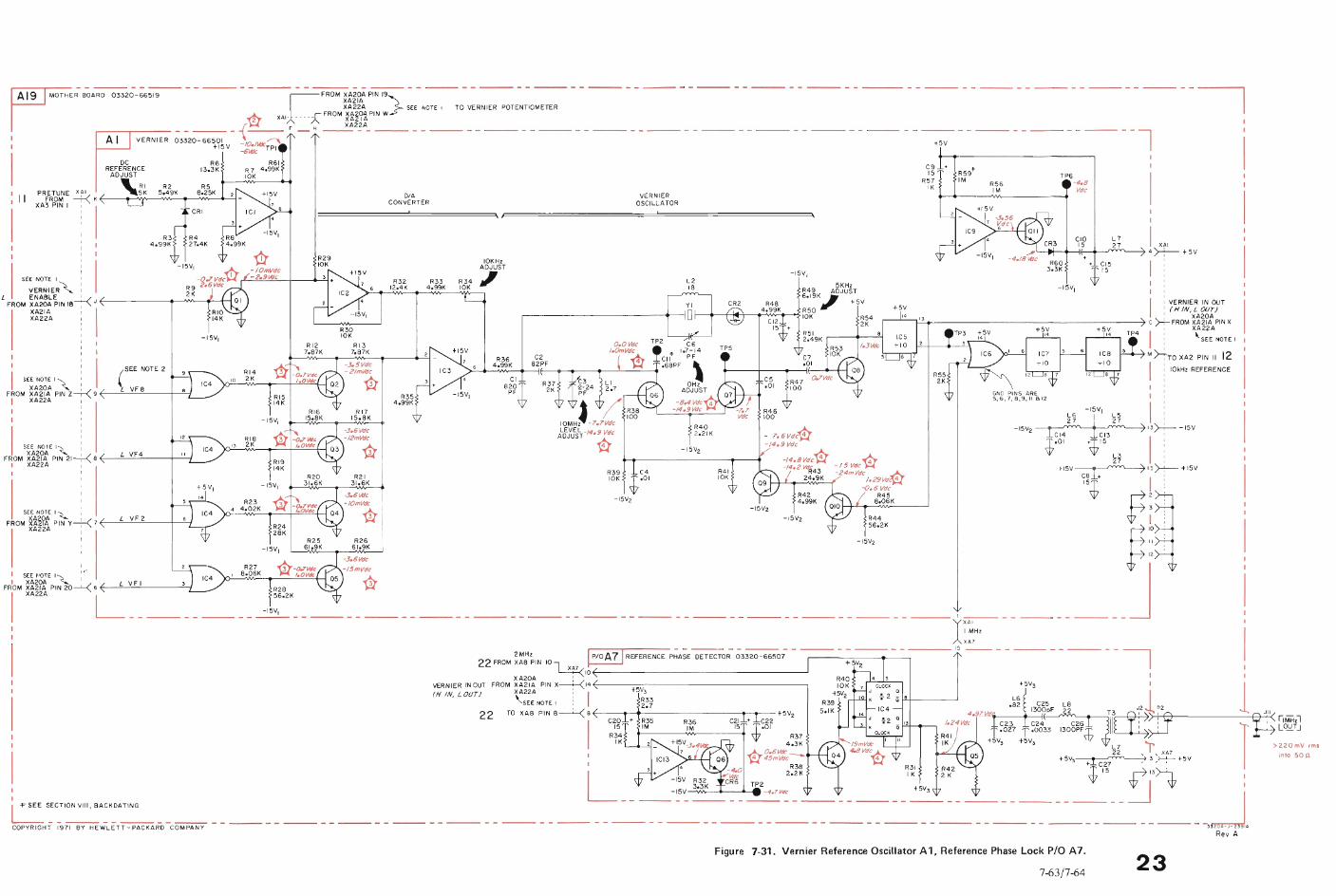
----"~ARev A
TP6-4.8Vdc
-15V,
+5V3 1
L6 1.82
~----j~------:lfct~~f--I~~~~fJ> 220 mV rms
into 50 tl
I
I
C9IS
R57IK
-----------------,-----::-- ---- ------ ---- --l
+SV
R4456.2K
I :VERNIER IN OUTI (H IN, LOOT)I XA20A
r--".::...~--------------------_4c >-t FROM ~~~~A/'N X
.---+-----"-1 I: '-SEE NOTE I
M>+TOXA2PINII 12I ['0kHZ REFERENCE
II
5,6,7,8,9,11812 I I
~6 -ISVI LS I:
27 27 :-15V2 ">-:-- -ISV
CI4 CI3 I
¢.Ol +~'S I:~1 ,
fISV~'5>-T--+15V
ilt ~!'~:~ i
t 12
___J
-,SV,
R4110K
L218
VERNIEROSCILLATOR
R46100
- T.6VdC*-14.9 Vdc,... ~ *".-,----------....--1 -14.8VdC~ 4
-14.2 VdJ:43
-15 VdcH -24mVdc .A
H-'-~_2:.,4oA·;;9.::K~ ~:c:::c~R45
8.06K
SKHzR49 ADJUST6.19K •
YI CR2 , +5V
,-------------+--JO r-+--I'-t'IIrt----<o>-¥_t_~~5KO R542K
10KHzADJUST
JR3410K
--- - - --- - - --- - - --- - - --- - - --- - - ----t-~:-~-H-Z-- - - --- --
222MHz IP/OA71 REFERENCE P~A;E~OR- 03320-6650'; - --- - - --- - - ----- 15 --- - - --- ~ - ---- --
FROM XA8 PI N 10 l XA7, + SV2~IO(,------------------------"
VERNIER IN OUT FROM ~~~?: PIN X--l-<'4E_----:-:::-,------------------,(H IN, LOUr) XA22A : I +SV,
\SEE NOTE ,: ~;f22 TO XA8 PIN 8~8E_--t_+_--------~r_,.._-+5V2
I
R334.99K
R3212.4K
D/ACONVERTER
-J'.6Vdc
-/5mVdc
R2910K
~3010K
RI37.87K
R36 C2-3.5Vdc 4.99K 82PF-2/mVdc
*CI
R37820~PF 2K
R3S4.99K
RI7IS.8K
-3.6Vdc-/2mVdc
~
R2131.6K
-306~c- 15V2-IOmVdc
*R26-ISVI
61.9K
*-/OmVdc-2.9IAJc
-15V,
R613.3K
CRI
R34.99K
I '!" SEE SECTION VIII, 8ACKDATING
COPYRIGHT 19iiBY'""HEWLET~RO-COMPANY - - --- - - --- - - --- - - --- - - ---- - - ---- - - --- - - ---- - - --- - - ---- - - --- - - --- - - --- - - --- - - ---- - - ---- - - ---
IAI9 I,,,",;.~'". 00"0-"-51-9-- - - ---- - - ----h-- FROM XAlOA PIN 19)- - - --- - - ---- - - --- - - --- - - --- - - --- - - ---- - - ---- -XA21AXA22A SEE NOTE I TO VERNIER POTENTIOMETER* XAI- ;CFROM ~~~?iPIN W
I - - ---- - {---- F _ H X_A2~A - _ --- - - --- - - --- - - --- - - ---- - - ---- - - ---
I A I VERNIER 03320-66~nV -IO./~.;;;'-6Wc
R61R 7 4.99K10K
I,I,II,
SEE NOTE I <... I
FROM ~~~?t PIN V-+< 7 f--=L,-,-V,-F.=.2__+--,,-/XA22A ,
,,,
I (SEE NOTE 2I SEE NOTE '~FROM ~ ~~?f PIN z--1-( 9 ~_-=L,--"V-,-F-=8'-_---1---1"-1I XA22A I,
III
I SEE NOTE '<.- iFROM ~~~?t PIN 21--1-( 8 ~_-=L,--,-V,-F",,4__---1---1-'-1
XA22A
,SEE f\'OTE I~ I ,.
I XA20A , ' VFIFROM XA21A PIN 20----'--( 6 L R28
XA22A L 15:~·2K _
DCREFERENCE
ADJUST
'RI R2 R5II PAfR6U~E -+-< K ~_~~V15I"K_~S",.4"9_K~~~8".2,,S-K-+~
XA3 PIN I I
I
i ":;:;~,~.... iL FROM ~~~k~'N 18~ J ~-------<t--JW'--<f---1H
XA21A IXA22A
Figure 7-31. Vernier Reference Oscillator A1, Reference Phase Lock PIO A7.
7-63/7-64 23

- ---
----
----
----
-
::::::::
::::::::
:::::
...,
J..
.,J..
.,J-.
..J-.
..J
......
...,J
OlO
l:!>
:!>
:!>
:!>
:!>
-0'0--
--_
._
,O
JO
JtI
lco
OJ
::1
::1
-0
"0
"0
"0
-0
()O
J:S
'3'
3'3
'3
'-.
..lO
Jr"
O:;
~2
~O
o-I
~m
~
c;i ~ w ~ a ~ ~
I-~l'
I(0
C4
".
-R
3-
~R4-
"t>_
&1-
=".
"3"t>
=:l
~,-=
"=
Za
=:u
a:::
0~
r:::::
:=J
~0~
"-----
(t\z»
c:::
:::J
=<
a-
l>~cn
&1~l
>~~~I
l",
OJ
o....
10
a>x
C2
Pri~
~E~
C2
iji
'"
='"
"=
-R
2-
-R
I-
~·~c-:
=---:'
.~
IC
I
J----"'-
(0 o-1
5
o-,
OO
Gnd
[D
-R
7--CR2~
BO
--
RIO
-0
-+5
IC2
-C
3-
,.000
-R
4
-R
2-
·e"ICI
-•
.ro
-R
28
-
~R9
-C
I-
•-
R3
S-
.~~
-~R33-
~w
-A3
4
•0
-CR
12
-C
RIO
---R
36
--R
30
-_
R3
7_
8-A
29
-~
Q6
-CRI3~
-R
38
-~
-R2
4-
(.01
-cs
--R
22
-
B"--
C6
-R
18
-IC
4-R
25
-
-CR
6-
0!:
=~~~=
0+
15
8- CR
7-
-R
6-A
27
Q
4-C
R8
--R
S-
-CR
I-_
_C
7-_
-R
I-
® -A
I2
--R
I3-
-R
I4-
-C
5-
--
C2
--
R8
-
-R
32
-
@ -R
3-
-A
19
--R
20
--R
21
-
@
®®
-A
43
-I
C9
J•
t30
~C
10
-
G"d
-CR
I4-
e-R
44
-
-R
39
-Q
8~CRI5-
LC13~
•-3
0-R
40
--R
42
-
-R4
6-
-R4
5--e-
-R"3
5-
-R4
7-
C-R
33
-®
®-R
48
-.1
5.(
J>-R
34
-•
-15
".
§-G
12
--C
RI2
--R
49
-
•-5
..,-R
50
-01
2-R
28
--C
R1
0-
".
-=
=-R
36
-G
"d"t>
="
--R
30
-a
=8
e-R
29
--R
"3
1-
=::.
=-C
RI3
--R
38
-
rn"J
=z
=-C
RI6
--R
24
-
=0
-R32~
---c
s--
-R2
2-
:u-
l>=
=8
e-~C6~
"Z
_=
;;oS
1>=
Q5
-R
I8
-IC
4
<?
-J-R
25
-"'"
....=
-CR
6-.
.01
-R.2
6-
..0
l>=
<'"
--J
0
=-R
I9
-e-
CR
7-
-R
6-
-C
R9
-•
tl5
'"=
0'j'
CDX
-R
20
-0
4-C
R8
--R
5---R
27
-
d=
l>=
'"a>
~-R
21
--C
RI---C7-~
•t'
Nx=
=-R
I-
-R
7-
-C
R2
-•
+5
0a>
=@
1l>
=~
=®
8--R
10
-
'""'=
--J
IC2
-C
3-
'"'"
==
-R
3-
-R
i2-
w-R
4-
'"=
-CR
4-
-R
I3-
0•
-R
2-
'""
=u;
1c:::
::J-C
R5
--A
I4-
'"-C
5-
8"
@-C
2-
ICI
w
0-~A8-
".
-R
I7---R9-~e-
-R
I6-
-c
1-
IC3
w-C
4-
-R
I5-
00
]]2
0.0
.-8
-30
81
Ii ;:;
W <C iJ1 B\9i ro
~ ~ "0 " -< o ~ B S-g ~N
:.
00tv
'•
.b:
>~;J
::o,
:f'>
'bd.
"8;::;~:;~bb
<0
1°
000
8g
0.«
««
00
.0
.a.
.....0
00
.0
0.0
0
....
....
.0
.-+
00
,O
Or+
O.-+
.-+
ww
,o
.....o
o.....
.o
rn
'(J'l
0'l
(Jl
~~~~~~~
00
10
NO
OO
««
«<
a.a.
a.a.
a.a.
a.o
no
oo
oo

-30V
R4715K
OWe
R432.87K
R4210K
R4515K
CIO100PF
7-65/7-66
24Power Supplies; A16A, A17A, 3320A; A16B, A17B, 3320B.
CRI4
Figure 7-32.
P/oAI78 POWER-SUPPLY 03320-66517 (B Onlyj - --- - - --- - - ~
, MOUNTED ON AI7A
~ t---::;;~+- '\4"07 ",SEE NOTE I
">-- BOV
XAI7
III,,I,
~.~III,I-4TVdc
3/Vdc
-30.6 Vdc
R4815K
I -30Vde IR49
~ '-< 3 2.7 XAl7
L l~l ~\~' "",.J.>-
3320BONLY~
+t~O~
I I
~I~I1
11
R322K
I I~--------'--<: I : , I
I R4 C4 II 22K +T 1000 I
I 17 I
L __ .--J Q5~3320~ONLY
TI1
1'1';~!!!!!!!!!!!!!!~ NOTONM~~i'ATED !!!!!!!!!!!!!!!!!!!!!~\ iI-"'::;;~--~---<"--_-~ P )>-+-1-...;...-~
I
R6lOOK
CI.001B
RII.BK
7Vde CRI
------ll-......,.....,.,.....J POWER SUPPLY 03320-66535 (B Only) R9 I
0.1
r---~--------- -------POWER SUPPLY 03320-66535 (A Onlyl
~~
15.2 Vde
-14.6Vde
RI8
I~-------::i~~'7:;;5:-T--,/~5~v.~d:£e----__----<r-----l""r6-:-~-K----~--+T,....r-6-~--~1L
1
>,: ,,:,----+---.__..s rl3 1~5~ W
12 I IR24 I I
I7.,5K' ,, '
, I
I '
xAI6 I I>-!_..... -+-< '" I :
II ,I ,
~f~ I ',: I ',:~-------==-r--'M.-r--::C/'''5~v~d~e--------+---------,....-_:!'-- ....--+-_~4
~~~ j~}' (LI~V_ ~R30 ~·r 1 ' TO 5MHz OVEN
14.3K r53; J>-!- (OPTION 0021
I
~~8 I :r5~4 7>-t-- 5V
, CRI3 I 13 I.. 5.IIV I
>-'_..... --'-( E -29 +15V:R32 +15V R35 r-79 >-"- TO 5101Hz OVENL 3.01K 7.5K W (OPTION 0021
COPYRIGHT I97IBY H-EWLETT-PACKARDCOMPANY - ---- - - --- - - --- - - ---- - -~
RI470
RI/2K
I
I
I~"~: I
1,,,,, IL- '-<·:,I .,...._...._ ......---.:~II
I R2 C2
I 12K J3K
L- __~
~ TO XA27A PIN 15
~ TO XA27A PIN S
71 ~
115
IL1iE I,,,,,
III
I I J- 1 '" 61
I L__:; L __ ...J J~E~~~I~ _

25Figure 7-33. Wiring Diagram.
I) SO II
I) II ~LEVELING1 SWITCH
SOWIRE rRIBBON
t3//CABLE
[3-'/ PANEL
13J'J'LIGHTS
I , t 3J'J'J ~--l
RED EDGE? _~NDICATES NO.1..., -:';;;I-A~ -, rJi?n rI
(~~~~e~1 I t003 I t'B'Modell I
SO WIRE g6~~NI SO WIRERIBBON
A39 I RIBBONCABLE (B'Mode CABLE
OPTION I0071 I I
, II
I 1
I I1
I50 ~ SO I
r A20---'
I (A'ModeI OR
A21~ ...j. I~ :'a'Mode
~
l,I
III REAR PANEL
~ ~-~9-lr-------''''''-'~97='--+1 + IS
..--------'='='-+ - IS
J!Q, GNDr-+-+-_---'~==2'___;_ +S 1 'B' MODEL ONLY
&Q, 1 I STANDARD -r-++-+-I--=~91~2-+~ND OPTIONS 001,
+=--__ J 002,006 16 '543-211
I ITO A221'A MODEL OPTION 003) 1 AIS 1
(B'MODELOPTIONS 004 AND 007) I 1
r;- - -'0 II i4 "7 B Pl TO A20l'A MODEL ;~~N~~~D6~~I; I 1
r------==='------+13 1 TOA21I'B'MODELSTANOARD,001, L6rS 432 I r-- --,I I 002AND006l ~2 AI3 1
1--+----"'=_-+ A17 l .2.., -----.Ll,.l,\,-+-+-1-++-I--I--I-+L'---l" I~ I1 N 7 1 ~I d &Q, ,9Q, 1
L-----==--7 S RI I I ~ 1I J J 1 I~ LEVELING
r---------rl M I r - - - - - - -1 'B' MODEL ONLY J t SWITCH
I &, 13 13 OPTIONS _ J 1
1 ~t lSI 004, 007 ~ I~""1-+-----1- 12 I I AI6 I ~ ~
I I I I 1 I=:}"" PANELL ---==--t K 1 I I~ LIGHTS
I 'I l~"",------r' 1 ~ I I I 1 '3:,,-,
'I E41 ~ II 3 1----'''''24;e- L_-_-_~ L_-__1t- t- - - _...J L_...J L __ ---1
1-+----'="---+, 6 "I L )IS II C (:.. ~e-j----'.,Z1,""4=----------------------------.JJ
1 F 1"1 ~ _
,---""-------+1 2 IH---=--;-I I I
1 1 ~'-----"'---+ A ,:1 _-==- __1
! I
I : 41__-==_90_1-----+-+-+-+---+~ - - -JI ~-11 pifp? :1~ ~- -1 ~--II elr ~ +30V I I I I I 1 I 2 I I
.:!.J i I I 1 PloL~-oJ2 IL-------t
l0 C,-----'=::::....-----4-H-+--+-30V ~I I I I I I
L J ~~~~~~~-J~ L __~ L J L-rJ
JJ I;C-~~H,_-I -- iAL~~~1___;0-=3J3~MHzlI ~'!D-~E.L0J,i1 ~ _ -91il__ J L- _0\11 _ ~
~ I~ ~r COPYRIGHT BY HEWLETT-PACKARD CCMPANY3320A/B-J-3269
~
JI~7+s ~
&.Q, RI CI
-d, F2 ~
:=fiCRI]
&" TI ~n I~ ~I
1/II
~'If &, ~: 6I d..,
il~~-----l
8
~~ r- ~ ~
~
~I
~I ~III ~
~I
I I
I \9b ~i ~ ~
I I
~I I I
I ~
I -Q, -Q, IL.rOWER MODULE
I &1L
----------------~ J., - &, &,
.:L 1EJ~
0.L
f J.., ~
~ ~
~~
~
7-f:,7/7-68

Model 3320A/B
SECTION VIII
BACKDATING
Section VIII
8-1. INTRODUCTION.
8-2. This section contains backdating material which makesthis manual applicable to instruments with serial numberslower than the serial number listed on the title page. Eachchange has been keyed in the text or illustration with adagger (t). This alerts the user to a change which may applyto his instrument. If this manual is to be used with anearlier instrument only, the changes which apply to thatinstrument may be entered into the text where applicable.Where component values in an instrument differ from the~eplaceable Parts List, yet are not listed in the backdatingsection, the components should be replaced using the partnumber in this manual.
8-3. INSTRUMENT SERIAL NUMBER SEQUENCE.
Designator Descri ption Part NumberA8C41 , C42, C43, C44 C: 0.01 IlF 100 V 0150-0093A8C45 C: 230 pF 500 V 0160-2005A8C46 C: 680 pF 300 V 0140-0208A8R 62 R: fxd 1000 n 5% 0683-1025A8R63 R: fxd 620 n 5% 0683-6215A8R64, R68 R: fxd 47 n 5% 0683-4705A8R65 R: fxd 470 n 5% 0683-4715A8R66, R67, R69 R:fxd5100n5% 0683-5125A8R70 R: fxd 560 n 5% 0683-5615A8R71 R: fxd 51 n 5% 0683-5105A8Q13,Q14 TSTR:SiPNP 1853~203
A8L7 Coil: RF 9140-0088A8P1 Conn: RF 1250-1195A8Tl TFMR: Toroid 9100-1362
c. In Table 6-1 make the following component changes:
Delete: AICll, MP29Add: Al R58, R: fxd 10 kQ 1% 1/8 W 0757-0442Change: Al R59 to R: fxd 10 kQ 1% 1/8 W 0757-0442
MP31 to 03320-60102 I each Assy: rear deck
d. In Figure 7-30 add the following circuitry to the A8assembly: To Junction
C33 and C37
R63620
84. Changes are listed in instrument serial number order(lower serial numbers first). However, when referring to thechanges for a particular instrument, begin with the latestchange and progress to the earliest change that applies tothe serial number in question. Table 8-1 lists the serialnumbers versus the changes.
8-5. CHANGE 1, FOR SERIAL NUMBERS 1121A-00110AND BELOW (3320A), 1122A-00120 AND BELOW(3320B).
8-6. Make the following changes:
a. In table 6-1 and Figures 7-12 and 7-17 delete A23 R3and A23R4.
b. In Table 6-1 add the following components to the A8assembly:
+15V
+15V
lC41
t:~fIK
1~
,-,,-__~NO CONN
'r
Table 8-1. Serial Number Index.
3320A 33208
Instrument ChangesSerial
Number
1121 A-0011 0 and below 1
1138A-00135 and below 4,51138A-00185 and below 71138A-00275 and below 9
Instrument Changes
SerialNumber
1122A-00120 and below 1
See Paragraph 8-7 2See Paragraph 8-9 31139A-00200 and below 41139A-00250 and below 51139A-00340 and below 61139A-00540 and below 71139A-00590 and below 81319A~0690 and below 9
8-1

SectionVIII
e.InFigure7-31makethefollowingcin;uitchangesontheAlassembly:
Delete:AICll,AIR59Add:AIR58andAIR59,10kQ,frompin2
andpin3respectivelyofIC9toground
8-7.CHANGE2,3320B.
8-8.Priortothe15lineGPIB,Option007,the3320Bcontaineda10lineGPIB,Option005.ThismanualincludesinformationfortheOption007.ForinformationconcerningtheOption005,ordertheManualInsertSheet3320B-H18orcontactyourlocalSalesandServiceOffice.
8-9.CHANGE3,3320B.
8-10.Change3isdesignedtoimprovethe3320Bharmonicdistortionandshouldbeincorporatedinall3320B's.
a.InTable6-1thefollowingcomponentchangeshavebeenmade:
Delete:AI4C17,A14C28,C:fxdcer0.1pF,0150-0084
b.InFigure7-25thefollowingcircuitrychangeshavebeenmade:
Delete:A14C17,A14C2!:\Change:A15Q9AandA14Q9BtoA14Q16andA14Q9
respectfully.AI4R22to49.9QAl4R56to49.9Q
8-11.CHANGE4,FORSERIALNUMBERS1138A00135ANDBELOW(3320A),1139A-00200ANDBELOW(3320B).
8-12.Makethefollowingchanges:
a.InTable6-1makethefollowingcomponentchanges:Add:A2L2,coil/choke:0.82pH,9100-1614
A2R8,R:fxdcomp2000ohm,0683-2025Change:A2CRl,A2CR2,A2CR3,A2CR4to
Diode:Si50rnA30wv,1901-0040.A2IC2toIC:TTLTriple3-inputANDGate,
1820-0372.A2IC8toIC:DigitalTTLDualJ-KFF,
1820-0451A2R9toR:fxdcomp,51Q,0683-5105
b.InFigure7-20makethefollowingcircuitrychanges:
>sv
8-2
Model3320AjB
8-13.CHANGE5,FORSERIALNUMBERS1138A00135ANDBELOW(3320Aj,1139A-00250ANDBELOW(3320B).
8-14.InTable6-1andFigure7-21makethefollowingcomponentchanges:
Change:MR8to820Q,0683-8215A4R9to470Q,0683-4715A7ICIto1820-0923
8-15.CHANGE6,FORSERIALNUMBERS113~A
00340ANDBELOW(3320B).
8-16.InTable6-1andFigure7-28A12BC19C:fxd18pF100V0160-2322hasbeenadded.Thisincreasestheoutputamplitudeaccuracyandstabilization.SeeFigure7-28forlocation.
8-17.CHANGE7,FORSERIALNUMBERS1138A00185ANDBELOW(3320Aj,1139A-00540ANDBELOW(3320B).
8-18.TheAI3A/BSwitchAssemblyintheseinstrumentsarenotdesignedforthereplacementofindividualswitchwafersanddetents.IftheAI3A/Bassemblyfailsintheseinstrumentsitisnecessarytoreplacethefrontpanelassemblywiththenewfrontpanelassembly(MP20)listedinTable6-1.ThefrontpanelassemblylistedinTable6-1containsthelatestA13A/BSwitchAssembly.Thisassemblyisdesignedforreplacementofindividualswitchcomponents.Adisassembly/assemblyprocedureforthefrontpanelassemblyisoutlinedinSectionV,Paragraph5-49.
8-19.CHANGE8,FORSERIALNUMBERS1139A00590ANDBELOW(3320B).
8-20.InTable6-1deleteCableAssembly03320-61618.

Model 3320A/B
8-21. CHANGE 9, FOR SERIAL NUMBERS 1138A00275 AND BELOW (3320Aj, 1319A-00690 ANDBELOW (3320B).
8-22. Make the following changes:
a. In Table 6-1 delete A3C26 and A3R85. ChangeA3R55 to R: fxd 8060 D 1% 0698-4473.
b. In Figure 7-19 Change A3QI1 and A3Q12 circuitryas follows:
-5.9/ We
Section VIII
R558.06K
C 10 R5615~ 10K
-15V
8-3


CODE LIST OF MANUFACTURERS
The following code numbers are from the Federal Supply Code for Manufacturers Cataloging Handbooks H4-1 (Name to Code) and H4-2 (Codeto Name) and their latest supplements. The date of revision and the date of the supplements used appear at the bottom of each page. Alphabetical codes have been arbitrarily assigned to suppliers not appearing in the H4 Handbooks.
CodeNo. Manufacturer Address Code
No. Manufacturer Address CodeNo. Manufacturer Address
. . Burlington , Wis.
· ..Syracuse, N. Y.. .. Dayton,Ohio
· . Compton, Calif.·Los Angeles, Cal.· .Wakefield, Mass.
. . Chicago, Ill.
. . San Mateo, Cal. . .. Berne, Ind.
Teterboro, N.J.
Newark, N.J.Buena Park, Cal.
Palo Alto, Cal.Camden, N. J.
Shady Grove, Pa.
Palo Alto, Cal......Downey. Cal.
Jamaica, N. Y.. Costa Mesa, Cal.
CTS of Berne, Inc.Chicago Telephone ofCalifornia, Inc. So. Pasadena, Cal.
Bay State Electronics Corp. . .. Waltham, Mass.Teledyne Inc. ,Microwave
Div ..National SealPrecision Connector Corp .Duncan Electronics Inc.General Instrument Corp. ,
Semiconductor Division ProductsGroup
Imperial Electronic, Inc ..Melabs, Inc.Philadelphia Handle Co.Grove Mfg. Co. , Inc.Culton Ind. Inc. ,Data SystemDiv. . Albuquerque, N. M.
Clarostat Mfg. Co Dover, N. H.Elmar Filter Corp. W. Haven, Conn.Nippon Electric Co. , Ltd. . Tokyo, JapanMetex Electronics Corp. . .... Clark, N.J.Delta Semiconductor Inc.. Newport Beach, Cal.Dickson Electronics Corp. . Scottsdale, ArizonaAirco Supply Co. , Inc Witchita, KansasWilco Prooucts Detroit, Mich.Thermolloy . Dallas, TexasSolitron Devices Inc. . . Tappan, N. Y.Telefunken (GmbH) . Hanover ,GermanyMidland-Wright Div. of
Pacific Industries, Inc .... Kansas City, KansasSem-Tech. . .. Newbury Park, Cal.Calif. Resistor Corp. . . Santa Monica, Cal.American Components, Inc ... Conshohocken, Pa.ITT Semiconductor, a Div. of
Int. Telephone and TelegraphCorporation ... West Palm Beach, Fla.
Hewlett-Packard Company. . Loveland, Colo.Cornell Dublier Electric Corp Newark, N. J.Corning Glass Works . Corning, N. Y.Electro Cube Inc.. . .. san Gabriel,Cai.Williams Mfg. Co. san Jose, Cal.The Sphere Co. ,Inc. . .. Little Falls, N.J.Webster Electronics Co New York, N. Y.Scionics Corp. Northridge ,Cal.Adjustable Bushing Co..... N. Hollywood, Cal.Micron Electronics . .Garden City, Long Island,N. Y.Amprobe lnst. Corp. Lynbrook, N. Y.Cabletronics ... Costa Mesa, Cal.Twentieth Century Coil
Spring Co. ~Sa.nta Clara, Cal.Fenwal Elect. Inc. Framingham, Mass.Amelco Inc. Mountain View, Cal.Spruce Pine Mica Co Spruce Pine, N. C.Omni-Spectra Inc. Detroit, Ill.Computer Diode Corp. ... Lcx1i, N. J.Electroid Co. Union, N.J.Boots Aircraft Nut Corp. Pasadena, Cal.Ideal Prec. Meter Co. ,Inc. ,
De Jur Meter Div. Brooklyn, N. Y.Delco Radio Div. of G. M. Corp.... Kokomo, Ind.Thermonetirs Inc. Canoga Park,Cal.Tranex Company .. Mountain View, Cal.Hamlin Metal Products Corp. Akron, OhioAngstrohm Prec. Inc. No. Hollywood, Cal.Siliconix Inc. .Sunnyvale, Cal.McGraw-Edison Co. Manchester, N. H.Power Design Pacific Inc. . . Palo Alto, Cal.Clevite Corp. Semiconductor Div .. Palo Alto, Cal.Signetics Corp. Sunnyvale, Cal.Ty-Car Mfg. Co. ,Inc. Holliston, Mass.TRW Elect. Camp. Div. Des Plaines, Ill.Chomerics Plainville, Mass.Curtis Instrument,lnc. . .. Mt. Kisco, N. Y.Vishay Instruments Inc.. Malvern, Pa.E. I. DuPont and Co., Inc. Wilmington, Del.Durant Mfg. Co. . . Milwaukee, Wis.The Bendix Corp. ,Navigation &
Control Div.Thomas A. Edison Industries,Div.of McGraw-Edison . West Orange, N.J.
Coneoa . Baldwin Park, Cal.19589
167581710917474176751774517856178701804218083183241847618486185651858318612188731891119315
19500
14493146551467414752149601510615203152871529115558155661563115772
1580115818160371617916352165541658516688
1171711870121361236112574
126971272812859128811293012954130191306113103133271339613835
14099141931429814433
1123611237
11314114531153411711
1124211312
. Burbank, Cal.
. . Chicago, Ill.. .Newton, Mass.
Phoenix, ArizonaParamus, N.J.
Cleveland, Ohio. . . Rockford, Ill.
Bridgeport, Conn.Redwood City, Cal.
Mountain View, Cal.
. Minneapolis, Minn.
. .. Rochester, N. Y.
Ultronix, Inc.Union Carbine Corp., Elect.
Div. . . New York, N. Y.Viking Ind. Inc. . . Canoga Park, Cal.Icore Electro-Plastics Inc Sunnyvale, Cal.Cosmo Plastic (c/o Electrical
Spec. Co.) ..Barber Colman Co.Tiffen Optical Co.
Roslyn Heights, Long Island, N. Y.Metro-Tel Corp.. . . WestburY,N. Y.Stewart Engineering Co. . Santa Cruz, Cal.Wakefield Engineering Inc Wakefield, Mass .Bassick Co. , Div. of StewartWarner Corp.
Raychem Corp.Bausch and Lomb Optical
Co.E.T.A. Products Co. ofAmerica '"
Amatom Electronic HardwareCo., Inc. New Rochelle, N. Y.
Beede Electrical InstrumentCo. , Inc. " Penacook, N. H.
General Devices Co. ,Inc Indianapolis, Ind.Components Inc. ,Ariz. Div Phoenix, ArizonaTorrington Mfg. Co. ,West Div Van Nuys, Cal.Varian Assoc. Etmac Div. San Carlos, Cal.Kelvin Electric Co. Van Nuys, Cal.Digitran Co. . . . ... Pasadena. Cal.Transistor ElectronicsCorp ..
Westinghouse ElectricCorp. ,Electronic Tube Div ..... Elmira, N. Y.
Filmohm Corp. . New York, N. Y.Cinch-Graphik Co. City of Industry, Cal.Silicon Transistor Corp. . .. Carle Place, N. Y.Avnet Corp.. . Culver City, Cal.Fairchild Camera & Inst. Corp. ,Semiconductor Div.. . . .. Mountain View, Cal.
Minnesota Rubber Co Minneapolis, Minn.Birtcher Corp, The.. . ..Monterey Park, Cal.Sylvania Elect. Prod. Inc.,
Mt. View Operations. .. Mountain View, Cal.Technical Wire Products
Inc. Cranford, N.J.Bodine Elect. Co. Chicago, Ill.Continental Device Corp. . .. .Hawthorne, Cal.Raytheon Mfg. Co., Semi-
conductor Div ..Hewlett-Packard Co. ,
New Jersey Division. . Rockaway, N. J.U. S. Engineering Co Los Angeles, Cal.Blinn, Delbert Co., . . . Pomona, Cal.Burgess Battery Co..
... Niagara Falls, Ontario, CanadaDeutsch Fastener Corp..... Los Angeles, Cal.Bristol Co. , The Waterbury, ConnSloan Company Sun Valley, Cal.ITT Cannon Electric Inc. ,
Phoenix Div ...National Radio Lab. Inc.CBS Electronics SemiconductorOperations,Div.of CBS Inc .... Lowell, Mas~.
General Electric Co. ,Miniature Lamp Dept. . Cleveland, Ohio
Mel-Rain ...Indianapolis, Ind.Babcock Relays Div.. . ..Costa Mesa, Cal.Electronic Enclosures Inc ... Los Angeles, Calif.Texas Capacitor Co. Houston, TexasTech. Ind. Inc. Atohm
Elect. .Electro Assemblies, Inc ...C & K Components Inc ..Mallory Battery Co. ofCanada, Ltd.. Toronto, Ontario, Canada
Pennsylvania Florocarbon. Clifton Heights, Penn.Burndy Corp. . . . Norwalk, COM.General Transistor Western
Corp. . . .. Los Angeles, Cal.Ti-Tal,Inc. Berkeley, Cal.Carborundum Co. Niagara Falls, N. Y.
07980
08524086640871708718
081450828908358
078290791007933
07700
06540
06402
073220738707397
0562405728
05729057830582006004
097950992210214
0714907233072560726107263
07138
0534705397
092500935309569
0609006175
06555
08806
06666067510681206980070880712607137
055740559305616
0872708792
1041110646
0898409026090970913409145
U. S. A Common Any supplier of U. S.McCoy Electronics Mount Holly Springs, Pa.Sage Electronics Corp. . . Rochester, N. Y.Cemco, Inc. ..... . . Danielson,Conn.Humidial Colton, Calif.Mietron, Co. , Inc Valley Stream, N. Y.Garlock Inc. .Cherry Hill, N.J.Aerovox Corp. . . ... New Bedford,Mass.Amp. Inc. . .. Harrisburg, Pa.Aircraft Radio Corp.. Boonton, N. J .Croven, Ltd. . . . .Whitby, Ontario, CanadaNorthern EngineeringLaboratories, Inc ..
Sangamo Electric Co. ,Pickens Div. . .Pickens, S.C.
Goe Engineering Co City of Industry, Cal.Carl E. Holmes Corp Los Angeles, Cal.Microlab Inc Livingston, N.J.General Electric Co. ,Capacitor Dept.. . . Hudson Falls, N. Y.
Alden Products Co Brockton,Mass.Allen Bradley Co.. . Milwaukee,Wis.Litton Industries, Inc Beverly Hills, Cal.TRW Semiconductors, Inc Lawndale, Cal.Texas Instruments, Inc. ,Transistor Products Div. . . . Dallas, Texas
The Alliance Mfg. Co .. " .. Alliance, OhioSmall Parts Inc. . . Los Angeles, Cal.Pacific Relays, Inc. . Van Nuys, Cal.Gudebrod Bros. Silk Co New York, N.Y.Amerock Corp. . . Rockford, lll.Pulse Engineering Co ..... Santa Clara, Cal.Ferroxcube Corp. ofAmerica. . .Saugerties, N. Y.
Wheelock Signals ,Inc. . . .Long Branch, N.J.Cole Rubber and Plastics Inc .. &mnyvale, Cal.Amphenol-Borg Electronics
Corp. . .... Broadview, 01.Radio Corp. of America,Semi
conductor and MaterialsDivision .... Somerville, N. J .
Vocaline Co. of America,Inc. . . . . Old Slybrook, Conn.
Hopkins EngineeringCo... .san Fernando, Cal.Hudson Tool & Die . . . . Newark, N. J .Nylon Molding Corp Springfield, N. J.G. E. Semiconductor Prod.
Dept.Apex Machine & Tool Co.Eldema Corp.Parker Seal Co..Transitron Electric Corp.Pyrofilm Resistor Co. ,
Inc. . .....Cedar Knolls, N.J.Singer Co. , Diehl Div. ,
Finderne Plant. . . . . . . Sumerville, N. J .Arrow, Hart and Hegeman
Elect. Co.. . . . . . . . . Hartford, Conn.Taruus Corp. . . Lambertville, N.J.Arco Electronic Inc.. . . . Great Neck, N. Y.Essex Wire. . Los Angeles, Cal.Hi-Q Division of Aerovox .. Myrtle Beach, S. C.Precision Paper Tube Co Wheeling, TILPalo Alto Division of Hewlett-
Packard Co. . .. Palo Alto, Cal.Sylvania Electric Prooucts,
Microwave Device Div ...Mountain View, Cal.Dakota Engr ~Inc. . Culver City, Cal.Motorola Inc. Semiconductor
Prod. Div. . .... Phoenix, ArizonaFiltron Co. ,Inc. WesternDiv. Culver City, Cal.
Automatic Electric Co. . Northlake, Ill.Sequoia Wire Co. . . . Redwood City, Cal.Precision Coil Spring Co. El Monte, Cal.P. M. Motor Company. . . Westchester, IIIComponent Mfg. Service
Co. . .. W. Bridgewater, Mass.Twentieth Century Plastics,
Inc. Los Angel~s, Cal.Westinghouse Electric Corp.
Semiconductor Dept. .. Youl\:.owood, Fa.
00866008910092901002
00853
0370503797038180387703888
03954
000000013600213002870033400348003730065600779007810080900815
0477304796048110487004919
02735
04651
05006
02771
02777028750329603508
05277
0467304713
0100901121012550128101295
04732
04009
040130406204217042220435404404
01349015380158901670019300196002114
021160228602660
00015-49Revised: May, 1970
From: Handbook SupplementsH4-1 Dated January 1970

CODELISTOFMANUFACTURERS(Continued)
CodeNo.
ManufacturerAddressCode
No.ManufacturerAddressCode
No.ManufacturerAddress
So.Pasadena,Cal.
......Keasby,N.J.
Thompson-Bremer&.Co.Chicago,Ill.TilleyMfg.Co.SanFrancisco,Cal.StackpoleCarbonCoSt.Marys,Pa.StandardThomsonCorp..Waltham,Mass.TinnermanProducts,Inc.Cleveland,OhioTransformerEngineers....SanGabriel,Cal.UciniteCo..Newtonville.Mass.WaldesKohinoorInc...LongIslandCity,N.Y.VeederRoot,Inc....Hartford,Conn.WencoMfg.Co.Chicago,Ill.Continental-WirtElectronicsCorp.
..Philadelphia,Pa.ZierickMfg.Corp.NewRochelle,~.Y.MepcoDivisionofSessionsClockCo.
.Morristown,N.J.PrestoleCorp.Toledo,OhioSchnitzerAlloyProductsCo.Elizabeth,N.J.ElectronicIndustriesAssociation.
Standardtubeorsemi-conductordevice,anymanufacturer.
UnimaxSwitch,Div.MaxonElectronicsCorp..Wallingford,Conn.
UnitedTransformerCorp....NewYork,N.Y.OxfordElectricCorp.Chicago,Ill.BournsInc..Riverside,Cal.AreaDiv.ofRobertshawControlsCo.
...........Columbus.OhioAllStarProductsInc.....Defiance,OhioAveryLabelCo.Monr.ovia,Cal.HammarlundCo.,Inc..MarsHill,N.C.Stevens,Arnold,Co.,Inc...Boston,Mass.DimcoGrayCo.Dayton,OhioInternationalInst.Inc...Orange.Conn.GrayhillCo...........LaGrange,Ill.TriadTransformerCorp.Venice,Cal.WinchesterElec.Div.LittonInd.,Inc.
Oakville.Conn.MilitarySpecification.InternationalRectifierCorp.ElSegundo,Cal.AirpaxElectronics,Inc.Cambridge,MarylandBarryControls,Div.BarryWrightCorp.
Watertown,Mass.CarterPrecisionElectricCo.Skokie,Ill.SpertiFaradayInc..CopperHewitt
ElectricDiv..Hoboken,N.J.ElectricRegulatorCorp.Norwalk,Conn.JeffersElectronicsDivisionof
SpeerCarbonCo..DuBois,Pa.FairchildCamera&Inst.Corp.
Space&DefenseSystemsDiv..Paramus,N.J.MagurieIndustries,Inc.....GreenWich,Conn.SylvaniaElectricProd.•Inc.
ElectronicTubeDivision....Emporium,Pa.AstronCorp.....EastNewark,Harrison,N.J.Switchcraft,.nc."Chicago,Ill.Metals&.ControlsInc.,
SpencerProducts.Attleboro,Mass.Phillips-Adv~nceControlCo..Joliet,Ill.ResearchProductsCorpMadison,Wis.Roltan'Mfg.Co.,Inc.Woodstock,N.Y.VectorElectronicCo....Glendale,Cal.CarrFastenerCo..Cambridge,Mass.NewHampshireBall
Bearing,IncPeterborough,N.H.GeneralInstrumentCorp.
CapacitorDiv...........Darlington,S.C.ITTWireandCableDiv....LosAngeles,CaLVictoryEng.Corp.Springfield,N.J.BendixCorp.,RedBankDivRedBank,N.J.HubbellCorp..Mundelein,Ill.RosanInc.....NewportBeach,Cal.Smith.HermanH.Inc.Brooklyn,N.Y.TechLabsPalisadesPark,N.J.CentralScrewCo.Chicago,Ill.GavittWireandCableCo.,Div.of
AmeraceCorp.Brookfield,Mass.BurroughsCorp.,Electronic
TubeDiv...Plainfield,N.J.UnionCarbideCorp.,Consumer
Prod.Div..NewYork,N.Y.ModelEng.andMfg.,IncHuntington,Ind.LoydScruggsCo...Festus,Mo.AeronauticalInst.&RadioCo.....Lodi,N.J.ArcoElectronicsIncGreatNeck,N.Y.A.J.GlesenerCo.,Inc.SanFrancisco,Cal.TRWCapacitorDiv..Ogallala,Neb.
8204282047
804868050980583806408081381030810738109581312
8211682142
82170
8220982219
7845278471784887849378553787907894779136791427925179727
800338012080131
83125
80223802488029480411
7996380031
823768238982647
81349814838154181860
827688286682877828938305883086
80207
83594
831488318683298833158332483330833328338583501
83740
837778382183942841718439684411
.Chicago.Ill.
.Elgin,111.Braintree,Mass.
NewYork,N.Y.Pitman,N.J.
.So.
C.P.Clare&Co.CentralabDiv.of
GlobeUnionInc....Milwaukee,Wis.CommercialPlasticsCoChicago,Ill.CornishWireCo..TheNewYork,N.Y.CotoCoilCo.,Inc.Providence.R.I.ChicagoMiniatureLampWorks...Chicago,Ill.CinchMfg.Co.,
HowardB.JonesDivChicago.Ill.DowCorningCorpMidland,Mich.ElectroMotiveMfg.Co.,Inc.
Willimantic,Conn........Brooklyn,N.Y. DialightCorp.
IndianaGeneralCorp.ElectronicsDiv.
GeneralInstrumentCorp.CapDivision.Newark,N.J.
DrakeMfg.Co.HarwoodHeights,Ill.HughH.EbyInc.Philadelphia,Pa.GudemanCo....Chicago,Ill.ElasticStopNutCorpUnion.N.J.RobertM.HadleyCo..LosAngeles.Cal.ErieTechnologicalProducts.Inc....Erie.Pa.HansenMfg.Co.,IncPrinceton,Ind.H.M.HarperCoChicago,Ill.HelipotDiv.ofBeckmanInst.Inc.
.Fullerton,Cal.HughesProductsDivisionof
HughesAircraftCo....NewportBeach,CaLAmperexElect.Co..Hicksville.L.I..N.Y.BradleySemiconductorCorp.
...........NewHaven.Conn.CarlingElectric.Inc.Hartford.Conn.CircleFMfl;.Co......Trenton,N.J.GeorgeK.GarrettCo.
Div.MSLIndustries.Inc.Philadelphia,Pa.FederalScrewProducts,Inc....Chicago,Ill.FischerSpecialMfl;.Co.Cincinnati,OhioGeneralIndustriesCo..The.....Elyria,OhioGoshenStamping&.ToolCo....Goshen,Ind.JFDElectronicsCorp..Brooklyn,N.Y.JenningsRadioMfg.Corp.SanJose,Cal.Groove-PinCorp...Ridg-efield,N.J.SignaliteInc..Neptune,N.J.J.H.Winns,andSonsWinchester.Mass.IndustrialCondenserCorpChicago,IlLR.F.ProductsDivisionof
Amphenol-BorgElectronicCorp.Danbury.Conn.
E.F.JohnsonCoWaseca.Minn.InternationalResistanceCo.Philadelphia.Pa.KeystoneCarbonCo.,IncSt.Marys,Pa.CTSKnights,Inc..Sandwich,Ill.KulkaElectricCorp..Mt.Vernon.N.Y.LenzElectricMfg.Co......Chicago.Ill.Littlefuse,Inc..DesPlaines,Ill.LordMfg.Co...Erie.Pa.C.W.Marwedel.sanFrancisco,Cal.GeneralInstrumentCorp.
MicamoldDivisionNewark,N.J.JamesMillenMfg.Co.•Inc.Malden.Mass.J.W.MillerCoLosAngeles,Cal.Cinch-Monadnock,Div.ofUnitedCarr
FastenerCorp....SanLeandro,Cal.MuellerElectricCo....Cleveland,OhioNationalUnion...Newark,N.J.OakManufacturingCo......crystalLake,Ill.TheBendixCorp.,
ElectrodynamicsDiv.N.Hollywood,Cal.PacificMetalsCo...SanFrancisco,Cal.PhaostranInstrumentand
ElectronicCo.PhiladelphiaSteeland
WireCorp..Philadelphia,Pa.AmericanMachine&FoundryCo.
Potter&BrumfieldDivPrinceton,Ind.TRWElectronicComponentsDiv.Camden,N.J.GeneralInstrumentCorp.,
RectifierDivisionBrooklyn,N.Y.ResistanceProductsCo.Harrisburg,Pa.RubbercraftCorp.ofCalif....Torrance,Cal.ShakeproofDivisionof
IllinoisToolWorks.Sigma..SignalIndicatorCorp.Struthers-DunnInc.
74970750427526375378753827581875915760057621076433
77252
764877649376530
7707577221
76545767037685477068
7148271590
7373473743737937384673899739057395774276744557486174868
735597358673682
7261972656
72699
727657282572928729627296472982730617307673138
73293
7161671700717077174471785
7198472136
7344573506
77342
7763077638
782777828378290
777647796978189
LRCElectronics....Horseheads,N.Y.ElectraMfg.Co.Independence,KansasGeneralAtronicsCorp.Philadelphia,Pa.Executone,Inc.LongIslandCity,N.Y.FafnirBearingCo.,TheNewSTitian,Conn.FansteelMetallurgicalCorp....N.Chicago,Ill.GeneralReedCo..Metuchen,N..J.TexscanCorp....Indianapolis,Ind.BritishRadioElectronicsLtd...Washington,D.C.G.E.LampDivision,NelaPark,Cleveland,OhioGeneralRadioCo....WestConcord,Mass.MemcorInc.,Camp.Div..Huntington,Ind.GriesReproducerCorp..NewRochelle,N.Y.GrabertFileCo.ofAmerica,Inc.Carlstadt,N.J.Compac/HollisterCo.Hollister.Cal.HamiltonWatchCo.Lancaster,Pa.Hewlett-PackardCo.PaloAlto,Cal.HeymanMfg.CoKenilworth,N.J.InstrumentSpecialtiesCo.
Inc..LittleFalls,N.J.G.E.ReceivingTubeDeptOwensboro,Ky.LectrohmInc....Chicago,Ill.StanwyckCoilProducts.
Ltd.Hawkesbury,Ontario,CanadaCunningham,'t'.H.&.Hill,
Ltd...Toronto,Ontario,CanadaP.R.Mallory&Co.,Inc...Indianapolis,Ind.MechanicalIndustriesProd.Co.Akron,OhioMiniaturePrecisionBearings,Inc..Keene,N.H.HoneywellInc..Minneapolis,Minn.MuterCo..Chicago,Ill.C.A.NorgrenCo.Englewood,Colo.OhmiteMfg.Co...Skokie,fll.PennEng.&Mfg.Corp......Doylestown,Pa.PolaroidCorp....Cambridge,MaSS.
PrecisionThermometer&.Inst.Co.Southampton,Pa.
Microwave&PowerTubeDivWaltham,Mass.RowanControllerCo...Westminster,Md.HPCoMed.Elec.Div.Waltham,Mass.ShaflcrossMfg.Co.Selma,N.C.SimpsonElectricCo.........Chicago.Ill.SonotoneCorp......Elmsford,N.Y.RaytheonCo.CommercialApparatus
&SystemDiv.So.Norwalk,Conn.SpauldingFibreCo.,Inc.....Tonawanda,N.Y.SpragueElectricCo.NorthAdams,Mass.SuperiorElect.CoBristol,Conn.TelexCorp..Tulsa,Okla.Thomas&BettsCoElizabeth,N.J.TriplettElectricalInst.Co.Bluffton,OhioUnionSwitchandSignalDiv.ofWestinghouseAirBrakeCo...Pittsburgh,Pa.
UniversalElectricCo.Owosso,Mich.Ward-LeonardElectricCo.Mt.Vernon,N.Y.WesternElectricCo.,Inc.NewYork,N.Y.WestonInst.Inc.Weston-Newark.Newark,N.J.WittekMfg.Co..Chicago,fll.MinnesotaMining&Mfg.Co.RevereMincomDiv..St.Paul,Minn.
AllenMfg.CoHartford,Conn.AlliedControl...NewYork.N.Y.AllmetalScrewProductCo.,Inc.
.....GardenCity,N.Y.Amplex.Div.ofChryslerCorp..Detroit,Mich.AtlanticIndiaRubberWorks,Inc...Chicago,Ill.AmperiteCo.,Inc.UnionCity,N.J.ADCProductsInc..Minneapolis,Minn.BeldenMfg.Co..Chicago.fll.BirdElectricCorpCleveland,OhioBirnbachRadioCo.NewYork.N.Y.BlileyElectricCo..Inc....Erie,Pa.BostonGearWorksDiv.of
MurrayCo.ofTexas...Quincey,Mass.BudRadio.Inc.Willoughby,OhioCambridgeThermionicsCorp.Cambridge,Mass.CamlocFastenerCorp.Paramus.N.J.CardwellCondenserCorp.
................Lindenhurst.L.I..N.Y.BussmannMfg.Div.of
McGraw-EdisonCo.St.Louis.Mo.ChicagoCondenserCorp.....Chicago,Ill.Calif.SpringCo.,Inc.Pico-Rivera.Cal.CTSCorpElkhart,lnd:ITTCannonElectricInc.LosAngeles,Cal.Cinema.Div.AerovoxCorp.....Burbank.Cal.
71218712797128671313
19644197012018321226213552152023020230422378324455246552468126365264622685126992284802852030817
49956520905298354294550265593355938
702767030970318
331733543436196
71400
704177048570563706747090370998710027103471041
36287
37942395434092040931421904399044655463844790448620
7143671447714507146871471
621196374364959650926629566346
56137562895847459446597306074161775
00015-49Revised:May.1970
From:HandbookSupplementsH4-1DatedJanuary1970

CODE LIST OF MANUFACTURERS (Continued)
CodeNo. Manufacturer
CodeAddress No. Manufacturer
CodeAddress No. Manufacturer Address
Newark, N.J.
. Quincy, Mass.
... Loveland, Colo.
9487085454854718547485660859118617486197
8657986684
869288703487216
87473
8766487930881408822088698892318947389479896659003090179
90365
907639097091146
91260913459141891506916379166291673917379182791886
Sarkes Tarzian, Inc. . Bloomington. Ind.Boonton Molding Company Boonton J N. J.A. B. Boyd Co. .... . .. San Francisco. Cal.R. M. Bracamonte & Co.... San Francisco. Cal.Koiled Kords, Inc. Hamden, Conn.Seamless Rubber Co. . .. Chicago, TILFafnir Bearing Co. . . Los Angeles I Calif.Clifton Precision Products Co.• Inc.
. . Clifton Heights. Pa.Precision Rubber Products Corp. Dayton, OhioRadio Corp. of America. Electronic Compo
& Devices Division Harrison, N.J.Seastrom Mfg. Co. .. Glendale J Cal.Marco Industries .... Anaheim, Cal.Philco Corporation (Lansdale Division)
. . . . Lansdale, Pa.Western Fibrous Glass Products Co.
...... San Francisco, Cal.Van Waters & Rogers Inc San Francisco, Cal.Tower Mfg. Corp. . Providence, R. I.Cutler-Hammer, Inc. Lincoln, Ill.Gould-National Batteries, Inc•.. St. Paul, Minn.General Mills, Inc. ...•. Buffalo, N. Y.Graybar Electric Co. . . . . . .. . Oakland I Cal.G. E. Distributing Corp Schenectady, N. Y.Security Co Detroit, Mich.United Transformer Co Chicago, Ill.United Shoe Machinery Corp Beverly, Mass.U. S. Rubber Co. , Consumer Ind. &
Plastics Prod. Div Passaic, N.J.Belleville Speciality Tool Mfg. , Inc.
. . . . . . . . . . . . . . . . Belleville, Ill.United Carr Fastener Corp. . Chicago, Ill.Bearing Engineering Co.... San Francisco, Cal.ITT Cannon Elect. Inc. , salem Div.•••• r • • • • • • • • • • • • • • • • • • Sa.lem, Mass.
Connor Spring Mfg. Co.... San Francisco, Cal.Mlller DIal & Nameplate Co. . .. El Monte, Cal.Radio Materials Co. . Chicago, lll.Aupt Inc. . Attleboro, Mass.Dale Electronics, Inc Columbus, Nebr.Eko Corp. . .•.......... WUlow Grove, Pa.Epiphone Inc New York, N. Y.Gremar Mfg. Co. I Inc. • •...Wakefield, Mass.K F Development Co. . . . .. Redwood City, Cal.Malco Mfg. , Inc.....•........ Chicago, Ill.
91929
91961921809236792607
927029296693332
9336993410
93632939299413794144
94148
94154
94197
94222943309437594682
9469695023
95146952369523895263952659527595348953549556695712959849598796067
Honeywell Inc. , Micro Switch Division. . . . . . .. Freeport, Ill.
Nahm-Bros. Spring Co. .. Oakland, Cal.Tru-Connector Corp Peabody, Mass.Elgeet Optical Co. , Inc. Rochester, N. Y.Tensolite Insulated Wire Co. , Inc.
Tarrytown, N. Y.IMC Magnetics Corp....Westbury, L.1. , N. Y.Hudson Lamp Co. . Kearney, N.J.Sylvania Electric Prod. Inc .•
Semiconductor Div Woburn, Mass.Robbins & Myers Inc Pallisades Park, N. J.stemco Controls, Div. of Essex
Wire Corp. . . . Mansfield, OhioWaters Mfg. Co. . ... Culver City, Cal.G. V. Controls Livingston, N. J.General Cable Corp. Bayonne, N.J.Raytheon Co. , Compo Div.
Ind. Camp. Operations ...Scientific Electronics
Products, Inc ...Wagner Elect. Corp. ,
Tung-Sol Diy...Curtiss-Wright Corp. ,
Electronics Div East Patterson, N.J.South Chester Corp. . Chester, Pa.Wire Cloth Products, Inc Bellwood, Ill.Automatic Metal Products Co.. Brooklyn, N. Y.Worcester Pressed Aluminum Corp.
........... Worcester, Mass.Magnecraft Electric Co. . . . . . . . Chicago, 111.George A. Philbrick Researchers, Inc.
. . . . . . . . . , .. Boston, Mass.Aleo Elect. Mfg. Co Lawrence, Mass.Allies Products Corp. Diania, Fla.Continental Connector Corp Woodside, N. Y.Leecraft Mfg. Co. , Inc Long Island, N. Y.National Coil Co Sheridan , Wyo.Vitramon, Inc. .. . Bridgeport , Conn.Gordos Corp. . Bloomfield, N.J.Methode Mfg. Co Rolling Meadows, Ill.Arnold Engineering Co Marengo, TILDage Electric Co. ,Inc Franklin, Ind.Siemon Mfg. Co Wayne, Ill.Weckesser Co. . Ch.icago, Ill.Microwave Assoc. ,West, Inc.. &1nnyvale, Cal.
96095962569629696396
96330963419650196508967339688197464975399797997983
981419815998220
9827898291983769841098731
98734
9882198978
9910999313993789951599707
9980099848999289993499942
99957
Hi-Q Div. of Aerovox Corp. . Olean, N. Y.Thordarson-Meissner Inc Mt. Carmel, Ill.Solar Mfg. Co. . . . Los Angeles, Cal.Microswitch, Div. of
Minn. -Honeywell . Freeport, Ill.Carlton Screw Co. Chicago, Ill.Microwave Associates, Inc.. Burlington, Mass.Excel Transformer Co. . ... Oakland, Cal.Xcelite, Inc Orchard Park, N. Y .San Fernando Elec. Mfg. Co. San Fernando, Cal.Thomson Ind. Inc. . Long Island, N. Y.Industrial Retaining Ring Co Irvington, N. J.Automatic & Precision Mfg Englewood, N.J.Reon Resi::;tor Corp. . . . . . Yonkers, N. Y.Litton System Inc., Adler-Westrex
Commun. Div. . . . .. New Rochelle, N. Y .R-Tronics, Inc. . . Jamaica, N. Y.Rubber Teck, Inc. . . Gardena, Cal.Hewlett-Packard Co.
Medical Elec. Div. . Pasadena, Cal.Microdot, Inc. So. Pasadena, Cal.Sealectro Corp. .... Mamaronech, N. Y.Zero Mfg. Co. . ... Burbank, Cal.Etc Inc. . .. Cleveland I OhioGeneral Mills Inc., Electronics Div.
Minneapolis, Minn.Paeco Division of Hewlett-Packard Co.
. . . . . Palo AI to, Cal.North Hills Electronics, Inc.. Glen Cove, N. Y.International Electronic Research Corp.
. .. Burbank J Cal.Columbia Technical Corp.... New York, N. Y.Varian Associates. . . Palo Alto, Cal.Allee Corp. . . . . Winchester, Mass.Marshall Ind. , Capacitor Div. . Monrovia, Cal.Control Switch Division, Controls Co.
of America .... . .... EI Segundo, Cal.Delevan Electronics Corp. East Aurora, N. Y.Wilco Corporation Indianapolis, Ind.Branson Corp. Whippany, N.J.Rembrandt, Inc. Boston, Mass.Hoffman Electronics Corp.,
Semiconductor Division ..... EI Monte, Cal.Technology-Instrument Corp.
of California Newbury Park, Cal.
The follOWing HP Vendors have no number assigned in the latest supplement to the Federal Supply Code for Manufacturers Handbook.
OOOOFOOOOZOOOABOooBB
Maleo Tool and Die Los Angeles. Calif.Wl110w Leather Products Corp Newark, N.J.ETA EnglandPrecision Instrument Compo Co. Van Nuys, Cal.
OOOCS Hewlett-Packard Co., ColoradoSprings Div. . .. Colo·rado Springs, Colorado
OOOMM Rubber Eng. & Development ...Hayward , Cal.OOONN A "N" D Mfg. CO. . . . . .san Jose, Cal.
OOOQQ Cooltron ...OOOWW CalIfornia Eastern Lab.OOOYY S. K. Smith Co...
. . Oakland, Cal.. .. Burlington, Cal... Los Angeles, Cal.
00015-49Revised: May, 1970
From: Handbook SupplementsH4-1 Dated January 1970


ELECTRONIC
SALES Be SERVICE OFFICES
UNITED STATESALABAMAP.O. Box 42072003 Byrd Spring Road S.W.Huntsville 35802Tel, (205) BB1·4591TWX, 810·726-2204
ARIZONA2336 E. Magnolia St.Ph.enlx B5034Tel, (602) 244-1361TWX, 910-951-1330
5737 East BroadwayTucson 85711Tel, (602) 298-2313TWX, 910-952-1162
CALIFORNIA1430 East Orangethorpe Ave.Fullert.n 92631Tel, (714) 870-1000TWX, 910-592-1288
3939 lankershlm BoulevardN.rth H.II,.,••d 91604Tel, (213) 877-1282TWX, 910-499-2170
6305 Arizona PlaceLos Angeles 90045Tel, (213) 649·2511TWX, 910-328-6148
1101 Embarcadero RoadPal. Alt. 94303Tel, (415) 327-6500TWX, 910·373-1280
2220 Walt Ave.Sacramenta 95825Tel, (916) 482-1463TWX, 910-367-2092
9606 Aero DriveSOn 01'1. 92123Tel, (714) 279-3200TWX, 910-335·2000
COLORADO7965 Easl PrenllceEnll••••d 80110Tel, (303) 771-3455TWX, 910-935-0705
CANADAALBERTAHewlelt-Packord (Canada) LId.11748 Kingsway Ave.EdmontonTel, (403) 452-3670TWX, 610·831·2431
CONNECTICUT12 lunar DriveNew Haven 06525Tel, (203) 389-6551TWX, 710-465-2029
FLORIDAP.O. Box 242102806 W. Oakland Park Blvd.Ft. laUderdale 33307Tel, (305) 731-2020TWX, 510-955-4099
P.O. Box 139106177 lake Ellenor Dr.Orlando. 32809Tel, (305) 859-2900TWX, 810-850·0113
GEORGIAP.O. Box 28234450 Interstate NorthAllanla 30328Tel, (404) 436-6181TWX, 810-766-4B90
HAWAII2875 So. King StreetHonolUlU 96814Tel, (808) 955-4455
ILLINOISS500 Howard Street$II.klt 60076Tel, (312) 677-0400TWX, 910-223-3613
INDIANA3839 Meadows DriveIndlanlll.lls 46205Tel, (317) 546-4891TWX, 810-341-3263
LOUISIANAP.O. BOI 8563239 Williams BoulevardK.nner 70062Tel, (504) 721-6201TWX, 810-955-5524
BRITISH COLUMBIAH.wlett·Packard (Canada) ltd.4519 Canada WayMort' lurnaby 2Tel, (604) 433-8213TWX, 610-922-5059
MARYLAND6707 Whitestone RoadBaltimore 21207Tel, (301) 944-5400TWX, 710-862-9157
P.O. Box 16482, Choke Cherry RoadR.ckvill. 20850Tel, (301) 94B-6370TWX, 710-828-9684
MASSACHUSETTS32 Hartwell Ave.lellngton 02173Tel, (617) 861-8960TWX, 710·326-6904
MICHIGAN21840 West Nine Mile RoadS.uthfl.ld 48075Tel, (313) 353-9100TWX, 810-224-4882
MINNESOTA2459 University AvenueSt. Paul 55114Tel, (612) 645-9461TWX, 910-563-3734
MISSOURI11131 Colorado Ave.Kansas CIIJ 64137Tel, (816) 763·8000TWX, 910-771-2087
148 Weldon ParkwayMaryland Neilhls 63043Tel, (314) 567-1455TWX, 910-764-0830
'NEVADALit V'IIITel, (702) 382·5777
NEW JERSEYW. 120 Century RoadParamus 07652Tel, (201) 265-5000TWX, 710-990-4951
1060 N. Kings HighwayCherfJ Hili 08034Tel, (609) 667-4000TWX, 710-892·4945
MANITOBAHewlett-Packard (Canada) ltd.513 Century St.WinnipegTel, (204) 786·7581TWX, 610-671-3531
NEW MEXICOP.O. Box 8366Station C6501 lomas Boulevard N.E.Albuquerque 87108Tel, (50S) 265-3713TWX, 910-989-1665
156 Wyatt DriveLas Cruces 88001Tel, (505) 526-2485TWX, 910-983-0550
NEW YORK6 Automation laneComputer ParkAlbany 12205Tel, (518) 458-1550TWX, 710-441·B270
1219 Campville RoadEndlc.tt 13760Tel, (607) 754-0050TWX, 510-252·0890
New York CityManhattan, BronxContact Paramus, NJ OfficeTel, (201) 265-5000Brooklyn, Queens, RichmondContact Woodbury, NY OfficeTel. (516) 921·0300
82 Washington StreetPoolbk.ep.le 12601Tel, (914) 454-7330TWX. 510-248·0012
39 Saginaw Drive.,claest,r 14623Tel, (716) 473-9500TWX, 510·253-5981
5858 East Molloy RoadSyracuse 13211Tel, (315) 454-2486TWX, 7tO-541-0482
1 Crossways Park WestW••dbufJ 11797Tel, (516) 921-0300TWX, 510·221·2168
NOVA SCOTIAHewlett-Pac!tard (Canada) ltd.2745 Dutch Village Rd.Suite 206Hallfl!Tel, (902) 455-0511TWX, 610-271·4482
NORTH CAROLINAP.O. Box 51881923 North Main StreetHigh P.int 27262Tel, (919) BB5-8101TWX, 510-926-1516
OHIO25575 Center Ridge RoadCleveland 44145Tel, (216) 835-0300TWX, 810-427-9129
3460 South Dixie DriveDayt.n 45439Tel, (513) 298-0351TWX, 810-459-1925
1120 Morse RoadColumbus 43229Tel, (614) 846-1300
OKLAHOMAP.O. Box 32008Oklah.ma Cily 73132Tel, (405) 721-0200TWX, 910-830-6862
OREGON17890 SW Boones Ferry RoadTualalln 97062Tel, (503) 620-3350TWX, 910-467-8714
PENNSYLVANIA2500 Moss Side BoulevardMoar,e,llIe 15146Tel, (412) 271-0724TWX, 710-797-3650
1021 8th AvenueKing of Prussia Industrial ParkKine of Prussia 19406Tel, (215) 265-7000TWX, 510-660-2670
RHODE ISLAND873 Waterman Ave.East Providence 02914Tel, (401) 434-5535TWX, 710-381-7573
'TENNESSEEMemphisTel, (901) 274-7472
ONTARIOHewlett-Packard (Canada) ltd.1785 Woodward Or.otta.a 3Tel, (6131 255-6180, 255-6530TWX, 610-562-8968
Hewlell-Packard (Canada) Ltd.50 Galaxy BlVd.Rudor.Tel, (416) 677-9611TWX, 610-492-4246
TEXASP.O. Box 1270201 E. Arapaho Rd.Richardson 75080Tel, (214) 231-6101TWX, 910-867-4723
P.O. BoX 274096300 Weslpark DriveSuite 100Houston 77027Tel, (713) 781-6000TWX, 910-8BI-2645
231 Billy Mllchell RoadSan Antonio 78226Tel, (512) 434-4171TWX, 910·871-1170
UTAH2890 South Main StreelSail Lake City 84115Tel, (801) 487-0715TWX, 910-925-5681
VIRGINIAP.O. Box 65142111 Spencer RoadRichmond 23230Tel, (703) 285-3431TWX, 710-956-0157
WASHINGTON433-108th N.E_Bellevue 98004Tel, (206) 454-3971TWX, 910-443-2303
'WEST VIRGINIACharlestonTel, (304) 768-1232
WISCONSIN9431 W. Beloit RoadSuite 117Milwaukee 53227Tel, (414) 541-0550
FOR U.S. AREAS NOTLISTED:Contact the regional office near·est you: Atlanta, Georgia .North Hollywood, California .Paramus, New Jersey ... Skokie,Illinois. Their complete ad·dresses are listed above.
·Servlce Only
QUEBECHewlett-Packard (Canada) ltd.275 Hymus IfoulevardP.lnt. ClaireTel, (514) 697-4232TWX, 610·422-3022Telex, 01-20607
FOR CANADIAN AREAS NOTLISTED:Contact HeWlett-Packard (Canada) ltd. in Pointe Claire, atthe complete address listedabove.
CENTRAL AND SOUTH AMERICAARGENTINAHewlett-Packard ArgentinaS_A_C.e.1Lavalle 1171.3°Buenos AiresTel, 35-0436, 35·0627, 35-0341Telex, 012·1009Cable, HEWPACK ARG
BRAZILHewlett·Packard Do BrasilI.E.C. LTDA.Rua Frel Caneca 111901307-So. Paul. - 3, SPTel, 288-7111, 287-5858Cable: HEWPACK Sao Paulo
Hewlett-Packard Do BrasilI.E.C. LTOA.Praca Com Feliciano 78Salas 806/B089000-Porto Alegre RSRio Grande do Sui (RS}-BrasilTeJ, 25-8470Cable, HEWPACK Porto Alegre
Hewlett·Packard Do BrasilI.E.C. LTOA.Rua da Matriz 292000-Rio de Janeiro, GBTel, 266-2643Cable: HEWPACK Rio de Janeiro
BOLIVIAStambuk & Mark (Bolivia) l TDA.Av. Mariscal, Santa Cruz 1342La PazTel, 40626, 53163, 52421Telex, 3560014Cable, BUKMAR
CHILEH~ctor Calcagni y Cia, ltda.Casillo 16_475Santlal'Tel, 423 96Coble, CALCAGNI Santiago
COLOMBIAInstrumentaci6nHenrik A. langebaek & Kier S.A.Carrera 7 No. 48-59Apartado A~reo 6287B.g.", 1 D_E.Tel, 45·78-06, 45-55-46Cable, AARIS BogotaTelex, 44400lNSTCO
COSTA RICAlie. Alfredo Gallegos Gurdi.in.a,artado 10159San JodTel, 21·86-13Coble, GALGUR San Jos~
ECUADORlaboratorlos de Radio·lngenieriaCalle GuayaQuil 1246Post Office Sox 3199Qull.Tel, 212-496: 219-185Cable, HORVATH Quito
EL SALVADORElectronic AssociatesApartado Postal 1682Centro Comercial GiganteSan Salvador, EI Salvador C.A.Paseo Escalon 4649-4° PisoTel, 23-44-60, 23-32-37Cable, ELECAS
GUATEMALAIPESA5a via 2·01, Zona 4Guatemala CityTel, 63-6-27 & 64-7-86Telex. 4192 TELTRO GU
MEXICOHewlett-Packard Mexicana, S.A.de C.V.Adolfo Prieto 622Col. del ValleMexico 12, D.F.Tel, 543-4232: 523-1874Telex, 017-74-507
NICARAGUARoberto Ter.in G.Apartado Postal 689Edificio Ter.inManaluaTel, 3451, 3452Cable: ROTERAN Managua
PANAMAElectr6nico Balboa, S.A.P.O. Box 4929Ave. Manuel Espinosa No. 13·50Sldg. AlinaPanama CityTel, 230B33Telex: 3481003, Curundu,Canal ZoneCable: ElECTRON Panama City
PARAGUAYZ.J_ Melamed S.R_L.Division: Aparatos y EquiposMedicosSal6n de Exposici6n y Escritorio:Chile 482Edificio Victoria-Planta BajaAsuncion, ParaguayTel, 4-5069, 4·6272Cable, RAMEL
PERUCompania Electro Medica S.A.Ave. Enrique Canaual 312San IsidroCasUla 1030LimaTel, 22-3900Cable: ElMED lima
PUERTO RICOSan Juan Electronics, Inc.P.O. Box 5167Ponce de leon 154Pda. 3·PTA de TierraSan Juan 00906Tel, (809) 725·3342, 722-3342Cable: SATRONICS San JuanTelex: SATRON 3450 332
URUGUAYPablo Ferrando S.A.Comerclal e IndustrialAvenlda lIalio 2877Casilla de Correo 370MontevideoTel, 40-3102Cable: RADIUM Montevideo
VENEZUELAHewlett-Packard Oe VenezuelaC.A.Aparlado 50933CaracasTel, 71.88.05, 71.88.69, 71.99_30Cable: HEWPACK CaracasTelex, 21146 HEWPACK
FOR AREAS NOT LISTED,
CONTACT:Hewlett·PackardInter-Americas3200 Hillview Ave.Pal. Allo, California 94304Tel, (415) 493-1501TWX, 910·373-1267Cable, HEWPACK Palo AltoTelex, 034-8300, 034-8493
E 3-73

EUROPEAUSTRIAHewlett-PackardGes.m.b.HHandelska52/3P.O.Box7A·1205ViennaTel:(0222)336606to09Cable:HEWPAKViennaTelex;75923hewpaka
BELGIUMHewlett·PackardBeneluxSA/N.V.AvenueduCol-Vert.1B-1170BrusselsTel;(02)722240Cable:PAlOBENBrusselsTelex:23494palobenbru
DENMARKHewlett-PackardA/SDatavej38DK-3460BlrkerodTel:(01)816640Cable:HEWPACKASTelex:16640hpas
Hewlett·PackardA/STervet9OK-8GODSilkeborgTet:(00)82-71-66Telex:16640hpasCable:HEWPACKAS
FINLANDHewlett-PackardOyBulevardi26P.O.Box12185SF·DOI20Helsinki12Tel:(90)13730Cable:HEWPACKQYHelsinkiTelex;12·15363her
FRANCEHewlett-PackardFranceQuartierdeCourtaboeufBoltePostaleNo.6F-91401OrslYTel,(1)907782SCable:HEWPACKOrsayTelex:60048
Hewlett·PackardFrance4QuaidesEtroitsF-69321lyonCedex1Tel,(781426345Cable:HEWPACKlyonTelex:31617
Hewlett·PackardFrance29ruedelaGareF·31700BlagnacTel:(61)858229Telex:51957
GERMANFEDERALREPUBLICHewlett-PackardGmbHVertriebszentraleFrankfurtBernerstrasse117Postfach5601400-6000Frankfurt56Tel:(0611)5004-1Cable:HEWPACKSAFrankfurtTelex:413249fra
Hewlett-PackardGmbHVertriebsburoBoblingenHerrenbergerstrasse1100·7030Biiblingen,WurttembergTel,(07031)667287Cable:HEPAKBoblingenTelex:7265739bbn
Hewlett-PackardGmbHVertriebsburoDusseldorfVogelsangerWeg380-4000DusseldorfTel:(0211)638031/35Telex:85/86533hpddd
Hewlett-PackardGmbHVertriebsburoHamburgWendenstr.230·2000Hamburg1Tel:(0411)240551/52Cable:HEWPACKSAHamburgTelex:2163032hphhd
Hewlett-PackardGmbHVertriebsburoMunchenUnterhachingerStrasse28ISARCenter0·8012OttobrunnTel,(0811)6013061/7Telex:524985Cable:HEWPACKSAMuchen
(WestBerlin)Hewlett-PackardGmbHVertriebsburoBerlinWilmersdorferStrasse113/1140-1000BerlinW.12Tel:(0311)3137046Telex::183405hpblnd
GREECEKostasKarayannis18,ErmouStreetGR·Athens126Tel:3230-303Cable:RAKARAthensTelex:215962rkargr
IRELANDHewlett-Packardltd.224BathRoadGB-Slough,Sll4OS,BucksTel:Slough(0753)33341Cable:HEWPIESloughTelex:84413
Hewlett-Packardltd.TheGraftonsStamfordNewRoadAltrincham,Cheshire,EnglandTel:(061)928-8626Telex:668068
ITALYHewlett·Packardl1alianaS.p.A.ViaAmerigovespucci21-20124MilanTel:(2)6251(10lines)Cable:HEWPACKITMilanTelet:32046
Hewlett·PackardItatianaS.p.A.PiazzaMarconi1-00144Rome-EurTel:(6)59!2544/5,5915947Cable:HEWPACKITRomeTelex:61514
Hewlett·PackardItalianaS.p.A.vicoloPastori,31·35100PadovaTel:(49)664062Telex:32046viaMilan
Hewlett-PackardItalianaS.p.A.ViaColli,241-10129TurinTel:(11)538264Telex:32046viaMilan
LUXEMBURGHewlett·PackardBeneluxS.A./N.V.AvenueduCol-Vert,1B-1170BrusselsTel:(03/02)722240Cable:PAlOBENBrusselsTelex:23494
NETHERLANDSHewlett-PackardBenelux,N.V.Weerdestein117P.O.Box7825NL·Amsterdam,Z11Tel:(020)427777Cable:PAlOBENAmsterdamTelex:13216hepanl
NORWAYHewlett·PackardNorgeA/SNesveien13Box149N-1344HaslumTel:(02)538360Telex:16621hpnasn
PORTUGALTelectra-EmpresaTecnicadeElectricosS.a.r.1.RuaRodrigodaFonseca103P.O.Box2531P·lisbon1Tel:(l9)686072Cable:TElECTRAlisbonTelex:1598
SPAINHewlett·PackardEspanola,SAJerezNo8E-Madrid16Tel:4582600Telex:23515hpe
Hewlett-PackardEspanoia,SAMilanesado21-23E·Barcelona17Tel:(3)2036200Telex:52603hpbee
SWEDENHewlett·PackardSverigeABEnighetsvagen1-3FackS-16120Bromma20Tel:(08)981250Cable:MEASUREMENTS
StockholmTelex:10721
Hewlett-PackardSverigeASHagakersgatan9C5-43141MiilndalTel:(031)276800/01Telex:21312hpmindls
SWITZERLANDHewlettPackard(Schweiz)AGZurcherstrasse20P.O.Box64CH·8952SchlierenZurichTel:(Ol)981821/24Cable:HPAGCHTelex:53933hpagch
Hewlett-Packard(Schweiz)AG9,CheminLouis·PictetCH·1214Vernier-GenevaTel:(022)414950Cable:HEWPACKSAGenevaTelex:27333hpsach
TURKEYTelekomEngineeringBureauSaglikSokNo.15/1Ayaspasa·BeyogluP.O.Box437BeyogluTR·lstanbulTel:494040Cable:TElEMATIONIstanbul
UNITEDKINGDOMHewlett·Packardltd.224BathRoadGB-Slough,Sll4OS,BucksTel:Slough(0753)33341Cable:HEWPIESloughTelex:84413
Hewlett-Packardltd."TheGraftons"StamfordNewRoadGB-Altrincham,CheshireTel:(061)928-8626Telex:668068
Hewlett-Packardltd'sregisteredaddressforV.A.T.purposesonly:70,FinsburyPavementLondon,EC2AISXRegisteredNo:69057
SOCIALISTCOUNTRIESPLEASECONTACT:Hewlett-PackardGeS.m.b.H.Handelskai52/3P.O.Box7A-1205YiennaPh:(0222)336606to09Cable:HEWPACKViennaTelex:75923hewpaka
ALLOTHEREUROPEANCOUNTRIESCONTACT:Hewlett·PackardS.A.RueduBois·du·lan7P.O.Box85CH-1217Meyrin2Geneva
SwitzerlandTel:(022)415400Cable:HEWPACKSAGenevaTelex:22486
OTHERAREASNOTLISTED,CONTACT:Hewlett-PackardExportTradeCompany3200HillviewAve.PaloAlto,California94304Tel:(415)326·7000
(Feb.71493-1501)TWX:910-373-1267Cable:HEWPACKPaloAltoTelex:034-8300,034-8493
THAILANDUNIMESACo.,ltd.ChongkoineeBuilding56SuriwongseRoadBangkOkTel:37956,31300,31307,
37540Cable:UNIMESABangkok
UGANDAUgandaTele-ElectrlcCo.,ltd.P.O.Box4449KampalaTel:57279Cable:COMCOKampala
VIETNAMPeninsularTradingInc.P.O.BoxH·3216Hien·YuongSaigonTel:20-805,93398Cable:PENTRA,SAIGON242
ZAMBIAR.J.Tilbury(Zambia)ltd.P.O.Box2792lusakaZambia,CentralAfricaTel:73793Cable:ARJAYTEE,lusaka
MEDITERRANEANANDMIDDLEEASTCOUNTRIESNOTSHOWNPLEASECONTACT:Hewlett-PackardCo-ordinationOfficeforMediterraneanandMiddleEastOperationsViaMarocco,71-00144Rome·Eur,ItalyTel,(6)S94029Cable:HEWPACKITRomeTelex:61514
TAIWANHewlettPackardTaiwan39ChungShlaoWestRoadSec.1OverseasInsuranceCorp.Bldg.7thFloorTaipeiTel:389160,1,2,375121,Ext.240-249Telex:TP824HEWPACKCable:HEWPACKTaipei
PAKISTANMushko&Company,ltd.OosmanChambersAbdullahHaroonRoadKarachi3Tel,511027,512927Cable:COOPERATORKarachi
Mushko&Company.ltd.38B,SatelliteTownRawalpindiTel:41924Cable:FEMUSRawalpindi
PHILIPPINESElectromexInc.5thFloor,ArchitectsCenterBldg.AyalaAve.,Makati,RizalC.C.P.O.Box1028Makati,RizalTel:86-18-87,87·76·77Cable:ElEMEXManila
SINGAPOREMechanicalandCombustion
EngineeringCompanyltd.9,JalanKltangRedHillIndustrialEstateSingapore,3Tel:642361-3;632611Cable:MECOMBSingapore
Hewlett-PackardFarEastAreaOfficeP.O.Box87AlexandraPostOfficeSingapore3Tel:633022Cable:HEWPACKSINGAPORE
SOUTHAFRICAHewlettPackardSouthAfrica
(PlY.),ltd.P.O.Box31716BraamfonteinTransvaalMilnerton30DeBeerStreetJOhannesburgTel:725-2080,725-2030Telex:0226JHCable:HEWPACKJohannesburg
HewlettPackardSouthAfrica(Ply.),lId.
BreecastleHouseBreeStreetCapeTownTel:3-6019,3·6545Cable:HEWPACKCapeTownTelex:5-0006
HewlettPackardSouthAfrica(Pty.),ltd.
641RidgeRoad,DurbanP.O.Box:99overport,NatalTel:88-6102Telex:567954Cable:HEWPACK
Yokogawa·Hewlett·Packardltd.NittaBldg.2-4·2Shinohara-KitaKohoku-kuYokohama222Tel:045·432-1504Telex:382-3204YHPYOK
Yokogawa-Hewlett-Packardltd.ChuoBldg.Rm.6033,2-ChomeIZUMI-CHO,Mito,310Tel:0292-25-7470
KENYAKenyaKineticsP.O.Box18311Nairobi,KenyaTel,S7726Cable:PROTON
KOREAAmtracoCorporationIndustrialProductsDiv.SeoulP.O.Box11038thfloor,OaeKyungBldg.107SejongRoChongro-Ku,SeoulTel:73·8924-7Cable:AMTRACOSeoul
LEBANONConstantinE.MacridisP.O.Box7213Rl-BeirutTel:220846Cable:ELECTRONUCLEARBeirut
MALAYSIAMECOMBMalaysialtd.2lorong13/6ASection13PetalingJaya,SelangorCable:MECOMBKualalumpur
MOZAMBIQUEA.N.Goncalves,lOA.4.1Apt.14Av.D.luisP.O.Box107lour,ncoMarquesTelex:6-203NEGONMOCable:NEGON
NEWZEALANDHewlett-Packard(N.Z.)ltd.94-96DixsonS1.P.O.Box9443CourtenayPlaceWellington,N.Z.Tel:56-559Telex:6-203NEGONMUCable:HEWPACKWellington
HewlettPackard(N.Z.)ltd.Box51092PukurangaTel:56-9837Cable:HEWPACK,Auckland
NIGERIATeil(MesaComDivision)25MoronllSt,Suru·lere,P.O.Box5705lagosCable:THETElllAGOS
IRANMulticorpInternationalltd.AvenueSoraya130P.O.Box1212IR-TeheranTel:831035·39Cable:MUlTlCORPTehranTelex:2893MCITN
ISRAELElectronics&Engineering
Dlv.ofMotorolaIsraelltd.17AmlnadavStreetTel-AvivTel:36941(3lines)Cable:BASTElTel-AvivTelex:33569
JAPANYokogawa-Hewlett-Packardltd.OhashiBuilding1·59·1YoyogiShibuya-ku,TokyoTel:03-370-2281/92Telex:232-2024YHPCable:YHPMARKETTOK23·724
Yokogawa-Hewlett-Packardltd.NiseiIbaragiBldg.2-2-8KasugaIbaragi-ShiOsakaTel:(0726)23-1641Telex:5332-385YHPOSAKA
Yokogawa·Hewlett-Packardltd.NakamoBuildingNo.24Kamisasazima·choNakamura-ku,NagoyaCityTel:(052)571-5171
INDONESIABahBolonTradingCoy_N.Y.DjalatlMerdeka29BandungTel:4915;51560Cable:IlMUTelex:08-809
ETHIOPIAAfricanSalespower&Agency
Privateltd.,Co.P.O.Box71858/59CunninghamSI.AddisAbabaTel:12285Cable:ASACOAddls.bab.
BlueStar,ltd.1·1·117/1SarojiniDeviRoadStcanderabad500003Tel:76391,77393Cable:BlUHRQSTTelex:459
BlueStar,ltd.23124SecondlineBeachMadras600001Tel:23955Telex:379Cable:BlUESTAR
BlueStar,ltd.IBKaiserBungalowDindliRoad
HONGKONGJamshedpur831001Schmidt&Co.(HongKong)ltd.Tel:3804P.O.Box297Cable:BlUESTAR1511,Prince'sBUilding15thFloolTelex:24010,ChaterRoadHongKongTel:240168,232735Cable:SCHMIDTCOHongKong
CYPRUSKypronlcs19Gregorios&XenopoulosRoadP.O.Box1152CY-NlcosiaTel:45628/29Cable:KYPRONKSPANOEHIS
INDIABlueStarltd.KasturiBuildingsJamshedjiTataRd.Bombay400020Tel:295021Telex:3751Cable:BlUEFROST
BlueStarltd.BandBoxHousePrabhadeviBombay400025Tel:457301Telex:3751Cable:BlUESTAR
BlueStarltd.14/40CivillinesKampur208001Tel:68882Cable:BlUESTAR
BlueStar,ltd.7HareStreetP.O.Box506Calcutta700001Tel:23-0131Telex:655Cable:BlUESTAR
BlueStarltd.BlueStarHouse,34RingRoadlajpatNagarNewDelhi110024Tel;623276Telex:463Cable:BlUESTAR
BlueStar,ltd.BlueStarHousel1/11AMagarathRoadBangalore560025Tel:51413Telex:430Cable:BlUESTAR
AUSTRALIAHewlett·PackardAustralia
Ply.ltd.22-26WeirStreetGlenIris,3146VictoriaTel:20-1371(6lines)Cable:HEWPAROMelbourneTelex:31024
Hewlett-PackardAustraliaPty.ltd.
CornerBridge&WestStreetsPymble,NewSouthWales2073Tel:4496566'Cable:HEWPARDSydneyTelex:21561
Hewlett·PackardAustraliaPty.ltd.
97ChurchltlRoadProspect5082SouthAustraliaTel:65-2366Cable:HEWPARDAdelaide
HewlettPackardAustraliaPty.ltd.
2ndFloor,Suite13CasablancaBuildings196AdelaideTerracePerth,W.A.6000Tel:25-6800Cable:HEWPARDPerth
Hewlett-PackardAustraliaPly.lId.
10WoolleyStreetP.O.Box191DicksonA.C.T.2602Tel:49-8194Cable:HEWPARDCanberraACT
Hewlett·PackardAustraliaPty.ltd.2ndFloor,49GregoryTerraceBrisbane,Queensland,4000Tel:291544
CEYLONUnitedElectrlcalsltd.P.O.Box68160,ParkSt.Colombo2Tel:26696Cable:HOTPOINTColombo
AFRICA,ASIA,AUSTRALIAANGOLATelectraEmpresaHcnia
deEQuipamentosElectricosSAR
RuadeBarbosaRodrigues42·'·
Box6487lundaCable:TElECTRAluanda
E3·73

03320-90001
HEWLETT~PACKARD
Printed in U.S.A.
I