Highlights 1. Dielectric unusual behavior has been ... - arXiv
21
Highlights 1. Dielectric unusual behavior has been successfully explained by the Rezlescu model. 2. Long (ns) is determined, can be utilized for memory and spintronics devices. 3. a th is calculated and well compared with a expt . 4. Sn substituted Ni-Zn single phase inverse cubic spinel has been synthesized. Highlights (for review)
-
Upload
khangminh22 -
Category
Documents
-
view
1 -
download
0
Transcript of Highlights 1. Dielectric unusual behavior has been ... - arXiv

Highlights
1. Dielectric unusual behavior has been successfully explained by the Rezlescu
model.
2. Long (ns) is determined, can be utilized for memory and spintronics devices.
3. ath is calculated and well compared with aexpt.
4. Sn substituted Ni-Zn single phase inverse cubic spinel has been synthesized.
Highlights (for review)

Structural and electrical properties of Sn substituted double sintering derived
Ni-Zn ferrite
M.A. Alia, M.N.I. Khan
b, F.-U.-Z. Chowdhury
a, S.M. Haque
b, M.M. Uddin
a,*
a Department of Physics, Chittagong University of Engineering and Technology (CUET),
Chittagong-4349, Bangladesh. b
Materials Science Division, Atomic Energy Center, Dhaka-1000, Bangladesh.
Abstract
The Sn substituted Ni-Zn ferrites were synthesized by the standard double sintering technique
using nano powders of nickel oxide (NiO), zinc oxide (ZnO), iron oxide (Fe2O3) and tin oxide
(SnO2). The structural and electrical properties have been investigated by the X-ray diffraction,
scanning electron microscopy, DC resistivity and dielectric measurements. Extra intermediate
phase has been detected along with the inverse cubic spinel phase of Ni-Zn ferrite. Enhancement
of grain size is observed in Sn substituted Ni-Zn ferrites. DC resistivity as a function of
temperature has been investigated by two probe method. The DC resistivity was found to
decrease whereas the dielectric constants increase with increasing Sn content in Ni-Zn ferrites.
The dielectric constant of the as prepared samples is high enough to use these materials in
miniaturized memory devices based capacitive components or energy storage principles.
Keywords: Ni-Zn ferrite, double sintering method, structural properties, electrical properties, DC
resistivity, activation energy.
* Corresponding author.
E-mail address: [email protected] (M. M. Uddin)
*ManuscriptClick here to view linked References

1. Introduction
In recent years, the spinel ferrites belong to AB2O4 structure having tetrahedral A site and
octahedral B site have drawn huge attention due to their characteristic properties to meet the
necessities in various applications. Remarkable progresses have been observed to invent and
development of new ferrites. The research and application of magnetic materials have been
developed considerably in the few past decades. The Ni-Zn ferrites have been found to be the
most versatile ferrites systems from the viewpoint of their technological application because of
its high electrical resistivity, high permeability, chemical stability and low eddy current losses
[1-5], especially ideal for high frequency applications. The properties of Ni-Zn ferrites can be
altered by changing chemical composition, preparation methods, sintering temperature (Ts) and
impurity element or levels. The improvement of the basic properties of Ni-Zn ferrites regarding
various applications have been reported [6-20] by altering chemical composition, doping ions or
levels having different valence states. The tetravalent ions such as Ti4+
, Sn4+
and Si4+
substitution
have greatly influenced the properties Ni-Zn ferrites [21].
Details investigation onTi4+
doping in Ni-Zn ferrite system has been carried out [6-8, 12, 17]
while introduction of Sn4+
has attracted less attention [7, 9]. Though some studies have mainly
focused on the magnetic properties of Sn substituted Ni-Zn ferrites, the nonmagnetic properties
such as electrical conductivity and dielectric properties are not reported. The materials with high-
dielectric constants (≥ 103) have become immense interest for the miniaturized memory devices
that are based on the capacitive components or energy storage principles [22, 23]. Moreover,
investigations are limited in substitution of non-magnetic ions of Fe3+
in Ni-Zn ferrite system.
Simultaneous change of Ni and Zn by Sn substitution in the Ni-Zn ferrite system is essential to
elucidate basic understanding and mechanism.
In this study, we have reported the structural and electrical properties of pure and Sn substituted
Ni-Zn ferrite. To the best of our knowledge; this is the first detailed study on tin substituted Ni-
Zn ferrite prepared by double sintering technique.
2. Materials and methods
Solid state reaction route was followed to synthesize Sn substituted Ni-Zn ferrite, Ni0.6-
x/2Zn0.4-x/2SnxFe2O4 (x = 0.00, 0.05, 0.10, 0.15, 0.20 and 0.30) (NZSFO). We have used high
purity (99.5%) (US Research Nanomaterials, Inc.) oxide precursors. The nano powders are taken
as raw materials. The particle size of nickel oxide (NiO), zinc oxide (ZnO), iron oxide (Fe2O3)
and tin oxide (SnO2) are 20-40, 15-35, 35-45 and 35-55 nm, respectively. The preparation
technique is described elsewhere [5]. The final sintering of the samples was carried out at
1300°C for 4 h in air and natural cooling was followed. Structural characterization of the
synthesized samples was carried out by X-ray diffraction (XRD) using Philips X’pert Pro X-ray
diffractometer (PW3040) with Cu-Kα radiation (λ = 1.5405 Å) and scanning electron microscope
(SEM). DC resistivity was measured using Keithley-6514 DC measurement system. Dielectric
measurements were done by a Wayne Kerr precision impedance analyzer (6500B) in the
frequency range of 10 Hz to 100 MHz with drive voltage 0.5V at room temperature.
3. Results and discussion
3.1 Structural properties
The XRD patterns of Sn substituted Ni-Zn ferrites with the chemical composition Ni0.6-
x/2Zn0.4-x/2SnxFe2O4 (NZSFO) are shown in Fig. 1. It is seen that the observed peaks (111), (220),
(311), (400), (422), (511), (440) and (533) confirmed the spinel structure of the Ni0.6Zn0.4Fe2O4
(NZFO) for x=0.0. The extra new intermediate phase of NiSnO3 and SnO2 is observed at around
2=33.3 for the Sn concentration higher than that of x > 0.1. Similar extra phase of NiSnO3 has

also been observed and reported in Sn substituted NiFe2O4 ferrite system [24]. The intensity of
extra phase increases with the increase of Sn concentration. The corresponding positions of all
the sharp peaks were used to obtain the interplanar spacing. The lattice parameter for each peak
of the samples was calculated using the equation .
Fig. 1. The X-ray diffraction patterns of NZSFO (x = 0.0, 0.05, 0.1, 0.15, 0.2 and 0.3) ferrites
samples.
To determine the exact lattice parameter, Nelson–Riley (N-R) extrapolation method was
used. The N-R function is represented by the equation . The exact
lattice parameter a0 was determined using least square fit method from the plot of lattice
parameter ‘a’ of each peak versus F() [figure not shown].
Theoretical calculation of lattice parameter can also be done using the following equation
)](3)(33
800 RrRra BAth , where R0 is the radius of the oxygen ion (1.32 Å) [3] and rA
and rB are the ionic radii of the tetrahedral (A-site) and octahedral (B-site) sites, respectively
[25]. The values of rA and rB can be calculated from the cation distribution of the system and be
represented by
20 30 40 50 60 70
x=0.30
x=0.20
x=0.15
x=0.10
x=0.05
Inte
nsi
ty (
a.
u.)
2 (deg.)
x=0.00
(111) (220)
(311)
(222) (400) (422) (511) (440)

)()()( 423 SnrCCdrCFerCr ASnAZnAFeA and )()()(2
1 432 SnrCFerCNirCr BSnBFeBNiB [26, 27].
The information of cation distribution can be used to know about the magnetic behavior of ferrite
sample. The materials with desired properties for practical application can be developed with the
help of cation distribution [28]. The cation distribution is assumed based on the hypothesis that
Sn has a tendency to occupy tetrahedral (A) site at lower concentration, whereas it occupies the
octahedral site at higher concentration. The cation distribution of A and B sites for each
substitution level (Sn content) is presented in Table 1. The ionic radii for Fe, Ni, Zn and Sn are
0.65, 0.69, 0.75 and 0.69 Å, respectively.
The effect of Sn substitution on the lattice constant, aexpt is shown in Fig. 2 (a). It is found
that the lattice constant initially decreases up to x = 0.1 and thereafter it increases at x = 0.15,
again it decreases up to x = 0.3 and finally increases for x > 0.3. It indicates that the variation of
a with x does not obey the Vegard’s law [29]. Our experimental results follow nonlinear trend
with x which is consistent with the reported observation for Sn substituted NiFe2O4 [24]. The
variation of theoretical lattice constant with Sn content is also shown in Fig. 2 (a). The similar
trend for both experimental and calculated lattice constant is observed. The lattice constant of all
the doped composition is less than that of the parent one. A decreasing trend in lattice constant
with an increase in the content of Sn can be attributed to the ionic size differences since the unit
cell has to contract when substituted by ions with smaller size. The ionic radius of the Sn4+
and
Zn2+
is 0.69 and 0.75Å, respectively. The partial replacement of Zn2+
by Sn4+
might be expected
to cause shrinkage of the unit cell. It can be noted that the ionic radii of Sn and Ni is same
(0.69Å), hence the substitution of Sn for Ni does not affect the lattice constant value.

Fig. 2. (a) The experimental and theoretical lattice constants; (b) the average grain size as a
function of Sn concentration (x = 0.0, 0.05, 0.1, 0.15, 0.2 and 0.3) of NZSFO ferrites.
The X-ray density (ρx-ray), bulk density (ρb) and porosity (P) of the NZSFO ferrites are
presented in Table 1. Normally the ρb of the same composition is smaller than the ρx-ray. This can
be explained by the existence of pores within the samples which are developing during the
sintering process and depend on the sintering temperatures, conditions and time. The ρb of doped
sample (NZSFO) is less than that of the parent (NZFO). The porosity of the NZSFO increases
almost linearly with Sn doping concentration and relatively higher values are observed. The
porosity in the samples is strongly dependent on the amount of applied pressure during sample
preparation. In the present case, the applied pressure is 10 kN/cm2 (1 ton/cm
2).
3.2 Microstructure study
Fig. 3 (a-g) shows the SEM micrographs of Sn substituted Ni-Zn ferrite taken at room
temperature. Clear grains and grain boundaries are evident from the micrographs. SEM
micrographs reveal the polycrystalline nature of microstructures with grains of different shapes
and size. The linear intercept technique has been used to calculate the average grain size
0.0 0.1 0.2 0.3
10
20
30
Gra
in s
ize
(nm
)
Sn concentration, x
(b)
0.0 0.1 0.2 0.3
8.36
8.40
8.44
ath
La
ttic
e C
on
sta
nt
(ナ)
Sn contcentration
aexpt
(a)

Table 1
Variations of lattice parameter, X-ray density, bulk density, average grain size, porosity and activation energy of (NZSFO).
Sn
content,
x
Chemical formula A site B site rA
(Å)
rB
(Å)
ath
(Å)
aexp
(Å)
ρx-ray
(gm/cc)
ρb
dB
(gm/cc)
Dg
(m)
P
(%)
Ea
(eV)
0.0 Ni0.6Zn0.4Fe2O4 FeZn0.4 FeNi0.6 0.95 0.532 8.43341 8.39311 5.32 4.28 07.8 19.6 0.19
0.05 Ni.575Zn.375Sn.05Fe2O4 FeZn0.375Sn0.025 [FeNi0.575Sn0.025]O42-
0.948 0.532 8.4311 8.38996 5.41 3.73 10.1 31.0 0.119
0.1 Ni.55Zn.35Sn.1Fe2O4 FeZn0.35Sn0.03 [FeNi0.55Sn0.07]O42-
0.933 0.538 8.42595 8.37546 5.52 3.85 18.8 30.2 0.116
0.15 Ni.525Zn.325Sn.15Fe2O4 FeZn0.325Sn0.035 [FeNi0.525Sn0.0115]O4
2
-
0.917 0.545 8.42079 8.38137 5.59 4.10 21.0 26.6 0.1023
0.2 Ni.5Zn.3Sn.2Fe2O4 FeZn0.3Sn0.04 [FeNi0.5Sn0.016]O42-
0.902 0.552 8.41563 8.37665 5.68 3.80 30.1 33.1 0.099
0.3 Ni.45Zn.25Sn.3Fe2O4 FeZn0.25Sn0.05 [FeNi0.45Sn0.25]O42-
0.872 0.566 8.40532 8.34531 5.91 3.87 34.8 34.5 0.11

Fig. 3. SEM micrographs of the NZSFO ferrite for (a) x = 0.0, (b) x = 0.05, (c) x = 0.1, (d) x =
0.15, (e) x = 0.2, and (f) x = 0.3.
(g)
(c) (d)
(e) (f)
(a)
(b)

(grain diameter) and values are given in Table 1 for different Sn concentration [30]. Micrographs
show that the grains are almost homogenously distributed throughout the sample surface.
It is seen from the Fig. 2 (b) that the grain size increases with increasing Sn content. Some
oxides, like SnO2, could bring down the melting point. So for the same sintering temeprature,
presence of Sn helps to sinter better or it is equivalent to raising the sintering temperature for the
ferrite. As we know that the grain size is increased with increasing sintering temperature. As a
result enhancement of grain might be expected.
3.3. Electrical properties
3.3.1. DC resistivity
DC resistivity of the NZSFO samples was measured by two probe method and is plotted
as a function of temperature in Fig. 4 (a). It is observed that the resistivity decreases
exponentially with increasing temperature indicating semiconductor behavior of the prepared
ferrites. It is also found that the resistivity decreases with increasing Sn contents x which can be
explained as a consequence of microstructural and structural modification owing to the change in
composition. It is observed from the SEM micrographs that the grain size increases with
increasing Sn concentration. As a result the number of grains and the grain boundaries
decreases. The insulating behavior of grain boundaries may be attributed to the bulk of the
resistivity in ferrite [31]. The grain size increases faster than the porosity in NZSFO with the
increase of Sn contents. The average grain size for x = 0.0 (NZFO) is found to be around 4.2-7.8
μm, while for the NZSFO ferrite the range is 10-34 μm. Though the porosity causes an increase
in resistivity but the increase in grain size results in a decrease in resistivity. The combined effect
of the two events might decrease the resisitivty of prepared ferrites. In addition, another reason
is that Sn simultaneously substituted Zn ions (prefer tetrahedral A site) and Ni ions (prefer

octahedral B site) [32], this will lead to the migration of Fe3+
and Fe2+
(which is responsible for
electric conduction in ferrite) and the fluctuation of valence states for tin as Sn2+
and Sn4+
increases the electronic exchange resulting the resistivity decreases. The reduction of resistivity
might be a result of the combined effect.
The DC electrical resistivity as a function temperature of the samples can be presented by
the Arrhenius type equation: , where ρ and ρ0 are resistivity of samples at
any temperature and room temperature, respectively. The parameter Ea is the activation energy; k
is the Boltzmann constant (= 8.62×10⁻⁵
eV) and T is the absolute temperature. The activation
energy in the ferromagnetic region of the sample was calculated from the plot of Fig. 4 (b) using
the relation [33] and presented in Table 1.
Fig. 4. (a) Variation of resistivity as a function of temperature and (b) log vs. 1000/T graph for
different Sn concentration.
The value of Ea is found to be decreased with increasing Sn content which confirms the
electronic character of the conduction process. The value of activation energy is higher for the
sample with high electrical resistivity. Our calculated values are consistent with this conclusion
1.5 2.0 2.5 3.0
1
2
3
4
log
1000/T
x=0.00
x=0.05
x=0.10
x=0.15
x=0.20
x=0.30
(b)
1 2 3 4
0
5
10
15
20
(
-cm
)
(C 102)
x=0.00
x=0.05
x=0.10
x=0.15
x=0.20
x=0.30
(a)

except for x = 0.3 [34]. The conduction process due to electron exchange between Fe3+
and Fe2+
may be accelerated with the increase of Sn content.
3.3.2. Dielectric relaxation properties
The dielectric permittivity () [ =CL/0A, where, C is the capacitance, L is the thickness, A is
the cross-sectional area of the flat surface of the pellet and ε0 is the constant of permittivity for
free space] and tan of the NZSFO ceramics for (x = 0.0, 0.05, 0.1, 0.15, 0.2 and 0.3) as a
function of frequency are illustrated in Fig. 5. At lower frequency the value of is much higher
while it shows very small value at high frequency. It is also observed that the shows fast
decreasing trend with increasing frequency at lower frequencies, whereas it decreases slowly at
higher frequencies even becomes almost zero and independent of frequency. This can be
elucidated by the Koop’s phenomenological theory based on the Maxwell-Wagner model [35-
37] considering inhomogeneous double layer dielectric structure. The Koop’s theory assumes
that the ferrites are composed of well conducting grains separated by a thin layer of poorly
conducting grain boundaries. The grains with high conductivity are formed during the ferrite
preparation. These grains are separated by poorly conducting grain boundaries. These grain
boundaries could be formed during the sintering process due to the superficial reduction or
oxidation of crystallites in the porous materials as a result of their direct contact with the firing
atmosphere [38]. The poorly conducting grain boundaries have been found to be effective at
lower frequencies while ferrite fairly conducting grains is effective at high frequencies [39].
Therefore, the values of ε´ are found to be higher at lower frequencies and with increasing
frequency it decreases.

It is found that the dielectric constant of Sn substituted NZSFO ferrite is higher than that
of NZFO. The observed variation in the dielectric constant with Sn concentration could be
explained on the basis of local displacement of charge carriers in presence of external electric
field and octahedral (B) site occupancy of Sn ions. In NZSFO ferrite system, two probable
conduction mechanisms, viz. electron hopping between Fe3+
and Fe2+
and hole hopping between
Ni3+
and Ni2+
ions might be operative. Ferrite system containing Ni when sintered and cooled in
air, a considerable amount of oxygen is absorbed, giving rise to the formation of Ni3+
ions. In
oxygen rich region, conduction takes place through Ni2+
↔ Ni3+
and in oxygen deficient
regions, conduction takes place through electron hopping between Fe3+
↔ Fe2+
. Tin cations (Sn2+
and Sn4+
) have greater tendency to occupy the octahedral sites in comparison to tetrahedral sites
[40]. Since Sn is replacing nickel at B site (with the increase of Sn concentrations), a large
number of Fe3+
ions are expected to present in B site and there is a possibility of electron
exchange between Fe2+
↔ Fe3+
due to Zn volatilization. This can also be attributed from the
fluctuation of valence states of Sn2+
and Sn4+
. Moreover, microstructure has great influence in
dielectric constant. The dielectric constant of ferrite generally increases with increasing grain
sizes. Large grain size has noticeable difference between grain and grain boundaries resistances
which enhances polarization and hence dielectric constant [41].
Frequency dependent loss factor (tan, is defined as /) for different Sn concentration
of NZSFO is shown in Fig. 5 (b). The curves show the dielectric relaxation peaks at a particular
frequency [42]. The dielectric relaxation peaks appear when the externally applied AC electric
field becomes equal to that of the jumping frequency of localized electric charge carrier [43].
The unusual behavior of the dielectric in ferrites could be successfully explained by the Rezlescu
model which states that the collective contribution of both types of electric charge carriers
(electron and hole) to the dielectric polarization is the main source for that type of dielectric

relaxation [44]. In ferrites, the electrical conduction arises due to the electron exchange between
Fe2+
and Fe3+
and hole transfer between Ni3+
and Ni2+
at the octahedral (B) sites which is similar
to that of dielectric polarization in ferrites [44, 45]. The ions of Fe and Ni are formed by the
following mechanism: Ni2+
+ Fe3+
↔ Ni3+
+ Fe2+
and Fe3+
↔ Fe2+
+ e−.
Fig. 5. Frequency dependence of (a) dielectric constants and (b) dielectric loss tangent for
different Sn concentration. [Inset: formation of peaks].
3.3.3. Electric modulus
By the study of complex dielectric modulus the information about the electrical response
of the materials can be understood. It also gives information on the nature of polycrystalline
samples (homogenous or inhomogeneous). The electric modulus provides ideas about the
electrical relaxation process of a conducting material [46]. In order to reconfirm the relaxation
process in the sample the real and imaginary parts of the electric modulus are calculated using
the relations
102
103
104
105
106
107
108
0
1
2
3
4
5
6
tan(
10
2)
Frequency, f (Hz)
x=0.00
x=0.05
x=0.10
x=0.15
x=0.20
x=0.30
(b)
104
105
106
107
0
4
8
tan
f (Hz)
x=0.00
x=0.05
x=0.10
x=0.15
x=0.20
x=0.30
102
103
104
105
106
107
108
0
1
2
3
4
5
(
10
9)
Frequency, f (Hz)
x=0.00
x=0.05
x=0.10
x=0.15
x=0.20
x=0.30
(a)

It is observed that the value of M´(ω) is very low (approaching zero) in the low frequency region
and continuously increasing with the rise in frequency by showing a tendency to saturate at
maximum asymptotic value (i.e., M∞ =1/e∞) (Fig. 6), which indicates the short range mobility of
the charge carrier conduction process in the samples [47].
The variation of M´´(ω) as a function of frequency for different Sn concentration is
characterized by a clearly resolved peak in the pattern. Significant asymmetry in the peak with
their positions lying in the dispersion region of M´(ω) and M´´(ω) versus frequency pattern is
observed. The low frequency side of the M´´(ω) peak determines the range in which charge
carriers can move over long distances i.e., successful hopping of charge carriers is possible. The
high frequency side of the M´´(ω) peak determines the range in which the charge carriers are
spatially confined to their potential wells and being mobile over short distances. Thus, the peak
frequency is indicative of transition from long range to short range mobility with increase in
frequency. The peak frequency shifts towards higher value with increasing Sn contents. The
characteristic frequency at which M´´(ω) is maximum (M´´max) corresponds to relaxation
frequency and is used for the evaluation of relaxation time, . The dielectric
relaxation time () is found to be 8 ns and 159 ns for x= 0.0 and 0.05 and 80 ns for 0.05<x<0.3.
10
210
310
410
510
610
710
8
0
1
2
3
4
(
10
-3)
Frequency, f (Hz)
x=0.00
x=0.05
x=0.10
x=0.15
x=0.20
x=0.30
(a)
102
103
104
105
106
107
108
0
2
4
6
102
103
104
105
106
107
0
6
12
18
24
Frequency, f (Hz)
M (1
0-5
)
x=0.05
x=0.10
x=0.15
x=0.20
x=0.30
Frequency, f (Hz)
M (
10
-3)
x=0.00(b)
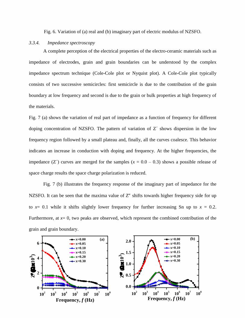
Fig. 6. Variation of (a) real and (b) imaginary part of electric modulus of NZSFO.
3.3.4. Impedance spectroscopy
A complete perception of the electrical properties of the electro-ceramic materials such as
impedance of electrodes, grain and grain boundaries can be understood by the complex
impedance spectrum technique (Cole-Cole plot or Nyquist plot). A Cole-Cole plot typically
consists of two successive semicircles: first semicircle is due to the contribution of the grain
boundary at low frequency and second is due to the grain or bulk properties at high frequency of
the materials.
Fig. 7 (a) shows the variation of real part of impedance as a function of frequency for different
doping concentration of NZSFO. The pattern of variation of Z´ shows dispersion in the low
frequency region followed by a small plateau and, finally, all the curves coalesce. This behavior
indicates an increase in conduction with doping and frequency. At the higher frequencies, the
impedance (Z´) curves are merged for the samples (x = 0.0 – 0.3) shows a possible release of
space charge results the space charge polarization is reduced.
Fig. 7 (b) illustrates the frequency response of the imaginary part of impedance for the
NZSFO. It can be seen that the maxima value of Z shifts towards higher frequency side for up
to x= 0.1 while it shifts slightly lower frequency for further increasing Sn up to x = 0.2.
Furthermore, at x= 0, two peaks are observed, which represent the combined contribution of the
grain and grain boundary.
102
103
104
105
106
107
108
0
2
4
6
Z (
1
03)
Frequency, f (Hz)
x=0.00
x=0.05
x=0.10
x=0.15
x=0.20
x=0.30
(a)
102
103
104
105
106
107
108
0.0
0.5
1.0
1.5
2.0
Frequency, f (Hz)
Z (
10
3)
x=0.00
x=0.05
x=0.10
x=0.15
x=0.20
x=0.30
(b)

Fig. 7. Variation of (a) real and (b) imaginary part of complex impedance of NZSFO.
The complex impedance spectra (Cole-Cole plot) of the sample measured for different Sn
concentration are shown in Fig. 8(a). The Cole-Cole plot typically shows two partially
overlapping semicircular arcs at low temperatures with center lying slightly below the real axis
suggesting the departure from ideal Debye type of relaxation process. Two very clear
semicircular arcs have been observed for x = 0.0 for NZFO, whereas only one semicircular arc is
observed for NZSFO (x = 0.05, 0.1, 0.15, 0.2 and 0.3). The presence of one of the semicircular
arcs is diminished with the introduction of Sn concentration. The observed two overlapping
semicircular arcs for pure NZFO are due to the contribution of the grain (bulk) and grain
boundary to electrical properties of the material [5]. The contribution of grains is dominant in the
NZSFO samples leading to a single semicircular arc. It can be understood that grain size
(diameter) increases with increasing Sn contents in the NZSFO [shown in Fig. 2 (b)] which
means grain boundary decreases. The contribution of grain boundary is also decreased results
one semicircle in the NZSFO samples. Fig. 8 (b) represents the RC equivalent circuit for single
semicircle for the NZSFO samples.
(b)
Fig. 8. (a) Cole-Cole plot of the NZSFO (b) equivalent model circuit for single semicircle Cole-
Cole plot.
0 1 2 3 4 5 6 7
0.0
0.5
1.0
1.5
2.0
Z(
1
03)
Z(103)
x=0.00
x=0.05
x=0.10
x=0.15
x=0.20
x=0.30
(a) Rg
Cg
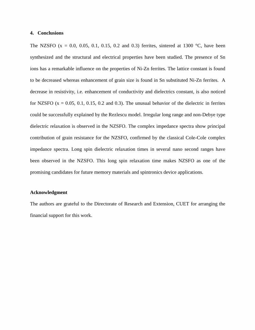
4. Conclusions
The NZSFO (x = 0.0, 0.05, 0.1, 0.15, 0.2 and 0.3) ferrites, sintered at 1300 °C, have been
synthesized and the structural and electrical properties have been studied. The presence of Sn
ions has a remarkable influence on the properties of Ni-Zn ferrites. The lattice constant is found
to be decreased whereas enhancement of grain size is found in Sn substituted Ni-Zn ferrites. A
decrease in resistivity, i.e. enhancement of conductivity and dielectrics constant, is also noticed
for NZSFO (x = 0.05, 0.1, 0.15, 0.2 and 0.3). The unusual behavior of the dielectric in ferrites
could be successfully explained by the Rezlescu model. Irregular long range and non-Debye type
dielectric relaxation is observed in the NZSFO. The complex impedance spectra show principal
contribution of grain resistance for the NZSFO, confirmed by the classical Cole-Cole complex
impedance spectra. Long spin dielectric relaxation times in several nano second ranges have
been observed in the NZSFO. This long spin relaxation time makes NZSFO as one of the
promising candidates for future memory materials and spintronics device applications.
Acknowledgment
The authors are grateful to the Directorate of Research and Extension, CUET for arranging the
financial support for this work.

References
[1] Q. Chen, P. Du, W. Huang, L. Jin, W. Weng, G. Han, Appl. Phys. Lett. 90 (2007) 132907.
[2] M. Sugimoto, Ceram. J. Am. Soc. 82 (2) (1999) 269.
[3] J. Smit, H.P.G. Wijn, Ferrites (1959) 136.
[4] W. Eerenstein, N.D. Mathur, J.F. Scott, Nature 442 (2006)759.
M.A. Ali, M.N.I. Khan, F.-U.-Z. Chowdhury, S. Akhter, M.M. Uddin, J. Sci. Res. 7 (2015)
65.
[5] D.C. Khan, M. Misra, A.R. Das, J. Appl. Phys. 53 (1982) 2722.
[6] A.R. Das, V.S. Ananthan, D.C. Khan, J. Appl. Phys. 57 (1985) 4189.
[7] D.C. Khan, M. Misra, Bull. Mater. Sci. 7(1985) 253.
[8] D.C. Khan, R.C. Srivastava, A.R. Das, J. Phys.:Condens. Matter 4 (1992) 1379.
[9] P.K. Maskar, S.V. Kakatkar, R.S. Patil, V.A. Jadhav, N.D. Chaudhari, A.M. Sankpal, S.R.
Sawant, Mater. Chem. Phys. 41 (1995) 156157.
[10] M. Pal, P. Brahma, D. Chakravorty, J. Magn. Magn. Mater. 152 (1996) 370.
[11] O.G. Mundada, K.M. Jadhav, G.K. Bichile, J. Mater. Sci. Lett. 16 (1997) 432.
[12] B.P. Rao, K.H. Rao, K. Trinadh, O.F. Caltun, J. Optoelectr. Adv. Mater. 6 (2004) 951.
[13] K. Sun, Z. Lan, Z. Yu, L. Li, J. Huang, Japanese J. Appl. Phys. 47 (2008) 7871.
[14] A. Kumar, Annveer, M. Arora, M.S. Yadav, R.P. Pant, Phys. Proc. 9 (2010) 20.
[15] S. Hua, Z. Huai-wu, T. Xiao-li, J. Yu-lan, Trans. Nonferrous Met. Soc. China 21 (2011)
109.
[16] M. Kaiser, Physica B 407 (2012) 606.
[17] B. Kaur, M. Arora, A. Shankar, A.K. Srivastava R.P. Pant, Adv. Mat. Lett., 3 (2012) 399.
[18] M. Hashim, Alimuddin, S. Kumar, S. Ali, B.H. Koo, H. Chung, R. Kumar, J. Alloy. Comp.
511 (2012) 107.
[19] A. Mandal, D. Ghosh, A. Malas, P. Pal, C.K. Das, J. Engg. Art. ID 391083 (2013) 1.
[20] V.A. Bokav, G.V. Novikov, Y.G. Saksonov, V.T. Trukhtanov, S.T. Yuschchuk, Sov. Phys.
Solid State 16 (1975) 2364.
[21] C.C. Homes, T. Vogt, S.M. Shapiro, S. Wakimoto, A.P. Ramirez, Science 293 (2001) 673.
[22] C.C. Homes, T. Vogt, S.M. Shapiro, S. Wakimoto, M.A. Subramanian, A.P. Ramirez,
Phys. Rev. B 67 (2003) 092106.
[23] S. Balaji, R.K. Selvan, L.J. Berchmans, S. Angappan, K. Subramanian, C.O. Augustin,
Mater. Sci. Eng. B 119 (2005) 119.
[24] S.A. Mazen, M.H. Abdallah, R.I. Nakhla, H.M. Zaki, F. Metaw, Mater. Chem. Phys., 34
(1993) 35.
[25] M. Panatage, S.E. Shirsath, B.G. Toksha, S. Jadhab, S.J. Sukla, K.M. Jadhab, Appl. Phys.
A 95 (2009) 429.
[26] A. Globus, H. Pascard, V. Cagan, J. Phys. Colloques, 38 (1977) C1-163-C1-168.
[27] M.A. Hakim, S.K. Nath, S.S. Sikder, K.H. Maria, J. Phys. Chem. Solids, 74 (2013) 1316.
[28] L. Vegard, Phys. Astro. 5 (1921) 17.
[29] A.K.M. Akther Hossain, “Investigation of colossal magnetoresistance in bulk and thick
film magnetites,” Ph. D. Thesis, Imperial College, London, (1998).
[30] A. Verma, R. Chatterjee, J. Magn. Magn. Mater. 306 (2006) 313.
[31] M.E. McHenry, D.E. Laughlin, Acta Mater. 48 (2000) 223.
[32] S.P. Chaudhuri, S.K. Patra, A.K. Chakraborty, J. Euro. Ceram. Soc. 19 (1999) 2941.
[33] Z.Y. Li, B.G. Liu, K.C. Zhou, D. Zhang, L. Zhang, Mater. Res. Bull. 45 (2010) 1668.
[34] Z. Yue, J. Zhou, L. Li, X. Wang, Z. Gui, Mater. Sci. Engg. 86 (2001) 64.

[35] K.W. Wagner, Analen der. Physik., 345 (1913) 817.
[36] J.C. Maxwell, A Treatise on Electricity and Magnetism. Clarendon Press, Oxford, (1982).
[37] P. Reddy, T. Rao, J. Less-Common Met. 86 (1982) 255.
[38] B. Kumar, G. Srivastava, J. Appl. Phys. 75 (1994) 6115.
[39] S. Baijal, C. Prakash, P. Kishan, K.K. Laroia, J Phys C 17 (1984) 5993.
[40] A. Sutka, K.A. Gross, G. Mezinskis, G. Bebris, M. Knite, Phys. Scr. 83 (2011) 025601.
[41] C.G. Koops, Phys. Rev. 83 (1951) 121.
[42] V.R. Murthy, J. Sobnandari, Phys. Stat. Sol. (a) 36 (1976) K133.
[43] N. Rezlescu, E. Rezlescu, Phys. Stat. Sol. (a) 23 (1974) 575.
[44] L.G.V. Uitert, J. Chem. Phys. 23 (1955) 1883.
[45] J.R. Macdonald, Impedance Spectroscopy: Emphasizing Solid State Material and Systems,
Wiley, New York, (1987).
[46] K.P. Padmasree, D.D. Kanchan, A.R. Kulkami, Solid State Ionics 177 (2006) 475.

Table Caption
Table 1 Variations of lattice parameter, X-ray density, bulk density, average grain size, porosity
and activation energy of (NZSFO).
Figure Captions
Fig. 1. The X-ray diffraction patterns of NZSFO (x = 0.0, 0.05, 0.1, 0.15, 0.2 and 0.3) ferrites
samples.
Fig. 2. (a) The experimental and theoretical lattice constants; (b) the average grain size as a
function of Sn concentration (x = 0.0, 0.05, 0.1, 0.15, 0.2 and 0.3) of NZSFO ferrites.
Fig. 3. SEM micrographs of the NZSFO ferrite for (a) x = 0.0, (b) x = 0.05, (c) x = 0.1, (d) x =
0.15, (e) x = 0.2, and (f) x = 0.3.
Fig. 4. (a) Variation of resistivity as a function of temperature and (b) log vs. 1000/T graph for
different Sn concentration.
Fig. 5. Frequency dependence of (a) dielectric constants and (b) dielectric loss tangent for
different Sn concentration. [Inset: formation of peaks].
Fig. 6. Variation of (a) real and (b) imaginary part of electric modulus of NZSFO.
Fig. 7. Variation of (a) real and (b) imaginary part of complex impedance of NZSFO.
Fig. 8. (a) Cole-Cole plot of the NZSFO (b) equivalent model circuit for single semicircle Cole-
Cole plot.
(g)
(i)
(g)
(i)