Hardware Implementation of The Message Digest Procedure MDP-384
10
IJCSNS International Journal of Computer Science and Network Security, VOL.10 No.12, December 2010 5 Manuscript received December 5, 2010 Manuscript revised December 20, 2010 Hardware Implementation of The Message Digest Procedure MDP-384 Rabie Mahmoud 1 , Magdy Saeb 2 1 Department of Mathematics, Faculty of Science, Cairo University, Cairo, Egypt. 2 Computer Engineering Department, Arab Academy for Science, Tech. & Maritime Transport (AAST), Alexandria, Egypt. ABSTRACT The message digest procedure MDP-384 is a cryptographic hash function improvement of the hash function MDP-192 which is based on the principles provided by Markel’s work, Rivest MD-5, SHA-1 and RIPEMD. MDP-384 accepts a variable-size input message and returns a fixed-size string as 384-bit long hash that utilizes twelve variables for the round function with cascaded XOR operations and deliberate asymmetry in the design structure to provide higher security with negligible increase in execution time and memory requirement. In this work, we provide a Field Programmable Gate Array (FPGA) hardware implementation of this hash function. Keywords: FPGA, Hash function, MDP-384, Cryptography, Hardware. 1. Introduction The message digest procedure MDP-384 is a one-way function having the attributes of cryptographic hash function and can be applied in many applications of computer communication security as message tampering detection, message authentication codes, digital signatures, user authentication when used with a secret key, code recognition for protecting original codes, malware identification, commitment schemes, key update and derivation, cryptographic primitive for block and stream ciphers, detection of random errors, and finally random number generation which is used in stone metamorphic cipher. The details of the stone metamorphic cipher and its FPGA implementation can be found in [1] and [2] respectively. MDP-384 modified and based on the provided principles of the hash function MDP-192 where twelve variables instead of six variables in MDP-192 are used for the round function. The principles similar to those used by SHA-1 of the Secure Hash Standard (SHS) of the US Federal Information Processing Standard Publications (FIPS PUB 180-3) [3], [4] ,[5], the design objectives of MD-2, MD-4, and MD-5 [6], [5], [7] developed by Ron Rivest, RIPEMD-160 [8], and Merkle, in his dissertation [9] are adopted in MDP-192 and MDP-384. The main improvements which included in MDP-384 to be more secure than MDP-192 are: ● The increased size of the hash; that is 384 bits compared to 192, 128 and 160 bits for the MDP-192, MD-5 and SHA-1 schemes respectively. The security bits have been increased from 64, 80 and 96 to 192 bits in MDP-384. ● The other improvement than MDP-192 is based on processing the message blocks employing twelve variables rather than six variables where this contributes to better security and faster avalanche effect. Also the hash function MDP-384 inherits all improvements of MDP-192 which are: ● The message block size is increased to 1024 bits providing faster execution times. ● The message words in the different rounds are not only permuted but computed by XOR and addition with the previous message words. This renders it harder for local changes to be confined to a few bits. In other words, individual message bits influence the computations at a large number of places. This, in turn, provides faster avalanche effect and added security. ● Moreover, adding two nonlinear functions and one of the variables to compute another variable, not only eliminates the possibility of certain attacks but also provides faster data diffusion. ● The XOR and addition operations do not cause appreciable execution delays for today’s processors. Nevertheless, the number of rotation operations, in each branch, has been optimized to provide fast avalanche with minimum overall execution delays [10]. In the following sections, we provide the conventional method of using a hash as message authentication code, the formal description of MDP-384 algorithm, the details of our circuit design, discussion of the results of the FPGA implementation and finally a summary and our conclusions.
-
Upload
independent -
Category
Documents
-
view
0 -
download
0
Transcript of Hardware Implementation of The Message Digest Procedure MDP-384

IJCSNS International Journal of Computer Science and Network Security, VOL.10 No.12, December 2010
5
Manuscript received December 5, 2010 Manuscript revised December 20, 2010
Hardware Implementation of The Message Digest Procedure MDP-384
Rabie Mahmoud1, Magdy Saeb2 1Department of Mathematics, Faculty of Science, Cairo University, Cairo, Egypt.
2Computer Engineering Department, Arab Academy for Science, Tech. & Maritime Transport (AAST), Alexandria, Egypt.
ABSTRACT The message digest procedure MDP-384 is a cryptographic hash function improvement of the hash function MDP-192 which is based on the principles provided by Markel’s work, Rivest MD-5, SHA-1 and RIPEMD. MDP-384 accepts a variable-size input message and returns a fixed-size string as 384-bit long hash that utilizes twelve variables for the round function with cascaded XOR operations and deliberate asymmetry in the design structure to provide higher security with negligible increase in execution time and memory requirement. In this work, we provide a Field Programmable Gate Array (FPGA) hardware implementation of this hash function. Keywords: FPGA, Hash function, MDP-384, Cryptography, Hardware.
1. Introduction
The message digest procedure MDP-384 is a one-way function having the attributes of cryptographic hash function and can be applied in many applications of computer communication security as message tampering detection, message authentication codes, digital signatures, user authentication when used with a secret key, code recognition for protecting original codes, malware identification, commitment schemes, key update and derivation, cryptographic primitive for block and stream ciphers, detection of random errors, and finally random number generation which is used in stone metamorphic cipher. The details of the stone metamorphic cipher and its FPGA implementation can be found in [1] and [2] respectively. MDP-384 modified and based on the provided principles of the hash function MDP-192 where twelve variables instead of six variables in MDP-192 are used for the round function. The principles similar to those used by SHA-1 of the Secure Hash Standard (SHS) of the US Federal Information Processing Standard Publications (FIPS PUB 180-3) [3], [4] ,[5], the design objectives of MD-2, MD-4, and MD-5 [6], [5], [7] developed by Ron Rivest, RIPEMD-160 [8], and Merkle, in his dissertation [9] are adopted in MDP-192 and MDP-384.
The main improvements which included in MDP-384 to be more secure than MDP-192 are:
● The increased size of the hash; that is 384 bits compared to 192, 128 and 160 bits for the MDP-192, MD-5 and SHA-1 schemes respectively. The security bits have been increased from 64, 80 and 96 to 192 bits in MDP-384. ● The other improvement than MDP-192 is based on processing the message blocks employing twelve variables rather than six variables where this contributes to better security and faster avalanche effect.
Also the hash function MDP-384 inherits all improvements of MDP-192 which are:
● The message block size is increased to 1024 bits providing faster execution times. ● The message words in the different rounds are not only permuted but computed by XOR and addition with the previous message words. This renders it harder for local changes to be confined to a few bits. In other words, individual message bits influence the computations at a large number of places. This, in turn, provides faster avalanche effect and added security. ● Moreover, adding two nonlinear functions and one of the variables to compute another variable, not only eliminates the possibility of certain attacks but also provides faster data diffusion. ● The XOR and addition operations do not cause appreciable execution delays for today’s processors. Nevertheless, the number of rotation operations, in each branch, has been optimized to provide fast avalanche with minimum overall execution delays [10]. In the following sections, we provide the conventional method of using a hash as message authentication code, the formal description of MDP-384 algorithm, the details of our circuit design, discussion of the results of the FPGA implementation and finally a summary and our conclusions.
IJCSNS International Journal of Computer Science and Network Security, VOL.10 No.12, December 2010
6
2. Description of The Procedure
The procedure can be summarized as follows: 1). Read a file as binary file, we call it the message (m). 2). Divide this file into a number of 1024-bit blocks
. 3). Last block will, in general, need padding to complete it
to 1024-bit block where the padding can be achieved by adding a “1” followed by as many as needed “0” then a 64-bit integer representing the original length of the message.
4). Use the algorithm of MDP-192 for all : k = 0, 1, 2, … , n. 5). Append hash to original message, encrypt and send to
destination.
3. The Algorithm
The formal description of the MDP-192 algorithm is shown in [10], and we provide a summary of message digest procedure MDP-384 as follows: The symbols in the algorithm which illustrates different actions during a process are: Symbol Mnemonic Operation
ROTL m Rotate to the left m times ADD Addition
XOR Bitwise XOR ← ASG Assigned to
AND Bitwise AND OR Bitwise OR INV Complement
Algorithm: Message Digest Procedure MDP-384 INPUT: A given set of 1024-bit blocks (M0, M1, ... , Mn
where each block is 32 32-bit words); this set of blocks represents the message to be hashed.
OUTPUT: A 384-bit hash function that is representing the original message.
Begin Repeat Begin
{For all Mk for k =1, 2, … , n} {Within each block Mk, process each word Wi as follows :}
for i = 0 to 383 {That is the reason we need to expand Wi from 32 values to 384 since each 1024-bit message Mi is only 32 32-bit words}
begin ←
; ← ; ← ; ← ;
← ; ← ; ←
; ← ; ← ; ← ; ← ; ← ;
end; {The number of rotations for each branch mi is optimized for fast avalanche effect; taken equal to 00100 for each side} Repeat this iteration loop until end-of message; {That is Repeat for all blocks Mk for k= 1, 2, … , n, until end-of-message. After processing the message, the message digest is computed by concatenating the final values of the twelve variables: Af , Bf , Cf , Df , Ef , Ff , Pf , Qf , Rf , Sf , Tf , Uf; This is a 384-bit message digest where the final values of each variable are computed as follows: }
Repeat End; ← ← ← ← ← ← ← ← ← ← ←
← End. The functions :
for i = 0 to 31;for i = 192 to 223;
for i = 32 to 63;for i = 224 to 255;
for i = 64 to 95;for i = 256 to 287;
for i = 96 to 127;for i = 288 to 319;
for i = 128 to 159;for i = 320 to 351;
for i = 160 to 191;for i = 352 to 383.

IJCSNS International Journal of Computer Science and Network Security, VOL.10 No.12, December 2010
7
The values of Wi: ← for i = 0 to 31; ←
for i = 32 to 383. Also, this algorithm is summarized in Figure 1.
Figure 1. Operation of MDP-384 hash function
The constants :
← for i = 0 to 31; ← for i = 32 to 63; ← for i = 64 to 95; ← for i = 96 to 127; ← for i = 128 to 159; ← for i = 160 to 191; ← for i = 192 to 223; ← for i = 224 to 255; ← for i = 256 to 287; ← for i = 288 to 319; ← for i = 320 to 351; ← for i = 352 to 383.
To initialize the iteration process, we used the following randomly chosen Initialization Values (IV) based on some natural unrelated constants, rather than a mathematical function:
← Based on Electron Charge; ← Based on Electron Mass; ← Based on Avogadro’s number; ← Based on Earth’s Diameter; ← Based on Earth’s Mass; ← Based on Moon’s Diameter; ← Based on Speed of Light; ← Based on Euler's Constant; ← Based on Faraday’ Constant; ← Based on Proton’s Mass; ← Based on Neutron’s Mass; ← Based on Planck's Constant.
4. FPGA Implementation
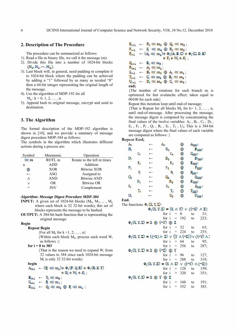
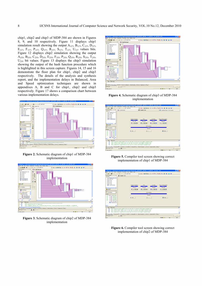
The lucidity of the message digest procedure MDP-384 lead to a relatively easy-to-design FPGA-based implementation. We have implemented the MDP-384 using VHDL hardware description language [11], [12], [13] and Quartus II 9.1 Service Pack 2 Web Edition [14], and utilizing Altera design environment. The hash function implementation is performed by dividing the procedure into three parts in order to use three FPGA devices or chips connected sequentially on the board. The first chip (chip1) is responsible for padding the 256-bit input to 1024-bit block. Subsequently, The block is divided into 32-bit words Wi; starting from the twelve initial values A0, B0, C0, D0, E0, F0, P0, Q0, R0, S0, T0, U0 to produce A127, B127, C127, D127, E127, F127, P127, Q127, R127, S127, T127, U127 values as outputs. The second chip (chip2) employs the outputs of chip1 as inputs producing A255, B255, C255, D255, E255, F255, P255, Q255, R255, S255, T255, U255 as outputs. The third chip (chip3) is used to compute the values A383, B383, C383, D383, E383, F383, P383, Q383, R383, S383, T383, U383 and then applying the last step in the algorithm by XORing the initial values with resulting values and concatenating the result values together to have a 384-bit hash block as output. The schematic diagrams for demonstrative parts of MDP-384 algorithm are shown in Figures 2, 3, and 4. The design was implemented using three EP2C70F896C6, Cyclone II family devices. Based on this device characteristic, the worst case pin-to-pin delay in chip1 was found to be equal to 1089.363 ns. The worst case pin-to-pin delay in chip2 was found to be equal to 1159.366 ns. The worst case pin-to-pin delay in chip3 was found to be equal to 1203.756 ns. A series of screen-captures of the different implementation results are shown in Figures 5 to 16. For example, Figures 5, 6, and 7 provide indication of successful compilation for chip1, chip2 and chip3 of MDP-384 respectively. In addition, parts of RTL for
IJCSNS International Journal of Computer Science and Network Security, VOL.10 No.12, December 2010
8
chip1, chip2 and chip3 of MDP-384 are shown in Figures 8, 9, and 10 respectively. Figure 11 displays chip1 simulation result showing the output A127, B127, C127, D127, E127, F127, P127, Q127, R127, S127, T127, U127 values bits. Figure 12 displays chip2 simulation showing the output A255, B255, C255, D255, E255, F255, P255, Q255, R255, S255, T255, U255 bit values. Figure 13 displays the chip3 simulation showing the output of the hash function procedure which is highlighted in this screen capture. Figures 14, 15 and 16 demonstrate the floor plan for chip1, chip2 and chip3 respectively. The details of the analysis and synthesis report, and the implementation delays in Balanced, Area and Speed optimization techniques are shown in appendixes A, B and C for chip1, chip2 and chip3 respectively. Figure 17 shows a comparison chart between various implementation delays.
Figure 2. Schematic diagram of chip1 of MDP-384 implementation
Figure 3. Schematic diagram of chip2 of MDP-384 implementation
Figure 4. Schematic diagram of chip3 of MDP-384 implementation
Figure 5. Compiler tool screen showing correct implementation of chip1 of MDP-384
Figure 6. Compiler tool screen showing correct implementation of chip2 of MDP-384

IJCSNS International Journal of Computer Science and Network Security, VOL.10 No.12, December 2010
9
Figure 7. Compiler tool screen showing correct implementation of chip3 of MDP-384
Figure 8. RTL screen for part of chip1 of MDP-384 implementation
Figure 9. RTL screen for part of chip2 of MDP-384 implementation
Figure 10. RTL screen for part of chip3 of MDP-384 implementation
Figure 11. Simulator screen showing the outputs of chip1 of MDP-384
Figure 12. Simulator screen showing the outputs of chip2 of MDP-384

IJCSNS International Journal of Computer Science and Network Security, VOL.10 No.12, December 2010
10
Figure 13. Simulator screen showing the hash MDP-384
Figure 14. Floor-plan of chip1 implementation
Figure 15. Floor-plan of chip2 implementation
Figure 16. Floor-plan of chip3 implementation
Figure 17. Delays in our design of the MDP-384 implementation
Summary & Conclusion
We have furnished a brief discussion of the hardware implementation of the Message Digest Procedure MDP-384. Various modules, using three Altera Cyclone II family devices, are connected sequentially to allow for the FPGA implementation relatively high gate count. The resulting circuit provides a proof-of-concept FPGA implementation. It was shown that the worst case pin-to-pin delay in chip1 is equal to 1089.363 ns. The worst case pin-to-pin delay in chip2 is equal to 1159.366 ns. The worst case pin-to-pin delay in chip3 is equal to 1203.756 ns. The reports also indicate 87%, 89% and 94% total logic elements utilization in chip1, 2 and 3 respectively. A comparison with other implementations is not applicable since this is the first time this hash function is FPGA- implemented. This and other related issues will be dealt with in future development of the device.
IJCSNS International Journal of Computer Science and Network Security, VOL.10 No.12, December 2010
11
References
[1] Magdy Saeb, "The Stone Cipher-192 (SC-192): A Metamorphic Cipher," The International Journal on Computers and Network Security (IJCNS), Vol.1 No.2, pp. 1-7, Nov., 2009.
[2] Rabie Mahmoud, Magdy Saeb, "Hardware Implementation of the Stone Metamorphic Cipher," International Journal of Computer Science & Network Security, Vol.10, No.8, pp. 54-60, 2010.
[3] Bruce Schneier, Applied Cryptography, second edition, John Wiley & Sons Inc., 1996.
[4] Federal Information Processing Standard Publication, "Secure Hash Standard (SHS)," FIPS PUB 180-3, http://csrc.nist.gov/publications/fips/fips180-3/fips180-3_final.pdf, October 17, 2008.
[5] Paul C. van Oorschot, Alfred J. Menezes, Scott A. Vanstone, Handbook of Applied Cryptography, MIT Press, 1996.
[6] Bruce Schneier, Secrets and Lies, John Wiley & Sons Inc., 2000.
[7] Wenbo Mao, Modern Cryptography, second printing, Prentice Hall PTR, 2004.
[8] Hans Dobbertin, Antoon Bosselaers, Bart Preneel, "RIPEMD-160: A Strengthened Version of RIPEMD," Fast Software Encryption, LNCS 1039, Springer-Verlag, pp. 71.82, 1996.
[9] Ralph C. Merkle, Secrecy, Authentication and Public Key Systems, Ph.D. Dissertation, Stanford University, June, 1979.
[10] Magdy Saeb, "Design & Implementation of the Message Digest Procedures MDP-192 and MDP-384," ICCCIS2009, International Conference on Cryptography, Coding & Information Security, Paris, June 24-26, 2009.
[11] Enoch O. Hwang, Digital Logic and Microprocessor Design with VHDL, La Sierra University, Riverside, California, USA, 2005.
[12] Pong P. Chu, RTL Hardware Design Using VHDL, John Wiley & Sons, Inc., New Jersey, 2006.
[13] Volnei A. Pedroni, Circuit Design with VHDL, MIT Press, 2004.
[14] Altera’s user-support site: http://www.altera.com/support/examples/vhdl/vhdl.html
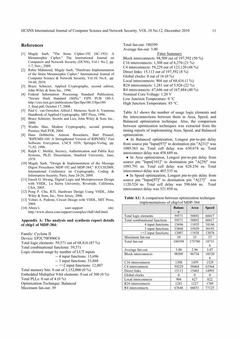
Appendix A: The analysis and synthesis report details of chip1 of MDP-384: Family: Cyclone II Device: EP2C70F896C6 Total logic elements: 59,571 out of 68,416 (87 %) Total combinational functions: 59,571 Logic element usage by number of LUT inputs
-- 4 input functions: 13,696 -- 3 input functions: 33,868 -- <=2 input functions: 12,007
Total memory bits: 0 out of 1,152,000 (0 %) Embedded Multiplier 9-bit elements: 0 out of 300 (0 %) Total PLLs: 0 out of 4 (0 %) Optimization Technique: Balanced Maximum fan-out: 39
Total fan-out: 180399 Average fan-out: 3.00
Fitter Summary Block interconnects: 98,509 out of 197,592 (50 %) C16 interconnects: 1,308 out of 6,270 (21 %) C4 interconnects: 59,229 out of 123,120 (48 %) Direct links: 15,113 out of 197,592 (8 %) Global clocks: 0 out of 16 (0 %) Local interconnects: 904 out of 68,416 (1 %) R24 interconnects: 1,281 out of 5,926 (22 %) R4 interconnects: 67,646 out of 167,484 (40 %) Nominal Core Voltage: 1.20 V Low Junction Temperature: 0 °C High Junction Temperature: 85 °C. Table A1 shows the number of usage logic elements and the interconnections between them in Area, Speed, and Balanced optimization technique. Also, the comparison between optimization techniques was extracted from the timing reports of implementing Area, Speed, and Balanced optimization. ● In Balanced optimization, Longest pin-to-pin delay from source pin "Input[97]" to destination pin "A[31]" was 1089.363 ns. Total cell delay was 630.674 ns. Total interconnect delay was 458.689 ns. ● In Area optimization, Longest pin-to-pin delay from source pin "Input[101]" to destination pin "A[29]" was 1093.791 ns. Total cell delay was 628.256 ns. Total interconnect delay was 465.535 ns. ● In Speed optimization, Longest pin-to-pin delay from source pin "Input[97]" to destination pin "A[27]" was 1120.524 ns. Total cell delay was 598.666 ns. Total interconnect delay was 521.858 ns. Table A1: A comparison between optimization technique
implementations of chip1of MDP-384 Balanc
e Area Speed
Total logic elements 59571 58892 60417Total combinational functions 59571 58892 60417
4 input functions 13696 11035 181463 input functions 33868 35929 30193
<=2 input functions 12007 11928 12078Maximum fan-out 39 35 37 Total fan-out 180399 175780 18731
6 Average fan-out 3.00 2.96 3.07 Block interconnects 98509 96734 10320
8 C16 interconnects 1308 1459 1529 C4 interconnects 59229 58464 63564Direct links 15113 15402 14993Global clocks 0 0 0 Local interconnects 904 627 822 R24 interconnects 1281 1227 1789 R4 interconnects 67646 66031 77125
IJCSNS International Journal of Computer Science and Network Security, VOL.10 No.12, December 2010
12
Appendix B: The analysis and synthesis report details of chip2 of MDP-384: Family: Cyclone II Device: EP2C70F896C6 Total logic elements: 60,740 out of 68,416 (89 %) Total combinational functions: 60,740 Logic element usage by number of LUT inputs
-- 4 input functions: 14,143 -- 3 input functions: 35,108 -- <=2 input functions: 11,489
Total memory bits: 0 out of 1,152,000 (0 %) Embedded Multiplier 9-bit elements: 0 out of 300 (0 %) Total PLLs: 0 out of 4 (0 %) Optimization Technique: Balanced Maximum fan-out: 28 Total fan-out: 184776 Average fan-out: 3.02
Fitter Summary Block interconnects: 99,603 out of 197,592 (50 %) C16 interconnects: 942 out of 6,270 (15 %) C4 interconnects: 57,565 out of 123,120 (47 %) Direct links: 15,988 out of 197,592 (8 %) Global clocks: 0 out of 16 (0 %) Local interconnects: 883 out of 68,416 (1 %) R24 interconnects: 1,339 out of 5,926 (23 %) R4 interconnects: 70,041 out of 167,484 (42 %) Table B1 shows the number of usage logic elements and the interconnections between them in Area, Speed, and Balanced optimization technique. Also, the comparison between optimization techniques was extracted from the timing reports of implementing Area, Speed, and Balanced optimization. ● In Balanced optimization, Longest pin-to-pin delay from source pin "Input[32]" to destination pin "A[31]" was 1159.366 ns. Total cell delay was 680.616 ns. Total interconnect delay was 478.750 ns. ● In Area optimization, Longest pin-to-pin delay from source pin "Input[36]" to destination pin "P[30]" was 1150.398 ns. Total cell delay was 677.351 ns. Total interconnect delay was 473.047 ns. ● In Speed optimization, Longest pin-to-pin delay from source pin "Input[32]" to destination pin "P[20]" was 1171.155 ns. Total cell delay was 671.717 ns. Total interconnect delay was 499.438 ns. Table B1: A comparison between optimization technique
implementations of chip2 of MDP-384 Balance Area Speed Total logic elements 60740 59803 62048 Total combinational functions
60740 59803 62048
4 input functions 14143 10195 20299 3 input functions 35108 38173 29835
<=2 input functions 11489 11435 11914 Maximum fan-out 28 26 30 Total fan-out 184776 178071 194431Average fan-out 3.02 2.95 3.11 Block interconnects 99603 96675 105328C16 interconnects 942 893 1327 C4 interconnects 57565 55571 63353 Direct links 15988 15607 15801 Global clocks 0 0 0 Local interconnects 883 718 1096 R24 interconnects 1339 1119 1888 R4 interconnects 70041 66083 79269
Appendix C: The analysis and synthesis report details of chip3 of MDP-384: Family: Cyclone II Device: EP2C70F896C6 Total logic elements: 64,479 out of 68,416 (94 %) Total combinational functions: 64,479 Logic element usage by number of LUT inputs
-- 4 input functions: 14,583 -- 3 input functions: 34,544 -- <=2 input functions: 15,352
Total memory bits: 0 out of 1,152,000 (0 %) Embedded Multiplier 9-bit elements: 0 out of 300 (0 %) Total PLLs: 0 out of 4 (0 %) Optimization Technique: Balanced Maximum fan-out: 25 Total fan-out: 192436 Average fan-out: 2.97
Fitter Summary
Block interconnects: 103,679 out of 197,592 (52 %) C16 interconnects: 1,164 out of 6,270 (19 %) C4 interconnects: 60,876 out of 123,120 (49 %) Direct links: 18,265 out of 197,592 (9 %) Global clocks: 0 out of 16 (0 %) Local interconnects: 688 out of 68,416 (1 %) R24 interconnects: 1,305 out of 5,926 (22 %) R4 interconnects: 70,453 out of 167,484 (42 %) Nominal Core Voltage: 1.20 V Low Junction Temperature: 0 °C High Junction Temperature: 85 °C. Table C1 shows the number of usage logic elements and the interconnections between them in Area, Speed, and Balanced optimization technique. Also, the comparison between optimization techniques was extracted from the timing reports of implementing Area, Speed, and Balanced optimization. ● In Balanced optimization, Longest pin-to-pin delay from source pin "Input[96]" to destination pin "Output[254]" was 1203.756 ns. Total cell delay was 686.548 ns. Total interconnect delay was 517.208 ns. ● In Area optimization, Longest pin-to-pin delay from source pin "Input[34]" to destination pin "Output[254]"
IJCSNS International Journal of Computer Science and Network Security, VOL.10 No.12, December 2010
13
was 1191.374 ns. Total cell delay was 683.596 ns. Total interconnect delay was 507.778 ns. ● In Speed optimization, Longest pin-to-pin delay from source pin "Input[98]" to destination pin "Output[54]" was 1213.668 ns. Total cell delay was 658.809 ns. Total interconnect delay was 554.859 ns. Table C1: A comparison between optimization technique
implementations of chip3 of MDP-384 Balanc
e Area Speed
Total logic elements 64479 63413 65627 Total combinational functions
64479 63413 65627
4 input functions 14583 10125 19945 3 input functions 34544 38108 29930
<=2 input functions 15352 15180 15752 Maximum fan-out 25 26 29 Total fan-out 192436 184952 200842 Average fan-out 2.97 2.90 3.04 Block interconnects 103679 100898 108563 C16 interconnects 1164 726 1420 C4 interconnects 60876 55432 66769 Direct links 18265 18173 17526 Global clocks 0 0 0 Local interconnects 688 324 979 R24 interconnects 1305 1235 1556 R4 interconnects 70453 67713 78926
Appendix D: Sample VHDL code for a MDP-1 module of hash function LIBRARY ieee; USE ieee.std_logic_1164.all; USE ieee.std_logic_arith.all; USE ieee.std_logic_unsigned.all; USE ieee.numeric_std.all; ENTITY MDP_1 IS Port (input_to_hash : in std_logic_vector (1023 downto 0); M_D_P_1 : out std_logic_vector (383 downto 0)); END MDP_1; ARCHITECTURE behavioral OF MDP_1 IS signal W0 : std_logic_vector (31 downto 0); signal K0 : std_logic_vector(31 downto 0) := "01100000011100010100100110001111"; signal A0 : std_logic_vector(31 downto 0) := "01011111011111110100010111001100"; signal B0 : std_logic_vector(31 downto 0) := "00110110010010111101000001001100"; signal C0 : std_logic_vector(31 downto 0) :=
"00100011111001010000111001110000"; signal D0 : std_logic_vector(31 downto 0) := "01001100000010000001110010000000"; signal E0 : std_logic_vector(31 downto 0) := "00100011100110111110011111101001"; signal F0 : std_logic_vector(31 downto 0) := "00010100101101111111010010000000"; signal P0 : std_logic_vector(31 downto 0) := "00010001110111100111100001001010"; signal Q0 : std_logic_vector(31 downto 0) := "00100010011001111001110010110001"; signal R0 : std_logic_vector(31 downto 0) := "00111001100000100111111010000111"; signal S0 : std_logic_vector(31 downto 0) := "01100011101100100010111001000101"; signal T0 : std_logic_vector(31 downto 0) := "01100011110101010101110001101011"; signal U0 : std_logic_vector(31 downto 0) := "00100111011111101001010000110000"; signal A1, B1,C1, D1, E1, F1, P1,Q1, R1, S1, T1, U1
: std_logic_vector(31 downto 0); BEGIN W0 <= input_to_hash (1023 downto 992); A1 <= (P0(30 downto 0) & P0(31)) + ((P0 and Q0) or
((not P0) and R0)) + ((R0 and S0) or ((not R0) and T0)) + U0 + W0 + K0;
B1 <= (T0(26 downto 0) & T0(31) & T0(30) & T0(29) & T0(28) & T0(27));
C1 <= (P0(30 downto 0) & P0(31)); D1 <= (Q0(29 downto 0) & Q0(31) & Q0(30)) xor (P0(30
downto 0) & P0(31)); E1 <= (R0(28 downto 0) & R0(31)& R0(30) & R0(29))
xor (Q0(29 downto 0) & Q0(31) & Q0(30)); F1 <= (S0(27 downto 0) & S0(31) & S0(30) & S0(29) &
S0(28)) xor (R0(28 downto 0) & R0(31) & R0(30) & R0(29));
P1 <= (A0(30 downto 0) & A0(31)) + ((A0 and B0) or ((not A0) and C0)) + ((C0 and D0) or ((not C0) and E0)) + F0 + W0 + K0;
Q1 <= (E0(26 downto 0) & E0(31) & E0(30) & E0(29) & E0(28) & E0(27));
R1 <= (A0(30 downto 0) & A0(31)); S1 <= (B0(29 downto 0) & B0(31) & B0(30)) xor (A0(30
downto 0) & A0(31)); T1 <= (C0(28 downto 0) & C0(31) &C0(30) & C0(29))
xor (B0(29 downto 0) & B0(31) & B0(30)); U1 <= (D0(27 downto 0) & D0(31) & D0(30) & D0(29) &
D0(28)) xor (C0(28 downto 0) & C0(31) & C0(30) & C0(29));
M_D_P_1 <= A1 & B1 & C1 & D1 & E1 & F1 & P1 &
Q1 & R1 & S1 & T1 & U1; END behavioral;

IJCSNS International Journal of Computer Science and Network Security, VOL.10 No.12, December 2010
14
Sample VHDL code for a MDP-352 module of hash function LIBRARY ieee; USE ieee.std_logic_1164.all; USE ieee.std_logic_arith.all; USE ieee.std_logic_unsigned.all; USE ieee.numeric_std.all; ENTITY MDP_352 IS Port (A351, B351, C351, D351, E351, F351, P351, Q351, R351, S351, T351, U351 : in std_logic_vector (31 downto 0); W319 : in std_logic_vector (31 downto 0); M_D_P_352: out std_logic_vector (383 downto 0)); END MDP_352; ARCHITECTURE behavioral OF MDP_352 IS signal K11 : std_logic_vector (31 downto 0) := "11101111110000100011100100100001"; signal A352, B352, C352, D352, E352, F352, P352, Q352, R352, S352, T352, U352: std_logic_vector (31 downto 0); BEGIN A352 <= (P351(30 downto 0) & P351(31)) + (P351 xor
Q351 xor R351) + (R351 xor S351 xor T351) + U351 + W351 + K11;
B352 <= (T351(26 downto 0) & T351(31) & T351(30) & T351(29) & T351(28) & T351(27));
C352 <= (P351(30 downto 0) & P351(31)); D352 <= (Q351(29 downto 0) & Q351(31) & Q351(30))
xor (P351(30 downto 0) & P351(31)); E352 <= (R351(28 downto 0) & R351(31) & R351(30) &
R351(29)) xor (Q351(29 downto 0) & Q351(31) & Q351(30));
F352 <= (S351(27 downto 0) & S351(31) & S351(30) & S351(29) & S351(28)) xor (R351(28 downto 0) & R351(31) & R351(30) & R351(29));
P352 <= (A351(30 downto 0) & A351(31)) + (A351 xor B351 xor C351) + (C351 xor D351 xor E351) + F351 + W351 + K11;
Q352 <= (E351(26 downto 0) & E351(31) & E351(30) & E351(29) & E351(28) & E351(27));
R352 <= (A351(30 downto 0) & A351(31)); S352 <= (B351(29 downto 0) & B351(31) & B351(30))
xor (A351(30 downto 0) & A351(31)); T352 <= (C351(28 downto 0) & C351(31) & C351(30) &
C351(29)) xor (B351(29 downto 0) & B351(31) & B351(30));
U352 <= (D351(27 downto 0) & D351(31) & D351(30) & D351(29) & D351(28)) xor (C351(28 downto 0) & C351(31) & C351(30) & C351(29));
M_D_P_352 <= A352 & B352 & C352 & D352 & E352 & F352 & P352 & Q352 & R352 & S352 & T352 & U352;
END behavioral;
Magdy Saeb received the BSEE, School of Engineering, Cairo University, in 1974, the MSEE, and Ph.D. degrees in Electrical & Computer Engineering, University of California, Irvine, in 1981 and 1985, respectively. He was with Kaiser Aerospace and Electronics, Irvine California, and The Atomic Energy Establishment, Anshas, Egypt. Currently, he is a professor in the Department of Computer Engineering, Arab Academy for Science, Technology
& Maritime Transport, Alexandria, Egypt; He was on-leave working as a principal researcher in the Malaysian Institute of Microelectronic Systems (MIMOS). His current research interests include Cryptography, FPGA Implementations of Cryptography and Steganography Data Security Techniques, Encryption Processors, Mobile Agent Security.
Rabie Mahmoud received the BS. Degree, Faculty of Science, Tishreen University, Syria, in 2001, the MS. in Computational Science, Faculty of Science, Cairo University, Egypt, in 2007. Currently, he is working on his Ph.D. Dissertation in the Department of Mathematics, Faculty of Science, Cairo University, His current interests include Image processing, Cryptography, FPGA Implementations of Cryptography and
Data Security Techniques.