Satellite Cognitive Communications: Interference Modeling ...
Upload
khangminh22Category
view
1download
0
NPL Report DFS 129
Guidance onEliminating Interference from Sensitive
Electrical Circuits
B P Kibble and I A RobinsonDivision of Electrical ScienceNational Physical Laboratory
T eddingtonMiddlesex, UK, TWll OLW
ABSTRACT

@ Crown Copyright 1993
ISSN 0143-7305
National Physical LaboratoryTeddington, Middlesex, UK, TWll OLW
No extracts from report may be produced without the prior written consent of the ChiefExecutive, National Physical Laboratory; the source must be acknowledged.
Approved on behalf of Chief Executive, NPL,by Dr T G Blaney, Head, Division of Electrical Science
NPL Report DES 129
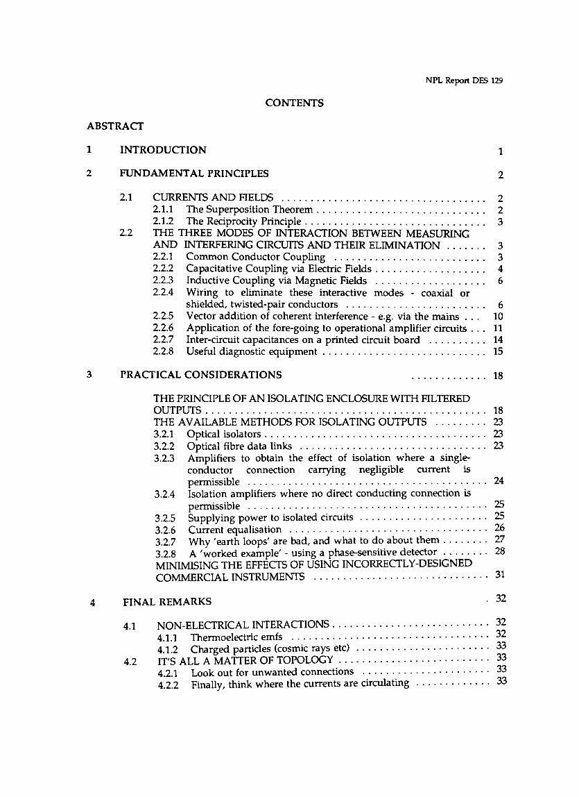
CONTENTS
ABSTRACT
1 INTRODUCfION 1
2 FUNDAMENTAL PRINCIPLES 2
2.1 223
2.23346
610111415
CURRENI'SANDFIELDS 2.1.1 The Superposition Theorem. 2.1.2 TheReciprocityPrinciple THE THREE MODES OF INTERACTION BETWEEN MEASURING
AND INTERFERING CIRCUITS AND THEIR ELIMINA nON. 2.2.1 Common Conductor Coupling 2.2.2 Capacitative Coupling via Electric Fields. 2.2.3 Inductive Coupling via Magnetic Fields. 2.2.4 Wiring to eliminate these interactive modes -coaxial or
shielded, twisted-pair conductors. 2.2.5 Vector addition of coherent interference -e.g. via the mains. ..
2.2.6 Application of the fore-going to operational amplifier circuits. ..
2.2.7 Inter-circuit capacitances on a printed circuit board. 2.2.8 Useful diagnostic equipment ,.""""",."",.,.""..
3 PRACTICAL CONSIDERATIONS 18
~~
THE PRINCIPLE OF AN ISOLATING ENCLOSURE WITH FILTEREDOUTPUTS. 18THE AVAILABLE METHODS FOR ISOLATING OUTPUTS. 233.2.1 Optical isolators 233.2.2 Opticalfibredatalinks 233.2.3 Amplifiers to obtain the effect of isolation where a single-
conductor connection carrying negligible current ispermissible 24
3.2.4 Isolation amplifiers where no direct conducting connection ispermissible. 25
3.2.5 Supplying power to isolated circuits. 253.2.6 Current equalisation 263.2.7 Why 'earth loops' are bad, and what to do about them. 273.2.8 A 'worked example' -using a phase-sensitive detector. 28MINIMISING THE EFFECTS OF USING INCORRECTLY-DESIGNEDCOMMERCIAL INSTRUMENTS 31
~
.32FINAL REMARKS4
323233333333
4.1
4.2
NON-ELECTRICAL INTERACTIONS. 4.1.1 Thermoelectricemfs 4.1.2 Charged particles (cosmic rays etc) IT'S ALL A MATTER OF TOPOLOGY. 4.2.1 Look out for unwanted connections. 4.2.2 Finally, think where the currents are circulating. ...
NPL Report DFS 129
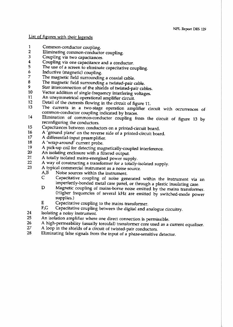
List of fi&Jdres with their legends
12345678910111213
14
151617181920212223
2425262728
Common-conductor coupling.Eliminating common-conductor coupling.Coupling via two capacitances.Coupling via one capacitance and a conductor.The use of a screen to eliminate capacitative coupling.Inductive (magnetic) coupling.The magnetic field surrounding a coaxial cable.The magnetic field surrounding a twisted-pair cable.Star interconnection of the shields of twisted-pair cables.Vector addition of single-frequency interfering voltages.An unsymmetrical operational amplifier circuit.Detail of the currents flowing in the circuit of figure 11.The currents in a two-stage operation amplifier circuit with occurrences ofcommon-conductor coupling indicated by braces.Elimination of common-conductor coupling from the circuit of figure 13 byreconfiguring the conductors.Capacitances between conductors on a printed-circuit board.A 'ground plane' on the reverse side of a printed-circuit board.A differential-input preamplifier.A 'wrap-around' current probe.A pick-up coil for detecting magnetically-coupled interference.An isolating enclosure with a filtered output.A totally isolated mains-energised power supply.A way of constructing a transformer for a totally-isolated supply.A typical commercial instrument as a noise source.A,B Noise sources within the instrument.C Capacitative coupling of noise generated within the instrument via an
imperfectly-bonded metal case panel, or through a plastic insulating case.D Magnetic coupling of mains-borne noise emitted by the mains transformer.
(Higher frequencies of several kHz are emitted by switched-mode powersupplies.)
E Capacitative coupling to the mains transformer.F,G Capacitative coupling between the digital and analogue circuitry.Isolating a noisy instrument.An isolation amplifier where one direct connection is permissible.A high-permeability (usually toroidal) transformer core used as a current equaliser.A loop in the shields of a circuit of twisted-pair conductors.Eliminating false signals from the input of a phase-sensitive detector.

NPL Report DES 1291 INTRODUCTION
1

NPL Report DES 129
2 FUNDAMENTAL PRINCIPLES
2.1 CURRENTS AND FIELDS
It is helpful to visualise the circulatin~ currents and the magnetic fiE~ to which they giverise, and the electricall2otentials of conductors and the electric fields emanating from them,as the physically real entities. It is in many ways unfortunate th.it the vast majority ofelectrical test and measuring instruments (for example, voltmeb~rs, oscilloscopes andspectrum analysers) are regarded as responding to an input volta~e. and these are what isused to explore conditions in a circuit. It is easy to forget that the volt:ages recorded are onlymanifestations of currents flowing through impedances in their circulating paths. It isimportant to bear in mind at all times the elementary, but crucial, principle that:-
CURRENTS FLOW AROUND COMPLETE CIRC1JITS.
They can be envisaged as starting out from a source -a battery, power supply, signalgenerator, an emf generated between the ends of a conductor in which another current iscirculating, or whatever, -but having traversed a possibly very complicated network ofconductors and impedances, they!DJ:!§! return in their entirety to that source. Do not permityourself to think that they go to 'ground' or 'earth' and disappear!
It follows that the actual conductors which are represented by ~ symbols have flowing inthem currents returning to their source. Therefore, unless they are superconductors and thecurrent is DC, they cannot be at the same potential. This can most certainly matter insensitive circuits. The actual return conductors, and the precise po:ints at which they areinterconnected should be drawn and considered together with the currents flowing in them.Particular care should be taken to represent the topology of the connections of the actualcircuit correctly. We return to this matter in discussing common-conductor coupling insection 2.2.1.
We have found it helpful also to replace the words 'earth' or 'ground' in our vocabularywith more specific terms such as 'current return conductor', 'instrument case', 'mains(green/yellow) safety wire' etc. as appropriate, and to designate a particular node of anetwork as a potential reference point to which all voltages are understood to be referred.The time spent in thinking in this more precise way will be amply repaid, particularly ineliminating common-conductor couplings.
2.1.1 The Superposition Theorem
In a network of ~ circuit elements -for example, impedances, sub-circuits and sources-in which the current traversing them is proportional to the voltage across them, the currentarising from each individual source behaves as if no other currents ~'ere ~resent.
This theorem, properly appreciated and applied, is an extremely powerful and useful mentaltool as it permits the untangling of many complex situations. It should be borne in mind atall times when considering interference elimination.
2

NPL Report DF5 1292.1.2
MEASURING AND
3
NPL Report DES 129
Figure 2 Eliminating common-conductor coupling
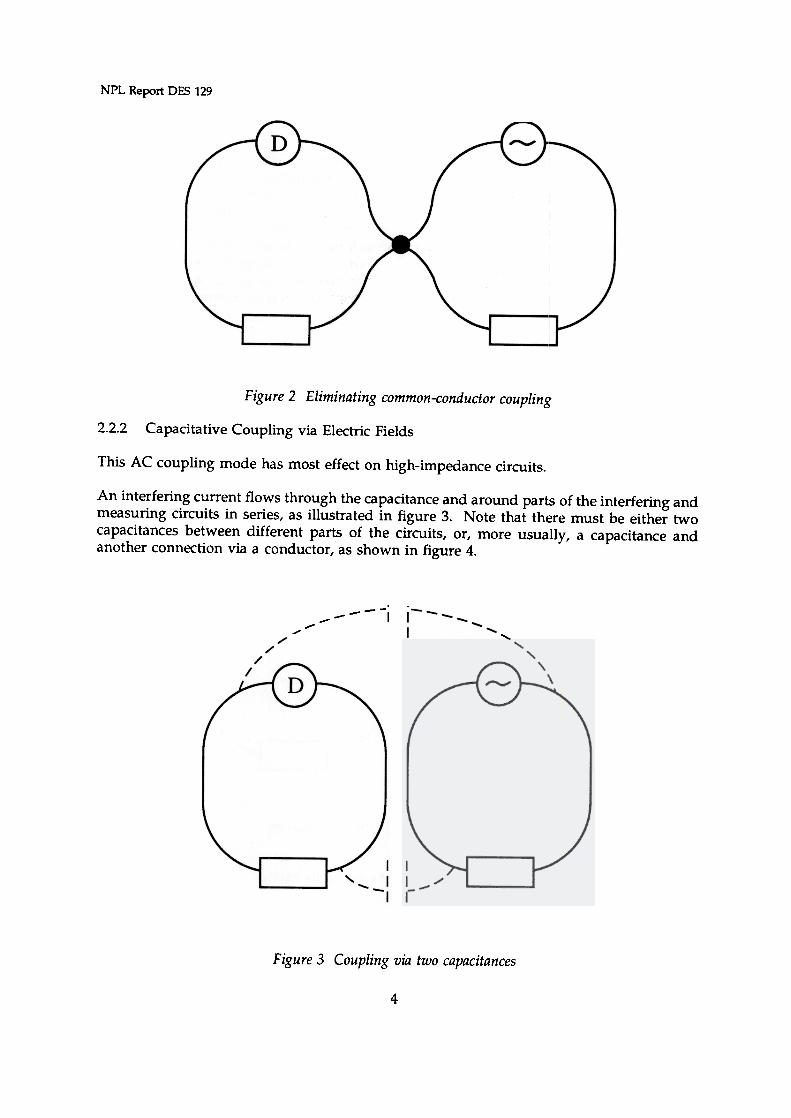
2.2.2 Capacitative Coupling via Electric Fields
This AC coupling mode has most effect on high-impedance circuits.
An interfering current flows through the capacitance and around parts of the interfering andmeasuring circuits in series, as illustrated in figure 3. Note that there must be either twocapacitances between different parts of the circuits, or, more usually, a capacitance andanother connection via a conductor, as shown in figure 4.
--'I
~~~
Figure 3 Coupling via two capacitances
4

NPL Report DES 129
I I I--I--
I I I---I 1--
~
,..
5

NPL Report DES 129
Subtle causes of capacitative interaction occur in practice. For example, the panels of aninstrument case may be prevented from being connected to each other by paint or bydeliberate or age-induced anodising. Capacitance from outside sources to the case panelswill be in series with capacitance from the panel to various parts of the interior circuitry.Capacitative currents can also be led to the interior of the case via protruding controls,switches and indicators if these are not connected to the case in some way.
Inductive Coupling via Magnetic Fields
This AC coupling mode has most effect on low-impedance circuits.
A proportion of a magnetic field generated by the interfering circuit may thread themeasuring circuit, as illustrated in figure 6, resulting in mutual inductive coupling betweenthem. Reduction of this coupling depends upon arranging the conductors of either theinterfering, or the measuring network, or preferably both, in such a way that each and everyreturn current path is routed adjacent to the corresponding outward current path as shownin figure 7 by using either twisted or coaxial conductor-pairs (see the next section).
Figure 6 Inductive (magnetic) coupling Figure 7 Eliminating inductive coupling
Wiring to eliminate these interactive modes -coaxial or shielded, twisted-pairconductors
Consider a portion of a straight coaxial cable, as illustrated in figure 8. Suppose by sometechnique (discussed later in section 3.2.6), the current traversing the outer conductor ismade to be equal and opposite to that traversing the inner. Since the total current in thecable as a whole is zero, by Ampere's law the line integral of magnetic field around a closedpath threaded by the cable is zero. If this path is taken to be circular with the cable as itsaxis, by symmetry the field is the same at all points around the path and must therefore bezero at all points outside the outer conductor. Such cables are of course not used in straightinfinite lengths, but the magnetic field is still usually negligibly small if a finite length ofconductor bent into an arc is considered instead, provided the length and radius of the arcare large compared with the diameter of the cable -a condition automatically ensured by itsmechanical stiffness.
6

NPL Report DFS 129
Figure 8 The magnetic field surrounding a coaxial cable
In a network of instruments interconnected by such cables, the outer conductors should beelectrically continuous, without any appreciable impedance in their circuits. Therefore,despite the currents flowing in them, they form a near-equipotential surface, and the electricfield outside the cables is also negligibly small.
We now have a system of conductors outside which there is no appreciable electromagneticfield. That is, it cannot radiate interference. Therefore, by the reciprocity theoremexpounded in 2.1.2, it cannot respond to outside interference, and we have a completelyinterference-free system. In order to eliminate interference from DC networks, they shouldalso be constructed according to these principles.
The problem with this method of inter-instrument wiring is how to ensure the equality ofinner and outer currents which makes the cables coaxial, in an electrical sense. This happensautomatically at radio and higher frequencies because the characteristic cable impedance isusually lower than that of free space. At low frequencies the impedance outside the cablemust be enhanced by the current equalisers described in section 3.2.6 provided that theimpedance of the circuit of one of the conductors, usually the outer, is low. Even thistechnique fails for very low frequencies and for DC, unfortunately.
Coaxial cables are therefore useful for eliminating interference from audio and higherfrequency measuring circuits. For measuring circuits working at lower frequencies or DC,the alternative cable topology of shielded, twisted conductor-pairs may be used instead.Consider figure 9 and suppose the tightly and uniformly twisted conductors carry equal goand return currents. At a small distance from these conductors, the magnetic field from eachof them tends to cancel, and at distances greater than the twist length this cancellation isfurther enhanced by the opposite directions of the remanent field produced by successivetwists. The magnetic field here is as small as that produced by a coaxial cable. The electricfield is dealt with by surrounding the twisted conductors by a continuous shielding foil orwoven mesh, but the interconnection of these shields must be arranged differently from thecoaxial case. The shield of each cable ought to be connected to the rest, using singleconductor extensions if necessary, without any loops, as illustrated in figure 10. In practice,many of the shield connections will be made directly to the outer shielding case of an
7

NPL Report DFS 129
instrument. The shield should be connected to the twisted-pair circuitry at almost one point,and capacitative currents from the shield to the twisted-pair circuit should be considered.
B~O
Figure 9 The magnetic field surrounding a twisted-pair cable
Figure 10 Interconnection of the shields of twisted-pair cables
We emphasise again the point that the 'go' and 'return' currents of a pair must beconstrained to be equal for all current values -adjusted equality for one current value onlywill not ensure the circuit is immune to interference. Equality is automatic for a twisted-pairgoing only to an isolated instrument, as on the left of figure 9, but measures such assymmetrical loads or using a current equaliser must be used for loop circuits, as on the right.
If the circuit design cannot meet the requirement that the circuit of one of the conductors ofthe pair is of small impedance, so that the above current equalisation technique cannot beused, recourse must be had either to the concept of isolation or of balancing. Isolation is
8

NPL Report DES 129
c--- -0-"'"' ,~,I'
/ "I \
\, " , @-"'I I::::::X:>C::X:::::>C
X:>C)c::=::,I II IL I
I
\,A8"--.
"]
B~ ~
B
)
Figure 11 Balancing a conductor-pair circuit
9

NPL Report DES 129
2.2.5 Vector addition of coherent interference -e.g. via the mains
As we have noted in the introduction, the whole subject of interference elimination is oftenviewed as something of a black art, with piecemeal' cures' such as ferrite beads or mainsinterference filters being proposed on a trial-and-error basis. One cause of the adoption ofthis straw-grasping approach lies in the vector addition of induced voltages A,B,C, etc.emanating from one common source. The commonest situation of this kind is the receptionof mains and mains-borne interference. This enters a measurement circuit by various routes,each route having a different magnitude and phase associated with it. The situation isillustrated in the phase diagram of figure 12.
Ds
c
BA
Figure 12 Vector addition of single-frequency interfering voltages
These voltages sum to a final voltage 5/ as observed between two points of the measuringcircuit by some test instrument -oscilloscope, voltmeter etc. Very likely/as a furtherdiabolical twist, some additional voltage components will arise from the loops added to thenetwork by the very act of connecting such an observing instrument.
Suppose now that one suspected cause of entry of the interference is identified and removedso that one of the contributing voltage vectors, say C/ is eliminated. The remaining vectors,represented by the broken lines, then sum to give a new resultant 5// which will verypossibly have a greater magnitude than S. There is now a tendency to think that the actiontaken to eliminate C was incorrect, to restore the status quo/ and try some other remedy atrandom instead.
10

NPL Report DES 129
2.2.6
2) ensures that the input, and therefore by virtue of the feedback, the output, is notinfluenced by the magnitude of V + or V-.
Actual operational amplifiers approach this ideal rather closely.the unsymmetrical amplifier circuit drawn in figure 13.
A common application is
i is the total feedback current through RF' and io is the total output current flowing throughthe load RL" Because of the high voltage gain of the operational amplifier, the feedbackoperates so that VI = 0 at all times. Therefore,
i = Vo/RF and Vs + iRI = 0
The voltage gain of the network is V o/V 5 = -RF/Rlo Also,
io = Vo/RL = (RF/RJi.
Usually io is considerably greater than i. An example of some possible numerical values mayhelp the situation to be more meaningful. For an amplifier having a voltage gain of 100, wemight have RF = 105 Q, RI = 103 Q and RL = 103 Q so that io = 1001. If Vs = 10 mV, i = 10 ~and io = 1 mA.
11

NPL Report OS 129
Figure 13 The currents flowing in an unsymmetrical amplifier circuit
Note that, in figure 13, the currents i and io complete their circuit through the powersupplies, which supply fractions a and b of the total current, plus the currents (not shown)needed to operate the internal circuitry of the amplifier. Because io and therefore the outputvoltage across the load has been made immune by the design of the operational amplifierto variations in either supply voltage, it is therefore also highly immune to noise voltages ineither supply and noise current in from any such source flows only around the supply loop.
This simple situation becomes much more complex when two amplifier circuits are connectedin cascade and fed, as is usual, from the same supply rails. The circuit is drawn in figure 14.The feedback and output currents belonging to the first stage are in lower case characters,and those belonging to the second stage, in upper case.
12

NPL Report DES 129
Figure 14 The currents in a two-stage operation amplifier circuit withoccurrences of common-conductor coupling indicated by braces
Note that
common-conductor coupling at C provides additional input to the second operationalamplifier, and
1)
if the operational amplifiers are not, in fact, completely immune to changes in thesupply voltages, common conductor coupling along the supply rails and currentreturn conductor could cause problems. In severe cases, common-conductor couplingcan give rise to feedback and oscillations in high-gain circuits.
2)
Some of these difficulties are avoided if the circuit interconnections are remade as infigure 15. Star connections are used to avoid some common-conductor couplings and thedifferential input properties of both operational amplifiers are used to sense a remote voltagesource. Other potential problems which might be introduced by these measures includecouplings due to the voltage drops down the longer supply conductors, and mutual inductivecouplings between any loops they form.
13

NPL Report DES 129
Figure 15 Elimination of common-condudor coupling from thecircuit of figure 14 by reconfiguring the conductors
2.2.7 Inter-circuit capacitances on a printed circuit board
Some aspects of capacitances between various parts of a circuit, for example betweenconductors on the surface of a printed circuit board, are often misunderstood. The basicprinciples are illustrated in figure 16. The capacitance C12 between conducting surfaces 1 and2 is modified by the presence of a third conducting surface. If surface 3 is maintained at adefinite potential with respect to 1 and 2, C12 is decreased somewhat to, say, Cu. Thischange is independent of the particular potential of 3, be it zero ('ground') potential orseveral kilovolts with respect to 1,2 or any other nearby conducting surfaces. If the potentialof 3 is indeterminate -that is if it is not connected to the circuitry which determines thepotential of 1 and 2 -the current through C12 will be augmented by that through C13 and C23in series.
Figure 16 Capacitances between conductors on a printed-circuit board
14

NPL Report DFS 129
We can apply these concepts to two conductors on a printed circuit board which is providedwith a 'ground plane' in the intervening space between them, as in figure 16, or covering thewhole of the reverse side of the board, as in figure 17. In either case, the direct capacitancebetween the two conductors is only approximately halved. In a circuit containing onlyimpedances low compared with 1/(2xfC13) etc. the 'ground plane' has no role, but at higherfrequencies f the potential divider formed by C'12 and either ~3 or C13 may well besignificant and useful.
"* ,,.. ,/ '-
; , ,I / ,," C ' \I / 12' \
I ---,I /,,"" "", , \
I I 1/ ', \ \1/,,"" " , \ \ I
\ I I I 1/ , , \ \ f I, , I , I I //:: ~, \ \ , /~.'-~; t f E- ~ -~,.~, , , , / -
2pc" .,\ \ '"1 / I I' \ \ '- // I I I \ \ \ '
\\\\I
II
I,I "I,
\\\
,
.II
II
.;'
\ II\
/'
/3
Figure 17 A' ground plane' on the reverse side of a printed-circuit board
2.2.8 Useful diagnostic equipment
There are some devices which, when used in conjunction with a oscilloscope or spectrumanalyser of the requisite bandwidth and sensitivity/are particularly useful in revealing thecauses of interference problems.
Differential inl2ut l2re-aml2lifier. This device should always be used as to a large extent itavoids the problem, already mentioned in section 2.2.5, of additional significant currentpaths with concomitant interference being introduced by the very act of connecting thediagnostic equipment itself. A properly-designed differential input is a three-terminal device,as illustrated in figure 18, which has the property of responding to a voltage input betweenten11inals 1 and 2, whilst having a very much smaller response to voltages between ten11inals1 or 2 and terminal 3. Therefore a true indication of circuit conditions will be given iften11inals 1 and 2 are connected to the nodes of the circuit between which we want toexamine the voltage. Now careful thought must be given, however, as to what to connectto terminal 3. If there is no other connection between the circuit and the test instrument, viafor example the green/yellow safety conductor, ten11inal 3 should be connected to a pointon the current return path of the circuit. If there is already a low impedance connection,ten11inal 3 should be left unconnected to avoid introducing an extra return current path.The existence or otherwise of a connection can quickly be deten11ined by aresistance-measuring meter connected between a point on the current return path of thecircuit and ten11inal 3.
15

NPL Report DE 129
1
s3
Figure 18 A differential-input preamplifier
A sensitive differential-input preamplifier correctly used in this manner can detectcommon-conductor problems by connecting inputs 1 and 2 to the two points on a conductorbetween which no potential difference is thought to exist.
Hook-around current I2robes. This almost indispensable device displays directly, with theaid of an oscilloscope, the current flowing in a conductor. A commercial version (seefigure 19) has a high-permeability magnetic circuit which can be mechanically separated bysliding a portion of it aside, so that a conductor can be threaded through it without havingto disconnect either end. In the magnetic circuit is a Hall effect device which detects themagnetic flux at DC and low frequencies. Its output is a measure of the current in theconductor which causes the flux. Additionally, there is a secondary winding on the core.This winding detects any AC in the conductor as a single-turn primary winding. Thisdetection mode extends the frequency range to higher frequencies up to 1 MHz and beyond.The sensitivity of the device can be enhanced by winding several turns of the conductor tobe examined through the core.
16

NPL Report DES 129
, T -/-
/-~-:..,.t./, , " ,
, -,,-'T-
-~, --,"
"~
-I
Figure 19 A 'wrap'around' current probe
Unfortunately, the commercial device is expensive but, if as is usually the case, only ACinterference is being investigated and if one end of the conductor under investigation maybe disconnected temporarily, it can be threaded one or more times through a completetoroidal magnetic core which has a secondary winding connected to an oscilloscope. Toroidalcores suitable for a range of frequencies are cheaply and readily available.
Current measurement of this kind can (and should) be applied to sensing whether thecurrents in a coaxial or twisted conductor-pair are truly balanced to be equal and opposite.
Pick-uI2 coils for magnetic interference A short solenoid wound on a insulating former andcovered with a conducting screen having an insulated overlap so that it does not constitutea shorted turn, as shown in figure 20, can be connected to an oscilloscope. It will give aninduced voltage proportional to any AC magnetic flux threading it and can therefore revealthe presence of unwanted flux threading the circuit under examination. Steps can then betaken to eliminate the problem by one or more of the methods outlined in sections 2.2.4 and3.
17

NPL Report OS 129
Figure 20 A pick-up coil for detecting magnetically-coupled interference
CaI2acitative I2robes. A capacitative probe is :simply a sheet of conductor, preferably coveredwith an insulating layer to protect circuitry from short-circuits caused by accidental contactwhich is connected via a length of screened cable to the input of an oscilloscope or otherdetecting instrument. When handled by the screened cable with the handler connected alsoto the screen, and placed in the vicinity of the circuit under examination, it will reveal thepresence of any unwanted electric fields which might be part of a capacitative current flow.Because of the high impedance nature of this lLlseful device, it is somewhat harder to interpretthe results obtained than those of a magnetic search coil.
3 PRACfICAL CONSIDERATIONS
In this section we address the problem of how, ab initio, to design measuring circuits to beimmune to interference. If this approach is impracticable, there remains the harder problemof how to get the best results from invariabl:v incorrectly designed commercial equipment.
3.1 THE PRINCIPLE OF AN ISOLATING ENCLOSURE WITH FILTERED OUTPUTS
By proper design it is possible to totally isolate a circuit so that it cannot communicateelectrically with the world outside its screened boundary, except by the desired coupling toother like circuits or measuring instruments. This concept, which is central to interferencerejection, can be appreciated by referring to jfigure 21. The circuit may well contain one ormore noise sources and a filter must be used to short the output of these sources to the localscreen of the circuit so that the noise current~; are constrained to follow paths totally withinthe local screen. The circuit must either be constructed using the conductor-pair techniquesof section 2.1.4, or the local screen must not allow magnetic as well as electric fields topenetrate it. The local screen is connected to the overall screen which isolates themeasurement system as a whole from external electric fields at just one point A as shown.Similarly, the measurement shield may be connected to the green/yellow conductor of themains for safety reasons at just one point B.
118

NPL Report DES 129
,I II
1- IJ
IIII
I I
IIII
I
II
Il___~ I I
IA I
J
li3
Figure 21 An isolating enclosure with a filtered output
The two examples which follow should help to make the application of this simple principleclearer.
Exam~Ie 1. A totall~ isolated mains-driven DC ~ower su~~l~
This is illustrated in figure 22. The 'filter' consists of the storage capacitors and voltageregulation circuitry. These ensure that only a DC potential is allowed to exist between theoutput terminals. The transformer is uniformly wound on a toroidal magnetic core with ananti-progression turn to cancel the single-turn effect of the winding as it advances around thecore. This transformer construction does not propagate its magnetic flux into the
surroundings.
The two toroidal shields over the primary winding need to be constructed with theircircumferential overlaps as shown in figure 23 which shows a cross-section through the axisof a toroidal core and nested shields. For perfect capacitative isolation, the cross-capacitancesbetween them at their overlapping gaps, which are of the order of a few picofarads, need tobe equalised with a trimmer capacitor put in parallel with the lesser. This adjustment canbe carried out by connecting a highly-sensitive oscilloscope between the inner and outershields and adjusting the capacitor for minimum observed 50 Hz signal.
19

NPL Report DES 129
Figure 22 A totally-isolated mains-driven power supply
20

NPL Report DFS 129
,
"-""
Secondaryoutput
-r----
Mains --input
Figure 23 A cross-section through a toroidal transformer for a totally-isolated supply
The isolation of a supply constructed along these lines can be such that only a fewpicoamperes of current will flow at mains frequencies from the primary to the measurementsystem, and thence to the measurement shield and back to the primary.
Exam12le 2. Isolating a nois);: instrument
Many commercial instruments, as for example digital voltmeters, are insufficiently isolatedfrom the mains by their internal power supplies. They often also generate noise from theirinternal digital and analogue workings which appears as noise sources between their in12!!1terminals and between these terminals and their case or internal shield. The instrument isdesigned to be sufficiently immune to this self-generated noise but the rest of themeasurement system connected to it may well not be so. Figures for this noise are not
21

NPL Report DES 129
usually given in the manufacturers specifications. Possible noise sources and couplings ina typical instrument are illustrated in figure 24.
~I
_L,
-T'
C,,",.. .'
---F \\...
~\. -O-:'"taI.. 0I gIC1I'CUltIy
Opto-isolato~ 0
IEEE 488data highwayHi
~
-0-
-
~'"Analoguecimritry
InptnLo
-- --
'--
Mains
)
'-
(e'Eanh'
\D
Figure 24 A typical commercial instrument as a noise source
The problem is amenable to the general approach given in this section, as illustrated infigure 25. A mains-voltage to mains-voltage isolation transformer must be constructedaccording to the method given in example 1, and the instrument needs to be placed in twonested shields, as shown. In practice, the conducting case of the instrument will be, or canbe made, adequate to serve as the inner shield. Usually the most significant noise source isthat between the 'low' input terminal and the instrument case or shield. Its effects can beconfined to the interior of the inner shield by connecting this to the 'low' terminal. The noisesource between the 'low' and 'high' input terminals may well be insignificant, so that thefilter is unnecessary and degradation of the performance of the instrument can be avoided.
22
live
Neutral
G/Ysafety

NPL Report DFS 129
Figure 25 Isolating a noisy instrument
3.2 THE AVAILABLE METHODS FOR ISOLATING OUTPUTS
Sections 3.2.1 to 3.2.5 address the problem of replacing direct connections between circuitsvia conductors with indirect coupling methods involving negligible capacitance between thecircuits. Common-conductor coupling, inductive coupling and with appropriate shields,capacitative coupling can be eliminated. Sections 3.2.6 and 3.2.7 deal with inductive couplingonly and are therefore more applicable to low-impedance circuits where direct connectionscannot easily be avoided.
Optical isolators
There are available many integrated-circuit packages whose internal circuitry is divided intotwo separated halves with information, usually digital, passed between them via light-emitting diodes in one circuit and light-sensitive receivers on the other circuit. The onlydirect electrical connection between the circuits is via the high insulation resistance of thesubstrate and package and the capacitance between the two circuits. Because of the smalldimensions of the circuits this capacitance is only of the order of a picofarad. These opto-isolators are valuable, if not perfect, isolation devices. The circuit on the measurement sidemay produce unconfined interference of its own. To gain full benefit from the smallness ofthe capacitance between the circuits, the integrated-circuit package ought to be arranged tobe threaded through a hole of minimal size in the measurement screen so that the plane ofthe screen coincides with the gap between the circuits. Otherwise, interference generated athigh potential on the receiving side may be carried capacitatively to and from themeasurement side. Unfortunately, these devices are rarely used with this degree of care.
Optical fibre data links
There are again several commercial examples of these devices where the light between thetwo isolating circuits is transmitted via optical fibres. Since the circuits can now be as farapart as desired, and the fibres are easily threaded though small holes in the measurementscreen, capacitive coupling can easily be made completely negligible. But, in the commercial
23

NPL Report DES 129
versions, the circuit within the measurement screen can create interference as it generates andreceives the light pulses from the other circuit.
This interference has been greatly reduced in an optical-fibre data highway devised by oneof us (I.A. Robinson, tt An optical-fibre ring interface bus for precise electrical measurements".
Meas. Sci. Technol. £ (1991) 949-656) by two measures.
1) The 20 MHz clock needed in the circuitry within the measurement screen tosynchronise the transfer of information with the other circuits on the highway istotally enclosed within its own nested screen with no output until data transfer isrequested.
2) The transfer of data on the highway is so arranged and controlled that a givenoutstation circuit within a measurement shield is not activated unless the circuitrywithin that shield is ready to report the results of a measurement. Therefore, it canoften be arranged that the outstation is totally electrically quiet whilst the circuitrywithin its measurement shield that it reports on is actually making measurements.
3.2.3 Amplifiers to obtain the effect of isolation where a single-conductor connectioncarrying negligible current is permissible
Figure 26 is a diagram of a circuit whose input is a symmetrical pair of FET -input operationalamplifiers coupled to an output operational amplifier. By choice of the resistance ratiosR2/R1 and R4/R3' the voltage gain of the circuit can be made to have any desired value ofless than, equal to, or unity. The circuit is differential, that is, the output voltage Voc is theamplified difference voltage Vab and contains no component of the 'common mode' voltagesVac and Vbc' By using FET input operational amplifiers, the AC input currents and need beonly a few picoamperes flowing through their high input impedance of about 1 pF in parallelwith 10130 slope resistance. In addition, there will be the DC input bias currents of thedevices, which will be a constant pA or so. The sum of these currents will flow back to themeasurement circuit through the current-return connection CC, but will often be so small asnot to perturb the measurement circuit significantly.
24

NPL Report DES 129
Ao
--~:~Vv\ty ,...R2
~~\Av'\~~-R3 '-00
R2~--~~~~Iv R~j\~,'y~-
B 0
~"c
Figure 26 An isolation amplifier where one direct connection is permissible
Isolation amplifiers where no direct conducting connection is permissible
These perfonn the same function for analogue information as do opto-isolators for digitalinfonnation. The circuitry within the measurement shield is based on a conventionaloperational amplifier. Its output is converted to a fonn suitable for reception by the circuitryoutside the measurement shield without any direct electrical connections by conductors,using a variety of techniques including optical coupling, conversion of the infonnation to ahigh frequency followed by transfonner coupling or coupling via a capacitor of only a fewpF. Similar feedback techniques across the isolation are used to ensure that the analoguesignal voltages or currents in the measurement circuit transmitter are accurately reflected bythose generated to match them in the receiving circuitry. As in the case of the optical fibredata link, the isolation of these devices is often designed to withstand voltages of a kilovoltor more between transmitter and receiver. The isolation is compromised only by theimpedance between transmitter and receiver, which is typically a few pF in parallel with afew C.Q.
Supplying power to isolated circuits
Each of the isolation devices described in the above four sections requires power to besupplied to the circuit within the measurement shield in a manner which does notsignificantly degrade its isolation. Disposable or re-chargeable batteries contained entirelywithin the measurement shield can do this, but with the expense and inconvenience ofreplacing or re-charging them when exhausted. The isolated power supply described insection 3.1, example 1 was devised to fulfil this need, but there is a more economic solution
25

NPL Report DES 129
which may be adequate for the purpose provided by isolated DC-DC converters. These aresimilar to the isolation amplifiers of section 3.2.4 in that DC power outside the measurementshield is converted to high-frequency AC and conveyed to the circuit inside the measurementshield by a high-frequency transformer with physically separated windings. The AC isre-converted to DC power within the measurement shield, with any residual AC beingfiltered and returned to the measurement shield to prevent its passage back to the measuringcircuit. The isolation is incomplete, being compromised by the winding-to-windingcapacitance and leakage resistance of the transformer, which might amount to a few pF inparallel with a few G.o., but this is often ad'equate in practice.
3.2.6 Current equalisation
This technique was developed in conjunction with the coaxial AC bridges used to compareimpedances at the highest accuracy levels in standards work because it enables the electricaldefinition of the standards concerned to be complete. It also ensures that these bridgenetworks have negligible magnetic fields external to the coaxial cables and, by virtue of thereciprocity theorem that they are therefore immune to magnetically-coupled interference.This latter property concerns us here, and although the technique is not generally applied ininterference elimination, it is worth understanding in case it is useful in particularcircumstances.
Consider, as illustrated in figure 27a, just one mesh of a network of conductor-pairs (usuallycoaxial cable) the circuit of whose inner conductors incorporates a voltage source and acomparatively high impedance which sets the value of the current flowing around it. Thecircuit of the outer shield conductor has a low impedance. If the conductor as a whole isthreaded through a high-permeability magnetic transformer core as shown, the meshbecomes a current transformer with the inner conductor as a high-impedance primarywinding and the outer as a near short-circuit across which, to a good approximation, novoltage can be developed. The circuit is redrawn to illustrate this, in figure 27b. Hencethere is only a very small residual flux in the core, and to produce this state, the primary andsecondary currents must be nearly equal and opposite, so that the total current in the cableas a whole is nearly zero, as required. The effectiveness of the device can be greatlyenhanced if the cable is threaded through the core a few times rather than just once. Thusthe conditions of section 2.2.4 can be met for frequencies from 10 Hz to 1 MHz. If the circuitconsists of several meshes, each one ought to be provided with one equaliser; it is irrelevantat which point around the mesh it equalises each equaliser is placed.
1) The circuit of one of the two conductors (the outer of coaxial cable conductors or oneof a twisted-pair) must have an impedance low compared with the inductance of thewound equaliser.
2) The circuits of the two conductors must be nearly coincident in space, that is, theopen area between them must be small.
26

NPL Report DFS 129
I
L
(a) (b)
Figure 27 A high-permeability (usually toroidal) transformer core used as a current equaliser
3.2.7 Why 'earth loops' are bad, and what to do about them
In the literature on interference rejection, reference is often made to problems caused by'earth loops'. This phrase means the accidental or deliberate provision of more than onecurrent-returning path in the interconnections between circuits. Because these paths usuallyhave a very low impedance, quite large interfering voltages can be propagated amongst thecircuits by the common-conductor coupling discussed in section 2.2.1. These can beeliminated by removing unnecessary return conductors and making appropriate starconnections amongst the rest. There is one other aspect of a 'loop' of this kind, which wecan best illustrate by an example.
Consider the shielded, twisted conductor-pair circuit illustrated in figure 28. It might besupposed that, because there is no (or at most, only one) connection between the shield andthe conductors it surrounds and hence no common-conductor coupling between them, thepresence of any currents in the shield caused by an interfering source such as that drawn atthe bottom of the diagram, would be irrelevant. Such currents however set up a magneticflux threading the loop and this flux induces equal voltages in the two conductors of the pair.If the circuit differs in its response to these tv.'o voltages, interference will be coupled in.
2,1

NPL Report DES 129
Instrument1
Instrument2
I .,
.
MagneticFlux
><
~
l ~~~~)
A loop in the shields of a circuit of twisted-pair conductorsFigure 28
To cure this problem, either the loop can be broken at an appropriate point, or, if this is notpermitted because it forms a part of the safety conductor system, a small impedance of a fewohms inserted in an appropriate point in the loop may reduce the circulating current and theflux it generates to an acceptably low value. If it is inserted in a safety conductor, theimpedance ought to be an inductor, rather than a resistor. The inductor should be sodesigned that in overload conditions, its magI\etic core saturates and its impedance drops topermit passage of fuse-blowing current.
A 'worked example' -using a phase-sensitive detector3.2.8
Consider for simplicity, using a phase-sensitive detector as a null-detector to detect theabsence of a signal. Measuring a wanted signal involves exactly the same considerations,which then ensure that there is no un'wanted component added to this signal.Phase-sensitive detectors pose a particular problem because they need an additional reference
28
~

NPL Report DFS 129
input which must be phase-locked to the signal to be detected. Careless wiring causescoupling of this reference signal into the measurement input and this causes consequenterroneous results. Coupling could arise in the usual application where a signal source isused both to stimulate the measurement circuitry and provide the reference signal, asillustrated in figure 29. Currents at the source frequency circulate in the outer conductorsof coaxial cables used to link the source, measurement circuit and detector and result in bothmutual inductive and common-conductor coupling into the detector. The important pointis that there should be no significant current in the inner or outer conductor of the coaxialcable connecting the measurement network to the signal input of the detector. A nullindication of the detector presumably indicates that the current in the inner is zero. A simpletest for the effect of any current in the outer is to insert a resistance temporarily in series withthe outer conductor. Doing this, if all is well, should have no effect on the indication of thedetector.
Measuring" I ~ 1:0 ~system "-- \WJ;P.SD.
,
~ .~ Reference
in-put
ModullationI
source
a) A current equaliser reduces the loop current in the outer shielding conductor of thecoaxial cables
Figure 29
29


NPL Report OFS 129
3.3 MINIMISING THE EFFECfS OF USING INCORRECTLY-DESIGNED COMMERCIALINSTRUMENTS
Sections 3.1 and 3.2 above have been a counsel of perfection. Our experience is that in veryparticular circumstances, when systematic errors caused by the rectification of noise bymeasuring instruments (a common problem) are significant, or very noise-sensitiveinstrumentation is involved, the construction of the correctly-designed isolating systemsdescribed in these sections are very worthwhile, if not mandatory. An example of thecompulsory use of these techniques is the automated operation of measuring systemsinvolving a SQUID. a.M. Williams and A. Hartland. -An automated cryogenic -currentcomparator resistance ratio bridge. IEEE Trans. IM40, 1991,267-270.)
But these specialised transfonners and supplies are not yet readily available and involveadditional expense. By making use of the fundamental principles of section 2, we attempt inthis section to suggest practical guidelines for getting the best interference-rejectionperfonnance from the usual commercial equipment. It must be realised that we can only giveguidelines as there is no limit to the ingenuity of instrument designers to making thingsdifferently difficult. Each case must be considered separately, taking account of thefundamental principles. Because most commercial instruments are not correctly constructedaccording to the simple principles we have outlined, making a measurement circuitincorporating them becomes an exercise in damage limitation. Nevertheless, the simplegeneral principles applied with a view to the relative importance of the effects which shouldbe minimis ed, can usually achieve acceptable results in practice.
'Typical' instruments (all of which we will suppose are mains-powered) are:-
i) Power supplies.
ii) Signal sources, which could very well be viewed as AC power supplies.
iii) Low-level measuring instruments such as sensitive digital voltmeters, phase-sensitivedetectors, pre-amplifiers and so on.
A diagrammatic representation of any of these can, for the present purpose, be drawn as infigure 24. The 'Hi' and 'Lo' input terminals may very well be the inner and outerconnections made by a coaxial socket.
Some guidelines for obtaining the best performance from these imperfect instruments are:-
i) Eliminate common-conductor couplings in the external wiring. Remember that datahighway cables plugged in later might violate a carefully thought-out circuit.
ii) Decide whether the circuit connected to the input of a low-level measuring instrumentis of high or low impedance.
iii) The mutual-inductive coupling which causes problems in low-impedance circuits isperhaps easier to eliminate than capacitative coupling. Use impedance-transformingdevices such as operational amplifiers having a low output impedance, orimpedance-matching transformers or, maybe, isolation amplifiers to transform to
31

NPL Report DE 129
low-impedance interconnection networks. Then pay particular attention toeliminating outer-conductor loops. (See sections 3.2.6 and 3.2.7)
For the ultimate perfonnance, the offending instrument must be put in a totally-enclosingFaraday cage and supplied via a specially-constructed mains-mains isolation transfonner asdescribed in section 3.1 example 2.
4 FINAL REMARKS
4.1 NON-ELECTRICAL INTERACTIONS
In the above, we have assumed that all coupling modes between circuits (interference) areelectrical. In fact, significant energy can sometimes be coupled acoustically -that is, theinterfering circuit can have some element which behaves like a loudspeaker, and themeasuring circuit an element which behaves like a microphone. Examples of the formerinclude mechanical movement of power transformer cores and conductors, vibration ofcooling fans, piezo-electric elements and electric-field or mechanically induced movement ofshielding conductors, and of the latter, acoustic modulation of the reluctance of matching andisolation transformer cores, triboelectric effect in dielectric insulators and capacitancemodulation of shields. Coupling modes can often be identified simply by altering thedamping of the emitter, transmitting medium or receiver by clamping or grasping in thehand, or by altering the disposition of components. Once identified, it is usually a simplematter to provide the necessary acoustic isolation by using non-microphonic cables for criticalconnections and acoustically lossy mountings for troublesome components.
4.1.1 Thermoelectric ernfs
The combination of temperature gradients and circuits composed of differing conductorsproduces emfs in the microvolt range. These can cause errors when making low-level DCmeasurements, and if the temperature gradients are time-dependent, the consequent variationof thermoelectric voltage is a source of low-frequency noise.
In principle, the problem can be eliminated from low-level DC measurements by reversingthe polarity of the source of the desired signal. If the measuring circuit is linear, only thatpart of the response due to the source will reverse. Taking half of the difference between thesource 'forward' and source 'reversed' signals then eliminates unwanted signals from stable,non-reversing sources such as thermoelectric emfs. A similar result can often be obtainedfrom the difference between the 'source forward' and 'source off' signals. If the sourcecannot be turned off or reversed rapidly, thermoelectric emfs must be minimised by reducingtemperature gradients and ensuring that dissimilar materials are eliminated as much aspossible from the circuit. Input terminals to instruments can be lagged to reduce temperaturedifferences between them and to protect them from draughts, and copper-to-copperconnections should be used elsewhere in the circuit.
For applications where reduction to thermal emfs to the nanovolt level is important, it maybe necessary as well to use oxygen-free high purity copper, or materials with proven low-thermal emf with respect to it, everywhere in the circuit. The unstressed structure of theconductors must not be compromised by excessive stressing or work-hardening, for example
32.

NPL Report DFS 129
by bending or twisting. Temporary or permanent connections around the circuit need specialattention. Switch contacts used for this kind of work should be made from special alloys, orsilver- or gold-coated pure copper. If a rubbing action accompanies the act of makingcontact, several seconds may be needed for induced thermoelectric emfs to die away.
Soft-soldered joints need careful treatment. Ordinary tin-lead solder as used for electricalconnections has a high thermoelectric emf with respect to copper. It can nevertheless be usedif the pre-tinned copper conductors to be joined are brought into intimate contact by applyingpressure whilst being soldered together. If there is no great excess of solder surrounding theresulting joint, thermoelectric effects will be minimal. This approach is, in our experiencepreferable to using 'low-thermal' solder containing cadmium as it is difficult to obtain anelectrically or mechanically sound joint with this material. Pure copper crimped joints area alternative to soldering as the stress in the metal is only localised.
Charged particles (cosmic rays etc)
These are mentioned more for the sake of completeness than for being a likely practicalnuisance, although they can be significant in certain very high-impedance instrumentation,such as photomultipliers and electrometers. Shielding is usually impracticable, andelimination by suitable signal conditioning must be resorted to.
4.2 IT'S ALL A MATTER OF TOPOLOGY
After experience has been gained in putting into practice the principles expounded in thisreport, it will be realised that the correct desigt1 of an interference-free electrical measurementsystem is largely a matter of topology -that is, the correct arrangement of the connectivityof conductors and conducting surfaces, and the layout of magnetic circuits. The exactgeometrical disposition of the system other than ensuring the contiguous paths of conductor-points should then be unimportant. Our experience is that there is one, and only one, correcttopological arrangement of a circuit, and that the search for it is very worthwhile.
Look out for unwanted connections
It follows that only the minimum number of connections necessary to the functioning of acircuit should be made. In particular, the interconnection of everything in sight to 'earth' isa counsel of despair. Instead, one should draw a complete circuit diagram, rememberingthat the circuit which exists in reality may not correspond with the working circuit diagramin small, but vital, details. For example, there may be conducting or capacitative routes forcurrents through ostensibly non-electrical apparatus such as optical tables, pressure sensorsand so on. Routes of this kind should be drawn explicitly on the circuit diagram and theireffects considered.
Finally, think where the currents are circulating
-and imagine the effects of the resulting potential drops and electric and magnetic fields.There is really nothing more to it than this. Remember every interference phenomenon hasa rational, if sometimes obscure, explanation, and be persistent. If we have helped a littletowards thinking out a rational approach to the problem of interference, we will haveaccomplished our purpose. Good luck!
33

Copyright © 2022 FDOKUMEN