
Getting started with the STDES-7KWOBC 7 kW on-board ...
76
Introduction The STDES-7KWOBC is an on-board charger (OBC) reference design that allows charging the battery of electric vehicles (EV) through your home AC mains plug or a private/public outlet (AC charging station). The reference design embeds two sections: an interleaved totem pole PFC with SiC and a dual galvanic isolated full bridge LLC DC-DC ZVS resonant converter, based on MDmesh DM6 super-junction power MOSFETs. The power platform is a 7 kW module able to deliver a constant current (CC) or constant voltage (CV) on the output to be used as standalone (1 PH+ N), in parallel or in 3-phase mode (3Ph + N) to reach 21 kW. The underlying insulated metal substrate (IMS) on aluminum base plate enables very effective heat dissipation, forced air or liquid cooling. Each module composing the reference design allows an easy interconnection among modules of the same type through wires or bus bar connection, reaching a higher output power. This reference design key factor is the efficiency and high-power density gained thanks to SiC and SJ power MOSFETs, silicon and SiC diodes, gate drivers, the SPC58NN84E7RMHBR power architecture automotive-grade microcontroller, and SCR thyristors for inrush current limitation. The STDES-7KWOBC is a fully assembled kit developed for performance evaluation only, not available for sale. Figure 1. STDES-7KWOBC reference design Fully assembled board developed for performance evaluation only, not available for sale Getting started with the STDES-7KWOBC 7 kW on-board charger reference design UM2940 User manual UM2940 - Rev 2 - February 2022 For further information contact your local STMicroelectronics sales office. www.st.com
-
Upload
khangminh22 -
Category
Documents
-
view
1 -
download
0
Transcript of Getting started with the STDES-7KWOBC 7 kW on-board ...

Introduction
The STDES-7KWOBC is an on-board charger (OBC) reference design that allows charging the battery of electric vehicles (EV)through your home AC mains plug or a private/public outlet (AC charging station).The reference design embeds two sections: an interleaved totem pole PFC with SiC and a dual galvanic isolated full bridge LLCDC-DC ZVS resonant converter, based on MDmesh DM6 super-junction power MOSFETs.The power platform is a 7 kW module able to deliver a constant current (CC) or constant voltage (CV) on the output to be usedas standalone (1 PH+ N), in parallel or in 3-phase mode (3Ph + N) to reach 21 kW.The underlying insulated metal substrate (IMS) on aluminum base plate enables very effective heat dissipation, forced air orliquid cooling.Each module composing the reference design allows an easy interconnection among modules of the same type through wiresor bus bar connection, reaching a higher output power.This reference design key factor is the efficiency and high-power density gained thanks to SiC and SJ power MOSFETs,silicon and SiC diodes, gate drivers, the SPC58NN84E7RMHBR power architecture automotive-grade microcontroller, and SCRthyristors for inrush current limitation.The STDES-7KWOBC is a fully assembled kit developed for performance evaluation only, not available for sale.
Figure 1. STDES-7KWOBC reference design
Fully assembled board developed forperformance evaluation only,
not available for sale
Getting started with the STDES-7KWOBC 7 kW on-board charger reference design
UM2940
User manual
UM2940 - Rev 2 - February 2022For further information contact your local STMicroelectronics sales office.
www.st.com

1 Safety and operating instructions
1.1 General precautions
Danger: During assembly and operation, the STDES-7KWOBC poses several inherent hazards,including bare wires, and hot surfaces. There is danger of serious personal injury anddamage to property if the DC-DC converter or its components are not used or installedcorrectly.All operations involving transportation, installation and use, and maintenance must beperformed by skilled technical personnel able to understand and implement nationalaccident prevention regulations.For the purposes of these basic safety instructions, “skilled technical personnel” are suitablyqualified people who are familiar with the installation, use, and maintenance of powerelectronic systems.
1.2 Reference design intended useRefer to STDES-7KWOBC documentation for technical data and strictly observe them.
1.3 Electronics connectionImportant: The STDES-7KWOBC is intended for evaluation purposes only. Supply the reference design through an AC-DC
source lab supply only.The electrical installation has to be completed in accordance with the appropriate requirements (for example,cross-sectional areas of conductors, fusing, and GND connections).
1.4 Operating instructions
Warning: Do not touch the reference design immediately after disconnection from the voltage supplyas several parts and power terminals contain energized capacitors that need time todischarge.Do not touch the reference design after disconnection from the voltage supply as severalparts like heat-sinks and transformers could still be very hot.
Important: Always use the reference design with a plexiglass.Do not use the kit without the aluminum plate attached under the IMS.Always connect the earth ground connection to the input connector before you turn the reference design on.
UM2940Safety and operating instructions
UM2940 - Rev 2 page 2/76

2 Overview
2.1 Features• Front-end PFC stage using 2-channel interleaved totem pole topology operating at 70 kHz• Digital inrush current control• DC-DC stage using FB LLC resonant topology with 140 kHz resonant frequency• Constant current and constant voltage mode• Control stage based on SPC58NN84E7RMHBR MCU• 12 V input supply voltage galvanically isolated from output voltage GND (high voltage battery)• Bus bar interconnection possibility• PFC stage:
– Key products: TN3050H-12GY-TR SCRs, STBR3012G2Y bypass diodes, SCTH35N65G2V-7AG SiCpower MOSFET
– Input: 85 to 265 VAC, 45 to 65 Hz– Digital inrush current limiter– Max. input current: 32 Arms
– Switching frequency: 70 kHz– Average current mode control in continuous conduction mode (CCM)– PID or 2p2z 2x independent current loop regulators– PID or 2p2pz voltage regulator– SPC58NN84E7RMHBR MCU controller
• DC-DC stage:– Key products: STB47N60DM6AG power MOSFET, STPSC20065GY-TR output diodes, A6387 gate
driver– Output voltage: 250 to 450 VDC
– Switching frequency: 92 to 250 kHz with start-up at 350 kHz– Two independent current loops (CC)– One voltage loop plus current balancing (CV)– PID regulators– SPC58NN84E7RMHBR MCU controller
• RoHs compliant
UM2940Overview
UM2940 - Rev 2 page 3/76

2.2 ArchitectureThe STDES-7KWOBC consists of an AC-DC totem pole PFC and a DC-DC LLC resonant converter.
Figure 2. STDES-7KWOBC topology
The switching frequency of the interleaved totem pole PFC is 70 kHz, whereas for the dual DC-DC LLC resonantconverter is in the range of 80 to 310 kHz.The interleaved totem pole features an inductor current balanced control while the DC-DC LLC features outputcurrent balance control. These functions ensure a balanced current of the parallel connection stages.The AC-DC totem pole PFC section converts an input voltage of 85 VAC to 265 VAC into 400 V. The maximuminput current is 32 A at 50 Hz or 60 Hz.The PFC works in continuous conduction mode (CCM). The TN3050H-12GY-TR SCR thyristors implement inrushcurrent with a dynamic resistance of 14 mohm. PID or 2p2 controllers regulate the current via two independentcurrent loop regulators. These controls are implemented on the SPC58NN84E7RMHBR MCU controller.The second converter is the dual resonant DC-DC LLC based on super junction MOSFETs.The output DC-DC voltage is in the range of 250 VDC to 450 VDC. Two independent constant current loops (CC)and one constant voltage loop (CV) plus current balancing are implemented on a second SPC58NN84E7RMHBRMCU controller.
UM2940Architecture
UM2940 - Rev 2 page 4/76

2.3 Control boardThe digital control board of the PFC and DC-DC section is based on two automotive gradeSPC58NN84E7RMHBR microcontrollers, which are connected to the driver board through a standard 64-pinDIN 41612 connector with a specific pinout for DSMPS applications.
Figure 3. Digital control board
The key features are:• MCU supply voltage configurable either at 5 V or 3.3 V• compatibility with ST standard 64-pin DSMPS connector• pinout assignment based on driving and feedback signals of the main DMSPS topologies• opto-coupled serial communication for board-to-board communication• four rail-to-rail embedded comparators for fast protection• user interface communication (LIN, CAN) compatible with the adapter board for STM32
UM2940Control board
UM2940 - Rev 2 page 5/76

2.4 Adapter boardThe adapter board provides various communication interface options for the microcontroller unit on the controlboard. The adapter board interfaces with the control board through a 10-pin connector that provides the SWDinterface for debugging and USART communication for user interface.
Figure 4. STEVAL-DPSADP01 adapter board
Note: The STEVAL-DPSADP01 is not available for separate sale.The adapter board features a 20-pin JTAG connector to allow programming and debugging communicationbetween a standard debugger (ST-LINK, J-Link, etc.) and the microcontroller on the control board.It also embeds transceivers for the RS-232 (through DB9 male connector) and CAN (through DB9 femaleconnector) protocols, as well as a reset button and a system management bus (SMBus) connector.The USART interface can be set to RS-232, CAN or SMBus through appropriate jumper configuration.
2.5 MCU control signalsThe following figure shows all the signals involved in the system.
UM2940Adapter board
UM2940 - Rev 2 page 6/76

Figure 5. STDES-7KWOBC internal block schematic
Vac sense
ADC
COMP COMP
Curr. Sensor2
Curr. Sensor1
SiC drivers SCRs drivers
PWM1 PWM5
Bus voltage
PFC Temperature
ADC
Resonantcurrentmeasurement
MOSFETs drivers
COMP+
PWM7 Output current andvoltagemeasurement
Vo
LLC Temperature
fsw = 70 kHz
fsw~92-250 kHz,start-up 350 kHz
ZVD signal
CAN
UART
MCU PFC MCU LLC
ADC
OPTO
+L1
L2
VBUS
Single Module 7 kW
ADC
TIMER
ADC
ADC
250 – 450VDC
PWM2PWM3PWM4
PWM6
PWM8PWM9PWM10
ADC
ADCADC
ADC ADCCOMP+ADC
The PFC section exploits several signals: zero crossing signals of the sinusoidal mains voltage, mains signals,current sensor 1 for the first totem pole inductor, current sensor 2 for the second totem pole inductor, comparatorsfor max. current limits, SiC drivers signals, SCR driver signals, bus voltage, and PFC temperature sensingsignals.The DC-DC converter dual full bridge LLC section exploits the following signals: bus voltage galvanically isolatedsensing signal, resonant current of the resonant cells, output current and output voltage, LLC temperature, andMOSFET driving signals for the two full bridge LLCs.
2.6 Specifications
Table 1. STDES-7KWOBC electrical specifications
Parameter Value
Input voltage 85 to 265 VAC
Input frequency 45 to 65 Hz
Max. input current 32 Arms
PFC switching frequency 70 kHz
Output voltage 250 to 450 VDC
DC-DC switching frequency 92 to 250 kHz with start-up at 350 kHz
Resonant frequency 140 kHz
DC-DC input 400 V
External input supply voltage 12 V
UM2940Specifications
UM2940 - Rev 2 page 7/76

3 Power section functional area
The STDES-7KWOBC power section boards are based on insulated metal substrate (IMS) screwed on aluminumbase plate. This plate has a thickness of 3 mm for effective heat dissipation, forced air, or liquid cooling.
Figure 6. STDES-7KWOBC - IMS positioning1. IMS thickness = 1.5 mm with 105 µm of copper; IMS substrate = 91 mm x 65 mm (DC-DC output diodes)2. IMS: VT-4A1/VT-4A1; PP: thermal conductivity = 1.6 W/mK; ceramic filled aluminum thickness of 1.5 mm, dielectric layer
of 100 µm, copper thickness of 105 µm3. IMS substrate = 203 x 139 mm; PFC totem pole SiC MOSFETs plus LLC; DC-DC MOSFETs (PFC and DC-DC power
part)4. Aluminum baseplate thickness of 6 mm
12
3 4
UM2940Power section functional area
UM2940 - Rev 2 page 8/76

Figure 7. STDES-7KWOBC - functional areas (top view)1. PFC inductor2. PFC inductor3. Bulk capacitors4. LLC current limit transformers5. 64-pin DSMPS connector6. LLC control board7. DC-DC resonant inductors8. DC-DC transformers9. External 12 V supply voltage10. DC output voltage11. AC input voltage12. Input filter13. 64-pin DSMPS connector14. PFC control board15. DC-DC AUX supply
12
3
4 5 6 7 8 9
10
11
12131415
Figure 8. STDES-7KWOBC functional areas (lateral view) - dimension: 200 x 420 x h 70
UM2940Power section functional area
UM2940 - Rev 2 page 9/76

4 Control board and cable connections
The STDES-7KWOBC platform can manage up to 7 kW of power across the operating input voltage range. Forfunctional and efficiency testing, use the following equipment:• a 7500 W programmable AC voltage source• 500 V max / 28 A DC electronic load• a power analyzer (optional)• a digital oscilloscope (optional)
Step 1. Connect the programmed control board to the 64-pin connector.PFC section and LLC section work with different firmware.The control boards of the platform are already programmed and ready to use, thus you do not need toload firmware.To program a new control board, power it with an external 5 V supply through J3 connector of thecontrol board.
Note: Do not connect the control board to the power board for this operation.
Note: Do not swap the control boards.
Step 2. Connect the programmable AC voltage source to the board AC input voltage, respecting the cross-section gauge to sustain 32 A.
Step 3. Connect the output load to J28-J29 connectors with a cable of appropriate cross-section to carry thedesired load current (28 A max.).
Note: Always connect the earth to the input connector.
Step 4. Ensure the STDES-7KWOBC is not powered.
UM2940Control board and cable connections
UM2940 - Rev 2 page 10/76

5 Architecture and implementation
The PFC section is an interleaved totem pole that uses 2 x 510 µH inductors and 2240 µF bulk capacitors. Theswitching frequency is 70 kHz. The HF legs use SiC MOSFETs (STB47N60DM6AG) and the low frequency leg isSCR-based (TN3050H-12GY-TR).This PFC is designed to work in continuous conduction mode (CCM) using average current control with twoindependent current loops (type II or PID), mains voltage feedforward, PWM startup at zero crossing to avoidcurrent spikes.
Figure 9. Average current control - block diagram
5.1 Voltage feedforwardThe RMS mains voltage value (Vrms) allows calculating the input current reference:iref = Vreg_out ⋅ VmainsVrms2 (1)
Being the Vrms value proportional to mains average value, the last one is calculated using a digital low passfilter with 10.6 Hz cut-off frequency and 0.011 gain, in order to limit third harmonic content at 0.75%, on currentreference. The figure below shows the result of the digital filter on a 6 kHz sampled test signal (red stars)comparing the result given by MATLAB (blue squares) and what computed by the MCU (black dots).
UM2940Architecture and implementation
UM2940 - Rev 2 page 11/76

Figure 10. Absolute sampled value of Vmains
Figure 11. Filter output comparison
Note: • 1Vrms2 assures constant power if input voltage changes;
• a low pass digital filter calculates Vrms to limit the second harmonic distortion, and then third harmoniccontent of line current, in order to meet EN-61000-3-2 standard;
• digital filter parameters: mains voltage sampled at 6 kHz, third harmonic = 0.75%, gain = 0.011, cut-offfrequency = 10.61 Hz;
• the filter is designed through MATLAB; the output of the MATLAB filter and the MCU results using testsignal (Vtest = 2 ⋅ 230 ⋅ sin 2π ⋅ 50 ⋅ t ) are the same.
UM2940Voltage feedforward
UM2940 - Rev 2 page 12/76

5.2 Type II digital controller• Mostly used for current controllers (two poles and one zero):
H s = ωp0s × sωz1 + 1sωp2 + 1• Applying bilinear transformation (s = 2T ⋅ 1− z−11 + z−1 ), we obtain a two-pole, two zero digital controller:
H z = y zx z = B2z−2 + B1z−1 + B0−A2z−2 + A1z−1 + 1• Linear differential equation (LDE):y n = A1y n − 1 + A2y n − 2 + B0x n + B1x n − 1 + B2x n − 2
5.3 PFC current controller• Independent controllers for each HF leg executed cycle by cycle at PWM frequency (70 kHz);• Selectable PID or two-pole, two-zero controller;• Designed in frequency domain to satisfy the stability criteria of phase margin and crossover frequency
(φm ≥ 45°), with Fx between 2 and 10 kHz;• LDE coefficient calculation executed in MATLAB and pasted in C code;• Same results using exact or simplified plant model (at high frequency the exact model plot converges to the
simplified plot).
Figure 12. PFC plant model comparison
UM2940Type II digital controller
UM2940 - Rev 2 page 13/76

Figure 13. Current loop designGm = -Inf dB (at 0 rad/s), Pm = 70 deg (at 2.51e+04 rad/s
5.4 PFC voltage controller• Voltage control loop executed at 6 kHz (same frequency of feedforward calculation);• Selectable PID or two-pole, two-zero controller;• Designed in frequency domain to satisfy the stability criteria of phase margin and crossover frequency (φm
around 50 or 60°), with Fx between 5 and 10 kHz;• LDE coefficient calculation executed in MATLAB and pasted in C code;• After calculating the amplitude current reference (from voltage regulator output and feedforward), the current
reference (iref) is built using the last Vmains value to shape mains voltage.
UM2940PFC voltage controller
UM2940 - Rev 2 page 14/76

Figure 14. Voltage loop designGm = -Inf dB (at 0 rad/s), Pm = 50 deg (at 31.4 rad/s
5.5 Inrush current limiterAt startup, when DC bus capacitors are discharged, the mains might absorb a high current. Usually, an NTCresistor and a bypass relay can limit the inrush current.Using SCRs in PFC low frequency leg and adopting a progressive phase control at board startup, you can limitinrush current without the need of NTC and relay.At steady state, SCRs are driven with 50% duty cycle, and with a safe dead time, synchronized with the mains.With the totem pole PFC using the SCRs, the bus capacitor can be smoothly charged with a progressive phasecontrol, avoiding the use of an NTC or a resistor.
UM2940Inrush current limiter
UM2940 - Rev 2 page 15/76

Figure 15. Interleaved PFC totem pole topology with SCRs
As long as the SCRs are not driven, the bridge does not conduct the current and the DC bus capacitors are notcharged. To start charging the DC capacitors, SCR T1 and SCR T2 have to be turned on according to the ACline voltage polarity (T1 is turned on when the AC line polarity is negative and T2 is turned on when the AC linepolarity is positive).To reduce the inrush current, the SCRs are alternatively triggered at the end of the half line voltage cycle, just afew hundreds of microseconds before the line zero voltage. This allows the output capacitor to be charged to alow level (around 10 to 30 V) and not directly to the peak line voltage. The current driven from the line is thenmuch lower than in the case of a direct full charge of the DC capacitor.This soft start solution can work only when an inductor is present on the line side as the rate of the currentincrease has also to be limited to prevent SCR damage. The inductor is already present for most applicationswhere the EMI filter usually embeds a common mode choke, which has a differential mode parasitic inductor dueto the copper turns of the windings.To control the inrush current at PFC board startup with the SCRs, a solution has been implemented in the MCUfirmware: the variable SCRs on the delays allow a complete charge of this capacitor to the peak line voltage.SCRs have to be triggered on the subsequent half cycle with a shorter turn on delay than the one used to startcharging.
UM2940Inrush current limiter
UM2940 - Rev 2 page 16/76

Figure 16. SCRs driving signals and DC bus charging
By reducing the SCR turn-on delay by few tens or hundreds of microseconds from half-cycle to half-cycle, theoutput capacitor is progressively charged while the line current is kept low. The step of the SCR turn-on delayreduction is constant from one half-cycle to the following one.The SCR1 and SCR2 TON start at 30 µs and 60 µs, respectively. Each TON is incremented step-by-step by a ΔT(30 µs) until reaching a quarter of the mains period. When the mains voltage reaches its peak value, then the ONtime is equal to the half mains period, with a short time interval, before and after the mains zero crossing, in whichboth devices are not driven (Figure 16).
5.6 SCR control signalsA zero crossing detection (ZCD) signal, which gives the mains polarity and comes from a comparator, detectsboth the mains frequency and the duty (it should be around 50%) using a timer in input mode, and synchronizeslow frequency PWM signals (that is the synchronization of another timer).The figure below shows:• dc that represents the delay of the comparator output;• dr1 that is the delay rising of the SCR1 turn on with respect to the rising edge of ZCD in steady state (when
the inrush procedure is completed);• df1 is the falling delay of the same signal respect to the falling edge of ZCD with one programmable value• dr2 and df2 are rising and falling delays of SCR2 driving signal respect to ZCD.All these delays are defined and can be changed in the control firmware.
UM2940SCR control signals
UM2940 - Rev 2 page 17/76
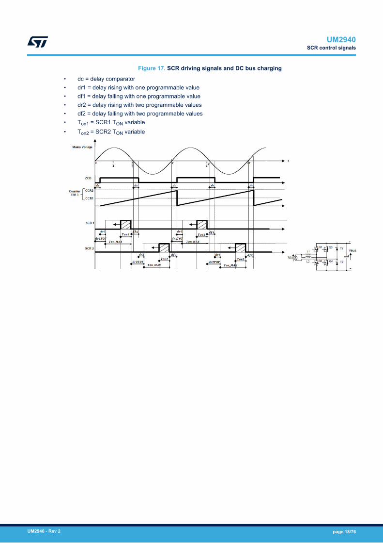
Figure 17. SCR driving signals and DC bus charging
• dc = delay comparator• dr1 = delay rising with one programmable value• df1 = delay falling with one programmable value• dr2 = delay rising with two programmable values• df2 = delay falling with two programmable values• Ton1 = SCR1 TON variable• Ton2 = SCR2 TON variable
UM2940SCR control signals
UM2940 - Rev 2 page 18/76

6 PFC control signals
Figure 18. Interleaved totem pole PFC signals
Current sampling is performed in the middle point of the TON PFC switching period.In the bridgeless totem pole PFC, the roles of the switches in the high frequency legs depend on the mainspolarity: when the mains voltage is positive, Q2 and Q4 (low side) are the active switches, whereas Q1 and Q3(high side) are driven in a complementary way with a fixed dead time. In the latter case, the current can circulate,in the low frequency leg, through T2, whereas T1 is off.During the negative mains voltage half cycle, Q1 and Q3 (high side) are the active switches, whereas Q2 andQ4 (low side) are driven in a complementary way with a fixed dead time. In the latter case, the current circulatesthrough T1 in the low frequency leg.To generate the necessary four PWMs signals, two different timers, with the phase shifted by 180°, are used toobtain an interleaving driving and to minimize the input current ripple.At the TON period midpoint of each active switch, an injected acquisition of the related inductor current is triggeredby the ADC. At the end of each conversion, once obtained the last current measure, the current control algorithmis executed and the new duty cycle value is written in the timer registers before the end of the actual periodbecomes effective at the next PWM cycle.
UM2940PFC control signals
UM2940 - Rev 2 page 19/76

6.1 MCU PFC tasks
Table 2. PFC tasks
Task name Priority Frequency Description
Current control loop X2 Very high 70 kHzThere are two independent current loops: one sinusoidal currentreference calculation and two PID or 2p2z regulators; one dutycycle computation and actuation.
Voltage control loop High 6 kHz A PID or 2p2z regulator calculates the amplitude of currentreference.
Mains voltage rmsand feedforwardcomputation, enable/disable SR
High 6 kHz Computes rms value of input voltage using a low pass digital filter,and feedforward term for input current reference calculation.
Mains frequencycomputation Medium 45-65 Hz
Computes mains frequency from a ZVD external signal (slow timerconfigured in input capture to measure the time between twoconsecutive rising edges).
Inrush current algorithm Medium 2*(45-65) Hz Drives SCRs at twice mains frequency to charge slowly the busvoltage at startup. The algorithm drives SCRs also in steady state.
Duty cycle soft-start atzero crossing Medium 2*(45-65) Hz At mains zero crossing, the duty cycle is slowly changed from the
max. to the required value to avoid current spikes.
Slow protection checks Low -
Compares the measured values with high and low thresholds, andmanages the state machine:• Input under/over voltage;• Input under/over frequency;• Output under/over voltage;• Overtemperature• Current sensor calibration error;• Startup failed protection.
Fast protection checks Very highImmediately afterADC conversiondelay
Fast protection based on ADC AWD:• Inductor 1 overcurrent;• Inductor 2 overcurrent.
Serial communication Very low
5 Hz orimmediately aftera fault on primaryside
Manages primary to secondary side opto-coupled communicationin a two-MCU solution.
UM2940MCU PFC tasks
UM2940 - Rev 2 page 20/76
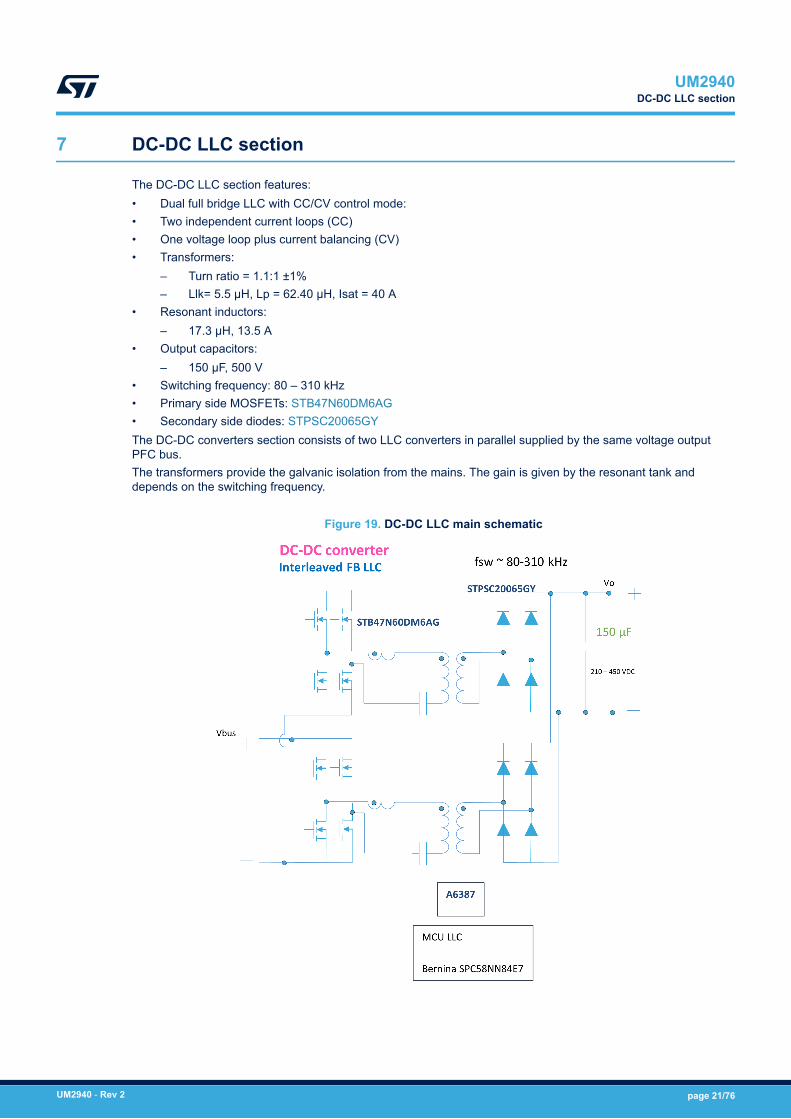
7 DC-DC LLC section
The DC-DC LLC section features:• Dual full bridge LLC with CC/CV control mode:• Two independent current loops (CC)• One voltage loop plus current balancing (CV)• Transformers:
– Turn ratio = 1.1:1 ±1%– Llk= 5.5 µH, Lp = 62.40 µH, Isat = 40 A
• Resonant inductors:– 17.3 µH, 13.5 A
• Output capacitors:– 150 µF, 500 V
• Switching frequency: 80 – 310 kHz• Primary side MOSFETs: STB47N60DM6AG• Secondary side diodes: STPSC20065GYThe DC-DC converters section consists of two LLC converters in parallel supplied by the same voltage outputPFC bus.The transformers provide the galvanic isolation from the mains. The gain is given by the resonant tank anddepends on the switching frequency.
Figure 19. DC-DC LLC main schematic
UM2940DC-DC LLC section
UM2940 - Rev 2 page 21/76

7.1 FB LLC control signals
Figure 20. LLC main schematic and switching periods
The command signals for each LLC resonant full bridge converter are square waves with 50% duty and deadtime. Each PWM group mentioned as PWM7 and PWM8 in the figure above is used at the same time for Q7-Q10and Q9-Q8, respectively. The same is for PWM9 and PW10 for Q11-Q14 and Q13-Q12, respectively.In the constant voltage mode, the two full bridge LLC converters can be driven in the interleaved mode. In thiscase, the PWM signals have the same frequency and are 90 degrees shifted. However, due to the tolerance ofthe electric parameters of the two resonant tanks, the output current balance is not ensured.A dedicated control has been implemented to solve the unbalanced current issue. If a certain unbalance on theoutput current is present, the control provides a change on the PWM9 frequency with respect to the PWM7. AΔfs is introduced thanks to a PI regulator, executed at a lower frequency, to obtain the switching frequency of thesecond converter (fs2) in order to balance the output currents of the two stages (see the figure below).
Figure 21. Constant voltage with current control block
UM2940FB LLC control signals
UM2940 - Rev 2 page 22/76

The figure below shows the block diagram of the constant current control.
Figure 22. Constant current control block
In this case, the current loops are independent. The two switching frequencies, fs1 and fs2, are generated by twodifferent current regulators.The charger is able to switch from the constant current to the constant voltage mode via firmware, depending onthe battery voltage value and following the desired charging profile.
UM2940FB LLC control signals
UM2940 - Rev 2 page 23/76

7.2 MCU LLC tasks
Table 3. LLC tasks
Task name Priority Frequency Description
Main control loop High 50 kHz
Current mode and voltage mode are set according to the status ofthe battery and its charging profile.
Current mode: two PID regulators calculate the switching period toregulate the two output currents.
Voltage mode: a PID regulator calculates the switching period toregulate the output voltage. An additional PID regulator assurescurrent balance at 5 kHz.
Frequencydecrease Medium 50 kHz or lower
Startup procedure to linearly decrease the switching frequency up tothe reference value to avoid overcurrent. It occurs at startup phaseinstead of the main control loop.
Slow protectionchecks Low -
Compares the measured values with high and low thresholds, andmanages the state machine:• Input under/over voltage;• Input under/over frequency;• Output under/over voltage;• Overtemperature• Current sensor calibration error;• Startup failed protection.
Fast protectionchecks
Very high(hardware)
Immediately aftercomputation delay
Fast hardware protection and related Irq handler:• Resonant current 1 overcurrent;• Resonant current 2 overcurrent.
Serialcommunication Very low
5 Hz orimmediately aftera fault on primaryside
Manages primary to secondary side opto-coupled communication ina two-MCU solution.
CANcommunication Very low - Manages communication with the user interface and/or among the
three modules.
UM2940MCU LLC tasks
UM2940 - Rev 2 page 24/76
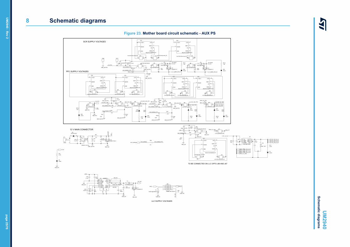
8 Schematic diagrams
Figure 23. Mother board circuit schematic - AUX PS
+
-
LLC SUPPLY VOLTAGES
12 V MAIN CONNECTOR
TO BE CONNECTED ON LLC OPTO J68 AND J67
+5V_PFC
+5V_ISO
CAN_L CAN_H
+12V
AUX_ENABLE
GND_SCR_K1
+5V_SCR1 +5V_SCR2
GND_SCR_K2EN2
GND_ISO PFCGND_ISO PFC
GND_PFC
GND_ISO
GND_ISOGND_ISO
GND_ISO
GND_ISO
GND_ISO
GND_ISO
GND_ISO PFCGND_ISO PFC
GND_ISO PFC
GND_ISO
GND_PFC
GND_ISOGND_ISO PFC
GND_ISO PFC
GND_ISO PFC
GND_ISO PFCGND_ISO PFC
GND_ISO PFC
GND_ISO PFC
GND_ISO PFC
GND_ISO
GND_ISO PFC
GND_CTRB_LS2_B_LLCGND_CTRB_LS1_B_LLC
GND_CTRB_LS1_A_LLCGND_CTRB_LS2_A_LLC
+12V_LS1_A_LLC+12V_LS2_A_LLC
+12V_LS1_B_LLC+12V_LS2_B_LLC
GND_LLC_Opto
+20V_HS1_PFC
-5V_HS1_PFC
GND_HS1_PFCGND_HS2_PFC
+20V_HS2_PFC
-5V_HS2_PFC
GND_LS2_PFC+20V_LS1_PFC+20V_LS2_PFC
-5V_LS1_PFC-5V_LS2_PFC
GND_LLC_Opto
+15V_LLC
GND_LS1_PFC
D90Green
D83Green
D88Green
C2910uF
R30N.M
A6986F5VIC1
RST1
VBIAS16
SYNCH4
MLF6
SS/INH3
PGND112 VIN15
PGND11
DELAY8
FSW5
SGN
D10
COMP7
LX114
LX13
VCC2
VOUT9
EP17
R509
N.M
R11 0.0
PS5
MGJ3T12150505MC-R7
16 +VDC1
3 EN/DIS
1 GND
10+20V
7GND18-5V
GND2 9
J57
con4-2x2-strip-male_90
1234
C20
0.1uF
C42220pF
C3491uF
J60
con4-2x2-strip-female
1 23 4
R26
0.0
R23
0.0
C310.1uF
CONN,10Pin,Walcon
J2213579
246810
R313.57k
J75con4-2x2-strip-female
1 23 4
C3501uF
J78
con4-2x2-strip-female
1234
R20
0.0
C30
0.1uF
+ C2247uF
12
R25
N.M
J63
con4-2x2-strip-female
1234
R5138.2K
PS2
MGJ3T12150505MC-R7
16 +VDC1
3 EN/DIS
1 GND
10+20V
7GND18-5V
GND2 9
R5111.5K
J66
con4-2x2-strip-male_90
1234
J56
con4-2x2-strip-female
1 23 4
PS4
MGJ3T12150505MC-R7
16 +VDC1
3 EN/DIS
1 GND
10+20V
7GND18-5V
GND2 9
C250.1uF
R32 1M
C3481uF
J76con4-2x2-strip-male_901 23 4
R29
0.0
C35410uF
+ C291470uF
12
PS8
MGJ3T12150505MC-R7
16 +VDC1
3 EN/DIS
1 GND
10+20V
7GND1
8-5V
GND2 9
R17
0.0
C230.1uF
+ C3847uF 10V
12
D3Green
R5158.2K
C40
68nF12
D2STPS3150UY
A C
J77 con4-2x2-strip-male_901234
R5181.5K
C34
1uF12
TP17
1R5161.5K
R14 0.0
D85Green
U3ESDA6V1LY
2K2
1K1A
3
J55
con4-2x2-strip-female
1234
L3
70Ohm@100MHz
12
L6
120Ohm@100MHz
12
J61
con4-2x2-strip-male_90
1 23 4
C360.1uF
U4ESDA6V1LY
2K2
1K1A
3
U5
L4931ABD120TR
VOUT1
GND12
GND23
NC4
INHIBIT5 GND36 GND47 VIN8
D87Green
J74
con4-2x2-strip-female
1234
J58
con4-2x2-strip-male_90
1 23 4
R340.0
L46.8uH 1.5A 100MOhm
1 2
C35110uF
J67
con4-2x2-strip-female
1234
J62
con4-2x2-strip-male_90
1234
J69
con4-2x2-strip-male_90
1 23 4
C330.1uF
PS3
MGJ3T12150505MC-R7
16 +VDC1
3 EN/DIS
1 GND
10+20V
7GND1
8-5V
GND2 9
D86Green
J80
con4-2x2-strip-female
1234
T1
2000ohm 4A 50V
41
32
D91Green
C280.1uF
L5
330Ohm@100MHz
12
R5101.5K
+C35
100uF 25V
12
R28
0.0
J70
con4-2x2-strip-male_90
1234
R160.0
U6ESDA14V2LY
2K2
1K1A3
R33 75K
C4168nF
D89Green
C3471uF
R27
0.0
D1Green
R133.57k
R22
0.0
J68
con4-2x2-strip-female
1 23 4
PS1
MGJ3T12150505MC-R7
16 +VDC1
3 EN/DIS
1 GND
10+20V
7GND18-5V
GND2 9
D84Green
R5171.5K
PS7
MGJ3T12150505MC-R7
16 +VDC1
3 EN/DIS
1 GND
10+20V
7GND18-5V
GND2 9
TP66
1
JP1
CON2
12
J79con4-2x2-strip-male_90 1234
C39470nF
U7ESDA6V1LY
2K2
1K1A
3
L2
70Ohm@100MHz
12
C352
10uF
R5148.2K
+ C2147uF
12
R15
0.0
J72
con4-2x2-strip-male_90
1234
+C32
100uF 25V
12
J59
con4-2x2-strip-female
1234
+ C2747uF
12
C3710nF
R5121.5K
R210.0
C35310uF
+12V PFC+12V PFC
AUX_ENABLE PFC
AUX_ENABLE PFC
+12V+5
V_IS
O
AUX_ENABLE
AUX_ENABLE PFC
+15V_LLC
AUX_ENABLE PFC
+12V
+12V
PFC
+12V
+12V PFC
AUX_ENABLE PFC
AUX_ENABLE PFC
AUX_ENABLE PFC
AUX_ENABLE PFC
SCR SUPPLY VOLTAGES
PFC SUPPLY VOLTAGES
UM
2940 - Rev 2
page 25/76
UM
2940Schem
atic diagrams

Figure 24. Mother board circuit schematic - bus monitoring
all resistors are 1% of tolerance
VBUS
LLC Vbus Monitor
+5V_ISO
-VBUS A_GND_LLC
+5V_LLC_Opto
GND_LLC_Opto
R44
2.2KR45
39
R35390K
C450.1uF
R3768K
D52.7V 500mW
R47160
R417.5k
R484.02K
R39390K
R4368K
R520
39
R36390K
-
+ U8TSZ121IYLT
3
41
52
D6LS L296-P2Q2-1-Z
AC
C48150pF
U9
ACPL-782T-500E
VDD11
VIN-3
GND14
VIN+2
GND25Vout-6Vout+7VDD28
R4068K
C460.1uF
C4710nF
L7470 Ohm
12
R46
2.2K
C43
0.1uFC44 150pF
R38390K
D4BZT52C9V1-7-F
AC
R42
4.02K
all resistors are 1% of tolerance
Figure 25. Mother board circuit schematic - HV discharge circuitVBUS
-VBUS
HV_discharge_Bus_PFC
+5V_PFC
+3.3V_PFCD24P6KE440A
R86165k
R90165k
Q9STN1NK80Z1
32 4
D26BZV55-B15,115A
C
C10447nF1
2
R9410k
Q13STN4NF03L
2
1
34
C1031uF
Q11STN4NF03L
2
1
34
R92499
R872.7k
R84165k
UM
2940 - Rev 2
page 26/76
UM
2940Schem
atic diagrams

Figure 26. Mother board circuit schematic - input section
R94 and R87 10k f or 3. 3V si gnal18k f or 5V si gnal
VDD_MCU_PFC
VAC Monitor N_GND
VAC Monitor P_GND
VDDA_PFC
VAC
N
GND_PFC
VDDA_PFC
VDDA_PFC
GND_PFC
GND_PFC
GND_PFC
A_GND_PFC
A_GND_PFC A_GND_PFC
A_GND_PFC
A_GND_PFC
GND_PFC
A_GND_PFC
Zero Voltage Detection
TW72
Con1
1
U12
BAR43SFILM
1 23
R112 499
C118470pF
12
R110
470k
R99
470k
R98470k
U13
TSV611ILT
IN+1
VCC-2
IN-3
OUT4
VCC+5
C117100pF
TP245001
L22
33uH1 2
R100
470k
L23
10uH 600mA1 2
R96470k
-
+
U11
TS3021HIYLT
3
41
52
C1130.1uF
R114
470k
L161.5mH 38A
4
1
7
1023 12
11
896
5
R103
470k
C12610nF 630V
R101
470k
T67448011305
3
1 4
2
TW16
SCREW_M4X6
1
C1074.7nF
12
R104
470k
C1140.1uF
C1124.7nF1
2
C1190.1uF
C120100pF
R105
470k
C1100.47uF
U14
BAR43SFILM
1 23
L25
33uH
1 2
R111
470k
C1081 uF
12
L20
470 Ohm
1 2
C1210.1uF
L24
470uH1 2
C1161 nF
R106
10k
J36
Earth
C1221uF
R116 5K
J35
N
L15
10uH 31.5A1 2
L19
10uH 31.5A1 2
R115
470k
C1234.7uF
C128N.M.
J33
P
F1
Fuse10X38
L181.5mH 38A
4
1
7
1023 12
11
896
5
C127N.M.
L26
10uH 600mA1 2
L21
470 Ohm
1 2
C1110.1uF
+ C1242.2uF
12
C125N.M.
U10
1 23
R10810k
R109
470k
C1091 uF
12
R102
10k
MOV1
R107 10k
C115470pF
12
R97470k
R113
470k
L17
900uH 32A
4
1
7
1023 12
11
896
5
P_Filter VAC Monitor P
VAC Monitor NN_Filter
P_Filter
N_Filter
P_Filter
N_Filter
UM
2940 - Rev 2
page 27/76
UM
2940Schem
atic diagrams

Figure 27. Mother board circuit schematic - LLC control
Note: Keep all filtering parts traces as short as possible to the DSMPS Connector
CAN connection and serial
CAN COMMUNICATION
LLC Resonant Current2
LLC Vout Monitor
LLC Temperature
LLC Resonant Current1LLC Output Current1
LLC Vbus Monitor
VDDA_LLC
USART_LLC_TXUSART_LLC_RX
+5V_ISO
AUX_ENABLE
LLC Output Current2
CAN_TXCAN_RX
CAN_TX
CAN_RX
VDD_MCU_LLC
CAN_H
CAN_L
VDDA_LLC
VDDA_LLC
A_GND_LLCA_GND_LLC
VDDA_LLC
A_GND_LLC
VDDA_LLC
VDDA_LLC
A_GND_LLC
A_GND_LLC
VDDA_LLC
A_GND_LLC
VDDA_LLC
A_GND_LLC
VDDA_LLC
A_GND_LLC
GND_ISO
A_GND_LLC
VDDA_LLC
GND_ISO
GND_ISO
GND_ISO
GND_ISO
A_GND_LLC
LLC_SPI_MOSILLC_SPI_MISO
LLC_SPI_CKLLC_SPI_CSLLC_SPI_SD
LLC_PWM_HS1_ALLC_PWM_LS1_ALLC_PWM_HS2_ALLC_PWM_LS2_A
LLC_DIAG2LLC_DIAG1
LLC_PWM_HS1_BLLC_PWM_LS1_BLLC_PWM_HS2_BLLC_PWM_LS2_B
R126 NM
C1382.2uF
12
R145
0.0
TP33
1
D33
BAT754
R1320.0
R146
100
C1390.1uF
C13547nF
R1300.0
J38
Con212
R144
100
L27
470 Ohm
1 2
R147NM
R121
100
D34BAT754
R149NM
R153 0.0
R123 NM
TP26
1
R143 0.0
R141 0.0R142 0.0
C133
4.7nF
12
C1370.1uF
C1360.1uF
R134100
TP27
1
TP32
1
D30BAT754
R127 NM
D31BAT754
TP28
1
D29BAT754
C1290.1uF
R148 0.0
R1200.0
R139 0.0
LLC_CONNECTOR
DSMPS CONNECTOR
USART_TX_isoUSART_RX_iso
CAN_TXCAN_RX
SMBus_SCL/UI_USART_RXSMBus_SMBA/SPI_MOSI
SMBus_SDA/UI_USART_TX
+5V+3.3V
FAULT_1
GPIO_1/COMP_3_OUT/GP_PWM_1/EEV_4
PWM_1PWM_2PWM_3PWM_4PWM_5PWM_6PWM_7PWM_8PWM_9
PWM_10PWM_11PWM_12
GPIO_2/COMP_2_OUT/GP_PWM_2GPIO_3/COMP_1_OUT/FAULT_2GPIO_4/EEV_1GPIO_5/DAC_1/COMP_4_INP/SPI_NSSGPIO_6/DAC_2/SPI_SCLKGPIO_7/DAC_3/OP-AMP_1_OUTGPIO_8/EEV_2GPIO_9/EEV_3/SPI_MISOGPIO_10/DAC_4
ADC_1/DIFF_ADC_1+
A_VDDADC_2/DIFF_ADC_1-/OP-AMP_2+ADC_3/DIFF_ADC_2+/OP-AMP_2_OUT/COMP_1_NMADC_4/DIFF_ADC_2-/OP-AMP_2-ADC_5ADC_6/OP-AMP_1-
COMP_2_INP/ADC_12/OP-AMP_1+
ADC_7/COMP_2_INMADC_8ADC_9ADC_10
COMP_1_INP/ADC_11
COMP_3_INP GND_ISO
D_GND
A_GND
VDD_ISO
R117 0.0
C13247nF
R1180.0
C1342.7nF
12
R1290.0
R135
0.0
U15
LTC2875HS8#PBF
TXD1
GND2
VCC3
RXD4
SPLIT5
RS8
CANL6
CANH7
R1310.0
R124 NM
R128 0.0
R151120
R119 0.0
D28BAT754
TP31
1
C1412.2uF
12
T7100uH 150mA
12
34
TP25
1
R137 0.0
D35ESDCAN24-2BLY
3
1 2
TP34
1
R138NM
C1312.7nF
12
R140
0.0
R122
100
R1520.0
R150
100
C1300.1uF
C140470nF
TP30
1D32BAT754
R136
100
TW17Con1
1
R133 0.0
TP291
LLC Resonant Current sensing2LLC Output Current sensing2
LLC Vout Monitor sensing
LLC Temperature sensing
A_VDD_LLC_CONN
LLC Resonant Current sensing1 LLC Output Current sensing1
LLC_PWM_HS1_ALLC_PWM_LS1_ALLC_PWM_HS2_ALLC_PWM_LS2_A
LLC_DIAG1
LLC Resonant Current sensing2LLC Resonant Current sensing1
LLC_PWM_HS1_BLLC_PWM_LS1_BLLC_PWM_HS2_BLLC_PWM_LS2_B
LLC Output Current sensing2
LLC Output Current sensing1
LLC Vout Monitor sensing
LLC Temperature sensing
LLC Vbus Monitor sensing
LLC Vout Monitor sensing
A_VDD_LLC_CONN
+5V_ISO
+5V_ISO
CAN_L
CAN_H
VDD_MCU_LLC
LLC Vbus Monitor sensing
VDD_MCU_LLC
Default setting: jumper mounted
UM
2940 - Rev 2
page 28/76
UM
2940Schem
atic diagrams

Figure 28. Mother board circuit schematic - PFC control
Note: Keep all filtering parts traces as short as possible to the DSMPS connector
Secondary isolated supply voltage for optocoupled communication
PFC Temperature
PFC Inductor Current1PFC Inductor Current2
A_GND_PFC
PFC Vbus
VAC
+5V_PFC
VDD_MCU_LLC
VAC Monitor P_GND HV_discharge_Bus_PFC
USART_LLC_TX
USART_LLC_RX
VDDA_PFC
VDDA_PFC
VDDA_PFC VDDA_PFC
VDDA_PFC
A_GND_PFC
A_GND_PFC
A_GND_PFC
A_GND_PFC
A_GND_PFC
A_GND_PFC
A_GND_PFC
GND_PFC
GND_ISO PFC
A_GND_PFC
A_GND_PFC
PFC_SPI_CKPFC_SPI_CSPFC_SPI_SD
PFC_PWM_HS1PFC_DIAG2
PFC_DIAG1 PFC_PWM_LS1PFC_PWM_HS2PFC_PWM_LS2
PFC_PWM_SCR1PFC_PWM_SCR2
PFC_SPI_MOSIPFC_SPI_MISO
Zero Voltage Detection
R177 0.0 R178
1.5K
D39BAT754
R185 0.0
R169 0.0R167 0.0
C1460.1uF
PFC CONNECTOR
DSMPS CONNECTOR
USART_TX_isoUSART_RX_iso
CAN_TXCAN_RX
SMBus_SCL/UI_USART_RXSMBus_SMBA/SPI_MOSI
SMBus_SDA/UI_USART_TX
+5V+3.3V
FAULT_1
GPIO_1/COMP_3_OUT/GP_PWM_1/EEV_4
PWM_1PWM_2PWM_3PWM_4PWM_5PWM_6PWM_7PWM_8PWM_9
PWM_10PWM_11PWM_12
GPIO_2/COMP_2_OUT/GP_PWM_2GPIO_3/COMP_1_OUT/FAULT_2GPIO_4/EEV_1GPIO_5/DAC_1/COMP_4_INP/SPI_NSSGPIO_6/DAC_2/SPI_SCLKGPIO_7/DAC_3/OP-AMP_1_OUTGPIO_8/EEV_2GPIO_9/EEV_3/SPI_MISOGPIO_10/DAC_4
ADC_1/DIFF_ADC_1+
A_VDDADC_2/DIFF_ADC_1-/OP-AMP_2+ADC_3/DIFF_ADC_2+/OP-AMP_2_OUT/COMP_1_NMADC_4/DIFF_ADC_2-/OP-AMP_2-ADC_5ADC_6/OP-AMP_1-
COMP_2_INP/ADC_12/OP-AMP_1+
ADC_7/COMP_2_INMADC_8ADC_9ADC_10
COMP_1_INP/ADC_11
COMP_3_INP GND_ISO
D_GND
A_GND
VDD_ISO
TP44
1
R158 0.0
TP45
1
R172 0.0
TP401
D37BAT754
C1480.1uF
R162 0.0R163 0.0
R184 0.0
R1803K
R156 0.0
R186 0.0
R165 0.0R164 0.0
R154 0.0
TP39
1
TP46
1
R166 0.0
R155 0.0
R188
100
TP41
1
R176
1.5K
R182 0.0
R168 0.0
C149470nF
C14447pF
12
R187
100
R173 0.0
C14547pF
12
R1813K
D38BAT754
TP35
1
R171 0.0
L28
470 Ohm
1 2
C1470.1uF
R159 0.0
TP47
1
C14222nF
TP431
D36BAT754
R160 0.0
R175 0.0
R170 0.0
TP42
1
TP37 1
R174 0.0
R183 0.0
R161 0.0
R179 0.0
TP38
1
PFC Vbus sensing
PFC Inductor Current sensing1
VAC Monitor sensing P
PFC Inductor Current sensing2
VAC Monitor sensing PVAC Monitor sensing N
PFC Inductor Current sensing1
PFC Inductor Current sensing2
PFC Vbus sensing
PFC Temperature sensing
PFC Inductor Current sensing1PFC Inductor Current sensing2
PFC_DIAG1
PFC_DIAG2PFC_PWM_SCR1
PFC_PWM_SCR2PFC_PWM_SCR1
PFC_PWM_SCR2
PFC_PWM_HS1PFC_PWM_LS1PFC_PWM_HS2PFC_PWM_LS2
Zero Voltage Detection
Zero Voltage Detection
PFC_SPI_MOSI
PFC_SPI_MISO
PFC_SPI_CKPFC_SPI_CS
PFC_SPI_SD
A_VDD_PFC_CONN
A_VDD_PFC_CONN
PFC Temperature sensing
+5V_PFC
+5V_PFC
PFC Inductor Current sensing1
Figure 29. Mother board circuit schematic - vertical adapterVDD_ISO GND_ISO_ADP
D_GNDA_VDD
+3.3VA_GND
USART_TX_is o USART_RX_is oUSART_TX_is o USART_RX_is o
CAN_TX_ADP CAN_RX_ADPSMBus _SCL/UI_USART_RX SMBus _SMBA/SPI_MOSI CAN_TX_ADP CAN_RX_ADPSMBus _SDA/UI_USART_TX SMBus _SCL/UI_USART_RX SMBus _SMBA/SPI_MOSI
SMBus _SDA/UI_USART_TX+5V +3.3VGPIO_1/COMP_3_OUT/GP_PWM_1/EEV_4
GPIO_1/COMP_3_OUT/GP_PWM_1/EEV_4PWM_2PWM_4PWM_6PWM_8
PWM_2PWM_4PWM_6PWM_8
FAULT_1PWM_1PWM_3PWM_5PWM_7PWM_9PWM_11
GPIO_2/COMP_2_OUT/GP_PWM_2
PWM_10PWM_12GPIO_3/COMP_1_OUT/FAULT_2
FAULT_1PWM_1PWM_3PWM_5PWM_7PWM_9PWM_11
GPIO_2/COMP_2_OUT/GP_PWM_2
PWM_10PWM_12GPIO_3/COMP_1_OUT/FAULT_2GPIO_4/EEV_1
GPIO_5/DAC_1/COMP_4_INP/SPI_NSS GPIO_6/DAC_2/SPI_SCLKGPIO_7/DAC_3/OP-AMP_1_OUT GPIO_8/EEV_2
GPIO_4/EEV_1GPIO_5/DAC_1/COMP_4_INP/SPI_NSS GPIO_6/DAC_2/SPI_SCLK
GPIO_9/EEV_3/SPI_MISO GPIO_10/DAC_4 GPIO_7/DAC_3/OP-AMP_1_OUT GPIO_8/EEV_2GPIO_9/EEV_3/SPI_MISO GPIO_10/DAC_4
A_VDDADC_1/DIFF_ADC_1+
ADC_2/DIFF_ADC_1-/OP-AMP_2+ADC_3/DIFF_ADC_2+/OP-AMP_2_OUT/COMP_1_NM
ADC_4/DIFF_ADC_2-/OP-AMP_2-ADC_4/DIFF_ADC_2-/OP-AMP_2-
ADC_1/DIFF_ADC_1+ADC_2/DIFF_ADC_1-/OP-AMP_2+
ADC_3/DIFF_ADC_2+/OP-AMP_2_OUT/COMP_1_NMADC_5
ADC_6/OP-AMP_1-COMP_2_INP/ADC_12/OP-AMP_1+
ADC_7/COMP_2_INMADC_8ADC_9ADC_10
ADC_5ADC_6/OP-AMP_1-
COMP_2_INP/ADC_12/OP-AMP_1+ADC_7/COMP_2_INM
ADC_8ADC_9ADC_10COMP_1_INP/ADC_11
COMP_3_INP
P4
1B1B
2A2A
2B2B
Digital Power Connector
3B3B
4A4A
4B4B
5A5A
5B5B
6A6A
6B6B
7B7B
8A8A
8B8B
9A9A
9B9B
10A10A
10B10B
11A11A
11B11B
12A12A
12B12B
13A13A
13B13B
14A14A
14B14B
15A15A
15B15B
16A16A
16B16B
17A17A
17B17B
18A18A
18B18B
19A19A
19B19B
20A20A
20B20B
21A21A
21B21B
22A22A
22B22B
23A23A
23B23B
24A24A
24B24B
25A25A
25B25B
7A7A
1A1A
26B26B
29B29B
27B27B
28B28B
30B30B
26A26A
27A27A
28A28A
29A29A
30A30A
32A32A 31B
31B
32B32B31A
31A
3A3A
P3
1B1B
2A2A
2B2B
Digital Power Connector
3B3B
4A4A
4B4B
5A5A
5B5B
6A6A
6B6B
7B7B
8A8A
8B8B
9A9A
9B9B
10A10A
10B10B
11A11A
11B11B
12A12A
12B12B
13A13A
13B13B
14A14A
14B14B
15A15A
15B15B
16A16A
16B16B
17A17A
17B17B
18A18A
18B18B
19A19A
19B19B
20A20A
20B20B
21A21A
21B21B
22A22A
22B22B
23A23A
23B23B
24A24A
24B24B
25A25A
25B25B
7A7A
1A1A
26B26B
29B29B
27B27B
28B28B
30B30B
26A26A
27A27A
28A28A
29A29A
30A30A
32A32A 31B
31B
32B32B31A
31A
3A3A
VDD_ISO GND_ISO
D_GNDA_VDD
+3.3VA_GND
VDD_ISO GND_ISOVDD_ISO
D_GND+5V +3.3V D_GND
D_GNDD_GND
A_VDD
A_GND
+5V+5V
COMP_1_INP/ADC_11COMP_3_INP
GND_is o_ADP
A_GND
UM
2940 - Rev 2
page 29/76
UM
2940Schem
atic diagrams

Figure 30. Mother board circuit schematic - DSMPS connector
USART_TX_is o USART_RX_is o
CAN_TX CAN_RXSMBus _SCL/UI_USART_RX SMBus _SMBA/SPI_MOSISMBus _SDA/UI_USART_TX
GPIO_1/COMP_3_OUT/GP_PWM_1/EEV_4PWM_2PWM_4PWM_6PWM_8
FAULT_1PWM_1PWM_3PWM_5PWM_7PWM_9PWM_11
GPIO_2/COMP_2_OUT/GP_PWM_2
PWM_10PWM_12GPIO_3/COMP_1_OUT/FAULT_2
GPIO_4/EEV_1GPIO_5/DAC_1/COMP_4_INP/SPI_NSS GPIO_6/DAC_2/SPI_SCLK
GPIO_7/DAC_3/OP-AMP_1_OUT GPIO_8/EEV_2GPIO_9/EEV_3/SPI_MISO GPIO_10/DAC_4
ADC_4/DIFF_ADC_2-/OP-AMP_2-
ADC_1/DIFF_ADC_1+ADC_2/DIFF_ADC_1-/OP-AMP_2+
ADC_3/DIFF_ADC_2+/OP-AMP_2_OUT/COMP_1_NM
ADC_8ADC_9ADC_10
ADC_5ADC_6/OP-AMP_1-
COMP_2_INP/ADC_12/OP-AMP_1+ADC_7/COMP_2_INM
GND_ISO
D_GND
COMP_1_INP/ADC_11COMP_3_INP
A_GND
VDD_ISO
+5V
A_VDD
+3.3V
P1
1B1B
2A2A
2B
Digital Power Connector
2B
3B3B
4A4A
4B4B
5A5A
5B5B
6A6A
6B6B
7B7B
8A8A
8B8B
9A9A
9B9B
10A10A
10B10B
11A11A
11B11B
12A12A
12B12B
13A13A
13B13B
14A14A
14B14B
15A15A
15B15B
16A16A
16B16B
17A17A
17B17B
18A18A
18B18B
19A19A
19B19B
20A20A
20B20B
21A21A
21B21B
22A22A
22B22B
23A23A
23B23B
24A24A
24B24B
25A25A
25B25B
7A7A
1A1A
26B26B
29B29B
27B27B
28B28B
30B30B
26A26A
27A27A
28A28A
29A29A
30A30A
32A32A 31B
31B
32B32B31A
31A
3A3A
+3.3V
A_VDD
GND_ISO
D_GND
A_GND
GND_ISO
D_GND
D_GND
A_GND
VDD_ISO
+5VA_VDD
+3.3VVDD_ISO
+5V
USART_TX_is o USART_RX_is o
CAN_TX CAN_RXSMBus _SCL/UI_USART_RX SMBus _SMBA/SPI_MOSISMBus _SDA/UI_USART_TX
GPIO_1/COMP_3_OUT/GP_PWM_1/EEV_4PWM_2PWM_4PWM_6PWM_8
FAULT_1PWM_1PWM_3PWM_5PWM_7PWM_9PWM_11
GPIO_2/COMP_2_OUT/GP_PWM_2
PWM_10PWM_12GPIO_3/COMP_1_OUT/FAULT_2
GPIO_4/EEV_1GPIO_5/DAC_1/COMP_4_INP/SPI_NSS GPIO_6/DAC_2/SPI_SCLK
GPIO_7/DAC_3/OP-AMP_1_OUT GPIO_8/EEV_2GPIO_9/EEV_3/SPI_MISO GPIO_10/DAC_4
ADC_4/DIFF_ADC_2-/OP-AMP_2-
ADC_1/DIFF_ADC_1+ADC_2/DIFF_ADC_1-/OP-AMP_2+
ADC_3/DIFF_ADC_2+/OP-AMP_2_OUT/COMP_1_NM
ADC_8ADC_9ADC_10
ADC_5ADC_6/OP-AMP_1-
COMP_2_INP/ADC_12/OP-AMP_1+ADC_7/COMP_2_INM
GND_ISO
D_GND
COMP_1_INP/ADC_11COMP_3_INP
A_GND
VDD_ISO
+5V
A_VDD
+3.3V
P2
1B1B
2A2A
2B
Digital Power Connector
2B
3B3B
4A4A
4B4B
5A5A
5B5B
6A6A
6B6B
7B7B
8A8A
8B8B
9A9A
9B9B
10A10A
10B10B
11A11A
11B11B
12A12A
12B12B
13A13A
13B13B
14A14A
14B14B
15A15A
15B15B
16A16A
16B16B
17A17A
17B17B
18A18A
18B18B
19A19A
19B19B
20A20A
20B20B
21A21A
21B21B
22A22A
22B22B
23A23A
23B23B
24A24A
24B24B
25A25A
25B25B
7A7A
1A1A
26B26B
29B29B
27B27B
28B28B
30B30B
26A26A
27A27A
28A28A
29A29A
30A30A
32A32A 31B
31B
32B32B31A
31A
3A3A
+3.3V
A_VDD
GND_ISO
D_GND
A_GND
GND_ISO
D_GND
D_GND
A_GND
VDD_ISO
+5VA_VDD
+3.3VVDD_ISO
+5V
Figure 31. Mother board circuit schematic - A6387 LLC (1 of 4)VH
GateH
EmitterH
PWM_H
PWM_L
+5V_LLC_Opto
GateL
EmitterL
GateHEmitterH
GateLEmitterL
PWM_HPWM_L
GND_Lowside
GND_D
GND_D
GND_D
VH+5V_LLC_Opto
GND_D
GND_Lowside
GND_Lowside
D52STTH1R06A
AA
CC
R226
330C2140.22uF
R234 4.7
R231 1
R227
20
D53STPS1L30A
AC
C2120.1uF
R230 4.7
C36133pF
R232
330
C2131uF
R228 1IC2
A6387D
LIN1
HIN2
VCC3
Vboot8
LVG5
OUT6
HVG7
GND4
U20
1
3
4
7
6
2
5
8R233 20
D51STPS1L30A
AC
C2151uF
C36033pF
R229 20
R523330
U19
1
3
4
7
6
2
5
8
C2111uF
D50
STTH1R06AA
AC
C
R524330
VH
+5V_LLC_Opto
PWM_HPWM_L
GateHEmitterH
GateLEmitterL
GND_D
GND_Lowside
UM
2940 - Rev 2
page 30/76
UM
2940Schem
atic diagrams

Figure 32. Mother board circuit schematic - A6387 LLC (2 of 4)VH
GateH
EmitterH
PWM_H
PWM_L
+5V_LLC_Opto
GateL
EmitterL
GateHEmitterH
GateLEmitterL
PWM_HPWM_L
GND_Lowside
GND_D
GND_D
GND_D
VH+5V_LLC_Opto
GND_D
GND_Lowside
GND_Lowside
D56STTH1R06A
AA
CC
R235
330C2190.22uF
R243 4.7
R240 1
R236
20
D57STPS1L30A
AC
C2170.1uF
R239 4.7
C36333pF
R241
330
C2181uF
R237 1IC3
A6387D
LIN1
HIN2
VCC3
Vboot8
LVG5
OUT6
HVG7
GND4
U22
1
3
4
7
6
2
5
8R242 20
D55STPS1L30A
AC
C2201uF
C36233pF
R238 20
R525330
U21
1
3
4
7
6
2
5
8
C2161uF
D54
STTH1R06AA
AC
C
R526330
VH
+5V_LLC_Opto
PWM_HPWM_L
GateHEmitterH
GateLEmitterL
GND_D
GND_Lowside
Figure 33. Mother board circuit schematic - A6387 LLC (3 of 4)VH
GateH
EmitterH
PWM_H
PWM_L
+5V_LLC_Opto
GateL
EmitterL
GateHEmitterH
GateLEmitterL
PWM_HPWM_L
GND_Lowside
GND_D
GND_D
GND_D
VH+5V_LLC_Opto
GND_D
GND_Lowside
GND_Lowside
D60STTH1R06A
AA
CC
R244
330C2240.22uF
R252 4.7
R249 1
R245
20
D61STPS1L30A
AC
C2220.1uF
R248 4.7
C36533pF
R250
330
C2231uF
R246 1IC4
A6387D
LIN1
HIN2
VCC3
Vboot8
LVG5
OUT6
HVG7
GND4
U24
1
3
4
7
6
2
5
8R251 20
D59STPS1L30A
AC
C2251uF
C36433pF
R247 20
R527330
U23
1
3
4
7
6
2
5
8
C2211uF
D58
STTH1R06AA
AC
C
R528330
VH
+5V_LLC_Opto
PWM_HPWM_L
GateHEmitterH
GateLEmitterL
GND_D
GND_Lowside
UM
2940 - Rev 2
page 31/76
UM
2940Schem
atic diagrams

Figure 34. Mother board circuit schematic - A6387 LLC (4 of 4)VH
GateH
EmitterH
PWM_H
PWM_L
+5V_LLC_Opto
GateL
EmitterL
GateHEmitterH
GateLEmitterL
PWM_HPWM_L
GND_Lowside
GND_D
GND_D
GND_D
VH+5V_LLC_Opto
GND_D
GND_Lowside
GND_Lowside
D64STTH1R06A
AA
CC
R253
330C2290.22uF
R261 4.7
R258 1
R254
20
D65STPS1L30A
AC
C2270.1uF
R257 4.7
C36733pF
R259
330
C2281uF
R255 1IC5
A6387D
LIN1
HIN2
VCC3
Vboot8
LVG5
OUT6
HVG7
GND4
U26
1
3
4
7
6
2
5
8R260 20
D63STPS1L30A
AC
C2301uF
C36633pF
R256 20
R529330
U25
1
3
4
7
6
2
5
8
C2261uF
D62
STTH1R06AA
AC
C
R530330
VH
+5V_LLC_Opto
PWM_HPWM_L
GateHEmitterH
GateLEmitterL
GND_D
GND_Lowside
Figure 35. Mother board circuit schematic - STGAP1AS PFC (1 of 4)
VDD = VREG only for VDD = 3.3V
VDD
GND
VH
VL
GND_ISO
Gate
SPI_SDO
SPI_SDI
SPI_CS
SPI_CK
Emitter
IN-/DIAG2
IN_PWM Vsense
DIAG1
SPI_SD
GND_D
GND_D
GND_D
GND_DGND_D
GND_D
R264 0.0
C23414.
7uF
2
C238
1uF
12
C231
1
0.1uF
2
C23214.
7uF
2
R2692.2
C24014.
7uF
2
C2351
0.1uF
2
D69
AC
STPS360AFY
C233
1
0.1uF 2
C237
1
0.1uF 2
R266 2.7
C242
1
0.1uF
2
C239
1
0.1uF
2
D66
AC
STPS360AFY
C241
1
100pF2
R262
0.0
IC6
1GND
STGAP1AS
2SDO
3SDI
CS4
CK5
6Vreg
VDD7
8IN-/DIAG2
IN+9
DIAG110
SDSD1_1
GND112 13
GND_ISO
VL14
15VREG_ISO
16SENSE
VH17
DESAT18
19VCECLAMP
GON20
GOFF21
CLAMP22
VL123
ASC24
R270
100
10R267
C236
1
100pF2
R268
100
C2431uF1
2
VDD
GND
VH
VREG_ISOVDD
VL
GND_ISO
VL
VH
CLAMP
VREG
VDD
VCE_CLAMP
DESAT VL
GND_ISO
VH
VREG_ISO
GND VL
CLAMP
VREG
UM
2940 - Rev 2
page 32/76
UM
2940Schem
atic diagrams

Figure 36. Mother board circuit schematic - STGAP1AS PFC (2 of 4)
VDD = VREG only for VDD = 3.3V
VDD
GND
VH
VL
GND_ISO
Gate
SPI_SDO
SPI_SDI
SPI_CS
SPI_CK
Emitter
IN-/DIAG2
IN_PWM Vsense
DIAG1
SPI_SD
GND_D
GND_D
GND_D
GND_DGND_D
GND_D
R273 0.0
C24714.
7uF
2
C251
1uF
12
C244
1
0.1uF
2
C24514.
7uF
2
R2782.2
C25314.
7uF
2
C2481
0.1uF
2
D73
AC
STPS360AFY
C246
1
0.1uF 2
C250
1
0.1uF 2
R521 2.7
C255
1
0.1uF
2
C252
1
0.1uF
2
D70
AC
STPS360AFY
C254
1
100pF2
R271
0.0
IC7
1GND
STGAP1AS
2SDO
3SDI
CS4
CK5
6Vreg
VDD7
8IN-/DIAG2
IN+9
DIAG110
SDSD1_1
GND112 13
GND_ISO
VL14
15VREG_ISO
16SENSE
VH17
DESAT18
19VCECLAMP
GON20
GOFF21
CLAMP22
VL123
ASC24
R279
100
10R522
C249
1
100pF2
R277
100
C2561uF1
2
VDD
GND
VH
VREG_ISOVDD
VL
GND_ISO
VL
VH
CLAMP
VREG
VDD
VCE_CLAMP
DESAT VL
GND_ISO
VH
VREG_ISO
GND VL
CLAMP
VREG
UM
2940 - Rev 2
page 33/76
UM
2940Schem
atic diagrams

Figure 37. Mother board circuit schematic - STGAP1AS PFC (3 of 4)
VDD = VREG only for VDD = 3.3V
VDD
GND
VH
VL
GND_ISO
Gate
SPI_SDO
SPI_SDI
SPI_CS
SPI_CK
Emitter
IN-/DIAG2
IN_PWM Vsense
DIAG1
SPI_SD
GND_D
GND_D
GND_D
GND_DGND_D
GND_D
R282 0.0
C26014.
7uF
2
C264
1uF
12
C257
1
0.1uF
2
C25814.
7uF
2
R2872.2
C26614.
7uF
2
C2611
0.1uF
2
D77
AC
STPS360AFY
C259
1
0.1uF 2
C263
1
0.1uF 2
R284 2.7
C268
1
0.1uF
2
C265
1
0.1uF
2
D74
AC
STPS360AFY
C267
1
100pF2
R280
0.0
IC8
1GND
STGAP1AS
2SDO
3SDI
CS4
CK5
6Vreg
VDD7
8IN-/DIAG2
IN+9
DIAG110
SDSD1_1
GND112 13
GND_ISO
VL14
15VREG_ISO
16SENSE
VH17
DESAT18
19VCECLAMP
GON20
GOFF21
CLAMP22
VL123
ASC24
R288
100
10R285
C262
1
100pF2
R286
100
C2691uF1
2
VDD
GND
VH
VREG_ISOVDD
VL
GND_ISO
VL
VH
CLAMP
VREG
VDD
VCE_CLAMP
DESAT VL
GND_ISO
VH
VREG_ISO
GND VL
CLAMP
VREG
UM
2940 - Rev 2
page 34/76
UM
2940Schem
atic diagrams

Figure 38. Mother board circuit schematic - STGAP1AS PFC (4 of 4)
VDD = VREG only for VDD = 3.3V
VDD
GND
VH
VL
GND_ISO
Gate
SPI_SDO
SPI_SDI
SPI_CS
SPI_CK
Emitter
IN-/DIAG2
IN_PWM Vsense
DIAG1
SPI_SD
GND_D
GND_D
GND_D
GND_DGND_D
GND_D
R291 0.0
C27314.
7uF
2
C277
1uF
12
C270
1
0.1uF
2
C27114.
7uF
2
R2962.2
C27914.
7uF
2
C2741
0.1uF
2
D81
AC
STPS360AFY
C272
1
0.1uF 2
C276
1
0.1uF 2
R293 2.7
C281
1
0.1uF
2
C278
1
0.1uF
2
D78
AC
STPS360AFY
C280
1
100pF2
R289
0.0
IC9
1GND
STGAP1AS
2SDO
3SDI
CS4
CK5
6Vreg
VDD7
8IN-/DIAG2
IN+9
DIAG110
SDSD1_1
GND112 13
GND_ISO
VL14
15VREG_ISO
16SENSE
VH17
DESAT18
19VCECLAMP
GON20
GOFF21
CLAMP22
VL123
ASC24
R297
100
10R294
C275
1
100pF2
R295
100
C2821uF1
2
VDD
GND
VH
VREG_ISOVDD
VL
GND_ISO
VL
VH
CLAMP
VREG
VDD
VCE_CLAMP
DESAT VL
GND_ISO
VH
VREG_ISO
GND VL
CLAMP
VREG
UM
2940 - Rev 2
page 35/76
UM
2940Schem
atic diagrams

Figure 39. Mother board circuit schematic - A6387 drivers plus IMS connector
AB0026- A- 1 AB0026- A- 1LLC_HS2_A_Gate
LLC_HS1_A_Gate
LLC_HS2_A_SourceLLC_HS1_A_Source
LLC_LS1_A_Gate
LLC_LS2_A_Gate
LLC_LS1_A_SourceLLC_LS2_A_Source
LLC_HS2_B_GateLLC_HS1_B_Gate
LLC_HS2_B_SourceLLC_HS1_B_Source
LLC_LS1_B_Gate
LLC_LS1_B_Source
LLC_LS2_B_Gate
LLC_LS2_B_Source
+5V_ISO VDD_MCU_LLC+5V_ISO +5V_ISO
+3.3V_LLC
GND_ISO
GND_ISOGND_ISO
GND_ISO
+5V_ISO
+3.3V_LLC
GND_ISOGND_ISO GND_ISOGND_ISO
GND_ISO
GND_ISO GND_ISOGND_ISO GND_ISO
+12V_LS1_A_LLCGND_CTRB_LS1_A_LLCLLC_PWM_HS1_A LLC_PWM_HS2_A
GND_HS1_A_LLCGND_HS2_A_LLC
LLC_PWM_LS1_A LLC_PWM_LS2_A
LLC_PWM_HS1_B LLC_PWM_HS2_B
GND_HS1_B_LLCGND_HS2_B_LLC
+12V_LS1_B_LLCGND_CTRB_LS1_B_LLC
+12V_LS2_B_LLCGND_CTRB_LS2_B_LLC
LLC_PWM_LS1_B LLC_PWM_LS2_B
+5V_LLC_Opto
+12V_LS2_A_LLCGND_CTRB_LS2_A_LLC
+5V_LLC_Opto
+5V_LLC_Opto +5V_LLC_Opto
+15V_LLC +5V_LLC_Opto
GND_LLC_OptoGND_LLC_Opto
J7
Con4F
13
24
C36.8uF
U2LF50CDT-TRY
GND
4
Vin1
Vout3
TP75001
C17
470pF
C111uF
J2
CON4
13
24
TP45001
C1827pF
J12
CON4
13
24
TP95001
C121uF
R6249k
J11
Con4F
13
24
TP115001
L1
10uH 2.5A
1 2
C1668nF
R1
0.0
J1
Con4F
13
24
TP135001
R2
0.0
C106.8pFN.M.
J8
CON4
13
24
J15
Con4F
13
24
Drive 8
Gate Driver LLC
VH
+5V_LLC_Opto
GateH
PWM_HPWM_L
GateL
EmitterL
EmitterH
GND_D
GND_Lowside
Drive 5
Gate Driver LLC
VH
+5V_LLC_Opto
GateH
PWM_HPWM_L
GateL
EmitterL
EmitterH
GND_D
GND_Lowside
Drive 6
Gate Driver LLC
VH
+5V_LLC_Opto
GateH
PWM_HPWM_L
GateL
EmitterL
EmitterH
GND_D
GND_Lowside
TP15001
J6
CON4
13
24
Drive 7
Gate Driver LLC
VH
+5V_LLC_Opto
GateH
PWM_HPWM_L
GateL
EmitterL
EmitterH
GND_D
GND_Lowside
TP165001
J13
Con4F
13
24
TP155001
R786.6k
TP65001
+ C7100uF
12
J16
CON4
13
24
C50.1uF
+ C9100uF 20V
12
TP145001
J4
CON4
13
24
TP85001
TP25001
C8470nF
R31M
R8
43k
J9
Con4F
13
24
J14
CON4
13
24
C158.2nF
R9 NM
TP35001
U1
A6986F
Vin15
SGND10
MLF6
Vcc2
FSW5
SYNCH4
DELAY8
SS/INH3COMP 7
EXPa
d17
FB 9
VBIAS 16
RST 1
PGND_12 12PGND_11 11
LX_13 13LX_14 14
TP55001
R10
0.0
TP125001
+C4
100uF
12
J10
CON4
13
24
TP105001
J3
Con4F
13
24
C26.8uF
C61uF
J5
Con4F
13
24
C1470nF
VDD_MCU_LLC
RST_3V3_LLC
UM
2940 - Rev 2
page 36/76
UM
2940Schem
atic diagrams

Figure 40. Mother board circuit schematic - full bridge LLC plus diodes on IMS
+ 200V- 450V
ISOLATIONBARRIER
resistor tolerance 1%
Output bus monitoring
Power Boar d
AB0026-A-1
LLC_LS1_A_Gate
LLC_LS1_A_Source
LLC_HS2_A_Gate
LLC_HS2_A_Source
VBUS
LLC_HS2_B_Gate
LLC_HS2_B_Source
LLC_LS1_B_Gate
LLC_LS2_B_Gate
LLC_LS1_B_Source
LLC_LS2_B_Source
LLC_HS1_A_Source
LLC_HS1_A_Gate
Vo +
Vo -
Vo -
VBUS
LLC_HS1_B_Source
-VBUS
+5V_ISO
LLC_HS1_B_Gate
LLC_LS2_A_Gate
LLC_LS2_A_Source
-VBUS
LLC
Res
onan
t Cur
rent
2
LLC Resonant Current1
LLC Output Current1
LLC Output Current2
VDDA_LLC
VDDA_LLC
+5V_ISO
LLC Vout Monitor
+12V
Vo +
LLC Temperature
A_GND_LLC
GND_POWER_OUT
+5V_ISO
A_GND_LLC
A_GND_LLC
A_GND_LLC
A_GND_LLC
GND_POWER_OUTA_GND_LLC
A_GND_LLC
GND_POWER_OUTGND_ISO
A_GND_LLC
VDDA_LLC
+5V_POWER_OUT
+5V_POWER_OUT
C640.1uF 630V
TP185001
TW61Screw_M3X6
1
R551
L37470 Ohm
12
TW6
Con1
1
C9747nF
R83
100
D11
STPSC20065GY-TR
34
1
TW9
Con1
1
C561uF 630V
C75 4.7nF12
C734.7nF 1
2
C5733nF 1700V
L36
330Ohm@100MHz
12
T4750316796
112
124531
8910
67
D82
BZT52C9V1-7-F
AC
R514.7k
C28910nF
C8633nF 1700V
L14
470 Ohm
1 2
TW1SCREW_M4X6
1
C542.2nF
12
R53
NM
D71N4148WS
AA
CC
+C802.2uF
12
R761
Q8
STB47N60DM6AG
1
34
+C9082uF
12
TW10
Con1
1
TW69
Screw_M3X6
1
TW68
SpacerM3X40
1
t
HT1
Heatsink1
C69
2.2nF
12
ICS2ACS724LLCTR-20AU-TIP
1+2
IP-
3
VCC
8IP
+1
IP1-
4
VIO
UT
7
FILT
ER6
GN
D5
C5833nF 1700V
D16
1N4148WS
AA
CC
R3084.02K
TP21
5001
C5210nF
L10
900uH 32A
4
1
7
1023 12
11
896
5
C981uF
R7910k
TW13Con1
1
R72
24
D9
1N4148WS
AA
CC
D19
1N4148WS
AA
CC
R631
C285
0.1uF
TW14
Con1
1
C8733nF 1700V
C2870.1uF
TW73
SpacerM3X40
1
TW7Con1
1
C500.1uF
C1014.7nF
C49
4.7nF
12
C290150pF
R70
0.0
TW77
Con1
1
R73
NM
R58470k
tRT1
10K
R6710k
C550.1uF 630V
Q5
STB47N60DM6AG
1
34
TW64SpacerM3X40
1
R7810k
C512.2uF
12
R751
C1021uF
+C62
82uF
12
TW74
SpacerM3X40
1
C932.2nF
12
C1001uF
L916.8uH 30A
12
PS9
PES1-S12-S5-M
VIN2 +VO 5
0V 4GND1
NC
8
C600.1uF 630V
D17
1N4148WS AA
CC
C831uF
TP20
5001
D18
1N4148WS
AA
CC
D12STPSC20065GY-TR3
4
1
TW78
Con1
1
T3
XFRM_LIN/CT-SEC_0
23 9
8
1
5 74
2A10
3A6
8A
9A
11
12
D23
STPSC20065GY-TR
34
1
L1316.8uH 30A
12
D14STPSC20065GY-TR
34
1
TW8
Con1
1
R306
2.2K
C672.2nF
12
R61470k
R74
100
TP19
5001
R541
C680.1uF 630V
TW75
SpacerM3X40
1
C920.1uF 630V
R8210k
TW5
Con1
1
TW60Screw_M3X6
1
+ C6368uF
12
D21STPSC20065GY-TR
34
1
Q6STB47N60DM6AG1
34
C532.2nF
12
J29
+200-450V
J32
Jum
p1
12
C942.2nF
12
T2750316796
112
124531
8910
67
R500.0
TW65Screw_M3X6
1
C2834.7uF
J28-200-450V
R6610k
J27
Jum
p11
2
R298390K
R71
0.0
U27
ACPL-782T-500E
VDD11
VIN-3
GND14
VIN+2
GND25Vout-6Vout+7VDD28
TW76
SpacerM3X40
1
TW63
Screw_M3X6
1
TW3
Con1
1
J23
13
24
TW11
Con1
1
C890.1uF 630V
C950.47uF
R299390K
R304
2.2K
C650.1uF 630V
C780.47uF
Q2STB47N60DM6AG1
34
Q7
STB47N60DM6AG
1
34
C844.7nF
ICS1ACS724LLCTR-20AU-TIP
1+2
IP-
3
VCC
8IP
+1
IP1-
4
VIO
UT
7
FILT
ER6
GN
D5
T5
XFRM_LIN/CT-SEC_0
23 9
8
1
5 74
2A10
3A6
8A
9A
11
12
+ C28447uF 10V
12
TW15
Con1
1
C9910nF
J24
Con4F
13
24
C286 150pF
TW2
Con1
1
TW59SpacerM3X40
1
R5710k
C660.1uF 630V
C7910nF
D101N4148WSA
AC
C
R64
1 -
+ U28TSZ121IYLT
3
41
52
R307160
R52
24
R490.0
D20STPSC20065GY-TR
34
1
R5610k
Q3STB47N60DM6AG1
34
TW58
Screw_M3X6
1
TP225001
Q4
STB47N60DM6AG
1
34
TW79
Con1
1
C910.1uF 630V
L11
470 Ohm
1 2
C762.2nF
12
C2880.1uF
C8147nF
R305
39
+C962.2uF
12
C880.1uF 630V
R301390K
R3027.5k
D8
1N4148WS AA
CC
R801
C851uF
TW4
Con1
1
Q1
STB47N60DM6AG
1
34
D22
STPSC20065GY-TR
34
1
C821uF
D15LS L296-P2Q2-1-Z
AC
D13STPSC20065GY-TR
34
1
TW80
Con1
1
R300390K
TW12
Con1
1R303
4.02K
C772.2nF
12
C590.1uF 630V
R7710k
R811
TP235001
TW62
SpacerM3X40
1
C721uF 630V
C614.7nF 1
2TW66Screw_M3X6
1
Earth
Out
2_T3
Out
2_T5
V+_PB
V+_PB
Out
1_T3
Out
1_T5
Out1_T3
Out2_T3
Out1_T5
Out2_T5
Out2_T3
Out1_T3
Out1_T5
Out2_T5
ISOLATIONBARRIER
AB0026-A-1
AB0026-A-1
AB0026-A-1
AB0026-A-1
UM
2940 - Rev 2
page 37/76
UM
2940Schem
atic diagrams

Figure 41. IMS board and mother board mechanical parts
Clips 455-2522-1-ND
AB0026-A-1
GND
SP1
SupportM3X40
1
TW82
SCREW_M4X6
1
TW20 Con1
1
TW36 Con1
1
SP2
SupportM3X40
1
J89
SpacrM4X14
1
TW42
SCREW_M4X6
1
TW23 Con1
1
J83
SpacrM4X14
1
J81
SpacrM4X14
1
TW33 Con1
1
TW32 Con1
1
J82
SpacrM4X14
1
TW28 Con1
1
J84
SpacrM4X14
1
TW35 Con1
1
TW43
SCREW_M4X6
1
TW21 Con1
1
TW30 Con1
1
J85
SpacrM4X14
1
TW38
SCREW_M4X6
1
TW37 Con1
1
J86
SpacrM4X14
1
TW44
SCREW_M4X6
1
TW18 Con1
1
TW39
SCREW_M4X6
1
J90
SpacrM4X14
1
TW26 Con1
1
J87
SpacrM4X14
1
TW24 Con1
1
TW19 Con1
1
TW27 Con1
1
TW29 Con1
1
TW40
SCREW_M4X6
1
TW31 Con1
1
J88
SpacrM4X14
1
TW22 Con1
1
TW25 Con1
1
TW34 Con1
1
TW41
SCREW_M4X6
1
UM
2940 - Rev 2
page 38/76
UM
2940Schem
atic diagrams

Figure 42. Mother board circuit schematic - PFC GAP drivers plus IMS connector
AB0026- A- 1 AB0026- A- 1
+5V_PFC
+3.3V_PFC
VDD_MCU_PFC
PFC_HS2_Gate
PFC_HS2_Source
PFC_LS1_Gate
PFC_LS1_Source
PFC_LS2_Gate
PFC_LS2_Source
PFC_HS1_Gate
PFC_HS1_Source
+5V_PFC
GND_PFC
GND_PFC
+5V_PFC
+5V_PFC
+3.3V_PFC
+3.3V_PFC
GND_PFC GND_PFC
GND_PFC
+3.3V_PFC
GND_PFC GND_PFC
GND_PFC
GND_PFC
GND_PFC
GND_PFC GND_PFC
GND_PFC
+20V_HS1_PFC +20V_HS2_PFCPFC_SPI_CK -5V_HS2_PFC-5V_HS1_PFC
PFC_PWM_HS1 PFC_PWM_HS2
PFC_DIAG2PFC_DIAG1
GND_HS1_PFCGND_HS2_PFC
+20V_LS2_PFC-5V_LS1_PFC -5V_LS2_PFC
PFC_PWM_LS1 PFC_PWM_LS2
GND_LS1_PFCGND_LS2_PFC
PFC_SPI_CSPFC_SPI_SD
PFC_SPI_CKPFC_SPI_CSPFC_SPI_SD
PFC_SPI_CKPFC_SPI_CSPFC_SPI_SD
PFC_SPI_CKPFC_SPI_CSPFC_SPI_SD
PFC_SPI_MOSI
PFC_SPI_MISO
PFC_DIAG2PFC_DIAG1
PFC_DIAG2PFC_DIAG1
PFC_DIAG2PFC_DIAG1
+20V_LS1_PFC
PFC_DIAG1PFC_DIAG2
J45
1
Con4F3
24
J40
1
Con4F3
24
gapDrive 1
VL
Gate Driver PFC
Gate
GND_ISO
VDD
VH
SPI_CSSPI_SD
IN_PWM
DIAG1IN-/DIAG2
SPI_CK
SPI_SDISPI_SDO
EmitterVsense
GND
J43
1
Con4F3
24
C1551uF
12
C1536.8uF
gapDrive 3
VL
Gate Driver PFC
Gate
GND_ISO
VDD
VH
SPI_CSSPI_SD
IN_PWM
DIAG1IN-/DIAG2
SPI_CK
SPI_SDISPI_SDO
Emitter
Vsense
GND
R200
43k
R1910.0
C150470nF
gapDrive 2
VL
Gate Driver PFC
Gate
GND_ISO
VDD
VH
SPI_CSSPI_SD
IN_PWM
DIAG1IN-/DIAG2
SPI_CKSPI_SDISPI_SDO
Emitter
Vsense
GND
C160
470pF
D67
AC
LS L296-P2Q2-1-Z
R1920.0
J42
1
CON4
324
TP605001
gapDrive 4
VL
Gate Driver PFC
Gate
GND_ISO
VDD
VH
SPI_CSSPI_SD
IN_PWM
DIAG1IN-/DIAG2
SPI_CKSPI_SDISPI_SDO
Emitter
Vsense
GND
J41
1
CON4
324
R1961M
R193
0.0
TP61
5001
R265750
J39
1
Con4F3
24
TP585001
U16
A6986F
Vin15
SGND10
MLF6
Vcc2
FSW5
4 SYNCH
8 DELAY
3 SS/INH 7COMP
17EX
Pad
FB 9
VBIAS 16
RST 1
12PGND_1211PGND_11
LX_13 13LX_14 14
C156470nF
+ C151
1
100uF
2
TP645001
R263750
C16127pF
TP65
5001
C1520.1uF
C1588.2nF
D68
AC
LS L296-P2Q2-1-Z
C1546.8uF
R1890.0
R198249k
NMR195
TP59
5001
R194
0.0
R19986.6kR197
0.0
J44
1
CON4
324
C1576.8pFN.M.
R1900.0
TP625001
C15968nF
J46
1
CON4
324
L291 2
10uH 2.5A
TP63
5001
VDD_MCU_PFC
VDD_MCU_PFCVDD_MCU_PFC
VDD_MCU_PFC
VDD_MCU_PFC
RST_3V3
VDD_MCU_PFC
UM
2940 - Rev 2
page 39/76
UM
2940Schem
atic diagrams

Figure 43. IMS board circuit schematic - SCR drivers plus IMS connectors
AB0026-A-1SCR_G1
+5V_SCR1
SCR_K1
SCR_G2
+5V_SCR2
SCR_K2
GND_SCR_K1
GND_SCR_K2
GND_PFC
GND_PFC
PFC_PWM_SCR1
PFC_PWM_SCR2
C1671
2.2uF
2
J48
1
CON4
324
U17
A1
K2
ACPL-K49T-000E
GND5
DR7
NC3
NC14
NC26
VCC8
J471
Con4F
324
J491
Con4F
324
C16610nF
C16310nF
U18
A1
K2
ACPL-K49T-000E
5GND
DR7
NC3 NC2
6
TP52
1
R202
390
1kR205
R201
270
27C16210nF
TP54 1
C165
5001
270
R203
390
TP49
1
J50
1
CON4
324
C1641
2.2uF
2
TP51
5001
5001
1TP50
TP55
5001
Q161
3
MJD32CT4-A
4R207
390
R2101k
Q151
3
MJD32CT4-A
4
R208
390
PFC_PWM_SCR1
27R209
1
1
2
34
5GND
4NC1
8VCC
1
1kR205
27
R204
1
C16510nF
TP48
R206
1
1
TP53
1TP50
1
1
UM
2940 - Rev 2
page 40/76
UM
2940Schem
atic diagrams

Figure 44. IMS board circuit schematic - totem pole PFC and current sensors
Power Board
AB0026-A-1
VBUS
L
N
PFC_HS2_Gate
PFC_HS2_Source
PFC_LS2_Gate
PFC_LS2_Source
SCR_K1
SCR_G1
SCR_K2
SCR_G2
PFC_HS1_Gate
PFC_HS1_Source
PFC_LS1_Gate
PFC_LS1_Source
+5V_PFC
-VBUS
PFC Vbus
A_GND_PFC
PFC Inductor Current2
A_GND_PFC
PFC Inductor Current1
A_GND_PFC
VBUS_PB
-VBUS_PB
A_GND_PFC
PFC Temperature
400VDC
+5V_PFC
+5V_PFC
+5V_PFC
A_GND_PFC
A_GND_PFC
VDDA_PFC
Cur_Sense1+ Cur_Sense1-
Cur_Sense2+ Cur_Sense2-
Cur_Sense1-
Cur_Sense1+
Cur_Sense2+
Cur_Sense2-
t
1
D
1
5
2
6 743
J51
13
24
1
IP1+2
IP-3
VCC8
IP+1
IP1-4
VIOUT7
FILTER6
GND5
D44SMAJ5.0A-TR
+
12
1 2
1
D
1
5
2
6 743
D49SMAJ5.0A-TR
R2114.7k
1 2
TW50Con1
1
+
12
1
1
TW54Con1
1
C1692.2uF
12
TP56
1
314
+
12
1
12
+
12
1
314
R21210k
C17010nF
1
D
1
5
2
6 743
1
1
D42STBR3012G2Y-TR
14
3
C176150pF
13
24
1 2
+
12
12
IP1+2
IP-3
VCC8
IP+1
IP1-4
VIOUT7
FILTER6
GND5
+
12
TP57
1
D
1
5
2
6 743
TW71
1
+
12
D40SMAJ18A-TR
12
1
14
3
A_GND_PFC to be connected only close to control connector
A_GND_PFC to be connected only close to control connector
A_GND_PFC to be connected only close to control connector
L
N
SCR_K1
SCR_G1
SCR_K2
PFC_HS1_Source
+5V_PFC
R21310k
tRT2
10K
R221
100
C1880.047uF 630V
TW70
Con1
1
R2223.6k
Q21SCTH35N65G2V-7AG
12
C1820.1uF 630V
TW49Con1
1
ICS4
ACS724LLCTR-30AB-T
IP1+
IP-3
VCC8
IP+
IP1-4
VIOUT7
FILTER6
GND5
C20610nF
C1910.1uF
+C1972.2uF
12
R21810k
L33
470 Ohm
2
R215180K
C200100pF
TW55Con1
1
R220100
C193100pF
C1964.7uF
C20910pF
Q18SCTH35N65G2V-7AG
D
C1940.1uF
C1951uF
L31
514UH 26A
R224
100
TW50Con1
1
C18447nF
R217180K
+ C185560uF
TW47
Spacer M4x12
1
TW81Con1
1
C2050.47uF
TW54Con1
1
R214100
C175150pF
1
Q19
TN3050H-12GY-TR
314
C19910nF
+C178560uF
C2021uF
D48SMAJ5.0A-TR
TW52
SCREW_M4X6
1
L30
514UH 26A
R223
0.0
+ C179560uF
1
TW48
SCREW_M4X6
1
C2010.1uF
C2034.7uF
C190150pF
C18347nF
Q22TN3050H-12GY-TR
C21010pF
C189150pF
D46SMAJ18A-TR
TW56
Con1
R225
100
Q17SCTH35N65G2V-7AG
D5 6 743
TW53Con1
TW51
Spacer M4x12
14
3
C2080.1uF
C1680.1uF
C176
J52
Con4F
R21910k
L32
470 Ohm
D43SMAJ5.0A-TR
+ C186560uF
L3410uH 30A
C192100pF
D41SMAJ18A-TR
ICS3
ACS724LLCTR-30AB-T
IP1+
IP-
VCCIP+
IP1-
VIOUT
FILTER
GND
+ C2042.2uF
C2070.1uF
D45SMAJ18A-TR
Q20SCTH35N65G2V-7AG
Con1
1
+ C187560uF
L35
10uH 30A
C1770.1uF
R216180K
TW57Con1
1
C1980.47uF
D47
STBR3012G2Y-TR
UM
2940 - Rev 2
page 41/76
UM
2940Schem
atic diagrams

Figure 45. Control board circuit schematic - communication
USART_RX_iso
USART_TX_iso
MCU_USART_TX
MCU_USART_RX
VDD_iso
VDD_HV_IO
GND_isoGND
VDD_HV_IO
VDD_iso
GND_isoGND_iso
GND_iso
GND_iso
GND
GND
GND
GND
VDD_iso
GND_iso
VDD_HV_IO
GND
VDD_isoVDD_HV_IO
R13 0 N.M.
C11
0.1uF
2
C31
0.1uF
2
R1 39
0R4
R7
0
R6 39
J2
12
USART_CON
34
V CC
V E
NC
NC GND
U1
2
LTV-0601
3
7
8
5
1
4
6
R10 0 N.M.
0R9
V CC
V E
NC
NCGND
U2
2
LTV-0601
3
7
8
5
1
4
6
C2
1 15pF
2
0R14
N.M.
R3 47
J1
12
USART_CON
34
R2
820
R5 820
C4
1 15pF
2
R12 0
R847
0R11
N.M.
USART_TX_iso
MCU_USART_RX
USART_RX_iso
MCU_USART_TX
USART_TX_iso
MCU_USART_TX
MCU_USART_RX
USART_TX_isoUSART_RX_iso
USART_RX_iso
VDD_HV_IO
OPTOCOUPLERS
CONNECTION BETWEEN TWO CONTROL BOARDS
Vcc: 2.7 - 5.5V
TO PLACE ON THE RIGHT AND ON THE LEFT SIDE OF THE BOARD RESPECTIVELY
UM
2940 - Rev 2
page 42/76
UM
2940Schem
atic diagrams

Figure 46. Control board circuit schematic - comparators
VDD_HV_IO
V_Ref_Comp_1
V_Ref_Comp_4
V_Ref_Comp_2
V_Ref_Comp_3
IN_Comp_1 IN_Comp_2
IN_Comp_3IN_Comp_4
TIM0_1
DTMA_AUX_0
GND
GND
GND
VDD_HV_IO
GND
GND
GND
GND
GND
GND
VDD_HV_IO
GND
GND
GND
GND
GND GND
GND
VDD_HV_IO
VDD_HV_IO
VDD_HV_IO
GND
VDD_HV_IO
GND
GNDGND
R2910k
R24 4.99k
R2010k
J41 2
U7D12
13
SN74AHC32MPWREP
11
147
C131
0.1uF
2
C91
0.1uF
2
C61
0.1uF
2
TP4
R18 4.99k
C101
0.1uF
2
J31 2
R1910k
R1510k
R2710k
R23-
4.99k+
U63
2
TS3011IYLT4
1
5
TP3
R2610k
-
+U53
2
TS3011IYLT41
5
-
+U43
2
TS3011IYLT41
5
J51 2
C11
1
10nF2
-
+U33
2
TS3011IYLT4
1
5
R2110k
R2210k
U7B4
56
SN74AHC32MPWREP
147
C51
0.1uF
2
R2810k
U7A1
23
SN74AHC32MPWREP
147
R2510k
TP1 TP2
R17 4.99k
C8
1
10nF2
U7C9
10
SN74AHC32MPWREP
8
147
C7
1
10nF2
R1610k
C1210nF
12
Comp2_OUT
Comp1_OUT
TIM0_1
DTMA_AUX_0Comp3_OUT
Comp4_OUT
Comp1_OUT Comp2_OUT
Comp4_OUTComp3_OUT
U7_Vcc (pin14)
U28_GND (pin7)
Comp_1
Comp_3
Comp_2
Comp_4
UM
2940 - Rev 2
page 43/76
UM
2940Schem
atic diagrams

Figure 47. Control board circuit schematic - DSMPS connector
+3.3V
VDD_isoUSART_TX_iso
+5V
PWM_11GPIO_2/COMP_2_OUT/GP_PWM_2
A_VDD
FAULT_1PWM_1
CAN_TXSMBus_SCL/UI_USART_RXSMBus_SDA/UI_USART_TX
PWM_2PWM_4PWM_6PWM_8
CAN_RX
PWM_3PWM_5PWM_7PWM_9
SMBus_SMBA/SPI_MOSI
GPIO_4/EEV_1GPIO_5/DAC_1/COMP_4_INP/SPI_NSS
GPIO_7/DAC_3/OP-AMP_1_OUTGPIO_9/EEV_3/SPI_MISO
ADC_1/DIFF_ADC_1+
COMP_1_INP/ADC_11COMP_3_INP
USART_RX_iso
ADC_2/DIFF_ADC_1-/OP-AMP_2+ADC_3/DIFF_ADC_2+/OP-AMP_2_OUT/COMP_1_NM
PWM_10PWM_12GPIO_3/COMP_1_OUT/FAULT_2
ADC_7/COMP_2_INM
ADC_4/DIFF_ADC_2-/OP-AMP_2-ADC_5
ADC_6/OP-AMP_1-COMP_2_INP/ADC_12/OP-AMP_1+
ADC_8ADC_9ADC_10
GPIO_6/DAC_2/SPI_SCLKGPIO_8/EEV_2GPIO_10/DAC_4
A_GND
GND_iso
GPIO_1/COMP_3_OUT/GP_PWM_1/EEV_4
GND
GND
P1
A1A2A3A4A5
Digital Power Connector
A7A8A9
A10A11A12A13A14A15A16A17A18A19A20A21A22A23A24A25A26A27A28A29A30A31A32
B1B2B3B4B5B6B7B8B9B10B11B12B13B14B15B16B17B18B19B20B21B22B23B24B25B26B27B28B29B30B31B32
A6
UM
2940 - Rev 2
page 44/76
UM
2940Schem
atic diagrams

Figure 48. Control board circuit schematic - SPC58NN84E7 MCU IOPWM_1PWM_2PWM_3PWM_4PWM_5PWM_6
PWM_9PWM_10PWM_11PWM_12
FAULT_1
CAN_RXCAN_TX
SMBus_SCL/UI_USART_RXSMBus_SDA/UI_USART_TX
MCU_USART_TXMCU_USART_RX
GPIO_3/COMP_1_OUT/FAULT_2
GPIO_1/COMP_3_OUT/GP_PWM_1/EEV_4GPIO_2/COMP_2_OUT/GP_PWM_2
GPIO_7/DAC_3/OP-AMP_1_OUT
GPIO_10/DAC_4
ADC_1/DIFF_ADC_1+
SMBus_SMBA/SPI_MOSIGPIO_9/EEV_3/SPI_MISOGPIO_6/DAC_2/SPI_SCLK
GPIO_5/DAC_1/COMP_4_INP/SPI_NSSGPIO_8/EEV_2
ADC_8ADC_9
ADC_2/DIFF_ADC_1-/OP-AMP_2+ADC_3/DIFF_ADC_2+/OP-AMP_2_OUT/COMP_1_NM
ADC_4/DIFF_ADC_2-/OP-AMP_2-
ADC_10
PWM_7
ADC_7/COMP_2_INM
PWM_8
COMP_1_INP/ADC_11ADC_5
ADC_6/OP-AMP_1-COMP_2_INP/ADC_12/OP-AMP_1+
RESET
DTMA_AUX_0
V_Ref_Comp_1V_Ref_Comp_2V_Ref_Comp_3V_Ref_Comp_4
TIM0_1
IN_Comp_1
IN_Comp_2
IN_Comp_3IN_Comp_4
COMP_3_INPGPIO_4/EEV_1
A_VDD
GND
GND
VDD_HV_IOVDD_HV_IO
GND
GND
GND
GND
GND GND
A_GND
VDDAA_GND
A_GND
VDDAA_GND
A_GND
VDDAA_GND
VDD_HV_IO
GND
GNDGND
A_GND
VDDAA_GND
VDD_HV_IO
VDDA
GND
GND
C156pF1
2
TP33
R5410k
C281 100pF
2
R40
10
TP11
TP445001
R44
10
U11
5
DA108S1RL
8
REF
4
1R
EF1
2I/O
13
I/O 2
4I/O
36
I/O 4
REF
37
REF
2
C251
100pF2
R4710
TP475001
U9
5
DA108S1RL
8
REF
4
REF
11 2
I/O 1
3I/O
24
I/O 3
6I/O
4R
EF3
7R
EF2
TP8
TP485001
TP415001
TP13
R37
10
J81 2
SWD/COM
3 45 67 89 10
U12
5
DA108S1RL
REF
4
81
REF
12
I/O 1
3I/O
24
I/O 3
6I/O
4R
EF3
7R
EF2
R52 0
TP16
TP7
TP375001
J7
1
Con3
2
3
TP24
C211
100pF2
TP25
R36
10
TP29
R45 10
C201100pF
2
TP6
C22
1
100pF
2
TP9
TP34
TP18
R3110k
U8B
SPC
58N
N84
E7 e
LQFP
176
SPC58NN84E7
PF[1]74PF[0]75
PA[3]82
84PF[6] 85PF[7]
88PA[15]
PF[8]90
PF[9]9596
PF[10] 97PF[11] 98PF[12]PF[13]
107
PA[14]110
PA[8]111 PA[7]112
PA[9]113
PA[5]114
PA[6]115
PF[14]116
PA[4]120
PA[2]133 PA[1]134
PA[12]135
PA[13]136
PA[0]137
PA[10]142
PA[11]143
PF[4]169
PF[5]170
PF[3]173PF[2]174
PF[15]119
PD[1]158
PD[2]157
PD[3]156
PD[4]129
PD[5]130
PD[6]109
PD[7]108
PD[8]83
PD[9]7677
PD[10] 63PD[11] 17PD[12] 18PD[13] 1PD[14] 2PD[15]
67PB[0]66PB[1]PB[2]
6564
PB[3]PB[4]
61
PB[5]3646
PB[6]45PB[7]81PB[8]PB[9]
8079
PB[10]78PB[11]35PB[12]34PB[13]33PB[14]32PB[15]
PD[0]159
PE[0]1415
PE[1] 16PE[2]PE[3]
19
PE[4]20
PE[5]126
PE[6]127
PE[7]128
PE[8]131
PE[9]132
PE[10]145
PE[11]146
PE[12]16062
PE[13] 60PE[14] 59PE[15]
13PC[0]PC[1]
1211
PC[2]9PC[3]8PC[4]7PC[5]6PC[6]5PC[7]4PC[8]3PC[9]PC[10]
167
PC[11]166
PC[12]165
PC[13]163
PC[14]162
PC[15]161
TP12
J6
JTAG
1 23 45 67 89 10
11 1213 14
D1A C
LED BLUE
C18 1
100pF 2
TP455001
R49
10k
C32
1 10nF
2
TP22
TP5
TP425001
U8C
SPC
58N
N84
E7 e
LQFP
176
SPC58NN84E7
86PJ[0] 87PJ[1] 89PJ[2]PJ[3]
91
PJ[4]92
93PH[5]94PH[6]
PH[11]117
118TESTMODE
PORST121
ESR0122
PH[2]144
PH[3]147
PH[4]148
PH[10]149 PH[9]150 PH[8]151 PH[7]152
PH[15]168 PH[14]172 PH[13]175 PH[12]176
XTAL103
EXTAL102
PI[0]3738
PI[1] 39PI[2] 40PI[3] 41PI[4] 42PI[5]PI[6]
4748
PI[7]PI[8]
22
PI[9]2373
PI[10] 72PI[11] 71PI[12] 70PI[13]PI[14]
105
PI[15]106
21PG[0]PG[1]
2829
PG[2]PG[3]
30
PG[4]3143
PG[5]PG[6]
4449
PG[7]PG[8]
5055
PG[9]56PG[10]57PG[11]58PG[12]PG[13]
124
PG[14]125
PL[8]10
PM[13]154
TP14
R3910
TP495001
TP30
C271
100pF2
R4310
TP26
C29
1 100pF
2
C24 1
100pF
2
C146pF 1
2
TP31
32STATUS_LEDR
C26 1
100pF 2R42
10
TP10
TP27
0R30
R35
10
TP17
TP28
TP365001
TP395001
R46 10TP465001
C171
100pF2
TP405001
TP55
5001
R53
10k
C301
0.1uF
2
C23 1
100pF 2
0
R51
N.M
R38 10
J9
1
Con32
3
TP20
TP15
C16 1
100pF 2
Y12
40MHz
43
1
TP23
U10
5
DA108S1RL
REF
4
8R
EF1
1 2I/O
13
I/O 2
4I/O
36
I/O 4
7R
EF3
REF
2
C19 1
100pF2
R48
10k
TP435001
TP54
5001
TP21
D2A
LED RED
C
R4110
C31
10.1uF
2
TP32
0R50
TP19
TP35
R34
10
R33
TP385001
TDITDOTCK
TMS
JCOMP
RESET
GPIO_68
DSPI1_CS0
DSPI1_SCK
DTMA_AUX_0
GPIO_1
ATOM0_5ATOM0_4
ATOM0_0ATOM0_1
ATOM0_6
GPIO_63
DSPI1_CS3
DSPI1_SIN
DSPI1_SOUT
LIN0_TXDLIN0_RXD
CAN1_TXDCAN1_RXD
LIN1_TXD
LIN1_RXD
TCKTMSTDITDO
GPIO_0 FAULT_LED
ADC1_12B_AN_91
ATOM0_5N
GPIO_49STATUS_LED
GPIO_52GPIO_53
FAULT_LED
ATOM0_1NATOM0_1ATOM0_3NATOM0_3ATOM0_5ATOM0_5N
ATOM0_2
ATOM0_0NATOM0_0
ATOM0_2ATOM0_2N
GPIO_0
LIN1_RXDLIN1_TXD
DSPI1_SOUT
LIN0_TXDLIN0_RXD
DSPI1_CS0
DSPI1_SINDSPI1_SCK
ATOM0_4
GPIO_2
ATOM0_6
GPIO_1
DSPI1_CS3
TIM0_7
ADC1_12B_AN_29ADC1_12B_AN_28
ADC1_12B_AN_26
ADC0_12B_AN_12ADC0_12B_AN_11
PORST
ADC0_12B_AN_10
ESR0
PORSTRESET
ESR0
ATOM0_7ATOM0_7N
CAN1_RXDCAN1_TXD
RESET
JCOMP
TIM0_7
ATOM0_3DTMA_AUX_0
ATOM0_1N
RESET
ADC1_12B_AN_27
ATOM0_7
ATOM0_7N
ATOM0_0N
ATOM0_2N
ATOM0_3N
V_Ref_Comp_1V_Ref_Comp_2V_Ref_Comp_3V_Ref_Comp_4
TIM0_1
CAN1_TXD CAN1_RXD
LIN1_TXD LIN1_RXD
GPIO_65
V_Ref_Comp_4V_Ref_Comp_3V_Ref_Comp_2V_Ref_Comp_1
TIM0_1
ADC0_12B_AN_8
ADC0_12B_AN_13
ADC0_12B_AN_8
ADC1_12B_AN_28
ADC0_12B_AN_10ADC0_12B_AN_11ADC0_12B_AN_12ADC0_12B_AN_13
ADC1_12B_AN_29
ADC1_12B_AN_91
ADC1_12B_AN_26ADC1_12B_AN_27
DTMA_AUX_0GPIO_2
UM
2940 - Rev 2
page 45/76
UM
2940Schem
atic diagrams

Figure 49. Control board circuit schematic - SPC58NN84E7 MCU PSU
RESET
RST_3V3
RST_1V2
VDD_LVA_VDD
A_GND
OSC_GND
A_GND A_GND
GND
GND
GND
GND
GND
OSC_GND
GND
GND
GND GND
GNDGND
GND
GND
VDD_HV_IO_Main
GND
VDD_HV_IO
GND
GND
VDD_HV_IO
VDD_HV_IO
VDD_HV_IO
VDD_HV_IO
OSC_GND
VDD_HV_IO
VDD_LV
GNDGNDGND GND
VDD_HV_IO
VDD_HV_IO
GND
GND
VDDA
VDDA
VDD_HV_IO
OSC_GNDGND
A_GND
VDD_LVVDDA
C35
VDD_HV_IO_Main
1 0.1uF
2
C60
1 0.1uF
2
0
R63
C6210nF1
2
C38
1 10nF
2
C34
1 10nF
2
0
R60
0R59
C41
1
10nF
2
C63
1 47nF
2
C33
1 0.1uF
2
ADC
OSC &
SPC
58N
N84
E7 e
LQFP
176
JTAG ( 3. 3VOR 5V)
FLEXRAY I / O ( 3. 3V)
FLASH DECOUPLI NG
I / O ( 3. 3V- 5V)
SMPS
U8A
MCU CORE LOGI C ( 1. 25V)
SPC58NN84E7
26VDD_HV_ADR_D
52VDD_HV_ADR_S
51VSS_HV_ADR_S27VSS_HV_ADR_D 54
VDD_HV_ADV53
VSS_HV_ADV
24VDD_LV1
68VDD_LV2VDD_LV3
100123
VDD_LV4
25VDD_HV_IO_MAIN1
69VDD_HV_IO_MAIN2
99VDD_HV_IO_MAIN3
VSSOSC101 104
VDD_HV_JTAG_OSC
139VDD_HV_IO_MAIN4
171VDD_HV_IO_MAIN5
155VDD_HV_FLA
164VDD_HV_IO_FLEX
EPAD177
153
EXTR
EG_S
EL
138
SMPS
_PM
OS
141
SMPS
_NM
OS
140
SMPS
_VLX
C74
1 10nF
2
C45
10.1uF
2
C43
1
10nF
2
0
R62
C6610nF1
2
TP51VDD_LV
D4A C
LED YELLOW-GREEN
C55
1 10nF
2
R61 0 N.M
C4910nF
12
D3A C
LED YELLOW-GREEN
C53
1 4.7uF
2
R55
0 N.M
0
R56
C51
10.1uF
2
C72
1
0.1uF2
C67
1 47nF
2
C36
1 10nF
2
U13
Vcc4
STM6315RDW13F
3nMR
1Vss
2nRST
C69
1
2.2uF
2
SW11 4
2 3
0
mini switch-KMR211GLFS
C47
1 4.7uF
2
R68
680
C731
0.1uF
2
C61
1 47nF
2
C37
1 0.1uF
2
Q11
2
BC847ALT1G
3
L21 2
470 OHM
C58
1 10nF
2
C64
1 10nF
2
D5
AC
LED RED
L11 2
470 OHM
TP50
C40
1
0.1uF
2
C46
1
10nF
2
C44
1 4.7uF
2
C70
1
2.2uF
2R7910k
C39
1 2.2uF
2
C42
10.1uF
2
C59
1 0.1uF
2
C56
1 4.7uF
2
C6547nF1
2
C50
1
4.7uF
2
R67
470
R66
100
C54
10.1uF
2
C6810nF1
2
C48
1
0.1uF
2
R65
100
C57
1
0.1uF
2
C5210nF 1
2
C711uF
12
R64
0 N.M
0
R58
RESET
VDD_IO_Main
VDD_HV_FLEX
VDD_HV_FLARESET
RST_3V3
RST_1V2
VDD_LVVDDA
VDD_LV
R57
UM
2940 - Rev 2
page 46/76
UM
2940Schem
atic diagrams

Figure 50. Control board circuit schematic - power supply
+5V+3.3V
RST_3V3
VDD_HV:_IO Default value: 5.0 V
RST_1V2
VDD_HV_IO
A_VDD
VDD_LV
VDD_HV_IO
VDD_LV
A_VDD
GND
+5V
GNDGND
GND
A_GND
GNDP-GND
+5V
GND
GNDGND
GND
P-GND GND
GND GND
+5V
P-GNDGND P-GNDGND
GND
GND GND
GND
GND GND
GND GND
+5V+3.3V
+5V
GND GND
GND
+3.3V
+1.2V
C78
1 470nF
2
C85
1
0.47uF2
C1026.8pF
1
N.M.2
C8927pF1
2
L31 2
10uH 2.5A
0
R74
R751M
U14
A6986F
Vin15
SGND10
6 MLF
Vcc2
FSW5
4 SYNCH
8 DELAY
3 SS/INH 7COMP
EXPa
d17
FB 9
16VBIAS
1RST
12PGND_1211PGND_11
13LX_13 14LX_14
C97
1
6.8pF
2
C76
1 0.1uF
2
R76
220k
C90
1 68nF
2
+ C77
1
100uF
2
C82
1 470nF
2
C75
1 6.8uF
2
TP525001
+ C94
1
100uF
2
U15
A6986F
Vin15
SGND10
6 MLF
Vcc2
5 FSW4 SYNCH
8 DELAY
3 SS/INH 7COMP
EXPa
d17
FB 9
16VBIAS
RST 1
12PGND_1211PGND_11
13LX_13LX_14 14
R77
560k
R73
43k
C9968nF1
2
C1001
820pF
2
C8410nF
12
J11
JUMPER
C881
470pF
2
J13
12
GND CON
C10147pF1
2
12
+ C8310uF
L51 2
8.2uH-2.8AC9322uF
12
L41
470 OHM
2
R71249k
TP535001
+ C86
1
100uF
2
+ C80
1
100uF
2
R7286.6k
J14
JUMPER
C79
1 6.8uF
2
C96
1 470nF
2
0
R69
C98
1 8.2nF
2
C91
1 6.8uF
2
J10
JUMPER
R701M
C87
1 8.2nF
2
C95
1 0.1uF
2
R78
24k
C92
1 470nF
2
C81
1 0.1uF
2
J12
12
EXT SUPPLY
VDD_HV_IO
RST_3V3
RST_1V2
VDDA
RST_3V3RST_1V2
VDD_HV_IO
VDD_LV
VDDA
UM
2940 - Rev 2
page 47/76
UM
2940Schem
atic diagrams

9 Bill of materials
Table 4. STDES-7KWOBC bill of materials
Item Q.ty Ref. Part/value Description Manufacturer Order code
1 1 - - Table 5. Motherboard ST Not available for separate
sale
2 1 - - Table 6. IMS board ST Not available for separatesale
3 1 - - Table 7. Controlboard ST Not available for separate
sale
Table 5. Mother board bill of materials
Item Q.ty Ref. Part/value Description Manufacturer Order code
1 6C1, C8, C39,C149, C15,C156
470 nF 0603(1608 Metric) 25V±10% X7R
Ceramiccapacitors
WurthElectronicsInc.
885012206075
2 2 C2, C1536.8 µF 1206 (3216Metric) 16 V ±20%X7R
Ceramiccapacitors
TDKCorporation
CGA5L1X7R1C685M160AC
3 2 C3, C1546.8 µF 1206 (3216Metric) 16 V ±20%X7R
Ceramiccapacitors
TDKCorporation
CGA5L1X7R1C685M160AC
4 3 C4, C7,C151
100 µF Radial,Can - SMD 16 V±20%
Aluminiumcapacitors
PanasonicElectronicComponents
EEE-FT1C101AR
5 1 C50.1 µF 0603 (1608Metric) 50 V ±10%X7R
Ceramiccapacitor
WurthElectronicsInc.
885012206095
6 29
C6, C11,C12, C82,C83, C85,C98, C100,C102, C103,C122, C195,C202, C211,C213, C215,C216, C218,C220, C221,C223, C225,C226, C228,C230, C347,C348, C349,C350
1 µF 0805 (2012Metric) 50 V ±10%
Ceramiccapacitors
WurthElektronik 885012207103
7 1 C9100 µF 20 V 2917(7343 Metric) 20 V±20%
Capacitor AVXCorporation TAJE107M020RNJ
8 2 C10, C1576.8 pF 0603 (1608Metric) 50 V 0.5pF C0G/NP0
Capacitors (notmounted)
WurthElectronicsInc.
885012006050
9 2 C15, C158 8.2 nF 0603 (1608Metric) 50 V ±10%
Ceramiccapacitors Kemet C0603C822K5RACTU
10 3 C16, C41,C159
68 nF 0603 (1608Metric) 50 V ±10%X7R
Ceramiccapacitors
WurthElectronicsInc.
885012206094
UM2940Bill of materials
UM2940 - Rev 2 page 48/76

Item Q.ty Ref. Part/value Description Manufacturer Order code
11 1 C17470pF 0603 (1608Metric) 50 V ±10%C0G
Ceramiccapacitor
WurthElectronicsInc.
885012206081
12 1 C1827 pF 0603 (1608Metric) 50 V ±5%C0G/NP0
Ceramiccapacitor
MurataElectronicsNorth America
GCM1885C1H270JA16D
13 32
C20, C23,C25, C28,C30, C31,C33, C36,C43, C45,C46, C50,C113, C114,C119, C121,C146, C147,C148, C152,C168, C194,C201, C207,C208, C212,C217, C222,C227, C285,C287, C288
0.1 µF 0603 (1608Metric) 50 ±10%
Ceramiccapacitors
WurthElektronik 885012206095
14 2 C21, C22 47 µF 2917 (7343Metric) ±10%
Ceramiccapacitors
AVXCorporation TAJD476K025RNJ
15 1 C27 47 µF 2917 (7343Metric) ±10%
Ceramiccapacitor
AVXCorporation TAJD476K010RNJ
16 5C29, C351,C352, C353,C354
10 µF 0805 (2012Metric) 25 V ±10%
Ceramiccapacitors
SamsungElectro-MechanicsAmerica, Inc.
CL21A106KAYNNNG
17 2 C32, C35100 µF25 V Radial-SMD,6.3x5.4 mm
Aluminiumcapacitors Wurth 865080445010
18 1 C34 1 µF 1206 (3216Metric) 50 V ±20%
Ceramiccapacitor Kemet C1206C105M3RACTU
19 11
C37, C47,C79, C99,C162, C163,C165, C166,C199, C206,C289
10 nF 0603 (1608Metric) 50 ±10%
Ceramiccapacitors
WurthElektronik 885012206089
20 2 C38, C28447 µF radial-SMD,5x5.4 mm 10 V±20%
Aluminiumcapacitors Wurth 875105242006
21 1 C40 68 nF 0603 (1608Metric) 50 V ±10%
Ceramiccapacitor Wurth 885012206094
22 1 C42 220pF 0603 (1608Metric) 50 V ±10%
Ceramiccapacitor Wurth 885012206079
23 4 C44, C48,C286, C290
150 pF 0603(1608 Metric) 50±10%
Ceramiccapacitors
WurthElektronik 885012206103
24 2 C49, C75 4.7 nF 0805 (2012Metric) 50 V ±10%
Ceramiccapacitors KEMET C0805C472K5RACTU
25 4 C51, C164,C167, C169
2.2 µF 0805 (2012Metric) 50 V ±10%X7R
Ceramiccapacitors
TDKCorporation
C2012X7R1H225K125AC
26 2 C52, C170 10 nF 0603 (1608Metric) 50 ±10%
Ceramiccapacitors
WurthElektronik 885012206089
UM2940Bill of materials
UM2940 - Rev 2 page 49/76

Item Q.ty Ref. Part/value Description Manufacturer Order code
27 8
C53, C54,C67, C69,C76, C77,C93, C94
2.2 nF 1812(4532 Metric)1000 V (1kV) ±5%C0G/NP0
Ceramiccapacitors KEMET C1812C222JDGACTU
28 5C55, C65,C66, C68,C92
0.1 µF 630V 1812(4532 Metric) 630V ±10%
Ceramiccapacitors WURTH 885342211006
29 2 C56, C72 1 µF 630 V radial±20%
Ceramiccapacitors
TDKElectronicsInc.
B32923C3105M000
30 4 C57, C58,C86, C87
33 nF 1600 Vradial ±5%
Ceramiccapacitors Kemet R75TI2330AA30J
31 6C59, C60,C64, C88,C89, C91
0.1 µF 630 V 1812(4532 Metric) 630V ±10%
Ceramiccapacitors WURTH 885342211006
32 5C61, C73,C107, C112,C133
4.7 nF radial, disc440 VAC ±20%
Ceramiccapacitors KEMET ERK610Z472MCRU
33 2 C62, C9082 µFradial,22x35 mm500
Ceramiccapacitors Nichicon LGN2H820MELZ35
34 1 C6368 µFradial,22x30 mm500
Ceramiccapacitors
CornellDubilier 380LX680M500H032
35 4 C78, C95,C198, C205
0.47 µF 0603(1608 Metric) 25±10%
Ceramiccapacitors
WurthElektronik 885012206075
36 5C80, C96,C124, C197,C204
2.2 µF SMD,3216-18 10 V
Ceramiccapacitors Kemet T491A225M010ATT
37 2 C81, C97 47 nF 0603 (1608Metric) 50 ±10%
Ceramiccapacitors
MurataElectronicsNorth America
GCM188R71H473KA55D
38 2 C84, C1014.7 nF 0603 (1608Metric) 50 ±10%X7R
Ceramiccapacitors
WurthElektronik 885012206063
39 1 C10447 nF 0603 (1608Metric) 50 V ±10%X7R
Ceramiccapacitors
MurataElectronicsNorth America
GCM188R71H473KA55D
40 2 C108, C109 1 µF radial ±20% Ceramiccapacitors EPCOS (TDK) B32924C3105K000
41 1 C110 0.47 µF 305 VACX2 ±20%
Ceramiccapacitor TDK B32922H3474M
42 1 C111 0.1 µF radial 305VAC ±20%
Ceramiccapacitor EPCOS (TDK) B32921C3104M000
43 2 C115, C118470 pF 0603(1608 metric) 50 V±5% C0G/NP0
Ceramiccapacitors
WurthElectronicsInc.
885012006061
44 1 C1161 nF 0805 (2012metric) 100 V±10%
Ceramiccapacitor
WurthElektronik 885012207116
45 4 C117, C120,C193, C200
100 pF 0603(1608 metric) 50±10%
Ceramiccapacitors
WurthElektronik 885012206077
UM2940Bill of materials
UM2940 - Rev 2 page 50/76

Item Q.ty Ref. Part/value Description Manufacturer Order code
46 4 C123, C196,C203, C283
4.7 µF 0805 (2012Metric) 25 V ±20%
Ceramiccapacitors
WurthElektronik 885012107018
47 3 C125, C127,C128
N.M. 0603 (1608metric) 50 ±10%
Ceramiccapacitors
48 1 C126 10 nF 630 V radial±20%
Ceramiccapacitors EPCOS (TDK) B32921C3103M289
49 5C129, C130,C136, C137,C139
0.1 µF 0603 (1608metric) 50 V ±10%
Ceramiccapacitors Wurth 885012206095
50 2 C131, C134 2.7 nF 0603 (1608metric) 50 V ±10%
Ceramiccapacitors
SamsungElectro-Mechanics
CL10B272KB8NNNC
51 2 C132, C135 47 nF 0603 (1608metric) 50 V ±10%
Ceramiccapacitors
MurataElectronicsNorth America
GCM188R71H473KA55D
52 2 C138, C141 2.2 µF 0805 (2012metric) 50 V ±10%
Ceramiccapacitors
TDKCorporation
C2012X7R1H225K125AC
53 1 C140470 nF 0603(1608 metric) 25 V±10%
Ceramiccapacitor Wurth 885012206075
54 1 C14222 nF 0603 (1608metric) 50 V ±10%X7R
Ceramiccapacitor
WurthElektronik 885012206091
55 2 C144, C14547 pF 0603 (1608metric) 50 V ±5%C0G
Ceramiccapacitors
TDKCorporation
C1608C0G1H470J080AA
56 1 C155 1 µF 0603 (1608Metric) 50 V ±10%
Ceramiccapacitor
SamsungElectro-MechanicsAmerica, Inc.
CL10A105KB8NNNC
57 1 C160470 pF 0603(1608 metric) 50 V±5% C0G
Ceramiccapacitor
TDKCorporation
CGA3E2C0G1H471J080AD
58 1 C16127 pF 0603 (1608metric) 50 V ±5%C0G/NP0
Ceramiccapacitor
MurataElectronicsNorth America
GCM1885C1H270JA16D
59 4 C175, C176,C189, C190
150 pF 0805(2012 metric) 50 V±5%
Ceramiccapacitors
WurthElektronik 885012007058
60 2 C177, C191 0.1 µF 0805 (2012metric) 50 V ±10%
Ceramiccapacitors
WurthElektronik 885012207098
61 5C178, C179,C185, C186,C187
560 µFradial,35X45 pitch10 450 ±20%
Aluminumelectrolyticcapacitors
EPCOS (TDK) B43268A5567M060
62 1 C182 0.1 µF 630 Vradial ±20%
Ceramiccapacitor
TDKElectronicsInc.
B32921C3104M000
63 2 C183, C18447 nF 1210 (3225metric) 630 V±20% X7R
Ceramiccapacitors TDK CGA6M4X7R2J473M20
0AA
64 1 C188 0.047 µF 630 Vradial ±20%
Ceramiccapacitor
TDKElectronicsInc.
B32921C3473M189
UM2940Bill of materials
UM2940 - Rev 2 page 51/76

Item Q.ty Ref. Part/value Description Manufacturer Order code
65 1 C192100 pF 0603(1608 metric) 50±10%
Ceramiccapacitor
WurthElektronik 885012206077
66 2 C209, C210 10 pF 0603 (1608metric) 25 V ±5%
Ceramiccapacitors
WurthElektroniK 885012006032
67 4 C214, C219,C224, C229
0.22 µF 0805(2012 metric) 50 V±10%
Ceramiccapacitors
WurthElektronik 885012207100
68 24
C231, C233,C235, C237,C239, C242,C244, C246,C248, C250,C252, C255,C257, C259,C261, C263,C265, C268,C270, C272,C274, C276,C278, C281
0.1 µF 0603 (1608metric) 50 V ±10%
Ceramiccapacitors
WurthElektronik 885012206095
69 12
C232, C234,C240, C245,C247, C253,C258, C260,C266, C271,C273, C279
4.7 µF 0603 (1608metric) 10 V ±20%
Ceramiccapacitors
WurthElectronicsInc.
885012106012
70 8
C236, C241,C249, C254,C262, C267,C275, C280
100 pF 0603(1608 metric) 50 V±10% C0G/NP0
Ceramiccapacitors
WurthElectronicsInc.
885012206077
71 8
C238, C243,C251, C256,C264, C269,C277, C282
1 µF 0603 (1608metric) 50 V ±10%
Ceramiccapacitors
SamsungElectro-MechanicsAmerica, Inc.
CL10A105KB8NNNC
72 1 C291470 µF radial-SMD, 10x10 mm25 V ±20%
Aluminiumelectrolyticcapacitor
WurthElektronik 865060457009
73 8
C360, C361,C362, C363,C364, C365,C366, C367
33 pF 0603 (1608metric) 25 ±5%
Ceramiccapacitors
WurthElektronik 885012006035
74 11
D1, D3, D83,D84, D85,D86, D87,D88, D89,D90, D91
Green 0603 (1608metric)
Green LEDdiode
WurthElektronik 150060VS55040
75 1 D2STPS3150UYDO-214AA, SMB820 mV 3A
Automotive 150V, 3 A powerSchottkyrectifier
ST STPS3150UY
76 2 D4, D82BZT52C9V1-7-FSOD-123 9.1 V500 MW SOD123
Zener diodes DiodesIncorporated BZT52C9V1-7-F
77 1 D5
2.7 V 500 mWDO-213AC, MINI-MELF, SOD-801.5V @ 200 mA10 µA @ 1 V 500mW
Zener diode
VishaySemiconductorDiodesDivision
TZMB2V7-GS08
UM2940Bill of materials
UM2940 - Rev 2 page 52/76

Item Q.ty Ref. Part/value Description Manufacturer Order code
78 4 D6, D15,D67, D68
LS L296-P2Q2-1-Z 0603 (1608metric)
Red LED diodeOSRAM OptoSemiconductors Inc.
LS L296-P2Q2-1-Z
79 8
D7, D8, D9,D10, D16,D17, D18,D19
1N4148WSSC-90, SOD-323F1V @ 10 mA 150mA 75 V
Generalpurpose diodes
Fairchild/ONSemiconductor 1N4148WS
80 8
D11, D12,D13, D14,D20, D21,D22, D23
STPSC20065GY-TR D2PAK,TO-263AB
Automotive 650V, 20 A SiCpower Schottkydiode
ST STPSC20065GY-TR
81 1 D24
P6KE440ADO-204AC,DO-15, Axial 600W
600 W TVS inDO-15 ST P6KE440A
82 1 D26
BZV55-B15,115DO-213AC, MINI-MELF, SOD-80900 mV @ 10mA50 nA @ 10.5 V500 mW
Zener diode Nexperia USAInc. BZV55-B15,115
83 11
D28, D29,D30, D31,D32, D33,D34, D36,D37, D38,D39
BAT754 SOT-23-3200 mA (DC) 200MA
Schottky diodes Nexperia USAInc. BAT754,215
84 1 D35ESDCAN24-2BLYTO-236-3, SC-59,SOT-23-3
Automotivedual-line TVS inSOT23-3L forCAN bus (12 Vsystem)
ST ESDCAN24-2BLY
85 4 D40, D41,D45, D46
SMAJ18A-TRDO-214AC, SMA400 W
400 W TVS inSMA ST SMAJ18A-TR
86 2 D42, D47
STBR3012G2Y-TR TO-263-3,D²Pak (2 Leads+ Tab), TO-263AB1.3 V @ 30 A
Automotive1200 V, 30 Abridge rectifierdiode
ST STBR3012G2Y-TR
87 4 D43, D44,D48, D49
SMAJ5.0A-TRDO-214AC, SMA400 W
400 W TVS inSMA ST SMAJ5.0A-TR
88 8
D50, D52,D54, D56,D58, D60,D62, D64
STTH1R06ADO-214AC, SMA1.7 V @ 1 A
600 V, 1 ATurbo 2 ultra-fast diode
ST STTH1R06A
89 8
D51, D53,D55, D57,D59, D61,D63, D65
STPS1L30ADO-214AC, SMA1 A
30 V, 1 A lowdrop powerSchottkyrectifier
ST STPS1L30A
90 8
D66, D69,D70, D73,D74, D77,D78, D81
STPS360AFYSOD-128 3 A
Automotive 60V, 3 A powerSchottkyrectifier
ST STPS360AFY
91 1 F1 Fuse10X382XClips Fuse Eaton+Mersen BK/1A3400-09-
R+A214107
UM2940Bill of materials
UM2940 - Rev 2 page 53/76

Item Q.ty Ref. Part/value Description Manufacturer Order code
92 1 HT1 Heatsink1 Heat-sinkAAVIDTHERMALLOY
93 1 IC1
A6986F5V 16-TSSOP (0.173",4.40 mm width)exposed pad
Automotive 38V, 1.5 Asynchronousstep-downswitchingregulator with30 µAquiescentcurrent
ST A6986F5V
94 4 IC2, IC3,IC4, IC5 A6387D
High-voltagehigh and lowside driver forautomotiveapplications
ST A6387D
95 4 IC6, IC7,IC8, IC9
STGAP1AS SMDSO24
Galvanicallyisolated singlegate driver
ST STGAP1S
96 2 ICS1, ICS2
ACS724LLCTR-20AU-T 8-SOIC(0.154", 3.90 mmwidth)
Hall currentsensors
AllegroMicroSystems,LLC
ACS724LLCTR-20AU-T
97 2 ICS3, ICS4
ACS724LLCTR-30AB-T 8-SOIC(0.154", 3.90 mmwidth)
Hall currentsensors
AllegroMicroSystems,LLC
ACS724LLCTR-30AB-T
98 16
J1, J3, J5,J7, J9, J11,J13, J15,J24, J39,J40, J43,J45, J47,J49, J52
Con4F Connectorheaders
SullinsConnectorSolutions
PPTC022LFBN-RC
99 16
J2, J4, J6,J8, J10, J12,J14, J16,J23, J41,J42, J44,J46, J48,J50, J51
CON4 Connectorheaders
MolexConnectorCorporation
0015912040
100 1 J22 CONN, 10-pin Connectorheader
SullinsConnectorSolutions
SBH11-PBPC-D05-ST-BK
101 2 J27, J32 Jump1 Uninsulatedshorting plug Harwin Inc. D3080-05
102 1 J28 -200-450 V Shank, THRWurthElectronicsInc.
74651195R
103 1 J29 +200-450 V Shank, THRWurthElectronicsInc.
74651195R
104 1 J33 P Shank, THRWurthElectronicsInc.
74651195R
105 1 J35 N Shank, THRWurthElectronicsInc.
74651195R
UM2940Bill of materials
UM2940 - Rev 2 page 54/76

Item Q.ty Ref. Part/value Description Manufacturer Order code
106 1 J36 Earth Shank, THRWurthElectronicsInc.
74651195R
107 1 J38 Con2 Connectorheader Amphenol FCI 77311-118-02LF
108 11
J55, J56,J59, J60,J63, J67,J68, J74,J75, J78,J80
con4-2x2-strip-female, female,100 dual str, 4pos
Connectorheaders
SullinsConnectorSolutions
PPTC022LFBN-RC
109 9
J57, J58,J61, J62,J66, J72,J76, J77,J79
con4-2x2-strip-male_90
Connectorheaders
WurthElektronik 61300421021
110 2 J69, J70 con4-2x2-strip-male_90
Connectorheaders
WurthElektronik 61300421021
111 10
J81, J82,J83, J84,J85, J86,J87, J88,J89, J90
SpacrM4X14 Tower Harwin Inc. R40-1001402
112 1 JP1 CON2 Terminal block WurthElectronics 691253510002
113 2 L1, L29 10 µH 2.5 A non-standard ±20% Fixed inductors TDK
Corporation VLS5045EX-100M-CA
114 2 L2, L370 Ohm@100MHz 0603 (1608metric)
Ferrite beadsMurataElectronicsNorth America
BLM18SG700TN1D
115 1 L4
6.8 µH 1.5 A100 MOhm 1919(4848 metric)±30%
Fixed inductorWurthElectronicsInc.
744042006
116 2 L5, L36330 Ohm@100MHz 0603 (1608metric)
Ferrite beadsMurataElectronicsNorth America
BLM18SG331TN1D
117 1 L6120 Ohm@100MHz 0603 (1608metric)
Ferrite beadMurataElectronicsNorth America
BLM18AG121SN1D
118 10
L7, L11, L14,L20, L21,L27, L28,L32, L33,L37
470 Ohm 0603(1608 metric) Ferrite beads
WurthElectronicsInc.
742792643
119 2 L9, L13 16.8 µH 30 A Inductors Wurth 750344211
120 2 L10, L17 900 µH 32 Avertical, 12 PC pin CMC
WurthElectronicsInc.
7448053201
121 2 L15, L19 10 µH 31.5 A non-standard ±15% Fixed inductors WURTH
ELEKTRONIK S20100037
122 2 L16, L181.5 mH 38 Avertical, 12 PC pin38 A
CMC WürthElektronik 7448063801
123 2 L22, L25 33 µH 1210 (3225metric) ±10% Fixed inductors Würth
Elektronik 744764133
UM2940Bill of materials
UM2940 - Rev 2 page 55/76

Item Q.ty Ref. Part/value Description Manufacturer Order code
124 2 L23, L2610 µH 600mA 1008 (2520metric) ±20%
Fixed inductors WürthElektronik 74438323100
125 1 L24470 µH 1812(4532 metric)±10%
Fixed inductors WürthElektronik 74476624
126 2 L30, L31514 µH 26 Aradial, D 70 mmxH 56 mm
InductorsWurthElectronicsInc.
750344522
127 2 L34, L35 10 µH 30 A non-standard ±15% Fixed inductors
WurthElectronicsInc.
7443641000
128 1 MOV1 250 V disc 20 mm Varistor EPCOS (TDK) B72220S0251K101
129 2 P1, P2 CON64AB Connector Erni284166 32X2 ERNI 284166
130 1 P3 CON64AB Connector Erni284166 32X2 ERNI 284166
131 1 P4 CON64AB
ConnectorERNI 53340632X2 male 90grade
ERNI 384241
132 7
PS1, PS2,PS3, PS4,PS5, PS7,PS8
MGJ3T12150505MC-R7 0.91" L x0.89" W x 0.58" H(23.0mm x 22.6mm x 14.7 mm)
DC-DCconverters
Murata PowerSolutions Inc. MGJ3T12150505MC-R7
133 1 PS9PES1-S12-S5-M8-SMD module, 5leads 1 W
DC-DCconverter CUI Inc. PES1-S12-S5-M-TR
134 8Q1, Q2, Q3,Q4, Q5, Q6,Q7, Q8
STB47N60DM6AG D2PACK
Automotive-grade N-channel 600 V,70 mOhm typ.,36 A MDmeshDM6 PowerMOSFET in aD2PAKpackage
ST STB47N60DM6AG
135 1 Q9
STN1NK80ZTO-261-4,TO-261AA 2.5 W(Tc)
N-channel 800V, 13 Ohm typ.,0.25 ASuperMESHZener protectedPowerMOSFET in aSOT-223package
ST STN1NK80Z
136 2 Q11, Q13
STN4NF03LTO-261-4,TO-261AA 3.3W(Tc)
N-Channel 30V- 0.039 Ohm -4A - SOT-223STripFETpowerMOSFET
ST STN4NF03L
137 2 Q15, Q16
MJD32CT4-ATO-252-3, DPak(2 leads + tab),SC-63
Automotive-grade lowvoltage PNPpower transistor
ST MJD32CT4-A
UM2940Bill of materials
UM2940 - Rev 2 page 56/76

Item Q.ty Ref. Part/value Description Manufacturer Order code
138 4 Q17, Q18,Q20, Q21
SCTH35N65G2V-7AG H2PAK-7
Automotive-grade siliconcarbide powerMOSFET 650V, 45 A, 55mOhm (typ. TJ= 25 C) in anH2PAK-7package
ST SCTH35N65G2V7AG
139 2 Q19, Q22
TN3050H-12GY-TR TO-263-3,D²Pak (2 leads +tab), TO-263AB
1200 V, 30 Aautomotive-grade AEC-Q101 SCRthyristor
ST TN3050H-12GY-TR
140 12
R1, R2, R10,R11, R16,R17, R28,R140, R193,R194, R197,R223
0.0 0805 (2012metric) 0.125 W,1/8 W jumper
Resistors Yageo RC0805JR-070RL
141 2 R3, R321 M 0603 (1608metric) 0.1 W,1/10 W ±1%
Resistors TEConnectivity CRGCQ0603F1M0
142 2 R6, R198249 k 0603 (1608metric) 0.1 W,1/10 W ±1%
Resistors Vishay MCT06030C2493FP500
143 2 R7, R19986.6 k 0603 (1608metric) 0.1 W,1/10 W ±1%
Resistors Stackpole RMCF0603FT86K6
144 1 R843 k 0603 (1608metric) 0.1 W,1/10 W ±1%
Resistors Panasonic ERJ-3EKF4302V
145 2 R9, R195NM 0805 (2012metric) 0.125 W,1/8 W ±1%
Resistors (notmounted) Any Any
146 2 R13, R313.57 k 0603 (1608metric) 0.1 W,1/10 W ±1%
Resistors Yageo RC0603FR-073K57L
147 62
R14, R15,R20, R23,R26, R29,R34, R49,R50, R70,R71, R117,R118, R119,R120, R128,R129, R130,R131, R132,R133, R135,R137, R139,R141, R142,R143, R145,R148, R153,R154, R155,R156, R158,R159, R160,R161, R162,R163, R164,R165, R166,R167, R168,R169, R170,R171, R172,
0.0 0603 (1608metric) 0.1 W,1/10 W jumper
Resistors Yageo RC0603JR-070RL
UM2940Bill of materials
UM2940 - Rev 2 page 57/76

Item Q.ty Ref. Part/value Description Manufacturer Order codeR173, R174,R175, R177,R179, R182,R183, R184,R185, R186,R189, R190,R191, R192
148 3 R21, R22,R152
0.0 0603 (1608metric) 0.1 W,1/10 W jumper
Resistors Yageo RC0603JR-070RL
149 2 R25, R509N.M 0603 (1608Metric) 0.1 W,1/10 W jumper
Resistors Yageo RC0603JR-070RL
150 1 R270.0 1206 (3216metric) 0.25 W, ¼W jumper
Resistor Yageo RC1206JR-070RL
151 1 R30N.M 0603 (1608metric) 0.1 W,1/10 W jumper
Resistor (notmounted) Yageo RC0603JR-070RL
152 1 R3375 K 0603 (1608metric) 0.1 W,1/10 W ±1%
Resistor Yageo RC0603FR-0775KL
153 8
R35, R36,R38, R39,R298, R299,R300, R301
390 K 1206 (3216metric) 0.25 W,1/4 W ±1%
Resistors Yageo RC1206FR-07390KL
154 3 R37, R40,R43
68K 2512 (6432metric) 2 W ±1% Resistors
TEConnectivityPassiveProduct
352168KFT
155 2 R41, R3027.5 k 005 (2012metric) 0.125 W,1/8 W ±1%
Resistors Yageo RC0805FR-077K5L
156 4 R42, R48,R303, R308
4.02 K 0603 (1608Metric) 0.1 W,1/10 W ±0.1%
ResistorsPanasonicElectronicComponents
ERA-3AEB4021V
157 4 R44, R46,R304, R306
2.2 K 0603 (1608metric) 0.1 W,1/10 W ±1%
Resistors Yageo RC0603FR-072K2L
158 3 R45, R305,R520
39 0603 (1608metric) 0.1 W,1/10 W ±1%
ResistorsPanasonicElectronicComponents
ERJ-3EKF39R0V
159 2 R47, R307160 0603 (1608metric) 0.1 W,1/10 W ±1%
Resistors Yageo RC0603FR-07160RL
160 2 R51, R2114.7 k 0603 (1608metric) 0.1 W,1/10 W ±1%
Resistors
161 1 R5224 Ohm 1206(3216 Metric) 0.25W, 1/4 W ±1%
Resistor Yageo RC1206FR-0724RL
162 2 R53, R73NM 1206 (3216metric) 0.25 W,1/4 W ±1%
Resistors (notmounted) Any Any
163 8
R54, R55,R63, R64,R75, R76,R80, R81
1 2512 (6432metric) 1 W ±1%
Resistors (notmounted) Vishay Dale CRCW25121R00FKEG
UM2940Bill of materials
UM2940 - Rev 2 page 58/76

Item Q.ty Ref. Part/value Description Manufacturer Order code
164 8
R56, R57,R66, R67,R77, R78,R79, R82
10 k 0805 (2012metric) 0.1 W,1/10 W ±1%
Resistors Yageo RC0805FR-0710KL
165 2 R58, R61 470 k 2512 (6432metric) 1 W ±5% Resistors Vishay Dale CRCW2512470KJNEG
166 1 R7224 1206 (3216Metric) 0.25 W,1/4 W ±1%
Resistor Yageo RC1206FR-0724RL
167 6R74, R221,R268, R277,R286, R295
100 0603 (1608metric) 0.1 W,1/10 W ±1%
Resistors Yageo RC0603FR-07100RP
168 12
R83, R121,R122, R134,R136, R144,R146, R150,R187, R188,R224, R225
100 0603 (1608metric) 0.1 W,1/10 W ±1%
Resistors Yageo RC0603FR-07100RP
169 3 R84, R86,R90
165 k 1206 (3216metric) 0.25 W,1/4 W ±1%
Resistors Yageo RC1206FR-07165KL
170 1 R87 2.7 k 5329 5 W±5% Power resistor
TECONNECTIVITY
SMF52K7JT
171 1 R92499 0805 (2012metric) 0.125 W,1/8 W ±1%
Resistor Stackpole RNCP0805FTD499R
172 2 R94, R10710 k 0603 (1608metric) 0.1 W,1/10 W ±1%
Resistors Yageo RC0603FR-0710KL
173 15
R96, R97,R98, R99,R100, R101,R103, R104,R105, R109,R110, R111,R113, R114,R115
470 k 1206 (3216metric) 0.25 W,1/4W ±1%
Resistors Yageo RC1206FR-07470KL
174 3 R102, R106,R108
10 k 0805 (2012metric) 0.1 W,1/10 W ±1%
Resistors Yageo RC0805FR-0710KL
175 1 R112499 Ohm 0603(1608 metric) 0.1W, 1/10 W ±1%
Resistors Stackpole RNCP0603FTD499R
176 1 R1164.99K Ohm 0603(1608 metric) 0.1W, 1/10 W ±1%
Resistors Panasonic RC0603FR-074K99L
177 4 R123, R124,R126, R127
NM 0603 (1608metric) 0.1W,1/10W 1%
Chip resistors(not mounted) Any Any
178 3 R138, R147,R149
NM 0603 (1608metric) 0.1 W,1/10 W ±1%
Chip resistors(not mounted) Any Any
179 1 R151120 0603 (1608metric) 0.125 W,1/8 W ±1%
Resistor VishayBeyschlag MCT06030C1200FP500
UM2940Bill of materials
UM2940 - Rev 2 page 59/76

Item Q.ty Ref. Part/value Description Manufacturer Order code
180 8
R176, R178,R510, R511,R512, R516,R517, R518
1.5 K 0603 (1608metric) 0.1 W,1/10 W ±1%
Chip resistors TEConnectivity CRGCQ0603F1K5
181 2 R180, R1813 K 0603 (1608metric) 0.1 W,1/10 W ±1%
Chip resistors Vishay MCT06030C3001FP500
182 1 R1961 M 0603 (1608metric) 0.1 W,1/10 W ±1%
Resistor Vishay CRCW06031M00FKEA
183 1 R20043 k 0603 (1608metric) 0.1 W,1/10 W ±1%
Resistor Panasonic ERA-3AEB433V
184 2 R201, R206270 Ohm 0603(1608 metric) 0.1W, 1/10 W ±1%
Resistors Vishay RMCF0603FT270R
185 4 R202, R203,R207, R208
390 0603 (1608metric) 0.1 W,1/10 W ±1%
Resistors Yageo RC0603FR-07390RL
186 2 R204, R209 27 2512 (6432metric) 1 W ±1% Resistors Yageo AC2512FK-0727RL
187 2 R205, R2101 k 0603 (1608metric) 0.1 W,1/10 W ±1%
Resistors Yageo RC0603FR-071KL
188 4 R212, R213,R218, R219
10 k 0805 (2012metric) 0.1 W,1/10 W ±1%
Resistors
Vishay FoilResistors(Division ofVishayPrecisionGroup)
Y162910K0000F9R
189 2 R214, R220100 0805 (2012metric) 0.125 W,1/8 W ±1%
Resistors
190 3 R215, R216,R217
180 K 1206 (3216metric) 0.25 W,1/4 W ±0.1%
ResistorsPanasonicElectronicComponents
ERA-8AEB184V
191 1 R2223.6 k 0805 (2012metric) 0.125 W,1/8 W ±1%
Resistors Yageo RC0805FR-073K6L
192 16
R226, R232,R235, R241,R244, R250,R253, R259,R523, R524,R525, R526,R527, R528,R529, R530
330 0805 (2012metric) 0.1 W,1/10 W ±0.01%
Resistors TEConnectivity CRG0805F330R
193 4 R227, R236,R245, R254
20 1210 (3225Metric) 0.5 W, 1/2W ±1%
ResistorsStackpoleElectronicsInc.
RMCF1210FT20R0
194 8
R228, R231,R237, R240,R246, R249,R255, R258
1 2010 (5025metric) 1 W ±1% Resistors Vishay Dale CRCW20101R00FKEFH
P
195 8
R229, R233,R238, R242,R247, R251,R256, R260
20 2010 (5025metric) 1 W ±1% Resistors
StackpoleElectronicsInc.
RMCP2010FT20R0
UM2940Bill of materials
UM2940 - Rev 2 page 60/76

Item Q.ty Ref. Part/value Description Manufacturer Order code
196 8
R230, R234,R239, R243,R248, R252,R257, R261
4.7 2010 (5025metric) 1 W ±5% Resistors Bourns Inc. CRM2010-JW-4R7ELF
197 8
R262, R264,R271, R273,R280, R282,R289, R291
0.0 0603 (1608metric) 0.1 W,1/10 W jumper
Resistors Yageo RC0603JR-070RL
198 2 R263, R265750 0603 (1608metric) 0.1 W,1/10 W ±1%
Resistors Yageo RC0603FR-07750RL
199 4 R266, R284,R293, R521
2.7 Ohm 2010(5025 metric) 1 W±1%
Resistors Panasonic ERJ-12ZYJ2R7U
200 4 R267, R285,R294, R522
10 Ohm 2010(5025 metric) 1 W±1%
ResistorsStackpoleElectronicsInc.
ERJ-12ZYJ100U
201 4 R269, R278,R287, R296
2.2 1206 (3216metric) 0.25 W,1/4W ±1%
Resistors Bourns Inc. CRM1206-JW-2R2ELF
202 4 R270, R279,R288, R297
100 0603 (1608metric) 0.1 W,1/10 W ±1%
Resistors Yageo RC0603FR-07100RP
203 3 R513, R514,R515
8.2 K 0603 (1608metric) 0.1 W,1/10 W ±1%
Resistors Panasonic RC0603FR-078K2L
204 2 RT1, RT2 10 K 0805 (2012metric) 210 mW Thermistor Vishay BC
Components NTCS0805E3103FLT
205 2 SP1, SP2 SupportM3X40 Support Essentra TCBN-T1-M3-8-40
206 1 T1 2000 ohm 4 A 50V Filter Wurth 744237151
207 2 T2, T4
750316796 0.560"L x 0.530" W(14.22 mm x13.46 mm)
Current sensefilters
WurthElectronicsInc.
750316796
208 2 T3, T5XFRM_LIN/CT-SEC_0 375-425V ±10%
Transformer WURTH 750317867
209 1 T67448011305vertical, 4 PC pin1.3 A
CMC WürthElektronik 7448011305
210 24
TP1, TP2,TP3, TP4,TP5, TP6,TP7, TP8,TP9, TP10,TP11, TP12,TP13, TP14,TP15, TP16,TP58, TP59,TP60, TP61,TP62, TP63,TP64, TP65
5001 0.100" Dia x0.180" L (2.54mmx 4.57mm)
Test points KeystoneElectronics 5001
211 1 T7100 µH 150 mAhorizontal, 4 L-Lead
CMC EPCOS (TDK) B82789C0104N002
UM2940Bill of materials
UM2940 - Rev 2 page 61/76

Item Q.ty Ref. Part/value Description Manufacturer Order code
212 30
TP17, TP25,TP26, TP27,TP28, TP29,TP30, TP31,TP32, TP33,TP34, TP35,TP37, TP38,TP39, TP40,TP41, TP42,TP43, TP44,TP45, TP46,TP47, TP49,TP50, TP52,TP54, TP56,TP57, TP66
ALERT 0.079" Lx 0.047" W (2.00mm x 1.20 mm)
Test points Harwin Inc. S2751-46R
213 11
TP18, TP19,TP20, TP21,TP22, TP23,TP24, TP48,TP51, TP53,TP55
5001 0.100"diameter x 0.180"L (2.54 mm x 4.57mm)
Test points KeystoneElectronics 5001
214 9
TW1, TW38,TW39,TW40,TW41,TW42,TW43,TW44, TW82
SCREW_M4X6 Screws RS Pro 483-0158
215 16
TW2, TW4,TW5, TW6,TW7, TW8,TW10,TW11,TW12,TW13,TW14,TW49,TW50,TW54,TW56, TW81
Con1 Towers RS 222-402
216 10
TW3, TW9,TW15,TW17,TW53,TW55,TW57,TW70,TW71, TW72
Con1 Screws RS 482-8515
217 3 TW16,TW48, TW52 SCREW_M4X6 Screws RS Pro 483-0158
218 20
TW18,TW19,TW20,TW21,TW22,TW23,TW24,TW25,TW26,TW27,TW28,TW29,TW30,TW31,
Con1 Screws RS 482-8515
UM2940Bill of materials
UM2940 - Rev 2 page 62/76

Item Q.ty Ref. Part/value Description Manufacturer Order codeTW32,TW33,TW34,TW35,TW36, TW37
219 2 TW47, TW51 Spacer M4x12 Spacers WürthElektronik 970120474
220 3 TW58,TW61, TW65 Screw_M3X6 Screws RS 482-8515
221 8
TW59,TW62,TW64,TW68,TW73,TW74,TW75, TW76
SpacerM3X40 Spacers WürthElektronik 971400324
222 4TW60,TW63,TW66, TW69
Screw_M3X6 Screws RS 482-8515
223 4TW77,TW78,TW79, TW80
Con1 Screws RS 482-8515
224 2 U1, U16
A6986F 16-TSSOP (0.173",4.40 mm width)exposed pad
Automotive 38V, 1.5 Asynchronousstep-downswitchingregulator with30 µAquiescentcurrent
ST A6986F
225 1 U2
LF50CDT-TRYTO-252-3, DPak(2 leads + tab),SC-63
Very low dropvoltageregulator withinhibit
ST LF50CDT-TRY
226 3 U3, U4, U7ESDA6V1LYTO-236-3,SC-59,SOT-23-3
Automotivedual Transilarray for ESDprotection
ST ESDA6V1LY
227 1 U5L4931ABD120TR8-SOIC (0.154",3.90 mm width)
Very low dropvoltageregulators withinhibit
ST L4931ABD120TR
228 1 U6ESDA14V2LYTO-236-3,SC-59,SOT-23-3
Automotivedual Transilarray for ESDprotection
ST ESDA14V2LY
229 2 U8, U28 TSZ121IYLTSC-74A, SOT-753
Very highaccuracy (5 µV)zero drift 5 VCMOS Op-Amp, single,GBP = 400 kHz
ST TSZ121IYLT
230 2 U9, U27 ACPL-782T-500E8-SMD, Gull Wing Opamp Broadcom
Limited ACPL-782T-500E
UM2940Bill of materials
UM2940 - Rev 2 page 63/76

Item Q.ty Ref. Part/value Description Manufacturer Order code
231 3 U10, U12,U14
BAR43SFILMTO-236-3, SC-59,SOT-23-3 100 mA
30 V, 100 mAVf 0.33 V @ 2mA SMDgeneralpurpose signalSchottky diode
ST BAR43SFILM
232 1 U11 TS3021HIYLTSC-74A, SOT-753
Rail-to-rail 1.8V high-speedcomparator,150oCextendedtemperaturerange
ST TS3021HIYLT
233 1 U13
TSV611ILTSC-74A,SOT-753,SOT23-5L
Rail to railinput/output 5 VCMOS Op-Amp, micro-power (10 uA),GBP = 120 kHz
ST TSV611ILT
234 1 U15LTC2875HS8#PBF 8-SOIC (0.154",3.90mm Width)
IC TXRX CAN LinearTechnology LTC2875HS8#PBF
235 2 U17, U18ACPL-K49T-000E8-SOIC (0.268",6.81mm Width)
Optoisolatortransistors
BroadcomLimited ACPL-K49T-000E
236 8
U19, U20,U21, U22,U23, U24,U25, U26
ACPL-K72T-060EHigh speedautomotiveoptocouplers
Broadcom/Avago ACPL-K72T-060E
Table 6. IMS board bill of materials
Item Q.ty Ref. Part/value Description Manufacturer Order code
1 8
C53, C54,C67, C69,C76, C77,C93, C94
2.2 nF 1812 (4532metric) 1000 V (1kV) ±5%
Capacitors (notmounted) KEMET C1812C222JDGACT
U
2 6C59, C60,C64, C88,C89, C91
0.1 µF 630 V 1812(4532 metric) 630±10%
Ceramiccapacitors
WurthElektronik 885342211006
3 4 C175, C176,C189, C190
150 pF 0805(2012 metric) 50 V±5%
Ceramiccapacitors
WurthElektronik 88501207058
4 2 C177, C191 0.1 µF 0805 (2012Metric) 50 V ±10%
Ceramiccapacitors
WurthElektronik 885012207098
5 8
D11, D12,D13, D14,D20, D21,D22, D23
STPSC20065GY-TR D2PAK
Automotive650 V, 20 ASiC powerSchottky diode
ST STPSC20065GY-TR
6 4 D40, D41,D45, D46
SMAJ18A-TRDO-214AC, SMA400 W
400 W TVS inSMA ST SMAJ18A-TR
7 2 D42, D47
STBR3012G2Y-TR TO-263-3,D²Pak (2 leads+ tab), TO-263AB1.3 V @ 30 A
Automotive1200 V, 30 Abridge rectifierdiode
ST STBR3012G2Y-TR
UM2940Bill of materials
UM2940 - Rev 2 page 64/76

Item Q.ty Ref. Part/value Description Manufacturer Order code
8 4 D43, D44,D48, D49
SMAJ5.0A-TRDO-214AC, SMA400W
400 W TVS inSMA ST SMAJ5.0A-TR
9 2 BX1, BX2 BOXAluminiumboxes (notmounted)
HAMMOND 1550P
10 16
J2, J4, J6, J8,J10, J12, J14,J16, J23, J41,J42, J44, J46,J48, J50, J51
CON4 Connectorheaders
MolexConnectorCorporation
0015912040
11 8Q1, Q2, Q3,Q4, Q5, Q6,Q7, Q8
STB47N60DM6AG D2PACK
Automotive-grade N-channel 600 V,70 mOhm typ.,36 A MDmeshDM6 PowerMOSFET in aD2PAKpackage
ST STB47N60DM6AG
12 4 Q17, Q18,Q20, Q21
SCTH35N65G2V-7AG H2PAK-7
Automotive-grade siliconcarbide PowerMOSFET 650V, 45 A, 55mOhm (typ. TJ= 25 C) in anH2PAK-7package
ST SCTH35N65G2V7AG
13 2 Q19, Q22
TN3050H-12GY-TR TO-263-3,D²Pak (2 leads +tab), TO-263AB
1200 V, 30 Aautomotive-grade AEC-Q101 SCRthyristor
ST TN3050H-12GY-TR
14 8
R54, R55,R63, R64,R75, R76,R80, R81
1 2512 (6432metric) 1 W ±1% Resistors Vishay Dale CRCW25121R00FKE
G
15 12
R56, R57,R66, R67,R77, R78,R79, R82,R212, R213,R218, R219
10k 0805 (2012metric) 0.1 W,1/10 W ±1%
Resistors Yageo RC0805FR-0710KL
16 2 R204, R209 27 2512 (6432Metric) 1W 1% Resistors Yageo AC2512FK-0727RL
17 2 R214, R220100 0805 (2012Metric) 0.125W,1/8W 1%
Resistors
18 2 RT1, RT2 10K 0805 (2012Metric) 210mW Thermistors Vishay BC
Components NTCS0805E3103FLT
19 16
TW2, TW4,TW5, TW6,TW7, TW8,TW10, TW11,TW12, TW13,TW14, TW49,TW50, TW54,TW56, TW81
Con1 Towers RS 222-402
UM2940Bill of materials
UM2940 - Rev 2 page 65/76
Item Q.ty Ref. Part/value Description Manufacturer Order code
20 20
TW18, TW19,TW20, TW21,TW22, TW23,TW24, TW25,TW26, TW27,TW28, TW29,TW30, TW31,TW32, TW33,TW34, TW35,TW36, TW37
Con1 Screws RS 482-8515
21 2 TW47, TW51 Spacer M4x12M4x12 Spacers Wurth
Elektronik 970120474
22 1 IMS PCB(90.4x63.8mm +203x138.5 mm) x1.63mm
IMS PCB - -
Table 7. Control board bill of materials
Item Q.ty Ref. Part/value Description Manufacturer Order code
1 24
C1, C3, C5,C6, C9, C10,C13, C30,C31, C33,C35, C37,C40, C42,C45, C48,C51, C57,C59, C60,C72, C73,C76, C81
0.1 µF 0603 (1608Metric) 50 V ±10%
Ceramiccapacitors KEMET C0603C104K5RACTU
2 2 C2, C4 15 pF 0603 (1608Metric) 25 V ±10%
Ceramiccapacitors Any Any
3 21
C7, C8, C11,C12, C32,C34, C36,C38, C41,C43, C46,C49, C52,C55, C58,C62, C64,C66, C68,C74, C84
10 nF 0603 (1608metric) 50 V ±5%
Ceramiccapacitors
AVXCorporation 06035C103JAT2A
4 2 C14, C15 6 pF 0603 (1608metric) 50 V ±10%
Ceramiccapacitors Any Any
5 14
C16, C17,C18, C19,C20, C21,C22, C23,C24, C25,C26, C27,C28, C29
100 pF 0603 (1608metric) 50 V ±5%
Ceramiccapacitors
MurataElectronicsNorth America
GRM1885C1H101JA01D
6 3 C39, C69,C70
2.2 µF 0603 (1608metric) 16 V ±20%
Ceramiccapacitors
TDKCorporation
CGA3E1X7S1C225M080AC
7 5C44, C47,C50, C53,C56
4.7 µF 0805 (2012metric) 10 V ±10%
Ceramiccapacitors
MurataElectronicsNorth America
GCM21BC71A475KA73L
8 1 C54 0.1 µF 0603 (1608metric) 16 V ±10%
Ceramiccapacitor
WurthElectronics Inc. 885012206046
UM2940Bill of materials
UM2940 - Rev 2 page 66/76

Item Q.ty Ref. Part/value Description Manufacturer Order code
9 4 C61, C63,C65, C67
47 nF 0603 (1608metric) 50 V ±10%
Ceramiccapacitors
MurataElectronicsNorth America
GCM188R71H473KA55D
10 1 C71 1 µF 0603 (1608metric) 50 V ±10%
Ceramiccapacitors
SamsungElectro-MechanicsAmerica, Inc.
CL10A105KB8NNNC
11 3 C75, C79,C91
6.8 µF 1206 (3216metric) 16 V ±20%
Ceramiccapacitors
TDKCorporation
CGA5L1X7R1C685M160AC
12 4 C77, C80,C86, C94
100 µF radial, Can -SMD 16 V ±20%
Aluminiumcapacitors
PanasonicElectronicComponents
EEE-FT1C101AR
13 4 C78, C82,C92, C96
470 nF 0603 (1608metric) 25 V ±10%
Ceramiccapacitors
WurthElectronics Inc. 885012206075
14 1 C83 10 µF 1206 (3216metric) 16 V ±10%
Ceramiccapacitor
AVXCorporation TAJA106K016RNJ
15 1 C85 0.47 µF 1206 (3216metric) 50 V ±10%
Ceramiccapacitor
WurthElectronics Inc. 885012208091
16 2 C87, C98 8.2 nF 0603 (1608metric) 50 V ±5%
Ceramiccapacitors
TDKCorporation
CGA3E2NP01H822J080AA
17 1 C88 470 pF 0603 (1608metric) 50 V ±5%
Ceramiccapacitor
TDKCorporation
CGA3E2C0G1H471J080AD
18 1 C89 27 pF 0603 (1608metric) 50 V ±5%
Ceramiccapacitor
MurataElectronicsNorth America
GCM1885C1H270JA16D
19 2 C90, C99 68 nF 0603 (1608metric) 50 V ±10%
Ceramiccapacitors KEMET C0603C683K5RACTU
20 1 C93 22 µF 1206 (3216metric) 6.3 V ±20%
Ceramiccapacitor
TDKCorporation
CGA5L1X7R0J226M160AC
21 1 C95 0.1 µF 0603 25 V±10%
Ceramiccapacitor Kemet C0603C104K3RAC
22 1 C97 6.8 pF 0603 (1608metric) 50 V 0.5 pF
Ceramiccapacitor
WurthElectronics Inc. 885012006050
23 1 C100 820 pF 0603 (1608metric) 50 V ±10%
Ceramiccapacitor
24 1 C101 47 pF 0603 (1608metric) 50 V ±5%
Ceramiccapacitor
TDKCorporation
C1608C0G1H470J080AA
25 1 C102 6.8 pF 0603 (1608metric) 50 V 0.5 pF
Ceramiccapacitor (notmounted)
WurthElectronics Inc. 885012006050
26 1 D1 LED BLUE 0402(1005 metric) 5 mA Blue LED
VishaySemiconductorOpto Division
VLMB1500-GS08
27 2 D2, D5LED RED 0402(1005 metric) 20mA
Red LEDVishaySemiconductorOpto Division
VLMS1500-GS08
28 2 D3, D4LED YELLOW-GREEN 0402 (1005metric) 20 mA
Yellow-greenLED
VishaySemiconductorOpto Division
VLMG1500-GS08
29 2 J1, J2 USART_CON ConnectorsTE ConnectivityAMPConnectors
215079-4
30 3 J3, J4, J5 JUMPER-con2-strip-male Jumpers Any Any
UM2940Bill of materials
UM2940 - Rev 2 page 67/76

Item Q.ty Ref. Part/value Description Manufacturer Order code
31 1 J6 JTAG Connectorheader
SullinsConnectorSolutions
SBH11-PBPC-D07-ST-BK
32 2 J7, J9 Con3 Headers Harwin Inc. M20-9990345
33 1 J8 SWD/COM Connectorheader Any Any
34 1 J10 JUMPER Connectorheader Any Any
35 2 J11, J14 JUMPER Jumpers Any Any
36 1 J12 EXT SUPPLY Terminal block PhoenixContact 1725656
37 1 J13 GND CON Connectorheader
38 7
J15, J16,J17, J18,J19, J20,J21
Jumper_Female JumpersSullinsConnectorSolutions
QPC02SXGN-RC
39 3 L1, L2, L4 470 OHM 0402(1005 metric) Ferrite beads Wurth
Electronics Inc. 7427927141
40 1 L3 10 µH 2.5A non-standard ±20% Fixed inductor TDK
Corporation VLS5045EX-100M-CA
41 1 L5 8.2 µH-2.8A non-standard ±20% Fixed inductor Wurth
Electronics Inc. 78438357082
42 1 P1 Digital powerconnector
ConnectorErni 90°384241 32X2male
ERNI 384241
43 1 Q1BC847ALT1GTO-236-3, SC-59,SOT-23-3
Transistor ONSemiconductor BC847ALT1G
44 2 R1, R639 0603 (1608metric) 0.1 W, 1/10W ±1%
ResistorsPanasonicElectronicComponents
ERJ-3EKF39R0V
45 2 R2, R5820 0603 (1608metric) 0.1 W, 1/10W ±1%
Resistors Yageo RC0603FR-07820RL
46 2 R3, R847 0603 (1608metric) 0.1 W, 1/10W ±1%
Resistors Yageo RC0603FR-0747RL
47 8
R4, R7, R9,R12, R30,R59, R62,R63
0 0603 (1608metric) 0.1 W, 1/10W jumper
ResistorsPanasonicElectronicComponents
ERJ-3GEY0R00V
48 4 R10, R11,R13, R14
0 2512 (6432metric) 1 W jumper
Resistors (notmounted) Yageo RC2512JK-070RL
49 17
R15, R16,R19, R20,R21, R22,R25, R26,R27, R28,R29, R31,R48, R49,R53, R54,R79
10 k 0603 (1608metric) 0.1 W, 1/10W ±1%
Resistors Yageo RC0603FR-0710KL
UM2940Bill of materials
UM2940 - Rev 2 page 68/76

Item Q.ty Ref. Part/value Description Manufacturer Order code
50 4 R17, R18,R23, R24
4.99 k 0603 (1608metric) 0.1 W, 1/10W ±1%
Resistors Vishay Dale CRCW06034K99FKEA
51 1 R32470 0603 (1608metric) 0.1 W, 1/10W ±1%
Resistor
52 1 R33390 0603 (1608metric) 0.1 W, 1/10W ±1%
Resistor Yageo RC0603FR-07390RL
53 14
R34, R35,R36, R37,R38, R39,R40, R41,R42, R43,R44, R45,R46, R47
10 0603 (1608metric) 0.1 W, 1/10W ±1%
Resistors
54 2 R50, R520 0603 (1608metric) 0.1 W, 1/10W ±1%
Resistors
55 1 R510 0603 (1608metric) 0.1 W, 1/10W ±1%
Resistor (notmounted)
56 1 R550 0603 (1608metric) 0.1 W, 1/10W jumper
Resistor (notmounted)
PanasonicElectronicComponents
ERJ-3GEY0R00V
57 4 R56, R57,R58, R60
0 0603 (1608metric) 0.1 W, 1/10W ±1%
Resistors
58 2 R61, R640 0603 (1608metric) 0.1 W, 1/10W ±1%
Resistor (notmounted)
59 2 R65, R66100 0603 (1608metric) 0.1 W, 1/10W ±1%
Resistors Yageo RC0603FR-07100RP
60 1 R67470 0603 (1608metric) 0.1 W, 1/10W ±1%
Resistor
61 1 R68680 0603 (1608metric) 0.1 W, 1/10W ±1%
Resistor
62 2 R69, R740 1206 (3216metric) 0.25 W,1/4W jumper
Resistors Yageo RC1206JR-070RL
63 2 R70, R751M 0603 (1608metric) 0.1 W, 1/10W ±1%
Resistors Vishay Dale CRCW06031M00FKEAC
64 1 R71249 k 0603 (1608metric) 0.1 W, 1/10W ±1%
Resistor
65 1 R7286.6 k 0603 (1608metric) 0.1 W, 1/10W ±1%
Resistor
66 1 R7343 k 0603 (1608metric) 0.1 W, 1/10W ±1%
Resistor
UM2940Bill of materials
UM2940 - Rev 2 page 69/76

Item Q.ty Ref. Part/value Description Manufacturer Order code
67 1 R76220 k 0603 (1608metric) 0.1 W, 1/10W ±1%
Resistor
68 1 R77560 k 0603 (1608metric) 0.1 W, 1/10W ±1%
Resistor
69 1 R7824 k 0603 (1608metric) 0.1 W, 1/10W ±1%
Resistor
70 1 SW1Miniswitch-KMR211GLFS 4.60mm x 2.80 mm
Switch C&K KMR211GLFS
71 54
TP1, TP2,TP3, TP4,TP5, TP6,TP7, TP8,TP9, TP10,TP11, TP12,TP13, TP14,TP15, TP16,TP17, TP18,TP19, TP20,TP21, TP22,TP23, TP24,TP25, TP26,TP27, TP28,TP29, TP30,TP31, TP32,TP33, TP34,TP35, TP36,TP37, TP38,TP39, TP40,TP41, TP42,TP43, TP44,TP45, TP46,TP47, TP48,TP49, TP50,TP52, TP53,TP54, TP55
5001 0.100" Dia x0.180" L (2.54 mm x4.57 mm)
Test points KeystoneElectronics 5001
72 1 TP51VDD_LV 0.100" Diax 0.180" L (2.54 mmx 4.57 mm)
Test point KeystoneElectronics 5001
73 2 U1, U2LTV-0601 8-SOIC(0.154", 3.90 mmwidth)
Optoisolators Lite-On Inc. LTV-0601
74 4 U3, U4, U5,U6
TS3011IYLTSC-74A, SOT-753
Rail-to-railhigh-speedcomparators
ST TS3011IYLT
75 4 U9, U10,U11, U12
DA108S1RL 8-SOIC (0.154", 3.90mm width)
Diode arrays ST DA108S1RL
76 1 U13STM6315RDW13FTO-253-4,TO-253AA
Open drainmicroprocessor reset
ST STM6315RDW13F
UM2940Bill of materials
UM2940 - Rev 2 page 70/76

Item Q.ty Ref. Part/value Description Manufacturer Order code
77 2 U14, U15A6986F 16-TSSOP(0.173", 4.40 mmwidth) exposed pad
Automotive 38V, 1.5 Asynchronousstep-downswitchingregulator with30 µAquiescentcurrent
ST A6986F
78 1 U7
SN74AHC32MPWREP 14-TSSOP(0.173", 4.40mmwidth)
IC gate TexasInstruments SN74AHC32MPWREP
79 1 U8SPC58NN84E7RMHBR LQFP 17624x24x1.4
32-bit powerarchitectureMCU for highperformanceapplications
ST SPC58NN84E7RMHBR
80 1 Y140 MHz 0.098" L x0.079" W (2.50 mmx 2.00 mm)
Crystal ECS Inc. ECS-400-8-36CKM
UM2940Bill of materials
UM2940 - Rev 2 page 71/76

Revision history
Table 8. Document revision history
Date Revision Changes
21-Jan-2022 1 Initial release.
10-Feb-2022 2 Updated Section 9 Bill of materials.
UM2940
UM2940 - Rev 2 page 72/76

Contents
1 Safety and operating instructions . . . . . . . . . . . . . . . . . . . . . . . . . . . . . . . . . . . . . . . . . . . . . . . . . .21.1 General precautions . . . . . . . . . . . . . . . . . . . . . . . . . . . . . . . . . . . . . . . . . . . . . . . . . . . . . . . . . . . . 2
1.2 Reference design intended use. . . . . . . . . . . . . . . . . . . . . . . . . . . . . . . . . . . . . . . . . . . . . . . . . . . 2
1.3 Electronics connection . . . . . . . . . . . . . . . . . . . . . . . . . . . . . . . . . . . . . . . . . . . . . . . . . . . . . . . . . . 2
1.4 Operating instructions. . . . . . . . . . . . . . . . . . . . . . . . . . . . . . . . . . . . . . . . . . . . . . . . . . . . . . . . . . . 2
2 Overview . . . . . . . . . . . . . . . . . . . . . . . . . . . . . . . . . . . . . . . . . . . . . . . . . . . . . . . . . . . . . . . . . . . . . . . . . .32.1 Features . . . . . . . . . . . . . . . . . . . . . . . . . . . . . . . . . . . . . . . . . . . . . . . . . . . . . . . . . . . . . . . . . . . . . . 3
2.2 Architecture . . . . . . . . . . . . . . . . . . . . . . . . . . . . . . . . . . . . . . . . . . . . . . . . . . . . . . . . . . . . . . . . . . . 4
2.3 Control board . . . . . . . . . . . . . . . . . . . . . . . . . . . . . . . . . . . . . . . . . . . . . . . . . . . . . . . . . . . . . . . . . . 5
2.4 Adapter board . . . . . . . . . . . . . . . . . . . . . . . . . . . . . . . . . . . . . . . . . . . . . . . . . . . . . . . . . . . . . . . . . 6
2.5 MCU control signals . . . . . . . . . . . . . . . . . . . . . . . . . . . . . . . . . . . . . . . . . . . . . . . . . . . . . . . . . . . . 6
2.6 Specifications. . . . . . . . . . . . . . . . . . . . . . . . . . . . . . . . . . . . . . . . . . . . . . . . . . . . . . . . . . . . . . . . . . 7
3 Power section functional area. . . . . . . . . . . . . . . . . . . . . . . . . . . . . . . . . . . . . . . . . . . . . . . . . . . . . .84 Control board and cable connections . . . . . . . . . . . . . . . . . . . . . . . . . . . . . . . . . . . . . . . . . . . . .105 Architecture and implementation . . . . . . . . . . . . . . . . . . . . . . . . . . . . . . . . . . . . . . . . . . . . . . . . .11
5.1 Voltage feedforward . . . . . . . . . . . . . . . . . . . . . . . . . . . . . . . . . . . . . . . . . . . . . . . . . . . . . . . . . . . 11
5.2 Type II digital controller. . . . . . . . . . . . . . . . . . . . . . . . . . . . . . . . . . . . . . . . . . . . . . . . . . . . . . . . . 13
5.3 PFC current controller. . . . . . . . . . . . . . . . . . . . . . . . . . . . . . . . . . . . . . . . . . . . . . . . . . . . . . . . . . 13
5.4 PFC voltage controller . . . . . . . . . . . . . . . . . . . . . . . . . . . . . . . . . . . . . . . . . . . . . . . . . . . . . . . . . 14
5.5 Inrush current limiter . . . . . . . . . . . . . . . . . . . . . . . . . . . . . . . . . . . . . . . . . . . . . . . . . . . . . . . . . . . 15
5.6 SCR control signals . . . . . . . . . . . . . . . . . . . . . . . . . . . . . . . . . . . . . . . . . . . . . . . . . . . . . . . . . . . 17
6 PFC control signals. . . . . . . . . . . . . . . . . . . . . . . . . . . . . . . . . . . . . . . . . . . . . . . . . . . . . . . . . . . . . . .196.1 MCU PFC tasks. . . . . . . . . . . . . . . . . . . . . . . . . . . . . . . . . . . . . . . . . . . . . . . . . . . . . . . . . . . . . . . 20
7 DC-DC LLC section . . . . . . . . . . . . . . . . . . . . . . . . . . . . . . . . . . . . . . . . . . . . . . . . . . . . . . . . . . . . . . .217.1 FB LLC control signals . . . . . . . . . . . . . . . . . . . . . . . . . . . . . . . . . . . . . . . . . . . . . . . . . . . . . . . . . 22
7.2 MCU LLC tasks . . . . . . . . . . . . . . . . . . . . . . . . . . . . . . . . . . . . . . . . . . . . . . . . . . . . . . . . . . . . . . . 24
8 Schematic diagrams . . . . . . . . . . . . . . . . . . . . . . . . . . . . . . . . . . . . . . . . . . . . . . . . . . . . . . . . . . . . . .259 Bill of materials . . . . . . . . . . . . . . . . . . . . . . . . . . . . . . . . . . . . . . . . . . . . . . . . . . . . . . . . . . . . . . . . . . .48Revision history . . . . . . . . . . . . . . . . . . . . . . . . . . . . . . . . . . . . . . . . . . . . . . . . . . . . . . . . . . . . . . . . . . . . . . .72List of tables . . . . . . . . . . . . . . . . . . . . . . . . . . . . . . . . . . . . . . . . . . . . . . . . . . . . . . . . . . . . . . . . . . . . . . . . . .74List of figures. . . . . . . . . . . . . . . . . . . . . . . . . . . . . . . . . . . . . . . . . . . . . . . . . . . . . . . . . . . . . . . . . . . . . . . . . .75
UM2940Contents
UM2940 - Rev 2 page 73/76

List of tablesTable 1. STDES-7KWOBC electrical specifications. . . . . . . . . . . . . . . . . . . . . . . . . . . . . . . . . . . . . . . . . . . . . . . . . . . 7Table 2. PFC tasks. . . . . . . . . . . . . . . . . . . . . . . . . . . . . . . . . . . . . . . . . . . . . . . . . . . . . . . . . . . . . . . . . . . . . . . . 20Table 3. LLC tasks . . . . . . . . . . . . . . . . . . . . . . . . . . . . . . . . . . . . . . . . . . . . . . . . . . . . . . . . . . . . . . . . . . . . . . . . 24Table 4. STDES-7KWOBC bill of materials . . . . . . . . . . . . . . . . . . . . . . . . . . . . . . . . . . . . . . . . . . . . . . . . . . . . . . . 48Table 5. Mother board bill of materials. . . . . . . . . . . . . . . . . . . . . . . . . . . . . . . . . . . . . . . . . . . . . . . . . . . . . . . . . . . 48Table 6. IMS board bill of materials. . . . . . . . . . . . . . . . . . . . . . . . . . . . . . . . . . . . . . . . . . . . . . . . . . . . . . . . . . . . . 64Table 7. Control board bill of materials . . . . . . . . . . . . . . . . . . . . . . . . . . . . . . . . . . . . . . . . . . . . . . . . . . . . . . . . . . 66Table 8. Document revision history . . . . . . . . . . . . . . . . . . . . . . . . . . . . . . . . . . . . . . . . . . . . . . . . . . . . . . . . . . . . . 72
UM2940List of tables
UM2940 - Rev 2 page 74/76

List of figuresFigure 1. STDES-7KWOBC reference design. . . . . . . . . . . . . . . . . . . . . . . . . . . . . . . . . . . . . . . . . . . . . . . . . . . . . . 1Figure 2. STDES-7KWOBC topology . . . . . . . . . . . . . . . . . . . . . . . . . . . . . . . . . . . . . . . . . . . . . . . . . . . . . . . . . . . 4Figure 3. Digital control board . . . . . . . . . . . . . . . . . . . . . . . . . . . . . . . . . . . . . . . . . . . . . . . . . . . . . . . . . . . . . . . . 5Figure 4. STEVAL-DPSADP01 adapter board . . . . . . . . . . . . . . . . . . . . . . . . . . . . . . . . . . . . . . . . . . . . . . . . . . . . . 6Figure 5. STDES-7KWOBC internal block schematic . . . . . . . . . . . . . . . . . . . . . . . . . . . . . . . . . . . . . . . . . . . . . . . . 7Figure 6. STDES-7KWOBC - IMS positioning. . . . . . . . . . . . . . . . . . . . . . . . . . . . . . . . . . . . . . . . . . . . . . . . . . . . . . 8Figure 7. STDES-7KWOBC - functional areas (top view) . . . . . . . . . . . . . . . . . . . . . . . . . . . . . . . . . . . . . . . . . . . . . . 9Figure 8. STDES-7KWOBC functional areas (lateral view) - dimension: 200 x 420 x h 70 . . . . . . . . . . . . . . . . . . . . . . . 9Figure 9. Average current control - block diagram . . . . . . . . . . . . . . . . . . . . . . . . . . . . . . . . . . . . . . . . . . . . . . . . . . 11Figure 10. Absolute sampled value of Vmains . . . . . . . . . . . . . . . . . . . . . . . . . . . . . . . . . . . . . . . . . . . . . . . . . . . . . . 12Figure 11. Filter output comparison . . . . . . . . . . . . . . . . . . . . . . . . . . . . . . . . . . . . . . . . . . . . . . . . . . . . . . . . . . . . 12Figure 12. PFC plant model comparison . . . . . . . . . . . . . . . . . . . . . . . . . . . . . . . . . . . . . . . . . . . . . . . . . . . . . . . . . 13Figure 13. Current loop design. . . . . . . . . . . . . . . . . . . . . . . . . . . . . . . . . . . . . . . . . . . . . . . . . . . . . . . . . . . . . . . . 14Figure 14. Voltage loop design. . . . . . . . . . . . . . . . . . . . . . . . . . . . . . . . . . . . . . . . . . . . . . . . . . . . . . . . . . . . . . . . 15Figure 15. Interleaved PFC totem pole topology with SCRs . . . . . . . . . . . . . . . . . . . . . . . . . . . . . . . . . . . . . . . . . . . . 16Figure 16. SCRs driving signals and DC bus charging . . . . . . . . . . . . . . . . . . . . . . . . . . . . . . . . . . . . . . . . . . . . . . . 17Figure 17. SCR driving signals and DC bus charging . . . . . . . . . . . . . . . . . . . . . . . . . . . . . . . . . . . . . . . . . . . . . . . . 18Figure 18. Interleaved totem pole PFC signals . . . . . . . . . . . . . . . . . . . . . . . . . . . . . . . . . . . . . . . . . . . . . . . . . . . . . 19Figure 19. DC-DC LLC main schematic. . . . . . . . . . . . . . . . . . . . . . . . . . . . . . . . . . . . . . . . . . . . . . . . . . . . . . . . . . 21Figure 20. LLC main schematic and switching periods . . . . . . . . . . . . . . . . . . . . . . . . . . . . . . . . . . . . . . . . . . . . . . . 22Figure 21. Constant voltage with current control block. . . . . . . . . . . . . . . . . . . . . . . . . . . . . . . . . . . . . . . . . . . . . . . . 22Figure 22. Constant current control block . . . . . . . . . . . . . . . . . . . . . . . . . . . . . . . . . . . . . . . . . . . . . . . . . . . . . . . . 23Figure 23. Mother board circuit schematic - AUX PS. . . . . . . . . . . . . . . . . . . . . . . . . . . . . . . . . . . . . . . . . . . . . . . . . 25Figure 24. Mother board circuit schematic - bus monitoring . . . . . . . . . . . . . . . . . . . . . . . . . . . . . . . . . . . . . . . . . . . . 26Figure 25. Mother board circuit schematic - HV discharge circuit . . . . . . . . . . . . . . . . . . . . . . . . . . . . . . . . . . . . . . . . 26Figure 26. Mother board circuit schematic - input section. . . . . . . . . . . . . . . . . . . . . . . . . . . . . . . . . . . . . . . . . . . . . . 27Figure 27. Mother board circuit schematic - LLC control . . . . . . . . . . . . . . . . . . . . . . . . . . . . . . . . . . . . . . . . . . . . . . 28Figure 28. Mother board circuit schematic - PFC control . . . . . . . . . . . . . . . . . . . . . . . . . . . . . . . . . . . . . . . . . . . . . . 29Figure 29. Mother board circuit schematic - vertical adapter. . . . . . . . . . . . . . . . . . . . . . . . . . . . . . . . . . . . . . . . . . . . 29Figure 30. Mother board circuit schematic - DSMPS connector . . . . . . . . . . . . . . . . . . . . . . . . . . . . . . . . . . . . . . . . . 30Figure 31. Mother board circuit schematic - A6387 LLC (1 of 4) . . . . . . . . . . . . . . . . . . . . . . . . . . . . . . . . . . . . . . . . . 30Figure 32. Mother board circuit schematic - A6387 LLC (2 of 4) . . . . . . . . . . . . . . . . . . . . . . . . . . . . . . . . . . . . . . . . . 31Figure 33. Mother board circuit schematic - A6387 LLC (3 of 4) . . . . . . . . . . . . . . . . . . . . . . . . . . . . . . . . . . . . . . . . . 31Figure 34. Mother board circuit schematic - A6387 LLC (4 of 4) . . . . . . . . . . . . . . . . . . . . . . . . . . . . . . . . . . . . . . . . . 32Figure 35. Mother board circuit schematic - STGAP1AS PFC (1 of 4) . . . . . . . . . . . . . . . . . . . . . . . . . . . . . . . . . . . . . 32Figure 36. Mother board circuit schematic - STGAP1AS PFC (2 of 4) . . . . . . . . . . . . . . . . . . . . . . . . . . . . . . . . . . . . . 33Figure 37. Mother board circuit schematic - STGAP1AS PFC (3 of 4) . . . . . . . . . . . . . . . . . . . . . . . . . . . . . . . . . . . . . 34Figure 38. Mother board circuit schematic - STGAP1AS PFC (4 of 4) . . . . . . . . . . . . . . . . . . . . . . . . . . . . . . . . . . . . . 35Figure 39. Mother board circuit schematic - A6387 drivers plus IMS connector. . . . . . . . . . . . . . . . . . . . . . . . . . . . . . . 36Figure 40. Mother board circuit schematic - full bridge LLC plus diodes on IMS . . . . . . . . . . . . . . . . . . . . . . . . . . . . . . 37Figure 41. IMS board and mother board mechanical parts . . . . . . . . . . . . . . . . . . . . . . . . . . . . . . . . . . . . . . . . . . . . . 38Figure 42. Mother board circuit schematic - PFC GAP drivers plus IMS connector . . . . . . . . . . . . . . . . . . . . . . . . . . . . 39Figure 43. IMS board circuit schematic - SCR drivers plus IMS connectors . . . . . . . . . . . . . . . . . . . . . . . . . . . . . . . . . 40Figure 44. IMS board circuit schematic - totem pole PFC and current sensors . . . . . . . . . . . . . . . . . . . . . . . . . . . . . . . 41Figure 45. Control board circuit schematic - communication. . . . . . . . . . . . . . . . . . . . . . . . . . . . . . . . . . . . . . . . . . . . 42Figure 46. Control board circuit schematic - comparators . . . . . . . . . . . . . . . . . . . . . . . . . . . . . . . . . . . . . . . . . . . . . 43Figure 47. Control board circuit schematic - DSMPS connector . . . . . . . . . . . . . . . . . . . . . . . . . . . . . . . . . . . . . . . . . 44Figure 48. Control board circuit schematic - SPC58NN84E7 MCU IO . . . . . . . . . . . . . . . . . . . . . . . . . . . . . . . . . . . . . 45Figure 49. Control board circuit schematic - SPC58NN84E7 MCU PSU. . . . . . . . . . . . . . . . . . . . . . . . . . . . . . . . . . . . 46Figure 50. Control board circuit schematic - power supply . . . . . . . . . . . . . . . . . . . . . . . . . . . . . . . . . . . . . . . . . . . . . 47
UM2940List of figures
UM2940 - Rev 2 page 75/76

IMPORTANT NOTICE – PLEASE READ CAREFULLY
STMicroelectronics NV and its subsidiaries (“ST”) reserve the right to make changes, corrections, enhancements, modifications, and improvements to STproducts and/or to this document at any time without notice. Purchasers should obtain the latest relevant information on ST products before placing orders. STproducts are sold pursuant to ST’s terms and conditions of sale in place at the time of order acknowledgement.
Purchasers are solely responsible for the choice, selection, and use of ST products and ST assumes no liability for application assistance or the design ofPurchasers’ products.
No license, express or implied, to any intellectual property right is granted by ST herein.
Resale of ST products with provisions different from the information set forth herein shall void any warranty granted by ST for such product.
ST and the ST logo are trademarks of ST. For additional information about ST trademarks, please refer to www.st.com/trademarks. All other product or servicenames are the property of their respective owners.
Information in this document supersedes and replaces information previously supplied in any prior versions of this document.
© 2022 STMicroelectronics – All rights reserved
UM2940
UM2940 - Rev 2 page 76/76