GBTX emulator for development and special versions of GBT ...
10
P JINST I W R I D J – J , G, B GBTX emulator for development and special versions of GBT-based readout chains W.M. Zabolotny, A.P. Byszuk, D. Dementev, D. Emschermann, M. Gumiński, M. Kruszewski, P. Miedzik, K. Poźniak, R. Romaniuk, C.J. Schmidt and M. Shitenkov Institute of Electronic Systems, Warsaw University of Technology, Nowowiejska 15/19, 00-665 Warszawa, Poland Veksler and Baldin Laboratory of High Energy Physics, Joint Institute for Nuclear Research, Baldin str. 6, Dubna 141980, Russian Federation GSI - Helmholtzzentrum für Schwerionenforschung GmbH, Planckstraße 1, 64291 Darmstadt, Germany E-mail: [email protected] A: The GBTX ASIC is a standard solution for providing fast control and data readout for radiation detectors used in HEP experiments. However, it is subject to export control restrictions due to the usage of radiation-hard technology. An FPGA-based GBTX emulator (GBTxEMU) has been developed to enable the development of GBT-based readout chains in countries where the original GBTX cannot be imported. Thanks to utilizing a slightly modified GBT-FGPA core, it maintains basic compatibility with standard GBT-based systems. The GBTxEMU also may be an interesting solution for developing GBT-based readout chains for less demanding experiments. K: Data acquisition circuits, Front-end electronics for detector readout, Digital electronic circuits AX P: 2109.11591 Corresponding author. arXiv:2109.11591v3 [physics.ins-det] 31 Oct 2021
-
Upload
khangminh22 -
Category
Documents
-
view
0 -
download
0
Transcript of GBTX emulator for development and special versions of GBT ...

Prepared for submission to JINST
22nd International Workshop on Radiation Imaging DetectorsJune 27 – July 1, 2021Ghent, Belgium
GBTX emulator for development and special versions ofGBT-based readout chains
W.M. Zabołotny,𝑎 A.P. Byszuk,𝑎 D. Dementev,𝑏 D. Emschermann,𝑐 M. Gumiński,𝑎 M.Kruszewski,𝑎 P. Miedzik,𝑎 K. Poźniak,𝑎 R. Romaniuk,𝑎 C.J. Schmidt𝑐 and M. Shitenkov𝑏
𝑎Institute of Electronic Systems, Warsaw University of Technology,Nowowiejska 15/19, 00-665 Warszawa, Poland
𝑏Veksler and Baldin Laboratory of High Energy Physics, Joint Institute for Nuclear Research,Baldin str. 6, Dubna 141980, Russian Federation
𝑐GSI - Helmholtzzentrum für Schwerionenforschung GmbH,Planckstraße 1, 64291 Darmstadt, Germany
E-mail: [email protected]
Abstract: The GBTX ASIC is a standard solution for providing fast control and data readout forradiation detectors used in HEP experiments. However, it is subject to export control restrictionsdue to the usage of radiation-hard technology. An FPGA-based GBTX emulator (GBTxEMU) hasbeen developed to enable the development of GBT-based readout chains in countries where theoriginal GBTX cannot be imported. Thanks to utilizing a slightly modified GBT-FGPA core, itmaintains basic compatibility with standard GBT-based systems. The GBTxEMU also may be aninteresting solution for developing GBT-based readout chains for less demanding experiments.
Keywords: Data acquisition circuits, Front-end electronics for detector readout, Digital electroniccircuits
ArXiv ePrint: 2109.11591
1Corresponding author.
arX
iv:2
109.
1159
1v3
[ph
ysic
s.in
s-de
t] 3
1 O
ct 2
021

Contents
1 Introduction 1
2 Concept of the GBTxEMU board 2
3 Hardware platforms for the GBTxEMU board 2
4 Implementation of the GBTxEMU firmware 44.1 J1B system controller 44.2 GBTxEMU internal bus 44.3 The GBT-FPGA core 54.4 Implementation of E-Links 6
5 Current use and results 6
6 Conclusions 7
1 Introduction
The GBTX ASIC [1] is a standard solution for fast control and data readout for radiation detectorsused in HEP experiments [2–5]. Together with the dedicated GBT-FPGA [3] core suitable forimplementation in FPGA, it can be used for time-deterministic transmission of commands in thedownlink direction and transmission of command responses and readout data in the uplink direction.For communication, a dedicated high-speed 4.8 Gb/s GBT Link protocol [6] is used. Connectionto the Front-End ASICs is made via convenient SPI-Like E-Link interfaces.
Many readout systems have been created based on the GBTX [7–10]. For the STS and MUCHdetectors in the CBM experiment, dedicated front-end ASICs [11] have been developed, togetherwith a special HCTSP protocol [12] oriented on communication via AC-coupled links.
Unfortunately, the GBTX is not widely available. It is not a "custom of the shelf" (COTS) part.Additionally, due to the usage of the radiation-hard technology, it is subjected to export restrictionsand unavailable in certain countries.
Therefore, in many international experiments, certain collaboration members cannot developGBTX-based readouts in their countries. The usage of GBTX chips in all development sites alsomay not be justified from an economic point of view.
The GBTX emulator (GBTxEMU) board has been developed to eliminate the mentionedlimitations.
– 1 –
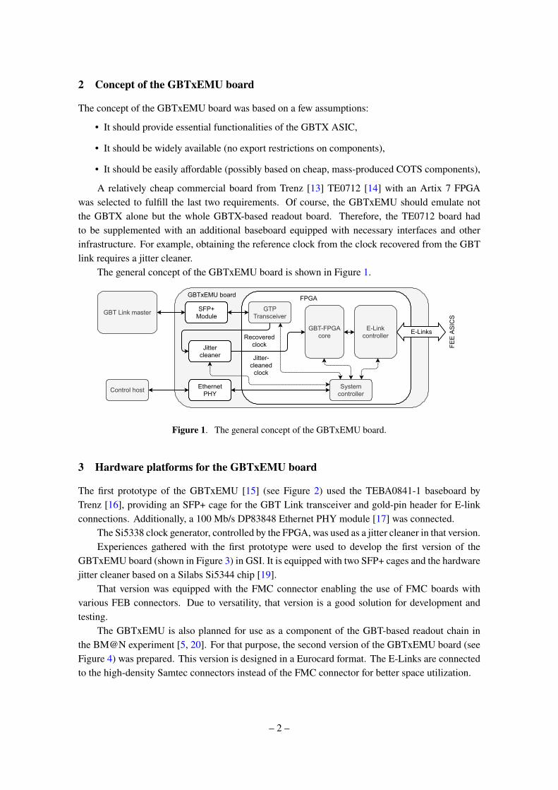
2 Concept of the GBTxEMU board
The concept of the GBTxEMU board was based on a few assumptions:
• It should provide essential functionalities of the GBTX ASIC,
• It should be widely available (no export restrictions on components),
• It should be easily affordable (possibly based on cheap, mass-produced COTS components),
A relatively cheap commercial board from Trenz [13] TE0712 [14] with an Artix 7 FPGAwas selected to fulfill the last two requirements. Of course, the GBTxEMU should emulate notthe GBTX alone but the whole GBTX-based readout board. Therefore, the TE0712 board hadto be supplemented with an additional baseboard equipped with necessary interfaces and otherinfrastructure. For example, obtaining the reference clock from the clock recovered from the GBTlink requires a jitter cleaner.
The general concept of the GBTxEMU board is shown in Figure 1.
GTPTransceiver GBT Link master SFP+
Module
Jittercleaner
Recoveredclock
GBT-FPGAcore
Jitter-cleaned
clock
E-Linkcontroller
FEE
ASIC
S
E-Links
FPGAGBTxEMU board
Systemcontroller Control host Ethernet
PHY
Figure 1. The general concept of the GBTxEMU board.
3 Hardware platforms for the GBTxEMU board
The first prototype of the GBTxEMU [15] (see Figure 2) used the TEBA0841-1 baseboard byTrenz [16], providing an SFP+ cage for the GBT Link transceiver and gold-pin header for E-linkconnections. Additionally, a 100 Mb/s DP83848 Ethernet PHY module [17] was connected.
The Si5338 clock generator, controlled by the FPGA, was used as a jitter cleaner in that version.Experiences gathered with the first prototype were used to develop the first version of the
GBTxEMU board (shown in Figure 3) in GSI. It is equipped with two SFP+ cages and the hardwarejitter cleaner based on a Silabs Si5344 chip [19].
That version was equipped with the FMC connector enabling the use of FMC boards withvarious FEB connectors. Due to versatility, that version is a good solution for development andtesting.
The GBTxEMU is also planned for use as a component of the GBT-based readout chain inthe BM@N experiment [5, 20]. For that purpose, the second version of the GBTxEMU board (seeFigure 4) was prepared. This version is designed in a Eurocard format. The E-Links are connectedto the high-density Samtec connectors instead of the FMC connector for better space utilization.
– 2 –

Figure 2. The first prototype of GBTxEMU, based on TE0712 and TEBA0841 boards. Picture from thepresentation [18].
Figure 3. The first version of the GBTxEMU board developed at GSI. On the left – the top side with theFMC equipped with ZIF connectors for FEBs. On the right – the bottom side with a TE0712-2 module.
Figure 4. The second version of the GBTxEMU developed at JINR in the Eurocard format and withhigh-density Samtec connectors for FEBs. The TE0712-2 module is covered with a heat sink.
– 3 –

4 Implementation of the GBTxEMU firmware
The block diagram of the GBTxEMU firmware is shown in Figure 5
Jittercleaner
IC
GTP Tx GBT-FPGA(adapted) E-links
Wishbone bus
IPbus J1B Forth CPU
UART
100
Mb/
sE
ther
net
GTP Rx
SM
X-A
SIC
S
DP
B
PH
Y
Startup clock
I2Cmaster
Si5338 Clocktuning
GTP RxGTP Tx
1000
BA
SE
-XE
ther
net
Figure 5. Block diagram of the GBTxEMU firmware (based on [21]).
Because the main system clock is obtained by the jitter-cleaning of the clock recovered fromthe GBT Link it means that certain initialization must be done before the main clock is available.For that purpose the GBTxEMU is equipped with the J1B system controller using the additional“boot clock”1.
4.1 J1B system controller
Initialization of the GBTxEMU requires configuring the clock generator, the jitter cleaner, and theGTP transceivers. For that purpose, a simple synthesizable J1B CPU [22] was implemented. Itis programmed in Forth [23] language. Due to good code density, despite relatively small 32 kBRAM, it may perform quite complex initialization routines. An example code that reads the board’sMAC address from a UNI/O FLASH memory [24] is shown in Listing 1.
The Forth language is considered to be difficult to learn but offers efficient possibilities ofinteractive work. It needs only a UART connection2 to the operator’s console. In the interactivemode, it is possible to create new procedures (called words in Forth) and execute them. ThenceForth may be a perfect debugging tool. The captured word definitions may also be compiled andput into the GBTxEMU configuration bitstream. The user-defined word cold is executed after thesystem starts.
4.2 GBTxEMU internal bus
Most functional blocks of the GBTxEMU are connected to the internal Wishbone bus. The bus ismanaged by the Address Generator for Wishbone (AGWB) system [4] which assigns the addresses
1The “boot clock” has a frequency of 10MHz in the first batches of GBTxEMU and then it was replaced with 20MHz2It is also possible to emulate UART via JTAG. The J1B connected via JTAG-emulated UART is used in the
KCU116_J1B project [25].
– 4 –

$1030 constant SCIO
\ This word keeps reading UNI/O dout until its ready
: scio_read_doutbeginSCIO io@ dup$80000000 and 0<>
whiledrop
repeatdup $40000000 and 0<> if$3 err_halt
then;
: scio_read_next_byte$32a006 SCIO io!
scio_read_dout
;
: read_mac ( -- MAC_hs3bytes MAC_ls3bytes )$fa00 SCIO 1 + io!
$54a003 SCIO io!
scio_read_dout
8 lshiftscio_read_next_byte
or 8 lshiftscio_read_next_byte
or\ Higher 3 bytes are on TOS
scio_read_next_byte
8 lshiftscio_read_next_byte
or 8 lshiftscio_read_next_byte
or\ Lower 3 bytes are on TOS
;
: set_mac ( MAC_hs3bytes MAC_ls3bytes -- )swap//_mac_ms3bytes wb!
//_mac_ls3bytes wb!
;
Listing 1: Example Forth code for the J1B, used to read the MAC address from the UNI/O FLASHmemory.
for the internal registers, generates the VHDL code providing access to those registers, and generatesthe software modules for Forth and Python, enabling convenient access to those registers via theirname. The address map may be automatically adjusted after modification of the register file.
The internalWishbone bus has three masters. The first of them is J1B, described in the previoussection and used for initialization and debugging. The second is the IPbus [26] master, which maycontrol the GBTxEMU via the independent Ethernet interface (with 100 Mb/s or 1 Gb/s speed).That requires that the board is initialized to the stage where the Ethernet connection is working.Otherwise, it enables control and debugging using Python running on the computer, which ismore convenient than Forth. The third master is the controller based on the GBT-SC core [27].This master provides the best emulation of GBTX because control commands and responses aretransmitted via the GBT link, just like in the case of the real GBTX.
4.3 The GBT-FPGA core
The GBT-FPGA core was developed by CERN [28]. It implements the essential GBTX function-alities in an FPGA. The original implementation, however, does not support the Artix 7 FPGAs.Therefore, certain modifications were necessary.
Adaptation of GBT-FPGA core was made based on a version prepared for Kintex 7 as itwas the most similar. The Artix 7 FPGAs use GTP transceivers [29], while Kintex 7 uses theGTX transceivers [30]. The necessary modifications were related to different widths of the internaldatapath, internal clock frequencies, and configurations of the PLL blocks generating the transceiverclock. The operation ofGTP transceivers at 4.8Gb/s (required for a standardGBT link)was achievedsuccessfully.
– 5 –

The Artix 7 FPGAs offer lower performance than Kintex 7. Despite this, it was possible toimplement the forward error correction (FEC) in the downlink direction, which is essential forreliable transmission of control commands to front-end ASICs. Also, the optimized latency modewas possible in the downlink direction – it is necessary to synchronize the front-end ASICs. Inthe uplink direction, the ported GBT-FPGA provides standard latency transmission in the Widebusmode (without FEC).
4.4 Implementation of E-Links
The E-Link block is responsible for retrieving the appropriate bits from the downlink GBT frameand sending them serially via E-Links, and simultaneously for receiving the bits from the E-Linksand storing them into the uplink GBT frame. The uplink direction is optimized for transmission ofthe hit data from the FEE ASIC. Thence, it is assumed that the uplink data are transmitted with adual data rate (DDR). Because the downlink in the FEC mode used by the GBTxEMU delivers one80-bit downlink frame every 25 ns, and the uplink in the Widebus mode accepts one 112-bit frameevery 25 ns, the possible number of E-Links depends on the E-Link clock frequency 𝑓EL CLK. It islimited by the number of bits available in the uplink frame and may be calculated according to theformula: 𝑁E-Links = ceil
(112·40 MHz2 𝑓EL CLK
).
Therefore, for E-Link clock frequency 𝑓EL CLK = 40MHz, the GBTxEMU may support up to56 E-Links, while for 𝑓EL CLK = 80MHz only 28.
The original GBTX ASIC offers a possibility to control the phase of the generated E-Linkclock and the delay of the input E-Link data. That enables adaptation to different values of the skewand length of the cable used for the FEE ASIC connection. In the GBTxEMU, the E-Link clockphase may be adjusted with a resolution of 78.125 ps using the MMCM block to produce the outputclock. The input data from the E-Link are delivered through the IDELAYE2 blocks with run-timecontrollable delay (up to 2.496 ns with 78 ps resolution and with selectable clock edge) [21]. Whenused together, those functions enable reliable operation of the E-Links.
5 Current use and results
Different versions of the GBTxEMU have been used in test setups in WUT, GSI, and JINR (seeFigure 6). The WUT setup is used mainly for development and testing purposes. In GSI, theGBTxEMU has been successfully used for debugging the port of the GBT-FPGA developed for theCRI readout board. The GBTxEMU provided extended diagnostics at the slave end of the GBTlink. In JINR, the GBTxEMU is used to develop the readout chain for the BM@N. It is also plannedto be used in its final version [5]. Of course, the FPGA-based design can not assure radiationhardness. However, in situations where the highest throughput of E-Links is not needed, the boardmay be placed at some distance from the on-detector electronics, outside of a high magnetic fieldand radiation environment. The 10-meter length copper cable connection between the front-endelectronics and GBTxEMU was proven to be stable in the BM@N STS project.
– 6 –

Figure 6. Three test setups equipped with GBTxEMU boards. On the left – the setup in GSI with 2GBTxEMU v1 and two connected FEB-8 boards. In the center – the setup at WUT with a single GBTxEMUv1 and connected FEB-8 board. On the right – setup at JINR with a GBTxEMU v2 and connected BM@NSTS FEB board.
6 Conclusions
The GBTX emulator (GBTxEMU) appeared to be a useful tool enabling the development of GBT-based readout systems in locations where the original GBTX ASIC cannot be used. It has alsoshown its potential at debugging the GBT links during porting of the GBT-FPGA IP core to thenew FPGAs. The GBTxEMU may be used in special versions of the GBT-based readout chain,where radiation hardness is not essential. It may also be a basis for creating the GBT-controlledtest setups for testing the FEE ASICs and modules connected via GBTX-compatible E-Links. TheFPGA-based design is highly flexible, providing the end-users with the possibility to implementtheir own extensions.
Acknowledgments
The work has been partially supported by GSI, and partially by the statutory funds of Institute ofElectronic Systems. This project has also received funding from the European Union’s Horizon2020 research and innovation programme under grant agreement No 871072.
References
[1] P. Moreira et al., “GBTX manual.”https://espace.cern.ch/GBT-Project/GBTX/Manuals/gbtxManual.pdf [Online; accessed22-September-2021], 2018.
[2] J. Mitra, E. David, E. Mendez, S.A. Khan, T. Kiss, S. Baron et al., Trigger and timing distributionsusing the TTC-PON and GBT bridge connection in ALICE for the LHC Run 3 Upgrade, NuclearInstruments and Methods in Physics Research Section A: Accelerators, Spectrometers, Detectors andAssociated Equipment 922 (2019) 119.
[3] M.B. Marin, S. Baron, S. Feger, P. Leitao, E. Lupu, C. Soos et al., The GBT-FPGA core: features andchallenges, Journal of Instrumentation 10 (2015) C03021.
[4] W. Zabolotny et al., Automatic management of local bus address space in complexFPGA-implemented hierarchical systems, in Proc. SPIE, vol. 11176, (Wilga, Poland), p. 1117642,SPIE, Nov., 2019, DOI.
[5] D. Dementev, M. Guminski, I. Kovalev, M. Kruszewski, I. Kudryashov, A. Kurganov et al., FastData-Driven Readout System for the Wide Aperture Silicon Tracking System of the BM@NExperiment, Physics of Particles and Nuclei 52 (2021) 830.
– 7 –

[6] P. Moreira, A. Marchioro and K. Kloukinas, The GBT, a proposed architecture for Multi-Gb/s datatransmission in high energy physics, in Proceedings of the Topical Workshop on Electronics forParticle Physics, TWEPP 2007, (Geneva), pp. 332–336, 2007.
[7] P. Antonioli, C. Baldanza, D. Falchieri, F. Giorgi, A. Mati and C. Tintori, Design and test of a GBTxbased board for the upgrade of the ALICE TOF readout electronics, in 2016 IEEE-NPSS Real TimeConference (RT), (Padova, Italy), pp. 1–3, IEEE, June, 2016, DOI.
[8] S. Naik, On-detector Electronics for the LHCb VELO Upgrade, Journal of Instrumentation 12 (2017)C02031.
[9] A. Fernandez Prieto, P. Vazquez Regueiro, K. Hennessy, J. Buytaert, M. van Beuzekom,E. Lemos Cid et al., Phase I Upgrade of the Readout System of the Vertex Detector at the LHCbExperiment, IEEE Transactions on Nuclear Science 67 (2020) 732.
[10] J. Lehnert, A. Byszuk, D. Emschermann, K. Kasinski, W. Müller, C. Schmidt et al., GBT basedreadout in the CBM experiment, Journal of Instrumentation 12 (2017) C02061.
[11] K. Kasinski, R. Kleczek, P. Otfinowski, R. Szczygiel and P. Grybos, STS-XYTER, a high count-rateself-triggering silicon strip detector readout IC for high resolution time and energy measurements, in2014 IEEE Nuclear Science Symposium and Medical Imaging Conference (NSS/MIC), (Seattle, WA,USA), pp. 1–6, IEEE, Nov., 2014, DOI.
[12] K. Kasinski et al., A protocol for hit and control synchronous transfer for the front-end electronics atthe CBM experiment, Nucl. Instrum. Methods Phys. Res. A 835 (2016) 66.
[13] “Trenz electronic.” https://www.trenz-electronic.de/en/ [Online; accessed22-September-2021], 2020.
[14] “Trenz Electronic TE0712 FPGA Modules with Xilinx Artix-7.”https://shop.trenz-electronic.de/en/Products/Trenz-Electronic/TE07XX-Artix-7/
TE0712-Artix-7/ [Online; accessed 22-September-2021], 2021.
[15] W. Zabolotny, A. Byszuk, M. Guminski, G. Kasprowicz, K. Michal, K. Pozniak et al., Preparation ofthe GBTX emulator, in CBM Progress Report 2018, V. SFriese and I. Selyuzhenkov, eds., (Darmstadt,Germany), p. 141, GSI Helmholtzzentrum fuer Schwerionenforschung, GSI, Darmstadt (2019), DOI.
[16] “TEBA0841 - Simple base for TE0841 and TE0741 .” https://shop.trenz-electronic.de/en/TEBA0841-02-TEBA0841-Simple-base-for-TE0841-and-TE0741 [Online; accessed22-September-2021], 2021.
[17] “DP83848 Ethernet Board.” https://www.waveshare.com/dp83848-ethernet-board.htm[Online; accessed 22-September-2021], 2021.
[18] “Presentation: GBTX Emulation for BM@N/MPD Data Acquisition Systems.”https://indico.cern.ch/event/802303/contributions/3775110/attachments/
2003728/3345799/Zabolotny.pdf [Online; accessed 22-September-2021], 2019.
[19] “Si5344d high-performance clock jitter attenuator, jitter cleaner.”https://www.skyworksinc.com/en/Products/Timing/
High-Performance-Jitter-Attenuators/Si5344D [Online; accessed 22-September-2021],2021.
[20] M. Shitenkov, D. Dementev, A. Voronin, I. Kovalev, I. Kudryashov, A. Kurganov et al., Front-EndElectronics for BM@N STS, Physics of Particles and Nuclei 52 (2021) 826.
[21] W. Zabolotny, A. Byszuk, M. Guminski, G. Kasprowicz, K. Michal, K. Pozniak et al., Firmware
– 8 –

development for CBM DAQ, in CBM Progress Report 2019, P. Senger, ed., (Darmstadt, Germany),pp. 160–161, GSI Helmholtzzentrum fuer Schwerionenforschung, GSI, Darmstadt (2020), DOI.
[22] W. Zabołotny et al., “Application of Forth CPU for control and debugging of FPGA-implementedsystems.” Presented at XLIV-th IEEE-SPIE Joint Symposium Wilga 2019https://www.waveshare.com/dp83848-ethernet-board.htm [Online; accessed22-September-2021]. 10.13140/RG.2.2.22940.85123.
[23] “Thinking Forth Project.” http://thinking-forth.sourceforge.net/ [Online; accessed22-September-2021].
[24] “11AA02E48 2Kb UNI/O Serial EEPROM with Pre-Programmed EUI-48 MAC Address.”https://www.microchip.com/en-us/product/11AA02E48 [Online; accessed22-September-2021], 2018.
[25] “Project for KCU116 board with internal Wishbone bus controlled either via J1B Forth CPU and viaIPbus or E2Bus.” https://gitlab.com/WZab/kcu116_j1b [Online; accessed22-September-2021].
[26] C.G. Larrea, K. Harder, D. Newbold, D. Sankey, A. Rose, A. Thea et al., IPbus: a flexibleEthernet-based control system for xTCA hardware, Journal of Instrumentation 10 (2015) C02019.
[27] “GBT-SC module for FPGA.” https://gitlab.cern.ch/gbtsc-fpga-support/gbt-sc[Online; accessed 22-September-2021].
[28] “Firmware dedicated to the GBT chipsets (GBTx, GBT-SCA, LpGBT ...)..”https://gitlab.cern.ch/gbt-fpga [Online; accessed 22-September-2021].
[29] “7 Series FPGAs GTP Transceivers User Guide.” https://www.xilinx.com/support/documentation/user_guides/ug482_7Series_GTP_Transceivers.pdf [Online; accessed22-September-2021].
[30] “7 Series FPGAs GTX/GTH Transceivers User Guide.” https://www.xilinx.com/support/documentation/user_guides/ug476_7Series_Transceivers.pdf [Online; accessed22-September-2021].
– 9 –