Gate-All-Around Nanowire MOSFET With Catalytic Metal Gate For Gas Sensing Applications
6
IEEE TRANSACTIONS ON NANOTECHNOLOGY, VOL. 12, NO. 6, NOVEMBER 2013 939 Gate-All-Around Nanowire MOSFET With Catalytic Metal Gate For Gas Sensing Applications Rajni Gautam, Member, IEEE, Manoj Saxena, Senior Member, IEEE, R. S. Gupta, Life Senior Member, IEEE, and Mridula Gupta, Senior Member, IEEE Abstract—In this paper, gate-all-around (GAA) MOSFET with catalytic metal gate is proposed for enhanced sensitivity of gas sen- sor. P-channel GAA MOSFET with palladium (Pd) metal gate is used for hydrogen sensing and n-channel GAA MOSFET with silver (Ag) metal gate is used for Oxygen sensing. The GAA nanowire MOSFET has already been demonstrated experimen- tally for biosensing and chemical sensing applications. However, cylindrical GAA MOSFET with catalytic metal gate for gas sens- ing applications is proposed for the first time in this paper. An ana- lytical model is developed for both p-channel and n-channel GAA MOSFET to calculate the sensitivity of the device in the presence of gas molecules and analytical model is verified with the simulation results of ATLAS-3D. Sensitivity of the GAA MOSFET gas sensor is compared with the conventional bulk MOSFET gas sensor and impact of the radius of the silicon pillar on the sensitivity of the GAA MOSFET is also studied. Index Terms—ATLAS-3D, gas sensor, gate-all-around (GAA) MOSFET, sensitivity, work function. I. INTRODUCTION T O meet ever increasing demand of gas detection sensors for environmental monitoring, automotive and medical in- dustries, MOSFET-based gas sensors [1]–[3] is a good choice as it offers low cost, low power, small size, and high sensitivity along with CMOS compatibility. In recent years, a MOSFET gas sensor has been developed for detection of gas species by measuring the induced shift of work function at the surface of a sensitive film. Research and development in this field is undergo- ing in two directions: 1) exploration of suitable sensitive films such as catalytic metals [1]–[7], metal compounds [8]–[15], hydrated salts [16], [17], polymers, and other organic com- pounds [18], [19]; and 2) device engineering including design and optimization of the field-effect device to enhance the sen- sitivity. In the area of device engineering, floating gate MOS- FET [20], SOI MOSFET [21], dual-gate MOSFET [3], and now nanowire MOSFET [14], [15] devices have been taken into con- Manuscript received March 17, 2013; revised July 21, 2013; accepted July 29, 2013. Date of publication August 2, 2013; date of current version November 6, 2013. The review of this paper was arranged by Associate Editor A. Bhalerao. R. Gautam and M. Gupta are with the Semiconductor Device Research Lab- oratory, Department of Electronic Science, University of Delhi, South Campus, New Delhi 110021, India (e-mail: [email protected]). M. Saxena is with the Department of Electronics, Deen Dayal Upadhyaya College, University of Delhi, New Delhi 110015, India. R. S. Gupta is with the Department of Electronics and Communication Engi- neering, Maharaja Agrasen Institute of Technology, New Delhi 110086, India. Color versions of one or more of the figures in this paper are available online at http://ieeexplore.ieee.org. Digital Object Identifier 10.1109/TNANO.2013.2276394 sideration. To increase the sensitivity by increasing the opportu- nities for surface reactions, a high ratio of surface area to volume is needed. High surface-to-volume ratio, low leakage current, better gate control, and nearly ideal subthreshold characteris- tics [22], [23] make gate-all-around (GAA) nanowire MOS- FET promising device architecture for developing a low-power highly sensitive, and nanoscale CMOS-compatible gas sensor. Gas sensors based on metal oxide NWs such as ZnO, In 2 O 3 , and SnO 2 field-effect transistors (FETs) are already demon- strated [13]–[15]. Another class of FET-based gas sensors using catalytic metal gate is reported earlier [1]–[3]. Reaction of gas molecules at the catalytic metal gate surface results in change in the work function of the gate metal which further causes change in flat-band voltage, threshold voltage, and drain current of the MOSFET device. This change in conductivity is directly related to the amount of a specific gas present in the environ- ment, resulting in a quantitative determination of gas presence and concentration. Recently, an FET-based oxygen sensor using Ag catalytic metal gate has been reported in [2]. Dual-gate FET hydrogen gas sensor using Pt metal gate was studied by Tsukada et al. [3]. However, cylindrical GAA MOSFET with catalytic metal gate has not been explored for gas sensing applications. In this paper, a GAA p-channel MOSFET with catalytic metal gate is proposed for the first time for improving the sensitivity applications. Conventionally, FET-based gas sensors use thresh- old voltage as the sensitivity parameter; however, in this study, subthreshold current instead of threshold voltage is used to cal- culate sensitivity of the gas sensor, which enables low-power operation along with high sensitivity. A much higher sensitiv- ity for gas detection is observed in this study when the device is operated in the subthreshold regime. This type of behavior was also reported by Gao et al. [24] for nanowire biosensors. They have reported 500 times improvement in protein detec- tion limit by operating NW FET in the subthreshold regime. This high sensitivity in the subthreshold regime is attributed to the additional band bending taking place in absence of Fermi level pinning due to change in metal semiconductor work func- tion after surface reaction. Fabrication of GAA MOSFET has already been demonstrated experimentally [25], [26] and its de- vice physics is explained through an analytical model [27], [28]. In this study, GAA MOSFET with Ag metal gate for Oxygen sensing [5] is modeled and validated by the simulated results using the ATLAS device simulator [29]. The impact of the ra- dius of the silicon body on the sensitivity of the gas sensor is also investigated. The sensitivity of the GAA MOSFET is com- pared with the Bulk MOSFET which is a conventionally used architecture for the FET-based gas sensor. 1536-125X © 2013 IEEE
Transcript of Gate-All-Around Nanowire MOSFET With Catalytic Metal Gate For Gas Sensing Applications

IEEE TRANSACTIONS ON NANOTECHNOLOGY, VOL. 12, NO. 6, NOVEMBER 2013 939
Gate-All-Around Nanowire MOSFET With CatalyticMetal Gate For Gas Sensing Applications
Rajni Gautam, Member, IEEE, Manoj Saxena, Senior Member, IEEE, R. S. Gupta, Life Senior Member, IEEE,and Mridula Gupta, Senior Member, IEEE
Abstract—In this paper, gate-all-around (GAA) MOSFET withcatalytic metal gate is proposed for enhanced sensitivity of gas sen-sor. P-channel GAA MOSFET with palladium (Pd) metal gate isused for hydrogen sensing and n-channel GAA MOSFET withsilver (Ag) metal gate is used for Oxygen sensing. The GAAnanowire MOSFET has already been demonstrated experimen-tally for biosensing and chemical sensing applications. However,cylindrical GAA MOSFET with catalytic metal gate for gas sens-ing applications is proposed for the first time in this paper. An ana-lytical model is developed for both p-channel and n-channel GAAMOSFET to calculate the sensitivity of the device in the presence ofgas molecules and analytical model is verified with the simulationresults of ATLAS-3D. Sensitivity of the GAA MOSFET gas sensoris compared with the conventional bulk MOSFET gas sensor andimpact of the radius of the silicon pillar on the sensitivity of theGAA MOSFET is also studied.
Index Terms—ATLAS-3D, gas sensor, gate-all-around (GAA)MOSFET, sensitivity, work function.
I. INTRODUCTION
TO meet ever increasing demand of gas detection sensorsfor environmental monitoring, automotive and medical in-
dustries, MOSFET-based gas sensors [1]–[3] is a good choiceas it offers low cost, low power, small size, and high sensitivityalong with CMOS compatibility. In recent years, a MOSFETgas sensor has been developed for detection of gas species bymeasuring the induced shift of work function at the surface of asensitive film. Research and development in this field is undergo-ing in two directions: 1) exploration of suitable sensitive filmssuch as catalytic metals [1]–[7], metal compounds [8]–[15],hydrated salts [16], [17], polymers, and other organic com-pounds [18], [19]; and 2) device engineering including designand optimization of the field-effect device to enhance the sen-sitivity. In the area of device engineering, floating gate MOS-FET [20], SOI MOSFET [21], dual-gate MOSFET [3], and nownanowire MOSFET [14], [15] devices have been taken into con-
Manuscript received March 17, 2013; revised July 21, 2013; accepted July29, 2013. Date of publication August 2, 2013; date of current version November6, 2013. The review of this paper was arranged by Associate Editor A. Bhalerao.
R. Gautam and M. Gupta are with the Semiconductor Device Research Lab-oratory, Department of Electronic Science, University of Delhi, South Campus,New Delhi 110021, India (e-mail: [email protected]).
M. Saxena is with the Department of Electronics, Deen Dayal UpadhyayaCollege, University of Delhi, New Delhi 110015, India.
R. S. Gupta is with the Department of Electronics and Communication Engi-neering, Maharaja Agrasen Institute of Technology, New Delhi 110086, India.
Color versions of one or more of the figures in this paper are available onlineat http://ieeexplore.ieee.org.
Digital Object Identifier 10.1109/TNANO.2013.2276394
sideration. To increase the sensitivity by increasing the opportu-nities for surface reactions, a high ratio of surface area to volumeis needed. High surface-to-volume ratio, low leakage current,better gate control, and nearly ideal subthreshold characteris-tics [22], [23] make gate-all-around (GAA) nanowire MOS-FET promising device architecture for developing a low-powerhighly sensitive, and nanoscale CMOS-compatible gas sensor.Gas sensors based on metal oxide NWs such as ZnO, In2O3 ,and SnO2 field-effect transistors (FETs) are already demon-strated [13]–[15]. Another class of FET-based gas sensors usingcatalytic metal gate is reported earlier [1]–[3]. Reaction of gasmolecules at the catalytic metal gate surface results in changein the work function of the gate metal which further causeschange in flat-band voltage, threshold voltage, and drain currentof the MOSFET device. This change in conductivity is directlyrelated to the amount of a specific gas present in the environ-ment, resulting in a quantitative determination of gas presenceand concentration. Recently, an FET-based oxygen sensor usingAg catalytic metal gate has been reported in [2]. Dual-gate FEThydrogen gas sensor using Pt metal gate was studied by Tsukadaet al. [3]. However, cylindrical GAA MOSFET with catalyticmetal gate has not been explored for gas sensing applications.In this paper, a GAA p-channel MOSFET with catalytic metalgate is proposed for the first time for improving the sensitivityapplications. Conventionally, FET-based gas sensors use thresh-old voltage as the sensitivity parameter; however, in this study,subthreshold current instead of threshold voltage is used to cal-culate sensitivity of the gas sensor, which enables low-poweroperation along with high sensitivity. A much higher sensitiv-ity for gas detection is observed in this study when the deviceis operated in the subthreshold regime. This type of behaviorwas also reported by Gao et al. [24] for nanowire biosensors.They have reported 500 times improvement in protein detec-tion limit by operating NW FET in the subthreshold regime.This high sensitivity in the subthreshold regime is attributed tothe additional band bending taking place in absence of Fermilevel pinning due to change in metal semiconductor work func-tion after surface reaction. Fabrication of GAA MOSFET hasalready been demonstrated experimentally [25], [26] and its de-vice physics is explained through an analytical model [27], [28].In this study, GAA MOSFET with Ag metal gate for Oxygensensing [5] is modeled and validated by the simulated resultsusing the ATLAS device simulator [29]. The impact of the ra-dius of the silicon body on the sensitivity of the gas sensor isalso investigated. The sensitivity of the GAA MOSFET is com-pared with the Bulk MOSFET which is a conventionally usedarchitecture for the FET-based gas sensor.
1536-125X © 2013 IEEE

940 IEEE TRANSACTIONS ON NANOTECHNOLOGY, VOL. 12, NO. 6, NOVEMBER 2013
Fig. 1. Schematic structure of GAA MOSFET with air gap dielectric. Deviceparameters: channel length (L) = 50 nm, radius (R) = 5 nm, oxide thickness(tox ) = 2 nm, and channel doping (NA ) = 1 × 10²¹ m−3 . (b) Simulatedstructure of GAA MOSFET.
TABLE ILIST OF TECHNOLOGY PARAMETERS
II. SIMULATION AND CALIBRATION
Fig. 1(a) shows the schematic structure and Fig. 1(b) showsthe simulated structure of GAA MOSFET gas sensor with cat-alytic metal gate. N-channel GAA MOSFET with Ag metal gateis used for oxygen detection and p-channel GAA MOSFET withPd gate is used for hydrogen sensing. Ag with p-channel andPd with n-channel can also be used but it results in very low offcurrents (i.e., in the range of femtoamperes) which are undermeasurable limits and also vulnerable to noise. Also, sensingcircuitry for such low currents adds to the cost of the sensorwhich is a major concern. Table I shows all the technologyparameters used in the simulation and model.
Calibration of model parameters used in the simulation hasbeen performed according to the experimental results [25]. Sinceradius of silicon pillar is greater than 5 nm, thus quantum effects
Fig. 2. Validation of simulation results with experimental results [25] for acylindrical GAA MOSFET. L = 60 nm, R = 5 nm, and tox = 3.5 nm.
are not taken into account [28]. Various models used in sim-ulation are as follows: drift diffusion, concentration-dependentmobility, field-dependent mobility, and Shockley–Read–Hall re-combination model. Closed proximity of analytical and simu-lated results with the experimental results [25] as shown in Fig. 2validates the choice of parameters taken in modeling and sim-ulation. Two catalytic metal gates (i.e., Pd for hydrogen sensorand Ag for oxygen sensor) are used. Chemical reaction of gasmolecules at the surface of the catalytic metal gate changes thework function of the metal. Thus, gas sensitivity of the deviceis manifested as a change of the threshold voltage and draincurrent. This work is valid at room temperature only as workfunction principle of gas sensing is dedicated for room tempera-ture or slightly elevated temperatures of operation as suggestedby Eisele et al. [30].
III. ANALYTICAL MODEL FORMULATION
Assuming parabolic profile in the radial direction and apply-ing appropriate potential and electric field boundary conditions,surface potential can be expressed as
φs (z) = Aekz + Be−kz + Φ for an n-channel
φs (z) = −Aekz − Be−kz − Φ for a p-channel (1)
where k is given by
k2 = 2εox/(εsiR2 ln(1 + tox/R)) (2)
and Φ is given by
Φ = Vgs − Vfb − qNsi/εsik2 for n-channel
Φ = Vfb − Vgs − qNsi/εsik2 for p-channel. (3)
Boundary conditions of electric potential and field are givenas follows.
1) The center potential is a function of z only:
φ (r = 0, z) = φc(z). (4)
2) The electric field at the center of silicon film is zero:
dφ (r, z)dr
∣∣∣∣r=0
= 0. (5)
GAUTAM et al.: GATE-ALL-AROUND NANOWIRE MOSFET WITH CATALYTIC METAL GATE FOR GAS SENSING APPLICATIONS 941
3) The electric field at the silicon oxide interface is given by
dφ (r, z)dr
∣∣∣∣ r= t s i
2=
Cox
εsi
(
Vgs − Vfb − φ
(
r =tsi2
, z
))
for n-channel
dφ (r, z)dr
∣∣∣∣ r= t s i
2=
Cox
εsi
(
φ
(
r =tsi2
, z
)
− Vgs + Vfb
)
for p-channel. (6)
Here, Cox is the oxide capacitance per unit area of the GAAMOSFET represented by
Cox = εox/ ((R/2) ln(1 + tox/R)) . (7)
tsi is the silicon film thickness, R is the silicon pillar radius, andtox is the gate dielectric layer thickness. εsi is the permittivity ofthe silicon and εox is the permittivity of the oxide layer. Vgs isthe gate-to-source voltage and Vfb is the flat-band voltage. ΔΦm
is the change in the catalytic metal work function induced bythe gas molecules reaction at the metal surface. Thus, effectiveVfb is given by
V ′fb = φm − φs ± Δφm (8)
where φs is the silicon work function given by
φs =Eg
2+ χ + qφf p for n-channel
φs =Eg
2+ χ − qφf n for p-channel (9)
Δφm depends upon the gate metal and the gas to be detectedand is given by
Δφm = cont −(
RT
4F
)
ln P (10)
where F is Faraday’s constant, R is the gas constant, T is theabsolute temperature, and P is the gas partial pressure. Sincepartial pressure depends upon concentration of gas molecules,thus the gas sensors can be calibrated to read out in mole fractionof the gas in air, or units of moles of gas per mole of air.
The coefficients A and B are calculated using boundary con-ditions at the source and drain and are given by
A =(Vbi + φ)
(
1 − e−kL)
+ V ds
2 sinh (kL)(11)
B =(Vbi + φ)
(
ekL − 1)
− V ds
2 sinh (kL). (12)
Complete 2-D potential is given by
φ (r, z) = φs (z) +Cox
2εsiR(Vgs − Vfb − φs (z)) (r2 − R2),
for n-channel
φ (r, z) = φs (z) +Cox
2εsiR(φs (z) − Vgs + Vfb) (r2 − R2),
for p-channel . (13)
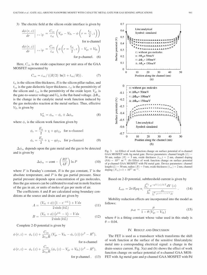
Fig. 3. (a) Effect of work function change on surface potential of n-channelGAA MOSFET with Ag metal gate. Device parameters: channel length (L) =50 nm, radius (R) = 5 nm, oxide thickness (tox ) = 2 nm, channel doping(NA) = 1021 m−3 . (b) Effect of work function change on surface potentialof p-channel GAA MOSFET with Pd metal gate. Device parameters: channellength (L) = 50 nm, radius (R) = 5 nm, oxide thickness (tox ) = 2 nm, channeldoping (NA )=1 × 10²¹ m−3 .
Based on 2-D potential, subthreshold current is given by
Isub = 2πRμq ni
∫ Vd
Vse−q V (z )/k T dV (z)
∫ L
0dz
∫ R0 eq φ ( r , z ) / k T dr
. (14)
Mobility reduction effects are incorporated into the model asfollows:
μeff =μ
1 − θ (Vgs − Vth)(15)
where θ is a fitting constant whose value used in this study isθ = 0.04.
IV. RESULT AND DISCUSSION
The FET is used as a transducer which transforms the shiftof work function at the surface of the sensitive film/catalyticmetal into a corresponding electrical signal: a change in thedrain-source current. Fig. 3(a) and (b) shows the effect of workfunction change on surface potential of n-channel GAA MOS-FET with Ag metal gate and p-channel GAA MOSFET with Pd

942 IEEE TRANSACTIONS ON NANOTECHNOLOGY, VOL. 12, NO. 6, NOVEMBER 2013
Fig. 4. (a) Ids versus Vgs with and without gas molecules for n-channel GAAMOSFET with Ag metal gate. Device parameters: channel length (L) = 50 nm,radius (R) = 5 nm, oxide thickness (tox ) = 2 nm, channel doping (NA ) =1021 m−3 , drain-to-source voltage (Vds ) = 0.05 V. (b) Ids versus Vgs with andwithout gas molecules for p-channel GAA MOSFET with Pd metal gate. Deviceparameters: channel length (L) = 50 nm, radius (R) = 5 nm, oxide thickness(tox ) = 2 nm, channel doping (NA ) = 1021 m−3 , and drain-to-source voltage(Vds ) = 0.05 V.
metal gate, respectively. Reaction of gas molecules at the cat-alytic metal gate surface results in change in the work functionof the gate metal which further causes change in flat-band volt-age due to additional band bending. Flat-band voltage changeresults in shift in the surface potential, threshold voltage Vth ,and drain current. Thus, by monitoring the change in Vth , Ioff ,and Ion , it is possible to detect the presence of gas molecules, forexample, oxygen, hydrogen, ammonia, and other hydrocarbonsusing suitable catalytic metal gates. Fig. 4(a) and (b) shows theeffect of work function change on the drain current for n-channeland p-channel GAA MOSFET respectively. As can be seen, Ioffis changed exponentially when the work function is changedin millivolts and it clearly shows that effect of gas moleculesis much higher on Ioff as compared to Ion ; thus, subthresholdregion offers much higher sensitivity along with low-power op-eration, thus providing low-cost gas sensor device. This highsensitivity in the subthreshold regime is attributed to the ad-
Fig. 5. Ids versus Vgs with and without gas molecules for p-channel bulkMOSFET with Pd metal gate. Device parameters: channel length (L) = 50 nm,silicon film thickness (tsi ) = 20 nm, oxide thickness (tox ) = 2 nm, channeldoping (NA )=1021 m−3 , drain-to-source voltage (Vds ) = 0.05 V.
TABLE IISENSITIVITY COMPARISON OF p-CHANNEL GAA MOSFET WITH Pd GATE
AND BULK MOSFET WITH Pd GATE
ditional band bending in absence of Fermi level pinning dueto change in metal semiconductor work function after surfacereaction of gas molecules. This type of behavior has also beenreported by Gao et al. [24] for nanowire biosensors. 100-meVchange in work function of Pd metal gate in p-channel GAAMOSFET results in 43 times change in Ioff . Close proximityof the analytical results with the simulated results for both n-channel and p-channel GAA MOSFETs validates the analyticalmodel. Fig. 5 shows the effect of work function change ondrain current characteristics of the bulk MOSFET. The order ofchange in Ioff is only five times for bulk MOSFET, whereas it is43 times for GAA MOSFET for 100-meV change in the workfunction; thus, GAA MOSFET shows much higher sensitivityfor gas detection as compared to bulk MOSFET.
Table II demonstrates the sensitivity comparison in terms oforder of change in Ioff , i.e., ratio of Ioff before and after gasreaction at the gate metal. The effect of work function change

GAUTAM et al.: GATE-ALL-AROUND NANOWIRE MOSFET WITH CATALYTIC METAL GATE FOR GAS SENSING APPLICATIONS 943
induced by gas molecules on Ioff is compared for two architec-tures, i.e., bulk MOSFET and GAA MOSFET. Both devices areoptimized for the same threshold voltage. Enhanced sensitivityin case of GAA structure is due to surrounding gate structurehaving higher surface-to-volume ratio which means exposingthe channel to a more effective control of gate which appears ingreater change in subthreshold current when the work functionof the gate metal is changed due to reaction of gas moleculeswith catalytic metal gate. Table II also illustrates the effect ofsilicon pillar radius on the sensitivity of the GAA MOSFET gassensor. For a GAA MOSFET, higher radius gives higher currentdriving capability and higher gain but thinner radius leads tobetter subthreshold characteristics. Since in this study, changein subthreshold current is used as the sensitivity parameter forgas sensing, therefore, subthreshold characteristics are of majorconcern. It can be seen from Table II that sensitivity is enhancedfor thinner silicon body. Higher sensitivity in case of thinnersilicon body is attributed to the higher surface to volume ratio,enhanced gate control, and low subthreshold leakage current.
V. CONCLUSION
GAA MOSFET with catalytic metal gate shows high sen-sitivity toward detection of gas molecules over conventionalbulk MOSFET due to its surrounding gate structure and highersurface-to-volume ratio. N-channel GAA MOSFET with Aggate is used for oxygen sensing and p-channel GAA MOSFETwith Pd gate is used for hydrogen sensing. Change in subthresh-old current induced by work function change of gate metal dueto reaction of gas molecules at the surface of gate catalyticmetal is used as the sensitivity parameter which provides veryhigh sensitivity as compared to the case when sensitivity is cal-culated in terms of threshold voltage change or change in oncurrent. Operating device in the subthreshold region is also ad-vantageous because it provides low-power, low-cost gas sensor.The sensitivity of the device can be further increased by de-creasing the radius of the silicon nanowire. The effective gatecontrol, large surface-to-volume ratio, and better short-channelcharacteristics of GAA MOSFET make it a promising candidatefor ultrasensitive, small, low-power, low-cost, CMOS-based gassensors.
ACKNOWLEDGMENT
The authors are grateful to the Defence Research and De-velopment Organization, Government of India. R. Gautam isthankful to the University Grants Commission, Government ofIndia for providing the necessary financial assistance to carryout this research work.
REFERENCES
[1] I. Lundstrom, M. Armgarth, A. Spetz, and F. Winquist, “Gas sensors basedon catalytic metal-gate field-effect devices,” Sens. Actuators, vol. 10,pp. 399–421, Nov. 1986.
[2] K. Tsukada, D. Kiriake, K. Sakai, and T. Kiwa, “Silver gate field effecttransistor for oxygen gas sensor,” in Proc. 2nd Int. Conf. Sens. DeviceTechnol. Appl., French Riviera, France, Aug. 21–27, 2011, pp. 5–7.
[3] K. Tsukada, M. Kariya, T. Yamaguchi, T. Kiwa, H. Yamada, T. Maehara,T. Yamamoto, and S. Kunitsugu, “Dual gate field effect transistor hydro-
gen gas sensor with thermal compensation,” Jpn. J. Appl. Phys., vol. 49,pp. 024206-1–024206-5, 2010.
[4] T. L. Poteat and B. Lalevi, “Pd-MOS hydrogen and hydrocarbon sensordevice,” IEEE Electron Device Lett., vol. EDL-2, no. 4, pp. 82–84, Apr.1981.
[5] K. Scharnagl, A. Karthigeyan, M. Burgmair, M. Zimmer, T. Doll, andI. Eisele, “Low temperature hydrogen detection at high concentrations:Comparison of platinum and iridium,” Sens. Actuators B, vol. 80, pp. 163–168, 2001.
[6] K. Scharnagl, M. Eriksson, A. Karthigeyan, M. Burgmair, M. Zimmer,and I. Eisele, “Hydrogen detection at high concentrations with stabilizedpalladium,” Sens. Actuators B, vol. 78, pp. 138–143, 2001.
[7] M. Zimmer, M. Burgmair, K. Scharnagl, A. Karthigeyan, T. Doll, andI. Eisele, “Gold and platinum as ozone sensitive layer in work-functiongas sensors,” Sens. Actuators B, vol. 80, pp. 174–178, 2001.
[8] A. Karthigeyan, R. P. Gupta, K. Scharnagl, M. Burgmair, S. K. Sharma,and I. Eisele, “A room temperature HSGFET ammonia sensor based oniridium oxide thin film,” Sens. Actuators B, vol. 85, pp. 145–153, 2002.
[9] A. Karthigeyan, R. P. Gupta, K. Scharnagl, M. Burgmair, M. Zimmer,S. K. Sharma, and I. Eisele, “Low temperature NO2 sensitivity of nano-particulate SnO2 film for work function sensors,” Sens. Actuators B,vol. 78, pp. 69–72, 2001.
[10] T. Doll, A. Fuchs, I. Eisele, G. Faglia, S. Gropelli, and G. Sberveglieri,“Conductivity and work function ozone sensors based on indium oxide,”Sens. Actuators B, vol. 49, pp. 63–67, 1998.
[11] M. Bogner, A. Fuchs, T. Doll, and I. Eisele, “Thin (NiO)1−x (Al2 O3 )x,Al doped and Al coated NiO layers for gas detection with HSGFET,”Sens. Actuators B, vol. 47, pp. 145–151, 1998.
[12] E. N. Dattoli, Q. Wan, W. Guo, Y. B. Chen, X. Q. Pan, and W. Lu, “Fullytransparent thin-film transistor devices based on SnO2 nanowires,” NanoLett., vol. 7, no. 8, pp. 2463–2469, 2007.
[13] Z. Y. Fan, D. W. Wang, C. C. Pai, W. Y. Tseng, and J. G. Lu, “ZnOnanowire field-effect transistor and oxygen sensing property,” Appl. Phys.Lett., vol. 85, pp. 5923–5925, 2004.
[14] C. Li, D. H. Zhang, X. L. Liu, S. Han, T. Tang, J. Han, and C. W. Zhou,“In2 O3 nanowires as chemical sensors,” Appl. Phys. Lett., vol. 82,pp. 1613–1615, 2003.
[15] R. Gupta, Z. Gergintschew, D. Schipanski, and P. Vyas, “New gas sensingproperties of high TC cuprates,” Sens. Actuators B, vol. 56, pp. 65–72,1999.
[16] V. M. Fuenzalida, M. E. Pilleux, and I. Eisele, “Adsorbed water on hy-drothermal BaTiO3 films: Work function measurements,” Vacuum, vol. 55,pp. 81–83, 1999.
[17] A. Fuchs, M. Bogner, T. Doll, and I. Eisele, “Room temperature ozonesensing with HSGFET gas sensors based on KI layers,” Sens. ActuatorsB, vol. 48, pp. 297–300, 1998.
[18] M. Liess, D. Chinn, D. Petelenz, and J. Janata, “Properties of insulatedgate field effect transistors with polyaniline gate electrode,” Thin SolidFilms, vol. 286, pp. 252–255, 1996.
[19] V. Meister, K. Potje-Kamloth, and H. D. Liess, “Polymer-oxide-siliconfield effect transistor (POSFET) as sensor for gases and vapors,” in Proc.6th Int. Meeting Chem. Sens., 1996, p. 179.
[20] M. A. R. Barranca, S. M. Acevedo., L. M. F. Nava, A. A. Garcıa,E. N. V. Acosta, J. A. M. Cadenas, and G. C. Cruz, “Using a floating-gate MOS transistor as a transducer in a MEMS gas sensing system,” inProc. Sensors 2010, 2010, vol. 10, pp. 10413–10434.
[21] F. Udrea, J. W. Gardner, D. Setiadi, J. A. Covington, T. Dogaru, C. C. Lu,and W. I. Milne, “Design and simulations of a new class of SOI CMOSmicro hot-plate gas sensors,” Sens. Actuators B, Chem., vol. 78, pp. 180–190, 2001.
[22] S. H. Oh, D. Monore, and J. M. Hergenrother, “Analytical descriptionof short-channel effects in fully-depleted double-gate and cylindrical,surrounding-gate MOSFETs,” IEEE Electron Device Lett., vol. 21, no. 9,pp. 445–447, Sep. 2000.
[23] B. Yu, Y. Yuan, J. Song, and Y. Taur, “A two-dimensional analyticalsolution for short-channel effects in nanowire MOSFETs,” IEEE Trans.Electron Devices, vol. 56, no. 10, pp. 2357–2362, Oct. 2009.
[24] X. P. A. Gao, G. Zheng, and C. M. Lieber, “Subthreshold regime hasthe optimal sensitivity for nanowire FET biosensors,” Nano lett, vol. 10,pp. 547–552, 2010.
[25] B. H. Hong, Y. C. Jung, J. S. Rieh, S. W. Hwang, K. H. Cho, K. H. Yeo,S. D. Suk, Y. Y. Yeoh, M. Li, D. W. Kim, D. Park, K. S. Oh, and W. S. Lee,“Possibility of transport through a single acceptor in a gate-all-aroundsilicon nanowire PMOSFET,” IEEE Trans. Nanotechnol., vol. 8, no. 6,pp. 713–717, Nov. 2009.

944 IEEE TRANSACTIONS ON NANOTECHNOLOGY, VOL. 12, NO. 6, NOVEMBER 2013
[26] K. D. Buddharaju, N. Singh, S. C. Rustagi, S. H. G. Teo, G. Q. Lo,N. Balasubramanian, and D. L. Kwong, “Si-nanowire CMOS inverterlogic fabricated using gate-all-around (GAA) devices and top-down ap-proach,” Solid State Electron., vol. 52, pp. 1312–1317, 2008.
[27] T. K. Chiang, “A compact, analytical two-dimensional threshold voltagemodel for cylindrical, fully-depleted, surrounding-gate (SG) MOSFETs,”Semicond. Sci. Technol., vol. 20, pp. 1173–1178, 2005.
[28] A. Tsormpatzoglou, D. H. Tassis, C. A. Dimitriadis, G. Ghibaudo,G. Pananakakis, and R. Clerc, “A compact drain current model of short-channel cylindrical gate-all-around MOSFETs,” Semicond. Sci. Technol.,vol. 24, pp. 1–8, 2009.
[29] ATLAS User’s Manual: 3-D Device Simulator, Version 5.14.0.R, SIL-VACO International, Santa Clara, CA, USA, Version 5.14.0.R, 2010.
[30] I. Eisele, T. Doll, and M. Burgmair, “Low power gas detection with FETsensors,” Sens. Actuators B, vol. 78, pp. 19–25, 2001.
Rajni Gautam (M’10) is currently working towardthe Ph.D. degree in the Department of Electronic Sci-ence, University of Delhi South Campus, New Delhi,India.
Manoj Saxena (SM’08) received the B.Sc.(Hons.),M.Sc., and Ph.D. degrees in electronics from the Uni-versity of Delhi, New Delhi, India.
He is currently an Associate Professor with DeenDayal Upadhyaya College, University of Delhi, In-dia.
R. S. Gupta (LSM’10) received the Ph.D. degreefrom Banaras Hindu University, Varanasi, India, in1970.
He is currently a Professor and a Department Headwith the Maharaja Agrasen Institute of Technology,New Delhi, India.
Mridula Gupta (SM’09) received the Ph.D. degreefrom the University of Delhi, New Delhi, India, in1998.
She is currently an Associate Professor withthe Department of Electronic Science, University ofDelhi South Campus, New Delhi.