Γ _ . - ~ _ ., ~ _ ,τ τ~~ . ." . ~ . ι. ι . . . ~ . Υ . , . . , .~ . . ~ - . ..
109
Γ _ . - ~ _ ., ~ _ ,τ τ ~~~ . ." . ~ . ι. ι . . . ~ . Υ . , . . , .~ . . ~ - . ..
-
Upload
khangminh22 -
Category
Documents
-
view
1 -
download
0
Transcript of Γ _ . - ~ _ ., ~ _ ,τ τ~~ . ." . ~ . ι. ι . . . ~ . Υ . , . . , .~ . . ~ - . ..

Γ _.
-
~
_ .,
~
_
,ττ~~~
. ."
.~ .
ι. ι .
. . ~ . Υ .
,
.
. ,
.~ .
.~ -
.
..

Tektro
7S11SAMPLING
UNIT
" Tektron ix , Inc.Ρ.Ο . Box 500Beaverton , Oregon97077
Serial Nu mber
1X@COMMITTEDTO EXCELLENCE
PLEASE CHECK FOR CHANGE INFORMATIONAT THE REAR OF THIS MANUAL.
INSTRUCTION MANUAL
F irst P rinting FEB 1970070-0985-00
Revised JUN 1981

Co pyrig ht ' 1970 Te ktro n ix, I n c . All rig hts reserved .Contents of this p u blication may not be reproduced inanyform without t h e written permission of Tektronix, Inc .
Products of Tektronix, Inc . and its s ubsidiaries arecovered by U .S . and foreig n patents a n d'or pe n dingpatents .
TEKTRONIX, ΤΕΚ , SCO PE-MO BIL E , and
areregistered trademar ks of Tektronix, Inc . T ELEQU IP-ΜΕΝΤ is α registere d trademar k of Tektronix U .KLimited .
Printed in U.S.Α. Specification and price c h a ngeprivileges are reserved .

TABLE OF CONTENTS
SECTION 1 SPECIFICATION Page
General Information 1-1Electrical 1-1Environmental Characteristics 1-2Physical Characteristics 1-2
SECTION 2 OPERATING INSTRUCTIONS
General Information 2-1Installation 2-1Mating 2-1First-Time Operation 2-2
Equivalent-Time Sampling Operation 2-2Controls and Connectors 2-2
Basic Operating Information 2-2Basic Applications 2-9
SECTION 3 BASIC SAMPLING PRINCIPLES
Introduction 3-1Basic Sampling Techniques 3-1
Effective Sampling Time 3-4Traveling Wave Sampling Gate 3-5Dot Response (Loop Gain) 3-5Smoothing 3-5Smoothing of Random Noise 3-6Tangential Noise 3-7Display Sensitivity-Deflection Factor 3-7DC Offset 3-7Real-Time Sampling 3-8Sweep Rates 3-8
SECTION 4 CIRCUIT DESCRIPTION
Introduction 4-1Block Diagram 4-1
Feedback Loop and Pulse Amplifier Chain 4-1Vertical Output Amplifier 4-1

SECTIO N
SECTION
REV. Β , JULY, 1977
TABLE OF CONTENTS (cont)
Sweep U nit Drive 4-1Readout Logic 4-3
Circuit Description 4-3Trigger Logic 4-3Post Amplifier and Attenuators 4-3Memory 4-5Output Amplifier 4-8Real Time Oscillator 4-8Gate Generator 4-9R eadout Logic 4-11Power Distribution and Decoup ling 4-11
5 MAI N TENANCE
Introduction 5-1Preventive Maintenance 5-1
General 5-1Cleaning 5-1Lubrication 5-1Visual Inspection 5-1Calibration 5-1Parts I dentification 5-1Parts Replacement 5-2
Troubleshooting 5-4Introduction 5-4Troubleshooting Aids 5-4Troubleshooting Techniq ues 5-5Transistor Checks 5-5Diode Checks 5-5F ield Effect Transistors (FET) 5-6
Repackaging for Shipment 5-7
6 PERFORMANCE CHECK/CA L I BRATION
Introduction 6-1Test Equi pment Required 6-1Short Form Procedure 6-2Preliminary Procedure 6-3Check -12.2-Volt Power Supply 6-5Check Interdot Blanking 6-6Check Dot Response and Smoothing 6-7Adj ust Memory Gate Wid th (13460) andMemory Gain (C275) W ith Normalizer Head 6-7

SECTION 7
ELECTRICAL PARTS LIST
Abbreviations and SymbolsParts Ordering InformationIndex of Electrical Parts ListElectrical Parts List
SECTION 8
DIAGRAMS AND MECHANICAL PARTS ILLUSTRATIONS
DiagramsMechanical Parts IllustrationsRepackaging Instructions
SECTION 9
MECHANICAL PARTS LIST
Mechanical Parts List InformationIndex of Mechanical Parts IllustrationsMechanical Parts ListAccessories
CHANGE INFORMATIONAbbreviations and symbols used in this manual are based on ortaken directly from IEEE Standard 260 "Standard Symbols forUnits", MIL-STD-12B and other standards of the electronicsindustry . Change information, if any, is located at the rear ofthis manual .
TABLE OF CONTENTS (cont)
Adjust Memory Gate Width (R460) andMemory Gain (C275) With Sampling Head 6-8
Adjust Variable Balance (13305) andSmoothing Balance (13245) 6-9
Check Deflection Factor Accuracies,Variable Control Range and Adjust GAIN 6-10
Check Memory Overdrive Recovery 6-11Check Vertical Signal Out 6-11Check Vertical Gain Change in SMOOTH 6-11Check Memory Slash 6-11Check Delay 6-12Check/Adjust Real Time Sampling (13415) 6-12Check DC Offset and Adjust Position (13325) 6-12Check Real-Time Trigger Amplifier Output 6-14

Fig . 1-1 . 7511 Sampling Unit .

General Information
The 7511 Sampling Unit is α single channel verticalamplifier plug-in unit designed for operation in Tektron ix7000-Series Oscillosco pes . The 7511 accepts the S-SeriesSampling Heads. The Samp ling Head determi nes the i nputcharacteristics and the availability of α trigge r pickoff.
The S-Series Sampling Head used can be plugged into the7511 or used remotely on an optional extender cable unit.The 7511 provides the power for the sampling head .Interconnections to the sampling head circuits are providedby the connector in the sampling head compartment of the7511 .
The 7511 and α
7T11 Sampling Sweep Unit operated inthe center p l ug-in compartments of α 7000-Seriesoscilloscope provide α si ngle channel sampling system . Two7S1 1's and one
7T11 provide dual-trace sampli ng, using theelectronic switching in the oscilloscope vertical amplifier .Χ-Υ operation is provided by two 7S1 1's operated in thecenter plug-in compartments of the oscilloscope.
If α trigger pickoff is provided in the sampling head,interconnections between two 7S11's and the Μ1through the fixed and movable shoes provide α trigge rselection ci rcuit to trigger the 7Τ11 . An internallyreconstructed signal is provided to trigge r α real-timetime-base such as the 71350.
Sampled signals are presented to both the oscilloscopevertical amplifier and to the front panel connectors forextern al use with auxiliary equipment such as penrecorders.
Characteristic
Deflection F acto r
Units/DivisionRange
SECTION l7S11 SPECIFICA ΤΙΟΝ
Change information, if any, affecting this section will be foundat the rear of themanual.
TABLE 1-1
ELECTRICAL
Performance
2 to 200 in seven steps in 1, 2, 5sequence . The Units/Division arethose labeled on the sampling head.
TABLE 1-1 (cont)
7511
' Unless otherwise stated on sampling head front-panel .
Characte ristic Performance
Gain Accuracy W it hin 3% when NORMAL/( Ratio to add SMOOTH function is NORMAL,to accuracies of with GAIN adjusted at any Units/source, oscillo- Division switch setting. W ithi n 6%scope, attenu- when NORMAL/SMOOTH func-ators, etc.) tion is SMOOTH .
Units/Division Extends deflection factor from 1Variable Range unit/division or less to at least 400
units/division.
GAIN Range Permits adjustment of deflectionfactor at any Units/Division switchsetting for all 7000-series oscillo-scopes .
DELAY Range At least 10 ns.
Memory Slash 0.1 division or less at 20 Hz forambient temperatu re of 0°C to lessthan 30°C.
DC OFFSET +1 volt to -1 volt or more.'Range
OFFSET OUT
Range +10 volts to -10 volts or more .
Relation to Actual Offset = (0 .1) (Offset Out)actual Offset within 2% .
Source resista nce 10 kΩ with in 1% .( related to
actual Offset)
VERTical SIGnalOUT
200Amplitude i n (Signal input i n volts) Units/Dιν
volts within 2% . 2.4 volts peak-to-peak( Referenced maximum.to input)
Deflection factor 200 mV/displayed division within( Referenced 3% in +UP or INVERT.to CRT)
Source resistance 10 kΩ within 0.5%.

Dimensions
Height
Width
Length
5 inches (12.7 centimeters)
3 inches (7 .6 centimeters)
14 1/2 inches (37 centimeters)
Approximate dimensions including knobs and connec-tors .
STANDARD ACCESSORIES
Standard accessories supplied with the 7511 are listed onthe last page of the Mechanical Parts List section . Foroptional accessories available for use with this instrument,see the Tektronix, Inc. catalog.
Specification-7511
ENVIRONMENTAL CHARACTERISTICS Finish Front panel is anodized aluminum .
Storage-altitude up to 50,000 feet or 15,000 meters and Weight
-55° C. Operating characteristics are the same as those Net About 2 pounds (0.9 kilogram) .listed in the 7000-series oscilloscope manual .
Shipping About 3 1/4 pounds (1 .46 kilo-PHYSICAL CHARACTERISTICS grams) .

General Information
Th is section discusses installation, first time operation,function of front panel controls a nd connectors, basic oper-ation and applications of the 7511 . If you are unfam iliarwith samp ling, it may be hel pfu l to read Section 3, BasicTektronix Sam pling Principles, before proceed ing with thissection .
The 7511 is α single-channel sam pling unit for use in αsampling system consisting of α Tektronix 7704 or 7504Oscilloscope mainframe, α sam pling sweep unit (7T11) orreal-time time-base and α 7511-sa mpling head combination .The 7511 accepts an S-series samp ling h ead which deter-mines the input characteristics of the samp ling system and(except for the Type S-3 Sam pling H ead ) provides α triggerpic koff .
The 7511 can be used for real time operation with real-tim e time-base units such as the 713711 or 71370 with the7704 Oscilloscope, or the 713511 or 71350 with th e 7504Oscilloscope . An internal trigger source from the displaysignal is provided for real time operation . Nevertheless, themaximum useable sweep rate is about .1 ms/div (with α 1kHz signal), since at h igher freq uencies the horizontal d otsize increases and the number of dots per d ivision becom esless than three .
The vertical deflection factors of 2 to 200 a re calibratedto the un its labeled on the samp ling head. Three-foot andsix-foot samp ling head extend er cables are available tooperate th e S-series samp ling heads remotely . Order theth ree-foot samp ling h ead extender cable by Tektronix PartNo . 012-0124-00 . Order the six-foot sampling head ex-tender cable by Tektron ix Part No . 012-0125-00 . Contactyou r local Tektronix F iel d Engi neer or Rep resentative forprice and availability of these optional accessories .
I nstalling the 7511 i n the Oscilloscope
Insert the 7511 into the Right Vertical open ing of theoscilloscope and slide the 7511 comp letely i nto the com-partment . The 7511 will lock into place with the springloaded latch knob .
Α
SECTION 2OPERATING INSTRUCTIONS
Change information , ifany, affecting this section will be found at the rear of the manual.
Insert the samp ling head into the 7511 with the latchknob free to move until comp letely in the 7511, then pu shthe latc h to lock the head in p lace . To remove, pull thelatc h knob away from the panel, then pull the unit fromth e 7511 .
The
7T11 Samp ling Sweep Unit, no rmally used with th e7511, must be installed in the Α H orizontal opening next tothe 7511 to make con nections between the two unitsthrough side connectors (the movable and fixed shoes) .
Mating
7511
The 7511 Vertical Output Amp lifier gai n must bematched to the oscilloscope CRT deflection factor for accu-rate gain measureme nts . The GAIN control, α screwd riveradjustment on th e front panel, adjusts the Vertical OutputAmp lifier gain of the 7511 . Adjustment of this GAIN con-trol usi ng the Type 284 Pulse Generator as α signal source isshown u nder Equivalent Time Sampling Operation wh ichfollows . For further Gain information, refer to the GainAdjustment instructions later in th is section .
Fig . 2-1 . Equ ivalent time sampling system .

Operating Instructions-7Sl1
Equivalent-Time Sampling Operation
Equivalent time sampling operation as described here isprovided by α system consisting of the 7504 Oscilloscope,the 7511 Sampling U nit, the Type S-1 Sampling Head , andthe 7Τ11 Sampling Sweep Un it . The system is shown inF ig . 2-1 . Operation of the oscillosco p e, sampling head , andthe sampling sweep un it is covered more fully in each in-strumen t's manual . In th is descr iption, α Type 284 PulseGenerator is used as α sign al source .
Set the Oscilloscope Vertical Mode switch to R ight, theΑ Trigger Source switch at R ight Vert, and the Horizon talMode switch to Α. Other oscilloscope controls may be inany desired position .
2-2
FIRST-TIME OPER ATION
Set the 7511 controls as follows:
DELAY Midrange+ UP /I NVERT
+ UPDC OFFSET and F I NE
M idrangeVAR IABLE
Pushed inUnits/Div
200DOT RESPON SE
M idrangeNORMAL/SMOOTH NORMA L
Set the
7T11 controls as follows:
Time Position and FineSlopeTr ig LevelStabilityRandom/SequentialTrig AmpVariableTime/DivSweep Range1 nt/ExtScanRep/Μαη/Ext Input
Type 284
Square Wave Amp litudePeriodModeLead Time
F ully clockwise
M idrangeFully counterclockwiseSequen tialΧ10Pushed in.1 As5 μsIntMidrangeRep
1 .0 V1 AsSquareWave Output75 ns
Connect the SquareWave Output signal of the Type 284th rough α 5 ns coaxial cab le (Tektronix Part No .017-0512-00) to the input connector of the Sampling Headinstalled in the 7511 .
Center the trace on the graticu le with the DC OFFSETcontrol and adjust the Trig Level and Stab ility cont rols onthe 7Τ 11 clockwise for α stable display . The GAIN adjust-ment is properly set if the amp litude is 5 vertical d ivisions .If the amplitude is not correct, ad just the GAIN controlwith α small screwdriver for 5 divisions of vertical deflec-tion .
ΝΟΤΕ
Operating the sampling head without the input con-nector terminated by α 50 Ω resistor or coaxial cablewill cause α few millivolts vertical shift to the zerosignal baseline . This occurs because of the strobekickout signal is reflected from the open input con-nector. The kickout signal arrives back at the samp-ling bridge during sampling time, while the bridge isstill conducting. To avoid this baseline shift, connectthe input circuitry, then set the display zero referencepoint Use at least 20 cm of airline between the TypeS-1 input and α fast generator (such as α tunnel diodepulse generator) or circuit that is sensitive to the fastStrobe kickout signal.
CONTROLS AND CONNECTORS
Α brief description of the function and operation of thecontrols and connectors of the 7511 follows. The controlsetup ch art, F ig . 2-2, shows the front panel with an S-seriessampling head installed . Th is figure may be reproduced andused as α test setup reco rd for special applications or pro-cedures, or it may be used as α training aid for familiari-zation with th is instrument.
DE LAY (10 ns
Varies the time position of the αρRANGE)
p lied sign al in relation to displayedsignals from other vertical inst ru-ments operating in the same m ain-frame.
+UP /I NVERT
In the + UP button setti ng, α posi-tive input signal deflects the CRTbeam upward . In the INVERT pushbutton settin g, the displayed signalis inverted, α negative signal deflectsthe CRT beam upward .
DC OFFSET ±1 V
Applies inte rnal signal offset volt-age of +1 to -1 volt to the samp -ling head . The input signal ze rorefe rence (related to the CRT) isthe DC Offset voltage instead ofground . Permits all portions of α+1-volt input signal to be posi-tioned through the CRT graticulearea vertically even at α deflectionfactor of 2 units per d ivision . Ver ti-
Ο

DATA :
ΤΥΡΕ 7511 SAMPL ING UN IT SETUP CHART
DELAY(10ησ RANGE ) ρ + υΡ
α INVERT
VAR IABLE (CAL IN)
F INEDC OFFSET ±1V
TEKTRONIXSAMPLING UNIT
ΙΝΤ TRIGσ
Fig . 2-2. Control Setup Chart.
Operating Instructions-7511

Operating Instructions-7511
cal deflection total is 16 mV with αdeflection factor of 2 mV/Div, and1 .6 V when the deflection factor is200 mV/Div . The front panel OFF-SET jack allows accurate slide-backvoltage measurements to be madeof part or all of α signal at 10Χ theactual offset voltage app lied to thehead.
F I NE
Provides vernier control of th e DCOffset function . Concentric withthe DC OFF SET ±1 V control.
U nits/Div
Selects calibrated deflection factorfrom 200 units/div to 2 units/d iv inα 1-2-5 sequence. The units are selected and named on the adjacentS-series sampling head . For ex-am ple, with α Type S-1 SamplingHead, the Units/Div switch set at100, each major d ivision of d eflec-tion corresponds to 100 millivoltsof applied signal at the S-1 inputconnector when the VAR IABLEcontrol is at the (CA L IN) position.
VARIABLE
Provides uncalibrated , variable ver(CA L IN)
tical d eflection factor betweenlabeled values of the Units/Divswitch. When the VARIABLE con-trol is rotated from the counter-cloc kwise position, d isplayed ampli-tude varies from less th an 0.5 tomore than 2.5 times the calibrateddisp layed amplitude .
DOT RESPONS E
Permits adjustment of loop gain foro ptimum d ot transient responsewh en th e N ORMAL/S MOOTHswitch is i n the NORMAL position.
GAINScrewdriver adjustment permits cal-ibration of the vertical output am-plifier gain to match the oscillo-scope CRT deflection factor .
NORMAL/SMOOTHSelects unity loop gain at the NOR-MAL push button setting . Red ucesthe loop gain to 0.3 or less atSMOOTH p ush button setting .NORM AL provides the correct loopgain required when measuring rise-time . SMOOTH reduces the effectof random noise on the d is playwh ile requiring h igh sampling dot
-
density for the correct d isplayedrisetime .
2-4
ΙΝΤ TRIG
Push button selects internal triggeroperation between two 7S11's . In-ternal triggering is canceled whenassociated time base in the same7000-series mainframe is switchedto external triggeri ng . Lights upwhen internal triggering is restored .
OFF SET OUT
U nless otherwise specified on theΧ 10 101<2
sampling head front-panel, the opencircuit voltage at th is miniature con-nector is ten times the internal DCOffset voltage as set by the DCOFFS ET control . The output resist-ance is 10 kΩ .
VERT SIG OUT
Α facsimile signal (the same Mem-.2 V/DIV 10 kΩ
ory output signal th at drives theVertical Amplifier) is available atthis miniature connector. The .2V/DIV label applies only when theVARIA BLE control is at its CALIN position and is limited to about2 .5 V maximum . (The VARIABLEcontrol alters the CRT deflectionfactor but does not change the sig-nal amplitude fed to the VERT SIGOUT miniature connector.) Outputvoltage swing is not limited to themagnitude d is played on the CRT.Permits α non-sampling ty pe oscillo-scope to monitor the facsimile sig-nal . Output resistance is 10 kΩ.
GND
Miniature connector provides α con-venient front-panel ground point .
Dual Trace
BASIC OPERATING I NFORMATIO N
The dual-trace features of the 7504 Oscilloscope VerticalMode permits observation of two 7511 displays simultane-ously . This is useful for comparing amplitude, risetime,waveshape, and time relationship of two signals . The sweepcan use either 7511 as the internal trigger source . Be sure totrigger from the 7511 with the earliest signal event. Useinput signal cables with equal delays to preserve the timerelationship of the two signals .
The DELAY control adds α variable to the time coinci-dence of the two signals to accommodate small time d iffer-ence in cables or sam pling heads, so that both signals can bed is played in the correct time relationship .

F ig . 2-3 . D ual trace operation.
Dual-trace sampli ng operation requires two 7511 Samp-ling Units, α 7T11 Samp ling Sweep U nit, and two S-seriessampling heads installed in the 7504 Oscillosco pe. As withsingle-trace operation, th e
7T11 must be installed in the ΑHoriz open ing adjacent to the 7511 for internal triggeringconnections. Th e second 7511 is installed in the Left Vertopeni ng . See Fig. 2-3. Set th e controls as follows:
D ELAY+UP/I NVERTDC OFF SET and FINEVA RIA BLEUn its/DivDOT R E SPONSE
NORMAL/SMOOTH
Time Position and F ineSlopeTrig Level and StabilityRandom/SequentialTrig AmpVariableTime/DivSweep RangeI nt/ExtScanRep/Μαη /Extlnput
7511 Sampling Units
Midrange+UPMidrangePushed in50Unity loop gai n( F ig . 2-5)NORMAL
7T11 Samp ling Sweep Unit
Fully clockwise
For triggered d isplayRand omΧ 1Pushed in5 μs50 μsExt 50 Ω 2 V MAX9 o'clock settingRep
Add
Type 284 Pulse Generator
Mode
Lead Time
75 ns
O perating I nstru ctions-7511
Pu lse Outpu t
Set the 7504 Oscilloscope Vertical Mode switch to
Chop . Connect the Type 284 Pulse Output signal to thesamp ling head input con nectors th rough α power d ividerand two 5 ns coaxial cables . Con nect the Type 284 TriggerOutput signal to the 7T11 Trig I nput connector th rough α50 Ω coaxial cable and 3 mm to BNC adapter, suppliedwith the 7T1 1 .
Ad j ust the 7Τ11 Trig Level control for α stable display.Center both traces on the graticule vertically with the DCOFFSET controls. This properly triggered dual-trace dis-play will be similar to Fig. 2-4Α .
Time Positio n . To show DELAY control operation,ch ange the 7T11 Sweep Range switch to 5 μs and theTime/Div switch 2 ns . Turn the Time Position controlcounterclockwise to place the rising portion of the pulseson th e graticule . Time difference between the two displaysshou ld be eliminated by adjusting one or both DE LAY con-trols .
The algebraic add ition of two signals can be obtainedwith the Oscillosco pe Vertical Mode switch set i n the Addposition . The DELAY control can be used to compensatefor small time differences between displays before ma k ingaccurate algebraic addition of the two signals . For accuratealgebraic addition, both samp ling heads should be sametype. Use the same display as described under d ual-tracetime positioning .
The two signals can be superimposed using the DC OFF-SET and DELAY controls for most accurate time coi nci-dence setting . Set the Oscillosco pe Vertical Mode switch toAdd . The superi mposed signals at d ual-trace will be si milarto the d isp lay of Fig . 2-4 Β .
Push the I NVERT switch on one 7511 . The displayshown i n Fig. 2-4C is nearly α straight line ind icating equaland opposite signal amplitude. Rotate the DELAY controlof either 7511 and notice th at any time difference betweenthe two displays will appear as α pulse, either positive ornegative depend ing on the time position relative to the timecoincidence .
Dot Response. Th e loop gain of the sampling unit ischanged with adjustment of the DOT R ESPONSE control.Random process sampling (available with th e 7Τ11) or
2-5

Operating Instructions-7511
multiple triggering (with α real-time time-base) are conven-
ient ways to adjust the DOT RESPONSE control to α set
ting of unity loop gain (each sample respond ing to the full
Α. Proper du al-trace triggering .
Β. Superimposed signals i n Add mode.
C. Superimposed signals, right 751.1 inve rted i n Add mode.
F ig . 2-4. Displays of du al-t race (C hop) and Add operation .
2-6
signal amplitude) . 100 millivolts with the Type 284 Pulse
Output signal applied to two inputs through the power divi-der ( keeping the same signal connections as above) woulduse the R andom mode of the 7T1 1 .
Push the +UP switch and the Oscillosco pe Vertical Modeswitch Left or R igh t button . Observe the d isp lay as theDOT RESPONSE control is rotated clockwise and cou nter-clockwise. Α setting of unity loop gain occurs when therand om dots do not overshoot or undershoot the d is play,see Fig. 2-5.
_ . . ~...�.:_ :._..
DOT RESPONSEClockwise
Loop Gain >1r..,. .. ,.
.α--
-
Unit Loop Gain
DOT RESPONSECounterclockwiseLoop Gain <1
F ig . 2-5 . Loop gain adjustment, triple exposure .
Vertical-Horizontal (X-Y)
Two 7511 Sampling Units operated in the center com-partments ( Right Vert and Α Horiz) of the 7504 Oscillo-scope will produce the Χ-Υ d is play for phase differencecalculations . See Fig. 2-6Α. Any time-related signals wh ichdo not exceed samp ling head input specifications may beused at the input connectors .
The 7511 in the R ight Vert compartment controls thevertical deflection and the 7511 in the Α H oriz compart-ment controls horizontal deflection . Set the OscilloscopeVertical Mode switch at R ight and the Horizontal Mode toΑ Horiz . To produce α Lissa jous figure, apply α sine wave toboth in put con nectors through the power d ivider and 5 nscoaxial cables . The Type 284 1 ns Sine Wave Output can beused. Set the Units/Div switches at 10 and VARIABLEcontrols for α 6 division display both vertically and horizon-tally ; theDELAY control of either 7511 can be used to giveα circle display (90° out of phase) W α d iagonal straight line(0° or 180° out of phase) for setting the 6 divisions. Set theDELAY control for the d iagonal straight line to eliminatephase d ifference at th e 5 ns coaxial cable inputs.
After these adjustments, the system is ready to showaccurate phase d ifference disp lays over α wide range of fre-quencies. Connect the signals to th e 5 ns coaxial cable in-

puts. F ig . 2-6C shows α method for calculating the phasedifference between the two signals .
F ig . 2-6. Χ -Υ operatio n.
OA 1
Real Time Sampling
CAUTIONΛλΜrλΝλ'
Operating Instructions-7511
Never operate the real-time time-base without theside covers in place because of possible damage to themovable shoe contacts or to parts in the time-baseun it.
Real Ti me Samp li ng operation uses the three slowestranges of the 7Τ 11 Sweep Range switch or α real-time time-base unit such as the 71350, 71351, 71370 or 71371 . The 7511provides oscillator controlled Strobe Drive pulses to thesampling head, independent of the real-ti me time-base unit.The repetitive Strobe Drive pulses are turned on when the
7T11 Sweep Range switch is at the 50, 5, and .5 ms rangesor when the time-base un it is α real-time ti me-base unit.Real ti me internal triggering is available even when thesampling head does not contain α trigger pickoff circuit.I nstall the 7511 and real-ti me time-base units in the centercompartments (or the Left Vert and Β Horiz) of the oscillo-scope.
The 7504 Oscilloscope Calibrator Output of 1 kHz,Amplitude switch at 0.4 V into 50 Ω may be used as thesignal source . Con nect the Calibrator Output to the samp-ling head input connector through α 50 Ω coaxial cable andBN C to GR adapter . Set the U nits/Div switch to 100 andthe ti me-base unit Time/Div switch to .5 ms . Obtain αstable display with the Level/Slope control or the TrigLevel and Stability controls .
Real time samp ling offers DC offset capabilities matchedwith good overload recovery. Random noise in the d is playcan be reduced through smooth ing with the DOT RE-SPONSE control and SMOOTH operation .
Gain Adjustment
NO ΤΕ
Type S-5 Sampling Head vertical noise may be re-duced for real time sampling by lowering the oscil-lator frequency by adjusting Rep Rate control(8415). This also will lower the dot density.
The GAIN control (α front-panel screwd river adjust-ment) matches the gai n of the 7511 vertical output ampli-fier to th e Oscilloscope CRT deflection factor . The gainshould be chec ked and ad j usted each ti me th e 7511 is usedwith α d ifferent oscilloscope. Α 1%ο d ifference is possiblebetween chan nels .
An accurate voltage source should be used into the i nputconnector of the sampling head. The signal sou rce imped-ance must be considered wh en it d ri ves th e input of α 50 Ωsampling head .
For 50 Ω i nput sampling heads, the Tektronix Type 284(with in 0.5%ο at 10 μs and 1 μs), the 50 Ω Amplitude Cali-brator with in 0.25%, or α precision chopped voltage can be
2-7

2-8
used . The Oscilloscope Calibrator output, with an accuracywith in 1%, can be used also .
Using the Type 284 . Set the controls as follows using
the Type 284, accu racy withing 0.5% producing 7511deflection factor better than 3.5%, as the signal sou rce tocheck or adjust the GAI N control of the 7511 and 50 Ω
sampling head:
Connect the Square Wave Output signal from the Type284 to the sampling head input connector through α coaxial .
cable . Connect the Trigger Output signal from the Type284 to the 7Τ11 Trig Input connector through α coaxial
cable and BNC to 3 mm adapter .
Adjust the
7T11 Trig Level control for α stable display .Center the trace on the graticule with the DC OFFSETcontrols and observe the square wave amplitude . If theamplitude is not 5 vertical divisions, adjust the GAI N con-trol with α small screwd river for 5 vertical divisions.
Using Oscilloscope Calibrator . Set the cont rols asfollows using the Oscilloscope Cali brator as the signal
Vertical Signal Output
sou rce to check or adjust the GAI N control of the 7511and 50 Ω sampling head. The 1 kH z, 0.4 V output has anaccuracy of ±1%, producing α 7511 deflection factoraccu racy better than 4%.
Apply the signal from the Oscilloscope Calibrator Voltsoutpu t connector to the sampling head input connectorthrough α BNC coaxial cable and BNC to GR adapter .Adju st the Trig Level control for α stable display of thesqua re wave . Set the DOT RESPONSE control to unityloop gain (no overshoot or undershoot at the leading frontcorner ) .
Center the trace on the graticule with the DC OFFSETcontrols and observe the amplitude . If the amplitude is not4 vertical divisions, adju st the GAIN control with α smallscrewdriver for 4 vertical divisions .
Α composite signal is available at the Vertical Signal Out-put jack (VERT SIG OUT) . This signal is taken after thesampling process and is α proportional representation of thedisplay signal rather than the input signal itself . In real timesampling, the output signal voltage follows the rate of theinternal real time oscillator . The open circuit voltage at thejack is 200 millivolts per d ivision of display when theVAR IABLE control is pushed in . The output resistance is
Ο71
7Τ11 7Τ11
Time Position and F ine Fully clockwise Time Position and Fine Fully clockwise
Slope SlopeTrig Level Triggered display Trig Level Trigge red display
Stability Trigge red display Stability Triggered display
Random/Sequential Sequential R andom/Sequential Sequential
Trig Amp Χ 1 Trig Amp Χ 1
Variable Pushed in Variable Pushed in
Time/Div .2 μs Time/Div .5 ms
Sweep Range 50 μ s Sweep Range 50 ms
Ι ηt/Ext Ext 1 nt/Ext Int
Scan 9 o'clock position Scan Optional
Rep/Μαη/Extlnput Rep Rep/Μαη/Extlnput Rep
Type 2847504
SquareWave Amplitude 1 .0 VCalibrator Volts 4 V (0.4 V
PeriodMode
1 AsSquare Wave Output into 50 92)
Lead Time Optional Rate 1 kHz
Operating I nstructions-7511
7511 7511
D ELAY Midrange DELAY M idrange+UP/INVERT +UP +UP/INVERT +UP
DC OFFSET and F INE Midrange DC OFFSET and FINE Midrange
VAR IABLE Pu shed in VAR IABLE Pushed in
Units/Div 200 Units/Dίν 100
DOT RESPONSE Midrange DOT RESPONSE Unity loop gain
NORMA L/SMOOTH NORMAL NORMAL/SMOOTH NORMA L
10 kΩ. The signal is not affected by the Oscillosco pe Verti-cal Mode switch. The signal is changed by the U nits/Divswitch, the DC OFFSET controls, and the NORM AL/SMOOTH switches . The I NVER T switch does not invertthe signal . Output voltage swing is limited to 2.5 volts peakor about 6 d ivisions above and below the graticule centerdepend ing on the actual position. The U nits/Div switch isactive but th e output voltage is always proportional to theCRT d isplay (0 .2 V/Div) up to 12 d ivisions maximum peakto peak. Since the signal at the Vertical Output jack is anequivalent time signal, it is useful for pen recorder applica-tions when the sampling sweep unit external input is drivenby the recorder .
The OFFSET OUT monitor jack permits accuratemeasurement of the DC voltage set by the DC OFFSETcontrols . The output voltage has α range of +10 to -10volts. Unless otherwise specified on the samp ling head frontpanel, the monitor jack output voltage is ten times theinternal DC offset voltage. The output resistance is 10 kΩ .
BASIC APPLICATIONS
Vertical Deflection MeasurementsVertical d isplacement of the trace on the CRT is directly
proportional to th e signal at the samp ling head input con-nector installed in th e 7511 . The amount of displacementfor α given signal can be selected with the Units/Div switch .To provide sufficient deflection for best resolution, set theUnits/Div switch so the display spans α large portion of thegraticule. Also, wh en measuring between points on the dis-play, be sure to measure consistently from either thebottom, middle, or top of the trace . This prevents thewidth of the trace from affecting the measurements .
To make α vertical deflection difference measurementbetween two points on the d isplay, proceed as follows:
1 . Note the vertical deflection, in graticule divisions,between the two points on the d isplay. Make sure theVARIABLE control is in the CAL position.
ΝΟΤΕ
The vertical deflection factor is determined by theUnits/Div switch and the value of the units ofmeasure as stated on the sampling head front panel.The ratio of the input signal to the resultant deflec-tion is called the deflection factor. For example, withthe sampling head unit values stated as m V/Div, andthe Units/Div switch set to 20, the vertical deflectionfactor will be 20 mV/division .
2. M ultiply the divisions of vertical deflection by thedeflection factor, and the external attenuator or probe
Operating Ι nstructions-7511
attenuation factor (if any) . The product is the voltaged ifference between the two points measured .
For examp le, suppose you measure 4.4 divisions of de-flection between two points on the d isplay and the Units/Div switch is set for 20 mV/Div . M ultip ly 20 millivolts/division by 4.4 divisions, the prod uct is 88 millivolts . This isthe voltage difference at the input connector between thetwo points on the d isp lay . Now assume there is α 10Χexternal attenuator (probe) between the input connectorand the signal source . To determine the actual signal voltageat the source, multip ly 10 (the attenuation factor of theprobe) by 88 millivolts ; th is product (880 millivolts or 0.88volts) is the actual voltage at the signal source .
It is also possible to measure an instantaneous (or DC)voltage to ground from the d isplay. This measurement isaccomp lished in the same man ner, except that with no sig-nal app lied , you must first establis h α ground-referencepoint on the CRT.
ΝΟΤΕ
To establish the ground reference point be sure theinput connector is either terminated by α 50 Ω resis-tor or coaxial cable connected to the input .
To do th is, trigger the sam pling sweep unit with thesignal source and d isplay α trace. Then, position the trace soit is exactly aligned with one of the graticule lines. Theactual graticule line you select will be largely determined bythe polarity and am plitude of the app lied signal . Afterestablish ing the ground reference, make no further ad just-ments with the DC OFFSET control .
Apply the signal and measure the voltage in the mannerpreviously described . Make all measurements from theestablis hed ground reference point. Accuracy of th is meas-urement is with in ±3%.
If the applied signal has α relatively h igh DC level, theground-reference point and the actual signal may be so farapart that neither will appear on the CRT. In this case, referto the following discussion on "Voltage MeasurementsUsing the DC Offset Control ."
Voltage Measu rements Using the DC OFFSETControl . Unless otherwise stated on the samp li ng headfront panel, the DC offset voltage cancels the effect of anapp lied DC voltage of up to ±1 volt at the samp li ng headinput . Also, accurate slideback amplitude measurements ofthe app lied signal can be obtained by positioning the dis-play at various points and measuring the amount of voltagechange at the OFF SET OUT monitor jack.
2-9

Operating Instructions-7511
Source resistance for the voltage at the OFFSET OUTmonitor jack is 10 kΩ ; therefore, meter loading may be αfactor if other than an infinite-imped ance meter is used .The accuracy of the DC offset voltage measurementdepends on the accuracy and the loading effect of the meas-uring device. The following measuring devices are recom-mended, in order of preference, for monitoring voltage atthe OFFSET jacks .
(1) Differential, non-loading DC voltmeter accurate within0.2% or better . This type of device provides absoluteoffset voltage measurements accurate within 2% . Measurements of small changes in offset voltage can bemade more accurately than 2% .
(2) Vacuum-tube voltmeter with an input impedance of atleast 10 megohms. Accuracy of the VTVM should be ash igh as practical .
(3) Zero-center ±1 mA milliammeter with as h igh an accur-acy as practical . The milliammeter should be connecteddirectly between the OFFSET OUT monitor jack andground . When using α milliammeter, 1 milliam pere isequivalent to 1 volt of the actual offset voltage. Theloading effect is within 2%ο + the error percentage deter-mined by: 100 (Rmeter/10000) .
Slideback Measurement Procedure . To measure the volt-age difference between two points on α waveform (such aspeak or peak-to-peak volts), proceed as follows:
1 . Set the DC OFFSET control to about midrange .
2. Apply the signal to be measured to the sampling headinput. Adjust for α stable display with about 7 divisions ofvertical deflection between the two points of the signal tobe measured .
3. With the DC OFFSET controls, move one of thepoints to be measured to the center line of the graticule andmeasure the voltage at the OFFSET OUT monitor jack. Useone of the measuring devices mentioned previously .
4. With the DC OFFSET control, move the display sothe other point to be measured is aligned with the center-line of the graticule and again measure the voltage at theOFFSET OUT monitor jack.
5. Find the difference between the voltage measured instep 3 and the voltage measured in step 4, and divide by 10 .
2- 1 0
The result is the voltage difference, in volts, between thetwo points on the waveform . This voltage tolerance is ±2%οof the input signal plus the tolerance and loading effect ofthe measuring device.
Use of Smoothing
Random process sam pling does not generally permit theuse of smoothing. This process requires unity loop gain toconstruct α coherent d isplay from the samples taken at ran-dom. When using random process sam p ling, operate the7511 with the NORMAL switch pushed in, and adjust theDOT RESPONSE control to unity loop gain .
N ormal process samp ling does permit the use of smooth-ing. Time and amplitude noise may sometimes be objection-able when operating at minimum deflection factors or max-imum sweep rates . For Smoothing operate the 7511 withthe SMOOTH switch pushed in .
This will reduce the random noise by about one half bydecreasing the gain of the sampling feedback loop . F ig . 2-7shows the advantage of using smoothing when observing αlow-amplitude signal .
Dot Density . N ormally the risetime of the display willnot be significantly affected in smoothed operation if thedot density is sufficient . If, however, the display waveformshape is affected when the SMOOTH switch is pushed in, αcompromise must be made between smoothing and dotdensity. F ig . 2-7C illustrates the effect produced when thedot density is low with smoothed operation. This effect canbe compared to the h igh dot density of the same inputsignal as shown in F ig . 2-7Β.
"False" Displays
Because samp ling d isplays only α fraction of any onecycle of α repetitive signal, it is sometimes possible toobtain α false equivalent-time display of the signal . Theincorrect equivalent-time d isp lay occurs when the samplingrate is an exact multip le of the signal rate . Each samplevertical position represents the correct signal amp litude, butan incorrect number of samples is taken, causing the falseequivalent-time d isplay.
F alse equivalent-time displays can be detected by chang-ing the sampling sweep unit Scan control ; i .e ., changing thedot density . Occasionally such α false equivalent-time dis-play occurs when the sampling sweep unit triggering circuitis adjusted to free run, and at the same time the triggeringsignal amp litude synchronizes it falsely . Any time the dis-play equivalent time changes when changing the dot den-sity, alter the Time/Div switch to obtain α d isplay with an

equivalent time that does not change with dot densitychange. Usually the sweep rate should be increased (turnthe Time/Div control clockwise), but some false d isplayscan be obtained when the signal repetition rate is slowerthan can be shown by equivalent-time normal process samp-
Α. Normal operation.
Β. Smoothed operation .
C . Smoothed operation, low dot density .
Fig. 2-7 . Use of NORMAL/SMOOTH switch in sequential processsampling for decreasing display noise when viewing α low amplitudesignal .
ling . When that occurs, the d isplay can usually be correctedby changing to real-time sam pling . Fig. 2-8 gives an examp leof α false and α correct display for two sweep rates whenthe signal is α 500 MHz sine wave .
Time Domain Reflectometry (TDR)
The 7511 with the Type S-1 Sampling Head can be usedfor Time Domain Reflectometry d isplays . TDR using theType 284 Pulse Generator is described in the Type 284Instruction Manual . Very fast displays, and special TDRanalysis of small reactances is possible with the Type S-4and the Type S-50 . See the Type 1S2 Instruction Manualfor information about such fast d isplays.
Pen Recorder Operation
Operati ng Instructions-7511
The signal available at the Vert Sig Out jack provides αconvenient source for d riving the Υ axis of α pen record er .It is common practice to manually scan the CRT (with the
Α. F alse display .
Β. Correct display.
Fig. 2-8 . Typical false and correct disp lays using α 500 MHz signalinput .
2- 1 1

Operating Instructions-7511
samp ling sweep p lug-in controls) while driving the time axisof the recorder with the sweep output voltage . Anothermethod for pen recording is to couple the scanning voltageof the recorder to the external sweep input connector ofthe sweep unit . Be sure the sweep voltage from the recorderagrees with the limits of the input to the samp ling sweepp lug-in . The source resistance of the output jack is 10 kΩ.This impedance must be considered in the calibration ofsome types of pen recorder amp lifiers .
Use of α Sampling Head Extender Cable
Two different sam pling head extender cables are avail-able for operating one or both samp ling heads outside the7S11 . One is three feet long (Tektronix Part No .012-0124-00), and the other six feet long (Tektronix PartNo . 012-0125-00) . Contact your Tektronix F ield E ngineeror Representative for price and availability information .
Sampling heads can be operated on either length ex-tender cable without compromising system step functionresponse . Loop gain adjustment range may be lost with longextender cables so special calibration of the 7511 loop gainand memory gate width controls is necessary. See Section6. Also, the extender cable signal delay must be consideredin allowing proper pretrigger leadtime for normal processsam pling . As compared to operating the sampling head in-side the 7511 use of α three foot cable adds about 5 ns tothe required pretrigger leadtime ; use of the six foot ex-tender cable adds about 10 ns . To illustrate the above,assume the following conditions : 7Τ 11 Sequential opera-tion ; Type S-1 or S-2 Sampling Head on 3-foot extendercable from the 7511 ; and external trigger 50 Ω couplingcoaxial cable with 5 ns signal delay . W ith these cond itions,minimum trigger leadtime for α fast step d isplay is 73 ns .
The time coincidence of two 7511 d isplays is maintainedwhen one samp ling h ead is installed and the other is on αsix foot extender cable by using α DELAY control .
The first time α sampling head is operated on an ex-tender cable, its B ridge ΒαΙ control may need adjustment,particularly if DC Offset measurements are to be madeaccurately referenced to ground . The samp ling h ead instruc-tion manual describes B ridge ΒαΙ adjustments . Read just-ment of the control may be required when the samp linghead is again installed directly into the 7511 .
Input Connectors
The type of sampling head installed in the 7511 deter-mines the input impedance . Type S-1 and S-2 samplingheads are both 50 Ω input. 50 Ω coaxial cables may beused for applying input signals with minimum signal loss ordistortion .
2- 1 2
Coaxial Cables
ΝΟΤΕ
Operating the sampling head without the input con-nector terminated by the 50 Ω resistor or coaxialcable will cause α vertical shift of the zero signal base-line by α few millivolts. This is because the strobekickout signal is reflected from the open input con-nector. It arrives back at the sampling bridge duringsampling time, while the bridge is still conducting. Setthe display zero reference point with the input circuitconnected, not before connecting it . Also use at leastα 20 cm airline between the sampling head input andα fast generator or circuit that is sensitive to the faststrobe kickout signal.
When connecting α signal to the input, many factorsmust be taken into consideration, including loading of thesource, losses in coaxial cables, time delay, AC or DC coup-ling, attenuation of large signals and matching impedancesat h igh frequencies.
Signal cables that connect the vertical signal from thesource to α 50 Ω input connector should have α character-istic impedance of 50 ohms. Impedance other than 50 ohmswill cause reflections that may make it d ifficult to interpretthe display. H igh-quality low-loss coaxial cables should beused , especially with high speed samp ling heads such asType S-2 and Type S-4, to ensure that all the informationobtained at the source will be delivered to the input. If it isnecessary to use cables with characteristic impedance otherthan 50 ohms, suitable impedance-matching devices will aidin obtaining meaningful d isplays.
The characteristic impedance, velocity of propagationand nature of signal losses in α coaxial cable are determinedby the physical and electrical characteristics of the cable.Common coaxial cables, such as R G-213/U, have lossescaused by energy d issipation in the dielectric proportionalto the signal frequency. Some small d iameter cables (1/8inch) lose much of the high-frequency information of αfast-rise pulse in α very few feet of cable, while the3 mm isexcellent for low losses .
Losses of h igh frequency information can be shown withα fast rise pulse generator and sampling system . Using α5-ns-delay R G-58Α/U coaxial cable as α connecting cable, αd isplay similar to F ig . 2-9Α can be shown. Aoding an add i-tional 10 ns-delay RG-58Α/U coaxial cable in the signalpath results in α disp lay similar to that of F ig . 2-913 . Byusing larger diameter, h igher quality cable such asRG-213/U (or 3 mm) in the same system, less loss is shownwith the same length of connecting cable. Tektronix 7M 11Dual Delay-Line is h igh quality, low loss cable with dual 50Ω, 75 ns delay lines.

Attenuating the Input Signal
The maximum signal amplitude that should be app liedto the input connector of the sampling head will dependupon the sampling head installed in the 7511 . To attenuatethe signals to 50 Ω input samp ling heads, use an attenuatorprobe and /or external coaxial attenuators . The attenuatorsmust have good frequency response beyond the frequencyresponse of the samp ling head to avoid reducing systemperformance . High quality coaxial attenuators are availablethrough your Tektronix F ield Office or Representative withattenuation factors such as 10Χ , 5Χ and 2Χ . When theattenuators are stacke d , their attenuation factors multip ly ;i .e ., two 10Χ attenuators produce 100Χ attenuation . The50 Ω attenuators must be matched to 50 Ω input andoutput impedances to provide their stated attenuation fac-tor .
Fig . 2-9. Coaxial cables in α fast-rise system .
Operating Instructions-7511
To d ivide α signal into two equal parts, and maintain αgood 50 Ω impedance match, use α power d ivider such asGR 874 TPD Tektronix Part No . 017-0082-00. The lossbetween any two of the power d ivider connectors is 6 d B(half voltage) when each connector has α 50 Ω circuit con-nected .
Passive Probes. The Tektronix Ρ6034 10Χ Probe andthe Ρ6035 100Χ Probe are moderate-resistance passiveprobes designed for use with 50-ohm systems. They aresmall in size permitting measurements to be made in minia-turized circuitry. Power rating is 0.5 watt up to α frequencyof 500 MHz. Momentary voltage peaks up to 500 volts canbe permitted at low frequencies, but voltage derating isrequired at higher frequencies. Characteristic data is givenin the probe instruction manuals.
The Ρ6034 10Χ Probe places 500 ohms resistance andless than 0.8 pF capacitance in p arallel with the signalsource at low frequencies. The probe bandwidth is DC toapproximately 3.5 GHz, and risetime is 100 picoseconds orless (10% or 90%ο) . At 1 GHz the input resistance is about300 ohms and the capacitive reactance is about 400ohms .
The Ρ6035 100Χ Probe places 5 kΩ resistance and lessthan 0.7 p F capacitance in p arallel with the signal source atlow frequencies. Bandwidth of the probe is DC to approxi-mately 1 .5 GHz, and risetime is 200 picoseconds or less(10%ο to 90%) . At 1 GHz the input resistance is about 2 kΩand the capacitive reactance is about 450 ohms .
B uilt-in Probes . Another satisfactory method of coup-ling fractional nanosecond signals from within α circuit is todesign the circuit with α built-in 50-ohm output terminal .With this built-in probe, the circuit can be monitored with-out being disturbed . When the circuit is not being tested , α50-ohm terminating resistor can be substituted for the testcable. If it is not convenient to build in α permanent50-ohm test point, an external coupling circuit, which maybe considered α probe, can be attached to the circuit .
Several factors must be considered when constructingsuch α built-in signal probe. Α probe is designed to transferenergy from α source to α load , with controlled fidelity andattenuation. Both internal and external characteristicsaffect its operation. It must be able to carry α given energylevel, be mechanically adaptable to the measured circuit,and be equally responsive to all frequencies within thelimits of the system . The probe must not load the circuitsignificantly or the d isplay may not present α true rep re-sentation of the circuit operation. Load ing may even dis-rupt the operation of the circuit . When it is necessary toAC-coup le the probe, the capacitor should be placedbetween the series attenuator resistance and the 50-ohmprobe cable to minimize differences between the input
2- 1 3

(Α) It . + 50> 5
+C Rτ Χ
Ζ"Ζ~Rτ
Το 50 ΩInput
( Β) R, + 50 - Rτ
Το 50 ΩInput
lC) R + 25
5 Rτ Χ Ζ"a "Rτ + ' Ζ"
To 50 sτInput
Operating Instructions-7511
F ig . 2-10 . Built-in probes for coupling to α test circuit . (Α) Parallelmethod ; (Β) series method ; (C) reverse-terminated parallel method.
characteristics with and without the capacitor. In α 50-ohmenvironment, stray capacitance to ground has α shorter andmore uniform time constant than if the capacitor werep laced at the signal source where the impedance is usuallyh igher and sometimes of unknown value.
Fig. 2-10Α shows the parallel method of coupling to αcircuit under test . Resistor Rs is connected in series withthe 50-ohm input cable to the sampling unit, placing Rs +50 ohms across the impedance in the circuit . This methodusually requires the use of an amplitude correction factor .In order to avoid overloading the circuit, the total resist-ance of Rs + 50 ohms should not be less than 5 times theimpedance of the device (RL in p arallel with Ζο) requiringα 20°/ο correction . The physical position of R s will affectthe fidelity of the coupling .
Fig . 2-10Β shows the series method of cou pling to αcircuit . Resistor Rs plus the 50 ohm Sampling Head inputresistance replaces the impedance of the circuit under test .If R L is 50 ohms, simply substitute the 50-ohm test cablewithout R s. It is best to locate Rs in the original position ofRL and to ground the coaxial cable where RL wasgrounded .
Α variation of the p arallel method is the reverse-terminated network shown in Fig. 2-10C. This system maybe used across any impedance up to about 200 ohms . Ath igher source impedances, circuit loading would requiremore than 20%ο correction . The two 100-ohm resistorsacross the cable input serve to reverse-terminate any smallreflections due to connectors, attenuators, etc. The seriescapacitor, which is optional, blocks any DC component andprotects the resistors.
Introduction
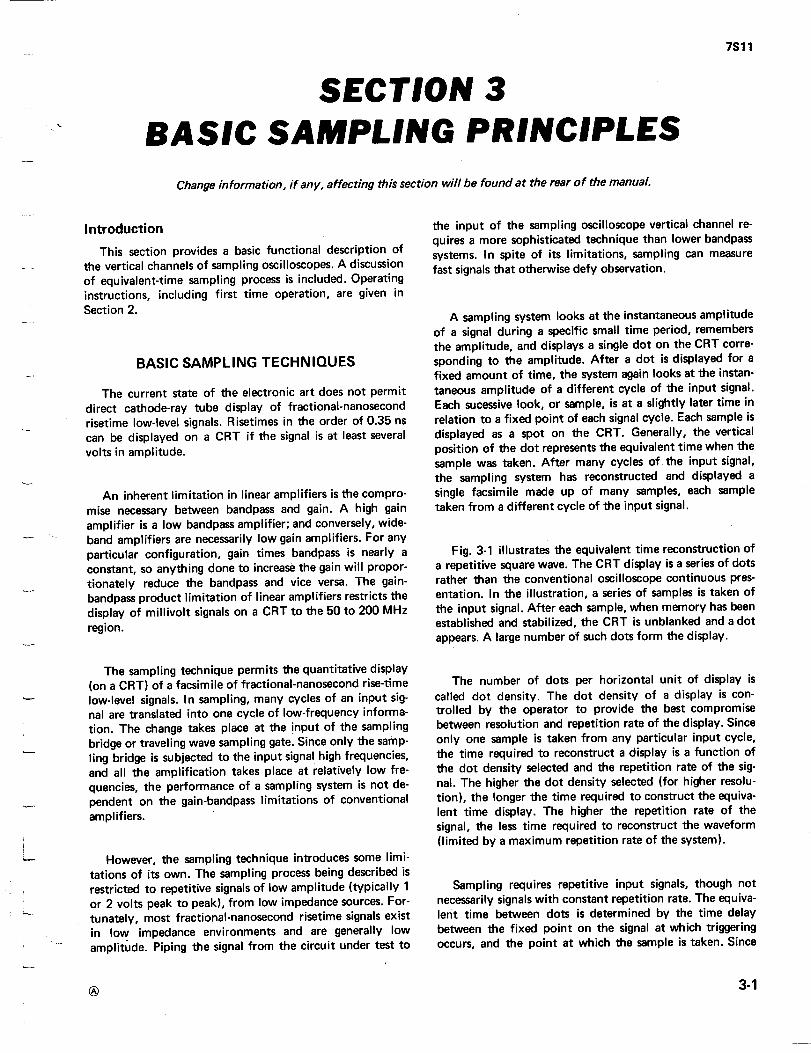
SECTION 3BASIC SAMPLING PRINCIPLES
Change information, if any, affecting this section will be found at the rear of the manual.
Th is section provides α basic functional descriptio n ofthe ve rtical channels of sampling oscillosco pes . Α discussionof equivalent-time sampling process is included . Operatinginstructio n s, includ ing first time operation, are given inSectio n 2.
BASIC SAMPL ING TECHN IQUES
The current state of the electronic art does not permitdirect cathode-ray tube d isplay of fractional-nanosecondrisetime low-level signals . R isetimes in the order of 0.35 nscan be displayed on α CRT if the signal is at least seve r alvolts in amplitude.
An inherent limitation in linear amplifiers is the comp ro-mise necessa ry between bandpass and gain . Α h igh gainamplifier is α low bandpass amp lifier ; and conversely, wide-band amp lifiers are necessarily low gain am p lifiers. For anyparticular configuration , gain times bandpass is nearly αconstant, so anything done to increase the gain will propor-tionately reduce the bandpass and vice versa . The gain -bandpass product limitation of linear amplifiers rest ricts thedisplay of millivolt signals on α CRT to the 50 to 200 MHzregion .
The samp ling technique permits the quantitative display(on α CRT) of α facsimile of fractional-nanosecond rise-timelow-level signals . 1η samp ling, many cycles of an input sig-nal are translated into one cycle of low-frequency inform a-tion . The change takes place at the input of the samplingbridge or traveling wave samp ling gate . Since only the sarnp -ling bridge is su bjected to the input signal high frequencies,and all the amplification takes place at relatively low fre-quencies, th e perfo rmance of α sampling system is not de-pendent on the gain-bandpass limitations of convention alamplifiers .
However , the sampling tech nique introduces some limi-tations of its own. The sampling process being described isrestricted to repetitive signals of low amplitude (typically 1or 2 volts peak to peak ), from low impedance sources. For-tunately, most fraction al-nanosecond risetime signals existin low impedance environments and are generally lowamplitude. Piping the sign al from the circuit under test to
7511
the input of the sampling oscilloscope vertical channel re-quires α mo re sophisticated technique than lower bandpasssystems. 1 η spite of its limitations, sampling can measurefast signals that otherwise defy observation .
Α sampling system looks at the instantaneous amplitudeof α sign al during α specific small time period, remembersthe amp litud e, and d isplays α single dot on the CRT corre-sponding to the amplitude . After α dot is d isplayed fo r αfixed amoun t of time, the system again looks at the instan-taneous amplitude of α different cycle of the input sign al .Each sucessive look , or samp le, is at α slightly later time inrelation to α fixed point of each sign al cycle. Each samp le isdisplayed as α spot on the CRT. Generally, the ve rticalposition of the dot represents the equivalent timewhen thesamp le was taken . After many cycles of the input sign al,the samp ling system has reconstructed and d isplayed αsingle facsimile made up of many samp les, each sampletaken from α different cycle of the input sign al .
F ig . 3-1 illu st rates the equivalent time reconstruction ofα repetitive square wave . The CRT d isplay is α se ries of dotsrather than the convention al oscilloscope continuous pres-entation . In the illustration, α se r ies of samples is taken ofthe input signal . Afte r each samp le, when memory has beenestablished and stabilized , the CRT is unblanked and α dotappea rs. Α large numberof such dots form the d isplay.
The number of dots per horizon tal unit of d isplay iscalled dot density . The dot density of α d isp lay is con-trolled by the operator to provide the best compromisebetween resolution and repetitio n rate of the display. Sinceonly one samp le is taken from any particular input cycle,the time requ i red to reconstruct α display is α function ofthe dot density selected and the repetition rate of the sig-nal . The higher the dot density selected (for higher resolu -tion), the longer the time req ui red to construct the equiva-lent time display . The h igher the repetition rate of thesign al, the less time required to reconstruct the wavefo rm(limited by α maximum repetition rate of the system) .
Samp ling requires repetitive input signals, though notnecessarily signals with constant repetition rate . The equiva-lent time between dots is determined by the time delaybetween the fixed point on the signal at wh ich t riggeringoccurs, and the point at wh ich the sample is taken . Since

Basic Sampling Prin ciples-7511
--------0---------0
_1P---------119---------It ---------V---------v-,
Equ ivalen t TimeDisp lay
----------- 40-_----_----
InputSign al
Fig. 3-1. Equ ivalent time display of repetitive real time sign al by mea ns of th e samp lin g techn iqu es .
both time reference (tr iggering-time and sample-time) aretaken f rom the same cycle of the signal, the signal repeti-tion s do not have to be identical in amplitude, time du ra-tion , and sh ape. Any differences in the ind ividual cyclesshow as noise or j itte r in the reconstructed d isplay .
Samp ling systems have maximum signal rep etitio n ratesat wh ich samp les can be taken and accurately displayed .The primary limit is th e time requ ired fo r the preamp andth e AC amp lifie r to stab ilize after α samp le has been taken .
Signals below 100 kH z may have considerable repetitionrate j itter and still the samp ling oscilloscope will presen t αsample of each cycle, without d isplay j itter . For sign alswith α repetition rate higher than 100 kH z, the timing unit
3-2
hold s off retriggeri ng for α maximum of about 10 μs. Th ismeans th at α samp le will not be taken from every cycle of αh igh repetition rate sign al . Only those cycles are samp ledwh ich occur after the end of the holdofξ. If the signal istruly rep etitive and each cycle is identical, these "missed"cycles are of little significance .
The circuits in the vertical channel of α Tektronix samp-ling oscillosco pe comp rise an error-sampled feedback sys-tem with ratchet memory . The memory output is not resetto ze ro after displaying α dot. The memory output remainsat the displayed amp litude of each dot in succession u ntil itis corrected by the next samp le . The amp litude differencebetween the two samp les is then the error between thememory output and the new samp led amplitude .
Fig. 3-2. Simp lified b lock d iagram of an error-sampled feedback system with α ratchet memory.

Fig. 3-2 shows α simplified block diagram of an error-sam pled feed back system with ratchet memory . The outputsignal from the sampling bridge is the d ifference, or error,between the instantaneous am plitude of the signal atsample time and the previously memorized amplitude. Αchange is made to the memory output only when theinstantaneous amplitude of the signal at sample time isdifferent from the memory output . The memory output"ratchets" up or down at sam ple time as α result of theerror signal samp led . The transition of memory from oneoutput voltage to another occurs between d is played dots,and is therefore not seen on the CRT.
The error-sam pled ratchet-memory technique has theadvantage of allowing d isp layed noise to be "smoothed ".Smoothing is d iscussed later in this section . The error-sampled approach also minimizes signal kickout into theinput cable by the samp ling bridge interrogate pulse (here-after called "strobe" pulse) . Since the sample is always thedifference between the signal and the memory output, the
Basic Sampling Principles-7511
error-signal and kickout are much smaller in amplitude than
they would be if the memory output reverted to zero andthe entire signal was sampled after each dot .
The output from the sampling bridge at samp ling time isabout 2°/α of the difference between the signal voltage andthe memory output . The 2% signal is the input to the firstamplifier . The output of the amplifier is AC-cou pled to αmemory gate . The memory gate couples the signal to thememory amp lifier during the time it is gated on . Thememory amplifier changes the memory feed back voltage toequal the signal voltage at the instant of sampling . Thesechanges in memory output occur while the CRT is blanked,and do not show up in the d isplay . The memory outputdoes not revert to zero, but remains at α fixed voltage untilcorrected by the next error signal . (The signal to the ampli-fier of α typical sampling system is only about 2% of theerror signal sampled by the b ridge . The percentage of re-sponse, or attenuation through the sampling bridge, is thesam pling efficiency) .
ι ιιCRT Blanking
Pulsesι ι ,
CRT Blanked 1 .0
Ι Ι
Sampling Gate
Ι Ι
(Strobe) Pu lses
Ι Ι Ι
Ι Ι~2 ι~
3 Ι ΙΙ ι
~ Ι Ι
Α _Ι ΙΙΙ
Ι Ιιι
ί ΙίΙ Ιι
ιMemo r y ou t pu t to CRTFeedback to Sampling Gate
Ι
Ι Ι
Ι
Ι Ι
Ι
Ι ΙΙ
ΙΙι
ι
ι Ιι
ίι
Ι
Ι
Ι ι
Ι
~ Ι! ~ ι
Ι ι Ι
Ι ι !
Display Time(time during which α d ot is displayed)
F ig . 3-3. Simplified representation of an error-sampled ratchet-memory waveform .
3-3

Basic Sampling Principles-7511
F ig . 3-4. Simplified diagram, showing how the strobe pulse causes the sampling bridge to conduct.
At each sample time, the difference between thememory feed back and the 2°/ο signal value is amplifie d andapplied to the memory circuit via the memory gate, tocause the memory output to follow α rising signal in αseries of steps as shown in Fig. 3-3. This figure shows theinput signal and memory feedback voltages for six samplesalong the rise of α step waveform .
At the time of sample 1, the input signal and the feed-back voltage are equal. There is no error voltage, so thememory output is not changed . The CRT is blanked untilthe circuit stabilizes after the memory gate pulse ends.
At the time of sample 2, the input signal is (for example)0.1 volt . The memory output is 0 . Assuming α samp lingefficiency of 10°/ο , the input of the amplifier receives 10°/ο ofthe error signal, or 0 .01 volt . The 0.01 volt, times the gainof the amp lifier (Χ 10), corrects the memory output andfeed back to equal the 0.1 volt signal at sample time . Again,the CRT is . blanked during this change until the circuit isstabilized .
3-4
At the time of sample 3, the difference between theinput signal and the feedback is 0.35 volt . The amp lifierinput responds to 10°/ο of 0.035 volt . The gain of the amp li-fier and memory changes the feedback 0.35 volt to the newvalue of 0.45 volt (equal to the signal at number threesampling time). The CRT is again blanked during thischange until the circuit is stabilized .
Effective Sampling Time
The minimum risetime α sampling system can d isplay iscontrolled by the time interval during which the strobepulse app lies forward bias to the sampling bridge diodes .The duration of the bridge forward b ias is controlled by thetime the strobe pulse exceeds α fixed reverse bias. Specialcircuitry is used to make the strobe duration as short aspossible consistent with noise and diode recovery time . Thestrobe pulse is generate d by α snap-off d iode and α shortsection of shorte d transmission line called α clipping line .The effective bridge conduction time is adjusted primarilyby controlling the amplitude and duration of the strobepulse, thus controlling the time during which the strobe

F ig . 3-5 . Error-signal source and path to Preamp shown by dottedlines . DIEL denotes dielectric other than air .
pulse exceeds the reverse bias. Adjusting the reverse bias is αsecondary means of controlling the samp ling bridge conduc-tion time . Fig . 3-4 shows how the strobe pulse breaksthrough the reverse bias on the samp ling bridge . The reversebias is shown by dashed lines through the strobe pulses .
Traveling Wave Sampling Gate
The sampling system may use α traveling wave gateinstead of the sampling bridge as the input stage. Fig . 3-5shows α simp lified schematic of the traveling wave samplinggate . The input signal is connected to the Preamplifier onlyduring the time α sam p le is taken. The six diodes form thetraveling wave gate .
Step response is determined by the travel time of thestrobe drive pulse end through part of the sampling gate . Inα samp ling bridge, the step response is determined by thestrobe pulse width .
Part of the input signal is stored temporarily betweensamp ling gate diodes at the strobe pulse end ; then it is fedto the Preamplifier at α slower rate than the step responserisetime . The environment is controlled in the input andtraveling wave sampling gate to minimize reflections of fastpulse signals . The environment of following circuitry passesonly moderate rate-of-rise signals .
Dot Response (Loop Gain)
Smoothing
Basic Sampling Pr inciples-7511
Dot response is the ability of the system to reduce theerror voltage to zero after each samp le . When the gain ofthe memory feedback loop is equal to (and compensatesfor) the attenuation across the sam pling bri dge, the loopgain is unity or 1 . In this case, the memory feedback volt-age equals the value of samp ling time signal voltage.
If the loop gain is less than unity, the memory outputsignal and feedback to the first amplifier is less than neces-sary to reduce the error voltage to zero . The memory out-put and the feedback will then approach the signal asymp -totically after several samples have been taken . The errorvoltage thus approaches zero (for α steady state signal) afterseveral samples, being reduced by the same factor after eachsample . In the case of α loop gain of less than unity, thefeedback voltage is effectively α moving average of severalpreced ing samp les .
If the loop gain is greater than unity, the feedback volt-age will be greater than the error signal after each sample .The displayed dot sequence of α step signal will then alter-nately overshoot and undershoot for αfew samples.
For least displayed waveform distortion, the loop gainmust be unity, allowing the system to track the input signalas closely as possible .
Α loop gain of less than unity can be useful, if the result-ing com promise is understood and the system is operatedproperly . R andom noise in the display is reduced whenloop gain is less than unity, since several consecutivesamp les are averaged . The averaging may also slow downthe fastest d isplay risetime capability, depend ing upon thenumber of dots contained in the step transition and or theloop gain . By increasing the number of dots in α step transi-tion, the d isp lay will follow the actual step transition moreclosely.
Fig . 3-6 shows the usual effects on α step d isp lay whensmoothing is used for two d ifferent sampling densities(samp ling density or dot density is the number of samp lesor dots per horizontal division) . In the 7511 the operationalchoice of loop gain is either 1 .0 (NORMAL) or 0.3(SMOOTH). In Fig. 3-6Α the actual risetime (between the10% and 90% points) for unity loop gain displays 4 dots.When operating at 0.3 loop gain, 7 dots are shown . There isα significant difference between the 0.3 loop gain(SMOOTH) and the unity loop gain (NORMAL) d isplays .
In Fig. 3-6Β the sampling density is increased, showing αdifference of one sample in the SMOOTH and NORMALpositions between the 10% and 90%ο points of the step tran-sition .
3-5

Basic Sampling Principles-7511
g0%-
-Unity LoopF-- Gain
( Normal)
~
...... ... "_. . .. .". . .. .."......." .~ . ..".
- " .
; ιΈ"'
Ι ι ιι Ι10 ο/ο --*Ι
90% -
"i1
ι"ι λ,
ιι
-
ί ""ι.
,
1 ι
Ιι ιΙ"f---". ί
i"
ιι
U nity LoopGain
(Normal)
ί ί
Ι ίί
f"ί
0.7/ ί-- τ- 0.3
ι fίι ί
10 οο _ ιΊ-f~- -
~"~0.3 Loop Gain
(SMOOTH)-.0-0-0-0
--"
0.3 Loop(SMOOTH)
0 .7
0.3
(Β) Increased Samp lingDen sity
(A) Low SamplingDe n sity
When the smoothed mode has α loop gain of 0.3, as inthe 7511, 15 or more samples between the 10% and 90%οpoints of α risetime will result in the smoothed and υη -smoothed d isplays having essentially the same risetime .When the smoothed display contains 12 samples betweenthe 10%ο and 90ο/ο point, th e smoothed risetime will beabout 6ο/ο longer than for the unsmoothed d isp lay. As thenumber of sam p les contained in the risetime is red ucedbelow 12, the difference between smoothed and υη -smoothed d isplay increases rap idly .
Smoothing Of R andom Noise
F ig . 3-6. Equivalent-time display with and without smoothing fo r two different sampling densities .
When the loop gain is reduced to 0.3, the d isp layed dotsrepresent the average of several consecutive sam ples . Noiseof α randomnature will be materially reduced in the displayat the possible expense of introd ucing an error in the d is-
3-6
played risetime . Therefore, if random noise is apparent, re-ducing the loop gain may improve the display. Note thatth is'is only - true for random noise . Systematic noise (noisewith its repetition rate h armonically related to the signal) istreated as part of the signal .
The 7511 has α loop gain control labeled NORMAL-SMOOTH. In the SMOOTH mod e, loop gain is reduced to0.3 . Always check that there is sufficient sampling densityto warrant smoothing. This can be done by,changing thedots/division, (or samples/d ivision) 'control on the timingu nit, and observing the effect of sampling density on thed isplayed risetime .
Smoothing cannot be applied where the full amplitudeof each sample is req uired . When using the random samp -ling sweep unit like the 7T1 1, each samp le requires unity
loop gain . The display dots are not presented in time se-quence, and therefore cannot be averaged .
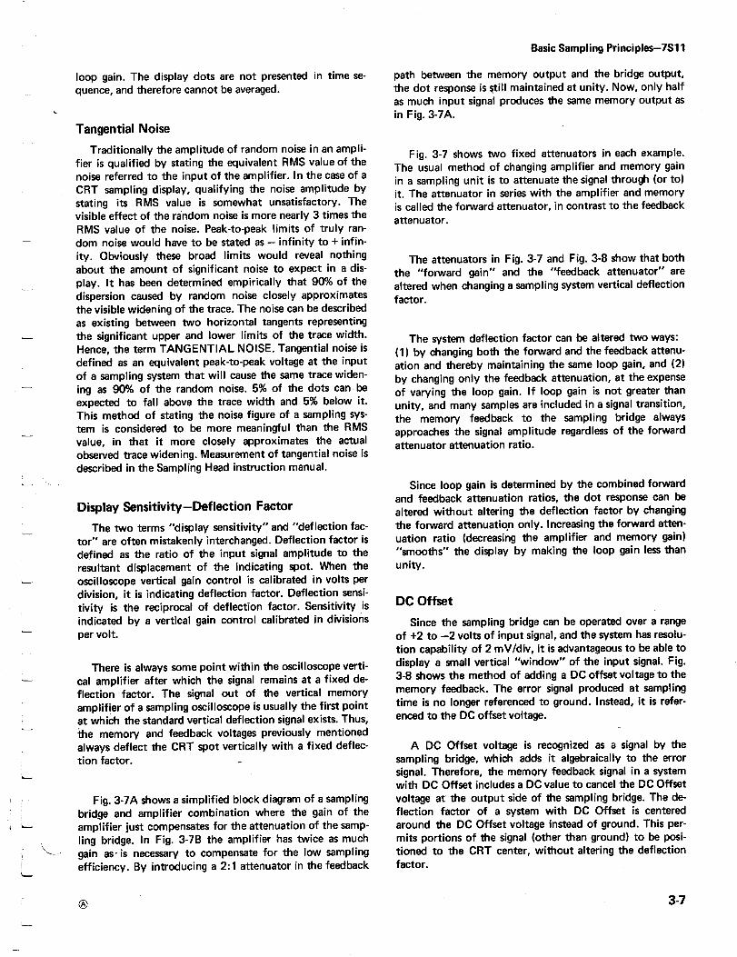
Tangential Noise
Traditionally the amplitude of random noise in an ampli-fier is qualified by stating the equivalent RMS value of thenoise referred to the input of the amp lifie r . In the case of αCRT samp li ng display, qualifying the noise amplitude bystating its RMS val u e is somewhat unsatisfactory . Thevisi b le effect of the random noise is more nearly 3 times theRMS value of the noise . Peak-to-peak limits of truly ran -dom noise would have to be stated as - infinity to + infin-ity . Obviously these broad limits would reveal noth ingabout the amount of significant noise to expect in α dis-play . It has been determined empirically that 90% of thedispersion caused by random noise closely approximatesthe visib le widening of the trace . The noise can be describedas existing between two horizontal tangents rep resentingthe significant uppe r and lower limits of the trace width .Hence, the term TAN G ENTIA L NOISE . Tangential noise isdefined as an equivalent peak-to-peak voltage at the inputof α sampling system that will cause the same trace widen-ing as 90% of the random noise . 5% of the dots can- beexpected to fall above the trace wid th and 5% below it .Th is method of stating the noise figure of α sampling sys-tem is considered to be mo re mean ingful than the RMSvalue, in that it mo re closely approximates the actualobserved trace widen ing . Measurement of tangential noise isdescribed in the Samp ling Head instruction manual .
Display Sensitivity-Deflection Factor
The two terms "display sensitivity" and "deflection fac-tor" are often mistakenly interchanged . Deflection facto r isdefined as the ratio of the input sign al amplitude to theresultan t displacement of the indicating spot . When theoscilloscope vertical gain control is calibrated in volts perdivision, it is indicating deflection factor . Deflection sensi-tivity is the reciprocal of deflection factor . Sensitivity isindicated by α ver tical gain control calibrated in divisionsper volt .
There is always some point with in the oscilloscope verti-cal amplifier after wh ich the sign al remains at α fixed de-flection factor. The signal out of the vertical memoryamp lifier of α samp ling oscilloscope is usually the first pointat wh ich the standard vertical deflection signal exists . Thu s,the memory and feedback voltages previously mentionedalways deflect the CRT spot vertically with ά fixed deflec-tion factor .
-
Fig. 3-7Α shows α simplified block diagram of α samplingbridge and amp lifier combination where the gain of theamplifier just compensates for the attenuation of the samp -ling bridge . In Fig . 3-7Β the amp lifier has twice as muchgain as- is necessary to compensate for the low samp lingefficiency . By introducing α 2:1 attenuato r in the feedback
Basic Samp ling Principles-7511
path between th e memory output and the bridge output,the dot response is still maintained at un ity . Now, only halfas much input signal produces the same memo ry output asin Fig . 3-7Α .
Fig . 3-7 shows two fixed attenuators in each examp le.The usual method of changing amp lifie r and memory gainin α sampling un it is to attenuate the signal th rough (or to)it . The attenuator in series with the amp lifier and memoryis called the forward attenuator, in contrast to the feedbackattenuator .
The attenuators in F ig . 3-7 and Fig . 3-8 show that boththe "forward gain" and the "feedback attenuator" arealtered when changing α samp ling system ve rtical deflectionfactor .
The system deflection factor can be alte red two ways :(1) by changing both the forward and the feedback attenu-ation and thereby maintaining the same loop gain , and (2)by changing only the feedback attenuation , at the expenseof varying the loop gain . If loop gain is not g reate r thanun ity, and many samp les are included in α signal transition,the memo ry feedback to the samp ling bridge alwaysapproaches the sign al amp litude regard less of the forwardattenuato r attenuation ratio .
Since loop gain is determined by the combined forwa rdand feedback attenuatio n ratios, the dot response can bealtered without altering the deflection factor by changingthe forward attenuation only . I nc reasing the forwa rd atten-uation ratio (dec reasin g the amplifier and memory gai n )"smooths" the display by making the loop gain less thanunity .
DC Offset
Since the sampling bridge can be operated over α rangeof +2 to -2 volts of input sign al, and the system has resolu-tion capability of 2 mV/div, it is advantageous to be able todisplay α small ve rtical "window" of the input signal . Fig .3-8 shows the method of adding α DC offset voltage to th ememo ry feedbac k . The e rror signal produced at samplingtime is no longer referenced to ground . Instead, it is refer-enced to the DC offset voltage .
Α DC Offset voltage is recognized as α signal by thesampling bridge, which adds it algebraically to the errorsignal . Therefore, the memory feedback signal in α systemwith DC Offset includes α DC value to can cel the DC Offsetvoltage at the outpu t side of the sampling bridge . The de-flection factor of α system with DC Offset is centeredaround the DC Offset voltage instead of ground . Th is per-mits po rtions of the signal (other than ground) to be posi-tioned to the CRT center, withou t altering the deflectionfacto r.
3-7

Basic Sampling Principles-7511
Real-Time Sampling
Fig . 3-7 . M ethod of decreasing the ve rtical deflection facto r wh ile main tain ing un ity loop gain .
Real-time samp ling is α method of operation in wh ichthe samples are taken at α constant rate from relatively lowfrequency signals (DC to 20 kHz approximately) and dis-played at α sweep rate determined by the Time/Div switchon the time-base un it. Thu s, the samples are taken con tinu-ously along the input signal rather than tak i ng one samplefrom each cycle of the signal . The displayed series of dotsfollows theactual shape of the input signal waveform .
In real-time samp ling operation , the ve rtical signal pro-vides the trigge r to start the sweep . The display, however, iscomposed of samples at α fixed repetition rate, not neces-sarily relate d to the input frequency.
3-8
Sweep Rates
The range of sweep rates available fo r use i n real-timesampling is from the slowest rate provided by the real-timesweep un it to about 0.1 ms/div . At th is sweep rate, theusual 50 kHz sampling rate provides about 100 samples/sweep . At faster sweep rates above 0.1 ms/d iv, the d isplaydots begin to have significant horizon tal dimension due totheir duration in real time, and interpretation pf the d isplaybecomes difficult .
The characteristics of real-time samp ling, in addition toslow sweeps at fu ll bandwidth , are reduction of randomnoise in thed isplay th rough smooth in g, and DC offset capa-bility matched with good overload recovery .
C

Sampli ng Bridge Am p lifie r and Memo ry
Fig . 3-8. Method of adding α DC Offset voltage to the memory feedback .
Basic Sampling Principles-7511

Introduction
This section of the manual contains α block diagramdescriptio n and α circuit description of the 7511 SamplingUnit . The block diagram descri ption is an ex pansion ofSection 3, Basic Sampling Principles. The circuit descriptionfollows the sequence of diagrams at the back of thismanual .
Refer to F ig . 4-1 and the comp lete block d iagram at theback of the manual during the following description . BothFig . 4-1 and the complete block diagram include α simp li-fied block of α typ ical sampli ng head . The 7511 SamplingUn it functions as part of α sam pling system only when αsampling head is installed, so α samp ling head block is in-cluded .
Feedback Loop and Pulse Amplifier ChainF ig . 4-1 relates to F ig . 3-4 and F ig . 3-8 . The recon-
structed signal out of the Memory block (F ig . 4-1) is thefirst point in the 7511 at wh ich the amp litude is always α
standard value of 0.5 volt per CRT vertical division . Thereis no signal between the sampling head output and theMemory input when the samp li ng head input signal is notchanging. The Post Amplifier, AC Amp lifier and Memoryare part of α pulse amplifier chain that amp lifies the samp-ling head output signal just after each sample is taken . Sig-nals through the amplifier chain are greatest in amplitudewhen the sampled signal is at its full amplitude differencefrom the last sample . Th is is called the error signal .
To complete the association of F ig . 4-1 with Section 3,the following describes the operating cycle:
α . The sampling head bridge applies an error signal to thehead preamp whenever there is α voltage d ifference at thebridge input and output terminals at sampling time . Theerror-signal voltage amp litude is just α few per cent of thedifference (sampling efficiency), and the pulse duration outof the bridge is equal to the bridge conduction time . Αsmall storage capacitance at the head Preamp input time-stretches the pulse so the pulse chain can amplify the errorsignal pulses at moderate rates of rise .
SECTION 4CIRCUIT DESCRIPTION
Change information, if any, affecting this section will be found at the rear of the manual.
BLOCK DIAG RAM
b. The time-stretched pulse is amplified by the 7511Post Amplifier and sent forward into the attenuating net-work made up the NORMAL/SMOOTH switch, the DOTRESPONSE control and the Forward Attenuator portion ofthe Units/Div switch.
ε. The AC Amplifier again amplifies the pulse andapplies it to the Memory circuit during conduction time ofthe Memory Gate. In effect, the error signal charge appliedto the head Preamp is then transferred to the feedbackcapacitor of the Memory circuit.
d . The Memory ci rcuit applies its error signal correctedoutput voltage to both the vertical amplifier and the feed -back Atttnuator and sampling head bridge output terminal .Control of the input deflection factor by the Forward andFeedback Attenuators is described near the end of Section3. The DOT RESPONSE control is also described in Section3 .
Vertical Output Amplifier
7511
Th e I NVERT/+UP switch and the Vertical Ou tput Am-
p lifier drive th e oscilloscope vertical amp lifier stage .
Sweep Unit Drive
Drive from the timing unit is applied to the samplinghead avalanche and snap-off and the Memory Gate Driver.The timing unit controls the free running oscillator used inthe 7511 .
Sampling Operation. The 7511 is α single-channel samp-ling unit when used with α 7T11 or other sampling sweepunit in α 7000-series oscilloscope.
For dual-channel operatipn, another 7511 must beinstalled in the adjacent vertical compartment of theoscilloscope . Interconnection between the two 7S1 1's andthe sampling sweep unit are made by connecting-shoes onthe plug-ins . These interconnections combine the TriggerLogic circuits of the two 7S11's into α bistable multivi-brator, and complete the other connections necessary toprovide amplification of internally-generated triggers . Forexternal trigger operation, the sampling sweep I nte rnal

Circu it Description-7S 11
4-2
ΗΟΗωΝωωΟ
Υaάψ
ΥυαmΔωωω
χΗΟΟΝ
ωΝΗ ΖΌή
Οωσ
JQ¢υΨ¢W Jd>0άΗ
ΔΔ¢~yJ~J ZF> ΝZOO
Ν LqΟ
mΓ
Qξα
11
Fig . 4-1 . The 7511 and sampling head feedback loop block diagram.
ω>ΔωΗαυ>σ
ω ωυ LL.Ζ Ο
CLJ Ζ> Να
ξΟωωΝ ΗjvZd?~jii~reξωΔά
0-7
0ωΙΖJdξQΝ

Mode trigger amp lifiers and the bistable multivibrator aredisable d .
Non-Sampling Operation. When the 7511 is used fordual-channel real time operation in company with α non-sampling time base unit, no sampling d rive pulse is avail-able, nor is α ground provided for the Real Time Oscillatorand Trigger Logic multivibrator . The R eal Time Oscillatorwill oscillate at the specified frequency and drive theMemory Gate Driver and the CRT blanking circuit . Internaltrigger is obtained from the Real Time Trigger block . Theoperational differences between the two types of time basesare explained in the O perating Instructions, Section 2.
Readout LogicThe Readout logic in the 7511 provides the necessary
time-slot current to operate the Scale Factor read out on theindicator oscilloscope . Currents supplied from the 7511control the display of decimal magnitud e, Normal/Invert,N ormal/Uncal, 1-2-5 Scaling and the symbols m,μ, V and Ι .The indicator oscilloscope manual includes the d etails ofScale Factor Readout operation .
The following circuit description follows the sequence ofthe diagrams in Section 9.
Trigger LogicThe Trigger Logic circuit (see Post Am p lifier and Atten-
uators circuit d iagram) consists of Q108, Q113, Q116 andassociated components. The circuit sets the level for for-ward bias of the timing unit trigger amplifier so that thetrigger is passed from the samp ling head to the timing unit(see F ig . 4-2Α ) . The Internal setting of the timing unit trig-ger switch grounds the base of Q113 through R109, and thecollector of Q108 through R108-13109 . Q108 is reversebiased by current through R102 and CR 108 to clamp thebase at +15 .6 volts . CR113 is off and Q113 is forwardb iased by the current through R111 and R 109. Conductioncauses Q113 collector to be more positive than the cathodeof CR 116 so that both CR 116 and CR115 are off. Q116supp lies current to the lamp, DS116, indicating that this7511 is supplying the internal trigger to the timing unit .R 115 sets the base current for Q116 .
Setting the trigger switch in the timing unit to ΕΧΤremoves the ground from R109, which turns on CR 113 andclamps Q113 base at +5.6 volts, α reverse bias . Q108 re-mains at reverse bias as with Internal trigger operation.CR 115 clamps Q116 base at -0.6 volt so Q116 is off andthe ΙΝΤ TRIG lamp is off. CR116 is on, reverse biasing thetiming-unit transistor, so no trigger signal from the samplinghead can trigger the timing unit .
CIRCUIT DESCRIPTION
Circuit Description-7511
Two 7511 units operated together will complete the b i-stable multivibrator shown in F ig . 4-2Β. Selection of thedesired 7511 as the Internal trigger source is done throughthe turning off of Q108 in that unit . The Internal setting ofthe trigger switch in the timing unit provides ground toboth halves of the bistable multivibrator . Pushing the ΙΝΤTRIG switch momentarily places α positive trigger on Q108(in the desired 7S11), puts reverse bias between base andemitter, and turns on CR108, which clamps Q108 base at+15.6 volts. The positive trigger is applied to Q108 collec-tor in the second 7511, which turns that Q108 on, addingcurrent through R109 to the current through R111 andR109 to clamp Q113 base at +5.6 volts through CR113.Operation of the Off 7511 is the same as d iscussed forExternal trigger operation with α single 7511 . The On 7S11operates similar to α single 7511 in Internal trigger oper-ation .
Switching the timing unit trigger switch to one of theΕΧΤ positions removes the ground from the R109 commonpoint . The R109 common point rises to +5.6 volts, theclam ped voltage at the bases of the Q1 13's, so the multivi-brator remains in the state in which it was set. The multivi-brator remains in the state in which it was set when thetiming unit trigger mode is again placed at Internal unlessthe other 7511 ΙΝΤ TRIG button is pushed .
Post Amplifier and Attenuators
The Post Amp lifier and Attenuators diagram includesthe Post Amplifier, Forward and Feedback Atenuators, DCOffset, and the Trigger Logic .
The Post Amp lifier is α two-stage non-inverting opera-tional amplifier with AC coupled com plementary emitterfollowers between the second stage and the output . Theinput impedance is 90.9 Ω, which properly terminates thecoaxial cable feed from the sampling h ead . Outpu t imped -ance is very low to provide signal current to the 500 ΩForward Attenuator . Total AC gain is approximately 12,producing α 2.4 volt output signal for α 0.2 volt input sig-nal. DC gain is essentially unity and feedback keeps theamp lifier within its proper dynamic range.
Q123 and Q128 are the amp lifier transistors, and Q133and Q136 are the output emitter followers. Q133 ensureslow output impedance for positive output signals, andQ136 ensures low output imped ance for negative outputsignals . Each emitter follower has α resistor in the collectorfor parasitic oscillation suppression . C134 permits the out-put emitters to be at different DC voltages and ensures thatthe emitter of the non-driving transistor follows the outputvoltage.
Output of the Post Amplifier is AC cou p led to theNORMAL/SMOOTH switch, DOT RESPONSE control andthe Forward Attenuator (part of the U nits/Div switch).
4-3

Circuit Description-7511
4-4
+50 V
ΓSAMPLING HEAD -1I
SIGNAL
Α. Single 7571 circuit .
+15 V
R102CR108
0108
ΙΝΤ
Ε%ΤΟ
TIMINGUN ITL_-----i
+15 V
+5γ ( Lamp)
The F orward Attenuation Network consists of theNORMAL/SMOOTH switch, the DOT RESPONSE control,and the Forward Attenuator portion of the Units/Divswitch .
Pushing the SMOOTH switch introduces R 141 in serieswith the Post Am p lifier output signal, reducing the loopgain to 0.3 or less com pared to loop gain in the NORMALsetting . R142 maintains α constant 500 Ω load on the out-put stage for time constant and amplitude considerations .
Fig . 4-2. Trigger Logic circuit .
L -- _ - _ --_-_--JΓι ΙΝΤ
R 101
TIMING UN IT
Ι
Β. Bistable multivibrator of two 7511 circuits .
+50 V
R 102
+15V
+5 V
CR113
The Forward Attenuator, made up of resistors R145Athrough R145G, presents α constant 500 Ω load to thedriving side. The input resistance to the AC Amplifier ischanged by the forward attenuator from 1 kΩ to 100 kΩ inseven steps. Six of the seven resistors are always in parallelconnection to ground , with the seventh in series with thesignal to the AC Amp lifier input . Signal pulse amp litudeacross the forward attenuator input resistance (500 Ω toground ) does not change when the Units/Div switch p osi-tion is changed . Attenuation occurs because of α changingcurrent d rive into the low impedance of the operational AC

Circuit Description-7511
SW141BSMOOTH
SW141A
AC AmplifierInput
Zero ΩTerminal Impedance
F ig . 4-3. Forward Attenuation network, showing that the outp ut resistor of the Units/Div Forward Attenuator is actually the AC Amplifierinput resistor .
Amplifier. Fig . 4-3 shows the full forward attenuator net-work and identifies the AC Amplifier input terminal .
The AC Amp lifier gain is controlled by the ratio of feed -back resistor R 209 to the value of the series element ofR 145. The gain ch anges from 15 at 2 units/d iv to 0.15 at200 units/d iv .
The F orward Attenuator portion of the U nits/Div switchis ganged with the Feedback Attenuator portion . The resultis th at changing the Units/Div switch does not change thed ot respo n se (or loop gain). Changing either theNORMAL/SMOOTH switch or the DOT RESPONS E con-trol changes the forward signal, and thus changes the loopgain .
The Feedback Attenuator and the DC Offset are connec-ted together within the sampling head where they are com-bined and applied to the Sampling B ridge output terminals.The Feedback Attenuator receives the Memory circuit out-put signal from α very low impedance . The attenuatorplaces one of seven resistors in series with th e Memoryoutput signal, and the other six resistors are paralleled toground as slightly more than 2000 Ω. Maximum attenu-ation (at 2 U nits/Div) allows 0.42% of the Memory signal topass to the Sampling Bridge circuit . Minimum attenuation(at 200 Units/Div) allows 42%ο of the Memory signal to passto the Samp ling B ridge Circuit. The attenuation of 0.42%and 42% is corrected to exactly 0.40% and 40% by theparallel value of R147, R149 and the 53 kΩ to groundinside the sampling head. (The F orward Attenuator ratio orAC Amplifier gain ratio of 100:1, and the feedback attenu-
ator ratio of 1 :100 ensure that the loop gain is not alteredthrough out the Units/Div switch range) .
The DC Offset Circuit is α single transistor emitter fol-lower that converts the fairly h igh resistance of the DCOFF SET control to α fairly low resistance at the emitter.Q163 emitter voltage follows the voltage of the arm of theDC OFFSET control, offset by -0.6 volt . Q163 drives α22.4 kΩ resistive load , consisting of Q163 output resist-ance, R 165 (19.1 kΩ) and 2000 Ω of the Feedback Attenu-ator . Thus the DC OFFSET voltage at Q163 emitter de-velops α fixed voltage across the Feedback Attenuator 2000Ω regardless of the Units/Div switch setting.
MemoryThe memory diagram includes the AC Amp lifier, the
Memory Gate, and the Memory Amplifier .
The AC Amplifier (whose gain is described above withthe Forward Attenuation Network) is an inverting opera-tional amplifier with AC coup led complementary emitte rfollowers at th e output . Q204 is the voltage amplifier,Q208 emitter follower add s current gain to Q204 collectorsignal, and Q212-Q214 provide the very low output resist-ance .
The amplifier input is AC cou pled by C201 to permitthe am plifier DC operating voltages to be independent ofthe changes made in input resistance by the Units/Divswitch . Q204 base is the summing inpu t terminal of theoperational amplifier . As α signal arrives and changes the
4-5

Circu it Description-7511
AC Amp lifie r MemoryGate
MemoryC275-C276
Feedback
Fig . 4-4. B asic Memory Gate circuit between AC Amplifier and Memory Am plifier . (Detailed block of Memory diagram.)
base voltage, the collector voltage changes in the oppositedirection and Q208 emitter drives current of the oppositepolarity through R209 back to the Q204 base . The inputand feedback signal currents are nearly equal, keeping thebase voltage almost constant . The output signal is coupledto the Memory Gate by Q212, Q214 and R 219-C219 . R219limits the signal output current, ensuring that C219 doesnot receive α significant charge for output signals of highpulse amplitude.
CR201 and CR206 provide protection when transistorsare removed from their sockets. CR201 conducts if Q208 isremoved , and C R206 cond ucts if Q204 is removed . Para-sitic suppressing resistors include R 206, R207, R 211, R 213and R214.
The Memory Gate is α special pulse-driven d iode gatethat ensures α very h igh input resistance to the Memoryexcept for about 0.15 to 0.20 μs at the time of eachsamp le . During th e conduction time, the Memory Gate is α
low imped ance that allows the AC amp lifier to introduce αcharge into the Memory .
Fig. 4-4 is α detailed block diagram of the circuits on theMemory diagram . The Memory Gate is represented by αresistor, α coil and α relay switch . The resistor is the parallelvalue of the four biasing resistors which ensure that thefour gating diodes are normally not conducting . Thisequivalent circuit shows that the Memory input is zero voltswhen there is no error signal at sample time .
Looking from the Memory Gate output toward its input,the four gating diodes are normally reverse biased by the
4-6
voltage of Zener diode VR221 . (Two of the four diodesprovide very high reverse biased leakage resistance, althoughthey don't turn off very fast . The other two turn off fast atthe end of the gating pulse, although they don't providehigh resistance when reverse biased ) . VR221 voltage is bal-anced to ground by R 224 and R226 so CR236 cathoderests at +2.5 volts and CR238 anode rests at -2.5 volts .C221 ensures that the AC Amplifier output signal drivesboth sides of the memory gate d iodes .
The gate diodes are forward biased into conduction byΤ230 at the time of each sample due to the drive pulsefrom the Memory Gate Driver . Τ230 is α toroidal trans-former specially wound to balance capacitive and inductivecoupling to the two second ary windings . The winding withonly one end connected provides the capacitive balance.The magnetic toroid core provides the inductive balance.Thus, the d rive pulse is converted to identical drive signalsto ensure that the output j unction of the four diodes accur-ately d ivides th e 5 volts of VR 221-C221 . Th is places the
junction of CR237-CR239 at ground when no error signal isapplied from the AC Amplifier . The functions of the twolimiting diodes CR224-CR226 and the Memory Gate arediscussed in the Memory description next . R 229, R 231 andCR232 are shunt, damping loads to Τ230 which minimizeself-inductance ringing when the memory gate drive pulseends.
The Memory amplifier is an integrating operationalamplifier with special low leakage (high DC resistance) in-put circuit . The input and feedback components are capac-itors, making the AC input impedance very low. The inter-nal h igh gain ensures α very low output resistance ; so that as

long as there is no change at the input, the output DCvoltage remains stable . The input low leakage circuit has noDC connection to ground except during the time theMemory Gate conducts .
The Memory amp lifier is specially decou p led from thepower supp lies because the output stage (Q262 and Q266)can req uire α current pulse as great as 30 mA for α 20 voltoutput change at sample time . The decoup ling networks areR 261-C261 and R267-C267 . L268 in th e VERT SIG OUTand feedback lead presents α h ig h impedance to theMemory output for h ig h frequency (fast change) signals.The inductor ensures that the output amp lifier does noth ave to provide h igh current to the output load . L268 slowsthe output signal response, but at α time wh en the CRT isblanked .
Α dual junction FET (Q242) is the input stage. It isbiased for essentially no leakage at the input gate, and thestage has h igh voltage gain at the in-phase output drain lead .Any voltage change at the left Q242 gate lead is amplifiedand applied to the inverting amplifier Q256 . Q256 collectorcircuit applies proper bias to both bases of the outputcomplementary emitter follower pair, Q262-Q266 and re-stores th e DC level negatively so α zero in put signal (at theleft side of Q242) is also α zero output signal . Q256 collec-tor and Q262-Q266 output lead operate linearly th roughthe range of +10 to -10 volts.
Because of the h igh open-loop gain, the M emory Amp li-fier does not have the fast risetime that th e prior amplifiershave. The AC Amp lifier output pulse duration is shorterthan the Memory Amplifier risetime . C239 at Q242 inputgate lead accepts some of the charge from the AC Ampli-fier, stores it until the Memory amplifier can respond , andthen loses the charge again due to feedback current.
Α cycle of operation at samp le time takes the followingsequence :
α . The Memory Gate drive pulse arrives at essentially thesame time the Sampli ng B ridge is strobe d into conduction .The CRT is blan ked during th is same time . Propagationdelay through the three AC coupled amp lifiers is quiteshort. (The fact th at the Memory amplifier input is alwaysat zero volts, and the Memory Gate is balanced around zerovolts, prevents any false changes in C275-C276 charge .Therefore, there is nc ch ange in the Memory amplifier out-put voltage during the time th e Memory Gate conductsahead of the arrival of the AC Amplifier output signal) .
b. The AC Amplifier applies α pulse signal throughR219-C219 and th e Memory Gate to the Memory amp lifierinput . C239 accep ts some of the charge until the amp lifierbegins to respond , driving an equal and opposite currentback to the input through th e feedback capacitors .
Circuit Descr iption-7511
ε. Since the AC Amp lifier output signal is app lied to theMemory Amplifier "virtual signal ground" input, C219receives about 10% of the total error signal charge beforethe Memory Gate stops conducting . Thus, as the AC Ampli-fier output returns to its quiescent voltage, the output sideof C219 overshoots . The 743 Ω of the Memory Gate d is-charges C219 well in advance of the next error signal .
If the 7511 is displaying α single transition step over thefull graticule with the d isp lay starting at the lower left andending at the upper right, the error signal is very large dur-ing retrace. Such large error signals (even during randomprocess samp ling) apply α significant charge to C219 . In thiscase, the overshoot at the end of the error signal pulse islarge enough to cause one side of the Memory Gate toconduct and remove some of the intended charge in thefeedback capacitors. Two normally non-conducting clampdiodes prevent such undesired removal of memory charge .CR224 and C R226 h elp to discharge C219 if it receives toogreat α charge during the Memory Gate conduction time,thus preventing false amplitude d isp lays . These two d iodesdo not conduct at any other time .
d . As the Memory Gate drive pulse end s, C239 charge isremoved by the Memory amp lifier feedback. This causesth e Memory output voltage to continue changing towardproper amp litu de for α short period of time after theMemory Gate stops conducting. As soon as C239 is re-turned to normal, th e output voltage remains fixed untilth e next sam p le .
The actual resting voltage at the left Q242 gate may notbe precisely zero, but it is within α few millivolts of zero .Any deviation from zero can be due to several things : slig htdifferences in conduction of the Memory Gating diodes ;slig ht differences in resistance of the four Memory Gatebiasing resistors; some small error signal b eing generated ateach samp le time even when the samp ling head input signalis zero . Q242 right gate voltage is adjusted over α smallrange to allow the above-normal variations . Ad justment ofthe righ t Q242 gate voltage is called the Smoothing Balancead justment, because it is set so th ere is no change inMemory amplifier output when the forward attenuation ischanged . The forward attenuation is changed by push ingeither the NORMAL or SMOOTH switch . Whatever smallzero-input error signal may exist in the system, it alwayshas an average value that will not alter the memory storedcharge . Changing th e forward attenuation changes the peakamplitu de of the residual error signal, but not its averagevoltage zero value. Therefore, Q242 gate voltage is adjustedto equal the average voltage zero value of the residual errorsignal, and the trace does not move wh en the NORMAL orSMOOTH switch is pushed .
Memory output voltage limits of about +10 and -10 areset by two d iodes in p arallel with the feedback capacito rs.
4-7

Circu it Description-7511
The diodes, CR272 and CR 274, are reverse biased by 9volts each . If the output tries to go more positive thanabout +10 volts, CR274 conducts (9 + 0.6 = 9.6 volts)reducing the amplifier gain to much less than 1 . If theoutput tries to go more negative than about -10 volts,CR272 conducts, reducing the amplifier gain to much lessthan 1 . The clamp i ng diodes prevent the amp lifier transis-tors from saturating at the time of an overdrive signal, andthus ensure fast transition away from the clamped voltageat the next sample .
CR242 conducts only when Q242 is removed from thesocket wh ile the power is on, thus keeping -50 volts offthe source leads wh en Q242 is plugged in . Temperaturecompensation of the amplifier is accomplished effectivelyby the source-coupled FET input amplifier and CR257 andCR259. Q252 is an active load for Q242 . Th is active loadcauses the signal current to the base of Q256 to be abouttwice the signal current out of the drain of Q242 right.Q252 also serves to speed up the circuit response time . Thetwo identical halves of Q242 compensate each other sotheir total current does not change with temperaturechange . CR257 and CR259 have junction-drop temperaturecoefficients similar to Q262 and Q266 base-emitter junc-tions, and th us stabilize the output circuit .
The Memory amp lifier drives the front panel verticaloutput jack through α resistive attenuator that delivers 40%of the memory signal through 10 kΩ. The jack is labeledVERT SIG OUT, 0.2 V/DIV, 10 kΩ . The memory outputsignal is the standard deflection signal mentioned in Section3, and is 0.5 volt/CRT d ivision. The Memory drives theV ertical Output through the Invert switch .
4-8
ΝΟΤΕ
The Memory output limits of ±10 volts at a5 Vldivequals 40 CRT divisions of display area, requiredwhen operating at high sensitivity and many divisionsof DC OFFSET. The whole pulse amplifier chain isdesigned for full response and fast recovery so thaton-screen displays have accurate deflection factorsand DC offset reference . Such operation providesaccurate signals at the front panel Vert Output jack,even though much of the signal is not displayed onthe CRT.
Output Amplifier
The Output Amplifier diagram includes the Vertical Out-put and the Real Time Trigger.
The V ertical Output amplifier follows the I nvert switch,I NVERT/+UP which sets the signal path from the Memorycircuit. The Vertical Output amplifier consists of α two-stage push-pull balanced ci rcu it . The first stage includ es theVARIABLE gain control and the Position adjustment i n the
common emitter circuit of Q314 and Q334 . The Positionadjustment changes the current through each side of thepush-pull circuit for α center-screen output voltage. Gain ofthe stage is controlled by the VARIA BLE control. Maxi-mum gai n occurs with minimum resistance between the twoemitters . The Variable Balance ad justment sets the level onthe base of Q334 so that no current flows between emittersunder no-signal conditions. This ensures that there is noground reference shift of the trace when the VARIABLEcontrol is turned .
The second stage of the Vertical Output amp lifier in-cludes the GAIN adjustment, which varies the emitter d e-generation of Q344 and Q354 . The push-pull outputs areapplied to the oscilloscope vertical am p lifier as α currentsource .
The R eal Time Trigger amp lifier (Q362 and Q366) is αbalanced circuit with push-pull input from the first stage ofthe Vertical Output am p lifier . Positive and negative triggersignals are applied to the timing unit through the oscillo-scope interface.
Gate Generator
The Gate Generator diagram includes the Real TimeOscillator and M emory Gate Driver . The sam p ling d rivepulse from the sam pling sweep unit is slewed in time fromthe initial sweep trigger event and further delayed in theDelay circuit. The M emory Gate Driver circuit provides theproper time-positioning of the Memory Gate pulse so th atthe error signals are gated at the correct time . T he RealTime Oscillator oscillates at about 47 .5 kH z to start thesamp ling process when driven by α non-sampling sweepunit .
The Memory Gate Driver is preceded by α block ing oscil-lator (Q430 and associated components) which standardizesthe risetime and am p litude of the sam p ling pulse from thesam p ling sweep . Until the positive samp ling drive pulseoccurs, Q430 is cut off and its collector is at +15 volts. Thearriving pulse causes the transistor to start conduction as αnormal amp lifier, but the regenerative feedback from Τ430via CR430 quickly drives Q430 into saturation . As the cur-rent through Τ430 reaches α steady value, the cou nter-EMFgenerate d in the secondary of Τ430 is stopped by thereverse-biasing of CR430 . Q430 remains in saturation u ntilcut off when the sampling drive pulse ends.
The M emory Gate Driver circuit consists of α low-current amplifier (Q452) a nd α monostable multivibrator(Q456-Q464) . At quiescence, the base voltage of Q452(determined by the DELAY control setting) is between +11and +15 volts. T he current th rough Q542 is about 1 mA,wh ich is insufficient to forward-bias Q456. Diod e C R 455holds the base of Q456 at -15.6 volts to ensure that the

Memory Gate Driver output does not change as the DELAYcontrol is ch anged. Q464 is reverse-biased by the currentthrough R 461, R 460 (Memory Gate Width ad justment),CR462 and R 462, and its base voltage is clam ped at +0.6volts by CR464. The collector voltage of Q464 rests at-14.5 volts.
When the blocking oscillator fires, th e negative-goingtransition at Q430 collector is integrated i nto α fastnegative-going ram p by R434 and C434 . The ramp voltagedrops to α level (determined by the DELAY control setting)sufficie nt to forward-bias CR434 and shortly thereafter,Q452 is d riven to conduct h arder . The add itional currentrequired by th e emitter of Q452 is furnished by C451, andthe collector of Q452 rises far enough to forward-biasQ456 . When Q456 conducts its collector voltage drops, thenegative change is cou pled by C460 to reverse-bias CR 462,wh ic h turns on Q464 . R464 app lies α steady 50 mA currentto the M emory Gate transformer p rimary (Τ230) for about180 nanoseconds. The positive-going ch ange at the collectorof Q464 is coup led back to the base of Q456 as positivefeedback, hold ing Q456 i n conduction .
The negative-going transition at the collector of Q456 isalso coupled via C457 and C447 to the base of Q452, hold-ing that transistor in h ard cond uction . The Strobe for thesampling head is taken from th e j u nction of C457 a ndC447 .
The regeneration from C447 to Q452 d oes not last aslong as that hold i ng Q456 in conduction, but since the basevoltage of Q456 cannot go more positive tha n about -14 .4volts, Q452's collector voltage does not change . The p osi-tion of the Memory Gate W idth control ad j usts the chargerate of C460 and therefore th e conduction time of Q464 .The cond uction time and gate duration vary d irectly withthe resistance of R 460.
As C460 ch arges toward +15 volts, CR462 again con-ducts and turns Q464 off, ending the Memory Gate pulseand the d rive to the base of Q456 . H owever, Q456 was insaturation, so it does not stop conducting immediately. Thecollector voltage of Q456 rises positive about 350 ns afterthe tra nsistor was turned on. Th is R C rise is slow and doesnot coup le much energy th rough eith er C457 or C460 .
Real Time Oscillator
The Real Time Oscillator consists of two blocking oscil-lator circuits . One, α low freq uency block ing oscillator, iscomposed of transistor Q404 and associated circuitry . Thesecond , α h igh freq uency blocking oscillator, is composedof transistors Q408, 0410 and associated circuitry. TheR eal Time Oscillator circuit is controlled by the oscillatorco ntrol li ne from the sam p ling sweep unit . When the oscil-
Circuit Description-7511
lator control line is at th e h igh state, neither of the two
oscillators can operate si nce their source of current is
shunted by diod es CR413 and CR414 (see Gate Generatordiagram 4) . When the oscillator control line is at the lowstate, both diod es are back b iased and the oscillators canoperate.
The low frequency blocking oscillator uses transforme rcoupling from emitter to base to perform the oscillatoraction . During equivalent time samp ling operation, theanode of CR413 is held at about +.6 volt . Most of thecurrent from R404 travels through CR413, and Q404remains reverse biased . When the sampling sweep unitΤΙΜΕ/DIV switch is rotated to α real time position, theoscillator control line drops to α point slightly belowground potential and the cath ode of CR413 drops to about-.6 volt . As the cathode of CR413 drops below groundpotential, Q404 begins to conduct. Current through Τ400coup les positive feedback via CR401 to the base of Q404,driving it further into conduction . The current for the rapidsaturation of Q404 is furnished first by C406 ; then as theemitter of Q404 rises positive, CR402 begins to conductand clamps the emitter of Q404 at about +.6 volt . The fieldaround Τ400 begins to collapse, rapidly driving Q404 intocutoff . The result at the base of Q408 is α single positivepulse used to drive the h igh frequency blocking oscillator .
When the oscillator control line is at the h igh state, theanode of CR414 is at approximately ground potential,which is sufficient for the d iode to conduct. Since there isno difference in potential from the cathode of CR413 toth e cathode of CR414, both Q408 and Q410 are reversebiased when the oscillator control line is at the h igh state.When the samp ling sweep unit is switched to α real timeΤΙΜΕ/DIV setting, the oscillator control line drops toapproximately -0.6 volt . The cathode potential of CR414drops to approximately -1 .2 volts at wh ich point Q410,CR 411 and Q408 begin conduction (the base of Q408 ispulled positive by the cond uction of Q404) . The change inthe collector of Q410 through the primary of Τ410 startspositive feedback to the base of Q410 . Q410 is drivenrapidly into saturation . When Q410 saturates, the collapsingfield across Τ410 then drives Q410 into cutoff . The result isα sharp negative pulse, wh ich is coup led across C418 to thebase of Q422 . Although the repetition rate of the h ighfrequency oscillator depends primarily on the output rateof the low frequency oscillator, the h igh freq uency oscilla-tor output frequency can be varied by the repetition rateadjustment, R415.
Transistor Q422 inverts the negative pulse from the h ighfrequency oscillator and drives the base of Q430 when thesampling sweep unit is in real time operation.
4-9

Circuit Description-7S11
ProbeCoding Data------- -- -
Probe Cod ingContact (R ing on BNC) "
Probe MultiplicationFactor (1Χ , 10Χ, 100Χ)
and Identify
R512is Samp li ng
Head MultiplicationFacto r
0.1 Χ, ix, 10Χ
4-1 0
Fig . 4-5. Simplified Readout Logic Coding.

Readout LogicThe R eadout Logic diagram sh ows the circuitry used to
generate differe nt current levels for analog coding. Thetransistors and diode are used to simp lify the switching.F ig . 4-5 sh ows α sim plified diagram of the switches andresistances used for encod ing.
in some sampli ng heads there is no probe coding. Probecoding is performed via α ring around the BNC connectorand Q506 and Q516 wh ich convert the resistance value inthe probe into analog current pulses during timeslot 1, Β33 .Trace identification is implemented by ground i ng th e probecod ing ring around the BN C connector.
Power Distribution and Decoup ling
The Power Distribution & Decoupling d iagram containsthe power supply decoup ling networks and internal powersupp ly for the S-series sampling head. Power from the indi-cator oscilloscope enters through the center circuit board atthe rear .
Circuit Description-7S11
The -12.2 Volt Su pp ly consists of the com parator Q624and the series regulator Q626. The output voltage is com-pared with the reference divider voltage of R621-13622 .
The voltage reference divider, R621 and R 622, appliesapproximately -12.2 volts to the base input of Q624 . Thisreference is coup led to the emitter-base junction of the out-put side of Q624 through common emitter resistor R 624 .
Α positive-going change in voltage decreases the currentthrough the output collector of Q624 wh ich places α morenegative voltage on the base of Q626 . As the currentthrough Q626 i ncreases, th e output voltage decreases to itsproper value.
Q624 is protected from reverse bias by d iodes CR624and CR625.

Introduction
Th is section of the manual contains maintenanceinformation for use in preventive maintenance, correctivemaintenance or troubleshooting of the 7511 .
General
Preventive maintenance consists of cleaning, visualinspection, lubrication, etc . Preventive maintenanceperformed on α regular basis will help preven t instrumen tfailure . The seve rity of the environment to wh ich the 7511is subjected will determine th e frequency of maintenance.
Cleaning
Change information, ifany, affecting this section will be found at the rear of the manual.
PREVENTIVE MAINT ENANCE
The 7511 shou ld be cleaned as often as operati ngcond itions require . Accumulation of dirt in the instrumentcan cause overheating and component breakdown . Dirt oncomponents acts as an insulating blanket and preventsefficien t heat dissipation . It also p rovides an elect ricalconduction path .
The top and bottom covers of the in struments in wh ichthe 7511 operates provide p rotection against dust in theinte rio r of the in st rument. Operating without the cove rs inplace will requi re more frequent cleaning .
Avoid the use of chemical cleaning agents whichmight damage the plastic used in this instrument.Some chemicals to avoid are benzene, toluene,xylene, acetone or similar solvents.
External . Loose dust accumulated on the outside of the7511 can be removed with α soft cloth o r small pain t brush .The pain t brush is particularly usefu l for dislodging di rt onand a round the f ront-p an el cont rols . Dirt wh ich remain s canbe removed with α soft cloth dampened in α mild solutionof water and detergent . Abrasive cleaners shou ld not beused .
REV 13, MAR 1979
SECTION 5MAINTENANCE
7511
Inter ior . Du st in the inte rior of the instrumen t should beremoved occasionally due to its electrical conductivityunder high -humid ity cond itions. The best way to clean theinter ior is to blow off the accumulated dust with dry,low-velocity ai r . Remove any dirt wh ich remains with α softpaint brush or α cloth dampened with α mild detergent andwater solution.
Lubrication
The reliab ility of Potentiometers, rotary switches and
other moving pa rts can be increased if they are kept
properly l ubricated . Use α cleaning-type lubricant onswitch contacts . Lubricate switch detents with α heavie rgrease (such as Tektronix Part No . 006-0219-00) . Poten-tiometers should be lubricated with α lubricant wh ich willnot affect electrical character istics (such as Tektronix Par tNo . 006-2574-00) . Do not ove r-lubricate . Α lubrication kitcontaining the necessa ry lubrican ts and in structions isavailable from Tektronix . Order Tektronix Part No . 003-0342-01) . The VAR IABLE on/off slide switch uses Beacon#325 grease .
Visual Inspection
The 7511 should be inspected occasionally fo r such de-
fects as b roken connections, improperly seated transisto rs,damaged circu it boards and heat-damaged parts .
The remedy fo r most visib le defects is obvious ; howeve r ,care must be taken if heat-damaged parts are located . Over-
heating is usually only α sympton of trouble . Fo r th is
reason, it is essential to determine the actual cause of over-
heating before the heat-damaged parts are replaced ; other-wise, the damage may be repeated .
Calibration
To en sure accurate measuremen ts, check the calibratio nof th is instrument afte r each 500 hours of operation oronce every six mon ths.
Parts Identification
Identification of Switch Wafers . Wafe rs of switchesshown on the ci rcuit diagram are numbered from the f irst

M aintenance-7511
wafer located behind the detent section of the switch to thelast wafer. The letters F and R indicate whether the frontor the rear of the wafer is used to perform the particularswitching function . For example, the designation 213printed by α switch section on α schematic identifies theswitch section as being on the rear side of the second waferwhen counting back from the front panel .
Wiring Color Code. The wiring in the 7511 is colorcoded to facilitate circuit tracing.
Resistor Coding . The 7511 uses α number of very stablemetal film resistors identified by their gray backgroundcolor and color coding .
If the resistor has three significant figures with α m ulti-plier, the resistor will be ΕΙΑ color coded . If it has foursignificant figures with α multiplier, the value will beprinted on the resistor . For example, α 333 kΩ resistor willbe color coded, but α 333.5 kΩ resistor will have its valueprinted on the resistor body.
5-2
F ig . 5-1 . Resistor and ceramic capacitor color-code .
The color-coding sequence is shown in Fig. 5-1 .
Capacitor Marking. The capacitance values of commondisc capacitors and small electrolytics are marked in micro-farads on the side of the component body . The white cer-amic capacitors used in the 7511 are color coded in pico-farads using α modified ΕΙΑ code (Fig . 5-1) .
Diode Color Code. The cathode end of each glass-encased diode is indicated by α stripe, α series of stripes or αdot . For most silicon or germanium diodes with α series ofstripes, the color-code also indicates the type of diode oridentifies the Tektronix Part Number using the resistorcolor-code system (e .g ., α d iode color-coded blue or pink-brown-gray-green indicates Tektronix Part Number152-0185-00) . The cathode and anode end of metal-encaseddiodes can be identified by the diode symbol marked onthe body.
Parts Replacement
All parts used in the 7511 can be purchased directlythrough your Tektronix Field Office or Representative .
(D@ and Ο -1 st, 2nd and 3rd significant figures;
-multiplier; ο -tolerance;
TC -temperature coefficient .
Resistor and Capacitor Color Code
Signifi- Multiplier I Tolerancecant Resis- Cαραcί- R esis- Capaci-
Color Figures toys toys tors tors
*For capacitance of 10 pF or less .
NOTE : Ο and/or © color code for capacitors depends uponmanufacturer and capacitor type . Μαα
not be present In some cases.

However, replacements for standard electronic items cange nerally be obtained locall y in less time than is required toobtain them from Tektronix . Rep lacements for the specialparts used in the assembly of the 7511 should be orderedfrom Tektronix since these parts are either manufactured orselected by Tektronix to satisfy α particu lar requi rement .Before purchasing or ordering, consult the Electrical PartsL ist to determi ne the value, tolerance and rating req uired .
ΝΟΤΕ
When selecting the replacement parts, it is importantto remember that the physical size and shape of αcomponent may affect its performance at high fre-quencies . Parts orientation and lead dress shouldduplicate those of the original part since many of thecomponents are mounted in α particular way toreduce or control stray capacitance and inductance .After repair, portions of the instrument may requirerecalibration .
Pushbutton Switch es . The pushbutton switches are notrepairable and should be replaced if defective . Com ponentswh ich are mou nted on th e circuit board associated with thepushbutton switch can be replaced usin g the normal re-placement p roced ures.
Rota ry Switch es . I nd ivid ual wafers or mechanical partsof rotary switches are normally not replaced . The availabil-ity of replacement switches, either wired or unwired , isdetailed in th e E lectrical Parts L ist .
Circuit Boards . Use ord inary 60/40 solder and α 35- to40-watt pencil type soldering iron on the circuit boards .The tip of the iro n sh ould be clean and properly tinned forbest heat transfer to th e sol der j oi n t . Α h igher wattage sol-dering iron may separate the etched wiri ng from the basematerial .
All of the com ponents mou nted on the Vertical andI nter-Channel Control circ u it board s can be replaced with-out removing the boards fro m the instrument. Observe sol-dering precautions given under Soldering Techni ques in th issection .
Replacement of soldered-in diodes . Grasp the diode leadbetween the body of the diode and the circuit board with αsmall pair of tweezers . Touch the tip of the sold ering ironto the lead where it enters the circuit board . Do not lay theiron tip directly on the circ u it board . Gently but firm ly pullthe diode lead from the h ole in the circuit board . If removalof the lead d oes not leave α clean hole, apply α sharp objectsuch as _ α toothp ic k or pointed tool wh ile reheating thesolder . Avoid using too much heat .
ΝΟΤΕ
Maintenance-7511
Cleaning of the circuit board hole while the board ismounted in the instrument is not recommended.Solder pushed through the hole toward the back sidecannot always be cleared away unless the back side isaccessible. Thus, clear the mounting holes only whenthe board is out of the instrument.
To place the new diode, bend the leads and trim to fitj ust through the board . Tin each lead wh ile u sing the tweez-ers as α heat sin k . Place the diode leads in the h oles . Applyα small amount of solder, if necessary, to ensure α goodbond. Use the tweezers as α heat si nk and use only enoughheat for α good co n nection .
Replacement of other soldered-in components . Grip thecomponent lead with long-nose p liers . Touch the solderingiron to th e lead at the solder connection . Do not lay theiron d irectly on the board , as it may damage the board .Refer to F ig . 5-2 .
When the solder begins to melt, pull th e lead out gentl y .This should leave α clean h ole in the board . If not, the holecan be cleaned by reheating the solder and placing α sharpob ject such as α toothpick or pointed tool into the hole toclean it out .
Bend the leads of the new component to fit the holes inthe board . If the component is replaced wh ile the board ismounted in the instrument, cut the leads so they will justprotrud e th rough the board .
Pre-tin th e leads of the component by app lying the sol-deri ng iron and α small amount of solder to each (heat-sh unted) lead . I nsert th e leads into the board until the com-ponent is firm ly seated against the board . If it does not seatproperly , heat the solder and gently press the componenti nto place .
Fig . 5-2 . Apply the soldering iron to the heat-shunted lead whenremovi ng α component from α circ u it card .
5-3

Maintenance-7511
Apply the iron and α small amount of solder to theconnection to make α firm solder joint . To protect heat-sensitive components, hold the lead between the compo-nent body and the solder joi nt with α pair of long-nosep liers or other heat sin k.
Clean the area around the soldered connection with αflux-remover solvent to maintain good environmental char-acteristics . Be careful not to remove information printed onthe board .
Incandescent bulbs for lighting the pushbutton switchesare soldered to the circuit board on the pushbuttonswitches . Remove the screws and cover to expose the bul bs.
Metal Terminals. When soldering metal terminals (e .g .,switch terminals, potentiometers, etc.), ord i nary 60/40solder can be used . The soldering iron should have α 40- to75-watt rating with α 1/8 inch wide chisel-s haped tip .
Observe the following precautions when soldering metalterminals :
1 . Apply only enough heat to make the solder flowfreely .
2. Apply only enough solder to form α solid connection .Excess solder may impair the function of the part .
3. If α wire extends beyond the solder joint, clip off theexcess .
4. Clean the flux from the solder joint with α flux-remover solvent.
Circuit Board Replacement . If α circuit board is dam-aged and cannot be repaired , the entire assembly includingall soldered-on components should be rep laced. The partnumber given in the Mechanical Parts List is for α com-pletely wi red board .
Replace the Vertical and Inter-Channel Control circuitboards with attention to the sc rews which are springmounted to the center ci rcuit board . Be certain that thesc rews are gradually loosened so the ci rcuit board assemblydoes not spring up at one end and cause damage. Loosenthe screws one turn at α time to equalize stress caused bythe springs . Check that the p i ns are straig ht before replace-ment . Replace the circuit board with careful alignment ofthe holes over the pins with pressure on the area around thescrews to overcome spring resistance for the initial screw
5-4
tightening, then tighten all the screws gradually, (as in theremoval) one turn at α time . Tighten all screws finger-tight.
The Interface assembly board can be removed as fol-lows : first, loosen (or remove) the phillips head screws andlocking nuts holding the fixed shoe on the left side of the7511 and lift the shoe away, then remove the six ph illipshead screws holding the Interface assembly board to themetal chassis. Remove the four phillips head screws hold ingthe rear plastic connector guide . Loosen the set screw in theshaft cou pling h old ing the VARIABLE control shaft to thecontrol (switch pushed in) . The Inter-Channel Control cir-cuit board must be removed for removal of pin connectionsat pins Α, Β and ground . Tag the wires with masking tapeand mark for identification. Disconnect all pin-and-connec-tor wire connections. U nsold er the leads at the samplinghead connector, gently lifting them away from the board.Pull the assembly board from the 7511 to the rear, watch-ing the wires connected to the movable shoe for possiblehang-up on the notches, and placing them so they bendoutside the chassis holes .
Interface board replacement involves installation of theboard , watching and placing the wires for least interferenceand final location . Install and tighten the four screws h old-ing the rear p lastic connector. Next, install and tighten thesix chassis screws. Solder the sampling head connector pinsand connect the wires. I nstall the fixed shoe connector intothe slot and install the Inter-Channel Control board . Re-assemble the VARIABLE control shaft and coup ling andtighten the set screw.
Introd uction
Troubleshooting Aids
TROUBLESHOOTI NG
The following information is provided to facilitatetroubleshooti ng of the 7511 . Information contained inother sections should be used along with the followinginformation to aid in locating the defective component. Anunderstanding of the ci rcuit operation is very h elpful inlocating troubles . See the Circuit Description section if theoperation of α particular circuit is not clear.
Diagrams. Complete ci rcuit diagrams are given on fold -out pages in the Diagrams section . The component numberand electrical value of each component in this instrumentare shown on the diagrams . Each main circuit is assigned αseries of component numbers. Table 5-1 lists the main cir-cuits i n the 7511 and the series of component numbersassigned to each . Important voltages and waveforms are alsoshown on the diag rams. The portions ofthe circuit mountedon circuit boards are enclosed with α blue line .
Ο

TABLE 5-1
Component Numbers
Troubleshooti ng Techni ques
This troubles hooting procedure is arranged in an orderwh ich checks the simp le trouble possibilities before pro-ceeding with extensive troubles hooting . The first fewchecks ensure proper connection, operation and calibration .If the trouble is not located by these checks, the remainingsteps aid in locating th e defective component . When thedefective com ponent is located , it should be rep laced , fol-lowing the replacement procedures given in this section.
1 . Check Control Settings . Incorrect control settings canind icate α trou ble that does not exist . F or example, incor-rect setting of the VARIA BLE control appears as incorrectgain, etc . If there is any question about the correct functionor operation of any control, see the O perating Instructionssection of this manual .
2. Check Associated Equipment. Before proceedingwith troubleshooting of the 7511, check that the equip-ment used with the 7511 is operating correctly . Check thatthe signal is properly connected and that th e inter-connecting cables are not defective. Also, check th e powersource .
3. V isual Check . Visually check the portion of theinstrument in which the trouble is located . Many troublescan be located by visual ind ications such as unsoldered con-nections, broken wires, damaged circuit board s, damagedcomponents, etc.
4. Check Instrument Calibration . Check the calibrationof the instrument, or the affected circuit if the troubleexists in one circuit . The ind icated trouble may only be aresult of misad justment or may be corrected by calibration .Complete instructions are given in the Calibration sectionof th is manual .
5. Isolate the Trou ble to α Circuit. To isolate trouble toα circuit, note th e trouble symptom . The symptom oftenidentifies the circuit in which the trouble is located . Whentrouble symptoms appear in more than one circuit, checkaffected circuits by taking voltage and waveforms read ings .
Transistor Checks
Transistors should not be replaced unless they are actu-ally defective . Transistor defects usually take the form ofthe transistor opening, sh orting, or developing excessiveleakage . To check α transistor for these and other defects,use α transistor curve disp lay instrument such as α Tek-tronix Type 576 or 575. However, if α good transistorchecker is not read ily available, α defective transistor can befound by signal-tracing, by making in-circuit voltage checks,by measuring the transistor forward-to-back resistance usingproper ohmmeter resistance ranges, or by using the substi-tution method . The location of all transistors is shown inth e parts location figures later in this section .
To check transistors using α voltmeter, measure theemitter-to-base and emitter-to-collector voltages and deter-mine if the voltages are consistent with the normal resist-ances and currents in the circuit (see F ig . 5-3) . Note thelead configuration in F ig . 5-4.
When check ing transistors by substitution, be sure th atthe voltages supp lied to the transistor are normal beforemaki ng the substitution . If α transistor is substituted with-out first checking out th e circuit, the new transistor mayimmed iately be damaged by some defect in the circuit .
Diode Checks
Maintenance-7511
Α diode can be checked for an open or shorted cond i-tion by measuring th e resistance between terminals. W ith anohmmeter scale having an internal source of about 1 .5volts, the resistance should be very h igh in one directionand very low when the leads are reversed .
Fig . 5-3. In-circuit voltage checks ΝΡΝ or ΡΝΡ transistors.
5-5
Component numberson diagrams
Diagramnumber Circuit
101-149 1 Post Amp &Attenuators
201-299 2 Memory301-399 3 Output Amplifier401-499 4 Gate Generator501-549 5 Readout Logic601-649 7 Power Distribution
& Decoup ling

Maintenance-7511
Do not use an ohmmeter scale that has α high internalcurrent. High currents may damage the diode. Do notmeasure tunnel diodes with an ohmmeter,- use α dy-namic tester (such as Tektronix Type 576 or 575Transistor Curve Tracer) .
Fiel d Effect Transistors ( FET)
Memory Amplifier field effect transistors in the 7511should not be tested with an oh mmeter . Rather, if yoususpect the dual FET, pull th e unit out of the socket, rotateit 180° and re-insert it . The leads are arranged in α mannerto permit the unit to be installed with the guide pin point-ing either forward or backward . If there is no ch ange incircuit operation, both sections of the dual FET are prob-ably good .
Actual condition of either half of α d ual FET can bechecked using α Tektronix Type 576 Transistor CurveTracer . The Gate corresponds to the Base, Drain to theCollector, and Source to the Emitter of an ordinary tran-sistor at the curve tracer sockets.
Set the Type 576 Curve Tracer controls :
Install th e FET Test F ixture in the Type 576 StandardTest F ixture and the FET to be tested in the Test F ixture .
Turn the Variable Collector Su pply control clockwiseuntil about 10 volts is displayed horizontally .
5-6
F ig . 5-4. Lead config uration for transistors used in the 7511 .
Press the Step Generator Polarity Invert button for theDep letion mode of operation or release th e button for theEnhancement mode of operation .
Turn the Amplitud e switch counterclockwise until αfamily of curves is d isplayed . Set the Peak Power Wattsswitch for α maximum collector supply power output ofless than th e maximum power rating of the FET under test.
Increase the collector supply voltage as follows:
(1) Set the Variable Collector Supp ly control fully coun-terclockwise ;
(2) Install the protective box and close the lid ;
(3) Set the Max Peak Volts switch to to the desired voltagerange;
(4) Turn the Variable Collector Supply control clockwiseuntil the desired collector supp ly voltage is obtained .
Vertical Current/Div 1 mADisplay Offset 0
Centerline Value DivDisplay Invert ReleasedZero ReleasedCal ReleasedHorizontal Volts/Div 1 CollectorMax Peak Volts 15Watts 0.1
Polarity + (ΝΡΝ)Mode NormNumber of Steps 10Offset Mult 0.00Step/Offset Amp litude .05 VOffset Zero PressedSteps PressedStep Family Rep PressedRate Norm PressedStep Mult 1 Χ ReleasedStep/Offset Polarity Invert PressedVariable Collector Supply 0Emitter Grounded Step Gen

Turn the Amplitude switch countercloc kwise for αh igh er drain current .
Small-signal gm of the FET is eq ual to the Verticalswitch setting divided by the Amplitude switch setting(note the gm PER DI V RE ADOUT), multiplied by the ver-tical separation of two curves of the displayed family .
Ma jor Circuit and Parts LocationThe remainder of th is section includes photographs of
sections of the 7511 . Major circuit areas are identified . Allcomponents mounted on circuit boards are identified bycircuit n umbers . All circuit board connections are identifiedby pin letters .
REV. Β , JULY, 1977
REPACKAGING FOR SH IPMENT
M aintenance-7511
If the Tektronix instrument is to be shipped to α TektronixService Center for service or repair, attach α tag showi ng :owner (with address) and the name of an individual at yourfirm th at can be contacted, complete instrument serialnumber and α description of the service required .
Save and re-use the package in which you r instrument wassh ipped . If the original packaging is un fit for use or notavailable, repackage the instrument as follows :
Surround the instrument with polyethylene sheeti ng toprotect the finish of the instrument . Obtain α carton ofcorrugated cardboard of the correct carton strength andh aving inside d imensions of no less than six i nches morethan the instrument dimensions . Cush ion the instru me ntby tightly packing three inches of dunnage or u reth anefoam between carton and instrument, on all sides . Sealcarton with sh ipping tape or ind ustrial sta pler .
The carton test strength for you r instru ment is 200 pounds .
5-7

Maintenance-7S11
*See Parts List forserial number ranges.
5-8
Ρ, 127C127
F ig . 5-5. Vertical circuit board.
REV Β , MAR 1979
~: :ςή;1 ε;'ι2 2' Σ'τ 21<'
t:(SΩqRΓ,ι?t ;
R 208.
ιi,ρ,α °
. . ,.~~,c;R2
Ε~ 20 7
( :Γ05
-3 ,14 1??1 έ:
R 139 ε;έ,ΟF R GO . r
2~'`' '̀ ι~ ι ~ "ττ CR2()(ϊ R21<1 ~ ι
Ρ Ε;296 ' UCI ίΟδ ' CR i 28 C602 ` 8216
t ! ~(i'~
R 161 'R 123 R 213
Ω 1~:7 C 120 ` R 204 0,c ; 125 F; 202 P209
C201'Ρ 138 CR201C 1 .i9 ω >

F ig. 5-6. Inter-Channel Control circuit board .
Mounted on other si d eCR403 C637
Maintenance-7S3 Ι
Red on wht coaxial
5-9

Ir α
F ig . 5-7 . Interface circuit board , left side .

Α
'Y' 5>1 οπ ιvh t ϊο <ιχία
F ig . 5-8 . Interface circuit board , rig ht side .
Maintenance-7511
5- 1 1

SECTION 6PERFORMANCE CHECK/CA
Introduction
REV C JAN 1981
Change information, ifany, affecting this section will be found at the rear of the manual.
This procedure comb ines the 7511 performance checkand calibration procedures si nce α number of the steps arecommon to both procedu r es . After the "Preliminary Pro-cedure", which is perfo rmed before the 7511 is installed inthe oscilloscope, the Performance Check Procedure (usingthe test equipment recommended and without access tointernal controls or test points) includes all the steps thatcan be done on the 7511 once it is i nstalled in the oscillo-scope . Notes in the text titled "PERFO RMANCE CHECKONLY" give instructions that pertain to the performancecheck procedure only and list the next step applicable tothe performance check . All these steps herein pertain to thecalibration procedure .
As an aid to the calibration of the instrument, α Short-Form Procedure is given prior to the complete procedure .To facilitate instrument calibration for the experienced cali-brator, the Short-Form Procedure lists the calibrationadjustments necessary for each step and the applicabletolerances . This p rocedure also includes the step numberand title as listed in the complete Performance Check/Calibration Procedure and the page number where each stepbegins. Therefore, the Short-Form Procedure can be used asan index to locate α step in the complete procedure . Thisp rocedure can be reproduced and used as α permanentrecord of instrument calibration .
Completion of each step in the complete PerformanceCheck/Calibration Procedure insures that th is instrumentmeets the electrical specifications given in Section 1 . Wherepossible, inst rument performance is checked before anadjustment is made. For best overall instrument perform-ance when performing α complete calibration procedure,make each adjustment to the exact setting even if the checkis within the allowable tolerance.
ΝΟΤΕ
Α// waveforms shown in this procedure were takenwith α Tektronix Oscilloscope Camera System.Limits, tolerances and ωaveforms in this procedureare given as calibration guides and should not beinterpreted as instrument specifications except asspecified in Section 1 .
General
TEST EQU IPM ENT REQUI RED
7571
LIBRAΤΙΟΝ
The following test equipment and accesso r ies, or itsequivalent, is required for complete calibration of the 7511 .Specifications given are the minimum necessary for accu-rate calibration ; therefore, some of the recommendedequipment may have specifications that exceed those given .All test equipment is assumed to be correctly calibrated andoperating within the given specifications . If equipment issubstituted, it must meet or exceed the specificatio ns of therecommended equipment .
Special Tektronix Calibration fixtures a re used in thisprocedure only where they facilitate calibration . Thesespecial calibration fixtures are available from Tektronix,I nc . Order by part number through your local TektronixF ield Office or representative.
Test Equipment
1 . Oscilloscope, α 7504 or α 7704, in which to operatethe 7511 .
2. Type S-1 Sampling Head .
3 .
7T11 Sampling Sweep Unit .
4 . Test oscilloscope with α differential comparator; mini-mum deflection factor required is 5 mV/div or less, risetimerequi red is 20 ns or less. Α 7Α13 Differential Comparatorand 71350 Time Base can be operated in the 7504 (or 7704)Oscilloscope requ i red for the 7511, or use α sepa rateoscilloscope such as the Type 547 with the Type W Plug-inUnit .
5 . 1Χ Probe, Ρ6101 . Tektronix P art No . 010-6101-01 .
6 . 50 Ω Amplitude Calibrator . Output impedance 50 Ω ;voltage range 0.012 to 1 .2 volts square wave; accuracy with -
i n ±0.3% . Tektronix Calibration F ixture 067-0508-00 .

Performance Check/CαΙίbrαtίοη-7571
7 . Α special Variable Αttenυαtοr with GR 874 connec-tors. It consists of α 100 Ω potentiometer across α 50 Ωline, and does not have α guaranteed response . TektronixPart No. 067-0511-00 .
8 . Normalizer Head, optional (recommended if morethan one sampling head will be used with the 7511) forMemory Gain and Memory Gate Width adjustments. Tek-tronix Calibration Fixture 067-0572-01 .
9. DC Resistance Br idge (such as ESI 250 DA) formeasuring 10 kΩ , accurate within ±0.5% .
ΝΟΤΕ
This test instrument is notrequired if the PreliminaryProcedure is omitted.
10 . 10Χ Probe, Ρ6012. Tektronix Part No. 010-0203-00.
11 . 2 1/2 inch ground lead . Tektronix Pa rt No. 175-
0249-00 .
12 . Adapter, BNC (F) to GR 874. Tektronix Part No.017-0063-00 .
13 . Adapte r, 3 mm (Μ ) to BNC (F) . Tektron ix Part No.015-1018-00, supplied with the 7T1 1 .
14 . 50 Ω coaxial cable about 4 feet long with BNCconnectors, for example, RG58C/U cable, Tektronix PartNo. 012-0057-01 .
15 . 50 Ω coaxial cable with G R 874 connectors, such as5 ns signal delay RG58C/U cable, Tektronix Part No.017-0512-00.
16 . Screwdriver . Three-inch shaft, 3/32-inch bit for
slotted screws . Tektronix Part No. 003-0192-00 .
17 . Extender , Tektro n ix Cali bration F ixture067-0589-00.
18 . Special cable assembly, RF, about 36 inches inlength with mini-coaxial connectors. Tektronix Part No.012-0203-00.
6-2
19 . Patch cordwith insulated aligato r clips.
SHORT-FORM PROCEDURE
7511, Serial Number
Calibration Date
Calibrated By
1 . Check -12.2-Volt Power Supply
Page 6-5
-12.2 volts ±0.24 volt ; ripple 1 mV Ρ-Ρ or less .
2 . Check Interdot Blank ing
Page 6-6
Blanking Pulse width between 0.75 μs and 2 μs at the50% amplitud e, SN Β 101608 and below . 7 μ s to 9.5 μsat the 50% amplitud e, SN Β 101609 and up .
3 . Check Dot Response and Smoothing,
Page 6-7Adjust Gain
DOT RESPONSE control can set the display to un itloop gain in NO RMAL operation; loop gain dec reasesto 0.3 or less of NORMAL in SMOOTH ope ration.
4. Adjust Memory Gate Width ( R460) and
Page 6-7Memory Gain (C275) With Normalizer Head
Memory Gate Width control to given maximum traceseparation and Memory Gain control for 5 divisiontrace separation with the DOT RESPONSE control setat electrical midrange.
5 . Adjust Memory Gate Width (R460) and
Page δ-8
Memory Gain (C275) with Sampling Head
Memory Gate between 160 ns and 180 ns, 50% ampli-tude level ; Memory Gain set for 5 division trace separa-tion with α 400 mV error signal at test point 121 .
6 . Adju st Variable Balance (R305) and
Page 6-9Smoothing Balance (R245)
No trace movement with VAR IABLE control rotationor whenSMOOTH switch is pushed .
7 . CheckDeflection
Facto r Accuracies,
Page 6-10Variable Control Range, and Adjust Gain
Units/Div switch setting amp litude co rrect within 3%with the GAIN set any switch setting, VARIABLE con-trol at CAL; VAR IABLE control inc reases the deflec-tion amplitude 2.5 times or more at fully clockwisesetting and decreases the deflection amplitude to 0.5 orless at fully counterclockwise setting.
REV. Β , OCT . 1975

8 . Check Memory Ove rdrive Recovery
Page 6-11
B aseline (unity loop gain indicatio n) shift at 10 mV/divnot more than 1 div with about 8 times the normalsignal d isplayed .
9. Check Vertical Signal Out
Page 6-11
Output is 200 Χ Signal Input in volts,
+2°/ο .Units/Div
Output is 200 mV (within 3°/ο ) per d is played d ivision in+UP o r I NVERT.
10 .
Check
Vertical
Gain
Change
in
Page 6-11SMOOTH
Vertical gain change in SMOOTH operation with in 3°/οof NORMAL operation
11 . Check Memory Slash
Page 6-11
Vertical amplitude of slash at 20 Hz is 0.1 d ivision orless .
12 . Check Delay
Page 6-12
Displayed range of DELAY control is at least 10 ns .
13 .
Check/Ad j ust
Real
Time
Sampling
Page 6-12(R 415)
Repetitio n rate is 47.5 kHz with in 10°/ο , frequencymodulated ; FM rate between 120 H z and 440 H z; FMdeviation with in 8°/ο of the repetitio n rate .
14 . Check DC Offset and Adjust Position
Page 6-12( R325)
Displayed range of DC OFF SET control +1 volt and-1 volt or more ; Offset voltage range at OFFSET OUTjack from at least +10 volts to -10 volts. Actual d is-played offset = (0 .1) (Offset Out) within 2°/ο .
15 . Check Real-Time Trigger Amp lifier Out-
Page 6-14put
(0 .1) (Memory Output)
General
PERFORMANCE CHE CK/CAL I BRATION PROCEDURE
The following procedure is arranged so the 7511 can becalibrated with the least interaction of ad justments and re-connection of equi pment . Α picture of the test equipment
required for each group of steps is given to aid in id entifi-
cation of the necessa ry equipment . Th e cont rol settings andtest equ ipment setup th roughout th is procedure continuefrom preceding step(s) un less noted otherwise .
Preliminary Proced ure
Performance Check
Performance Check/Calibration-7511
ΝΟΤΕ
Control titles which are printed on the front panel ofthe 7511 are capitalized in this procedure (e .g ., DE-LAY). Internal adjustments are initial capitalizedonly (e.g., Position) .
The following procedure uses the equipment listed underTest Equipment Required . If other equipment is substi-tuted, control settings or calibration setup may need to bealtered to meet the requirements of the equipment used .Detailed operating instructions for the test equipment arenot given in th is procedure. Refer to the instruction manualfor the test equipment if more information is required.
ΝΟΤΕ
Many tole rances given in th is procedureareguides tocorrect instrument operation and are not instrumen tspecifications.
Before installing the 7511 in the oscilloscope, check thesource resistance of the Offset Out and Veιt Sig Out jacks.
NO ΤΕ
Th is preliminary Procedure may be omitted if th isverification is not required.
The Offset Out jack resistance must be 10 kΩ ±1°/ο , (9 .9kΩ to 10.1 1< 92 ) .
α . Ground test point 163, see Fig . 6-1 . Use α DC resist-ance bridge and measure the DC source resistance at theOFFSET OUT jack.
b. Ground test point 264, see F ig . 6-1 . Measure the DCsource resistance at the VERT SIG OUT jack with the DCresistance b ridge .
The Vert Sig Out jack resistance must be 10 kΩ ±0.5°/ο(9.95 kΩ to 10.05 kΩ) .
I nstall the
7T11 in the Α ΝΟR ΙΖ compartment of the7504 Oscilloscope and the 7511 (with α calibrated samplinghead i nstalled ) in the RIGHT VERT compartment.
Begin the performance check with step 3.
6-3

Performance Check/Calibration-7511
F ig . 6-1 . V ertical circuit board location of grounded test points foroutp ut jack resistance measurement .
Calibration Procedureα . Assemble the extender, the 7511 and 7711 at the
7504 Oscilloscope. Remove the mini-coaxial connector atthe top of the 7711 (see F ig . 6-2) and insert the specialmini-coaxial cable through the chassis (so the 7711 can beinstalled in the oscilloscope) and connect it to the connec-tor. Place the disconnected cable within the chassis andtape the connector to avoid contact with components. Re-move the mini-coaxial connector on the 7511 left side(Inter-Channel Control circuit board ) and connect thespecial cable. This completes the oscillator control andstrobe drive circuits . The 7511 ΙΝΤ TRIG lamp will not beon when the 7711 is at Ι nt trigger .
b. Install the 7711 in the Α HORIZ compartment of theoscilloscope. Connect the 7511 to the solid or flexibleextender, th en install the extender in the RIGHT VE RTcompartment .
ε . Install the Type S-1 Sampling Head in the 7511 .
Both Proceduresα . Install the 7Α13 in the Oscilloscope Left Vert com-
partment and th e 71350 in the Β HORIZ compartment.
b. Make all power connections. Turn on the power to allequipment . Allow 20 minutes warmup time before pro-ceeding. Set the controls as listed under Preliminary Con-trol Settings .
6-4
Preliminary Control Settings
Set the 7511 controls as follows:
DELAY
Midrange
+UP
Pushed inDC OF FSET ±1 V and F I NE
MidrangemVOLTS/D 1V
50VARIABLE
Pushed inDOT RESPONS E
MidrangeNORMAL
Pushed in
Set th e 7711 controls as follows:
Time Position and Fine
F ully cloc kwiseSequential
Pushed inSweep R ange
5 μsTime/Div
0.5 μs
Variable
Pushed in
Scan
F ully cloc kwiseRepPus hed inSlope +
Pushed inTrig Level
M i drangeStability
Fully clockwiseTrig Amp Χ 1
Pushed inExt 1 ΜΩ
Pushed in
Set the 7504 Oscillosco pe controls as follows :
Α Intensity
M i drangeFocus
Adjusted for well d efi neddisplay
Β Intensity
M i drange
F ig . β-2 . Special connectio ns for calibration.

Readout
As desired1 . Check -12.2-Volt Power Supp lyControl Mum
As desiredGrat Ilium
As desired
PERFORMANCE CHECKONL Υ
Calibrator
4V (0.4 V into 50 Ω)Rate
1 kH z
Set the 7Α13 and 71350 (test oscilloscop e) controls asfollows :
F ig . 6-3 . Test equ i pment req u ired .
Performance Check/Calibration-7511
Steps 1 and 2 are not applicable to the performancecheck . Set controls as given under Preliminary Con-trol Settings and begin the performance check withstep 3.
α. Test equipment required is shown in F ig . 6-3. Set the+InputComparison Voltage
-0.000 Volts
7504 Oscillosco pe Vertical Mode switch to Left and H ori-
Volts+Input
/Div
1ΑCmV
zontalMode switch to Β .
BW
5 MH zTime/Div
10 ms
b. Connect α 1Χ probe from the + Input to Pin Α at theTrigger Mode
Ρ-Ρ Auto
samp ling head connector, see F ig . 6-4 .Triggering Coup ling
ACTriggering Source
LineMagnifier
Χ 1
NOTE
The -122-Volt power supply voltage and rippletolerance are typical values provided as guides tocorrect instrument operation and are not instrument
Set the 50 Ω Amp litude Calibrator as follows:
specifications. Actual values may exceed these valueswithout loss of measurement accuracy if the ίnstru-
Test-Operate
Operate
ment meets the specifications given in Section 1, as
Volts
0.3
tested in this procedure .
6-5

Perfo rmance Check/Calibration-7511
Α. -12 .2 volt test point, right side.
ΙΕ~"~ ΉNOMMEMEN-~-~NEENEEMMMEMENEEMEN
®ME®β . Oscilloscope d isplay of ripple.
F ig . 6-4. Power supply checks.
ε. Check that the ripp le is not more than 1 mV peak topeak .
d. Set
the
7Α13
Volts/Div
to
50 mV
and
theComparison Voltage to 12.00. Set the + Inpu t to GND andposition the trace at graticu le center .
e. Set the +I nput to DC and the -Input to Vc. Adjustthe Comparison Voltage to position trace at graticu le centerand check that voltage is -1 .244 to -1 .196 .
6-6
f. Set +Inpu t and -Inpu t to GN D and remove the probe.
2. Check Interdot Blankingα . Change the 7Α13 probe from 1Χ to 10Χ and set the
controls as follows:
Volts/Div
10mV+Input
AC
b. Connect the 10Χ probe ground clip to α 7511 Groundtest point and the probe ti p to pin AC, see F ig . 6-5Α.
ε . Set the 7504 Oscillosco pe Vertical Mode switch toALT. Set the 7T11 Sweep Range switch to 0.5 ms and theTime/Div switch to 5 μs . Set the 7Τ11 Stability controlfully clockwise and the Trig Level control at midrange (dotstraig ht up).
Β. Blanked 7511 trace and 7Α13 trace, 5Ν Β 101608 an d below.
F ig . 6-5. Interdot blanking checks.
R EV. Β , NOV. 1975

d . Set the 71350 Time/Div switch to 1 μs and adjust theLevel/Slope control for α stable d isplay similar to Fig. 6-5Β .
e. Check the blanked trace (7511) for 0.75 μs to 2 μs,SN Β101608 and below (7 μs to 9.5 μs, SN Β101609 andup) as shown in F ig . 6-5 Β.
3. Check Dot Response and Smoothing
α. Connect the 50 Ω Amplitude Calibrator Output to theSampling Head input connector through α 50 Ω coaxialcable and the Trigger Output to the 7T11 Trig I nput con-nector through α 50 Ω coaxial cable and BNC to 3 mmadapte r.
b . Set the 7504 Vertical Mode switch to R ight, Horiz-zontal Mode switch .to Α, and Α Trigge r source switch toR ight.
ε . Set the
7T11 Sweep Range switch to 50 μs and theTime/Div switch to 2 μs. Push in the Ext 50 Ω 2 V Maxswitch. Obtain α stable display with the Stability controlfully counterclockwise and the Trig Level control asneeded . Center the positive level of the squa re wave on thegraticule with the Time Position control .
d . Set the 7511 GAIN control for exactly 6 d ivisions ofdisplay amplitude.
e. Observe the first dot at the front corner of the posi-tive level as the DOT RESPONSE control is turned fullyclockwise and fully counterclockwise, see F ig . 6-6Α. Checkthat the first dot moves more than 1 division above andbelow the positive level.
f. Set the DOT RESPONSE control at unity loop gain,the fi rst dot is at the same level as the positive level of thesquare wave .
g. Push the SMOOTH switch in and check that the firstdot on the rising portion of the waveform is less than 1 .8divisions from the negative level (0.3 of the 6 d ivision dis-play amplitude, i .e ., loop gain is reduced to 0.3 of unityloop gain) . See F ig . 6-6Β.
h. Push in the NORMAL switch. Set the 7T11 Scancontrol to about 9 o'clock.
REV. Β , OCT. 1975,
Performance Check/Calibration-7511
4. Adjust Memory Gate Width (R460)
Οand Memory Gain (C275) With NormalizerHead
PERFORMANCE CHECKONL Y
Steps 4, 5 and 6 are not applicable to αperformancecheck. Set controls as given in step 7 and proceedwith step 7.
ΝΟΤΕ
Steps 4 and 5 accomplish the same adjustments. Ifthe Normalizer Head is used, time is savedand step5can be disregarded.
α: Remove the Type S-1 Sampling Head and install theN ormalizer Head, Tek tronix Calib ration Fixture067-0572-01 .
Α. DOT RESPONSE control fully counterclockwise,loop gain less than unity.
Β . Smoothed display .
Fig. 6-6. Dot response and smoothed operation check.
6-7
Performance Check/Calibration-7511
b. Set the 7511 Units/Div switch to 100. Set the Nor-malizer Head Units/Div M ultip lier to Χ1 and the Unitsswitch to Volts .
c. Set the
7T11 Sweep R ange switch to 50 ms and theTime/Div switch to 5 ms . Set the Stability control fullyclockwise and the Trig Level control for α free-running dis-play .
d . Adjust the Memory Gate Width control, 8460, formaximum vertical separation between traces . See F ig . 6-7for control location .
e. Set the DOT RESPON SE control at electrical mid -range; turn the control fully clockwise, note separation,turn control fully counterclockwise and note separation.Average the two noted separations and set the DOTRESPONSE for the average separation . (The knob dotshould be at 12 o'clock setting.)
f . Adjust Memory Gain control C275 for 5 d ivisions ofvertical separation between traces .
g. Remove the Normalizer Head . Install the Type S-1Samp ling Head .
5. Adjust Memory Gate W idth (R460)
Οand Memory Gain (C275) With SamplingHead
α. Connect the 50 Ω Amplitude Calibrator Output to theSampling Head input connector through α 50 Ω G R 874coaxial cable and variable attenuator . Set the Volts switchto 1 .2 .
b. Set the 7511 Units/Div switch to 100. Set the
7T11Sweep Range to 5 ms, the Time/Div switch to 0.5 ms, theStability control fully clockwise and the Trig Level controlfor α free-running disp lay.
ε . Set the variable attenuator for an applied signal amp li-tude of 5 divisions . Turning the DOT RESPONSE controlappears as extra lines, see F ig . 6-8Α. Set the DOT RE-SPONSE control at electrical midrange; turn the controlfully clockwise, note separation of the extra lines of dots,turn control fully counterclockwise and note separation .Average the two noted separations and set the extra lines ofdots at the average separation with the DOT RESPONSEcontrol. (Either the top or bottom trace can be used aloneif the extra lines exceed the graticule area in separation bynoting the maximum above and below movement of theextra lines from one trace and setting the lines at the aver-age.)
d. Set the 7Α 13 Volts/Div switch to 100 mV and the BWswitch to F ull. Set the 71350 Time/Div switch 0.1 μs. Set
6-8
the 7504 Vertical Mode switch to L eft, the Horizon tal
Mode switch to Β, and the Β Trigger Source switch to LeftVert.
e. Connect the 7Α 13 10Χ probe to test point 230, theMemory Gate Driver, see F ig . 6-7.
f. Obtain α stable d isplay and center the waveform .Check that the Memory Gate is between 160 ns and 180 nswide at the 50% level, see F ig . 6-8Β .
g . Adjust the Memory Gate W idth control R460, F ig .6-7, for α Memory Gate between 160 ns and 180 ns wide atthe 50% amp litude level .
h . Connect the 7Α13 10Χ probe to test point 121, thePost Amp lifier Input, see F ig . 6-7, and use α short groundlead (Tektronix Part No . 175-0249-00) to minimize ringing.Set the 7Α13 Volts/Div switch to 10 mV.
i . Connect α 1Χ probe from the 71350 Ext Trig In con-nector to test point 230 and push the Ext Triggering Sourceswitch .
j . Remove Q404, see F ig . 6-7, and obtain α stable,double-triggere d display in such α manner that there aretwo, most defined , waveform traces, one positive and onenegative, as shown in F ig . 6-8C . If not, change the real-timeoscillator frequency by adjusting R415 .
k . Set the variable attenuator at the Sampling Headinput connector for α d isplay 400 mV peak to peak (200mV peak to peak if not α Type S-1 Samp ling Head), ignoreringing, and use α vertical graticule line to check the amp li-tud e, about 80 ns to 100 ns from the start of ringing. SeeF ig . 6-8C.
Ι . Set the 7504 V ertical Mode switch to R ight and theHorizontal Mode switch to Α. Check that the bright tracesare 5 divisions apart.
m. Adjust the Memory Gain control C275, see F ig . 6-7,for 5 divisions separation (2 .5 d ivisions if n6t α Type S-1),similar to F ig . 6-8Α .
η . Remove the probes and install Q404 . See Step 13 forR415 adjustment .

α . R emove Q262 and Q266, then short test point 264 toground with α patch cord . See F ig . 6-7 .
b. Release th e VAR IA BL E Units/Div control and rotatethe control throughout its range . Chec k that the tracemoves no more th an 0.2 d ivision vertically .
6. Adjust Variable Balan ce (13305) and
ΟSmooth i ng Bala nce (13245)
F ig . 6-7 . Test poi nts and adjustments, steps 4 through 13 .
Performance Check/Calibration-7511
c. Adjust Variable ΒαΙ control R 305 for minimum traceshift as the VARIABLE control is rotated throughout itsrange . See F ig . 6-7 for location of control .
d . R etu rn the VARIABLE control to th e CAL IN posi-tion . R emove the patch cord and install transistors Q262and Q266 .
e . Push the SMOOTH switch in and check for no tracemovement .
β-9
Performance Check/Calibration-7511
)= ~"MM"MI= Ι
ENEEMENNNIMMMENNNNN
Applied signal
ME MEM
~rrΦΦNSίίίΑ. σ tesult of DOT RESPONSE control turned clockwise .
'EnsINESNEEMENE
lm ME momMMaIPYRi "q-
0
ENNEENNEN
REMINEMENE
Β. Memory Gate Wi dth adjustment, test point 230 waveform.
SIMONSONI I
iι~ι
~ιίί~ιυ~
ιιιιι~m~ι ιίί~ι~ιιιιιιι~~~ιν,.iNUMrιιawl
ι ONESC. Post Amplifier I nput, test point 121, 0404 removed, ampli-tude set with variable atte nuator.
F ig . 6-8. Memory Gate Width and Memory Gain adjustments withsampli ng head.
6-10
f . Adjust Smoothing ΒαΙ co ntrol R245 for no tracemovement when either the N ORMAL or SMOOTH switchis pushed .
g . Push in the NORMAL switch . Disconnect the variableattenu ator and cable at the sam pling head input connector .
7. Check Deflection Factor Accuracies,Variable Control Range and Adju st GAIN
α . Set the 7511 Units/Div switch to 100 and apply 0 .6volts from th e 50 Ω Amplitude Calibrator to the samplingh ead inp ut connector th rough α 50 Ω coaxial cable andcon nect α coaxial cable from the Amplitude CalibratorTrigger Output connector to the 7Τ 11 Trig Input connec-tor.
b. Pu sh the 7Τ 11 Ext 50 Ω 2 V Max switch, set th eSweep Range switch to 50 μs and the Time/Div switch to 5μs. Obtain α stable disp lay with the Trig Level control.
ε . Adjust the front panel GAIN control for α d is playamplitude of 6 d ivisions .
Normal range of the GAIN control is from 6.4 d ivisions,control fully clockwise, to 5.6 divisions, control fullycountercloc kwise (minimum range) .
d . Check all positions of the attenuator switch, as listedin Table 6-1, for α 6 d ivision d isplay amplitude with in αtolerance of ±0.18 d ivision.
TABL E 6-1
ΝΟΤΕ
Record deflections in each case. If one range is abovetolerance, GAIN can be reduced to bring α// rangeswithin tolerance without need for checking the Feed-back Α ttenuator resistor values.
e. Set the Units/Div switch to 200 and the 50 Ω Amp li-tude Calibrator to 0.6 volts. Display amplitude is 3 divi-sions.
Units/Div 50 Ω AmplitudeCalibrator
200 1 .2 V100 .6 V50 .3 V20 .12 V10 .06 V5 .03 V2 .012 V

f. Push the VARIABLE cont rol to release it f rom theCAL IN position . Turn the VAR IABLE control fullycountercloc kwise and check the display amplitude for 1 .5divisions or less .
g . Turn the VAR IABLE control fully clockwise andcheck the display amplitude for 7.5 divisions or more .
h. Return the VAR IABLE control to the CAL IN posi-tion .
8 . Check Memory Overdrive Recovery
α . Set the 50 Ω Amplitude Calibrator Outpu t Volts to0.03 and the 7511 Units/Div switch to 10 . Set the 7T11Stability control fu lly clockwise and adjust the Trig Levelcontrol for α free running display .
b . Set the DOT RESPONSE control so the display con-sists of two continuous lines 3 divisions apart (indication ofunity loop gain) .
ε . Set the 50 Ω Amplitude Calibrator Output Volts to0.3 and position the bottom of the display on the g raticulewith the DC OFFSET control .
d . Observe that the continuous line may become twolines, ind icating that the loop gain has changed .
e . Check that the separation does not exceed 1 division .
9 . Check Vertical Signal Out
α . Set the 7511 Units/Div switch to 100 and set the 50Ω Amplitude Calibrator Volts switch to 0.6 .
b . Set the 7504 Vertical Mode switch to L eft and theHorizontal Mod e switch to B . Set the 71350 Time/Divswitch to 5 ms . Set the 7Α 13 controls as follows :
Comparison Voltage
++ I nput
DCVolts/Div
20 mV-I nput
VcR IN (internal switch S10) φ
ε . Connect the 1 Χ probe from the 7A13 +Input to the7511 VERT SIG OUT jack . Position the bottom of thesignal at the center of the graticule with the 7511 DC OFF-SET control .
d . Set the 7Α 13 Comparison Voltage so the positive por-tion of the disp lay (top of the square wave) is at the centerof the graticule .
Performance Check/Calibration-7511
e . Check that the Comparison Voltage is 1 .2 volts ±2%(1 .176 to 1 .224), wh ich is 200 mV per division of displayamplitude .
f . Disconnect the probe . Set the 7Α 13 -Input switch toGND.
10 . CheckVertical Gain Change in SMOOTH
α . Set the 7504 Vertical Mode switch to R ight and theHorizontal Mode switch to Α .
b . Use the 600 mV from the 50 Ω Amplitude Calibrato rat the 100 Units/Div switch setting from the preced ing step .
ε . Push the SMOOTH switch .
d . Check that the peak amplitude does not decreasemore than 3% (0.2 d ivision of the 6 d ivision display) .Ignore any rolloff at the leading portion of the display .
If the display amplitude changes more than minus 3%,the Memory amplifie r internal gain (open loop gain) islower than it should be . Check R248 and/or transistorsQ242, Q252 and 0256 .
e . Reset the NORMAL switch . Disconnect the inputsignal and trigger signal .
11 . Check Memory Slash
α . Set the
7T11 Stability control fully clockwise and theTrigger Level control fo r α free-running trace .
b . Turn the T rigger Level control counterclockwise tostop triggering . The trace will blank for about 3 seconds,
then unblank; observe the dot vertical movement .
ε . Check that the dot movement in the vertical directiondoes not exceed 2 d ivisions in 1 second (count one thou-sand and one) .
PERFORMANCE CHECKONL Υ
The remainder of the procedure requires access tointernal test points and controls and is therefore partof the Calibration Procedure only.
6- 1 1

Performance Check/Calibration-7511
12 . Check Delay
α. Set the 7504 Vertical Mode switch to Left and theHorizontal Mode switch to Β. Connect the 1Χ probe at the71350 Ext Trig In connector.
b. Set the 7Α13 +I nput to AC and the Volts/Div switchto 0.1 V. Connect the 10Χ probe at the +Input and theprobe tip to test point 230, Memory Gate Driver .
ε . Set the 7Τ 11 in α real time mode (SWEEP RANGEswitch in .5 ms; 5 ms or 50 ms position) . Connect the 1Χprobe to the collector of Q422 (7S11) .
d . Set the 71350 Time/Div switch to 0.05μs and Trigger-ing Source switch to E xt . Obtain α stable disp lay, then pushthe Magnifier Χ10 switch. Observe the falling portion of theMemory Gate signal ; the horizontal position is affected bythe Triggering Level/Slope control .
e. Turn the 7511 DELAY control fully counterclockwiseand check that the falling portion moves to the right atleast 10 ns . See F ig . 6-9.
6-12
f. Disconnect the probes. I nstall Q404 .
13. Check/Adjust Real Time Sampling
Ο(R415)
α. Set the 7Α13 Volts/Div switch to 0.2 V, the 71350Triggering Source switch to I nt, and the Time/Div switch to10 μs.
b. Connect the 7Α13 10Χ probe to test point 230, seeF ig . 6-7 .
MEMEEMENEιιιιιιιιιMEM/~ ιιr." ιrν y
MMENENNNNN-At least 10 ns IN.
MEE NEED
Fig. 6-9. Delay control ra nge chec k.
ε . Obtain α stable d isplay and check that the repetitio nrate is 47 .5 kHz ±10%, displayed as α period of 19 μs to 23μs, measured between pulse group centers. See F ig . 6-10Α.
d . Ad j ust Rep Rate control R415 for α period between19 μs and 23 μs. See F ig . 6-7 for location . See NOTE inReal Time Sampling on page 2-7 regard ing th is ad justmentfor Type S-5 Sampling H ead use .
e. Change the 7Β50 Time/Div to 2 μs. Align the secondpulse at the center graticule line with the Variable Time/Divcontrol .
f . Check that the FM deviation is within 5°/ο and 15%ο ofthe repetition rate, determined by measuring the width ofthe pu lses at graticule center and d ividing by 5 d ivisions.See F ig . 6-10Β .
g . Set the 71350 Variable Time/Div control to Calibratedand set the Time/Div switch to 1 ms .
h . Place the 10Χ probe tip at the emitter of Q408 .Obtain α stable d is play.
i . Check that the FM rate is between 120 Hz and 440Hz, d is played as α period between 8.3 ms and 2.3 ms . SeeF ig . 6-10C.
j . Remove the probe tip.
14. Check DC Offset and Adjust Position ( R325)
α . Set the 7504 Vertical Mode switch to R ight and theHorizontal Mode switch to Α.
b. Set the 7511 Units/Div switch to 100 . Connect the 50Ω Amp litude Calibrator Ou tput to the sampling head inputconnector through α 50 Ω coaxial cable . Set the Voltsswitch to 0.3 . Connect the Trigger Output to the 7T11 TrigInput connector through α 50 Ω coaxial cable and BN C to3 mm adapter.
c. Set the
7T11 Sweep Range switch to 50 μs and theTime/Div switch to 5 μs. Set the Trig Level control for αstable d isplay.
d. Set th e 7504 Vertical Mode switch to Chop . Set the7Α 13 Comparison Voltage to -0000, Volts/Div switch to50 mV, +Input switch to DC, -I nput to Vc. The RIN isinfinite (internal switch S10) . Connect the 1 Χ probe to the+Input . Connect the probe tip to the 7511 OFFSET OUT

WMEMMMMMEM
MMMMMMMMMN
ι
;
MMMMENNOMI
NNENNUMMM-NEENWE®NEMEN,, .-~
Repetition rate using test point 230 wavefo rm .
OMMMMMEM
NNNEEMEMMM
ENNUMEMEn
Β . FM deviation using test point 230 waveform .
"NEEMENEEN
C. FM rate using 0408 em itterwaveform .
F ig . 6-10 . Real-time samp ling checks .
jack. Set_ the 7511 DC OF FSET con trol for zero volts out;
positon the trace at graticule center .
Performance Check/Calibration-7511
e. Adjust Position control R325, shown in F ig . 6-11, tomove the top of the d isplayed 7511 signal to the center ofthe graticule.
f . Set the 7511 Units/Div switch to 5 and use the Posi-tion control to again set the top of the d isp layed signal tothe center of the graticule.
g. Turn th e DC OFFSET control clockwise until thebottom of the 7511 signal is d isplayed at the center of thegraticule.
h . Measure the OFF SET OUT voltage. Set the 7Α13Comparison Voltage Fine control to return the trace to thecenter of the graticu le . OFFSET OUT voltage must be 2.94to 3.06 volts (3 volts ±2%) .
i . Set the DC OFFSET control fu lly clockwise and checkthat th e OFFSET OUT voltage is at least minus 10 volts.
j . Set th e 7Α13 Comparison Voltage to +, turn the 7511DC OF FSET control fully countercloc kw ise, and check forat least plus 10 volts at the OFFS ET OUT jack.
k. Disconnect the square wave signal .
Ι . Set the 7511 Units/Div switch to 200 and set the
7T11Stability con trol fully clockwise for α free-running trace.
F ig . 6-11 . Control and test p oi nt locations (7S11 right sid e) for DCOFFSET and real-time trigger checks.
6-1 3

Performance Check/Calibration-7511
m . Set th e DC OFFSET control for zero volts at theOFFSET OUT jack. Set the Positon control, R325, so thetrace is 3 divisions below the center graticule line .
η . Turn the DC OFFSET control fully clockwise andcheck that the trace moves at least 5 divisions upward .
ο . Reset the DC OFFSET control for zero volts at theOFFSET OUT jack. Set the Position control, R 325, so thetrace is 3 d ivisions above th e center graticule line .
ρ . Turn th e DC OF FSET control fully counterclockwiseand check th at the trace moves at least 5 divisions down-ward .
q . Reset the DC OFF SET control for zero volts at theOFFSET OUT jack.
r . Adjust the Position control so the trace is at the centergraticule line .
Normal centering range of the Position control is at least+3 divisions to -3 divisio n s from graticu le center .
s. Disconnect the IX probe tip. Set the 7504 VerticalMode switch to R ight.
15 . Check Real-Ti me Trigger Amplifier Output
α . Connect the 50 Ω Amplitude Calibrator Output to thesam pling head input connector through α 50 Ω coaxialcable.
b. Turn the Stability control fully counterclockwise andset the Trig Level control for α stable d is play.
c. Set the 50 Ω Amp litude Calibrator Volts switch to0.12 and the 7S11 Units/Div switch to 20 .
d . Set th e 7504 Vertical Mode switch to L eft, the 7Α 13-Input to GND, and RIN (S10 internal) to 1 ΜΩ .
e. Measure the signal amplitude at +Trigger and -Triggerpins with the 1 Χ probe and add the two am plitu des . SeeF ig . 6-11 .
f . Check that the differential am plitude is 300 mV±10% .
g. Disconnect th e square wave signal and the 1Χ probe .

REPLACEABLEELECTRICAL PARTS
PARTS ORDER ING INFORMATION
Replacement parts are available from or th rough your local Tektronix, Inc. Field Officeor representative .
Changes to Tektron ix instruments are sometimes made to accommodate improvedcomponents as they become availa ble, and to give you the benefit of the latest ci rcuitimprovements developed in our engineering department . It is therefore importa nt, whenorderi ng parts, to incl ude the following informatio n in your order : Part number, i nstrumenttype or number, serial numbe r, and modificatio n number if applicable .
If αpart you have ordered has been re placed with α new or improved part, your localTektronix, I nc. Field Officeor re presentative will contact you concerning any change in partnumber.
Change info rmatio n, if any, is located at the rear of this manual.
SPECIAL NOTES AND SYMBOLSΧΟΟΟ
Part fi rst added at this serial number
ΟΟΧ
Part removed after this serial number
ITEM NAME
In the Parts List, an Item Name is separated from the description by α colon (:) .Because of space limitations, an Item Name may sometimes appea r as incomplete . Forfurther Item Name identification, the U.S . Federal Catalogi ng Handbook 1-16-1 can beu tilized where possible.
ABBREVIATIONS
Section 7-7811
REV Ε, SEP 1976
7-1
ACTR ACTUATOR PLSTC PLASTICASSY ASSEMBLY QTZ QUARTZCAP CAPACITOR RECP RECEPTACLECER CERAMIC RES RESISTORCKT CIRCUIT RF RADIO FREQUENCYCOMP COMPOSITION SEL SELECTEDCONN CONNECTOR SEMICOND SEMICONDUCTORELCTLT ELECTROLYTIC SENS SENSITIVEELEC ELECTRICAL VAR VARIABLEINCAND INCANDESCENT WW WI REWOUN DLED L IGHT EM ITTJNG DIODE XFMR TRANSFORMERNONWIR NON WIREWOUND XTAL CRYSTAL

Replaceable Electrical Parts-7511
7-2
CROSS IN DEX-MFR . CODE NUM BER TO MA NUFACTURER
REV Η, JAN 1981
M fr . Code M anufact urer Add ress City, State, Zip
00853 SANGAMO ELECTRIC CO ., S . CAROLINA DIV . Ρ 0 BOX 128 PICKENS, SC 2967101121 ALLEN-BRADLEY COMPANY 1201 2ND STREET SOUTH MILWAUKEE, WI 5320401295 TEXAS INSTRUMENTS, INC ., SEMICONDUCTOR Ρ 0 BOX 5012, 13500 Ν CENTRAL
GROUP EXPRESSWAY DALLAS, TX 7522203508 GENERAL ELECTRIC COMPANY, SEMI-CONDUCTOR
PRODUCTS DEPARTMENT ELECTRONICS PARK SYRACUSE, NY 1320104713 MOTOROLA, INC ., SEMICONDUCTOR PROD . DIV . 5005 Ε MCDOWELL RD,PO BOX 20923 PHOENIX, AZ 8503605574 V IKING INDUSTRIES, INC . 21001 NORDHOFF STREET CHATSWORTH, CA 9131107263 FAIRCHILD S EMICONDUCTOR, Α DIV . OF
FAIRCHILD CAMERA AND INSTRUMENT CORP . 464 ELLIS STREET MOUNTAIN VIEW , CA 9404208806 GENERAL ELECTRIC CO ., MINIATURE
LAMP PRODUCTS DEPARTMENT NELA PARK CLEVELAND, OH 4411211237 CTS ΚΕΕΝΕ , INC . 3230 RIVERSIDE AVE . PASO ROBLES, CA 9344612697 CLAROSTAT MFG . CO ., INC . LOWER WASHINGTON STREET DOVER, NH 0382014552 MICRO SEMICONDUCTOR CORP . 2830 F FAIRVIEW ST. SANTA ΑΝΑ, CA 9270424546 CORNING GLASS WORKS, ELECTRONIC
COMPONENTS DIVISION 550 HIGH STREET BRADFORD, PA 1670127014 NATIONAL SEMICONDUCTOR CORP . 2900 SEMICONDUCTOR DR . SANTA CLARA, CA 9505132997 BOURNS, INC ., TRIMPOT PRODUCTS DIV . 1200 COLUMBIA AVE . RIVERSIDE, CA 9250751642 CENTRE ENGINEERING INC . 2820 Ε COLLEGE AVENUE STATE COLLEGE, PA 1680156289 SPRAGUE ELECTRIC CO . 87 MARSHALL ST . NORTH ADAMS, MA 0124771468 ΙΤΤ CANNON ELECTRIC 666 Ε . DYER RD . SANTA ANA, CA 9270271590 CENTRALAB ELECTRONICS, DIV . OF
GLOBE-UNION, INC . Ρ 0 BOX 858 FORT DODGE, IA 5050172982 ERIE TECHNOLOGICAL PRODUCTS, INC. 644 W . 12TH ST . ERIE, PA 1651273138 BECKMAN INSTRUMENTS, INC ., HELIPOT DIV . 2500 HARBOR BLVD . FULLERTON, CA 9263476854 OAK INDU STRIES, INC ., SWITCH DIV . S . MAIN ST . CRYSTAL LAKE, IL 6001480009 TEKTRONIX, INC . Ρ 0 BOX 500 BEAVERTON, OR 9707791418 RADIO MATE RIALS COMPANY, DIV . OF Ρ . Α.
MALLORY AND COMPANY, INC . 4242 W ΒΑΥΝ MAWR CHICAGO, IL 6064691637 DALE ELECTRONICS, INC . Ρ . 0 . BOX 609 COLUMBUS, NE 6860198291 SEALECTRO CORP . 225 ΗΟΥΤ MAMARONECK , NY 10544

Replaceable Electrical Parts-7511
REV, JUL 1981
Τ3
Ck t No .Te ktronixPart No .
Serial/ M odelEff
No .Dscont N ame & Description
MfrCode M fr Part Numbe r
670-1088-00 Β010100 Β109999 CKT BOARD ASSY : VERTICAL 80009 670-1088-00670-1088-01 Β110000 CKT BOARD ASSY : VERTICAL 80009 670-1088-01670-1089-00 ΒΟΙΟΙΟΟ Β049999 CKT BOARD ASSY : INTER-CHANNEL CONTROL 80009 670-1089-00670-1089-01 Β050000 Β079999 CKT BOARD ASSY : INTER-CHANNEL CONTROL 80009 670-1089-01670-1089-02 Β080000 Β099999 CKT BOARD ASSY : INTER-CHANNEL CONTROL 80009 670-1089-02670-1089-03 Β 100000 Β 119999 CKT BOARD ASSY : INTER-CHANNEL CONTROL 80009 670-1089-03
670-1089-04 Β120000 CKT BOARD ASSY : INTER-CHANNEL CONTROL 80009 670-1089-04670-1090-00 Β010100 Β029999 CKT BOARD ASSY :INTERFACE 80009 670-1090-00670-1090-01 Β030000 Β039999 CKT BOARD ASSY : INTERFACE 80009 670-1090-01670-1090-02 Β040000 Β079999 CKT BOARD ASSY : INTERFACE 80009 670-1090-02670-1090-03 Β080000 Β099999 CKT BOARD ASSY : INTERFACE 80009 670-1090-03670-1090-04 ΒΙΟΟΟΟΟ CKT BOARD ASSY : INTERFACE 80009 670-1090-04
670-1148-00 Β010100 Β019999 CKT BOARD ASSY :+UP/INVERT 80009 670-1148-00670-1148-01 Β020000 CKT BOARD ASSY :+UP/INVERT 80009 670-1148-01670-1149-00 Β010100 Β019999 CKT BOARD ASSY :NORMAL/SΜΟΟΤΗ-ΙΝΤ TRIGGER 80009 670-1149-00670-1149-01 Β020000 CKT BOARD ASSY :NORMAL/SΜΟΟΤΗ-ΙΝΤ TRIGGER 80009 670-1149-01670-1165-00 CKT BOARD ASSY :COMMUTATOR SW MOVING 80009 670-1165-00670-1166-00 CKT BOARD ASSY :COMMUTATOR SW FIXED 80009 670-1166-00
C104 283-0003-00 CAP ., FXD ,CER DI :O .O 1 UF ,+80-20%,150V 72982 855-558Z5U-103ΖC115 283-0072-01 CAP .,FXD ,CER DI :O .OlUF ,+80-20%,200V 51642 S-300-200Ζ5ν103ΜC120 283-0059-00 CAP ., FXD ,CER DI :1 UF ,+80-20%,25V 72982 8131N031Z 5UO1O5Z
C127 283-0051-00 CAP .,FXD ,CER DI :0 .0033UF ,5%,100V 72982 8131N1450000332 JC134 283-0059-00 CAP .,FXD ,CER DI : 1 UF , +80-20%,25V 72982 8131N031Z5U01052C139 283-0000-00 CAP ., FXD ,CER DI :O .OO lUF , +100-0%,500V 72982 831 -516Ε102Ρ
C149 283-0103-00 CAP .,FXD ,CER DI :180PF ,5%,500V 56289 40C638C159 283-0026-00 CAP ., FXD ,CER DI :0 .2UF , +80-20%,25V 56289 274C3C160 283-0026-00 CAP .,FXD ,CER DI :0 .2UF , +80-20%,25V 56289 274C3C161 283-0059-00 CAP .,FXD ,CER DI : lUF , +80- 20%,25ν 72982 8131ΝΟ 31Ζ5υ0105ΖC166 283-0000-00 CAP ., FXD ,CER DI :O .OO l UF , +100-0%,500ν 72982 831 -516Ε102ΡC201 283-0059-00 CAP ., FXD ,CER DI :1UF , +80-20%,25V 72982 8131N031Z5U0105Z
C216 283-0059-00 CAP ., FXD ,CER DI :lUF, +80-20%,25V 72982 8131Ν031Ζ5υ0105ΖC219 283-0032-00 CAP .,FXD,CER DI :470PF ,5%,500V 72982 0831085 Z5E00471J
C221 283-0059-00 CAP ., FXD,CER DI :1UF , +80-20%,25V 72982 8131Ν031Ζ5υ0105Ζ
C234 283-0059-00 CAP .,FXD ,CER DI : 1UF , +8Ο-20%,25V 72982 8131Ν03 1Ζ5υ0105ΖC239 283-0549-00 CAP .,FXD,MICA D :25 PF ,10% 72982 65403818Α0250ΚC245 283-0023-00 CAP .,FXD ,CER DI :O . IUF , +80- 20%,12V 91418 ΜΧ0104Ζ 1205Α5
C256 281-0579-00 CAP ., FXD,CER DI :21 PF ,5%,500V 72982 301 -05000G0210JC261 283-0059-00 CAP .,FXD ,CER DI : lUF , +80-20%,25V 72982 8131Ν031Ζ5υ0105ΖC267 283-0059-00 CAP .,FXD,CER DI :lUF, +80-20%,25V 72982 8131N031z5U0105ZC269 283-0103-00 CAP .,FXD ,CER DI :180PF ,5%, 5OOV 56289 40C638C272 283-0026-00 Β010100 Β 109999 CAP .,FXD ,CER DI :0 .2UF , +80-20%,25V 56289 274C3C272 283-0110-00 Β 110000 CAP .,FXD ,CER DI :0 .005UF , +80- 20%,150V 56289 19C242B
C274 283-0026-00 Β010100 Β 109999 CAP .,FXD ,CER DI :0 .2UF , +80-20%,25V 56289 274C3C274 283-0110-00 Β 110000 CAP ., FXD ,CER DI :O .OO5UF , +80-20%,150V 56289 19C242 BC275 281-0092-00 CAP ., VAR ,CER DI :9-35PF ,200V 72982 538-011 D9-35C276 283-0600-00 CAP .,FXD,MICA D :43PF ,5%,500V 00853 D105E430J0C341 283-0060-00 CAP .,FXD ,CER DI : 1 00PF ,5%,200V 72982 855-535U2J 1o1JC406 283-0059-00 CAP .,FXD ,CER DI :1UF , +80-20 %,25V 72982 8131Ν031Ζ5υ0105Ζ
C411 283-0065-00 CAP ., FXD ,CER DI :O .o01UF ,5%, l OOV 72982 805-518-Z5D0102JC414 283-0081-00 CAP ., FXD ,CER DI :O . lUF , +80-20%,25V 56289 36C600C418 283-0054-00 CAP .,FXD ,CER DI :150PF ,5%,200V 72982 855-535U2J 151 JC423 283-0060-00 CAP .,FXD ,CER DI : l O0PF ,5%,200V 72982 855-535U2J 101JC427 283-0060-00 CAP .,FXD,CER DI : 100PF ,5%,200V 72982 855-535U2J 101JC431 283-0032-00 CAP .,FXD ,CER DI :47oPF ,5%,500V 72982 0831085Z5E00471J
C432 283-0175-00 ΧΒ100000 CAP .,FXD ,CER DI : 1 OPF ,5%,200V 72982 8101 B210c0001 O0JC434 . 283-0109-00 CAP .,FXD ,CER DI :27PF ,5%,100oV 56289 20C376C444 283-0032-00 CAP .,FXD ,CER DI :470PF ,5%, 5OOV 72982 0831085Z5E00471 JC447 283-0115-00 CAP ., FXD ,CER DI :47PF ,5%,200V 72982 805 -519-COF0470JC449 283-0059-00 CAP ., FXD ,CER DI : lUF ,+80-20%,25V 72982 8131N031 Z 5U0105Z

Replaceable Elect rical Parts-7511
Te ktron ix
Serial/Model No .
M fr
Ck t No .
Part No .
E ff
Dscont
N ame & DescriptionCode
Mfr Part N um ber
7_4
REV G, SEP 1980
C451 283-0032-00 CAP .,FXD,CER DI :470PF,5%,500V 72982 0831085Z5E00471JC457 283-0103-00 CAP .,FXD,CER DI :180PF,5%, 500V 56289 40C638C460 283-0109-00 CAP .,FXD,CER DI :27PF,5%,1000V 56289 20C376C471 281-0579-00 Β010100 Β099999 CAP .,FXD,CER DI :21PF,5%,500 V 72982 301 -05000G0210JC471 283-0605-00 Β 100000 CAP .,FXD,MICA D:678PF,17,,300V 00853 D153F6780FOC476 283-0060-00 Β010100 Β099999Χ CAP .,FXD,CER DI :l00PF,5%,200V 72982 855-535U2J1o1J
C479 283-0060-00 Β010100 Β099999Χ CAP .,FXD,CER DI :lO0PF,5%,200V 72982 855 -535U2J101JC602 283-0004-00 CAP .,FXD,CER D 1 :0 .02UF, +80-20%,150V 72982 855 -558Z5VO203ZC603 290-0134-00 0AP .,FXD,ELCTLT :22 UF,20%,15V 56289 150D226X001582C604 290-0134-00 0AP .,FXD,ELCTLT :22 UF,20%,15V 56289 150D226X0015B2C605 283-0059-00 CAP .,FXD,CER DI :1UF, +80-20%,25V 72982 8131N031Z 5 UO10 5ZC606 283-0059-00 CAP .,FXD,CER D I :1UF, +80-20%,25V 72982 8131 Ν031 Ζ 5 υ0105 Ζ
C607 290-0134-00 0AP .,FXD,ELCTLT :22UF,20%,15V 56289 150D226X001582C608 290-0134-00 0AP .,FXD,ELCTLT :22UF,20%,15V 56289 150D226XO015B2C609 283-0059-00 CAP .,FXD,CER DI :lUF, +80-20%,25ν 72982 8131Ν031 Ζ 5υΟ105ΖC621 283-0059-00 CAP .,FXD,CER DI :1UF, +80-20%,25V 72982 8131N031Z 5UO105ZC629 290-0134-00 0AP .,FXD,ELCTLT :22υF,20%,15V 56289 150D226XO015B2C631 290-0327-00 CAP .,FXD,ELCTLT :0 .56UF,20%,100V 56289 150D564XO100A2
C632 290-0134-00 CAP .,FXD,ELCTLT :22UF,20%,15V 56289 150D226X0015B2C634 283-0059-00 CAP .,FXD,CER D1 :l UF, +80-20%,25ν 72982 8131Ν031Ζ 5υ0105ΖC635 283-0059-00 CAP .,FXD,CER DI :1UF, +80-20%,25V 72982 8131Ν031Ζ5υ0105ΖC636 283-0059-00 CAP .,FXD,CER DI :lUF, +80-20%,25V 72982 8131Ν031Ζ 5υ0105ΖC637 283-0059-00 CAP .,FXD,CER D I :lUF, +80-20%,25V 72982 8131N031Z5UOlO5ZC638 283-0059-00 CAP .,FXD,CER DI :lUF, +80-20%,25V 72982 8131N031ZSUOlO5Z
C639 290-0327-00 CAP .,FXD,ELCTLT :0 .56UF,20%,100V 56289 150D564XO100A2
CR108 152-0141-02 SEMICOND DEVICE :SILICON,30V,150MA 01295 1 N4152 RCR113 152-0141-02 SEMICOND DEVICE :SILICON,30V ,150MA 01295 IN4152RCR115 152-0141-02 SEMICOND DEVICE :SILICON,30V,150MA 01295 IN4152RCR116 152-0153-00 SEMICOND DEVICE :SILICON,15V ,50MA 07263 FD7003CR128 152-0141-02 SEMICOND DEVICE :SILICON,30V,150MA 01295 IN4152RCR201 152-0141-02 SEMICOND DEVICE :SILICON,30V ,150MA 01295 1N4152 R
CR206 152-0141-02 SEMICOND DEVICE :SILICON,30V ,150MA 01295 IN4152RCR224 152-0141-02 SEMICOND DEVICE :SILICON,30V,150MA 01295 IN4152RCR226 152-0141-02 SEMICOND DEVICE :SILICON,30V ,150MA 01295 1 N4152 RCR232 152-0141-02 SEMICOND DEVICE :SILICON,30V,150MA 01295 1N4152R
CR236 152-0141-02 SEMICOND DEVICE :SILICON,30V,150MA 01295 1N4152 RCR237 152-0323-00 SEMICOND DEVICE :SILICON,35V ,O .lA 80009 152-0323-00
CR238 152-0141-02 SEMICOND DEVICE :SILICON,30V ,150MA 01295 1N4152RCR239 152-0323-00 SEMICOND DEVICE :SILICON,35V ,O .lA 80009 152-0323-00CR242 152-0141-02 SEMICOND DEVICE :SILICON,30V ,150MA 01295 1N4152 RCR257 152-0141-02 SEMICOND DEVICE :SILICON,30V ,150MA 01295 IN4152RCR259 152-0141-02 SEMICOND DEVICE :SILICON,30V,150MA 01295 IN4152RCR272 152-0323-00 SEMICOND DEVICE :SILICON,35V ,O .lA 80009 152-0323-00
CR274 152-0323-00 SEMICOND DEVICE :SILICON,35V ,O .lA 80009 152-0323-00CR401 152-0141-02 SEMICOND DEVICE :SILICON,30V ,150MA 01295 1N4152 RCR402 152-0141-02 SEMICOND DEVICE :SILICON,30V ,150MA 01295 1N4152 RCR403 152-0141-02 SEMICOND DEV ICE :SILICON,30V ,150MA 01295 IN4152RCκ410 152-0141-02 SEMICOND DEV ICE :SILICON,30V ,15oMA 01295 1N4152 RCR411 152-0141-02 SEM ICOND DEV ICE :SILICON,30V ,150MA 01295 1N4152 R
CR413 152-0141-02 SEMICOND DEV ICE :SILICON,30V ,150MA 01295 1N4152R
CR414 152-0141-02 SEMICOND DEV ICE :SILICON,30V ,150MA 01295 1 N4152RCR425 152-0141-02 SEMICOND DEV ICE :SILICON,30V ,150MA 01295 1 N4152RCR429 152-0141-02 SEMICOND DEV ICE :SILICON,30V ,150MA 01295 1 N4152RCR430 152-0141-02 SEM ICOND DEV ICE :SILICON,30V ,150MA 01295 IN4152RCR434 152-0141-02 SEMICOND DEV ICE :SIL1CON,30V ,150MA 01295 1N4152R
CR444 152-0141-02 SEM ICOND DEV ICE :SILICΠN,30V,150MA 01295 1 N4152R

Replaceable Electrical Parts-7511
7REV, JUL 1981
-5
Ck t No .Te ktronix Serial/M od elPart No . Eff
No .Dscont Name & Description
MfrCode Mfr Part Num ber
CR455 152-0141-02 SEMICOND DEVICE :S ILICON ,30V ,150MA 01295 IN4152R
CR462 152-0141-02 SEMICOND DEVICE :S ILICON ,30V ,150MA 01295 1 Ν4152Α
CR464 152-0141-02 SEMICOND DEVICE :SILICON ,30V ,150MA 01295 IN4152R
CR471 152-0141-02 SEMICOND DEVICE :SILICON ,30V ,150MA 01295 1Ν4152Α
CR474 152-0141-02 ΧΒ100000 SEMICOND DEVICE :SILICON ,30V ,150MA 01295 1 N4152R
CR476 152-0141-02 Β010100 Β099999Χ SEMICOND DEVICE :SILICON ,30V ,150MA 01295 IN4152R
CR479 152-0141-02 SEMICOND DEVICE :SILICON ,30V ,150MA 01295 IN4152R
CR506 152-0141-02 SEMICOND DEVICE :S ILICON ,30V ,150MA 01295 1Ν4152Α
CR528 152-0141-02 ΧΒ040000 SEMICOND DEVICE :S ILICON ,30V ,150MA 01295 IN4152R
CR624 152-0141-02 SEMICOND DEVICE :SILICON ,30V ,150MA 01295 1N4152RCR625 152-0141-02 SEMICOND DEVICE :S ILICON ,30V ,150MA 01295 IN4152R
DS116 150-0057-01 Β010100 Β019999 LAMP,INCAND :5 V, 0 .115A ,WIRE LD ,SEL 76854 17AS15
DS116 150-0048-01 Β020000 LAMP,INCAND : 5V ,0 .06A,SEL 08806 683AS15
DS141 150-0057-01 Β010100 Β019999 LAMP,INCAND :5V ,0 .115A,WIRE LD ,SEL 76854 17AS15
DS141 150-0048-01 Β020000 LAMP , INCAND :5V ,0 .06A ,SEL 08806 683AS15
DS302 150-0057-01 Β010100 Β019999 LAMP,INCAND :5V ,0 .115A,WIRE LD ,SEL 76854 17AS15
DS302 150-0048-01 Β020000 LAMP,INCAND :5V ,0 .06A,SEL 08806 683AS15
J100 131-0410-00 CONN,RCPT,ELEC : 71468 DM53741-5001
J101 131-0391-00 CONNECTOR, RCPT , :50 OHM ,COAX,SNAP-ON MALE 98291 51-051-0049
J114 131-0391-00 CONNECTOR, RCPT , :50 OHM,COAX,SNAP-ON MALE 98291 51-051-0049J120 131-0581-00 CONNECTOR, RCPT , :12 FEMALE CONTACTS 05574 000221-0355
J165 131-0779-00 JACK,TIP :FOR 0 .08 INCH DIA TEST POINT 98291 016-8010-00-0208
J 166 131-0779-00 JACK,TIP :FOR 0 .08 INCH DIA TEST POINT 98291 016-8010-00-0208
J269 131-0779-00 JACK,TIP :FOR 0 .08 INCH DIA TE ST POINT 98291 016-8010-00-0208
J449 131-0391-00 ΧΒ080000 CONNECTOR , RCPT , :50 OHM ,COAX,SNAP-ON MALE 98291 51-051-0049
L268 120-0402-00 XFMR,TOROID :3 TURNS SINGLE 80009 120-0402-00
L603 120-0382-00 XFMR ,TOROID :14 TURNS,S INGLE 80009 120-0382-00L604 120-0382-00 XFMR , TOROID :14 TURNS,SINGLE 80009 120-0382-00
L607 120-0382-00 XFMR , TOROID :14 TURNS,SINGLE 80009 120-0382-00
L608 120-0382-00 XFMR,TOROID :14 TURNS,SINGLE 80009 120-0382-00
L631 120-0382-00 XFMR,TOROID :14 TURNS,SINGLE 80009 120-0382-00
L632 120-0382-00 XFMR,TOROID :14 TURNS,SINGLE 80009 120-0382-00
L639 120-0382-00 XFMR,TOROID :14 TURNS,S INGLE 80009 120-0382-00
Q108 151-0188-00 TRANSISTOR:SILICON,PNP 04713 SPS6868KQ113 151-0188-00 TRANSISTOR:SILICON,PNP 04713 SPS6868K
Q116 151-0207-00 TRANSISTOR:SILICON,NPN 03508 X32D6191
Q123 151-0192-00 TRANSISTOR:SILICON,NPN ,SEL FROM MPS6521 04713 SPS8801Q128 151-0188-00 TRANSISTOR:S ILICON,PNP 04713 SPS6868KQ133 151-0190-00 TRANS ISTOR :S ILICON,NPN 07263 S032677
Q136 151-0188-00 TRANS ISTOR :S ILICON,PNP 04713 SPS6868KQ163 151-0190-00 TRANS ISTOR :SILICON,NPN 07263 S032677
Q204 151-0190-00 TRANS ISTOR :S ILICON,NPN 07263 S032677
Q208 151-0190-00 TRANSISTOR :SILICON,NPN 07263 S032677
Q212 151-0190-00 TRANSISTOR :SILICON,NPN 07263 S032677
Q214 151-0188-00 TRANS ISTOR :SILICON,PNP 04713 SPS6868K
Q242A , B 151-1037-00 TRANSISTOR:SILICON,FET,N-CHANNEL 80009 151-1037-00
Q252A , B 151-0261-00 TRANSISTOR :SILICON,PNP,DUAL 80009 151-0261-00
Q256 151-0188-00 TRANSI STOR :S ILICON,PNP 04713 SPS6868KQ262 151-0190-00 TRANS I STOR :S ILICON,NPN 07263 S032677
Q266 151-0188-00 TRANSI STOR :S ILICON,PNP 04713 SPS6868KQ314 151-0192-00 TRANS ISTOR :S ILICON,NPN ,SEL FROM MPS6521 04713 SPS8801
Q334 151-0192-00 TRANS I STOR :S ILICON,NPN ,SEL FROM MPS6521 04713 SPS8801
Q344 151-0216-00 TRANS ISTOR :SILICON,PNP 04713 SPS8803Q354 151-0216-00 TRANS ISTOR :SILICON,PNP 04713 SPS8803Q362 151-0216-00 TRANSISTOR :SILICON,PNP 04713 SPS8803Q366 _ 151-0216-00 TRANSISTOR :SILICON,PNP 04713 SPS8803

Replaceable Electrical Parts-7511
7-6 REV Η, JAN 1981
Ck t No .TektronixPart No .
Serial/ ModelEff
No .Dscon t N ame & Description
M frCode Mfr Part N umber
Q404 151-0190-00 TRANS ISTOR :SILICON,NPN 07263 S032677Q408 151-0190-00 TRANS ISTOR :SILICON,NPN 07263 S032677Q410 151-0190-00 TRANS ISTOR :SILICON,NPN 07263 S032677Q422 151-0188-00 TRANS ISTOR :S ILICON,PNP 04713 SPS6868KQ430 151-0190-00 Β010100 Β049999 TRANS ISTOR :S ILICON,NPN 07263 S032677Q430 151-0269-00 Β050000 Β099999 TRANS ISTOR :S ILICON,NPN ,SEL FROM 5Ε3005 07263 ΣΜΤ5092
Q430 151-0441-00 Β 100000 TRANS ISTOR :SILICON,NPN 04713 SRF501Q452 151-0188-00 TRANS ISTOR :S ILICON,PNP 04713 S PS6868KQ456 151-0190-00 TRANSISTOR :S ILICON,NPN 07263 S032677Q464 151-0188-00 TRANS ISTOR :S ILICON,PNP 04713 S PS6868KQ474 151-0190-00 TRANS ISTOR :S ILICON,NPN 07263 S032677Q476 151-0190-00 ΧΒ 100000 TRANS ISTOR :S ILICON, NPN 07263 S032677
Q477 151-0301-00 ΧΒ 100000 TRANS ISTOR :S ILICON,PNP 27014 2Ν2907ΑQ478 151-0190-00 TRANSISTOR :S ILICON,NPN 07263 S032677Q502 151-0188-00 TRANSI STOR:S ILICON,PNP 04713 SPS6868KQ506 151-0190-00 TRANSI STOR:S ILICON,NPN 07263 θ032677Q508 151-0188-00 TRANSISTOR :S ILICON,PNP 04713 SPS6868KQ512 151-0188-00 TRANSISTOR:S ILICON,PNP 04713 SPS6868K
Q516 151-0281-00 TRANSISTOR:S ILICON,NPN 03508 Χ16Ρ4039Q518 151-0281-00 TRANSISTOR:S ILICON,NPN 03508 Χ16Ρ4039Q624A, B 151-0261-00 TRANSISTOR:S ILICON,PNP,DUAL 80009 151-0261-00Q626 151-0134-00 TRANSISTOR:S ILICON,PNP 80009 151-0134-00
Α101 317-0124-00 RES ., FXD,CMPSN:120K ΟΗΜ,5%,0 .125W 01121 ΒΒ1245Α102 317-0244-00 RES .,FXD,CMPSN:240K ΟΗΜ,5%,0 . .125W 01121 ΒΒ2445Α104 317-0153-00 RES .,FXD ,CMPSN :15K ΟΗΜ ,5%,0 .125W 01121 ΒΒ1535R106 317-0153-00 RES .,FXD ,CMPSN :15K ΟΗΜ ,5%,0 .125W 01121 ΒΒ1535R107 317-0151-00 ΧΒ030000 RE S ., FXD,CMPSN:150 ΟΗΜ ,5 Υ<,0 .125W 01121 ΒΒ1515Α108 317-0302-00 RES .,FXD,CMPSN :3K ΟΗΜ ,5%,0.125W 01121 ΒΒ 3025
Α109 317-0152-00 RES .,FXD,CMPSN:1 .5K ΟΗΜ,5%,0 .125W 01121 ΒΒ 1525R111 315-0203-00 RES .,FXD ,CMPSN :20K ΟΗΜ ,5%,0 .25W 01121 CB2035R113 315-0122-00 RES .,FXD ,CMPSN :1 .2K ΟΗΜ ,5%,0 .25W 01121 CB 1225Α114 321-0206-00 RES .,FXD,FILM :1 .37K ΟΗΜ ,1%,0 .125W 91637 MFF1816G13700FR115 317-0431-00 RES .,FXD ,CMPSN :430 ΟΗΜ,5%,0 .125W 01121 ΒΒ4315R116 315-0390-00 RES .,FXD ,CMPSN :39 OHM,5%,0 .25W 01121 CB3905
Α121 321-0093-00 RES .,FXD,FILM:90 .9 ΟΗΜ ,1Ζ ,0 .125W 91637 MFF1816G90R90FΑ123 315-0183-00 RES .,FXD ,CMPSN :18K ΟΗΜ,5%,0 .25ω 01121 C B 1835Α125 315-0752-00 RES .,FXD ,CMPSN :7 .SK OHM,5%,0 .25W 01121 CB7525Α127 321-0154-00 RES .,FXD,FILM:392 ΟΗΜ ,1%,0 .125ω 91637 MFF1816G392ROFR129 315-0512-00 RES .,FXD ,CMPSN :5 .1K OHM,5%,0 .25W 01121 CB5125R130 315-0101-00 RES .,FXD ,CMPSN :100 OHM,5%,0 .25W 01121 CB 1015
R 133 315-0101-00 RES .,FXD ,CMPSN :100 OHM,5%,0 .25W 01121 C B 1015R134 315-0153-00 RES .,FXD ,CMPSN :15K OHM,5%,0 .25W 01121 CB 1535R 135 315-0153-00 RES .,FXD ,CMPSN :15K OHM,5%,0 .25W 01121 C B 1535Α136 315-0101-00 RES .,FXD ,CMPSN :100 OHM,5%,0 .25W 01121 C B1015R137 315-0101-00 RES .,FXD ,CMPSN :100 OHM,5%,0 .25W 01121 C B 1015Α138 321-0263-00 RES .,FXD, FILM:5 .36K ΟΗΜ ,1%,0 .125W 91637 MFF1816G53600F
R141 317-0222-00 RES .,FXD ,CMPSN :2 .2K ΟΗΜ ,5%,0 .125W 01121 ΒΒ2225Α142 317-0681-00 RES ., FXD ,CMPSN:680 OHM , 5Y,,0 .125W 01121 ΒΒ6815Α143 311-0095-00 RES ., VAR ,NONWIR:500 ΟΗΜ ,10% 11237 41022R145A 321-0193-00 RES .,FXD,FILM :IK ΟΗΜ,1%,0 .125W 91637 MFF 1816G10000FR145B 321-0231-00 RES .,FXD,FILM :2 .49K ΟΗΜ ,1%,0 .125W 91637 MFF 1816G24900FR145C 321-0260-00 RES .,FXD,FILM :4 .99K ΟΗΜ ,1%,0 .125W 91637 MFF 1816G49900F
R 145D 321-0289-00 RES .,FXD,FILM :l OK ΟΗΜ ,1%,0 .125W 91637 MFF 1816G10001FR 145E 321-0327-00 RES .,FXD,FILM :24 .9K ΟΗΜ ,1%,0 .125W 91637 MFF 1816G24901FR145F 321-0356-00 RES .,FXD,FILM :49 .9K ΟΗΜ ,1%,0 .125W 91637 MFF 1816G49901FR145G 321-0385-00 RES .,FXD,FILM :l 00K ΟΗΜ ,1%,0 .125W 91637 MFF 1816G10002FR147A 32 Ι-0450-01 RES .,FXD,FILM :475K ΟΗΜ ,0 .5%,0 .125W 24546 NA55D4753D

Replaceable Electrical Parts-7511
REV 1, SEP 1980
7-7
C k t No .TektronixPart No .
Serial/ Model No .Eff Dsco n t Name & Descri ption
M frCode Mfr Part N um ber
R147B 321-0760-π 1 RES .,FXD,FILM :189 .9K OHM,O.SY,,0 .125W 24546 NA55D18992DR147C 321-0759-Λ 1 RES .,FXD,FILM :95K ΟΗΜ,0 .5%,0 .125W 24546 NA55D9502DR147D 321-0354-Λ 1 RES .,FXD,FILM :47 .SK ΟΗΜ ,0 .5%,0 .125W 91637 MFF1816G47501DR 147E 321-0757-Λ 1 RES .,FXD,FILM :18 .99K ΟΗΜ ,0.5%,0 .125W 24546 NASSD18991DR 147F 321-0758-Π 1 RES .,FXD,FILM :9 .SK ΟΗΜ ,0 .5%,0 .125W 24546 NASSD9501DR147G 321-0258-01 RES .,FXD,FILM :4 .75K ΟΗΜ ,0 .5%,0 .125W 24546 NA55D4751D
R 149 321-0354-01 RES .,FXD,FILM :47 . 5K ΟΗΜ ,0 .5%,0 .125W 91637 MFF1816G47501DR 151 311-0965-00 Β010100 Β059999 RES .,VAR,NONWIR :2 Χ 10Κ ΟΗΜ ,10%, 10W 80009 311-0965-00
----- ----- (FURNISHED AS Α UNIT WITH R157)χ 151 311-1162-00 Β060000 Β089999 ΑΕ S ., VΑR, ΝοΝωτΑ :2 χ 1οΚ ΟΗΜ ,10%,1W 12697 381 -CM39691
----- ------ (FURNISHED AS Α UNIT WITH Α157)Α 151 311-1591-00 Β090000 RES .,VAR,NONWIR :PNL,2 Χ ΙΟΚ OHM,1W 12697 381-CM40266
----- ----- (FURNISHED Α5 Α UNIT WITH R157)
R153 315-0273-00 RES .,FXD,CMPSN :27K OHM,5%,0 .25W 01121 CB2735R154 315-0273-00 RES .,FXD,CMPSN :27K OHM,5%,0 .25W 01121 CB2735R156 315-0101-00 RES .,FXD,CMPSN :100 OHM,5%,0 .25W 01121 CB1015Α157 311-0965-00 Β010100 Β059999 RES .,VAR,NONW I R :2 X 10Κ ΟΗΜ,10%, 10W 80009 311-0965-00
----- ----- (FURNISHED AS Α UNIT WITH R151)R157 311-1162-00 Β060000 Β089999 RES .,VAR,NONW IR :2 Χ 10Κ ΟΗ 4,10%,1W 12697 381 -CM39691
----- ----- (FURNISHED AS Α UNIT W ITH Α151)
R157 311-1591-00 Β090000 RES .,VAR ,NONWI R :PNL,2 Χ ΙΟΚ OHM,1W 12697 381 -CM40266----- ----- (FURNISHED Α5 Α UNIT W ITH R151)
R158 315-0821-00 RES .,FXD,CMPSN:820 OHM,5%,0 .25W 01121 C B8215R159 315-0101-00 RES .,FXD,CMPSN: 100 OHM,5%,0 .25W 01121 C B1015Α161 315-0101-00 RES .,FXD,CMPSN :100 OHM,5%,0 .25W 01121 C B1015R162 315-0101-00 RES .,FXD,CMPSN :100 OHM,5%,0 .25W 01121 CB1015
R163 315-0123-π 0 RES .,FXD,CMPSN :12K OHM,5%,0 .25W 01121 CB1235Α165 321-0316-00 RES .,FXD,FILM :19 .IK ΟΗΜ ,1%,0 .125W 91637 MFF1816G19101FΑ166 321-0289-00 RES .,FXD,FILM :lOK ΟΗΜ,1%,0 .125W 91637 MFF1816G10001FR202 321-0391-00 RES .,FXD,FILM :115K ΟΗΜ , Ι%,0 .125Κ 91637 MFF1816G11502FR204 315-0183-()0 RES .,FXD,CMPSN :18K OHM,5%,0 .25W 01121 CB1835R206 315-0122-ΛΟ RES .,FXD,CMPSN :1 .2K OHM,5%,0 .25W 01121 CB1225
R207 315-0101-00 RES .,FXD,CMPSN :100 OHM,5%,0 .25W 01121 CB1015Α208 315-0512-00 RES .,FXD,CMPSN :5 .1K OHM,5%,0 .25W 01121 CB5125R209 321-0306-00 RES .,FXD,FILM :15K ΟΗΜ ,1%,0 .125W 91637 MFF1816G15001FR211 315-0101-00 RES .,FXD,CMPSN :100 OHM,5%,0 .25W 01121 CB1015R213 315-0101-00 RES .,FXD,CMPSN :100 OHM,5%,0 .25W 01121 CB1015R214 315-0220-00 RES .,FXD,CMPSN :22 OHM,5%,0 .25W 01121 CB2205
R216 315-0752-ύ0 RES .,FXD,CMPSN :7 .SK ΟΗΜ ,5%,0 .25W 01121 CB7525R218 315-0752- ΠΟ RES .,FXD,CMPSN :7 .SK OHM,5%,0 .25W 01121 CB7525Α219 315-0101-00 RES .,FXD,CMPSN :100 OHM,5%,0 .25W 01121 CB1015R221 321-0245-00 RES .,FXD,FILM :3 .48K ΟΗΜ ,1%,0.125W 91637 MFF1816G34800FR222 321-0245-00 RES .,FXD,FILM :3 .48K OHM,IY,,0 .125W 91637 MFF1816G34800FR224 321-0231 -ΠΟ RES .,FXD,FILM :2 .49K ΟΗΜ ,1%,0 .125W 91637 MFF1816G24900F
R226 321-0231-00 RES .,FXD,FILM :2 .49K ΟΗΜ ,1%,0 .125W 91637 MFF1816G24900FR229 315-0102-00 RES .,FXD,CMPSN :IK OHM,5%,0 .25W 01121 CB1025R231 315-0102-00 RES .,FXD,CMPSN :IK OHM,5%,0 .25W 01121 CB1025R234 315-0100-00 RES .,FXD,CMPSN :10 OHM,5%,0 .25W 01121 CB1005Α239 317-0510-00 χΒ110000 RES .,FXD,CMPSN :51 ΟΗΜ ,5%,0 .125W 01121 ΒΒ5105R242 321-0328-00 RES .,FXD,FILM :25 . 5K ΟΗΜ ,1%,0 .125W 91637 MFF1816G25501F
R244 321-0432-00 RES .,FXD,FILM :309K ΟΗΜ,1%,0 .125W 91637 MFF1816G30902FΑ245 311-0732-00 Β010100 Β060969 RES ., VAR ,NONWIR:TRMR,IK OHM,0 .5W 01121 SV 1021R245 311-1263-00 Β060970 RES ., VAR ,NONWIR :IK ΟΗΜ ,10%,0 .50W 32997 3329 Ρ-L58-102R246 315-0432-00 RES .,FXD,CMPSN :4.3K OHM,5%,0 .25W 01121 C B4325R248 315-0106-00 RES .,FXD,CMPSN :lOM OHM,5%,0 .25W 01121 CB1065R253 315-0101-00 RES .,FXD,CMPSN :100 OHM,5%,0 .25W 01121 CB1015
R257 315-0241-00 RES .,FXD,CMPSN :240 OHM,5%,0 .25W 01121 CB2415

Replaceable Electrical Parts-7511
7_8
REV J, SEP 1980
Ck t No .TektronixPart No . Eff
Serial/ Model No .Dscon t N ame & Description
M frCod e Mfr Part N umber,
R258 315-0241-00 RES .,FXD,CMPSN :240 OHM,5%,0 .25W 01121 CB2415
R259 315-0243-00 RES .,FXD,CMPSN :24K OHM,5%,0 .25W 01121 CB2435R261 315-0101-00 RES .,FXD,CMPSN :100 OHM,5%,0 .25W 01121 CB1015
R264 315-0101-00 RES .,FXD,CMPSN :100 OHM,5%,0 .25W 01121 CB1015R266 315-0101-00 RES .,FXD,CMPSN :100 OHM,5%,0 .25W 01121 CB1015Α267 315-0101-00 RES .,FXD,CMPSN :100 OHM,5%,0 .25W 01121 CB1015
R268 321-0745-03 RES .,FXD,FILM :25 . 05K ΟΗΜ,0 .25%,0 .125W 91637 MFF1816D25051C
R269 321-1310-03 RES .,FXD,FILM :16 .7K ΟΗΜ ,0 .25%,0 .125W 91637 MFF1816D16701C
R271 321-0360-00 RES .,FXD,FILM :54 .9K ΟΗΜ , Ι %,0 .125W 91637 MFF1816G54901F
R272 321-0283-00 RES .,FXD,FILM :8 .66 K ΟΗΜ ,1%,0 .125W 91637 MFF1816G86600F
R274 321-0283-00 RES .,FXD,FILM :8 .66K ΟΗΜ ,1%,0 .125W 91637 MFF1816G86600F
Α275 321-0360-00 RES .,FXD,FILM :54 .9K ΟΗΜ , Ι%,0 .125W 91637 MFF1816G54901F
R301 315-0105-00 RES .,FXD,CMPSN :IM OHM,5%,0 .25W 01121 CB1055
R302 315-0512-00 RES .,FXD,CMPSN :S .1K OHM,5%,0 .25W 01121 CB5125R303 315-0512-00 RES .,FXD,CMPSN :5 .1K OHM,5%,0 .25W 01121 CB5125Α304 315-0105-00 RES .,FXD,CMPSN :IM OHM,5%,0 .25W 01121 CB1055
R305 311-0831-00 RES ., VAR ,NONWIR :TRMR,l00K OHM,O .SW 73138 91-104-0
R311 321-0207-00 RES .,FXD,FILM :1 .4K ΟΗΜ , 1%,0 .125W 91637 MFF1816G14000F
χ312 321-0234-00 RES .,FXD,FILM :2 .67K ΟΗΜ , Ι %,0 .125W 91637 MFF1816G2670oF
R314 321-0194-00 RES .,FXD,FILM :1 .02K ΟΗΜ , Ι %,0 .125W 91637 MFF1816G10200F
R316 321-0371-00 RES .,FXD,FILM :71 . 5K ΟΗΜ ,1%,0 .125W 91637 MFF1816G71501F
R317 321-0372-00 RES .,FXD,FILM :73 .2K ΟΗΜ ,1%,0 .125W 91637 MFF1816G73201F
κ319 315-0243-00 RES .,FXD,CMPSN :24K OHM,5%,0 .25W 01121 CB2435R320 311-0585-00 RES .,VAR,NONWIx :15K ΟΗΜ,20%,0 .25W 71590 ΒΑ201 -061
----- ----- (FURNISHED AS Α UNIT WITH S320)
R321 321-0251-00 RES .,FXD,FILM :4 .02K ΟΗΜ , Ι%,0 .125W 91637 MFF1816G40200F
R322 321-0191-00 RES .,FXD,FILM :953 ΟΗΜ ,1%,0 .125W 91637 MFF1816G953ROF
R325 311-0883-00 RES .,VAR,NONWIR :SOK ΟΗΜ ,0 .50W 01121 SV5031R326 321-0191-00 RES .,FXD,FILM :953 ΟΗΜ ,1%,0 .125W 91637 MFF1816G953ROF
κ332 315-0684-00 RES .,FXD,CMPSN :680K ΟΗΜ ,5%,0 .25ω 01121 CB6845R334 321-0194-00 RES .,FXD,FILM :1 .02K ΟΗΜ ,1%,0 .125W 91637 MFF1816G10200F
Α336 321-0371-00 RES .,FXD,FILM :71 . 5K ΟΗΜ ,1%,0 .125W 91637 MFF1816G71501F
R337 321-0372-00 RES .,FXD,FILM :73 .2K οΗΜ ,1%,0 .125W 91637 MFF1816G73201F
Α339 315-0243-00 RES .,FXD,CMPSN :24K OHM,5%,0 .25W 01121 C B2435
κ343 321-0238-00 RES .,FXD,FILM :2 .94K ΟΗΜ ,1%,0 .125W 91637 MFF1816G29400F
R344 321-0146-00 RES .,FXD,FILM :324 ΟΗΜ ,1%,0 .125W 91637 MFF1816G324ROF
R345 311-0258-00 RES ., VAR,NONWIR :PNL,100 0HM,O .SOW 01121 WAIG024S101UA
R346 321-0209-00 RES .,FXD,FILM :1 .47K ΟΗΜ ,1%,0 .125W 91637 MFF1816G14700F
R353 321-0238-00 RES .,FXD,FILM :2 .94K οΗΜ ,1%,0 .125W 91637 MFF1816G29400F
R356 321-0209-00 RES .,FXD,FILM :1 .47K ΟΗΜ ,1%,0 .125W 91637 MFF1816G14700F
R362 321-0222-00 RES .,FXD,FILM :2K ΟΗΜ,1%,0 .125W 91637 MFF1816G20000F
R363 321-0251-00 RES .,FXD,FILM :4 .02K ΟΗΜ ,1%,0 .125ω 91637 MFF1816G40200F
R365 321-0251-00 RES .,FXD,FILM :4 .02K οΗΜ ,1%,0 .125W 91637 MFF1816G40200F
R366 321-0222-00 RES .,FXD,FILM :2K ΟΗΜ,1%,0 .125W 91637 MFF1816G20000F
R368 321-0150-00 RES .,FXD,FILM :357 ΟΗΜ ,1%,0 .125W 91637 MFF1816G357 ROF
R401 317-0103-00 RES .,FXD,CMPSN : 10K ΟΗΜ,5%,0 .125W 01121 ΒΒ1035
κ402 317-0750-00 RES .,FXD,CMPSN :75 ΟΗΜ ,5%,0 .125W 01121 ΒΒ7505
R404 321-0402-00 RES .,FXD,FILM :150K ΟΗΜ,1%,0 .125ω 24546 NASSD1503F
R410 317-0750-00 RES .,FXD,CMPSN :75 ΟΗΜ ,5%,0 .125W 01121 ΒΒ7505
R411 317-0103-00 RES . ,FXD,CMPSN :lOK ΟΗΜ ,5%,0 .125W 01121 ΒΒ1035
R414 315-0473-00 RES .,FXD,CMPSN :47K OHM,5%,0 .25W 01121 CB4735R415 311-0831-00 801010Ο Β059999 κES ., VAΑ ,NONW IΑ :7RMR ,l00K OHM,O .SW 73138 91-104-0
χ415 311-1272-00 Β060000 RES., VAR,NONW I Α :lOOx ΟΗΜ ,10%,0 .50W 32997 3329Ρ-L58-104
R418 3 Ι 7-0512-00 RES .,FXD,CMPSN :S .1K οΗΜ,5%,0 .125 01121 ΒΒ 5125κ422 317-ο103-0ο RεS ., ΣxD,CMPSN :1oK οΗΜ ,5%, ο .125W 01121 ΒΒ 1035
R423 317-0132-0 Π RES .,FXD,CMPSN :1 .3K ΟΗΜ ,5%,0 .125W 01121 ΒΒ 1325
R427 317-0132-00 RES .,FXD,CMPSN :1 .3K ΟΗΜ ,5%,0 .125W 01121 ΒΒ 1325
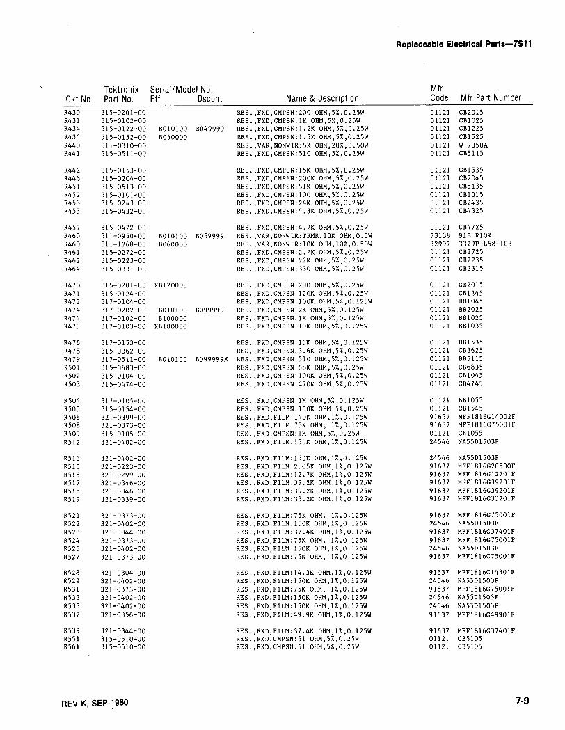
Replaceable Electrical Parts-7511
REV Κ, SEP 1980 7-9
Ckt No .TektronixPart No .
Serial/ Model No .Eff Dscon t Name & Descri ptio n
MfrCode Mfr Part N umber
R430 315-0201-00 RES ., FXD ,CMPSN:200 OHM,5%,0 .25W 01121 CB2015R431 315-0102-00 RES .,FXD ,CMPSN:IK OHM,5%,0 .25W 01121 CB 1025Α434 315-0122-00 Β010100 Β049999 RES ., FXD ,CMPSN:1 .2K OHM,5%,0 .25W 01121 CB 1225R434 315-0152-00 Β050000 RES .,FXD ,CMP SN:1 . 5K ΟΗΜ ,5%,0 .25W 01121 CB 1525Α440 311-0310-00 RES .,VAR ,NONWIR :SK ΟΗΜ ,20Υ�0 .50W 01121 W-7350ΑR441 315-0511-00 RES ., FXD ,CMP SN:510 OHM,5%,0 .25W 01121 CB5115
R442 315-0153-00 RES .,FXD ,CMP SN:15K OHM,5%,0 .25W 01121 CB 1535R446 315-0204-00 RES .,FXD ,CMP SN:200K OHM,5%,0 .25W 01121 CB2045R451 3 15-0513-00 RES .,FXD ,CMP SN:S1K OHM,5%,0 .25W 01121 CB5135R452 315-0101-00 RES ., FXD,CMP SN :100 OHM,5%,0 .25W 01121 C B 1015Α453 315-0243-00 RES .,FXD,CMP SN :24K OHM,5%,0 .25W 01121 C B2435Α455 315-0432-00 RES ., FXD ,CMP SN :4 .3K OHM,5%,0 .25W 01121 C B4325
Α457 315-0472-00 RES ., FXD,CMP SN :4 .7K OHM,5%,0 .25W 01121 C B4725R460 311-0950-00 Β010100 Β059999 RES .,VAR,NONWIR :TRMR,l OK OHM,O .SW 73138 91Β R10KR460 311-1268-00 Β060000 RES ., VAR,NONWIR : lOK ΟΗΜ ,10%, 0 . 50W 32997 3329 Ρ-L 58-103Α461 315-0272-00 RES ., FXD,CMP SN :2 .7K OHM,5%,0 .25W 01121 CB2725R462 315-0223-00 RES ., FXD,CMP SN:22K OHM ,57,,0 .25W 01121 CB2235R464 315-0331-00 RES ., FXD ,CMP SN :330 OHM,5%,0 .25W 01121 C B3315
R470 315-0201-00 ΧΒ120000 RES ., FXD,CMPSN :200 OHM,5%,0 .25W 01121 CB2015R471 315-0124-00 RES ., FXD,CMPSN :120K OHM,5%,0 .25W 01121 CB1245R472 317-0104-00 RES .,FXD,CMPSN :I OOK ΟΗΜ ,5%,0 .125W 01121 ΒΒ1045R474 317-0202-00 Β010100 Β099999 RES .,FXD,CMPSN :2K ΟΗΜ ,5%,0 .125W 01121 ΒΒ2025R474 317-0102-00 Β1Ο 00Ο0 RES .,FXD ,CMPSN :IK ΟΗΜ ,5%,0 .125W 01121 ΒΒ1025R475 317-0103-00 ΧΒ1Ο 00Ο0 RES .,FXD,CMPSN :l OK ΟΗΜ ,5%,0 .125W 01121 ΒΒ1035
R476 317-0153-00 RES .,FXD ,CMPSN :15K ΟΗΜ ,5%,0 .125W 01121 ΒΒ1535R478 315-0362-00 RES .,FXD ,CMPSN :3 .6K OHM,5%,0 .25W 01121 CB3625R479 317-0511-00 Β010100 Β099999Χ RES ., FXD ,CMPSN :510 ΟΗΜ,5%,0 .125W 01121 ΒΒ5115R501 315-0683-00 RES .,FXD,CMPSN :68K OHM,5%,0 .25W 01121 CB6835R502 315-0104-00 RES .,FXD ,CMPSN : 1 00K OHM,5%,0 .25W 01121 CB1045R503 315-0474-00 RES .,FXD ,CMPSN :470K OHM,5%,0 .25W 01121 CB4745
Α504 317-0105-00 RES .,FXD ,CMPSN :IM OHM ,5Y,,0 .125W 01121 ΒΒ1055R505 315-0154-00 RES ., FXD ,CMPSN :150K OHM,5%,0 .25W 01121 CB1545R506 321-0399-00 RES .,FXD,FILM :140K ΟΗΜ,1%,0 .125W 91637 MFF 1816G14002FR508 321-0373-00 RES .,FXD,FILM :75K OHM, 1%,0 .125W 91637 MFF 1816G75001FΑ509 315-0105-00 RES .,FXD ,CMPSN :IM OHM,5%,0 .25W 01121 CB1055R512 321-0402-00 RES .,FXD,FILM :150K ΟΗΜ,1%,0 .125W 24546 NA55D1503F
R513 321-0402-00 RES .,FXD,FILM :150K ΟΗΜ, 1 %,0 .125W 24546 NA55D1503FR515 321-0223-00 RES .,ΣXD,FILM :2 . 05K ΟΗΜ ,1%,0 .125W 91637 MFF1816G20500 FΑ516 321-0299-00 RES .,FXD,FILM :12 .7K ΟΗΜ ,1%,0 .125W 91637 MFF1816G12701 FR517 321-0346-00 RES .,FXD,FILM :39 .2K ΟΗΜ ,1%,0 .125W 91637 MFF1816G39201 FR518 321-0346-00 RES .,FXD,FILM :39 .2K ΟΗΜ , Ι%,0 .125W 91637 MFF1816G39201FΑ519 321-0339-00 RES .,FXD,FILM :33 .2K ΟΗΜ , Ι%,0 .125W 91637 MFF1816G33201 F
Α521 321-0373-00 RES . ,FXD,FILM :75K OHM, 1%,0 .125W 91637 MFF1816G75001 FR522 321-0402-00 RES .,FXD,FILM :150K ΟΗΜ,1%,0 .125W 24546 NA55D 1503FΑ523 321-0344-00 RES .,FXD,FILM :37 .4K ΟΗΜ ,1%,0 .125W 91637 MFF 1816G37401FΑ524 321-0373-00 RES .,FXD,FILM :75K OHM, 1%,0 .125W 91637 MFF1816G75001FR525 321-0402-00 RES .,FXD,FILM :150K ΟΗΜ , Ι %,0 .125W 24546 NA55D 1503FR527 321-0373-00 RES .,FXD,FILM :75K OHM, 1%,0 .125W 91637 MFF 1816G75001F
R528 321-0304-00 RES .,FXD,FILM :14 .3K ΟΗΜ,1%,0 .125W 91637 MFF 1816G14301FR529 321-0402-00 RES .,FXD, FILM :150K OHM , 1 Y,,0 .125W 24546 NA55D 1503FR531 321-0373-00 RES .,FXD,FILM :75K OHM, 1 Y,,0 .125W 91637 MFF 1816G75001FR533 321-0402-00 RES .,FXD,FILM :150K OHM , 1 Y,,0 .125W 24546 NA55D 1503FR535 321-0402-00 RES .,FXD,FILM :150K OHM , lY,,0 .125W 24546 NA55D 1503FR537 321-0356-00 RES .,FXD,FILM :49 .9K ΟΗΜ , 1%,0 .125W 91637 MFF 1816G49901F
R539 321-0344-00 RES .,FXD,FILM :37 .4K ONM, 1Y,,0 .125W 91637 MFF 1816G37401FR551 315-0510-00 RES .,FXD ,CMPSN:51 OHM,5%,0 .25W 01121 CB5105R561 315-0510-00 RES .,FXD ,CMPSN:51 OHM,5%,0 .25W 01121 CB5105

Replaceable Electrical Parts-7511
7-10 REV Ι , SEP 1980
C k t No .Tektron ixPart No .
Serial/Mod elE ff
No .Dscon t Name & Description
M frCode Mfr Part Number
R602 315-0101-00 RES .,FXD,CMPSN :100 ΟΗΜ ,5%,0 .25W 01121 CB1015R605 315-0101-00 RES .,FXD,CMPSN :100 ΟΗΜ ,5%,0 .25W 01121 CB1015R606 315-0101-00 RES .,FXD,CMPSN :100 ΟΗΜ ,5%,0 .25W 01121 CB1015R609 315-0101-00 RES .,FXD,CMPSN :100 ΟΗΜ ,57,0 .25W 01121 CB1015Α621 321-0632-00 RES .,FXD,FILM :9 .41K ΟΗΜ ,0 .5%,0 .125W 91637 MFF1816D941000R622 321-0601-00 RES .,FXD,FILM :2 .141K ΟΗΜ ,0 .25%,0 .125W 91637 MΣF1816D21410C
R624 321-0236-00 RES .,FXD,FILM :2 .8K ΟΗΜ ,1%,0 .125W 91637 MFF1816G28000FΑ626 321-0315-00 RES .,FXD,FILM :18 .7K ΟΗΜ ,1%,0 .125W 91637 MFF1816G18701FR627 315-0180-00 RES .,FXD,CMPSN :18 ΟΗΜ,5%,0 .25W 01121 CB1805Α629 315-0512-00 RES .,FXD,CMPSN:S .1K ΟΗΜ ,5%,0 .25W 01121 CB5125Α634 315-0100-00 RES .,FXD,CMPSN :10 ΟΗΜ ,5%,0 .25W 01121 CB1005R635 315-0470-00 RES .,FXD,CMPSN:47 ΟΗΜ ,5%,0 .25W 01121 CB4705
R636 315-0101-00 RES .,FXD,CMPSN:100 ΟΗΜ ,5%,0 .25W 01121 CB1015R638 315-0101-00 RES .,FXD,CMPSN :100 ΟΗΜ ,5%,0 .25W 01121 CB1015
S141A-C 670-1149-00 Β010100 Β019999 SWITCH,PUSH : 80009 670-1149-00S141A-C 670-1149-01 Β020000 SWITCH,PUSH : 80009 670-1149-01S146 262-0894-00 SWITCH, WIRED :VOLTS/DIV 80009 262-0894-00S146 260-1090-00 SWITCH,ROTARY :VOLTS/DIV 80009 260-1090-00S302A,B 670-1148-00 Β010100 Β019999 SWITCH,PUSH : 80009 670-1148-00S302A,B 670-1148-01 Β020000 SWITCH,PUSH : 80009 670-1149-01
5320 311-0585-00 RES .,VAR,NONWIR :15K ΟΗΜ ,20%,0 .25W 71590 ΒΑ201-061----- ----- (FURNISHED AS Α UNIT WITH Α320)
Τ230 120-0547-00 XFMR,TOROID :4-15 TURN WINDINGS 80009 120-0547-00Τ400 120-0650-00 XFMR,TOROID :2 WINDINGS 80009 120-0650-00Τ410 120-0487-00 XFMR,TOROID :5 TURNS BIFILAR 80009 120-0487-00Τ430 120-0546-00 XFMR,TOROID :4 TURNS BIFILAR 80009 120-0546-00
VR221 152-0226-00 SEMICOND DEVICE :ZENER,0 .4W ,S .1 V,5% 14552 TD3810980

SECTION 8DIAGRAMS
ANDMECHANICAL
PARTS ILLUSTRATIONS
The following special symbols are used on the diagrams :
0A- Screwdriver adjustment.
Front- or rear-panel control or connector .
Refers to the indicated diagram .
Test point .
Blue line encloses components located oncircuit board .
Connection made to circuit board withinterconnecting pin .
Connection made to circuit board withpin socket .
Coax connector .
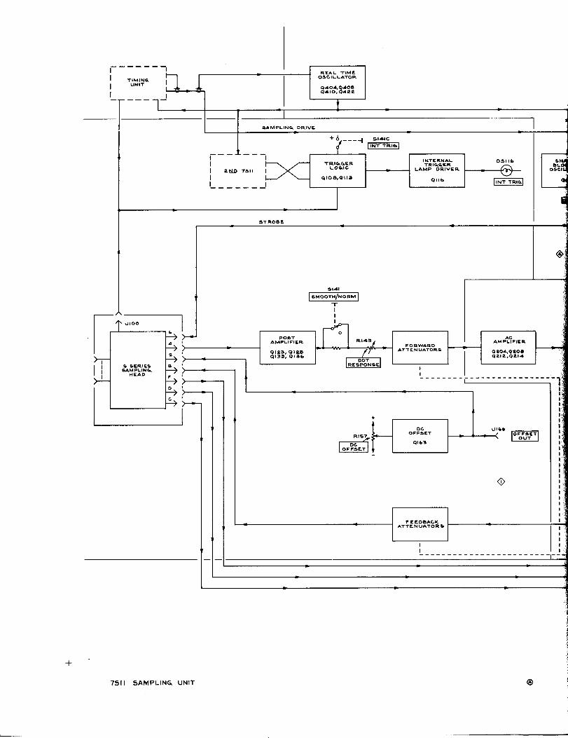


The typical voltage measurements were obtained under the following conditions unless noted otherwise on the ind ividualdiagrams:
Vertical ModeH orizontal ModeΒ IntensityΑ Trigger SourceΒ Trigger Source
7504
LeftΒOptimumR ig ht VertLeft Vert
7Α13 (left vertical compartment,P601 0, at +Input connector,
10Χ probe used for waveforms)
VOLTAGE ANDWAVEFORM TEST CONDITIONS
ΝΟΤΕ
Slope
+Stability
Fully clockwise (freeSequential
Pushed inSweep R ange
5 μsTime/Div
.1 AsInt
Pushed inScan
Rep
The spring tension of the pin sockets ensures α good connectionbetween the circuit board and pin . This spring tension may be damagedby using the pin sockets as α connecting point for spring-loadedprobetip, alligator clips, etc.
cable connected . Noinput signal .
7Τ11 (right horizontal compartment)
run)
All voltages given on the diagrams are in volts . Waveforms shown are actual waveform photographs taken with α TektronixOscilloscope Camera System and Pro jected Graticule. Vertical deflection factor shown on waveform is the actual deflectionfactor from the in put connector and does not include the 10Χ attenuation of the probe. The voltages and waveforms (shownin blue) on the d iagrams are not absolute and may vary between instruments because of component tolerances, internalcalibration, or front panel control settings . Voltage and time readouts are simulated in larger-t han-normal type .
71350 (left horizontal compartment)Volts ++Input DC Mode AutoComparison Voltage Cou pling AC
Center display on Source 1 ntgraticule Magnifie r Χ 1
Volts/Div See waveforms Time/Div See Waveforms
Voltmeter 7511 (right verticalcalibrated Sampling
compartment,Head installed)
Type MultimeterSensitivity 20,000 ohm/volt Uη i ts/Div 200Ranges 0.6 and 12 volts VAR IA BLE CAL INRecommended type (used Triplett Mod el 630-NA +UP Pushed infor measuring the voltages DC OFFSET M idrange, 0 volts atshown on the diagrams) OFFSET OUT jack.
NORMAL Pushed inI nput signal Termination or Coaxial


ΝΟΤΕ S :
2 ΒυΤΤ0 .+ UP/ I NV 6_ ί2"Γέi0ARD
P35b
R305ΙΟΟΚ
415V(DCPL* Ι )
Ι . FOR DECO UPL I NGPOWER DISTR I BUTION
2 . 5EE PARTS LIST FORSEMICON DUCTO R TYPES
ιΓ -Ι
VG L 7AG E conditions given on Diagram
R302S .I K
~ P3Sb
~ P30b
Ί
5302Β
[-+=UP
R303S . I Κ
~ P30b
P3Sb
~ P35b
5Ε Ε
Ι
-SOV
83122 . b7K
R301ΙΜ
S302AINVERT
R304ΙΜ
ΤΙ
",,_ VARIABLE- Ι5 V
BAL(DCPL a2)
3. ΤΙΝΤΕ D
ΑΡΕΑ
- . .-- .- 3 Ε5Ι hPΤE RFAC EBOARD
(C~Ε ~_ ; ΕίyΤΡΑ,Ε -; =rJ τι F
Fecr.,~_ zo-c
5ΕΕ
7S11 SAMPL ING UΝ ΙΤ
ΒΗR332bBOK
ΤΟ ΒΑ5ΕQSIb Ο
-l b ν(οCΡι#2)
PARTIA L VERTICA L B OA RD
R3111Ι:4ΟΚ
R3141.02K
vER r ι c. Α L ουΤΡυτ
Q314
Q334
R334Ι . Ο2Κ
R317-73.2K
R33773 .2 Κ
R Ε F Ε R Ε Ν C Ε
D Ι Α G R Α Μ 5
R325SOK
-50V
POSITION
ΟΙ POST AMP Έ ATTENUATO RS
Ο2 MEMORY
5Ο READOUT LOGIC
O POWER DISTR I BUTION λς D ECOUPL ING
® FRONT PA NEL CON TROLS t CONNECTORS


PARTS OR DER ING INFORMATION
Replacement p arts a re availa b le from or throu gh you r local
Te k tro n ix, I n c . F ield Office o r representative .
C h anges to Tek t ro n ix inst ruments are sometimes made to
accommodate improved components as t hey become availab le,
and to give you t he ben efit of t he latest circ u it im p rovements
develo ped i n our e n gi n eeri ng department . It is t h e refore
importa n t, w hen ord eri ng parts, to i n cl ude t he followi ng
i n formation i n yo ur orde r : Pa rt numb er, instrumen t ty pe o r
n umber, se rial number, and modificatio n number if applicable .
If α pa rt you have or de red has been replace d wit h α new or
improved part, you r local Tektron ix, Inc . F ield Office o r
represen tative will contact you concerning any cha nge i n p a r t
numbe r .
C hange i n formation, if any, is located at t h e rear of th is
manual .
SPE CIAL NOTES AND SYMBOLSΧΟΟΟ
ΟΟΧ
FIGURE AND INDEX NUMBERSItems i n t h is section a re refe re nced by figu re a nd i ndex
n umbe r s to t he illustratio n s .
REV Ε, SEP.1976
Part fi r st added at t h is serial nu mber
Part removed after t h is serial n umber
RE PLACEABLEMECHANICAL PARTS
ABBREVIATIONS
IN DENTATION SYSTEM
1 2 3 4 5
Name & Desc r ip tion
Assembly and/o r Componen t
Attach in g pa rts fo r Assembly and/o r Componen t
Detail Part of Assembly and/or Componen t
Attaching par ts fo r Detail Part
P a r ts of Detail Par t
Attach ing pa r ts for Parts of Detail Pa r t
ITEM NAME
Section 9-7S11
Th is mechan ical parts list is i nde n ted to i nd icate item
relatio n s h i p s . Following is an examp le of t he i nd entation system
use d in th e d escri p tio n column .
Attach i ng Parts always appea r in t he same i ndentatio n as
t he item itmoun ts, wh ile t h e detail parts are i ndented to t h e rig ht.
I ndented items are p a rt of, and in cluded with , the n ext h ig he r
inde n tatio n . The separatio n sym b ol ---' --- i ndicates t he end of
attac h i n g p arts .
Attach i ng pa rts must be purchased separately, unless otherwise
spec if ied .
In t he P a r ts List, an item Name is se p arate d from th e
description by α colon ( :) . Because of s pace limitation s, an Item
Name may sometimes appear as incomplete . F o r furt h er Item
Name i de n tificatio n , t h e U.S . Fede r al Catalogi ng Handbook Η 6-1
can be utilize d wh ere possible .
I N C H ELCTRN ELECTRONα NUMBER SIZE ELEC ELECTRICA LACTR ACTUATOR ELCTL T ELECTRO L YTICADPT R ADAPTER ELEM ELEMEN TAL IG N A L IGNMENT EPL ELECTR ICA L P A RTS L IST
AL ALUM INUM EQPT EQU I PMENTASSEM ASSEMBLED ΕΧΤ EXTERNA LASSY ASSEMBLY FI L F I LL IST ER HEADΑΤΤΕΝ ATTENUATOR FLE X FLEXI BLEAWG AMERICAN W IRE GAGE FLH FLAT HEADBD BOARD FL T R F I LT ERBRKT BRACKET FR FRAME or FRONTBRS BRASS FSTNR FASTENERBRZ BRONZ E FT FOOTBSHG BUSH I NG FXD FIXEDCAB CAB I NET GSK T GASKE TCAP CAPACITOR HDL HA NDLECER CER AM IC HEX HEXAGONCHAS CHASSIS HEX HD HEXAGONAL HEADCKT CI RC U IT HEX SΟC HEXAGONAL SOCKETCOMP COMPOSITIO N HLC P S HELICA L COMPRESSIONCONN CONNECTOR HLEXT HELICA L EXTENSIO NCO V COVER HV HIG H VO LTAGECPLG COUPL I NG IC I NT EGRATED CI RCU ITCRT CATHODE RAY TUBE ID I N SID E DIAMETERDEG DEGREE (D ENT IDENTI F ICATIONDWR DRAWER IMPLR I MPELLER
IN I N C H S E SI NGLE END
I NCA ND I NCANDESCENT S ECT SECTION
INSUL INSULATOR SEMICO ND SEMICONDUCTOR
INT L INTERNAL SHLO S H I ELDLPHLDR LAMPHOLDER SHLDR S HOULDEREDMACH MACH I NE SKT SOCKET
MECH MECHANICAL SL S L ID E
MTG MOUNTING SLFLKG S ELF-LOCK I N G
NIP N I PPLE SLVG SLEEVI NG
NON W I RE NOT W IRE WOUND SPR SPR I NG
OBD ORDER BY DESCR I PTION so SQUAREOD OUTSID E DIAMETER SST STAINLESS STEEL
OVH OV ALHEAD STL STEELΡΗ BRZ PHOSPHOR BRONZE ςω SWITCH
PL PL AI N or PL AT E Τ TUBEPLSTC PLASTIC TERM TERM I NA LPIN PART NUMBER THD THREADΡΝΗ PAN HEAD ΤΗΚ TH IC KPWR POWER TNSN TEN SIONRCPT RECEPTACLE T PG TAPP I N G
RES RESISTO R TRH TRUSS HEAD
RGD RIGID V VO LTAGERLF REL I EF VAR V ARIABLERTNR RETAINER W / W ITH
SCH SOCKET HEAD WSHR WASHER
SCOPE OSCILLOSCOPE XFMR T RANS FORMER
SCR SCREW XSTR TRANSISTO R

Replaceable Mechanical Parts-7511
M fr . CodeΟΟΟΒΚOOOCYOOOFW007790557407707082612252622599552107027671159
7146871785737437444578189
7913680009833858483087308
904849390798291
9-2
C ROSS I N D EX- MFR. CODE NUM BER TO MANUFACTURER
REV Η, SEP 1980
M a nufactu re r
STAUFFER SUPPLYNORTHWEST FASTENER SALE S, INC .WESTERN S INTERING CO INC .AMP, INC .
Address105 SE TAYLOR7923 SW C IRRUS DRIVE2620 STEVENS DRIVEΡ 0 Box 3608
City, State, Zip
PORTLAND, OR 97214BEAVERTON, OREGON 97005RICHLAND, WA 99352HARRISBURG, PA 17105
VIKING INDUSTRIES, INC . 21001 NORDHOFF STREET CHATSWORTH, CA 91311
USM CORP ., USM FASTENER DIV . 510 RIVER RD . SHELTON, CT 06484
SPECTRA-STRIP CORP . 7100 LAMPSON AVE . GARDEN GROVE, CA 92642
BERG ELECTRONICS, INC . YOUK EXPRESSWAY NEW CUMBERLAND, PA 17070
ESNA, DIV . OF AMERACE CORPORATION 16150 STAGG STREET VAN NUYS, CA 91409
GETTIG ENG . AND MFG . COMPANY PO BOX 85, OFF ROUTE 45 SPRING MILLS, PA 16875
ALLEN MFG. CO . Ρ . 0 . DRAWER 570 HARTFORD, CT 06101
BRI STOL SOCKET SCREW, DIV . OFAMERICAN CHAIN AND CABLE CO ., INC . Ρ 0 BOX 2244, 40 BRISTOL ST . WATERBURY, CT 06720
ΙΤΤ CANNON ELECTRIC 666 Ε . DYER RD . SANTA ANA, CA 92702
TRW , CINCH CONNECTORS 1501 MORSE AVENUE ELK GROVE VILLAGE, IL 60007
FISCHER SPECIAL MFG . CO . 446 MORGAN ST . CINCINNATI, OH 45206
HOLO-KROME CO . 31 BROOK ST . WEST HARTFORD, CT 06110
ILLINOIS TOOL WORKS, INC .SHAKEPROOF DIVI S ION ST . CHARLES ROAD ELGIN, IL 60120
WALDES, ΚΟΗΙΝΟΟΑ , INC . 47-16 AUSTEL PLACE LONG ISLAND C ITY, NY 11101
TEKTRONIX, INC . Ρ 0 BOX 500 BEAVERTON, OR 97077
CENTRAL SCREW CO . 2530 CRESCENT DR . BROADV IEW, IL 60153
LEE SPRING COMPANY, INC . 30 MAIN STREET BROOKLYN, NY 11201
Ν. L . INDUSTRIES, INC ., SOUTHERN SCREWDIV . Ρ . 0. BOX 1360 STATESVILLE, NC 28677
ΙΤΤ , SURPRENANT DIV . 172 STERLING STREET CLINTON, ΜΑ 01510
CAMCAR SCREW AND MFG . CO . 600 18TH AVE . ROCKFORD, IL 61101
SEALECTRO CORP . 225 ΗΟΥΤ MAMARONECK, NY 10544

ReplaceableMechanical Parts-7511
REV, JUL 1981 9-3
Fig . &IndexNo .
TektronixP art No .
Serial/ M o d elEff
No .Dsco n t Qty 1 2 3 4 5 N ame & Descriptio n
M frCode Mfr Part N umber
ι- ι 366-0392-02 1 KNOB :GY,0 .125 ID Χ0 .375 Η Χ 0 .812 Η 80009 366-0392-02_2 1 RESISTOR,VAR:(SEE R440 REPL)
(ATTACHING PARTS)213-0020-00 1 SETSCREW:6-32 Χ 0 .125 INCH ,HEX.SOC STL 70276 OBD
-3 366-1189-00 1 KNOB :GRAY 80009 366-1189-00213-0153-00 1 . SETSCREW:5-40 Χ 0 .125,STL ΒΚ ΟΧD ,ΗΕΧ SKT OOOCY OBD
-4 ----- ----- 1 RE SI STOR,VAR :(SEE Α143 REPL)(ATTACHING PARTS)
-5 361-0143-00 1 WASHER,KEY :0 .281 ID Χ 0 .562 INCH OD 80009 361-0143-00-6 210-0583-00 1 NUT,PLAIN,HEX . :0 .25-32 Χ 0 .312 INCH,BRS 73743 2Χ20317-402
-7 366-1064-00 Β010100 Β059999 1 KNOB :GRAY 80009 366-1064-00366-1084-00 Β060000 1 KNOB :GRAY 80009 366-1084-00213-0239-00 1 . SETSCREW:3-48 Χ 0 .062 INCH,HEX SOC STL 71159 OBD
-8 366-1148-00 Β010100 Β029999 1 KNOB : 80009 366-1148-00366-1148-01 Β030000 Β059999 1 KNOB :GRAY 80009 366-1148-01366-1101-00 Β060000 1 KNOB :GRAY 80009 366-1101-00213-0153-00 2 . SETSCREW :5-40 Χ 0 .125,STL ΒΚ OXD,HEX SKT OOOCY OBD
-9 ----- ----- 1 RES ISTOR,VAR :(SEE Α151,Α157 REPL)(ATTACHING PARTS)
-10 210-0583-00 1 NUT,PLAIN,HEX . :0 .25 -32 Χ 0 .312 INCH, BRS 73743 2Χ20317-402
-11 366-1168-00 1 KNOB :BLACK CAP AND RED BODY 80009 366-1168-00213-0153-00 1 . SETSCREW :5-40 Χ 0 .125,STL ΒΚ OXD,HEX SKT OOOCY OBD
-12 366-1057-00 1 KNOB :GRAY 80009 366-1057-00213-0153-00 1 . SETSCREW:5-40 Χ 0 .125,STL ΒΚ OXD,HEX SKT OOOCY OBD
-13 ----- ----- 1 SWITCH ,WIRED :VOLTS/DIV(SEE S146 REPL)(ATTACHING PARTS)
-14 210-0590-00 1 NUT,PLAIN,HEX . :0 .375 Χ 0 .438 INCH ,STL 73743 2Χ28269-402
-15 214-1205-00 1 ACTUATOR,SW : 80009 214-1205-00213-0075-00 1 . SETSCREW:4-40 Χ 0 .094,STL ΒΚ OXD,HEX SKT ΟΟΟΒΚ OBD
-16 214-1190-00 1 CPLG,SHAFT , RGD :0 .125 OD ΤΟ 0 .125 OD,AL 80009 214-1190-00213-0075-00 1 . SETSCREW :4-40 Χ 0 .094,STL ΒΚ OXD,HEX SKT ΟΟΟΒΚ OBD213-0140-00 1 . SETSCREW :2-56 Χ 0 .94 INCH,HEX SOC STL 70276 OBD
- 17 ----- ----- 1 RES ISTOR, VAR:(SEE R345 REPL)(ATTACHING PARTS)
-18 220-0510-00 1 NUT,PLAIN,HEX . :0 .25-32 Χ 0 .312 INCH 80009 220-0510-00-19 210-0046-00 1 WASHER , LOCK :0 .261 ID,INTL ,0 .018 THK,BRS 78189 1214-05-00-0541C-20 358-0409-00 1 BSHG,MACH . THD :0 .25-32 Χ 0 .159 ID Χ 0 .24 80009 358-0409-00
-21 ----- ----- 1 CKT BOARD ASSY : +UP/INVERT (SEE REPL)380-0148-00 1 . HOUS ING,LIGHT : 80009 380-0148-00
(ATTACHING PARTS)213-0181-00 1 . SCR ,TPG, THD FOR:2-32 Χ 0 .375 INCH,PNH STL 83385 OBD
-22 131-0589-00 6 . ΤΕΑΜ , ΡΙΝ :0 .46 L Χ 0 .025 SQ . PH ΒΑΖ GL 22526 47350-23 131-0590-00 2 . CONTACT , ELEC :0 .71 INCH LONG 22526 47351
(ATTACHING PARTS FOR CKT BD ASSY )-24 211-0156-00 1 SCREW,MACHINE :1-72 Χ 0 .25",82 DEG,FLH STL 93907 OBD
-25 ----- ----- 1 CKT BOARD ASSY : NORMAL/SMOOTH- ΙΝΤ TRIG(SEE REPL)380=0154-00 1 . HOUSING, LIGHT :STAINLESS STEEL 80009 380-0154-00
(ATTACHING PARTS)213-0181-00 1 . SCR,TPG,THD FOR :2-32 Χ 0 .375 INCH,PNH STL 83385 OBD
-26 131-0589-00 9 . ΤΕRΜ , ΡΙΝ :0 .46 L Χ 0 .025 SQ . PH ΒΑΖ GL 22526 47350-27 131-0590-00 2 . CONTACT ,ELEC :0 .71 INCH LONG 22526 47351
(ATTACHING PARTS FOR CKT BD ASSY)-28 211-0156-00 1 SCREW ,MACHINE :1-72 Χ 0 .25",82 DEG, FLH STL 93907 OBD
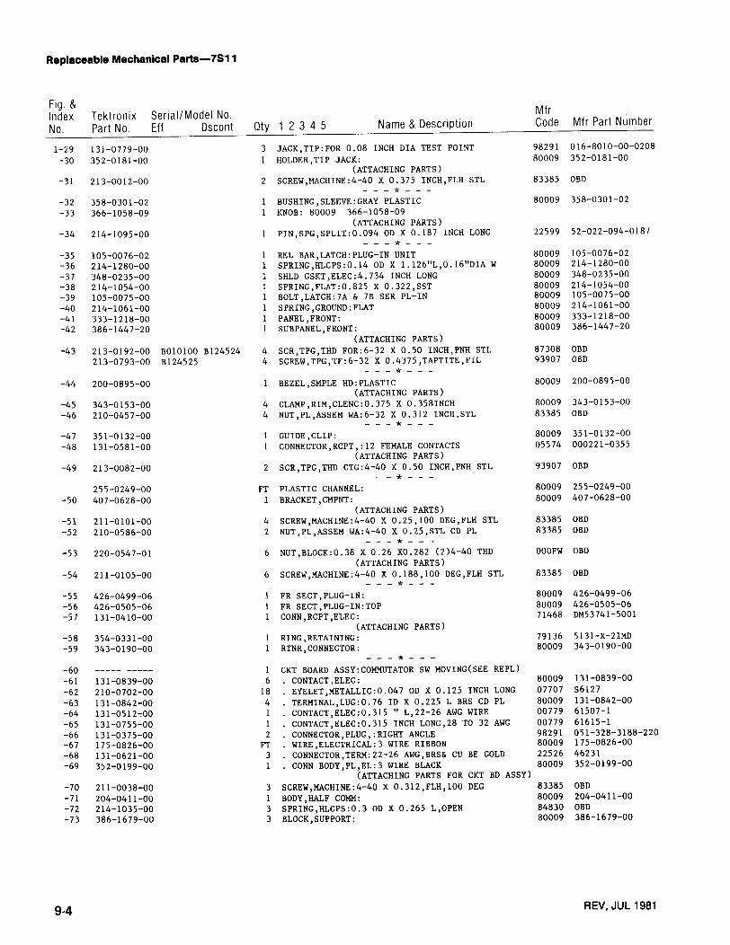
Replaceab le Mechanical Parts-7511
9-4REV, JUL 1981
F ig . &
IndexNo .
Tektron ixP art No .
Serial/M od elEff
No .Dscont Qty 1 2 3 4 5 Name & Descrip tion
M fr
Code Mfr Part Num ber
1-29 131-0779-00 3 JACK,TIP :FOR 0 .08 INCH DIA TEST POINT 98291 016-8010-00-0208
-30 352-0181-00 1 HOLDER,TIP JACK : 80009 352-0181-00(ATTACHING PARTS)
-31 213-0012-00 2 SCREW,MACHINE :4-40 Χ 0 .375 INCH,FLH STL 83385 OBD
-32 358-0301-02 1 BUSHING,SLEEVE :GRAY PLASTIC 80009 358-0301-02-33 366-1058-09 1 KNOB : 80009 366-1058-09
(ATTACHING PART S)-34 214-1095-00 1 PIN ,SPG,SPLIT :0 .094 OD Χ 0 .187 INCH LONG 22599 52-022-094-0187
-35 105-0076-02 1 REL BAR,LATCH:PLUG-IN UNIT 80009 105-0076-02-36 214-1280-00 1 SPRING,HLCPS :0 .14 OD Χ 1 .126 "L,0 .16"DIA W 80009 214-1280-00-37 348-0235-00 1 SHLD GSKT , ELEC :4 .734 INCH LONG 80009 348-0235-00-38 214-1054-00 1 SPRING, FLAT:0 .825 Χ 0 .322,SST 80009 214-1054-00-39 105-0075-00 1 BOLT,LATCH:7A & 7Β SER PL-IN 80009 105-0075-00
-40 214-1061-00 1 SPRING,GROUND :FLAT 80009 214-1061-00
-41 333-1218-00 1 PANEL,FRONT : 80009 333-1218-00
-42 386-1447-20 1 SUBPANEL,FRONT : 80009 386-1447-20(ATTACHING PARTS)
-43 213-0192-00 Β010100 Β124524 4 SCR,TPG,THD FOR :6-32 Χ 0 .50 INCH,PNH STL 87308 OBD213-0793-00 Β 124525 4 SCREW, TPG,TF :6-32 Χ 0 .4375, TAPTITE,FIL 93907 OBD
-44 200-0895-00 1 BEZEL ,SMPLE HD :PLASTIC 80009 200-0895-00(ATTACHING PARTS)
-45 343-0153-00 4 CLAMP , RIM ,CLENC :0 .375 Χ 0 .3581NCH 80009 343-0153-00
-46 210-0457-00 4 NUT,PL ,ASSEM WA:6-32 Χ 0 .312 INCH ,STL 83385 OBD
-47 351-0132-00 1 GUIDE ,CLIP : 80009 351-0132-00-48 131-0581-00 1 CONNECTOR , RCPT , :12 FEMALE CONTACTS 05574 000221-0355
(ATTACHING PARTS)-49 213-0082-00 2 SCR,TPG,THD CTG :4-40 Χ 0 .50 INCH,PNH STL 93907 OBD
255-0249-00 FT PLASTIC CHANNEL : 80009 255-0249-00
-50 407-0628-00 1 BRACKET ,CMPNT : 80009 407-0628-00(ATTACHING PARTS)
-51 211-0101-00 4 SCREW ,MACHINE :4-40 Χ 0 .25,100 DEG, FLH STL 83385 OBD-52 210-0586-00 2 NUT,PL,ASSEM WA:4-40 Χ 0 .25,STL CD PL 83385 OBD
-53 220-0547-01 6 NUT ,BLOCK :0 .38 Χ 0 .26 ΧΟ .282 (2)4-40 THD OOOFW OBD(ATTACHING PARTS)
-54 211-0105-00 6 SCREW ,MACHINE :4-40 Χ 0 .188,100 DEG,FLH STL 83385 OBD
-55 426-0499-06 1 ΣΑ SECT,PLUG-IN : 80009 426-0499-06-56 426-0505-06 1 FR SECT ,PLUG-ΙΝ : ΤΟΡ 80009 426-0505-06-57 131-0410-00 1 CONN,RCPT,ELE C : 71468 DM53741-5001
(ATTACHING PARTS)-58 354-0331-00 1 RING, RETAINING : 79136 5131 -Χ-21MD-59 343-0190-00 1 RTNR ,CONNECTOR : 80009 343-0190-00
_6ρ ----- ----- 1 CKT BOARD ASSY :COMMUTATOR SW MOVING(SEE REPL)-61 131-0839-00 6 . CONTACT,ELEC : 80009 131-0839-00
-62 210-0702-00 18 INCH LONG. EYELET,METALLI C :0 .047 OD Χ 0 .125 07707 S6127-63 131-0842-00 4 CD PL. TERMINAL,LUG :0 .76 ID Χ 0 .225 L BRS 80009 131-0842-00-64 131-0512-00 1 ". CONTACT , ELEC :0 .315 L ,22-26 AWG WIRE 00779 61507-1-65 131-0755-00 1 . CONTACT , ELEC :0 .315 INCH LONG,28 ΤΟ 32 AWG 00779 61615-1-66 131-0375-00 2 . CONNECTOR,PLUG, :RIGHT ANGLE 98291 051-328-3188-220-67 175-0826-00 FT . WIRE,ELECTRICAL:3 WIRE RIBBON 80009 175-0826-00-68 131-0621-00 3 GOLD. CONNECTOR,TERM :22-26 AWG, BRS& CU BE 22526 46231-69 352-0199-00 1 . CONN BODY,PL,EL:3 WIRE BLACK 80009 352-0199-00
(ATTACHING PARTS FOR CKT BD ASSY )-70 211-0038-00 3 SCREW,MACHINE :4-40 Χ 0 .312, FLH ,100 DEG 83385 OBD-71 204-0411-00 1 BODY, HALF COMM: 80009 204-0411-00-72 214-1035-00 3 SPRING, HLCPS :0 .3 OD Χ 0 .265 L ,OPEN 84830 OBD-73 386-1679-00 3 BLOCK,SUPPORT : 80009 386-1679-00

REV, JUL 1981
Replaceable Mechanical Parts-7511
9-5
F ig . &IndexNo .
TektronixPart No .
Serial/ ModelEff
No .Dscont Qty 1 2 3 4 5 Name & Description
MfrCode Mfr Part N um ber
1-74 213-0230-00 3 SCREW ,MACHINE : 80009 213-0230-00-75 220-0567-00 3 NUT,PLAIN,PLATE : 80009 220-0567-00-76 211-0101-00 3 SCREW,MACHINE :4-40 Χ 0 .25,100 DEG,FLH STL 83385 OBD
_77 ----- ----- 1 CKT BOARD ASSY:COMMUTATOR SW FIXED(SEE REPL)-78 131-0842-00 2 . TERMINAL,LUG :0 .76 ID Χ 0 .225 L BRS CD PL 80009 131-0842-00-79 175-0826-00 FT . WIRE,ELECTRICAL :3 WIRE RIBBON 80009 175-0826-00-80 131-0621-00 3 . CONNECTOR,TERM:22-26 AWG, BR Sfi CU BE GOLD 22526 46231-81 352-0199-00 1 . CONN BODY,PL,EL :3 WIRE BLACK 80009 352-0199-00-82 131-0512-00 1 ". CONTACT ,ELEC :0 .315 L ,22-26 AWG WIRE 00779 61507-1-83 131-0755-00 1 . CONTACT ,ELEC :0 .315 INCH LONG,28 ΤΟ 32 AWG 00779 61615-1
(ATTACHING PARTS FOR CKT BD ASSY )-84 211-0038-00 3 SCREW,MACHINE :4-40 Χ 0 .312, FLH,100 DEG 83385 OBD
210-0001-00 3 WASHER,LOCK :INTL ,0 .092 ID Χ 0 .18"OD ,STL 78189 1202-00-00-0541C-85 210-0405-00 3 NUT,PLAIN,HEX . :2-56 Χ 0 .188 INCH,BRS 73743 2ΧΙ 2157-402
-86 204-0410-00 1 BODY HALF ,COMM :STATIONARY 80009 204-0410-00(ATTACHING PARTS)
211-0038-00 3 SCREW ,MACHINE :4-40 Χ 0 .312,FLH ,100 DEG 83385 OBD-87 210-0586-00 3 NUT,PL ,ASSEM WA:4-40 Χ 0 .25,STL CD PL 83385 OBD_88 ----- ____- 1 CKT BOARD ASSY : VERTICAL(SEE REPL)-89 136-0220-00 24 . SΚΤ , ΡL-IN ELEK:TRANSI STOR 3 CONTACT,PCB MT 71785 133-23-11-034-90 136-0235-00 2 . SOCKET , PLUG-ΙΝ :6 CONTACT,ROUND 71785 133-96-12-062-91 136-0263-03 Β010100 Β 102089 39 . SOCKET,PIN TERM :FOR 0 .025 INCH SQUARE PIN 00779 86250-2
136-0263-04 Β102090 39 . SOCKET,PIN TERM:FOR 0 .025 INCH SQUARE PIN 22526 75377-001-92 214-0579-00 10 . TERM,TEST POINT :BRS CD PL 80009 214-0579-00-93 361-0238-00 4 . SPACER ,SLEEVE :0 .25 OD Χ 0 .34 INCH LONG 80009 361-0238-00-94 211-0155-0 0 4 . SCREW, EXT,RLV Β:4-40 Χ 0 .375 INCH ,SST 80009 211-0155-00-95 ----- ----- 1 CKT BOARD ASSY : INTER-CHANNEL CONTROL (SEE REPL)-96 131-0391-0 0 Β010100 Β079999 1 . CONNECTOR , RCPT , :50 OHM ,COAX,SNAP-ON MALE 98291 51-051-0049
131-0391-00 Β080000 2 . CONNECTOR , RCPT , :50 OHM,COAX,SNAP-ON MALE 98291 51-051-0049-97 136-0183-00 1 . SOCKET , PLUG-ΙΝ :3 PIN,ROUND 80009 136-0183-00-98 136-0220-00 10 . SΚΤ ,ΡL-IN ELEK :TRANS ISTOR 3 CONTACT , PCB MT 71785 133-23-11-034-99 136-0235-00 1 . SOCKET ,PLUG-ΙΝ :6 CONTACT,ROUND 71785 133-96-12-062-100 136-0263-03 Β010100 Β102089 19 . SOCKET,PIN TERM:FOR 0 .025 INCH SQUARE PIN 00779 86250-2
136-0263-04 Β 102090 16 . SOCKET,PIN TERM:FOR 0 .025 INCH SQUARE PIN 22526 75377-001-101 426-0121-00 1 . MOUNT ,COMPONENT :DELRIN 80009 426-0121-00-102 361-0007-00 1 . SPACER ,SLEEVE :0 .250 INCH DIA, PLASTIC 80009 361-0007-00-103 361-0238-00 3 . SPACER ,SLEEVE :0 .25 OD Χ 0 .34 INCH LONG 80009 361-0238-00-104 211-0155-00 3 . SCREW,EXT, RLV Β :4-40 Χ 0 .375 INCH ,SST 80009 211-0155-00-105 _____ -___- 1 CKT BOARD ASSY : INTERFACE (SEE REPL)-106 131-0391-00 2 . CONNECTOR,RCPT , :50 OHM ,COAX,SNAP-ON MALE 98291 51-051-0049-107 131-0566-00 2 . BUS CONDUCTOR : DUMMY RES,2 .375,22 AWG 55210 L-2007-1-108 131-0589-00 40 . ΤΕRΜ , ΡΙΝ :0 .46 L Χ 0 .025 SQ . PH BRZ GL 22526 47350
131-0590-00 Β010100 Β079999 48 . CONTACT ,ELEC :0 .71 INCH LONG 22526 47351131-0590-00 Β080000 46 . CONTACT , ELEC :0 .71 INCH LONG 22526 47351131-0593-00 4 . CONTACT ,ELEC :1 .15 INCH LONG 22526 47354131-0665-00 1 . TERMINAL , ΡΙΝ :0 .88 L Χ 0 .025 SQUARE 22526 47358131-0827-00 1 . CONTACT , ELEC :0 .55 INCH LONG 22526 47349
-109 131-0593-00 4 . CONTACT , ELEC :1 .15 INCH LONG 22526 47354-110 136-0183-00 1 . SOCKET , PLUG-ΙΝ :3 PIN, ROUND 80009 136-0183-00-111 136-0220-00 2 . SΚΤ , ΡL-IN ELEK :TRANS I STOR 3 CONTACT , PCB MT 71785 133-23-11-034-112 351-0155-00 5 . INSULATOR ,STDF :CONNECTOR,DELRIN 80009 351-0155-00-113 351-0188-00 7 . GUIDE -POST , LOCK :0 .65 INCH LONG 80009 351-0188-00-114 351-0185-00 1 . GUIDE-POST , LOCK :0 .65 INCH LONG 80009 351-0185-00

Replaceable Mechanical Parts-7511
9-6REV, JUL 1981
F ig . &
IndexNo .
Te ktro n ixPart No .
Serial/ Model No .Eff Dscont Qty 1 2 3 4 5 N ame & Description
M fr
Code Mfr Part N um ber
1-115 214-1140-00 8 . SPRING, HLCPS :0 .251 OD Χ 0 .375"L ,SST WIRE 80009 214-1140-00-116 214-1136-00 1 . ACTUATOR ,SL SW : DUAL DPST 80009 214-1136-00-117 351-0180-00 1 . SLIDE ,GUIDE :SWITCH ACTUATOR 80009 351-0180-00-118 407-0553-00 1 . BRACKET ,CMPNT :BRASS ALBALOYPL 80009 407-0553-00-119 ----- ----- 1 . RES ISTOR,VAR :(SEE Α320 REPL)-120 210-0583-00 1 . NUT,PLAIN,HEX . :0 .25-32 Χ 0 .312 INCH,BRS 73743 2Χ20317-402
(ATTACHING PARTS FOR CKT BD ASSY)-121 211-0116-00 Β010100 Β124149 6 SCR,ASSEM WSHR :4-40 Χ 0 .312 INCH,PNH BRS 83385 OBD
211-0292-00 Β124150 6 SCR,ASSEM WSHR :4-40 Χ 0 .29, BRS ΝΙ PL 78189 OBD
-122 386-1402-00 1 PANEL,REAR : 80009 386-1402-00(ATTACHING PARTS)
-123 213-0192-00 Β010100 Β 124524 4 SCR,TPG,THD FOR :6 -32 Χ 0 .50 INCH,PNH STL 87308 OBD213-0793-00 Β124525 4 SCREW ,TPG, TF :6-32 Χ 0 .4375, TAPTITE,FIL 93907 OBD
-124 337-1238-00 Β010100 Β059999 1 SHIELD,ELEC : LEFT SIDE 80009 337-1238-00337-1238-01 Β060000 1 SHIELD,ELEC : LEFT SIDE 80009 337-1238-01
-125 337-1247-00 Β010100 Β059999 1 SHIELD,ELEC :RIGHT SIDE 80009 337-1247-00337-1247-01 Β060000 1 SHIELD,ELEC : RIGHT SIDE 80009 337-1247-01
-126 131-0375-00 Β010100 Β079999 1 . CONNECTOR,PLUG, :RIGHT ANGLE 98291 051-328-3188-220131-0375-00 Β080000 2 . CONNECTOR,PLUG, :RIGHT ANGLE 98291 051-328-3188-220
-127 175-0825-00 FT . WIRE,ELECTRICAL:2 WIRE RIBBON 80009 175-0825-00-128 175-0828-00 FT . WIRE,ELECTRICAL:5 WIRE RIBBON 08261 SS-0526-710610C-129 175-0831-00 FT . WIRE,ELECTRICAL:8 WIRE RIBBON 08261 SS-0826-710610C-130 175-0832-00 FT . WIRE,ELECTRICAL:9 WIRE RIBBON 08261 SS-0926(1061)OC-131 352-0162-00 1 . HLDR,TERM CONN :4 WIRE BLACK 80009 352-0162-00-132 352-0163-00 1 . CONN BODY,PL,EL :5 WIRE BLACK 80009 352-0163-00-133 352-0169-00 1 . HLDR,TERM CONN :2 WIRE BLACK 80009 352-0169-00
352-0169-02 2 . CONN BODY,PL,EL:2 WIRE RED 80009 352-0169-00-134 352-0176-00 1 . CONN BODY,PL,EL :4 WIRE,DBL ROW BLACK 80009 352-0176-00-135 352-0198-00 1 . HLDR,TERM CONN :2 WIRE BLACK 80009 352-0198-00-136 352-0201-00 3 . CONN BODY, PL,EL :5 WIRE BLACK 80009 352-0201-00-137 352-0204-00 1 . CONN BODY,PL,EL :8 WIRE BLACK 80009 352-0204-00-138 352-0205-00 1 . CONN BODY,PL,EL :9 WIRE BLACK 80009 352-0205-00-139 131-0707-00 1 . CONNECTOR , TERM. :22-26 AWG,BRS& CU BE GOLD 22526 47439
131-0708-00 1 . CONTACT ,ELEC :0 .48"L ,28-32 AWG WIRE 22526 47437-140 131-0621-00 Β010100 Β020369 1 . CONNECTOR,TERM:22-26 AWG, BRS& CU BE GOLD 22526 46231
131-0792-00 Β020370 3 . CONNECTOR ,TERM:18-20 AWG,CU BE GOLD PL 22526 46221131-0622-00 1 . CONTACT ,ELEC :0 .577"L ,28-32 AWG WIRE 22526 46241
-141 384-0664-00 1 . SHAFT ,STRAIGHT :1 .05 L Χ 0 .1247 OD SST 80009 384-0664-00-142 384-0679-00 1 . ΕΧΤ SRAFT :5 .29 L Χ 0 .124 STEP OD STL CD PL 80009 384-0679-00-143 376-0051-00 1 . CPLG,SHAFT ,FLEX:0 .127 ID Χ 0 .375 ID DELRIN 80009 376-0051-00
213-0048-00 4 . SETSCREW:4-40 Χ 0 .125 INCH ,HEX SOC STL 74445 OBD-144 175-1020-00 Β0101ο0 Β 102088 1 CABLE,RF :50 OHM COAX,WHT POLYTHN JKT 90484 DAB70JAAAWHITE
175-1769-00 Β102089 1 CABLE ASSY ,RF :1-50 OHM COAX,4 .75 L 80009 175-1769-00

Fig . &Index
Tek tro n ix
Serial/ Model No .
MfrNo.
Part No .
Eff
Dsco n t
Qty 1 2 3 4 5
Name & Descri p tion
Code
M fr Part Num ber
070-0985-00
1 MANUAL,TECH :INSTRUCTION'
80009 070-0985-00
REV. Β SEP 1976 7511 SAMPL ING UN IT

MANUAL CHANGE INFORMATION
At Tektronix, we continually strive to keepup with latest electron ic developmentsby add ing circuit and component im provements to our instrume nts as soon as theyare developed an d tested .
Sometimes, d ue to printing and sh i pping requirements, we can't get thesechanges immediately i nto p ri nted man uals . He n ce, your manual may contain newchan ge information on following pages.
Α single c hange may affect several sections. Since thechange i nformation sheetsare carried in the man ual until all ch anges are permanently entered, somedu pl ication may occur. If no such chan ge pages appear following this page, yourmanual is correct as printed.
SERVICE ΝΟΤΕ
Because of the un iversal parts procurement problem,some electrical parts in youri nstrument may be different from those described in theReplaceable Elect rical PartsL ist . The parts used will in no way alter or compromise the performance or reliabilityof this i nstrument . They are i nstalled when necessary to ensu re prompt delivery tothe customer . Order replaceme nt parts from the Replaceable Electrical Parts L ist .

CALIBRATION TEST EQUIPMENT REPLACEMENT
Calibration Test Equipment Chart
This chart com pares TM 500 p roduct performan ce to that of older Tekt ronix equipment . Only those
characteristics wh ere significant specification differe n ces occur, are listed . In some cases the new i nstrument
may not be α total functional replacemen t . Additional su pport i nstrumentation may be needed or α change i n
calibratio n procedure may be necessary. .
Comparison of Main Characte r istics
NOTE: All TM 500 generator ou tputs are short-proof . All TM 500 plug-in i n struments requir e TM 500-Series Power Module .
REV Β , JUN 1978
DM 501 replaces 7D13PG 501 replaces 107 PG 501 - Risetime less than 107- R isetime less th an
3.5 ns i nto 50 Ω . 3 .0 ns i n to 50 Ω .108 PG 501 - 5 V outpu t pulse ; 108- 10 V output pulse
3 .5 ns Risetime 1 ns Risetime
PG 502 replaces 107
108 PG 502 - 5 V output 108- 10 V outpu t111 PG 502 - Risetime less t han 111 - Risetime 0 .5 ns ; 30
1 ns ; 10 ns to 250 nsPret r igge r pulse Pret r igge r pulsedelay delay --
PG 508 replaces 114Performance of replacement equ i pmen t is the same or
115 better than equ i pment being replaced .2101
PG 506 replaces 106 PG 506 - Positive-goi ng 106- Positive and N egative-t rigger output sig- goi ng trigger ou tputηαΙ at least 1 V; sig n al, 50 ns a nd 1 V;High Amplitude out- High Amplitude ou tpu t,pu t, 60 V. 100 V.
067-0502-01 PG 506 - Does not have 0502-01 - Comparato r outputchopped feature . can be alternately
chopped to α refe r -ence voltage.
SG 503 re places 190,190Α , 190Β SG 503 - Am plit ude range 190Β - Am plit ude range 40 mV
5mV to5.5 V ρ-ρ . to 10 V Ρ -ρ .191
067-0532-01 SG 503- Frequency range 0532-01- Frequency range250 kHz to 250 MHz . 65 MHz to 500 MHz.
SG 504 replaces067-0532-01 SG 504 - Frequency range 0532-01 - Frequency range
245 MHz to 1050 MHz . 65 MHz to 500 MHz .067-0650-00
TG 501 replaces 180,180Α TG 501 - T rigger ou tp ut- 180Α - Trigger pulses 1, 10,
slaved to marke r 100 Hz ; 1, 10, andoutput f rom 5 sec 100 kHz . Mu lti p let hrough 100 ns. One time-mark s can betime-mark can be generated si mu lta n -generated at α ti me . eously.
181 181 - M ulti ple time-mark s184 TG 501 - T rigger outpu t- 184 - Separate t rigge r
slaved to market pulses of 1 and 0 .1output f rom 5 sec sec ; 10, 1, and 0.1t hrough 100 ns. One ms ; 10 and 1 μs.time-mark can begenerated at α ti me .
2901 TG 501 - Trigge r outpu t- 2901 - Separate t riggerslaved to marker pulses, from 5 secou tpu t f rom 5 sec to 0 .1 μs. Mu lti p lethrough 100 ns . time-mar k s can beOne time-mark can generated simultan-be generated at eously .α ti me .

![«Η λογοτεχνία 1830-1880», Ιστορία του νέου ελληνισμού 1770-2000, τ. 4, Ελληνικά Γράμματα, [Ιανουάριος] 2004, σ. 195-210.](https://static.fdokumen.com/doc/165x107/631274fcb033aaa8b20fa5cb/i-logoteni-1830-1880-istori-tou-neou-ellinismou.jpg)