Full characterization at 904 nm of large area Si p-n junction photodetectors produced by LID...
10
International Journal of Modern Physics B Vol. 19, No. 31 (2005) 4619-4628 © World Scientific Publishing Company FULL CHARACTERIZATION AT 904nm OF LARGE AREA Si p-n JUNCTION PHOTODETECTORS PRODUCED BY LID TECHNIQUE RAID A. ISMAIL * , OMAR A. ABDULRAZAQ † ASEEL A. HADI ‡ and ODAY ATA HAMADI § * Solar Cells and Applied Physics Center, Ministry of Science and Technology, Baghdad, IRAQ † NASSR State Company, Ministry of Industry and Minerals, Baghdad, IRAQ ‡ School of Applied Sciences, University of Technology, Baghdad, IRAQ § P. O. Box 55159, Baghdad 12001, IRAQ § [email protected] Received 23 March 2005 In this paper, we report the experimental data of photoresponse namely; voltage responsivity and speed of response at =904nm of silicon photodiode formed by pulsed laser-induced diffusion technique. Experimental results demonstrated that the photodiode parameters strongly depend on the laser energy and substrate temperature. Maximum Responsivity obtained for p-n junctions photodetectors prepared by laser fluence of 9.17J/cm 2 for Al-doped Si and 10.03J/cm 2 for Sb-doped Si at substrate temperature (Ts) of 598K. The pulse response waveform of photodetectors illustrated that the rise time is not dominated by RC. Non-linearity deviation coefficient was improved by factors 1.6 for and 2.7 for for Al-doped Si and Sb-doped Si photodetectors respectively when Ts is raised from 300K to 598K. Keywords: Silicon photodetector; photoresponse; laser-induced diffusion; optical non-linearity 1. Introduction The use of pulsed laser-induced diffusion in semiconductor processing was extensive of many active researches [1-4]. The major importance advantages of using laser in annealing and diffusion of semiconductor photodetector junction devices are: (i) short processing time, (ii) ultra-shallow junction can be obtained, (iii) do not need post-diffusion heat treatment, (iv) offer excellent abruptness and junction depth control, (v) due to the localization of laser spot size on the semiconductor device, the minority-carrier lifetime of the substrate is reserved, (vi) high control of the sensitive area on the photodiode by controlling the laser spot size, (vii) capability to achieve high concentration doping (10 17 -10 19 cm -3 ), (viii) dopants activate above the solid solubility limit [5-6]. 4619
Transcript of Full characterization at 904 nm of large area Si p-n junction photodetectors produced by LID...
International Journal of Modern Physics B Vol. 19, No. 31 (2005) 4619-4628 © World Scientific Publishing Company
FULL CHARACTERIZATION AT 904nm OF LARGE AREA Si p-n JUNCTION PHOTODETECTORS PRODUCED
BY LID TECHNIQUE
RAID A. ISMAIL *, OMAR A. ABDULRAZAQ †ASEEL A. HADI ‡ and ODAY ATA HAMADI §
* Solar Cells and Applied Physics Center, Ministry of Science and Technology, Baghdad, IRAQ
† NASSR State Company, Ministry of Industry and Minerals, Baghdad, IRAQ ‡ School of Applied Sciences, University of Technology, Baghdad, IRAQ
§ P. O. Box 55159, Baghdad 12001, IRAQ § [email protected]
Received 23 March 2005
In this paper, we report the experimental data of photoresponse namely; voltage responsivity and speed of response at λ=904nm of silicon photodiode formed by pulsed laser-induced diffusion technique. Experimental results demonstrated that the photodiode parameters strongly depend on the laser energy and substrate temperature. Maximum Responsivity obtained for p-n junctions photodetectors prepared by laser fluence of 9.17J/cm2 for Al-doped Si and 10.03J/cm2 for Sb-doped Si at substrate temperature (Ts) of 598K. The pulse response waveform of photodetectors illustrated that the rise time is not dominated by RC. Non-linearity deviation coefficient was improved by factors 1.6 for and 2.7 for for Al-doped Si and Sb-doped Si photodetectors respectively when Ts is raised from 300K to 598K.
Keywords: Silicon photodetector; photoresponse; laser-induced diffusion; optical non-linearity
1. Introduction The use of pulsed laser-induced diffusion in semiconductor processing was extensive of many active researches [1-4]. The major importance advantages of using laser in annealing and diffusion of semiconductor photodetector junction devices are: (i) short processing time, (ii) ultra-shallow junction can be obtained, (iii) do not need post-diffusion heat treatment, (iv) offer excellent abruptness and junction depth control, (v) due to the localization of laser spot size on the semiconductor device, the minority-carrier lifetime of the substrate is reserved, (vi) high control of the sensitive area on the photodiode by controlling the laser spot size, (vii) capability to achieve high concentration doping (1017-1019cm-3), (viii) dopants activate above the solid solubility limit [5-6].
4619
R. A. Ismail et al. 4620
Since the photo-energy of Nd:YAG laser (1.17eV) is ideally matched to the energy band-gap of silicon (1.12eV at 300K), Nd:YAG laser had been widely used in silicon processing [7-8]. Our preliminary results showed that the peak photoresponse of Si photodiode fabricated by laser-induced diffusion was around 900nm [9].
Few investigations have been reported on photoresponse of Si photodiodes fabricated by pulsed Nd:YAG laser-induced diffusion. These investigations do not cover the comprehensive characterization of photodiode parameters at peak wavelength (900nm) [10-11].
In this paper, we report the first comprehensive study on Si photodiode at peak response prepared by long Nd:YAG laser pulses.
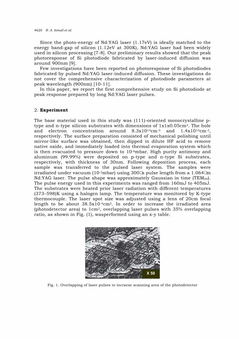
2. Experiment The base material used in this study was (111)-oriented monocrystalline p-type and n-type silicon substrates with dimensions of 1x1x0.05cm3. The hole and electron concentration around 8.3x1014cm-3 and 1.4x1015cm-3,respectively. The surface preparation consisted of mechanical polishing until mirror-like surface was obtained, then dipped in dilute HF acid to remove native oxide, and immediately loaded into thermal evaporation system which is then evacuated to pressure down to 10-6mbar. High purity antimony and aluminum (99.99%) were deposited on p-type and n-type Si substrates, respectively, with thickness of 30nm. Following deposition process, each sample was transferred to the pulsed laser system. The samples were irradiated under vacuum (10-2mbar) using 300µs pulse length from a 1.064µmNd:YAG laser. The pulse shape was approximately Gaussian in time (TEM00). The pulse energy used in this experiments was ranged from 160mJ to 405mJ. The substrates were heated prior laser radiation with different temperatures (373–598)K using a halogen lamp. The temperature was monitored by K-type thermocouple. The laser spot size was adjusted using a lens of 20cm focal length to be about 38.5x10⁻⁴cm2. In order to increase the irradiated area (photodetector area) to 1cm2, overlapping laser pulses with 35% overlapping ratio, as shown in Fig. (1), wasperformed using an x-y table.
Fig. 1. Overlapping of laser pulses to incraese scanning area of the photodetector
X 50
Full Characterization at 904nm of Large Area Si p-n Junction Photodetectors Produced by LID Technique 4621
Before making ohmic contacts, the samples were rinsed in NaOH to remove residual atoms of Sb and Al. Subsequently; ohmic contacts were made on p-type and n-type sides using Au-Sb and Al electrodes, respectively. 200ns pulses of 904nm GaAlAs laser were employed to investigate the responsivity and the response speed of photodiodes (RL=50Ω, VR=5-30V) fabricated at various conditions. The pulse shape was recorded by 250MHz Tektronix storage oscilloscope.
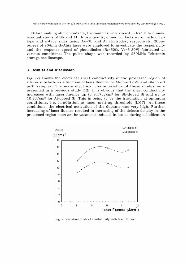
3. Results and Discussion Fig. (2) shows the electrical sheet conductivity of the processed region of silicon substarte as a function of laser fluence for Al-doped n-Si and Sb-doped p-Si samples. The main electrical characteristics of these diodes were presented in a previous study [12]. It is obvious that the sheet conductivity increases with laser fluence up to 9.17J/cm2 for Sb-doped Si and up to 10.3J/cm2 for Al-doped Si. This is being to be the irradiation at optimum conditions, i.e, irradiation at laser melting threshold (LMT). At these conditions, the electrical activation of the dopants was very high. Further increasing of laser fluence resulted in increasing of the defects density in the processed region such as the vacancies induced in lattice during solidification
Fig. 2. Variation of sheet conductivity with laser fluence
R. A. Ismail et al. 4622
(a) (b)
(c) (d)
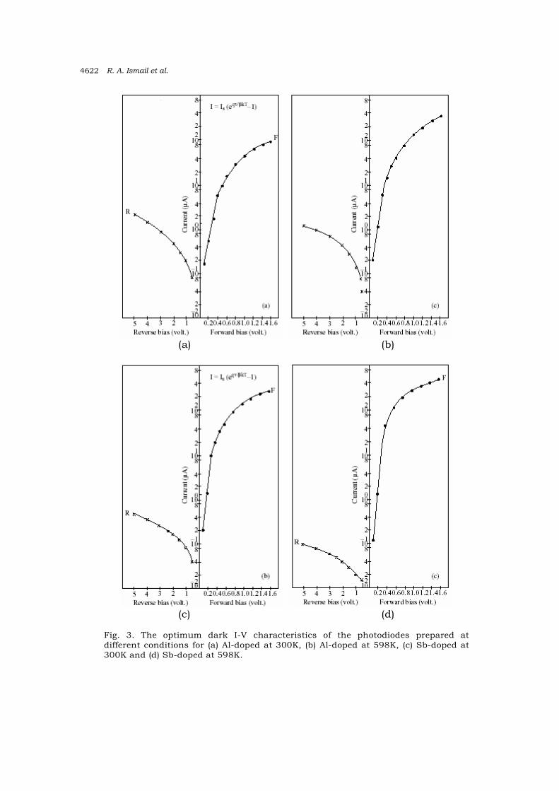
Fig. 3. The optimum dark I-V characteristics of the photodiodes prepared at different conditions for (a) Al-doped at 300K, (b) Al-doped at 598K, (c) Sb-doped at 300K and (d) Sb-doped at 598K.
Full Characterization at 904nm of Large Area Si p-n Junction Photodetectors Produced by LID Technique 4623
process [13]. These defects in turn lead to decrease sheet conductivity of the layer. Fig. (3) explains the dark I-V characteristics of the photodiodes prepared at different conditions. It is clear from this figure that the photodiodes exhibit
0
2
4
6
8
10
12
0 4 8 12 16 20 24 28 32
Reverse Bias (V)
R (V/W)
8.5J/cm2
9.17J/cm2
10.03J/cm2
11.4J/cm2
12.7J/cm2
0
2
4
6
8
10
12
14
0 4 8 12 16 20 24 28 32
Reverse Bias (V)
R(V/W)
8.5J/cm29.17J/cm210.03J/cm211.4J/cm212.7J/cm2
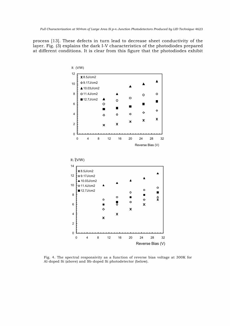
Fig. 4. The spectral responsivity as a function of reverse bias voltage at 300K for Al-doped Si (above) and Sb-doped Si photodetector (below).
R. A. Ismail et al. 4624
good rectification behaviour (high If/Ir ratio) and particularly these photodiodes fabricated with Sb-doped substrate at 598K (Fig. 3d). As compared to diodes fabricated at room temperature, good features can be observed due to the reduction of defects. Heating the sample to 598K caused a reduction in the ideality factor to 1.65. This is attributed to the improvement in the crystal characteristics induced by heating [13].
Fig. (4) demonstrates the responsivity in the reverse biasing for p-n Al-doped Si and Sb-doped Si photodetectors fabricated with different laser fluences at 300K. Irradiation with low laser fluence result in poor junction and hence no responsivity was observed.
The peak responsivity obtained at 9.17J/cm2 laser fluence for Al-doped n-Si and was 10.03J/cm2 for Sb-doped p-Si photodetectors, where these laser fluences represent the melting threshold (irradiation condition with minimum defects) [7]. The responsivity is competitive to that of silicon p-n junction photodiodes made by other methods. Working at laser fluence higher than LMT leads to decrease the responsivity and this may be properly due to four reasons: (i) decreasing of the junction depth due to decreasing of the sheet conductivity [14], (ii) structural defects such as cracks, ripple, recombination and trapping centers, (iii) vaporization of dopant materials, and (iv) highly non-equilibrium process occurring during fast solidification process [15].
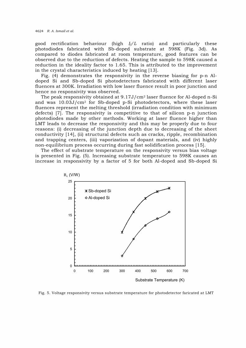
The effect of substrate temperature on the responsivity versus bias voltage is presented in Fig. (5). Increasing substrate temperature to 598K causes an increase in responsivity by a factor of 5 for both Al-doped and Sb-doped Si
0
5
10
15
20
25
0 100 200 300 400 500 600 700
Substrate Temperature (K)
Rλ (V/W)
Sb-doped Si
Al-doped Si
Fig. 5. Voltage responsivity versus substrate temperature for photodetector faricated at LMT
Full Characterization at 904nm of Large Area Si p-n Junction Photodetectors Produced by LID Technique 4625
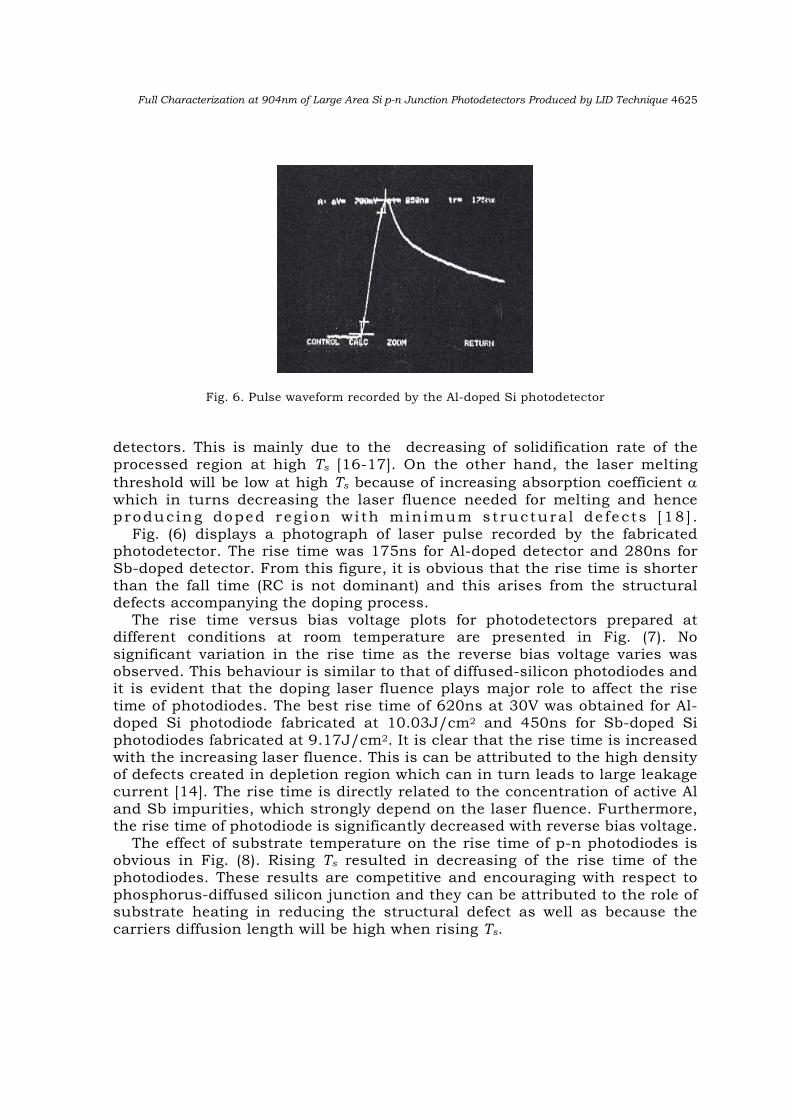
Fig. 6. Pulse waveform recorded by the Al-doped Si photodetector
detectors. This is mainly due to the decreasing of solidification rate of the processed region at high Ts [16-17]. On the other hand, the laser melting threshold will be low at high Ts because of increasing absorption coefficient αwhich in turns decreasing the laser fluence needed for melting and hence produc ing doped reg i on wi th min imum s t ructura l de fe c ts [ 18 ] .
Fig. (6) displays a photograph of laser pulse recorded by the fabricated photodetector. The rise time was 175ns for Al-doped detector and 280ns for Sb-doped detector. From this figure, it is obvious that the rise time is shorter than the fall time (RC is not dominant) and this arises from the structural defects accompanying the doping process.
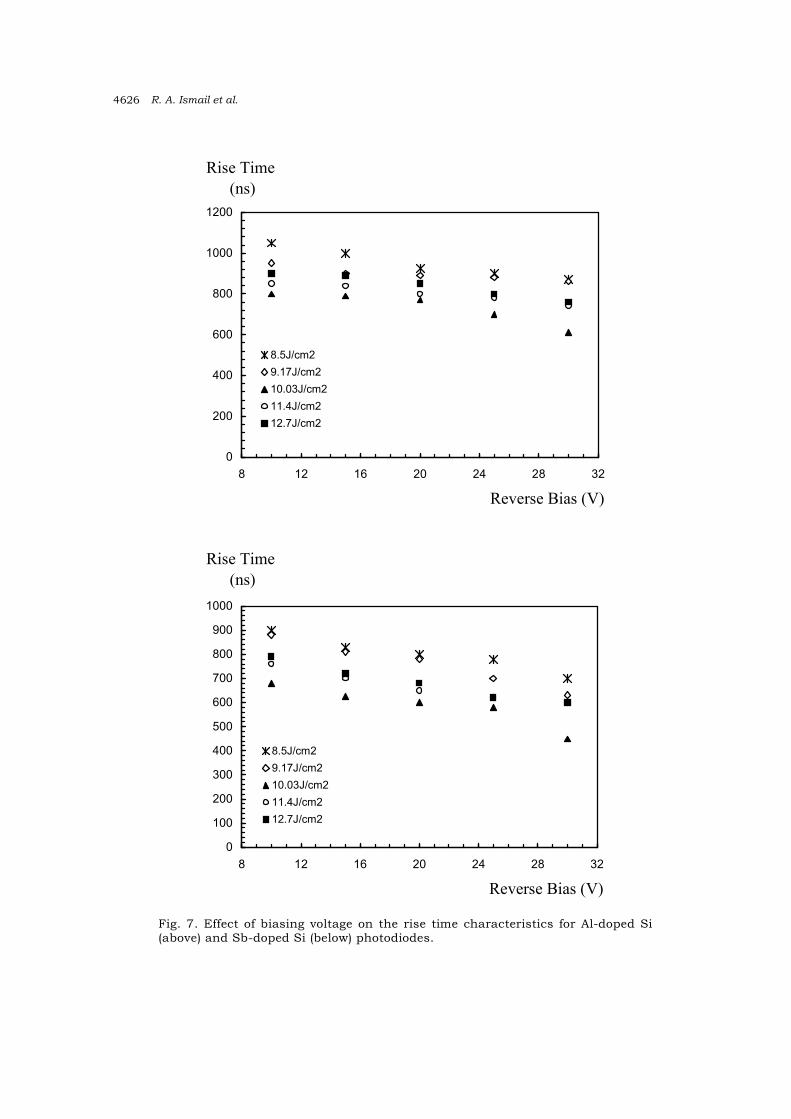
The rise time versus bias voltage plots for photodetectors prepared at different conditions at room temperature are presented in Fig. (7). No significant variation in the rise time as the reverse bias voltage varies was observed. This behaviour is similar to that of diffused-silicon photodiodes and it is evident that the doping laser fluence plays major role to affect the rise time of photodiodes. The best rise time of 620ns at 30V was obtained for Al-doped Si photodiode fabricated at 10.03J/cm2 and 450ns for Sb-doped Si photodiodes fabricated at 9.17J/cm2. It is clear that the rise time is increased with the increasing laser fluence. This is can be attributed to the high density of defects created in depletion region which can in turn leads to large leakage current [14]. The rise time is directly related to the concentration of active Al and Sb impurities, which strongly depend on the laser fluence. Furthermore, the rise time of photodiode is significantly decreased with reverse bias voltage.
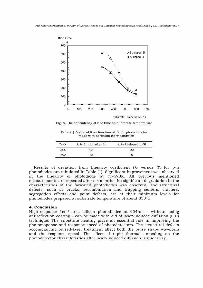
The effect of substrate temperature on the rise time of p-n photodiodes is obvious in Fig. (8). Rising Ts resulted in decreasing of the rise time of the photodiodes. These results are competitive and encouraging with respect to phosphorus-diffused silicon junction and they can be attributed to the role of substrate heating in reducing the structural defect as well as because the carriers diffusion length will be high when rising Ts.
R. A. Ismail et al. 4626
0
200
400
600
800
1000
1200
8 12 16 20 24 28 32
Reverse Bias (V)
Rise Time (ns)
8.5J/cm29.17J/cm210.03J/cm211.4J/cm212.7J/cm2
0
100
200
300
400
500
600
700
800
900
1000
8 12 16 20 24 28 32
Reverse Bias (V)
Rise Time (ns)
8.5J/cm29.17J/cm210.03J/cm211.4J/cm212.7J/cm2
Fig. 7. Effect of biasing voltage on the rise time characteristics for Al-doped Si (above) and Sb-doped Si (below) photodiodes.
Full Characterization at 904nm of Large Area Si p-n Junction Photodetectors Produced by LID Technique 4627
0
100
200
300
400
500
600
700
0 100 200 300 400 500 600 700
Substrate Temperature (K)
Rise Time (ns)
Sb-doped SiAl-doped Si
Fig. 8. The dependency of rise time on substrate temperature
Table (1). Value of K as function of Ts for photodetector made with optimum laser condition
Ts (K) k % Sb-doped p-Si k % Al-doped n-Si
300 25 22 598 15 8
Results of deviation from linearity coefficient (k) versus Ts for p-n photodiodes are tabulated in Table (1). Significant improvement was observed in the linearity of photodiode at Ts=598K. All previous mentioned measurements are repeated after six months. No significant degradation in the characteristics of the faricated photodiodes was observed. The structural defects, such as cracks, recombination and trapping centers, clusters, segregation effects and point defects, are at their minimum levels for photodiodes prepared at substrate temperature of about 350°C. 4. Conclusion High-response 1cm2 area silicon photodiodes at 904nm – without using antireflection coating – can be made with aid of laser-induced diffusion (LID) technique. The substrate heating plays an essential role in improving the photoresponse and response speed of photodetectors. The structural defects accompanying pulsed-laser treatment affect both the pulse shape waveform and the response speed. The effect of rapid thermal annealing on the photodetector characteristics after laser-induced diffusion is underway.
R. A. Ismail et al. 4628
References
1. Y. Miyata, M. Furuta and T. Kawamura, J. AppI. Phys., 73, 327 (1993). 2. P. M. Smith, P. G. Carey, and T. W. Sigmon, Appl. Phys. Lett., 70, 342 (1997). 3. Y. Takamura, S. Jang, P. B. Griffin and J. D. Plummer, Mater. Symp. Proc.,
669 (2001). 4. S. Baek, T. Jang, H. Hawang, Appl. Phys. Lett., 80, 2272 (2002). 5. H. Tsukamoto, H. Yamamoto, T. Noguchi, Jpn. J. Appl. Phys., 35, 3810
(1996). 6. V. Privitera, C. Spinella, G. Fortunato, L. Mariucci, Appl. Phys. Lett., 77, 552
(2000). 7. R. A. Ismail and W. K. Hamoudi, J. Eng. Technol. (Published in Iraq), 19, 119
(2000). 8. W. K. Hamoudi, and R. O. Dala, J. Mater. Sci., 45, 1 (2000). 9. A. Hadi, M.Sc Thesis, University of Technology, Baghdad, Iraq, 1999, p. 110.
10. Y. Matsuoka, and A. Usama, J. Phys. D: Appl. Phys., 7, 1259 (1974). 11. E. Fograssy, R. Stucky, and M. Toulemonde, J. Appl. Phys., 54, 5059 (1983). 12. R.A. Ismail and A.A. Hadi, Turkish J. of Phys., 27, 1 (2003). 13. G. Minnino, V. Privitera, A. Magna, Appl. Phys. Lett., 86, S1909 (2004). 14. S. Earles, M. Laww, R. Brindows, K. Jones, S. Talwar, S. Corcoran, IEEE
Trans. Electron. Devices, 49, 1118 (2002). 15. V. M. Artyunyan, A. P. Akhoyan, Z. N. Adamyan, R. S. Barsegyam, Technical
Physics, 46, 198 (2001). 16. J. Narayan, J. Cryst. Growth, 59, 583 (1982). 17. H. Kuriyama, Jpn. J. Appl. Phys., 30 (12B), 3700 (1991). 18. R. A. Ismail, J. Eng. Technol. (Published in Iraq), 19, 148 (2000).