Format guide for IJAET - CiteSeerX
11
International Journal of Advances in Engineering & Technology, May, 2014. ©IJAET ISSN: 22311963 521 Vol. 7, Issue 2, pp. 521-531 DESIGN AND DEFORMATION ANALYSIS OF MEMS BASED PIEZORESISTIVE PRESSURE SENSOR Naga Jyothi Madduri 1 , Gopinadh Lakkoju 2 , Bhanu Lahari Kasturi 3 , Sravani Sravanam 4 and Talam Satyanarayana 5 National MEMS Design centre (NMDC), Dept. of Electronics & Instrumentation Engineering, Lakireddy Bali Reddy College of Engineering (Autonomous), L.B. Reddy Nagar, Mylavaram–521 230, Andhra Pradesh, India. ABSTRACT The present work reports about the design and simulation analysis of MEMS based piezoresistive pressure sensor. The design includes diaphragm using n-silicon material and piezoresistor using p-silicon material those are integrated on to diaphragm. Specifically, the proposed design has been simulated to get maximum deformation of diaphragm for small input of pressure. The design has been simulated for different crystallographic forms of silicon for different inputs Using COMSOL Multiphysics v 4.3b., the study is extended and analyses has been done such that flexibility of measuring pressure for polysilicon material has best performance compared to single crystal silicon and interchanged p-type, n-type of single crystal silicon. KEYWORDS: MEMS, Piezoresistivity, Tolerance value, Polycrystalline. I. INTRODUCTION With the emerging MEMS technology [1], recent advancements in its innovation gives rise to achieve rapid progress in high resolution and accuracy which mainly involves extension in its range depending on its application. The development of extremely small sensors came in to existence,which were replaced by bulky sensors. Dynamic characterstics like pressure, acceleration and force etc are measured accurately. Microsensors are designed and tested for its reliability using comsol multiphysics. Recent researches has been transferred to micromachined sensors [2] which promises robustness, accuracy, low power consumption, high efficiency. These are widely used in the fields like biomedical [3] optoelectronics [4], automotive [5] and industrial applictions [6]. Recent days, the major attention has been focused on investigating new materials for improved performance,relibility, lower production cost and new applications. The pressure sensors are of different types like piezoelectric, optical, elctromagnetic, potentiometric, capacitive. For micromachined sensors, piezoresistivity is a common sensing principle. Among all known piezoresistive materials, silicon in particular, exhibits remarkable piezoresistive [7, 8] response characteristics. Apart from pressure measurement piezoresistive pressure sensors are classified as acceleration, vibration and velocity sensors. Piezoresistive pressure sensors are one of the very first products. The first Piezoresistive pressure sensor designed to reduce fuel consumption by a tight control of the ratio between air and fuel. These sensors are used commonly for repeatability measurements. This sensor uses piezoresistive effect explained by change in resistance of sensing material when they are subjected to stress usually associated with semiconductor materials that allows conduction. Resistivity of semiconductor changes by applying pressure as band structure of material varies with conduction. It uses wheatstone bridge [9] principle for measuring resistance of material. The resistivity depends on force applied on the wafer. The conduction flows as usual when there is no force. Change in applied force causes in change in conduction that associated with change in resistivity.The related work has many changes that optimized the performance of sensor [10-15]. The application of piezoresistive
-
Upload
khangminh22 -
Category
Documents
-
view
1 -
download
0
Transcript of Format guide for IJAET - CiteSeerX

International Journal of Advances in Engineering & Technology, May, 2014.
©IJAET ISSN: 22311963
521 Vol. 7, Issue 2, pp. 521-531
DESIGN AND DEFORMATION ANALYSIS OF MEMS BASED
PIEZORESISTIVE PRESSURE SENSOR
Naga Jyothi Madduri1, Gopinadh Lakkoju2, Bhanu Lahari Kasturi3, Sravani
Sravanam4 and Talam Satyanarayana5 National MEMS Design centre (NMDC), Dept. of Electronics & Instrumentation
Engineering, Lakireddy Bali Reddy College of Engineering (Autonomous), L.B. Reddy
Nagar, Mylavaram–521 230, Andhra Pradesh, India.
ABSTRACT The present work reports about the design and simulation analysis of MEMS based piezoresistive pressure
sensor. The design includes diaphragm using n-silicon material and piezoresistor using p-silicon material those
are integrated on to diaphragm. Specifically, the proposed design has been simulated to get maximum
deformation of diaphragm for small input of pressure. The design has been simulated for different
crystallographic forms of silicon for different inputs Using COMSOL Multiphysics v 4.3b., the study is extended
and analyses has been done such that flexibility of measuring pressure for polysilicon material has best
performance compared to single crystal silicon and interchanged p-type, n-type of single crystal silicon.
KEYWORDS: MEMS, Piezoresistivity, Tolerance value, Polycrystalline.
I. INTRODUCTION
With the emerging MEMS technology [1], recent advancements in its innovation gives rise to
achieve rapid progress in high resolution and accuracy which mainly involves extension in its range
depending on its application. The development of extremely small sensors came in to existence,which
were replaced by bulky sensors. Dynamic characterstics like pressure, acceleration and force etc are
measured accurately. Microsensors are designed and tested for its reliability using comsol
multiphysics. Recent researches has been transferred to micromachined sensors [2] which promises
robustness, accuracy, low power consumption, high efficiency. These are widely used in the fields
like biomedical [3] optoelectronics [4], automotive [5] and industrial applictions [6]. Recent days, the
major attention has been focused on investigating new materials for improved performance,relibility,
lower production cost and new applications. The pressure sensors are of different types like
piezoelectric, optical, elctromagnetic, potentiometric, capacitive. For micromachined sensors,
piezoresistivity is a common sensing principle. Among all known piezoresistive materials, silicon in
particular, exhibits remarkable piezoresistive [7, 8] response characteristics. Apart from pressure
measurement piezoresistive pressure sensors are classified as acceleration, vibration and velocity
sensors. Piezoresistive pressure sensors are one of the very first products. The first Piezoresistive
pressure sensor designed to reduce fuel consumption by a tight control of the ratio between air and
fuel. These sensors are used commonly for repeatability measurements. This sensor uses
piezoresistive effect explained by change in resistance of sensing material when they are subjected to
stress usually associated with semiconductor materials that allows conduction. Resistivity of
semiconductor changes by applying pressure as band structure of material varies with conduction. It
uses wheatstone bridge [9] principle for measuring resistance of material. The resistivity depends on
force applied on the wafer. The conduction flows as usual when there is no force. Change in applied
force causes in change in conduction that associated with change in resistivity.The related work has
many changes that optimized the performance of sensor [10-15]. The application of piezoresistive

International Journal of Advances in Engineering & Technology, May, 2014.
©IJAET ISSN: 22311963
522 Vol. 7, Issue 2, pp. 521-531
pressure sensor is to measure pressure more accurately. The study gives the importance of tolerance
value which shows performance of the proposed pressure sensor design. The paper presents details of
design work, geometry, required physical interfaces, simulation, results & analyses, conclusion along
with future scope of the work.
II. DESIGN WORK
Comsol multiphysics software is a good tool to create models. The design work uses the materials, p-
type silicon for piezoresistors and n-type silicon for the entire diaphragm [16]. The Finite Element
Method(FEM) is adopted to optimize the pressure sensor for parameters like sensitivity and linearity.
This is achieved by choosing the proper shape of piezoresistor, thickness of diaphraghm and the
position of piezoresistor on the pressure sensor. It consists of various material properties in built that
can be used to design required device. The model builder of comsol software can be used to solve
models and allows to access required functionality. The software is a powerful tool as it creates
environment for multiphysics for creating, analyzing, visualizing models when different physics are
coupled which are predefined on software. Geometric values can be given using geometry tool of
comsol software which consists of in built geometric figures. For any design the following steps are
required in comsol software defining geometry that is constructing model using geometry tool,
addition of physical interface that adds physics equations to model automatically, giving materials to
model that adds material properties which are predefined in materials library, meshing for proper
distribution for inputs provided.
III. GEOMETRY DETAILS
The diaphraghm with a square membrane of side1 mm and thickness 20µm around its edge by region
0.1mm wide is designed. The piezoresistor as in wheatstone bridge is constructed using various
predefined structures in geometry [17] as shown in Fig. 1.
Figure 1.Geometry of piezoresistor.
The upper surface, lower surface and membrane lower are defined using geometry tool. The area of
membrane lower surface is subtracted from upper surface using comsol and is fixed. The fixed area
doesnot experience any change, whereas the remaining area experiences, when force is applied on the
pressure sensor.

International Journal of Advances in Engineering & Technology, May, 2014.
©IJAET ISSN: 22311963
523 Vol. 7, Issue 2, pp. 521-531
Figure 2.Fixed area of lower surface diaphragm
The lower membarane is fixed on boundary of it. The inner portion is set free which is represented as
pink colour in Fig. 2 . The blue coloured portion is fixed. The input pressure is applied on the upper
surface which transforms to piezoresistor.
IV. PHYSICAL INTERFACE
The propose design works on the principle of piezoresistive effect [18], with increase in applied
pressure, change in resistivity is measured with change in deformation. The physics used is
piezoresistive boundary currents that is applied to the device that automatically facilitates with
definitions of linear elastic material, thin conducting layer and piezoresistive layer for model. The
linear elasticity ensures the property of material that stress is linear function of strain and acts as
reversible process. It automatically includes thermal expansion property to material. Thus thermal
properties are coupled with existent physics to model. The piezoresistive material library consists of
single crystal and polycrystalline p,n-typed doped silicon.
The applied stress on diaphragm changes the band structure that induces strain in it, which is the
result of piezoresistance effect. The electric field in the vicinity of surface of diaphragm with applied
stress is given as equation.
𝐸 = 𝜌. 𝐽 + 𝛥𝜌. 𝐽 ............................................... (1)
Where '𝜌′ is resistivity, J is current in piezoresistors, '𝛥𝜌' is induced change in resistivity. It is given as
function of stress by the equation.
𝛥𝜌 = 𝛱. 𝜎 ............................................... (2)
Where 'π' is piezoresistance tensor, a material property. '𝜎′ is shear stress. '𝛥𝜌′ is induced change in
resistivity that couples current in one direction, electric field perpendicular to current direction.
V. SIMULATION
After defining the geometry of the proposed model, materials are added, which givesa solid design.
Later, meshing is done in-order to distribute the applied pressure equally on the device. The sizes of
meshing are as follows, for the entire wafer maximum meshing size is 60 µm, and minimum is 0.5µm.
For piezoresistor maximum is 2 µm, minimum is 0.1 µm, for connectors maximum is 6 µm and for
edges maximum is 0.4 µm. Terminal and ground are defined on the connectors of the piezoresistor, so
that it forms an electrode [18] to measure voltage as a measure of pressure [17]. The terminal voltage
is given as 3 volts as bias. Simulation has been carried out for the proposed design with the inputs
ranging from 100 kPa to till the tolerance value and results are noticed as deformations of diaphraghm
are shown below.

International Journal of Advances in Engineering & Technology, May, 2014.
©IJAET ISSN: 22311963
524 Vol. 7, Issue 2, pp. 521-531
Figure 3.The deformation of the pressure sensor at the applied pressure of 2277 kPa of single crystal
silicon(n,p type).
Figure 4.The deformation of the pressure sensor at the applied pressure of 4128 kPa of single crystal
silicon interchanged (p,n type).

International Journal of Advances in Engineering & Technology, May, 2014.
©IJAET ISSN: 22311963
525 Vol. 7, Issue 2, pp. 521-531
Figure 5. The deformation of the pressure sensor at the applied pressure of 10752 kPa of poly crystal silicon
(n,p) type.
5.1. Single crystal material (n,p type)
Comparison of maximum deformation of single crystal silicon(n,p) [16] at 2277kPa pressure (Fig. 3),
single crystal silicon interchaned (p,n) at 4128 kPa pressure (Fig. 4) and polycrystal silicon (n,p) at
10752 kPa pressure (Fig. 5). The maximum deformation for interchanged n, p type single crystal
silicon material is found to be 51.831µm. It can be noted that the maximum deformation for p, n-types
single crystal silicon was 28.59 µm. Thus maximum sensing capability has been observed from the
proposed design with interchanging of n and p-type silicon. It can be concluded that the performance
of pressure sensor enhanced approximately double the given design that can be seen from the above
Fig. 4 . The maximum deformation for polycrystalline silicion material is found to be 126.64 µm.
which can be seen from Fig. 5 . Thus the maximum deformation is enhanced [17] to 126.64 µm, when
compared to single crystalline silicon materials. Thus the optimised sensing action has been noticed
with the polysilicon material. The maximum deformations (µm) at the center for various loads applied
to different forms of materials of silicon of proposed pressure sensor are tabulated and shown in Table
I.
VI. RESULTS AND ANALYSIS
Simulation is carried out in three steps. Firstly, using single crystalline form of silicon material, next
interchanging p,n-type single crystal silicon and finally poly crystal silicon form. The below equation
explains about the shear stress at the mid-point of the diaphragm [16].
𝜎𝑙,12 = 014 (𝐿
𝐻)
2............................................... (3)
Where, P is the applied pressure, L is the length of the diaphragm edge and H is the diaphragm
thickness.

International Journal of Advances in Engineering & Technology, May, 2014.
©IJAET ISSN: 22311963
526 Vol. 7, Issue 2, pp. 521-531
Table 1.The maximum deformation values at center of diaphragm for different applied pressures.
Applied Pressure
(kPa)
Deformation (µm)
Singlecrystal Silicon (n,p type) Singlecrystal Silicon
Interchanged (p,n type)
Polycrystal
silicon
(n,p type)
1000 12.556 12.556 11.778
2000 25.112 25.112 23.556
3000 - 37.668 35.334
4000 - 50.224 47.112
5000 - - 58.89
6000 - - 70.668
7000 - - 82.446
8000 - - 94.224
9000 - - 106
10000 - - 117.78
6.1. Single crystal material (n, p type)
As mentioned above, simulation of pressure sensor has been carried out for the single crystal solid
design. Deformation of diaphragm in response of applied pressrue ranging from 100 kPa [17] to 2277
kPa has been studied and same can be seen from the figure 3. It is important to note that the design
cannot hold the pressure beyond 2277 kPa. From this analysis, it is clear that the single crystal solid
design [16] exhibits maximum deformation of 28.59 µm with the maximum applied pressure of 2277
kPa. The shear stress distribution of device at 2277 kPa pressure is studied as shown in Fig. 6. The
second piola kirchoff's law is also given as graph of arc length v/s shear stress in Fig. 7.
Figure 6.Shear stress tensor for single crystal silicon at the applied pressure 2277kPa.

International Journal of Advances in Engineering & Technology, May, 2014.
©IJAET ISSN: 22311963
527 Vol. 7, Issue 2, pp. 521-531
Figure 7.Arc lenght v/s shear stress tensor at the applied pressure 2277 kPa.
6.2. Single crystal material interchanged (p, n type)
The next analysis done on interchanging of n-type and p-type single crystal silion and the response of
deformation in diaphragm is noticed for different applied pressure ranging from 100 kPa to 4128 kPa
as it cannot tolerate beyond that value. The result shows the maximum deformation as 51.831 µm at
the pressure of 4128 kPa. Hence by using the same material, the performance has been optimized
from the maximum deformation 28.59 µm to 51.831 µm. Thus the design is extended [16] to improve
results. The shear stress distribution and second Piola kirchoff’s law are given in Fig. 8, 9
respectively.
Figure 8.Shear stress tensor for single crystal silicon at the applied pressure of 4128 kPa.
International Journal of Advances in Engineering & Technology, May, 2014.
©IJAET ISSN: 22311963
528 Vol. 7, Issue 2, pp. 521-531
Figure 9.Arc lenght v/s shear stress tensor at the applied pressure of 4128 kPa.
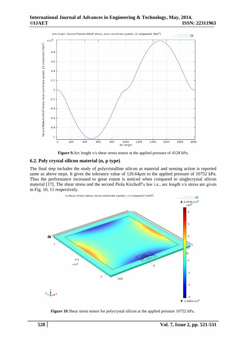
6.2. Poly crystal silicon material (n, p type)
The final step includes the study of polycristalline silicon as material and sensing action is reported
same as above steps. It gives the tolerance value of 126.64µm to the applied pressure of 10752 kPa.
Thus the performance increased to great extent is noticed when compared to singlecrystal silicon
material [17]. The shear stress and the second Piola Kirchoff’s law i.e., arc length v/s stress are given
in Fig. 10, 11 respectively.
Figure 10.Shear stress tensor for polycrystal silicon at the applied pressure 10752 kPa .

International Journal of Advances in Engineering & Technology, May, 2014.
©IJAET ISSN: 22311963
529 Vol. 7, Issue 2, pp. 521-531
Figure 11.Arc lenght v/s shear stress tensor at the applied pressure 10752 kPa.
Hence the study has been extended which gives polycrystalline form of silicon as it shows maximum
optimizated results as pressure sensor.
Table 2.The following comparison table briefly explains about the maximum deformation, shear stress and
stess sensor respectively.
Material
Maximum
Deformation (µm)
Maximum Shear Stress
(MPa)
Maximum Stress
Tensor (MPa)
Single crystalline silicon
(n,p type)
28.59
1171.1
500
Single crystalline
silicon (p,n type)
51.831
2025.2
800
Polycrystalline
silicon (n,p type)
126.64
4363.5
2000
Thus, the proposed forms will be useful in making devices for producing desired deformations of
pressure sensor using the different forms of materials providing the optimized results as tolerance.
VII. CONCLUSION
MEMS based piezoresistive pressure sensor is designed using COMSOL MultiPhysics
v. 4.3b. The sensor has been studied with different forms of silicon materials for diaphragm with
different applied pressures and corresponding results are compared. From the analyses of simulation
results, it can be concluded that the proposed piezoresistive pressure sensor design provided with
polysilicon material for diaphragm found to exhibit optimum deformation in turn beter sensing action
for given input of applied pressure in comparision with designs [16] of other p & n type material
interchanges for the wafer and piezoresistors.

International Journal of Advances in Engineering & Technology, May, 2014.
©IJAET ISSN: 22311963
530 Vol. 7, Issue 2, pp. 521-531
VIII. FUTURE WORK
The proposed design can be extended by making changes in the geometry of diaphragm, applied
inputs and meshing inturn to get better sensing mechanism. Further, there will be lot of scope to add
other semiconducting materials those are to be assigned to diaphragm to get optimum output from the
proposed solid pressure sensor design for small applied inputs.
ACKNOWLEDGMENTS
The authors would like to thank NPMASS for the establishment of National MEMS Design Centre
(NMDC) at Lakireddy Bali Reddy Autonomous Engineering College. The authors would also like to
thank the Management and Director, Head of the Department of Electronics and Instrumentation
Engineering for providing the necessary facilities to carry out this work.
REFERENCES
[1]. Leo, O’Connor,“MEMS-microelectromechanical System”,Mechanical Engineering, pp. 40-47, 1992.
[2]. Tu Xiang-Zheng, Li Yun-Yan, "Silicon diaphragm piezoresistive pressure sensor and fabrication method
of the same", Grant publication,1993.
[3]. C Pranamik, H Saha ,"Design optimization of a high performance silicon MEMS piezoresistive pressure
sensor for biomedical applications", J. Micromechanics and Microengineering, 2006.
[4]. William P. Eaton ; James H Smith , "Micromachined pressure sensors: review and recent
developments", Smart electronics and MEMS, 1997.
[5]. Eddy , David S , "Applications of MEMS technology in automotive sensors and actuators", Proc. IEEE,
Vol. 86, Issue 8, 1998.
[6]. Lynch, J., Partidge, A., Law, "Design of Piezoresistive MEMS-Based Accelerometer for Integration with
Wireless Sensing Unit for Structural Monitoring", J.Aersosp. Eng.,16(3), pp. 108-114,2003.
[7]. Smith, C.S., “Piezoresistance Effect in Germanium and Silicon”,Physics Review, pp. 42–49, 1954.
[8]. Kanda, Y., “Piezoresistance Effect of Silicon, Sensors and Actuators”, A: Physical, pp. 83–91, 1991.
[9]. J.M. Lin, “Teaching and Design on Smart MEMS Pressure Sensor Module”, International Conference
on Engineering Education and Research "Progress through Partnership", ICEER, pp. 273-281, 2004.
[10]. N Kattabooman, Sarath S, Rama Komaragiri “VLSI Layout Based Design Optimization of a
Piezoresistive MEMS Pressure Sensors Using COMSOL”, Institute of smart structures, 2013.
[11]. Suja K J, Vidya Gopal T V, Rama Komaragiri, “Optimized Design of Double Diaphragm Based MEMS
Pressure Sensor for Wider Range and Better Sensitivity”, International Journal of Emerging Science and
Engineering (IJESE) , ISSN: 2319–6378, Volume-2, Issue-1, November 2013.
[12]. Mohummad Aniq Sazni, “Enhancing the performance of pressure sensor using ‘v’ shaped piezoresistor -
sensing elements”, Journal of scientific and industrial research,v. 73, feb- 2014.
[13]. Thirumani A. Selvani, Gururaj U. Shenoy, Saravanan Sadasivan, Raghavendra Muniraju “ Design of a
wet/wet amplified differential pressure sensor based on silicon piezoresistive technology”, Honewell
international inc., 2007.
[14]. Sh Mohd Firdaus, Husna Omar and Ishak Abd Azid , “High Sensitive Piezoresistive Cantilever MEMS
Based Sensor by Introducing Stress Concentration Region (SCR)”, Finite element analysis –New trends
and developments, 2012.
[15]. David William Burns, Philip Jason Stephanou, Ravindra V. Shenoy, Kurt Edward Petersen “Gas
encapsulated pressure sensor”, Honewell international inc., 2013.
[16]. S.D. Senturia, Chapter 18: “A Piezoresistive Pressure Sensor”, Microsystem Design, Springer, 2000.
[17]. M. Bao, “Analysis and Design Principles of MEMS Devices”, Elsevier B. V., 2005.
[18]. Motorola Semiconductor MPX100 series technical data, “document: MPX100/D”, 1998 (available from
Freescale Semiconductor Inc at http://www.freescale.com), 2005.

International Journal of Advances in Engineering & Technology, May, 2014.
©IJAET ISSN: 22311963
531 Vol. 7, Issue 2, pp. 521-531
AUTHORS
M. Naga Jyothi, final year graduate of Department of Electronics and Instrumentation
Engineering at Lakireddy Bali Reddy Autonomous Engineering College. She has been
working in the area of MEMS technology since three years. She has done her Internship at
Lanco, Kondapally Power plant and also attended various workshops in relation with
Instrumentation.
L. Gopinadh, final year graduate of Department of Electronics and Instrumentation
Engineering at Lakireddy Bali Reddy Autonomous Engineering College. He has been
working in the area of MEMS technology since three years. He has done his Internships at
Oil and Natural Gas Corporation (ONGC), Thatipaka and in Vizag Steel Plant. He has also
attended various workshops in relation with instrumentation.
Bhanu Lahari .K, final year graduate of Department of Electronics and Instrumentation
Engineering at Lakireddy Bali Reddy Autonomous Engineering College. She has been
working in the area of MEMS technology since three years. She has done her Internships at
Oil and Natural Gas Corporation (ONGC), Thatipaka and in Vizag Steel Plant. She also
attended various workshops in relation with instrumentation.
S. Sravani, final year graduate of Department of Electronics and Instrumentation
Engineering at Lakireddy Bali Reddy Autonomous Engineering College. She has been
working in the area of MEMS technology since three years. She has done her Internship at
Defence Research and Development Organization (DRDO) and she has also attended
various workshops in relation with MEMS technology.
T. Satyanarayana, received his Ph.D from Acharya Nagarjuna University, India. He
worked as research scholar at the Department of Engineering Physics, University of Aveiro,
Portugal. The author has published more than 28 research papers in highly repute
International journals and presented papers in International conferences viz., Japan, Spain
and Portugal. He has also worked in DST & DRDO, Govt. of India funded projects.