
Final Year Project of BS Electronic Engineering (BUITEMS 2007)
107
JUUN230707 BIT SLICE MICROPROCESSOR
Transcript of Final Year Project of BS Electronic Engineering (BUITEMS 2007)

JUUN230707 BIT SLICE
MICROPROCESSOR

JUUN230707 BIT SLICE MICROPROCESSOR
PROJECT REPORT
By
Mohammad Jehanzeb Shahid Ubaid Ahsan
Umair Anwar Khan Naeem Baig
BS ELECTRONICS ENGINEERING
Department Of Electronics
Faculty of Computer and Emerging Sciences
Balochistan University of Information Technology and Management Sciences
Quetta

JUUN230707 BIT SLICE MICROPROCESSOR
PROJECT REPORT
BS ELECTRONICS ENGINEERING
Prepared by:
Mohammad Jehanzeb Shahid Roll No. 03F-BSEE-022
Ubaid Ahsan Roll No. 03F-BSEE-012
Umair Anwar Khan Roll No. 03F-BSEE-046
Naeem Baig Roll No. 03F-BSEE-066
Project Advisors:
Engr. Naveed Ahmed (Internal Advisor)
Mr. Aurangzeb (External Advisor)
Department Of Electronics
Faculty of Computer and Emerging Sciences
Balochistan University of Information Technology and
Management Sciences Quetta

THIS PROJECT IS DEDICATED TO:
PROFESSOR SABIR HUSSAIN USMANI (late)
HE GAVE US THE INCENTIVE TO WORK ON VLSI TECHNIQUES AND
DEVICE FABRICATION
MAY ALLAH SHOWERS THE BLESSINGS ON HIS SOUL AND RAISE HIS
RANKS IN HEAVEN

vi
Preface
This project is prepared for the partial fulfillment Degree of BS Electronics Engineering
from Balochistan University of Information Technology & Management Sciences.
The project is based upon Microprocessor Design after a detailed study of VLSI design
techniques. The approach hence is Behavioral Level of Hardware Description Language
(HDL), i.e. Verilog.
It is tried that the flow of project is should be simple and comprehensive at the same time.
In Chapter 1, introduction to Digital systems is discussed which primarily include FPGA
and Microprocessors. Chapter 2 includes the basic concepts of Embedded Systems
specially Bit Slicing and AMD 2900 Family.
Chapter 3 is the core part of this thesis as it illustrates the processes of this project. These
processes include:
• Bit Slice approach using VLSI
• Fundamental ALU
• Cascading Modules
• FDE Operations Flow
• FPGA Implementation
Chapter 4 discusses the TOOLS used in this project in detail. These tools are;
• FPGA Device
• Simulation Software
• FPGA Download
• Supporting Software
In chapter 5, some applications are given so that the utilization of this project should be
clear.

vii
In all the 5 chapters are interlinked along with 3 appendices. The first appendix includes
the HDL source code; second appendix has all outputs, synthesis reports, design
architecture and simulation diagrams and the third appendix contains the board diagrams
and device parameters.
The effort regarding this project is sincere and efficient. The group members have spent
reasonable time to bring the thesis in presentable form. It is hoped that the project will
serve the purpose proficiently.
Date: 06-09-07
Jehanzeb Shahid
Ubaid Ahsan
Umair Anwar
Naeem Baig

viii
Contents
Chapter 1 FOREWORD TO PROJECT 1
1.1) Basic concepts of number systems 2
1.1a Digital number systems 2
1.1a1 Decimal system 2
1.1a2 Binary system 2
1.1a3 Hexadecimal system 2
1.2) Integrated circuits 3
1.2a Classification of IC(s) 3
1.2.a1 TTL 3
1.2.a2 CMOS 4
1.2a3 ASIC 5
1.2a4 CPLD 5
1.2a5 FPGA 6
1.3) Field Programmable Gate Array 6
1.3a Difference between FPGA & CPLD 6
1.3b FPGA Architecture 7
1.3c FPGA Logic Block 8
1.4) Microprocessor 9
1.4a General description 9
1.4b Microprocessor Architecture and the Intel Series 10
Chapter 2 EMBEDDED SYSTEM 13
2.1) Microprocessor based PC System 14
2.1a Information Exchange 14
2.1b Buses 14
2.1c Accumulator Register 15
2.1d Control Unit 15
2.2) Arithmetic and Logic Unit 16
2.3) Addressing Modes 18
2.3a Types of Addressing Modes 18
2.3b Block Representation of Addressing Modes 18
2.4) Memory Organization 20
2.5) Organization of Memory Units 20
2.6) Bit Slicing 21
2.6a Characteristics of Bit Slicing 22
2.6b Advantages of Bit Slicing 22
2.7) AMD Bit Slice Processors 23
2.7a AMD2900 Family 23
2.7b AMD8080 Emulator 24
Chapter 3 Project Structure and Experimentations 26
3.1) Arithmetic & Logic Unit 28
3.2) VLSI and Arithmetic Operations 29
3.3) Bit Slice Design 29
3.4) Fundamental ALU 30
3.4a Module Explanation 30
3.4b Instruction Format 31

ix
3.4c Cascading Module 33
3.4d Bit Slicing Techniques 34
3.5) FDE Operations 35
3.5a Fetch 35
3.5b Decode 36
3.5c Execute 36
3.6) FPGA Design 38
3.6a ISE 9.1i 38
3.6b Design Implementation 38
3.6c Downloading Program to Device 38
3.6d Schematic Diagrams & Simulation 39
3.7) VERI-WELL Simulator 39
3.8) Source Code 39
3.9) Timeline of Project 40
Chapter 4 TOOLS 41
4.1) SPARTAN 3 FPGA 42
4.2) Hardware Description Language 43
4.2a Verilog HDL 44
4.2b Verilog Syntax 44
4.2c Stimulus in Verilog 46
4.2d Logic synthesis with Verilog 47
4.2e Impact of Logic Synthesis 48
4.2f State Machines 48
4.3) Xilinx-Integrated Software Environment (ISE) 48
4.3a PACE 49
4.3b Floor Planner 49
4.3c ImPACT 50
4.3d FPGA Editor 50
4.4) ISE 9.1i Programming process 50
4.4a ISE process 50
4.4b FPGA downloading 51
4.5) SyntaptiCAD VERI-WELL Simulator 52
4.6) Supporting Tools 52
4.6a VISIO TECH4.5 52
4.6b MS-OFFICE 53
Chapter 5 Utilization of JUUN230707 Bit Slice Processor 54
5.1) Education purpose 55
5.2) Commercial purpose 56
5.3) VLSI and Bit Slice Micro processing 58

x
SUMMARY 59
APPENDIX A 63
APPENDIX B 72
APPENDIX C 91
REFERENCES 95

xi
List of Figures
Chapter 1 Page
1.1 Transistor-transistor logic circuit 3
1.2 Simple CMOS inverter 4
1.3 Physical design NAND gate 5
1.4 Difference of CPLD and FPGA 7
1.5 FPGA architecture 7
1.6 Pin location 8
1.7 Switch box topology 9
1.8 Basic system components 10
1.9 FDE operation 10
1.10 Intel CPU 11
Chapter 2
2.1 Basic elements of Microprocessor 14
2.2 The buses 16
2.3 Inside ALU 17
2.4 Logic symbol of ALU 17
2.5 Addressing modes 19-20
2.6 Bit slice memory organization 21
2.7 16-bit ALU 22
2.8 Bit slice organization of AM900 series 23
Chapter 3
3.1 Some MSI circuits 28
3.2 N-bit ALU 29
3.3 Block description of ALU 30
3.4 Fundamental of ALU block 30
3.5 Instruction format 31
3.6 General architecture of bit slicing 33
3.7 16-bit ALU 34

xii
3.8 Processor modules schematic 35
3.9 VERI-WELL installation module 37
Chapter 4
4.1 SPARTAN-3 FPGA 43
4.2 Typical design flow 45
4.3 Logic synthesis 47
4.4 Xilinx ISE design flow 49

xiii
LIST OF TABLES
Tables Page
2.1 AMD processor family 24
3.1 Instruction set 1 32
3.2 Instruction set 2 32
3.3 OPCODES for basic instructions 33
3.4 Module list 39
3.5 Timeline 39
4.1 Verilog levels of Abstraction 46

JUUN230707 BIT SLICE MICROPROCESSOR
Chapter1: Foreword To Project
Department of Electronics, BUITMS 1
Chapter 1
Foreword to Project
Topics covered in this chapter:
• Basic concepts of Number systems
• The integrated circuits
• TTL
• CMOS
• ASIC
• CPLD
• FPGA
• Microprocessor

JUUN230707 BIT SLICE MICROPROCESSOR
Chapter1: Foreword To Project
Department of Electronics, BUITMS 2
1.1) Basic Concept of Number Systems
1.1a) Digital Number Systems
Many number systems are in use in digital technology. The most common are:
• Decimal
• Binary
• Octal
• Hexadecimal systems
The decimal system is clearly the most familiar to us because it is a tool that we use every
day.
1.1. a1) Decimal System
Decimal System The decimal system is composed of 10 numerals or symbols. These 10
symbols are 0, 1, 2, 3, 4, 5, 6, 7, 8, 9; using these symbols as digits of a number, we can
express any quantity. The decimal system, also called the base-10 system because it has
10 digits.
1.1. a2) Binary System
In the binary system, there are only two symbols or possible digit values, 0 and 1. This
base-2 system can be used to represent any quantity that can be represented in decimal or
other number system.
1.1. a3) Hexadecimal System
The hexadecimal system uses base 16. Thus, it has 16 possible digit symbols. It uses the
digits 0 through 9 plus the letters A, B, C, D, E, and F as the 16 digit symbols.

JUUN230707 BIT SLICE MICROPROCESSOR
Chapter1: Foreword To Project
Department of Electronics, BUITMS 3
1.2) Integrated Circuits
It is a combination of circuits comprising of transistors, logic gates and various electronic
components in a compact and portable single package; having specific I/O pins. The
integrated circuit (IC) can be made by the process called “Device Fabrication”.
Semiconductor devices are best utilized in IC chips. As ICs are cost effective and
generally perform well, the use of ICs has greatly increased.
1.2a) Classification of ICs
The ICs are mainly categorized in the following packages:
• Transistor-Transistor Logic (TTL)
• Complementary Metallic Oxide Semiconductors (CMOS)
• Application Specific Integrated Circuit (ASIC)
• Complex Programmable Logic Design (CPLD)
• Field Programmable Gate Arrays (FPGA)
1.2 a1) Transistor-Transistor Logic
TTL is a class of digital circuits built from bipolar junction transistors (BJT), and
resistors. It is called transistor-transistor logic because both the logic gating function
(e.g. AND) and the amplifying function are performed by transistors. Because of the wide
use of this logic family, signal inputs and outputs of electronic equipment may be called
"TTL" inputs or outputs, signifying compatibility with the voltage levels used. Given
below is the figure showing simple TTL circuit.
Figure 1.1: TTL circuit

JUUN230707 BIT SLICE MICROPROCESSOR
Chapter1: Foreword To Project
Department of Electronics, BUITMS 4
Some functions implemented in TTL are listed below:
• Latch elements
• Counters
• Registers
• Timers
• Driver circuits
• R/W memory and ROM
1.2. a2) Complementary Metallic Oxide Semiconductor Technology (CMOS)
CMOS is a major class of integrated circuits. CMOS technology is used in chips such as
microprocessors, microcontrollers, static RAM, and other digital logic circuits. CMOS
technology is also used for a wide variety of analog circuits such as image sensors, data
converters, and highly integrated transceivers for many types of communication. Figure
1.2 shows the implementation of CMOS.
Figure 1.2: Simple CMOS Inverter
Two important characteristics of CMOS devices are:
• High noise immunity and low static power supply drain. Significant power is
only drawn when its transistors are switching between on and off states;
consequently.
• CMOS devices do not produce as much heat as other forms of logic such as TTL.
CMOS also allows a high density of logic functions on a chip.
The complementary-symmetry nature of CMOS leads to a fantastic output of designed
system in semiconductors. The most important phase regarding CMOS in Very Large

JUUN230707 BIT SLICE MICROPROCESSOR
Chapter1: Foreword To Project
Department of Electronics, BUITMS 5
Scale Integration (VLSI) is the physical layout of the implemented circuit. Figure 1.3
illustrates the example of NAND gate. This design layout is achieved after long
procedure of device fabrication.
Figure 1.3: Physical design of NAND gate; colored boxes show KEY of materials used
1.2. a3) Application Specific Integrated Circuits (ASIC)
ASIC is an integrated circuit customized for a particular use, rather than intended for
general-purpose use. As feature sizes have shrunk and design tools improved over the
years, the maximum complexity (and hence functionality) possible in an ASIC has grown
from 5,000 gates to over 100 million. Modern ASICs often include entire 32-bit
processors, memory blocks including ROM, RAM, EEPROM, Flash and other large
building blocks. Such an ASIC is often termed an S-o-C (System-on-a-chip). Designers
of digital ASICs use a hardware description language (HDL), such as Verilog or VHDL,
to describe the functionality of ASICs.
1.2. a4) Complex Programmable Logic Design (CPLD)
A CPLD has a somewhat restrictive structure consisting of one or more programmable
sum-of-products logic arrays feeding a relatively small number of clocked registers. The

JUUN230707 BIT SLICE MICROPROCESSOR
Chapter1: Foreword To Project
Department of Electronics, BUITMS 6
result of this is less flexibility, with the advantage of more predictable timing delays and
a higher logic-to-interconnect ratio.
A CPLD contains a bunch of PLD blocks whose inputs and outputs are connected
together by a global interconnection matrix. Hence a CPLD has two levels of
programmability: each PLD block can be programmed, and then the interconnections
between the PLD(s) can be programmed.
1.2. a5) Field Programmable Gate Arrays FPGA
FPGA(s) are the modern day equivalent of 7400 series logic and a breadboard, containing
programmable logic blocks and programmable interconnects that allow the same FPGA
to be used in many different applications. For smaller designs and/or lower production
volumes, FPGAs may be more cost effective than an ASIC design. The Non-recurring
engineering cost (the cost to setup the factory to produce a particular ASIC) can run into
hundreds of thousands of dollars.
The general term application specific integrated circuit includes FPGAs, but most
designers use ASIC only for non field programmable devices and differ between ASIC
and FPGAs.
1.3) Field Programmable Gate Array (FPGA)
1.3a) Difference between FPGA and CPLD
The primary differences between CPLDs and FPGAs are architectural. A CPLD has a
fairly restrictive structure consisting of programmable sum-of-products logic arrays
feeding a relatively small number of clocked registers. The FPGA architectures, on the
other hand, are dominated by interconnect. This makes them far more flexible (in terms
of the range of designs that are practical for implementation within them) but also far
more complex to design for.

JUUN230707 BIT SLICE MICROPROCESSOR
Chapter1: Foreword To Project
Department of Electronics, BUITMS 7
Figure 1.4: Difference of CPLD and FPGA (Courtesy: Xilinx, Inc)
Another notable difference between CPLDs and FPGAs is the presence in most FPGAs
of higher-level embedded functions (such as adders and multipliers) and embedded
memories. A related, important difference is that many modern FPGAs support full or
partial in-system reconfiguration, allowing their designs to be changed "on the fly" either
for system upgrades or for dynamic reconfiguration as a normal part of system operation.
Some FPGAs have the capability of partial re-configuration that lets one portion of the
device be re-programmed while other portions continue running.
1.3b) FPGA Architecture
The typical basic architecture consists of an array of Configurable Logic Blocks (CLB)
and routing channels. Multiple I/O pads may fit into the height of one row or the width of
one column in the array. Generally, all the routing channels have the same width (number
of wires).The typical FPGA logic blocks consist of a 4-input lookup table (LUT), and a
flip-flop, as shown below:
Figure 1.5: FPGA Architecture

JUUN230707 BIT SLICE MICROPROCESSOR
Chapter1: Foreword To Project
Department of Electronics, BUITMS 8
There is only one output, which can be either the registered or unregistered LUT output.
The logic block has four inputs for the LUT and a clock input. Since clock signals (and
often other high-fan-out signals) are normally routed via special-purpose dedicated
routing networks in commercial FPGAs, they and other signals are separately managed.
1.3c) FPGA Logic Block
The locations of the FPGA logic block pins are shown below:
Figure 1.6: Pin Locations
Each input is accessible from one side of the logic block, while the output pin can
connect to routing wires in both the channel to the right and the channel below the logic
block. Each logic block output pin can connect to any of the wiring segments in the
channels adjacent to it. Similarly, an I/O pad can connect to any one of the wiring
segments in the channel adjacent to it. For example, an I/O pad at the top of the chip can
connect to any of the W wires (where W is the channel width) in the horizontal channel
immediately below it.
Generally, the FPGA routing is un-segmented. That is, each wiring segment spans one
logic block before it terminates in a switch box. By turning on some of the programmable
switches within a switch box, longer paths can be constructed. For higher speed
interconnect, some FPGA architectures use longer routing lines that span multiple logic
blocks. Whenever a vertical and a horizontal channel intersect there is a switch box. In
this architecture, when a wire enters a switch box, there are three programmable switches
that allow it to connect to three other wires in adjacent channel segments. The pattern, or
topology, of switches used in this architecture is the planar or domain-based switch box

JUUN230707 BIT SLICE MICROPROCESSOR
Chapter1: Foreword To Project
Department of Electronics, BUITMS 9
topology. In this switch box topology, a wire in track number one connects only to wires
in track number one in adjacent channel segments, wires in track number 2 connect only
to other wires in track number 2 and so on. The figure below illustrates the connections in
a switch box.
Figure 1.7: Switch box topology
Modern FPGA families expand upon the above capabilities to include higher level
functionality fixed into the silicon. Having these common functions embedded into the
silicon reduces the area required and gives those functions increased speed compared to
building them from primitives. Examples of these include multipliers, generic DSP
blocks, embedded processors, high speed IO logic and embedded memories.
FPGAs are also widely used for systems validation including pre-silicon validation, post-
silicon validation, and firmware development. This allows chip companies to validate
their design before the chip is produced in the factory, reducing the time to market.
1.4) Microprocessor
1.4a) General Description
A comprehensive electronic semiconductor device that is used for processing of data with
certain instructions to fetch, decode and execute, is called microprocessor. The system
consists of three parts. The synchronization between the three modules is a main feature
of micro processing. These three modules are memory, processor or CPU and I/O devices
as shown in figure 1.8:

JUUN230707 BIT SLICE MICROPROCESSOR
Chapter1: Foreword To Project
Department of Electronics, BUITMS 10
ProcessorMemory
I/O Devices
Figure 1.8: Basic System Components
The system has synchronized program flow hence to give more efficient output to any
given input. The microprocessor is comprehensively shown in figure 1.9, in which the
data flow is clearly visible, as Fetch, Decode and Execute blocks are shown along with an
Arithmetic and Logic Unit. The dark arrows show buses used to interface I/O, memory
and processor modules.
Figure 1.9: FDE blocks; Simple CPU (Courtesy www.Wikipedia.com)
1.4b) Microprocessor Architecture-The Intel Series
An Intel microprocessor consists of following units:
• Bus Interface Unit (BIU)
• Execution Unit (EU)

JUUN230707 BIT SLICE MICROPROCESSOR
Chapter1: Foreword To Project
Department of Electronics, BUITMS 11
The system block diagram of Intel 8086 is shown in figure 1.9 to illustrate the dataflow
and Units mentioned above.
The BIU comprises of system buses. These are Data, Address and Control buses, where
as the EU consists of control circuitry, Instruction decoder and the ALU (figure 1.10).
Figure 1.10: Intel CPU Block Diagram (Courtesy Intel Corporation)
The Intel 8086 high performance 16-bit CPU is available in three clock rates: 5, 8 and 10
MHz. The CPU is implemented in N-Channel, depletion load, silicon gate technology
(HMOS-III), and packaged in a 40-pin CERDIP or plastic package. The 8086 operates in
both single processor and multiple processor configurations to achieve high performance
levels.
The 8086 chips have variety of enhancements and generally termed as X-86 family,
which primarily include 80-186, 80- 286, 80-386 and 80-486 processors. These
processors are upward compatible.

JUUN230707 BIT SLICE MICROPROCESSOR
Chapter1: Foreword To Project
Department of Electronics, BUITMS 12
Intel also developed a Math-processor known as 8087, which can be used for binary
integers, packed decimal numbers and real numbers. The instructions include data
transfer and arithmetic operations classified in separate categories.
The introduction to Intel 80X86 is illustrated because of the fact that its architecture is
followed to develop JUUN230707 Bit Slice Microprocessor.
JUUN230707 BIT SLICE MICROPROCESSOR
Chapter 2: Embedded Systems
Department of Electronics, BUITMS 13
Chapter 2
Embedded Systems
Topics covered in this chapter:
• Microprocessor based PC system
• Program control instructions
• ALU
• Addressing modes
• Memory organization
• AMD Bit-Slice processors

JUUN230707 BIT SLICE MICROPROCESSOR
Chapter 2: Embedded Systems
Department of Electronics, BUITMS 14
2.1) Microprocessor Based PC System
2.1a) The Information Exchange
Typical microcomputers employ a microprocessor unit (MPU), a clock, and interfaces to
memory and external input/output devices. The units are connected by buses which
transfer information between them. In figure 2.1, a basic microcomputer is shown with
typical arrangements of units for information exchange.
Clock
ROM
Interface
Adopter
I/O Device
RAM
MPU
Figure 2.1: Basic elements of a Microcomputer
The microprocessor contains the arithmetic logic unit (ALU) and the control unit for a
microcomputer. It is connected to memory and I/O by buses which carry information
between the units.
2.1b) Buses
Any computer program consists of many instructions for operating on data. A processor
executes the program through four operating stages: fetch, decode, execute and retire (or
complete). The fetch stage reads a program's instructions and any needed data into the

JUUN230707 BIT SLICE MICROPROCESSOR
Chapter 2: Embedded Systems
Department of Electronics, BUITMS 15
processor. The decode stage determines the purpose of the instruction and passes it to the
appropriate hardware element. The execution stage is where that hardware element, now
freshly fed with an instruction and data, carries out the instruction. This might be an
ADD, bit-shift, floating-point multiplies or vector operation. The retire stage takes the
results of the execution stage and places them into other processor registers or the
computer's main memory.
An important part of a microprocessor is its built-in clock, which determines the
maximum speed at which other units can operate and helps synchronize related
operations. Clock speed is measured in megahertz and, increasingly, gigahertz. There will
be one conductor for each bit of information to be passed, e.g., 16 lines for a 16 bit
address bus. There will be address, control, and data buses. Information is transferred
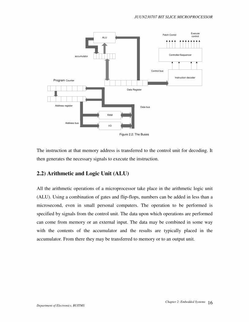
between units of the microcomputer by collections of conductors called buses. Figure 2.2
explain the functions of buses.
2.1c) Accumulator Register
The register which is widely used in all operations is known as ‘Accumulator’ or AX
register. The accumulator is the principal register of the ALU of a microprocessor. It is
the repository for successive results of arithmetic operations, which may then be
transferred to memory, to an output device, etc.
2.1d) Control Unit
The control unit of a microprocessor directs the operation of the other units by providing
timing and control signals. It is the function of the microcomputer to execute programs
which are stored in memory in the form of instructions and data. The control unit
contains the necessary logic to interpret instructions and to generate the signals necessary
for the execution of those instructions. The descriptive words "fetch" and "execute" are
used to describe the actions of the control unit. It fetches an instruction by sending and
address and a read command to the memory unit.
JUUN230707 BIT SLICE MICROPROCESSOR
Chapter 2: Embedded Systems
Department of Electronics, BUITMS 16
ALU
Controller/Sequencer
Instruction decoder
accumulator
Program Counter
Address register
Control bus
RAM
I/O
Fetch ContolExecutecontrol
Data bus
Address bus
Data Register
Figure 2.2: The Buses
The instruction at that memory address is transferred to the control unit for decoding. It
then generates the necessary signals to execute the instruction.
2.2) Arithmetic and Logic Unit (ALU)
All the arithmetic operations of a microprocessor take place in the arithmetic logic unit
(ALU). Using a combination of gates and flip-flops, numbers can be added in less than a
microsecond, even in small personal computers. The operation to be performed is
specified by signals from the control unit. The data upon which operations are performed
can come from memory or an external input. The data may be combined in some way
with the contents of the accumulator and the results are typically placed in the
accumulator. From there they may be transferred to memory or to an output unit.

JUUN230707 BIT SLICE MICROPROCESSOR
Chapter 2: Embedded Systems
Department of Electronics, BUITMS 17
Accumulator
MemoryUnit
Logic CircuitsControl
Unit
Data Register
Figure 2.3: Inside ALU
The general and logical representation of ALU is shown in figure 2.4, consisting two n-
bit inputs (A and B) and one n-bit (R) output. There is also a control input (F). The output
D (or C_out) is the state of ALU.
Figure 2.4: Logic Symbol of ALU
There are certain simple and complex operations or instructions that can be performed by
an ALU. The classification of these operations is:
• Integer Arithmetic operations
• Bit wise logic operations
• Shifting Operations

JUUN230707 BIT SLICE MICROPROCESSOR
Chapter 2: Embedded Systems
Department of Electronics, BUITMS 18
2.3) Addressing Modes
Addressing modes, a concept from computer science, are an aspect of the instruction set
architecture in most central processing unit (CPU) designs. The various addressing modes
that are defined in a given instruction set architecture define how machine language
instructions in that architecture identify the operand (or operands) of each instruction.
2.3a) Types of Addressing Modes
Addressing modes are categorized according to the type of data transfer and logic in use.
The addressing modes are:
• Absolute mode
• Register Indirect mode
• Register mode
• Base-Offset mode
• Immediate mode
• Direct mode
• Index mode
• Base Index mode
• Base-Index-offset mode
2.3b) Block Representation of Addressing Modes
Figure 2.5 illustrates the instruction formats and specifications of each mode. An
addressing mode specifies how to calculate the effective memory address of an operand
by using information held in registers and/or constants contained within a machine
instruction or elsewhere. The Effective Address represents the offset of the desired
operand from the segment base.

JUUN230707 BIT SLICE MICROPROCESSOR
Chapter 2: Embedded Systems
Department of Electronics, BUITMS 19
Absolute Mode
ADDRESSOUT
Effective address = address as given in instruction
ADDRESSSTORE (via)
Effective address = contents of specified register
ResultMUL
Register Mode
No effective Adress; registers are used for inputs
Reg_A Reg_B
REGLOAD
Effective address = offset plus contents of specified base register
BASE OFFSET
BASE-OFFSET Mode
REG_AADD
No effective address; REG_A stores REG_B+constant
REG_B constant
Immidiate Mode
REG_ALOAD
Effective address = address as given in instruction
ADDRESS
Direct Mode
Base-Index Mode
REG_ALOAD INDEXBASE
Effective address = contents of specified base register
plus contents of specified index register

JUUN230707 BIT SLICE MICROPROCESSOR
Chapter 2: Embedded Systems
Department of Electronics, BUITMS 20
Effective address = offset plus contents of specified base
register plus contents of specified index register.
Base-Index-Offset Mode
REG_ALOAD INDEXBASE OFFSET
Figure 2.5: Addressing Modes
2.4) Memory Organization
Most memories encountered in computer systems are coordinate-addressed. It means
that the memory is accessed by supplying a number (address) which is used directly to
identify a particular physical storage location. Data is then copied into or out of the
selected location.
A few special subsystems within some computers make use of memory that is content-
addressed; also called associative memory. A content-addressed memory is accessed by
supplying a data value for certain portions (fields) of a storage location, rather than the
physical address of that location.
2.5) Organization of Memory Units
Basic memory unit provides the ability to store and access a fixed number of bits
(anywhere from a few thousand to several million with current technology). Each bit
within such a unit may be selected individually for reading and writing. Usually only one
bit in a given memory unit may be accessed at a time. The high speed requirements of
data transfer throughout a computer system create a need to access storage bits
simultaneously in many cases. The most obvious example arises in reading or writing a
complete word of data. All the bits of the word are available or needed at once, and if
possible should be transferred simultaneously.
Memory units are usually distributed as bit slices i.e. if a chip can store 64K bits, each
chip will be used to store one bit each from 64K different locations, rather than a
complete byte (assuming a byte-addressed architecture) from 8K different locations.

JUUN230707 BIT SLICE MICROPROCESSOR
Chapter 2: Embedded Systems
Department of Electronics, BUITMS 21
Figure 2.6 illustrates the bit-slice memory organization. In addition to parallel access to
the individual bits of a word, newer architectures support increasing opportunities to
usefully access more than one word at a time. Data may be flowing between memory and
disk units while the CPU executes other instructions. Increasing use of pipelining and
overlap require fetching instructions and data at the same time in some cases, or reading a
sequence of instructions as fast as possible.
........2 1 0
BITS
.
.
.
.
210 Words
UNIT: n-1
UNIT: 0
Figure 2.6: Bit-slice memory organization
Since data and instructions can be read and written at the same time only if they are
located in different memory units, it is often desirable to use smaller units even if larger
ones are available. The complete set of words in the address space is divided among the
various units. The division is designed so that a group of bits from the address select a
unit (actually a set of bit-sliced units), while the remaining bits select the location within
that unit.
2.6) Bit Slicing
Bit slicing is a technique for constructing a processor from modules of smaller bit width.
Each of these components processes one bit field or "slice" of an operand. The grouped
processing components would then have the capability to process the chosen full word-
JUUN230707 BIT SLICE MICROPROCESSOR
Chapter 2: Embedded Systems
Department of Electronics, BUITMS 22
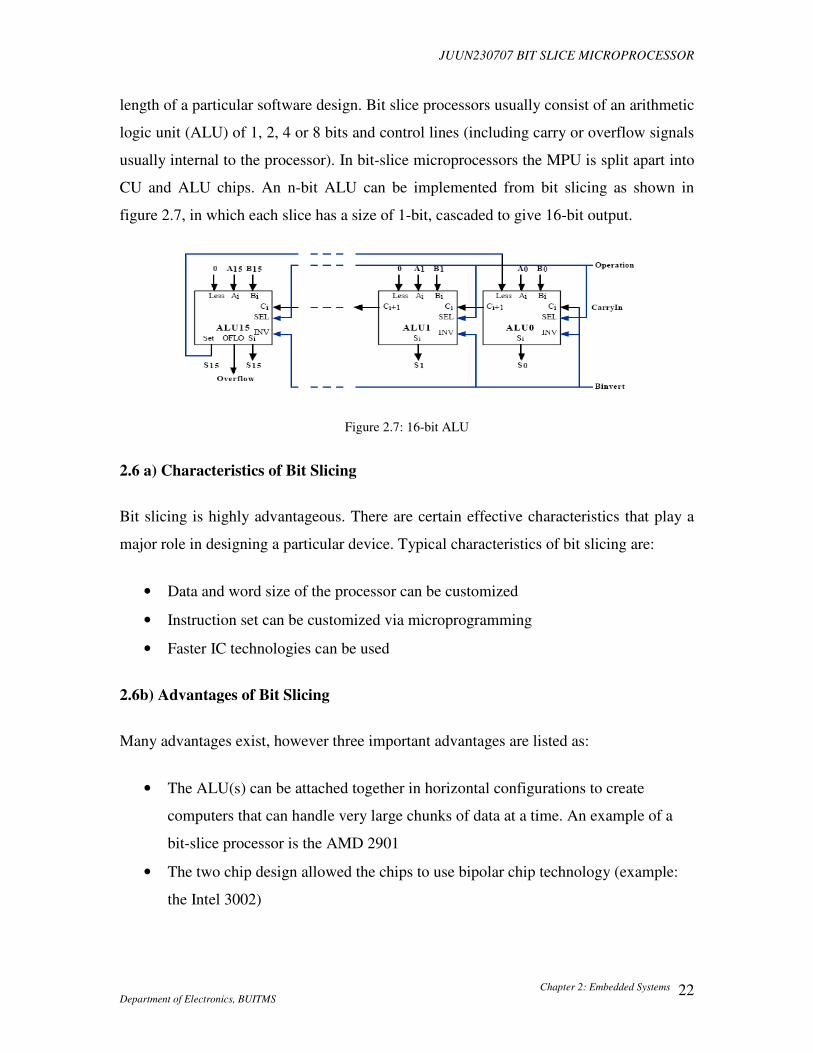
length of a particular software design. Bit slice processors usually consist of an arithmetic
logic unit (ALU) of 1, 2, 4 or 8 bits and control lines (including carry or overflow signals
usually internal to the processor). In bit-slice microprocessors the MPU is split apart into
CU and ALU chips. An n-bit ALU can be implemented from bit slicing as shown in
figure 2.7, in which each slice has a size of 1-bit, cascaded to give 16-bit output.
Figure 2.7: 16-bit ALU
2.6 a) Characteristics of Bit Slicing
Bit slicing is highly advantageous. There are certain effective characteristics that play a
major role in designing a particular device. Typical characteristics of bit slicing are:
• Data and word size of the processor can be customized
• Instruction set can be customized via microprogramming
• Faster IC technologies can be used
2.6b) Advantages of Bit Slicing
Many advantages exist, however three important advantages are listed as:
• The ALU(s) can be attached together in horizontal configurations to create
computers that can handle very large chunks of data at a time. An example of a
bit-slice processor is the AMD 2901
• The two chip design allowed the chips to use bipolar chip technology (example:
the Intel 3002)

JUUN230707 BIT SLICE MICROPROCESSOR
Chapter 2: Embedded Systems
Department of Electronics, BUITMS 23
• The ability to allow users to create their own instruction sets for their applications.
Instructions sets could be created to emulate, or enhance, existing processors such
as the 6502 or 8080, or to create a unique instruction set specially adapted to
maximize performance of a specific application
2.7) AMD Bit Slice Processors
2.7a) AMD 2900 Family
Advance Micro Devices (AMD) developed several ALU(s) by using bit-slicing
technique. Some of the processors are Am 2900, Am 2903, Am 2910 and Am2909. In
Figure 2.8, block diagram of Am 2900 series is shown.
opcode
PLA
MAP
sequencer
Control Store
Pipe-line
registers
ALU
Status Registers
Exte
rnal
clo
ck
Figure 2.8: Bit slice Organization of Am 2900 series
Am2900 series is developed on the basis of Bit-Slicing. Am2900 family was introduced
in 1976 and became one of the widely used bit-sliced processor families. This family is

JUUN230707 BIT SLICE MICROPROCESSOR
Chapter 2: Embedded Systems
Department of Electronics, BUITMS 24
based upon low-powered Schottky TTL technology which combines high speed with
moderate power consumption. The members of 2900 family are:
i. Processor slices
ii. Micro program sequencers
iii. Memories
The microprocessors implemented under 2900 family are precisely given in the table
below:
Table 2.1: AMD Processor Family
Am2900 Family Comments
Am2901 4-bit
Am2902 4-bit with carry look ahead
Am2903 4-bit with ripple carry
Am2909 4-bit micro program sequencer
Am2910 4-bit micro program sequence
This project works well for 16-bit arithmetic and logic instructions along with basic
microprocessor functions for FDE operations.
2.7b) AMD 8080 Emulator
Bit-sliced components have found extensive use in new processors and controller
designs, but they are also used in designing some existing CPUs. Intel 8086 has some of
its versions designed on bit-sliced configurations. An 8080 Emulator is one such example
which is used in Intel 8086 architecture.
Such an organization is designed to achieve to replace the standard MOS circuit
comprising 8080 chip proper, a clock generator, and a status control latch. The emulator
has precisely the same bus size and instruction set. It uses 60 ICs including four 2901
processor slices, three 2909 micro program sequencer slices, 11 PROM chips and large
number of MSI/SSI circuits and the operating clock frequency is 5MHz.

JUUN230707 BIT SLICE MICROPROCESSOR
Chapter 2: Embedded Systems
Department of Electronics, BUITMS 25
AMD Emulators have also contributed in the field of advance micro processing.
Regarding the project, the core difference in AMD design and this project is that
whatever the development has been done, the bit size is confined to 4, whereas in this
project, the basic module is of 4-bits and overall it is a 16-bit system.
The HDL advantage leads to fabulous innovations in digital design. The bit-slice method
is one of the important techniques to enhance the processor’s size in many directions,
specially, complex mathematical formulations.
JUUN230707 BIT SLICE MICRO PROCESSOR
Chapter 3: Project Structure and Experimentations
Department of electronics, BUITMS 26
Chapter 3
JUUN230707 BIT SLICE MICROPROCESSOR
Project Structure and Experimentations
Topics covered in this chapter:
• Arithmetic processor
• Instruction formats and instruction sets
• Buses
• FDE operations
• FPGA implementation

JUUN230707 BIT SLICE MICRO PROCESSOR
Chapter 3: Project Structure and Experimentations
Department of electronics, BUITMS 27
JUUN230707
J=JEHANZEB
2307=23rd July
U=UBAID
07=2007
U=UMAIR
N=NAEEM

JUUN230707 BIT SLICE MICRO PROCESSOR
Chapter 3: Project Structure and Experimentations
Department of electronics, BUITMS 28
3.1) Arithmetic and Logic Unit (ALU)
In fact, the fundamental part of arithmetic micro processing is known as Arithmetic and
Logic Unit (ALU). Simply, it is defined as the unit of microprocessor that performs
arithmetic and logic operations.
Certain basic arithmetic functions can be implemented directly by combinational MSI
circuits. Chip density and package pin restrictions limit the data types that can be
processed by these circuits. Integrated-circuit complexity considerations also restrict the
types of operations performed to addition, subtraction and some associated functions.
However, networks of MSI components can be designed to perform these operations
according to various sequential algorithms.
Some examples of MSI arithmetic circuits are binary adder and full adder (n-bits), as
shown in figure 3.1.
z
2-bit
2-bit binary adder
(7482)
y
2-bit
x
2-bit
Cout Cin
3.1-a) 7482 2-input binary adder
Full Adder
yo
Xo
Zo
Co C inFull Adder
y1
X1
Z1
Cout C o
3.1-b) Parallel combination of full adders
Figure 3.1: Some MSI circuits

JUUN230707 BIT SLICE MICRO PROCESSOR
Chapter 3: Project Structure and Experimentations
Department of electronics, BUITMS 29
3.2) VLSI and Arithmetic Operations
VLSI design choices are often dictated by weighing all known relevant factors and then
making selections based on satisfying the most critical specifications. Several design
cycles may be needed to work out all of the details to the point where an acceptable
design is achieved.
3.3) BIT SLICE Design
Consider an ALU that accept n-word inputs A and B and n-bit result F as shown in figure
3.2.
ALUFigure 3.2: An n-bit ALU
A
n-bits
Bn-bits
Control inputs
Fn-bits
The architectural level function of ALU can be defined as:
F = F (A, B, control)
Bit slice design is based on the fact that logic deals with data at the bit level. Word-size
operations are obtained using individual parallel-wired bit-level circuits that perform the
same operation.
An n-bit ALU is created by paralleling n-identical slices as shown in figure 3.3.

JUUN230707 BIT SLICE MICRO PROCESSOR
Chapter 3: Project Structure and Experimentations
Department of electronics, BUITMS 30
.
.
.
Function 0
Function 1
Function 2
Function 3
Function m-2
Function m-1
Ao
.
.
.
Bo
B n-1
.
.
.
f0
f1
f2
f3
MU
X
.
.
.
Co
C n-1
LOGIC
BLOCK
Figure 3.3: Block description of ALU
Control
A n-1
3.4) Fundamental ALU
The basic module of ALU designed is a 4-bit I/O device, i.e. the inputs and output are of
4-bits each, as illustrated in figure 3.4.
ALU
A4-bits
B4-bits
MODE
Sele
ct
0
Sele
ct
1
F4-bits
Carry Out
Figure 3.4: Fundamental ALU block
Carry In
3.4a) Module Explanation
The basic features of this ALU are:

JUUN230707 BIT SLICE MICRO PROCESSOR
Chapter 3: Project Structure and Experimentations
Department of electronics, BUITMS 31
• Two inputs A & B, each having a size of 4-bits.
• Two select inputs, one input carry and one MODE input.
• MODE is a special input which is either active HIGH or active LOW; for each
active input there are specific arithmetic and logic operations to be performed.
• Carry input is LOW for 1st 16 instructions and HIGH for other 12 instructions.
The list of those operations can be seen in the next topic. In all, there are 28 operations;
15 of which are performed when MODE in active LOW, 12 are performed when MODE
is active HIGH.
3.4b) Instruction Format
Each processing device depends upon some specific codes. These codes in technical
terms are known as Instructions.
The combination of various fields form an instruction and further combining these
instructions in a sequence is called Program.
Given below is the instruction format of JUUN230707 processor. It comprises of three
fields namely:
• OPCODE Field
• Register Field
• Address Field
OPCODE Field
5-bits
Register Field
3- bits
Address Field
8-bits
Figure 3.5: Instruction format
For arithmetic operations, there are total 29 instructions which are programmed in this
microprocessor. These 29 instructions are separated in 3 parts. There is an input to the
ALU namely ‘mode’ that has different operations on active high/low states.
When ‘MODE’ pin is active LOW (0) then the ALU performs 15 operations, which are
programmed as shown in figure 3.2.
The instruction set is shown in table 3.1

JUUN230707 BIT SLICE MICRO PROCESSOR
Chapter 3: Project Structure and Experimentations
Department of electronics, BUITMS 32
Table 3.1: Instruction set 1
Mnemonics
S. No
OPCODES Mode = 0
Comments
1. 00000 TRANSZ Transmit 0
2. 00001 SUB1 Subtract b-a
3. 00010 SUB2 Subtract a-b
4. 00011 ADD Add a+b
5. 00100 XOR a XOR b
6. 00101 OR a OR b
7. 00110 AND a AND b
8. 00111 NAND a NAND b
9. 01000 XNOR a XNOR b
10. 01001 SHL1A Shift a 1 to left
11. 01010 SHRA1 Shift a 1 to right and Add 1
12. 01011 SHR1B Shift b 1 to right
13 01100 SHL1B Shift b 1 to left
14. 01101 SRB1 Shift b to rite and ADD 1
15. 01110 ADR1 Add a ,b and shift 1 to right
16. 01111 ADL1 Add a, b and shift 1 to left
Table 3.2 shows the op-codes and mnemonics for other operations, when MODE is set
active HIGH with input-carry 1 for 12 operations.
Table 3.2: Instruction set 2
Mnemonics
S. NO
OPCODES MODE = 1
Comments
1. 10000 SUBA1 Subtract a-1
2. 10001 ANDS1 AND, subtract 1
3. 10010 NANDS1 NAND, subtract 1
4. 10011 CMAS1 Compliment a and subtract 1
5. 10100 ORAACB OR a : add a compliment b
6. 10101 ANONOR AND a, b : or : a XNOR b
7. 10110 SAB1 subtract a, b then 1
8. 10111 ADCMB add to a compliment b
9. 11000 AORAB a OR a+b
10. 11001 XNOR XNOR a, b

JUUN230707 BIT SLICE MICRO PROCESSOR
Chapter 3: Project Structure and Experimentations
Department of electronics, BUITMS 33
11 11010 ACBOAB a NAND b OR a+b
12. 11011 CMAAB compliment a ADD b
General instructions of LOAD, STORE and OUT are also developed with specific op-
codes and mnemonics, are shown in table 3.3.
Table 3.3: OPCODES for Basic Instructions
S. No OPCODES Mnemonics Comments
1. 11101 LOAD Load instruction
2. 11110 STORE Store instruction
3 11111 OUT Send to output port
3.4c) Cascading Modules
The main feature of this project is parallel combination of ALU designed, in a complete
microprocessor setup. The basic architecture of bit slicing in shown in figure 3.6 below:
Pro
secco
r sliceS
n-1
Pro
secco
r sliceS
0
Data bus
n-bits
control bus
Pro
secco
r sliceS
n-2
Figure 3.6: Gerneral Architecture of Bit slicing
.........
The objective was to design a complete microprocessor in which four modules of ALU
were cascaded (sliced). As shown in table 3.3, there are microinstructions to perform
various operations. The four modules were combined to form an over all 16-bit I/O
arithmetic processor whose block diagram is shown in figure 3.7.

JUUN230707 BIT SLICE MICRO PROCESSOR
Chapter 3: Project Structure and Experimentations
Department of electronics, BUITMS 34
Address
16-bit
Data
16-bits
Control
4-b
it v4
-bit
4-b
it
4-b
itv v
instruction register
Figure 3.7: 16-bit ALU
AL
U s
lice
1
AL
U s
lice
2
AL
U s
lice
4
AL
U s
lice
3microinstruction register
Data
control memory
(65536 locations)
Address
microprogram sequencer
3.4d) Bit Slicing Technique
The modules are cascaded using “Ripple carry Method” for parallel combination of 4-bit
ALU modules to give a 16-bit instantiated in Processor module. The schematic diagram
of Processor module is shown below:

JUUN230707 BIT SLICE MICRO PROCESSOR
Chapter 3: Project Structure and Experimentations
Department of electronics, BUITMS 35
Figure 3.8: Processor module schematic
It comprises of 16-bit data bus (Data_2) and two 16-bit inputs A & B. Inside slices; each
input has the bus size of 4-bits for both input and output. The select input (4-bits) is same
in size for all slices. Thus each 4-bit I/O module is termed as slice. Appendix B shows the
slices of ALU and its timing diagram.
The memory comprises of 2n
words each with a size of 1 byte. Where n=16; i.e. number
of address lines in the bus.
3.5) FDE Operations
3.5a) Fetch
The instructions are stored in memory. Since there is no peripheral input to the processor,
all instructions are thus kept in memory module. The instructions are in hexadecimal
format. Each instruction is allocated at consecutive two memory locations. The size of
one complete instruction is 2-bytes. The format of instructions stored in memory is:
MEMORY_1[12] = 8'h32;
MEMORY_1[13] = 8'h0c;

JUUN230707 BIT SLICE MICRO PROCESSOR
Chapter 3: Project Structure and Experimentations
Department of electronics, BUITMS 36
3.5b) Decode
The instruction when fetched is separated in three fields as shown in figure 3.5, by using
the following syntax of Verilog HDL:
IR=MBR [15:11]REG=MBR [10:8];MAR=MBR [7:0];
The instruction pointer (IR) is connected to ALU select pin (ALU_sel), so to count the
instruction OPCODES.
The operand is fetched in the next cycle. It is dependent upon the OPCODE to store itself
in any of the GPRs, as directed by the memory. The data for the operand is coming from
memory buffer register (MBR). The Verilog syntax for the operand fetch operation is:
MBR=data_B_IN;
case(REG)
0: alu_1=AX;
1: alu_1=BX;
2: alu_1=CX;
3: alu_1=DX;
endcase
alu_2= MBR;
3.5c) Execute
After reading the OPCODE, the processor reads instruction from ALU performs the
operation and sends the result to output. An important point about IR is that it is
connected to ALU_sel only for ALU operations. The instructions of LPAD, STORE, and
OUT are other than that of ALU; as they totally belong to the microprocessor.
Using the VERI-WELL Verilog simulator, whose output is shown in appendix B, the top
level module is instantiated as:

JUUN230707 BIT SLICE MICRO PROCESSOR
Chapter 3: Project Structure and Experimentations
Department of electronics, BUITMS 37
memory1 alias0(addr_p,data_pr_in,data_pr_out,Rd,Wr,M_io);
Ports alias2(addr_p[7:0],data_pr_in,data_pr_out,Rd,Wr,i_mio);
SYSTEM_CLOCK alias3(clk_1);
PROCESSOR alias4(addr_p,data_pr_out,data_pr_in,M_io,clk_1,RESET,Rd,Wr);
The modules are combined in a particular sequence. The VERI-WELL simulator
instantiation diagram is given in figure 3.9, along with the connections. Only one external
input of RESET is there, rest of the data transfer is being done by Memory. Hence the
project is static in nature.
Top Level instantiation Module
Processor
16-bit ALU
Slice 4 Slice 3 Slice 2 Slice 1
Memory Ports
b3 a3 b2 a2 a1b1 a0b0
f0f1f2f3
data In
address bus
CLK
data bus
M_EN
rdwr
address bus
8bit
rdwr
IO_en
RD
WR
M_IO
OUTPUT
Address
Memory out Port out
data bus
OUTPUT data
RESET
data bus
data
bus
data
bus
data bus
ALU_SEL

JUUN230707 BIT SLICE MICRO PROCESSOR
Chapter 3: Project Structure and Experimentations
Department of electronics, BUITMS 38
3.6) FPGA Design
3.6a) ISE 9.1i
Using the tool ISE 9.1i, the design of this project is implemented. The procedure of ISE
is explained in chapter 4. ISE itself designs the HDL for FPGA by converting the
program into various circuit logics.
This design flow is after assigning package pins and timing constraints. Given in
Appendix B, is the package design and pin-out of JUUN230707 Bit-Slice
Microprocessor. The diagrams of package architecture and pin-out are shown in
Appendix B.
3.6b) Design Implementation
The next step in developing the project is to implement the design. After assigning
the package pins and timing constraints, following methods are adopted:
• Translate
• Map
• Place and Route
It is also a lengthy process and takes time to execute. However its successful
execution leads to the final stage of project.
3.6c) Downloading the Program to Device
Last step is to download the code on the device. The device used (xc3s200-4ft256)
was utilized 50% of the total package. A backup encoded file is automatically
generated and the program is ready to be downloaded on the device.
ISE provides this process by using FPGA Editor and Floor Plan. When the device is
configured, two devices of selected FPGA appear i.e. volatile and non-volatile
programmable memories.

JUUN230707 BIT SLICE MICRO PROCESSOR
Chapter 3: Project Structure and Experimentations
Department of electronics, BUITMS 39
If the program has to be dumped temporarily, the SRAM of FPGA is selected and
programmed. The displays of FPGA are turned on. This is the simulation process
however the most effective method of simulation is through ISE simulator, as the
frequency affects the display a lot.
3.6c) Schematic and Simulation Diagrams
ISE develops the hardware of given HDL after synthesis of the project. The diagrams
obtained from Schematic Engine of ISE are shown in Appendix B. Built-In ISE
simulator was used to simulate the processor. The timing diagram is constructed
manually for some inputs and ISIM Engine runs those particular inputs to produce
output waveforms at given clock cycles. These timing diagrams are also shown in
Appendix B.
3.7) VERI-WELL Simulator
The project code was initially executed in VERI-WELL simulator. This software can
generate quality simulation. The simulation and outputs using this software is shown
in Appendix B.
3.8) Source Code
The source code comprises of different modules which are interconnected using
HDL syntax. Table3.4 below shows the modules.
Table 3.4: Module List
S.No
Module Name
Function
1. Basic ALU 4-bit I/O arithmetic & logic operations
2. ALU Slices 4-bit I/O chunks, giving 16-bit design
3. Memory 65536 memory locations
4. Ports IO ports
5. Processor FDE cycles using finite state machine

JUUN230707 BIT SLICE MICRO PROCESSOR
Chapter 3: Project Structure and Experimentations
Department of electronics, BUITMS 40
These five modules along with their source codes are given in Appendix A. The
same source code is used for FPGA download; the FPGA dumping process is
described in chapter 4.
3.9) Timeline of Project
It is always necessary to mention the timeline of any proposal; hence there was also a
schedule proposed after consulting the supervisors. The time required in completing this
project was estimated as:
Table 3.5: Timeline
S. No Task Estimated time (app in weeks)
1. Verilog HDL programming 6 weeks
2. Xilinx ISE Tools 6 weeks
3. Troubleshooting,
Verifications & simulation Semester break (3 weeks)
4. Second stage documentation 3 weeks
5. FPGA, testing & simulation 4 weeks
6. Final documentation 4 weeks
The project was started on November 21st 2006 and the target eyed was July 2007.
Thanks to Allah All Mighty who enabled us to complete the project on July 23rd
2007.
JUUN230707 BIT SLICE MICROPROCESSOR
Chapter 4: Project Tools
Department of Electronics, BUITMS 41
Chapter 4
Project Tools
Topics covered in this chapter:
• Spartan-3
• Hardware Description Language
• Design flow of Verilog HDL
• Xilinx ISE
• VERI-WELL Verilog simulator
• Supporting Tools

JUUN230707 BIT SLICE MICROPROCESSOR
Chapter 4: Project Tools
Department of Electronics, BUITMS 42
4.1) Spartan-3 FPGA
A field programmable gate array (FPGA) is a semiconductor device containing
programmable logic components and programmable interconnects. The programmable
logic components can be programmed to duplicate the functionality of basic logic gates
such as AND, OR, XOR, NOT or more complex combinational functions such as
decoders or simple math functions. In most FPGAs, these programmable logic
components (or logic blocks, in FPGA parlance) also include memory elements, which
may be simple flip-flops or more complete blocks of memories.
The FPGA used in the project is Spartan-3. It is the Platform for highest density and Pin-
Count Applications. For applications where both high logic density and high I/O count
are important. It is ideal for highly-integrated data-processing applications.
Some capabilities of Spartan-3 are:
• The Spartan™-3 platform FPGA series combines a large amount of
programmable logic, intellectual property (IP) cores, advance clocking circuitry,
and embedded memory with versatile, fast interconnect structures.
• Spartan-3 FPGAs provide a single, easily customized platform for the following
technologies in a sophisticated system-on-a-chip (SoC) design:
• System connectivity
• DSP
• Embedded processing
• System connectivity consists of the physical parallel I/O interface and the
protocols required for higher bandwidth.
• All Spartan-3 device I/O pins support full Select-IO™ – Ultra functionality for
fast, flexible electrical interfaces.

JUUN230707 BIT SLICE MICROPROCESSOR
Chapter 4: Project Tools
Department of Electronics, BUITMS 43
• PCI compliance
• 24 I/O standards, DDR I/O registers, DCM(s)
• Ideal bridging functions
Digitally Controlled Impedance (DCI) technology is also available on selected I/O
standards. Using DCI can match the impedance of each user output to the external
reference impedance dedicated to one of the eight I/O banks. This allows you to:
• Eliminate the need for most external termination resistors.
• Perform high-precision impedance matching for high speed solutions.
• Tune applications on the fly for multiple environments.
Figure 4.1: Spartan-3 (Courtesy: www.xilinx.com)
4.2) Hardware Description Language (HDL)
The hardware description languages came into existence due to extensive growth of
digital technology. HDLs allow the designers to model the concurrency of processes
found in hardware elements. Verilog HDL and VHDL are most common in this regard.
Verilog however, is the more generally well understood and thus the backbone of this
project.

JUUN230707 BIT SLICE MICROPROCESSOR
Chapter 4: Project Tools
Department of Electronics, BUITMS 44
4.2a) Verilog HDL
Verilog originated in 1983 at Gateway Design Automation. It is now considered as IEEE
standard (IEEE 1364-1995 and IEEE1364-2001). Some of its characteristics are:
• Verilog stands for ‘VERIfy LOGic’.
• Its syntax is much similar to C-programming.
• It allows different levels of abstraction to be mixed with the same model.
• All fabrication vendors provide Verilog HDL libraries for post-logic synthesis
solutions.
In typical design flow of Verilog HDL
• Specifications are written first in order to mention the functionality of the system.
• Behavioral description is created to analyze the design in terms of functionality
and performance.
• RTL is developed by manually converting the behavioral description. Dataflow
has to be described by the designer.
• Logic synthesis converts the RTL to gate-level net-list.
• Gain the logic is verified and then the system is planned for connections and
routing.
• Physical design is constructed.
• Final step is the implementation.
4.2b) Verilog Syntax
Figure 4.2 elaborates the typical design flow of Verilog HDL. Since the basic syntax of
Verilog HDL resembles with C language, the blocks called modules are initialized as:
module NAME_HDL(O_PORT,....,I_PORT....);------->inside parenthesis: terminal list
output O_PORT;
input I_PORT;
...
...
<program Logic....>
......
......

JUUN230707 BIT SLICE MICROPROCESSOR
Chapter 4: Project Tools
Department of Electronics, BUITMS 45
......
endmodule
Design specification
Verification and Testing
RTL Description
Behavioral Description
Gate-level Netlist
Logical Testing and Verification
Logic and Timing Synthesis
Floor PlanningAutomatic Place and Rout
Physical Layout
Layout Verification
Implementation
Figure 4.2: Typical Design Flow
Verilog is both behavioral and structural language. Internals of each module can be
defined at four levels of abstraction, depending upon the design. The levels of abstraction
are:
• Behavioral level
• Dataflow level
• Gate level
• Switch level

JUUN230707 BIT SLICE MICROPROCESSOR
Chapter 4: Project Tools
Department of Electronics, BUITMS 46
The behavioral level is the highest level of abstraction in which algorithmic terms are
implemented. In dataflow level, the designer is aware how the data flows between
hardware registers and its process in the design. The module implemented in terms of
logic gates is called gate level and the module implemented in terms of switches, nodes
and interconnects is called switch level; which is the slowest.
The convention in implementing the modules is:
• Identify the output ports first
• Input ports should be followed by output ports
Verilog also allows the designer to mix the four levels. The Register Transfer Language
(RTL) is frequently used for Verilog description that allows the combination of
behavioral and dataflow constructs. Verilog also allows each of the modules to be
constructed in separate level of abstraction.
Given below is the table to exemplify the syntaxes of Verilog Levels of Abstraction.
Table 4.1: Verilog levels of Abstraction
S.
No
Verilog Levels of Abstraction Description Syntax
1. Behavioral Algorithms are implemented like C. Logic
statements are used.
F=A+B
2. Dataflow Assign statement is used for complex logics Assign
{co,sum}=A^B
3. Gate Gates are implemented; logical names are used xor g1(sum,a,b); and
g2(co,a,b);
4. Switch Transistor names, Vcc and ground are predefined. pmos t1(vdd,out,in);
nmos t2(out,g,in);
4.2c) Stimulus in Verilog
After designing all modules, there is a highest level instantiation module that is used to
stimulate the program. This module is declared without ports. The inputs are declared as
registers (reg) and outputs as wires (wire). Binary vales are assigned to control inputs and
the program runs after compilation. Stimulus block is same for all levels of abstraction.

JUUN230707 BIT SLICE MICROPROCESSOR
Chapter 4: Project Tools
Department of Electronics, BUITMS 47
4.2d) Logic Synthesis with Verilog
Logic synthesis is the process of converting high-level description to optimized gate-level
representation. This representation is in the form of standard cell library consisting of
certain design constraints. The constraints are logic gates such as AND, OR and XOR
etc. The logic synthesis with Verilog can be done either by designer’s mind or by CAD
tools. Figure 4.3 explains the flow of logic synthesis by using Verilog HDL.
Architectural Description
Gate-Level Description
Designer's Mind
high Level Blocks
Design Constraints
Optimized Gate Level
Representation
YES
Design Iterations
NO
Design Constraints
Standard Library
a: Logic Synthesis by Designer's Mind
Architectural Description
Optimized Gate-LevelNetlist
Computer Aided Logic
Synthesis
high Level Blocks
Meet Constraints
Placa and Rout
YES
NO
Design
Constraints
Standard Library
(Technologydependent)
b: CAD Synthesis
Figure 4.3: Logic Synthesis

JUUN230707 BIT SLICE MICROPROCESSOR
Chapter 4: Project Tools
Department of Electronics, BUITMS 48
4.2e) Impact of Logic Synthesis
The logic synthesis revolutionized the digital design. The impact of CAD synthesis is:
• High-level design is much more flaw less.
• High-level design is done without much concern about design constraints.
• Conversion to gate-level is fast.
• Synthesis tools optimize the design as whole.
• Logic synthesis allows technology independent design.
• Design reuse is possible.
Verilog synthesis can easily be done by using RTL as it combines behavioral and
dataflow constructs.
4.2f) State Machines
The use of state machines is extremely important as far as the implementation of Verilog
based design is concerned. The FDE operations of 23/07-JUUN-07 bit slice processor are
based on state machines; explained in project description.
4.3) Xilinx-Integrated Software Environment (ISE)
Xilinx® Integrated Software Environment (ISE) explains how to create, define, and
compile FPGA design using the suite of ISE tools available from the Project Navigator
(sub-tool) describes what’s new in the software release and how to migrate past projects
to the current software.
The ISE sequel to start a project and its completion is figuratively described as:

JUUN230707 BIT SLICE MICROPROCESSOR
Chapter 4: Project Tools
Department of Electronics, BUITMS 49
Figure 4.4: Xilinx ISE Design Flow (courtesy: Xilinx Inc)
Sub tools inside a complete suit of ISE and those used in this project are:
• Pins Area Constraint Editor (PACE)
• Floor Planner
• ImPACT
• FPGA Editor
4.3a) PACE
It is a major sub tool which:
• Explains GUI to define legal pin assignments and to create properly sized area
constraints.
• Includes information on how to create non-rectangular areas.
4.3b) Floor Planner
The Floor Planner is an important sub-tool of ISE in order to create the design using
HDL. The Floor Planner:
• Explains how to use the GUI to floor-plan the design
• Includes information on creating relationally placed macro (RPM) cores,
editing constraints, cross-probing to the Timing Analyzer, and placing ports
for Modular Design.

JUUN230707 BIT SLICE MICROPROCESSOR
Chapter 4: Project Tools
Department of Electronics, BUITMS 50
4.3c) ImPACT
The FPGA is configured using this sub-tool. Hence ImPACT:
• Describes how to download bit-streams to an FPGA or CPLD using a Xilinx
Parallel Cable III, Parallel Cable IV, Multi-LINX™ Cable, Platform Cable
USB, or Multi-PRO Desktop Tool
• Describes how to read back and verify design configuration data and how to
perform functional tests on any device
• Describes how to generate programmable read-only memory (PROM)
programming files and programming files using Xilinx System ACE™, a
configuration environment that allows space-efficient, pre-engineered, high-
density configuration solutions for systems with multiple FPGAs.
4.3d) FPGA Editor
The Graphical user Interface (GUI) is accommodated by using FPGA Editor. The Editor:
• Explains how to use GUI to manually place and route the FPGA design.
• Includes information on adding probes the design and working with Integrated
Logic Analyzer (ILA) cores.
4.4) ISE 9.1i: Programming Process
4.4a) ISE Process
The most updated software for device configuration is ISE 9.1i. Using ISE 9.1i, there are
certain steps involved from writing a program to dumping on FPGA. Its main feature is
the built in Clock for synchronization of modules where required. The steps are precisely
explained and there diagrams are shown in Appendix B. Some important steps are:

JUUN230707 BIT SLICE MICROPROCESSOR
Chapter 4: Project Tools
Department of Electronics, BUITMS 51
1. Open the sub-tool ‘Project Navigator’.
2. From file menu, select ‘New project’
3. A link window opens, type module name in it.
4. Click ‘next’, another window opens.
5. Click ‘new source’ to generate a Verilog Module and place check on ‘Add to
Project’.
6. Select Simulator.
7. Click ‘Next->Next->Finish’
8. A working window will open. Type the program and save it.
9. To the left of screen, there is a Process window. Double click ‘Synthesis XST’;
the program will be complied.
10. Again from the Process window, select ‘Implement Timing Constraints’. The
environment of ISE will create a file by using PACE, in which CLOCK input is
adjusted.
11. After saving the Constraints file, click ‘Assign package pins’.
12. Configure the device pins as specified by PACE and save the file.
13. Double Click ‘Implement Design’.
14. Select ‘View RTL Schematic’, it will generate the schematic diagram of modules.
15. The final step is to dump the code on FPGA. From the source window, select
‘Generate programming file’, the successful program can be dumped on FPGA.
16. Selecting ‘Configure device’ after connecting the FPGA to the system dumps the
code on FPGA.
4.4b) FPGA Downloading
When the code is dumped on FPGA, the user has to check the following:
• After detecting the device, ISE asks for MODES of operation on FPGA. User has
to select ‘boundary-scan mode’.
• Another window opens in which two devices (memories) are shown. One to the
left side is volatile memory and other is PROM.
• Select volatile memory and add ‘.bit’ file in it.

JUUN230707 BIT SLICE MICROPROCESSOR
Chapter 4: Project Tools
Department of Electronics, BUITMS 52
• Right-click the device and select ‘program’.
• If a successful program dumping is achieved, a message appears “Program
Succeeded”.
• RAM of FGPA is programmed and the LED display shows the results.
• Once the volatile memory is programmed, select ‘generate PROM….’ to create a
‘.mcs’ file.
• Again select ‘configure device’ and program the device on right side of the screen
by adding ‘.mcs’ file to it.
• This program will remain in FPGA till it is erased from the device.
4.5) SynaptiCAD Veri-well Simulator
One of very smart simulators available for HDLs is SynaptiCAD Veri-well simulator.
This software runs on ‘command prompt’ of Windows™ XP. The important feature of
Veri-well is that a Clock module must be written for synchronized logics.
This software can also generate:
• Timing diagrams
• Waveforms
• Test bench modules
• Datasheets according to timing diagrams
The code and output by this software are shown in Appendix A. This software supports
the code from 1000-2500 lines.
4.6) Supporting Tools
4.6a) VISIO TEHNICAL 4.5
There are many figures and slow charts drawn in this thesis. The tool used for this
purpose is VISIO TEHNICAL 4.5, as it provides a huge flexibility in creating quality
figures. It covers almost all fields in one package. Some of the major fields, which it
covers regarding diagrams, are:
• Block diagrams
• Flow charts

JUUN230707 BIT SLICE MICROPROCESSOR
Chapter 4: Project Tools
Department of Electronics, BUITMS 53
• Business diagrams
• Data base diagrams
• Electrical and electronic diagrams
• Industrial process
The above mentioned categories contain subcategories which makes this tool more
compact.
4.6b) MS Office
MS Office is a vital part of every document. The text and its related tasks of the thesis are
performed in MS Office. Core tools used are:
• MS WORD: for documentation
• MS Power Point: for presentations
The features of MS Office are known to everyone hence only names of used components
are mentioned.

JUUN230707 BIT SLICE MICRO PROCESSOR
Chapter 5 Utilization of JUUN230707 Bit Slice Processor
Department of electronics, BUITMS
54
Chapter 5
Utilization of JUUN230707 Bit Slice Processor
Topics covered in this chapter:
• University Purpose
• Commercial Use
JUUN230707 BIT SLICE MICRO PROCESSOR
Chapter 5 Utilization of JUUN230707 Bit Slice Processor
Department of electronics, BUITMS
55
5.1) Educational Purpose
Bit slice microprocessors provide if-shelf IC(s) that enable system designers to define
their own CPU architectures. Bit slice families also provide various building blocks for
the design of micro programmable control units and other system components.
In systems with heavy workloads, substantial performance increases can be achieved y
offloading certain tasks from CPU to more specialized auxiliary processors. Although bit
sliced processors are used in innovations regarding microprocessor design, these families
are used in constructing emulators for existing processors.
The speed improvements result from the use of faster IC technologies and
implementation of complex operations in micro-instruction level firmware rather than
conventional instruction-level software.
Since the project is developed by using HDL, it can be extremely beneficial to serve
upcoming students. Working in the field of IC-Design, this project can be helpful as:
• The students can understand the basic Intel Architecture of Microprocessor
Design.
• By learning sophisticated HDL, the design can be further improved and size of the
processor can be increased.
• FPGA design can be understood by using this project.
• Software regarding FPGA design is described in detail, which can lead to many
successful designs, provided the HDL logic is correct.
If proper attention is given to the logic of this thesis, it is safely predicted that innovations
of high class are expected. The project provides a platform to those students who want to
adopt the field of VLSI and Embedded Systems Design.

JUUN230707 BIT SLICE MICRO PROCESSOR
Chapter 5 Utilization of JUUN230707 Bit Slice Processor
Department of electronics, BUITMS
56
The HDL used is flexible enough to be improved as much as one desire. The instructors
of courses like Computer Architecture, Microprocessor Systems and VLSI Techniques
may contribute in raising the design standards.
5.2) Commercial Purpose
There are many fields in which microprocessors are used as backbones. The scope of
Microprocessor Design is unlimited regarding the innovations required for Data
Processing.
The major applications of bit slice microprocessors are:
• Building high performance CPUs
• Graphic display terminals
• Navigation control systems and
• Large general-purpose computers
Listed below are some commercial applications of this project:
• The digital image processing requirements of today's industry are increasing at an
astounding rate. With the faster satellite data transmission rates and more frequent
data collection periods, both spatial storage and processing speed problems are
becoming more prevalent. Digital image processing algorithms must be precise
and efficient to meet these needs. This research project studies the implementation
of an image smoothing algorithm as a combination of custom tailored hardware
and firmware, i.e., using bit slice design. Bit slice microprocessor design involves
the configuration of very fast bit slice devices and the microprogramming
necessary to command the hardware to perform a specific task
• In DIP, the level of granularity-state machine, a bit slice processor or a full
processor-is a primary concern. The finer the level of granularity, the better the
performance.

JUUN230707 BIT SLICE MICRO PROCESSOR
Chapter 5 Utilization of JUUN230707 Bit Slice Processor
Department of electronics, BUITMS
57
• A high speed graphics processor can be created, maintained microcode and test
applications utilizing bit-slice processors in pipeline architecture in a team
environment.
• One chip microprocessors, which are true microcomputers formed on the same
silicon substrate. Thus, on a single chip, they comprise at least one processing
unit, a memory and an input/output device.
• The memories associated with or integrated with these microprocessors are
essentially of the RAM and/or ROM and/or PROM and/or EPROM and/or
EEPROM types. For a given application, the choice of a microprocessor also
involves the choice of the type of memory to be integrated or associated with the
microprocessor.
• A flexible, high-speed digital voice processor has been designed for use in
conjunction with the JTIDS communication terminal to be installed for testing on
board F-15 fighter aircraft and in Army JTIDS installations.
• Vo-coders in real time are sufficiently powerful to accommodate more
sophisticated, computationally intensive algorithms should the extra performance
they provide be required in the severe F-15 operational environment.
• The Aerospace Computer used stack instructions to save program memory space,
which has a major impact on reducing size, weight, power, and cost for spacecraft
applications. Stack instructions were also chosen to direct support high order
languages to enhance software reliability.
• Typical systems for data acquisition used commercial microprocessors for
controlling the data transfer between the analog-to-digital conversions, and the
storage of the digitized data words for processing. As the need for higher speed
sampling of a greater number of analog signal lines, bit slice microprocessors

JUUN230707 BIT SLICE MICRO PROCESSOR
Chapter 5 Utilization of JUUN230707 Bit Slice Processor
Department of electronics, BUITMS
58
were designed into the data acquisition systems. Bit slice microprocessors
processes transfer of data faster than the commercial microprocessors previously
used.
5.3) VLSI and Bit Slice Microprocessing
VLSI technology offers the possibility of building enormously complex bit slice and
multiprocessors at low cost. It is possible to place a number of simple microprocessors on
a single chip. In relatively new years since the introduction of microprocessors, the
surface of powerful digital systems is scratched based on VLSI devices.

JUUN230707 BIT SLICE MICROPROCESSOR
Summary
Department of Electronics, BUITMS 59
Summary
S.1) Foreword
The basic concept of digital systems arises from Number systems. There are following
number systems exist:
• Decimal
• Binary
• Octal
• Hexadecimal systems
All number systems have their unique significance, particularly binary and hexadecimal
system s the digital systems work on these two.
The advancement in semiconductor technology is admirable. The IC(s) have played a
major role in developing digital systems. The general classification of IC(s) is:
• Transistor-Transistor Logic (TTL)
• Complementary Metallic Oxide Semiconductors (CMOS)
• Application Specific Integrated Circuit (ASIC)
• Complex Programmable Logic Design (CPLD)
• Field Programmable Gate Arrays (FPGA)
Since the project is based on FPGA, hence the precise function FPGA is given here.
FPGA(s) are the modern day equivalent of 7400 series logic and a breadboard, containing
programmable logic blocks and programmable interconnects that allow the same FPGA
to be used in many different applications. For smaller designs and/or lower production
volumes, FPGA(s) may be more cost effective than an ASIC design. The primary
differences between CPLD(s) and FPGA(s) are architectural. A CPLD has a fairly
restrictive structure consisting of programmable sum-of-products logic arrays feeding a
relatively small number of clocked registers.

JUUN230707 BIT SLICE MICROPROCESSOR
Summary
Department of Electronics, BUITMS 60
Microprocessors are most sophisticated systems in digital design. Microprocessors are
comprehensive electronic semiconductor devices that are used for processing of data with
certain instructions to fetch, decode and execute, is called microprocessor. The system
consists of three parts. Intel 80X86 is the most widely used microprocessor.
S.2) Embedded Systems
Inside microprocessor are BIU and CU. The information exchange is done through BIU
and process control is performed by CU. ALU is the fundamental part of any
microprocessor. All the arithmetic operations of a microprocessor take place in the
arithmetic logic unit (ALU). Using a combination of gates and flip-flops, numbers can be
added in less than a microsecond, even in small personal computers. The operation to be
performed is specified by signals from the control unit.
Addressing modes are used as per requirement to transfer data. The addressing modes
are:
• Absolute mode
• Register Indirect mode
• Register mode
• Base-Offset mode
• Immediate mode
• Direct mode
• Index mode
• Base Index mode
• Base-Index-offset mode
Memory organization is also a vital part in micro processing. Memories are also
organized using Bit-Slicing. Two memory organizations exist:
• Coordinate Addressed
• Content Addressed

JUUN230707 BIT SLICE MICROPROCESSOR
Summary
Department of Electronics, BUITMS 61
Bit slicing is the process for constructing nonstandard length expressions being made
compatible with standard length. Bit slice processors usually consist of an arithmetic
logic unit (ALU) of 1, 2, 4 or 8 bits and control lines. AMD 2900 is known as bit slice
microprocessor family.
S.3) JUUN230707 Bit Slice Microprocessor
The project is constructed in Verilog HDL and an FPGA system is developed by using
ISE 9.1i. The source code is also simulated by using VERI-WELL simulator. The project
outline is:
• The Intel architecture is followed
• 4-bit ALU which is the basic block
• 16-bit ALU made by cascading 4-bit modules
• Memory of 65536 locations with width of 2-bytes
• A processor module
• I/O Ports
• The instruction format comprises of 5-bit OPCODE, 3-bit Register field and 8-bit
Address field
• Finally the program was downloaded on FPGA
S.4) Tools
The tools are very important in completing any project. In this project both hardware and
software tools are used which are listed below:
• Spartan 3 FPGA
• Xilinx ISE 9.1i
• Verilog HDL
• VERI-WELL HDL Simulator
• Visio Technical 4.5
• MS Office

JUUN230707 BIT SLICE MICROPROCESSOR
Summary
Department of Electronics, BUITMS 62
S.5) Utilization of JUUN230707 Bit Slice Microprocessor
Some applications are listed below:
• BUITMS can use this project as guideline for the subject of Microprocessor
design.
• HDL flow can be used to instruct students to improve this project.
• Instructors can help in further simplify the Architecture of Microprocessors.
Commercially it can be used in:
• Building high performance CPUs
• Graphic display terminals
• Navigation control systems and
• Large general-purpose computers
• DPS and Space Technology also utilize Bit Slice technology and thus this project
can be modified according to what the purpose stands for.
S.6) Timeline and Project Name
This project was started on 21-11-06 and completed on 23-07-07. The name of this
project is placed after the initials of each group member. The project name structure is:
• J= Jehanzeb
• U=Ubaid
• U=Umair
• N=Naeeem
The term 230707 emplies:
• 2307= July 23rd
• 07= Year 2007
There were many ups and downs came during this whole period but thanks to Allah
Almighty that we completed the project in due time.

JUUN230707 BIT SLICE MICROPROCESSOR
References
Department of Electronics, BUITMS 95
References
1. Introduction to VLSI Circuits and Systems
John P. Uyemura, Page 606, ‘Bit Slice Design’
2. Digital System Design and Microprocessors
John P. Hayes, Page 686,’Bit Slice Processors’
3. An Introduction to Digital Computer Design (3rd
Edition)
Rajaraman, Radhakrishnan, Page 353, ‘Bit Slice Organization’
4. Intel Microprocessors (4th
Edition)
Berry B. Brey, Page 517, ‘Arithmetic Co-Processor’
5. Microprocessor and Interfacing (2nd
Edition)
D.V Hall, Page 579,’Intel 8086 CPU Block Diagram’
6. Verilog HDL, Guide to Digital Design Synthesis (2nd
Edition)
Sameer Palintker
7. Introduction to Verilog (Carleton University)
Nyasulu, Knight
Web links
www.intel.com
www.xilinx.com
Search Engines
www.wikipedia.com
www.amazon.com
www.google.com.pk
www.ask.com

JUUN230707 BIT SLICE MICROPROCESSOR
Appendix A
Department of Electronics, BUITMS 63
Appendix A
Project Codes
• ALU module
• Bit slicing module
• Memory and Ports Modules
• Processor module

JUUN230707 BIT SLICE MICROPROCESSOR
Appendix A
Department of Electronics, BUITMS 64
A.1) Fundamental ALU Module
////BALOCHISTAN UNIVERSITY OF INFORMATION TECHNOLOGY AND MANAGEMENT SCIENCES////
//////////========TAKATOO CAMPUS QUETT============///////// //==========DEPARTMENT OF ELECTRONICS=============//
///======[23/07JUUN07 BIT-SLICE Microprocessor]=======///
/* TECHNIQUE:BIT-SLICING Module: Fundamental ALU GROUP MEMBERS: 1. MOHA1. MOHA1. MOHA1. MOHAMMAD JEHANZEB SHAHID==MMAD JEHANZEB SHAHID==MMAD JEHANZEB SHAHID==MMAD JEHANZEB SHAHID===>LEADER=>LEADER=>LEADER=>LEADER 2. UBAID AHSAN2. UBAID AHSAN2. UBAID AHSAN2. UBAID AHSAN 3. 3. 3. 3. UMAIR ANWAR KHANUMAIR ANWAR KHANUMAIR ANWAR KHANUMAIR ANWAR KHAN 4. NAEEM BAIG4. NAEEM BAIG4. NAEEM BAIG4. NAEEM BAIG */ //*********************************************************************///// module ALU_Pro(data_1,a,b,sel,cout,Reset,mode); inout[3:0] data_1; output cout; reg cout; input mode,Reset; input[3:0] a,b; input[4:0] sel; reg[3:0] f; assign data_1[3:0]=f; always @(sel) begin if(Reset==1) $display("\n\n\t ALU RESET"); if(Reset==0) begin if(mode==0) begin case (sel) 0: {cout,f} = 4'b0000; //TRANSZ 1: {cout,f} = b - a; //SUB1 2: {cout,f} = a - b; //SUB2 3: {cout,f} = a + b; //ADD 4: {cout,f} = a ^ b; //XOR 5: {cout,f} = a | b; //OR 6: {cout,f} = a & b; //AND 7: {cout,f} = ~(a & b); //NAND 8: {cout,f} = ~(a ^ b); //XNOR; 9: {cout,f} = a<<1; //SHL1 10: {cout,f} = a>>1; //SHR1 11: {cout,f} = b>>1; //SHR1B 12: {cout,f} = b<<1; //SHL1B 13: {cout,f} = (b+1)>>1; //SRB1 14: {cout,f} = (a+b)>>1; //ADR1 15: {cout,f} = (a+b)<<1; //ADL1 endcase//case1 end//for mode //==============================================================// if(mode==1) begin case (sel) 16: {cout,f}=a-1; //SUBA1 17: {cout,f}=(a&b)-1; //ANDS1 18: {cout,f}=(a&(~b))-1; //NANDS1 19: {cout,f}=(~a)-1; //CMAS1 20: {cout,f}=(a|(a+(~b))); //ORAACB 21: {cout,f}=((a&b)|(a+(~b))); //ANONOR 22: {cout,f}=a-b-1; //SAB1 23: {cout,f}=(a+(~b)); //ADCMB

JUUN230707 BIT SLICE MICROPROCESSOR
Appendix A
Department of Electronics, BUITMS 65
24: {cout,f}=(a|(a+b)); //AORAB 25: {cout,f}=a | ~b; //XNOR 26: {cout,f}=(a&(~b)|(a+b)); //ACBOAB 27: {cout,f}=~a+b; //CMAAB endcase //case3 end //for mode end //reset end //always block endmodule
A.2) BIT-Slicing Module
////BALOCHISTAN UNIVERSITY OF INFORMATION TECHNOLOGY AND MANAGEMENT SCIENCES//// //////////========TAKATOO CAMPUS QUETT============/////////
//==========DEPARTMENT OF ELECTRONICS=============//
///======[23/07JUUN07 BIT-SLICE Microprocessor]=======/// /* TECHNIQUE:BIT-SLICING Module: ALU Slicing GROUP MEMBERS: 1. MOHA1. MOHA1. MOHA1. MOHAMMAD JEHANZEB SHAHID==MMAD JEHANZEB SHAHID==MMAD JEHANZEB SHAHID==MMAD JEHANZEB SHAHID===>LEADER=>LEADER=>LEADER=>LEADER 2. UBAID AHSAN2. UBAID AHSAN2. UBAID AHSAN2. UBAID AHSAN 3. UMAIR ANWAR KHAN3. UMAIR ANWAR KHAN3. UMAIR ANWAR KHAN3. UMAIR ANWAR KHAN 4. NAEEM BAIG4. NAEEM BAIG4. NAEEM BAIG4. NAEEM BAIG */ //*********************************************************************///// module ALU_slice(Data_2,A,B,sel,Cout,Reset,M); input[4:0] sel; input[15:0] A,B; input Reset,M; inout[15:0] Data_2; output Cout; wire w1,w2,w3; // [BIT SLICING OF MODULES] ALU_Pro sl_3(Data_2[15:12],A[15:12],B[15:12],sel,w1,Reset,M); ALU_Pro sl_2(Data_2[11:8],A[11:8],B[11:8],sel,w2,Reset,M); ALU_Pro sl_1(Data_2[7:4],A[7:4],B[7:4],sel,w3,Reset,M); ALU_Pro sl_0(Data_2[3:0],A[3:0],B[3:0],sel,Cout,Reset,M); endmodule

JUUN230707 BIT SLICE MICROPROCESSOR
Appendix A
Department of Electronics, BUITMS 66
A.3) Memory and Ports
////BALOCHISTAN UNIVERSITY OF INFORMATION TECHNOLOGY AND MANAGEMENT SCIENCES////
//////////========TAKATOO CAMPUS QUETT============///////// //==========DEPARTMENT OF ELECTRONICS=============//
///======[23/07JUUN07 BIT-SLICE Microprocessor]=======///
/* TECHNIQUE:BIT-SLICING Module: MEMORY and PORTS GROUP MEMBERS: 1. MOHA1. MOHA1. MOHA1. MOHAMMAD JEHANZEB SHAHID==MMAD JEHANZEB SHAHID==MMAD JEHANZEB SHAHID==MMAD JEHANZEB SHAHID===>LEADER=>LEADER=>LEADER=>LEADER 2. UBAID AHSAN2. UBAID AHSAN2. UBAID AHSAN2. UBAID AHSAN 3. UMAIR ANWAR KHAN3. UMAIR ANWAR KHAN3. UMAIR ANWAR KHAN3. UMAIR ANWAR KHAN 4. NAEEM BAIG4. NAEEM BAIG4. NAEEM BAIG4. NAEEM BAIG */ //===========================<MEMORY 1>===============================// module memory1(addr_m1,d_out_m1,d_in_m1,rd,wr,m_en); reg [7:0] MEMORY_1 [0:255]; input [15:0] addr_m1; input[15:0] d_in_m1; input rd,wr,m_en; output [15:0] d_out_m1; reg [15:0] d_out_m1; integer i; initial begin for(i=0;i<=64000;i=i+1) MEMORY_1[i] = 8'b0000_0000; //for mode=0 and ci=0 MEMORY_1[102] = 8'he8; MEMORY_1[103] = 8'h00; //LOAD MEMORY_1[0] = 8'h00; MEMORY_1[1] = 8'h00; //TRANSZ MEMORY_1[2] = 8'h09; MEMORY_1[3] = 8'h02; //SUB1 MEMORY_1[4] = 8'h12; MEMORY_1[5] = 8'h04; //SUB2 MEMORY_1[6] = 8'h1b; MEMORY_1[7] = 8'h06; //ADD MEMORY_1[8] = 8'h20; MEMORY_1[9] = 8'h08; //XOR MEMORY_1[10] = 8'h29; MEMORY_1[11] = 8'h0a; //OR MEMORY_1[12] = 8'h32; MEMORY_1[13] = 8'h0c; //AND MEMORY_1[14] = 8'h3b; MEMORY_1[15] = 8'h0e; //TRANS1 MEMORY_1[16] = 8'h40; MEMORY_1[17] = 8'h12; //SHR1A MEMORY_1[18] = 8'h49; MEMORY_1[19] = 8'h14; //SHL1A MEMORY_1[20] = 8'h52; MEMORY_1[21] = 8'h16; //SRA1 MEMORY_1[22] = 8'h5b; MEMORY_1[23] = 8'h18; //SHR1B MEMORY_1[24] = 8'h60; MEMORY_1[25] = 8'h1a; //SHL1B MEMORY_1[26] = 8'h69; MEMORY_1[27] = 8'h1c; //SRB1 MEMORY_1[28] = 8'h72; MEMORY_1[29] = 8'h1e; //ADR1 MEMORY_1[30] = 8'h7b; MEMORY_1[31] = 8'h20; //ADL1 MEMORY_1[106] = 8'hf1; MEMORY_1[107] = 8'h2c; //STORE MEMORY_1[100] = 8'hfa; MEMORY_1[101] = 8'h64; //OUT

JUUN230707 BIT SLICE MICROPROCESSOR
Appendix A
Department of Electronics, BUITMS 67
//for mode=1 MEMORY_1[102] = 8'he8; MEMORY_1[103] = 8'h00; //LOAD MEMORY_1[32] = 8'h80; MEMORY_1[33] = 8'h2d; //SUBA1 MEMORY_1[34] = 8'h89; MEMORY_1[34] = 8'h2f; //ANDS1 MEMORY_1[36] = 8'h92; MEMORY_1[37] = 8'h31; //NANDS1 MEMORY_1[38] = 8'h9b; MEMORY_1[39] = 8'h33; //CMAS1 MEMORY_1[40] = 8'ha0; MEMORY_1[41] = 8'h35; //ORAACB MEMORY_1[42] = 8'ha9; MEMORY_1[43] = 8'h37; //ANONOR MEMORY_1[44] = 8'hb2; MEMORY_1[45] = 8'h39; //SAB1 MEMORY_1[46] = 8'hbb; MEMORY_1[47] = 8'h7b; //ADCMB MEMORY_1[48] = 8'hc0; MEMORY_1[49] = 8'h3d; //AORAB MEMORY_1[50] = 8'hc9; MEMORY_1[51] = 8'h3f; //AORAB MEMORY_1[52] = 8'hd2; MEMORY_1[53] = 8'h41; //ACBOAB MEMORY_1[54] = 8'hdb; MEMORY_1[55] = 8'h43; //CMAAB MEMORY_1[106] = 8'hf9; MEMORY_1[107] = 8'h2c; //STORE MEMORY_1[100] = 8'hfa; MEMORY_1[101] = 8'h64; //OUT end always@(addr_m1 or rd or wr) begin $display("\n====<MEMORY:1>=====\n"); if(rd==1 && wr == 0 && m_en==1) begin d_out_m1[15:8]=MEMORY_1[addr_m1]; d_out_m1[7:0]=MEMORY_1[addr_m1+1]; $display("\n READ: Address = <%h> Data OUt =<%b %b>",addr_m1,d_out_m1[15:8],d_out_m1[7:0]); end else if(rd==0 && wr==1 && m_en==1) begin MEMORY_1[addr_m1]= d_in_m1 [15:8]; MEMORY_1[addr_m1+1]= d_in_m1 [7:0]; $display("\n WRITE: Address = <%h> Data in = <%b> Memory =<%b %b>",addr_m1,d_in_m1,MEMORY_1[addr_m1],MEMORY_1[addr_m1+1]); end else $display("\n\n \t Memory1 DISABLED"); end endmodule //===================================<PORTS>=================================// module Ports(paddress,port_out,port_in,rd,wr,io_en); output [15:0] port_out; input [15:0] port_in; input [7:0] paddress; input rd,wr,io_en; reg [15:0] buff; reg [15:0] temp_out; reg [7:0] io_port [3:0]; assign port_out = (io_en == 1) ? buff : 16'bz ; always@(rd or wr or io_en or port_in) begin if(paddress==8'h12 && io_en==1 && wr==1) begin buff=port_in; $display("Data obtained at port is %h",buff);

JUUN230707 BIT SLICE MICROPROCESSOR
Appendix A
Department of Electronics, BUITMS 68
end if(rd==1 && wr==0 && io_en==1) begin temp_out[15:8]= io_port[0]; temp_out[7:0]= io_port[1]; buff = temp_out; temp_out=port_out; $display("READ: Input port = %b",port_out); end if(rd==0 && wr==1 && io_en==1) begin io_port[2] = port_in[15:8]; io_port[3] = port_in[7:0]; $display("WRITE: Output port = %b",port_out); end if(io_en ==0) begin $display("\n\n\t IO PORT DISABLED"); end end endmodule
A.4) PROCESSOR and CLOCK Modules
////BALOCHISTAN UNIVERSITY OF INFORMATION TECHNOLOGY AND MANAGEMENT SCIENCES//// //////////========TAKATOO CAMPUS QUETT============/////////
//==========DEPARTMENT OF ELECTRONICS=============//
///======[23/07JUUN07 BIT-SLICE Microprocessor]=======/// /* TECHNIQUE:BIT-SLICING Module: CLOCK and Processor GROUP MEMBERS: 1. MOHA1. MOHA1. MOHA1. MOHAMMAD JEHANZEB SHAHID==MMAD JEHANZEB SHAHID==MMAD JEHANZEB SHAHID==MMAD JEHANZEB SHAHID===>LEADER=>LEADER=>LEADER=>LEADER 2. UBAID AHSAN2. UBAID AHSAN2. UBAID AHSAN2. UBAID AHSAN 3. UMAIR ANWAR KHAN3. UMAIR ANWAR KHAN3. UMAIR ANWAR KHAN3. UMAIR ANWAR KHAN 4. NAEEM BAIG4. NAEEM BAIG4. NAEEM BAIG4. NAEEM BAIG //======================<CLOCK>============================// module SYSTEM_CLOCK(clk); output clk; reg clk; initial clk=1'b1; always #1 clk=~clk; initial #334 $finish; endmodule //=============================<PROCESSOR>==========================// module PROCESSOR(address,data_B_OUT,data_B_IN,M_IO,clk_p,reset,RD,WR); output RD,WR,M_IO; reg RD,WR,M_IO; //processor output strobes input clk_p, reset; //processor input strobes reg [7:0] PC; //program counter reg [15:0] MAR; //address register reg [15:0] MBR; //buffer register reg [4:0] IR; //instruction register reg [15:0] AX,BX,CX,DX; //GPRs
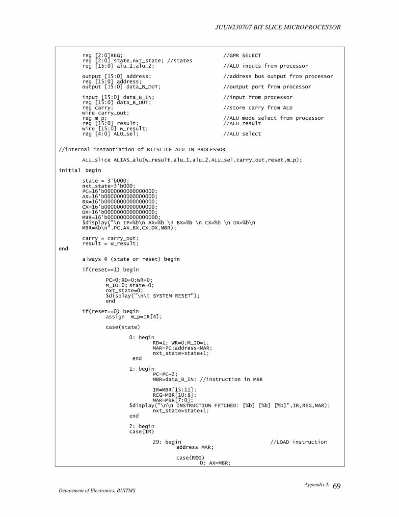
JUUN230707 BIT SLICE MICROPROCESSOR
Appendix A
Department of Electronics, BUITMS 69
reg [2:0]REG; //GPR SELECT reg [2:0] state,nxt_state; //states reg [15:0] alu_1,alu_2; //ALU inputs from processor output [15:0] address; //address bus output from processor reg [15:0] address; output [15:0] data_B_OUT; //output port from processor input [15:0] data_B_IN; //input from processor reg [15:0] data_B_OUT; reg carry; //store carry from ALU wire carry_out; reg m_p; //ALU mode select from processor reg [15:0] result; //ALU result wire [15:0] w_result; reg [4:0] ALU_sel; //ALU select //internal instantiation of BITSLICE ALU IN PROCESSOR ALU_slice ALIAS_alu(w_result,alu_1,alu_2,ALU_sel,carry_out,reset,m_p); initial begin state = 3'b000; nxt_state=3'b000; PC=16'b0000000000000000; AX=16'b0000000000000000; BX=16'b0000000000000000; CX=16'b0000000000000000; DX=16'b0000000000000000; MBR=16'b0000000000000000; $display("\n IP=%b\n AX=%b \n BX=%b \n CX=%b \n DX=%b\n MBR=%b\n",PC,AX,BX,CX,DX,MBR); carry = carry_out; result = w_result; end always @ (state or reset) begin if(reset==1) begin PC=0;RD=0;WR=0; M_IO=0; state=0; nxt_state=0; $display("\n\t SYSTEM RESET"); end if(reset==0) begin assign m_p=IR[4]; case(state) 0: begin RD=1; WR=0;M_IO=1; MAR=PC;address=MAR; nxt_state=state+1; end 1: begin PC=PC+2; MBR=data_B_IN; //instruction in MBR IR=MBR[15:11]; REG=MBR[10:8]; MAR=MBR[7:0]; $display("\n\n INSTRUCTION FETCHED: [%b] [%b] [%b]",IR,REG,MAR); nxt_state=state+1; end 2: begin case(IR) 29: begin //LOAD instruction address=MAR; case(REG) 0: AX=MBR;

JUUN230707 BIT SLICE MICROPROCESSOR
Appendix A
Department of Electronics, BUITMS 70
1: BX=MBR; 2: CX=MBR; 3: DX=MBR; endcase nxt_state = 5; end 30: begin //STORE instruction case(REG) 0: MBR=AX; 1: MBR=BX; 2: MBR=CX; 3: MBR=DX; endcase address=MAR; data_B_OUT=MBR; WR=1; RD=0; M_IO=1; nxt_state = 5; end 31: begin //OUT instruction case(REG) 0: MBR=AX; 1: MBR=BX; 2: MBR=CX; 3: MBR=DX; endcase M_IO=0;RD=0; WR=1; address=MAR; data_B_OUT=MBR; nxt_state = 5; end default: begin //All ALU operations address=MAR; ALU_sel=IR; M_IO=1; RD=1; WR=0; nxt_state=3; end endcase //IR end 3: begin //operand fetch MBR=data_B_IN; case(REG) 0: alu_1=AX; 1: alu_1=BX; 2: alu_1=CX; 3: alu_1=DX; endcase $display("\n\n ALU INPUTS 1: [%d] 2: [%d]",alu_1,alu_2); alu_2= MBR; nxt_state=4; end 4: begin case(REG) 0: AX=w_result; 1: BX=w_result; 2: CX=w_result; 3: DX=w_result; endcase $display("\n\nRESULT = [%d] carry=[%b] MODE=[%b]",w_result,carry_out,m_p); nxt_state=5; end 5: begin RD=0;WR=0; M_IO=0; MAR=0; address=0; MBR=0;

JUUN230707 BIT SLICE MICROPROCESSOR
Appendix A
Department of Electronics, BUITMS 71
nxt_state=0; end endcase // FSM for states end// reset end // for 1st always block always @(posedge clk_p) begin state=nxt_state; $display("\n\n State= %b",state); end endmodule
A.5) TEST BENCH Instantiation Module
////BALOCHISTAN UNIVERSITY OF INFORMATION TECHNOLOGY AND MANAGEMENT SCIENCES////
//////////========TAKATOO CAMPUS QUETT============///////// //==========DEPARTMENT OF ELECTRONICS=============//
///======[23/07JUUN07 BIT-SLICE Microprocessor]=======///
/* TECHNIQUE:BIT-SLICING Module: TEST BENCH GROUP MEMBERS: 1. MOHA1. MOHA1. MOHA1. MOHAMMAD JEHANZEB SHAHID==MMAD JEHANZEB SHAHID==MMAD JEHANZEB SHAHID==MMAD JEHANZEB SHAHID===>LEADER=>LEADER=>LEADER=>LEADER 2. UBAID AHSAN2. UBAID AHSAN2. UBAID AHSAN2. UBAID AHSAN 3. UMAIR ANWAR KHAN3. UMAIR ANWAR KHAN3. UMAIR ANWAR KHAN3. UMAIR ANWAR KHAN 4. NAEEM BAIG4. NAEEM BAIG4. NAEEM BAIG4. NAEEM BAIG //********************************************************************************// module M1_P_ALU_PROCESSOR; wire clk_1; //for clock wire [15:0] addr_p; wire [15:0] data_pr_out; wire Rd,Wr; wire [15:0] data_pr_in; //processor wire M_io; wire i_mio; reg RESET; //modules instantiation memory1 alias0(addr_p,data_pr_in,data_pr_out,Rd,Wr,M_io); Ports alias2(addr_p[7:0],data_pr_in,data_pr_out,Rd,Wr,i_mio); SYSTEM_CLOCK alias3(clk_1); PROCESSOR alias4(addr_p,data_pr_out,data_pr_in,M_io,clk_1,RESET,Rd,Wr); assign i_mio = ~M_io; initial begin RESET=1; #1 RESET=0; end endmodule

JUUN230707 BIT SLICE MICROPROCESSOR
Appendix B
Department of Electronics, BUITMS 72
Appendix B
Outputs
• Software simulation & Timing diagrams
• The Outputs of Modules
• Schematic Diagrams
• ISE Synthesis and Project Parameters

JUUN230707 BIT SLICE MICROPROCESSOR
Appendix B
Department of Electronics, BUITMS 73
B.1) ALU Simulation for 2-Inputs
The timing diagram of simulation of signals is shown in the following figure:
Figure B.1: ALU Simulation

JUUN230707 BIT SLICE MICROPROCESSOR
Appendix B
Department of Electronics, BUITMS 74
B.2) Address Generation, Inputs and Control Signals
Figure: B.2: Address Generation and Strobes

JUUN230707 BIT SLICE MICROPROCESSOR
Appendix B
Department of Electronics, BUITMS 75
B.3) FPGA Simulation using ISE 9.1i
The input wave form is given below:
Figure B.3: ISE Input Diagram

JUUN230707 BIT SLICE MICROPROCESSOR
Appendix B
Department of Electronics, BUITMS 76
The corresponding FPGA simulation is:
Figure B.4: ISE Simulation

JUUN230707 BIT SLICE MICROPROCESSOR
Appendix B
Department of Electronics, BUITMS 77
B.4) FPGA Architecture and Package Layout
Figure B.5: Architecture of FPGA
The blue circles indicate connections formed by PACE after completing the FPGA design. In
figure b.2, the blue marks show package pins.

JUUN230707 BIT SLICE MICROPROCESSOR
Appendix B
Department of Electronics, BUITMS 78
Figure B.6: Pin-Out of FPGA

JUUN230707 BIT SLICE MICROPROCESSOR
Appendix B
Department of Electronics, BUITMS 79
B.5) ALU Outputs
The VERI-WELL simulator produces the following output for only ALU Operations:
Dumping macros: __VERIWELL__ VeriLogger simulation log created at Wed Aug 29 19:53:48 2007 Beginning Compile Beginning Phase I Compiling source file: ALU.v Finished Phase I Entering Phase II... Finished Phase II Entering Phase III... Finished Phase III Highest level modules: sel_clock Compile Complete . Running... <F=0000000000000000> <C_O=0> <A= 2>-----<B= 5> <Mode=0> <C_I=0> <Select= 0> <F=0000000000000011> <C_O=0> <A= 2>-----<B= 5> <Mode=0> <C_I=0> <Select= 1> <F=0000000000000111> <C_O=0> <A= 2>-----<B= 5> <Mode=0> <C_I=0> <Select= 3> <F=0000000000000111> <C_O=0> <A= 2>-----<B= 5> <Mode=0> <C_I=0> <Select= 4> <F=0000000000000000> <C_O=0> <A= 2>-----<B= 5> <Mode=0> <C_I=0> <Select= 6> <F=0000000000000111> <C_O=0> <A= 2>-----<B= 5> <Mode=0> <C_I=0> <Select= 5> <F=0000000000000000> <C_O=0> <A= 2>-----<B= 5> <Mode=0> <C_I=0> <Select= 6> <F=1111111111111101> <C_O=1> <A= 2>-----<B= 5> <Mode=0> <C_I=0> <Select= 7> <F=0000000000000001> <C_O=0> <A= 2>-----<B= 5> <Mode=0> <C_I=0> <Select= 8> <F=0000000000000100> <C_O=0> <A= 2>-----<B= 5> <Mode=0> <C_I=0> <Select= 9> <F=0000000000000001> <C_O=0> <A= 2>-----<B= 5> <Mode=0> <C_I=0> <Select=10> <F=0000000000000010> <C_O=0> <A= 2>-----<B= 5> <Mode=0> <C_I=0> <Select=11> <F=0000000000001010> <C_O=0> <A= 2>-----<B= 5> <Mode=0> <C_I=0> <Select=12> <F=0000000000000011> <C_O=0> <A= 2>-----<B= 5> <Mode=0> <C_I=0> <Select=13> <F=0000000000000011> <C_O=0> <A= 2>-----<B= 5> <Mode=0> <C_I=0> <Select=14> <F=0000000000001110> <C_O=0> <A= 2>-----<B= 5> <Mode=0> <C_I=0> <Select=15> <F=1111000000001110> <C_O=0> <A= 2>-----<B= 5> <Mode=1> <C_I=1> <Select=16> <F=1111111100001110> <C_O=0> <A= 2>-----<B= 5> <Mode=1> <C_I=1> <Select=17> <F=1111111111111110> <C_O=0> <A= 2>-----<B= 5> <Mode=1> <C_I=1> <Select=18>

JUUN230707 BIT SLICE MICROPROCESSOR
Appendix B
Department of Electronics, BUITMS 80
<F=1110111011101100> <C_O=1> <A= 2>-----<B= 5> <Mode=1> <C_I=1> <Select=19> <F=1111111111111110> <C_O=1> <A= 2>-----<B= 5> <Mode=1> <C_I=1> <Select=20> <F=1111111111111100> <C_O=1> <A= 2>-----<B= 5> <Mode=1> <C_I=1> <Select=21> <F=1111111111111100> <C_O=1> <A= 2>-----<B= 5> <Mode=1> <C_I=1> <Select=22> <F=1111111111111100> <C_O=1> <A= 2>-----<B= 5> <Mode=1> <C_I=1> <Select=23> <F=0000000000000111> <C_O=0> <A= 2>-----<B= 5> <Mode=1> <C_I=1> <Select=24> <F=1111000000000111> <C_O=0> <A= 2>-----<B= 5> <Mode=1> <C_I=1> <Select=25> <F=0000000000000111> <C_O=0> <A= 2>-----<B= 5> <Mode=1> <C_I=1> <Select=26> <F=1111000000000111> <C_O=0> <A= 2>-----<B= 5> <Mode=1> <C_I=1> <Select=27> 0 Errors, 0 Warnings Compile time = 0.00000, Load time = 0.00000, Execution time = 0.01500 Normal exit
B.6) JUUN230707 Processor Output
Dumping macros: __VERIWELL__ VeriLogger simulation log created at Wed Aug 29 20:09:56 2007 Beginning Compile Beginning Phase I Compiling source file: demo_pr.v Finished Phase I Entering Phase II... Finished Phase II Entering Phase III... Finished Phase III Highest level modules: M1_P_ALU_PROCESSOR Compile Complete . Running... IP=00000000 AX=0000000000000000 BX=0000000000000000 CX=0000000000000000 DX=0000000000000000 MBR=0000000000000000 State= 000 SYSTEM RESET Memory1 DISABLED READ: Address = <0000> Data OUt =<00000000 00000000> READ: Input port = xxxxxxxxxxxxxxxx IO PORT DISABLED State= 001 INSTRUCTION FETCHED: [00000] [000] [0000000000000000] State= 010 State= 011 ALU INPUTS 1: [ 0] 2: [ x] State= 100 RESULT = [ 0] carry=[0] MODE=[0] State= 101 Memory1 DISABLED IO PORT DISABLED State= 000 READ: Address = <0002> Data OUt =<00001001 00000010> READ: Input port = xxxxxxxxxxxxxxxx IO PORT DISABLED State= 001 INSTRUCTION FETCHED: [00001] [001] [0000000000000010] State= 010 State= 011 ALU INPUTS 1: [ 0] 2: [ 0] State= 100 RESULT = [ 0] carry=[0] MODE=[0]

JUUN230707 BIT SLICE MICROPROCESSOR
Appendix B
Department of Electronics, BUITMS 81
State= 101 Memory1 DISABLED IO PORT DISABLED State= 000 READ: Address = <0004> Data OUt =<00010010 00000100> READ: Input port = xxxxxxxxxxxxxxxx IO PORT DISABLED State= 001 INSTRUCTION FETCHED: [00010] [010] [0000000000000100] State= 010 State= 011 ALU INPUTS 1: [ 0] 2: [ 2306] State= 100 RESULT = [ 1806] carry=[1] MODE=[0] State= 101 Memory1 DISABLED IO PORT DISABLED State= 000 READ: Address = <0006> Data OUt =<00011011 00000110> READ: Input port = xxxxxxxxxxxxxxxx IO PORT DISABLED State= 001 INSTRUCTION FETCHED: [00011] [011] [0000000000000110] State= 010 State= 011 ALU INPUTS 1: [ 0] 2: [ 4612] State= 100 RESULT = [ 4612] carry=[0] MODE=[0] State= 101 Memory1 DISABLED IO PORT DISABLED State= 000 READ: Address = <0008> Data OUt =<00100000 00001000> READ: Input port = xxxxxxxxxxxxxxxx IO PORT DISABLED State= 001 INSTRUCTION FETCHED: [00100] [000] [0000000000001000] State= 010 State= 011 ALU INPUTS 1: [ 0] 2: [ 6918] State= 100 RESULT = [ 6918] carry=[0] MODE=[0] State= 101 Memory1 DISABLED IO PORT DISABLED State= 000 READ: Address = <000a> Data OUt =<00101001 00001010> READ: Input port = xxxxxxxxxxxxxxxx IO PORT DISABLED State= 001 INSTRUCTION FETCHED: [00101] [001] [0000000000001010] State= 010 State= 011 ALU INPUTS 1: [ 0] 2: [ 8200] State= 100 RESULT = [ 8200] carry=[0] MODE=[0] State= 101 Memory1 DISABLED IO PORT DISABLED State= 000 READ: Address = <000c> Data OUt =<00110010 00001100> READ: Input port = xxxxxxxxxxxxxxxx IO PORT DISABLED State= 001 INSTRUCTION FETCHED: [00110] [010] [0000000000001100] State= 010 State= 011 ALU INPUTS 1: [ 1806] 2: [10506] State= 100 RESULT = [ 0] carry=[0] MODE=[0] State= 101 Memory1 DISABLED IO PORT DISABLED State= 000 READ: Address = <000e> Data OUt =<00111011 00001110> READ: Input port = xxxxxxxxxxxxxxxx IO PORT DISABLED State= 001 INSTRUCTION FETCHED: [00111] [011] [0000000000001110] State= 010

JUUN230707 BIT SLICE MICROPROCESSOR
Appendix B
Department of Electronics, BUITMS 82
State= 011 ALU INPUTS 1: [ 4612] 2: [12812] State= 100 RESULT = [65011] carry=[1] MODE=[0] State= 101 Memory1 DISABLED IO PORT DISABLED State= 000 READ: Address = <0010> Data OUt =<01000000 00010010> READ: Input port = xxxxxxxxxxxxxxxx IO PORT DISABLED State= 001 INSTRUCTION FETCHED: [01000] [000] [0000000000010010] State= 010 READ: Address = <0012> Data OUt =<01001001 00010100> State= 011 ALU INPUTS 1: [ 6918] 2: [15118] State= 100 RESULT = [55029] carry=[1] MODE=[0] State= 101 Memory1 DISABLED IO PORT DISABLED State= 000 READ: Address = <0012> Data OUt =<01001001 00010100> READ: Input port = xxxxxxxxxxxxxxxx IO PORT DISABLED State= 001 INSTRUCTION FETCHED: [01001] [001] [0000000000010100] State= 010 READ: Address = <0014> Data OUt =<01010010 00010110> State= 011 ALU INPUTS 1: [ 8200] 2: [18708] State= 100 RESULT = [ 9740] carry=[0] MODE=[0] State= 101 Memory1 DISABLED IO PORT DISABLED State= 000 READ: Address = <0014> Data OUt =<01010010 00010110> READ: Input port = xxxxxxxxxxxxxxxx IO PORT DISABLED State= 001 INSTRUCTION FETCHED: [01010] [010] [0000000000010110] State= 010 READ: Address = <0016> Data OUt =<01011011 00011000> State= 011 ALU INPUTS 1: [ 0] 2: [21014] State= 100 RESULT = [ 4100] carry=[0] MODE=[0] State= 101 Memory1 DISABLED IO PORT DISABLED State= 000 READ: Address = <0016> Data OUt =<01011011 00011000> READ: Input port = xxxxxxxxxxxxxxxx IO PORT DISABLED State= 001 INSTRUCTION FETCHED: [01011] [011] [0000000000011000] State= 010 READ: Address = <0018> Data OUt =<01100000 00011010> State= 011 ALU INPUTS 1: [65011] 2: [23320] State= 100 RESULT = [ 9476] carry=[0] MODE=[0] State= 101 Memory1 DISABLED IO PORT DISABLED State= 000 READ: Address = <0018> Data OUt =<01100000 00011010> READ: Input port = xxxxxxxxxxxxxxxx IO PORT DISABLED State= 001 INSTRUCTION FETCHED: [01100] [000] [0000000000011010] State= 010 READ: Address = <001a> Data OUt =<01101001 00011100> State= 011 ALU INPUTS 1: [55029] 2: [24602] State= 100 RESULT = [49188] carry=[1] MODE=[0] State= 101

JUUN230707 BIT SLICE MICROPROCESSOR
Appendix B
Department of Electronics, BUITMS 83
Memory1 DISABLED IO PORT DISABLED State= 000 READ: Address = <001a> Data OUt =<01101001 00011100> READ: Input port = xxxxxxxxxxxxxxxx IO PORT DISABLED State= 001 INSTRUCTION FETCHED: [01101] [001] [0000000000011100] State= 010 READ: Address = <001c> Data OUt =<01110010 00011110> State= 011 ALU INPUTS 1: [ 9740] 2: [26908] State= 100 RESULT = [13590] carry=[0] MODE=[0] State= 101 Memory1 DISABLED IO PORT DISABLED State= 000 READ: Address = <001c> Data OUt =<01110010 00011110> READ: Input port = xxxxxxxxxxxxxxxx IO PORT DISABLED State= 001 INSTRUCTION FETCHED: [01110] [010] [0000000000011110] State= 010 READ: Address = <001e> Data OUt =<01111011 00100000> State= 011 ALU INPUTS 1: [ 4100] 2: [29214] State= 100 RESULT = [17421] carry=[0] MODE=[0] State= 101 Memory1 DISABLED IO PORT DISABLED State= 000 READ: Address = <001e> Data OUt =<01111011 00100000> READ: Input port = xxxxxxxxxxxxxxxx IO PORT DISABLED State= 001 INSTRUCTION FETCHED: [01111] [011] [0000000000100000] State= 010 READ: Address = <0020> Data OUt =<10000000 00101101> State= 011 ALU INPUTS 1: [ 9476] 2: [31520] State= 100 RESULT = [ 1608] carry=[0] MODE=[0] State= 101 Memory1 DISABLED IO PORT DISABLED State= 000 READ: Address = <0020> Data OUt =<10000000 00101101> READ: Input port = xxxxxxxxxxxxxxxx IO PORT DISABLED State= 001 INSTRUCTION FETCHED: [10000] [000] [0000000000101101] State= 010 READ: Address = <002d> Data OUt =<00111001 10111011> State= 011 ALU INPUTS 1: [49188] 2: [32813] State= 100 RESULT = [ 5363] carry=[0] MODE=[1] State= 101 Memory1 DISABLED IO PORT DISABLED State= 000 READ: Address = <0022> Data OUt =<00101111 00000000> READ: Input port = xxxxxxxxxxxxxxxx IO PORT DISABLED State= 001 INSTRUCTION FETCHED: [00101] [111] [0000000000000000] State= 010 READ: Address = <0000> Data OUt =<00000000 00000000> State= 011 ALU INPUTS 1: [49188] 2: [14779] State= 100 RESULT = [63935] carry=[0] MODE=[0] State= 101 Memory1 DISABLED IO PORT DISABLED State= 000 READ: Address = <0024> Data OUt =<10010010 00110001> READ: Input port = xxxxxxxxxxxxxxxx

JUUN230707 BIT SLICE MICROPROCESSOR
Appendix B
Department of Electronics, BUITMS 84
IO PORT DISABLED State= 001 INSTRUCTION FETCHED: [10010] [010] [0000000000110001] State= 010 READ: Address = <0031> Data OUt =<00111101 11001001> State= 011 ALU INPUTS 1: [17421] 2: [ 0] State= 100 RESULT = [48915] carry=[0] MODE=[1] State= 101 Memory1 DISABLED IO PORT DISABLED State= 000 READ: Address = <0026> Data OUt =<10011011 00110011> READ: Input port = xxxxxxxxxxxxxxxx IO PORT DISABLED State= 001 INSTRUCTION FETCHED: [10011] [011] [0000000000110011] State= 010 READ: Address = <0033> Data OUt =<00111111 11010010> State= 011 ALU INPUTS 1: [ 1608] 2: [15817] State= 100 RESULT = [43745] carry=[1] MODE=[1] State= 101 Memory1 DISABLED IO PORT DISABLED State= 000 READ: Address = <0028> Data OUt =<10100000 00110101> READ: Input port = xxxxxxxxxxxxxxxx IO PORT DISABLED State= 001 INSTRUCTION FETCHED: [10100] [000] [0000000000110101] State= 010 READ: Address = <0035> Data OUt =<01000001 11011011> State= 011 ALU INPUTS 1: [ 5363] 2: [16338] State= 100 RESULT = [50797] carry=[0] MODE=[1] State= 101 Memory1 DISABLED IO PORT DISABLED State= 000 READ: Address = <002a> Data OUt =<10101001 00110111> READ: Input port = xxxxxxxxxxxxxxxx IO PORT DISABLED State= 001 INSTRUCTION FETCHED: [10101] [001] [0000000000110111] State= 010 READ: Address = <0037> Data OUt =<01000011 00000000> State= 011 ALU INPUTS 1: [13590] 2: [16859] State= 100 RESULT = [49879] carry=[1] MODE=[1] State= 101 Memory1 DISABLED IO PORT DISABLED State= 000 READ: Address = <002c> Data OUt =<10110010 00111001> READ: Input port = xxxxxxxxxxxxxxxx IO PORT DISABLED State= 001 INSTRUCTION FETCHED: [10110] [010] [0000000000111001] State= 010 READ: Address = <0039> Data OUt =<00000000 00000000> State= 011 ALU INPUTS 1: [48915] 2: [17152] State= 100 RESULT = [57605] carry=[0] MODE=[1] State= 101 Memory1 DISABLED IO PORT DISABLED State= 000 READ: Address = <002e> Data OUt =<10111011 01111011> READ: Input port = xxxxxxxxxxxxxxxx IO PORT DISABLED State= 001 INSTRUCTION FETCHED: [10111] [011] [0000000001111011] State= 010 READ: Address = <007b> Data OUt =<00000000 00000000>

JUUN230707 BIT SLICE MICROPROCESSOR
Appendix B
Department of Electronics, BUITMS 85
State= 011 ALU INPUTS 1: [43745] 2: [ 0] State= 100 RESULT = [44546] carry=[0] MODE=[1] State= 101 Memory1 DISABLED IO PORT DISABLED State= 000 READ: Address = <0030> Data OUt =<11000000 00111101> READ: Input port = xxxxxxxxxxxxxxxx IO PORT DISABLED State= 001 INSTRUCTION FETCHED: [11000] [000] [0000000000111101] State= 010 READ: Address = <003d> Data OUt =<00000000 00000000> State= 011 ALU INPUTS 1: [50797] 2: [ 0] State= 100 RESULT = [43745] carry=[0] MODE=[1] State= 101 Memory1 DISABLED IO PORT DISABLED State= 000 READ: Address = <0032> Data OUt =<11001001 00111111> READ: Input port = xxxxxxxxxxxxxxxx IO PORT DISABLED State= 001 INSTRUCTION FETCHED: [11001] [001] [0000000000111111] State= 010 READ: Address = <003f> Data OUt =<00000000 00000000> State= 011 ALU INPUTS 1: [49879] 2: [ 0] State= 100 RESULT = [65535] carry=[1] MODE=[1] State= 101 Memory1 DISABLED IO PORT DISABLED State= 000 READ: Address = <0034> Data OUt =<11010010 01000001> READ: Input port = xxxxxxxxxxxxxxxx IO PORT DISABLED State= 001 INSTRUCTION FETCHED: [11010] [010] [0000000001000001] State= 010 READ: Address = <0041> Data OUt =<00000000 00000000> State= 011 ALU INPUTS 1: [57605] 2: [ 0] State= 100 RESULT = [49879] carry=[0] MODE=[1] State= 101 Memory1 DISABLED IO PORT DISABLED State= 000 READ: Address = <0036> Data OUt =<11011011 01000011> READ: Input port = xxxxxxxxxxxxxxxx IO PORT DISABLED State= 001 INSTRUCTION FETCHED: [11011] [011] [0000000001000011] State= 010 READ: Address = <0043> Data OUt =<00000000 00000000> State= 011 ALU INPUTS 1: [44546] 2: [ 0] State= 100 RESULT = [ 7930] carry=[1] MODE=[1] Exiting VeriLogger at simulation time 334000 0 Errors, 0 Warnings Compile time = 0.00000, Load time = 0.00000, Execution time = 0.07800 Normal exit

JUUN230707 BIT SLICE MICROPROCESSOR
Appendix B
Department of Electronics, BUITMS 86
B.7) Schematic Diagrams
Figure B.6: Processor Block
Figure B.7: Memory Latch
Figure B.8: Memory

JUUN230707 BIT SLICE MICROPROCESSOR
Appendix B
Department of Electronics, BUITMS 87
B.8) ALU Slices
Figure B.9: ALU Slices

JUUN230707 BIT SLICE MICROPROCESSOR
Appendix B
Department of Electronics, BUITMS 88
B.9) ISE Synthesis and Project Parameters
=========================================================================
* HDL Compilation *
=========================================================================
Compiling verilog file "PROESSOR.v" in library work
Module <MEMORY> compiled
Module <Ports> compiled
Module <SIM_ALU> compiled
Module <ALU_slice> compiled
Module <Project_processor> compiled
Module <PRO_CALL> compiled
No errors in compilation
Analysis of file <"PRO_CALL.prj"> succeeded.
HDL Synthesis Report
Macro Statistics
# Adders/Subtractors : 29
4-bit adder carry out : 12
5-bit adder : 4
5-bit addsub : 4
5-bit subtractor : 8
8-bit adder : 1
# Registers : 24
1-bit register : 20
5-bit register : 4
# Latches : 213
1-bit latch : 16
16-bit latch : 1
5-bit latch : 1
8-bit latch : 195
# Multiplexers : 2
8-bit 255-to-1 multiplexer : 1
8-bit 256-to-1 multiplexer : 1
# Tristates : 1
16-bit tristate buffer : 1
# Xors : 4
4-bit xor2 : 4
=========================================================================
Advanced HDL Synthesis Report
Macro Statistics
# Adders/Subtractors : 28
4-bit adder carry out : 12

JUUN230707 BIT SLICE MICROPROCESSOR
Appendix B
Department of Electronics, BUITMS 89
5-bit adder : 4
5-bit addsub : 4
5-bit subtractor : 8
# Registers : 40
Flip-Flops : 40
# Latches : 213
1-bit latch : 16
16-bit latch : 1
5-bit latch : 1
8-bit latch : 195
# Multiplexers : 2
8-bit 255-to-1 multiplexer : 1
8-bit 256-to-1 multiplexer : 1
# Xors : 4
4-bit xor2 : 4
=========================================================================
* Final Report *
=========================================================================
Final Results
RTL Top Level Output File Name : PRO_CALL.ngr
Top Level Output File Name : PRO_CALL
Output Format : NGC
Optimization Goal : Speed
Keep Hierarchy : NO
Design Statistics
# IOs : 34
Cell Usage :
# BELS : 25
# GND : 1
# LUT2 : 24
# IO Buffers : 33
# IBUF : 1
# OBUF : 32
=========================================================================
Device utilization summary:
---------------------------
Selected Device : 3s200ft256-4
Number of Slices: 14 out of 1920 0%
Number of 4 input LUTs: 24 out of 3840 0%
Number of IOs: 34
Number of bonded IOBs: 33 out of 173 19%
---------------------------
TIMING REPORT
NOTE: THESE TIMING NUMBERS ARE ONLY A SYNTHESIS ESTIMATE.
FOR ACCURATE TIMING INFORMATION PLEASE REFER TO THE TRACE REPORT
GENERATED AFTER PLACE-and-ROUTE.

JUUN230707 BIT SLICE MICROPROCESSOR
Appendix B
Department of Electronics, BUITMS 90
Clock Information:
------------------
No clock signals found in this design
Asynchronous Control Signals Information:
----------------------------------------
No asynchronous control signals found in this design
Timing Summary:
---------------
Speed Grade: -4
Minimum period: No path found
Minimum input arrival time before clock: No path found
Maximum output required time after clock: No path found
Maximum combinational path delay: 10.029ns
Timing Detail:
--------------
All values displayed in nanoseconds (ns)
=========================================================================
Timing constraint: Default path analysis
Total number of paths / destination ports: 24 / 24
-------------------------------------------------------------------------
Delay: 10.029ns (Levels of Logic = 3)
Source: reset (PAD)
Destination: f_data_out<15> (PAD)
Data Path: reset to f_data_out<15>
Gate Net
Cell:in->out fanout Delay Delay Logical Name (Net Name)
---------------------------------------- ------------
IBUF:I->O 24 0.821 2.136 reset_IBUF (reset_IBUF)
LUT2:I0->O 2 0.551 0.877 AA/data_B_OUT<9>1 (f_data_out_9_OBUF)
OBUF:I->O 5.644 f_data_out_9_OBUF (f_data_out<9>)
----------------------------------------
Total 10.029ns (7.016ns logic, 3.013ns route)
(70.0% logic, 30.0% route)
B.10) Place and Route Report
NGDBUILD Design Results Summary: Number of errors: 0 Number of warnings: 0 Total memory usage is 63980 kilobytes Writing NGD file "PRO_CALL.ngd" ... Writing NGDBUILD log file "PRO_CALL.bld"...

JUUN 230707 BITSLICE MICROPROCESSOR
Appendix C
Department of Electronics, BUITMS 91
Appendix C
Spartan 3 FPGA
• Device parameters
• Board diagrams

JUUN 230707 BITSLICE MICROPROCESSOR
Appendix C
Department of Electronics, BUITMS 92
C.1) Spartan 3 FPGA
The device name is:
• XC3S200-4FT256
• The device parameters using ISE 9.1i are:
Figure C.1: Device parameters for Project
The Spartan 3 characteristics are:
• 200,000 FPGA in a 256-ball thin Ball Grid Array package (XC3S200FT256)
• 4,320 logic cell equivalents
• Twelve 18K-bit block RAMs (216K bits)
• Twelve 18x18 hardware multipliers
• Four Digital Clock Managers (DCMs)
• Up to 173 user-defined I/O signals

JUUN 230707 BITSLICE MICROPROCESSOR
Appendix C
Department of Electronics, BUITMS 93
C.2) Board Diagram
Figure C.2: FPGA Board (Top view)
(Courtesy Xilinx Inc)
Figure C.3: FPGA Board (Bottom View)
(Courtesy Xilinx Inc)

JUUN 230707 BITSLICE MICROPROCESSOR
Appendix C
Department of Electronics, BUITMS 94
C.3) Display Control
Figure C.4: LED Display Control
(Courtesy Xilinx Inc)


![mandlfi "~ BS]BANKBRI - Repository - Polman Bandung](https://static.fdokumen.com/doc/165x107/63273eb8cedd78c2b50d7a9a/mandlfi-bsbankbri-repository-polman-bandung.jpg)