Quasi-configurations: building blocks for point-line configurations
Upload
khangminh22Category
view
0download
0
Feedback amplifier configurations
E.M.Cherry
Alistract: Systciiiatic rc1;ations exist l ~ c t w c c ~ ~ tl ic foni- basic single-loop li.cdbacli amplilicr conligtirations (voltag~-gain, current-gain, tl';iiisl'cr-adiiiitt;incc and traiiafcr-impcd~iiice) and certain iicwcr conligtirations lor wliicli hantlwidtli is inclclmidciit of gain. Loop gain pi-oviclcs tlic linli. I'or i i
givcii amplilicr witliotit l'ccdback and spcciliccl tlcmanclctl g i i i i 3 loop gain and liciicc banclwidtli ciiii be iiiitxiiiiisccl by optimnm clioicc ol' the I'ccclhack resistors. I;or losistors liir rcmovctl li.om this optimum, loop gain c~iii ici i i i i i i i constant as tlcmantlcd gain is vwicd. Clc:ai~ly tlclincd coiiditioiis exist wlicrc adding 21 unity-gain coiiiiiioii-collector or common-hasc stage at the input will increase the loop gain. Shilling the ground point. S ~ L I I W or l o i i c l gciicratcs xldit ional lccdb;icli amplilicr conligiifii(ions.
1 Introduction
' l ' l ic 'traditional' approach to I'ccdbacli amplifier design is t1i;at the aiiiplilicr witliotit i'ccdhack sliotiltl he I I [air approxiniation to (lie typc that is tlclinccl by the fccdlxicli connection. I+" cxainplc, il' 21 voltag,c-g;iin fcct lbd< aiiipli- ficr is rcquirctl, tlicii the amplilicr witlioiit fccdback should itscll' he a voltage aiiiplilicr with largc inpiit re. smal l output resistance: such i i i i amplifier is cliaractcrisctl principally hy its voltage amplilication liictor.
Ilcccntly tlicrc have hccn reports o f [ccdlxiclc aiiiplilicrs which arc not dcsigiicd i n ~iccordaiicc with this approach. 'l ' l ic so-caIIcd ctirrciit fecdbacli amplifier i s one instance [I 51, a traiisfcr-coiidtictancc forward p i th with v i h y Iicccl- haclc is another 161, and tlicrc iirc viariotis tl.ansfcr-iiiipcc1- iiiicc conligurations 17 IO]. 'l'lic pt~rposc 0 1 this papcr is to present ii systematic npproacli to all possible fcctlhack amplificr conligiiations [I I].
2 Feedback basics
I'orwerd-path gain G and l'ccdh;ick 1Bctor / I arc dclincd in Fig. 1 for ii hlock-tli;igraiii fccdbacli system. Loop gnin GI/ and ovcr;ill gain /I arc rc1;atctl to tlicsc by
and the t1cm;andcd gain i s
I'or real I'cetlhack amplifiers wlicrc hotli voltagc and cair- rent i i i t ist be coiisidcrcd. thcrc iirc l'otir basic wiys (sliown i n Ijig. 2) in which fccdhaclc can hc ;applied via ii resistive network: all arrangements \vlicrc this network sciiscs cihcr
otitptit voltage or output current, comhincd with all arr:angcmcnts wlicrc the fccdb;aclc subtracts from either input vollagc or input current. In each ciisc the tlciiiantlcd gain, li.om Ilic TliCvcnin or NorLon cqtiivalciil gciicrator within the sotircc to tlic liiial output into tlic load, is t l ic iiivcrsc of tlic idcal fccdback liictor. Ovcrall gain is then givcn iii terms ol'tlcmaiidctl gain and loop gain by cqiis. I and 2. with appropriate suhstittitions. If the loop gain i s largc, ovcrnll gain ;ippro;aclics tlic dcmanclcd gain: il bccomcs indcpciitlcnt of parameters ol' the ainplilicr w i h out l'ccdlxick, and indcpcndcnt ol' the sotircc and load resistances
I I feedback factor
H (si feedhac k
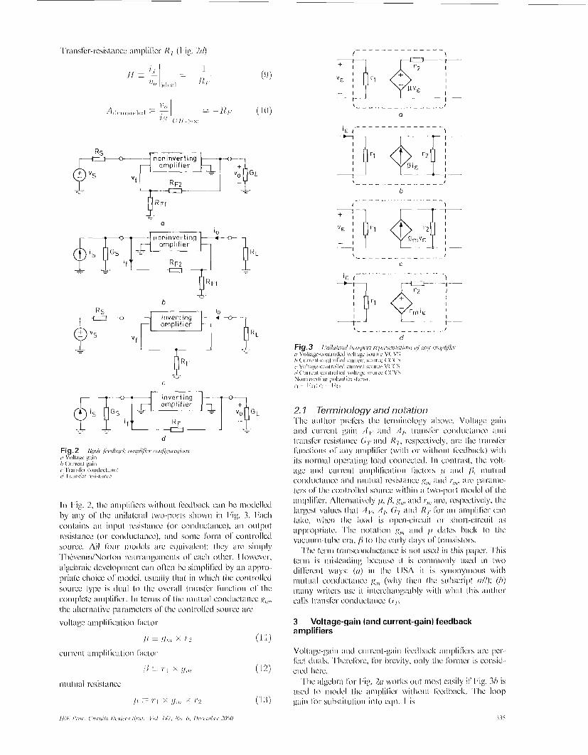
Traiisl'cr-resistance aiiiplilicr R , (Iiig, Ltl)
In I;ig. I, the ;iinplilicrs wilhotit fcceihaclc cm Iic i i iodcllcd by any 01' the tinilatcnil two-ports showii iii Fig. 3. I:acIi contains iiii input resistance (or concluctaiicc). iiii output rcsistancc (or coiitluct;incc), iiiicl soi i ic l i)rm 01' coiitrollcd SOLII-C~~ All li)iir i i i d c l s arc cqtiivalcnl: llicy iirc simply 'fliCvcninlNorloii rcarrangciiicnIs 01' c x h otlicr. I~lowcvcr, algchraic tlcvclopmcnt can olicii he siniplilicil b y xi appro- priate choice of iioclcl, iisLiiilly that iii which tlic con~rollctl so~ircc type i s dual to Llic overall traiisl'cr liinction 01' the complctc aiiiplilicr. In tcri i is ol' the niritual conductancc ,y,,,. the alternative par>iiiictcrs 01' tlic controlled soiircc arc
voltage ;iiiiplilication liictor
/ " ! I r , , x /'2 (1 1)
,i ' 7 ' 1 x !I,,! ( 1 % )
( 13)
cui-rent ampliiication l i i ch r
iiiulual resistance
I / = 7 . 1 x q,,, x 7'2
4
3 Voltage-gain (and current-gain) feedback amplifiers
Voltage-gain iiiid cui-relit-gain I'ccdhack amplilicrs iirc pcr- fcct cluals. '~ l icrc lorc, lor brevity, only tlic former is coiisicl- CI.CCI IlCIL'.
'I'lic algclm for I.'ig. 20 works out most c;isily il ' I'ig. B h i s used to modcl tlic aiiiplilicr without Ikcclhaclc. 'I'lic loop gain I'or siihstitution into cqn. I is
ni

( I T i l )

ievei shi f t
(j- -
- compensating
capac i to r

coiiiiiion-ciiiittct. transistor). the current-l'cctlhaclc amplilicr rcduccs to Fig. 6. A gciicratioii ago this circuit wiis callccl i i
voltage-feeclhack pair. It tlil'lcrs Il.oiii Fig, 2ri only iii that the current Ilowing into the Iclt-hand side 01' i l i c fccdback network is the input ctirrcnt mttltiplictl by the g i in 01' thc lirsl iwisistor, iis distinct li.oiii the i tiptit ctirrciit itscll'. l'hc fcctlhack conncction is voltage-sensing at the OLI~~L I I and vol~agc-subtl.acting iit the input, the circuit is an ordinary voltage-gain fccdhaclt amplifier. The term 'ctirrcnt-fcctl- I)iicI( iiiiiplilicr' scciiis ii coiiiplctc iiiisiioiiicr.
dcma iiclccl gai ii
1." ii voltage-l'cctlhack pair:
- in c+
e x t r o p in ex terno l capaci tor #
signal ground tprobobly V - - 1
3.4 The 'transconductance- feedback' amplifier A current-lcctlbaclt opcr"tioii;il aiiiplificr i s tinsuit;ihlc lor soi i ic circtiit applications hccatisc t l ic input resistances at i ts noninverting (hasc) and inverting (cmiitcr) inptit tcrmiiialh clill'cr by a i l . ortlcr of iuagnitutlc. Wilson's so-c~iIIcd il.aiiscondtictancc-l'cctlhoclt amplilicr (shown in Fig. 8) ovcrcoiiics this disadvant;tgc. Again, tl ic terminology appears it iiiisiiotiicr: tlic first two st;tgcs in I&. 8 liiivc (lie coiivcntional voltage-lcccll~iclc conncction o l Fig. 2o.
- - - - - - :cur ren t -yo in vol taye
T a amplifier , f o l l o w e r
111 thcsc latier ciiscs the loop gain is indcpcnclcnl 01' tlcmandcd gain. Thcrc arc many piiriillcls with Section 3. I.
l l i c ctirrciit-l'cctlhack iiiiiplilicr corrcspoiids to cqti. 30h. Physically, i n hoth I:igs. 5 and 6 Lhc ovcuill loop gain rciiiiiiiis constant 11s X , , i s vai-icd. bcc;itisc applies local scrics fcctlback to tlic lint stage and dclincs i ts triinslcr conductancc i~ll/~~il iis approximakly (hinging /<,.I (while lioltling RI,? constaiit) clinngcs tlic tlcm~iiidcd gain, hut il itlso cliaiigcs the lirst-siagc gain (cind hcncc tlic lor- warcl-path gain) in approxiiiiatcly the smic ratio.
It s h o u l d he ctiipliiisiscd that loop gain ol'a currciit-fccd- lxiclc aiiiplilicr is less than i t co~ i ld hc lor the saiiic tlcniandcd gain a n c l tlic w i i c amplilicr without fccdhxk; ilic sensitivity is greater than it could he and tlic ovci.iil1 bantlwidth is less. It is ii matter of dchatc whctlicr th is price is worth piying for tlic coiivciiiciicc ol'conskint 1~;intiwidtli iis dcmantlctl gain is viiricd. Optiinutn ~cctlback resistors plus ii well clioscn conipcnsating capacitor would scciii prcfcfiihlc. A compciicaiing ;irrangcmcnt lilcc I-'ig. 7 13X
Fig. 8 corrcspoiids to I l ic situation tlcscribctl hy cqii. I Xu. .l'lic oplimtii i i fcctlback resistors iii cqtis. IO and I7 arc piislied right over to the large side hy setting hot11 GI, (which licrc corresponds to the input coiiduci:tncc 01' the
current-gain amplilicr) to ~ c r o . The lcctlhack resistors iirc t l ic o n l y loiid on the currcni-gain aiiiplilicr, s o forward- path voliagc gain is directly Importion:il to ihcsc resistors. I-lcncc loop gain remains conskint if dcmandctl gain is clinngctl hy varying RI2 at constant R, I _
* l 'hc sigii;il input volkigc to the circuit cannot cxcccd the voltage thai can be tlcvclopctl iicross R,.., hy the IiiiixiiiiLiiii aviiilohlc output current lrom tlic current-gain nmplilicr. liecall that is tlic siiiallcr I~cdhiick resistor, and is hcld constanl iis dciii;itidcd gain i s varied 'l'hcrcforc, the availa- hlc outpiit voltage is scvcrcly rcsirictccl wlici i thc dcm;indctl gain is s m d l .
voltagc Ibllowcl.) illld g 2 (LllC OLl ipLI t condLlcl~lncc 01' thc
l ' r w h l limitations of th is circuit includc:

* I3ccaiisc the second stage s l io t i l i l liiivc xcro output admit- lance, Miller coiiipciisiition s l i o d d not he i d . ' I ' l i i i s the bcnclits 01' pole-splitting arc lost.
* l'lic voltage followcr is outsiclc the iiiiiiii I'ccdhack loop, iiiid thcrcl'orc is not sul~jcct Lo tlic liciiclici il I c II' ccts 011 out- Iput resistance iiiid nonlinear distortion.
4 Transfer-resistance (and transfer-conductance) feedback amplifiers
'I'ransl'cr-resistance a n c l transfer-coiitltictancc I'cctllxick amplilicrs ;ire perfect duals. l'licrc arc i i l s o many siiiiilari- tics hctwccii their analyses iiiicl t l ia t Ibr t l ic voltage-gain fccdh;ick ainplilicr. Only the transli.r-rcsisl;iiicc ;iiiiplilicr (Fig. 3ii) i s coiisidcrccl i i r this Seclion, :rnd the treatment is hricl'.
'l'lic algebra for Fig. 2il works out iiio.;L casilp il' I;ig. 3 is tisctl to moclcl the aiiiplilicr witlioul Ikcdb;ick. The loop gain in cqn. I is
As in cqii. 14, the li)iirtIi [Imclcct] is tlic liccclb;iclc kictor / I , s o the lirst thrcc Ilxacltctsl Intist constittitc Lhc Ibrward- path gain G l 'hc l i r s l iiiicl third [ l m d t c t s l iiicliciitc lo;iciing cll'ccts at the input iiiid outpiit. the sccoiid [lmclcct] iii cqii. 3 lo inclutlcs l'orwxcl Icakagc 01' signal thi-ough the I'cctlbaclc iictwork. Eqn. 3 Ih (which ignores this kist cl'lcct) is iiii almost tinivcrsally v;ilid aliji'.oxiiii;ition.
L
4.7 Optimum feedback resistor t3ccaiisc there is only oiic l'cctlbaclc resistor in I-'ig. 211, tlicrc i s no li-ccdoiii lo vary loop gain while liolcliiig thc dcniandcd gain conskint. (As iiii aside. tlircc-resistor arrangciiicnts stich iis I'ig. 9 scrvc OIIIJJ l o rcdticc tlic loop gain hclow what c o ~ i l d liiivc hccn iicliicvcd with :I single I'ccdback resistor.) I-lowcvcr, thcrc is iiii optimiiiii valuc Ibr RI,. at which loop gain is maxiinisccl
( 3 2 ) I h'/,,(,,,>,,) = {r _ _ ~ ___
i(:s-I !JI)(C/, I (h)
For v;ilucs iiciir t h i s optiinriiii, loop gain (and liciicc sciisi- tivity and 1x1 iidwidth) I-cmiiin const;iiit ;is dcniiindctl gain i s varicd. At valucs lirr removed I'roiii the optiiiitim, loop gain l i i l l s ol'f either directly o r invcrscly \villi tlcnianilcil gain. Fig. 10 sliows the asymptotes.
Acliially. I'ig. IO is no( quite correct. I-;cln. 310 s l i ows that llicrc is ii ntill in loop gain (antl liciicc OVCI.IIII gain)
//.'/~ / ~ , , , ~ . - c ' , r < , ~ , l . ! /kr,<<'$ , $ , ' \ I , I id 147, vi,. 0. /)c<ci,,
* !J,,,l?/', ( 3 t; b) <; ,<<'I / I < , (;,,'<:I / I ; , , '
The situation in cqn. BSh, with 'si i i i i l l ' sotircc and load con- ductances, corrcspoiids to 'ideal' usngc 01' i~ translcr-resist- iiiicc iimplilici.. However, the criteria 01' siiiiilliicss coiiilxirctl with may he tinrealistic in practicc. Input aiid output conductanccs lllK

5 Poles and zeros
I:or simplicity. (lie notation i n Sections 1 4 is i i i Leixiis 01' rcsislivc circuits, althoiigh i.csisl;incc coii ld ohvioiisly he rcplaccd cvc~~ywlici~c hy impcdancc t o givc ;in o\~crvicw 01' the dynainic iuponsc. We iiow coiisitici. polcs and /cros explicitly.
5. I The gain-bandwidth theorem l ' l i c iiuthor's prclkrrctl ~t;itciiicnt (Seclion 13.6 01' 1131) 0 1 ' tlic g;iiii-h~iiidwiiltIi tlicorciii ill Ihc context 01' ii Iowpi~s fccclhaclc aiiiplilicr is
(42/1)
inaiiy witlctxuici aniplificrs. u id includes iiiany (hi11 not ;ill) li)riiis 01' induckiiicc higli-l'rcqticncy Ipwkiiig.
I:or 1"ig. I in tlic coniplcx-freqticncy domain

(,I!))
(51)

pensating cap;icitor, ancl the p l c 0 1 tlic inpil l stage. In the ovcr~ill closed-loop singttlarity pa(tcrn, the fortncr po le iiiovcs Lo >a position which is lirst-ortlcr clcpcntlent on loop gain. But loop gain remains co1isl;mt i t s tlcmandcd gain i s varied b y changing R, , at coiistwnl (cqti. 30h). 'I'Iicrc- forc this dominant closed-loop pole remains const;int i t s
tlcmanitlcti gain i s changccl. tlominatcs in the parallcl comhination R , = /<l,lll/<l,2.
Thcrcforc thc pole o l tlic first slagc iiiovcs a s tlctnantkxl gain is changctl. From cqn. 53, this pole is morc-a-lcss proportional to K,; ;incl tlicrcforc inversely proportional l o stage gain. However. Ilic pole is l'ar beyond the l'rcqticncy of Iinity ovci.al1 loop gain and, i n accord;ancc with Section 5.2, appears almost tiiitiiovcd in the ovcrall closctl-loop s i i i - gularity pattcrn. l'luis, iiltliough the dominant overall pole of' t i c t i r~~n t - l ccd l~ack amplifier rctiiiaiiis cons t " iis gain is varied. ii nonclomin~tnt pole is itivcrsc with gain. T l ~ c protl- nc l 01' iiiid-hand gain with ill1 the poles is approxiinalcly constant.
C:omplctc awilysis conlirms that the gaiti-bandwidth the- orem is qitantitatively corrcct. I,vitlciitly, all poles tiitiut Ix includcd in airy conclusion hascd on the gaiii-bantl\vitllli tlicorciii, not mcrcly the dominant ones.
Bccatisc tlic ovcrall closed-loop siiigiilarily pattern of a cui.rcnt-l~cdhack amplilicr contains a nondoininant pole, the bandwiilth m n s t (in nccordilncc with Section 5.2) hc less than it cotild liitvc hccn lor the w n c coinbination 01' tran- sistors and t l ic sx i ic overall mid-bmitl gain.
5.3.1 Slewing rate: Ctirrcn~-l'ccdhacli amplilicrs tend to liiivc high slewing rates. This is not l'roni amy iiilicicnt xlvatitagc i n tiic fccdbaclc coiiiicctioii, but l?om the ability of the class-Al3 input stage to cliargc the scconcl-stage coti i- pensating capacitor.
I ;or i i dil lcrcntial- i~i ir lirst-stagc with current mirror (1;igs. 8 iiiid 12). the output current i s hard l imited to k/,',jl.
I n contrast, tlicrc is no lirst-order limit to the o t ~ t p t ~ t current available I'rom the lirst stage in Fig. 5. so tlrc slewing rate ciaii hc large.
3'12
5.4 Maximising the bandwidth 111 Sections 3 and 4 i t is stated that, with qtt;tlilications, the ovenill closcd-loop handwitlth i s iiiaxitniscd by maximising the loop gain. What is actually maximiscd iii those Sections, hy optimtim choice 01' fccdhacli resistors, is tlic mitl-band loop gain.
1 ;or i t practicd lcccllxick amplilicr. tlic ovcrall cut-on' l'rc- qticticy is approximately the li.cqncncy at wliicII loop gain hlls through tinily antl, for given tlcmaridctl gain, th is 1i.c- qucncy i s 1;irgcly clctci.minccl hy tlic inid-hand gain of the forw;ircl 1xalIi ;iiid its ~ w o most cloiiiiiiaiit polcs (loop cut- ol'f rates greater than two-pole invite (ro~iblc). Rccall that noiidomin;int poles ol' (;(,Y) appciir more or lcws unc1i;lngcd in A(x). 'l'licrcl'orc, in lhc gnili-bantlwitltli IhcorctIi, Ihc product of thcsc polcs is iiiorc or less the ~a t i ic in both G(s) a n c l A(,S). l'hcrcforc, to ii good apl,roximation, maxiiiiising the overall ctit-ol'l' lrcqucncy implies m;iximising thc prod- net 01' (;,,,i,, with its domiiiant ~ m l c s . 'I'liat is. the tiiaxiiiiLtiii ovcraII cut-oH' lrcqticncy is achicvcd by maximising the high-licqttcncy asymptote 01' (;(,\) \vliilc consitlcring only its domin;int poles.
For single-loop fcctlh~iclc amplilicrs, G(,s) c:an he split into tlircc tcriiis. a s cxcmplilictl i n ccliis. 14 ant l 31: - l o d i n g at the input ol'thc amplilicr without I'ccdback (the lint tertii), * loading ;it the oittpttt 01' the ;itnplilicr witliout l'ccdhack ( the third term), * the gain of the rest olthc amplilicr without lbctlbacli (the second term, i n its approximate liirtii). 'l'hc Imt ol' thcsc is indcpcndcnt (11' the choice o f fcctlhack resistors. 'l'hcrcforc, ;iny Ixintlwitltli maximisalion is containctl within Lhc load- ttig tcrms.
I'IicrcTorc, il' hotli tlominnnt ~polcs o l G(,s) occttr i n the 'gain o l the res1 of the amplilicr'. there is sttrcly ii gain- bii ndw id tli atlvantiigc i II iiiiixiiii isi ng I Iic 111 id-1x1 nd loop gi in. I lowcvcr, tlic situation is iiiorc compliuitctl if dotni- nairt poles occtir in the Ionding tcrms.
I?g. 13 is iiti illustl.;ition. T l i c l'orwerd-path gain follows l'roiii cqn. 14h a s
r 1

wliich is iiiiixiiiiiscd hy choosing
wliicli i s tiiiixiiiiiscd hy clioosing
( G O )
stage Ic~ivcs the voltagc miiplilic;itioii liictor { I a i d iiititiial conductance si,, 01' the aiiiplilicl- without fccdhack csscii- tiiilly Liiichangctl, hut iiicrciiscs the current i i i i ipl i l iwt ioi i liictor /I iiiicl mut tiiil resistance I;!,. iiiicl iiicrciiscs tl ic inpiit
- l/<qI, A uiiity-cuI.rciit-~iiii ( :I3 st;igc lciivcs /I
'I'hc clii.cts 01' atltliiig ii stage a t llic input 01' ii voltage- giiiii o r tr~iii~l'cr-~i~liiiittiii~cc Icct lhxlc iiiiiplilicr x c basic;illy [lie w i r e , hcciitisc the fcctll-raclt connection ;it thc input is scrics ( o r vol~~igc-aiil-rtl.iicting) iii both GISCS. Similarly, tlic cllkcts 01' acltling 21 slagc to ;I current-grin or Lr;insl'cr- iiiipcdmcc l ~c t l hack amplilicr arc tlic siiiiic 1xc;uisc the I'ccdbaclt connect ioii i s sht i i i t (or cui-rent subtrxting). I'or I-rrcvity, we coiisicicr only tlic voltagc-g;tiii aiitl ti-aiisl'cr- iiiipcdiiiicc GISCS. 'l'~aiial'cr-im17ccl;lncc is t l ic siiiiplcr, aiid is trcatctl lirsl. A ntliiil-rcr 01' rclatcd two-stage grottps arc cat- ;ilog~icd iii Scctioii 14.4 ol' I 1.31,
6.7 Transfer-impedance (or current-gain) amplifier with added stage I:qti. 3 I / J givcs the loop gain 01' the general tl.aiisl'ci.-rcsist- iiiicc aiiiplilicr iii terms 01' Iorwal-&path i i i i i tua l coiiduct-
iirrangctl iii terms 01' the cui-rent
iiicc
Il'initl-band coiisiticra Lions ;ire p;iraiiiotint. tI1ci.c iirc simple I-rrit clcliiiitivc ;iiiswcrs to tlic qticstion 01' when iiii cxtra stage will i i icrcxc tlic loop gain.
(U) I3cc;itisc an atlclcd ( ' C ' stage ;it tlic input docs not change :;!,,, ir11 relevant inl'ori1i;itioii is in the lirst [ Ix ic l tct ] 01' cqii. 31. 11' ,yl 01' t l ic iiiiiplilicr without I'cctlback aiid without the ;icltlcil stage is s i i i a l l enough to he iicgligihlc in tlic ~iiil.iillcI comhiii;ition with GS iiiicl RI, , tlicrc is iio l-rciic- lit. l'lic lirst [lmcltctI ;ipproachcs i ts tipper hotitid 01' + I//</;) withotit tlic x l d c d stage.
( / J ) Uccausc ;in iitltlcil ( ' I 3 skigc at the inpint docs not change /I, all relevant inlhrmation is in tlic l i l -s l (hriickctI 01' cq i i . 62. I I ' fil 01' the aiiiplilicr witliout I'ccdhack ;ind witli- out thc ;icldcd stage is I q c ciiotigli Lo tloiiiinatc it1 the piir- i i l lcl comhinatioii with GS i i i i c l RP tlicrc is tic) bciiclit. ' l ' l ic lirst Ibracltct] a1ipro:icIics ita tip1)cr borintl 01' unity witliout tho iltlclctl stagc.
111 widchanil aiiiplilici-s t l ic situation is I'tindaiiiciitally the sillllc, hut thcrc arc so i11;iny 11101-c tlcgrccs 01' l'rcctlom that any iiitlivitlual ciisc is hest trcatctl on its iiici.its. As t i i i
cxuiiplc, wiclchand t~iiisl'cr-iiiipcclaiii moiily tiscd witli a capacitive sotircc such 11s i r photo diode and, at high ciiotigh I'rcqticiicics, this c;ilxicit;iiicc doiiii- nates the l i rst I lx ic l tct l iii tlic cxpicssioii h r loop gain. I lgs. 14 iitid 15 show partial circuits 11)r amplilici-s with iiiicl without ai1 iitlclcd CII stage. i i i i d t l ic Ipaitial cqtiiualcnt circuih relevant to calculating loop giiii

A likely scctiiirio is:
{I,,, >> I / /? / , , >> ! l j , ) / t l
c, >> 1 ' 1
In this ciisc:
( ( I ) iiiitl-hand loop grin for IGg. IS is tlic hrgcr hy i i i i order 01' iiiagnititdc
( / I ) the dominant pole i n the p a t M cxprcssions Ibr loop gain iirc 01' the siiiiic order of iii;igiiilutlc Ibr both circuils
((,) I lg . 15 l i i ih OIIC extra pole, ahotit iiii order ol'iiiagnittitic higher iti frequency than the tiotiiiti;int pole
r- rest of ompl i f ier
-& l-_d
r - c
par t i a l loop gain
111 combination, the larger iiiitl-Ixintl loop gain atid tlic extra pole suggest thal I:ig. I S would hc tl ic harder l o skthilisc. Tlicrc is t l ic liltcliliovil 01' soiiic polcs moving closc to Llic ,jco axis wlii lc others ~ i i o v c far oul to the lc l i 01' Llic
344
complcx I'rcqticncy plane. Iiowcvcr, the gcomckic tiiciiii oi' i t s I'orward-patli poles is greater tl ian Ibr 1 :ig. 14; l l icrcli~rc, in ;iccordancc with tlic g~iiii-banelwid~li thcorciii, (lie geometric incan ol' i ts overall poles i i i t ts t Ix iilso l ie the greater and, i l ' t l ic poles (all 0 1 ' them, no1 ~i icrcly Lhc domi- naiit ones) cilii bc designed into lii\~ourahlc positions, then i ts hanclwic l t l i is potcnhl ly the greater.
Fig. I6 shows I3oclc plots or tlic two parlial loop giiins, aiid gives ;I tlifli.rcnt pel-spcctivc on the siiiiic conclitsion. Loop gain for Fig. I S is greater at a l l I'rcclticiicics 1117 to ,qtJcl (that is, m, ol' Lhc Lrxisislors), I lowcvcr, the extra pliasc s h i l l associated with the sccotid 1poIc is liltcly to be iiii ciiihiirrxsstiiciit if the ovcr~11I closcil-loop handwidth nppr0;lcIlcs ,q))/(c',s -1 q).
6.2 Voltage-gain (or transfer-admittance) amplifier with added stage 111 volt;igc-gain ant i tr;iiisl'cr-~idiiiitt~iiicc fccdh;eIt amplili- crs, lhc sollrcc illld fccdhack voltagcs InLlst bc conncclcd to separate tcriii i i i i i ls of the input s~agc to acliicvc subtraction I lie iitimhcr ol' cii-cttit ~irl.angcmcnts with iiii ;~ddctl C(' or CH stag: is rcslrictcd. I:ig. 17 exhausts the possi l i i l i t ics hut. in Lhc I w s l Lwo, the adtlcd stage is ~irgtiahly outside the rccclhaclc 1001).
_ _
t
I
r - - -
rest of
R F I O R F 7
I Gg. 17n is tlic well known arrangciiicnt 01' a voltage-gain amplilicr with an cmittcr lbllowcr lo iiicrciisc its iiipiit resistance. Said tlillcrcntly, Llic iirrii ngciiicnl rcdticcs the sig-
sotircc resistance. 'I'lic tlcmanticcl gain IS given hy cqii. 4. and the lirsl [Ixicltctl iti c q n 14 for looli gain liccoiiics
llill currcnt tI1I.oLlgll (ancl llcllcc Lhc volt2!gc drop acro5s) lhc

----I----.
tnpi. ploy 11 [IC k
head
O v:, k 50U mi l
I
i.
4 h
uctuol ground 'I qround f o r 0
*
output
-0

Copyright © 2022 FDOKUMEN