FAST NEURAL NETWORK IMPLEMENTATION - CiteSeerX
17
-
Upload
khangminh22 -
Category
Documents
-
view
2 -
download
0
Transcript of FAST NEURAL NETWORK IMPLEMENTATION - CiteSeerX

FAST NEURAL NETWORKIMPLEMENTATIONMiroslav Skrbek�Abstract: This article is focused on implementation of neural networks in hard-ware. We give an overview of so-called shift-add neural arithmetics, which providesa complete set of functions suitable for fast perceptron and RBF neuron implemen-tation. The functions use linear approximation to reach su�cient simplicity. Sincethe linear approximation produces imprecise results, precision analysis and testsin the learning process are included. They show a very small negative in uence ofthe linear approximation on the neuron behavior.Furthermore we show the gate-level implementation of all functions providedby the shift-add arithmetics. Only adders and barrel shifters are necessary to ac-complish all complex functions like multiplication, square, square root, logarithm,exponent and non-linear activation function of a neuron. All functions are opti-mized to be performed in a very short time (a few nanoseconds).We made the �rst implementation of the shift-add arithmetics on FPGAs. Thetests were proceeded on the ECX card. The results are presented in this article.Further implementation, which is also presented in this article, was an on-chipdesign. Propagation delays and the necessary chip area are discussed in the lastsection.Key words: Neural network, implementation, neurochip, FPGA, on-chip designReceived: April 19, 1999Revised and accepted: September 15, 19991. IntroductionPersonal computers as an implementation platform for neural networks are verypopular at present. Many of neural net simulation tools are available (NeuralWorks, Brain Maker, etc). They provide a very exible platform to implementneural nets varying in type and size. Since personal computers mostly containone processor, the time spent by neural calculations grows with the size of thenetwork. This dependence can be suppressed by using parallelism. However, specialhardware is necessary to implement many neural units working in parallel.�Miroslav SkrbekDepartmentof Computer Science and Engineering, Czech Technical University in Prague, Karlovonám. 13, 121 35 Prague 2, Czech Republic, E-mail: [email protected] ICS AS CR 1999 375

Neural Network World 5/99, 375-391Since 1990, dedicated neural integrated circuits (neurochips) have been com-mercially available. These chips are optimized to perform neural calculations withthe aim to speed up not only the recall a phase, but also the learning phase. Neu-rochips can be arranged into a large neural system to provide su�cient power.They are suitable for time-critical or embedded applications.There are many ways how to design a fast neural processing element for a neu-rochip. Most of them are based on various technologies (analog, digital or mixed).Fast neural units must be very simple to reach a su�ciently small propagationdelay. On the other hand, it must keep most of the required functionality. Thisarticle is just focused on problems of neural chips and the design of their internalstructure.Each neurochip itself contains a number of independent neural units. One can�nd that most operations in neural networks are addition, multiplication, non-linear function (sigmoid-like) and square function. Sometimes the square rootfunction is necessary if the Euclidean measure is applied. Besides addition, theother functions can be considered as complex because their implementation is verytime- and chip-area consuming.Neurochips use various simpli�cations to implement these functions. Most ofthem are based on reducing the input and output ranges of neurons. Binary in-puts and outputs are an example. Binary inputs do not need multipliers and thesigmoida-like activation function of a neuron is a simple step function. For nobinary inputs and outputs, the multiplier and continuous activation functions arevery complex and slow. Especially, if many fast processing units are implementedon a chip.2. Shift-Add ArithmeticsThis section gives an overview of neural arithmetics based on linearly approximatedfunctions. Fundamental stones of the shift-add arithmetic are 2x, log2 x, sigmoid-like, gauss-like functions. All these functions are based on the shift operation incombination with the linear approximation.2.1 Simple functionsThe linearly approximated 2x function can be de�ned by the expressionEXP2(x) = 2int(x)(1 + frac(x)): (1)The shift operation calculates 2n, where n 2 N . In the range of h2n; 2n+1), thelinear approximation is used. Because n = int(x), we separate x to its integral andfractional (frac(x)) parts. The integral part of x assesses the number of shift-leftoperations for the (1 + frac(x)) expression.The linearly approximated log2 x function can be expressed byLOG2(x) = int (log2(x)) + x2int(log2(x)) � 1: (2)This equation is valid for x from the range of h1;1). For easy implementation,zero as a result is generated for x in the range of h0; 1). The integral part of the376

Skrbek M.: Fast neural network implementationresult, int(log2 x), is equal to the left-most one in the bit-grid of x. The fractionalpart of the result is composed of all bits of the bit-grid of x that follow the left-mostone (left to right direction).The sigmoid or tanh functions are often used an activation function of a neuron.Both functions are based on ex which is very complex to calculate. Instead, weintroduce a new function based on the power of two. This function is de�ned bys(x) = sgn(x) �1� 12jxj �. Its linearly approximated version isS(x) = sgn(x)� 12int(jxj) � frac(jxj)2 � 1�+ 1� : (3)The range of this function is (�1; 1), like tanh; however, this is much closer tothe sigmoid function adopted to the range of (�1; 1). Only the shift operation isnecessary for calculation of this function. The �rst step is to prepare a fractionalpart of x by shifting x once to the right (inserting zero from the left). The secondstep is to shift this value by int(x) to the right. Ones must be inserted from theleft in this case.RBF neural networks mostly use the gauss-like activation function. Instead ofthis, we de�ne a new function g(x) = 2�jxj. The linearly approximated version ofg(x) can be de�ned by the expressionG(x) = 12int(jxj) �1� frac(jxj)2 � : (4)Both S(x) and G(x) functions are shown in Fig. 1. As can be seen, the appear-ance of S(x) and G(x) in the shape of the sigmoid-like and gauss-like functions ispreserved. The very small error caused by linear approximation is obvious.-1
-0.8
-0.6
-0.4
-0.2
0
0.2
0.4
0.6
0.8
1
-10 -5 0 5 10
y
x
G(x)g(x)s(x)
S(X)
Fig. 1 S(x) and G(x) functions.2.2 Complex functionsComplex functions are a composition of simple functions. Some complex functionsrequire additional add operation to accomplish them. Therefore, we are talking377

Neural Network World 5/99, 375-391about shift-add architecture. The complex functions are multiplication, square,and square root functions.Multiplication is de�ned byx � y = sgn(x)sgn(y)EXP2(LOG2(2njxj) + LOG2(2njyj)22n ; (5)where n is the width of the bit grid on which calculations are performed. Thearguments, x, y, and the result are in the range of (�1; 1). It is useful becauseit ensures that the product never exceeds one. The sign of the result is evaluatedseparately.The square function is de�ned for x in the range of (�1; 1) bySqr(x) = EXP2(2LOG(2njxj))22n :The root square function is de�ned for 0 < x < 1 bySqrt(x) = EXP2 �12LOG(2nx)�2n2 :3. Precision ConsiderationsThe linearly approximated functions induce an error to the result. The basic ques-tion is whether the error can in uence the neuron behavior. Important informa-tion is the maximum error, which is generated by individual functions. Tab. Isummarizes the errors calculated analytically. The table also presents the resultsof statistical evaluation. The statistical characteristic has been calculated underassumption that arguments of a given function are independent random variableswith uniform distribution. They are useful if we want to use the weights of alearned neural net for a net using shift-add arithmetics.Function �max �(�) �2(�)EXP2(x) 0.086 n/a n/aLOG2(x) �0:086 n/a n/ax � y �0:0625 0 2:268 10�4S(x) �0:043 0 1:64 10�4G(x) �0:043 n/a n/aSqr(x) 0.043 n/a n/aTab. I Precision of linearly-approximated functions.Note: The maximum error of the EXP2(x) function is scaled to the maximumoutput range due to the other error compatibility. Variance of S(x) is calculatedfor the x range of (�8; 8).The table shows that the maximum error of all signi�cant functions is less than6.5%. This very small error indicates good functionality. If we use weights of378

Skrbek M.: Fast neural network implementationthe learned neural network for the network based on shift-add arithmetics, themissclassi�cation is only 5% greater.The Fig. 2 shows the in uence of imprecise operations on the decision bound-aries. The left �gure is the decision boundary of the neuron of the perceptron type.Precise calculation would produce straight lines in this case. The �gure on the rightis the decision boundary of the RBF neuron. Precise calculations would producesmooth circles in this case. The linear approximation produces a systematic error,no noise-like error. The experimental results show that a learning algorithm caneasily suppress these errors.-1
-0.5
0
0.5
1-1 -0.5 0 0.5 1
-1
-0.5
0
0.5
1-1 -0.5 0 0.5 1Fig. 2 Decision boundary of a neuron of a perceptron type (on the left) and theRBF type (on the right).4. Software ModelsFirst the proposed architecture was simulated by software models. The shift-addprocessing element model was written in the assembler and encapsulated in thePASCAL procedures. These procedures were used to build the feed-forward neu-ral network which was learned by the standard Back propagation (BP) learningalgorithm. All calculations used in the learning rules of the BP algorithm wereperformed as oating-point operations. Each weight had both oating-point andinteger representations. The delta-rule updates (BP) a�ected the oating-pointweights, whereas the recall phase used the integer weights. Weight convertions( oating-point to integer) were done at the end of each iteration.A number of neural benchmarks, which are commonly used, were applied for theshift-add neural net testing. The XOR problem, parity problem, digit recognition,an inside-outside test, sonar signal recognition1 were used.Fig. 3 shows the learning curves for the XOR problem. The curve, BP, describesthe learning process error of the neural net without shift-add processing elements.The curve, AP, was obtained for the net by processing elements using the activationfunction according to Eq. (3). The multiplication based on the shift-add arithmeticswas not applied for this net. The last curve, NP, shows the learning curve of thenet with shift-add processing elements being fully implemented.1The data set used by Gorman and Sejnowski in their study of the clasi�cation of sonar signalsby neural nets. It is a benchmark provided by Carnegie Mellon University School of ComputerScience. 379

Neural Network World 5/99, 375-391The experiments show that the BP and NP curves di�er due to the shapedi�erences between the sigmoida and the S(x) function. The higher slope of S(x)function (for x = 0) speeds up the learning process. On the contrary, the veryclosed AP and NP curves show a very small negative in uence of the linearlyapproximated multiplication function on the net behavior.Furthermore, generalization was tested as a very important neural net property.The result of the generalization test of the XOR problem is shown in Fig. 4. Sincethe network has two inputs and one output, an approximation of the input spacecan be shown as a grey-scale picture. The pixel coordinates in the picture relates tothe neural net inputs and the pixel color relates to the neuron output. The whitelines show the decision boundaries of hidden neurons.If a su�ciently small learning error is reached, then solutions corresponding tothe BP and NP learning curves are very close. Fig. 4 shows the surface approxi-mating the XOR function and its contours. The contours of the surface show thatthe surface is not seriously corrupted.0
0.1
0.2
0.3
0.4
0.5
0.6
0 200 400 600 800 1000 1200 1400 1600 1800 2000
Err
or
iteration
BPAPNP
0
0.05
0.1
0.15
0.2
0.25
0.3
0.35
0 500 1000 1500 2000 2500 3000 3500 4000
Err
or
iteration
BPAPNP
XOR PROBLEM INSIDE-OUTSIDE PROBLEM
Fig. 3 Learning error of XOR problem and inside-outside test.1
0.5
0
-0.5
-1
Input 1
-1 -0.5 0 0.75 1
Inp
ut
2
-1
-0.5
0
0.5
1
0.648 0.328 0.0068 -0.314 -0.635
SURFACE CONTOURS
Fig. 4 XOR problem { generalization test.380

Skrbek M.: Fast neural network implementationA more complicated benchmark is the inside-outside problem. It also needs atwo-input neural network with one output and one hidden layer. The training setcontains pairs: coordinates of a point in the input space, and the desired outputvalue expressing the membership of the point to a given set of points in the inputspace. We used a set in the shape of two clusters located on the diagonal of theinput space. The lower cluster is smaller than the upper one. The generalizationcan be shown in the same way as it was for the XOR problem.The results are shown in Fig. 5. The related learning curves are shown inFig. 3 (right side). Fig. 5 shows that the shift-add neural network provides verygood approximation. Even the approximation of NP is better than BP in this casebecause the learning process of BP was stopped at a higher learning error. Thefaster convergence is obvious from Fig. 3.1
0.5
0
-0.5
-1
Input 1
-1 -0.5 0 0.75 1
Inp
ut
2
-1
-0.5
0
0.5
1 1
0.5
0
-0.5
-1
Input 1
-1 -0.5 0 0.75 1
Inp
ut
2
-1
-0.5
0
0.5
1
BP NP
Fig. 5 Generalization test of the inside-outside problem.5. Implementation in HardwareIn this section, we show the implementation of functions de�ned in Sect. 2. Mostfunctions are based only on the shift operation that can be implemented very eas-ily in hardware. Simplicity of all functions enable high operational speed. Imple-mented functions are arranged to functional blocks. Each block accepts or generatesa value in the �xed point format. The following formats are recognized: fracval(FV), logval (LV) and sgmval (SV). The FV value represents numbers in the rangeof (�1; 1), the LV value is the logarithm of FV multiplied by 216. The SV is anumber in the range of (�16; 16). All formats use a direct code to express negativenumbers. The implementation presented uses sixteen-bit-wide data paths, but itmay be scaled for any meaningful width.5.1 Basic building blocksThe EXP2(x) function is implemented by the EXP block (see Fig. 6). This blockaccepts a logval value which is the logarithm of the sixteen bit fracval number. Theoutput of this block generates the fracval value that can be directly accepted by381
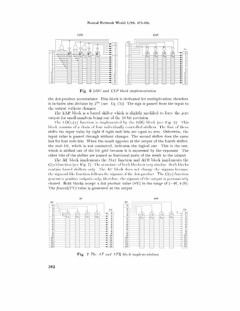
Neural Network World 5/99, 375-391LOG EXP
0 0 0 0
-10-11-12-13-14
-9-8-7-6-5-4-3-2-101234S
-1-2-3-4-5-6-7-8-9
-10-11-12-13-14-15
S
LV
FV
4 81 2
-10-11-12-13-14
-9-8-7-6-5-4-3-2-101234S
-1-2-3-4-5-6-7-8-9
-10-11-12-13-14-15
S
0
124
0
8
0 0 0Fig. 6 LOG and EXP block implementation.the dot-product accumulator. This block is dedicated for multiplication; thereforeit includes also division by 22n (see. Eq. (5)). The sign is passed from the input tothe output without changes.The EXP block is a barrel shifter which is slightly modi�ed to force the zerooutput for small numbers being out of the 16-bit precision.The LOG2(x) function is implemented by the LOG block (see Fig. 6). Thisblock consists of a chain of four individually controlled shifters. The �rst of themshifts the input value by eight if eight msb bits are equal to zero. Otherwise, theinput value is passed through without changes. The second shifter does the samebut for four msb bits. When the result appears at the output of the fourth shifter,the msb bit, which is not connected, indicates the logical one. This is the one,which is shifted out of the bit grid because it is expressed by the exponent. Theother bits of the shifter are passed as fractional parts of the result to the output.The AF block implements the S(x) function and AFR block implements theG(x) function (see Fig. 7). The structure of both blocks is very similar. Both blockscontain barrel shifters only. The AF block does not change the signum becausethe sigmoid-like function follows the signum of the dot-product. The G(x) functiongenerates positive outputs only; therefore, the signum of the output is permanentlycleared. Both blocks accept a dot product value (SV) in the range of (�16;+16).The fracval(FV) value is generated at the output.AF AFR
01 1
4-1-2-3-4-5-6-7-8-9
-10-11-12-13-14
0123S
SV
8
1
2
1
1
1
FV
-14-15
-13-12-11-10
-8-7-6-5-4-3-2-1S
-9
1
0 0
42
08
0
-1-2-3-4-5-6-7-8-9
-10-11-12-13-14
0123S
SV
01
FV
-14-15
-13-12-11-10
-8-7-6-5-4-3-2-1S
-9Fig. 7 The AF and AFR block implementation.382

Skrbek M.: Fast neural network implementation5.2 Composed blocksThe multiplier, square and square root blocks are considered as complex blocks.Each composed block is a composition of the basic blocks.MultiplierThe multiplier is based on two LOG blocks and one EXP block. Two input valuespassed through the LOG blocks are added and sent to the EXP block after that.The signum is calculated separately by the XOR function.Square functionThe square can have the same structure as the multiplier, but the adder is replacedby the shift-to-the-left operation. We also propose an implementation that avoidsthe barrel shifter of the LOG block. This can be described by the equationSqr(x) = (a + 2c) 0� (n+ xn�1)where a = 2n, n is a position of the left-most one, b = xn�12n�1, xn�1 is a value ofthe bit which is the right neighborhood of the left-most one, c = x� a� b. The 0�symbol represents the shift to the left operation (zeros are inserted from the right).The Sqr(x) function is evaluated in two steps. The �rst step is to determine the a,b, c, and n+xn�1. The second step is shift to the right by n+xn�1. If the operationis performed for numbers in the range of (0; 1), then the negative argument changesthe direction of the shift operation. Detection of the left-most one (i.e. n+ xn�1)and 2c calculation can be done by a chain of simple blocks (see Fig. 8).The Sqr(x) block receives fracval(FV) value (sixteen bit). Bits 2�1 : : :2�9 ofthe input are passed through the chain. After this, the chain calculates a+ 2c andsets the XC outputs. Simultaneously, one of SHR outputs is activated. The activethe SHR bit asks the barrel shifter for an appropriate number of shifts. The XCbits are completed by 2�9�2�15 bits and the complete tuple is passed through theshifter.0
x(-8)x(-7)x(-6)x(-5)x(-4)
0
x(-1) x(-2) x(-3)
-1 -2 -3 -4 -5 -6 -7 -8 0 1 2 3 4 5 6 7
SHRXC
E E EE E E E
x(-9)
E
PI
x(n) x(n-1)
0 1
BI
E-block
PO
BO
xc(n) SHR(m)Fig. 8 Sqr(x) chain. 383

Neural Network World 5/99, 375-391Square root functionSimilarly, we can calculate the square root function. It can be realized as a com-position of the LOG, shift, and EXP blocks. We can also use an alternative imple-mentation de�ned asSqrt(x) = ( (a+ d=2) 0� (n=2) if n is even(a+ a=2 + d=2) 0� (n�12 ) if n is oddwhere a = 2n, n is a position of the left most one and d = x � a. The internalstructure of SQRT block is similar to the SQR block.5.3 Neural blocksThe blocks de�ned in Sect. 5.2 correspond to particular functional units of a neuralprocessing element (PE). They create a collection of blocks su�cient for implemen-tation of the processing elements of both perceptron and RBF types. The structureof the perceptron and the RBF processing element are shown in Fig. 9.LogAdd Exp
Threshold
Scale
DpAcc
x (LV)
w (LV) SC AF Logy (LV)
Sub
DpAcc SCw (FV)
x (FV)
SQR
Scale
AFRy (FV)
0
RBFPerceptronFig. 9 Perceptron and RBF processing element structure.Perceptron type PEThis processing element accepts the weights and inputs in their logarithm form(logval, LV). Each pair of input and weight is added by the LogAdd block and theresult is passed through the EXP block to the dot product accumulator (DpAcc).DpAcc accumulates products, wixi. After processing all inputs, the dot productvalue is passed through a chain of post-processing blocks. This chain consists of thescale (SC), activation function (AF) and logarithmer (Log) block. The logarithmerproduces the logarithm of the output to ensure compatibility to other processingelements.The processing rate of this block depends on the adder and barrel shifter prop-agation delay in the LogAdd, Exp and DpAcc blocks. If we use a fast conditional-sum adder for the LogAdd, the propagation delay can be a few nanosecond. Thedot product adder should be implemented as a carry save adder to reach su�cientlyshort propagation delay for the 24 or the 32 bits wide dot product.384

Skrbek M.: Fast neural network implementationRBF type PEThe RBF processing element is slightly di�erent. Its block diagram is also shownin Fig. 9. The Sub and SQR blocks are used to calculate the Euclidean distancebetween the input and the weight vectors. The gauss-like activation function, G(x),is implemented by the AFR block. The DpAcc block is the same as the DpAccblock of the perceptron type.Both types of the processing element use the SC block. This block multipliesthe dot-product by a value which determines the scale factor of weights. This isnecessary because the weights are in the range of (�1; 1), which is insu�cient formost neural applications. The multiplier is not necessary because the set of powersof two su�ciently covers the usual scale factors.6. ECX CardThe �rst implementation of the shift-add arithmetics was veri�ed on a card calledthe ECX card. The ECX card was designed and produced in the shape of an ISAcard for the PC compatible computers. The block diagram is shown in Fig. 10.16 16 16 16
16
W-RAM4 x 32k x 8
I/O RAM2 x 8k x 8
X1XILINX
XC3064/3090XILINX
XC3064/3090
X2
ISA BUS INTERFACE
I/O address
w-address
inter XILINX contol signals
]
External busInterface
data bus (16 bits)Fig. 10 ECX block diagram and the board picture.The card contains two XILINX FPGAs of the XC3000 family. The �rst FPGA(X1) acts as a neural processing element and the second FPGA (X2) acts as acontroller. The other circuits create an environment in which XILINX FPGAsbehave. This environment consits of� weight memory,� input/output data memory,� ISA bus interface,� external data interface.The weight memory is a fast static RAM of 32K�32 bits. All 32 bits are passedto X1 at once. Thus the interface ensures su�cient data throughput between theprocessing elements and the weight memory. The weight memory is mapped intothe host computer memory address space, so that the weights can be directly loadedor modi�ed by the host. The weight download and the modi�cation are limited tosixteen-bit wide transactions. 385

Neural Network World 5/99, 375-391The input/output memory is a fast static RAM of 8K words. Each word is only16-bit wide. This memory uses separated data bus, so the weights and inputs canbe sent to the X1 chip at once. No time multiplexing is required. The input/outputmemory is also mapped to the host computer memory address space.The X2 chip controls weight and input/output memory addressing. Its nexttask is to synchronize access to both memories with host computer to avoid accesscon icts. Synchronization proceeds by interrupt that inform the host computerthat the access into the memories is allowed.The ISA bus interface ensures all data transfers between the host computer andthe card. This interface establishes mapping of the card memories into the memoryaddress space of the host computer. Further, it provides I/O port for downloadingthe con�guration data into FPGAs. This interface also provides signals to createfour control registers as a part of the X2 chip design. These registers are visiblein the host I/O space. A de�nition of these registers is not strictly given, it onlydepends on X2 chip con�guration. We use these registers to control the neural netevaluation.The external bus interface is provided for the direct connection with an applica-tion by a simple asynchronous protocol. This interface consists of the bidirectionalbus drivers on the data path and control signals for handshaking. The protocolcan be customized by the X2 chip con�guration. The external bus enables to by-pass the host computer with the aim to speed up the data transfer between theapplication and the card.Weight mapping Data mapping
Xilinx configuration
interfaceData & control inteface
ECX card
Configuration data
Application
desired outputs
inputs
outputs
LEARNING ALGORITHM
Fig. 11 ECX software structure.6.1 Host softwareThe ECX card is controlled by host software. The host software consists of low level(driver like software) and application software. The low level software provides the386

Skrbek M.: Fast neural network implementationFPGA download function and the application interface. FPGA con�guration �lesare read by the ECX software and serialized to a bit stream that is downloadedto X1 and X2 chips. This operation is performed at power up or always whenrecon�guration of FPGAs is required.The application interface establishes the data connection between the applica-tion and the card memories. Low level software must control the memory mappingbecause three pages of the card memories are mapped into the single 64kB windowof the host memory address space.The application software for the ECX card provides learning algorithm, learningdata access, storing results, user interfaces and data presentation. The applicationsoftware varies according to a neural-net paradigm being tested.6.2 Neural net implementation on the ECX cardNeural net implementation on the ECX card consists of a neural unit and a con-troller. The neural unit implements all neural calculations while the controllermaps the weights, inputs and outputs to the neural unit according to the requiredtopology.The neural unit can contain one or more neural processing elements workingin parallel. The number of the processing elements is constrained by the X1 chipcapacity and the bandwidth of the weight memory bus. Two 16-bit wide weightsor four 8-bit wide weights can all be passed at once.The controller is implemented in the X2 chip. The X2 chip addresses weight,input and output memories and ensures data transfers. The structure of the con-troller depends on network topology. Even more topologies can be supported.Since neural nets usually have more neurons than the processing elements available,time-sharing technique is used. The physically implemented processing element areapplied for di�erent parts of the network. This can be easily realized by variousmemory addressing strategies.The layered, feed-forwarded topology was implemented for our experiments.The controller contains the layer, neuron, input and output counters. The memoryaddressing is derived from the content of these counters. The number of neuronsper layer is variable and controlled by the control registers.Tab. II summarizes the delay and complexity of the implemented perceptron-like PE. The �rst part of the table summarizes the building blocks of the PE. Thesecond part summarizes the PE implementation. The delay of PE is separatedto weighting, i.e. the sum of wixi products, and activation function evaluation.The processing rate is given by the delay of weighting. Our results correspond to3.5 MCPS (connections-per-second) processing rate.The latest version of the ECX card has been modi�ed for the XILINX XC4010FPGAs (XC4000 series). This version can implement more complex processingelements and operate faster. BP16, BP8, BP8D, RBF16, RBF8, RBF8D processingelements were tested on a modi�ed card. BP or RBF in the name denotes theprocessing element type (perceptron or RBF). The number 16 or 8 is weight andinput/output data width. D denotes two neurons working in parallel. FPGAcapacity usage for all processing elements is shown in Tab. III. 387

Neural Network World 5/99, 375-391Function Delay CLBs2x (16 bits) 58 33log2 x (16 bits) 83 35multiplication(add-exp, 16 bits) 148 47Pi ai (24 bits) 160 56activation function f , 16 bits) 49 30PE(perceptron) N/A 198PE ('t = 't�1 + wixi) 295 N/APE (f(')) 169 N/ATab. II PE's components implemented on XC3090.Max BP8 BP8D BP16 RBF8 RBF8D RBF16CLB 400 239 368 365 211 332 308I/O cells 61 57 57 57 57 57 57F&G generators 800 246 461 426 201 371 338H generators 400 37 58 43 23 30 41Flip- ops 800 130 175 160 124 165 154CLB fast carry logic 400 18 36 28 14 28 24Tab. III Processing elements on XC4010EPC84-4.The neural network implemented on the ECX card was tested under the samesoftware as it was used in software tests. The recall phase of the network wasreplaced by the interface to the ECX card, the other parts including learning stayedunchanged. The XOR problem, the inside-outside test, and the sonar test were usedto verify the card functionality. Fig. 12 shows the learning error curves of hardwareimplementing the eight-bit and sixteen-bit version of the processing element. Theeight-bit version has lower weight resolution; therefore it needs a longer learningperiod complicated task as XOR.The recall delay of the ECX card was measured on the neural net with 60 inputs,10 outputs and 140 hidden neurons. Average delay per input vector was calculatedafter processing 500 vectors. The results are summarized in Tab. IV. The tablealso contains the recall delay of the software model (BP) running on PC withK5 processor at 166MHz.Network BP8D BP8 BP16 BP (SW model)60/140/10 1.76 2.52 2.52 27.56Tab. IV ECX card delay [ms] vs. the software model delay [ms].The ECX delays presented in Tab. IV include also certain overhead caused bydata transfers and setup of the ECX card before starting the network evaluation.388

Skrbek M.: Fast neural network implementation0
0.1
0.2
0.3
0.4
0.5
0.6
0.7
0 500 1000 1500 2000 2500
Err
or
iteration
BPHW16HW8D
0
0.1
0.2
0.3
0.4
0.5
0.6
0 100 200 300 400 500 600 700
Err
or
iteration
BPHW16HW8D
SONARXOR
Fig. 12 Learning curves measured for ECX card.7. On Chip ImplementationThe fastest implementation we did was on-chip implementation. The processingelements introduced in Sect. 5.3 were designed on 0.7 �m Standard Cell Technologyby the CADENCE design system with ES2 standard cell libraries. All functionblocks were designed and veri�ed by simulation. For each block a chip layout hasbeen created to measure the required chip area and the propagation delay. Theresults are summarized in Tab. V. The table contains a list of functional blocks.The �rst group of the blocks includes all basic and complex blocks. This groupcontains two LogAdder blocks, a faster and a slower versions. The slower version isa carry-ripple adder and the faster version is a conditional-sum adder. The secondgroup shows various multiplier con�gurations. For comparison purposes a precise16� 16 multiplier was also added to this group.For each block, we present the required chip area, the typical and the maximumpropagation delay. The delay for the whole shift-add processing element is splitinto two delays. One is for product calculation (from input to DpAdder), and theother is for the activation function evaluation (from DpAdder to output).The standard implementation of the processing element requires about 2.5mm2.Most of the chip area is covered by the multiplier and the RAM implementingactivation function. The processing rate is given by the sum of the multiplier delayand the DpAcc block delay. This delay is about 37 ns. The activation functiondelay is about 14 ns (RAM propagation delay).A chip area of about 1.4 mm2 is required for the shift-add neural processingelements. The delay a�ecting the processing rate is 18 ns. The shift-add activationfunction evaluation is about 4.3 ns.From these results we can see that the shift add architecture provides a fasterand simpler processing element than any other commonly used. The results pre-sented here strongly depend on the technology used. More progressive technologies(0.35 �m for example) will allow to design faster shift-add blocks than we present.However, if we compare the standard and the shift-add implementation on a giventechnology, the advantages of the shift-add arithmetics are obvious. 389

Neural Network World 5/99, 375-391Block Ar Dt DmLogAdd(slow) 0.083 7.2 14.2LogAdd (fast) 0.234 3.8 7.4EXP 0.106 2.3 4.7LOG 0.250 3.3 6.5AF 0.081 2.1 4.2AFR 0.086 2.1 4.3SC 0.083 2.2 4.4DP Adder (24 bit) 0.472 3.9 6.8SQR 0.104 4.4 8.6SQRT 0.117 4.8 9.4MUL (16� 16) 0.946 n/a 30.2MUL(2� Log-Add(s)-Exp) 0.689 12.8 25.4MUL(2� Log-Add(f)-Exp) 0.840 9.5 18.6MUL(Add-Exp) fast 0.345 6.1 12.1MUL(Add-Exp) slow 0.193 9.5 18.9SH-A proc. elem. (PER) 1.44 9.3 18.011.7 23.3SH-A proc. elem. (RBF) 1.29 16.4 32.44.4 8.9Tab. V Summary of delays and chip areas for proposed neural blocks. Ar is achip area in (mm2), Dt is a typical delay per block and Dt is the maximum delayper block.8. ConclusionThe shift-add arithmetics is the background for a fast neural implementation. Theshift-add arithmetics provides a number of simple functions required by perceptronand RBF neurons. The great advantage is that these functions can be easilyimplemented in hardware. Most functions are based on the barrel shifter principle.Since the functions use linear approximation, they do not produce precise re-sults. Software tests show that errors can be easily suppressed by the learningalgorithm. By comparing the various models learned under the back propagationalgorithm, we found a very small negative in uence of the imprecise multiplica-tion. On the other hand, the power of two based activation functions speed up thelearning process.First implementation of the shift-add architecture was tested on the XILINXFPGA based card. The tests show the functionality of the shift-add architecture inhardware. The nets implemented on the card were much faster than the softwareimplementation.Another implementation was made on a chip. The chip had not been fabricatedyet, but a chip design provided a lot of valuable results. The simulation providedan area necessary to implement the chip and propagation delays of all functionalblocks. From the result we can see that it is possible to obtain faster and area-saving neural blocks. The results reached strongly depend on the technology and390

Skrbek M.: Fast neural network implementationthe design, so a better result can be obtained for optimized technology libraries.Better results can also be obtained on technologies with an optimized multiplexorbecause our blocks contain more than ninety percent of multiplexors.AcknowledgmentThe author of this article thanks all institutions and people who participated inthis project. Namely to the Department of Computer Science, Faculty of ElectricalEngineering, Czech Technical University in Prague (Czech Republic) and the Fac-ulty of Applied Physics TU Delft and the Faculty of Technical Mathematics andInformatics TU Delft (The Netherlands). The author also thanks all his studentswho participated in this project. Namely to Jaroslav Maurenc, Jan Hvozdovi�c,Karel Sr�se�n and Jakub Adamczyk.This research was supported by the internal grant of the Czech Technical Uni-versity in Prague, no.3096374/1997.References[1] Marchesi M., Orlandi G., Piazza F.: Fast neural networks without multipliers. IEEE Trans-action on Neural Networks, 4, 1, January 1993, 53-62.[1] ElmasryM.I.: VLSI arti�cial neural networks engineering.Kluwer Academic Publishers, 1994,ISBN 0-7923-9493-3.[2] Jabri M., Coggins R., Flower B.: Adaptive analog VLSI neural systems. Chapman & Hall,London 1996. ISBN 0-412-61630-0.[3] Maurenc J.: Neurochip architecture. Final thesis, Czech Technical University in Prague,Prague, 1995.[4] Hvozdovi�c J.: Neuronov�a s���t na FPGA XILINX. Final thesis, Czech Technical University inPrague, Prague, 1995.[5] Sr�se�n K.: Shift-add neuron na standardn��ch bu�nk�ach. Final thesis, Czech Technical Universityin Prague, Prague, 1998.[6] Adamczyk J.: Neuronov�y akceler�ator na X4010. Final thesis. Czech Technical University inPrague, Prague, 1999.[7] Skrbek M., �Snorek M.: An architecture for an e�cient implementation of neural networks.Proceedings of the ESM'95, M. �Snorek and M. Sujansky and A. Verbraeck (eds.), Prague,Czech Republic, 1995, 785-789.[8] �Snorek M., Skrbek M.: Arti�cial neural network accelerators. Elektrotechnik und Infomation-stechnik, Neuronale Netze, 7-8, 1995, 329-333.[9] Skrbek M.: Experimental card for shift-add neural architecture veri�cation. Workshop'96,CTU Prague and TU Brno, Prague, 1996, 295-296.[10] Skrbek M.: New neurochip architecture. Ph.D. thesis. Czech Technical University in Prague,Prague, 1999.391