External interfaces in series Vortex86MX SoC - Index of
44
External interfaces in series Vortex86MX SoC GPIO, PWM/SERVO, SPI, I2C, COM Document version 1.1 7/2012
-
Upload
khangminh22 -
Category
Documents
-
view
5 -
download
0
Transcript of External interfaces in series Vortex86MX SoC - Index of

External interfaces in series
Vortex86MX SoC
GPIO, PWM/SERVO, SPI, I2C, COM
Document version 1.1 7/2012

External interfaces Vortex86MX series www.xtendlan.com
-2-
Content 1. Valid models ................................................................................................................................................. 3 2. Connector description ................................................................................................................................... 3 3. Function block diagram ................................................................................................................................ 5 4. VCC .............................................................................................................................................................. 7 5. GPIO – General Purpose Input Output ports ................................................................................................ 7
5.1. Pinout .................................................................................................................................................... 7 5.2. Electrical characteristics ....................................................................................................................... 8 5.3. Programming......................................................................................................................................... 8 5.4. GPIO vs. BIOS Setup ........................................................................................................................... 9 5.5. Performance .......................................................................................................................................... 9
6. SPI – Serial Peripheral Interface bus .......................................................................................................... 10 6.1. Characteristics..................................................................................................................................... 10 6.2. Pinout .................................................................................................................................................. 10 6.3. Programming....................................................................................................................................... 11
7. I2C – Inter integrated Circuit interface....................................................................................................... 12 7.1. Characteristics..................................................................................................................................... 12 7.2. Pinout .................................................................................................................................................. 12 7.3. Programming....................................................................................................................................... 13
8. Serial ports .................................................................................................................................................. 14 8.1. Characteristics..................................................................................................................................... 14 8.2. Pinout .................................................................................................................................................. 15 8.3. Programming....................................................................................................................................... 15
9. PWM - Pulse Width Modulation ................................................................................................................ 16 9.1. Pinout .................................................................................................................................................. 16 9.2. Electrical characteristics ..................................................................................................................... 16 9.3. Performance ........................................................................................................................................ 16 9.4. Programming....................................................................................................................................... 17
10. Microcontroller 8051 notice ................................................................................................................... 17 11. Software libraries .................................................................................................................................... 18
11.1. RoBoIO library ............................................................................................................................... 18 11.2. How to use ...................................................................................................................................... 19
12. Appendix A - Technical Reference......................................................................................................... 22

External interfaces Vortex86MX series www.xtendlan.com
-3-
1. Valid models Information provided in this manual fully valid for series with externalized GPIO/PWM/SPI/I2C ports TC-261MXI GPIO, 3x RS232, 512MB RAM TC-261MXGI GPIO, 3x RS232, 1GB RAM TC-261MXIC GPIO, 1x RS485, 2x RS232, 512MB RAM TC-261MXGIC GPIO, 1xRS485, 2x RS232, 1GB RAM There are models with same structure which does not have GPIO header external. For them are information also valid but does not have practical usage, because missing physical interface there. Here just for notice: a) only information related with COM ports valid for: TC-261MXC 2x RS232, 1x RS485, 512MB RAM TC-261MXGC 2x RS232, 1x RS485, 1GB RAM b) none externalized interface are on models: TC-261MXH TC-261MXGH TC-261MXK
2. Connector description Devices have on front panel multipurpose box header 26-pin. This is connector 2 row, 2x13, pitch 2.54mm. Many suppliers provide this connector typically for flat cables As you can see from picture there is available power pin, GND and sets of GPIO, PWM, SPI and I2C pins. Their functionalities are possible to select in BIOS Setup or by programming PCI register in run time. So their can be also switched during operations by user’s application.
Totally there are available ports: GPIO: 3 groups of ports, each with 8-bit input/output, totally 24 bit PWM: 2 groups, each with 8-bit, totally 16 PWM ports SPI: 1 port I2C: 2 ports COM: 3 ports

External interfaces Vortex86MX series www.xtendlan.com
-4-
Front panel
Back panel

External interfaces Vortex86MX series www.xtendlan.com
-5-
3. Function block diagram Vortex86MX provides several types of interfaces for general usage in the system.
Refer to Vortex86MX functions block diagram:

External interfaces Vortex86MX series www.xtendlan.com
-6-
Detailed scheme of Vortex86MX connections
Have to note those in detailed schemes are not externally accessible Parallel port and GPIO Port 2.

External interfaces Vortex86MX series www.xtendlan.com
-7-
4. VCC User can feed devices connected on GPIO port through pin VCC with voltage of 5V. However there should be considered their limitations. VCC pin has in circuit PTC fuse which limits current from this output. Maximal continuous current is 1,1A (5,5W). For short period is allowed to feed 1,3A. When device feeds more than 1,3A then PTC device starts to trip into high impedance state. Trip time is about 0,3s @ 8A. Maximal current which can PTC withstand without damage is 40A.
5. GPIO – General Purpose Input Output ports GPIO ports are commonly used for relatively slow data acquisitions or for signaling external devices. On devices all GPIO pins are independent and can be configured as inputs or outputs, with or without pull-up/pull-down resistors.
5.1. Pinout
GPIO port #0, #1 are shared with PWM #0, #1
GPIO port #3 is shared with SPI and I2C ports
Numbering of pins is from down to top and left to right when looking on open connector from outside. GPIO group #0: pin 4,6,8,10,12,14,16,17 in order 0.-7. bit GPIO group #1: pin 3,5,7,9,11,13,15,17 in order 0.-7. bit GPIO group #3: pin 20,22,24,26,19,21,23,25 in order 0.-7. bit

External interfaces Vortex86MX series www.xtendlan.com
-8-
Pin description, box header on front panel 26-pin, 2.54mm, 2 row
Pin# Signal Name Pin# Signal Name1 VCC 2 GND 3 GP10 4 GP00 5 GP11 6 GP01 7 GP12 8 GP02 9 GP13 10 GP03 11 GP14 12 GP04 13 GP15 14 GP05 15 GP16 16 GP06 17 GP17 18 GP07 19 GP34 20 GP30 21 GP35 22 GP31 23 GP36 24 GP32 25 GP37 26 GP33
5.2. Electrical characteristics GPIO in output mode can drive 16mA. GPIO in input mode are unterminated and are pulled-high by 75kOhm resistor. Note: For testing purposes you can easily check state in which ports are. Typicaly if are in output state you will measure 0V or 3.3V. In input state will measure 2.5V
5.3. Programming Description of programming GPIO ports provided in sample codes. Here is GPIO summary for direction and data registers:
Port #0
Port #1
Port #2
Port #3
Port #4
Description
Data Register 78H 79H 7AH 7BH 7CH
Direction Register
98H 99H 9AH 9BH 9CH 0: GPIO pin is input mode 1: GPIO pin is output mode
If send value 0FH to port 98H, it means that GPIO port0 [7-4] are input mode and port[3-0] are output mode.
If send value 00H to port 98H, it means that GPIO port0 [7-0] are input mode. If send value FFH to port 98H, it means that GPIO port0 [7-0] are output mode.
If send value 03H to port 98H, it means that GPIO port0 [7-2] are input mode and port[1-0] are output mode.
External interfaces Vortex86MX series www.xtendlan.com
-9-
5.4. GPIO vs. BIOS Setup
GPIO port modes can be re-setup in program code by direct writing into PCI registers. If this setup is not done then is valid what is setup in BIOS. So if the pin is setup by BIOS into I2C mode then will ignore GPIO write/reads. Recommend to see Appendix A - Technical Reference
5.5. Performance Tested maximum possible frequency of switching of GPIO ports using software loop which is doing just on/off operation on GPIO ports under Linux (Debian 6.0) and DOS (FreeDOS 1.1) is period approximately 550kHz. Is necessary to note that such period is unstable and fluctuate 340-600kHz. Should be noted that for reading GPIO ports there is commonly possible to use interrupt. Port can have delay of time on which signal must be presented on GPIO to be interrupt initiated. The range of time is from 2ms to 100ms. Signal can be defined if should be high or low.

External interfaces Vortex86MX series www.xtendlan.com
-10-
6. SPI – Serial Peripheral Interface bus SPI ports are commonly used for fast data acquisitions from others integrated circuits. It is ideal interface to be connected on external ADC, DAC and other devices.
SPI interface discussed in this chapter is hardware controlled. Please do not mix with software emulated SPI interface (much slower).
6.1. Characteristics SPI interface is intended only for high speed devices and is half duplex mode only. Has maximum speed 150Mbps, minimum speed 10Mbps. Support only two clock modes: CPOL = 0, CPHA = 0 CPOL = 1, CPHA = 0 Good description for modes http://en.wikipedia.org/wiki/Serial_Peripheral_Interface_Bus Clock modes are: 18750kHz, 15000kHz, 12500kHz, 10000kHz, 10714kHz, 11538kHz, 13636kHz, 16666kHz 21400kHz, 25000kHz, 30000kHz, 37000kHz, 50000kHz, 75000kHz, 150000kHz. Clock 21.4MHz counted as default.
6.2. Pinout SPI is shared with GPIO group #3. SPI is using pin 20,22,24,26.

External interfaces Vortex86MX series www.xtendlan.com
-11-
Signals are: pin 20: SS (ENABLE) pin 22: CLOCK (SCK) pin 24: MOSI (SDO) pin 26: MISO (SDI) pin 2: common GND
6.3. Programming Description of programming SPI is provided in sample codes and by libraries. Recommend to see Appendix A - Technical Reference with registry description.

External interfaces Vortex86MX series www.xtendlan.com
-12-
7. I2C – Inter integrated Circuit interface I2C is typically used for connection of low and medium speed peripheral devices using two wire bus.
7.1. Characteristics I2C interface in device support both master and slave modes. Support 10bit address (master only). Support all speed modes
standard mode (up to 100 kbps) fast mode (up to 400 kbps) high-speed mode (up to 3.3 Mbps)
Note that speed setup can be any speed up to 3.3Mbps, there are not fixed speed steps.
7.2. Pinout I2C interfaces are shared with GPIO group #3. I2C group #0 is using pin 19,21. I2C group #1 is using pin 23,25.
Signals are: pin 19: SCL0 pin 21: SDA0 pin 23: SCL1 pin 25: SDA1 pin 2: common GND

External interfaces Vortex86MX series www.xtendlan.com
-13-
7.3. Programming Description of programming I2C is provided in sample codes and by libraries. Special notice should be taken for devices which are addressed 10bit or 7bit.

External interfaces Vortex86MX series www.xtendlan.com
-14-
8. Serial ports Serial ports COM1, COM3 and COM4 can be used as standard COM ports in Windows, Linux and DOS.
8.1. Characteristics Serial ports in devices are in back panel. Port COM1 is labeled connector “COM1”. It is standard signals COM1 port on connector DB9. This port can be uased fully as standard COM port, f.e. for RS-232 connection of serial modems. Port COM3 and COM4 are both on connector labeled “COM2”. They have only signal RX and TX available. This port can be used only for devices which do not need controlling signals. Typical applications are UART interfaces. User’s can modify in BIOS all parameters of ports: IRQ, I/O base address and default speed. Ports have speed from 2400-115200 as standard speed. It has also boosted speeds 31 200 – 748 800 bps. Please note: Ports can be RS-232, RS-422 or RS-485 type. However his type is given by model and regardless of setup in BIOS. So if user will setup device which is RS-232 as RS-485 port, it will anyway stays and will work as RS-232.

External interfaces Vortex86MX series www.xtendlan.com
-15-
8.2. Pinout Connector DB9 (9pin) labeled as “COM1” COM1: Pin 1: DCD for RS-232 / TX- for RS-422 / Negative for RS-485 Pin 2: RxD for RS-232 / TX+ for RS-422 / Positive for RS-485 Pin 3: TxD for RS-232 / RX+ for RS-422 Pin 4: DTR for RS-232 / RX- for RS-422 Pin 5: GND Pin 6: DSR for RS-232 Pin 7: RTS for RS-232 Pin 8: CTS for RS-232 Pin 9: RI Connector DB9 (9pin) labeled as “COM2” COM3: Pin 2 RxD Pin 3 TxD COM4: Pin 8 RxD Pin 7 TxD Common: Pin 5 GND Note: pinout is designed in such way that if not COM4 used there is not necessary to change piut of connection cable.
8.3. Programming Ports can be used as standard ports without special programming. Anyway also sample codes and libraries provided.

External interfaces Vortex86MX series www.xtendlan.com
-16-
9. PWM - Pulse Width Modulation PWM ports are typical used for controlling of power switches for stepper motors and servos. They could be also used for communication devices or communication interface emulations.
9.1. Pinout
PWM #0, #1 are shared with GPIO #0, #1
9.2. Electrical characteristics PWM port can drive 16mA. Value can be tuned from 4mA to16mA by programming PCI registers. 16mA is default value.
9.3. Performance Resolution of PWM self is up to 20ns (50MHz clock of counter). PWM is hardware feature and works independently of CPU load. When applied with servos and libraries mentioned later can control feedback pulses +/- 1us. PWM is possible to be programmed for exact number of pulses (counting mode) or into continual method. If in counting mode then is possible to check end of sequence and to program by software other sequence. Time to detect near-end of counting and start new sequence is about 8us (Linux Debian).

External interfaces Vortex86MX series www.xtendlan.com
-17-
End of counting sequence is possible to detect by three methods: 1. use interrupt – end of counting will call interrupt service procedure 2. by polling the Interrupt Status Register – to check if interrupt should come 3. by polling the Registry Counter field in Control Register – to check how many counts to end pending
9.4. Programming Description of programming PWM is provided in sample codes and by libraries. There are available samples and libraries for direct PWM usage as low level function. Additionally there are libraries allows usage PWM for servos control with already prepared libraries for intelligent servo controls. For better understanding is recommended to study documents related to “Intel 8254 programmable interval timer” and Appendix A - Technical Reference
10. Microcontroller 8051 notice The SoC have also microcontroller 8051 inside. However this is undocumented possibility in device. User can met that setting is shared in BIOS with GPIO. Currently none documentation is provided or planed to be provided.

External interfaces Vortex86MX series www.xtendlan.com
-18-
11. Software libraries Most comprehensive software libraries for this device counts development for Roboard platform. This platform is designed by SoC’s authors and is specialized for robotics’s applications. Because most components and architecture is identical then such libaries are applicable directly or with very little modifications. Home page of project http://www.roboard.com/ We should note that hardware (RB-100, RB110 etc.) for this project can be also sourced from us. Even user have took in consideration that those equipment is considered for a bit different application. It means there is not embedded VGA, no case etc.
11.1. RoBoIO library Whole project is build around RoBOIO library and has those above all significant points:
open-source library free for academic & commercial use everyone is permitted to redistribute and/or modify it without restriction
Popular OS supported, library is cross-platformed
Linux Windows XP Windows CE 6.0 DOS
Wrappers for development libraries available
.NET (C# and VB.NET) for .NET Framework 2.0 & above Visual Basic 6.0 Borland C++ Builder JAVA for Windows XP Python for Windows XP
Currently (version 1.8) supported I/O functions which are directly applicable with discussed devices
GPIO PWM SPI hardware I2C hardware COM (RS-232, RS-485, TTL)
Additionally there libraries which gives very good idea for own project, they could be used directly or are very good for inspirations of own projects
SPI software emulated for slow SPI equipment

External interfaces Vortex86MX series www.xtendlan.com
-19-
I2C software emulated for nonstandard device A/D complete libraries for connection on ADC circuit by Analog AD79x8 family on SPI RC servo control for many servos (KONDO, HiTEC,….) Easier integration for sensors and information for real applications of
o A/D, SPI, I2C: accelerometer, gyroscope, … o COM: GPS, AI servos, … o PWM: RC servos, DC motors, … o GPIO: bumper, infrared sensors, on/off switches, … o USB: webcam, … o Audio in/out: speech interfaces
For developers there is big advantage thanks wide range of tools they can freely use, because platform is x86 based and almost all resources on PC can be employed as development tools
Languages: C/C++/C#, Visual Basic, Java, Python, LabVIEW Libraries: OpenCV, SDL, LAPACK IDE: Visual Studio, DevVisual Dev--C++, Eclipse GUI: Windows Forms, GTK
11.2. How to use From home page of project http://www.roboard.com/ is recommend to download latest versions. Is very good idea to read introduction documents. Highly recommended document which gives overview is “RoBoIO 1.8 Introducion Slide“ Then download libraries and related to planed OS. Is recommended to follow guides attached to libraries and recompile them for your OS. After successful compilation for your OS is necessary to modify one or two file to allow full operations of libraries on discussed platform. A] In fact will enough to switch-off Roboard platform checks. For this case developers already prepared code and in code is parameter ROBOIO. Unfortunately at least in version 1.8 code not completely clean up so there are two ways how to customize code for your platform. in file ROBOIO/libsrc/define.h remove line #define ROBOIO (0x0181) or do same using parameter for compiler. This will be completely ok if code is cleaned up and it will allow to skip codes sections which verifying if hardware is exactly RoBoard. Unfortunately is not, so during compilation you will met procedures which claimes for missing roboio_GetRBVersion(). This is then easily solved using section #ifdef ROBOIO

External interfaces Vortex86MX series www.xtendlan.com
-20-
… #endif Please check in file ROBOIO/libsrc/i2c.cpp modify those functions: i2cResetPin(void) and i2cClearResetPin(void) #ifdef ROBOIO if (roboio_GetRBVer()!= …… ) {… return false}; #endif Please check in file ROBOIO/libsrc/spi.cpp modify those functions: spi_DisableSS(void) and spi_EnableSSn(void) #ifdef ROBOIO if (roboio_GetRBVer()!= …… ) {… return false}; #endif Please note that this patch has drawback – all samples written then in package RoboKit counts with ROBOIO define, so will claim for functions related with this define. Maybe faster for first usage of library is to use a bit ugly patch mentioned in variant B] B] This kind of patch modifies source coude such way that you will then declared your Vortex86DX or MX board as RB100 for RoboIO libraries. Advantage is that you can use for future regulary sample files even they are written for Roboard without any modifications. Please check in file ROBOIO/libsrc/common.cpp modify those functions: Roboio_CheckRBVer(void) find line if (cpu_id == CPU_VORTEX_DX_1) return true; and add after him line if (cpu_id == CPU_VORTEX_MX) return true if (cpu_id == CPU_VORTEX_MX_PLUS) return true; Please check in file ROBOIO/libsrc/io.cpp modify those function: Io_init(void) find line which content following condition if ((io_CpuID() != CPU_VORTEX_DX_1) && (io_CpuID() != CPU_VORTEX_DX_2) && (io_CpuID() != CPU_VORTEX_DX_3)) and modify them to accept also CPU_VORTEX_MX and CPU_VORTEX_MX_PLUS

External interfaces Vortex86MX series www.xtendlan.com
-21-
if ((io_CpuID() != CPU_VORTEX_DX_1) && (io_CpuID() != CPU_VORTEX_DX_2) && (io_CpuID() != CPU_VORTEX_DX_3) && (io_CpuID() != CPU_VORTEX_MX) && (io_CpuID() != CPU_VORTEX_MX_PLUS)) With this patch you can call libraries and claim them that you have RB100 board. You can compile sample programs from RoboKit and try their functionalities immediately on your platform. Note that patch A] and patch B] does not collide.

Technical Reference
-22-
12. Appendix A - Technical Reference Description of Vortex86DX and Vortex86MX series registers.

1. PCI Configuration Registers
Technical Reference PCI Configuration Registers
I/O Port: CF8h ─ Accessed as a Dword
Register Name: PCI Configuration Address Register
Reset Value: 00000000h
31 30 29 28 27 26 25 24 23 22 21 20 19 18 17 16 15 14 13 12 11 10 9 8 7 6 5 4 3 2 1 0
C
E Rsvd BN DN FN RN Rsvd
Configuration Address Register is a 32-bit register accessed only when referenced as a DWORD. A byte or word
reference will pass through the Configuration Address Register onto the PCI bus as an I/O cycle.
Bit Name Attribute Description
31 CE R/W
Configuration Enable.
When this bit is set to 1, accesses to PCI configuration space are enabled. If this bit is
reset to 0, accesses to PCI configuration space are disabled.
30-24 Rsvd RO Reserved.
23-16 BN R/W
Bus Number.
When the bus number is programmed to 00h, the target of the configuration cycle is
either the North-Bridge or the PCI Device that is connected to the North-Bridge. If the
bus number is programmed to 00h and the North-Bridge is not the target, a Type 0
configuration cycle is generated on PCI Bus. IF the bus number is non-zero, a Type 1
configuration cycle is generated on PCI bus with the bus number mapped to AD[23:16]
during the address phase.
15-11 DN R/W
Device Number.
This field selects one agent on the PCI bus. During a Type 1 configuration cycle, this
field is mapped to AD[15:11]. During a Type 0 configuration cycle, this field is decoded
and one of AD[31:11] is driven to 1.
10-8 FN R/W
Function Number.
This field allows the configuration registers of a particular function in a multi-function
device to be accessed. The Vortex86DX North Bridge only responds to configuration
cycle with a function number of 000b.
7-2 RN R/W
Register Number.
This field selects one register within a particular Bus, Device, and Function as specified
by the other fields in the Configuration Address Register.
1-0 Rsvd RO Reserved.

Technical Reference GPIO Interrupt Relative Registers
I/O Port: CFCh ─ Accessed as a Dword
Register Name: PCI Configuration Data Register
Reset Value: 00000000h
31 30 29 28 27 26 25 24 23 22 21 20 19 18 17 16 15 14 13 12 11 10 9 8 7 6 5 4 3 2 1 0
CDR
Configuration Data Register is a 32-bit read/write window into configuration space. The portion of configuration space
that is referenced by Configuration Data Register is determined by the contents of Configuration Address Register.
Bit Name Attribute Description
31-0 CDR R/W
If bit 31 of PCI Configuration Address Register is 1, any I/O reference that falls in the
PCI Configuration Data Register space is mapped to configuration space using the
contents of PCI Configuration Address Register.

3. Set period time that interrupt will be generated while the event loading time of any one of GPIO[7-0] is longer
1. Configure interrupt mask register to determine which GPIO can trigger interrupt individually.2. Set trigger level (high or low) for each GPIO.
2.1. GPIO
2.2. GPIO with Interrupt
GPIO availability.
See further Internal Peripheral Feature Control Register in chapter Servo Registry for description how to control
externaly connected.
y. In your system is possible that some GPIO group is not
onfigured as outputs, pins have 16 mA drive capabili
40 GPIO pins are provided by the Vortex86DX/MX for
Technical Reference GPIO
general usage in the system. All GPIO pins are independent
and can be configured as inputs our outputs; when c ty and are
unterminated; when configured as inputs, pins are pulled-high with a 75k ohm resistance.
GPIO port 0,1 and 2 are always free for use normall
Setup GPIO Direction
Here is GPIO direction and data registers:
Port 0
Port 1
Port 2
Port 3
Port 4
Description
Data Register 78H 79H 7AH 7BH 7CH
Direction Register
98H 99H 9AH 9BH 9CH 0: GPIO pin is input mode
1: GPIO pin is output mode
If send value 0FH to port 98H, it means that GPIO port0 [7-4] are input mode and port[3-0] are output mode.
If send value 00H to port 98H, it means that GPIO port0 [7-0] are input mode.
If send value FFH to port 98H, it means that GPIO port0 [7-0] are output mode.
If send value 03H to port 98H, it means that GPIO port0 [7-2] are input mode and port[1-0] are output mode.
GPIO port 0 & 1 in Vortex86DX support interrupt trigger. Programmers can use interrupt to instead of polling GPIO tosave CPU performance. GPIO port0 interrupt registers are at offset DCh~DFh in PCI south bridge and GPIO1registers are at offiset E0h~E3h.
Here are steps to setup GPIO to trigger interrupt:
than the time parameters.4. Select IRQ.5. Set interrupt trigger once or continuously.

2.3. GPIO Interrupt Relative Registers
Technical Reference GPIO Interrupt Relative Registers
Register Offset: DCh
Register Name: GPIO PORT0 Interrupt Mask Register
Reset Value: 00h
7 6 5 4 3 2 1 0
P0INTM
Bit Name Attribute Description
7-0 P0INTM R/W
GPIO PORT0 Interrupt Mask Register: This mask register is workable when Port0[x] is
at input or output mode. If Port0[x] is at output mode and interrupt level set as high, the
interrupt will occur base on the GPIO_PORT0 interrupt control register.
Bit0 for Port0[0], Bit1 for Port0[1], …, Bit7 for Port0[7]
1: Enable Interrupt happen
0: Disable interrupt
Register Offset: DDh
Register Name: GPIO PORT0 Interrupt Level Register
Reset Value: FFh
7 6 5 4 3 2 1 0
P0INTL
Bit Name Attribute Description
7-0 P0INTL R/W
GPIO PORT0 Interrupt Level Register
Bit0 for Port0[0], Bit1 for Port0[1], …, Bit7 for Port0[7]
1: Interrupt activated on Port0 low level
0: Interrupt activated on Port0 high level
Register Offset: DEh
Register Name: GPIO PORT0 Interrupt Control Register
Reset Value: 00h
7 6 5 4 3 2 1 0
En IKP P0INTR
Bit Name Attribute Description
7 En R/W GPIO PORT0 Interrupt Function Enable bit.
0: Disable (Default)

Technical Reference GPIO Interrupt Relative Registers
Bit Name Attribute Description
1: Enable
6-4 IKP R/W
Interrupt Keep Period.
Interrupt will be generated while the event loading time of any one of port0[7-0] is longer
than the following time parameters . Reference 14.318MHz
000: 002ms
001: 005ms
010: 010ms
011: 020ms
100: 040ms
101: 060ms
110: 080ms
111: 100ms
3-0 P0INTR R/W
GPIO PORT0 Interrupt Routing Register
Bit 11 Bit 10 Bit 9 Bit 8 Routing Table
0 0 0 0 Disable.
0 0 0 1 IRQ[9]
0 0 1 0 IRQ[3]
0 0 1 1 IRQ[10]
0 1 0 0 IRQ[4]
0 1 0 1 IRQ[5]
0 1 1 0 IRQ[7]
0 1 1 1 IRQ[6]
1 0 0 0 IRQ[1]
1 0 0 1 IRQ[11]
1 0 1 0 Reserved
1 0 1 1 IRQ[12]
1 1 0 0 Reserved
1 1 0 1 IRQ[14]
1 1 1 0 Reserved
1 1 1 1 IRQ[15]
Register Offset: DFh
Register Name: GPIO PORT0 Interrupt Mode Control Register
Reset Value: 00h
7 6 5 4 3 2 1 0
P0INTCTL
Bit Name Attribute Description
7-0 P0INTCTL R/W GPIO PORT0 Interrupt Control Register

Technical Reference GPIO Interrupt Relative Registers
Bit0 for Port0[0], Bit1 for Port0[1], …, Bit7 for Port0[7]
1: trigger the interrupt continuously if level is activated and match interrupt keep period
settings.
0: Trigger the Interrupt once if level is activated.
Register Offset: E0h
Register Name: GPIO PORT1 Interrupt Mask Register
Reset Value: 00h
7 6 5 4 3 2 1 0
P1INTM
Bit Name Attribute Description
7-0 P INTM R/W
GPIO PORT1 Interrupt Mask Register: This mask register is workable when Port1[x] is
at input or output mode. If Port1[x] is at output mode and interrupt level set to high, the
interrupt will occur base on the GPIO_PORT1 interrupt control register.
Bit0 for Port1[0], Bit1 for Port1[1], …, Bit7 for Port1[7]
1: Enable Interrupt happen
0: Disable interrupt
Register Offset: E1h
Register Name: GPIO PORT1 Interrupt Level Register
Reset Value: FFh
7 6 5 4 3 2 1 0
P1INTL
Bit Name Attribute Description
7-0 P1INTL R/W
GPIO PORT1 Interrupt Level Register
Bit0 for Port1[0], Bit1 for Port1[1], …, Bit7 for Port1[7]
1: Interrupt activated on Port1 low level
0: Interrupt activated on Port1 high level
Register Offset: E2h
Register Name: GPIO PORT1 Interrupt Control Register
Reset Value: 00h
7 6 5 4 3 2 1 0
En IKP P1INTR
Technical Reference GPIO Interrupt Relative Registers
Bit Name Attribute Description
7 En R/W
GPIO PORT1 Interrupt Function Enable bit.
0: Disable (Default)
1: Enable
6-4 IKP R/W
Interrupt Keep Period.
Interrupt will be generated while the event loading time of any one of port0[7-0] is longer
than the following time parameters .
Reference 14.318MHz
000: 002ms
001: 005ms
010: 010ms
011: 020ms
100: 040ms
101: 060ms
110: 080ms
111: 100ms
3-0 P1INTR R/W
GPIO PORT1 Interrupt Routing Register
Bit 11 Bit 10 Bit 9 Bit 8 Routing Table
0 0 0 0 Disable.
0 0 0 1 IRQ[9]
0 0 1 0 IRQ[3]
0 0 1 1 IRQ[10]
0 1 0 0 IRQ[4]
0 1 0 1 IRQ[5]
0 1 1 0 IRQ[7]
0 1 1 1 IRQ[6]
1 0 0 0 IRQ[1]
1 0 0 1 IRQ[11]
1 0 1 0 Reserved
1 0 1 1 IRQ[12]
1 1 0 0 Reserved
1 1 0 1 IRQ[14]
1 1 1 0 Reserved
1 1 1 1 IRQ[15]
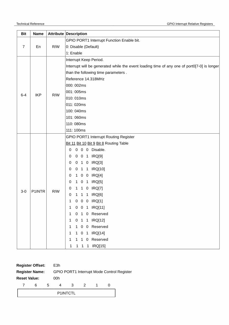
Register Offset: E3h
Register Name: GPIO PORT1 Interrupt Mode Control Register
Reset Value: 00h
7 6 5 4 3 2 1 0
P1INTCTL

Technical Reference Servo Registers
Bit Name Attribute Description
7-0 P1INTCTL R/W
GPIO PORT1 Interrupt Control Register
Bit0 for Port1[0], Bit1 for Port1[1], …, Bit7 for Port1[7]
1: trigger the interrupt continuously if level is activated and match interrupt keep period
settings.
0: Trigger the Interrupt once if level is activated.

3. Servo Registers
Technical Reference Servo Registers
SERVO Registers
(Base Address Refers to the Register of index D3h-D0h, IDSEL = AD18/SB of PCI Configuration Register)
IO Address Register Name
BA + 00H SERVO Interrupt Mask Register
BA + 04H SERVO Interrupt Status Register
BA + 08H SERVO Sync Register
BA + 0CH SERVO[0] Pulse Low Count Register
BA + 10H SERVO[0] Pulse High Count Register
BA + 14H SERVO[0] Control Register
BA + 18H SERVO[1] Pulse Low Count Register
BA + 1CH SERVO[1] Pulse High Count Register
BA + 20H SERVO[1] Control Register
BA + 24H SERVO[2] Pulse Low Count Register
BA + 28H SERVO[2] Pulse High Count Register
BA + 2CH SERVO[2] Control Register
BA + 30H SERVO[3] Pulse Low Count Register
BA + 34H SERVO[3] Pulse High Count Register
BA + 38H SERVO[3] Control Register
BA + 3CH SERVO[4] Pulse Low Count Register
BA + 40H SERVO[4] Pulse High Count Register
BA + 44H SERVO[4] Control Register
BA + 48H SERVO[5] Pulse Low Count Register
BA + 4CH SERVO[5] Pulse High Count Register
BA + 50H SERVO[5] Control Register
BA + 54H SERVO[6] Pulse Low Count Register
BA + 58H SERVO[6] Pulse High Count Register
BA + 5CH SERVO[6] Control Register
BA + 60H SERVO[7] Pulse Low Count Register
BA + 64H SERVO[7] Pulse High Count Register
BA + 68H SERVO[7] Control Register
BA + 6CH SERVO[8] Pulse Low Count Register
BA + 70H SERVO[8] Pulse High Count Register
BA + 74H SERVO[8] Control Register
BA + 78H SERVO[9] Pulse Low Count Register
BA + 7CH SERVO[9] Pulse High Count Register
BA + 80H SERVO[9] Control Register
BA + 84H SERVO[10] Pulse Low Count Register

Technical Reference Servo Registers
IO Address Register Name
BA + 88H SERVO[10] Pulse High Count Register
BA + 8CH SERVO[10] Control Register
BA + 90H SERVO[11] Pulse Low Count Register
BA + 94H SERVO[11] Pulse High Count Register
BA + 98H SERVO[11] Control Register
BA + 9CH SERVO[12] Pulse Low Count Register
BA + A0H SERVO[12] Pulse High Count Register
BA + A4H SERVO[12] Control Register
BA + A8H SERVO[13] Pulse Low Count Register
BA + ACH SERVO[13] Pulse High Count Register
BA + B0H SERVO[13] Control Register
BA + B4H SERVO[14] Pulse Low Count Register
BA + B8H SERVO[14] Pulse High Count Register
BA + BCH SERVO[14] Control Register
BA + C0H SERVO[15] Pulse Low Count Register
BA + C4H SERVO[15] Pulse High Count Register
BA + C8H SERVO[15] Control Register
BA + CCH SERVO[16] Pulse Low Count Register
BA + D0H SERVO[16] Pulse High Count Register
BA + D4H SERVO[16] Control Register
BA + D8H SERVO[17] Pulse Low Count Register
BA + DCH SERVO[17] Pulse High Count Register
BA + E0H SERVO[17] Control Register
BA + E4H SERVO[18] Pulse Low Count Register
BA + E8H SERVO[18] Pulse High Count Register
BA + ECH SERVO[18] Control Register
BA + F0H SERVO[19] Pulse Low Count Register
BA + F4H SERVO[19] Pulse High Count Register
BA + F8H SERVO[19] Control Register
BA + FCH SERVO[20] Pulse Low Count Register
BA + 100H SERVO[20] Pulse High Count Register
BA + 104H SERVO[20] Control Register
BA + 108H SERVO[21] Pulse Low Count Register
BA + 10CH SERVO[21] Pulse High Count Register
BA + 110H SERVO[21] Control Register
BA + 114H SERVO[22] Pulse Low Count Register
BA + 118H SERVO[22] Pulse High Count Register
BA + 11CH SERVO[22] Control Register
BA + 120H SERVO[23] Pulse Low Count Register

Technical Reference Servo Registers
IO Address Register Name
BA + 124H SERVO[23] Pulse High Count Register
BA + 128H SERVO[23] Control Register
BA + 12CH SERVO[24] Pulse Low Count Register
BA + 130H SERVO[24] Pulse High Count Register
BA + 134H SERVO[24] Control Register
BA + 138H SERVO[25] Pulse Low Count Register
BA + 13CH SERVO[25] Pulse High Count Register
BA + 140H SERVO[25] Control Register
BA + 144H SERVO[26] Pulse Low Count Register
BA + 148H SERVO[26] Pulse High Count Register
BA + 14CH SERVO[26] Control Register
BA + 150H SERVO[27] Pulse Low Count Register
BA + 154H SERVO[27] Pulse High Count Register
BA + 158H SERVO[27] Control Register
BA + 15CH SERVO[28] Pulse Low Count Register
BA + 160H SERVO[28] Pulse High Count Register
BA + 164H SERVO[28] Control Register
BA + 168H SERVO[29] Pulse Low Count Register
BA + 16CH SERVO[29] Pulse High Count Register
BA + 170H SERVO[29] Control Register
BA + 174H SERVO[30] Pulse Low Count Register
BA + 178H SERVO[30] Pulse High Count Register
BA + 17CH SERVO[30] Control Register
BA + 180H SERVO[31] Pulse Low Count Register
BA + 184H SERVO[31] Pulse High Count Register
BA + 188H SERVO[31] Control Register
I/O Port: BA + 00h
Register Name: SERVO Interrupt Mask Register
Reset Value: 00000000h
31 30 29 28 27 26 25 24 23 22 21 20 19 18 17 16 15 14 13 12 11 10 9 8 7 6 5 4 3 2 1 0
SIM[31-0]
Bit Name Attribute Description
31-0 SIM[31-0] R/W
SERVO[31-0] Interrupt Mask Register
1: Enable Interrupt
0: Disable Interrupt

Technical Reference Servo Registers
I/O Port: BA + 04h
Register Name: SERVO Interrupt Status Register
Reset Value: 00000000h
31 30 29 28 27 26 25 24 23 22 21 20 19 18 17 16 15 14 13 12 11 10 9 8 7 6 5 4 3 2 1 0
SIS[31-0]
Bit Name Attribute Description
31-0 SIS[31-0] R/W
SERVO[31-0] Interrupt Status Register
1: Interrupt happen and write “1” to clear
0: No Interrupt
I/O Port: BA + 08h
Register Name: SERVO Sync Status Register
Reset Value: 00000000h
31 30 29 28 27 26 25 24 23 22 21 20 19 18 17 16 15 14 13 12 11 10 9 8 7 6 5 4 3 2 1 0
SYNC[31-0]
Bit Name Attribute Description
31-0 SYNC[31-0] R/W
SERVO[31-0] Sync Register
1: SERVO will be hold
0: SERVO without hold
I/O Port: BA + 0CH, 18H, 24H, 30H, 3CH, 48H, 54H, 60H, 6CH, 78H, 84H, 90H, 9CH, A8H, B4H, C0H,
CCH, D8H, E4H, F0H, FCH, 108H, 114H, 120H, 12CH, 138H, 144H, 150H, 15CH, 168H, 174H,
180H
Register Name: SERVO Pulse Low Register
Reset Value: 00000000h
31 30 29 28 27 26 25 24 23 22 21 20 19 18 17 16 15 14 13 12 11 10 9 8 7 6 5 4 3 2 1 0
SPL
Bit Name Attribute Description
31-0 SPL R/W SERVO Pulse Low Register. SERVO clock is 10MHz
I/O Port: BA + 10H, 1CH, 28H, 34H, 40H, 4CH, 58H, 64H, 70H, 7CH, 88H, 94H, A0H, ACH, B8H, C4H, D0H, DCH,
E8H, F4H,100H,10CH,118H,124H,130H,13CH,148H,154H,160H,16CH,178H,184H
Register Name: SERVO Pulse High Register

Technical Reference Servo Registers
Reset Value: 00000000h
31 30 29 28 27 26 25 24 23 22 21 20 19 18 17 16 15 14 13 12 11 10 9 8 7 6 5 4 3 2 1 0
SPH
Bit Name Attribute Description
31-0 SPH R/W SERVO Pulse High Register. SERVO clock is 10MHz
I/O Port: BA + 14H, 20H, 2CH, 38H, 44H, 50H, 5CH, 68H, 74H, 80H, 8CH, 98H, A4H, B0H, BCH, C8H, D4H, E0H,
ECH, F8H, 104H, 110H, 11CH, 128H, 134H, 140H, 14CH, 158H, 164H, 170H, 17CH, 188H
Register Name: SERVO Control Register
Reset Value: 00000000h
31 30 29 28 27 26 25 24 23 22 21 20 19 18 17 16 15 14 13 12 11 10 9 8 7 6 5 4 3 2 1 0
SE
CM
INV
S
Rsvd
RC
Bit Name Attribute Description
31 SE R/W
SERVOx Enable Control
1: SERVOx enable
0: SERVOx disable
30 CM R/W
SERVOx Continuous Mode
1: SERVOx Continuous Mode enable
0: SERVOx Continuous Mode disable
29 INVS R/W
Inverse SERVO signal
0: default SERVO out ‘0’, SPH specify ‘I’, SPL specify “0”.
1: Inverse output signal of upper case
28 Rsvd RO Reserved
27-0 RC R/W SERVOx Repeat Count. It is used when CM=0.

Technical Reference Servo Registers
Vortex86DX South Bridge Configuration Registers
Register Offset: 01h – 00h
Register Name: Vendor ID Register
Reset Value: 17F3h
15 14 13 12 11 10 9 8 7 6 5 4 3 2 1 0
VID
Bit Name Attribute Description
15-0 VID RO This register contains a 16-bit value assigned to South Bridge Vendor ID.
Register Offset: 03h – 02h
Register Name: Device ID Register
Reset Value: 6031h
15 14 13 12 11 10 9 8 7 6 5 4 3 2 1 0
DID
Bit Name Attribute Description
15-0 DID RO This register contains a 16-bit value to specify a particular device.
Register Offset: 4Bh – 48h
Register Name: Buffer Strength/Clock Output Control Register
Reset Value: 3FFF3600h
31 30 29 28 27 26 25 24 23 22 21 20 19 18 17 16 15 14 13 12 11 10 9 8 7 6 5 4 3 2 1 0 R
vd
GP
IO4_D
RV
GP
IO3_3_D
RV
GP
IO3_2_D
RV
GP
IO3_1_D
RV
GP
IO2_D
RV
GP
IO1_D
RV
GP
IO0_D
RV
Rvd
PC
I_CT
L_SR
PC
I_CT
L_DR
V
PC
I_DT
_SR
PC
I_DT
_DR
V
Rvd
ISA
CK
_CT
L
14M_C
TL
24M_C
TL
25M_C
TL
Bit Name Attribute Description
31-30 Rvd RO Reserved
29-28 GPIO4_DRV RW
GPIO4[7-0]/SERVO[31-24]/COM1 Driving Current Control
00: 4mA
01: 8mA
10: 12mA
11: 16mA (default)
21-20 GPIO2_DRV RW GPIO2[7-0]/SERVO[23-16]/SA[31-24] Driving Current Control

Technical Reference Servo Registers
Bit Name Attribute Description
00: 4mA
01: 8mA
10: 12mA
11: 16mA (default)
19-18 GPIO1_DRV RW
GPIO1[7-0]/SERVO[15-8] Driving Current Control
00: 4mA
01: 8mA
10: 12mA
11: 16mA (default)
17-16 GPIO0_DRV RW
GPIO0[7-0]/SERVO[7-0] Driving Current Control
00: 4mA
01: 8mA
10: 12mA
11: 16mA (default)
Register Offset: BFh – BCh
Register Name: On-Chip Device Control Register
Reset Value: 00000000h
31 30 29 28 27 26 25 24 23 22 21 20 19 18 17 16 15 14 13 12 11 10 9 8 7 6 5 4 3 2 1 0
Reserved
UD
P
GS
P
SV
P
G1IP
G0IP
I2C1P
I2C0P
Reserved
PP
P
Reserved
CO
M9P
CO
M4P
CO
M3P
CO
M2P
CO
M1P
Rsvd
MA
CP
US
B2P
US
B1P
IDE
P
Bit Name Attribute Description
20 SVP R/W
ON-Chip SERVO power-down control
0: on-chip SERVO activate (default)
1: on-chip SERVO power-down
Register Offset: C3-C0h
Register Name: Internal Peripheral Feature Control Register
Reset Value: 032C0500h
31 30 29 28 27 26 25 24 23 22 21 20 19 18 17 16 15 14 13 12 11 10 9 8 7 6 5 4 3 2 1 0
Rsvd
IO16W
IO8W
ME
M16W
ME
M8W
ISA
CLK
Int_zw
Rsvd
IDE
IS
PW
M2
PW
M1
PW
M0
FC
DC
MC
LK
EM
IQ
PIN
S6
SF
CE
PIN
S5
PIN
S4
CP
S
PIN
S2
PIN
S1
PIN
S0

Internal Peripheral Feature Control Register II
Technical Reference Servo Registers
Bit Name Attribute Description
1 PINS1 R/W
PINS selection for COM1 and GPIO Port 4
0: 8 PINs for COM1(default)
1: 8 PINs for GPIO port 4
0 PINS0 R/W
PINS selection for External SPI and GPIO Port3 [3-0]
0: 4 pins for GPIO port3 [3-0] (default)
1: 4 pins for external SPI
Register Offset: CBh – C8h
Register Name:
Reset Value: 00000000h
31 30 29 28 27 26 25 24 23 22 21 20 19 18 17 16 15 14 13 12 11 10 9 8 7 6 5 4 3 2 1 0
GS[31-24] GS[23-16] GS[15-8] GS[7-0]
Bit Name Attribute Description
31-24 GS[31-24] R/W
GPIO_P4[7-0] and SERVO[31-24] selection. This register is used only when SB
register C0h bit1 is “1”.
0: PINS for GPIO_P4 (default)
1: PINS for SERVO
23 – 16 GS[23-16] R/W
GPIO_P2[7-0] and SERVO[23-16] selection. This register is used only when
STRAP[1] (NB register 60h bit19) is “1”.
0: PINS for GPIO_P2 (default)
1: PINS for SERVO
15 – 8 GS[15-8] R/W
GPIO_P1[7-0] and SERVO[15-8] selection.
0: PINS for GPIO_P1 (default)
1: PINS for SERVO
7 – 0 GS[7-0] R/W
GPIO_P0[7-0] and SERVO[7-0] selection.
0: PINS for GPIO_P0 (default)
1: PINS for SERVO
Register Offset: D3h – D0h
Register Name: Internal SERVO Control Register
Reset Value: 00000000h
31 30 29 28 27 26 25 24 23 22 21 20 19 18 17 16 15 14 13 12 11 10 9 8 7 6 5 4 3 2 1 0
Reserved
CLK
S
UE
Rsvd SIRT UIOA Reserved

Technical Reference SPI Registers
Bit Name Attribute Description
31-25 Rsvd RO Reserved
24 CLKS R/W
Servo Clock selection
0: 10MHz (default)
1: 50MHz
23 UE R/W
Enable/Disable Internal SERVO IO Address Decode
0: Disable (Default)
1: Enable
22-20 Rsvd RO Reserved
19-16 SIRT R/W
SERVO IRQ Routing Table
Bit19 Bit18 Bit17 Bit16 Routing Table
0 0 0 0 Disable.
0 0 0 1 IRQ[9]
0 0 1 0 IRQ[3]
0 0 1 1 IRQ[10]
0 1 0 0 IRQ[4]
0 1 0 1 IRQ[5]
0 1 1 0 IRQ[7]
0 1 1 1 IRQ[6]
1 0 0 0 IRQ[1]
1 0 0 1 IRQ[11]
1 0 1 0 Reserved
1 0 1 1 IRQ[12]
1 1 0 0 Reserved
1 1 0 1 IRQ[14]
1 1 1 0 Reserved
1 1 1 1 IRQ[15]
These four bits are used to route SERVO IRQ to any 8259 Interrupt lines. The BIOS
should be used to inhibit the setting of the reserved value.
15-9 UIOA R/W Internal SERVO IO Address. The Bit[15:9] contain the base IO address A[15:9] of
internal SERVO.
8-0 Rsvd RO Reserved. All are ‘0’s. Writing any value to these bits causes no effect.

4. SPI Registers
Technical Reference SPI Registers
(Base Address Refers to the Register of index 43h-40h, IDSEL = AD11/NB of PCI Configuration Register)
IO Address Register Name
BA + 00h Flash SPI Output Data Register
BA + 01h Flash SPI Input Data Register
BA + 02h Flash SPI Control Register
BA + 03h Flash SPI Status Register
BA + 04h Flash SPI Chip-Select Register
BA + 05h Flash SPI Error Status Register
BA + 08h External SPI Output Data Register
BA + 09h External SPI Input Register
BA + 0Ah External SPI Control Register
BA + 0Bh External SPI Status Register
BA + 0Ch External SPI Chip Select Register
BA + 0Dh External SPI Error Status Register
BASE_ADDR defined on NB PCI CFG 40h
Register Offset: BASE_ADDR+00h
Register Name: Flash SPI Output Data Register
Reset Value: --
7 6 5 4 3 2 1 0
OUTDAT
Bit Name Attribute Description
7-0 OUTDA
T WO Data output to SPI when write. No function when read.
Register Offset: BASE_ADDR+01h
Register Name: Flash SPI Input Register
Reset Value: FFh
7 6 5 4 3 2 1 0
INDAT
Bit Name Attribute Description
7-1 INDAT R/W Data input from SPI when read. Preload data from SPI when write

Technical Reference SPI Registers
Register Offset: BASE_ADDR+02h
Register Name: Flash SPI Control Register
Reset Value: 55h/5Ah (DRAM frequency <= 200MHz, >200 MHz)
It is not recommended to modify this register when SPI operation.
7 6 5 4 3 2 1 0
RSVD FRE AFDI
S FIEN CKDIV
Bit Name Attribute Description
7 RSVD RO Reserved
6 FRE R/W Fast read enable( This bit can be set if it is NOT AMTEL flash, and Bit 5 must be 0 )
5 AFDIS R/W
0: Auto-fetch enable
1: Auto-fetch disable
Reset to 0 if flash ROM write protect (default).
4 FIEN R/W FIFO mode enable when set.
3-0 CKDIV R/W
SPI clock divided.
The SPI clock is DRAM clock/(2 * SPI clock divided) , 0 is not allowed
Under 45MHz is recommended for Vortex86DX internal SPI flash.
Register Offset: BASE_ADDR+03h
Register Name: Flash SPI Status Register
Reset Value: 10h
7 6 5 4 3 2 1 0
BUSY FIFU IDR ODC RSVD
Bit Name Attribute Description
7 BUSY RO SPI controller is BUSY.
6 FIFU RO FIFO full
5 IDR RO Input data ready when set.
4 ODC RO Output complete/FIFO empty when set.
3-0 RSVD RO Reserved
Register Offset: BASE_ADDR+04h
Register Name: Flash SPI Chip Select Register
Reset Value: 01h
7 6 5 4 3 2 1 0
Reserved CS

Technical Reference SPI Registers
Bit Name Attribute Description
7-1 RSVD RO Reserved
0 CS R/W 0: SPI CS# is low, 1: SPI CS# is high
Register Offset: BASE_ADDR+05h
Register Name: Flash SPI Error Status Register
Reset Value: 00h
7 6 5 4 3 2 1 0
RSVD WCT
E DOLE
FIUR
E
FIOR
E
FHOP
E
Bit Name Attribute Description
7-5 RSVD RO Reserved
4 WCTE R/WC Error status 4, Write SPI Control Register when controller is busy. Write 1 to clear.
3 DOLE R/WC Error status3, Input data overlap. Write 1 to clear.
2 FIURE R/WC Error status2, FIFO under-run. Write 1 to clear.
1 FIORE R/WC Error status1, FIFO over-run. Write 1 to clear.
0 FHOPE R/WC Error status0, CPU fetch during SPI port operation. Write 1 to clear.
Register Offset: BASE_ADDR+08h
Register Name: External SPI Output Data Register
Reset Value: --
7 6 5 4 3 2 1 0
OUTDAT
Bit Name Attribute Description
7-0 OUTDA
T WO Data output to SPI when write. No function when read.
Register Offset: BASE_ADDR+09h
Register Name: External SPI Input Register
Reset Value: FFh
7 6 5 4 3 2 1 0
INDAT
Bit Name Attribute Description

SPI RegistersTechnical Reference
7-1 INDAT RO Data input from SPI when read. Preload data from SPI when write
Register Offset: BASE_ADDR+0Ah
Register Name: External SPI Control Register
Reset Value: 15h
7 6 5 4 3 2 1 0
RSVD FIEN CKDIV
Bit Name Attribute Description
7-5 RSVD RO Reserved
4 FIEN R/W FIFO mode enable when set.
3-0 CKDIV R/W SPI clock divided.
The SPI clock is DRAM clock/(2 * SPI clock divided) , 0 is not allowed
Register Offset: BASE_ADDR+0Bh
Register Name: External SPI Status Register
Reset Value: 10h
7 6 5 4 3 2 1 0
BUSY FIFU IDR ODC RSVD
Bit Name Attribute Description
7 BUSY RO SPI controller is BUSY.
6 FIFU RO FIFO full
5 IDR RO Input data ready when set.
4 ODC RO Output complete/FIFO empty when set.
3-0 RSVD RO Reserved
Register Offset: BASE_ADDR+0Ch
Register Name: External SPI Chip Select Register
Reset Value: 01h
7 6 5 4 3 2 1 0
Reserved CS
Bit Name Attribute Description
7-1 RSVD RO Reserved
0 CS R/W 0: SPI CS# is low, 1: SPI CS# is high

SPI RegistersTechnical Reference
Register Offset: BASE_ADDR+0Dh
Register Name: External SPI Error Status Register
Reset Value: 00h
7 6 5 4 3 2 1 0
RSVD WCT
E DOLE
FIUR
E
FIOR
E RSVD
Bit Name Attribute Description
7-5 RSVD RO Reserved
4 WCTE R/WC Error status 4, Write SPI Control Register when controller is busy. Write 1 to clear.
3 DOLE R/WC Error status3, Input data overlap. Write 1 to clear.
2 FIURE R/WC Error status2, FIFO under-run. Write 1 to clear.
1 FIORE R/WC Error status1, FIFO over-run. Write 1 to clear.
0 RSVD RO Reserved