Experimental investigation of the optimal laser-induced microbridges
8
Precision Engineering 34 (2010) 578–585 Contents lists available at ScienceDirect Precision Engineering journal homepage: www.elsevier.com/locate/precision Experimental investigation of the optimal laser-induced microbridges Kuan-Jung Chung a,* , Joseph B. Bernstein b a Department of Mechatronics Engineering, National Changhua University of Education, No.2 Shida Rd., Changhua 500, Taiwan, ROC b Department of Mechanical Engineering, University of Maryland, College Park, MD 20742, USA article info Article history: Received 16 September 2008 Received in revised form 21 September 2009 Accepted 12 February 2010 Available online 20 February 2010 Keywords: Microbbridges Laser processing materials IC interconnects Laser energy window ASICs abstract Three new microbridge structures, which are able to form lateral-and-vertical links simultaneously in the metal layers of ICs for low resistance interline connections, are presented in order to solve the issue of undesirable links occurred after laser processing. Comprehensive laser processing experiments were performed to verify these designs. The results show that there exits different performance (electrical resistances) and laser energy windows for these structures. There is no perfect design so that one structure (S2) is selected as an optimal structure by considering of the production reality with respect to the highest yield first and then wider energy window, though it only presents the second low resistance. In addition, the same experiments were performed with the scaled-down structure sizes and two additive factors, relative process window and minimum resistance and its variation, are applied as the criteria to evaluate the scalability of these structures. The structure (S2) is selected as an optimal structure since it is the best design for scalability and it has a low resistance in the small scale. Therefore, structure 2 is determined to be the optimal microbridge design for all structures and scales due to the wide laser energy window, low resistance, high yield, and the best scalability. Moreover, it is able to achieve the fundamental requirements of low power consumption and current leakage for most applications of ASICs. © 2010 Elsevier Inc. All rights reserved. 1. Introduction Laser processing techniques have presented widespread appli- cations in the repair of integrated circuit on semiconductor chips for yield enhancement, and in certain custom-made ones. A focused laser pulse is employed to cut the polysilicon “fuses” in defective cells to alter the signal paths to the other functional redundancy ones. The fuses are generally fabricated by heavily doped polycrys- talline silicon lines connected by vias to the metal signal buses, and covered with the glass passivation layer in order to adopt stan- dard semiconductor manufacturing processes [1]. The cutting lines in these fuses have been widely applied with dynamic and static RAMs to improve yields [2]. An alternative laser defect avoidance (redundancy) technique is to connect the collection of digital inverters, gates, counters, and other customized circuit blocks to create a specific or new func- tion for the IC. Cook et al. are one of these pioneers to develop connect and disconnect conductors on FET chips using nanosec- ond nitrogen dye laser pulses, and showed promise for high yield and reliability [3]. Cohen et al. [4] developed the theoretical model of the laser melting thin conducting lines, and it agreed well with * Corresponding author. Tel.: +886 4 7232105x7815; fax: +886 4 7211149. E-mail address: [email protected] (K.-J. Chung). the experimental results. They designed a large area restructurable VLSI circuit that used laser radiation for both cutting lines and form- ing links, shown in Fig. 1 (schematic description). The cutting line is to cut lower metal aluminum lines to open the electrical routes, and the forming-link used a metal-to-metal layer is to connect lines. These structures are generally made by the last step of semiconduc- tor device manufacturing called metallization processes, involved a first layer of 1 m Al–Cu pad, an intermetal layer of 1.5 m SiO 2 ,a second layer of 1.5 m Al–Cu pad, and top layer of 2 m glass layer [5]. Later more devices have been developed using laser additive redundancy techniques to connect the programmable logic arrays (PLAs) [6,7], and now these devices are called application specific integrated circuits (ASICs). Nowadays the integrated circuits are getting dense and com- plicated to drive the metallization process toward fine pitch conductors. The laser cutting technique has become increasingly difficult to obtain high yield due to the lower corner cracks at the metal lines after processing since they use more laser energy than linking technique. Bernstein et al. [8] showed that the unfavor- able cracks by cutting lines damage the intermetal layer to lead the reliability issue such as current leakage and cross-talk between conductors. Hence, the laser energies are limited in order to obtain a clean cut. Later, they developed a only laser formed connection 0141-6359/$ – see front matter © 2010 Elsevier Inc. All rights reserved. doi:10.1016/j.precisioneng.2010.02.002
-
Upload
independent -
Category
Documents
-
view
5 -
download
0
Transcript of Experimental investigation of the optimal laser-induced microbridges
Precision Engineering 34 (2010) 578–585
Contents lists available at ScienceDirect
Precision Engineering
journa l homepage: www.e lsev ier .com/ locate /prec is ion
Experimental investigation of the optimal laser-induced microbridges
Kuan-Jung Chunga,!, Joseph B. Bernsteinb
a Department of Mechatronics Engineering, National Changhua University of Education, No.2 Shida Rd., Changhua 500, Taiwan, ROCb Department of Mechanical Engineering, University of Maryland, College Park, MD 20742, USA
a r t i c l e i n f o
Article history:Received 16 September 2008Received in revised form21 September 2009Accepted 12 February 2010Available online 20 February 2010
Keywords:MicrobbridgesLaser processing materialsIC interconnectsLaser energy windowASICs
a b s t r a c t
Three new microbridge structures, which are able to form lateral-and-vertical links simultaneously inthe metal layers of ICs for low resistance interline connections, are presented in order to solve the issueof undesirable links occurred after laser processing. Comprehensive laser processing experiments wereperformed to verify these designs. The results show that there exits different performance (electricalresistances) and laser energy windows for these structures. There is no perfect design so that one structure(S2) is selected as an optimal structure by considering of the production reality with respect to the highestyield first and then wider energy window, though it only presents the second low resistance.
In addition, the same experiments were performed with the scaled-down structure sizes and twoadditive factors, relative process window and minimum resistance and its variation, are applied as thecriteria to evaluate the scalability of these structures. The structure (S2) is selected as an optimal structuresince it is the best design for scalability and it has a low resistance in the small scale. Therefore, structure2 is determined to be the optimal microbridge design for all structures and scales due to the wide laserenergy window, low resistance, high yield, and the best scalability. Moreover, it is able to achieve thefundamental requirements of low power consumption and current leakage for most applications of ASICs.
© 2010 Elsevier Inc. All rights reserved.
1. Introduction
Laser processing techniques have presented widespread appli-cations in the repair of integrated circuit on semiconductor chipsfor yield enhancement, and in certain custom-made ones. A focusedlaser pulse is employed to cut the polysilicon “fuses” in defectivecells to alter the signal paths to the other functional redundancyones. The fuses are generally fabricated by heavily doped polycrys-talline silicon lines connected by vias to the metal signal buses,and covered with the glass passivation layer in order to adopt stan-dard semiconductor manufacturing processes [1]. The cutting linesin these fuses have been widely applied with dynamic and staticRAMs to improve yields [2].
An alternative laser defect avoidance (redundancy) technique isto connect the collection of digital inverters, gates, counters, andother customized circuit blocks to create a specific or new func-tion for the IC. Cook et al. are one of these pioneers to developconnect and disconnect conductors on FET chips using nanosec-ond nitrogen dye laser pulses, and showed promise for high yieldand reliability [3]. Cohen et al. [4] developed the theoretical modelof the laser melting thin conducting lines, and it agreed well with
! Corresponding author. Tel.: +886 4 7232105x7815; fax: +886 4 7211149.E-mail address: [email protected] (K.-J. Chung).
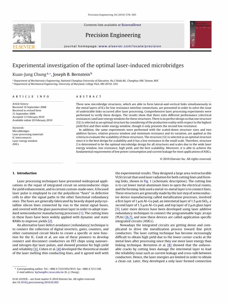
the experimental results. They designed a large area restructurableVLSI circuit that used laser radiation for both cutting lines and form-ing links, shown in Fig. 1 (schematic description). The cutting lineis to cut lower metal aluminum lines to open the electrical routes,and the forming-link used a metal-to-metal layer is to connect lines.These structures are generally made by the last step of semiconduc-tor device manufacturing called metallization processes, involveda first layer of 1 !m Al–Cu pad, an intermetal layer of 1.5 !m SiO2, asecond layer of 1.5 !m Al–Cu pad, and top layer of 2 !m glass layer[5]. Later more devices have been developed using laser additiveredundancy techniques to connect the programmable logic arrays(PLAs) [6,7], and now these devices are called application specificintegrated circuits (ASICs).
Nowadays the integrated circuits are getting dense and com-plicated to drive the metallization process toward fine pitchconductors. The laser cutting technique has become increasinglydifficult to obtain high yield due to the lower corner cracks at themetal lines after processing since they use more laser energy thanlinking technique. Bernstein et al. [8] showed that the unfavor-able cracks by cutting lines damage the intermetal layer to leadthe reliability issue such as current leakage and cross-talk betweenconductors. Hence, the laser energies are limited in order to obtaina clean cut. Later, they developed a only laser formed connection
0141-6359/$ – see front matter © 2010 Elsevier Inc. All rights reserved.doi:10.1016/j.precisioneng.2010.02.002
K.-J. Chung, J.B. Bernstein / Precision Engineering 34 (2010) 578–585 579
Fig. 1. Schematic description of programmable VLSI circuits using laser radiation,developed by Cohen et al. [4].
without any cutting line, called MakeLink®,1 and showed muchgreater promise with wide laser energies and high yields in redun-dant and programmatic devices [9–12].
The design of MakeLink is classified by lateral-link and vertical-link. The first structure of lateral-link is a direct metal-to-metalconnection between two adjacent metal lines on the same level ofmetallization. The energy of a pulsed laser absorbed mostly by themetal generates enormous thermal stress to break the surroundeddielectrics, then the molten metal fills the crack to form the link[11,13]. The second vertical-link is formed by the same mechanismbut the link connection is between two different levels of metal-lization. The vertical-link structure has several advantages such assmaller size design and higher reliability [14,15]. Many applicationssuch as Laser PROM, laser field programmable gate array (LFPGA),and analog array (LFPAA) have been developed using MakeLinkstructure as the connections between circuit blocks [16,17].
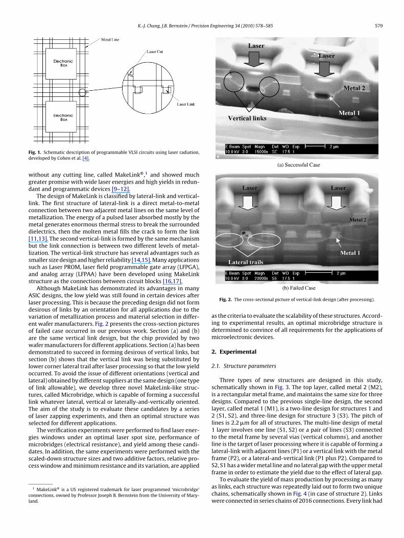
Although MakeLink has demonstrated its advantages in manyASIC designs, the low yield was still found in certain devices afterlaser processing. This is because the preceding design did not formdesirous of links by an orientation for all applications due to thevariation of metallization process and material selection in differ-ent wafer manufacturers. Fig. 2 presents the cross-section picturesof failed case occurred in our previous work. Section (a) and (b)are the same vertical link design, but the chip provided by twowafer manufacturers for different applications. Section (a) has beendemonstrated to succeed in forming desirous of vertical links, butsection (b) shows that the vertical link was being substituted bylower corner lateral trail after laser processing so that the low yieldoccurred. To avoid the issue of different orientations (vertical andlateral) obtained by different suppliers at the same design (one typeof link allowable), we develop three novel MakeLink-like struc-tures, called Microbridge, which is capable of forming a successfullink whatever lateral, vertical or laterally-and-vertically oriented.The aim of the study is to evaluate these candidates by a seriesof laser zapping experiments, and then an optimal structure wasselected for different applications.
The verification experiments were performed to find laser ener-gies windows under an optimal laser spot size, performance ofmicrobridges (electrical resistance), and yield among these candi-dates. In addition, the same experiments were performed with thescaled-down structure sizes and two additive factors, relative pro-cess window and minimum resistance and its variation, are applied
1 MakeLink® is a US registered trademark for laser programmed ‘microbridge’connections, owned by Professor Joseph B. Bernstein from the University of Mary-land.
Fig. 2. The cross-sectional picture of vertical-link design (after processing).
as the criteria to evaluate the scalability of these structures. Accord-ing to experimental results, an optimal microbridge structure isdetermined to convince of all requirements for the applications ofmicroelectronic devices.
2. Experimental
2.1. Structure parameters
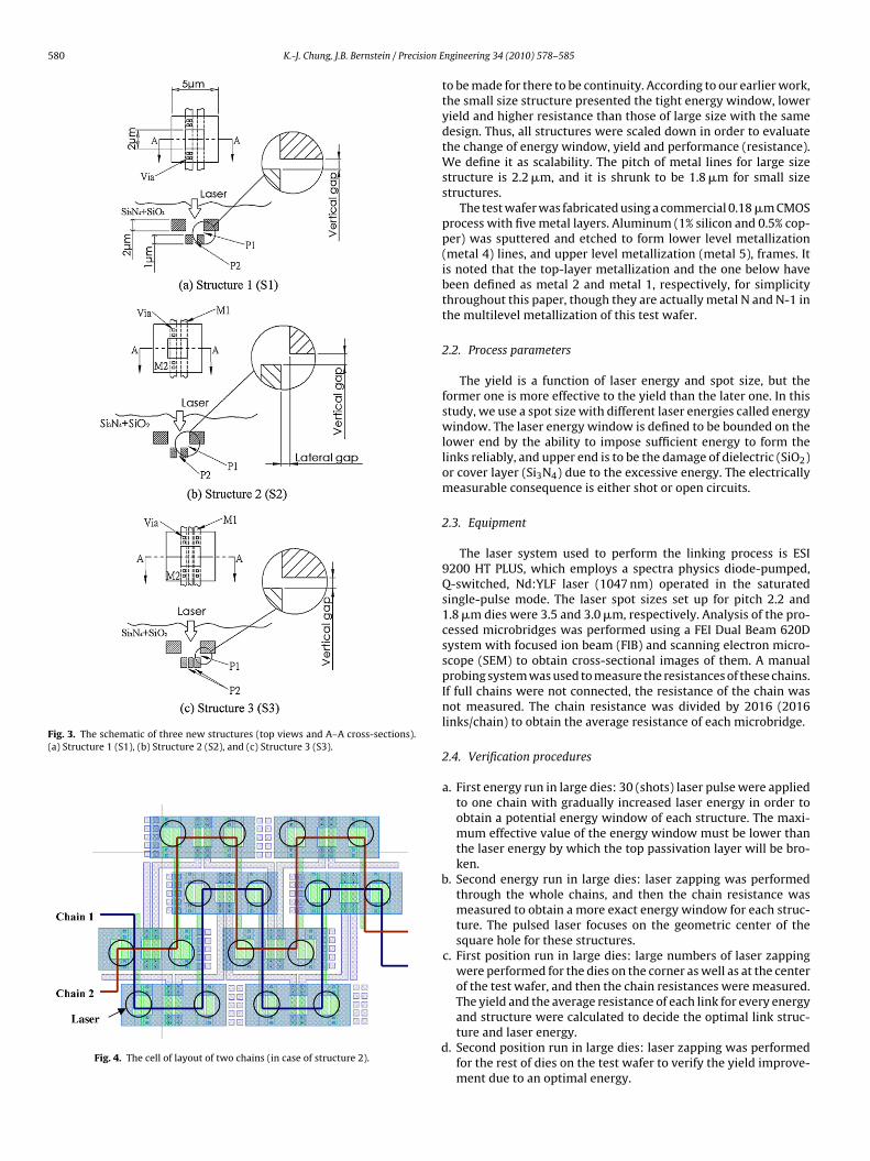
Three types of new structures are designed in this study,schematically shown in Fig. 3. The top layer, called metal 2 (M2),is a rectangular metal frame, and maintains the same size for threedesigns. Compared to the previous single-line design, the secondlayer, called metal 1 (M1), is a two-line design for structures 1 and2 (S1, S2), and three-line design for structure 3 (S3). The pitch oflines is 2.2 !m for all of structures. The multi-line design of metal1 layer involves one line (S1, S2) or a pair of lines (S3) connectedto the metal frame by several vias (vertical columns), and anotherline is the target of laser processing where it is capable of forming alateral-link with adjacent lines (P1) or a vertical link with the metalframe (P2), or a lateral-and-vertical link (P1 plus P2). Compared toS2, S1 has a wider metal line and no lateral gap with the upper metalframe in order to estimate the yield due to the effect of lateral gap.
To evaluate the yield of mass production by processing as manyas links, each structure was repeatedly laid out to form two uniquechains, schematically shown in Fig. 4 (in case of structure 2). Linkswere connected in series chains of 2016 connections. Every link had
580 K.-J. Chung, J.B. Bernstein / Precision Engineering 34 (2010) 578–585
Fig. 3. The schematic of three new structures (top views and A–A cross-sections).(a) Structure 1 (S1), (b) Structure 2 (S2), and (c) Structure 3 (S3).
Fig. 4. The cell of layout of two chains (in case of structure 2).
to be made for there to be continuity. According to our earlier work,the small size structure presented the tight energy window, loweryield and higher resistance than those of large size with the samedesign. Thus, all structures were scaled down in order to evaluatethe change of energy window, yield and performance (resistance).We define it as scalability. The pitch of metal lines for large sizestructure is 2.2 !m, and it is shrunk to be 1.8 !m for small sizestructures.
The test wafer was fabricated using a commercial 0.18 !m CMOSprocess with five metal layers. Aluminum (1% silicon and 0.5% cop-per) was sputtered and etched to form lower level metallization(metal 4) lines, and upper level metallization (metal 5), frames. Itis noted that the top-layer metallization and the one below havebeen defined as metal 2 and metal 1, respectively, for simplicitythroughout this paper, though they are actually metal N and N-1 inthe multilevel metallization of this test wafer.
2.2. Process parameters
The yield is a function of laser energy and spot size, but theformer one is more effective to the yield than the later one. In thisstudy, we use a spot size with different laser energies called energywindow. The laser energy window is defined to be bounded on thelower end by the ability to impose sufficient energy to form thelinks reliably, and upper end is to be the damage of dielectric (SiO2)or cover layer (Si3N4) due to the excessive energy. The electricallymeasurable consequence is either shot or open circuits.
2.3. Equipment
The laser system used to perform the linking process is ESI9200 HT PLUS, which employs a spectra physics diode-pumped,Q-switched, Nd:YLF laser (1047 nm) operated in the saturatedsingle-pulse mode. The laser spot sizes set up for pitch 2.2 and1.8 !m dies were 3.5 and 3.0 !m, respectively. Analysis of the pro-cessed microbridges was performed using a FEI Dual Beam 620Dsystem with focused ion beam (FIB) and scanning electron micro-scope (SEM) to obtain cross-sectional images of them. A manualprobing system was used to measure the resistances of these chains.If full chains were not connected, the resistance of the chain wasnot measured. The chain resistance was divided by 2016 (2016links/chain) to obtain the average resistance of each microbridge.
2.4. Verification procedures
a. First energy run in large dies: 30 (shots) laser pulse were appliedto one chain with gradually increased laser energy in order toobtain a potential energy window of each structure. The maxi-mum effective value of the energy window must be lower thanthe laser energy by which the top passivation layer will be bro-ken.
b. Second energy run in large dies: laser zapping was performedthrough the whole chains, and then the chain resistance wasmeasured to obtain a more exact energy window for each struc-ture. The pulsed laser focuses on the geometric center of thesquare hole for these structures.
c. First position run in large dies: large numbers of laser zappingwere performed for the dies on the corner as well as at the centerof the test wafer, and then the chain resistances were measured.The yield and the average resistance of each link for every energyand structure were calculated to decide the optimal link struc-ture and laser energy.
d. Second position run in large dies: laser zapping was performedfor the rest of dies on the test wafer to verify the yield improve-ment due to an optimal energy.
K.-J. Chung, J.B. Bernstein / Precision Engineering 34 (2010) 578–585 581
Fig. 5. Energy windows of large dies (pitch 2.2 !m).
e. Repeat the procedure (a)–(d) for the small die (pitch 1.8 !m) toevaluate the scalability of these structures.
3. Results and discussion
3.1. Process development for 2.2 !m pitch chip (large size)
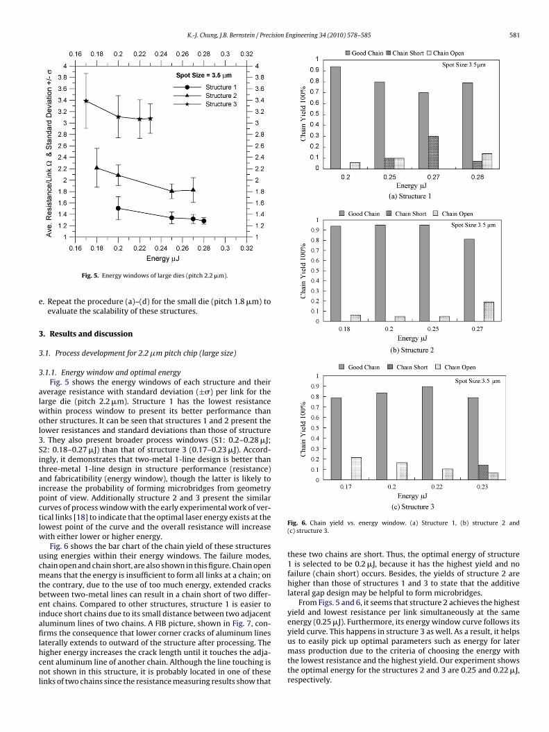
3.1.1. Energy window and optimal energyFig. 5 shows the energy windows of each structure and their
average resistance with standard deviation (±") per link for thelarge die (pitch 2.2 !m). Structure 1 has the lowest resistancewithin process window to present its better performance thanother structures. It can be seen that structures 1 and 2 present thelower resistances and standard deviations than those of structure3. They also present broader process windows (S1: 0.2–0.28 !J;S2: 0.18–0.27 !J) than that of structure 3 (0.17–0.23 !J). Accord-ingly, it demonstrates that two-metal 1-line design is better thanthree-metal 1-line design in structure performance (resistance)and fabricatibility (energy window), though the latter is likely toincrease the probability of forming microbridges from geometrypoint of view. Additionally structure 2 and 3 present the similarcurves of process window with the early experimental work of ver-tical links [18] to indicate that the optimal laser energy exists at thelowest point of the curve and the overall resistance will increasewith either lower or higher energy.
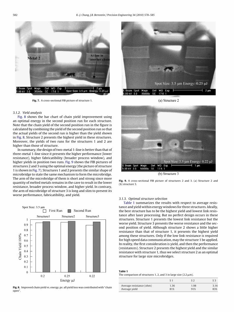
Fig. 6 shows the bar chart of the chain yield of these structuresusing energies within their energy windows. The failure modes,chain open and chain short, are also shown in this figure. Chain openmeans that the energy is insufficient to form all links at a chain; onthe contrary, due to the use of too much energy, extended cracksbetween two-metal lines can result in a chain short of two differ-ent chains. Compared to other structures, structure 1 is easier toinduce short chains due to its small distance between two adjacentaluminum lines of two chains. A FIB picture, shown in Fig. 7, con-firms the consequence that lower corner cracks of aluminum lineslaterally extends to outward of the structure after processing. Thehigher energy increases the crack length until it touches the adja-cent aluminum line of another chain. Although the line touching isnot shown in this structure, it is probably located in one of theselinks of two chains since the resistance measuring results show that
Fig. 6. Chain yield vs. energy window. (a) Structure 1, (b) structure 2 and(c) structure 3.
these two chains are short. Thus, the optimal energy of structure1 is selected to be 0.2 !J, because it has the highest yield and nofailure (chain short) occurs. Besides, the yields of structure 2 arehigher than those of structures 1 and 3 to state that the additivelateral gap design may be helpful to form microbridges.
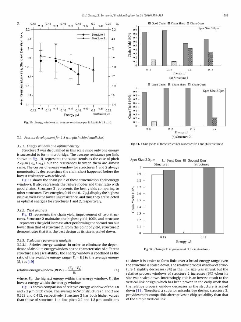
From Figs. 5 and 6, it seems that structure 2 achieves the highestyield and lowest resistance per link simultaneously at the sameenergy (0.25 !J). Furthermore, its energy window curve follows itsyield curve. This happens in structure 3 as well. As a result, it helpsus to easily pick up optimal parameters such as energy for latermass production due to the criteria of choosing the energy withthe lowest resistance and the highest yield. Our experiment showsthe optimal energy for the structures 2 and 3 are 0.25 and 0.22 !J,respectively.
582 K.-J. Chung, J.B. Bernstein / Precision Engineering 34 (2010) 578–585
Fig. 7. A cross-sectional FIB picture of structure 1.
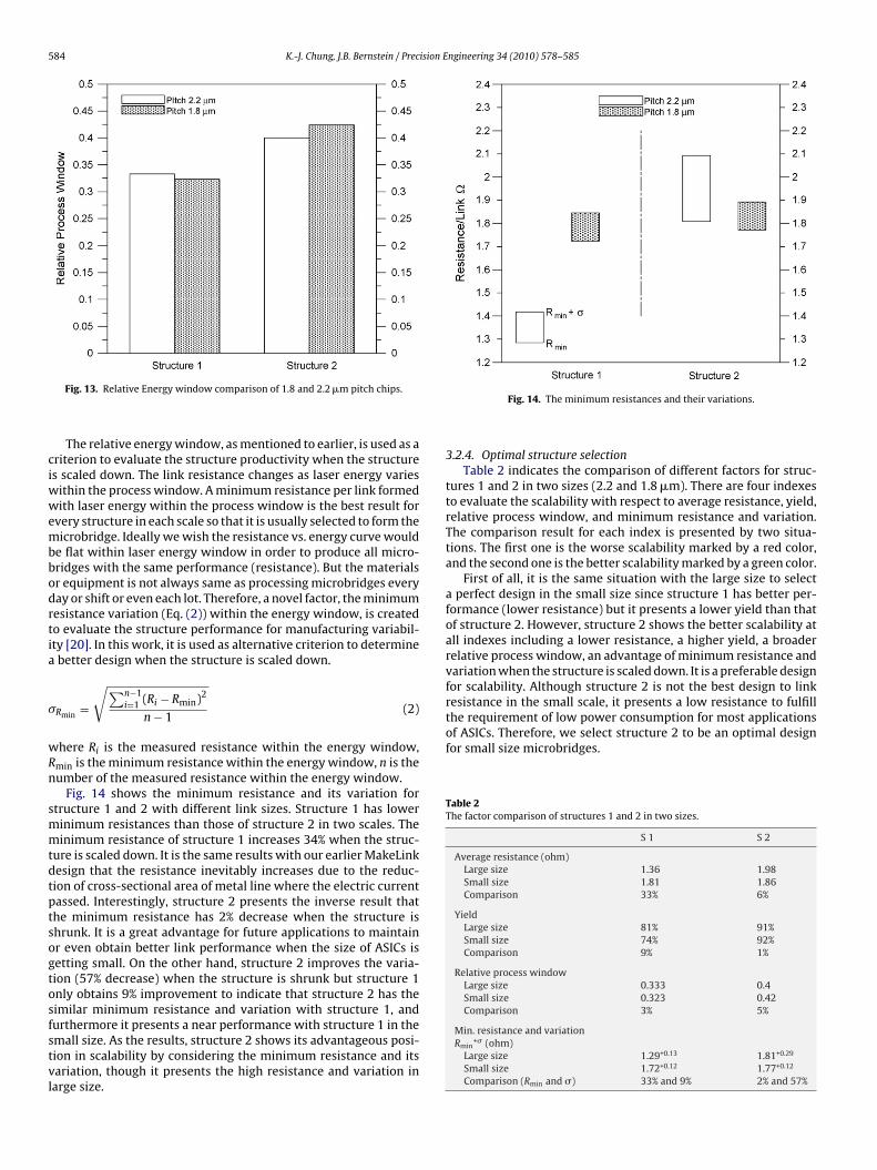
3.1.2. Yield analysisFig. 8 shows the bar chart of chain yield improvement using
an optimal energy in the second position run for each structure.Note that the chain yield of the second position run in the figure iscalculated by combining the yield of the second position run so thatthe actual yields of the second run is higher than the yield shownin Fig. 8. Structure 2 presents the highest yield in these structures.Moreover, the yields of two runs for the structures 1 and 2 arehigher than those of structure.
In summary, the design of two-metal 1-line is better than that ofthree-metal 1-line since it presents the higher performance (lowerresistance), higher fabricatibility (broader process window), andhigher yields in position two runs. Fig. 9 shows the FIB pictures ofstructures 2 and 3 using the optimal energy (the picture of structure1 is shown in Fig. 7). Structures 1 and 2 presents the similar shape ofmicrobridge to state the same mechanism to form the microbridge.The arm of the microbridge of them is short and strong since morequantity of melted metals remains in the cave to result in the lowerresistance, broader process window, and higher yield. In contrary,the arm of microbridge of structure 3 is long and slim to present itsworse performance, fabricatibility, and yield.
Fig. 8. Improved chain yield vs. energy. ps: all yield loss was contributed with “chainopen”.
Fig. 9. A cross-sectional FIB picture of structures 2 and 3. (a) Structure 2 and(b) structure 3.
3.1.3. Optimal structure selectionTable 1 summarizes the results with respect to average resis-
tance and yield within energy windows for three structures. Ideally,the best structure has to be the highest yield and lowest link resis-tance after laser processing. But no perfect design occurs in thesestructures. Structure 1 presents the lowest link resistance but theworse yield. Structure 3 presents the worse resistance and the sec-ond position of yield. Although structure 2 shows a little higherresistance than that of structure 1, it presents the highest yieldamong these structures. Only if the low link resistance is requiredfor high speed data communication, may the structure 1 be applied.In reality, the first consideration is yield, and then the performance(resistances). Structure 2 presents the highest yield and the similarresistance with structure 1, thus we select structure 2 as an optimalstructure for large size microbridges.
Table 1The comparison of structures 1, 2, and 3 in large size (2.2 !m).
S 1 S 2 S 3
Average resistance (ohm) 1.36 1.98 3.16Average yield 81% 91% 83%
3.2.3.2. Minimum resistance and its variation.
K.-J. Chung, J.B. Bernstein / Precision Engineering 34 (2010) 578–585 583
Fig. 10. Energy windows vs. average resistance per link (pitch 1.8 !m).
3.2. Process development for 1.8 !m pitch chip (small size)
3.2.1. Energy window and optimal energyStructure 3 was disqualified in this scale since only one energy
is successful to form microbridge. The average resistance per link,shown in Fig. 10, represents the same trends as the case of pitch2.2 !m (RS2 > RS1), but the resistances between them are almostsame. The curves of energy window for structures 1 and 2 alwaysmonotonically decrease since the chain short happened before thelowest resistance was achieved.
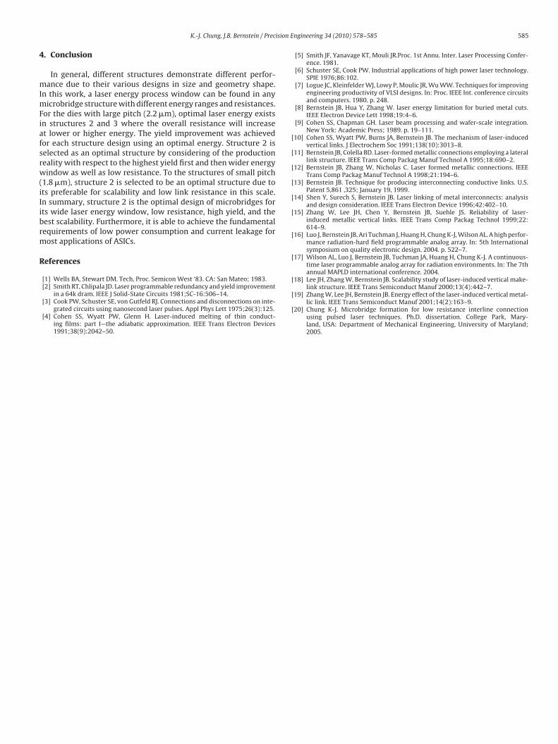
Fig. 11 shows the chain yield of these structures vs. their energywindows. It also represents the failure modes and their ratio withgood chains. Structure 2 represents the best yields comparing toother structures. Two energies, 0.15 and 0.17 !J, display the highestyield as well as the lower link resistance, and thus they are selectedas optimal energies for structures 1 and 2, respectively.
3.2.2. Yield analysisFig. 12 represents the chain yield improvement of two struc-
tures. Structure 2 maintains the highest yield 100%, and structure1 represents the yield increase after performing the second run butlower than that of structure 2. From the point of yield, structure 2demonstrates that it is the best design as its size is scaled down.
3.2.3. Scalability parameter analysis3.2.3.1. Relative energy window. In order to eliminate the depen-dence of absolute energy window on the characteristics of differentstructure sizes (scalability), the energy window is redefined as theratio of the available energy range (Eh " El) to the average energy(Ea) as [19]
relative energy window (REW) = (Eh " El)Ea
(1)
where, Eh: the highest energy within the energy window, El: thelowest energy within the energy window.
Fig. 13 shows comparison of relative energy window of the 1.8and 2.2 !m pitch chips. The average REW of structures 1 and 2 are0.328 and 0.412, respectively. Structure 2 has both higher valuesthan those of structure 1 in line pitch 2.2 and 1.8 !m conditions
Fig. 11. Chain yields of these structures. (a) Structure 1 and (b) structure 2.
Fig. 12. Chain yield improvement of these structures.
to show it is easier to form links over a broad energy range eventhe structure is scaled down. The relative process window of struc-ture 1 slightly decreases (3%) as the link size was shrunk but therelative process windows of structure 2 increases (6%) when itssize was scaled down. Interestingly, this is an inverse result to thevertical link design, which has been proven in the early work thatthe relative process window decreases as the structure is scaleddown [11]. Therefore, a superior microbridge design, structure 2,provides more compatible alternatives in chip scalability than thatof the simple vertical link.
584 K.-J. Chung, J.B. Bernstein / Precision Engineering 34 (2010) 578–585
Fig. 13. Relative Energy window comparison of 1.8 and 2.2 !m pitch chips.
The relative energy window, as mentioned to earlier, is used as acriterion to evaluate the structure productivity when the structureis scaled down. The link resistance changes as laser energy varieswithin the process window. A minimum resistance per link formedwith laser energy within the process window is the best result forevery structure in each scale so that it is usually selected to form themicrobridge. Ideally we wish the resistance vs. energy curve wouldbe flat within laser energy window in order to produce all micro-bridges with the same performance (resistance). But the materialsor equipment is not always same as processing microbridges everyday or shift or even each lot. Therefore, a novel factor, the minimumresistance variation (Eq. (2)) within the energy window, is createdto evaluate the structure performance for manufacturing variabil-ity [20]. In this work, it is used as alternative criterion to determinea better design when the structure is scaled down.
"Rmin =
!"n"1i=1 (Ri " Rmin)2
n " 1(2)
where Ri is the measured resistance within the energy window,Rmin is the minimum resistance within the energy window, n is thenumber of the measured resistance within the energy window.
Fig. 14 shows the minimum resistance and its variation forstructure 1 and 2 with different link sizes. Structure 1 has lowerminimum resistances than those of structure 2 in two scales. Theminimum resistance of structure 1 increases 34% when the struc-ture is scaled down. It is the same results with our earlier MakeLinkdesign that the resistance inevitably increases due to the reduc-tion of cross-sectional area of metal line where the electric currentpassed. Interestingly, structure 2 presents the inverse result thatthe minimum resistance has 2% decrease when the structure isshrunk. It is a great advantage for future applications to maintainor even obtain better link performance when the size of ASICs isgetting small. On the other hand, structure 2 improves the varia-tion (57% decrease) when the structure is shrunk but structure 1only obtains 9% improvement to indicate that structure 2 has thesimilar minimum resistance and variation with structure 1, andfurthermore it presents a near performance with structure 1 in thesmall size. As the results, structure 2 shows its advantageous posi-tion in scalability by considering the minimum resistance and itsvariation, though it presents the high resistance and variation inlarge size.
Fig. 14. The minimum resistances and their variations.
3.2.4. Optimal structure selectionTable 2 indicates the comparison of different factors for struc-
tures 1 and 2 in two sizes (2.2 and 1.8 !m). There are four indexesto evaluate the scalability with respect to average resistance, yield,relative process window, and minimum resistance and variation.The comparison result for each index is presented by two situa-tions. The first one is the worse scalability marked by a red color,and the second one is the better scalability marked by a green color.
First of all, it is the same situation with the large size to selecta perfect design in the small size since structure 1 has better per-formance (lower resistance) but it presents a lower yield than thatof structure 2. However, structure 2 shows the better scalability atall indexes including a lower resistance, a higher yield, a broaderrelative process window, an advantage of minimum resistance andvariation when the structure is scaled down. It is a preferable designfor scalability. Although structure 2 is not the best design to linkresistance in the small scale, it presents a low resistance to fulfillthe requirement of low power consumption for most applicationsof ASICs. Therefore, we select structure 2 to be an optimal designfor small size microbridges.
Table 2The factor comparison of structures 1 and 2 in two sizes.
S 1 S 2
Average resistance (ohm)Large size 1.36 1.98Small size 1.81 1.86Comparison 33% 6%
YieldLarge size 81% 91%Small size 74% 92%Comparison 9% 1%
Relative process windowLarge size 0.333 0.4Small size 0.323 0.42Comparison 3% 5%
Min. resistance and variationRmin
+" (ohm)Large size 1.29+0.13 1.81+0.29
Small size 1.72+0.12 1.77+0.12
Comparison (Rmin and ") 33% and 9% 2% and 57%
K.-J. Chung, J.B. Bernstein / Precision Engineering 34 (2010) 578–585 585
4. Conclusion
In general, different structures demonstrate different perfor-mance due to their various designs in size and geometry shape.In this work, a laser energy process window can be found in anymicrobridge structure with different energy ranges and resistances.For the dies with large pitch (2.2 !m), optimal laser energy existsin structures 2 and 3 where the overall resistance will increaseat lower or higher energy. The yield improvement was achievedfor each structure design using an optimal energy. Structure 2 isselected as an optimal structure by considering of the productionreality with respect to the highest yield first and then wider energywindow as well as low resistance. To the structures of small pitch(1.8 !m), structure 2 is selected to be an optimal structure due toits preferable for scalability and low link resistance in this scale.In summary, structure 2 is the optimal design of microbridges forits wide laser energy window, low resistance, high yield, and thebest scalability. Furthermore, it is able to achieve the fundamentalrequirements of low power consumption and current leakage formost applications of ASICs.
References
[1] Wells BA, Stewart DM. Tech, Proc. Semicon West ‘83. CA: San Mateo; 1983.[2] Smith RT, Chlipala JD. Laser programmable redundancy and yield improvement
in a 64k dram. IEEE J Solid-State Circuits 1981;SC-16:506–14.[3] Cook PW, Schuster SE, von Gutfeld RJ. Connections and disconnections on inte-
grated circuits using nanosecond laser pulses. Appl Phys Lett 1975;26(3):125.[4] Cohen SS, Wyatt PW, Glenn H. Laser-induced melting of thin conduct-
ing films: part I—the adiabatic approximation. IEEE Trans Electron Devices1991;38(9):2042–50.
[5] Smith JF, Yanavage KT, Mouli JR.Proc. 1st Annu. Inter. Laser Processing Confer-ence. 1981.
[6] Schuster SE, Cook PW. Industrial applications of high power laser technology.SPIE 1976;86:102.
[7] Logue JC, Kleinfelder WJ, Lowy P, Moulic JR, Wu WW. Techniques for improvingengineering productivity of VLSI designs. In: Proc. IEEE Int. conference circuitsand computers. 1980. p. 248.
[8] Bernstein JB, Hua Y, Zhang W. laser energy limitation for buried metal cuts.IEEE Electron Device Lett 1998;19:4–6.
[9] Cohen SS, Chapman GH. Laser beam processing and wafer-scale integration.New York: Academic Press; 1989. p. 19–111.
[10] Cohen SS, Wyatt PW, Burns JA, Bernstein JB. The mechanism of laser-inducedvertical links. J Electrochem Soc 1991;138(10):3013–8.
[11] Bernstein JB, Colella BD. Laser-formed metallic connections employing a laterallink structure. IEEE Trans Comp Packag Manuf Technol A 1995;18:690–2.
[12] Bernstein JB, Zhang W, Nicholas C. Laser formed metallic connections. IEEETrans Comp Packag Manuf Technol A 1998;21:194–6.
[13] Bernstein JB. Technique for producing interconnecting conductive links. U.S.Patent 5,861 ,325; January 19, 1999.
[14] Shen Y, Surech S, Bernstein JB. Laser linking of metal interconnects: analysisand design consideration. IEEE Trans Electron Device 1996;42:402–10.
[15] Zhang W, Lee JH, Chen Y, Bernstein JB, Suehle JS. Reliability of laser-induced metallic vertical links. IEEE Trans Comp Packag Technol 1999;22:614–9.
[16] Luo J, Bernstein JB, Ari Tuchman J, Huang H, Chung K-J, Wilson AL. A high perfor-mance radiation-hard field programmable analog array. In: 5th Internationalsymposium on quality electronic design. 2004. p. 522–7.
[17] Wilson AL, Luo J, Bernstein JB, Tuchman JA, Huang H, Chung K-J. A continuous-time laser programmable analog array for radiation environments. In: The 7thannual MAPLD international conference. 2004.
[18] Lee JH, Zhang W, Bernstein JB. Scalability study of laser-induced vertical make-link structure. IEEE Trans Semiconduct Manuf 2000;13(4):442–7.
[19] Zhang W, Lee JH, Bernstein JB. Energy effect of the laser-induced vertical metal-lic link. IEEE Trans Semiconduct Manuf 2001;14(2):163–9.
[20] Chung K-J. Microbridge formation for low resistance interline connectionusing pulsed laser techniques. Ph.D. dissertation. College Park, Mary-land, USA: Department of Mechanical Engineering, University of Maryland;2005.