EXPERIMENT REPORT OF BASIC MATERIAL SCIENCE
30
EXPERIMENT REPORT OF BASIC MATERIAL SCIENCE Written By : MUHAMAD RIZKI 1111097000016 DEPARTMENT OF PHYSICS FACULTY OF SCIENCE & TECHNOLOGY UNIVERSITAS ISLAM NEGERI SYARIF HIDAYATULLAH JAKARTA 2014
Transcript of EXPERIMENT REPORT OF BASIC MATERIAL SCIENCE
EXPERIMENT REPORT
OF
BASIC MATERIAL SCIENCE
Written By :
MUHAMAD RIZKI
1111097000016
DEPARTMENT OF PHYSICS
FACULTY OF SCIENCE & TECHNOLOGY
UNIVERSITAS ISLAM NEGERI SYARIF HIDAYATULLAH
JAKARTA
2014

i
PREFACE
Assalaamu'alaikum Warrahmatullahi Wabarakatuh,
Praise to Allah, the Lord of hosts who have given favors health and free time so that this
paper can be resolved. Blessings and greetings do not forget to always delivered to the Prophet
Muhammad, his family, his companions and his followers that we may remain unchanged to
follow his teachings. Ameen.
Material Physics is a science that studies the properties of solid materials. In this paper,
insya Allah, Iwill discuss on some physical properties of materials.
Do not forget to always say, thank you for those who helped to complete this paper. Thanks
to Basic Material Science Experiment lecturer, Priyambodo, S.Si which has provided an overview
of the material. Thanks also to the parents and brothers, sisters, & Indira Juliana Safitri who are
always motivating and pray that the completion of this paper and do not forget to also thank
companions in arms at the Physics Department of UIN Jakarta 2011 class.
We apologize for the shortcomings of this paper. As a constituent, I really hope there is
constructive criticism and suggestions to this paper. Hopefully that is in this paper could be better
and could be an inspiration to every reader, ameen ya Robb. Similarly, exposure of me.
Wassalamu'alaykum Warrohmatullohi Wabarokatuh.
ii
CONTENTS
1. Characteristics of Semiconductor’s Electrical Resistance ........................................ 1
2. Characteristics of Conductor’s Electrical Resistance ............................................... 6
3. Ferromagnetic Hysterisis Curve ............................................................................... 12
4. Diamagnetic, Paramagnetic, Ferromagnetic Substance ............................................ 15
5. Scanning Tunneling Microscope (STM) .................................................................. 19
6. Elastic Deformation .................................................................................................. 24

1
Characteristics of Semiconductor’s Electrical Resistance
A. OBJECTIVE
- To determine influence of temperature to semiconductor electrical resistance.
- To obtain gap energy value in the semiconductor.
B. THEORIES
Semiconductors constitute a large class of substances which have resistivities lying
between those of insulators and conductors. The resistivity of semiconductors varies in wide
limits, i.e., 10–4 to 104 Ω-m and is reduced to a very great extent with an increase in temperature
(according to an exponential law) as shown in Figure below.
It has been found that semiconductor will become insulator in the low temperatur and will
become conductor in the high temperature. It has been proven by measuring its electrical resistivity
when it heated.The resistivity changing by temperatur changing can be expressed by equation :
kTEeRR 2/
0
whereas:
T : temperature (K)
R : electric resistance (Ω)
Figure 1.1 Graph of Temperature Influence to Electrical Resistance

2
E : gap Energy (J)
k : Bolztmann constant = 1,38 . 10-23 J/K or = 86,1 x 10⁻⁶ eV/K
The band structure in a solid determines whether the solid is an insulator or a conductor or
a semiconductor. The bands are filled up to a certain level by the electrons within each atom. The
highest band in which electrons are still predominantly attached to their atoms are found is
called the valence band. This is the band in which the valence (outermost) electrons from each
atom will be located. These are the electrons that are the possible carriers of electricity.
However, in order for an electron to conduct, it must get up to a slightly higher energy so that is
free of the grip of its atom.
When the electrons excitated toward conducting band populated by electrons and leaves
valence band populated by holes. As result, both bands wills half-filled and it Wills conducting
charge if it given an electrical field.The valence energy can be expressed by :
*
22
2)(
h
vm
kkE
The main parameter of the energy is me, mh and band gap Eg.
C. Apparatus & Methods
The experiments measure the resistance values as a function of temperature using a
Wheatstone bridge. The multimeter measured-value recording system is ideal for recording and
evaluating the measurements.
3
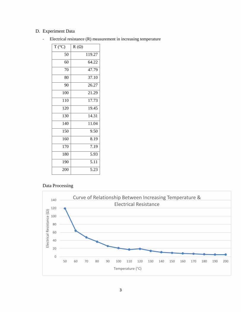
D. Experiment Data
- Electrical resistance (R) measurement in increasing temperature
T (°C) R (Ω)
50 119.27
60 64.22
70 47.79
80 37.10
90 26.27
100 21.29
110 17.73
120 19.45
130 14.31
140 11.04
150 9.50
160 8.19
170 7.19
180 5.93
190 5.11
200 5.23
Data Processing
0
20
40
60
80
100
120
140
50 60 70 80 90 100 110 120 130 140 150 160 170 180 190 200
Elec
tric
al R
esis
tan
ce (
Ω)
Temperature (°C)
Curve of Relationship Between Increasing Temperature & Electrical Resistance

4
Gap Energy calculation on the semiconductor
R0 = 119.27 Ω
T (°C) R (Ω) T (K) x (1/T) y (ln R) x2 x.y
50 119.27 323 0.003096 5 9.59E-06 0.014803
60 64.22 333 0.003003 4 9.02E-06 0.012499
70 47.79 343 0.002915 4 8.50E-06 0.011274
80 37.1 353 0.002833 4 8.03E-06 0.010237
90 26.27 363 0.002755 3 7.59E-06 0.009004
100 21.29 373 0.002681 3 7.19E-06 0.008199
110 17.73 383 0.002611 3 6.82E-06 0.007507
120 19.45 393 0.002545 3 6.47E-06 0.007552
130 14.31 403 0.002481 3 6.16E-06 0.006603
140 11.04 413 0.002421 2 5.86E-06 0.005815
150 9.5 423 0.002364 2 5.59E-06 0.005322
160 8.19 433 0.002309 2 5.33E-06 0.004857
170 7.19 443 0.002257 2 5.10E-06 0.004453
180 5.93 453 0.002208 2 4.87E-06 0.003929
190 5.11 463 0.00216 2 4.66E-06 0.003523
200 5.23 473 0.002114 2 4.47E-06 0.00291
0.040754 45.04892 0.000105 0.118487∑
b = 1128.448
because, kTEeRR 2/
0
Ln R = Ln R + ∆E/ 2kT
y = a + bx
so, b = ∆E/2k ∆E = b x 2k
∆E = 1128.448 x 3,76 x 10-23 J = 4242.96 x 10-23 J
E. Discussion
The experiment is done by giving electric current into semiconductor material in the
device & measure the electric resistance in the temperature increasing.
Theoritically the electric resistance on the semicoductor will be decreased
exponentially in the icreasing of temperature.
We can look on the data that when we increased the temperature of the material from
50°C into 200°C, the electrical resistance is decreased from 119.27 Ω until 5.23 Ω. Also, we can

5
find the value of gap energy by least square method from the resistance equation. Thus, we
get the gap energy of the material is 4.24 x 10⁻²⁰ J
It can be explained that when the material’s temperature is increased, the outest shell
electrons in the semiconductor will be oscillating & they will be exictated & move freely
if the heat is enough. The heat energy is conversed into gap energy, so it can excitate
electron from valence band into conducting band.
F. Conclusion
The electrical resistance of the semiconductor will decreased exponentially by the
icreasing of temperature.
G. Reference
Jorena. 2000. Penentuan Celah Energi pada semikonduktor.
Mayasari, Ika. 2011. Makalah Semikonduktor.
Rolf Enderlein, Norman J.M. Horing. Fundamental of Seminconductor Physics &
Device.

6
Characteristic of Conductor’s Electrical Resistance
A. Objective
- To determine influence of temperature to conductor electrical resistance.
- To determine the value of temperature influenced-resistance coefficient.
B. Theoeries
Conductivity property of solid material can be explained by theory of energy band.
Theory of energy band state that every outest electron (valence electron) has energies that
must be through to conducting electricity. Energy band is divided into :
1. Valence band
2. Conducting band
Valence band state that bounding energy of electrons to keep attached to nucleon.
Electron on this state cannot conducting electricity. To conducting electricity, the electrons
must leap from valence band into conducting band. But there is a distance between valence
band & conducting band. The distance is called gap energy.
In the conductor especially metals, there are valence electrons & free electrons-called
electron clouds- that contribute in conductivity. The valence electrons in the conductor
have very small value of gap energy, so they can easily to leap into conducting band.
Since crystalline defects serve as scattering centers for conduction electrons in metals,
increasing their number raises the resistivity (or lowers the conductivity). The
concentration of these imperfections depends on temperature, composition, and the degree
of cold work of a metal specimen. In fact, it has been observed experimentally that the total
resistivity of a metal is the sum of the contributions from thermal vibrations, impurities,
and plastic deformation; that is, the scattering mechanisms act independently of one
another. This may be represented in mathematicalform as follows:
in which and represent the individual thermal, impurity, and deformation resistivity
contributions, respectively. This equation is sometimes known as Matthiessen’s rule. the
resistivity rises linearly with temperature above about Thus,

7
where and a are constants for each particular metal. This dependence of the thermal
resistivity component on temperature is due to the increase with temperature in thermal
vibrations and other lattice irregularities (e.g., vacancies), which serve as electron-
scattering centers.
C. Aparatus & Methods
The experiments measure the resistance values as a function of temperature using a
Wheatstone bridge. The multimeter measured-value recording system is ideal for recording and
evaluating the measurements.
Figure 2.1 Thermal-electric resistance characteristic of conductor

8
D. Experiment Data
- Electrical resistance measurement in temperature increasing
T (°C) R (Ω)
50 116.69
60 120.41
70 124.34
80 127.93
90 131.91
100 135.93
110 139.94
120 143.88
130 147.97
140 152.25
150 156.51
160 160.74
170 164.79
180 168.91
190 173.13
200 177.83

9
E. Data Processing
Data processing to determine temperature influenced-resistance coefficient
x --> T
(°C) y --> R (Ω) x2 x.y
50 116.69 2500 5834.5
60 120.41 3600 7224.6
70 124.34 4900 8703.8
80 127.93 6400 10234.4
90 131.91 8100 11871.9
100 135.93 10000 13593
110 139.94 12100 15393.4
120 143.88 14400 17265.6
130 147.97 16900 19236.1
140 152.25 19600 21315
150 156.51 22500 23476.5
160 160.74 25600 25718.4
170 164.79 28900 28014.3
180 168.91 32400 30403.8
190 173.13 36100 32894.7
200 177.83 40000 35566
∑ 2000 2343.16 284000 306746
y = 0.407x + 95.52R² = 0.999
0
50
100
150
200
0 50 100 150 200 250
Re
sist
ance
(Ω
)
Temperature (°C)
Curve of Relationship Between Increasing Temperature & Electrical Resistance

10
b = 1.0801
Because R = R0 + R0.α . ∆T
y = a + b.x
So, b = R0 . α α =b/R0
α = 0.0092561 /°C
F. Discussion
The experiment is done by giving electric current into conductor material in the
device & measure the electric resistance in the temperature 50°C until 200°C by interval
10°C.
Theoritically we know that conductor material is a good electric conducting material
when the electric field is given. Most of conductor material is metal that have different
atomic bonding than the others. Metal has electrons that move freely surrounding the
atoms called electron clouds. If the electric field is given, the electron clouds will move
to more positive charge region. But we must remember that metal has 1 to 3 valence
electrons (except transition metal) that still bounded in the atom. If the temperature is
increased, the valence electrons will be excitated from valence band into conducting band.
The more electrons are excitated, the more collision will be increased among the electrons
that can made increasing of resistivity.
The experiment data show that the electrical resistance on the material is increased
linearly from 116.69 Ω to 177.83 Ω in a row of temperature increasing. We also able to
determine the tempreature influenced-resistance coefficient by least square method. By
define b (variable’s coefficient) as R0 . α, we got the value of tempreature influenced-
resistance coefficient 0.0092561 /°C. This coefficient define the ability of resistivity increasing
in the temperature increasing of the material.
G. Conclusion
The temperature increasing will increase electrical resistance of the conductor
material linearly.

11
H. Reference
Callister,Jr. , William D. Material Science & Engineering An Introduction.2007. New
York : John Willey & Son, Inc.

12
Ferromagnetic Hysterisis Curve
A. Objective
- Study about frequency & voltage influence into ferromagnetic hysterisis curve.
B. Theories
Certain metallic materials possess a permanent magnetic moment in the absence of an
external field, and manifest very large and permanent magnetizations. Theseare the
characteristics of ferromagnetism, and they are displayed by the transition metals iron
(as BCC ferrite), cobalt, nickel, and some of the rare earth metals such as gadolinium
(Gd). Magnetic susceptibilities as high as are possible for ferromagnetic materials.
Consequently, we write
Permanent magnetic moments in ferromagnetic materials result from atomic
magnetic moments due to electron spin—uncancelled electron spins as a consequence of
the electron structure. There is also an orbital magnetic moment contribution that is small
in comparison to the spin moment. Furthermore, in a ferromagnetic material, coupling
interactions cause net spin magnetic moments of adjacent atoms to align with one another,
even in the absence of an external field. The origin of these coupling forces is not
completely understood, but it is thought to arise from the electronic structure of the metal.
This mutual spin alignment exists over relatively large volume regions of the crystal called
domains. The maximum possible magnetization, or saturation magnetization of a
ferromagnetic material represents the magnetization that results when all the magnetic
dipoles in a solid piece are mutually aligned with the external field;there is also a
corresponding saturation flux density The saturation magnetization isequal to the product
of the net magnetic moment for each atom and the number of atoms present. For each of
iron, cobalt, and nickel, the net magnetic moments per atom are 2.22, 1.72, and 0.60 Bohr
magnetons, respectively.
13
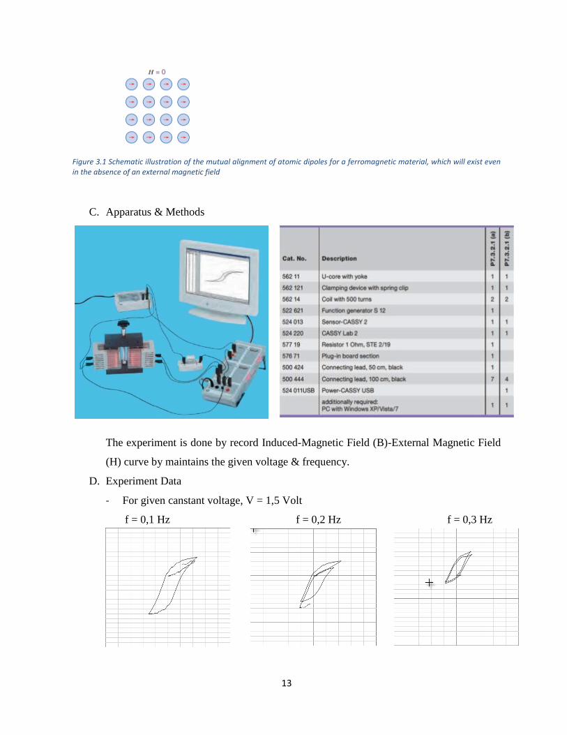
Figure 3.1 Schematic illustration of the mutual alignment of atomic dipoles for a ferromagnetic material, which will exist even in the absence of an external magnetic field
C. Apparatus & Methods
The experiment is done by record Induced-Magnetic Field (B)-External Magnetic Field
(H) curve by maintains the given voltage & frequency.
D. Experiment Data
- For given canstant voltage, V = 1,5 Volt
f = 0,1 Hz f = 0,2 Hz f = 0,3 Hz
14
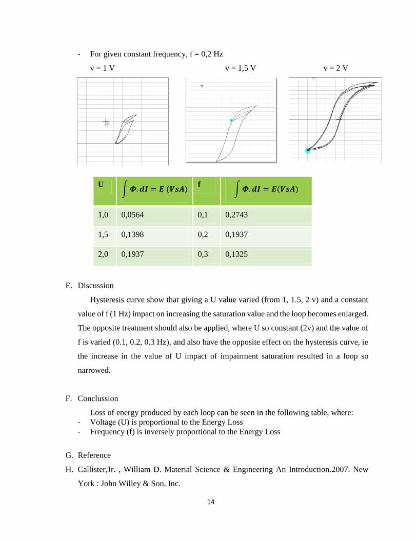
- For given constant frequency, f = 0,2 Hz
v = 1 V v = 1,5 V v = 2 V
U ∫𝜱. 𝒅𝑰 = 𝑬 (𝑽𝒔𝑨)
f ∫𝜱.𝒅𝑰 = 𝑬(𝑽𝒔𝑨)
1,0 0,0564 0,1 0,2743
1,5 0,1398 0,2 0,1937
2,0 0,1937 0,3 0,1325
E. Discussion
Hysteresis curve show that giving a U value varied (from 1, 1.5, 2 v) and a constant
value of f (1 Hz) impact on increasing the saturation value and the loop becomes enlarged.
The opposite treatment should also be applied, where U so constant (2v) and the value of
f is varied (0.1, 0.2, 0.3 Hz), and also have the opposite effect on the hysteresis curve, ie
the increase in the value of U impact of impairment saturation resulted in a loop so
narrowed.
F. Conclussion
Loss of energy produced by each loop can be seen in the following table, where:
- Voltage (U) is proportional to the Energy Loss
- Frequency (f) is inversely proportional to the Energy Loss
G. Reference
H. Callister,Jr. , William D. Material Science & Engineering An Introduction.2007. New
York : John Willey & Son, Inc.

15
Diamagnetic, Paramagnetic, & Ferromagnetic Substance
A. Objective
To identify diiamagnetic, paramagnetic, & ferromagnetic substance.
B. Theories
Magnetism, the phenomenon by which materials assert an attractive or repulsive
force or influence on other materials, has been known for thousands of years. However,
the underlying principles and mechanisms that explain the magnetic phenomenonare
complex and subtle, and their understanding has eluded scientists until relatively recent
times. Many of our modern technological devices rely on magnetism and magnetic
materials; these include electrical power generators and transformers, electric motors,
radio, television, telephones, computers, and components of sound and video reproduction
systems. Iron, some steels, and the naturally occurring mineral lodestone are well-known
examples of materials that exhibit magnetic properties. Not so familiar, however, is the
fact that all substances are influenced to one degree or another by the presence of a
magnetic field.
Diamagnetism is a very weak form of magnetism that is nonpermanent and persists
only while an external field is being applied. It is induced by a change in the orbital motion
of electrons due to an applied magnetic field. The magnitude of the induced magnetic
moment is extremely small, and in a direction opposite to that of the applied field. Thus,
the relative permeability is less than unity (however, only very slightly), and the magnetic
susceptibility is negative; that is, the magnitude of the Bfield within a diamagnetic solid
is less than that in a vacuum. The volume susceptibility for diamagnetic solid materials is
on the order of When placed between the poles of a strong electromagnet, diamagnetic
materials are attracted toward regions where the field is weak.
For some solid materials, each atom possesses a permanent dipole moment by virtue
of incomplete cancellation of electron spin and/or orbital magnetic moments. In the
absence of an external magnetic field, the orientations of these atomic magnetic moments
are random, such that a piece of material possesses no net macroscopic

16
magnetization.These atomic dipoles are free to rotate, and paramagnetism results when
they preferentially align, by rotation, with an external field as shown in Figure 4.1.These
magnetic dipoles are acted on individually with no mutual interaction between adjacent
dipoles. Inasmuch as the dipoles align with the external field, they enhance it, giving rise
to a relative permeability that is greater than unity, and to a relatively small but positive
magnetic susceptibility. Susceptibilities for paramagnetic materials range from about 10-
5 to 10-2 .
Figure 4.1The atomic dipole configuration for a diamagnetic material : (a) Diamagnetic , (b) Paramagnetic , (c) Ferromagnetic
Certain metallic materials possess a permanent magnetic moment in the absence of
an external field, and manifest very large and permanent magnetizations. These are the
characteristics of ferromagnetism, and they are displayed by the transition metals iron
(as BCC ferrite), cobalt, nickel, and some of the rare earth metals such as gadolinium
(Gd). Magnetic susceptibilities as high as are possible for ferromagnetic materials.
(c)

17
C. Apparatus & Methods
In the experiment three 9 mm long rods with different magnetic behaviors are suspended
into homogenous magnetic field so that they can easily rotate, allowing them to be
attracted or repelled by the magnetic field depending on their respective magnetic
property.
D. Experiment result & Discussion
The experiment is done by examine the magnetization of 3 kinds of substances,
Bismuth (Bi), Copper (Cu), & Iron (Fe). We gave the external field from electromagnetic
induction to the sample & observed their respond. The result can be looked on these table.
No. Substance Attracted Repel
1 Bismuth (Bi) - Yes
2 Copper (Cu) Yes -
3 Iron (Fe) Yes -
From the table above, Bitmuth show a repellent to the external magnetic field that
indicate it is a diamagnetic material. However, copper & iron give attraction to the
external magnetic field. We can determine if they are paramagnetic or ferromagnetic

18
material because the different among paramagnetic & ferromagnetic material is on their
magnetic susceptibility. So, we have to take quantitative magnetic examine to determine
their magnetization kind.
E. Conclussion
It is sufficient to determine a substance is a diamagnetic material by giving external
magnetic field. But, we have to measure it’s magnetic susceptibility to distinguish which
paramagnetic or ferromagnetic is.
F. Reference
Callister,Jr. , William D. Material Science & Engineering An Introduction.2007. New
York : John Willey & Son, Inc.
19
Scanning Tunneling Microscope (STM)
A. Objective
Investigating Gold (Au), Graphite, & MoS2 surface using a Scanning Tunneling
Microscope (STM).
B. Theories
The scanning tunneling microscope was developed in the 1980’s by G. Binnig & H.
Rohrer. It uses a fine metal tip as a local probe; the probe is brought so close to an
electrically conductive samole that the electrons ‘tunnel’ from the tip to the sample due
to quantum-mechanical effects.
When an electric field is applied between the tip and the sample, an electric current,
tunnel current, can flow. As the tunnel current varies exponentially with the distance, even
an extremely minute change in distance of 0.01 nm results in a measurable change in the
tunnel current. The tip is mounted on a platform which can be moved in all three spatial
dimensions by means of piezoelectric control elements. The tip is scanned across the
sample to measure its topography.
A control circuit maintains the distance between tip and sample extremely precise at
a constance distance by maintaining a constant tunnel current value. The controlled
motion performed during the scanning process are recorded and imaged using computer.
The image generated in this manner is a composite in which the sample topography and
the electrical conductivity of the sample surface are superimposed.
C. Apparatus
- Scanning Tunneling Microscope
- Molybdenum disulphide (MoS2) sample
- Gold (Au) sample
- Graphite sample
- PC with windows XP/7/Vista

20
D. Experiment Method
The experiments use a scanning tunneling micreoscope specially developed for
practical experiments, whic operates at standard air pressure. At the beginning of the
experiment, a measuring tip is made from platinum wire. The graphite sample is prepared
by taering off a strip of tape. When the gold sample is handled carefully, it requires no
cleaning; the same is valid for teh MoS2 probe. The investigation of the samples begins
with an overview scan. In the subsequent procedure, the step width of the measuring tip
is reduced until the positions of the individua atoms of the sample with respect to each
other are clearly visible in the image.
21
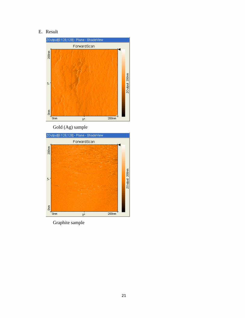
E. Result
Gold (Ag) sample
Graphite sample
22
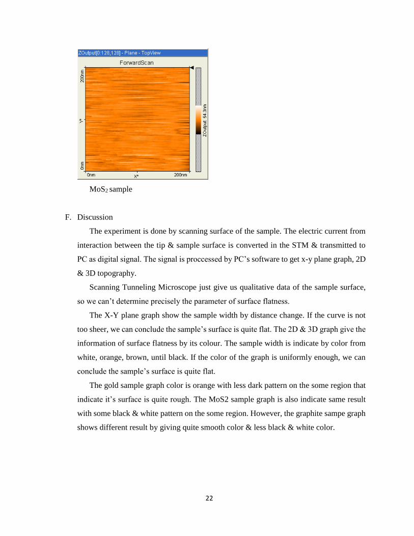
MoS2 sample
F. Discussion
The experiment is done by scanning surface of the sample. The electric current from
interaction between the tip & sample surface is converted in the STM & transmitted to
PC as digital signal. The signal is proccessed by PC’s software to get x-y plane graph, 2D
& 3D topography.
Scanning Tunneling Microscope just give us qualitative data of the sample surface,
so we can’t determine precisely the parameter of surface flatness.
The X-Y plane graph show the sample width by distance change. If the curve is not
too sheer, we can conclude the sample’s surface is quite flat. The 2D & 3D graph give the
information of surface flatness by its colour. The sample width is indicate by color from
white, orange, brown, until black. If the color of the graph is uniformly enough, we can
conclude the sample’s surface is quite flat.
The gold sample graph color is orange with less dark pattern on the some region that
indicate it’s surface is quite rough. The MoS2 sample graph is also indicate same result
with some black & white pattern on the some region. However, the graphite sampe graph
shows different result by giving quite smooth color & less black & white color.
23
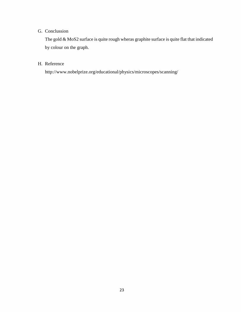
G. Conclussion
The gold & MoS2 surface is quite rough wheras graphite surface is quite flat that indicated
by colour on the graph.
H. Reference
http://www.nobelprize.org/educational/physics/microscopes/scanning/

24
Elastic Deformation
A. Objective
- To determine tensile stress & strain value in the elastic deformation
- To determine Young Modulus value of copper & iron
- To determine mechanical characteristic of copper & iron
B. Theories
Elasticity deals with elastic stresses and strains, their relationship, and the external forces
that cause them. An elastic strain is defined as a strain that disappears instantaneously once the
forces that cause it are removed. The theory of elasticity for Hookean solids -- in which stress is
proportional to strain -- is rather complex in its more rigorous treatment.
The normal stress s is defined as this ‘‘resistance” per unit area. Applying the equilibrium-
offorces equation from the mechanics of materials to the lower portion of the specimen, we have
This is the internal resisting stress opposing the externally applied load and avoiding the
breaking of the specimen. The following stress convention is used: Tensile stresses are positive
and compressive stresses are negative. In geology and rock mechanics, on the other hand, the
opposite sign convention is used because compressive stresses are much more common. As the
applied force F increases, so does the length of the specimen. For an increase dF, the length l
increases by dl. The normalized (per unit length) increase in length is equal to
or, upon integration,
where l0 is the original length. This parameter is known as the longitudinal true strain. In
many applications, a simpler form of strain, commonly called engineering or nominal strain, is
used. This type of strain is defined as

25
C. Apparatus & Methods
The experiment is done by fasten the copper & iron wire on the linear expansion apparatus
set & measure the elongation every multiple of 50 grams loads given.
D. Experiment Result & Data Processing
Copper
d = 0,2 mm l0 = 50 cm
Load Mass
(gram)Elongation (cm) Stress (Pa) Strain (%)
Young Modulus
(Pa)
50 0.12 1592356.688 0.24% 663481953.3
100 0.19 3184713.376 0.38% 838082467.3
150 0.27 4777070.064 0.54% 884642604.4
200 0.36 6369426.752 0.72% 884642604.4
817712407.3Young Modulus Average

26
Iron
d = 0,2 mm l0 = 50 cm
0
1000000
2000000
3000000
4000000
5000000
6000000
7000000
0.24 0.38 0.54 0.72
STR
ESS
(Pa)
STRAIN (%)
COPPER STRESS -STRAIN CURVE
Stress (Pa)
Load Mass (gram) Elongation (cm) Stress (Pa) Strain (%)Young Modulus
(Pa)
50 0.08 1592356.688 0.16% 995222929.9
100 0.14 3184713.376 0.28% 1137397634
150 0.17 4777070.064 0.34% 1405020607
200 0.23 6369426.752 0.46% 1384657989
1230574790Young Modulus Average
0
1000000
2000000
3000000
4000000
5000000
6000000
7000000
0.16% 0.28% 0.34% 0.46%
STR
ESS
(Pa)
STRAIN (%)
IRON STRESS -STRAIN CURVE
Stress (Pa)

27
E. Discussion
The experiment is done by fasten the copper & iron wire on the linear expansion apparatus
set & measure the elongation every multiple of 50 grams load given.
Afterwards, we list the elongation data in the table to calcuwhilate the tensile stress &
strain by their formula. Then we can find their Young modulus by divide stress with strain.
The tables show that copper & iron have high value of stress from 1,600,000 Pa to
6,400,000 Pa & less of strain from 0.16 % to 0.72 %. Their Young Modulus value also show high
value by the average 817712407.3 Pa & 1230574790 Pa. It’s indicate copper & iron is a strong
material which able to hold up relative heavy loads & iron is stronger than copper.
F. Conclussion
The tensile stress value of copper & iron is between 1592356.688 Pa to 6369426.752 Pa.
The tensile strain value of copper & iron is between 0.16 % to 0.72 %.
The Young modulus value of copper & iron are serially 817712407.3 Pa & 1230574790 Pa.
Iron & copper is a strong material with high Young Modulus value.
G. Reference
Meyer, Marc Andre & Krishan Kumar Chawla. Mechanical Behavior of Materials. 2009.
London : Cambridge University Press