
Escuadro_Thesis.pdf - Bedzyk Research Group
232
NORTHWESTERN UNIVERSITY X-Ray Standing Wave Imaging of Metal Atoms on Semiconductor and Oxide Surfaces A DISSERTATION SUBMITTED TO THE GRADUATE SCHOOL IN PARTIAL FULLFILLMENT OF THE REQUIREMENTS for the degree DOCTOR OF PHILOSOPHY Field of Materials Science and Engineering By Anthony Atilano Escuadro EVANSTON, ILLINOIS December 2005
-
Upload
khangminh22 -
Category
Documents
-
view
2 -
download
0
Transcript of Escuadro_Thesis.pdf - Bedzyk Research Group
NORTHWESTERN UNIVERSITY
X-Ray Standing Wave Imaging of Metal Atoms on Semiconductor
and Oxide Surfaces
A DISSERTATION
SUBMITTED TO THE GRADUATE SCHOOL IN PARTIAL FULLFILLMENT OF THE REQUIREMENTS
for the degree
DOCTOR OF PHILOSOPHY
Field of Materials Science and Engineering
By
Anthony Atilano Escuadro
EVANSTON, ILLINOIS
December 2005

ii
Copyright by Anthony Escuadro 2005 All Rights Reserved
iii
ABSTRACT
X-Ray Standing Wave Imaging of Metal Atoms
on Semiconductor and Oxide Surfaces
Anthony Atilano Escuadro
The 1/3 monolayer (ML) Sn/Si(111)-(√3 x √3)R30° surface structure has been
extensively studied using x-ray standing waves (XSW). The summation of several
XSW measured hkl Fourier components results in a three-dimensional, model-
independent direct-space image of the Sn atomic distribution. While the image
demonstrates that the Sn atoms are located at Si(111) T4-adsorption sites, it alone
cannot determine whether the Sn atomic distribution is flat or asymmetric. However,
conventional XSW analysis can make this distinction, concluding that one-third of the
Sn atoms are located 0.26 Å higher than the remaining two-thirds. This ''one up and two
down'' distribution is consistent with the vertical displacements predicted by a
dynamical fluctuations model. A second sample prepared in a slightly different manner
exhibits the same long-range surface symmetry, but a direct space image clearly reveals
that a significant fraction of the Sn atoms in the second surface have substituted for Si
atoms in the bottom of the Si surface bilayer.
In addition, the electronic and atomic-scale structure of 1/2 ML V on α-
Fe2O3(0001) as a function of the vanadium oxidation state has also been investigated
using x-ray photoemission spectroscopy (XPS) and XSW direct-space imaging. The
iv
XSW data is used to generate a direct-space image of the vanadium distribution as the
surface is oxidized and reduced using atomic oxygen and hydrogen. The direct-space
atomic density profile shows the average adsorption height of the V atoms is increased
by 0.39 Å after the vanadium is oxidized, which suggests the oxidized vanadium is
arranged in VO4 units. The direct-space image also shows a secondary V position,
which can be explained by the chemical interaction between these VO4 units. These
structural changes can be understood in light of recent XPS results, which suggest the
exposure of the vanadium adlayer to atomic oxygen converts the vanadium into a V2O5
film and reoxidizes the hematite at the film-substrate interface. The current XSW
results also suggest the oxidation of the supported vanadium is a reversible process; by
exposing the submonolayer vanadia to atomic hydrogen, the oxidized vanadium is
reduced and the geometry of the as-deposited surface is restored.
Approved:
––––––––––––––––––
Professor Michael J. Bedzyk
Department of Materials Science and Engineering
Northwestern University
Evanston, Illinois
v
ACKNOWLEDGEMENTS
First of all, I would like to show my appreciation to the various sources of
research funding that helped make the research detailed here possible. I would first like
to recognize the Walter P. Murphy Fellowship that supported my studies during my
initial year at Northwestern. The research I conducted in subsequent years was
supported by two research centers: the Northwestern University Materials Research
Science and Engineering Center (NU-MRSEC), which is funded by the National
Science Foundation (NSF), and the Institute for Environmental Catalysis (IEC), which
was established with funding from the NSF and is currently funded by the U.S.
Department of Energy.
I would also like to acknowledge all the numerous people that have helped and
encouraged me during my graduate studies here at Northwestern. First of all, I would
like to acknowledge all the former members of Prof. Michael Bedzyk’s research group
who helped me get my start in graduate school, including Drs. Likwan Cheng, William
Rodrigues, Brad Tinkham, Zhan Zhang, Joseph Libera, Don Walko, and especially Dr.
John Okasinski, whose help with the UHV apparatus and direct-space imaging analysis
proved invaluable for my thesis work.
I would also like to thank all the current members of the Bedzyk group,
especially Dr. Yongseong Choi, Duane Goodner, and Dr. Chang-Yong Kim. It is hard
to overstate the importance of the advice and assistance that Chang-Yong and Duane
provided during our many beamtimes; without their time and energy, much of the work
vi
detailed here would not have been possible. Thanks also to the DND-CAT staff for all
their support during our beamtime preparations, especially Dr. Denis Keane. I also
appreciate the time Prof. Laurie Marks, Prof. Mark Hersam, Prof. Peter Stair, and Prof.
Paul Lyman have dedicated to serving on my thesis committee, as well as their helpful
advice they have provided throughout my graduate career.
Of course, I must also express my gratitude to my thesis advisor, Prof. Bedzyk,
whose guidance, expertise, and encouragement helped me to learn how to become a
good scientist. I also thank him for the patience and support he has extended to me
since the very beginning of my time here at Northwestern.
On a personal note, I must express my thanks to the two families that have
supported me in so many ways as I progressed towards my degree: my dad Ramon, my
aunt Cory, and my siblings Francis and Nicole in California, as well as my wife’s
family Eugene, Lina, and Eugene Jr. here in Chicago. Both of these families have
helped shape me into the person I am today. I would also like to give a special thanks to
my mother Maridol, who I sorely miss and will always be part of my life.
Last, but certainly not least, I cannot thank enough my wife Liza, whose
understanding, sacrifice, and support throughout my graduate studies made this
achievement possible. I owe her a tremendous debt, for I cannot imagine having been
able to complete this accomplishment without her at my side.
vii
TABLE OF CONTENTS
Chapter 1: Introduction.....................................................................................................1
Chapter 2: Background on the 1/3 ML Sn/Si(111) Surface..............................................6 2.1 Introduction..........................................................................................................6 2.2 The Si(111) Surface Structure .............................................................................6 2.3 Sn/Si(111) Surfaces ...........................................................................................11
2.3.1 The Sn/Si(111) phase diagram................................................................... 11 2.3.2 Dynamical fluctuations and the 1/3 ML Sn/Ge(111) surface .................... 13 2.3.3 The 1/3 ML Sn/Si(111)-(√3x√3)R30° surface........................................... 17
Chapter 3: Background on the V/α-Fe2O3(0001) Surface ..............................................26 3.1 Introduction........................................................................................................26 3.2 Crystal Structure of Bulk Fe2O3.........................................................................26 3.3 Preparation and Characterization of the α-Fe2O3(0001) Surface.......................30 3.4 Overview of the Oxides of Vanadium ...............................................................38 3.5 Vanadium Oxide Films Supported on Oxide Substrates ...................................42 3.6 Vanadium and Vanadium Oxides Supported on α-Fe2O3(0001).......................47
Chapter 4: The X-Ray Standing Wave Method..............................................................54 4.1 Introduction........................................................................................................54 4.2 Dynamical Theory of X-ray Diffraction............................................................58 4.3 Photoexcitation from X-ray Standing Waves ....................................................67 4.4 XSW Analysis....................................................................................................70
4.4.1 Measuring atomic distributions with XSW................................................ 70 4.4.2 Structural analysis using the coherent fraction and coherent position....... 74 4.4.3 The XSW direct-space imaging method.................................................... 79
Chapter 5: Experimental Apparatus................................................................................90 5.1 Introduction........................................................................................................90 5.2 X-Ray Optics at the 5ID and 12ID Beamlines at the APS ................................90 5.3 UHV Surface Science Equipment at the 5ID-C and 12ID-D Beamlines ..........99
5.3.1 UHV Chamber at the 12ID-D Endstation................................................ 100 5.3.2 UHV Psi-circle diffractometer at the 5ID-C Endstation.......................... 104
5.4 XSW Data Collection at the Advanced Photon Source ...................................110
Chapter 6: XSW Measurements of the 1/3 ML Sn/Si(111)-(√3x√3)R30 Surface........115 6.1 Sample Preparations ........................................................................................115 6.2 X-Ray Standing Wave Measurements.............................................................118 6.3 Results and Discussion of the 1/3 ML Sn/Si(111)-√3 Surface ........................133
6.3.1 XSW direct space imaging of the 0.23 ML Sn/Si(111)-(√3x√3) surface 133 6.3.2 Conventional XSW analysis for the 0.23 ML Sn/Si(111) surface........... 137
viii
6.4 The Substitution of Sn within the Si Bilayer ...................................................140 6.5 Discussion of XSW Results .............................................................................143 6.6 Summary..........................................................................................................148
Chapter 7: XSW Measurements of the 1/2 ML V/α-Fe2O3(0001) Surface ..................149 7.1 Sample Preparation..........................................................................................149 7.2 X-Ray Standing Wave Measurements.............................................................154 7.3 Results and Discussion of the 1/2 ML V/Fe2O3(0001) System .......................158
7.3.1 General observations regarding XSW results .......................................... 158 7.3.2 XSW direct space imaging for the 1/2 ML V/Fe2O3(0001) system......... 165 7.3.3 XSW direct space imaging for the oxidized V/Fe2O3(0001) system ....... 170
7.4 Summary..........................................................................................................178
Chapter 8: Summary and Future Work.........................................................................179 8.1 Thesis Summary ..............................................................................................179 8.2 Future Work.....................................................................................................182
REFERENCES .............................................................................................................185
Appendix: Software Packages for XSW Analysis........................................................195 A.1 Recent Developments with SWAN .................................................................195
A.1.1 New functionality in SWAN (as of version 2.1.3).................................. 197 A.1.2 New SWAN functions ............................................................................ 198 A.1.3 Modifying, compiling, and distributing SWAN ..................................... 201
A.2 Global Analysis of XSW Data using IGOR PRO............................................203 A.2.1 IGOR PRO function for XSW global fit................................................. 212
A.3 Atomic Coordinates for the Bulk α-Fe2O3 Crystal Structure...........................213 A.4 Calculated XSW Data for the Fe Atomic Density Map...................................215
ix
LIST OF FIGURES
Figure 2.1: Top view of the Si(111) surface showing the three high-symmetry adsorption sites. The Si (1 x 1) surface unit cell is also outlined............................. 7
Figure 2.2: Side view projection of the Si(111) structure along the [10
�
1 ] direction. The stacking of Si atoms in the [111] direction consists of Si bilayers. The lattice spacing of the (111) atomic planes (d111 = 3.136 Å) is also shown.......................... 8
Figure 2.3: Top view of the Si(111)-(7 x 7) unit cell. The shaded triangles denote the adatom clusters that form the adatom layer. The figure is reproduced from reference [4]. .......................................................................................................... 10
Figure 2.4: Surface phase map as determined by RHEED during the high temperature annealing of Sn deposited on the Si(111) surface. Reprinted from reference [6], Copyright 2005, with permission from Elsevier.................................................... 12
Figure 2.5: Ball-and-stick diagram of the 1/3 ML Sn/Si(111) surface. (a) Sn adatoms occupy one-third of the T4 adsorption sites. The (1 x 1) surface unit cell is inscribed in a solid black line and the (√3 x √3)-R30° surface unit cell is inscribed in a dashed grey line. (b) Side view of the Sn/Si(111) surface. Si atoms are displaced from their bulk-like positions according to the calculated atomic displacements of Ref. [18]. .................................................................................... 14
Figure 2.6: Sn 4d core-level spectra of the RT √3 and LT (3 x 3) Sn/Ge(111) surface phases. The presence of the two components suggests both surface reconstructions are composed of two types of Sn adatoms. Reprinted with permission from reference [22]. Copyright 2005 by the American Physical Society....................... 16
Figure 2.7: Sn 4d core-level spectra of the LT √3 Sn/Si(111) surface reconstruction. The two component spectrum appears quite similar to the core-level spectra acquired from the LT and RT Sn/Ge(111) surface. Reprinted with permission from reference [28]. Copyright 2005 by the American Physical Society....................... 20
Figure 2.8: k//-resolved inverse photoemission spectroscopy (KRIPES) spectra of the √3 Sn/Si(111) surface phase before and after exposure to atomic hydrogen. The difference curve reveals the presence of two adsorption-sensitive surface states, which suggest multiple adatom states for the RT surface. Reprinted with permission from reference [31]. Copyright 2005 by the American Physical Society.................................................................................................................... 21
x
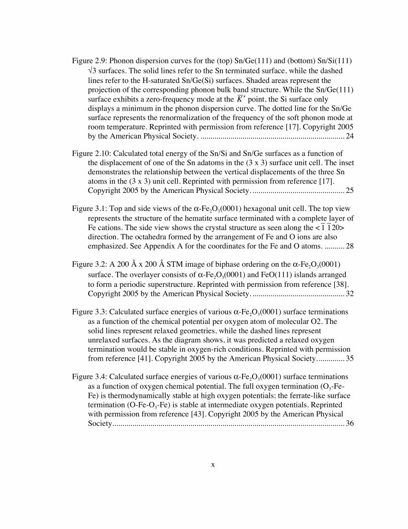
Figure 2.9: Phonon dispersion curves for the (top) Sn/Ge(111) and (bottom) Sn/Si(111) √3 surfaces. The solid lines refer to the Sn terminated surface, while the dashed lines refer to the H-saturated Sn/Ge(Si) surfaces. Shaded areas represent the projection of the corresponding phonon bulk band structure. While the Sn/Ge(111) surface exhibits a zero-frequency mode at the
�
! K point, the Si surface only displays a minimum in the phonon dispersion curve. The dotted line for the Sn/Ge surface represents the renormalization of the frequency of the soft phonon mode at room temperature. Reprinted with permission from reference [17]. Copyright 2005 by the American Physical Society. ........................................................................ 24
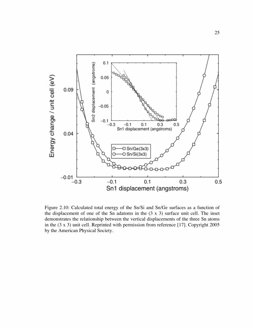
Figure 2.10: Calculated total energy of the Sn/Si and Sn/Ge surfaces as a function of the displacement of one of the Sn adatoms in the (3 x 3) surface unit cell. The inset demonstrates the relationship between the vertical displacements of the three Sn atoms in the (3 x 3) unit cell. Reprinted with permission from reference [17]. Copyright 2005 by the American Physical Society. .............................................. 25
Figure 3.1: Top and side views of the α-Fe2O3(0001) hexagonal unit cell. The top view represents the structure of the hematite surface terminated with a complete layer of Fe cations. The side view shows the crystal structure as seen along the <
�
1
�
1 20> direction. The octahedra formed by the arrangement of Fe and O ions are also emphasized. See Appendix A for the coordinates for the Fe and O atoms. .......... 28
Figure 3.2: A 200 Å x 200 Å STM image of biphase ordering on the α-Fe2O3(0001) surface. The overlayer consists of α-Fe2O3(0001) and FeO(111) islands arranged to form a periodic superstructure. Reprinted with permission from reference [38]. Copyright 2005 by the American Physical Society. .............................................. 32
Figure 3.3: Calculated surface energies of various α-Fe2O3(0001) surface terminations as a function of the chemical potential per oxygen atom of molecular O2. The solid lines represent relaxed geometries, while the dashed lines represent unrelaxed surfaces. As the diagram shows, it was predicted a relaxed oxygen termination would be stable in oxygen-rich conditions. Reprinted with permission from reference [41]. Copyright 2005 by the American Physical Society.............. 35
Figure 3.4: Calculated surface energies of various α-Fe2O3(0001) surface terminations as a function of oxygen chemical potential. The full oxygen termination (O3-Fe-Fe) is thermodynamically stable at high oxygen potentials; the ferrate-like surface termination (O-Fe-O3-Fe) is stable at intermediate oxygen potentials. Reprinted with permission from reference [43]. Copyright 2005 by the American Physical Society.................................................................................................................... 36
xi
Figure 3.5: Orthorhombic unit cell of the bulk V2O5 crystal structure. The unit cell shown consists of two V2O5 layers that are weakly bound to each other. The crystallographic data used to produce the figure originates from reference [53]. . 41
Figure 3.6: The work function as a function of V deposition time. The inset shows the rapid decrease in the work function with the onset of V adsorption. The figure is reproduced from reference [69]. ............................................................................ 51
Figure 3.7: The Fe 2p (left) and O 1s and V 2p (right) XPS spectra as a function of increasing vanadium coverage. The spectrum from the clean α-Fe2O3(0001) appears as the bottom of the figure. The figure is reproduced from reference [69]................................................................................................................................. 52
Figure 3.8: The effect of atomic oxygen exposure on the Fe 2p spectra (top) and O 1s and V 2p spectra (bottom). The figures are reproduced from reference [69]. ....... 53
Figure 4.1: The generation of the X-ray standing wave via the interference of an incident and diffracted X-ray plane waves (with wave vectors K0 and KH, respectively). The period of the XSW is equal to the lattice spacing dhkl of the Bragg diffraction planes, as seen by the antinodes of the XSW highlighted in red. The electric field intensity of the XSW excites characteristic x-ray fluorescence from atoms in the vicinity of the XSW.................................................................. 56
Figure 4.2: The variation in normalized reflectivity and relative XSW phase on the normalized angle parameter η′ for the Si(111) Bragg reflection at 7 keV. The relative XSW phase experiences a shift of π radians as the Si crystal traverses through the strong Bragg condition. This results in the antinodes of the XSW field coinciding with the Si(111) Bragg diffraction planes on the high-angle side of the Bragg reflection (η′ < -1). For this phase calculation the unit cell origin (that enters via the structure factor F111) was chosen to coincide with a Si atom in the top of the bilayer. ................................................................................................... 64
Figure 4.3: (a) Graphical representation of the individual hhh Fourier components for the Si atomic density distribution in the [111] direction. Each ρhhh component is offset by +3 in the vertical scale. (b) The calculated 1D direct-space image of the Si density distribution, which is produced by the summation of the Fourier terms shown in (a). The effect of an increasing number of Fourier components on the density distribution is demonstrated. ..................................................................... 85
Figure 4.4: Projection of the Fourier summation calculated Fe atomic density onto the (11
�
2 0) crystallographic plane. The red areas represent regions where the calculated density distribution is greater or equal to 80% of the maximum Fe atomic density. To aid comparison, the locations of the Fe atoms in the bulk hematite structure are shown as black spots overlaid on the density map............. 89
xii
Figure 5.1: A depiction of the experimental equipment located at the 5ID and 12ID beamlines of the Advanced Photon Source. The post monochromator optics and UHV chamber are located in the beamline hutches upstream of the HHLM. Note: the dual focusing mirrors that are used at 5ID-C for rejecting higher-order harmonics are not shown. Also, the reflectivity detector used at 12ID-D is located within the UHV chamber, unlike the external reflectivity detector used at 5ID-C that is depicted here................................................................................................ 92
Figure 5.2: DuMond diagram for the x-ray optics of the 5ID-C beamline at 7 keV. The output of the Si(111) high-heat load monochromator and two Si(111) detuned channel-cuts is shown and compared to the Si(111) sample reflection. ................ 96
Figure 5.3: DuMond diagram for the x-ray optics of the 5ID-C beamline at 7 keV. The output of the Si(111) high-heat load monochromator and a single Si(333) detuned channel-cut is shown and compared to the Si(333) sample reflection................... 97
Figure 5.4: DuMond diagram for the x-ray optics of the 5ID-C beamline at 7 keV. The output of the Si(111) high-heat load monochromator and a single Si(022) detuned channel-cut is shown and compared to the Fe2O3 sample reflection. .................... 98
Figure 5.5: Schematic of the top view of the UHV system at the BESSRC 12ID-D undulator system. The figure is reproduced from reference [81]. ....................... 101
Figure 5.6: Photograph of the UHV chamber/diffractometer located at the 5ID-C endstation. The image is taken from within the endstation and shows the downstream side of the UHV chamber. The entire assembly is situated on a set of rails that allow it to be translated perpendicular to the incident x-ray beam direction; the picture shows the chamber/diffractometer when not in the path of the x-ray beam. The photograph is reproduced from reference [82]. ........................ 106
Figure 5.7: One of the x-ray fluorescence spectra collected at the 12ID-D endstation during the 1/3 ML Sn/Si(111) XSW experiment (Eγ = 6.90 keV). The total spectrum is the result of 70 XSW scans added together. Since each scan includes 32 angular steps and the counting time at each step was 1 second, this plot is averaged over 2240 seconds of collection time. .................................................. 114
Figure 6.1: LEED images (as captured and inverted) for the different Si(111) surfaces observed during the 1/3 ML Sn/Si(111) XSW experiment. (a) LEED images from the clean Si(111)-(7 x7) surface, E=30.1 eV. (b) LEED images from the 0.23 ML Sn/Si(111)-√3 surface, E=28.5 eV....................................................................... 117
Figure 6.2: Reflectivity (closed squares) and normalized Sn Lα fluorescence yield (closed circles) experimental data along with theoretical fits (solid lines) for the (111) XSW measurement on 0.23(3) ML Sn/Si(111).......................................... 121
xiii
Figure 6.3: Reflectivity (closed squares) and normalized Sn Lα fluorescence yield (closed circles) experimental data along with theoretical fits (solid lines) for the (333) XSW measurement on 0.23(3) ML Sn/Si(111).......................................... 122
Figure 6.4: Reflectivity (closed squares) and normalized Sn Lα fluorescence yield (closed circles) experimental data along with theoretical fits (solid lines) for the (444) XSW measurement on 0.23(3) ML Sn/Si(111).......................................... 123
Figure 6.5: Reflectivity (closed squares) and normalized Sn Lα fluorescence yield (closed circles) experimental data along with theoretical fits (solid lines) for the (555) XSW measurement on 0.23(3) ML Sn/Si(111).......................................... 124
Figure 6.6: Reflectivity (closed squares) and normalized Sn Lα fluorescence yield (closed circles) experimental data along with theoretical fits (solid lines) for the (
�
1 11) XSW measurement on 0.23(3) ML Sn/Si(111)......................................... 125
Figure 6.7: Reflectivity (closed squares) and normalized Sn Lα fluorescence yield (closed circles) experimental data along with theoretical fits (solid lines) for the (
�
3 33) XSW measurement on 0.23(3) ML Sn/Si(111)......................................... 126
Figure 6.8: Reflectivity (closed squares) and normalized Sn Lα fluorescence yield (closed circles) experimental data along with theoretical fits (solid lines) for the (5
�
1
�
1 ) XSW measurement on 0.23(3) ML Sn/Si(111)........................................ 127
Figure 6.9: Reflectivity (closed squares) and normalized Sn Lα fluorescence yield (closed circles) experimental data along with theoretical fits (solid lines) for the (111) XSW measurement on 0.33(4) ML Sn/Si(111).......................................... 128
Figure 6.10: Reflectivity (closed squares) and normalized Sn Lα fluorescence yield (closed circles) experimental data along with theoretical fits (solid lines) for the (333) XSW measurement on 0.33(4) ML Sn/Si(111).......................................... 129
Figure 6.11: Reflectivity (closed squares) and normalized Sn Lα fluorescence yield (closed circles) experimental data along with theoretical fits (solid lines) for the (022) XSW measurement on 0.33(4) ML Sn/Si(111).......................................... 130
Figure 6.12: Reflectivity (closed squares) and normalized Sn Lα fluorescence yield (closed circles) experimental data along with theoretical fits (solid lines) for the (311) XSW measurement on 0.33(4) ML Sn/Si(111).......................................... 131
Figure 6.13: Reflectivity (closed squares) and normalized Sn Lα fluorescence yield (closed circles) experimental data along with theoretical fits (solid lines) for the (
�
1 33) XSW measurement on 0.33(4) ML Sn/Si(111)......................................... 132
xiv
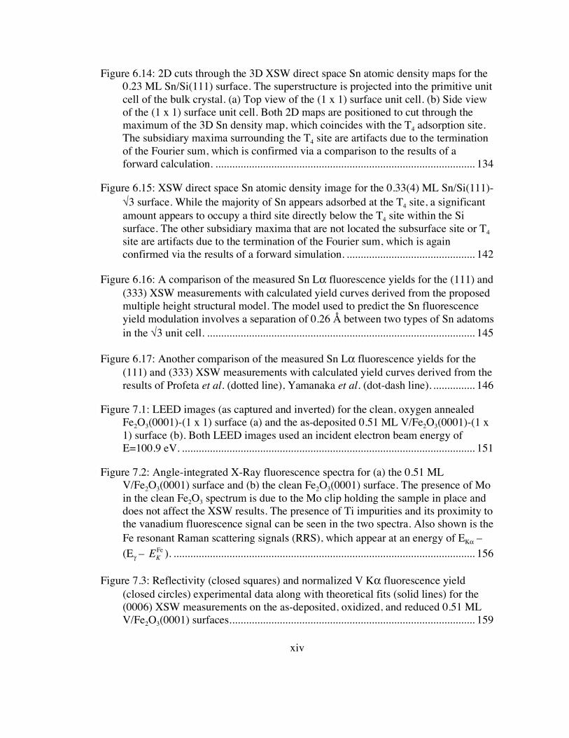
Figure 6.14: 2D cuts through the 3D XSW direct space Sn atomic density maps for the 0.23 ML Sn/Si(111) surface. The superstructure is projected into the primitive unit cell of the bulk crystal. (a) Top view of the (1 x 1) surface unit cell. (b) Side view of the (1 x 1) surface unit cell. Both 2D maps are positioned to cut through the maximum of the 3D Sn density map, which coincides with the T4 adsorption site. The subsidiary maxima surrounding the T4 site are artifacts due to the termination of the Fourier sum, which is confirmed via a comparison to the results of a forward calculation. ............................................................................................. 134
Figure 6.15: XSW direct space Sn atomic density image for the 0.33(4) ML Sn/Si(111)-√3 surface. While the majority of Sn appears adsorbed at the T4 site, a significant amount appears to occupy a third site directly below the T4 site within the Si surface. The other subsidiary maxima that are not located the subsurface site or T4 site are artifacts due to the termination of the Fourier sum, which is again confirmed via the results of a forward simulation. .............................................. 142
Figure 6.16: A comparison of the measured Sn Lα fluorescence yields for the (111) and (333) XSW measurements with calculated yield curves derived from the proposed multiple height structural model. The model used to predict the Sn fluorescence yield modulation involves a separation of 0.26 Å between two types of Sn adatoms in the √3 unit cell. ................................................................................................ 145
Figure 6.17: Another comparison of the measured Sn Lα fluorescence yields for the (111) and (333) XSW measurements with calculated yield curves derived from the results of Profeta et al. (dotted line), Yamanaka et al. (dot-dash line). ............... 146
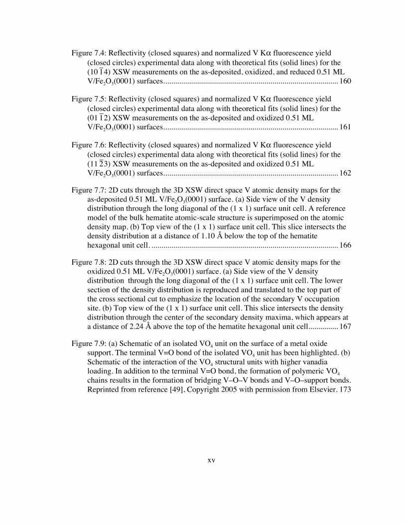
Figure 7.1: LEED images (as captured and inverted) for the clean, oxygen annealed Fe2O3(0001)-(1 x 1) surface (a) and the as-deposited 0.51 ML V/Fe2O3(0001)-(1 x 1) surface (b). Both LEED images used an incident electron beam energy of E=100.9 eV. ......................................................................................................... 151
Figure 7.2: Angle-integrated X-Ray fluorescence spectra for (a) the 0.51 ML V/Fe2O3(0001) surface and (b) the clean Fe2O3(0001) surface. The presence of Mo in the clean Fe2O3 spectrum is due to the Mo clip holding the sample in place and does not affect the XSW results. The presence of Ti impurities and its proximity to the vanadium fluorescence signal can be seen in the two spectra. Also shown is the Fe resonant Raman scattering signals (RRS), which appear at an energy of EKα – (Eγ – E
K
Fe ). ............................................................................................................ 156
Figure 7.3: Reflectivity (closed squares) and normalized V Kα fluorescence yield (closed circles) experimental data along with theoretical fits (solid lines) for the (0006) XSW measurements on the as-deposited, oxidized, and reduced 0.51 ML V/Fe2O3(0001) surfaces........................................................................................ 159
xv
Figure 7.4: Reflectivity (closed squares) and normalized V Kα fluorescence yield (closed circles) experimental data along with theoretical fits (solid lines) for the (10
�
1 4) XSW measurements on the as-deposited, oxidized, and reduced 0.51 ML V/Fe2O3(0001) surfaces........................................................................................ 160
Figure 7.5: Reflectivity (closed squares) and normalized V Kα fluorescence yield (closed circles) experimental data along with theoretical fits (solid lines) for the (01
�
1 2) XSW measurements on the as-deposited and oxidized 0.51 ML V/Fe2O3(0001) surfaces........................................................................................ 161
Figure 7.6: Reflectivity (closed squares) and normalized V Kα fluorescence yield (closed circles) experimental data along with theoretical fits (solid lines) for the (11
�
2 3) XSW measurements on the as-deposited and oxidized 0.51 ML V/Fe2O3(0001) surfaces........................................................................................ 162
Figure 7.7: 2D cuts through the 3D XSW direct space V atomic density maps for the as-deposited 0.51 ML V/Fe2O3(0001) surface. (a) Side view of the V density distribution through the long diagonal of the (1 x 1) surface unit cell. A reference model of the bulk hematite atomic-scale structure is superimposed on the atomic density map. (b) Top view of the (1 x 1) surface unit cell. This slice intersects the density distribution at a distance of 1.10 Å below the top of the hematite hexagonal unit cell. .............................................................................................. 166
Figure 7.8: 2D cuts through the 3D XSW direct space V atomic density maps for the oxidized 0.51 ML V/Fe2O3(0001) surface. (a) Side view of the V density distribution through the long diagonal of the (1 x 1) surface unit cell. The lower section of the density distribution is reproduced and translated to the top part of the cross sectional cut to emphasize the location of the secondary V occupation site. (b) Top view of the (1 x 1) surface unit cell. This slice intersects the density distribution through the center of the secondary density maxima, which appears at a distance of 2.24 Å above the top of the hematite hexagonal unit cell............... 167
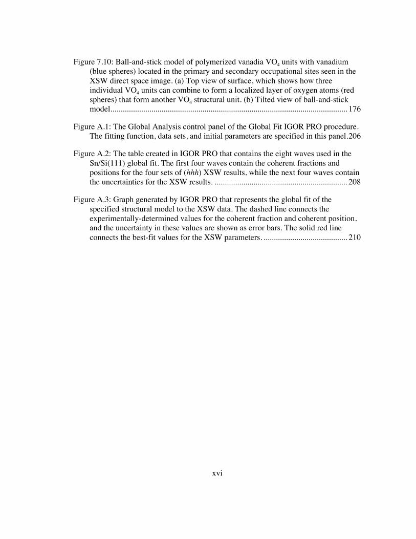
Figure 7.9: (a) Schematic of an isolated VO4 unit on the surface of a metal oxide support. The terminal V=O bond of the isolated VO4 unit has been highlighted. (b) Schematic of the interaction of the VO4 structural units with higher vanadia loading. In addition to the terminal V=O bond, the formation of polymeric VO4 chains results in the formation of bridging V–O–V bonds and V–O–support bonds. Reprinted from reference [49], Copyright 2005 with permission from Elsevier. 173
xvi
Figure 7.10: Ball-and-stick model of polymerized vanadia VO4 units with vanadium (blue spheres) located in the primary and secondary occupational sites seen in the XSW direct space image. (a) Top view of surface, which shows how three individual VO4 units can combine to form a localized layer of oxygen atoms (red spheres) that form another VO4 structural unit. (b) Tilted view of ball-and-stick model.................................................................................................................... 176
Figure A.1: The Global Analysis control panel of the Global Fit IGOR PRO procedure. The fitting function, data sets, and initial parameters are specified in this panel.206
Figure A.2: The table created in IGOR PRO that contains the eight waves used in the Sn/Si(111) global fit. The first four waves contain the coherent fractions and positions for the four sets of (hhh) XSW results, while the next four waves contain the uncertainties for the XSW results. ................................................................. 208
Figure A.3: Graph generated by IGOR PRO that represents the global fit of the specified structural model to the XSW data. The dashed line connects the experimentally-determined values for the coherent fraction and coherent position, and the uncertainty in these values are shown as error bars. The solid red line connects the best-fit values for the XSW parameters. ......................................... 210
xvii
LIST OF TABLES
Table 4.1: The calculated values for coherent fraction fH and coherent position PH for the bulk Si atomic distribution in the [111] direction. The unit cell origin chosen for this calculation coincides with the Si atom located at the top of the bilayer. Furthermore, the ordered fraction C and Debye-Waller factor DH are equal to unity. ...................................................................................................................... 83
Table 6.1: Summary of the XSW results for the 0.23(3) ML Sn/Si(111) surface. The unit cell origin coincides with the top of the bulk-like Si bilayer........................ 120
Table 6.2: Summary of the XSW results for the 0.33(4) ML Sn/Si(111) surface. The unit cell origin coincides with the top of the bulk-like Si bilayer........................ 140
Table 7.1: Summary of the XSW measurements conducted on the various surface treatments on the 1/2 ML V/Fe2O3(0001) surface................................................ 157
Table A.1: The calculated values for coherent fraction fH and coherent position PH for the bulk Fe atomic distribution in the hematite unit cell. The coordinates for this calculation are contained in the .ctl file shown in Section A.3............................ 215
1
Chapter 1: Introduction
One of the main tenets of materials science is the need to understand the
relationship between the microstructure of a material and its electrical, mechanical, or
chemical properties. Nowhere is this relationship more obvious than in the field of
surface science, for the properties of surfaces or interfaces can undergo profound
changes as surface atoms shift their positions by as little as hundredths of nanometers.
Therefore, as the critical length scale of devices shrink ever smaller, there is a growing
need for more precise analytical tools for probing increasingly complex atomic-scale
structures. The x-ray standing wave (XSW) method is one such response to this call for
more sophisticated and powerful surface science techniques.
With regards to surface and interface studies, there are two overriding
advantages that the XSW method provides. First, because the XSW technique is
inherently element specific, achieving the necessary surface sensitivity can be relatively
straightforward since the signal collected from surface adatoms can be distinct and
easily separated from the signal from the bulk. Furthermore, what separates the XSW
technique from other diffraction methods is that it does not suffer from the famous
phase problem of X-ray diffraction. While it has been recognized for over twenty years
that the XSW technique yields information regarding both the amplitude and phase of
atomic distribution functions [1], it is only recently that this advantage has been fully
exploited by the direct transformation of XSW data into a real space image of an
unknown atomic distribution. Because it is possible to assemble this real space image in
2
a model independent way, this becomes an extremely powerful technique for
determining the complex atomic distributions commonly found at surfaces and
interfaces.
The focus of the work presented here is the application of this unique
experimental technique to two distinctly different material systems: the 1/3 monolayer
(ML) of Sn on the Si(111) surface, and the oxidation and reduction of submonolayer V
on the Fe2O3(0001) surface. These two surfaces have little in common with each other
with regards to their technological applications, yet it demonstrates the versatility of the
XSW method in that we can acquire atomic-scale structural information from these two
disparate systems using the XSW technique.
A brief review of the Sn/Si(111) surfaces is presented in Chapter 2, which will
include a short overview of the structural characteristics of both the clean Si(111)
surface and the various surface reconstructions formed with the adsorption of Sn on
Si(111). However, the main focus of this chapter will be on the 1/3 ML Sn/Si(111)-(√3
x √3)R30° surface, which is a familiar adsorption system that has been the basis of
several surface structural studies. However, while it was believed that the atomic
geometry of this surface had been reasonably well-established, the recent developments
regarding a controversial surface phase transition on the related Sn/Ge(111) surface and
its puzzling absence on the Sn/Si(111) surface have renewed much of the scientific
interest on these particular material systems. The goal of this chapter is not only to
3
describe these latest findings, but also convince the reader that the XSW technique can
provide an important contribution to the current understanding of this unique surface
behavior.
A short introduction to the V on α-Fe2O3(0001) surface is given in Chapter 3. In
addition to reviewing the structural properties of the iron and vanadium oxides studied
in this thesis, the “monolayer catalysis” effect will also be discussed. This mechanism
refers to the phenomenon where the catalytic behavior of supported metal oxide layers
is affected by the properties of the metal oxide support. The driving force behind this
phenomenon is not well understood, which provides the motivation for much of the
current research interest on supported metal oxide catalysts. Most of the surface
investigations devoted to this “monolayer catalysis” effect have typically concentrated
on the electronic and catalytic properties of vanadium oxide catalysts supported on
TiO2 or Al2O3 substrates. Therefore, this chapter will hopefully convey the uniqueness
of the investigation presented here, as we have attempted to characterize both the
electronic and geometric structure of vanadium layers supported on hematite, which is
an important metal oxide for various catalytic processes.
A detailed description of the XSW technique is presented in Chapter 4. This
chapter demonstrates how the XSW method combines both x-ray scattering and x-ray
interference and results in a powerful analytical tool for the surface studies explained
here. While a more conventional method of XSW analysis is reviewed in this chapter,
4
the highlight of this chapter is the recently developed XSW direct space imaging
technique. Using a few examples that are particularly relevant to the surface studies
detailed in this thesis, it is demonstrated how the simple methodology for producing the
direct space images from XSW data allows the direct visualization of complex atomic
distributions. Most importantly, the real space image is generated in an element-
specific and model-independent way.
Both XSW experiments on the Sn/Si(111) and V/Fe2O3(0001) surfaces have an
stringent set of requirements with regards to ultra-high vacuum (UHV) sample
preparation, data collection, and x-ray conditioning. Therefore, an important
component of these experiments involves the use of specialized equipment for
preparing and characterizing these surfaces in an UHV environment. The design and
operation of this equipment is the subject of Chapter 4. Each surface described in this
document was characterized at a separate experimental station at the Advanced Photon
Source, so the common capabilities and the important differences of the two
experimental stations are highlighted.
In Chapter 6 the results of the XSW experiments on the 1/3 ML
Sn/Si(111)-(√3 x √3)R30° surface are detailed. By acquiring a considerable amount of
XSW data over a large region in reciprocal space, it becomes possible to generate XSW
direct space images of the Sn atomic density distribution. The atomic density map
generated from the Sn/Si(111) surface reveals some structural details of the Sn
5
distribution, but is unable to resolve the more intriguing question of whether the √3
symmetry hides an underlying superstructure. Therefore, a traditional approach to XSW
analysis is employed to extract the atomic-scale details of the Sn atomic distribution
and address the controversial behavior of the Sn/Si(111) surface. The direct-space
image derived from another Sn/Si(111) surface prepared under slightly different
annealing conditions reveals that the Sn atomic density distribution undergoes an
unexpected change. This shift involves the migration of Sn adatoms below the Si(111)
surface, which is a surprising result that would have been difficult to determine using
conventional XSW analysis.
The experimental results of the 1/2 ML V/Fe2O3(0001) system are described in
Chapter 7. Once again the results of the acquired XSW data are presented in the form
of Fourier-derived XSW direct space images. Instead of probing a single surface
preparation as in the Sn/Si(111) study, multiple instances of the V/Fe2O3(0001) surface
were prepared by exposing the as-deposited vanadium to oxidizing and reducing agents
in the UHV chamber. Therefore, the XSW direct space images reveal in a model-
independent way the evolution of the atomic-scale structure of the vanadium adatoms
as a function of their oxidation state. The last chapter, Chapter 8, contains a summary
of the results from the two XSW investigations presented here, as well as provides an
outlook for future surface studies involving other experimental techniques or surface
interactions.
6
Chapter 2: Background on the 1/3 ML Sn/Si(111) Surface
2.1 Introduction
This chapter will present some background information related to the atomic-
scale structure and electronic behavior of the 1/3 ML Sn/Si(111) surface. In Section 2.2
the structural characteristics of the bulk-terminated Si(111)-(1 x 1) surface will be
briefly reviewed. In Section 2.3 a short overview of previous structural and electronic
investigations of the Sn/Si(111)-(√3 x √3)R30° surface will be provided. Because
interest in this particular surface is motivated by the unique observations made for the
related 1/3 ML Sn/Ge(111) surface, a brief synopsis of the Sn/Ge(111) system and its
controversial phase transition will be also presented.
2.2 The Si(111) Surface Structure
The atomic-scale structure of the topmost Si(111) surface layer can be described
as two alternating rows of Si atoms as shown in Figure 2.1. This figure demonstrates
how the two offsetting rows of Si are arranged to form the bulk-terminated Si(111)
surface. This arrangement can be described by the hexagonal surface unit cell depicted
in Figure 2.1; the in-plane lattice parameter of this surface unit cell is equal to the
lattice spacing between the Si{110} atomic planes, or asurf = 3.84 Å. The side view of
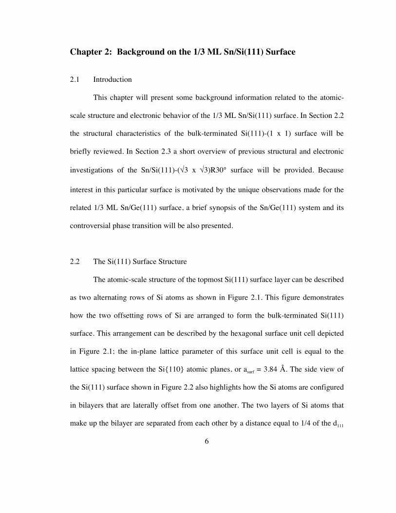
the Si(111) surface shown in Figure 2.2 also highlights how the Si atoms are configured
in bilayers that are laterally offset from one another. The two layers of Si atoms that
make up the bilayer are separated from each other by a distance equal to 1/4 of the d111
7
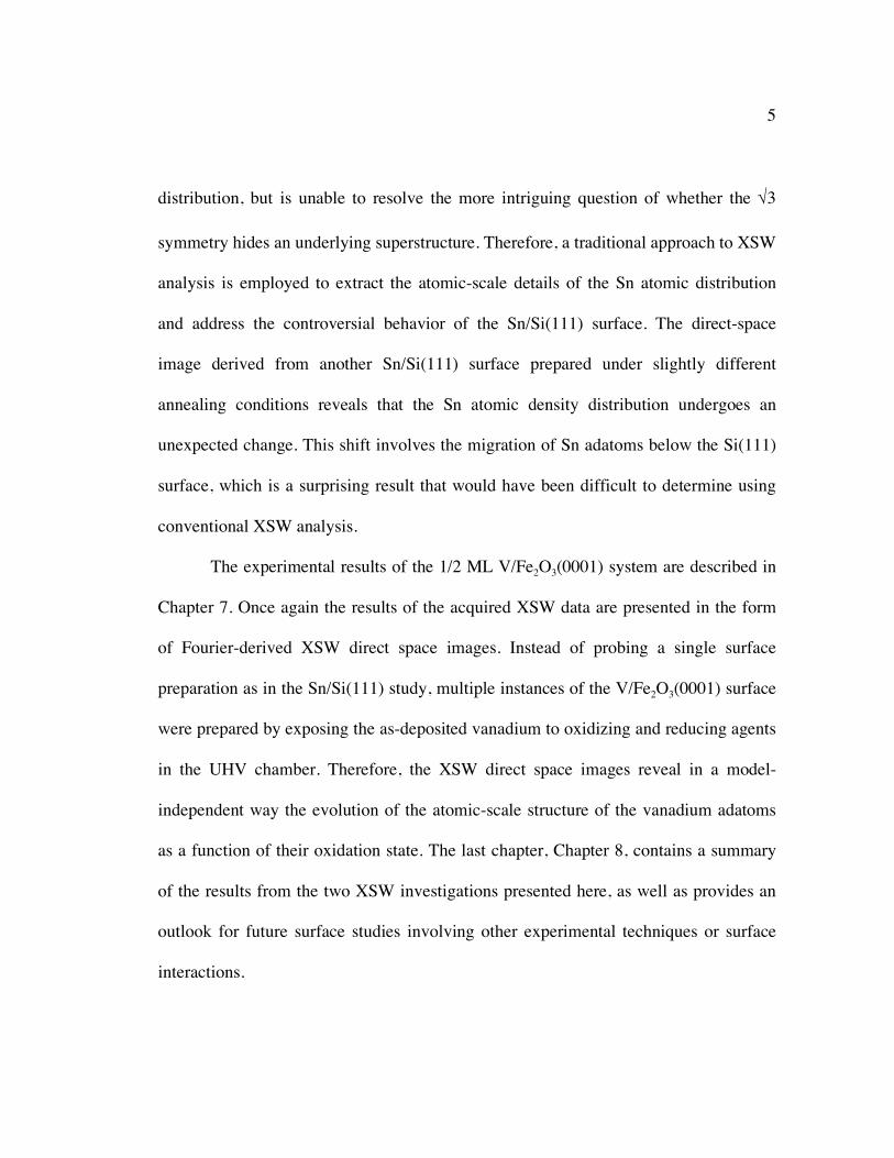
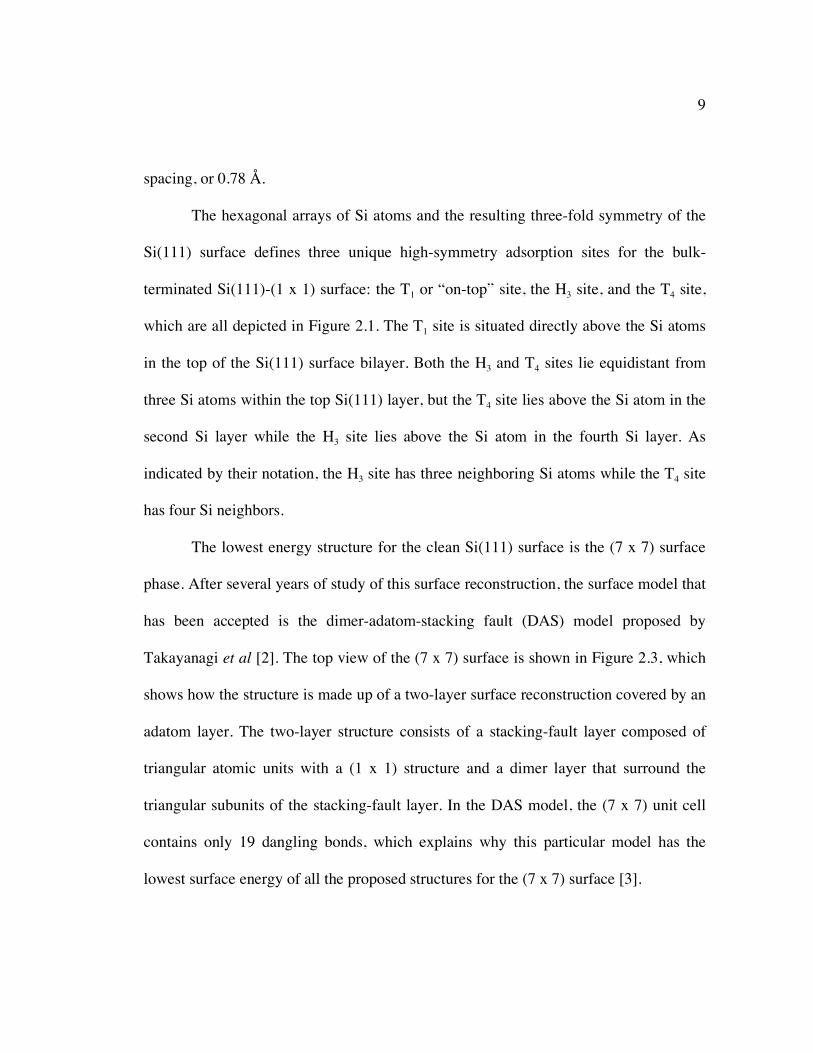
Figure 2.1: Top view of the Si(111) surface showing the three high-symmetry adsorption sites. The Si (1 x 1) surface unit cell is also outlined.
8
Figure 2.2: Side view projection of the Si(111) structure along the [10
�
1 ] direction. The stacking of Si atoms in the [111] direction consists of Si bilayers. The lattice spacing of the (111) atomic planes (d111 = 3.136 Å) is also shown.
9
spacing, or 0.78 Å.
The hexagonal arrays of Si atoms and the resulting three-fold symmetry of the
Si(111) surface defines three unique high-symmetry adsorption sites for the bulk-
terminated Si(111)-(1 x 1) surface: the T1 or “on-top” site, the H3 site, and the T4 site,
which are all depicted in Figure 2.1. The T1 site is situated directly above the Si atoms
in the top of the Si(111) surface bilayer. Both the H3 and T4 sites lie equidistant from
three Si atoms within the top Si(111) layer, but the T4 site lies above the Si atom in the
second Si layer while the H3 site lies above the Si atom in the fourth Si layer. As
indicated by their notation, the H3 site has three neighboring Si atoms while the T4 site
has four Si neighbors.
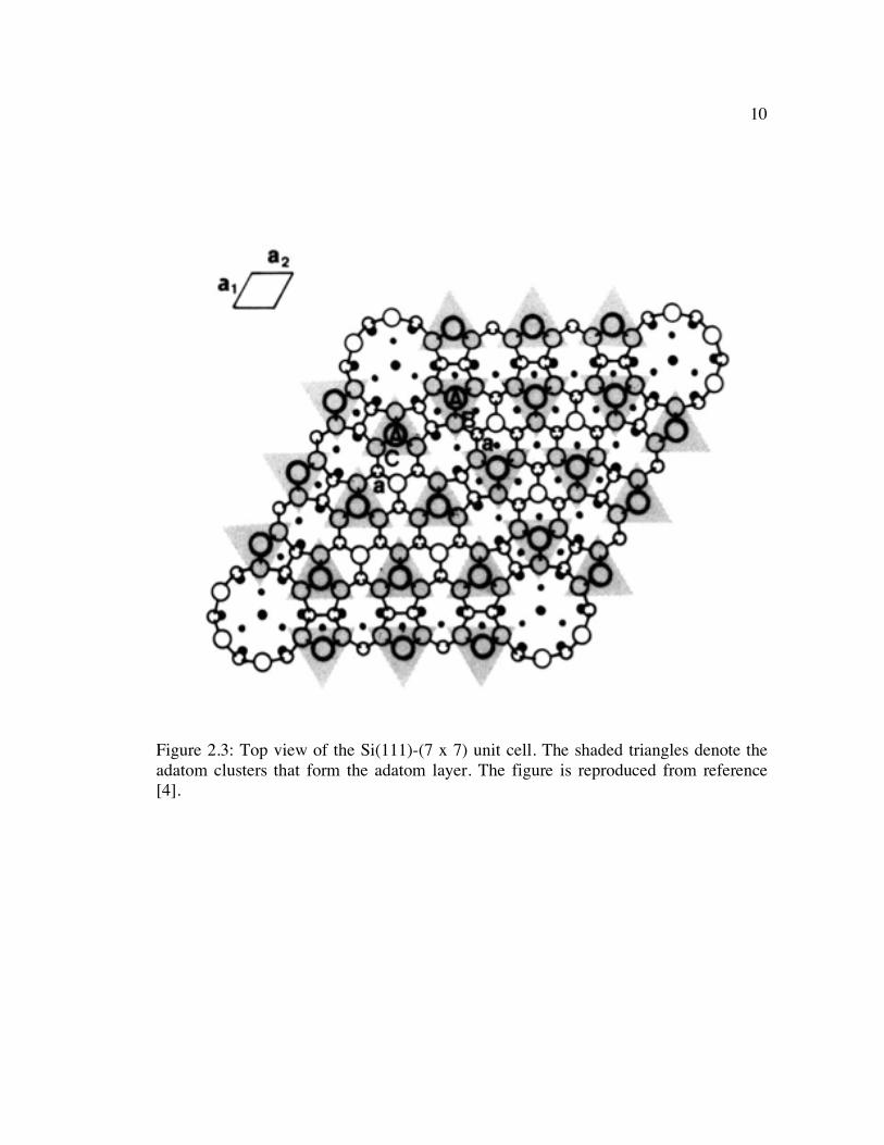
The lowest energy structure for the clean Si(111) surface is the (7 x 7) surface
phase. After several years of study of this surface reconstruction, the surface model that
has been accepted is the dimer-adatom-stacking fault (DAS) model proposed by
Takayanagi et al [2]. The top view of the (7 x 7) surface is shown in Figure 2.3, which
shows how the structure is made up of a two-layer surface reconstruction covered by an
adatom layer. The two-layer structure consists of a stacking-fault layer composed of
triangular atomic units with a (1 x 1) structure and a dimer layer that surround the
triangular subunits of the stacking-fault layer. In the DAS model, the (7 x 7) unit cell
contains only 19 dangling bonds, which explains why this particular model has the
lowest surface energy of all the proposed structures for the (7 x 7) surface [3].
10
Figure 2.3: Top view of the Si(111)-(7 x 7) unit cell. The shaded triangles denote the adatom clusters that form the adatom layer. The figure is reproduced from reference [4].
11
2.3 Sn/Si(111) Surfaces
2.3.1 The Sn/Si(111) phase diagram
The adsorption of Sn on Si has long presented a rich opportunity for surface
science, in part because of the chemical similarities between the adsorbate and the
semiconductor substrate. This attribute typically results in an atomically abrupt
interface between the Sn adlayer and the underlying Si substrate, which leads to the
possibility for interesting and well-characterized metal/semiconductor interface studies.
One such example is the study of the behavior of Sn as a surfactant for the epitaxial
growth of Si on Si(111) [5].
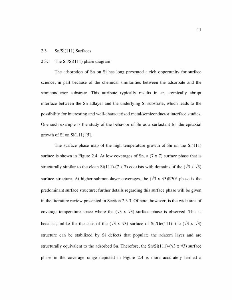
The surface phase map of the high temperature growth of Sn on the Si(111)
surface is shown in Figure 2.4. At low coverages of Sn, a (7 x 7) surface phase that is
structurally similar to the clean Si(111)-(7 x 7) coexists with domains of the (√3 x √3)
surface structure. At higher submonolayer coverages, the (√3 x √3)R30° phase is the
predominant surface structure; further details regarding this surface phase will be given
in the literature review presented in Section 2.3.3. Of note, however, is the wide area of
coverage-temperature space where the (√3 x √3) surface phase is observed. This is
because, unlike for the case of the (√3 x √3) surface of Sn/Ge(111), the (√3 x √3)
structure can be stabilized by Si defects that populate the adatom layer and are
structurally equivalent to the adsorbed Sn. Therefore, the Sn/Si(111)-(√3 x √3) surface
phase in the coverage range depicted in Figure 2.4 is more accurately termed a
12
Figure 2.4: Surface phase map as determined by RHEED during the high temperature annealing of Sn deposited on the Si(111) surface. Reprinted from reference [6], Copyright 2005, with permission from Elsevier.
13
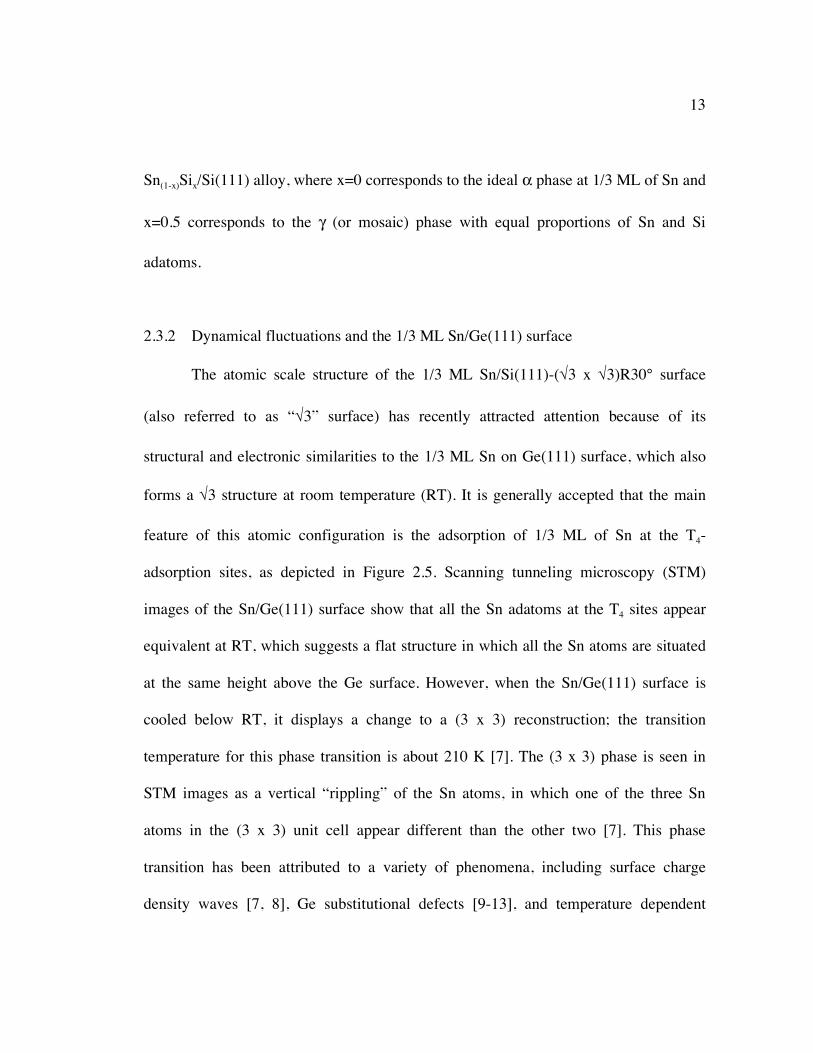
Sn(1-x)Six/Si(111) alloy, where x=0 corresponds to the ideal α phase at 1/3 ML of Sn and
x=0.5 corresponds to the γ (or mosaic) phase with equal proportions of Sn and Si
adatoms.
2.3.2 Dynamical fluctuations and the 1/3 ML Sn/Ge(111) surface
The atomic scale structure of the 1/3 ML Sn/Si(111)-(√3 x √3)R30° surface
(also referred to as “√3” surface) has recently attracted attention because of its
structural and electronic similarities to the 1/3 ML Sn on Ge(111) surface, which also
forms a √3 structure at room temperature (RT). It is generally accepted that the main
feature of this atomic configuration is the adsorption of 1/3 ML of Sn at the T4-
adsorption sites, as depicted in Figure 2.5. Scanning tunneling microscopy (STM)
images of the Sn/Ge(111) surface show that all the Sn adatoms at the T4 sites appear
equivalent at RT, which suggests a flat structure in which all the Sn atoms are situated
at the same height above the Ge surface. However, when the Sn/Ge(111) surface is
cooled below RT, it displays a change to a (3 x 3) reconstruction; the transition
temperature for this phase transition is about 210 K [7]. The (3 x 3) phase is seen in
STM images as a vertical “rippling” of the Sn atoms, in which one of the three Sn
atoms in the (3 x 3) unit cell appear different than the other two [7]. This phase
transition has been attributed to a variety of phenomena, including surface charge
density waves [7, 8], Ge substitutional defects [9-13], and temperature dependent
14
Figure 2.5: Ball-and-stick diagram of the 1/3 ML Sn/Si(111) surface. (a) Sn adatoms occupy one-third of the T4 adsorption sites. The (1 x 1) surface unit cell is inscribed in a solid black line and the (√3 x √3)-R30° surface unit cell is inscribed in a dashed grey line. (b) Side view of the Sn/Si(111) surface. Si atoms are displaced from their bulk-like positions according to the calculated atomic displacements of Ref. [18].
15
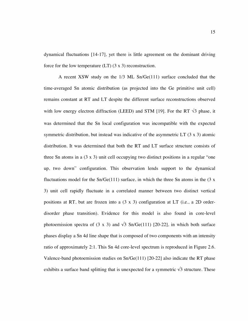
dynamical fluctuations [14-17], yet there is little agreement on the dominant driving
force for the low temperature (LT) (3 x 3) reconstruction.
A recent XSW study on the 1/3 ML Sn/Ge(111) surface concluded that the
time-averaged Sn atomic distribution (as projected into the Ge primitive unit cell)
remains constant at RT and LT despite the different surface reconstructions observed
with low energy electron diffraction (LEED) and STM [19]. For the RT √3 phase, it
was determined that the Sn local configuration was incompatible with the expected
symmetric distribution, but instead was indicative of the asymmetric LT (3 x 3) atomic
distribution. It was determined that both the RT and LT surface structure consists of
three Sn atoms in a (3 x 3) unit cell occupying two distinct positions in a regular “one
up, two down” configuration. This observation lends support to the dynamical
fluctuations model for the Sn/Ge(111) surface, in which the three Sn atoms in the (3 x
3) unit cell rapidly fluctuate in a correlated manner between two distinct vertical
positions at RT, but are frozen into a (3 x 3) configuration at LT (i.e., a 2D order-
disorder phase transition). Evidence for this model is also found in core-level
photoemission spectra of (3 x 3) and √3 Sn/Ge(111) [20-22], in which both surface
phases display a Sn 4d line shape that is composed of two components with an intensity
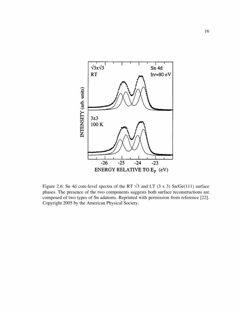
ratio of approximately 2:1. This Sn 4d core-level spectrum is reproduced in Figure 2.6.
Valence-band photoemission studies on Sn/Ge(111) [20-22] also indicate the RT phase
exhibits a surface band splitting that is unexpected for a symmetric √3 structure. These
16
Figure 2.6: Sn 4d core-level spectra of the RT √3 and LT (3 x 3) Sn/Ge(111) surface phases. The presence of the two components suggests both surface reconstructions are composed of two types of Sn adatoms. Reprinted with permission from reference [22]. Copyright 2005 by the American Physical Society.
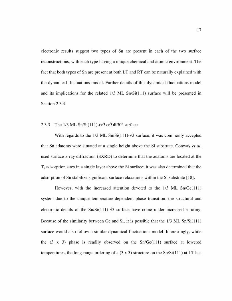
17
electronic results suggest two types of Sn are present in each of the two surface
reconstructions, with each type having a unique chemical and atomic environment. The
fact that both types of Sn are present at both LT and RT can be naturally explained with
the dynamical fluctuations model. Further details of this dynamical fluctuations model
and its implications for the related 1/3 ML Sn/Si(111) surface will be presented in
Section 2.3.3.
2.3.3 The 1/3 ML Sn/Si(111)-(√3x√3)R30° surface
With regards to the 1/3 ML Sn/Si(111)-√3 surface, it was commonly accepted
that Sn adatoms were situated at a single height above the Si substrate. Conway et al.
used surface x-ray diffraction (SXRD) to determine that the adatoms are located at the
T4 adsorption sites in a single layer above the Si surface; it was also determined that the
adsorption of Sn stabilize significant surface relaxations within the Si substrate [18].
However, with the increased attention devoted to the 1/3 ML Sn/Ge(111)
system due to the unique temperature-dependent phase transition, the structural and
electronic details of the Sn/Si(111)-√3 surface have come under increased scrutiny.
Because of the similarity between Ge and Si, it is possible that the 1/3 ML Sn/Si(111)
surface would also follow a similar dynamical fluctuations model. Interestingly, while
the (3 x 3) phase is readily observed on the Sn/Ge(111) surface at lowered
temperatures, the long-range ordering of a (3 x 3) structure on the Sn/Si(111) at LT has
18
not been observed via any previous structural investigations. One STM study conducted
by Ottaviano et al. found no indications of a phase transition down to 120 K. It was
pointed out that localized domains with (3 x 3) symmetry were identified centered at
defect sites [23]. In an another STM and LEED investigation of 1/3 ML Sn/Si(111),
Morikawa et al. found no evidence of any (3 x 3) symmetry at temperatures as low as 6
K and proposed the dynamical fluctuations model could not be correctly applied to the
Sn/Si(111) system based on this result [24].
In one of the few structural studies of this surface, Yamanaka et al. used the
electron standing wave (ESW) method to probe the 1/3 ML Sn/Si(111) surface; while
the original ESW analysis only considered a single layer of adsorbed Sn, the ESW data
was also compatible with an atomic arrangement composed of multiple Sn heights [25].
Another study investigated the structural properties of the √3 surface with full-potential
linearized augmented plane wave (FLAPW) calculations and concluded the adsorbed
Sn was located at a single position that was in good agreement with the earlier SXRD
and ESW studies [26]. In another theoretical investigation, Profeta et al. used density
functional theory calculations to conclude the ground state of the ideal 1/3 ML
Sn/Si(111) surface presents a √3 symmetry that does exhibit distortions that lead to a
(3 x 3) structure [27].
However, these results are difficult to reconcile with recent electronic structural
measurements of the 1/3 ML Sn/Si(111)-√3 surface. These measurements are similar to
19
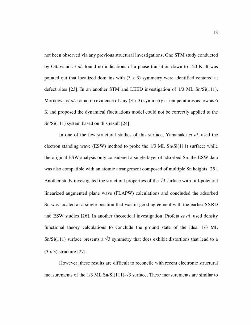
those conducted on the Ge(111) surface in that they suggest there are two unique types
of Sn are present on the RT surface. For example, the core-level and valence band
photoelectron spectra of the Sn/Si(111)-√3 surface collected by Uhrberg et al. [28]
display many of the same features that are suggestive of the (3 x 3) structure of the
Sn/Ge(111) system. This is demonstrated in Figure 2.7, which shows the two
components of the core-level spectra that point to multiple site occupation and the
dynamical fluctuations model. However, it should be pointed out that the smaller
component appears on the low binding-energy of the large component for Sn/Si(111),
which is the opposite behavior of the Sn/Ge(111) surface. A recent core-level
photoemission study probed the nature of these two components by dosing the surface
with electron and hole donors, which revealed the relationship between the bimodal
nature of the core level spectra and two well-defined states of unlike charge [29]. In
presenting these results, Davila et al. related their findings to the theoretical results of
Ballabio et al., which proposed a different type of dynamical model in which different
Sn structural configurations beyond a “one up, two down” arrangement are driven by
strain but are obscured by thermal fluctuations [30]. It was suggested that these
configurations represent a charge disproportionation phenomenon, and the Sn/Si(111)
surface may represent a case of dynamical valence fluctuation, in which a classical
fluctuating state or a quantum fluctuating state can exist.
Further evidence of dynamical fluctuations is found in the angle-resolved
20
Figure 2.7: Sn 4d core-level spectra of the LT √3 Sn/Si(111) surface reconstruction. The two component spectrum appears quite similar to the core-level spectra acquired from the LT and RT Sn/Ge(111) surface. Reprinted with permission from reference [28]. Copyright 2005 by the American Physical Society.
21
Figure 2.8: k//-resolved inverse photoemission spectroscopy (KRIPES) spectra of the √3 Sn/Si(111) surface phase before and after exposure to atomic hydrogen. The difference curve reveals the presence of two adsorption-sensitive surface states, which suggest multiple adatom states for the RT surface. Reprinted with permission from reference [31]. Copyright 2005 by the American Physical Society.
22
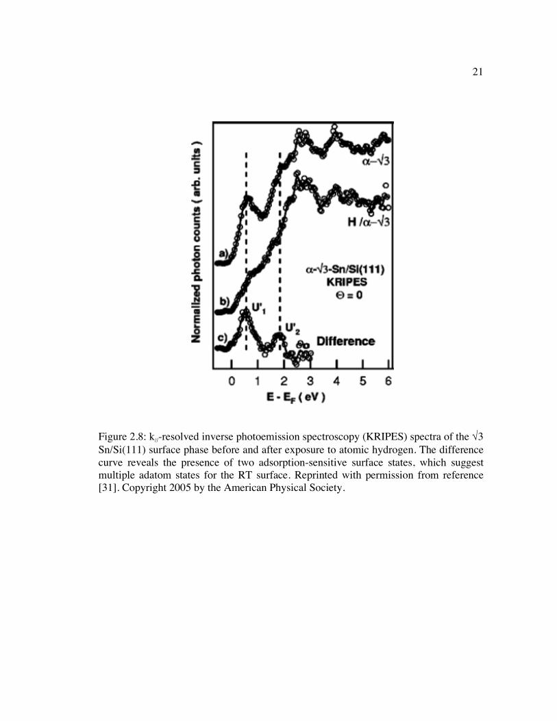
inverse photoemission (KRIPES) results of Charrier et al., a portion of which is shown
in Figure 2.8 [31]. The observation of the two surface states (U´1 and U´2 in Figure 2.8)
again points to the presence of more than one type of Sn adatom in the Sn/Si(111)
surface, which is in direct conflict with the STM and LEED observations presented
earlier. Angle-resolved photoemission was also used to investigate the electronic
character of the surface as a function of Sn coverage; this study concluded that a
splitting in the surface band, which is characteristic of an underlying (3 x 3) symmetry,
is present within a range of Sn coverage (0.23–0.33 ML) [32].
While the discrepancy between the existing electronic and structural results has
a convincing explanation in the dynamical fluctuation model, this model as presented
does not fully explain why the (3 x 3) symmetry observed by the electronic
measurements has not been observed by other structural techniques, even at
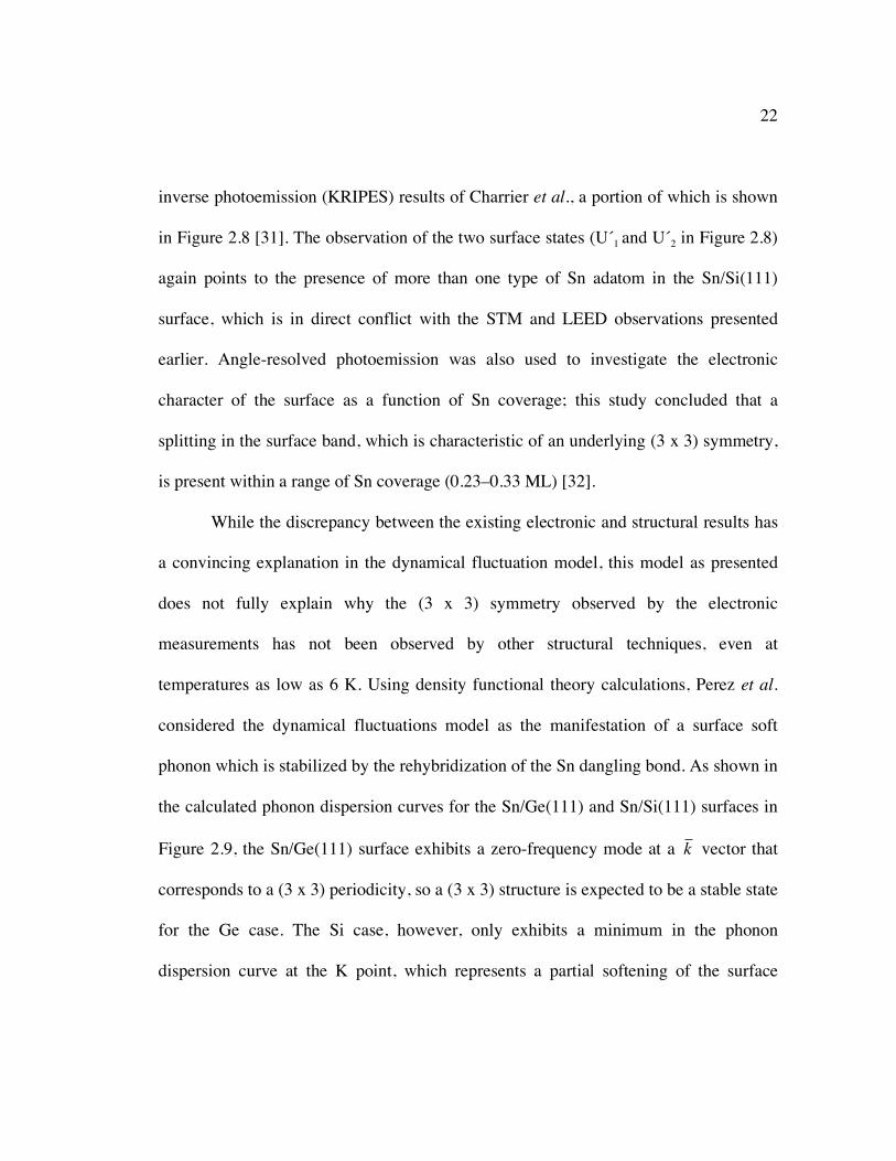
temperatures as low as 6 K. Using density functional theory calculations, Perez et al.
considered the dynamical fluctuations model as the manifestation of a surface soft
phonon which is stabilized by the rehybridization of the Sn dangling bond. As shown in
the calculated phonon dispersion curves for the Sn/Ge(111) and Sn/Si(111) surfaces in
Figure 2.9, the Sn/Ge(111) surface exhibits a zero-frequency mode at a
�
k vector that
corresponds to a (3 x 3) periodicity, so a (3 x 3) structure is expected to be a stable state
for the Ge case. The Si case, however, only exhibits a minimum in the phonon
dispersion curve at the K point, which represents a partial softening of the surface
23
phonon and explains why a static (3 x 3) periodicity is not observed for the Sn/Si(111)
surface.
Despite the differences in the behavior of the surface phonons for the two
surfaces, the surface structures found on Si and Ge are similar at room temperature.
This observation can be understood from the energy calculations for the two surfaces
presented in Figure 2.10, which shows the total energy change as a function of adatom
displacement. Because of the flat energy surfaces exhibited by both surfaces, there is
only a minimal energy penalty for large atomic displacements, which manifest
themselves as the correlated vibrations observed at room temperature for both the
Sn/Ge(111) and Sn/Si(111) surfaces [17].
24
Figure 2.9: Phonon dispersion curves for the (top) Sn/Ge(111) and (bottom) Sn/Si(111) √3 surfaces. The solid lines refer to the Sn terminated surface, while the dashed lines refer to the H-saturated Sn/Ge(Si) surfaces. Shaded areas represent the projection of the corresponding phonon bulk band structure. While the Sn/Ge(111) surface exhibits a zero-frequency mode at the
�
! K point, the Si surface only displays a minimum in the phonon dispersion curve. The dotted line for the Sn/Ge surface represents the renormalization of the frequency of the soft phonon mode at room temperature. Reprinted with permission from reference [17]. Copyright 2005 by the American Physical Society.
25
Figure 2.10: Calculated total energy of the Sn/Si and Sn/Ge surfaces as a function of the displacement of one of the Sn adatoms in the (3 x 3) surface unit cell. The inset demonstrates the relationship between the vertical displacements of the three Sn atoms in the (3 x 3) unit cell. Reprinted with permission from reference [17]. Copyright 2005 by the American Physical Society.
26
Chapter 3: Background on the V/α-Fe2O3(0001) Surface
3.1 Introduction
In this chapter a overview of the structural and electronic properties of the V/α-
Fe2O3(0001) surface will be presented. In Section 3.2 some background material on the
bulk structural characteristics of hematite will be given. The following section (Section
3.3) will detail some examples in the literature to prepare and characterize the structure
of the α-Fe2O3(0001) surface. Later sections will focus on the catalytic role of
vanadium and its assorted oxides when supported on various metal oxide substrates. A
short review of the properties of some of the relevant vanadium oxides, namely V2O5
and V2O3, will be given in Section 3.4. Previous experimental investigations focused on
the growth and oxidation of vanadium thin films on metal oxide supports will be
reviewed in Section 3.5. While most of these studies have dealt with the case of
vanadium oxide supported on the TiO2(110) surface, our research group has recently
investigated the interaction between submonolayer amounts of vanadium and the α-
Fe2O3(0001) surface using X-ray photoelectron spectroscopy (XPS). This study will be
reviewed in further detail in Section 3.6.
3.2 Crystal Structure of Bulk Fe2O3
Iron oxides are abundant materials that are commonly found in nature and easily
synthesized in laboratory or industrial environments. Because iron oxides are so
prevalent in the all aspects of the global system, from iron ore in the terrestrial
27
environment to precipitates in the marine environment, it is not surprising that the study
of iron oxide is an important field in geology, mineralogy, and geochemistry. However,
iron oxides have an important role in other disciplines as well, such as industrial and
environmental chemistry, which includes catalytic research, and even medicinal and
biological research. The oldest known of the iron oxides is hematite (α-Fe2O3), which is
a stable oxide that is used as pigmentation and for magnetic recording [33]. However, it
is the importance of hematite in applications of heterogeneous catalysis,
photoelectrolysis, corrosion, and gas sensing that has motivated much of the effort to
understand the atomic and electronic structure of the hematite surface.
Like all iron oxides, hematite consists of close packed arrays of oxygen anions
in which the interstitial sites are occupied by Fe cations. In the case of hematite, the Fe
and O atoms crystallize in the corundum structure (space group R
�
3 c), in which the
oxygen O2- ions are arranged in a hexagonal close packed (hcp) array, and the
interstices of the hcp array are partially filled by trivalent Fe. This arrangement forms
octahedra, which consist of the central Fe3+ anion and the surrounding anion ligands, as
shown in the depiction of the hematite hexagonal unit cell in Figure 3.1. More
specifically, the Fe3+ cations occupy two-thirds of the sites in an ordered arrangement,
where two adjacent sites in the (0001) plane are filled followed by an empty site.
Because the cations are slightly larger than the octahedral sites formed by the anion
close packing, the anion packing in the [0001] direction is slightly irregular and the
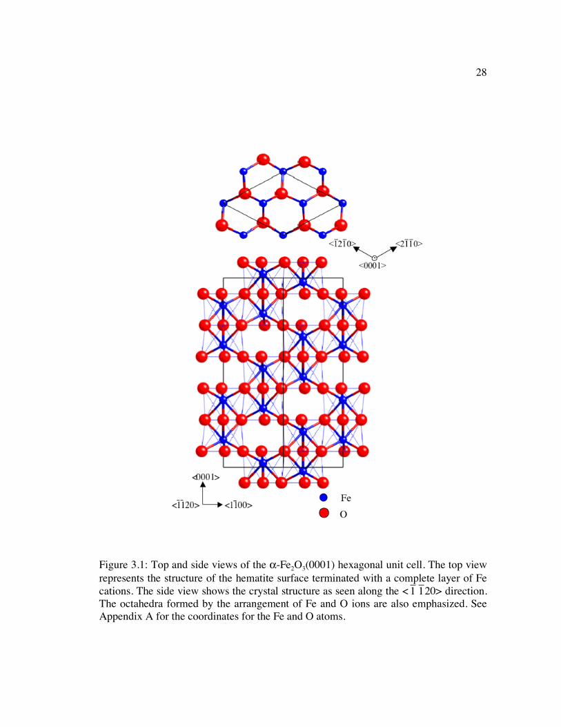
28
Figure 3.1: Top and side views of the α-Fe2O3(0001) hexagonal unit cell. The top view represents the structure of the hematite surface terminated with a complete layer of Fe cations. The side view shows the crystal structure as seen along the <
�
1
�
1 20> direction. The octahedra formed by the arrangement of Fe and O ions are also emphasized. See Appendix A for the coordinates for the Fe and O atoms.
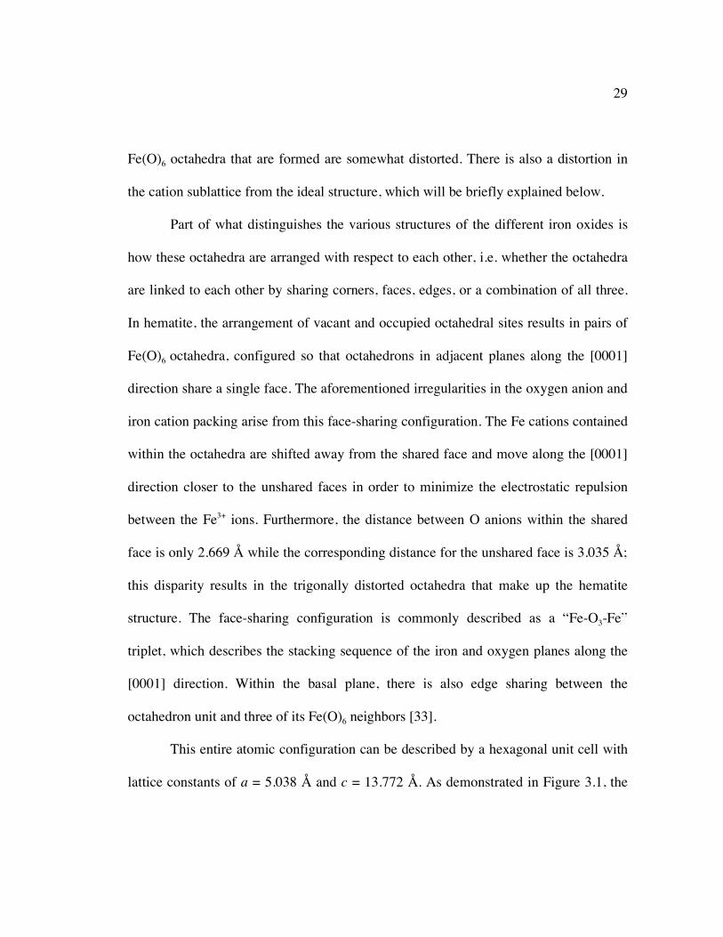
29
Fe(O)6 octahedra that are formed are somewhat distorted. There is also a distortion in
the cation sublattice from the ideal structure, which will be briefly explained below.
Part of what distinguishes the various structures of the different iron oxides is
how these octahedra are arranged with respect to each other, i.e. whether the octahedra
are linked to each other by sharing corners, faces, edges, or a combination of all three.
In hematite, the arrangement of vacant and occupied octahedral sites results in pairs of
Fe(O)6 octahedra, configured so that octahedrons in adjacent planes along the [0001]
direction share a single face. The aforementioned irregularities in the oxygen anion and
iron cation packing arise from this face-sharing configuration. The Fe cations contained
within the octahedra are shifted away from the shared face and move along the [0001]
direction closer to the unshared faces in order to minimize the electrostatic repulsion
between the Fe3+ ions. Furthermore, the distance between O anions within the shared
face is only 2.669 Å while the corresponding distance for the unshared face is 3.035 Å;
this disparity results in the trigonally distorted octahedra that make up the hematite
structure. The face-sharing configuration is commonly described as a “Fe-O3-Fe”
triplet, which describes the stacking sequence of the iron and oxygen planes along the
[0001] direction. Within the basal plane, there is also edge sharing between the
octahedron unit and three of its Fe(O)6 neighbors [33].
This entire atomic configuration can be described by a hexagonal unit cell with
lattice constants of a = 5.038 Å and c = 13.772 Å. As demonstrated in Figure 3.1, the
30
in-plane lattice parameter of the hexagonal unit cell corresponds to the interatomic
distance between Fe cations within a single layer of the Fe bilayer. Six formula units
comprise the nonprimitive hexagonal unit cell. The primitive bulk hematite structure
can also be described using the rhombohedral unit cell, which has a lattice parameter of
arh = 5.427 Å and α = 55.3°; there are two formula units per unit cell in the
rhombohedral system.
3.3 Preparation and Characterization of the α-Fe2O3(0001) Surface
As previously mentioned, the importance of metal oxides such as hematite for
heterogeneous catalysis and gas sensing applications motivates the desire to understand
the atomic scale surface structure of the oxide, since much of the chemical or catalytic
properties are determined by its atomic arrangement at the surface. However, obtaining
the necessary structural information from a metal oxide surface such as the α-
Fe2O3(0001) surface can be a complicated endeavor for a number of reasons.
First of all, several structural investigations of the hematite surface have found
that the manner in which the surface is prepared can result in several different surface
phases or morphologies. A common surface treatment for producing a clean hematite
surface is Ar+ ion sputtering; however, Kurtz et al. has shown that ion sputtering can
preferentially remove oxygen from the surface layers and produce a reduced surface
[34]. Replacing the lost surface oxygen by annealing in an oxygen environment can fill
31
the vacancies caused by sputtering, but the recovery of the ideal surface can be strongly
dependent on the annealing conditions. One early LEED and XPS structural study of
the α-Fe2O3(0001) surface suggested that the sputtering process transforms part of the
hematite surface into a thin layer of metallic Fe0 that lies above a thicker reduced iron
oxide layer [34]. Similar investigations have suggested that it is the annealing
temperature (and not the annealing environment) that primarily governs the extent of
re-oxidation of the surface overlayers. It has been proposed that the choice of annealing
temperature also determines whether the re-oxidized surface region consists solely of
hematite or if a magnetite (Fe3O4) layer is produced by the removal of oxygen anions
from the underlying Fe2O3 [35]. However, other investigations have found that after a
surface layer of magnetite is formed during sputtering, annealing under an increased
oxygen pressure allows the Fe3O4 to be reoxidized at a lower annealing temperature
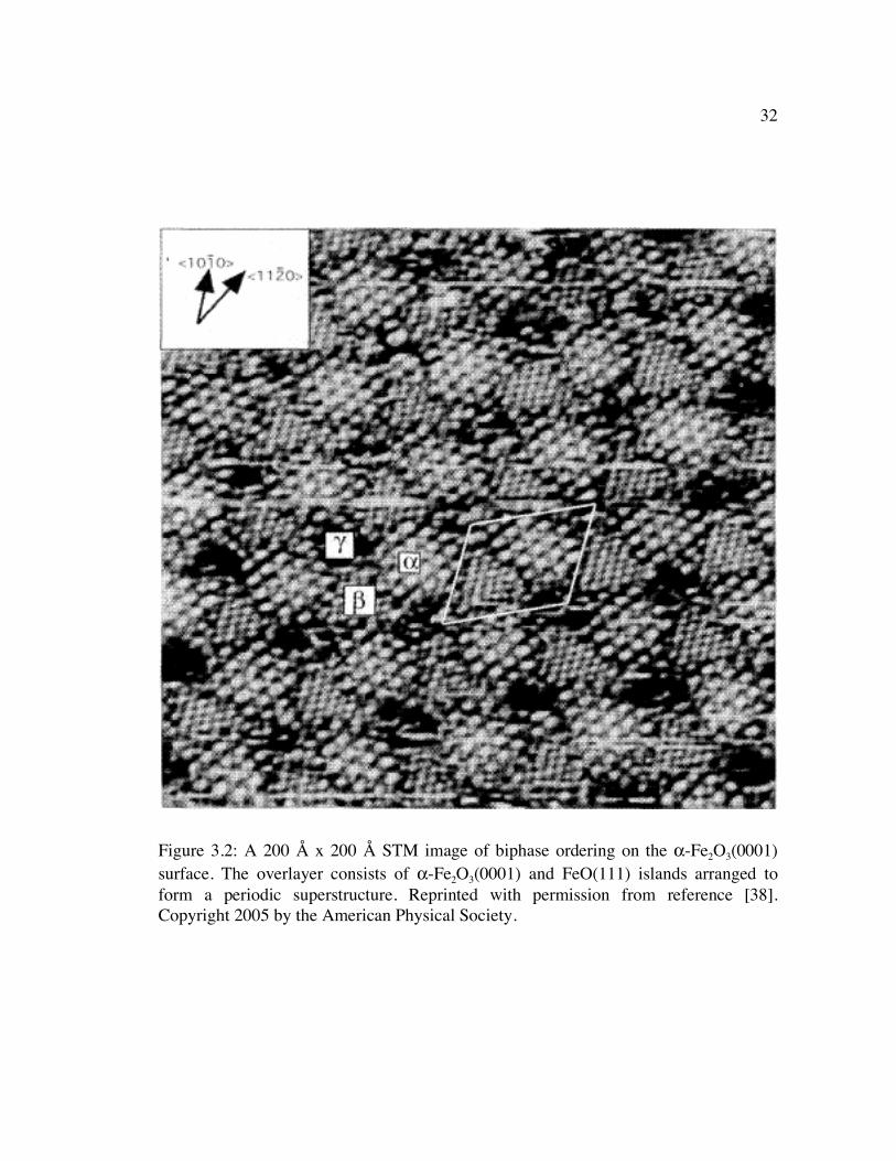
[36]. Finally, in an STM study, Condon et al. reinterpreted some of these conclusions
as the result of a phenomenon called biphase ordering, in which islands of α-Fe2O3 and
FeO(111) coexist on the hematite surface and form an extended superlattice [37, 38].
STM images of this unique overlayer structure are shown in Figure 3.2.
An extensive surface x-ray diffraction (SXRD) investigation on the α-
Fe2O3(0001) surface encountered all these aforementioned iron oxide phases as the
oxygen-deficient hematite surface was recovered to the stoichiometric (1 x 1) surface
[39]. Unlike the electron-based surface techniques that probe only the first few atomic
32
Figure 3.2: A 200 Å x 200 Å STM image of biphase ordering on the α-Fe2O3(0001) surface. The overlayer consists of α-Fe2O3(0001) and FeO(111) islands arranged to form a periodic superstructure. Reprinted with permission from reference [38]. Copyright 2005 by the American Physical Society.
33
layers of the surface, the x-ray scattering provides structural information from both the
surface and subsurface regions. It was determined that after annealing the reduced
surface in a molecular oxygen environment, the uppermost surface layers can be
recovered to the stoichiometric Fe2O3 phase, but a remnant magnetite layer remains
below the recovered oxide surface. By slightly increasing the oxygen annealing
temperature (from 1008K to 1018K in this particular study), the subsurface magnetite
can be converted to hematite, but the previously stoichiometric surface is
simultaneously transformed into the non-stoichiometric biphase ordered surface. The
topmost biphase layer can finally be converted to Fe2O3 by annealing in an atomic
oxygen environment. This elaborate surface history is a telling example of some of the
complexities that can arise when preparing and characterizing the stoichiometric α-
Fe2O3(0001) surface.
Furthermore, even if the stoichiometric structure can be recovered from the
oxygen deficient surface using oxygen annealing, the question of what is the chemical
composition of the α-Fe2O3(0001) surface remains. Because of the “Fe-O3-Fe” stacking
sequence of the bulk hematite structure, it is possible that the α-Fe2O3(0001) surface
can consist of a terminal layer of either Fe cations or O anions. In addition, the hematite
surface can be expected to undergo significant atomic relaxations, which are in part
driven by the tendency of the surface cations to increase their oxygen coordination. A
detailed theoretical study employing a variety of periodic slab models and
34
computational methods found a large relaxation effect for the two outermost surface
layers of a Fe-terminated α-Fe2O3(0001) surface. These substantial relaxations were
attributed to the reduced coordination of the surface atoms [40]. In one spin-density
functional theory (DFT) study, Wang et al. calculated the surface energies of various α-
Fe2O3(0001) surface terminations as a function of the oxygen chemical potential. From
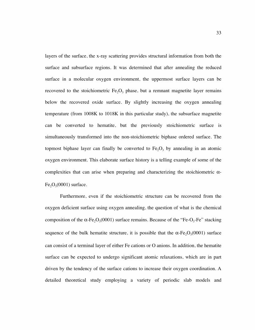
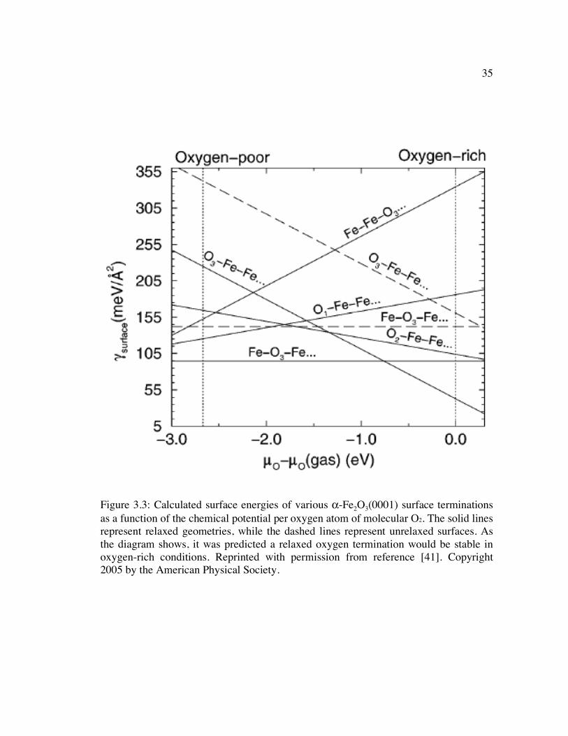
the results of these calculations (which are summarized in Figure 3.3), it was
determined that both a Fe-terminated (Fe-O3-Fe) and an O-terminated (O3-Fe-Fe)
surface can be stabilized if they were accompanied with significant atomic interlayer
relaxations. The presence of both surface terminations was observed using STM [41].
Another STM study [42] also observed the significant dependence of the hematite
surface structure on the ambient oxygen pressure detailed in Ref. [41]. In another DFT
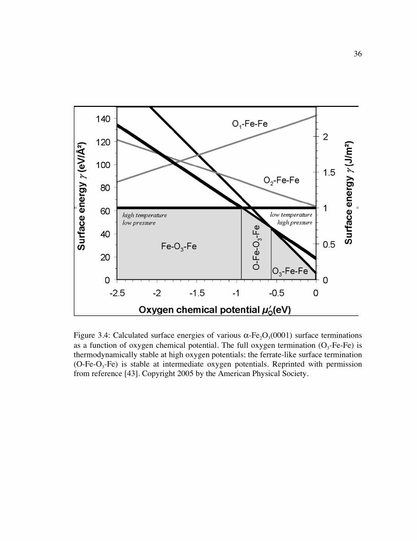
investigation of the α-Fe2O3(0001) surface, several Fe- and O-terminated hematite
surfaces were explored, including an additional surface phase involving a single O
atom bonded on top of a reactive surface Fe atom; this structure stabilizes as the surface
is allowed to relax in an oxygen-rich environment, as shown in the calculated surface
phase energy plot shown in Figure 3.4 [43].
However, these results were somewhat disputed by Chambers et al. in a XPD
and STM investigation of α-Fe2O3(0001) surfaces grown by oxygen-plasma-assisted
molecular beam epitaxy. This study suggested that the Fe-terminated surface is the
most stable surface even under highly-oxidizing conditions [44]. These experimental
35
Figure 3.3: Calculated surface energies of various α-Fe2O3(0001) surface terminations as a function of the chemical potential per oxygen atom of molecular O2. The solid lines represent relaxed geometries, while the dashed lines represent unrelaxed surfaces. As the diagram shows, it was predicted a relaxed oxygen termination would be stable in oxygen-rich conditions. Reprinted with permission from reference [41]. Copyright 2005 by the American Physical Society.
36
Figure 3.4: Calculated surface energies of various α-Fe2O3(0001) surface terminations as a function of oxygen chemical potential. The full oxygen termination (O3-Fe-Fe) is thermodynamically stable at high oxygen potentials; the ferrate-like surface termination (O-Fe-O3-Fe) is stable at intermediate oxygen potentials. Reprinted with permission from reference [43]. Copyright 2005 by the American Physical Society.
37
results were supported by an ab initio theoretical study, which included electron
correlation effects within a density functional description. By including the strong
correlation effects, it was determined that a Fe-terminated surface is the most stable
surface over the allowable range of oxygen chemical potentials; the proposed surface
model consists of a partially occupied Fe layer in which half of the octahedral sites are
vacant [45]. An earlier X-ray photoelectron diffraction (XPD) experiment also found
this particular structure to be the most stable surface phase and found no evidence of a
possible O-termination [46]. The authors of this study suggested that since the partially
occupied Fe termination layer fully autocompensates the hematite surface due to charge
transfer from the Fe dangling bonds to the O dangling bonds, it is not surprising that the
Fe-termination surface model provided the best fit to the PED spectra [47].
Finally, for some catalytic investigations the presence of surface point defects
may be desirable, since oxygen vacancies can result in a redistribution of charge and a
reduction of surface cations, which can help promote the adsorption and dissociation of
foreign molecules. A surplus of cations in the form of Fe interstitials is another form of
non-stoichiometry that can also contribute to the catalytic activity. Therefore, there is a
need to characterize non-ideal hematite surfaces in order to more accurately model real-
world catalytic processes. In a theoretical study of the defect chemistry of the α-
Fe2O3(0001) surface, Warschkow et al. found that at the hematite surface, the energy
required to form an oxygen vacancy is markedly smaller than in the bulk [48].
38
Furthermore, the same investigation determined a lowering of some of the transition
barriers to oxygen vacancy migration within the uppermost oxygen layers near the
hematite surface. However, there are few experimental studies on the formation of
defects and their effect on the properties of the α-Fe2O3(0001) surface.
3.4 Overview of the Oxides of Vanadium
The study of supported vanadium-based oxides and their interaction with the
supporting material represents one of the most active fields of catalytic research. This
reflects the significance of vanadium oxide-based catalysts in many important industrial
processes, such as the production of sulfuric acid and phthalic anhydride, and in the
reduction of environmental byproducts, such as the selective reduction of nitrogen
oxides from the flue gas of power plants [49]. Two reasons have been mentioned for
the importance of vanadium for metal oxide catalysis: the variety of oxidation states
(from +2 to +5) and the assortment of structural geometries that are available for
vanadium oxides. Because of the variability of atomic arrangements that are present in
vanadium oxides, the surface oxygen anions can have a number of possible
coordination geometries, which in turn has a strong effect on the oxides’ catalytic
properties.
When employed as a catalyst, the vanadium oxide is typically distributed on a
supporting material, either by impregnation, adsorption from solution, a deposition
39
method such as chemical vapor deposition, or by co-precipitation [50]. The original
intent of using a support material was to enhance the catalytic activity of the vanadium
oxide by increasing its mechanical strength, surface area, thermal stability, and
endurance. However, recent studies have demonstrated that the catalytic properties of
supported metal oxides, especially vanadium oxides, are enhanced by the properties of
the support itself. This phenomenon has been termed the “metal oxide-support” or
“monolayer catalysis” effect; Bond et al., Weckhuysen et al., and Surnev et al., in
preparing extensive reviews of this mechanism, have focused on the role of supported
vanadium oxides. While these reviews examine the properties of both the principal
vanadium oxides and mixed valency oxides in many different molecular configurations
(such as an isolated vanadium oxide species, two-dimensional vanadium oxide chains,
or three-dimensional crystals of vanadium oxide), this thesis will present only a brief
overview of the pentoxide V2O5 and the sesquioxide V2O3 as they have been studied in
various supported metal oxide investigations [49-51].
The geometric structure of V2O5 can be described as edge-sharing units of VO5
that form double chains along the b-direction. The VO5 oxide units form square
pyramids, but because the chains are connected at the corners and stacked on top of
each other in the c-direction, the vanadium oxide unit is actually a distorted VO6
octahedron. There are three distinct V–O bond distances within this octahedron. The
V=O double bond along the c-direction is 1.58 Å in length, while the V–O bond
40
directly opposite the double bond is 2.79 Å. The four V–O bonds involving the
bridging oxygens in the basal plane have a length of 1.83 Å [49]. A ball-and-stick
model of the orthorhombic unit cell of V2O5 is shown in Figure 3.5. As for the
electronic state of the pentoxide, V2O5 has a formal oxidation state of +5 and has the d0
electronic configuration. Therefore, V2O5 cannot gain any additional oxygen and would
not be expected to be an active catalyst in its stoichiometric state [52]. However,
supported layers of V2O5 can be activated with high temperature reducing environments
in order to produce a variety of surface oxidation states; this enables the vanadium
oxide to participate in subsequent catalytic reactions. The material supporting the
vanadium oxide and the reducing species can also influence the distribution of
vanadium oxidation states and oxygen coordination geometries that are present after
reduction [49].
Unlike V2O5, bulk V2O3 (which crystallizes in the corundum structure, similar to
α-Fe2O3) or its clean surfaces have received much less attention with regards to their
catalytic properties. However, there are several surface investigations of vanadia
deposition on metal oxides such as α-Al2O3 or TiO2 where it was determined the
deposited vanadium oxide layer has the characteristics of V2O3. Some examples of such
surface studies will be given in the following section.
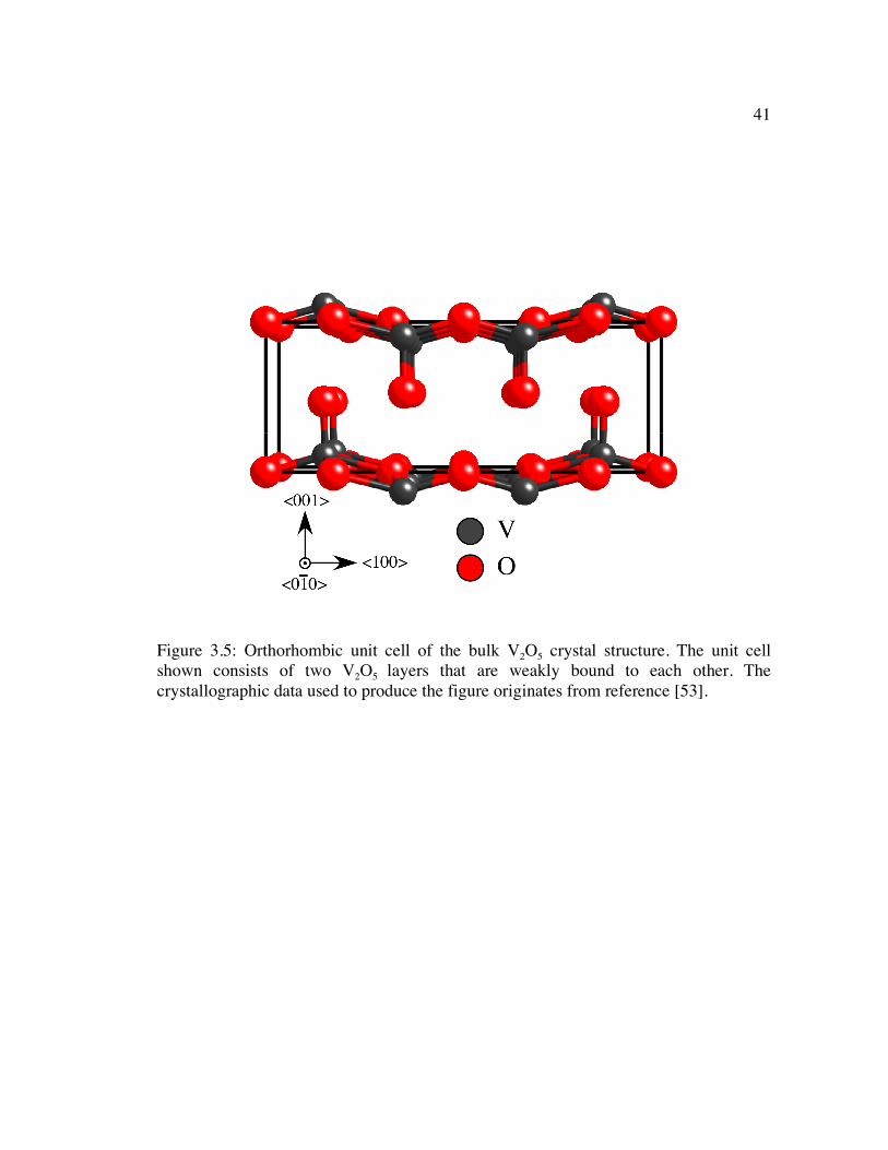
41
Figure 3.5: Orthorhombic unit cell of the bulk V2O5 crystal structure. The unit cell shown consists of two V2O5 layers that are weakly bound to each other. The crystallographic data used to produce the figure originates from reference [53].
42
3.5 Vanadium Oxide Films Supported on Oxide Substrates
When a transition metal such as vanadium is deposited on a metal oxide
substrate, there can be a complex interaction between the adsorbed metal and the oxide
substrate. Because of the various oxidation states that are available to transition metals,
especially in the case of vanadium, the transition metal can assume any of several
electronic configurations depending on the availability of charge carriers in the
substrate and the magnitude of the surface potential at the adsorption site [52]. The
characteristics of the bonding between metal and metal oxide can be complicated as
well due to the partially-filled and localized d orbitals that govern the chemistry of the
adsorbed transition metal; in addition to an ionic component of the bonding due to
charge transfer between the adsorbate and the substrate, there may also be some direct
overlap between the d orbitals of the two atomic species that leads to a metallic type of
chemical bond [52]. Finally, the adsorption of the metal can disturb the metal oxide
surface in a significant way by reacting with the lattice oxygen. Vanadium, in
particular, has a relatively large oxygen affinity (based on its heat of formation of the
stable vanadium oxide), so it would be expected that adsorbed vanadium could be
particularly effective in reducing a hematite substrate and forming a surface layer of
vanadium oxide.
While the focus of this thesis is the interaction of submonolayer amounts of
vanadium and the α-Fe2O3(0001) surface, there has been a wealth of surface
43
investigations on the structural, electronic, and catalytic properties of vanadium oxide
films on TiO2(110) and, to a lesser extent, α-Al2O3(0001). This overview will present
some of the most recent results of various vanadium oxides at the TiO2(110) surface;
because α-Al2O3 is isostructural with hematite, it will be useful to review the findings
of the surface studies of vanadium oxide on alumina as well.
In one early investigation of the interaction of vanadium and vanadium oxide
with TiO2(110), Zhang et al. recognized that because of the strong oxygen affinity of
both V and Ti, the competition between the two transition metals for the lattice O2- ions
would result in an interesting system [54]. When vanadium is deposited on the
stoichiometric TiO2(110) surface at submonolayer coverages in ultra-high vacuum
(UHV) conditions, Zhang et al. found an immediate reduction of the titania surface as
charge is transferred from Ti4+ cations to V adatoms to form a thin, disordered Ti–O–V
layer. This strong interaction between vanadium and the substrate was not present when
deposited on reduced TiO2(110) surfaces. Further vanadium deposition beyond 1
monolayer (ML) produced a metallic V layer above the disordered Ti–O–V compound.
In a later surface investigation also conducted in UHV, Biener et al. determined the
TiO2 substrate is reduced upon vanadium deposition, and both V2+ and V3+ as well as
Ti3+ cations are produced. This charge-transfer process is not limited to the initial
surface layers; rather, subsurface lattice oxygen cations migrate toward and partially
oxidize the vanadium overlayer [55].
44
When vanadium is deposited in a molecular oxygen environment (1 x 10⁻⁷ Torr)
on stoichiometric TiO2(110), a weakly interacting and disordered vanadium oxide
forms with a composition similar to V2O3 or VO2 [54]. In a separate XPD study of
room temperature (RT) deposition of V followed by a mild annealing, Sambi et al.
proposed that the adsorbed V atoms occupy a well-defined atomic site that
corresponded to a Ti bulk-like substitutional site within the first surface layer. There
was no diffraction evidence of diffusion of the vanadium before the initial surface
layer. It was suggested the mild annealing provided the necessary energy for bulk
oxygen to diffuse to the TiO2 surface and fully oxidize the surface Ti and V atoms [56].
The same researchers also reported on the growth of several monolayers of epitaxial
VO2 on the TiO2(110) surface. The VO2 oxide layer was prepared with successive
depositions of vanadium; after each deposition step, the TiO2 surface was annealed in
an oxygen environment. This growth process was described as “deposition under
thermodynamic control,” in which the post-deposition annealing process was intended
to enhance the order and oxidation of the surface. It was determined that the resulting
vanadium oxide layer was well-ordered and pseudomorphic to the TiO2(110) substrate
[57, 58].
In another extensive surface investigation employing LEED, Auger electron
spectroscopy (AES), XPS, and near edge X-ray absorption fine structure spectroscopy
(NEXAFS), Biener et al. proposed that if vanadium is deposited on the TiO2 substrate
45
at RT in an oxygen ambient, the vanadium does not reduce the TiO2 surface. Instead, it
is suggested that a disordered layer of V2O3 forms via a simultaneous growth mode, in
which the vanadia grow as islands that eventually combine to form the complete V2O3
layer [59]. Sambi et al. conducted a similar surface study using XPS, AES, and XPD
and determined that while the vanadium oxide grown in an oxygen environment may
have an electronic structure typical of V2O3, the atomic-scale structure of the oxide is
actually isomorphic to the rutile lattice of the TiO2 substrate below [57, 60]. The
authors suggested that the unique way the thin layers of vanadia adopted the underlying
structure of the TiO2 substrate might have a role in the oxide’s catalytic activity. Instead
of performing the vanadium deposition at RT, Guo et al. attempted to form a vanadium
oxide thin film by depositing vanadium on the TiO2(110) surface at 570K in an oxygen
ambient [61]. This surface study also observed the formation of a vanadium oxide layer
characteristic of V2O3 when the vanadium coverage was above one monolayer
equivalent (MLE). However, at lower vanadium coverages, both core-level XPS
spectra and electron energy loss spectra (EELS) suggested that both V3+ and V4+ were
present at the vanadia-titania interface.
Finally, there have been some successful efforts to prepare thin layers of V2O5
supported on TiO2 by codosing the titania surface with VOCl3 and water vapor at RT,
then annealing the vanadium-covered surface in an oxygen environment (2 x 10⁻⁶ Torr).
At submonolayer coverages, the vanadia layers consisted of vanadium cations with a
46
+5 oxidation state, while at larger coverages some V4+ cations are present [62]. The
resulting V2O5 adlayers could be repeatedly reduced to lower oxidation states and
reoxidized with exposure to the appropriate gaseous species [63]; the vanadium 5+
oxidation state also resulted in the vanadia surface exhibiting an increased catalytic
activity for the partial oxidation of methanol to formaldehyde, especially at a coverage
of one monolayer [62]. Wong et al. also prepared V2O5 films on the TiO2(110) surface
using vapor-deposited vanadium and oxidizing at a relatively high oxygen partial
pressure (1 x 10⁻³ Torr of O2) [64]. The catalytic properties of these V2O5 films are
somewhat different than the properties of the films generated through the hydrolysis of
VOCl3; it was proposed that these variations might result from differences in the
atomic-scale structure of the two vanadia films.
The aforementioned surface studies have demonstrated the strong interaction
between vanadium and the TiO2(110) support; the interaction with vanadium and the α-
Al2O3(0001) surface has also garnered its share of scientific attention. Because α-Al2O3
and TiO2 are quite different with regards to their crystal structure and their reducibility,
it might be expected that the vanadium oxides supported on these two metal oxides
would be somewhat dissimilar. For example, Bäumer et al. explored the growth and
reactivity of submonolayer vanadium deposited in UHV on a thin Al2O3 film; their XPS
and NEXAFS results demonstrated that that the electronic structure of the vanadium
deposits at low vanadium coverage (Θ < 0.12 ML) did not correspond to the electronic
47
structure of a principal oxide such as V2O3 or VO2. The oxidized vanadium had instead
acquired a formal oxidation state between +1 and +2. Interestingly, with further
vanadium deposition in an oxygen atmosphere (7 x 10⁻⁷ Torr of O2), the surface
vanadium seems to promote the unexpected growth of the thin alumina film [65].
However, Biener et al., using XPS and NEXAFS, also attempted to determine the
electronic state of vanadium deposited on α-Al2O3(0001) at RT in an oxygen ambient.
The results for their investigation of vanadium deposition on alumina were quite similar
to those derived from a titania support; namely, a vanadium oxide similar to V2O3
forms through a simultaneous multilayer growth mode [66, 67]. The NEXAFS results
also suggest that the local atomic arrangement of the vanadium oxide layer consists of
vanadium cations with an octahedral coordination with its oxygen neighbors. While this
particular study clearly shows evidence of the formation of a vanadium oxide, the
oxidation of the deposited vanadium was not accompanied by a reduction of the
aluminum cations at the α-Al2O3 surface. Therefore, it was suggested that the
interaction between the vanadium and aluminum atoms at the oxide interface involved
a subtle redistribution of charge instead of change in formal oxidation state [68].
3.6 Vanadium and Vanadium Oxides Supported on α-Fe2O3(0001)
As the examples described above clearly demonstrate, there is a healthy
scientific interest in the behavior of submonolayer of vanadium and vanadium oxides
48
when supported on metal oxide substrates. However, to our knowledge, there are no
published experimental or theoretical studies that have focused on the interaction
between vanadium and an underlying iron oxide support. Therefore, as an
accompaniment to the X-ray standing wave investigation on the V/α-Fe2O3(0001)
system that will be detailed in Chapter 7, our research group conducted an extensive
XPS study on the electronic structure of vanadium and vanadia films on the α-
Fe2O3(0001) surface [69]. This study has provided insight into the chemical interactions
that arise between the adsorbed vanadium and the hematite surface. We can then
associate these changes in the electronic structure with any changes in the geometric
structure that the XSW experiment reveals.
In this investigation, a clean α-Fe2O3(0001) surface was prepared by oxygen
annealing at 723 K in a stream of atomic oxygen gas. After annealing the Fe2O3 for 30
minutes, the surface displayed a sharp (1 x 1) LEED pattern, and no amount of carbon
contamination could be detected with XPS. Successive amounts of vanadium were then
deposited on the clean α-Fe2O3(0001) surface at RT, and XPS spectra were collected
after each vanadium dose in order to measure any changes in the electronic state of the
surface and in the substrate work function. A total of 8 ML of vanadium was deposited
on the sample surface, forming a thick vanadium film. This film was then oxidized by
exposure to atomic oxygen at RT, and XPS measurements of the vanadia film were
performed.
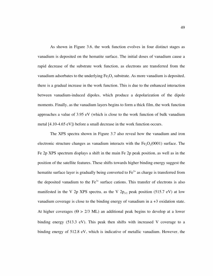
49
As shown in Figure 3.6, the work function evolves in four distinct stages as
vanadium is deposited on the hematite surface. The initial doses of vanadium cause a
rapid decrease of the substrate work function, as electrons are transferred from the
vanadium adsorbates to the underlying Fe2O3 substrate. As more vanadium is deposited,
there is a gradual increase in the work function. This is due to the enhanced interaction
between vanadium-induced dipoles, which produce a depolarization of the dipole
moments. Finally, as the vanadium layers begins to form a thick film, the work function
approaches a value of 3.95 eV (which is close to the work function of bulk vanadium
metal [4.10-4.65 eV]) before a small decrease in the work function occurs.
The XPS spectra shown in Figure 3.7 also reveal how the vanadium and iron
electronic structure changes as vanadium interacts with the Fe2O3(0001) surface. The
Fe 2p XPS spectrum displays a shift in the main Fe 2p peak position, as well as in the
position of the satellite features. These shifts towards higher binding energy suggest the
hematite surface layer is gradually being converted to Fe2+ as charge is transferred from
the deposited vanadium to the Fe3+ surface cations. This transfer of electrons is also
manifested in the V 2p XPS spectra, as the V 2p3/2 peak position (515.7 eV) at low
vanadium coverage is close to the binding energy of vanadium in a +3 oxidation state.
At higher coverages (Θ > 2/3 ML) an additional peak begins to develop at a lower
binding energy (513.3 eV). This peak then shifts with increased V coverage to a
binding energy of 512.8 eV, which is indicative of metallic vanadium. However, the
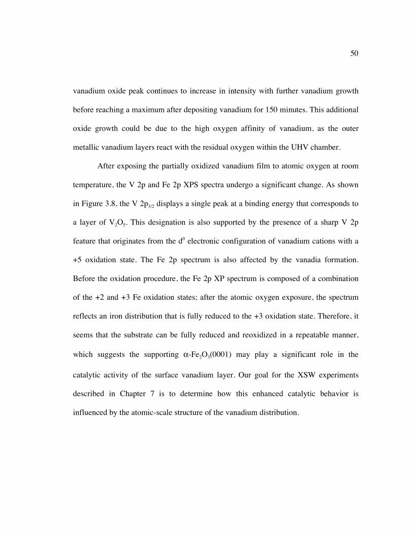
50
vanadium oxide peak continues to increase in intensity with further vanadium growth
before reaching a maximum after depositing vanadium for 150 minutes. This additional
oxide growth could be due to the high oxygen affinity of vanadium, as the outer
metallic vanadium layers react with the residual oxygen within the UHV chamber.
After exposing the partially oxidized vanadium film to atomic oxygen at room
temperature, the V 2p and Fe 2p XPS spectra undergo a significant change. As shown
in Figure 3.8, the V 2p3/2 displays a single peak at a binding energy that corresponds to
a layer of V2O5. This designation is also supported by the presence of a sharp V 2p
feature that originates from the d0 electronic configuration of vanadium cations with a
+5 oxidation state. The Fe 2p spectrum is also affected by the vanadia formation.
Before the oxidation procedure, the Fe 2p XP spectrum is composed of a combination
of the +2 and +3 Fe oxidation states; after the atomic oxygen exposure, the spectrum
reflects an iron distribution that is fully reduced to the +3 oxidation state. Therefore, it
seems that the substrate can be fully reduced and reoxidized in a repeatable manner,
which suggests the supporting α-Fe2O3(0001) may play a significant role in the
catalytic activity of the surface vanadium layer. Our goal for the XSW experiments
described in Chapter 7 is to determine how this enhanced catalytic behavior is
influenced by the atomic-scale structure of the vanadium distribution.
51
Figure 3.6: The work function as a function of V deposition time. The inset shows the rapid decrease in the work function with the onset of V adsorption. The figure is reproduced from reference [69].
3.5
4
4.5
5
5.5
0 100 200 300 400 500 600 700 800
work
fu
nct
ion
, ! (
eV)
Depositon time (min)
3.81 eV
3.95 eV
!0=5.38 eV
3.5
4
4.5
5
5.5
0 20 40 60 80 100 120Depositon time (min)
FIG. 1, C.-Y. Kim, Physical Review B
Deposition time (min)
52
Figure 3.7: The Fe 2p (left) and O 1s and V 2p (right) XPS spectra as a function of increasing vanadium coverage. The spectrum from the clean α-Fe2O3(0001) appears as the bottom of the figure. The figure is reproduced from reference [69].
-750 -740 -730 -720 -710 -700
Inte
nsi
ties
Binding Energy (eV)
Fe 2p1/2
Fe 2p3/2
FIG. 2, C.-Y. Kim, Physical Review B
-535 -530 -525 -520 -515 -510
Inte
nsi
ties
Binding Energy (eV)
V 2p1/2
V 2p3/2O 1s
FIG. 3, C.-Y. Kim, Physical Review B
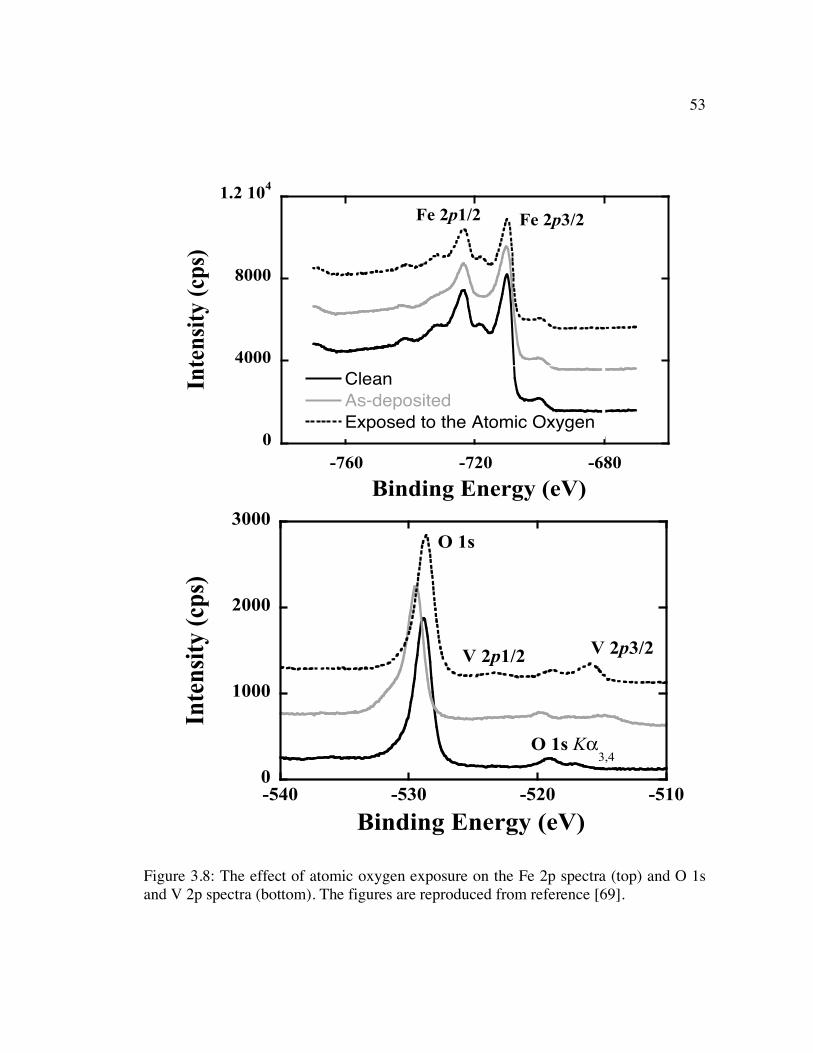
53
Figure 3.8: The effect of atomic oxygen exposure on the Fe 2p spectra (top) and O 1s and V 2p spectra (bottom). The figures are reproduced from reference [69].
0
4000
8000
1.2 104
-760 -720 -680
Clean
As-deposited
Exposed to the Atomic Oxygen
Inte
nsi
ty (
cps)
Binding Energy (eV)
Fe 2p3/2Fe 2p1/2(c)
0
1000
2000
3000
4000
5000
-540 -530 -520 -510
Inte
nsi
ty (
cps)
Binding Energy (eV)
V 2p3/2V 2p
1/2
O 1s
As-deposited
Oxidized
Annealed
(a)
0
1000
2000
3000
-540 -530 -520 -510
Inte
nsi
ty (
cps)
Binding Energy (eV)
V 2p3/2V 2p1/2
O 1s
O 1s K!3,4
(b)
FIG. 7, C.-Y. Kim, Physical Review B
0
4000
8000
1.2 104
-760 -720 -680
Clean
As-deposited
Exposed to the Atomic Oxygen
Inte
nsi
ty (
cps)
Binding Energy (eV)
Fe 2p3/2Fe 2p1/2(c)
0
1000
2000
3000
4000
5000
-540 -530 -520 -510
Inte
nsi
ty (
cps)
Binding Energy (eV)
V 2p3/2V 2p
1/2
O 1s
As-deposited
Oxidized
Annealed
(a)
0
1000
2000
3000
-540 -530 -520 -510
Inte
nsi
ty (
cps)
Binding Energy (eV)
V 2p3/2V 2p1/2
O 1s
O 1s K!3,4
(b)
FIG. 7, C.-Y. Kim, Physical Review B
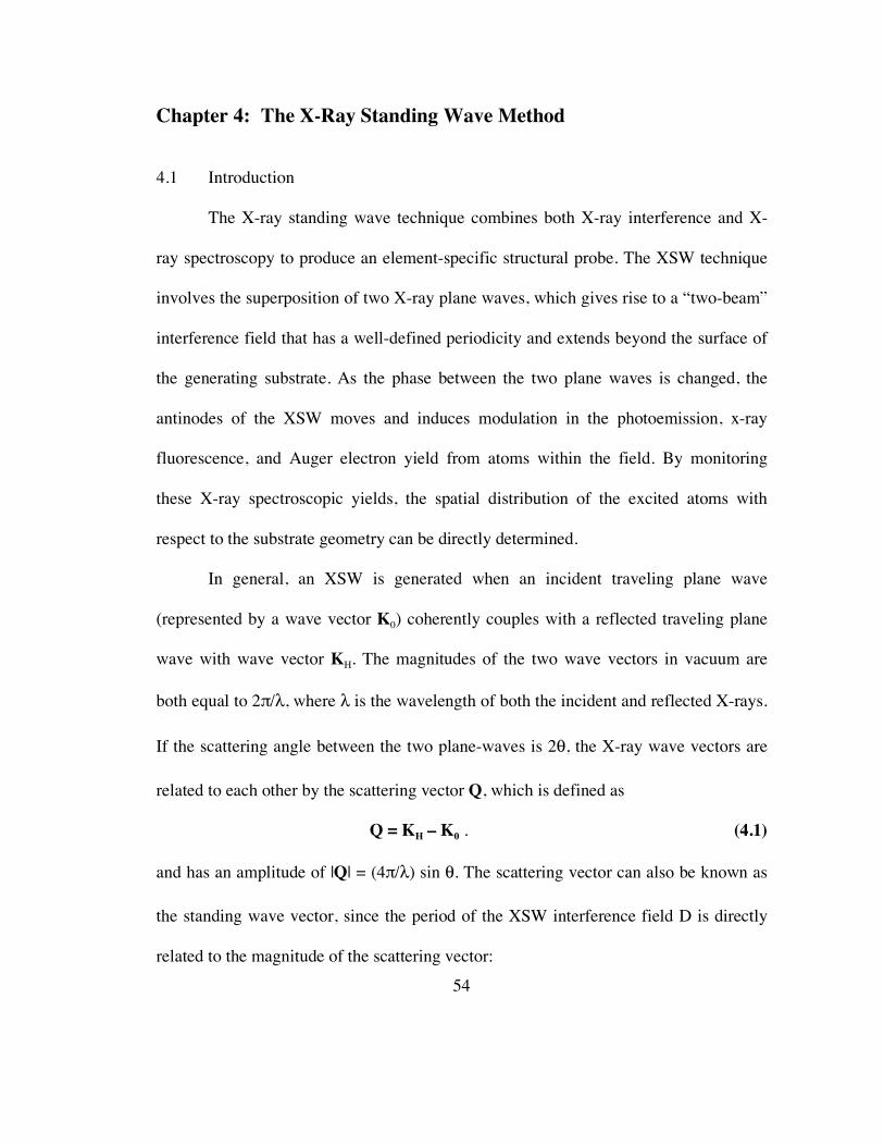
54
Chapter 4: The X-Ray Standing Wave Method
4.1 Introduction
The X-ray standing wave technique combines both X-ray interference and X-
ray spectroscopy to produce an element-specific structural probe. The XSW technique
involves the superposition of two X-ray plane waves, which gives rise to a “two-beam”
interference field that has a well-defined periodicity and extends beyond the surface of
the generating substrate. As the phase between the two plane waves is changed, the
antinodes of the XSW moves and induces modulation in the photoemission, x-ray
fluorescence, and Auger electron yield from atoms within the field. By monitoring
these X-ray spectroscopic yields, the spatial distribution of the excited atoms with
respect to the substrate geometry can be directly determined.
In general, an XSW is generated when an incident traveling plane wave
(represented by a wave vector K0) coherently couples with a reflected traveling plane
wave with wave vector KH. The magnitudes of the two wave vectors in vacuum are
both equal to 2π/λ, where λ is the wavelength of both the incident and reflected X-rays.
If the scattering angle between the two plane-waves is 2θ, the X-ray wave vectors are
related to each other by the scattering vector Q, which is defined as
Q = KH – K0 . (4.1)
and has an amplitude of |Q| = (4π/λ) sin θ. The scattering vector can also be known as
the standing wave vector, since the period of the XSW interference field D is directly
related to the magnitude of the scattering vector:
55
�
D =!
2sin"=2#
Q. (4.2)
Furthermore, as shown in Figure 4.1, the scattering vector points in the direction of the
XSW, as the antinodes of the X-ray interference field form planes that are
perpendicular to the standing wave vector.
There are a number of possible ways of producing the two-beam interference
condition described above, and each method can generate an XSW with a unique
period. For example, when producing diffraction from periodic structures such as
crystals or periodic layered-synthetic microstructures (LSM), the standing wave will
have a period that is equivalent to the diffraction plane spacing. The d-spacing for
single crystals will typically be between 0.5 Å and 10 Å, while the layer period in an
LSM, which represents the lattice plane spacing that produces the diffracted X-ray
plane wave, can vary between 20 Å to 300 Å. A standing wave with a longer period can
also be generated when the incident angle θ is smaller than the critical angle θc, which
results in total external reflection (TER). During the TER condition the resulting
standing-wave field has a period D that varies from infinity at an incident angle of θ = 0
to D = Dc = λ/2θc when θ = θc. Therefore, TER-XSW can be used when investigating
atomic distributions with length scales from 50 Å to 2000 Å, which would be
impossible to probe using an XSW generated with first-order Bragg diffraction.
Because the standing-wave period can span several orders of magnitude depending on
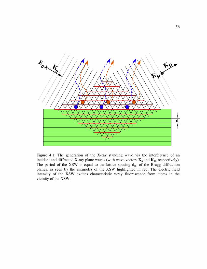
56
Figure 4.1: The generation of the X-ray standing wave via the interference of an incident and diffracted X-ray plane waves (with wave vectors K0 and KH, respectively). The period of the XSW is equal to the lattice spacing dhkl of the Bragg diffraction planes, as seen by the antinodes of the XSW highlighted in red. The electric field intensity of the XSW excites characteristic x-ray fluorescence from atoms in the vicinity of the XSW.
57
how the interference field is generated, the XSW technique is a powerful tool that can
be widely applied to a wide range of materials with an assortment of critical length-
scales. In this overview, however, the main focus will be on how an XSW generated via
Bragg diffraction from single crystals can be used to probe adsorbate distributions on
surfaces.
The development of the XSW technique as a tool for surface science started
with Batterman’s discovery of an XSW field within a Ge crystal undergoing Bragg
diffraction. He also demonstrated how the XSW field shifts as the Ge crystal sweeps
through the Bragg condition [70]. This discovery led to the development of the XSW as
an analytical tool, as Batterman showed how the location of As impurity atoms within a
Si crystal could be determined using the XSW technique [71]. Once it was realized that
the standing-wave field also extends above the crystal surface, Cowan et al. extended
Batterman’s findings to surface investigations by using an XSW to determine the height
of an adsorbate above its surface [72]. Golovchenko et al. later employed both normal
and off-normal Bragg reflections in order to determine the in-plane position as well as
height of an adsorbate [73]. These early findings showcase some of the inherent
advantages of using the XSW technique to investigate surface structures. One such
advantage is that the adsorbates in the vicinity of the XSW respond to the standing
wave in a chemically specific way. A major issue of many surface science experiments
is separating the signal that originates exclusively from atoms on the surface from the
58
signal that is generated by the appreciably larger number of atoms in the bulk. In the
XSW technique, one can easily distinguish the spectroscopic response of the surface
atoms from that of the bulk atoms, which in turn provides the necessary surface
sensitivity.
In Section 4.2, more detail will be provided about how the standing-wave field
behaves and how it can be understood using the dynamical theory of X-ray diffraction.
The process in which adsorbate atoms are excited by the X-ray interference field will
also be discussed in Section 4.3, as well as how we can take advantage of the dipole
approximation when analyzing the induced photoelectric yields. Finally, two distinct
approaches of XSW analysis will be presented in Section 4.4: a more conventional
model-dependent method in which several XSW measurements are used to triangulate
the adsorbate positions, and a newly developed direct-space imaging method that is
model-independent.
4.2 Dynamical Theory of X-ray Diffraction
As discussed in the introduction, the creation of a standing-wave field is a
fundamental wave phenomenon in which two coherent traveling plane waves interfere
with each other. Because the traveling X-ray plane waves can also be considered as
electromagnetic waves, they can be expressed in terms of their electric field. The
incident plane wave has the form of
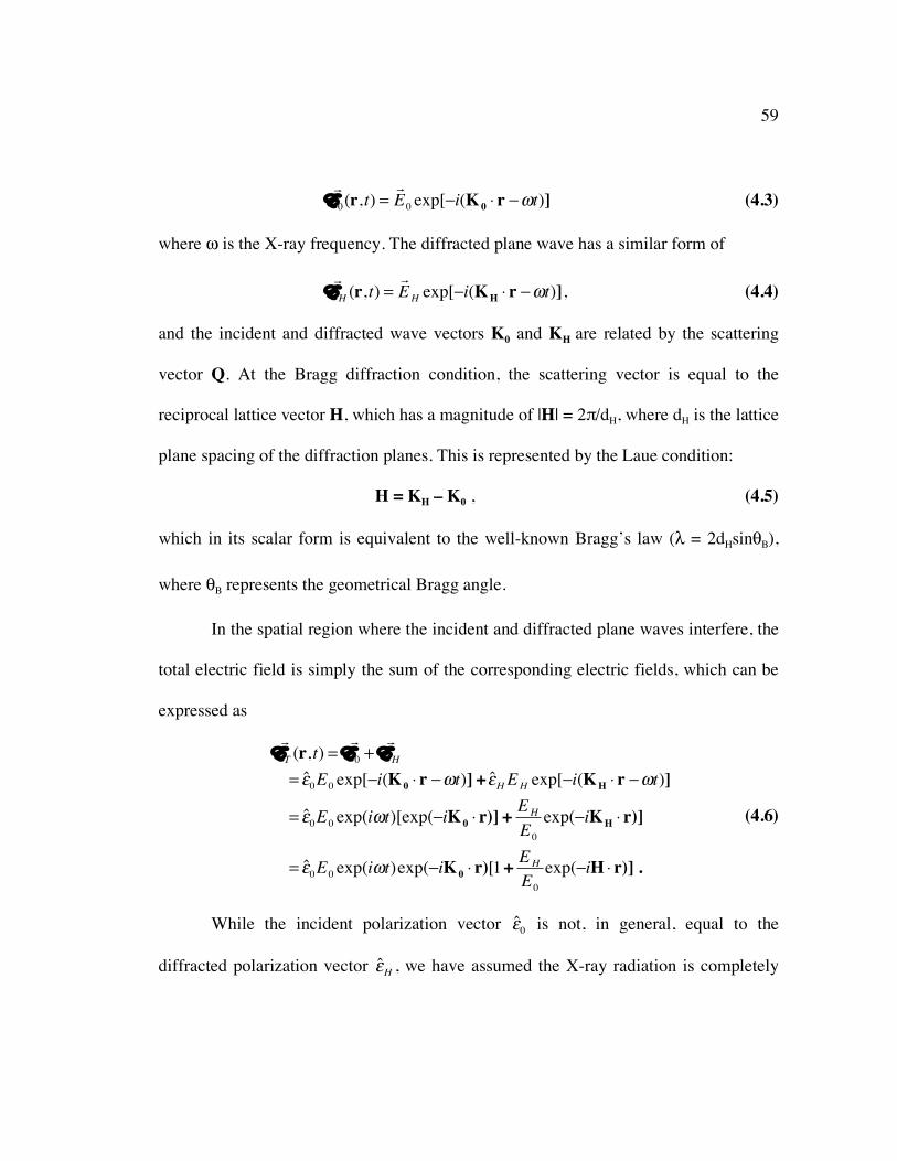
59
�
! E 0(r,t) =
! E 0 exp[!i(K
0" r !#t)] (4.3)
where ω is the X-ray frequency. The diffracted plane wave has a similar form of
�
! E
H(r,t) =
! E
Hexp[!i(K
H" r !#t)], (4.4)
and the incident and diffracted wave vectors K0 and KH are related by the scattering
vector Q. At the Bragg diffraction condition, the scattering vector is equal to the
reciprocal lattice vector H, which has a magnitude of |H| = 2π/dH, where dH is the lattice
plane spacing of the diffraction planes. This is represented by the Laue condition:
H = KH – K0 , (4.5)
which in its scalar form is equivalent to the well-known Bragg’s law (λ = 2dHsinθB),
where θB represents the geometrical Bragg angle.
In the spatial region where the incident and diffracted plane waves interfere, the
total electric field is simply the sum of the corresponding electric fields, which can be
expressed as
�
! E
T(r,t) =
! E 0 +
! E
H
= ˆ ! 0E0 exp["i(K0 # r "$t)] + ˆ ! HE
Hexp["i(KH # r "$t)]
= ˆ ! 0E0 exp(i$t)[exp("iK 0 # r)] +E
H
E0
exp("iKH # r)]
= ˆ ! 0E0 exp(i$t)exp("iK0 # r)[1+E
H
E0
exp("iH # r)] .
(4.6)
While the incident polarization vector
�
ˆ ! 0 is not, in general, equal to the
diffracted polarization vector
�
ˆ ! H
, we have assumed the X-ray radiation is completely
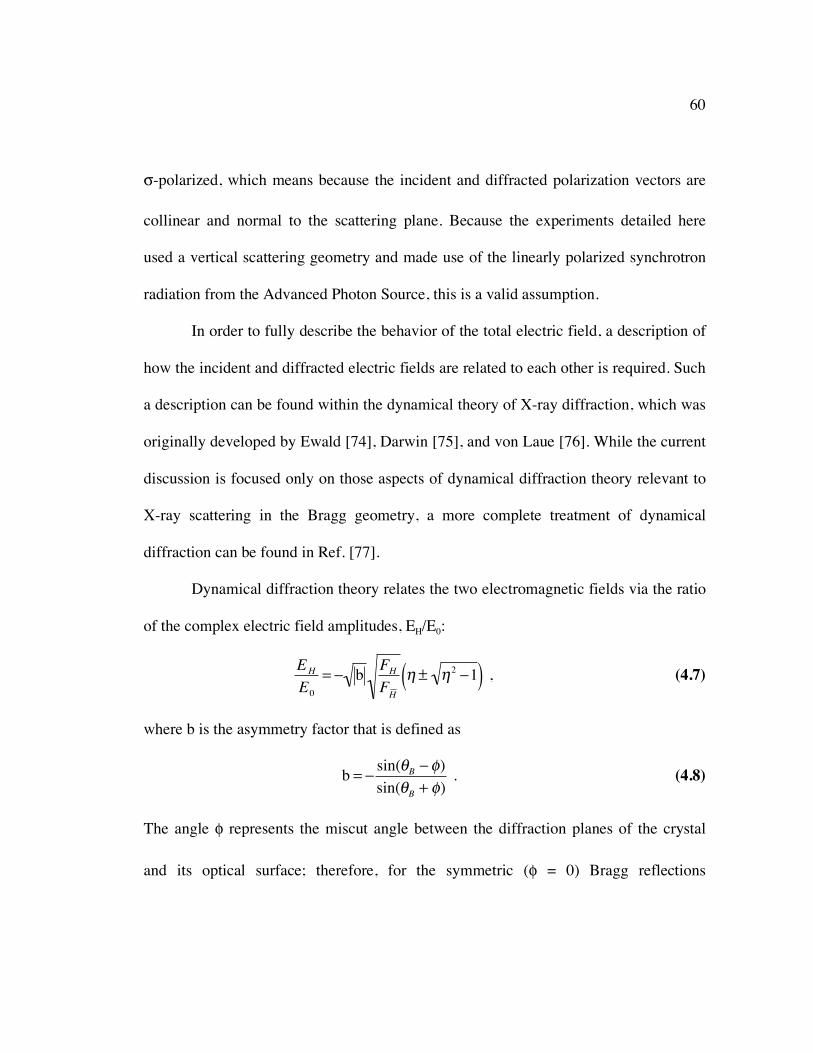
60
σ-polarized, which means because the incident and diffracted polarization vectors are
collinear and normal to the scattering plane. Because the experiments detailed here
used a vertical scattering geometry and made use of the linearly polarized synchrotron
radiation from the Advanced Photon Source, this is a valid assumption.
In order to fully describe the behavior of the total electric field, a description of
how the incident and diffracted electric fields are related to each other is required. Such
a description can be found within the dynamical theory of X-ray diffraction, which was
originally developed by Ewald [74], Darwin [75], and von Laue [76]. While the current
discussion is focused only on those aspects of dynamical diffraction theory relevant to
X-ray scattering in the Bragg geometry, a more complete treatment of dynamical
diffraction can be found in Ref. [77].
Dynamical diffraction theory relates the two electromagnetic fields via the ratio
of the complex electric field amplitudes, EH/E0:
�
EH
E0
= ! bF
H
FH
" ± "2!1( ) , (4.7)
where b is the asymmetry factor that is defined as
�
b = !sin("
B!#)
sin("B
+ #) . (4.8)
The angle φ represents the miscut angle between the diffraction planes of the crystal
and its optical surface; therefore, for the symmetric (φ = 0) Bragg reflections
61
considered in this dissertation, the asymmetry factor b is equal to –1. The quantity FH is
the structure factor for the H Bragg reflection, which is the Hth-order Fourier coefficient
of the electron density of the crystal ρ(r) and therefore can be expressed as
�
FH
= !(r)V" exp(iH # r)dV . (4.9)
Due to the periodic nature of the crystal, this Fourier component can also be considered
as the combined effect of the individual scattering contributions within the unit cell,
�
FH = fn exp(iHn=1
N
! " rn )
= ( f0 + # $ f + i# $ $ f )n exp(iHn=1
N
! " rn )
. (4.10)
The sum over n is over the N atoms that make up the unit cell, and the atomic scattering
factor of the nth atom at the fractional unit cell location rn is fn. The atomic scattering
factor is itself a complex quantity that is wavelength dependent, so the Hönl corrections
(Δf′ and Δf′′) are included with the atomic form factor f0 in order to account for
resonant scattering and absorption. Whether the structure factor FH is considered a
discrete sum or a continuous integral, it is in general a complex quantity and can be
written as
�
FH
= ! F H
+ i ! ! F H
, (4.11)
where
�
! F H
and
�
! ! F H
are the real and imaginary components of FH, respectively.
62
Returning now to the electric field amplitude ratio EH/E0, it can be seen that this
ratio is a function of the normalized angle parameter η, which in turn is a function of
the relative incident angle Δθ = θ - θB via
�
! =
b"# sin(2#B) +1
2$F0(1% b)
$ b FH
FH
. (4.12)
The constant Γ is equal to
�
! =re"2
#Vc
(4.13)
where re = 2.818 x 10⁻⁵ Å is the classical electron radius and Vc refers to the volume of
the unit cell. Because the electric field ratio is a complex quantity and the electric fields
are coherent, the electric field amplitude ratio can be rewritten in polar form:
�
EH
E0
=E
H
E0
exp(i!) (4.14)
The amplitudes of the two electric fields can be related using the reflectivity R, which
is defined as the intensity ratio of the two X-ray plane waves:
�
R =IH
I0
=E
H
E0
2
. (4.15)
Both the reflectivity R and phase ϕ are functions of the normalized angular coordinate
η; an example of this dependence on η is shown in Figure 4.2, which shows the
reflectivity and phase for the Si(111) Bragg reflection at Eγ = 7 keV. The region of
63
strong Bragg reflection occurs over a small range ω, which is defined as the region
where η shifts from +1 to –1. (Because of how η is defined in Eq. 4.12, an increase in
incident angle corresponds to a decrease in η.) The angular range ω is known as the
Darwin width of the Darwin-Prins reflectivity curve (or rocking curve) and can be
expressed as:
�
! = "#$=%1 %"#$= +1=2& ' F
H' ' F H
+ ' ' F 0
2 % ' ' F H
' ' F H
b sin2#B
. (4.16)
The center of the rocking curve at η = 0 does not coincide with the geometrical Bragg
angle at θB due to refraction of the X-rays at the crystal surface. The angular offset due
to this refraction effect can be expressed as
�
!"#= 0=
$ % F 0
sin2"B
1+ b
2b
&
'
(
)
*
+ . (4.17)
While the reflectivity approaches unity as the crystal is scanned through the rocking
curve, the phase ϕ between EH and E0 experiences a significant change. As shown in
Figure 4.2, the phase changes by π, as the two plane waves are out of phase when η > 0
on the low-angle side of the rocking curve but become in phase on the high-angle side
(when η < 0).
While the behavior of the incident and diffracted electric fields within the
region of the Bragg condition has been discussed in length, we have not discussed what
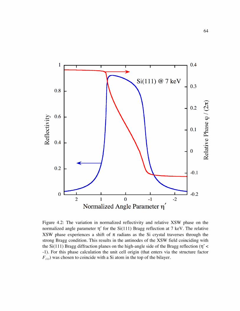
64
Figure 4.2: The variation in normalized reflectivity and relative XSW phase on the normalized angle parameter η′ for the Si(111) Bragg reflection at 7 keV. The relative XSW phase experiences a shift of π radians as the Si crystal traverses through the strong Bragg condition. This results in the antinodes of the XSW field coinciding with the Si(111) Bragg diffraction planes on the high-angle side of the Bragg reflection (η′ < -1). For this phase calculation the unit cell origin (that enters via the structure factor F111) was chosen to coincide with a Si atom in the top of the bilayer.

65
this means for the total electric field that gives rise to the observed XSW. By
substituting Eq. 4.14 in our original expression for the total electric field ET, Eq. 4.6
can be expressed as
�
! E
T(r,t) = ˆ ! 0E0 exp(i"t)exp(#iK0 $ r)[1+
EH
E0
exp(i% # iH $ r)] , (4.18)
and the normalized intensity of the total electric field becomes
�
I(!,r) =
! E
T"!
E T
*
E0
2
= [1+ R(!) + 2 R(!) cos(#(!) $H " r)]%1; above the surface
e$µz (! )z ; at depth z below surface
& ' (
(4.19)
Within the crystal, K0 has an imaginary component that leads to the effect of X-ray
absorption that is calculated using an exponential damping term exp(-µZz), which varies
with θ and z, the depth below the surface. The quantity µZ is the effective linear
absorption coefficient and is defined as
�
µz(!) =
µ0
sin!B
1+" F H
" " F 0
EH
E0
#
$ %
&
' (
""+
" " F H
" " F 0
EH
E0
#
$ %
&
' (
")
*
+ +
,
-
.
. , (4.20)
where µ is the linear absorption coefficient and is equal to
�
µ0
=2!
"# $ $ F
0 . (4.21)
66
The first term in Eq. 4.20 accounts for normal absorption, while the second and third
terms dominate when in the vicinity of a Bragg reflection. This explains the strong
extinction effect that strongly reduces the X-ray penetration depth as the crystal scans
through a Bragg reflectivity peak.
Looking closely at the total electric field intensity given by Eq. 4.19, it is clear
that the superposition of the incident and diffracted plane waves has resulted in a time-
independent, spatially modulated electric field. This wavefield is in fact the X-ray
standing wave field produced by the interference of the two traveling X-ray plane
waves. The modulation of the electric field take the form of planes, since the dot
product H ⋅ r is a dimensionless real number that is at a maximum in the direction
parallel to H and equal to zero in the direction perpendicular to H. Therefore, the nodes
and antinodes of electric field intensity form an XSW with a period that is equal to the
lattice d-spacing of the hkl diffraction planes.
While the diffraction vector H determines the periodicity of the XSW, it is the
phase ϕ that governs the position of the XSW. The phase ϕ represents both the incident
X-rays relative to the diffracted beam, as well as the phase of the XSW with respect to
the chosen origin for the structure factor FH. Typically the origin is selected so that the
standing wave phase can be referenced with respect to the diffraction planes. Choosing
this particular origin means that when the incident angle is much smaller than the
geometrical Bragg angle θB, the XSW phase ϕ is equal to ϕ′ + π, and the nodes of the
67
XSW coincide with the diffraction planes while the antinodes lie halfway between the
diffraction planes. At the other extreme, when the incident angle is much larger than θB,
the phase ϕ is now equal to ϕ′ because of the π phase shift of the XSW. This causes the
antinodes and nodes to exchange positions, with the antinodes located exactly on the
diffraction planes. The end result is that when the crystal is scanned in angle through its
rocking curve, the XSW field gradually shifts inward one-half of the XSW period (and
therefore one-half of a diffraction plane d-spacing).
4.3 Photoexcitation from X-ray Standing Waves
In the previous section, it was demonstrated that the XSW is a direct result of
the scattering of an incident X-ray plane wave from a set of diffraction planes.
However, it is the scattering of the standing-wave field itself that enables the XSW to
be detected and used as a high-precision structural probe. While there are many
possible interactions between the XSW and the atomic distributions of interest, this
overview will focus solely on atomic photoexcitation and the secondary emission
processes that ensue. The photoexcitation process will be discussed with respect to the
dipole approximation, which simplifies the XSW analysis and is partly responsible for
the high resolution provided by the XSW technique. While some of the limits of the
dipole approximation will be addressed, the dipole approximation is a valid one for all
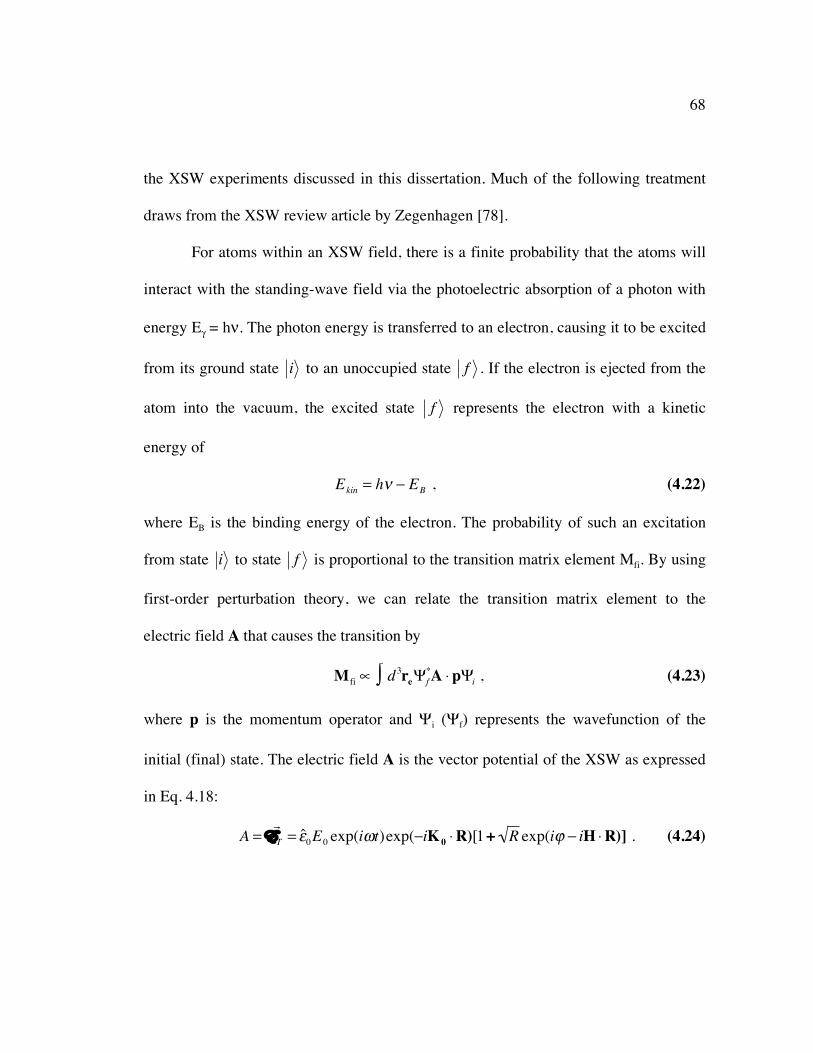
68
the XSW experiments discussed in this dissertation. Much of the following treatment
draws from the XSW review article by Zegenhagen [78].
For atoms within an XSW field, there is a finite probability that the atoms will
interact with the standing-wave field via the photoelectric absorption of a photon with
energy Eγ = hν. The photon energy is transferred to an electron, causing it to be excited
from its ground state
�
i to an unoccupied state
�
f . If the electron is ejected from the
atom into the vacuum, the excited state
�
f represents the electron with a kinetic
energy of
�
Ekin
= h! " EB , (4.22)
where EB is the binding energy of the electron. The probability of such an excitation
from state
�
i to state
�
f is proportional to the transition matrix element Mfi. By using
first-order perturbation theory, we can relate the transition matrix element to the
electric field A that causes the transition by
�
Mfi! d
3re" #f
*A $p#i , (4.23)
where p is the momentum operator and Ψi (Ψf) represents the wavefunction of the
initial (final) state. The electric field A is the vector potential of the XSW as expressed
in Eq. 4.18:
�
A =!
E T
= ˆ ! 0E0 exp(i"t)exp(#iK0 $R)[1+ R exp(i% # iH $R)] . (4.24)
69
where the modulus of the complex field ratio |EH/E0| has been replaced with the square
root of the reflectivity R. The position vector R refers to the location of the absorbing
electron; this position can be referenced relative to the atom at a position r via
�
R = re
+ r (4.25)
where re is the location of the electron with respect to the atom. This allows Eq. 4.24 to
be rewritten as
�
A =!
E T
= ˆ ! 0E0 exp(i"t)exp(#iK0 $ r)exp(#iK0 $ re ) %
[1+ R exp(i&)exp(#iH $ r)exp(#iH $ re)]
(4.26)
The exponential functions of re has the Taylor series expansion
�
exp(!iK0 " re ) =1! i K0 " re( ) + 12K0 " re( )
2!… ,
exp(!iH " re) =1! i H " r
e( ) + 12H " r
e( )2!…
(4.27)
which is equivalent to a multipole expansion. In the dipole approximation, only the first
order term is significant because it is assumed the terms K0 ⋅ re and H ⋅ re are
negligible. Therefore, the terms exp(-iK0 ⋅ re) and exp(-iH ⋅ re) are both equal to 1, and
the electric field A can be rewritten as
�
A =!
E T
= ˆ ! 0E0 exp(i"t)exp(#iK0 $ r)[1+ R exp(i%)exp(#iH $ r)] , (4.28)
which is independent of re. Therefore, the absorption cross section, which is
proportional to the square modulus of the matrix element Mfi and therefore proportional
to the square modulus of the electric field, can be expressed as
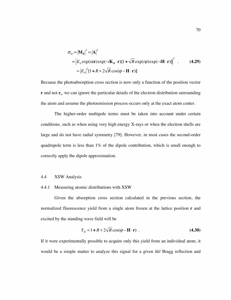
70
�
!D"Mfi
2" A
2
" E0 exp(i#t)exp($iK0 % r)[1+ R exp(i&)exp($iH % r)]2
= E0
2[1+R + 2 R cos(& $H % r)]
. (4.29)
Because the photoabsorption cross section is now only a function of the position vector
r and not re, we can ignore the particular details of the electron distribution surrounding
the atom and assume the photoemission process occurs only at the exact atom center.
The higher-order multipole terms must be taken into account under certain
conditions, such as when using very high energy X-rays or when the electron shells are
large and do not have radial symmetry [79]. However, in most cases the second-order
quadrupole term is less than 1% of the dipole contribution, which is small enough to
correctly apply the dipole approximation.
4.4 XSW Analysis
4.4.1 Measuring atomic distributions with XSW
Given the absorption cross section calculated in the previous section, the
normalized fluorescence yield from a single atom frozen at the lattice position r and
excited by the standing wave field will be
�
YH
=1+R + 2 R cos(! "H # r) . (4.30)
If it were experimentally possible to acquire only this yield from an individual atom, it
would be a simple matter to analyze this signal for a given hkl Bragg reflection and
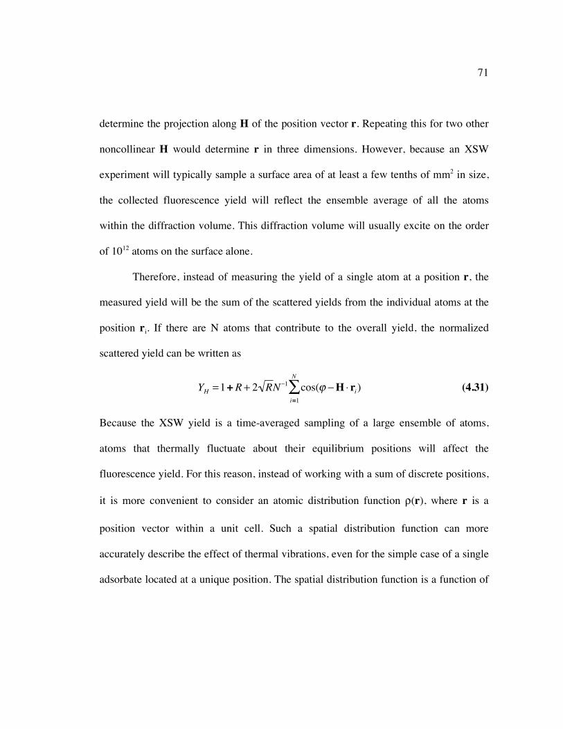
71
determine the projection along H of the position vector r. Repeating this for two other
noncollinear H would determine r in three dimensions. However, because an XSW
experiment will typically sample a surface area of at least a few tenths of mm2 in size,
the collected fluorescence yield will reflect the ensemble average of all the atoms
within the diffraction volume. This diffraction volume will usually excite on the order
of 1012 atoms on the surface alone.
Therefore, instead of measuring the yield of a single atom at a position r, the
measured yield will be the sum of the scattered yields from the individual atoms at the
position ri. If there are N atoms that contribute to the overall yield, the normalized
scattered yield can be written as
�
YH
=1+R + 2 RN!1
cos(" !H # ri
i=1
N
$ ) (4.31)
Because the XSW yield is a time-averaged sampling of a large ensemble of atoms,
atoms that thermally fluctuate about their equilibrium positions will affect the
fluorescence yield. For this reason, instead of working with a sum of discrete positions,
it is more convenient to consider an atomic distribution function ρ(r), where r is a
position vector within a unit cell. Such a spatial distribution function can more
accurately describe the effect of thermal vibrations, even for the simple case of a single
adsorbate located at a unique position. The spatial distribution function is a function of
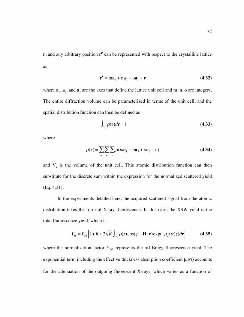
72
r, and any arbitrary position r′ can be represented with respect to the crystalline lattice
as
r′ = ma1 + na2 + oa3 + r (4.32)
where a1, a2, and a3 are the axes that define the lattice unit cell and m, n, o are integers.
The entire diffraction volume can be parameterized in terms of the unit cell, and the
spatial distribution function can then be defined as
�
!(r)dr =1Vc" (4.33)
where
�
!(r) = !(ma1
+ na2
+ oa3
+ r)o
"n
"m
" (4.34)
and Vc is the volume of the unit cell. This atomic distribution function can then
substitute for the discrete sum within the expression for the normalized scattered yield
(Eq. 4.31).
In the experiments detailed here, the acquired scattered signal from the atomic
distribution takes the form of X-ray fluorescence. In this case, the XSW yield is the
total fluorescence yield, which is
�
YH =YOB 1+R + 2 R !(r)cos(" #H $ r)exp(#µ f (%)z)drVc&[ ] , (4.35)
where the normalization factor YOB represents the off-Bragg fluorescence yield. The
exponential term including the effective thickness absorption coefficient µf(α) accounts
for the attenuation of the outgoing fluorescent X-rays, which varies as a function of
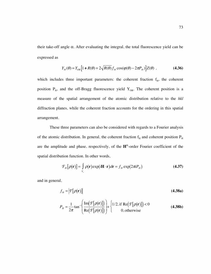
73
their take-off angle α. After evaluating the integral, the total fluorescence yield can be
expressed as
�
YH (!) =YOB 1+R(!) + 2 R(!) f H cos("(!) # 2$PH )[ ]Z(!) , (4.36)
which includes three important parameters: the coherent fraction fH, the coherent
position PH, and the off-Bragg fluorescence yield YOB. The coherent position is a
measure of the spatial arrangement of the atomic distribution relative to the hkl
diffraction planes, while the coherent fraction accounts for the ordering in this spatial
arrangement.
These three parameters can also be considered with regards to a Fourier analysis
of the atomic distribution. In general, the coherent fraction fH and coherent position PH
are the amplitude and phase, respectively, of the Hth-order Fourier coefficient of the
spatial distribution function. In other words,
�
FH ! r( )[ ] = ! r( )exp iH " r( )drVc
# = f H exp 2$iPH( ) (4.37)
and in general,
�
f H = F ! r( )[ ] (4.38a)
�
PH
=1
2!tan
"1Im F # r( )[ ]( )Re F # r( )[ ]( )
$
%
& &
'
(
) )
+1/2, if Re F # r( )[ ]( ) < 0
0, otherwise
* + ,
(4.38b)
74
From our expressions for the spatial distribution function (Eq. 4.33) and the normalized
XSW yield (Eq. 4.36), it can be seen that the off-Bragg fluorescence yield is the zeroth-
order Fourier (F0) coefficient of the atomic distribution.
4.4.2 Structural analysis using the coherent fraction and coherent position
Now that the origin of the coherent fraction and coherent position has been
established, the remaining question is how these parameters can be used to analyze an
unknown atomic configuration. As mentioned earlier, the coherent position is a
measurement of the arrangement of the atomic distribution with respect to a selected set
of diffraction planes. The coherent fraction is also an indication of the atomic species’
geometric configuration, as well as its degree of ordering. One contribution to the
atoms’ ordering is the thermally induced motion of the atoms. Therefore, the coherent
fraction fH can be considered as the combination of three factors:
fH = C aH DH . (4.39)
Each of the three contributions to the coherent fraction can vary from zero to unity. The
ordered fraction C is the fraction of atoms that are ordered with respect to the substrate
crystalline lattice; an ordered fraction of one corresponds to a completely ordered
distribution, while a completely random arrangement of the atoms will result in an
ordered fraction of zero. The geometrical factor aH is a measure of the atomic
75
arrangement of the fluorescent species, and the Debye-Waller factor DH accounts for
deviations from the atoms’ equilibrium positions due to thermal vibrations.
One way of describing the atomic distribution is that some of the atoms of
interest are randomly distributed among the crystal, while the rest of the atoms occupy
N inequivalent lattice sites with a given occupation fraction. The N different unit cell
locations can be represented by r1, r2, …, rN, while the occupation fractions of the
atoms at these N sites are c1, c2, …, cN. The ordered fraction C can then be written as
�
C = cn
n=1
N
! . (4.40)
From Eq. 4.38a and 4.38b, the geometrical structure factor SH for the coherent atoms
can be defined as
�
SH
=1
Ccnexp iH ! r
n( )[ ]n=1
N
" . (4.41)
From this definition, the geometrical factor aH can be expressed as
�
aH
= SH
, (4.42)
while the coherent position becomes
�
PH
=1
2!Arg S
H[ ] . (4.43)
The last contribution to the coherent fraction is the Debye-Waller factor DH, which
quantifies the effect of thermal vibrations on the time-averaged atomic distribution.
This effect can be considered for the entire distribution as a whole or for the individual
76
atoms that make up the distribution. In this treatment, the assumption is that all the
atoms within the spatial distribution have the same vibrational amplitude. By
convoluting the atomic distribution with a normalized Gaussian distribution, the
Debye-Waller factor DH can be expressed as
�
DH
= exp !M( ) = exp !1
2uH
2H2
"
# $
%
& ' = exp
!2( 2uH
2
dH
2
"
#
$ $
%
&
' ' . (4.44)
where the term
�
uH
2 represents the mean square vibrational amplitude of the atoms in
the H direction.
The process of determining the details of an unknown atomic distribution from
the measured XSW parameters is best demonstrated with a few examples. The simplest
example involves a spatial distribution where all the atoms occupy a single atomic site
above the crystal surface. In this case, N = 1, C = 1 (assuming there is no incoherent
fraction), and the geometrical factor aH is equal to unity. Therefore, the coherent
fraction fH is simply equal to the Debye-Waller factor for the fluorescence-selected
adatoms, and the coherent position is equal to the (H ⋅ r)/2π fractional position of the
occupation site relative to the bulk diffraction planes. If the measured coherent position
originates from a Bragg reflection in the surface-normal direction, the coherent position
will reveal the out-of-plane location of the atomic site. This information can be
combined with the results of off-normal XSW measurements in order to determine the
in-plane configuration of the adsorbate. Triangulating the unique atomic site position
77
would theoretically require the combination of three XSW measurements from a set of
mutually non-collinear diffraction vectors. However, the adatom will typically be
located at a high-symmetry adsorption site, which can be triangulated using one
surface-normal and one off-normal XSW measurement. No matter which particular
Bragg reflections are employed in an XSW experiment, the derived structural
information can be quite precise, since it is the lattice spacing between the selected
diffraction planes that represents the “ruler” that probes the atomic distribution.
If the fluorescent-selected atoms occupy multiple sites, the analysis of the
coherent fraction and coherent position becomes more complicated. For example, if the
atoms were located at two adsorption sites in equal populations, the geometrical factor
can be expressed as
�
aH
= cos H ! r1" r
2( ) /2[ ] , (4.45)
and the coherent position will be equal to
�
PH
=r1
+ r2( )
2dH
. (4.46)
If r1 = r2, the geometric factor would equal one as expected, since this would be
identical to the single adsorption site scenario. However, if the two atomic sites were
separated from each other by a distance equal to one-half of the lattice d-spacing
�
r2! r
1= d
H/2( ), then the geometrical factor (and therefore the coherent fraction) will
be equal to zero. This situation is directly comparable to the case when a particular
78
Bragg reflection is forbidden due to its structure factor. Furthermore, if the coherent
fraction is zero, the measured coherent position does not convey any meaningful
information about the atomic distribution. If an intermediate distance separated the two
atomic sites, however, the coherent position would be equal to the average position of
the two adsorption sites with respect to the diffraction planes, and the geometrical
factor would be nonzero.
Of course, real materials systems can involve much more complex distributions
made up of multiple adsorption sites that have different occupation fractions, and it
may not be possible to directly determine the locations of the atoms from the set of
measured XSW parameters. In such cases analyzing XSW data will typically involve
designing a reasonable structural model based on existing information and using this
model as the basis for calculating a set of coherent fractions and coherent positions. By
comparing the XSW parameters calculated from the chosen structural model to the
measured XSW data, the model can be refined using a best-fit chi-squared routine.
However, this method can be problematic if there are errors or omissions in the initial
model that traditional XSW analysis cannot reveal; in such a scenario, an inappropriate
model could lead to a result that would be compatible with the experimental XSW data
but ultimately flawed. While acquiring several sets of XSW measurements or making
other types of structural measurements would minimize this possibility, it would be
preferable if the structure determined by the XSW analysis was independent of the
79
fitting procedure or the initial model used in the fit. This is made possible with the
XSW direct space imaging method, which takes advantage of the phase information
that is retained in the XSW technique to produce a model-independent direct space
image of the atomic distribution. How this image is generated is the subject of the
following section.
4.4.3 The XSW direct-space imaging method
One of the inherent limitations of conventional diffraction experiments is that
by only measuring the intensity of the diffracted X-rays far from the region where the
incident and reflected X-ray beam coherently couple, any information regarding the
relative phase between the incident and scattered X-rays is unavailable. However, in an
XSW experiment, not only do we detect the intensity of the diffracted beam, but we
also detect the intensity of the electric fields itself using the characteristic fluorescence
emitted from the atoms that lie within the XSW. As elucidated in Section 4.4.1, by
measuring the electric field intensity via the modulation of the induced fluorescence
yield, the amplitude and phase of the scattering amplitude of an individual atomic
species can then be extracted in the form of the coherent fraction and coherent position.
Because the coherent fraction and coherent position together make up the Hth-
order Fourier coefficient of the XSW-measured atomic distribution, examination of Eq.
4.37 suggests the atomic density profile of the fluorescent-selected atoms ρ(r) can be
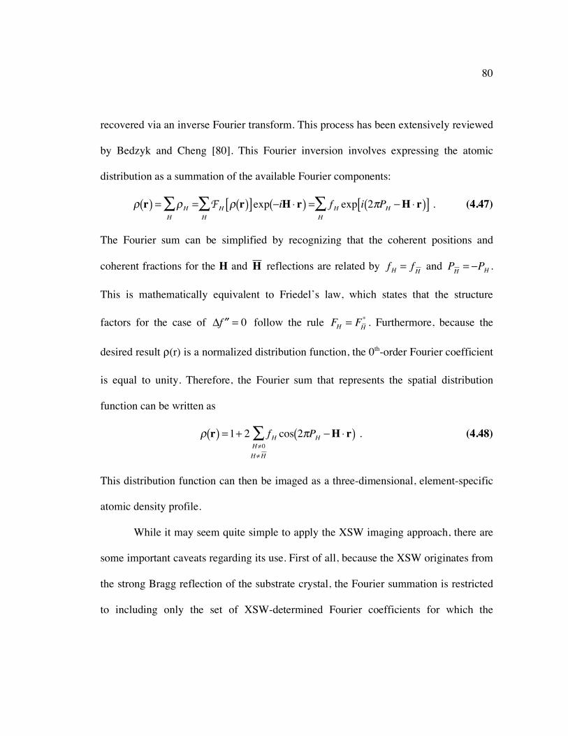
80
recovered via an inverse Fourier transform. This process has been extensively reviewed
by Bedzyk and Cheng [80]. This Fourier inversion involves expressing the atomic
distribution as a summation of the available Fourier components:
�
! r( ) = !H =H
" FH ! r( )[ ]exp #iH $ r( ) =H
" f H exp i 2%PH #H $ r( )[ ]H
" . (4.47)
The Fourier sum can be simplified by recognizing that the coherent positions and
coherent fractions for the H and
�
H reflections are related by
�
f H = fH
and
�
PH
= !PH
.
This is mathematically equivalent to Friedel’s law, which states that the structure
factors for the case of ! ""f = 0 follow the rule FH= F
H
* . Furthermore, because the
desired result ρ(r) is a normalized distribution function, the 0th-order Fourier coefficient
is equal to unity. Therefore, the Fourier sum that represents the spatial distribution
function can be written as
�
! r( ) =1+ 2 f H cos 2"PH #H $ r( )H%0
H%H
& . (4.48)
This distribution function can then be imaged as a three-dimensional, element-specific
atomic density profile.
While it may seem quite simple to apply the XSW imaging approach, there are
some important caveats regarding its use. First of all, because the XSW originates from
the strong Bragg reflection of the substrate crystal, the Fourier summation is restricted
to including only the set of XSW-determined Fourier coefficients for which the
81
corresponding bulk structure factor is nonzero. This limitation means the atomic
distribution that results from the Fourier sum will be projected within the bulk primitive
unit cell. For example, in surface studies it is often that the adsorption of foreign atoms
on a surface produces a change in the surface geometry and an expansion of the surface
unit cell. It would be impossible to fully probe this reduction in the surface symmetry
relying on the XSW-derived imaging approach alone, since the image would represent
the new extended atomic-scale structure as compressed within the primitive substrate
unit cell.
While the structure factor of the substrate restricts the amount of possible
Fourier coefficients that can be included in the Fourier sum, the limited amount of time
allowed for an XSW experiment and the technical constraints affecting the experiment
itself (such as an unachievable X-ray energy or sample geometry) prevent the collection
of all but a fraction of the available Fourier components. Because the summation can
only contain a finite number of Fourier components, its abrupt termination will be
reflected in the resulting image as background density oscillations. As additional
Fourier terms are included and the truncated Fourier sum more closely reproduces the
real atomic density distribution, the amplitude of these background oscillations will
decrease, while the actual atomic density maxima will intensify. Therefore, it is to our
advantage to include as many Bragg reflections as possible to lessen the likelihood of
mistaking a false background peak for an actual atomic position.
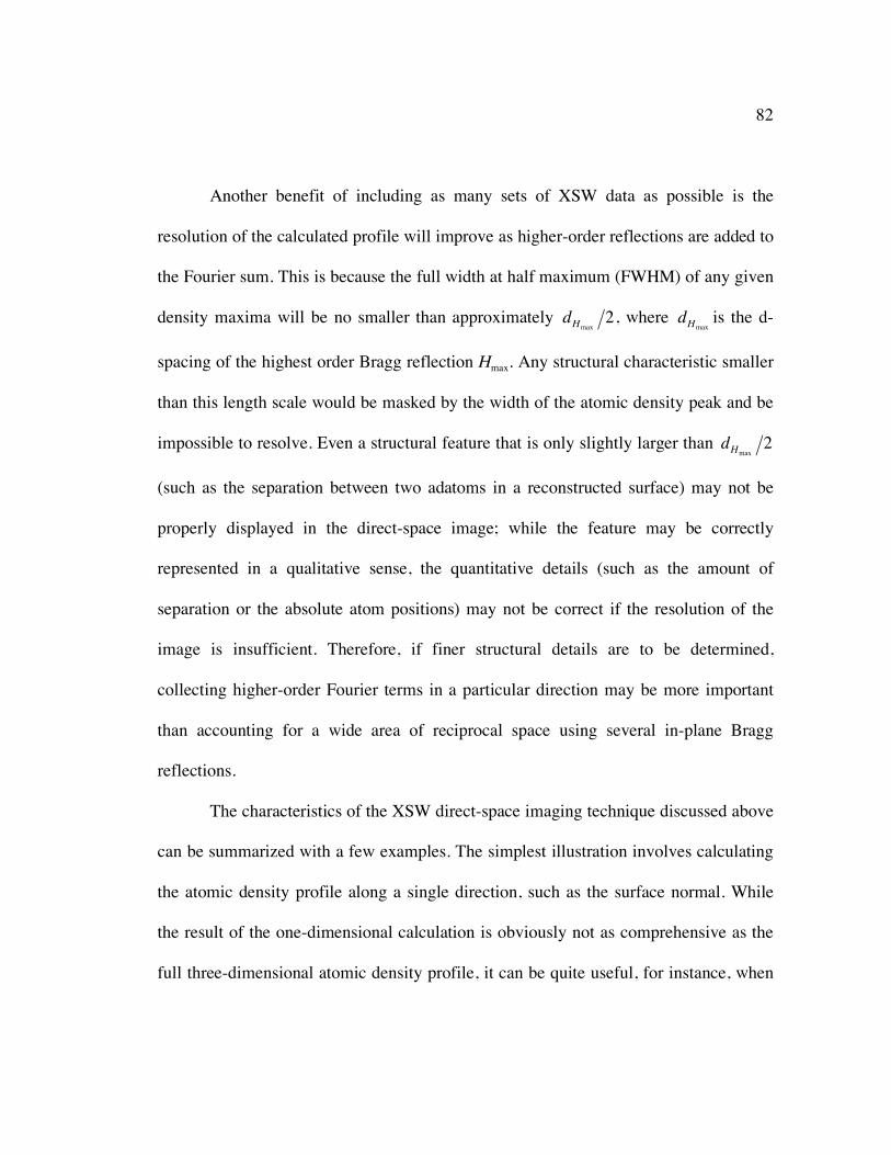
82
Another benefit of including as many sets of XSW data as possible is the
resolution of the calculated profile will improve as higher-order reflections are added to
the Fourier sum. This is because the full width at half maximum (FWHM) of any given
density maxima will be no smaller than approximately
�
dHmax
2, where
�
dHmax
is the d-
spacing of the highest order Bragg reflection Hmax. Any structural characteristic smaller
than this length scale would be masked by the width of the atomic density peak and be
impossible to resolve. Even a structural feature that is only slightly larger than
�
dHmax
2
(such as the separation between two adatoms in a reconstructed surface) may not be
properly displayed in the direct-space image; while the feature may be correctly
represented in a qualitative sense, the quantitative details (such as the amount of
separation or the absolute atom positions) may not be correct if the resolution of the
image is insufficient. Therefore, if finer structural details are to be determined,
collecting higher-order Fourier terms in a particular direction may be more important
than accounting for a wide area of reciprocal space using several in-plane Bragg
reflections.
The characteristics of the XSW direct-space imaging technique discussed above
can be summarized with a few examples. The simplest illustration involves calculating
the atomic density profile along a single direction, such as the surface normal. While
the result of the one-dimensional calculation is obviously not as comprehensive as the
full three-dimensional atomic density profile, it can be quite useful, for instance, when
83
(hkl) reflection (111) (222) (333) (444) (555) (666) (777) (888)
fH 0.707 0 0.707 1 0.707 0 0.707 1
PH -0.125 0 0.125 0 -0.125 0 0.125 0
Table 4.1: The calculated values for coherent fraction fH and coherent position PH for the bulk Si atomic distribution in the [111] direction. The unit cell origin chosen for this calculation coincides with the Si atom located at the top of the bilayer. Furthermore, the ordered fraction C and Debye-Waller factor DH are equal to unity.
investigating adsorbate structures in which the in-plane geometry is fairly well-
established but the structural details in the out-of-plane direction are in question. This is
a rather apt description of the 1/3 ML Sn/Si(111) surface discussed later in this
dissertation. Therefore, investigating the bulk Si atomic distribution along the [111]
direction would be a suitable example of the XSW direct-space imaging approach.
In order to produce a Si density profile in one dimension, the selected set of
coherent fractions and positions presented in Table 4.1 are calculated according to Eqs.
4.39 and 4.43 after choosing an appropriate origin for the Si unit cell. While the
coherent fractions listed in Table 4.1 are independent of the choice of unit cell origin,
the tabulated coherent positions are not. For the values in Table 4.1, the chosen origin
coincides with the top atom of the Si bilayer. For simplicity, the ordered fraction C and
the Debye-Waller factor DH are equal to unity.
84
The individual contributions of each Fourier component are shown in Figure
4.3(a), which depicts the Si Fourier terms over an interval corresponding to the one-
dimensional fractional unit cell along the [111] direction. In total, nine separate hhh
Fourier components (h=0 to 8) are represented in the figure. Figure 4.3(b) demonstrates
how the Fourier sum changes as higher-order terms are included in the summation of
Eq. 4.48. The h=1 term arises from the Si(111) reflection and produces a single atomic
density maxima centered at z = –0.125. The effect of higher-order Fourier coefficients
on the synthesized density distribution starts to become apparent with the addition of
the h=3 term (the h=2 term has no effect because the coherent fraction for the (222)
reflection is zero). The summation of the h=0 to 3 Fourier terms produces a density
profile in which two density maxima appear at z = 0 and z = –0.25. While the two
peaks in the distribution are quite broad (FWHM = 0.564 Å as compared to d333 = 1.045
Å) and do not appreciably extend beyond the background oscillations, their location
does approximate the actual location of the Si atoms within the fractional unit cell.
As the additional higher-order hhh terms are added to the h=0 to 3 Fourier
components, the amplitude of the density maxima increases and their width decreases,
resulting in a better representation of the Si atomic distribution. For example, when the
summation only includes the h=0 to 5 hhh Fourier terms, the FWHM of the density
maxima is equal to 0.323 Å, which is 52 percent of the 0.627 Å spacing between the Si
(555) diffraction planes. When the summation is completed up to the h=8 term so that
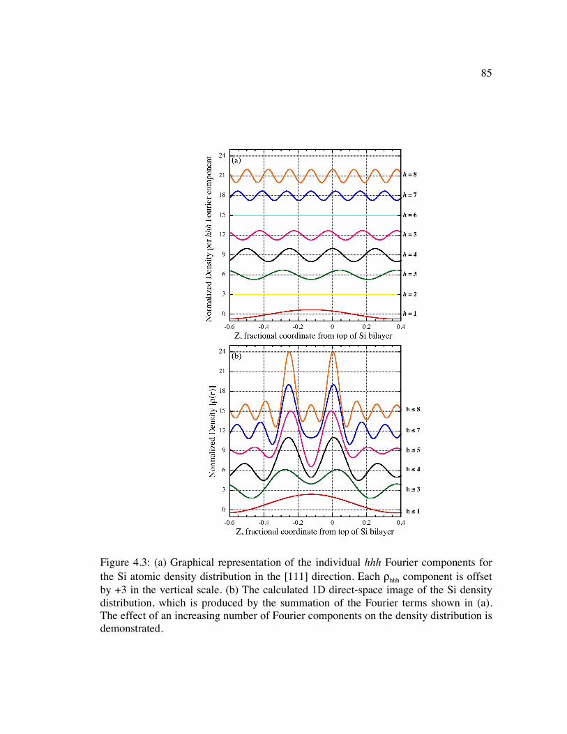
85
Figure 4.3: (a) Graphical representation of the individual hhh Fourier components for the Si atomic density distribution in the [111] direction. Each ρhhh component is offset by +3 in the vertical scale. (b) The calculated 1D direct-space image of the Si density distribution, which is produced by the summation of the Fourier terms shown in (a). The effect of an increasing number of Fourier components on the density distribution is demonstrated.
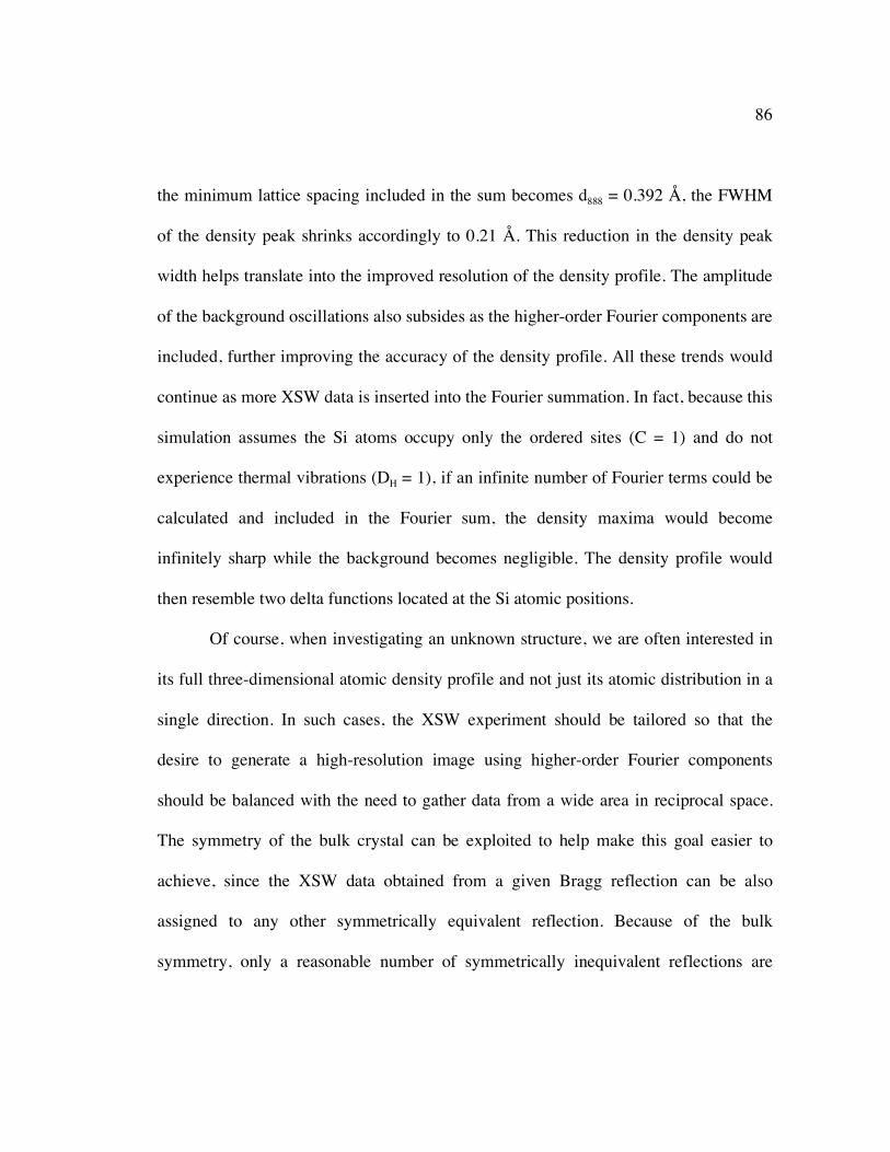
86
the minimum lattice spacing included in the sum becomes d888 = 0.392 Å, the FWHM
of the density peak shrinks accordingly to 0.21 Å. This reduction in the density peak
width helps translate into the improved resolution of the density profile. The amplitude
of the background oscillations also subsides as the higher-order Fourier components are
included, further improving the accuracy of the density profile. All these trends would
continue as more XSW data is inserted into the Fourier summation. In fact, because this
simulation assumes the Si atoms occupy only the ordered sites (C = 1) and do not
experience thermal vibrations (DH = 1), if an infinite number of Fourier terms could be
calculated and included in the Fourier sum, the density maxima would become
infinitely sharp while the background becomes negligible. The density profile would
then resemble two delta functions located at the Si atomic positions.
Of course, when investigating an unknown structure, we are often interested in
its full three-dimensional atomic density profile and not just its atomic distribution in a
single direction. In such cases, the XSW experiment should be tailored so that the
desire to generate a high-resolution image using higher-order Fourier components
should be balanced with the need to gather data from a wide area in reciprocal space.
The symmetry of the bulk crystal can be exploited to help make this goal easier to
achieve, since the XSW data obtained from a given Bragg reflection can be also
assigned to any other symmetrically equivalent reflection. Because of the bulk
symmetry, only a reasonable number of symmetrically inequivalent reflections are
87
required to populate the Fourier sum with a significant amount of reciprocal lattice
data.
As an example of this approach, a three dimensional density profile for the Fe
atoms that make up the bulk hematite (α-Fe2O3) structure can be generated from a
moderate number of Bragg reflections. This example is the three-dimensional analogue
to the one-dimensional profile introduced earlier for Si(111). In the V/Fe2O3(0001)
surface investigation discussed later in this thesis, four symmetrically inequivalent
reflections were measured, consisting of one off-normal measurement (the (0006)
Bragg reflection) and three off-normal measurements (the (10
�
1 4), (01
�
1 2), and (11
�
2 3)
Bragg reflections). Applying the bulk symmetry operators of the hematite structure
(space group R
�
3 c) to these four Fourier components increases the number of Fourier
terms that are included in the density calculation to 20 reflections. The (11
�
2 3) Bragg
reflection has a multiplicity of 12 for the bulk hematite structure; in the example shown
here, all 12 symmetrically equivalent reflections are included in the Fourier summation.
The result of the calculation is shown in Figure 4.4, which represents the projection of
the atomic density maxima onto the (11
�
2 0) Fe2O3 crystallographic plane. The bulk
positions of the Fe atoms have been overlaid on this projection to aid the comparison
between the density calculation and the expected bulk structure. For the one-
dimensional Si(111) example, the complete result of the Fourier sum was shown.
However, in the three-dimensional case, only the regions of the spatial distribution
88
where the atomic density equals or exceeds 80% of the overall density maximum are
shown for the sake of clarity. This example demonstrates how the summation of only
four symmetrically inequivalent Fourier components can produce a density profile that
successfully replicates the location of the Fe atoms within the interior of the hexagonal
unit cell. The FWHM of a given density maxima in the surface normal direction is 1.20
Å. This can be compared to the 2.295 Å d-spacing of the (0006) Fe2O3 diffraction
planes. However, the density profile is much less precise in the off-normal direction;
the maximum peak width of the density maxima as measured in the direction parallel to
the basal plane is 2.6 Å. The resolution of this density map can be improved by
collecting further Fourier terms using additional off-normal Bragg reflections.
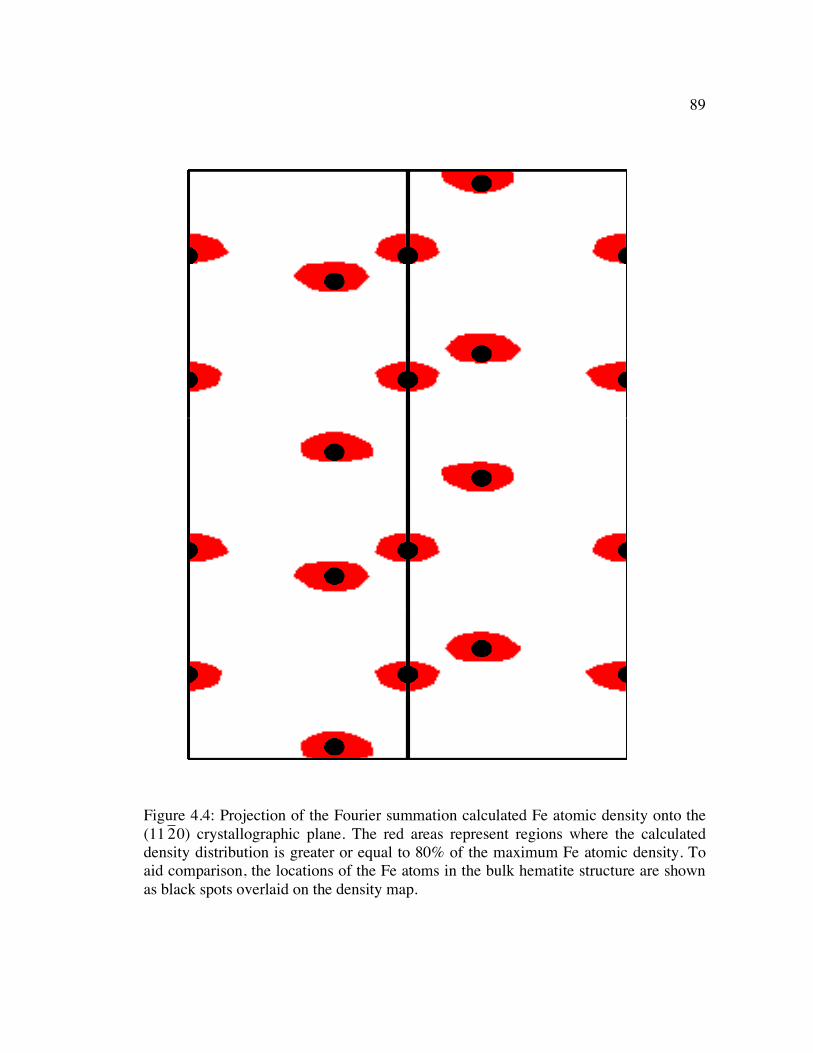
89
Figure 4.4: Projection of the Fourier summation calculated Fe atomic density onto the (11
�
2 0) crystallographic plane. The red areas represent regions where the calculated density distribution is greater or equal to 80% of the maximum Fe atomic density. To aid comparison, the locations of the Fe atoms in the bulk hematite structure are shown as black spots overlaid on the density map.
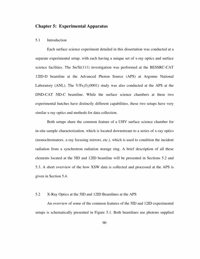
90
Chapter 5: Experimental Apparatus
5.1 Introduction
Each surface science experiment detailed in this dissertation was conducted at a
separate experimental setup, with each having a unique set of x-ray optics and surface
science facilities. The Sn/Si(111) investigation was performed at the BESSRC-CAT
12ID-D beamline at the Advanced Photon Source (APS) at Argonne National
Laboratory (ANL). The V/Fe2O3(0001) study was also conducted at the APS at the
DND-CAT 5ID-C beamline. While the surface science chambers at these two
experimental hutches have distinctly different capabilities, these two setups have very
similar x-ray optics and methods for data collection.
Both setups share the common feature of a UHV surface science chamber for
in-situ sample characterization, which is located downstream to a series of x-ray optics
(monochromators, x-ray focusing mirrors, etc.), which is used to condition the incident
radiation from a synchrotron radiation storage ring. A brief description of all these
elements located at the 5ID and 12ID beamline will be presented in Sections 5.2 and
5.3. A short overview of the how XSW data is collected and processed at the APS is
given in Section 5.4.
5.2 X-Ray Optics at the 5ID and 12ID Beamlines at the APS
An overview of some of the common features of the 5ID and 12ID experimental
setups is schematically presented in Figure 5.1. Both beamlines use photons supplied

91
by the Hybrid Undulator A, a third generation synchrotron insertion-device source
designed by the APS staff. For both experiments the APS operated in top-mode,
maintaining the storage ring current at about 100 mA throughout the course of the
experiments. The entire V/Fe2O3(0001) investigation and much of the Sn/Si(111)
experiment was conducted using an incident x-ray beam energy close to 7.00 keV. This
energy is within the range of the undulator’s first harmonic (2.9 to 13.0 keV). One of
the XSW measurements at 12ID required using a higher incident energy (15.80 keV).
This was achieved using the third harmonic, which provides for a maximum incident
energy of 38 keV.
In order to select the desired energy from the white-beam undulator radiation,
both the 5ID and 12ID beamlines employ a double crystal, fixed exit high-heat load
monochromator (HHLM). The HHLM at both beamlines is made up two Si(111)
crystals in which the position of the second Si crystal is continuously controlled by a
feedback mechanism in order to maintain a chosen detuning value. Because the HHLM
is exposed to the full power of the x-ray beam, the first Si crystal of the 5ID HHLM is
cryogenically cooled. Liquid nitrogen is used to directly cool the first Si crystal of the
12ID HHLM, while copper braids linked to a liquid nitrogen supply cool the second Si
crystal.
The post-monochromator optics of the two beamlines differ somewhat. At 5ID,
a pair of horizontally deflecting glass mirrors provides both harmonics rejection and
92
Figure 5.1: A depiction of the experimental equipment located at the 5ID and 12ID beamlines of the Advanced Photon Source. The post monochromator optics and UHV chamber are located in the beamline hutches upstream of the HHLM. Note: the dual focusing mirrors that are used at 5ID-C for rejecting higher-order harmonics are not shown. Also, the reflectivity detector used at 12ID-D is located within the UHV chamber, unlike the external reflectivity detector used at 5ID-C that is depicted here.
93
horizontal focusing (with 1:1). When working at high x-ray energies (above 11 keV), a
stripe of Pt or Rh located on the glass mirror can be used as the reflecting surface;
because the experiment of interest was conducted at 7.00 keV, the bare glass surface
was used to focus the incoming x-rays. At 12ID, the rejection of higher-order
harmonics is achieved by the detuning of the HHLM, at a typical value of 80% of the
peak intensity of the Si(111) reflection from the first Si crystal. The x-rays diffracted
from the HHLM then pass through an evacuated beam pipe into the experimental hutch
(12ID-D or 5ID-C), which contains the post-monochromator optics and the UHV
surface science chamber.
The post-monochromator optics serve to reduce the energy and angular
dispersion of the conditioned x-rays from the HHLM. It is made up of two non-
dispersive, two-bounce Si channel-cut monochromators that are mounted on ZXθ
stages. These stages are located on an optical table, which can be remotely moved in
the X, Y, and Z directions. Each monochromator is made up of three separate Si
channel-cut crystals with a different surface orientation: (00l), (hh0), and (hhh). The
three Si channel-cuts are positioned on the XZθ stage so that the desired Si surface
orientation can be easily selected to better match the d-spacing of the sample’s Bragg
reflection. Each channel-cut also has two available gaps to make larger Bragg angles
(and therefore energy range) accessible to each channel-cut, which in turn allows a
wider range of x-ray energies for the experiment.
94
Ion chambers filled with He are situated upstream and downstream from each
monochromator to measure the x-ray beam intensity before and after being diffracted
from the Si channel-cuts. These ion chambers not only allow the intensity of the x-rays
to be constantly monitored, but they also are used as the input signals for a feedback
loop that continually maintains a user-selectable detuning value of the two Si channel-
cut monochromators. The feedback mechanism maintains the chosen detuning setting
using either analog monochromator stabilizer (MOSTAB) units (at 5ID-C) or digital
MOSTABs (at 12ID-D) to compare the ion chamber signals with the desired detuning
value and adjust the angular position of the Si channel-cuts accordingly. These minute
adjustments are made by MOSTAB-regulated piezo transducers that deflect the torsion-
bearing stages that support the Si channel-cuts. Typically, the first MOSTAB is set to
detune the first channel-cut to 80% of the x-ray intensity from the HHLM, while the
second MOSTAB keeps the second channel-cut at a detuning value of 25% of the peak
intensity from the previous channel-cut. By tuning the channel-cuts to these values, the
angular width and energy distribution of the incident x-ray beam is minimized, which
improves the phase contrast of the XSW, which in turn makes the XSW results more
precise. Finally, in addition to the three ion chambers needed for the channel-cut
stabilization setup, there is a fourth ion chamber that measures the beam intensity once
the x-ray beam size is defined by a pair of slits.
The end result of the aforementioned x-ray optics can be graphically depicted in
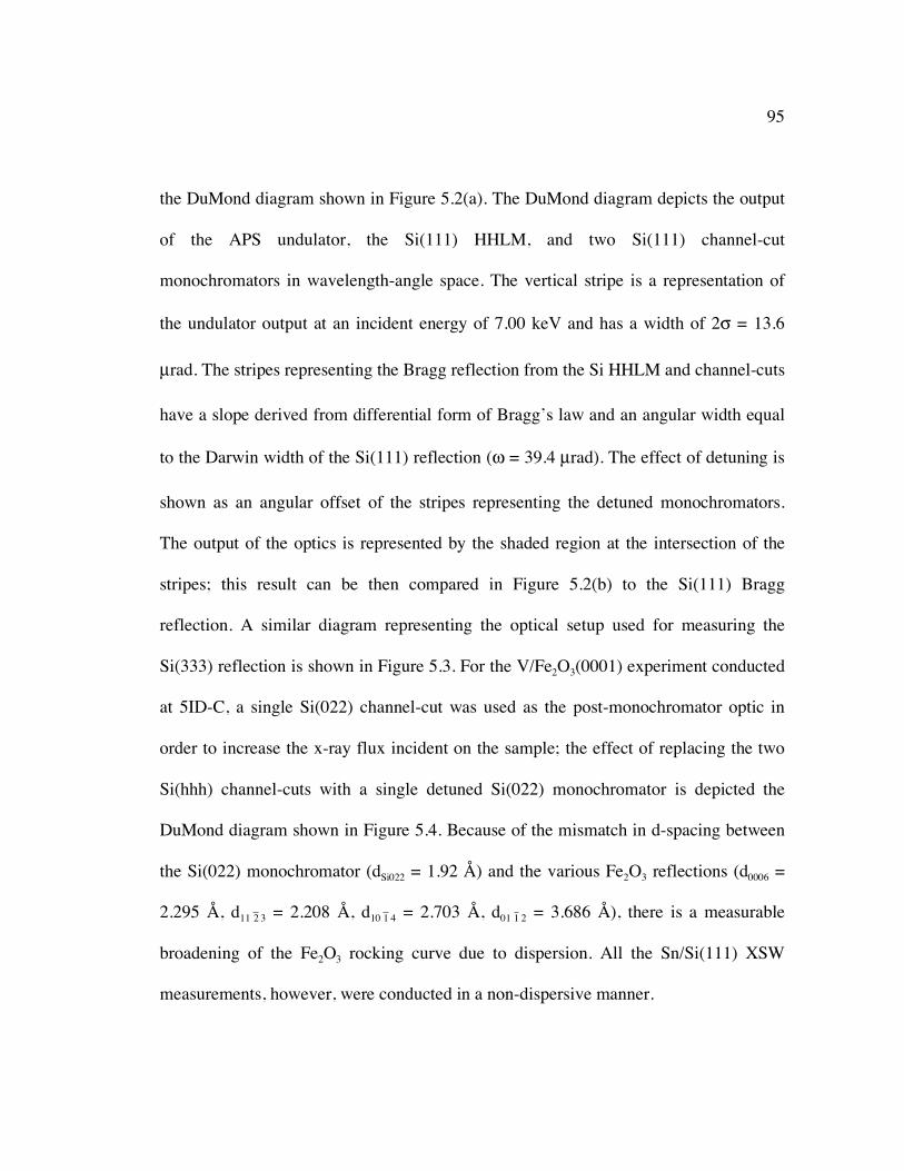
95
the DuMond diagram shown in Figure 5.2(a). The DuMond diagram depicts the output
of the APS undulator, the Si(111) HHLM, and two Si(111) channel-cut
monochromators in wavelength-angle space. The vertical stripe is a representation of
the undulator output at an incident energy of 7.00 keV and has a width of 2σ = 13.6
µrad. The stripes representing the Bragg reflection from the Si HHLM and channel-cuts
have a slope derived from differential form of Bragg’s law and an angular width equal
to the Darwin width of the Si(111) reflection (ω = 39.4 µrad). The effect of detuning is
shown as an angular offset of the stripes representing the detuned monochromators.
The output of the optics is represented by the shaded region at the intersection of the
stripes; this result can be then compared in Figure 5.2(b) to the Si(111) Bragg
reflection. A similar diagram representing the optical setup used for measuring the
Si(333) reflection is shown in Figure 5.3. For the V/Fe2O3(0001) experiment conducted
at 5ID-C, a single Si(022) channel-cut was used as the post-monochromator optic in
order to increase the x-ray flux incident on the sample; the effect of replacing the two
Si(hhh) channel-cuts with a single detuned Si(022) monochromator is depicted the
DuMond diagram shown in Figure 5.4. Because of the mismatch in d-spacing between
the Si(022) monochromator (dSi022 = 1.92 Å) and the various Fe2O3 reflections (d0006 =
2.295 Å, d11
�
2 3 = 2.208 Å, d10
�
1 4 = 2.703 Å, d01
�
1 2 = 3.686 Å), there is a measurable
broadening of the Fe2O3 rocking curve due to dispersion. All the Sn/Si(111) XSW
measurements, however, were conducted in a non-dispersive manner.
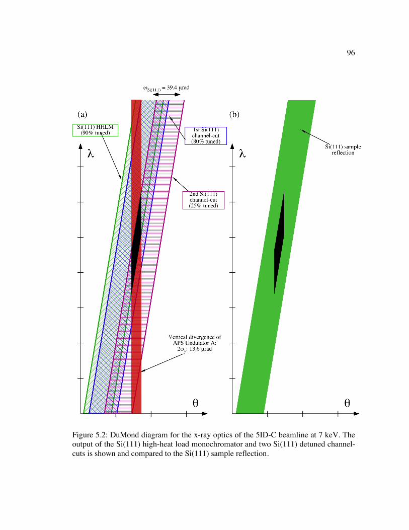
96
Figure 5.2: DuMond diagram for the x-ray optics of the 5ID-C beamline at 7 keV. The output of the Si(111) high-heat load monochromator and two Si(111) detuned channel-cuts is shown and compared to the Si(111) sample reflection.
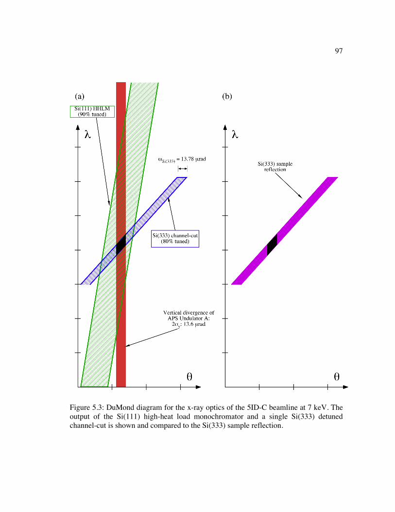
97
Figure 5.3: DuMond diagram for the x-ray optics of the 5ID-C beamline at 7 keV. The output of the Si(111) high-heat load monochromator and a single Si(333) detuned channel-cut is shown and compared to the Si(333) sample reflection.
98
Figure 5.4: DuMond diagram for the x-ray optics of the 5ID-C beamline at 7 keV. The output of the Si(111) high-heat load monochromator and a single Si(022) detuned channel-cut is shown and compared to the Fe2O3 sample reflection.
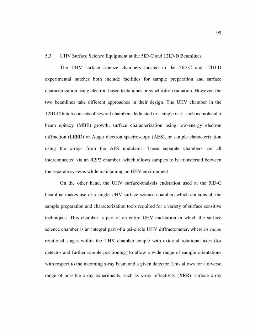
99
5.3 UHV Surface Science Equipment at the 5ID-C and 12ID-D Beamlines
The UHV surface science chambers located in the 5ID-C and 12ID-D
experimental hutches both include facilities for sample preparation and surface
characterization using electron-based techniques or synchrotron radiation. However, the
two beamlines take different approaches in their design. The UHV chamber in the
12ID-D hutch consists of several chambers dedicated to a single task, such as molecular
beam epitaxy (MBE) growth, surface characterization using low-energy electron
diffraction (LEED) or Auger electron spectroscopy (AES), or sample characterization
using the x-rays from the APS undulator. These separate chambers are all
interconnected via an R2P2 chamber, which allows samples to be transferred between
the separate systems while maintaining an UHV environment.
On the other hand, the UHV surface-analysis endstation used at the 5ID-C
beamline makes use of a single UHV surface science chamber, which contains all the
sample preparation and characterization tools required for a variety of surface sensitive
techniques. This chamber is part of an entire UHV endstation in which the surface
science chamber is an integral part of a psi-circle UHV diffractometer, where in vacuo
rotational stages within the UHV chamber couple with external rotational axes (for
detector and further sample positioning) to allow a wide range of sample orientations
with respect to the incoming x-ray beam and a given detector. This allows for a diverse
range of possible x-ray experiments, such as x-ray reflectivity (XRR), surface x-ray
100
diffraction (SXRD) in both grazing-incident and grazing-exit configurations, surface
extended x-ray absorption fin structure (SEXAFS), and of course, x-ray standing
waves. Both the similarities and differences of the UHV setup at the two APS
beamlines will be detailed in the following section, as well as how these differences
result in some unique advantages and disadvantages for our XSW measurements.
5.3.1 UHV Chamber at the 12ID-D Endstation
A schematic of the entire UHV surface science assembly is presented in Figure
5.5. As mentioned briefly in the following section, the most distinct feature of the UHV
chamber at the 12ID-D station is a central R2P2 chamber, which facilitates sample
transfer from the various chambers mounted along the circumference of the R2P2
chamber while maintaining UHV. The vacuum within the R2P2 is maintained by a 400
liter/sec ion pump. A titanium sublimation pump is also available to improve pumping
speeds, especially when the chamber pressure rises significantly above the base
pressure, which is less than 1 x 10⁻¹⁰ Torr. Two separate chambers are connected
directly to the R2P2: a sample carousel for the storage of samples without exposing
them to a non-UHV environment, and a surface analysis chamber, which provides both
reverse-view LEED and a cylindrical mirror analyzer (CMA) for AES. Samples are
typically transferred to the analysis chamber before and after any growth processes or
XSW measurements to check the long-range surface structure (using LEED) and the
101
Figure 5.5: Schematic of the top view of the UHV system at the BESSRC 12ID-D undulator system. The figure is reproduced from reference [81].
102
amount of surface contamination due to residual gases (using AES).
There are three other chambers are accessible from the R2P2, but they are
connected to the R2P2 via gate valves so that these chambers may be isolated from the
rest of the vacuum system when needed. Therefore, each of these chambers needs their
own pumping system to achieve the required vacuum environment. One of these
chambers is an introduction chamber, which is evacuated using a turbomolecular pump
(TMP). This load-lock system allows the storage of six samples in HV conditions (~1 x
10-6 Torr) for eventual insertion into the main UHV chamber; while the gate valve
between the load-lock and the main chamber is open, the pressure in the main chamber
will usually increase into the 10-9 Torr range, but will typically drop quickly once the
gate valve is closed.
Another chamber that can be closed off from the R2P2 system is the MBE
growth chamber. This chamber contains equipment dedicated to surface preparation,
such as three Knudsen cells for atomic deposition, a quartz crystal monitor for
monitoring the effusion flux from the Knudsen cells, and a quadrupole mass
spectrometer for residual gas analysis. The chamber also contains a sample manipulator
for sample positioning and heating to over 1000°C via a tungsten filament. The growth
chamber has a base pressure of less than 1 x 10⁻¹⁰ Torr, which is achieved using a
cryopump. During MBE growth, the gate valve connecting the growth chamber and the
R2P2 is usually kept closed, so that the cryopump alone is used to maintain the vacuum
103
in the growth chamber. However, because the cryopump He compressor causes
vibrations in the system that can adversely affect the XSW measurements, the gate
valve is opened and the cryopump is turned off during x-ray scans, leaving only the
main ion pump to pump on the growth chamber.
The final chamber to be discussed is the x-ray chamber, which can also be
isolated from the main system using a gate valve. As such, this chamber has its own
400 liter/sec ion pump and titanium sublimation pump for UHV operation. Because this
chamber holds the samples during the actual XSW scans, the chamber must allow for
precision orientation of the sample, the detection of both the diffracted beam and the x-
ray fluorescence, and of course, a way of allowing x-rays from the undulator to reach
the sample. Therefore, the chamber contains a sample manipulator that can translate the
sample in the X and Z directions, as well as adjust the incident (θ) and tilt (χ) angles of
the sample so that various normal and off-normal reflections can be detected. The
manipulator also contains a tungsten filament that allows heating of samples up to
800°C. Detection of the diffracted beam is accomplished using a Si in vacuo
photodiode that can be positioned up to a two-theta angle of 150°. X-ray fluorescence is
measured using a custom-built PGT Si(Li) solid-state detector with a 0.3 mil thick Be
window. The detector is seated within a detector “snout”, which extends into the x-ray
chamber from the chamber top. On the side of the snout near the sample manipulator is
a small Be window, which allows fluorescence emitted from the sample to exit the
104
chamber and be collected by the PGT detector. Finally, two thin Be windows located
directly across from one another allow x-rays from the post-monochromator optics to
enter and exit the x-ray chamber.
While the aforementioned sample manipulator can be used coarsely position the
incident angle of the sample, the motion of the theta stage is not precise enough to scan
the sample through its rocking curve without introducing artifacts into the reflectivity
curve. Therefore, the entire UHV system is mounted on a frame, which in turn is
supported by three z-motion translation stages that are driven by stepper motors. Once
the desired Bragg condition is found using the theta drive of the x-ray sample
manipulator, these translation stages can be used to “rock” the entire UHV system and
therefore scan through the sample rocking curve. The small changes in the sample’s
incident angle can be as small as 2 x 10⁻⁵ degrees in theta, which is fine enough to be
able to reproducibly capture the Si(444) reflectivity curve at 9.40 keV (ω = 7.7 µrad).
For narrower rocking curves (such as the Si(555) reflection at 11.20 keV, which has a
Darwin width of ω = 3.0 µrad), scanning the sample rocking curve can be performed by
scanning one of the post-monochromator channel cuts.
5.3.2 UHV Psi-circle diffractometer at the 5ID-C Endstation
The design of the UHV psi-circle surface science diffractometer was motivated
by the need to provide a flexible endstation instrument capable of facilitating both
105
UHV surface preparation as well as surface analysis via x-ray or electron scattering and
x-ray or electron spectroscopy. This desired versatility presented a number of design
difficulties, one example being the need to position samples within the UHV chamber
so that neither x-ray experiments nor electron-based surface analysis would be
compromised. The following section will describe how such design challenges were
overcome and detail some of the important features of the diffractometer.
A photograph of the UHV chamber/diffractometer at the 5ID-C endstation is
shown in Figure 5.6, which shows the UHV system as seen from the downstream
direction. The UHV diffractometer sits on an X-Z table, which allows the entire
assembly to be positioned with respect to the incoming x-ray beam. The diffractometer
configuration is composed of six rotational axes in a psi-circle geometry. The psi-circle
configuration is also known as “4S+2D” due to the four degrees of freedom (DOF) for
the sample and two DOF for the detector. This design choice allows for a simplified
vacuum interface between the UHV chamber and rotational stages; more importantly, it
is also responsible for the large amount of reciprocal-space that can be accessed by the
detector through the chamber’s Be windows. Of the six rotational axes that comprise
the psic geometry, four axes (del, eta, mu, and nu) are implemented using high-
precision angular stages with 20:1 gear reducers. The UHV sample manipulator
contains the stages for the remaining two (chi and phi) rotational motions, as well as an
X-Y-Z stage, which is essential for precise translational positioning of the sample with
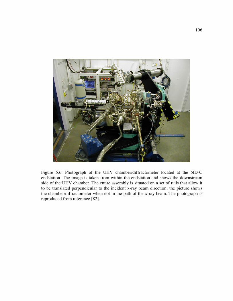
106
Figure 5.6: Photograph of the UHV chamber/diffractometer located at the 5ID-C endstation. The image is taken from within the endstation and shows the downstream side of the UHV chamber. The entire assembly is situated on a set of rails that allow it to be translated perpendicular to the incident x-ray beam direction; the picture shows the chamber/diffractometer when not in the path of the x-ray beam. The photograph is reproduced from reference [82].
107
respect to the incoming x-ray beam. For the XSW experiments detailed here, the chi
and phi in vacuo rotation stages were used to orient the surface normal of the samples
so that the desired off-normal XSW measurements could be performed. The
diffractometer was then used much like a 2-circle reflectivity setup would be for these
XSW experiments, with mu=nu=0, eta=θ, and del=2θ.
While the sample manipulator is an integral part of the psic configuration, it
also plays an important role in UHV surface preparation. The sample manipulator
contains a tungsten filament for annealing samples up to 1100 K, as well as indirect
sample cooling to 115 K from copper braids affixed to the sample stage. The Cu braids
are cooled from an in vacuo liquid nitrogen reservoir. Other instruments that can be
used during sample preparation include a residual gas analyzer, a differentially-pumped
ion gun for sputter cleaning samples, three Knudsen cells for MBE growth, a reverse-
view LEED, and a double-pass CMA for AES and x-ray photoelectron spectroscopy.
Unused ports on the chamber are available for installing more specialized equipment,
such as the oxygen source used in the V/Fe2O3 study. This oxygen source will be
described further in Chapter 7. The entire chamber is evacuated using an ion pump,
which is equipped with a titanium sublimation pump and cryoshield and backed by a
TMP. This pumping system results in a base pressure of ~1.5x10⁻¹⁰ Torr.
As in the 12ID-D x-ray chamber discussed previously, synchrotron radiation
enters and exits the UHV chamber via Be windows on Conflat flanges. For the 5ID-C
108
chamber, a single rectangular Be window allows x-rays to enter the chamber; directly
downstream from this window lies a ten inch diameter circular Be window, which
allows a wide range of angles for x-rays to exit and be collected. Another smaller
rectangular Be window is situated on top of the UHV chamber and permits scattering
for larger incident and exit angles. Because of space and design considerations, these
Be windows must be located relatively far from some of the other surface analysis
equipment, such as the LEED or CMA. Therefore, the sample must be able to occupy a
range of positions so that both x-ray and electron analysis can be conducted in the UHV
chamber. Instead of requiring the sample manipulator to traverse the length of the UHV
chamber so that the sample can be accessed by the Be windows or the various surface
science tools, the sample stage remains more or less fixed in space, while the chamber
itself can translate independent of the sample and diffractometer. This translation is
achieved via a linear translation stage, a large bellows that connects the chamber to the
diffractometer, and an air piston system that counteracts the vacuum force using a
series of pulleys and cables.
When the chamber is translated into the scattering position, the sample is
accessible by a 7-element Canberra Ultra LEGe solid-state detector (SSD), which is the
primary detector used for collected x-ray fluorescence spectra. The SSD connects to the
UHV chamber via a differentially-pumped custom-built UHV interface that is situated
directly opposite the bellows and sample manipulator. When the detector is not used for
109
data collection (for example, during sample preparation), it can be retracted behind a
pair of UHV gate valves that make up part of the UHV interface. In order to collect x-
ray fluorescence spectra, these gate valves must be opened and the detector inserted
into the UHV chamber. The interface between the SSD and the main chamber has a
differential pumping port for a TMP and a set of Kapton seals that wrap around the
detector snout. Both devices serve to reduce the pressure increase caused by the
presence of the SSD inside the UHV chamber.
The position of the SSD is chosen so that the fluorescence signal from the
sample provides reasonable statistics for the XSW scans but does not saturate the SSD
electronics. Therefore, the SSD position will depend on the position of the sample, the
size of the incident x-ray beam, and the amount of fluorescing material within the
diffraction volume. When the detector is fully inserted into the UHV chamber, the SSD
detector array will be exposed to x-ray fluorescence arising from not only the sample,
but also from the Be windows that span the UHV chamber. Typically this x-ray
fluorescence is characteristic of any evaporated material from the Knudsen cells that
have been inadvertently deposited on the Be windows. Therefore, a collimator
assembly can be placed between the detector snout and the sample in order to restrict
the line of sight of the SSD to only the area directly in front of the detector snout. There
are three separate collimators that can be rotated in front of the detector, and each
collimator can be equipped with thin foils that act as filters to attenuate the strong
110
fluorescence signal from the sample substrate and prevent pile-up effects. The user can
select the foils to be installed depending on the incident x-ray energy and the particular
sample; one collimator will usually be used without a filter to allow the full x-ray
fluorescence spectra to be collected without attenuation.
5.4 XSW Data Collection at the Advanced Photon Source
While the experimental setups at the 5ID-C and 12ID-D are different in many
ways, the process of acquiring XSW data at the APS has been designed to be very
consistent between the two beamlines. This allows users to become familiar with how
XSW experiments are typically performed at either of the two beamlines, and then be
able to apply their experience at the other endstation with a minimum amount of
training required. This is made possible by implementing a common interface for
experimental control and spectroscopy analysis that can work with the unique
experimental setups (such as different vacuum chambers and fluorescence detectors)
used at the two beamlines.
One important element of this data acquisition system is the electronics that
provide the digital x-ray processing of fluorescence spectra. This electronics system is
comprised of the X-ray Instrumentation Analysis (XIA) DXP-2X spectrometers, which
digitally analyzes the incoming pulses from the preamplifier of a fluorescence detector.
The DXP-2X system features four amplifier and pulse processing channels on a single
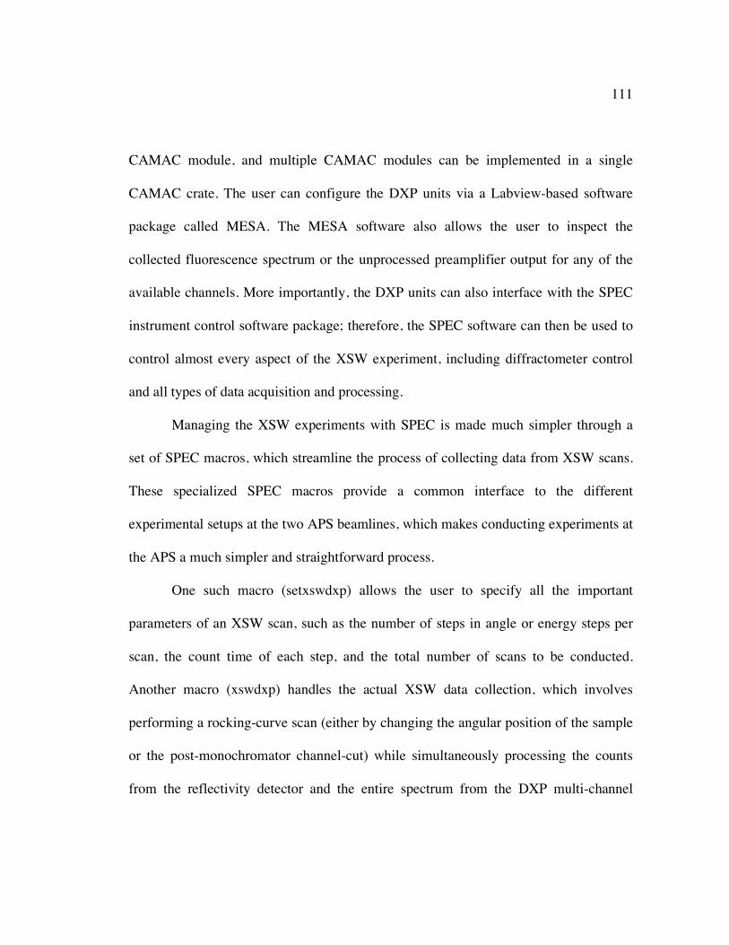
111
CAMAC module, and multiple CAMAC modules can be implemented in a single
CAMAC crate. The user can configure the DXP units via a Labview-based software
package called MESA. The MESA software also allows the user to inspect the
collected fluorescence spectrum or the unprocessed preamplifier output for any of the
available channels. More importantly, the DXP units can also interface with the SPEC
instrument control software package; therefore, the SPEC software can then be used to
control almost every aspect of the XSW experiment, including diffractometer control
and all types of data acquisition and processing.
Managing the XSW experiments with SPEC is made much simpler through a
set of SPEC macros, which streamline the process of collecting data from XSW scans.
These specialized SPEC macros provide a common interface to the different
experimental setups at the two APS beamlines, which makes conducting experiments at
the APS a much simpler and straightforward process.
One such macro (setxswdxp) allows the user to specify all the important
parameters of an XSW scan, such as the number of steps in angle or energy steps per
scan, the count time of each step, and the total number of scans to be conducted.
Another macro (xswdxp) handles the actual XSW data collection, which involves
performing a rocking-curve scan (either by changing the angular position of the sample
or the post-monochromator channel-cut) while simultaneously processing the counts
from the reflectivity detector and the entire spectrum from the DXP multi-channel
112
analyzer. The xswdxp macro also contains a drift-control subroutine, which is
responsible for adjusting the rocking-curve scan to correct mechanical instabilities and
then discarding XSW data collecting during unstable scans. The macro can then records
acceptable XSW data to text files, which include all the relevant motor positions,
monitor and detector counts, pulse-processing statistics (which can be used to calculate
the deadtime of the solid-state detector during a given dataset), and the entire MCA
spectrum as processed by the XIA DXP units. While the XSW data from each
individual rocking curve scan can be captured separately, it is usually more practical to
configure the xswdxp macro to save the sum of several scans into a separate dataset in
order to reduce the size of the resulting data files.
Once the data files are parsed using our custom-built XSW analysis software
package (SUGO) [83], the fluorescence spectrum collected by the MCA can be
extracted. For example, a typical MCA spectrum from one of the Sn/Si(111) XSW
scans is shown in Figure 5.7. An incident energy of 6.90 keV was used for these
experiments, which shows up in the MCA spectrum as the strong elastic peak located at
the far right. The incident x-rays excite the Lα and Lβ x-ray fluorescence from the Sn
adsorbate layer at 3287 eV and 3663 eV, as well as Si Kα fluorescence at 1740 eV
originating from the underlying Si(111) substrate. Because the Sn/Si(111) investigation
was conducted at the 12ID-D endstation, this fluorescence spectrum demonstrates the

113
performance of the single-element PGT detector used at 12ID-D, with the pulse-height
analysis performed by the aforementioned XIA DXP units.
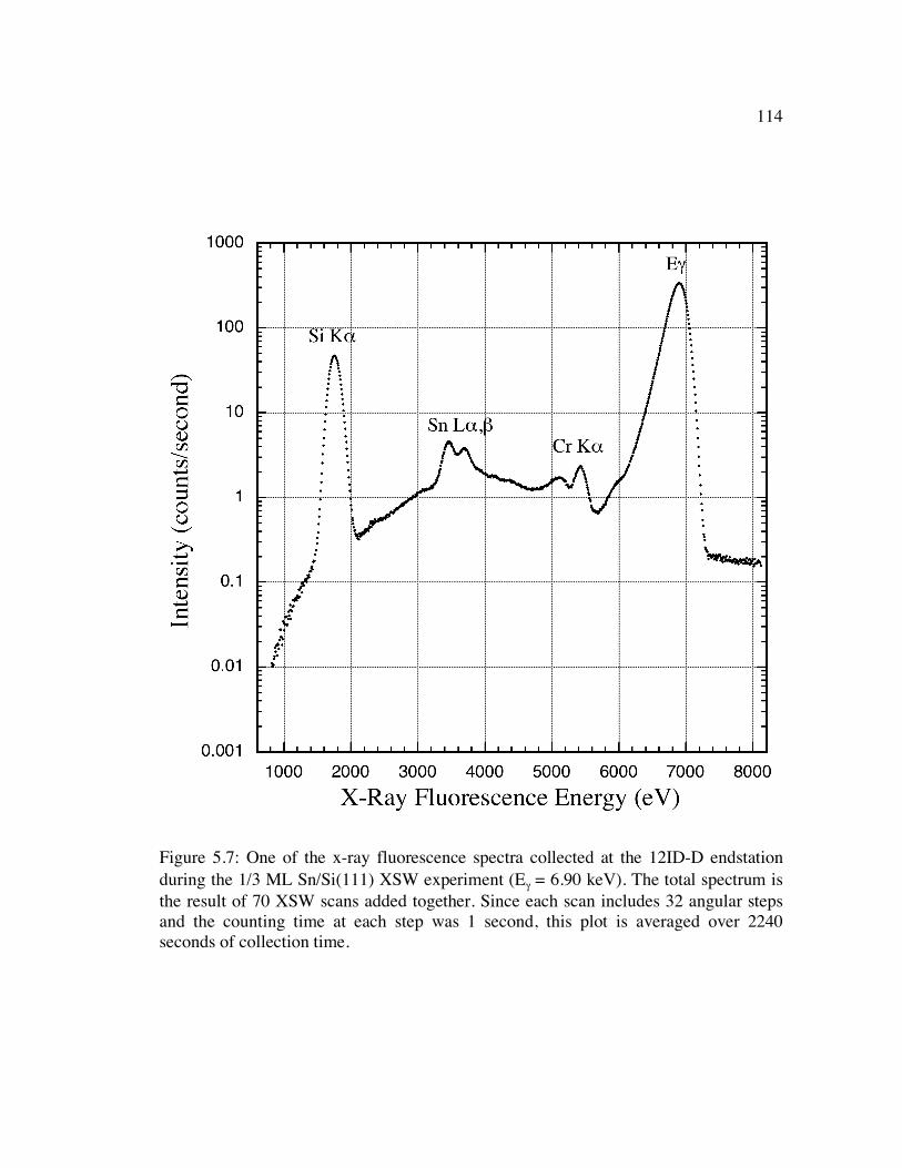
114
Figure 5.7: One of the x-ray fluorescence spectra collected at the 12ID-D endstation during the 1/3 ML Sn/Si(111) XSW experiment (Eγ = 6.90 keV). The total spectrum is the result of 70 XSW scans added together. Since each scan includes 32 angular steps and the counting time at each step was 1 second, this plot is averaged over 2240 seconds of collection time.
115
Chapter 6: XSW Measurements of the 1/3 ML Sn/Si(111)-(√3x√3)R30 Surface
6.1 Sample Preparations
Sample preparation and characterization were conducted in an ultra-high
vacuum (UHV) chamber (base pressure ~1.5 x 10⁻¹⁰ Torr) located at the 12ID-D
undulator BESSRC-CAT experimental station at the Advanced Photon Source,
Argonne National Laboratory. The single-crystal Si(111) samples were cut from a high
purity boule of float zone Si with a miscut angle less than 0.1°. After etching, the Si
samples were Syton polished to produce a mirror-like finish. In cases where some
Syton residue remained on the sample surface due to the polishing process, the samples
underwent an additional cleaning with a piranha etch (H2SO4:H2O2 [2:1] at 130ºC) to
remove any visible polishing debris. The samples were then further cleaned in
ultrasonic baths of acetone, then methanol, then finally trichloroethylene.
The degreased samples were then etched using a modified Shiraki process and
mounted on molybdenum sample holders before insertion into the UHV system. These
holders support the winged design of the Si samples using small strips of tantalum that
fit between the sample wings and the sample holder walls; these thin tantalum ribbons
apply a small amount of pressure on the wings of the sample, affixing the sample in
place without applying undue pressure that could affect the sample rocking curve.
Before mounting the Si substrates, the sample holders were degassed by heating them
in UHV for several hours at 1273 K in order to minimize any sample contamination
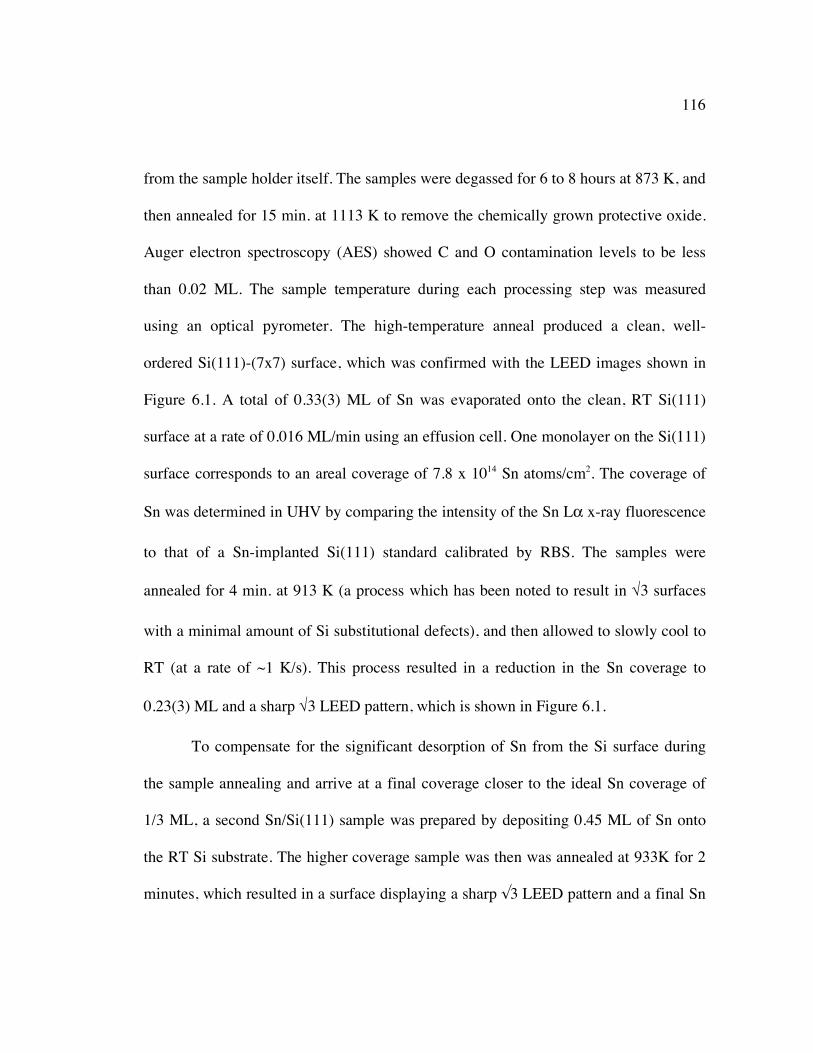
116
from the sample holder itself. The samples were degassed for 6 to 8 hours at 873 K, and
then annealed for 15 min. at 1113 K to remove the chemically grown protective oxide.
Auger electron spectroscopy (AES) showed C and O contamination levels to be less
than 0.02 ML. The sample temperature during each processing step was measured
using an optical pyrometer. The high-temperature anneal produced a clean, well-
ordered Si(111)-(7x7) surface, which was confirmed with the LEED images shown in
Figure 6.1. A total of 0.33(3) ML of Sn was evaporated onto the clean, RT Si(111)
surface at a rate of 0.016 ML/min using an effusion cell. One monolayer on the Si(111)
surface corresponds to an areal coverage of 7.8 x 10¹⁴ Sn atoms/cm2. The coverage of
Sn was determined in UHV by comparing the intensity of the Sn Lα x-ray fluorescence
to that of a Sn-implanted Si(111) standard calibrated by RBS. The samples were
annealed for 4 min. at 913 K (a process which has been noted to result in √3 surfaces
with a minimal amount of Si substitutional defects), and then allowed to slowly cool to
RT (at a rate of ~1 K/s). This process resulted in a reduction in the Sn coverage to
0.23(3) ML and a sharp √3 LEED pattern, which is shown in Figure 6.1.
To compensate for the significant desorption of Sn from the Si surface during
the sample annealing and arrive at a final coverage closer to the ideal Sn coverage of
1/3 ML, a second Sn/Si(111) sample was prepared by depositing 0.45 ML of Sn onto
the RT Si substrate. The higher coverage sample was then was annealed at 933K for 2
minutes, which resulted in a surface displaying a sharp √3 LEED pattern and a final Sn
117
Figure 6.1: LEED images (as captured and inverted) for the different Si(111) surfaces observed during the 1/3 ML Sn/Si(111) XSW experiment. (a) LEED images from the clean Si(111)-(7 x7) surface, E=30.1 eV. (b) LEED images from the 0.23 ML Sn/Si(111)-√3 surface, E=28.5 eV.
118
coverage of 0.33(4) ML. While the annealing temperature used for this sample was not
significantly higher than the annealing conditions for the 0.23 ML Sn/Si surface, the
initial Sn coverage was increased by 36% over the first sample. This particular sample
was characterized using a different set of XSW measurements as the lower-coverage,
0.23 ML Sn/Si surface, which will be detailed further in the following section.
6.2 X-Ray Standing Wave Measurements
The XSW measurements were made after allowing both samples to cool to
room temperature. The data shown in Figs 6.2-6.8 was collected by scanning the 0.23
ML sample in angle through the allowed Si (hhh) Bragg reflections (h = 1, 3, 4, and 5)
and simultaneously collecting the diffracted beam intensity and x-ray fluorescence
spectra (using an in vacuo photodiode and energy-dispersive Si(Li) detector,
respectively) at each angular step. Three additional off-normal XSW measurements
were collected in the same manner utilizing the Si (
�
1 11), (
�
3 33), and (5
�
1
�
1 ) Bragg
reflections in order to determine the in-plane Sn distribution. The {111}, {333}, and
(5
�
1
�
1 ) XSW measurements were collected using 6.90 keV x-rays that were conditioned
by the high-heat-load 12ID Si(111) monochromator. For the {111} XSW
measurements, a pair of detuned non-dispersive Si(111) channel-cut crystals was used
to condition the incident beam; in all other cases, a single d-spacing-matched Si(hhh)
channel cut was used to maximize the available x-ray intensity on the Sn/Si(111)
119
sample. Because the range of the motion for the in-vacuo photodiode is limited, the
higher-order Si(hhh) measurements required the use of higher-energy x-rays (h = 4,
9.40 keV; h = 5, 11.20 keV) to ensure the diffracted x-ray beam would be collected by
the photodiode reflectivity detector.
For the higher coverage 0.33 ML Sn/Si(111) surface, the data shown in Figs
6.9-6.13 was collected using the Si (111) and (333) Bragg reflections to provide
structural information in the surface normal direction. The higher-order Fourier
components employed for the 0.23 ML sample could not be acquired due to
experimental time constraints. The Si (022), (311) and (
�
1 33) Bragg reflections were
used to probe the in-plane Sn distribution instead of the off-normal {111} and {333}
Bragg reflections because of mechanical problems moving the sample surface into the
proper orientation. Because the higher-order (hhh) Bragg reflections were not collected
for the higher-coverage sample, all the XSW measurements for the 0.33 ML surface
were acquired using an incident x-ray energy of 7.00 keV. While the XSW data for the
(hhh) Fourier components employed a pair of detuned non-dispersive Si(111) channel-
cut crystals to decrease the angular spread of the incident x-rays, the off-normal XSW
data was collected in a dispersive manner by using a single (004) channel-cut as the
post-monochromator optics.
Fitting the normalized reflectivity and Sn Lα fluorescence yield with dynamical
diffraction theory produced the coherent position (PH) and coherent fraction (fH) for the
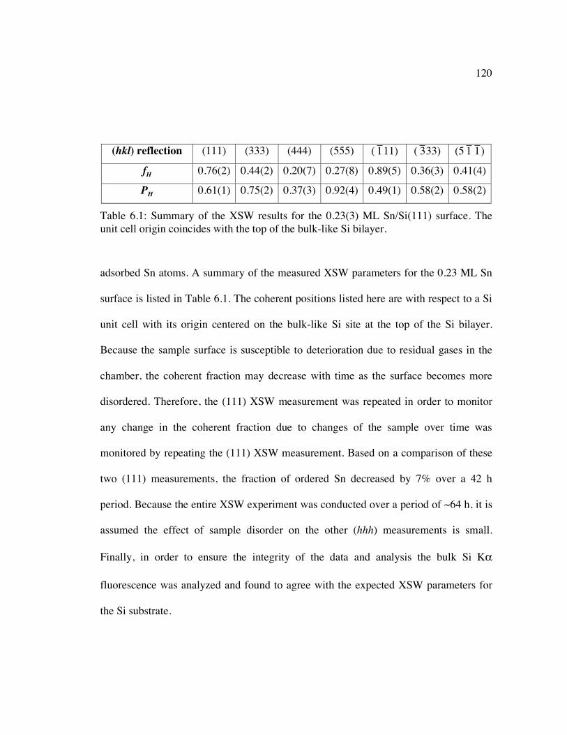
120
(hkl) reflection (111) (333) (444) (555) (
�
1 11) (
�
3 33) (5
�
1
�
1 )
fH 0.76(2) 0.44(2) 0.20(7) 0.27(8) 0.89(5) 0.36(3) 0.41(4)
PH 0.61(1) 0.75(2) 0.37(3) 0.92(4) 0.49(1) 0.58(2) 0.58(2)
Table 6.1: Summary of the XSW results for the 0.23(3) ML Sn/Si(111) surface. The unit cell origin coincides with the top of the bulk-like Si bilayer.
adsorbed Sn atoms. A summary of the measured XSW parameters for the 0.23 ML Sn
surface is listed in Table 6.1. The coherent positions listed here are with respect to a Si
unit cell with its origin centered on the bulk-like Si site at the top of the Si bilayer.
Because the sample surface is susceptible to deterioration due to residual gases in the
chamber, the coherent fraction may decrease with time as the surface becomes more
disordered. Therefore, the (111) XSW measurement was repeated in order to monitor
any change in the coherent fraction due to changes of the sample over time was
monitored by repeating the (111) XSW measurement. Based on a comparison of these
two (111) measurements, the fraction of ordered Sn decreased by 7% over a 42 h
period. Because the entire XSW experiment was conducted over a period of ~64 h, it is
assumed the effect of sample disorder on the other (hhh) measurements is small.
Finally, in order to ensure the integrity of the data and analysis the bulk Si Kα
fluorescence was analyzed and found to agree with the expected XSW parameters for
the Si substrate.
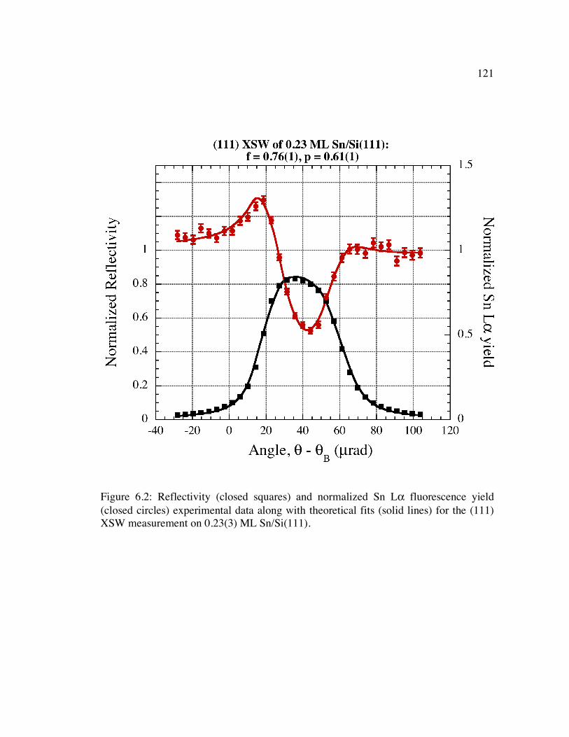
121
Figure 6.2: Reflectivity (closed squares) and normalized Sn Lα fluorescence yield (closed circles) experimental data along with theoretical fits (solid lines) for the (111) XSW measurement on 0.23(3) ML Sn/Si(111).
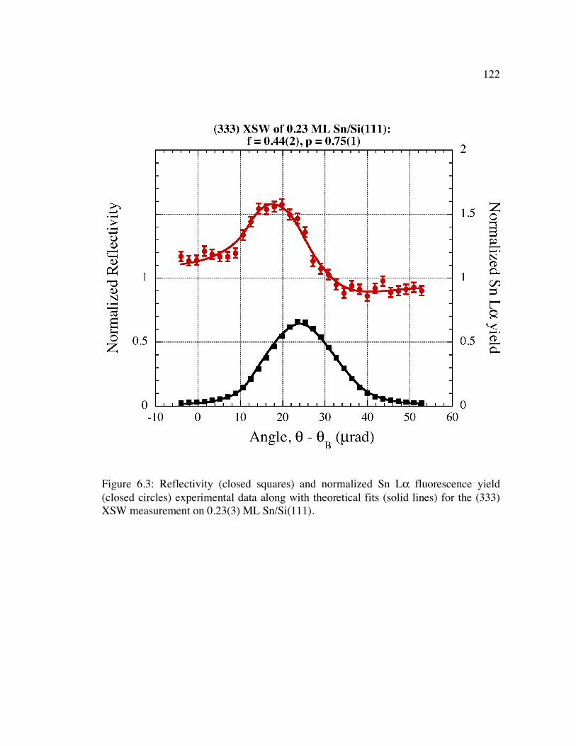
122
Figure 6.3: Reflectivity (closed squares) and normalized Sn Lα fluorescence yield (closed circles) experimental data along with theoretical fits (solid lines) for the (333) XSW measurement on 0.23(3) ML Sn/Si(111).
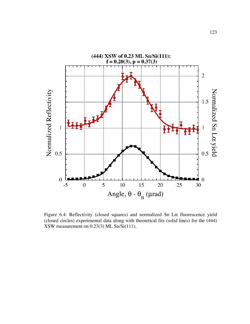
123
Figure 6.4: Reflectivity (closed squares) and normalized Sn Lα fluorescence yield (closed circles) experimental data along with theoretical fits (solid lines) for the (444) XSW measurement on 0.23(3) ML Sn/Si(111).
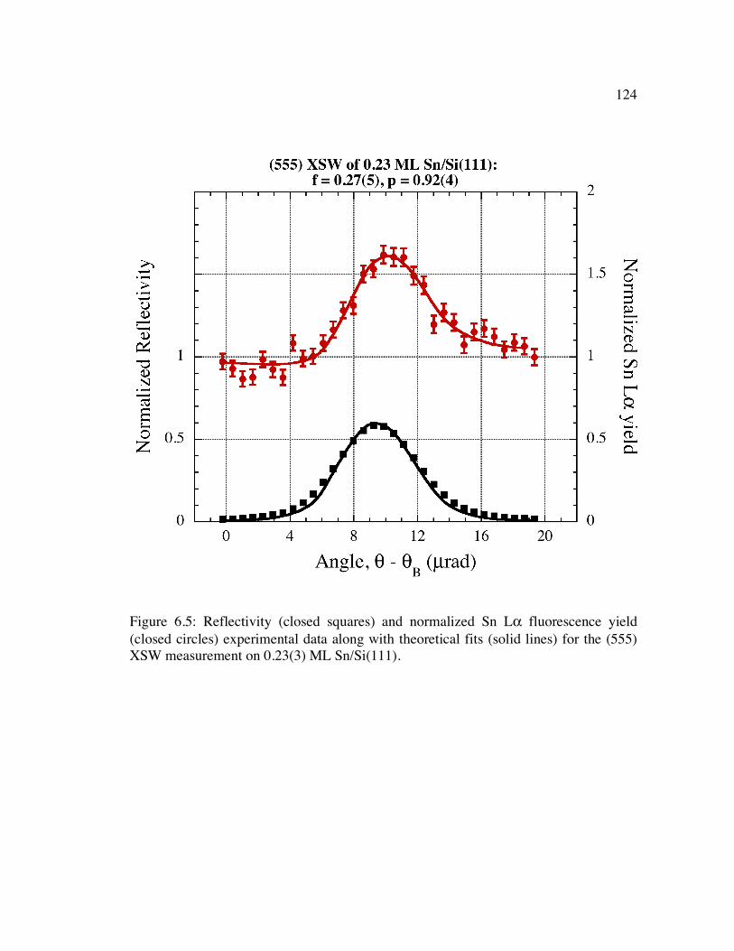
124
Figure 6.5: Reflectivity (closed squares) and normalized Sn Lα fluorescence yield (closed circles) experimental data along with theoretical fits (solid lines) for the (555) XSW measurement on 0.23(3) ML Sn/Si(111).
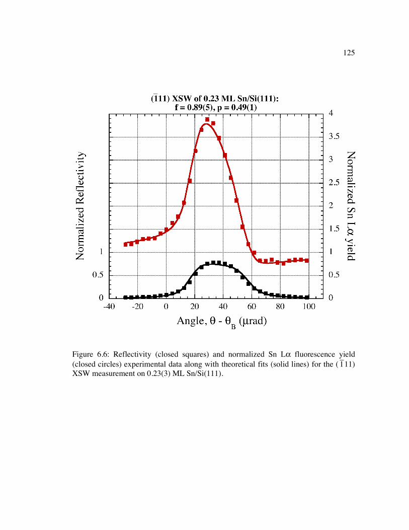
125
Figure 6.6: Reflectivity (closed squares) and normalized Sn Lα fluorescence yield (closed circles) experimental data along with theoretical fits (solid lines) for the (
�
1 11) XSW measurement on 0.23(3) ML Sn/Si(111).
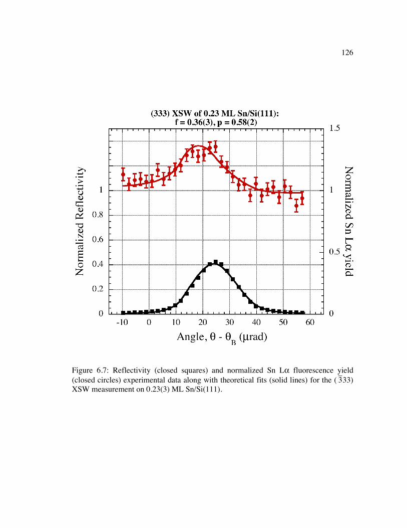
126
Figure 6.7: Reflectivity (closed squares) and normalized Sn Lα fluorescence yield (closed circles) experimental data along with theoretical fits (solid lines) for the (
�
3 33) XSW measurement on 0.23(3) ML Sn/Si(111).
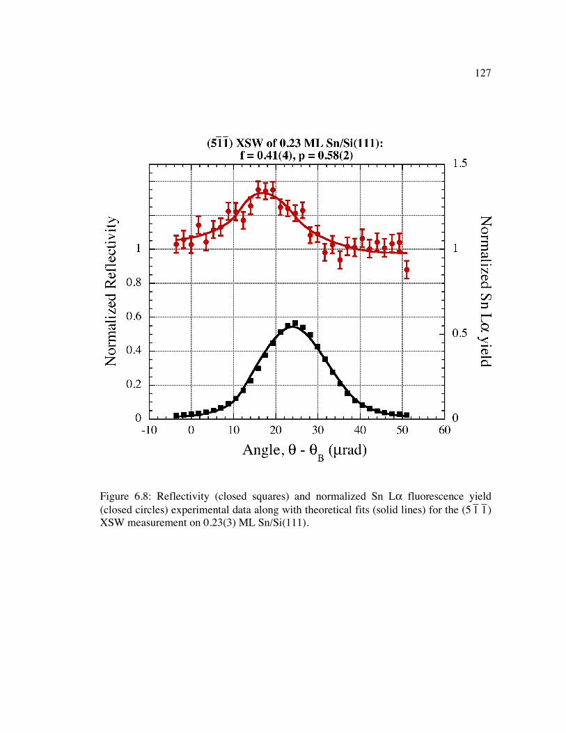
127
Figure 6.8: Reflectivity (closed squares) and normalized Sn Lα fluorescence yield (closed circles) experimental data along with theoretical fits (solid lines) for the (5
�
1
�
1 ) XSW measurement on 0.23(3) ML Sn/Si(111).
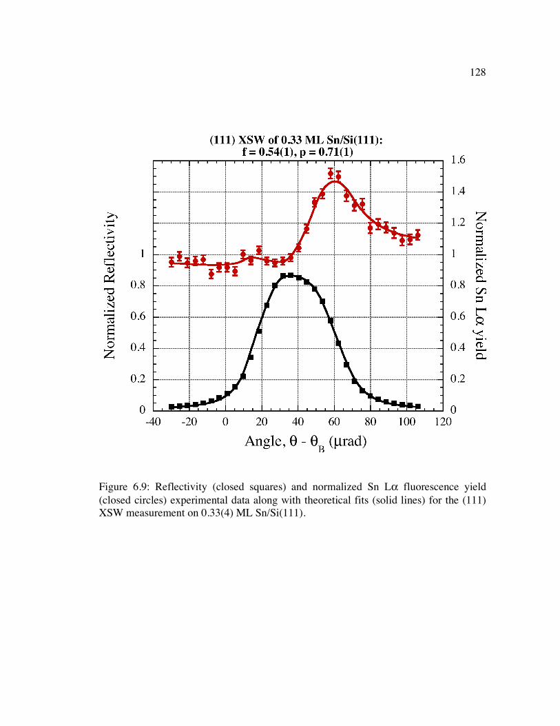
128
Figure 6.9: Reflectivity (closed squares) and normalized Sn Lα fluorescence yield (closed circles) experimental data along with theoretical fits (solid lines) for the (111) XSW measurement on 0.33(4) ML Sn/Si(111).
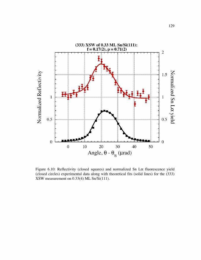
129
Figure 6.10: Reflectivity (closed squares) and normalized Sn Lα fluorescence yield (closed circles) experimental data along with theoretical fits (solid lines) for the (333) XSW measurement on 0.33(4) ML Sn/Si(111).
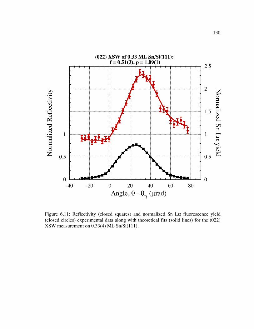
130
Figure 6.11: Reflectivity (closed squares) and normalized Sn Lα fluorescence yield (closed circles) experimental data along with theoretical fits (solid lines) for the (022) XSW measurement on 0.33(4) ML Sn/Si(111).
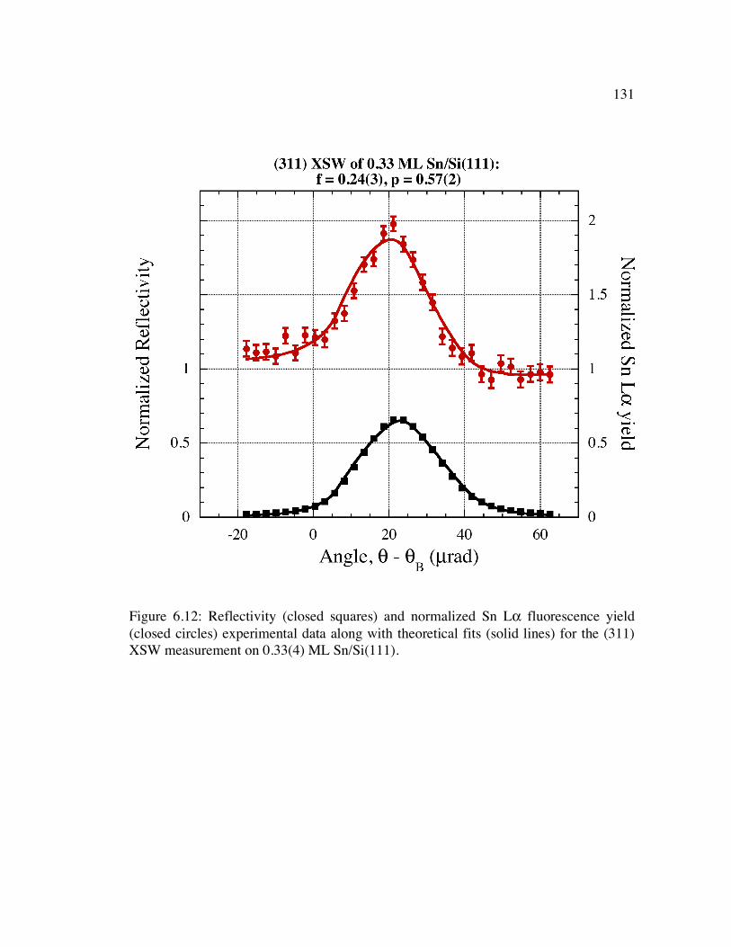
131
Figure 6.12: Reflectivity (closed squares) and normalized Sn Lα fluorescence yield (closed circles) experimental data along with theoretical fits (solid lines) for the (311) XSW measurement on 0.33(4) ML Sn/Si(111).
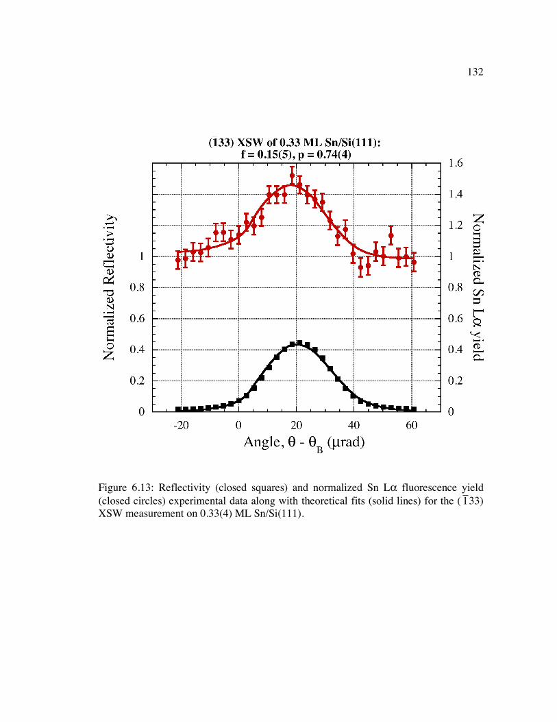
132
Figure 6.13: Reflectivity (closed squares) and normalized Sn Lα fluorescence yield (closed circles) experimental data along with theoretical fits (solid lines) for the (
�
1 33) XSW measurement on 0.33(4) ML Sn/Si(111).
133
6.3 Results and Discussion of the 1/3 ML Sn/Si(111)-√3 Surface
6.3.1 XSW direct space imaging of the 0.23 ML Sn/Si(111)-(√3x√3) surface
In Section 4.4.3, it was explained how a direct-space image of the atomic
density distribution for the fluorescent-selected atoms can be produced by a summation
of the available XSW-determined Fourier components. By measuring a sufficiently
complete set of Fourier coefficients, the collected XSW reciprocal-space data can be
Fourier-inverted to generate a three-dimensional density map that is specific to the
fluorescence-selected atoms and is independent of any presupposed structural model.
The direct-space Sn density distribution generated by the measured XSW
parameters from Table 6.1 is shown in Figure 6.14. The resolution limit of this method
corresponds to one-half of the smallest d-spacing measured, which in this case is d555/2
= 0.31 Å. The top view shown in Figure 6.14(a) shows the Sn density variations at a
height of 1.80 Å above the Si(111) surface (where the origin is chosen to be the top
atom of the bulk-like Si(111) bilayer). This view demonstrates the maximum Sn atom
density is centered at the T4 adsorption site, as expected. This is confirmed by the XSW
coherent position measurements agreeing with the relationships
�
P1 11
= (P111
+1)/ 3 and
�
P3 33
=(P333
+1) /3, which are the geometrical symmetry conditions for the occupation of
T4-adsorption sites on the Si(111) surface.
The side view shown in Figure 6.14(b) is a cross-sectional cut through the Sn
density distribution containing the long diagonal of the (1x1) surface unit cell. While
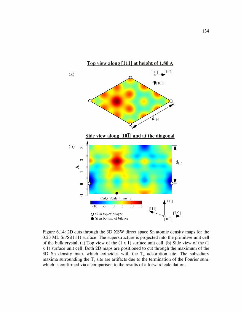
134
Figure 6.14: 2D cuts through the 3D XSW direct space Sn atomic density maps for the 0.23 ML Sn/Si(111) surface. The superstructure is projected into the primitive unit cell of the bulk crystal. (a) Top view of the (1 x 1) surface unit cell. (b) Side view of the (1 x 1) surface unit cell. Both 2D maps are positioned to cut through the maximum of the 3D Sn density map, which coincides with the T4 adsorption site. The subsidiary maxima surrounding the T4 site are artifacts due to the termination of the Fourier sum, which is confirmed via a comparison to the results of a forward calculation.
135
this view also shows the Sn occupies the T4-adsorption site, there is no obvious vertical
asymmetry or multiple density maxima, as would be expected for Sn adsorbed at
multiple heights. The subsidiary density maxima that also appear in the direct-space
image arise from the abrupt termination of the Fourier sum; this is confirmed by
comparing the direct-space images shown in Figure 6-14 with the atomic density maps
generated from the results of a forward calculation. In the forward calculation, a
structural model under consideration is used to calculate the coherent fractions and
positions for multiple sets of Bragg reflections. One set should encompass the set of
hkls used in the actual XSW experiment, while other sets should include additional
XSW data derived from a subset of the Fourier components that were not
experimentally acquired. These simulations then become the basis for a new Fourier
sum and XSW direct-space image, which can then be compared with the
experimentally-derived atomic density map. Therefore, this comparison helps answer
the question of whether the density fluctuations that are visible in the XSW direct-space
image are a result of the actual atomic-scale structure of the fluorescent-selected atoms
or if they are simply artifacts of the Fourier inversion process.
The presence of only a single Sn density maxima can be interpreted in one of
two ways: either the Sn is arranged in a flat, √3 structure as seen in STM images, or the
Sn is in a “rippled” configuration with a separation between the Sn adatoms that is
smaller than the 0.31 Å resolution of this XSW direct-space image. In order to
136
distinguish between these two possibilities, a comparison between the measured (hhh)
coherent positions can be made to obtain a qualitative sense of the vertical distribution
of the Sn atoms.
If the equilibrium state of the √3 surface is composed of Sn atoms at a single
height, the time-averaged distribution of Sn, as projected along the [111] direction is
symmetric, and it would be expected that the measured P111 and P333 would follow the
relationship P333 = Mod1[ 3P111 ]. However, if one compares the results from the (111)
and (333) XSW measurements, it can be seen that our measured value for P333 = 0.75 is
less than Mod1[3P111] = 3(0.61)-1 = 0.83, which demonstrates the Sn atomic distribution
is not consistent with the single height model suggested by earlier structural studies. In
fact, relating the measured (111) and (333) coherent positions demonstrates the time-
averaged projected Sn distribution is asymmetric and furthermore bottom-heavy. While
the additional (hhh) XSW parameters will help refine the details of this asymmetric
configuration, this simple comparison of two measurements immediately addresses the
primary question concerning the 1/3 ML Sn/Si(111) surface structure: whether or not
the RT Sn vertical distribution is flat or asymmetric. However, in order to precisely
determine the structural details of this asymmetric Sn distribution, an appropriate model
for the Sn/Si(111) surface can be employed to interpret the XSW results.
137
6.3.2 Conventional XSW analysis for the 0.23 ML Sn/Si(111) surface
While the XSW direct-space image of the 0.23 ML Sn/Si surface was not able
to definitively determine the source of the asymmetric Sn distribution, analyzing the
XSW data in a more conventional way may shed light on the geometric arrangement of
the Sn adatoms. When analyzing the available XSW data in a traditional manner, the
typical approach is to refer to a reasonable structural model, compare the
experimentally determined XSW parameters with the model-derived XSW parameters,
and use the results of the comparison to determine whether the model should be refined
or discarded in favor of a new structural model.
One model that can be used for reference was developed in the XSW
investigation of 1/3 ML Sn/Ge(111) discussed in Chapter 2 [19]. These XSW
measurements concluded that the Sn atoms are located at the T4-adsorption sites and
favored a “one up, two down” structure at both RT and at 115 K. These same
assumptions detailed in the earlier XSW study can also be used here: 1) one-third of the
ordered Sn is located at a height hA and the remaining two-thirds are at a height hB, 2)
the rms vibrational amplitudes <u2>1/2 along the [111] direction for all Sn atoms are
identical, and 3) some fraction of Sn (1 - C) is randomly distributed, while the
remaining fraction C is located at T4 sites. As the direct-space images in the previous
section show, this last assumption is a valid one.
138
In order to relate the measured amplitude (fH) and phase (PH) of the Hth Fourier
coefficient (FH ) to the model parameters, the following equation is used:
�
Fm = fmexp(2!iPm ) =
C[(1/3)exp(2!imhA /d111) + (2/3)exp(2!imhB /d111)]exp("2!2m
2u2/d111
2). (6.1)
In this equation, m refers to the order of the (hhh) reflection of interest (m = 1,3,4,5). A
global chi-squared minimization routine was used to integrate the four sets of XSW
data, account for the relative errors for each individual XSW measurement, and
calculate a set of model parameters. The fitting routine resulted in a structural model
made up of a “one up, two down” configuration, with the up position at hA = 2.04(5) Å
above the top of the Si bulk-like layer and the down position at hB = 1.78(3) Å. The
vibrational amplitude for the Sn atoms in the [111] direction was calculated to be
<u2>1/2 = 0.13(3) Å, while the Sn ordered fraction was C = 0.81(2). The reduced chi-
squared value for this fit was 1.98.
With the Sn adatoms arranged in the configuration detailed above, the resulting
Sn-Si bond length would be 3.01 Å for the top Sn atoms and 2.84 Å for the lower Sn
atoms assuming Si were located at bulk-like positions. These distances, which are 10-
17% larger than the sum of the Sn and Si covalent radii (2.58 Å), indicate a strong
possibility of substantial Si relaxations. An earlier surface x-ray diffraction (SXRD)
study of 1/3 ML Sn/Si(111)-√3 calculated that the adsorption of Sn produced
considerable atomic relaxations within the first six sublayers of the Si substrate [18].
139
Similar vertical Si displacements were determined in an electron standing wave (ESW)
structural study [25] and a theoretical full-potential linearized augmented plane wave
(FLAPW) study [26]. In the SXRD investigation, it was calculated that the Si atoms
within the first substrate layer experiences a lateral displacement of 0.211 Å towards
the Sn adatom. Incorporating these relaxations with the XSW-determined Sn time-
averaged distribution results in a more realistic estimate for the Sn-Si bond lengths
(from 3.01 Å to 2.86 Å for the upper Sn atoms and from 2.84 Å to 2.68 Å for the lower
Sn atoms).
Beyond providing a more realistic picture of the Sn bonding arrangement,
significant Si relaxations may have other consequences as well. The SXRD study
calculated a large strain energy of 2.29 eV per √3 surface unit cell due to the stretching
of Si bonds [18]. Some of this strain energy may be relieved by the substitution of Sn
from the adatom layer into the Si substrate. While this phenomena has not been directly
observed by STM images of Sn/Si(111), STM images have shown Si can substitute for
Sn atoms in the adatom layer [84]. Furthermore, small shifts of the Sn adatoms from
the T4 site were interpreted as the effect of substitutional Sn defects located in the first
two Si layers. In the following section, it will be demonstrated how this Sn substitution
phenomenon has been directly observed in the case of the XSW measurements of the
0.33 ML Sn/Si(111) surface.
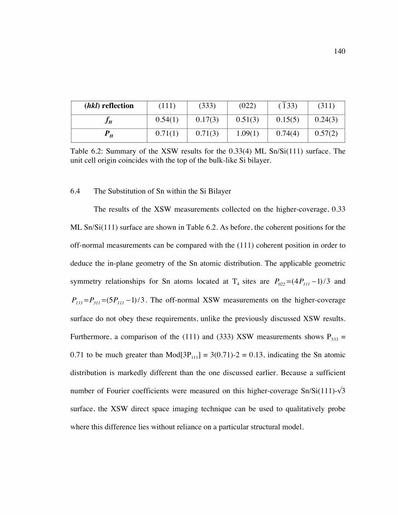
140
(hkl) reflection (111) (333) (022) (
�
1 33) (311)
fH 0.54(1) 0.17(3) 0.51(3) 0.15(5) 0.24(3)
PH 0.71(1) 0.71(3) 1.09(1) 0.74(4) 0.57(2)
Table 6.2: Summary of the XSW results for the 0.33(4) ML Sn/Si(111) surface. The unit cell origin coincides with the top of the bulk-like Si bilayer.
6.4 The Substitution of Sn within the Si Bilayer
The results of the XSW measurements collected on the higher-coverage, 0.33
ML Sn/Si(111) surface are shown in Table 6.2. As before, the coherent positions for the
off-normal measurements can be compared with the (111) coherent position in order to
deduce the in-plane geometry of the Sn atomic distribution. The applicable geometric
symmetry relationships for Sn atoms located at T4 sites are
�
P022
=(4P111
!1) /3 and
�
P133
=P311
=(5P111
!1) /3 . The off-normal XSW measurements on the higher-coverage
surface do not obey these requirements, unlike the previously discussed XSW results.
Furthermore, a comparison of the (111) and (333) XSW measurements shows P333 =
0.71 to be much greater than Mod[3P111] = 3(0.71)-2 = 0.13, indicating the Sn atomic
distribution is markedly different than the one discussed earlier. Because a sufficient
number of Fourier coefficients were measured on this higher-coverage Sn/Si(111)-√3
surface, the XSW direct space imaging technique can be used to qualitatively probe
where this difference lies without reliance on a particular structural model.
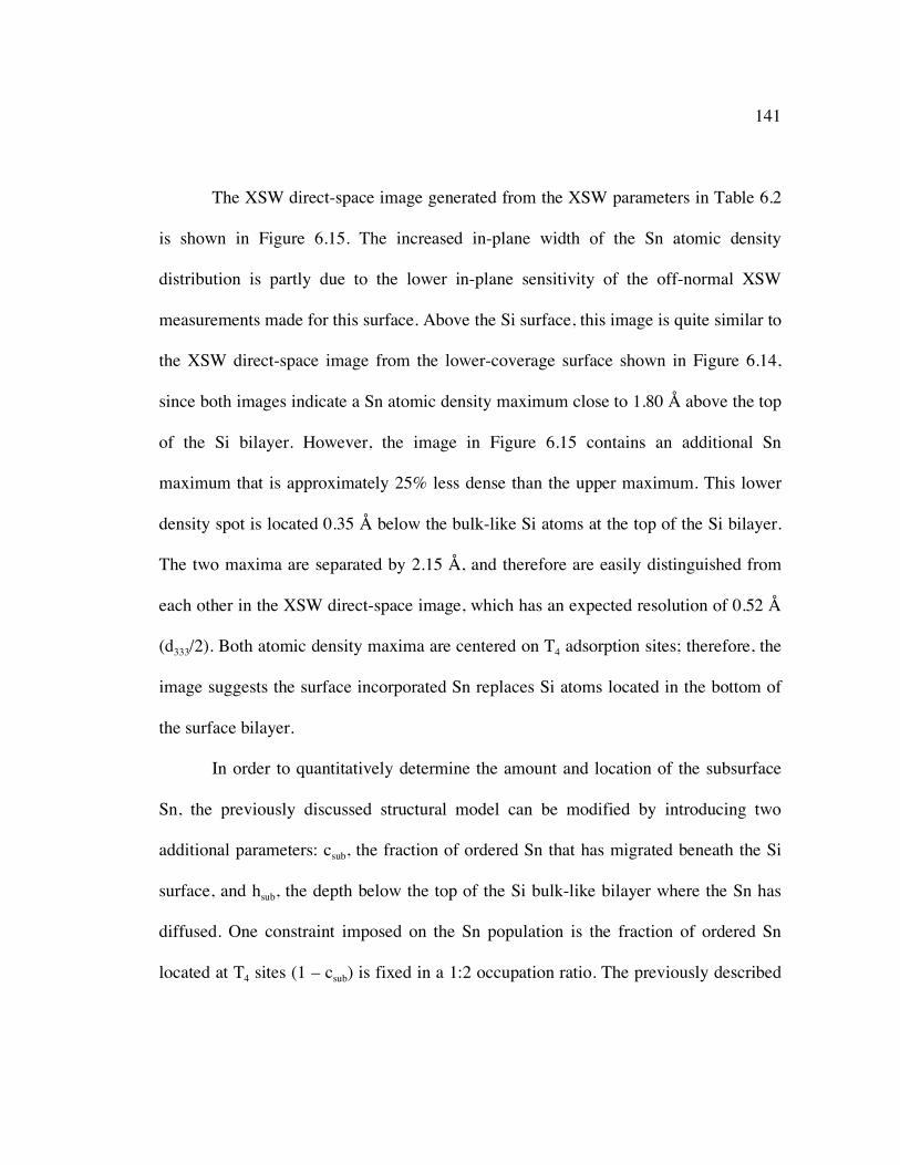
141
The XSW direct-space image generated from the XSW parameters in Table 6.2
is shown in Figure 6.15. The increased in-plane width of the Sn atomic density
distribution is partly due to the lower in-plane sensitivity of the off-normal XSW
measurements made for this surface. Above the Si surface, this image is quite similar to
the XSW direct-space image from the lower-coverage surface shown in Figure 6.14,
since both images indicate a Sn atomic density maximum close to 1.80 Å above the top
of the Si bilayer. However, the image in Figure 6.15 contains an additional Sn
maximum that is approximately 25% less dense than the upper maximum. This lower
density spot is located 0.35 Å below the bulk-like Si atoms at the top of the Si bilayer.
The two maxima are separated by 2.15 Å, and therefore are easily distinguished from
each other in the XSW direct-space image, which has an expected resolution of 0.52 Å
(d333/2). Both atomic density maxima are centered on T4 adsorption sites; therefore, the
image suggests the surface incorporated Sn replaces Si atoms located in the bottom of
the surface bilayer.
In order to quantitatively determine the amount and location of the subsurface
Sn, the previously discussed structural model can be modified by introducing two
additional parameters: csub, the fraction of ordered Sn that has migrated beneath the Si
surface, and hsub, the depth below the top of the Si bulk-like bilayer where the Sn has
diffused. One constraint imposed on the Sn population is the fraction of ordered Sn
located at T4 sites (1 – csub) is fixed in a 1:2 occupation ratio. The previously described
142
Figure 6.15: XSW direct space Sn atomic density image for the 0.33(4) ML Sn/Si(111)-√3 surface. While the majority of Sn appears adsorbed at the T4 site, a significant amount appears to occupy a third site directly below the T4 site within the Si surface. The other subsidiary maxima that are not located the subsurface site or T4 site are artifacts due to the termination of the Fourier sum, which is again confirmed via the results of a forward simulation.
143
minimization routine can then be applied to the following equation for the hhh Fourier
components:
�
Fm = fmexp(2!iPm ) = C " [[(1# csub )/3]exp(2!imhA /d111 ) + [2(1# csub )/3]"
exp(2!imhB /d111) + (csub )exp(2!imhsub /d111)]" exp(#2!2m
2u2/d111)
. (6.2)
When fitting this revised set of equations to the XSW data in Table 6.2, the heights hA
and hb as well as the thermal vibrational amplitude are fixed at the values determined
from the previously discussed calculation (hA = 2.04 Å, hB = 1.78 Å, <u2>1/2 = 0.13 Å).
After applying these constraints, the least-squares minimization routine returns a best-
fit in which 38% (±3%) of the ordered Sn is located 0.37(4) Å below the top of the Si
bulk-like surface. The fraction of Sn that is not randomly distributed is C = 0.81(4).
A similar analysis can be used to quantify the amount of subsurface Sn for the
0.23 ML Sn/Si(111) surface. Reevaluating the XSW data for this surface determined
only a small amount of Sn (6±3%) of the ordered Sn is located 0.5(1) Å below the ideal
Si surface. The inclusion of subsurface Sn in our surface model did not significantly
affect the other structural parameters. The reduced chi-squared value for this fit was
1.87.
6.5 Discussion of XSW Results
To further assess if the chosen structural model for the 0.23 ML Sn/Si surface is
reasonable, we can compare the measured Sn fluorescence yield modulation with
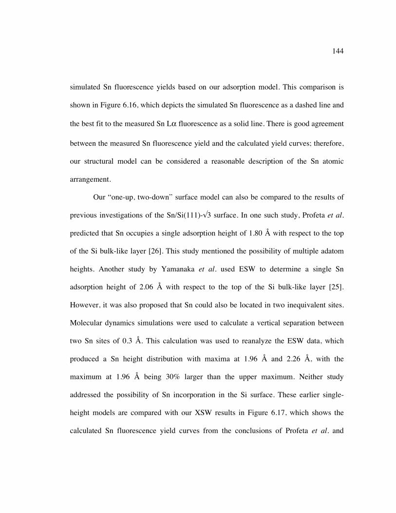
144
simulated Sn fluorescence yields based on our adsorption model. This comparison is
shown in Figure 6.16, which depicts the simulated Sn fluorescence as a dashed line and
the best fit to the measured Sn Lα fluorescence as a solid line. There is good agreement
between the measured Sn fluorescence yield and the calculated yield curves; therefore,
our structural model can be considered a reasonable description of the Sn atomic
arrangement.
Our “one-up, two-down” surface model can also be compared to the results of
previous investigations of the Sn/Si(111)-√3 surface. In one such study, Profeta et al.
predicted that Sn occupies a single adsorption height of 1.80 Å with respect to the top
of the Si bulk-like layer [26]. This study mentioned the possibility of multiple adatom
heights. Another study by Yamanaka et al. used ESW to determine a single Sn
adsorption height of 2.06 Å with respect to the top of the Si bulk-like layer [25].
However, it was also proposed that Sn could also be located in two inequivalent sites.
Molecular dynamics simulations were used to calculate a vertical separation between
two Sn sites of 0.3 Å. This calculation was used to reanalyze the ESW data, which
produced a Sn height distribution with maxima at 1.96 Å and 2.26 Å, with the
maximum at 1.96 Å being 30% larger than the upper maximum. Neither study
addressed the possibility of Sn incorporation in the Si surface. These earlier single-
height models are compared with our XSW results in Figure 6.17, which shows the
calculated Sn fluorescence yield curves from the conclusions of Profeta et al. and
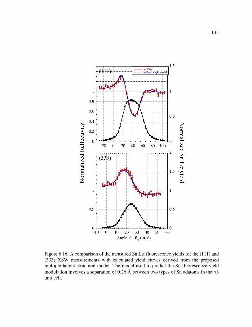
145
Figure 6.16: A comparison of the measured Sn Lα fluorescence yields for the (111) and (333) XSW measurements with calculated yield curves derived from the proposed multiple height structural model. The model used to predict the Sn fluorescence yield modulation involves a separation of 0.26 Å between two types of Sn adatoms in the √3 unit cell.
146
Figure 6.17: Another comparison of the measured Sn Lα fluorescence yields for the (111) and (333) XSW measurements with calculated yield curves derived from the results of Profeta et al. (dotted line), Yamanaka et al. (dot-dash line).
147
Yamanaka et al. as dashed and “dot-dash” lines, respectively. It is clear from this
comparison that our multiple-adsorption height model best matches the measured Sn
fluorescence yield from the 0.23 ML Sn/Si(111) surface.
It is also important to consider other possible explanations for the observed
vertical Sn asymmetry other than the dynamical fluctuations model. First and foremost,
we can consider the effect of the presence of defects in the Sn/Si(111) surface. In the
specific case of the low coverage surface, the most obvious defect is the amount of Sn
is smaller than the ideal 1/3 ML coverage. This raises the question of whether the
asymmetric height distribution observed by XSW is caused by this reduced coverage.
For Sn on Si(111), the √3 phase is stable over a wide coverage range (0.16 to 0.33 ML)
[85], unlike in the Sn on Ge case. This is because Si adatoms will occupy the T4 sites
that would be filled by Sn adatoms if the coverage was closer to 0.33 ML. Therefore,
instead of considering the effect of Sn surface vacancies on the observed Sn
distribution, it is more useful to consider the effect of Si adatoms located in T4 sites. A
recent angle-resolved photoemission study examined the effect of Sn coverage on the
electronic band structure of the SixSn(1-x)/Si(111) √3 phase [32]. It found that the
electronic structure is constant as a function of coverage in the 0.23-0.33 ML range,
signifying the dangling bonds of the intermixed Si adatoms behave similarly to the Sn
dangling bonds and there is no significant charge transfer between the two types of
atoms. This finding suggests the influence of neighboring Si adatoms on the Sn vertical
148
distribution is small, as least from an electronic standpoint.
6.6 Summary
It has been experimentally determined that Sn adatoms are arranged in a “one
up, two down” configuration, with one-third of the Sn at 2.04 Å above the top of the
ideal Si bilayer and two-thirds at 1.78 Å. This Sn distribution is similar to the atomic
distribution measured by XSW of the √3 phase and (3 x 3) phase of Sn/Ge(111). This
similarity supports a dynamical fluctuations model of the Sn/Si(111) surface, in which
Sn atoms move in a correlated fashion between two unique adsorption sites. This
atomic arrangement presents an underlying (3 x 3) structure, as expected from previous
core-level and valence-band photoemission studies and as observed in the isoelectronic
1/3 Sn/Ge(111) system. In a separate surface treatment, a higher initial coverage of Sn
was deposited on Si(111). The measured Sn XSW Fourier coefficients were used to
generate a model-independent 3D direct-space image, which unambiguously shows Sn
migrating below the Si(111) surface and substituting for Si in the bottom of the surface
bilayer.
149
Chapter 7: XSW Measurements of the 1/2 ML V/α-Fe2O3(0001) Surface
7.1 Sample Preparation
The sample treatments and XSW measurements for the 1/2 ML V/α-
Fe2O3(0001) system were conducted in the UHV chamber/diffractometer located at the
5ID-C surface science endstation detailed in Section 5.3.2. The α-Fe2O3(0001) samples
were purchased from Commercial Crystal Laboratories as a 1.0 mm thick polished
wafer. The <0001> orientation of the sample was confirmed using a Laue apparatus
and a four-circle x-ray diffractometer located at the Northwestern University X-ray
facility. Samples whose crystallographic orientation exhibited a large miscut angle with
respect to the sample surface were repolished to achieve a miscut less than 0.1°. After
degreasing the hematite surface, the samples were attached to molybdenum sample
platens (Thermionics, model # STLCP-1LR) via a set of molybdenum clips. The
sample platens support the hematite samples and allow the rear face of the samples to
be directly exposed to the manipulator filament for more efficient heating.
The clean α-Fe2O3(0001) surface was prepared by annealing the sample at 733
K for 1 hour under a stream of atomic oxygen, which is produced via an Oxford
Applied Research Universal Thermal Cracker (model TC50). The cracker consists of a
refractory capillary tube connected directly to a small vial of molecular oxygen. The O2
gas is dissociated as it flows through the cracker tube, which is heated by an electron
beam and water cooled to minimize outgassing. When used at its maximum power

150
rating (60 W), the ratio of atomic oxygen to molecular oxygen the oxygen source
produces is 1.5 as measured by a residual gas analyzer. The chamber pressure during
the production of atomic oxygen is maintained between 4.0 x 10⁻⁶ and 6.0 x 10⁻⁶ Torr
during the annealing process and as the sample was allowed to cool down to room
temperature. Because the capillary tube is directed toward the sample during the
oxygen annealing, the actual oxygen partial pressure close to the sample surface is
probably higher than the overall chamber pressure indicated by the ionization gauges.
The atomic oxygen treatment produced a clean, well-ordered surface that exhibits a
sharp (1x1) LEED pattern, as shown in Figure 7.1. The (1x1) surface is also expected to
be free of carbon impurities, since previous XPS measurements on a similarly prepared
surface detected no carbon contamination after a shorter period of oxygen annealing
(30 min vs. 1 hr).
Once the clean α-Fe2O3(0001) surface was achieved, the preparation of the
vanadium adlayer and its subsequent oxidation and reduction proceeded in three steps.
After each step, the newly prepared surface was characterized using LEED and XSW in
order to monitor the effect of each processing step on the atomic-scale structure. The
first step involved the evaporation of vanadium onto the clean hematite surface at room
temperature. The vanadium (99.9%, Goodfellow) was deposited using a high-
temperature Knudsen cell that was set at a temperature of 1820 K, which resulted in a
V deposition rate of 0.35 ML/minute. The sample surface was then oriented to be
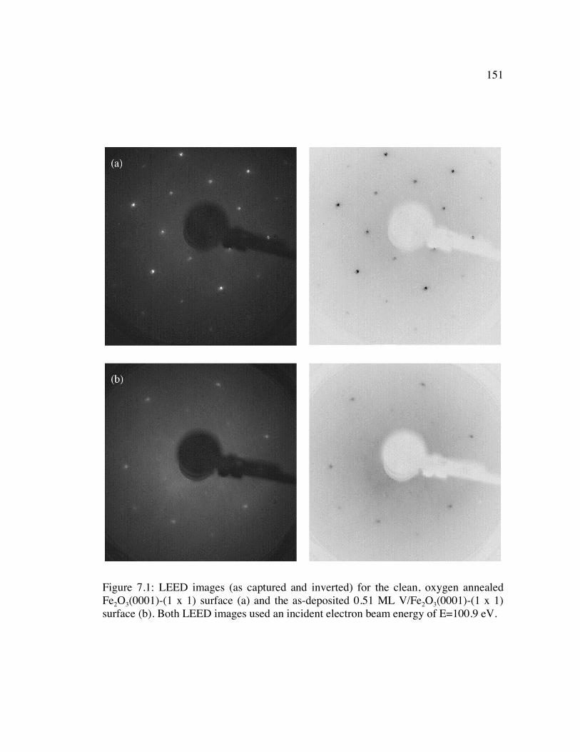
151
Figure 7.1: LEED images (as captured and inverted) for the clean, oxygen annealed Fe2O3(0001)-(1 x 1) surface (a) and the as-deposited 0.51 ML V/Fe2O3(0001)-(1 x 1) surface (b). Both LEED images used an incident electron beam energy of E=100.9 eV.
152
normal to the Knudsen cell and exposed to the vanadium flux by opening the Knudsen
cell shutter for a period of 88 seconds, resulting in a vanadium coverage of 0.51 ML on
the Fe2O3(0001) surface. The total coverage was determined by measuring the
vanadium coverage of a separate sample prepared under the same conditions using ex
situ Rutherford backscattering spectroscopy (RBS). The estimated error in the areal
density calculation is about 10% of the calculated value.
The LEED images of the as-deposited surface shown in Figure 7.1 demonstrate
the unreconstructed (1x1) symmetry of the clean Fe2O3(0001) surface has become
obscured by the adsorbed vanadium surface layer. The sharp (1x1) diffraction spots of
the clean surface have become noticeably weaker, and appear in front of a diffuse
background with no discernible superstructure. In comparison, vanadium has a similar
effect on the (1x1) LEED pattern of the clean Cr2O3(0001) surface when deposited on
the chromia surface [86], while in the investigations of the V/Al2O3(0001) surface,
there were no reports of LEED observations for the vanadium covered surface [86].
After conducting a set of XSW measurements for the as-deposited surface, the
submonolayer vanadium was oxidized by exposing the surface to atomic oxygen. In
preparing the vanadium oxide, the atomic oxygen source was operated at the same
power settings used for the oxygen cleaning, while the oxygen partial pressure was
maintained at 1.0 x 10⁻⁵ Torr. The vanadium surface was exposed to the atomic oxygen
flow for 85 minutes. The oxygen exposure was conducted at room temperature to avoid
153
the possible interdiffusion of vanadium into the hematite substrate. Attempts to
characterize the oxidized surface using LEED did not result in meaningful structural
information due to the extreme charging of the oxide adlayer. Therefore, the
experiment continued by conducting the same set of XSW measurements that were
collected for the as-deposited surface, so that a direct comparison could be made
between the vanadium and vanadium oxide surfaces.
After this second set of XSW data was collected, the vanadium surface was
modified a final time by an exposure to atomic hydrogen. Hydrogen was chosen in
order to reduce the vanadium oxide surface layer and therefore determine if the
recovery of the electronic structure is accompanied by a change in the geometric
structure. Atomic hydrogen was generated using the thermal cracker for a total of 60
minutes; during the first 15 minutes of the hydrogen exposure, the thermal cracker
power was set to 60 W, while for the final 45 minutes the power was increased to 67
W. The measured chamber pressure due to the influx of atomic hydrogen was 2.0 x 10⁻⁵
Torr. After allowing the chamber pressure to recover from the increased pressure, the
structure of the reduced vanadium oxide surface was again probed with XSW.
However, due to time constraints, it was not possible to obtain the entire set of XSW
measurements that was collected for the as-deposited and oxidized surface. Further
details on the XSW measurements conducted for each of the three distinct surfaces will
be given in the following section.
154
7.2 X-Ray Standing Wave Measurements
As previously mentioned, a specific set of XSW measurements was collected
after each of the three separate surface treatments. For the as-deposited vanadium and
the oxidized vanadium surfaces, the Fe2O3 (0006), (10
�
1 4), (01
�
1 2), and (11
�
2 3) Bragg
reflections were employed to probe the vanadium atomic distribution. However, for the
reduced vanadium surface exposed to atomic hydrogen, only the (0006) and (10
�
1 4)
XSW measurements could be obtained in the remaining time allotted for the
experiment.
Each XSW measurement proceeded by scanning the Fe2O3 single crystal
substrate through the desired hkl Bragg reflection and simultaneously collecting the
diffracted beam intensity and induced X-ray fluorescence spectra at each angular step
of the rocking curve. The incident beam energy of 7.00 keV was chosen in order to
prevent the excitation of a large Fe Kα fluorescence signal from the hematite substrate
and the UHV chamber walls. As mentioned in Chapter 5, a single Si(022) channel-cut
was used as the post-monochromator optic in order to maximize the x-ray flux incident
on the sample. The increase in intensity was required because small slit apertures
(typically 200 µm x 200 µm) were used to define the size of the incident beam, since
illuminating small areas of the sample would usually result in narrower rocking curves.
Another method that was used to improve the quality of the hematite rocking curve was
155
the use of an “x-ray eye” that was mounted on the detector arm. The x-ray eye was used
to visually inspect the diffracted beam profile, and by adjusting the sample position
laterally until the profile of the diffracted beam was as uniform as possible, the peak
reflectivity and rocking curve width would typically improve.
A typical example of the x-ray fluorescence spectra collected from the as-
deposited V/Fe2O3(0001) surface is shown in Figure 7.2(a). Ideally the fluorescence
signal of interest (in this case, the V Kα peak at 4949 eV) should be situated away from
other fluorescence lines present in the spectrum in order to facilitate the XSW analysis.
However, if there are impurities in or around the sample, this situation can be
impossible to achieve. In this case, the presence of Ti impurities gives rise to the Ti Kα
fluorescence peak with an energy of 4508 eV located to the left of the V Kα
fluorescence signal. Therefore, it can be expected that the V Kα peak would obscure
the presence of a Ti Kβ fluorescence peak that sits underneath the dominant V Kα
fluorescence signal. This is confirmed by examining the x-ray fluorescence spectrum of
the clean Fe2O3(0001) surface, which is shown in Figure 7.2(b). The spectrum clearly
shows the two emission lines characteristic of Ti K fluorescence, with the Ti Kβ yield
located only about 20 eV from the position of the V Kα yield peak. Therefore, the
contribution from the Ti impurities must be quantified and removed from the integrated
intensity of the V Kα fluorescence peak in order to determine the correct modulation in
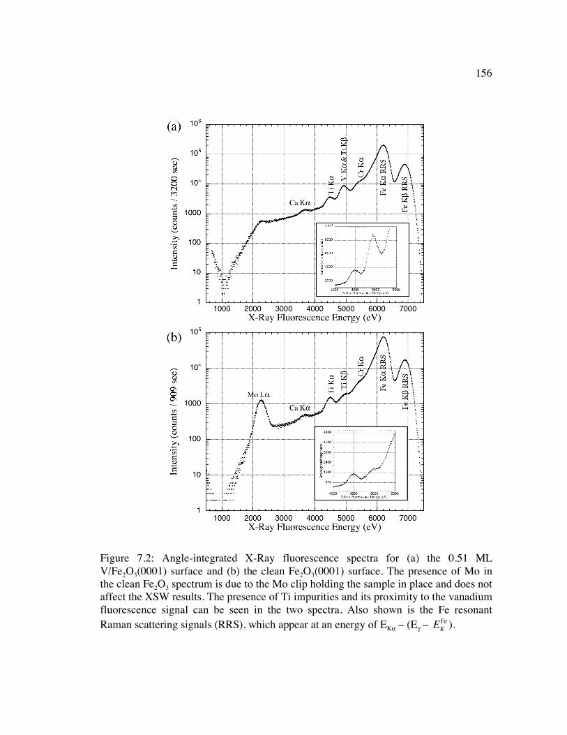
156
Figure 7.2: Angle-integrated X-Ray fluorescence spectra for (a) the 0.51 ML V/Fe2O3(0001) surface and (b) the clean Fe2O3(0001) surface. The presence of Mo in the clean Fe2O3 spectrum is due to the Mo clip holding the sample in place and does not affect the XSW results. The presence of Ti impurities and its proximity to the vanadium fluorescence signal can be seen in the two spectra. Also shown is the Fe resonant Raman scattering signals (RRS), which appear at an energy of EKα – (Eγ – E
K
Fe ).
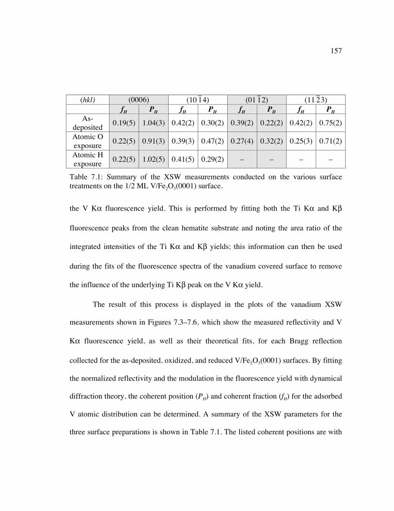
157
(hkl) (0006) (10
�
1 4) (01
�
1 2) (11
�
2 3) fH PH fH PH fH PH fH PH
As-deposited 0.19(5) 1.04(3) 0.42(2) 0.30(2) 0.39(2) 0.22(2) 0.42(2) 0.75(2)
Atomic O exposure 0.22(5) 0.91(3) 0.39(3) 0.47(2) 0.27(4) 0.32(2) 0.25(3) 0.71(2)
Atomic H exposure 0.22(5) 1.02(5) 0.41(5) 0.29(2) – – – –
Table 7.1: Summary of the XSW measurements conducted on the various surface treatments on the 1/2 ML V/Fe2O3(0001) surface. the V Kα fluorescence yield. This is performed by fitting both the Ti Kα and Kβ
fluorescence peaks from the clean hematite substrate and noting the area ratio of the
integrated intensities of the Ti Kα and Kβ yields; this information can then be used
during the fits of the fluorescence spectra of the vanadium covered surface to remove
the influence of the underlying Ti Kβ peak on the V Kα yield.
The result of this process is displayed in the plots of the vanadium XSW
measurements shown in Figures 7.3–7.6, which show the measured reflectivity and V
Kα fluorescence yield, as well as their theoretical fits, for each Bragg reflection
collected for the as-deposited, oxidized, and reduced V/Fe2O3(0001) surfaces. By fitting
the normalized reflectivity and the modulation in the fluorescence yield with dynamical
diffraction theory, the coherent position (PH) and coherent fraction (fH) for the adsorbed
V atomic distribution can be determined. A summary of the XSW parameters for the
three surface preparations is shown in Table 7.1. The listed coherent positions are with
158
respect to the unit cell depicted in Figure 3.1, where a Fe atom is located at the
fractional coordinates of (0.0, 0.0, 0.3553), while an O atom is located at the fractional
coordinates of (0.3059, 0.0, 0.25). Note the origin of the unit cell does not coincide
with any particular Fe or O atom.
7.3 Results and Discussion of the 1/2 ML V/Fe2O3(0001) System
7.3.1 General observations regarding XSW results
Unfortunately, as mentioned in Section 7.2, the surface exposed to atomic
hydrogen was not characterized with the full complement of Bragg reflections used for
the other two surfaces due to time constraints during the beamtime. However, if one
examines the two XSW datasets that are available for comparison, the modulation of
the V Kα fluorescence when scanning through the (0006) and (10
�
1 4) rocking curves
are qualitatively very similar. More importantly, the values for the coherent fraction
and position derived from these measurements are essentially the same. As a result, it is
reasonable to suggest that these two XSW measurements are representative of the same
vanadium surface structure. This hypothesis is supported by the XPS investigation
detailed in Section 3.6, which determined the electronic structure of the as-deposited
vanadium adlayer could be recovered after oxidation.
Therefore, there are two separate vanadium atomic distributions that will be
discussed: the as-deposited and reduced vanadium surface, and the oxidized vanadium
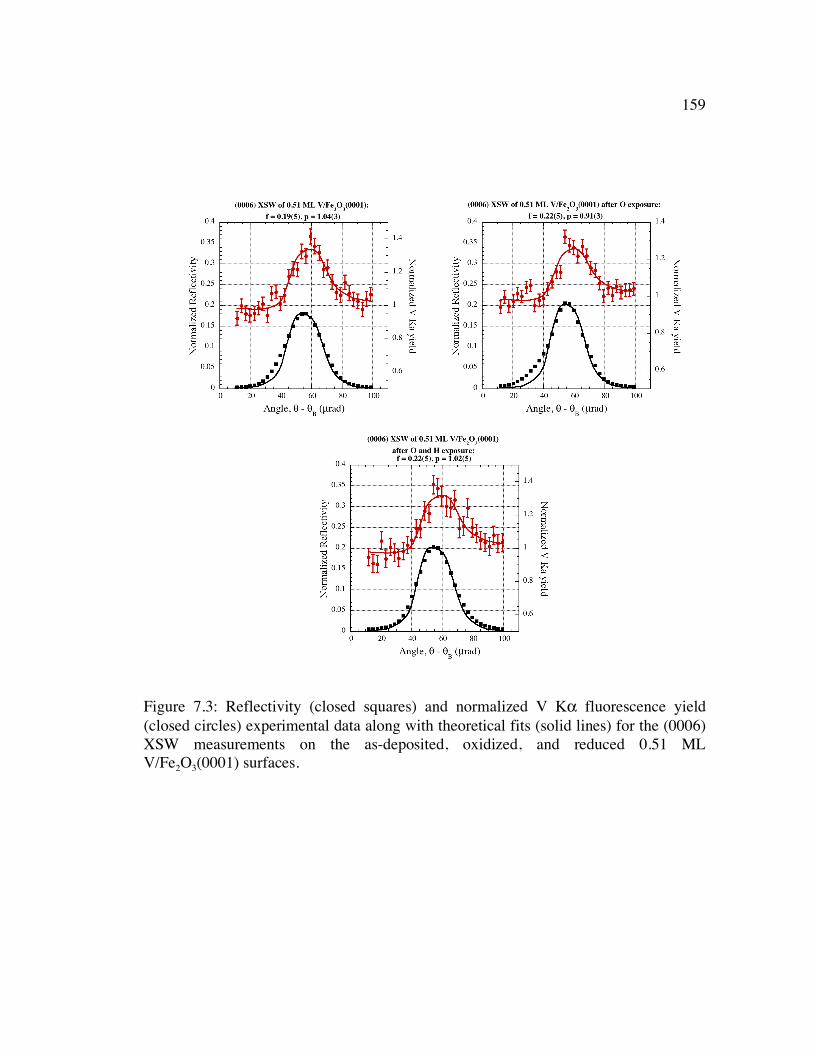
159
Figure 7.3: Reflectivity (closed squares) and normalized V Kα fluorescence yield (closed circles) experimental data along with theoretical fits (solid lines) for the (0006) XSW measurements on the as-deposited, oxidized, and reduced 0.51 ML V/Fe2O3(0001) surfaces.
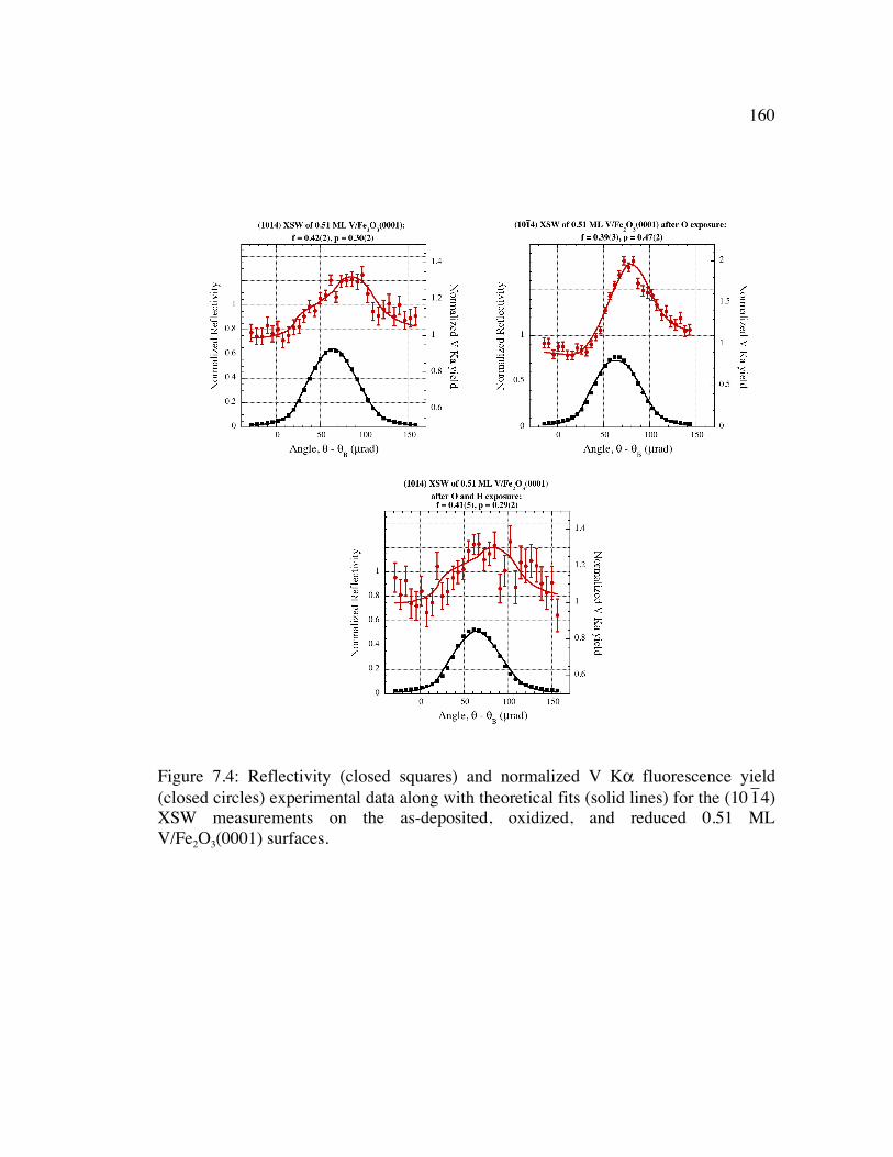
160
Figure 7.4: Reflectivity (closed squares) and normalized V Kα fluorescence yield (closed circles) experimental data along with theoretical fits (solid lines) for the (10
�
1 4) XSW measurements on the as-deposited, oxidized, and reduced 0.51 ML V/Fe2O3(0001) surfaces.
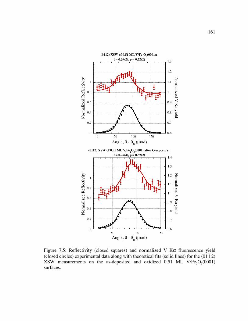
161
Figure 7.5: Reflectivity (closed squares) and normalized V Kα fluorescence yield (closed circles) experimental data along with theoretical fits (solid lines) for the (01
�
1 2) XSW measurements on the as-deposited and oxidized 0.51 ML V/Fe2O3(0001) surfaces.
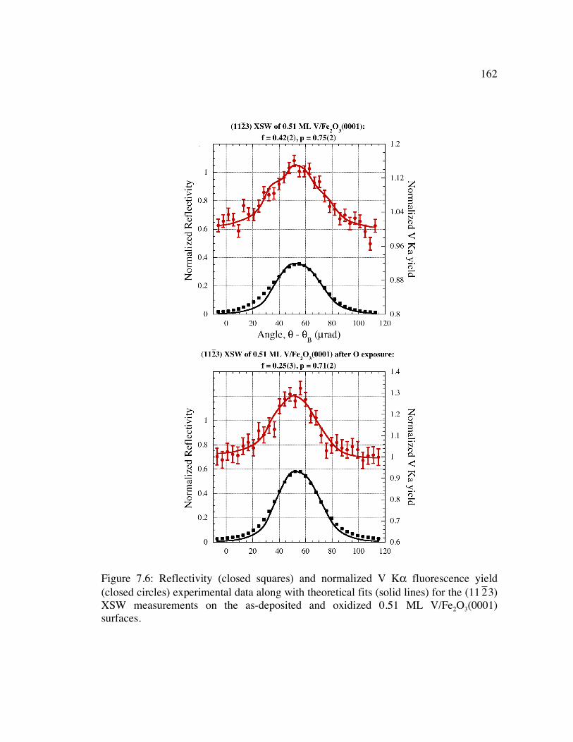
162
Figure 7.6: Reflectivity (closed squares) and normalized V Kα fluorescence yield (closed circles) experimental data along with theoretical fits (solid lines) for the (11
�
2 3) XSW measurements on the as-deposited and oxidized 0.51 ML V/Fe2O3(0001) surfaces.
163
surface. This distinction can be justified by simply comparing the shape of the
modulation of the V Kα fluorescence yields from the two different surface treatments.
When focusing solely on the results of the (0006) XSW measurements, it seems as if
the change in the V fluorescence yield modulation and the measured coherent fraction
from P0006 = 1.04(3) for the as-deposited vanadium surface to P0006 = 0.91(3) after
oxidation is small. This change in the coherent position corresponds to a reduction in
the height of the ordered vanadium atoms of 0.30 Å if the vanadium atoms were to
occupy a single unique adsorption site. However, when comparing the off-normal XSW
measurements obtained for the two surfaces, it is clear that there is a significant change
in the fluorescence yield modulation after the surface is oxidized. This marked change
in the V Kα yield points to a definitive shift in the measured coherent positions and the
lateral adsorption site arrangement as the vanadium is oxidized by the atomic oxygen
exposure.
As described in Section 4.4.2, it is possible that if the vanadium atoms are
located at a single atomic site, the collected normal and off-normal coherent positions
can be combined to triangulate the position of the vanadium atoms. However, the
measured coherent positions for the as-deposited surface do not definitively point at a
single unique adsorption site; while the off-normal coherent positions of
�
P01 1 2
= 0.22(2)
and
�
P10 1 4
= 0.30(2) for the as-deposited surface intersect at a location close to a bulk-
like oxygen position above the iron bilayer, this intersection point does not coincide
164
with the coherent position for the (0006) XSW measurement. The same is essentially
true for the oxidized surface, with the intersection of the off-normal coherent positions
of
�
P01 1 2
= 0.32(2) and
�
P10 1 4
= 0.47(2) shifted upward from the bulk-like oxygen position
by 0.6 Å. Although this triangulated position is somewhat closer to the normal coherent
position of P0006 = 0.91(3), the three XSW measurements still do not triangulate to a
unique three-dimensional atomic site.
It is possible that the low coherent fractions in the surface normal direction may
point to a significant amount of disorder in the vanadium spatial distribution; it is also
possible that the vanadium atoms may occupy multiple adsorption sites above the
hematite surface, which would partly explain the low coherent fractions observed for
the (0006) XSW measurements. However, it is unlikely that the vanadium cations are
incorporated within the close-packed plane of oxygen atoms by substituting for a
particular oxygen anion. This is because there is a large dissimilarity between the
electronic state of the oxygen anions that occupy these sites and the electronic state of
the adsorbed vanadium cations. It is difficult to imagine a scenario in which these
vanadium cations could be coordinated with neighboring Fe2+ or Fe3+ cations and form
a stable V/Fe2O3(0001) surface. However, the vanadium atoms could be located at
locations near the bulk-like oxygen atomic sites if one assumes the planes of iron and
oxygen atoms are displaced from their bulk-like positions due to the truncation of the
bulk atomic geometry by the surface. Such surface relaxations for the clean
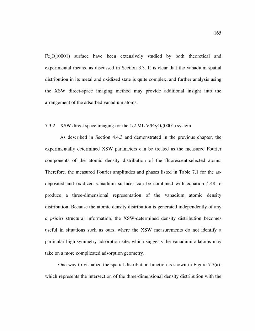
165
Fe2O3(0001) surface have been extensively studied by both theoretical and
experimental means, as discussed in Section 3.3. It is clear that the vanadium spatial
distribution in its metal and oxidized state is quite complex, and further analysis using
the XSW direct-space imaging method may provide additional insight into the
arrangement of the adsorbed vanadium atoms.
7.3.2 XSW direct space imaging for the 1/2 ML V/Fe2O3(0001) system
As described in Section 4.4.3 and demonstrated in the previous chapter, the
experimentally determined XSW parameters can be treated as the measured Fourier
components of the atomic density distribution of the fluorescent-selected atoms.
Therefore, the measured Fourier amplitudes and phases listed in Table 7.1 for the as-
deposited and oxidized vanadium surfaces can be combined with equation 4.48 to
produce a three-dimensional representation of the vanadium atomic density
distribution. Because the atomic density distribution is generated independently of any
a prioiri structural information, the XSW-determined density distribution becomes
useful in situations such as ours, where the XSW measurements do not identify a
particular high-symmetry adsorption site, which suggests the vanadium adatoms may
take on a more complicated adsorption geometry.
One way to visualize the spatial distribution function is shown in Figure 7.7(a),
which represents the intersection of the three-dimensional density distribution with the
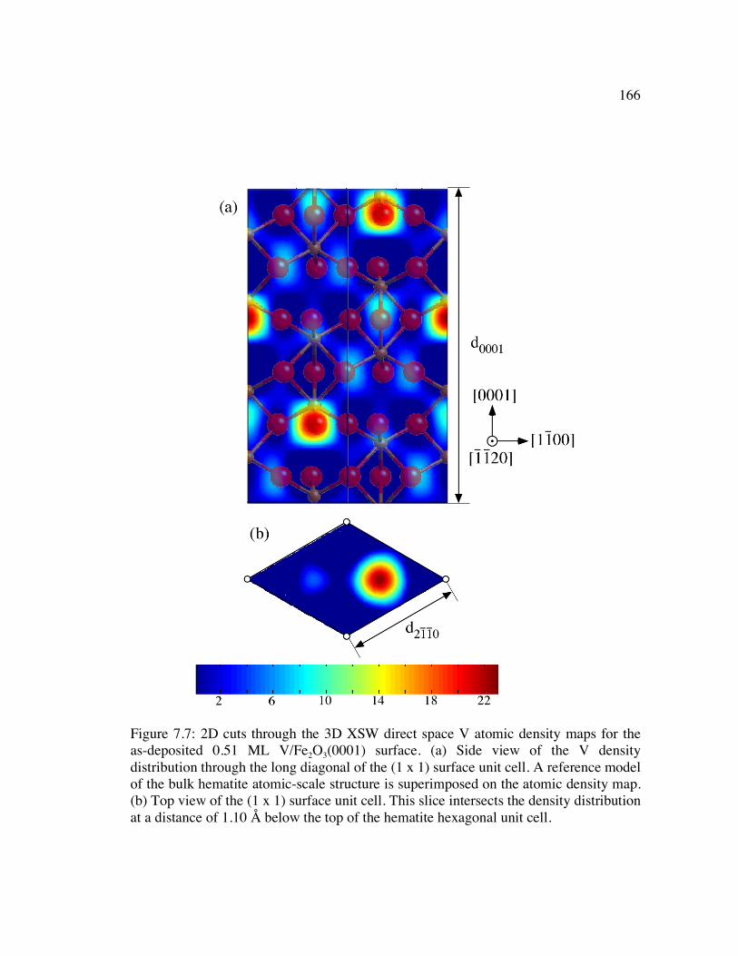
166
Figure 7.7: 2D cuts through the 3D XSW direct space V atomic density maps for the as-deposited 0.51 ML V/Fe2O3(0001) surface. (a) Side view of the V density distribution through the long diagonal of the (1 x 1) surface unit cell. A reference model of the bulk hematite atomic-scale structure is superimposed on the atomic density map. (b) Top view of the (1 x 1) surface unit cell. This slice intersects the density distribution at a distance of 1.10 Å below the top of the hematite hexagonal unit cell.
167
Figure 7.8: 2D cuts through the 3D XSW direct space V atomic density maps for the oxidized 0.51 ML V/Fe2O3(0001) surface. (a) Side view of the V density distribution through the long diagonal of the (1 x 1) surface unit cell. The lower section of the density distribution is reproduced and translated to the top part of the cross sectional cut to emphasize the location of the secondary V occupation site. (b) Top view of the (1 x 1) surface unit cell. This slice intersects the density distribution through the center of the secondary density maxima, which appears at a distance of 2.24 Å above the top of the hematite hexagonal unit cell.
168
(11
�
2 0) plane of the hexagonal Fe2O3 unit cell. Because the density map of both the as-
deposited and oxidized surfaces employ the same Bragg reflections to generate the
Fourier sum, the spatial resolution of each of the direct-space atomic density plots is the
same and is equal to one-half of the smallest d-spacing measured (
�
d112 3
= 1.10 Å). The
bulk Fe and O atomic positions are shown on the density map as a ball-and-stick model
overlaid on the direct-space image. It should also be noted that because the Fourier
components used to generate the density function are limited to that of the substrate
Bragg reflections, the image represents a projection of the distribution function into the
primitive unit cell of the hematite crystal. Furthermore, because the Fourier sum must
necessarily include only a finite number of terms, the premature truncation of the
Fourier sum will be seen in the direct-space image as spurious density maxima. This
was confirmed by generating the types of forward simulation density maps outlined in
Section 6.3.1.
Figure 7.7(b) also shows another cross-sectional slice that coincides with the
vanadium atomic density maximum, which appears at a distance of 1.10 Å from the top
of the hematite unit cell. As the two views demonstrate, the adsorbed vanadium appears
to occupy a single atomic position that lies within the basal plane of close-packed
oxygen atoms, as suggested by the partial triangulation of XSW measurements. While
several density maxima appear in the side view, each of the vanadium maxima are
symmetrically equivalent to one another and should not be interpreted as the presence
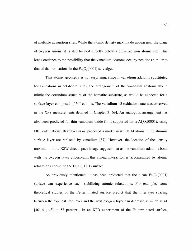
169
of multiple adsorption sites. While the atomic density maxima do appear near the plane
of oxygen anions, it is also located directly below a bulk-like iron atomic site. This
lends credence to the possibility that the vanadium adatoms occupy positions similar to
that of the iron cations in the Fe2O3(0001) selvedge.
This atomic geometry is not surprising, since if vanadium adatoms substituted
for Fe cations in octahedral sites, the arrangement of the vanadium adatoms would
mimic the corundum structure of the hematite substrate, as would be expected for a
surface layer composed of V3+ cations. The vanadium +3 oxidation state was observed
in the XPS measurements detailed in Chapter 3 [69]. An analogous arrangement has
also been predicted for thin vanadium oxide films supported on α-Al2O3(0001); using
DFT calculations, Brázdová et al. proposed a model in which Al atoms in the alumina
surface layer are replaced by vanadium [87]. However, the location of the density
maximum in the XSW direct-space image suggests that as the vanadium adatoms bond
with the oxygen layer underneath, this strong interaction is accompanied by atomic
relaxations normal to the Fe2O3(0001) surface.
As previously mentioned, it has been predicted that the clean Fe2O3(0001)
surface can experience such stabilizing atomic relaxations. For example, some
theoretical studies of the Fe-terminated surface predict that the interlayer spacing
between the topmost iron layer and the next oxygen layer can decrease as much as 41
[40, 41, 43] to 57 percent. In an XPD experiment of the Fe-terminated surface,
170
Thevuthasan et al. measured interlayer relaxations that are consistent with those
predicted by theory [46]. The deposition of vanadium on the hematite surface may
result in more extensive atomic relaxations, since the high oxygen affinity of vanadium
may induce the migration of lattice oxygen near the surface layer the hematite towards
the adsorbed vanadium. It has also been demonstrated that the adsorption of vanadium
induces a reduction of the hematite substrate, producing a mix of Fe2+ and Fe3+ cations
at the Fe2O3(0001) surface [69]. It is reasonable that such changes would only further
the extent of any structural deviations of the surface from the bulk Fe2O3 arrangement
(as compared to the clean Fe2O3(0001) atomic geometry). Unfortunately, the XSW
technique as described here is unable to provide any information regarding the structure
of Fe–O3–Fe–Fe layers that make up the selvedge, so we are unable to quantify any
surface relaxations in the iron or oxygen layers due to the adsorption of vanadium.
However, judging from the position of the vanadium density maximum in the direct-
space image, it is reasonable to suggest that any resulting surface relaxations
experienced by the as-deposited surface would be similar to those predicted for the
clean hematite surface.
7.3.3 XSW direct space imaging for the oxidized V/Fe2O3(0001) system
Turning now to the oxidized surface, when the analogous direct-space density
maps are generated the vanadium atomic distribution exhibits a significant change. As
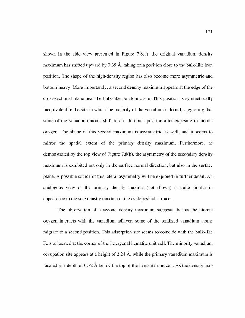
171
shown in the side view presented in Figure 7.8(a), the original vanadium density
maximum has shifted upward by 0.39 Å, taking on a position close to the bulk-like iron
position. The shape of the high-density region has also become more asymmetric and
bottom-heavy. More importantly, a second density maximum appears at the edge of the
cross-sectional plane near the bulk-like Fe atomic site. This position is symmetrically
inequivalent to the site in which the majority of the vanadium is found, suggesting that
some of the vanadium atoms shift to an additional position after exposure to atomic
oxygen. The shape of this second maximum is asymmetric as well, and it seems to
mirror the spatial extent of the primary density maximum. Furthermore, as
demonstrated by the top view of Figure 7.8(b), the asymmetry of the secondary density
maximum is exhibited not only in the surface normal direction, but also in the surface
plane. A possible source of this lateral asymmetry will be explored in further detail. An
analogous view of the primary density maxima (not shown) is quite similar in
appearance to the sole density maxima of the as-deposited surface.
The observation of a second density maximum suggests that as the atomic
oxygen interacts with the vanadium adlayer, some of the oxidized vanadium atoms
migrate to a second position. This adsorption site seems to coincide with the bulk-like
Fe site located at the corner of the hexagonal hematite unit cell. The minority vanadium
occupation site appears at a height of 2.24 Å, while the primary vanadium maximum is
located at a depth of 0.72 Å below the top of the hematite unit cell. As the density map
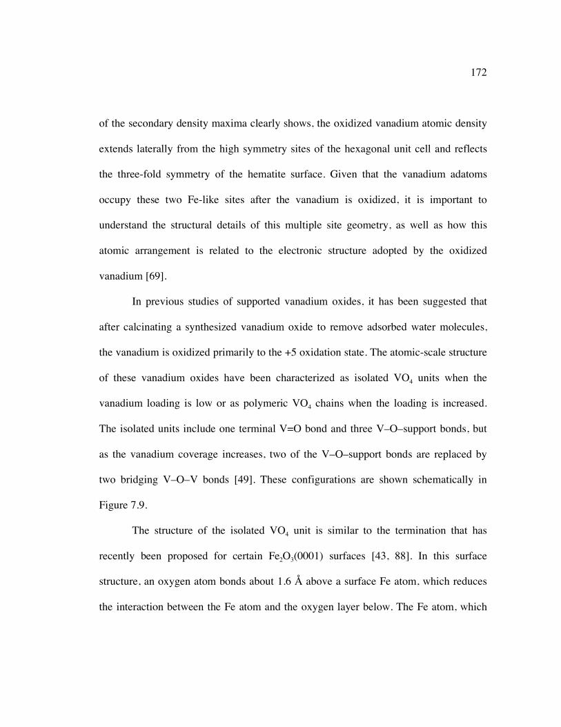
172
of the secondary density maxima clearly shows, the oxidized vanadium atomic density
extends laterally from the high symmetry sites of the hexagonal unit cell and reflects
the three-fold symmetry of the hematite surface. Given that the vanadium adatoms
occupy these two Fe-like sites after the vanadium is oxidized, it is important to
understand the structural details of this multiple site geometry, as well as how this
atomic arrangement is related to the electronic structure adopted by the oxidized
vanadium [69].
In previous studies of supported vanadium oxides, it has been suggested that
after calcinating a synthesized vanadium oxide to remove adsorbed water molecules,
the vanadium is oxidized primarily to the +5 oxidation state. The atomic-scale structure
of these vanadium oxides have been characterized as isolated VO4 units when the
vanadium loading is low or as polymeric VO4 chains when the loading is increased.
The isolated units include one terminal V=O bond and three V–O–support bonds, but
as the vanadium coverage increases, two of the V–O–support bonds are replaced by
two bridging V–O–V bonds [49]. These configurations are shown schematically in
Figure 7.9.
The structure of the isolated VO4 unit is similar to the termination that has
recently been proposed for certain Fe2O3(0001) surfaces [43, 88]. In this surface
structure, an oxygen atom bonds about 1.6 Å above a surface Fe atom, which reduces
the interaction between the Fe atom and the oxygen layer below. The Fe atom, which
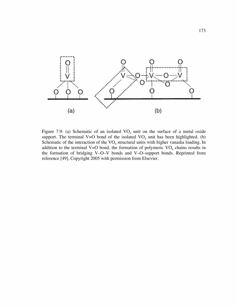
173
Figure 7.9: (a) Schematic of an isolated VO4 unit on the surface of a metal oxide support. The terminal V=O bond of the isolated VO4 unit has been highlighted. (b) Schematic of the interaction of the VO4 structural units with higher vanadia loading. In addition to the terminal V=O bond, the formation of polymeric VO4 chains results in the formation of bridging V–O–V bonds and V–O–support bonds. Reprinted from reference [49], Copyright 2005 with permission from Elsevier.
174
has a formal oxidation state of +5, is tetrahedrally coordinated with the underlying
oxygen layer and the sole oxygen atom directly above. This ferryl (Fe=O) termination
was predicted to be stable under high oxygen chemical potentials using density
functional theory calculations [43], and was directly observed using STM and infrared
reflection absorption spectroscopy (IRAS) [88]. Therefore, the structural similarity
between the vanadium pentaoxide in the VO4 state and the ferryl termination of the α-
Fe2O3(0001) surface would seem to suggest the vanadium adatoms observed in this
study have a similar oxygen coordination. Furthermore, it provides a natural
explanation for the upward shift experienced by a majority of the adsorbed vanadium.
The presence of the minority vanadium adsorption site may also be understood
in terms of these VO4 structural units and how they interact with each other. Because of
the low vanadium coverage involved in this experiment (0.51 ML), it is not surprising
that the majority of the adsorbed vanadium would adopt an atomic arrangement similar
to that of the isolated VO4 units. Because the vanadium coverage may not constitute a
continuous adlayer on the surface, it is reasonable to believe most of the vanadium will
be widely dispersed on the hematite surface, and therefore the VO4 units will not
interact with each other. However, other areas of the surface may have an increased
vanadium areal density, and there will be a greater likelihood that the VO4 units will
interact and bond with each other.
175
As previously mentioned, the interaction of these isolated vanadia units on
various oxide surfaces can result in other types of chemical bonding, namely the
formation of dimeric and polymeric chains of the VO4 molecules. With the formation
of these polymerized species on the oxide surface, it is possible that the vanadium
adatoms may rearrange and take up other atomic positions, such as the minority
vanadium occupation site visualized in the XSW direct-space image. Therefore, it may
be reasonable to incorporate these polymeric vanadium oxides in any structural models
that account for the secondary vanadium position. In addition, because these polymeric
vanadia units typically possess bridging V–O–V bonds, the presence of these bridging
bonds may be an important component of any proposed surface model.
One such example that includes these two attributes is shown in Figure 7.10,
which proposes how the interaction of three neighboring VO4 units can form three
bridging V–O–V bonds. The vanadium adatom common to these three bonds is located
in the secondary adsorption site, and possesses the same tetrahedral oxygen
coordination as the isolated VO4 units with the bonding of an on-top oxygen anion. The
V–O–V bridging bonds also reflect the spatial breadth of the secondary vanadium
density maxima, which is shown in Figure 7.8 as extending towards the primary
adsorption site in the same direction as the bridging bonds depicted in Figure 7.10. It
must be noted that it has been assumed that the bridging bonds described here are
derived from the terminal V=O bond between the oxidized vanadium and the on-top
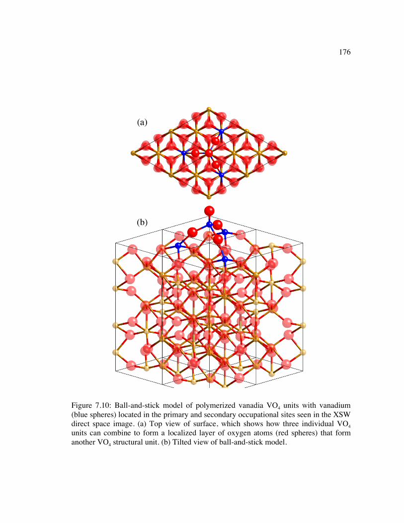
176
Figure 7.10: Ball-and-stick model of polymerized vanadia VO4 units with vanadium (blue spheres) located in the primary and secondary occupational sites seen in the XSW direct space image. (a) Top view of surface, which shows how three individual VO4 units can combine to form a localized layer of oxygen atoms (red spheres) that form another VO4 structural unit. (b) Tilted view of ball-and-stick model.
177
oxygen atom. Therefore, the small fraction of VO4 units that polymerize and adopt this
proposed bonding arrangement may have a different electronic configuration than the
isolated VO4 units that make up a majority of the vanadium distribution. For instance,
while the previous XPS measurements previously described suggest the oxidized
vanadium has a +5 oxidation state, the polymerized vanadia units may deviate from this
formal oxidation state.
Another alternative to this scenario a surface model consisting of vanadium
adatoms that coexist with Fe atoms in the adlayer, which has a similar structure to the
complete bulk-like Fe bilayer. This bilayer of 1/2 vanadium atoms and 1/2 iron atoms is
then terminated by a layer of oxygen atoms, which essentially reproduces the bulk-like
hematite structure. Another vanadium oxide VO4 structural unit can then be situated on
top of this oxygen terminated surface, thereby populating the minority adsorption site
seen in the direct-space image. Because the oxidized vanadium was observed to consist
of V5+ cations, if the vanadium adatoms are arranged such that they extend the bulk-like
crystal structure, their configuration may have a parallel in the distorted octahedral
coordination that describes the structure of crystalline V2O5. Such VO6 units have been
observed in supported vanadium oxides with very high vanadia loadings [49].
However, because the VO6 units that comprise this surface model coexist with the
octahedrally coordinated Fe3+ cations, this surface model is quite complex, and further
investigations on the potential stability of such a surface are required.
178
7.4 Summary
The atomic-scale structure of submonolayer vanadium and vanadium oxides
adsorbed on the α-Fe2O3(0001) surface has been experimentally determined using the
XSW direct-space imaging method. The XSW results clearly indicate there is a
reversible change in the vanadium atomic distribution as the vanadium is oxidized and
reduced in a cyclic catalytic process involving atomic oxygen and atomic hydrogen. In
order to provide further structural details of the as-deposited and oxidized vanadium
surfaces, XSW direct-space images were generated of the two distinct surfaces. The
XSW direct-space image of the as-deposited surface suggest the V3+ cations adopt Fe
bulk-like positions on the hematite surface and continue the corundum structure of the
hematite substrate. The adsorption of vanadium on the clean Fe2O3(0001) surface may
also be accompanied by surface relaxations of the iron or oxygen atomic layers. After
oxidizing the adsorbed vanadium, direct-space images suggest there is a vertical shift of
0.39 Å in the vanadium spatial distribution as the vanadium cations in their +5
oxidation state become arranged in VO4 structural units. A secondary vanadium
occupational site also is apparent from the direct-space image. While the VO4 units are
typically isolated from one another at low vanadium coverages, the observed minority
site may be the result of the VO4 structural units interacting with each other and
forming polymeric chains.
179
Chapter 8: Summary and Future Work
8.1 Thesis Summary
The primary motivation for the work detailed in this dissertation is the structural
characterization of two very different material systems using the XSW technique and
the XSW direct-space imaging method. These two surfaces, the 1/3 ML Sn/Si(111)-(√3
x √3)R30° and the 1/2 ML V/Fe2O3(0001) system, have very different electronic,
structural, and physical properties, yet it is a testament to the flexibility of the XSW
technique that we can successfully probe these two disparate surfaces. More
specifically, we have demonstrated the usefulness of the model-independent XSW
direct-space imaging method, especially in cases where traditional XSW analysis fails
to determine a particular adsorption geometry.
In our study of the 1/3 ML Sn/Si(111) √3 surface, it was demonstrated that by
using the XSW technique to collect a number of Fourier components of the Sn atomic
density distribution, we can determine the atomic scale structure of the room
temperature Sn adatom distribution. Most of the XSW measurements were collected
along the surface normal direction in order to address the question of whether the Sn
adatoms are arranged in a single-layer, as suggested by other structural studies, or in a
rippled configuration, as predicted by a dynamical fluctuations model. Direct-space
atomic density maps generated from the normal and off-normal XSW data confirmed
the Sn adatoms are located at T4 adsorption sites. By applying a reasonable structural
model to these (hhh) XSW measurements, it was determined that Sn adatoms are
180
configured in a “one up and two down” geometry, with the two types of Sn separated
by 0.26 Å. This lends support to the behavior predicted by the dynamical fluctuations
model, which concludes the √3 symmetry observed by other structural investigations is
actually the effect of thermal fluctuations, which obscures the actual (3 x 3) symmetry
of the ground state.
The XSW measurements conducted on another Sn/Si(111) surface preparation
were not consistent with a surface structure made up of Sn adatoms located at the T4
adsorption sites. However, by generating the Sn atomic density distribution from the
XSW-determined Fourier components, the direct-space image clearly explained this
discrepancy by showing that while most of the Sn adatoms were present at the T4 sites,
some of the Sn had migrated to a second occupational site below the Si substrate. By
modifying the previously discussed structural model to account for the subsurface Sn, it
was determined that the additional Sn atoms are located 0.37 Å below the top of the Si
bulk-like surface and substitute for Si atoms located in the bottom of the surface
bilayer.
In the XSW investigation of the 1/2 ML V/Fe2O3(0001) surface, the focus was
on determining how the surface structure of the adsorbed vanadium is affected by the
presence of oxidizing and reducing agents, such as atomic oxygen and atomic
hydrogen. Recent XPS measurements have demonstrated how the electronic structures
of both the vanadium adlayer and the hematite substrate are modified by the exposure
181
to atomic oxygen and restored with a subsequent exposure to atomic hydrogen. The
results of our XSW measurements have demonstrated how these electronic changes are
accompanied by significant changes in the geometry of the vanadium atomic
distribution.
By comparing the acquired XSW data for the as-deposited, oxidized, and
reduced vanadium surfaces, it becomes obvious that there is a shift in the vanadium
adsorption geometry after exposing the vanadium adlayer to oxygen. Furthermore, the
structure of the oxidized vanadium distribution then reverts to that of the as-deposited
surface after being exposed to atomic hydrogen. By generating XSW real-space density
maps using the collected Fourier coefficients, the vanadium atomic density distribution
can be directly imaged and used as the basis for proposing a viable structural model for
each of the two distinct vanadium surfaces.
As seen in the XSW direct-space images, the atomic arrangement of the as-
deposited and reduced surfaces involves vanadium adatoms located in the bulk-like Fe
positions. This adsorption geometry also involves measurable atomic relaxations in the
direction normal to the Fe2O3(0001) surface. The presence of the vanadium adatoms in
the Fe bulk-like positions is not unexpected, because the structure of the vanadium
adlayer mimics the corundum crystallographic structure of the bulk hematite substrate.
This is also consistent with XPS measurements that indicate the as-deposited and
reduced vanadium atoms have oxidation states of +3.
182
The XSW direct-space images of the oxidized vanadium surface show that the
as-deposited vanadium atoms are elevated by 0.39 Å after being exposed to atomic
oxygen. Furthermore, a secondary adsorption site becomes apparent in the image; this
minority vanadium site is also located near a bulk-like Fe position. The image was
interpreted as the result of vanadium pentaoxides configured as VO4 units, in which the
oxidized vanadium adatoms are tetrahedrally coordinated to the surrounding oxygen
atoms. The low vanadium coverage suggests most of these VO4 units will be isolated
from each other, yet in regions of the sample where the vanadium areal density is
higher, the secondary adsorption site shown on the direct-space image can be populated
by these VO4 atomic units. These units can interact and result in bridging oxygen bonds
between the two types of vanadium adsorption sites.
8.2 Future Work
One important aspect of the 1/3 ML Sn/Si(111) surface that separates it from
the more widely studied 1/3 ML Sn/Ge(111) surface is it is can be considered a surface
alloy, as the √3 surface is stable over a relatively wide range of Sn coverages. This is
because any deviation from the ideal Sn coverage of 1/3 ML is compensated by the
presence of Si adatoms that occupy the T4 adsorption sites and maintain the √3
symmetry. While there have been several studies that examined the electronic structure
of the Sn/Si(111) surface as a function of the Sn coverage, it would be interesting to
183
probe how the “rippled” configuration of the Sn adatoms is affected by the intermixing
of Sn and Si atoms in the adlayer. This would require collecting several sets of XSW
data over a wide range of Sn coverage from 0.15 ML to 0.40 ML.
The XSW direct-space images of the higher-coverage Sn/Si(111) surface clearly
demonstrate that there is a secondary Sn occupation site within the bulk Si substrate at
Si substitutional sites. However, the question of what is the driving force behind this
unexpected migration of Sn adatoms remains. Because we observed only a single
instance of this subsurface Sn for a particular surface preparation, it is difficult to
definitively point to a specific cause for the appearance of this secondary occupational
site. While it is known that differences in sample preparation (such as the annealing
temperature) has a profound effect on the density of defects in the surface layer, it is
not clear if the presence of Sn substitutional defects below the surface has a similar
dependence. What is required is a series of XSW experiments conducted over a wide
area in coverage-temperature space, in order to determine the effect of different surface
preparations on the population of the subsurface site. Another potentially more exciting
experiment would be to use XSW to probe the Sn surface during the annealing process,
in order to possibly achieve a time-resolved understanding of the migration of Sn from
the surface layer.
In the XSW investigation of the V/Fe2O3(0001) system, we were able to directly
ascertain the adsorption geometry of the vanadium in its as-deposited, oxidized, and
184
reduced state. However, the XSW technique is unable to provide any structural
information about the surface iron or oxygen ions that are affected by the adsorption of
vanadium. Density functional theory calculations are currently underway in order to
investigate the stability of the proposed structural models, as well as provide some
information regarding the atomic arrangement of the surface iron and oxygen. These
calculations will also prove important in furthering our understanding of the oxidation-
reduction process that is initiated by the vanadium adatoms. Furthermore, by
complementing our XSW data with extended X-ray absorption fine structure (EXAFS)
measurements, we can experimentally determine the local atomic geometry
surrounding the adsorbed vanadium for comparison with the theoretical results.
Another aspect of the V/Fe2O3(0001) system that is not explored by the XSW
experiments is the morphology of the vanadium deposits. However, an appropriate
comparison may be found in the morphology of submonolayer vanadium on alumina
surfaces. Using STM to probe the conformation of vanadium deposited on thin alumina
films, Baümer et al. observed that the vanadium is incorporated in islands, which span
about 20–30 Å in diameter [65]. The height and diameter of these vanadium particles
increased with the vanadium coverage, and as the amount of adsorbed vanadium grew
over one monolayer, the particles merge into a continuous surface layer. Determining
if this simultaneous multilayer growth mode also describes the growth of vanadium on
the hematite surface is an opportunity for a local probe such as STM or AFM.
185
REFERENCES 1. N. Hertel, G. Materlik, and J. Zegenhagen, X-ray standing wave analysis of
bismuth implanted in Si(110). Zeitschrift fur Physik B (Condensed Matter), 1985. 58(3), 199.
2. K. Takayanagi, Y. Tanishiro, S. Takahashi, and M. Takahashi, Structure analysis of Si(111)-7 x 7 reconstructed surface by transmission electron diffraction. Surface Science, 1985. 164(2-3), 367.
3. V.G. Lifshits, A.A. Saranin, and A.V. Zotov, Surface phases on silicon: preparation, structures, and properties. 1994, Chichester [England]; New York: J.Wiley. xiv, 448 p.
4. K. Takayanagi and Y. Tanishiro, Dimer-chain model for the 7 x 7 and the 2 x 8 reconstructed surfaces of Si(111) and Ge(111). Physical Review B, 1986. 34(2), 1034-1040.
5. S. Iwanari and K. Takayanagi, Surfactant epitaxy of Si on Si(111) surface mediated by a Sn layer I. Reflection electron microscope observation of the growth with and without a Sn layer mediate the step flow. Journal Of Crystal Growth, 1992. 119(3-4), 229-240.
6. T. Ichikawa, Structural study of ultrathin Sn layers deposited onto Ge(111) and Si(111) surfaces by RHEED. Surface Science, 1984. 140(1), 37-63.
7. J.M. Carpinelli, H.H. Weitering, M. Bartkowiak, R. Stumpf, and E.W. Plummer, Surface charge ordering transition: α phase of Sn/Ge(111). Physical Review Letters, 1997. 79(15), 2859-2862.
8. J.M. Carpinelli, H.H. Weitering, E.W. Plummer, and R. Stumpf, Direct observation of a surface charge density wave. Nature, 1996. 381(6581), 398-400.
9. A.V. Melechko, J. Braun, H.H. Weitering, and E.W. Plummer, Two-dimensional phase transition mediated by extrinsic defects. Physical Review Letters, 1999. 83(5), 999-1002.
186
10. A.V. Melechko, J. Braun, H.H. Weitering, and E.W. Plummer, Role of defects in two-dimensional phase transitions: An STM study of the Sn/Ge(111) system. Physical Review B, 2000. 61(3), 2235-2245.
11. L. Petersen, Ismail, and E.W. Plummer, Defect-blurred two-dimensional phase transition. Progress in Surface Science, 2002. 71(1-4), 1-29.
12. H.H. Weitering, J.M. Carpinelli, A.P. Melechko, J.D. Zhang, M. Bartkowiak, and E.W. Plummer, Defect-mediated condensation of a charge density wave. Science, 1999. 285(5436), 2107-2110.
13. T.E. Kidd, T. Miller, M.Y. Chou, and T.C. Chiang, Sn/Ge(111) surface charge-density-wave phase transition. Physical Review Letters, 2000. 85(17), 3684-3687.
14. J. Avila, Y. Huttel, G. Le Lay, and M.C. Asensio, Dynamical fluctuation and surface phase transition at the Sn/Ge(111) √3 x √3R30°-α interface. Applied Surface Science, 2000. 162, 48-55.
15. D. Farias, W. Kaminski, J. Lobo, J. Ortega, E. Hulpke, R. Perez, F. Flores, and E.G. Michel, Phonon softening, chaotic motion, and order-disorder transition in Sn/Ge(111). Physical Review Letters, 2003. 91(1), 016103.
16. J. Ortega, R. Perez, and F. Flores, Dynamical fluctuations and the √3 x √3 ⇔ 3 x 3 transition in α-Sn/Ge(111) and Sn/Si(111). Journal of Physics-Condensed Matter, 2002. 14(24), 5979-6004.
17. R. Perez, J. Ortega, and F. Flores, Surface soft phonon and the √3 x √3 ⇔ 3 x 3 phase transition in Sn/Ge(111) and Sn/Si(111). Physical Review Letters, 2001. 86(21), 4891-4894.
18. K.M. Conway, J.E. Macdonald, C. Norris, E. Vlieg, and J.F. Vanderveen, The structure of the Si(111)(√3 x √3)R30°-Sn surface determined using X-ray diffraction. Surface Science, 1989. 215(3), 555-565.
187
19. J.S. Okasinski, C.-Y. Kim, D.A. Walko, and M.J. Bedzyk, X-ray standing wave imaging of the 1/3 monolayer Sn/Ge(111) surface. Physical Review B, 2004. 69(4), 041401-4.
20. J. Avila, A. Mascaraque, E.G. Michel, M.C. Asensio, G. LeLay, J. Ortega, R. Perez, and F. Flores, Dynamical fluctuations as the origin of a surface phase transition in Sn/Ge(111). Physical Review Letters, 1999. 82(2), 442-445.
21. R.I.G. Uhrberg, H.M. Zhang, and T. Balasubramanian, Determination of the Sn 4d line shape of the Sn/Ge(111) √3 x √3 and 3 x 3 surfaces. Physical Review Letters, 2000. 85(5), 1036-1039.
22. R.I.G. Uhrberg and T. Balasubramanian, Electronic structure of the √3 x √3- and 3 x 3 periodicities of Sn/Ge(111). Physical Review Letters, 1998. 81(10), 2108-2111.
23. L. Ottaviano, M. Crivellari, L. Lozzi, and S. Santucci, STM investigation of the α-Sn/Si(111) phase at 120 K. Surface Science, 2000. 445(1), L41-L46.
24. H. Morikawa, I. Matsuda, and S. Hasegawa, STM observation of Si(111)-α-√3 x √3-Sn at low temperature. Physical Review B, 2002. 65(20), 201308.
25. T. Yamanaka and S. Ino, Surface electron standing waves and adatom heights on Si(111)- √3 x √3-(Ga,In,Sn) surfaces. Physical Review B, 2000. 61(8), R5074-R5077.
26. G. Profeta, A. Continenza, L. Ottaviano, W. Mannstadt, and A.J. Freeman, Structural and electronic properties of the Sn/Si(111) √3 x √3R30° surface. Physical Review B, 2000. 62(3), 1556-1559.
27. G. Profeta, L. Ottaviano, S. Santucci, and A. Continenza, Two-dimensional alloying on Si(111) surface: An ab initio study. Physical Review B, 2002. 66(8), 081303.
188
28. R.I.G. Uhrberg, H.M. Zhang, T. Balasubramanian, S.T. Jemander, N. Lin, and G.V. Hansson, Electronic structure of Sn/Si(111) √3 x √3: Indications of a low-temperature phase. Physical Review B, 2000. 62(12), 8082-8086.
29. M.E. Davila, J. Avila, M.C. Asensio, and G. Le Lay, Giant effect of electron and hole donation on Sn/Ge(111) and Sn/Si(111) surfaces. Physical Review B, 2004. 70(24), -.
30. G. Ballabio, G. Profeta, S. de Gironcoli, S. Scandolo, G.E. Santoro, and E. Tosatti, Disproportionation phenomena on free and strained Sn/Ge(111) and Sn/Si(111) surfaces. Physical Review Letters, 2002. 89(12), 126803.
31. A. Charrier, R. Perez, F. Thibaudau, J.M. Debever, J. Ortega, F. Flores, and J.M. Themlin, Contrasted electronic properties of Sn-adatom-based (√3 x √3)R30° reconstructions on Si(111). Physical Review B, 2001. 64(11), 115407.
32. J. Lobo, A. Tejeda, A. Mugarza, and E.G. Michel, Electronic structure of Sn/Si(111)-(√3 x √3)R30° as a function of Sn coverage. Physical Review B, 2003. 68(23), 235332.
33. R.M. Cornell and U. Schwertmann, The iron oxides: structure, properties, reactions, occurrences, and uses. 2nd, completely rev. and extended ed. 2003, Weinheim: Wiley-VCH. xxxix, 664 p.
34. R.L. Kurtz and V.E. Henrich, Geometric structure of the α-Fe2O3(001) surface: a LEED and XPS study. Surface Science, 1983. 129(2-3), 345-354.
35. R.J. Lad and V.E. Henrich, Structure of α-Fe2O3 single crystal surfaces following Ar+ ion bombardment and annealing in O2. Surface Science, 1988. 193(1-2), 81-93.
36. M. Pollak, M. Gautier, N. Thromat, S. Gota, W.C. Mackrodt, and V.R. Saunders, An in-situ study of the surface phase transitions of α-Fe2O3 by X-ray absorption spectroscopy at the oxygen K edge. Nuclear Instruments & Methods
189
in Physics Research Section B-Beam Interactions with Materials and Atoms, 1995. 97(1-4), 383-386.
37. N.G. Condon, F.M. Leibsle, A.R. Lennie, P.W. Murray, T.M. Parker, D.J. Vaughan, and G. Thornton, Scanning tunnelling microscopy studies of α-Fe2O3(0001). Surface Science, 1998. 397(1-3), 278-287.
38. N.G. Condon, F.M. Leibsle, A.R. Lennie, P.W. Murray, D.J. Vaughan, and G. Thornton, Biphase Ordering of Iron-Oxide Surfaces. Physical Review Letters, 1995. 75(10), 1961-1964.
39. C.Y. Kim, A.A. Escuadro, M.J. Bedzyk, L. Liu, and P.C. Stair, X-ray scattering study of the stoichiometric recovery of the α-Fe2O3(0001) surface. Surface Science, 2004. 572(2-3), 239-246.
40. F. Alvarez-Ramirez, J.M. Martinez-Magadan, J.R.B. Gomes, and F. Illas, On the geometric structure of the (0001) hematite surface. Surface Science, 2004. 558(1-3), 4-14.
41. X.G. Wang, W. Weiss, S.K. Shaikhutdinov, M. Ritter, M. Petersen, F. Wagner, R. Schlogl, and M. Scheffler, The hematite (α-Fe2O3) (0001) surface: Evidence for domains of distinct chemistry. Physical Review Letters, 1998. 81(5), 1038-1041.
42. S.K. Shaikhutdinov and W. Weiss, Oxygen pressure dependence of the α-Fe2O3(0001) surface structure. Surface Science, 1999. 432(3), L627-L634.
43. W. Bergermayer, H. Schweiger, and E. Wimmer, Ab initio thermodynamics of oxide surfaces: O2 on Fe2O3(0001). Physical Review B, 2004. 69(19), 195409.
44. S.A. Chambers and S.I. Yi, Fe termination for α-Fe2O3(0001) as grown by oxygen-plasma-assisted molecular beam epitaxy. Surface Science, 1999. 439(1-3), L785-L791.
190
45. A. Rohrbach, J. Hafner, and G. Kresse, Ab initio study of the (0001) surfaces of hematite and chromia: Influence of strong electronic correlations. Physical Review B, 2004. 70(12), 125426.
46. S. Thevuthasan, Y.J. Kim, S.I. Yi, S.A. Chambers, J. Morais, R. Denecke, C.S. Fadley, P. Liu, T. Kendelewicz, and G.E. Brown, Surface structure of MBE-grown α-Fe2O3(0001) by intermediate-energy X-ray photoelectron diffraction. Surface Science, 1999. 425(2-3), 276-286.
47. M.D. Pashley, Electron counting model and its application to island structures on molecular-beam epitaxy grown GaAs(001) and ZnSe(001). Physical Review B, 1989. 40(15), 10481-10487.
48. O. Warschkow, D.E. Ellis, J.H. Hwang, N. Mansourian-Hadavi, and T.O. Mason, Defects and charge transport near the hematite (0001) surface: An atomistic study of oxygen vacancies. Journal of the American Ceramic Society, 2002. 85(1), 213-220.
49. B.M. Weckhuysen and D.E. Keller, Chemistry, spectroscopy and the role of supported vanadium oxides in heterogeneous catalysis. Catalysis Today, 2003. 78(1-4), 25-46.
50. G.C. Bond and S.F. Tahir, Vanadium-Oxide Monolayer Catalysts - Preparation, Characterization and Catalytic Activity. Applied Catalysis, 1991. 71(1), 1-31.
51. S. Surnev, M.G. Ramsey, and F.P. Netzer, Vanadium oxide surface studies. Progress in Surface Science, 2003. 73(4-8), 117-165.
52. V.E. Henrich and P.A. Cox, The Surface Science of Metal Oxides. 1994, Cambridge: Cambridge University Press.
53. R. Enjalbert and J. Galy, A refinement of the structure of V2O5. Acta Crystallographica Section C-Crystal Structure Communications, 1986. 42, 1467-1469.
191
54. Z.M. Zhang and V.E. Henrich, Electronic interactions in the vanadium/TiO2(110) and vanadia/TiO2(110) model catalyst systems. Surface Science, 1992. 277(3), 263-272.
55. J. Biener, M. Baumer, J. Wang, and R.J. Madix, Electronic structure and growth of vanadium on TiO2(110). Surface Science, 2000. 450(1-2), 12-26.
56. M. Sambi, G. Sangiovanni, G. Granozzi, and F. Parmigiani, Early stages of epitaxial growth of vanadium oxide at the TiO2(110) surface studied by photoelectron diffraction. Physical Review B, 1996. 54(19), 13464-13467.
57. M. Sambi, M. Della Negra, and G. Granozzi, Growth and structural characterisation of vanadium oxide ultrathin films on TiO2 (110). Thin Solid Films, 2001. 400(1-2), 26-36.
58. M. Sambi, G. Sangiovanni, G. Granozzi, and F. Parmigiani, Growth and the structure of epitaxial VO2 at the TiO2(110) surface. Physical Review B, 1997. 55(12), 7850-7858.
59. J. Biener, M. Baumer, and R.J. Madix, A synchrotron study of the deposition of vanadia on TiO2(110). Surface Science, 1999. 432(3), 178-188.
60. M. Sambi, M. Della Negra, and G. Granozzi, The structure of vanadia ultrathin films grown on TiO2(110) in an oxygen ambient. Surface Science, 2000. 470(1-2), L116-L122.
61. Q. Guo, S. Lee, and D.W. Goodman, Vanadium oxides thin films grown on rutile TiO2(110)-(1 x 1) and (1 x 2) surfaces. Surface Science, 1999. 437(1-2), 38-48.
62. Q.G. Wang and R.J. Madix, Partial oxidation of methanol to formaldehyde on a model supported monolayer vanadia catalyst: vanadia on TiO2(110). Surface Science, 2002. 496(1-2), 51-63.
192
63. Q.G. Wang and R.J. Madix, Preparation and reactions of V2O5 supported on TiO2(110). Surface Science, 2001. 474(1-3), L213-L216.
64. G.S. Wong, M.R. Concepcion, and J.M. Vohs, Reactivity of monolayer V2O5 films on TiO2(110) produced via the oxidation of vapor-deposited vanadium. Surface Science, 2003. 526(3), 211-218.
65. M. Baümer, J. Biener, and R.J. Madix, Growth, electronic properties and reactivity of vanadium deposited onto a thin alumina film. Surface Science, 1999. 432(3), 189-198.
66. J. Biener, M. Baumer, R.J. Madix, P. Liu, E.J. Nelson, T. Kendelewicz, and G.E. Brown, A synchrotron study of the growth of vanadium oxide on Al2O3(0001). Surface Science, 1999. 441(1), 1-9.
67. R.J. Madix, J. Biener, M. Baumer, and A. Dinger, The growth of vanadium oxide on alumina and titania single crystal surfaces. Faraday Discussions, 1999(114), 67-84.
68. J. Biener, M. Baumer, R.J. Madix, P. Liu, E. Nelson, T. Kendelewisz, and G. Brown, Growth and electronic structure of vanadium on α-Al2O3(0001). Surface Science, 2000. 449(1-3), 50-60.
69. C.Y. Kim, The electronic structure study of the V/Fe2O3 system. (submitted to Physical Review B).
70. B.W. Batterman, Effect of Dynamical Diffraction in X-Ray Fluorescence Scattering. Physical Review, 1964. 133(3A), A759-A764.
71. B.W. Batterman, Detection of Foreign Atom Sites by Their X-Ray Fluorescence Scattering. Physical Review Letters, 1969. 22(14), 703.
193
72. P.L. Cowan, J.A. Golovchenko, and M.F. Robbins, X-Ray Standing Waves at Crystal-Surfaces. Physical Review Letters, 1980. 44(25), 1680-1683.
73. J.A. Golovchenko, J.R. Patel, D.R. Kaplan, P.L. Cowan, and M.J. Bedzyk, Solution to the Surface Registration Problem Using X-Ray Standing Waves. Physical Review Letters, 1982. 49(8), 560-563.
74. P.P. Ewald, Zur Begründung der Kristalloptik - Teil III. Ann. Physik, 1917. 54, 519-597.
75. C.G. Darwin, The theory of X-ray reflection. Philosophical Magazine, 1914. 27, 315.
76. M. von Laue, Röntenstrahl-Interferenzen. 3rd ed. 1960, Frankfurt: Akademische Verlagsgesellschaft.
77. B.W. Batterman and H. Cole, Dynamical Diffraction of X Rays by Perfect Crystals. Reviews of Modern Physics, 1964. 36(3), 681-717.
78. J. Zegenhagen, Surface-Structure Determination with X-Ray Standing Waves. Surface Science Reports, 1993. 18(7-8), 199-271.
79. H. Wagenfeld, Normal and Anomalous Photoelectric Absorption of X Rays in Crystals. Physical Review, 1966. 144(1), 216-224.
80. M.J. Bedzyk and L.W. Cheng, X-ray standing wave studies of minerals and mineral surfaces: Principles and applications. Applications of Synchrotron Radiation in Low-Temperature Geochemistry and Environmental Sciences, 2002. 49, 221-266.
81. D. Marasco, X-Ray Investigations of Ferroelectric Thin Films and Related Surface Structures. 2002, Northwestern University: Evanston.
194
82. J.S. Okasinski, Investigations on the (√3 x √3)R30° to (3 x 3) Phase Transitions for the 1/3 ML Sn/Ge(111) and 1/3 ML Pb/Ge(111) Surfaces. 2003, Northwestern University: Evanston.
83. Y. Qian, X-Ray Standing Wave Investigations of Group III and V Elements Adsorbed on the Si(001) Surface: Structure, Dynamics, and Kinetics. 1995, Northwestern University: Evanston.
84. S.T. Jemander, N. Lin, H.M. Zhang, R.I.G. Uhrberg, and G.V. Hansson, An STM study of the surface defects of the (√3 x √3)-Sn/Si(111) surface. Surface Science, 2001. 475(1-3), 181-193.
85. C. Tornevik, M. Göthelid, M. Hammar, U.O. Karlsson, N.G. Nilsson, S.A. Flodström, C. Wigren, and M. Ostling, Adsorption of Sn on Si(111)7x7: reconstructions in the monolayer regime. Surface Science, 1994. 314(2), 179-187.
86. W.D. Xiao, K. Xie, Q.L. Guo, and E.G. Wang, Interaction of metal with oxide films: V on Cr2O3(0001)/Re(0001) and Cr on V2O3(0001)/Re(0001). Journal of Physics-Condensed Matter, 2002. 14(25), 6321-6328.
87. V. Brazdova, M.V. Ganduglia-Pirovano, and J. Sauer, Periodic density functional study on structural and vibrational properties of vanadium oxide aggregates. Physical Review B, 2004. 69(16), 165420.
88. C. Lemire, S. Bertarione, A. Zecchina, D. Scarano, A. Chaka, S. Shaikhutdinov, and H.J. Freund, Ferryl (Fe=O) termination of the hematite α-Fe2O3(0001) surface. Physical Review Letters, 2005. 94(16), 166101.
195
Appendix: Software Packages for XSW Analysis
A.1 Recent Developments with SWAN
The primary software tool used to manipulate and analyze data from a XSW
experiment is SWAN (Standing Wave ANalysis), which is derived from an older
application known as DARE developed by M. Bedzyk and J. Zegenhagen. SWAN has
three primary uses during the data collection and analysis process. First, SWAN can
calculate some physical parameters such as Bragg angles, structure factors, and ideal
Darwin widths for a given crystal under a chosen dynamical diffraction condition.
SWAN is also used to manipulate the data files created during the course of an XSW
experiment and generate new files containing the reflectivity and fluorescence data of
interest. Most importantly, SWAN is able to calculate and convolve the ideal
monochromator and sample reflectivity curves and fit the result of this convolution to
the experimental rocking curve data. The result of the reflectivity fit is then used to
perform a fit of the theoretical fluorescence yield to the experimental fluorescence yield
data in order to obtain the resulting coherent position, coherent fraction, and off-Bragg
normalized fluorescence yield.
While the basic functionality of SWAN has not changed since its initial
development, it is occasionally required to modify its behavior, either to correct
calculation errors or to introduce new functionality to streamline the analysis process.
There have been several significant changes to the SWAN software since it was first
documented in the doctoral dissertation of Likwan Cheng. These modifications, as well
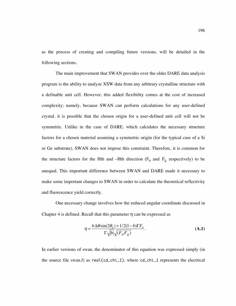
196
as the process of creating and compiling future versions, will be detailed in the
following sections.
The main improvement that SWAN provides over the older DARE data analysis
program is the ability to analyze XSW data from any arbitrary crystalline structure with
a definable unit cell. However, this added flexibility comes at the cost of increased
complexity; namely, because SWAN can perform calculations for any user-defined
crystal, it is possible that the chosen origin for a user-defined unit cell will not be
symmetric. Unlike in the case of DARE, which calculates the necessary structure
factors for a chosen material assuming a symmetric origin (for the typical case of a Si
or Ge substrate), SWAN does not impose this constraint. Therefore, it is common for
the structure factors for the Hth and –Hth direction (FH and
�
FH
respectively) to be
unequal. This important difference between SWAN and DARE made it necessary to
make some important changes to SWAN in order to calculate the theoretical reflectivity
and fluorescence yield correctly.
One necessary change involves how the reduced angular coordinate discussed in
Chapter 4 is defined. Recall that this parameter η can be expressed as
�
! =b"# sin(2#
b) +1/2(1$ b)%F0
% b (FH
FH )
. (A.1)
In earlier versions of swan, the denominator of this equation was expressed simply (in
the source file swan.f) as real(cd_chi_1), where cd_chi_1 represents the electrical
197
susceptibility in the Hth direction. While this expression was sufficient for the simpler
DARE software package, it is insufficient when FH and
�
FH
are not equivalent, as may
be the case for an arbitrary crystalline system used in SWAN. Therefore, the definition
for η in SWAN was changed to include the term real(sqrt(cd_chi_1*cd_chi_1_b))
(where cd_chi_1_b represents the electrical susceptibility in the –Hth direction) in the
denominator in order to better reflect the true expression for the reduced angle
parameter. Before this change was implemented, SWAN would occasionally calculate
rocking curves with a reversed angle scale depending on how the unit cell origin was
chosen. Instructions on how future versions of SWAN should be maintained, compiled,
and distributed will be presented in Section A.1.3.
A.1.1 New functionality in SWAN (as of version 2.1.3)
While there have been several “under-the-hood” changes in the SWAN analysis
software, there have also been some more obvious additions to SWAN that serve to
streamline the analysis process. Furthermore, there are some features available in
DARE that were not carried over in previous versions of SWAN; these have been
reintroduced in the current version in order to provide more control over the χ2 fitting
routine. These additional capabilities will be detailed in the following sections.
198
A.1.2 New SWAN functions
“cm” (change monochromator b-factor) and “cs” (change sample b-factor):
As described in Appendix B of the thesis dissertation of Dr. Yonglin Qian, the
sample rocking curve may be wider than expected because of thermal strains,
crystalline defects, or mechanical vibrations affecting the monochromator. It is possible
to account for these imperfections when analyzing rocking curve data by assuming the
monochromator has a larger effective b-factor than one would expect for a given
optical setup. By adjusting the monochromator b-factor, it is possible to obtain the best-
fit for a particular rocking curve than if the monochromator b-factor was fixed at the
expected value. In earlier versions of SWAN and DARE, however, adjusting the
monochromator asymmetry was somewhat tedious, since the reflectivity fit would have
to be repeated anew. Therefore, the “change monochromator” (“cm”) and “change
sample” (“cs”) commands were introduced.
After a rocking curve fit is completed (using the “r0” command), the
monochromator b-factor can be changed without reentering the sample and
monochromator parameters. Entering the “cm” command will prompt the user to
choose a new monochromator b-factor. Once the new b-factor is given, SWAN will
calculate the relevant structure factors and reflectivity for the revised b-factor, print out
the relevant monochromator parameters, and prompt the user if the χ2 fit should
proceed with the new b-factor. The user can then continue with the new rocking curve
199
fit and review the results. A similar command (“cs”) can be used to change the sample
b-factor if the user wishes to examine the effect of changes in the sample asymmetry on
the eventual rocking curve fit. In either case, these two commands allow reflectivity
data to be repeatedly analyzed without re-reading the data files or re-entering the
experimental parameters, saving time and keystrokes.
“fp” (fumili parameters) and “rf” (run fumili):
Fitting experimental rocking curve data typically requires only that the user
input the sample and monochromator parameters, as well as certain parameters unique
to the experiment (incident x-ray energy, angular or energy range of the rocking curve
scan, etc.). However, the user may wish to also control the parameters of the χ2 fitting
routine if the results of the fit are not satisfactory. For example, there are instances in
which the fit may weigh the “tails” of the rocking curve (i.e. the regions of the rocking
curve further from the Bragg condition) at the expense of the central region where the
reflectivity is higher. This is generally not a desirable situation, but it can be overcome
by manually adjusting the χ2 fit parameters, such as specifying the initial guesses for
the fitting parameters or by fixing the fit parameters to a particular value. This can be
done using the “fp” or “fumili parameters” command. This option allows the user to
have direct control of the fitting parameters used by the general χ2 routine (which is
contained in the Fortran subroutine fumili.f).
200
The “fp” and “rf” commands can be used after a rocking curve or fluorescence
yield curve has been initially fit in order to repeat the fit with a new set of fit
parameters. The command “fh” (fumili help) can be used to display the fit parameters
for a given fit. The following on-line help will then be displayed:
Fumili Parameters: for r0 rocking-curve fit: 1: Angular Scale gain 2: Angular Scale offset 3: Reflectivity Scale gain 4: Reflectivity Scale offset for f1 fluorescence fit: 1: Off-Bragg Counts (gain) 2: Offset Counts 3: Coherent Fraction 4: Coherent Position
As the help screen shows, the “fp” command may be more useful for refining
reflectivity fits rather than fluorescence yield fits, since two of the four florescence
yield fit parameters can be modified without using the “fp” command. After typing
“fp”, SWAN will then prompt the user on how the fitting parameters should be
changed. The syntax for this command is to enter three numbers separated by commas;
the first number will be the label of the fit parameter that will be modified, the second
number will be the initial guess for the chosen parameter, and the last number will be
the step size to be used in the fitting of the selected parameter. (For example, to fix the
201
reflectivity scale gain at a value of 1.3, the syntax would be 4,1.3,0.0.) Multiple fit
parameters can be modified in this way, and once all the desired changes have been
entered, the user should enter 0,0,0. The “rf” command can then be used to start the χ2
fit routine once the user confirms the SWAN parameters set using the “rp” command
are satisfactory, and the results of the fit with the revised fit parameters can then be
reviewed.
A.1.3 Modifying, compiling, and distributing SWAN
The process of implementing changes to SWAN is similar to the development
process for much of the Fortran software used in the Bedzyk group. Because most of
our data analysis software is written in the Fortran language, developing a usable
application that can be used on the current Macintosh platform requires either a native
Fortran compiler or a way to convert Fortran source code into C source code. A C or
C++ development tool can then handle the translated C source code. In our case, we
have chosen the second approach, because it allows us to use some plotting routines
that have been developed in C++, as well as use the popular development environment
known as CodeWarrior for Mac OS. By using CodeWarrior, we can include convenient
features in our applications such as standard Macintosh dialog boxes and alerts.
CodeWarrior is used in concert with MacF2C
(http://alumnus.caltech.edu/~igormt/Mac_F2C.html), which is a freely available
202
Fortran-to-C translator that runs under Mac OS 9 (or the Classic environment in Mac
OS X). In our finding, the most stable combination of CodeWarrior and Mac F2C is
CodeWarrior Pro release 5 and Mac F2C v1.4.2 (as of August 2004). While there are
more recent versions of these programs available, using the older versions tends to
result in fewer translation and compilation errors when developing new applications
The first step in producing an updated version of SWAN (or any other Fortran-
derived application) is to modify the source code. This is usually much easier using the
original Fortran source rather than the translated C code generated by Mac F2C. Once
the initial changes to the source Fortran code have been made, the next step is to use the
“Translate…” command in Mac F2C to convert the newly changed Fortran file into a
new C source file. During the translation process, F2C presents a status window that
shows the current Fortran routine being translated and informs the user if there are any
errors in the Fortran code that affect the translation.
If the translation is successful, at least one new file is created. One source file
that will always be created will be the translated C source code, which will have the
name filename.C (assuming the source Fortran code is named filename.f). Another file
that will also be produced is filename.P, which is a prototype file that describes the
calling sequence of a function. In order to use the results of the f2c translation with the
CodeWarrior compiler, a CodeWarrior project file (i.e. swan.prj or swan.µ) keeps track
203
of all the translated files, F2C libraries, and CodeWarrior libraries that are needed to
successfully compile a working program.
A.2 Global Analysis of XSW Data using IGOR PRO
For a given atomic distribution for which the ordered adatoms occupy only a
single position and the geometrical factor aH is unity, the adsorbate location with
respect to the underlying lattice can be determined by combining the results of normal
and off-normal XSW measurements to triangulate the position of the ordered site.
However, in atomic configurations in which there may be multiple adsorption sites,
determining the atomic distribution can be more complex. For example, in the case of
the 1/3 ML Sn/Si(111) surface described in Chapter 6, the various XSW measurements
did not triangulate to a single adsorption height above the Si(111) surface. Therefore, a
reasonable surface model was developed to account for the possibility of multiple site
adsorption. In order to determine the best-fit structural parameters and refine our
model, a systematic method was needed to fit this model to all of the {hhh} XSW
results. Because each set of XSW parameters (i.e. coherent fraction and coherent
position) is an independent measurement of the atomic-scale structure, it would be
desirable if we could fit all the XSW measurements simultaneously in order to realize
the benefit of a larger number of data points. To achieve this global analysis, we used
204
IGOR PRO, a popular graphing and data analysis software package, and the additional
functionality provided by the “Global Fit” procedure file.
As described in the IGOR PRO documentation, the Global Fit procedure
provides all the necessary functions to combine the individual data sets into a single
data set in order to fit the multiple experiments as a single one. Of course, it is also able
to connect the appropriate fitting parameters with the correct data points. More
importantly, it allows the fitting parameters to be defined as either global or local
parameters. Global parameters are those that will be fit with the same value for all the
data sets, while local parameters can have unique values for each individual data set. In
our particular case, it is assumed that each {hhh} XSW measurement is probing the
same Sn/Si(111) surface (i.e. the surface structure is not changing significantly over the
course of several XSW measurements). Therefore, the structural parameters contained
in our surface model will be designated as global parameters. However, a local
parameter will be used to account for each set of XSW data, which are separate Fourier
components of the Sn atomic distribution.
Of course, much of this functionality would be of limited use if IGOR PRO
were limited to fitting only the built-in mathematical functions to experimental data.
Fortunately, IGOR PRO allows users to define their own functions, enabling us to
encapsulate our surface model (as described in Equation 6.1) into a form that IGOR
PRO and the Global Fit procedures can handle. In Equation 6.1 there are four fit
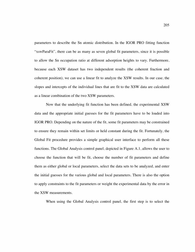
205
parameters to describe the Sn atomic distribution. In the IGOR PRO fitting function
“xswParaFit”, there can be as many as seven global fit parameters, since it is possible
to allow the Sn occupation ratio at different adsorption heights to vary. Furthermore,
because each XSW dataset has two independent results (the coherent fraction and
coherent position), we can use a linear fit to analyze the XSW results. In our case, the
slopes and intercepts of the individual lines that are fit to the XSW data are calculated
as a linear combination of the two XSW parameters.
Now that the underlying fit function has been defined, the experimental XSW
data and the appropriate initial guesses for the fit parameters have to be loaded into
IGOR PRO. Depending on the nature of the fit, some fit parameters may be constrained
to ensure they remain within set limits or held constant during the fit. Fortunately, the
Global Fit procedure provides a simple graphical user interface to perform all these
functions. The Global Analysis control panel, depicted in Figure A.1, allows the user to
choose the function that will be fit, choose the number of fit parameters and define
them as either global or local parameters, select the data sets to be analyzed, and enter
the initial guesses for the various global and local parameters. There is also the option
to apply constraints to the fit parameters or weight the experimental data by the error in
the XSW measurements.
When using the Global Analysis control panel, the first step is to select the
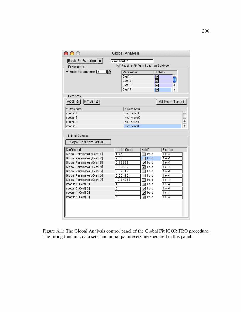
206
Figure A.1: The Global Analysis control panel of the Global Fit IGOR PRO procedure. The fitting function, data sets, and initial parameters are specified in this panel.
207
appropriate fit function. A pull-down menu displays the available fitting functions,
which include both the built-in functions and any user-defined functions. The parameter
information can be then set in the “Parameters” section of the Global Analysis control
panel. In the case of our surface model, there are a possible total of eight fit parameters.
Seven of these eight parameters represent the structural details of the Sn distribution
(such as adatom height, Sn occupation, fraction of Sn substituting for Si atoms, etc.)
and are therefore treated as global parameters. The other parameter (defined as w[0] in
the xswParaFit function) does not directly relate to the Sn/Si surface structure, but
rather is used to track which {hhh} Fourier component is involved in the global fit.
Therefore, this parameter is designated as a local one and will be fixed at an integer
value (m = 1, 3, 4, and 5) during the fit process.
The Data Sets portion of the control panel allow any number of data sets to be
entered for global analysis. The data sets can be either entered via the “Add” pull-down
menu in the Data Sets section or from an existing graph of the data to be analyzed.
When using the pull-down menu, the user should specify both the Y Data Set and the X
Data Set, if the appropriate X data exists. If there is no specific X data that corresponds
with the Y Data to be fit, the “_Calculated_” Data Set should be selected as the
matching X Data Set. The data sets to be analyzed can also be loaded from an open
graph using the “All from Target” button. In our case, the individual XSW results are
defined as a series of Igor Pro waves, which are tabulated in Figure A.2. There are a
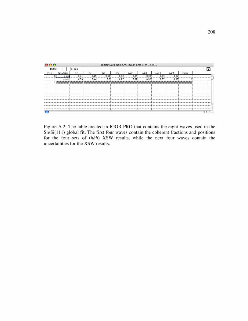
208
Figure A.2: The table created in IGOR PRO that contains the eight waves used in the Sn/Si(111) global fit. The first four waves contain the coherent fractions and positions for the four sets of (hhh) XSW results, while the next four waves contain the uncertainties for the XSW results.
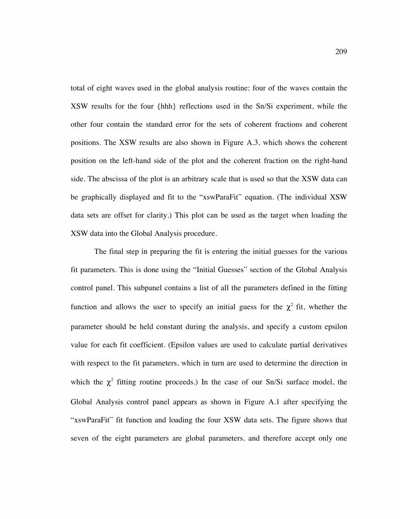
209
total of eight waves used in the global analysis routine; four of the waves contain the
XSW results for the four {hhh} reflections used in the Sn/Si experiment, while the
other four contain the standard error for the sets of coherent fractions and coherent
positions. The XSW results are also shown in Figure A.3, which shows the coherent
position on the left-hand side of the plot and the coherent fraction on the right-hand
side. The abscissa of the plot is an arbitrary scale that is used so that the XSW data can
be graphically displayed and fit to the “xswParaFit” equation. (The individual XSW
data sets are offset for clarity.) This plot can be used as the target when loading the
XSW data into the Global Analysis procedure.
The final step in preparing the fit is entering the initial guesses for the various
fit parameters. This is done using the “Initial Guesses” section of the Global Analysis
control panel. This subpanel contains a list of all the parameters defined in the fitting
function and allows the user to specify an initial guess for the χ2 fit, whether the
parameter should be held constant during the analysis, and specify a custom epsilon
value for each fit coefficient. (Epsilon values are used to calculate partial derivatives
with respect to the fit parameters, which in turn are used to determine the direction in
which the χ2 fitting routine proceeds.) In the case of our Sn/Si surface model, the
Global Analysis control panel appears as shown in Figure A.1 after specifying the
“xswParaFit” fit function and loading the four XSW data sets. The figure shows that
seven of the eight parameters are global parameters, and therefore accept only one
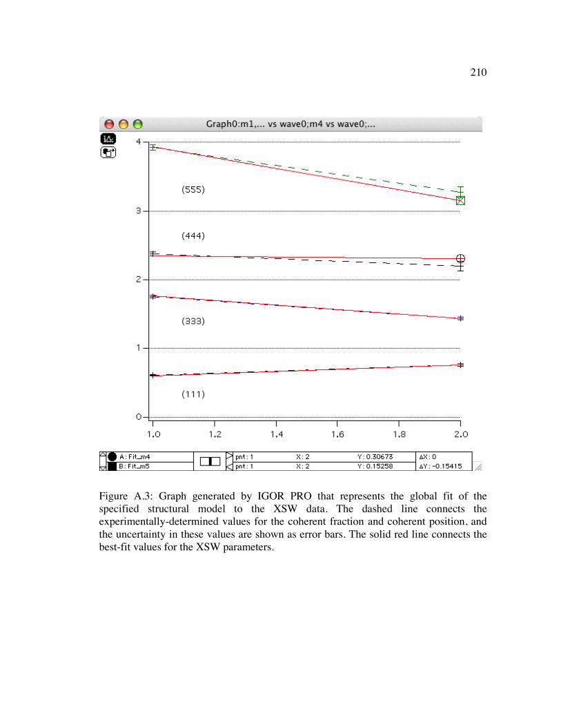
210
Figure A.3: Graph generated by IGOR PRO that represents the global fit of the specified structural model to the XSW data. The dashed line connects the experimentally-determined values for the coherent fraction and coherent position, and the uncertainty in these values are shown as error bars. The solid red line connects the best-fit values for the XSW parameters.
211
value for each global parameter. One of the fit coefficients is a local parameter,
however, and therefore requires four values for each of the four XSW data sets
specified. As mentioned previously, the four parameters keep track of the different
{hhh} XSW-determined Fourier components and are held at their value during the fit
process.
Some optional fit attributes can be set at the bottom of the control panel. The
most useful of these options are the “Apply Constraints” and the “Weighting…”
parameters. These allow for the fine-tuning of the χ2 fit routine by letting the user force
some or all of the fit coefficients to remain within set limits, or select a separate set of
error waves that will be used to weight the XSW data sets. In order to produce a
meaningful goodness-of-fit parameter, the error for the XSW results are saved as
separate waves and used as the weighting waves (“e_m#”, where “#” refers to the data
set to which the error applies). The correct error waves must be selected and matched
with the appropriate XSW data set in the “Weighting…” dialog.
Once all these initial parameters and options are selected, the fit process can
begin using the “Fit!” button on the Global Analysis panel. After the fitting routine is
finished, information about the fit results is displayed in the command window, such as
the best-fit values of the fit coefficients, the χ2 value of the completed fit, and the
calculated standard deviation of the fit parameters. The fit results can also be displayed
graphically to allow for a visual comparison between the experimental data and the
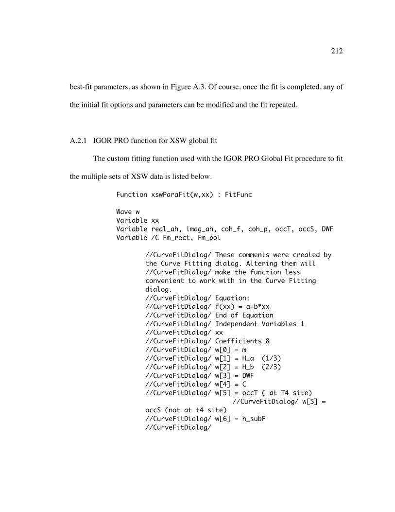
212
best-fit parameters, as shown in Figure A.3. Of course, once the fit is completed, any of
the initial fit options and parameters can be modified and the fit repeated.
A.2.1 IGOR PRO function for XSW global fit
The custom fitting function used with the IGOR PRO Global Fit procedure to fit
the multiple sets of XSW data is listed below.
Function xswParaFit(w,xx) : FitFunc Wave w Variable xx Variable real_ah, imag_ah, coh_f, coh_p, occT, occS, DWF Variable /C Fm_rect, Fm_pol //CurveFitDialog/ These comments were created by
the Curve Fitting dialog. Altering them will //CurveFitDialog/ make the function less
convenient to work with in the Curve Fitting dialog.
//CurveFitDialog/ Equation: //CurveFitDialog/ f(xx) = a+b*xx //CurveFitDialog/ End of Equation //CurveFitDialog/ Independent Variables 1 //CurveFitDialog/ xx //CurveFitDialog/ Coefficients 8 //CurveFitDialog/ w[0] = m //CurveFitDialog/ w[1] = H_a (1/3) //CurveFitDialog/ w[2] = H_b (2/3) //CurveFitDialog/ w[3] = DWF //CurveFitDialog/ w[4] = C //CurveFitDialog/ w[5] = occT ( at T4 site)
//CurveFitDialog/ w[5] = occS (not at t4 site)
//CurveFitDialog/ w[6] = h_subF //CurveFitDialog/
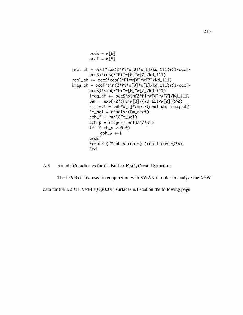
213
occS = w[6] occT = w[5] real_ah = occT*cos(2*Pi*w[0]*w[1]/kd_111)+(1-occT-
occS)*cos(2*Pi*w[0]*w[2]/kd_111) real_ah += occS*cos(2*Pi*w[0]*w[7]/kd_111) imag_ah = occT*sin(2*Pi*w[0]*w[1]/kd_111)+(1-occT-
occS)*sin(2*Pi*w[0]*w[2]/kd_111) imag_ah += occS*sin(2*Pi*w[0]*w[7]/kd_111) DWF = exp(-2*(Pi*w[3]/(kd_111/w[0]))^2) Fm_rect = DWF*w[4]*cmplx(real_ah, imag_ah) Fm_pol = r2polar(Fm_rect) coh_f = real(Fm_pol) coh_p = imag(Fm_pol)/(2*pi) if (coh_p < 0.0) coh_p +=1 endif return (2*coh_p-coh_f)+(coh_f-coh_p)*xx End
A.3 Atomic Coordinates for the Bulk α-Fe2O3 Crystal Structure
The fe2o3.ctl file used in conjunction with SWAN in order to analyze the XSW
data for the 1/2 ML V/α-Fe2O3(0001) surfaces is listed on the following page.
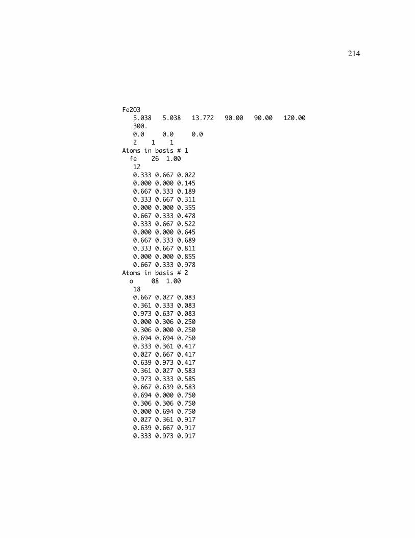
214
Fe2O3 5.038 5.038 13.772 90.00 90.00 120.00 300. 0.0 0.0 0.0 2 1 1 Atoms in basis # 1 fe 26 1.00 12 0.333 0.667 0.022 0.000 0.000 0.145 0.667 0.333 0.189 0.333 0.667 0.311 0.000 0.000 0.355 0.667 0.333 0.478 0.333 0.667 0.522 0.000 0.000 0.645 0.667 0.333 0.689 0.333 0.667 0.811 0.000 0.000 0.855 0.667 0.333 0.978 Atoms in basis # 2 o 08 1.00 18 0.667 0.027 0.083 0.361 0.333 0.083 0.973 0.637 0.083 0.000 0.306 0.250 0.306 0.000 0.250 0.694 0.694 0.250 0.333 0.361 0.417 0.027 0.667 0.417 0.639 0.973 0.417 0.361 0.027 0.583 0.973 0.333 0.585 0.667 0.639 0.583 0.694 0.000 0.750 0.306 0.306 0.750 0.000 0.694 0.750 0.027 0.361 0.917 0.639 0.667 0.917 0.333 0.973 0.917
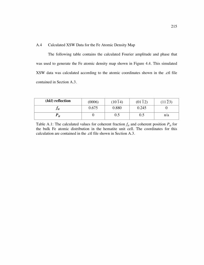
215
A.4 Calculated XSW Data for the Fe Atomic Density Map
The following table contains the calculated Fourier amplitude and phase that
was used to generate the Fe atomic density map shown in Figure 4.4. This simulated
XSW data was calculated according to the atomic coordinates shown in the .ctl file
contained in Section A.3.
(hkl) reflection (0006) (10
�
1 4) (01
�
1 2) (11
�
2 3) fH 0.675 0.880 0.245 0
PH 0 0.5 0.5 n/a
Table A.1: The calculated values for coherent fraction fH and coherent position PH for the bulk Fe atomic distribution in the hematite unit cell. The coordinates for this calculation are contained in the .ctl file shown in Section A.3.