Enhancement of Titania Photoanode Performance by ... - MDPI
16
materials Article Enhancement of Titania Photoanode Performance by Sandwiching Copper between Two Titania Layers Fan Yang 1,2 , Ruizhuang Yang 1 , Lin Yan 1 , Jiankun Wu 1 , Xiaolin Liu 1,2 , Lirong Yang 1 , Minglong Zhong 1 , Xuan Luo 1, * and Lin Zhang 1,2 1 Research Center of Laser Fusion, China Academy of Engineering Physics, Mianyang 621900, China; [email protected] (F.Y.); [email protected] (R.Y.); [email protected] (L.Y.); [email protected] (J.W.); [email protected] (X.L.); [email protected] (L.Y.); [email protected] (M.Z.); [email protected] (L.Z.) 2 Department of Physics, University of Science and Technology of China, Hefei 230026, China * Correspondence: [email protected] Received: 6 August 2020; Accepted: 10 September 2020; Published: 28 September 2020 Abstract: Vacancies in semiconductors can play a versatile role in boosting their photocatalytic activity. In this work, a novel TiO 2 /Cu/TiO 2 sandwich structure is designed and constructed. Abundant vacancies were introduced in TiO 2 lattice by Cu reduction under heat treatment. Meanwhile, Cu atom could diffuse into TiO 2 to form Cu-doped TiO 2 . The synergistic effect between oxygen vacancies and Cu atoms achieved about 2.4 times improved photocurrent of TiO 2 /Cu/TiO 2 sandwich structure compared to bare TiO 2 thin film. The enhanced photoactivity may be attributed to regulated electron structure of TiO 2 by oxygen vacancies and Cu dopant from experimental results and density functional theory calculations. Oxygen vacancies and Cu dopant in TiO 2 formed through copper metal reduction can introduce impurity levels and narrow the band gap of TiO 2 , thus improve the visible light response. More importantly, the Cu 2+ and oxygen vacancies in TiO 2 lattice can dramatically increase the charge density around conduction band and promote separation of photo-induced charge carriers. Furthermore, the oxygen vacancies on the surface may serve as active site for sufficient chemical reaction. This work presents a novel method to prepare doped metal oxides catalysts with abundant vacancies for improving photocatalytic activity. Keywords: metal reduction; oxygen vacancies; TiO 2 ; electronic structure; photoanode 1. Introduction Photoelectrochemical (PEC) water splitting is a promising strategy to convert renewable solar energy into chemical energy for tackling the growing energy shortage and environmental crisis. In comparison with other energy conversion approaches, PEC water splitting stands out due to its low cost, environmental friendliness and easy separation of hydrogen and oxygen from water [1,2]. Unsatisfactorily, the energy conversion efficiency is hindered by the sluggish reaction kinetics which involves four electrons oxidation process [3,4]. Many studies have focused on the photoanode for accelerating the water oxidation reaction [5,6]. Many semiconductors have been investigated as photoanodes. Among them, TiO 2 is still a promising candidate because of its appropriate band edge position, abundant reserves and excellent chemical stability. However, the water oxidation kinetics of TiO 2 -based photoelectrodes is severely impeded by wide band gap and fast electron-hole recombination. To solve these problems, great efforts have been made on TiO 2 materials. A common and effective method is introducing extra elements into TiO 2 crystal. Metal ions such as Cu [7], Mg [8], Sn [9] and Fe [10,11] have been doped to regulate the electron structure of TiO 2 . Typically, a transition metal would create donor levels near the conduction band minimum by their 3d orbital electrons. Materials 2020, 13, 4326; doi:10.3390/ma13194326 www.mdpi.com/journal/materials
-
Upload
khangminh22 -
Category
Documents
-
view
0 -
download
0
Transcript of Enhancement of Titania Photoanode Performance by ... - MDPI

materials
Article
Enhancement of Titania Photoanode Performance bySandwiching Copper between Two Titania Layers
Fan Yang 1,2, Ruizhuang Yang 1, Lin Yan 1, Jiankun Wu 1, Xiaolin Liu 1,2, Lirong Yang 1,Minglong Zhong 1, Xuan Luo 1,* and Lin Zhang 1,2
1 Research Center of Laser Fusion, China Academy of Engineering Physics, Mianyang 621900, China;[email protected] (F.Y.); [email protected] (R.Y.); [email protected] (L.Y.);[email protected] (J.W.); [email protected] (X.L.); [email protected] (L.Y.);[email protected] (M.Z.); [email protected] (L.Z.)
2 Department of Physics, University of Science and Technology of China, Hefei 230026, China* Correspondence: [email protected]
Received: 6 August 2020; Accepted: 10 September 2020; Published: 28 September 2020�����������������
Abstract: Vacancies in semiconductors can play a versatile role in boosting their photocatalyticactivity. In this work, a novel TiO2/Cu/TiO2 sandwich structure is designed and constructed.Abundant vacancies were introduced in TiO2 lattice by Cu reduction under heat treatment. Meanwhile,Cu atom could diffuse into TiO2 to form Cu-doped TiO2. The synergistic effect between oxygenvacancies and Cu atoms achieved about 2.4 times improved photocurrent of TiO2/Cu/TiO2 sandwichstructure compared to bare TiO2 thin film. The enhanced photoactivity may be attributed to regulatedelectron structure of TiO2 by oxygen vacancies and Cu dopant from experimental results and densityfunctional theory calculations. Oxygen vacancies and Cu dopant in TiO2 formed through copper metalreduction can introduce impurity levels and narrow the band gap of TiO2, thus improve the visiblelight response. More importantly, the Cu2+ and oxygen vacancies in TiO2 lattice can dramaticallyincrease the charge density around conduction band and promote separation of photo-induced chargecarriers. Furthermore, the oxygen vacancies on the surface may serve as active site for sufficientchemical reaction. This work presents a novel method to prepare doped metal oxides catalysts withabundant vacancies for improving photocatalytic activity.
Keywords: metal reduction; oxygen vacancies; TiO2; electronic structure; photoanode
1. Introduction
Photoelectrochemical (PEC) water splitting is a promising strategy to convert renewable solarenergy into chemical energy for tackling the growing energy shortage and environmental crisis.In comparison with other energy conversion approaches, PEC water splitting stands out due to itslow cost, environmental friendliness and easy separation of hydrogen and oxygen from water [1,2].Unsatisfactorily, the energy conversion efficiency is hindered by the sluggish reaction kinetics whichinvolves four electrons oxidation process [3,4]. Many studies have focused on the photoanode foraccelerating the water oxidation reaction [5,6]. Many semiconductors have been investigated asphotoanodes. Among them, TiO2 is still a promising candidate because of its appropriate bandedge position, abundant reserves and excellent chemical stability. However, the water oxidationkinetics of TiO2-based photoelectrodes is severely impeded by wide band gap and fast electron−holerecombination. To solve these problems, great efforts have been made on TiO2 materials. A commonand effective method is introducing extra elements into TiO2 crystal. Metal ions such as Cu [7], Mg [8],Sn [9] and Fe [10,11] have been doped to regulate the electron structure of TiO2. Typically, a transitionmetal would create donor levels near the conduction band minimum by their 3d orbital electrons.
Materials 2020, 13, 4326; doi:10.3390/ma13194326 www.mdpi.com/journal/materials

Materials 2020, 13, 4326 2 of 16
Many studies have experimentally proved that the doped metal elements would red shift absorptionedge of TiO2 to visible light region, which would greatly improve the photocatalytic performance.Zhang and co-authors [12] tuned the absorption edge of TiO2 up to 700·nm by incorporating Cuelement to TiO2 nanosheet. The resulted Cu-doped TiO2 nanosheet exhibited remarkable photoactivity.In addition, non-metal elements have been explored to dope in TiO2 materials [13–15]. The substitutionalnon-metal elements would create the acceptor state above the valence band maximum, leading to bandgap narrowing and an expansion of photo-absorption region. However, the non-metal ions could alsoserve as color center to facilitate the recombination of charge carriers to some extent.
As a dopant-free strategy, oxygen vacancies (Vo) play a crucial role in metal oxidesemiconductors [16–21] The previous studies indicate that oxygen vacancies could introduce defectlevel in semiconductor’s band gap and promote the exciton dissociation as well. The defects on thesurface of semiconductors may act as active sites for chemical reaction. Thus, Vo-rich semiconductorexhibits enhanced photocatalytic activity due to its improved light absorption, charge separationability and surface reaction. Chen and co-authors [22] firstly reported the Vo-rich TiO2 prepared by H2
reduction, and revealed the important impact of oxygen vacancies on the structure and properties ofTiO2 material. Since that, a series of strategies such as metal (e.g., Al) reduction [23], UV radiation [24]and plasma treatment [25,26] are developed to create Vo in metal oxides materials. The melted Al isused as a reductant to decrease oxygen partial pressure and drive TiO2 reduction kinetically. At thesame time, the melted Al will also be partially oxidized with formation of enough oxygen vacancies.It may be a promising and effective strategy to prepare Vo-rich heterostructure and Vo-rich materialswith doped metal through metal reduction approach. There is rare study combining metal doping withmetal reduction. One challenge is metal nanoparticles, especially the 3d transitional metal, are easilyoxidized to metal oxides when exposed to air or oxygen atmosphere because the nanoparticles alwayspossess strong redox ability. Coating with chemically stable material could prevent the active metalfrom oxidation, and the stability is thereby increased [27]. Previous study [28] reported the Cunanoparticles embedded in TiO2 particles for CO2 reduction. However, the fabrication process wascomplicated and strict.
We designed and prepared TiO2/Cu/TiO2 films with sandwich structure. After annealing under Aratmosphere, the core cooper layer was reduced surrounding TiO2 films and cooper atoms also diffusedinto TiO2 lattice. The resulted material possessed abundant oxygen vacancies with copper dopants.
2. Materials and Methods
2.1. Deposition of TiO2/Cu/TiO2 Thin Films
R200 ALD reactor (Picosun, Espoo, Finland) with thermal reaction chamber was employed todeposit TiO2 on fluorine-doped tin oxide (FTO, Foshan shi yuan jing mei glass Co. Ltd., Foshan,China) substrate [29] The titanium tetrachloride (TiCl4, 99.999%, Nanjing ai mou yuan Scientificequipment Co., Ltd., Nanjing, China) and ultra-pure water (H2O) were selected as Ti and O precursors,respectively. The ultrahigh purity N2 served as carrier gas and purge gas during the deposition process.The 600 cycles of TiO2 deposition were performed at 160 ◦C. Typically, the pulse times for TiCl4 andH2O were 1 s and 0.1 s, respectively.
Cu thin film was deposited on as-prepared TiO2/FTO by magnetron sputtering system [30](SKY technology development, Shenyang, China). In brief, as-prepared TiO2/FTO samples wereimmediately transferred into the deposition chamber. A copper target (99.95% purity) was employedin the deposition chamber with a base pressure of 5.0 × 10⁻³ mbar. The sputtering power was kept at40 W for all samples. The deposition time was 1, 2, 3 and 4 min to obtain copper films with differentthicknesses, respectively. After that, Cu/TiO2/FTO substrates were taken out and quickly delivered toALD reaction chamber. Next, in 600 successive cycles, TiO2 was deposited on Cu/TiO2 FTO substratesfor the formation of TiO2/Cu/TiO2 (denoted as TCT) sandwich structure. After being calcined at 500 ◦Cfor 2 h under Ar atmosphere, the samples were denoted as TCT-1, TCT-2, TCT-3 and TCT-4, respectively.

Materials 2020, 13, 4326 3 of 16
2.2. Density Functional Theory Calculation
The density of states and electronic band structure were estimated by CASTEP module inMaterials Studio. The 2 × 2 × 1 supercells of TiO2 with no vacancy in lattice (perfect TiO2), TiO2 withoxygen vacancies, TiO2 with Cu2+ and TiO2 with incorporation of Cu2+ and Cu+ structures werebuilt to perform the DFT + U calculations. For Ti 3d orbitals, the Hubbard U correction was set to5.9 eV [31]. GGA (Generalized gradient approximation)-PBE (Perdew–Burke–Emzerhof) exchangedfunction and ultrasoft pseudopotential was used to correct the exchange correlations between electrons.Ionic relaxations were optimized under conventional energy with 2 × 10⁻⁵ eV and all atoms wereallowed to relax until forces were less than 0.05 eV/Å. The plane wave cutoff energy was set to 450 eV.
2.3. Characterization
The thicknesses of ALD TiO2, Cu layers and TiO2/Cu/TiO2 thin films were determined byellipsometry measurement (SENTECH SE850, Sentech, Berlin, Germany). Measurements wereconducted at 70◦ angle of incidence with wavelengths ranging from 400 to 800 nm. Field-emissionscanning electron microscope (FE-SEM, ZEISS ultra 55, Lel Tech, Jena, Germany) with an acceleratingvoltage of 20 kV was utilized to observe the morphologies of these TiO2/Cu/TiO2 materials. The phasestructure and crystallinity were revealed by X-ray diffraction (XRD, D8 advance system, Bruker,Billerica, MA, USA) with a copper Kα radiation (λ = 1.5406 Å). Transmission electron microscopy(JEOL-2100F, Jeol, Akishima, Japan) with energy dispersive X-ray spectroscopy (Quantax 1.9,Bruker Nano GmbH, Berlin, Germany) with an acceleration voltage of 200 kV was used to observethe morphology and element dispersion. X-ray photoelectron spectroscopy (XPS) and Auger spectrameasurement was performed on ESCALAB 250Xi (ThermoFischer, Waltham, MA, USA) system withMg Kα radiation at a pressure of about 5 × 10⁻¹⁰ mbar. The optical absorption was investigatedby UV–vis absorbance spectra (LS 5 Lambda 950, PekinElemer, Waltham, MA, USA) from 200 to800 nm. InVia Reflex (Renishaw, Gloucestershire, UK) microscope was employed to record Ramanspectra under excitation wavelength at 532 nm. Photoluminescence (PL) spectra were recorded on aPekinElemer LS55 spectrofluorometer at room temperature under different excitation wavelength at390 and 425 nm, respectively.
2.4. Photoelectrochemical Measurement
The PEC measurements were performed on a CHI 660E electrochemical station (Shanghai ChenghuaMachinery Company, Shanghai, China). A standard three-electrode quartz cell with 0.5 M Na2SO4 aqueoussolution (pH = 6.8) was employed. The as-prepared TCT samples on FTO substrate were treated aswork electrodes. Platinum foil and saturated calomel electrode were used as counter and referenceelectrode, respectively. A 300-W Xe lamp (PLS-SXE300/300UV, PerfectLight, Beijing, China) with opticalfilter was used as solar-simulated light source. The photocurrent responses of the photoelectrodeswere conducted by linear sweep voltammetry (LSV) at a scan rate of 10 mV s−1 under choppedlight illumination. The electrochemical impedance spectroscopy (EIS) was recorded by applying ACvoltage amplitude of 5 mV with frequency ranging from 0.1 Hz to 100 kHz under light irradiation.Incident photon to current efficiency (IPCE) tests were performed by LSV under Xe lamp irradiationcoupled with a monochromator from 300 to 550 nm. Mott–Schottky plots were obtained by applyingDC potential range at a frequency of 1 kHz.
3. Results and Discussion
3.1. Characterizations of TiO2/Cu/TiO2 Films
3.1.1. SEM Micrographs
The preparation of Cu-doped TiO2 films with abundant oxygen vacancies is illustrated inFigure 1a. Cu embedded in TiO2 double layers with sandwich structure was achieved through

Materials 2020, 13, 4326 4 of 16
ALD and magnetron sputtering technique. After heat treatment under Ar atmosphere, the Cu layercould reduce surrounding TiO2 films and Cu atoms diffused into TiO2 lattice. As shown in Table 1,the thicknesses of as-prepared bare TiO2 and TCT thin films increased from 104.74 to 144.59 nm withthe sputtering time prolonging. The morphology of TiO2 thin film with/without Cu layer embeddedwas characterized by SEM measurement. As displayed in Figure 1, the bare TiO2 thin film had asimilar appearance with FTO substrate, suggesting the conformal deposition of TiO2 on the substrateby atomic layer deposition [29]. After sputtering the cooper films, the extra nanoparticles appeared onthe surface, which indicated island growth of cooper film by magnetron sputtering. Besides, the longersputtering time resulted in denser nanoparticles.
Materials 2020, 13, x FOR PEER REVIEW 4 of 16
magnetron sputtering technique. After heat treatment under Ar atmosphere, the Cu layer could reduce surrounding TiO2 films and Cu atoms diffused into TiO2 lattice. As shown in Table 1, the thicknesses of as-prepared bare TiO2 and TCT thin films increased from 104.74 to 144.59 nm with the sputtering time prolonging. The morphology of TiO2 thin film with/without Cu layer embedded was characterized by SEM measurement. As displayed in Figure 1, the bare TiO2 thin film had a similar appearance with FTO substrate, suggesting the conformal deposition of TiO2 on the substrate by atomic layer deposition [29]. After sputtering the cooper films, the extra nanoparticles appeared on the surface, which indicated island growth of cooper film by magnetron sputtering. Besides, the longer sputtering time resulted in denser nanoparticles.
Figure 1. Schematic illustration of preparation process of Cu-doped TiO2 thin films by Cu reduction (a); and SEM images: of FTO glass (b); bare TiO2 (c); TCT-1 (d); TCT-2 (e); TCT-3 (f); and TCT-4 (g).
Table 1. The thicknesses of as-prepared bare TiO2 and four TCT thin films.
Samples Bare TiO2 TCT-1 TCT-2 TCT-3 TCT-4 Thickness (nm) 104.74 ± 1.63 115.18 ± 2.67 124.13 ± 1.40 135.26 ± 1.42 144.59 ± 1.27
3.1.2. X-Ray Diffraction
The XRD pattern in Figure 2a suggests that the as-prepared TCT materials without heat treatment showed no identified phase of copper or copper oxides. It indicated that the deposited metallic Cu layers had poor crystallinity and good stability in air [32] As displayed in Figure 3b, all TiO2 samples with Cu embedded had typical anatase TiO2 phase (JCPDS No. 21-1271) after annealing
Figure 1. Schematic illustration of preparation process of Cu-doped TiO2 thin films by Cu reduction (a);and SEM images: of FTO glass (b); bare TiO2 (c); TCT-1 (d); TCT-2 (e); TCT-3 (f); and TCT-4 (g).
Table 1. The thicknesses of as-prepared bare TiO2 and four TCT thin films.
Samples Bare TiO2 TCT-1 TCT-2 TCT-3 TCT-4
Thickness (nm) 104.74 ± 1.63 115.18 ± 2.67 124.13 ± 1.40 135.26 ± 1.42 144.59 ± 1.27
3.1.2. X-Ray Diffraction
The XRD pattern in Figure 2a suggests that the as-prepared TCT materials without heat treatmentshowed no identified phase of copper or copper oxides. It indicated that the deposited metallic Culayers had poor crystallinity and good stability in air [32] As displayed in Figure 3b, all TiO2 sampleswith Cu embedded had typical anatase TiO2 phase (JCPDS No. 21-1271) after annealing process.Notably, extra diffraction peaks appeared in TCT-4 at 38.4 ◦ and 43.1 ◦, which were identified as(1 1 1) and (2 0 0) planes of Cu2O (JCPDS No. 05-0667). This represented that the core Cu layerwas partially oxidized in TiO2 shell. There was no obvious Cu2O, CuO or Cu phase in other TCTmaterials, meaning the Cu films were oxidized and diffused into TiO2 layers with no or less residual

Materials 2020, 13, 4326 5 of 16
Cu. Previous studies [30,33] reported Cu layer in TiO2/Cu/TiO2 sandwich structure displaying metallicCu diffraction peak under 350 ◦C treatment. It was assumed that metallic Cu could not react withsurrounding TiO2 layer at such low temperature. The higher concentration of Cu would lead toinsufficient reaction of Cu film with TiO2 surrounding layers under heat treatment, resulting in theformation of cuprous oxide.
Materials 2020, 13, x FOR PEER REVIEW 5 of 16
process. Notably, extra diffraction peaks appeared in TCT-4 at 38.4 ° and 43.1 °, which were identified as (1 1 1) and (2 0 0) planes of Cu2O (JCPDS No. 05-0667). This represented that the core Cu layer was partially oxidized in TiO2 shell. There was no obvious Cu2O, CuO or Cu phase in other TCT materials, meaning the Cu films were oxidized and diffused into TiO2 layers with no or less residual Cu. Previous studies [30,33] reported Cu layer in TiO2/Cu/TiO2 sandwich structure displaying metallic Cu diffraction peak under 350 °C treatment. It was assumed that metallic Cu could not react with surrounding TiO2 layer at such low temperature. The higher concentration of Cu would lead to insufficient reaction of Cu film with TiO2 surrounding layers under heat treatment, resulting in the formation of cuprous oxide.
Figure 2. XRD pattern of FTO, bare TiO2 and different TCT samples before (a) and after (b) annealing.
3.1.3. TEM Micrographs
To demonstrate the interaction between Cu and TiO2 layers, TEM images of TCT-4 were characterized. The sandwich structure of TCT-4 can be clearly seen in the low-resolution images in Figure 3a,b. The thickness of Cu layer was estimated to be 38.56 nm, which corresponded to the ellipsometry measurement result (39.85 nm). This indicated that the deposition rate was about 10 nm/min during magnetron sputtering process. In addition, the growth rate of ALD TiO2 was determined to be 0.92 nm/cycle from the ellipsometry measurement and line scanning model of TEM (Figure S1). As displayed in Figure 3c, Cu atoms diffused into TiO2 layer after annealing, and the resident Cu atoms were oxidized with the appearance of oxygen atoms. Obviously, there is a boundary between the TiO2 and Cu layer in Figure 3d. The high revolution TEM images in Figure 3e,f show that the lattice spacing is 0.359 nm, ascribed to (1 0 1) plane of anatase TiO2. The compound formed in Cu layer was identified as Cu2O with the lattice spacing 0.24 nm of (1 1 1) plane, which was consistent with XRD results.
Figure 2. XRD pattern of FTO, bare TiO2 and different TCT samples before (a) and after (b) annealing.Materials 2020, 13, x FOR PEER REVIEW 6 of 16
Figure 3. Cross-sectional TEM image with low magnification ((a) 1 μm and (b) 50 nm); EDX image (c); and high resolution TEM images at the interface (d) between TiO2 layer (e) and Cu layer (f) of TCT-4.
3.1.4. X-Ray Photoelectrons Spectra and Auger Spectra
To further explore the Cu species and element information of this sandwich structure, the XPS and Auger spectra were employed. Figure 4 and Figure S2 show the O 1s, Ti 2p and Cu 2p core level spectra of bare TiO2 and four TCT samples, respectively. It was clearly seen that the peak for O 1s (Figure 4a) could be deconvoluted into two peaks at around 530 and 531.7 eV. These peaks were assigned to the Ti-O bond and oxygen atoms in the vicinity of vacancy [21,29]. With the thickness of Cu film increasing, the concentration of oxygen vacancies grew. This revealed that more metallic cooper reacted with surrounding TiO2 films and accelerated the formation of oxygen vacancies. The Ti 2p spectra are displayed in Figure 4b. Compared to bare TiO2, the peak position of TCT films showed a negative shift. This shift could be ascribed to formation of Ti3+, as the evidence of TiO2
reduction [34,35]. Furthermore, The Cu species in TCT materials were revealed by Cu 2p XPS spectrum and auger electron spectra. As exhibited in Figure 4c, all TCT samples had strong Cu signals. The binding energy of Cu 2p3/2 at 935.2 eV could be ascribed to Cu2+ species. The satellite peaks at about 943 and 962 eV were evidence of existence of Cu2+. The strong satellite peak of TCT-1, TCT-2 and TCT-3 suggested the Cu2+ was the main valence state. The binding energy of Cu 2p1/2 at 952.2 eV and Cu 2p3/2 at 932.9 eV could be ascribed to Cu0 or Cu+. It was difficult to identify Cu+ and Cu0 due to the small difference between their binding energy. Considering that, the Cu Auger electron spectrum was collected to further confirm the Cu chemical state. The binding energy of Cu LMM is about 570.1 eV, representing the existence of Cu+ rather than Cu0 (567.9 eV) [36]. This meant that metallic Cu totally reacted with TiO2 under annealing process. In addition, the thickness of metallic Cu film determined the interaction between Cu core layer and TiO2 shell. Thicker Cu film in TCT-4 would be preferably oxidized to Cu+, and thinner film would result in more formation of Cu2+, which was in agreement with the XRD results.
Figure 3. Cross-sectional TEM image with low magnification ((a) 1 µm and (b) 50 nm); EDX image (c);and high resolution TEM images at the interface (d) between TiO2 layer (e) and Cu layer (f) of TCT-4.
3.1.3. TEM Micrographs
To demonstrate the interaction between Cu and TiO2 layers, TEM images of TCT-4 werecharacterized. The sandwich structure of TCT-4 can be clearly seen in the low-resolution imagesin Figure 3a,b. The thickness of Cu layer was estimated to be 38.56 nm, which corresponded tothe ellipsometry measurement result (39.85 nm). This indicated that the deposition rate was about10 nm/min during magnetron sputtering process. In addition, the growth rate of ALD TiO2 wasdetermined to be 0.92 nm/cycle from the ellipsometry measurement and line scanning model of TEM(Figure S1). As displayed in Figure 3c, Cu atoms diffused into TiO2 layer after annealing, and theresident Cu atoms were oxidized with the appearance of oxygen atoms. Obviously, there is a boundarybetween the TiO2 and Cu layer in Figure 3d. The high revolution TEM images in Figure 3e,f show that

Materials 2020, 13, 4326 6 of 16
the lattice spacing is 0.359 nm, ascribed to (1 0 1) plane of anatase TiO2. The compound formed in Culayer was identified as Cu2O with the lattice spacing 0.24 nm of (1 1 1) plane, which was consistentwith XRD results.
3.1.4. X-Ray Photoelectrons Spectra and Auger Spectra
To further explore the Cu species and element information of this sandwich structure, the XPS andAuger spectra were employed. Figure 4 and Figure S2 show the O 1s, Ti 2p and Cu 2p core level spectraof bare TiO2 and four TCT samples, respectively. It was clearly seen that the peak for O 1s (Figure 4a)could be deconvoluted into two peaks at around 530 and 531.7 eV. These peaks were assigned to theTi-O bond and oxygen atoms in the vicinity of vacancy [21,29]. With the thickness of Cu film increasing,the concentration of oxygen vacancies grew. This revealed that more metallic cooper reacted withsurrounding TiO2 films and accelerated the formation of oxygen vacancies. The Ti 2p spectra aredisplayed in Figure 4b. Compared to bare TiO2, the peak position of TCT films showed a negative shift.This shift could be ascribed to formation of Ti3+, as the eVidence of TiO2 reduction [34,35]. Furthermore,The Cu species in TCT materials were revealed by Cu 2p XPS spectrum and auger electron spectra.As exhibited in Figure 4c, all TCT samples had strong Cu signals. The binding energy of Cu 2p3/2 at935.2 eV could be ascribed to Cu2+ species. The satellite peaks at about 943 and 962 eV were eVidenceof existence of Cu2+. The strong satellite peak of TCT-1, TCT-2 and TCT-3 suggested the Cu2+ was themain valence state. The binding energy of Cu 2p1/2 at 952.2 eV and Cu 2p3/2 at 932.9 eV could beascribed to Cu0 or Cu+. It was difficult to identify Cu+ and Cu0 due to the small difference betweentheir binding energy. Considering that, the Cu Auger electron spectrum was collected to furtherconfirm the Cu chemical state. The binding energy of Cu LMM is about 570.1 eV, representing theexistence of Cu+ rather than Cu0 (567.9 eV) [36]. This meant that metallic Cu totally reacted with TiO2
under annealing process. In addition, the thickness of metallic Cu film determined the interactionbetween Cu core layer and TiO2 shell. Thicker Cu film in TCT-4 would be preferably oxidized toCu+, and thinner film would result in more formation of Cu2+, which was in agreement with theXRD results.Materials 2020, 13, x FOR PEER REVIEW 7 of 16
Figure 4. (a) O 1s; (b) Ti 2p; and (c) Cu 2p XPS spectra of bare TiO2 and TCT samples; and (d) auger spectra of TCT-4 photocatalyst.
3.1.5. Raman Spectroscopy
Raman spectra of different TCT samples and bare TiO2 are shown in Figure 5. It was clear that anatase was the main crystalline phase in all samples. There were no obvious signals of Cu or cooper oxides, indicating the small concentration or small grain size of cooper compounds. The vibration Raman modes occurring at 144, 396, 515 and 638 cm−1 were attributed to Eg, B1g, A1g and Eg, respectively [37]. The evidence of Cu doped into TiO2 could be identified by analyzing the main vibration mode of anatase at 144 cm−1. This Eg vibrational mode showed an increasing full width at half maximum (FWHM) from 11.5 to 12.8 cm−1 with the Cu content raising. The increasing FWHM can be ascribed to structure regulation related to shortening of the Ti-O bond at this Eg vibration mode [38]. Compared with bare TiO2 photocatalyst, this weakness of Ti-O bond originated from the oxygen vacancies caused by metallic Cu reduction reaction and Jahn–Teller distortion from incorporation of Cu2+ into TiO2 crystal [12].
Figure 4. (a) O 1s; (b) Ti 2p; and (c) Cu 2p XPS spectra of bare TiO2 and TCT samples; and (d) augerspectra of TCT-4 photocatalyst.
Materials 2020, 13, 4326 7 of 16
3.1.5. Raman Spectroscopy
Raman spectra of different TCT samples and bare TiO2 are shown in Figure 5. It was clear thatanatase was the main crystalline phase in all samples. There were no obvious signals of Cu or cooperoxides, indicating the small concentration or small grain size of cooper compounds. The vibrationRaman modes occurring at 144, 396, 515 and 638 cm−1 were attributed to Eg, B1g, A1g and Eg,respectively [37]. The eVidence of Cu doped into TiO2 could be identified by analyzing the mainvibration mode of anatase at 144 cm−1. This Eg vibrational mode showed an increasing full width athalf maximum (FWHM) from 11.5 to 12.8 cm−1 with the Cu content raising. The increasing FWHM canbe ascribed to structure regulation related to shortening of the Ti-O bond at this Eg vibration mode [38].Compared with bare TiO2 photocatalyst, this weakness of Ti-O bond originated from the oxygenvacancies caused by metallic Cu reduction reaction and Jahn–Teller distortion from incorporation ofCu2+ into TiO2 crystal [12].
Materials 2020, 13, x FOR PEER REVIEW 8 of 16
Figure 5. (a) Raman spectra of bare TiO2 and TCT materials; and (b) the enlarged Raman spectra at around 144 cm−1 of all five samples.
3.1.6. UV–Vis Absorption and Photoluminescence Spectroscopy
Figure 6a displays the UV–vis absorption spectra for bare TiO2 and as-prepared TCT samples. Almost all samples exhibited main absorbance at UV region. However, compared with pure TiO2 materials, TCT samples showed an increasing absorption at visible light region with the thickness of Cu increasing. Without any doubt, the heavy doping of Cu would narrow the band gap of TiO2. The thicker Cu film in TCT-4 would even produce Cu2O with 2.2 eV band gap [39] from the XRD result. The extending light absorption would improve the photocatalytic property. Furthermore, it should be noted that metal nanoparticles could generate surface plasmon resonance (SPR) effect [40]. Many authors researched embedded noble metal (Au [41–43] and Ag [44]) into double TiO2 layers to enhance the visible light absorption. In addition, copper nanoparticles could SPR effect at wavelength of around 570 nm. Figure 6a clearly shows that no such absorption peak was present in all TCT samples. This also suggested that the metallic Cu reacted with TiO2 sufficiently without metallic Cu leftover.
Photoluminescence spectra were recorded to investigate the migration and recombination of photo-induced carriers. Under excitation at wavelength of 390 nm, the bare TiO2 showed strongest emission peak at 512 nm caused by recombination of photogenerated holes and electrons. The heavy doping of Cu led to a weak intensity of emission peak, suggesting much more oxygen vacancies caused by Cu atoms that would serve as trapping sites to capture electrons, which could promote the separation of electrons and holes. Interestingly, the TCT-2 sample had the lowest emission peak intensity, indicating that the moderate amount of doped Cu in TiO2 lattice would facilitate efficient separation and migration of charge carriers, thus benefiting photoelectrochemical water oxidation. To classify the effect of doped Cu on the separation of charge carriers, the PL spectra under excitation light with long wavelength was collected. Figure 6c shows the excitation peak with the emission wavelength of 512 nm. The excitation peak at 350–400 nm corresponded to TiO2 band gap. The excitation peak of TiO2 showed a red shift with the thickness of Cu films increasing, which was ascribed to change of the electron structure by Cu 3d orbitals. These data also prove that the doped Cu narrowed the band gap of TiO2 and improved the light absorption. The excitation peak at 425 nm and the emission peak at 550 nm were attributed to CuxO. The intensity of excitation peak rose when the concentration of Cu increased. The presence of this excitation peak disclosed that the thicker Cu film would produce CuxO when reacted with TiO2. These results reveal that the balance between doped Cu atoms and oxygen vacancies led to effective separation of electron–hole pairs.
Figure 5. (a) Raman spectra of bare TiO2 and TCT materials; and (b) the enlarged Raman spectra ataround 144 cm−1 of all five samples.
3.1.6. UV–Vis Absorption and Photoluminescence Spectroscopy
Figure 6a displays the UV–vis absorption spectra for bare TiO2 and as-prepared TCT samples.Almost all samples exhibited main absorbance at UV region. However, compared with pure TiO2
materials, TCT samples showed an increasing absorption at visible light region with the thicknessof Cu increasing. Without any doubt, the heavy doping of Cu would narrow the band gap of TiO2.The thicker Cu film in TCT-4 would eVen produce Cu2O with 2.2 eV band gap [39] from the XRDresult. The extending light absorption would improve the photocatalytic property. Furthermore,it should be noted that metal nanoparticles could generate surface plasmon resonance (SPR) effect [40].Many authors researched embedded noble metal (Au [41–43] and Ag [44]) into double TiO2 layers toenhance the visible light absorption. In addition, copper nanoparticles could SPR effect at wavelengthof around 570 nm. Figure 6a clearly shows that no such absorption peak was present in all TCT samples.This also suggested that the metallic Cu reacted with TiO2 sufficiently without metallic Cu leftover.

Materials 2020, 13, 4326 8 of 16
Materials 2020, 13, x FOR PEER REVIEW 9 of 16
Figure 6. (a) UV–vis spectra of FTO substrate, bare TiO2 and TCT samples, respectively; (b) photoluminescence spectra of all samples with the excitation wavelength at 390 nm; (c) PL spectra of all samples with the emission wavelength at 512 nm; and (d) PL spectra of all samples with the excitation wavelength at 425 nm.
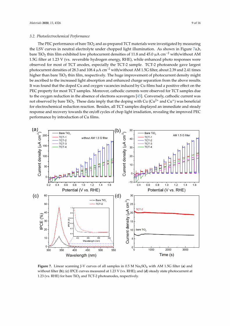
3.2. Photoelectrochemical Performance
The PEC performance of bare TiO2 and as-prepared TCT materials were investigated by measuring the LSV curves in neutral electrolyte under chopped light illumination. As shown in Figure 7a,b, bare TiO2 thin film exhibited low photocurrent densities of 11.8 and 45.0 μA cm−2
with/without AM 1.5G filter at 1.23 V (vs. reversible hydrogen energy, RHE), while enhanced photo responses were observed for most of TCT anodes, especially the TCT-2 sample. TCT-2 photoanode gave largest photocurrent densities of 28.3 and 108.4 μA cm–2 with/without AM 1.5G filter, about 2.39 and 2.41 times higher than bare TiO2 thin film, respectively. The huge improvement of photocurrent density might be ascribed to the increased light absorption and enhanced charge separation from the above results. It was found that the doped Cu and oxygen vacancies induced by Cu films had a positive effect on the PEC property for most TCT samples. Moreover, cathodic currents were observed for TCT samples due to the oxygen reduction in the absence of electrons scavengers [45]. Conversely, cathodic current was not observed by bare TiO2. These data imply that the doping with Cu (Cu2+ and Cu+) was beneficial for electrochemical reduction reaction. Besides, all TCT samples displayed an immediate and steady response and recovery towards the on/off cycles of chop light irradiation, revealing the improved PEC performance by introduction of Cu films.
To evaluate the photoconversion efficiency of the TCT materials, incident photon to current efficiency (IPCE) measurements were performed and calculated. Figure 7c shows the IPCE spectra of bare TiO2 and TCT-2 sample measured at 1.23 V (vs. RHE). It could be clearly seen that TCT-2 and bare TiO2 photocatalysts had the main photocatalytic activity in the UV region. Both samples displayed the highest IPCE at 340 nm with 46.2% and 16.7% for TCT-2 and bare TiO2, respectively.
Figure 6. (a) UV–vis spectra of FTO substrate, bare TiO2 and TCT samples, respectively; (b) photoluminescencespectra of all samples with the excitation wavelength at 390 nm; (c) PL spectra of all samples with the emissionwavelength at 512 nm; and (d) PL spectra of all samples with the excitation wavelength at 425 nm.
Photoluminescence spectra were recorded to investigate the migration and recombination ofphoto-induced carriers. Under excitation at wavelength of 390 nm, the bare TiO2 showed strongestemission peak at 512 nm caused by recombination of photogenerated holes and electrons. The heavydoping of Cu led to a weak intensity of emission peak, suggesting much more oxygen vacanciescaused by Cu atoms that would serve as trapping sites to capture electrons, which could promote theseparation of electrons and holes. Interestingly, the TCT-2 sample had the lowest emission peak intensity,indicating that the moderate amount of doped Cu in TiO2 lattice would facilitate efficient separationand migration of charge carriers, thus benefiting photoelectrochemical water oxidation. To classifythe effect of doped Cu on the separation of charge carriers, the PL spectra under excitation light withlong wavelength was collected. Figure 6c shows the excitation peak with the emission wavelength of512 nm. The excitation peak at 350–400 nm corresponded to TiO2 band gap. The excitation peak ofTiO2 showed a red shift with the thickness of Cu films increasing, which was ascribed to change of theelectron structure by Cu 3d orbitals. These data also prove that the doped Cu narrowed the band gapof TiO2 and improved the light absorption. The excitation peak at 425 nm and the emission peak at550 nm were attributed to CuxO. The intensity of excitation peak rose when the concentration of Cuincreased. The presence of this excitation peak disclosed that the thicker Cu film would produce CuxOwhen reacted with TiO2. These results reveal that the balance between doped Cu atoms and oxygenvacancies led to effective separation of electron–hole pairs.
Materials 2020, 13, 4326 9 of 16
3.2. Photoelectrochemical Performance
The PEC performance of bare TiO2 and as-prepared TCT materials were investigated by measuringthe LSV curves in neutral electrolyte under chopped light illumination. As shown in Figure 7a,b,bare TiO2 thin film exhibited low photocurrent densities of 11.8 and 45.0 µA cm−2 with/without AM1.5G filter at 1.23 V (vs. reversible hydrogen energy, RHE), while enhanced photo responses wereobserved for most of TCT anodes, especially the TCT-2 sample. TCT-2 photoanode gave largestphotocurrent densities of 28.3 and 108.4 µA cm–2 with/without AM 1.5G filter, about 2.39 and 2.41 timeshigher than bare TiO2 thin film, respectively. The huge improvement of photocurrent density mightbe ascribed to the increased light absorption and enhanced charge separation from the above results.It was found that the doped Cu and oxygen vacancies induced by Cu films had a positive effect on thePEC property for most TCT samples. Moreover, cathodic currents were observed for TCT samples dueto the oxygen reduction in the absence of electrons scavengers [45]. Conversely, cathodic current wasnot observed by bare TiO2. These data imply that the doping with Cu (Cu2+ and Cu+) was beneficialfor electrochemical reduction reaction. Besides, all TCT samples displayed an immediate and steadyresponse and recovery towards the on/off cycles of chop light irradiation, revealing the improved PECperformance by introduction of Cu films.
Materials 2020, 13, x FOR PEER REVIEW 10 of 16
This could be mainly attributed to the enhanced separation of photogenerated charge carriers. Furthermore, it should also be noticed that TCT-2 exhibited slight improvement of IPCE near visible light (400–450 nm) compared to bare TiO2 photoanode. This improvement might originate from the narrowed band gap of TiO2 caused by Cu doping and oxygen vacancies. Above a wavelength of 450 nm, two samples exhibited negligible IPCE values, indicating the poor photocatalytic activity towards long wavelength light. In addition, the steady state photocurrent test for TCT and bare TiO2 photoanodes shown in Figure 7d suggested that these two samples showed a stable photocurrent (less than 6% decay) under long time illumination.
Figure 7. Linear scanning J-V curves of all samples in 0.5 M Na2SO4 with AM 1.5G filter (a) and without filter (b); (c) IPCE curves measured at 1.23 V (vs. RHE); and (d) steady state photocurrent at 1.23 (vs. RHE) for bare TiO2 and TCT-2 photoanodes, respectively.
To further explore the separation and diffusion of photogenerated electrons and holes during the PEC reaction, the EIS and Mott–Schottky curves were collected. As shown in Figure 8a, all TCT samples gave the smaller arc radius than bare TiO2, which indicated the fast interfacial charge transport and low charge transport resistance between the electrode and electrolyte. These data demonstrate that the Cu doping could promote the charge separation in photocatalysts by introducing sufficient oxygen vacancies. Meanwhile, TCT-2 sample possessed the smallest arc radius among all TCT and bare TiO2 materials, displaying the highest transport efficiency of charge carriers. These results were consistent with the PL behaviors as expected. In MS plots, the EFB could be obtained from Mott–Schottky equation. Figure 7b,c shows that all samples exhibited positive slopes, indicating the n-type feature of all materials. Although the existence of Cu2O was revealed from XRD pattern, the MS plot of TCT-4 showed no negative slope as the evidence of p type semiconductor. It might be explained by the small content of Cu2O in comparison with TiO2 matrix. The charge carrier density was calculated using the MS equation. The obtained values were 1.03 × 10¹⁴, 2.63 × 10¹⁵, 3.49 × 10¹⁶, 1.66 × 10¹⁶ and 2.64 × 1016 cm–3 for bare TiO2, TCT-1, TCT-2, TCT-3 and TCT-4, respectively.
Figure 7. Linear scanning J-V curves of all samples in 0.5 M Na2SO4 with AM 1.5G filter (a) andwithout filter (b); (c) IPCE curves measured at 1.23 V (vs. RHE); and (d) steady state photocurrent at1.23 (vs. RHE) for bare TiO2 and TCT-2 photoanodes, respectively.

Materials 2020, 13, 4326 10 of 16
To eValuate the photoconversion efficiency of the TCT materials, incident photon to currentefficiency (IPCE) measurements were performed and calculated. Figure 7c shows the IPCE spectra ofbare TiO2 and TCT-2 sample measured at 1.23 V (vs. RHE). It could be clearly seen that TCT-2 and bareTiO2 photocatalysts had the main photocatalytic activity in the UV region. Both samples displayed thehighest IPCE at 340 nm with 46.2% and 16.7% for TCT-2 and bare TiO2, respectively. This could bemainly attributed to the enhanced separation of photogenerated charge carriers. Furthermore, it shouldalso be noticed that TCT-2 exhibited slight improvement of IPCE near visible light (400–450 nm)compared to bare TiO2 photoanode. This improvement might originate from the narrowed band gapof TiO2 caused by Cu doping and oxygen vacancies. Above a wavelength of 450 nm, two samplesexhibited negligible IPCE values, indicating the poor photocatalytic activity towards long wavelengthlight. In addition, the steady state photocurrent test for TCT and bare TiO2 photoanodes shown inFigure 7d suggested that these two samples showed a stable photocurrent (less than 6% decay) underlong time illumination.
To further explore the separation and diffusion of photogenerated electrons and holes duringthe PEC reaction, the EIS and Mott–Schottky curves were collected. As shown in Figure 8a, all TCTsamples gave the smaller arc radius than bare TiO2, which indicated the fast interfacial charge transportand low charge transport resistance between the electrode and electrolyte. These data demonstratethat the Cu doping could promote the charge separation in photocatalysts by introducing sufficientoxygen vacancies. Meanwhile, TCT-2 sample possessed the smallest arc radius among all TCT andbare TiO2 materials, displaying the highest transport efficiency of charge carriers. These resultswere consistent with the PL behaviors as expected. In MS plots, the EFB could be obtained fromMott–Schottky equation. Figure 7b,c shows that all samples exhibited positive slopes, indicatingthe n-type feature of all materials. Although the existence of Cu2O was revealed from XRD pattern,the MS plot of TCT-4 showed no negative slope as the eVidence of p type semiconductor. It might beexplained by the small content of Cu2O in comparison with TiO2 matrix. The charge carrier densitywas calculated using the MS equation. The obtained values were 1.03 × 10¹⁴, 2.63 × 10¹⁵, 3.49 × 1016,1.66 × 1016 and 2.64 × 1016 cm–3 for bare TiO2, TCT-1, TCT-2, TCT-3 and TCT-4, respectively. Obviously,the incorporation of Cu atoms into TiO2 lattice greatly tuned the concentration of charge carriers inTiO2 due to the carriers’ capture and immobilization. The charge carriers’ density of TCT-2 samplewas two orders of magnitude higher than that of bare TiO2 films, which demonstrated the accelerationof photogenerated carriers’ transfer by doped Cu and oxygen vacancies. The calculated flat bandpotentials are shown in Figure 8b,c. The EFB of bare TiO2 was –0.23 V versus the RHE. The flat bandpotentials of TCT samples were more positive than that determined for bare TiO2, which was dueto introduction of Cu 3d orbitals. With the increasing thickness of Cu films, the flat band showed amore positive shift. The band positions are drawn in Figure 8d by the values estimated from VB-XPS(Figure S3) and Mott–Schottky plots, respectively. Indeed, the valence band displayed a negativeshift with the increasing of Cu doping, which might be ascribed to the formation of oxygen vacanciesinduced by Cu reduction and Jahn–Teller distortion. It might be thermodynamically hard for TCTsamples to take oxygen eVolution reaction compared to bare TiO2 counterpart. This was the reason thatTCT-3 sample showed a relatively lower photocurrent density compared to bare TiO2. The analysisof optical absorption and charge carrier migration demonstrated that all TCT samples were believedto possess better photocatalytic activity than bare TiO2 thin films. On the other hand, the narrowingband gap estimated from the valence band maximum (VBM) and conduction band minimum (CBM)extended the photo response to visible light region.

Materials 2020, 13, 4326 11 of 16
Materials 2020, 13, x FOR PEER REVIEW 11 of 16
Obviously, the incorporation of Cu atoms into TiO2 lattice greatly tuned the concentration of charge carriers in TiO2 due to the carriers’ capture and immobilization. The charge carriers’ density of TCT-2 sample was two orders of magnitude higher than that of bare TiO2 films, which demonstrated the acceleration of photogenerated carriers’ transfer by doped Cu and oxygen vacancies. The calculated flat band potentials are shown in Figure 8b,c. The EFB of bare TiO2 was –0.23 V versus the RHE. The flat band potentials of TCT samples were more positive than that determined for bare TiO2, which was due to introduction of Cu 3d orbitals. With the increasing thickness of Cu films, the flat band showed a more positive shift. The band positions are drawn in Figure 8d by the values estimated from VB-XPS (Figure S3) and Mott–Schottky plots, respectively. Indeed, the valence band displayed a negative shift with the increasing of Cu doping, which might be ascribed to the formation of oxygen vacancies induced by Cu reduction and Jahn–Teller distortion. It might be thermodynamically hard for TCT samples to take oxygen evolution reaction compared to bare TiO2 counterpart. This was the reason that TCT-3 sample showed a relatively lower photocurrent density compared to bare TiO2. The analysis of optical absorption and charge carrier migration demonstrated that all TCT samples were believed to possess better photocatalytic activity than bare TiO2 thin films. On the other hand, the narrowing band gap estimated from the valence band maximum (VBM) and conduction band minimum (CBM) extended the photo response to visible light region.
Figure 8. (a) EIS curves measured under light illumination; (b,c) Mott–Schottky plots of bare TiO2 and four TCT photoanodes, respectively; and (d) band positions of all measured materials.
3.3. Density Functional Theory Calculations
To understand the effect of Cu ions and oxygen vacancies on TiO2 electronic structure in molecular sight, density functional theory calculations were employed. As shown in Figure 9, anatase bulk TiO2 with perfect structure possessed a standard band gap of 3.22 eV. The bare TiO2 photoanode in this work showed an energy gap of 3.17 eV, less than the common anatase TiO2. This was caused by the introduction of oxygen vacancies in ALD process. The energy gap of TiO2 with oxygen
Figure 8. (a) EIS curves measured under light illumination; (b,c) Mott–Schottky plots of bare TiO2 andfour TCT photoanodes, respectively; and (d) band positions of all measured materials.
3.3. Density Functional Theory Calculations
To understand the effect of Cu ions and oxygen vacancies on TiO2 electronic structure in molecularsight, density functional theory calculations were employed. As shown in Figure 9, anatase bulkTiO2 with perfect structure possessed a standard band gap of 3.22 eV. The bare TiO2 photoanode inthis work showed an energy gap of 3.17 eV, less than the common anatase TiO2. This was causedby the introduction of oxygen vacancies in ALD process. The energy gap of TiO2 with oxygenvacancies (Figure S4) was calculated to be 2.07 eV from DFT results, due to the existence of defect levelnear the valence band edge compared to perfect anatase TiO2. The formation of oxygen vacanciesnarrowed band gap of TiO2, which enhanced photo absorption in photocatalytic process. Notably,Figure 9f,i clearly shows that the introduced Cu2+ greatly modulated the electronic structure ofTiO2. Two energy levels appeared in TiO2 band gap at valence band edge and valence band edgerelative to pure TiO2. These energy levels were ascribed to the Cu-doping and oxygen vacancies.Oxygen vacancies mainly contributed to the new energy level at valence band edge, while Cu 3dorbitals were mainly responsible for the formation of impurity bands at conduction edge with respectto pure TiO2. The resulted Cu-doped TiO2 displayed a smaller band gap, giving the possibility ofvisible light absorption. Furthermore, extra Cu+ ions were added into above Cu2+-doped TiO2 latticeto explore the change of band structures. Interestingly, there were still two kinds of impurity levelsand the band gap of materials remained unchangeable, which indicated that the Cu+ did not changethe position of impurity levels. However, the intensity of energy levels improved by the addition ofCu+ compared with the Cu2+-doped TiO2. In addition, compared to Cu2+- and Cu+-codoped TiO2
and perfect TiO2, Cu2+-doped TiO2 displayed an increasing density of states in conduction band,which would benefit for electrons transport. The DFT results reveal that the moderate doped Cu2+

Materials 2020, 13, 4326 12 of 16
would have a positive effect on TiO2 photocatalytic activity by narrowing the band gap and enhancingthe charge transport.
Materials 2020, 13, x FOR PEER REVIEW 12 of 16
vacancies (Figure S4) was calculated to be 2.07 eV from DFT results, due to the existence of defect level near the valence band edge compared to perfect anatase TiO2. The formation of oxygen vacancies narrowed band gap of TiO2, which enhanced photo absorption in photocatalytic process. Notably, Figure 9f,i clearly shows that the introduced Cu2+ greatly modulated the electronic structure of TiO2. Two energy levels appeared in TiO2 band gap at valence band edge and valence band edge relative to pure TiO2. These energy levels were ascribed to the Cu-doping and oxygen vacancies. Oxygen vacancies mainly contributed to the new energy level at valence band edge, while Cu 3d orbitals were mainly responsible for the formation of impurity bands at conduction edge with respect to pure TiO2. The resulted Cu-doped TiO2 displayed a smaller band gap, giving the possibility of visible light absorption. Furthermore, extra Cu+ ions were added into above Cu2+-doped TiO2 lattice to explore the change of band structures. Interestingly, there were still two kinds of impurity levels and the band gap of materials remained unchangeable, which indicated that the Cu+ did not change the position of impurity levels. However, the intensity of energy levels improved by the addition of Cu+ compared with the Cu2+-doped TiO2. In addition, compared to Cu2+- and Cu+-codoped TiO2 and perfect TiO2, Cu2+-doped TiO2 displayed an increasing density of states in conduction band, which would benefit for electrons transport. The DFT results reveal that the moderate doped Cu2+ would have a positive effect on TiO2 photocatalytic activity by narrowing the band gap and enhancing the charge transport.
Figure 9. The lattice structure, calculated band structure and density of states (DOS) of: perfect anatase TiO2 (a–c); Cu2+-doped TiO2 (d–f); and TiO2 with Cu2+ and Cu+ codoped (g–i).
Combining the experimental and theoretical results, the proposed photocatalytic mechanism of TCT-2 samples is illustrated in Figure 10. Through copper reduction, doped Cu and abundant oxygen vacancies in TiO2 brought in impurity and defect levels, which shifted the CBM and VBM to 0.01 and 2.43 eV, respectively. These extra energy levels obviously decreased the band gap of TiO2 (2.42 eV) and promoted light absorption region to visible light. Besides, the formation of oxygen vacancies could trap electrons and improve the separation and transfer of charge carriers. In the case of oxygen
Figure 9. The lattice structure, calculated band structure and density of states (DOS) of: perfect anataseTiO2 (a–c); Cu2+-doped TiO2 (d–f); and TiO2 with Cu2+ and Cu+ codoped (g–i).
Combining the experimental and theoretical results, the proposed photocatalytic mechanismof TCT-2 samples is illustrated in Figure 10. Through copper reduction, doped Cu and abundantoxygen vacancies in TiO2 brought in impurity and defect levels, which shifted the CBM and VBM to0.01 and 2.43 eV, respectively. These extra energy levels obviously decreased the band gap of TiO2
(2.42 eV) and promoted light absorption region to visible light. Besides, the formation of oxygenvacancies could trap electrons and improve the separation and transfer of charge carriers. In the caseof oxygen vacancies on the surface, they were favorable for OH– adsorption and could serve as activesites for oxygen eVolution reaction. Based on the above analysis, the doping Cu ions and oxygenvacancies induced by Cu incorporation could significantly enhance the photo response and facilitatethe photo-generated charge carriers’ separation and transfer, eVidenced by experimental results aswell as DFT calculation.

Materials 2020, 13, 4326 13 of 16
Materials 2020, 13, x FOR PEER REVIEW 13 of 16
vacancies on the surface, they were favorable for OH– adsorption and could serve as active sites for oxygen evolution reaction. Based on the above analysis, the doping Cu ions and oxygen vacancies induced by Cu incorporation could significantly enhance the photo response and facilitate the photo-generated charge carriers’ separation and transfer, evidenced by experimental results as well as DFT calculation.
Figure 10. Proposed photocatalytic mechanism of TCT-2 sample under light irradiation.
4. Conclusions
In this study, we prepared TiO2/Cu/TiO2 sandwich structure. Through annealing under Ar atmosphere, the Cu-doped TiO2 with abundant oxygen vacancies formed. X-ray photoelectron and Auger spectra revealed the existence of doped Cu and oxygen vacancies. With the thickness of core Cu layer increasing, the number of oxygen vacancies and Cu+ grew. The core copper could promote the formation of Cu2+, Cu+ and oxygen vacancies by metal reduction and Jahn–Teller distortion. The resulted Vo-rich Cu-doped TiO2 exhibited an enhanced light absorption due to the introduction of impurity levels in TiO2 band gap, which was demonstrated by DFT calculations and UV–vis spectra. Furthermore, the PL spectra and EIS analysis indicated that the efficiency of charge carriers’ separation and transfer in-doped TiO2 was improved because of the electron capture by oxygen vacancies. In addition, the exceeding concentration of Cu+ would consume the electrons and impede the improvement of photocatalytic property. As a result, the moderate Cu-doped TiO2 exhibited an enhanced photoelectrochemical performance, about 2.4 times higher than undoped TiO2 materials. This work provides an efficient strategy to prepare metal- and non-metal-doped semiconductors with the simultaneous introduction of vacancies through heat reduction reaction, which leads to an improved photocatalytic performance.
Supplementary Materials: The following are available online at www.mdpi.com/xxx/s1, Figure S1: the atomic dispersion of TCT-4 from the line scanning model, Figure S2: XPS survey spectra of bare TiO2 and all TCT samples, respectively, Figure S3 XPS Valence band spectra of bare TiO2 and all TCT samples, respectively, Figure S4: The lattice structure, calculated band structure, and density of states (DOS) of TiO2-Vo, Figure S5: The transmittance (a) and reflectance (b) of five samples from UV–vis measurement.
Author Contributions: Conceptualization, F.Y. and L.Y.(Lin Yan); methodology, F.Y., R.Y., X.L.(Xiaolin Liu), and J.W.; software, F.Y. and L.Y.(Lirong Yang); validation, F.Y., L.Y.(Lin Yan), and X.L.(Xuan Luo); formal analysis, F.Y.; investigation, F.Y. and R.Y.; data curation, F.Y.; writing—original draft preparation, F.Y.; writing—review and editing, F.Y., L.Y.(Lin Yan), and M.Z; supervision, X.L.(Xuan Luo) and R.Y.; and project administration, L.Z. All authors have read and agreed to the published version of the manuscript.Funding: This research was funded by Key Laboratory of Precision Manufacturing Technology of CAEP (No. ZD18001) and Science and Technology on Plasma Physics Laboratory of CAEP (No. 6142A04190206)
Figure 10. Proposed photocatalytic mechanism of TCT-2 sample under light irradiation.
4. Conclusions
In this study, we prepared TiO2/Cu/TiO2 sandwich structure. Through annealing under Aratmosphere, the Cu-doped TiO2 with abundant oxygen vacancies formed. X-ray photoelectron andAuger spectra revealed the existence of doped Cu and oxygen vacancies. With the thickness of coreCu layer increasing, the number of oxygen vacancies and Cu+ grew. The core copper could promotethe formation of Cu2+, Cu+ and oxygen vacancies by metal reduction and Jahn–Teller distortion.The resulted Vo-rich Cu-doped TiO2 exhibited an enhanced light absorption due to the introductionof impurity levels in TiO2 band gap, which was demonstrated by DFT calculations and UV–visspectra. Furthermore, the PL spectra and EIS analysis indicated that the efficiency of charge carriers’separation and transfer in-doped TiO2 was improved because of the electron capture by oxygenvacancies. In addition, the exceeding concentration of Cu+ would consume the electrons and impedethe improvement of photocatalytic property. As a result, the moderate Cu-doped TiO2 exhibited anenhanced photoelectrochemical performance, about 2.4 times higher than undoped TiO2 materials.This work provides an efficient strategy to prepare metal- and non-metal-doped semiconductorswith the simultaneous introduction of vacancies through heat reduction reaction, which leads to animproved photocatalytic performance.
Supplementary Materials: The following are available online at http://www.mdpi.com/1996-1944/13/19/4326/s1,Figure S1: the atomic dispersion of TCT-4 from the line scanning model, Figure S2: XPS survey spectra of bareTiO2 and all TCT samples, respectively, Figure S3 XPS Valence band spectra of bare TiO2 and all TCT samples,respectively, Figure S4: The lattice structure, calculated band structure, and density of states (DOS) of TiO2-Vo,Figure S5: The transmittance (a) and reflectance (b) of five samples from UV–vis measurement.
Author Contributions: Conceptualization, F.Y. and L.Y. (Lin Yan); methodology, F.Y., R.Y., X.L. (Xiaolin Liu),and J.W.; software, F.Y. and L.Y. (Lirong Yang); validation, F.Y., L.Y. (Lin Yan), and X.L. (Xuan Luo); formal analysis,F.Y.; investigation, F.Y. and R.Y.; data curation, F.Y.; writing—original draft preparation, F.Y.; writing—reviewand editing, F.Y., L.Y. (Lin Yan), and M.Z.; supervision, X.L. (Xuan Luo) and R.Y.; and project administration, L.Z.All authors have read and agreed to the published version of the manuscript.
Funding: This research was funded by Key Laboratory of Precision Manufacturing Technology of CAEP(No. ZD18001) and Science and Technology on Plasma Physics Laboratory of CAEP (No. 6142A04190206).
Acknowledgments: The author would like to thank Xudong Liu and Xichuan Liu for the guidance ofelectrochemical tests and thank Daojian Qi for assistance of XRD measurement.
Conflicts of Interest: The authors declare no conflict of interest.
Materials 2020, 13, 4326 14 of 16
References
1. Chen, Y.; Feng, X.; Liu, Y.; Guan, X.; Burda, C.; Guo, L. Metal oxide-based tandem cells for self-biasedphotoelectrochemical water splitting. ACS Energy Lett. 2020, 5, 844–866. [CrossRef]
2. Yang, W.; Prabhakar, R.R.; Tan, J.; Tilley, S.D.; Moon, J. Strategies for enhancing the photocurrent, photovoltage,and stability of photoelectrodes for photoelectrochemical water splitting. Chem. Soc. Rev. 2019, 48, 4979–5015.[CrossRef] [PubMed]
3. Jiang, C.; Moniz, S.J.A.; Wang, A.; Zhang, T.; Tang, J. Photoelectrochemical devices for solar watersplitting—materials and challenges. Chem. Soc. Rev. 2017, 46, 4645–4660. [CrossRef] [PubMed]
4. Roger, I.; Shipman, M.A.; Symes, M.D. Earth-abundant catalysts for electrochemical and photoelectrochemicalwater splitting. Nat. Rev. Chem. 2017, 1, 1–13. [CrossRef]
5. Seo, J.; Nishiyama, H.; Yamada, T.; Domen, K. Visible-light-responsive photoanodes for highly active, stable wateroxidation. Angew. Chem. Int. Ed. 2018, 57, 8396–8415. [CrossRef]
6. Wu, X.; Zhu, C.; Wang, L.; Guo, S.; Zhang, Y.; Li, H.; Huang, H.; Liu, Y.; Tang, J.; Kang, Z. Control strategy ontwo-/four-electron pathway of water splitting by multidoped carbon based catalysts. ACS Catal. 2017, 7,1637–1645. [CrossRef]
7. Zhu, S.; Chen, X.; Li, Z.; Ye, X.; Liu, Y.; Chen, Y.; Yang, L.; Chen, M.; Zhang, D.; Li, G.; et al. Cooperationbetween inside and outside of TiO2: Lattice Cu+ accelerates carrier migration to the surface of metal copperfor photocatalytic CO2 reduction. Appl. Catal. B Environ. 2020, 264, 118515. [CrossRef]
8. Gao, L.; Lia, Y.; Ren, J.; Wang, S.; Wang, R.; Fu, G.; Hu, Y. Passivation of defect states in anatase TiO2 hollowspheres with Mg doping: Realizing efficient photocatalytic overall water splitting. Appl. Catal. B Environ.2017, 202, 127–133. [CrossRef]
9. Xu, M.; Da, P.; Wu, H.; Zhao, D.; Zheng, G. Controlled Sn-doping in TiO2 nanowire photoanodes withenhanced photoelectrochemical conversion. Nano Lett. 2012, 12, 1503–1508. [CrossRef]
10. Momeni, M.M.; Ghayeb, Y. Fabrication, characterization and photoelectrochemical behavior of Fe–TiO2
nanotubes composite photoanodes for solar water splitting. J. Electroanal. Chem. 2015, 751, 43–48. [CrossRef]11. Zhao, W.; Fu, W.; Yang, H.; Tian, C.; Li, M.; Ding, J.; Zhang, W.; Zhou, X.; Zhao, H.; Li, Y. Synthesis and
photocatalytic activity of fe-doped tio2 supported on hollow glass microbeads. Nano-Micro Lett. 2011, 3,20–24. [CrossRef]
12. Zhao, Y.; Zhao, Y.; Shi, R.; Wang, B.; Waterhouse, G.I.N.; Wu, L.Z.; Tung, C.H.; Zhang, T. Tuning oxygenvacancies in ultrathin TiO2 nanosheets to boost photocatalytic nitrogen fixation up to 700 nm. Adv. Mater.2019, 31, 1806482. [CrossRef] [PubMed]
13. Liu, G.; Yin, L.-C.; Wang, J.; Niu, P.; Zhen, C.; Xie, Y.; Cheng, H.-M. A red anatase TiO2 photocatalyst for solarenergy conversion. Energ. Environ. Sci. 2012, 5, 9603–9610. [CrossRef]
14. Cho, I.S.; Lee, C.H.; Feng, Y.; Logar, M.; Rao, P.M.; Cai, L.; Kim, D.R.; Sinclair, R.; Zheng, X. Codoping titaniumdioxide nanowires with tungsten and carbon for enhanced photoelectrochemical performance. Nat. Commun.2013, 4, 1723. [CrossRef]
15. Wu, T.; Niu, P.; Yang, Y.; Yin, L.C.; Tan, J.; Zhu, H.; Irvine, J.T.S.; Wang, L.; Liu, G.; Cheng, H.M. Homogeneousdoping of substitutional nitrogen/carbon in TiO2 plates for visible light photocatalytic water oxidation.Adv. Funct. Mater. 2019, 29, 1901943. [CrossRef]
16. Zhang, W.; Huang, C.; Xiao, Q.; Yu, L.; Shuai, L.; An, P.; Zhang, J.; Qiu, M.; Ren, Z.; Yu, Y. Atypicaloxygen-bearing copper boosts ethylene selectivity toward electrocatalytic CO2 reduction. J. Am. Chem. Soc.2020, 142, 11417–11427. [CrossRef]
17. Zhang, T.; Low, J.; Yu, J.; Tyryshkin, A.M.; Mikmekova, E.; Asefa, T. A blinking mesoporous TiO2-x composedof nanosized anatase with unusually long-lived trapped charge carriers. Angew. Chem. Int. Ed. 2020, 59, 15000.
18. Chen, X.; Liu, L.; Huang, F. Black titanium dioxide (TiO2) nanomaterials. Chem. Soc. Rev. 2015, 44, 1861–1885.[CrossRef]
19. Sun, Y.; Gao, S.; Lei, F.; Xie, Y. Atomically-thin two-dimensional sheets for understanding active sites incatalysis. Chem. Soc. Rev. 2015, 44, 623–636. [CrossRef]
20. Lei, F.; Sun, Y.; Liu, K.; Gao, S.; Liang, L.; Pan, B.; Xie, Y. Oxygen vacancies confined in ultrathin indium oxideporous sheets for promoted visible-light water splitting. J. Am. Chem. Soc. 2014, 136, 6826–6829. [CrossRef]

Materials 2020, 13, 4326 15 of 16
21. Zhang, N.; Li, X.; Ye, H.; Chen, S.; Ju, H.; Liu, D.; Lin, Y.; Ye, W.; Wang, C.; Xu, Q.; et al. Oxide defectengineering enables to couple solar energy into oxygen activation. J. Am. Chem. Soc. 2016, 138, 8928–8935.[CrossRef] [PubMed]
22. Chen, X.; Liu, L.; Yu, P.Y.; Mao, S.S. Increasing solar absorption for photocatalysis with black hydrogenatedtitanium dioxide nanocrystals. Science 2011, 331, 746–750. [CrossRef] [PubMed]
23. Wang, Z.; Yang, C.; Lin, T.; Yin, H.; Chen, P.; Wan, D.; Xu, F.; Huang, F.; Lin, J.; Xie, X.; et al. Visible-lightphotocatalytic, solar thermal and photoelectrochemical properties of aluminium-reduced black titania.Energ. Environ. Sci. 2013, 6, 3007. [CrossRef]
24. Wu, J.; Li, X.; Shi, W.; Ling, P.; Sun, Y.; Jiao, X.; Gao, S.; Liang, L.; Xu, J.; Yan, W.; et al. Efficient visible-light-drivenCO2 reduction mediated by defect-engineered BiOBr atomic layers. Angew. Chem. Int. Ed. 2018, 57, 8719–8723.[CrossRef]
25. Wang, Z.; Zhang, Y.; Neyts, E.C.; Cao, X.; Zhang, X.; Jang, B.W.L.; Liu, C.-j. Catalyst preparation withplasmas: How does it work? ACS Catal. 2018, 8, 2093–2110. [CrossRef]
26. De Respinis, M.; De Temmerman, G.; Tanyeli, I.; van de Sanden, M.C.; Doerner, R.P.; Baldwin, M.J.;van de Krol, R. Efficient plasma route to nanostructure materials: Case study on the use of m-WO3 for solarwater splitting. ACS Appl. Mater. Inter. 2013, 5, 7621–7625. [CrossRef] [PubMed]
27. Gao, C.; Lyu, F.; Yin, Y. Encapsulated metal nanoparticles for catalysis. Chem. Rev. 2020. [CrossRef]28. Zhao, J.; Li, Y.; Zhu, Y.; Wang, Y.; Wang, C. Enhanced CO2 photoreduction activity of black TiO2−coated
Cu nanoparticles under visible light irradiation: Role of metallic Cu. Appl. Catal. A-Gen. 2016, 510, 34–41.[CrossRef]
29. Yang, F.; Zhu, J.; Zou, X.; Pang, X.; Yang, R.; Chen, S.; Fang, Y.; Shao, T.; Luo, X.; Zhang, L. Three-dimensionalTiO2/SiO2 composite aerogel films via atomic layer deposition with enhanced H2S gas sensing performance.Ceram. Int. 2018, 44, 1078–1085. [CrossRef]
30. Sun, H.-T.; Wang, X.-P.; Kou, Z.-Q.; Wang, L.-J.; Wang, J.-Y.; Sun, Y.-Q. Optimization of TiO2/Cu/TiO2
multilayers as a transparent composite electrode deposited by electron-beam eVaporation at room temperature.Chinese Phys. B 2015, 24, 047701. [CrossRef]
31. Yang, K.; Dai, Y.; Huang, B.; Feng, Y.P. Density-functional characterization of antiferromagnetism inoxygen-deficient anatase and rutile TiO2. Phys. Rev. B 2010, 81, 033202. [CrossRef]
32. Awad, M.A.; Raaif, M. Optical and electrical performance of transparent conductive TiO2/Cu/TiO2 multilayersprepared by magnetron sputtering. J. Mater. Sci-Mater. El. 2017, 29, 2815–2824. [CrossRef]
33. Peng, L.; Jiang, S.; Guo, R.; Xu, J.; Li, X.; Miao, D.; Wang, Y.; Shang, S. IR protection property and colorperformance of TiO2/Cu/TiO2 coated polyester fabrics. J. Mater. Sci-Mater. El. 2018, 29, 16188–16198.[CrossRef]
34. Xu, M.; He, S.; Chen, H.; Cui, G.; Zheng, L.; Wang, B.; Wei, M. TiO2–x-Modified Ni nanocatalyst with tunablemetal–support interaction for water–gas shift reaction. ACS Catal. 2017, 7, 7600–7609. [CrossRef]
35. Wu, T.; Zhao, H.; Zhu, X.; Xing, Z.; Liu, Q.; Liu, T.; Gao, S.; Lu, S.; Chen, G.; Asiri, A.M.; et al. Identifying theorigin of Ti(3+) activity toward enhanced electrocatalytic N2 reduction over TiO2 nanoparticles modulatedby mixed-valent copper. Adv. Mater. 2020, 32, 2000299. [CrossRef]
36. Man, Q.-B.; Hofmann, J.P.; Litke, A.; Hensen, E.J.M. Cu2O photoelectrodes for solar water splitting:Tuning photoelectrochemical performance by controlled faceting. Sol. Energ. Mat. Sol. C. 2015, 141, 178–186.
37. Su, W.; Zhang, J.; Feng, Z.; Chen, T.; Ying, P.; Li, C. Surface phases of TiO2 nanoparticles studied by UVraman spectroscopy and FT-IR spectroscopy. J. Phys. Chem. C 2008, 112, 7710–7716. [CrossRef]
38. Hinojosa-Reyes, M.; Camposeco-Solis, R.; Zanella, R.; Rodriguez Gonzalez, V. Hydrogen production bytailoring the brookite and Cu2O ratio of sol-gel Cu-TiO2 photocatalysts. Chemosphere 2017, 184, 992–1002.[CrossRef]
39. Leuenberger, D.; Zabka, W.D.; Shah, O.R.; Schnidrig, S.; Probst, B.; Alberto, R.; Osterwalder, J.Atomically resolved band bending effects in a p-n heterojunction of Cu2O and a cobalt macrocycle. Nano Lett.2017, 17, 6620–6625. [CrossRef]
40. Seo, D.-B.; Trung, T.N.; Kim, D.-O.; Duc, D.V.; Hong, S.; Sohn, Y.; Jeong, J.-R.; Kim, E.-T. Plasmonic Ag-decoratedfew-layer MoS2 nanosheets vertically grown on graphene for efficient photoelectrochemical water splitting.Nano-Micro Lett. 2020, 12, 1–14. [CrossRef]
41. Kim, D. Characterization of TiO2/Au/TiO2 films deposited by magnetron sputtering on polycarbonatesubstrates. Appl. Surf. Sci. 2010, 257, 704–707. [CrossRef]

Materials 2020, 13, 4326 16 of 16
42. Ding, Q.; Zhang, Y.; Wang, G.; Zhou, H.; Zhang, H. Enhanced photocatalytic activity of a hollow TiO2–Au–TiO2
sandwich structured nanocomposite. RSC Adv. 2016, 6, 18958–18964. [CrossRef]43. Javed, F.; Javed, S.; Mujahid, M.; Inam, F.U.; Bhatti, A.S. Modified optical characteristics of TiO2/Au/TiO2
thin composite films. Ceram. Int. 2019, 45, 22336–22343. [CrossRef]44. Tian, B.; Dong, R.; Zhang, J.; Bao, S.; Yang, F.; Zhang, J. Sandwich-structured AgCl@Ag@TiO2 with
excellent visible-light photocatalytic activity for organic pollutant degradation and E. coli K12 inactivation.Appl. Catal. B-Environ. 2014, 158, 76–84. [CrossRef]
45. Lin, Y.; Xu, Y.; Mayer, M.T.; Simpson, Z.I.; McMahon, G.; Zhou, S.; Wang, D. Growth of p-type hematite byatomic layer deposition and its utilization for improved solar water splitting. J. Am. Chem. Soc. 2012, 134,5508–5511. [CrossRef]
© 2020 by the authors. Licensee MDPI, Basel, Switzerland. This article is an open accessarticle distributed under the terms and conditions of the Creative Commons Attribution(CC BY) license (http://creativecommons.org/licenses/by/4.0/).