
Elektor-1979-07-08.pdf - World Radio History
156
I up-to-date electronics for lab and leisure } r }/111.t 51)52 july l august 1979 U.K. 110 p. Ú.S.A. I Can. 1$.50 . double issue with more than 100 circuits s Australia IV` Denmark Kr. 20 New Zealand S 3 Austria S. 72 France F. 16 1 Norway Kr. 20 Belgium , '.F.1,18 Germany DM. 8.40 1, Sweden Kr. 28 t recommended . %,'11 Netherlands DFL. 7 jY .Switzerland F. 8.80 I' i!. .tom
-
Upload
khangminh22 -
Category
Documents
-
view
3 -
download
0
Transcript of Elektor-1979-07-08.pdf - World Radio History

I
up-to-date electronics for lab and leisure
}
r }/111.t
51)52 july l august 1979
U.K. 110 p. Ú.S.A. I Can. 1$.50
. double issue with more than 100 circuits
s
Australia IV` Denmark Kr. 20 New Zealand S 3 Austria S. 72 France F. 16 1 Norway Kr. 20 Belgium , '.F.1,18 Germany DM. 8.40 1, Sweden Kr. 28 t recommended . %,'11 Netherlands DFL. 7
jY
.Switzerland F. 8.80
I'
i!. .tom

TTL's by TEXAS 7400 130 7401 14p 7402 140 7403 147 7404 17p 74504 90p 7405 110 7406 32p 7407 32p 7408 , 19p 7409 190 7410 160 7411 247 7412 20p 7413 307 I
7414 600 7416 27p 7417 27p 7420 17p 7421 400 7422 227 7423 34p 7425 307 7426 400 7427 347 7428 39p 7430 170 7432 307 7433 400 7437 367 7438 35o 7440 17p 7441 70o 74424 1100 7443 1127 -7444 112p 7445 100p 74464 90p 74474 11107
7448 107 7450 17p 7451 17p 7453 17p 7454 17p 7460 17p 7470 387 7472 300 7473 7474 7475 7476 7480 7481 7482 74834 7484 7485 7486 7489 74904 7491 74924 74934 7494 7495A 7496 7497 /4100 74104 74105 74107 74109 74110 74111 74116 74118 74119 74120 74121 74122 74123 74125 74126 74128 74132 74136 74141 74142 74145 74147 74148 74510 74151A 74153 74154 74155 74156 74157 74159 74160 74161 74162 74163 74164 74165 74166 74167 74170 74172 74173 74174 74175 74176 74177 74178 74180 74181 74182 741844 1/00 74185 1607
7415390 100 7415393 1507 7415445 1107 7415669 1000 7415670 270p
7415 SERIES 4029
741500 14p 40:í(I
741502 14o 4
4U330:)1 741.504 169 741505 25,.
40:34
741508 20o 4040 4035
741510 209 I 4041 741.511 400 4047 741513 360 4043 741514 90p 4044 741.S20 200 I d04f, 741521' 400 404/ 741577 29 741.527 350I4049 741S30 227 4050
34p 741537 277 4b,1 360 741542 317 741547 360 741.573 607 741574
100p 741575 Mp 741583 pp 741585
loop 741586 slop 741390 34p 741S92
21op 741.593 330 741596 90' 7415107 417 7415109 33p t 7415112 Mo 7415113 797 741S123 490 7415124
190'
I
7415125 1307' 7415132 167 7415133 M60 '7415136 34n 7415138 66p 7415139 66, 74LS148 700 741S151
200,' 7415153 130n, 7415154 2107 7415156 1107 7415157 250 7415158 410 7415160 5,16, 7415161 567 7415162 9Op 7415163 790 7415164 75p 7415165 750 7415166 70' 7415173
2000 741S174 900 741S175
190,' 7413181 150o 7415190 1007 7415191
707 7415192 700 7415193
1000 7415194 900 7415195 90p 7415196 70p 741S221
11107 741S240 1007 100n 1007 1000 1207 1307 140p 2000 2400 7207 120p
63p 160 900 /43374 2007 ,8197 1967 900 7415365 180p 811595 1200
1007 7415367 1100 811591, 140' 130 7415368 1100 811S97 12(2°
2007 7415373 196p 811598 1400 907
74186 400r 93 SERIES 74190 1000 9.1111
74191 1007 9311' 74192 100n 93034
74193 1000 9110 74194 100,, 555--.).4---n 9111 74195 160 4000 15r, 931) 74196 967 4001 lip 9.114 74197 SOP 4002 lip 9.116 74198 1500 4006 96n 91,1; 74199 1507 4007 tSn '11%.' 74200 (10 4008 90' 91/4 74221 1100 4009 40e 9'1118 74251 1400 4010 50n 9370 74259 250n 4011 177 9374 74265 900 4012 190 74278 2900 4013 507 74279 1400 41714 Mn LINEAR IC's 74283 1900 4015 Mn AV10212 74284 4007 4046 457 AVI 1313 74285 4000 4017 007 AVI-1320 74290 1507 4018 eon AV1 5050 74293 1500 4019 450 1AV5.1315 74294 2000 4020 100, A85.1317 74298 200p 41)21 1100 CA3019 74365 1600 4072 IOOn CA3046 74366 1500 4023 221' 043048 74367 1207 4074 501- LA311)0E 74368 1607 4075 20r CA30601 74390 130,, CA3086 74393 200p 4027
2000 4026 500 CA3089E
74490 225o 4028 640 CA3189E 100,' 2056,1
/07 200n 110,, 1007
1107 9O7 900 907
1107 1000
567 40p 49p
fiP 100
4052 900 /100 4053 100
1507 1247 1357 1907 1150 120p
560
160, 1767 3167 275r 2751' 1607 1667 2257 2257 1507 2257 200,, 200, 200n
CA.i090A0 CA31301 141140F CAJ 160L CA31611 CA3162E F X1t79 1Ct 7106 1C134038 t f 356P LF358P LM01A L M311 L 51318 1 M32 LM339 LM348
LM377 1.14380
LM381AN 1 M3895
11,4710 LM775 LM733 LM741 LM747
46011 LM 748 220 LM3900 20o 1543911 310 1 M413 227 MC1310P 220 MC1458 220 MC 14951
107p 'MC 1496
p MC 3340P F'MC3360P
340 1 71M57160
VEROSOARD 0.1 0.15 ( copoer clad)
28.35. 417 33p 2%1,5 460 450 34.3% 490 46o 34.5 560 900 214.17 1527 1217 34.17 1967 11313 44.17 252p Pkt of 35 pms 300 Spot face Culle, 1150 Pm msert,on tool 990
VERO WIRING PEN Plus Spool 3260 Spare spool ( wore) 507 Cnme 7n ^a--^
M K50.198 51531 1107
1117 NES40L 2100
3200 NE543K 2260
6107 )I NE5S5 9007 636o
Sop
2260 727
2257 461,
2257 240p 375', 1000
707 10770 1401' 4507 7507 /6Or 3407 960 757 30o
1207 2007
707 750 96o
1750 750
110p 1400 507
100o 207 700 350 707
1387 182711 5000 1207 XR22I6 6750 1900 182740 4000
887 75414 900
1000 75424E 1367 75425E 4007
1207 2510,24E 2007 1200 951190 5000 620p 171C90 C14
1760 VOLTAGE REGULATOR 1200 I Feud 9-11190 10.220 [11 IA
1 737 207i2V 787 7 7511
.56n 15V 1815 750 90P 18V 7818 96o
160,' 24V 7824 900 290
607 4054 4055
4S7 4056 900 4059
/00p 4060 407 4063 100 4066 7tp 4067 10p 4068 107 4069 160 4070 Ii07 4071
1007 4072 600 4073 760 4075
1967 4076 107 I 4081 960 4082 607 4093 56P 4094
. 600 4098 180 4411
175o 4507 IOOp. 4503 60p 4507
140o, 4510 907 4511 600 4514
1207 4515 1100 100mA TO 92 1300 4518 1000 ISV 78105 35n 100o 4520 907 12V 78112 367 140o' 4528 1000 15V 78115 350 1107 4532 140p 10TNER REGULATORS 1200. 4543 1107 161309K 1360 IOW I 4553 4fOn 1M3171 2000 1500 4556 10o ILM323K 6257 1107 4560 250p' 154723 377 1107 4583 90n
1100 4584 900 OPTOELECTRONICS
13307 40014 90p. 255777 460
7 40085 2007 ORP12 900 140097 90' ORP61 907
140000p 14411 C11 140p 54yyá1333
(E
23V 11 LE05 11207 40p 145W
.125 700p 1L321R
1207 1 14599 2900 1711209 Red 1407 111711 Gr 175p INTERFACE IC'F 111212 Ve
74LS241 176p 1 v1C14It8 1007 TIL216Red
741-5242 5707 MC1489 1000 741S243 12k 75107 1100 7415244 195p 75150 1757 7415245 1957 74154 1750 7415251 1400 75187 230' 7416253 1400 75324 3757 7415257 120o 75325 375n 7415258 2907 75451 720 745259 1100 754910,2 161,
7415766 500 8716 290,, 7415273 1307
7415279 1400 13195 190,
~PLAYS 3015F 01704 01707 Red
707 Gr 01747 Red
13C147/8 90 BC149 100 BC157/8 100 BC159 11p BC169C 12p 8C172 12p
8C177/8 17p 8C179 11117
BC182/3 109 227 8C1821 lip
NE556 707 BC183L II 5E56 03 42511 BC184L 110 5E556628 4250 BC184 11p
ÑÉ566 ¡gop BC187 300
NE567 176p BC212/3 117
'NE511 1260 '13C2121.tlp
54010244 (14 'BC2131 11p BC214L 1 l
SF F96364 11600 1760 8C11 120
SN76003N BC461 36p SN76013N 140p 5576018 140o BC477/8 30p
557601360 1200 BC516/1 60p
SNh,I.'.t5 1400 BC547B lbo 8C548C 16p
SYAa11INU 1200 SN11.)1 BC549C 110
13C5578 150 55151.3.IN 1757
"-' 167 43516477 2100BC559C 11p
'Sp11Sy 75á 8CV70 107 r4A6.'1 275., BCV71/2 227 TBA6418 n 225p 8C131/2 600 184b51 200p BD135/6 540 .1 84800 OOp 80139 9/0 T8A810 109, BD140 100 TBARIn tbn 8D242 707 TCA94u 175n 80856 20o TC445004 3007 8F200 30p TDA1004 3000TDAIU08
3200 BF
2448 357 8F2568 70p 1041022 p
TDA1024 120p 8F757/8 32D 104103413 2900 13F259 35p
1042070 320o 8FR39 300 TL 072 9t 'BFRdO 30D
1107 BFR41 307 1300 8FR79 30o
11170 69p BFR80 30O UL N7003 1007 BF R81 7
' x82206 30
3500 BF2¡9 300 1 z82207 4o0r MEMtSR1E5
2102 21
2112
2114 5101 6810 ROM/ PROM's 71301 745188 745201 '74S287 74S387
111-1.1 00J
7905 904 7912 900 7915 90o 7918 1007 7924 1000
-79105 79112 79115
78HG KC 79HG KC 78H05KC 78MG TIC
.
1
652 5550
6800 5071 6802 9001 80804 90 1558060
Z80 6760 EROMS 725g 1702A 676c1 2708 1 2716
TRANSISTORS 136 X311 34p 11P2955 750 AC126 257 BFX84/5 300 TI13055 700 AC 127/8 207 BF X86/ 7 30o 11S43 34p AC176 250 BF X88 300 11593 307 AC287/8 25p 8FW10 90p ITX108 12p AF116/7 307 BFV50 22p ITX300 13p 40149 707 BF856 330 2144500 15p AD161/2 45p BF890 90p LIz502 19r BC107/8 117 81883 7007 '2111504 300 BC109 lip 8R839 450 254574 2507 BC109C 12P 85X19/70 20o 75696 350
9C117 207 8U104 2257 75697 250 BU105 190p 75698 450
8U108 2500 2N 706A 200 13U109 2250 257084 20p-
BU205 2000 75918 457 BU208 2000 25930 110 80406 145p 751131/2 E420 70p 200
611481 1750 251613 25n'
MJ49I 200p 25171 25o MJ2501 225p 252102 600 M12955 1001, 262160 3907 MJ3001 22So 21522194 22p
MJE340 16p 262222A 20n MJE2955 100p 252369A 160 1.12E3055 70v 257484 300 MPF102 450 252646 500
MPF103/4400 767904/5 .714PF105 407 250
MP5406 30p 2529064 24p MPSA12 50o 2529074 300 MPSA56 32p 252926 9,, MPSU06 63p 263053 22P MPSU56 71p 263054 560
0C28 1300 253055 44p 0C35 130p 253442 1400
820085 2000 753553 2400 R20106 200p '253565 307 TIP29A 400.2N3643/4 ' TIP29C 56o 410 ' TIP30A 4So 2N3702/3 T1P30( 100 12o TIP314 550 '253704/5
TIP31C 620 12p TIP32A Mp '253706/7 TIP32C 120 140, 111334 900 '763708/9 TIP33C 1147 12p 111344 115o 253773 3007 TIP34C 1100 263819 257 TIP354 2250 .253820 600 TIP35C 2107 263823 70o 11P364 2700 253866 907 TIP36C 3407 '763903/4 TIP414 994, 1117
TIP41C 757 TIP42A 70o TIP42C
TfP 122
6820 6850 8205 8212
(10 d216
12000 8228 ([10 8224
1000 8251 12600 8253
5607 8255 C11 8257 11SOo
1N58295 MC14411
0007 MC14412V 7101 2801,10 [29 LRrr
821+ UART 130p AV 3 1015P
Av 5 101'W 1207 IM6402 228,; j[MS6011NC 279, CHARACTER 30pp GENERATOR 7001 3757ADC 5100 MCM6576 760c RO 3 2513U.0
RO 3-25131 C 7019 SN 74526245 2267
S17d1ER 375p 3100 3607
LOW MOf ILE DIL SOCKETS SY TEXAS OCP71 13001 8 Pin 117 18 Pin 25p 24 Pin 0RP60 10p 14 Pin 12P 70 Pin 207 28 Pin 11178 7001 16 Pin 137 22 Pin 207 40 Pin
0.2 767 T11220 Red '
13p T 11222 Gr 207 111728 Red 267 MV5491 TS ISO Clips
F N D500 160607
2000 14453640 1407 111311 140p 711312/3 1407 111321/7 2257 111330
747 Gr 2260 7750/60 F N0357 1207
DRIVERS 9368/9370 2000
Io 10 22p
120,, 37
1?;
T_ 1107 I',.. 1 o Deis 9~ on TTL'., C1110111,.
L14EAR,, MEMORIES, TRAN- SKTORS, ETC. AVAILAELE.
COUNTERS 74C9255 ICM7217A ZN 10405 4 DIGIT ~LAY NS85881 C.C.
4717 111107
7007
5707
OPTO -ISOLATORS ILD74 1300 111111 90p MCT26 1000 711112 90p M052400 190p TIL116 90p
TRANSFORMERS ( Prim 220-240V) C4Ak.( OR$ 6-0ó 100mA 1117 90-9 IA 2707 Low Voltage - 9-0-9 75rnA 920 12V 2A 3107'
EIew Volitic, -- 120.12 100mA 997 0.12.15- 0.120.12500704 2íO7 70-24.30 lA MOon Polyester, ELEKTOR PROJECTS'
15-0115 IA 2967 Tantalum, 7415374 1117 9607 100° Disc Ceramic, 7415377 1760 9602 220n ( Please add 50p oS p charge to all items marked
7415378 200 9603 600 at -ove Our normal' nip charge) available.
RESISTORS High Stab Carbon Fdm 5 %Tot 612 ANTEX VE11010ARDS PCB'9 for merry ELECTOR 17791607 990C1[41á Miniature to 859110. DIN 44051/2 SOLDERING- I DIP Breadboard 4.5.6.15 2707 %W:10R-1M 7p/ pack of 5 l one value) IRONS (Suitable for 20.14 pin or 16.16 ASC11 Keyboard 9965 , £650 8w 108.1064 lip/ pack of 3( One value) Model C 15W 396p pin DIL IC's) E lektermina( - 9966 £10.615 '111N PRESETS 1317$ Horz/Vert CX 1 7W 3í10p Dip Board 4.5.6.15 3400 100R1M 12° 'X25 3107 (With tracks for 31wav coonector) Uni. Digital Meter 79066 E1.90
CAR1011 TRACK POTENTIOMETER, CCN ' 3967 Connector Plug 31wav 1p0p Reliable Nicad Charger 79024 £1.75 '4100 or LIN Connector Socket 31w.v 1107 Piano -Octave. . 99 .l r
$71,76 51C151 Sop Spare Bits VO Boyd for ICs - no track tuning Piano -Master Tone Gen 9915 cr ' 'Sirgb with OP switch 5K.TM ,607 c/c X/ CCN 407 /05v BARCLAY AND VISA CARD ACCEPTED 'Dual SK IM ,757 X25 600
hi VAT RATE: All items at 8% except Please add 25p p&p and VAT at TECH I r OM AT I C L T D where marked .where 12'/2% appropriate rates. applies. Government, Colleges, etc. -Orders accepted 17 Burnley Road, London NW10
Mon. -Fri. 9345,30 (2 minutes Dollis Hill' tube station) (ample street parking) Please send S.A.E. for list. CALLERS WELCOME_ Saturday 10.344.30 Tel: 01452 1500 Telex: 922900'
253905/6 DIODES 20, BV127
264036 8671 0447 254058/9 OÁ81
127 '0485 '264060 12p 0490 '754061/7 0491-
1S0 0495 '254123/4 0A200
227 0.4202 264123/4 1N914
22p 16916 264125/6 '154148
22p 1540041/2 254289 20o 154003/4 254401/3 164005
27p 164006/7 254427 907 155401/3
'254871 10p 165404/ 7
'255087 277 15970 '255089 27p '255172 277 255179 907 755191 Up 255194 907
'265245 40p '265296 960 '255401 500 '255457/8 HEAT SINKS
40o For 10220 Vo11.
265459 407 age Regs. and 265460 407 Trans,stors 22p 265485 44p For 105 12p 266027 460 256247 1900 256254 1300 266290 16p 266292 160 36128 1207 36140 100p 35141 1107 35201 1107 40290 2507 40360 407 40361/2 45o 40364 1207 40408 707 40409 990 40410 667 40411 300p 405594 177 40595 1067 40673 767 40641 107 40871/2 107
42p SIP
-`°YdGE RECTIFIERS
1A 50V 407 1A 100V 227 1A 400V 30o IA 600V 350
24 50V 30o 24 100V 357 24 400V 457 34 200V 607 '3A 600V 72p
4A 100V 957 44 400V 10117
64 50V 907 6A 100V 1000 64 400V 1200 10A 400V 2007' 754 400V 2250
ZENERS 2 7Y.33V 40ornW 1W
.1111 ACS PLASTIC 3A 400V 34 500V 6A 400V SA 500V 84 400V 8A 500V 12A 400V 12A 500V 16A 400V 16A 500V 128000
190
107 460 700 Mo 717 157 1197
106o 110o 139p 130p
THYRIETORS 14 50V 40o 1.4 400V 6íp } lA 600V 70p 34 400V /07 84 600V 1407 12A400V 1107 16A 100V IMO 16A 400V 1107 164 600V 2397 BT106 1107 01060 010
14CR101 307 263526 1307 2144444 1407 ^
2N5060 140 265064 46p
LO{I/EARESIE 2% 648 79p 7', SR 7Ep 2 -SR
710 Ib, 8R 900p .s. . ,.. ..
Towle
400p SPOTTT
DPDT DPDT( olntn oN1
9160 Pusn to nW4 11000 ( RIXI Graan 'f° el: Blw) 500p Posit tp M41k
1>tOp I Bt.ü nly) CRYSTALS 1 OOKN2
4000 1MNt 9000 1.00MMIIi 7007 13g
79MÁ64 219p 10 Hs i25O 18MH2 p 26.690mH: , 127.t35MH: 7007 EDOEIOARD COM4EClb11S
C12 0.191' S.Ir Tel tl0'C11
2415 2410 tlp
4100 C11 2418 eon
131D í2l
22:2252
. 2.2225 w.v
C11 w4v
KEYqÍ111D 114C0011111 "SP; 11037 AV -5-2376 £10
WIRE WRAP SOCKEs 8 Pin 507 18 Pin 607 24 Pin elk
14 Pin 40p 20 Pin 707 28 Pin Mk 16 Pln Ilk 22 Pin no 40 Pin 1207
EDGE CONNNECTOR 0.1" VERO 11 Wan P,,,g - 1067 II Wan S,o,ket 1107
S i nO B,,,poar't [12
12p 90
169 160 07 b 17
1007p
4p 77 4o So 117
13 77
147 11p
So
ELEKTERMINAL ALL
SEMICONDUCTORS AVAILABLE
SIP qp 9/D07
L 7
19p
ala 1567 379p 3803 1960
3607
DECON-041.0 G477015 '' '' 0 0
VDU SYSTEM ( e9 £%stored in P. E. Nov/ Dec 1978)
A low-cost memory -mapped system Complete Kit ,nc VAT £49
NCB £6.00 + VAT + P&P SF F96364 01.50 + VAT + P&P
Reprints of "Practical Electronics" articles available at 750 + S.A.E.
Ports for mo4l ELEKTOR PROJECTS 1 incWd)rs9 Applicator) .v.i11b44, Pr...a phone or Wn0 SAE lee items not tiled
in this 4dMrtiwMnt.

elektor july/august 1979 UK 3 I
elektor 51/52 contents
1 disco lights G. Ghijselbrecht 2 3 -state CMOS logic indicator D Hackspiel 3 miniature traffic lights J Ladage 4 model railway block controller . A. v. Kollenburg 5 burglar's battery saver C Hentschel 6 curve tracer B Darnton 7 pachisi H J Walter 8 metronome W. Kluifhout 9 solar tracker W.H.M. Dreumel
10 improved DNL R E.M. van den Brink 11 resistance bridge J. Borgman 12 octave shifter for electric guitars H. Schmidt 13 liquid level sensor E Scholz 14 sun lamp timer A.W. Zwamborn 15 frequency ratio meter W. Dick 16 transistor tester R. Storn 17 'de luxe' transistor tester R. Storn 18 FM stereo noise reduction Q A. Rice 19 LED lamps U Hartig 20 news detector J Pelsma 21 transistor tester H G. Brink 22 floating input for DVM J. Borgman 23 digital wooing aid M. Muhr 24 voltage comparison on a scope J Meier 25 linear thermometer J. Borgman 26 ten channel TAP C Horevoorts 27 moisture sensor J.M. van Galen 28 digital heart beat monitor P. Lesh 29 sinewave oscillator G Schmidt 30 heated rear windscreen . . H.J.A. Roerdinkholder 31 car anti -theft protection B H.J. Bennink 32 autoranger J. Borgman 33 vicious chess buzzer B Leeming 34 cartridge life -expectancy counter .. J.G. Hemmer 35 shift -lock for ASCII keyboard .. T. Frankemolen 36 2 switches - 2 lamps - 1 wire W. Richter 37 frequency multiplier H Rol 38 frequency synthesiser .... R. Dürr/D Hackspiel 39 dwell meter J. Becela 40 FSK modem H. Stettmaier 41 motorcycle emergency lighting E. Wünsch 42 voltage prescaler P Sieben/J.P. Stevens 43 bio-control J. Mulke 44 barometer Y. Nijssen 45 tv programme multiplexer W. Frase 46 electronic weathercock D. Maurer 47 UFO detector M. Muhr 48 current dumping amplifier G Schmidt 49 slave flash F. Scháffler 50 photo -flash delay F. St;haffler 51 doorbell drone S Halom 52 opto -transmitter for speech 53 opto -receiver for speech 54 calculator as chess clock 55 sound processor 56 digital contrast meter ,
57 emergency flight controller ,W. van Staeyen 58 FM PLL using CA 3089 J Deboy 59 logic analyser P.C. Demmer
A.J. Mellink A.J. Mellink
N. Vischer A. Visser
J van Dijk
60 quick starter for fluorescent lamps D Kraft 61 flashing badge L Goodfriend 62 battery monitor S Jacobsson 63 oscilloscope light pen A.N. Dames 64 analogue frequency meter H. Bichler
A automatic battery charger Siemens B d.j. killer R Vanwersch C harmonic distortion meter D ultrasonic transmitter for headphones E servo amplifier F ultrasonic receiver for headphones
G frequency counter for synthesisers .... J. Naudts H autoranging peak meter P. de Bra
I inclusive always/exclusive never gate
65 66 67 68 69 70 71 72 73 74 75 76 77 78 79 80 81
82 83 84 85 86 87 88 89 90 91 92 93 94 95 96 97 98 99
100 101 102 103 104 105 106 data section
thermometer S Jacobsson sawtooths up or down an octave .... N. Nielsen stereo from mono A. Jahn digisplay A. Kraut electronic poker dice A Vandermaelen digitally -controlled phaser G. Duffau capacitance and inductance meter . T. Alfredsson nerves of steel R.J. Horst bicycle speedometer P. de Jong automatic windscreen clearer ... E Stamberger noise level meter P Barnes automatic battery charger H. Heere 5 -minute chess clock S. Woydig emergency break K Ziemssen voltage trend meter H. Ehrlich programmable function generator C Rohrbacher pseudo PROM .... J.F. Courteheuse/A. Monnier non-stop Newton's cradle K. Bartkowiak metal detector M. Kimberley -Jennings varispeed windscreen wiper delay D. Laues IR lock H.J. Urban sequencer J C.J. Smeets four quadrant multiplier P Creighton simple synthesising of PPM's J. Andersen ribbon cable tester J J van der Weele speed controller for model railways ... W. Pussel 7 -segment displays on a scope F. Kasparec pH meter circuit for DVM Th. Rumbach robot with reflexes M Blencowe car collision alarm M. Haest aircraft sound effects generator . M.J. Walmsley digital milometer R. Kuijer tape -slide synchroniser A. Hamm flexible intercom system P Deckers fermentation rate indicator J Ryan 256 -note sequencer T Emmens f -to -v converter for multimeter . F. Kasparec video pattern generator P. Needham audio sectioner R D. Fournier electronic horse J.M. Carreras programmable melody generator R. Pfister chorosynth J.D. Mitchell
p 8-09 - 8-18

'05'0 $ PPe eseeld 'Hew Me ;I I!ew eae;lns '6uln3ed 18 lsod apnlou! seaud 'LOZ40-058Z L '0173/V '08006 'le'J 'seleeuV sol '68908 x08 'O'd 'Aalua3 Ielsod ARM PIJo)yI 0/3'e3lJawb/;o nun ''pll sJays!Ignd 1o1nel3 of elgeAed JapJo Aeuow/anbeya inoA anew eseeld :AM) eta Joj 'Z
pue16u3 'Ainqyalueo 'pn sJays!Iqnd Jolnel3 of elgeAed anbeya AnoA anew eseeld 'L L -9L-017 apoa 6ul11oS
L85VLOLL 'ou 3/V 'Amqmelue3 'p4-1 nun' puelpm 01 'Bopped lg sod OVO 3 'Po! 'ivawAed :'V'Sfl ey1 ldesxe sa!1luno3 Ile pue 71n loj I, eauenpe u! eg ;sow 3uewAed NOI1dwá0ANI JNIa3a1:10
S14 .911 0b06L 11'4 90'Z 17E06L Oct 05'l 6106L
99'£ 99' £1061 96'0 9£' L 9Z06L 99'4 O1'Z 8466
90'E 09'1 9£06L 98'S 9L' L 4Z06L 5Z'17 06' 9006L 04'4 00'0 0L66
9b'9 917'Z LL06L 0l'£ 04' l E-6966 OL'£ Ob'l Z-6966 98-6 917'4 L-6966
09'91 00'L 9966
SC£ OL' l L006L SL'E OL-L 9006L
Olt 04' L 8866 OL'£ 017'L Z -L866 54'E 09.1 1L866
90'4 96' 1 9866 S0'SL 98-9 9966 OL'£ 017'L Z -9Z66 OZ' l l 90'9 L -9Z66
9Z'S Sc'Z 4L66 O0-11 ' .01'9 EL66
O L'E 04' ZL66 Olt . 017'L 5-8966 00'8 011 9-8966 00'4 08'1 E-8966 06'L SS-£ Z-8966 0l'4 011 1.8966
O l'E 04' L L966 918 .O6'£ 1966 94'Z 01; L E-0966 00-S 9Z'Z 0-0166 59'9 99'Z 1-0966
54'E 011 1966 90'6 ,0014 1-0966
9L'E OL' l 0966
991 l ,91L 9166 98'6 .917'4 1866 00'17 .08'1 6L66 9£'L .0E'E 4166
09'4 .0L -Z 4966 00'81 .919 6466 08' 4l .OL'9 9466 9Z-0 .90'1 8996
SC l 08-0 9908L 911 06'0 L1708L 911 98'0 £008L
Jolelnpow 6u9 Alddns JaMod qel ssnqoi
Jolejaua6 aneMau!s 6L61 H38V81 :L43
Jol3!paJd stood y31!Ms deja
lolelaua6 aneMeu!s Sods 6L61 A8Vf1H93d :943
Jalewllon!0!w 3V J a6jeyo peo!u alge!laJ
Ja1aw lel!6!p lesJanryn (183) s3!ydeJ600!3s0
6L61 ALIVnNVf :943
iolejaua6 isjnq-auol pieoq aseqaw!1
pieoq Ja66!JS pieoq AJowaw
IE43 'Z173) adoos Al leu!walslala
8L61 838W3330 :443
I6el ezlJd e u!M
pue llag ay1 6u!J ellalefieg 1as13od pJeoq dn-slo!d
pJeoq u!ew 'au oydal al 6u! sleadspnol
Jaw!1-66a 6u!ls!oea pjeoqAasl 113SV
pieoq Aelds!p'adoos!6!p pJeoq u!ew'adoos!6!p
8L61 8381,513AON :E43
1o13alap AL!w!xojd 1wn
uo!leJaqJanaJ an6oleue Ja;;nq sngelep Alddns JaMod
1!n3!3 3uAs Jax!w oap!n pjeoq u!ew Ja!;!ldwe-A
:adoos-Al J olelnpow dHn/dHA
ainpow Jall!; a3ueuosaJ uo!Sets wlele uo!lels anels
uo!1Bls Jalsew :welsAs wiele leJluao
8L61 8380130 :083
Jatawo;;nd d3A 8P 17Z
Luewo; uOJ! 6u!Japlos
paOoJluo>ajnlejadwal Jolejaua6 awn Jalsew
Jatp; Alddns Jannod
ane13o oue!d
8L61 8381.1131d3S :L43
lueuosuooald (spleoq E) luemwnl
lueuosu03 Ja!;!Idwe JeModoJ3!w
Jaww!p y3no1 Jalawopaatls a13Ao!q
Jaysel; JaMod
8L61 S1103813 831AI81nS :08/6£3
08'9 99'Z LZ66 Jaluno3-!u!w 9L'Z 00'l 9066 Jolelnpow punos Al 0L'Z .96'0 EZ66 owns
oaJals/ouow 3!lewolne 50'£ 1£'t 17-L886 dwe lndu! 'bat; LIEN
OZS 94'L E -L886 Uwe Sndu! baJ; Mo! SL'OZ- 017'6 Z -L886 Aelds!p pue Jalunoo SZ'8L 9Z'8 1-L886 IOJ1u03 pue asegaw!1
Jeluno3 zHsJ 17/t 8L61 3N111' :8E3
09-E .09'1 0066 »maza' aneMuoys !u!w 9L'Z .90.1 0-E166 pieoq uo!sualxa 99.6 .9018 1-£166 pieoq u!ew
'1!un uo!leieqJenaJ lel!6!p
96'
OL'L . 08'1
98'9 01'9
0Z'L Olt 06'4
99'4E 01.1 0£'8
96' l 94'L
016E
9L -L
010 Z066 y31!Ms Jolelowad 8L61 AVW :LE3
.91E 1166 99'Z 9066
.0l'£ 4L86 .96'0 L -60L6
SZ'£ 08'1 00'0
99'9 L
.OZ'E ,9L'£
9066 4986 Z686
9886 L8ZL6 1-LZL6
06'0 Z-0986 OL'0 PZ986
18'L1 0686
.01'£
910 .9£' 016Z 04'£ L
00'1 SIC
90'8 01.'4 08' L
OE'9
OS'0
0Z'l 9 90'1 EWE SL'6L
08'L
9117 91E1
01 l 01'L 011 18.17 56'S
SZ;6l
90'9
919 98'9
08' l
09'6 96.0
901.L
10' S
9L'4 011 011 91'0 010
014
19'1 90'9
,9L'£ 58' l 91£
dweeld I!oo 6u!now aoe;Jalu! auasse3
opewolslala
WOO :(9E3 ": 903) luewjo;
8L61 llLldV :9£3
Alddns JaMod dW/3S JatJanuo3 dHn
pJeoq sawe6 dHA :sawe6 Al inolo3
PJe3 OWE( >I4 elnpow as!ou alnpow Odl
:(17£3'" 9Z3) lueWJO; 8L6L H38VW :9£3
Jan!eoaJ JaA!wsueJl
:ale63y6!l paJ-el;u! O/I X3H
:IEE3 1E3) dW/3S ay1 yl!M 6u!luaw!Jadxa
L -90L6 von-1Vf1O .(EE3' ' 9Z3) ¡uewJo;
8L61 ALLVnIl83d :4£3
0986 £986 L986
Z£86 LL86
l-9ZL6
98'Z 09176
90'0 0086
95'0 .010 99'0 04- L
96'8
99L6 £4£6 9886 17986
91.986
.91£ 140L6
Jalaw ewweJ6ojd lead piso Ajowaw
pieoq snq :1013 '1E3) dW/OS
asp y1!M 6u11uawuadxa Jasllenba lolslale
ietewSlon031081 VVn asOV
:(ZE3'" 9Z3) tUeWJO; iolejaua6 uo!13un; aldw!s
8L61 ALIVnNVf :££3
(8Z3/LZ3) ;a!yojanpuey pauousl
(óZ3) loloalu! leu6!s (013) eoueleg snlAls Jalawly6!I anq!sues
Jolelnpow Al dHn nd3 :(LE3) dW/OS
all 111!M 6u!luawuadxa d3A
:(1£3 ' ' ' 903) tuewJO; LL6L 838813330 :ZE3
011 0-91786 PleoqdW/3S 90'9 1-91786 0/1-1AIV8
:dW/OS eyl yl!M 6u!luawuedxa OL'0
,L086 Jas!lau6ew
OL'0 0-9086 lalawo113ale Jo; siosuas SL'0 1-9086 Jelawo11301a
00'0 0-9086 Ja!;!Idwe eydle OL'Z 1-S086 Jolelaue6 Aelds!p
:sl3eqpaa;o!q oap!n .9L'8 1-£ZL6 03A
:10E3 "' 9Z3) 1uewJo; LL6L 838013AON :LE3
9£'Z
9 l'£ .59'0
.08'0
.1016
.9E' 1
O LS
5Z'Z 91'0 OL'0
, 9L'0 .9L'1 SZ'0
. 90'0
9b'Z .9L -Z
E9L6 LlZL6
f 1E86 1 £ZSb
£Z86 ZZ86
4-LZL6
E -1.0L6 Z -1.0L6
69£6
(spleoq oM1) eJawe3 ue!!J!)(
Jasluo! Ja11!wsueJl paJel;u!
LL6L 8380130 0£3
(ane530 auo) Jap!n!p pjeoqAasl
Aiddns JaMod Jan939J a3e;Jalu!
:Mg '503) luewJo; wo3Ja1U! sUlew ¡fa
LL6L 8391,131d3S :6Z3
601LL WA0 1!6!p %E 480LL sawe6 Al SLOLL Ja6Jey3 pe3!N 3!lewolne LLOLL jas!lenb-Js
OZOLL dweaid Jet!n6
0086 ;a!y3Jaslpuey pauousl LL6L S11n3813 83W81f1S :803/L03
98L6 (503) S1aSI!; Jano -ssoio Jesleadspnol snipe
1o1e1!naI
(903) aoe;lelu! pjeogAas! :luewlo;
5E'L 99'0
91£ 99'L
06'0 S4'0 96'Z 011
L-8446 aseqaw!1 uo!s!3aJd Jo; Alddns JaMod
8448 aseqaw!t uo!s!oaid LL6L 3Nnf :903
0-5186 JalUwsueJl 1-5 L86 jan!a3aJ/Ja3npsueJl al6u!s
:1613) 1egle LL6L AVIV :903
OZ. 1. 910 99L6 90'91 S£'L 69L6 911 OL'0 £17L6 94'O1 .SL'17 0-6146 04'9 .54'0 1-61176
SOL SZ'E 9L£6
09'6 S£17 89L6
Jopalu! leu6!s J epooap asJow
Ja6uey3 erns oSne uo!pas Aelds!p
U0113as le!;!13e1 'Wdd/nA 031 (EL 3) Aelds!6!p
LL6L lIBdV :4Z3
IunJ'1!qqeJ unJ
SZ'£ .911 6009 (1703 'L3) lid -V10 LL61 H08V81 :£Z3
91£ 99' L E9L6 90'11 .06'9 17496
04'0 OL-L 8086 910 OZ'L L£46
017'Z OL'L 9916
911 9L'0 1-4L86
01E 09'L 0946
014 01'Z Z-Z6E6
94'E 011 106E6
96'9 ,0L'0 1046 90'£ ,94' L 66E6 09'9 .010 86E6
OZ'Z 00' L 17-06E6
99'Z 001 £-06E6
014 OL'Z Z-06£6
94-E 011 L -06E6
010 .94'0 1-44E6
0917 .01'0 0-44E6
9£'£ .011 E -44E6
91' 1 .010 £4E6
SZ'£ .911 .6009
9 L' 4 .06'1 .6641
$ 3
salqJew Jax!w o!pne oajals
LL6L A8Vf1NVf 403
woy leu6!s Alddns JeMod'Jeqle
LL61 AeW'9Z3 ces neqle Wo316'UI
9L61 8391/113AON :613
838 Bu!sn 'Aelap Jad!M uaaJ3spu!M
pieoq 10.00 03 'J4001011301
(ZL3)laued lUO1; 'Jalawoyoel
IZ l3) PJeOq 1a1aw 031 '1elawoy3el
9L6L 839W31d3S :113
u!nba J21;ydwe IOJ1UO3'ooaJd
1a!;!lduieald 'weld 9L61 AVIN :EL3
pJeoq Aelds!p03191 'OLI VVn
pieoq 3!seq 'Jalawllon 031 'OL L V V n
IL L 3) ¡cued 1u0.1; 'Ja1ew,OLZbLI VVn
ILL 3) pJeoq o!seq 'Jaiaw ,OLZ 'OL L V V n
pieoq Jaly6nep s1uaW n11sw 'JBW W nJp 3!
pieoq laylow stuewnllsu! 'JaW W nJp 3!
(VV£SZW) 1o1e1au06 wylAyl
aoueleg sn1A1s
9L61 IIBdV 213
lid elo 9L61 838813AON :L3
J a!;!ldwe enba 4L61 838813330 :L3
(Aue;p xel 6u!pnlow IOU's u! a3!Jd .'L :epeue3 pue'VS'n
IVA%8 asiMjaylo :IVA %1Zl = '9 IVA ;o anrsnl3u! (3 u!) a3ud 'g
'>tr, slsew Japlos snoyl!M s'g'3'd = , 17
Jagwnu pieoq '£ (slalo!lie pale!oosse 01 a3uaja)aJ -¿
ali!11m3J13 l
L 9 S 17 E Z
SZ'L 19Z'E ?gal- (£1.3) Aelds!6!p
:altlwex3
'pew 1!e/')l'n'sslaaM aaiyl Alalew!xwdde s! awn AJan!la0 'spjeoq pall!Jp-aid pue payola Apeai
se algel!ene aje su6!sap asayl;o Jagwnu e'Aluo asn uMo itayl Jo; 'spjeoq 1l31!3 paluud uMo J!ayt 4313
01 pau!13u! lea; Lou op OyM asoyl lOd 's1!03!3 paluud Jo; su6isap Aq pa!uetlwo3oe aje sl!n3J!3 Jolslal3 Aueyq
OTAIØBVXTIJ sda e3lJuaslu!1d sde 6L61. tsn6ne/Alnf Aolnala 17>ln
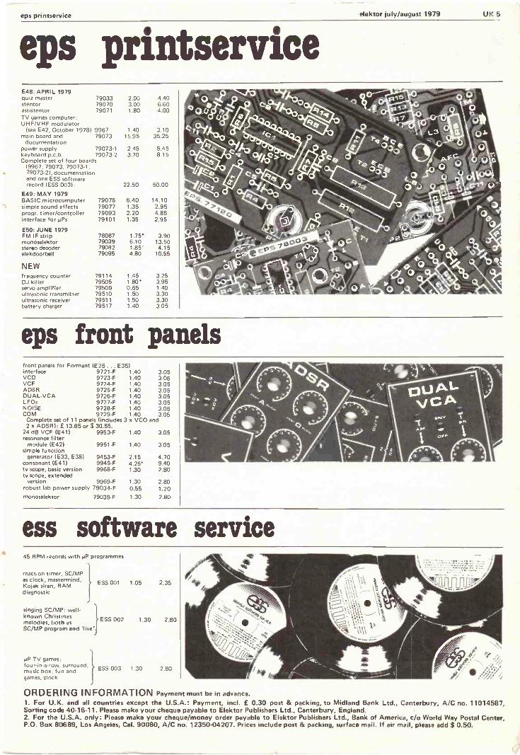
eps printservice elektor july/august 1979 UK 5
eps printservice E48: APRIL 1979 quiz master 79033 stentor 79070 assistentor 79071 TV games computer: UHF/VHF modulator
(see E42, October 1978) 9967 main board and 79073
documentation power supply 79073-1 keyboard p.c.b. 79073-2 Complete set of four boards
(9967. 79073. 79073-1, 79073-2), documentation and one ESS software record (ESS 003):
E49: MAY 1979 BASIC microcomputer simple sound effects progr. timer/controller interface for µPs
E50: JUNE 1979 FM IF strip monoselektor stereo decoder elekdoorbell
NEW frequency counter DJ killer servo amplifier ultrasonic transmitter ultrasonic receiver battery charger
79075 79077 79093 79101
78087 79039 79082 79095
79114 79505 79509 79510 79511 79517
2.00 3.00 1.80
4.40 6.60 4.00
1.40 3.10 15.95 35.25
2.45 5.45 3.70 8.15
22.50 50.00
6.40 1.35 2.20 1.35
1.75' 6.10 1.85' 4.80
1.45 1 .80' 0.65 1.50 1.50 1.40
14.10 2.95 4.85 2.95
3.90 13.50 4.15
10.55
3.25 3.95 1.40 3.30 3.30 3.05
-or`- 7taO v7 .
, (13 ?:.
giEpS:
áalp \ t
,..-, ° tt P { '1s 0 .ti '""«
Z
1.3 551
Oi
Q "Q
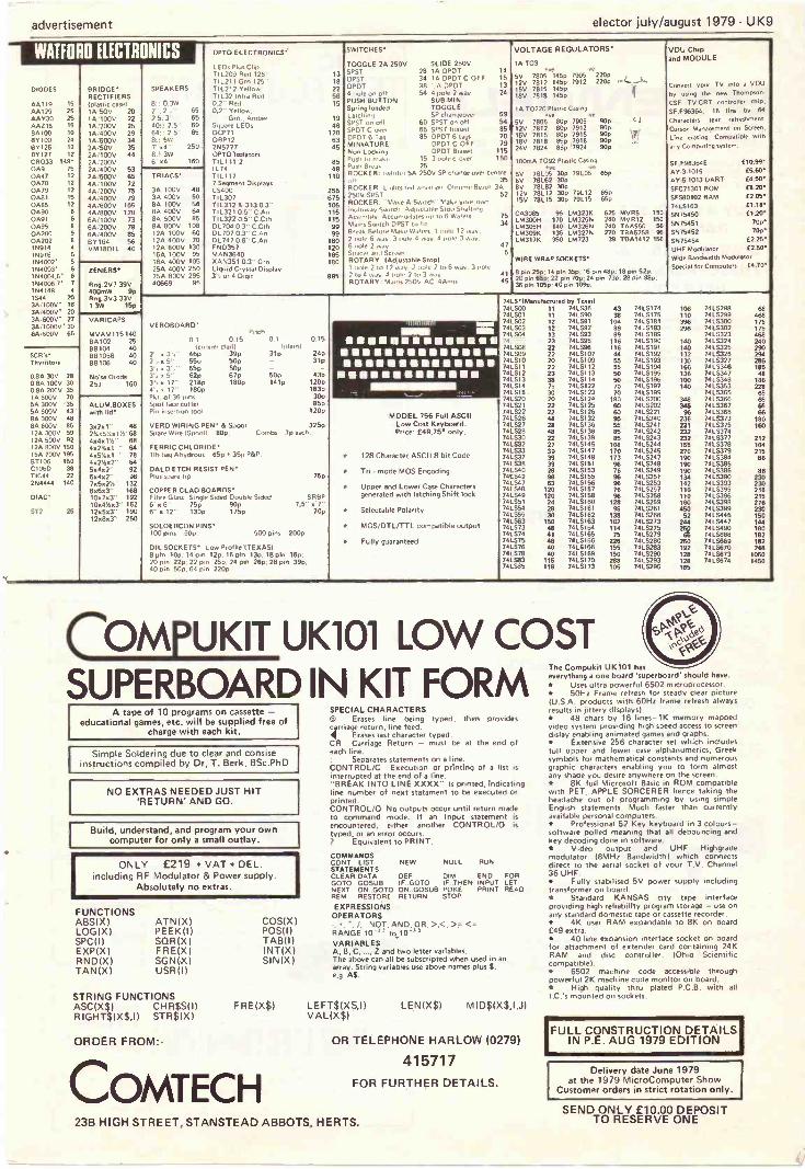
eps front panels front panels for Formant )E25 ... E35) interface 9721-F 1.40 3.05 VCO 9723-F 1.40 3.05 VCF 9724-F 1.40 3.05 ADSR 9725-F 1.40 3.05 DUAL-VCA 9726-F 1.40 3.05 LFOs 9727-F 1.40 3.05 NOISE 9728-F 1.40 3.05 COM 9729-F 1.40 3.05
Complete set of 11 panels (includes 3 x VCO and 2xADSR(:£13.85or$30.55.
24 dB VCF (E41) 9953-F 1.40 3.05 resonance filter
module (E42) 9951-F 1.40 3.05 simple function
generator (E33, E38) 9453-F 2.15 4.70 consonant 1E411 9945-F 4.25` 9.40 tv scope, basic version 9968-F 1.30 2.80 tv scope, extended
version 9969-F 1.30 2.80 robust lab power supply 79034-F 0.55 1.20 monoselektor 79039-F 1.30 2.80
a ---m
,U. m .. o
Y
N. 1
nM - pFF t
ii
ess software service 45 RPM records with µP programmes
reaction timer, SC/MP as clock, mastermind, Kojak siren, RAM diagnostic
ESS 001 1.05 2.35
singing SC/MP: well- known Christmas
ESS 002 1.30 2.80 melodies, both as SC/MP program and 'live'
µP TV games: four -in -a -row, surround,
ESS 003 music box, fun and games, clock
1.30 2.80
ORDERING INFORMATION Payment must be in advance. 1. For U.K. and all countries except the U.S.A.: Payment, incl. £ 0.30 post & packing, to Midland Bank Ltd., Canterbury, A/C no. 11014587, Sorting code 40-16-11. Please make your cheque payable to Elektor Publishers Ltd., Canterbury, England. 2. For the U.S.A. only: Please make your cheque/money order payable to Elektor Publishers Ltd., Bank of America, c/o World Way Postal Center, P.O. Box 80689, Los Angeles, Cal. 90080, A/C no. 12350.04207. Prices include post & packing, surface mail. If air mail, please add $ 0.50.

UK 6 elektor july/august 1979 decoder e
e or e 51/52 Volume 5 Number 7/8
Elektor Publishers Ltd., Elektor House, 10 Longport, Canterbury CT1 WE, Kent, U.K. Tel.: Canterbury (0227) 54430. Telex: 965504. Office hours: 8.30 - 12.45 and 13.30 - 16.45. Bank: 1. Midland Bank Ltd., Canterbury, A/C no. 11014587
Sorting code 40-16-11, Giro no. 315.42.54 2. U.S.A. only: Bank of America, c/o World Way
Postal Center, P.O. Box 80689, Los Angeles, CA 90080, A/C no. 12350-04207.
3. Canada only: The Royal Bank of Canada, c/o Lockbox 1969, Postal Station A, Toronto, Ontario, M5W 1W9. A/C no. 160-269-7.
Please make all cheques payable to Elektor Publishers Ltd. at the above address.
Elektor is published monthly. Number 51/52 (July/August) is a double issue.
SUBSCRIPTIONS: Mrs. S. Barber Subscription 1979, January to December incl.: U.K. U.S.A./Can. other countries
surface mail airmail surface mail airmail £ 8.50 $ 21.00 $31.00 £8.50 £ 14.00 Subscriptions normally run to December incl. Subscriptions from September issue:
U.S.A./Can. other countries U.K. surface mail airmail surface mail airmail £2.75 $7.00 $ 10.00 £ 2.75 £4.50 Back issues are available at original cover price. Change of address: Please allow at least six weeks for change of address. Include your old address, enclosing, if possible, an address label from a
recent issue.
ADVERTISING MANAGER: N.M. Willis National advertising rates for the English -language edition of Elektor and international rates for advertising in the Dutch, French and German issues are available on request.
U.K. EDITORIAL STAFF T. Day
EDITOR I. Meiklejohn W. van der Horst P. Williams
J. Barendrecht G.H.K. Dam P. Holmes E. Krempelsauer G. Nachbar
TECHNICAL EDITORIAL STAFF A. Nachtmann J. Oudelaar A.C. Pauptit K.S.M. Walraven P. de Winter
Technical telephone query service, Mondays only, 13.30 - 16.45. For written queries, letters should be addressed to dept. TO. Please enclose a stamped, addressed anvelope or a self-addressed envelope plus an I RC.
ART EDITOR: F. v. Rooij
Letters should be addressed to the department concerned: TQ = Technical Queries ADV = Advertisements ED = Editorial (articles sub- ADM = Administration
mitted for publication etc.) EPS = Elektor printed circuit SUB = Subscriptions board service
The circuits published are for domestic use only. The submission of designs or articles to Elektor implies permission to the publishers to alter and translate the text and design, and to use the contents in other Elektor publications and activities. The publishers cannot guarantee to return any material submitted to them. All drawings, photographs, printed circuit boards and articles published in Elektor are copyright and may not be reproduced or imitated in whole or part without prior written permission of the publishers.
Patent protection may exist in respect of circuits, devices, components etc. described in this magazine. The publishers do not accept responsibility for failing to identify such .
patent or other protection.
Dutch edition: Elektuur B.V., Postbus 75, 6190 AB Beek (L), the Netherlands.
German edition: Elektor Verlag GmbH, 5133 Gangelt, W -Germany French edition: Elektor Sarl, Le Doulieu, 59940 Estaires, France.
Distribution in U.K.: Seymour Press Ltd., 334 Brixton Road, London SW9 7AG.
Copyright ©1979 Elektor publishers Ltd. - Canterbury.
Printed in the UK.
OI 1141 MIOIT W 1.UV 01 CI,CVIAiIGp
A 111
I
decoder What is a TUN? What is 10 n? What is the EPS service? What is the TQ service? What is a missing link?
Semiconductor types Very often, a large number of equivalent semiconductors exist with different type numbers. For this reason, 'abbreviated' type numbers are used in Elektor wherever possible:
'741' stand for 4A741, LM741, MC641, MIC741, RM741, SN72741; etc. 'TUP' or 'TUN' (Transistor, Universal, PNP or NPN respect- ively) stand for any low fre- quency silicon transistor that meets the following specifi- cations:
UCEO, max IC, max hfe, min Ptot, max fT, min
20V 100 mA 100 100 mW 100 MHz
Some 'TUN's are: BC107, BC108 and BC109 families; 2N3856A, 2N3859, 2N3860, 2N3904, 2N3947, 2N4124. Some 'TUP's are: BC177 and BC178 families; BC179 family with the possible exeption of BC159 and BC179; 2N2412, 2N3251, 2N3906, 2N4126, 2N4291.
'DUS' or 'DUG' IL)iode Univer- sal, Silicon or Germanium respectively) stands for any diode that meets the following specifications:
DUS DUG UR, max 25V 20V IF, max 100mA 35mA IR, max 1µA 100 µA Ptot, max 250mW 250mW CD, max 5pF 10pF
Some 'DUS's are: BA127,BA217, BA218, BA221, BA222, BA317, BA318, BAX13, BAY61, 1N914, 1N4148. Some 'DUG's are: 0A85, 0A91, 0A95, AA116.
'BC107B', 'BC237B', 'BC547B' all refer to the same 'family' of almost identical better -quality silicon transistors. In general, any other member of the same family can be used instead.
BC107 (-8, -9) families: BC107 (-8, -9), BC147 (-8, -9), BC207 (-8, -9), BC237 (-8, -9), BC317 (-8, -9, BC347 l$, -9), BC547 (-8, -9), BC171 (-2, -3), BC182 (-3, -4), BC382 (-3, -4), BC437 (S, -9), BC414
BC177 (-8, -9) families: BC177 (-8, -9), BC157 1-8, -91, BC204 (-5, -6), BC307 (-8, -9), BC320 (-1, -2), BC350 (-1, -2), BC557 (-8, -9), BC251 (-2, -3), BC212 (-3, -4), BC512 (-3, 4), BC261 (-2, -3), BC416.
Resistor and capacitor values When giving component values, decimal points and large numbers
of zeros are avoided wherever possible. The decimal point is usually replaced by one of the following abbreviations: p (pico-) = 10-" n (nano-) = 10-9 µ (micro-) = 10-6 m (milli-) = 10-3 k (kilo-) = 103 M (mega-) = 106 G (giga-) = 109 A few examples: Resistance value 2k7: 2700 St. Resistance value 470: 470 fl. Capacitance value 4p7: 4.7 pF, or 0.000 000 000 004 7 F .. .
Capacitance value 10n: this is the international way of writing 10,000 pF or .01 µF, since 1 n is 10-' farads or 1000 pF. Resistors are'/. Watt 5% carbon types, unless otherwise specified. The DC working voltage of capacitors (other than electro- lytics) is normally assumed to be at least 60 V. As a rule of thumb, a safe value is usually approxi- mately twice the DC supply voltage.
Test voltages The DC test voltages shown are measured with a 20 Idt/V instru- ment, unless otherwise specified.
U, not V The international letter symbol 'U' for voltage is often used instead of the ambiguous 'V'. 'V' is normally reserved for 'volts'. For instance: Ub = 10 V, not Vb=10V. Mains voltages No mains (power line) voltages are listed in Elektor circuits. It is assumed that our readers know what voltage is standard in their part of the world! Readers in countries that use 60 Hz should note that Elektor circuits are designed for 50 Hz operation. This will not normally be a problem; however, in cases where the mains frequency is used for synchronisation some modifi- cation may be required.
Technical services to readers EPS service. Many Elektor
articles include a lay -out for a
printed circuit board. Some - but not all - of these boards are avail- able ready -etched and predrilled. The 'EPS print service list' in the current issue always gives a com- plete list of available boards.
Technical queries. Members of the technical staff are available to answer technical queries (relating to articles published in Elektor) by telephone on Mondays from 13.30 to 16.45 Letters with technical queries should be addressed to: Dept. TQ. Please enclose a stamped, self addressed envelope; readers outside U.K. please enclose an IRC instead of stamps.
Missing link. Any important modifications to, additions to, improvements on or corrections in Elektor circuits are generally listed under the heading 'Missing Link' at the earliest opportunity.

Largest range of quality components in the - U.K. over 8,000 types stocked
G
ars all Head Office and mail Order to Dept. ELK A. Marshall (London) Ltd., Kingsgate House, Kingsgate Place, London, NW6 4TA Tel: 01-624 0805 Tlx. 21442
Retail Sales: London:40 Cricklewood Broadway, NW2 3ET. Tel:01-452 0161/2 ALSO 325 Edgware Road, W2. Tel:01-723-4242. Glasgow:85 West Regent Street, G2 2QD. Tel:041-332 4133 AND Bristo1:108A Stoke's Croft, Bristol. Tel:0272 426801/2.
LEDS & OPTO BY SIEMENS
0 Displays 7 seg LEDS Coin anode or cash. Small 3mm Red Large 5mm Bmm HT £1.50 Extra lOmm HT £1.55 Bright 14mm HT £1.57 I//ed L0271 18mm HT £1.85 IR receiver
Opto coupler
Red Gr 18p 19P 2011 200
Yell 1911
20p
40p 40p 40p £0.55 £1.45 £1.55
Full range a data In our 79 catalogo.
RAACO STORAGE BOXES Strong durable high impact polystyrene boxes with brass hinge pins.
89 E1.62 818 £1.78
LINEAR (see catalogue for full range) LM339N LM340T5 LM340112 LM340115 LM340T24 LM341P.5 LM341P.12 LM341P.15 LM341P.24 LM345K LM348N LM350K LM358N LM360N LM370N LM371H LM373N LM374N LM377N LM378N LM3795 LM380N8 LM380N.14 LM381AN LM381N LM382N 1.61373419
LM386N LM387N LM388N LM389N LM392N LM701B LM701C LM702C LM703LN LM709CH LM709-8 LM709 14 LM710CH
.LM71o.14 LM711CN LM716 LM723CH LM723C14 LM741CH LM761C8 LM741C.14 LM747CN LM7488 LM748 14 LM900 LM911 LM921 LM923 LM 13035 LM1304N LM1305N LM1307N LM1310N
[0.60 £0.88 £0.88 £0.88 £0.88 £0.56 £0.56 £0.56 £0.56 £6.97 £0.95 £6.50 £0.60 £3.00 £3.30 C2.35 £3.35 £335 [1.B0 £2.40 [425 £0.96 £1.08 £2.70 £1.69 £1.32 £1.55 £0.88 £1.10 £1.00 £1.00 £0.87 £2.99 C2.99 £0.81 £1.15 £0.70 £0.50 £049 £0.67 £0.48 £0.40 £1.00 £0.62 £0.45 £0.50 £0.30 £0.60 £0.78 £0.50 £0.50 £050 £0.50 [0.50 £0.50 £1.15 £1.52 £1.02 £122 [2.10
LM1351N £1.30 LM1458N £0.45 L9,14965 £0.97 LM1800N £1.94 LM180IN £2.25 LM1808N £2.10 LM1812N £6.20 LM18205 £1.16 LM1828N £1.90 LM1830N £1.90 LM 18455 £1.50 LM 18485 [1.98 LM 18505 £1.90 LM1889N £2.50 LM1890N P.O.A. LM2907N 8 £1.80 LM2917N 8 f1.80 LM3301N £0.60 LM3302N £0.55 LM3401N . £0.55 LM3900N £0.68 LM3905N 61.15 LM39095 00.78 LM3911N £1.10 LM3913N P.O.A. LM3914N £2.79 LM4250CN E1.30 LM78L05CH £0.85 LM78L12CH 00.85 LM78L15CH £0.85 LM78L24CH £086 LM7805KC £1.56 LM7812KC £1.56 LM7815KC E1.56 LM7824KC £1.56 LM78L05CZ £0.30 LM78L12C2 £0.30 LM78L15CZ £0.30 LM78L74CZ C0.30 MC667P £2.75 MC671P £1.75 MC672P £1.75 MC774P £2.10 MC789P £180 MC790P £3.10 MC798P £2.20 MC799P £2.20 MC832P £0.70 MC833P £0.70 r.1C836P £0.82 MC837P £0.82 MC838P £2.35 MC840P £1.65 MC844P £0.70 MC846P £0.70 MC848P £1.10 MC849P £0.70 MC857P £0.85 MCB61P C065 MC1035P £1.90
CA3000 £3.30 CA3001 [425 CA3002 [3.30 CA3006 U.60 CA3007 £4.15 CA3008 £2.55 CA3012 £1.65 CA3013 £165 CA3014 £2.20 CA3018 £0.75 CA3018A £1.10 CA3020 £2.20 CA3020A £2.50 CA3021 £2.40 CA3022 [2 20 CA3023 £220 CA3026 [0.70 CA3028A £0.90 CA30286 £125 CA3029 £0.75 CA3029A £0.90 CA3030 £1.50 CA3030A £2.20 CA3033 £3.70 CA3034 £2.75 CA3035 £1.95 CA3036 £1.21 CA3038 £2.90 CA30384 £4.10 CA3039 £0.77 CA3040 £3.75 CA3041 £1.65 CA3042 £1.65 CA3043 f2.20 CA3045 £1.55 CA3046 £0.77 CA3047 £2.20 CA3047A £3.70 CA3048 £245 CA3049 £1.98 CA3050 £2 6fi CA3051 £1.82 CA3052 £1.78 CA3053 £0.77 CA3054 £1.10 CA3059 £2.10 CA3060 £250 CA3062 £3.75 CA3064 £1.10 CA3065 £1.10 CA3068 £3.80 CA3070 C1.90 CA3071 £1.90 CA3072 £1.90 CA3075 £1.70 CA3076 £2.12 CA3080 £0.85 CA30804 £2.10 CA3086 £0.50 CA3038F E1.87
MEMORIES (see catalogue for full range) 5102/1817 09.00 MM801,n8N C066 1 wau.,/5511610 1,154040I51 C646 413.171114J.N01563 M857040 (900 10111871:195 62 90 1M9103361 fl 75 T954116 7%4 (26 00 4111'35111.1.5 03 30
0953035 f4 83 08886.795 f2 08 1053036 ./51 £3.28 185416441 POA 4n1:3/111:I.N £9 35
0853014AN113.65 00601:305 (208 1M54035251 8279 1056011NI [536 410.15011.1.5 (1.30 M0S314 0460 54M531144 f4 47 1N54047 7N1 (298 14159g00J1 44 411 41)1,1/011.t.6 £9 35
91515316 VI 60 1,1.15/105N£1043 1M540412141 £2.98 11,5990151 00 66 4y2513 £8 75
80533014 /420 M6157,09501341 15154044 205 t 19.85 75r59907141 C9 16 41185107 (650 80601-956 f056 M9551606 £6 71 1515404520511915 15159903N1 (1374 Ay 35810 (12.75 81.6101.966 £066 M4.51161N C671 11054050 25i (646 15/59904 POA SI1I1101Á 0895 M01801'9>5 £0.58 7M5271611C1950 1M941h1791 f6 46 85159901. POA SI195364 (1600
TRIACS POWER TRIALS AT UNBEATABLE PRICES
TIC 2060 Plashc 1066 400V 4A £0.60 TIC225D Plastic 1066 400V 6A £0.70 TIC2260 Plastic 1066 400V 84 £0.70 TIC2360 Mastic 1066 400V 12A £1.00 TIC2460 Plastic 1066 TIC2530 Plastic 103
400V 16A 400V 204
£121 [167
TIC2630 Plastic 103 4000 25A £2.20 40576 £2.20 40669 £1.30 40842 [1.25 254444 £1.95
CMOS (see catalogue for full range) 74000N 74CO2N 74C04N 74C08N 74ClON 74C14N 74C20N 74C30N 74C32N 74C42N
£0.24 [0.24 £024 £0.24 £024 £0.95 £024 £0.24 £024 00.92
740485 74C73N 74C74N 74C765 74C83N 74C85N 74C86N 74C89N 74C90N 74C93N
£1.38 74C95N £0.54 74C107N E0.56 74C150N £0.54 74C1515 £130 74C154N £1.30 74C157N £0.64 74C160N £4.39 74C161N £0.85 74C162N £0.85 74C163N
£1.04 £1.22 £4.14 £2.47 £3.68 £2.21 £1.11 £1.11 £1.11 f1.11
CD4000 CDA001B CD4002 C04006 C04007 C0400813 CD4009 CD4010 CDA011B C04012
NEW 1979 CATALOGUE
48 page catalogue -new enlarged micro section -largest range of quality comp- onents from franchised suppliers available in UK. All VAT inclusive prices. Over 8000 line items plus lots more. 50p post paid or 40p to callers at any of our four branches
MAIL ORDER
Please add 40p for p/p to all our orders Telephone orders on credit cards E10.00 minimum.
£0.20 CD40138 £0.52 £0.20 CD4014 £1.00 f0.18 CD4015 £0.75 £1.25 CD4016 £0.51 £0.18 CD4017B £1.05 £099 C049188 £1.05 £0.58 CD40198 £052 £0.58 C040708 £1.15 £0.20 CD4021 £1.05 £0.20 CD4022B £1.00
Eft
M
W.711
NEW NEW TELETEXT CHIPS from Mullard-available now from Marshall's- Sole UK distributor to the hobbyist market.
SAA Series, for the reception, display and control of television based text display systems. Suitable for 'CEE -
FAX' and'ORACLE' Remote Control SAA5000 Infared/Ultrasonic SAA5010 Station selector/DICS SAA5012 Binary Imput Tuners TELETEXT (Dedicated I -C's) SAA5020 TIC (Timing Chain) SAA5030 VIP(Video Imput Processor) SAA5040 TAC(Teletext Data Acquisition and Control) SAA5050 TROM (Teletext Read -Only Memory) TIC,TAC,& TROM are NMOS--VIP is linear bipolar We recommend using DI sockets with these chips
TRANSISTORS (for full range see catalogue)
£3.48 £8.13 £8.13
£8.71 £11.61
£31.82
£18.86
753407 .21 253566 .25 253703 .14 254907 4.90 255033 .65 755194 80 255306 .33 2N5543 750 256131 .70 80181 1.90 BFW43 1.65 8FV76 .36 753404 .21 753567 25 253704 .14 764908 3.72 765035 1.10 265195 .97 255307 .30 755550 .38 256132 .70 60187 2.20 BFW59 1.75 BFV90 135 2N3405 .21 253570 4.50 753705 .14 254909 4.98 755036 1.20 255109 .35 255308 .33 255551 .44 2N6133 .70 80183 2.35 BFW87 1.75 80208 2.70 2N3414 .18 253571190 253706 .14 264910 1.20 255086 .30 755210 .38 7N5354..27 265555 .65 766134 .70 80187 95 BFW90 1.75 BUV2011.50 763415 .18 2635723.00 253707 .14 254913 1.45 255087 .30 265719 .16 7N5355 .20 2N5638 .45 256179 .77 813201 1.10 BFX12 .35 BUV21 12.96 253416 21 253583 1.25 253708 .12 764914 1.65 255088 .30 255770 .15 2N5356 .23 755640 .45 2561801.05 80202 1.25 BFX13 .33 8UV2713.77 253417 25 753584 935 253709 .12 764915 2.40 755089 .30 255221 16 7N5358 1.75 755654 55 256181 .68 80203 1.28 BFX19 49 BUV23 14.58 .753420 253605 .18 753710 .12 254916 .22 255126 .44 755727 20 765365 24 255655 .55 2562531.00 130204 1.35 80029 34 BUV24 15.39
12.50 753606 .18 263711 .12 254917 27 255177 22 2N5223 .16 255400 .33 755656 65 256254145 80220 .66 BFX30 .34 BUV7516.20 253439 .85 763607 .18 .53712 135 264918 .65 255128 .22 155224 .16 255401 44 116288 50 BOI21 .66 BF%3a ,6b J300 .37
253440 .75 263632 2N3713 150 264919 .70 755179 22 255225 .16 2N54151.05 255661 1N6289 .50 BD222 .66 BFX37 A9 J310 .GI
2N3441 .92 12.75 253714 1.55 254920 .83 255130 22 255226 .16' 2554161 65 2N6790 .50 BD223 .76 BFX68 1.10 MEO401 22 763447 1.45 2N3638 .17 253715 1.55 254921 54 255131 .22 2N5727 .16 255447 .16 2615786 .98 266292 50 80724 75 811084 .30 ME0402 .22 253444 1 35 7536384 .17 263716 2.29 254922 .60 255133 .22 255237 22 765448 .16 255813 55 6F139 .70 80737 .75 BFX85 .38 ME0404 17 763445 6.50 763639 .33 753724 65 254923 .75 265137 .22 2552374.23 255449 20 256027 64 AF240 1.25 80233 .45 BFX86 .30 ME0411 22 753446 253640 25 763775 60 254924 1.15 755138 22 255239 2.25 755450 .16 2N6036 1.39 AF279 18 80234 .46 BF%87 .35 ME0412 22
10.00 753641 25 7N37311.00 254926 1.70 765139 .22 765745 .37 765451 .16 256079 1.17 AF 280 .95 90235 .46 BFX88 .30 ME0413 .17 753447 753647 22 153734 ,75 754917 1.70 755140 .22 755746 .38 255457 .35 256099 .62 AFV42 1.65 00538 .77 BF 1.37 MJ3000 2.15
' 1050 753643 .38 753735 7.00 254978 220 255142 22 755247 .44 755458 35 256107 .45 AU110 1.70 80539 60 6F1/10 1.10 MJ3001 2.35 2193040 253644 40 7548711 .51 754941 .30 765143 ,12 265148 44 255459 .32 756108 55 AU113 1.70 1313540 .60 6F918 1.10 MJ4502 4.90
1200 253645 38 754888 .54 754945 .30 755172 .24 255249 38 255160 .65 256109 .55 BC409 27 80581 1.10 BF Y19 1.10 MJE340 .67 253468 1.32 753646 16 754889 .75 254964 '.28 755179 .75 2N5766 3.00 265461 .53 256111 .49 80413 .16 0D582 1.30 BFV37 1.10 MJE350 .62 753507 253667 25 754891 1.30 1554965 .28 255180 .58 255293 .44 255462 .65 156121 A1 BC414 .17 80675 .60 8(139 .38 MJE370 .62
10,00 253663 .29 254898 1.55 254966 ,28 2651831.10 255794 ,44 155484 .37 756127 44 8C415 .16 80676 .65 BF Y41 .88 MJE371 .66
IN3511 1.10 1N3690 .45 7NJ901 1.65 7Na967 ,28 255188 .44 255295 .44 7N5a85 40 256123 .48 130153 105 80677 .70 8F950 .35 MJE520 .50
753553 153697 65 754902 220 254968 .18 255189 .40 2N5296 44 2N5486 .40 756124 45 80155 1.10 89678 82 8F951 35 MJE521 .70 3.25 253697 45 754903 2.75 254969 ...28 755190 .65 255298 .44 755490 .64 256125 A7 80157 .70 8F598 .33 13F152 .35 MJE29551.65
253563 .25 753693 .50 254904 1.85 255010 5.75 2N5191 .75 255301 4.00 265492 .64 756126 .48 8D158 .70 BFW10 .83 BFV53 .40 541E30551.05 753564 .25 253694 .50 154905 2.40 255017 8 25 255192 .80 255303 5.50 255494 65 256129 60 130159 .70 BFW11 .83 8FV72 .99 MP8111 .40 253565 25 753702 .14 154906 2.99 255030 .22 2N5193 .75 255305 .26 755496 .67 256130 .65 BD160 740 BFW30 2.45 8F175 .77 MP8112 45
THYRISTORS TYPE RATING CASE PRICE T IC441 0.671 30V 1018 £0.30 T1C461 0.6A 100V 1018 £0.50 T IC471 0.64 200V 1018 £0.60 2N5060 0.54 25V 1018 f0.32 255061 0.5A 50V 7018 £0.33 2N5062 0.54 100V 1018 £0.40 255063 0.5A 150V 1018 £0.43 255064 0.54 2000 .1018 £0.45 8,160246 4.74 700V Plastic £1.48 87106 Stud Mounting £1.10 BT1201XK3139/3158/3132) BT121IXK31341
C1.10 C1.10
TTL (see catalogue for full range) 55)40055(000 $57411105C055 51480115[055 55100705 [0.55 55/e11215(055 55)40305[05!
)415855 C095 /415065 0044 40.5905 (0.4 UN 5915 [120 HL5975 [0.70 )5,5935 [064
14157435 £125 14157445 0150 14652455 (1.4; 611.524 IN [10/ 141.57485 [1 01 701.52495 (101
SN7451405 [0.771 55145'575 t295 557451085 [2.70 551e51895 [111 551452005 [350 557/52015 (3.71
5555040N[055 SN>40SIN[O55
>4159547a0090 1415965 [135
74152515 [100 24L575" CI 00
55745262511250 5524528>5 [2.95
55740535ro56 55/a0S(N£055
,4151075 [0.42 /.5.5r095(0.42
I41.525114 (100 HLS258N 0100
557452885 [2.10 S57452895 L111
55510%5 [0% $5100605(955
153511751042 141.51131+10.47
)41.52595 [155 74657615 C325
557453005 (566 S57453015 (3.71
55)40625(055 S5741005 00 55
74951145 (0,42 5651225 (0.62
14152865 (0 41 74152135 1120
5574538)5 [3.05 557454 705 CSO6-
55141025 00 55 5574,045 [0.60
7415123N (013 5415124N (1 70
241.52155 [3.70 741.52195 [051
557454715 05.48 557454>75113.40
S5741475 [3.10 557417450090
14151255 (0.50 74151765 (050
741.52805 [1 65 /4152835 01.20
557451>3N (13.44 557/1547419 01343
S5741355 C262 55741935(2.90
/4151325 89.45 74151065 (0.42
14152895 C3.14 HL57905 [100
5N7454155[13.44 55149045 C036 ÍI
)415065 0027 1415015 00 26
74151385ro65 74051395 00 65
14657935 [100 14157955 01.35
557491 /15 [0.10 55749/5 1.0.06
7415025 03.20 )0-135 0026
74,51455 ft 30 >41514750165
74652985 01 35 74152995 [2.16
5574935 (0.38 5574045 (010
7,1("45 [0.21 1215055 CO 29
5115148N II 75 14151515 (050
74153235 (060 74153245 01 65
5574955 80.76 5574965 (051
1415005 CO26 1015095 00.26
74151535 0056 746515.15 f 1.45
14153755 0240 14153765 02.70
5514975 01. $57410011 014
7615105 (0.24 74,5115 00 26
14L51555GOO 74651565C010
74153275 £255 74/ 53485 L1.10
S5741075 C0.24 S514118N 03 90
1415125 CO26 74,5135 (055
74151515C060 14151585 MG
741.53525 0107 74153535 [107
55741195 [140 55741215 (024
7415145 [0.15 7415155 [026
74151605 [010 74151615 85
74153655 (055 741.53565 [055
SN74122N (0.56 95741238/ MSS
)41.5705 (0.24 7415315 [0.26
72151625 [010 74151635 03 95
74153675 ro.55 74153685 0.55
55141245 [120 58/741255 [0295
7485725 1026 141.5265 [032
141516a5 [1.10 74151655 [1.15
1413313N [055 741S]735 C0.15
55741415 [050 55741455 (005
72L5275 (0.24 7415205 CO 29
74151665 f1 66 )4151685 [1A5
4653 5N (066 246S317N [1.30
5514I485 [1.36 55241505 [0.90
7415305 [0.1, 1411125 (0.27
74151695 [1.45 14151705 CI SO
141.53785 [1.00 12153795 [125
55741515 (0.16 557415391 roe
1415335 £029 741.5315 ro32
74151135 [1.10 14151745 [0.75
74153865 [0 44 74153905 ro.90
S5721525 11.20 55741565 [0.70'
14LS]8N [0.32 )a15405 [016
14151155 £0.75 51151131N (2.75
74153935 (0.90 741.53955 91.50
55741515 [0.71 5514160AN C090
7415425 [050 74154174 [1 09
74151835£2.70 74151895 (3.74
74153985 [1.90 74153995 0145
557416145 r0e0 55741624N 0290
7416495 81 00 74L5295 elO1
74151905 [110 74151915 9100
74154905 1090 14L56105 [1.90
557416345 0290 55741645 10.98
7415515 10.29 7415545 CO 26
74151975 CO 95 74151935 00.95
S5745005 (0.77 55745005 (0.77
55741655 (0.18' 55141675 (250
7415555 CO 213
7415635 01 26 74,51945 [0.70 74151955 00.70
5514504N [0.84 511745105 0.77
55141745 01.00 S5741755 11.00
74,5735 (0.42 74,5745 ro.42
74151965 8010 741.61975 [0 80
55745205 C0.77 55746405 ro.77
55741765 (0.10 55741775 (010
741.5755 C05/ 7465765 [0.42
14652215 1010 74152405 [1 50
57474S645 (0.77 56745656 £0.77
5574180N (100, SN741815 02.00
141.578N (042 141.58345 (0.90
14652415 [150 74151425 L1.25
S8/745117501,70 55745114501.70
55741675 0340
KNOBS for 1/444 spindles see catalogue for full range. MI Black 0
'
moon. metal mutt 75t 4, . . 0015 A. 1,2
insert gna
Al er
MI but '33mrn 4.2. won £0.31
M3 Black p m tal t
achined slut 36mm
4.. £0.37 1,4 Black plashc 7.94 'mpetune0
metal insert and Pon me (0.37
M5 Black plasm tmachined insert and 91,/I 30mm
do £0.33 116 87.1k 0ta1hc body won metal
inlay 21mm drrneter £0.18 M]
n inlay
compact a. very Myln. diameter 24mm £032
1,8 As 400.0 but 28mm 4.a. CO 62
MI5 Black pl.,hc pointer knob onto white marker OD 18mmisarrtl Pointer 31mm 1009 , . 00.15
816 0,9nly polnne4 metal 0124 200 pointer. Diameter 22mm
0020
;110
r Marshall's 325 Edgware Road London W2. Tel 01.723 4242 II. <ff IrA
Marshal I's 108A Stokes Croft Bristol. Tel 0272 654201

UK8 - elektor july/august 1979 advertisement
WATFORD ELECTRONICS 33/35 CARDIFF ROAD, WATFORD, HERTS, ENGLAND
MAIL ORDER, CALLERS WELCOME. Tel. Watford 45588/9
ALL DEVICES BRAND NEW, FULL SPEC. AND FULLY GUARANTEED. ORDERS DESPATCHED BY RETURN OF POST. TERMS OF BUSINESS: CASH/CHEOUE/P.O.s OR BANKERS DRAFT WITH ORDER. GOVERNMENT AND EDUCATIONAL INSTITUTIONS OFFICIAL ORDERS ACCEPTED. TRADE AND EXPORT INQUIRY WELCOME. P & P ADD 300 TO ALL ORDERS UNDER 610.00. OVERSEAS ORDERS POSTAGE AT COST. Send 50p (plus 250 p&cal for our catalogue.
VATExpon orders no VAT. Applicable -to U.K. Customers only. Unless stated otherwise. all cams are exclusir of VAT. Please add 8% to devices marked . To the rest add 12%. We stock many more items. It pays to rise us. We are situated behind Watford Football
Ground. Nearest Underground/Br. Rail Station: Wedord High Street. Open Monday to Saturday 9 a.m, to 6 pm. Ample Free Car Perking Space evadable.
POLYESTER CAPACITORS: Axial Lead Type. 400V: 1nF, 1n5, 2n2. 3n3, 4n7, 6n8. 10n, 15n, 9p: 18. 10p; 22n. 33n. I1p: 47n, 68n, 140; 100n 17p;
150n. 220n. 24p; 330n. 470n 410' 680n 480. 160V: 39nF, 150n, 220n. 11p; 330n.470n 190:68n. luF 220; 2.20F 32p;4.7uF 360. Dubilier 1000V: 10n, 15n, 200; 22n 22p; 47n 26p; 100n 38p; 470n 530; luF 175,
POLYCARBONATE CAPACITORS: ISIEM ANSI PCB Type 250V: 1nF,Ins,2n2.3n3,4n7,6n8,10n,7p;12n,15n,18n, 80. 22n. 27, 33n. 9p: 39n, 47n, 56n
68, 100; 82n, 100n 12p. 100V: 100n, lop; 120n, 150n, 13p; 180n, 220n. 16p: 270n, 330n, 390n, 470n. 240: 560n. luF 30p;
1.SuF 38p:2.2uF 48p.
ELECTROLYTIC CAPACITORS: Axial Lead Tope (Values are in uF). 500V: 10 400; 47 63p; 250V: 100 65p; 63V: 047. 1.0, 1 5. 2.2. 2.5, 3.3. 4.7.6.8, 8, 10, 15, 22. 8p:47. 32. 50 15p. 63. 100. 27p; 50V: 1.0 7p, 50, 100. 220 25p; 470 320; 1000 500; 400: 22. 33uF8p: 100 120. 2700, 3300 68p; 4700 85p: 35V 10. 33. 7, 330, 470. 32p. 1000 50p. 25V. 10, 22.47. 60; B0, 100, 160, 8p; 220. 250, 13p; 470. 640, 250; 1000 27p; 1500 300. 2200 45p. 3300 620; 4700 740; 160: 10. 40. 47 68. 70: 100. 125.8p:220,330. 140: 470 16p: 1000. 1500 20p: 2200 34p: 10V: 100 60: 640 120: 1000 tap. TAG END TYPE:70V: 2000 89p; 4700 135p; 50V: 10000 225p, 40V: 2500 65p: 3300 4700 70p: 15,000 2290: 75V: 4700 680; 2000 480:40V: 2000.7000 95p.
TANTALUM BEAD CAPACITORS 35V 0.10F, 0.22. 033, 0.47. GM 1 0. 2.20F 3.3. 4.7. 6.8. 75V: 1 5, 10, 20V 1.5uF 130 each, 10V. 22uF, 33. 200.6V: 22uF, 160.47oF 35p. 100uF 40p 2200F 460.
MYLAR FILM CAPACITORS 100V: 0.001, 0.002. 0.005, 0.01 u F
0.015. 0.02, 0.03, 0.04, 0.05. 0.056uF 0.1uF, 0.2. 9p 50V: 0.470F
6p 7p
12p
POTENTIOMETERS (AB of EGENI Carbon Track, 0 25W Log & 0.5W Linea, values 5001!. IK & 214 ILIN ONLYI Single 27p 5K!í 2MS! tingle gang 27p 5K!! 2M11 tingle gang D P switch 65p SKI. 2MS. dual gang stereo 780
CERAMIC CAPACITORS 50V Range: 0.5pF to 10nF ISnF,22nF,33nF,47nF, 4p IOOnF
POLYSTYRENE CAPACITORS: 100F to I nF. Bp 1.5nF to 47nF 100.
30
SLIDER POTENTIOMETERS 0.25W log and linear values 60nm track 5K! 1.500K! t single gang 10K.. 50061! Dual gang Sell.Strek graduated Alum Bezels
70p 800 220
6p PRESET POTENTIOMETERS 0.25W 10011 3.30111 Hoof large, 0.25W 25094.7M11 Vert.
10p 10p
SILVER MICAIpFI
SILVER MICA(pF) 3.3. 417. 6.8. 10. 12. 18. 22. 27, 33, 47, 50, 68. 75. 82. 85. 100, 120, 150 180, 220, 90 250, 300, 330,360. 390. 600 & 8200F 16p each 1000, 2200 200
S'OEC:350p'
S -DEC
T. DEC
U'DEC'A'
U -DEC '8'
3500'
4000'
4650'
699p'
RESISTORS -Erie make
RESISTORS -Este make 5% carbon M,n,atue High Stability. Low Noise
RANGE Val 1.99 0.25W 2.2114.7V E24 1.5p 0.5W 2.294.7M E 1 2 2p 1W 2.211.10M E12 5p Z% Metal Film (0S! IM 6p 1%0.5W 51111M E24 10p
loo 10
15p 4p 4p 8p
TRIMMERS miniature 2.50F; 3.100F: 330pF; 3.50pF 22p 5.25pF;65pF BBpF 30p
COMPRESSION 340pF; 10 80p 25 200pF 100.500pF
300 45p 45p
GAS AND SMOKE DETECTORS TGS812 or 813 415'
RF CHOKES luF, 4.7. 10, 22, 47, 100, 220, 470, 750 /mM, 2.5, 5, 10mH, 35p. 35nrH, 10omn, 600
CRYSTALS' 100kHe 455k He IMHe 1.80MHz I.BMMe 3 2768MH7 4.032MHa S.OMHt 8.083333MHa 14,31818MHe 18MHe 17.648MHa 100MHz
3850 3850 3230 385p 395p 3230 3230 355p 275p 323p 395p 3500 3230
COMPUTER HARDWARE: - 2102 1000 4047 2101.2 170p 745188 2111 195p 74S762 2112.2N 250p 745287 2114 2513 2708 77L08 2716 CP1610' TMS6011 4020
785p 745470 650p 745475 775p 81LS95 995p 81LS96
1650p 81LS97 930p MC1488 355p MC1489 325P Z802.5MH7
7500 165p 8950 325p 325p 8250
99p 990
125p 85p 90p
10500
TRANSISTORS p p BC177' 18
AC107' 28 BC178' 16
AC117' 35 BC179' 18
AC125' 20 BC181 20 AC126' 20 BC182 9 AC127' 20 BC183 9 AC128' 20 BC184 9
AC141' 24 BC1821. 11 AC141K' 38 8C1831 10 AC142' 24 8C184L 11 AC142K' 38 8C186' 21 AC176' 24 BC187' 28 AC187' AC188' 2424 13C212LBC212
10 11
ACY17' 35 BC213 10 ACY18 40 BC213L 12 ACV19 40 BC214 10 ACV20 40 BC214K 14 ACY21' 35 BC214L 13 ACV22' 40 BC307B 20 ACY28' 40 8C308 13 ACY39 78 BC3088 20 A0149' 70 BC327 15 AD161' 42 BC328 15 AD162' 42 BC338 12 AF106 50 13C441' 36 AF114' 40 BC461' 36 AF115' 40 BC477' 25 AF 116' 40 BC547 12 AF117' 40 BC548 12 AF118' 65 BC549C 13 AF 121' 48 BC557 15 AF124' 55 BC558 20 AF 125' 35 BC559 20 AF126' 50 BCY30' 57
AF139' AF127' 3535 BCY34' 75
BCY39' 80 AF 178' 70 BCY40' 78 AF180' 70 BCY42' 48 AF239' 42 BCY43' 85 AFZ12 126 BCY58' 90 ASY26' 40 BCY59' g0 ASY27' 45 BCY70' 18 ASY50' 95 BCY71' 20 ASY76' 95 ' 20 BC107' 9 BCY78BCY72' 25 BC107B' 10 BCZ10' 145 BC108' 9 BCZ11' 145 BC108B' 10 BD112' 95 BC108C' 12 813115' BC109 9 80121' 79 BC109B' 12 BD123' 98 BC109C' 12 130124' 115 BC113 20 BD131' 45 BC114 20 BD132' 45 BC715 20 B0133' 43 BC116 20 B0135' 38 BC117 20 13D136' 36 BC118 20 80137' 36 BC119' 28 130138' 50 BC134 20 BD139' 40 BC135 20 8D140' 36 BC136 18 BD142' 59 BC137 20 BD744' 198 BC140' 35 BD145' 198 BC142' 30 813181' 125 BC143' 30 80205' 13C147C147B
10 8
BD3 8D222'78 B'
8BC1C14848B
10 8 8815)453142:
D BD434'517'
BC148C 10 8D695A' BC149 8 B0696A' BC149C 10 BDY11' BC153 27 8DY17' BC154 BC157 10 BDY60' BC158
27 8DY56'
11 BDY61, eC159 11 BF115' BC160' 4p 136154' BC167A 71 BF158 BC168C 12 BF160'' 8C169C 14 BF161' BC170 BC171
18 BF167'BF173'
BC172 1111 BF177' BC173 12 8F178'
65
110 75
4265
5 6
65
22605
195 156 110 165
25 29 30 60 30 25 24 25
BF 179* BF 180' 8F181' 8F182' B F 183' BF184' BF 194 BF 195 BF 196 BF197 BF198 BF 199 BF 200' 8F244A OF 244 OF 2448 BF 256. BF257' B F 258' BF 259' OF 274 BF 336 BF394 BF594 BF595 BF R39 BFR40 BF R41 BF R79 BF R80 BF R81 BF R98 BF X29' BF X84 8F X85' BF X86' OF X87 BF X86' BFX88' BFY18' BFY50' BFY51' BF Y52' BF Y53. 8FY55' BF Y56* BFY64' B F Y71' BF Y81 BSX20' BSX29' BSX78' BSV95A BSZ26' 8U105' BU205 BU208 E113 E176' E421 MDB001 ME1120 ME4102 M E6002 MJ400' MJ491' MJ2955' MJ2966' MJE340' MJE370' MJE371 MJE520' MJE521' MJE2955' MJE3055 MPF 102 MPF 103 MPF104 MPF 105 MPF 106 MPF107 M PS3904 MPSA05 MPSA06 MPSA12' MPSA55 MPSA56 MPSA70
30 35 35 35 35 38
1
28 28 28 50 20 20 20 28 45 45 40 20 45 18 45 55 18 75
140 190 228
95
05
MPSUO2 MPSUO5 MPSU06 MPSU52 MPSU55
1212
OC23 MPU131NPSU56 '
' 12 OC25' 14 OC26' 18 0C28'
0C35' 18 0C29' 32 18 0C36' 29 0C41' 30 0042' 60 OC43' 30 30
0C44' 0C45'
30 OC46' 18 0070' 35 0071' 27 40
OC72'
OC76 OC74'
38 ' 25 0077' 25 ' 28 OC81' 28 28 0083'
OC 28 0084'
122' 28 0C123' 26 0C139' 28 OC140'
0C141' OC170' OC171' 0C200 OC201' OC202 OC203'
TIP
UC204' SJE5039'
29 TIP29A
TIP29C TI
TIP30A
TI TP308P30C
TIP31' TIP31A' TIP31B' TIP31C' T
115 TIP32AP32'.
150 TIP328' 158 TIP32C
5 T1P33'
10 TIP33A' 10 TIP338' 90 TIP33C'
160 T1P34'
95 TIP34A' 105
TIP
TIP34B yt TIP34C' 58 35'
0 TIP35A' 65 TIP356' 74
TIP35C' 99 TIP36' 70
TIP36A' 66 TIP368'
36 TIP36C'
36 TIP41A'
36 TIP41B 40 TIP42A' 50 TIP42B' 40 TIP2955' 25 S43
TIP3055' TI
51T1S45544 .
TI T1546
34
58 50 56 65 55 60 39
170 170 170 150 160 130 130
48 48 55 31 28 28 28 28 45 55 36 76 76 50 50 48 44 75 75
110 110 110
85 75 85 75 95 85 85 95 .43 44 56
TIS47 TIS48 TIS49 TIS50 TIS60 TIS62 71574 TI588A TIS90 TIS91 ZTX107 ZTX108 ZTX109 ZTX212 ZTX300 ZTX301 ZTX302 ZTX303 ZTX304 2T%311 ZTX314 27X320 27X326 ZTX341. ZTX500 ZTX501 ZTX502 ZTX503 ZTX504 ZTX531 ZTX550 40250' 40251' 40311' 40313' 40315' 40316' 40317' 40319' 40320' "
40323' 40324' 40326' 40327' 40347' 40348' 40360'
60 . 40361' 47 40362' 50 40406' 64 40407' 65 40408' 50 40411
40412' 40467' 40594' 40595' 40603' 40636' 40673' 25697' 25698' 25699' 2N706A 25707' 25708' 25914' 25916' 25918' 25920' 251131' 251132' 251303'
52 58 65 55 58 70 75 80 85
100 105 85 85
110 110 179 185 195 220 210 220 230 255
66 73 64 82 65 65 34 45 45 45
251304' 251305' 2N1306' 251307' 251308' 251613' 2N1670' 2N16718' 252160' 252217' 2N2218A' 2N2219A
p
0550
0 5 47 52 52 47 00 20 24 12 12 14 28 13 15 20 25 24 17 24 30 40 20 15 15 19 15 25 25 25 85 97 60
125 55 85 52 71 56 60 85 52
80 105
43 45 48 65 52 70
295 65 95 90 98 65
125 68 25 44
1854
39 19 32 27 40 51 22 22 50 50 28 35 50 46 23
150 215 350 43 34 22
252220A' 2N2221A 2N2222A' 2N2303' 252368' 2N2369A' 252483' 252484' 2N2646' 2N2784 252846' 252894 252904' 252905A' 252906' 252907' 2N2907A 2N2926G 253011' 2N3053' 253054' 253055' 253108' 2N3442' 253504 253563 253614' 253615' 253663' 253703 253703 253704 253705 253706 253707 253708 253709 253710 2N3711 12 253713' 215 2N3715' 250 2N3771' 233 253772' 195 2N3773' 288 253819 22 253820 45 253822 130 253823' 95 253824' 70 2613866' 90 253903 20 253904 18 253905 18 253906 254037' 2N4041' 254058' 254061 254062 254064' 254069 254236 254286 254289 254427' 254859 254922' 255135 255136 255138 255172 255179" 255180' 255191' 255305' 255457 255458 32 255459 32 255485 35 255642' 750 255777 45 256027 40 256109 50 35128' 112 35140 112 Matched Pair 20p extra.
26 23 20 45 21 15 28 25 48 55
140 35 22 22 22 22 22 10 24 20 55 48 32
140 55 23
169 135 26 11 11 11 11 11 -d 11 11 11 16
17 52 80 17 17 17
120 45
145 20 20 75 65 55 42 42 20 25 on 60 80 70 40 32
TRANSFORMERS (mains P im. 220.240V) 50.60100mA; 9.0-9V 75rnA; 12.0-12V 50mA 95p O60 06V 280mA: 0.12V 0.12V 150mA 180p 8VA type: 6V -.5A 6V, A; 9V..44 9V..44; 120-.3A 12V..34: 150.254 150..254 195p 12V4: 4,5V1.54 4.5V1.54; 60.1.24 651.24; 12054 12V..54
2200120p p&p) 24VA: 6V1.54 60.1.54; 9V1.24 9V1.2Á; 12V. to 12V IA; 15V..84 15V..BA; 20V..64 20V..64 290p145p P&P) 50VA: 6V4A 604V; 911.25A 9V.254; 12V.24 120.24; 15V1.54 15V1.54; 200.1.2Á20V1.2Á; 250.1 A 25014; 300..84300..BÁ 35001500 P&P) 100VA: 12V44 120.44; 15V34 15V 3A: 200.2.54 20V.2.54; 300.1.5A 3001.54; 400.3.25440V1.25Á: 50014 500.1 A 650p1600 p&p/ (N.B. P&P charge to be added above our normal postal charge.)
ANNOUNCING THE TMS 990/189 11
'EX ' STOCK ONLY 6 249.50' P&P insured please add 61.50
Single board, 16 bit CPU Onboard ASCII terminal Piezoelectric disc for audio 0/p Audio Cassette interface 520 page teaching manual.
This powerful system was developed using the 16 bit TM59980. An can -boxed ASCII terminal supplies 87 characters and a 10 character
1 display giving 9 contiguous characters from a
64 character buffer. Numerous connections are n.nn.. `"`*"'-` available for easy expansion and interfacing. Powerful NMOS 16 bit TMS9980 microprocessor If playing games and writing HANGMAN in
.7 l.e.d. Indicators BASIC is your idea of micro technology then g character display with this is not for you. If you really want to know a 64 character buffer about microprocessors, utilising uplo4ate 16 4K of ROM/EPROM containing bit architecture, then this is the system. The monitor and symbolic manual goes from basic concepts right up to assembler expandable eal'time applications, all of which can be tried onboard to 6K out on the board) 16 of RAM . expandable omboard to 2K The expansion capabilities will enable you to 40 pin Bus connector build the system further In stages that you 40 pin I/O expanson dictate le.g. extra memory. BASIC in ROM, connector VDU's, printers etc.).
('power supply available if required)
...Fully built, tested and guaranteed by TEXAS INSTRUMENTS LTD.IENGLANO)
LINEAR IC's LD130' 702' 75 LF3 5' 709C Opio' 35 LM3 1A' 710' 67 LM308T' 723 14pin' 39 LM3 741 Boin' 18 LM3 8H'
78 LM3 4A' 36 LM339
150 LM348' 159 LM349' 580 LM3 9' 660 LM3 0 315 LM3 1N 190 LM381AN 145 LM382 195 LM7 3' 560 LM1458' 390 LM3900' 450 LM3909' 260 LM3 11' 450 M25 AA' 560 M25 AA' 630 MCI 03 510 MCI 04P 735 MCI 10P 137 MCI 12P0 68 MC1458'
170 MC1495' 170 MC1496L' 80 MC1710
240 MC3340P' 110 MC3360P 190 MC3401 140 MC3403'
71 MFC6040' 210 MK50253' 175 MK50362' 70 MK50398'
190 MM5303' 210 MM5307' 398 MM57160' 200 MSM5526' 85 NE543K'
747C 14pin' 748C Spin' 753 8pin' 810' 40.1.0212 AY11313A' AY.1.1320 AY1.5050 AY.1 5051 AV.1 6721/6 40.3.1015' AY.3 8500' AY.5.1013' AV.6-1224A' AV -5.1230' AY .5-1315 AT&T 3174 AY53500' AY5.8100' CA3014' CA3018' CA3020 CA3023 CA3028A' CA3035 CA3036 CA3043 CA3045' CA3046' CA3048 CA3075 CA3080E' CA3081' CA3089E CA3090A0 CA3123 CA3130' CA3140' 70 NE544' ICL7106' 795 NE555' ICL7107' 975 NE556D8' ICL8038CC' 340 NE560' 1CM7205' 1150 NE561' ICM7215' 1050 NE5628' ICM7217A' 790 NE564' ICM7555' 89 NE565A'
452 NE566' 98 NE567V' 30 NE570
110 NE571' 120 RC41360' 205 SA01024' 68 SG3402' 70 5N76003N 90 5N76013N
125 SN76018' 375 SN76023N
80 SN76033N 145 SN76115N 248 SN76131' 15 S5762275 125 SN76477'
50,SN76660 60 SP/3629' 70 TAA621AX1
125 7446614 750 TAD100 795 TBA120S 88 TBA540
260 T845500 150 TBA641.Al2/ 195 BX1 or BXI1
50 TBA651 350 788000 92 T8A8105 79 TBA820
120 TBA9200 120 TCA965'
52 TOA1004' 135 7041008' 97 T0A1022
650 TDA2020 650 TL061C' . 635 TL062CP' 635 TL064CN'
1275 TL072CP' 620 TL074CN' 850 TL081CP' 210 TL082CP' 185 TL083CP'
22 TL084CP' 60 UAA170
325 UAA180 395 ZN414 410 710424E 425 2N425E' 120 ZN1034'
160 170 395 420 120
1450 295 170 140 148 140 175 215 110 115 225
90 450 250 155 159 70
220 330
250 180 90 95 70
260 120 290 310 575 320
76 125 199 125 199
48 96
105 130 198 198 90 130 415 200
4021 95 TTL 74' (TEXAS) 74147 175 74249 204 4022 85
11 7473 32 74148 109 74251 125 4073 22
11 7474 5 74150 99 74265 63 4074 66
11 74151 64 74273 320 4025 19
12 77475 38 774153 774278 1240 40267 180
18 7480 86
58
74155 53 74283 173 405 81
28 748/ 74150 80 74284 385 4029 99
17 7483 7482
72 74159 185 740 125 40314030 03 74157 65 75 39501
205
17 7084 75 74160 82 74293 125 4032 100
p7485 , 74161 74297 236 4033 145 7486
1a0 74162 92 74298 185 4034 116
4077 21 4073 21 4075 23 4076 85 4077 40 4078 21 4081 20 4082 21 4085 74 4086 73 4089 150 4093 85 4094 190 4095 105
3Ó 49Ó 30 74 163 105
74365 /28 4036 335 4097 372 4035 111 4096
45 7491 75 74165 105 74366 118 a037 100 4098 110
7416 30 7492 74166 140 74368 124 4038 108 4099 145
7417 30 7493 74167 200 74380 184 4039 3101, 4160 109
7420 16 7494 78 74170 185 74393 184 040 105 4161 109 7421 29 7495 65 74172 625 74490 198 4041 80 4162 109 7422 17 7496 57 74173 120 75150 175 4042 75 4163 109 7423 27 7497 189 74174 97 76491 92 4043 94 4174 110 7425 27 74100 119 74175 B7 75492 92 4044 95 4175 99
7426 36 74104 62 74176 75 4045 145 4194 108
7427 27 74105 62 74177 78 4046 128 4408 720
7428 35 74107 29 74178153 4047 87 4409 720
.)430 17 74109 5q 74179 4048 58 4410 720
7432 25 7a110 5g 7a180 85 CMOS d049 d8 4411 958
7433 ao 74111 6g 74181 16S 4050 08 4412V 1380 7437 30 74112 125 74182 88 4000 13 4051 72 4415F 795
438 33 74116 198 74184 135 4001 13 4052 73 4415V 795
7440 15 74110 83
771444111587502153
4185 135 4002 15 4053 72 441B 280 7441 74 74119 149 74188175 4006 87 q054 110 4422 545 7442 68 74120 115 7a190 95 4007 18 4055 128 4433 995 7443 115 74121 25 74191 95 4008 82 4056 135 4435 825
7q122 46 74192 98 4009 38 40571950 4440 1275 74123 48 74193 98 4010 38 4059 480 4450 295 74125 38 74194 98 4011 18 4060 115 4451 295 74126 57 74195 98 4012 18 40611425 4452 74128 74 74196 93 4013 42 4062 995 4490F 695 70132 73 74197 80 4014 80 4063 110 44900 55 70136 65 74198150 4015 82 4066 58 4501 74141 56 74199150 4016 45 4067 380 4502 120 74142 209 74221 132 4017 82 4068 22 4503 69 74143 314 74246204 4018 87 4069 20 4555 75 74144 314 74247204 4019 48 4070 32 4506 51 74145 65 74248240 4020 99 4071 21 4507 55
7400 7401 7402 7403 7404 7405 7406 7407 7408 7409 7410 7411 7412 7413 7414
7444 112 7445 94 7446 94 7447 57 7448 56 7450 17 7451 17 7453 17 7454 17 7460 17 7470 28 7472 25
4508 155 4510 375 4511 398 4512 150 4513 72 4514 451 4515 105 4516 375 4517 210 4518 65 4519 533 4520 155 4521 268, 4522 280, 4526 26 4527 594 4528 297 4529 130 4530 75 4531 63 4532 105 4534 298 4536 99 4538 150 4539 98 4541 206 4543 265 4549 299 4550 120 4554 382 4556 102 4557 55 4558 108 4559 228 4560 149 4561 149 4562 152 4566 99 4568 145 4569 85 4572 135 4580 115 4581 575 4582 365 4583 142 4584. 105 4585 1%
t` A
advertisement elector july/august 1979 - UK9
WATFORD ELECTRONICS OPTO ELECTRONICS' SWITCHES' VOLTAGE REGULATORS.
DIODES
AA119 15
AA729 25 66030 25 46115 15
86100 10 8Y100 24 BY176 12
6Y127 12
CR033 148 069 7
0647 1
0670 1
0A79 1
0681 1
0485 1
0490 0691 0A95 06200 06202 15914 1N916 164002' 154003' 1540045' 164006,7' 164148 1544 20 36/100V' 18
3A/400V' 20 3A/600V' 27 3A/1000V' 30 6A/600V 65
SCR's. Thyristors
BRIDGE RECTIFIERS (plastic casel IA 505 20 16'100V 22 14,'100V 25 1Á'400V 29 1Á;600V 34 2A/50V 35 2A/100V 44 2A,'200V 2A/400V 53 2A/600V 65 4A1 100V 72 4A, 200V 75 4A/400V 79 4A/600V 105 4A/800V 120 6A/100V 73 6A/200V 78 6A/400V 85 BY164 56 VM18DIL 40
ZENEIIS
Rn 2V7 39V 400mW 9p Rng.3V3 33V 1.3W 15p
VAR ICAPS
MVAM115140 8A102 25 88104 40 BB105B 40 8E3106 40
0.8A 30V 28 Noise Diode 0.8A 100V 30 25J 160 0.86 200V 35 IA 600V 70 5A300V 35 ALUM.BOXES SA 600V 43 with lid BA 300V 48 BA 6000 85 342:1" 48 12A 3000 59 25.x5'4111'6"68 126 5000 92 4x40 115" 68 126 8000 150 402'.x1 " 64 156 700V 195 4x5'do1 " 78 BT106 150 4,2'442" 64 C106D 38 5,442" 92 TIC44 22 604x2" 98 7N4444 140 705x2'%" 132
80603" 168 DIAC' 1007,3" 192
101(4'%03" 162 ST2 25 1205x3" 190
1208x3" 250
SPEAKERS
8:: 03W
25.3" 40:: 2 5 ' 64:: 7 5'" 8:: 5w
8:: 3W
TRIACS'
65 65 69 65
250
160
3A 100V 48 3A 400V 50 84 100V 54 BA 400V 64 8A 500V 85 BA 800V 108 12A 100V 60 12A 400V 70 12A 800V 130 16A 100V 95 16A.400V 105 25A 400V 250 25A 800V 295 40669 95
VEROBOARD'
LEDs Plus Clip T 1120 Red 125" TIL211 Grn 125" TIL212 Yellow T1 L32 Infra Red 0.2" Red 0.2" Yellow.
Grn., Amber Square LEDs OCP71 ORP12 255777 OPTO Isolators TIL111'2 1L74 511117 7 Segment Displays 15400 TIL307 711312 6 313 0.3" TI1321 0.5" C An TIL3220.5"C.Cth DL704 0.3" C.Cth 01707 0.3" C.An 01747 0.6" C An F N0357 M A 6364 066351 0.3" Grn. Liquid Crystal Display 3', or 4 Digit
13 18
22 58 15
19 48
120 63 45
85 48 10
55 75 05 15 15
99 99 80 20 65 80
85
TOGGLE 2A 250V SLIDE 250V SPST 28 IA DPDT 14
DPST 34 1A DPDTC OFF 15
DPDT 38 ':A DPDT 13 4 :role on off 54 4 pole 2 way 24 PUSH BUTTON SUB.MIN Spring loaded TOGGLE Latching SP changeover 59 SPST on off 60 SPST on off 54 SPDT C over 65 SPST biased 85 OPDT 6 Tan 85 OPOT 6 tags 70 MINIATURE DPDT C OFF 79 Non"locking DPDT Based 115 Push to make 15 3 pole c over 150 Push Break 25 ROCKER: ...hug 56 250V SP change over centre nn 35 ROCKER: Lights red ch.., on. Chrome Berel 3A 2505 SPST 52 ROCKER. `Make A Switch" Make vim' own nWhwav Switch. Adustable Stou Stalin Ass mtdy Accun,o,Ldes up to 6 Walerf 75 Maus Swdch DPST to ht 34 Break Before Make Wafers. 1 Inge 17 way. 2 par 6 wary. 3 pole 4 way.4 pole 3 was. 6 Dole 2 way Slec,r and Screen 5 ROTARY. (Adjustable Sropl 1 :,ule 2 its 12 way 2 r,ao 2 m 6 wa 2 to way 41,0íe 2 to30.10 ROTARY: Mans 7500 AC 46,nis
47
IA TO3
v Ve 5V 7805145p 7905 220p 12V 7812 1450 7912 220p 15V 7815 145p p
18V 7818 145p 'I
IA T0220 Plastic Casing
5V 7805Ve BOp 7905Ne 90P 12V 7812 80p 7912 900 15V 7815 80p 7915 900 16V 7818 85p 7918 900 24V 7824 85p 7924 90P
100mA 7092 Plastic Casing
5V 78105e 30p 79105 65p 6V 78162 380 8V 78182 300 12V 78112 300 79L12 15V 78115 30p 79115
CA3085 LM300H LM305H LM309K LM317K
95 LM323K 170 LM325N 140 LM326N 135 LM327N 350 LM723
WIRE WRAP SOCKETS'
660 650
C1
625 MVR5 150 240 MVR12 150 240 TAA550 50 270 1866258 95
39 T1361412 150
3 pole 41 8 pin 250; 14 pin 35p. 16 pin 48p; 18 pin 520;
45 30 pin 1550 22 pin 7008 24 pin 730; 28 pin 850; 36 pin 1050:400,0 1090.
Pitch 0 1 0.15 0.1
Ipnsl:er clad) (Wain) 2'. . 3°," 46p 390 31p 2': a 5" 55p 50p - 3'..3'." 55p 500 3', . 5" 62p 67p 50- p 31 o 17" 218p 180p 141p 4'. o 17" 180p Pkt. 01 36 pins Spot lace cutter Pm insertion tool
0.15
24p 31p
43p 120p 1830 300 85p
120p
VERO WIRING PEW!. Spool 325p Spare Wire 1500011 80p. Combs 7p each.
FERRIC CHLORIDE. 110 hay Ahydrous 65p 35p PEP.
DALO ETCH RESIST PEN' Plus spare lip 75P
COPPER CLAD BOARDS' Fibre Glass Single Sided Double Sided SRBP 6"4 6" 75p 90p 6" x 12" 130p 175p 70p
SOLDERCON PINS. 100 pins 50p. 500 pins 200p
DIL SOCKETS' Low Profile'ITEXASI 8 pin 10p; 14 pm 12p. 16 pin 130: 18 pin 16p: 20 pin 22p. 22 pin 25p, 24 pin 26p; 28 pm 39p; 40 pm 50p. 64 pin 220p
VDU Chip and MODULE
Convert your TV into a VDU
by using the new Thompson"
CSF TV.CRT controller chip.
SF.F96364. 16 line by 64
Characters text refreshment.
Cursor Management on Screen.
Line erasing Compatible with
any Computing system.
SF.F96364E £10.99' AY.3.1015 (5.60' AV5-1013UART £450' SFC71301 ROM £8.20' 0E590102 RAM £205' 7415163 £1.18 5N75450 £1.20'
SN75451 708' 0675452 7Op' 5105454 62.25 UHF Modulator £2.50 Wide Bandwidth Modulator
Special for Computers £4.70
74L5IManufaeturad by Texas/ 74L500 11 741586 741501 11 74LS90
OM r, 7dL 12 741S91 Il 11 74150350I 12 741592
7dLSO4 13 741593 IZIII IIMI IIIOINIEM III III 74Ign 23 741095 Li74L509
74LS11 MENIME 11L573
74L0 74L515
741521 741522 741526 741527 741528 741530 741532 741533
MODEL 756 Full ASCII Low Cost Keyboard. Price: E49.75' only.
128 Character ASCII 8 bit Code
Tri mode MOS Encoding
Upper and Lower Case Characters generated with latching Shift lock
Selectable Polarity
MOS/DTL/TTL compatible output
Fully guaranteed
43 741S174 106 7415298 38 7415175 110 7410299
104 7410181 398 7415300 89 74LS183 298 7415302 89 7415189 7410323
116 7415190 140 7415324 22 741596 116 7415191 140 7410325 22 7415107 44 7415192 132 7415326 20 7415109 55 7415193 130 7415327 22 7415112 55 7410194 166 7410348 23 7415113 50 7415195 136 7410347 38 7415114 50 7415196 100 74L5348 75 7410122 70 7415197 140 7410353 30 7415123 70 7415199 7415365 20 7415124 180 7415200 348 7415366 22 7415125 60 7415202 345 7415367 22 7415126 60 74L5221 96 7415368 48 741.5132 95 7415240 236 7415373 28 7415136 55 7410241 231 7415375 48 7415138 85 7415242 232 7410374 22 7415139 85 7415243 232 7415377 27 7415145 /08 7415244 155 7415378 39 7415147 170 7415245 270 7415379
741537 39 7410148 173 7415247 190 7415384 741538 39 7415151 96 7415248 190 7415385 741040 28 7415153 76 7415249 190 7415386 741542 98 7415155 96 7415251 134 7415390 741547 63 7415156 96 7415253 142 7415393 741548 120 7410157 76 74LS257 110 74LS395 741549 120 7415158 96 7410258 110 7415396 741551 24 7415160 128 7415259 160 7415398 741554 28 7415161 98 7415261 450 7415399 74L055 30 7415162 138 7410266 52 7415445 74L563 150 7415183 102 7415273 241 7415447 74L573 46 74L5164 114 7415275 250 741549074L574
41 74L5165 75 7aL5279 66 7415668 741075 48 7415166 226 7415280 250 7415669 741576 40 7416168 155 741S283 192 74LS670 741078 40 7415169 150 7415290 128 7415673 741583 115 7415170 288 7410293 128 7415674 741585 118 7410173 105 7415295 185
OMDUKIT UK101 LOW COST SUPERBOARD IN KIT FORM
A tape of 10 programs on cassette - educational games, etc. will be supplied free of
charge with each kit.
Simple Soldering due to clear and consise instructions compiled by Dr, T. Berk, BSc.PhD
NO EXTRAS NEEDED JUST HIT 'RETURN' AND GO.
Build, understand, and program your own computer for only a small outlay.
ONLY £219 + VAT +DEL. including RF Modulator & Power supply.
Absolutely no extras.
FUNCTIONS ABSIX) ATN(X) LOG(X) PEEK(I) SPC(I) SQRIX) EXP(X) FRE(X) RNDIX) SGN(X) TAN(X) USR(I)
COSIX) POS(I) TAB(I) INT(X) SIN(X)
STRING FUNCTIONS ASCIX$) CHR$S11) FRE(4) RIGHT$(X$,1) STR$IX)
ORDER FROM:-
COMTECH
SPECIAL CHARACTERS @ Erases line being typed, then provides cprriage return, line feed.
Erases last character typed. CR Carriage Return - must be at the end of each line.
Separates statements on a line. CONTROL/C Execution or printing of a list is
interrupted at the end of a line. "BREAK INTO LINE XXXX" is printed, indicating line number of next statement to be executed or printed. CONTROL/0 No outputs occur until return made to command mode. If an Input statement is
encountered, either another CONTROL/O is
typed, or an error occurs. ? Equivalent to PRINT.
COMMANDS CONT LIST NEW NULL RUN STATEMENTS CLEAR DATA DEF DIM END FOR GOTO GOSUB IF..GOTO IF .THEN INPUT LET NEXT ON GOTO ON..GOSUB POKE PRINT READ REM RESTORE RETURN STOP
EXPRESSIONS OPERATORS
/, NOT, AND, OR, ><,>p<= RANGE 10'7 to_10'at VARIABLES A, B, C, ..., Z and two letter variables. The above can all be subscripted when used in an array. String variables use above names plus S.
e.g. AS.
LEFT$IXS,I) LENIX$) MID$IX$,I,J) VAL(X$)
OR TELEPHONE HARLOW (0279)
415717 FOR FURTHER DETAILS.
The Compukit UK101 has everything a one board 'superboard' should have.
Uses ultra powerful 6502 microprocessor. * 50Hr Frame refresh for steady clear picture (U.S.A. products with 60Hz frame refresh always results in jittery displays).
48 chars by 16 lines -1K memory mapped video system providing high speed access to screen dislay enabling animated games and graphs.
Extensive 256 character set which includes full upper and lower case alphanumerics, Greek symbols for mathematical constants and numerous graphic characters enabling you to form almost any shape you desire anywhere on the screen. * 8K full Microsoft Basic in ROM compatible with PET, APPLE SORCERER hence taking the headache out of programming by using simple English statements. Much faster than currently available personal computers. * Professional 52 Key keyboard in 3 colours- sof tware polled meaning that all debouncing and key decoding done in software.
Video output and UHF Highgrade modulator 18MHz Bandwidth) which connects direct to the aerial socket of your T.V. Channel 36 UHF.
Fully stabilised 5V power supply including transformer on board. * Standard KANSAS city tape interface providing high reliability program storage - use on any standard domestic tape or cassette recorder.
4K user RAM expandable to 8K on board £49 extra. * 40 line expansion interface socket on board for attachment of extender card containing 24K RAM and disc controller. (Ohio Scientific compatible).
6502 machine code accessible through powerful 2K machine code monitor on board. * High quality thru plated P.C.B. with all I.C.'s mounted on sockets.
FULL CONSTRUCTION DETAILS IN P.E. AUG 1979 EDITION
Delivery date June 1979 at the 1979 MicroComputer Show
Customer orders in strict rotation only.
468 175 175 468 240 290 294 286 185
48 186 228
65 65 65 66
180 160
212 164 215
86
86 230 230 218 215 276 230 150 144 180 182 182 248
1050 1450
23B HIGH STREET, STANSTEAD ABBOTS, HERTS. SEND ONLY £10.00 DEPOSIT
TO RESERVE ONE

UK10 - elektor july/august 1979 advertisement
GREENWELD 443E Millbrook R
S01 OHX Tel: All prices quoted include VAT.Add 25e UK/BFPO Postage. Most orders despatched on day of receipt. SAE with enquiries please. MINIMUM ORDER VALUE E1. Official orders accepted from schools.
BUY A COMPLETE RANGE OF
COMPONENTS AND THESE PACKS WILL
HELP YOU
SAVE ON TIME - No delays in wasting for parts to come or shops to open!
*SAVE ON MONEY -Bulk buying means lowest prices --just compare with others!
oad Southampton (0703) 772501
etc. (Minimum invoid charge E51. Eaport/Wholesele enquiries welcome. Wholesale list now available for beta fade traders. Surplus components always wanted.
1979 CATALOGUE 64 BIG PAGES!!
FEATURES INCLUDE: 500 Discount Vouchers Quantity prices for bulk buyers Bargain List Supplement Reply Paid Envelope Priority Order For
VAT inclusive paces
ONLY
30p +15p post
PC ETCHING KIT MK III Now contains 200 sq. mt Conner clan hoard. lib FerricChloride, DALO etch.resist pen, abase.cleaner,
twominiature drill bits. etching dish and testsuchons.24 75.aí
n
NAVE THE RIGHT PART -No guesswork POPULAR SEMICONDUCTORS
or substitution necessary! Type 741
1.99 18p
100 14'4P
555 25p 19%0 556 55p 49p BC107 9p 7p
ALL PACKS CONTAIN FULL SPEC. BC108 8p 6%O
BRAND NEW, MARKED DEVICES -SENT BC109 9e 7p
BY RETURN OF POST. VAT INCLUSIVE .125 Red LED tip 8Xp PRICES. .2 Red LED 14p 10p
76003N 76013N
160p 130p
100p 85p
76023N 130p 85p K001 50V ceramic plate capacitors. 5%. 10 of each. 76033N 160p 100p value 22p0 to 1000pF. Total 210, E3.60. 104108 2p 1.30 K002 Extended range, 22pF to 0.1uF. 330 values 104003 Op 1.9p E5.40. 1N4007 7p 4.9p 6003 Polyester capacitors, 10 each of these values: 0.01. 0.015, 0.022, 0.033, 0.047, 0.068, 0.1. 0.15. 0.22, 0.33, 0.4luF. 110 altogether for 64.95. 6004 Mylar caoacdors. mm 100V type 10 each all values from 1000pF to 10000oF. Total 130 for 63.75. 6005 Polystyrene capacitors, 10 each value from 10pF to 10.000cF, 612 series 5% 160V. Total 370 foe C12.30. 6006 Tantalum bead capacitors, 10 each of the following: 0.1, 0.15, 0.22, 033, 0.47. 0.68, 1, 2.2, 3.3. 4.7, 6.8, all 35V: 10/25 15/16 22/16 33/10 47/6 100/3. Total 170 for 614.20. 6007 Electrolytic capacitors 25V working, small phvbcal size. 10 each of these popular values: 1.2.2, 4.7, 10, 22, 47, 100uF. Total 70 for E3.50. 6008 Extended range, as above, also including 220, 470 and 1000uF. Total 100 for £5.90. K021 Miniature carbon film 5% resistors, CR25 or sirrolar.10 of each value from IOR to 1M. E l2 series. Total 610 resistors. 66.00, K022 Extended range, total 850 resistors from 1R to 10M E8.30. 6041 Zenner diodes, 400mW 5% BZy88, etc. 10 of each value from 2.7V to 36V, E24 series. Total 280 for £15.30. K042 As above but 5 of each value 68.70.
OSCILLOSCOPES We have available horn stock the following SCOPES models. 4D10A DC10MHz; lOmV se vity: Stab. power supplies: Dual beam; 3% accuracy. Excellent value at E214 inc: VAT and cam. 456.DC 6MH,; 10mV vity. Ideal portable scope. Solid state circuitry. All for [150 inc. VAT & Cart.
74 SERIES PACK Selection of boards containing many different 74 series IC's. 20 for El; 50 lot E2.20; 100 for C4,
STEREO V.U. METER 2 meters 00 a OOmm plus driver board supplied with full data and circuit E350.
PUSH BUTTON BANKS Illustrated list of types from 30p in our Bargain List No. 6Send SAE.
NIXIE TUBES ITT Type GNP7A14. Supplied with data 60p each. 7'seg display, wire ended tube NEC type LD8012 'S" high, with data 65p. 7'seg display, (as above) Futaba type 0G'100T 0.3" mar. 700 wipe data.
£1 BARGAIN PACKS K101-16 BC2398 N.P.N. Low None. K102-15 BC349B N.P.N. Low Noise. K103-10 BC546B N.P.N. 80 Volt. 6104-18 BC1828 N.P.N. 60 Volt. K105-50 104148 Silicon Diode. 6106-18 BC184L N.P.N. Low Noise. K107-18 BC213L P.N.P. Gen. Purpose. 6108-8 255060 30N .BA SCR. K109-15 BC114 N.P.N. Low Noise. 6114-15 )(66116 (BF2411 N.P.N. 200MHz, K115 18 SP1218 (2037021 P.N.P. Gen. Purpose. K117-10 BF450 0.07. T.V. IF Amp. K118-16 ME4101 N.P.N. 60V Low Noise. 6124 -50 .02uF Doc Ceramics. 6125 200 1k 5%'hW. CF Resistors.
ALL PACKS £1 each Send S.A.E. for our bargain list which lists 55 more pMks.
SN76110 Stereo decoder 750: 25/615 1001£45. BC184 Preformed for TO5 spacing 100 [4.50 1000/230. BC213L straight leads 100/E5 1000 £33. 205060 0.8A SCR 30V. Ig 200uA 10/62 1001215 1000/f 120. 104148, bandoliered 1000/615 2500 632 10,000/690. Loose boxes of 101,1675. 741 BOIL 10161.80 1001614.50. 555 BOIL 10/62.40 100/619.50. 1N4003 100/62.90 1000/224. 154007 100/64.90 1000/644. Eleclrolytics: 10u400 PC mntg 25/61.25 100/63; 4.7063V V.PC mntg, lu/63V H.PC mntg same price. 1250u/25V can 10/£1.60 100/610. 1500u/40V can 10/62.20 100/615. 800u/2500 can 10/65.50 100/644. 400u/400V can 10/28 100/256. 700.1/360V 100.100550/3000 (all in one can) 10/65 100/636. Pots.lOk lin std bush & spindle 1" long 10/E1 100/6750 1000/250. Slider 1.8k in 60mm long prices as above. Dual 100k sin PC or chassis mntg min type 18x 136 17mm 0.125- spindle supplied with smart knob 400 10/63.50 100/230. Compression trimmer, 10-100pF 10 for El .20 100/68.50. Resistors %W 6% carbon film, these slues only: 2200 1k 349 4k7 33k 47k 220k 18R 330k 391,, All at 1001E4 (min my of one value) or 235 per 10,000
ley mix. 80chm 2% inch speaker 55p. 100/638. 103 sockets 10p. 100/C7. Ferrite rod aerial 140mm610mm with LAS and MAY windings . 40p. 100/230, Powerful 6V buzzer 50mmx20mm 70p. 100/248. BC2398 100/64 1000/627. 1% half Watt resistors 111k, 333k, 500k, 900k 100/62.50. Other values on bargain list send S.A.E.
AUDIO
Only
TEST
regular
Telephone
stocks
AND EQUIPMENT
listed All your or send
Prices order
CENTREPRICES
- other include with
cheque
1iplit c with
makes V.A.T.
Access and order.
a}
RETAIL - RADE EXPORT QUANTITY
ON REQUEST
and models available
Barclaycards
ey Ge. -- :-.r
DM SERIES I! _ yl SUPER 10 TE22D
LONDON'S TEST GEAR CENTRE OPEN 6 DAYS A WEEK 9 am -6 pm
SCOPES 3"5699, Single Beam ... . 97.00
ys6M1.0Cale Super 6M, Single Beam, .14900 FREQUENCY COUNTERS Calscoce Super IOMH, Dual Trai e 225.00 MAX 50 MHz 6 digit 4025 Scope s 25MH, Dual Tra e . . . 339.00 pocket counter 57.50 4"51461, Single Beare . .. .. . 117.72 MAX 100 100MHz 8 digit 5" 12MHZ Single Bean , .18900 portable counter 83 75 SINCLAIR IOMH, ninety osse P.O.A. MAX 550 550MHz 6 digit PROBES el x10 14.50 x109.95 al 7.95 pocket counter 9950 SCOPE LEADS .. ... .... .. .295 500 MHZ Prescaler for DIGITAL MULTIMETERS mak50 or max100 3780 DM235 Sinclair portable 3% digit LED . . 49 95 PFM200 Sinclair 200MHz
DM350 Sinclair portable 3'4 drgil LED . 69.95 Pocket Counter 8 digit 49 95
DM450 Sinclair portable 4'4 digit LED . . ...9995 OPTO7000 8 digit, 600MHz PDM35 Sinclair pocket 315 digit LED , .2995 Portable 1Hz RES with N/CADS
Mains adaptors .. 3.75 DM series carry case 895 and charger (was 61681 129.50 30Kv Probe 18.25
M1200 Elenco Bench/Portable LED 11 Osgrt.. . 59.40 935 Data precnon 29 Range 311 019,1 LCD . ..106.92 MULTIMETERS GENERAL PURPOSE & ELECTRONIC Muln.Ranm Instruments featuring AC'DC.oin, DC currant. Re,ntence Ranges .s with mitre, scams erupt LTtOIIIT I'2/TM3AITM3 AC soles only). some with AC currant ete. TM11 incredible IZO Range Electronic Mulbmeter 148.50 1708 AC Microvoltmeter 3M9a 4Megohm 14250 980TR 100k/yolt 23 Rang halos transistor checkers. Large scale 36 95 CAOE 20k/volt 20 Rang. Large Kale 29.95 7001 SOk/vost 36 Rang Multrmeter , 21.95 Tmk600 31:9 /roil 22 Rang raultimeter lolls conrnIsty brzaarl 21 95 68OR 204/roil 52 Rang Pocket Mulbmeter N 60 720020ahon 22 R one,. Double Mulnmerw. 1795 Micro 00 20k/roll 26 Rang Pocket Multrmeter 17 90 REl3ña/IT1.220k/volt 16 Range Popular Multrmeter 11.95 LT22 20,/rat 19 Rang Pocket Multrmeter earth nary cm 14 50 21254/rot 13 Range Pocket Multrmeter e50 LT1O1 Ik/volt 12 Range Pocket Multrmeter 695 AT20550k/solt 21 Range New Model 2595 K200 FET 0008 38 Ranges 7700 TR202 20k/wit 23 Rarye/Transmor Checker/Comma, Checker 19 95 RE 11269 20k/roll 17 Range Mulbmeter 13 50 RE 152, 2114/vale 19 Range Mulbmeter Plus Tramntor
AV0 et and a Low range of rep'remeel Tester 17 95
test tenet in dock
GENERAL EQUIPMENT GENERATORS TE7 Signal Tracer 895 TG152 Series 3Hz300H0 SRanges TR1000 Transistor checker In/out circuit 11 95 T01520 81 00 SE250B Signal Injector 4.95 TG152Dm (with meter) 101.00 SWR50 SINK Power Meter 19.50 TG200 Series RC oscillators Sine/Square Output LP3030MHz Low Pass Filter 4.95 161 1MHz 12 Ranges CX3A 150 watt away AE Switch 7.50 TG200D 107.00 501010 SWR Meter 12.95 TG2000m (with meter) 125.00 9 Value Caps. Subs. Box 3.95 TG200Dmp (with meter and fine control) 137.00 DR51036 Value Rest,. Box 395 TE22DIAudiol 4 Bands, sine20.200k Hz XP600 0/40V. 0/3A Twin Meter Power Supply . , 75.00 square 20.150kHz 65.00 MOD63 Signal Injector 750 4001 Digital Pulse Generator 0.5H2t5MHz 99.50 RP124 0.24V /A Meter. Variable P/S 38 50 2001 Function Generator Slne/Sguare/Trlangle/TTL RP230N 0.30V 1A 2.Meters. P/S 80 00 Square tH7.100kHz 81.00 LB1 Transistor/Dosde Checker 21.50' 3101 Clamp Meter 0/1k ohm 0/160/300/600 AC volts 0/300 amps 3695 IN STOCK C3042 SW R & FS Meter 995 Protoboards . Kits and Separate Panels M5319 le 100watt Audio writ Meter 11 95 500V EXP300 5 75 EXP600 6.30 Magohmeter 500Megohms 48.00 2% Amp Variable Transformer 1995
PBS 9.20 00100 11.80
LOGIC PROBES AND MONITORS DRILLS KITS AND TOOLS L72000 Economy Probe /OMIfz .1195 9.12 Volt Drills with Collets Max 1/8" LM1 Monitor 31 00 Small 8.85 LP1 Probe 10MHz 3348 Medium 990 LP21.5MHz 1944 Mains Units (Optional) 9.95 16 pin IC Tess Clip 195 Printed Circuit Drill Kits with Small Drill 34.130.
361.2mm P/S 9-12 Volt 12 95
PIEZO HORN TWEETERS With Mains Adaptor 17.95 Op to 100 watts each No %over read.
Drill Kit 1912 Volt) with various 1201 Tools and Bib, (Small Drill) 13 95
ONLY aach.lc/p 2Oel As Above (Medium Drill) 16 95 £4.95 12 Volt X" Heavy Duty Drill 12 50 , 10% Discount for 10 or more. a
16/18 Watt Miniature Solder Irons 3.78 Desolder Pumps 5.95
MICROPH%NESSPEAKERS, AND COMPONENTS,4K TRS80 COMPUTER SYSTEM
LARGEE RANGE N STOCK Level 11. Complete with Keyboaed/Dlslay Unit/Recorder etc 6578.00
SPECIAL OFFER Stereo C ssetce Deck with i--"1
prd/P ay. Pel Auto _.:.. stop. Tw Stop. Meters. Piano Key Ope actors, Ready to use. Mg E 1.50 P&P 61.50.
(limited number at this price) * e
WE SELL (61, ^ KM, Seas; Audex, Fan*, TM3 e Goodmans,Peedess,
Elec. Motorola Speakers/Kits, etc.
TM11 TMK500 CALL IN AND SEE FOR YOURSELF
FREE CATALOGUE AUDIO ELECTRONICS
301 EDGWARE RD., LONDON W2 1BN SENO STAMREO
01-724.3664. OPEN 9-6, MON-SAT. ADDRESSED ENVELOPE
ELECTRONIC COMPONENTS AND EQUIPMENT (MIN 9va a 6 1
NOM PRICES CORRECT AT 2/5/79 VIDE fOR YOUR COPY
ALSO AT 248 TOTTENHAM COURT ROAD W1.

j
Thr
ee T
rum
ps fr
om A
corn
Aco
rn C
ontr
olle
r' '
° °
Des
igne
d as
an
indu
stria
l con
trol
ler
mod
ule,
it is
bas
ed'o
n th
e 65
02 C
PU
w
ith 2
K E
prom
, 1.
25K
ram
and
32
I/O l
ines
. In
eur
ocar
d fo
rmat
it is
°.
°
prov
ided
with
an
onbo
ard
mon
itor
The
Aco
rn
(2 x
74.
S5,
71)
givi
ng c
ompr
ehen
sive
de
velo
pmen
t an
d de
bugg
ing
Mic
roco
mpu
ter
faci
litie
s. A
lso
avai
labl
e in
min
imum
. co
nfig
urat
ion
forlo
w c
ost
OE
M
appl
icat
ions
. .
The
Aco
rn c
ontr
olle
r m
odul
e m
ount
ed b
enea
th a
mat
chin
g eu
roca
rd w
ith h
ex k
eybo
ard,
8 d
igit
seve
n se
gmen
t di
spla
y an
d C
UT
S
tape
inte
rfac
e re
quire
s on
ly a
sin
gle
unst
abili
sed
pow
er s
uppl
y to
form
'
, th
e po
wer
ful A
corn
mic
roco
mpu
ter.
@
@@
@@
, *
í S
. O
rder
form
°
Sen
d to
: Aco
rn C
ompu
ters
Ltd
. 4A
Mar
ket H
ill,
Cam
brid
ge, C
ambs
.
(qty
) Aco
rn M
icro
com
pute
r(s)
in k
it fo
rm a
t £6
5.00
plu
s £5
.20
VA
T
(qty
) Aco
rn M
icro
com
pute
r(s)
ass
embl
ed a
nd te
sted
at
£ 75
.00
plus
.
£6.0
0 V
AT
(q
ty)
Aco
rn c
ontr
olle
r(s)
(m
inim
um c
onfig
urat
ion)
at
£35
.00
plus
£2.
80 V
AT
(q
ty) A
corn
Mem
ory(
s) a
ssem
bled
and
tes
ted
at £
95.0
0 pl
us £
7.60
VA
T
N.B
. P
rice
show
n is
for f
ull
8K o
f ra
m,
pric
es f
or s
mal
ler
mem
ory
optio
ns a
nd E
prom
add
ition
s av
aila
ble
on r
eque
st.
ó I en
clos
e a
cheq
ue f
or £
...
m
ade
out
to A
corn
Com
pute
rs L
td.
Nam
e s.
Add
ress
R
egd.
No
1403
810.
AC
OR
N:
CO
PU
TE
A: t `
' \ 3C
'
cijiP
Alth
ough
des
igne
d fo
r ex
pand
abili
ty'th
e A
corn
M
icro
com
pute
r is
a co
mpl
ete
deve
lopm
ent s
yste
m f
or t
he A
corn
co
ntro
ller a
nd to
geth
er w
ith th
é A
corn
U
sers
Man
ual
prov
ides
the
perf
ect
'intr
oduc
tion
to h
ex p
rogr
amm
ing;
the
care
fully
opt
imis
ed m
onito
r has
the
fo
llow
ing
func
tions
:
Sys
tem
Pro
gram
S
et o
f su
b -r
outin
es fo
r us
e in
pr
ogra
mm
ing
Pow
erfu
l de
-bug
ging
faci
lity
disp
lays
al
l int
erna
l regi
ster
s T
ape
load
and
sto
re /`
v .-
'ti 0
0r1
4.,. r '
All
Aco
rn m
odul
es
are
guar
ante
ed a
nd f
ull
afte
r sal
es a
nd te
chni
cal
advi
ce s
ervi
ces
are
avai
labl
e. .
Aco
rn M
emor
y:
The
firs
t in
our
ser
ies
of e
xpan
sion
ca
rds
is t
he A
corn
8K
+ 8
K "
stat
e ' of
the
art
" m
emor
y m
odul
e. O
n a
mat
chin
g eu
roca
rd i
t pr
ovid
es 8
K
of r
am (
21 1
4) a
nd 8
K o
f E
próm
'
(273
2) o
r 4K
of
Epr
om (
2716
). I
t re
quire
s a
sing
le 5
V r
ail;
is
desi
gned
for
dire
crco
nnec
tion
via
.a,3
2 w
ay e
dge
conn
ecto
r to
the
Aco
rn b
us a
nd i
s fu
lly b
uffe
red
for
wiri
ng i
nto
any
syst
em.
Tw
o on
boar
d so
cket
s pr
ovid
e in
depe
nden
t po
sitio
ning
of
Epr
om
and
ram
.
tom
Sof
twar
e av
aila
ble
soon
incl
udes
'
4K-E
dito
r-A
ssem
bler
-Dis
asse
mbl
er,
4K P
ropr
ieta
ry F
ast
Bas
ic,
Dis
c op
erat
ing
syst
em w
ith f
ull f
ile
hand
ling.
,
Alth
ough
a s
tand
ard
strip
of
t
r .
vero
boar
d is
all
that
is r
equi
red
for
a fu
ll ba
ckpl
ane;
a ra
ckin
g sy
stem
ca
n be
mad
e av
aila
ble
by A
corn
C
ompu
ters
. T
he r
ack
show
n in
clud
es th
e V
DU
inte
rfac
e, tw
o m
emor
y ca
rds
and
dual
flo
ppy
disc
in
terf
ace.

1JK12 - elektor july/august 1979 advertisement
Here's why you should buy an ICE instead
ofjúsf any multirneter.
* Best Value for money. *Used by professional engineers, D.I.Y.
enthusiasts, hobbyists, service engineers. * World-wide proven reliability. * Low servicing costs. * 20K/volt sensitivity and high accuracy. * Large mirror scale meter. *Fully protected against overload.
* Large range of inexpensive accessories. *12 month warranty, backed by a full after
sales service at E.B.Sole U.K.Distributors.
Prices from £16.60 - '
£32.00 +VAT -/.- i o 1 y-'--/ :_-/ n \
-L-"
- 0 kji.AIte'
so
`
t---7s 1r , zv
rf`oae 11.
po `(!n e0 vr
g0
I.C.E. ELECTRONIC BROKERS LIMITED]
ma 49-53 Pancras Road, London NW1 2QB. Tel: 01-837 7781. Telex: 298694.
Please send me full colour leaflet and prices on whole ICE range including Iaccessories.
Name
I Address É L
LINES FROM OUR VAST STOCKS ALL BELOW MANUFACTURERS' PRICES ALL NEW STOCKS. Quantity discounts -
postage and packing add 5 per cent minimum 35p EXPORT . ORDERS add ten per cent for carriage and packing. Payment by International Money Order in Sterling.
CALCULATOR CHIPS General instrument GIMT4 on anti -static foam 24 pin SIL socket for use with Bowmar display £1.50 ea. Pack of 25 chips £25. 100 for £80. 500 for £350 BOWMAR 9DIGIT CALCULATOR display with PC connector 0.2dí its. Common cath- ode with bezel £1.25 ea; '10 for £10;100/065. ORP12 light dependent resitance (Eq RPY30) 2 for £1 10 for £4, 100 for £35. FAIRCHILD FNd10 0.15 7 seg display. C cathode 50p. 10 for £4.50. 100 for £40. TBA 120A TV IC amplifier Siemens 75p. 10 for £6. 100 for £50. 1000 for £350. BECKMAN 500 kcs. Triggerable clocking oscillator for use with calculator chips 5v supply with circuit £1. 10 for E8. 100 for £65. BURROUGHS 9 DIGIT Panaplex calculator display 7 segment 0.25 digits. Neon type with red bezel socket and data. E1.95. 10 for £17. 100 for £140. SMITHS INDUSTRIES Audible arning devices 6.12volts. 2 transistors 30x lOmm encapsulated 50p 10/£4 100/£35 1000/£300 HONEYWELL PROXIMITY DETECTOR
. integral amplifier 8v DC £2.50 ea. 10 for E20, 00 for £175
OSMOR CHANGE OVER REED RELAY 12v coil 20m/a opoe rating current 59x17x. 13mm 75p ea. 10 for £5. 100 for E45. 1000 for E400 MARRIOT TAPE HEADS Quarter Track all T 50% discount
Each .10 100 XfPS18 RECORD/REPLAY £3 £25 £200 XRPS36 RECORD/REPLAY £4 £35 £250 XESII ERASE £1.25 £11 £100 MULLARD AD161-AD162 MATCHED PAIRS 1panr £1, 10pair £8, 100pair E70, Cartons of 600pairs- 350 EX STOCK. RADIATION DETECTORS Quartz fibre Dosimeters. Pen type with clip with lens and scale 0.50R. Original) £5 OUR PRICE 95p EACH. 10 for £8, 100 for £60,1000 for £500. CLOCKING OSCILLATOR (Pye Dynamics), thick film 1mHZ supply 5v 19x25x8mm 85p 10 for £7,_100 for £60. TV TUNERS by Mallard. UHF 38mcs size 3Y.x2%ol'/. E2.50 ea. 10 for £20, 100 fór £175, 500 for E750 1000 for £1250. TV SOUND TUNER KIT Through your FM tuner.. Kit of parts with Inttrucuiont £5.50 Read built, tested £7.00. JOYSTICK CONTROLS (Ideal for TV Games, model control I, sturdily constructed compact
, giving full 360 movement and control. Each unit fitted 4 off 100K linear controls. Pair E4
- IMMEDIATE DELIVERY NEW BRANDEDBF216/Br220(BC207 near equivalent) Silicon NPN TU92 as low as 2p each. Packs of 100 E3.50 Packs of 1000 E25.00 Packs of 5000 £100.00 We only have 25,000 available SO HURRY. INTEGRATED CIRCUITS I.T.T. High level logic Ceramic 14 pin D.I.L.in packs of 20 £2.00 Packs of 500 £30.00. MANUFACTURERS BOXES OF 1200 (50. Only 20,000 available. MULLARD TUNER .MODULES with data LP1171 combined AM/FM IF strip £3.50 LP1179 FM front end with AM tuning gang used with LP1171 E3.50. LP1171 and 79 pair £5.75-10 pairs £50, 100 pairs £400 CA3085 RCA POSITIVE VARIABLE REG. 5volt 100m amp variable 1.8.24v 55p.ea. 10 E5, 100 £35,1000 E300. MULLARD LP1157 AM TUNER MODULES WITH CIRCUIT £2.50 ea. 10 (20, 100 £175 2N3055A T03 POWER 80 VOLT VERSION 10 for £2.50,100 for £22.501000 for £200. LUSTRAPHÓNE RIBBON MIKE £1.50 with Creamy on chassis 3e2xlinoh,10 ro E12.50. SWATT GOULD-ADVANCE AMPLIFIER (Built) 500kc into 2K input 48 ohms with data E3 aa. 11.5x6xcm. Power supply kit £2.50 AVO-8 METER MOVEMENTS for military version.PRECISION 37.5 micro -amp. (50yá with integral shunt) movement £12.50 MINIATURE MAINS TX 240 volt primary 12v: 100m/arnp size 60x40x42mm. 95p ea, 10 for 18 100 for (65. 500 for £250. PHOTO CONDUCTIVE CELL £1.25. High power Cds cell, 600mw. for control circuits resetance 800ohm to 4K. Max volts 240 size
-115x5Sinch. 10 for £11, 100 for E100. DYNAMIC MICROPHONE Low imp. Foster nsert. E1.45 10 for (11 100 for E100. UHF TUNER BY G.E.C. 38mc/s with slow motion tuning size 5x3x2ins. £3.00 ea. 10 for E25 100 for £220 500 for £1000. TWO GA1SG MINIATURE VARICAP TUNER, 500 pt with tuning knob, size 30'% x1%ins. (1.25, 10 for £10, 100 for £85.00 TRANSISTORS QUANTITY DISCOUNTS
P,.,:e p., AC178 40149 BCf07 BC 114 8C137 BC 153 BC177 BC173 80187 8E181 BF v64 BF P90 BU205 131.1708 LM31111 TBA6758%5
10 11.10 500 I UM 0 730 0 700 0 180 0 150 0 750 0 650 0 550 0 490 0 100 0 085 0 075 0 065 0080 0065 0050 0040 0 080 0 065 0.050 0 040 0085 0070 0055 0045 0075 0060 0050 0040 0075 0060 0050 0040 0 700 0 600 0 500 0 440 0 240 0 700 0 185 0 160 0 270 0 195 0 175 0 150 '
0 750 0.680 0 630 0 550 1 000 0.900 0 800 0 750 1 750 1 100 1000 0 900 0 700 0 600 0 550 0 500 0 680 0 600 0 550 0 500
1krr..al, \.,-. Atiemyy5
All s Henryme's Radio o 404 Edgware Rd f,
Phone (011 723 1008 London W2 England
HOBBY -KIT TV -GAMES COMPUTER 2650.79073 Hfl. £
Printset 79073-0/1/2, manual, ESS-record with 4 programs 100,- 24,- Mainboard IC's, CPU, USG, PVI, ROM with IC -sockets 373,- 90, - Manual 2650 AN, datasheets 2621, 2636, 2616 22,- 5,30 Further components for base -set 2K bit, 74 LS, RAM, LOCMOS,
Opamp, semi -conductors, R's and C's, Xtal, speaker and IC -sockets 194,- 47, - Supplement till 16K bit (2K byte) 148,- 36,- PowersuPely 79073-1, 5V -2A adjustable, transformer, components and
heat sine 76,- 18,30 Keyboard 79073, 28 switches with text 66,- 15,90
idem without text 43,- 10,40 VHF/UHF TV -modulator 9967, R's and C's, semi -conductors, Xtal . 35,- 8,50 Joystick with potmeterrange 2 x 700 K OHM per set 96,- 23,10 Enclosure for games -computer, 2 boxes for keyboard/joystick, fixing -
material, plugs, cable 168,- 40,40 Supplementary software, such as more games, modeltrain control), home -computer etc., will be soon deliverable. Only the original Signetics-parts, delivered by us, will be guaranteed. Delivery: via retail or directly.
ELA©©E B.V. WILGENSTRAAT 1
5492 EL ST. OEDENRODE (BOSKANT) HOLLAND Telefoon: 04138-2254

advertisement. elektor july/august 1979 - UK13
r
4111
Now, the complete MK 14 micro -computer system from Science of Cambridge
VDU MODULE. £31.62 (£25.14 without character generator) inc..p & p.
Display up to 1/2K memory (16 lines x 32 chars. with character generator; or 4096 spot positions in graphics mode) on UHF domestic TV. Eurocard-sized module includes UHF modulator, runs on single 5 V supply. Complete ascii upper-case character set can be mixed with graphics.
POWER SUPPLY. £5.85 inc. p & p. Delivers 8 V at 600 mA from 220/240 V mains - sufficient to drive all modules shown here simultaneously. Sealed plastic case, BS -approved.
`ct` .o + .
r!
:.-i
MK 14 MICROCOMPUTER KIT. -t £43.55 inc. p & p. Widely -reviewed microcomputer kit with hexadecimal keyboard, display, 8 x 512 - byte PROM, and 256 - byte RAM, and optional 16 -lines I/O plus further 128 bytes of RAM.
To order, complete coupon and post to Science of Cambridge for DELIVERY WITHIN 14 DAYS. Return as received within 14 days for full money refund if not completely satisfied.
Science of Cambridge Ltd 6 Kings Parade, Cambridge, CAMBS., C132 1SN. Tel: 0223 311488.
.. .,,. - 's . t,
J4
_ - _Ta
J
.05 Y
PROM PROGRAMMER. £10.95 inc. p & p. Use to transfer your own program developed
and debugged on the MK 14 RAM to PROM (745571) to replace SCIOS monitor for special applications, e.g. model railway control. Software allows editing and verifying.
......
. a
" vs.4 ,.
1111 A
...
á 11,
- . ._ t
CASSETTE INTERFACE MODULE. £6.63, inc. p & p. Store and retrieve programs on any cassette recorder. Use for serial transmission down single line at up to 300 baud (teletype speed), e.g. over telephone line, and to communicate between two or more MK 14s.
To: Science of Cambridge Ltd, 6 Kings Parade, Cambridge, Cambs., CB2 1SN.
Please send me: MK 14 standard kit @ £43.55.
O Extra RAM © £3.88 per pair. RAM I/O device « £8.V.
O VDU module including character generator @ £31.62. VDU module without character generator @ £25.14.
I enclose cheque/MO/PO for £ (total).
Cassette interface module rt
PROM programmer Q £10.95. O Power supply Q £5.85.
Full technical details of the MK 14 System, with order form.
All prices include p and p.
Name
Address (please print)
Lelivery within 14 days.

--/ UK14 - elektor july/august 1979 advertisement
O O OQ Q O y 5 )y`
5 QQ 00
OP `Q5 }Q,5 y
'It 0 ,` J Q 0 y,tQ
nL ELECTFOnICS 119 ALPHA BUILDING PRESIDENT KRUGER ST. VANDERBIJLPARK 1900
L
TELEX 8-9111 SA
(Pty.) Ltd. (Edmt.) Bpk.
P.O. BOX 1289 VANDERBIJLPARK 1900
TEL. (016) 31-1546 (4 lines)
Johannesburg Branch, 127 Bouhof, Robin Hood Road, Randburg. Tel 464954/5/6 P.O. Box 51779 Randburg 2125.
THE ONE -STOP COMPONENT SHOP
,``05 J 0 5 k
SV P O,tQ GI
C 11. vc, O0
* `05
oJ.,° JQ .ay
S ,0 *

advertisement elektor july/august 1979 - UK15
F>ti QSS (<;15(6,' I /cs/
`os '
))!
4.4
E3 11 ELECTFDflICS. IEdm':ItBpk.
119 ALPHA BUILDING PRESIDENT KRUGER ST. VANDERBIJLPARK 1900
TELEX 8-9111 SA
P.O. BOX 1289 VANDERBIJLPARK 1900
TEL. (016) 31-1546 (4 lines)
Johannesburg Branch, 127 Bouhof, Robin Hood Road, Randburg. Tel 46-4954/5/6 P.O. Box 51779 Randburg 2125.
THE ONE -STOP COMPONENT SHOP
.o 00 4)3, `` 9s
S
C,ooO c9G 4 !F
JPv

'_._. r
f JI
,}'
y < <
,-
".
: -
740181-
er*a`.., ., i ; -: I t ! tu - ,,,..a{{{s11 /f s{{If f tf6 {/ It.
ei ilt*#itf#fiiíl\ . ;t.l.1s;j:á?tiit:T*t,étiT1Z 1° - r, ,.,F ll i Í
I
T. -i ...
(-t. -. { . ..
0 --b
. -- n <,,
0- -1..,"
- r1 " 111
i h.N.. , a
i V " yi _ «.ug
Y,ó i ¿:- 1
n,
k Zf A; d" a''4'au CA \ r i t
..°

advertisement elektor july/august 1979 - UK17
SYNTHISISIH AND SOUND If IICTS KITS , .PI ._ :
PHONDS.. ONICS . MAIL ORDER SUPPLIERS' OF QUALITY /, r
PRINTED CIRCUIT BOARDS, KITS AND '' / /9 7/ COMPONENTS TO A WORLD - WIDE MARKET.
FORMANT SYNTHESISER
"gory sOpltistluted music synth...on for the advanced constructor who pots performance before dice.
BASIC COMPONENT SETS :
Keyboard Interface (Jun 77) : KIT 86.1 011.19 PCB 9721.1 02.31
Gate Pulse Detector & Dly'der (Sept 77) : KIT 662 (5.42 PCB 9721-2 [1.18 PCB 97214 .67
Power Supply (Sept 77) : KIT 663 [16.76 PCB 9721.3 C3.69
Log VCO & Waveform Converter (Oct/Novi:KIT 06-4 [28.05 PCB 9723 [7.38 KIT 064 08.73 PCB 9724 03.03
Voltage Controlled Filter (Dec 77)
Voltage Controlled Amplifier (Feb 78) :
ADSR Envelop Shaper lion 76)
Three Low FregO.cillaton 1Mr 761 :
None Generator (Mr 78)
Control & Output (Apr 78) :
24dB Voltage Controlled Filter (Sept 781:
KIT 06-6 PC89720 KIT '05-7 PCB 9725 KIT 664 PCB 9727 KIT (169 PCB 9728 KIT 66.10 PCB 9729 KIT 66-11 PCB 9953
C8.38 (2.90 £4.93 £2A0 [7.84 03.16 (4.16 C2.72 [1.53 C2.49
(13.04 C3.13
For full Formal essembly }he following quantities an required: 3 9721 .4,3.66-4,3.9723.2x66.7,7.9725, & 1 a inch or the other kits& PCBs Keyboard required: 3 Octave plus 3 Octave GB contacts.
ELECTRONIC PIANO 1September 1978)
A Mud, ensiatoa, mulllpeeoicing 6 octM piano using the awl i egrated circuit techniques for the keying and envelope doping old. virtually elimin.tiñt Weems noise hitherto inherent in previous eleCVonic
B ASIC COMPONENT SETS :
Power Supply : KIT 80-1 09.40 PCB 9979 C1.52
Master Tone Grimm, : KIT 602 017.22 PCB 9915 90.72
Keying Circuits (parts for to 5 Oca) : KIT 60-3 001.06 (n.b. 6 x PCB 9914 an needed) PCB 9914 (2.80
Voicing Filter : KIT 804 131.97 PCB 9981 £3.78
KEYBOARD required : 5 Ocupo plus 5 Octay. GJ Contacts.
10% DISCOUNT VOUCHER EL50
TERMS: Goods in current adverts and lists over C50 goods value (excl. P&P & VAT). Correctly costed, C.W.O. U.K. orders only. This voucher must accompany order. Valid until end of month on cover of ELEKTOR.
PHONOSONICS DEPT.
KIMBER.ALLEN KEYBOARDS AND CONTACTS KImb.r - Allen Keyboard, as rewired for many published circuits. The m nufacturers Claim that they are the finest moulded plastic keyboards evadable. All « re C to C. the keys we Mastic. spring -loaded, toted with actuators. and mounted on a robust aluminium name. 3 Octane 37 025.50 1 Optan. 49 note C32.25 S 0 we 61 note C39.75 Contact Assemblies (gold -clad wire) for use with the above Keyboards (I for each note) Type GJ:Smgiepole changeover each 25%p. Type GA: 1 peir of contacts normally open ...is 24p. Type GB: 2 pain of contacts, each pelt
normally open each 2890. Type GC: 3 pain of contacts, each Pei,
normally open each 7X0. Type GE: 4 pain of contacts. each pair
normally openeach 4611p.. Type GH: 5 airs of contacts, each pair
normally open each 58%p. Type 4P5: 3 pain of contacts plus singe -
pole changeover - each 57p.
Printed Circuit Bonds for use with most convicts (thus eliminating much interwiring) are available. Details in our lists.
OTHER SYNTHESISER, SOUND EFFECT, AND SOUND MODIFYING KITS' -(Basic component sets, incl. *PCB's.
'Mon details in lint.) P.E. 128 -note. Tune rogarnmable Sequencer P.E. String Ensemble (String Synthesiser) Iuitr Multiprocessor
si
Aperos :
coder Effects Padel itar Overdrive Unit
unlit Sustain Unit utter !squinty Doubler n Unit
Tremolo Unit Treble Boost Unit Simple Phasing Unit Autowdt Unit Wind & Rein Effects Unit Ring Modulator Voice Opreted Fader Electronic Tuning Fork Dynamic Range limiter Frequency Counter
E31 15 C92 37 C48 00 ro 12
C6 66jj1
ÉZ06
C3 97 C21 21
C27 Si More kits, plus components end eccessoras are in our lists.
PCBs ore r published in Elk tor unless 'nuked and are then designed by ourselves.
COMPONENT SETS Include all necessary resistors, uoaci tool, semi. cºhductors, pormhonwun end transformers Hardware such In sees, lockets, knobs. keyboards etc. an not included but most of 05.se may ee boruyn separately. Fuller details of kits. PCBs and pelts re shown in our lists. PHOTOCOPIES of rests for most of the kola are available pubs in our lists.
ADD : POST & HANDLING U.K orders Keyboards add E2.00 each plus VAT. Other goods - under C15 add 25p plus VAT; over £15 add 50p plus VAT. Recommended optional insurance against postal mishaps add 50p for cover up to E50; E1.00 for £100 cover, etc. pro -rata. N.B. Eire, C.I., B.F.P.O. and other countries are subject to higher export postage retes.
EL50 22 HIGH STREET SIDCUP
Printed circuit boards from individual drawings, photography, prototypes, small/ medium runs.
Resist coated glass fibre laminate for d.i.y. no unusual chemicals required. Photo- graphic positives and p,c.b's for those designs not offered by Elektor, from issue No. 18 onwards.
Drawing Materials,
Etch resist transfers,
Selected range accessories and components.
Send 20p for catalogue.
Ramar Electronics Services Ltd. Masons Rd. Stratford on Avon CV37 9NF. Tel. 4879
DIGITAL REVERBERATION UNIT (May 1978)
A very advanced unit using sophntitated i . tedrnioues Instead of mechaniul soring.lines. The basic delay range of 24m5 to 90mS can be extended up to 450m5 using the extension unit, Further delays obtainable using more ex temims.
Main Component Set :
Extension component set :
KIT 78.1 [16.45 PCB 9913-1 03.69 KIT 78-2 [13.36 *PCB 788 01.06
ANALOGUE REVERBERATION UNIT (Oct 1978)
Using. i.c.s. instead of spring lines, the main unit had a maximum delay of up to 100má, and the additional set extends this up to 700,4. May M used on either mono or stereo mode, Main component wt : KIT 83-1 £26.81 Additional Delay component set : KIT 83.2 (10.25 PCB to hold lath kits : PC6 9973 (4.31
RESONANCE FILTER (Oct 1978)
Allows a synthesiser to Produce a more realistic simulation of natural musical insturnents. Bathe component let : KIT 82.1 015.10
PCB 9951 03.29
PHASING AND VIBRATO UNIT (Dec 1976)
Includes manual and automatic control over the phning and vibrato rates, end slightly radengned to include a simple 2-impot mixer.
Basic component set KIT 701 017.311 PC6 70A C2.33
WAVEFORM CONVERTOR
A slightly modified extract from the Format Synthesiser for use as unit In its own right. Converts ....tooth waveform into 4 different were forms arkdspace sew -tooth, regular trend. form, and touare ,
wave with an ..t. navy controllable mark opece ratio.
Basic component set lind PCB.) : KIT 671 C6.40.
PHOTOGRAPHS in this advertisement dhow two of our unit. containing some projects built from our kits and PCBs. The cars were built by wcr- salre, and are not to, ,ale, thooW small selection of otheo cooks h viable.
PRICES ARE CORRECT AT TIME OF PRESS. E.&O.E. DELIVERY SUBJECT TO AVAILABILITY.
ADD 12X% VAT (or current rate if changed). Must be added to full total of goods, discount, post and handling on all U.K. orders. Does not apply to exports.
EXPORT ORDERS ARE WELCOME but to avoid delay we advise you to sae our list for postage rates. All payments must be cash- with -order, in Sterling, by International Money Order or through .an English Bank. To obtain list - Europe send 20p; other countries send 50p.
KENT DA14 6EH. TERMS: APPOIINTTMMENT (TEL
01402DER ell& COLLECTION
Do,', f7Ø PoleA' * Your chance to vote in our international
ELEKTOR £10,000 competition
* Win a prize simply by voting
* Voters will win £500 worth of prizes.
* See voting card elsewhere in this edition.

ÚK18 - elektor july/august 1979 advertisement
011 1 yyE
v..v'{Ci+k'vifk\i...::ti `:4vTI':vK:':itiiv
NO STAMP REQUIRED MAIL ORDER PRICES FRASER-MANNING LIMITED TEL: MAIL ORDER DEPARTMENT 0274 FREEPOST, SHIPLEY, WEST YORKS. BD18 1BR. 587433
Shops at: Electron House, 39 Bradford Rd., Shlpity, W. Yaks, 8018 3DS. TÚ:0274 587433 and 26 Hervey Street, Ipswich, Suffolk, IP4 2ES. TÚ:0473 50975 TERMS: POP 250 extra. Export pleas* add CS to order total to cover carriage O administration. Prices EXCLUDING VAT - please add 8% to all items marked' MI others please add 1244%. Peymenit by cash, eheiwi, PO or Barclaycard. All goods tublM to availability. Shop prices may vary. '
SWITCHES o.
STANDARD TOGGLE' MINIATURE TOGGLE' SPOT 2A 280 SPOT 2A DPDT 1A 310 SPOT 2A SPST 1555A 890
{DPpDT 52(AQ
ROCKIRAI0A 2600.01 990
500E0'Á1 V91CF 90CKE oe SPST Whin or Black 290 1250000 IOA) D95T WrI t. or 5.1. 5130 S/5T Black Illuminated 5P5T 99v SPST OaMd Black
14I0 T Block
^ SPST Mlmatur, 12p Pt. to Make 17.11 SPOT Miniature 14p PuAn to Break Rest) 2 pole 3 w.y Miniature 230 1 SPST 2A250Vec
SPOT 2A 250V.c
Ilumm//n9 LIDEIIA Vacl
1x6.3" 10.4.5.3 17.5.3'
7.:.3"
Al,'" . y4f 4' ...µ.91SiT.v _>t$9u.e t6í :aa IvawY}:', k{v+:k;:::____ .. 0':9400%ííi-_.n '?. ... %.
POST FREE ORDERING I SPECIAL
DIMMER SWITCH 50091 on MK awitd104.t4 299p
CASES O BOXES * ALUMINIUM 3.2.1' 48p 4.2\x11, 64o 4.7'..2 Mp
5'..4.1Y" 770 6.4.7" 88p
113p 1479 1390 16110
7
01570 COVERS 6.4,, 1
8.5..2
8.9.3''
12.8.3 SLOPING VINYL 12.8x5'. 4
16.11.7. )
54» 590 79p
229 72yi9
25o
69» 080
TWO TONE PLASTIC 5000 100.50.25n,m Gary ISW, 100.50.40mm G. 1090 120.155.40mm G.., 2130 150.130.50,, G., 7430
I10.80tm.. 5,.. 3210
ero 2a3.1 81 or Wn 3.1 ,-110,6
390
561911 POWER SUPP. y E TC PM3..2'..1 BI,A 590 963041..2...1 I. B.w. 690
o 3.57" 7650 4.1.3" 279p 51.8 ..75 4I e 3p '6.
SEMICONDUCTORS RECTIFIER DIODES 194001 50V IA 164007 1006 IA 164003 2006 la 194004 4000 IA 154005 6009 IA 1144006 1100v IA 1744007 1000V IA 155400 509 34 195401 100V 3A 155402 2009 7* 165404 4009 3A 1745406 6000 34 155407 8005 3* 155408 Í000V 3A 130171 !V I A
0447 0090 0491
AV. 400m14 1361039V l 1 316 1 30 to 100V
LINEAR I C9 4o CA30090 IF Su... bo CA309040 Stereo D 6o CA313009Am0FETIP 60 LM324 Quad 00 Amp 6p LM3802W Am» 717 L513111 59140 ».e4m» 70 LM7900 Dual Amo
170 MC1310 Sot.. D 160 MCMSE 18o 531 F. Slow Op Amo 190 555 Tow/ 240 556 DO.. Time, 250 566 VCO 29p 709 OIL Op Amo
111 C590,0 0w 723 ISOnA le poNto.
' 8o 741 Op Amo So 747 Dual 741 Oo Amp 40 748 Op Amp
SN 16013 Aud,o Amp 90 SN 75073 Audio Amp
' 170 TBA81015W Amp
' 90 04707 6p 15914
1144148
L
INDUCTORS MINIATURE CAMBION
150.nÁ 400 1U IBOnA 40p
22 u 190nA 400 47 65mA 400 100 u5 175mÁ 400 710u5 73mA 50o 470 u6 SOmA SO»
1 m5 38m4 600
REPANCO 5 u 4
5m552 25m552 SOmM
10 m 62
COIL FORMERS ' 3/16' 8464, cae 6 000 I ld" fo.mw 6 owe
1190 395p Mp 89p 790
144p 590
1490 491
1390 710
159p 24p 38p
17p 69p 350 1390 Il90 690
Al. 117K AC 125 AC126 AC137 A[t7B AC141K AC147 AC176 wC1761t GIB7
ACIB7K AC18B. AC1BBK ACI'17 ACYiB ACy'19 AC V 20 ACV21 AC777 AcV2B ACV40 ACV44 613140 AD142 AD141 40161 AD101/i ÁD162 AF114 APIt5 AF 116 AFI17 Af11a
4 AF171 AF124 AF 125 AF 126 AF 127 AP 139 AP 179 AF 100 AFlo6 AF 239 ASV76 A51'27 B C107 BC107B B C10B BC10BB BC IIIC BC109 BC 1098 BC 109C BC 113 BC1H BC115 B C116 6C1I7 BC118 BC119 BC1N 8C115 BC136 BC137 BC138 6C136 10140 BC142 BC147 Bc t47 BC148 BC149
. BC151 790. BC154 150 BC157
BC156 BCISg BC160 BC107 BC 1080 BC1MC 0C170 6C 111 80177 BC177
mu. nt 2T5, nn 800 Cat,. t lot un . l. 102o Ann 1ar,..c head 12nm1 20 VHF Cndw bull IA 220 VHF Cno., boll 3* 27p
INDICATORS 3mm LEDS Red 120 Green 170 Yellow 210 Gllp 300
5mm LED5 Red 14p 0,een tau Yellow 19» CI. 40
7 SEGMENT LED DISPLAYS 0.3" RED 14Ȓo DIL LHDP 890 0.6"RED 1891n DIL LHDP 173p 0.6"RED DOUR, DIG. RHDP 1990
CONNECTORS 7AGK 91065 . ^
xt...ad Mwal
130 150 250 320
7-5 35 ` " Mono ' Ste..0
'two 104
14o 180
Op.: 1.1HBO
B0
130 150
SOCKET 5.6!
Swncno0,
t)0_
DIN 2 pre Lhvak
t3.1111' Áu4
Pinto Metal I Sgewk
As.v1M Cols Mehl Sereen'1 tl'NANA4mm
Imm WANDER 17mm
PLUGS 100 lap
I5o 1130
ISy
16v
60
tt : OIL SOCKETS Low Pro61., Tex,; : 80, 100, 14001 170. 160,,. 13o. 1601 270 240.n 300 20».n 400,000.. 500
SOCKETS 60
ICp
6
LINE 100 160
12o 290
140 190
80
59
TRANSISTORS CAPACITORS 34o BC us 160 200 BC179 179 20o 6C102 Bo
7130 aCI971. 100 709 BCIB7 90 380 13C1133L 10p 250 13CIM 99 20p BCI64L 1 l 45O 17C11111 210 200 Ic107 270 36o BC712 IOp 300 9C712L Ilo 43o 13C713 110
35o BC713L 110 400 BC214 90 311 BC714L 110 400 BC3078 19p 3 BC301 190 4 8C377 12p
B C337 12p 4 BC336 120
aCM1 160 ]r. BCI61 360
0C477 300 13C547 120
4 BC548 12p 1 BC549 110 4 BC557 12o
BC55B BC 034 BCV39 S C 070 BCV71 B CY77
55 BD115 3 BD121 1Á 90123 J 00174 > 013131 6 80113 7. 00133 4 . 80135 42 80136
00131 45 80138
80139 80140 80145 130222 O 0017 8E115 00154 8E156 8E167 139173 89177 119170 8f179 8E180 139181 O f 1132
091133
14
11
11. 1 l 191 190 190 190 199 77 I'.
201, 199 260. 290 340 29p 300
71 8»
200 t5p 10p 100 110 470 Ib 110 10o 17p IIp 110 IBp
7So BOo ISp t8o IBo M9 7150
980 1150
450 43P
37p
35p 490 4E57
360 1890,
650 1950.
340 24o 790 299 740 24» 24p 2901
340
35o 350
r1M 1]p 89194 120 139195 110 80196 120 9F197 140 09190 no 110200 ' 30p 110224 170 BF7u 799 0f256 ' 500 09257 700 89259 709 8E259 200 1393514 20O 130594 400 8F595 ' 270 afR39 250 Of 040 740 O 9079 2E0 O 90130 230 BFR81 290 119070 200 aF%M 7e1.
B EMIS BF 0134
B F087 B f 686 139050 89051 09052 BR739 95%10 135%20
O 59954 110105 0U705 BU2m ME6107 M16002 141491 1.1.0191 1.132965 MJE310 64.11520 M1E671 M7KAl2 0C2s 0C20
«79 0035 OC36 0641 0042 0004 0646 OC70 0071 0072 0075 ()CIO OC77 Oc81
Da33 0034 00170 OC171 OCZ00 T1/294 71930 11931 T1931A 719310 T1P31C 11932A 119328 T1p32C T1933 T1133A TIP33B TIP33C TIP34 TI034A 7193413 TIP34C TIP41 TIP41A TI941C 11942 TIp42A 71543 T1S90 T1501 2T0107 2T%1013 ZTK109 210212 ZTX713
780 ?Bo 180 209 20p 2t1 440 I9D 170 170
1390 1890 1990
100 lOp
1690 160o 990 530 Mp 7Ao 410
124p 1740 1590 1790 1290 01 32» Np 260 27» 270 300 350 350
?So 390 470 44o
400 500 439 B 6o 490 Mo 570 610 440 690 740 799 79p 990
1090
640 1099 10190
740 590 099 600
330 6b
190 23p 12o 129 121 1150
149 ZT%214 . 17p 210303 ISp ZT%301 15o ZTK302 130 216303 lap ZT%304 7t0 270310 19p ZTX311 17p 2T0317 260 ZT%313 29C
RESISTORS 'CARBON FILM mlmetur4hl01 stability 5%
196 any val. 1099 one val. W IR -108 E12 2p each 1.6» each
%W 108 -IN 124 - 2p 1.50 44W 100.100 124 213 I 5 1W 100.100 112 Sp 4 50
12W 100.1014 E12 9p 75p 0 `4
LO Xp E_ n. mind Yalu« 9.c.
2TX314 2711320 Z7%321 270341 210342 270450 ZT050g 216501 210502 210503 200531 210550 79696 26097 79698 26099 25706 75705 214914 21.916 75919 26/920 214930 701131 2141132 251302 261303 2741304
251305 251306 2141307 21141300 751613 2141003 297160 262217
740 250 29. 200 26o
lbo 299
150 17P Ilb 190 24» 359 24o 430 Mp 16o 190 310 40p 210 50o 170 22P no 36o 490 490
400 35» 591 450 730 27o
3499 420
2N72104 790 262221 2142366 252309 252646 292904 797905 2047900 292907 7N2907A 220 1N30í1 73o 253063 200 293064 55o 253065 470 253014 168o 253615 1310 293702 104 2143703 110 253704 10 753706 110 2143706 /lp 793707 1p
2537116 II» 253109 tip 2143710 110 253711 Ile 2143771 1940 253772 ' 1961 2N3773 ' 2060 253019 210 253620 Á5o 263903 200 2143904 17» 793905 te» 2143906 17p 7714066 170 2NÁ000 15o 294001 17p 2114062 15p 294209 200 255136 410 295136 241 295406 340 40360 43o 40361 450 40362 450 40106 S20 40407 52» 40406 57
23» 210 15o 470 220 220 720
1091 one rel. 1p 0601 1p 1p 4p 6.50
6A. SR-I0M 124 So to
WIREWO 3r,
EA. KS UND iW E12100144cIn el.10R.1M Carbon C5.50 2.5W 220-2700 290: YW E12 -E24 10 "eh .1.10R 1M C.rbn. C5.60 4W 11/.10K 299 %W11210ot *WI 7a1,10R.1MCarbon 06.95 7W 111.22K 79» %W E12-02410 each r.l,10R.1M Carbon E695 11W 1111-72K 29u
FNERMISTORS 1T16' 10.221(3932.
Eou,.CZ4 6500 10 37R Hot 034 560 p41r.VA1076 or CZ13A 3700 to 28R Hot 0 3A 52p
Ir.VZ1104r0D141_rR IR 11
1K -2M2 LIN 0.51 270 117.2542 LOG 025W 27» 167.7142 LIN DUAL GANG 789 067.2512 LOG DUAL GANG 78p 167.2542 LIN WITH SWITCH 650 'K7 -2M2 LOG WITH SWITCH 6 /00K LOG ANTILO POT 7
LI Y '. ' 54.09eí1 5K -I11/ LIN 0.5W 400 56.154 LOG 0.25W 400 5K -100K LIN DUAL GANG CI39 51.20 LOG DUAL GANG (1.39 75Ká000 LIN WITH SWITCH 79» 5K-114 LOG WITH SWITCH 79»
036 1000 00 0 60 6o 90 Co BP
Bo Be 6p 60 8o
60 60 0p 90 6o 6o 70 16o Go 70 Bo 17o 6P 80 OP 200 7p 12p 14p 27p
17p 19p 200 490 ISO 190 25p 170 190 320
J 9pp yyI1yy
27p 3041
41;1.óo pCp ISuF'16V t7.1r7156 To. r-1CAf 16V b.
AXIAL ELECTROL7TICS IDO.ude ended mmlamrF ,Rulatadl VOLTAGE
VALVE 6.70 10V 160 250 400 03V 10051 4500 0 47 uF 5p Sp 80 99 Bp 80 6p I uF Bo M 110 BP BP 00 BP 160 2 2 uP 80 Bo 60 ro Bp eo Bo 19p
; 70 uF
000 uf 7700 uF 270 340 450 870 9Bu 4100 uF 4
y "CBFOE. VrLSI num. ltoe mku].7W1
VOLTAGE VALUE 639 10V 100 250 409 0.47 u9 t uf 7 3 uF eP 33 uF 1,7 uF 10 uF 6o 22 uF 60 6p 33 uf 70 17 uF 60 70 100 uF 00 7p 770 uF IOp 1 770 f Ilp 14p 170 oF 14p IOOp oF 140 20,
ER Ra041 letl 250 IMUIIn0 C780/352 ser.wl 001,00150022uP 5» 0.033.0 047.0 066.OloF 70 0.15,0 22.0 33oF 101. 017uF 1110. 0 60, 17p 1.00uF 190. 15uí 700
2 uF 31..
001 A Ra1.1 IMVll.rd 344 19%)
01,0 015,0 0770 033uF 047.006801,0.15.9 77.031,0A7uF 6130
1 00uf
e
450V 7i
4
L0d 40DV f 10p 17p 39» 790 990
IMu46,d C296 tows 10%1 I4u114,0 600 .rv mm,etorel 0 01.0 072150330 017. 180FJ300F1E177%10091 0.1y9 100 390964700011E12109,10051 00047 1400,1 100 lnF.77nF 1E3 00%6301 0077.0033.0068uf 4000 100 V.rt.ulMOonnry50V 0.IS,0.72uP 400V 710 Cw.m.c plate 0 380 E122211F.101330E
E6 1500]f 47nf DISC CERAMIC Lew 0011y 0 O 199 0 017u 171/
1,43509Po4r16,11001/ 22o 0.1uF 18V 7.100F 00y1M.01100V 720 O luF 305 2.22pF Po191611n11000 770 Ky. Volta9e 150Vde 5.585PE Pdy1Mm11005 290 O Wluf ,
3J009 Been,relA01 190 OOlui 3.101.9 M.0 Conorr..on 210 202501.0 Mica Compw.,on 360 504500F M. Compe..on 36o
F M. om,.ea0n44.
33uí 4009 POI ',STYRENE 1630 012.4 ..1 IOoF n I5,8000F TRIMMERS
7p
350 . OA. 0.15,022.033.04 068, 10uí t)0 : 2.2, 6 Bu P 10V 06,100 35V . 22, 3.3. 4.7, 6809 10V 16, 72uF
1651 220,9 490 My6 IFI is 11?/V AR l 0001.0002.000S 0 Oluf 60 0.02.004.005.9 70
THYRISTORS S TRIACS THYRISTORS 0.6A 100V mote) IA ó0V 110391 IA 4009 (T039) 3A 50V 110561 SA 400V (T0561 SA 4009 R2201 SA 8009 1T2101 l0A 4009 (STUD) 10A 600V (STUD'
300 27p 480 349 60o 600 900 800
110o
16A 000V ISTUDI 8T106 IA 7009 C1060 3A 400V 2041413 SA 1OOV TAIACS 6A 100V 6A 4009 10A 4000 DIACS BR100
TRANSFORMERS
33 uf 6o BP so 61. e1. 6o b 210 4.7 or BP 130 8o BP By Bo 6o 29» 10 00 Bo 90 6o So 6p 6o 9p 300 72 uF Bo go 00 6o 6o 7» lip 490 33 oF 80 6o 7o 6o 70 B0 170 79p 47 uF Flo 50 7o 60 Bp 6o 200 070 100 uF 8P 6p 70 7P BP 140 27p 145»
220 uF 11p 10p IOp 12p 19p 700 490
330 uF 17p 110 140 150 19p 250 490 12p 120 140 170 190 320 MP 190 140 200 270 360 450
70 Ip 7»
49
4»
90 Bo :
Bo 12p
9$
So
12
120e
20p
120p 119» 49p 89D
S3p 03» rt
IY0p
259 I .
GOOD REGULATION 1700.FM10 bow ,4n 10%) 0-0.50-4.511 600,4 (5.711 0-1 0-651 500.4 , (3.78 0-120-170 7500i4 C3.711
0-I5.0-ISV 260,0 5.78 0-700-706 15004 (3.78 0-0.50-4.5V 2.2A (3.99 0-60-651 1.64 (399 0120-125 6001.4 C399 0-150-15V 600mA E3 99 0-17.50-17.5V 5001a0 (3.99. 0-200-200 500,4 (3.99 0-4.50-4.514 5.54 (5.31 0-60-60 4.14 (5.31 0-12 0- 120 . 2A [531 O -15 0-156 ' 1.6A C531 0-700-200 12A (5.31 0.19.25,33.40.500- %A 013 97 0,11,25,33,40,509 IA (7 96
_ _3 swan 1000 to 4M7 Vertical or Hode0nM1 Bp
0.11.75_]3.40.SOV 2A C9 90.
MAINS 1240V p.mmyl GENERAL PURPOSE 0 0-051 100m4 06» 0-0-06 7SÁ 960 12-0-120 1000A 040 0-00-60 2813mÁ (2_00 0-120-120 ISOrnA (2.00 0-4.50-4.50 600104 (2.40 0-00-60 500m4 (2,40 0-12012V 750014 (2.48 0-150-150 2207,0 (2.48 0-200-209 15OnA (2.08 0-69 374 Q.01 0-9V Z7Á (2.66
0-170 I.6Á Q,00
0-116 1.14 (2.06 0-246 600,4 (2.14 0-0-69 114* (3.80 0-0-151 IA (2111 17-0-126 IA (360 IS-0-1SV IA LUIS 70-0-309 IA (ITS
WHY NOT USE BARCLAYCARD -YOU PHONE -WE SEND NEW LOW PRICES - DIRECT TO YOU FROM OUR WAREHOUSE
4 .K
4
S

advertisement elector july/august 1979 _ UK19
Did You MissThis One? A very worthwhile addition to the workshop is
the electronic temperature controlled soldering iron from the September '79 edition of ELEKTOR. Straightforward construction and a performance comparable to factory built types makes this one of our most popular projects. As always, a printed circuit board is available.
If you did miss this one, ELEKTOR E41 is still available as a back issue.
. r-' ..' -n° . o °
'21 r - +
_ h . ". - - 4=.,. rr,. . e, -"r
A _
+ y--.....
41> /-a ._I_ t'--
260
n
220
oC
280 300
/ ,/320
40
2p0 .
/ 180 . ..,
160
.c. _-- Í !
elektor
r conn
.,
Don't miss any more ELEKTOR projects! Take out a subscription now or place an order with your newsagent.
BE UP TO DATE IN ELECTRONICS, READ ELEKTOR EVERY MONTH.

UK20 - elektor july/august 1979 advertisement
ti
Courses in Logic
::: ;.;:><;o:;:`::,;sa^ú?::> .. More than ever before it is vital for everyone to
keep up with the latest concepts of computer and digital techniques.
Now Cossor Electronics, one of the UK's leading companies in microprocessor and digital applications are making this valuable expertise available in a series of 5 day Introduction to Logic seminars conducted by the company's own full time experienced instructors.
Covering logic gates, number systems and typical circuits, the courses are of benefit to engineers working with computer based systems as well as other technical personnel requiring a general introduction to the subject.
Further information and full details of the syllabus from: Service Division Sales, Cossor Electronics Limited, The Pinnacles, Elizabeth Way, Harlow, Essex. CM19 5138. Tel: (0279) 26862.
Name
Company
Address
USE THE PREPRINTED SERVICE CARD WHEN ORDERING FROM ADVERTISERS
elelator Readers' service card
please supply the following in response to your company's advertisementD or editorial exposure O from elektor magazine month page number
item Description price
please supply further information on
C. *s e . Name Address
ElGCtr0111Cs Tel. No. Thnkng for tomorrcMr Post Code Tel:
y..:.. w:::;>`n; v:..:.,:r:wu.:.,.;.:: m :.s:.,:.,.... . ... - . ,::.,::. w::.:, :;: x, sw .... - S;wiyMbe.... .:eo-..: +ia " ..+ r.. ^. . ..:;»: " .SL:;w. . ..as.,w.,r.u,:'v.,;.s,?3`i3:;,,4w`:'a:s..,s:a:a..resR.cc.o?Y.
is
Add your magazine label and name and new address below. Mail to:- ELEKTOR PUBLISHERS LTD., ELEKTOR HOUSE, 10 LONGPORT, CANTERBURY. CT1 2BR.
(Block Letters Please)
Surname
/ 1 -9 if
Please attach magazine label here, list new address below, and mail six to eight weeks before you' move. If you are receiving duplicate copies of ELEKTOR, please send both labels. Or if you have a question about your subscription attach label here and clip this form to your letter.
Initials
Street Ave. Blvd.
NM. Town
J County/province/state
I (- J Post code/Zip/area code Country

advertisement elektor july/august 1979 - UK21
E/MIT! ELECTRONICS A Division of Gothic Electronic Components Ltd.
GMT ELECTRONICS D FREEPOST BIRMINGHAM B19 1BR
TEL. ORDERS 021233 2400 (24 Hr. Telephone Answering Service)
ACCESS and BARCLAYCARD/VISA WELCOME
TELETEXT DECODER KIT
FEATURES STATE OF THE ART LSI CIRCUITS FOR MINIMUM ASSEMBLY PROBLEMS.
PREALIGNED UHF/ IF MODULES AVOIDS NEED FOR SPECIAL TEST GEAR
USES DOUBLE -SIDED PLATED THROUGH BOARDS FOR RELIABILITY
NEEDS NO INTERNAL CONNECTION TO TELEVISION SET
DOUBLE HEIGHT CHARACTERS SELECTABLE FOR LEGIBILITY
CHARACTER ROUNDING *** EFFECTIVELY DOUBLES DEFINITION
ULTRASONIC REMOTE CONTROL
SIZE: 430mm x 90mm x 220mm. SUPPLY: 240V 50Hz. 30W. INPUT : UHF AERIAL. OUTPUT: CHANNEL 35 UHF.
TELETEXT FULL KIT: £ 175.00 .(VAT Inclusive) Includes TUNER, PAL ENCODER, UHF MODULATOR, PSU,CASE with Screened and Punched Front Panel', REMOTE CONTROL with 24 KEY Keyboard And Transducer.
TELETEXT DECODER KIT: £ 122.00 (VAT Inclusive) Comprises DECODER and REMOTE CONTROL from FULL KIT
CARRIAGE, PACKING and INSURANCE £ 3.00 (VAT Inc)

UK22 - elector july/august 1979 advertisement
(A DIVISION OF GOTHIC ELECTRONIC COMPONENTS LTD) ACCESS
G L//'1/Li7 PO Box 290 TELEPHONE. BARCLAYCARD 8 Hampton Street CASH
ELECTRONICS Birmingham B19 3JR 021- 233.2400 CHEQUE
ALL PRICES IN PENCE EACH UNLESS OTHERWISE STATED
CAPACITORS Electrolytic A.. I Leads
10% to 50. Tr)
uF V 4A. 16 75
1 O. 15 271 33 41 68
10 15 77
.7 33 I
68 100 110 720 330 470 680
1000 15011
2700
B 9
1?
71 19 78
73 78
37 36 39
Order Code Cao 015 .7 V e
40 63
10
17
78 78 30
36 SS
79
34
37 44
50
Electrolytic Can Type Order Code
'090 8.oul., IEC G.,e I, Low E 5 R Go MR of Volts 5,091y l template troth V0,1,041 F aims Cup
7200.6 16V 8.91. la 4 95'C 144 47.50 C
4700.1 16V 766 354 10000_a 160 584 814
9 B. 13 74 1 34 IBA aso 64A R 0* 11 74
1284 1794 094 124 244 334
77000,r 2700.0 A100 .r 10000.1 77000..F 1000u[ 7700..[ 4700
10000 uF 1000.r 7700.1' 700 4700e1 100 1000uí 10010
7700,1 1000
160 750 75V 750 750 WV 400
04 400 70v
56A 924 18A 4 O 7511 4 08 78A
786 12 80
7 54 56A
1058 56A
1099
166
186 777 346 175 701 264 438 168 188 231 367 190 235 376 222 346
Tantalum Bead Order Code
70 Tul ,op PR of Voles
uF V de. I 1.151 6.3I 10 I 16 , 25 1 35
01 I I 1
. i 9
0 15 9 077'
w9 0 33 047 I
1
9 068' ' 9
7 I 15 I I 10
7.7 I 8 I 11
3 3 9 11
4.7 1 10 14 ' 15
6.8 9 1 l5 1 6
10 10 ,. e 16 20 15 H 70
77 11 16 I
33 15 16 70 I
47 16 20 68 16 70 I
100 I 170 1 .
CASES
Small Desk Console - Boss Industrial Mouldings Slop. room Console. Recessed Top ASS Base, C10 Brest Sutll, In Oran. lram 4lum.n,um Top Pend 6,0,.6x01 Grey
Order Code 0161. D96, 1139 1571 IRE Case 81671005 OR 0715 0130. 1147 173e 268 Caw 8141006 OR
Plastic Boxes - Boss Industrial Mouldings alo0040 Bo. and C16n F.u.ng Flange., Lad ABS Boa C W 8.40 Busnn and L.d In O.ange
Order Code 1.117 062 037 87 C4, 0147003 OR 1.150 W BO 050 115 C0.13142005 028 L190 W110060 195 C.n. 131507006 OP
Instrument Case - Boss Industrial Mouldings Cored Menu.xluren Iran 145WG Aluminum CS.ttn Menu1acluren from 1857E Mold Sloe Cores E.nnneo O.ange Chees,, E.nyhen 6ía1 01.ca
Electrolyde Radnl Leads 107 10 .SON Tu,
1.7 v0c163. 10 113
I
35 1
47 I I ' I
68 10 15 1? 3.3 47 68
10 15
77 6 33 R
47 68 10
100 8 750 770 10
10 1
Dedal Code Coo 014 or Volts
35 40 50 63
10
10
8
10
Mini Low Value Order
Pelylt9ene, *eye. I% Tor ,' 630 D.C. Wag
Corona Piale, 0.8,. Low K, 1.8aí -8 7pF 75pí Tol, 10.3300 7% Td, 1000 0 C Wkdk
Ce..ma Plate, Red.al, Men 6. 10% Td, 1000 D C W ko
Cerano PI.,, 8.4.41, H.gn K, -205. to 604 Tol, 630 D.0 Wag
Code Ce 424 Cap 632 Cap 630 Cap 629 Value
pF 424 632 630 1 629 of 474 1 632 ' 630 1629 nF 4774 ' 632 1 630 629
I 100 16 10 I 75 6
17 120 16 I 17 26
15 I I 150 16 15 I 70
18 2.2
i. 180 220
16
16
18
22 27
1 28 77 3.3 5 270
330 18 10
27 33
38 41
79 390 IB 39 43 41
(
470 18 5
56 68
560'16 5
680 16 5
87 S 870 16 5
10 1000116 5
17 5 1700, 16 5 15 5 1500 18 6 18 5 1800 18
71 5 7700118 6 6
27 5 7700 18
33 S 3300 IS 39 5 3900_18 6 47 4700 23 6 56 5800 73 68 6 6800 73 82 6 8200173
Trimmers Order Code Nrl 7500 D C Wkg F.Int 0,er,0 M.n,a ear
a lpf 2 80 7 7097
SS 595u1
ti
Order Code W750 6167 5 8 68.5 IChapn 153mm Deeol 1480 Can 8103000 011
Pinsk Boxes with Metal Lids - Boss IndusaMI Mouldings 2885 Top Bo. ABS Bale. CIA Beefs Bushes, In 00n. Imm Aluminum Tao Pane f.nnhed G.F
L65 6456 079 7.111 W71047 1161 7596 D53
9T 130 187
Order Code Get BI1.4003 OR Case 13144004 OR Case 13144005 OR
[Must Boxes - Boss Industrial Mouldings Daces' Bo. end Flaneed Let Alum.n.um Box and Lao. in Natu,N F.n,th
Lí17063031 L157 087 050 L192 0113 061
104 IBI 780
RESISTORS Carbon Film. Fixed
0.257. 674 Values 180.7067. 5%T. 0.50. 612 V.lean 180.4117. 10% Ted
Metal Film, Fixed
0.50, 624 Values. 581-I4, 71 To.. 2.507. 617 V14ues 100.278. 5% Tel.
Metal Gleza, Fixed
0 507. E74 Valun, 14.3310, 5% Tol.
Oiler Code Cap 81615003 NA Cow 8185005 NA Caw 81705006 NA
1.5 .. 90pI1001Mua 101V Ruel 7 ea. 1.75pI100 Muir 10 V aluel
6 ea. 3 80,100 (Mul110iVetuel 13 ea 7 90 100 1Mo11 101V a.ual
10 ea. S.W1100 'Mud 10'V.'uel
IC 19 21
29
Cap 808 Cap 800 8
Caw 008 C
Cc 808 D
Order Code
500v D C.0167 C004 EA Tup91e, Type
8 3 806 46 Cap 802 3
8 8 124.1 48 Ce 802 6 I 1306 61 Cp 807 12
1.7 19.7 62 Ceo 807 18
VERO ELECTRONICS PRODUCTS 25" .5" I evos Vocceo.ra 3 TS" a 5" 1 pet. vnoo. 75"1' 7 peas Vno.wro151 3 75' . 5" 1. ouch Plain Board 5137.. 7 9' 1" pack V O DIP Bw.d Soot Fes/ Cu.. P. lased.. Tool lo. 040 Type p. 05 Pet. 040 11801
SS P,m 040 11001 6min Bore 51.'9.1111001 IS.nm Bowe Sta.9oll 11001 19mm Bw,a 5Hn001111001 1..ow.re K,1 I l pen, 7-w+re. 2560.51 V.,ow.n Cano 11001
Vnow,n W... 141
Flee Top B.. S'.an, Black Fhe Top Boa. Large. 61441
59 66 70IPee 56
111
89 122 38 Meek 381Peek
1B11Pack 715'Park 77614ac0 375rE.1 a071Pack 776/Peck 197 250
Po yeller Radial Leads Doped Type. 20% Tol, ' 2501/ D C Wkg 8280,757 Sty.. Moldeo Type. 104 Tá..1000 0 C wag 10 7'.m One, Cenan Moulr.l Type, 10% Td. 7100V D C. Wkg 780,'. Pads Contras
,F I 352
001 0015 0022 5
.0033 5
0047 5
0068 5
01 5
.015 5 422 5
.033 5
.047 5 068 6
vERO 71069) VERO 210770 VERO 71016C I
FR0 71028E 0680210048 VE8O710170 VERO 71015F 06180 71089G V ER0 710178 VERO 713218 VERO 213276 VERO 713730 VERO 713410 VERO 71339f VERO 71340G VERO 213171) vERO 21319)
Small Desk Consoles - Boss Industrial Mouldings Slope 6.ont Consol.. R.eesun Top 08S B30.0090» Busnn In Oran. Imm Alumm,uon Top Panel e in,ln4d G..5 V.ntaa,on Slits In Base
0105 0143 0371561 W170 0143 1432 1561
0170 0214 1437 1871
706 271 375
Order Code C0,13146005 8146005 OR C... 8146006 OR C. 13106007 OR
All Metal Desk Comolel - Boss Industrial Mouldings Slope Front Console. 8.007.." Top Two Pece All Av
'
et Consul. Con Venti..tion Slots In R.. and Base
Cho0. aI 15 oe 30' Slop.ng Front 011 Whhe Top Peenee, Blue Bale
07102 0140 078 1511 15 slope W165 D711 H331761 151 600e 15754 0787 1133176115. pane .356 0787 H331761 15 710e. 84107 0140 1478 1761 30' stove 0165 0183 078 11021 30' pape 0254 0259 078 11021 30' .200. 0350 0209 028 11071 30' slope
1015 1350 1577 1823 1018 1202 1572 1823
Order Code Cae 88.471514 Case 811171549 Case 81471564 Case 81M71584 GM 11707301* Case 13007303A Casa 01107306A Case 8147308*
Eurocard Size Dnk Console - Boss Industrial Mouldings Slop. rant Console ABS Case. C.W Brass Bushes, In Orin. 1 mm a Iummnm Top Pend. F ,n.inM Grn
W 189 0177 045 1701 375
( 7 90 1000 'Mull 1001 V Iuel 00 1011000 IOWA, 100'Va1uet
02 40' 1000 I M V I t/001 V.l ue I
Order Code
Rev 8D', Rn RDS Value
Rn 10030 Res 17857
Va.,»
Rn VR37
Order Code Case 01708006 OR
360 PHE780 ,F 353
6 IS 7
22 B
33 10 47 12
08 15 1 0 19
1.5 77 77 32
HARDWARE D.I.L. Socked
B Pm Low Peofil. Sacker Tin 14 P.n Low Prof. Socket Tin 16 Pen Low Profile Socket Tin 74 Pen Low P.o.e. Socket Gold 26 A,. I ow Profile Socket Gold 40 Pin Low Pro61e Socket Gola
Heetllnk[ 1now,oual Type for I . T05 50C70 1041,1ayel Tyne for I 7066 10.5.CIyy Ir9mnuel Type too 1 T03 7.7'CM Inan,du4l Type for I . T0176 17eC)W Inow,nuel Type for 1 T0220 17'C.W
360 1 00F780 13 1 9
91 10
Ord r Code Cm 352 Cao 160 GP PHE
Order Code
11 011 SET 8
13 OIL SAT 14
14 DIL SKT 16
66 DIL SKT 74
78 DIL SKT 78 127 DIL SKT 40
10 5100 SF
76 Sink TV? 84 Sink 7V3 23 Sup 704 23 Sink TV5
P.C.B. Componen.' Del, Pen, Blue lee, Slow Dry., 92 Pen 33PC
Fuleholden
70m'. . 50,10 1-0ea
F.C.O. Mo,neng, Open Trpe (bao Mount.,. Open Too Pene' Mo,n1,M. S,eewde yr Slot F.». Mount., Fen., RNnle
Puses
700,0, S0,m Cl..,
Cuc1 Blow, Renee 106n4 -5A 5 ow Blow. Ron. 750,n4 -SA
Lempholden, Panel Mounting S.m,lar In Style to Fu41M 20P
Low Vona. Tyne Soots LES and MIF Bulb
Low Voltage. Red, Amt.'. Ginn Internal Neon 200IN0V Rep o. mt»,
Bubb, Low Voltage, L.E.S.
60, 0 360: 6.58. 1W. 140, 0.7507
Skeleton P , Mlni.ture
0.107. 13 Value, 1008.170, Lin. 00,10.1 Mounting 0.1W. E3 0.iop., 100R.I4. Len Honaomel MOum,p
Skeleton Pr...,,, Stendard
0 30, E3 V.lun, ICOR4107, Lin Vert0.l Mount., 0 307. E3 Va.un, 1008.47, Len Haaontei Mount.,
POtntiOmnes, Rotary
0 5W. E3 values. 1162617 Lin. 07507. 63 Values 487.2672 Log
7
10 10
34 34
8 FusnM708 17 u.0470C 71 FUM'1170PT i6 Fus.1070P
8 F.se 70 22 AlS Fose 20
75 Lamo 1.0
95 LP10p
C01o1..
22 en. LES
4uetwe
Code, Code ,
Id .n Proud V M.n Weed 14
Vdu
Sm PrntI V Stn P.eHI 11
Value
Por L.0 Pot Loll
Valve

advertisement elector july/august 1979 - UK23
FREEPOST ON ORDERS GMT ELECTRON/CS D IN VAT INCLUSIVE PRICES Freepost IN ADD 30p P & P Birmingham B19 1BR
24 HR TELEPHONE ANSWERING SERVICE TEL ORDERS WELCOME
DIGITAL INTEGRATED CIRCUITS 4000 Buffered C MOS - High Speed
5. 15V 'B' Seee. Up to 20067 7400 T.T.L. HEF4000 14 NE 84046 100 14E84514 250 474004 9 9744481 83 11741224 39 19741924 90 4741576N 37 a74151389 85 1474157539 105
0E84001 14 0E84047 87 14E84515 799 474014 11 474454 65 5741235 37 5741944 80 47415704 16 N74151395 85 47415757N 104
7eE84007 14 4E84049 20 0E61510 90 9740281 11 N7446.44 62 4)47754 32 47419514 79 57415375 24 N741515314 76 N74157564 107
14E84006 95 NE 84050 28 0E84517 382 474039 11 14744744 51 4711164 32 9741965 170 47/15335 32 . 11741515419 121 574152605 26
11E81007 14 14E84051 69 14E84518 69 8174019 12 147448414 44 4711284 74 4741994 139 N7416379 71 97415155111 SO 97415261N 300
14E84008 80 6E64052 71 0E84519 55 8474058 17 14745014 13 97413781 46 4747715 160 N74L53811 24 8174151565 80 N74157565 40
RE 8011 14 14E84053 71 14E114520 65 81740688 25 1474514 13 4741455 60 4747794 116 N74L5104 22 474L5157N 54 9741.57739 130
0E84012 14 0E84066 37 6E84571 188 1474074 27 1174534 15 14741474 175 4747988 200 57415475 53 147415158N 60 9741518319 116
0E84013 37 14E84067 380 0E84578 99 974065 13 4715411 13 81741489 83 97136581 150 47415514 77 474151604 170 974152909 90
0E84014 84 11E84066 It 14E84531 120 8174099 13 8174605 13 51741504 65 9743664 150 147415544 16 N74151614 78 N74157935 100
0E84015 60 11E84069 14 14E84534 510 11741081 II 474709 76 4741519 46 4743674 170 N7415554 22 474151624 130 974157985 100
14E84016 35 14E84070 14 0E84539 110 #1741881 18 574779 22 4741534 55 81743689 150 4741573N 29 574151635 78 974153245 170
14E84017 55 0E84071 II 11E84543 155 9741711 17 574735 23 9741548 96 N7415754 40 974151049 90 974153855 105
8E84018 14E84019
65 46
71E F4077 0E84073
16 16
14E84555 8E84556
78 78
974135 474144
73 46
474744 974755
23 28
57415581 5741565
53 44 7413 N7415764
14741378N 33 33
1474151704 974151735
200 100
574L53865 974153875
105 105
0E84070 88 0E84075 18 5E84557 386 574165 77 474 764 76 4711574 49 8171150018 15 471LS47A4 97 N7/151745 100 4741536884 105
11E84071 85 0E84076 55 14F F4505 97 574179 73 574805 43 5741584 54 N7415014 16 107415854 70 14741517514 100 474153734 150
14E84022 82 0E84077 14 14E84174 171 974709 11 5748381 53 5741604 74 N7L507N 16 47415864 33 47415181N 320 4141.5374N 150
'14EE4073 14 14E84078 16 14E840097 90 474714 26 574855 85 47416114 74 47115074 16 57415905 45 474L51905 91 1174153154 100
11E84024 45 14E84081 16 0E840098 73 474754 17 574865 23 4741624 74 N7415044 16 N7415974 70 5741519181 95 1174153764 160
0E84075 14 14E84082 16 11E840106 67 974769 72 574909 30 9741631* 71 1174L5054 23 N7415935 45 N74151924 178 47/15386N 35
14E84077 37 11E84065 64 14E840160 119 4747714 71 4749144 60 117416/4 65 197415084 19 N74159584 65 474131974 130 474153904 170
0E8402E6 52 14E84086 64 14E840141 119 974289 30 474924 33 9741654 65 47415094 72 14741596N 116 4741-S194N 150 N74153934 170
14E84079 60 NE 84093 50 11E840162 119 8174705 11 474934 31 4741664 93 N74L9105 16 817415107N 35 N74L5195414 170 47/153954 180
11E84030 49 14EE4094 175 0E840163 119 974328 21 1474944 74 4741704 134 57415114 n 5741510981 36 474 L51964 80 N74154904 130
0E84031 200 REF 4104 166 0E840171 119 4743311 30 47495AN 48 5741734 111' 8474L5179 73 N7415117N 40 47415/978 110 47415670N 170
RE84035 110 14E84507 91 14E840175 119 4743714 11 974965 46 19741744 63 47415134 38 4711S11314 38 N74152404 160
11F 84040 68 4E84505 571 5E840197 140 474384 11 11741005 68 14741754 62 474451414 74 117/15114H 38 47415241N 160
14784041 75 14E84508 151 14E840197 140 971399 80 N74107N 25 N741805 80 78741.5159 21 N71151754 40 N71152474 160
MEE4047 54 14E84510 70 8E440194 119 974404 17 4741094 42 57418114 165 97415209 16 817415126N 40 47415243N 160
0E84047 79 14E84581 110 11E640195 117 4744714 40 4741164 148 817418784 69 117415215 22 N74151374 60 N741524411 160 NE 84644 64 11454512 98 4744311 79 114741719 77 8741g42N 65 1171152719 74 97415136N 37 N74157514 90
LINEAR INTEGRATED CIRCUITS OPTO ELECTRONICS Order Cod. SWITCHES ad.Code C43011 97 455921í 162 Light Emitting Diode., Individual Miniature Toggw - Honeywell CA3018 75 R04136 130 .125" 13mml Red 14 C0154 SPOT 24/2501 A.C., 5AR0V D.C. 56 SW8A1011 CA3010 191 16A1205 79 Given 17 COV95 VDT 07011 67 SW 641021 0430284 86 7C8560 346 Slow 19 COV97 SPOT Doud. Oar To Gntr. 75 6610A1041 CA3046 76 7C4730 450 p.ryl SPOT Sing,. Au To Centre 75 878841061
48 N 0430S Mounting Clip to coil 2 LED] Pip TCA 740 150SPOT 8.44 70 5168Á1081 C430806 70 TD41006 316 .2" I5mml Red 15 COV24A OPDT 66 8Y40Á2611 CA30196 253 7041022 648 Green 17 C0184 0601 C/011 92 SW 842071 042139E 90 7041020 338 V1664..19 00796 0801 Dove,* 044 To Centra 102 SW 843041 042140E 38 7041079 336 Pen*. Mounting Clp town. S LEDS CIO 0601 Soy. 044 To Centre 102 551 842051 082189E 266 10410348 217 0607 Sir 96 5/4447081 1Jd301414 30 1042581 706 Light Emitting Diodes -7 Segment Dipley 103085 95 TD41640 197
R.N. Miniature Push -C & K
L5131881 200 176mm1 C. Anota primal Pt. TLOBIC8 75 SP Puco To M.Y., Morn.ntrV 0.54/250V A.C.. I4/780 D.C. 54 5W 8531 L5131911 716 1843245 70
TLOB4CN 110 Red 160 XAN3061
UA709CT 46 C.. Anode R.H. Decm46 pt. SP Awn To 15.4415.44Mcmeet4ry 54 561 8533
1883399 71 U.709C4 40 Green 199 8447051
103884 110 U4710C4 41 C. GUlode R.H. Ooom41 Slide - SW ttChcr.h
L1138144 180 UA711C14 65 Pt. Red, 104 current drain 160 0442074 DPOT Sundar0 4c4u4t0r 30 51646106
181381 120 U4741CT 47 13 116 2661 C. Aneó I. .14. 0Nc.tvl 0601 Slot Actw8or, Vá849. C81894.1.14.40 110/140 43 51646206E
941410.5 18 Pt. Red 230 8440620 .
UA747C4 SO C. Anoto L.M. Dr,.M 0874804 35 Pt. Green 230 0446520 SEMICONDUCTORS
MC1458N 35 eC14964 97 9E531 119
C 040h0d.1.H. Volt.9e R.qu4torl Oeom.l PL 646 230 X.116640 Diodes
19877 1194006 7 Be110G e 04202 NE536T 716 1.1430904 (K1 108 Photoreeieton 15914 . 4 144007 8 131177 1
NE540 225 NE5555 75 965565 60
U11723C1) 38 U47805CU 65 08612 90 06P12
UA7817CU 65 06661 90 06661
114916 5
I44001 4 N4002 4
144148 145407 IN540/
3 15 16
812176 3
81X10 1
0M7 1
Microwave
5E5605 351 5E5014 427
U. 781500 65 U47905CU 86 Pholotr.nti.tort 1814007 6
6844004 6 54013 943'38
6 27
0490 0491
5A9950 1091 C19900 2592
555675 461 U47912CU 86 00071 180 00871 1111005 7 68106141 122 04200 CKY11C 1280
NE5659 120 047915CU 86 98075 175 8PX75 NE 5664 155 U4 7131.05C5 32 B19179 175 86X79 Z.11.r Diode. 455674 170 1.1478106C5 32 400.61 C.4V7C.33 1316 C7VS{76 NE570N 405 1.3478117C5 37 P80100009181 821813910 79 e VOlu9 8 5Z0131 v Vol49e 16
1457111 459 U478115C5 32 BCDBXI 150 FCD870
Tnn5i,ton 24929 37 .254427 200 8G78 24 60088 18
SEMICONDUCTORS MAINS TRANSFORMERS Order Code 751893 30 794856 158 BC547 12 18.16340 48
Rectifier Bridge. 14 4001 5.1.1. 1.446000.8.1
Order Code Second.,,es mel' oe connected in »pm a 93 87179 para11e1 10 pee rode voltage r4,ge
Pnm.i.ee 0770, 7400 64 81164
752218A 28 292222 21 757389 19
7573694 20
254858 794960 755794 755416
134 172 43
108
BC548 10 8C5488 15
8C549 17
805498 20
068107 32 0078 107 0C35 . 95 0045 8?
1.54 1000 01.1. 33 01118 804 - Cierno Type Con.troctmn 7847646 42 755457 35 8C557 N OCP71 180
1.54 4005 0.1.1. 1.54 100V 1.54 4000
35 0548 4pOro4. 18% R.9ulrion. F.C. 54, 036,1135 45 1601
52 1604 04.5V, 0.1.56 5«ond.,ir 270 Tram 4314 45
257894 49 742895 18 292904 24
245458 2195459 2515758
30 32
432
8C558 14
BC559 17
8CY74 97
T16294 41
148290 53 TIP30A 44
24 1000 89 09148 03V,0436 60 2529048 24 40673 80 OCT 70 11 1/6300 57
24 4030 109 VS448 011V, 0.17V 120 252905 22 AC168 22 BCY71 tl TIP3IA . 43
641000 143 VR148 0.150,0.15V 150 7429054 24 40161 38 BCY77 15 TIP31C 58
64 400V 183 00448 6200, 0 700 200 257906 19 A0862 38 80131 35 I637A 413
104 1000 172 $3148 757907 72 4C107 10 60137 35 T1/02C 63
10A 1009 201 0.448 2004 - Cl4nm Tyo. Coniti pon 7929074 25 0C1078 14 60135 38 116414 59
154 100V 154 4000
215 81148 400.0.. 10% 444,146on F.C. 70,1146 W46 226 61448
2%2918 330 24302304 11
8C106 501080
lo Il
60136 37 80137 38
TIP41C 69 118414 59
304100V 30A 4001/
242 VK148 0430.04.5V Srond4re. 725 Tram 29V4 45
160 VK448 043V, 0a5 60
0.12v,0 110 170
24305 57
1470544 50 601080 80109 801098
le
10 17
60838 38 60139 35
. 90140 ]5
T4w7C 49 7161955 68 TIP3055 54
S.C.R.'/ 0.15V, 0159 150 '243055 50 OC109C q, 86115 78 71543 32
44 400V 17A 400V
017.50, 0.17.50 175 54 C106D 13205.020V 200
108 TIC1260
243055 Evil ISO Test 138
243340 30
6C147 9C148 BC149
7
9 8
8F1B0 37 5E181 37 88357 35
71 01090 11
Tries. 10A 500V 154 500V
55VA - Cl4rrp Type COnHrvction
124 511313 500 Appro.. 10% Rep,ladon F.C. 92, 064, W57
177 131139.600 0.6V, 04V Second..,ve 540 Tian. 5504 60
743442 141
293702 257703 7813704
8
BC157 BC158 BC159 BC177
10 9
11
15
88758 37 86259 36 88490 303 86571 428
734 5000 492 8.641500 0.170, 0.120 120
0150, 0155 50
0700,0100 700 COMMUNICATIONS INTEGRATED 0.30V, 0.300 300293707 CIRCUITS - PLESSEV
253705 293706
353708 253709 1
6C17b BCI79 80782 8C1821 BC193
Is 18
10 11
10
88013 23 6E084 26 BF 885 76 BF 006 30 BF X87 72
513600 242 518410 384 10004 - Freme Type Con.tr0ctiu11 293773 77 BC183L 11 BF 088 26
513620 302 61850C 885 A68r0.. 6% 6.94411840 1087, 6174. 064 253819 2 BC1B4 10 88750 15
51610 270 51611C 230 51617C 130
S16SIC 796 516520 379 025V, 0250 Seconder/es 875 Tram 1000A 750
518600 730 0409.0-400 50,
253870 39
2143866 97 742907 70
1301841 80712 1302111
11
10 I1
8F Y51 15 OF V57 18
88190 97
516830 390 SL701C 220 743904 8 5C213 10 8L%65 238
516200 347 51621C 347 51622C 854 51613C 629 516740 311
51.16100 166 5116110 166 511611C 166 511613C 193
5L1623C 251
511675C 225 5L1676C 751 SL1630C 166
SL1680C 170 5166000 B90 SL8640C 401 5186500 378
5 068679 446 5696306 1381
SP86558 1058 0698578 1058
569690 907 5687608 680 5687906 4751
see 7918 454
753905 12 2843908 12 2844941 95 754447 227 744401 20
8C2131 SC714 8C2141 80227 BCJ78
11
10
11
17
16
81135 1889 611974 7706 86025 175 96029 1 n 89179 45
516300 218 5116700 225 5L1640C 193 5P136598 907 744403 70 BC337 e6 8Sw69 33
516400 354 51.1571C 225 SL1641C 193 5880608 907 7144416 96 bC338 I4 05020 19

UK24 - elektor july/august 1979 advertisement
T.V. GA E PROGRAMMABLE -£31.86 inc. VAT Colour Cartridge TV Game , . The Waddingtons Videomaster PROGRAMMABLE Colour Cartridge is the latest development in TV games technology. The
console of this model can be compared to an audio cassette deck and is programmed to play a multitude of different games in
COLOUR, using various plug-in cartridges. At long last a TV game is available which will keep pace with imgoving technology by allowing you to extend your library of _
games with the purchase of additional cartridges as new games are developed.
Each cartridge contains up to ten different action games and the first cartridge containing ten sports games is included free
with the console. Other cartridges are currently available to enable you to play such games as Grand Prix Motor Racing, Super
Wipeout and Stunt Rider. Further cartridges are to be released later this year, Including Tank Battle. Hunt The Sub and Target.
The console comes complete with two removable joystick player controls to enable you to move in all foul directions (up/down/right/left) and built into these joystick
controls are ball serve and target lire buttons. Other features Include several difficulty option switches to handicap one player or to allow both players to compete in the 'professional' mode, automatic on screen digital
scoring and colour coding on scores, bats and balls. This In addition to the lifelike sound's transmitted through the TV's speaker, simulating the actual game being played,
gives more realism to the games and added excitement tot the players. (Manufactured by Waddington's Videomaster and guaranteed for 1 year.)
Extra Cartridges: ROAD RACE =£9.58 inc. VAT Grand Prix motor racing with gear changes, crash noises, etc.
SUPER WIPEOUT - E9.90 Inc. VAT 10 different games of blasting obstacles off the screen.
STUNT RIDE R- £13.13 Inc. VAT Motorcycle speed trials, jumping obstacles, leaping varying rows of up to 24 buses. etc.
6 GAME-COLOURSCORE II -£14.58 inc. VAT This non -programmable console offers foul exciting COLOUR games; Tennis, Football, Squash and Solo as well as an auxilliary socket for
connection to "Shooting Star", an electronic rifle, to add two additional Moving Target Shooting Games. Shooting Star can be used as
either a rifle or a pistol and comes complete with both a stock and barrel extension. Features of the Colourscore II include removable hand Controls for movement both up and down the screen, handicapping switch, ball speed
switch, automatic on -screen digital scoring and Colour coding. Realistic hit sounds are transmitted through the units' built -In speaker.
SHOOTING STAR GUN optional extra E4.136 Inc. VAT'(Manufactured by Waddington's Videomaster and guaranteed for 1 year )
10 GAM E - COLOUR SPORTSWORLD - £24.30 inc. VAT This non -programmable console offers ten exciting COLOUR games: Tennis, Squash, Hockey, Solo 1, Football. Basketball, Gridball, Solo 2
and two unique built-in target shooting games. Features include two removable joystick player controls to enable you to move In all four directions (up/down/right/left) and built Into these
Joystick Controls are ball serve and target fire buttons. Other features include handicapping switch, ball speed switch, automatic on -screen digital scoring and colour coding. Realistic hit sounds
are transmitted through the TV's speaker. (Manufactured by Waddington's Vitleomastet and guaranteed for 1 year.) 8V - A/C MAINS ADAPTOR -f3.13 inc. VAT Suitable for use with all of the models above. Unit is already fitted with a 13 amp plug.
CHESS CDM STAR CH ESS - £59.50 inc. VAT
.
E
.
PLAY CHESS AGAINST YOUR PARTNER using your own TV to display the board and pieces Star Chess is a new absorbing TV game for two players, which will interest and excite all ages. The unit plugs into the aerial socket of you rTV
set and displays the board and pieces In full colour (or black and white) on your TV screen. Based on the moves of chess, It adds even more
excitement and Interest to the game. For those who have never played, Star Chess is a novel introduction to the classic game of Chess. For the
experienced chess player, there is a whole new dimension of unpredictability and chance added to the strategy of the game. Not only can
pieces be taken In conventional chess type moves, but each piece can also exchange rocket fire with its opponents. Star Chess Is the first microprocessor based TV game to be developed In the UK and is manufactured by VIDEOMASTER (a subsidiary of Waddingtons. Europe's most experienced manufacturer of board games). The central processing unit forms a powerful computing system, taking Instructions from both o1 the player's hand Controls, and is capable of executing and Checking all -the moves in the game, as well as
generating a full range of sound effects. The unit can be used to play either conventional chess or Star Chess, and comes complete with a
- free 18V mains adaptor, full instructions and a twelve month guarantee. -o - -
CHESS CHAMPION 6-£89.50 inc. VAT PLAY CHESS AGAINST THE COMPUTER -6 LEVELS 7~1.-,
The very latest development in microprocessor technólogy now enables us to offer a massive reduction in the price of computer chess games
Chess Champion Is a newly developed electronic microcomputer, manufactured by VIDEOMASTER (a subsidiary of Waddingtons. Europe's most experienced manufacturer of board games). The stylish, compact. portable console can be set to play at six different levels of
ability from beginner to expert including "Mate In two" and "Chess by Mail". - - The various levels of play can be changed at any time during the game and you can use the override key to make multiple moves or board m.......m changes without the computer responding. The computer will only make responses which obey international chess rules. Castling, en
passant and promoting a pawn are all Included as part of the Computer's programme. It is possible to enter any given problem from magazines or newspapers or alternatively establish your own board positions and watch the computer react. You can also add or subtract pieces during the game or re-enter the board positions to put yourself either at an advantage or disadvantage. The computer always prays
black, but can be set to make the first move. The position of all pieces can be verified by using the computer memory recall button. Chess
Champion comes complete with a free 9V mains adaptor. full Instructions and a twelve month guarantee. World chess champion ANATOLY KARPOV says: "This chess computer is a new and Interesting partner with remarkable game variations,"
CHESS CHALLENGER 7-£92.50 inc. VAT CHESS CHALLENGER 7-£92.50 inc. VAT Play Chess against the computer at 7 different levels. (Similar to Chess Challenger 10. but unit has only 7 levels of play) Price includes unit with wood grained housing, and Staunton design chess pieces.
CHESS CHALLENGER 10-f154.50Inc. VAT NEW IMPROVED PROGRAMME -MK2 APRIL 1979 Play chess against the computer at 10 different levels. Price includes unit with solid walnut case, deluxe simulated leather and brushed gold foil playing surface, and Staunton design magnetised chess places
r -
nr
MUM
BORIS -£178.50 inc. VAT
o
(Chess Challenger 10 illustrated above)
Boris is an advanced chess computer that's programmed for all classic chess moves. He will play Black or White, even himself. He'll even teach you how to play chess and suggest the moves for you when you're unsure of what to do next. Boris can talk to his opponent through his alphanumeric display and will flash different messages during each game to keep you on your toes. Boris will not allow Illegal moves, and will allow you to enter problems or set up your own board positions. Boris comes in a
hand crafted, solid walnut case with Chess pieces and board.
FOR FREE BROCHURES -SEND S.A.E For fret illustrated brochures and reviews on TV and chess games please send a stamped, addressed envelope and state which particular games you require information on.
Callers welcome at our shop in Welling - demonstrations dally - Open from 9am-5.30pm Mon -Sat (9am-1 pm Wed) To order by telephone please quote your name, address and Access/Barclaycard nymber. VAT is included in all prices above - Postage & Packing FREE
AJD DIRECT SUPPLIES LIMITED, Dept.EK5, ,aapsxaat
102 Bellegrove Road, Welling, Kent, DA16 3QD l
Tel: 01-303 9145(Day) 01-850 8652(Evenings) aoggso

ielektor july/august 1979 7-01 I
The Elektor £ 10.000 competition
This edition of Summer Circuits differs from our traditional double issue since almost all of the contents are entries to our competition. The response to the competition was outstanding with over 3000 circuits and design ideas submitted from all corners of the world (and beyond). In practical terms, this is about two miles of paper and presented our staff with an enormous task in sorting and evaluating the various merits of each individual entry. The standard, as expected, was high, making the selection of a short list very difficult, however the 100 -odd circuits included in this issue are those chosen as being the most interesting and original. All the designs are as submitted by the authors with only minor but necessary modifications in a few cases. It is the intention that the prizewinning entries will, at a later date, get the full Elektor lab. treat- ment with possible modifications and improvements and a printed circuit - board design.
The short short list
The 20 winning entries will be chosen from this issue, by you, our readers. A 'voting card' is included elsewhere in this edition and you are invited to list, in your order of preference, the circuits and/or design ideas that appeal most to you. Although the card has positions for ten selections there is no obligation to list them all. Your vote can be any number from one to ten selections. It must be noted that those circuits containing printed circuit boards are not entries in the competition and should not therefore be included in your selection.
Prizes
Out of the voting cards returned, 51
will be drawn. One of these cards will win a complete kit for the T.V. games project, while the other 50 will receive gift vouchers for £ 8 worth of Elektor products, books, printed circuit boards or subscrip-
tions. The closing date for returning the card is August 27th (postmark date), so that the final results can be published in our November issue.
More prizes
Over £ 7.500 worth of prizes will be distributed amongst the 20 entries that receive the highest vote. The number of votes for any particular circuit will determine its share in the prize; the more votes, the bigger the prize!
However, in the event of an extreme vote in favour of one or two circuits, a limiting rule will come into effect, the maximum prize for any one .
entry being £ 2000. The remaining £ 2500 will be awarded by an Elektor jury consisting of members of the editorial staff for our several language editions. The selec- tion will be made on the same basis as the original selection; the most interesting and original circuits will be awarded.

7-02 elektor july/august 1979
1
R12
V ` I C7
00 I 10
9 :
T6
"MI
*see text
R16
BC
L_
R17
disco lights
o
O:llou BC 547 547 =I .10°7v
toy l0V
D6
7
C10.7.. R16
10V
R19
BC 547 T6
R20
2x AA119
J
J
Flashing lights are very much an integral part of the disco scene nowadays. Usually the lights are controlled or modulated in some way by the music, i.e. the lights turn on and off or become dimmer or brighter in accordance with the volume or pitch of the audio signal. The circuit described here can be used either as a dimmer, 'running light' controller, or form the basis of a light organ. The circuit, as shown in figure 1, is
divided into a number of separate blocks, each of which has a distinct function. The supply stage is of course an essential, although if the circuit is used exclusively as a
dimmer, IC2 and C6 can be omitted. The remainder of the dimmer circuit is contained in block (a). Together with T3, components P1, R5, R6 and Cl form a sawtooth generator which, via the pulse transformer Tr1, is used to trigger the triac. To ensure good synchron- isation with the mains waveform the triac is turned off every 10 ms. This is achieved by transistors T4 and T5 momentarily removing the supply to
2
0
0 uf
Al
A2
A3
A4
AS
A6
18 V
R3
R4
BC 557 T2
R1
RS
100k I
73
R6 1C o
BC 547
L
18v
o
o
311V
o
4 CI
L
2N 26464
66n Tr.l
1:1
10 V
2N 2905 T4 18 V
La
m
C2
1W
22n 4000
LI *
C3
22n 400V
1
l
0,35mH
79554 1
7ZzZILIZI7
79554 2

elektor july/august 1979 7-03 I
the oscillator (see figure 2). The position of P1 determines the bright- ness of the lamp, which is continu- ously variable from zero to full on. With the aid of block (b), the bright- ness of the lamp can be varied by an external control voltage (4 ... 8 V) which can be derived from a variety of add-on circuits. An example of one such control circuit is shown in block (d). By connecting each A - output of the 4017 to a circuit consisting of blocks (a) and (b), a
running light effect is obtained. The 'speed' of the running light will of course be determined by the frequency of the clock signal applied to IC3. If the brightness of the lamp is to be
modulated by the music signal, block (c) is used. The audio signal (from a preamplifier) is first amplified by T6 and then rectified by diodes D6 and D7. A DC voltage proportio- nal to the input signal thus appears across C10. This voltage is then fed via T7 and T8 to the base of T1. Particular attention has been paid to suppression of triac interference, since any mains transients etc. gen- erated by the triac switching on and off will be rendered audible as pops and crackles in the loudspeaker. L1 is
a conventional r.f. choke; the gauge of wire used for this coil, and indeed the rating of the triac itself, will depend upon the size of lamp(s) to be switched. C2 and C3 also form
3 -state CMOS logic indicator
The following circuit will provide an audible indication of CMOS logic states. Logic '0' is represented by a
low frequency tone (roughly 200 Hz), logic '1' by a high frequency tone (approximately 2 kHz), whilst an undefined level produces no out- put signal. The circuit functions as follows: two comparators are connected such that at voltage levels between roughly 21
Probe
R1
and 79% of the supply voltage the two oscillators formed by N2, R7, Cl and N3, R8, C2 are both in- hibited. With input voltages greater than 79% of supply, the output of Al swings low, thereby, (via inverter N1) starting the 'high frequency' oscillator. On the other hand, input voltages below 21% of supply take the output of A2 high, starting the low frequency' oscillator. The oscil-
part of the suppression circuit, and should be rated at 400 V. The satisfactory operation of the circuit is largely dependent upon the quality of Tr1. This should be a
transformer with a turns ratio of 1 : 1 and can be home-made by winding 2 x 150 turns of 0.3 mm enamelled copper wire on a par- titioned coil former, into which a
6 mm ferrite core is screwed. In view of the high voltages involved, it goes without saying that due care should be taken in the construction of the circuit.
G. Ghijselbrecht (Belgium)
lator output signals are fed to a simple buffer stage and then to a suitable loudspeaker. The power supply should be drawn from the circuit under test, and must lie between roughly 5 and 15 V.
D. Hackspiel (Switzerland)
R2
R3
R4
R6
R7
Cl
10On
R5
A2
4
C2
igM tOOn
R1p 56n._ 1 leon AW
i( LS an 200mW
79544
Al, A2 = IC1 = 4558 N1 ... N4=1C2=4093

7-04 elektor july/august 1979
Although the following circuit was submitted by the author as a design for an unusual brooch, it is certainly not limited to that application alone. For instance it could prove useful for the model enthusiast, or find favour with our younger readers as a
'novelty' badge. The operation of the circuit is
virtually self-explanatory. Each of the outputs will go low in turn whilst the other two are held high. The time for which each LED remains on is
determined by the corresponding RC constant. Three 1.5 V 'pen' cells will prove adequate to power the circuit.
J. Ladage (The Netherlands)
i
This simple circuit offers model railway enthusiasts a cheap alternative to the fairly expensive block section controllers which are available com- mercially. The circuit suffers from one disadvantage, namely that it can be used to control traffic in just one direction. However, cost may dictate that this is acceptable. The circuit and how it is connected to the rails, is shown in the ac-
companying diagram, where the direction of the trains is assumed to be from right to left. As can be seen, the 'earth' rail is broken at three places (using insulating track sections which are available in model shops). The lengths of rail sections A and B
will influence at what point the train stops, and should be chosen to suit individual circumstances (the length of the train(s) for example). The red and green lamps (L1 and L2) are built into a set of signals. The circuit works as follows: As long as there is no train in the vicinity, the green lamp (L2) will be lit and section A of the track is connected to earth via the circuit. Transistor T1 is turned off, so that transistor T2 is
turned on via L1 and R2. Should a train then approach, nothing will happen as long as it remains on block A of the track. When the train advances to block B,
miniature traffic lights 4,5V
R1
T1
R2
C2
ID 353
6V
R3
C3
1V
6V
R4
D2 rf,nber
T3
D3
N1 ...N3= 4011
T1...T3= T UP
IC1
79535
model railway block section controller
f-
however, diode D1 is forward biased via the motor of the train, which will slow down slightly since the diode drops 0.7 V of the supply voltage. The voltage dropped across the diode also turns on Ti, causing the red lamp (L1) to light up. At the same time T2 turns off, extinguishing the green lamp and breaking the connec- tion between block A of the track and earth. A subsequent train entering block A of the track is therefore forced to a stop. As soon as the first train leaves block B, the initial situation is restored, i.e. T2 conducts, the green lamp is
T1,T2 = AC 187
01,02=1N4001
79562
turned on and the connection between block A of the track and earth is restored. The train waiting in block A can therefore continue on its way. The circuit can also be used to control a crossing. The 'A' sections of track are laid before the crossing, and the B section forms the crossing itself. The signals are of course positioned on the approach to the crossing.
A. van Kollenburg (The Netherlands)

elektor July/august 1979 7-05 I
burglar's battery saver
Elektor attempt to cater for every- one and included here is a circuit for gentlemen in the nocturnal pro- fession. Put an end to stumbling in the shrubbery with the torch light controller described here. Inciden- tally it is also an excellent battery saver. Varying the brightness of a
torch appears simple enough but using a series resistor or poten- tiometer is out of the question since power is dissipated in the form of heat. One solution is not to use a
d.c. supply voltage but rather a
squarewave with a variable duty cycle. The brightness of the lamp then depends upon the length of the duty cycle. In the circuit shown, a 555 timer is
IC1 555
i cr
connected as an astable multivibrator and used to supply the squarewave. The duty cycle of the squarewave can be varied by potentiometer P1. Diodes D1 . D3 protect the circuit if the polarity of the battery is
curve tracer This transistor tester is not intended as a fully-fledged measuring instru- ment; it can be used when a general indication is required of the Ic/Uce characteristic of a transistor. Further- more, it is sufficiently reliable for use when looking for 'matched pairs'. Only NPN transistors can be tested, as well as diodes. Obviously, an oscilloscope with separate X- and Y -inputs is required. The circuit consists of three sections: a multivibrator, a staircase generator and a square-to-sawtooth converter. The multivibrator (T1 and T2) produces a 1 kHz squarewave. Its output is used to drive a so-called 'diode -transistor pump' (C3, C4, D1, T3), to obtain the staircase waveform; T4 and T5 reset the 'staircase' each time the bottom step is reached. This second section merits a more detailed explanation, for those readers who are unfamiliar with the 'diode -transistor -pump'. Let us assume that C4 is initially discharged - the voltage at the C4 -T3 -T4 junction is almost equal to the supply voltage. During the positive half of the squarewave from T2, C3 is charged to the supply voltage. When the collector of T2 swings down to supply common, C3 will pull the emitter of T3 down so that this transistor turns on. The charge on
C3 is transferred to C4, pulling the voltage at the C4 -T3 -T4 junction down one 'step'. Each following negative -going swing at the collector of T2 pulls the junction voltage down one further step, until T4 turns on. This turns on T5, and an 'avalanche' effect now rapidly dis- charges C4, ready for the next series of steps. The total number of steps in each cycle depends on the ratio between C3 and C4; in this circuit, 5 steps are obtained. The third section, the square-to- sawtooth converter, is not quite so complicated. It consists of R5, C5 and T6. The 'exponential' sawtooth obtained is good enough for this application. When in use, the staircase waveform
loon
H DUS
D3
SI
9V
1N 4001
7.2V 550mA 1 79531
reversed in which case the circuit will not operate and the torch will be 'full on'. Gentlemen, do not change your batteries in the dark!
C. Hentschel (Germany)
is applied to the base of the transis- tor under test (TUT) and the saw - tooth to its collector. The voltage across R7 is proportional to the (varying) collector current and is
applied to the Y -input of the 'scope. The X -input is used to display the collector -emitter voltage. Since the base current varies in five steps, five plots are obtained for IC (vertical axis) as a function of Uce (horizontal axis). If desired, a
different number of plots can be obtained by changing the values of C3 and/or C4. Diodes can also be tested: the anode is connected to R7 and the cathode to supply common.
B. Darnton (United Kingdom)

7-06 elektor july/august 1979
Pachisi is a simple game for two players, which is designed to test people's 'frustation quotient'. The basic idea is that each player has a
counter, which starts on one of the arrowed circles and then attempts to move round the board to the white rectangle in the centre of the 'M'. The players move alternately and the first person's counter to reach 'home' is the winner. Four different types of move are possible: forwards, back- wards, onto the next white circle, and onto the next black circle. Thus it is effectively possible to move
1 5V
T1...T4 =TUN
FF1, FF2 = IC1 = 7473 N1 ... N4 = IC2 = 7400
Although not exactly revolutionary, the circuit shown here is both very cheap and reliable. The well-known 555 timer IC is connected as an astable multivibrator, and delivers a
regular train of pulses which are rendered audible via the transistor and loudspeaker. The frequency of the metronome can be varied with potentiometer 131. A 9 V supply voltage means that the circuit can
pachisi either one or two steps forwards or backwards each turn. If one player lands on the circle currently occu- pied by his opponent, the former is
declared the winner, whilst if a
player retreats backwards off the edge of the board, he is deemed to have lost. The player's moves are determined by two pairs of LEDs. One pair decides whether the move is forwards or backwards, and the other pair whether it is to a white or black circle. Each time the pushbutton switch S1 (see circuit diagram) is
1 = white 2 = black 3 = forwards 4 = backwards
79526 1
2
metronome
)
106 220k 10V (250k)
79552
9v
BD136
6f1
pressed, a new random combination occurs. Thus it could happen that one player is on the point of winning when he is forced to take 'two steps backwards'! The actual circuit is straightforward. Two flip-flops form a two-bit binary counter, which is clocked by an oscil- lator built round NANDs N1 . N4. The oscillator is only enabled when S1 is closed. The output state of the counter is displayed via transistors on the four LEDs.
H.J. Walter (Germany)
79526 2
easily be powered by batteries. If a loudspeaker with an impedance of less than 8 SZ is used, it should be preceded by a series resistor (1 W)
which will compensate for the differ- ence in impedance (and - due to the lower current consumption - ensure that the batteries last longer).
W. Kluifhout (The Netherlands)

elektor july/august 1979 7-07 I
follow the sun ... .
solar tracker Sunlight is now recognised as an important source of 'alternative' energy, and the use of solar panels to convert the sun's rays into electricity is becoming ever more widespread. For solar panels to operate at maxi- mum efficiency, however, it is
important that the cells face squarely into the sun. Since the sun's position is constantly changing (apologies to Messrs. Kepler and Galileo), it is thus necessary to employ a 'solar tracker', which will vary the orientation of the solar panel accordingly. The position of the solar panel is
determined by a reversible motor, which in turn is controlled by the circuit, described here. The infor- mation concerning the alignment of the solar panel and sun is provided by two light dependent resistors (LDR5). These are mounted such that they lie in the same plane and are exposed to the sun, but are separated by a screen (see figure 1) mounted perpendicular to the plane of the LDRs. When the solar panel directly faces the sun, equal amounts of light fall upon each LDR and the motor is inoperative. However when the position of the sun changes, one of the LDRs will fall into the shadow of the screen. This imbalance in the amount of light falling on the two LDRs is detected by two compara- tors, which provide a control signal, causing the motor to restore the original state of equilibrium. The circuit of the solar tracker (see figure 2) is based upon a transis- tor bridge configuration (T1 ... T6) which incorporates the motor, and two comparators (IC1, IC2). The comparators have a single input, the reference input being provided in- ternally. When the outputs of IC1 and IC2 are both low, T1, T3 and T5 are turned off, whilst T2, T4 and T6 are turned on, with the result that the motor turns clockwise. With both comparator outputs high, T2, T4 and T6 are turned on, whilst T1, T3 and T5 are turned off, and the motor rotates in the opposite, i.e. anticlock- wise, direction. If the output of IC1 is high and the output of IC2 is low, the motor is turned off. This situation occurs over a 'dead zone', i.e. a range of differences in the resistance of the two LDRs over which the system fails to react. This ensures that the solar panel is not continuously turned to and fro as a result of small fluctuations in the resistance of the two LDRs and of the hysteresis of the system.
1
2
79561 1
4
IC1
T1 T2
T5 T6
4
e tut
LDR1
*R1
1C2
LDR2
T1..T3=TUV T4,T6=TUN IC1...IC2=TCA 345A
79561 2
9V* e
A suitable motor (with speed re- duction gearing) can be obtained from most model shops. To ensure that the operating range of the LDRs is not exceeded in even the strongest of sunlight, it is advisable to mount them below filters. The most suitable value for R1 will depend upon the speed of the motor, and can best be determined exper- imentally. The circuit can be pow- ered from the solar panel itself. To avoid exceeding the maximum per- missible supply voltage of the ICs, the supply voltage should not be greater than 10 V. The ideal solution is to take a 9 V tap from the solar panel.
W. H. M. Dreumel (The Netherlands)

7-08 elektor july/august 1979
Dynamic Noise Limiting (DNL) is a
noise reduction system patented by Philips, which is particularly useful for the reproduction of (cassette) tape recordings. As the name suggests, the system is dynamic, i.e. the noise is only suppressed at the moments when it is most intrusive which, in the case of a music signal, is during the quieter passages. The system also exploits an interesting psychoacous- tic effect, namely that during quiet passages the high frequency signal components are less important than is the case during louder sections of the music. A DNL circuit utilises this fact by attenuating the high frequency components, and hence the noise, during low amplitude portions of the input signal. The circuit described here is an updated and improved version of older DNL circuits. The most signifi- cant point in its favour is that the point at which noise reduction starts is continuously variable. The operation of the circuit is
illustrated by the block diagram of figure 1. The input signal is fed to a
phase shifter, which provides two output signals. One of these signals, ua, is equal to the input signal, but is
subjected to a frequency -dependent phase shift varying from 0° for low
2
R1
770
v 16V
R4
6
4
Phu*
2k2
CS C6
improved DNL 1
frequency signals to 180° for high frequency signals. The second output signal is identical to the input signal in all respects, including phase, and is fed to a highpass filter and then to an amplifier. The gain of the ampli- fier is determined by the feedback signal, uc, which is obtained by peak rectifying the amplifier output. The result is dynamic compression/ limiting of the high frequency signal components, i.e. the latter are amplified to a constant level, regard- less of input signal level. The amplifier output, uh, is summed with the phase -shifted version of the input
Cl I=1
22P 16V
C71 10n
II L1H-- 2n2 2n2
TO°ii 16V
R8
Amplitude P3
10k
R10
3
R3
EMI
signal. Since the phase shift was frequency -dependent, the high fre- quencies present in the two signals will tend to cancel. However due to the limiting effect of the amplifier stage, the greater the amplitude of the input signal, the less the cancel- lation, and the smaller the attenua- tion of the higher frequencies. The noise reduction is therefore severest at low input signal levels, i.e. during the quieter passages of music. The complete circuit diagram of the DNL circuit is shown in figure 2. The phase shifter is formed by T1, the frequency dependence of the shift
C8
A1,A2 = IC1 = 739
Uh
sensitivity
Q15
C1r5f
11/C141 k4I-O 3y3 16V
100n
R19
15V
15V
79527.2
015

elektor july/august 1979 7-09
being obtained by combining the collector (CF = 180°) and emitter (4) = 0°) signals via P2 and C4. The highpass filter is realised by the circuit round op -amp Al. This filter has a third -order Butterworth re- sponse with a turnover frequency of 5.5 kHz. The filter output is amplified/limited by A2. The gain of A2, and with it the sensitivity of the circuit, can be varied by means of potentiometer P1. The peak detector consists of 4 series -connected diodes, which ensures that the control signal, uc,
is only present when the input signal rises above a certain level. A FET, T2, is used to form the voltage controlled attenuator in the feedback loop of A2. The two signals ua and uh are summed via preset potentio- meter P3 and the series connection of R19 and C14. The DNL function of the circuit can be rendered inoperative by means of switch S1, which simply shorts the signal uh to earth. During construction care should be taken to ensure that the output signal of op -amp A2 is kept at least
resistance bridge Generally speaking, resistors with a
5% tolerance are more than adequate for most of the circuits published in Elektor. However from time to time there may be occasions when 1% re- sistors are required, or when the value of two resistors must be matched to within 1%. This is the case with for example digital meters, where it is worth the extra expense of using very accurate attenuator resistors in order to fully exploit the accuracy offered by a digital display. The circuit described here allows two resistors, Rx and Ry, of the same nominal value to be compared with one another, and the difference to be expressed directly in per cent. The accuracy and stability of the circuit are better than 0.1%, and resistors from 10 12 to 10 M1/ can be measured, providing the maximum permissible dissipation is not exceeded, i.e. '4 W types for example should be greater than 27 S2.
The operation of the circuit is based upon the resistance bridge formed by Rx, Ry and the voltage divider R1, P1 and R2. If R1 and R2 are exactly the same value, the bridge current will be proportional to the extent to which Rx and fly deviate from the mean value of these two resistors. For small differences between Rx and Ry the current is, to all intents and purposes, proportional to the difference between the two resistors. The percentage difference between the two 'unknown' resistances is
expressed directly on the scale regardless of which resistor is the greater. However with the aid of the simple comparator formed by T1 and T2, which of the two resistors is
the greater can be displayed on LEDs D1 and D2. The circuit can be adapted to suit a
variety of different meters. If a
several centimetres from the signal - carrying leads, so as to prevent the possibility of crosstalk. The circuit can be set up by driving it with a pure noise signal, such as that from an off station FM tuner, and varying P2 and P3 for maximum attenuation. The circuit as shown is optimised for standard level audio signal levels, i.e. 0 dB = 770 mV RMS, but can also be used for other signal levels.
R.E.M. van den Brink (The Netherlands)
Table:
scale meter M R1 = R2 P1 R3 DVM 0- 3% 0- 60 µA 1k2 100 it 5 k -0.3. . . +0.3 V 0-10% 0-200 µA 1k2 100 Si 5 k -1 ... +1 V 0-10% 0-500 µA 475 12 50 12 2 k -1 ... +1 V 0-10% 0-200 µA 1k2 100 S2 500 -0.1 . .. +0.1 V 0- 1% 0- 50 µA 475 12 50 S2 2 k -0.1 . . . +0.1 V
centre -zero reading meter or a DVM (with a floating input) are available these would be ideal in which case components D1 ... D7, R4 ... R6, T1, T2 and the two LEDs can be omitted. A universal meter with a
0-10 or 0-30 scale would also be suitable. The table lists other examples of possible meters and indicates the component changes required as well as the range scale obtained. High stability metal oxide or 1% precision wirewound resistors should be used for R1, R2 and R3. Calibrating the circuit is quite
straightforward. preferably be a
provisionally set
P1, which should multi -turn type, is to the mid -position
and two resistors of the same nominal value are connected in circuit. The meter reading is noted, and then the resistors changed over. If the new reading is the same as the first, no further adjustment is required. If that is not the case, P1 is adjusted until the average of the two readings is obtained. If desired the procedure can be repeated once more for an extra check.
J. Borgman (The Netherlands)
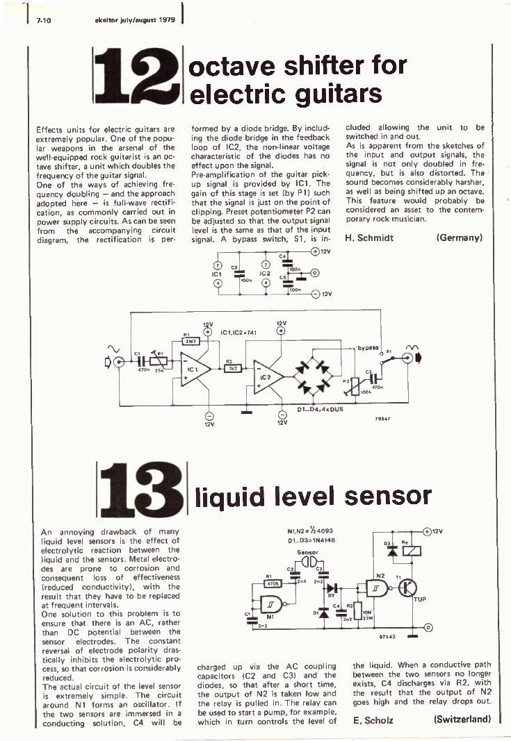
7-10 ekeltor july/august 1979
Effects units for electric guitars are
extremely popular. One of the popu- lar weapons in the arsenal of the well-equipped rock guitarist is an oc- tave shifter, a unit which doubles the frequency of the guitar signal. One of the ways of achieving fre- quency doubling - and the approach adopted here - is full -wave rectifi- cation, as commonly carried out in
power supply circuits. As can be seen
from the accompanying circuit diagram, the rectification is per -
octave shifter for electric guitars formed by a diode bridge. By includ- ing the diode bridge in the feedback loop of IC2, the non-linear voltage characteristic of the diodes has no effect upon the signal. Pre -amplification of the guitar pick- up signal is provided by IC1. The gain of this stage is set (by P1) such that the signal is just on the point of clipping. Preset potentiometer P2 can be adjusted so that the output signal level is the same as that of the input signal. A bypass switch, S1, is in-
IC1
Q
c -012V c
IC2 C5
toon = (i) TO°n 0 12
cluded allowing the unit to be switched in and out. As is apparent from the sketches of the input and output signals, the signal is not only doubled in fre- quency, but is also distorted. The sound becomes considerably harsher, as well as being shifted up an octave. This feature would probably be considered an asset to the contem- porary rock musician.
H. Schmidt (Germany)
12V
RI + ICI, IC2=741
--I21.17 )----
O 470n 25k
An annoying drawback of many liquid level sensors is the effect of electrolytic reaction between the liquid and the sensors. Metal electro- des are prone to corrosion and consequent loss of effectiveness (reduced conductivity), with the result that they have to be replaced at frequent intervals. One solution to this problem is to ensure that there is an AC, rather than DC potential between the sensor electrodes. The constant reversal of electrode polarity dras- tically inhibits the electrolytic pro- cess, so that corrosion is considerably reduced. The actual circuit of the level sensor is extremely simple. The circuit around N1 forms an oscillator. If the two sensors are immersed in a
conducting solution, C4 will be
12V
12V 0
0 12V
D1...04:4x0US
'bypass' /VM
1001, 470n
79547
liquid level sensor N1,N2 =1/2 4093
D1...D3=1N4148
Sensor
C2
RI
charged up via the AC coupling capacitors (C2 and C3) and the diodes, so that after a short time, the output of N2 is taken low and the relay is pulled in. The relay can be used to start a pump, for example, which in turn controls the level of
12V
the liquid. When a conductive path between the two sensors no longer exists, C4 discharges via R2, with the result that the output of N2 goes high and the relay drops out.
E. Scholz (Switzerland)

I elektor july/august 1979 7-11 I
F1 534
1LJA
I
F2 5R O
10OmA
15 V
52 O
Reset
RS
15 V
sun lamp timer
B 60C 600
0 15V 1 9 16
qle CIA IC 7 6RA 4015 DB1--
RR. Ó Ó Ó Ó Ó Ó Ó Ó
5 4 3 10 13 121 II 2
15V +
= RIA A IC 8 .2t 89 4015
51 AI 3 10 13
D
121 111 21
N1,N2 = IC2 = 4069 N3,N4 = IC4 = 4012 N5.N6.N8 = IC5 = 4001 N7.N9.N10 = IC6 = 4011
Before setting off for (hopefully) sunnier climes, many prospective holidaymakers use a UV lamp to acquire an initial tan. Unfortunately, things can go rather amiss, and instead of a nice golden brown, the careless or forgetful user can end up the colour of one of Her Majesty's pillar boxes! The following circuit was designed to prevent any of our readers from suffering just such a
painful experience. The circuit is basically a timer, which after a preset interval will produce an audio tone to warn the sunbather that his time is up. If the audio tone provokes no response from the user, the lamp is automati- cally switched off (via a relay) after another 30 seconds. If the sunbather wishes to turn over and brown another part of his or her anatomy, or someone else is to take his place, then by operating a reset button the lamp is prevented from switching off. The operation of the circuit is quite straightforward. A 50 Hz squarewave
15 V
IC3 4040
11 e M ÓÓÓOÓÓÓÓOÓÓ6 .1
is derived from the transformer secondary and fed to a 12 -bit binary counter (IC3). The outputs of the counter are gated (N3 ... N5) such that a pulse is supplied to the clock inputs of IC7 and IC8 every 30 seconds. Furthermore IC3 itself is
also reset every 30 seconds. IC7 and IC8 are shift registers, the outputs of which are taken high in turn by successive clock pulses. The position of S1 therefore determines how long it takes before the oscillator, which is formed by N9, N10 and associated components, is started. The oscillator, together with an amplifier stage and loudspeaker, provides the audio warning tone. With S1 in position '1', this period equals 12 x 30 s = 6 min- utes. Thirty seconds later, the next output of IC8 (Q1b) will go high, causing the relay to drop out and switch off the UV lamp. At any stage pressing S2 will reset ICs 3, 7, and 8, thereby initiating a
new count cycle. The volume of the warning tone can
O+15V
15V
Ottj
1N4005
T2
O
tti
BC 107 mla
79534
be varied by means of P2, whilst LED D3 provides a visual indication of whether the circuit is switched on. A relay which is capable of switching reasonably large currents, but which itself has a fairly small pull -in current (max. 100 mA) should be used.
A. W. Zwamborn (The Netherlands)

7.12 elektor july/august 1979
There are certain situations, e,g, when checking frequency multiplier or divider circuits, PLL circuits, certain music circuits etc., where it is more important to measure the frequency ratio of two signals, rather than simple measurement of fre- quency itself. With the aid of the circuit shown here, the ratio between the frequency of two signals, f1 and f2, can be measured and displayed directly on three seven -segment dis- plays. The circuit will measure ratios up to 99.9 with an accuracy of 0.1, providing f1 is larger than f2. The heart of the circuit is the coun- ter/display driver IC, MK 50398N, from Mostek, which has already been described in Elektor (see below). The higher frequency, f1 , is fed via the input stage around T1 to the clock input (pin 25) of the counter. Pulses will be counted at this input provided pin 26 (count inhibit) is held low. y Decade divider IC2 and flip-flop FF1 ensure that this pin is in fact held low for exactly ten cycles of the lower frequency signal, f2. Thus a
number appears on the displays which is ten times the ratio between ft and f2. By arranging for the decimal point to light between the second and third digits, the resulting figure is thus exactly equal to the ratio ft /f2. Flip-flop FF2 is connec- ted as a monostable, and is used to provide the counter IC with the correct 'store' and 'clear' pulses on pins 10 and 15 respectively. Literature: 7/a GHz Counter, Elektor 38, June 1978.
W. Dick (Germany)
Although not a precision instrument, this transistor tester should none- theless prove a useful aid for checking the quality of 'job lots' of transistors. The circuit will determine whether or not a transitor is defective, and whether the current gain of the transistor puts it in the class of 'A' -type transistors (current gain 140 ... 270), 'B' -type transistors
frequency ratio meter
common cathode
(HP 77601
814
12 V O+
C1
:On
04
LD1 LD2
I /
A 201 19
LD3
18
8
2
C12I
R1
I1100n
D3
up/down
D C B
D2
IC1 MK 50398 N
5 _
á A y
2 l7 C
DI
7
d
C
6
11 1 ,.L 1617Í 25
TBTCCT1 4. 150p
12 V
83 =on
C3
05
IC 3 IC 4
O+ 12V
Clock IC2 4017
26 10
9
8
D 4
Clock FF1 ó
R
13
10
,2
FF1,FF2 = IC3 = 4013 N1 ... N3=1C4=4049
T1,T2= BF 494 1N4148
transistor tester (270 . 500), or 'C' -type transistors (greater than 500). To test for example an NPN transis- tor, the device is inserted in the appropriate socket (TUT = transistor under test) and S2 switched to position C. If LED D2 lights up, the transistor is type C, if the LED remains out then S2 should be set to position B, or, if this fails to have
s D
lock FF2 ó 2
C6
=470n
79576
any effect, to position A. In each case the position of S2 in which the LED lights up indicates the class of transis- tor. If the LED fails to light even in position A, then it is defective, or has a current gain of less than 140, which for small signal transistors means that they are basically unusable. The base current to the transistor under test can be interrupted by means of

elektor july/august 1979 7-13 I
pushbutton switch S1. If the LED does not go out, it means a short exists between collector and emitter of the transistor. The operation of the circuit is quite simple: The transistor under test receives a base current of 10µA via R 1. Assuming the transistor is not defective, this results in a voltage drop across R2 ... R4, and depending upon the position of S2, a portion of this voltage is compared with a fixed reference voltage by IC1. The oper- ation of the right hand side of the circuit is virtually identical, except that it is arranged for PNP transistors. The circuit can be powered by battery.
TUT = Transistor Under Test
R. Storn (Germany)
'de luxe' transistor tester
Like the previous circuit, this transis- tor tester will indicate whether the current gain of the transistor under test is that of a class 'A'-, class 'B'- or class 'C' type. The circuit will also determine whether or not the transis- tor is defective. The advantage of this design, however, is that the class of transistor is automatically deter- mined and shown directly on a seven - segment display. The operation of the circuit is in many respects similar to its prede- cessor. Depending upon the current
gain of the device under test, a
certain DC voltage is dropped across resistors R2 ... R4 in the case of NPN transistors, or across R7 ... R9 in the case of PNP transistors. As this voltage increases (i.e. the greater the current gain of the transistor under test), the outputs of comparators IC1 ...IC3 (IC4...IC6 for PNP transistors) will go low in turn. The output state of the three comparators is decoded by R15 ... R19, Ti, T2 and T3, such that 'A', 'B', 'C' or 'F' appears on the seven -segment display.
'F' indicates a defective transistor, and is also obtained if no transistor is
connected in circuit, or if the push- button switch in the base lead of the transistor is pressed (opened). If that is not the case, the transistor has an emitter -collector short. S3 is used to switch between NPN and PNP types. The display is a common -anode type.
R. Storn (Germany)

7-14 elektor july/august 1979
It is a well-known fact that the signal-to-noise ratio of a VHF FM receiver is better on mono than on stereo. This principle is in fact used in some FM stereo noise reduction systems: crosstalk is introduced between the stereo signals to reduce the noise, while retaining some of the stereo effect. Since noise is more annoying at higher frequencies, some circuits only mix the two signals at higher frequencies. A good noise suppression system would be one where the crosstalk is introduced gradually, as required - not switched on abruptly by an (electronic) switch. It would be better still if the signal level not only determined the amount of crosstalk, but also the turnover frequency above which crosstalk occurs. These considerations are the basis for the design idea presented here.
0C1 ...0C3= opto coupler H11F1 (General Electric)
FM stereo noise reduction The two channels are mixed via optocouplers (OC1 ... 0C3) that use light-sensitive J-FETs. Admittedly, these are anything but readily available; however, they have better linearity than standard types - and that means less distortion. The capacitors in series with the optocouplers are chosen so that the turnover frequency decreases as more of the photo-J-FETs are turned on. The control voltage for the opto - couplers is derived from the input signals. These are summed in Al and fed through a high-pass filter (A2). The output from this filter is propor- tional to the high -frequency content of the stereo signal. After rectifica- tion (A3), buffering (A4) and smoothing, this signal is compared to a reference voltage in A5. The out- put from A5 is used to drive the LEDs in the optocouplers. As the
high -frequency content of the input signals rises, the drive to the LEDs is
decreased so that the crosstalk between the channels is reduced. Noise reduction therefore only occurs when it is necessary: at low levels.
Q. A. Rice (United Kingdom)
design idea

elektor july/august 1979 7-15 I
When it comes to mains indicator lamps, there are basically three main options: neon lamps, incandescent lamps, and LEDs. Neon lamps have the advantage that they can be
connected direct to the mains supply, and also that they consume very little power. Incandescent lamps, on the other hand, must be connected to a much lower voltage (e.g. to the secondary side of the transformer), and therefore provide only indirect indication of whether the mains supply is present, whilst as a rule dissipating a relatively large amount of power. LEDs would represent an ideal alternative to both the above ap- proaches, since they have a longer operating life than either neon or incandescent lamps, and dissipate no more than 20 to 30 mW. Unfortuna- tely it is necessary to protect the LED from excessive currents by employing a series resistor, which, with a mains voltage of 240 V, will itself dissipate something over 3.5 W.
The circuit shown here offers a
better solution. The current through
LED lamps the LED is limited to a safe value not by a dropper resistor, but by the reactance of a capacitor. The advan- tage of this method is that no power is dissipated in the capacitor, since the current though the latter is 90° out of phase with the voltage dropped across it. The formula for calculating power dissipation for DC voltages is
only valid for AC voltages provided the current and voltage are in phase i.e.
Pc=uc i cos 0
With a phase shift of 90°, which is
the case with capacitors, Pc is there- fore 0 W (cos 90° = 0). What little power is consumed by the circuit is
news detector To many people the radio news bull- etins are of primary interest. This design idea describes a method of switching on a radio by the 'pips' which of course immediately precede the news. The principle involved is quite simple, and utilises the fact that the pips have a frequency of almost exactly 1 kHz. The radio is in fact switched
permanently on, but because the (electronic) switch is normally open, the audio signal is not allowed to reach the output stage. Rather it is
fed to a selective filter with a turn- over frequency of 1 kHz. The output of the filter is rectified and used to switch a Schmitt trigger. The output pulses from the Schmitt trigger are counted, and only when
design idea
:6
entirely converted into light and heat by the LED. The value of capacitor C, can be calculated for any given voltage, frequency and current with the aid of the following equation:
C where:
6.28 u f C is the capacitance in Farads u is the RMS value of the mains
voltage f is the mains frequency in Hz i is the current through the LED in
Amps
With a mains voltage of 240 V, a
frequency of 50 Hz and a current of 20 mA, the nearest suitable value of capacitor is therefore 330 nF. The working voltage of the capacitor should be at least twice the mains voltage. Diode D2 is included to protect the LED from excessive reverse voltages.
U. Hartig (Germany)
six pulses occur within a predeter- mined time is the switch closed and the audio signal fed to the output stage. Once the news is over, pressing a
reset button will once more cut out the audio signal and return the circuit to its initial state.
J. Pelsma (The Netherlands)
' o 0 Resel
Reset
FF
to
79510
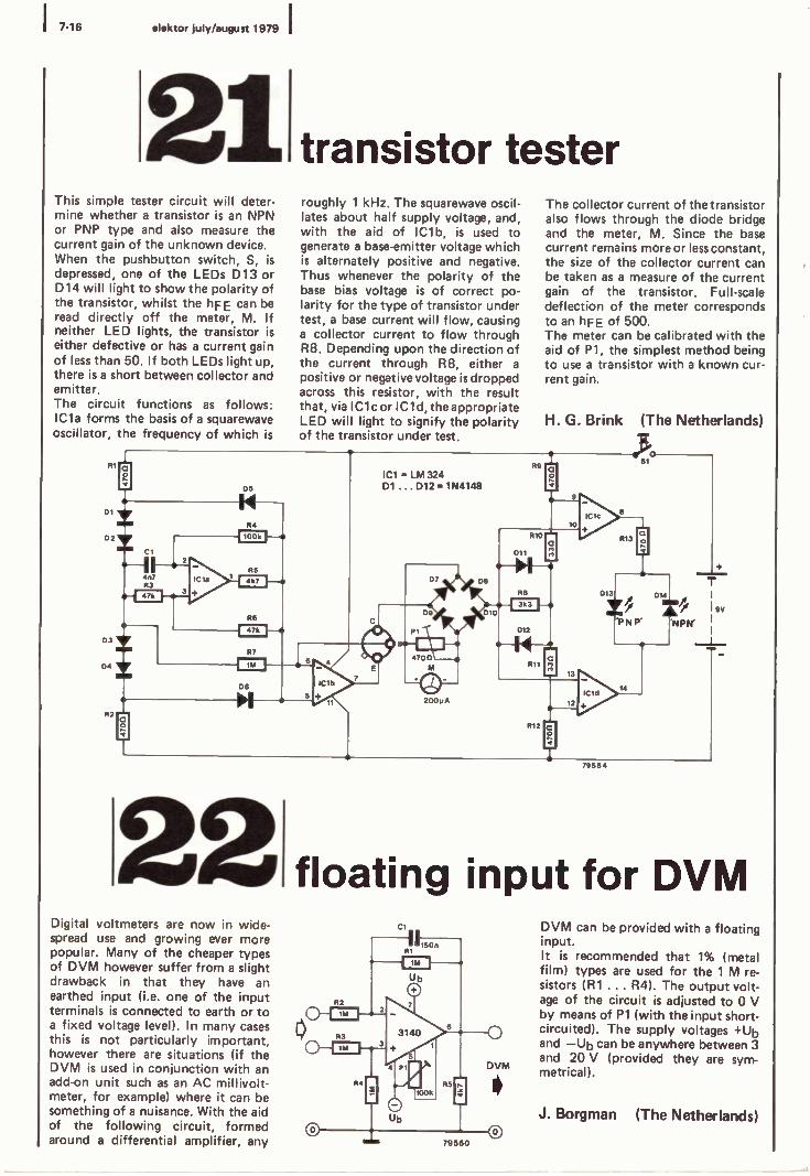
7-16 elektor july/august 1979
This simple tester circuit will deter- mine whether a transistor is an NPN or PNP type and also measure the current gain of the unknown device. When the pushbutton switch, S, is
depressed, one of the LEDs D13 or D14 will light to show the polarity of the transistor, whilst the hFE can be read directly off the meter, M. If neither LED lights, the transistor is either defective or has a current gain of less than 50. If both LEDs light up, there is a short between collector and emitter. The circuit functions as follows: IC1a forms the basis of a squarewave oscillator, the frequency of which is
Digital voltmeters are now in wide- spread use and growing ever more popular. Many of the cheaper types of DVM however suffer from a slight drawback in that they have an earthed input (i.e. one of the input terminals is connected to earth or to a fixed voltage level). In many cases this is not particularly important, however there are situations (if the DVM is used in conjunction with an add-on unit such as an AC millivolt - meter, for example) where it can be something of a nuisance. With the aid of the following circuit, formed around a differential amplifier, any
transistor tester roughly 1 kHz. The squarewave oscil- lates about half supply voltage, and, with the aid of IC1b, is used to generate a base -emitter voltage which is alternately positive and negative. Thus whenever the polarity of the base bias voltage is of correct po- larity for the type of transistor under test, a base current will flow, causing a collector current to flow through R8. Depending upon the direction of the current through R8, either a
positive or negative voltage is dropped across this resistor, with the result that, via IC1cor IC1d, the appropriate LED will light to signify the polarity of the transistor under test.
R9
ICI = LM 324 D1 . .. D12 = 1N4148
The collector current of the transistor also flows through the diode bridge and the meter, M. Since the base current remains more or less constant, the size of the collector current can be taken as a measure of the current gain of the transistor. Full-scale deflection of the meter corresponds to an hFE of 500. The meter can be calibrated with the aid of P1, the simplest method being to use a transistor with a known cur- rent gain.
H. G. Brink (The Netherlands)
s, si t
79564
+
-r
9V
NPN'
floating input for DVM DVM can be provided with a floating input. It is recommended that 1% (metal film) types are used for the 1 M re- sistors (R1 ... R4). The output volt- age of the circuit is adjusted to 0 V by means of P1 (with the input short- circuited). The supply voltages +Ub and -Ub can be anywhere between 3 and 20 V (provided they are sym- metrical).
J. Borgman (The Netherlands)

1 elektor july/august 1979 717 I
digital wooing aid And now for something completely different . . . . Whether or not one will find the following circuit useful, the originality of the concept cannot be denied. The basic idea is to assist those unfortunate souls who seem to become tongue-tied when confronted with the object of their desires, and are incapable of expressing the intensity of their emotions in words. In such cases the 'wooing aid' can be presented to the prospective partner, who upon pressing the button, will be greeted with the immortal line 'Hello beautiful'! Of course whether this, admittedly ingenious, amorous gambit will succeed in achieving the desired result is another question. The actual electronics involved are quite straightforward. The circuit
24
D1
23
IC1 7493
B c
22
A B
contains a clock generator (N1, N2), a 4 -bit binary counter (IC1), a
4 -to -16 decoder (IC2) and a diode matrix. The pulses from the clock generator are converted into binary code by IC1 and then fed to IC2, so that each of the outputs of IC2 are taken high in succession. The outputs are decoded by the diode matrix which ensures that the correct segments are enabled to produce the desired text. The rate at which one letter follows another is determined by the clock frequency, and may be varied by adjusting P1. If, as was the case with the prototype version, a Minitron 3015F type dis- play is used, R2 ... R8 may be omitted. If a different display is employed, care should be taken to
D
11
21 20 C D
1C2 74154
0 1 2 3 4 5 6 7 B 9 10 11 12 13 14 15
1 © . 17I
015
=1111~hr
D59
D14
12
18
19
ensure that the current consumption is not excessively high. Otherwise it will be necessary to provide buffers (e.g. 7407's or 7417's) between IC2 and the diodes D1 ... D14.
M. Muhr (Germany)
22011
i 6V
N1...N2=1C3=7413 D1... D14=DUG
D15...D59=DUS
2
R3220n R4 220n
a
c
R5 22001 R6 22on e R220n- R81 nj-9
79565
5V

-1 7-18 elektor july/august 1979
There are several different ways to measure DC voltages - multimeters, multichannel oscilloscopes etc. However if one possesses only a
single -channel scope, comparing several voltages must involve making more than one measure- ment. With the aid of the circuit shown here, it is possible to simul- taneously measure and compare two different voltages on a single - channel scope, provided the latter is equipped with an external trigger input. The circuit is extremely simple, and uses only a single IC, five resistors and a couple of capaci- tors. The IC is a CMOS quad switch, 4016. S1 and S2 form part of an astable multivibrator, and are opened and closed in turn. The two voltages to be measured are fed to S3 and S4, which are
The circuit described here employs a
forward -biased diode as temperature sensor. The forward voltage drop of a
diode falls by approximately 2 mV for an increase in temperature of 1° C. Since this negative temperature coefficient remains the same regard- less of actual ambient temperature, the scale of the thermometer will be linear. The temperature coefficient of a
diode is not particularly large, and is
easily exceeded by that of an NTC (negative temperature coefficient) resistor. However it is not possible to obtain a linear scale over a wide range of temperatures using an NTC resistor. Thus the use of a diode is
justified by the wide measurement range obtained and by the ease of calibration. The sensor diode - D1 in the circuit diagram - is a common -or -garden 1N4148, which can easily be mounted apart from the rest of the circuit. The diode forms part of a resistance bridge, comprising P1, P2, R5, R6 and R7. A reference voltage is
provided by a 723. Thus the voltage on the non -inverting input of IC2 is
held to a (variable) reference value via R5 and P1. Assuming the circuit
voltage comparison on a scope
controlled by S1 and S2. Thus the two voltages are fed alternately to the Y -input of the scope. The control signal for switch S4 is also used to trigger the scope. The supply voltage (3 ... 15 V) can be provided by, for example,
3...15V
Si... S4 _ IC 1- 4016, 4066
a 9 V battery, which, in view of the circuit's low power consump- tion (under 1 mA), should be assured of a long life.
J. Meier (The Netherlands)
linear thermometer is initially nulled by adjusting P1 and P2, variations in the forward voltage drop of the diode as a result of temperature fluctuations will cause the output of IC2 to swing either high or low depending upon whether
ea table.
12
6
vtn
v -
V
the temperature rises above or falls below zero. By using a diode bridge, D2 ... D5, the meter will show a positive deflection regardless of the polarity of the temperature. To provide an
RBdP
DVM
4x 1N4148
79556

elektor july/august 1979 7-19 I
indication of whether the temperature is in fact above or below 0°, the output of IC2 and the reference voltage are effectively connected to the non -inverting and inverting inputs respectively of the 723, which thus functions as a comparator. Assuming the circuit is calibrated for zero deflection at 0° C, as the temperature falls, the voltage drop across the diode increases, therefore the voltage on the inverting input of IC2 falls, the output of IC2 goes high, taking the non -inverting input of IC1 high and with it the output of IC1. Transistor T1 therefore turns on, lighting the LED. When the tempera- ture rises above 0° C, the reverse process occurs, resulting in the LED being extinguished. Resistor R8 is included to allow the use of a DVM (with floating input) as
a means of display. The accompanying table lists a number of alternative
Table 1
scale meter M temperature
0 - 30 0 - 300 µA -30 . . . +30° C
0 - 30 0 - 100 µA -30 . . . +30° C
0 - 50 0 - 300 µA -50 . . . +50° C
0 - 50 0 - 500 µA -50 . . . +50° C
0 - 100 0 - 1 mA -100. . .+100° C
2 x 3k3 parallel
values for R8 along with the measure- ment ranges obtained for various (moving coil) meter scales. Of course, if a DVM is used, then the moving coil meter as well as D2 . D5, R1 ...R4, T1 and the LED can be omitted. The circuit can be calibrated by suspending the sensor diode (together with a suitable length of connecting wire!) in crushed ice which is begin- ning to melt. With P2 provisionally set to the mid -position, P1 is then
ten channel TAP TAP (read: touch) switches come in all shapes and sizes, mainly as mo- mentary action or simple on/off (latched) switches. Using only a
handful of components, it is possible to construct a 'ten -channel' TAP, i.e. a ten -pole touch switch. When one of the ten sets of contacts is touched, the corresponding output will be
taken high. The heart of the circuit ís formed by a CMOS decade counter/decoder, 4017, which is clocked by a simple CMOS oscillator. However when the contacts are open, the counter is
inhibited, since the clock enable input is held high. The same is true if
3...15V
N1,N2=1/21C2-1/2 4 011
the contacts are bridged, but the corresponding output is already high, since in that case the additional skin resistance will have no effect. How- ever, if the corresponding output is
low when a set of contacts is touched, the skin resistance (which is negli- gibly small compared to the other resistances) forms part of a voltage divider, thereby pulling the clock enable input low. The counter is
started and increments until the out- put in question is taken high, where- upon the clock enable input is once more taken high and the 'count is
stopped. Capacitor C2 is included to suppress
R3
C2
Cl
T°
8
10n 13
Clock O
enable
2
3
Clock
ICI 4017 5
4
ONO 8
Reset
2
9
R4
R5
RB
R7
R8
R9
RIO
R11
R12
R13
R8 DVM
1 k -0.3 . . . +0.3 V 3 k -0.3 . . . +0.3 V 1.67 k -0.5 . . . +0.5 V
1 k -0.5 . . . +0.5 V 1 k - 1 . . . +1 V
adjusted so that zero deflection on the meter (or zero voltage across R8) is obtained. The diode is then dipped into boiling water, whereupon P2 is
adjusted until a voltage of 1 V over R8 is obtained. The above procedure can then be repeated. It is best to use distilled or demineralised water for both steps of the calibration pro- cedure.
J. Borgman (The Netherlands)
mains transients etc., whilst R4 .. R14 prevent the possibility of a shock in the event of a short between the contacts. It must be emphasised that when the counter is started, each output in turn will go high (for a very short period) until the selected channel is
reached. This should not prove to be
a problem with most applications, however provision must be made for this when used with flip-flops and other edge triggered devices.
C. Horevoorts(The Netherlands)
EMI
IOOk
O O O'O 0 0 0 0 0 0
-111- max lOOyA
4 V 10x TAP
79542

7-20 elektor july/august 1979
When the circuit shown here detects the presence of moisture, it causes a
reed relay to drop out. The relay can be used to disconnect a piece of equipment from its voltage supply, thereby eliminating the possibility of electrical shock. The original application for the circuit was in an underwater camera which employed an electronic shut- ter. In the event of ingress of water into the camera, the shutter circuit was disconnected, thus protecting the photographer from the risk of a
high voltage shock. However the circuit can also be used in a variety of other applications, for example a
'leak detector' for boats, or as a 'dry -washing' indicator, etc. The sensor is formed simply from a
pair of copper wires held slightly apart, and the presence of moisture is detected by the resultant drop in the resistance between the wires. When this falls below a certain value, the output of the Schmitt trigger formed by T1 and T2 goes high. The flip-flop formed by N1 and N2 is thus trig-
The sight of so many interesting and diverse circuits contained in one issue may well lead to a quickening of the pulse rate for some of our readers. However, we have taken this into account by including the following design for a digital heart beat moni- tor. The circuit measures the time interval between successive beats of the heart and then calculates the heart rate in beats per minute before displaying the result on a three digit LED display. The heart beats are detected by using a miniature lamp and a photo -diode, encased in a clip which is attached to the ear lobe. Each time the heart beats, it pumps blood around the body, and the density of the blood in the ear lobe increases or decreases as the blood pressure varies. These differences in density between the times when the blood pressure is at its highest or lowest are detected by the photo -diode, .thereby providing a
pulse for each time the hearts beats. The time interval between successive
moisture sensor gered via Cl, with the result that T3 is turned off and the relay drops out. The circuit also allows the option of the relay being pulled in when moisture is detected. R6 is simply connected to point A, rather than point B. The circuit is of a suf-
Sensor
ficiently 'universal' character that in place of the moisture sensor, vir- tually any alternative type of sensor (LDR, NTC etc.) can be used.
J. M. van Galen (The Netherlands)
N1, N2 = IC1 = 4011,7400
79533
digital heart beat monitor heart beats is measured, and on the basis of this value the beat rate is
calculated. This is done by simply counting the number of pulses of a
known frequency during the above time interval. The author chose a
frequency of 166.7 Hz for this application, hence for a heart rate of 60 beats per minute, the time be- tween successive heart beats will be 1 second, and a total of 166 pulses will be counted. Once counted, these pulses are transferred to a 256 bit presettable counter, so that they can be divided into 10,000 by clocking exactly 10,000 pulses into the counter. Consequently, for a heart rate of 60 beats per minute, a total
of 1 0 66 00
- 60 output pulses will be
available to be counted and displayed on the LEDs. The circuit functions as follows: The gates N1 and N2 form an oscillator with an output frequency of 1 MHz.
sv
This is divided by a factor of 6,000 by counters IC3 and IC4 to produce the required 166.7 Hz reference frequency. The variations in diode current are amplified by IC1 and IC2 so as to produce a pulsed output which is in sympathy with the heart beat. These pulses are fed to IC6 which gives an output pulse at pin 3 equivalent to the duration between successive beats of the heart. This counter is then inhibited so that no further heart beat pulses will have any effect. Both counters in IC5 are connected in series so that a total division of 256 is available. This counter is clocked by the 166.7 Hz reference frequency for the period between successive heart beats. Hence, a heart rate of 60 beats per minute will produce an output pulse from IC6 of 1 second duration which would permit 166 pulses to be counted in IC7. This number is transferred to the presettable counter IC8 which is clocked with exactly 10,000 pulses

elektor july/august 1979 7-21 I
so that a total of 60 pulses are available at its output. These heart rate pulses are then fed to the 3 digit counter/display chip IC9, and the result is subsequently displayed on the LEDs. The circuit is designed so that IC8 will only receive an enable pulse after the initial counting sequence of the
2208
166.7 Hz pulses has been completed. At the falling edge of the 10 ms enable pulse from IC5, the delay monostable is triggered, thereby inhibiting the count for roughly 3 seconds and allowing the display to be read off. Once this delay period has elapsed, all counters are reset in preparation for the subsequent count.
16í-;1 6 10
IC3 = 4518
WO®
R3
D1
® \ 12V
R6
/R5 X a
R4
R7
C2
if 1n
R81
R10
R21
16 1
Care should be taken during con- struction to ensure that the circuit is
we// insulated from any mains voltages. However the use of batteries as power source is strongly rec- ommended.
I C4 =
4518
VII 9113
1 MHz clock
12 15
2
145 12 V
2
3
16
C3
4118
IC9 =
MC 14553
IC1 = LF 351 12V IC2=LF351 ¡1 N1 . . . N4 = IC11 - 4011 J N5,N6 = IC12 = 4081
N7 ... N9 = IC13 = 4001
P. Lesh (United Kingdom)
1 16
12V
IC5 =
4518
10
IC6 =
4518
16 2
8 9110
6-: 61 101 8
IC7 = 4520
5 6 7 10 11 12 13
14
IC8 =
40103
13
8 R12
10
7
W
E o 3
4
10n
R13 ó m
C5
108 16V
2 15 5 6 7 9
2
161314
IC10 =
4511
51 8
5
R14
R15
R16
R17 o
12
6800 R18
13
R19
R20
13
DL 704
12 T1
2N3702
T2
DL 704
2N3702
T
DL 704
12
2N3702
1 79620

74 7-22 elektor july/august 1979
o
Under certain conditions if the out- put of a selective filter is fed back to the input a sinewave oscillator is pro- duced. In itself, the idea is not new (see for example the various spot sinewave generators published in Elektor), but the way in which it is realised in the circuit shown here is
original. The output of the state variable filter (again, no stranger to Elektor readers) formed by Al ...A3, R7 ... R11, Cl and C2 is fed back (from the output of A2) to the input (left hand side of R7). The amplitude of the output signal is stabilised by the action of FET Ti, which in conjunction with R1 forms a voltage -controlled attenu- ator. The control voltage is derived from the output of Al via a diode - resistor network and the integrator round A4. The sinewave signal is available at the outputs of Al, A2 and A3. Since A2 and A3 are connected as integrators, i.e. as lowpass filters, the distortion at output Ill will be lower than that at output I. The integrators have unity gain at the resonant frequency of the circuit.
Cold weather is one of the banes of a
motorist's life. Not only must he worry about the car starting on cold winter mornings, but there is the added nuisance of frozen windscreens to cope with. To help combat this latter problem, many cars are fitted with heated rear windscreens. Useful though these are, it still means one has to wait until the heating element has warmed up sufficiently to melt the frost before being able to move off. The circuit described here is designed to assist the motorist in a
'fast get -away', by ensuring that the heating element is switched on before he reaches the car. Basically the circuit will switch the heated windscreen on after a variable preset period. The idea is that before leaving the car in the evening, the motorist will calculate what time he expects to be using the car the following morning, and set the circuit accordingly. The circuit also incorporates two important safe-
sinewave oscillator
Re
Al . . . A4 = IC1 = TL 084 D1... D2=1N4148 T1 = BF 245
The desired value of Cl be calculated by:
Cl = C2 = f6
R
and C2 can
*C2
79604
O. it
15V
O
15V
where f is in kilohertz and C is in nanofarad.
G. Schmidt (Germany)
automatic heated rear windscreen
hours mins secs
S11 12 S10 6 S9 3
S8 1 30 S7 45 S6 22 32 55 11 16 S4 5 38 S3 2 48 S2 1 24 S1 42
guards - for the windscreen to be switched on the temperature must be below zero, and the car battery must be sufficiently well charged to ensure that the current drain of the heating element will not leave it flat. The basic principle is quite simple: The circuit around ICI is a square - wave oscillator which provides clock pulses to IC5, a 14 -stage binary counter. The outputs of IC5 are
ANDed together via diodes D1 ... Dl l and R5. The number of outputs gated together, and which outputs those are, can be selected by means of switches S1 ... S11. Thus by closing various combinations of switches it is possible to vary the interval which elapses before pin 6 of N3 is taken high. The output of N3 will only go low, however, if both inputs are high, i.e. if the output of N2 is also high. For this to be the case both inputs of N2 must be low and hence both inputs of N1 must be high. When the output of N3 is taken low, the output of N4 goes high, setting the flip-flop IC6 and pulling in the relay. However if the battery voltage falls below the reference level set by P3, the output of IC3 will go low, taking the output of N3 high and resetting the flip-flop. A suitable 'threshold value' for the battery voltage would be 11 V.
Similarly, the ambient temperature

elektor july/august 1979
12V
7.23 I -
61
R3
t-
D13
m : E 8
R2
2
CI
T
t ICI
84 I® 1008 16V
16
10
10k
P1
100k
12V
12V
is monitored by the negative tempe- rature coefficient resistor, R12. P2 is
adjusted such that the output of IC2 goes high when the temperature falls to 0°C. Above this temperature the output of IC2 will be low, reset- ting flip-flop IC6. Finally, the remaining preset in the circuit, namely P1, is adjusted to
clock
Vss 0a
V0r
IC5 = 4020
OS O6 07' OB O9 010 011 012
reset
013 014
B 71 51 41 61 131 121 141 151 1
01I 021 031 041 051 061 071 081 D9
110
12
8
10. 6 Sat
.+4t 106
o ciar 3 5
1a ta
IC4 IC6
4 Q 1
21 3
010 DII
R5
5 6Y`SB 59$10` 11
2
12V<c100mA
40
012
a 512 RB 1ATA -0 ®
BC 547
12V
o
1116 79539
D1 . . . D12 = DUS IC1 = 741 IC2 = 741 IC3 = 741 N1 ... N4=1C4=4011 IC5 = 4020 106 =4013
provide the correct clock frequency. After resetting IC5, the Q8 output should go high after 11 minutes and 16 seconds. The timing intervals provided by each of the switches S1 ... S11 are listed in the accompanying table. Assuming, for example, that the heated windscreen is to be turned
car anti -theft protection
The circuit described here is based on an unusual method of deterring a possible car thief. Shortly after it is started, an engine fault is simulated. Restarting gives the same result suggesting that the car may be more trouble than it is worth. The actual circuit is extremely simple. A 555 timer provides a delay of roughly 5 seconds. The normally closed contact of the relay is con- nected in the lead from the ignition switch to the ignition coil. Switch S1, which is used to arm the circuit, should of course be hidden. When power is supplied to the cir- cuit (via the ignition switch), the relay contact is initially closed and the engine will start. After the delay
R7
period provided by the 555 has elapsed, the relay contact is opened and the ignition coil is switched out of circuit. The delay period can be
altered as desired by selecting differ -
S12 a .on b = automatic c = 011
on eight hours and fifteen minutes after leaving the car, this interval can be obtained by closing switches S7, S8 and S10.
H.J.A. Roerdinkholder (The Netherlands)
79566
ent values for R1 or C1.
B. H. J. Bennink (The Netherlands)

7-24 elektor july/august 1979
Although designed in the first in- stance for use with the universal digital meter which was published in Elektor 45, this circuit for an auto- matic range switch (for DC input voltages) can also be used with other meters. Input voltages between 0 and 1 V are fed directly to the output, voltages between 1 V and 10 V are attenuated by a factor of 10, whilst voltages between 10 and 100 V are attenuated by a factor of 100. Thus the output voltage fed to the meter will always lie between 0 and 1 V, regardless of the amplitude of the in- put voltage. The basic principle of the circuit is
illustrated by the diagram shown in figure 1. When both switches are open, the input signal is fed unatten- uated to the output - always pro- vided the meter input has a suf- ficiently high input impedance, which is the case with the Elektor
1
79596 1
IC2 . . . IC4 = CA 3130 D1 ... D7=1N4148
R2 ... R11= Metal oxide 1%
T1 ... T3.TUN
2
0...100V 0...1V H H
MEE
R 7a
I
R7b
autoranger universal digital meter. When S1 is
closed, the input voltage is atten- uated by a certain factor - in the actual circuit this factor is 10. If both S1 and S2 are closed, the degree of attenuation is increased still further (a factor of 100). In the auto - ranger circuit S1 and S2 are electronic switches which are controlled by comparators. The comparators effec- tively measure the input voltage level, and are biased to switch at roughly 0.96 V and 9.6 V. Figure 2 shows the complete circuit diagram of the autoranger. The volt- age divider formed by R7/R8 divides the input voltage by 3, which is then buffered by IC2. Another voltage divider network, R9 ... R11 is con- nected to the output of IC2, and provides further attenuation by a
factor of 10. A voltage of roughly 320 mV (depending upon the setting of P1) is present on the inverting in -
e
3
04
DI
D2
D3
R8 RIO
C2
3
R13
R20
puts of the two comparators, IC3 and IC4. The result is that the out- put of IC3 swings high when the input voltage exceeds 0.96 V, and the output of IC4 does likewise when the input voltage exceeds 9.6 V. The comparator outputs control elec- tronic switches, which are formed by MOSFETs. These are contained in IC1, which is here used in a some- what unusual configuration; note that the positive supply voltage pin of this IC (pin 14) is left uncon- nected. If the circuit of figure 3 is connected between points A and B (figure 2), the position of the decimal point in the universal digital meter can also be controlled automatically. The three outputs of the circuit in figure 3 should be connected directly to R4, R5 and R6 in the meter circuit.
J. Borgman (The Netherlands)
R23
t IC3
C3
c4
R15
5V
NSD
0 LSD
0*
5V
0
loop
\RI loop
IC4
3
R
6
:
R18 112913:11
A
(So O
b b b IC2 IC3 IC4
5V
47n R12
{ 4k7j 1
R17 CMS
79596 2

elektor july/august 1979 7-25 I _
vicious chess buzzer Lightning chess is often played in chess clubs, the idea being that a
buzzer is sounded, usually every ten seconds or so, and the player whose turn it is to move must do so during the buzz, which lasts approximately one second. Despite the increased likelihood of a blunder by both players, it remains true that the more experienced, stronger player is still likely to defeat a weaker opponent. In fact the constraint of having to move quickly seems to exaggerate any difference in the strength of two players. The circuit described here offers the novice a new hope by providing an entirely random delay between successive buzzes. Thus there is the chance that the delays between his (strong) opponent's moves may be much shorter than those between his own. Of course the reverse is also true, but that is a risk which has to be taken! The circuit of the 'vicious chess buzzer' is shown in the accompany- ing diagram. N3 and N4 form a
simple squarewave oscillator with a
variable duty cycle. P1, R15 and D11 determine the charge period of timing capacitor C3 (the delay between successive buzzes), whilst P2, R16 and D12 determine the dis-
T1...T4=TUN D1...1:112=DUS
N1... N4=4011=IC2
charge period (the length of the buzz). With S1 as shown in the diagram, a fixed buzz interval of from 1 to 15 seconds can be set by adjusting P1, whilst the length of the buzz can be varied as desired by adjusting P2. The output of N3 drives the buzzer via N2, P3 and T4. By means of P3 the volume of the buzzer can be adjusted to a suitable level. The section of circuit described up to this point forms a 'normal' chess buzzer, however if S1 is switched to its alternative position, the delay times are randomised. The time taken to charge C3 then depends upon which Q output of IC1 happens to be high. The random element is
provided by a noise generator, built round T1, T2 and T3. T1 forms a
reverse -biased base -emitter junction which, in conjunction with C1 and R1, provides a random noise signal. This is amplified by T2 and T3 before being inverted, squared up and fed to the clock input of decade counter IC1. As long as the clock enable input (pin 13) of this IC is
low (i.e. when the output of N3 is
also low and the buzzer is sounding), the counter cycles through each of its output states. When the buzzer
T0Y
16V
stops, the counter is inhibited and one of the counter outputs is held high. The resulting delay is given by the formula T = R ° C3, where R is
one of the resistors R5 ... R14. With the values given in the circuit diagram the maximum delay is 27 seconds, and the minimum delay 1.8 seconds - plenty of scope for the buzzer to be really 'vicious'! The buzzer can also be used for other games (e.g. backgammon, or scrabble), in which case it may be desirable to alter the values of R5 ... R14 accordingly. A small 9 V buzzer was chosen to keep current consumption to a
minimum and permit the use of batteries. C3 should be a tantalum type.
B. Leeming (United Kingdom)
gv

1 7-26 elektor july/august 1979
This circuit is intended to give clear warning when it is time to replace the stylus in a record-player car- tridge. The unit indicates the 'playing time' that has already elapsed, using five LEDs. The first LED lights after the stylus has been in actual use for 100 hours, and each following LED lights after a further 100 hours. After 500 hours all LEDs are lit, indicating that it is time to replace the stylus. Otherwise, after a further 100 hours the five LEDs start flashing on and off - signaling that it is now high time! Once the stylus has been replaced, the counters are reset by briefly re- moving (or replacing) the battery. Power is derived from the mains when the record player is switched on. The battery is only used as a
stand-by supply for the counters during 'off hours' - or in the event of a mains failure ... In the circuit, S is the mains switch for the record player. When this is
closed, the multivibrator (N2, N3) starts to provide clock pulses to the
R3
cartridge life - expectancy counter counter chain (IC1 ... IC3). The final IC in this chain (IC3) is a series- in/parallel-out shift register. The clock frequency and division ratio in IC1 and IC2 are chosen so that IC3 receives one pulse every 100 hours; its (parallel) outputs are used to drive the LEDs. The flashing display at 600 hours is derived from the Q4 output of IC1 (0.2 Hz). C3, R4 and N4 are included to reset the counter chain when power is first applied - i.e. when the battery is
connected. To limit the drain on the battery, it is only used to power the ICs; the LEDs are only powered when the mains supply is on. Calibration is fairly easy. The clock frequency is set (by P2) for a period time of 0.17166 s. This can be meas- ured directly if the necessary test equipment is available; alternatively, the Q7 output of IC1 can be moni- tored with a multimeter: the period time at this point should be 22 se-
conds. The output voltage of the stabiliser (7805) is set to 10 V by means of P1.
Editorial note Provided it is handled with due care, a diamond stylus should last for any- thing up to 2000 hours. A lower clock frequency could therefore be used, giving a switching time for the LEDs of 200, 300 or even 400 hours. Furthermore, it would seem an improvement to use a nicad cell (9 V/100mAh) instead of the battery for a stand-by supply. Trickle -charg- ing can be provided by including a 1 k resistor in parallel with D2.
V
N2
C3
T20n
14¡ 161
VDo V00 1 CL 07 3 10
CL 014
ICI 4024
VSS i 0 IC2 =
4020
R
6
9
1 2 1A
J.G. Hemmer (France)
A B VDD L OA
OC
IC3 =
74C164 00
Vos
OE
OF
11
3
4 N
N7 N
03
D4
05
1J R5
rr
7
6 ® AD6rr R6
10 N
07 f
100,6A 84001000
250 'AA 7805
D1
R2
C4 C T10V
16V
2x 1N4004
T w O id
99 n IC4 IC5 IC6 IC7 O O y
1
79606
9V
N1 . . . N4 = IC4 = 4001 N5 . . . N7 = IC5 = 4023 N8 . . . N10 = IC6 = 4023 N11 ... N16 = IC7 = 4049

relektor july/august 1979 727 I
SHIFT -LOCK for ASCII keyboard
The following SHIFT -LOCK circuit should prove a useful addition to the ASCII keyboard published in Elektor 43 (November '78). The circuit is
also suitable for use with most other types of keyboard which are not already provided with this facility. There is no need for an extra key to be mounted on the keyboard, since the original SHIFT key performs both the SHIFT and SHIFT -LOCK functions; the length of time for which the key is depressed determines which function is selected. If the SHIFT key is held down for longer than 0.2 seconds, the shift output will go low (inactive) as soon as the key is released. If, however, the key is only depressed briefly (i.e. for less than 0.2 sec), the shift output is held high (active) until pressed a second time, i.e. the key functions as a
SHI FT -LOCK. The timing for the circuit is provided by the RC constant of R3 and C2. As soon as the voltage across C2 reaches approximately 45% of the supply voltage, N2 will change the input conditions of the JK flip-flop, IC2. Assuming that the O output is
initially high, the circuit functions as
follows: Momentarily depressing the SHIFT key has no effect upon the output of N2. The J input of the flip-flop therefore remains high, and the K input low. Shortly after the key is
N1,N2 N3 = ICI = 4093 FF1-V=IC2-4027 D1 DUS T1,T2 = TUP
pressed, the output of N1 goes low, taking the SHIFT output (via T2) high. When the SHIFT key is released, a positive going edge triggers the flip-flop, so that, given the state of the J and K inputs, the O output goes low, taking the K input high, and ensuring that the SHIFT output is held high (via Ti, T2). The next time the SHIFT key is held down briefly, the flip-flop is reset, i.e. the O output is returned high, taking the SHIFT output low. If the SHIFT key is originally de- pressed for longer than 0.2 seconds, the output of N2 goes low and takes the K input high, thereby holding the
2 switches - 2 lamps - 1 wire
When housewiring, the addition of an extra switch and light to an ex- isting circuit using the same power supply point would not normally cause any problems. However, the situation can arise where it is not possible to 'run' an extra cable between the additional switch and light thereby making it impractical to fit them. The circuit described here is a simple but effective method of solving this problem by replacing the missing wire with a little ingenuity. It will be seen from figure 1 that diodes D1 and D2 ensure that switch S1 controls lamp La1, whilst S2 controls lamp La2. The half -wave rectified mains voltage is partially smoothed by capacitors C1 and C2, so that an RMS voltage of approx- imately 240 V appears across the
s1 DI
-0 I
S2 I D2 -o
N a
41-
D1... D4=1N4006
lamps, which therefore burn at normal intensity. The value of these capacitors is determined by the power rating of the lamps used. The appropriate value can be calculated by using the following equation:
Px Cx=32 00
O output high. The SHIFT output will go low as soon as the key is
released. R1, C1 and R2 eliminate the effects of contact bounce, whilst LED D2 provides a visual indication of when the SHIFT -LOCK function is selected. If the circuit is used in conjunction with the Elektor ASCII keyboard, the track to pin 4 of the AY -5-2376 should be broken and the circuit connected between the SHIFT key and the IC.
T. Frankemolen (The Netherlands)
79612
where Cx is the new value of the capacitor (in µF) and Px the power rating (in W) of the corresponding lamp.
W. Richter (Germany)

1 7-28 elektor july/august 1979T -
There may be occasions when it is
required to measure low frequencies with a high degree of resolution. The circuit presented here is intended as a
frequency multiplier for just this purpose which offers a resolution of 0.1 Hz with a fast measuring time. A block diagram of the frequency multiplier is shown in figure 1. As can be seen, this configuration bears more than a passing resemblance to the (by now) fairly common PLL frequency synthesiser. However, in this instance it is the division ratio which is fixed and not the input (or reference) frequency. The VCO fre- quency is divided by 100 and then compared with the input frequency in a phase comparator. The resulting phase difference creates a DC signal which is used to correct the VCO frequency. This means that the VCO output frequency will be exactly 100 times that of the input. In the circuit diagram of figure 2, the input frequency is first amplified by
2
Cl
[5o R2
4
frequency multiplier 1
30 Hz ... 10 kHz
0o-
IC1 before being fed to the phase locked loop, IC2. The VCO output is
divided by 100 by the two decade counters IC3 and IC4 whereupon its phase is compared with that of the input signal in the PLL itself. The VCO output frequency is fed to the meter via the inverter formed by N2. Switch S1 is included so that the over- all frequency range of 30 Hz... 10 kHz
IC2
vco
100
3kHz... 1 MHz
79603 1
IC3, IC4
can be split into two separate ranges, namely 30 Hz . . . 300 Hz and 200 Hz . .. 10 kHz. The input sensi- tivity is quoted as being around 25 mV, and the output voltage is
approximately 4.5 Vp-p. Power supply requirements are 7 - 18 V at around 30 mA.
H. Rol
o R3
14
16 13
R6
1C2
e 11
R7 r 6.1
9 a j
Ste Sib
1008
C3
C4 ,OOn
1Y
98
(United Kingdom) O+o 5V
IC1= LM3302,LM339 IC2 = 4046 IC3 74LS90 IC4 = 74LS90 N1,N2 - 1/2 74LS00= ICS
A frequency range of 0.1 Hz to 999.9 kHz, a choice of CMOS or TTL output levels, and an accuracy/ stability which is limited only by that of the crystal oscillator - these are the main features of the digital
11
10 6l 2I 10( 6r 21
14 111 1C3 1C4
4
12
3 ® 11 9
79603 2
digital frequency synthesiser frequency synthesiser shown here. As can be seen from the block diagram in figure 1, the heart of the circuit is formed by a phase locked loop (PLL). In principle such a PLL circuit can be likened to an op -amp
connected with feedback, such that the output voltage of the op -amp varies to keep the voltage at both inputs the same; the PLL circuit varies the frequency of the output signal, so that the frequency of both
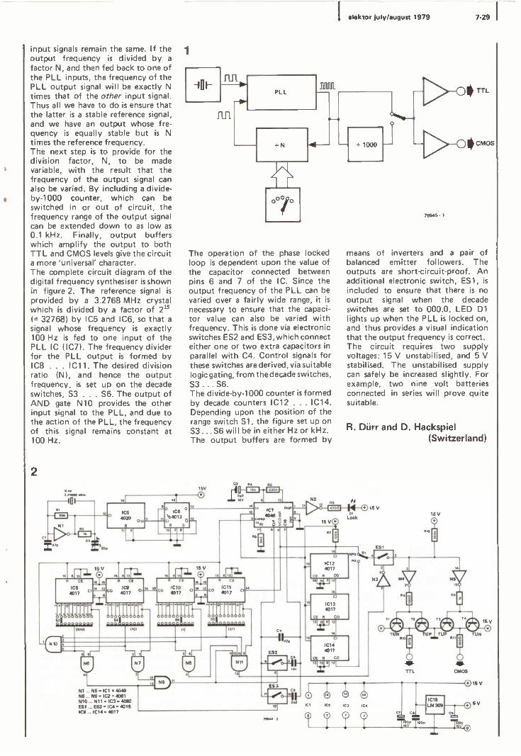
elektor july/august 1979 7-29 I
input signals remain the same. If the output frequency is divided by a
factor N, and then fed back to one of the PLL inputs, the frequency of the PLL output signal will be exactly N
times that of the other input signal. Thus all we have to do is ensure that the latter is a stable reference signal, and we have an output whose fre- quency is equally stable but is N
times the reference frequency. The next step is to provide for the division factor, N, to be made variable, with the result that the frequency of the output signal can also be varied. By including a divide - by -1000 counter, which can be switched in or out of circuit, the frequency range of the output signal can be extended down to as low as
0.1 kHz. Finally, output buffers which amplify the output to both TTL and CMOS levels give the circuit a more 'universal' character. The complete circuit diagram of the digital frequency synthesiser is shown in figure 2. The reference signal is
provided by a 3.2768 MHz crystal which is divided by a factor of 215
(= 32768) by IC5 and IC6, so that a
signal whose frequency is exactly 100 Hz is fed to one input of the PLL IC (IC7). The frequency divider for the PLL output is formed by IC8 . . . IC11. The desired division ratio (N), and hence the output frequency, is set up on the decade switches, S3 . . . S6. The output of AND gate N10 provides the other input signal to the PLL, and due to the action of the PLL, the frequency of this signal remains constant at 100 Hz.
2
Cl
IC .o 1216611 61144
1
16
1
Am- PLL
=N
The operation of the phase locked loop is dependent upon the value of the capacitor connected between pins 6 and 7 of the IC. Since the output frequency of the PLL can be varied over a fairly wide range, it is
necessary to ensure that the capaci- tor value can also be varied with frequency. This is done via electronic switches ES2 and ES3, which connect either one or two extra capacitors in parallel with C4. Control signals for these switches are derived, via suitable logic gating, from the decade switches, S3...S6. The divide -by -1000 counter is formed by decade counters IC12 . .. IC14. Depending upon the position of the range switch S1, the figure set up on S3 ... S6 will be in either Hz or kHz. The output buffers are formed by
15V
, EN
IC5 C' 4020
R
n1 8
R I ® EECTI
IC6 1,24013
CI P
10
N
15
P CE
IC8 4017
olgooaboaaa S] p noaynonn
11001
15V
16116
81131 6I1
CE
4ICs017
12
0009001>0 j10fN3 COnnnn
por
Co Ic1u 4017
4
0000aoR000 ¡3nnnqnSS noq
15V
16 11
1 12 _ 15 e113
IC7 PCP_
40413ó C04111
111 e 115
N2
79545 . 1
TTL
*CMOS
means of inverters and a pair of balanced emitter followers. The outputs are short -circuit -proof. An additional electronic switch, ES1, is
included to ensure that there is no output signal when the decade switches are set to 000.0. LED D1 lights up when the PLL is locked on, and thus provides a visual indication that the output frequency is correct. The circuit requires two supply voltages: 15 V unstabilised, and 5 V stabilised. The unstabilised supply can safely be increased slightly. For example, two nine volt batteries connected in series will prove quite suitable.
R. Dürr and D. Hackspiel (Switzerland)
n6 N
DEB
15 V Lock
CO 40ICI 17
4
00000 S6
lotl
13
N1 ... N5=1C1-4049 N6 ... N9-IC2=4081 N10 ... N11-IC3-4082 ES1 ... ES3 = 1C4 = 4016 ICe ... IC14 = 4017
tl
C
47o
ES2 CS
On
16
Cl
IC12 4017
CE R CO
1
IC13 4017
CE R CO 131 IS1 61 12
1C14 4017
CE R CO
13 15 6 12I
Rio
E53
'4°-'41- 2 n ui
O
^^ 41 oI
15V
ES1
TTL
Rt2
15V
CMOS
01645.2
O IC2 1C3 1C
Cl
TqOD 0n 11jV
q
IC15 LM 309
iE

7-30 elektor july/august 1979
Checking and adjusting the dwell angle of a contact breaker is really no problem - provided you have a
good dwell meter. By 'good' we mean that it must be accurate and linear, and work over a large range of ambient temperatures. The cir- cuit described here meets these specifications. It is intended for use in combination with a multimeter (500 µA f.s.d.), although any other 500 µA instrument can also be used, of course. The dwell angle is
measured in % (0... 100%). If a
reading in degrees is required, the actual reading must be multiplied by 3.6 and divided by the number of cylinders in the engine. The circuit could hardly be simpler. The most important section is a
constant -current source, consisting of T3 and a voltage -regulator IC (IC1). The extremely stable (and tempera- ture -independent) reference voltage
12V
O
dwell meter provided by the IC at pin 6 is connec- ted to the non -inverting input of a
differential amplifier inside the chip; the inverting input is connected to the emitter of T3. The IC will now adjust its output voltage (V0) so that the emitter of T3 is maintained equal to the reference voltage. The result will be obvious: a constant voltage, independent of temperature, across a fixed resistance (R5+P1) must produce an equally constant current. Since the base current of T3 is negligible, the collector current is
equal to the (highly constant) emitter current. So far, so good. The rest of the circuit either allows this constant current to pass through the meter, or else it doesn't ... When the contact breaker is open T1 and T2 will conduct, shorting out the meter circuit. As soon as the points close, T1 and T2 will turn off. The constant current determined by T3
D1, D2 = 1N4148
EELS
R
R4
R3
T1
D1
T2
TUP
TUN
02
T3
BC 549 BC 109
65
now flows through the meter, charging Cl at the same time. As the points open and close at rapid intervals, an average voltage is
developed across C1 and the meter. This voltage is proportional to the 'duty -cycle' of the breaker points: the longer the points remain closed (the larger the dwell angle, in other words), the larger the voltage across Cl will be - giving a correspondingly higher reading on the meter. The calibration procedure is like the circuit: simplicity itself. After connecting the supply and shorting the input (R1 to supply common), P1 is adjusted for full scale deflec- tion of the meter (100%). After all, a
shorted input corresponds to a dwell angle of 100%.
J. Becela
1006 16V
467
5009A
12
v VR C
1/0 IC1 =
D 723 non
nV O nV 1
(Germany)
C2
11~ 106 16V
, e The most notable feature of this circuit for an FSK modulator/de- modulator is its e..treme simpli- city: - it requires only one supply
voltage - uses only 4 common ICs - is simple to set up The circuit conforms to Kansas City Standard (CUTS) format, i.e. logic 0 = 1200 Hz, logic 1 = 2400 Hz, and the transmission rate is 300 Baud.
FSK modem The modulator circuit is quite staightforward. The clock signal is derived from the frequency of the UART, which is 16 times the baud rate (i.e. 4800 Hz). After the clock signal has been divided down by FF1 and FF2, 2400 Hz and 1200 Hz signals are available at the inputs of S1 and S2. Depending upon the logic level of the data input signal, one of these two switches is closed and a
signal of the appropriate frequency is
79616
present at the modulator output. At the input of the demodulator circuit, N2, N3 and N4 form an amplifier/limiter. The actual demo- dulation is performed by the two re--triggerable monostable multivi- brators, MMV 1 and MMV 2. The pulse duration of MMV 1 is roughly 420µs, whilst that of MMV 2 is
approximately 850 ps (depending upon the position of P1). With an input frequency of 2400 Hz, MMV 1

elektor july/august 1979 7-31 I
5V
Clock
O 4
3
R1 R
DATAITXD)
RTS
clear
cL FF1
D
5
13 10
clear preset
cL FF2
D
2
5V
FSK
IOOn
is continuously retriggered, so that its Q output is held high. No trigger pulses are fed to MMV 2, with the result that the Q (data) output re- mains high. However, with an input frequency of 1200 Hz, MMV 1 will not be retriggered before the Q output goes low, so that MMV 2 is
triggered and the data output also
6
I/ L -1J
9
goes low. By adjusting P1 to keep the pulse duration of MMV 2 as short as
possible, the delay between rising and falling edges of the data signal can also be kept short. Users of the Elekterminal can take the clock signal for the modulator from either pin 17 or pin 40 of the UART. The Baud rate switch on the
motorcycle emergency lighting
The following simple circuit should prove a useful safety aid to motor- cyclists. In contrast to car drivers, motorcyclists generally only have a
single headlight on their vehicle. Thus if it should fail whilst driving at night the motorcyclist is suddenly plunged into darkness and is effecti- vely 'blind', a dangerous state of affairs, to say the least. Normally the motorcyclist would have to fumble for the dipswitch and change over from dipped to full -beam or vice -versa, depending upon which bulb or filament had failed. The circuit described here ensures the safety of the motorcyclist by perfor- ming the task automatically in the event of either bulb (filament) failing. The headlight switch of the motor- cycle is represented by S1 in the circuit diagram. Between this switch
La 4
FF1,FF2 = 7474 =1C1 N1...N4=4011=1C2 S1 ... S4=4016=1C3 MMV1,MMV2 = 74LS123 = IC4
Elekterminal should be set to the 300 Baud position. The RTS input should only be used in conjunction with UARTs provided with such an output.
H. Stettmaier (Germany)
6...12V
*see text S7
Al 1009
mlm 16V
*Re 1N4001
1:23=.9 D1-
*Th li-
T S3
* S2 o- Sa-I
La1
® 79641
La1 = rear light La2 = high beam La3 = dipped La4 = warning light
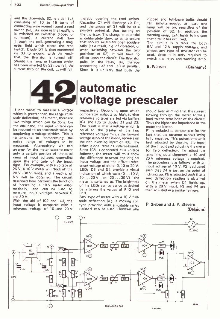
7-32 elektor july/august 1979 I
Cl rM T30n
40V
and the dipswitch, S2, is a coil (L), consisting of 10 to 15 turns of connecting wire wound round a reed switch (S3). As soon as the headlight is switched on (whether dipped or full -beam), a current will flow through the coil, generating a mag- netic field which closes the reed switch. Diode D1 is then connected via S3 to ground, with the result that the thyristor is turned off. Should the lamp or filament which has been selected by S2 now fail, the current through the coil, L, will fall,
i If one wants to measure a voltage which is greater than the range (full- scale deflection) of a meter, there are two things which can be done. On the one hand, the input voltage can be reduced to an acceptable value by employing a voltage divider. This is
tantamount to 'compressing' the entire range of voltages to be measured. Alternatively we can arrange for the meter scale to cover only a certain portion of the total range of input voltages, depending upon the amplitude of the input signal. For example, with a voltage of 26 V, a 10 V meter will 'look at' the 20 V - 30 V range, and a reading of 6 V will be obtained. The circuit described here performs the function of 'prescaling' a 10 V meter auto- matically, and can be used to measure input voltages between 0 and 30 V. With the aid of IC2 and IC3, the input voltage is compared with a
reference voltage of 10 and 20 V
IC 1
7815
L---- ---J C2
R1
100n
R2
-O a 0...30V
thereby opening the reed switch. Capacitor Cl will discharge via R1, and the anode of D1 will be at a
positive potential, thus turning on the thyristor. The change in potential is deliberately slow, so as to ensure that should switch S3 open acciden- tally (as a result, e.g. of vibration, or when switching between the two positions of S2), it will have no effect upon the circuit. The thyristor pulls in the relay, Re, thereby connecting La2 and La3 in parallel. Since it is unlikely that both the
dipped and full -beam bulbs should fail simultaneously, at least one lamp will be on, regardless of the position of S2. In addition, the warning lamp, La4, lights to indicate that a fault has occurred. The circuit is suitable for both 6 V and 12 V supply voltages, and almost any type of thyristor can be used, since it is only required to switch the relay and warning lamp.
E. Wünsch (Germany)
automatic voltage prescaler respectively. Depending upon which comparator outputs go high, further reference voltages are fed via buffers IC4 and IC5 to diodes D1 and D2. The result is that a voltage which is equal to the greater of the two reference voltages minus the forward voltage drop of the diode, appears on the non -inverting input of IC6. The other diode remains reverse -biased. Since IC6 is connected as a voltage follower, the meter will thus show the difference between the original input voltage and the offset (refer- ence) voltage of either 0, 10 or 20 V. LEDs D3 and D4 provide a visual indication of which scale (0 ... 10 V, 10 ... 20 V or 20...30 V) the meter is switched to. The brightness of the LEDs can be varied as desired by altering the values of R12 and R13. Any type of meter with a 10 V full- scale deflection (e.g. a moving coil type provided with a suitable series resistor) can be used. However one
O+
should bear in mind that the current flowing through the meter forms a
load to the remainder of the circuit. Thus the higher the impedance of the meter the better. P1 is included to compensate for the fact that the op -amps cannot swing fully negative. This potentiometer is
best adjusted by shorting the input of the circuit and adjusting the meter for zero deflection. To adjust the remaining potentiometers a 10 and 20 V reference voltage is required. The procedure is as follows: with an input voltage of 10 V, P2 is adjusted such that D4 is just on the point of lighting up. P5 is adjusted such that a
zero deflection reading is obtained on the meter when D4 lights up. With a 20 V input, P3 and P4 are then adjusted in a similar fashion.
P. Sieben and J. P. Stevens (Belgium)
DUS
D3
R15
(0...10v)
IC2...IC6= 741 s« teat
79592

elektor july/august 1979 7-33 I
see text
5V
1
bio-contro 5V+
2x HP 7750
5VCI)
5V R1
C2 loon
IOC1 14.33o111,11 n
d e l 9 a e d e 1 9
R15 iE
5V
6 IC9 2 555
1C2 16 IC3 74247 74247
2 6 5V
2 6
9 16 15 10
4
13
12
3
IC4 7475
9 16 15 10
4
13
s _ 5
3
8
2
9
7
12
6
1111
C3 e-15^"'' 1 - C14 mho
R20
El E2
The growing awareness of the con- tributory role which stress plays in causing illness has led to increased interest in various forms of 'autogenic' training as a means of promoting relaxation. In particular, different types of 'bio-feedback' circuits have become popular, the idea being that certain physiological functions (heart- beat, body temperature, brain ac- tivity) can be monitored and brought under the conscious control of the subject. The circuit descibed here operates on the principle of monitoring skin resistance as a measure of how tense the subject is. The same approach is
used in so-called lie detectors, however in that case it is the skilled interpretation of the subject's re- sponses to a variety of both innocu- ous and pointed questions which is
important. The description of the circuit is as
follows: variations in skin resistance (between electrodes El and E2) vary the frequency of the oscillator built round a 555 timer (IC10). The output of the oscillator is fed to a 7490
C B A B D
IC6 7490
3
IC5 7475
2
9
7
12
6
1111
3 10l
5V 1
5V
C B A El, D
IC7 7490
81 4I 5
IC10 555
C48~ C15- ton 18
IC8 A
7490
51 0 2I 3 6 17
divider (IC8), which in turn controls the reset inputs of the counter formed by IC6 and IC7. The result is
that the period between successive pulses from IC10 determines the number of clock pulses fed to this counter from a second oscillator (IC9). The outputs of the counter are decoded and displayed on a pair of 7 -segment displays, thereby providing a numerical indication of the subject's relative tenseness. The frequency of the second oscil- lator, which is also formed by a
555 timer, is determined by C3 and R15. By incorporating the circuit shown in figure 2, several different clock rates can be chosen, thereby allowing the sensitivity of the circuit to be varied to suit different circum- stances. Initially P1 should be adjusted to a suitably 'neutral' position. A pair of metal rings, which are slipped onto different fingers of the subject, will prove suitable sensors. The rings can be connected to points El and E2 by suitable lengths of wire. The current consumption of the
12
1
2
N1...N3=1C1=7400
áN 1:11
R18
lok
5 V R19 C6 MI=
12
13
79567 1
2
P2
R24
R23
SI
C7 CB
5V
16
100n
C11 C12 MIR
IC9 (2 +6+7)
C13
6n8 715n 778 T6n00nT Ty
79567 2
circuit is roughly 400 mA max. To eliminate any danger of electric shock, care should be taken to ensure that the supply voltage is quite safe, ideally a battery should be used.
J. Mulke (Germany)

7-34 elektor julylaugust 1979
A A
Barometic pressure is one of those things that is difficult to measure electronically. A sufficiently sensitive pressure sensor is not easy to obtain - unless, as in this design, you add some kind of electronic pickup to a
conventional mechanical barometer. The ferrite core of a coil is attached to the 'drum' in the barometer. As the barometric pressure changes, the core moves to and fro in the coil. Since the latter is part of an LC oscillator circuit, the ouput frequency will now depend on barometric pressure. The output from the oscillator is buffered by T2 and fed to a divide -by -ten counter (IC1), followed by a further divide -by -eight counter (IC2). The frequency has now been reduced to the point where it can be handled by a frequency -to -
T
barometer voltage converter, type LM 2907 (IC3). The output voltage from this IC will therefore vary with barometric pressure. For obvious reasons, this system will only work with reasonable linearity over a limited range. Fortunately, barometric pressure doesn't vary much either (± 5%), so that a suitable choice of pressure sensor, core and coil will provide a sufficiently accurate 'barometer'. The only real adjustment point in the circuit is P1. Initially, this is adjusted until the oscillator starts -a voltage will then appear at the output. If the oscillator frequency range is outside that of the frequency -to -voltage converter, this can sometimes be corrected by re -adjusting P1. If the frequency is too far off, however, the
L: a) 100 turns b) 25 turns 0 0,3 mm Cu Em
value of C2 will have to be changed. The preset at the output (P2) is used to adjust the output level as required. A digital or analogue millivoltmeter can be connected at this point.
Editorial note: At first sight, there doesn't seem to be much point in stripping an existing barometer in order to connect an electrical pointer instrument instead of the mechanical pointer. However, having an electrical voltage available that is proportional to barometric pressure opens a whole range of possibilities. Just to name one: What about designing a home weather - forecasting computer?
Y. Nijssen (France)
15 V
LI b a
rl BC 107
R2
C2
Tn
c3!
V 16T16V
Mr Frase has submitted an idea which could well revolutionise the viewing habits of the nation. Like many of us, he apparently has regular battles with the rest of his family over the choice of TV pro- grammes - and has decided to do something to restore harmony in the living room. After many long winter evenings spent in his attic study, pondering on the peculiar taste in programmes of others, he has come up with the following radical solu- tion. Although he is not yet ready to divulge all the details of his
C 4
Q
mV/mm lig
P2
10k
r OQ
79598
14 IC1 I CD 40178E
18
12 10
1s 13
IC2 CD 4020BE
11
C4
86 1n
2 8
IC3 LM 2907
C5
ion
tv programme multiplexer
1
spectacles

elektor july/august 1979 7-35 I
invention, the general principle is
now free for publication. The main point is that the TV set is not switched to just one of the channels available: all channels are selected simultaneously! To be more precise, the channels are scanned and each is displayed very briefly on the screen. In the interests of preserving the viewers' sanity, each is provided with a pair of special spectacles. These contain shutters, which are operated by electro- magnets. In each pair of spectacles the shutters are only opened at the moment that the corresponding TV programme is being displayed on the screen. The basic multiplex circuit is shown in figuur 2. Thus the viewer with spectacles '1' sees the first programme only; viewer '2' watches the second programme, and so on. Each pair of spectacles is
accompanied by a set of headphones, which provide the sound output for the corresponding channel. In this way, several people can watch the same TV set - each following their own programme. All in all, a
stroke of genius! The author is
presently working on the possibility of adapting the circuit for FM radio transmissions in both mono and stereo.
W. Frase (Germany)
clock
2
design idea
gcou le
electronic weathercock
The disadvantage of most wind direction meters is the need for complicated mechanical drive systems which are necessarily prone to wear. The unit described here is intended to offer a solution to this problem. A disc which contains a number of slots is attached to the spindle of
1
the weather vane. A light source is
mounted above the disc, and a row of 3 light dependent resistors (LDRs) is situated below the disc - as shown in figure 1. Which LDRs are illumina- ted will depend upon the position of the disc, and therefore upon the direction of the wind. If the slots in
2 N
the disc are correctly positioned (see figure 2, the information from the LDRs can be coded into BCD format, such that each of the eight main compass points will correspond to a particular BCD code. By means of a BCD -decimal converter, the resultant information, and hence
Table 1.
A B CD wind direction LED 0 0 0 0 north D1 1 0 0 0 north-east D2 0 1 0 0 east D3 1 1 0 0 south-east D4 0 0 1 0 south D5 1 0 1 0 south-west D6 0 1 1 0 west D7 1 1 1 0 north-west D8

7-36 elektor july/august 1979 I
the direction of the wind, can then be displayed on a circle of LEDs. The 'electronics' of the unit are shown in the circuit diagram of figure 3. If no light falls upon an LDR, the associated transistor is
turned off and the input of IC1 is
pulled down to 0 V via the 470 S2
resistor. As soon as sufficient light falls on an LDR to turn the transis- tor on, however, the corresponding input of IC1 is taken high. Thus the state of the three LDR5 is translated into a BCD code applied to the inputs of the 7442. Depending upon the combination of logic '0' s and '1' s
at the four inputs, the 7442 takes one of its outputs low, with the result that the corresponding LED lights. The BCD code for each of the eight compass points is listed in table 1.
Editorial note: If the disc should come to rest exactly between two compass points,
I This somewhat 'different' circuit was sent in by one of our subscribers in the more distant sector of Vega. It was described as being an Earth type UFO detector and may find favour with those of our readers who are constantly plagued by UFO's. The operation of the detector is based
3
D
12
NE E SE
. . 01 02 D3 D4 05
2
SW W NW 610
06 D7 DB
>> >>p>>
6
13
6
IC1 7442
15
6 I
a
5V e
T1...T3=TUN R1,R4,R7=LDR
6V SOmA
79537
e 2
e.g. between south and south-east, 100 = NE; 110=E; 010=SE; then the effect of stray light may 011 = S; 111 =SW, 101 =W; cause the wrong code to be presented 001 = NW. to IC1, and the NW LED will light up. Therefore, it would be better to use the 'Gray code', i.e. 000 = N; D. Maurer (The Netherlands)
UFO detector on the fact that all UFO's, regardless of type, cause sudden changes in the earth's magnetic field (or so our correspondent tells us, and he should know). These variations in magnetic intensity induce a small voltage in the search coil, L. This voltage is
amplified by IC1 and used to trigger
IC1 = 741 N1 . . . N3 = 1C2 = 4093 IC3 = 78u9 02 . . . D24 = LED D25. . . D26 = 1N4001
the flip-flop formed by N2 and N3, which then turns on the display formed by the array of LEDs. The brightness of the display can be varied by altering the value of R5. This may prove necessary in the event of transistor T2 having too great a gain. The original circuit used a radium
025

elektor july/august 1979 7-37
The basic principle of a current dumping amplifier has been de- scribed previously in Elektor (see
Elektors 8 and 21). To recap briefly, the circuit exploits the fact that, due to the effect of the four passive com- ponents, R2, R3, L and C shown in figure 1, the non-linear characteristic of the output stage becomes unim- portant. Thus it is possible to use a
Class -B output stage (i.e. the output transistors are biased to their cut-off points so that there is no quiescent output current) with all the advan- tages and none of the disadvantages (crossover distortion) of that con- figuration. The circuit shown in figure 2 func- tions on the above described current dumping principle. According to the designer it is capable of delivering 100 W into 4 SZ with a claimed har- monic distortion of 0.006% at 1 kHz and 60 W. If one possesses the equip- ment to make accurate distortion measurements, C3 can be replaced by a 22 pF variable capacitor, and the latter adjusted for minimum distor- tion. The circuit also has a useful extra facility in the form of a dummy load (R9). The output stage is driven (via driver transistors T2 and T5) by transistors T1 and T4, which are connected in series with the positive and negative supply lines respectively of IC1. In this way the slew rate of the 741 is
improved. If, however, a faster op -amp is desired (e.g. the LF 357), then the value of R4 and R7 should be altered to provide the correct quiescent current for the IC, so that the output stage draws no current.
krokopaard as a search element but as these are not yet readily available on Earth (even in Tottenham Court Road) the circuit was modified for use with a coil. The diameter of the coil, which consists of roughly 5000 turns of 0.2 or 0.25 mm enamelled copper wire, is approxi- mately 23 cm. This means that something over 3.6 km of wire is
required in all. We are unable to provide the final test instructions since not too many of our readers have bicycles capable of 14,000 miles per hour. However, there is a simpler method.
A magnet is used to set up the circuit. Potentiometer P1 is first set to the mid -position and P2 adjusted to roughly two thirds of its maximum value. The magnet is then moved around near the search coil, where- upon the display should light up. The sensitivity of the circuit is adjusted by means of P1. So as to be able to detect even the smallest of UFO's, the circuit will normally be adjusted for maximum sensitivity. The opti- mal setting for P2 will depend upon the speed at which the UFO's are moving and should therefore be determined experimentally.
current dumping amplifier
1
470n
Rt
R2
R3
R
R5
pre stage
7
According to Mr. (?) Xantor, if one builds and uses the circuit described here it should be possible to chart the flight paths of all the UFO's which fly over one's house, and the fact that Mr Xantor's compatriots will know they are being observed could well encourage them to instigate a 'close encounter of the third kind'!
Xantor (Vega IX*)
'Earthly representative: M. Muhr (Germany)
power stage
BD 140
79605 1
BC 141
=1N4004 TIP 142
C2
.-- LI 26H
0 30 V
C3
R10
.,
TIP 147
BD 139
- R11
1/2W
12p
0
LS
030 V
G. Schmidt (Germany) see text
79605 2
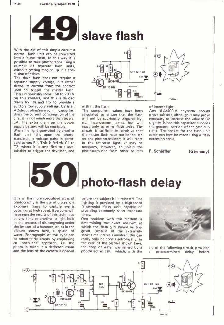
7-38 elektor july/august 1979
With the aid of this simple circuit a
normal flash unit can be converted into a 'slave' flash. In this way it is possible to take photographs using a
number of separate flash units, without getting tangled up in a con- fusion of cables. The slave flash does not require a
separate supply voltage, but rather draws its current from the contact used to trigger the master flash. There is normally some 150 to 200 V on this contact, and this is divided down by R4 and R5 to provide a
suitable low supply voltage. C2 is an AC-decoupling/reservoir capacitor. Since the current consumption of the circuit is not much more than several µA, the extra drain on the power supply battery will be negligible. When the light generated by another flash unit falls upon the photo - transistor, a voltage pulse is gener- ated across R1. This is fed via Cl to T2, where it is amplified to a level suitable to trigger the thyristor, and
One of the more specialised areas of photography is the use of ultra -short exposure times to capture events occuring at high speed. Everyone will have seen the results of this technique at one time or another: a light bulb in the process of disintegrating under the impact of a hammer, or, as in the picture shown here, a splash of water. Photographs of this type can be taken fairly simply by employing an 'open -lens' approach, i.e. the photo is taken in a darkened room and the lens of the camera is opened
5V
slave flash
with it, the flash. The component values have been calculated to ensure that the flash will not be spuriously triggered by, e.g. incandescent lamps, but will react only to other flash units. The circuit is sufficiently sensitive that the master flash need not be focused on the phototransistor; it will react to the reflected light. It may be necessary, however, to shield the phototransistor from other sources
of intense light. Any 8 A/400 V thyristor should prove suitable, although it may prove necessary to increase the value of C2 slightly (since this capacitor supplies the greatest portion of the gate cur- rent). The socket for the flash unit cable can best be made using a flash extension cable.
F. Schaffler (Germany)
photo -flash delay before the subject is illuminated. The lighting is provided by a high-speed (electronic) flash unit capable of providing extremely short exposure times. One problem with this method is
determining the exact moment at which the flash gun should be trig- gered. Because of the extremely short time intervals involved, this can really only be done electronically. In the case of the picture shown here, the drop of water was sensed by a photoelectric cell, which, with the
P5
R6 Y
BC 557B
R7
aid of the following circuit, provided a predetermined delay before
BST Bo 126
Th1 - r 330n
79571 6
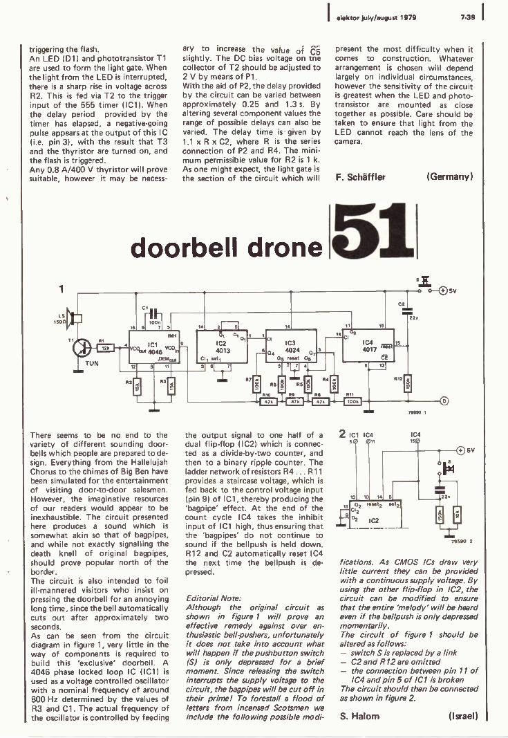
elektor july/august 1979 7-39 I
triggering the flash. An LED (D1) and phototransistor T1 are used to form the light gate. When the light from the LED is interrupted, there is a sharp rise in voltage across R2. This is fed via T2 to the trigger input of the 555 timer (IC1). When the delay period provided by the timer has elapsed, a negative -going pulse appears at the output of this IC (i.e. pin 3), with the result that T3 and the thyristor are turned on, and the flash is triggered. Any 0.8 A/400 V thyristor will prove suitable, however it may be necess-
1
ary to increase the value of 65 slightly. The DC bias voltage on the collector of T2 should be adjusted to 2 V by means of P1. With the aid of P2, the delay provided by the circuit can be varied between approximately 0.25 and 1.3 s. By altering several component values the range of possible delays can also be varied. The delay time is given by 1.1 x R x C2, where R is the series
connection of P2 and R4. The mini- mum permissible value for R2 is 1 k. As one might expect, the light gate is
the section of the circuit which will
doorbell drone
present the most difficulty when it comes to construction. Whatever arrangement is chosen will depend largely on individual circumstances, however the sensitivity of the circuit is greatest when the LED and photo - transistor are mounted as close together as possible. Care should be taken to ensure that light from the LED cannot reach the lens of the camera.
F. Scháffler (Germany)
5v
LS 1son 100n
14 2 1 5I 16 6 7 5
INH 01 Dl Ti
IC1 º_ IC2 out 4048 vCOIn 4013
TUN ,DEMout CI1 sell
12 11 31 61 1
3 R7
There seems to be no end to the variety of different sounding door- bells which people are prepared to de- sign. Everything from the Hallelujah Chorus to the chimes of Big Ben have been simulated for the entertainment of visiting door-to-door salesmen. However, the imaginative resources of our readers would appear to be inexhaustible. The circuit presented here produces a sound which is
somewhat akin so that of bagpipes, and while not exactly signalling the death knell of original bagpipes, should prove popular north of the border. The circuit is also intended to foil ill-mannered visitors who insist on pressing the doorbell for an annoying long time, since the bell automatically cuts out after approximately two seconds. As can be seen from the circuit diagram in figure 1, very little in the way of components is required to build this 'exclusive' doorbell. A 4046 phase locked loop IC (IC1) is
used as a voltage controlled oscillator with a nominal frequency of around 800 Hz determined by the values of R3 and Cl. The actual frequency of the oscillator is controlled by feeding
4
6
IC3
04 4024 OS reset 06
11 16
the output signal to one half of a
dual flip-flop (IC2) which is connec- ted as a divide -by -two counter, and then to a binary ripple counter. The ladder network of resistors R4 ... R11 provides a staircase voltage, which is
fed back to the control voltage input (pin 9) of IC1, thereby producing the 'bagpipe' effect. At the end of the count cycle IC4 takes the inhibit input of IC1 high, thus ensuring that the 'bagpipes' do not continue to sound if the bellpush is held down. R12 and C2 automatically reset IC4 the next time the bellpush is de- pressed.
Editorial Note: Although the original circuit as shown in figure 1 will prove an effective remedy against over en- thusiastic bell -pushers, unfortunately it does not take into account what will happen if the pushbutton switch (S) is only depressed for a brief moment. Since releasing the switch interrupts the supply voltage to the circuit, the bagpipes will be cut off in their prime! To forestall a flood of letters from incensed Scotsmen we include the following possible modi-
IC4
2
4017 `15 CE
131
R11
912
22n
2 IC1 IC4
79590 1
IC4
sv
79590 2
fications. As CMOS ICs draw very little current they can be provided with a continuous supply voltage. By using the other flip-flop in 1C2, the circuit can be modified to ensure that the entire 'melody' will be heard even if the bellpush is only depressed momentarily. The circuit of figure 1 should be altered as follows: - switch S is replaced by a link - C2 and R 12 are omitted - the connection between pin 11 of
IC4 and pin 5 of IC1 is broken The circuit should then be connected as shown in figure 2.
S. Halom (Israel)

7-40 elektor july/august 1979
Transmitting speech by modulating a beam of light isn't new. Usually, infra -red is used - as in some 'wire- less' headphone systems. However, it is also possible to use a normal torch bulb. The only point to note is that the filament must be run at a fairly high temperature, as otherwise the response will be too slow. For this reason, the bulb must be run at almost full brightness, with a very low modulation depth - about 1%. On the other hand, this has the advantage that the high light output carries over greater distances - cer- tainly if a so-called halogen lamp is used, as in this design. Using amplitude modulation would have the advantage that it makes for a simple receiver design. It would also have a few major disadvantages, particularly the fact that a suitable output stage for the transmitter (capable of driving a 60 watt lamp) would be rather expensive. For this reason (and some others), pulse -width
12 V
iF
C2
R2
0
R3 21Y 16V E C3
n 100
P1 / loon ( R1
Cl
TUN
sl Test
12 V
Re
0
9
R5
opto -transmitter for speech modulation was chosen. The inputsignal from the microphone is amplified by T1 and passed via the, 'modulation depth control' (P1) to a further amplifier stage, IC3. At this point, a DC offset is added to the signal. This offset is set by P2 to obtain the correct duty -cycle of the final output signal - more on this later. The pulse -width modulated signal is
obtained by feeding the (audio + DC) output of IC3 and a 35 kHz triangular wave -form to the two inputs of a comparator (IC4). The 35 kHz signal is produced by IC2. This opamp is used in what would normally be a multivibrator circuit (producing a square -wave), but owing to its limited slew rate the output is actually a triangular wave. The out- put of the comparator, IC4, is a
square -wave with a duty -cycle that varies with the speech signal. The average duty -cycle is set by P2 at 25% - i.e. T2, T3 and the lamp are
P2 R4
Ell -, EOM Eke
C5I
=4Y7 16V
10k ben log
R6
C7
R12
RIO
9
a C6
3
R7
on for 25% of the time. The lamp can be switched off by closing S2. A 12 V car battery can be used to power the circuit. It should be noted, however, that a 6 V lamp must be used in that case (with any power rating up to 60 W). Why a 6 V lamp on a 12 V supply? Surely that'll give four times the nominal power dissipation in the lamp? Sure enough, it will - for a quarter of the time, since a duty -cycle of 25% is used: the lamp is only on for a quarter of the time. And four times one quarter is one. One part of be discussed. multivibrator. this signal is
output. A 'lining up' receiver.
the circuit remains to IC1 is used as a 1 kHz As long as S1 is open, used to modulate the useful feature when the transmitter and
A. J. Mellink (The Netherlands)
4
~1,5
R13 2
3
IC4 3140 + 4
7
R20
BD 135 T2
T3
12 V
La * 89 max. 60W
2N3055 R18
R16
z7 4 4
3n
R11
EECI
This circuit is intended for use in conjunction with the 'opto -transmit- ter'. The modulated light beam is detected by a photo -transistor, T1; the output from this transistor is amplified by IC1. The overall gain of this stage can be adjusted by P1 and
M VVVVY
1 kHz .31 kHz
C2+ 741
4 \ R17
22k
12 V
R14
0
u
C8
T4n7 a
opto -receiver for speech P2 (fine and coarse adjustment, respectively). The optimum adjust- ment depends on the ambient lighting; it can be found (once the transmitter and receiver are correctly aligned) by 'tuning in' the 1 kHz test tone from the transmitter. After
s2* lamp
796456
WO text
the volume control, P3, the signal is
amplified by IC2 and IC3. The out- put stage is derived from an earlier Elektor circuit. If the transmitter and receiver are to be used in a reliable communica- tion system, some attention must be

elektor july/august 1979 7-41 `
Ti IC1 739
+
MPFT
C5
I0N R4 16V
330n 133n
paid to the mechanical and optical side of the units. Some kind of reflector -and -lens system will be required both at the transmitter and at the receiver. In practice, old car headlamps have proved quite satis- factory. Both units must be mounted on a sturdy tripod or some similar
+ IC2
2 741
T 109 16V
R7 l
C7 R8
68n
R9
R10
R12
adjustable base. The author claims that he has succeeded in obtaining reliable communication at distances of well over a mile - after dark, that is. If two-way communication is re- quired, the temptation to run a
transmitter and a receiver off the
calculator as chess clock
With only one or two minor modifi- cations, it is possible to adapt a
calculator to increment or decrement two separate numbers and display the results simultaneously. If we assume a calculator has an 8 -digit display, two 4 -digit numbers can be displayed thus:
4321 4321 number number
A B
It is a simple matter to subtract (or add) '1' to either of these numbers. In the case of number B, a straight- forward subtraction is all that is
required, whilst in the case of number A, the correct result can be obtained by subtracting 10000 from the 'total' number on the display. Thus: 43214321-10000=43204321
Number B remains unaltered during this operation. With the aid of the circuit described here, this method can be used to allow the calculator to function as a
chess clock, i.e. to display the amount of time each player currently has to complete the remainder of his moves. The circuit itself is
R7
R6
o
S1
IC1
RS
D1
R4 2M2
P1
2
m Omm IC2 IC3
4P
C4
I1--- 19
DUS
BD 135
28n
12V O
1009 16V
S S
C13= - 4709 16V
79645a
LS
8(2
same supply should be resisted. It won't work, unless the transmitter is switched off before the receiver is switched on.
A. J. Mellink (The Netherlands)
i ES1 ... ES3 = 3/4 IC1 = 4016,4066 N1 ... N4 = IC2 = 4011 N5... N8 = 1/3 I C3 = 4049
` C1
13
22n RI
6 R8
220_.47013
}0
B
10 R9 011. - 220...470(2 A
ES2 3
MR
ES319
79617
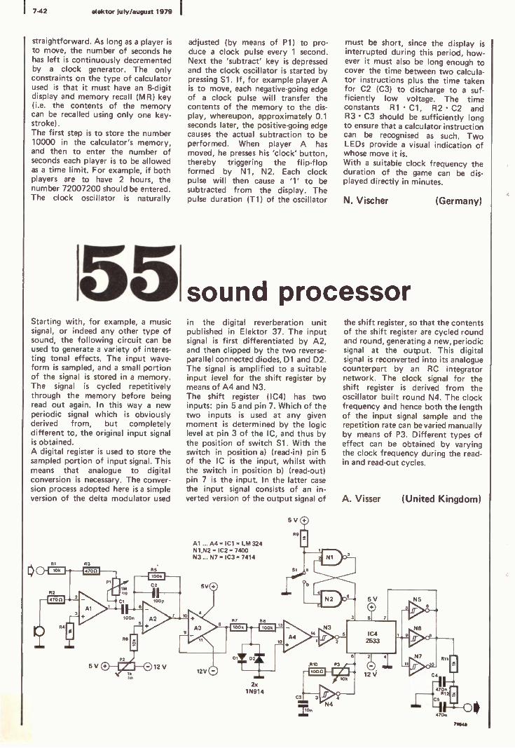
7-42 elektor july/august 1979 I
straightforward. As long as a player is to move, the number of seconds he has left is continuously decremented by a clock generator. The only constraints on the type of calculator used is that it must have an 8 -digit display and memory recall (MR) key (i.e. the contents of the memory can be recalled using only one key- stroke). The first step is to store the number 10000 in the calculator's memory, and then to enter the number of seconds each player is to be allowed as a time limit. For example, if both players are to have 2 hours, the number 72007200 should be entered. The clock oscillator is naturally
Starting with, for example, a music signal, or indeed any other type of sound, the following circuit can be used to generate a variety of interes- ting tonal effects. The input wave- form is sampled, and a small portion of the signal is stored in a memory. The signal is cycled repetitively through the memory before being read out again. In this way a new periodic signal which is obviously derived from, but completely different to, the original input signal is obtained. A digital register is used to store the sampled portion of input signal. This means that analogue to digital conversion is necessary. The conver- sion process adopted here is a simple version of the delta modulator used
adjusted (by means of P1) to pro- duce a clock pulse every 1 second. Next the 'subtract' key is depressed and the clock oscillator is started by pressing S1. If, for example player A is to move, each negative -going edge of a clock pulse will transfer the contents of the memory to the dis- play, whereupon, approximately 0.1 seconds later, the positive -going edge causes the actual subtraction to be performed. When player A has moved, he presses his 'clock' button, thereby triggering the flip-flop formed by N1, N2. Each clock pulse will then cause a '1' to be subtracted from the display. The pulse duration (T1) of the oscillator
must be short, since the display is interrupted during this period, how- ever it must also be long enough to cover the time between two calcula- tor instructions plus the time taken for C2 (C3) to discharge to a suf- ficiently low voltage. The time constants R1 C1, R2 C2 and R3 C3 should be sufficiently long to ensure that a calculator instruction can be recognised as such. Two LEDs provide a visual indication of whose move it is. With a suitable clock frequency the duration of the game can be dis- played directly in minutes.
N. Vischer (Germany)
sound processor in the digital reverberation unit published in Elektor 37. The input signal is first differentiated by A2, and then clipped by the two reverse - parallel connected diodes, D1 and D2. The signal is amplified to a suitable input level for the shift register by means of A4 and N3. The shift register (IC4) has two inputs: pin 5 and pin 7. Which of the two inputs is used at any given moment is determined by the logic level at pin 3 of the IC, and thus by the position of switch S1. With the switch in position a) (read -in) pin 5 of the IC is the input, whilst with the switch in position b) (read-out) pin 7 is the input. In the latter case the input signal consists of an in- verted version of the output signal of
A1 ... A4 = ICI = LM 324 N1,N2 = IC2 = 7400 N3 ... N7 = IC3 = 7414
2x 1N914
the shift register, so that the contents of the shift register are cycled round and round, generating a new, periodic signal at the output. This digital signal is reconverted into its analogue counterpart by an RC integrator network. The clock signal for the shift register is derived from the oscillator built round N4. The clock frequency and hence both the length of the input signal sample and the repetition rate can be varied manually by means of P3. Different types of effect can be obtained by varying the clock frequency during the read - in and read-out cycles.
A. Visser (United Kingdom)
71184º

elektor july/august 1979 7-43 I
digital contrast meter When enlarging photographs, two factors are of prime importance, the required exposure time, which is
determined by the density of the negative, and the contrast of the negative. The latter determines which grade of paper should be used in order to obtain a print with good overall tonal contrast. The contrast of the negative is basically the difference between the lightest and darkest portions of the exposed film. If we take the second log of this difference, we obtain the contrast ratio of the negative. Thus, for example, if the lightest part of the negative lets through 8 times as much light as the darkest part, the contrast ratio of the negative will be 3 (23 = 8). The circuit employs two light depen- dent resistors as sensors, and displays the contrast of the negative directly on a seven -segment display. The operation of the circuit is illustrated in the block diagram of figure 1. The amount of light falling upon the LDRs determines the frequency of the squarewave generators to which they are connected. The output of
2 5V
ti ti
..sk
portion
R1
RPY 58a
7
Cl '
mum
°
5V
ICI 555
RPY 58a
darkest
portion 5-
4
5V
5
IC 8 555
1 41101 31111
2
P1
6
1 lightest portion
darkest portion
1111fl - =16
enable
Start
counter
21, converter
16 r..e<
both oscillators are fed to a divide -by - sixteen counter. The pulses for the topmost counter (for the lightest portion of the negative) are counted for a period which is determined by the frequency of the signal from the lower counter. The result is that the value stored in the subsequent binary counter represents the ratio of the
5V
2
A 8 C D 13 clock C1aa
1 IC2 0 Clock LS197 D
0A Load
4k7
'1
...LOT 31 111
2 8 A B C D Gook Gear
1 IC9 6 aook LS197
2 1)D 1)A Loud
=51 11 101 91
up A BCD
anry r12
4 down IC3 boew I13
.wd LS193 dea 14
QADBCCDD »-j. 31 2 6 7
5V
3
FF
79546 1
two clock generator frequencies, and hence the ratio of the lightest and darkest portions of the negative. The contents of the 'ratio' counter, are then fed to the log2 converter, the output of which is decoded and displayed. A measurement cycle is
initiated by closing the start switch, which sets the flip-flop and resets the
5 4
15 1 10 9
12
IC4 LS193
3 4
14
3 2 6 7
R13
12
5V
3
1112 13 1 2 3 4 5 WI
11 1 13 14 15 16 17 1a I9
IC6 LS147
A B C D
9 71 6i 14i
6
2
151 11101 91
7
D
C
a
IC7 d
B LS247 A e
IC5 LS193
R4-R10
ID
Ir,
9
5
14
o2701)
2701)
617
5V
I/ dp
C2 RIM =1n
N1...N5=IC11=LSO4 N6 . . . N8 = IC12 = LS00 MMV1,MMv2=1C10=LS221
79546 2 0

7-44 elektor july/august 1979 I
counter. The complete circuit diagram of the contrast meter is shown in figure 2. With the exception of the two clock oscillators, in which 555 timers are used, the circuit is low power Schottky TTL. IC2 and IC9 are the divide -by -16 counters, whilst the binary 'ratio' counter consists of IC3, IC4 and 105. This counter uses negative logic, i.e. it begins with all outputs high, and then counts down. Thus at the start of each measurement cycle, a 'load' pulse, and not as one might expect, a 'reset' pulse, is applied to the counter. The paralleled data inputs of the counter are all held high, and the pulses to be counted are fed to the 'down' input. The reason for adopting this ar- rangement is the loge converter, which also uses negative logic. This converter is formed by IC6, a deci- mal -BCD priority encoder. This IC recognises the highest order bit in the
When flying radio controlled model aeroplanes there is always the chance that a fault will occur in either the transmitter or the receiver, and that the plane will no longer obey the control signals. If one is fortunate, the model will fall near the operator, however it may equally well happen that the plane will remain in flight for a considerable distance, and that the last the unfortunate owner will see of his model is it disappearing over the horizon! The circuit des- cribed here is designed to prevent the latter possibility, and also attempts to lessen the severity of the crash, by ensuring that the model will assume a glide trajectory. The circuit reacts to a loss of output from the receiver. When both trans -
1N4002
ClRI ffiElia
15p 16V
a
5n6
input signal which is active, i.e. logic 0, and outputs the BCD equivalent of that bit's 'weight'. For example, assume the counter holds the binary code for the number 8 (base 10). All bits will be logic 1, with the except- tion of 13 (remember, we are working with negative logic). lC6 recognises that the highest order bit which is
logic 0, is the third bit, therefore it outputs the BCD code for 3. As we have already established, 3 is loge of 8, thus the conversion is complete. The divide -by -sixteen counter, IC9, is
followed by a monostable, which provides a reset pulse to the flip-flop formed by N6 and N7 at the end of each measurement cycle. The set pulse is provided by a second monostable, which is triggered by the start switch, S1. The decimal point on the seven - segment display is lit during each measurement cycle. Since IC6 uses negative logic, its output signals must be inverted (by
N2 ... N5) before they can be fed to the BCD -seven -segment decoder, IC7. The display is a common -anode type, e.g. HP 5082-7750, FND 557. Any type of LDR which is intended for measurement purposes, as opposed to switching applications, can be used. The type named in the circuit diagram is particularly suitable. The circuit should be adjusted such that, as far as possible, the frequency of the two 555 oscillators is the same when identical amounts of light are falling on both LDRs. The LDRs should therefore be laid upon a surface which is evenly illuminated. Coarse adjustment is performed by varying the values of C1 and C2, whilst fine adjustment - which in many cases will be all that is required - is carried out with the aid of P1.
J. van Dijk (The Netherlands)
emergency flight controller mitter and receiver are functioning normally, the position of the servos is determined by the transmitted control pulses. Depending upon the make of servo, a pulse width of 1.5 ms corresponds to the neutral position, whilst pulse widths of 1 and 2 ms correspond to the extreme positions of the servo. When the stream of control pulses is interrup- ted, the three multivibrators in the circuit set the servos to a predeter- mined position. Input K4 is connected to the output of the receiver. Inputs K1, K2 and K3 are connected to the receiver servo control outputs for the elevator, rudder and engine throttle respect- ively, whilst outputs K1, K2 and K3 are connected to the correspon-
*see text
ding servos. As long as control pulses are received via K4, the multi- plexer, IC3, ensures that inputs K1, K2 and K3 are connected to the corresponding outputs (and servos). However when the control pulses are interrupted, the multiplexer switches to the outputs of the three oscillators. The position of P1, P2 and P3 then determine the position of the servo control horns. A mercury switch is connected across P3 (elevator con- trol). The switch should be mounted such that it will close when the angle of descent is greater than 10°, where- upon the position of the elevator servo will be determined by the value of Rx (10 ... 200 k).
W. van Staeyen (Belgium) *K1 * * K2 K3 -a -a -Q- 0 O O
10
R4
P2 R
C3
Tn6
250k
11 2
R6
250k
121 13
N1 ... N3 = IC1 = 4011 N4 ... N7 = IC2 = 4011
lA Se ect
5 1v
4
11
2A Q*K3* IC3 3A
74C1572v 7 K2* O 10
6 3B
2B 3Y 9
3 16
O*K1* Strobe
15
79642

elektor july/august 1979 7-45 I
FM PLL using CA 3089
The following circuit should prove particularly interesting to those readers considering building their own FM tuner. The novel feature of the circuit is that the well-known CA 3089 IC is not used as a conven- tional IF amplifier/demodulator, but as part of a phase locked loop. The resulting circuit is slightly more expensive and complicated than the 'standard' amplifier/de- modulator circuits, however the results obtained are a significant improvement on those of a 'classi- cal' CA 3089 IF strip. The circuit is intended as an IF amplifier/demodulator for a double conversion tuner operating at an intermediate frequency of 455 kHz. When using a PLL circuit for FM demodulation the S/N ratio of the demodulated signal is proportional to the ratio of frequency deviation/IF frequency, hence the PLL demodula- tor should operate at the lower IF of 455 kHz. Briefly, the circuit functions as
follows: The IF input signal is first
455kHz C2 2zn
jcy 2'
100n
fed to Cl, which removes any high frequency signal components which might affect the operation of the PLL. The exact value of Cl will depend upon the mixer circuit which converts the 10.7 MHz output of the front end to the desired IF fre- quency of 455 kHz. If the input signal is sufficiently 'clean' then lowpass filtering can be omitted. The CA 3089 amplifies and limits the IF signal to approximately 300 mV, whereupon it is fed to the on -chip quadrature detector. Output voltage U1 can be used to drive a
signal strength meter. The control voltage for the PLL VCO is taken from the AFC output (pin 7) of the IC. The voltage divider formed by R8/R9 is required to set the correct DC bias on pin 5 of IC2. Lowpass filtering of the control signal is
provided by R10 and C8. Largely for reasons of good linearity and high stability, a modern inte- grated circuit VCO, the NE566, was chosen. However the stability of the VCO is also significantly influenced
by the associated frequency -determi- ning components. P1 should prefer- ably be a cermet trimmer, whilst a
metal oxide resistor should be used for R11 and a ceramic disc capacotor with extremely low temperature coef- ficient should be used for C9. With the aid of a variable voltage divider (P2), the squarewave output voltage at pin 3 of IC2 (approximately 5.4 V) is reduced to roughly 0.3 V and then fed back via C11, to the input of the quadrature detector of 101. The demodulated output signal is
available at pin 6 of the CA 3089. If a squelch (muting) facility is required, this can be realised by feeding a
positive control voltage to pin 5 of IC1, thereby suppressing the audio output. Finally, the audio signal is
lowpass filtered and this output can be used with virtually any stereo decoder.
J. Deboy (Germany)
c IOOn
CI. R6
100n
U2
P2
C11 - 22n
IC 2 NE 566
106 C9E 1
Tn
6
810
R12
R14
TI
seep text
2x TUN
C
T2
C14 I1 Lr1 4147
`11
T6Op
79634
16V
LF

7-46 elektor july/august 1979
y_°put AMI1~111
o te
o w Ei
Trigger
0-
TR Q *
Ct
a
12 o
N5if /\
5V
5)16 1 Out
IC3 74LS151
0 51 02 03 D4 05 06 D7 4
12
1 t5 1a 1JI 12I
*
Although the name 'logic analyser' is generally understood to denote a quite different type of circuit, there are good reasons for borrowing the title to describe the electronic switch presented here. The switch is intended to simultaneously display the logic state of a number of test points in a digital circuit on an oscilloscope screen. The circuit functions as follows: The oscillator formed by N9/N10 generates a clock signal with a
frequency of either 1 kHz or 100 kHz, depending upon the position of switch S2. This signal is fed to a
counter, IC4, which, depending upon the position of switch S1, can be
An annoying disadvantage of fluor- escent lamps compared to the incandescent variety is the flickering delay before they actually burst into
logic analyser R6
5V 150 mA
5711.l t:
roorirooriZo7o4
R13 C7 11, 1014 16V 16V
--o
ti -0 Power Supply (9448-1)
5V
S1
5
10 n
R17
5V
preset to either '1000' (8), '1010' (10) or '1100' (12). The counter will therefore cycle through either the 8, 6 or 4 remaining output states before resetting to one of the above (preset) values. The result is that the A, B and C outputs of IC4 will count from either '000' to '111', from '010' to '111', or from '100' to '111'. The binary code present on these outputs determines which inputs are selected by the multiplexer, IC3. The multi- plexer scans the inputs in turn, and transfers the input signal to the out- put. Depending upon the position of S1, therefore, 4, 6 or all 8 inputs will be scanned. To ensure that each input signal is displayed 'separately'
615
100n
IC1
* see text
IC2
N1 ... N4 = IC1 = 74128 N5 ... N10 = IC2 = 74LS14 79628
on the screen, the corresponding binary code is also fed to inverters N2, N3 and N4, which, with the aid of the summing network R1 ... R4, ensure that a different DC offset is
added to each signal. Thus each signal will appear at a different 'height' on the screen. The trigger signal (TR) for the oscilloscope timebase is derived from the circuit under test. For slower scopes in particular, variable capaci- tor CI can be adjusted to obtain optimal picture quality.
P. C. Demmer(The Netherlands)
quick starter for fluorescent lamps life. This is because initially the gas in the tube is not at a sufficiently high temperature to ionise easily. Another reason is the fact that there
is no control over the point on the mains waveform at which the current through the starter coil is interrupted. The following circuit is designed to

elektor july/august 1979 7-47 I
1i
16 V
300 mA
B400800
1N4001
133
C4
IC1 7812
T2OP 40V
3
2
C
jR8
TOW
P1 47k
71
R2
BC 3078
BC 2378 R1
2
35V
01
DUS
R4
R3 Ó
14
IC2
O 12 V
12 V
o D2
DUS
P2 2M2
[ 1k I
D2
12V o 12V
o
1:9 BC 109C
T3
6®1 4
3 ® alp
C3
loon
N1 ... N3 = 1C2 = 3/4 4093 T
La t B2500800
D44
05
D6
D7
T5
4x W
OV
6 1009 3V
BC 140
BU 126
R6 ' I® 1W
DB
09
R7
010
resolve these problems and ensure. a flicker -free start. When the mains voltage is applied, the filaments of the lamp, La1, are pre -warmed for a period of approx- imately 1 second (depending upon the position of P2). At that stage the current flows through the rectifier, 81, and transistor T5. Once the lamp has reached a sufficiently high temperature, it can be started. To ensure that the voltage induced in the choke (L1) is as large as possible, the current through the coil should
be interrupted when it is at a
maximum. The correct time is
determined by the circuit round T1/T2. The pulse produced by T1/T2 triggers flip-flop N2/N3, with the result that transistor T5 is
turned abruptly off. The resultant voltage induced across L1 ignites the pre -warmed lamp. The RC network R5/C3 ensures that the flip-flop is
automatically reset at switch -on. Due to its inductive nature, the voltage across the coil is shifted in phase with respect to the current
flashing badge Although primarily intended as a
conversation piece at parties etc. the circuit described here can be used in numerous applications ranging from flashing house numbers to seat belt reminders. The circuit itself could hardly be simpler as it uses just one LM 3909 IC and a capacitor. When used as a flashing badge, the circuit is designed for use with a single HP7 (or similar) battery which can be
mounted inside one half of a battery holder while the capacitor and IC are mounted in the other half. There
79633
+ 1,5V
3X4001 79647
through the coil (the voltage leads the current). T1/T2 must therefore pro- vide a pulse just after the voltage has reached its maximum value. Poten- tiometer P1 should be adjusted until the lamp starts properly each time. The best setting for this potentio- meter will depend upon the type of lamp used. Transistor T5 dissipates little power and for so short a time that it does not need to be cooled.
D. Kraft (Germany)
are a number of possibilities for the badge display itself. The author suggests the use of a line -o -light LED display or a seven -segment display (encapsulated in a suitable resin) to show the initial of the flasher! Prospective constructors should bear in mind that the maximum output capability of the LM 3909 is around 50 mA.
L. Goodfriend (United Kingdom)
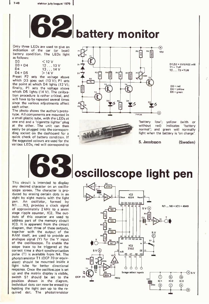
7-48 elektor july/august 1979
Only three LEDs are used to give an indication of the car (or boat) battery condition. The LEDs light as follows:
D3 <12V D3+D4 12...13V D4 13...14 V D4+D5 >14V
Preset P2 sets the voltage above which D3 goes out (13 V); P1 sets the point at which D4 lights (12 V); finally, P1 sets the voltage above which D5 lights (14 V). The calibra- tion procedure is rather critical, and will have to be repeated several times since the various adjustments affect each other. The photo shows the author's proto- type. All components are mounted in a small plastic tube, with the LEDs at one end and a 'cigarette lighter' plug at the other. The unit can then easily be plugged into the correspon- ding socket on the dashboard for a quick check of battery condition. If the suggested colours are used for the various LEDs, red will correspond to
This circuit is intended to display any desired character on an oscillo- scope screen. The character is pro- duced by erasing certain dots in an eight by eight matrix with the light pen. An oscillator, formed by N1 ... N3, provides a clock signal of approximately 2 kHz to a seven stage ripple counter, IC2. The out- puts of this counter are used to address part of the memory circuit IC3. It ís apparent from the circuit diagram, that three of these outputs, together with the output of the RAM itself, are used to provide an analogue signal (Y) for the Y input of the oscilloscope. To enable the scope trace to be triggered at the correct time a short synchronisation pulse (T) is available from N4. The phototransistor T1 (OCP 70 or equiv- alent) should be mounted inside a
light tube for better directional response. Once the oscilloscope is set up and the matrix display is visible, switch S1 should be set to the position shown in the diagram. Individual dots can now be erased by holding the light pen up to the re- quired dot. The phototransistor
battery monitor
.00,.:,r- r--- "` -M - r
4
D1,D2 = 5V6/400 mW T1 = TUP T2 . . . T5 =TUN
D3 = red D4 = yellow D5 = green
'battery low'; yellow (with or without red) indicates 'battery normal'; and green will normally light when the battery is 'on charge'.
S. Jacobsson (Sweden)
oscilloscope light pen
ti OCP 70
N1 7
RI
Cl
IC2 Clock 4024 Reset 2
01 02 03 04 05 06 12
R2 11
O Image select inputs
9 6 5 4
CÉ
A7 A8 A9 16 15 141
11
1:11
T00n
N1 ... N6 = IC1 = 4049
ó1a 10
Q 5 V
IC1 IC2 IC3

elektor july/august 1979 7-49 I
detects the arrival of the electron beam by the increase in light intensity and, once detected, provides a write pulse for the memory via N5, N6 and associated components. With S1 in the position shown, this pulse will write a '0' into the corresponding memory location. To replace dots back into the display the original matrix can be moved up
the screen whereupon a second matrix containing the missing dots will become visible. Switch S1 is then placed in the other position and the light pen again held up to the dot to be moved back into the upper matrix. It can be seen from the circuit dia- gram that only 64 of the possible 1024 memory locations are used and that A6 ... A9 of IC3 can be
analogue frequency meter
This circuit for a frequency meter offers six ranges: 100 Hz, 1 kHz, 10 kHz, 100 kHz, 1 MHz and 10 MHz. Switching between ranges is per- formed automatically, and the display is analogue. The input signal is first amplified to TTL level by means of IC1, T2 and N1, whereupon it is fed to a series of decade dividers (IC3 ... IC7). Thus a signal with a frequency between 10 Hz and 100 Hz can be obtained either at the output of N1, or at the output of one of the decade counters. The analogue section of the circuit (MMV1, the moving coil meter and associated components) is designed to produce a full-scale meter deflection for an input signal of 100 Hz. A multiplexer, IC8, is used to ensure that the correct divider output is
selected. The multiplexer is clocked by counter IC10. Each of the input signals are fed to the output in turn,
03
117
DUS `
22k
100yA
N1,N2 = IC2 - 7413 MMV1,MMV2 = IC9 = 74123
2
as long as the frequency of the out- put signal is lower than 10 Hz or higher than 100 Hz. If the frequency is lower than 10 Hz, then it is too low to keep the retriggerable mono - stable MMV2 continuously in the triggered state, with the result that the oscillator formed by N2 is
started and clock pulses are fed via IC10 to the multiplexer. If, on the other hand, the frequency of the output signal is greater than 100 Hz, MMV1 remains permanently triggered, so that MMV2 no longer receives trigger pulses. This mono - stable thus resets, thereby ensuring that the oscillator is enabled and the multiplexer continues to cycle through its inputs. Only when the output frequency of the multiplexer is between 10 Hz and 100 Hz is the oscillator stopped, since MMV1 is not triggered sufficiently often to keep MMV2 in the triggered state. The result of stopping the oscillator is
MMV1
NI
lo
switched to provide a total of sixteen different characters by extending the ladder network (4k7 and 10 k re- sistors). These address lines can also be encoded by suitable circuitry to convert the unit into a hexadecimal decoder and display, or even to provide an animated display.
A. N. Dames (United Kingdom)
i that the multiplexer in turn stops at the input which provided the signal of the appropriate frequency. LEDs D5 ... D10 provide an indication of the range selected. To calibrate the 'meter, P3 and P4 should initially be set to the mid - position, whilst P1 and P2 are ad- justed for maximum and minimum resistance respectively. A 100 Hz signal (with an ainplitude of greater than 1 V) is fed to the input of the circuit and P3 adjusted such that the multiplexer begins to cycle through its inputs. This can be verified by checking that the LEDs light up in turn. P2 is nowt adjusted until the 100 Hz range LED (D5) lights up. P1 is then adjusted for full-scale deflection on the meter. Finally, the circuit can be adjusted for maximum input 'sensitivity (approx- imately 10 mV)' by means of P4.
H. Bichler
5VO+
(Germany)
1C3 7490
11 14 IC4 7490
211'1611
12
IC5 7490
i1117r
12
11 14 IC6 7490
3It01 61 7T
IC7 7490
~21211:1
12
] 2 I 15 14I
C1
l0yy 6
MMV2
N2 v2 5V 5V MEE ` O
5k
100y 6Y
R P3 5 V
50 C
100y !v
IC8 74151
11 10 13
14
5
12
IC10 7490
12
IC11 7442
79596
5V

7-50 elektor july/august 1979
automatic battery charger The output of IC1 will be low, so that the base currents of T2 and T3, and hence the charging current, are determined solely by the position of P1
If the battery voltage is between 10 and 14 V, D3 is forward biased and T1 is turned on. The output of IC1 still remains low, so that the charging current is now determined by both P1 and P2. If the wiper voltage of P3 exceeds the zener voltage of D1, then due to the positive feedback via R4, the output voltage of 101 will swing up to a value determined by the zener voltage of D1 and the forward voltage drop of D2. As a result T1 is turned off and the charge current is
1
once again determined by the pos- ition of P1. In contrast to phase A-B, however, the higher output voltage of 101 means that current through P1, and hence the charging current, is reduced accordingly. Since D2 is forward biased, the effect of resistors R2 and R3 will be to gradually reduce the charging current still further, as the battery voltage continues to rise. To calibrate the circuit, P3 is adjusted so that the output of IC1 swings high when the output (i.e. battery) volt- age is 14.4 V. By means of P1 the 'top -up' charge current is set to the 20 -hour value (capacity of the battery in Ah divided
i to 72 14
1 16 18
14.4V
79517 1
-V
Recharging lead -acid batteries is often assumed to be an extremely straightforward matter. And that is indeed the case, assuming that no special demands are being made on the life of the battery. On the other hand, if one wishes to ensure that the battery lasts as long as possible, then certain constraints are placed upon the charge cycle. Figure 1 illustrates the ideal charge current characteristic for a normal 12 V lead -acid battery which is com- pletely discharged. During the first phase (A-B), a limited charging current is used, until the battery volt- age reaches approximately 10 V. This restriction on the charging current is
necessary to ensure that the charger is not overloaded (excessive dissi- pation). For the next phase (C-D), the battery is charged with the '5 -hour charging current'. The size of this current is determined by dividing the nominal capacity of the battery in ampere -hours (Ah) by 5. At the end of this period the battery should be charged to 14.4 V, whereupon the final phase (E-F) starts. The battery is charged with a much smaller 'top - up' current, which gradually would decrease to zero if the battery volt- age were to reach 16.5 V. The circuit described here (see figure 2) is intended to provide a
charge cycle which follows that described above. If the battery is completely discharged (volt- age < 10 V), so little current flows through D3 that T1 ís turned off.
1A
2
Tn B=B80C10000
4

elektor july/august 1979 7-51 I
79517
Parts list.
Resistors:
R1 =12k R2 = 10 k R3 = 82 k R4 = 1 M
R5,R6 = 8k2 R7=100S2 R8 = 3k9 R9 = 4k7 P1 = 100 k preset P2 = 220 k . . . 250 k preset P3 = 10 k preset
When we first published a circuit in last year's Summer Circuits issue which was designed to 'kill' the sound of a DJ's voice between records, little did we suspect that it would provoke such a widespread response. The circuit in question was even men- tioned in a well-known daily news- paper, with several prominent DJs asked for their comments! Such is
the evident popularity of the 'DJ killer' (at least among radio listeners, if not actually among the DJs themselves), that we have decided
1, _ C1a ..
ala_ ..
u
mu _ __
C - QLR 3 F0
0-1R2 1.0
L041:1 1 b aR6 }Q a..P143 -3- 0 1:179-1.0
Capacitors: C1a=C1b=4700µ/40 V
Semiconductors: T1 = TUN T2 = BD138, BD140 T3 = TIP2955 D1 = 6V8, 400 mW zener diode D2 = DUS D3 = 5V6, 400 mW zener diode IC1 = 741
Miscellaneous:
Tr = 16 V, 8 A mains transformer B = B80C10000 bridge rectifier fuse = 0.5 A slo-blo
d.j. killer to produce a printed circuit board for it. To recap briefly on how the circuit works: It is possible to distinguish speech
.from music by virtue of the fact that distinct pauses occur in speech, whereas music is more or less con- tinuous. The DJ killer detects these pauses and mutes the signal whilst the DJ is speaking. The left and right -channel signals are fed into the two inputs of the unit and are summed at the junction of
all ma
+0 .
by 20) for voltages between 14.5 and 15 V. Finally, with a battery voltage of between 11 and 14 V, P2 is ad- justed for the nominal (5 -hour) charging current. The initial charging current (phase A-B) is set by the value of the 'top -up' current, and depending upon the characteristics of the transistors, will be approximately 30 to 100% greater.
Siemens Components Report Volume XIII, No. 1 March 1978.
R14, R15 and R16. For use with a
mono radio only one input is
required. The summed signal is
amplified and limited by two high gain amplifiers IC1 and IC2, and is
then fed to two cascaded Schmitt triggers, N1 and N2. The output of N2 is used to drive a retriggerable monostable IC4a, the Q output of which is fed to the input of a second retriggerable monostable IC4b. So long as a continuous signal is
present at the input IC4a will be continuously retriggered by the out-
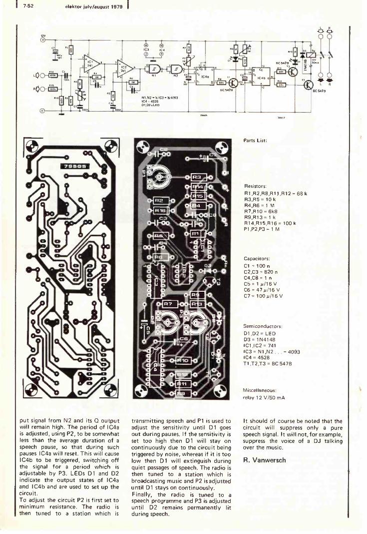
7-52 elektor july/august 1979 I
12V
79505
O
N1,N2-SSIC3-144093 IC4 - 4528 Dt,D2=LED
s4í
, . C ID .
.
I__r
11c. loY7ki t4W) . . -lrJ
112
put signal from N2 and its Q output will remain high. The period of IC4a is adjusted, using P2, to be somewhat less than the average duration of a
speech pause, so that during such pauses IC4a will reset. This will cause IC4b to be triggered, switching off the signal for a period which is adjustable by P3. LEDs D1 and D2 indicate the output states of IC4a and IC4b and are used to set up the circuit. To adjust the circuit P2 is first set to minimum resistance. The radio is
then tuned to a station which is
transmitting speech and P1 is used to adjust the sensitivity until D1 goes out during pauses. If the sensitivity is
set too high then D1 will stay on continuously due to the circuit being triggered by noise, whereas if it is too low then D1 will extinguish during quiet passages of speech. The radio is then tuned to a station which is
broadcasting music and P2 is adjusted until D1 stays on continuously. Finally, the radio is tuned to a speech programme and P3 is adjusted until D2 remains permanently lit during speech.
L p
Ci 00
78107
Parts List:
Resistors:
R1,R2,R8,R11,R12 = 68 k R3,R5 = 10 k R4,R6 = 1 M R7,R10 = 6k8 R9,R13 = 1 k R14,R15,R16= 100 k P1 ,P2 P3 = 1 M
Capacitors: C1=100n C2,C3 = 820 n
C4,C8 = 1 n
C5=1 µ/16V C6=47µ/16V C7= 100µ/16V
Semiconductors: D1,D2= LED D3 = 1N4148 IC1,IC2 = 741 IC3= N1,N2.. ,= 4093 IC4 = 4528 T1,T2,T3 = BC 5478
Miscellaneous:
relay 12 V/50 mA
It should of course be noted that the circuit will suppress only a pure speech signal. It will not, for example, suppress the voice of a DJ talking over the music.
R. Vanwersch

elektor july/august 1979 7-53 I
capacitors in parallel. For example, for a 1 kHz 'notch', 4n82 can be formed by 4n7 + 120 p. The filter is coarse tuned by P1/P3, and fine tuned by P2/P4. Inexpensive multi -turn trimmer potentiometers of the type used for station preset controls in radios and TV's can be employed. When tuning for zero fundamental, the two branches of the network (P1/P2 and P3/P4) should be adjusted alternately. The distortion signal is available at two outputs, D1 and D2. The signal at D2 is amplified by IC3 so that it is ten times greater than that at Dl. Once the filter has been optimally tuned and no further reduction in the fundamental can be obtained, the peak -peak value of the distortion signal (Dpp) and the peak -peak value of the input signal Uipp should be measured. The percentage distor- tion can then be calculated as follows: Miscellaneous:
UD 100 pp for D1, and
Uipp
%dpp - UDPP ' 10 for D2. Uipp
harmonic distortion meter
The following circuit is an improved version of the harmonic distortion meter published in the 1977 Summer Circuits issue. In place of transistors J-FET op -amps are used, whilst the circuit offers the choice of four switched spot frequencies as opposed to the single frequency available with the earlier version. The basic principle and operation of the circuit is the same, i.e. by applying bootstrapping to a twin -T network the Q of the filter is increased to the point where attenuation of the harmonics is eliminated. The filter thus rejects only the fundamental of the input (sinewave) signal, allowing the harmonic distortion products to be measured or examined on an oscilloscope. In the circuit shown here, the input signal is fed via Cl directly to the twin -T network. An input buffer stage is not required. Capacitors C6 ... C13 have a value C, where
C - 4 82 (C is in nanofarads and f
in kilohertz), whilst C2 ... C5 have a value 2C. Odd values can be ob- tained by choosing two suitable
C9b
C9a'
C9a
c7bl
411_
11
LI C2aC2b1 C311. C311 Cabl C5a
TTTTTTTT
parts list
resistors:
R1 = 100 k R2 = 33 k
R3 = 27 k
R4,R5 = 1 k R6 = 10 k R7 = 2k2 R8=18k R9 = 1k8 RIO =12k R11 = 1 k PI ,P3 = 10 k preset P2,P4 = 4k7 preset
Capacitors: Cl = 1 µ (MKM) C2a ... C13b: see text C14,C15 = 24/16 V
Semiconductors: IC1,IC2 = LF356 1C3 = LF356, LF357
S1 = three -pole, multi -way switch.
ICI
C1a I
O+ 15v
2y2 O7 16V
IC2 IC3 O C15
2y2 165 O 15V
IC1 , IC2-LF356
IC3= LF357
79519
4

I 7-54 elektor july/august 1979 I
79518
When considering constructing a
'wireless' headphones system, three basic approaches present themselves:
P1
C6
4k7 C2 ea
470
S 01R1 I-0 ón D1 D2 f + t 1!1!
O aÁ000
aoanaoani :,o{R9}o m m m mID
. ' Olga 10 / 2. 1-0
0.1R7R7 m
° 0011501c16411-11Cr O C11b Chia N 001 1-0 0-1I-0
c1tb craa poo-1 F'o o -I Fo
C13b C13a
OW b" oo-I F-0 01F-0 019 I I 3 A 0000 N O{R1º }p
Jo o
Jo o
P4 O a P3
tO o
® n
P1 O J=
ultrasonic transmitter for headphones a 'genuine' r.f. transmitter and receiver; an infra -red system em- ploying IR LEDs and photodiodes,
or an ultrasonic system. Since the first method is illegal and the second is both relatively complicated and
R3 Y
T1
L7 R6 100 m
C3
T2 22n
1
R5 1
T
R4
I C7 Milo í00n T
C1
555
D3
5V6 C5 r
6V
Cal
470P 63V
US*
D1,D2=1N4001 D4,D5,D7=1N4148 T1,T2=BC546B T3=BC557B
see 1..1
610
R9
D1
Cs O 100P 40V
18V = 25mA T100PsovD2
79 510

elektor july/august 1979 7-55 I
® l.L. o0-7rQ QR11 }Q T3 011Pi1? f+`
T! 0-'rv J ,4>M0 o~ C4
Q{031=17037 10 C9
05 O -H-0
I C7
CS I+ 111ZI <11ti
S, N QT
expensive, we are left with ultra- sonics, if we are looking for a reason- ably simple and cheap transmitter/re- ceiver. Because of its inherent simplicity, amplitude modulation (AM) was chosen in preference to the qualita- tively superior transmission system of frequency modulation. However providing one is reasonably ingenious in the design of the receiver, it is still possible to obtain highly acceptable quality from an AM system. The cir- cuit of the receiver is described in a
compánion article; the remainder of this article deals with the transmitter. Apart from the supply stage, the circuit consists of only two sections: an audio amplifier stage (T1, T2) connected with negative feedback, and an astable multivibrator (IC1). Transistor T2 is switched on and off by the astable at an ultrasonic fre- quency. Thus at the collector of this transistor is a signal whose amplitude is varied in accordance with the input audio signal, and whose frequency is
determined by the astable multivi-
1
C6 PP
MR 10
Mg3 f° gl
S2 Q
i7
II 1... I URI
brator. This signal is transmitted via an ultrasonic transducer. The design of the audio amplifier stage is such (virtual earth configur- ation) that the astable multivibrator has very little effect upon the quality of the input signal and distortion is minimal. The input sensitivity of the audio amplifier is about 60 mV. The modu- lation depth of the input signal can be varied by means of P1, whilst the fre- quency of the astable multivibrator, and hence of the transmitted ultra- sonic signal, can be varied between 15 and 35 kHz with the aid of P2. The optimal transmission frequency is determined in conjunction with the receiver and the type of trans- ducers used. The supply stage is extremely simple. Space is provided on the printed circuit board for a current source (T3), which can be used to charge ni - cad cells in the receiver, should these be used. The charging current is 6 to 7 mA, although this figure can be increased by altering R11 accord -
Resistors:
Resistors:
R1,R6,R12 = 22 k
R2,R3 = 100 k R4 = 330 52
R5 = 2k2 R7,R9 = 1 k R8 = 4k7 R10 = 3k9 R11=12052 P1 = 4k7 preset P2 = 10 k preset
Capacitors: Cl = 560 n
C2 = 47 p C3=22n C4 = 470 µ/63 V C5=47µ/6V C6 = 2n2 C7=100n C8,C9 = 100 µ/35 V
Semiconductors: D1,D2 = 1N4001 D3 = 5V6/400 mW zener diode D4,D5,D7 = 1N4148 D6 = LED T1,T2 = BC 107B, BC 54613 or
equ. T3 = BC 1776 or equ. IC1 = 555
Miscellaneous: L1= 100 mH US transducer: see text
ingly. Various types of ultrasonic transducer are suitable. A more detailed discussion of this point is
contained in the accompanying article on the receiver circuit.

7-56 elektor July/august 1979
A high quality servo amplifier can be built using only one IC and a handful of passive components. The SN28654 (Texas Instruments) contains a pulse - width modulator and an output stage that is capable of driving servo- motors (see figure 1). An input pulse at pin 3 is compared to a pulse that is generated by an internal monostable multivibrator (the 'monoflop'). The resultant pulse is stretched (using RC networks and Schmitt triggers) and passed to the output stage and from there to the motor. The complete circuit is shown in figure 2. Apart from the RC networks (R5/C4 and R8/C5) and some de - coupling capacitors, the only external components are the servo -motor and the associated servo -potentiometer. This potentiometer controls the timing of the internal monoflop, so that the motor will run until the internal pulse length corresponds to the input pulse - provided the motor is connected the right way round, of course! The printed circuit board (figure 3) offers the option of including the inverter (between pins 1 and 2) in the circuit if required. This means that either negative or positive input control pulses can be used. The advantages of this servo ampli- fier are:
high output current: 400 mA without external transistors; motor control in both directions with a single supply voltage; adjustable 'dead zone' (determined by C3); power consumption less than 800 mW.
Parts list.
Resistors:
R1,R5,R8= 10012 R2 = 8k2 R3 = 1 k
R4 = 1k2 R6,R7 = 33 k
R9 = 22 k
Capacitors: Cl = 33 µ/6 V C2,C4,C5 = 0.47 4/6 V C3 = 2n2
Semiconductors: IC1 = SN 28654
servo amplifier 1
2
3
R7
RC NC
114 13
A
Inverter input
12 11
SM
SM
B
10
NC
9
Monoflop
4
input VCC
o F2
R2
Cl =33V
C2 - 470n OM 6V
5
a
RC
8 ; < A
tD
5 1 6
Timing' L
C
y
795091
4,8 v
IC1 =
SN 28654
7 -
C3 fl T62
R6
12
R7
R5 R6
C4 C5 - 470n 470n T 6V T 6V
79509 2
el 9D
l
J

elektor july/august 1979 7-57 I `
ultrasonic receiver for headphones
Before going on to describe the circuit of the receiver, there is one point worth noting. Although primarily intended for use in an ultrasonic transmission system, it is in fact much more flexible than one might think. If the ultrasonic transducer is
replaced by a suitable (i.e. tunable) LC circuit, a highly sensitive 'conventional' AM receiver is ob- tained. The circuit can also be usefully employed as a direction finder in the 10 kHz to 30 MHz region. The receiver operates on the 'exalted - carrier' principle. The block diagram shown in figure 1 illustrates how this approach works. The received ultra- sonic signal is first amplified (block A) before being fed to a
limiter stage, which removes all traces of amplitude modulation and leaves only the carrier wave. The carrier signal is then multiplied with the non -limited AM signal in block X. Two product signals are obtained: the first is the modulation signal, and the second is a signal which has twice the frequency of the input signal. The output of the multiplier is fed to a lowpass filter which removes the high frequency modulation signal components, thus leaving the original audio signal, which can be fed via a
simple amplifier stage (block ALF) to the headphones. To ensure that differences in input signal level have as little effect as possible upon the level of the audio output signal, the circuit is provided with a simple automatic gain facility (AGC). To this end the output of the multiplier is amplified, rectified and fed back via a lowpass filter as a DC control signal to the input amplifier. Thus the greater the amplitude of the input signal, the lower the gain of the input stage. The circuit diagram of the receiver is shown in figure 2. The input amplifier is formed by an FET, type BF 256B (T1), connected in cascade with a
conventional r.f. transistor (T2). The amplified input signal is fed via emitter follower T3 to an SO41 P
(IC1), which is a combined limiter/ multiplier IC. The output of the multiplier (pin 8) is in turn fed via the active lowpass filter round T5 to the audio output stage formed by a
741 (IC2). Potentiometer P1 provides a volume control. The AGC feedback loop consists of T4 (amplifier) and D1, D2 (rectifier), which provides a negative voltage which is directly proportional to input signal level; this voltage is
1 EXALTED CARRIER DET.
----- só4fv----,
1 I
L -J
applied to the gate of FET T1. The high input impedance (500 k12) and low input capacitance (5 pF) of the circuit render it suitable for use with modern electret microphone capsules as transducers. The AKG types CK40/33, /35, and /36 will give the best results. Slightly less sensitive, but also quite acceptable are the CK40/37 and CK40/38.
Parts list
Resistors: R1,R2,R18,R19,R20 = 560 k
R3 = 4k7 R4,R17 = 27 k R5,R6 = 1k8 R7=18k R8 = 8k2 R9 = 1k5 R10=56012 R11 =220S2 R12,R13 = 3k9 R14,R16=15k R15= 1 k
R21 = 390 S2
P1 = 10 k preset
79511 1
For the transmitter transducer, AKG types CK5011, CK5015 and, to a
lesser extent, the CK5013, are best. In addition to the above mentioned types, there are a number of Valvo and Murata transducers which will also prove suitable for both the receiver and transmitter. If the system is used exclusively for speech transmission, the MA 40L1 R from
Capacitors: Cl ,C2,C3,C4,C5,C6,
C11 = 0.22 4/16 V Tantalum C7,C8,C9,C15,C16 = 0.47 µ/16 V
Tantalum C10,C18,C19 = 22 µ/16 V Tanta-
lum Cl 2 = 22 µ/3 V Tantalum C13=1 n
C14,C20 = 4n7 C17=15p
Semiconductors: D1,D2 = 1N4148 T1 = BF 256B T2,T3 = BF 494 T4 = BC 179C, BC 559C or equ. T5 = BC 109C, BC 549C or equ. IC1 = SO41P IC2 = 741 (MiniDip)
Miscellaneous:
us transducer (see text)

7.58 elektor july/august 1979 I
2
s*
RIO
220n 1ev
:
C C ce c 707ev Tnn Tv
*see text
Murata is a good choice. By mounting the components verti- cally, the printed circuit board is
extremely compact. Since the circuit can be powered by a 9 V battery, one can justifiably speak of a minia-
A frequency counter is an extremely useful tool for tuning the voltage controlled oscillators (VCOs) of a
synthesiser both quickly and accu- rately. To this end the author has designed a frequency multiplier which can be used in conjunction with the minicounter published in Elektor 38 (June 1978) to measure frequencies between 30 Hz and 10 kHz with much shorter gate/ count times than would otherwise be the case. With a gate time of 1 s the maximum readout is 999.9 Hz, whilst
1 12V
C1
2
"//0--1 IOOn
R2
ture receiver. The current consump- tion of the circuit is only 7 mA, so that the batteries should be ensured of a relatively long life. If ni -cad cells are used, these can be recharged with the aid of the special charging circuit
TI BF 256B T2,T3 = BF 494 T4 559C T5 549C IC1 SO41P 1C2 = 741 D1,D2 = 1N4148
on the transmitter board. In view of the wide bandwidth of the receiver, the transducer should be connected directly to the input of the circuit, i.e. no long leads between the two!
frequency counter for synthesisers with a gate time of 0.1 s the maxi- mum frequency is 9999 Hz. The circuit has two inputs: input 1
has a sensitivity of 1.3 Vpp (maxi- mum input voltage 50 Vpp); input 2 has a sensitivity of 130 mVpp (maxi- mum input voltage 5 Vpp). The first is intended to be connected direct to the output of the VCOs, whilst the second can be used with the monitor output of an amplifier. The input stage of the circuit is formed by two current controlled op -amps. Al attenuates the signal at
Al . . . A3 = IC1 = LM 3900 FF1, FF2 = IC2 = 4013
12 V O+
DUS C2
11. 2 16V
loon?
IC2 IC3 IC4
1 1 1
12 V
input 1 by a factor of 2, and ampli- fies the signal from input 2 by a
factor of 5. A peak detector (D1, C2) and a comparator (A2) convert the input signal into a squarewave, which is then fed to a Schmitt trigger (A3). Flip-flop FF1 ensures that the squarewave is symmetrical. The actual frequency multiplication is performed by means of a phase - locked loop (IC3), a dual -decade counter connected to divide by a
hundred (IC4), and a flip-flop, FF2. A squarewave signal with half the fre-
14
o D
FF2 iz 5 CI
R S
101 8
C3
6
1C3 4046
16V
12 VT 2 ,0 E2 E1
C12 IC4
041 4518 042 CI1 R2 R1
R11
12 V
T/
L
TUP
D2
R12
Pin 25
79114. 1

Dp4 DP 3 Dp 2 DPI 3
elektor july/august 1979 7-59
ll
12V 7
ll II
NI N2 3
71
D.
Parts list.
Resistors:
R1,R6,R7,R8= 220 k R2,R3,R9 = 1 M
R4,810 = 470 k
R5,R13 = 100 k R11 =33k R12=56052 R14 = 1 k R15= 10k
Capacitors:
C 1,C5 = 100 n
C2 = 1 µ116 V tantalum C3 = 47 p C4=22µ/16V
Semiconductors: IC1 = LM 3900 IC2 = 4013 IC3 = 4046 IC4 = 4518 T1 = TUN D1 - DUS 02 = LED
03
1.
quency of the input signal is fed to one of the phase comparator inputs of the PLL, whilst the output signal of the VCO, divided 200 (by IC4 and FF2) is fed to the other input. The VCO provides an output signal with a frequency which ensures that the two comparator input signals main- tain a constant phase relationship, i.e. they have the same frequency. Thus the output frequency of the PLL VCO will always be one hun- dred times that of the input fre- quency (Le. the clock frequency of
DP
10 R9 R8 R1
DUD 9I
D3 qL 1R
79114 . 2
FF1). The time constant R14/C4 determines the speed at which the VCO responds to changes in the input frequency. When the circuit is not 'locked -on', the display obtained will not be accu- rate. For this reason LED D2 is
included; when the VCO has locked - on this LED will extinguish, thereby indicating that the meter reading is
correct. The output of the circuit is connec- ted directly to the clock input of IC1 in the minicounter, which means that
a utoranging peak meter
If not always for exclusively technical reasons, output level meters are a
particularly popular type of circuit, especially in audio applications (power amps etc.) The circuit de- scribed here is for a moving coil meter with an autoranging facility. The meter will read from -40 to
-20 dB, and from -20 dB to 0 dB; two LEDs indicate which range is
selected (see figure 1). By adopting this approach the resolution of the meter is considerably improved. The circuit diagram of the meter is
shown in figure 2. The input signal is
fed to an attenuator (P1) before
4A: ao 01
a._ r-a aoJ 131h
1\411/4ó Ai s 21 W1-: P Q ,fijk _ Ike .41Al.9ll.cv.lie
79114.3
the input stage around T1 is omitted. The supply voltage can be derived from the minicounter itself. To ensure that the position of the decimal point on displays 1 and 2 (see figure 2) corresponds to the input range, several minor modifi- cations to the minicounter board are necessary. These are shown in figure 3.
J. Naudts
being full -wave rectified by the circuit round Al and A2. The output of the rectifier circuit is then fed through either S1 or S2, depending upon which switch is closed. The two switches are controlled by the com- parator, A6. The state of the com- parator in turn depends upon the

7-60 elektor july/august 1979 I
level of the input signal. If the volt- age at the non -inverting input of the comparator is lower than the wiper voltage of P3 (Le. if the input signal level on P1 is lower than -20 dB for sufficiently long), the output of the comparator will be low, D7 will light up, S2 will open and S1 close. A volt- age 3.3 times the input voltage of A3 is then fed to the peak rectifier circuit round A4. The gain of A3 is
determined by R8... R11. If, how- ever the input signal level is greater than -20 dB, the output of A6 goes high, D6 lights up, S1 opens and S2 is closed. Due to the effect of R10 ... R12, the rectifier input volt- age is attenuated by a factor of 0.33. Thus between the two switch states there is a difference in signal level of a factor of ten, i.e. 20 dB. The printed circuit board is designed to accomodate a stereo version of the circuit. The components shown in inverted commas and the pin num- bers in brackets belong to the right hand channel. A signal generator is required to calibrate the circuit. The wiper volt- age of P1 at which the maximum
100
50 -
10
o -40dB
.1
D7
-20dB ,
.
reading (0 dB) is obtained can, within reason, be selected as desired; however it is recommended that a
0 dB level corresponding to roughly
CoN2jor
Jr.13
7- c \7110, r Tof 79506
r--
íO: D6
Ode u,
79506-1
4 volts be chosen. The maximum output voltage of A5 is then approxi- mately 1.33 V; with a 100µA moving coil meter for M1 and M1', P2 should
D0440:I ® - r r
U v O v O 1u ,a
04420
R 0
\
7 v
1
rTár r ,° ' a q .
ir á
á*uu/ Ó fi 1- 1:51Y>
l7 a
iD
c o
Eck -r+ t.. ., I-
`o-Í1-0* ' C1 11'2 '''1 : i s g ;,l.f -4 º. fl"lyre
Itll., . e-
06
07
a m a
- ID
r1. 0
,
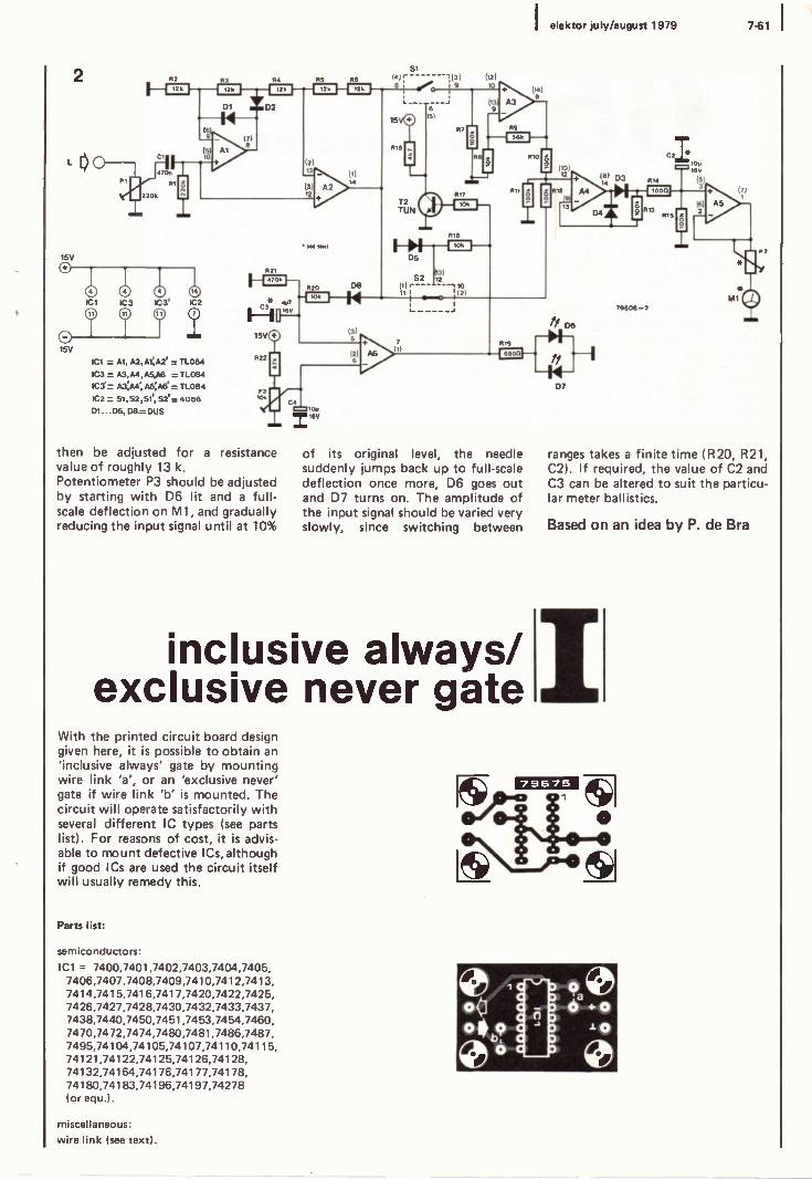
elektor july/august 1979 7-61 I
2
m m
el = Al, A2,A1¡A2' = TL084
1C3 = A3,A4,A5,A6 =TL084 IC3'= A3;Á4;A5;A6' =TL084 1C2 = 81,52,51', S2' = 4066 D1... 05,08..= DUS
then be adjusted for a resistance value of roughly 13 k. Potentiometer P3 should be adjusted by starting with D6 lit and a full- scale deflection on Ml, and gradually reducing the input signal until at 10%
of its original level, the needle suddenly jumps back up to full-scale deflection once more, D6 goes out and D7 turns on. The amplitude of the input signal should be varied very slowly, since switching between
inclusive always/ exclusive never gate
With the printed circuit board design given here, it is possible to obtain an 'inclusive always' gate by mounting wire link 'a', or an 'exclusive never' gate if wire link 'b' is mounted. The circuit will operate satisfactorily with several different IC types (see parts list). For reasons of cost, it is advis- able to mount defective ICs, although if good ICs are used the circuit itself will usually remedy this.
Parts list:
semiconductors: IC1 = 7400,7401,7402,7403,7404,7405,
7406,7407,7408,7409,7410,7412,7413, 7414,7415,7416,7417,7420,7422,7425, 7426,7427,7428,7430,7432,7433,7437. 7438,7440,7450,7451,7453,7454,7460, 7470,7472,7474,7480,7481,7486,7487, 7495,74104,74105,74107,74110,74115, 74121,74122,74125,74126,74128, 74132,74164,74176,74177,74178, 74180,74183,74196,74197,74278 (or equ.).
D7
ranges takes a finite time (R20, R21, C2). If required, the value of C2 and C3 can be altered to suit the particu- lar meter ballistics.
Based on an idea by P. de Bra
1,4";96:r 44:1
456-41.154-1
lp
miscellaneous: wire link (see text/.

7-62 elektor july/august 1979
The circuit shown here utilises the negative temperature coefficient of a diode to sense variations in tempera- ture. If a constant current is flowing through a forward -biased diode, the voltage dropped across the diode is inversely proportional to tempera- ture. In order to obtain a stable reference voltage, a 'super zener' configuration is used. IC1 ensures that a constant current flows through the zener diode, so that the zener voltage is unaffected by variations in the supply voltage. A 5.6 V zener was chosen for its low temperature coefficient. When the temperature of the sensor diode changes, the out- put voltage of IC2 varies by roughly
IC1
R2
6
R3
R4
Pt
6
thermometer 2 mV per °C. This voltage is ampli- fied by IC3 and fed to the meter. The meter is calibrated for zero reading at the lower end of the desired temperature scale (e.g. 0°C) by means of P1, and for full-scale deflection at the top end of the scale by means of P2. The circuit consumes relatively little current (roughly 3.5 mA), which means that it can be powered by a
9 V battery. The thermometer only draws current when a temperature reading is required (pushbutton switch S1 is depressed). Switch S2 allows the state of the battery to be monitored, and P3 should be adjusted to give a suitable deflection. However since the meter reading will also be
influenced by the temperature of the sensor diode, the measurement thus obtained should only be taken as a
rough indication of the battery state. With the component values shown in the diagram, the circuit has a
measurement range of roughly 50°C (depending upon the setting of P2). The range can be varied by altering the value of R7 (e.g. R7 = 33 k gives a range of 100°C). A further possibi- lity is to reverse the meter connec- tions, i.e. if the scale was previously 0 to 50°C, reversing the connections to the meter would give a scale of -50 to 0°C.
S. Jacobsson (Sweden)
10k
IC2
+ 10k 4 Cl
47n R7
88k
2
3
R6
The sawtooth is a favourite wave - shape in electronic organs. Twelve different frequencies are required within one octave; for other octaves, frequencies are needed that are a
multiple of two higher or lower. Given a sawtooth with a frequency fo, two new sawtooth waveforms can be obtained that are one octave higher and lower respectively (2 fo and 1/2 f0). The principle is described here.
1C3
+
7
R8
P3
1mA
ICI ... IC3 = 3x 741 D1 = 5V6/400mW D2 = 1 N4148
C2 Mal
T7n
79630
T
9V
-`
sawtooths up or down an octave
la
+1/2U
B -1/2U
+1/2U
2r A+B -1/2U
79618.1.

( elektor july/august 1979 7-63 I
The new sawtooth is obtained by adding a symmetrical square -wave to the original wave -form. As shown in figure la, adding signal A (with frequency f and amplitude U) to square -wave B (with frequency f and amplitude 1/2 U) results in a sawtooth with twice the frequency and half the amplitude of the original. Con- versely, if the squarewave is at half the original frequency and has the same amplitude as the input signal, the output will be a sawtooth at half the original frequency and twice the original amplitude - as shown in figure 1 b. Obviously, the above only applies if the 'edges' of the square - wave and sawtooth coincide - in other words, if the signals are 'in phase'. The block diagram of a suitable circuit is given in figure 2. The input signal is passed to a peak detector. This stores the peak level (+U) of the input signal; this level is passed via switch Sa to a summing circuit. Since the switch is operated (via a com- parator) by the input signal, it 'chops' the peak level U at the same frequency as the input signal. After restoring the symmetry of the squarewave with respect to supply common (by adding a series capacitor), the result is a squarewave with the same frequency but half the amplitude of the input sawtooth. Add it to the original sawtooth, and what do you get? Twice the original frequency and half the amplitude. To get the other output (at half the frequency), the peak level of the input signal must be doubled (x2) and the 'chopper' frequency for the switch must be halved (-2). Finally, if the upper summer has a gain of x2 and the lower has a 'gain' of x1/2, the sawtooths at the output will have exactly the same level as the original input signal. A 'rough draft' of a suitable circuit is
shown in figure 3. The peak detector (A1) is followed by a buffer (A2). The (electronic) switches both con- sist of two sections: when S1 opens, S2 closes - shorting any remaining feedthrough to ground and pulling C3 down. Flip-flop FF1 takes care of the frequency division required for the control signal to S3 + S4 (= Sb). Virtual -earth type summing amplifiers are used (A3 and A4), with a gain of x2 and x1/2, respectively.
N. Nielsen
lb
A iww
3
f A ://///./.
+u
1/2f C -
-u
+2U f
1/2f A+ C
-2U
Sa
B
79618 le
2 peak detector
-1 Comparator
(Denmark) fa 00--11
.0"
-2
R
3
0
53
11
Cs ' 1° O 9
2
R
zt /14,14,144,144.4/
X1
x2 -.-01112fa
A3
A4
796182
n4wwwvwv
0.2fp
R=10k C1,C3,C4 = 100 n
00 1/2fp
R2
Al
2,5 ... 7,5 V
2,5 ... 7,5 V
A2 6
51 ... S4=IC1 40668 A1...A4=1C2=4136 FF1 = 1/2 IC4 = 40278 N1 = 1/6 IC5 = 40498
2,5 ... 7,5 V
m0 m IC1 IC4 IC2 000
O
e 2,5 ... 7,5 V
2,5... 7,5 V
II 9
C Ó 14
121 If8
2,5 ... 7,5 V O 79618-3
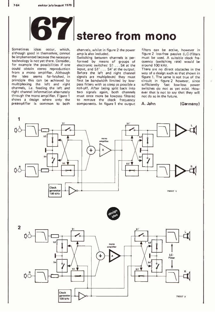
( 7-64 elektor july/august 1979
Sometimes ideas occur, which, although good in themselves, cannot be implemented because the necessary technology is not yet there. Consider, for example the possibilities if one could obtain stereo reproduction from a mono amplifier. Although the idea seems far-fetched, in principle this can be achieved by multiplexing the left and right channels, i.e. feeding the left and right channel information alternately through the mono amplifier. Figure 1
shows a design where only the preamplifier is common to both
1
2
S2
S4
R
51
Clock generator 100 kHz
stereo from mono channels, whilst in figure 2 the power amp is also included. Switching between channels is per- formed by means of groups of electronic switches: S1 ... S4 at the input, and S1' ... S4' at the output. Before the left and right channel signals are multiplexed they must first be bandwidth limited by low- pass filters with as steep as possible a
roll -off. After being split back into two signals again, both channels must once more be lowpass filtered to remove the clock frequency components. In figure 1 the output
S1
S2
mono mplifier
mono amplifier
Si'
filters can be active, however in figure 2 loss -free passive (LC -)filters must be used. A suitable clock fre- quency (switching rate) would be around 100 kHz. There are no direct obstacles in the way of a design such as that shown in figure 1. The same ís not true of the circuit in figure 2 however, since sufficiently fast low -loss power switches do not as yet exist. How- ever that is not to say that they will not do so in the future.
A. Jahn
Si,
79557 1
I 52
S
S3
LC- Filter
(Germany)
-411(
Clock generator 100 kHz
79557 2

elektor july/august 1979 7-65 I
The idea itself isn't new -a similar circuit was published in Elektor, May 1976 - but the simplicity of the circuit described here lends it a
special charm ... Only three ICs and a handful of other components are required to recognise the logic levels of sixteen different signals and dis- play them on an oscilloscope screen. The display consists of two rows of noughts and ones. This is achieved as
follows. If a sine -wave is applied to the Y -input of an oscilloscope, the display depends on the signal applied to the X -input. If a sawtooth is
applied, the sinewave is traced on the screen; if there is no signal on the X -input, a vertical line will be displayed; and, finally, if a sine -wave of the same frequency as the first but with different phase is applied, a
circle or ellipse can be obtained. The vertical line or circle can be positioned at any point on the screen by adding a suitable DC offset to the X- and/or Y -input signals. In the circuit de- scribed here, two rows of eight lines or circles are displayed. The circuit is shown in figure 1. Up to sixteen input signals are fed to the inputs of IC1. IC2 is a four -bit binary counter, and it applies binary numbers from 0 to 15 to the A, B, C and D inputs of IC1. When the number '0000' is applied, the signal at input 1 (E0, pin 8) of IC1 is passed (in inverted form) to its output, W. As the count at the A ... D inputs proceeds, the rest of the inputs 2 ... 16 are also scanned in sequence and passed to the output. When a '1' is present at the selected input, the output signal from IC1 is
at logic zero. The voltage at the R5/R6 junction is clamped to supply common via D1 and the output of N6 is 'high', so the X -output signal is
determined by the output of IC2 and the resistor network R11 ... R17. This signal is the 'DC component' that is required to step the display along the eight positions in one horizontal row. The Y -output signal consists of two components. A 'DC shift' signal is
taken from the D -output of IC2, to switch the display from the upper to the lower row and back, as required. Superimposed on this signal is the output from a simple RC oscillator (Ti). If all 16 inputs to IC1 are at logic one (so that the W output is
always '0'1, the display will there- fore consist of two rows of eight short vertical lines. When the W output goes to '1',
digisplay
5V®+
s0-3
24
E0 v E1 w E2
E3
E4 E5
E5 IC1
9o-23 E8 1101,0-22.
21 EE910
12021 Eli 130 19 E12
140 18 E13 S
15017E74 GNO 12
16016 EDSC B A
11 13 14 15
5V
74150
10
l however, the voltage at the R5/R6 junction is no longer clamped to supply common by D1. R5, R6, C4 and C5 are a phase -shifting network, so the sine -wave output from the oscillator is applied to the X -output (via R9) with a phase -shift with respect to the Y -output. The result: a circle on the screen. If the 16 inputs of IC1 are connected to the pins of a TTL IC (using a
DIL test clip, for instance), the logic levels at the pins of the IC will be displayed on the screen. The upper row corresponds 0...7, the lower row 8...15. Unconnected shown as 'ones'.
to inputs to inputs pins are
A. Kraut (Germany)
D1
NDUS
R6 R5
CS C4
¶900 MI= 1
208
11 8 9 12
D C B A
IB
IC2 IA
7493
RO1 GNDR02
RIO
4
R9
R
R8
47k
N1 ... N6 = IC3 = 7404
R18
5V
C6
6B0n
C7
100n
TUN .
O0x
R19
79575

7-66 elektor july/august 1979
Most people will have played with poker dice at one time or another, but not everyone will have realised that there are considerable possibili- ties for the skilled player to cheat. The following circuit for an electronic set of dice should contri- bute to ensuring a more honest game. The five dice are replaced by five rows of six LEDs (D1 ... D30, see figure 2) each LED corresponding to a different face of the die. For each row there is a 'throw' button (S2, S4, S6, S8, S10) and a 'set aside' button. When a 'throw' button is pressed, the result is not displayed immediately. To find out which
N1,N2 = 1/2 IC1 = 4011 N3. . . . N8 = IC3 = 74LSO4 1C4 ... IC11= 74LS75 N9 . . . N13 = IC12 = 5/6 4049 D1 . . . D30 = LED D31 . . . D40 = DUS T1 . . . T5 = TUN
IC1
14 OS íO
IC3 IC4.-IC11 1C12
5V
sv
electronic poker dice faces of the dice have been thrown, it is necessary to press the 'shaker' button S11, which, as it were, 'uncovers' the dice, enabling the players to see them. If one has thrown, say, a pair on the first turn, by pressing the corresponding 'set aside' buttons, the two LEDs re- presenting the pair will remain permanently lit. This is the equiva- lent of setting the pair of dice to one side (for all to see), before putting the remaining three dice back into the shaker and trying to im- prove one's score. The actual circuit (see figure 1) is
quite straightforward. A divide -by -six
16
6
I "ICE
14
IC2 =
4017
clock
15
Y1
3
Y4
y6 R
3
19
IC4
3
5 IC 5
1e
counter (IC2) is clocked by the oscillator round N1, N2. The outputs of N3 ... N8, which are connected to 5 x 6 = 30 latches (IC4 ... IC11), each go low in turn for the duration of one clock period. The outputs of the latches are connected to the dis- play LEDs, D1 ... D30. When one of the 'throw' buttons (S2, S4, S6, S8, S10) is pressed, the three enable inputs for the corresponding set of LEDs are taken high, with the result that the data present at that moment on the inputs of the latches are transferred to the outputs. The cathode of one LED in each set of six is pulled down virtually to ground,
14
10
9
tai
D5. -D8 115
C3 6
72 NiOR7 J :, .
D37 D32
ICE
e_2
16
ta 10
!/
1 14
3
IC7
I 09...012
!/ 1 10
13
IC8
1a1
D13...016
IC9
IC10
I! N
' N '° 14 9 1a,
D21...D24
15
025... 028
R
C41 R9 + S5 T3 _N1 1nR10 $ \/`C`.t%\T_.^ 1 a -o o
D33
T5
R14
038
SE
C6 R15
S9 476 R16 ' EIS .
S70 D35
D40 ' o 0 -.-4 16
r1 148
1
14 029...030
S11
79610 1

elektor july/august 1979 7-67
and these LEDs will light should S11 now be pressed (current being supplied via S11, D36...40, R2, R5, R8, R11, R14). If the corresponding 'set aside' button is pressed, the LEDs whose cathodes have been pulled down to earth will turn on permanently. Suppose, for example that S1 is
pressed, C2, which, when the 'throw' button was pressed, charged up via D31, is now discharged. The output of N9 is thus taken high, so that T1 supplies current to the LED, whose cathode is at earth There is one further point worth noting. Although it was stated that the circuit should help to ensure a
2 0 ON/OFF
® 1521
15121 2O 1541
30 1561
4C, )s9y
5CI 1510)
lift
1511)
9 10 J Q K
o Ó d o 0 03) 1041 ID61 1131) 1D21
1D7) 11291 1091 (010) 1D111
O O O O 1013) I0141 I1316) 10161 1017)
O O O O 1D191 020) 10211 10221 1023)
b o b o 0 10261 13261 113271 10281 (029)
1012) OIS3)
1D18)OS5)
(024)OIS71
10301 (so)
more honest game, it is important that each of the 'throw' buttons are pressed in turn, and not simul- taneously. The reason for this precaution is that if two or more
digitally -controlled phaser
Phasing is a well-known musical effect which is obtained by varying the phase relationship of a signal with respect to an original version of the same signal, whilst ensuring that its amplitude remains constant; the phase -shifted and original signals are then summed in proportions which are determined by the intensity of phasing required. In the circuit shown here, the phase shift is provided by op -amps A2 ... A7. The constant changes in phase are obtained by arranging for the resistance between the '+' inputs of the op -amps and earth to be varied
with the aid of a low frequency modulation signal. Normally FETs are used as voltage -controlled attenu- ators, however they have the draw- back of introducing a noise com- ponent and are not perfectly linear. The approach adopted here, although more complex, is superior. Eight resistors are switched in and out of circuit via multiplexers IC3... IC8 (which thus function as single -pole, 8 -way electronic switches). The multi- plexers are controlled by the infor- mation present on address lines A, B and C. Thanks to the configuration of gates, N1 ... N14, the address
78110
buttons are pressed at the same time, there is an increased chance of pairs or trebles etc.
A. Vandermaelen (Belgium)
data continuously cycles from 000 to 111 and back down to 000 again. The clock pulses are provided by the 555 timer, IC9. The clock frequency, and hence the speed of the phasing, can be varied by means of P3, whilst P1 allows the depth of phasing to be adjusted. The overall gain of the circuit is controlled by P2. A symmetrical supply voltage (max. ± 7.5 V) is used. In the prototype version the author used 2 x 4 1.5 V batteries to make up the 6 V supply lines shown in the diagram.
G. Duffau (France)
(CO
555
1113
a
IC3 4051
185
680
)C4 ' 4051
3
l"'1-
aI 0
ICS '
4051 ,
mI
'CO 4051
A
On
IC7 '
4051
88681.
On
108 4051
1Q
Al ... Ad - IC1 TL OB4,TL 074 A5 ... AB . IC2 IL 084.TL 074 N1 N2 2/31C11 - 4023 N3... N6. IC12.4011 N7...N10IC13.4011 N11 ... 014. IC14.4011 FF1 - 1/21C15 4027
61.11
01
=101 IC10 0, 4024 0,
04
12
1L
Cl 0" FF1
a `= B 5
6V° bbbbbó° 1a114V
0 1 o
5 ú
a114Y
uú
7 O 4)9,42 o 1 1 6V° Q
4Y 6V

7-68 elektor july/august 1979
1
R1
N2
design idea
IC1,IC2 = 747, TL 082 IC3,IC4 = CA 3240 N1,N2 = 1/2 IC5 = 4093
It is often very useful to ascertain the value of an unmarked or suspect capacitor or indeed to determine the value of a home -wound (or otherwise) inductor. The design idea described here is intended to fulfill both of these requirements by utilising an existing multimeter. In figure 1, a squarewave is produced by N1 and associated components, buffered by N2 and IC1 and fed to one of the high pass filters Rr/Lx or Cx/Rr (see figure 2a). After being differentiated by the filter network (figure 2b) the signal is again buffered (by IC3) and then integrated by the circuit around IC4. The resul- tant waveform is then amplified and rectified by IC2 whereupon it can be displayed on the multimeter. The formulae for calculating the voltage at the output of IC4 (so we are told!) are:
for capacitance: Uout = E RrCx R 2C2
for inductance: U out -E Lx R2C2Rr
Behind the above title lies a well- known type of dexterity game, in which two players each attempt to pass a ring along a length of wire without touching it. The first player to reach the end of the wire is the winner. If however a player's ring should happen to brush the wire, an LED lights, indicating that he must
capacitance and inductance meter
2a
2b
E
where E is the supply voltage. There- fore by selecting suitable range resistors Rr, and frequencies, different values of capacitors and inductors can be measured. The only proviso is
that the square -wave period time (=2.5 R1 C1) must be at least sixteen
LJfl_ 79636.2a
79636.26
times larger than
4x 1 N 4148
Lx Rr
79636-1
or CxRr, to
obtain a sufficiently accurate measurement.
T. Alfredsson (Sweden)
nerves of steel go back to the start and begin again. The circuit incorporates an additional refinement in that, whilst one player's 'go -back -to -start' LED is lit, the other player can touch his own wire without incurring a penalty (i.e. without his own LED lighting up), thereby enabling him to speed up. However the second player must
be careful, since the moment the first player reaches the start again, his LED will go out, simultaneously enabling the LED of the second player. The actual circuit is straightforward, being based on the operation of two flip-flops formed by N1 ... N4. At the start of the game, nice both

elektor July/august 1979 7-69 I
player's rings have touched the start electrodes (C and D), the out- puts of N2 and N3 are high (and LEDs D1 and D2 are extinguished), whilst the outputs of N1 and N4 are low. The free inputs of N2 and N3 are also low, i.e. at a potential just above the forward voltage drop of a
germanium diode (roughly 0.2 V). Assume now that player 1 touches his wire (B). The input of N1 is
momentarily taken low, which takes the output of N1 high and the
2
4,5V
output of N2 low. The 'go -back -to - start' LED of player 1 thus lights up, whilst the outputs of N3 and N4 remain unchanged. What happens now if player 2
touches the wire (with D1 still lit)? The input of N4 (E) is momentarily taken low, thus taking the free input of N3 high. Since the other input of N3 is low, the output of N3 will
remain high, so that LED D2 cannot light up. This situation will only change when the first player once
bicycle speedometer Circuits for bicycle speedometers have been fairly common (Elektor published one in last year's Summer Circuits issue No. 39/40), the differ- ence in this particular design being the digital readout. The speed sensing is carried out by a number of magnets attached to the spokes or rim of the wheel which operate a pair of reed switches. The principle is
illustrated in the drawing in figure 1.
where the reed switches are shown fitted on the bicycle front forks. The main advantage that a digital display has over a moving coil meter is that of robustness in a situation where the younger generation can create a very harsh environment. Current consumption is kept to a
1
more touches the start electrode, taking the output of N2 high again. Figure 2 shows a sketch of a possible layout for the game. Ordinary fairly stiff copper wire can be used, and obviously the 'difficulty factor' can be varied depending upon the shape into which the wire is bent and upon the diameter of the rings.
R.J. Horst (The Netherlands)
79522 1

7-70 elektor july/august 1979 I
minimum by arranging for the power supply to be switched on only when a readout is required. This switch (S2) should ideally be mounted on the handlebars (i.e. using an electric bicycle horn button or similar). The circuit diagram for the digital speedometer is shown in figure 2. The principle behind the circuit is uncomplicated: The pulses from the reed switches are fed to a counter (ICI, IC2) for a predetermined length of time. The counter is then inhibited and the count decoded and displayed. Decoding and display drive is performed by the counter itself. N3 and N4 serve to eliminate contact bounce from the reed switches, S1a and S1b, whilst the count pulses are fed to ICI via N7. The measurement period is deter- mined by the circuit round N5, N6, and can be varied by adjusting P1. The meter can therefore be calibrated with the aid of this preset. The charge time of capacitor C1 will ensure that the counters are reset by N1 before a new count cycle starts. Gate N2 prevents a count cycle starting before the reset is cleared. In view of the high current consump- tion of LED displays, a continuous readout is not feasible. A 'push- button' -type display was therefore chosen, i.e. each time S2 is depressed the speed of the bicycle at that particular moment is displayed. This approach also means that the com- ponents which would have been required to ensure that the counter is automatically reset after each count can be dispensed with. In principle any number of magnets can be employed, however in order
The designer of this circuit must have had frequent occasion to become annoyed at the various pamphlets, posters and advertising 'bumph' which is left under the windscreen wipers of parked cars, for he has come up with a radical antidote - an automatic windscreen clearer. Unfortunately this ingenious device has one slight drawback, any meter - maid or passing policeman who tries to leave a parking ticket under the wipers might well be less than pleased to see the ticket being repeatedly pushed off the windscreen (although perhaps some of our readers will find this prospect an
added attraction). The circuit reacts to the windscreen wipers being lifted off the wind -
2
RI
R2
IC4 IC3
9V
m C
toy T 16V
9V
9v
R4
N1 ... N4 =1C3 = CD4011 N5 ... N8 = IC4 = CD4011
i
2x FND 357
r'Tr-bn ITbn fibcdelg abcdefg
IC1 CD4026
CI t :10 Ic2 cI 1
CD4026 CE DE R CE DE
5 161 81 21 3 5 16 81 21 3
9V
to avoid excessively long count periods, a minimum of three is re- commended. The circuit should be calibrated (i.e. P1 adjusted for the
9V
47I 16V
47y 16V
79522 2
desired count period) with the aid of an existing speedometer.
P. de Jong (The Netherlands)
automatic windscreen clearer screen by switching on the wiper motor, with the result that the of- fending piece of paper is swept away. To detect when the wipers are lifted up, two reed switches are mounted on the .inside of the windscreen at the point where the wipers come to rest. A small magnet attached to each wiper holds the switches closed under normal conditions. However, when one of the wipers is lifted off the windscreen, the corresponding switch opens, and the flip-flop formed by N2 and N3 removes the inhibition on the decade counter, IC1. The latter starts to count clock pulses from the clock oscillator (N5, N6), and after the third pulse the Q3 output goes high, with the result that the second flip-flop,
formed by N11 and N12, turns on T1 and T2. The relay Re, is then pulled in, thereby switching on the wipers. After a further five clock pulses, the Q8 output of IC1 going high inhibits the clock signal via N4 and N7. Gates N8, N9 and N13 now ensure that the second flip-flop causes the relay to drop out (T1 and T2 are turned off) the moment both reed switches are closed. IC1 restarts to count, and upon the next clock pulse, the Q9 output goes high, causing the first flip-flop (N3, N4) to reset the counter. When power is applied, C3 and R5 ensure that the two flip-flops are
automatically reset. The length of time the wipers are switched on is
elektor july/august 1979 7-71 I
R
08
0
CE
C3
1,5
N1...N4=4011=1C2 N5...N8-4011-IC3 N4...N12=4011-IC4 N 13,N 14 = 4002 = 105
determined by P1, and can be varied as desired. The extra break contact in the relay prevents any difficulties arising in the event of wipers being turned on when the circuit is ope- rating. The circuit can only be used
loon
with wiper motors having an internal switch (wired in parallel with the manual switch) that opens to bring the wipers to rest. Fortunately, these are the most commonly used type. To deter even the most persistent
noise level meter There are many potential applications nowadays to justify the use of a noise level meter - for instance, monitoring the sound output at dances, discos etc. The unit described
1
R3
18V
strirla
0-
here was designed primarily to es- tablish the noise level produced by model engines. It has five switched ranges from 70 dB to 120 dB in 10 dB steps and is readable to 1/2 dB.
C3
5V
M1
R4
Ins
R
R6
R2
C6
D1... D5. DUS
RB
R7
BC547
BC140
02
1N4148
M
79638
18
t00 rnA
12V o Q+
12V
dashboard switch
of pamphleteers, one could even go so far as to use the circuit to switch on the windscreen washer as well as the wipers!
E. Stamberger (Austria)
The prototype was found to be accurate to ± 1 dB. The circuit for the noise level meter is shown in figure 1. The sound signal is picked up by the micro -
C41 R
108
P1
R15
514
Ion 79639 1

7-72 elektor july/august 1979 I
phone M1 and filtered by the net- work C1, C2, R1 and R2. These components, together with the capacitance of the microphone and the input impedance of the amplifier, ensure that the frequency response of the system is corrected to suit the internationally standardised 'A' weighting curve shown in figure 2. This 'weighted' signal is then fed to the operational amplifier Al, the gain of which can be altered by S2 to provide five noise ranges. The AC output of the op -amp is then rectified by diodes D1 ... D4 and fed to the meter via resistor R9. As this rectifier is included in the feedback loop the meter reading remains linear over the entire scale. Diode D5 is included to limit the current through the meter to a safe value, thereby reducing the risk
Automatic battery chargers are not particularly cheap, however the pro- tection they afford against over- charging and possible battery damage is highly desirable. The circuit shown here is intended to provide an inex- pensive alternative to the commer- cially available fully automatic chargers. The idea is to take a simple battery charger and incorporate an add-on unit which will automatically monitor the state of the battery and cut off the charge current at the desired point, i.e. when the battery is fully charged. The circuit basically consists of a
comparator, which monitors the battery voltage with respect to a
fixed reference value. If the battery voltage exceeds a presettable maxi- mum level, a relay is actuated which interrupts the charge current. If the battery voltage falls below a lower threshold value, the relay is released switching the charge current back in. The comparator is formed by a
741 op -amp. The supply voltage of
2
-20
-30
-40
-50
-60
70
of damage if a 'loud' noise is measured on a 'quiet' range. Components C5, C6 and R7 are included to provide frequency compensation and to prevent instability. Under normal operation the circuit will only draw about 2 mA, so it can be powered by two PP3 (or
10' 2 5 10'
F q y
79639.2
5 los
similar) batteries. The push-button switch S1 ensures that the circuit is not inadvertently left on. The meter should be calibrated in dBs and should have a full scale deflec- tion of +10 (normal log scale).
P. Barnes (United Kingdom)
automatic battery charger
-0
the op -amp is stabilised by R3 and D1, and is thus unaffected by vari- ations in the battery voltage. The reference voltage, which is fed to the inverting input of the op -amp, is derived from this stabilised supply via R4 and D2. The reference voltage is compared with a portion of the battery voltage, which is taken from the voltage divider, R1/P1/R2. As the battery voltage rises, at a certain point (determined by the setting of P1) the voltage on the non -inverting input of the op -amp will eventually exceed that on the inverting input, with the result that the output of the op -amp will swing high, turning on T1 and T2, pulling in the (normally - closed) contact of the relay and interrupting the charge current to the battery. LED D3 will then light up to indicate that the battery is fully charged. To prevent the battery being recon- nected to the charger at the slightest drop in battery voltage, a portion of the op -amp output voltage is fed
re1
O
79640
back via P2 and R5 to the non - inverting input. The op -amp thus functions in a fashion similar to a
Schmitt trigger, the degree of hyster- esis, i.e. the battery voltage at which the op -amp output will go low again, being determined by P2. The circuit is best calibrated by using a variable stabilised voltage as an 'artificial battery'. A voltage of 14.5 V is selected and P1 adjusted such that the relay just pulls in (opens). The 'battery' voltage is then reduced to 12.4 V and P2 adjusted until the relay drops out. Since P1
and P2 will influence one another, the procedure is best repeated several times. A final tip: if the charge current is
too large to be switched by the relay, the circuit can still be used by con- necting the relay in the primary of the battery charger transformer.
H. Heere (The Netherlands)

elektor july/august 1979 7-73
5 -minute chess clock In games of speed chess, where each player has only 5 or 10 minutes to complete all his moves, mechanical chess clocks leave something to be desired in terms of accuracy, es- pecially when both players have only 30 or 40 seconds left. The author of the circuit decribed here offers a
solution to this problem by employing LEDs to provide an unequivocal display which counts off the time remaining in multiples of 10 seconds. The clock uses two counters, one for player A and one for player B. By bridging a set of touch contacts
1
R1
2
6V
6V
+14a1.5V
_7_ mm00 u u u u
N1 ... N4=ICI 4011 IC2 . . . IC4 = 4017 53 ... S6=ICS 4066 N5 ... N10 = IC6 = 4049 N11 ... N16=IC7 4049
0 IC2'
R6
031 R5
228 228
each player can stop his own counter and start his opponent's. The state of each counter is displayed on a circle of 30 LEDs (see figure 2). In a
5 -minute game S1 is set to position 1, whereupon each LED lights up in turn for (300 seconds/30 =) 10 seconds. With S1 in position 2, the time limit is increased to 10 minutes per player, i.e. each LED lights up for 20 seconds. If a player exceeds his time limit, then LED D40 (A) or D40' (B) lights up. The counters can be reset for the start of a new game by
6V
N5
0l5
R11
DUS
012Q DUS
N6
V
IC2' ...1C4' = 4017 S3' ... S6' = IC5' = 4066 N7' ... N101 = IC6' = 4049 N11' ...N16' -IC7' =4049
Sensor A
6V
N7
6V
016
01...D30- LED
D39
6V
12 150 2
N8 N9 N70^ N11 N12
O' S0 R151
Reset 1
Sensor B Ilt 30 1'
0p000 0000000 O D40 O 250 Os
O O D35 o o
250 O O
040
0 D 36
O 05 O O
O O O o O O O O O
200 010 21í0o 00 00 00pO0 00p,00 OO1ó
ls 1s
pressing S2. LEDs D35 and D36 provide a visual indication of who is to move. Assuming player B has just made a
move on the board, he presses TAP switch B, which takes the output of N1 (which together with N2 forms a
set/reset flip-flop) high. The output of N2 goes low, causing counter A (IC2, IC3, IC4) to start counting the clock pulses provided by N3 and N4; counter B is inhibited until TAP switch A is touched. Since D31 is
now reverse biased, D35 will be turned on and off via D32 at a rate
a 10 1
N13 N14 N15
2 4 710 11 5 6 9 11,
0 1 2] 5 6 7 6 9
IC3 4017
íO5
IC2 IC3' IC4'
6V
_ = r
030
'time-up'LED
R19
79520 1
040
equal to the clock frequency. D33 is forward biased, pulling the input of N6 low, so that D36 will be ex- tinguished. The circuit can be powered by four 1.5 V batteries or by ni -cads. The current consumption is approxi- mately 45 mA. P1 and P2 can be calibrated using a known accurate timebase; each LED should light up for 10 seconds with S1 in position 1
and twenty seconds with S1 in position 2.
79520 2 S. Woydig (Germany)

7-74 elektor july/august 1979
If one's stereo system is pumping out too many watts, then there is always the danger that either one's loudspeakers or relations with the neighbours will suffer as a result. One obvious solution is to turn back the volume control. However, Mr. Ziemssen has come up with a
more drastic suggestion: disconnect the speakers automatically whenever the output signal exceeds a preset maximum level. The basic principle of the circuit is illustrated by the block diagram of figure 1. The sound level is
monitored by a microphone, the output of which is amplified and rectified, before being fed to a
flip-flop which disconnects the speakers (or interrupts the audio signal path at some other point). A second flip-flop input is desirable to reset the circuit when the audio signal falls back to an acceptable level (and also to ensure it assumes the proper state on power-up).The author originally submitted a detailed circuit design (see figure 2), however it suffered from the disadvantage of failing to provide an automatic reset facility, and - rather unecon- omically - used TTL. However the basic idea behind the circuit remains valid.
K. Ziemssen (Germany)
The advantages of a digital multi - meter are sufficienty well known that they do not need to be repeated here. However there are situations where it is useful to determine whether the quantity being measured is increasing or decreasing, particu- larly if it is subject to sudden flucta- tions. An op -amp connected as an AC amplifier is particularly suited to this task. Most simple DVMs contain an LSI chip with an input sensitivity of 200 mV and an extremely high input impedance. A suitable op -amp is the LF 355 used as a voltage -current converter, which has an input impe- dance of 1012 Ç.
emergency break 1
design idea
2 5V
Reset
N1,N2 = 1/2 74132 F F 1 = 1/2 7474
79558 1
79558 2
voltage trend meter
9

( elektor july/august 1979 7-75 I
The circuit shown here is designed for an input voltage of 200 mV and a current through the moving coil meter of 100µA. For other input voltage and/or output currents the trimmer potentiometer P1 . and resistor R1 should be altered accord- ingly. The op -amp requires two supply voltages (positive and negative) between 5 and 18 V. In view of the nominal current consumption of the circuit (several milliamps), these can
easily be provided by two 9 V batteries. The calibration procedure is quite straightforward. With the input short circuited, P2 is adjusted for a meter reading of zero volts. A 200 mV signal is then fed to the input, and P1 adjusted for the corresponding reading on the meter. If the meter has a scale of e.g. 0...3/30, then by calibrating the moving coil meter to read '2' for a
maximum reading (with e.g. 200
programmable digital function generator
The circuit shown here will generate pre -programmable periodic wave- forms. The waveform is stored digitally in two 256 x 4 bit RAMs which are connected in parallel to form a single 256 x 8 bit memory. The output waveform is obtained by repeatedly cycling through the contents of each of the 256 memory locations. The resulting digital signal is fed to a D/A converter and finally to a lowpass filter (not present in the circuit described here) to remove the clock frequency components. The address bus is clocked via an 8 -bit binary counter by the clock oscillator IC8. The frequency of the output signal is one twelfth that of
5V
StI 0 0
52.. 55 R
the clock frequency. The circuit is programmed as follows: A single period of the desired wave- form is divided into 256 discrete parts, each part having an address, starting with 00000000 and finishing with 11111111. The peak to peak amplitude of the waveform is also divided into 256 discrete levels, which are quantified digitally (00000000 for the lowest level and 11111111 for the highest level). Thus a list of addresses with corre- sponding data to be read into the RAMs is obtained. These addresses and data are set up on DIL switches S6 ... S13 (addresses) and S2 ... S5 and S14 ... S17 (data). Once this
5V Mal
22 17 1B 6 19
R3
R
R5
56..59 R6
R
2 3 1 10`A1 m m m
B1
12
L
R6
13
R
Q 4 4
A B2 2 IC3 3 MM 74C85
2
031
1.2 OD CND 11710.
IC1 2102
01
0
á á< Y á 703 20 3 2 21 5
10
2
14
9
5V( 16
7
0
510-.513 R10
R 1
R12
5
514 517
RI
R1
3 6
A1 A -B B.
16 10
IC4 2
MM B2
74C85 A3 93
"44:m m m
i<Ba +6 ¿IL
C1
9 3
e
20 3 2 21 s 7
15
11
R1
Do i 7 á: é,
01 IC2 D1
2102 0
2
03
ICS CD 4040
04
06
°' Clock Rm1
10
mV in) on the DVM, an 'overload' range up to 300 mV can be obtained. In the above case, with a constant current of 100 µA through the ana- logue meter, the value of R1 should be increased to 2k7. The circuit functions in a similar fashion for both current and resistance measurements. The DVM is connected in parallel with the analogue meter.
H. Ehrlich (Germany)
has been done (open switch = 0), switch S1 is momentarily depressed, thereby enabling the digital compara- tors IC3 and IC4. As soon as the address generated by IC8 and IC5 corresponds to the address set up on S6 ... S13, the output (pin 6) of IC4 goes high. The monostable formed by Cl, R18 and N1 then produces a
short write pulse on the R/W input of IC1 and IC2, causing the data set up on the data switches to be written into memory. The above procedure is then repeated for the remaining 255 memory locations.
C. Rohrbacher (France)
5VO+
100
5 V +O
12
IC8 555
R22
7
C3I' C
470k
ty
2
R21
IC7 LF 356 i
5V
RIO 22 7 19 6 19
5V 4r N 1= 1/4 I C9 = 1/4 CD 4011 79622

7-76 elektor july/august 1979
When developing programs for micro- computers a single mistake can have disastrous consequences. A particu- larly aggravating occurrence is when a section of program, which was con- sidered to be safely tucked out of harm's way in a different part of RAM, has been inadvertently written over. The simple circuit shown here offers a handy solution to this pro- blem, namely a Read Only switch for RAM. With the aid of this switch the Write signal is inhibited, so that data can only be read out of RAM. With the circuit shown in figure 1
four 128 x 8 bit RAMS, i.e. two 1/4 k
1 ADO
AD6
AD 7
pseudo PROM blocks, are protected by the Read Only switch. Naturally the circuit can be extended to cover larger blocks of memory. IF CMOS RAMs are used, then a
further interesting possibility is to provide a battery back-up power supply. Since the power consumption of CMOS memories is so low, a
normal 4.5 V battery would be suf- ficient to power the circuit for several days. A suitable battery buffer circuit is shown in figure 2. The state of the battery can be checked by means of switch S2; below a battery voltage of 3.9 V the LED will be
BLOCKl
(256 bytes)
NWDS
NRDS
BLOCK a
(256 bytes)
R7
SI
Cst
128X8
cs2
RAM
ADDRESS
CSO
128X8
cs1
sl 128X8
C52
RAM
1
1
128X8
cs1
CSO
Most people will have seen the desk- top ornament/toy known as a
'Newtons cradle' (see figure 1), which consists of usually five steel balls suspended in a row from a pair of threads. When one of the end balls is
lifted and then released so that it falls back and strikes the next ball, the energy of the impact is trans- mitted through the other balls, with the result that the ball on the op -
79613.1
completely extinguished. In actual fact CMOS ICs will work with supply voltages as low as 3 V, so the gradual loss of battery voltage should present no problems. As well as eliminating the possibility of accidentally altering the contents of a section of RAM, the above circuit allows one to preserve a pro- gram or section of program for several hours or more without having to use a cassette dump routine.
J.F. Courteheuse and A. Monnier (France)
2
5V
non-stop Newton's cradle posite end of the row swings up. It then in turn falls back, energy is again transmitted through the row, and the first ball swings up, and so on. The energy losses of the system are fairly high, and after a number of oscillations the balls are returned to rest. The idea behind the circuit described here, is to compensate for the natural energy losses of the system, so that it continues to
79613.2
oscillate indefinitely (i.e. until the circuit is disconnected or the bat- teries run out!). If, for the moment we ignore the energy losses, the frequency at which the system oscillates will be:
f- 1
2
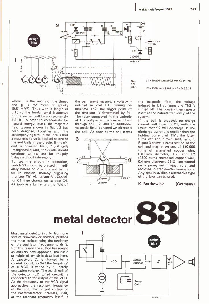
elektor july/august 1979 7-77 I
2
design idea
Th2
4 e
csI 101+
REIM10V
C106D1
R3
1.1
where I is the length of the thread and g is the force of gravity (9.81 m/s2 ). Thus with a length of 0.15 m, the fundamental frequency of the system will be approximately 1.3 Hz. In order to compensate for natural energy losses, the magnetic field system shown in figure 2 has been designed. Together with the accompanying circuit, the idea is that a magnetic force is applied to one of the end balls in the cradle. If the cir- cuit is powered by 6 1.5 V cells (manganese -alkali), the cradle should continue to oscillate for roughly 5 days without interruption. To set the circuit in operation, switch S1 should be pressed immedi- ately before or after the end ball is set in motion, thereby triggering thyristor Th1 via resistor R1. Capaci- tor Cl then charges up, as does C4. As soon as a ball enters the field of
21+2 100001+ 10V 10V
1
79579 2
Re= 5V 60 S2
the permanent magnet, a voltage is
induced in coil L1, turning on thyristor Th2; the trigger point of the thyristor is determined by P1. The relay connected in the cathode of Th2 pulls in, so that current flows through coil L2, and an additional magnetic field is created which repels the ball. As soon as the ball leaves
metal detector Most metal detectors suffer from one sort of drawback or another, perhaps the most serious being the tendency of the oscillator frequency to drift. For this reason the author has sought an entirely new approach, the basic principle of which is described here. A capacitor, C, is charged by a
current source, so that the frequency of a VCO is varied by a linearly decreasing voltage. The search coil of the detector (LC tuned circuit) is
connected to the output of the VCO. As the frequency of the VCO signal approaches the resonant frequency of the coil, the output voltage of the buffer/detector increases, until, at the resonant frequency itself, it
1
C
vco -e.
T
2200V 10V
L1 = 10.000 turns 0 0,1 mm Cu (= 1 ktl
L2 = 2300 turns 0 0.4 mm Cu (= 2501
the magnetic field, the voltage induced in L1 collapses and Th2 is
turned off. The process then repeats itself at the natural frequency of the system. If the ball is stopped, no charge current will flow to Cl, with the result that C2 will discharge. If the discharge current is smaller than the holding current of Th1, the latter turns off and circuit switches off. Figure 3 shows a cross-section of the coil and magnet system. L1 (10,000 turns of enamelled copper wire, 0.01 mm diameter, 1 k) and L2 (2300 turns enamelled copper wire, 0.4 mm diameter, 25 Si) are wound on a permanent magnet core, and enclosed in transformer laminations. Any readily available alternative type of thyristor can be used.
K. Bartkowiak (Germany)
Search coil
design idea
JT
79580 1
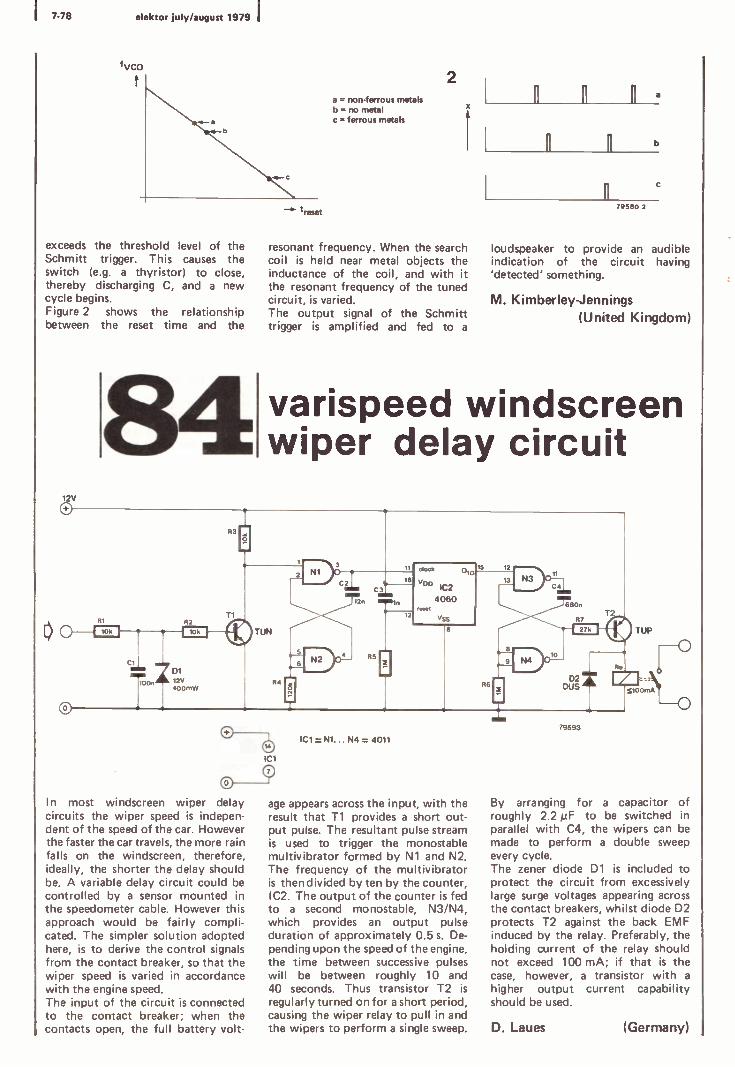
7-78 elektor july/august 1979 I
exceeds the threshold level of the Schmitt trigger. This causes the switch (e.g. a thyristor) to close, thereby discharging C, and a new cycle begins. Figure 2 shows the relationship between the reset time and the
12V
a = non-ferrous metals b = no metal c = ferrous metals
treset
2
resonant frequency. When the search coil is held near metal objects the inductance of the coil, and with it the resonant frequency of the tuned circuit, is varied. The output signal of the Schmitt trigger is amplified and fed to a
a
b
79580 2
loudspeaker to provide an audible indication of the circuit having 'detected' something.
M. Kimberley -Jennings (United Kingdom)
varispeed windscreen wiper delay circuit
R1
Cl D1
To 12v 400mW
R2
R3
T1
® TUN
IC1
In most windscreen wiper delay circuits the wiper speed is indepen- dent of the speed of the car. However the faster the car travels, the more rain falls on the windscreen, therefore, ideally,' the shorter the delay should be. A variable delay circuit could be controlled by a sensor mounted in the speedometer cable. However this approach would be fairly compli- cated. The simpler solution adopted here, is to derive the control signals from the contact breaker, so that the wiper speed is varied in accordance with the engine speed. The input of the circuit is connected to the contact breaker; when the contacts open, the full battery volt -
4
C3
11
R5
o
IC1 = N1. . . N4 = 4011
12
clock
VDD IC2
4060
Vss
age appears across the input, with the result that T1 provides a short out- put pulse. The resultant pulse stream is used to trigger the monostable multivibrator formed by N1 and N2. The frequency of the multivibrator is then divided by ten by the counter, IC2. The output of the counter is fed to a second monostable, N3/N4, which provides an output pulse duration of approximately 0.5 s. De- pending upon the speed of the engine, the time between successive pulses will be between roughly 10 and 40 seconds. Thus transistor T2 is
regularly turned on for a short period, causing the wiper relay to pull in and the wipers to perform a single sweep.
R6
12 11
13
79593
By arranging for a capacitor of roughly 2.2µF to be switched in parallel with C4, the wipers can be made to perform a double sweep every cycle. The zener diode D1 is included to protect the circuit from excessively large surge voltages appearing across the contact breakers, whilst diode D2 protects T2 against the back EMF induced by the relay. Preferably, the holding current of the relay should not exceed 100 mA; if that is the case, however, a transistor with a
higher output current capability should be used.
D. Laues (Germany)

elektor july/august 1979 7-79 I
The following circuit is intended as
an infra -red lock for house doors, garage doors, etc. Since the 'key' is
almost impossible to copy, it should provide an effective obstacle to unwanted visitors. Figure 1 shows the infra red trans- mitter. An astable multivibrator, formed by NAND gates N1 ... N3, drives an output transistor, T1, which turns the infra -red emitter diode on and off at a frequency which can be varied by means of P1. The receiver circuit is shown in figure 2. Light pulses received by the phototransistor T1 are amplified by IC1 and fed to an LC circuit tuned to roughly 23 kHz. The filtered output signal is rectified by D1 and fed to op -amp IC2, which is connected as a Schmitt trigger. The trigger thres- hold is set by zener diode D4 to 2.4 V. The unfiltered output of IC1 is also fed to a second Schmitt trigger, (103). The output of this op -amp (point 1) will remain high as long as the voltage level at its input is 2.4 volts or greater regardless of the frequency of the received signal. Assuming point 1 is high, a positive going edge at the output of IC2 (point 2) will 'turn the lock' as
follows: when point 2 goes high, the output of N1 also goes high, and
2
06 DUS
R1
T1
BPX 43
R6
11N914 T2 D2
TUN
C3 e> [a
467 16V
IR lock with it the input of monostable multivibrator MMV1. However, since this monostable is triggered by a
negative going edge, the output state of the monostable remains un- changed, i.e. the Q output remains low. The positive going edge at point 2 is also transferred to the trigger input of MMV2, which since it is triggered by positive going pulses, turns on the Darlington pair T3/T4 and pulls in the relay. Thus for the pulse duration of MMV2 the lock is 'opened'. If the modulation frequency of the transmitter signal deviates from 23
1N914
C6
7n T6V
4
+IC3 741
2V4 100mW
1 9V
IC1
N1...N3=3/41C1=4011
6
220p - 16V
N4,N5 = 1/2 IC5 = 4081
kHz, only point 1 will be high; point 2 will go low, with the result that, via N1, the negative going edge will trigger MMV1. Thus for the pulse duration of MMV1 - which is several minutes - MMV2 cannot be triggered. Even if the modulation frequency is subsequently corrected, since one input of N5 is held low, the lock cannot be opened during this period. If a flip-flop is used in place of a
relay, the circuit could, for example, be used to switch a car alarm system on and off.
H.J. Urban (Germany)
79644 - 1
®12,,
12V
6
13 16 11
1,?
105 1C4
(D12v
Ref 135 m TUN
MMV1,MMV2 = IC6 = 4528
1N914
BC 140
79644 - 2

7-80 elektor july/august 1979
1 r
The following design for a sequencer, which will generate a 10 note ana- logue waveform, is distinguished by its relative simplicity. To control a
synthesiser two types of signal are required: a gate pulse to trigger the envelope shaper (ADSR), and a con- trol voltage for the voltage con- trolled oscillators (VCOs). The VCO voltages are generated as follows. An oscillator, formed by N1, N2 and N3, clocks a decade counter (IC1). Each output of the counter is connected to an analogue switch (as shown in figure 2), the input voltage of which can be varied by means of a
potentiometer. The outputs of all the switches are joined together, so that an analogue waveform, composed of 10 discrete voltage levels, is gener- ated at this point. The frequency of the resultant signal can be varied by means of P1. The gate signal for the ADSR is
derived from the clock signal, how- ever since each synthesiser places different demands on the type of gate pulse required, no circuit is given. Readers may wish to experiment with extending the circuit. One possi- bility is to include a monostable multivibrator (at the clock input of IC1), which allows one to cycle through the analogue waveform step by step. Each of the preset voltage levels on the inputs of S1 ... S10 are then compared with a reference volt -
Multiply X and Y and you get XY - all very simple and straightfor- ward - at least on paper. But what if X and Y are analogue voltages, which may be of either polarity? How does one go about multiplying two such quantities? The following circuit for a 'four quadrant multiplier' - a
circuit which will multiply two input voltages and ensure the product is of the correct polarity - shows one way of approaching this problem. Basically the circuit generates a
squarewave signal, whose duty -cycle is proportional to one of the input signals and whose amplitude is pro- portional to the other. The average
sequencer 1 5...15V
14
IC5
47k b9.
R1
R2
R3
6
R5
8
4 _ 9
D, " DUS
10
C2 ohs
0 3
1 2
2
3 7
IC1 4
4017 5 I
6
10
8113¡ 151
2 5...15V
R6...R15
P2...P11
79625 O
5...15V ' ' ^ o :; 3
r-,-L o ' c
I Q 10k 51....510
N1 ... N3=3/4105=4011 S1 . . . S10 = IC2,1C3,IC4 = 4016
age. If a shorter cycle (i.e. less than 10 steps) is required, the appropriate output of IC1 should be connected
to the reset input (pin 15).
J.C.J. Smeets (The Netherlands)
four quadrant multiplier value of the squarewave, and hence the value of the product voltage, is obtained by lowpass filtering. The squarewave generator is formed by IC1, R1, R2, R4 and Cl. The out- put of IC1 is lowpass filtered by R7 and C2, then compared with the input voltage, X. The duty cycle of the squarewave is modulated via the output of IC2, R3 and Cl, whilst the amplitude of the output signal of IC1 is held constant. The output of IC1 is
also used to control the FET switch, T1. When this switch is 'closed' i.e. T1 is turned on, a voltage equal to -Y is present at the output of IC3; assuming P1 is correctly adjusted,
this op -amp then functions as an inverting amplifier. If T1 is turned off, i.e. the switch is 'open', IC3 is connected as a non -inverting ampli- fier. Thus at the output of IC3 will be a squarewave voltage with an amplitude which is proportional to Y, a duty -cycle proportional to X, and whose average value is proportional to XY. The latter is obtained by the lowpass filter formed by IC4, R10, R13 and C3. The turnover frequency of this filter is approximately 330 Hz. The circuit will quite happily mul- tiply analogue signals with fre- quencies which are an order of mag- nitude lower than the turnover point

elektor july/august 1979 7-81 I
15V
R1
of the two lowpass filters. The author has used the circuit for corre- lation measurements on very low fre- quency EEG signals. The adjustment of P1 is necessary
R8
T
R12
12k I
b IC1 1C2 1C3
'i'
4k7
R10
10k
2N3819 IC1, 1C2 = 748
IC3, IC4 = 741
b 1C4
g
79608
0 15V
y e
X.Y
since, when conducting, T1 has a of IC4 (roughly ± 40 mV). significant resistance. With an input voltage X = 0 (input grounded) and P. Creighton (United Kingdom) Y = + 6 or -6 V, P1 should be ad- justed for minimum output voltage
simple synthesising of PPM's by using LED's
Circuits for synthesising peak pro- gramme meters by using light emitting diodes are certainly not new, but the design shown here offers simplicity and flexibility and is
especially suited for multi -channel equipment. As can be seen from the block dia- gram in figure 1 the circuit consists of a master section and one or more channels. The master section provides a logarithmic volts a reference for the analogue bus AA together with the timing circuitry for multiplexing the display. The circuit for each channel consists of a full -wave rectifier and a comparator which enables the display. The circuit for the master section is shown in figure 2. A clock oscillator is formed by N1/N2 which should be adjusted to approximately 50 kHz by P1. The oscillator is buffered by N3 which drives a binary (up/Mown-counter IC1. The output of the binary counter is decoded by IC2 to form the digital system bus 0 . Pin 1 of IC2 is used to drive an analogue switch to charge up capacitor C2. During the count from 15 to 1 the switch is off and C2 is discharged
1 QUref
r
L
Master -Section
Timing Circuit
1
1
T _J
Channel 1
L
D splay
V
Other Channels 1
79637 1

7-82 elektor july/august 1979
through the preset potentiometer P2. This decaying voltage is then ampli- fied and buffered by IC5 and fed to the analogue bus. The rectifier section of this PPM synthesiser is not shown here, but readers are referred to Elektor 24 (April 1977) for a suitable circuit. Once rectified the input signal is compared with the voltage on the
2
3
13
12
4
mlw
16
D D P3 >o
u m
P2 m
PI
PO
PE
'Cl =
4029
ló w H ú
> D
8
R1
1C3 1C4
0 2 3
)14 02
clock
la
U
analogue bus by IC6 as shown in figure 3. When these two voltages are the same the output of IC6 will go high turning on transistor T1 thereby enabling the data on the digital bus to be displayed on the LED's via buffers IC7 ... IC9. The unit is calibrated by applying 12 V DC to the rectifier input and adjusting P3 until all the LED's are
N1 . . . N4 = IC3 = 4093 IC5 = 741 IC6 = 741 D2 . . . D16 = LED
Input from rectifier circuit.
Oi O
O
3
IC4 =
1 1/4 4066 -1
I o I to IC4I73
1
L__J 2
N4
R2
e
just turned on. The input voltage is
then altered to 0.48 V and P2 is adjusted until only one LED is on. The unit is then ready for use. The master section as shown is capable of driving up to five channels, but if more are required then the buses will have to be buffered accordingly.
J. Andersen (Denmark)
15V
R4
4
I®
vcc
IC7 =
7417
GND
1-70av 13
9
5
3
vcc
IC8 =
7417
TI
Dl = DUS
4
GND
12
10
e
141
13 VCC
11
9
3
I C9 =
7417
7
6
4
2
GND
12
10
D5 ü D14 6 I D8
D91
0114.
TUN
95
00 D11u D ^ 12
e
6
4
2
I/ 013), D14
015 )4 D16),
5v
5v
+ 79637 3

elektor july/august 1979 7-83 I
ribbon cable tester -+5V - 16
g 8 ' n 11
A 12 15 A 142
IC2 = IC1 =
7493 e 9 14 g 7442 1C3...106 1
Ain
N1 . . . N6 = 1C3 = 7404 N7 ... N12=IC4=7404 N13 . . . N16 = IC5 = 7400 N17 . . . N20 = 106 = 7400
For microcomputer enthusiasts and anyone working with large scale digital circuits, a ribbon cable tester can prove a useful aid. The circuit described here will simultaneously test 8 cores, with the facility for extending this to 16. A clock oscillator (N1 ... N3) drives a 4 -bit counter (IC2). Three of the counter's outputs are used to clock a BCD -decimal decoder (IC1). The outputs of the decoder each go low in turn for the duration of a certain clock period. The outputs are con- nected via inverters N5 ... N12 to a
set of terminals, to which one end of the ribbon cable is attached. The other end of the cable is connected to the inputs of gates N13 ... N20. Between the outputs of these gates and the outputs of IC1 8 pairs of
4
617
7 9
79594
10
e
12
N
/ I
5V O I®
--C]
I I/
D1 ... D16= LED
reverse -parallel connected LEDs (D1 ... D16) are inserted. The odd -numbered LEDs will light up only if the corresponding NAND output is low and the corresponding output of IC1 is high (871/2% of the time). The even -numbered LEDs on the other hand, will light up only if the NAND outputs are high and the outputs of IC1 are low (121/2% of the time). If there is a break in one of the cores, the corresponding NAND output will be low and the associated LED will light up. If the core is intact, then the LED will be ex- tinguished, since the logic levels on either side of the LED change state simultaneously. The circuit will also check for shorts between cores, since in that case the
11
P418
Si
anode of an even -numbered LED will be high, whilst the cathode will be low, causing the LED to light up. Note that series resistors for the LEDs are not necessary (see 'driving LEDs from TTL, circuit 72, Summer Circuits issue 1976). If no cable is connected, the odd -numbered LEDs will light up. Switch S2 functions as a lamp test for the even - numbered LEDs. For a 16 -core version of the circuit a
74154 should be used in place of IC1 (the D -input is of course used), whilst the number of inverters, NAND gates and LEDs is doubled.
J.J. van der Weele (United Kingdom)

7-84 elektor july/august 1979 I
1
14
1
5V 5V
1
IC7 .a8
74LS93 0c
2(í0I3
18
03 BI" IC2 04 2C 74156 tc os
In the world of model railways, electronics is playing an increasingly important role, and it is only a
matter of time before the micro- processor becomes a standard com- ponent in any large layout. The design described here brings this prospect nearer to becoming a
reality. With the aid of the following circuit a µP can be used to auto- matically control the speed of a train. The speed of the train is controlled by varying the pulse width of the squarewave supply voltage of the motor. The squarewave signal is
generated by the oscillator N1/N2, and fed to a 4 -bit binary counter. The counter outputs are in turn fed to a 1 -of -8 decoder. The decoder outputs are connected together such that at points a ... d there are four squarewave signals, whose pulse widths are in the ratio 1 : 2 : 4: 8 respectively (see figure 2). By com- bining one or more of these wave- forms a choice of 16 different duty cycles (0, 1, 2, 1+2, 4, 1+4, etc.) can be obtained. Which duty cycle is selected is deter- mined by NAND gates N7 ... N10; the output state of these gates is
in turn determined by the infor- mation present on the data bus (DBO... DB3) of the microprocessor system. Between the µP data bus and
NP -programmable speed controller for model railways
5 V Q - 012V SEL
o DB3
o DB2
o DB1
o DBo
o
5
3
2
5V
10
Ea
03 IC3
03
74LS75 D2 02
610
N11,8
N1 . .. N6 = 1C4 = 7404 N7 ... N10=IC5=7401 N11 ... N14=106=7409
2a n b
C
d
e=o
e= 1
La4 123 La2 La1
BC 107
2 BC 109
2N3055
4a 12 V 50 mA
12 V
La5
12 V 18 W
79668. 1
I
I I
n e= 2
e= 3 I
79568-2

elektor july/august 1979 7-85
With the aid of the following circuit a seven -segment display can be gener- ated on an oscilloscope screen. The height and width of the digits can be independently varied, and a decimal point can be provided on either side of the display. As is apparent from the block dia- gram of figure 1, the circuit com- prises the following sections: - an oscillator which clocks an
8 -output ring counter. - a multiplexer which switches the
7 -segment signal to the Z or Z input of the scope
- X and Y signal generators which are controlled by the output of the ring counter. - two D/A converters which trans- late the digital codes representing the X and Y deflection of the scope beam into analogue values.
The X and Y deflection signals shown in figure 2 are derived via capacitors Cl and C2 in the circuit diagram of figure 3. The voltage across these capacitors is controlled via MOS switches S1/S3 and S2/S4 by the outputs of N1 ... N4. The
3
S1
2
down
R13 R14 R15
1:1
i
R16
R17
R21
N15... N18=7400
R25
14
R27
IC7 3 74121
7 11
10 CF , 680n
C3 R26
1p 106
12
min/ max
11 lod O IIIC8 B
16 4
® 15V
anahle`3
aA O
2--() 14 _74LS191
CIOek pc 6-C) 5
Ao/wn Op 7 ® A B C D
15f 11 8101 9
the NAND gates is a 4 -bit latch (IC3). Information is only transferred from the data bus to the gates when a select pulse is received. The waveform selected by the µP is amplified by T1/T2/T3. Lamp L5 protects the circuit from excessive current in the event of a short on the track, whilst lamps Lai ... La4
indicate the speed of the train in binary code. If a µP system is not available, the 'manually -operated' processor circuit shown in figure 3 can be used instead. The circuit performs the same basic function as a µP, with the exception that the 'brainwork' is done by the hobbyist himself. By pressing either
7 -segment displays on a scope
1
79568 - 3
S1 or S2 the speed of the train can be increased or reduced in single steps. If the circuit of figure 3 is
used, then IC3 in figure 1 can of course be omitted.
W. Pussel (Germany)
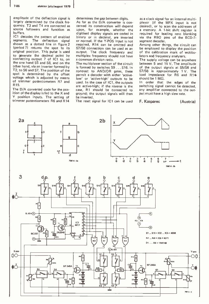
7-86 elektor july/august 1979 I
amplitude of the deflection signal is largely determined by the clock fre- quency. T3 and T4 are connected as source followers and function as buffers. IC1 decodes the pattern of enabled segments. The deflection signal shown as a dotted line in figure 2 (period 7) returns the spot to its original position. This pulse is used to generate the decimal point by connecting output 7 of IC1 to, on the one hand S5 and S8, and on the other hand, via an inverter formed by T2, to S6 and S7. The position of the spot is determined by the offset voltage which is adjusted by means of trimmer potentiometers R7 and R15. The D/A converted code for the pos- ition of the display is fed to the X and Y position inputs. The setting of trimmer potentiometers R6 and R14
2a
7
5
4
3
0 2 OP .
e
3 d.p. 9
X -pos
Mo
S9
2b
513 13
Si
c o
515
as a clock signal for an internal multi- plexer (if the MPX input is not desired), or to scan the addresses of a memory. A 1 -bit shift register is
required for leading zero blanking via the RBO pins of the BCD -7 -
segment decoder. Among other things, the circuit can be employed to display the position of the calibration mark of wobbu- lators and frequency analysers. The supply voltage can be anywhere between 5 and 15 V. The amplitude of the output signals at S5/S6 and S7/S8 is approximately 1 V. The load impedance for R6 and R14. should be 1 MS2. In order that the edges of the switching signal cannot be detected, any amplifier connected to the out- put must have a high slew rate.
F. Kasparec (Austria)
d e 0 o
4
516
a
determines the gap between digits. As far as the D/A converter is con- cerned its construction will depend upon, for example, whether the digitised display signals are coded in binary or in decimal, are inverted or normal. If the Y -POS input is not required, R14 can be omitted and S7/S8 connection can be used as an output. The clock frequency and multiplex frequency should not have a common division ratio. The multiplexer section of the circuit is formed by switches S9 ... S16. In contrast to AND/OR gates, these permit a decoder with either 'active - low' or 'active -high' outputs to be used. In the case of IC1, the outputs are active -high; if the reverse is the case, R1 should be connected to ground; the output signals will then be inverted. The reset signal for IC1 can be used
b
9
C
S10
d
79614 - 2.
Si
ó 9
S12
16
R4
7
13
14
CE
IC1
CI 4017
2
2
3 10 4
C5 2N2646
5 5
6
T00 0
toL 45 155,
2 4
aIº
12 13
N4
11
C2
R12
47n
IC2...IC6
134
0
06
79614.2E
S1 ... S16 = 1C2 ... IC5 = 4066
N1 ... N4=106=4071
D1 . . . D6 = 1N4148
BF 245A
Y -pos
R14 1006
S7 S8
813 C4 ~11
Tn6
3 o
R
Y
106
79614 . 3

elektor july/august 1979 7-87 I
pH meter circuit for DVM
To accurately measure the con- centration of hydrogen ions (pH value) in a solution, a 'glass electrode' is often used in chemistry laboratories. The electrode is con- structed on the principle of a galvanic cell, and the output voltage of the electrode is proportional to the pH value of the solution to be measured. The temperature of the solution considerably affects the pH value, thus a pH meter is effec- tively a temperature compensated milli voltmeter. The circuit shown employs an op -amp (Al) to amplify the output voltage of the electrode. The input impedance of the circuit is thus equal to that of the op -amp, which is
1012 S2, so that there is negligible loading of the electrode. The positive temperature coefficient (PTC) resistor TSP 102 (Texas) compensates for the effect of variations in the temperature of the solution. Together with the shunt resistor of exactly 2370 S2,
which should be made up of several metal film resistors (e.g. 2k2 + 150 S2
+ 10 S2 + 10 521, the resistance of the PTC varies linearly with temperature. The voltage at point A is amplified by op -amp A2, the output of which is divided by R5/R6 such that it varies the total output voltage by just the right amount. Op -amp A3 is
connected as a combined summing and differential amplifier and provides the output voltage for the DVM, which displays the pH value of the solution directly. Trimmer poten- tiometers P1 and P3 set the gain of the input stage while P2 ensures that Al is correctly biased. The calibration procedure for the circuit is as follows:
2 15V
1. With the inputs short-circuited P2 is adjusted for zero volts at point C.
2. Again with the inputs shorted, potentiometer P5 (wirewound type) is adjusted such that 7 volts are present at point D.
3. Trimmer potentiometer P4 (spindle type) is adjusted such that, with the PTC at a tempera- ture of 25° C, zero volts are present at point A.
4. A glass electrode, which is
suspended in a solution with a pH of 7, is connected to the input of the circuit. P5 is then adjusted until a reading of 7 volts is
obtained at point D (note that the temperature of the solution should be 25° C)
5. The glass electrode is suspended in a solution with a pH value of 4 and trimmer P4 (spindle type) is
adjusted for a reading of 4 volts at point D. Once again the tempera- ture of the solution must be 25° C.
15V
A1=IC1=LF356 A2=IC2=pA741 A3=IC3=NA741 PTC1 = TPS 102
ee tellt
15V
79646 2
6. Heat the solution to approximately 70° C, and with the PTC suspended in the solution check to see that a
reading of 4 volts is still obtained. If necessary, readjust P3.
7. Repeat the above procedure from point 3 onwards.
The high input impedance of the circuit renders it sensitive to r.f. pick-up, hum etc. and it should there- fore be well -screened, preferably by mounting it in a metal case. The connections to the PTC must be water, acid and alkali proof. The accuracy of the circuit depends upon a stable supply voltage (± 15 V), and upon the accuracy of the refer- ence solution used during calibration (not to mention the accuracy of the DVM). Glass electrodes are available com- mercially, and are supplied with instructions on how they should be used.
Th. Rumbach (Germany)

7-88 elektor july/august 1979
This robot is an example of a simple cybernetic model, i.e. it will take whatever manoeuvres necessary to navigate its way around any obstacles placed in its path. The robot will continue to travel in a straight line until it bumps into an obstruction of some sort, it then changes direc- tion to avoid the object in its way; if it becomes completely stuck, all the drive motors are switched off. The sensors used to detect obstacles
2
robot with reflexes 1
sensors
79583-1
5V
0
IC 2
555
loon
5V
0
7
C3
IC3
7475
D1
R2
47k
100y 16V tant.
Dí D3 D4j1
V
3
St _ S2 s3
I Y Y ^d7
24
12
14
13
15
.24
12
IC4
74180
right
take the form of switches. During construction care should be taken to ensure that these react to contact over the entire length of each side, hence some sort of bumper arrange- ment such as that shown in figure 1
should be adopted. When an impact occurs, the switches detect on which side it is, and the information is fed as a four -bit code to a latch (IC3). The outputs of the latch trigger a 555 timer (IC2). For
6-12V
right
14
13
15
12
ICS
74150
left
17
16
10
09
left
13
11
15
D5 = D6= D741k D8=
N1,N2 =IC8=7400 Dl... D12 =1N4001
79583-2
12
9
IC6
74150
backwards
13
15
1C7
74150
forwards
8 7
6
0
010
Ret
Re2
Ub

elektor july/august 1979 7.89 I
the period of the delay provided by the timer, this code is stored on the latch outputs, thus giving the robot time to take evasive action. The 4 -bit code serves as an address for the four data -selectors (IC4 ... IC7), which function as a look -up memory. The address information determines which of the data -selector outputs are enabled, and hence which of the four relays are pulled in. If a second collision occurs during the timer period, the latter is reset and a new code is fed to the latch. Once the timer delay has elapsed, the latch outputs go to 0000 and the robot continues on its way. The ac- companying table lists the various evasive manoeuvres the robot takes for each of the latch codes. Potentiometer P1 should be adjusted such that the robot has sufficient time to just clear the obstruction. With 0000 on the outputs of the
Table.
latch outputs data -selector outputs
right left back- wards
for- wards
right left back- wards
for wards
Direction
0 0 0 0 0 0 0 1 forwards 0 0 0 1 1 0 1 0 backwards and to the right 0 0 1 0 0 0 0 1 forwards 0 0 1 1 0 0 0 0 stop 0 1 0 0 1 0 0 1 forwards and to the right 0 1 0 1 1 0 1 0 backwards and to the right 0 1 1 0 1 0 0 1 forwards and to the right 0 1 1 1 0 0 0 0 stop 1 0 0 0 0 1 0 1 forwards and to the left 1 0 0 1 0 1 1 0 backwards and to the left
1 0 1 0 0 1 0 1 forwards and to the left 1 0 1 1 0 0 0 0 stop 1 1 0 0 0 0 1 0 backwards 1 1 0 1 0 1 1 0 backwards and to the left 1 1 1 0 0 0 0 1 forwards 1 1 1 1 0 0 0 0 stop
data -selectors both motors are stopped. If desired one can arrange for this state to be detected and an
car collision alarm With the overcrowding that is a
common feature of most car parks nowadays, the chances of coming back to one's car and finding a dent in the bumper or one of the wirtlgs are quite considerable. It is particu- larly galling if the culprit has made off without acknowledging his guilt and leaving behind his name and address. The following circuit is designed to attract the attention of passers-by in the event of someone bumping into your car. Hopefully the guilty party will then be unable to escape in anonymity, and will be compelled to own up to his mistake. First of all a suitable sensor, which wili detect an impact to the car, must be constructed. One idea is to suspend a small weight from a spring inside a tin or jar lined with a con -
R1
Cl
S2
R2 C2 C
6V H
4-` R3 11 10 91
IC1=74121
i
SI
C3 R4
T006 6V
ductive material (e.g. silver paper). Normally the weight and the tin will be isolated from one another, but if the car is subjected to a reasonably violent impact, the two will touch. The sensitivity of the sensor can be adjusted by shortening or lengthening the spring. One word of warning: if it is made too sensitive, it may react to severe gusts of wind! The circuit of the alarm is shown in figure 1. The sensor is mounted in place of S2. As soon as the two contacts are shorted, and assuming S1 is closed, the monostable multi - vibrator, IC1, is triggered, with the result that its output goes high. The period of the monostable can be varied between 0.5 and 10 seconds by means of P1. As long as the output of the monostable remains
1 nl,J IC2=7413 _
i JOn
N2 1 Ol
J
alarm to sound.
M. Blencowe (United Kingdom)
high it will enable the oscillator built around N1, T1 and associated components. The oscillator fre- quency can be adjusted by means of preset potentiometer P2. The output of the oscillator is fed via N2 to the amplifier section built around T2 ... T4 and hence to the outside world via the car horn: T4 is connec- ted in parallel with the existing horn button (S3). Note that in some cars the horn is only operative when the ignition is turned on. In that case, the supply connection to the horn will have to be modified - it must be transferred to a (fused) connection that is always 'on'.
M. Haest (Belgium)
12V
O 79553

7-90 elektor july/august 1979
The circuit described here was designed to fulfill the need for a
jet airliner sound effects generator in a school play which involved an attempted hijack. The unit had to be capable of producing a number of typical jet noises as heard from the inside of the aircraft - start-up, idle, take -off, in-flight, approach, landing and reverse thrust conditions - together with tyre squeal on landing and machine-gun fire. To simulate the sound of a jet engine both the roar from the 'hot end' of the engine and the whistle from the compressor (whose pitch varies with engine speed) are re- quired. The engine roar is obtained by feeding white noise through a
band pass filter which emphasises frequencies around 800 Hz. Transis- tor T1 and the zener diode D1 form the white noise generator whose output is fed to IC1, the band pass filter. The volume of the roar can be altered by potentiometer P1. The whistle is derived from the sine - wave output of the 8038 waveform generator IC3 whose frequency range
12 V 0
1Ok
12 V0
55
aircraft sound and 'hijack' effects generator is set by C8 and is typically between 10 Hz and 10 kHz. The actual frequency is determined by the throttle control P6 which is connec- ted to the FM input of IC3 via switches Sic and S2b, while the whistle volume is controlled by potentiometer P5. Engine inertia (lag in response to throttle demands) is
realistically imitated by the inte- grating network R21/C10. C10 should be a low -leakage type - if available, a 10 µ paper capacitor would be a
good choice. Both these signals, the engine roar and compressor whistle, are then summed by IC2 and passed to the external amplifier through the overall volume control P2. By varying the settings of these controls all of the above mentioned jet engine sounds can be realised. The purity of the sinewave signal can be adjusted by potentiometers P3 and P4. The gunfire effect is obtained from the squarewave output of IC3 when switch S1 is closed. By closing this switch the squarewave is allowed to pass through to the summing ampli-
3
R/1
O o
R7
517 RIB
RIO
IC2 +741
iF
Sic
9 - C9 WNW _
33n 47n
fier and the FM input of IC3 is taken high to give minimum frequency whilst the frequency range itself is
also decreased by the addition of C9 in parallel with C8. Resistor R19 is included so that C9 is always kept charged to the average voltage across C8 to prevent a 'chirp' when S1 is first closed. The tyre sqeal effect is also obtained from the squarewave output of IC3. When switch S2 is closed the squarewave is enabled, and the FM input of IC3 is initially taken to a
potential which gives a high fre- quency output via the potential divider R22/R23, but as R23 is now disconnected capacitor C11 will discharge to the positive supply rail and the frequency of the squarewave output will fall rapidly.
M. J. Walmsley(United Kingdom)
C5
P1 = jet roar volume P2 = overall volume P5 = compressor whistle volume P6 = throttle S1 =gunfire S2 = tyre squeal
1OOk log
*AF
5k C1Oit Clt R22 Ile G _ _
109 393 R21 35V 35V
*see text 79631

elektor july/august 1979 7-91 I
digital milometer
T _i_^
/ , xl0miles / , xlmile ' , Display
x0.lmile
R4 R71 R1B R4...R2a 21.330D Rto R17 R24
10 12 1J 9 11 6 7 10 12 1J 9 1 6 7 10 12 1J / 6 7
ra b c d e t g
IC1 1
CD4026
15
a b c d e t g a b e d a
s;lo IC2 1 5=10 IC3 2 CD4026 rz CD4026
3 15 5
9VO+ '
Ott, 53 Display
06
*see text
Reset 9 V +
N1
511 a
FF1 0 13
7
R2a
R2b
5¡ 6L
FF2 o
9
3
1 1
11-
----- 28"
)
FF1, FF2 = IC5 = CD4027 FF3, FF4 = IC6 = CD4027 FF5, FF6 = IC7 = CD4027 N1 = 1/3 IC8 = 1/3 CD4073 FF7=1/2 IC9= 1/2 CD4027
12
FF3 0 =J
51°1
L i6
FF4 o 1a
FF5 o
12
13
5I 6 9
.__O 9 V
9
10
12
111.356
1a
5
C211 7
MK711+ T10n +
1/2C /2 556
R3
C3 3 . C4
MKT1V TtOn
Mechanical mileage recorders for bicycles have been commonly available for a large number of years, however there are several advantages to be gained from adopting an elec- tronic approach: robustness, im- proved readability thanks to a
digital readout, and 'friction -free' operation. The distance travelled is measured by counting the number of wheel revolutions. Each complete revolution is sensed by means of a small magnet attached to one of the spokes. The magnet actuates a reed switch mounted at the appropriate height on the front forks of the bicycle.
7
*
C5 C tOOy
16V
S2
9V
FF6 o
10r 11C
FF7 o
16 16 16 16 16 16
IC1 IC2 IC3 IC5 IC6 IC7
In the circuit diagram the reed switch is represented by Si. Each time the magnet passes the switch, the latter closes momentarily, triggering the two 555 timers (IC4a, IC4b) and providing a pulse to the divider formed by FF1 ... FF7 and N1. The output of N1 in turn produces a
pulse every tenth of a mile. These pulses are fed to the three decade counters/decoders IC1 ... IC3 which are connected in cascade. The maximum count is therefore 99.9 miles. With a 27" wheel, a pulse every tenth of a mile corresponds to 74 revolutions (connections to N1
IC8 IC9
79521
9V
shown as unbroken lines), whilst in the case of a 28" wheel 72 revolutions (dotted connections to N1) are requ i red .
The current consumption of the circuit is 130 mA with the displays enabled (S3 in position 1) and 30 mA with the displays switched off (S2 in position 1). A 9 V battery (6 x 1.5 V) will provide a suitable power supply. Alternatively one could consider using ni -cad cells which are recharged via the dynamo. Of course the circuit no longer functions 'friction -free' in that case.
R. Kuijer (The Netherlands)

7-92 elektor july/august 1979
Slide shows can be improved greatly by providing them with accom- panying music and spoken comment from a tape. One way of changing the slides automatically at the correct
la
Audio
5 V0 C39
IC 1
10
tape -slide synchroniser moments is to record trigger pulses on an additional track on the tape. However, that requires an additional tape head (unless you make do with ,mono sound), which can prove
jAI
R2
16
IC3 T!TT 1
A7 ... A7=1C4... C10 = 741 N1,N2 = IC11 = 7413 N3,N4,N6,N12 = IC12 = 7400
C39... C46 8a10n
4 1 14 I
IC11 IC12 +I
qT4T
rather complicated. The circuit des- cribed here uses 30 Hz pulses, re- corded on the normal sound track - simplifying matters considerably. The circuit works as follows. During
(.5 14 1 i4 I C4e1
IC13 IC14 IC15
QT4T4 N7,N8,N10,N11 = 1C13 = 7400 N13,N14 = IC14 = 4001 N5,N9,N15,N16 =.IC15 = 7402 79623

elektor july/august 1979 7-93 I
recording, S1 is switched to position 1. The music and speech signal is fed through a buffer stage (A1), a
30 Hz high-pass filter (A2), a 30 Hz notch filter (A3, A4) and a summer (A5) to the tape recorder input. A 30 Hz oscillator (N 13/N 14) is enabled by operating either S3 (next slide) or S4 (back one slide). S3 triggers a
flip-flop (N7/N8), starting the oscil- lator and enabling the counter (IC1); the oscillator pulses are fed through T5 to this counter. After 7 pulses, IC1 resets the flip-flop.
lb º C13
100p 16V
R27
Operating S4 produces the same result, with one difference: in this case the flip-flop (N10/N11) is reset after 12 pulses have been counted. The pulses . are passed through a
band-pass filter (A6) and a low-pass filter (A7) to the summer (A5). During playback (S1 in position 2), the 30 Hz burst is filtered out and 'squared up' by N1 and N2. Each pulse triggers an MMV (IC3) that enables counter IC1 for 500 ms. During this period, the 30 Hz pulses are counted and Re1 or Re2 pulls
back one slide
®12
i / 1 *133,
12VRe1 12VR max. 100 mA max. 100 mA
P"
20 51,
C19 lOOy 16V
in - depending on the final count. A second MMV (the second half of IC3) causes the relay to drop out again afte'r 200 ms. The calibration procedure is as follows. Si is switched to position 1
(record) and the oscillator frequency is adjusted (with P4) for maximum output from A7. (Note that the oscillator will run continuously if S3 and S4 are both held down.) Turn P3 right down, make a temporary link from the output of A7 to the audio input .(S1a), and adjust P2 for
14
5V
R36
R37
C20 R38
R39 T
u
N3
A OD o4
R IC1 oA 7490
801 802
2; 3r 111)
12
0 3
IC2 7473 4
clear Ó
C18
13
5V
47n R35
I TUN
Sid
next slide
4
TUN
844
UN
T3
12 V
Irk 0 ' R45
111:®
N15 3
12
R28 1
T
11
Q\ ._ 5V
53 next slide
9 10
R29
5V
Cla
8 R30
CI C15
ln
® ® 1n
3
13 12 5V
T5 backone slide I +5V 79623

7-94 elektor july/august 1979
minimum output from A5. A suitable value for R25 should now be selected, so that the meter (M1) reads approxi- mately % scale; the exact indication can be marked on the scale. Connect the tape recorder, and set the correct recording level for the normal audio signal. Disconnect the 'normal' audio, depress S2, S3 and S4 and adjust P3 for 'full modulation' (sometimes indicated as '0 dB'). Release S2 and record a short 30 Hz 'reference tone' at the start of the tape. The actual program can now be
The criteria for a good domestic intercom system are as follows: First of all, it is essential that each station can call up any other station in the house, without having to route the signal via a 'central' or master station. Secondly, there should be as few wires as possible between each station. Thirdly, the system should be capable of being used as a babyphone, without interfering with normal operation. Finally, there should be no possi- bility of 'listening in' to stations (other than in the case of the baby - phone). The circuit described here fulfils all the above requirements. The basic principle of the system is illustrated in the block diagram of figure 1. A single four -core cable links all the stations; two of the cores are connected to a suitable power supply. In each station a
1
recorded, operating S3 and S4 as required to change the slides; the 30 Hz pulses will be recorded at -10 dB. For playback, S2 is set to position 2. The initial reference tone can be used to adjust P1 so that the meter gives the same '/4 scale reading as before. If the system is used in conjunction with a really good hi-fi installation, the 30 Hz pulses may be audible. In that case, the amplifier can be connected to the output of A5 so that the pulses are filtered out. The
only disadvantage is that P3 must then be turned right down, so that it will have to be re -calibrated before the next recording.
A. Hamm (United Kingdom)
flexible intercom system number of reference voltages (UREF) are derived from the supply line. When one of the switchesS1a ... S1d is operated, the corresponding reference voltage appears on the 'selector line'. At the same time switch Ste is closed (all five switches are mounted in an interlocking group), switching in the preamp and power amp. With the 'speak/ listen' switch S2a,b in the position shown, any signal appearing on the 'audio line' is fed via the power amp to the loudspeaker. With S2 in the alternative position, the loudspeaker functions as a microphone. In each post the voltage on the selector line is compared with one of the reference voltagés, which is used as the 'call up' voltage for that post. For example, in order to call up station 2, 4 V must appear on the selector line. This voltage is detected
by means of a window comparator, which controls an electronic switch (ES), turning on the amplifiers of the station in question. As soon as a
voltage above 2 V appears on the selector line, an LED will light at each post to indicate that the line is busy. The actual circuit is fairly straight- forward (see figure 2). The five reference voltages are derived via the five zener diodes D1 ... D5 which are connected in series. The call up voltages for the other four stations are selected by means of switches S1a ... Sid. The remaining reference voltage is fed to the window compa- rator formed by IC1a,b. Transistor T1 is the electronic switch (ES of figure 1) which connects the pre - and power amplifiers (IC2 a and b respectively) in or out of circuit. IC1c detects a call up voltage on the
Í II
10V
Uref
selector I
¡switch block
/ Y V r Ste
Std
$lc t
8V Q _0_ SiQ=b
6V
2V
4V
line busy
STATION 2/
'9591-1
LS
window comparator
E
_J
selector line
O
TO OTHER
STATIONS

elektor july/august 1979 7-95 I
2
I STATION 4 I
D6 ... D9 = 0495, DUG
DIO,D13 = 8ZX75c1V4*
DI... D5 = BZX75c2V1*
D71 = LED
012 = 8AV20,DUS
D14 = 1.3TX10,1N4001
T1 = 2N2905A
IC1a,b,c = TCA220
IC2a,b, = TCA210
S2b each station and a number of
norm strategically distributed sockets the sib` flexibility of the system can be
increased still further.
selector and turns on LED D11 to indicate that the line is busy. A couple of practical points: R12, the pull -down resistor on the selector line, is only required in one of the stations. If desired, each of the 2V1 zener diodes (D1 ... D5) can be replaced by three 'normal' silicon diodes connected in series; similarly, two normal diodes connected in series can be used in place of the 1V4 zeners D10 and D14. The supply voltage is not particularly critical; any reasonably stabilised 15 V/1 A supply will do. The modifications for use as a baby - phone are shown in dotted lines in figure 2. An extra switch, S3, and resistor, R24, are used. With S3 in the position shown, the station will function normally; with S3 in the alternative position, the station is permanently switched to the 'speak' mode, so that every other station can listen in simply by pressing the corresponding button. The sensitivity control, P1, should be adjusted with the circuit switched to the babyphone mode, whilst the sensitivity of the intercom when operating normally is determined by the value of R24. Finally, it is worth noting that each station can be situated anywhere 'on the line', thus with a plug on
fermentation rate indicator
P. Deckers (The Netherlands)
When making one's own wine, the number of times the level of the is produced. Towards the end of the fermentation rate can for the most (sterilising) liquid in the air -lock rises fermentation process however, the part be estimated by counting the and falls as a result of the CO2 which level tends to 'jitter' somewhat, so
1 a o
12-15V
o p3
R2
N1... N4= 1C1=4011
N5 ...N8= IC2=4011
13
12
11
79581-1
1a la
IC1 IC2
4
12-15V
tea ties
12-15V

7-96 elektor july/august 1979 I
that accurate measurements are not possible. One solution to this problem is to employ two electrodes, one of which is mounted higher than the other - see figure 2. The differ- ence in height between the two should be greater than that by which the level of liquid fluctuates (approx- imately 2 mm). The circuit shown in figure 1 is designed to produce an output pulse only if both electrodes are suspended in the liquid, after previously having been clear of the liquid. Enamelled copper wire, 0.3 mm in diameter is used for the electrodes. Insulating sleeving is pushed over the wire, whilst an earth connection is also suspended in the liquid. As is apparent from the circuit diagram, the input of inverters N1 and N2 are held high via pull-up resistors R1 and R2 when neither of the electrodes is in contact with the liquid. The output of the OR - gate formed by N3, N4 and N5 is therefore low, as is the output of the set -reset flip-flop N7/N8. The output of NAND gate N6 is high.
la
I I
5V
O
.N 2 DUS
DUS
REC.
2 b
N
79581- 2
If the level of the liquid in the fermentation lock rises to cover the
N2 lower of the two electrodes, the output of the corresponding inverter will go high. This has no effect upon the output of the NAND gate, but the output of the OR -gate will be taken high also. Due to the effect of diode D1, however, the set -reset flip-flop remains in its original state. Should the liquid level fall, the only result will be that the output of the OR -gate is returned low once again. Only if the level rises still further to cover the second electrode will the output of N6 go low and the flip-flop be triggered, turning on T1 and feeding a pulse to the counter (Re). Since the flip- flop can only be triggered by '0' logic levels via D1 and D2, both electrodes must clear the liquid before the flip-flop is reset and another pulse can be counted. Any normal 12 V impulse counter can be used.
J. Ryan (Ireland)
256 -note sequencer -0
PLAY o
- 2 DUS IC2 fi 741
DUS
IC3 741
'o.
42n
15V
O
15V
O
1áV
O 15
m U
N
] 12
2 1t
155
5
Q
0 9
2
2
9 12
S
l
wE 1 CE -134
Q
79119 1

elektor july/august 1979 7-97 I
The sequencer is intended to be used in conjunction with a voltage con- trolled synthesiser. It can store a se-
quence of up to 256 notes which can then be played back automatically. The sequence of voltages produced by the keyboard circuit of the syn- thesiser are fed to an 8 -bit A/D con- verter and then stored. The length of the note and the length of rests be- tween notes are also encoded with the aid of a clock generator and two counters. When the stored sequence of notes is to be played back, the 8 -bit data word corresponding to the keyboard voltage level is read out of the memory and re -converted back into an analogue voltage by a
D/A converter. Similarly, the note and rest length data are decoded to ensure that the original melody is
obtained. The above approach offers the fol- lowing advantages over other systems which employ an 'encoded key- board'.
lb
PL AV
REC.
15V
IC9 741
T6
O 15V
55
1. The existing keyboard does not need to be modified.
2. An 8 -bit A/D converter is cheaper than an encoded keyboard.
3. By using a 2 -way converter (A/D and D/A) the original sequence of notes can be reproduced with a
high degree of accuracy. The circuit functions as follows: To store a sequence of notes, switch S1 is set to the 'record' position; the memory is simultaneously switched to the 'write' mode. When one of the synthesiser keys is pressed, the key- board gate pulse sets flip-flop N11/ N12, .taking one of the data inputs of IC18 low and setting the address counter, IC19. The gate pulse also triggers ,a dynamic shift register formed by N20... N24. This shift register performs a number of func- tions: resetting IC10 (the 'note coun- ter') and IC13 (the 'rest counter'), resetting the AD - D/A converter, ZN425, enabling the memory IC18, and clocking the address counter.
4068 12
GATE PULSE p 516
1U0,
DUS
11 2x DUS
5V
6
17
5V
17
la
5
ti
oÑ Ué
,t
12
5V
u N8
4068
10
17
9
4
4068
The result of these control signals are that the first memory location re- mains empty. The keyboard voltage is digitised by the ZN425. IC10 counts clock pulses provided by IC9 for the duration of the note. When the key is released, IC10 again counts the clock pulses from IC9, this time to time the rest. When the next key is pressed the store cycle is initiated, and the previously obtained information is
written into the second memory location. Of course one cannot always use the keyboard gate pulse to determine the length of a note, especially if playing 'legato'. For this reason a detector (IC4, IC5) is
included which determines when the keyboard voltage changes. The detec- tor consists of a differentiating net- work followed by a window com- parator, which provides a negative pulse when the voltage level alters. When either IC10 or IC13 reach their maximum count (6 bits), the
T
17
WE CE
/
10
11
1
2
WE
e
N9
47
4068
`6 5V
(1l 79619 2
. . . _. ... IU I;

7-98 elektor july/august 1979 I
lc
E=1
DUS
HALT/ START RESET
O 63 1194 5411 2'-
GATE SL ULSE
-Cr
15. t0 _ tfi VT
IC12.10191C11
SINGLE SHOT REPEAT
5V
12
lo
IC18 2112
wE CE
14
2
N20
CHIP ENABLE
00
0, 02 IC19 Oj
4040 005 06 OT
lock CE
5
wE
C
PLAY
5V
N21
4701
oN22 /
s
5V
'CM 1C29, C30.IC31 IC19IC13 I021,1022,iClJ I011,ICIs,IC16
output of N4 or N9 goes low starting a new store cycle and reset- ting the counters. In this way either a note or rest can be programmed into two or more memory locations. It was stated that the first memory location remains empty. However if one wishes to start the sequence of notes with a rest, this location can be filled by pressing S3, which triggers ICs 10, 13 and 18 independently of the keyboard gate pulse. IC13 then counts clock pulses until a key is pressed, whereupon the above - described reset and store cycles write the 6 -bit data word corresponding to the rest into the first memory location of ICs 12 and 15. To playback the sequence of notes stored in memory, switch S1 is set to the 'play' position, switching the memory to the 'read' mode and the ZN425 to D/A conversion.
To regain the note and/or rest length information, IC10 is clocked until its output state corresponds with the data outputs of IC12 and IC15. During this period the gate pulse out- put remains high, and only goes low when the two sets of data coincide; clock pulses are then fed to IC13 until its output state coincides with the data outputs of ICs 15 and 17, whereupon the memory addresses are systematically scanned by IC19 and the stored data read out to the D/A converter. The output (pin 12) of IC18 goes high when the replay sequence is
finished. If the sequence of notes is
to be repeated, (S2 is switched to the 'repeat' position) the address counter 'wraps round' and begins again with the lowest address. The unused pins of IC18 can be employed as extra control inputs and connected (via
5V
79619
N1, N2, N5, N7 = IC20 = 4011 N26 ... N29 = IC21 - 4077 N30 ... N33 = 1C22 = 4077 N34 ... N37 = 1C23 = 4077 N15,N16,N18,N19-1C24-4011 NE. N20 . . N23,N25 = IC25 = 4049 N10 ... N13=1C26=4011 N38=1C27=4011 N3 = IC28 = 4068 N4 - IC29 = 4068 N8 - IC30 - 4068 N9 = IC31 = 4068 N24 = IC32 = 4068 N14,N17=1C33=4001
5V
10 la/ )1/C21 )BO 9
suitable buffers!) to VCOs, filters, etc. Two final remarks: Portamento and/or (coarse and fine) voltage controls should be connected after the sequencer. The A/D - D/A converter will accept the output of a 3 -octave keyboard. A 4 -octave keyboard can be used if the feedback resistor of op -amp IC3 is increased from 10 k12 to 18 k2.
T. Emmens (United Kingdom)

elektor july/august 1979 7-99 I
frequency to voltage converter for multimeter
10... 15 V 6 ...40 mA Rl
1
S1 ... S4 = IC1 = 4066
R2
01
t' 100n
MN P3 D2- R5
05 9V1 400 mw
47n R6
0311
5
S2 4
R9
100n
11
4
4707
D1...D4=DUS
Most frequency measurements are carried out by means of a digital frequency meter or else on an oscilloscope. However both these instruments are relatively expensive, and thus not often 'standard equip- ment' for the hobbyist. One way to measure the frequency of a signal without investing in specialised equipment is to use a frequency - voltage converter, which can then be 'plugged in' to an ordinary multi - meter. That is the function of the circuit described here. A meter with a 5 V range should be used; the conversion ratio is linear, assuming the scale is calibrated in ms (1 V = 5 ms). The circuit is built round a quad analogue switch IC, type 4066. The squarewave signal at point A is
switched via S1 to the differentiating network, C2/R6. The resulting pulses are then fed via S2 on the one hand to the inverter formed by T1, and on the other hand to S4. The result is
that S3 and S4 open and close alternately, i.e. S3 is open when S4 is
closed, and vice -versa. Assuming that S4 is closed, capacitor C4 will be charged linearly by the constant current source T2. The charge is
transferred via S4 to storage capacitor C5. S4 and C5 thus function as a
sample and hold circuit. If now S4 is
opened, S3 will close; capacitor C4 will discharge via S3 to ground, and a
new measurement cycle will begin. Depending upon the characteristics of the FET, T3, the sample and hold circuit will increase the voltage by approximately 2 V. Thus a maximum charge voltage of around 6.5 V is
possible. The circuit is calibrated as follows:
73
BF 245A
S4
C5
100n
P3
t R14
16
*see text
De
5V1
+ -
` 4700 P2
R12
0
With the input unconnected, the wiper of P2 is turned to the positive end stop (junction of P2 and R13). A
v
yt -
yC4
1
vC5
o
79563 . 2
79563
DC voltage of 6.5 V is applied to the gate of T3, and P2 is adjusted for full-scale deflection on the meter. Potentiometer P4 is adjusted for zero reading on the meter with 0 V on the gate of T3. A known frequency is
then fed to the input of the circuit (e.g. 50 Hz mains signal from a door- bell transformer), and P2 is then fine tuned for a reading of 20 ms. The pulse diagram in figure 2 illustrates the signals obtained at points A . . . E in the circuit, and across C4 and C5. With the com- ponent values shown in the circuit diagram, the meter will display frequencies between 40 and 2000 Hz (0.1 V = 0.5 ms = 2000 Hz). Different frequency ranges can be obtained by altering the value of components R11, R12 and C4 accordingly. The appropriate values can be calculated by using the formula;
UC4 C4fin IC4
where IC4 -ÚR11+UP1 R11 +P1
Finally one or two specifications: supply voltage: 10 ... 15 V current consumption: 5 mA input impedance: 1 M12 input sensitivity: minimum
1.5Vpp
F. Kasparec (Austria)

I 8-00 elektor july/august 1979
When setting up a television set, a video pattern generator is a very useful instrument to have at hand. While circuits for video pattern generators are by no means rare, they often suffer from overcomplex- ity or use of uncommon components. The design offered here, however, although using a large number of components, is neither complex nor are the components difficult to
r
video pattern generator obtain. As can be seen the design splits neatly into a number of parts the first of which is the Sync. generator (section A) which provides all the necessary timing pulses. The output of the crystal oscillator built round N3 is divided by 16 by IC1a to provide the line frequency. The field frequency is obtained from counters IC1b, IC2a and IC2b, which divide
7I-
the line frequency by 625. The out- puts of these counters are gated together to select three timers (IC3b, IC4a and IC4b) which provide the line sync pulse, the field sync pulse and the equalisation pulses after being triggered by IC3a (the front porch delay). The enable signal for IC3b is also gated with the 12 ps line blanking interval (from N4) to ensure that it is triggered at line
ºv
104 o
D
.'2BS IC7B
0:4- 0
B L o.
N
.}v
L
=IN
11
S
IC3
H H
Cs n.
IC3b
SYNC. GENERATOR A
C. emo RJ ..
I Che
ICAb
1
o:
r ----
T N
SOUND AND GREY SCALE CIRCUITRY
L
1000
JL
ES
IC12b 02
SOUND OUTPUT
. Cq =.I .
PlT
PAT O V. LINES
CROSS. HATCH
DOTS
LINES
CHESS. BOARD
BARS
RI.
H=1-1'1 Re:
EXT.
EXTERNAL INPUT
RIB
EXT. COLOUR IN
VIDEO STAGE L -
ICI - IC?. 4520 IC3 - IC4 4528 N7 ... N16 IC5... IC8 4001 N17 ... N20 ICE = 4077 N21... N28 = IC10,IC11 = 4001 IC12 4520 IC13 4011 Tl._T3BC108 All diodee: DUS
1
D
OUTPUT 1. 2 Vp.p FROM 7511 OUTPUT 2 1 Vp.p FROM 75 D
14424
J
PATTERN GENERATOR C J

elektor july/august 1979 8-01
frequency. The bistable N11/N12 produces the field blanking interval which is reset after 25 lines by IC2a. Both blanking pulses and the output from the pattern generator are gated by N9 to provide a blanked video drive to the mixer stage. The output from the mixer can be fed to a suitable UHF TV modulator (see Elektor 42, October 1978).
Sound output The sound output circuitry is shown in section B. The Q4 output of IC1a is divided by sixteen in IC12a to produce a 977 Hz signal at its Q4 output. This signal is then attenuated by R31 and P1 and filtered by C7 to produce a more pleasant sound.
Grey scale
The grey scale is produced by a gated oscillator built around N2/N29 and a
binary counter IC12b. During line and field blanking intervals the oscillator is inhibited and IC12b reset to zero to ensure that each new line is correctly positioned. The outputs of the counter are inverted by gates N30 ... N32 to give a grey scale of descending height. To select the grey scale the other inputs of gates N30 ... N32 are taken high, i.e. by operating switch S1.
Pattern generator The pattern generator (section C )
provides a selection of eight basic
black and white patterns which can be selected by a rotary switch.
Vertical lines.
The output of the grey scale counter (IC12b) is connected to gate N19 which gives a short output pulse each time the input changes state giving 15 vertical lines.
Horizontal lines. A horizontal line is produced after every 20 TV lines at the output of the bistable N15/N16. The gating on the input ensures that the line is
one TV line long between line sync pulses. Fourteen horizontal lines are thus produced.
Crosshatch. This is simply the vertical and horizontal lines ORed together.
Dots.
These are produced by ANDing the vertical and horizontal lines together.
Vertical Bars.
This is the output of the grey scale oscillator and gives sixteen bars.
Horizontal bars.
The output Q3 of the field counter IC2a gives thirteen horizontal bars.
Chessboard.
This is the output from the horizon -
audio sectioner Many phonetic research applications may benefit from the use of an audio system with a repeating loop. Ad- ditionally, a sectioning device is
often desirable - allowing only a
desired segment of the material re-
corded on the loop to be passed to the output. The system described here uses two tape recorders with remote control capabilities. The Master recorder holds an ordinary reel of tape on which the material for analysis has been recorded. The second, or Slave, tape recorder has no reels, but an endless tape loop of the desired length. A length of 3 seconds has been used for convenience, but the electronics of the Sectioner could be modified to allow for any length. Using a remote control panel in the Sectioner, the operator may play or rewind the tape on the Master tape recorder. During the 'listen' mode, the material is automatically recorded onto the loop of the Slave recorder.
By switching to the 'repeat' mode, the operator can make the loop repeat endlessly, while the Master recorder is stopped. In the 'repeat' mode, the Sectioner may be made to function. This device 'chops' out the undesired portions at the begining and end of the loop, leaving only the desired portion in a 'window' in the loop. The lead and lag controls (which define how much is chopped at the beginning and end of the loop, respectively) are infinitely adjustable, so that the window may be of any length and at any point in the loop. The material which is chopped is not erased, and the lead and lag controls may be subsequently readjusted for a
wider or narrower window. Addition- ally, the material on the entire loop may be played back without changing the lead and lag control settings, so
that the sectioned and unsectioned loops may be easily compared. The material on the Master tape
tal and vertical bars when connected to the EXclusive NOR gate N20.
External. Provision has been made so that an external pattern can be connected to the system via gate N26.
As can be seen the eight patterns are connected to gates N21 ... N28. By taking the unused input of these gates low the required pattern can be selected. Gates N14 and N17 allow the inverted or normal pattern to be selected. The number of patterns can be increased by selecting several basic patterns together (vertical bars with horizontal lines) or more complex patterns can be produced by using the binary outputs of IC12b.
Video stage.
Section D shows the circuit of the video stage of the pattern generator. The logic inputs are mixed together by the resistor network R38 ... R45. The composite video signal is then buffered by T1 which drives transis- tors T2 and T3 to provide two different output levels. The output of T3 can be adjusted by potentio- meter P3. Capacitor C11 is included to sharpen the vertical picture.
P. Needham (United Kingdom)
recorder (in the 'listen' mode) or on the loop (in the 'repeat' mode) may be played back through any audio amplifier and/or may be fed directly into an oscilloscope, oscillograph, spectrum analyzer, or other instru- ment. The chopping is accomplished electronically, and no detectable click is produced, so auditory or instrumental analysis are not marred by the noise of switching. A special circuit makes it easy to produce visual displays on an oscil- loscope. It allows the oscilloscope sweep to be triggered just before the beginning of the 'window'. As shown in figure 1, the Sectioner itself (enclosed in dotted lines) contains an oscillator and a tone decoder. The output from the latter triggers electronic timers (lead and lag) which create the 'window'. When the 'listen' mode switch is
pressed, the following sequence of operations occurs: 1. The Master tape recorder (that

8-02 elektor july/august 1979 I
1
MASTER
® Co
LE
Listen Relay Repeat
(Listen 1
4
l
Sta 11
I¡ S3
II
Rewind Sect loner
A on /off
11-1' el
¡1
ti
I
o i¡ Sib
I I
ret
ti
Sic
SLAVE
el "a
LE
Sid OIl
ti
S4a
i1 52a
re3
Sle
o 11 S2b
b 0 S4b
16V
12V
containing the pre-recorded reel) starts in the playback mode (S1a).
2. Voltage is applied to the relay (S1f).
3. The Slave tape recorder (that with the loop) starts in the record mode (re3, re4).
4. The Tone Generator is inhibited (S1b).
5. The Tone Decoder is inhibited (S1d).
6. The audio signal from the Master tape recorder is recorded on the Slave tape recorder (S1c, re2, S4a).
When the 'repeat' mode switch is pressed, the following sequence of operations occurs: 1. The Master tape recorder stops
(S1a).
2
12V
IC2
¡14
IC6
` 12V
2.
3.
4.
r
TONE OSCILLATOR
enable
out
TONE
DECODER
Voltage is removed from the relay (Si f) but the relay remains ener- gized while the capacitor (across its pins) discharges. During the discharge time (ap- proximately 100 milliseconds), the Slave tape recorder continues in a record mode (re3, re4). A tone from the Tone Generator is
recorded on the loop (S1c, re2). The Tone Generator is keyed by applying a ground connection (S1b, re1). After the delay (100 milliseconds), the relay de -energizes, thus the Slave tape recorder is switched from a record mode to a playback mode (S2b). Simultaneously, the Tone Generator is inhibited (ref )
5V
5V
TRIGGER OSCILLATOR
LEAD TIMER0.1
LAG TIMER
O+12V
ÓTrigger
79651-I
L
and its output is disconnected (re2). The audio output from the Slave tape recorder is fed to one pole of the Sectioner On/Off switch, and to the input of the decoder network (S4a, Sid).
The operator may rewind the master reel by pressing the rewind mode switch, and during this time the following sequence of operations occurs: 1. The Slave tape recorder stops (S1 e,
re4, S2b all open). 2. The relay is de -energized (S1f). Should the operator wish to by-pass the Sectioner and use the two tape recorders only, the mode selector switches retain their functions, and the 'Sectioner On/Off' switch pro -
N1, N20 IC6= 7420
IC2= 709
T7 =2N3903
T2_2N3905

elektor july/august 1979 8-03 I
vides the necessary circuit changes: .1. S4a by-passes the 'listen' mode
contacts and relay pin connec- tions, so that the audio signal goes from the Master tape recorder directly to the Slave tape recorder.
2. S4b by-passes the relay pin connections and enables the Slave tape recorder to be operated in the record mode.
3. S4c permits the operator to monitor the recorded audio signal of the loop. It is by operating this switch in the 'repeat' mode that the operator can compare the 'window' with the 'full loop', providing the Sectioner was turned On while the loop was recorded.
The circuit of the Sectioner is shown in figure 2. The signal from the loop is amplified (IC2, T1) and fed to the
tone decoder (IC3). The inherent phase -lock -loop qualities of the decoder ignores all signals other than its pre -tuned pure tone. When this signal is present, the decoder provides a saturated switch to ground. This ground condition triggers the lead and lag timers (IC4 and IC5) simul- taneously. The output logic of the timers is
independent of the input waveform and is controlled by the time constant of RtCt: any change in the value of the potentiometers (P5 and P6) will change the position of the beginning (lead) and end (lag) of the window. The output of the lead timer is
inverted (N1) and used to inhibit N2. When the 'lead' time expires, the output of N1 goes 'high' so that the output of N2 changes to 'low', creating the window. Transistor T2
electronic horse
1.2
- v .i- IC1 4020
04 05 06 07 08 09
twk14110-2 G]
413
129
TP 1m 0.0
N1 ... N8 = IC3,IC4 = 40018
The term 'electronic horse' is actu- ally something of a slight exagger- ation, for the circuit described here will not really carry you off into the sunset after a shoot-out at the O.K. corral. What it will do is imitate the sound of a horse carrying you off into the sunset. The circuit both 'neighs' and 'clip -clops' (throw away those old coconuts), and should prove an amusing diversion at parties or a useful special effects unit for amateur dramatics. The circuit functions as follows: oscillator N3/N4 is the clock gener- ator for a frequency divider (IC1).
1117
C3' =la Tn7
6 c.1 ,on
now conducts and the relay pulls in. With the loop signal present at one contact of the relay, and the output jack on the other contact of the relay, the sectioned audio signal is available. With the Synchronized Trigger switch in operation, the circuit at rest, the level at the emitter of T2 is 'high' and the oscilloscope trigger oscillator is inhibited. Upon conduction of the transistor, the level at pin 1 goes 'low' and the oscillator is keyed on. This condition allows the operator to trigger the visual display in synchron- ism with the sectioned signal. The tone oscillator (IC1) is enabled in the same way: by taking pin 1
high or low, the oscillator is turned off or on as required.
R.D. Fournier (Canada)
7
22
9
TUN 47k
R16 L
The two audio oscillators N1/N2 and N7/N8 are modulated by the outputs of the divider via resistor networks to produce 'neigh' and 'hoof' sounds re- spectively. To ensure that they do not sound too artificial, the clock generator is also modulated by the frequency divider. The pauses be- tween successive 'neighs' are provided by transistor T1. The frequency counter IC2, diode network D3 ... D6, the one-shot N5/N6 and transistor T2 ensure the correct rhythm between hoof beats. The circuit is calibrated as follows: - test point TP4 is connected to
D7 ... D7 = 1N4148
,On
Ton
I O12V
79586
+ supply (12 V) - connect a frequency meter be- tween test point TP1 and earth, then adjust P1 to a frequency of 1350 Hz
- adjust the frequency at test point TP2 (by means of P2) to 1550 Hz
- adjust the frequency at test point TP3 (by means of P3) to 400 Hz
- break the connection between TP4 and + supply.
Heigh-ho Silver!
J.M. Carreras (Spain)

8-04 elektor july/august 1979
R27
10
12
14
16
20
No, the circuit described here is not just another 'doorbell', it is intended primarily for use in electronic toys, musical car horns etc. Simple melodies of up to 25 notes can be
1
programmable melody generator stored in memory via the eight programming switches. Two 256 x 4 Bit random access memory (RAM) ICs (IC1 and IC2 in figure 1) comprise the melody
generator memory, IC1 stores the 'octave' data while IC2 stores the 'note' data. The address counter, IC3, is clocked by the astable multi - vibrator formed by the gates N1/N2,
R11
R15
R17
2200 T4 R18
019 RR 1.41
R19
R20
R23
R25
S8
Ile
19
001
Do2
DO3
R/W
GND
OD
CE1
ICI =
/`º 4
A1 I,
A2
A3
A.
2107 A5
A6
A7
vCC
CE2
1
t7 13
SI 52 S3
2
8
18
2
21
5
6
16 VC C
9 AO 7
6 A2
A3
A4 IC3 = 2 A5 CD4040
4 A8
2` 11
oy
2
IC2 =
2101
R/W
GND
00
AO 4
A1
A2 2
A3 1
21
A5 5
A6 6
vCC
CE2
9 11 13 15
S4 S5 S6 S7 oro
2^4.
1L
9 iC 9
10
2
1
D706050403D201 D
N1 . . . N4 = CD 4011 = IC11 N5 . . . N8 = CD 4011 = IC12 N9 . .. N12 = CD4081 = IC13 N13 . . . N16 = CD 4081 = IC14 11 = CD 4049 = IC15 T1 . . . T10 = TUN
IC9 =
928
S11
A7
GND
CD 4078
2
7
IOOk
e
10
9 8
ac LEARN b= RUN
79627 2
13
8 Z
5V
O

( elektor july/august 1979 8-05 (
Table 1.
note number master oscillator
Table 2.
note binary decimal frequency (Hz) D7 D6 D5 D4 octave number frequency of
C# 1 1 1 1 15 8870 binary decimal note A C 1 1 1 0 14 8372 D3 D2 D1 (Hz) B 1 1 0 1 13 7902
1 1 1 7 3520 A# 1 1 0 0 12 7459
1 1 0 6 1760 A 1 0 1 1 11 7040
1 0 1 5 880 G# 1 0 1 0 10 6645
1 0 0 4 440 G 1 0 0 1 9 6272 0 1 1 3 220 F# 1 0 0 0 8 5920 0 1 0 2 110 F 0 1 1 1 7 5588 0 0 1 1 55 E 0 1 1 0 6 5274 0 0 0 0 - D# 0 1 0 1 5 4978 D 0 1 0 0 4 4699 C# 0 0 1 1 3 4435 C 0 0 1 0 2 4186 B 0 0 0 1 1 3951 - 0 0 0 0 0
as long as the Run/Learn switch, S9, is in the Run position. Potentiometers P1 and P2 provide coarse and fine adjustment of the replay speed (tempo) of the melody respectively. If the AMV fails to start however, point A should be taken briefly to the +5 V rail. The basic frequency of the note generator (IC8 in figure 2) is deter- mined by which of the preset potentiometers P3 ... P17 is selected by the decoders IC4 and IC5. Table 1
lists the frequencies obtained from the data at the inputs of the decoders. The output of the note generator is divided by IC7 to provide the correct note for the particular octave which is selected (on the basis of input data) by counter IC6. The selected note can be sustained by means of transistor T9, depending on the data present at DO, while the decay time of the note is determined by capacitor C6. Programming a tune is carried out by setting the Read/Write switch, S8, to the Write (W) position, and the Run/Learn switch, S9, to the Learn position. The data to be stored is set up on switches SO ... S7 whereupon the single-step switch S10 is operated to transfer this data into memory one step at a time. At the beginning of every program, addresses 0 and 1
should receive 'zero' data to ensure that the melody does not start off on its own. This is accomplished by setting switches SO ... S7 to '0' and pressing S10 twice. Upon replay the zero data word is detected by the NOR gate IC9 and fed to the reset input of IC3 via the AND gate N9. As this 'zero' data interrupts the count cycle, it can also be used to shorten the melody i.e. the full 256 -bit cycle need not be used. The 'note' and 'octave' data are programmed on switches S1 ... S7 with reference to tables 1 and 2. Initially, for each note, switch SO is
set to '1' and the preset data written into memory when S10 is operated. If the note is to last for longer than
Table 3. 1 JJfJ r rttll'JJ 4 9999 3 191113 141313 1119 99 4
octave 4 -le 0-
.tttt4Irr rtttt ttrt jc
13131313131113 14 4 64414 14 13 13413 91111 99 octave 4 e4oct5 fed. oct 4+5.0-oct4
address note D7 D6 D5 D4 D3 D2 D1 DO remarks
0 - o 0 0 0 0 0 0 0 stop; wait for 1 - 0 0 0 0 0 0 0 0 start key 2 4 0 1 0 0 1 0 0 1
1st note 3 4 0 1 0 0 1 0 0 0 4 9 1 0 0 1 1 0 0 1 2nd note 5 9 1 0 0 1 1 0 0 0 6 9 1 0 0 1 1 0 0 1 3rd note 7 9 1 0 0 1 1 0 0 0 8 9 1 0 0 1 1 0 0 1 4th note 9 9 1 0 0 1 1 0 0 0
10 9 1 0 0 1 1 0 0 1 5th note 11 9 1 0 0 1 1 0 0 0 12 13 1 1 0 1 1 0 0 1 6th note 13 11 1 0 1 1 1 0 0 1 7th note 14 9 1 0 0 1 1 0 0 1 8th note 15 11 1 0 1 1 1 0 0 1 9th note 16 13 1 1 0 1 1 0 0 1
17 18
13 13
1
1
1
1
0 0
1
1
1
1
0 0
0 0
0 0
10th note
19 13 1 1 0 1 1 0 0 0
84 13 1 1 0 1 1 0 0 0 85 13 1 1 0 1 1 0 0 0 86 13 1 1 0 1 1 0 0 0 87 13 1 1 0 1 1 0 0 0 88 4 0 1 0 0 1 0 1 1
89 4 0 1 0 0 1 0 1 0 note '4' in 90 4 0 1 0 0 1 0 1 0 octave 51
91 4 0 1 0 0 1 0 1 0 92 13 1 1 0 1 1 0 0 1
93 13 1 1 0 1 1 0 0 0 94 9 1 0 0 1 1 0 0 1
/ 95 9 1 0 0 1 1 0 0 0 96 11 1 0 1 1 1 0 0 1 / 97 11 1 0 1 1 1 0 0 0 98 11 1 0 1 1 1 0 0 1
99 11 1 0 1 1 1 0 0 0 / 100 9 1 0 0 1 1 0 0 1
101 9 1 0 0 1 1 0 0 1
102 9 1 0 0 1 1 0 0 0 103 9 1 0 0 1 1 0 0 0 104 9 1 0 0 1 1 0 0 0 105 9 1 0 0 1 1 0 0 0 106 - 0 0 0 0 0 0 0 0 end

8-06 elektor july/august 1979 I
2
85
03
D2
D1
00
12V
R2
R3
3
R7
11
D1 . . . D15 = DUS 5V
4
R8
C3 0 6V R6
8 161
R1
IC8 =XR2206
0 J
12
4..100n , CS 16
® 0 14 Q 2
03 15
203 ó 04 II
CD 05
1
0006 7
8
0c) 2
3
5 04 II T 3 r.
5 u 06
4 07
6
6
10 AO
5V
07 4
5 6
one clock pulse, then S10 is pressed again. If, however, the note is to die away then SO is set to '0' before operating S10. To program the next note SO is switched back to '1'. When the full program has been entered, a
zero data word is placed into the final memory location. To replay the melody, switches S8 and S9 are placed in the Read and Run positions respectively and Switch S11 (the start switch) oper-
8
10
9 12 13
13
5 8 9 12
N15
10
IC10 =
CD 4078
13
61
R
ated. An example of how to program the melody generator is given in table 3.
Finally some specifications: Supply voltages:
5 V/200 mA stabilised 12 V/ 10mÁ
number of program steps: 256 maximum duration: approximately
4 minutes
11
o
5
minimum duration: approximately 15 seconds
clock frequency: 1 ... 15 Hz, adjustable by P2
15 basic notes, selected by S4 ... S7 7 octaves, selected by S1 ... S3 note sustain, selected by SO
R. Pfister (Switzerland)

elektor july/august 1979 8-07
Low-cost chorus/string synthesiser
The inherent sophistication of a syn- thesiser such as the Elektor Formant means that, on the one hand it is a
comparatively expensive instrument, and on the other hand that it re- quires considerable skill and practice to utilise its potential to the full when playing live. For readers with a limited budget who are particu- larly interested in stage work, the Chorosynth offers an attractive alternative. The Chorosynth contains four volt- age controlled oscillators (VCOs) as
the basic tone generators (see fig- ure 1). Three of the VCOs are tuned to the same pitch, whilst the fourth is tuned to a fifth higher. An inter- val of a fifth corresponds to a fre- quency ratio of 2:3, i.e. with a
basic note f1 = 1000 Hz, the fifth, f2 = 1000 3/2 = 1500 Hz. By tuning the fourth VCO to a
higher pitch, the harmonic structure
chorosynth of the resulting output signal is
enriched, providing a fuller, less arti- ficial sound. The outputs of the VCOs are fed to 4 -bit binary counters which function as octave dividers. From each of the outputs of VCOs 1 ... 3, the dividers produce 4 notes with a common interval of an octave (16', 8', 4', 2'1, whilst from the output of the fourth VCO, the twelfth (22/3) and larigot (11/3) are produced. The waveforms at the outputs of the octave dividers are symmetrical squarewaves, suitable for synthesising brass sounds. By feeding the outputs to pulse shapers in the form of NAND gates, three squarewaves with a duty -cycle of 25% are obtained. These form the basic input wave- forms for the string filters. Four chorus switches allow chorus effects to be obtained with each register or 'stop', whilst voicing fil- ters provide a choice of string or woodwind sounds. Altogether a
11111111111111111 1.
I ntert ace
Fine- tuning
U/I- converter
Vibrato oscillator
2
VCO1 VCO2 VC03 VC04
Divider Derider Divider Divider
2' 4'
8' 16'
Gate
Chorosynth Technical details:
Range: Tenor C to G5 (130 Hz to 6 kHz)
Keyboard: Printed circuit board with stylus; range C1 to C3, monophonic
Registers: Cello 16' (S10) Bassoon 16' (S14) Viola 8' (59) Clarinet 8' (S13) Violin 4' (S8) Clarinet 4' (S12) Violina 2' (S7) Flute T (S11) Twelfth 22/3' (S6) Larigot 11/3' (S5)
Effects: Chorus 16' (S4) Chorus 8' (S3) Chorus 4' (S2) Chorus 2' (Si)
Additional controls:
Glissando: Vibrato: Envelope
shaper:
(Portamento, P2) Depth and rate (P8 and P9)
Attack/decay or attack/ sustain/release, selectable by S15; attack and decay times independently variable between 1 ms and 10 s
(P10 and P11) Fine tuning: ±4 semitones (P7)
Pulse Pulse shaper
Pulse shaper
Pulse shaper shaper
2' á 8' 16'
Chorus switch
Register switch and
Filters
AD /ASR
WNNL'YY 2. OCTAVE KEYBOARD
(PCB -type)
VCA
79621
o
Table 1.
Keyboard divider resistors "+" = series connection // = parallel connection
R1 =6852 R2,R3 = 10 11
R4,R5,R6 = 12 11
R7=2712//2752 R8,R9=2712//3312 R10=1512 R11 =3312//3312 R12= 1812 R13,R14=3912//3952 R15=3912//4712 R16= 2212 R17=1211+1212 R18=1012+1512 R19=2712 R20=5612//5612 R21 =15 S2+1511 R22=1012+2212 R23=3312 R24 = 39 11 //470 52
R25 = 39 CZ // 1k5 R26 = 1k8

I 8-08 elektor july/august 1979 I
3
Stylus
CA 3140
'Firmo cl4PI
o
@
4
o
o -y
IDJ ._.FR 556
In 4520
wH ,R ICS
=L.oa 4510
VW]
.z
VW
ct
D. v ® O
®R
O.HI CD ( 1E
sZ
ssGa
Lb_ fl
STRING FILTERS
o ®' DI : v
SIT
0
tq IC9 4610
SI
fine how
o p ras -L
ICJ
choice of 10 different registers is
thus available. The circuit diagram is shown in figures 2 and 3. The VCOs are formed by 555 timers. The output voltage of the keyboard turns on transistors T2 ... T5, charging the frequency -determining capacitors C2... C5, and hence the pitch of the oscillator output signals. Ideally T1 ... T5 should have the same Ube characteristic. In theory, therefore, it would be best to employ a transistor array, however in practice it is sufficient to use individual tran- sistors of the same type (preferably from the same batch). Since the oscillators have a linear voltage -frequency characteristic, the keyboard tuning resistors must form a logarithmic potential divider. The appropriate values (listed in table 1) can all be made up using resistors from the E12 series. With 1% toler- ance resistors, a tuning accuracy of 1% of a semitone is obtained, how- ever 5% resistors will also prove suit- able, since the chorus effect by and large obscures any slight mistuning. The keyboard is tuned by means of P1, whilst the VCOs are tuned by P3 ... P6. S1 ... S4 are the chorus switches, which provide a separate chorus effect for each register. The tone filter circuits are comparatively simple. Passive highpass filters whose top -end response is slightly rolled off by C30 and C32 provide the voicing for strings. The woodwind filters are active lowpass elements
.-Lc.
v
OCTAVE DIVIDERS
. O
PULSE SHAPING
.
CHORUS ON/OFF SWITCHES
ó é éó 0 0 000 o
wO 1 I
IS
MICRO SWITCH
STOP SWITCHFS
o
ROO
ECZ
o
WOODWIND FILTERS
E. m
V
C, ,.H. =w
all ..,.oIKo,..,s.
TI .... TºSC11111 MT" -11c ,DJs n.no BC 17711
21115119 N1... Nil IC104011 NS -Ns 11 11 ID40 NºNWI-ICT]-1.4011 AJ_A.IC1JIMJb
with a turnover frequency of 2 kHz (for 16', 8' and 4') and 4.5 kHz (for the three top registers, 2', 22/3', and 11/31. The lower registers thus have a greater proportion of higher harmonics, which improves the musi- cal tone. For reasons of cost, a simple printed circuit board which is played with the aid of a stylus, was chosen as a
keyboard. The board is mounted on a microswitch, which provides a gate pulse each time one of the key con- tacts is touched. The gate signal triggers the AD/ASR (attack -decay/ attack -sustain -release) envelope shaper: the type of envelope contour obtained is selected by switch S15. With this switch in the AR position, the positive going edge of the gate signal triggers the flip-flop formed by NAND gates N10/N11, turning on T7 and charging capacitor C38 via the attack control, P10. As soon as
the voltage on C38 reaches approxi- mately 13.5 V, T10 turns off and the flip-flop is reset. The capacitor then starts to discharge via the release control, P11, and transistor T8. With the ASR envelope contour selected, the flip-flop remains set as long as the gate signal is present, i.e. as long as a note is held (sustained) on the keyboard. Only when the key is 'released' can T10 reset the flip- flop and C38 discharge (release). The output of the envelope shaper circuit controls a simple VCA (volt- age controlled amplifier), which in turn determines the dynamic ampli- tude characteristics of the output
ENVELOPE SHAPER o
signal. The VCA consists of an op - amp, with a FET (voltage controlled resistor) connected in the feedback loop. The VCA has two adjustment points: " P12 detérmines the minimum gain, and is adjusted such that, under quiescent conditions (i.e. no key- board output voltage, all registers switched in), no output signal is audible. A note is then 'struck' and held (S15 set to ASR!), whilst P13 is adjusted for, first of all, maximum volume, then slightly less than maxi- mum volume. A certain amount of care is needed in the construction of the Chorosynth. Particular attention should be paid to decoupling the VCOs, so that they do not synchronise and the chorus effect is lost. Screened signal leads and a metal case which is connected to circuit earth is also recommended. The prototype of the Chorosynth has been used live on stage by the author with considerable success, both as a
solo instrument and to provide string accompaniment. Although the Chorosynth is no replacement for a
full-scale modular synthesiser, it does fill the gap between synthesiser and organ. A particularly interesting possibility as far as organists are con- cerned is to use the Chorosynth with separate keyboard as an alternative to a small preset or string synthesiser.
J.D. Mitchell (United Kingdom)

elektor july/august 1979 8-09 ,
DUAL >INPUT NOR GATE PLUS INVERTER
4000
O 14 13 1.10 º 8
QUADRUPLE 2 -INPUT NOR GATE
4001
O 14 11 n09T
DUAL 4 -INPUT NOR GATE
4002
OO NC
14 12 .11.10.9. 8
r . . [,jq] rLiliA] . . :
... . . 1 2 3 4 5 6 7
NC NC
1 2 3 4 .L 5 61 7
.1.
. . . 1 2 3 4 . 5
NC
. 6 7
.¡.
QUADRUPLE 22NPUT NAND GATE
4011
O 14.1312. 11 .10. 9 8
DUAL 4 INPUT NAND GATE
4012
O 14.13.12.11
NC
9 8
DUAL
4013
0 -FLIP-FLOP
0 02 ó2
13 12.11 c
10 9
a
c d
- r14 .,- c... »',,,,,,,,,,,,-- . L. L_ i L . .
1 2 3 4 5 6 7 1 2 3 4 5 6 7
NC 01
.. . 2 4 5 ÓI
Ó W
w
O R O
7
DUAL 4 -BIT STATIC SHIFT REGISTER
4015
0: m m ag Om cm Ó 8 Ó Ó
16 .15=4 13 d 12 11 . 10 9
DIVIDE
4017
NV-iD SYNCHRONOUS
} O¢ UJ
16,. 15 14 . 13
COUNTER
' Q Sh
12
09 04 0B
11 101 9
SYNCHRONOUS
4016
Q 16
PRESETTASLE DIVIDE (V NCOUNTER
y a1
z u Ó D
p
15 14 13 ... 11 12
ii `'.1
10 . 9
_C. 81 .6. [lA!IrATU!;i R CE CO
06
09 O
07 ó R Li_iàJo . . 1 2 3 4
ó m
A
ri 35 8 8
5 6 7 8 F a r. ó ó
:
.... 4 5 1 2
os o1 00 Qa o6
. 6 7 8
07 03
. 1
151
W
2 3 4 5 6
Gi l ñ3
.` a oz
7 8 a i
hai O-
IT BITBINARY RIPPLE COUNTER
4020
0 011 0 0 08
16 .I15 .114 .13 09 z
12 11
1 01
10 . g
TRIPLE 3 -INPUT NANDGATE
4023
O 14 1'=1 10 .I 9.I 8
7STAGE
4024
14
BINARY RIPPLE COUNTER
O 01 02 03
L 13 12 11 10 9 8
F : .A [,uu.u,Ij . L.....
T AI
LuII..IUJ 1 2
4i,.
....3-4-5-6.7_, 1 2 3 4 5 6, 7 8 012 013 014 06 05 07 04
1 1 12.3.4M51.6 2
1, .1
3 4 5 6 7 7 7
07 06 05 04 y

8-10 elektor july/august 1979
TRIPLE 3 -INPUT NOR -GATE
4025
O 8 14 13 I 12 1 11 I10
DUAL JKFLIPFLOv
4027
8 01 01 c K1 J1 SET1
16I 15 14 13 12 10 9 I
BCD-TO-OECIMAL DECODER
4028
BCD INPUTS
------DOB 0 0] 01 11-"-T" 16 , 15 14 13 12.11 10 9 :
r 03 01 B C D
A. 01 Ól .
CKI RI MI J1$1
E .C2R2 K2 J2
L II II 1 2 3 4 5 6 7
... 2 3 4 5
04 02 00 07 09 05
. 6 7 8
06
rL r . 1' 2 3' 4 5 6 7 8
02 02 K2 J2 SET2 ... tl a
SYNCHRONOUS UP/DOWN
409
PRESET TABLE BINARY/DECADE COUNTER
DATA INPUTS
-
á
<
QUADRUPLE 2 -INPUT EXCLUSIVE -OR GATES
4030 71 401000.9mt po TTL Cpmp4ti61e Ian o1 21
141321110 9 8
4015 A BIT
PARALLEL-IN/PARALLEL OUT SHIFT REGISTER
rIYOUTPUT-, 19 IÓ p PARALLEL INPUTS
0 16
u O] 7J t D2 1 a
9 o ¿ ¿ 5 PI. Pl ] 16 I15 14 13 12 11
ví~ 10 9
T ..PI.3A r T I . 7 6 Oi02 10 á PI. P1. L [Íi1iái
W f AUI
2 3 4 5 6 04 I > OI
DA7A INPUTS u_
7
ú.2
8 "'. -,
O
1 2 3 4 5 6 7 2 3 4 5 6
IC 1 é 5
SERr1A`L M D0 o 0
7 8
i=¢ KMÓ
12 BIT BINARY
4040
0 16
RIPPLE COUNTER
011 OTO OB 09
1511312 1J,10
IY
I0 01
9
QUAD CLOCKED "D" LATCH
4042
Q 04 D4 D3 O] 0] 02 02
16 15014013112111 1019
MICROPOWER PLL
4046
< -
N á Í
Q 3 _ á c°i
16.15.1413I12110a
EXTERNAL RESISTORS
Ó Rr pf ¢p1
222
3' p 9
9
. I 64 . 6t Ra ItT!PP1PPi CK
L O:: :L.. LIIZii.íin.J 1
012
2 3 4 5 6 7 06 05 07 04 03 02
8 y
.. 1 2 3 4 5 6 7 8
04 01 S DI F D2
- D
t,8
1 2 tn -
áM.- 7pFp úr Ós Q
3
ó O a
4
É 2 8
>
"5'6'7'8 m 1-2. i
1
EXTERNAL CAPACITOR
2
MONOSTABLE/ASTABLE
4047
Q 1411311
MULTIVIBRATOR
j
D 2 I
Ó 0 0
1ü98 WO
4
HEX INVERTING BUFFER
4049
NC NC
16,1514 1211109
HEX. BUFFER
4050
NC
161115114131112
NC
11109 r . . .. 4111
Lá.I..... r : o.8
LuiuidJ 1 2 3 C0 RX RKCX
4 5 6 7
mm
1 2 3 4 6 7 8 O4
LILI. 1 2 3 4 5 6 7 8
,.. EXTERNAL COMPONENTS
á
a i Ú g
elektor july/august 1979 ' 8-11
BCHANNEL ANALOGUE MULTIPLEXER/OEMULTIPLEXER
4061
CHANNEL IN/OUT SELECT
LCD DRIVER
4056 1 11 Z 0 Z Z
á á i i á r
D ST3 DJ 512 D2 Si'l D
16I15 14 13 12 11 10 9
BCO TO ?SEGMENT DECODER/DRIVER
4056
7 SEGMENT OUTPUTS
' I B d 4 e e
16 i15 15 E. 12 11 10 9
Q 2 O B C
16 15 14 13 12 1111 10 9 _____, INWT LATCHES 1E:D -__.= ---
.,. r
C
A
. LEVEL SHIFT . lEVflSnIFT
L.----.-jLrn.-..]i L
L .... 1 21314.5.6.7 8
sTa > Z 04 03 02 01 W G- YEE ...
1 2 3 4 5 6 7 8
W Y Y Y i° ÍE YFE
1 2 E 5 O OUT/IN 2_,,_L,, Innis r COmmOH IN/OUT
6 7 8
rEE
é W OUTPUTS
M G
s ó 0 BCD
ÓW
1 BIT BINARY RIPPLE COUNTER AND OSCILLATOR
4060
Y. CLOCX
1 INPUT
O OIO 0g 09 C D1
1615 14 13 12 11
CLOCK OUTPUT
0 `
10 9
OUAD BILATERAL SWITCH
d G O BINPUT AND/NANO GATE
4068
0 NC
141.13n12 111.101.98
c i ' J Z J
0 8 8 2 Ó 8 3
141312111098 .
010
012
OB 09 R . E \ 1
Olt
2 3 4 5 Olo 016 OR OS O
4 6 7 8
04 5 L . 1 2.3.4.5.6.7
- Z Z O -- e
-= : e
z e e z ap ¢°
z z
1 2 m 3 4 5
n 6 7
NC y
. m 8 8
QUADRUPLE N1/PUT OR -GATE
4071
0 13 12 11109-8
TRIPLE 21NPUT AND GATE
4073
O
14121.11 1098I
8 INPUT
4078
14131.12
OR/NOR GATE
0 ti 109,8
NC
E.] EI11] . 1 2 3 4 5 6 7
.. 1 2 3 4- 5 6 7
y . 1 2 3 4 5 6 7
NC y
QUADRUPLE 2 -INPUT AND -GATE
a0B1
0 14 13 12 11 10 9 8 .
QUADRUPLE 2 -INPUT NAND SCHMITT.TRIGGER
4093
0 14 13 12 11 10 9 8
DUAL MONOSTABLE
4528
0K 1615
MULTIVIBRATOR
EXTERNAL COMPONENTS /'1
a
14 13 ... TRIGGER INPUT /--~1/--1 - 12L11,
OUTPUTS
9 IÓ
10 9 . [1I]. L..1.. I
l LIIItJ
1 2 3 4 5 6 7
J. 1 2 3 4 5 6
ú ú 6`, Ia
E 5 15
7 8
Z 1 2 3 4 5 6 7 J
y EXTERNAL TRIGGER OUTPUTS COMPONENTS INPUT
HEX SCHMITT.TRIGGER
40106
0 11 9 8
BCD TO 7SEGMENT LATCH/DECODER/DRIVER
4511
7 SEGMENT OUTPUTS
DUAL 4.811 SYNCHRONOUS UP COUNTERS
4518 BCD 4520 61nrr
11 OUTPUTS B 2 Ó
0 B aB
16 15 14131210 0 6.-57-07, g B
9
'7-11- 6 e d
161514 131211f110119` r14,1312
. I. , :===I1 !!9.!N . M . - ,
LL=__.-==DELODER LATCHES
B C Í y 0 A y aF i :á
m Z 11/
8. 12. Y
01A o2, 03A 04A, A
5 7
y ^ OUTPUTS A
14 d

8-12 elektor july/august 1979
QUADRUPLE 24NPUT NAND GATES
7400 7403 open cd1.014, output. 7437 pow« O ., If., out 301
0 10 L'1
8 14 13
OUADRUPLE 2 -INPUT NAND GATE WITH OPEN COLLECTOR OUTPUT
7401
O 14 1 11 10 9 8
QUADRUPLE 2 INPUT NOR GATES
7407 7428 power /Irmo Ilan out 301
O 14 13 12 11 10 9 8
D
Cá;1
Al
11 D
e.7 .1 D
7 1 2 3 4 5 6 7l
y 1 2 3 4 5 6 E
1 1 2 3 4 5 6 71
Z HELL INVERTERS
7404 7405 open cdlemor output. )406 open colt 790 Hry6.dr.7. outputs
Imo,. 30 V. fan 7416 open collector nun .oltape outputs
OInes. 30 V, fan
14 13 12 11
our
out
10
251
251
9 8
HEX BUFFER/DRIVER WITH OPEN HIGH VOLTAGE OUTPUTS Inr...
7407
O 14 13 12 11
COLLECTOR 30 V.
10
fan out
9
251
8
QUADRUPLE 2 -INPUT AND CATES
7408 7409 open IRUWO. output/
O 14 13 12 11 10 9 8
D . . . D D
I ti4 ri.
E
ria a 1 2 3 4 5 6 L7
1 1 2 3 4 5 6 n
Z a 2 3 4 5 6 E l
TRIPLE 34NPUT
7410 7412 open 400c10?
O 14 13
NAND
DOlOSO
12
GATES
11 10 9 8
TRIPLE 3 -INPUT
7411
O 14 13
AND GATE
12 11 10 9 8
DUAL 4 INPUT
7413
O 14 13
NAND
12
SCHMITT
11
TRIGGER
10 9 8
Lr+ ELI.óa D 1111. D D
&AD . IMP 2 3 4 5 6 1 2 3 4 5 6 7 2 3 4 5 6 7
HEX
7414
14
SCHMITT TRIGGER
O 13 12
INVERTER
11 10 9 8
DUAL 4 -INPUT
7420 7440 power duvet
14 13
NAND GATES
Ow out
12
301
11 10 9 8
B INPUT
7430
14
NAND
NC
13
GATE
12 11
NC NC
10 9 8
D 191111111110. . 111> Ill
D D . 6 1
2 3 4 5 6 n 1
1 2 3 4 5 6 7 l C 2 n 4J u 2_112_
BCD -TO DECIMAL COLLECTOR
7445
DECODER/DRIVER OUTPUTS Im... 30
INPUTS
WITH OPEN 0)
fen out 12.5 OUTPUTSO Hr 11 TO 7 SEGMENT DECODER/DRIVER
7447
OUTPUTS In.400A]
AND GATED WITH PRESET
7470
14
J -K POSITIVE AND CLEAR
W£ o:: CLOCK A. 13 12
EDGE
11
-TRIGGERED FLIP-FLOP
K2 K1 K
10 9
o
8 1----.:----C- a
15 14 13 12 11 10
-1 16
OOi AC 15 14 13 12 11 10 9
1
19 o a 0 .w.Ne
B C LT &/RBO I, RBI D
D
e C D a e D 7.
3 4 5 6
D > ,a
D r,.ut b2 iii 77T 19
UL2JWUU.£1L711 7 C, LAMP 1/1480 RBI B
INPUTS TEST OUTPUT INPUT
IMr 6 fan out 5
D A
INPUTS
aL
1
NC
Liji 4` 5`16` 7J
CLEAR J1 42 J D y I n In 2
1 2 3 4 5 6 7 8 1 1 2 -5 4 S Ti r.
OUTPUTS fan out .12.5

elektor july/august 1979 8-13
AND GATED) K PLIP.PLOP WITH PRESET AND CLEAR
7472
Ian ín2
DUAL J K FLIP-FLOP WITH CLEAR
7473
J a O + K 0 O
14 13 12 11 10 9 8
DUAL DTYPE POSITIVEEOGE TRIGGERED WITH PRESET AND CLEAR
)a7 Inn
)J
In
Nn í2n3 2 ^0 0 CLEAR D V
14 13 12 11
FLIP FLOP
2
2 ] 1 0 a
10 9 8
0 BESET CLOCK
[7,-,71r,71 12
L K2
11 10
K1 O
L 8
I
L s 0 o a. mi L.,' ..... ESE.
DLEAR CLOCK
CLEAR
CLOCK J
D OCL AR O
CLOCK a D CLEAR
IIIIIIIII 1
CLEAR
fen .n3
2 3
D O Y.
Inn .n2
4 5 6
? a -1 7
l
)J«e..
1 U U NC CLEAR J1
lanin2
L
,I u U J2 J3
u 7
5 + 1 2 3+ 4 5 6 7
CLOCK CLEAR K I 1
O CLOCK CLEAR J V 2
4 -SIT BISTABLE LATCH
)475
OUTPUTS ENABLE 2
OUTPUTS
DUAL J K MASTER SLAVE FLIP WITH PRESET AND CLEAR
7476
15 10 t5 O 16 15 14 13
FLOP
2K 20 2a 2J
12 11 10 9
BIT COMPARATOR
1a85
F
DATA INPUTS nen3
X01
16
002 02 IFn:64
15 14 13
1r áa3
12 11
03 Ó4 10 9
0 43 82 A2 AI 81 AO
15 14 13 12 11 10
BO'
9
D LL L.. « IOW D DI DI 01
D Al AO
010 OW
GM
.a
1 2 3 4© al DI 02 ENABLE
OUTPUT 3-4 INPUTS Mn m fan in1
6 O D04i
INPUTS an.
7 8 ¿IA
OUTPUT
2
1 2
CLOCK PRESET CLEAR 1 1
3
1
4
1J
I5} 6 7 8 - CLOCK PRESETCLEAR
2
1
B3
2 3 4 5 6 7 22: A..B A8 A.8
- m' +81
_ INPUT hnln3
- q e J ei 1
OUTPUTS Inn in2 I 2 CASCADING INPUTS
QUADRUPLE 24NPUT EXCLUSIVE
7486
14 13 12 11
OR GATE
10 9 8
64.BIT READ/WRITE 114n out 7.51
7489 SELECT
MEMORY
INPUTS DATA SENSE DATA SENSE INPUT OUTPUTINPUTOUTPUT
DECADE COUNTER
7490
INPUT
14
NC OA 00 OB OC
13 12 11 10 9 8
0 /
16 15 14
D
13
a 3 S 12 11 10 9
D L. r. t.LEI LI
D . C 0. 1
D °' .0111ROE,,
oc
1
BO INPUT
851
2 3
0014
4 5 6 7
NC RHO Rat)
ii ° le °a
SELECT INPUT A
2
> O i ENABLE
3
5 INPUT 5
4 DATA
I
5
SÉÑSE OUTPUT
1
6 7 8
DATA SENSE INPUT OUTPUT
2 2
1 2 3 4 5 6 a7 J.
DIVIDE.BYTWELVE
7492
fan INPUT
14
COUNTER
en 2
O O A
13 12 11
12 ane 81
O B C
10 9
O D
8
..BIT BINARY
7493
Ian In INPUT
COUNTER
2 OUTPUTS OUTPUTS
4-8I7 PARALLEL -IN PARALLEL -OUT SHIFT REGISTER
OUTPUTS 7495 CLOCK 2
O 14
' CLOCK IL OA
CONC DC CO R SHIFT (LOAD)
13 12 11 10 9
SHIFT
8 14
NC
13
,72.7:,,,
12 11
r On OC
10 9 8
D IN ` D D
OA OB CIC OD
w
L_DE ¿sow
1 1
1-31 (' 1
5 6 INPUT NC NC NC
AA 0 1,55 Ian in 3 RESET
7 1 2 3 INPUT 500`1 80121
I. I - 2 RESET
4 51. E E7 MC O NC NC
2 3 4 5 8 8. 1
SERIAL A B C 13 MODE INPUT Ni--v___,CONT21
INPUTS
MONOSTABLE MULTIVIBRATOR
74121
Reat/
© NC NC CeI C1 R.nt
1141 13 12 11 10 9
NC
RETRIGGERABLE MONOST
74122
e.t / 0 R4.1 NC
14 13 12
ABLE MULTIVIBRATOR WITH CLEAR
Ce.t NC R.nI 0
L I
10 9 8
DUAL
74123
RETRIGGERABLE
O 16
1
"C.44::'Ce.t.1/ C:.10 15 14
MONOSTABLE MULTIVIBRATOR WITH CLEAR
in 2 2a CLÉñR 20 2l.
13 12 11 10 9
D :.
3
1 2 3 4 5 6 7
Al A2 81 B2 CLEAR 5 + On in2
1 2 3 4 5 U E7 l- 18
OLD 1a 20
Ce f Fl áf/ fan In 2
8
y 2 3 4 5 6 7
a NC Al Al B O y fan in2
' 121...R0.1 21.1 NOM. '1.121 ... Rinf 4 IlD NOR.

8-14 elektor july/august 1979
QUAD BUFFER 13 STATE)
74125
O.
14 13 12 11 10 9 8
QUADRUPLE 2 -INPUT NANO SCHMITT TRIGGER
74132
O 11 ¶14' 13 12 10 9 8
BCD -TO -DECIMAL DECODER/DRIVER Ioutoula TO.. 60 V, ma.. 7 ,nAI
74141
OUTPUTS OUTPUTS
-0 I --5 4 y 16 7 3 16 15 14 13 12 11 10 9
LipLp I CD- D 9 8 0 1 5
D
4 6 7 3 2
e C
D
noA
-
hi
2 3 4 5
,--, A 0 2 O OUTPUTS
" INPUTS
6 7 8
OUTPUT INPUTS
1 W 3 4 5 6 E7 2 3 4 5 6, 7 I
1
PRIORITY ENCODER
74145
INPUTS 5 _ S OUTPUTS tOt on 2 _
615IT SERIAL -IN PARALL EL -OUT SHIFT REGISTER
74164 tF" out 5 OUTPUTS
HERO FLIP-FLOP WITH CLEAR
74174
Q OB D6 05 05
16 15 14 13 12
D4 04 CLOCK
11 10 9
I
O OH 0 OF OE CLEAR CLOCK 0 -
14 13 12 11 10 9 8
- O ENABLE GS 3 ] 1 p 13
16 15 14 13 12 11 10 9
111121111V.O D
DG Of OE CLEAR
A CLOCK
A 00 OC 0
D OM
o
.: .: A 2:11 1.111: 1 2 3
CLEAR DI DI
4 5
02 D2
6 7 8 03 03
1 2 3 4 5 6 7 j8 -4-1 4 7 ENABLE .2 1 - .,- 1 2 3 4 5 6 7
B OA Q9
INPUTS OUTPUTS I an 2 r
SERIAL OUTPUTS INPUTS tan out 5
SYNCHRONOUS BCD UP,OOWN COUNTER WITH UP DOWN MODE CONTROL.
INPUTS OUTPUTS INPUTS 74190 w w
SYNCHRONOUS a51T BINARY UP/DOWN COUNTER
74191
INPUTS OUTPUTS INPUTS
SYNCHRONOUS UP/DOWN
74192 INPUTS
DECADE COUNTER
OUTPUTS A.--,--/5.---, INPUTS ,--A----,
O A CLEAR
i6 15 14
BORR W
LARRY LDAQ
13 12
DATA DATA
11 10 9
O _ 16
, / W0 DATA DATA DATAw 1 9 A CLOCK CLO1CK
MA MINL l5Á5 C D
15 14 13 12 11 10 9
.-..-.5-,...-..-.5-,..DATA ¡DATA RIPPLE MAR/ DATA DATA
OO CLOCK CLOCK MIN LOAD C O
16 - 15 14 13 12 11 10 9 Ill -1M MU Offil D
A CLEAR
B
OWN
CARRY BORROW LOAD
COUNT COUNT UC C
D
QO.
I D
Aim. LLA LOAD C I , YF/onU.111111 Du ABM" .uv /OB O iU
2 3
DATA B 08 DA INPUT
s_v_./,_,____/ OUTPUTS
4 5
COUNT COUNT DOWN UP
N__v_./ INPUTS
6 7
OC OD J.
OUTPUTS
1 3 DATA OB OH ENABLE
0 I.n,n3 INPUT OUTPUTS
4 5 6 7 8 02.5/ OC OD
UD
INPUTS OUTPUTS
1 (21)3114) 516 DATA 00 OA ENABLE 03, OC
8 t^'n3DOWNr`r~ _...,- ,--,----. INPUTS OUTPUTS INPUTS OUTPUTS
Ul-1 00 y
OCTAL BUFFER AND LINE DRIVER 13 STATE)
74LS241
O 2G 191 244 1Y2 2A3 193 2A2 1Va 77 18 17 16 15 14 13 12.11 7A1
QUADRUPLE BUS TRANSCEIVER (3STATE)
74LS242
GBA C Wig 2B 36 5
7 13 12 11 10 9 8
QUADRUPLE BUS
741.3243
O GOA
7 13
TRANSCEIVER 13
NC IB
7 11
-STATE)
215 3B 414
10 9 8 1i D `
l' a l I I véoevév ~ I I II.
D `
viIIMAIM RoeSVA4 ii D D.11tlE.tl r 1 2
GAB NC
3 4 5 6 7 IA 2A 3A 44 H.
1
1 2 3 4 5 6 7 8
10 1A1 294 IA 2 303 1A3 292 1A4 291
9 10 1 2
GAR NC
3 4 5 6 7
IA 2A 3A HA
OCTAL BUFFER 13STATEI
811595
O G2 AB 90 A7 V7 A6
20 19 18 17 16 15 14
Y6 A5 YS
13 12 11
OCTAL BUFFER 1]STATEI
81LS97
O 02 e r0 Al Y7 A6
20 19 18 17 , 16 15 14
Y6 AS YS
13 12 11 . 4 1 4 rr. riI ID
I 4 Jed 4 bld 1 2 3 4 5 6 7 8 9 10
Gl Al 91 A2 92 A3 93 AH VS mt.
1 2 3 4 5 6 7 8 9 10
61 Al rI A2 r2 A3 r] A4 r4 y

transistors elektor july/august 1979 8-15
Type PNP = P
NPN = N
OLEO (Volt) Pma (mW)
iclmao) (mA) not cooled: hFE(min) 0 =<20 0 =<50 0 -<300 00 - 2540 00 = 55-100 00 = 305-1000 0 - < 20 case nr. comments 000 = 45-60 000 - 105-400 Cooled: 00 - 25-50 0000 - 65-80 0000 - 405-2 A 000 = 1.10 W 000 = 55-120 00000 = > 85 00000 = > 2 A 0006 - 10-35 W
00ºaa-> 40W 0000 = > 125
TUN N 0 00 0 000 TUP P 0 00 0 000 AC126 P 0 00 00 0000 2 AF239 P 0 0 0 0 1 grounded base: f IT - 700 MHz BC107 N 000 00 0 000 2 BC108 N 0 00 0 000 2 BC109 N 0 00 0 0000 2 low noise BC140 N 00 0000 00* 00 2 BC141 N 000 0000 00. 00 2 BC160 P 00 0000 00* 00 2 8C161 P 000 0000 00* 00 2 BC182 N 000 000 0 0000 2 6C212 P 000 000 0 000 2 BC546 N 0000 00 00 0000 2 BC556 P 0000 00 00 000 2 BD106 N 00 00000 00º4 00 7 BD130 N 000 00000 00aaa 0 7
80132 P 000 00000 00* 00 9 BD137 N 000 0000 000 00 9 BD138 P 000 0000 00* 00 9 BD139 N 0000 0000 00* 00 9 80140 P 0000 0000 00. 00 9 BDV20 N 000 00000 woes, 0 7 BF180 N 0 0 0 0 1 grounded base: IT - 675 MHz BF 185 N 0 0 0 00 12 grounded base: fT 220 MHz BF 194 N 0 0 0 000 10 grounded emitter: fT = 260 MHz BF195 N 0 0 0 000 10 wounded emitter: fT 200 MHz BF199 N 00 0 00 000 11 grounded emitter: fT = 550 MHz BF200 N 0 0 0 00 1 grounded base: fT = 240 MHz BF254 N 00 0 0 000 11 grounded emitter: fT - 260 MHz 8F257 P 00000 00 00 00 2 grounded emitter: fT = 90 MHz BF494 N 0 0 0 000 11 grounded emitter: fT = 260 MHz BFX34 N 000 00000 00 00 2 fT - 70 MHz BFX89 N 0 0 0 00 1 grounded emitter: fT = 1000 MHz BFY9O N 0 0 0 00 1 grounded emitter: fT = 1000 MHz BSX19 N 0 0000 0 000 2 BSX20 N 0 0000 0 000 2 BSX61 N 000 0000 00 000 2 HEP51 P 00 0000 00 000 1 fT - 150 MHz HEP53 N 00 0000 00 000 1 fT = 200 MHz HEP56 N 0 00 00 000 5 IT = 750 MHz MJE171 P 000 00000 00.0 00 9 MJE180 N 00 00000 00ti4 00 9 MJE181 t N 000 00000 000* 00 9 MJE340 N 00000 0000 00ºe 00 0 MPS A05 N 000 0000 00 00 13 MPS A06 N 0000 0000 00 00 13 MPS A09 N 0000 0 00 000 13 MPS A10 N 00 00 00 00 13 MPS A13 N 00 000 00 0000 13 MPS A16 N 00 00 00 0000 13 MPS All N 00 00 00 0000 13 MPS A18 N 000 000 00 0000 13 MPS A55 P 000 0000 0 00 13 MPS A56 P 0000 0000 0 00 13 MPS U01 N 00 00000 000 00 14 MPS U05 N 000 00000 00. 00 14 MPS 056 P 0000 00000 00. 00 14 MPS2926 N 0 00 00 00 13 fT = 300 MHz MPS3394 I N 00 00 00 000 13 MPS3702 P 00 000 00 000 13 fT = 100 MHz MPS3706 N 0 0000 00 00 13 MPS6514 N 00 00 0 0000 13 fT - 480 MHz T1P29 N 00 0000 00-4 0 3 TIP30 P 00 0000 000-0 0 3 TIP31 N 00 00000 OOoaº 0 3 TIP32 P 00 00000 00^ºa 0 3 TIP140 N 000 00000 004*0 0000 7 Darlington 71P142 N 00000 00000 OOaaa 0000 7 Darlington T1P2955 P 000 00000 0000a 0 3 TIP3055 N 000 00000 OOoaa 0 3 T1P5530 P 000 00000 00ººa 0 3
2N696 N 000 0000 00 0 2 2N706 N 0 0 0 0 2
2N914 N 0 0000 00 00 2 2N1613 N 000 0000 00 00 2 2N1711 N 000 0000 00 000 2 2N1983 N 00 0000 00 000 2 2N1984 N 00 0000 00 2 2N2219 N 00 0000 00 00 2 2N2222 N 00 0000 00 00 2 2N2925 N 00 00 0 0000 13 2N2955 P 00 00 0 0 2 0 MJE2955, TIP29551 2N3054 N 000 00000 00aºa 00 7
2N3055 N 000 00000 00aa0 0 7
2N3553 N 00 0000 00. 0 2 IT = 500 MHz 2N3568 N 000 0000 0 000 13 2N3638 P 00 0000 0 000 13 2N3702 P 00 000 00 000 13 2N3866 N 00 000 00. 0 2 fT = 700 MHz 2N3904 N 00 000 0 00 13 2N3905 p 00 000 00 000 13 2N3906 P 00 000 00 000 13 2N3907 N 000 0 0 000 13 2N4123 N 00 000 0 00 13 2N4124 N 00 000 0 000 13 2N4126 P 00 000 0 000 13 2N4401 N 00 0000 00 0 13 2N4410 N 0000 000 00 000 13 2N4427 N 0 000 00e 0 2 fT = 700 MHz 2N5183 N 0 0000 00 000 2
b C
O et
c
bt o
O
e
b
ceb
C
Itt bce
b
b
e
12
case
b
c
e
11 e
b c be c
13
11. cbe b e

8-16 elektor july/august 1979 linear-ics
OPAMPS, COMPARATORS
V o TAT OECOUPIINf OUTPUT
INPUT NIGH INPUT LOW
GROUND _ NOTE: Pin 4 connected to case.
V INPUT COLPA
CO -INPUT
INPUT
NC
NC
INPUT COMP A
-INPUT
INPUT
V
INPUT COMP B
V
OUTPUT
OUTPUT COMP
NC
NC
INPUT COMP B
V OUTPUT
OUTPUT COMP
NC
NOTE: Pin 7 connected to bottom of packape.
INPUT COMP 8
COMPINPUT / Q V O
.INPUT O2 © OUTPUT
O O INPUT OUTPUT
COMP V"
NOTE: Pin 4 connected to case.
A ,. a,t,,,, A T. I A c-)
D L N
t ]`CJ T. Output
on v o)
0 I. Osotpul
i ..o...Al . Input
L N rtIR.I.put I .ayl,wt
wOut., V
AMPI F,1R N0
.1 A1 W, LAG LAG .110,
CC. PUT LAG t I INPut luau(
OUT OUT INPUT INPUT NON VCC PUT PUT LAG LAG IRV INPUT
V
v
AMPLIFIER NO ,
NC
BAL
-IN
IN
V.
NC
NC
111 BAL(0
C
-INPUT O INPUT
Compensation
NC
V.
OUTPUT
SAL
NC
NC
NC
V.
OUTPUT
BAL
NC
V.
OUTPUT
BAL
Output a
C)
ó
TAB
INV. INPUT
NON-INV. INPUT
V.
OUTPUT
AMPLIFIER BIAS INPUT
NOTE: Pin 4 is connected to case.
Si.. wTPU, Celtic TU'I
NOTE: Pin 4 is connected to Case.
C) D ra
8
Phe,e ComoenL,Ion 1,M,
null
wInul
TAB Strobe -> 4K'
O p
egi O
©111111M 00..I 0 null
v-
Du1Pul
NOTE: Pin 4 is connected to case.
SPECIAL TYPES
Outpul
z outset A Row,
0,1[h.r.e
Thr..hold
Control Volt.q
Output
Tr....
GTouw
w_
O
BOTTOM VIEW
PONER SUP., COMPOSITE
DIV AMP .UT
LEST OuTP, OCCIAPMASIS
R
DEE OUTPUT
LAMP DRIVER
AUOUTrUT
LEFT OE 7
LEFT OUTPUT
NIGHT OVTPN
LAM. OlttvER
GRP
Control Von.. o id T. DM1p. L vCC
ONch....
Threshold
R...tControl
Malts,
Output
T0P.r
vcoCONTROL
L007 SISTER
P HASE D ETECTOR
PILOT MOMITOP
. LT FR
//CO CONTROL
L OOP FILTER
.1111,73
PILOT MONITOR
T mAf 51401.0
VOLTAGE REGULATORS
1
4.) NC
CURRENT LIMIT
8 CURRENT SENSE
- INPUT
INPUT
VREF
CURRENT SENSE
-INPUT
INP
CURRENT LIMIT
J t COMP
o® O 0
VREE
O O o V- VOUT
NC
COMP
V.
VC
VOUT
V1
NC
NOTE: On metal can, pin 5 is connected to case.
E) NEG.INNETV- IE
G) NC;
.6. OUTPUT in
Ñ . BEG SENSE tI
8 NEG. STAB. E
NC +1
VOLT LOU 4
107 ó N P,
ES. INPUT V- NPG.OUTPUT ó POS, INPUT VE
MFG. SENSE /-T\ VIER U'J1 POS. OUTPUT
POS INPUT Y.
NC
+ POS. OUTPUT
POS. SENSE
+, POS. STAB.
E BALANCE A01.
GNU
NEG. STAB \' J T.. '- E/ POS SENSE
\ET a)0 VOLT. ADJ.
GND
sTAe.
w tD
8
D° <
Output a
OUTPUt
OND
I.U,-
Input o
antral 2
Es -I tóD co OB w N O+
a
BOTTOM VIEW BOTTOM VIEW
CURRENT LIMIT
V,,,
BOOST
VIN
ONO
. v,N
REFERENCE
- BOOST
CURRENT LIMIT
NOTE: All IC's shown top view, unless otherwise stated.

tup-tun-dug-dus elektor July/august 1979 8-17
TUPTUNDUGDUS
Wherever possible in Elektor circuits, transistors and diodes are simply marked 'TUP' (Tran- sistors, Universal PNP), 'TUN' (Transistor, Universel NPN), 'DUG' (Diode, Universal Ger- manium) or 'DUS' (Diode, Universal Silicon). This indicates that a large group of similar devices can be used, provided they meet the minimum specifications listed in tables la and lb.
type Uceo max
Ic max
hfe min.
Ptot max
fT min.
TUN TUP
NPN PNP
20 V 20 V
100 mA 100 mA
100 100
100 mW 100 mW
100 MHz 100 MHz
Table la. Minimum specifications for TUP and TUN.
Table lb. Minimum specifications for DUS and DUG.
type UR max
IF max
I R
max Ptot max
CD max
DUS DUG
Si Ge
25 V 20 V
100 mA 35 mA
1 µA 100 µA
250 mW 250 mW
5 pF 10 pF
Table 2. Various transistor types that meet the TUN specifications.
TUN BC 107 BC 208 BC 384 BC 108 BC 209 BC 407 BC 109 BC 237 BC 408 BC 147 BC 238 BC 409 BC 148 BC 239 BC 413 BC 149 BC 317 BC 414 BC 171 BC 318 BC 547 BC 172 BC 319 BC 548 BC 173 BC 347 BC 549 BC 182 BC 348 BC 582 BC 183 BC 349 BC 583 BC 184 BC 382 BC 584 BC 207 BC 383
Table 3. Various transistor types that meet the TUP specifications.
TUP
BC 157 BC 253 BC 352 BC 158 BC 261 BC 415 BC 177 BC 262 BC 416 BC 178 BC 263 BC 417 BC 204 BC 307 BC 418 BC 205 BC 308 BC 419 BC 206 BC 309 BC 512 BC 212 BC 320 BC 513 BC 213 BC 321 BC 514 BC 214 BC 322 8C 557 BC 251 BC 350 BC 558 BC 252 BC 351 BC 559
The letters after the type number denote the current gain: A: a' (/3, hfe) = 125-260 B: a' = 240-500 C: a' = 450-900.
Table 4. Various diodes that meet the DUS or DUG specifications.
DUS DUG BA 127 BA 217 BA 218 BA 221 BA 222 BA 317
BA 318 BAX13 BAY61 1N914 1N4148
OA 85 OA 91 OA 95 AA 116
Table 5. Minimum specifications for the BC107, -108, -109 and BC177, -178, -179 families (according to the Pro -Electron standard). Note that the BC179 does not necessarily meet the TUP specification (lc,max = 50 mA1.
NPN PNP
BC 107 BC 108 BC 109
BC 177 BC 178 BC 179
Uceo
max
45 V 20 V 20 V
45 V 25 V 20 V
Ueb0
max
6 V
5 V 5V
5 V 5 V 5V
Ic
max
100mA 100 mA 100 mA
100 mA 100 mA 50 mA
Ptot.
max
300 mW 300 mW 300 mW
300 mW 300 mW 300 mW
fT
min.
150 MHz 150 MHz 150 MHz
130 MHz 130 MHz 130 MHz
F
max
10 dB 10 dB 4 dB
10 dB 10 dB
4 dB
Table 6. Various equivalents for the BC107, -108, ... families. The data are those given by the Pro -Electron standard; individual manu- facturers will sometimes give better specifi- cations for their own products.
NPN PNP Case Remarks
BC 107 BC 108 BC 109
BC 177 BC 178 BC 179
°
t
BC 147 BC 148 BC 149
BC 157 BC 158 BC 159
` 'a Pmax = 250 mW
BC 207 BC 208 BC 209
BC 204 BC 205 BC 206
°I0
BC 237 BC 238 BC 239
BC 307 BC 308 BC 309
° ®
BC 317 BC 318 BC 319
BC 320 BC 321 BC 322
` F Icmax = 150 mA
BC 347 BC 348 BC 349
BC 350 BC 351 BC 352
aÉ
BC 407 BC 408 BC 409
BC 417 BC 418 BC 419
' Pmax =
250 mW
BC 547 BC 548 BC 549
BC 557 BC 558 BC 559
® t Pmax =
500 mW
BC 167 BC 168 BC 169
BC 257 BC 258 BC 259
°
169/259
(cma50 mA
BC 171 BC 172 BC 173
BC 251 BC 252 BC 253
°Q, 251...253 low noise
BC 182 BC 183 BC 184
BC 212 BC 213 BC 214
'a lcmax - 200 mA
BC 582 BC 583 BC 584
BC 512 BC 513 BC 514
et.) = 200 mA
BC 414 BC 414 BC 414
BC 416 BC 416 BC 416
"Qf low noise
BC 413 BC 413
BC 415 BC 415 <
low noise
BC 382 BC 383 BC 384
"
BC 437 BC 438 BC 439
O" Pmax =
220 mW
BC 467 BC 468 BC 469
Oe
II Pmax = Pmax mW
BC 261 BC 262 BC 263 f
low noise

8.18 elektor july/august 1979
78L voltage regulators Low -power IC voltage regulators of the 78L series are now so cheap that they represent an economic alternative to simple zener stabilisers. In addition they offer the advantages of better regulation, current limiting/short circuit protection at 100 mA and thermal shutdown in the event of excessive power dissipation. In fact virtually the only way in which these regulators can be damaged is by incorrect polarity or by an excessive input voltage. Regulators in the 78L series up to the 8 V type will withstand input voltages up to about 35 V, whilst the 24 V type will withstand 40 V, Normally, of course, the regulators would not be operated with such a
large input-output differential as this would lead to excessive power
I V;
V
Parts list
Capacitors: Cl = see text and table C2 = 330 n
C3 = 10 n
Semiconductors: IC = 78LXX (see text and table) B = 40 V/800 mA bridge rectifier
dissipation. A choice of 8 output voltages is offered in the 78L series of regulators, as shown in table 1. The full type number also carries a letter suffix (not shown in table 1) to denote the output voltage tolerance and package type. The AC suffix denotes a voltage tolerance of ± 5%, whilst the C suffix denotes a
tolerance of ± 10%. The letter H denotes a metal can package, whilst the letter Z denotes a plastic package. Thus a 78L05ACZ would be a 5 V regulator with a 5% tolerance in a plastic package. All the regulators in the 78L series will deliver a maximum current of 100 mA provided the input-output voltage differential does not exceed 7 V, otherwise excessive power
dissipation will result and the thermal shutdown will operate. This occurs at a dissipation of about 700 mW; however, the metal -can version may dissipate 1.4 W if fitted with a heatsink. A regulator circuit using the 78L ICs is shown in figure 1, together with the layout of a suitable printed circuit board. The minimum and maximum transformer voltages to obtain the rated output voltage at a current up to 100 mA are given in table 1, together with suitable values for the reservoir capacitor, Cl. The capacitance/voltage product of these capacitors is chosen so that any one of them will fit the printed circuit board without difficulty.
see text 78052
Metal Can Package
bottom mew
Plastic Package
bottom view
LM78L05ACH LM78L05CH LM78L05ACZ LM78L05CZ LM78L06ACH LM78L06CH LM78L06ACZ LM78L08CZ LM78L08ACH LM78L08CH LM78L08ACZ LM78L08C2 LM78L10ACH LM78L10CH LM78L1OACZ LM78L10CZ LM78L12ACH LM78L12CH LM78L12AC2 LM78L12CZ LM78L15ACH LM78L15CH LM78L15ACZ LM78L15C2 LM78L18ACH LM78L18CH LM 78L 18ACZ LM78L18CZ LM78L24ACH LM78L24CH LM78L24ACZ LM78L24CZ
Table 1
'max. = 100 mA
Vout type Utr, irtMJl min. max.
C1
5 V 78L05 6.4 V 9.6 V 1000 416 V 6 V 78L06 7.3 V 10.3 V 1000 416 V 8 V 78L08 9.6 V 12.0 V 470 425 V
10V 78L10 11.0V 13.4V 470µ/25V 12 V 78L12 13.1 V 15.2 V 330 µ/25 V 15 V 78L15 15.2 V 17.3 V 330 425 V 18 V 78L18 17.5 V 19.5 V 330 µ/35 V 24 V 78L24 21.9 V 23.7 V 330 435 V

advertisement elektor july/august 1979 - UK25
e~`, 0\`c\O0 erec c`e `ae
19.1,4 -eft eo
4 aCÓ Sa for your copies of Elektor
It is evident that in your profession and/or hobby the design ideas published in Elektor are referred to time and time again.
We are therefore now introducing this new cassette style binder to keep yóur copies of Elektor clean and in order.
The chamfered corner of the cassette allows instant recognition of each months issue without the need to thumb through pages of previous months issues.
No wires or fastenings are used so copies are easily removed and replaced and each cassette will hold one year's volume of Elektor. Their smart appearance will look good on any laboratory shelf.
Coming Soon Page Extension for Elekterminal
Cassette Interface for BASIC µP
Digital Capacitance Meter
Grid Dip Meter
Digital Tuning
Audio Spectrum Analyser
SW Converter for Car Radios
and much, much more!
Place a regular order with yóur newsagent now!
September Issue on Sade August 17'

UK26 - elektor july/august 1979 advertisement
QUALITY REEL TO
REEL & CASSETTE TAPE HEADS iA PE H OSAR UNIVERSAL CASSETTE
812-D1 MONO PLAYBACK E1 84 MONO/STEREO ERASE 812-02 MONO RECORD/PLAYBACK . 83.12 B24-01 STEREO PLAYBACK O 22 824-02 STEREO RECORD/PLAYBACK EH.90
824 -RP STEREO GLASS FERRITE REC/PLBK 811.32 MAGNETIC TAPE HEADS CATALOGUE (N PENCE
AUDIO AND MLFI CATALOGUE IIIO PAGE FULL COLOUR' SO PENCE
E12-09
822-02 TWIN HALF TRACK RECORD/PLBK C44RPS02 QUAD QUARTER TRACK REC/PLBK C22E502 TWIN HALF TRACK ERASE . . .
11111 - _: - L.1TN THE MONOLITH ELECTRONICS CO. LTO. 5/7 CHURCH ST., CREWKERNE SOMERSET, ENGLAND. (04601 74321
E1 80
E5.12
E11.14
E4.60
PLEASE 155(051 SUp PAP WITH ORDER
alt PRIC15 1nCLUDt 1
Don't ,r», °fTofbteX * Your chance to vote in our international
ELEKTOR £10,000 competition
* Win a prize simply by voting
* Voters will win £500 worth of prizes.
* See voting card elsewhere in this edition.
1 .aJ THE ELEKTOR SOFTWARE SERVICE
BULK PURCHASE - E1lCLUSfÁpTASTE TÓ ÍC PRICES! ALLOWSENRY'S US TO SELL AT
QUALITY ITEM I AS USED INRARUn
Compare performance and _DIGITAL CLOCKS
specification with units costing 3 times as much)
DIGITAL1 24 HOUR
CLOCK
S
WITH BUILT IN
ALARM
SILENT RUNNING LARGE ILLUMINATED
NUMERALS
AC MAINS SIZE 0% x 2'% x 2/4
g> * lE it in an evening)
MECHANISM ONLY ' MECHANISM & CASE Inc.assembly instructions
£5.0°1E6.991 THREE FOR £13.50 THREE FOR £20
Send cheque. P.O./ M.O. for the correct areount whlcI includes VAT and P&P or pay by Access/Barclaycard. Send name/Card number (if applicable) and address to:
HENRY'S RADIO 404 EDGWARE ROAD, LONDON W2 TED ENGLAND
Modern Styling
COMPLETE UNIT
£ 7.99 THREE FOR £23
POST & VAT INCLUSIVE
AVAILABLE ONLY FROM
HEk/Ry5 Rad:c
NEW ESS 003
T.V. GAMES µP PROGRAMMES
The first disc for this project is now available and contains 5 programmes for the following
Four -in -a -row Surround Music Box Fun and Games Clock
ESS 003 Price £1.30/S2.80
.
F
~L ' \ '
DELIVERY 4.~LtFROM STOCK
elektor softwan:
f

advertisement elektor july/august 1979 - UK27
110
OUR 1979 CATALOGUE including the first edition of
STOP PRESS
Latest Low Prices Fascinating New Items
Special Offers a bargain on their own
Lowest Prices Ever For TTL Free 45p Worth Of Vouchers
C.P.U. 8080 5.49
NAM
1Ú2a71024.7 2
1,19 SG,n
16 ror 16 98
USE OUR "ORDER - RING" LINES VAT INCLUSIVE PRICES P&P 25p
electronics 56 Fortis Green Road Muswell Hill London N10 3HN
Telephone 01 - 883 3705, 01 - 883 2289
ELECTRO ALUE FOR A GOOD DEAL BETTER THAN MOST
YOUR LEADING DIRECT SUPPLIERS FOR
Transistors
Opto -electronics
I.C.s
Rs and Cs
Associated items of all kinds ' Tools, Meters
ALL IN OUR 120 -PAGE CATALOGUE NO.9 - FREE FOR THE ASKING
WE PAY POSTAGE on U.K.orders with cash. over £5 list value. If under,, add 27p. handling charge.
WE GIVE DISCOUNTS on C.W.O.orders in U.K. 5% on list value over £10; 10% on list value over £25 except net items.
WE STABILIZE PRICES by keeping to our quarterly price lists.
WE GUARANTEE all goods brand new, clean and to spec. No seconds or surplus.
GOOD TERMS FOR QUANTITY BUYERS
ELECTRDM LTD Dap,. E64, 24 St. loon Rotl. Enp1e11.10 Green. Epnam, Surrey. TW20 OMB. Phone Egham 3600. Tel. 264475.
Northern Bran. (Pneoo.l Shoppere n only), 680 Bor. L.n.Bump,Bu
M.nah..ter, 4416 I NA. Phone (0611432 4945.
WE ARE NATIONAL DISTRUBUTORS FOR
nm NASCOM MICROCOMPUTERS
For delivery from stock
Nascom 1 - £165 (net) + V.A.T. Also full supporting Nascom programme, club details etc. Brochure on request.
MOTOROLA Evaluation Kit (for M6800 Microprocessor) £175.67 (net) + V.A.T.
L'ohI 1,114 Ag;ui.
elektor tA-lo-Go111
Surname
tMP(:IIaE
If you have difficulty in obtaining this magazine take this form along to your newsagent and ask him to reserve a copy for you each month.
To the newsagent:- If you have difficulty in fulfilling our
W 101 Y1D tTC Irw customers order, contact our distributers: Seymour Press, 334 Brixton Rd., London SW9. 7AG.
Initials
I I I Street/Ave./Blvd.
I I
Town
[ I I 1
County/province/state
l I 1 I I I I 1 I I 1 I I I I I I
Post code/Zip/area code Country

UK28 - élektor july/august 1979 advertisement
THREE FOR FREE FROM CSC
ELECTRONICS BY NUMBERS LED BAR GRAPH UNIVERSAL INDICATOR Now using EXPERIMENTOR BREAD- BOARDS and following the instructions in "Electronics by numbers" ANYBODY can build electronic projects. Look at the diagram and select R1, this is a resistor with a value between 120 to 270 ohm. Plug it into holes X20 and D20, now take LED 1 and plug it into holes E20 and F20. Do the same with the Diodes e.g. plug D7 into holes G7 and G10.
triapia
tf 0141 11 110 .C.0 000 00D 000 000 000
1,00 000 000 000 000 000 100 000 000 000 000 0u0
óTeoóoolOo7eoólGoo V..o.o o
0°3.1::§w 0
..
YOU WILL NEED EXP- ANY EXPERIMENTOR BREAD- BOARD D1 to D15 - Silicon Diodes (such as 1 N914) R1 to R6 -.From 120-270 ohm resistors'/. watt. LED1 to LED6 - Light emitting diodes.
LED BAR GRAPHS are replacing analogue meters es voltage -level indicators in Many instances. This circuit uses the forward voltage drop of diodes to determine how many LEDs light up. Any type of diode can be used but you must use all the same type. For full working details of this circuit fill in the coupon. If you have already built the Two -transistor Radio and the Fish'n'cliks projects you will find that you can reuse the components from these projects to build other projects in the series.
FILL IN THE COUPON AND WE WILL SEND YOU FREE OF CHARGE FULL COPIES OF "ELECTRONICS BY NUMBERS" PROJECTS No 1, No 2 and No 3.
PROTO-CLIP TEST CLIPS. Brings IC leads up from crowded PC boards. Available plain or with cable with clips at one or both ends.
PC - 16 pin. £2.75. PC -16 pin with cable.
£6.00. PC - 16 with cable and 16 pin clips at
both ends. £10.25.
coxmww etcuants ccetoe.tow =M= Europe, Africa, MidEast: CSC UK LTD. Unit 1, Shire Hill Industrial Estate, Saffron Walden, Essex CB11 3AQ, Telephone: SAFFRON WALDEN 21682. Telex: 81 7477.
EXPERIMENTOR BREADBOARDS. No soldering modular breadboards, simply plug components in and out of letter number identified nickel -silver contact holes. Start small and simply snap -lock boards together to build breadboard of any size. All EXP Breadboards have two bus -bars as an integral part of the board, if you need more than 2 buses simply snap on 4 more bus -bars with the aid of an EXP.4B.
EXP.325. The ideal breadboard for 1
chip circuits. Accepts 8,14,16 and up to 22 pin IC's.
ONLY £1.60.
' EXP.350. £3.15. 270 contact points with two 20 -point bus -bars.
EXP. 300. 550 contacts with two 40 -point bus -bars.
£5.75.
11111111111
Illllllllllllllllllllll 'I 11IIIIIIIIIIlI1[IIIII
6 IIIIIIIIIIIIIIIIIIIIIIIIÍIIIIÑIIIÍIIIIIIIIIIIf 1
aIIIIIIIIIIIIIIIIIIIIIIIIIIRlIIIIIIIIIINIIIRI
EXP. 650 for Micro- processors. £3.60.
EXP 4B. More bus. bars.
£2.30.
IIIIIIIIIIIIIIIIIIIIIII 6
6f111111111111111111111116
11111 lltll 11111 11111 11111 11111 11111 11111 I ttstl 11111 11111 11111 11111 11111 11111 11111 6
ALL EXP.300 Breadboards mix and match with 600 series.
BY RONtCS
FRENUMBERS E PROJECTS
NO 1 No2 & No 3
PROTO-BOARDS. THE ULTIMATE IN BREADBOARDS FOR THE MINIMUM COST. TWO EASILY ASSEMBLED KITS.
O 'O O 'O
: :>,': :s::: sr ::
. =SS= ooerasera lrstxanss oo..osnros
PB.6 Kit, 630 contacts, four 5 -way binding posts accepts up to six 14 -pin Dips. PROTO-BOARD 6 KIT. £9.20.
o o
Proto- Vow 4 no.100 e
Cont.nentPl specialties
PB.100 Kit complete with 760 contacts accepts up to ten 14 -pin Dips, with two binding posts and sturdy base. Large capa- city with Kit economy.
PROTO-BOARD 100 KIT £11.80.
HOW TO ORDER AND RECEIVE FREE COPY OF TWO -TRANSISTOR RADIO PROJECT, FISH'N'CLIKS AND LED BAR GRAPH.
CSC UK LTD. Unit 1, Shire Hill Industrial Estate, Saffron Walden, Essex CB11 3AQ. It's easy. Give us your name and full postal address. in block capitals. Inclose cheque, postal Order or credit card number and expiry date. OR telephone 0799 21682 and give us your Access, American Express or Barclaycard number and your order will be in the Post that night. EXPERIMENTOR. CONTACT HOLES. IC CAPACITY UNIT PRICE BREADBOARDS. 14 PIN.DIP. INCLUDING POSTAGE
EXP. 32 5 E XP. 350 E XP. 300 EXP. 650
E XP. 48.
TEST CLIPS PC. 16.
PC.16-18. PC. 16-18 Dual Clip.
PRO.TO-BOARDS. P8. 6.
PB. 100.
NAME ADDRESS
130 270 550 270
Four 40 Point Bus -Bars
630 -760
1
3 6
use with 0.6 pitch Dip's
BusBar Strip
AND V.A.T. £ 2.53 £ 4.21 £ 7.29
£ 4.69 £ 3.29
E 3.78 £ 7.56 £12.15
6 £11.01 10 £13.82
Dept.2T
FILL IN COUPON & RECEIVE FREE COPY OF ELECTRONICS BY NUMBERS PROJECTS Nos 1, 2 AND 3

advertisement efektor july/august 1979 - UK29
TRANSAM COMPONENTS LTD., 12 CHAPEL STREET, LONDON, N.W.I. TEL: 402 8137
The exciting new
TRITON Personal Computer
Basic in Rom: a powerful 2k Tiny basic resident on board, makes Triton unique, easy to use and versatile. Graphics: 64 Graphic characters as
well as full alpha numerics. Single Board: Holds up to 8k of memory, 4k RAM and 4k ROM, sup- plied with 3k ROM and 2k RAM. Memory Mapping: 2 mode VDU, I/O or memory mapped for animated graphics. Cassette Interface: crystal controlled Modern tape I/O with auto start/stop + "named" file search. U.H.F. TV Interface: On board uhf modulator,plugs into TV aerial socket
COMES COMPLETE with keyboard, case, full power supply, quality through hole plated P.C.B. Full (118 page) instruction manual. A powerful lk Monitor and 2k Tiny basic in Eprom all I.C. Sockets. All components can be bought separately, so you can start con- struction on a low budget. Full details of prices and discounts are shown in
oDPANSION Bur Oalo ue.
MOTHERBOARD A--
8Dsllot A new 8 slot Triton Motherboard is now available based on Eurobus. It allows
peasy expansion and has its own
meatyower 8k STATIC RAM
supply.
Eurocard size (160 x 100mm) 8k Static Ram fully buffered, on board regulation and decoding uses 4k (lk x 4) static rams. Just plugs into Motherboard for memory expansion. 8k EPROM BOARD Designed to take 8 x 2708 Eproms on the Triton bus.
Prices exclude VAT 8%.
t
£286 TRITON KIT MOTHERBOARD KIT £50 8k RAM CARD £97 8k EPROM CARD £97
HUMBUG VSI New 1.5k Monitor as software mod. for printers. Exchange-You return 3 EPROMS. We supply 4 new ones! £25.00+VAT+P&P. 118 Page Manual inc. P&P £5.70 Full details in Catalogue 30p. + SAE.
[11
services to readers ' EPS print service
o
Many elektor circuits are accompanied by printed circuit designs. Some of these designs but not all! are also available as ready -etched and predrilled hoards, which can he ordered from any al our offices. A complete list of the available hoards is published under the heading 'F I'S print service' in. every issue. Deliv- ery time is approximately three weeks.
It should he noted, however, that only hoards which have at some time been published in the EPS list are available: the (act that a design for a hoard is published in a particular article does not necessarily imply that it can he supplied by elektor. Technical queries Please enclose a stamped, self addressed. envelope: readers outside U.K. please enclose an IRC instead of stamps.
Letters should he addressed to the department concerned: I Qt. = Technical Queries. Although we feel that
I. Questions that are not related to articles published in elektor cannot he answered.
2. Questions concerning the connection of elektor designs to other units (e.g. existing equipment) cannot normally be answered, owing to a lack of practi- cal experience with those other units. An answer can only he based on a
comparison of our design speufi- cations with those of the other equip- ment.
3. Questions about suppliers for com- ponent.. are usually answered on the basis of advertisements, and readers can usually check these hemselves.
4. As far as possible, answers will he on standard reply forms.
We trust that our readers will understand the reasons fur these restrictions. On the one hand we feel that all technical queries should he answered as quickly and Completely as possible; on the other hand this must not lead to overloading of our technical staff
-451
0~0 (D
A .
CO

UK30 - elektor july/august 1979 advertisement
WHO and HERE A directory of electronic component suppliers to Elektor readers IF THERE IS A COMPONENT SHOP IN YOUR AREA NOT LISTED BELOW PLEASE LET US KNOW
AREA 1
ACE Mailtronix Ltd., Tootal Street, Wakefield, W.Yorks. WF1 5JR. Tel: 0924 250 375 A. Marshall (London) Ltd., 85 West Regent Street, Glasgow G2 2QD Tel: 041-332-4133 Aitken Bros. & Co. 35 High Bridge, Newcastle-upon-Tyne, NE1 1EW Tel :0632-26729 The Amateur Radio Shop 4 Cross Church Street, Huddersfield, HD1 3PT. Tel: 20774 Derwent Radio 5 Columbos Ravine, Scarborough, N.Yorkshire. Tel: (0723) 63982 Electrovalue Ltd., 680 Burnage Lane, Manchester M19 1NA Tel: 061-432-4945
Gamma Enterprises 373 Blackness Road, Dundee, DD2 1TL Tel: Dundee 643061 Greenbank Electronics 94 New Chester Road, New Ferry, Wirral, Mersyside L62 5AG Tel: 051-645 3391
Harrogate Electronic Services, 25 Regency Parade, Harrogate.
Fraser -Manning Ltd. Electron House, 39 Bradford Road, Shipley, W. Yorks BD18 3DS. Tel: 0274 587433
Shudehill Supply Co. Ltd. 53 Shudehill, Manchester M4 4AW Tel: 061 834 1449
Tandy, Flottergate, Riverhead Centre, Grimsby. Tel: 57780 Spectron Electronics Manchester Ltd. 7 Oldfield Road, Salford, Greater Manchester. Tel: 061 834 4583 M & B Components Ltd. 86 Bishop Gate Street, Leeds 1 LS 4BB. Tel:0532 35649 Progressive Radio, 93 Dale Street, Liverpool 2 25D Tel: (051) 2360982 Electronic Assembly Services, Bright Street Works, Bury, Lancs. BL9 6AQ
AREA 2 A. Marshall (London) Ltd. 108A Stoke's Croft, Bristol.
Crystal Electronics 40 Magdalene Road,
Torquay, Devon. Tel: 22699 Durrant Radio (Component Service) 9 St. Marys Street, Shrewsbury, Shropshire. Tel: 61239 G.F. Milward 369 Alum Rock Road, Birmingham B8 3DR, Tel: 021-327 2339 G.M.T. Electronics P.O. Box 290, 8 Hampton Street, Birmingham. B19 3JR Tel: 021-233 2400 L.F.Hanney 77 Lower Bristol Road, Bath. BA2 3BS, Avon Tel: 0225-24811 Marco Trading, The Old School, Edstaston, Nr. Wem, Shropshire. SY4 5 Tel: 094872 464/465
RJ
Marcson Electronics, 155 High Street, Chasetown, Walsall, Staffs. Tel: (05436) 4632 Monolith Electronics Co. Ltd. 5/7 Church Street, Crewkerne, Somerset. Tel: 0460 74321
Ramar Electronic Services Ltd. Masons Road, Stratford-upon-Avon, CV37 9NF Tel: 4879
Steve's Electronics, 15/17 The Balcony, Castle Arcade, Cardiff. Tel: (0222) 41905
Strutt Electrical & Mechanical Engineering 3c Barley Market Street, Tavistock, Devon. Tel: Tavistock 5439 Telex: 45263 Swift Electrical 17-19 Harborough Road, Northhampton. NN2 7AX Tel: 0604 712999
AREA 3 A. Marshall (London) Ltd 40-42 Cricklewood Broadway, London. NW2 3ET Tel: 01-452-0161 325 Edgware Road, London. W2 Tel: 01-723-4242 Ambit International 25 High Street, Brentwood, Essex. Tel: (0277) 216029, Telex: 995194 Arrow Electronics Coptfold Road, .Brentwood, Essex.. Tel: 0277-219435 Audio Electronics 301 Edgware Road, London W2 1BN Tel: 01 724 3564 B. Bamber Electronics 5 Station Road, Littleport Cambs: CB6 1QE, Tel: ELY (0353) 860185 Baydis Ltd. 54 Mortimer Street, Herne Bay, Kent,. Tel: Herne Bay 64586
BI Pak, 18 Baldock Street, Ware, Herts. Tel: (0920) 61593 Bywood Electronics 68 Ebberns Road, Hemel Hempstead, Herts. HP3 9QRC Tel: 0442-62757 C.N.Stevenson 236 High Street, Bromley, Kent. BR1 1PQ Tel: 01-464 2951/5770 Cavern Electronics 94 Stratford Road, Wolverton, Milton Keynes, Tel: Milt. K. 314925 Charles Town 89 Carrington Street, Nottingham, Tel: Nottm. 868933 and 55489 Chromasonic Electronics 56 Fortis Green Road, Muswell Hill, London N10 3HN Tel: 01-883 3705 or 01-883 2289
Comtech Electronics 23B High Street, Stanstead Abbotts, Ware, Herts. Tel: 0279 415717
Continental Specialities Corpn. (UK) Ltd.
Shire Hill Industrial Estate, Saffron Walden, Essex CB11 3AQ Tel: 0799 21682
Cassor Electronics The Pinnacles, Elizabéth Way, Harlow, Essex. CM19 5BB Tel: 0279 26862 C.P. Developments 16 Hughenden Road, High Wycombe, Bucks. HP13 5DT Tel: 0494 30043 C.T.S. Ltd. 20 Chatham Street, Ramsgate, Kent. CT11 7PP. Tel: Thanet 54072
Custom Electronic Controls 45 Picardy Road, .
Belvedere, Kent DA17 5QH, Tel: Erith 34476 Direct Electronics 627 Romford Road, Manor Park, London E12 5AD Tel: 01-553 1174

advertisement elektor july/august 1979 - UK31
eab. 21:1
A directory of electronic component suppliers to Elektor readers IF THERE IS A COMPONENT SHOP IN YOUR AREA NOT LISTED BELOW PLEASE LET US KNOW
D.P.Hobbs 11 King Street, Luton Beds. Tel: (0582) 20907
Eagle Electronics 10 Eagle Street, Ipswich, Suffolk 1P4 1JB Tel:lpswich 58075 Electrovalue Ltd. 28 St. Judes Road, Englefield Green, Egham, Surrey TW20 OHB Tel:Egham 3603
Eley Electronics 100/104 Beatrice Road, Leicester. Tel: Leicester 871522 Frank Mozer Ltd. 5 Angel Corner Parade, Edmonton, London N18. Tel: 01-807 2784
Frazer -Manning Ltd. 26 Hervey Street, Ipswich. IP4 2ES Tel: 50975
Foreway Services 19 Old High Street, Headington, Oxford. Tel: 0865
GB Garland Bros. Ltd. Chesham House, Deptford Broadway, London SE8 4QN Tel: 01-692 4412
Greenweld Electronics 443E Millbrook Road, Southampton SO1 OHX Tel: 0703 772501 Harrington Colorvision 9 Queen Street, Colchester, Essex. Tel: Colchester 47503 Henry's Radio 404 Edgeware Road, London W2. Tel: 01-723 5095 H.G.Rapkin 11 Kettering Road, Abington Square, Northhants. ILP Electronics Ltd. Crossland House., Nackington, Canterbury, Kent. Tel: 0227 63218 J.T.Filmer, 82 Dartford Road, Kent. DA1 3ER Tel: (0322) 24057
Kays Electronics, 195 Sheffield Road, Chesterfield, Derbyshire. Tel: (0246) 31696
Maydale Electronic Services 2 Wellesley Parade, Godstone Road, Whyteleafe, Suurey CR3 OBL Tel: Upper Warlingham 5169
Mays of Church Gate 12/14 Church Gate, Leicester LE1 4AJ Tel: 58662
Orchard Electronics Orchard House, St. Martins St. Wallingford, Oxon. OX1O ODE Tel: Wallingford (0491) 35529 Phonosonics 22 High Street, Sidcup, Kent. RB Electrical & Electronics 24 Springfield Park, Hollyport, Maidenhead, Berks. Tel: 0628 39798 R.S.M. Television 38 Carrington Street, Nottingham. Tel: Nottm. 868933 S & A Enterprises, 25 Common View, Letchworth SG6 1 BZ, Herts. Tel: 01-467 0092 Noble Electronics 26 Lloyd Street, Altringham, Cheshire WA14 2DE Tel: 061 941 4510 Smiths of Edgware Road 287-289 Edgware Road, London W2 1 BE Tel: 01-723 5891
Swanley Electronics P.O. Box 68, Swanley, Kent. Tel: Swanley 64851
S.R. Services 2113' Park Road, (entrance Queens Road) Chislehurst, Kent. Tel: 01-467 0092 Suttons 50 Blue Boar Row, Salisbury. Tel: 27171
Tandy 1 Emmanuel Street, Cambridge CB1 1NE Tel: (0223) 68155
Technomatic Ltd., 17 Burnley Road, London NW 10. Tel: 01.452 1500 Telex: 922800 Telecraft 53 Warwick Road, New Barnet, Herts. EN5 5EQ Tel: 01-440 7033
Teleradio 325-7 Fore Street, Frlmnnfnn I nnrinrr nRF Tel: 01-807 3719 Transam Comps. Ltd. 12 Chapel Street, London NW1 Tel: 01-402 8137 Brian J. Reed, 161 St. Johns Hill, Battersea, London SW11 Tel: 01-223 5016 QC Trading 1 St. Michaels Terrace, Wood Green, London N22 4S Tel: 01-889 7593
Vero Electronics Ltd. Retail Dept., Industrial Estate, Chandlers Ford, Hants. S05 3ZR Tel: Chandlers Ford 2956
Watford Electronics 33 35 Cardiff Road, Watford, Herts. WD1 8DS Tel: 0923 37774 T. Powell 306 St. Pauls Road, Highbury Corner, London N1 Tel: 01-226 1489
Zartronix 115 Lion Lane, Haslemere, Surrey. Tel: 0428 52445
Rushmoor Electronics 43 Queens Road, Farnborough, Hants, GU14 6JP Tel: Farnborough 515373
AREA 4 The Electronic Centre 16 College Square East Belfast 1 N. Ireland Tel: Belfast 27357 WM.B.Peat & Company Ltd. 25/26 Parnel Street, Dublin 1, Ireland Tel:749973/4
WHO & WHERE INTERNATIONAL
BELGIUM Vadelec EÍectronics 24-26 Avenue de ('Heliport, 1000 Bruxelles. Tel: 02 218 26 40 Telex: 26061
CANADA Kitronic 26236 - 26th Avenue, RR 5,Aldergrove, British Columbia.
DENMARK Dansk MINI Radio Nr. Farimagsgade, 57-59, 1364 Copenhagen K.
Aage Nielsen Eftf. 1, Sortedam Dosseringen, 2200 Copenhagen N.
Hobby Electronics, 37, Negergade, 5000 Odense.
Frederikshave Hobby Elektronik 9, Havnegade, 900 Fréderikshavn.
WK Electronic, 6, Skoletorvet, 8600 Silkeborg.
Nolte Elektronik, Nolte Midtpunkt, 2840 Holte.
UK32 - elektor july/august 1979 advertisement
GREENBANK ELECTRONICS
14 tea naatea
T
Gn er vuo 12 ÚV óRpnM1f253/ 4ngltwn tuoe, 555 n 5tm 1.16 ^H. pMM Coml..ete r.coon. wppl,M w OunnM
PROM60x 12 C6363
UM1111736D,11 Lb 36 M.41.,Mh. E250
117 Av VAT. UM1231 U111 (h 36 V,4.0.. MM1ul.tn, woe Iwwlw.ltl, Ilur
1B, VAT,
OIL SOCKETS 81a 160..,
101 112p/13., 18 70 27 ,,,,.
IBIJ2Op/250 24 78 40
4 5010E RCON PINSS
100 50p 1000 03 95
DATA Now 4 W0Cl1ovt<t f. Pwuge1il oata boo.41.
n 911 al AA, o1
c6S01 her COSMOS DatJne N1
A I (a 95 r b .. .350trD..rr+I4h...JI f 3 ' 31 t n L,.. en Sl MP Y. 'n I.r D. D,,.( rol, r> 6.. . aII.r.I >5
110 T" SC MPu. Ca 'X nl..e. D.r,'. ...,,.w1 470 TOOT [3 AS c6 ia9r Cade 1w M. 4118 2S0 Ct6,.aq1 Do* ha IA 58154 u5P 8n 6SOr IN.h..Ml
555p00.PP cM or pn 18Ó2 P>o ll'ln v...../ IIICAI 6150 1451+ri..w1 P...O 8....v 0u1..,, u,. CrISMAC VISO ot. Tlu,l...bP,.n1<1nn,,.a.4,1..,.1...
Ca 50 <Ii5 odor
MÁCeóSNAC ,ni.uctn,y.on., 7iP
cal irrCOSMAC Mau f....r IRCA, >5P e TOO ...yMOSTE6Menuv IDes,,,e,G.,r..w.e,
w.IKO..co,llb4,v..g..lnw,n £2z0 i weI COSMI)5 ̀óe0a si.T1N,..kiRul ñn e71 wº COSMOS 0.µl. InTe9..enu.nn, I6CAI 11 c701..EU.wbuw,.h.,>CA1DSIecA1 CI SO 0350,g Da.. 4,n,...,an 051a1w.. IN.T...el 12 50
iK .n Z190 dala pact. 614 95 aI.Mln,ow..qZBO.n.,,.l
e ISO Ur, A..o. Í CPT.éim N1.n +..1rN 16 nwn
c101 IBOCI£ Pm.Ncl.an SI00I.c411..,, c2S IR ZBPp n Man... e]W rMw.uA 425 , w IRO M¢n Re1e...ic. Mon, c100 hoe St.Y,,, Snnuiano. Iw Roer Gehl: ID,nll(5 .wnl
10 eS0 page T in,te State e antes.< tCr.Oun, '<lo,<
wr nqamlPr,5n1e,e111Mnr,.Prnll (200 vat
75 ,He 1µUuecnon .t An1w., re P. Pro.D,.1at IO.,.m.o,n l
r (5 70 .1 oSComa=
Á Am énP1 ór6 m911(495 5.,.0 0n., GI..1v. Guess 5ox.01..munl 95
c 1v10c ,,w Macn,nc L..M.º n, a 5,v,ws
1n725 paw IIMe. tn .,q C,w.rP dec n, Pool G.an [5 10
IDnnhm.nl £650
TERMS VAT. C W O Cnelues etc 0 to Green...., I.1,
where... A.41 VAT to at Bt .. ce1A where
n.l u se Pull etc l UK 751.1., vAT 27p1 Ir f µNOVA 111.1.11751.17.41, 751, IEu ,101 .,,l[75Ó4 IPhlvs u w 99.1 clews va11 1eteoAone Then
zoo /8061,117.610.1 (1195 I804CP1114M1,1 C1795 I80CIC C795 180 010 C795
SCAMP 11, RAM I/O SC MP 11146111,1 C8 82 INS BIS4 RAM IO C775
6900 6800 MAU C6 55 0] Met C9.95
6810 [2.9] 101126.8 RAMI A
C3.75 6820. 6821 PIA (396 6850AC1A C3.08
CMOS COSMAC 1807 (13.95
CRT CONTROLLER. UARTI
Thompson CST ST 896364E C11 SO DP 8350 CRT SuoerM9
C3381 AY 5 1013, T P 1602 C4,00 AY 5 10I3A C4.70 AY3101nA f5 60 AY31015 f5 60
VOLTAGE REGULATORS
7805 75p 7905 C1 08 7812 7917 LM323K C561
(1.06 971
UV PROM ERASER P8UMB08 Ti [6363
INTERFACE 811 595 96 91 98 CI 25 IN 475 £3 95 6726 78 C2 64
DYNAMICS MK 4027 46 250,10 C3 50 MK 4116 166 750,5 £6.75 MK481626.8 C3052
STATICSIMo,tle 450nS) 2101 256.4 [2.15 21102 1601 (1.20 2111 256.4 C1.75 7112256.4 C1 25 68A10 118.8 C3.10 2114 16.4 C7 50 4118 16.812708 Coowlmlel [1850
FIRMW IRE ETIBUG 1 [14.95 E MUG ? (14.95 KITBUGISe,all 014 95
ITBUG MMII.21013) [1996
CHAR. GEN. KEYBOARD ENCODER
MCM 657110575,6516(9 95 MCM 56760 (9.75 MK 5302 [15.29 103751315V Uppercase'
[6 85 DM 9678 CAB/BWI [14.27 46.5 7376 (9.75
UV ERASE ARLES 5204 166.8 C750 2708118.8 (7.50 2716 20.8 1,091e 50(32 29
POWER SUPPLIES
Wig
O
SWITCHING MODE POWER SUPPLIES. OW.ouVv t the oa,nerv ., nut 1 érolepona,
too deer ;M. puyalue Featurn rHyh
el,CoerlCe 701 at tt rated output Compactorea w.etal
rowy. n ff nrCWher 1puH en enll y1
L Electromspn nterÍera~eALow npr I1.asM 50mV1 Turn on 'Turn oll overshoot It mar
DC 52215 SV lOA,r..te.ote l,r4e AC 82215 5v 54, 17v I A 78.90
£63 25 AC92215n822fn.t.IaSVOIA CM l0
'6 1,,..::!////,
Mt11\i\\U
HIGH PERFORMANCE POWER SUPPLY KIT
Zero 30v 5mA 1.5A current limit 0/P resistance Im12 (at board O/P)
Noise/ripple< . Very sharp current limit
Ideal lab standard PSU Generally idiot proof
Kit of parts/F/G pcb tinned, transformer controls, wire all
components £11 + 8% Schools and Colleges £10 +8%
P&P 70p
40kHz Ultrasonic Transducers £2/pair (15p)
Audio Amp I.C. y A706 3BA641 B
5w 12v 412 £1 (15p) Vernitron 10.7m Ceramic
Filters 65p (15p) 455 kHz Ceramic
Filters 50p (15p) Mono Cassette Amp/OSC,Board with Circuit £1.30 (15P)
Stereo Cassette Deck Top Loading £9(60p)
Tun Transistors ZTX type unmarked £5/100
RCA 3055 type EX EOPT 35p
2N3773 £2(25p) CR25 Resistors 1/3w
E12 £6/1000 (30p) LM 107 OP.amp sim.307/741 (compensated 301 but no offset null pins) 20p (10p)
Sprague 30A mains RFI Filter £4 (60p)
Papst Fan 46"x4'1."x2' 100 c.f.m. £3.50 (80p)
Humidity Switch Adjustable 50p (15p)
Air Operated Switch p.s.i. £1 (25p)
Mains Latching Relay 80p (20p) 8 pin Octal Relays
12v 24v 1 1 Ov DC coil 11 pin Octal Relays £1 ea (25p) 24v 48v DC coil 115v 240v AC coil
Bead Thermistors N.T.C. Res @ 20 C 250R 1k2 20k 220k 1m4 60p (100
Transformers 12v 10A £5 (90p) 24v 10A £6 (f 1). 9v 3A £1.60 (60p). 20v IA Toroid 3 dia x 1 £2.25 (30p). 6.0 6v 250mA £1.10 (20p). 6v 500mA £1,10 (20v). 18v 2.5A £2.25 (35p). 12 + 12v 36VA £2.25 (60p). 12v 4A £2.30 (65p(. 15.0 15v 36VA £2.25 (60p).
1 ELECTROLYTICS 4700p 25v 50p (15p) 4700p 40v 50p)15p) 15,0000 50v £1.25 )60p( 1000p 63v 25p(12p) 4700y 63v 80p(12p)
Toroid 030.360 4A E.S. £5 (50p)
1p 600v Paper Cap 65p (15p) Ideal for Electronic Ignition CONVERGENCE POTS 50 100 5012 2000 £51100 (40p)
W.W. RESISTORS 0.10 1% 10w 20p 0.30 1% h/sink resistor 25w 25p
P&P shown in brackets min. order £2
Add 1251% VAT to items marked 1
Others 8%
KEYTRONICS 332 LEY STREET, ILFORD, ESSEX
Shop open Mon. -Sat 9 30 a m.-2 p m Telephone 553 1863
1
A recent independent survey shows that on average 2.62 people read each copy of Elektor magazine each month.
If you are one of the 70,000 who are not buying your own copy but reading someone elses we would like to draw your attention to the following.
Due to our growth of circulation and popularity of articles we find our stocks of back issues rapidly decreasing to such an extent that very soon the only readers with all 1979 copies will be those who purchased theirs on publication.
However, it is still possible to avoid this by taking out a oz- subscription now for the rest of the year. Of course there are many other _ good reasons for subscribing not to mention the fact that you would receive
your own copy prior to general availability and if you are new to Elektor a subscription for the whole of 1979 entitles you to a copy of every issue published so far this year

advertisement elektorjuly/august 197,9 - UK33
OSCILLOSCOPE FEAjellRES
Respo to SMH7. - Sensitivity. 100mV to 50V/division. - Fully calibrated time -bast circuit and automatic blanking. - 100% solid state. - utilising 13 transistors. 1 FET and 1 specially designed time -base module. - Stabilised power supplies and active sync circuits. - Rugged construction together with portability. - Inexpensive - excellent value and performance.
SPECIFIC'A TIONS ELECTRICAL DATA (Vertical Axis Ivl Deflection Sensitivity - 10011V/division Bandwidth (between 3dB points) - DC - 5MHz Input Attenuetor IeuHhated) -9 step: 0.1. 0.2, 0.5, 1, 2, 5, 10, 20, 50V/dig. Input Impedance - 1 Meg,40 Pl in shunt Input Voltage -Max - 600V P -P
Horizontal Axis (X) Defection Sensrtivtty - 0-400m V /division Bandwidth (between 308 points) - 1Hz - 350kHz Gain control - Continuous: when time -base in EXT position Input Impedance - 1 Meg Input Voltage -Max - 600V P -P
TIME BASE
Sweep Ranee (calibrated) - 100msec/dig to 1p sec/din In 5 steps
Also from
248 Tottenham Court Rd., London W1 301 Edgeware Road, London W2
WITH FULL INSTRUCTION MANUAL
£89.95 Add VAT £7.19 Carriage £1.50
Export Add £5.00 FULLY GUARANTEED Fine Control - Variable between steps - includes time -base calibration position Blanking - Internal - on all ranges
SYNCHRONISATION Selection - internal, axlernal Synchronisation level - Continues from positive to negative
POWER SUPPLY
Input Voltage - 220V AC t 10% et 50/60Hz Power Diseipation - 18W
CRT DATA - 3" round display - single beam
Maximum high voltage - 750V - Filled with 10 section, blue filter ()reticule
PHYSICAL DATA Dimensions - 15cm 151 a 20.5cm 1w1 a 28cm Id) Weight - 3.8 Kg (approx.) Stand -2 position: flat and inclined Cue - Steal, epoxy enemellnd Colour - Light blue Front Panel - Anodised aluminium, epoxy prin tog
l1 Hu, it e xh VII,.
N All Mail to:'Henry's Radio 404 Edgeware Rd., London 11/2
RADIO Phone (01)723 1008 England legs"
The Mark III FM Tuner DIY Hi -Fi will never seem the same again. Ambit's Mark III tuner system is electrically & visually superior to all others. Some options available, but the illustrated version with reference series modules: (149.00 + £18.62 VAT
With Hyperfi Series modules E185.00 a E23.12
-
°
. .R...Ñ vO-;
QF :III
`C ..o..:c, p99l
ÁP
41 á© ifn-i
7oP
ñ G0
aaaxrrltanattl1;inqnys uw'oaaaayWa5tnta11nanl1rcIni10nfn7n'i/> GgPP
.ss g9:/siNPN0AO°u
P r0.,1J,ü.r;/./, '1 '.i
:yiv
".11 (, J:.
}J
VOl'O
''° ! JJ
!y, 1t t
4L JJ
ti'i, JJ J
1=1 Our new catalogue lists circuit boards for all your projects, from good old Veroboard through to specialised boards for ICs. And we've got accessories, module systems, cases and boxes - everything you need to give your equipment the quality you demand. Send 25p to cover post and packing, and the catalogue's yours.
VERO ELECTRONICS LTD. RETAIL DEPT. Industrial Estate, Chandlers Ford, Hants. 505 3ZR
Telephone Chandlers Ford (0421512956
y I L.,..._..._____.
L J
j .1.. + 0 - .. -
Digital Dorchester All Band Broadcast Tuner: LW/MW/SW'SW SW/FM stereo A multiband superhet tuner, constructed using a single IC for RF/IF processing - but with all features you would expect of designs of far greater complexity. The FM section uses e three section lair gang) tuned FET tunerhead, with ceramic IF filters and Interstation mute; AM employs a double balanced mixer input stage, with mechanical IF filters - plus a BFO and MOSFET product detector for CW/SSB reception. Styled in a matching unit to the Mark 111 FM only tuner, employing the same degree of care in mechanical design to enable easy construction. MW/LW reception via a ferrite rod antenna. Electronics only (PCB and all components thereon) £33.00 + E4.12 VAT Complete with digital frequency readout/dock-timer hardware £99.00 + E12.37 VAT Complete with MA1023 dock/timer module with dial scale £66.00 + E8.25 VAT Hardware packages are available separately if you wish to house your own designs in a professional case structure. Please deduct the cost of electronics from complete prices.
I :.11111.. ,.i Ihr ,,,14.111 Precision constriction & design of all parts Tinte/trequelwy display State of the art performance with facilities for updates. using modular plug in systems. Deviation level calibrator for recording MI usual tuner features
ALL TUNER KITS E3 carriage
ll is 511% 11I I I II 111_11.á 11rqu. n, 5 111.51.15 lob I'N Ir.iun. Update your old radio, or build this into a new design. Or use it as a servicing aid this low power unit with LCD display reads direct frequency in kHz/MHz, or ^ ' ' \ with usual AM/FM IF offsets for received frequency. c I `f1
Low power LCD means no RFI - 15.20mA at 9v even r++ ' s with the divide by 100 prescalar. FM resolution is
- 100kHz, AM 1kHz. Sensitivities better than 10mV Complete kit E19.50 +£1.66 VAT. Built end tested version E24.00 +.E1.92 VAT Various other DFM systems described in our cata(opue part 2 including a ore chip solution to providing digital display of FRG7 kHz dial, combined with clock/timers etc.
PW SANDBANKS PI METAL LOCATOR Maintaining our professional approach to home constructor kits, we offer the pulse induction 'Sandbanks'. Now with inject- ion molded casing for greatly improved envlromental sealing. C37.00. E2.96vat. VHF MONITOR RX WITH PLESSEY IC 4/9 channel version of the PM design -
but using standard 3rd OT crystals, and TOYO 8 pole crystal filter with matching transformers, Coil sets from our standard range to cover bands from 40 to 200MHz Complete module kit £31.25 +E3.90nat .
CTI REMCON RADIO CONTROL A tried and tested RC system with a
full set of supporting hardware from a
well known manufacturer. Please send for details and watch our ads for further news of developments in RC products.
Radio and Audio Modules : The biggest range/ best specs: EF5801/3/4 6 stage ncap tunerhaads with LO feed and various
levels of sophistication. New 5804 include pin AOC loop 'on board'. 5901:E17.45£2.I8vat - 5803:C19.75+E2.47vat 5804:£24.95 +E3.18vat. Frequencies in 40-180MHz on appcn.
EF5402 4 stage eericap with TDA1062, compound FET/Bipolar input stage, low noise, balanced mixer, pin age, me output. A worthy successor to the 5400. E10.75+E1.34vat
The 5402 is available centred on a wide range of frequencies from 30MHz to 180MHz. Non standard units £14.75+£1.84. 3 weeks. 8319 4 stage uncap tunerhed from Larsholt using MOSFET
RF and mixer stages. New temperature compensated oscillator for wide ranges of ambient temperature E13.45.El.68vat
7252 Complete Lersholt FM tuner less stereo decoder. £26.50+E3.31vat 7253 Stereo FM tunerset from Larsholt with FET head. (as 72521 944378 Hyperfi stereo decoder. The very best. E19.95+E2.49vat 911223 Pilot cancel stereo decoder, priced to make the MC1310 as
obsolete as it now deserves to be.E12.50+C1.56vat Inotec 1A fully DC tuned and switched LW/MW/FM stereo tuner
to interface with synthesiser control etc.A first! Details OA
COMPONENTS for Radio end Audio ICs, HMOS etc.. The list Is too long to attempt here, but AMBIT specializes In all types of semiconductor for radio reception, Including devices operating from DC to 50Hz. New low cost SBL1 diode ring mixers (Ruh caw M01011 etc) -first with HMOS fen, now with a PCB for DC amplifier, end offset tense end protection relay for speakers. See catalogue end updates for not Info. pee send an SAE for Information on anything you cannot find in catalogues. Radio ICs cost vet Stereo ICs pan +vet AF power ICs oost+vet. CA3089E 1.94 24 MC1310P 1.50 19 LM380N 1.00 12 CA3189E 2.45 30 uA758 220 27 TBABIOAS 1.09 14 HA1137W 2.20 27 CA3090A 2.75 34 TDA2002 1.95 24 SN76660 0.76 9 HA1196 3.95 49 TBA820M 0.75 9 TDA1090 3.35 42 HA11223 4.36 64 from the general list: TDA1083 1.95 24 K84437 4.36 54 LEDs:all colours and TDA1220 1.40 17 KB2224 2.75 34 low prices SL6640 2.75 34 Preamp ICs/switches 2SJ48/2SK134 HMOS MC3357 3.12 39 TDA1028 3.50 44 9.90 +£0.80 eat Pair) HA1197W 1.40 17 TDA1029 3.50 44 Signal fen/transistors end MC1496 1.25 18 TDA1074 4.14 52 TOKO COILS & FILTERS! LM373/4 3.75 49 KB4438 2.22 28
Current news: Work continues apace o our HMOS PA kit, and by the time this is published - we expect to be about to launch the product in a style that matches the Mark Ill system. The unit uses separate transformers and power supplies, and includes a DC offset sensing circuit combined with slow switch -on using a relay. We introduce the HyperFi FM IF with this advert - and a separate leaflet is available on request with an SAE. All new pricelist revision also available with an SAE. The Mallard DC controlled tone/volume and switch ICs with a 'more than HiFi' specification are in stock at last - together with reams of data lover 50 pages now). Also, RC enthusiasts will be Interested to learn that we are supplying parts for various kits now.
Terms: CWO please. Account facilities for commercial customers OA. Postage 25p per order. Minimum credit invoice for account customers E10.00. Please follow instructions on VAT, which is usually shown as a separate amount. Overseas customers welcome - please allow for postage etc according to desired shipping method. Access facilities for credit purchases. Catalogues: Ambit. Part 1 45p. Part 2 50p 90p pair. TOKO Euro shortform 20p. Alicrometals toroid cores 40p. All inc PP etc. Full data service described in pricelist supplements. Hours/phone: We are open from 9am -7pm for phone calls. Callers from 10am to 7pm. Administrative enquires 9am to 4.30pm please (not Saturdays). Saturday service 10am to 6pm.
AMBIT catalogues are guar.mted to contain the most up to dale end b,st lnlorrnrd comment on xxfern developments and ad vantta ,n the livid of rd,o and audio. There rs no comprtet
publ,ca14on that even approachra the broad range of partshnlormel,vn vn modem Irchmquee a li1DI t international 2 Gresham Road, Brentwood, Essen.

UK34 - elektor july/august 1979 advertisement
Elektor book service The following books are available direct from the publishers, Elektor Publishers Ltd.
BOOK 75 A selection of some of the most interesting and popular construction projects that were originally published in Elektor magazine issues 1 to 8. 30 projects are contained in this book, plus a 'DATA' section which includes a chart of pin
. connections and performance for common -anode LED displays, valuable information on MOS and TTL-ICs, opamps, transistors and our tup- tun-dug-dus code system for transistors and diodes. With over 100 pages, the wide variety of projects in this stimulates the professional designer to up -date his knowledge and even the beginning amateur should be able to build most of the projects.
price £3.00 (post & pack 30p extra) USA & Canada 86.50 (sent by Airmail)
ist m DIGIBOOK
;
ELEKTOR BOOK i.;- .....
«i.....r ..rr ..-le.l... V
..u..aeee n.r
b(.... .. . -.-.
.(1/
71)
.., a
DIGazvOK This brand new book from Elektor, provides a simple step- by-step introduction to the basic theory and application of digital electronics. Written in Elektor's typical style, there is
no need to memorise dry, abstract formulae, instead you will find clear explanations of the fundamentals of digital circuitry, backed up by experiments designed to reinforce this newly acquired knowledge. For this reason DIGIBOOK is accompanied by an experimenter's printed circuit board which will faciltate practical circuit construction.
price £4.50 (DIGIBOOK PLUS PCB) post & pack 25p extra USA & Canada 89.50
When ordering any of these books please use the Elektor readers service order form in this issue.
When ordering any of these books please use the Elektor readers service order form in this issue.
Elektor Publishers Ltd., Elektor House, 10 Longpot, Canterbury, Kent CT1 1PE
DøiitftrgetTo Ibtex * Your chance to vote in our international
ELEKTOR £10,000 competition
* Win a prize simply by voting
* Voters will win £500 worth of prizes.
* See voting card elsewhere in this edition.
Fotolak Positive light sensitive Aerosol Lacquer
Enables YOU to produce perfect printed circuits In minutes! Method: Spray cleaned board with lacquer. When dry, place positive master of required circuit on now sensitized surface. Expose to daylight, develop and etch. Any number of exact copies can of course be made from one master. Widely used In Industry for prototype work. FOTOLAK £1.50 Pre -coated 1/16" Fibre -glass Developer .30 board: 204 mm x 114 mm £1.50
204 trim x 228 mm C3.00 Ferric Chloride .40 408 mm x 228 mm C6.00 467 mm x 305 mm C9.00
Plain Copper -Clad Fibre -glass. Single -sided. Double sided. Approx. 3.18 mm thick. Sa. ft £1.25 EI.50 Approx. 2.00 mm thick. Sa. ft £2.00 E2.25 Approx. 1.00 mm thick. Sq. ft £1.50 £1.75 Single -sided Copper -clad paxolin. 10 sheets 245 mm x 150 mm
£2.50 Clear Acrylic Sheet for making master 12 Postage E. packing 60p Per order. VAT 8% on total.
G.F. Milward Electronic Components Ltd., 369, Alurr Rock Road. Birmingham B8 3DR Telephone: 021-327-2339
elektor Back Issues ELEKTOR BACK ISSUES Is this the first issue of Elektor you have seen? If it is, you will be pleased to know that you can obtain back issues direct from Elektor. Unfortunately our rapid growth is creating heavy demand and we regret some issues are now completely sold out. You may take some consola- tion however in knowing that we have 120,000 plus readers every month. We suggest you follow their example and order your back issues now using the reply paid order card in this issue, and place a regular order with your newsagent or Component shop for future issues.
1976 issue no's 10,18 & 19 £0.55 $1.50 each. issue no. 15/16 £0.95 $3.00 each.
1977 issue no's 21-26, 29 & 32 £0.60 issue no. 27/28 £1.05 1978 issue no's 33-38, 41 - 44 £0.65 issue no. 39/40 £1.'30
$1.50 each. $3.00 each.
$1.50 each. $3.00 each.
Based on 2.62 readers per sold copy. Elektor is a member of the Audit Bureau of circulations.
More and more people are reading Elektor

advertisement elektor july/august 1979 - UK35
* (50.50x31 mm) (100x50x25mm) (112x62.31mm1 (120x65x40mml (150x80x50mm) (190x110x6omm)
YOUR COMPLETE RANGE OF ELECTRONIC HARDWARE... BIMENCLOSURES
ALL METAL BIMCASES Red, Grey or Orange 14swg Aluminium removable top and bottom covers. 18 swg
black mild steel chassis with fixing support brackets.
BIM 3000 (250x 167.5x68.5mm) 04.58
MINI DESK BIMCONSOLES Orange, Blue, Black or
Grey ABS body in- corporates 1.8mm pcb guides, stand-off bosses
base with 4 BIMFEET supplied. 1mm Grey Aluminium
panel sits recessed with fixing screws into integral brass bushes. BIM 1005 (161 x 96 x 58mm) £2.18 BIM 1006 (215 x 130 x 75mm) £3.05
-
ALL METAL BIMCONSOLES All aluminium, 2 piece desk consoles with Colour Code Top Panel Base
either 15° or 30° sloping fronts, sit -on A Off White Blue 4 self-adhesive non -slip rubber feet. B Sand Green Ventilation slots in base and rear C Satin Black Gold panel for excellent cooling. See latest catalogue for new styles and sizes
15° Sloping Panel 30° Sloping Panel 81M7151 (102.140.51128)mm) BIM7301 (102x140x76(281mm) B1M71521165x140x51(281mm) BIM7302 (165x140x76(28(mm) B1M7153(165x216x51[281mml 61M7303(165x183x102(281mm) BIM 7154 1165.211.76133! mm) BIM 7304 (254x 140x 761281 mm( BIM7155 (254.211x761331 mm) BIM7305 (254x 183x 102(281 mm) 81M7156 (254.287.76133) mm) BIM7306 (254.259.102(28) mm) BIM7157 1356x211x76(331mm) BIM7307 (356x183x102(281mm( 81M7158 (356.287.76(33) mm) BIM7308 (356.259.102)281 mm)
ABS & DIECAST BIMBOXES
6 sizes in ABS or Diecast Aluminium. ABS moulded in Orange, Blue, Black or Grey. Diecast Aluminium in Grey Hammertone or Natural. All boxes incorporate 1.8mm pcb guides, stand-off supports in base and have close fitting flanged lids held by screws into integral brass bushes (ABS) or tapped holes (Diecastl.
ABS Diecast Hammertone Natural N/A BIM5001/11 IBA £1.02 BIM2002/12 £0.96 BIM5002/12 £1.46 £1.19 BIM2003/13 £1.13 BIM5003/13 £1.78 £1.46 BIM2004/14 £1.35 B1M5004/14 £2.24 £1.82 BIM2005/15 £1.52 8IM5005/15 £2.84 £2.28 BIM2006/16 £2.37 8IM5006r/16 £3.94 £111.33
£ 10.67 £11.44 £ 12.61 £ 13.82 £15.36 £16.67 £17.58 £18.55
Also available in Grey Polystyrene with no slots and self -tapping screws BIM 2007/17 (112x61x31mm) £1.00
BIMTOOLS +BIMACCESSORIES, -
MULTI PURPOSE BIMBOXES
Orange. Blue, Black or Grey ABS with 1mm
Grey Aluminium recessed front cover
held by screws into integral brass bushes.
1.8mm pcb guides incorpora- ted and 4 BIMFEET supplied.
BIM 4003 (85x56x28.5mm) £1.18 BIM 4004 (111x71x41.5mm) £ 1.62 BIM 4005 (161x96x52.5mm) f2.19
LOW PROFILE BIMCONSOLES Orange, Blue, Black or Grey ABS body has ventilation slots as well as 1.8mm pcb guides and stand-off bosses In base. Double angle recessed front panel with 4 fixing screws into integral brass bushes. 4 BIMFEET supplied.,
BIM 6005 (143 x 105 x 55.5 ( 31.51 mm) BIM 6006(143x 170x 55.5 (3151mm) BIM 6007 (214 x 170 x 82.0 (31.5( mml
£2.37 £3.08 £4.12
EUROCARD BIMCONSOLES Orange, Blue, Black or Grey ABS
body accepts full or Y. size Eurocards, with bosses in the
base for direct fixing. 1.8mm wide peb guides incorporated
. and 4 BIMFEET supplied. 1mm Grey aluminium lid sits flush with body
top and held by 4 screws into integral brass bushes.
MAINS BIMDRILLS Small, powerful 240V hand drill complete with 2 metre; of cable and 2 pin DIN plug. Accepts all tools with 1mm, 2mm or .125" dia. shanks' Drills brass, steel, aluminium and pcb's. Under 2509, off load speed 7500 rpm. Orange ABS, high impact, fully insulated body with integral on/off switch £10.53
Mains Accessory Kit 1 includes 1mm, 2mm, .125" twist drills, 5 burrs and 2.4mm collet £2.48
Mains Kit 2 includes Mains BIMDRI LL as above, 20 assorted drills, mops, burrs, grinding wheels and mounted points, 1mm, 2mm, 2.4mm and .125" collets. Complete in trans parent case measuring 230x130x58mm £22.14
BIMDAPTORS Allows pcb's to be flat mounted sandwirjl fashion in BIMBOXES, BIMCONSOLES, and all other enclosures having 1.5mm wide vertical guide slots. One plastic BIMDAPTOR on each corner of pcb(s) enables assembly to be simply slid into place. 54mm long, 10 slots on 5mm spacing and can be simply snipped off to length. £1.08 per pack of 25.
BIMFEET 11 mm dia. 3mm high, grey rubber self-adhesive enclosure feet.
£0.77 per pack of 24
12 VOLT BIMDRILLS 2 small, powerful drills easily hand held or used with lathe/stand adaptor. Integral on/off switch and 1 metre cable. Mini BIMDRILL with 3 collets up to 2.4mm dia. £ 8.10 Major BIMDRILL with 4 collets up to 3mm dia. £ 13.60
Accessory Kits 1 have appropriate drills and collets as above plus 20 assorted tools. Mini Kit 1 - £15.12, Major Kit 1 -- £19.44. Accessory KitS 2 have appro-
priate drills, collets plus 40 tools and mains -12V dc adaptor. Mini Kit 2 - £34.02, Major Kit 2 - £39.42. Accessory Kits 3 as appropriate Kits 2 plus stand/lathe unit. Mini Kit 3 - £45.36, Major Kit 3 - £50.76.
BIMPUMPS 2 all metal desolder- e1+' ing tools provide high
. t suction power and have ,w easily replaceable screw
in Teflon tips. Primed and released by thumb
operation with in-built safe- ty guard and anti -recoil system.
BIMPUMP Major (180mm long) £7.99 BIMPUMP Minor (150mm Iong)E6.80
Type 30 General Purpose 27 watt iron with long life, "
rapist change element, screw on tip, stainless steel
shaft and clip on hook. Styled handle with neon. £4.05 Type M3 Precision 17 watt iron, quick change tip, long life
element, styled handle with clip on hook. £4.43
BIM IRONS
...FROM BOSS INDUSTRIAL MOULDINGS LIMITED
DIL COMPATIBLE BIMBOARDS
Accept all sizes (4-50 pin) of DIL IC packages as well as resistors, diodes, capacitors and LEDs. Integral Bus Strips up each side for power lines and Component Support Bracket for holding lamps, switches and fuses etc. Available as;idgle or multiple
units, the latter mounted on 1.5mm thick black aluminium back plate which stand on non slip rubber feet and have .4 screw terminals for incoming power.
BIMBOA RD 1 has 550 sockets, multiple units utilising 2, 3 and 4 BIMBOAROS incorporate 1100;1650 and 2200 sockets, all on 2.5mm (0.1') matrix. -
BIMBOARD 1 E 8.83
BIMBOARD 2 £21.01
BIMBOARD 3 £29.84
BIMBOARD 4 £38.79 . .
DESIGNER PROTOTYPING SYSTEM 1, 2, or 3 BIMBOARDS mounted on BIM 6007 BIMCONSOLE with Integral Power Supply (±5 to ±l5Vdc @ 100mA and fixed +5Vdc @ 1A) All 0/P's fully isolated. Short circuit and fast fold back protection. Power rails brought out to cable clamps that accept stripped wire or 4mm plug.
DESIGNER 1 £55.62 DESIGNER 2 £61.02 DESIGNER 3 £66.42
BIM 8005 (169x127x70(451mm) £4.12 BIM 8007 (243x187.103(66) mm) £6.10
BIMBOARDS
-c111211y_7 .
All quoted Prices are 1 oll and ,nclwle Postage, Peck mg and V At terms are strictly cash n,th Otler un n% you ha.. author seat BOSS account ío- ,Mry o ldual data sheets r short torn. Catalogue on all BOSS products wort ,l.enunl salt Mores.. 4. 8 . en.r-bta
2 Herne Hill Ruad, London SE24 OAU Telephone 01 737 2383 Telex 919693 Answer Back 'I ITZEN G Cables 8, Telegrams 'LITZEN LONDON 5(74

UK36 - elektor july/august 1979 advertisement
Classified
The The adword
word la display
column cms). etc. Elektor notes registered together be sent ment Ltd., CT1 1
for classified prepaida rateis
pence ments12
13e (minimum12 words).
setting per centimetre (minimum
All cheques, postal to be made payable
Publishers Ltd. Treasury should always be
post. Advertisements, with remittance,
to the Classified Advertise- Manager, Elektor Publishers 10 Longport, Canterbury,
PE.
CONDITIONS OF ACCEPTANCE OF CLASSIFIED ADVERTISEMENTS
1. Advertisements are accepted subject to the conditions appearing on our current rate card and on the express understanding that the Advertiser warrants that the advertise-
oer ment does not contravene any Act of
perini-
Parliament nor is it an infringement of the British Code of Advertising
single Practice. 2.5
orders, 2. The Publishers reserve the right to to refuse or withdraw any advertisement.
sent 3 Although every care is taken, the Publishers shall not be liable for
should clerical or printers errors or their consequences.
4. The Advertisers full name and address must accompany each advertisement, submitted.
Microprocessor Video! Don Lancaster's "Cheap Video Cookbook" tells you how to interface your microprocessor to .a TV using the minimum of hardware. Most functions under software control, including cursor, screen formats up to 25 lines of 80 characters, and 250x250 graphics. Send today for your copy of "The Cheap Video Cookbook" - return it within.30 days for full refund if you do not agree it is the best book yet on g microprocessor video! Send cheque or P.O. for £4.35 (includes p.p.) to: Hetistar Systems Ltd., 150A Weston Road, Aston Clinton, Aylesbury, Bucks HP22 SEP.
WANTED: Elector Issue 7 (Nov. '75) in good condition. Any reasonable price. paid. M. Powell, Stoneleigh', Great Bridgeford, Stafford.
HEAT SHRINK TUBE (Black P.V.C.) Shrinks to approx. 50% original dia. Sizes:I/D 4.8mm 12p; 9.5mm 17p; 19mm 25p. per metre. + 25p P&P. A.D.S. ELECTRONICS, Lower Broad Heath, Worceste-.
CA3162E/CA3161 E for universal digital meter £5.45.inc. the pair. SN16889P plus PCB for automotive voltmeter £2.75 inc. TRITECH ELECTRONICS, 190 Roding Road, Loughton, Essex.
NUTS. BOLTS. WIRE. CAPACITORS. POTENTIOMETERS. ETC. Bargain Prices. Huge selection. SAE lists. MINFFORD'S, Ffestiniog, Gwynedd, N.Wales. (076-676) 2571.
TUNBRIDGE WELLS COMPONENTS at BALLARD'S, 108 Camden Road, Telephone: 31803. No lists. S.A.E. Enquiries.
TIRRO's new mail order price list of electronic components now available on receipt of SAE. TIRRO Electronics, Grenfell Place, Maidenhead, Berks.
PARCELS. Over 100 components£2.75. 10 Red LEDS 90p. Lists 15p. SOLE,(ELKA). 37 Standley St., Ormskirk, Lancs.,L39 2DH.
ADVERTISERS INDEX
AJDSupplies UK24 Acorn Computers UK11 Ambit International UK33 Audio Electronics UK10 B & L Electronics UK14 &15 Boss Electronics UK35 Chromasonic Electronics UK27 Classified UK36 Comtech U K9 Continental Specialities UK28. Cossor Electronics UK20 De Boer Electronica UK37 Elacom UK12 Electronic Brokers UK12 Electrovalue UK27 Elektor . U K 16, 17, 19, 20, 25, 26, 27, 29, 30 Elektor UK31, 32, 34
Fraser -Manning UK18 G.F. Milward Electronic Components UK34 G.M.T. Electronics . UK21, 22, 23 Greenbank Electronics UK32 Greenweld Electronics UK10 Henry's Radio UK12, 26, 33 Keytronics UK32 Marshall's UK7 Monolith Electronics ' UK26 Phonosonics UK17 Ramar Electronics UK17 Science of Cambridge' UK13 T. Powell UK38 Technomatic UK2 Transam Components UK29 Vero Electronics UK33 Watford Electronics UK8 & 9

DE BOER TAKE A NEW LOOK AT SC/MP
The new Elektor SC/MP Basic Microcomputer system is now available. This board, with built-in 4K NIBL BASIC interpreter ROM, is more versatile
than many similar microprocessor systems. It offers an inexpensive basis for a useful and reliable computer.
A specially priced package which includes the SC/MP board, Elekterminal, ASCII Keyboard, Bus board, 4K RAM, Power Supply and TV Modulator is
available for £275-00 SC/MP BASIC Microcomputer (79075) £50-95
Consonant (9945) Preconsonant (9945) Luminant (9949) Elektornado (9874)
ELEKTOR KITS
£42.50 Pools Forecaster (79053) £6.25 Bicycle Speedometer (78041)
£20.50 4 Watt Car Radio Amp (77101) £20.00 14 Ghz Counter (9887)
£8.15 £3.40 £5.25
£104.50
Moving Coil Preamp (9911) £19.50 Development Timer (9840) £ 18.50
Touch Dimmer (78065) É7.45 Telephone Amp (9987) £12.85
Ioniser (9823) £11.40 Cackling Egg Timer (9985) £8.80
TV Scope -basic version (9968) £34.48 Mini Short Wave Receiver (9920) £9.05
TV Scope -extension (9969) £48.25 Nicad Charger (79024) £ 15.20
.Oscillographics (9970) £12.00 AC Millivoltmeter (79035) £6.70
Digital Reverb-main unit (9913) £67.25 Analogue Reverb (9973) £33.85 Digital Reverb-extension (9913) £69.55 TV Modulator (9967) £6.45 Sensitive Lightmeter (9886) £12.55 Clap Switch (79053) £5.47 M.W. Reflex Receiver (9880) £7.55 Sine Wave Gen. (9948) £ 18.63 Magnetiser (9827) £4.50 Universal Digital Meter (79005) £17.50 Log Darkroom Timer (9797) £16.05 Audio Slide Changer (9743) £8.25 t Elektret Mike Preamp (9866) £5.07 31/2 Digit DVM (77109) £24.00 Electrometer (9826) £11.60 Morse Decoder (9759) £37.50 Piano, complete with keyboard £259.00 UAA 180 LED Meter (9817) £12.10 Equaliser (9832) £ 18.60 Kirlian Camera (4523/9831) £22.25
Metal Detector (9750) £11.45 Lab Power Supply 2.5 Amp (79034) £33.45 Stereo Audio Mixer (9444) £36.15 Lab Power Supply 5 Amp (79034) £41.60 IC Drum (9344) £52.70 Ring Modulator (79040) £7.48 Power Flasher (78003) £3.85 Stentor 4 Ohm (79070-6) £30.00 4
Peak Programme Meter (9860) £3.75 Stentor 8 Ohm (79070-6) £35.50 Format Synthesiser POA Assistentor (79071) £6.95 i
II Video Biofeedback Gen. £13.25 Quiz Master (79033) £6.75 !
Video Biofeedback Amp. £13.25 Mini Counter (9927) £27.70 UAA170 270° meter (9392) £16.00 Simple Function Generator (9453) £29.75 UAA170 LED Meter (9392) £7.80 Parking Meter Alarm (9491) £8.50
.
This is only part of our range of kits. Individual components are available on request.
SC/MP MICROPROCESSOR KITS
Basic Microcomputer (79075) SC/MP or KIM interface (79101) Basic Cassette Interface RAM I/O (9846-1) SCMP Board (9846-2) CPU Card (9851) BUS Board (9857) HEX I/O (9893) 4K RAM (9885) Power Supply (9906) Cass. Interface (9905) EI,BUG Eproms Elekterminal (9966) ASCII Keyboard (9965)
£50.95 £6.75
P.O.A. £26.75 £23.25 £42.90
£3.00 £62.55 £92,55 £ 19.50 £ 16.50 £37.00 £69.00 £46.50
ELEKTOR HOT LINE! Ring 04856-553 between 12 and 1pm, weekdays only, for our automatic answering service giving the new
Elektor kit prices as soon as they become available.
NEW ELEKTOR KITS
TV Games Computer (complete) £215.00 Simple Sound effects (79077) £5.90 Timer Controller (79077) £28.95 TDA1024 Electronic Relay 6 Amp £5.70 TDA1024 Electronic Relay 13 Amp £6.80
HOW TO ORDER UK Orders: Send Cheque or Postal order to de Boer Electronika, 2 LynnRoad, Grimston, King's Lynn, Norfolk, PE32 1AD. All prices include VAT, add 50p for postage and packing. Telephone Hillington (04856)553. Office hours Monday to Friday 9am to 5pm. Overseas orders: Send cheque or money order to de Boer Elektronika, Kleine Berg 41, Eindhoven, Netherlands. Telephone 40-448229. Telex 59307.
de hoer -7 Flelttronika
ÁMIZI WOO faI= WM Mai

LINEAR AY 8'.09I 450P SAS 3.161
1509
CA 3039 700 SA5140 2754
CA 1C141. 609 S\S1,70 7509
CA 6710 225p 51917N 6600
CA 1357, 200, SN 1146030 2754
LA 0715 25003 SN 710010 1504
LA 000 75p SN 7141) IN 1509
CA'W4 2504 51i 7807 1017 1304
CA 25 659 SNSN
760735 1500 71171300 1500
CA ]Bb 600 CA *OM 1904 SN /60115 180p
CA 6419 1600 SN 76111N 125p
CA 11911A17 3600 SN 71,2270 160p
CA11211 1304 SN 71,7780 1800
CA 4150 1000 SN 764405 75p CA 1141 609 lAA XXI 15Up
CA 11611 1504 IAA /4) 2709
., CA 1621 4004 IAA 540 35o
C7. 11001 270. TAA570 2509
FX 209 8000 IAAlA,18 1509
LD 110 4609 IAA 700 3507
LI 156 90.3 I AA RIO 3509 O100 /509 LI 157 804 TA
Lea 2111) MOp 160 116 /307
LM 100114 170p IAD 17370 600
LM 301AN 30p 180 1705 700
LM 001115 46o IBA 1701 900
:'7104 200V IRA 4800 200o
LM 3075 657 180 57110 200p
LM 108115 100o IRA MOO 200o
LM '108011 100p IBA 540 2009
LM 1096 1400 160 5500 293P
LM 110105 15053 IBA aiOC 250o
7 LM 311105 1500 1130 641012 2500
L6 1176 325p IRA 700 1800
LM 524 709 IBA 7700 2150
LM .19 60p IBA 7500 2009
LM 34819 900 IBA 800 90p LM 380 75p 'IBA 810 100. LM 381 N 1509 113A 820 100p
LM 382 120p TBA 9200 2809
LM 391 18013 ICA 7705 220p LM 565 75n ICA 2700 1209
LM 50 1300 ICA 760 3009
LM 709C 400 ICA 45007) 3609 LM 710105 600 IDA IOW 3009
LM 710115 659 IDA 1002 31109
LM 723104 409 nDA 1072 1709
LM 7130IL l09 400 1074 1509
LM 733 1209 TOA I034 3000
LM 739 15053 TOA 7007 3000
LM 741 70p TOA 7070 110. LM 747 750 TL 081 504
LM ]48 400 1 L 082 1004
LM 13035 1000 16083 1304
LM 1456 100p 1 L 004 1309 LM 3080 750 UAA 170 220p LM 3900 :7f P 013 320 250p
LM 3909N 654 08 2003 1509 MC 1310P 140p OR 2206 4509 MC 1312P 150p 00 2207 450o MC 1314P 1900 KR 2208 600P MC 1315P 2309 XR 7716 87SP
MK 57398 6504 OR 2264 450o
MM 4.14 3604 OR 2266 460,3
3.0.1 5516 4800 %R 2567 250p NE 5796 15053 08 4116 15033
NE 565 25p KR 4151 3509
NE 560 90o X84202 150)0
NE F6713 4a39 X 4217 1500 NE 566 1509 X84739 150, NE 567 1709 /N 114 1000
54u 11124 1200P Z51034E 200o SA5 500 1600 954490 000c
11090 1400
TTL 7400 100 74104 40p
7401 lOp 74105 400
7407 10p 74107 250
7403 10p 74109 750 7404 120 74120 800
7405 12p 74121 250 7406 254 74122 350
7407 254 74123 409 7408 12p 74125 350 7409 12p 74126 35p 7410 129 74128 600 7411 150 74130 1209 7412 159 74131 90p 7413 254 74132 45p 7414 454 74115 909 7416 254 74136 800 7417 25p 74137 900 7420 124 74141 50p 7421 201) 74142 18043
7422 154 74143 270p 7423 204 74144 2709 7425 209 74145 550 7426 22p 74147 1000 7427 22p 74140 909 7428 259 74150 650 7430 129 74151 460 7432 200 74153 460 7433 280 74154 70p 7437 20,3 74155 459 7438 200 74156 4553
7440 12p 74157 45o 7441 45o 74160 559 7442 40p 74161 55p 7443 600 74162 559 7444 504 74163 55o 7445 660 74164 1300 7446 509 74165 009 7447 504 74166 750 7448 504 74167 1609 7450 124 74170 1000 7451 124 74173 80o 7453 12p 74174 004 7.54 124 74175 604 7460 12p 74176 50p 7410 259 74177 50p 7472 204 74178 75p 7473 259 74179 1209 7474 254 74100 909 7475 254 74181 1309 7476 250 74182 5011 7480 400 74184 1209 7481 650 74185 1009 7482 754 74188 3209 7483 7Sp 74190 70p 74144 704 74191 700 7485 804 74192 60p 7406 254 74193 609 7499 1300 74194 550 7490 254 74195 509 7491 409 74196 509 7t.07 350 7419] 500 7493 304 74198 101q 7494 704 74199 1009 7495 454 74293 904 7496 464 74L500 199 74 74910
1700 600
7'5112 WO 111
Fuqóa 5L502 Non.MulholeXed 4 1)671 Phosphor Chafe Dlsolay With A.M./.M./Colon C6.00
ULTRASONIC TRANSDUCER BY
MURATA 40105 MA 10 LIS 2006 MA .0 LIR 200p
9 350p per DATA 10p
C/MOS 4000 12p 4047 809 4091 120 4048 501)
4007 12p 4049 259 6136 909 4050 250 4007 149 4054 100p 4009 300 4055 1309 4011 120 4056 1209 4012 /2p 4060 1000 4013 309 4066 350 4034 50, 4068 25p 4016 306' 4069 120 4017 50, 4070 12, 4018 559 4071 129 4019 400 4072 12p 4020 500 4075 250 402:: 509 4077 450 4023 12p 4081 129 4024 40p 4082 12D 4025 179 4093 709 4026 409 4501 209 4027 301) 4507 600 4078 454 4510 609 4029 509 4511 700 4030 309 5516 65p 4032 800 4518 651) 4013 1000 4520 65p 4040 bop 4528 800 4043 600 4583 709 4046 900
POLY CAPS 1000 P Sp 0190 603
2200 0F 5p 0 22 uF 7p 3300 PF 5o 0 33 uF 903
4703 PF 6p 047uF 12p 6800 PP 50 1 0 di 214 0019F 5p 22F 15G 0022PF 5o 4.7uF 359 0033PF 59 68..6 40p 001?PF Sp ICuF 600
1
ELEC CAPACITORS 04725 70 47/10 00 1/16 79 47/16 ep 1/25 7, 4725 80 150 7p 47/35 BP
12r25 79 47/5) 90 2 2/35 7p 1013/10 8p 3325 7p 100716 853
4 7/10 7o 100/25 80 4 7/16 74 100/50 Oo 4 7/25 74 100/53 169 4 7/50 79 220/16 129 6825 7p 220/25 140 10/10 7p 220/50 22p 10/16 7p 330/25 17p 1025 7p 330/35 180 10/50 7p 330/50 20p 22/6.3 7p 470/10 149 22/10 7p 47025 189 22/16 7p 470/35 20p 2225 74 470/50 249 22/35 7p 1000/16 27o 22/50 84 100025 300 33/6v3 7p 1000/35 35o 33/16 Bp 1000/40 409 3325 Bp 1000/63 50o 33/40 803 1200/63 609 33/50 =y 2200/10 309
ve
SPECIAL SCOOP OFFER
0.125 0.2,nch RED LEDS 154 each 10 for 61.00, 100 log £7.50, 10001oe (60 00.
TANT. BEADS 01/35V 14p 33/16V 14p 0 15/35V 140 4 7/16V 14p 0 22/359 14o 4 7í25V 14p 033/35V 140 47/35V 14p 047/109 140 68'693 144 047/35V 149 68735v 14p 068/35V 149 10/35v 14p 1.00/109 149 2Ní5.' 21p 1.00/35V 149 33/16V 259 1.5/350 140 47/3V 200 2.2255' 14p 47/16V 259 22/35v 149 100/3v 250
100/109 3005
ELEKTOR KITS Elektor kits include components and printed circuit board(s) as described in original articles together with any additional items as stated in "Missing Link". Kits can be supplied without boards. Calculate price of these by deducting cost of P.C.B.
from current Elektor magazine prices.
VHF/UHF TV.ModtIIatur 9967 £5.75 N1, ad Charrler 79024 .
£14.00 Elektonlado 100Wat1 Amplifier 9874 £16.00 Power Supply. Heatsulks etc for above £20.00
Consonant 9945 In. ludes Transformer and Front Panel £38.50 Pre onsondnt 9954 . . £5.50
Lunnnant9949 £20.00
Cassette Interface 9905 (as supplied to leading establishments) £15.00 '.Gill Counter 98871.umplete £99.00 Tulle Base and Corluul Board 9887-1 £25.00
Counter and Display Board 9887.2 £39.00 L F Input Board 9887 3 £6.00 H.F. Input Board 9887 4 £12.00 Mint Counter 9927 £26.00 Equaliser 9832 £18.00 Stentul Power Amplifier (12Volts) 4 ohm 790706 £31.00 Stentor Power Amplifier (12Volts) 8 ohm 79070-6 £39.00 Assiststentur 79071 £6.00 Universal Digital Meter 79005 .
£16.00 Moving Coil Preaino 9911 £17.50
Touch Dimmer 78065 £7 00 Function Generator 9453 £27.25 Develop !lent Tuner 9840 £16.75 Labore'ory Power Supply 2.5Anip 79034 £32.00 Laborlltory Power Sopply 5Alllp 79034 £39.50 Tclel'ion. Alr.plrfl"r 9987 £11.50 (le, !let MR ro (hone Prea.plifier 9866 . ..£4.90 Ioniser 982 £9.50 Stvieo Alt.l.', Ml.e' 9444 £34.00 Sensitive I ,ght Meter 9886 £11.00
Morse Decoder 9759 £34.00 Cackly .t Egg Taller 9985 £7.50 Mini Shortwave Receiver 9920 £8.50 A.0 Millivolt Meter 79035 £6.25 Sinewave Generator 9948 £16.90 3% Digit D.V.M 77109 £21.00 Analogue Reverb Using 2 x SAD1024 9973 £36.00 UAA 180 LED Voltmeter 9817 £11.00 Ring Modulator 79040 £6.90 Clap Switch 79026 £5.25
Magnetiser 9827 £4.50 Peak Programme Meter 9860 £3.60 Bicycle Speedometer 78041 £3.00 Pools Predictor 79053 . £7.75 Electrometer 9826 £11.00 Preco Preamplifier and Control Amplifier 9398/9399 £18.00 Guitar Preamplifier 77020 £6.25 Kirlian Camera 4523 & 9831 £21.00 T.V. Games 77084 £13.00 Power Flasher 78003 £3.25
SEMI -CONDUCTORS AA119 200 BD608 80p AA/ 17 309 80 609 8033
AC 126 20p 90610 807 AC 127 20p BD 679 75p
AC 128 ' 20p BD 680 7Sp
AD 149 ' 809 80% 42 50p AD 161 30p BF 167 364 AD 162 30p BF 173 209
AU161(1MP 704 BF178 309
AF 139 359 BF 179 304 AF 239 469 BF 180 30p' AF 279 50p BF 181 309
BB 104 609 BF 182 300 BB 105 36p BF 183 309
BB 105 50p BF 184 200 í BB 110 459 BF 185 400 ,
BC 107 lOp BF IB6 259 '
BC 1078 13p BF 194 10o 1
BC 1118 109 BF 195 10p
BC 1198 139 86 196 109
BC MSC 169 BF 197 lOc BC 119 104 BF 198 25p
BC 11913 139 BF 199 ', 260 8C 1191 159 I BF 200 7309 ,
BC 14Q 369 BF 224 ' 209
BC 141 309 BF 2446 361 BC 147 30p BF 257 .30. BC 143 30p BF 258 039 BC 147 lOp BF 259 350
BC 1478 13p OF 337 359
BC 147C 154 BF 451 269
8C 148 109 BF 458 509 BC 148C 150 BF 494 309
BC 149 lOp BF 495 30p
BC 149C 15p BF 900 2009
BC 157 109 600 61 36 BC 158 109 BEY 50 4oD BC 1559 10D BPI 51 20p
BC 160 309 BEY 52 200
BC 161 30p BF'? 90 750
BC 167A 12p BOW 34 2507
RC 1600 14p 13R7 39 36p
BC 169C 169 BR756 354
BC 171 12p BS% 20 200
BC 172 124 U 205 1504 BC 177 150 U 208 220p
BC 1778 /80 7 12G 159
BC178 160 V1:7 150
BC 17913 150 7K94 8, BC 179C 180 100 42p BC 182 10o 300 47p BC 1821. 124 310 000 BC 183 109 420 180o BC 183L 17y 430 1250 BC 184 100 501 95o
BC 184L 12D MJ 2955 ,
120o BC 212L 12p MJE 340 65o BC 213L 12p WE 2955 12170
BC 214L 12p MJE 3056 10313
BC 237 12p MPS A05 300 BC 2378 159 MPS A06 32p BC 300 3013 MPS A56 32D BC 301 30p MPS U51 65o BC303 309 TIP 290 360 BC 328 186 TIP 29C 407 8C 337 leo TIP 30 36D BC 338 149 TIP 30C 460 BC516 369 TIP31A 4Ep
8C 517 369 TIP 318 50p BC 547 12p TIP32 400 BC 54713 130 TIP 350 2259 - BC 54d 12p TIP41A 709 BC 548C 149 TIP42A 80o BC 549 12p TIP 122 009 BC 549C 153 TIP 2955 100 BC 557 130 TIP 3055 60D
BC 557B 159 T15 88A 25o BC 559 IS. VN 88AF 700 BC 5% 15p 10914 4P BC 559C 20p IN) 5P ,
BC 560C 209 15 4002 63.
BCY 70 18p 1N 4003 5P , BCY 71 1153 1N 4004 60 ,
(KY 72 189 IN 4005 8. i
BD 131 40p 10 4006 8P
80 132 409 15 4007 74
BD 133 460 214 1711 250 B D 135 35p 2N 2219A 259 BO 136 369 2N 2646 50D BO 137 40p 20 2905 259 BD 138 45p 2N 2906 250 BD 139 40p 2N 2907 250 BD 140 40P 2N 3553 2609 BD 144 1809 2N 3819 25P BD 181 180p 2N 4427 0000 60 182 140p 25 6777 809 BD 241 050 2N 6027 500 BD 242 060 374 211 7300 BD607 809
FERRITE READS: 6MM long OD 303M ID 1MM 303 141 10019 £2.00
FERRITE RINGS F% 1593 OD 1244 ID 6MM 10 39 704
A,1ort4 transistors
NC 147 BC 157 BC 148 BC 158 BF 149 BF 159
8C 194 100 BC 195 FOR BF 196 600p BF 197
ASSORTED GIANT SCREW PACKS INCLUDES
SELF TAPPING. SELF CUTTING SCREWS. NUTS, BOLTS, WASHERS,
EYELETS ETC. ETC. WEIGHT 189 2.214 Apeo, 1400 Herat
ONLY £190 (U.K. 5381,1
POWER SUPPLY CAPS. 2200/16 35,. 4700/40 659 2700340 50p 4700/63 1709 2200453 809 4 700730 1359 2200 100' 450p 10000110 100p 5910130 50p 10 00025 1509 3.104.5 1009 15.000115 1504 470075 509 72 000,25 2509
Reed 43.9 Is 28.5um n
orma% open 90445001881) 10 to. £100. 100 lo, C7.00
Tenn TIS 88A V N,F. F.E.T. 10 fo, £2]0
100 toe £20.00
100115 SWITCHES 1P12 WAY 3P4 WAY 206 WAY 4 36A
40o Fan
DECODER BOARD CONTAINING 18 . 74156.1 . 74155.
2 . 7409, 1 . 74180. 1 . 74150.1 a TIP32.
2 . 60 Way Edge Cov".c,on. Ohl, few 1,9 of the un.epeatabie 04.94/0 £3.50 each.
POTENTIOMETERS
14 LIN SKLOG 5K LIN 10K LOG 10K LIN 25K LOG 256 LIN 500 LOG 506 LIN 1000 LOG 100K LIS 2506 LOG 250K LIN 500K LOS 5006 LIN IM LOG 1M LIN 254 LOG
21.1 LIN All et 3'0 Each.
T. POWELL 306 ST PAULS ROAD HIGHBURY CORNER
LONDON N1 01-226 1489
SAIKLAYCARD E 5140 FOURS MON- FRI9- 5,30 PM SAT 9-4.30 FM
CLOSED SATURDAYS PRECEDING BANK HOLIDAYS
HOLIDAYS 4th to 13th AUGUST'
ALL PRICES INCLUDE POST AND VAT
DIL SOCKETS 8 P,n 13p 14 Pen 14p 16 P9 15p 24 09 359 209.n 459 400,n 55o
STOP PRESS
Teansloemer 9r 4 9np 3500 Asso, led arami0
2102 Rams 450 NAN does 300 Ice O
1009 each.
1


![Elektor[nonlinear.ir] 1976-03.pdf](https://static.fdokumen.com/doc/165x107/63255337cedd78c2b50c8927/elektornonlinearir-1976-03pdf.jpg)

