Electropolishing—A Practical Method for Accessing Voids in ...
10
applied sciences Article Electropolishing—A Practical Method for Accessing Voids in Metal Films for Analyses Sebastian Moser 1, *, Manuel Kleinbichler 1 , Sabine Kubicek 1,† , Johannes Zechner 1 and Megan J. Cordill 2,3 Citation: Moser, S.; Kleinbichler, M.; Kubicek, S.; Zechner, J.; Cordill, M.J. Electropolishing—A Practical Method for Accessing Voids in Metal Films for Analyses. Appl. Sci. 2021, 11, 7009. https://doi.org/10.3390/app11157009 Academic Editor: Francisco José Alguacil Received: 5 July 2021 Accepted: 26 July 2021 Published: 29 July 2021 Publisher’s Note: MDPI stays neutral with regard to jurisdictional claims in published maps and institutional affil- iations. Copyright: © 2021 by the authors. Licensee MDPI, Basel, Switzerland. This article is an open access article distributed under the terms and conditions of the Creative Commons Attribution (CC BY) license (https:// creativecommons.org/licenses/by/ 4.0/). 1 KAI Kompetenzzentrum Automobil-und Industrieelektronik GmbH, Europastrasse 8, 9524 Villach, Austria; [email protected] (M.K.); [email protected] (S.K.); [email protected] (J.Z.) 2 Erich Schmid Institute of Materials Science, Austrian Academy of Sciences, Jahnstrasse 12, 8700 Leoben, Austria; [email protected] 3 Department Materials Science, Montanuniversität Leoben, Jahnstrasse 12, 8700 Leoben, Austria * Correspondence: [email protected] † Present address: Research Area Biochemical Engineering, Institute of Chemical, Environmental and Bioscience Engineering, TU Wien, Gumpendorfer Strasse 1a, 1060 Vienna, Austria. Featured Application: Void quantification in the metallization layer of microelectronic chips. Abstract: In many applications, voids in metals are observed as early degradation features caused by fatigue. In this publication, electropolishing is presented in the context of a novel sample preparation method that is capable of accessing voids in the interior of metal thin films along their lateral direction by material removal. When performed at optimized process parameters, material removal can be well controlled and the surface becomes smooth at the micro scale, resulting in the voids being well distinguishable from the background in scanning electron microscopy images. Compared to conventional cross-sectional sample preparation (embedded mechanical cross-section or focused ion beam), the accessed surface is not constrained by the thickness of the investigated film and laterally resolved void analyses are possible. For demonstrational purposes of this method, the distribution of degradation voids along the metallization of thermo-mechanically stressed microelectronic chips has been quantified. Keywords: electropolishing; void analysis; thin metal film; copper; thermo-mechanical fatigue; scanning electron microscopy; poly-heater 1. Introduction Voids in copper have been reported in mechanical tensile and impact testing [1–3], mechanical and electrical fatigue testing [4–6], as well as in connection with exposure to irradiation [7,8] and processing related issues [9–11]. In the context of mechanical testing, voids can be considered as very early degradation features that, upon increased loading, grow in size, coalesce, and facilitate ductile crack growth [1,12–14]. Therefore, void analyses have a wide range of applications and, depending on the investigated specimen, a comparison of different possible preparation techniques can be very beneficial. Traditionally, the most widespread method to analyze voids, particularly suitable for bulk samples, is a metallographic cross-section [15–17] prepared by mechanical grinding and subsequent polishing steps. During these processing steps, plastic deformation of the subsurface [18,19] takes place that potentially results in void smearing [20], and additional chemical preparation might be necessary. For investigation of such prepared samples, typically an optical microscope or a scanning electron microscope (SEM) is used [3,21,22]. When considering thin film specimens, especially structured ones, as in microelec- tronics applications, focused ion beam (FIB) is a widely used preparation technique for investigating general defects, including voids [23–26]. Compared to embedded mechanical cross-sections, FIB has the advantage that no time-consuming pre-preparation steps are Appl. Sci. 2021, 11, 7009. https://doi.org/10.3390/app11157009 https://www.mdpi.com/journal/applsci
-
Upload
khangminh22 -
Category
Documents
-
view
3 -
download
0
Transcript of Electropolishing—A Practical Method for Accessing Voids in ...
applied sciences
Article
Electropolishing—A Practical Method for Accessing Voids inMetal Films for Analyses
Sebastian Moser 1,*, Manuel Kleinbichler 1, Sabine Kubicek 1,†, Johannes Zechner 1 and Megan J. Cordill 2,3
�����������������
Citation: Moser, S.; Kleinbichler, M.;
Kubicek, S.; Zechner, J.; Cordill, M.J.
Electropolishing—A Practical Method
for Accessing Voids in Metal Films for
Analyses. Appl. Sci. 2021, 11, 7009.
https://doi.org/10.3390/app11157009
Academic Editor: Francisco
José Alguacil
Received: 5 July 2021
Accepted: 26 July 2021
Published: 29 July 2021
Publisher’s Note: MDPI stays neutral
with regard to jurisdictional claims in
published maps and institutional affil-
iations.
Copyright: © 2021 by the authors.
Licensee MDPI, Basel, Switzerland.
This article is an open access article
distributed under the terms and
conditions of the Creative Commons
Attribution (CC BY) license (https://
creativecommons.org/licenses/by/
4.0/).
1 KAI Kompetenzzentrum Automobil-und Industrieelektronik GmbH, Europastrasse 8, 9524 Villach, Austria;[email protected] (M.K.); [email protected] (S.K.); [email protected] (J.Z.)
2 Erich Schmid Institute of Materials Science, Austrian Academy of Sciences, Jahnstrasse 12,8700 Leoben, Austria; [email protected]
3 Department Materials Science, Montanuniversität Leoben, Jahnstrasse 12, 8700 Leoben, Austria* Correspondence: [email protected]† Present address: Research Area Biochemical Engineering, Institute of Chemical, Environmental and
Bioscience Engineering, TU Wien, Gumpendorfer Strasse 1a, 1060 Vienna, Austria.
Featured Application: Void quantification in the metallization layer of microelectronic chips.
Abstract: In many applications, voids in metals are observed as early degradation features caused byfatigue. In this publication, electropolishing is presented in the context of a novel sample preparationmethod that is capable of accessing voids in the interior of metal thin films along their lateral directionby material removal. When performed at optimized process parameters, material removal can bewell controlled and the surface becomes smooth at the micro scale, resulting in the voids beingwell distinguishable from the background in scanning electron microscopy images. Compared toconventional cross-sectional sample preparation (embedded mechanical cross-section or focused ionbeam), the accessed surface is not constrained by the thickness of the investigated film and laterallyresolved void analyses are possible. For demonstrational purposes of this method, the distribution ofdegradation voids along the metallization of thermo-mechanically stressed microelectronic chips hasbeen quantified.
Keywords: electropolishing; void analysis; thin metal film; copper; thermo-mechanical fatigue;scanning electron microscopy; poly-heater
1. Introduction
Voids in copper have been reported in mechanical tensile and impact testing [1–3],mechanical and electrical fatigue testing [4–6], as well as in connection with exposureto irradiation [7,8] and processing related issues [9–11]. In the context of mechanicaltesting, voids can be considered as very early degradation features that, upon increasedloading, grow in size, coalesce, and facilitate ductile crack growth [1,12–14]. Therefore, voidanalyses have a wide range of applications and, depending on the investigated specimen,a comparison of different possible preparation techniques can be very beneficial.
Traditionally, the most widespread method to analyze voids, particularly suitable forbulk samples, is a metallographic cross-section [15–17] prepared by mechanical grindingand subsequent polishing steps. During these processing steps, plastic deformation of thesubsurface [18,19] takes place that potentially results in void smearing [20], and additionalchemical preparation might be necessary. For investigation of such prepared samples,typically an optical microscope or a scanning electron microscope (SEM) is used [3,21,22].
When considering thin film specimens, especially structured ones, as in microelec-tronics applications, focused ion beam (FIB) is a widely used preparation technique forinvestigating general defects, including voids [23–26]. Compared to embedded mechanicalcross-sections, FIB has the advantage that no time-consuming pre-preparation steps are
Appl. Sci. 2021, 11, 7009. https://doi.org/10.3390/app11157009 https://www.mdpi.com/journal/applsci
Appl. Sci. 2021, 11, 7009 2 of 10
required and that imaging is also possible between different milling steps, allowing fortomographic void analyses [27]. When it comes down to preparing samples on a largerlength scale, which usually is required for statistically sound void analyses, FIB becomesunattractive due to time and cost reasons.
The scope of this publication is to present electropolishing in the novel context ofa sample preparation technique for void analyses in metal thin film samples. Generally,electropolishing is an electrochemical process that removes material of an anodically poledmetallic work piece and in doing so polishes and deburrs the surface [28–31]. Alreadyin the 20th century, many publications released contributed to obtaining a fundamentalunderstanding of its underlying mechanisms [29,30,32–39]. As of today, recent reviewpublications [40,41] demonstrate that still a lot of research on electropolishing is performed,especially towards the direction of fine tuning process parameters [42] and the chemicalcomposition of the used electrolyte [43,44]; often in the application of specialized industrialmanufacturing processes [45–50]. Within the present publication, a simple experimen-tal setup for electropolishing single microelectronic chips with a copper metallizationis presented and optimized in terms of micro smoothing results. As a result from theelectropolishing process, sub-micrometer-sized degradation features (voids, cracks) in thechips’ metallization are not only accessed but can also be well distinguished from thebackground in electron micrographs, allowing quantitative void analyses. Finally, themajor advantage of electropolishing, accessing voids in the lateral direction of the thin film(compared to mechanical cross-section and FIB, accessing the cross-sectional direction orthrough thickness), is demonstrated by means of a statistically sound, laterally resolvedvoid study.
2. Device under Test
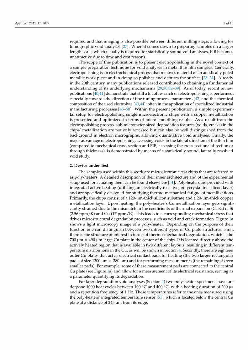
The samples used within this work are microelectronic test chips that are referred toas poly-heaters. A detailed description of their inner architecture and of the experimentalsetup used for actuating them can be found elsewhere [51]. Poly-heaters are provided withintegrated active heating (utilizing an electrically resistive, polycrystalline silicon layer)and are specifically designed for studying thermo-mechanical fatigue of metallizations.Primarily, the chips consist of a 120-µm-thick silicon substrate and a 20-µm-thick coppermetallization layer. Upon heating, the poly-heater’s Cu metallization layer gets signifi-cantly strained due to the mismatch in the coefficients of thermal expansion (CTEs) of Si(2.56 ppm/K) and Cu (17 ppm/K). This leads to a corresponding mechanical stress thatdrives microstructural degradation processes, such as void and crack formation. Figure 1ashows a light microscopy image of a poly-heater. Depending on the purpose of theirfunction one can distinguish between two different types of Cu plate structures: First,there is the structure of interest in terms of thermo-mechanical degradation, which is the700 µm × 490 µm large Cu plate in the center of the chip. It is located directly above theactively heated region that is available in two different layouts, resulting in different tem-perature distributions in the Cu, as will be shown in Section 4. Secondly, there are eighteenouter Cu plates that act as electrical contact pads for heating (the two larger rectangularpads of size 1300 µm × 280 µm) and for performing measurements (the remaining sixteensmaller pads). For example, some of these measurement pads are connected to the centralCu plate (see Figure 1a) and allow for a measurement of its electrical resistance, serving asa parameter quantifying its degradation.
For later degradation void analyses (Section 4) two poly-heater specimens have un-dergone 1000 heat cycles between 100 ◦C and 400 ◦C, with a heating duration of 200 µsand a repetition frequency of 1 Hz. These temperatures refer to the ones measured usingthe poly-heaters’ integrated temperature sensor [51], which is located below the central Cuplate at a distance of 245 µm from its edge.
Appl. Sci. 2021, 11, 7009 3 of 10Appl. Sci. 2021, 11, x FOR PEER REVIEW 3 of 10
Figure 1. (a) Light microscopy image of a poly-heater. (b) Schematic diagram of the electropolishing
setup and (c) an alligator clip electrically contacting a poly-heater for electropolishing.
For later degradation void analyses (Section 4) two poly-heater specimens have un-
dergone 1000 heat cycles between 100 °C and 400 °C, with a heating duration of 200 µs
and a repetition frequency of 1 Hz. These temperatures refer to the ones measured using
the poly-heaters’ integrated temperature sensor [51], which is located below the central
Cu plate at a distance of 245 µm from its edge.
3. Electropolishing Setup
A schematic representation of the setup used for electropolishing (a 2-electrode
setup) is shown in Figure 1b. This rather simple setup comprises a DC voltage supply, a
beaker, in which the two electrodes are in electrical contact with each other via an electro-
lyte, and a magnetic stirring system. The specific electrolyte used is well-suited for elec-
tropolishing copper and is composed of 45 vol% orthophosphoric acid (concentration
85%), 45 vol% methanol, and 10 vol% isopropanol. For the electropolishing experiments
presented in this work the poly-heater specimens were electrically contacted by an alliga-
tor clip, as shown in Figure 1c. To allow electropolishing of the central Cu plate without
damaging it, the alligator clip was used to contact one of the measurement pads that are
internally connected to the central plate. By using an alligator clip made of copper, no
additional metal was introduced to the system, minimizing measurement errors due to
the formation of a galvanic coupling and possible galvanic corrosion of the chip’s elec-
tropolished surface [52,53]. As depicted in Figure 1b, the alligator clip clamping the poly-
heater to be electropolished is fully immersed into the electrolyte and acts as an anode. By
this means, the contact surface between the anode and the electrolyte, determined by the
electrically contacted Cu surface of the poly-heater (≈2 mm2) and the alligator clip
(≈400 mm2), becomes large enough such that the resulting electrical currents can be meas-
ured, and reproducibility of the operating conditions can be guaranteed. A cylindrically
shaped mesh grid made of stainless steel with height 42 mm and diameter 16 mm func-
tions as a cathode. All experiments were performed at room temperature and with stirring
of a frequency of 200 revolutions per minute.
In addition to the electrode materials and the electrolyte, multiple parameters influ-
ence the electropolishing process. These comprise electrode distance, surface area ratio of
the cathode with respect to the anode but also applied voltage (and corresponding current
density), electropolishing duration, stirring, temperature, electrolyte bath age, etc.
[33,38,39,44,54,55]. Yang et al. [40] recommend to acquire a current-voltage curve to find
the optimal electropolishing voltage for the particular setup and operating conditions in
Figure 1. (a) Light microscopy image of a poly-heater. (b) Schematic diagram of the electropolishingsetup and (c) an alligator clip electrically contacting a poly-heater for electropolishing.
3. Electropolishing Setup
A schematic representation of the setup used for electropolishing (a 2-electrode setup)is shown in Figure 1b. This rather simple setup comprises a DC voltage supply, a beaker,in which the two electrodes are in electrical contact with each other via an electrolyte, anda magnetic stirring system. The specific electrolyte used is well-suited for electropolishingcopper and is composed of 45 vol% orthophosphoric acid (concentration 85%), 45 vol%methanol, and 10 vol% isopropanol. For the electropolishing experiments presented inthis work the poly-heater specimens were electrically contacted by an alligator clip, asshown in Figure 1c. To allow electropolishing of the central Cu plate without damagingit, the alligator clip was used to contact one of the measurement pads that are internallyconnected to the central plate. By using an alligator clip made of copper, no additionalmetal was introduced to the system, minimizing measurement errors due to the forma-tion of a galvanic coupling and possible galvanic corrosion of the chip’s electropolishedsurface [52,53]. As depicted in Figure 1b, the alligator clip clamping the poly-heater to beelectropolished is fully immersed into the electrolyte and acts as an anode. By this means,the contact surface between the anode and the electrolyte, determined by the electricallycontacted Cu surface of the poly-heater (≈2 mm2) and the alligator clip (≈400 mm2),becomes large enough such that the resulting electrical currents can be measured, andreproducibility of the operating conditions can be guaranteed. A cylindrically shaped meshgrid made of stainless steel with height 42 mm and diameter 16 mm functions as a cathode.All experiments were performed at room temperature and with stirring of a frequency of200 revolutions per minute.
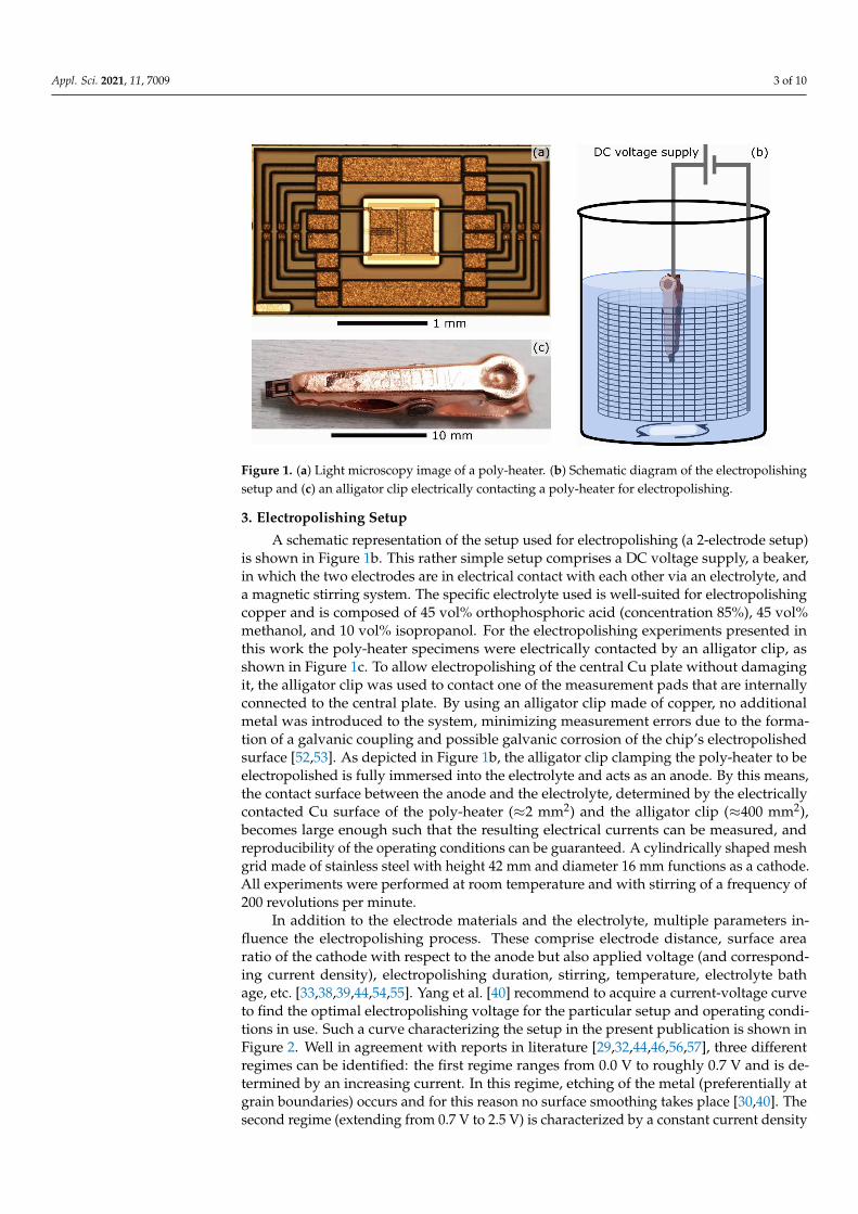
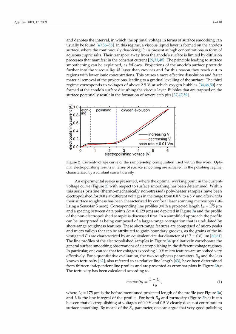
In addition to the electrode materials and the electrolyte, multiple parameters in-fluence the electropolishing process. These comprise electrode distance, surface arearatio of the cathode with respect to the anode but also applied voltage (and correspond-ing current density), electropolishing duration, stirring, temperature, electrolyte bathage, etc. [33,38,39,44,54,55]. Yang et al. [40] recommend to acquire a current-voltage curveto find the optimal electropolishing voltage for the particular setup and operating condi-tions in use. Such a curve characterizing the setup in the present publication is shown inFigure 2. Well in agreement with reports in literature [29,32,44,46,56,57], three differentregimes can be identified: the first regime ranges from 0.0 V to roughly 0.7 V and is de-termined by an increasing current. In this regime, etching of the metal (preferentially atgrain boundaries) occurs and for this reason no surface smoothing takes place [30,40]. Thesecond regime (extending from 0.7 V to 2.5 V) is characterized by a constant current density
Appl. Sci. 2021, 11, 7009 4 of 10
and denotes the interval, in which the optimal voltage in terms of surface smoothing canusually be found [49,56–58]. In this regime, a viscous liquid layer is formed on the anode’ssurface, where the continuously dissolving Cu is present at high concentrations in form ofaqueous cupric salts. Their transport away from the anode’s surface is limited by diffusionprocesses that manifest in the constant current [29,33,48]. The principle leading to surfacesmoothening can be explained, as follows. Projections of the anode’s surface protrudefurther into the viscous liquid layer than crevices and for this reason they reach out toregions with lower ionic concentrations. This causes a more effective dissolution and fastermaterial removal of the projections, leading to a gradual levelling of the surface. The thirdregime corresponds to voltages of above 2.5 V, at which oxygen bubbles [34,46,50] areformed at the anode’s surface disturbing the viscous layer. Bubbles that are trapped on thesurface potentially result in the formation of severe etch pits [37,47,59].
Appl. Sci. 2021, 11, x FOR PEER REVIEW 4 of 10
use. Such a curve characterizing the setup in the present publication is shown in Figure 2.
Well in agreement with reports in literature [29,32,44,46,56,57], three different regimes can
be identified: the first regime ranges from 0.0 V to roughly 0.7 V and is determined by an
increasing current. In this regime, etching of the metal (preferentially at grain boundaries)
occurs and for this reason no surface smoothing takes place [30,40]. The second regime
(extending from 0.7 V to 2.5 V) is characterized by a constant current density and denotes
the interval, in which the optimal voltage in terms of surface smoothing can usually be
found [49,56–58]. In this regime, a viscous liquid layer is formed on the anode’s surface,
where the continuously dissolving Cu is present at high concentrations in form of aqueous
cupric salts. Their transport away from the anode’s surface is limited by diffusion pro-
cesses that manifest in the constant current [29,33,48]. The principle leading to surface
smoothening can be explained, as follows. Projections of the anode’s surface protrude fur-
ther into the viscous liquid layer than crevices and for this reason they reach out to regions
with lower ionic concentrations. This causes a more effective dissolution and faster mate-
rial removal of the projections, leading to a gradual levelling of the surface. The third re-
gime corresponds to voltages of above 2.5 V, at which oxygen bubbles [34,46,50] are
formed at the anode’s surface disturbing the viscous layer. Bubbles that are trapped on
the surface potentially result in the formation of severe etch pits [37,47,59].
Figure 2. Current-voltage curve of the sample-setup configuration used within this work. Optimal
electropolishing results in terms of surface smoothing are achieved in the polishing regime, charac-
terized by a constant current density.
An experimental series is presented, where the optimal working point in the current-
voltage curve (Figure 2) with respect to surface smoothing has been determined. Within
this series pristine (thermo-mechanically non-stressed) poly-heater samples have been
electropolished for 360 s at different voltages in the range from 0.0 V to 4.5 V and after-
wards their surface roughness has been characterized by confocal laser scanning micros-
copy (utilizing a Sensofar S neox). Corresponding line profiles (with a projected length
𝐿0 = 175 µm and a spacing between data points ∆𝑥 ≈ 0.129 µm) are depicted in Figure
3a and the profile of the non-electropolished sample is discussed first. In a simplified ap-
proach the profile can be interpreted as being composed of a larger-range corrugation that
is undulated by short-range roughness features. These short-range features are comprised
of micro peaks and micro valleys that can be attributed to grain boundary grooves, as the
grains of the investigated Cu are characterized by an equivalent circular diameter of
(2.7 ± 0.6) µm [60,61]. The line profiles of the electropolished samples in Figure 3a quali-
tatively corroborate the general surface smoothing observations of electropolishing in the
different voltage regimes. In particular, one can see that for voltages exceeding 1.0 V micro
features are smoothed very effectively. For a quantitative evaluation, the two roughness
parameters 𝑅q and the less known tortuosity [62], also referred to as relative line length
[63], have been determined from thirteen independent line profiles and are presented as
error bar plots in Figure 3b,c. The tortuosity has been calculated according to
𝑡𝑜𝑟𝑡𝑢𝑜𝑠𝑖𝑡𝑦 =𝐿−𝐿0
𝐿0, (1)
Figure 2. Current-voltage curve of the sample-setup configuration used within this work. Opti-mal electropolishing results in terms of surface smoothing are achieved in the polishing regime,characterized by a constant current density.
An experimental series is presented, where the optimal working point in the current-voltage curve (Figure 2) with respect to surface smoothing has been determined. Withinthis series pristine (thermo-mechanically non-stressed) poly-heater samples have beenelectropolished for 360 s at different voltages in the range from 0.0 V to 4.5 V and afterwardstheir surface roughness has been characterized by confocal laser scanning microscopy (uti-lizing a Sensofar S neox). Corresponding line profiles (with a projected length L0 = 175 µmand a spacing between data points ∆x ≈ 0.129 µm) are depicted in Figure 3a and the profileof the non-electropolished sample is discussed first. In a simplified approach the profilecan be interpreted as being composed of a larger-range corrugation that is undulated byshort-range roughness features. These short-range features are comprised of micro peaksand micro valleys that can be attributed to grain boundary grooves, as the grains of the in-vestigated Cu are characterized by an equivalent circular diameter of (2.7 ± 0.6) µm [60,61].The line profiles of the electropolished samples in Figure 3a qualitatively corroborate thegeneral surface smoothing observations of electropolishing in the different voltage regimes.In particular, one can see that for voltages exceeding 1.0 V micro features are smoothed veryeffectively. For a quantitative evaluation, the two roughness parameters Rq and the lessknown tortuosity [62], also referred to as relative line length [63], have been determinedfrom thirteen independent line profiles and are presented as error bar plots in Figure 3b,c.The tortuosity has been calculated according to
tortuosity =L − L0
L0, (1)
where L0 = 175 µm is the before-mentioned projected length of the profile (see Figure 3a)and L is the line integral of the profile. For both Rq and tortuosity (Figure 3b,c) it canbe seen that electropolishing at voltages of 0.0 V and 0.5 V clearly does not contribute tosurface smoothing. By means of the Rq parameter, one can argue that very good polishing
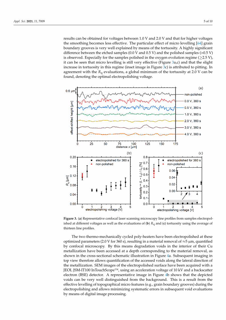
Appl. Sci. 2021, 11, 7009 5 of 10
results can be obtained for voltages between 1.0 V and 2.0 V and that for higher voltagesthe smoothing becomes less effective. The particular effect of micro levelling [64] grainboundary grooves is very well explained by means of the tortuosity. A highly significantdifference between the etched samples (0.0 V and 0.5 V) and the polished samples (>0.5 V)is observed. Especially for the samples polished in the oxygen evolution regime (≥2.5 V),it can be seen that micro levelling is still very effective (Figure 3a,c) and that the slightincrease in tortuosity in this regime (inset image in Figure 3c) is attributed to pitting. Inagreement with the Rq evaluations, a global minimum of the tortuosity at 2.0 V can befound, denoting the optimal electropolishing voltage.
Appl. Sci. 2021, 11, x FOR PEER REVIEW 5 of 10
where 𝐿0 = 175 µm is the before-mentioned projected length of the profile (see Figure 3a)
and 𝐿 is the line integral of the profile. For both 𝑅q and tortuosity (Figure 3b,c) it can be
seen that electropolishing at voltages of 0.0 V and 0.5 V clearly does not contribute to
surface smoothing. By means of the 𝑅q parameter, one can argue that very good polish-
ing results can be obtained for voltages between 1.0 V and 2.0 V and that for higher volt-
ages the smoothing becomes less effective. The particular effect of micro levelling [64]
grain boundary grooves is very well explained by means of the tortuosity. A highly sig-
nificant difference between the etched samples (0.0 V and 0.5 V) and the polished samples
(>0.5 V) is observed. Especially for the samples polished in the oxygen evolution regime
(≥2.5 V), it can be seen that micro levelling is still very effective (Figure 3a,c) and that the
slight increase in tortuosity in this regime (inset image in Figure 3c) is attributed to pitting.
In agreement with the 𝑅q evaluations, a global minimum of the tortuosity at 2.0 V can be
found, denoting the optimal electropolishing voltage.
Figure 3. (a) Representative confocal laser scanning microscopy line profiles from samples elec-
tropolished at different voltages as well as the evaluations of (b) 𝑅q and (c) tortuosity using the
average of thirteen line profiles.
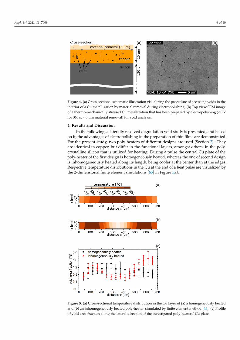
The two thermo-mechanically cycled poly-heaters have been electropolished at these
optimized parameters (2.0 V for 360 s), resulting in a material removal of ≈5 µm, quanti-
fied by confocal microscopy. By this means degradation voids in the interior of their Cu
metallization have been accessed at a depth corresponding to the material removal, as
shown in the cross-sectional schematic illustration in Figure 4a. Subsequent imaging in
top view therefore allows quantification of the accessed voids along the lateral direction
of the metallization. SEM images of the electropolished surface have been acquired with
a JEOL JSM-IT100 InTouchScope™, using an acceleration voltage of 10 kV and a backscat-
ter electron (BSE) detector. A representative image in Figure 4b shows that the depicted
Figure 3. (a) Representative confocal laser scanning microscopy line profiles from samples electropol-ished at different voltages as well as the evaluations of (b) Rq and (c) tortuosity using the average ofthirteen line profiles.
The two thermo-mechanically cycled poly-heaters have been electropolished at theseoptimized parameters (2.0 V for 360 s), resulting in a material removal of ≈5 µm, quantifiedby confocal microscopy. By this means degradation voids in the interior of their Cumetallization have been accessed at a depth corresponding to the material removal, asshown in the cross-sectional schematic illustration in Figure 4a. Subsequent imaging intop view therefore allows quantification of the accessed voids along the lateral direction ofthe metallization. SEM images of the electropolished surface have been acquired with aJEOL JSM-IT100 InTouchScope™, using an acceleration voltage of 10 kV and a backscatterelectron (BSE) detector. A representative image in Figure 4b shows that the depictedvoids can be very well distinguished from the background. This is a result from theeffective levelling of topographical micro features (e.g., grain boundary grooves) during theelectropolishing and allows minimizing systematic errors in subsequent void evaluationsby means of digital image processing.
Appl. Sci. 2021, 11, 7009 6 of 10
Appl. Sci. 2021, 11, x FOR PEER REVIEW 6 of 10
voids can be very well distinguished from the background. This is a result from the effec-
tive levelling of topographical micro features (e.g., grain boundary grooves) during the
electropolishing and allows minimizing systematic errors in subsequent void evaluations
by means of digital image processing.
Figure 4. (a) Cross-sectional schematic illustration visualizing the procedure of accessing voids in
the interior of a Cu metallization by material removal during electropolishing. (b) Top view SEM
image of a thermo-mechanically stressed Cu metallization that has been prepared by electropolish-
ing (2.0 V for 360 s, ≈5 µm material removal) for void analysis.
4. Results and Discussion
In the following, a laterally resolved degradation void study is presented, and based
on it, the advantages of electropolishing in the preparation of thin films are demonstrated.
For the present study, two poly-heaters of different designs are used (Section 2). They are
identical in copper, but differ in the functional layers, amongst others, in the polycrystal-
line silicon that is utilized for heating. During a pulse the central Cu plate of the poly-
heater of the first design is homogeneously heated, whereas the one of second design is
inhomogeneously heated along its length, being cooler at the center than at the edges.
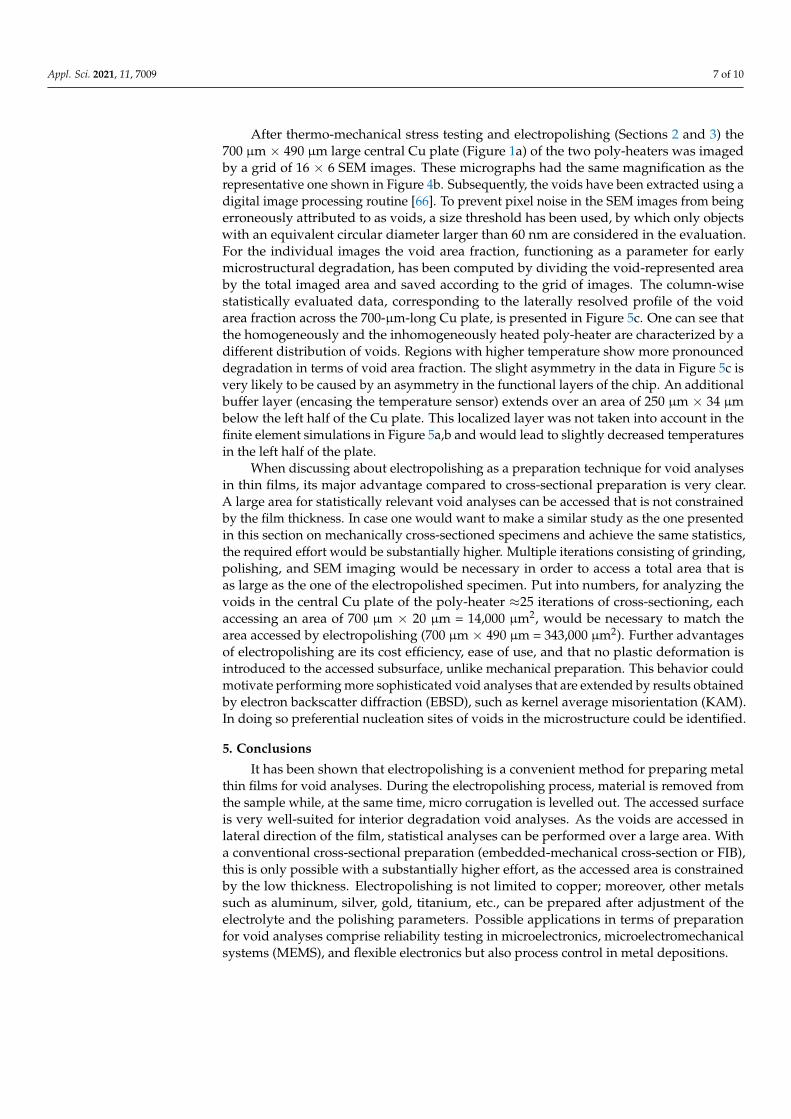
Respective temperature distributions in the Cu at the end of a heat pulse are visualized
by the 2-dimensional finite element simulations [65] in Figure 5a,b.
After thermo-mechanical stress testing and electropolishing (Sections 2 and 3) the 700
µm × 490 µm large central Cu plate (Figure 1a) of the two poly-heaters was imaged by a
grid of 16 × 6 SEM images. These micrographs had the same magnification as the repre-
sentative one shown in Figure 4b. Subsequently, the voids have been extracted using a
digital image processing routine [66]. To prevent pixel noise in the SEM images from being
erroneously attributed to as voids, a size threshold has been used, by which only objects
with an equivalent circular diameter larger than 60 nm are considered in the evaluation.
For the individual images the void area fraction, functioning as a parameter for early mi-
crostructural degradation, has been computed by dividing the void-represented area by
the total imaged area and saved according to the grid of images. The column-wise statis-
tically evaluated data, corresponding to the laterally resolved profile of the void area frac-
tion across the 700-µm-long Cu plate, is presented in Figure 5c. One can see that the ho-
mogeneously and the inhomogeneously heated poly-heater are characterized by a differ-
ent distribution of voids. Regions with higher temperature show more pronounced deg-
radation in terms of void area fraction. The slight asymmetry in the data in Figure 5c is
very likely to be caused by an asymmetry in the functional layers of the chip. An addi-
tional buffer layer (encasing the temperature sensor) extends over an area of 250 µm × 34
µm below the left half of the Cu plate. This localized layer was not taken into account in
the finite element simulations in Figure 5a,b and would lead to slightly decreased temper-
atures in the left half of the plate.
Figure 4. (a) Cross-sectional schematic illustration visualizing the procedure of accessing voids in theinterior of a Cu metallization by material removal during electropolishing. (b) Top view SEM imageof a thermo-mechanically stressed Cu metallization that has been prepared by electropolishing (2.0 Vfor 360 s, ≈5 µm material removal) for void analysis.
4. Results and Discussion
In the following, a laterally resolved degradation void study is presented, and basedon it, the advantages of electropolishing in the preparation of thin films are demonstrated.For the present study, two poly-heaters of different designs are used (Section 2). Theyare identical in copper, but differ in the functional layers, amongst others, in the poly-crystalline silicon that is utilized for heating. During a pulse the central Cu plate of thepoly-heater of the first design is homogeneously heated, whereas the one of second designis inhomogeneously heated along its length, being cooler at the center than at the edges.Respective temperature distributions in the Cu at the end of a heat pulse are visualized bythe 2-dimensional finite element simulations [65] in Figure 5a,b.
Appl. Sci. 2021, 11, x FOR PEER REVIEW 7 of 10
Figure 5. (a) Cross-sectional temperature distribution in the Cu layer of (a) a homogeneously heated
and (b) an inhomogeneously heated poly-heater, simulated by finite element method [65]. (c) Profile
of void area fraction along the lateral direction of the investigated poly-heaters’ Cu plate.
When discussing about electropolishing as a preparation technique for void analyses
in thin films, its major advantage compared to cross-sectional preparation is very clear. A
large area for statistically relevant void analyses can be accessed that is not constrained
by the film thickness. In case one would want to make a similar study as the one presented
in this section on mechanically cross-sectioned specimens and achieve the same statistics,
the required effort would be substantially higher. Multiple iterations consisting of grind-
ing, polishing, and SEM imaging would be necessary in order to access a total area that is
as large as the one of the electropolished specimen. Put into numbers, for analyzing the
voids in the central Cu plate of the poly-heater ≈25 iterations of cross-sectioning, each
accessing an area of 700 µm × 20 µm = 14,000 µm2, would be necessary to match the area
accessed by electropolishing (700 µm × 490 µm = 343,000 µm2). Further advantages of elec-
tropolishing are its cost efficiency, ease of use, and that no plastic deformation is intro-
duced to the accessed subsurface, unlike mechanical preparation. This behavior could mo-
tivate performing more sophisticated void analyses that are extended by results obtained
by electron backscatter diffraction (EBSD), such as kernel average misorientation (KAM).
In doing so preferential nucleation sites of voids in the microstructure could be identified.
5. Conclusions
It has been shown that electropolishing is a convenient method for preparing metal
thin films for void analyses. During the electropolishing process, material is removed
from the sample while, at the same time, micro corrugation is levelled out. The accessed
surface is very well-suited for interior degradation void analyses. As the voids are ac-
cessed in lateral direction of the film, statistical analyses can be performed over a large
area. With a conventional cross-sectional preparation (embedded-mechanical cross-sec-
tion or FIB), this is only possible with a substantially higher effort, as the accessed area is
constrained by the low thickness. Electropolishing is not limited to copper; moreover,
Figure 5. (a) Cross-sectional temperature distribution in the Cu layer of (a) a homogeneously heatedand (b) an inhomogeneously heated poly-heater, simulated by finite element method [65]. (c) Profileof void area fraction along the lateral direction of the investigated poly-heaters’ Cu plate.
Appl. Sci. 2021, 11, 7009 7 of 10
After thermo-mechanical stress testing and electropolishing (Sections 2 and 3) the700 µm × 490 µm large central Cu plate (Figure 1a) of the two poly-heaters was imagedby a grid of 16 × 6 SEM images. These micrographs had the same magnification as therepresentative one shown in Figure 4b. Subsequently, the voids have been extracted using adigital image processing routine [66]. To prevent pixel noise in the SEM images from beingerroneously attributed to as voids, a size threshold has been used, by which only objectswith an equivalent circular diameter larger than 60 nm are considered in the evaluation.For the individual images the void area fraction, functioning as a parameter for earlymicrostructural degradation, has been computed by dividing the void-represented areaby the total imaged area and saved according to the grid of images. The column-wisestatistically evaluated data, corresponding to the laterally resolved profile of the voidarea fraction across the 700-µm-long Cu plate, is presented in Figure 5c. One can see thatthe homogeneously and the inhomogeneously heated poly-heater are characterized by adifferent distribution of voids. Regions with higher temperature show more pronounceddegradation in terms of void area fraction. The slight asymmetry in the data in Figure 5c isvery likely to be caused by an asymmetry in the functional layers of the chip. An additionalbuffer layer (encasing the temperature sensor) extends over an area of 250 µm × 34 µmbelow the left half of the Cu plate. This localized layer was not taken into account in thefinite element simulations in Figure 5a,b and would lead to slightly decreased temperaturesin the left half of the plate.
When discussing about electropolishing as a preparation technique for void analysesin thin films, its major advantage compared to cross-sectional preparation is very clear.A large area for statistically relevant void analyses can be accessed that is not constrainedby the film thickness. In case one would want to make a similar study as the one presentedin this section on mechanically cross-sectioned specimens and achieve the same statistics,the required effort would be substantially higher. Multiple iterations consisting of grinding,polishing, and SEM imaging would be necessary in order to access a total area that isas large as the one of the electropolished specimen. Put into numbers, for analyzing thevoids in the central Cu plate of the poly-heater ≈25 iterations of cross-sectioning, eachaccessing an area of 700 µm × 20 µm = 14,000 µm2, would be necessary to match thearea accessed by electropolishing (700 µm × 490 µm = 343,000 µm2). Further advantagesof electropolishing are its cost efficiency, ease of use, and that no plastic deformation isintroduced to the accessed subsurface, unlike mechanical preparation. This behavior couldmotivate performing more sophisticated void analyses that are extended by results obtainedby electron backscatter diffraction (EBSD), such as kernel average misorientation (KAM).In doing so preferential nucleation sites of voids in the microstructure could be identified.
5. Conclusions
It has been shown that electropolishing is a convenient method for preparing metalthin films for void analyses. During the electropolishing process, material is removed fromthe sample while, at the same time, micro corrugation is levelled out. The accessed surfaceis very well-suited for interior degradation void analyses. As the voids are accessed inlateral direction of the film, statistical analyses can be performed over a large area. Witha conventional cross-sectional preparation (embedded-mechanical cross-section or FIB),this is only possible with a substantially higher effort, as the accessed area is constrainedby the low thickness. Electropolishing is not limited to copper; moreover, other metalssuch as aluminum, silver, gold, titanium, etc., can be prepared after adjustment of theelectrolyte and the polishing parameters. Possible applications in terms of preparationfor void analyses comprise reliability testing in microelectronics, microelectromechanicalsystems (MEMS), and flexible electronics but also process control in metal depositions.
Appl. Sci. 2021, 11, 7009 8 of 10
Author Contributions: Conceptualization, S.M.; methodology, S.M.; software, M.K.; validation, S.M.and M.K.; formal analysis, S.M. and M.K.; investigation, S.M. and S.K.; data curation, S.M. andM.K.; writing—original draft preparation, S.M.; writing—review and editing, S.K., J.Z. and M.J.C.;visualization, S.M.; supervision, S.K. and J.Z.; project administration, J.Z. and M.J.C. All authors haveread and agreed to the published version of the manuscript.
Funding: This work was funded by the Austrian Research Promotion Agency (FFG, Project No. 881110).
Institutional Review Board Statement: Not applicable.
Informed Consent Statement: Not applicable.
Data Availability Statement: The data presented in this study may be available upon reasonablerequest by contacting the corresponding author. Restrictions apply to the availability of these data.
Acknowledgments: The authors would like to express their gratitude to J. Karlovska for the super-vision during the electrochemical experiments and to P. Hoffmann for providing the finite elementsimulations presented in this publication.
Conflicts of Interest: The authors declare no conflict of interest.
References1. Pardoen, T.; Doghri, I.; Delannay, F. Experimental and numerical comparison of void growth models and void coalescence criteria
for the prediction of ductile fracture in copper bars. Acta Mater. 1998, 46, 541–552. [CrossRef]2. Dzieciol, K.; Borbély, A.; Sket, F.; Isaac, A.; Di Michiel, M.; Cloetens, P.; Buslaps, T.; Pyzalla, A.R. Void growth in copper during
high-temperature power-law creep. Acta Mater. 2011, 59, 671–677. [CrossRef]3. Mayes, J.L.; Hatfield, S.L.; Gillis, P.P.; House, J.W. Void formation in OFE copper. Int. J. Impact Eng. 1993, 14, 503–508. [CrossRef]4. Kraft, O.; Wellner, P.; Hommel, M.; Schwaiger, R.; Arzt, E. Fatigue behavior of polycrystalline thin copper films. Z. Met. Kd. 2002,
93, 392–400. [CrossRef]5. Zhang, G.P.; Volkert, C.A.; Schwaiger, R.; Wellner, P.; Arzt, E.; Kraft, O. Length-scale-controlled fatigue mechanisms in thin copper
films. Acta Mater. 2006, 54, 3127–3139. [CrossRef]6. Liniger, E.; Gignac, L.; Hu, C.-K.; Kaldor, S. In situ study of void growth kinetics in electroplated Cu lines. J. Appl. Phys. 2002, 92,
1803–1810. [CrossRef]7. Fisher, S.B.; White, R.J.; Miller, K.M. Quantitative analysis of void swelling in pure copper. Philos. Mag. A 1979, 40, 239–255.
[CrossRef]8. Zinkle, S.J.; Kulcinski, G.L.; Knoll, R.W. Microstructure of copper following high dose 14-MeV Cu ion irradiation. J. Nucl. Mater.
1986, 138, 46–56. [CrossRef]9. Hung, C.-C.; Lee, W.-H.; Chang, S.-C.; Wang, Y.-L.; Hwang, G.-J. Investigation of copper scratches and void defects after chemical
mechanical polishing. Jpn. J. Appl. Phys. 2008, 47, 7073. [CrossRef]10. Nakahara, S. Microscopic mechanism of the hydrogen effect on the ductility of electroless copper. Acta Metall. 1988, 36, 1669–1681.
[CrossRef]11. Nakahara, S.; Okinaka, Y. Microstructure and Mechanical Properties of Electroless Copper Deposits. Annu. Rev. Mater. Sci. 1991,
21, 93–129. [CrossRef]12. Garrison, W.M., Jr.; Moody, N.R. Ductile fracture. J. Phys. Chem. Solids 1987, 48, 1035–1074. [CrossRef]13. Benzerga, A.A.; Leblond, J.-B. Ductile Fracture by Void Growth to Coalescence. Adv. Appl. Mech. 2010, 44, 169–305. [CrossRef]14. Rudd, R.E.; Belak, J.F. Void nucleation and associated plasticity in dynamic fracture of polycrystalline copper: An atomistic
simulation. Comput. Mater. Sci. 2002, 24, 148–153. [CrossRef]15. Barnes, R.S. The generation of vacancies in metals. Philos. Mag. 1960, 5, 635–646. [CrossRef]16. Goland, A.N. Radiation-enhanced helium precipitation in copper. Philos. Mag. 1961, 6, 189–193. [CrossRef]17. Hills, C.R. A Simple Technique for Preparing Bulk Metallographic Cross Sections. Rev. Sci. Instrum. 1971, 42, 1093. [CrossRef]18. Guo, Y.B.; Warren, A.W. Microscale mechanical behavior of the subsurface by finishing processes. J. Manuf. Sci. Eng. 2005, 127,
333–338. [CrossRef]19. Janssen, P.; Hoefnagels, J.; Keijser, T.d.; Geers, M. Processing induced size effects in plastic yielding upon miniaturisation. J. Mech.
Phys. Solids 2008, 56, 2687–2706. [CrossRef]20. Brett, J.; Seigle, L. Shrinkage of voids in copper. Acta Metall. 1963, 11, 467–474. [CrossRef]21. Dow, W.-P.; Huang, H.-S. Roles of Chloride Ion in Microvia Filling by Copper Electrodeposition: I. Studies Using SEM and
Optical Microscope. J. Electrochem. Soc. 2005, 152, C67. [CrossRef]22. Wu, X.; Sha, W. Experimental study of the voids in the electroless copper deposits and the direct measurement of the void fraction
based on the scanning electron microscopy images. Appl. Surf. Sci. 2009, 255, 4259–4266. [CrossRef]23. Smorodin, T.; Wilde, J.; Alpern, P.; Stecher, M. Investigation and Improvement of Fast Temperature-Cycle Reliability for DMOS-
Related Conductor Path Design. In Proceedings of the 2007 IEEE International Reliability Physics Symposium, 45th Annual,Phoenix, AZ, USA, 15–19 April 2007. [CrossRef]
Appl. Sci. 2021, 11, 7009 9 of 10
24. Nelhiebel, M.; Illing, R.; Schreiber, C.; Wöhlert, S.; Lanzerstorfer, S.; Ladurner, M.; Kadow, C.; Decker, S.; Dibra, D.; Unterwalcher, H.A reliable technology concept for active power cycling to extreme temperatures. Microelectron. Reliab. 2011, 51, 1927–1932.[CrossRef]
25. Zhang, M.; Yoshihisa, Y.; Furuya, K.; Imai, Y.; Hatasako, K.; Ipposhi, T.; Maegawa, S. Reliability study of thermal cycling stress onsmart power devices. Jpn. J. Appl. Phys. 2014, 53, 04EP12. [CrossRef]
26. Wurster, S.; Bigl, S.; Cordill, M.J.; Kiener, D. Accelerated thermo-mechanical fatigue of copper metallizations studied by pulsedlaser heating. Microelectron. Eng. 2017, 167, 110–118. [CrossRef]
27. Wijaya, A.; Eichinger, B.; Rose, J.; Sartory, B.; Mischitz, M.; Brunner, R. 3D Microanalysis of Porous Copper Using FIB-Tomographyin Combination with X-ray Computed Tomography. Microsc. Microanal. 2017, 23, 254–255. [CrossRef]
28. Jacquet, P.A. Electrolytic Method for obtaining Bright Copper Surfaces. Nature 1935, 135, 1076. [CrossRef]29. Jacquet, P.A. On the Anodic Behavior of Copper in Aqueous Solutions of Orthophosphoric Acid. Trans. Electrochem. Soc. 1936,
69, 629. [CrossRef]30. Kauczor, E. Elektrolytisches Polieren und Ätzen. In Metallographische Arbeitsverfahren; Kauczor, E., Ed.; Springer: Berlin/Heidelberg,
Germany, 1957; pp. 39–54. ISBN 978-3-540-02231-2.31. Buhlert, M. Elektropolieren: Elektrolytisches Glänzen, Glätten und Entgraten von Edelstahl, Stahl, Messing, Kupfer, Aluminium, Magnesium
und Titan, 2. Auflage; Leuze: Bad Saulgau, Germany, 2017; ISBN 9783874802987.32. Elmore, W.C. Electrolytic Polishing. J. Appl. Phys. 1939, 10, 724. [CrossRef]33. Walton, H.F. The anode layer in the electrolytic polishing of copper. J. Electrochem. Soc. 1950, 97, 219. [CrossRef]34. Edwards, J. The Mechanism of Electropolishing of Copper in Phosphoric Acid Solutions: I. Processes Preceding the Establisment
of Polishing Conditions. J. Electrochem. Soc. 1953, 100, 189C. [CrossRef]35. Edwards, J. The mechanism of electropolishing of copper in phosphoric acid solutions: II. The mechanism of smoothing.
J. Electrochem. Soc. 1953, 100, 223C. [CrossRef]36. Wagner, C. Contribution to the theory of electropolishing. J. Electrochem. Soc. 1954, 101, 225. [CrossRef]37. Landolt, D. Fundamental aspects of electropolishing. Electrochim. Acta 1987, 32, 1–11. [CrossRef]38. Vidal, R.; West, A.C. Copper Electropolishing in Concentrated Phosphoric Acid: I. Experimental Findings. J. Electrochem. Soc.
1995, 142, 2682. [CrossRef]39. Vidal, R.; West, A.C. Copper Electropolishing in Concentrated Phosphoric Acid: II. Theoretical Interpretation. J. Electrochem. Soc.
1995, 142, 2689. [CrossRef]40. Yang, G.; Wang, B.; Tawfiq, K.; Wei, H.; Zhou, S.; Chen, G. Electropolishing of surfaces: Theory and applications. Surf. Eng. 2017,
33, 149–166. [CrossRef]41. Han, W.; Fang, F. Fundamental aspects and recent developments in electropolishing. Int. J. Mach. Tools Manuf. 2019, 139, 1–23.
[CrossRef]42. Ramasawmy, H.; Blunt, L. 3D surface topography assessment of the effect of different electrolytes during electrochemical
polishing of EDM surfaces. Int. J. Mach. Tools Manuf. 2002, 42, 567–574. [CrossRef]43. Awad, A.M.; Ghany, N.A.; Dahy, T.M. Removal of tarnishing and roughness of copper surface by electropolishing treatment.
Appl. Surf. Sci. 2010, 256, 4370–4375. [CrossRef]44. Pircher, E.; Martinez, M.R.; Hansal, S.; Hansal, W. Electropolishing of copper alloys in phosphoric acid solutions with alcohols.
Plat. Surf. Finish. 2003, 90, 74–79.45. Datta, M.; Landolt, D. Fundamental aspects and applications of electrochemical microfabrication. Electrochim. Acta 2000, 45,
2535–2558. [CrossRef]46. Huo, J.; Solanki, R.; McAndrew, J. Electrochemical Polishing of Copper for Microelectronic Applications. Surf. Eng. 2003, 19,
11–16. [CrossRef]47. Liu, S.-H.; Shieh, J.-M.; Chen, C.; Dai, B.-T.; Hensen, K.; Cheng, S.-S. Two-Additive Electrolytes for Superplanarizing Damascene
Cu Metals. Electrochem. Solid-State Lett. 2005, 8, C47. [CrossRef]48. Liu, S.-H.; Shieh, J.-M.; Chen, C.; Hensen, K.; Cheng, S.-S. Roles of additives in damascene copper electropolishing. J. Electrochem.
Soc. 2006, 153, C428. [CrossRef]49. Park, K.; Lee, J.; Yoo, B. Electrochemical Polishing of Cu Redistribution Layers for Fan-Out Wafer Level Packaging. J. Nanosci.
Nanotechnol. 2019, 19, 6512–6515. [CrossRef] [PubMed]50. Shieh, J.-M.; Chang, S.-C.; Wang, Y.-L.; Dai, B.-T.; Cheng, S.-S.; Ting, J. Reduction of etch pits of electropolished Cu by additives.
J. Electrochem. Soc. 2004, 151, C459. [CrossRef]51. Moser, S.; Zernatto, G.; Kleinbichler, M.; Nelhiebel, M.; Zechner, J.; Cordill, M.J.; Pippan, R. A Novel Setup for In Situ Monitoring
of Thermomechanically Cycled Thin Film Metallizations. JOM 2019, 71, 3399–3406. [CrossRef]52. Kondo, S.; Sakuma, N.; Homma, Y.; Ohashi, N. Slurry Chemical Corrosion and Galvanic Corrosion during Copper Chemical
Mechanical Polishing. Jpn. J. Appl. Phys. 2000, 39, 6216. [CrossRef]53. Wang, T.C.; Wang, Y.L.; Hsieh, T.E.; Chang, S.C.; Cheng, Y.L. Copper voids improvement for the copper dual damascene
interconnection process. J. Phys. Chem. Solids 2008, 69, 566–571. [CrossRef]54. Mendez, J.; Akolkar, R.; Andryushchenko, T.; Landau, U. A Mechanistic Model for Copper Electropolishing in Phosphoric Acid.
J. Electrochem. Soc. 2007, 155, D27. [CrossRef]

Appl. Sci. 2021, 11, 7009 10 of 10
55. Kwon, G.D.; Kim, Y.W.; Moyen, E.; Keum, D.H.; Lee, Y.H.; Baik, S.; Pribat, D. Controlled electropolishing of copper foils atelevated temperature. Appl. Surf. Sci. 2014, 307, 731–735. [CrossRef]
56. Hoar, T.P.; Rothwell, G.P. The influence of solution flow on anodic polishing. Copper in aqueous o-phosphoric acid. Electrochim.Acta 1964, 9, 135–150. [CrossRef]
57. Abdel-Fattah, T.M.; Loftis, J.D. Comparison of the Electrochemical Polishing of Copper and Aluminum in Acid and Acid-freeMedia. ECS Trans. 2009, 25, 327. [CrossRef]
58. Petzow, G. Metallographic Etching, Techniques for Metallography, Ceramography, Plastography, 2nd ed.; ASM International: MaterialsPark, OH, USA, 1999; ISBN 9781615032204.
59. Chang, S.-C.; Shieh, J.-M.; Dai, B.-T.; Feng, M.-S.; Li, Y.-H.; Shih, C.H.; Tsai, M.H.; Shue, S.L.; Liang, R.S.; Wang, Y.-L. Superpolishingfor Planarizing Copper Damascene Interconnects. Electrochem. Solid-State Lett. 2003, 6, G72. [CrossRef]
60. Wimmer, A.; Heinz, W.; Leitner, A.; Detzel, T.; Robl, W.; Kirchlechner, C.; Dehm, G. Micro-tension study of miniaturized Cu linesat variable temperatures. Acta Mater. 2015, 92, 243–254. [CrossRef]
61. Wimmer, A.; Heinz, W.; Detzel, T.; Robl, W.; Nellessen, M.; Kirchlechner, C.; Dehm, G. Cyclic bending experiments on free-standing Cu micron lines observed by electron backscatter diffraction. Acta Mater. 2015, 83, 460–469. [CrossRef]
62. Clennell, M.B. Tortuosity: A guide through the maze. Geol. Soc. Spec. Publ. 1997, 122, 299–344. [CrossRef]63. Gadelmawla, E.S.; Koura, M.M.; Maksoud, T.; Elewa, I.M.; Soliman, H.H. Roughness parameters. J. Mater. Process. Technol. 2002,
123, 133–145. [CrossRef]64. Hryniewicz, T.; Karpinski, T.; Lukianowicz, C. The evaluation of electrolytically polished surfaces. Wear 1977, 45, 335–343.
[CrossRef]65. Hoffmann, P.; Moser, S.; Kofler, C.; Nelhiebel, M.; Tscharnuter, D.; Karunamurthy, B.; Pettermann, H.E.; Todt, M. Thermomechanical
Fatigue Damage Modeling and Material Parameter Calibration for Thin Film Metallizations. Int. J. Fatigue under review.66. Kleinbichler, M.; Kofler, C.; Stabentheiner, M.; Reisinger, M.; Moser, S.; Zechner, J.; Nelhiebel, M.; Kozeschnik, E. Void Initiation in
Thermo-Mechanical Fatigue of Polycrystalline Copper Films and its Relation to Grain Structure. Microelectron. Reliab. under review.