ELECTRONIC COMPONENTS DISTRIBUTOR - ELCODIS.COM
62
DS07-12547-4E FUJITSU SEMICONDUCTOR DATA SHEET 8-bit Original Microcontroller CMOS F 2 MC-8L MB89530A Series MB89535A/537A/537AC/538A/538AC/F538 MB89P538/PV530 ■ DESCRIPTION The MB89530A series is a one-chip microcontroller featuring the F 2 MC-8L core supporting low-voltage and high- speed operation. Built-in peripheral functions include timers, serial interface, A/D converter, and external interrupt. This product is an ideal general-purpose one-chip microcontroller for a wide variety of applications from household to industrial equipment, as well as use in portable devices. ■ FEATURES • Wide range of package options • Two types of QFP packages (1 mm pitch, 0.65 mm pitch) • LQFP package (0.5 mm pitch) • SH-DIP package • Low voltage, high-speed operating capability • Minimum instruction execution time 0.32 μs (at base oscillator 12.5 MHz) •F 2 MC-8L CPU Core • Instruction set optimized for controller operation • Multiplication/division instructions • 16-bit calculation • Branching instructions with bit testing • Bit operation instructions, etc. • Five timer systems • 8-bit PWM timer with 2 channels (usable as either interval timer of PWM timer) • Pulse width count timer (supports continuous measurement or remote control receiving applications) • 16-bit timer counter • 21-bit time base timer • Watch prescaler (17-bit) • UART • Synchronous or asynchronous operation, switchable • 2 serial interfaces (Serial I/O) • Selection of transfer direction (specify MSB first or LSB first) for communication with a variety of devices (Continued) Downloaded from Elcodis.com electronic components distributor
-
Upload
khangminh22 -
Category
Documents
-
view
1 -
download
0
Transcript of ELECTRONIC COMPONENTS DISTRIBUTOR - ELCODIS.COM
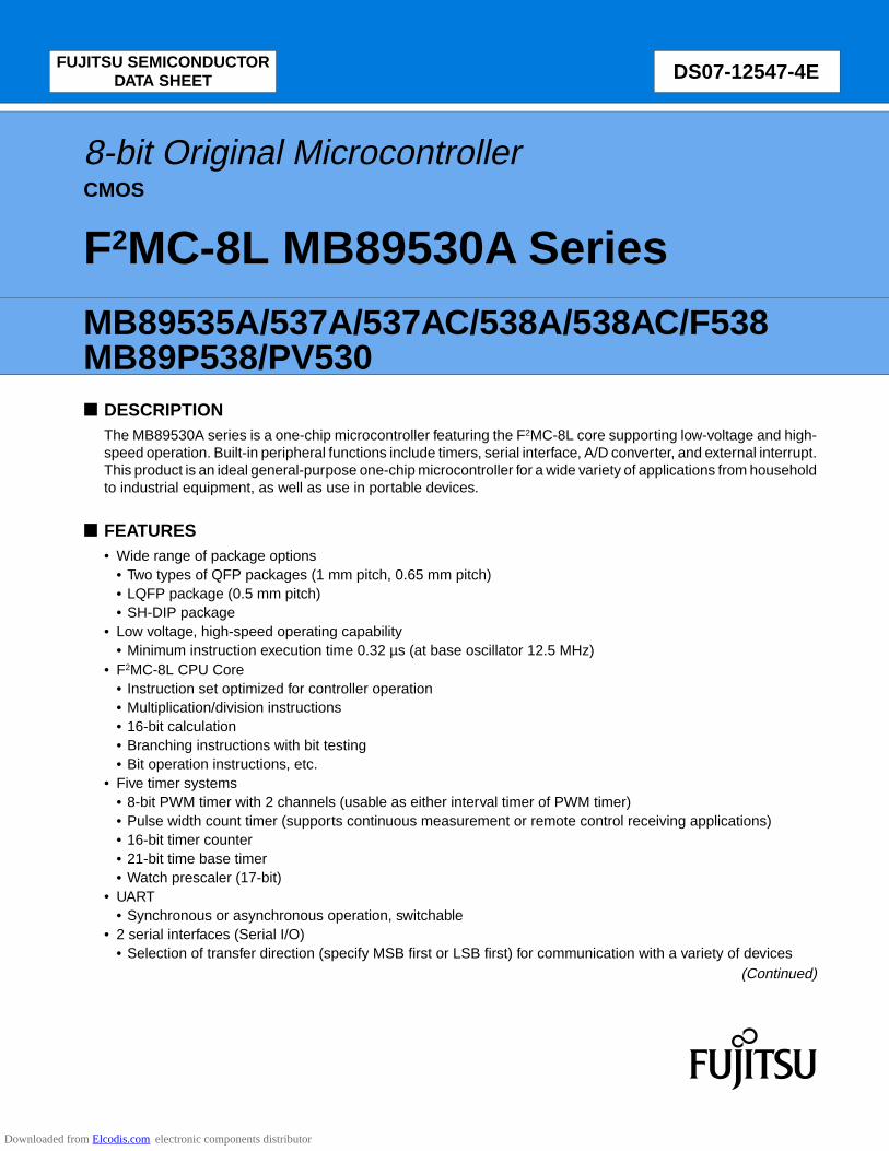
DS07-12547-4EFUJITSU SEMICONDUCTORDATA SHEET
8-bit Original Microcontroller CMOS
F2MC-8L MB89530A Series
MB89535A/537A/537AC/538A/538AC/F538MB89P538/PV530 DESCRIPTION
The MB89530A series is a one-chip microcontroller featuring the F2MC-8L core supporting low-voltage and high-speed operation. Built-in peripheral functions include timers, serial interface, A/D converter, and external interrupt.This product is an ideal general-purpose one-chip microcontroller for a wide variety of applications from householdto industrial equipment, as well as use in portable devices.
FEATURES• Wide range of package options
• Two types of QFP packages (1 mm pitch, 0.65 mm pitch) • LQFP package (0.5 mm pitch) • SH-DIP package
• Low voltage, high-speed operating capability• Minimum instruction execution time 0.32 µs (at base oscillator 12.5 MHz)
• F2MC-8L CPU Core• Instruction set optimized for controller operation• Multiplication/division instructions• 16-bit calculation• Branching instructions with bit testing• Bit operation instructions, etc.
• Five timer systems• 8-bit PWM timer with 2 channels (usable as either interval timer of PWM timer) • Pulse width count timer (supports continuous measurement or remote control receiving applications) • 16-bit timer counter• 21-bit time base timer• Watch prescaler (17-bit)
• UART• Synchronous or asynchronous operation, switchable
• 2 serial interfaces (Serial I/O) • Selection of transfer direction (specify MSB first or LSB first) for communication with a variety of devices
(Continued)
Downloaded from Elcodis.com electronic components distributor

MB89530A Series
2
(Continued)• 10-bit A/D converter (8 channels)
• External clock input for startup support• Time base timer output for startup support (except MB89F538)
• Pulse generators (PPG) with 2-program capability• 6-bit PPG with selection of pulse width and pulse period• 12-bit PPG (2 channels) with selection of pulse width and pulse period
• I2C interface circuits• External interrupt 1 (single-clock system : 4 channels, dual-clock system : 3 channels)
• 4 or 3 independent inputs, release enabled from standby mode (includes edge detection function) • External interrupt 2 (8 channels)
• 8 independent inputs, release enabled form standby mode (includes level edge detection function) • Standby modes (low power consumption modes)
• Stop mode (oscillator stops, virtually no power consumed) • Sleep mode (CPU stops, power consumption reduced to one-third) • Sub clock mode• Watch mode
• Watchdog timer reset• I/O ports
• Maximum portsSingle-clock system : Except MB89F538 53 ports
: MB89F538 52 portsDual-clock system : Except MB89F538 51 ports
: MB89F538 50 ports• 38 general-purpose I/O ports (CMOS) (MB89F538 : 37 general-purpose I/O ports) • 2 general-purpose I/O ports (N-ch open drain) • 8 general-purpose output ports (N-ch open drain) • General-purpose input ports (CMOS) : single-clock system : 5 ports, dual-clock system : 3 ports
PACKAGES64-pin, Plastic SH-DIP 64-pin, Plastic LQFP 64-pin, Plastic QFP
(DIP-64P-M01) (FPT-64P-M03) (FPT-64P-M06)
64-pin, Plastic QFP 64-pin, Ceramic MDIP 64-pin, Ceramic MQFP
(FPT-64P-M09) (MDP-64C-P02) (MQP-64C-P01)
Downloaded from Elcodis.com electronic components distributor

MB89530A Series
3
PRODUCT LINEUP
(Continued)
Part number
ParameterMB89535A MB89537A/
537ACMB89538A/
538AC MB89F538 MB89P538 MB89PV530
Type Mass produced (Mask ROM) Flash memoryOne-time
programmableEvaluation
ROM capacity16 K × 8-bit
(built-in ROM)
32 K × 8-bit (built-in ROM)
48 K × 8-bit (built-in ROM)
48 K × 8-bit (built-in
Flash memory) (write from
general purposeEPROM writer)
48 K × 8-bit (built-in ROM)
(write fromgeneral purposeEPROM writer)
48 K × 8-bit (external ROM) *2
RAM capacity512 byte ×
8-bit1 K × 8-bit 2 K × 8-bit
Operating voltage2.2 V to 5.5 V *1
(MB89535A/537A/538A/537AC/538AC) 3.5 V to 5.5 V 2.7 V to 5.5 V 2.7 V to 5.5 V
CPU functions
Basic instructions : 136Instruction bit length : 8-bitsInstruction length : 1 bit to 3 bitsData bit length : 1, 8, 16-bitsMinimum instruction execution time : 0.32 µs / 12.5 MHzMinimum interrupt processing time : 2.88 µs / 12.5 MHz
Ports
Input ports : single-clock system : 5 (4 also usable as external interrupts) dual-clock system : 3 (3 also usable as external interrupts)
Output-only ports (N-ch open drain) : 8 (8 also usable as ADC input)
I/O ports (N-ch open drain) : 2 (2 also usable as SO2/SDA or SI2/SCL) I/O ports (CMOS) (Except MB89F538)
: 38I/O ports (CMOS) (MB89F538)
: 37 (21 have no other function) Total (except MB89F538) : single-clock system : 53
dual-clock system : 51Total (MB89F538) : single-clock system : 52
dual-clock system : 50
Time base timer
21 bitsInterrupt periods at main clock oscillation frequency of 12.5 MHz (approx. 0.655 ms, 2.621 ms, 20.97 ms, 335.5 ms)
Watchdog timer
Reset period of approx. 167.8 ms to 335.6 ms at main clock frequency of 12.5 MHzReset period of approx. 500 ms to 1000 ms at sub clock frequency of 32.768 kHz.
PWM timer
8-bit interval timer operation (supports square wave output, operating clock period : 1, 8, 16, 64 tinst*3) Pulse width measurement with 8-bit resolution (conversion period : 28 tinst*3 to 28 × 64 tinst*3) 2 channels (can also be used as interval timer, can also be used as ch1 output and ch2 count clock)
Watch prescalerInterval times at 17-bit sub clock base frequency of 32.768 kHz (approx. 31.25 ms, 0.25 s, 0.50 s, 1.00 s, 2.00 s, 4.00 s)
Per
iphe
ral f
unct
ions
Downloaded from Elcodis.com electronic components distributor

MB89530A Series
4
(Continued)
*1 : Depends on operating frequency.
*2 : Using external ROM and MBM27C512.
*3 : tinst represents instruction execution time. This can be selected as 1/4, 1/8, 1/16, 1/64 of the main clock cycle or 1/2 of the sub clock cycle.
Note : MB89535A/537A/538A have no built-in I2C functions.To use I2C functions, choose the MB89PV530/MB89P538/F538/537AC/538AC.
Part number
ParameterMB89535A MB89537A/
537ACMB89538A/
538AC MB89F538 MB89P538 MB89PV530
Pulse width count timer
8-bit one-shot timer operation (supports underflow output, operating clock period : 1, 4, 32 tinst*3, external) 8-bit reload timer operation (supports square wave output, operating clock period : 1, 4, 32 tinst*3, external) 8-bit pulse width measurement operation (continuous measurement, H width measurement, L width measurement, ↑ to ↑, ↓ to ↓, H width measurement and ↑ to↑)
16-bit timer/counter
16-bit timer operation (operating clock period : 1 tinst*3, external) 16-bit event counter operation (select rising, falling, or both edges) 16-bit × 1 ch
Serial I/O8 bit lengthSelection of LSB first or MSB firstTransfer clock (2, 8, 32 tinst*3, external)
UART/SIOCLK synchronous/CLK asynchronous data transfer capability (8, 9 bit with parity bit, or 7,8 bit without parity bit) .Built-in baud rate generator provides selection of 14 baud rate settings.
UART
CLK synchronous/CLK asynchronous data transfer capability (4, 6, 7, 8 bit with parity bit, or 5, 7, 8, 9 bit without parity bit) .Built-in baud rate generator provides selection of 14 baud rate settings.External clock output, 2-channel 8-bit PWM timer output also available for baud rate settings.
Externalinterrupt 1
Single-clock system : 4 channels independent, dual-clock system : 3 channels independent.Selection of rising, falling, or both edge detection.Can be used for recovery from standby mode (edge detection also available in stop mode)
Externalinterrupt 2
Except MB89F538 : 8 ch, MB89F538 : 7 chCan be used for recovery from standby mode.
6-bit PPG, 12-bit PPG
Can generate square wave signals with programmable period.6-bit × 1 channel or 12-bit × 2 channels.
I2C businterface
1-channel , compatible with Intel System Administrator bus version 1.0 and Philips I2C specifications.2-line communications (on MB89PV530/P538/F538/537AC/538AC)
A/D converter
10-bit resolution × 8 channels.A/D conversion functions (conversion time : 60 tinst*3) Supports repeated calls from external clock (except MB89F538) .Supports repeated calls from internal clock.Standard voltage input provided (AVR)
Standby modes (power saving modes)
Sleep mode, stop mode, sub clock mode, watch mode.
Process CMOS
Per
iphe
ral f
unct
ions
Downloaded from Elcodis.com electronic components distributor

MB89530A Series
5
MODEL DIFFERENCES AND SELECTION CONSIDERATIONS
O : Model-package combination available
X : Model-package combination not available
Conversion sockets for pin pitch conversion (manufactured by Sunhayato Corp.) can be used.
Contact : Sunhayato Corp. : TEL : +81-3-3984-7791FAX : +81-3-3971-0535E-mail : [email protected]
Package
Part numberMB89535A MB89537A/
537ACMB89538A/
538AC MB89F538 MB89P538 MB89PV530
DIP-64P-M01 O O O O O X
FPT-64P-M03 O O O X X X
FPT-64P-M06 O O O O O X
FPT-64P-M09 O O O O O X
MDP-64C-P02 X X X X X O
MQP-64C-P01 X X X X X O
Downloaded from Elcodis.com electronic components distributor
MB89530A Series
6
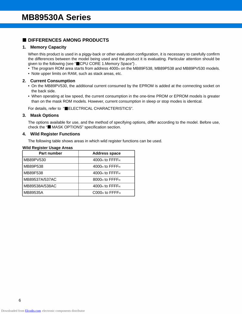
DIFFERENCES AMONG PRODUCTS1. Memory Capacity
When this product is used in a piggy-back or other evaluation configuration, it is necessary to carefully confirmthe differences between the model being used and the product it is evaluating. Particular attention should begiven to the following (see “ CPU CORE 1.Memory Space”) .• The program ROM area starts from address 4000H on the MB89F538, MB89P538 and MB89PV530 models.• Note upper limits on RAM, such as stack areas, etc.
2. Current Consumption• On the MB89PV530, the additional current consumed by the EPROM is added at the connecting socket on
the back side.• When operating at low speed, the current consumption in the one-time PROM or EPROM models is greater
than on the mask ROM models. However, current consumption in sleep or stop modes is identical.
For details, refer to “ ELECTRICAL CHARACTERISTICS”.
3. Mask Options
The options available for use, and the method of specifying options, differ according to the model. Before use,check the “ MASK OPTIONS” specification section.
4. Wild Register Functions
The following table shows areas in which wild register functions can be used.
Wild Register Usage AreasPart number Address space
MB89PV530 4000H to FFFFH
MB89P538 4000H to FFFFH
MB89F538 4000H to FFFFH
MB89537A/537AC 8000H to FFFFH
MB89538A/538AC 4000H to FFFFH
MB89535A C000H to FFFFH
Downloaded from Elcodis.com electronic components distributor
MB89530A Series
7
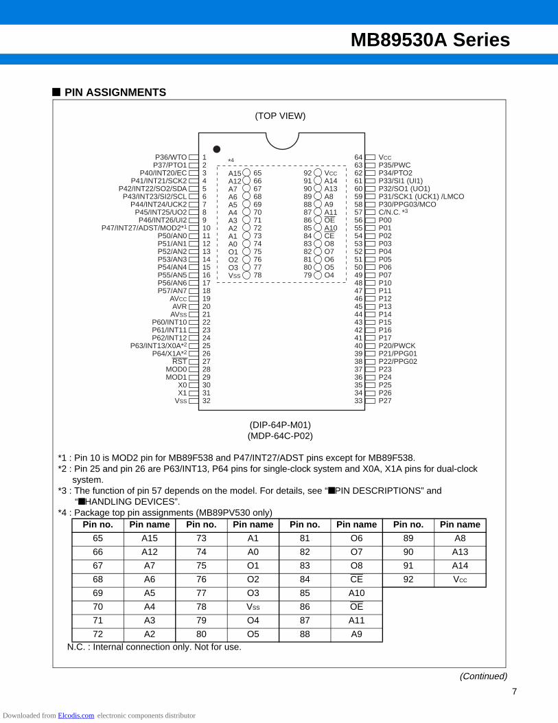
PIN ASSIGNMENTS
(Continued)
(TOP VIEW)
(DIP-64P-M01) (MDP-64C-P02)
*1 : Pin 10 is MOD2 pin for MB89F538 and P47/INT27/ADST pins except for MB89F538.*2 : Pin 25 and pin 26 are P63/INT13, P64 pins for single-clock system and X0A, X1A pins for dual-clock
system.*3 : The function of pin 57 depends on the model. For details, see “PIN DESCRIPTIONS” and
“HANDLING DEVICES”. *4 : Package top pin assignments (MB89PV530 only)
N.C. : Internal connection only. Not for use.
Pin no. Pin name Pin no. Pin name Pin no. Pin name Pin no. Pin name
65 A15 73 A1 81 O6 89 A8
66 A12 74 A0 82 O7 90 A13
67 A7 75 O1 83 O8 91 A14
68 A6 76 O2 84 CE 92 VCC
69 A5 77 O3 85 A10
70 A4 78 VSS 86 OE
71 A3 79 O4 87 A11
72 A2 80 O5 88 A9
1234567891011121314151617181920212223242526272829303132
P36/WTOP37/PTO1
P40/INT20/ECP41/INT21/SCK2
P42/INT22/SO2/SDAP43/INT23/SI2/SCL
P44/INT24/UCK2P45/INT25/UO2P46/INT26/UI2
P47/INT27/ADST/MOD2*1
P50/AN0P51/AN1P52/AN2P53/AN3P54/AN4P55/AN5P56/AN6P57/AN7
AVCCAVR
AVSSP60/INT10P61/INT11P62/INT12
P63/INT13/X0A*2
P64/X1A*2
RSTMOD0MOD1
X0X1
VSS
6463626160595857565554535251504948474645444342414039383736353433
VCCP35/PWCP34/PTO2P33/SI1 (UI1)P32/SO1 (UO1)P31/SCK1 (UCK1) /LMCOP30/PPG03/MCOC/N.C. *3
P00P01P02P03P04P05P06P07P10P11P12P13P14P15P16P17P20/PWCKP21/PPG01P22/PPG02P23P24P25P26P27
9291908988878685848382818079
6566676869707172737475767778
VCCA14A13A8A9A11OEA10CEO8O7O6O5O4
A15A12A7A6A5A4A3A2A1A0O1O2O3VSS
*4
Downloaded from Elcodis.com electronic components distributor
MB89530A Series
8
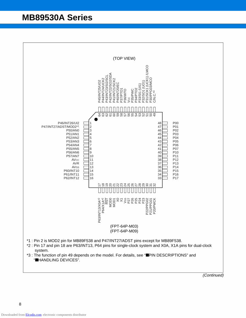
(Continued)
(TOP VIEW)
(FPT-64P-M03) (FPT-64P-M09)
*1 : Pin 2 is MOD2 pin for MB89F538 and P47/INT27/ADST pins except for MB89F538.*2 : Pin 17 and pin 18 are P63/INT13, P64 pins for single-clock system and X0A, X1A pins for dual-clock
system.*3 : The function of pin 49 depends on the model. For details, see “PIN DESCRIPTIONS” and
“HANDLING DEVICES”.
12345678910111213141516
P46/INT26/UI2P47/INT27/ADST/MOD2*1
P50/AN0P51/AN1P52/AN2P53/AN3P54/AN4P55/AN5P56/AN6P57/AN7
AVCC
AVRAVSS
P60/INT10P61/INT11P62/INT12
P00P01P02P03P04P05P06P07P10P11P12P13P14P15P16P17
48474645444342414039383736353433
64 63 62 61 60 59 58 57 56 55 54 53 52 51 50 49
17 18 19 20 21 22 23 24 25 26 27 28 29 30 31 32
P63
/INT
13/X
0A*2
P64
/X1A
*2R
ST
MO
D0
MO
D1
X0
X1
VS
S
P27
P26
P25
P24
P23
P22
/PP
G02
P21
/PP
G01
P20
/PW
CK
P45
/INT
25/U
O2
P44
/INT
24/U
CK
2P
43/IN
T23
/SI2
/SC
LP
42/IN
T22
/SO
2/S
DA
P41
/INT
21/S
CK
2P
40/IN
T20
/EC
P37
/PTO
1P
36/W
TOV
CC
P35
/PW
CP
34/P
TO2
P33
/SI1
(U
I1)
P32
/SO
1 (U
O1)
P31
/SC
K1
(UC
K1)
/LM
CO
P30
/PP
G03
/MC
OC
/N.C
.*3
Downloaded from Elcodis.com electronic components distributor

MB89530A Series
9
(Continued)
(TOP VIEW)
(FPT-64P-M06) (MQP-64C-P01)
*1 : Pin 3 is MOD2 pin for MB89F538 and P47/INT27/ADST pins except for MB89F538.*2 : Pin 18 and pin 19 are P63/INT13, P64 pins for single-clock system and X0A, X1A pins for dual-clock
system.*3 : The function of pin 50 depends on the model. For details, see “PIN DESCRIPTIONS” and “HANDLING DEVICES”. *4 : Package top pin assignments (MB89PV530 only)
N.C. : Internal connection only. Not for use.
Pin no. Pin name Pin no. Pin name Pin no. Pin name Pin no. Pin name65 N.C. 73 A2 81 N.C. 89 OE
66 A15 74 A1 82 O4 90 N.C.
67 A12 75 A0 83 O5 91 A11
68 A7 76 N.C. 84 O6 92 A9
69 A6 77 O1 85 O7 93 A8
70 A5 78 O2 86 O8 94 A13
71 A4 79 O3 87 CE 95 A14
72 A3 80 VSS 88 A10 96 VCC
12345678910111213141516171819
P30/PPG03/MCOC/N.C.P00P01P02P03P04P05P06P07P10P11P12P13P14P15P16P17P20/PWCK
51504948474645444342414039383736353433
P45/INT25/UO2P46/INT26/UI2
P47/INT27/ADST/MOD2*1
P50/AN0P51/AN1P52/AN2P53/AN3P54/AN4P55/AN5P56/AN6P57/AN7
AVCCAVR
AVSSP60/INT10P61/INT11P62/INT12
P63/INT13/X0A*2
P64/X1A*2
64 63 62 61 60 59 58 57 56 55 54 53 52
RS
TM
OD
0M
OD
1X
0X
1V
SS
P27
P26
P25
P24
P23
P22
/PP
G02
P21
/PP
G01
94 95 96 65 66 67 68
84 83 82 81 80 79 78
20 21 22 23 24 25 26 27 28 29 30 31 32
P44
/INT
24/U
CK
2P
43/IN
T23
/SI2
/SC
LP
42/IN
T22
/SO
2/S
DA
P41
/INT
21/S
CK
2P
40/IN
T20
/EC
P37
/PTO
1P
36/W
TOV
CC
P35
/PW
CP
34/P
TO2
P33
/SI1
(U
1)P
32/S
O1/
(U
O1)
P31
/SC
K1
(UC
K1)
/LM
CO
858687888990919293
777675747372717069
*4*3
Downloaded from Elcodis.com electronic components distributor

MB89530A Series
10
PIN DESCRIPTIONS
(Continued)
Pin no.Pin name
I/Ocircuittype
FunctionSH-DIP*1
MDIP*2QFP*3
MQFP*4LQFP*5
QFP*6
30 23 22 X0A
Connecting pins to crystal oscillator circuit or other os-cillator circuit. The X0 pin can connect to an external clock. In that case, X1 is left open.31 24 23 X1
28 21 20 MOD0B
Input pins for memory access mode setting. Connect directly to Vss.29 22 21 MOD1
27 20 19 RST C
Reset I/O pin. This pin has pull-up resistance with CMOS I/O or hysteresis input. At an internal reset re-quest, an ’L’ signal is output. An ’L’ level input initializes the internal circuits.
56 to 49 49 to 42 48 to 41 P00 to P07 D General purpose I/O ports.
48 to 41 41 to 34 40 to 33 P10 to P17 D General purpose I/O ports.
40 33 32 P20/PWCK EGeneral purpose I/O port.Resource I/O pin (hysteresis input).Hysteresis input. This pin also functions as a PWC input.
39 32 31P21/
PPG01D
General purpose I/O port.This pin also functions as the PPG01 output.
38 31 30P22/
PPG02D
General purpose I/O port.This pin also functions as the PPG02 output.
37 30 29 P23 D General purpose I/O port.
36 29 28 P24 D General purpose I/O port.
35 28 27 P25 D General purpose I/O port.
34 27 26 P26 D General purpose I/O port.
33 26 25 P27 D General purpose I/O port.
58 51 50P30/
PPG03/MCO
DGeneral purpose I/O port.This pin also functions as the PPG03 output.
59 52 51P31/SCK1 (UCK1) /LMCO
EGeneral purpose I/O port.Resource I/O pin (hysteresis input).This pin also functions as the UART/SIO clock in-put/output pin.
60 53 52P32/SO1
(UO1) D
General purpose I/O port.This pin also functions as the UART/SIO data output pin.
61 54 53P33/SI1
(UI1) E
General purpose I/O port.Resource input/output pin (hysteresis input).This pin also functions as the UART/SIO serial data input pin.
62 55 54 P34/PTO2 DGeneral purpose I/O port.This pin also functions as the PWM timer 2 output pin.
63 56 55 P35/PWC EGeneral purpose I/O port.Resource I/O pin (hysteresis input).This pin also functions as a PWC input.
Downloaded from Elcodis.com electronic components distributor
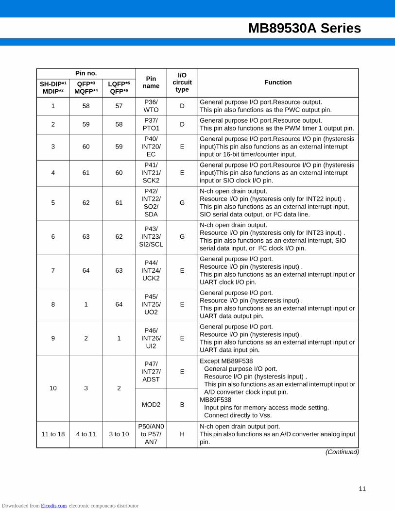
MB89530A Series
11
(Continued)
Pin no.Pin
name
I/Ocircuittype
FunctionSH-DIP*1
MDIP*2QFP*3
MQFP*4LQFP*5
QFP*6
1 58 57P36/WTO
DGeneral purpose I/O port.Resource output.This pin also functions as the PWC output pin.
2 59 58P37/
PTO1D
General purpose I/O port.Resource output.This pin also functions as the PWM timer 1 output pin.
3 60 59P40/
INT20/EC
EGeneral purpose I/O port.Resource I/O pin (hysteresis input)This pin also functions as an external interrupt input or 16-bit timer/counter input.
4 61 60P41/
INT21/SCK2
EGeneral purpose I/O port.Resource I/O pin (hysteresis input)This pin also functions as an external interrupt input or SIO clock I/O pin.
5 62 61
P42/INT22/SO2/SDA
G
N-ch open drain output.Resource I/O pin (hysteresis only for INT22 input) .This pin also functions as an external interrupt input, SIO serial data output, or I2C data line.
6 63 62P43/
INT23/SI2/SCL
G
N-ch open drain output.Resource I/O pin (hysteresis only for INT23 input) .This pin also functions as an external interrupt, SIO serial data input, or I2C clock I/O pin.
7 64 63P44/
INT24/UCK2
E
General purpose I/O port.Resource I/O pin (hysteresis input) .This pin also functions as an external interrupt input or UART clock I/O pin.
8 1 64P45/
INT25/UO2
E
General purpose I/O port.Resource I/O pin (hysteresis input) .This pin also functions as an external interrupt input or UART data output pin.
9 2 1P46/
INT26/UI2
E
General purpose I/O port.Resource I/O pin (hysteresis input) .This pin also functions as an external interrupt input or UART data input pin.
10 3 2
P47/INT27/ADST
E
Except MB89F538General purpose I/O port.Resource I/O pin (hysteresis input) .This pin also functions as an external interrupt input or A/D converter clock input pin.
MB89F538Input pins for memory access mode setting. Connect directly to Vss.
MOD2 B
11 to 18 4 to 11 3 to 10P50/AN0 to P57/
AN7H
N-ch open drain output port.This pin also functions as an A/D converter analog input pin.
Downloaded from Elcodis.com electronic components distributor
MB89530A Series
12
(Continued)
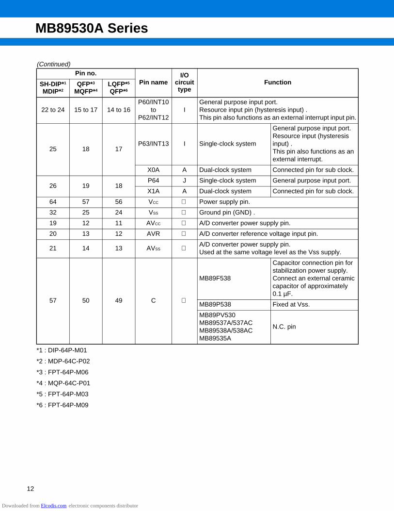
*1 : DIP-64P-M01
*2 : MDP-64C-P02
*3 : FPT-64P-M06
*4 : MQP-64C-P01
*5 : FPT-64P-M03
*6 : FPT-64P-M09
Pin no.Pin name
I/Ocircuittype
FunctionSH-DIP*1
MDIP*2QFP*3
MQFP*4LQFP*5
QFP*6
22 to 24 15 to 17 14 to 16P60/INT10
to P62/INT12
IGeneral purpose input port.Resource input pin (hysteresis input) .This pin also functions as an external interrupt input pin.
25 18 17P63/INT13 I Single-clock system
General purpose input port.Resource input (hysteresis input) .This pin also functions as an external interrupt.
X0A A Dual-clock system Connected pin for sub clock.
26 19 18P64 J Single-clock system General purpose input port.
X1A A Dual-clock system Connected pin for sub clock.
64 57 56 VCC Power supply pin.
32 25 24 VSS Ground pin (GND) .
19 12 11 AVCC A/D converter power supply pin.
20 13 12 AVR A/D converter reference voltage input pin.
21 14 13 AVSS A/D converter power supply pin. Used at the same voltage level as the Vss supply.
57 50 49 C
MB89F538
Capacitor connection pin for stabilization power supply. Connect an external ceramic capacitor of approximately 0.1 µF.
MB89P538 Fixed at Vss.
MB89PV530MB89537A/537ACMB89538A/538ACMB89535A
N.C. pin
Downloaded from Elcodis.com electronic components distributor
MB89530A Series
13
External EPROM Socket Pin Function Descriptions (MB89PV530 only)
*1 : MDP-64C-P02
*2 : MQP-64C-P01
Pin no.Pin name I/O Circuit
type FunctionMDIP*1 MQFP*2
65666768697071727374
66676869707172737475
A15A12A7A6A5A4A3A2A1A0
O Address output pins.
757677
777879
O1O2O3
I Data input pins
78 80 VSS O Power supply pin (GND) .
7980818283
8283848586
O4O5O6O7O8
I Data input pins.
84 87 CE OROM chip enable pin. Outputs an “H” level signal in standby mode.
85 88 A10 O Address output pin.
86 89 OE OROM output enable pin. Outputs “L” at all times.
878889
919293
A11A9A8
O
Address output pins.90 94 A13 O
91 95 A14 O
92 96 VCC O EPROM power supply pin.
65768190
N.C. OInternally connected. These pins always left open.
Downloaded from Elcodis.com electronic components distributor

MB89530A Series
14
I/O CIRCUIT TYPES
(Continued)
Type Circuit Remarks
A
Oscillator feedback resistance• High speed side = approx. 1 MΩ• Low speed side = approx. 10 MΩ
B
• Hysteresis input• Pull-down resistance built-in to
MB89535AMB89537A/537ACMB89538A/538AC
C
• Pull-up resistance approx. 50 kΩ• Hysteresis input
D
• CMOS I/O• Software pull-up resistance can be
used. Approx. 50 kΩ
E
• CMOS I/O• Software pull-up resistance can be
used. Approx. 50 kΩ
Nch
Nch
X1 (X1A)
X0 (X0A) Pch
Pch
R
Pch
Nch
Pch
Pch
Nch
R Pull-up control resistor
Pch
Pch
Nch
R Pull-up control resistors
Port inputResource input
Downloaded from Elcodis.com electronic components distributor

MB89530A Series
15
(Continued)Type Circuit Remarks
G
• N-ch open drain output• Hysteresis input• CMOS input
H
• N-ch open drain output• Analog input (A/D converter)
I
• Hysteresis input• CMOS input• Software pull-up resistance can be
used. Approx. 50 kΩ
J
• CMOS input• Software pull-up resistance can be
used. Approx. 50 kΩ
Nch
Resource inputPort input
Nch
Pch
Analog input
PchR
Pull-up control resistors
Port
Resource
PchR
Pull-up control resistors
Port
Downloaded from Elcodis.com electronic components distributor

MB89530A Series
16
HANDLING DEVICES1.Preventing Latchup
Care must be taken to ensure that maximum voltage ratings are not exceeded (to prevent latchup) . When CMOSintegrated circuit devices are subjected to applied voltages higher than Vcc at input and output pins (other thanmedium- and high-withstand voltage pins), or to voltages lower than Vss, as well as when voltages in excess ofrated levels are applied between Vcc and Vss, the phenomenon known as latchup can occur.
When a latchup condition occurs, supply current can increase dramatically and may destroy semiconductorelements. In using semiconductor devices, always take sufficient care to avoid exceeding maximum ratings.
Also when switching power on or off to analog systems, care must be taken that analog power supplies (AVCC,AVR) and analog input signals do not exceed the level of the digital power supply.
2.Power Supply Voltage Fluctuations
Even within the warranted operating range of the Vcc supply voltage, sudden changes in supply voltage cancause abnormal operation. As a measure for stability, it is recommended that the Vcc ripple fluctuation (peak topeak value) should be kept within 10% of the reference Vcc value on commercial power supply (50 Hz-60 Hz),and instantaneous voltage fluctuations such as at power-on and shutdown should be kept within a transientvariability limit of 0.1V/ms.
3.Treatment of Unused Input Pins
If unused input pins are left open, abnormal operation may result. Any unused input pins should be connectedto pull-up or pull-down resistance.
4. Treatment of N.C. Pins
Any pins marked ’NC’ (not connected) must be left open.
5. Treatment of Power Supply Pins on Models with Built-in A/D Converter
Even when A/D converters are not in use, pins should be connected so that AVCC = VCC, and AVSS = AVR = VSS.
6. Precautions for Use of External Clock
Even when an external clock signal is used, an oscillator stabilization wait period is used after a power-on reset,or escape from sub clock mode or stop mode.
7. Execution of Programs on RAM
Debugging of programs executed on RAM cannot be performed even when using the MB89PV530.
8. Wild Register Functions
Wild registers cannot be debugged with the MB89PV530 and tools. To verify operations, actual in-device testingon the MB89P538 or MB89F538 is advised.
Downloaded from Elcodis.com electronic components distributor
MB89530A Series
17
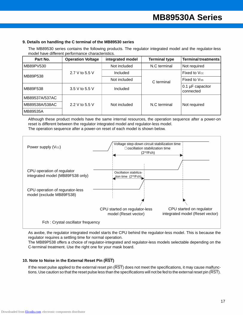
9. Details on handling the C terminal of the MB89530 series
The MB89530 series contains the following products. The regulator integrated model and the regulator-lessmodel have different performance characteristics.
Although these product models have the same internal resources, the operation sequence after a power-onreset is different between the regulator integrated model and regulator-less model.The operation sequence after a power-on reset of each model is shown below.
As avobe, the regulator integrated model starts the CPU behind the regulator-less model. This is because theregulator requires a settling time for normal operation.The MB89P538 offers a choice of regulator-integrated and regulator-less models selectable depending on theC-terminal treatment. Use the right one for your mask board.
10. Note to Noise in the External Reset Pin (RST )
If the reset pulse applied to the external reset pin (RST) does not meet the specifications, it may cause malfunc-tions. Use caution so that the reset pulse less than the specifications will not be fed to the external reset pin (RST).
Part No. Operation Voltage integrated model Terminal type Terminal treatments
MB89PV530
2.7 V to 5.5 V
Not included N.C terminal Not required
MB89P538Included
C terminal
Fixed to VCC
Not included Fixed to VSS
MB89F538 3.5 V to 5.5 V Included0.1 µF capacitor connected
MB89537A/537AC
2.2 V to 5.5 V Not included N.C terminal Not requiredMB89538A/538AC
MB89535A
Power supply (VCC)
CPU operation of regulator integrated model (MB89F538 only)
CPU operation of regurator-less model (exclude MB89F538)
Voltage step-down circuit stabilization time + oscillation stabilization time
(219/Fch)
Oscillation stabiliza-tion time (218/Fch)
CPU started on regulator-less model (Reset vector)
CPU started on regulator integrated model (Reset vector)
Fch : Crystal oscillator frequency
Downloaded from Elcodis.com electronic components distributor

MB89530A Series
18
PROGRAMMING AND ERASING FLASH MEMORY ON THE MB89F5381. Flash Memory
The flash memory is located between 4000H and FFFFH in the CPU memory map and incorporates a flashmemory interface circuit that allows read access and program access from the CPU to be performed in the sameway as mask ROM. Programming and erasing flash memory is also performed via the flash memory interfacecircuit by executing instructions in the CPU. This enables the flash memory to be updated in place under thecontrol of the CPU, providing an efficient method of updating program and data.
2. Flash Memory Features• 48 K byte × 8-bit configuration (16 K + 8 K + 8 K + 16 K sectors) • Automatic programming algorithm (Embedded algorithm* : Equivalent to MBM29LV200) • Includes an erase pause and restart function• Data polling and toggle bit for detection of program/erase completion• Detection of program/erase completion via CPU interrupt• Compatible with JEDEC-standard commands• Sector Protection (sectors can be combined in any combination) • No. of program/erase cycles : 10,000 (Min)
*: Embedded Algorithm is a trademark of Advanced Micro Devices.
3. Procedure for Programming and Erasing Flash Memory
Programming and reading flash memory cannot be performed at the same time. Accordingly, to program orerase flash memory, the program must first be copied from flash memory to RAM so that programming can beperformed without program access from flash memory.
4. Flash Memory Register• Control status register (FMCS)
5. Sector Configuration
The table below shows the sector configuration of flash memory and lists the addresses of each sector for bothduring CPU access a flash memory programming.
• Sector configuration of flash memory
* : Programmer addressThe programmer address is the address to be used instead of the CPU address when programming data from a parallel flash memory programmer. Use the programmer address on programming or erasing using a general-purpose parallel programmer.
Flash Memory CPU Address Programmer Address*
16 K bytes FFFFH to C000H 1FFFFH to 1C000H
8 K bytes BFFFH to A000H 1BFFFH to 1A000H
8 K bytes 9FFFH to 8000H 19FFFH to 18000H
16 K bytes 7FFFH to 4000H 17FFFH to 14000H
R R/W R/W
RDY
bit7 bit6 bit5 bit4 bit3 bit2 bit1 bit0
007AH
Address
000X00-0B
Initial value
Reserved Reserved Reserved
R/W R/WR/WR/W
INTE RDYINT WE
Downloaded from Elcodis.com electronic components distributor
MB89530A Series
19
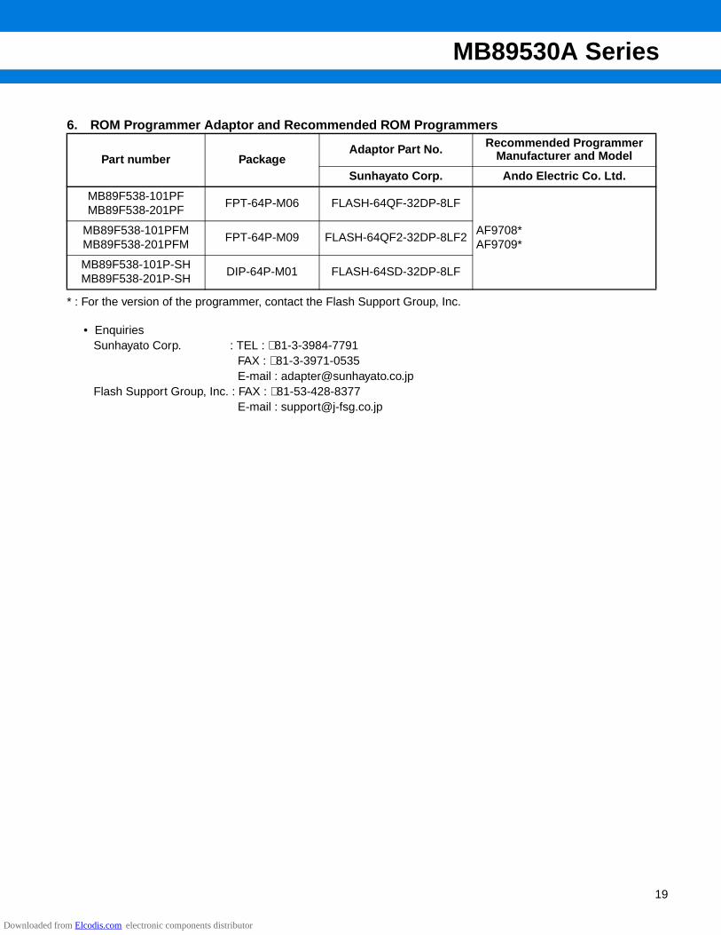
6. ROM Programmer Adaptor and Recommended ROM Programmers
* : For the version of the programmer, contact the Flash Support Group, Inc.
• EnquiriesSunhayato Corp. : TEL : +81-3-3984-7791
FAX : +81-3-3971-0535E-mail : [email protected]
Flash Support Group, Inc. : FAX : +81-53-428-8377E-mail : [email protected]
Part number PackageAdaptor Part No. Recommended Programmer
Manufacturer and Model
Sunhayato Corp. Ando Electric Co. Ltd.
MB89F538-101PFMB89F538-201PF
FPT-64P-M06 FLASH-64QF-32DP-8LF
AF9708*AF9709*
MB89F538-101PFMMB89F538-201PFM
FPT-64P-M09 FLASH-64QF2-32DP-8LF2
MB89F538-101P-SHMB89F538-201P-SH
DIP-64P-M01 FLASH-64SD-32DP-8LF
Downloaded from Elcodis.com electronic components distributor
MB89530A Series
20
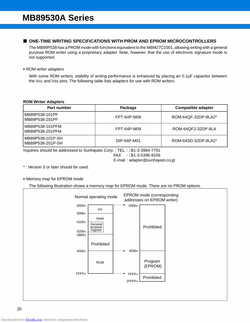
ONE-TIME WRITING SPECIFICATIONS WITH PROM AND EPROM MICROCONTROLLERSThe MB89P538 has a PROM mode with functions equivalent to the MBM27C1001, allowing writing with a generalpurpose ROM writer using a proprietary adapter. Note, however, that the use of electronic signature mode isnot supported.
•••• ROM writer adapters
With some ROM writers, stability of writing performance is enhanced by placing an 0.1µF capacitor betweenthe Vcc and Vss pins. The following table lists adapters for use with ROM writers.
ROM Writer Adapters
Inquiries should be addressed to Sunhayato Corp. : TEL : +81-3-3984-7791FAX : +81-3-5396-9106E-mail : [email protected]
* : Version 3 or later should be used.
•••• Memory map for EPROM mode
The following illustration shows a memory map for EPROM mode. There are no PROM options.
Part number Package Compatible adapter
MB89P538-101PFMB89P538-201PF
FPT-64P-M06 ROM-64QF-32DP-8LA2*
MB89P538-101PFMMB89P538-201PFM
FPT-64P-M09 ROM-64QF2-32DP-8LA
MB89P538-101P-SHMB89P538-201P-SH
DIP-64P-M01 ROM-64SD-32DP-8LA2*
4000H
FFFFH
1FFFFH
0000H 0000H
RAM
ROM
I/O0080H
4000H
0880H
FFFFH
0200H
0100HGeneralpurposeregister
Normal operating mode
Prohibited
EPROM mode (corresponding addresses on EPROM writer)
Program (EPROM)
Prohibited
Prohibited
Downloaded from Elcodis.com electronic components distributor
MB89530A Series
21
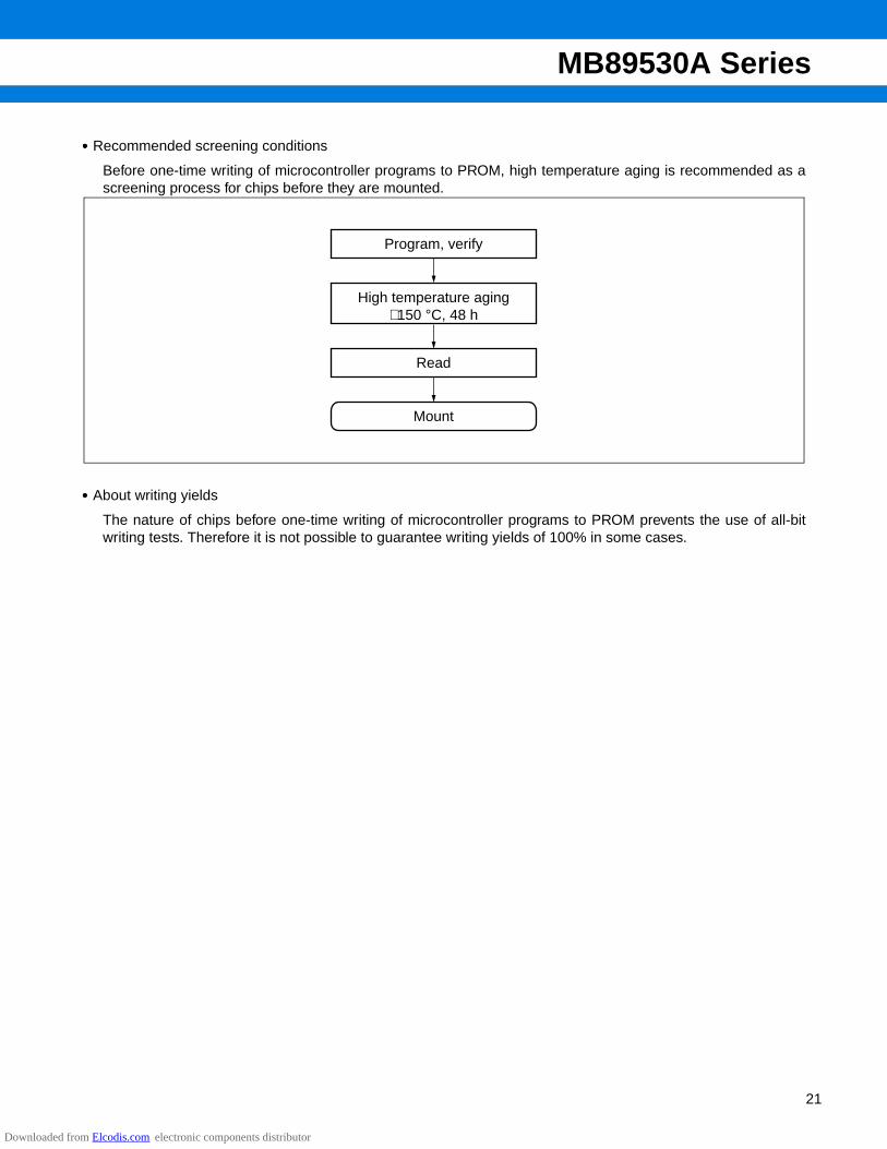
•••• Recommended screening conditions
Before one-time writing of microcontroller programs to PROM, high temperature aging is recommended as ascreening process for chips before they are mounted.
•••• About writing yields
The nature of chips before one-time writing of microcontroller programs to PROM prevents the use of all-bitwriting tests. Therefore it is not possible to guarantee writing yields of 100% in some cases.
Program, verify
High temperature aging+150 °C, 48 h
Read
Mount
Downloaded from Elcodis.com electronic components distributor
MB89530A Series
22
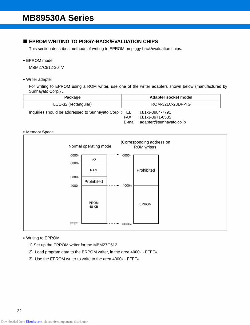
EPROM WRITING TO PIGGY-BACK/EVALUATION CHIPSThis section describes methods of writing to EPROM on piggy-back/evaluation chips.
•••• EPROM model
MBM27C512-20TV
•••• Writer adapter
For writing to EPROM using a ROM writer, use one of the writer adapters shown below (manufactured bySunhayato Corp.) .
Inquiries should be addressed to Sunhayato Corp. : TEL : +81-3-3984-7791FAX : +81-3-3971-0535E-mail : [email protected]
•••• Memory Space
•••• Writing to EPROM
1) Set up the EPROM writer for the MBM27C512.
2) Load program data to the ERPOM writer, in the area 4000H - FFFFH.
3) Use the EPROM writer to write to the area 4000H - FFFFH.
Package Adapter socket model
LCC-32 (rectangular) ROM-32LC-28DP-YG
4000H
FFFFH
0000H 0000H
RAM
PROM48 KB
EPROM
I/O0080H
4000H
FFFFH
0880H
Normal operating mode
Prohibited
(Corresponding address onROM writer)
Prohibited
Downloaded from Elcodis.com electronic components distributor
MB89530A Series
23
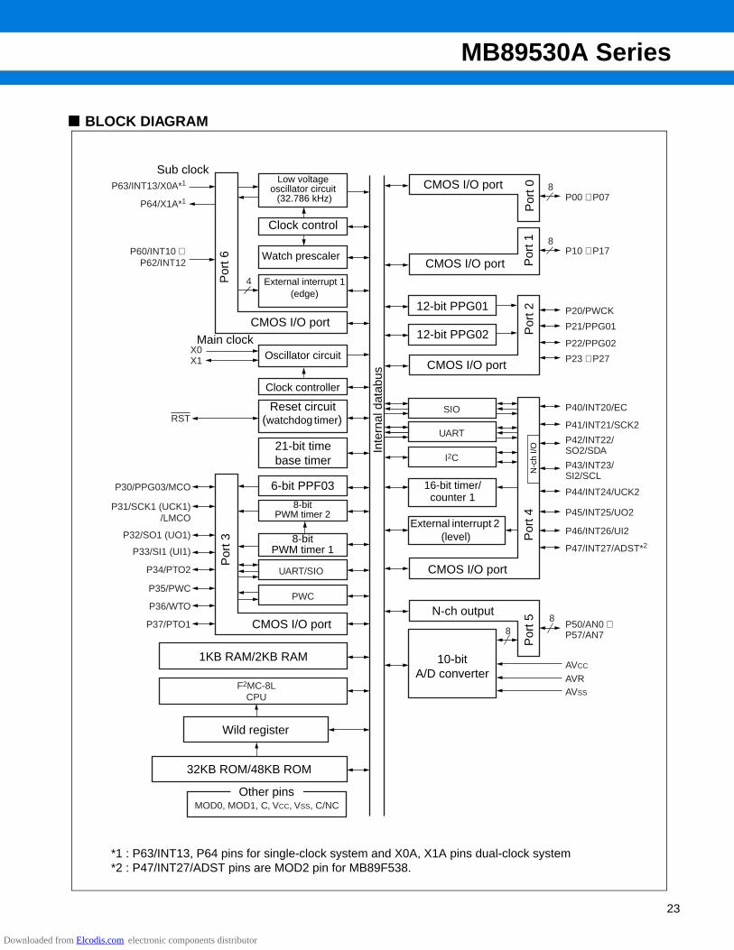
BLOCK DIAGRAM
4
P63/INT13/X0A*1
P64/X1A*1
P60/INT10 ∼ P62/INT12
X0X1
RST
P30/PPG03/MCO
P32/SO1 (UO1)
P34/PTO2
P35/PWC
P36/WTO
P37/PTO1
P33/SI1 (UI1)
P31/SCK1 (UCK1)/LMCO
F2MC-8LCPU
MOD0, MOD1, C, VCC, VSS, C/NC
PWC
UART/SIO
8
8
P00 ∼ P07
P10 ∼ P17
P20/PWCK
P21/PPG01
P22/PPG02
P40/INT20/EC
P41/INT21/SCK2
P44/INT24/UCK2
P45/INT25/UO2
P46/INT26/UI2
P47/INT27/ADST*2
P50/AN0 ∼ P57/AN7
AVCC
AVRAVSS
P43/INT23/SI2/SCL
P42/INT22/SO2/SDA
P23 ∼ P27
88
SIO
UART
I2C
Sub clock
Main clock
Low voltage oscillator circuit (32.786 kHz)
Clock control
Watch prescaler
External interrupt 1 (edge)
CMOS I/O port
Oscillator circuit
Clock controller
Reset circuit (watchdog timer)
21-bit time base timer
6-bit PPF03
8-bit PWM timer 2
8-bit PWM timer 1
CMOS I/O port
1KB RAM/2KB RAM
Wild register
32KB ROM/48KB ROM
Other pins
CMOS I/O port
CMOS I/O port
12-bit PPG01
12-bit PPG02
CMOS I/O port
16-bit timer/counter 1
External interrupt 2 (level)
N-c
h I/O
CMOS I/O port
N-ch output
10-bit A/D converter
Por
t 6
Por
t 0P
ort 1
Por
t 2P
ort 4
Por
t 3
Por
t 5
Inte
rnal
dat
abus
*1 : P63/INT13, P64 pins for single-clock system and X0A, X1A pins dual-clock system*2 : P47/INT27/ADST pins are MOD2 pin for MB89F538.
Downloaded from Elcodis.com electronic components distributor

MB89530A Series
24
CPU CORE1. Memory Space
The MB89530A series has 64 KB of memory space, containing all I/O, data areas, and program areas. The I/Oarea is located at the lowest addresses, with the data area placed immediately above. The data area can bepartitioned into register areas, stack areas, or direct access areas depending on the application. The programarea is located at the opposite end of memory, closest to the highest addresses, and the highest part of thisarea is assigned to the tables of interrupt and reset vectors and vector call instructions. The following diagramshows the structure of memory space in the MB89530A series.
•••• Memory Map
0000H
RAM
ROM
I/O0080H
0C80H
0480H
FFFFH
0200H
0100H
0C91H
8000H
FFC0H
0000H
RAM
MB89537A/537AC
0000H
RAM
ROM
I/O0080H
0C80H
0280H
FFFFH
0200H
0100H
0C91H
C000H
FFC0H
MB89535A
MB89PV530MB89P538/F538
MB89538A/538AC
ROM
I/O0080H
0C80H
0880H
FFFFH
0200H
0100H
0C91H
4000H
FFC0H
Generalpurposeregister
Generalpurposeregister
Generalpurposeregister
Open
Wild register
Open
Vector tables*2
Open
Wild register
Open
Vector tables*2
*1 : The external ROM area is on the MB89PV530 only.*2 : Vector tables (reset, interrupt, vector call instructions)
External ROM*1
Open
Wild register
Open
Vector tables*2
Downloaded from Elcodis.com electronic components distributor
MB89530A Series
25
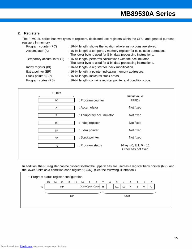
2. Registers
The F2MC-8L series has two types of registers, dedicated-use registers within the CPU, and general-purposeregisters in memory.
In addition, the PS register can be divided so that the upper 8 bits are used as a register bank pointer (RP), andthe lower 8 bits as a condition code register (CCR). (See the following illustration.)
Program counter (PC) : 16-bit length, shows the location where instructions are stored.Accumulator (A) : 16-bit length, a temporary memory register for calculation operations.
The lower byte is used for 8-bit data processing instructions.Temporary accumulator (T) : 16-bit length, performs calculations with the accumulator.
The lower byte is used for 8-bit data processing instructions.Index register (IX) : 16-bit length, a register for index modification.Extra pointer (EP) : 16-bit length, a pointer indicating memory addresses.Stack pointer (SP) : 16-bit length, indicates stack areas.Program status (PS) : 16-bit length, contains register pointer and condition code.
PC
A
T
IX
EP
SP
PS
16 bits
: Program counter
: Accumulator
: Temporary accumulator
: Index register
: Extra pointer
: Stack pointer
: Program status
FFFDH
Initial value
Not fixed
Not fixed
Not fixed
Not fixed
Not fixed
I-flag = 0, IL1, 0 = 11Other bits not fixed
• Program status register configuration
PS
RP CCR
15 14 13 12 11 10 9 8 7 6 5 4 3 2 1 0
RP H I IL1 IL0 N Z V COpen Open Open
Downloaded from Elcodis.com electronic components distributor

MB89530A Series
26
The RP register shows the address of the register bank currently being used, so that the RP value and the actualaddress are related by the conversion rule shown in the following illustration.
The CCR register has bits that show the content of results of calculations and transferred data, and bits thatcontrol CPU operation during interrupts.
In addition, the following general purpose registers are available.
General purpose registers: 8-bit length, used to contain data.
The general purpose registers are 8-bit registers located in memory. There are eight such registers per bank,and the MB89530A series have up to 32 banks for use. The bank currently in use is indicated by the registerbank pointer (RP).
H-flag : Set to 1 if calculations result in carry or borrow operations from bit 3 to bit 4, otherwise set to 0. This flag is used for decimal correction instructions.
I-flag : This flag is set to 1 if interrupts are enabled, and 0 if interrupts are prohibited. The default value at reset is 0.
IL1, 0 : Indicates the level of the currently permitted interrupts. Only interrupt requests having a more powerful level than the value of these bits will be processed.
IL1 IL0 Interrupt level Strength
0 01
Strong
Weak
0 1
1 0 2
1 1 3
N-flag : Set to 1 if the highest bit is 1 after a calculation, otherwise cleared to 0.Z-flag : Set to 1 if a calculation result is 0, otherwise cleared to 0.V-flag : Set to 1 if a two’s complement overflow results during a calculation, otherwise cleared to 0.C-flag : Set to 1 if a calculation results in a carry or borrow operation from bit 7, otherwise cleared to 0.
This is also the shift-out value in a shift instruction.
• General purpose register area real address conversion principle
"0" "0" "0" "0" "0" "0" "0" "1" R4 R3 R2 R1 R0 b2 b1 b0
A7 A6 A5 A4 A3 A2 A1 A0A15 A14 A13 A12 A11 A10 A9 A8Address generated
RP upperOperation code
lower
Downloaded from Elcodis.com electronic components distributor

MB89530A Series
27
•Register bank configuration
R0
R1
R2
R3
R4
R5
R6
R7
Address at this location = 0100H + 8 × (RP)
Memory area
32 banks
Downloaded from Elcodis.com electronic components distributor

MB89530A Series
28
I/O MAP
(Continued)
Address Register name Register description Write/Read Initial value
00H PDR0 Port 0 data register R/W XXXXXXXXB
01H DDR0 Port 0 direction register W 0 0 0 0 0 0 0 0B
02H PDR1 Port 1 data register R/W XXXXXXXXB
03H DDR1 Port 1 direction register W 0 0 0 0 0 0 0 0B
04H to 06H (Reserved area)
07H SYCC System clock control register R/W X -1 MM1 0 0B
08H STBC Standby control register R/W 0 0 0 1 0 - - -B
09H WDTC Watchdog control register R/W 0 - - - XXXXB
0AH TBTC Time base timer control register R/W 0 0 - - - 0 0 0B
0BH WPCR Watch prescaler control register R/W 0 0 - - 0 0 0 0B
0CH PDR2 Port 2 data register R/W XXXXXXXXB
0DH DDR2 Port 2 direction register R/W 0 0 0 0 0 0 0 0B
0EH PDR3 Port 3 data register R/W XXXXXXXXB
0FH DDR3 Port 3 direction register R/W 0 0 0 0 0 0 0 0B
10H PDR4 Port 4 data register R/W XXXX 1 1 XXB
11H DDR4 Port 4 direction register R/W 0 0 0 0 - - 0 0B
12H PDR5 Port 5 data register R/W 1 1 1 1 1 1 1 1 B
13H PDR6 Port 6 data register R XXXXXXXXB
14H to 21H (Reserved area)
22H SMC11 Serial mode control register 1 (UART) R/W 0 0 0 0 0 0 0 0B
23H SRC1 Serial rate control register (UART) R/W - - 0 1 1 0 0 0B
24H SSD1 Serial status and data register (UART) R/W 0 0 1 0 0 - 1XB
25HSIDR1/SODR1
Serial input/output data register (UART) R/W XXXXXXXXB
26H SMC12 Serial mode control register 2 (UART) R/W - - 1 0 0 0 0 1B
27H CNTR1 PWM control register 1 R/W 0 0 0 0 0 0 0 0B
28H CNTR2 PWM control register 2 R/W 0 0 0 - 0 0 0 0B
29H CNTR3 PWM control register 3 R/W - 0 0 0 - - - -B
2AH COMR1 PWM compare register 1 W XXXXXXXXB
2BH COMR2 PWM compare register 2 W XXXXXXXXB
2CH PCR1 PWC pulse width control register 1 R/W 0 0 0 - - 0 0 0B
2DH PCR2 PWC pulse width control register 2 R/W 0 0 0 0 0 0 0 0B
2EH RLBR PWC reload buffer register R/W XXXXXXXXB
2FH SMC21 Serial mode control register 1 (UART/SIO) R/W 0 0 0 0 0 0 0 0B
30H SMC22 Serial mode control register 2 (UART/SIO) R/W 0 0 0 0 0 0 0 0B
31H SSD2 Serial status and data register (UART/SIO) R/W 0 0 0 0 1 - - -B
32HSIDR2/SODR2
Serial data register (UART/SIO) R/W XXXXXXXXB
33H SRC2 Baud rate generator reload register R/W XXXXXXXXB
Downloaded from Elcodis.com electronic components distributor

MB89530A Series
29
(Continued)
Address Register name Register description Write/Read Initial value
34H ADC1 A/D control register 1 R/W 0 0 0 0 0 0 - 0B
35H ADC2 A/D control register 2 R/W - 0 0 0 0 0 0 1B
36H ADDL A/D data register low R/W XXXXXXXXB
37H ADDH A/D data register high R/W - - - - - - 0 0B
38H PPGC2 PPG2 control register (12-bit PPG) R/W 0 0 0 0 0 0 0 0B
39H PRL22 PPG2 reload register 2 (12-bit PPG) R/W 0X0 0 0 0 0 0B
3AH PRL21 PPG2 reload register 1 (12-bit PPG) R/W XX0 0 0 0 0 0B
3BH PRL23 PPG2 reload register 3 (12-bit PPG) R/W XX0 0 0 0 0 0B
3CH TMCR 16-bit timer control register R/W - - 0 0 0 0 0 0B
3DH TCHR 16-bit timer counter register high R/W 0 0 0 0 0 0 0 0B
3EH TCLR 16-bit timer counter register low R/W 0 0 0 0 0 0 0 0B
3FH EIC1 External interrupt 1 control register 1 R/W 0 0 0 0 0 0 0 0B
40H EIC2 External interrupt 1 control register 2 R/W 0 0 0 0 0 0 0 0B
41H to 48H (Reserved area)
49H DDCR DDC select register R/W - - - - - - - 0B
4AH to 4BH (Reserved area)
4CH PPGC1 PPG1 control register (12-bit PPG) R/W 0 0 0 0 0 0 0 0B
4DH PRL12 PPG1 reload register 2 (12-bit PPG) R/W 0X0 0 0 0 0 0B
4EH PRL11 PPG1 reload register 1 (12-bit PPG) R/W XX0 0 0 0 0 0B
4FH PRL13 PPG1 reload register 3 (12-bit PPG) R/W XX0 0 0 0 0 0B
50H IACR I2C address control register R/W - - - - - 0 0 0B
51H IBSR I2C bus status register R 0 0 0 0 0 0 0 0B
52H IBCR I2C bus control register R/W 0 0 0 0 0 0 0 0B
53H ICCR I2C clock control register R/W 0 0 0 XXXXXB
54H IADR I2C address register R/W - XXXXXXXB
55H IDAR I2C data register R/W XXXXXXXXB
56H EIE2 External interrupt 2 control register R/W 0 0 0 0 0 0 0 0B
57H EIF2 External interrupt 2 flag register R/W - - - - - - - 0B
58H RCR1 6-bit PPG control register 1 R/W 0 0 0 0 0 0 0 0B
59H RCR2 6-bit PPG control register 2 R/W 0X0 0 0 0 0 0B
5AH CKR Clock output control register R/W - - - - - - 0 0B
5BH to 6FH (Reserved area)
70H SMR Serial mode register (SIO) R/W 0 0 0 0 0 0 0 0B
71H SDR Serial data register (SIO) R/W XXXXXXXXB
72H PURR0 Port 0 pull-up resistance register R/W 1 1 1 1 1 1 1 1 B
73H PURR1 Port 1 pull-up resistance register R/W 1 1 1 1 1 1 1 1 B
74H PURR2 Port 2 pull-up resistance register R/W 1 1 1 1 1 1 1 1 B
75H PURR3 Port 3 pull-up resistance register R/W 1 1 1 1 1 1 1 1 B
76H PURR4 Port 4 pull-up resistance register R/W 1 1 1 1 - -1 1 B
77H WREN Wild register enable register R/W - - 0 0 0 0 0 0B
Downloaded from Elcodis.com electronic components distributor

MB89530A Series
30
(Continued)
• Description of write/read symbols :
• Description of initial values :
Note : Do not use reserved spaces.
Address Register name Register description Write/Read Initial value
78H WROR Wild register data test register R/W - - 0 0 0 0 0 0B
79H PURR6 Port 6 pull-up resistance register R/W - - - 1 1 1 1 1 B
7AH FMCS Flash memory control status resister R/W 0 0 0 0 0 0 - 0B
7BH ILR1 Interrupt level setting register 1 W 1 1 1 1 1 1 1 1B
7CH ILR2 Interrupt level setting register 2 W 1 1 1 1 1 1 1 1B
7DH ILR3 Interrupt level setting register 3 W 1 1 1 1 1 1 1 1B
7EH ILR4 Interrupt level setting register 4 W 1 1 1 1 1 1 1 1B
7FH ITR Interrupt test register Access prohibited XXXXXX0 0B
C80H WRARH1 Upper address setting register 1 R/W XXXXXXXX
C81H WRARL1 Lower address setting register 1 R/W XXXXXXXX
C82H WRDR1 Data setting register 1 R/W XXXXXXXX
C83H WRARH2 Upper address setting register 2 R/W XXXXXXXX
C84H WRARL2 Lower address setting register 2 R/W XXXXXXXX
C85H WRDR2 Data setting register 2 R/W XXXXXXXX
C86H WRARH3 Upper address setting register 3 R/W XXXXXXXX
C87H WRARL3 Lower address setting register 3 R/W XXXXXXXX
C88H WRDR3 Data setting register 3 R/W XXXXXXXX
C89H WRARH4 Upper address setting register 4 R/W XXXXXXXX
C8AH WRARL4 Lower address setting register 4 R/W XXXXXXXX
C8BH WRDR4 Data setting register 4 R/W XXXXXXXX
C8CH WRARH5 Upper address setting register 5 R/W XXXXXXXX
C8DH WRARL5 Lower address setting register 5 R/W XXXXXXXX
C8EH WRDR5 Data setting register 5 R/W XXXXXXXX
C8FH WRARH6 Upper address setting register 6 R/W XXXXXXXX
C90H WRARL6 Lower address setting register 6 R/W XXXXXXXX
C91H WRDR6 Data setting register 6 R/W XXXXXXXX
R/W : read/write enabledR : Read onlyW : Write only
0 : This bit initialized to “0”.1 : This bit initialized to “1”.X : The initial value of this bit is not determined.M : The initial value of this bit is a mask option.- : This bit is not used.
Downloaded from Elcodis.com electronic components distributor

MB89530A Series
31
ELECTRICAL CHARACTERISTICS1. Absolute Maximum Ratings
(AVss = Vss = 0 V)
* : AVcc and Vcc are to be used at the same potential. AVR should not exceed AVcc + 0.3V.
WARNING: Semiconductor devices can be permanently damaged by application of stress (voltage, current, temperature, etc.) in excess of absolute maximum ratings. Do not exceed these ratings.
Parameter SymbolRating
Unit RemarksMin Max
Supply voltage
VCC,AVCC
VSS − 0.3 VSS + 6.0 VMB89535A/537A/538A*MB89537AC/538ACMB89F538/P538MB89PV530AVR VSS − 0.3 VSS + 6.0 V
Input voltage VIVSS − 0.3 VCC + 0.3 V Other than P42, P43
VSS − 0.3 VSS + 6.0 V P42, P43
Output voltage VOVSS − 0.3 VCC + 0.3 V Other than P42, P43
VSS − 0.3 VSS + 6.0 V P42, P43
“L” level maximum output current
IOL 15 mA
“L” level average output current
IOLAV 4 mAAverage value (operating current × operating duty)
“L” level maximum total output current
ΣIOL 100 mA
“L” level average total output current
ΣIOLAV 40 mAAverage value (operating current × operating duty)
“H” level maximum output current
IOH −15 mA
“H” level average output current
IOHAV −4 mAAverage value (operating current × operating duty)
“H” level maximum total output current
ΣIOH −50 mA
“H” level average total output current
ΣIOHAV −20 mAAverage value (operating current × operating duty)
Current consumption PD 300 mW
Operating temperature TA −40 +85 °C
Storage temperature Tstg −55 +150 °C
Downloaded from Elcodis.com electronic components distributor
MB89530A Series
32
2. Recommended Operating Conditions (AVss = Vss = 0 V)
* : Varies according to frequency used, and instruction cycle.See “Operating voltage vs. operating frequency ” and “5. A/D Converter Electrical Characteristics”.
Parameter SymbolValue
Unit RemarksMin Max
Supply voltage
VCC, AVCC
2.2* 5.5 VRange warranted for normal operation
MB89535AMB89537A/538AMB89537AC/538AC1.5 5.5 V
RAM status in stop mode
2.7* 5.5 VRange warranted for normal operation MB89P538
MB89PV5301.5 5.5 V
RAM status in stop mode
3.5 5.5 VRange warranted for normal operation
MB89F538
3.0 5.5 VRAM status in stop mode
AVR 3.5 AVCC V
Operating temperature TA −40 +85 °C
Downloaded from Elcodis.com electronic components distributor

MB89530A Series
33
Operating voltage vs. operating frequency (MB89P538/MB89PV530)
Operating voltage vs. operating frequency (MB89535A/537A/538A/537AC/538AC)
5.5
5.0
4.0
3.5
3.0
2.02.2
2.7
1.0
01.0
4.0
2.0
2.0
3.0 4.0 5.0
0.8
6.0 7.0 8.0 9.0 10.0
0.4
11.0 12.012.5
0.32
Range of warranted analog precision : VCC = AVCC = 3.5 V to 5.5 V
Ope
ratin
g vo
ltage
VC
C (
V)
Operating frequency (MHz) (at instruction cycle = 4 / Fc)
Minimum instruction execution time (Instruction cycles) (µs)
indicates warranted operation at TA = −10 °C to +55 °C
5.5
5.0
4.0
3.5
3.0
2.02.2
2.7
1.0
01.0
4.0
2.0
2.0
3.0 4.0 5.0
0.8
6.0 7.0 8.0 9.0 10.0
0.4
11.0 12.012.5
0.32
Range of warranted analog precision : VCC = AVCC = 3.5 V to 5.5 V
Ope
ratin
g vo
ltage
VC
C (
V)
Operating frequency (MHz) (at instruction cycle = 4 / Fc)
Minimum instruction execution time (Instruction cycles) (µs)
Downloaded from Elcodis.com electronic components distributor
MB89530A Series
34
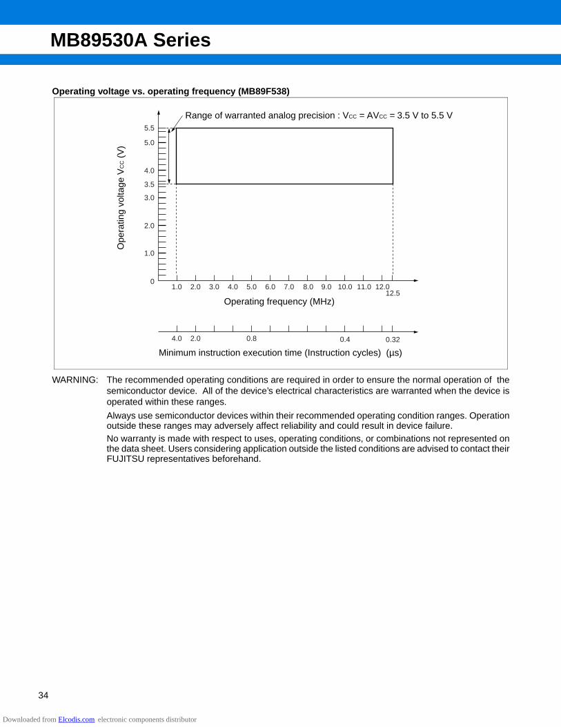
Operating voltage vs. operating frequency (MB89F538)
WARNING: The recommended operating conditions are required in order to ensure the normal operation of thesemiconductor device. All of the device’s electrical characteristics are warranted when the device isoperated within these ranges.
Always use semiconductor devices within their recommended operating condition ranges. Operationoutside these ranges may adversely affect reliability and could result in device failure.No warranty is made with respect to uses, operating conditions, or combinations not represented onthe data sheet. Users considering application outside the listed conditions are advised to contact theirFUJITSU representatives beforehand.
5.5
5.0
4.0
3.5
3.0
2.0
1.0
01.0
4.0
2.0
2.0
3.0 4.0 5.0
0.8
6.0 7.0 8.0 9.0 10.0
0.4
11.0 12.012.5
0.32
Range of warranted analog precision : VCC = AVCC = 3.5 V to 5.5 VO
pera
ting
volta
ge V
CC (
V)
Operating frequency (MHz)
Minimum instruction execution time (Instruction cycles) (µs)
Downloaded from Elcodis.com electronic components distributor
MB89530A Series
35
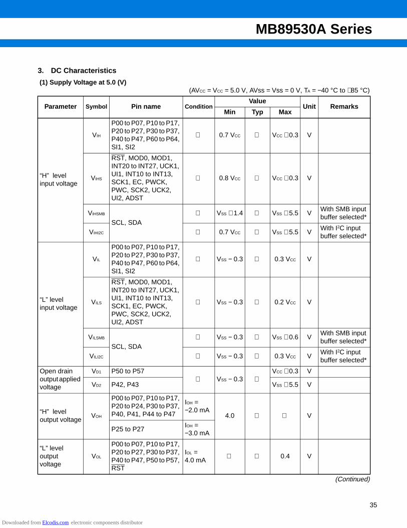
3. DC Characteristics
(1) Supply Voltage at 5.0 (V) (AVCC = VCC = 5.0 V, AVss = Vss = 0 V, TA = −40 °C to +85 °C)
(Continued)
Parameter Symbol Pin name ConditionValue
Unit RemarksMin Typ Max
“H” level input voltage
VIH
P00 to P07, P10 to P17, P20 to P27, P30 to P37, P40 to P47, P60 to P64, SI1, SI2
0.7 VCC VCC + 0.3 V
VIHS
RST, MOD0, MOD1, INT20 to INT27, UCK1, UI1, INT10 to INT13, SCK1, EC, PWCK, PWC, SCK2, UCK2, UI2, ADST
0.8 VCC VCC + 0.3 V
VIHSMB
SCL, SDA VSS + 1.4 VSS + 5.5 V
With SMB input buffer selected*
VIHI2C 0.7 VCC VSS + 5.5 VWith I2C input buffer selected*
“L” level input voltage
VIL
P00 to P07, P10 to P17, P20 to P27, P30 to P37, P40 to P47, P60 to P64, SI1, SI2
VSS − 0.3 0.3 VCC V
VILS
RST, MOD0, MOD1, INT20 to INT27, UCK1, UI1, INT10 to INT13, SCK1, EC, PWCK, PWC, SCK2, UCK2, UI2, ADST
VSS − 0.3 0.2 VCC V
VILSMB
SCL, SDA VSS − 0.3 VSS + 0.6 V
With SMB input buffer selected*
VILI2C VSS − 0.3 0.3 VCC VWith I2C input buffer selected*
Open drain output applied voltage
VD1 P50 to P57 VSS − 0.3
VCC + 0.3 V
VD2 P42, P43 VSS + 5.5 V
“H” level output voltage
VOH
P00 to P07, P10 to P17, P20 to P24, P30 to P37, P40, P41, P44 to P47
IOH = −2.0 mA
4.0 V
P25 to P27IOH = −3.0 mA
“L” level output voltage
VOL
P00 to P07, P10 to P17, P20 to P27, P30 to P37, P40 to P47, P50 to P57, RST
IOL = 4.0 mA
0.4 V
Downloaded from Elcodis.com electronic components distributor

MB89530A Series
36
(AVCC = VCC = 5.0 V, AVss = Vss = 0 V, TA = −40 °C to +85 °C)
(Continued)
Parameter Symbol Pin name ConditionValue
Unit RemarksMin Typ Max
Input leak current (Hi-Z output leak current)
ILI
P00 to P07, P10 to P17, P20 to P27, P30 to P37, P40 to P47, P50 to P57, P60 to P64
0.0 V < VI < VCC
−5 +5 µAWith no pull-up re-sistance specified
Open drain output leak current
ILIOD P42, P430.0 V < VI < VSS + 5.5 V
+5 µA
Pull-up resistance
RPULL
P00 to P07, P10 to P17, P20 to P27, P30 to P37, P40, P41, P44 to P47, P60 to P64, RST
VI = 0.0 V 25 40 100 kΩ
With pull-up resistance speci-fied. The RST sig-nal is excluded.
Supply current
ICC1
VCC
FCH = 10.0 MHzVCC = 5.0 Vtinst = 0.4 µs
15 20 mAMB89P538/PV530
6 10 mA MB89F538
8 13 mAMB89535A/7A/8AMB89537AC/538AC
ICC2
FCH = 10.0 MHzVCC = 5.0 Vtinst = 6.4 µs
5 8.5 mAMB89P538/PV530
1.5 3 mA MB89F538
1.5 3 mAMB89535A/7A/8AMB89537AC/538AC
ICCS1
FCH = 10.0 MHzVCC = 5.0 Vtinst = 0.4 µs
5 7 mASleep modeMB89P538/PV530
3 5 mASleep modeMB89F538
2.5 5 mA
Sleep modeMB89535A/7A/8AMB89537AC/538AC
ICCS2
FCH = 10.0 MHzVCC = 5.0 Vtinst = 6.4 µs
1.5 3 mASleep modeMB89P538/PV530
1 2 mASleep modeMB89F538
1 2 mA
Sleep modeMB89535A/7A/8AMB89537AC/538AC
Downloaded from Elcodis.com electronic components distributor

MB89530A Series
37
(Continued) (AVCC = VCC = 5.0 V, AVss = Vss = 0 V, TA = −40 °C to +85 °C)
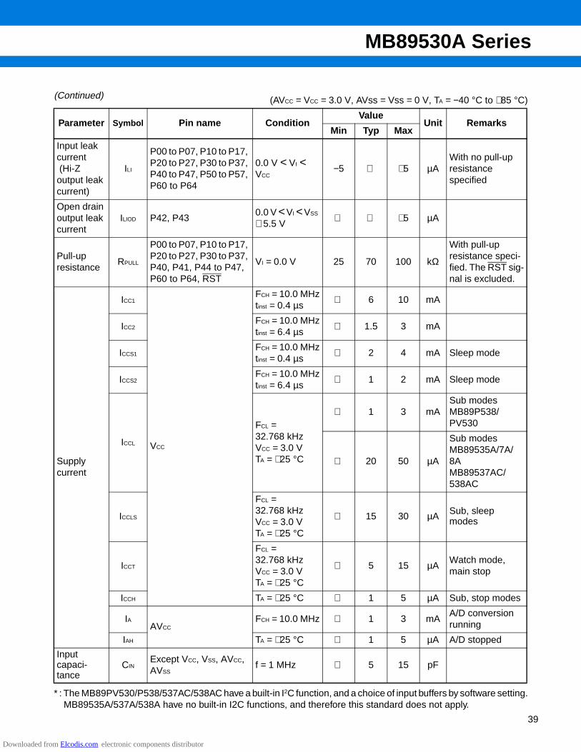
* : The MB89PV530/P538/537AC/538AC have a built-in I2C function, and a choice of input buffers by software setting.MB89535A/537A/538A have no built-in I2C functions, and therefore this standard does not apply.
Parameter Symbol Pin name ConditionValue
Unit RemarksMin Typ Max
Supply current
ICCL
VCC
FCL = 32.768 kHzVCC = 5.0 VTA = +25 °C
3 7 mASub modeMB89P538/PV530
400 800 µASub modeMB89F538
50 85 µA
Sub modeMB89535A/7A/8AMB89537AC/538AC
ICCLS
FCL = 32.768 kHzVCC = 5.0 VTA = +25 °C
30 50 µASub, sleep mode MB89P538/PV530
15 30 µASub, sleep modeMB89F538
15 30 µA
Sub, sleep mode MB89535A/7A/8AMB89537AC/538AC
ICCT
FCL = 32.768 kHzVCC = 5.0 VTA = +25 °C
5 15 µAWatch mode, main stop
ICCH TA = +25 °C 3 10 µA Sub, stop modes
IAAVCC
FCH = 10.0 MHz 4 6 mAA/D conversion running
IAH TA = +25 °C 1 5 µA A/D stopped
Input capacitance CIN
Except VCC, VSS, AVCC, AVSS
f = 1 MHz 5 15 pF
Downloaded from Elcodis.com electronic components distributor

MB89530A Series
38
(2) Supply Voltage at 3.0 (V) (except MB89F538) (AVCC = VCC = 3.0 V, AVss = Vss = 0 V, TA = −40 °C to +85 °C)
(Continued)
Parameter Symbol Pin name ConditionValue
Unit RemarksMin Typ Max
“H” level input voltage
VIH
P00 to P07, P10 to P17, P20 to P27, P30 to P37, P40 to P47, P60 to P64,
SI1, SI2
0.7 VCC VCC + 0.3 V
VIHS
RST, MOD0, MOD1, INT20 to INT27, UCK1, UI1, INT10 to INT13, SCK1, EC, PWCK,
PWC, SCK2, UCK2, UI2, ADST
0.8 VCC VCC + 0.3 V
VIHSMB
SCL, SDA
VSS + 1.4 VSS + 5.5 VWith SMB input buffer selected*
VIHI2C 0.7 VCC VSS + 5.5 VWith I2C input buffer selected*
“L” level input voltage
VIL
P00 to P07, P10 to P17, P20 to P27, P30 to P37, P40 to P47, P60 to P64,
SI1, SI2
VSS − 0.3 0.3 VCC V
VILS
RST, MOD0, MOD1, INT20 to INT27, UCK1, UI1, INT10 to INT13,
SCK1, EC, PWCK, PWC, SCK2, UCK2, UI2, ADST
VSS − 0.3 0.2 VCC V
VILSMB
SCL, SDA
VSS − 0.3 VSS + 0.6 VWith SMB input buffer selected*
VILI2C VSS − 0.3 0.3 VCC VWith I2C input buffer selected*
Open drain output applied voltage
VD1 P50 to P57
VSS − 0.3
VCC + 0.3 V
VD2 P42, P43 VSS + 5.5 V
“H” level output voltage
VOH
P00 to P07, P10 to P17, P20 to P24, P30 to P37, P40, P41, P44 to P47
IOH = −2.0 mA2.4 V
P25 to P27 IOH = −3.0 mA
“L” level output voltage
VOL
P00 to P07, P10 to P17, P20 to P27, P30 to P37, P40 to P47, P50 to P57, RST
IOL = 4.0 mA 0.4 V
Downloaded from Elcodis.com electronic components distributor
MB89530A Series
39
(Continued) (AVCC = VCC = 3.0 V, AVss = Vss = 0 V, TA = −40 °C to +85 °C)
* : The MB89PV530/P538/537AC/538AC have a built-in I2C function, and a choice of input buffers by software setting.MB89535A/537A/538A have no built-in I2C functions, and therefore this standard does not apply.
Parameter Symbol Pin name ConditionValue
Unit RemarksMin Typ Max
Input leak current (Hi-Z output leak current)
ILI
P00 to P07, P10 to P17, P20 to P27, P30 to P37, P40 to P47, P50 to P57, P60 to P64
0.0 V < VI < VCC
−5 +5 µAWith no pull-up resistance specified
Open drain output leak current
ILIOD P42, P430.0 V < VI < VSS + 5.5 V
+5 µA
Pull-up resistance
RPULL
P00 to P07, P10 to P17, P20 to P27, P30 to P37, P40, P41, P44 to P47, P60 to P64, RST
VI = 0.0 V 25 70 100 kΩ
With pull-up resistance speci-fied. The RST sig-nal is excluded.
Supply current
ICC1
VCC
FCH = 10.0 MHztinst = 0.4 µs
6 10 mA
ICC2FCH = 10.0 MHztinst = 6.4 µs
1.5 3 mA
ICCS1FCH = 10.0 MHztinst = 0.4 µs
2 4 mA Sleep mode
ICCS2FCH = 10.0 MHztinst = 6.4 µs
1 2 mA Sleep mode
ICCL
FCL = 32.768 kHzVCC = 3.0 VTA = +25 °C
1 3 mASub modesMB89P538/PV530
20 50 µA
Sub modesMB89535A/7A/8AMB89537AC/538AC
ICCLS
FCL = 32.768 kHzVCC = 3.0 VTA = +25 °C
15 30 µA Sub, sleep modes
ICCT
FCL = 32.768 kHzVCC = 3.0 VTA = +25 °C
5 15 µAWatch mode, main stop
ICCH TA = +25 °C 1 5 µA Sub, stop modes
IAAVCC
FCH = 10.0 MHz 1 3 mAA/D conversion running
IAH TA = +25 °C 1 5 µA A/D stopped
Input capaci-tance
CINExcept VCC, VSS, AVCC, AVSS
f = 1 MHz 5 15 pF
Downloaded from Elcodis.com electronic components distributor

MB89530A Series
40
4. AC Characteristics
(1) Reset Timing (VCC = 5.0 V, AVss = Vss = 0 V, TA = −40 °C to +85 °C)
Notes: • tHCYL is the main clock oscillator period.• If the reset pulse applied to the external reset pin (RST) does not meet the specifications, it may
cause malfunctions. Use caution so that the reset pulse less than the specifications will not be fed to theexternal reset pin (RST).
(2) Power-on Reset (AVss = Vss = 0 V, TA = −40 °C to +85 °C)
Note : Be sure that the power supply will come on within the selected oscillator stabilization period. Also, when varying the supply voltage during operation, it is recommended that the supply voltage be increased gradually.
Parameter Symbol ConditionValue
Unit RemarksMin Max
RST “L” pulse width tZLZH 48 tHCYL ns
Parameter Symbol ConditionValue
Unit RemarksMin Max
Power on time tR 0.5 50 ms
Power shutoff time tOFF 1 msFor repeated operation
RST 0.2 VCC0.2 VCC
tZLZH
VCC
tR
2.2 V
0.2 V 0.2 V 0.2 V
tOFF
Downloaded from Elcodis.com electronic components distributor

MB89530A Series
41
(3) Clock Timing Standards (AVss = Vss = 0 V, TA = −40 °C to +85 °C)
Parameter Symbol Pin name Condi-tion
ValueUnit Remarks
Min Typ Max
Clock frequencyFCH X0, X1
1 12.5 MHz Main clock
FCL X0A, X1A 32.768 kHz Sub clock
Clock cycle timetHCYL X0, X1 80 1000 ns Main clock
tLCYL X0A, X1A 30.5 µs Sub clock
Input clock pulse width
PWH
PWLX0 20 ns External clock
PWHH
PWLLX0A 15.2 µs External clock
Input clock rise, fall time
tCR
tCFX0 10 ns External clock
• X0, X1 timing and application conditions
• Clock application conditions
tHCYL
PWH
tCR tCF
PWL
0.2 VCC 0.2 VCC 0.2 VCC
0.8 VCC 0.8 VCC
X0
X0 X1
C1 C2
FCH
FCH
X0 X1
Using a crystal oscillatoror
ceramic oscillator
Using an external clock signal
Open
Downloaded from Elcodis.com electronic components distributor
MB89530A Series
42
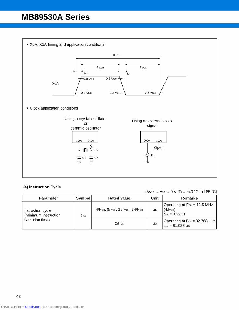
(4) Instruction Cycle (AVss = Vss = 0 V, TA = −40 °C to +85 °C)
Parameter Symbol Rated value Unit Remarks
Instruction cycle (minimum instruction execution time)
tinst
4/FCH, 8/FCH, 16/FCH, 64/FCH µsOperating at FCH = 12.5 MHz (4/FCH) tinst = 0.32 µs
2/FCL µsOperating at FCL = 32.768 kHztinst = 61.036 µs
•••• X0A, X1A timing and application conditions
•••• Clock application conditions
tLCYL
PWLH
tCR tCF
PWLL
0.2 VCC 0.2 VCC 0.2 VCC
0.8 VCC 0.8 VCC
X0A
X0A X1A X0A X1A
C1 C2
FCL
FCL
Using a crystal oscillatoror
ceramic oscillator
Using an external clock signal
Open
Downloaded from Elcodis.com electronic components distributor

MB89530A Series
43
(5) Serial I/O Timing (VCC = 5.0 V, AVss = Vss = 0 V, TA = −40 °C to +85 °C)
Note : For tinst see “ (4) Instruction Cycle”.
Parameter Sym-bol Pin name Condition
ValueUnit Remarks
Min Max
Serial clock cycle time tSCYC SCK, UCKInternal clock
operation
2 tinst µs
SCK↓→SO tSLOV SCK, SO, UCK, UO −200 +200 ns
Valid SI→SCK↑ tIVSH SI, SCK, UI, UCK 200 ns
SCK↑→valid SI hold time tSHIX SCK, SI, UCK, UI 200 ns
Serial clock “H” pulse width tSHSLSCK, UCK
External clock
operation
1 tinst µs
Serial clock “L” pulse width tSLSH 1 tinst µs
SCK↓→SO time tSLOV SCK, SO, UCK, UO 0 200 ns
Valid SI→SCK↑ tIVSH SI, SCK, UI, UCK 200 ns
SCK↑→ valid SI hold time tSHIX SCK, SI, UCK, UI 200 ns
Internal shift clock mode
External shift clock mode
SCKUCK
SOUO
SIUI
tSCYC
tIVSH
tSLOV
tSHIX
0.8 V
0.8 V
2.4 V
0.8 VCC
0.2 VCC
0.8 VCC
0.2 VCC
0.8 V2.4 V
SCKUCK
SOUO
SIUI
tSLSH tSHSL
tIVSH
tSLOV
tSHIX
0.2 VCC
0.8 V
2.4 V
0.8 VCC
0.2 VCC
0.8 VCC
0.2 VCC
0.2 VCC
0.8 VCC0.8 VCC
Downloaded from Elcodis.com electronic components distributor
MB89530A Series
44
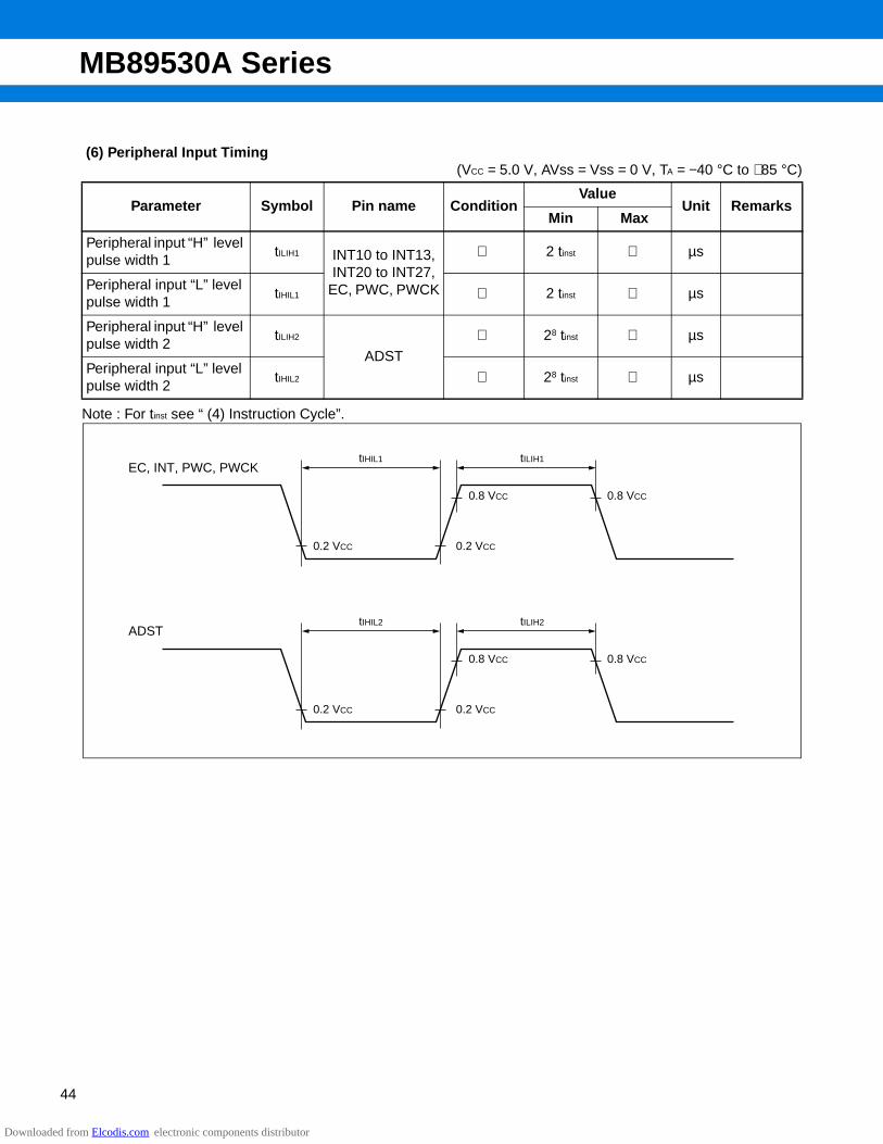
(6) Peripheral Input Timing (VCC = 5.0 V, AVss = Vss = 0 V, TA = −40 °C to +85 °C)
Note : For tinst see “ (4) Instruction Cycle”.
Parameter Symbol Pin name ConditionValue
Unit RemarksMin Max
Peripheral input “H” level pulse width 1
tILIH1 INT10 to INT13, INT20 to INT27,
EC, PWC, PWCK
2 tinst µs
Peripheral input “L” level pulse width 1
tIHIL1 2 tinst µs
Peripheral input “H” level pulse width 2
tILIH2
ADST
28 tinst µs
Peripheral input “L” level pulse width 2
tIHIL2 28 tinst µs
EC, INT, PWC, PWCKtIHIL1 tILIH1
0.2 VCC 0.2 VCC
0.8 VCC0.8 VCC
ADSTtIHIL2 tILIH2
0.2 VCC 0.2 VCC
0.8 VCC0.8 VCC
Downloaded from Elcodis.com electronic components distributor

MB89530A Series
45
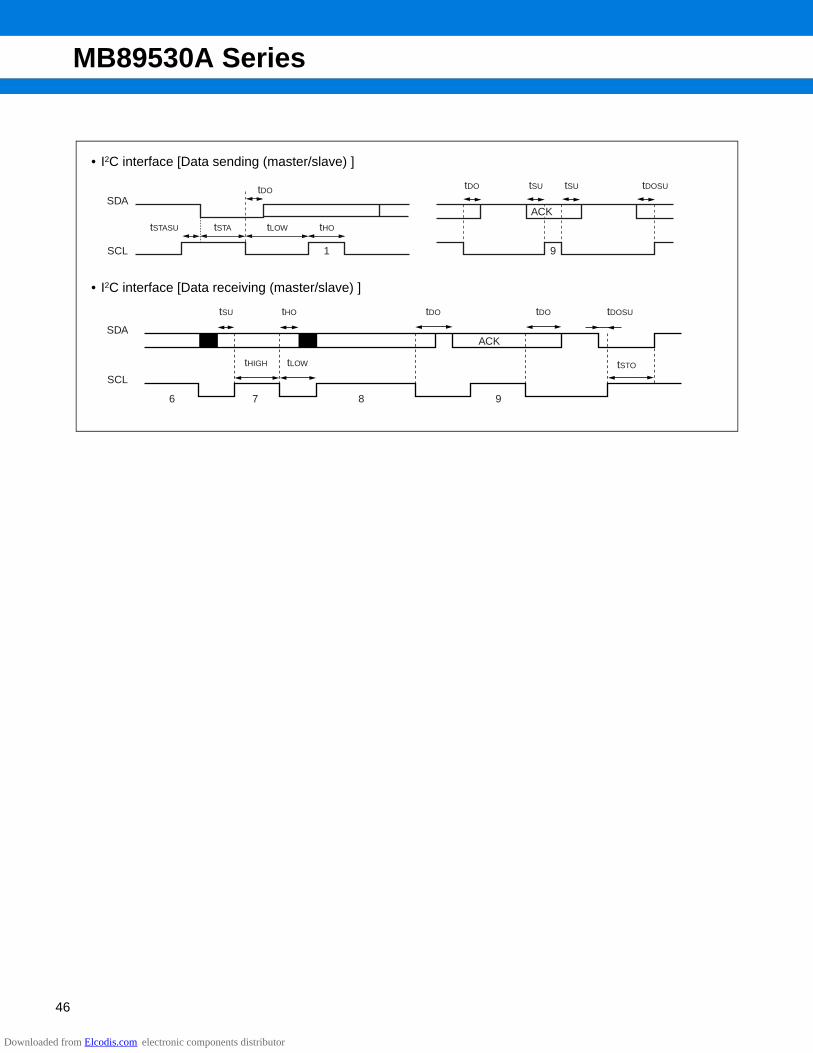
(7) I2C Timing (VCC = 5.0 V, AVss = Vss = 0 V, TA = −40 °C to +85 °C)
Notes : • For tinst see “ (4) Instruction Cycle”.• The value “m” in the above table is the value from the shift clock frequency setting bits (CS4-
CS3) in the clock control register “ICCR”. For details, refer to the register description in the hardware manual.
• The value ’n’ in the above table is the value from the shift clock frequency setting bits (CS2-CS0) in the clock control register “ICCR”. For details, refer to the register description in the hardware manual.
• tDOSU appears when the interrupt period is longer than the SCL “L” width.• The rated values for SDA and SCL assume a start up time of 0 ns.
Parameter Symbol Pin name Condition
ValueUnit Remarks
Min Max
Start condition output tSTASCLSDA
1 / 4 tinst × m × n − 20
1 / 4 tinst × m × n + 20
nsMaster only
Stop condition output tSTOSCLSDA
1 / 4 tinst × (m × n + 8) − 20
1 / 4 tinst × (m × n + 8) + 20
nsMaster only
Start condition detection tSTASCLSDA
1 / 4 tinst × 6 + 40 ns
Stop condition detection tSTOSCLSDA
1 / 4 tinst × 6 + 40 ns
Restart condition output tSTASUSCLSDA
1 / 4 tinst × (m × n + 8) − 20
1 / 4 tinst × (m × n + 8) + 20
nsMaster only
Restart condition detection tSTASUSCLSDA
1 / 4 tinst × 4 + 40 ns
SCL output “L” width tLOW SCL 1 / 4 tinst × m × n − 20
1 / 4 tinst × m × n + 20
nsMaster only
SCL output “H” width tHIGH SCL 1 / 4 tinst × (m × n + 8) − 20
1 / 4 tinst × (m × n + 8) + 20
nsMaster only
SDA output delay time tDO SDA 1 / 4 tinst × 4 − 20 1 / 4 tinst × 4 + 20 ns
Setup after SDA output interrupt interval
tDOSU SDA 1 / 4 tinst × 4 − 20 ns
SCL input “L” width tLOW SCL 1 / 4 tinst × 6 + 40 ns
SCL input “H” width tHIGH SCL 1 / 4 tinst × 2 + 40 ns
SDA input setup tSU SDA 40 ns
SDA input hold tHO SDA 0 ns
Downloaded from Elcodis.com electronic components distributor
MB89530A Series
46
• I2C interface [Data sending (master/slave) ]
• I2C interface [Data receiving (master/slave) ]
9
ACK
tDO tSU tSU tDOSUtDO
tHOtLOWtSTAtSTASU
SDA
SCL 1
SDA
SCL
6 7 8 9
tSU
tHIGH tLOW
tHO tDO tDO tDOSU
tSTO
ACK
Downloaded from Elcodis.com electronic components distributor

MB89530A Series
47
5. A/D Converter Electrical Characteristics (1) MB89535A/537A/537AC/538A/538AC/P538/PV538
(VCC = 3.5 V to 5.5 V, AVSS = VSS = 0 V, TA = −40 °C to +85 °C)
* : Includes sampling time.
Note : For tinst see “ (4) Instruction Cycle”.
(2) MB89F538 (VCC = 3.5 V to 5.5 V, AVSS = VSS = 0 V, TA = −40 °C to +85 °C)
* : Includes sampling time.
Note : For tinst see “ (4) Instruction Cycle”.
Parameter Symbol Pin name ConditionValue
Unit RemarksMin Typ Max
Resolution capability
10 bit
AVCC = VCC
Total error
AVR = AVCC
±3.0 LSBLinear error ±2.5 LSBDifferential linear error ±1.9 LSB
Zero transition voltage VOTAVSS − 1.5
LSBAVSS + 0.5
LSBAVSS + 2.5
LSBmV
Full scale transition voltage
VFSTAVR − 3.5
LSBAVR − 1.5
LSBAVR + 1.5
LSBmV
Inter-channel variation
4.0 LSBConversion time
60 tinst µs *Sampling time 16 tinst µsAnalog input current IAIN AN0 to
AN7 10 µA
Analog input voltage VAIN 0 AVR VReference voltage
AVRAVSS + 3.5 AVCC V
Reference voltage supply current
IR A/D running 400 µAIRH A/D off 5 µA
Parameter Symbol Pin name ConditionValue
Unit RemarksMin Typ Max
Resolution capability
10 bit
AVCC = VCC
Total error
AVR = AVCC
±5.0 LSBLinear error ±2.5 LSBDifferential linear error ±1.9 LSB
Zero transition voltage VOTAVSS − 1.5
LSBAVSS + 0.5
LSBAVSS + 4.5
LSBmV
Full scale transition voltage
VFSTAVR − 6.5
LSBAVR − 1.5
LSBAVR + 1.5
LSBmV
Inter-channel variation
4.0 LSBConversion time
60 tinst µs *Sampling time 16 tinst µsAnalog input current IAIN AN0 to
AN7 10 µA
Analog input voltage VAIN 0 AVR VReference voltage
AVRAVSS + 3.5 AVCC V
Reference voltage supply current
IR A/D running 400 µAIRH A/D off 5 µA
Downloaded from Elcodis.com electronic components distributor
MB89530A Series
48
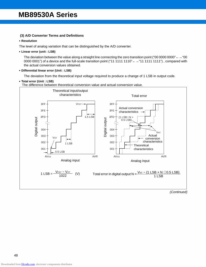
(3) A/D Converter Terms and Definitions
•••• Resolution
The level of analog variation that can be distinguished by the A/D converter.
•••• Linear error (unit : LSB)
The deviation between the value along a straight line connecting the zero transition point (“00 0000 0000”←→“000000 0001”) of a device and the full-scale transition point (“11 1111 1110”←→“11 1111 1111”) , compared withthe actual conversion values obtained.
•••• Differential linear error (Unit : LSB)
The deviation from the theoretical input voltage required to produce a change of 1 LSB in output code.
•••• Total error (Unit : LSB) The difference between theoretical conversion value and actual conversion value.
(Continued)
VFST
1.5 LSB
1 LSB
0.5 LSB
VOT
AVRAVSS
3FF
3FE
3FD
004
003
002
001
VNT
(1 LSB I N + 0.5 LSB)
AVRAVSS
3FF
3FE
3FD
004
003
002
001
Theoretical input/outputcharacteristics
Analog input
Dig
ital o
utpu
t
1 LSB = VFST − VOT
1022 (V)
Total error
Analog input
Dig
ital o
utpu
t
Total error in digital output N = VNT − 1 LSB × N + 0.5 LSB1 LSB
Actual conversion characteristics
Actual conversion
characteristicsTheoretical characteristics
Downloaded from Elcodis.com electronic components distributor

MB89530A Series
49
(Continued)
004
003
002
001
AVSS
3FF
3FE
3FD
3FC
AVR
3FF
3FE
3FD
004
003
002
001
AVSS AVR
VNT
(1 LSB × N + VOT)
V (N + 1) T
VNT
N + 1
N
N − 1
N − 2
AVSS AVR
Zero transition error
Analog input
Full-scale transition error
Dig
ital o
utpu
t
Dig
ital o
utpu
t
Linear error
Analog input
Differential linear error
Analog input
Dig
ital o
utpu
t
Dig
ital o
utpu
t
−1Differential linear error in digital output N
V (N + 1) T − VNT
1 LSB
Actual conversion characteristics
Actual conversion characteristics
VOT (actual measurement value)
Actual conversion characteristics
VFST (actual measurement value)
Actual conversion characteristics
Actual conversion characteristics
VOT (actual measurement value)
VFST
(actual measure-
ment value)
Theoretical characteristics
Actual conversion characteristics
Actual conversion characteristics
Theoretical characteristics
Actual conversioncharacteristics
Analog input linear error in digital output N
VNT − 1 LSB × N + VOT1 LSB
Theoretical characteristics
= =
Analog input
Downloaded from Elcodis.com electronic components distributor

MB89530A Series
50
(4) Precautionary Information
•••• Input Impedance of Analog Input Pins
The A/D converter of MB89530A has a sample & hold circuit as shown below, which uses a sample-and-holdcapacitor to obtain the voltage at the analog input pin for 8 instruction cycles following the start of A/D conversion.For this reason if the external circuits providing the analog input signal have high output impedance, the analoginput voltage may not stabilize within the analog input sampling time. It is therefore recommended that the outputimpedance of external circuits be reduced to 10 kΩ or less.
•••• About error
The smaller the absolute value |AVR - AVss| is, the greater the relative error becomes.
•••• MB89535A/537A/537AC/538A/538AC Analog Input Equivalent Circuit
C = 45 pF
R = 2.2 kΩIf analog input impedance is 10 kΩ or more, the use of a capacitor of approximately 0.1 µF is recommended.
Analog input pin
Sample-and-hold circuit
Compara-tor
Closes 8 instruction cycles after the start of A/D conversion
Analog channel selector
•••• MB89P538 and MB89PV530 Analog Input Equivalent Circuit
C = 64 pF
R = 3 kΩIf analog input impedance is 10 kΩ or more, the use of a capacitor of approximately 0.1 µF is recommended.
Analog input pin
Sample-and-hold circuit
Compara-tor
Closes 8 instruction cycles after the start of A/D conversion
Analog channel selector
•••• MB89F538 Analog Input Equivalent Circuit
C = 30 pF
R = 3.2 kΩ
Analog channel selector
Compara-tor
Analog input pin
If analog input impedance is 10 kΩ or more, the use of a capacitor of approximately 0.1 µF is recommended.
Closes 8 instruction cycles after the start of A/D conversion
Sample-and-hold circuit
Downloaded from Elcodis.com electronic components distributor
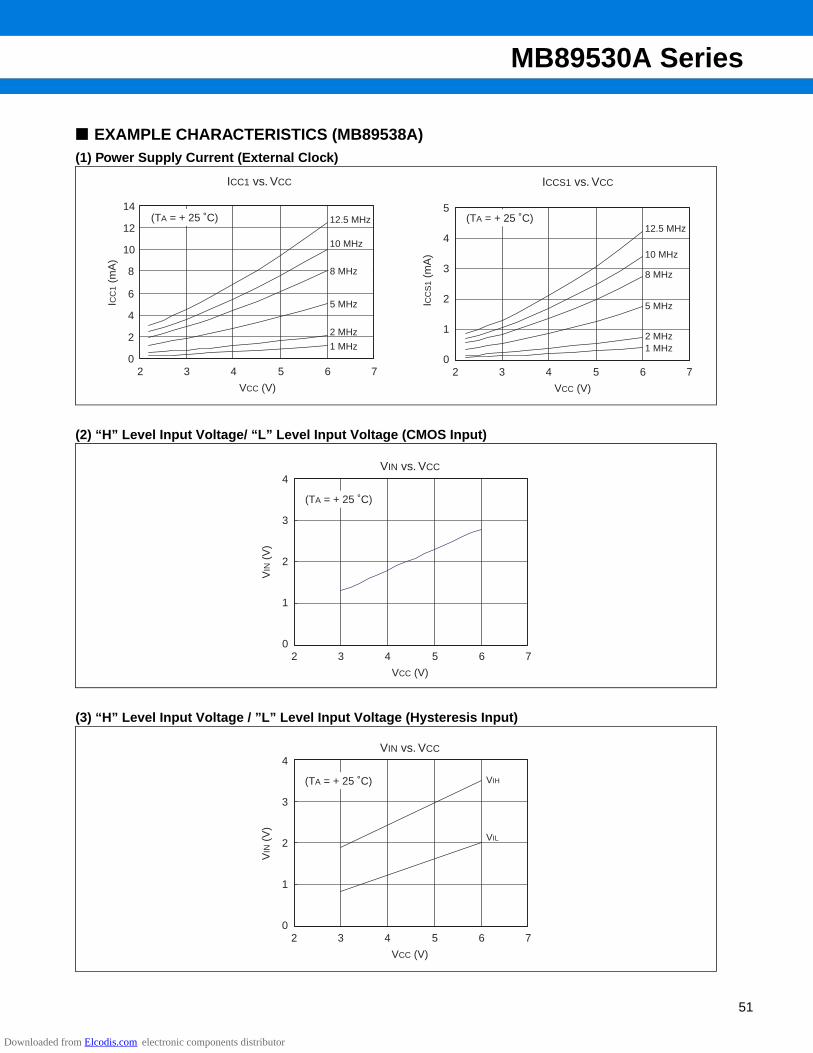
MB89530A Series
51
EXAMPLE CHARACTERISTICS (MB89538A)(1) Power Supply Current (External Clock)
(2) “H” Level Input Voltage/ “L” Level Input Voltage (CMOS Input)
(3) “H” Level Input Voltage / ”L” Level Input Voltage (Hysteresis Input)
ICC1 vs. VCC
0
2
4
6
8
10
12
14
2 3 4 5 6 7
VCC (V)
ICC
1 (m
A)
(TA = + 25 ˚C) 12.5 MHz
1 MHz
2 MHz
5 MHz
8 MHz
10 MHz
ICCS1 vs. VCC
0
1
2
3
4
5
2 3 4 5 6 7
VCC (V)
ICC
S1
(mA
)
(TA = + 25 ˚C)12.5 MHz
1 MHz2 MHz
5 MHz
8 MHz
10 MHz
VIN vs. VCC
0
1
2
3
4
2 3 4 5 6 7
VCC (V)
VIN
(V
)
(TA = + 25 ˚C)
VIN vs. VCC
0
1
2
3
4
2 3 4 5 6 7
VCC (V)
VIN
(V
)
(TA = + 25 ˚C) VIH
VIL
Downloaded from Elcodis.com electronic components distributor
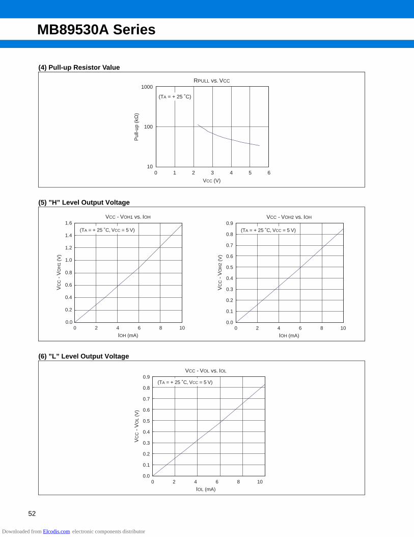
MB89530A Series
52
(4) Pull-up Resistor Value
(5) ”H” Level Output Voltage
(6) ”L” Level Output Voltage
RPULL vs. VCC
10
100
1000
0 3 4 52 6
VCC (V)
Pul
l-up
(kΩ
)
(TA = + 25 ˚C)
1
VCC - VOH1 vs. IOH
0.0
1.0
1.2
1.4
1.6
0 4 6 82 10
IOH (mA)
VC
C -
VO
H1
(V)
(TA = + 25 ˚C, VCC = 5 V)
0.4
0.2
0.6
0.8
VCC - VOH2 vs. IOH
0.0
0.5
0.6
0.7
0.8
0 4 6 82 10
IOH (mA)
VC
C -
VO
H2
(V)
(TA = + 25 ˚C, VCC = 5 V)
0.2
0.1
0.3
0.4
0.9
VCC - VOL vs. IOL
0.0
0.5
0.6
0.7
0.8
0 4 6 82 10
IOL (mA)
VC
C -
VO
L (V
)
(TA = + 25 ˚C, VCC = 5 V)
0.2
0.1
0.3
0.4
0.9
Downloaded from Elcodis.com electronic components distributor
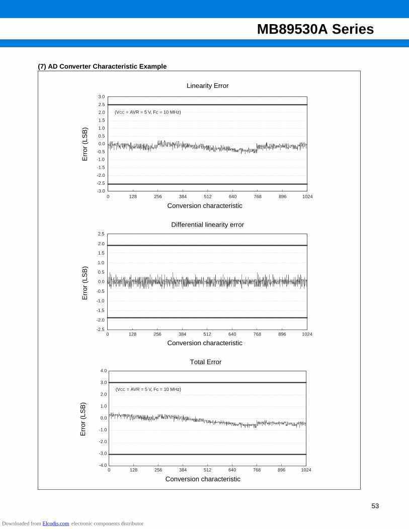
MB89530A Series
53
(7) AD Converter Characteristic Example
-2.5
0.0
1.5
2.0
2.5
0 640 768 896512 1024
(VCC = AVR = 5 V, Fc = 10 MHz)
-1.5
-2.0
-1.0
-0.5
3.0
128 256 384-3.0
1.0
0.5
-2.5
0.0
1.5
2.0
2.5
0 640 768 896512 1024
-1.5
-2.0
-1.0
-0.5
128 256 384
1.0
0.5
-4.0
0.0
2.0
3.0
4.0
0 640 768 896512 1024
(VCC = AVR = 5 V, Fc = 10 MHz)
-2.0
-3.0
-1.0
128 256 384
1.0
Linearity ErrorE
rror
(LS
B)
Conversion characteristic
Differential linearity error
Err
or (
LSB
)
Conversion characteristic
Total Error
Err
or (
LSB
)
Conversion characteristic
Downloaded from Elcodis.com electronic components distributor

MB89530A Series
54
MASK OPTIONS
* : FCH: Main clock frequency
NoPart number
MB89535AMB89537A
MB89537ACMB89538A
MB89538AC
MB89F538-101MB89F538-201
MB89P538-101MB89P538-201
MB89PV530-101
MB89PV530-201
Method ofspecification
Specify at time of mask order
Settingnot possible
Settingnot possible
Settingnot possible
1
Main clockSelect oscillatorstabilization wait period
(FCH* = 10 MHz)approx.214/FCH*
(approx.1.6 ms) approx.217/FCH*
(approx.13.1 ms) approx.218/FCH*
(approx.26.2 ms)
Selectionavailable
218/FCH* (approx. 26.2 ms)
218/FCH* (approx. 26.2 ms)
218/FCH* (approx. 26.2 ms)
2Clock mode selection• 2-system clock mode• 1-system clock mode
Selectionavailable
• 101 : 1-system clock mode• 201 : 2-system clock mode
Downloaded from Elcodis.com electronic components distributor

MB89530A Series
55
ORDERING INFORMATION
Part number Package Remarks
MB89535APMB89537APMB89537ACPMB89538APMB89538ACPMB89P538P-101MB89P538P-201MB89F538P-101MB89F538P-201
DIP-64P-M01MB89535AP, MB89537AP and MB89538AP do not have I2C functions.
MB89535APFMB89537APFMB89537ACPFMB89538APFMB89538ACPFMB89P538PF-101MB89P538PF-201MB89F538PF-101MB89F538PF-201
FPT-64P-M06MB89535APF, MB89537APF and MB89538APF do not have I2C functions.
MB89535APFMMB89537APFMMB89537ACPFMMB89538APFMMB89538ACPFMMB89P538PFM-101MB89P538PFM-201MB89F538PFM-101MB89F538PFM-201
FPT-64P-M09MB89535APFM, MB89537APFM and MB89538APFM do not have I2C functions.
MB89535APFVMB89537APFVMB89537ACPFVMB89538APFVMB89538ACPFV
FPT-64P-M03MB89535APFV, MB89537APFV and MB89538APFV do not have I2C functions.
MB89PV530C-101MB89PV530C-201
MDP-64C-P02
MB89PV530CF-101MB89PV530CF-201
MQP-64C-P01
Downloaded from Elcodis.com electronic components distributor
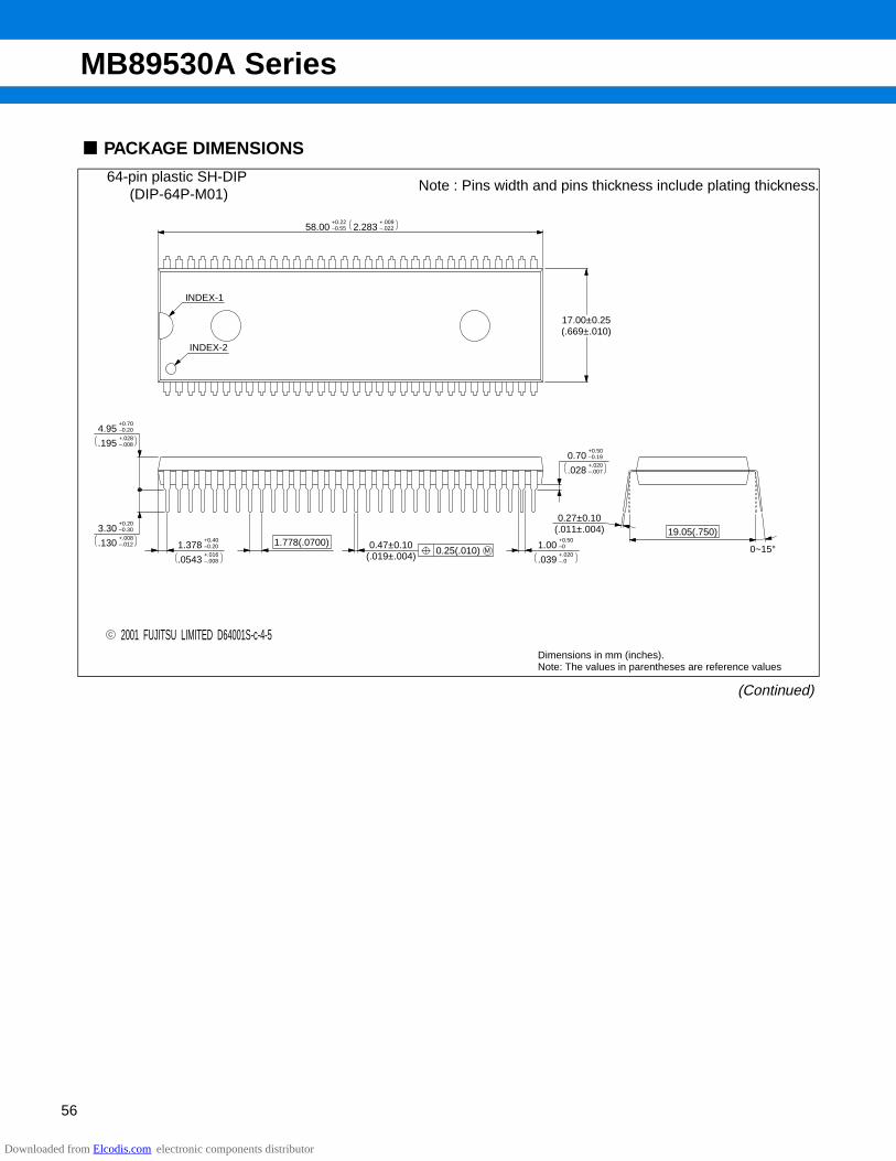
MB89530A Series
56
PACKAGE DIMENSIONS
(Continued)
64-pin plastic SH-DIP (DIP-64P-M01)
Note : Pins width and pins thickness include plating thickness.
Dimensions in mm (inches).Note: The values in parentheses are reference values
C 2001 FUJITSU LIMITED D64001S-c-4-5
58.00+0.22–0.55
+.009–.0222.283
17.00±0.25(.669±.010)
3.30+0.20–0.30
.130 –.012+.008
+.028–.008.195
–0.20+0.70
4.95
+.016–.008.0543
–0.20+0.40
1.378 1.778(.0700) 0.47±0.10(.019±.004)
1.00+0.50–0
.039 –.0+.020
+.020–.007.028
–0.19+0.50
0.70
19.05(.750)(.011±.004)0.27±0.10
0~15°
INDEX-2
INDEX-1
M0.25(.010)
Downloaded from Elcodis.com electronic components distributor

MB89530A Series
57
(Continued)
64-pin, Plastic LQFP (FPT-64P-M03)
Note 1)* : These dimensions do not include resin protrusion.Note 2)Pins width and pins thickness include plating thickness.Note 3)Pins width do not include tie bar cutting remainder.
Dimensions in mm (inches).Note: The values in parentheses are reference values
LEAD No.
Details of "A" part
0.25(.010)
(Stand off)(.004±.004)0.10±0.10
(.024±.006)0.60±0.15
(.020±.008)0.50±0.20
1.50+0.20–0.10
+.008–.004.059
0˚~8˚
"A"
0.08(.003)
(.006±.002)0.145±0.055
0.08(.003) M(.008±.002)0.20±0.050.50(.020)
12.00±0.20(.472±.008)SQ
10.00±0.10(.394±.004)SQ
INDEX
49
64
3348
17
32
161
2003 FUJITSU LIMITED F64009S-c-5-8C
(Mounting height)
*
Downloaded from Elcodis.com electronic components distributor
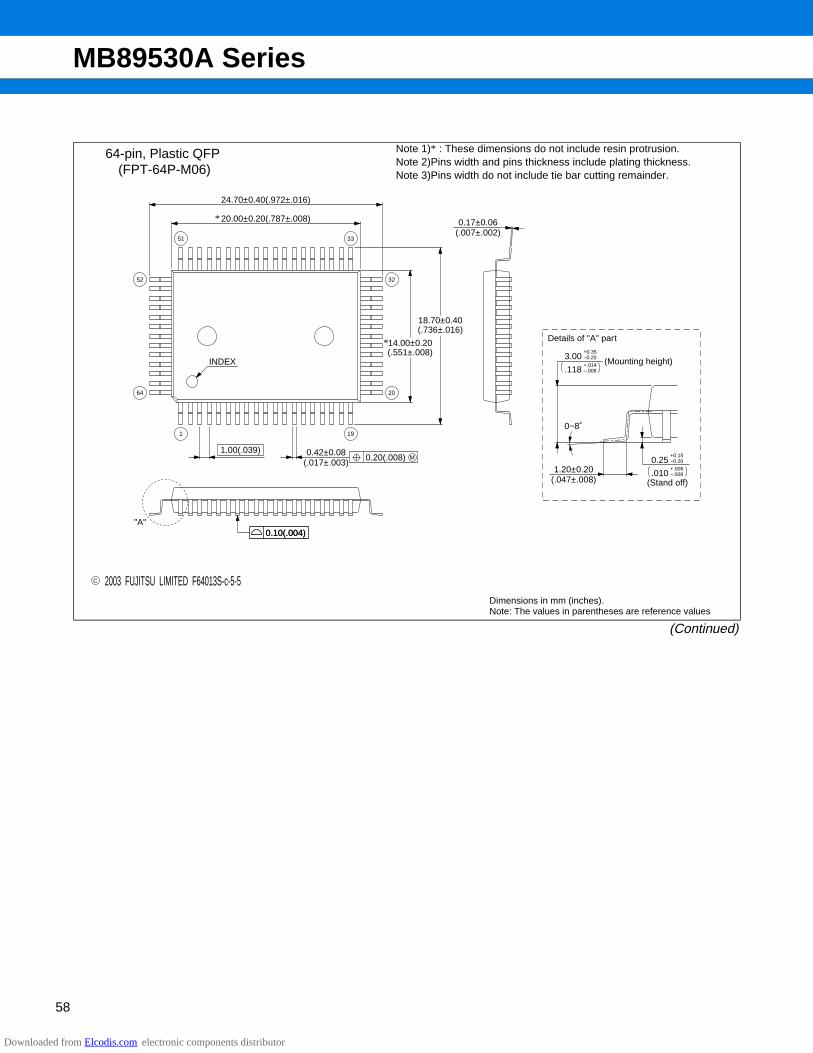
MB89530A Series
58
(Continued)
64-pin, Plastic QFP (FPT-64P-M06)
Note 1)* : These dimensions do not include resin protrusion.Note 2)Pins width and pins thickness include plating thickness.Note 3)Pins width do not include tie bar cutting remainder.
Dimensions in mm (inches).Note: The values in parentheses are reference values
C 2003 FUJITSU LIMITED F64013S-c-5-5
0.20(.008) M
18.70±0.40(.736±.016)
14.00±0.20(.551±.008)
1.00(.039)
INDEX
0.10(.004)
1 19
20
3252
64
3351
20.00±0.20(.787±.008)
24.70±0.40(.972±.016)
0.42±0.08(.017±.003)
0.17±0.06(.007±.002)
0~8˚
1.20±0.20(.047±.008)
3.00+0.35–0.20
(Mounting height).118
+.014–.008
0.25+0.15–0.20
.010+.006–.008
(Stand off)
Details of "A" part
"A"0.10(.004)
*
*
Downloaded from Elcodis.com electronic components distributor
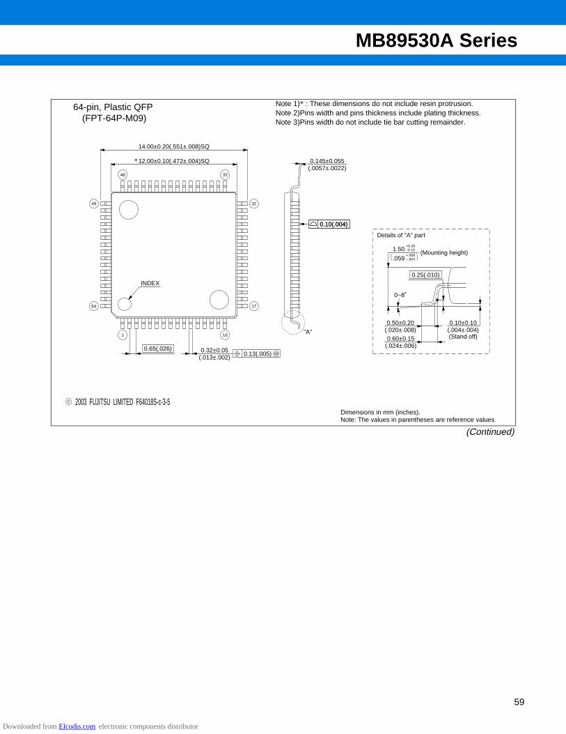
MB89530A Series
59
(Continued)
64-pin, Plastic QFP (FPT-64P-M09)
Note 1)* : These dimensions do not include resin protrusion.Note 2)Pins width and pins thickness include plating thickness.Note 3)Pins width do not include tie bar cutting remainder.
Dimensions in mm (inches).Note: The values in parentheses are reference values
C 2003 FUJITSU LIMITED F64018S-c-3-5
0.65(.026)
0.10(.004)
1 16
17
3249
64
3348
12.00±0.10(.472±.004)SQ
14.00±0.20(.551±.008)SQ
INDEX
0.32±0.05(.013±.002)
M0.13(.005)
0.145±0.055(.0057±.0022)
"A"
.059 –.004+.008
–0.10+0.20
1.50
0~8˚
0.25(.010)
(Mounting height)
0.50±0.20(.020±.008)0.60±0.15
(.024±.006)
0.10±0.10(.004±.004)
Details of "A" part
(Stand off)
0.10(.004)
*
Downloaded from Elcodis.com electronic components distributor
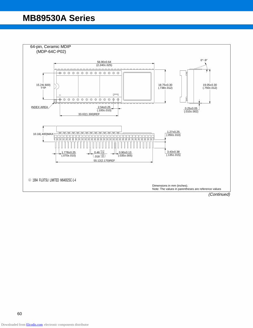
MB89530A Series
60
(Continued)
64-pin, Ceramic MDIP (MDP-64C-P02)
Dimensions in mm (inches).Note: The values in parentheses are reference values
+0.13–0.08+.005–.003
INDEX AREA
0°~9°
(.750±.012)19.05±0.30
0.46
.018
(2.240±.025)
(.010±.002)0.25±0.05
(.050±.010)1.27±0.25
(.135±.015)3.43±0.38
55.12(2.170)REF
(.035±.005)0.90±0.13
(.070±.010)1.778±0.25
10.16(.400)MAX
33.02(1.300)REF(.100±.010)2.54±0.25
(.738±.012)18.75±0.30
TYP15.24(.600)
56.90±0.64
1994 FUJITSU LIMITED M64002SC-1-4C
Downloaded from Elcodis.com electronic components distributor
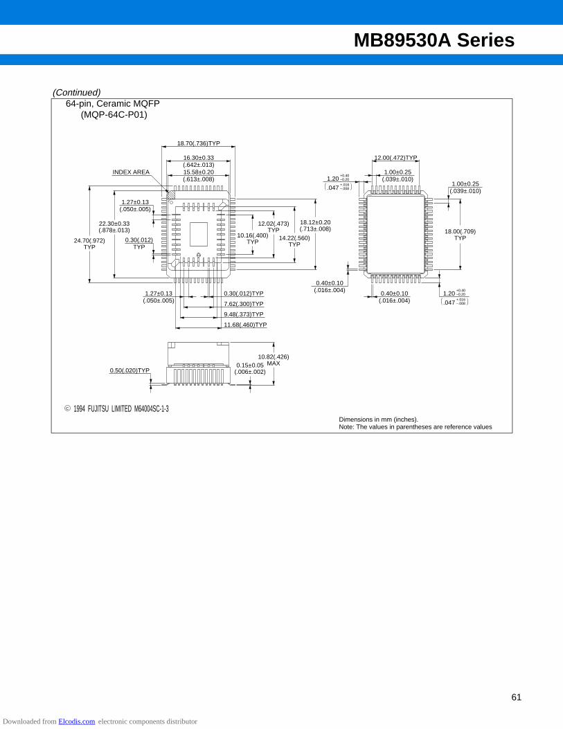
MB89530A Series
61
(Continued)64-pin, Ceramic MQFP
(MQP-64C-P01)
Dimensions in mm (inches).Note: The values in parentheses are reference values
C 1994 FUJITSU LIMITED M64004SC-1-3
15.58±0.20(.613±.008)
16.30±0.33(.642±.013)
18.70(.736)TYP
INDEX AREA
0.30(.012)TYP
1.27±0.13(.050±.005)
22.30±0.33(.878±.013)
24.70(.972)TYP
10.16(.400)TYP
12.02(.473)TYP
14.22(.560)TYP
18.12±0.20(.713±.008)
1.27±0.13(.050±.005)
0.30(.012)TYP
7.62(.300)TYP
9.48(.373)TYP
11.68(.460)TYP
0.50(.020)TYP0.15±0.05
(.006±.002)
10.82(.426)MAX
0.40±0.10(.016±.004) .047 –.008
+.016
–0.20+0.40
1.20
0.40±0.10(.016±.004)
1.00±0.25(.039±.010)
18.00(.709)TYP
1.00±0.25(.039±.010)
12.00(.472)TYP
.047 –.008+.016
–0.20+0.40
1.20
Downloaded from Elcodis.com electronic components distributor

MB89530A Series
FUJITSU LIMITEDAll Rights Reserved.
The contents of this document are subject to change without notice. Customers are advised to consult with FUJITSU salesrepresentatives before ordering.The information, such as descriptions of function and applicationcircuit examples, in this document are presented solely for thepurpose of reference to show examples of operations and uses ofFujitsu semiconductor device; Fujitsu does not warrant properoperation of the device with respect to use based on suchinformation. When you develop equipment incorporating thedevice based on such information, you must assume anyresponsibility arising out of such use of the information. Fujitsuassumes no liability for any damages whatsoever arising out ofthe use of the information.Any information in this document, including descriptions offunction and schematic diagrams, shall not be construed as licenseof the use or exercise of any intellectual property right, such aspatent right or copyright, or any other right of Fujitsu or any thirdparty or does Fujitsu warrant non-infringement of any third-party’sintellectual property right or other right by using such information.Fujitsu assumes no liability for any infringement of the intellectualproperty rights or other rights of third parties which would resultfrom the use of information contained herein.The products described in this document are designed, developedand manufactured as contemplated for general use, includingwithout limitation, ordinary industrial use, general office use,personal use, and household use, but are not designed, developedand manufactured as contemplated (1) for use accompanying fatalrisks or dangers that, unless extremely high safety is secured, couldhave a serious effect to the public, and could lead directly to death,personal injury, severe physical damage or other loss (i.e., nuclearreaction control in nuclear facility, aircraft flight control, air trafficcontrol, mass transport control, medical life support system, missilelaunch control in weapon system), or (2) for use requiringextremely high reliability (i.e., submersible repeater and artificialsatellite).Please note that Fujitsu will not be liable against you and/or anythird party for any claims or damages arising in connection withabove-mentioned uses of the products.Any semiconductor devices have an inherent chance of failure. Youmust protect against injury, damage or loss from such failures byincorporating safety design measures into your facility andequipment such as redundancy, fire protection, and prevention ofover-current levels and other abnormal operating conditions.If any products described in this document represent goods ortechnologies subject to certain restrictions on export under theForeign Exchange and Foreign Trade Law of Japan, the priorauthorization by Japanese government will be required for exportof those products from Japan.
F0303 FUJITSU LIMITED Printed in Japan
Downloaded from Elcodis.com electronic components distributor