
Electroluminescent mis structures incorporating langmuir ...
286
• • •
-
Upload
khangminh22 -
Category
Documents
-
view
0 -
download
0
Transcript of Electroluminescent mis structures incorporating langmuir ...

Durham E-Theses
Electroluminescent mis structures incorporating
langmuir-blodgett �lms
Batey, J.
How to cite:
Batey, J. (1983) Electroluminescent mis structures incorporating langmuir-blodgett �lms, Durham theses,Durham University. Available at Durham E-Theses Online: http://etheses.dur.ac.uk/7260/
Use policy
The full-text may be used and/or reproduced, and given to third parties in any format or medium, without prior permission orcharge, for personal research or study, educational, or not-for-pro�t purposes provided that:
• a full bibliographic reference is made to the original source
• a link is made to the metadata record in Durham E-Theses
• the full-text is not changed in any way
The full-text must not be sold in any format or medium without the formal permission of the copyright holders.
Please consult the full Durham E-Theses policy for further details.
Academic Support O�ce, Durham University, University O�ce, Old Elvet, Durham DH1 3HPe-mail: [email protected] Tel: +44 0191 334 6107
http://etheses.dur.ac.uk

ELECTROLUMINESCENT MIS STRUCTURES INCORPORATING
LANGMUIR-BLODGETT FILMS
by
J, BATEY, B,Sc,
A Thesis submitted for the
Degree of Doctor of Philosophy
in the University of Durham
October 1983
The copyright of this thesis rests with the author.
No quotation from it should be published without
his prior written consent and information derived
from it should be acknowledged.
(J(;TtJ> w:::~\:\
' .

DECLARATION
I hereby declare that the work reported in this thesis has not
previously been submitted for any degree and is not being
currently submitted in candidature for any other degree.
Signed -------------------------
The work reported in this thesis was carried out by the candidate.
Signed
Dirtctors of Studies
Cand lda!te

- i -
ABSTRACT
The Langmuir-Blodgett {LB) technique provides an excellent method of
depositing thin, uniform, insulating films of accurately defined thickness. They
can therefore be used effectively in the investigation of metal/thin insulator/
semiconductor electroluminescent structures where the insulator requirements are
good dielectric properties allied to uniformity and an accurately defined thick-
ness.
The insertion of a fatty acid LB film into the gold/n-type GaP system pro
duces an increase in the effective barrier height of the device and also enables
electroluminescence to be observed. The electroluminescent efficiency is shown
to depend on the thickness of the organic film whereas the increase in the effec
tive barrier height is relatively independent of this parameter, The optimum
efficiency is obtained for a film thickness of approximately 27 nm, well above
that predicted on the basis of direct quantum mechanical tunnelling, The
increase in the effective barrier height is shown not to be due to an increased
band bending in the semiconductor and a simple energy band model, which accounts
for most of the experimental observations1 is proposed. Measurements made on the
diodes under illumination both support the proposed model and provide information
about the mechanism of minority carrier injection. Diodes fabricated using
phthalocyanine as the LB film exhibit very different characteristics, in
particular the optimum thickness for EL efficiency is approximately 5.6 nm and
the diodes appear to conform to the conventional tunnel injection theory. The
prospects for commercial exploitation are quite promising in the case of the
phthalocyanine-based diodes, particularly if the system can be extended to
incorporate an efficient II-VI phosphor as the luminescent material, The results
of preliminary experiments using ZnSe as the semiconductor are encouraging in
this respect, Preliminary results for two other potential applications of LB
films in metal/insulator/semiconductor devices are also described, The first of
these concerns an attempt to invert the surface of p~type GaAs, with a view to
producing an n-channe1 inversion mode field effect transistor, and the second
describes the high field injection of charge into silicon dioxide, which has
potential applications in 'the field of semiconductor memory devices.

- 11 -
ACKNOWLEDGEMENTS
Many people have helped to make this thesis possible and I would like
to take this opportunity to thank them, I thank my f1·iends and colleagues
1n the Department of Applied Physics and Electronics at the University of
Durham for helping to make my time there both stimulating and enjoyable.
In particular, I would like to express my gratitude to my supervisors,
Professor G, G. Roberts and Dr, M, C, Petty, for their guidance, assistance
and encouragement during the course of this research. I am indebted to
Mr. S. Baker and all of the other members of the research group for con
tributing their help and expertise. The skills and expert knowledge of the
workshop staff, headed by Mr. F, Spence, have been invaluable and greatly
appreciated. I am grateful to Mrs. J, Smart for drawing the diagrams used
in this thesis and I am indebted to Mrs. P. Morrell for her proficiency and
patience in typing it,
The financial support provided by the SERC and RGRE, Malvern is
gratefully acknowledged, and the provision of semiconductor substrates, by
RSRE, Plessey and IBM 1s also greatly appreciated. I would also like to
thank Dr, D. R, Wight (RSRE), Dr. G.Lidgard (Plessey) and Professor C·.
Hilsum (GEC) for valuable discussions and assistance during the course of
this work,
Finally, I would like to thank my wife, Gillian, and also our parents,
for their constant support and encouragement over the past years.
- iii -
CONTENTS
ABSTRACT
ACKNOWLEDGEMENTS
CHAPTER 1
CHAPTER 2
CHAPTER 3
INTRODUCTION
THE PHYSICS OF ELECTROLUMINSCENT DEVICES
2.1 Introduction
2.2 Excitation Processes
2.2.1 Avalanche Multiplication
2,2,2 Internal Field Emission
2.2.3 Minority Carrier Injection
2.2.4 Exciton Formation
2.3 Recombination Processes
2.3.1 Radiative Processes
2.3.2 Non"Radiative Processes
2.4 Electroluminescent Structures
2.4.1 The p-n Homojunction
2.4.2 The Schottky Barrier
2.4.3 The MIS Diode
2.4.4 Other Structures
2.5 Electroluminescent Efficiency
2.6 Electroluminescence in GaP
2;6,1 The Isoelectronic Trap
2,6.2 Green Luminescence Mechanisms
2.6.3 Loss Mechanisms
.2.7 Electroluminescence in ZnSe
SCHOTTKY BARRIER AND METAL"THIN INSULATOR" SEMICONDUCTOR THEORY
3.1 Introduction
3,2 Schottky Barrier Formation
3,2.1 Schottky Matt Theory
3.2.2 Bardeen Model
3.2.3 Recent Developments
i
11
1
4
4
4
5
5
6
7
8
8
11
12
13
16
19
20
23
24
25
27
28
31
34
34
35
35
36
39
CHAPTER 4
CHAPTER 5
- iv -
3,3 The Near-Ideal Schottky Barrier
Introduction
The Schottky Effect
3.3.1
3.3,2
3.3.3
3,3.4
3,3,5
3,3.6
Current Transport ~rocesses
Capacitance of a Schottky Barrier
Measurement of Barrier Height
Minority Carrier Injection
3,4 The Metal - Thin Insulator - Semiconductor Diode
3.4.1
3.4,2
3,4,3
Modifications to Schottky Barrier Theory
Minority Carrier Injection
The MIS Light Emitting Diode Review
A Brief
3.4.4 Photovoltaic Properties of the MIS Diode
LANGMUIR-BLODGETT FILM TECHNOLOGY
4.1 Introduction
4,2 The Langmuir Trough
4.2.1 Mechanical Construction
4.2,2 Instrumentation
4,3 Materials for Langmuir-Blodgett Films
4.3.1 Cla~sical Materials
4.3.2 Novel Materials
4,4 Langmuir-Blodgett Film Deposition
4,4,1
4.4.2
4,4,3
4.4.4
Monolayer Spreading
Film Compression and Isotherm Recording
Film Deposition
Quality Assessment
4,5 Applications of LB Films
EXPERIMENTAL DETA:tLS
'>.1 Sample Details
Page_
42
42
43
45 52
53
58
60
61
69
72
76
82
82
84
84
85
87
87
89
91
91
92
93
96
97
100.
100.

CHAPTER 6
CHAPTER 7
- v -
5,2 Device Fabrication
5. 2.1 Ohmic Contacts
5.2.2 Surface Preparation
5,2,3 LB Film Deposition
5,2.4 Electrode Deposition
5.3 Device Characterisation
5.3.1 Electrical Measurements
5.3.2 Optical Measurements
5.4 General Procedures
RESULTS AND DISCUSSION GaP SCHOTTKY BARRIER DEVICES
6.1. Introduction
6.2 Near-Ideal Schottky Barriers
6,2.1 Measurement of Barrier Height
6,2,2 Photovoltaic Properties
6.2.3 Assessment of Interfacial Layer
6.2,4 Energy Band Scheme
6.2,5 Electroluminescent Properties
6.3 Non-Ideal Schottky Diodes
6.3.1 Electrical Characterisation
6,3.2 Electroluminescence Measurements
6,4 GaP/LB Film Interface : Interfacial Layer Assessment
6,5 Summary
RESULTS AND DISCUSSION GaP MIS STRUCTURES
101
101
102
104
108
no 112
112
113
115
115
116
116
119
121
123
124
125
125
127
128
112
7,1 Introduction 134
7,2 General Characteri~ation of the MIS ~tructure 135
7, 2.1 'Meas.urement o,f Ba~J:der Retght
(a) Au : CdSt2 : (n) Ga? Devices
(b) Device~ Incorporating W"TA LB :F:i, lms
135
135
138

CHAPTER 8
CHAPTER 9
7.2.2
7.2.3
7.2.4
- V1 -
Capacitance Data
Proposed Model
Analysis of c" 2 -V Characteristics
7.3 Optical Characterisation
7. 3.1 Experimental Results
7.3.2 Discussion
7.3.3 Comparison between ELand Photovoltaic Properties
7.3.4 LED Degradation
(a) Device Lifetimes
(b) Degradation Mechanisms
142
147
152
156
156
159
166
168
168
168
7.4 Devices Incorporating Phtha1ocyanine LB Films 170
7,4.1 Electrical Characterisation
7.4.2 EL Measurements
7.4.3 Assessment of Future Prospects
7.5 Summary
PRELIMINARY STUDIES OF LB FILM DEVICE STRUCTURES ON OTHERSEMICONDUCTORS
8.1 Introduction
8.2
8.3
8.4
ZnSe : LB Film MIS EL Devices
8.2.1 Electrical Characterisation
8.2.2 EL Measurements
GaAs : LB Film MIS Structures
Double Dielectric Structures : LB Films on sio2 .
8.4.1 Improved Electrical breakdown of Sio2 using Phthalocyanine LB Films
8,4.2 Current Injection into sio2 using Anthracene LB Films
CONCLUSIONS AND SUGGESTIONS FOR FURTHER WORK
171
173
176
178
181
181
182
182
184
185
188
189
191
195
- vii -
Page No.
APPENDIX A THE QUASI FERMI LEVEL 199
FIGURE CAPTIONS 201
REFERENCES 210

CHAPTER 1
INTRODUCTION
Many electroluminescent (EL) devices depend on the introduGtion of
minority carriers into the luminescent region of a semiconductor for their
operation, In the majority of cases this is achieved using a forward biased
p-n homojunction, in which the minority carrier injection ratio (y) is
inherently very high, However, many materials which have otherwise
excellent properties from an EL viewpoint are poor amphoteric semiconductors,
i.e. they are difficult to prepare in both n and p"type form. This is
particularly true of the II-VI materials such as ZnS and ZnSe which are very
efficient phosphors with wide, direct bandgaps, but can only be made n-type
in low resistivity form. A great deal of effort has been expended in clevis-
ing an alternative structure for such materials, One possibility is to use
a metal-semiconductor (Schottky barrier) structure. Howevei, in such a
device y -4 .
is known to be small, typically of the order of 10 , which
imposes severe constraints on the maximum EL efficiency possible using such
a device. Fortunately, this value can be improved in a number of ways. For
example, since y is a sharp exponential ft::nction of the difference between
the majority and minority carrier barrier heights :• a significant improvement
can be achieved by modifying the device in such a way as to increase the
majority carrier barrier height. However, the largest increase can be
achieved by the incorporation of a thin insulator between the semiconductor
and the metal electrode, This increase is critically dependent on the insulator
thickness and to achieve the optimum value of minority carrier injectiqn ratio,
fine control over both the thickness and uniformity of the insulating film is
essential.
The Langmuir"Blodgett (LB) technique has received a good deal of attention .
in recent years as its potential for use in a variety of applications has been
increasingly recognized, One of its attributes is that it provides an excellent
method for depositing thin, uniform, insulating
.61~·~c-)' \::;,._z iJl-
i .: ,· film§ bf &eeurately oefined

- 2 -
thickness, arid in this respect is ideal for use in the investigation of MIS
electroluminescent devices. In addition, there have been a number of
recent reports concerning majority carrier barrier height modification
using LB films, where the incorporation of the film is thought to increase
the height of the Schottky barrier, The aim of this study was to attempt
to capitalize on these interesting properties by investigating a 'model'
LB film MIS EL system, based on well-characterised materials which, if
successful, could be extended to incorporate other LB films and semicon
ductor materials. The system chosen for the initial investigation was gold/
cadmium stearate/n-type gallium phosphide. GaP was chosen because it is a
well-characterised semiconductor whose luminescent properties are well
understood. Furthermore, p-n junction devices fabricated from material
with similar properties are readily available for comparison purposes.
N-type material was chosen since the aim was to develop a system which could
be extended to incorporate the (n-type only) II-VI materials ZnS and ZnSe.
Cadmium stearate was chosen as the insulator because it is a particularly
well-characterised LB film material and gold was used as the barrier elect:rode
since it has a high work function, and hence is expected to form a relatively
large Schottky barrier on n-type material. Gold also has the advantage of
being easy to deposit as a continuous, semi-transparent evaporated electrod~
which is important from a light-extraction viewpoint. Since the work is con
cerned specifically with n-type semiconductors, the discussion in subsequent
chapters makes the implicit assumption of an n-type material, althou.gh the
arguments are equally valid for p-type material provided the necessary ·
polarity changes are made,
The thesis begins with a general discussion concerning the ppysics of
electroluminescent devices which is fo11owed by a detailed account of the
theory of Schottky barrier and thin ... MIS diodes, These chapters establish
the basic theory upon which much of the remainder of the thesis is based.

- 3 -
Chapter ~which briefly reviews the technology of LB films, includes a
description of the equipment used to deposit these films, In chapter 5
a description of the measuring equipment used, and the procedures adopted,
in this work is given, together with an account of the device fabrication.
Also included are the results of some basic, but nevertheless very
important preliminary experiments concerned with device fabrication, The
data for GaP Schottky barrier structures, explained in chapter 6, help to
establish a standard by which the LB film MIS diodes may be judged, In
addition, the extent and influence of the interfacial layer, which must
inevitably be present between the LB film and the semiconductor surface,
is assessed, Chapter 7 details the electrical and optical characteristics
of the MIS devices and includes a detailed investigation into the effect of
LB films on the Schottky barrier height, The significant effect of incor
porating other LB films,in particular the very stable phthalocyanine
material, is also considered; this chapter concludes with an assessment
of the future prospects for MIS EL devices based on LB technology. The
penultimate chapter describes the results of preliminary experiments aimed
at extending the system to incorporate ZnSe as the: luminescence material and
also preliminary results for two other potential applications of LB films
in MIS devices. The first of these concerns the use of LB films ·in MIS
capacitors fabricated on p-type GaAs, in an attempt to invert the surface
of this material with a view to producing ann-channel inversion mode FET.
The second concerns the use of LB films in double insulator structures with
a view to achieving high field charge injection into silicon dioxide at low
voltages, which has potential applications in the field of memory devices.
The thesis concludes with a summary of the objectives achieved and
some suggestions concerning the direction of future research in this field,
with particular emphasis on the potential for commercial exploitation,

- 4 -
CHAPTER 2
THE PHYSICS OF ELECTROLUMINESCENT DEVICES
2.1 INTRODUCTION
The conversion of energy into photons can be achieved using a number
of different techniques, one of which is electroluminescence (EL). This
1s .defined as the direct conversion of electrical energy into light. It
is important to be able to distinguish between EL and other, possibly con
current processes such as thermoluminescence. This is often achieved by
studying the spectral characteristics of the emitted light which, iri the
case of EL, contain relatively narrow ranges of wavelength.
The requirements for an EL device are essentially twofold. Firstly,
the physical system involved must, when in an excited state, be able to
relax through one or more dirferent processes, of which at least one must
be radiative. Secondly a means of exciting this system with electrical
energy is required. In the vast majority of cases this involves the use
of specially doped semiconducting material, with suitable electrodes to
facilitate excitation, and the subsequent recombination of electron-hole
pairs.
This chapter discusses both the excitation and recombination procea~es
in some detail before describing a number of the structures used in EL
devices. It concludes with more detailed comments relating to the speci fie
materials used in this work.
2.2 EXCITATION PROCESSES
There are many different methods by which the population of free
carriers in a semiconductor can be increased above the thermal equilibrium
value. This section deals with those mechanisms pertaining to electro
luminescence, i.e. electrical excitation processes.

- 5 -
2.2.1 Avalanche Multiplication
Rectifying structures, such as p·n junctions or Schottky diodes, are
often employed to obtain avalanche EL, Inherent in these devices is a
relatively thin, depletion region, across which.most of the applied voltage
is dropped. Under the influence of a reverse bias, the only current ~hich
can flow through these diodes is the relatively small, ·reverse saturation
< current. At low values of electric field (i.e. ~ lOV/cm), the average
electron energy is approximately equal to the equilibrium value of kT. As
the field is increased, the average electron energy increases and the
electrons are then said to be 'hot 1 , They nre characterised by the tempera-
ture which would be required to excite these electrons by purely thermal
means. (> 5 .·
If the field is high enough rv 10 V/cm), the electrons become
sufficiently energetic to promote other. electrons, bound to either lattice
or impurity atoms, into the conductionband by impact ionization. An extra
electron and hole are produced, each of which can in turn create another
such pair. Thus an avalanche of carriers is produced by continuous
ionization from the impact of hot carriers. This resu~.ts in a large popu-
lation of free carriers of both types in the depletion region and, provided
the avalanche can be controlled so that catastrophic breakdown does not
occur, then recombination will result. Methods by which the avalanche can
be controlled are discussed in §2.4.4.
2.2.2 Internal Field Emission
Internal field emission is the term used to describe the creation of
free carriers in a semiconductor by enhanced quantum mechanical tunnelling
due to high electric fields. For example, fig, 2.1 shows a Schottky parrier,
structure to which a large reverse bias has been applied, When the band
edges become so steep that the physical separation between bound electrons
and the vacant states in the conduction band approaches tunnelling

Figure 2.1
Figure 2.2
qvr .__-+---Ec
-------Etm
.___---Ev·
Internal field emission in a reverse-biased Schottky diode
______ Ec
n-type 1q:l'" Ef- ----------------- ---------E
/ p-type v
_/ . (a) ---------
electron flow :. E ~----_,... _ _...._ c
~
1~'{f__ -~ ---Ev
hole flow (b)
Energy band diagram of a p~n junction (a) in equilibrium
and (b) under a small forward bias.

- 6 -
• • ( < ) d1mens1ons "-' lOnm , then the electrons are able to tunnel into the con-
duction band by one of the mechanisms illustrated. In process (a) the
electrons are injected into the conduction band directly from the metal,
process (b) involves the tunnelling of electrons bound to impurity atoms
and (c), the so called "Ze.ner effect" is the tunnelling of bound valence
electrons into the conduction band, The result of one or more of these
processes occurring is, as in the case of avalanche multiplication, a
large population of free carriers in the high fie.ld region. These are
able to diffuse into the semiconductor bulk and recombine,: possibly
radiatively.
The electric field required for the onset of either of these high
field effects is a function of the particular system employed; it depends
on the type of semiconductor, the impurity concentrations and the contact
metal used. The onset of one process usually precludes the other and the
system is often tailored to promote one mechanism in preference to the
other.
2.2.3 Minority Carrier Injection
The two mechanisms described up to this point require high electric
fields and consequently, relatively large operating voltages. Ho~cvcr, in
many instances an EL device whose operating voltage is low (~ 5 volts) ts
desirable. This can most easily be achieved by the process kriown as
minority carrier injection. This concept is best understood by considering
fig. 2.2. which shows the energy band diagrams of a p-n junction (a) in
equilibrium and. (b) under the application of a small forward bias. At
equilibrium the inbuilt potential barrier, qVd, whose magnitude is just
sufficient to align the Fermi levels in each material, prevents the flow
of electric current. The small current due to minority carriers, created
on either side of the junction, being swept away by the inbuilt electric ·
field,is just balanced by the rate at which majority carriers surmount the

- 7 -
barrier by thermal means. If this delicate equilibrium is .altered by the .
application of a forward bias, then the potential barrier is lowered and
a current flows. The. total current comprises a number of components, one
of which is the diffusion current; electrons diffuse from then-side to
the p-side and vice-versa for holes. The carriers are sa~d to be injected
into the semiconductor bulk and since, once introduced into the opposite sid~
of the junction, they are minority carriers, the process ~s termed
'minority carrier injection'. The result is a population of minority
electrons and holes on either s.ide of the junction which leads to the
possibility of radiative recombination. This highly idealised treatment ~s
useful in that it helps demonstrate the concept of carr~er injection, The
picture 1s, however, greatly complicated in practice by several factor~ not
least of which is the existence of alternative current mechanisms such as
recombination via impurity levels in the depletion region.
The p~n junction is the structure most often utilized to achieve
minority carrier injection and, indeed, it forms the basis of most commercial
LEDs. However, there has been considerable recent interest in the use of
Schottky barriers, or more correctly MIS diodes, as injection EL structures
and these are the subject of this study, A thorough treatment of minority
carrier injection in these devices is given in chapter 3.
2.2.4 Exciton Formation
It is possible for a free electron and a free hole to experience a
Coulombic attraction since they are essentially a pair of opposite charges.
In this situation the electron can be considered to be bound t6 the hole in
a hydrogenic orbit, This entity is known as an exciton and since the energ;y
associated with it is less than that of a· free electron, excitonic st~tes are
located within the energy gap, In fact the exciton binding energies are small
and consequently, the states are located very close to the conduction

- 8 ,..
band edge (usually within 0.1 eV), The salient feature of an exciton is
its ability to move through the crystal lattice, as the energy involved is
transferred from atom to atom, without an associated flow of current,
Since the electron. and hole are spatially associated, localization of one
of the charges (at an impurity centre, for example) binds the exciton.
Bound excitons play an important role in the efficient production of EL in
many devices, particularly those fabricated from indirect bandgap semicon
ductors such asGaP (see§ 2,6), Furthermore, excitonic transitions involve
energies close to the bandgap energy which is important in the production
of light with a high photon energy,
Electrons can enter exciton states in much the same manner as they
enter other states, for example by tunnelling, thermal means or photo
excitation, and, once formed, have a certain lifetime before either recom
bination or dissociation occurs. From an EL viewpoint the rate of recom
bination via a radiative process must be favourable compared to the rate
at which dissociation or non~radiat.ive recombination occurs.
2.3 RECOMBINATION PROCESSES
This section describes qualitatively the van.ous processes by which
an excited carrier may lose its excess energy, It is intended as a
description of the general mechanisms involved in most semiconductors and
not as an exhaustive acc~unt of the subject, For a more quantitative treat
ment, the reader is referred to reference (1),
2,3,1 Radiative Recombination
Figure 2,3 shows the basic methods by which recombination can occur
resulting in the production of light, These are now discussed in sequence:
(a) Interband Recombirt3!ion
If a conduction electron encounters a valence band hole 1 then electron
hole annihilation occurs resulting in the production of a photon of light

Figure 2.3
Figure 2.4
a b c
--+k
SiT!lplified E-k diagrams, depicting recombinati6n (a) in a
direct bandgap material and (b) in an indirect be~ndgap
material.

- 9 -
with energy, hv f\J Eg, Except at very high excitation levels and low
(2) temperatures , the . r'adiative. decay times are much longer than the
scattering times of hot carriers by lattice vibrations, Consequently,
recombination occurs between electrons and holes which are each in
equilibrium with their respective populations, Thus most of the radiation
produced by this process has an energy equal to Eg, although the thermal
distribution of the carriers results in a broadening of the spectrum, In
such a transition the nature of the bandgap (i.e, whether the positions, in
k-space, of the valence band maximum and conduction band minimum result in
a direct or indirect energy gap) is crucial, Fig, 2,4 shows a simple E-k
diagram for (a) a direct energy gap and (b) an indirect gap, In the case
of the direct gap, the probability of the transition from Ec to Ev is only
significantly greater than zero if momentum and energy are conserved( 3).
Since the momentum of a photon is negligible compared to that of an
electron, such a transition must occur between states of equal momentum,
i.e, vertically in fig. 2,4(a). In the case of the indirect gap, the
transition is only allowed if the difference 1n momentum is accounted-for
by interactions with the lattice vibrations, i.e. by the emission of a
phonon with a specific energy. The resulting radiation has a photon energy
which is less than Eg by an amount equal to the phonon energy,.~.
(b) Recombination via Impurity Centres
Impurities, which give rise to allowed energy levels in the bandgap,
are often used to activate EL. Usually the process involves the capture of
at least one free carrier although there are exceptions (e.g, the well
known manganese centre in ZnS is excited through impact ionisation), The
impurity level involved may be shallow (~.e. situated close to one of the
band edges), or located deeper in the energy gap, Usually the centre
involved is relatively deep since carriers captured by shallower centres

- 10 -
are immobilised for only a short period of time which depends on the
thermal activation rate, If this rate is larger than the radiative recom-
bination rate, then the centre acts as a trap rather thar a recombination
centre. Clearly, deeper centres are more likely to activate radiative
recombination. Another important parameter is the density of these centres
compared to the density of non-radiative centres, Both these factors play
an important role in determining radiative efficiency and are discussed in
. . (4) more detail, specifically for nitrogen doped GaP, by Dapkus et al . How-
ever, the actual mechanism is essentially the same irres?ective of the con-
centration or the position of the impurity centre: An electron, in th~
vicinity of an ionized impurity, falls into the empty state - the energy
involved usually being dissipated as heat. Providing the radiative recom-
bination rate is greater than both the thermal activation rate and the non-
radiative recombinabion rate, the electron will recombine with a hole ~n
the valence band and the excess energy will be emitted as a photon of light.
Clearly the use of deep centres to activate visible EL 1s restricted to
semiconductors with relatively large bandgaps, such as ZnSe and GaP, since
such a process necessarily results in a significant reduction in photon
energy compared to interband mechanisms,
(c) Donor"Acceptor Pair Recombination
In semicondcutors where the doping densities are large, the Coulombic
attraction between the donor and acceptor impurities tends to cause them to
associate into pairs, Such a pair is capable of capturing an electron and
a hole which may subsequently recombine radiatively, Since the capture of
carriers is subject to the ·trapping kinetics discussed above, this type of
EL is usually only important at temperatures low enough, to quench thermal
ionization(~ 150K in GaP). Low temperature study reveals a discrete line
spectrum attributed to this kind of EL, each line being characteristic of
a pair with a specific separation, Clearly, the greater the separation the

- 11 -
smaller the wavefunction overlap and hence the longer the decay time, In
fact this time can be used effectively to study the spatial separation of
these pairs. This separation is depicted in fig, 2.3 by using a diagonal
line to representthe transition,
One mechanism, not illustrated in this figure, is the recombination
of excitons. As mentioned previously, an electron in an exciton state is
not free but is bound, albeit loosely, to an atom. One method by which the
exciton may give up its excess energy is to recombine radiatively resulting
in the production of a photon. If the exciton is bound to an impurity
centre, then the momentum conservation constraints may be relaxed since the
impurity can play a role in the conservation of momentum, This can be
important in indirect gap semiconductors where the probability of radiative
recombination is low. The specific case of excitons bound to nitrogen
impurities in GaP is considered in detail in § 2.6.
2.3.2 Non-Radiative Processes
Mechanisms involving the recombination of charge carriers which do not
produce light are also very important as they are in direct competition with
those that do. In general, however, they are less well-understood due mainly
to the difficulty experiencedin studying them (by their very nature they do
not produce characteristic spectra). This section deals with the basic
mechanisms by which non-radiative transitions occur, although there are
differences in detail between various systems.
(a) Auger Recombination An electron in the conduction band, when
falling into a lower energy state, can give up its energy by promoting a
second free electron into a higher level in the continuum of states com
prising the conduction band. This is Auger recombination, and it is non
radiative since the excited electron dissipates its energy as heat as it
returns to the bottom of the conduction band. The process can also involve
two holes and an electron and is particularly important when one carrier
density is high and dominant.

- 12 -
(b) Multiphonon Emission. An electron may also lose energy by the
simultaneous production of a number of phonons. However, interband trans-
itions of this sort are unlikely in large bandgap materials since the
number of phonons required is so large (e.g, in GaP, Eg = 2.25eV whereas
the phonon energy is of the order of O,OSeV). Impurity or defect levels
in the energy gap, particularly deep ones, can significantly increase the
rate of these multiphonon transitions by dividing the required transition
into two or more stages. Exciton states can also assist in this manner
as an electron can cascade down the allowed exciton levels by successive
production of phonons - the final transition occurring by an Auger or
indeed multiphonon process, A similar 'cascade' mechanism has been pro-
(5) posed by Lax who argued that a conduction band electron could fall into
an excited energy level of an atom, from which it can decay to the ground
state (via the allowed eneigy states associated with the impurity) by
successive phonon emission.
Recombination in the vicinity of the semiconductor surface often
represents a major loss mechanism, The perturbation of the crystal lattice
by the surface gives rise to defect levels additional t0 those found in the
bulk of the material, although the processes by which the excited electron
decays are essentially the same as those described previously,
2.4 ELECTROLUMINESCENT STRUCTURES
In § 2.2 the various mechanisms by which a semiconductor could he
excited in order to produce EL were discussed, Of the~e, minority carrier
injection is by far the most common method used ln commercial devices and
the majority of this section deals with the structures used to facilitate
this mechanism, Since the P"n homojunction is such a important device,
it is considered in some detail in § 2,4.1, The following sections
describe the Schottky barrier or, more correctly, the MIS diode which has

- 13 ~
recently received a good deal of attention because of its potential as
an alternative to the p-n junction for use with materials that are not
good amphoteric semiconductors (e,g, many wide bandgap II-VI compounds).
Since these structures are used exclusively in this work, chapter 3 is
devoted to a discussion of the physics of these devices and therefore the
treatment given at this stage is rather qualitative. The final section
deals with other structures which can be used to excite EL, the majority
of which do not involve minority carrier injection,
2.4.1 The p-n Homojunction
Figure 2,5 shows a schematic diagram of a p-n junction (a) in
equilibrium, (b) under the application of a reverse bias and (c) under
forward bias. When the junction is initially formed, electrons flow from
the n-side to the p-side (and vice-versa for holes) until the Fermi levels
on either side of the junction are aligned, No further riet transfer of
charge occurs. The electrostatic potential required to achieve this
equilibrium is ~alled the diffusion potential, Vd, and is supported by the
space charge on either side of the junction, This space .charge arises
from the uncompensated ionized impurities in the region which is depleted
of majority carriers - the so cailed 'depletion layer', W. The magnitude
of the diffusion potential can be shown to be given by
Vd ::; kT q
ln n
n n
p = kT
q ln (2,1)
where n represents the density of electrons in the p-type material and p
n p p are defined using the same convention, The depletion region n' p' n
represents a layer rv lJJm thick which has a much higher resistivity than
the bulk. This means that any bias applied to the diode will be dropped
prec1ominantly across this region causing a realignmen·.: of the band

----.J.~_vy----- Ec
--------------------Et
Ev--------~~~~· ~w~ (a)
-----Ec
q(Vd+Va) -----Efp
qVa
Etn------
Ev-----' (b)
...., ____ __..._Ec
~lmptrity. level
Jrg . - ----- - -Efp
Ev ______ _..,.
(c)
Figure 2.5 Schematic diagram of a p-n junction (a) in equilibrium,
(b) under reverse bias and (c) under forward bias.

- 14 -
structure on either side of the junction, by an amount approximately
equal to qVa, the applied voltage. The effect of both a reverse and a
forward bias can be seen in figs. 2.5(b) and 2.5(c) respectively. It 1s
possible to achieve relatively large electric fields in t'.1e depletion region for
even modest values of reverse bias, and a reverse biased p.:.;n junction has
been used to obtain EL from a number of materials. In these cases the
excitation mechanism is either avalanche multiplication or field emission.
However, the forward biased p-n junction is by far the more important
structure from a connnercial viewpoint and the remainder of this section
is devoted to a discussion of this particular structure. Under forward
bias, the potential barrier to current flow is reduced by an amount
approximately equal to the applied voltage. As a result a current, com-
prising a number of different processes, flows~ Two such processes,
Jd and J are shown in fig. 2.5(c) and these represent the diffusion rg .
current and the net current due to recombination and generation in the
depletion region respectively. These are now discussed in turn.
(a) The Diffusion Current. When the potential barrier is lowered,
charge carriers diffuse into the material on the opposite side of the \
junction which represents an injection of minority carriers into both
sides of the device.· This is. the most important current mechanism from
an EL viewpoint as the injected minority carriers are able to recombine
to produce light. On average, electrons on the p-side will have a life
time, tn during which they will travel one diffu~ion length; Ln' before
recombining. The parameter Ln is related to 'n by the eguation Ln = k
(D T ) 2 where D is the electron diffusion coefficient (which is a function n n n
of the electron mobility). . },:
A similar relation, L = (D T )2 is true for . p p p .
the holes injected into the n-side. The ideal· current-voltage. character-
istic is given by the Schockley equation:
J = q(D n /Ln + D p /L ) n po . p no p (exp. qV/kT - 1) (2.2)

- 15 -
where n and p are the equilibrium concentrations of electrons in the po no
p-type, and holes in the n-type m&terial respectively, Frequently in EL
diodes, either the electron or the hole component of the diffusion current
is made dominant, Usually, this is either because radiative recombination
~s more efficient on one side ofi the junction, or because of the problems
involved in extracting light from both sides. In such a 'situation the
minority carrier injection ratio, y , (defined as the ratio of the
minority carrier current to the total current) can be very large, indeed
close to unity, As will be seen in § 2. 5 (when EL efficiency is discuss·ed)
y ~s a very important parameter,
(b) The Recombination Current, The recombination of minority carriers
via impurity levels in the vicinity of the depletion region can often be
an important current mechanism, This current is given by the approximate
relationship
Jr ex: exp (q.V/nkT) (2.3)
where n is a constant, usually between 1 and 2. This process is
particularly important from an EL viewpoint since it does not ·give rise to
radiative recombination and is, therefore, in direct competition with the
radiative mechanisms. Thus in practical diodes much care is exercised in
order to minimise this 'loss' mechanism. This is usually achieved by care-
ful control of the crystal growth conditions so that ·unwanted impurities,
which are the main source of the recombination centres, are minimised.
The recombination current represents a deviation from the ideal currerlt
which is predicted by the Schockley equation (eq', (2, 2)), There are a
number of other such deviations, one of which is due to the effeCt of int~r-
band tunnelling, If the n and p-type materials are degenerately doped
and the depletion region is very thin, a .signific:imt current can flow due to
quantum mech?nical t~nnel~ing from the filled states in the conduction

- 16 -
band on the n-side to empty states in the valence band on the p-side.
However, in most practical diodes this current is very small and not
significant when compared to the other two mechanisms. Another deviatiot!
from eq. (2,2), which is particularly important in p-n junction laset
devices, is the so called 'high injection condition'. In this case the
electric field in the semiconductor bulk is appreciabl~ and consequentlYl
both drift and diffusion terms must be analysed. However, the current
densities required to achieve this condition are very large, typically
> 3 2 ~ 10 A/em . This is much higher than the current levels employed in a
conventional LED and this mechanism is therefore not discussed further.
One other deviation from ideality is mentioned, for completeness. This is
the surface effect and it arises primarily because of lonic charges in the
vicinity of the semiconductor surface which induce image charges in the seitll-
conductor. These can give rise to surface depletion layer regions which
lead to surface leakage currents. However, the effect is usually smal1 nnd
negligible compared to recombination in the depletion region.
2.4.2 The Schottky Barrier
In this section the Schottky diode is discussed qualitatively from
the viewpoint of its use as an EL structure. Only the ideal case is con-
sidered, i.e. an intimate, abrupt metal-semiconductor interface which is
free from the influence of interface states. Nevertheless it serves to
illustrate some of the advantages of using such a structure and provides
an intro·duction to chapter 3 in which the Schottky bar::ier and the tunnel-
ling MIS diode are considered in detail,
Fig, 2.6 shows the band alignment in an idealized situation when a
metal is brought into contact with an n-type semiconductor (a) before, and
(b) after, contact has beenmade, For the particular case shown (i.e. the
semiconductor electron affinity, X , is less than the metal work function, s

Metal vacuum semiconductor
Vacuum level
(a) (b)
Figure 2.6 Simplified energy band diagram~ depicting the formation of
an ideal Schottky barrier (a) before, and (b) after, con-
tact has been made.
(a) (b)
Figure 2. 7 Energy band diagram of Schottky diode (a) under forward
bias and (b) under reverse bias. I

- 17 -
~m), charge flows from the semiconductor to the metal, once contact is
made, until the Fermi levels in the two materials align and thermal equili-
brium is established. This results in a: build up of charge a:t the metal
surface which is countered by an equal and opposite charge in the semicon-
ductor. However, unlike the metal, the semiconductor is unable to accommo-
date this charge at its surface and consequently it is distributed along a
length which is termed the depletion or space charge region. The barrier
height of the junction ~bn• is simply the difference between the metal work
function and the semiconductor electron affinity, i.e. ~bn· = t/lm Xs·
This is the definitive barrier height although the barrier 's~en' by 0lectrons
in the conduction band is slightly less than this. It is given by the
diffusion voltage, Vd, which represents the amount by which the semiconductor
bands are bent. This is related to ~bn by the relationship. Vd = ~bn r:::,
where e:· is the difference between the Fermi level and the conduction
band edge irt the semiconductor bulk. Fig. 2.7 depicts the band structure
(a) under forward bias (positive to the metal) and (b) under reverse bias.
Under conditions of reverse bias, EL can be obtained as a result of either
1 .1 .. 1' . ( 6 ) ava anche mu t1.p 1.cat1on or field emission as in a p-n junction. When a
forward bias is applied, the degree of band bending in the semiconductor is
reduced and a current flows. This current may comprise several components
and these are discussed in detail in chapter·3. The important components
fro~ an EL viewpoint are the flow of majority e1e.ctrons into the metal and
the injection of minority holes into the semiconductor. More precisely, it
is the minority carrier injection ratio, y, which is important as this is
directly related to the device efficiency (see §2,5). Unfortunately, in
the vast majority of cases this device is essentially a unipolar (~ajority
"' carrier) device (at least under low or moderat~ forward bias conditions).
Tn fact in a typical Schottky barder y rv 10~4, which means tl~at it is. not
practicable as an EL structure unless a subst<lntial improvpment :tn Y can be

- 18 -
achieved. Nevertheless these structures have received a good deal of
attention recently as possible EL structures. One reason for this is
the potential savings in processing time, and hence cost, that such a
structure offers over the p-n junction, Another is the fact that the
light in a Schottky barrier device is generated essentially at the sur-
face of the device and consequently does not have to pass through the
semiconductor in order to be extracted. (The only problem concerned with
light extraction is involved with the obstruction due to the barrier
electrode which must be made semi"transparent. Self-absorbtion in p-n
junction diodes 1.s a major source of inefficiency and requires a degree
of 'device engineering' in order to reduce it to acceptable le~els.)
However, the greatest stimulus has been the advances made in crystal growth
techniques, in particular, the growth of wide-bandgap II-VI semiconductors
such as ZnS and ZnSe, which are extremely efficient phosphors and can, 1.n
principle, be suitably doped to emit light of virtually any wavelength in
the visible spectrum. Indeed, a recent EL device, based on ZnS, has been
reported which emits 'white 1 light ( 7). Unfortunately, these materials are
difficult, if not impossible to fabricate in low-resistivity p-type form,
hence the interest in the Schottky barrier structure as an alternative to
the p-n junction. -4
Fortunately, the value of~ 10 quoted previously for
y can be improved upon in a number of ways. Most of ~hese involve tailor-
ing the system by varying the metal and/or the semiconductor properties
and do not usually result in great improvements. However, for a given
system a dramatic increase in y can be achieved simply by incorporating a
thin insulator, between the metal and the semiconductor, to form a metal-
insulqtor"sewiconductor (MIS) structure. This is considered in the follow-
ing section

- 19 -
2.4.3. The MIS Diode
Figure 2.8 shows an exaggerated, idealised band diagram of an MIS
diode (a) in equilibrium and (b) under the application of a forward bias.
The insulator here is assumed to be ideal, i.e. there al'e no defect
levels in the insulator bandgap and the .conduction ba~d edge is givet1 by
the vacuum level. It is also assumed, however; that the insulator is
thin enough to allow direct quantum mechanical tunnelling to occur
between the energy bands in the semiconductor and empty states in the
metal. At equilibrium, a voltage, ~0 , is developed across the insulatd~
and, in the absence of interface states, the metal-semi~onductor barriet
height has been reduced from the Schottky barrier value to a value given
by ~bn = X -8
11 • 0
Under forward bias, a portion of the appli~J
voltage is dropped across the insulator and the remainder across the
semiconductor depletion region. The result is a reduced amount of band
bending in the semiconductor (as in the Schottky barrier case) but alsb tl
relative shift between the metal Fermi level and the semiconductor baricl
structure (fig. 2.8(b)). Electrons in the conduction band are able to
tunnel into the metal but, more importantly, electrons in the valence bn11d
are also able to tunnel into empty states above the metal Fermi level.
This represents an injection of holes (minority carriers) into the semi·
conductor, and an increase in the minority carrier injection ratio over
the·corresponding Schottky barrier level has been achieved. The real
picture is, of course, much more complicated than this as several factots
(not just the realignment of the band structure) have an important effect
on the injection ratio . In particular, it will be shown that a real
. insulator can cause significant deviations from theory and the EL efficiency
of the MIS diode can depend critically on the properties of the insulator
and its associated interfaces.

...._--'--.r.---Ec Etm - --Efs
------Ev
M 5
(a)
~-----..-. Ec. -- -~~-- --Efs ·
qVf
M 5
(b)
Figure 2.8 Exaggerated, idealised band diagram of a thin-MIS dio~e
(a) in equilibrium and (b) under forward bias.

- 20 -
If the insulator in an MIS device is sufficiently thick to prevent
any current flow between the metal and the semiconductor, then EL can
often be observed under the application of an alternating voltage(B)( 9).
In this case the metal and semiconductor can be considered to be
capacitively coupled and during the period when the voltage is negative
(for an n-type material) a transient p-n junction is created at the
surface. When the excitation voltage goes positive, the holes in the
surface inversion region are 'injected' into then-type bulk and radiative
recombination can occur. However, the voltages required are relatively
large and the external efficiencies are low, hence the structure is not
particularly important from a comffiercial viewpoint.
2.4.4. Other Structures
This section deals with other structures, not previously mentioned,
from which EL can be obtained, The majority is devoted to high field,
large area structures which are designed specifically with flat panel dis-
plays in mind; however, another low field, injection structure is considered
first - the heterojunction.
(a) The p-n Heterojunction. This is an alternative to the p-n homo-
junction, particularly suitable for use with non amphot::eric semiconductors.
In this respect it competes with the MIS diode as a possible structure for
use with II-VI materials but suffers from several disadvantages, not least
of which ~s the difficulty involved in fabrication. An excellent example
of this type of structure is the ZnTe - ZnSe junction. ZnTe can only be
made p-type in low resistivity form whereas ZnSe can only be made n-type
and a p-n heterojunction can easily be fabricated. This systemhas been
. . . ( 10' 11) d d. d ~nvest~gated as an EL structure an other structures stu ~e
. (12) (13) include heterojunctions formed from Cu2s - ZnS and ZnTe - CdS .
Although these devices can, in principle, be formed from very different
- 21 -
mat~rials, ideally the two should have similar structural properties,
particularly their lattice constants. This minimises the stresses
established at the interface and hence reduces the dislocation and inter-
face state densities. Furthermore, in order to achieve a high minority
carrier injection ratio, the source of minority carriers should be the
material with the larger bandgap. Unfortunately in practi~al devices~ at
least those fabricated from II~VI materials, these conditions cannot be
met, . resulting in low, room-temperature quantum efficiencies with ·the
light emitted predominately in the red.
(b) Large Area Structures. The recent increase 1n demand for large
area EL displays has led to a great deal of interest in the II-VI compound
phosphors. These structures are essentially high field devices and do not
require low resistivity material since the EL is usually excited by impact
ionization. The devices can be classified into AC or DC driven structures;
the essential difference being that in the AC case the active phosphor is
usually sandwiched between insulators and capacitively coupled to the
excitation signal. Early work concentrated on the use of powdered phosphors
dispersed in transparent dielectrics. Destriau(l4 ) is first credited with
discovering the phenomenon of intrinsic EL, using phosphor powder dispersed
in caster oil to which a high alternating electr.ic field was applied. More
recently, however, attention has been focussed on the use of thin films of
phosphor and particular success has been achieved with ·the production of
AC driven panels. The research to date on thin film. EL devices has been
extensively reviewed recently(lS, 16 ), as has the general field of EL
(17) panels . Thus only some of the basic structures used in the production
of these panels are discussed'here. Fig. 2.9 (a) shows a schematic diagram
of the thin film AC EL device. Typically, the metal electrode is aluminium,
the insu:1ltur m:1y be Y2o3 , Si3N4 or A1 2o3 and the phosphor is almost
invariably ZnS which has been suitably doped to emit EL of the desired

Figure 2.9
Insulating layer
mm1m:sm~~:s:s:s:m~~-Active phosphor
(a)
Transparent electrode
Glass substrate
. · ./ Metal electrode . ·
. . _. ____ IILJ/ ZnS powder
8"'""'""'"""'"''·"::§--~:~:;:,;~:~ctrodo Glass slbstrote
{b)
Unformed phosphor
med phosphor
~....r..t.UJ.J.f.[JJj.'.I.II.J.'UJJ.Arou.(Ji.fl,aLJ.i.UJ.'.l.l.l.~:::;-- Tr an spa rent e I ec t rode
'-------------....... '<.---Glass substrate
(c)
Schematic diagrams depicting various structures used in
large area display devices; (a) A.C. driven device, (b)
" D.C. driven 'composite' device and (c) D.C. driven powder
deviee.

- 22 -
wavelength. The design of DC driven cells is much more complex and
indeed DC thin film panels have not yet reached a stage where they may
be commercially produced. The main problem is due to the absence of
the protective insulating layer, which is present in AC devices, leacliHg
to catastrophic failure at 'hot-spots'. Attempts to employ a current
limiting film between the electrode and phosphor, in orier to stabilize
(18) the device have had only limited success At present, the composit~
(19) structure . shown in fig. 2.9 (b) appears to be most promising. Here
the ZnS film is the active region and the powder serves to stabilize the
structure by essentially separating the high field region from the active
region. DC driven powder devices have enjoyed much more success and con~
siderable progress has been made in the last decade. l'ig. 2.9(c) shows a
typical device. Unfortunately, these devices require an initial 'formingj
process in order to produce the insulating, high field region necessary fot
their operation. This process must be carefully controlled as the panel is
easily damaged by the heat dissipated during forming. The use. of an intct-
layer as shown 1n (c) improves maintenance and reduces the forming power.
Typical operating voltages for these panels are of the order of lOOv
and this restricts their usefulness. Recently, however, progress has beeri
made in reducing this value by a variety of means such as the use of
. (20) dielectrics with ferroelectric propert1es or thin films of single
crystal phosphor material grown epitaxially onto . d . b (2i) sem1con uct1ng su strates .
EL has also been observed from organic materials, in particular from
thin films of anthracene, formed by both evaporation and the LB
. (22) tech n1q ue . In this ca$e the geometry employed was ; simple sandwich
structure with the anthracene sandwiched between aluminium and gold
electrodes. 8 ~1 For applied fields greater than ~ 5 x 10 Vm , double
injection effects gave rise to EL. Holes were injected from the gold
contact and electrons from the aluminium contact.

- 23 -
2.5 ELECTROLUMINESCENT EFFICIENCY
There are several types of EL efficiency normally encountered in
the literature and these are now discussed in sequence:
(a) The Visual Effidency. This term is a photometric quantity
and relates to the effectiveness of the emitted light in stimulating the
human eye. It has units of lumen per watt and is the luminous flux pro-
duced by 1 watt of radiation. The human eye is most sensitive to li&ht
of wavelength 'V 555 nm and at this wavelength the visual efficiency is
unity with 1 watt of radiant energy being equivalent to 680 lumen. However,
it falls to almost zero at the extremes of the eye's response (i.e. at
380 and 780 nm). This is an interesting parameter but not one which
usually places constraints on LED design or fabr:lcation.
(b) The guantum Efficiency. This has units of photons per electron
and is the ratio of the number of photons emitted per second to the number
of electrons supplied to the diode per second. Care must be exercised
when dealing with quantum efficiences as it is sometimes unclear whether
the value quoted represents an external or an internal qua-qtum efficiency.
(The internal quantum efficiency is sometimes called the light generation
efficiency to avoid confusion,) In fact the two parameters are related
by the relationship;
= n. l.
(2.4)
where n is the external quantum efficiency, n. is the internal or light q l.
generation efficiency, y is the minority carrier injection ratio and ne 1.s
the fraction of which escapes from the diode; (n is sometimes called the e
light extraction efficiency).
(c) The Power Conversion Efficiency. This is rrore conventional in
that it is dimensionless and is simply the ratio of the total radiant flux

- 24 -
(in watts) to the input power supplied to the diode (in watts). For
moderate bias levels the power conversion efficiency is approximately
equal to the quantum efficiency since the applied voltage (multiplied by
q) is comparable to the photon energy of the emitted light. In this wtJtk
the efficiencies quoted are power conversion efficiencies. However, tH~~e
values are likely to be significantly less than the true efficiency sirit~
they were calculated, not from the total radiant flux, but that fractidrl
which was incident on the photodetector. This is quite acceptable for ~
comparative study such as this, altho~gh an estimate of the true efficiertcy
was also attempted by 'calibrating' the measuring system using a standgtd
p-n junction LED with a known external quantum efficiency.
The factor which limits the maximum attainable external quantum
efficiency 1n an LED depends very much on the material used. For exampld j
in green light emitting p-n junction diodes, the internal cjuantum efficiet18y
is poor and this limits the theoretical maximum external efficiency to iess
than 1%; whereas in ZnS EL devices the internal efficiency is very higH
(up to 'V30%). However, in the former case, external efficiencies close tb
the theoretical maximum can be achieved due to efficient injection and
light extraction processes, whereas in the latter, the maximum external
efficiency claimed for an injection EL device is "-' 10-4 which is a
consequence of the poor injection and extraction efficiercies, An efficiertt
injection structure for ZnS (or, indeed, other II-VI phosphors) 1s therefore
highly desirable.
2,6 ELECTROLUMINESCENCE IN GaP
There are a number of important considerations when choosing materia1s
for visible LEDs: The human eye is only sensitive to lir;ht witli a photon
energy of greater than approximately 1,8eV 0 "-' 0. 7!lm), which places a
minimum constraint on the energy gap of the material to be used. Furthermore,

- 25 -
as discussed in § 2.3,1, the first~order nature of the radiative processes
in a direct bandgap semiconductor means that such materials are preferable
to those with indirect bandgaps, · Another important factor is cost. The
material must be economical to produce in high-quaJity, large area form
with good control of the electrical characteristics. GaP satisfies two of
these three requirements; it has a well~established growth technology and
its bandgap of 2.2SeV is very close to the photon energy at which the eye
is most sensitive. However, since GaP has an indirect bandgap, only a
minute fraction of the emitted light is due to interband recombination ,
the remainder has a photon energy of less than this, determine.d by the
impurity content, By varying the growth conditions to incorporate varying
concentrations of different impurities, EL with a range of different energies
can be activated. The material used in this work was doped with nitrogen
which is an isoelectronic impurity in GaP (see later) and mbst of the
following discussion is devoted to this particular system, A comprehensive
account of the other luminescence mechanisms in GaP can be found in
reference (1).
2.6.1 The Isoelectronic Trap
An isoelectronic impurity atom is one which has replaced a host atom
from the same group in the periodic table. Independent studies, on
. . (23) d • • G p(24) tellur1um 1n CdS an n1trogen 1n a re~ealed that such impurities
can lead to bound states in semiconductors. The work on GaP : N was soon
h . • 1 'd d( 2S) extended and the nature of t e trans1t1on e uc1 ate : Although the
outer electronic structure of the impurity and host atoms are very similar,
the structure of the electronic cores may be considerably diffeFent. In
this case, a short range potential perturbation is produced in the lattice
which can capture and bind a free carrier, Th·e type of charge carrier trapped
by the ~entre depends on the difference between the electronegativity of the

- 26 -
. . d h (26) . . 1mpur1ty an ost atom . Once a carr1er of one type 1-s bound, the
centre becomes charged and the resulting long range Coulomb potential
can then trap a carrier of the opposite type to form a bound exciton.
Nitrogen replaces phosphorus ato.ns when introduced into the GaP
lattice and gives rise to an electron trap located very close to the
conduction band edge. The short range potential whichbinds the electron
is very different to the more usual Co~lomb potential and the electron 1-s
highly localized at the nitrogen centre. Consequently, the electronic
wave function is rriore extensive ~nm)mentum (k) space which means that the
exciton can undergo phonon-less recombination, thus emitting a photon of
light with an energy very close to the bandgap of GaP. The extension of·
the wavefunction in k-space effectively relaxes the momentum conservation
constraints usually encountered in indirect bandgap materials and results
1n a much shorter radiative lifetime for the impurity centre. This leads
to a significant increase in the internal efficiency of the material when
compared to non-nitrogen doped GaP. Another feature of using nitrogen,
as an EL activator in GaP is that it c.an be introduce i in very large con-
. ( 1 19 - 3) . h . 'f' 1 ff .. h t' centrat1-ons > 0 em w1-t out s1-gn1- 1-cant y a ect1-ng t e concentra 1on
of free carr1-ers. This is important since non-radiative Auger recombina-
tion, which is particularly significant in indirect semiconductors, is
greatly enhanced as the carrier concentration is increased.
A different kind of isoelectronic trap is responsible for the efficient
production of red EL in GaP - the so called 'molecuL_,r isoelectronic centre'.
Here a Zn:O complex replaces a Ga:P pair and results in.a trap very similar
to the nitrogen centre but with a much greater binding energy <~ 0.3eV).
This mechanism is not relevant to the work described here and is .not dis-
cussed further.

- 27 -
2.6.2 Green Luminescence Mechanisms
The features of the isoelectronic nitrogen centre make it the only
known method of producing relatively efficient, near-gap EL in GaP. In
fact there 1s a total four processes which give·rise to measurable
amounts of near-gap EL in GaP; (a) the recombination of bound excitons
t . 1 . d . • . . ( 24 ) (b) h . b . • f . a 1so ate n1trogen 1mpur1t1es . , t e recom 1nat1on o exc1tons
b d t . f . • . . . ( 25 ) . ( ) h b. . f f oun o pa1rs o n1trogen 1mpur1t1es , c t e recoR 1nat1on o ree
't ( 27) d (d) f b. d . . . ( 27 ) . h b' . exc1 ons an ree to oun trans1t1ons , 1.e. t e recom.1nat1on
of free holes at neutral Clonors. However, only those processes involving
the isoelectronic centre are significant.from an LED viewpoint and, con-
sequently, only they will be discussed here. A full account of the other
mechanisms, and addit.ional processes which are only important at very low
temperatures can be found in reference (1).
Figure 2.10 shows the cathodoluminescence (CL) spectrum obtained from
. 18 -3 '(30) a GaP LED doped with nitrogen to a concentration of rvlO em The
fine structure of the spectrum is revealed at 77K. Three dominant processes
are evident. The one corresponding to the highest energy transition is
the well known 1 A 1 line which is due to the recombination of exci tons bound
to isolated impurity atoms in the manner described pre\riously. Several
lower energy mechanisms can also be identified. These include phonon
assisted recombination at isolated centres with both acoustic and optical
modes being present. The strong A-0 line is the first optical phonon
replica. Also evident is the mechanism labelled NN1 : This is the result
of phonon-less recombination of excitons bound to nearest neighbour
nitrogen pairs. This becomes more significant as the nitrogen concentration
. . d d • . . d. d lo19 '" 3 1s 1ncrease an as 1t 1s 1ncrease towar s rv em , the EL becomes
• (29) progress1vely more yellow , Again, the NN1 feature is the principle line
of a series, stretching down to almost 600nm (rv2 eV). These can be attri-
buted both to phonon assisted modes and to processes associated with pairs
of nitrogen 'atoms at variqus separations.

~ ., c Cll -c
500
Figure 2.10
A
300 K
650 Wavelength ( nm)
Cathodoluminescence spectra obtained from nitrogen .. doped
(rv 1018 cm- 3) GaP materiaL (after Wight et al\(3o)) ..

- 28 -
It should be noted that the spectra shown in fig. 2.10 are the result
of CL studies. However, an excellent correlation has been demonstrated( 30)
between both spectral and efficiency properties as measured by CL and EL.
2.6.3 Loss Mechanisms
Loss mechanisms can be divided into two distinct groups: those which
lead to a decrease in the internal quantum efficiency (i.e; ·those giving
rise to competing, non-radiative mechanisms), and those vhich affect the
light extraction efficiency. The former processes are an intrinsic feature
of the semiconductor material and cari only be improved by careful control
of purity and crystallinity at the crystal gr·owth stage. The other
mechanisms are less fundamental and significant improvements can be
achieved by employing a range of device engineering techniques.
(a) Internal Loss Mechanisms, It is instructive ta define two life-
times, Tnr and Tr, associated with the non-radiative and radiative processes
respectively. Using these lifetimes, which represent transitions by all of
the possible processes, one can define the internal efficiency as
n. ].
= tnr
Tr + tnr [ . Rr l Rnr + Rr (2.5)
where Rr and Rnr are the corresponding recombination rates. It can be
seen from this relationship that in order to increase n· one must either ].
decrease Tr or increase Tnr. A decrease of well over an order of magnitude
in Tr J.S achieved by incorporating nitrogen impurities, but even with the
. . ( 1 20 -3) 'bl . . 1 b very h1gh concentratJ.ons rv 0 em possJ. e J.n mater1a grown y vapour
phase epitaxy, Tr cannot be decreased to values comparable with 'tnr
(typically ~OOns). A further improvement in tr can be achieved by increas-
ing the concentration of free carriers since the creation of free and
bound excitons depend on the carrier concentration. Unfortunately, when

- 29 -
18 -3 the carrier concentration increases to ~ 10 em , Auger recombination
is enhanced and this counters the beneficial decrease ~n Tr by decreas-
ing Tnr. It would therefore appear that the best chance of increasing
ni lies in the control of the factors that influence the rton-radiative
lifetime, Tnr. As has been mentioned previously non~radiative processes
are, in general, very difficult to study. In nitrogen~doped GaP this
study has been facilitated by the fact that the exciton states involved
in the EL processes are shallow when compared to the r0om temperature
thermal energy. This means that the excited carriers can be assumed to
be in equilibrium with the free carrier population and consequently,
measurements of the EL (or.CL) decay time can give information on the
minority carrier lifetime in the material, Since the majority of the
transitions in GaP are non~radiative, then the minority carrier lifetime
is approximately equal to Tnr. Indeed, the variation of ni with Tnr
. (31) has been investigated by measuring CL decay t1mes . However, the study
of the actual processes and associated levels through which non-radiative
recombination occurs is much more difficult and, in general, these 'shunt-
paths' are poorly understood. It is known that in GaP (at least inn-type
material) the recombination processes are dominated by non radiative
recombination via a deep hole trap located~ 0.75eV above the valence band.
The precise origin of the trap is uncertain although there is good evidence
to suppose that it may be • (32)
due to a gall1um vacancy complex . The trap
has been found to have an extremely large capture cross section c~ 1o- 13 cm2
)
d h b d · t t · f to ~ 1o15cm- 3 . an as een measure 1n concen ra 1ons o up ·u The mechanism
by which recombination occurs via this centre is thought to be predominantly
multiphonon emission although Auger recombination in GaP has also been
observed( 33 ). Recombination at dislocations and at surface or interface
states have also been demonstrated to occur in GaP although these processes
are believed to be only minor sources of inefficiency in device grade

- 30 -
material. A discussion of these processes can be found in reference (34).
Despite the intense research carried out in this area over the past
two decades, the best internal efficiencies achieved to date in green
luminescent GaP are of the order of 1% which accounts for the low extern.al
efficiencies of green~emitting GaP LEDs,
(b) Light Extraction Inefficiencies. With such a low internal
efficiency, LED device design becomes very important. The light extraction
efficiency must be made as large as possible within the constraints
imposed by economic considerations. This is primarily a technological
concern and, consequently, only a brief description of the major losses
and their minimisation is given h~re. The main sourceof loss is due to
reabsorption in the semiconductor before the light can be extracted. The
largest amount of reabsorption occurs in the heavily nitrogen-doped region
although intrinsic processes in the bulk can also contribute. Methods of
minimising this reabsorption have been extensively studied and these vary
from simple design considerations (such as choosing the junction side with
the lowest absorption coefficient to act as the LED window, and keeping
this as thin as possible), to the design of complex enl!apsulant structures
affording a higher probability of escape for the generated light. Such
encapsulants improve the refractive index mismatch at the GaP/air boundary
and as a result, the critical angle fot escape can be increased. (Light
incident on the boundary at an angle greater than this critical value is
totally internally reflected.) Another major source of inefficiency is
due to absorption at the Ohmic contacts. Often, a grid dielectric, inter
posed between the Ohmic contact and the substrate is used to reduce the
surface area of the contact and hence the amount of absorption. However,
a compromise is necessary as the dielectric results in a non-uniform
current distribution and a higher series resistance,

- 31 -
Using techniques such as these it is possible to achieve lar~ light
extraction efficiencies and indeed green~emitting devices with external
quantum efficiencies of almost 1% have been fabricated.
2.7 ELECTROLUMINESCENCE IN ZnSe
Zinc selenide, and indeed all of the IIftVI phosphors, have a direct
energy gap which means that radiative processes can compete efficiently
with the alternative, non-radiative loss mechanisms. Consequently, it is
possible to produce material with very high internal luminescence
efficiencies. (For example, the ZnSe used in this work had an internal
efficiency estimated to be approximately 30%( 35 ).) Unfortunately, the
growth of these wide-bandgap materials (possessing the desired properties)
in a reproducible, controllable fasion is an exacting pr~blem, and this
has been a major factor in preventing the widespread exploitation of such
materials in LED fabrication. Nevertheless, their importance for usc in
display devices in general has led to a great deal of research aimed at
elucidating the mechanisms responsible for producing luminescence in these
materials. These processes can be divided into two groups, namely edge
emission and deep centre mechanisms.
(a) Edge Emission. Edge emission is the term used to describe emission
resulting from transitions between levels located close to the band edg~s.
The photon energy of the emitted l,ight the1;1 corresponds quite closely (within
a few tenths of an electron volt) to the bandgap energy. Edge emission in
II-VI compounds in general has been attributed to a number of different
processes. Photo- and cathodoluminescence studies have enabled free
exciton, bound exciton and distant pair recombination, together with their
phonon replicas, to be identified, These processes have been described
previously and will therefore not be described here.

- 32 -
(b) Deep Centre Luminescence, These mechanisms can be divided into
localized and non-localized categories, In the non-localized transitions,
electrons or holes in the semiconductor bands make transitions to the
impurity level itself (i.e. the process described in§ 2.3.1). In
localized transitions, the emission and absorption processes occur within
the electronic structure of the impurity ion. Transition metal elements
(e.g. manganese) or rare .. earth ions give rise to this type of process.
Such impurities are usually excited by impact ionization and, consequently,
have little relevance to this work,
A wide range of impurities have been used to activate non-localised
transitions in II .. VI materials, including copper, aluminium .and chlorine.
Alternatively the emission may be self .. activated with intr~~icde[ects
such as vacancy complexes giving rise to radiative transitions.
The luminescence properties of the particular material vary greatly
depending on the growth conditions and the concentration·of unintentional
impurities. In particular, it is often difficult to produce material in
which the component due to edge emission is dominant. More often the
luminescence properties are dominated by deep centre mechanisms resulting
from the incorporation of extrinsic impurities or the formation of intrinsic
defects. The ZnSe material used in this study (see chapte~ 5) has been
shown to produce dominant near gap luminescence using favourable growth
. d. . ( 36 ) 1 h d h . 1 .. d con 1t1ons , a thoug eep centre mec an1sms are a so ev1 ent. In.fact
in some samples, particularly those grown on (111) oriented GaAs substrates,
the luminescence properties were dominated by broad band,.· lower energy
emission associated with copper impurities .. The near-gap luminescence was
identified to be due to both free exciton recombination and the recombina
tion of excitons bound to neutral acceptors ( 35 ),

- 33 -
SUMMARY
This chapter has dealt, in a qualitative, manner with the physics
of electroluminescent devices, beginning·with a discussion of the general
principles involved and progressing to a description of the specific
mechanisms present in the material used in this work, The section on
electroluminescent structures provided a general description of a number
of device configurati6ns used to obtai~ EL. In the following chapter,
those structures of particular interest to this work, namely the Schottky
barrier and the metal-thin insulator-semiconductor diode, are discussed
in more detail.

- 34 -
CHAPTER 3
SCHOTTKY BARRIER AND METAL-THIN INSULATOR - SEMICONDUCTOR DIODE THEORY
3.1 INTRODUCTION
The first report of rectification between a metal (point) contact
and a crystal dates back to 1874(l); However, despite the intensive
research carried out since then on first point, and then plariar contact
diod~s, many aspects of metal-semiconductor barriers have yet to be fully
explained. This is particularly true· of the mechanism of formation of a
Schottky barrier, although recent work has enabled a nuniuer of promising
theories to be developed. The question of Schottky barrier formation is
considered first in this chapter, beginning with a brief review o[ early
theory and ending with a description of the more recent schools of
thought. This is followed by a discussion on the properties of (and
processes involved in) a I near-ideal' Schottky diode, i.e. the situation
which is usually achieved in normal, practical cases. ;fhe remainder of
the chapter is devoted to the theory and applications of the metal-thin
insulator-semiconductor (thin-MIS) diode. For the purposes of this dis-
cussion, the insulator is taken to be ideal. That is, to have band edges
coincident withthe vacuum level and no defect or impurity levels in the
bandgap. It will be shown that while the inclusion of such an insulator
into the Schottky barrier structure complicates the picture quite con-
siderably, it can, un~er certain circumstances, be used to. great advantage
1n a number of ele ronic devices. Particular emphasis is obviously placed
on the use of the thin-MIS structure as an EL device and a descriptive
review of the pre ious work in this fi.eld is given. This i13 followed by a
brief descr:iption f the thin-MIS solar cell since there are certain
similarities between their modes of operation, Practical evidence to
~~~~oit this virw will be ~escribed in a later ~hipter.

- 35 -
3.2 SHOTTKY BARRIER FORMATION
3.2.1. Schottky-Mott Theory
In the previous chapter the formation of an ideal Schottky barrier
was considered from the viewpoint of the flow of charge from the semi-
conductor to the metal as the two were brought into contact (fig. 2.6).
The height of the barrier involved was described by Mott( 2 ) as
<Pbn <I> - X m s
(3.1)
where <P is the metal work function ·and x ·is the electron affinity of m · s
the semiconductor. Schottk/ 3) (4 ) proposed that the \incompensated donors,
which give rise to the space charge, are uniformly distributed up to the
semiconductor surface. This uniform space charge gives rise to a l:i..nearly
increasing electric field strength and hence a quadraticf!lly increasing
electrostatic potential. The resulting parabolic barrier is known as a
(2) . Schottky barrier (fig. 3 .1). Mott , however, proposed a. somewhat
different model. He assumed the existence of a narrow region at the sem~-
conductor surface, in which there are no donor impurities. This gives
rise to the so-called 'Mott barrier 1 , in which the elect:ric field 1s
constant throughout the depletion region yielding a linearly increasing
electrostatic potential. The Mott barrier, although occa$ionally encountered
in practice, is very rare and most practical contacts give rise to parabolic,
Schottky barriers. The expression giveri in eq. (3.1) is sometimes called
the Schottky-Mott relation.
The Schottky-Mott theory makes a number of somewhat gross assumptions.
In Particular, the assumption is made that the surface dipole contributions
to <l>m and xs (or at least their difference) remains constant as the two
materials are brought together. (The work functions of semiconductors and
metals and the semiconductor electron affinities have, in general, surface

(a) f
(b) lEI I •
I
(c) ltPI
I X
Figure 3.1 Depicting variation of (a) charge density, (b) electric
field strength, and (c) electrostatic potential with dis-
tance for an ideal Schottky barrier .
• t ' Efm
Efm
M s M M
(a) (b) (c)
Figure 3.2 Seq~ence of energy band diagrams depicting Schottky barrier ·
formation in the presence of a high density of surface
states. (NB. The interfacial layer has been omitted for
simplicity.)

- 36 -
and bulk contributions. The surface contribution arises from the
distortion of the electron gas around the atoms at the surface,
g~v~ng rise to an effective dipole layer which may not remain constant
as the surface properties are altered.) This assumption is now
k 1 d d b . d 1 h f . 1 d (S) h ac now e ge to e ~ncorrect, an a wea t o exper~menta ata as
shown that the linear dependence of cj>bn on cj>m' predicted by eq. 3.1 ~s
not usually observed. (Although it is true that metals with higher
work functions do tend to form larger Schottky barriers on n-type
material.) Bardeen( 6) was one of the first authors to propose an
explanation for this observation and his model is now considered.
3.2.2 The Bardeen Model
(6) Bardeen proposed that the relative independence of cj>bn on cj>m
could be explained by invoking the presence of interface (surface) states.
Before proceeding to discuss the model it is instructive to examine the
origins and properties of these states.
Surface States
The forbidden energy gap of a material arises because the solutions
of the Schrodinger equation for an electron wave function in a periodic
potential (i.e. the crystal lattice) are of a special form -the so-called
'Bloch functions'. These functions are themselves periodic and predict the
band structure familiar to all solid-state scientists. (A detailed
description of the theory of band structure can be found in reference (7).)
Surface states are allowed solutions of the Schrodin.?;er equation which
relate to energy levels in the 'forbidden' gap, They become allowed if
the perturbation of the crystal periodicity by the semiconductor surface
is included in the analysis. In the simplest case they can be thought
of, physically, in terms of a 'dangling bond' picture, where each surface
atom has one unpaired electron associated with it in a localized orbit at

- 37 -
right angles to the surface plane. This is a dangling bond and it can
be characterised as being either donor-like (positive when empty) or
acceptor-like (negative when full). Distinct from these intrinsic
surface states (i.e. those associated with a perfect free surface) are
those due to the presence of defects or adsorbed foreign atoms at the
surface. These are called extrinsic surface states, (It should be
emphasised, however, that there is no conclusive evidence linking such
states to specific defects.)
( 6) . Bardeen suggested that, if the density of thesP states is
sufficiently high' then the space charge region in the semiconductor may
be a property, not of the meial work function, but of the charge
localized in the interface states. Furthermore, he introduced the concept·
of a neutral level, 4>0
, for these states, defined as that level below
which the states must be filled in order to achieve an electrically neutral
surface. Fig. 3.2 shows a simplified sequence of ener,:~y band diagrams,
depicting the formation of a Schottky barrier on an n-type semiconductor
in which the density of surface states is assumed to be very high. When
the metal ·and semiconductor are fa~ removed (a), the surface states are in
equilibrium with the semiconductor bulk (i.e. full to the level denoted by
Ef)and the charge localized at the surface is balanced by an equal (and
opposite) charge comprising the depletion region at th~ semiconductor surface.
The bands are bent even though the metal and semiconductor are not in
equilibrium. If the two materials are now electrically connected (b),
alignment of the two Fermi levels occurs which results in an electric field
being developed across the gap, Since the density of surface states is very
high, then as the materials are brough~ into contact, the extra charge
(associated with the field in the gap) can easily be accommodated by these
states without affecting the pol;lition of Ef appreciably. The height of
the barrier is then determined mainly by the properties of the semiconductor

- 38 -
surface and not the metal work function; the Fermi level has been 'pinned'
relative to the band edges by the surface, states and in the limit
is given by
= Eg (3.2)
where Egis the energy gap of the·semiconductor.
In the general case, the barrier height is a function of both the
charge in the interface states and the metal work function and, indeed,
Cowley and Sze(B) extended the Bardeen mo~el to derive a general
express1on for the barrier height. It.is important to note the assump-
tions made in their analysis. These are: (a) the existence of an inter-
facial layer between the metal and the semiconductor, of the order of
atomic dimensions, which is transparent to sufficiently energetic
electrons, and (b) that the surface states are uniformly distributed
across the energy gap and their density is a property oniy of the semi-
conductor surface and not of the metal. They showed.t~at the barrier
height could, inmost practical cases, be given by the approximate
expression
~bn + (3.3)
where c2 = E./(E. + qeD ) 1 1 s
(3.4)
D is the density of surface states, ~ is measured from the valanc~ band s 0 . •
edge, t.~bn is the image force barrier lowering (see §3.3.2), e:i and 8
are the permittivity and thickness of the interfacial layer respectively.
(Fig. 3.3(a) shows the energy band diagram corresponding to e1is
generalised expression for the barrier height,) The two limiting cases
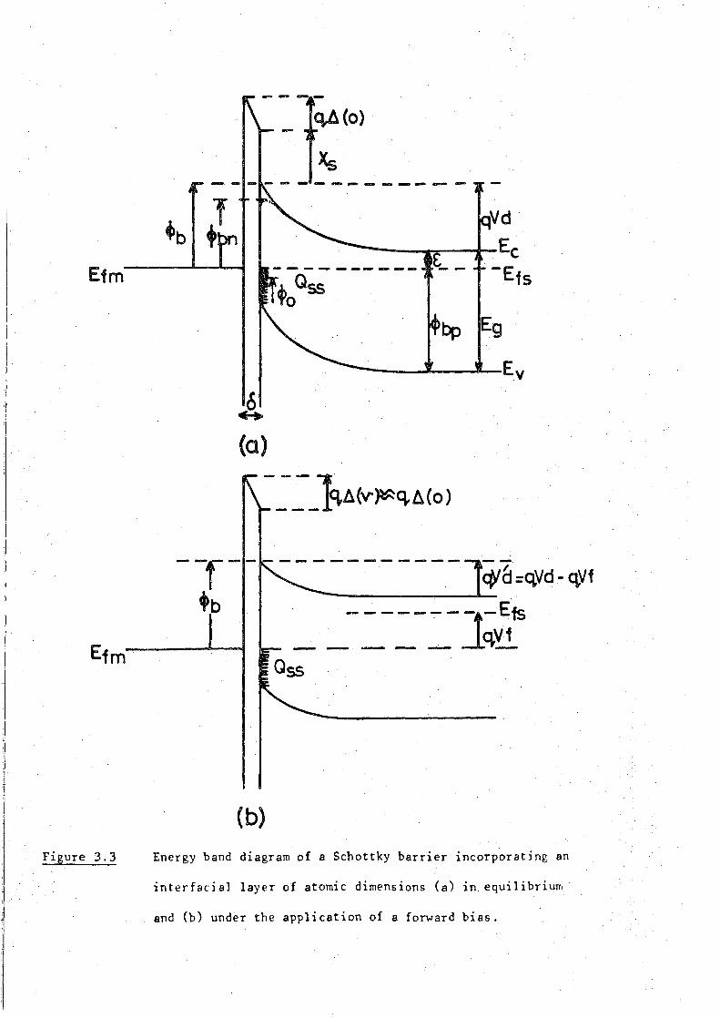
qA(o)
Etm
4>bp Eg
A (a)
- ~~-}i..Mv~q.A(o)
----------~ / <i'a :qVd- q,Vf ----------------~~ ------- -]~v~ts - - - ----- q.:_
(b)
'Figure 3.3 Energy band diagram of a Schottky barrier incorporating an
interfacial layer of atomit dimensions (a) in equilibrium
and (b) under the application of a forward bias.
- 39 -
(i.e. Ds ~ 0 and Ds is very high) can be identified from eq (3.3).
If D s
= 0 then the expression reduces to the Schottky-Matt theory
given in eq. (3.1). If, however, D is very large then eq. (3.3) approaches s .
the Bardeen Limit, i.e. eq. (3.2). (8) Cowley and Sze also attempted to
correlate eq. (3.3) with previously published results obtained for a
number of semiconductors. They found that it gave a reasonable explanation
of the data for Si, GaP and GaAs diodes (particularly so in the case of
GaP), although, in general, there was a significant amount of scatter
involved. In contrast, results for CdS appeared to conform to the Schottky-
Matt theory and were thus inconsistent with their model.
It is now acknowledged· that this model provides a reasonably accurate
explanation for the variation of "' with 't'bn "' for many covalent semicon'~'m
ductors and has been widely used in the past to analyse Schottky barrier
( 9) systems . However, many do not conform to this theory (e.g. the more
ionic semiconductors CdS and ZnS) and the model cannot be· considered ns
universal. Indeed, more recently, a number of different theories have
been proposed, some of which are essentially extensions of the Bardeen
model; others are radically different. These developments are discussed
in the following section.
3.2.3 Recent Developments
The Bardeen model is rather idealised, b.oth in terms of .the explicit
assumptions mentioned earlier, and in terms of those imJlicit in the
theory supporting the model. These include the. assumption of abrupt inter-
facial boundaries, the use of point charges to represent interface states
(whereas, in fact, they extend into the semiconductor to a distance of
up to 1 nm(lO)), and also the assumption that the metal, interfacial layer
and semiconductor are all chemically inert, The fact that this last 1 •
11. ( 11)
assumption may not always be valid was demonstrated by Andrews and Ph~ ~ps
- 40 -
who studied transition metal- silicide " silicon diodes. (These are
now a well-established class of Schottky barriers in modern integrated
circuits.) They found a high degree of correlation (up to 97%) between
the Schottky barrier height and the heat,of formation of the chemical
reaction which occurs at the surface. This demonstrated, at least for
this class of diodes, a definite link between Schottky barrier formation
and metal reactivity. Our lack of understanding of Schottky barrier
formation W?S aptly demonstrated by the fact that they found it
necessary to distinguish four types Of Schottky barriereach conforming
(11) to a different theory , one of which was their metal reactivity
model. A d . 1 . . k b '11 (l2) more ra 1ca v1ew was ta en y Br1 son who, using a
wide range of both reactive and non-reactive metals, )resented evidence
to show that in .the case of CdS and CdSe, interface chemical reaction
and local charge redistribution dominated the Schottky barrier properties.
He proposed that these mechanisms may dominate Schottky barrier formation
in general. The same effect was demonstrated for the Al/GaAs system(l 3)
which is known to possess a relatively abrupt interface. Once again,
microscopic charge rearrangement was proposed as the dominant mechanism
in determining the macroscopic barrier height.
. 1(14 ) d h . . . . f Sp1cer et a prove t .at 1ntr1ns1c sur ace states could not be
used to explain Schottky barrier formation (at least iri the III-V
compounds) when they showed that, although the cleavage (110) face of
these semiconductors does not possess intrinsic surface states in the
energy gap, the position of the Fermi level could be pinned by much less
than a monolayer coverage of metal - the pinned position showing little
dependence on the metal species, They proposed the 'unified defect
model 1 for Schottky barrier formation where the Fermi level is pinned
by extrinsic interface states caused by lattice defects resulting from
the adsorption of impurity (metal or oxygen) atoms. Although Spicer et al
correlated the defect levels with missing column III or V elements,

there has recently been some contention of this point(lS) .. Williams
t l (l6 ) . k' . d d 1 d . . . e a · , wor ~ng ~n epen ent y, rew s~m~lar conclus~ons from their work
on InP, thus providing strong support for the unified defect model .. It
should be noted, however, that thismodel does not contradict the
previously mentioned results showing the influence of surface chemical
reactions on Schottky barrier formation. Indeed, the relevauce of this
work to the unified defect model has been discussed by Spicer et al(l7)
where they suggest that it is the heat of condensation of the metal on
the III-V materials which is responsible for the appearancE;: of semiconductor
. 1 . h l(l4 ) . mater~a ~n t e meta and stress the ~mportance of the development of
interface (surface) thermodyanics and kinetics in order to provide a
fuller understanding of the problem. (However, they also s·.:ress that they
believe it is surface chemical interactions which are the determining factor
and not the formation of bulk reaction products.)
Thus an elegant model, based on a wealth of experimental evidence,
has been developed which can explain the problem of Schottky·barrier
formation 1n terms of extrinsic surface states and is therefore consistent
with much of the Rardeen modeL However, there remains considerable con
troversy and, indeed, Freeouf(lS) has recently argued that the use of inter-
face states to explain some of the experimental rE!SUlts for Schottky barriers
is inconsistent with a number of other experimental observations; and' with
(19) . Woodall , suggests an effective work functi6n.model as an alternative
to the unified defect model. In this case the macroscopic barrier height
is determined by the work functio~s of microclusters of one or more inter-
face phases resulting from chemical reactions during fo.rmation. In addition
to this, Lee et al(ZO) have proposed a metal~amorphous film~semiconductor
configuration as the structure of a real Schottky barrier, and have used
this model to t~xplain many of the experimental observations traditionally
attributed to interface states, Observations such as the difference in <Pbn

- 42 -
indicated by capacitance measurements compared to that measured by con-
ductivity or photoemission techniques(§ 3.4.1); the variation in diode
ideality factor(§ 3.3.3); the origin of Fermi-level pinning; and the
difference in the interface behaviour between covalent $Ud more ionic
semiconductors. (These experiments .were performed on diodes fabricated
on chemically prepared semiconductor surfaces in comparison to much of
the previously mentioned work which was performed, largely, using diodes
fabricated on cleaved surfaces in UHV .. This is certain to prove an
important factor in determining the precise structure of the diodes.)
The work reviewed in this section has undoubtedly led to important
advances in the understanding of the theory of Schottky barrier formation.
However, the majority of practical diodes can be analysed quite succ.ess-
fully using the Rardeen model and, since this is used extensively in this
thesis, the model is discussed in more detail in the subsequent section.
3.3 THE NEAR-IDEAL SCHOTTKY BARRIER
3.3.1 Introduction
A 'near-ideal' Schottky diode is defined here as one where the semi-
conductor (and hence the charge in the interface states) is separated
from the metal by a very thin insulating layer of atonic dimensions. It
is assumed to be essentially 'transparent' to electrons (i.e. readily
traversed by quantum mehanical tunnelling) but nevertheless is able to
withstand a potential. This interfacial layer is necessary from electro-
static considerations in order to analyse the diode according to the
Bardeen model. (If the interfacial layer were absent, then the ~ffect
of the metal would be to 1screen 1 the interface stat~s thus preventing
them from affecting <!> • ) The band diagram ·for m
is shown in fig. 3,3 (a) and is the model used
such a Schottky barrier
(8) by Cowley and Sze

~ 43 -
in their analysis. Since the interfacial layer is so thin, it is assumed
to have a negligible affect on the Schottky barrier properties. In
particular, a neg1-igible proportion of any applied voltage is developed
across this insulator and the degree of band bending in the semiconductor
is approximately given by Vd + Va (where Va is the applied voltage).
A consequence of this is that the position of the conduction and valence
band edges (at the semiconductor surface) remain fixed with respect to
the position of the metal Fermi level. This can be seen in fig. 3.3(b)
which illustrates the situation under forward bias. An important
consequence of this is that the charge localized in the interface states
(which equilibrates with the metal Fermi' level for such a thin insulator)
is essentially fixed and independent of bias. This, together with the
assumption that the effect of the insulator on the processes of current
transport is negligible, enablesthe insulator to be omitted in much of
the following discussion.
This near-ideal situation is close to that achieved in practice,
when the semiconductor is carefully prepared chemically. (before deposition
of the metal electrode) with the intention of minimising the interfacial
layer.
3.3.2 The Schottky Effect
The Schottky effect is the lowering of a potential barrier due to
the existence of an image force between an electron and the surface of a
metal. This originates from the fact that an electron, at a distance, x,
from the metal. surface, experiences an attractive force due to an induced
positive charge on the metal surface. The effect on the metal-semiconductor
barrier height is shown :t..n fig, 3,4. The barrier height is lowered from
1
<Pb to <Pbn, by an amount, Mbn, This barrier lowering is due to a
combination of the electric field in the depletion region and the potential
due to the.image force. This force, F., is given by ].
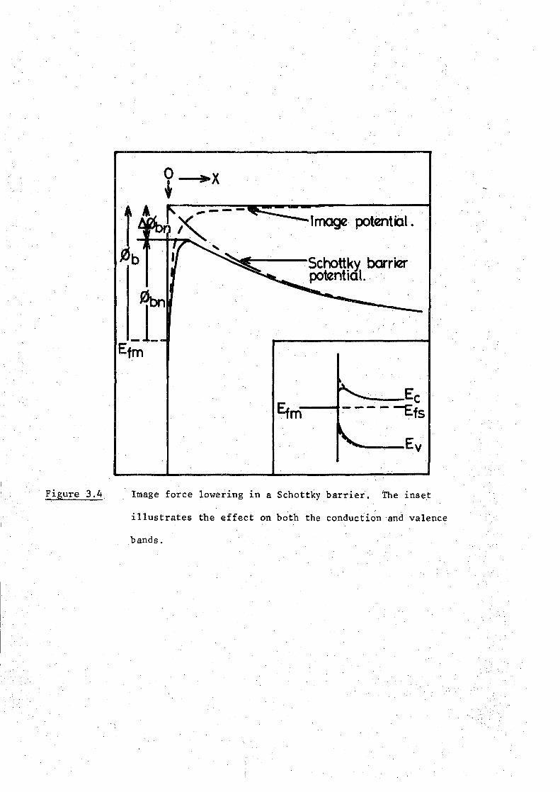
Image potential .
. SchottkY. barrier potential. ·
---Ev
Figure 3.4 Image force lowering in a Schottky barrier. The inset
illustrates the effect on both the conduction and valence
bands.

F. = ~
- 44 -
(3.5)
where ss is the permittivity of the semiconductor. The potential energy
due to F. is represented by the dashed line in fig. 3.4, and this, super~
imposed with the potential energy due to the Schottky barrier, gives the
resulting barrier as shown. Since the image force is only significant in
the vicinity of the interface, to a good approximation the field in the
depletion region is constant and equal to E . Then the potential energy max
of an electron at a position, x is given by
X
X(x) =
I 00
F.dx + qEx l
q E x max
This expression can be differentiated and equated to zero to. yield.
and
X max
(3.6)
(
(3.7)
(3.8)
Holes in the semiconductor valence band also experience an image force but
in this case the effect on the band structure close to the semiconductor
surface ~s to bend the valence band upwards, as shown in the inset to
fig. 3.4.
Although the effect of this image force lowering is small ( "-0.04eV),
it can have a significant effect on the Schottky barrier properties,
particularly the current transport processes since the current depends
exponentially on ~bn' Furthermore, the amount by which the barrier is

- 45 -
lowered depends on E and hence on the applied bias - an effect dis-max
cussed in the following section.
3. 3 . 3 C\lrrent .transpor.t pr0cesses
There are several processes by which current may flow in a Schottky
barrier under the influence of an applied bias. These are shown
schematically in fig. 3.5 and are illustrated for the case of an applied
forward bias (positive to the metal). Under reverse bias the exact
inverse processes occur. These mechanisms are; (a) the emission of
electrons over the top of the barrier, (b) quantum mechanical tunnelling
through the barrier, (c) recombination 1n the depletion region and (d)
recombination in the semiconductor bulk. Processes (c) and (d) are the
result of minority carrier injection into the semiconductor with (d) being
the true injection of interest in this work as it can lead to radiative
recombination in the semiconductor. However, it is well known that, in
the vast majority of cases, the minority carrier current in a Schottky
barrier represents only a small fraction of the total c·trrent(2l) and the
Schottky barrier is predominantly a majority carrier device. Consequently,
processes (c) and (d) are very small, as is (b) unless the material is very
heavily doped or at a low temperature. This means that emission over the
barrier (process (a)) is the dominant current mechanism in most Schottky
barriers. However, before the carriers can be emitted over the barrier,
they must be transported from the semiconductor bulk t( the interface region.
This occurs by the normal processes of diffusion and drift and is in series
with the actual emission over the barrier. . ( 22) Wagner and then Schottky and
Spenke( 4 ) proposed that the diffusion process limited and hence deter-
. (23) mined the current flow in the diode, whereas Be the proposed the,uinionic
emission as the limiting process. It is now acknowledged that in the vast
nwjodty of cases (even in those semiconductors, like GaP, with relatively

Figure 3.5
Figure 3.6
a ~
b~ """-."'I. c - - d
( 1--- . . "::.,...~- ------1--.. 'l.Vf
.. 1
.. .. .. ----- --- --
... ~f
.1111 ... ... M s
Schematic diagram depicting basic current transport processes
in an MIS diode under forward bias.
b a
M
~~--------Et Efs
--~'LU.J(.,LL,J.~"'~Ec
~-------------Ev s
Field and thermionic field emissl.on in a degenerately doped
Schottky barrier structure.

- 46 ..
low mobilities), the current-voltage characteristics are best described
by the thermionic emission theory and this is discussed next in some
detail.
(a) Emission Over the Barrier
(i) Thermionic Emission Theory. Since, under non-equilibrium con-
ditions, the change in the quasi-Fermi level with distance is indicative
of the'driving force' behind the carrier flow (see appendix A), then this
theory is tantamount to assuming that the electron quasi-Fermi level is
flat throughout the depletion region and coincident with the Fermi ·level
in the semiconductor bulk. (In order to account for the discontinuity of
the Fermi level at the surface, one must either assign the energetic
electrons which enter the metal their own quasi-Fermi level, as shown .in
:t;ig. 3.5, or assume that thermal equilibrium is established at the metal-
semiconductor plane.) It follows that the electron concc)ntration in the
semiconductor, at the interface, is given by
n = N c exp. { -q (¢bn - V)/kT } (3.9)
where N is the effective density of states in the conduction band and V c
" . d 1 1s the appl1e vo tage. For a semiconductor in which the electrons have
an isotropic velocitydistribution (i.e. spherical constant energy surfaces),
the number of electrons impinging on unit area of the interface per
second can be shown (by kinetic theory) to be nv/4, where v is the average
electron thermal velocity. Thus, the current density passing fromt:he
semiconductor to the metal, J is given by sm
J sm ;:::
~
qN v c .
4 exp ( -q (¢bn - V)/~T] (3.10)

- 47 -
Since there is a flow of electrons into the metal even at zero bias,
there must be an equal and opposite flow from the metal which is governed
by the value of ~bn and is thus independent of bias. The total current
is given by
J = N v
c
4 exp ( -q~bn/kT) { exp (qV/kT) - 1 } (3.11)
~·( ~ Since for a maxwellian velocity distribution v = (8kT/Tim ) , then J is
given by
J = -/( 2
A T exp (-q~bn/kT) {exp (qV/kT) - 1} (3.12)
* * 2 3 * where A = 4Tim qk /h ; m is the electron effective mass and h is Planck's
~'(
constant. The term A ~s the effective Richardson constant which accounts
for the electron effective mass, but neglects the effect of optical phonon
scattering and quantum mechanical reflection( 24). Eq. (3.12) is often
written in the form
J = J {exp (qV/kT) - 1} 0
where the reverse saturation current density, J0
, is given by
J 0
= * 2 A T exp (-q ~bn/kT)
(3.13)
(3.14)
These equations represent the thermionic emission theory for current flow
in an ideal Schottky diode.
(ii) The Diffusion Theory, !n contrast to the thermionic emission
theory, the assumptions inherent in the diffusion theory are the equivalent
of assuming that the electrons in the semiconductor, at the interface,

- 48 -
arein equilibrium with the metal. This implies that the electron quasi-
Fermi level (as shown by the dotted line in fig. 3.5) is not flat through-
out the depletion region, indicating that the processes o~ drift and
diffusion in this region represent the main impediment to current flow.
Beginning with the general equation for the current flow in the depletion
region i.e.
J = qn ~n E + q Dn ( ddn;x) (3.15)
(where J.l is the electron mobility; D is the electron diffusion coefficient) n n
and assuming that E, the electric field in the barrier is constant and ' .
equal to E , it can be shown(ZS) that the current density is given by max
J = q NcJ.ln Emax exp (-q ~bn/kT) {exp(qV/kT) -1} (3.16)
or J = Jd {exp (qV/kT) -1} (3.17)
In· this case, however, .Jd is not a saturation current since E 1s a max
function of bias which causes Jd to increase with the applied voltage.
(iii) The Thermionic Emission - Diffusion Theory. In the most
general case, the current will be determined by a combination of the two
limiting theories. (24)
Such a combination has been derived by Crowell and Sze
in which the current density is given by the expression
J ( 3 .18)
where v is an effe.ctive recombination velod.ty at the potential energy r
maximum, and vd is an effective diffusion velocity for the transport of

- 49 -
electrons from the edge of the depletion region to the potential energy
maximum.
However, it has been shown theoreticall/ 26 ) that diodes f'abricated
on reasonably high mobility semiconductors should behave according to
the thermionic emission theory. This has been confirmed experimentally
for the vast majority of Schottky diodes, even those with :relatively low
mobilities. Nevertheless, practical diodes invariably deviate from the
ideal behaviour predicted by eq. (3.13). In particular, graphs of ln J
versus V (which should be linear for V ~ 3kT/q) 'V
do not exhibit the
predicted slope of q/kT. Instead they canbe described by the relation
J = J exp (qV/nkT) 0
(3.19)
for V > 3kT/q. The parameter 'n' is known as the ideality factor and 'V
has a value greater than, or equal to, the ideal value of unity. The most
common cause of this departure from ideality is due to the bias-dependence
of the barrier height which arises primarily from the presence of an inter-
facial layer (see § 3.4). However, even in the absence of such a layer,
the barrier height is still bias-dependent because of the effect of the
image force, which itself depends on the applied bias. The value of n
depends critically on the diode preparation procedure and, with care,
values very close to unity can be repeatedly obtained using normal
laboratory techniques.
Reverse Characteristics
Eq, (3.13) predicts a reverse current density w.hich saturates at
the value of J given by eq, (3,14), This is dtie to the thermionic emission 0
of electrons from the metal over the barrier and into the semiconductor,
However, any bias-dependence of the barrier height will prevent the

- 50 -
reverse eurrent from saturating. The magnitude of this effect is
governed by the same factors which influence the ideality factor of the
forward bias characteristics.
(b) Quantum Mechanical Tunnelling Through the Barrier
In heavily doped materials at low temperature, it is possible for an
appreciable current to flow due to electrons, with energies less than the
barrier height, traversing the barrier by quantum mechanical tunnelling.
This has been studied extensivel/ 27 ' 28 ) and both field emission and
thermionic-field emission have been identified. The tunnelling current
1s a function of the transmission coefficient, the occupancy of the states
in the semiconductor, and the available states in the metal .. consequently,
in a degenerate semiconductor at very low temperatures (under forward bias),
the.energy distribution of the tunnelling electrons is centred around the
semiconductor Fermi energy. This is field emission and is depicted by
process (a) in fig. 3.6. If the temperature is increased, the excited
electrons 1 see 1 a narrower (and lower) potential barrier a-..td a second dis-
tribution., centred around Et (the Fermi energy plus the thermal energy),
is evident. This is thermionic field emission, i.e. process (b) in fig.3.6.
The forward bias current density - voltage characteristic is described
by(27)
J = J exp (V/E ) s 0
where E 0
= E coth (q E /kT) and E = h ·. ( ~~ )~. oo oo oo 47T m~\. s
(3.20)
(28) The term J is a function of both the temperature and the barrier height
s
Reverse Characteristics
Tunnelling from the metal into the semiconductor is much more dominant
a process than in the corresponding forward bias case, This is due to the

- 51 -
fact that, under reverse bias the electrons, at a given energy in the
metal, 'see' a narrower barrier (see § 2.2.2). It represents a further
departure from the ideal reverse bias characteristic and is a common
cause of its non~saturation in practical devices.
(c) Recombination in the Depletion Region
This process has previously been discussed when it was considered
as a non-radiative recombination path for injected minority carriers. The
importance of this mechanism when compared to the other processes depends
critically on the particular system investigated. It can; in so,me cases,
significantly affect the forward current-v~ltage characteristic (29 ). This
current can be analyse/ 29 ) using Schockley-Read-:-Hall statistics by assum-
ing that recombination proceeds via a centre located approximately mid-gap.
Then the current density is given by
J = J exp (qV/2kT) r
(3.21)
where Jr = q ni W/T, ni is the intrinsic carrier concentration, W is the
width of the depletion region and T is the lifetime in the depletion
region. This process can affect both the ideality factor, n, and the
saturation current density, J , of eq. 3.13 and is particularly evident 0
at low temperatures when the thermionic emission procers is much reduced.
Reverse Characteristics
Under reverse bias conditions, the opposite process occurs, namely,
generation in the depletion region, Electron~hole pairs thus formed are
separated and swept away by the electric field which gives rise to an
additional current component. This is proportional to the width of the
depletion region and consequently increases with reverse bias thus prevent-
ing current saturation.

- 52 -
3.3.4 The Capacitance of a Schottky Barrier
The capacitance of a Schottky barrier arises from the charge due to
ionised donors in the depletion region and an equal, opposite charge on the
surface of the metal. Since the width of the depletion region varies with
applied bias then the capacitance is also a function of bias. The
depletion approximation can be employed to simplify the analysis, This
states that the charge density is constant and equal to qNd up to the edge
of the depletion region and equal to zero past this position. Then the
charge in the depletion region is given by Gauss's law as
Qd = k
(2£ q NdVd) 2
s (3. 22)
when Nd is the donor density and Vd is the diffusion voltage. This is
the case. for zero bias; under the application of a reverse bias, Vd is
replaced by Vd' = Vd + Vr which is a measure of the degree of band bending
in the semiconductor. The capacitance is usually measured by superimposing
a small alternating voltage onto the D.C. bias and, consequently, it is
the response of the charge distribution to the AC signal which gives rise
to the capacitance; i.e. the differential capacitance is measured. This
capacitance (per unit area) is given by
dQd c =
dV = ( q t:: Nd
s
2(Vd+Vr) (3.23)
A more rigorous analysis, allowing for the effect of a non~abrupt depletion
region, yields
c "" q ~ Nd s
2(Vd + Vr .. kT/q)
(3,24)

- 53 -
An assumption, inherent in the above analysis, is that the charge 1n the
semiconductor is due solely to ionised donors. This is incorrect if
there is an appreciable concentration of holes at the semiconductor surfac~
as would be the case if the surface were inverted. In such a situation
the charge due to the holes must be subtracted from Qd and this complicates
the theory considerably(30). The effect is essentially to replace Vd in
eq. (3.24) with a bias dependent voltage, and this results in a non-linear
c-2 - Vr relationship (see § 3.3.5).
Practical Schottky diodes contain deep traps, due to unintentional
impurities or defects, which may be filled or emptied according to external
stimuH_ and consequently affect the capacitance. In fact this forms the
basis of a wide range of capacitance spectroscopy techniques, a good
account of which can be found in ref. (31).
3.3.5 Measurement of Barrier Height
There are a number of methods by which the Schottky barrier height,
~bn' may be deduced. These are now discussed in sequence.
(a) Current-Voltage Measurements
The forward bias current density-val tage characteristic of a ne·ar-
ideal Schottky diode is given by the thermionic emission theory as
J =
where J = 0
J 0
exp. (qV /nkT) for V
-/( 2 A T exp. (-q~bn/kT)
> 3kT "'
i.e. eq. ( 3, 19)
Consequently, a plot of ln(J) against V can be used to determine both the
ideality factor and the Schottky barrier height according to the following
equations,
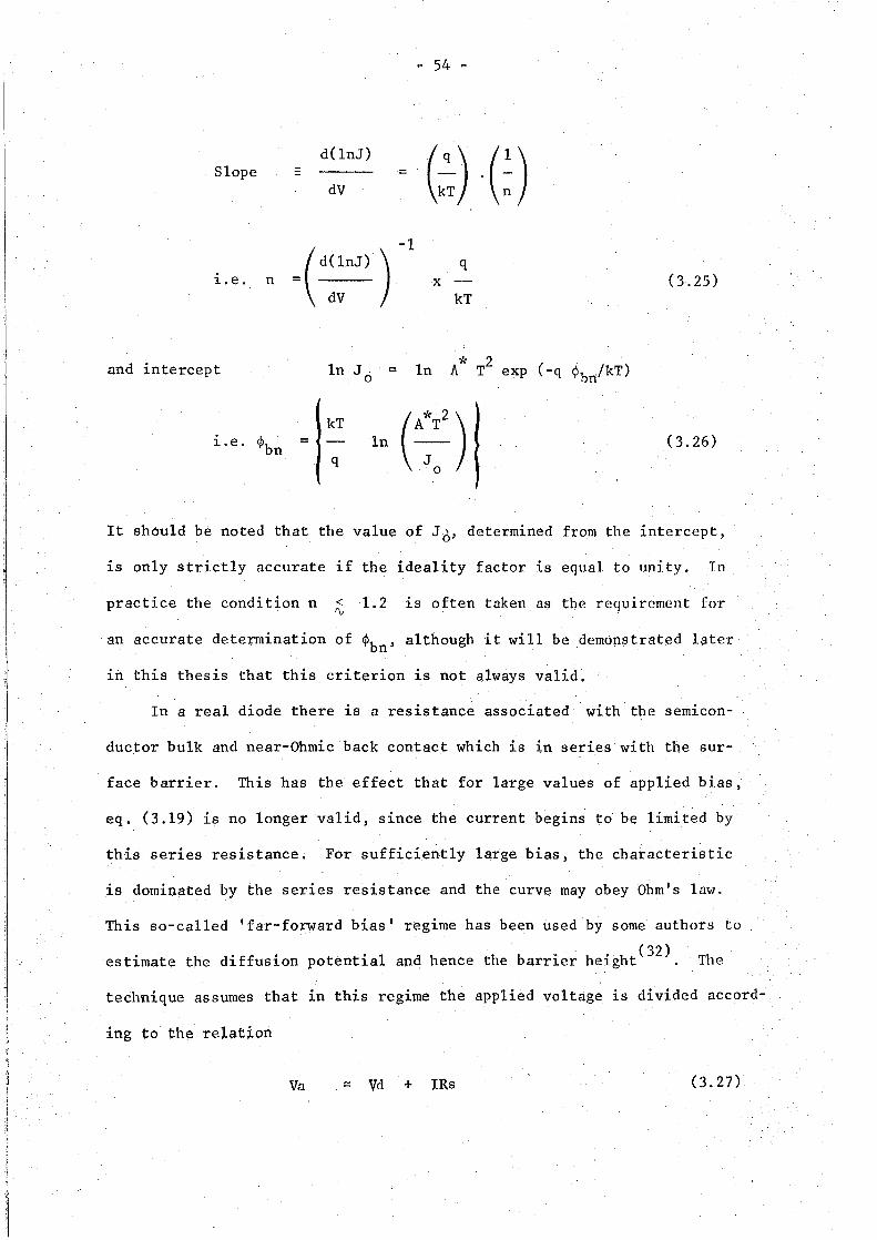
~ 54 ~
d(lnJ)
(k:) ·G) Slope - = dV
~1
= ( d::nJ) ) q i.e. n X- (3.25)
kT
and intercept * 2 ( -q ¢br/kT) ln J. = ln A T exp
0
kT e::2) i.e. ~bn = ln q
(3.26)
It should be noted that the value of J 0, determined from the intercept,
is only strictly accurate if the ideality factor is equal to unity. In
practice the condition n < 'V
1.2 is often taken as the requirement for
an accurate determination of ~ although it will be demonstrated later '~'bn'
in this thesis that this criterion is not always valid.
In a real diode there is a resistance associated with the semicon-
ductor bulk and near-Ohmic back contact which is in serieswith the sur-
face barrier. This has the effect that for large values of applied bias,
eq. (3.19) is no longer valid, since the current begins to be limited by
this series resistance. For sufficiently large bias, the characteristic
is dominated by the series resistance and the curve may obey Ohm's law.
This so-called 'far-forward bias' regime has been used by some authors to
estimate the diffusion potential and hence the barrier height(32). The
technique assumes that in this regime the applied voltage is divided accord-
ing to th~ relatLon
Va ~ Vd + lRs (3.27)

- .55 -
where Rs is the diode series resistance and I is the current, (i.e.
Voltage in excess of that required to flatten the bands in the sem1con-
ductor is dropped across the serie~ resistance.) Consequently, a plot
of I against Va is, to a first approximation, linear with an inter-
cept on the voltage axis equal to the diffusion voltage.
Reverse Characteristics
The barrier height may also be determined from the reverse current
since the thermionic emission theory predicts that this characteristic
should saturate at a value given by J0
, In this situation <Pbn can be
determined using eq. (3.26). However, the fact that in practical diodes.
the reverse current rarely saturates (due to one or more of the processes
discussed in § 3.3.3), limits the usefulness of this technique. Further-
more, if the barrier height is large, then the reverse current is often
undetectable which has been the case in most of the diodes studied in this
work.
i'(
If either the active device area, Aa, or the relevant value of A 1s
unknown, then an activation energy plot can be used to determine <Pbn· For
. example, 2 1/. Bhould give a ilope of -q<Pbn/kT a graph of ln (I0 /T ) versus T
and an intercept on the vertical axis of .,,
ln(A Aa). In addition, there
are a number of modified versions of this technique which have been
developed to overcome specific problems . . d'f' . (33) . For example, one such roo 1 1cat1on
enables <Pbn to be measured even in the presence of a large series resistance,
which would prevent its measurement from the usual J-V characteristic.
All of these techniques suffer from the disadvantage of being tedious to
employ and are therefore only used when the more straightforward methods
fail.
(b) Photoelectdc Measurement
The photoelectric determination of the Schottky barrier height involves
shining monochromatic light, of varying wavelength, onto the metal barrier

- 56 -
electrode and monitoring the current due to photoexcited el!ctrons in
the metal which surmount the barrier and are collected by the electric
field in the depletion region. ( 34) . Fowler stud1ed the photoresponse of
clean metal surfaces to monochromatic light and developed the theory
upon which this technique is based. The photocurrent per absorbed photon
R is given by the Fowler theory( 34 ) as
R "-' - k (Es-hv) 2
2 X
2
for .x ~ 0; where x = h(v- v )/kT 0
( -x
e -
-2x -3x e e
+ 4 9
-4x e
16 (3.28)
(3.29)
The term hv 0
represents the Schottky barrier height, ' ~bn' and Es is
equal to the sum of ~bn and the Fermi energy (measured from the bottom
of the metal conduction band). Provided Es >> hv (a condition which is
almost always valid) and hv .,. hv > 3kT, then to a good approximation 0 'V
eq. (3.28) reduces to
R = C(hv (3.30)
where C 1s a constant. k
Thus, a plot of.R 2 versus hv is linear over a
certain range of energy and the interse'ction of this linear region with
the energy axis gives a direct measurement of the barrier height. The
range over which eq. (3,30) is valid is determined, at low energy, by the
requirement X > 'V
3, and at high energy by th~~ condition that Es » hv.
In practice, however, the high energy Hmi tati,,n is usually due to the
generation of free carriers in the depletion -tegion as hV appro·aches the
value of Eg. This effect can be reduced by employing a relatively thick
top electrode in order to reduce the amount of light being transmitted
to the semiconductor. Since the mean free path of a photoexc i ted

~ 57 ~
electron in a metal can be quite large( 3S) (<u 75 nm in gold), electrodes
which are almost opaque can be used effectively. The same technique has
been used to eliminate non~linearities in these 1Fowler 1 plots due to the
photoexcitation of carriers from surface states by light of energy,
hv <. Eg(36
) .. However this is usually a problem only when there is a
significant interfacial layer present (see§ 3.4).
(c) Capacitance Measurements
The differential capacitance associated with the Schottky barrier
depletion region is given by eq. (3.24) which may be writt~n as
C-2 = 2(Vd - kT/q + Vr)/qE Nd
. s ( 3.31)
Thus, a plot of c- 2 against Vr should be linear (provided Nd is constant
in the depletion region) with an intercept,. V0
, on the voltage axis given
by
V = Vd 0
kT
q ~bn · - E -
kT
q (3,32)
where E is the difference between the conduction band edge and the Fermi
level in the semiconductor bulk (as shown in fig. 3.3(a)). That this
technique should measure Vd (and not ~bn) results from lhe fact that
. -2 extrapolating to the voltage at which C = 0, i.e. the capacitance is
infinity, indicates the voltage at which the band-bending is eliminated,
i.e. Vd. Furthermore, since the technique does not involve the idea of
charge carriers approaching the barrier (and cons.equently the concept of
image charge), then the value of ~bn deduced/ from such a measurement does
not include the effect of Schottky barrier lowering. The term '~:::' is given by
= kT/q 1~ (Nc/Nd) (3.33)

- 58 -
which can easily be computed since the value of Nd can be :i,nferred from
the slope of the -2 C - V plot.
Of the techniques described previously for the determination of the
barrier height, the capacitance method is the least direct. Both the J-V
and photoelectric techniques involve processes whereby carriers actually
surmount the barrier, and therefore include the effect of processes such as
image force lowering. Furthermore, the capacitance technique is, in general,
the most
presence
unreliable and inaccurate since it is highly susceptible to the
of an interfacial layer( 37). Nevertheless, for the near-ideal
diodes considered in this section, good agreement can be expected using
the various techniques.
The photoelectric method is the most accurate, since it directly
measures the minimum energy required by an electron in order to surmount.
the barrier. It is generally regarded to be the definitive measurement
and to provide the only irrefutable value for <Pbn' However, new results
for GaP described in chapter 7 cast some doubt on its general applicability.
3.3.6 Minority Carrier Injection
The minority carrier injection ratio , y, is defined as the ratio of
the minority carrier current, Jp, to the total current.
1. e. Jp Jp (3.34) y =
Jp + Jn Jn
provided the majority carrier current, Jn >> Jp (i.e. assuming low
injection conditions). Rhoderick( 3B) has shown that, in addition to
assuming an electron quasi"Fermi level that is flat in the depletion
region, the hole quasi-Fermi level can be assumed flat throughout this
region and coincident with the metal Fermi level at the interface (see
Appendix A). This indicates that for the hole current, the limiting

- 59 -
mechanism is not emission over the barrier but rather the processes of
drift and diffusion in the semiconductor bu1k. If the applied bias is
assumed to be sufficiently low so that diffusion is the do~inant
mechanism, then the hole current density can be expressed using p~n
junction theory as
Jp = (p(w) - Pno) ( exp (qV/kT) - 1 ) (3.35) = L
where L is the width of the quasi~neutral region in the semiconductor
(assumed to be less than the minority carrier diffusion length), Pno 1s
the equilibrium concentration of holes and p(W) is the concentration at
the edge of the depletion region. Then y is given by eq. (3.34) ns
y = .2
q D n .. p 1
* 2 Nd LA T exp(- ~bn/kT) (3.36)
. (29) This expression has been verified exper1mentally for low injection con-
ditions in silicon diodes. Using typical values for gold/(n)Si diodes,
eq. (3.36) yields a y value of the order of lo- 5• It is for this reason
that the near-ideal Schottky diode is often termed.a majority carrier device.
Scharfetter( 2l) has considered the effect of including the drift component
in the analysis and showed that for current densities greater than a
critical value, Jc, the injection ratio increases linearly·from that
predicted by eq. (3.36), This critical current density is given by
q Dn. Nd/L (3,37)
above which y is given by

'Y
2 n. J 1
- 60 -
(3.38)
where b is the mobility ratio. This increase has been ·demonstrated
. • (29) exper1mentally , although only over a limited range and, in fact, the
theory has been extended by Green and S h h ( 39) :t.. . d. 1' . c ewe un . wuo pre 1ct a 1m1t
to the increase in y due to both a limit in the supply of holes (by
thermionic emission over the hole barrier at the surface)' and the fact
that Jp becomes comparable with Jn.
The value of Jc is typically of the order of 100 A cm- 2 which is
much larger than the current densities employed in this. study and the effect
is not significant in the LED work described in this thesis.
3.4 THE METAL - THIN INSULATOR - SEMICONDUCTOR DIODE
In this section, the inclusion of an insulator which has an appreciable
effect on the device properties is considered. In this situation the
insulator can no longer be considered as transparent totunnelling electrons
and represents a significant additional barrier to carrier transport. The
band diagram for the MIS diode (a) in equilibrium and (b) under conditions
of forward bias are shown in fig. 3. 7. It can be seen that the applied
voltage, Vf, 1s developed partially across the semiconductor depletion
region, !::,.Vd, and partially across the interfacial layer, b.V. ·. A consequence 1.
of this is that the interface state charge is not fixed, it is bias dependent
and, depending on the properties of the interfacial layer, may be determined
by interactions with either the metal or the semiconductor, Under conditions
of forward biasi the relative shift between the metal Fermi level and the.
semiconductor band structure, which gives rise to both the change in inter~
face state charge and a bias dependent barrier height, can be seen in
fig. 3.7. This is in contrast to the near-ideal situation depicted in fig. 3.3

__ .... __________ _
-----ft~"-~Ec Etm ~-Ets
M I 5 ~--__;,..--~~-Ev
·tie (i) +bn > ~bn (ii) Vf = llVi +llVd
(a)
{iii) Qss< 0 > . * Oss (V) q,ll(V):qA (o) -qllVi .
------------...-----I .
Vtt = q.Vd -llq.Vd ·
-------~----71·-.E~ . . /
- - _ ~ - _ tp _ ___ / q,Vf ~----
Oss(V) ..-~,pi
(b)
Figure 3. 7 Energy band diagram of an MIS diode, (a) in equilibrium and
(b) under forward bias showing the behaviour of the quasi-

- 61 -
where 6.V] was assumed to be negligible and the band edges at the surface
were ' pinned' relative to the position of the metal Fermi level.
3.4,1 Modifications to Schottky Batrier·Theory
The modifications to the theory discussed in §3.3 (which are necessary
to account for the effects on an appreciable insulating layer) are now
discussed.
(a) Current-Voltage Characteristics
The effect of such an insulator on the J-V characteristics has been
considered by Card and Rhoderick( 40), They divided the interface states
into two groups, one of which communicates more easily with the metal, the
other with the bands in the semiconductor, The relative densities of these
two groups is determined essentially by the thickness of the interfacial
layer. k . . b f . ( 40) b 1 h h By rna 1.ng a num er o assumpt1.ons they were a·. e to s ow t at
the main effect of the layer was to alter the pre-exponential, J0
, term
in eq. (3.19) to give
J = J 00 exp (qV /nkT). (3. 39)
where J00 = (3.40)
x is the mean barrier height (in eV) presented by the energy gap of the
insulating layer and o is its thickness in Angstrom units. (In fact
there is a constant with units of (eV-% ~-l) and a value of very close to
unity which has been omitted from the term (-x%8) for sim:plidty.) In
addition to this effect, the ideality factor is also affected by the
presence of the insulator. It is governed predominantly by the bias-
dependence of ~bn which originates from a combination of.the voltage
drop in the insulator and the subsequent change in the interface state
. . • b (40) cha,rge density. In this case the ideality factor 1.s g1.ven Y

1 +
" 62 "
(o/~i) (ss/W + q Osb)
1 + (~/s.) q Dsa 1.
(3.41)
where Dsa and Dsb are the density of interface states which communicate
with the metal and semiconductor respectively. For very thin insulators
Dsa >> Dsb; eq. (3,41) reduces to
n 1 + 8 8 s
W(si + oqDsa) (3 .42)
Conversely, for thicker insulators, Dsb » Dsa and n is given by.
n 1 + €
s
€. w 1.
+ qDsb (3.43)
A third limiting case exists, namely when the density of interface states,
of either group, is very low then eq.(3.41) reduces to
n 1 + 0€
s
Ws. 1.
. (3 .44)
Eq. (3.42) 1.s the result derived by Crowell & Sze( 24 ) who had earlier
approached this problem by assuming that the interface states were all in
equilibrium with the metal Fermi level,
Reverse Characteristics
The main effect of the insulator on the reverse characteristics is to
prevent the current from saturating with increasing reverse bias. This,

- 63 -
aga1n, is a consequence of the bias~dependence of ¢bn' but in this case
~b decreases with bias, It is similar to the effect of the image force
(see §3.3.3) in this respect but is much more pronounced and therefore
usually dominates.
It is clear from the above discussion that the analysis of the J-V
curves from MIS diodes is much more difficult than in the Schottky barrier
k case, In particular, the value of (x 2 o) is almost impossible to predict
since it must represent an average term due to the fact that both X and 8
are likely to vary over the area of the electrode. This point was stressed
by Card and Rhoderick who showed that experimentally-determined values of
k (x 2 o) differed greatly from those predicted using the relevant bulk values.
It is often assumed that the condition n < "'
1.2 is justification for assum-
ing that the diode is near ideal and thus employing eqs. (3.19) and (3.14)
to evaluate ¢bn' The general validity of this assumption must be question
able as it is possible to envisage situations where the interfacial layer
has only a small effect on .n but a significant eff~ct on J0
. Indeed, 10
chapters 6 and 7, results will be presented which show ideality factors of
close to unity even though the insulating layer is thick and has a pronounced
effect on the other diode characteristics.
(b) Capacitance - Voltage Characteristics
Th f - 2 h . . d . d d h "' h e use o C -V c aracter1st1cs to eter~1ne V , an ence ~bn' as
been discussed previously. However, in many practical cases the barrier
height calculated from such a plot far exceeds that measured by the photo-
1 · h . ( 37 ) G d (4 l) h d' d d'ff e ectr1c or J-V tee n1ques . oo man as stu 1e many 1 ·erent
parameters which may influence these characteristics and showed that the
intercept, V0
, of the c- 2-v plot is always greater than Vd when there is
an interfacial layer present. Cowley( 37 ) extended this analysis to
include the effect of both the insulator and the bias-dependent interface
states. He developed a number of models in an attempt to obtain some

- 64 -
quantitative agreement with his experimental data, obtained for diodes
fabricated on GaP. His results have been widely used in the literature
to analyse non-ideal -2 (42)
C -V plots and more recently the same approach
-2 was used to derive a general expression (for C as a function of V) where
the interface states were divided into the two groups Dsa and Dsb
described previously. The approach which was used can most easily under-
stood by considering first an MIS diode without interface states:
In terms of the energies defined in fig. 3.7(a), • cart be defined as TJlS
Le. • ms
=
=
• - <x + E) m s
Vd + Mo)
(3.45)
(3 .46)
Using Gauss' law to relate the charge in the depletion region, Qd, to the
potential, ~(o), yields (using the depletion approximation)
Mo) (a/E.) (2q ~
= E Nd Vd) 1 s
k k (3 .4 7) or Mo) = v 2 Vd 2
1
2q Nd 2 2 (3.48) where vl = E 0 /E. s 1
I
Under the application of a reverse bias, ~(v) replaces ~(o) and Vd replaces
Vd. Then eqs. (3.46) and (3.47) can be written as
¢· ms +
and Mv) =
v =
k lk V 2 Vd 2
1
I
Vd + A(v)
Eliminating ~(v) from these equations yields
I
+ v Vd + I 1!\..
V ~ Vd 11
1 (3.49)

- 65 -
The semiconductor space charge is given by Gauss 1 law as I },
Qd = (2qe:s Nd Vd ) 2, and hence the differential capacitance is given by
dQd c = = (2q
], Nd) 2
e:s
I ],
d(Vd 2)
dV (3.50)
The quadratic equation (3.49) can be solved and substituted into eq. (3.50)
to yield
c =
. c-2 = J..e.
(2/q k
E Nd) 2
s -k
(~ + V + v1/4) 2
ms
(3.51)
Thus a graph of c- 2 against V is linear with a slope e·qual to that of the
simple Schottky barrier case but an interceptwhich is significantly
larger.
If the effect of interface states is included, the analysis is some-
what more complicated: Assuming that both type (a) and (b) interface states
are uniformly distributed, i.e. Dsa and Dsb are both constant as a function
of energy, then the change in the interface state charge, under the
application of a bias can be shown to be
l',Qss = qDsbV - qDsb l',Vi qDsa !J.V. 1
(3.52)
Also tJ.( 0) and tJ.( v) are now given by the modified expressions
!, !, /l(o) = v ~ Vd 2 + ~lei Qss(o) 1
tJ.(v) ~ 1],: o-'\i. Qss C.v) and = v . Vd ;! +
1
% I!, ~) I (3.53) l.,e ""'V· = vl (Vd 2 ~ Vd +o:e:. !J.Qss 1 . ' 1

- 66 -
Th h d . . . 11 b 1 ( 37 ) 1 . ( ) e approac use 1n1t1a y y Cow ey , and later fo lowed 1n ref 42 ,
b • ( ) ' ( ) I~ was to su st1tute eq. 3.52 1nto 3.53 , solve for Vd and to use
eq. (3.50) to determine C. The following expression ia obtained
where
-2 c =
=
2 ( 1 + al + a2)
qss Nd(l + a 1)
Vd (1 + a1 + a 2)
(1 + a1
)
vl _ _.:;:.___ +
4(l+a1+a2)(l+a1)
+ v
qDsb o/f. .. 1
1 1 V 2 Vd 2
1 +
(3.54)
Very recently> however, Fonash( 43 ) has re-examined the problem and
pointed to a flaw in the argument used by Cowley and in subsequent analyses.
This concerns the use of eq. (3.53), which is essentially a quasistatic
relationship derived simply by the summation of potentials, in the equation
(3.50) for the differential capacitance. The point being that, if the
charge in the interface states (in group (a) or (b)) can not respond to
the high frequency measuring signal, then the quasistatic expression for I
Vd (obtained from eq. (3.50)) does not accurately describe the variation I
of Vd in response to this signal. It in 1act describes the variation in
I (43) Vd with respect to the applied d.c. bias. Fonash has used the
I
correct (a,c.) variation of Vd to analyse several models and has predicted
-2 that in only two cases is the slope of the C -V plot constant with bias.
These are, the simple case of Dsa = Dsb = 0 (eq, (3.51)) and the situation
·when all of the interface states communicate with the metal, i.e. Dsb = 0,
and can follow the applied signal, In this latter case, the expressionJ
(43) . derived by Fonash 1s
-2 c = 2
e e Nd s
~ 67 -
+ + Vd + V (3.55)
In all of the other cases, Fonash( 43 ) predicts a non-linear c~ 2 -V plot
even for a uniform density of states, It 1s interesting to note that
the. characteristics observed consistently in this, and other studies
(of highly linear c- 2 -V curves whose slope and intercept increase with
film thickness) is not predicted by any of the models analysed by Fonash.
This will be considered in more detail in chapter 7 when the C-V data
are analysed.
Before proceeding, it is useful to reconsider the original analysis
(37) of Cowley . In that work, the aim was to develop a model which agreed
quantitatively with the data.obtained using GaP MIS diodes incorporating
interfacial 'oxides' resulting from the fabrication procedure. In order
to achieve this, Cowley essentially chose an arbitraryfunction to relate
the change in the interface state charge (with bias) to the thickness of
the interfacial layer and hence, despite the flaw in his argument, the
final model gave a good description of his experimental results. Since
the 'non-ideal 1 diodes described in this work itt chapter 6 also contained
an interfacial 'oxide' resulting from the fabrication procedure, the model
developed by Cowley is used later in this thesis to infer an approximate
value for the thickness of the interfacial layer. Such a value can only
be considered as very approximate since it ll)ust be assnmed ~hat the two
interfacial layers possesssimilar properties,
The interpretation of the C-V characteristics of thin,.'MIS diodes.
is dearly a very comple" problem and due consideration must be given
wheq. attempting sucQ. an analysh. In particular, the intercept on the

- 68 -
voltage axis of the c- 2 -V curve cannot, in general, be considered as
an accurate measurement of the diffusion voltage.
(c) The Photoelectric Measurement of Barrier Height
The'direct measurement of metal~semiconductor barrier heights in
MIS diodes has been the subject of a number of studies (see for exampl·=,
ref. (36) and references contained therein). However, in most cases the
measurement is hampered by the presence of non-linearities in the Fowler
plots which make the extrapolation to zero photorespohse very difficult.
The problem has been shown to increase with increasing insulator thickness
and has been attributed to the photoexcitation of carriers from interface
states: If a diode is illuminated from the front surface and the barrier
electrode is reasonably thin, and hence transparent, then the light may
not all be absorbed by the metal and can therefore promote electrons
trapped 1n interface states into the semiconductor conduction band. This
generates an additional current, in parallel to the photoexcitation of
carriers from the metal, which does not. conform to the Fowler theory. In
a near-ideal diode this additional current is swamped by the relevant
response, since the photoexcited electrons in the metal can readily
tunnel through the interfacial layer. As the insulator thickness is
increased, its transmission coefficient is decreased anl the unwanted,
parallel component becomes appreciable. (36)
Arora et al have shown that
such anomalies can be largely eliminated by using a thick ('V 50nm) barrier
electrode. In this case most of the light is absorbed with "' 15 nm of the
free surface and hence does not pass through to the interface. However,
the photoexcited carriers can have mean free paths in excess of 50nm
('V 75nm in gold films( 3S)) and can therefore easily reach the metal-
insulator interface,

- 69 -
3.4.2 Minority Carrier Injection
The effect of an interfacial layer on minority carrier injection has
. (44) been analysed by Card and RhoderLck who approached the problem
theoretically and found qualitative agreement with their experimental
results. The enhancement of minority carrier injection in MIS structures
was described briefly in § 2.4 . .3 and from that discussion it is clear
that both the insulator thickness and the degree of band realignment
between the metal Fermi level and the semiconductor band structure are
the important parameters: The insulator must be sufficiently thick so
that a significant degree of band realignemnt may occur, but not too
thick to prevent the minority carriers from tunnelling into the semi-
conductor with relative ease. It is convenient to discuss, separately,
the effect of thin and thicker insulators.
(a) Thin Insulators
Since tunnelling can take place relatively easily through very thin
insulators, the minority carrier current is limited by the rate of
diffusion into the bulk (as in the case of a p-n junction) and not by the
barrier presented by the insulator. For extremely thin insulators, the
hole current is well described by eq. (3.35), i.e.
Jp = { exp (qV/kT) - 1 }
sLnce 6~ . , the change in the hole quasi-Fermi level across the insulator, pL
is very small and negligible when compared to the total change, which is
approximately equal to the applied voltage (see fig·. 3.7(n)). In this
situation, the degree of band realignment is negligible and any increase
in 'Y is expect~d to be small, As the insulator thickness is increased,
t-~pi becomes significant and, although the hole quasi-Fermi level can
still be considered as horizontal (see appendix A), its position at the
- 70 -
surface is given by Efm + L'l<J>pi (as shown in fig. 3.7(b)). Eq. (3.35)
must now be modified to include L'l<Ppi; then Jp is given by
Jp !::' { exp. (qV- Mpi)lkT- 1 } (3.56)
However, as 8 1s increased still further, L'l<j> . 1ncreases and the bias pl
dependence of Jp is reduced. . (44) Following the example of Card and Rhoder1ck ,
eq. (3.56) is now rewritten as
Jp !::' { exp (qV /~kT) - 1 } (3. 57)
where nh is an 'ideality factor' for the hole current. ( This assumes
that L'l<j> . is proportional to the applied voltage, which is valid over a p1
limited range). The minority carrier injection ratio, for the general case
of a thin insulator, where significant band realignm::mt does not occur, is
given by
y
since pho
Jp/Jn
exp {qV ( 1
~
qD Nv _P_
LA~'<"T 2
l ) /kT} n
e
= Nv exp ( -q<j>bp'/kT)
(3.58)
(3.59)
where Nv is the effective density of states in the valence band and <P hn is
the barrier height to holes (as shown in fig. 3,7(a)).

- 71 -
(b) Thicker Insulators
When the insulator is sufficiently thick, the minority carrier
turrent is limited by the tunnelling transmission coefficient of the
insulator bandgap. The determination of the hole current is much more
complicated than in the diffusion limited case. Indeed it has been shown( 44 )
that the expression for Jp includes an integral which cannot be solved in
closed form. However, for such thick insulators a significant degree of
band realignment occurs under forward bias and Card and Rhoderick( 44 ) have
determined Jp for three different cases; These are (i) the case when the
bias voltage is less than that required to align the metal Fermi level,
Efm, and the edge of the semiconductor valence band edge, Evo, (i.e.
v (ii) the case when Efm ~ Evo (i.e V ~ ~bp); (iii) the case
when Efm > Evo (i.e. V ~ ~bp). Only the third of these cases is
particularly relative to this work and is considered here. In this
. . h h 1 . . b (44) s1tuat1on, t e o e current 1s g1ven y
Jp ~ (3. 60)
* where mp is the effective mass of holes in the valence band and x 18 the . p
mean height of the barrier presented to these holes by the insulator band-
g~p. Consequently, the minority carrier injection ratio is given by ' .. · ''
y * * m /2m p . n
where X , p
electrons
X 8 8 are effective values of X p, n, p
(subscript n) or holes(subscript p).
(3.61)
and 8 pertaining either to
. (44) Card and Rhodenck .
were able to obtain a good agreement between the theoretical predictions
and their experimental results, They showed that, under the application
of a forward bias, y could be increased from 10"'4
to over. 10 .. 1
, in

- 72 -
Au : sio2 : (n)Si diodes, by using an insulator of the optimum thickness.
This optimum was found to vary quite significantly depending on the
method used to prepare the oxide: Those produced by thermal means gave an
optimum of 8 ~ 3nm, whereas those prepared by r.f.sputtering showed less
dependency on thickness and gave an optimum of 8 ~ 8nm. The weak
dependency was attributed to a 'forming' process in the poorer quality
sputtered oxide.
It should be stressed at this point that the above discussion assumes
that the transport process across the oxide 1s quantum mechanical tunnell-
ing, and this accounts for the appearance of the transmission coefficients
in eq. (3.61). If, however, an alternative transport process is respons
ible for the injection of minority carriers, then eq. (3.61) cannot be
applied although, qualitatively, the same argument is valid. An alterna
tive current path of this kind would tend to increase the optimum insulator
thickness for minority carrier injection. This, presumably, is the effect
observed by Card and Rhoderick( 44 ) in the case of r.f. sputtered oxides
where, above a certain threshold, a 'shunt' path was produced or 1 formed'.
For such 'imperfect' insulators, the impediment to current flow (due to
the insulator) is less than in the ideal case. Furthermore, the proportion
of the applied voltage which is developed across the insulator may also be
less. Since these considerations define the thick::-.ess at which y is
optimised, it follows that an ideal insulator will exhibit a smaller optimum
thickness than an imperfect one.
3.4.3. The MIS Light Emitting Diode : A Brief Review
In the preceding section it was shown how, by careful control of the
insulator thickness in an MIS device, it is possible to achieve a consider
able increase in the minority carrier injection ratio under the application
of a forward bias. Since the EL efficiency of an LED is directly proportional

~ 73 ~
to this parameter (see § 2.5), then a corresponding increase is possible
over the EL efficiency of a simple Schottky diode. The possibility of
using,the MI~ structure as an alternative to the p~n junction for LED
design has been the focus of much attention in recent years, particularly
from the viewpoint of its use with the II-VI compounds such as ZnS and
ZnSe. These materials are very efficient phosphors with large bandgaps
and Ln this respect are ideally suited as LED materials. However, they
are poor amphoteric semiconductors and are very difficult, if not
impossible, to produce in low resistivity p-type form. Conversely, the
high intrinsic luminescence efficiency of these materials meanst for
example, that an ZnSe MIS diode emitting in the Yellow and operating at
a 10% injection ratio would be significantly more efficient than a p-n
junction GaP LED and, of course, much cheaper to manufacture. The rewards
of finding a configuration in which this level of injection is possible
promLse to be extremely lucrative and the MIS structure has been
extensively studied for this purpose.
Long before Card and Rhoderick( 44) delineated, quantitatively, the
effect of an interfacial layer on y, enhanced minority carrier injection
was well established as a method of obtaining measurable quantities of
light from semiconductors. The first reports of tunnel-injection EL were
on Cds( 45 • 46 ). J kl ' 1(46 ) b ' d E - 1'. d 1 a ev1c et a o ta1ne L Lor app 1e vo tages as
low as 1.3V and proposed the tunnel-injection of minority carriers to
explain the phenomenon. Since then, and in particular after the details
concerning the electrical characteristics of the MIS diode had been
elucidated in the early 1970s, there have been many ot',1er reports of
thin MIS diodes fabricated on a variety of semiconductors( 47 ~SJ). All
of these reports employed the concept of enhanced minority carrier
injection to explain the experimental observations, The research carried
out on diodes fabricated from GaP( 47 ~ 49 ), and ZnS(SO) are particularly
relevant to this work and will therefore be discussed in more detail.

- 74 -
Tunnel-Injection EL in GaP
Card and Smith( 47) have measured the optimum insulator thickness
for EL in Au-Sio2 - (n) GaP diodes to be approximately 4nm .. The Sio2
was deposited by the decomposition of tetraethoxysilane and a power out-
put approximately 10% of that achieved using a comparable p-n junction
LED was claimed. The density of the excitation current, however, seems
to have been very large(> 200 A cm- 2) and no indication of the device
lifetime or efficiency was g1ven. A comprehensive study of MIS LEDs
formed on GaP was subsequently carried ou.t by Haeri and Rhoderick (48 )
They employed a variety of insulators (native 'oxide', sputtered Sio2
and sputtered si 3N4 ) and found that the best results were obtained with .r
a native oxide ~ 5nm thick. In this case a quantum efficiency of
~ 5 x l0- 3% was achieved from which they inferred an injection ratio of
approximately 10%. For insulator thicknesses greater than 6 nm,
forming occurred which resulted in a drastic fall in EL efficiency.
There was evidence that, if insulator forming could have been prevented'·
a further increase in efficiency would have been possible and this would
have resulted in an optimum thickness in excess of 5 nm. For the
sputtered Sio2
insulators, forming was observed for all thicknesses
between 2 and 60 nm with a correspondingly low EL efficiency. The diodes
fabricated with si3l'if4 as the insulator exhibited no forming effects
although the efficiency was low (lo-4% for the optimum thickness of 8 nm),
a re:ult attributed to the transport process through the insulator which
was not tunnelling and was thought to be Poole Frenkel emission.
Chybicki(4g) also encountered insulator forming problems when using
polymer films as the insulator on Gal'.
MIS EL in II-VI C0mpounds
Walker and Pratt(,50), working on ZnS and using Nai as the insulator,
obtained green and blue EL from their diodes with an external quantum

- 75 -
efficiency of~ lo-5 for the best devices. These were fabricated with
average insulator thicknesses of 59R which was the minimum thickness
achieved. Their results were attributed to the tunnel injection of
minority carriers and were analysed using the theory developed by Card
and Rhoderick(44
). The observed trend, of increasing efficiency with
decreasing film thickness, led them to conclude that the optimum
insulator thickness was less than 59~.
In addition to these results, several workers, investigating forward
(54-57) biased MIS LEDs fabricated from II-VI compounds · , have reported
observations which can not be explained using conventional tunnel injection
theory. The peculiar features of these devices are that, although the
turn on voltage is low (less than the photon energy of the emitted light),
the efficiency is relatively independent of insulator thickne.ss. For
1 . . . 1 ( 54 ) f d h h . 50 examp e, L1v1ngstone et a oun t at over t e range 0 to . nm, the
quantum efficiency increased by over four orders of m.3.gnitude, but was
essentially independent of thickness over the range 50 to 200 nm. Their
variation of quantum efficiency with insulator thickness {s shown
reproduced in fig. 3.8. Clearly quantum mechanical tunnelling cannot
be the mechanism by which the minority carriers are injected into the
semiconductor bulk and an alternative mechanism must be responsible.
The explanation which is currently most favoured is that, first proposed
. (58) (59) by F1scher , and subsequently by Watanabe et al . This involves
a two stage process which is shown schematically in fig. 3.9. (N.B. In
this figure the insulator is depicted, as having the same bandgap as the
semiconductor. This is .due to the fact that in many cases the same
material, but with different doping levels, is used as both the insulator
and the semiconductor ~ see, fo:r example, l;'eference (55), This is not a
necessary requirement(S6) but it is used here in order to simply the dis-
cuss ion). Under the application of a forward bias, electrons arrive at

Figure 3.8
Efm
Figure 3.9
Film tNc:kneaa, l 10-s 1
Cl E
0 N
-0 ... ~ ·u ;;: ... ~ -c 0
& 10-
Forward btos for 20 mA, V
Variation of EL quantum efficiency with insulator thickness
in ZnSe MIS diodes (after Livingstone et al(S4)).
<D Ec.
4>b r----Efs lqVf
------M I s
Minority carrier injection by two stage Auger ~ecombination
process (refer to text for explanation).
- 76 -
the metal with energies given by Efm + ~b (stage 1). It 1s believed
that these 'hot' electrons recombine in an Auge~ fashion, creating an
energetic hole which may now surmount the hole barrieli ~hn and enter the
semiconductor where radiative recombination may occur (stage 2). This
model explains the relative independence of EL efficiency on insulator
thickness. The fact that plasma radiation from hot electrons in the
metal has been detected in inefficient MS diodes(SS) has been used to
support the model. Furthermore, it has recently been shown (60) that by
using polymeric sulphur nitride (SN)x' instead of the metal electrode, an
increase of up to 100 can be achieved over the EL efficiency of diodes
fabricated with gold top electrodes. This 1s attributed to the fact that
the values of ¢bn achieved using (SN)x are ~ 0.75 eV higher than those
achieved with gold, and consequently the electrons entering the metal in
stage 1 do so with significantly higher energies, However, this Auger
mechanism is thought to be an inherently inefficient one and this may
well explain why the efficiencies achieved to date (~ le-4) fall dis-
appointingly short of the theoretical maximum. The limitation, therefore,
appears to be the inefficient injection mechanism and it is possible that
a much higher efficiency could be achieved if a system, based on the wore
conventional injection theory, could be developed. The problem is
essentially the lack of a good quality insulator, with suitable properties,
which can be readily deposited with an accurately defin~d thickness.
3.4.4. Photovoltaic Properties of the MIS Diode
There are certain similarities between the physics of an MIS LED and
that of an MIS solar cell. For instance, both are dependent upon minority
carrier flow in their operation, In both cases the minority carriers are
required to traverse the insulator with relative ease for efficient
operation. In view of these similarities it was envisaged that measurements
made on the diodes while under illumination might provide vahw1>1 e

- 77 -
information on the minority carrier transport process. In this section
the photovoltaic properties of the MIS diode are briefly described in
order to establish the basic principles which will be referred to in
later discussions. It is not intended as a comprehensive account and is
somewhat qualitative in its approach. For a more rigorous analysis the
~eader is referred to the book by Fonash( 6l) and the references contained
therein.
The main source of photovoltaic action in a Schottky barrier or MIS
solar cell is the depletion region. For simplicity the Schottky barrier
structure is considered first. Figure 3.10 shows the variou~ processes
which occur in an illuminated Schottky barrier. The photogenerated
electron - hole pairs are separated by the field in the depletibn region
and the holes are collected by the metal electrode. The electrons, however,
must pass through the semiconductor bulk before being collected, and if
this distance is greater than the diffusion length, then the photocurrent
due to the electron flow is very small. Consequently, the photocurrent is
predominantly a minority carrier current. These photogenerated minority
carriers can be 'lost' by a number of processes, labelled 1 to 4 in
fig. 3.10, which all represent sources of inefficiency. Process 1
represents recombination in either the bulk or the depletion region, 2
represents losses at the Ohmic contact, 3 is recombination via interface
states and process 4 represents the thermionic emission of majority
carriers over the barrier. Those holes which are not lost are available
to do work in an external load and constitute the photocurrent. These
carriers are collected by the metal simply by arriving at the interface
- there is no barrier to hole extraction in this simple case. Alternatively,
the holes may be trapp~d at the inter~ace and subsequently tunnel into the
metal (process 5 in fig. 3.10). In most Schottky barrier solar cells, it
is process 4, namely the thermionic emission of majority carriers from the

Metal Semiconductor
- ..... -. 4 h'J>Eg~- -~ -
Figure 3.10
Figure 3.11
I
4' I I I
' ~--~-\
Eg I I I I
1
c--.-- -----o .. -~..;o ----0-'----- ~"
Various processes which can occur in an illuminated
Schottky barrier solar cell.
____________ J ___ E
/ fs ---,A~ · · I . "-- ""Ll ,p~ I ...... r 1
', I . ' I ······· .. ' I ........ I '"'-- - - - - - -
f X:O X'-"LP
Band diagram of an MIS diode under illumination with an
external load connected, depicting the behaviour of the.
quasi-Fermi levels.

- 78 -
semiconductor to the metal, which is the dominant loss mechanism. This
emission 1s in the opposite sense to the photocurrent, and thus cancels
part of it. Such a loss can be significantly reduced by inserting a
suitable insulator to form an MIS solar cell. The incorporation of such
an insulator can have a number of advantageous effects. For example, it
can reduce the density of interface states both by satisfying the dangling
bonds and minimising the formation of extrinsic interface states. However,
the most important effect is the reduction that 1s possible in the
thermionic emission loss mechanism. There are two main causes of this:
The presence of fixed charge, of suitable polarity, in the insulator can
increase the Schottky barrier height, ¢bn' by increasing the size of the
depletion region. Also, the presence of the insulator represents another
barrier in series with the semiconductor depletion region which must be
surmounted. There have been many recent studies of MIS solar cells from
which it has become clear that the result of incorporating a suitable
insulator into a Schottky barrier solar cell 1s to increase, quite
significantly, the op~pn circuit voltage without affecting the magnitude
f h h . • ( 62 ) . f' b . h . . o t e s ort c1rcu1t current . It 1s not at 1rst o.v1ous ow 1t 1s
possible to introduce a tunnellable insulator which consequently decreases . . ~
the dark (majority carrier) current, by the amount exp (-x o), but which
has no significant effect on the minority carrier photocurrent. Card ( 63
)
has considered this theoretically with particular emphasis on the
Au - Sio2
- (n)Si system. He used essentially the sane theory that was
(44) developed to describe minority carrier injection in MIS structures and
this is considered next,
Mode of Operation
The apparent anomaly is explained using a similar argument as that
employed to explain the effect of enhanced minority carrier injection,
In an MIS device, both electrons in the conduction band and holes in the

- 79 -
valence band experience essentially two ~urrent processes in series.
Namely, the normal process of drift and diffusion (catagorised here as
one mechanism for simplicity) in the semiconductor and a barrier limited
process (which for holes is the barrier due solely to the insulator
bandgap, and for electrons is that due to the depletion region in series
with the insulator). Since the concentration of electrons in the con-
duction band is large then carriers can readily be removed or suppl:led
to the interface. The largest impediment to electron flow is the barrier
at the surface. However, in the case of the holes in the valehce band the
concentration is much less, the hole flow is limited, not by the insulator
barrier but by the rate at which holes are supplied from the bulk. (The
difference is further compounded by the fact that Jl . > Jl • ) · Thus the n p
insulator has a much more significant effect on the majorL:y carriers than
on the minority carriers. As the insulator thickness is increased, the
impediment to hole flow, due to the insulator barrier, increases until it
is comparable to the impediment due to the processes of drift and
diffusion. At this critical thickness, oc, the short circuit photocurrent
will begin to be reduced by an increase in insulator thickness. This is
illustrated diagratrnnatically in fig. 3.11 which shows the bimd diagram
of an MIS· diode under illumination with an external load connected. The
dashed lines indicate the positions of ~p and ~n for the case of a thin
oxide (a < !Sc), and the dotted line represents ¢' in the case a thicker n
oxide (o > oc). Remembering that the change in quasi Fermi level with
distance represents a 'driving force 1 , it is clear that in the former
case the largest impediment to hole flow is due toprocesses in the semi'-
conductor, whereas in the latter c~se it is du7 to the barrier presented
by the insulator. Car/ 63 ) has equated these .two current processes for
holes and used the criterion A~pi ~kT in order to evaluate 6c, His
predicted value of zoR for the Au " Si02 ~ (ri) Si system agrees well with
that fquna e~periment~l.ly.

~ 80 ~
Under illumination the total current is given by:
J = J s/c J ' exp 0
( ~x 2 o) exp .--. k ( qV) (3.62) n'kT
neglecting the recombination current.
An expression for the open circuit voltage can be found b~ setting
J = 0 which yields;
V = ·n 1 (kqT) o/c ln =
. (3.63)
The term J represents the saturation current, as defined by eq.O.l4), 0
I
but with ~hn replaced with the barrier height under illumination <j>bn .
Similary n1
represents the ideality factor under illumination, These
terms may be different from their corresponding dark values. Since the
illumination can alter the charge localised at the interface by photo~
ionization processes.
SUMMARY
This chapter has described the physics of the Schottky barrier and
the thin-MIS diode in some detail. A review of.the current theories con-
cerned with Schottky barrier formation was given first and this.was
followed by an analysis of the near-ideal Schottky diode, as defined in
§ 3,3.1, which was based essentially on the Bardeen model. This near-
ideal situation is that usually achieved using normal (laboratory)
preparation techniques and the theory descdbed in § 3. 3 will be used in:.
~h~pter 6 to analyse the GaP Schottky barrier devices, This theory was
extended to account for the incorporation of a thin insulator into the
structure and the effect of this inf!ulator on the device properties was

- 81 -
discussed, In particular, it was shown how the MIS structure could be
used to obtain EL due to the phenomenon of minority carrier enhancement.
A brief rev1ew of previous MIS LED work was given and from that it is
clear that the main problem preventing the commercial realisation of MIS
LEDs, is concerned with the insulator. Langmuir-Blodgett insulating
films possess many of the features which are desirable from the viewpoint
of MIS LEDs and in the next chapter, a brief description of the
technology of LB films is given.

- 82 -
CHAPTER 4
LANGMUIR BLODGETT FILM TECHNOLOGY
4.1 INTRODUCTION
This chapter deals with the technology of Langmuir-Blodgett (LB)
films. A Langmuir film is formed by spreading a small quantity of material
onto the surface of a liquid subphase,. and subsequently compressing this
material so that a solid sheet, one molecule thick is produced. Generally,
the liquid used for the subphase is ultra-pure water. In addition, it 1s
connnon to dissolve the material in a solvent, and spread this solution on,to
the water surface, in order to aid dispersion. Once spread, the solvent
evaporates, thereby leaving the film material on the water surface. Under
certain conditions, the film may be transfe·rred onto a suitable substrate;
this is achieved by passing the substrate through the film on the surface
of the water. Subsequent traversals of the monolayer-subphase interface
enable multilayer structures to be built up. A film transferred in this
manner is termed a Langmuir-Blodgett film.
In this chapter spec:ific details concerning the LB technique are
described. A brief historical introduction is given first and this is
fol+owed by a description of the Langmuir trough used to deposit the films
described in this study. Materials which are used to produce LB films are
discussed in .t 4. 3 which is followed by a general discussion concerning
film deposition. The chapter is concluded with a discussion of some
potential applications for LB films.
~n Historical Introduction
l'hr ear:Uest r:~ports of scientific expedments with 'Langmuir' films
involved obsqrvatiqn,s concerning the behaviour of oil films on water; in
1774 Franklin (1) described the spreading of a small quantity of oil over

- 83 -
a large area of water. However, it was not until 1891 that Pockels( 2)
described the first methods for manipulating these films using a very
crude trough and in 1899 Rayleigh( 3) proposed that they were only one
1 1 h ' k S b 1 I ' L ' (4) h d h f.'l mo ecu e t 1c . u sequent y, rv1ng angmu1r s owe t at 1 ms
consisting of long chain fatty acids gave the same value of cross-
sectional area per molecule, irrespective of the chain length. This
classic work led to the first detailed description of the structure of
these films. Langmuir concluded not only that they were, indeed, one
monolayer thick, but also that the individual molecules were oriented
nearly vertically on the water surface and hence the film thickness was
equal to the molecular length. Some years later, working with Katherine
Blodgett (S), Langmu1'r d·eveloped th t t 1· d t · f th e process o con ro an rans er ese
films onto substrates which still forms the basis of modern LB film
technology.
The trough used by Langmuir and Blodgett in their.early work consisted .,
of a metal container, which had been coated with paraffin wax in order to
make it hydrophobic, filled to the brim with water. A control 'barrier 1 ,
also rendered hydrophobic' was used both to define the effective. area of
the trough and to clean the surface of the water, simply 'by passing it
across the surface thus forcing surfactant material into the unused region
behind the control barrier. The .material to be ·used to form the LB film
was compressed using an oil piston, the oil being separated from the
material by a waxed, silk thread floating on thEl water and fastened to
the trough on each side, The substrates were raised and lowered through.
the film by means of a simple hand~winder, the .oil piston maintaining a
constant surface pressure as the material was deposited.
There have b~en many devalopments since these early~ pioneering
experiments, a full ~ccount of which (up to 1966) can be found in the
(7) book by Gaines . Modern troughs, although based on the principles

- 84 -
described above, are much more sophisticated,, both irl.mechanical con
struction and in the instrumentation used to control the procedure. The
troughs employed to deposit the films ~sed in this work are ~f an
advanced design, and a description of one of them is given in the
following section.
4.2 THE LANGMUIR TROUGH
4.2.1 Mechanical Construction
A photograph of one of the troughs used in Durham is shown in fig.4.1.
. . .· (6) It employs a constant perimeter, variable area compress1on system
using a PTFE-coated glass-fibre belt, located on PTFE rollers, as the
barrier (marked 'A' in fig. 4.1). The use of a belt e.liminates the need
for a trough filled to the brim and allows a water .level which is variable,
within the limits imposed by the depth of the belt'. .. The actual trough
itself is. made of glass (B) and is located in a metal frame onto which the I
beams (C), which support the barrier, are mounted.· ·These beams are,. in
turn, supported by V-shaped rollers located on stainless steel r<>4s, arid
are motor driven via a toothed belt (D). The dipping head (E) consists of
a supported overbeam, to which a motor-driven micrometer screw is attached,
The substrate is attached to the micrometer by a pressure clamp, and can be
raised and lowered smoothly at a controlled speed .. Microswit.ches are
located at the extremes of the.micrometer movement and adjustable trip rods
can be set to give the desired dipping range. Alternatively, a linear
potentiometer can be used instead of the microswitches and trip rods, to
enable remote control of the dipping range,
Wherever posstble, stainl.e!=!s steel or l'TFE was used. in the construction
of the trough, and when this was not! possible (e.g, f(')r the lax-ge tnetal
frame and overbeams), the metal was ei thex- chrome.-l'1ated or anodized. This
wa~ not O'JllY important from the viewpoint of avoiding contamination, but

~ 85 -
also increased the time interval between major overhauls. The complete
trough structure was housed in a glass~doored cabinet which was fitted
with an extractor fan to aid in the removal of solvent vapour. The
microbalance head, with which the surface pressure was monitored, was
located on top of the cabinet, immediately above the dipping area of the
trough. A piece of filter paper of known dimensions was used as a
Wilhelmy plate. This was suspended by a thread from one part of the
microbalance and enabled the surface pressure of the film to be measured.
This was deduced directly from the force exerted on the plate by the
compressed monolayer.
4.2.2. Instrumentation
A range of peripheral equipment is associated with the Langmui~
trough: The surface pressure of the monolayer was monitored using a
Beckman LM 600 microbalance, the output of which was fed directly to a
Bryans 2900 X-Y chart recorder which was used to plot compression
isotherms (see § 4.4.2). In addition, the surface pressure and the area
enclosed by the barrier were monitored continuously, throughout the
dipping procedure using a Bryans 312, 2 channel Y-t chart recorder. The
pH of the subphase was monitored using a Pye-Unicam PW9409 pH meter. A
purpose-built control box enabled several of the functions of the
Langmuir trough to be automated. This box afforded the user full control
over both barrier movement and dipping head functions. It:. enabled the
dipping operation to be controlled manually or automatically. In the
latter mode, the number of 1dips' required could be pre-progrannned and,
with the limit awitches defining the dipping range and the dipping speed
set to the required va'l.ue~ the.rest e>"t the procedure was automated, The
barrier could be clo.sed (and hence the fUm compressed) ?t a variable
speec1, or reversed at high speec1. ;t:n addition, a third barrier function,

- 86 -
i.e. 'control' enabled the surface pressure to be maintained com;tant
throughout the dipping procedure. The output from the Beckman balance,
which was proportional to the actual surface pressure, was compared by
a differential amplifier with a preset voltage corresponding to the
desired surface pressure. The output from the comparator was fed back
to the barrier control circuit so that fluctuations in the surface
pressure could be compensated by variations in the area enclosed by the
barrier. In particular, the loss of material from the monolayer, due to
deposition onto a substrate, was automatically compensated by a decrease
in the area enclosed by the barriers, thereby maintaing a con~tant
surface pressure. The introduction of this feedback circuit into the
Langmuir trough design(B, g) represented an important advance in Langmuir
trough technology, and today is acknowledged as essential for the repeat-
able production of high quality LB films.
As in any device processing technology, cleanliness is of paramount
importance,, and for this reason the troughs in Durham are housed in a
microelectronics, class 10000 clean room. Furthermore, a thorough
weekly cleaning procedure was adopted which involved cleaning all remov-
able parts of the trough (in particular the components of the barrier
mechanism), changing the subphase and Wilhelmy plate, and also recalibra
tion of the instrumentation. The ultrapure water subphase was supplied to . . ,. ; , .. ,
the trough via high purity polypropylene tubing. The .water was purified
by double ionization, activated charcoal organic remov:1l, and 0.2 J.Jm
filtration. The resistivity of the final water, used for both the subphase
and cleaning procedures, waa appr<:>ximately 10 MS'lem. A fine glass vacuum
nozzle, attached to a water driven pump, was used to clean the subphase
surface before spreading the fUm material, 'l.'hia als<:~ enabl~d the unused
mpnolayer to be removed once the deposition was complete.

~ 87 ~
4.3 MATERIALS FOR LANGMUIR-BLODGETT FILMS
For the purposes of this discussion, the range of LB film materials
have been classified into 'classical' and 'novel' materials. Classical
materials have been taken to be the long chain fatty acids and alcohols,
on which much of the pioneering work was performed, and also other
materials with a similar long chain structure. The novel materials are
those which differ in some significant way to the classical structure.
The majority of these have been specially synthesised and have only
recently been used to form LB films. The discussion is not intended to
be exhaustive and only those materials used in this work are described
in any detail. A comprehensive review of the field up to 1980 can be
found in ref. (10).
4.3.1 Classical Materials·
A material which is to be suitable for the formation of a Langmuir
film must possess certain features. In the simplest case it should
consist of a hydrophilic end to the molecule (usually an acid or
alcohol group) to which is attached a hydrophobic region (usually a hydro
carbon chain)J. On the surface of the water the polar group will tend to
encourage the molecule to dissolve, whereas the hydrocarbon chain will
tend to prevent this. In fact the solubility of the material is
essentially determined by the length of this chain. In practice the chain
length must be fairly long (rvZo carbons)to be completely insoluble, and
this is important since in monomolecular form, the area in contact with
the water is very large when compared to the volume of the material.
Fig. 4,2(a) shows the chemical st~ucture of stearic acid which is the
fatty acid used in much of this study, rt has eighteen carbons in the
aliphatic chain and is referred to as C18 fatty acid, In practice, it
1s advantageous to introduce a divalent metal ion (usually in the form
of a chloride) into the subphase, This can replace the
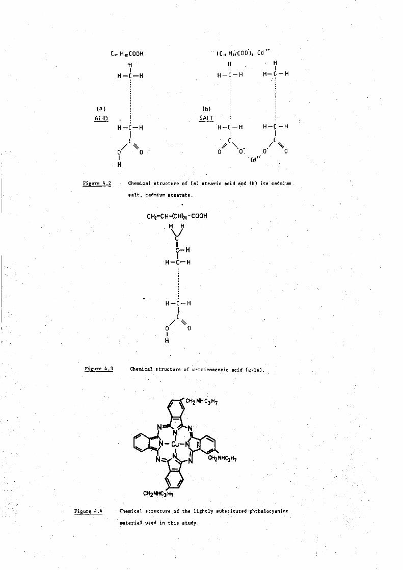
(a)
ACID
Figure 4.2
C., HKCOOH
H I
H-C-H
H-C-H I ( /~
0 0 I H
Chemical structure of (a) stearic acid and (b) its clldmium
salt, cadmium stearate.
CHz:.CH-(CH~0-COOH H H \I
I c-H I
H-C-H
H-C-H I (
/~ 0 . 0 I H
Figure 4,3 Chemical structure of w-tricosenoic acid (w-TA).
. ~CH,NHC!H7
~J:;(N ~-eu- 1 ~
~~3*1
Fig\lrt: 4.4 Ch~mical structure of the lightly substituted phthalocyanine
material used in this study.

~
. ~ +" ·-U1 ~
~ > ·-c: :J
E 0 .r:. L. :::J Cl
c ~ (/) :J (/)
.r:. g' 2 t=
?
~ ·-:J E 2' _g ~
£ +"
0 ~ c: 0
r-. ~ . 01 ·-LL.
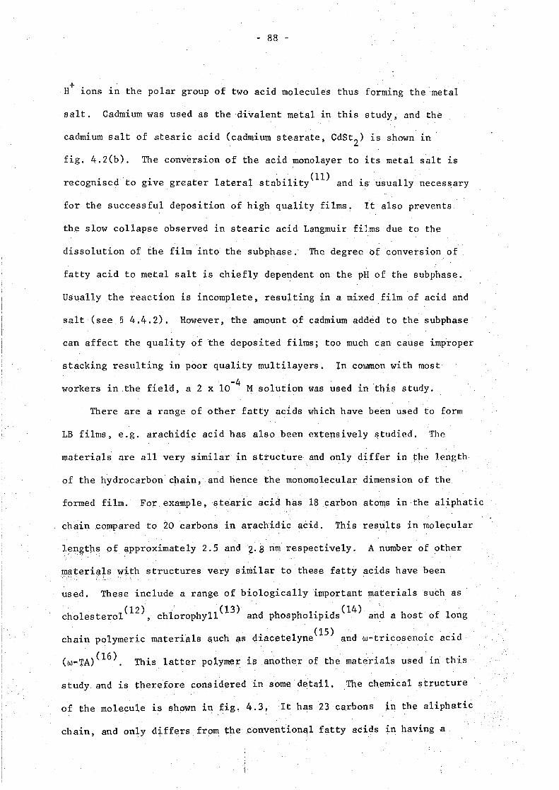
- 88 -
+ . . 1 H wns ~n the po ar group of two acid molecules thus forming the metal
salt. Cadmium was used as the divalent metal in this study, and the
cadmium salt of stearic acid (cadmium stearate, Cdst2
) is shown in
fig. 4.2(b). The conversion of the acid monolayer to its metal salt is
. d . 1. 1 b. '1' (ll) d . 11 recogn~se to g~ve greater atera sta ~ ~ty an ~s usua y necessary
for the successful deposition of high quality films. If also prevents
the slow collapse observed in stearic acid Langmuir films due to the
dissolution of the film into the subphase. The degree of conversion of
fatty acid to metal salt is chiefly dependent on· the pH of the subphase.
Usually the reaction is incomplete, resulting in a mixed film of acid and
salt (see § 4.4.2). However, the amount of cadmium added to the subphase
can affect the quality of the deposited films; too much can· cause improper
stacking resulting in poor quality multilayers. In coumon with most
workers in the field, a 2 x 1o"4 M solution was used in tqis study.
There are a range of other fatty acids which have been used to form
LB films, e.g. arachidic acid has also been extensively studied. The
materials are all very similar in structure and only differ in the length
of the hydrocarbon chain, and hence the monomolecular dimension of the
formed film. For example, stearic acid has 18 carbon atoms in the aliphatic
chain compared to 20 carbons in arachidic acid. This results in. molecular
l~n~t]:ls of approximately 2. 5 and 2· 8 nm respectively. A humber of other
materials with structures very similar to these fatty acids have been
used. These include a range of biologically important materials such as
cholesterol (l 2), chlorophyll (13 ) and phospholipids (l4 ) and a host of long
. . . h d. 1 ( 15 ) d . . . d cha1n polymer~c mater~als ~uc as ~acete yne an · W"tr~coseno~c ac~
((!J-'.rA) ( 16 ). This latter polymer is another of the materials 1.1sed in this
study and is therefore considered in some detail. The chemical structure
of the molecule is shown in fig, 4. 3, It has 23 carbons in the aliphatic
chain, and only differs from the conventionql fatty acids in having a

- 89 -
double vinyl bond, CH = CH2 , which replaces the CH3
group. The material
can be readily polymerized by an electron beam forming a linear polymer
due to cross linking between the 'w' double bonds. It may thus have
important applications in the field of electron beam resists (see § 4.5)
and in fact it was in this context that it was first considered. In
(17) . addition, a recent study has shown that ~t is possible to deposit
multilayers at high speed and still retain a high degree of order - an
obvious prerequisite for any electron beam resist material.
4. 3. 2 Novel Materials
In many instances, the LB technique provides an excellent method
for the deposition and/or study of a material of interest. However,
this material may not readily form a monolayer on the surface of the
subphase and it must be modified in some way to render it suitable for
use with the LB technique. The simplest method of achieving this is to
mix the material with a conventional fatty acid in orC::,:er to form a mixed
Langmuir film(lS) or alternatively to cause the materiai to be adsorbed
onto a fatty acid film(l 9) · Recently a great deal of interest has been
generated in the photoactive properties of materials in the form of LB
films(Z0- 23 ) (see § 4.5). In these cases the active molecule (usually a
dye) is either incorporated in a conventional film or substitutedwith
long hydrocarbon chains. However, even in this latter case, a mixed
film is necessary to enable high quality films to be produced. In all
of these cases the specific property of interest is necessarily diluted
and the resulting films have limited mechanical and thermal stability.
Recently some innovative chemistry has enabled a number of interesting
materia1a to be studied in LB fHm form: Vincett et.a.'J.(Z4) have shown
that the aromatic material anthracene, ~ubstituted with short (C4)
aliphatic side chains can be built up into multi layers. This was

- 90 .,.
expected to reveal the electrical properties of the conjugated w electron
system to a much greater extent than with a conventionAl long chain
substitution, and the layers were indeed found to exhibit some very
. t t' 1' t . 1 ( d . 1) . ( 2S, 26 ) 1 J.n eres 1ng e ec n.ca an opt1ca propert1es . Very recent y,
LB films of phthalocyanine (Pc) dye molecules without long chain sub-
. . h b d(27, 28, 29) stJ.tutJ.ons ave een reporte The.first .· (27)
hlms produced
were of metal-free, unsubstituted Pc and were definitely not monomolecular,
although they were of reproducible thickness. Since then, lightly sub-
t 't t d p h b 'd( 28 )( 29 ) d f 1' d . . f 1 s 1 u e c as een use an success u epos1t1on o at east
bilayer, if not monolayer, films· has been achieved, This is expected to
prove an extremely important development for several reasons. The
phthalocyanines are well known to be extremely stable, in particular their
melting points (greater than 400°C) are far higher than that of any other
LB film material. Furthermore, the layers have been found to adhere
strongly to both substrates and each other, and to resist mechanical
abrasion and the action of many solvents. Early reports suggest that the
f 'l . 1 . . ( 27 ) 1 h h h '. h ~ ms possess 1nsu at1ng propert1es , a t oug t ere ex1sts t e
possibility of producing LB films of Pc with semiconducting properties,
since the phthalocyanines are a well established group of organic semi-
conductors. In addition to these important properties, Pc is also
. d . '' ' " h 1 ' . . ( 30) 1 h ' h . ' recogn1se as an 1mportant p otovo ta1c p1gment , a t aug. 1ts use
has been hindered by difficulties experienced in producing it in thin film
form by other techniques. The phthalocyanines may well prove to be an
important step towards the production of commercially viable LB film-based
devices which to date has been prevented largely by the instability of the
more conventional materials, For this reason l.'c was also used in this s.tttdy
and fig, 4.4. shows the 'chemical structure of the parHcu1.ar Pc dedvative
used, It is a lightly substituted, copper
(28) ·deposited film is approxi111ately 0.8 nf!l
Pc and the thickness of the

- 91 -
4.4 LANGMUIR-BLODGETT FILM DEPOSITION
The LB film materials used in this study were all synthesised to. a
high degree of purity and the spreading solvents used were all of Aristar
(BDH) grade. Usually, the material was dissolved in the solvent (invariably
-3 chloroform) to a concentration of approximately 1 mg em and fresh
solutions were made up at regular intervals to eliminate. possible ageing
problems. The further precaution of storing the w-TA in the dark was
taken to eliminate the possibility of UV-polyme~ation.
The deposition pro~edure can be divided into three distinct procedures;
i.e. monolayer spreading, monolayer compression (and isotherm measurement),
and actual film deposition. These are now discussed 1n sequence.
4.4.1 Monolayer Spreading
Prior to spreading the monolayer, the surface of the subphase had to
be cleaned. This was achieved by closing the barrier to its minimum area
and 'vacuuming' the surface with the previously-:-described vacuum nozzle.
It was found that the cleanest surface could be achieved by the spreading
and subsequent removal of a Langmuir film. This was thought to be due
to the adherence of surface particles to the film. The amount of contamin-
ation on the surface could be deduced from the residual surface pressure as
tpe barrier was closed to minimum area. With care, this could be reduced -1 . . . . ·.
to < 0.05 mN m and under these circumstances good isotherms and high ... "' ,. ··.. '·'
quality monolayers could be expected. After cleaning the surface of the ·
subphase, the material (in solution in the solvent) was spread using the
following technique: A known amount of solution was deposited, one drop
at a time using a micrometer syringe system. The film was spread from the
centre of the trough so that any surfactant material, remaining after t::he
ThiB cleaning proerdure, wa~ forced to the perimeter of the dipping aren.
reduc~d the possibility of any residua1 material being deposited onto the
substrate. The solvent was then allowed about five minutes in which to
ev.;tporate with the extractor fan :aiding the proces~,

- 92 -
4.4.2 Film Compression and Isotherm Recording
As a matter of routine, a surface pressure - area plot (a 'compression
isotherm') was recorded each time a film was spread. Fig. 4.5 (a) shows
such an isotherm for stearic acid, where the area axis has been calibrated
in terms of the average area occupied by each molecule. It is convenient
to draw an analogy between the compression of a monolayer on the surface of
the trough and the compression of a gas - the main difference being that
the the monolayer is essentially two dimensional and hence surface pressure
replaces bulk pressure and surface area replaces volume·. Before compression,
the stearic acid molecules are well spaced out with the polar groups
immersed in the water and the aliphatic chains oriented at random away from
the water surface. The monolayer is said to be in the gas phase. On com
pressing the film, the average area occupied by each molecule reduces but
there is little change in the surface pressure until at approximately
24~_2/molecule, the monolayer undergoes a phase change. The molecul~s begin
to interact and further compression results in a gradual increase in surface
pressure. This is termed the liquid or expanded phase. The molecules can
be envisaged as being relatively closely spaced and almost vertically
aligned. A further phase change occurs at about 20~2/molecule and the
film is in the solid or condensed phase. The molecules are fully aligned
and tightly packed. With the film in this condensed phase, a small com
pression of the monolayer results in a large increase in the surface pressure.
However, in practice.the situation is not quite so simple since the conver
sion of stearic acid to cadmium stearate is often promoted and, since this
reaction is pH dependent, the pH of the subphase has a marked effect on the
shape of the isotherm. Fig. 4,5(b) shows isotherms for a stearic acid/
cadmium stearate film at two di;fferent pH ~eve1s. At ~ow pH the curve is
very similar to the stearic acid isotherm and the film consists largely of
s;tearic aciq. However, at higher pH the extent of the liquid region .is

-E -z E -~ ... ::J (/) (/) ~ ... a. ~
~ ..... .... ::J
(f)
35~----~~--~~----~~--~--~--~--~~--~
a b
-pH:s:so pH:S-75- -pH:S-60
0 1 111 I I I :>,. I I 1--// I I I ' >' 1 I ~I
15 18 21 21. 27 30 15 18 21 24 27 30
Area Molecule (A 21 Molecule )
Figure 4.5 Typical compression isotherms for (a) stearic acid and
(b) a mixed CdSt 2/stearic acid film at two different pH
levels •.

- 93 -
reduced and the liquid-solid 'break' point occurs at a substantially
lower surface pressure. These two effects are indicative of the enhanced
stability of the film which now is a mixed film of acid and salt. At
still higher pH levels, the liquid phase is virtually non-existent and at
a pH of 6.5 the monolayer is largely CdSt2
. It should be stressed that
isotherms obtained for fatty acids and their divalent metal salts are
nearly ideal. Many other films, including w-TA and Pc, do not exhibit such
well-defined phase changes and the isotherms are, in general, much more
rounded and featureless. (Typical isotherms for w-TA and Pc films are
presented in chapter 5.) The control of pH was much less crucial in the
deposition of these latter materials since cadmium was not incorporated
into the subphase. Good quality multilayers could be deposited without
the use of cadmium and, in fact, there was some evidence to suggest it
may be detrimental. In practice, irregularities in the isotherms, such
as additional features or poorly-defined breakpoints, were sometimes
observed. These were almost certainly due to contaminetion and a thorough
clean of the subphase surface, or in rare cases the entire trough, always
resolved the problem.
After recording a satisfactory isotherm, the required surface pressure
was preset and the trough was put into control mode, The monolayer was
compressed to the preset surface pressure and usually left for about 10
minutes to allow any final rearrangement of the molecv.lar packing before
dipping commenced.
4.4.3 Film Deposition
In order to achieve successful c;iepoaition o:f high quality films in a
repeatable fashion, the film must be transferred on~o the substrate whilst
in ithe condensed phase, This ensures that the deposited film is essentially
homogeneous and slight variations in surface pressure have a relatively
small effect on the film structure.

- 94 -
Classically, three deposition modes are recognised, namely the
X, Y and Z modes. These deposition types are illustrated schematically
1n fig. 4.6 (a), (b) and (c) respectively. X·type deposition is used to
describe the situation when deposition occurs only on the downstroke,
Z-type on the upstroke only, and Y-type (often termed normal deposition)
when pick-up occurs in both directions. The type observed in practice
depends on factors such as the pH of the subphase and the substrate
preparation. Although Y-type is by far the most often observed mode,
X-type is sometimes encountered at extreme pH leve}s. When Langmuir and
Blodgett( 3l) first discussed the different modes, Z-type deposition had
not been observed and its definition was merely speculative. Since then,
however, this mode has been observed( 32 ) and was also encountered in this
work when depositing lightly substituted Pc films. However, the. actual
stacking arrangement predicted from the deposition mode has been shown to
b . 1' f. . ( 33 , 34 ) d h k'. . h e an overs1mp 1 1cat1on an t e exact stac 1ng sequence 1s muc
more complex. In particular, studies of both X and Y-type deposited
fl.'lms( 35 • 36 ), have shown that th t' f th. 'd · e separa 1on o ·. e ac1 groups 1s
invariably twice the molecular length, suggesting that deposited films
always stack 'Y-type'. Several authors 07 ' 33 ) have invoked the idea of
overturning of the molecules during X-type deposition t·::> explain this
discrepancy. More recently, another deposition mode (XY-type) has been
observed( 34) and an elegant model, based on the formation of two distinct
forms of salt, was used to explain both this, and X• type deppsition
without invoking the idea of overturning. The structure of deposited
multilayers is obviously a complex problem which has yet to be conclusively
resolved. At present, only Y-type films arc known to ?ossess a uniform,
bilayer structure. In most ~f the devices prepared for this study, the
deposition was Y-type ~ the substrate surface being sufficiently hydro~
philic to prevent deposition on the first downstroke.

sub5trote. 1
i I
11 u .£1 1 l ll .£t ll
mor.c!oye~
~ subphose , ......
~
i l ll
~ .
•
.
~ .
(3) (b) {C)
Figure 4.6 Depicting the three types of LB film deposition, (a) X~type,
(b) Y-type and (c) Z-type.

- 95 -
The quality of the first deposited layer is of paramount importance
to the quality of the eventual multilayer. This 1s due to the fact that
any faults or inclusions are likely to be duplicated or to persist in
subsequent layers. Furthermore, the bonding of the first layer is
fundamentally different to the 'head to head, tail to tail' bonding of
subsequent layers. For these reasons extreme care was taken to ensure a
high quality first layer and this was achieved by depositing the first
layer very slowly ('V 1 mm/min.) immediately after the substrate had been
etched. The deposition of subsequent layers is more straightforward and
can, in general, be performed at much greater speeds. The details of the
deposition conditions used and the procedures adopted are given in § 5.2.
During the deposition procedure a 2 channel Y-t chart recorder con-
tip.uously monitored both the surface pressure and the change in the an~n
enclosed by the barrier, thus providing a record of the operation. A
typical example is shown in fig. 4.7. From this it can be seen that, as
the film is removed,the barrier area decreases in response to the .feed-
back mechanism, thereby maintaining the surface pressure constant. A know-
ledge of the sample surface area enables the deposition ratio to be
calculated which, .for good quality films is very close to 100%. This is
discussed in more detail in § 5.2 when the effect of surface preparation
on this deposition ratio is studied.
The deposition of Pc LB films is more complex than that used for more
conventional films. Briefly the main complic·ati.ons are as follows: Tite
unsubstituted Pc is not soluble in the common organic solvl;:!nts. This
. 1 b • . ( 27 ) . d./ '. h . 1 b t. t necessitates e1ther a meta su st1tut1on an or a per1p era su s 1 u-
tion such as that shown in fig. 4,4. The latter of these enables chl~ro-
form to be used as the solvent. However, since the molecul!;:!s cio not
possess the classical hydrophilic - hydrophobic structure, transfer onto

~QQsition ratio-----------..,
layer no. ratio(t4°/o) ·
Figure 4. 7 ·
1 99°/o 2 98°/o.
3 '~l/o
4 5
time ~------~~-~.------~
Typical deposition record for CdSt 2 onto GaP;

- 96 -
a substrate occurs only on the upstroke, i.e. Z-type deposition. Simple
precautions are necessary to ensure that no transfer occurs on the down-
(28) stroke .
4.4.4 Quality Asl)essment
Langmuir-Blodgett films, especially those of the fatty acids or
other similar aliphatic materials are generally good insulators with high
breakdown strengths ( > 106 V /em) and dielec.tric constants which are almost
independent of frequency, for frequencies ~ 106 Hz. The electrical
properties of these films are usually studied by incorporating them into
MIM or MIS structures and a number of such studies have been made (see
for example, ref. (46)). ·Poole-Frenkel conduction between neutral traps
is thought to be the dominant conduction mechanism it). multilayered LB
films although other mechanisms have been observed under certain circum-
stances. For example, irt MIS devices fabricated on n-type semiconductors,
electron injection into the ins~lator, resulting in space-charge-limited
h . . h b b d( 46 ) c aracter1st1cs, as een o serve .
A convenient. measurement, which can be used to assess the general
quality of an LB film is a reciprocal capacitance plot. This is usually
achieved by depositing a stepped .thickness LB film onto a metal substrate
and producing MIM structures with a variety of insulator thicknesses. The
total capacitance Ct, (per unit area) of such a structure is given by
1 Nd
= + cS ox 4.1 E:
OX
where cS is the thickness of the inte'rfacial ~etal-oxide film, E: is ox ox
its permittivity, e1b is the permittivity of the LB film~ d £s the single
monolayer thickness and N is the number of monolayers incorporated into

- 97 -
the structure. -1 Thus, a graph of Ct against N should be linear with
a slope equal to d/Elb for a good quality film; . -1
The intercept on the ct
axis can be used to determine the mean thickness of the interfacial layer.
Such a plot is used in §5.2 to assess the effect of electrode evaporation
on the LB film quality.
4,5 APPLICATIONS OF LB FILMS
·Although the LB technique was developed in the early twentieth century
and LB films have been studied for well over fifty years, it is only
recently that widespread interest has led to the demonstr,1tion of their
potential for use in electronic and optical devices. This section provides
a brief review of some of the more important applications for which LB films
have been considered. A more detailed discussion can be· found in ref. (lo).
The insulating properties of these films have been u.tilised in many
devices. For example, they have been used as the dielectric in low-loss
. ( 38 ) ( h. h . . . d . ) . capac1tors an area w 1c 1s enJoy1ng renewe 1ntereut an +n
. . h . (38) capac1t1ve ygrometers . In addition, several electronic devices, based
mainly on the MIS structure, have been fabricated: (39 40)
Tanguy et al . '
studied MIS capacitors formed on silicon and demonstrated near-ideal
behaviour. The Durham group have fabricated MIS field effect transistors
b d I ( 4 1) d h '1' ( 42 ) Th h d LB ase on nP an amorp ous s1. 1con . e same group as use
films to investigate the properties of MIS solar cells based on CdTe( 43)
and have achieved a significant improvement in efficiency over the corres-
ponding Schottky barrier cells. MIS devices have been fabricated on the
. (44) narrow bandgap mater1als InSb and HgCdTe with a view to producing
improved infra-red detectors. ·Recently, considerable interest has been
' d d ' . ' LB f~lm( 45 .. ). generated in the production of 1on an gas . etect1ng FETs us1ng an •
. . f (46) . h . . . . or the LB film - sem1conductor 1nter ace as t e act1ve reg1on.
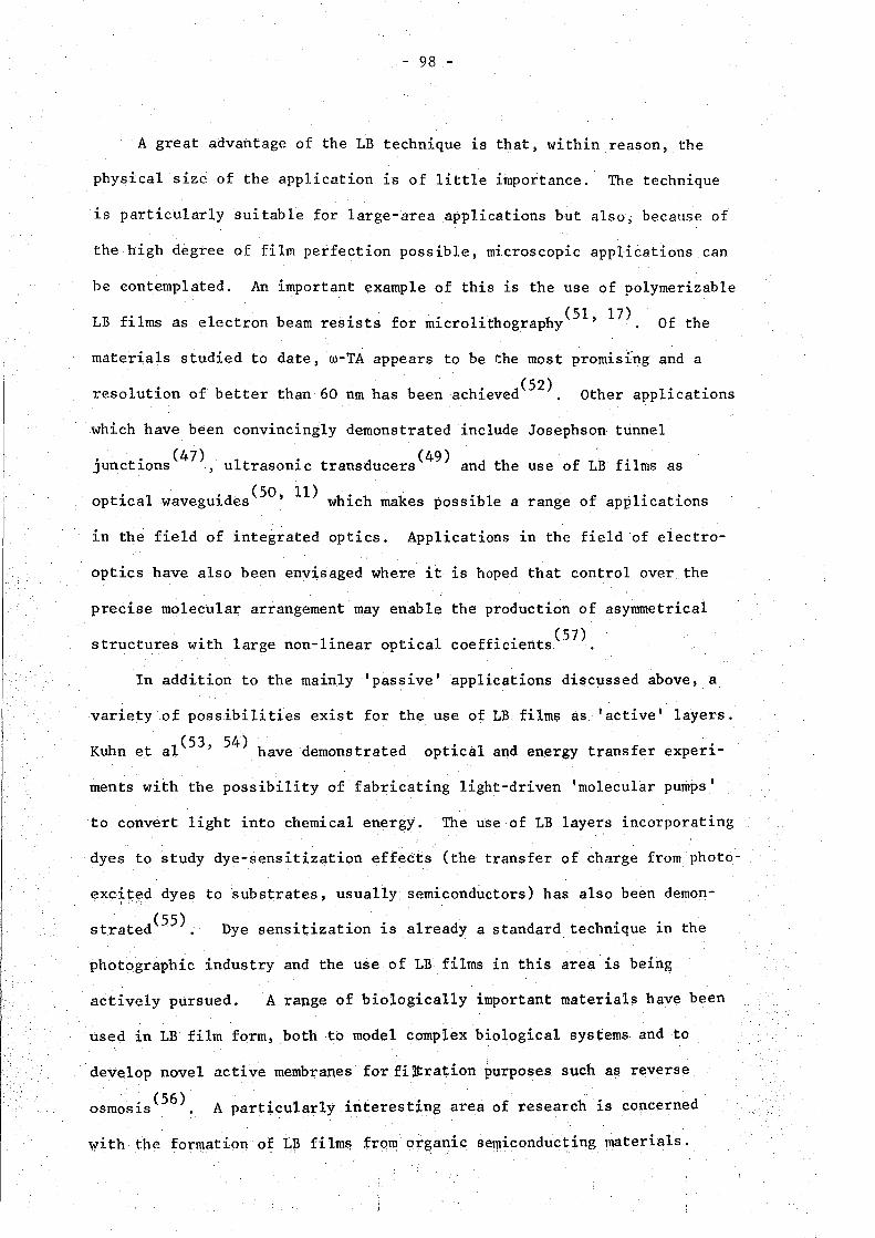
- 98 -
A great advantage of the LB technique is that, within reason, the
physical size of the application is of little importance. The technique
is particularly suitable for large-area applications but also; because of
the high degree of film perfection possible, microscopic applications can
be contemplated. An important example of this is the use of polymerizable
LB f . 1 1 t b . . f . 1' h h ( 51 ' 1 7) 0 f h L ms as e ec ron earn resLsts or mLcro Lt ograp y . t e
materials studied to date, w-TA appears to be the most promising and a
resolution of better than 60 nm has been achieved(S 2). Other applications
which have been convincingly demonstrated include Josephson tunnel
• . ( 4 7) 1 . d ( 49 ) h f f. 1 JUnctLons , u trasonLc trans ucers and t e use o LB L ms as
. 1 . d (so' 11 ) h. h k . bl f 1' . optLca waveguL es w LC ma es possL e a range o app 1catLons
in the field of integrated optics. Applications in the field of electro-
optics have also been envisaged where it is hoped that control over. the
precise molecular arrangement may enable the production of asymmetrical
. h 1 1' . 1 ff. .. ( 57 ) structures wLt arge non- Lnear optLca coe Lc1ents .
In addition to the mainly 'passive' applications discussed above, a
variety of possibilities exist for the use of LB films as 'active' layers.
Kuhn et al(S 3, 54 ) have demonstrated optical and energy transfer exper1-
ments with the possibility of fabricating light-driven 'molecular pumps'
to convert light into chemical energy. The use of LB layers incorporating . .
dyes to study dye-sensitization effects (the transfer of charge from photo-
excit:ed dyes to substrates, usually semiconductors) has also been demon
strated(SS). Dye sensitization is already a standard technique in the
photographic industry and the use of LB films in this area· is being
actively pursued. A range of biologically important materials have been
used in LB film form, both to model complex bio~ogical systems and to
develop novel active membranes for filtration purposes such as reverse
. (56) osmos1s · A particularly interesting area of research is concerned
with the formation of LB film~ frqm organic Sef!liconducting materials.

- 99 -
For example, films of lightly substituted anthracene have been prepared
and shown to exhibit electroluminescent and photoconductive properties( 26 ).
Phthalocyanine is also a well-knoWn organic semiconductor and it is hoped
that LB films of this material will possess some interesting properties.
In particular, it may be possible to produce films exhibiting either n-
or p-type conductivity by using suitable metal substitutions. ·Other
'active' applications include the use of magnetic atoms, periodically
d . L f'l d d' . 1 ' . ( 48 ) space 1n an B 1 m, to pro uce two 1mens1ona magnet1c arrays and
and also radioactive nuclides incorporated irt a conventional.film to
produce a dilute radioactive source.
The range of potential applications is clearly vast and varied and,
although much of the work is at an early stage, many are being actively
purs~ed. In this study, the insulating properties of the conventional
fatty acid films, allied to the control over insulator thickness .which
is possible using the LB technique, have been employed to study injection
electroluminescence in MIS structures. In addition, diodes fabricated
using films of phthalocyanine have also been studied in an attempt to
benefit from the attractive properties possessed by this material.

- 100 -
CHAPTER 5.
EXPERIMENTAL DETAILS
In this chapte~ a general description of the equipment and materials
used in this work is given, together with an account of the experimental
procedures adopted. In addition, the results of some of the basic, but
nevertheless very important preliminary experiments concerned with device
fabrication are presented and discussed.
5.1 SAMPLE DETAILS
(a) Gallium Phosphide
The GaP used in this investigation was n-type, single crystal
material grown epitaxially onto large area ("' 10 cm2) n + stibstrates. These
substrates were doped with sulphur to give a carrier concentration of
. . 1. 1018 -3 approxLmate y em The GaP epilayers were grown by vapour phase
epitaxy to a thickness of about 40 11m. These layers were sulphur doped to
give carrier concentrations in the range 1o15 - 1017 cm- 3 Additionally,
the fin~l 10 microns were doped with nitrogen to a concentration of
approximately 1018 - 1o19 cm~ 3 The slices were supplied highly polished
and were optically very smoo~h and uniforin. The. internal quantum efficiency
of the nitrogen activated EL from this material was of the order of 1%.
The external quantum efficiency of unencapsulated, p-n junction LEDs,
fabricated from GaP with very similar properties to that used here, is
typically 'V0.05%.
(b) Zinc Selenide
The ~nSe samples were single crystal, n-type material grown epitaxially
onto GaAs single crystal substrates. These substrates were either semi-
insulating or in some cases were heavily dope?'to provide a sample
. . '. (1) suitable fpr a sqndwLch geometry. The ZnSe epLlayers were grown ,

- 101 -
using the recently-developed technique of organometallic chemical vapour
deposition (OM-CVD), to a thickness of typically 3 jlm and were intentionally
doped with aluminium to yield carrier concentrations in the yange
1o16
- 1018
cm- 3 . The cathodoluminescence spectra of the ZnSe material
used here has been studied by Wight et al( 2), and found to contain features
in both the blue and yellow regions of the spectrum. The relative
intensities of these emissions varied from one sample to another. The
external quantum efficiency of material which emitted predominantly in the
blue was measured to be 0.14% corresponding to an estimated internal
ff • • f ') a,(2) e 1c1ency o rv_10'<> • A somewhat higher external efficiency ('V0.6) has
been deduced for the yellow emission (3) due to the reduction in the effect
of internal reabsorption. No previous EL measurements have been reported
for conducting ZnSe grown by organometallic-CVD.
5. 2 DEVICE FABRICATION
5.2.1 Ohmic Contacts
(a) Gallium Phosphide Samples
Since the active EL region of the GaP ~lices was only rv 10Jlm thick,
extreme care was necessary, particularly from the viewpoint of etchants, to
ensure that as little as possible of the surface material was removed during
device fabrication. The following procedure was used to give reproducible,
highly Ohmic, low resistance contacts without the need for an etching or
chemical polishing process at this stage of the fabrication: The slices
were thoroughly degreased by refluxing in isopropyl alcohol vapour for
several hours. High quality (99.999%) indium wire was used to make two
small, preformed contacts on the back face of each sample. These were then
annealed in an inert atmosphere at 500°C for lOminutes. The Ohmicity of
the contacts was measured using a transistor curve tracer. The resistance
thus measured was invariably of the order ·of a few Ohms and agreed well

- 102 -
with the expected va~ue which was calculated from the resitivity of the
bulk material.
(b) Zinc Selenide Samples
Two geometries were used for the ZnSe samples in this work, i.e.
surface and sandwich geometries. For the surface arrangement, the Ohmic
contacts were formed on the same sample ·surface as the barrier electrode,
i.e. to the ZnSe material. In the sandwich structure, the Ohmic contact
was formed, as usual, on the opposite face to the barrier electrode, i.e.
to the GaAs material. In both instances the samples were degreased by
refluxing in isopropyl alcohol vapour for several hours. Preformed con-
tacts, made from indium wire for contacts to the ZnSe material and from
an indium /5% tin alloy for contacts to GaAs, were annealed in an inert
atmosphere for 10 minutes at 275°C.
5.2.2 Surface Preparation
The Langmuir-Blodgett technique is a room temperature, low energy
technique which causes relatively little damage to the substrate surface
when compared to other, more conventional techniques such as sputtering or
evaporation. This means that the pre-LB film-deposition surface prepara-
tion is of paramount importance, as it can, in some 'instances, determine
!J:te nature of the LB film,..substrate interface. This is particularly ··': ~ ; 'r ; ' '
~mportant when the substrate to be coated is a semiconduct.or; it has been .:·i ",:Y:', <'
. .
shown for example, that the InP-LB film interface state density distribution
can be significantly altered by suitable surface preparation(4 ). From the
viewpoint of this work, a particularly important considerationwas the
influence and extent of the inevitable interfacial layer which was present
betwe~p the LB film and the semiconductor as a result of the surface·
preparation. A var.iety of.etchants and chemical polishes w~re used in
thi~ !)tudy and these.are discussed below.

- 103 -
{a) Gallium Phosphide
Three different chemical polishes, which have been reported as being
suitable for GaP were investigated. Table 5.1 lists these polishes and
some of their properties. Of these preparations, the peroxide treatment
is the least useful from the viewpoint of this work. The resulting surface,.
as revealed microscopic examination, was generally good, although it did
contain a number of gross defects which were the result of preferential
etching. Moreover, the etch rate is quite large and this necessitated
the use of a very brief etch in the case of EL material since the a~tive
region was only "-'lOJJm thick. This meant that it was les; controllable
than polishes with slower rates, and hence more likely to produce an uneven
surface. It was not considered f~rther in this work. The ferricyanide and
Br2/cH3
0H preparations exhibited more controllable, slower rates of action
and this, coupled to their non-preferential polishing action, resulted in
high-quality, polished surfaces. It was necessary to follow the BrziCH30H
treatment with an HF, oxide-removal stage since devices fabricated without
this invariably exhibited non-ideal characteristics. This was attributed
to the presence of a significant interfacial layer {see § 6 . .3}. The HF
stage was not necessary in the case of samples prepared using the fcrricyanide
treatment, as such samples, although possessing a thin interfacial layer,
still exhibited near-ieleal characteristics {see § 6.2). In summary, both
t]1e ferricyanide and the Br2/cH30B-HF polishes result in similar, high-quality
semiconductor surfaces and both are suitable for use with the GaP EL material.
However, the latter preparation is thought likely to result in a relatively
oxide-free surface whereas the former is expected to possess some form of
interfacial layer.
The etch rates listed in table 5.1 were determined by first prqtecting
half qf the semicondt1ctor with 'Lacomit' and then polishing the sample for
a )<now~ period Q( tint~, usually several minutes: Subsequent removal of the

Preparation Concentrations Abbreviation 'Etch' Rate Conrrnents
Bromine/Methanol 0.5% Bromine Mixture must be used fresh (ages
by volume Br/CH30H "' lllm/mm. rapidly). Results in polished, mirror- I
like surface
Hydrofluoric Acid 40% by Volume HF - Oxide Removal. Used with Br/CH30H to
produce high quality, oxide-free
surface.
Potassium Ferricyanide 3g K3
Fe(CN)6 Ferricyanide rv 2.51Jm/min. Used at 80°C. Results in high quality
Potassium Hydroxide 0,24g KOH polished surface. In Water
lOccs H20 -
Sulphuric Acid/ H2so4 :H2o2 :H2o Peroxide 'V 811m/min. Known to leave oxidised surface. Hydrogen Peroxide 4 : 1 . : 1 Surface quality good, although some In Water
I ·By Volume preferentially etched regions.
Table 5.1 Listing the various surface preparations used for GaP and some of their properties

- 104 -
lacquer enabled the depth to which material had been removed to be
measured using a microscope with a calibrated stage.
(b) Zinc Selenide
The scarcity of the organometallic-CVD ZnSe material used in this
work meant that a comprehensive study of the effects of different surface
preparations was not possible. Furthermore, the fact that the ZnSe
epilayers were only ~ 3~m thick meant that extreme care was necessary
during surface preparation in order to prevent the ZnSe from being com-
pletely removed. The following technique was found to yield Schottky
barriers with reasonably good characteristics and was therefore used to
prepare all of the ZnSe devices: The samples were refluxed in isopropyl
alcohol vapour,for several hours and then polished, at room temperature
using a mixture of bromine and methanol (0.5% bromine b~ volume) for
1 minute. This was followed by a carbon disulphide rinse in order to
remove the surface bromine compounds which are a consequence of the
1 . h" d ( 5) po 1s 1ng proce ure .
5.2.3 LB Film Deposition
In all cases, the first monolayer was deposited as soon as possible
after the semiconductor surface had been prepared. In practice this was
invariably within 30 minutes. Similar deposition conditions were used
each time a film was deposited so that, as far as possible, the structure
a:nd properties of the insulating films were reproducible.
(a) Cadmium Stearate
The following deposition conditions were used to deposit CdSt 2 LB
( + ) ' 1. 8 '( :!: 2 ) °C • films: The subphase pB was 5.75 - 0.05 and its temperature was
The surface pressure of the monolayer spread on the water surface was
maintained at either 25 mN/m or 30 mN/m. Cadmium ions, in the form of

- 105 -
CdC12 , were added to the subphase to give the required 2 x·lo-4 M
solution. It was shown in § 4.4 how a compression isotherm could be
measured to give some indication of the quality of the monolayer, and
this was routinely performed prior to each deposition procedure. A
typical isotherm (pH= 5.75) is shown in fig. 5.1. (At this pH, the
film consists largely of CdSt2 , although the conversion is not comple.te
.and there is still some stearic acid present.) The fi~·st monolayer was
always deposited slowly, at a speed of "' 1-2 rrnn/min. Subsequent layers
were found to deposit better (see later) if the samples were desiccated
for 'Vl-2 hours under a low pressure of dry nitrogen. These subsequent
layers were deposited more quickly, at speeds of up to 10 mm/min.
(b) w-Tricosenoic Acid
The deposition conditions were as follows: The subphase pH was
5.5 (!: 0.1) and the subphase temperature was 18 (-:!: 2)°C. The surface
pressure of the monolayer was maintained at 35 mN/m. No cadmium was added
to the subphase. A typical isotherm, obtained under these conditions, is
shown in fig. 5.2. Since w-TA is known to undergo an ageing process on
h f f h L . h( 6) .11 d 't' 1 d . t e sur ace o t e angm~~r troug , a epos~ ~ons were comp ete 1n
less than 1 hour using a freshly spread monolayer. Difficulty was
experienced when attempting to deposit an aged film (i.e. more than four
hours oleO onto the semiconductors used in this work. The first monolayer -, ,'•,M (;·
wa~ deposited at a speed of "' 1-2 mm/min and subsequent layers were
deposited immediately at speeds of up to SO nim/tnin. The post-first layer
drying stage was found to be unnecessary when using w-TA as the LB material.
(c) Substituted Phthalocyanine
The procedure used to deposit LB films of phthalocyanine is more
complicated than that used for the more conventional· films. This procedure
was described briefly in chapter 4. The following deposition conditions
•'
.·

35.
_30~ E -~ 25 -
C» u 0 -... ::I
1/)
:t
figure S.l
I -~-T -- r- I
I
I I \ I I I 15 18 21 21. 21 30
Ar~a/Mot~cul~ (A2 /Mol~cul~ ).
Typical CdSt2
compression isothe·rm
atpHS.7S.·
-E -z E -C» ~
.::I Ill Ill C» ...
(l,
C» u 0 -.... -~
I ,. . .
I
15 18 21 21. 27 30
Arlla/Mol~cut~ (A 2 /Moi~Zcute)
figure S .. 2 Typical- w-TA -compression isotherm
at pH 5.6.
35
-E -z E -C» ... ::I Ill Ill C» ... (l,
C» u 0 -._ ~
0 30 40 50 60 70 80 ~
Area,/Molecule (A 21 Molecule)
figure S.3 Typical Pc.compression isotherm at pH 5.5,

- 106 -
were used: + The subphase pH was adjusted to a value of 5.4 (-· 0.2) and
+ 0 its temperature was 18 (- 2) C. The surface pressure of the monolayer
was maintained at 30 mN/m during the actual deposition. No cadmium was
added to the subphase. A typical isotherm obtained under these conditions
is shown in fig. 5.3. In this case all of the layers were deposited
slowly, at a speed of ~ 1-2 rom/min.
Irrespective of the material used to form the LB film, the samples
were always desiccated, under a low pressure of dry nitrcgen, for
approximately 2 days prior to top electrode deposition. This is thought
to improve the quality of the LB film and indeed, if this stage were
omitted, then devices fabricated with insulators more than one monolayer
thick invariably exhibited irreproducible characteristics. ·
Surface Preparation. In addition to being very important from the
viewpoint of ·the interface properties, the sample surface preparation is·
also crucial with regard to LB film deposition. Usually this means that
the surface must be either hydrophilic or hydrophobic in order to be
conducive to pick-up. In the previous section, the properties of the
GaP surface, as prepared by three different treatments, were discussed.
One of these, the peroxide etch, was found to be unsuitable. It is con-
venient at this stage to consider the effect of the two remaining surface
preparations on the success of the LB film deposition procedure. This will
prove to be valuable in helping to choose the more suitable chemical polish
with which to prepare the GaP for MIS diode fabrication. It was shown in
§4.4 how a record of the dipping procedure could be made by monitoring
the surface pressure and the surface area of the monolayer as a function
of time. Fig. 5.4 shows such a record for a sample prepared using the
ferricyanide treatment, onto which CdSt2 was deposited. It can be seen
that the surface pressure rell)ains es~entially constant (at ''•25 mN/m) as
the material is n~movr<t from the surface of the water~ thu::~ caqs in~ the
•

·3
Fig 5-4
Q!QQsition ratio
layer no. ratio (t4°/o) 1 97°/o 2 99°/o 3 4 5
Figure 5.4
4 5
Figure 5.5
3
4 5
Figure· 5.6
time
Deposition record for CdSt 2 onto ferricyanidP~treated GaP
(continuous deposition).
99°/o 98°/o 'it!l/o (.J!l/o 9Pf/o
time ~------~~~------~~
Deposition record for CdSt2
ont'o ferricyanide·treated GaP
(including two hour drying period between 1st and 2nd'
depositions).
time __ , _ _, ___________ ~------D~~o~ition rec~rd for cdst 2 onto Br 2 /CH 30H·HF~treated GaP
~inclyding t~o.ho~r drying peri~d).
till o-0'\ e! N a o E .I:. c u u .... -
~. ::::J lf) lf)-
~ E CL ...... <:il)z u E 0~ ....... ...
·::::J
r./)

Figure 5 .7 Photograph of a go}d . electrc-d~ or. Gar exhibiting the
·· crazed' · appecarance which is characteristic of th.ermal exp.an•
sion problems.
-I lL.
N -
E N
0 .... -u
0
' ,, ~
- (b)
2 4 6 8 10 12 14 16 No. of Monolayers (N)
Fist:.:re 5.8 Reciprocal capacitance as a function of the numbi'r of mono-
layers, N, for two different MlM samples.
18

- 107 -
chapge in the area enclosed by the barrier. From this change, in area,
the deposition ratio was calculated by comparing it to the surface area
of the sample which was measured using a microscope with a calibrated,
moving stage. These deposition ratios are listed in fig. 5.4. (It
should be noted that the ,LB film ~as deposited in a stepped-thickness
manner which explains why the change in area is not the saroe in all
cases.) The substrate in this instance was dipped continuously, i.e.
with no drying time between the deposition of the 1st and 2nd layers.
The ratios are largely very good (i.e. close to 100%) with an obvious
exception relating to the pick-up of the third layer. This effect was
unique to the deposition of CdSt2 onto Ga.P, and was relatively indepen
dent of the mode of surface treatment. Its cause is·uncertain, although
it can be seen from the shape of the trace that the deposition gradually
improves as the third layer is deposited, It was found that this effect
could be eliminated, in the case of the ferricyanide treated substrates,
by desiccating the sample for 'Vl-2 hours after the first layer had been
deposited. Fig. 5.5 shows another record where, in this case, the sample
was desiccated for approximately 2 hours between the first. and second
depositions. It can be seen that the effect is no longer apparent and
the deposition ratios are all close to 100%. 'I'his 'third layer' effect
is clearly related to the pro~erties of t~e 1st layer and this explains
why it was never observed at any other stage itLthe procedure (e.g.
during the deposition of the fifth layer). One:, possible explanation is
that the crucial factor is the adherel).ce of the second layer to the first.
The unusual shape of the third trace in fig. 5.4 may be due to .·the partial
removal. of the second layer as the third deposi.tion· is attempted, rather
than simply the incomplete deposition of the third layer. If this is
the case·, then the drying stage must render the first layer more con
ductive ,. to pick-up.

- 108 -
The problem was not so easily overcome, however, in the ca$e of a
sample prepared using the Br2/cH3oH-HF treatment. Fig. 5.6 show$ the
dipping record for such a sample, Both the dipping conditions (pH,
temperature and speed), and the drying period were identical to those
used to obtain the record shown in fig. 5.5. In this case the third layer
anomaly was still evident, although somewhat reduced in magnitude. How-
ever, it could usually be eliminated b.y the use of very slow dipping speeds
(less than 1 mm/min.) although this was time-consuming and inconvenient.
Another experimentally-observed trend can be seen in fig. 5.6, namely that
the deposition ratios were, in general, lower than in the corre~ponding
ferricyanide-treated samples. In concluding, it can be said that the
ferricyanide treatment results in a somewhat better surface from the view-
point of LB film .deposition, although, with care, successful deposition is
possible using either treatment.· The difference between the two surfaces
1.s likely to be due to the fact that the HF"'prepared surface. is expected
to be essentially oxide-free, whereas the surface left by the .ferricyanide
preparation is expected to be uniformly coated with a thin 1 oxide 1 ·layer.
The extent of this layer, and its influence on device properties; 1s
clearly an important issue and this is considered in §6.2.
5.Z.4 Electrode Deposition
Since conventional LB film materials have, :ln general, low melting
points, care must be exercised when evaporating metal electrodes. (For
example., stearic acid has a bulk melting point of only rv70°C - although for
CdSt2 it is slightly higher than this and indeed, in monomolecular form it
may well be higher still.) Previously, the mf!thod used to guard against
thermal damage tq the film has been to cool the substrate to a low temper-
ature (rv -lOq°C) <ll.Jring the evaporating procedl!re. However, some authors (4)
have e~perienced difficulty using this technique due to the mis-match of

- 109 -
the thermal expansion coefficients of the metal, insulator and substrate.
This' problem was found to be particularly acute when GaP was used as the
substrate, and only a very low yield of reliable contacts was possible.
Fig. 5. 7 shows a photograph of a gold elec.trode (on GaP) exhibiting the
'crazed' appearance which is characteristic of this problem. Consequently,
an alternative method for the evaporation of metal ele=trodes onto LB
films was sought. It was found that, providing the evaporation was
performed slowly, i.e. at a rate of about 0,5 nm/min in stages of "' lnm
at a time, the.thermal damage caused to the film was minimal. This can
be seen by considering fig. 5.8 which shows the reciprocal capacitance,
plotted against the number of monolayers for two different metal-insulator-
metal samples. These samples were identical, aluminized glass slides,
. which had been simultaneously coated with a stepped thickness, CdSt2 LB
film. The gold top electrodes were deposited (a) using the cooled substrate
approach and (b) using the slow, staged technique. Each point represents
an average value determined from several contacts on each region of the
two samples. It can be seen that the two curves are very similar. Both
are highly linear with almost identical slopes although the intercepts on
the capacitance axis are some~hat different. These data can be analysed
according to equation ~.1, i.e. p-l = Nd/e: 1be: + o./e:.e: . This yields ·. . 0 ~ ~ 0
.· + -10 . a value for d/Elb of 9.8 (• 0.2) x 10 m wh~ch agrees well with previous
results( 4). Assuming a molecular chain length of 2.5 nm, yields a value
for the dielectric constant, Elb' of "'2.5. The y-axis intercept can be
used to deduce the thickness of the interfacial aluminium oxide layer.
The intercept of curve (b) yields a value for oi of '\..4.5 nm (assuming a
dielectric constant of 8.5 for the aluminium oxide). Again this value is
consistent with that measured by other workers. However, the difference
in t:h~ ~wo ~ntercepts is quite significant. It is not thought to be due
to a dif~erence in the thicknesses Of the Al2o3 tayer, since both samples

- 110 -
were fabricated in parallel under identical conditions (except for the
method used to evaporate the top electrodes). The origin of this anomaly
is unclear, it may be due to a reduction in the effective electrode area
resulting from the cooling technique, or alternatively, it may be due to
contamination of the LB film prior to electrode deposition (e.g. back-
streaming diffusion pump oil condensing onto the cooled substrate). Tf1e
slow staged technique is clearly the better of the two; it eliminates
the problem of crazeq contacts and also appears to result in better metal -
insulator interfaces. This technique w.as used to evaporate top electrodes
onto ail of the samples used in this study. The evaporation procedure
itself was shutter controlled and performed at a pressure of less than
10-6 torr to a final thickness of rv 15nm, as measured by a quartz-crystal
oscillator, film thickness monitor. The contacts were delineated using a
metal mask containing circular aperatures, typically 0.5 to 1.5 mm in
diameter.
5.3 DEVICE CHARACTERISATION
Figure 5. 9 shows a schematic diagram of the device geometry of a
typica~ sample prepared using the procedures outlined in the previous
section. It is shown specifically for devices fabricated .on GaP but it
is ess~ntially ·the. same for the ZnSe sandwich-type· structures. For the
4nSe surface geometry samples, the Ohmic contact was ~ade on the same
. surface as the gold electrode and was not coated with the LB film. Using
reasonably _large area substrates, it was possibie to prepare samples with
up to nine different regions of film thickness with approximately 15-25
' contacts per region. This enabled a large number of di9des from e'!ch area
to be sampled and representative ones chosen for full characterisation . . '
In general, the'reproducibility over a range of contacts from the same
region was good. Samples which did not exhibit such reproducibility were
not used further. The most reliable and cqnvenient method qf testing

MS
Au
LANGMUIR BLODGETT
FILM
n -GaP EPILAYER N - DOPED
n•- GaP
In
MIS
Figure 5.9 Schematic diagram of the device geometry ..

-d u
~
. en
lL.

- 111 "'
this reproducibility was found to be by monitoring the current-voltage
characteristics; In practice, the current taken by each device at a
couple of preset voltage levels was measured and these data were used
to choose typical contacts. This was 'found, in general, to be a more
sensitive technique than, for example, measuring the diode capacitance,
since the current taken by a diode is highly susceptible to defects or
irregularities in the structure of the device.
Most of the experimental measurements were performed in a specially
designed sample chamber, A photograph of this chamber is shown in
fig. 5.10. Electrical contact was made using a gold ball("· 0.5 mm 1.n
diameter) fastened to the end of the micromanipulator (A). A Peltier
heater (B) placed beneath the sample mount, gave the chamber a limited
cryogenic facility with a range of approximately -30°C to +60°C. A
vacuum line connected to a rotary pump enabled the chamber to be evacuated,
and a needle-valved gas inlet (C) allowed the atmosphere inside the
chamber to be controlled. Furthermore, mesh covered metal trays contain-
ing silica gel desiccant (D) were used to provide a dry atmosphere.
Illumination of the sample was possible through a glass window in the
chamber lid. Alternatively, the optical fibre Fght pipe (E) could be
positioned either directly over the electrode (as shown) or, by using an · , · · ., '·· . ' ~ r·: ,· L ' '.· '· ·'
alterna,tive sainple base, directly undernea~hthe electrode. This could
aJ.so be used for collecting the light .emitted from the diodes and
guiding it to the detection equipment. A thermometer, placed inside the
chamber, enabled the ambient temperature to be monitored and the thertno-
couple (F) was used to measure the sample temperature whenever the
cryogenic facility was used.

- 112 -
5.3.1 Electrical Measurements
The current-voltage data were obtained using a Time Electronics
type 20038 DC voltage calibrator and a Keithley 410A or 414 picoarnrr.eter.
The analogue output from the picoarmneter was monitored using a Y-t chart
recorder so that the equilibrium current values could be taken. (The
time taken for the cu.rrent to reach equilibrium after a chapge in voltage
was very much dependent on the particular substrate and LB film used. It
was usually of the order of a few minutes although in some instances was
as long as "'30 minutes.) The capacitance-voltage measurements were made
using a Boonton. 72BD capacitance meter. This meter employs a lSmV(rms),
lMHz measuring signal and enables an external bias to be applied via
the measuring terminals. The photoresponse data were obtained by coupl-
ing the sample to a Bausch and Lomb, high intensity (2SOW) grating mono-
chromator by means of the optical.fibre, and monitoring the short circuit
photocurrent with a Keithley 410A picoarmneter •. Suitable filters, placed
between the monochromator and the light pipe, were used to eliminate
second order effects. The complete system was calibrated by replacing
the sample with an Oriel 3810 thermopile, the output of which was
measured using a Keithley 181 nanovoltmeter. as a function of photon
energy. This enabled the rel~ti~~ number of incident photons, and hence
the photoresponse per incident photon to be calculated as.a function of
the photon energy.
5.3.2 Optical Measurements
The EL spectra were obtained by collecting the light ¢mitted (through
the back face of the diode for GaP devices, or through the gold electrode
for ZnSe devices) using the. ·optical fibre attachment and guiding it to a
Hilger and Watts motor-driven grating monc:chromator coupled to an EMI
type 9558QC photomultiplier tu~e. Tqe output f:rom the photomultiplier was ·
- 113 -
recorded on a Y-t chart recorder via the analogue output of a Keithley
414 picoammeter. The time axis of the chart recorder was calibrated in
terms of the monochromator wavelength setting. A constant drive current -2 ..
density of <vlOA em was used to excite the EL. The efficiency measure-
ments were made using a calibrated silicon photodiode. The sample was
placed about 10 mm from the photodiode, in a specially constructed
chamber. The active region of the photodiode was <vS rnm square. In some
instances, particularly in the case· of less efficient dibdes, it was
necessary to use a larger drive current density. In these cases heating
effects were eliminated by using a switching circuit to pulse the diodes
with a constant current. A frequency of 500 Hz with· a 2% duty cycle was
-2 used, providing a tl1aximum current density of 'V25A c:m ·The val tage .
developed across the diode, and the output from the silicon photocell
were measured using a Telequipment DlOll oscil~oscope. The external
quantum efficiencies (in photons/electron) were measured using a
calibrated, large area (<v 7 cm2) silicon photodiode. The photovoltaic
measurements were made under ~pproximate AMl conditions which wore
provided using a Thorn OHS lSOOW halogen lamp as a s~lar simulator.
5.4 GENERAL PROCEDURES
As in all aspects o~ semiconductor device ~abrication, c+eanliness
was of paramount importance. Extreme care was taken to eliminate con-
tamination of either the semiconducto-r substrates or the materials used
at·any stage of the device fabricatioh. Only the purest (Aristar grade)
chemicals were used and all glassware was routinely cleaned with
chromic acid, 1Dec 0 n 90 1 detergent and purified water prior to usc.
'L'he semiconductor surface preparation was performed in a fume cupbonrd
situateq in a clean room in order to minimise contamination of the
~he~~cally prepared surface.

- 114 -
Each time a different semiconductor slice was used to fabricate
MIS devices, a small piece was cut onto which near-ideal Schottky barriers
were formed by evaporating the top electrodes soon after the surface
preparation. Measurements made on these diodes were then used to
characterise the slice and provide a standard by which the MIS diodes
were judged. After fabrication, as a matter of routine, all samples were
examined under an optical microscope. This revealed any gross defects
or inclusions in the LB film and also any faults in the top electrodes.
For device characterisation, the samples were usually mounted onto a
PTFE base and a flying lead connection was made to the ohmic contact.
The samples were stored, between measurements in an atmosphere of dry
nitrogen at low pressure.

- 115 -
CHAPTER 6
RESULTS AND DISCUSSION GaP SCHOTTKY BARRIER DEVICES
6.1 INTRODUCTION
In this chapter the characteristics of GaP Schottky barrier devices,
fabricated using a variety of surface preparations, are presented and dis
cussed. Diodes fabricated using the ferricyanide and Br/CH30H - HF
treatments are shown to behave in a near-ideal fashion (as defined in §3.3).
These diodes are fully characterised both electrically and optically in
order to provide a standard by which the LB film MIS diodes can be judged.
In addition, the theory described in § 3.3 is employed to deduce as much
information as possible about the structure of the Schottky diodes,
particularly with regard to the extent of the unintentional interfacial
layer which is inevitably present. Devices· prepared using a Br/CH1oH
surface treatment, without the HF oxide removal stage, are shown to
exhibit non-ideal characteristics which ·are attributed to the presence of
a significant interfacial layer. These devices are characterised and
analysed in terms of the model described in §3.4, i.e. that pertaining to
conventional MIS diodes. These diodes are essentially MIS structures
incorporating a native 'oxide' layer as the insulator, and are therefore
useful as a comparison for the LB film MIS data which are presented in
chapter 7. Finally, the effect ,on the Schottky diode characteristics, of
exposing the semiconductor substrate to the conditions necessitated by the
LB film deposition procedure is considered. This is used to obtain informa
tion on the extent and influence of the interfacial layer which will be
present between the sellliconductor surface and the LB film in the devices
studied in chapter 7. This aspect is clearly very important since the
el~gance of the LB technique, from the viewpoint of this work, lies in

- 116 -
the ability to define the insulator thickness to a high degree of
accuracy. This benefit would obviously be lost if the interfacial layer
was completely uncharacterised.
6.2. NEAR-IDEAL SCHOTTKY BARRIERS
The characteristics of Schottky diodes fabricated using two different
surface preparations are now considered. Diodes (a) were prepared using
the ferricyanide treatment and diodes (b) using the Br2/cH30H-HF prepara
tion. Both samples were cut from the same crystal slice and the fabrication
procedure, except for the surface preparation stage, was identical in both
cases. The gold electrodes were deposited onto the two samples simultaneously
using the slow, staged technique described previously.
6.2.1 Measurement of Barrier Height
The current density-voltage curves for typical diodes fabricated using
the two different surfaces preparations are shown in fig. 6.1. Only that
region of the characteristic which corresponds to the barrier limited
regime is shown (for J ·~ lOAm- 2 the characteristics begin to be limited by·
the series resistance of the diode). The error bars represent the standard
I
deviation of the experimental scatter measured over a large number of contacts on
each slice. There is a small but definit~ difference evident between the
two diodef'l, even when the experimental scatter is taken into account. The
linear regions of the two curves are.well described by eq~. (3.19) and (j,l4)
i.e. J = * 2 J 0 exp (qV/nkT); where J0
=AT exp (- q~bn/kT). This is the
thermionic emission theory (V > 3kT) describing current transport in a "'
Schottky barrier, and applying this to. the data shown in fig. 6.1 yields
an ideality factor very close to unity ("- 1.01) for both diodes but slightly
different barrier heights in each case (1.37eV for diode (a) compared to
1.3leV for diode (b)). Fig. 6,2 shows an activation energy plot for a
typic~l diod~ faqricated ul'dng the ferricyan~de preparation: Here the

-N
102
. ~ 10-2 ~~-
?:' .,u; c (!,)
0
c ! L.
. . .:J u
0 0·4 0-6 Bias (Volts)
0,8 1·0
.?ig.t:re 6.1 Current density as a ·function of fon.-ar.d !:-ias for typical
diodes prepared using (a) the ferrkyanide treatment and (b)
the .Br 2/CH30H - HF treatment. (Thi' re,·e.rse current was
undetectable for an applied bias of -10\').
J A*t2
10-9 --r---
3-5
1000 (K-1} T
4·0
Figure 6.1 Activation energy plot for a near-ideal Schottky diode
prepared using the ferricyanide treatment.
4-5

-Ul ..... ·c: ::J
.0 t...·
<{ ....... >-.....
"iii
§ .&
~ ~ ~ 0::
3-0
2·
2-0
1·5
1-0 .h
O ~~ ~20 I 560 I ~ I it.o 1
wavelength (nm)
Figure 6 . 11 Spectral distribution of EL from a typical non-ideal Schottky
diode.
I
..... ,
•
Figure 6.12 Photograph showing·. the irregular nature of the EL emission
from a non- ideal Schottky diode.
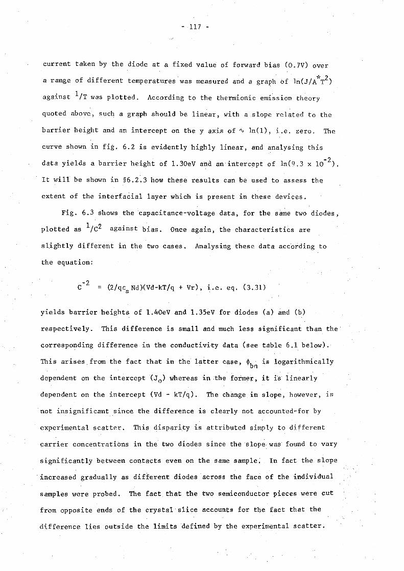
- 117 -
current taken by the diode at a fixed value of forward bias (O. 7V) over
. * 2 a range of different temperatures was measured and a graph of ln(J/A T )
against 1/T was plotted. According to the thermionic emission theory
quoted above, such a graph should be linear, with a slope related to the
barrier height and an intercept on the y axis of "' ln(l), 1. e. zero. The
curve shown 1n fig. 6.2 is evidently highly linear, and analysing this
data yields a barrier height of 1.30eV and an intercept of ln(9.3 x lo- 2).
It will be shown in §6.2.3 how these results can be used to assess the
extent of the interfacial layer which is present in these devices.
Fig. 6.3 shows the ·capacitance-voltage data, for the same two diodes,
plotted as 1;c2 against bias. Once again, the characteristics are
slightly different in the two cases. Analysing these data according to
the equation:
-2 C = (2/qes Nd)(Vd-kT/q + Vr), i.e. eq. (3.31)
yields barrier heights of 1.40eV and 1.35eV for diodes (a) and (b)
respectively. This difference is small and much less significant than the
c;orresponding difference in the conductivity data (see table 6.1 below).
This arises from the fact that in the latter case, ~b is logarithmically n
dependent on the intercept (J0 ) whereas in the former, it is linearly
dependent on the intercept (Vd- kT/q). The change in slope, however, 1s
not insignificant since the difference is clearly not accounted-for by
experimental scatter. This disparity is attributed simply to different
carrier concentrations in the two diodes since the slope was found to vary
significantly between contacts even on the same sample. In fact the slope
increased gradually as different diodes across the face of the individual
samples were probed. The fact that the two semiconductor pieces were cut
from opposite ends of the crystal slice accounts for the fact that the
difference lies outside the limits defined by the experimental scatter.

-3
.;::.,N -c: 0
~ -I g :E a.
-2 ·1 0 BIAS (VOLTS)
... ~
N I
LL .... 52 ~
N I u
Figure 6.3 Reciprocal capacitance squared against bias for the two diodes
used to obtain the data shown in fig. 6.1 .
1·6 1·7 1·8 Photon Energy (h~) (eV)
li_gure 6.4 (Photoresponse per incident photo!'!)~ vPrRus photon enPrgy
('Fowler plots') for the two diodes used to obtain thP data
shown in fig. 6.1.
2·0
2

- 118 -
An approximate doubling of the doping concentration across the diameter
of the semiconductor slice was noted.
The photoelectric data for the same two diodes are shown, in the
form of Fowler plots, in fig. 6.4. Both diodes are well described by
the relationship; R = C(hv- hv ) 2 (i.e. eq.(3.3o)) and extrapolating 0
back to R = 0 yields barrier heights,' ~b = hv , which are very similar n o
in each case ( ~1.39eV).
The information gathered from these three techniques ~s collated in
table 6.1 below.
J-V Data 11cz - V Data Photoelectric Data
Ideality Barrier Diffusion -3 Barrier Barrier factor Height(eV) Voltage(eV) Nd(cm ) Height(eV) Height(eV)
.. -··---Ferri cyanide
1.37("!:0.01) S.Oxlo15 + + Preparation 1.01 1.23eV 1.40(-0.03) 1.39(-0.0l) (Diode (a))
··----·
+ Br2/CH3
oH-HF . + 8.8xlo15 1. 3s("!:o. o3) Preparation 1.02 1.31(-0.01) 1.18eV 1.39(-0.0l)
(Diode (b))
Table 6.1 . Information Deduced from figs. 6.1, 6.3 and 6.4
It can be seen from this data that there is a good agreement· between
the harrier heights measured by the various techniques, although those
measured by the J-V technique are somewhat lower than the values determined
from the other methods. Since the photoelectric technique gives the only
direct measurement of this parameter, it can be assumed that the value of
1.39eV, measured for both diodes, is the mos~ accurate. This means that
the different values indicated by the J ... V technique for the two diodes is
not due tq a real difference in barrier height. The only other possibility
is thpt diqde (a) pqs~esses a more significant interfacial layer than
- 119 -
. k. diode (b) and hence the J-V characteristics are affected by the (x 2 o)
tunnelling transmission coefficient (§3.4.1). However, this layer is not
of sufficient magnitude to cause a bias dependent barrier height since the
ideality factor is still very close to unity. This interpretation is
corroborated by the fact that the photoresponse, at any given photon
energy, is smaller in the case of diode (a) (see fig. 6.4) which indicates
an additional impediment to the current flow. This interfacial layer is
considered in more detail in §6.2.3. It is interesting to note from
fig. 6.1 how, at low bias, curve (a) tends towards curve (b)~ This can
be explained if one assumes that the interfacial layer contains a
significant pinhole density. At very low currents the conduction occurs
via these pinholes and not by quantum mechanical tunnelling. Howev~r, at
higher current densities this current path becomes saturated and the
dominant mechanism is tunnelling which l~ads to the observed shift in the
forward current characteristic.
6.2.2 Photovoltaic Properties
Gallium phosphide, with a bandgap of ~2.25eV, is not a material which
one would consider as suitable for solar cell applications since a large
proportion of the solar spectrum would not be utilised by such a cell.
However, the photovoltaic properties of the MIS devices will be shown to
provide valuable information about the mechanism of minority carrier ,. v ~ . . , ..
transport across the insulator. The photovoltaic characteristics of the
near-ideal diodes are presented here, both for future reference, and to
give additional information about the magnitude of the interfacial layer
present in these devices, Fig, 6.5 shows the current density-voltage ,. . ,'
characteristics for a typical Schottky diode (type (b)) both in the dark
and under illumination. For this particular diode, the open circuit ' . -2
volt~g~ is ~ 0. 59V an~ the :;hort circuit current is ~ 0.18 Am • Table 6.2
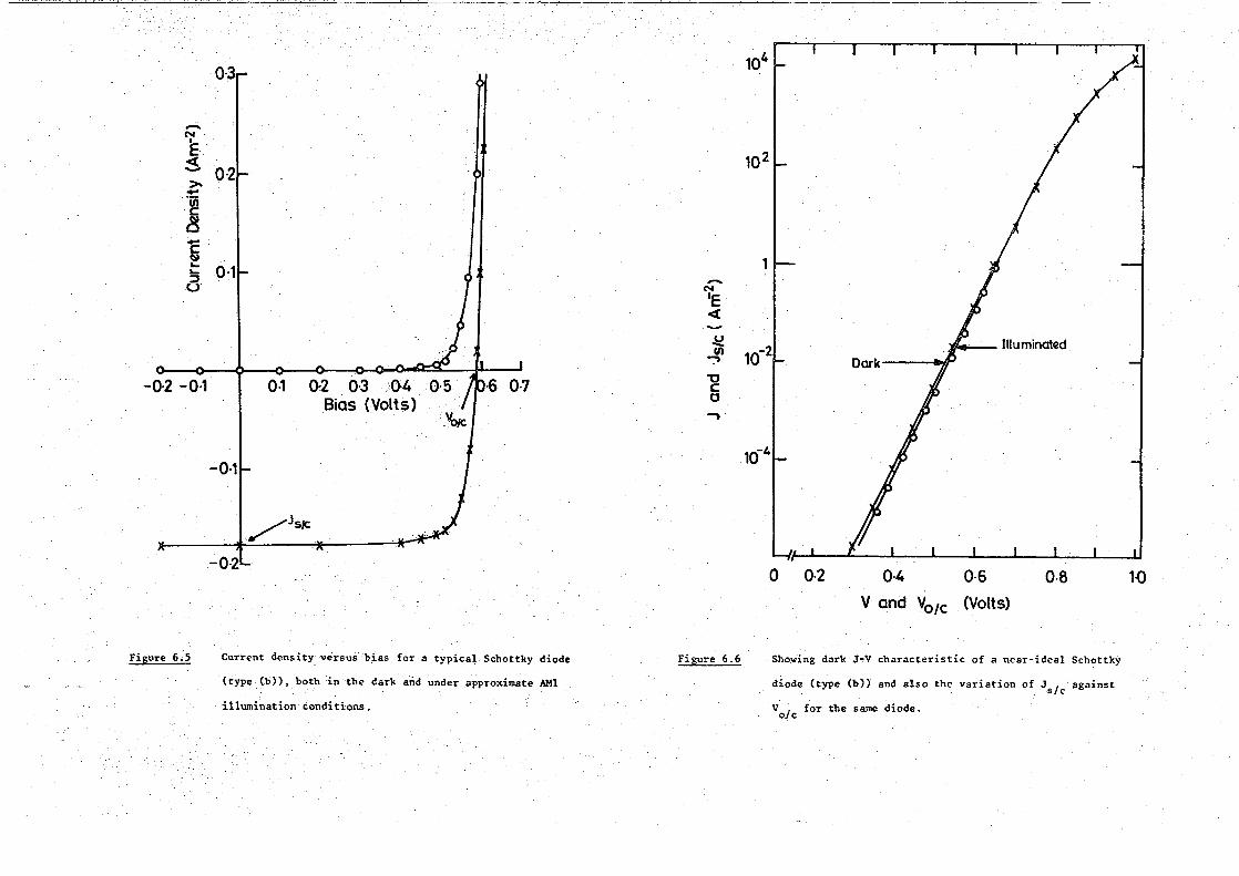
-~ E s
.> -··~ -5
0·3
0·2
II..
5 0·1 u
-0·2 -0·1 I 0·1
-0·1
/JSIC
-0·2
.. Voic
Figure 6.5 Current density vers~s ·b~as for a typical Schottky diode
(type (b)), both in the dark and under approximate AMI
illumination·conditions.
-N
'E <( -~ Cl) ~
"C c 0 ..,
Figure 6.6
104
102
1
10-2~ 'II.. Illuminated
Dark
104
0 0·2 0·4 0·6 o.s V and V01c . (Volts)
Showing dark J-V characteristic of a near-ideal Schottky
diode (type (b)) and also the variation of Js/c against
vo/c for the same diode.
1{)

- 120 -
shows these characteristics for diodes (a) (prepared using the ferri-
cyanide treatment) and (b) (prepared using the Br21cH3oH- HF treatment).
They were determined from a number of contacts on each slice, the
figures quoted being average values.
J sic
(Aim2) v ole
(Volts)
Diodes (a) 0.19 + (-0.02) 0.65 c:!:o.o3)
Diodes (b) 0.19 (:!."0.04) 0.60 c:!:o.o4)
Table 6.2 Photovoltaic properties of diodes fabricated using different surface preparation~
The J-V characteristic of a Schottky diode under illumination can be
written as:
exp (qVIn'kT) - J I for V > s c "'
3kT.
A relationship for the open circuit voltage can be found by equating J
to zero. This yields:
J sic --,-
J 0
where n' and J ' represent the terms n and J under illumination. For 0 0
the diodes used in this study, the values of n and J were almost unaffected 0
by the illumination. This can be seen from fig. 6.6 which shows a plot
of J I against V I for a range of illumination intensities in addition s c . 0 c
to a usual 1dark 1 J-V characteristic. The slopes, and hence ideality factors
are similar in each case and there is only a slight change in Jn. Tf the

- 121 -
value of J 0 ' deduced from fig. 6.6 along with the short circuit current
given ~n table 2 is used in the above relationship, V is found to be ole
equal to 0.61 volts. This is in excellent agreement with the figure
quoted in table 2 for the diodes fabricated using the Br21cH30H - HF
treatment and suggests that these diodes are particularly ideal, with a
minimal interfacial layer. The slight increase in open circuit voltage
observed in the case of diodes (a) is most likely due to the presence of
an increased interfacial 'oxide' layer.
6.2.3 Assessment of Interfacial Layer
A number of conclusions can be drawn from the data presented in the
previous two sections: Diodes (b), i.e. those fabricated using the
Br21cH30H - HF treatment, exhibit the more ideal characteristics and are
genuinely near-ideal since they agree well ,~·ith the theory developed in
§3.3. The photovoltaic data suggest that the interfacial layer in these
devices is essentially 'transparent' to tunnelling electrons, i.e. the
. k (x 2 o) tunnelling coefficient can be considered to be essentially zero.
However, diodes fabricated using the ferricyanide preparation are not so
ideal and this difference can be accounted-for by assuming the presence
of a more significant interfacial layer. Nevertheless the diodes still
behave largely according to the near-ideal model and they do not exhibit
a bias-dependent barrier height. This is revealed by the fact that n is
close to unity and that the barrier height measured by the capacitance
technique agrees well with that calculated from the photoelectric technique.
The thickness of this interfacial layer can be estimated indirectly from
either the photoelectric or J-V data. Assuming that the difference in
V (shown in table 6,2) is due to the presence of an interfacial layer, ole
then V I can 0 c
k + x2 oL This
be related to J I by eq. (3.63); i.e. VI s c 0 c
yields a value for (x~o) of approximately 2.
= n'kTiq {ln(J I IJ 0 ') s c
As has been
previously discussed, it is virtually impossible to assign a theoretical
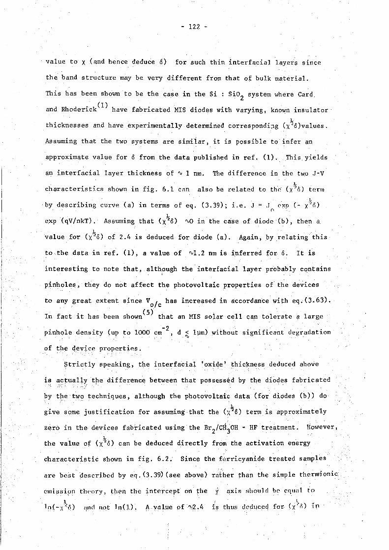
- 122 -
value to X (and hence deduce o) for such thin interfacial layers since
the band structure may be very different from that of bulk material.
This has been shown to be the case in the Si : Sio2
system where Card.
and Rhoderick(l) have fabricated MIS diodes with varying, known insulator
1 thicknesses and have experimentally determined correspondi:;1g (x 2o)values.
Assuming that the two systems are simiiar, it is possible to infer an
approximate value for o from the data published in ref. (1). This yields
an interfacial layer thickness of rv 1 nm. The difference in the tw.o J-V 1,.
characteristics shown in fig. 6.1 can also be ·eel a ted to the ( x'2 o) term
by describing curve (a) in terms of eq. (3.39); i.e. J = .J p
1 exp (qV/nkT). Assuming that (x 2o) rvo in the case of diode (b), then a
1 . value for (x 2 o) of 2.4 is deduced for diode (a). Again, by relating this
to the data in ref. (1), a value of rvl,2 nm is inferred for o. It is
interesting to note that, although the-interfacial layer probably contains
pinholes, they do not affect the photovoltaic properties of the devices
to any great extent since VI has increased in accordance with eq.(3.63). 0 c
In fact it has been shown (S) that an MIS solar cell can tolerate a large
-2 . pinhole density (up to 1000 em , d ~ lpm) without significant degradation
of the qev:ice properties.
Strictly speaking, the interfacial 'oxide' thickness d~duced above
i~ ~cfu~llY, tpe difference between that· possessed by the diodes fabricated j
py tpe two techniques, although the photovoltaic data (for d:i.odes (b)) do 1 .
give some justification for assuming that the (x 2 o) term is approximately
zero in the devices fabricated using· the Br2/cH3
0H - HF treatment. However,
1 the value of (x 2 o) can be deduced directly from the activation energy
characteristic shown in fig. 6.2. Since the ferricyanide treated samples
are best described by eq.(3.39)(see above) rather than the simple thermionic
end ssipn tlwory, then the :intercept on the y axis should be equnl to
. ' 1 ln(-x~~) qnd not ln(l)~ A value of ~2.4 is thus deduce~ for <x~o) in

- 123 -
the ferricyanide treated samples which is in excellent agreement with
that deduced earlier. Consequently, diodes fabricated using the
Br2/cH30H - HF treatment can be assumed to be free of any significant
interfacial layer, whereas those fabricated using the ferr~cyanide
preparation possess an interfacial layer, of the order of 1 nm thick,
which has an appreciable tunnelling transmission coefficient but which
does not result in a bia~ dependent barrier height. Such diodes will
still be classed as near-ideal for the purposes of this work.
6.2.4 Energy Band Scheme
According to the simple Schottky - Mott theory (eq. (3.1)), the
Schottky barrier height for the gold : (n) GaP system should be 1.1 eV.
This is clearly not the case here where a value of 1.39eV has been
measured. In fact, a wide range of barrier heights have been reported for
this system and the exact value depends on both the surface preparation
and the semiconductor properties. The Bardeen model of a Schottky barrier,
i.e. the model used in the previous section to assess the extent of the
interfacial layer, assumes that the Schottky barri"er height is determined
by the charge localised at the semiconductor surface in the interface
states. Thus, by applying eq. (3.3) ~ i.~. ~bn = C2 (~~- Xs) + (1 - C2)
(Eg - ~0 ) - Mbn' to this system assm11ing o "' lnm, e:i "' 2e:0
,
Eg - ~ = 1.6 ev( 2), and neglecting the image force barrier lower:i.n~,
. . 0
. 13 -2 . -1 yields an interface state density of approximately 1.5 x 10 em eV .
This value agrees well with the figures given in ref. (2) for a variety of
Schottky diodes. This analysis will be extended in §6. 3 when the effect
of increasing o is discussed and also in chapter 7 when the LB film MIS
diodes are considered.
The proposed band diagram for the near~ideal Au : (n) GaP diodes
described so far is shown in fig. 6.7. Dsa is the density of surface
stateE; and the su}Jscript 1 a 1 is used to denote the fact th;1t their

. 6 Vacwm leYel Eci
" +m=5-1cV
tt.T1·39eV
Efm•---'--"--1
Au. g ....-
6 ""1nm
Xs=4,0eV
Ec I
I ----E --- ts
g=2·251N
----- I • Ev
n - type· GaP.
Figure b.7 The proposed band diagram !or the neu-ideal Au : (n) CaP
Schottky diodes.
-N I
E ~ ->--"iii
-~
~ ''::l u
Figure 6.8
102 I I I I 17
I . I ·. 0·6 0-6
I I I I I
I
. Barrier Helghts
From Photoel~tctric Mzasur~Emmts
(a) I 1·43
(b) I 1·39
1·0 1-2 Bias (Volts)
Current density-voltage data for a typical non-ideal diode
(a}. Also shown is a near-ideal characteri&tic (b). The
in&et shows the measured barrier h.eigh-ts. (The reverse
current was undetectable for V • -lOV).
.;.:,

- 124 -
population is governed by quantum mechanical tunnelling to and from the
metal, i.e. they are populated according to the position of the metal
Fermi-level. Since the interfacial·layer is so thin, only a small
fraction of any applied voltage is developed·across the insulator. This
means that the position of the Fermi level at the interface is essentially
fixed relative to the band edges, and consequently the charge localised
in the interface states does not vary with applied voltage, which explains
the ideality of the diode characteristics. The band diagram under the
application of a forward bias has been discussed previously and is shown
in fig. 3.3.
6.2.5 Electroluminescent Properties
Irrespective of the method used to prepare the devices, none of the
diodes discussed so far emitted any detectable EL, even for·drive currents
-2 of up to 50 A em which is approximately an order of magnitude higher than
that used in typical LEDs. The reason for this can be appreciated by
considering fig. 6.7. The metal-semiconductor barrier which preventH holes
from being injected into the semiconductor bulk (~bp) is' rv2.09eV high.
This is much greater than the barrier presented to electrons ( ~bn = 1. 39eV)
crossing from the semiconductor into the metal. Therefore the bulk of the
current, under the application of a forward bias, is due to electron flow
and the minority carrier injection ratio , y, is consequently 1very low.
In fact by applying eq. (3.36) to the Au (n)GaP system, y can be
estimated. This equation, which is known to be accurate fpr Au : ( n) Si
diodes, yields y rv lo- 14 . This value is extremely small which is a __L
consequence of the fact that y a exp { ~ kT (<P,p - ~bn)} and is therefore
acutely dependent on the value of (~bp - ~bn). Since the EL efficiency
is directly proportional toy, it is notsu~rising that noEL could be
detected from these near-ideal diodes. The scope for improvement, by

- 125 -
incorporating an insulator which enables a significant degree of band
realignment to occur, is enormous since it should be possible to
effectively reduce the height of cf>b to zero by alignment of the metal . p
Fermi level and insulator valence band edge (see fig. 2.8). Moreover,
the control of insulator thickness afforded by the LB technique shouJ..d
enable diodes with the optimum thickness for EL efficiency to be
fabricated.
6.3 NON-IDEAL SCHOTTKY DIODES
These diodes were prepared by polishing the sample for~ 2 mins.
in a 0.5% Br2/CH30H solution, and then. exposing the semiconductor surface
to atmospheric conditions for several hours before depositing the gold
barrier electrodes. The HF oxide-removal stage was omitted. These
devices are more accurately defined as MIS structures since the diode
characteristics reveal the presence of a substantial interfacial layer
which has a pronounced effect on the device properties. This layer is
evidently a chemically prepared native 'oxide' and the diodes are termed
'non-ideal' in order to distinguish them from those containing the
intentionally introduced, insulating layers (i.e. LB films).
6. 3.1 Electrical Characterisation
The current density-voltage data for a typical diode is shown in
fig. 9.8 ~curve (a)). For comparison curve (b) shows the char;;tcteristic
of a diode fabricated using the normal Br~/CH30H - HF treatment. The
corresponding barrier heights, as measured by the photoelectric technique,
are also givep. in fig. 6.8. The \2 against voltage curves for the
same two devices are shown in fig. 6.9, It is inunediately obvious that
diode ([.:1) is very different ,from the near .. ideal diode (b), Both the
increase in the ideality factor and the large voltage intercept on the
\2 - y plpt are ip.dicative of a bias ~ dependence of the· barrier height

-3
Figure 6.9
Figure 6.10
-2 -1 0 1 Bias (Volts)
v~ (a)= 3·12 v Vi (b): 1·20V
2 '3 V~(a)
Reciprocal capacitance squared against voltage curve for a
typical non-ideal diode. Also shown is a near-ideal
characteristic (b).
GoP-Au m= 4.70 f/.V
X5 = 4·0 eV
2 <to= 0·66 f/.V Ds= 3 x x:>'3cm·2~v-1 Ej:£0
1
0 10 20
b - Angstroms
30
Variation of V with 6 for non-ideal GaP Schottky diodes. 0
(After Cowley( 3)).

- 126 -
resulting from the presence of a substantial interfacial layer. The
theory described by Cowley( 3) (see §3.4.1), which was developed
specifically to fit the Au : (n) GaP system, can be applied to the data
in fig. 6. 9. The ~ain features of these data are that the·. slopes of the
two curves are essentially the same whereas the intercepts are very
different. These are precisely the features around which the Cowley
(3) theory was developed. The model which was found to best describe this
behaviour was one based on the presence of charged interface states and an
interfacial layer significant enough to cause a degree of band realign-
ment under the application of a bias. This results in a bias dependent
interface charge density. The variation of V0
(the intercept on the
voltage axis) with o pr'edicted by this model ( 3) is reproduced in
fig. 6.10, from which an approximate value of o can be deduced. This
yields an insulator thickness of"' 3nm for diode (a) in fig. 6.9.· However,
this analysis must be considered as very approximate since the theory is
rather complex and ~n order to produce the graph shown in fig. 6.10, a
number of assumptions were made( 3). In particular, the dependency of
the change in the interface charge on the degree of band realignment was
chosen arbitrarily to provide a reasonable fit to the experimental data.
In addition, an unknown fraction of the surface state charge may be
governed by interactions with the semiconductor band structure rather than
the metal. This latter problem is also encountered when attempting to
relate the ideality factor of these diodes to o using eq. 0.41). Never-
the less, the value of "' 3nm predicted from figure 6 .10 for o is not
unreasonable since in the Si Sio2 system an insulator thickness of
"'2.2nm results in an ideality factor of 1.7(l). The value of 1.8,
calculated from fig, 6.8, for diode (a) agrees well with this.

- 127 -
6.3.2 Electroluminescence Measurements
A consequerice of the voltage developed across the oxide under the
application of a bias, is that an increase in the minority carrier
injection ratio is achieved for a given value of forward bias. This
effect has been discussed previously in§ 2.4.3. and in more detail in
§ 3.4 .1 and in fig. 2. 8 the band realignment is clearly depicted.
Since y is an exponetial function of q/kT (~n ~ ~bp), even a small
change in the relative positions of the metal Fermi level and semicon-
ductor valence band will result in a dramatic increase in y and
possibly enable EL to be detected. This was indeed found to be the cnsP.
Under the application of a forward bias (V 'V > 4.4 V) green/yellow light
could be seen to be emitted from beneath the gold top electrode. The
spectral distribution of this emission is shown in fig. 6:11. A drive
-2 current density of lOA em was used to excite the EL. At least two
mechanisms can be distinguished in this spectrum and these can be
identified, by their corresponding photon energies of 2,11 eV and 2.16eV,
as the NN1 and A-0 processes respectively. The origins of these
mechanisms were discussed in §2.6.2 and will therefore not be described
here. However, the important aspect is that they are extremely
characteristic of minority carrier recombination at nitrogen impurity
centres. This confirms· that the EL is a result of enhanced minority
carrier injection due to the presence of the interfacial layer. The
possibility of exciton formation due to impact ionization is ruled out
since the turn on voltage for EL is known to be less than 4.4V, i,e.
the lowest voltage at which EL could be detected. The electric fields
necessary for impact ion~zation could not be achieved using such low
voltages, The d.c. power conversion efficiency was measured to be at
least 2.4 (~ 0,1) x lo-4%. -2
Comparing this value to that of 'V5 x 10 %,
which is the efficiency of a typical, unencapsulated p-n junction diode

~ 128 ·~
and assuming an injection ratio of 100% for the p-n junction, yields a
value for y of at least rvO.S%. This represents a large increase over
the value of lo- 12% predicted for the near-ideal diodes by ~q. (3.36).
However, the light emitted from the area beneath the gold electrode was
not uniform. Fig. 6.12 shows a photograph of the emission as viewed
through the back face of the semiconductor. The light· can be seen to
originate from nu~erous small regions. This is indicative. of the
irregular nature of the native 'oxide' layer with the bright spots
being regions of high electric field. These diodes are clearly unaccept-
able as commercial devices although they are useful as a comparison for
the MIS diodes fabricated using LB films. Since these films are highly
uniform, both in thickness and in structure, a significant improvement
in the uniformity of the light emitted should be possible. Furthermore,
the fine control over the insulator thickness which is afforded by the
LB technique will enable o to be optimised and an improvement in the EL
efficiency should be also possible. The results obtained for such diodes
are discussed in chapter 7.
6.4 GaP/LB FILM INTERFACE : INTERFACIAL LAYER ASSESSMENT
Before proceeding to discuss the characteristics of LB film MIS •
diodes, it is useful at this stage to consider the question of the
unintentional interfacial layer which must be present between the LB film
and the semiconductor surface. It has already been demonstrated that in·
the case of the near-ideal Schottky diodes, this interfacial layer is of
the order of rvl nm thick. However, in the LB film diodes this thickness
may be somewhat different as a result of the device fabrication procedure.
There are primarily three stages during the deposition of an LB film when
an interfacial layer may grow on the semiconductor surface. These are:
(i) the period during which the semiconductor is exposed to the aqueous
environment of the Langmuir trough, (ii) during the 1-2 hour, post~lst
- 129 -
layer drying period and (iii) during the 2'·3 day pre-electrode deposition
period. (The two latter periods both involve storage under a low pressure
of dry nitrogen.) It has previously been mentioned that the J-V character-
istic 1.s very sensitive to the presence of an interfacial layer, and
the effect of each of the above stages on this characteristic is now
considered in sequence. Fig. 6.13 shows three typical current-voltage
characteristics: Curve (a) represents the control diode 'where the barrier
electrode was deposited immediately after the ferricyanide surface prepara
tion .. Curve (b) represents a typical diode which was prepared in parallel
with sample (a) but also dipped at usual speed into the Langmuir trough
(without a film spread on the surface) prior to deposition of the barrier
electrode. Curve (c) is the characteristic of a typical diode from a
sample which was dipped with sample (b), but then desiccated for 2 hours
before metal electrode deposition. The error bars are again indicative of
the experimental scatter over a wide range of contacts. There is little
difference between the three characteristics with all exhibiting ideality
factors very close to unity (rvl.Ol) and no significant change in the
magnitude of the forward current. In all three cases the reverse current,
-12 for VR = lOV, was less than 10 A i.e. below the sensitivity of the
measuring equipment. The barrier heights (see inset to.fig. 6~13), as
measured by the photoelectric technique, were very similar for all three
diodes. From these data it can be concluded that neither exposing the
sample to the aqueous environment of the trough, nor storage under dry
nitrogen for 2 hours increases the magnitude of the interfacial layer to
any significant extent. However, this was found not to be· the case for
stage (iii). Exposure to a low pressure of dry nitrogen for 2-3 days was
found to result in the growth of an appreciable 1oxide 1 layer qn thli! semi-
conductor surface. The effect of this layer on the device characteristics
can be seen in fig, 6.14 where curve (b) shows the characteristic of a

-8. ~ --c: ! "·:l u
Barrier Heights
From Photoelectric Meosure!'Tl(lnts
Diode eV)
{a) 1·39
(b) I 1·40
{c) I 1·39 I r1Pi I
10-12!
Figure 6.13
0·2 0·4 0·6 o.a Bias {Volts)
Three typical J-V characteristics for diodes fabricated using
different techniques (refer to the text for a description).
·The corresponding barrier heights are listed in the inset.
-8. E
<{
-c: ! ,_ 1Cf1 a
Figure 6.14
.
From photoelectric Meo51.JT'(2:!'1'l1
Diode I tbn t Q.Q1(eV
0·4 Q.6 08
Bias {Volts)
lO
1·39 1·54 1·65 1-64
Showing typical J-V characteris~ics for four different
l2
diodes (refer !':o the text for a description). The correspond-
ing barrier heights are listed in the ins~t.

- 130 -
typical diode fabricated by this method and (a), shown for comparison, 1s
for a near ideal diode which had been desiccated for only 2 hours prior
to electrode deposition. The barrier heights of the two devices are also
listed in fig. 6.14. There is clearly a large difference between the
characteristics of the two diodes. AHhough there has been little change
in the ideality factor (from 1.01 to 1.05), there has been a dramatic
decrease (of over six orders of magnitude) in the value of the forward
current at a g1ven voltage. In addition, the extent of the barrier
limited regime has been redticed and the series resistance, associ~ted
with the diode has increased. All of these observations are indicative
of a significant interfacial layer and although the ideality factor is J
still close to unity, these diodes cannot be considered as 'near-ideal'.
The fact that the ideality factor remains largely unaltered indicates,
that, although this layer may in fact be relatively thick, the majority
of the interface states are populated according to the position of the
metal Fermi level. This can be deduced from eq. (3.41); i.e.
n = 1 + (o/E.)(E /W + qDsb)/(1 + (o/£.) qDsa) where it is evident that 1 s 1
interface states which equilibrate with the metal tend to maintninn at
approximately unity whereas those which equilibrate with the semiconductor
tend to increase n. The large decrea(le in the forward current can be
explained, at least in part, by the increase in the Schottky barrier height,
as revealed by the photoelectric measurement. This increase of 0.15 eV is
(2) predicted by the general expression for ~bn derived by Cowley and Sze
(eq. (3.3)) as a consequence of an increase in o. It accounts for a
decrease in the current of over two orders of magnitude. The remaining
decrease must be due to the (x~o) term in eq.(3.39)and by relating curve (b) I,
to this equation, it is possible to deduce a value of "'10 for (x'7.6), The
thickness of the interfacial layer can be estimated (a) by comparinR the
\ . . . d' d (l) value for x-~ deduced here to data obta1ned using 81 : 8102 10 es , or
,, ;~

- 131 -
(b) by relating the increase in barrier height to eq. (3.3). The former
of these methods yields a value of ~3nm whereas the latter gives ~snm,
which 1s a reasonable agreement considering the approximations involved.
It is interesting to compare the characteristics of these diodes with
those discussed in §6. 3.1. Although the effective thickness of the
interfacial layer may, in fact, be quite similar in the two cases, their
properties are clearly very different. This is understandable since the
diodes discussed in §6.3 contained a chemically preparedinterfacial
layer whereas those discussed in this section possessed a 'grown' layer
whose structure and properties may differ significantly. The former of
these layers evidently possesses the better insulating properties,
possibly due to a lower density of defects and pinholes. The effective
'resistance' of this layer is.significant when compared to that of the
semiconductor depletion region and this is manifest in the pronounced
bias dependence of the barrier height. The intercept on the voltage
-2 ax1s in the C -V data was much smaller in the case of the 'grown'
layer ( 1. 6V compared with 3.1 V for devices incorporatirtg the chemically
prepared layer) which again indicates a much reduced bias-dependency of
the barrier height.
The cause of the oxide growth during stage (c) is uncertain although
it could be a result of impurities contained in the nitrogen gas or
possibly residual oxygen in the desiccator, since diodes fabricated on
samples exposed to the atmosphere for 2-3 days exhibited similar
characteristics. Whatever the cause, an important question arises: Does
this layer grow only in the exposed region of an LB film-coated sample,
or is it also present beneath the LB film? This is of para~ount importance
since the elegance of the LB technique, from the viewpoint of this work,
lies in the ability to accurately define the insulator thickness.
Furthermore, it is important to distinguish between effects due to the

- 132 -
presence of the LB film and those due to the interfacial layer, The
problem arises because it has been shown that some LB films are porous
. (4) . to certaLn gases , thus the Lnsulator may not prevent the growth of
such a layer. The question can be answered by again considering fig. 6.14.
Curve (c) represents the current-voltage characteristic of an MIS diode
fabricated with one monolayer (2.5 nm) of Cdst 2 , which was desiccated for
~2 hours before electrode deposition. Curve (d) corresponds to a diode
fabricated on an identical subBtrate except that it was desiccated for
~2 days prior to metallisation. The finer details of these curves will
be discussed in chapter 7 together with the other MIS data and are there-
fore not discussed here. However, it can be seen that there is only a
small difference in the magnitude of the forward current at a given
voltage and that the barrier heights are approximately the same for the
two diodes. This is in marked contrast to the difference between curves
(a) and (b), and indicates that the deposition o~ a monolayer of the LB
film prevents, or at least greatly retards, the growth of the interfacial
layer. Hence the unintentional layer present Ln a metal LB film - (n) GaP
device can be assumed to be of the order of 1 nm thick and not to significantly
affect the device properties. It should be noted that once the barrier
electrodes had been deposited, none of the characteristics shown in fig. 6.14
exhibited any ageing effects over a period of several weeks.
6.5 SUMMARY
In summarising the results presented Ln this chapter, the following
conclusions can be drawn:
(a) Devices fabricated by either the ferricyanide or the Br2/cH30H - HF
methods can be said to exhibit near~ideal characteristics, although those
prepared using the ferricyanide treatment posses a slightly more
significant interfacial layer (rvl nm thick). This interfacial lay·~r

- 133 -
represents an additional barrier to the transport of electrons across
1 the interface which manifests itself as a (X 28) term. It is not, however,
sufficient to cause an appreciable realignment of the band structure
under the application of a bias.
(b) No EL can be detected from any of these near-ideal diodes even
-2 for drive current densities of up to "-'SOA em . This is a consequence of
the extremely low value of y in these devices.
(c) Diodes fabricated with a chemically prepared native 1 oxide 1
layer exhi.bit non-ideal characteristics which can be described using the
MIS diode model discussed in §3.4. The thickness of this interfacial layer
is estimated to be "-'3 nm and is sufficient to cause a degree of band align-
ment under the application of a forward bias. This results in a
dramatic increase in the minority carrier injection ratio· and enables
EL to be observed, although the emission is very irregular in nature and
-4 has a low measured external efficiency ("' 2 x 10 %) •
(d) It has been demonstrated that it is possible to incorporate an
interfacial layer which has a pronounced effect on the current-voltage
characteristics without causing a significant increase in the ideality
factor. This is interpreted as an indication that the majority of inter-
face, states equilibrate with the metal. The criterion 1n < 1.2 1 which 'V
is often assumed to justify the use of the simple Schottky barrier thermionic
emission theory may therefore not always be valid.
(e) The interfacial layer present beneath the LB film in the MIS
devices ~s not significantly different in extent or influence from that
present in the near-ideal diodes, i.e, it is of the order of 1 nm thick
and has only a small effect on the device properties. The characteriqdcs
of the LJ3film MIS diodes t which are described in the following chapter, can
therefore be attributed to the presence of the LB film and are not a con-
r:;equence of any unintentional interfacial layer.

- 134 -
CHAPTER 7
RESULTS AND DISCUSSION : GaP MIS STRUCTURES
7.1 INTRODUCTION
The results presented in this section can be roughly divided into two
catagories. The first deals with the characterisation of the devices from
the viewpoint of their band structure, electrical properties and mode of
operation, and the second concerns the light-emitting properties of'the
devices. Some of the data which will be presented later in this chapter,
together with the results of an independent, parallel study of the Au
LB film : (n) GaP system have been the subject of a number of recent
bl . . (l-6) . 1 f h h h. h.b. pu 1.cat1.ons . It 1.s c ear rom t ese reports t at t .1s system ex 1 1ts
a number of very interesting properties. In particular, the insertion of
an LB film into the Au : (n) GaP Schottky barrier structure has been demon-
strated to significantly increase the effective barrier height in the
device. However, the mechanism by which this is achieved is not under-
stood, and more importantly, the actual mode of operation of the device
remains uncertain. This increase in the (majority carrier) barrier height
is very important from the viewpoint of this work since it would be expected
to cause a significant improvement in the minority carrier injection ratio,
and hence the EL efficiency. A thorough investigation of this phenomenon
is made and a model is proposed to explain both the results presented here and
previously published data. The EL properties are presented and interpreted
in terms of the model. Measurements made on the devices under illumination
are shown both to support the proposal and to provide some insight into the
actual EL mechanism. The question of device lifetimes and degradation
mechanisms is considered in §7. 3 .4, which concludes the work on fatty acid-
based devices. In the final section the 'model 1 system is extended to
incorporate LB films of phthalocyanine and the properties of these dibdes
·are examined. The chapter concludes with an assessment of the .future
prospects for MIS LEDs based on LB technology.

- 135 -
7.2 GENERAL CHARACTERISATION OF THE MIS STRUCTURE
In this section, the results of probing the MIS diode barrier, in
devices with a range of insulator thicknesses, are presented, analysed
and discussed. The methods employed are the J-V, C-V and photoelectric
techiques whichwere described in §3.3.5 and §3.4.J., and used in chapter 6
to study the near-ideal Schottky diodes. Most emphasis is placed on the
Au : CdSt2 : (n) GaP system although some data are also presented for
devices incorporating w-TA as the insulator. The capacitance-voltage
characteristics are discussed separately
by Cowley(7 ) which was later modified by
7.2.1 Measurement of Barrier Height
(a) Au : CdSt2 : (n) GaP Devices·
following the approach used first
(8) Fonash .
Conductivity Data. The forward bias current density-voltage curves
for a number of typical MIS diodes with varying insulator thickness are
shown in fig. 7.1. Curve (b) corresponds to a diode fabricated with one
monolayer of CdSt2 (molecular length of ~2.5 nm), curve (c) corresponds to
a diode incorporating three monolayers, and (d) corresponds to five mono-
layers. Also shown (for comparison) is the characteristic of a near-ideal
Schottky diode, fabricated in parallel with the MIS devices. There are a
number of important features in these data: ( i) All of the curves exhibit
well-defined linear regions which can be described by the relation
J = J exp (qV/nkT). Furthermore, the value of tl1e ideality factor, n, is 0
approximately the same in all cases and is very close to unity (n ~1.05).
(ii) The effect of incorporating one monolayer is very prqnounced and
represents a decrease of over four orders of magnitude in the value of the
intercept, J 0
However, the effect of subsequent layers is much smaller and
indE~ed a slight 1ncrease in J is observed in the case of curves (c) and 0
(d) over that of (b). (iii) As the film thickness is increased, the extent
of the linear region is decreased and the deviation from linearity at higher

,...... N e u ._ en a.. E < -~ ...., ·-en c: ~
i '-:3 u
Figure 7.1
10-6
10-8
0·4 Q.6 0·8 1·0 1·2 Bias (Volts)
Current density versus forward bias for diodes incorporating
a range of Cdst2 insulator thicknesses; (a) no insulator
(near-ideal curve), (b) one monolayer, (c) three monolayers
and (d) five monolayers. (The reverse current was undetect-
able for V = -lOV).

- 136 -
biases is more pronounced. This indicates that, although the addition
of subsequent layers, after the first, have little effect on J , they do 0
introduce an additional, series impediment to current flow in the same
manner as the series resistance associated with the semiconductor bulk.
The effect of the insulator can be seen more easily in fig. 7.2(a) which
shows the J-V characteristic for a diode fabricated with 9 monolayers
(22.5 nm) of CdSt2 . In this case a larger current range has been investi
gated and three distinct regions can be identified. The linear (barrier
limited) region (a) is much reduced, as expected from the trend discussed
in (iii) above. Region (c) is the usual, series limited regime and the
characteristic is near-ohmic for V ~ 2.1V. Region (b), which is completely
absent from both the near-ideal and non-ideal Schottky characteristics, is
evidently a consequence of the LB film. This, together with the feature
marked by the arrow in fig. 7.2(a) will be discussed at a later stage.
(iv) The current carried by the diodes is much larger than that expected
considering the insulating properties of the LB film. This is demonstrated
~ by fig. 7.2(b) which shows a graph of log J against V for a Au : Cdst2 : Al,
MIM device incorporating five monolayers of Cdst2 . The curve is highly
linear and characteristic of the Poole-Frenkel type hopping mechanism which
is believed to be the dominant conduction mechanism in multilayered LB films.
The characteristic exhibits only a slight depend~nce on the polarity of the
applied bias and the value of the dielectric. co:nstant estimated from the
slope of the curve is of the correct order of ma~;nitude. Comparing this
characteristic with curve (d) in fig. 7.1 reveals a clear anomaly between
the currents measured in the MIM diode and those measured in an MIS diode
incorporating an identical insulating film. This aspect must be explained
by any model which is proposed to explain the other diode characteristics.
Photoresponse Data. The photoelectric technique is generally regarded
to give the definitive measurement of the metal-semiconductor barrier height,
~

-N I
E 0 < ->--·u; c -8 ...... c ~ '-::J u
10-2
10-4
10-6
I
10-e
10
1-0·
(a)
1-5 Bias (Volts)
10-S
-N I
E 0
< ->--·u; c ~
"U ...... 10-7 c ~ 3 u
10- 8Lt~---__L __ --l. __ __j~----' 0 1-0 1-4 1-8
2·0 \bltage ~ (V Y2)
Fi gur.<:_7 . 2 (a) Current density versus forward bias for a diode incor-
porating nine monolayers (22.5 r.~) of CdSt2
.
(b) Current density ·versus V'l; for an~~:~ device incorporating
five monolayers (12.5 nm) of CdSt2
.

- 137 -
¢bn' However,a more accurate assessment of the technique is that the
Fowler plot gives a direct measurement of the height of the barrier which
is surmounted by photoexcited electrons in order to enter the semiconductor
conduction band. Fig. 7.3 shows the Fowler plots for the same four diodes
used to obtain the J-V data shown in fig. 7.1, with curves (a) to (d)
representing devices fabricated with 0, 1, 3 and 5 monolayers, respectively.
These data confirm the implications of the J-V results, i.e. that the effect
of the insulator is to increase the height of the actual barrier presented
to majority carriers, and that this increase is relatively independent of
the film thickness. An increase of "' 0. 25eV is revealed due to the incor-
poration of one monolayer of CdSt 2 and a subsequent slight decrease of
"'0.05eV is measured due to the incorporation of additional layers. There
are two important features in these data : Firstly, the curves are all
reasonably linear - even for diode (d) where the insulator thickness is at
least 12.5 nm; and secondly, the barrier heights measured directly ~sing
the photoelectric technique agree remarkably well with those calculated
from the J-V data (fig. 7.1) using the simple Schottky barrier theory
i.e J = * 2 A T exp ( -q~bn/kT) exp ( qV/nkT)
The barrier heights measured by the two techniques are shown in table 7.1
below.
Measured Barrier Height C±o.ol) (eV) Diode
J-V Data Photoelectric Data.
(a) 1. 31 1.39 (b) 1.58 1.64 (c) 1.54 1.59 (d) 1.55 l,r;q
Table 7.1
Barrier Heights Measured by J .. v and Pho.toelecttic Techniques

15 1
-U'l
5 .£i 10 N
~
I
<( E u - -~ - ~
6 0
E <( --a. - :?:-
~ c -~
8. ~
5 ~ -
0 c
~ ~ ~ ~ :::J u -
ol..../J I I L l I I I I I
1·4 . 1-6 1·8 Photon energy (eV)
0-8 1-0 l2 1·4 l6 1·8 2·0 2·2 Figure 7. 3 Photoresponse data (Fowler plots) for the same four diodes Bias (Volts)
used to obtain the data shown in fig. 7.1. Figure 7.4 Conductivity data for diodes incorporating a rangP of (w-TA)
ins~lator thicknesses; (i) one mon0layer, (ii) seven mono-
layers, (iii) nine monolayers, (iv) eleven monolayers.

- 138 -
], This implies that there is no tunnelling transmission (x 2 o) term in the
expression for the current and presents another anomaly which must be
resolved.
(b) Devices Incorporating w-TA LB Films
These devices displayed characteristics which were very similar to
those described in the previous section. Fig. 7.4 shows the J-V character-
istics for diodes fabricated with a range of insulator thicknesses, and it
is clear that they exhibit the same features as the CdSt2 devices. The
only difference ~s that the extent of the barrier limited regime is reduced,
which indicates that the effect of the insulator at higher biases is more
pronounced in the case of the w-TA diodes. The barrier heights, as
measured by the photoelectric technique, in diodes incorporating one and
three monolayers of w-TA were very similar (1.60 and 1.61 (± 0.01) eV
respectively). These too agree well with the values measured in the
corresponding cadmium stearate devices, and also with the barrier heights
reported for a range of gold : LB film: (n) GaP devices(l). However, the
slight decrease in the barrier height, observed in the Cdst2 devices due ; .
to the incorporation of subsequent layers (after the first}, was not detected
in the w-TA diodes. This may be an effect of incorporating excess cadmium
ions in the CdSt2 films and hence producing an effective dipole in the inter,..
face region. (The w-TA films were deposited without the use of cadmium ions
in the subphase .) However, in view of the other similarities between the two
types of devices (it will subsequently become evident that the .optical
properties are also very similar) the discussion from this point will be
concerned with the more general gold : fatty acid LB film : (n) GaP system.
Discussion
There are at least two possible explanations for the results presented
so far : The measured increase in the height of the barrier may be a 'real'
effect, i.e. an increase in the actual degree of band-bending in the

- 139 -
semiconductor, or it could be an 'apparent' increase which is related in
some way to the barrier presented by the insulator.
Consider first the possibility that the increase is a real increase
in the diffusion potential. There has been much interest in recent years
in the modification of the Schottky barrier height by interfacial, insulat-
ing layers (see for example ref. (9) and the references contained therein).
This is because of the fact that such an increase would be highly desirable
in a number of electronic devices (for example in MESFETs, IMPATTs and MIS
solar cells). Many of the reports concerning barrier height modification
have been the result of incorporating native 'oxides' into the device
structure and these have been explained using the Bardeen model discussed
in chapter 3. (1 ) - .
For example, Pruniaux and Adams 0 have demonstrated a
linear variation of ~bn with o, approximately in accordance with the
general expression for the barrier height derived by Cowley and Sze(ll)
(i.e. eq. (3.3)). (An increase due to the presence of a native 'oxide'
was also observed in this work (see §6.4) where an increase from 1.39eV to
1 54 V d ) ( 12 ) h h b. . h . h h . e was measure . In some cases , owever, t e arrLer eLg t as
been measured only by the J-V and c-v techniques and not directly-by the
photoelectric technique. The results from such studies may not always be
conclusive, a point demonstrated by Morgan and Frey( 9), due to the
susceptibility of these techniques to the presertce of an interfacial layer.
The first report of an apparent increase in ~b due to the presence of an n.
LB film, concerned diodes fabricated on CdTe(l3). In these devices the
beneficial effect on the photovoltaic propertieu was studied, although the
authors stressed that an ·independent measurement of ~bn (by the photo
electric technique) would .be necessary to distinguish between a real change
k ., in ~bn and an effect due to the (x 2 ~) transmission coefficient for the
(1) . ' insulator bandgap. Tredgold and Jones fir~t reported an effect on CuP
devices when studying the photovoltaic properties of GaP MIS diodes.

- 140 -
They showed that incorporating a single monolayer of stearic acid into
the Au : (n) GaP system almost doubled the open circuit voltage of the
devices and they demonstrated that this was due to an effective increase
in the barrier height. In their case the near-ideal Schottky barrier I
height was "' l.leV and this increased to "' 1.6eV due to the presence of
the monolayer. They demonstrated the phenomenon for a range of LB film
materials, although the effect of thicker insulators was not studied in
any detail. They used the fact that good agreement was obtained between
the J-V and photoelectric measurement of barrier height, and that the
ideality factors were close to unity, to interpret their data in terms
of a real increase in barrier height, assuming that the LB monolayer was . . k
'transparent' to tunnelling electrons (i.e (x 2 o) 'V0). The expression
derived by Cowley and Sze (eq. (3.3)) was used to explain the .increase in
~bn' However, this model predicts a further increase in ~bn on increasing
the film thickness and the data shown in fig. 7. 3 clearly show that this is
not the case. If the increase in the measured barrier height is a real
increase in ~bn' then the effect is evidently related to the properties
of the first monolayer (or the interface) and models based on the thickness
of the LB film must be rejected. A possible explanation was proposed by
(3) Batey et al , who suggested that a chemical reaction, similar to that
(14) observed on aluminium substrates , could occur between the surface of
the semiconductor and the LB film. Such a reaction could have an effect
on ~bn analogous to that recognised to occur in a variety of metal-semi
conductor systems (e.g. in metal- silicide- silicon diodes as discussed
in § 3. 2. 3). If this were the case, then the addition of subsequent layers. ' ( 6)
might not be expected to substantially change ~bn, Winter and Tredgold · · '
having presented further experimental evidenceto refute their earlier
model (based on interface states) have extended the idea of an interfacial
chemical reaction, They studied the effect of irtcorporating polymeric

- 141 -
monolayers into Au : (n) GaP diodes which could be modified in various
ways to produce monolayers with differing headgroups, but with the same
monomolecular thickness. They demonstrated a limited control over the
barrier height (as measured by the J-V, C-V and photoelectric techniques)
by depositing various modified versions of the polymer. Again, only the
effect of single monolayers was reported and the results were interpreted
as a real increase in barrier height.
However, the data presented here, for dio-des incorporating thicker
LB films reveal some inconsistencies in any model based on a conventional
MIS diode with an increased barrier height.
(i) The ideality factor of a thin-MIS structure is given by eq.(3.41) as
n = 1 + ( of f.·) ( E: I . + qDsb)
·~ s w
1 + (8/s.) qDsa ~
It can be seen from this equation that, in order that n should be close
to unity, Dsa >> Dsb, i.e. the majority of the interface states must
communicate more easily with the metal than with the semiconductor. This
is clearly not a reasonable assumption when the insulator is greater than
five monolayers (12.5 nm) thick.
(ii) The barrier heights determined from the J-V characteristics using
the simple thermionic emission theory agree reasonably well with the va~ues
measured by the photoelectric technique (see table 7 .1).
This too is inconsistent with the idea of a conventional MIS diode
with a real change in ~bn' since no account has been made of the additional k '
barrier due to the insulating layer. That is, no (x 2 o) tunnelling trans-
mission coefficient was invoked in the analysis and it is clearly unreason-
able to suppose that this might be zero for such thick insulators. More-
over, the greatest insulator thicknesses are known to be in excess of the
direct quantum mechanical tunnelling regime (';: lOnm) and this conduction
mec:hanism cannot be used to explain the experimental observations.

- 142 -
(iii) The currents passed by the diodes are much too high to be explained
by conduction through the bulk of the CdSt2
film. This can be seen by com
paring the conductivity data in fig. 7.1 with those in fig. 7.2(b)(which
1: show the log J-V 2 characteristic of an MIM diode fabricated with 5 mono..:.
layers of Cdst 2). It can be seen that in this latter case a voltage of lv
causes a current density of ~ 3 x 10⁻⁸ Acm- 2 to flow, whereas in the
corresponding MIS case, the current density is approximately four orders
of magnitude greater than this.
There is clearly good reason to look for an alternative explanation of
the results. (5)
Batey et al have recently proposed that the barrier measured
by the J-V and photoelectric techniques involves the metal - insulator inter-
face rather than the conventional barrier due to the depletion region of the
semiconductor. In the following sections further evidence will be presented
to support this view and the model is discussed in some detail. The model
essentially proposes that the measured increase in the barrier height is not
a real increase, i.e. that the diffusion potential is not increased by the
presence of the LB film. An independent measurement of the diffusion
potential is an obvious test for this theory.
7.2.2. Capacitance Data
The c- 2 -V characteristics are most often used to measure the diffusion
voltage, Vd. These characteristics, for the same four diodes used to
obtain the data shown in figs. 7,1 and 7,3, are presented in fig. 7.5. It
can be seen from these data that the effect of incorporating an LB film
1s, in general, to increase both the slope and the intercept of the curves.
At first sight, the data seem to suggest that the harrier height increase is
real, and that the metal-semiconductor barrier height, calculated from the
intercept, is ~ 1.66eV in all cases where an LB film is present. However,
the change in slope is a certain indication that interface states, separated
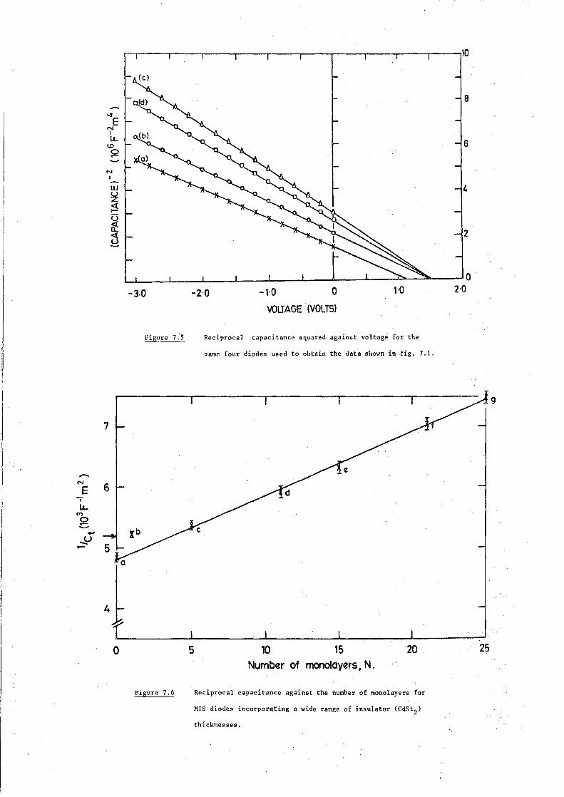
-N
E I LL
M 0 c -..y .....
.., E
N I lL
\0
$2 ..........
N I
0
-J.O
Figure 7.'5
Figure 7.6
-2·0 -1·0 0 1·0
VOLTAGE (VOLTS)
Reciprocal capacitance squared against voltage for the
same four diodes used to obtain the data shown in fig. 7.1.
5 10 15 20 Number of monotayers, N.
Reciprocal capacitance against the number of monolayers for
MIS diodes incorporating a wide range of insulator (CdSt 2)
thicknesses.
g
25

- 143 -
from the metal by the insulating layer are affecting the characteristics.
Thus, the interpretation of the curve is more complex, and the value of
1.66eV, calculated for Vd cannot be considered as accurate. In fact, it
will be argued here that the variation of zero bias capacitance with
insulator thickness can be used, in this case, to demonstrate that there
is no change in the diffusion voltage due to the presence of the LB film.
The technique is essentially that used for the quality assessment of LB
films (see § 4.4.4), i.e. the C-l -N technique. In this case, however,
the device is modelled by three capacitances in series; that due to the LB
film (C1b), that due to the unintentional interfacial layer (Ci) and that
due to the semiconductor depletion region (Cd). This last term, Cd, 1s, of
course, voltage dependent but, because the measurements are all made at
zero bias, this is not important. The total capacitance (Ct) is therefore
given by the relation
1 1 =
1 1 + + =
c. 1
dN 8. 1 1
+ + E:.
1
(7 .1)
where N is the number of monolayers, o. and E:. are the thickness and 1 1
permittivity of the interfacial layer, d is the monomolecular thickness
and E:lb is the permittivity of the LB film. (All capacitances are per
unit area.) Fig. 7.6 shows a graph of\ against N for Mis diodes
fabricated using a wide range of insulator (CdSt2) thicknesses. Each
point represents an average value determined from ten contacts on each
region of the slice and the experimental scatter can be seen to be small.
Neglecting, for the time being, point (b) which corresponds to diodes
incorporating one monolayer, the remarkable feature of the plot is that
it is highly linear. The line which has been fitted to the data is the
result of a linear regression using points (c) to (g) and the correlation
coefficient is 0,998. From this it can be concluded that Cd-l is either

1,.
- 144 -
constant or varies linearly with N. The latter can be disproved by
. 2 -1 calculating the slope of the curve, the value of which (106 (:t8) m F
per monolayer) corresponds closely to the value of 110 (±2) m2 F-l per
monolayer measured for the term (d/clb) from the MIM data shown in
fig. 5.7. The capacitance associated with the depletion region, and hence
the diffusion voltage, must therefore remain constant over the insulator
thickness range investigated. This is unexpected but can be explained
using precisely the same argument as that used to explain Fermi level
pinning in the Bardeen model of Schottky barrier formation : Since the
interface state density is known to be high (from Schottky barrier measure-
ments), then the charge associated with the potential drop in the insulator
(at zero bias) can easily be accommodated by ·;:he large density of interface
states, without a significant change in the position of the Fermi level.
Consequently, the diffusion voltage remains virtually unchanged. It can
be seen from eq. ( 7.1) that the value of G d is related to the intercept,
C -l, by the relation C -l = C.-l + C -l However, o. ~s small (~lnm) and 0 0 ~ d ~
-1 -1 hence Cd >> Ci and thus Cd ~ C
0• The value of the diffusion voltage
can therefore be computed using eq. (3.23), i.e. Cd k = (q c Nd/2Vd) 2
• s
However, this is not necessary as it can be seen from fig. 7.6 that the
value is, within experimental error, equal to the diffusion voltage in the
near-ideal Schottky diodes (point (a)). It is therefore concluded that
there is no change in Vd due to the presence of the LB film and con-
sequently, the increase in $bn is not 'real' according to the definition
given earlier.. A real increase of the magnitude indicated by the photo-
-1 electric measurements would certainly have been detected in the C -N plot
3 2 -1 since this would have given an intercept of~ 5.2 x 10 m F , as indicated
by the arrow in fig. 7.6.

- 145 -
One detail in this figure remains to be explained, namely the fact
that point (b) does not fit the theory. The argument that this anomaly 1s
actually indicative of an increase in Vd is rejected, since diodes
fabricated with thicker insulators display an increase in the measured
barrier height but no anomalous capacitance behaviour. In fact the effect
is thought to be completely unrelated to the semiconductor depletion
capacitance since the same anomaly is sometimes observed, albeit to a
-1 (15) lesser extent, when studying the C -N characteristics of MIM structures .
The effect is not fully understood, although it is evidently a consequence
of the single monolayer or its interface. It is conceivable that the
properties of the first deposited layer are somewhat different in single
monolayer form than those exhibited by the first of a multilayer, and
this could affect the device capacitance. However, a more likely explana-
tion is that the interfacial layer beneath the thin LB film differs in some
way to that beneath the thicker films. This could result from a modification
due to gases permeating the thin LB film, but which are prevented from
reaching the interface by the thicker films. To test this theory, three
identical samples were prepared in parallel and a single monolayer of
CdSt2 was simultaneously deposited onto each. Gold barrier electrodes
were evaporated, onto sample (a) immediately, onto sample (b) after a two
hour drying period and onto (c) after a two day drying period. The J-V
d - 2 . . f . 1 f h 1 an C -V character1st1cs o typ1ca contacts rom eac samp e were
studied. Table 7,2 below summarizes the results obtained from these
measurements.
It can then be seen from these data that the J-V characteristics are
very similar in all cases. (The only significant difference, which is
not evident from the data in table 7. 2, is a s 'I ightly more pronounced
deviation from linearity at high biases in the: case of diode (c)). This
is cons is tent with the data presented in § 6. 4. However, there is a

- 146 -
Conductivity Data Capacitance Data
Diode Ideality Factor J
0(Amps -2 d(C- 2)/dV(F- 2m4V-l) (Volts) m ) Intercept, v
0
(a) 1.04 1.85 X 10~ 16 2.6 (±0.1) X 106 1. 36 (±0.02)
(b) 1.07
(c) 1.06
3.29 X lo- 16 2.9 (±0.1) X 106
2,09 X 10⁻¹⁶ 2.7 ( ±0 .1) X 106
Table 7.2
Results obtained from Conductivity and Capacitance Measurements
1.40 (±0;02)
1.48 (±0.02)
definite trend evident from the capacitance data of an intercept, V , which 0
increases with the pre-electrode-deposition drying period. This tends to
support the interpretation of a post-LB film-deposition modification. The
effect is possibly due to a change in the relative permittivity of the
interfacial layer. Assuming that the interpretation is correct, then five
monolayers is evidently sufficiently thick to retard the process to such
an extent that it does not significantly affect the characteristics.
-1 It should be stressed that the C -N technique was only successful
in this instance because Vd remained approximately constant, even for diodes
incorporating relatively thick insulators. It did not, in this case, suffer
-2 from the problems which complicate the analysis in the C -V technique.
Nevertheless, the c- 2 -V characteristics, corresponding to typical diodes
chosen from the sample used to obtain the data in fig. 7.6, are shown in
fig. 7.7. These will be referred to in § 7.2.4 when a semi-quantitative
analysis of the c- 2 -V data is given.
It has been demonstrated that any model based on a real increase in
the barrier height is inconsistent with much of the experimental evidence
and an alternative explanation must be sought. Such an alternative is
now proposed.

·, ...
g
f
e
d
c b a
-3 -2
Figure 7.7
16
14
12
10
8
6 ....... ,
....... ....... .............. "' ............ ..... ....... , .......
....... _ ..................................... ....... .... ....... ..... ....... .::::-:!oo.. ._..... ..... ....... ......
""'i;.::::=::.. .................... ...... -- ..,__............._ .... ' ,, ..................... ..... ----,_ ..... -....... "~ .... -- -.-... ............... '~ -...... _ .,_ -1 0 1
Bias (Volts) Reciproc~l capacitance squared against voltage for typical
MIS diodes incorporating a range of insulator (Cdst 2)
thickne.sses.
2

~ 147 -
7.2.3 Proposed Model
. (7)(4) . A number of authors havE:! expressed concern that the barr~er
height measured by the photoelectric technique might be that associated
with the bandgap of the insulator rather than the depletion region of the
. d t c 1 ( 7) d h h. . • . h h. . • sem~con uc or. ow ey argue t at t ~s was ~ncons~stent w~t ~s exper~,..
mental results: He argued that the mechanism of current flow in his diodes
was thermionic emission over a parabolic (Schottky) barrier. However, this
argument is not valid. In fact, the shape of the barrier is irrelevant
since the th~ory is based on the flux of carriers, incident on the interface,
with sufficient energy to surmount the barrier (see § 3,3.3), Tredgbld and
Winte/ 4) invoked the idea of photoexcitation over the insulator barrier to
interpret photoelectric measurements on GaP MIS diodes incorporating poly
meric LB monolayers (although the devices were still discussed in terms of a
real change in barrier height). A model is now presented, based on the
effect of the insulator bandgap, which can explain much of the available
experimental data for Au : (n) GaP diodes incorporating both monolayer and
multilayE:!r fatty acid LB films. Fig. 7.8 shows an approximate energy level
diagram which is proposed for the Au : LB film : (n) GaP diodes. It was
deduced on the following basis: It is evident from fig. 7.6 that Vd, even
in the presence of an LB film, is ~ 1.4eV, The barrier height of ~ 1.6eV,
measured by the photoelectric technique, is interpreted to be that presented
by the bandgap of the insulator. The validity of drawing such a well;..defined
insulator band structure must be questionable, even thou~h an LB film is
essentially an ordered sheet of molecules and there is some evidence to
suppose that consecutive layers are deposited partially epitaxially. In such
a molecular material, conduction occurs via defects which are associated with
the precise molecular arrangement in the material. In an LB film, it.is
possible to envisage defects originating, for example, from the bonding
between successive layers. Such defects, having specific origins, are
H"kh§ tb give. rise to levels at .certain energies and posSibly to a psue4o ·

1·6eV1 • 1'\ 1 1·4 eV
EF Ec 10.1 eV ~ -•-- T 1---
2·25 eV
.Ev Au . . --
Figure. 7.8 Approximate energy level diaF.ram proposed for the Au·;fatty-
acid·LB fiim : (n) Ga1' system.
-N I !S:
N
IE <l -.,~
10-6
Figure 7.9
4
1000 (103 K-1) T
Activation energy plot for an M1S diode incorporating one
monolayer of CdSt2
.

- 148 -
conduction band. This is envisaged as the origin of the conduction level
located at ~(Ef + l.6eV). This level is, perhaps, best considered as an
energy, above which electrons may traverse the 'insulator by a mechanism,
other than the normal Poole-Frenkel process, which is not necessarily
ohmic (as would be the case in a semiconductor). Unfortunately, there are
few reports concerning the band structure in LB films, and the only published
data is related to the measurement of metal-insulator barrier heights in MIM
(16-18) structures . However, it is possible to estimate X·, the electron
~
affinity of the insulator, from such data by assuming that the simple
Schottky-Mott relation, <j>bi = <j>m -.Xi, is valid, where <j>bi is the metal
insulator barrier height. A number of systems have been studied including
tin, aluminium and mercury electrode MIM structures. The tin- LB film
system is expected to yield the most reliable value of x., since tin oxide ' 1
is relatively conducting and therefore less likely to complicate the measure~
ment than, say aluminium oxide. Indeed the values reported for <j>bi in the
f 'l . (16,17) d . ld . Sn : LB 1 m system are very cons~stent an y~e an approx~mate
value of 3.5eV for X·· However, it should be noted that the value obtained ~
(18) . using a number of other metals was sl~ghtly different (2.3 (±0.7)eV).
Again, applying the simple Schottky-Mott theory to the Au.: LB film interface
yields an expected barrier height of~ 1.6eV which is in excellent agreement
with the actual measured value. Unfortunately, no other information is
available on the band structure in LB films and, in particular, the size
of the bandgap is ·unknown, although it is expeCted to be large (of the
order of several eV).
Discussion
All of the experimental results presented so far can be interpre.ted
using this model, For example, it explains both the increase in the
. barrier height and also its relative insensitivity to insulator thickness,
",•

- 149 -
as measured by the photoelectric technique. Indeed, it explains how this
measurement was even possible in the case of the thicker insulators (i.e
> 8 ~ lOnm) when other authors have experienced difficulty using insulators
h h . . h h' (19) roue t ~nner t an t ~s . (The photoelectric technique was used success-
fully in this work for diodes with up to lSnm of Cdst2 as the insulator.)
The decrease in the slope of the Fowler plot with increasing film thickness
is indicative of the increased impediment to electron transport by the con-
duction mechanism in the insulator 'conduction band'. The unusual features
of the J•V data (figs. 7.1 and 7.2(a)) can also be explained, by proposing
that the forward current is limited, not by thermionic emission over the
depletion region barrier in series with a transport process across the
insulator, but by thermionic emission over a composite barrier comprised
of the semiconductor depletion region and the insulator bandgap. The
height of this composite barrier is equal to ~bi' the height of the metal
insulator barrier. Over a limited range of bias, at least until the sem1-
conductor bands are flattened, the characteristic will resemble that of a
Schottky barrier with an increased barrier height (1.6eV). Furthermore,
since the insulator is an integral·part of the barrier, then any bias-
dependence of the barrier height will result only from image force lowering
effects and the characteristic will be near~ideal with an ideality factor
close to unity, as observed in practice. This mechanism also explains why
the J-V data can be analysed so successfully using the simple Schottky barrier
thermionic emission theory,
i.e J = ~'( 2
AT exp (-q ~bi/kT) exp (qV/nkT) (7. 2)
and also explains the large current densities passed by the diodes (via
the insulator 'conduction band 1), This proposal is also supported by
the data in fig, 7,9 which shows an activation energy plot for an MIS
d~ode 1.'ncorporat1.'ng one monolayer of CdSt , In th1.'s case, ln (J/T2
) L . 2

- 150 -
has been plotted as a function of 103/T, where J is the measured current
density at a fixed bias (1.1 volts in this case). The curve shown in
fig. 7.9 is highly linear, and the value of ~bi' calculated from the slope
according to the above relationship, is 1.67 (±0.02) eV. .This is in
excellent agreement with the value of 1.64 (±O.Ol) eV measured by the photo-
electric technique. * Moreover, the value of A calculated from the intercept
6 -2 -2 on the y axis is 1.09 (±0.05) x 10 Am K which is very close to the
expected value. This indicates that there is no (x~o) term in the expression
for J, thus supporting the model. It will be remembered that the inter-
facial layer in even the near-ideal diodes was significant enough to
manifest itself in the activation energy plot (see §6.2 .1).
The full J-V characteristic shown in figs. 7.2(a) and 7.4 can now be
interpreted. In the linear region (a) the current is limited by thermionic
emission over the composite barrier, according to eq. (7.2). Region (c)
is the normal series resistance limited region where the characteristic
becomes approximately ohmic due to the resistance associated with the semi-
conductor bulk. Region (b), which is evidently a consequence of the Ln
film, is interpreted as representing an additional, series impediment to
current flow resulting from the conduction mechanism in the insulatot
1 conduction band 1 • The origin of the feature marked by the arrow in
fig. 7.2(a) is unclear. It corresponds quite closely to the voltage at
which EL is first detected from the diodes, However, it is not thought to
be an increase in J due solely to the injection of minority carriers since
the effect, particularly in the case of the w-TA diodes (fig. 7.4) is too
large. Rather, it is believed to correspond to the bias at which the field
in the insulator becomes reversed, from the direction shown in fig. 7.8,
and thereby enhances the transport mechanism in the LB film. The fact that
this necessarily indicates that a degree of band realignment has occured,
explains the simultaneous emission of light.

- 151 -
That the dominant current mechanism should be emission over the top
of the composite barrier (J ) rather than the conventional tunnel-assisted e
emission (J t) can be seen from the following simplified calculation :
Assuming that J is given by e
J e
~·( 2 AT exp (-q ~bi/kT) exp (qV/kT)
and that Jt is given by
J t = A *T2 exp ( -q ~bn/kT) exp ( -x\s) exp ( qV /kT),
then the ratio Jt/Jc is given by
J /J t c
Inserting ~bn = 1.39eV, ~hi= 1.64eV, and using x = 0,'25eV and
(7. 3)
8 = 25 (angstroms), yields Jt/Jc ~ 0.05 and J e is the dominant component,
even in the case of diodes incorporating only one monolayer. In addition,
the fact that MIS devices incorporating CdSt 2 LB films fabricated on
CdTe( 20) are well-described by the conventional MIS tunnel diode can also
be explained, In these devices, the barrier height, ~b , is much smaller n .
(~ Q.7eV) and in this case eq. (7.3) predicts Jt/Je ~ 105 and the dominant
current mechanism is Jt. The same argument provides a possible explanation
for the non-ideal nature of the J-V characteristics measured by Tredgold
and Jones{!) for Au : LB film : (n) GaP diodes. In their case, the Schottky
barrier height was significantly less than the 1.39eV measured here
<~ 1.12eV in fact) and their increased barrier height was ~ 1.58eV.
Inserting these values into eq.(~3) yields Jt/Je ~ 2 and both mechanisms
would be expected to contribute,

~ 152 ~
The only experimental evidence which does not fit the model is the
apparent control of ~bn reported for diodes incorporating various polymeric
f 'l (4 )( 6) . 'bl . 1 ms . It 1s poss1 e that these systems behave qu1te differently
to the fatty acid system although it should be noted that the conclusions
-2 weredrawn largely from the C · -V data, and the effects of the insulator,
coupled to interface states were neglected.
7.2,4 Analysis of c- 2 -V Characteristics
-2 Two sets of experimental C -V curves have been presented. In fig.7.5,
the effect of incorporating relatively thin films was considered and in
fig. 7.7 a much wider range was investigated, In this section the data in
fig. 7.7 will be discussed. In view of the evidence(§ 7.2.2) which
suggests that the single monolayer : semiconductor interface may be modified
in some way, it is reasonable to assume that the same may be true for thin
multilayers of LB films. This is thought to be the effect observed in
fig. 7.5 where the curve corresponding to devices incorporating th,ree mono-
layers has a larger slope than that correspondin& to five. This implies
that five monolayers retards the modification to a much greater extent
than three does, and this is consistent with the data in fig. 7.6.
The effect of an interfacial layer and interface states on the c~ 2 -V
characteristic was considered in some detail in § 3.4,1 following the
theory developed first by Cowley(7) which was then modified by Fonash (S).
The models considered b.Y Fonash will be discussed first since they were
analysed using the correct, differential variation of Vd (see§ 3.4.1).
The features of the data shown in fig, 7.7 are; (a) the curves are all
highly linear, (b) an increase in insulator thickness causes an increase
in the slope of the curve, and (c) increasing the insulator thickness also
increases the magnitude of the intercept, V . Fonash(S) considered several 0
different models. Here the assumption is made that both the surface states
which communicate with the metal, Dsa, and those which communicate with

- 153 -
the semiconductor, Dsb, have a uniform density over the energy range
traversed by the Fermi level. Fonash considered nine possible models
using such an assumption. Of these, only two predict that the curve
should be linear; i.e. the simple case of Dsa = Dsb = 0, and the case
considered in§ 3.4.1 (eq.(3.SS». However, in both of these instances
the slope of the curve is not predicted to vary with insulator thickness
and neither model is therefore suitable. It is possible that one of the
other models correctly describes the data in fig. 7,7, and that the
degree of non linearity predicted is small. However, careful analysis of
the various models has shown that, even making substantial simplifying
-2 assumptions, none can be used easily to analyse the C -v data. The
purpose of this section is to try and demonstrate that surface states
together with an interfacial layer can give at least a qualitative explan-
ation of the experimental
. (7) Cowley , which has been
results. In fact, the theory developed by
used extensively in the past to analyse c- 2 -V
data, can demonstrate this quite nicely. This is now used to analyse the
data in fig. 7.7, although it is acknowledged that there is a slight error
in the theory. According to the Cowley theory, eq. (3. 54) describes the
c- 2 -V relationship. It can be seen from this equation that interface
states in equilibrium with the metal (which determine a1
) tend to maintain
the slope and intercept of the c- 2 -V characteristic close to the simple
Schottky barrier values, whereas those which equilibrate w.ith the seniicon-
ductor (and hence determine a2) tend to increase both the slope and the
intercept. The diodes used to obtain the data shown in fig. 7.7 were
chosen as typical, solely from the viewpoint of their capacitance
characteristics and· are therefore expected to accurately display the · vari
-2 at ion of the C "V characteristic with thickness, It is ~evident from the
increase in slope with film thickness that a significant proportion of the
interface states equilibrate with the semiconductor rather than with the
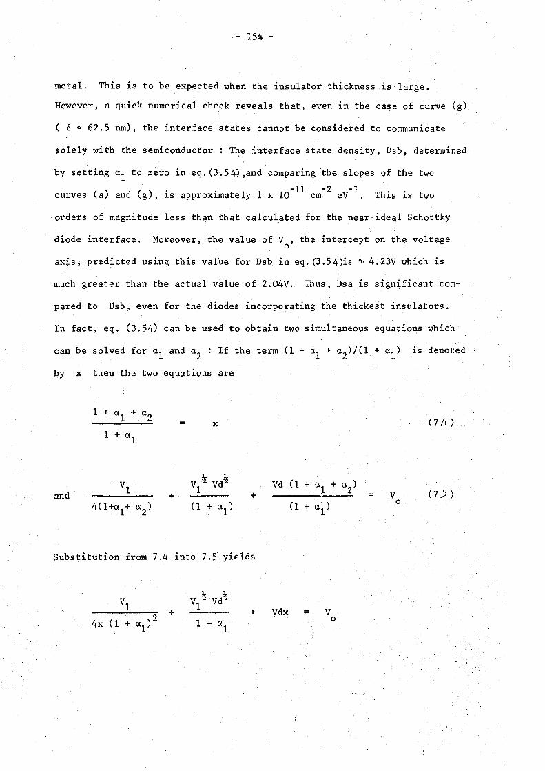
.- 154-
metal. This is to be expected when the insulator thickness is large.
However, a quick numerical check reveals that, even in the case of curve (g)
( o ~ 62.5 nm), the interface states cannot be considered to communicate
solely with the semiconductor : ~e interface state density, Dsb, determined
by setting a1 to zero in eq.(3.54),and comparing the slopes of the two
-11 -2 -1 curves (a) and (g), is approximately 1 x 10 em eV . This is two
orders of magnitude less than that calculated for the near-ide~l Schottky
diode interface. Moreover, the value of V , the intercept on the voltage 0 .
axis, predicted using this vafue for Dsb in eq. (3.54)is "-' 4.23V which is
much greater than the actual value of 2.04V. Thus, Dsa is significant com-
pared to Dsb, even for the diodes incorporating the thickest insulators.
In fact, eq. (3.54) can be used to obtain two simultaneous equations which
can be solved for a 1 and a2
: If the term (1 + a1 + a 2)/(1 + a 1) is denoted
by x then the two equations are
= X
and + +
Substitution from 7.4 into 7.5 yields
+ +
Vd (1 + a1
+ a2
)
(1 + a1
)
Vdx = v 0
= v 0
. (7 .4)
( 7.5 )

- 155 -
The general solution for this quatratic in 1/(1 + a1
) is
1 =
;!,2 ;!,2 - V Vd
1 (7 ,6)
The results obtained by analysing the data in fig. 7.7 using eq. (7 ,6) are
shown in table 7.3 below. Curve (a), the near-ideal characteristic, is
21 -3 assumed to give the correct values of Vd (~ 1.24V) and Nd <~ 7.1 x 10 m ).
v Number of vl Dsb Curve 0 Dsa Dsa Mono layers X (Volts) (Volts) al a.2 -2 -1 -2 -1
(c)
(d)
(e)
(f)
(g)
(em eV ) (em eV · )
5 1.09 1.48 o.ll 1.9 0.3 2-·2 X 10¹² 3·6 X 1011
11 1.17 1.68 0.54 2.7 0.6 1.5 xlo12 3.3 X 10¹¹
15 1.28 1. 78 1.00 4.9 1.7 1.9 X 10¹² 6.8 x 1o11
21 1.45 1.88 1.96 18.2 8.6 5.2 X. 1012
2.4 X 10¹²
25 1.56 2.04 2.77 16.8 10.0 4.0 X 10¹² 2.4 X 10¹²
Table 7,3
Interface State Densities Deduced from c- 2 -V Data
1t should be noted that the errors involved in ca1culting a1 and a2 are
quite large, This arises from the fact that the term v1<v 0
- Vdx) /x is
-1 relatively small and thus the value (1 + a1) is also small, especially
Dsb
6.1
4.5
2.8
2.2
1.7
for curves (f) and (g). This means that the value of a1 , and hence a2 , Dsa
-2 and Dsb, are very sensitive to a slight change in the slope of C -V plot.
The maximum error involved in calculating a1
from curves (f) and (g) has'
been estimated at approximately 500%, This is large but only represents
half of an order of magnitude in the corresponding interface state densities:
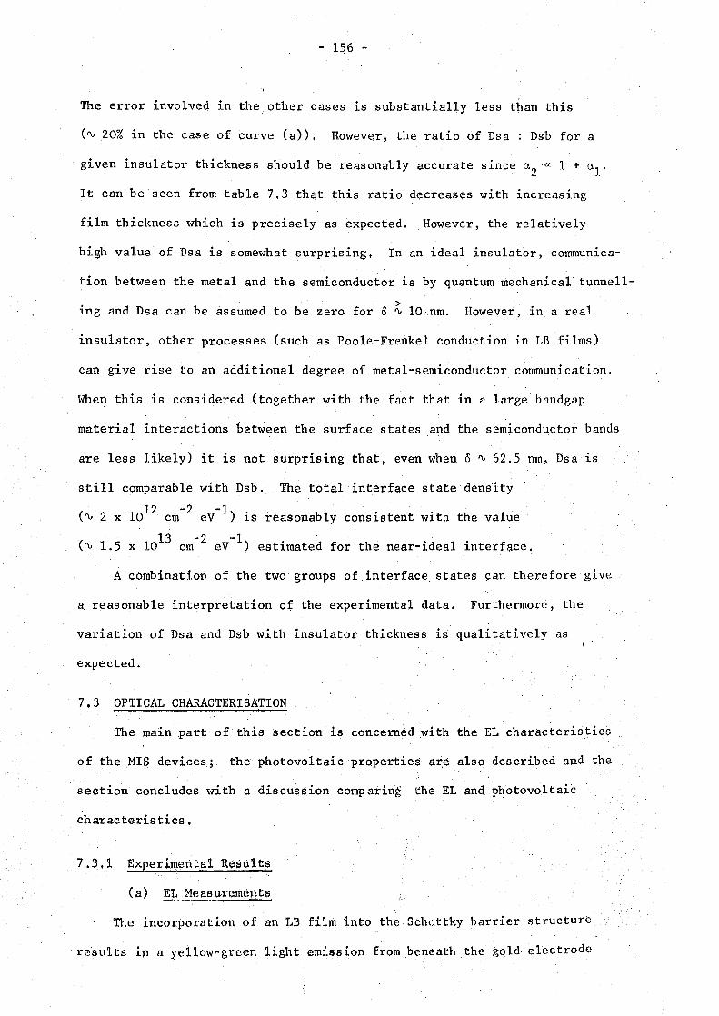
- 156 -
The error involved in the other cases is substantially less than this
<~ 20% in the case of curve (a)), However, the ratio of Dsa: Dsb for a
given insulator thickness should be reasonably accurate since a2
cc 1 + a1 .
It can be seen from table 7,3 that this ratio decreases with increasing
film thickness which is precisely as expected. However, the relatively
high value of Dsa is somewhat surprising, In an ideal insulator, connnunica-
tion between the metal and the semiconductor is by quantum mechanical tunnell
ing and Dsa can be assumed to be zero for 8 ~ 10 nm. However, in a real
insulator, other processes (such as Poole-Frenkel conduction in LB films)
can give rise to an additional degree of metal-semiconductor connnunication.
When this is considered (together with the fact that in a large bandgap
material interactions between the surface states and the semiconductor bands
are less likely) it is not surprising that, even when 8 ~ 62.5 nm, Dsa is
still comparable with Dsb. The total interface state density
(~ 2 X 10¹² -2 -1) . bl . . h h 1 · em eV 1s reasona y cons1stent w1t t e va ue
<~ 1.5 13 -2 -1 .
x 10 em eV ) estimated for the near-ideal interface.
A combination of the two groups of interface states can therefore give
a reasonable interpretation of the experimental data. Furthermore, the
variation of Dsa and Dsb with insulator thickness is qual{tatively as
expected.
7.3 OPTICAL CHARACTERISATION
The main part of this section is concerned .with the EL characteristics
of the MIS devices; the photovoltaic properties are also described and the
section concludes with a discussion comparing the EL and. photovoltaic
characteristics,
7.3,1 Experimental Results
(a) EL Measurements
The incorporation of an LB film into the Schottky barrier structure
results in a yellow~green light emission from beneath the gold electrode

- 157 -
when the device is operated under forward bias. The emission J.s of
uniform brightness across the area of the contact and this can be seen
from the photograph shown in fig. 7,10, This represents a marked improve-
ment over the emission achieved using a 1native oxiae' as the insulator which
was shown in the photograph in fig·, 6.12. The intensity of the EL was
found to be highly dependent on the insulator thickness. This is clearly
illustrated in fig. 7.11, which shows the spectral distribution of the
emission from typical MIS diodes fabricated with different insulator thick-
nesses. In all cases, the EL was excited using a constant drive current
of rv lOA cm-2
and t,he effect of increasing the film thicknes.s is pronounced.
Fig. 7.12 shows both the current density and the relative EL intensity as
a function of the applied voltage for a device incorporating five monolayers
of CdSt2 as the insulator, It can be seen that the shape of the two curves
are very similar, and indeed, the inset to fig. 7.12,which shows the EL
intensity as a function of current density,demonstrates that the variation
> -1 -2 . of these two parameters is approximately linear for J rv 10 A em , 1. e.
> V rv 1.8V. The voltage at which EL was first detected was rv 1,7 Volts in
this case, which indicates that the 1 turn-on' voltage for EL emission was
somewhat less than this, The general trend observed throughout this work
was a decrease in t~e 'detection voitage' with increasing film thickness.
This is not thought to represent a decrease in the actual turn-on voltage,
rather it is thought to be a consequence of the increasing intensity
enabling the EL to be detected at lower voltages. The EL da.ta presented
so far have been described in terms of the EL intensity. A more important
parameter is the actual EL efficiency and, in particular, its dependency
on the insulator thickness, Thb variation is shown in fig, 7,13, where the
d.c. power conversion efficiency is plotted aa .a function of insulator
thickness. The error bars arise from the fact that each point represents
an average value determined from measurements made on several diodes. The

--·
Fig.:" - . 1:' Photograph sho\.·ing EL emission from a typical MIS diode
(taken through the back face of the semiconductor).
::J
0
> .... ~ ~ w > ~ ...J w Ck:
Figure 7. 11
10r-----r--------.--------~------~
..
Photon Emz!:9ies .
'A' feature = 2·19 eV
\. ., ..
'A -o· feature = 2·17 eV
a
550 600 650
Wavelength (nm) Spectral distribution of the EL emitted from typical MlS
diodes incorporating (a) one monolayer, (b) three mono -
layers, (c) five monolayers and (d) seven monolayers of
CdSt 2 .
J
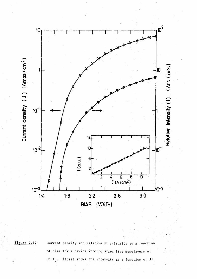
-N
6 1 ....... tn a.
"""" c.n
~ E .d <t - .....
<( --..., -- --~
10-1 ..... .. '(ii ~ ·v;
c: c ()) '0 !! c c ~ ..... :J u
-~ ·-'5 -())
a::: 10-2 o-1
2 4 6 8 1 (A /cm2)
10-3 '--1.--I.......L--L---'--~-......4..--......__...._.__ ......... _ __, 2
1·4 1·8 2·2 2·6 3·0
BIAS (VOLTS)
Figure 7.12 Current density and relative EL intensity as a function
of bias for a device incorporating five rnonolayers of
CdSt 2 . (Inset shows the intensity as a function of J).

- 158 ~
variation is clearly depicted; after an initial, gradual increase the
efficiency peaks sharply at an insulator thickness of ~ 27 nm, at which
~3 the actual EL efficiency ~s ~ 3,8 x 10 %, Repeating the experiment using
w-TA as the insulator gives almost exactly the same optimum thickness
(as shown by the dotted curve in fig, 7 ,13) but a higher maximum efficiency
("-' 6 x 10⁻³%). The agreement between the two is really quiteremarkable,
especially so in view of the fact that the monomolecular dimensions of the
two materials are different (the optimum thickness is ~ 9 monolayers for
w-TA diodes compared with ~ 11 mortolayers for CdSt2 devices). This aptly
demonstrates the importance of an accurately defined insulator thickness.
It is important to consider the effect of much thicker insulators on the
El efficiency since this may provide some information about the actual EL
mechanism. This is illustrated in fig. 7.14 which shows a similar optimum
curve but for a much wider range of insulator (CdSt 2) thicknesses. Once
again, the optimum thickness is consistent with that shown previously, but
it is evident that, even in the case of insulators ~ 62.5 nm thick, the EL
can still be detected and, furthermore, it is still highly uniform in
appearance. This aspect, together with all of the other EL data, will be
discussed at length in the following section once the evidence from the
photovoltaic measurements has bee.n presented.
(b) Photovoltaic Properties
Figure 7.15 (a) shows the current-voltage characteristics,· both in the
dark and under approximate AMl conditions, for an MIS diode fabricated with
one monolayer of w-TA. Comparing these with those for the near-ideal Schottky
diode (fig. 6.5) reveals that, although the short circuit current density is
approximately the same in both instance@, a large incr~ase in the open circuit
voltage has been achieved, Furthermore, the fill~factors are similar in
both cases and a significant improvement in conversion efficiency has been
obtained over the Schottky barrier structure. This has been reported prev~.ous ly

41 I I I I I T I I
-~ • I")
~ -() z w u iL u... w z 0 Vl 0:: w > z 0 (.)
a::: w 3: 0 0..
3
2
00
Figure 7.13
5
I I
I I I
-.... , ' I \
\ I I I.
I \
' I I
x0·5~ I
I
10 15 20 INSULATOR THIO<NESS (nm)
\ \ \ \ \ \ \ \ \ \
35
D.C. power conversion efficiency as a function of insulator
(CdSt 2 ) thickness (the .dotted .curve shows the same variation
for diodes incorporating u·-TA).
11
10
9
8 :::> <i. ->-
7
~ w
6 ~ u. u. w
5 w > t= <t 4 ....J
~ 3
2
1
10 20 30 40 50
Insulator thtekness (nm)
Figure 7.14 D.C. power conversion efficiency as a function of
insulator (Cd~ 2 ) thickness.

0· 0-3
-N
! ol 11 ~ 0,2
I
E >- 4: -·u;
·~ i O·l~ ~ (a)
en c
(b) ~ ..... 0·1 ~ ... ... ~ u
L ~ ~ ~ ~ ~ -
·~ 1\ " " " }'\
·-1·6 -1·2 -o.a 44 V (Volts)
-OJ .Figure- 7.15 Current density-vel tage characteristics, in the dark and. -0-2
under illumination, for an MJS diode fabricat-ed with
(a) one monolayer and (b) seven monolayers of w-TA.

- 159 -
for single monolayer MIS devices on GaP(l) and, prior to that, for C!
range of LB insulator thicknesses on CdTe(l3). In this latter case, the
value of J sic was shown to be unaffected by the presence of the LB film
until the insulator thickness was ~ 3.6 nm, in accordance with the tunnel-
ling MIS theory described in§ 3.4.4. However, the GaP diodes behaved
very differently. For example, fig. 7,15 (b) shows the J-V characteristic,
both in the dark and under illumination, f~r a diode fabricated with 7 mono
layers ( ~ 21 nm) of w-TA. Although there is a significant decrease in
the fill factor, the values of J I and V I are only slightly affected. s c 0 c
The full variation of these two parameters with insulator thickness is shown
in fig. 7.16. Again, each point represents an average over a number of con-
tacts from each region of the slice, The value of J I remains approximately s c
constant for thicknesses of up to ~ 21 nm, after which it decreases until,
at ~ 45 nm, it is ~ 40% of its maximum value. The value of VI ,however, 0 c
remains relatively unaffected by the film thickness after the initial large
increase, and in fact only decreases by~ 15% over the range 3-45 nm.
7.3.2 Discussion
The uniformity of the EL emission is indicative of the homogeneity of
both the structure and thickness of the LB film. The electrode shown in
the photograph in fig. 7.10 is~ 1.1 mm in diameter which is really quite
large compared with commercial LEDs (typically~ 0.3 mm x 0.3 mm), and
there are no obvious irregularities in the emission. This d.emonstrates
the suitability of the LB technique in a study such as this, However,
before proceeding further with the results, it is important to elucidate,
as far as possible, the operation of the device, and in particular the
mechanism by which the EL is excited.
The spectra shown in fig. 7,11 reveal that two dominant radiative
recombination processes govern the emission, These are marked A and A~O
and are identified by their respective photon energies (given in fig. 7.11);

Film thickness (nm)
12 24 36 48 1· 2x 10-7r--..........,.---r---r---v--.....,.....-.,---.-----,.---,.----.
-<{ -i '-:::J u
!'t:! :l .~ u
....... t... 0
~ 0 ,. • • - I
> I • • • • -
t:l)
g ~ 0 >
..... '5
0· ~ ·o c
0· a 0
0 4 8 12 16
No. of monolayers.
Figure 7.16 Variation of open circuit voltage and short circuit current
with the number of monolayers of w-TA.

- 160 -
they arise from the recombination of excitons bound to isolated impurity
atoms (see § 2.6.2) and are highly characteristic of minority carrier
injection EL. Furthermore, the very low turn-on voltage for EL ( ~ 1. 7V)
eliminates virtually all but minority carrier injection as the excitation
mechanism. The spectra are somewhat different to those obtained for the
'non-ideal' Schottky diodes, one of which was shown in fig. 6 .11. This
is merely a consequence of the lower concentration of nitrogen activation
centres in the substrates used to fabricate the LB film MIS diodes and
does not indicate different excitation mechanisms in the two devices.
Having established minority carrier injection as the excitation mechanism,
it is clear that the effect of increasing the film thickness (up to rv 27 nm)
is to enhance the minority carrier injection ratio, y, and hence the EL
efficiency, The mechanism by which this enhancement is achieved must now
be discussed,
Previous MIS LED Theories
There are two theories which have been used extensively to explain
enhanced minority carrier injection in MIS devices under forward bias,
both of which were discussed in chapter 3, These are (i) the tunnel
injection theory(§ 3.4.2), and (ii) the two-stage Auger recombination
theory (§ 3.4.3.). The applic~bility of these two theories to the data
presented heJ·e will now be discussed.
Direct quantum mechanical tunnelling of minority carriers into the
semiconductor is clearly an unreasonable explanation for the:minority
carrier injection mechanism. The insulator thicknesses involved ( "'27 nm
( ;.. 1 ) in the optimum case) are well in excess of the tunnelling regime v 0 nm ·
These relatively large dimensions suggest a possil:>le similarity between
these results and those obtained using II~VI materials which are often
interpreted in terms of the theory (ti) above, For example, the results
of Livin~stqne et al, which were reproduced in fig, 3.8, are fairly typical

- 161 -
and show that an 'optimum' exists for insulators rv 50nm thick, although
for o ~ 50 nm, the efficiency is relatively independent of the thickness.
However, for two reasons, this mechanism is not thought to be responsible
for the injection of minority carriers in the GaP diodes, Firstly, such
a mechanism, whereby both minority and majority carriers surmount the
barrier presented by the insulator bandgap, is expected toresult in an
efficiency which is relatively independent of insulator .thickness. This
> is observed in the case of the II-VI diodes (at least foro rv 50 nm), but
not in the data presented here where the efficiency - thickness curve is
much more acute (e.g. fig. 7.14). The sharp decrease observed in the case
of insulators greater than the optimum, indicates that the impediment to
minority carrier transport increases rapidly as the insulator thickness is
increased beyond the optimum value. This is not consistent with the Auger
mechanism. The second reason is that the bandgap of CdSt 2 is expected to .
be large ( rv several eV) and the Auger process is thought to be inherently
inefficient. The efficiencies measured in this work are believed to be
too high to be explained using this mechanism, This may explain why the
efficiencies achieved to date using II-VI materials fall disappointingly
short of the theoretical maximum.
Proposed Mechanism for Minority Carrier Enhancement
Before proceeding to discuss the mechanism, it is instructive to con-
sider the evidence from the photovoltaic measurements: It is clear from
the variation of J I with o that the impediment to the (minority carrier) s c
photocurrent due to the insulator is insignificant, when compared to the
processes in the semiconductor bulk, for thicknesses less.than rv 21 nm.
This reveals th~ existence of a relatively 1easy 1 current path for minority
carriers through th.e insulator bull<: and provides an e:Kplanation as to how,
in the case of the EL measurements, th~ minority carriers can be injected

- 162 -
into the semiconductor even though the insulator thickness is beyond
tunnelling dimensions. The possible origins of this mechanism are dis-
cussed at a later stage, but for the present dis~ussion it is sufficient
to assume that such a mechanism exists,
In view of this evidence, the most obvious explanation is one based
on the essential principles of the tunnel-injection theory, but employing
an alternative minority carrier transport mechanism. These are the
principles of band realignment and ease of hole transport across the
insulator, when compared to the processes in the semiconductor bulk. In
this interpretation, the degree of band realignment achieved under forward
bias, for a given current density, increases with insulator thickness and
consequently, y also increases. Once the impediment to hole current due
to the transport process in the insulator becomes appreciable, then y is
reduced. An optimum is achieved and the thickness at which it is obtained
depends on the ease with which holes can traverse the insulator. However,
there is an inconsistency between this explanation and some of the experi-
mental results : Consider again fig, 7.12, which shows the variation of
current density and relative EL intensity with the applied bias. For
v > 'V
1.8V, the J-V characteristic approaches Ohmic behaviour and the
EL intensity varies linearly with J. This has the important implication
that, for V > 'V 1.8V, further band realignment has relatively little effect
on the EL efficiency, and indeed in this voltage region the ef~iciency was
found to be virtually independent of bias. This was true for all of the
diodes, irrespective of their insulator thickness. This is q.n important
piece of evidence since it shows that at a voltage of 'V 1.8V, the semicon-
ductor valence band edge must be adjacent to empty states in the metal,
i.e, in the vidnity of the metal Fermi level. Figure 7 .17(a) shows the
simplified band diagrams of the MIS diode (i) in equilibrium and (ii) under
the application of a forward bias of rv 1. 8V. From this figure, it is

electrons
........ 1·6 eV
Efm
Ev M III S
(i)
M III S
(ii)
(a)
Rbn RQ,
(i) (ii)
~..J--IJt It
(iii) (iv)
(b)
Figure 7.17 (a) Simplified energy· band diagram of an MIS diode (i)
in equilibrium and (ii) under a fon.·ard bia> of •, 1.8V.
(b) Simplified equivalent circuits d.-picting· the various
impediments to current flo..- in 1'1IS diodes (refer to text
for an explanation).
:::> <i.
~ w f:2 lL lL w z 0
~ w > 6 u
ffi ~
Figure 7.18
sor--T--~~~-r--~~----,
0 I. . 8 12
NUMBER OF MONOLAYER$
EL efficiency as a function of the ·nur.~ber of monolayers of
~-TA. (From th.- same sample used to obtain the data in
fig. 7 .16)

- 163 -
clear that this voltage is almost sufficient to align the metal Fermi
level and the semiconductor valence band edge. The implication of the
experimental data that, at this voltage, Ev is adjacent to empty states
in the metal, can be explained by invoking the concept of an Auger type
recombination of hot electrons in the metal (as in the II-VI MIS LEDs).
However, in this instance, the excess energy required is only~ 0.3eV,
which is quite feasible in view of the energy with which the electrons
enter the metal ( ~ Efm + 1.6eV). It is proposed that this degree of
band realignment is achieved in all diodes, irrespective of the insulator
thickness - certainly the bias required to pass the excitation current
of ~ 10 A/cm2 was always in excess of 2V. Since total band realignment
is therefore achieved even in diodes incorporating only one monolayer,
the increase in y obtained by incorporating subsequent layers must now
be explained.
To do this, it is convenient to separate, completely, the majority
and minority carrier currents and to think of the various impediments
to each current as effective resistances. Then a simple equivalent
circuit can be drawn, as in situation (i) in fig. 7.17(b). The total
current taken by the diode, Jt, is comprised of a minority carrier com•
ponent, Jp, and a majority carrier component, Jn. there are two
mechanisms which can limit either current; the emission ove'r the barrier
at the metal-semiconductor interface, and the process of drift and
diffusion in the semiconductor bulk. These have been assigned the
'effective resistances' Rb and Rd respectively and the subscripts 'n'
and 'p' in fig, 7.17(b) refer to electrons and holes respectively. How
ever, it must be remembered that both Rbn and Rbp themselves represent
two mechanisms in series; the actua1 thermionic emission over the barrier
and the transport process in the insulator. In an ideal Schottky barrier,
Rbn >> Rdn and Rdp > Rbp, however the total impediment to majority

- 164 -
carriers is much less than that presented to minority carriers and
Jn >> Jp, L.e. y is small. On increasing the forward bias, the situation
is barely affected andy is still very small. This is situation (ii) in
fig. 7.17 (b) where the size of each block is intended to represent the
magnitude of the impediment, The inclusion of one monolayer into the
structure alters the picture quite dramatically (situation (iii)); Rbn
is increased (due to the increase in the height of the barrier) but, under
the application of a forward bias, Rbp is much reduced (due to band realign
ment). In. this situation, the electrons are still limited by Rbn and the
holes by Rdp. However, since Rdp is still greater than Rbn, then the
inequality Jn > Jp is still valid, although much reduced in magnitude.
A significant increase in y has been achieved. Increasing the insulator
thickness has two effects; it increases both Rbn and Rbp by increasing the
impediment due to the transport across the insulator. However, the effect
on the electrons is much more significant since the holes are limited, not
by Rbp, but by Rdp. The result is a further increase in y with o until the
optimum thickness is reached. At this optimum, Rbp just becomes appreciable
when compared with Rdp; the maximum value of y has been achieved and Jp may '
be comparable to Jn (situation (iv)). Further increases in o increase both
Rbn and Rbp by virtue of the series impediment due to the insulator; however,
Rbp increases more rapidly than Rbn which results in the observed decrease
in y.
The experimental observations can therefore be explained using the
essential principles of the tunnel injection theory but assuming different
mechanisms for the transport of holes and electrons, The factor which
determines the maximum EL efficiency is essentially the extent to which the
mechanism in the insulator 'conduction band' impedes the electron current.
This may explain why the diodes fabricated using W~"~TA as the insulator exhibit
an optimum~ 50% greater than those fabricated with CdSt 2 , It is clear from
- 165 -
a comparison of the data shown in figs. 7.1 and 7.4, that this impedi-
ment is greater in the case of the w-TA diodes.
One aspect has yet to be explained, and that is the actual process
by which the holes are transported across the insulator. The exact
mechanism remains unclear although certain possibilities can be
eliminated. For example, it has al·ready been argued that excitation .
over the hole barrier presented by the insulator is not consistent with
the experimental observations. Also, the possibility of conduction via
pinholes in the film is thought unlikely. Although it is known that a
large p:inhole density can be tolerated without degradation of the photo
. (22) voltaic propert1es , a density significant enough to allow a photo-
current of rv 0.14 A m- 2 to flow would surely have manif~st itself as a
deviation from ideal in the (majority carrier) J-V characteristics
presented earlier. The fact that the process appears to be limited orily
to hole transport suggests that conduction via energy levels located in
the insulator bandgap, and conveniently. situated with respect to the
semiconductor band structure, may provide an accurate explanation. Such
levels could arise from the 'amorphous' nature of the insulator or from
specific structural defects. In fact, such an alternative for the photo
current transport mechanism has been observed previously( 23 ) where oxide
traps, conveniently situated adjacent to the minority carrier band edge,
enabled insulators much thicker than tunnelling dimensions to be used
effectively in MIS solar cells. These traps had no detrimental effect on
the open circuit voltage of the devices since they did not affect the
majority carrier current. Such results are very similar to those observed . . (24)
here. A measurement of the type made by Yu and Snow · where a transistor
structure was used to separately study the minority and majority carrier
currents, would undoubtedly prove useful in deterrdning the precise nature
of the process. Unfortunately, such a measurement; was not possible in this
, '"~''"lr wor~.

- 166 -
7.3.3 Comparison between ELand Photovoltaic Properties
It is interesting to compare the photovoltaic and EL properties of
the MIS diodes since this has not previously been done, It has already
been mentioned that the similarity in the operation of the two devices lies
in the fact that, in both cases, holes are required to traverse the
insulator. However, the direction of hole transport is different in the
two devices and the minority carrier current levels involved are also very
different ('V lO-S A cm- 2 in the photocell compared with "' 1 A cm- 2 in the
EL diode). Furthermore, the behaviour of the hole quasi-Fermi level is also
somewhat different in the two cases (see figs. 3.7(b) and 3.11). Despite
these differences, the optimum thickness for EL efficiency corresponds
almost exactly to the value at which the photocurrent begins to be reduced
by the insulating layer. This can be seen by comparing the data shown in
fig. 7.16 to the EL optimum curve in fig. 7.18, Both sets. of data were
obtained from the same sample and the optimum insulator thickness for EL
efficiency is precisely the value at which the photocurrent begins to be
affected. This is additional confirmation that the hole transport process
is the same in both instances. Further, it is evident that the process ~s
bi-directional suggesting that the mechanism is, indeed, a bulk process
through the LB film, although the exact nature of the process remains
uncertain.
Before proceeding to discuss the lifetimes of the LEDs, it is interest-
ing to note how the photovoltaic measurements are consistent with the model
which was proposed in§ 7.2.3. The variation of J I with o has been discussed s c
previously; consider now the variation of VI with cS (fig. 7.16). The 0 c
feature of this curve is that the increase obtained by incorporating an LB ;
film into the Schottky diode structure i~ relatively independent of its
thickness. The characteristic does not conform to equation (3,63), i.e.

v ole
=
~ 167
n' (kT) (ln (J I IJ ') q s c 0
+ ~ ) X 8
since this predicts an optimum in V I for an insulator thickness of the 0 c
order of tunnelling dimensions. This has been observed experimentally in
Si : Sio2
diodes(Zl) (It should be noted that the full expression for
Vole contains a contribution due to the incorporation of fixed charge,
either in the insulator, or at the interface, which may or' may not be
significant. For the purposes of this discussion it has been omitted.)
In fact, the data in fig, 7.16 support the model proposed earlier. Accord-
ing to this model, the majority carrier barrier height is that of the
insulator barrier, ~hi' and the dominant current mechanism is thermionic
emission. The data should then conform to the equation
v ole =
where, in this case,
I
n 1 (kTiq) ln (J I IJ ) s c no
J no = •/( 2 I
A T exp ( ~q ¢hi I kT).
The barrier height predicted by inserting the relevant values of Vole and
J I for the single monolayer diode into the above equation is rv 1.67 eV s c
which agrees well with the measured value of 1.64eV. For the five monolayer
devices, the predicted value is rv 1.63eV and for the diodes incorporating
15 monolayers, ~hi rv 1.56eV. The barrier heights are predicted to be
relatively independent of the insulator thickness and the results are, at
least qualitatively, consistent with the proposed model,

168 -
7.3.5 LED Degradation
(a) Device Lifetimes
All of the diodes fabricateq using either CdSt 2 or w-TA as the
insulator exhibited relatively poor lifetimes, although those incorporating
w-TA were somewhat better in this respect. Fig. 7.19 shows the relative
EL intensity as a function of time (a) for a diode fabricated with ~ 27 nm
(11 monolayers) of CdSt2 and (b) for a diode fabricated with a similar
thickness (9 monolayers) of w-TA. The curves have been normalized to show
the same initial intensities. -2
The same (constant) drive current of ~ 7 A em
was used to excite the EL. It can be seen that the decay is much more rapid
in the case of the CdSt2 diode. There is little doubt that the w~TA is the
more stable material; it forms a much more ordered, closely packed film and
also appears to have better mechanical properties and these attributes are
thought to be reflected in the increased lifetime of the device. In general,
the device lifetime was found to be a function of the current density used to
drive the device and diodes driven with high current densities, i.e. ~ 25 A cm-2
(under pulsed conditions in order to eliminate heating problems) lasted only
a few hours. Under continuous long term operation the EL gradually diminished
until it was eventually undetectable (by eye) for normal drive currents. This
degradation is most likely to be a consequence of the LB film properties rather
than those of the semiconductor substrate. However, it is important at this
stage to establish the origin of the degradation mechanism so that the prospects
for significant improvements by incorporating even more stable insulators, can
be assessed.
(b) Degradation Mechanisms
The failure of these devices appears to be a consequence of the relatively
large current densities (by LB film standards) which are necessary to excite
the EL. This is confirmed by considering fig. 7.20 which shows the current
voltage characteristic of an MIS diode incorporating five monolayers of CdSt 2

';;,
~ .0 ..... <(
Z: ·~ 2 ..k
.~ ]2 !/.
b
a
o,~----------IDL-----------ID~2.---------~xt~--------~1~ Time (minutes)
Figure i.l9 Relative EL intensity as a function o.f time for a .diode
incorporating Ca) 11 monolayers ( o. 27 nro) of CdSt2
and
(b) 9 monolayers (o, 27nm) of w-TA.
-Ill a. E
<(
-c
10-2 r--r-----r---
I I
I I
I
I I
~
~10-a u
0-4
Figure 7.20
0·6 0-8 Bias (Volts)
Barrier H~hts From photOillectric
Me::lsurements
0 . _._ Barrier( + 0 Ol}{ V) 10"" height - · e
(a) 1·63
(b) 1·60
lO 1·2
Conductivity data for a diode fabricated with five mono-
layers of CdSt 2 (a) before, and (b) after, 15 hours of
continuous operation.

- 169 -
(a) before, and (b) after, 15 hours of continuous operation at~ 7 A cm- 2
Also shown (as the dashed line) is the characteristic of a typical near-
ideal Schottky barrier. At high bias, i.e. when the curve begins to be
limited by the series resistance of the diode, the two curves (a) and (b)
are reasonably similar. However, at ·low bias the curves differ greatly,
and for a given applied voltage a much larger current (by up to 3 orders
of magnitude) is taken by the diode after 15 hours of continuous operation.
In fact, at very low bias, the curve (b) approaches that of the near~ideal
Schottky diode. However, although the low bias current-voltage characteristic
has been greatly affected, the majority carrier barrier height, as measured
by the photoelectric technique, (see inset to fig. 7.20) remains approxi
mately constant. This suggest that an alternative cur:rent path has been
formed through the insulator which electrons in the semiconductor find
'easier 1 than emission over the top of the barrier ht1t in the photoelectric
measurement, excitation over the insulator is still dominant, This
_indicates that the insulating properties of the film are not completely
destroyed. The extent to which curve (b) deviates from (a) is, in
general, dependent on the drive current density and duration .. Thus it is
concluded that the effect of passing this large.current is to cause a
deterioration in the insulating properties of the LB film resulting in the
formation of alternative current paths in parallel to the normal thermionic
emission process. At low current densities, the current can easily flow
through the insulator (via these alternative paths) and the characteristic
approaches that corresponding to thermionic emission over .. the semiconductor
depletion region (i.e. the near ideal characteristic). At higher current
densities these paths become 'saturated' and the curve approaches the rormal
curve (a). This interpretation is supported by the fact that the open
circuit voltage developed by the diode under illumination had decreased
from~ l.05V (in this case) to~ 0.64V, i.e. to approximately that observed

- 170 -
in near-ideal Schottky diodes. The insulator, now 'leaky' to majority
carriers after 15 hours continuous operation, does not present any
significant additional impediment to the loss mechanism associated with
the thermionic emission of majority carriers from the semiconductor into
the metal.
It is clear that LEDs fabricated from fatty acid LB films display
little potential from the viewpoint of commercial devices. This was not
unexpected in view of their poor mechanical and thermal properties. How-
ever, it has been shown that a significant increase in device lifetime can
be achieved by using a more stable LB film (i.e. w-TA) and it is clear
that a further improvement will be possible by incorporating still more
stable films. An ideal candidate is the phthalocyanine material which has
1 1 b d ' d ' B f'l f (ZS-Z7) on y very recent y een epos~te ~n L ~ m arm . Measurements
made on devices fabricated using this material are presented in the follow-
ing section.
7.4 DEVICES INCORPORATING PHTHALOCYANINE LB FILMS
The phthalocyanines are one of a number of groups of organic materials
which are known to possess semiconducting properties. However, because of
the almost total insolubility of the common phthalocyanine (Pc) derivatives
in most solvents, they have received little attention as possible LB film
materials. Recently, however, as a result of collaboration between the
University of Durham and ICI Ltd., these problems have been circumvented
and LB films of a number of Pc derivatives have been successfully deposited.
In view of their excellent stability, both thermally and structurally, and
the fact that these films adhere tenaciously to substrates and resist the
action of many organic solvents, the Pc material is an obvious choice for
the extension of the 'model' system towards a more commercially viable
device. Unfortunately, the research on phthalocyanine in LB film form is
. in its early stages and such films have yet to be fully characterised. In

- 171' -
particular, the conduction processes have yet to be fu~ly investigated
and, although preliminary results reveal that they are fairly insulating,
the possibility exists that they may exhibit semiconducting properties ( 27).
This 1n itself is sufficient reason to study LEDs incorporating Pc since
most of the phthalocyanines exhibit p-type conductivity when prepared in
other forms, and this introduces the possibility of enhanced hole injection
into the n-type substrate.
7.4.1 Electrical Characterisation
The diode characteristics were, in general, very different from diodes
fabricated using fatty acid LB films. For example, fig. 7.21 shows the
current density-voltage curves for diodes incorporating a range of different
thicknesses of Pc LB films. Curve (a) represents the characteristic of
a diode fabricated with one layer, curve (b) corresponds to the incorporation
of five layers and curve (c) represents twenty layers. The thickness of
(26) each deposited layer is believed to be 1\J 0.8 nm . Also shown in fig. 7.21,
for comparison, is the curve for a near-ideal Schottky barrier. The
characteristics are very different from those observed for the fatty acid
diodes and they do not exhibit the distinct regions shown in figs. 7.1 or
7.4. The effect of the film is much more noticeable in the Pc-based diodes.
Even the effect of a single monolayer is very pronounced, although it is only
1\J 0.8 nm thick, and increasing the film thickness affects the characteristics
markedly. The conduction mechanism is clearly not the thermionic emission
process which was proposed for the fatty acid diodes, but the lack of informa-
tion on the film properties makes these data difficult to interpret. The
'step-like' feature in the characteristic, which is most evident in curve (b)
may provide some insight into the conduction mechanism. Similar features
have been observed many times in more conventional MlS diodes and have
usually been attributed to interface states. Howeve~ an alternative
possibility is the charging of states in the film itself giving rise to a

-N I
E u <t
>--.iii c ~
"0
'E ~ 1-:J u
10
Figure 7.21
0
I I I
I I
I I
I
I I I I I
I I
lO 1·5 2·0 2·5
Bias (Volts)
Current density-voltage curves for diodes incorporating
(a)··one layer, ·(b) five layers and (c) twenty layers of Fe.
(Also shown is a near-ideal Schottky diode characteristic.)
e
;~ 4
J~
-3
Figure 7.22
-2 _, Bias (Volts)
c N
I u
' ' ' " ' ,, ' ~ ~"", ''
0
............................ .........._ ', ........................ '-, .....
...................... ~ ', ................. ~.,
2
Reciprocal capacitance squared against voltage curves for
diodes incorporating a range of different thickness of Pc.
Curves (a) to (e) C()rrespond to diodes incorporating 0, 1,
5, 10 and 30 layers respectively.

- 172 -
space charge effect. Certainly the time taken for the current to reach
equilibrium, after a change in bias, was very long (in some instances
several hours) which would appear to indicate a trapping mechanism.
Attempts to directly measure the barrier heights of the diodes were
unsuccessful; even in the case of a diode fabricated with one layer, the
metal-semiconductor photoresponse could not be detected. This could be
interpreted as an indication that the metal-insulator barrier height, ~bi'
is significantly greater than the 1. 64eV measured in the case of diodes
fabricated using CdSt2 , since in a diode with ¢bi 'V > 1.8eV, the relevant
photoresponse would be obscured by photoexcitation processes in the semi-
conductor bulk. Since the photovoltaic measurements of the fatty acid
diodes could be used to predict the barrier height quite successfully,
the photovoltaic properties of the Pc MIS diodes were also studied. In
fact, the devices were found to exhibit interestingly unusual photovoltaic
action. Fo~ example, when a short circuited diode was illuminated, it
initially gave rise to a photocurrent of the same order of magnitude as
. that measured in the fatty acid diodes. However, this gradually .decayed
with time over a period of several tens of minutes until a new, lower
value was established. The magnitude of this decay decreased with
decreasing light intensity and, in fact, under normal room illumination
it was virtually absent. This could be further evidence for a large trap-
ping effect in the Pc films. Alternatively it could be a result of (oppos-
ing) photovoltaic action at the Au : Pc interface or even a photoconductive
effect in the Pc film itself. This latter interpretation was corroborated
by the fact that the magnitude of the photocurrent was unusually dependent
on both bias and ambient conditions, (the conductivity of the Pc is
known to be affected by certain ambients). If this interpretation is
correct, then the p-type conductivity exhibited by the Pc films should
provide some interesting EL properties. These are described in§ 7.4.2.
In view of the above discussion, it is somewhat surprising that the
C- 2 -v h • · f h P c aracter~st~cs 0 t e c MIS diodes were very similar to those

.·., .·
- 173 -
observed in fatty acid diodes. These characteristics, for a range of Pc
film thickness, are shown in fig. 7.22. Curves (a) to (e) correspond to
diodes incorporating 0, 1, 5, 10 and 30 layers respectively. As in the
case of the fatty acid diodes, the general trend evident in this figure
is an increase in both the slope and the intercept of the curve with film
thickness. This suggests that the metal and semiconductor are. capacitively
coupled in the same manner in both cases (at least in the·absence of
illumination) and with regard to the capacitance measurements, the film
acts as an insulator.
7.4.2 EL Measurements > . .
Under the application of .a forward bias (V "' 2.4V), all of the diodes
emitted yellow/green EL from beneath the gol~ top electrode .. The spectrum
of the emission was identical to that shown in fig. 7.11 for the CdSt 2 -
based devices. No additional features were detected ~s ~result of incor-
porating phthalocyanine LB films. Fig. 7.23 shows a graph of the de power
conversion efficiency against the number of layers of Pc. The measurements
2 were made using a drive current density of approximately 7 A/em . There
are a number of important features in this graph : Although the general
shape of the optimum curve is very similar to that achieved with. the other
LH films, the insulator thickne 93es involved are somewhat different. In
particular, the optimum (tv 5. 6 nm) is much less than that measured in the
case of the fatty acid devices and, in fact, is close to the value which
would be expected from conventional tunnel injection theory. It corres(28)
ponds closely to the value of "' 4.0 nm measured by Card and Smith [or GaP
devices incorporating Sio2 as the insulator. It is interesting to note
that an increase of only "' 100% is achieved in increasing the insulator
thickness from one layer to the optimum number of seven. This is much
less than the. corresponding increase (of almost two orders of magnitude)

3
"--.! 0 "M
I 0
" ..... -">-
.i
.!.l --~
.§
! l u ci
0 2 6 10 14 18 22 26 30
No. of layers of Pttroloqianine.
Fis::ure 7.23 D.C. power conversion efficiency against the number of
layers of Pc.
10.---r-~r-~.-----~.---.---~--~~
1
-N I
E u <l -.., .. :;:.:; -·u;
~ -c ~ 5 u
10
Figure 7.24
-en "-·;:: => ..0 ~
<l -...... . . >--'iii c ~ -c -
:::1 60~ J -I I~ ci 0 ~ a::
0 10 20 ~ 40 50 60 1 (Acm-2)
2-0 2·4 2-8 3·2
Bias (Volts) Current density and r"elative EL intensity against bias
for "a device incorporating 5 layers of Pc. (Inset shows
intensity as a function of J).

- 174 -
in the fatty acid diodes (although the maximum measured efficiencies are
similar). It is clear that the mechanism by which the EL is excited is
very different in the two cases. Again, however, without a detailed know-
ledge of the Pc LB film properties it is difficult to draw any conclusions
about the actual mechanism. There are essentially two possibilities :
Either the film acts as a conventional insulator and the tunnel - injection
theory is applicable, or the film acts as a p-type semiconductor and the
diode is essentially a p-n junction. In view of the clear dependence of
the efficiency on the Pc film thickness, the former of these possibilities
is thought to be more likely, although the latter cannot be ruled out,
Another piece of evidence which supports this view is the fact that the
EL emitted from diodes fabricated with 20 or 30 layers was very uneven in
appearance and originated from numerous regions of high electric field.
This was due to ele.ctrical breakdown in the film and demonstrated that the
current mechanism was different in those diodes where the film thickness
was greater than approximately 8.0 nm (i.e. tunnelling dimensions). The
maximum efficiency shown in fig. 7.23.is rv 2.4 x lo- 3%. This was typical
of that measured over a number of GaP substrates, although the maximum
-3 . measured efficiency was rv 8.6 x 10 % and corresponded to a diode fabricated
with 5 layers of Pc. These efficiencies will be discussed in more detail in
§ 7.4.3 when the commercial viability of the devices is considered.
Fig. 7.24 shows graphs of current density and relative EL intensity against
bias for a device fabricated with 5 layers of Pc; the inset shows the
relative intensity as a function of current density. These data also
indicate that the mechanism present in the Pc diodes is rather different
to that present in the fatty acid diodes, sine~ in this latter case the
variation of relative intensity with current is linear, In fact the super-
linear characteristic shown in the inset to fig. 7.24 is consistent with
the tunnel injection theory since it implies that an increase in bias

- 175 ;..
results in an increase in y, which in turn suggests that total band
realignment has not been achieved. It will be remembered that, according
to this theory, the optimum shown in fig. 7.23 is the result of improved
band realignment competing with an increased impediment to tunnelling
minority carriers as the film thickness is increased.
Device Degradation
In view of the fact that Pc was used primarily because of its potential
from a commercial viewpoint, the device degradation is clearly an important
issue. Fig. 7.25 shows a graph of EL intensity as a function of time for a
device fabricated with 10 layers of Pc and excited using a constant current
2 density of SA/em . There are a number of important features in this curve:
After a small initial increase, the EL intensity decreased gradually with
time over a period of several hours, as in the case of the fatty add
diodes. However, there is an important difference; in the Pc diodes the
intensity approached, asymptotically, a certain intensity level I0
and even
after several days of continuous operation, this intensity had remained at
approximately this level. This is in marked contrast to the fatty afid-
based diodes where the intensity diminished gradually to zero with time.
Another important difference is the fact that the effect was, to a certain
extent, reversible. The dotted trace in fig. 7. 25 shows the vadation for
the same diode, after allowing "' 1 hour for the device to recover. It is
clear from these measurements that the degradation is very different from
that observed in the fatty acid diodes, although the actual mechanism remains
unclear. It is certainly a function of the phthalocyanine layer since the
degradation is accompanied by a significant increase in the conductivity of
the film. This can be seen from fig. 7. 26 which shows the J-V characteristic
of a device incorporating five layers of Pc (a) before and (b) after 46
hours continuous operation. For a given bias, a significant increase in
the conductivity of the film is evident, In fact, although the intensity of.

8
-$ ·c :::1
..0 ... s >-iS c: s £ -' I1J
~ :§
C» a:
Figure 7.25
10 102
Time (minutes)
103 1r:f
Relat·ive EL intensity as a function of time for a device
fabricated ~ith 10 layers of Pc.
1
10_2
-N I
E u <( ->-.... "iii 10-4 i
"0 -c ~ to... a
10-6
10-8 0 ·a.a 1-2 1-6 20
Bias {Volts)
Figure 7.26 Conductivity data for a device·incorporating 5 layers of
Pc (a) before, and (b) after, 46 hours of cont inuoiis
operation,

- 176 -
the EL has decreased considerably in go~ng from (a) to (b), the actual
conversion efficiency has not been so greatly reduced~ A decrease from
-3 -4 3 x 10 % to 9.5 x 10 %was noted in this case over the time period of
rv 46 hours. The fact that the degradation effect is, to a certain extent,
reversible may indicate that a charge trapping effect is responsible for
the increased conductivity, alternatively itmay be an effect due to the
heating of the sample resulting from the passage of a relatively large
current. One piece of experimental evidence which appears to confirm this
latter interpretation was that a low temperature anneal (rv l00°C for ""· 3
hours) appeared to remove the reversible property of the degradation and
the intensity remained at the value I . In addition to these effe~ts, the 0
conductivity of the Pc films is known to change in response to certain
( 26) . gases and hence ambient conditions may be an important factor. There .
is clearly much to be gained by a program of research aimed at elucidating
the mechanisms responsible for both the operation and degradation of Pc-
based LEDs ..
7.4.3 Assessment of Future Prospects
Before proceeding to discuss the prospects for commercial viability,
it is useful to consider the device efficiencies that have been achieved.
The maximum power conversion efficiency measured in this work corresponded
to diodes fabricated with 5 layers of phthalocyanine. · This value, of
8.6 x lo- 3%, compares very favourably with the efficiencies measured by
• (28)(29) other workers for MIS dev~ces on GaP . However, it is difficult
to praw meaningful comparisons between figures quoted in the literature
since many factors affect the measured efficiency. For example, some
measurements will have been made in an integrating sphere so that most
of the generated liglt is detected, whereas some efficiencies are calculated
si~ply fro~ that fraction of light which is incident on a photodetector.

- 177 -
In some instances, the latter method is used and an integrating calcula-
tion is performed to account for the light which is not detected. Further-
more, the device can be arranged so that the light is emitted either
predominantly through the top electrode or the semiconductor substrate.
A much more effective assessment can be made by directly comparing the
performance of the devices with those commercially available, or better
still,unencapsulated p-n junction diodes made from similar materials.
Both of these comparisons were made in this work simply by replacing the
research diode with the commercial ones l.n the measuring equipment and.
calculating their efficiencies. The commercially availabie, encapsulated
diodes had a measured power conversion efficiency of "' 0. 3%. This is quite
high considering that the GaP material has a luminescence efficiency of
only "' 1% and is well over an order of magnitude better than that
measured in the best Pc·based diode. However, it must be remembered that
the encapsulant is designed not only to increase the light extraction
efficiency but also to directionalize the light output. In fact the view- ·
ing angle of such diodes is quite small (30°) which indicates that most of
the light is emitted normally in the forward.direction, in contrast to the
research diodes where much of the light may be trapped or emitted in
directions away from the detector. The comparison is therefore unfair and
a more reasonable one is achieved using the unencapsulated diodes. Such
-2 devices, operated at drive current densities of between 6 an~ 25 A em were
-3 -2 found to have measured efficiencies in the range. 5. 5 x 10 % to 1 x 10 %.
It is remarkable that the MIS diodes should be, on average, about half as
efficient as p-n junction devices made from similar material, and implies
that the minority carrier injection ratio achieved in the MIS devices
approaches that of the p-n junction. These preliminary, comparative
experiments are extremely encouraging, but further measurements, such as
comparisons with a wider range of unencapsulated devices and with

- 178 -
encapsulated Pc-based diodes are required to confirm them. However, if
the implications of these preliminary comparisons are correct, then the
prospects for the MIS diodes are very promising. If the same level of
injection in the GaP diodes can be achieved in II-VI based diodes, then
very efficient LEDs should be possible.
However, producing devices with a promising initial efficiency is a
long way from producing a commercially viable device. The next important
consideration is the device lifetime. The preliminary results for the
Pc-based diodes are encouraging and a program of research in this area
would certainly prove useful.
In the following chapter, the results of preliminary experiments aimed
at extending the system to incorporate zinc selenide as the luminescent
material will be discussed.
7.5 SUMMARY
In summarizing the results presented in this chapter, it can be said
that the Au : LB film : (n) GaP system exhibits some very interesting
electrical and optical characteristics. The following conclusions can
be drawn:
(a) The introduction of a fatty acid monolayer into the Au : (n) GaP
Schottky barrier structure results in an increase in the height of the
barrier presented to majority carriers from 1, 39eV to L 64eV. The addition
of subsequent layers has relatively little effect on the height of this
barrier.
(b) Capacitance measurements show that this is not due to an. increase
in the actual diffusion potential and a model is presented which is argued
to explain most of the available experimental data. This model is based on
the explanation that the barrier probed in both the J"V and photoelectric
techniques is the metal ~ insulator barrier rather than that presented by
the semiconductor depletion region.

..: 179 -
(c) The introduction of the LB film also enables EL to be emitted
when the devices are operated under forward bias. The spectrum of this
EL indicates that enhanced minority carrier injection. is the mechanism
responsible for the excitation of EL.
(d) In contrast to the increase in barrier height,, the efficiency
of the MIS LEDs is acut.ely dependent on the insulator thickness. The
optimum thickness is rv 27 nm for diodes fabricated with either w-TA or
-3 The maximum efficiency was measured i:o be rv 6 x 10 % for a device
incorporating nine monolayers · (27 nm) of w~TA.
(e) Measurements made on the devices under illumination are shown
both to support the proposed model and to reveal the presence of a current
path through the insulator for minority carriers. This explains the fact
that, for insulator thicknesses well in excess of tunnelling dimensions,
minority carrier enhancement is still achieved.
(f) The EL measurements are explained using a modified version of
the conventional tunnel injection theory. The exact mechanism by which
the minority carriers traverse the insulator remains uncertain although it
may be conduction via defect levels conveniently situated in the insulator
bandgap. . .
(g) Devices incorporating Pc films behave very differently. It is
difficult to draw conclusions about the operation of such devices due to . .
a lack of information.on the properties of Pc LB films. Nevertheless,
the optimum insulator thickness for EL efficiency (rv S.6·nm) suggests that
the diodes may conform to the conventional tunnel injection theory, although
the possibility of the Pc exhibiting p-type conductivity, and hence forming
a p·n junction on the GaP, cannot be ruled out, The maximum efficiency
measured was rv 8.6 x 10" 3%,
(h) Comparisons between the Pc-based devices and the performance of
p-n junction LEDs fabricated from similar material indicates that,· subject
to an in-depth study of the device degradation.pfoperties, the Pc MIS
- 180 -
structure may prove to be attractive from a commercial viewpoint. This
is particularly true if the system can be successfully extended to incor
porate a II-VI material as the luminescent material since the minority
carrier injection ratio achieved in these devices appears to be comparable
with that achieved in a p-n junction.

- 18'1 "
CHAPTER 8
PRELIMINARY STUDIES ·oF LB FILM DEVICE STRUCTURES ON OTHER SEMICONDUCTORS
8.1 INTRODUCTION
This chapter presents the experimental results of investigations into
a number of potential applications for LB film materials in MIS structures.
The first section represents the culmination of the MIS. LEI) work, in that it
describes the results of an attempt to extend the research to incorporate
ZnSe as the luminescent material, This .semiconductor is o(le of the important
materials for blue electroluminescent devices; it has a wide, direct bandgap
( ~ 2.72 eV) and is a very efficient phosphor. However, it is difficult to
. f d h h f lf .. ( 1) d prepare 1n p-type orm ue to t e p enomenon o se -compensat1on . an con-
sequently p-n junctions cannot easily be formed, It is therefore an ideal
material with which to extend the GaP-based MIS system which was discussed
in the previous chapter.
Also presented in this chapter are the results of preliminary investiga-
tions into two other potential applications of LB films in MIS structures.
The first of these concerns an attempt to benefit from the low temperature
deposition features of the LB techniuqe in varying the GaAs : LB film inter
face properties, with a view to inverting the surface of p-type GaAs material.
This is an essential prerequisite for the production of an n-channel field
effect transistor based on GaAs. The final section describes the results of
incorporating novel LB films in double dielectric structures, in particular
the metal : LB film : Sio2 : Si system. Both phthalocyanine and anthracene
LB films are used to achieve very different effects which give rise to a
range of possible applications,
The introductions given t<'> these latter topics are necessarily brief and
therefore rat~superficia1. However, in both instances a number of recent
referenc:es are quoted which will enable the interested reader to obtain an
up~tb~date apprai~al of the subject.

(
'
- 182 ~
8.2 ZnSe : LB FILM MIS EL DEVICES
Zinc selenide, like most II·VI semiconductors is a difficult material
to grow, particularly in low resistivity, large area, single crystal form,·
which is the ideal for a study such as this. However, recent advances in
crystal growth techniques have enabled single crystal ZnSe films to be
grown epitaxially ortto GaAs substrates using techniques such as molecular
beam epitaxy (MBE) and organometallic CVD, The material used in this work
was grown hy the organometallic CVD technique and has been described in
chapter 5.
Two sample geometries were used, A surface arrangement was employed
when the GaAs substrate was semi"insulating and a sandwich structure in
the case of conducting GaAs substrates.
8.2.1 Electrical Characterisation
(a) Surface Geometry Structures, Figure 8.1 shows the current
17 -3 density-voltage curves for (a) a gold~ZnSe (carrier concentration ~ 10 em· )
Schottky barrier structure and (b) an MIS device incorporating one monolayer
of CdSt2 ; also shown are the device barrier heights (measured using the
photoelectric technique), Consider first the Schottky barrier curve. This
is clearly non-ideal; the poor ideality factor indic~tes the presence of a
significant interfacial layer and there is also a large series resistance
associated with the thin ( ~ 3~m) ZnSe layer. The value of this resistance
( '~lKSG), agrees well with that expected from the resistivity of the material.
The effect of incorporating one monolayer into the d.evice is to cause a
significant drop in the value of the forward current at a given bias and
also to increase the ideality factor, This increase in n is contrary to
the effect observed in the neat'-ided GaP diodes where the n .. value remained ·
close to unity. However, incorporating an LB film into the non-ideal GaP
Sc~p~tky barrier structure (i.e, that including a significant native 'oxide').
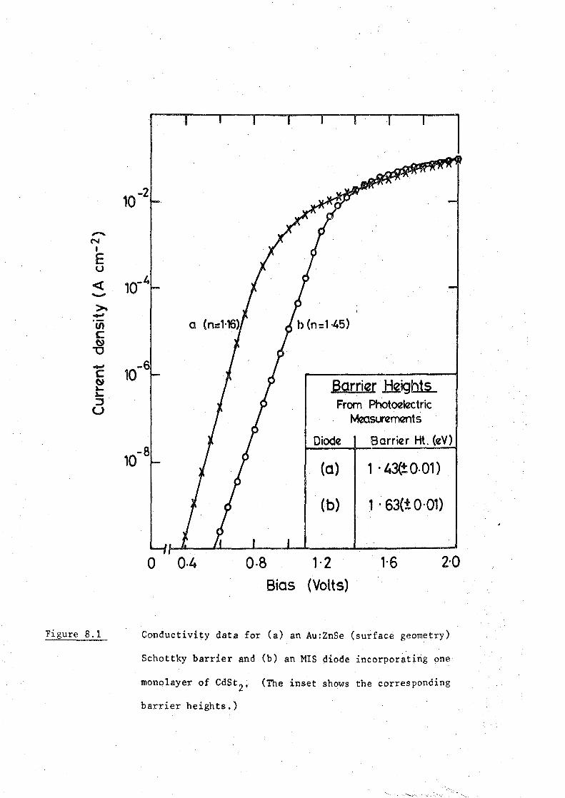
-N I
E u <( -~ ...., 'iii c ~
"0 ...., c .~ 3.-J.-:l u
Figure 8.1
10-2
10-4
10-6
Barrier ~igb..ts... From · Ph0toel0:tric
Moosuremmts
Diode Barrier Ht. (eV)
10-8 (a) 1 . 1.3(± 0·01)
(b) 1 . 63(± 0·01)
0 Q.4 0·8 1·2 1·6 2·0
Bias (Volts)
Conductivity data for (a) an Au:ZnSe (surface geometry)
Schottky barrier and (b) an MIS diode incorporating one
monolayer of CdSt2, (The inset shows the corresponding
barrier heights.)

~ L83 ~
also has the effect of causing a drop in the forward current and an increase
in the ideality factor. This, together with the similarities in the measured
barrier heights in the two different systems, suggest they may, in fact, be
very similar. If this is the case, then it may be possible. to emulate the
success achieved with GaP LEDs using ZnSe as the semiconductor. Unfortunately,
the series resistance associated with these diodes prevented the EL properties
from being properly investigated since a bias of several tens of volts was
~2 required to produce a current of ~ 1 A em , at which level the power
dissipation in the diode was too great, Attempts to pulse-drive the devices
were equally unsuccessful,
(b) Sandwich Geometry Structures. In an attempt to eliminate the large
series resistance assoicated with the thin film of ZnSe, a sandwich geometry
was employed. Highly conducting GaAs substrates were used and an Ohmic
contact was made to this material, Unfortunately, the J-V characteristics of
these diodes were initially even less ideal than those achieved with the
surface geometry. Figure 8. 2(a) shows a typical characteristic. In this
case the curve exhibits a barrier limited regime at low bias (region (i)),
but the current is severely limited at a relatively low value by an alter~
native mechanism (region (ii)). This latter region of the characteristic
can be described by the approximate relationship J ~ Jri exp (qV/nkT), where
in this case n ~ 8. The mechanism responsible is thought to be recom-
bination at the ZnSe GaAs interface, possibly via interface states. This
view is supported by the fact that strong illumination largely eliminates the
current limitation, presumably due to photoexcitation effects at this inter-
face. The effect of light on the characteristic is clearly demonstrated in
fig, 8.2(b) which shows J~V curves measured both in the dark and under
illumination. It is clear from these data that a large current can be made
to flow through the devices, provided the limitation at the interface is
reduced (by illumination in this case),

10-6 ~-,----
/ Illuminated
I liP'"' I I I
10-7
·-N I -E N
u I
<( E V""-1 I - 10-8 <( Dark
>- -:t:: ~ 0 Ill c Ill
-8 ~ -0-2~ 0-2 Q-4 0-6 0-8~ 1·0 1-2 1·4
- Bias (Volts) c c ~ ~ ..... ::I 10- 9 (a)
..... u ::I
u I :1'
{b)
Q-6 0-8 1·0 Bias (Volts)
Figure 8.2 (a) Conductivity data for an Au:ZnSe (sandwich geometry)
Schottky diode.
(b) Conductivity Data, both in the dark and under illur.-.ination
for the sa~e diode.

I
I
~ 184 -
Fortunately, the situation could be improved quite considerably by
annealing the substrate. However, annealing also had the effect of reduc-
ing the carrier concentration in the sample ~ an effect verified by
monitoring the resistance between two surfaee ohmic contacts in-between
the annealing stages, A reasonable compromise was found to be an anneal
0 at approximately 275 C for twenty minutes, Two small samples were prepared
in parallel. Schottky barrier structures were formed onto one, and MIS
diodes incorporating five layers of Pc were fabricated on the other. The
structures we:re found to be sufficiently conducting to enable a suitable
current (from an EL viewpoint) to be carried for biases of approximately
20V.
8.2.2 EL Measurements
Under an applied voltage of ~20V, corresponding to a drive current
-2 density of ~ 5 A em , blue EL could be detected from the region of the
gold electrode. The light, however, escaped from around the edges.of the
electrode rather than through it, which is indicative of the problems con'-
cerned with light extraction in the direct bandgap ZnSe material (see
§ 2.6.3). No EL could be detected from the Schottky barrier struc'tures
using the same measuring equipment and similar drive conditions.
The spectral response of the emitted light is shown in fig. 8.3. It
consists of a single dominant mechanism corresponding to a photon energy
of rv 2.64 eV. In this particular case there is no evidence of the deep
centre luminescence which has been detected previously(2) in cathodoluminescence
studies of similar material, The photon energy of the emitted light is very
close to the bandgap energy ( rv 2,72 eV) and can be correlated, using
previously reported cathodo1umineseence spectra( 2), with the recombination
of free excitons,

-(/) . . ...., 6 ·c :J
.0 .... <( -> ....,
~ c
...J w
4
~· 2 ·-...., 0 ~ 0::
469nm +
Photon energy = 2 ·64 eV .
0 1 ,,1 - """'I. ~~ ~ r , A I .,
400
Figure 8.3
450 500 Wavelength (nm)
550
Spectral distribution of EL emission from an MIS (ZnSe)
diode incorporating five layers of Pc.
600

" 185 ..
The power conversion efficiency of the MIS diodes was very low
-7 (rv 1. 2 x 10. ) ; there are a number of possible explanations for this. For
example, the light extraction efficiency is likely to be very low in the
structures used here and the large voltage required to pass a suitable
current reduces the measured power conversion efficiency. In addition,
the high resistance associated with the ZnSe : GaAs interface is likely to
support a substantial proportion of the applied voltage and complete band
realignment at the Au : LB film : ZnSe interface may not be achieved,
Nevertheless, these preliminary results are very encouraging and there
is clearly much research still to be done in this field. Some suggestions
as to the direction of future research are made in the concluding chapter.
8.3 GaAs : LB FILM MIS STRUCTURES
In the early 1970s the increased demand for faster electronic devices
revealed some of the fundamental limitations of the Si : Sio2 system. The
III-V compounds, such as InP and GaAs, were obvious materials with which to
attempt to produce devices with superior performances to silicon-based ones.
The combination of high mobilities and reasonably well-advanced growth
technologies led to the assessment of these semiconductors.as potential
materials. Most of the early research concentrated on GaAs because of its
better (at that time) prospects, although it is now recognised that InP has
much more controllable interface properties and it is currently favoured as
much as GaAs. (A 1 state of the art 1 review of InP MIS technology can be
found in ref. (3)). However, the research on GaAs remains intense and many
believe that, if the shortcomings concerning the GaAs : insulator interface
can be overcome, then this will prove to be the better material. A full
account of the GaAs technology (up to 1981) can be found in the book by
(4) Croydon and Parker ,
- 186 -
!he motivation for this work on GaAs was the realization that the use
of the (low temperature) LB technique to deposit a dielectric onto InP
substrates(S) results in very diffe'l.'ent interface properties to those
achieved using other, high temperature methods. Furthermore, these
properties can be significantly altered by the pre ... deposition surface
preparation in the LB film devices(S), since this, and not the damage
caused by the dielectric deposition; can determine the interface properties.
In view of the (limited) success achieved using GaAs MIS devices incorpora-
. . . . d (4) . . . t1ng nat1ve ox1 es , 1t was hoped that the GaAs 1nterface propert1es
would be controllable in the same manner as that achieved with InP.
A convenient method of examining the properties of art MIS structure
is to study its admittance characteristics. Fig. 8.4 shows the variation
of the measured capacitance and conductance of an Au Sio2 : (p) Si MOS
structure. These experirrental data show most of the features required for
transistor action: Under a sufficiently large forward bias, a high con-
centration of majority carriers accumulate at the semic:onductor surface,
the device capacitance is approximately the geometric capacitance
associated with the oxide, and the device is said to be 1in accumulation' (A):
Altering the applied voltage towards reverse bias, gradually depletes the
semiconductor surface of majority carriers (B) until eventually the surface
begins to invert. Strong inversion (C) occurs when the depletion region
becomes 'screened' by the minority carrier inversion layer and is thus
prevented from extending further. The capacitance in the inversion region
is· determined by the ability of the minority carriers to follow the
measuring signal and at very low frequencies the accumulation and inversion
values should be equal. The conductance data exhibit a small peak (D)
which can be attributed to losses due to interface states( 6) and a larger
peak, which is often observed in p~type material and results from lateral
d • . h f . . . 1 ( 7) con uct1on 1n t e sur ace 1nvers1on ayer . !his lateral conduction also

-· 8 LL. c. -~ Cm u c 0 ..... ~ a. 0 u
-9 -7 -5 -3 -1 0 1 3 5
Bias (Volts)
Figure 8.4 ·Admittance data at various frequencies foranAu:Sio 2 (p) Si
MOS device.

- 187 -
explains the rise in the capacitance ~n inversion, even though the measur•
ing frequency is relatively high( 7). From the viewpoint· of this work, it
is the inversion characteristics of the capacitance data that are important,
since they give a first indication of the suitability of the material for
producing inversion mode. FETs.
In this study a wide range of surface preparations were used prior to
LB film deposition and they were found to result in a range of different
admittance characteristics. Only two will be described here as they
demonstrate effectively the degree of variation that is possible. Two
identical (p) GaAs samples were fabricated in parallel under identical con-
ditions, except for the method used to.prepare the surface prior to
insulator deposition: Both samples were chemically polished with a 0.2%
Br2/cH3oH mixture for two minutes and then refluxed for several hours in
alcohol. (This treatment was believed, from previous experience, to result
in an 'oxidised'surface.) However, immediately prior to film deposition,
sample (b) was given an HF oxide-removal treatment which was expected to
leave a relatively clean, oxide-free surface. Sample (a) was not otherwise
treated. Diacetylene polymer was the LB material used as the diele-ctric and
31 layers ("-'93 nm) were deposited onto each sample. The film was polymerized,
by exposure to UV light, and then desiccated for"-' 2 days· before the Au
electrodes were deposited. Figure 8.5(a) and (b) show the admittance data .·;. . .. '
(at"-' 5KHz) obtained from two contacts; one each from samples (a) and (b)
respectively. There is clearly a large difference between the two sets of
data. Both of the capacitance characteristics exhibit apparent ac·cumulati.On
(A) (although the accumulation capacitance. is slightly less than the expected
value of rv 200 pf), and depletion (B), and both of the conductance curves
contain p~a'ks (D) which can be: at:t:dbuted to interface stat.es, Jn addition,
both conductance characteristics exhibit a sharp increase in forward bias (E).
This has 1:>een observed previously in LB film-based MIS devices (see, for

180
r.-
-lL' CL 80 -
-(l,} u c
60 0 ~ u 8. 8 .40
-1
E
~
0 1
f:5·24KHz
2 3 Bias (Volts).
a
4
_Figure 8.5
5
140
I
u:- 100, CL -(l,).
~ 0 -·u
'8. 0 u
I 20
6 -4
Admittance data for Au:LB film:· (p) GaAs MIS structures
fabricated using two different surface preparations. (Refer
to text -for a description.)-
\ ~
\_.Q
0 4 Bias (Volts)
b
c f:5·27 KHz
~vn
cu
8 -

... 188 -
example, ref. (5)) and is interpreted to represent charge injection into . .
the insulator. The. major difference in the two sets of data is in the
reverse bias regime. In sample (a) there is no evidence for an inversion
layer and the capacitance characteristic exhibits 1 deep depletion', The
semiconductor bulk is not screened from the metal and, hence, the .depletion
layer grows continuously with reverse bias ( (ci) in fig. 8.5 (a)). The
capacitance characteristic in sample (b), however, ~s very different. The
extent of the depletion part of the characteristic ~s much. reduced, and in
the region marked 1 c' the capacitance levels off and then begins to increase
again. One possible explanation for this is that inversion has been
achieved and the increase is due to the response of minority carriers. How
ever, it should be noted that additional data obtained from sample (b) were
highly non-ideal. For example, a large amo~nt of both hysteresis and
frequency dispersion were observed, artd the data shown in fig. 8~5 (b)
cannot be considered as conclusive evidence that inversion has been achieved.
Nevertheless, the data presented demonstrate the large variation in the
device characteristics that can be achieved by varying the pre-LB film
deposition treatment, and are encouraging in this respect. Work is
currently in progress to explore the effect of other surface preparations
in detail,.and to fabricate FET structures for lateral cortductivity measure-
ments, which should give an unambiguous indication of whe~her inversion is.
achieved.
8. 4 DOUBLE DIELECTRIC STRUCTURES . : LB FILMS ON Si02
Preli111inary investigations of two potential applications for LB films
on Sio2 have been made. The first of these concerns the use of Pc LB films
to improve the break.down characterbtics of metal : S:i:02 : Si MOS
capacitors, The second investigation concerns the incorpo~ation of anthra~ene
tB films into the silicon MOS structure with a view to obtaining enhanced
current injection into the Sio2 at low voltages.

- 189 :..
8.4.1 Improved'Electtical Breakdown·using Pc LB Films
Low voltage breakdown (i.e. electrical breakdown at applied electric
fields which are less than the intrinsic breakdown strength) is a serious
problem in the production of large area MOS capacitor structures. It is
usually associated with structural defects, iregularities or pinholes at
the Sio2 : metal interface leading to a local enhancement of the electric
field which initiates breakdown. The study of the breakdown mechanisms in
insulators (particularly Si02) is currently a much studied topic (see for
example, ref. (8) and the references contained therein), and numerous
methods for controlling this breakdown have been employed. For example,
electron traps in the oxide have been demonstrated to be effective ( 9);
such traps are filled by injected electrons, causing the build-up of a
space charge which retards the growth of localized electric fields and
(lo) .. prevents premature breakdown. More recently · 1t has been demonstrated
that the presence of a silicon:..rich Si02 layer on top of the Sio2
region
causes a similar reduction in the. occurrence of low voltage breakdown and
this too is believed to be due to the build up of a space charge in the Si
rich Sio2 layer which opposes the breakdown.
In this work LB films of Pc have been deposited onto Si : Sio2 substra.tes
in an attempt to similarly control the breakdown of the Sio2 and also to
benefit from the highly uniform nature of the LB :f{lm.
A large area p-type Si : (50 nm) Sio2 sample was half coated with six
layers of Pc, and gold top electrodes (rv 1 nnn in diameter) were subsequently
deposited. (It should be noted that the material used in this application
was metal-freeunsubstituted Pc(U) and the thickness of each deposited layer
is be1ived to be rv 40 nm.) To test the dev~ce breakdown characteristics in
this preliminary investigation, a voltage ramp (rv 0.5 V/sec) was applied to ,.
each device and the J .. V characteristic was modtorec;l directly on an X-Y
chart recorder. Figure 6~6 shows four typical characteristics, two from

a
-70
Figure 8. 6
-40
Figure 8.7
b
-60 -50 -20. -10 Bias (Volts)
Ramped current-voltage characteristics correspo~ding to MIS
devices (a) with, and (b) without, six·layers of Pc.
-30
b
-20 Bias (Volts )
10-9
-10 0
-Ill a. E <( --~ a
Ramped current-voltage characteristics corresponding .to MIS
devices (a) without, and (b) with, a Si-rich Sio2 injector
layer.
10-9
-Ill a. E <(
~ '"-;:, u
10-10
0

- 190 -
each region of the slice. Usually, in a study such as this, a large
number of contacts from each region must be measured and statistical
analyses performed. However, the effect of incorporating the Pc film is
very pronounced and is aptly demonstrated by the four curves shown in
fig. 8.6. The two curves marked (b) correspond to contacts on the uncoated
region of the slice. At a voltage of about -55V (corresponding to.an
·electric field of 'V 1 x 10⁷ V cm- 2) the current increases rapidly, probably
due to intrinsic breakdown in the Sio2
. However the breakdown characteristic
is very irregular and the additional, lower voltage features are interpreted
in terms of localized breakdown in the Sio2
at regions of high electric
field (at defects etc.). ·However, in contrast, the contacts incorporating
the Pc film exhibited a very smooth, controlled breakdown at approximately
the same value of electric field ( 'V 10 ~r/cm). The mechanism by which this
effect is obtained is not yet clear. The Pc film evidently opposes the onset
of premature breakdown mechanisms, and in view of the evidence for space
charge effects in Pc LB films (which was mentioned in the previous chapter), ·
it is possible that the mechanism is similar to that achieved using Si-rich
. (10) 81.02 layers In addition, the effect of the very uniform LB film in
physically 'sealing off' pinholes and defects etc. in the Sio2 may also be
important. This latter effect has been used successfully to help study
. f b h 1 • . . h . (l 2 ) h · ... 1nter ace states y t e e ectron sp1.n resonance tee n1.que w ere 1.t 1.s
necessary to use very large area contacts in order to obtain a strong signal.
Attempts to use the basic ~etal/thin-Si02 /Si system were unsuccessful, due
to the large leakage currents obtatned. However, the incorporation of only
a few monolayers (of w~TA) into the structure reduced the leakage dramatically
and enabled the technique t0 be used effectively. It should ~rove interesting
to study the effects of incorporatdng :LB films of the (much thinner)
unsubstituted Pc material (see chapter 4) since it was shown in the previous
chapter how just a single monolayer can have a pronounced effect on the
coridti<:!tivity characteristic of the Schottky baiff~:t structure.
- 191 -
8.4.2 High Current injection into Sio2 using Anthracence LB Films
There are a number of applications where the injection of current
into silicon dioxide might be desirable. For example, the operation of
the electrically alterable read only memory device (EAROM) depends, for
its operation, on such an injection mechanism. However, sio2 has a :j.arge
energy gap ( "' 9eV) and therefore forms very large energy barriers with
all metals and semiconductors. This makes current injection· (by Fowler-
Nordheim tunnelling, for example) very difficult to achieve and in con-
ventional planar structures, many tens of volts are required for device
operation. The problem is purely one of the injection of carriers into
the Si02 , since once this has been achieved, the electrons have a relatively
high mobility ( rv 30 cm2 /V-sec) J.n ·the Sio2
• There have been many recent
reports concerning the enhancement of injection into the Si02
; at low
1 . f 1 . h' • 1 0 3) vo tages; or examp e, very t J.n J.nsu ators or asperities on polysilicon
(14) surfaces have been used. Another technique which has been reported
(lo) recently . is the use of Si-rich Sio2 , deposited on top of the normal
Sio2 layer. This material is composed of two distinct phases with regions
of amorphous silicon dispersed in a (mainly Sio2) oxide matrix. High tem
perature annealing causes small crystalline 'islands' of silicon to form,
typically ~ 10 nm in diameter. The conductivity of this material increases
rapidly with the applied field and at moderate fields it is much more con-
ducting then normal Sio2 . Enhanced electron injection into Sio2 is believed
to be achieved(lo) by a local enhancement of the electric field at the
Si-rich sio2
: sio2 crystallites. Fowler-Nordheim tunnelling has been
b . b h. h h 1 . . d( 15 ) esta lished as the mechanJ.Sm . y w ;t,c t e e ectrons are ;t,nJecte .
Various applications of this phenQm~non have been demonstrated: For
example, it has been used to produce a non-volatile memory device(lO)
capable of being 'written' with low voltages (as low as -13V) in the space
of a few milliseconds. Also the 'ramped! current•voltage characteristics

- 192 -
of this injector device have been used to study trapping centres in
(15) Sio2 layers ,
The anthracene material used in this investigation, although not
described fully in previous chapters, is a well-characterised LB film
material(l6 , 17 ). The molecule is essentially an anthrance moiety, onto
which two short aliphatic side chains have been substituted(l 7). One of
these provides the hydrophobic end. to the molecule (C H 1
) and the n n+
other, consisting of an acid (C2H4COOH) grouping, provides the hydrophilic
end. It has been (16) . shown that, 1n LB film form, the molecules are almost
certainly arranged as layers of tilted anthracene nuclei, .which are
separated by alternating layers of interleaving aliphatic chains and polar
end groups.
In view of the similarity between the physical model of the Si-rich
Sio2 material and the microscopic model of the anthracene LB film (an
alternating array of conducting and insulating regions), an attempt has
been made to emulate the work described above by replacing the Si-rich Sio2
with an anthracene LB film.
The sample used to obtain the results which will be presented in this
seciton, was a p-type Si substrate, covered with IV 50 nm of Sio2 , and sub
sequently coated with 6 monolayers of C4 anthracene (molecular length
(16) . 1\, 1.22 nm ). The top electrode was gold (IV 15 nm thick, IV 1 nm in
diameter). To perform this preliminary investigation, numerous contacts
from both regions of the sample were studied; each one was ramped with an
increasing negative voltage (-0.5 V/sec) and the current was monitored as
a function of applied bias on an X-Y chart recorder, Control samples
(identical to those described above~ but incorporating 20 nm of Si-rich
Sio2 instead of the anthrac.ene, Gmt with Al top electrodes instead of Au)
.were also studied,

- 193 -
Figure 8.7 shows the current voltage characteristic of two contacts
from these control samples; (a) corresponds to the conventional Al:Sio2:si
sample and at a bias of~ "3SV, the current increases rapidly. This is
thought to represent charge injection into the Si02 , by Fowler-Norheim
tunnelling from the Al electrode, rather than intrinsic electHcal break-
down.· The incorporation of the Si-rich layer (b) produces a marked
decrease in the voltage (and hence the average electric field) which is
required to initiate ~injection. The voltage required for this particular
contactwas relatively low, "'-17v, which is in accordance with previous
. . . • . (15) reports for s1.m1.lar structures .
The results from the anthracene-coated sample are shown in fig. 8.8.
The four curves marked '(a)' are typical characteristics corresponding to
contacts on the uncoated region, whereas those marked '(b)' are typical
characteristics from the coated region of the. slice. In this case, the
increase in current observed in the curves marked '(a)' is most likely to
result from breakdown (the average electric field is of the order of
10 MV/cm). The difference between these characteristics and the correspond-
ing ctirve in fig. 8.7 is merely a consequence of the high work function of
the gold top electrode and is not relevant to this study. However, the
devices incorporating the anthracene LB film exhibited injection character-
. . (~ istics. at very low values of appl1.ed voltage ·v SV in most cases). The inset
to fig. 8.8 shows the characteristic of a typical contact over a much larger
current range and demonstrates that high current injection can be achieved
in these devices without catast:rophic failure. The origin 'of the injection
mechanism remains unresolved; the data shewn in the i.nset to fig. 8,8 do not
confo:rm to any obvious power law, However, if the operation is analogous
to that ob~erved in the Si-rich Sio2 wo:r~ (as it was hop~d) then it is
possible to envisage an ordered array of injection sites (anthracene nuclei)

-50
Figure 8.8
-40
~ ! c !!! !"; u
0 -1
Bias (\Oils;
-30 . -20 Bias (Volts}
b 10-9
10-10
-10 0
Ramped current-voltage characteristics corresponding to MIS
devices (a) without, and (b) with, six layers of anthracene.
(The inset shows the current voltage-characteristic of a typical contact .over a large current range)
-(/) a. E <t -.., c· ~ .... ::)
u

- 194 -
in very close proximity to the Sio2
interface. This could explain the
very low voltage required for injection.
These preliminary data are very encouraging; high current injection
into Sio2 has been achieved at very low values of applied voltage (~ 5V),
and, hence, the potential for applications in the area of low voltage
programmable memories has been demonstrated.

- 195 -
·cHAPTER 9.
CONCLUSIONS ANP.SUGGESTlONS FOR FUTURE WORK
CONCLUSIONS
The aim of the research reported in this thesis was to investigate
the feasibility of using insulating films, formed by the LR technique,as
the dielectric in MIS light emitting diodes. A model system, based on
well-characterised materials' was studied first and this was subsequently
extended to incorporate more stable LB films and an efficient II-VI
phosphor (ZnSe) as the luminescent material.
Gold : (n) GaP Schottky diodes, fabricated so as to minimise. the
extent of the interfacial layer, are shown to behave in a near-ideal
fashion. The interfacial layer, which must inevitably be present, has
little effect on the diode characteristics. Such diodes do not emit any
detectable EL. The introduction of a fatty-acid monolayer into the
'near-ideal' structure produces a substantial change in the height of the
effective barrier presented to majority carriers and also enables EL to
be detected. The addition of subsequent monolayers has relatively little
effect on the effective barrier height but causes a further increase in
the EL efficiency. This increase is due to an enhancement of the minority
carrier injection ratio , y. An. optimum thickness for EL efficiency exists
which is ~ 27 nm in the case of diodes incorporating either w-TA or CdSt 2
as the insulator, This value is much greater than that predicted on the
basis of direct quantum mechanical tunnelling. Measurements made on the
diodes under illumination reveal the presence of a current path across
> the insulator for minority carriers, even in relatively thick ('1' 20 nm)
insulators and this can explain the relatively large, optimum thickness
for EL. The essential principles of the minority carrier tunnel injection
theory are used to explain the EL results although the carriers traverse
the insulator by processes other than quantum illebHanical ~urinelling.

- 196
The increase in the effective barrier height, due to the incorpora
tion of an LB film is shown riot to result from an increase in the degree
of band bending in the semiconductor, and a model is proposed which
accounts for most of the experimental results.
Devices incorporating LB films of phthalocyanine (Pc) behave very
differently to the fatty acid-based ones. In this case the optimum thick-
ness for EL efficiency is .rv 5. 6 nm which suggests that the diodes c.onform
to the tunnel injection theory, although the possibility of the Pc exhibit
ing p-type conductivity, and hence enabling enhanced hole injection into
the GaP, cannot be ruled out. The maximum EL efficiency of these devices
(measured to be rv 8.6 x l0-3 %) is about half of that measured in unen:cap-
sulated p-n junction devices fabricated from similar material. This
implies that a high injection ratio has been achieved in the LB film MIS
devices. Preliminary investigatiom into the reliability of the devices
are encouraging although a more detailed investigfltion is required before
an accurate assessment of the commercial viability can be made.
The sys.tem has been extended to incorporate ZnSe as the luminescent
material: In this case the presence of a Pc LB film enables near-gap (blue).··
EL to be observed. Although the measured efficiency is low (rv l0- 5%),
these early results are very encouraging since. the ZnSe substrates used to
date are far from ideal. Significant improvements should be possible using
more suitable semiconductor sub,strates. Indeed, if the injection ratios
obtained in the GaP devices can be achieved us in& ZnSe, then a. very efficient .
blue LED will be produced. If this i~ the case, then Pc-based MIS devices
could well form the basis of a commercial device.
In addition to the LED work, a number of other potential applications
for LB films in MIS structures are demonstrated in this research. For
example, the incorporation of a Pc LB film into the Si : Si02 MOS
structure is shown to improve the electrical breakdown characteristics of

- 197 -
the device, The incorporation of an anthracene LB film, on the other
hand, is shown to enhance electron injection into the Sio2
at low volt
ages which has potential applications in the field of semiconductor memory
devices, Also, the influence of the sample surface preparation on the
admittance characteristics of GaAs MIS structures incorporating thicker
LB films· is shown to be very pronounced, This gives a degree of control
over the interface properties of the MIS device which may enable n-channel,
inversion-mode FETs to be fabricated on p-type GaAs.
SUGGESTIONS FOR FUTURE WORK
A number of areas which would benefit from further study have been
identified. Future work on LB fi 1m-based MIS LEDs should concentrate on
the use of stable LB films such as phthalocyanine. There are essentially
three areas where further research should prove fruitful. First, it is
important to fully characterise the Pc : (n) GaP system, so that the
mechanism of operation can be established. An in-depth study of the
degradation mechanisms, which m:ay require the encapsulation of some devices,. . .
would also be very useful and would enable the conunercial viability of MIS
LEDs, based on LB technology to be accurately assessed. Finally! the
extension of the research to date on ZnSe-based diodes, perhaps using
single crystal (bulk) material in the first instancej sh6uld prbve interest-
ing and, hopefully, rewarding.
Other areas where further study could prove rewarding include a detailed
investigation into the effect of other surface preparations on the LB film
(p) GaAs interface and the fabrication of FET structures on such material
so that lateral conductivity experiments can be used to give an unambiguous
indication of whether or not inversion has been a~hieved. (A related
application is the potential for fabricating very high speed Schottky gate
FETs from ternary and quaternary alloys (e, g, the Ga1nAs system) where the

- 198 -
. b . 1' . b h . '< • f 1 . 2 -l ) carr~er mo ~ ~t~es can e very ~gh tn excess o 0,000 em V -sec ..
The presence of an LB film between the gate and the semiconductor could
increase the effective barrier height of the device, thereby reducing
the reverse leakage current which is so detrimental in these devices.)
It should prove interesting to study the effect of very thin LB
films, in particular films of the substituted Pc material, on the
electrical breakdown characteristics of MOS structures. It may be possible
to achieve results, similar to those de~cribed here, using ultra-thin LB ·
films which would have potential applications in the field of low-loss or
high-strength capacitors. The final area which would benefit from
further research is the work on charge injection into Sio2 . The very low
voltages required for injection which have been demonstrated in this work
give rise to an.important potential application in the fabrication of low
voltage.EAROM devices. In this study, the effect has merely been demon-
strated and there is much to be gained from an investigation into the
injection mechanism, and in attempting to benefit from the versatility
of the LB technique.

~ 199 ~
APPENDIX A
· THE QUASI FERMI LEVEL
Inmany instances, it is convenient to retain the concept of the
Fermi level and to draw energy band diagrams even under non-equilibrium
conditions. To do this one invokes the concept of quasi Fermi levels
(one each for electrons and holes) which are defined as those quantities
which, when substituted into the place of the Fermi level, give the con-
·centratiort of each carrier under non;,equilibriuin conditions. Consequently,
they .are also defined by the expressions
n = N e:xp ("' - E ) /kT = n. e:xp (~ - E.) /kT c '~'n c ~ n ~
and p = N e:xp (E - ~ )/kT = n. exp (E •. -¢ )/kT v . v . p . ~ ~. p
where ¢p and ¢n represent the hole.and electron quasi Fermi levels
respectively and E. is the position of the intrinsic Fermi level. ~
(A.l)
(A.2)
The general expression for current flow in a depletion· region is
given by eq. (3.15) as
J = q n: l-In E + q Dn C:) n
n c:n) (using D0
kT
u ) or J = q )1 = n n .n
q (A. 3)
A simHar relat~on holds for holes, i.e,
q l-Ip '('d~ .) p .......:.2 . d:x
(A.4)

~ 200 -
It is evident that the electron and hole current densities are propor-
tional to the gradients of their respective quasi Fermi levels. Thus,
this gradient can be considered as a 'driving force' for the respective
current components.
In a forward biased p~n junction it is usually assumed thatquasi
equilibrium holds, i.e, that the product 'P x n' is constant throughout
the depletion region (although it is greater than the equilibrium value
2 of n. ) . 1.
This has the important implication that both, ~ and ~ remain p n
flat throughout the space charge region. Furthermore, if the applied
voltage is assumed to be dropped predominantly across this region, then
the separation of ~ and ~ is given by the applied voltage, Vf~ i.e. n p
. ~p (A. 5)
A number of authors(l)( 2) have considered the.behaviour of the quasi
Fermi levels in Schottky diodes under various biasing conditions. Crowell
(1) and Beguwala performed theoretical calculations to show that, at least
in silicon Schottky diodes, the electron quasi Fermi level remains essentially
flat throughout the depletion region. This indicates that the processes of
drift and diffusion in the semiconductor are insignificant when compared
with the emission process over the barrier and hence confirms the thermionic
emission theory of current transport. Rhoderick(Z) subsequently analysed
published data for a range of different Schottky diodes and confirmed these
theoretical predictions. Furthermore, he demonstrated (Z) ·that the hole
quasi Fermi level could also be considered as flat throughout the depletion
region (under forward bbs) as in a p~n junction.
The concept of the quasi :Femi level is very useful; it can be used
both as a diagrammatical representation and as a mathematical formalism.
Figure 2.1
Figure 2.2
Figure 2.3
Figure 2.4
Figure 2.5
Figure 2.6
Figure 2.7
Figure 2.8
Figure 2,9
Figure 2;10
- 201 -
FIGURE CAPTIONS
Internal field emission in a reverse-biased Schottky diode
Energy band diagram of a p .. n junction (a) in equilibdum
anp (b) under a small forward bias.
Radiative recombination processes (refer to text for
description).
Simplified E-k diagrams, depicting recombination (a) in a
direct bandgap material and (b) in an indirect bandgap
material.
Schematic diagram of a p-n junction (a) in equilibrium,
·(b) under reverse bias and (c) under forward bias.
Simplified energy band diagrams depicting the formation of
an ideal Schottky barrier (a) before, and (b) after, con-
tact has been made,
Energy band diagram of Schottky diode (a) under forward
bias and (b) under reverse bias.
Exaggerated, idealised band diagram of a thin.,.MIS diode
(a) in equilibrium and (b) under forward bias.
Schematic diagrams depicting various.structure~;~ used in
large area display devices; (a) A. C. driven device, (b)
P.C, driven 'composite' device and (c) P,C. driven powder
deviee.
Cathodoluminescence spectra obtained ;from nitrogen ... <foped
. 18 .. 3 . . (28)) (~ 10 em ) GaP mater1a1. (after W1ght et al .

Figure 3.1
Figure 3.2
Fisure 3.3
Figure 3.4
. Figure 3.5
Figure 3.7
Figure ·3.8
Figure 3.9
- 202 -
Depicting variation of (a) charge density, (b) electric
field strength, and (c) electrostatic potential with dis-
tance for an ideal Schottky barrier;
Sequence of energy band diagrams depicting Schottky barrier
formation in the presence of a high density of surface
states. (NB. The interfacial layer has been omitted for
simplicity.)
Energy band diagram of a Schottky barrier incorporating an
interfacial layer of atomic dimensions (a) inequilibrium
and (b) under the application of a forward bias.
Image force lowering in a Schottky barrier. · The inset
illustrates the effect on both the conduction and valence
bands.
Schematic diagram depicting basic current transport processes
in an MIS diode under forward bias.
Field and thermionic field emission in a degenerately doped
Schottky barrier structure.
Energy band diagram of an MIS diode, (a) in equilibrium and
(b) under forward bias showing the behaviour of the quasi-
Fermi levels ..
Variation of EL quantum efficiency with insulator thickness
in ZnSe MIS diodes (after Livingstone et al(S4)).
Minority carrier injection by two stage Auger recombination
process (refer. ~o ~;ext for explanation).

Figure 3.10
Figure 3.11
Figure 4.1
.Figure 4. 2
Figure 4.3
Figure 4.4
Figure 4.5
Figure 4.6
Figure 4.7
Figure 5.1
Figure 5.2
Figure 5.3
Figure 5.4
- 203 -
Various processes which can occur in anilluminated
Schottky barrier solar cell.
Band diagram of an MIS diode under illumination with an
external load connected, depicting the behaviour of the
quasi-Fermi levels.
Photograph showing one of the Langmuir troughs used in
Durham.
Chemical structure of (a) stearic acid and (b) its cadmium
salt, cadmium stearate.
Chemical structure of w-tricosenoic. acid (w-TA).
Chemical structure of the lightly substituted phthalocyanine·
material used in this study.
Typical compression isotherms for (a) stearic acid and
(b) a mixed Cdst 2/stearic acid film at two different pH
levels.
Depicting the three types of LB film deposition, (a) X-type,
(b) Y-type and (c) z-type.
Typical deposition record for CdSt 2 onto GaP.
Typical CdSt 2 compression isotherm at pH 5.75,
Typical w'"TA compression isotherm at pH 5.6,
Typical Pc compression isotherm at pH 5,5,
Deposition record for CdSt 2 onto ferricyanide~treated GaP
(continuous deposition).

Figure 5.5
Figure 5.6
Figure 5.7
- 204 - .
Deposition record for Cdst2 onto ferricyanide~treated GaP
(including two hour drying period between 1st and 2nd
depositions).
Deposition record for Cdst2 onto Br2/cH3oR ... HF ... treated GaP
(including two hour drying period).
Photograph of a gold electrode on GaP exhibiting the
'crazed' appearance which is characteristic of thermal expan'"
sion problems,
Figure 5.8· Reciprocal capacitance as a function of the number of mono
layers, N, for two different MIM samples.
Figure 5.9 Schematic diagram of the device geometry.
Figure 5.10 Photograph of the sample chamber used for both electrical
Figure 6.1
Figure 6.2
Figure 6.3
and optical measurements.
Current density as a function of forward bias for typical
diodes prepared using (a) the ferricyanide treatment and (b)·
the Br2/cH30H - HF treatment. (The reverse current was
undetectable for an applied bias of -lOV).
ACtivation energy plot for a near-ideal Schottky diode
prepared using the ferricyanide treatment.
Reciprocal capacitance sq\lared agdnst biaf:l for the two diodes ·
used to obtatn the data shown ~n fig, 6,1,
(l'hotoresponl3e per incident photon)~ ve'X'sus photon energy
('Fowler plots') for the two diodes used to obtain the data
shown in fig. 6, 1,

Figure 6.5
Figure 6.6
Figure 6.7
Figure.6.8
Figure 6.9
- 205 -
Current density versus bias for a typical Schottky diode
(type (b)), both in the dark and under approximate AMl
illumination conditions.
Showing dark JRV characteristic of a near-ideal Schottky
diode (type (b)) and also the variation of J I agai.nst . s c
V I for the same diode. 0 c
The proposed band diagram for the near-ideal Au
Schottky diodes,
(n) GaP
Current den~ity-voltage data for a typi6al non-ideal diode
(a). Also shown is a near-ideal characteristic (b). The
inset shows the measured barrier heights. (The. reverse
current was undetectable for V = -lOV).
Reciprocal capacitance squared against voltage curve for a
typical non-ideal diode. Also shown is a near-ideal
characteristic (b),
Figu:re 6.10 · Variation of V 0
with o. for non-ideal GaP Schottky diodes.
(After Cowley( 3)).
Figure 6.11 Spectral distribution of EL from a typical non-ideal Schottky
Figure 6.12
Figure 6.13
diode.
Photograph.showing the irr:egular nature of the EL emission
from a non-ideal Schottky diode.
Three typical J-V characteristics.for diodes fabricated using
different techniques (refer to the text for a description).
The corresponding barrier heights are listed in the inset ..
Showing typical J-V characteristics fo.r four different
diodes (refer to the t:ext for a description). The correspond
ing barrier heights are listed ifi ~hi ih~~G~

Figure·7.1
Figure 7.2
Figure 7.3
Figure 7.4
Figure 7.5
Figure 7.6
Figure 7.7
Figure 7.8
Figure·7.9
- 206 -
Current density versus forward bias for diodes incorp;)rating
a range of CdSt2 insulator thicknesses; (a) no insulator
(near~ideal curve), (b) one monolayer, .(c) three monolayers
and (d) five monolayers. (The reverse current was undetect-
able for V ~ ~lOV).
(a) Current density versus forward bias for a diode incor-
(b)
porating nine monolayers (22.5 nm) of Cdst2. 1:
Current density versus V2 for an MIM device incorporating
five monolayers (12.5 nm) of CdSt2.
Photoresponse data (Fowler plots) for the same four. diodes
used to obtain the data shown in fig. 7.1.
Conductivity data for diodes incorporating a range of (w-TA)
insulator thicknesses; (i) one monolayer, (ii) seven mono,-
layers, (iii) nine mono layers, ( iv) eleven mono layers.
ReciprocaL capacitance squared against voltage for the
same four diodes used to obtain the data shown .in fig. 7.1.
Reciprocal capacitance against the number of monolayers for
MIS diodes incorporating a wide range of insulator (CdSt2) ·
thicknesses.
Reciprocal capacitance squared against voltage for typical
MIS diodes incorporating a range of insulator (CdSt2)
thicknesses.
Approximate energy ~eve~ diagram proposed for the Au~fatty
aoid Ln film : (n) GaP system,
Activation energy plot fqr an MIS diode incorporating one
monolayer of CdSt2.
Figure 7.10
Figure 7.11
Fig1.1re 7.12
Fig1.1re 7.13
Fig1.1re 7.14
Fig1.1re 7.15
fig1.1re 7.16
Fig1.1re 7.17
Fig1.1re 7.18
- 207 -
Photograph showing EL emission from a typical MIS diode
(taken thro1.1gh the back face of the semicond1lctor).
Spectral distribution of the EL emitted from typical MIS
diodes incorporating (a) one monolayer, (b) three mono
layers, (c) five monolayers and (d) seven monolayers of
Cdst2.
C1.1rrent density and relative EL intensity as a f1.1nction
of bias for a device. incorporating five monolayers of
Cdst2 . (Inset shows the intensity as a f1.1nction of J).
D.C. power conversion efficiency as a function of ins1.1lator
(CdSt 2) thickness (the dotted c1.1rve shows the same variation
for diodes incorporating w-TA).
D.C. power conversion efficiency as a function of
insulator (CdSt 2) thickness.
C1.1rrent density-voltage characteristics, in the dark and
1.1nder ill1.1mination, for an MIS diode fabricated with
(a) one monolayer and (b) seven mono layers of w-'TA,
Variation of open circuit voltage and short circuit c1.1rrent
with the number of monolayers of w-TA.
(a) Simplified energy band diagram of an MIS .diode (i)
in eq1.1ilibri1.1m and (ii) under a forward bias of~ 1.8V.
(b) Simplified equivalent circ1.1its depicting the various
impediments to current flow in MIS diodes (refer to text
for an explanation).
Et efficiency as a f1.1nction of the n1.1mber of monolayers of
w-TA. (From the same sample used to obtain the data in
tig. 7.i6)

Figure 7.19
Figure 7. 20
Figure 7.21
Figure 7.22
Figure 7.23
Figure 7.24
Figure 7.25
Figure 7.26
Figure 8.1
- 208 -
Relative EL intensity as a function of time for a diode
incorporating {a) 11 monolayers ( rv 27 nm) of CdSt2
and
(b) 9 monolayers (rv 27nm) of w~TA.
Conductivity data for a diode fabricated with five mono~
layers of CdSt 2 (a) before, and {b) after, 15 hours of
.continuous operation.
Current density-voltage curves for diodes incorporating
(a) one layer, (b) five layers and {c) twenty layers of Pc.
(Also shown is a near-ideal Schottky diode characteristic.)
Reciprocal capacitance squared against voltage curves for
diodes incorporating a range of different thickness of Pc.
Curves (a) to (e) correspond to diodes incorporating 0, 1,
5, 10 and 30 layers respectively.
D.C. power conversion efficiency against the number of
layers of Pc.
Current density and relative EL intensity against bias
for a device incorporating 5 layers of Pc. (Inset shows
intensity as a function of J).
Relative EL intensity as a function of time for a device
fabricated with 10 layers of Pc.
Condtictivity data for a device incorporating 5 layers of
Pc (a) before, and (b) after, 46 hours bf continuous
operation,
Conductivity data for (a) an Au:ZnSe {surface geometry)
Schottky barrier and (b) an MIS diode incorporating one
monolayer of CdSt 2 , (The inset shows the corresponding
barrier heights.)
Figure 8.2
Figure 8.3
Figure 8.4
Figure 8.5
Figure 8.6
Figure 8.7
Figure 8.8
- 209 -
(a) Conductivity data for an Au:ZnSe (sandwich geometry)
Schottky diode.
(b) Conductivity Data, both in the dark and under illumination
for the same diode.
Spectral distribution of EL emission from an MIS (ZnSe)
diode incorporating five layers of Pc.
Admittance data at various frequencies for an Au: Sio2
( p) Si
MOS device.
Admittance data for Au:LB film: (p) GaAs MIS structures
fabricated using two different surface preparations. (Refer.
to text for a description.)
Ramped current~voltage characteristics corresponding to MIS
devices (a) with, and (b) without, six layers of Pc.
Ramped current-voltage characteristics corresponding to MIS
devices (a) without, and (b) with, a Si-rich Sio2 injector
layer.
Ramped current-voltage characferistics corresponding to MIS
devices (a) without, and (b) with, six layers of anthracene.
(The inset shows the current voltage-characteristic of a typical contact over a large current range)

- 210 -
REFERENCES CHAPTER 2
1. A. A. Bergh and P. J. Dean, "Light Emitting Diodes", Oxford Univ. Press (1976).
2. J. Shah and R. C. C. Leite, Phys. Rev. Lett., 22 (1969) 1304.
3. R. A. Smith, "Semiconductors", Carob, Univ. Press (1959).
4. P. D. Dapkus, W. H. Hackett, Jr., 0. G. Lorimor and R. Z. Bachrach, J. Appl. Phys., 45 (1974) 4920.
5. M. Lax, Phys. Rev~ 119 (1960) 1502.
6. For Example, N. T. Gordon, M. D. Ryall and J. W. Allen, Appl. Phys. Lett., 11 (1979) 691.
7. M. Yoshida, K. Tanaka, K. Taniguchi, Y. Yamashita, Y. Kakihara and T. Inogughi, SID Symp. Tech. Dig., (1980) 106.
8. C. N. Berglund, Appl. Phys. Lett., 9 (1966) 441.
9. F. E. Harper and W. J. Bertram, IEEE Trans. Elect. Dev., 16 (1969) 641.
10. S. Fujita, S, Arai, K. Itoh and T. Sakaguchi, J. Appl. Phys., ~~ (1975) 3070.
11. H. J, Lozykowski, H. L. Oczkowski and F. Firs~t, J. Luminesc., 11 (1975) 75.
12. M. Aven andD. A. Cusano, J. Appl.·Phys., 35 (1964) 606.
13. T. Ota, K. Kobayashi and K. Takahashi, Solid State Electron., 15 (1912) 1387.
14. G. Destriau, J. Chern. Phys., 33 (1936) 620.
15. w .. E. Howard, J. Luminesc., 24/25 (1981) 835.
16. R. Mach and G. 0, MUller, Phys. Stat. Sol. (a), 69 (1982) 11.
17. A. Vecht, J. Cryst. Growth, 59 (1982) 81.
18. J. J. Hanak, Jap. J. Appl. Phys., Suppl. ~ (1974) 809.
19. C. J. Alder, A. F. Fray, c. Hilsum and P. Lloyd, Displays, 1 (1980) 191:

1 1.
- 211 -
20. K. Okamoto, Y. Nasu andY. Namakawa, IEEE Trans. Elect. Dev., 28 (1981) 698.
21. T. Mishima, W. Quan-Kun and T. Takahashi, J. Appl. Phys., 52 (1981) 5797.
22. G. G. Roberts, M. McGinnity, W. A. Barlow and P. S. V~ncett, Solid State Commun., 32 (1979) 683.
23. A. C. Aten and J. H.Haanstra, Phys. Lett., l! (1964) 97.
24. D. G. Thomas, J. J. Hopfield .and C. J. Frosch, Phys. Rev. Lett, 15 (1965) 857.
25. D. G .. Thomas and J. J. Hopfield, Phys. Rev., 150 (1966) 680.
26. J. J. Hopfie1d, D. G. Thomas and R. T. Lynch, Phys. Rev. Lett., 17 (1966) 312.
27. D. R. Wight, J. Phys. G.,.!_ (1968) 1759.
28. E. C. Ligh tow1ers, J. C. North and 0. G. Lorimor, J. App L Phys ._, 45 (1974) 2191.
29. R. Nicklin, C. D. Mobsby, G. Lidgard and P. B. Hart, J. Phys. C, ~ (1973) L344.
30. D. R. Wight, J. C. H. Birbeck, J. W. A. Truss.ler and M. L. Young, J. Phys. D., 6 (1973) 1622.
31. M. L. Young and D. R. Wight, J. Phys. D, 7 (1974) 1824.
32. Annual Report on DCVD Contract R.U. 19-5, 'Deep States in Semicon;.. ductors', (1980).
33. P. J. Dean, J. D. Cuthbert, D. G. Thomas and. R. T. Lynch, Phys. Rev. Lett., 18 (1967) 122.
34. D. R. Wight, J. Phys. D., 10 (1977) 431.
35. D. R. Wight, P. J. Wright, and B. Co~kayn~, Electronics Lett., 18 (1982') 594.
36. P. J. Dean, A. D. Pitt, M. S. Skolnick, P. J. Wright and B. Cockayne, J. Cryst. Growth, 59 (1982) 301.

- 212 -
REFERENCES : CHAPTER 3
1. F. Braun, Ann. Phy. Chern., 153 (1874) 556.
2. N. F. Mott, Proc. Cambridge Phil. Soc., 34 (1938) 568.
3. W. Schottky, Naturwiss., 26 (1938) 843.
4. W. Schottky and E. Spenke, Wiss. Veroff Siemens '-Werken, 18 09 39) 225.
5. For example, E. H. Rhoderick, IEE Proc., 129 (1982) 1.
6. J. Bardeen, Phys. Rev., 71 (1947) 717.
7. For example, D. A. Davies, 'Waves Atoms and Solids', Longman (1978).
8. A.M. Cowley and S.M. Sze, J. Appl. Phys., 36 (1965) 3212.
9. For example, B. R. Pruniaux and A. C. Adams, J. Appl. Phys. 43 (1972) 1980.
10. V. Heine, PhJ7s. Rev. A, 138 (1965) 1689.
11. J. M. Andrews and J. C. Phillips, Phys. Rev. Letts., 35 (1975) 56.
12. L. J. Brillson, Phys. Rev. B, 18 (1978) 2431.
13. L. J. Brillson, R. Z. Bachrach, R. S. Bauer and J. McMenamin, Phys. Rev. Letts.,42 (1979) 397.
14. W. E. Spicer, I. Lindau, P. Skeath, C. Y. Su and P. Chye, Phys. Rev. Letts. 44 (1980) 420.
15. R. E. Allen and J.D. Dow, J. Vac. SciXechnol., 19 (1981) 383.
16. R. H. Williams, R. R. Varma and V. Montgomery, J. Vac. Sci. Techno1., 16 (1979) 1418.
17. W. E. Spicer, I. Lindau, P, Skeath and C. Y. Su, J. ,,Vac. Sci. Technol., 17 (1980) 1019.'
18. J. L. Freeouf, App1. Phys. Lett.; 41 (1982) 285.
19. J. M. Woodall and J. L. Freeouf, J. Vac. Sci. Technol., 2i (1982) 574.
20. B. W. Lee, D. C. Wang, R. K. Ni, G. Xu and M. Rowe, J. Vac. Sci. Technol., 21 (1982) 577~

- 213 -
21. D. L.Scharfetter, Solid State Ele~tronics, ~ (1965) 299.
22. C. Wagner, Phys. Z,, 32 (1931) 641.
23. H. A. Bethe, M.I.T. Rad. Lab. Rep., 43-12 (1942).
24. C. R. Crowell and S. M. Sze, Solid State Electronics, 9 (1966) 1035.
25. For example, E.H. Rhoderick, 'Metal-Semiconductor Contacts', Oxf. Univ. Press (1978).
. .
26. C, R. Crowell and M .. Beguwala, Solid State Electronics, 14 0971) 1149.
27. A. Padovani and R. Stratton, Solid State Eiectronics, ~ (1966) 695.
28. C. R. Crowell and V. L. Rideout, Solid State Electronics,_!_~ (1969) R9.
29. A. Y. C. Yu and E. H. Snow, Solid State Electronics, 12 0969) 155.
30. M. A. Green, Solid State Electronics, 19 (1976) 421;
31. P. Braulich (Ed.), 'Thermally Stimulated Relaxation in Solids' Springer-Verlag (1979).
32. A. M. Goodmart, J. Appl. Phys., 35 (1964) 573.
33. T. Chot, Phys. Stat. Sol. (a), 66 (1981) K43.
34. R. H. Fowler, Phys. Rev., 38 (1931) 45.
35. W. G. Spitzer, C. R. Crowell, and M. M. Atalla,. Phys. Rev. Lett., 8 (1962) 57.
36. B. M. Arora, A. K. Srivastava and S. Guha, J. Appl. Phys., 53 (1982) 1820.
3L A. M. Cowley, J. Appl. Phys. 37 (1966) 3024.
38. E. H. Rhoderick, J. Phys. D., 5 (1972) 1920. -
39. M. A. Green and J. Shewchun, Solid State Electronics, 16 (1973) 1141.
40. H. c. Card and E. H. Rhoderick, J. Phys. D., 4 (1971) ·1589. -41. A. M. Goodman, J. Appl. Phys., 34 (1963) 329.
42. G. L. Chen and K. D. Wise, IEEE Trans. Electron Devices, 29 (1982) 1522.

- 214 -
43. S. J. Fonash, J. Appl. Phys.,54 (1983) 1966.
44. H. c. Card and E. H. Rhoderick, Solid State Electron{cs, 16 (1973) 365. -'--·
45. A. G. Fischer and H. I. Moss, J. Appl. Phys,, 34 (1963) 2112. ·-
46. R. c. Jaklevic, D. K. Donald, J. Lambe and W. c. Vas sell, Appl. Phys. Letts., 2 (1963) 7. -
47. H. C. Card and B. L. Smith,). Appl. Phys., 42 (1_971) 5863.
48. S. Y; Haeri and E. H. Rhoderick, InsL Phys. Conf. Ser., 22 (1974) 84.
49. M. Chybicki, Acta. Phys. Pol., A48 (1975) 575.
50. L. G. Walker and G. w. Pratt Jr., J. Appl. Phys., 47 (1976) 2129.
51. E. H. Nicollian, B. Schwartz, D. J. Coleman Jr., R. M. Ryder and J. R. Brews, J. Vac. Sci. Technol., 13 (1976) 1047.
52. J. I. Pa.nkove, IEEE Trans. Electron Devices, ED-22 (1975) 721.
53. 0. Lagerstedt, B. Manemar and H. Gilslason, J. Appi. Phys., 49 (1978) 2953.
54. A. W. Livingstone, K. Turvey and J. W. Allen, Solid State Electronics, 16 (1973) 351.
55. c. Lawther and J. Woods, Phys. Stat. Sol., 50 (1978) 491.
56. c. Lawther and J. woods, Phys. Stat. Sol. (a), 44 (1977) 693.'
57 .. N. B. Lukyanchikova, G. s. Pekar, N. N. Tranchenko, Hoang Mi Shin, M. K. Sheinkman, Phys. Stat. Sol. (a), 41 ( 1977) 299.
58. A. G. Fischer, Phys. Letts., 12 (1964) 313.
59. H. Watanabe, T. Chikamura and M. Wada, Jap. J. Appl. Phys., 13 (1974) 357.
· 60. A. E. Thomas, J. Woods and z. V. Hauptman, J. Phys. D.,~ 1123.
61. S. J. Fonash, 'Solar Cell Device Physics', Academic Press, (1981).
62. See For Example, D. R. Lillington andW.G. Townsend, Appl. Phys. L~tts.,,.28 (1976) 97.
63. H. C. Card, Solid St~te Electronics, 20 (1977) 971.

- 215 -
REFERENCES CHAPTER 4
1. .See For Example, V, J, Bigelow, ''The Complete Works of Benjamin Franklin", .2. p, 253,
2. A. Pockels, Nature, 43 (1891) 437,
3, Lord Rayleigh, Phil, Mag,, 48 (1899) ·321,
4, I, Langmuir, J, Am, Chern, Soc,, 39 0917) 1848,
5. K, B. Blodgett and I, langmuir, Phys. Rev,, 5~ (1937) 964,
6. J. Jaffe, G. Bricman and A. Gelbecke, J, Chern, Phys., 64 (1967) 1)42.
7, G, L, Gaines, Jnr., 'Insoluble Monolayers at Liquid .. Gas Interfaces', Wiley (1966),
8, H, Bucher, K. H. Drexhage, M, Fleck, H, Kuhn, D. Mobius, F, P. Schafer, J. Sondermann, W. Sperling, P. Tillman and J, Wiegand, Mol. Cryst., 2 0967) 199.
9. G, G, Roberts, P. S. Vincett, W, A, Barlow, Phys, Technol., _12_ (1981) 69.
10. P. S, Vincett and G. G, Roberts, Thin Solid Films,.§.~ (1980) 135.
11. For Example, C. W. Pitt and L. M, Walpita, Thin Solid Films, 68 (1980) 101.
12. L, Y. Wei and B. Y. Woo, Biophys; J,' 13 (1973) 215. -
13. w. H. Simpson and P. J; Reucroft, Thin Solid Films, §_ (1970) 167.
14. w. L. Procarione and J. w. Kaufman, Chern. Phys ~ Lipids, _!l (1974) 251.
15. B. Tieke, G. Wegner, D, Naegele and H. Ringsdorf, Angew. Chern. Int. Ed. Engl,, l.2_ (1976) 764,
16, A, Barraud, C, Rosilio and A, Ruaudel .. Teixier 1 J, Coll, Interface Sci,, 62 (1977) 509,
17. I, R, Peterson, G, J, Russel'l and G, G, Roberts, To .be pubHshed in Thin Solid Films,
18, T, Ohnishi 1 M, Hata~eyama, N, Yamamoto and H, Tsubomura 1 Bull, Chern, Soc, Jpn,, 1! (1978) 1714,
19, A. Sen and G, S. Singhal, J, Coll, Interface Sci,, 68 (1979) 471,

- 216' -
20, H, Kuhn, J, Photochem,, 10 (1979) 111,
21, H, Kuhn, Pure Appl, Chern,, 51 (1979) 341.
22, M. Sugi, K, Nembach and D, Mobius, Thin Solid Films, 27 (1975) 205.
23, H, Killersreiter, Z, Naturforsch, Teil A, 34 (1979) 737,
24, P, S, Vincett, W, A, Barlow, F, T, Boyle, J, A, Finney and G, G, Roberts, Thin Solid Films, 60 (1979) 265,
25, G, G, Roberts, T, M, McGinnity, W, A. Barlow and P. S, Vincett, Thin Solid Films, 68 (1980) 223,
26, G, G, Roberts, T, M. McGinnity, W. A. Barlow and P. S, Vincett, Solid State Commun,; 32 (1979) 683,
27, S, Baker, M, C. Petty, G. G, Roberts and M, V, Twigg, Thin Solid Films, 99 (1983) 53,
28, S. Baker, G. G, Roberts and M, C, Petty, IEE, Proc. Accepted for Publication ( 1983),
29. R, A. Hann, W, A, Barlow, J, H, Steven and B. L, Eyers, M, V, Twigg, G, G, Roberts, Paper presented at 2nd International Workshop on Molecular Electron, Devices, Washington (1983),
30. S, Grammatic and J, Mort, Appl, Phys, Lett,, 38 (1981) 445.
31. K. B. Blodgett, J, Am, Chern, Soc,, 57 (1935) 1007.
32. See For Example, reference (24),
33. For Example, E. P. Honig, J, Colloid, Int. S.ci.,~l_ (1973) 65.
34. H. Hasmonay, M. Vincent and M, Dupeyrat, Thin Solid Films,§~ (1980) 21.
35. C. Holley and s. Bernstein, Phys, Rev,, 52 (1937) 525,
36. I, Fanteuchen, Phys, Rev, 1 53 (1938) 909,
37. G, L, Gaines, Jnr,, Nature,~ (1960) 384,
38, Electronics, Nov, 23 (1978),
39, A, Barraud, J, Messier, A, Rosilio and 3, Tanguy, Colloqu, AVISEM, Versailles, 1971 Soc, Fr. Ing, Tech, Vide, Paris (1971) p,341,
{.•.;
4b. J, Tanguy, Thin Solid Films, 13 (1972) 33,

l \ 1.
- 217 -
41. G. G, Roberts, K, P. Pande and W, A. Barlow, Solid State Electron. Dev., 2 (1978) 169,
42, .J, P, Lloyd, M, C, Petty, G, G, Roberts, P, G, LeComber and W. E. Spear, Thin Solid Films, 99 ( 1983) 297,
43. G. G; Rob~rts, M, G, Petty and I, M, Dharmadasa, IEE Proc., 128 (1981) 197'
44. K. K, Kan, G. G, Roberts and M, C, Petty, Thin Solid Films, 99 (1983) 291.
45. A, D, Brown, Ph.D, Thesis, Univ, of Southampton (1981),
46, R. W, Sykes, Ph.D, Thesis, Univ. of Durham (1980),
47. G, L, Larkens, Jnr,, E. D, Thompson, E. Ortiz, C. W. Burkhart and J. B. Lando, Thin Solid Films, 99 (1983) 277,
48, For Example, I. A. Asaolu, B, H. Blott, W. I, Khan and D, Me~ville, Thin Solid Films, 99 (1983) 263,
49. J. R. Drabble and S. M. Al-Khowaildi, Thin Solid Films, 99 (1983) 271.
50. C. W. Pitt and L. M. Walpita, Electrocomp, Sci. Technol., 3 (1977) 19L
51. A. Barraud, Thin Solid Films, 99 (1983) 317.
52. G. Fariss, J. B. Lando and S, Rickert, Thin Solid Films, 99 (1983) 305.
53. H. Kuhn, D, Mobius and H. Bucher, 'Spectroscopy of Monolayer Assemblies', In A. Weissberger and B. Rossiter (eds,), Physical Methods of Chemistry, Vol. 1, Part 3B, Wiley, New York (1972). ·
54. E. E .. Polyrrteropoulos, D. Mobius and H. Kuhn, Thin Solid Films, 68 (1980) 173.
55. M. Sugi, T. Fukui, S, Iizima and R. Iriyama, Bull. Electrotech, Lab., 43 (1979) 625.
56, K, Heckmann, Ch, Stropl and S, Bauer, Thin Solid Fi1ms, 22, (1983) 265.
57, A, F, Garito and K, D, Singer, J, Opt, Soc~ety, lQ (1980) 1399,

- 218 -
REFERENCES " CHAPTER 5
1. P. J. Wright and B, Cockayne, J, Cryst, Growth, 59 (1982) 148,
2, D. R. Wight, P. J, Wright and B. Cockayne, Electronics Lett,, 18 (1982) 594,
3. D, R. Wight, Private Communication.
4. R, W, Sykes, Ph,D. Thesis, Univ. of Durham (1980).
5, A. Sagar, W. Lehmann and J, Faust, J, App1, Phys., 39 (1968) 5336.
6. I, R. Peterson, G. J, Russell and G. G, Roberts, To be published in Thin Solid Films.
REFERENCES - CHAPTER 6
1. H. c. Card and E. H. Rhoderick, J, Phys, D. , .:±_ (1971) 1589.
2. A. M. Cowley and s. M, Sze, J. App1. Phys,, ~~ (1965) 3212.
3. A, M, Cowley, J. Appl. Phys,, '}2 (1966) 3024.
4. R, w. Sykes, Ph.D. Thesis, Univ, of Durham ( 1980),
5. ~1. A. Green, Appl, Phys, Lett., 33 (1978) 178.

- 219 -
REFERENCES : CHAPTER 7
1. R. H. Tredgold and R, Jones, IEE Proc,, 128 (1981) 202,
2, R. H, Tredgold and G, W. Smith, IEE ?roc,, 129 (1982) 137. ~
3, J, Batey, G. G, Roberts and M, C, Petty, Thin Solid Films, 99 (1983) 283.
4. R, H. Tredgold and C, S. Winter, Thin Solid Films, 2.2_ (1983) 81.
5. J, Batey, M, C, Petty and G, .G, Roberts, Proc, INFOS Conf., Eindhoven (1983), To be Published,
6, c. s. Winter and R, H, Tredgold, IEE Proc,, (1983), To be Published.
7. A. M. Cowley, J, Appl. Phys, ;'E._ (1966) 3024.
8. s. J, Fonash, J. Appl. Phys,, 54 (1983) 1966.
9. D. v. Morgan and J. Frey, Phys, Stat, Sol. (a)' 51 (1979) K29.
10. B. R. Pruniaux and A. c. Adams, J. App1, Phys ., 43 ( 1972) 1980.
11. A. M, Cowley and S, M, Sze, J, Appl. Phys., ~ (1965) 321.2,
12. 0. Wada and A. Majerfeld, Electronics Lett., 14_ (1978) 125.
13. G. G. Roberts, M, C. Petty and I, M. Dharmadasa, IEE Proc,, 128 (1981) 197.
14. A. Barraud, C. Rosilio and A .. Ruaude1-Teixier, Thin Solid Films, 68 (1980) 7.
15. R. W. Sykes, Ph.D. Thesis, Univ. of Durham (1980).
16. S, Horiuchi, J. Yamaguchi and K, Naito, J, E1ectrochem Soc Sol. State Sci,, 115 (1968) 634,
17, T. D, Clark, Mullard Res, Rept, No, 512 (1964),
18, E. E. Polymeropou1os, 3, .Appl, Phys,, ~.§. (1977) 2404,
19, B. M, Arora, .A. K, Srivastava and S, Guha, 3, App1, Phys. 1 53 (1982) 1820,
20, I. M, Dharmadasa, G, G, Roberts and M, C, Petty, Electronics Letts., 16 (1980) 201.

- 220 -
21, D, R, Lillington and W, G, Townsend, Appl, Phys, Letts,, 28 (1976) 97.
22. M. A. Green, Appl, Phys, Letts,, 33 (1978) 178,
23. A. H. M, Kepperman, S, C, M, Kac~erra, H, J, Maaskanip and R. J, C. van Zolingen; Proc, Photovoltaic Solar Energy Conf,, Luxembourg (1977), Reidel Amsterdam,
24. A . Y. C. Yu and E, H. Snow, Solid State Electronics, 12 (1969) 155,
25, s. Baker, M, C, Petty, G, G, Roberts and M, V, Twigg, Thin Solid Filmsi 99 (1983) 53,
26, S. Baker, G. G, Roberts and M, C, Petty, IEE, Proc,, Accepted for Publication,
27. R. A. Hann, W. A. Barlow, J, H, Steven and B, L, Eyers, M. V. Twigg, G. G. Roberts, Paper presented at 2nd Int. Workshop on Mol. Electron. Dev., Washington (1983),
28, H. C. Card and B. L'. Smith, J. Appl. Phys., .4J. 0971) .5863.
29. S. Y. llaeri and E, H. Rhoderick, Inst, Phys. Conf. Scr,, ~-~ (1974) Rlf.
REFERENCES : CHAPTER 8
1. G. Mandel, Phys. Rev., 134 (1964) Al073.
2. D. R. Wight, P. J. Wright and B. Cockayne, Electronics Lett., 18 (1982) 594.
3. J. J. Simonne, Proc. INFOS Conf., Eindhoven (1983), to be published.
4. W. F. Croydon and E. H. C. Parker, 'Dielectric Films on GaAs', Gordon and Breach (1981).
5. R. W. Sykes, Ph.D. Thesis, Univ. of Durham (1980).
6. A. Goetzberger, E, K1ausmann, M. J. Schulz, CRC Critical Rev. in. Sol. St, Sci.,~ (1976) 1.
7. E. H, . Nicoll ian and A. Goetzberger, IEEE Trans. Elec. Dev ~ ED"' 12 (1965) 108.
8. J. M. Gibson, D. W. Dong, and R. J. Zeto, J, E1ectrochem. Soc., i27 (1980) 2722.

- 221 -
9. D. J. DiMaria, D. R. Young, D. W. Ormond, Appl. Phys. Lett., 31 (1977) 680,
10. D. J. DiMaria, K. M. De Meyer, C. M. Serrano, and D. W. Dong, J. Appl. Phys., 52 (1981) 4825.
11. S. Baker, M. C, Petty, G. G. Roberts and M. V. Twigg, Thin Solid Films, 99 ( 1983) 53.
12. G. G. Rober~s, M, C. Petty, P. J. Caplan and E. H. Poindexter, Proc. INFOS Conf., Eindhoven (1983), To be published.
13. M, Horiuchi and H. Katto, IEEE Trans. on Electron Dev., ED-26 (1979) 914.
14. R. Klein, W. H .. Owen, R. T. Simko, W. E. Tchon, Electronics, 52 (1979) 111.
15. D. J. DiMaria, R. Ghez and D. W. Dong, J. Appl. Phys., 2! (1980) 4830.
16, P. S. Vincett and W. A. Barlow, Thin Solid Films, fl:. (1980) 305.
17. P. S. Vincett, W. A. Barlow, F. T. Boyle, J. A. Finney and G. G. Roberts, Thin Solid Films, 60 (1979) 265.
APPENDIX A - REFERENCES
1. C. R. Crowell and M. Beguwala, Solid State Electron., 14 (1971) 1149.
2. E. H. Rhoderick, J. Phys. D., 5 (1972) 1920.


![Networks, [Mis]trust, and Pentecostal Conversion - University ...](https://static.fdokumen.com/doc/165x107/631c806ab8a98572c10ceeb3/networks-mistrust-and-pentecostal-conversion-university-.jpg)