Electro-optic modulator with exceptional power-size performance enabled by transparent conducting...
18
Electro-optic modulator with exceptional power- size performance enabled by transparent conducting electrodes Fei Yi 1. , Fang Ou 1. , Boyang Liu 1. , Yingyan Huang 1. , Seng-Tiong Ho 1 *, Yiliang Wang 2. , Jun Liu 2. , Tobin J. Marks 2. , Su Huang 3. , Jingdong Luo 3. , Alex K.-Y. Jen 3. , Raluca Dinu 4. and Dan Jin 4. 1 Department of Electrical Engineering and Computer Science, Northwestern University, 2145 Sheridan Rd, Evanston, IL, 60208, USA 2 Department of Chemistry, Materials Research Center, Northwestern University, 2145 Sheridan Rd, Evanston IL, 60208, USA 3 Department of Materials Science and Engineering, Box 352120, University of Washington, Seattle, WA, 98195, USA 4 GigOptix Inc, 2400 Geng Road, Suite 100, Palo Alto, CA. 94303, USA *[email protected] Abstract: An EO phase modulator having transparent conducting oxide electrodes and an inverted rib waveguide structure is demonstrated. This new modulator geometry employs an EO polymer having an in-device r 33 = 60pm/V. The measured half-wave voltage V π of these devices ranges from 5.3V to 11.2V for 3.8 and 1.5 mm long devices, respectively. The lowest V π L figure-of-merit corresponds to 0.6V-cm (7.2mW-cm 2 of power length product) in a dual-drive configuration. The trade-off between V π , insertion loss and modulation bandwidth is systematically analyzed. An optimized high-speed structure is proposed, with numerical simulation showing that this new structure and an in-device r 33 = 150pm/V, can achieve V π = 0.5V in a 5mm long active length with dual drive operation. The insertion loss is targeted at 6dB, and a 3dB optical modulation bandwidth can reach > 40GHz. ©2010 Optical Society of America OCIS codes: (250.4110) Modulators; (250.2080) Polymer active devices. References and links 1. W. S. C. Chang, RF Photonics Technology in Optical Fiber Links, Cambridge University Press (2002). 2. M. Haurylau, G. Chen, H. Chen, J. Zhang, N. A. Nelson, D. H. Albonesi, E. G. Friedman, and P. M. Fauchet, “On-chip Optical Interconnect Roadmap: Challenges and Critical Directions,” IEEE J. Sel. Top. Quantum Electron. 12(6), 1699–1705 (2006). 3. B. Kuhlow, “Modulators,” in Laser Fundamentals Part 2, Springer Berlin Heidelberg (2006). 4. Y.-J. Cheng, J. Luo, S. Huang, X. Zhou, Z. Shi, T.-D. Kim, D. H. Bale, S. Takahashi, A. Yick, B. M. Polishak, S.-H. Jang, L. R. Dalton, P. J. Reid, W. H. Steier, and A. K.-Y. Jen, “Donor-Acceptor Thiolated Polyenic Chromophores Exhibiting Large Optical Nonlinearity and Excellent Photostability,” Chem. Mater. 20(15), 5047–5054 (2008). 5. P. A. Sullivan, H. Rommel, Y. Liao, B. C. Olbricht, A. J. P. Akelaitis, K. A. Firestone, J.-W. Kang, J. Luo, J. A. Davies, D.-H. Choi, B. E. Eichinger, P. J. Reid, A. Chen, A. K.-Y. Jen, B. H. Robinson, and L. R. Dalton, “Theory-guided design and synthesis of multichromophore dendrimers: an analysis of the electro-optic effect,” J. Am. Chem. Soc. 129(24), 7523–7530 (2007). 6. T.-D. Kim, J.-W. Kang, J. Luo, S.-H. Jang, J.-W. Ka, N. Tucker, J. B. Benedict, L. R. Dalton, T. Gray, R. M. Overney, D. H. Park, W. N. Herman, and A. K.-Y. Jen, “Ultralarge and thermally stable electro-optic activities from supramolecular self-assembled molecular glasses,” J. Am. Chem. Soc. 129(3), 488–489 (2007). 7. Y. Wang, D. L. Frattarelli, A. Facchetti, E. Cariati, E. Tordin, R. Ugo, C. Zuccaccia, A. Macchioni, S. L. Wegener, C. L. Stern, M. A. Ratner, and T. J. Marks, “Twisted π-Electron System Electro-Optic Chromophores. Structural and Electronic Consequences of Relaxing Twist-Inducing Non-Bonded Repulsions,” J. Phys. Chem. C 112(21), 8005–8015 (2008). 8. E. C. Brown, T. J. Marks, and M. A. Ratner, “Nonlinear response properties of ultralarge hyperpolarizability twisted π-system donor-acceptor chromophores. Dramatic environmental effects on response,” J. Phys. Chem. B 112(1), 44–50 (2008). (C) 2010 OSA 29 March 2010 / Vol. 18, No. 7 / OPTICS EXPRESS 6779 #122281 - $15.00 USD Received 5 Jan 2010; revised 26 Feb 2010; accepted 1 Mar 2010; published 17 Mar 2010
Transcript of Electro-optic modulator with exceptional power-size performance enabled by transparent conducting...

Electro-optic modulator with exceptional power-
size performance enabled by transparent
conducting electrodes
Fei Yi1., Fang Ou
1., Boyang Liu
1., Yingyan Huang
1., Seng-Tiong Ho
1*, Yiliang Wang
2.,
Jun Liu2., Tobin J. Marks
2., Su Huang
3., Jingdong Luo
3., Alex K.-Y. Jen
3., Raluca Dinu
4.
and Dan Jin4.
1Department of Electrical Engineering and Computer Science, Northwestern University, 2145 Sheridan Rd,
Evanston, IL, 60208, USA 2Department of Chemistry, Materials Research Center, Northwestern University, 2145 Sheridan Rd, Evanston IL,
60208, USA 3Department of Materials Science and Engineering, Box 352120, University of Washington, Seattle, WA, 98195, USA
4GigOptix Inc, 2400 Geng Road, Suite 100, Palo Alto, CA. 94303, USA
Abstract: An EO phase modulator having transparent conducting oxide
electrodes and an inverted rib waveguide structure is demonstrated. This
new modulator geometry employs an EO polymer having an in-device r33 =
60pm/V. The measured half-wave voltage Vπ of these devices ranges from
5.3V to 11.2V for 3.8 and 1.5 mm long devices, respectively. The lowest
VπL figure-of-merit corresponds to 0.6V-cm (7.2mW-cm2 of power length
product) in a dual-drive configuration. The trade-off between Vπ, insertion
loss and modulation bandwidth is systematically analyzed. An optimized
high-speed structure is proposed, with numerical simulation showing that
this new structure and an in-device r33 = 150pm/V, can achieve Vπ = 0.5V
in a 5mm long active length with dual drive operation. The insertion loss is
targeted at 6dB, and a 3dB optical modulation bandwidth can reach >
40GHz.
©2010 Optical Society of America
OCIS codes: (250.4110) Modulators; (250.2080) Polymer active devices.
References and links
1. W. S. C. Chang, RF Photonics Technology in Optical Fiber Links, Cambridge University Press (2002).
2. M. Haurylau, G. Chen, H. Chen, J. Zhang, N. A. Nelson, D. H. Albonesi, E. G. Friedman, and P. M. Fauchet,
“On-chip Optical Interconnect Roadmap: Challenges and Critical Directions,” IEEE J. Sel. Top. Quantum
Electron. 12(6), 1699–1705 (2006).
3. B. Kuhlow, “Modulators,” in Laser Fundamentals Part 2, Springer Berlin Heidelberg (2006).
4. Y.-J. Cheng, J. Luo, S. Huang, X. Zhou, Z. Shi, T.-D. Kim, D. H. Bale, S. Takahashi, A. Yick, B. M. Polishak,
S.-H. Jang, L. R. Dalton, P. J. Reid, W. H. Steier, and A. K.-Y. Jen, “Donor-Acceptor Thiolated Polyenic
Chromophores Exhibiting Large Optical Nonlinearity and Excellent Photostability,” Chem. Mater. 20(15),
5047–5054 (2008).
5. P. A. Sullivan, H. Rommel, Y. Liao, B. C. Olbricht, A. J. P. Akelaitis, K. A. Firestone, J.-W. Kang, J. Luo, J. A.
Davies, D.-H. Choi, B. E. Eichinger, P. J. Reid, A. Chen, A. K.-Y. Jen, B. H. Robinson, and L. R. Dalton,
“Theory-guided design and synthesis of multichromophore dendrimers: an analysis of the electro-optic effect,” J.
Am. Chem. Soc. 129(24), 7523–7530 (2007).
6. T.-D. Kim, J.-W. Kang, J. Luo, S.-H. Jang, J.-W. Ka, N. Tucker, J. B. Benedict, L. R. Dalton, T. Gray, R. M.
Overney, D. H. Park, W. N. Herman, and A. K.-Y. Jen, “Ultralarge and thermally stable electro-optic activities
from supramolecular self-assembled molecular glasses,” J. Am. Chem. Soc. 129(3), 488–489 (2007).
7. Y. Wang, D. L. Frattarelli, A. Facchetti, E. Cariati, E. Tordin, R. Ugo, C. Zuccaccia, A. Macchioni, S. L.
Wegener, C. L. Stern, M. A. Ratner, and T. J. Marks, “Twisted π-Electron System Electro-Optic Chromophores.
Structural and Electronic Consequences of Relaxing Twist-Inducing Non-Bonded Repulsions,” J. Phys. Chem. C
112(21), 8005–8015 (2008).
8. E. C. Brown, T. J. Marks, and M. A. Ratner, “Nonlinear response properties of ultralarge hyperpolarizability
twisted π-system donor-acceptor chromophores. Dramatic environmental effects on response,” J. Phys. Chem. B
112(1), 44–50 (2008).
(C) 2010 OSA 29 March 2010 / Vol. 18, No. 7 / OPTICS EXPRESS 6779#122281 - $15.00 USD Received 5 Jan 2010; revised 26 Feb 2010; accepted 1 Mar 2010; published 17 Mar 2010

9. H. Kang, A. Facchetti, H. Jiang, E. Cariati, S. Righetto, R. Ugo, C. Zuccaccia, A. Macchioni, C. L. Stern, Z. Liu,
S.-T. Ho, E. C. Brown, M. A. Ratner, and T. J. Marks, “Ultralarge hyperpolarizability twisted π-electron system
electro-optic chromophores: synthesis, solid-state and solution-phase structural characteristics, electronic
structures, linear and nonlinear optical properties, and computational studies,” J. Am. Chem. Soc. 129(11),
3267–3286 (2007).
10. G. Xu, Z. Liu, J. Ma, B. Liu, S. T. Ho, L. Wang, P. Zhu, T. J. Marks, J. Luo, and A.-K. Jen, “Organic electro-
optic modulator using transparent conducting oxides as electrodes,” Opt. Express 13(19), 7380–7385 (2005).
11. Y. Enami, C. T. Derose, D. Mathine, C. Loychik, C. Greenlee, R. A. Norwood, T.-D. Kim, J. Luo, Y. Tian, A.
K.-Y. Jen, and N. Peyghambarian, “Hybrid polymer/sol–gel waveguide modulators with exceptionally large
electro–optic coefficients,” Nat. Photonics 1(3), 180–185 (2007).
12. Y. Enami, D. Mathine, C. T. DeRose, R. A. Norwood, J. Luo, A. K.-Y. Jen, and N. Peyghambarian, “Hybrid
cross-linkable polymer/sol-gel waveguide modulators with 0.65V half wave voltage at 1550nm,” Appl. Phys.
Lett. 91(9), 093505 (2007).
13. D. Jin, D. Huang, B. Chen, H. Chen, L. Zheng, A. Barklund, G. Yu, E. Miller, M. Moolayil, B. Li, and R. Dinu,
“Low half-wave voltage modulators using nonlinear optical polymers,” Proc. SPIE 6653, 66530Q (2007).
14. R. Dinu, D. Jin, D. Huang, M. K. Koening, A. M. Barklund, and Y. Fang, “T. C. Parker Z. Shi, J. Luo and A. K.-
Y. Jen, “Low-voltage electro-optic polymer modulators,” Proc. SPIE 6243, 62430G (2006).
15. Y. Shi, W. Lin, D. J. Olson, J. H. Bechtel, H. Zhang, W. H. Steier, C. Zhang, and L. R. Dalton, “Electro-optic
polymer modulators with 0.8 V half-wave voltage,” Appl. Phys. Lett. 77(1), 1–3 (2000).
16. R. Harold Fetterman and William H. Steier, “High-Speed Polymer Optical Modulators and Their Applications,”
in High-speed photonic devices, by Nadir Dagli, Taylor & Francis (2003)
17. J. K. Luo, and H. Thomas, “Transport properties of indium tin oxide/p-InP structures,” Appl. Phys. Lett. 62(7),
705 (1993).
18. M. J. Tsai, A. L. Fahrenbruch, and R. H. Bube, “Sputtered oxide/indium phosphide junctions and indium
phosphide surfaces,” J. Appl. Phys. 51(5), 2696 (1980).
19. M. Yan, M. Lane, C. R. Kannewurf, and R. P. H. Chang, “Highly conductive epitaxial CdO2 thin films prepared
by pulsed laser depostion,” Appl. Phys. Lett. 78(16), 2342 (2001).
20. X. Wang, S. Yang, J. Wang, M. Li, X. Jiang, G. Du, X. Liu, and R. P. H. Chang, “Structural and optical
properties of ZnO films by plasma-assisted MOCVD,” Opt. Quantum Electron. 34(9), 883–891 (2002).
21. M. Yan, Y. Koide, J. R. Babcock, P. R. Markworth, J. A. Belot, T. J. Marks, and R. P. H. Chang, “Selective-area
atomic layer epitaxy growth of ZnO features on soft lithography-patterned substrates,” Appl. Phys. Lett. 79(11),
1709 (2001).
22. R. Asahi, A. Wang, J. R. Babcock, N. L. Edleman, A. W. Metz, M. A. Lane, V. P. Dravid, C. R. Kannewurf, A.
J. Freeman, and T. J. Marks, “First-Principles Calculations for Understanding High Conductivity and Optical
Transparency in InxCd1-xO Films,” Thin Solid Films 411(1), 101–105 (2002).
23. A. J. Freeman, K. R. Poeppelmeier, T. O. Mason, R. P. H. Chang, and T. J. Marks, “Chemical and Thin Film
Strategies for new Transparent Conducting Oxides,” Mats. Res. Soc. Bull. 25, 45–51 (2000).
24. L. Wang, M. H. Yoon, G. Lu, Y. Yang, A. Facchetti, and T. J. Marks, “High-performance transparent inorganic-
organic hybrid thin-film n-type transistors,” Nat. Mater. 5(11), 893–900 (2006).
25. R. M. Corless, G. H. Gonnet, D. E. G. Hare, D. J. Jeffrey, and D. E. Knuth, “On the Lambert W function,” Adv.
Comput. Math. 5(1), 329–359 (1996).
26. COMSOL Multiphysics 3.5, COMSOL AB.
27. Lumerical Mode Solutions 3.01 trial, Lumerical Solutions Inc.
28. S. Y. Wang, and S. H. Lin, “High speed III-V electrooptic waveguide modulators at λ = 1.3 µm,” J. Lightwave
Technol. 6(6), 758–771 (1988).
29. High Frequency Structure Simulator 9.1, Ansoft Corp.
1. Introduction
Many aerospace and telecommunications applications require greatly increased bandwidths
and lower operating power for high-speed data transmission and analysis, which could, in
principle, be enabled by lower power, higher speed electro-optic (EO) modulators than are
currently available. One important application area requiring high-speed EO modulators with
substantially lower driving power is RF photonics, which promises replacement of electrical
RF transmission lines with much lighter weight, more power-efficient RF optical links. RF
photonics, when fully developed, will have many application spaces, including antenna
remoting, antenna beam formation, signal synthesis, frequency conversion and
channelization, as well as radar and communications [1]. Another important application area
that would benefit from ultra-low power EO modulators is efficient optical interconnects,
which would enable next-generation microprocessors [2].
A critical performance requirement in RF photonics and optical interconnect design is that
the operating power requirements of the enabling high-speed modulators be as low as
(C) 2010 OSA 29 March 2010 / Vol. 18, No. 7 / OPTICS EXPRESS 6780#122281 - $15.00 USD Received 5 Jan 2010; revised 26 Feb 2010; accepted 1 Mar 2010; published 17 Mar 2010

possible so that minimum power semiconductor lasers can achieve efficient, near-unity RF-
to-optical power conversion. For example, commercial LiNbO3 modulators have switching
voltages (also called the π-phase-shift or half-wave voltage, Vπ) of 5V, an active length of L =
2cm, and an electrical terminal impedance of Z = 50Ω [3]. This means that the electrical
power required to drive the modulator, given by P = Vπ2/Z, is ~500mW, which is excessive in
terms of electrical-to-optical signal power conversion since the semiconductor laser powers
used in fiber optic communication are typically less than 10mW. Note that the required
electrical power scales as (Vπ)2, so that there is a great advantage to reducing Vπ. For example,
a 5.0V→ 0.5V reduction in Vπ reduces LiNbO3 modulator driving power requirements 100-
fold to 5mW, and if the total optical insertion loss is held below 6dB, a nearly one-to-one
electrical-to-optical signal power conversion can be achieved with a 10mW semiconductor
laser. Recently, there have been substantial advances in polymeric EO materials with r33
coefficients reaching the impressive 200pm/V regime–more than 5x larger than that of
LiNbO3 [4–9]. EO modulators using these organic EO materials and conventional device
structures [e.g., Fig. 1(a)] have been reported with in-device r33s from 140 - 170pm/V [11,12].
Although these devices have reached Vπ = 0.66 – 1.0 V, the great potential of these new
materials is not realized in conventional modulator designs, due to the large voltage drop
across the thick cladding layers required to avoid metal electrode-induced optical loss.
Typical interelectrode distances in these devices range from 8 - 15µm, and the corresponding
active electrode lengths Les are necessarily large, 2.4 - 3.5cm, since Vπ scales inversely with
Le. However, such long active lengths limit the electrical bandwidth by increasing the RF-
optical velocity mismatch and RF loss in the active region. Therefore, achieving sub-1V EO
modulators with large modulation bandwidths and compact device lengths (sub-1cm) presents
a daunting challenge for conventional modulator designs.
Here we report an alternative approach which builds on the attractions of these organic
materials but drastically modifies the modulator design for maximum performance. This
includes replacing the thick cladding layers with non-metallic transparent conducting oxide
(TCO) bridge electrodes, or inserting thin TCO layers between the cladding and core layers.
In both strategies, the TCO acts as a “bridge” to conduct the driving voltage from the metal
transmission line directly to the EO layer. The interelectrode distance is then reduced from
the thickness sum of the top cladding layer + the active layer + the bottom cladding layer, to
the thickness of the active layer only.
(C) 2010 OSA 29 March 2010 / Vol. 18, No. 7 / OPTICS EXPRESS 6781#122281 - $15.00 USD Received 5 Jan 2010; revised 26 Feb 2010; accepted 1 Mar 2010; published 17 Mar 2010
Fig. 1. Evolution of a conventional organic EO modulator structure to a TCO electrode-based
organic EO modulator design using a side conduction geometry. (a) Conventional organic EO
modulator structure having two thick waveguide cladding layers that separate the metal
electrodes from the EO optical waveguide core to reduce metal-induced optical loss. (b) TCO-
based modulator having a top-down conduction geometry utilizing a TCO material as the
waveguide cladding layers to conduct the driving voltage directly from the metal electrodes to
the EO waveguide core. This geometry is limited by the high refractive index of typical TCO
materials versus that of organic EO materials. (c) TCO-based EO modulator design with a side
conduction geometry utilizing a pre-etched trench structure in the bottom cladding layer to
form an effective optical waveguide, and two thin TCO layers acting as bridge electrodes to
laterally deliver the switching voltage to the waveguiding EO core from metal side electrodes.
In previous work, we briefly reported an early modulator design using side-conducting
TCO electrodes, a top cladding arrangement (a horizontal multi-mode “effective”
waveguide), and a low-r33 organic EO material [10]. We also estimated the modulation
bandwidth. In the present contribution, we now report: 1) a new, more easily fabricated
“inverted rib waveguide” design with better polymer compatibility, 2) incorporation of a
high-response organic EO material (AJCKL1) with a larger r33 and greater thermal stability
[4], 3) a comprehensive analytical model to optimize Vπ , the optical insertion loss, and the
modulation bandwidth based on full wave numerical simulation. 4) a new buried waveguide
structure with a side conduction geometry which minimizes RF loss and velocity mismatch,
yet maintains good electrical-optical confinement. The sum of these results shows that TCO
electrode-based modulators combining current-generation EO polymers (r33 = 100 -
200pm/V) offer Vπ = 0.5V, high operation frequency potential (40-100GHz), and compact
dimensions (5mm active length). Such devices should be ideal for RF photonics applications,
with the compact sizes capable of on-chip integration with semiconductor lasers.
2. Voltage-size figure-of-merit enhancement using TCO modulator electrodes
The voltage-size figure-of-merit for an EO modulator is given by the product of the half-wave
voltage Vπ and the length L of the device [Eq. (1)], where λ is the optical wavelength, n is the
3
el sepdV L
n rπ
λ −=Γ
(1)
EO polymer refractive index, Г is the overlapping factor of the light field within the EO
region, and r is the polymer effective EO coefficient. In a single-waveguide polarization
interference geometry, r = (r33 – r13) = (2/3)r33 (assuming r33 ~1/3r33), while in a dual-
waveguide “push-pull” Mach-Zehnder modulation geometry, r is effectively 2r33 [11]. The r33
coefficient defines the refractive index change in the modulating electric field direction. In
many applications, it is equally meaningful to specify the power-size figure-of-merit given
by: PπL2 = (Vπ
2L
2)/Z0, where Z0 is the transmission line impedance that is typically 50Ω. We
see from Eq. (1) that Vπ is proportional to the electrode-electrode distance del-sep. For the
conventional modulator of Fig. 1(a), del-sep is much larger than the EO layer thickness dcor due
to the necessity of having two thick cladding layers (top layer thickness = dtcl and bottom
(C) 2010 OSA 29 March 2010 / Vol. 18, No. 7 / OPTICS EXPRESS 6782#122281 - $15.00 USD Received 5 Jan 2010; revised 26 Feb 2010; accepted 1 Mar 2010; published 17 Mar 2010
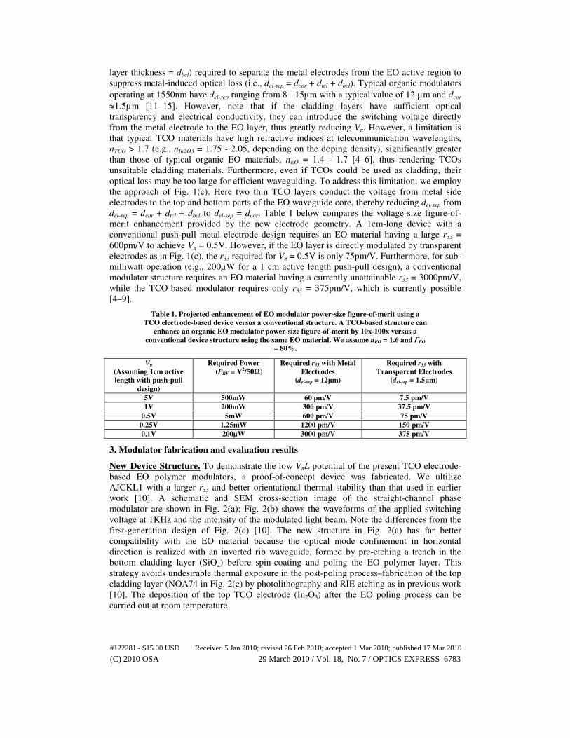
layer thickness = dbcl) required to separate the metal electrodes from the EO active region to
suppress metal-induced optical loss (i.e., del-sep = dcor + dtcl + dbcl). Typical organic modulators
operating at 1550nm have del-sep ranging from 8 −15µm with a typical value of 12 µm and dcor
≈1.5µm [11–15]. However, note that if the cladding layers have sufficient optical
transparency and electrical conductivity, they can introduce the switching voltage directly
from the metal electrode to the EO layer, thus greatly reducing Vπ. However, a limitation is
that typical TCO materials have high refractive indices at telecommunication wavelengths,
nTCO > 1.7 (e.g., nIn2O3 = 1.75 - 2.05, depending on the doping density), significantly greater
than those of typical organic EO materials, nEO = 1.4 - 1.7 [4–6], thus rendering TCOs
unsuitable cladding materials. Furthermore, even if TCOs could be used as cladding, their
optical loss may be too large for efficient waveguiding. To address this limitation, we employ
the approach of Fig. 1(c). Here two thin TCO layers conduct the voltage from metal side
electrodes to the top and bottom parts of the EO waveguide core, thereby reducing del-sep from
del-sep = dcor + dtcl + dbcl to del-sep = dcor. Table 1 below compares the voltage-size figure-of-
merit enhancement provided by the new electrode geometry. A 1cm-long device with a
conventional push-pull metal electrode design requires an EO material having a large r33 =
600pm/V to achieve Vπ = 0.5V. However, if the EO layer is directly modulated by transparent
electrodes as in Fig. 1(c), the r33 required for Vπ = 0.5V is only 75pm/V. Furthermore, for sub-
milliwatt operation (e.g., 200µW for a 1 cm active length push-pull design), a conventional
modulator structure requires an EO material having a currently unattainable r33 = 3000pm/V,
while the TCO-based modulator requires only r33 = 375pm/V, which is currently possible
[4–9].
Table 1. Projected enhancement of EO modulator power-size figure-of-merit using a
TCO electrode-based device versus a conventional structure. A TCO-based structure can
enhance an organic EO modulator power-size figure-of-merit by 10x-100x versus a
conventional device structure using the same EO material. We assume nEO = 1.6 and ГEO
= 80%.
Vπ
(Assuming 1cm active
length with push-pull
design)
Required Power
(PRF = V2/50Ω)
Required r33 with Metal
Electrodes
(del-sep = 12µm)
Required r33 with
Transparent Electrodes
(del-sep = 1.5µm)
5V 500mW 60 pm/V 7.5 pm/V 1V 200mW 300 pm/V 37.5 pm/V
0.5V 5mW 600 pm/V 75 pm/V 0.25V 1.25mW 1200 pm/V 150 pm/V 0.1V 200µW 3000 pm/V 375 pm/V
3. Modulator fabrication and evaluation results
New Device Structure. To demonstrate the low VπL potential of the present TCO electrode-
based EO polymer modulators, a proof-of-concept device was fabricated. We ultilize
AJCKL1 with a larger r33 and better orientational thermal stability than that used in earlier
work [10]. A schematic and SEM cross-section image of the straight-channel phase
modulator are shown in Fig. 2(a); Fig. 2(b) shows the waveforms of the applied switching
voltage at 1KHz and the intensity of the modulated light beam. Note the differences from the
first-generation design of Fig. 2(c) [10]. The new structure in Fig. 2(a) has far better
compatibility with the EO material because the optical mode confinement in horizontal
direction is realized with an inverted rib waveguide, formed by pre-etching a trench in the
bottom cladding layer (SiO2) before spin-coating and poling the EO polymer layer. This
strategy avoids undesirable thermal exposure in the post-poling process–fabrication of the top
cladding layer (NOA74 in Fig. 2(c) by photolithography and RIE etching as in previous work
[10]. The deposition of the top TCO electrode (In2O3) after the EO poling process can be
carried out at room temperature.
(C) 2010 OSA 29 March 2010 / Vol. 18, No. 7 / OPTICS EXPRESS 6783#122281 - $15.00 USD Received 5 Jan 2010; revised 26 Feb 2010; accepted 1 Mar 2010; published 17 Mar 2010

Fig. 2. (a) Inverted rib waveguide structure used for the present demonstration of a TCO
electrode-based organic EO modulator; and SEM cross-section image of the fabricated device;
(b) Measured waveforms of the switching voltage and the detected output light intensity. The
measurement was made at λ = 1.3µm, with a driving voltage frequency of 1kHz. (c) Earlier
device structure from ref. [10]. (d) Mode pattern for TE / TM mode and a photo of the mode
taken with a CCD camera. In the simulation, we assume nEO = 1.68 and nTCO = 2.0. The new
structure has higher ГEO ≥ 95% than in previous work because the top cladding layer is now air
rather than NOA74. The optical mode overlapping factor in the top TCO layer, the EO layer
and the bottom TCO layer for both TM and TE mode are listed. The total TCO overlapping
factor is ГTCO = 0.78% for TM mode and ГTCO = 1.71% for TE mode.
TCO modulator fabrication. Process steps are shown in Fig. 3. After fabrication of the
inverted rib structure on a 3µm thick SiO2 layer on Si by standard photolithography (step 1), a
60nm In2O3 TCO layer was grown by Ion-Assisted Deposition (IAD) at room temperature
[23] to form the bottom TCO bridge electrode (step2). A 90nm SiO2 layer was then grown on
top of the TCO layer as protective layer to reduce EO polymer breakdown during electric
field poling (step 3). A 150nm gold layer was then thermally evaporated/patterned by shadow
masking on the side of the bottom TCO bridge electrode to act as the bottom contact (step 4).
Next, a 1.5µm EO polymer layer was spin-coated onto the substrate. The AJ-CKL1 EO
polymer was formulated by doping 30 wt% of chromophore AJY02 into a low-loss, high-Tg
amorphous polycarbonate (APC) host. Thus, 32.0 mg of APC and 13.7 mg of AJY02 was
dissolved in 770 mg of dibromomethane, and the mixture shaken for 3 h to obtain a
homogeneous solution. This solution was then filtered through a 0.2 µm pore size PTFE filter
and spin-coated onto the device substrate, followed by drying under vacuum at 80°C for 0.5
h. The film thickness was adjusted to ~1.5-1.8 µm using a 1100-1600 rpm spinning speed.
Under these processing conditions, the EO polymer filled the trench and formed the desired
inverted rib optical waveguide structure. The refractive indices of this polymer in its unpoled
form were measured with a MetriCon 2010 Prism Coupler and are estimated to be 1.693 (TE)
and 1.680 (TM) at 1300 nm; and 1.661 (TE) and 1.642 (TM) at 1550 nm(step 5). The EO
polymer fills the trench and forms the desired inverted rib optical waveguide structure. Next,
a solution of 20 wt% poly(4-vinylphenol) (PVP) in n-propanol was spin-coated on the top of
the EO layer to deposit a 1.5µm PVP film (step 6). The PVP/EO bilayer was then thoroughly
dried under vacuum at 80 °C. This PVP layer is used as a sacrificial buffer for poling, and is
essential to produce poled EO films with acceptable surface quality. We explored the
undoped version of PVP (resistivity ~1x10¹⁰Ω*m) and a PEDOT-PSS doped version
(resistivity ~1x10⁶Ω*m), to see whether the doped PVP layer might enhance the poling
efficiency versus the undoped PVP layer. After the PVP layer deposition and drying, a 100nm
gold poling electrode was thermally evaporated onto the PVP layer (step7). The poling
(C) 2010 OSA 29 March 2010 / Vol. 18, No. 7 / OPTICS EXPRESS 6784#122281 - $15.00 USD Received 5 Jan 2010; revised 26 Feb 2010; accepted 1 Mar 2010; published 17 Mar 2010

voltage applied to the EO/PVP stack was ~250V-300V for the device with undoped PVP
layer and 150V – 250V for the device with a doped PVP layer. The film temperature was then
ramped from 60°C to 135°C at a rate of 10°C/min. The poling current increased during the
temperature ramp process. The maximum current observed during poling of the EO/PVP
stack was 5µA for undoped PVP (250V poling voltage), and 30µA for doped PVP (225V
poling voltage). Under the same poling profile, the maximum current during the poling of the
single EO layer is 170µA, which means that the PVP protective layer reduces the maximum
achievable poling current.
Fig. 3. Fabrication process for the side conduction TCO electrode-based EO modulator of
Fig. 1(c).
Once the maximum temperature is reached, the sample is slowly cooled to room
temperature before terminating the voltage (step 8). After the EO poling process, the gold
poling electrode was removed by wet etching and the PVP protective layer removed with
ethanol (step 9). A 60nm In2O3 TCO layer was then grown by IAD at room temperature on
top of the poled EO film to form the top TCO bridge electrode (step 10). Finally, a 150nm
gold layer is thermally evaporated/patterned on top of the TCO bridge electrode to form the
top metal contact (step11).
Measurement of VπL figure-of-merit. The EO phase shift was measured by converting the
phase modulation to intensity modulation using a cross-polarization interference setup: input
light from a 5mW 1310nm semiconductor laser was linearly polarized at + 45° to the
direction of the switching electric field. The light was coupled into the straight waveguide
using a 60x objective lens with a numerical aperture of 0.6. The output light from the
waveguide was collected by another 60x objective lens and passed through a polarization
analyzer oriented with an analyzed polarization at −45° to the direction of the switching
electric field. Phase modulation was converted to intensity modulation after the analyzer. The
intensity modulation is detected by a photo-detector and recorded with an oscilloscope.
For a number of devices fabricated, the observed voltage-size figure-of-merit ranged from
0.6V-cm to 0.9V-cm, after physically reasonable conversion of the directly measured VπL to
that for a push-pull geometry. We summarize details of the measurement results in Table 2.
As discussed above, for the sacrificial poling protective layer (PVP), we explored both un-
doped and doped (conductive) PVPs. For each PVP formulation, we also varied the poling
voltage. From Table 2 note that the device with the conductive PVP layer and higher poling
(C) 2010 OSA 29 March 2010 / Vol. 18, No. 7 / OPTICS EXPRESS 6785#122281 - $15.00 USD Received 5 Jan 2010; revised 26 Feb 2010; accepted 1 Mar 2010; published 17 Mar 2010
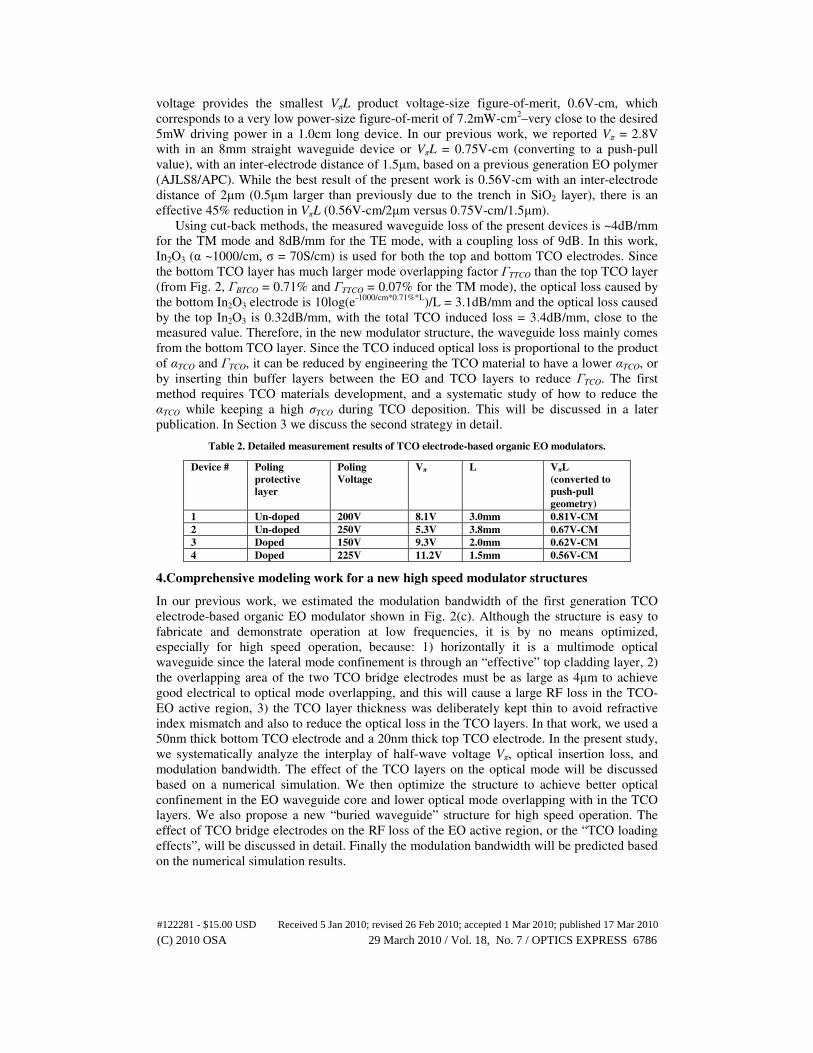
voltage provides the smallest VπL product voltage-size figure-of-merit, 0.6V-cm, which
corresponds to a very low power-size figure-of-merit of 7.2mW-cm2–very close to the desired
5mW driving power in a 1.0cm long device. In our previous work, we reported Vπ = 2.8V
with in an 8mm straight waveguide device or VπL = 0.75V-cm (converting to a push-pull
value), with an inter-electrode distance of 1.5µm, based on a previous generation EO polymer
(AJLS8/APC). While the best result of the present work is 0.56V-cm with an inter-electrode
distance of 2µm (0.5µm larger than previously due to the trench in SiO2 layer), there is an
effective 45% reduction in VπL (0.56V-cm/2µm versus 0.75V-cm/1.5µm).
Using cut-back methods, the measured waveguide loss of the present devices is ~4dB/mm
for the TM mode and 8dB/mm for the TE mode, with a coupling loss of 9dB. In this work,
In2O3 (α ~1000/cm, σ = 70S/cm) is used for both the top and bottom TCO electrodes. Since
the bottom TCO layer has much larger mode overlapping factor ГTTCO than the top TCO layer
(from Fig. 2, ГBTCO = 0.71% and ГTTCO = 0.07% for the TM mode), the optical loss caused by
the bottom In2O3 electrode is 10log(e-1000/cm*0.71%*L
)/L = 3.1dB/mm and the optical loss caused
by the top In2O3 is 0.32dB/mm, with the total TCO induced loss = 3.4dB/mm, close to the
measured value. Therefore, in the new modulator structure, the waveguide loss mainly comes
from the bottom TCO layer. Since the TCO induced optical loss is proportional to the product
of αTCO and ГTCO, it can be reduced by engineering the TCO material to have a lower αTCO, or
by inserting thin buffer layers between the EO and TCO layers to reduce ГTCO. The first
method requires TCO materials development, and a systematic study of how to reduce the
αTCO while keeping a high σTCO during TCO deposition. This will be discussed in a later
publication. In Section 3 we discuss the second strategy in detail.
Table 2. Detailed measurement results of TCO electrode-based organic EO modulators.
Device # Poling
protective
layer
Poling
Voltage Vπ L VπL
(converted to
push-pull
geometry)
1 Un-doped 200V 8.1V 3.0mm 0.81V-CM 2 Un-doped 250V 5.3V 3.8mm 0.67V-CM 3 Doped 150V 9.3V 2.0mm 0.62V-CM 4 Doped 225V 11.2V 1.5mm 0.56V-CM
4.Comprehensive modeling work for a new high speed modulator structures
In our previous work, we estimated the modulation bandwidth of the first generation TCO
electrode-based organic EO modulator shown in Fig. 2(c). Although the structure is easy to
fabricate and demonstrate operation at low frequencies, it is by no means optimized,
especially for high speed operation, because: 1) horizontally it is a multimode optical
waveguide since the lateral mode confinement is through an “effective” top cladding layer, 2)
the overlapping area of the two TCO bridge electrodes must be as large as 4µm to achieve
good electrical to optical mode overlapping, and this will cause a large RF loss in the TCO-
EO active region, 3) the TCO layer thickness was deliberately kept thin to avoid refractive
index mismatch and also to reduce the optical loss in the TCO layers. In that work, we used a
50nm thick bottom TCO electrode and a 20nm thick top TCO electrode. In the present study,
we systematically analyze the interplay of half-wave voltage Vπ, optical insertion loss, and
modulation bandwidth. The effect of the TCO layers on the optical mode will be discussed
based on a numerical simulation. We then optimize the structure to achieve better optical
confinement in the EO waveguide core and lower optical mode overlapping with in the TCO
layers. We also propose a new “buried waveguide” structure for high speed operation. The
effect of TCO bridge electrodes on the RF loss of the EO active region, or the “TCO loading
effects”, will be discussed in detail. Finally the modulation bandwidth will be predicted based
on the numerical simulation results.
(C) 2010 OSA 29 March 2010 / Vol. 18, No. 7 / OPTICS EXPRESS 6786#122281 - $15.00 USD Received 5 Jan 2010; revised 26 Feb 2010; accepted 1 Mar 2010; published 17 Mar 2010
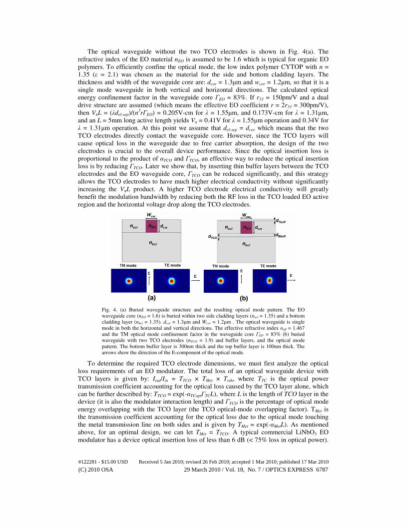
The optical waveguide without the two TCO electrodes is shown in Fig. 4(a). The
refractive index of the EO material nEO is assumed to be 1.6 which is typical for organic EO
polymers. To efficiently confine the optical mode, the low index polymer CYTOP with n =
1.35 (ε = 2.1) was chosen as the material for the side and bottom cladding layers. The
thickness and width of the waveguide core are: dcor = 1.3µm and wcor = 1.2µm, so that it is a
single mode waveguide in both vertical and horizontal directions. The calculated optical
energy confinement factor in the waveguide core ГEO = 83%. If r33 = 150pm/V and a dual
drive structure are assumed (which means the effective EO coefficient r = 2r33 = 300pm/V),
then VπL = (λdel-sep)/(n3rГEO) = 0.205V-cm for λ = 1.55µm, and 0.173V-cm for λ = 1.31µm,
and an L = 5mm long active length yields Vπ = 0.41V for λ = 1.55µm operation and 0.34V for
λ = 1.31µm operation. At this point we assume that del-sep = dcor which means that the two
TCO electrodes directly contact the waveguide core. However, since the TCO layers will
cause optical loss in the waveguide due to free carrier absorption, the design of the two
electrodes is crucial to the overall device performance. Since the optical insertion loss is
proportional to the product of αTCO and ГTCO, an effective way to reduce the optical insertion
loss is by reducing ГTCO. Later we show that, by inserting thin buffer layers between the TCO
electrodes and the EO waveguide core, ГTCO can be reduced significantly, and this strategy
allows the TCO electrodes to have much higher electrical conductivity without significantly
increasing the VπL product. A higher TCO electrode electrical conductivity will greatly
benefit the modulation bandwidth by reducing both the RF loss in the TCO loaded EO active
region and the horizontal voltage drop along the TCO electrodes.
Fig. 4. (a) Buried waveguide structure and the resulting optical mode pattern. The EO
waveguide core (nEO = 1.6) is buried within two side cladding layers (nscl = 1.35) and a bottom
cladding layer (nbcl = 1.35). dcor = 1.3µm and Wcor = 1.2µm . The optical waveguide is single
mode in both the horizontal and vertical directions. The effective refractive index neff = 1.467
and the TM optical mode confinement factor in the waveguide core ГEO = 83% (b) buried
waveguide with two TCO electrodes (nTCO = 1.9) and buffer layers, and the optical mode
pattern. The bottom buffer layer is 300nm thick and the top buffer layer is 100nm thick. The
arrows show the direction of the E-component of the optical mode.
To determine the required TCO electrode dimensions, we must first analyze the optical
loss requirements of an EO modulator. The total loss of an optical waveguide device with
TCO layers is given by: Iout/Iin = TTCO × TMet × Toth, where TTC is the optical power
transmission coefficient accounting for the optical loss caused by the TCO layer alone, which
can be further described by: TTCO = exp(-αTCoptΓTCL), where L is the length of TCO layer in the
device (it is also the modulator interaction length) and ΓTCO is the percentage of optical mode
energy overlapping with the TCO layer (the TCO optical-mode overlapping factor). TMet is
the transmission coefficient accounting for the optical loss due to the optical mode touching
the metal transmission line on both sides and is given by TMet = exp(-αMetL). As mentioned
above, for an optimal design, we can let TMet = TTCO. A typical commercial LiNbO3 EO
modulator has a device optical insertion loss of less than 6 dB (< 75% loss in optical power).
(C) 2010 OSA 29 March 2010 / Vol. 18, No. 7 / OPTICS EXPRESS 6787#122281 - $15.00 USD Received 5 Jan 2010; revised 26 Feb 2010; accepted 1 Mar 2010; published 17 Mar 2010
The typical fiber coupling loss at the input and output ports can typically be lower than 30%
(1.5dB) per port, yielding a total coupling loss of less than 50% (3dB). Assuming that other
propagation losses, including EO material absorption loss, total to be less than 20% (1dB),
Toth will be no less than (1 − 0.3) × (1 − 0.3) × (1 − 0.2) ≈0.4 (4dB). To achieve a similar total
device insertion loss of 6 dB for our modulator design, it is desirable to keep the optical
propagation loss due to the TCO and metal to be less than 40%, i.e., keep (TTCO × TMet) > 0.6
(less than 2.2dB) or TTCO > 0.775 (less than 1.1dB) assuming TTCO = TMet, so that (Toth × TTCO
× TMet) will be greater than 0.25 (< 75% loss or < 6 dB total device insertion loss). For here
and all examples given below, we assume an RF-optical interaction length L = 0.5 cm, so that
the optical transmission TTCO will be > 0.8 if αTCoptΓTC < ln(0.8)/L = 0.22/L (for L in cm)
which requires αTCopt ΓTCO < 0.44/cm when L = 0.5cm. Table 3 summarizes the optical loss
caused by each part of the TCO electrode-based EO modulator.
Table 3. Details of the optical insertion loss caused by each modulator component
Total Insertion loss: 6dB Coupling loss (2 ports) 3dB
Metal induced loss 1dB TCO layer induced loss 1dB
Other materials loss 1dB
Regarding TCO electrode composition, materials such as tin-doped indium oxide (ITO)
are used widely in flat panel displays. While ITO is excellent for visible wavelength
applications, it is not suitable for the 1550nm fiber-optic telecommunication wavelengths due
to the high IR optical absorption. Since the modulators of interest are intended to operate at
1550nm, TCOs with low optical absorption in this region are essential. For such applications,
TCOs such as undoped In2O3, ZnO, or CdO are more suitable due to their low optical
absorption at 1300-1550nm [17–23], as given by the loss coefficient αTCO. Besides the low
loss requirement, an electrode TCO material must have a sufficiently high electrical
conductivity, σTCO, to drive the modulator at high speed. While doping TCO materials with
additional carriers increases σTCO, it also increases free carrier absorption at longer
wavelengths, increasing αTCO [17–24]. The electrical conductivity to optical absorption
coefficient ratio, FTCO = σTCO/αTCO, is an intrinsic materials property at a given wavelength
and an important TCO modulator figure-of-merit. As discussed before, the acceptable αTCO is
inversely proportional to ΓTCO through the relationship αTCoptΓTCO < 0.44 when L = 0.5cm,
while σTCO is proportional to αTCO when a certain FTCO is assumed. Therefore, the optical
mode overlapping factor ΓTCO must be as small as possible to obtain as large a σTCO as
possible. This can be achieved by either making the two TCO layers very thin, or adding thin
buffer layers between the EO layer and the TCO layers. Table 4 shows the numerical
simulation results for the relationship between ΓTCO and the thicknesses of the TCO and
buffer layers. The results are given by COMSOL, which is an FEM method based mode
solver [26]. Here we define the optical mode overlapping factor in the bottom TCO layer to
be ΓBTCO and the optical mode overlapping factor in the top TCO layer to be ΓTTCO. The total
mode overlapping factor in the TCO layers is ΓTCO = ΓBTCO + ΓTTCO. Note that if the TCO
layers directly contact the EO layer, ΓTCO is 2.9% and the corresponding αTCopt = 15 /cm.
ΓBTCO is larger than ΓTTCO because the refractive index top cladding layer (air) is smaller than
the bottom cladding layer (CYTOP), and the optical mode is shifted towards the CYTOP side.
However if there is a 300nm thick bottom buffer layer and 100nm top buffer layer in between
the bottom TCO layer and the EO layer, ΓTCO will be reduced to 0.77%, and the
corresponding αTCopt becomes 57 /cm . Here we make dBBuff > dTBuff to assure that ΓBTCO ≈ΓTTCO
(i.e. separate bottom TCO layer away from the EO layer further than the top TCO layer). The
thickness of the two TCO layers TTCO is set here to 100nm. Assuming FTCO = 1S, the
corresponding σTCO = 57S/cm. Note that the 400nm thick buffer layer will only increase the
Vπ to 0.54V for λ = 1.55µm operation and to 0.44V for λ = 1.31µm operation. Later we will
(C) 2010 OSA 29 March 2010 / Vol. 18, No. 7 / OPTICS EXPRESS 6788#122281 - $15.00 USD Received 5 Jan 2010; revised 26 Feb 2010; accepted 1 Mar 2010; published 17 Mar 2010

show that higher TCO electrode electrical conductivity will greatly reduce the RF loss and the
horizontal TCO-RC voltage drop along the two TCO electrodes. Therefore we can choose
dBbuff = 300 nm and dTbuff = 100nm. In Table 4 we also list the overlap integral ηoverlap between
the TM mode of the structure with TCO layers, and the TM mode of the structure without
TCO layers, found by a commercial mode solver [27]. Here ηoverlap is defined as
* *
1 2 2 1
* *
1 1 2 2
( )( ) 1[ ]
( )overlap
E H d S E H d SRe
E H d S Re E H d S
η
→ →→ → → →
→ →→ → → →
× ×=
× ×
∫ ∫
∫ ∫
i i
i i
(2)
Note in Table 4 that the values of ηoverlap are all close to 100% which means that the
optical loss in the optical waveguide caused by the mode mismatch between the section
without TCO layers and the TCO loaded section can be ignored.
Table 4. Relationship between ГTCO and the thicknesses of buffer layers. The thickness of
the TCO layer TTCO = 100nm, and here we assume λ = 1.55µm. The data is for TM mode.
dBbuff (nm)
dTbuff del-sep ГBTCO ГTTCO ГTCO αTCopt ηOverlap
0 0 1.3µm 2.39% 0.50% 2.90% 15/cm 100% 100 0 1.4µm 1.24% 0.58% 1.82% 24/cm 97.6% 200 0 1.5µm 0.69% 0.64% 1.33% 33/cm 97.6% 300 0 1.6µm 0.39% 0.67% 1.06% 42/cm 97.3% 300 100nm 1.7µm 0.40% 0.37% 0.77% 57/cm 96.1%
In Fig. 5(b), we show the values of neff and ngopt at different optical wavelengths for the
modulator structure with dBbuff = 300 nm and dTbuff = 100nm. Here ngopt = nopt – λ0dnopt/dλ. The
group index optical waveguide ngopt is found to be 1.642 at λ = 1.31µm and 1.643 at λ =
1.55µm–slightly higher than neff. Later in the RF simulation, ngopt will be used to calculate the
velocity mis-match. Figure 5(c) shows the relationship between ГEO, ГTCO, and λ. Note that
ГTCO at λ = 1.31µm is smaller than ГTCO at λ = 1.55µm and therefore will allow the TCO
layers to have a larger αTCO. Figure 5(d) shows the relationship between αMet (calculated from
the extinction coefficient к) and Wgap. As discussed above, the metal-induced optical insertion
loss is required to be <1dB. This requires that we find a Wgap at which TMet = exp(-αMetL) >
0.775, or αMet < 0.44/cm when L = 5mm. In order to minimize Wgap, we first choose a large
refractive index difference between the EO waveguide core (nEO = 1.6) and the side cladding
layer (nscl = 1.35). This ensures a good horizontal mode confinement in the EO waveguide
core region. Secondly, as shown in Fig. 5(a), the two metal electrodes are located on the two
sides of the waveguide and the two TCO bridge electrodes extend to the top and bottom of the
EO waveguide core region. The modulator will work in TM mode since its E-component is
parallel to the RF electric field provided by the two TCO bridge electrodes. This arrangement
also helps minimize Wgap because the TM mode has a better horizontal confinement in the EO
waveguide core, compared with the TE mode case. In the numerical simulation, αMet is found
through the extinction coefficient к which is the imaginary part of the complex effective
refractive index of a mode (nc = n + iк) using the relationship: к = αMetλ/(4π). We see from
Fig. 5(d) that when Wgap > 1.6µm, αMet is small enough (below 0.44/cm for both λ = 1.31µm
and λ = 1.55µm).
(C) 2010 OSA 29 March 2010 / Vol. 18, No. 7 / OPTICS EXPRESS 6789#122281 - $15.00 USD Received 5 Jan 2010; revised 26 Feb 2010; accepted 1 Mar 2010; published 17 Mar 2010
Fig. 5. (a) Buried waveguide structure with two TCO electrodes and buffer layers. Two side
copper electrodes are also included to find the metal induced optical loss coefficient αMet. nscl =
nbcl = 1.35. dcor = 1.3µm, Wcor = 1.2µm, dBbuff = 300nm, dTbuff = 100nm, dTCO = 100nm. (b)
Effective refractive index and group index of the optical waveguide for TM mode c) The
optical mode confinement factor in the EO waveguide core ГEO and the optical mode
overlapping factor in the two TCO layers ГTCO = ГBTCO + ГTTCO, under different wavelength. d)
Metal-induced optical loss coefficient αMet versus the width of the gap Wgap.
Before going into the details of the RF transmission line design, we first analyze the
theoretical upper limit of the acceptable values of the microwave attenuation coefficient αRF
and TCO-RC voltage drop coefficient rRC. Figure 6 shows the standard RF model for the TCO
electrode-based EO modulator. An RF source launches the RF wave into the active region (a
TCO bridge loaded transmission line) through a standard Zs = 50Ω feeding transmission line.
A ZL = 50Ω termination is assumed at the end of the active region.
Fig. 6. Transmission line model for the TCO electrode-based EO modulator. The entrance
point of the TCO loaded EO active region is defined as x = 0. The termination point is defined
as x = L.
Assuming the voltage applied to the feeding transmission line is Vappl, then the
instantaneous RF voltage seen by the optical packet along the active region is given by:
(2 )
2( , ) [ ]
1
gopt goptRF RF
RF
x xj j
v vx L zEO
eff appl LL
metal L S
V TV x V e e e e
V e
ω ωγ γ
γω − − −−
= • • • + Γ−Γ Γ
(3)
Here γRF = αRF + jβRF is the complex propagation constant of the RF wave and ω = 2πf is
the angular frequency. αRF is the microwave attenuation coefficient which accounts for the RF
loss in the TCO loaded active region. βRF is the propagation constant which determines the
(C) 2010 OSA 29 March 2010 / Vol. 18, No. 7 / OPTICS EXPRESS 6790#122281 - $15.00 USD Received 5 Jan 2010; revised 26 Feb 2010; accepted 1 Mar 2010; published 17 Mar 2010
traveling speed of RF wave in the active region. RF reflection often happens when the
characteristic impedance of the active region Zm is not equal to Zs and ZL, and this is
accounted for by Гs = (Zs-Zm)/ (Zs + Zm), which is the RF reflection coefficient at the entrance
of the active region, and ГL = (ZL-Zm)/(ZL + Zm), which is the RF reflection coefficient at the
termination of the active region. T = 1- Гs is defined as the RF transmission coefficient at the
entrance of the active region. Because the TCO electrodes are often thin layers with limited
conductivity, the voltage they conduct to the EO waveguide core will drop below the voltage
on the metal transmission line, due to the TCO-RC loading effect, especially at the high
frequency. This fact is accounted for by adding an RC voltage drop coefficient: rRC =
VEO/Vmetal. The average switching voltage applied to the optical packet after it leaves the
active region, is found by integrating Veff(x,ω) along 0 to L:
2
0
1( ) (1/ )Re( ( , ) ) Re[ ( )]
FW FW RFLL L
L
av eff appl RC REF L
FW BW
e e eV L V x f dx V r r
L L
γγ γ
ωγ γ
−− −− −= = • +Γ∫ (4)
Here γFW and γBW are given by γFW = αRF + j (ω/c)(nRF-ngopt) and γBW = αRF + j (ω/c)(nRF +
ngopt).
Equation (4) gives the complete analytical model to predict how the effects of the applied
voltage will change with increased frequency. Note that our model is only slightly different
from the model given in [28] because here we add the TCO-RC drop factor rRC into the model
and also we define the entrance of the transmission line as x = 0.
The challenging part of designing a high-speed (3dB optical bandwidth>40GHz) TCO
based organic EO modulator is to manage the RF propagation loss along the TCO loaded EO
active region (denoted by αRF) and the voltage drop along the TCO bridge electrodes (denoted
by rRC). To find the theoretical upper limit of the RF loss, we can assume perfect impedance
matching between the feeding transmission line and the active region, and a perfect velocity
match between the RF wave and the optical wave, by setting Zm = Zs = ZL. and βRF = ω/vRF =
ω/vgopt (which means ngRF = ngopt). Later we will show that this can be achieved by carefully
selecting the dielectric materials and tuning the transmission line dimensions. Then, (ω/vgRF)
− βgRF = 0 and Eq. (4) becomes:
( )
(1 )( ) ( )
( )
RF f L
av eff appl RC
RF
eV f V r f
f L
α
α
−
−
−= • • (5)
We can see that now the averaged effective switching voltage Vav-eff(f) is determined by
two factors: one is the TCO-RC voltage drop factor rRC(f), which is a function of frequency f,
and the other is the RF decay factor (1 − e-x
)/x, in which x = αRF(f)L. The RF decay factor is
also a function of frequency f because the microwave attenuation coefficient αRF(f) will
increase with frequency f. The modulation bandwidth of an EO modulator can then be found
by solving for the frequency fBW at which the Vav-eff drops to Vappl/2 (optical 3dB bandwidth,
3dBo) or
( ) ( )(1 )
( ) 0.5( )
RF BWf Lav eff BW
RC BW
RF BW appl
V fer f
f L V
α
α
−−−
• = = (6)
In other words, if we have a targeted bandwidth fBW, the requirement for αRF(f)L is given
by:
0.5
1 , here ( )( )
x
RF BW
RC BW
e x x f Lr f
α−− = = , (7)
The solution of Eq. (7) is:
( )
0.5( ) ( )
( ) ( )0.5 0.5
RC BWr f
RC BW RC BW
RF BW
r f r fx f L W eα
−= = − + (8)
(C) 2010 OSA 29 March 2010 / Vol. 18, No. 7 / OPTICS EXPRESS 6791#122281 - $15.00 USD Received 5 Jan 2010; revised 26 Feb 2010; accepted 1 Mar 2010; published 17 Mar 2010

Here W(x) is the Lumbert W function [25]. Assuming rRC(fBW) = 1, or no RC voltage drop
along the TCO electrodes, then αRF(f)L = W(−2e−2
) + 2 = 1.6, or αRF(f) = 3.2 /cm if L = 0.5cm.
Here αRF is defined as the microwave attenuation coefficient of the electric field amplitude of
the RF wave, therefore 3.2/cm corresponds to 20log(e3.2L
)/L = 27.7dB/cm. For example, if the
target 3dB optical bandwidth is 40GHz, then the theoretical upper limit of αRF(40GHz) is
3.2/cm for a device with a 5mm long active length. If the TCO-RC voltage drop along the
TCO electrode factor rRC is taken into consideration, then the upper limit of αRF(fBW) will be
reduced to a lower value. Figure 7 shows the theoretical upper limit of αRF(fBW) under
different rRC values. It can been seen that if the frequency cutoff is already determined by the
TCO-RC voltage drop frequency cutoff factor (e.g., when rRC(f) ~0.5), there is little room for
the RF loss, and a small αRF(f) will push it to the cutoff (when the voltage drops to half). More
importantly, when L is increased from 5mm to 2cm, the theoretical upper limit of αRF when
rRC = 1 (no TCO-RC voltage drop effect) reduces by 4x to only 6.9dB/cm. This means the
room left for RF loss shrinks with increased active length.
In a TCO-enabled organic EO modulator, the RF loss comes from the metal transmission
line and the loading effect of the TCO electrodes in the EO active region. The metal
transmission line loss in the organic EO modulator structure is mainly caused by the skin-
effect of the metal electrodes and can be reduced [14,16]. Assuming the RF loss from the
metal transmission line to be as high as 7.7dB/cm at 40GHz, we still have 20dB/cm left for
TCO-induced RF loss. The actual RF loss in the TCO electrode loaded region depends on the
device structure and the TCO electrical conductivity. Later we will discuss the RF loss in
detail using a specific example. Note here that the active length L plays an important role in
the theoretical upper limit of the RF loss and the TCO-RC voltage drop. For example, in a
conventional organic EO modulator with a typical del-sep = 9µm (6x larger than a TCO-based
structure), the required active length L becomes 3cm, and the acceptable αRF(f) is reduced by
6x to 0.53 /cm, or 4.63dB/cm, which is only enough for the metal transmission line loss.
Fig. 7. Theoretical upper limit of the microwave attenuation coefficient αRF versus rRC under
different active lengths L. Here we assume perfect impedance match and velocity match.
Therefore, we see that the TCO electrode-based EO modulator has high speed potential
(f3dBo > 40GHz) because it can be made short (<5mm active length) while still achieving low
switching voltages (Vπ < 0.5V with dual drive) with currently available organic EO materials
(in device r33 = 150pm/V).
Now we give a specific example of an RF design based on full wave simulation to show
the effect of the two TCO electrodes on the device performance and how to optimize the
structures to achieve large modulation bandwidths. Figure 8 shows the proposed buried
waveguide with a coplanar slot transmission line and TCO side conduction geometry. In this
structure, the two parallel metallic plates to the left and right of the EO waveguide core form
a high-frequency RF transmission line. In the active region, the TCO material forms “bridge
electrodes” to transmit the voltage laterally from the metallic transmission line to the active
EO material region.
(C) 2010 OSA 29 March 2010 / Vol. 18, No. 7 / OPTICS EXPRESS 6792#122281 - $15.00 USD Received 5 Jan 2010; revised 26 Feb 2010; accepted 1 Mar 2010; published 17 Mar 2010

Fig. 8. High frequency structure design for a TCO-electrode based organic EO modulator. The
structure comprises a pair of high speed metallic transmission lines and two TCO electrodes
conducting the voltage from the metallic transmission line to the EO optical waveguide core.
In the numerical simulation, we use Wcor = 1.2µm, Wgap = 1.6µm, Wcopper = 250µm, dcor =
1.3µm, dTbuff = 100nm, dBbuff = 300nm, del-sep = dcopper = dcor + dBbuff + dTbuff = 1.7µm, dTCO =
100nm, dbcl = 3µm, dsub = 100µm, εEO = εTCO = 3, εscl = εbcl = εsub = 2.1. In practice, a low-k
substrate is required.
The structure is modeled using HFSS, which is a commercial finite element method
(FEM) solver [29]. The simulated electric field pattern of the RF mode in the TCO-EO core
region is shown in Fig. 8. It can be seen that in the EO waveguide core region, the RF electric
field is perpendicular to the TCO bridge electrodes and the electric field strength is uniform
across the entire EO waveguide core region. This ensures a good RF electric field - optical
mode overlapping in the EO waveguide core. Figure 9 shows the numerical simulation results
of the RF loss, the TCO-RC voltage drop factor rRC, the characteristic impedance Z0, and the
RF transmission line effective group index ngRF. Figure 9(a) and 9(b) show that the structure
is optimized so that Z0 is tuned to match 50Ω and the ngRF also matches ngopt (~1.64). This
means that the effects of the impedance mismatch and RF-optical velocity mismatch are
minimized. From Fig. 9(c) and 9(d) we can see that αRF and rRC depend on the electrical
conductivity of the TCO electrodes which is in turn dependent on the TCO material figure of
merit FTCO = σTCO/αTCO where αTCO = 57/cm is determined by the optical insertion loss
(C) 2010 OSA 29 March 2010 / Vol. 18, No. 7 / OPTICS EXPRESS 6793#122281 - $15.00 USD Received 5 Jan 2010; revised 26 Feb 2010; accepted 1 Mar 2010; published 17 Mar 2010

requirement discussed before. We explored the FTCO = 0S, 0.2S, 0.5S and 1S cases and the
corresponding σTCO = 0S/cm, 11.4S/cm, 28.5S/cm and 57S/cm, cases, respectively. The curve
with σTCO = 0S/cm represents the case in which only pure copper coplanar slot transmission
lines are present. Note that αRF in this case can be quite small. At 40GHz, the predicted αRF in
this situation is as low as 0.1328/cm or 1.15dB/cm. However, when the two TCO electrodes
are loaded in the active region, αRF will increase significantly. Note from Fig. 9(c) that when
σTCO = 11.4S/cm or FTCO = 0.2S, αRF at 40GHz becomes 1.0898/cm, or 9.466dB/cm. This is
because the RF wave interacts with the two TCO electrodes which have only finite electrical
conductivity. Although αRF is significantly higher than the value when there are only pure
metallic transmission lines (0.1328/cm or 1.15dB/cm), it is still below the theoretical upper
limit because in this case rRC = 0.81718 [Fig. 9(d)] and from Fig. 7 we find that the
corresponding theoretical upper limit of αRF at 40GHz is 2.15/cm or 18.68dB/cm. Note that
the structure is already optimized to achieve near impedance and velocity match. More
importantly, with TCO materials having larger FTCO values (0.5S or 1S), σTCO can be
increased to 28.5S/cm or 57S/cm. In these cases, at 40GHz, αRF will fall to 0.58/cm
(5.3dB/cm) for FTCO = 0.5S, or 0.37/cm (3.21dB/cm) for FTCO = 1S. And at the same time, rRC
increases to 0.956 for FTCO = 0.5S, and 0.984 for FTCO = 1.0S, which can be seen from
Fig. 9(d). This result shows the importance of the TCO figure of merit because a larger FTCO
will allow higher σTCO values, which in turn lead to lower αRF and higher rRC. From this trend,
note also the importance of short active length L and the buffer layers. For a device with a
short active length (~5mm), αTCO can be larger than the value in a conventional structure with
a 2cm long active length. Similarly, the buffer layers reduce the optical mode overlapping
factor with the TCO layers ГTCO and this in turn leads to larger αTCO (as shown in Table 4).
When FTCO is fixed, larger αTCO values mean larger σTCO.
Fig. 9. Simulation results for modulators having a TCO electrode loaded coplanar transmission
line (the active region), as shown in Fig. 8. (a) Characteristic impedance Z0 under different
σTCO. (b) Effective RF refractive index c) Microwave attenuation coefficient αRF d) TCO-RC
voltage drop coefficient rRC.
(C) 2010 OSA 29 March 2010 / Vol. 18, No. 7 / OPTICS EXPRESS 6794#122281 - $15.00 USD Received 5 Jan 2010; revised 26 Feb 2010; accepted 1 Mar 2010; published 17 Mar 2010

Note that the size of TCO overlapping area has a significant impact on the microwave
attenuation coefficient αRF. Figure 10 shows the value of αRF under different overlapping
widths Woverlap. When the TCO overlapping area width drops from 3.2µm to −0.8µm, αRF
drops from 0.445/cm or 3.86dB/cm to 0.195/cm or 1.69dB/cm. Here the σTCO is set to be
57S/cm (FTCO = 1S case). This is because the two overlapped TCO bridge electrodes act as a
loading capacitor with two series resistors. Increasing Woverlap will increase the loading
capacitance and the series resistance per unit length and therefore causes a larger RF loss
along the active region. To achieve good electrical-optical mode overlapping, the two TCO
electrodes must cover the entire EO waveguide core, meaning Woverlap ≥ Wcor Therefore, in the
design of the optical waveguide, we chose a low index material (CYTOP with n = 1.35) to be
the side cladding material, in order to minimize the width Wcor of the EO waveguide core. The
overall frequency response of the average applied voltage Vav is found by plugging the results
in Fig. 9(a)–9(d) into Eq. (4), and the final result of Vav is shown in Fig. 11. Note that 3dB
optical bandwidths (at which the average effective voltage drops to half the DC value) of
40GHz-100GHz can be achieved. Table 5 summarizes the complete device performance of
the proposed buried waveguide structure with coplanar metal transmission lines and the TCO
side conduction geometry.
Fig. 10. Microwave attenuation coefficient αRF versus the width of the TCO overlapping area
in the modulator structure shown.
Fig. 11. Overall frequency response of the average applied voltage found by plugging the
numerical results given in Fig. 9 into Eq. (4).
(C) 2010 OSA 29 March 2010 / Vol. 18, No. 7 / OPTICS EXPRESS 6795#122281 - $15.00 USD Received 5 Jan 2010; revised 26 Feb 2010; accepted 1 Mar 2010; published 17 Mar 2010

Table 5. Complete modeling result of the TCO based EO modulator.
Vπ L Required r33 Optical Insertion loss 3dB optical bandwidth ~0.5V 5.0mm 150 pm/V ≤6dB ≥40GHz
7. Conclusions
We have shown here that a transparent conducting oxide (TCO) electrode-based organic EO
modulator structure can be used to achieve substantially higher power-size performance than
conventional modulator designs. An optimized high-speed structure is proposed and its
performance carefully analyzed based on full wave numerical simulation. A compact device
(5mm long device) with 0.5V driving voltage and 40GHz – 100GHz optical bandwidth is
predicted. Note that a 0.5 V modulator operating at 40 Gbps in NRZ format has a switching
energy on the order of 63 fJ/bit. Experimentally, we have demonstrated a new EO modulator
structure which features an inverted ridge waveguide geometry offering a simpler fabrication
process, better thermal compatibility with the organic EO material, and a high-response EO
polymer active layer. Initial results demonstrate a power-size figure-of-merit of 7.2mW-cm2.
Compared with our previous experimental results, this represents an effective 45%
improvement.
(C) 2010 OSA 29 March 2010 / Vol. 18, No. 7 / OPTICS EXPRESS 6796#122281 - $15.00 USD Received 5 Jan 2010; revised 26 Feb 2010; accepted 1 Mar 2010; published 17 Mar 2010