Effect of Annealing on the Properties of Indium−Tin−Oxynitride Films as Ohmic Contacts for...
6
Effect of Annealing on the Properties of Indium-Tin-Oxynitride Films as Ohmic Contacts for GaN-Based Optoelectronic Devices Marcel Himmerlich, †,‡ Maria Koufaki, §,⊥ Gernot Ecke, † Christof Mauder, † Volker Cimalla, †,| Juergen A. Schaefer, † Antonis Kondilis, ⊥ Nikos T. Pelekanos, ⊥,# Mircea Modreanu, 3 Stefan Krischok,* ,† and Elias Aperathitis ⊥ Institute of Micro- and Nanotechnologies, TU Ilmenau, P.O. Box 100565, 98684 Ilmenau, Germany, Physics Department, University of Crete, P.O. Box 2208, 71003 Heraklion, Crete, Greece, Microelectronics Research Group, Institute of Electronic Structure & Laser, Foundation for Research and Technology - Hellas, P.O. Box 1385, 71110 Heraklion, Crete, Greece, Materials Science & Technology Department, University of Crete, P.O. Box 2208, 71003 Heraklion, Crete, Greece, and Photonics Group, Tyndall National Institute, Lee Maltings, Prospect Row, Cork, Ireland ABSTRACT Indium-tin-oxynitride (ITON) films have been fabricated by rf sputtering from an indium-tin-oxide target in nitrogen plasma. The influence of postdeposition annealing up to 800 °C is analyzed by electrical, optical, and surface characterization of the films in comparison to indium-tin-oxide (ITO) films fabricated in argon plasma. High-temperature annealing resulted in ITO(N) films with similar carrier concentrations. However, the resistivity and optical transmittance of the ITON films were higher than those of the ITO films. Photoelectron spectroscopy revealed that nitrogen is incorporated into the ITON structure in an unbound state as well as through the formation of metal-nitrogen and oxynitride bonds that decorate oxygen vacancies. When the core level electron spectra of ITO and ITON films are compared, a correlation between carrier concentration and the incorporated nitrogen is found. Changes in ITON electrical properties are mainly induced by the release of nitrogen at temperatures above 550 °C. In this context, ohmic contact behavior was achieved for ITON on p-type GaN after annealing at 600 °C, while no ohmic contact could be realized using ITO. KEYWORDS: oxides • oxynitrides • semiconductors • sputtering • photoelectron spectroscopy INTRODUCTION I ndium-tin-oxide (ITO) is, in addition to ZnO, SnO 2 , and CdO, a very commonly used transparent conductive oxide. When ITO is utilized for optoelectronic devices, it serves as optical as well as contact material. Even though ITO is a wide band gap material (the onset of optical absorption varies between 3.5 and 4.0 eV, depending on the deposition technique), it is an n-type degenerate semicon- ductor with oxygen vacancies and tin atoms at indium sites mainly determining the conductivity of the material. Due to the lack of p-type oxides with similar properties (wide band gap and at the same time high conductivity) ITO has been used in many III-V-based optoelectronic devices. In par- ticular, for the case of devices based on the wide band gap III-nitride compounds, ITO has been used as the ohmic contact on p-GaN layers (1, 2). It should be noted that the metallic ohmic contact forma- tion on p-GaN is still a developing technology, mainly due to the low doping density of p-GaN. Attempts to improve or modify the properties of ITO for other technological applica- tions have been reported, such as changing its composition using H 2 + and O + implantation (3) or adding Zn (4), Ag (5), or Zr (6) during deposition. In a previous study we have shown that the introduction of nitrogen in the plasma chamber during rf sputter deposi- tion of ITO results in the incorporation of nitrogen into the film structure and the formation of ITON films (7). Deposi- tion performed in pure nitrogen plasma, followed by post- deposition annealing at 400 °C, resulted in ITON films with improved optical properties but inferior electrical properties compared to conventional ITO films deposited in argon plasma (8). In this work, we investigate the chemical structure of the incorporated nitrogen in ITON as well as the surface com- position of ITO(N), by employing photoelectron spectrosco- * To whom correspondence should be addressed. E-mail: stefan.krischok@ tu-ilmenau.de. Received for review March 3, 2009 and accepted May 24, 2009 † TU Ilmenau. ‡ Current address: Fraunhofer Institute for Manufacturing Technology and Applied Materials Research, Wiener Str. 12, 28359 Bremen, Germany. § Physics Department, University of Crete. | Current address: Fraunhofer Institute for Applied Solid State Physics, Tullastr. 72, 79108 Freiburg, Germany. ⊥ Foundation for Research and Technology - Hellas. # Materials Science & Technology Department, University of Crete. 3 Tyndall National Institute. DOI: 10.1021/am900138f © 2009 American Chemical Society ARTICLE www.acsami.org VOL. 1 • NO. 7 • 1451–1456 • 2009 1451 Published on Web 06/09/2009 Downloaded by TECHNISCHE UNIV ILMENAU on July 29, 2009 Published on June 9, 2009 on http://pubs.acs.org | doi: 10.1021/am900138f
-
Upload
independent -
Category
Documents
-
view
0 -
download
0
Transcript of Effect of Annealing on the Properties of Indium−Tin−Oxynitride Films as Ohmic Contacts for...

Effect of Annealing on the Properties ofIndium-Tin-Oxynitride Films as OhmicContacts for GaN-Based OptoelectronicDevicesMarcel Himmerlich,†,‡ Maria Koufaki,§,⊥ Gernot Ecke,† Christof Mauder,† Volker Cimalla,†,|
Juergen A. Schaefer,† Antonis Kondilis,⊥ Nikos T. Pelekanos,⊥,# Mircea Modreanu,3Stefan Krischok,*,† and Elias Aperathitis⊥
Institute of Micro- and Nanotechnologies, TU Ilmenau, P.O. Box 100565, 98684 Ilmenau, Germany, PhysicsDepartment, University of Crete, P.O. Box 2208, 71003 Heraklion, Crete, Greece, Microelectronics Research Group,Institute of Electronic Structure & Laser, Foundation for Research and Technology - Hellas, P.O. Box 1385,71110 Heraklion, Crete, Greece, Materials Science & Technology Department, University of Crete, P.O. Box 2208,71003 Heraklion, Crete, Greece, and Photonics Group, Tyndall National Institute, Lee Maltings,Prospect Row, Cork, Ireland
ABSTRACT Indium-tin-oxynitride (ITON) films have been fabricated by rf sputtering from an indium-tin-oxide target in nitrogenplasma. The influence of postdeposition annealing up to 800 °C is analyzed by electrical, optical, and surface characterization of thefilms in comparison to indium-tin-oxide (ITO) films fabricated in argon plasma. High-temperature annealing resulted in ITO(N)films with similar carrier concentrations. However, the resistivity and optical transmittance of the ITON films were higher than thoseof the ITO films. Photoelectron spectroscopy revealed that nitrogen is incorporated into the ITON structure in an unbound state aswell as through the formation of metal-nitrogen and oxynitride bonds that decorate oxygen vacancies. When the core level electronspectra of ITO and ITON films are compared, a correlation between carrier concentration and the incorporated nitrogen is found.Changes in ITON electrical properties are mainly induced by the release of nitrogen at temperatures above 550 °C. In this context,ohmic contact behavior was achieved for ITON on p-type GaN after annealing at 600 °C, while no ohmic contact could be realizedusing ITO.
KEYWORDS: oxides • oxynitrides • semiconductors • sputtering • photoelectron spectroscopy
INTRODUCTION
Indium-tin-oxide (ITO) is, in addition to ZnO, SnO2, andCdO, a very commonly used transparent conductiveoxide. When ITO is utilized for optoelectronic devices,
it serves as optical as well as contact material. Even thoughITO is a wide band gap material (the onset of opticalabsorption varies between 3.5 and 4.0 eV, depending on thedeposition technique), it is an n-type degenerate semicon-ductor with oxygen vacancies and tin atoms at indium sitesmainly determining the conductivity of the material. Due tothe lack of p-type oxides with similar properties (wide band
gap and at the same time high conductivity) ITO has beenused in many III-V-based optoelectronic devices. In par-ticular, for the case of devices based on the wide band gapIII-nitride compounds, ITO has been used as the ohmiccontact on p-GaN layers (1, 2).
It should be noted that the metallic ohmic contact forma-tion on p-GaN is still a developing technology, mainly dueto the low doping density of p-GaN. Attempts to improve ormodify the properties of ITO for other technological applica-tions have been reported, such as changing its compositionusing H2
+ and O+ implantation (3) or adding Zn (4), Ag (5),or Zr (6) during deposition.
In a previous study we have shown that the introductionof nitrogen in the plasma chamber during rf sputter deposi-tion of ITO results in the incorporation of nitrogen into thefilm structure and the formation of ITON films (7). Deposi-tion performed in pure nitrogen plasma, followed by post-deposition annealing at 400 °C, resulted in ITON films withimproved optical properties but inferior electrical propertiescompared to conventional ITO films deposited in argonplasma (8).
In this work, we investigate the chemical structure of theincorporated nitrogen in ITON as well as the surface com-position of ITO(N), by employing photoelectron spectrosco-
* To whom correspondence should be addressed. E-mail: [email protected] for review March 3, 2009 and accepted May 24, 2009† TU Ilmenau.‡ Current address: Fraunhofer Institute for Manufacturing Technology and AppliedMaterials Research, Wiener Str. 12, 28359 Bremen, Germany.§ Physics Department, University of Crete.| Current address: Fraunhofer Institute for Applied Solid State Physics, Tullastr.72, 79108 Freiburg, Germany.⊥ Foundation for Research and Technology - Hellas.# Materials Science & Technology Department, University of Crete.3 Tyndall National Institute.DOI: 10.1021/am900138f
© 2009 American Chemical Society
ARTIC
LE
www.acsami.org VOL. 1 • NO. 7 • 1451–1456 • 2009 1451Published on Web 06/09/2009
Dow
nloa
ded
by T
EC
HN
ISC
HE
UN
IV I
LM
EN
AU
on
July
29,
200
9Pu
blis
hed
on J
une
9, 2
009
on h
ttp://
pubs
.acs
.org
| do
i: 10
.102
1/am
9001
38f
py, just after deposition and after annealing at temperaturesabove 400 °C. A comparison of the results derived fromsurface characterization is made to the results from theanalysis of electrical and optical properties. Furthermore, thepotential of ohmic contact formation on p-type GaN layersis evaluated.
EXPERIMENTAL SECTIONThe ITON and ITO thin films were deposited by rf sputtering
from an indium-tin-oxide (80% In2O3-20% SnO2) target inpure N2 or Ar plasma, respectively. Details of the sputteringprocedure have been reported elsewhere (9). All films wereprepared at 5 mTorr pressure and different rf powers, varyingbetween 150 and 550 W. Depending on the requirements ofthe experimental techniques used in this study, the depositionwas performed on different substrates: double side polishedsapphire for the electrical and optical characterization of thefilms, p-type (100) Si wafers (1-10 Ωcm) for electron spectros-copy studies, and commercially available p-type GaN templates(TDI Inc.), having a hole concentration of ∼4 × 1017 cm-3, tostudy the contact properties between substrate and depositedfilm. Material properties were investigated just after rf sputterdeposition and after postdeposition annealing performed in arapid thermal annealing (RTA) system (Jipelec FAV4) for 1 minunder a nitrogen atmosphere (flow 450 sccm) at temperaturesup to 800 °C.
The thickness of the films was 150-200 nm, as measuredby a profilometer, and the surface morphology was examinedby atomic force microscopy (AFM). The optical properties of thefilms were recorded in the UV-near-IR region (Varian, Cary 50),and the electrical properties were determined by Hall measure-ments using the four-probe Van der Pauw technique.
The surface chemical composition, including the presenceand the role of nitrogen in the ITON films, was examined in aUHV system by X-ray photoelectron spectroscopy (XPS) usingmonochromated Al KR radiation (hν ) 1486.7 eV) and ahemispherical electron analyzer, resulting in an overall energyresolution of <0.6 eV of the Ag3d5/2 level for the chosenexperimental conditions (10, 11). XPS measurements wereperformed after gentle Ar+ ion bombardment of the samplesurface, in order to remove any adsorbed contaminants whichcould originate from transferring the sample through ambientconditions. Special care has been taken to avoid metal forma-tion at the surface due to preferential sputtering. Additionally,quadrupole mass spectroscopy (QMS) was used in order toanalyze species desorbing from ITON during annealing underUHV conditions. Furthermore, Auger-electron spectroscopy(AES) depth profiling measurements were performed using aThermo Microlab 350 instrument equipped with a high spatialresolution field emission electron beam column and a highenergy resolution hemispherical analyzer.
For the characterization of contact properties on p-GaN, thecircular transmission line method (c-TLM) was employed andthe patterns were formed using standard photolithographictechniques. For this purpose, the p-GaN surface was treated byaqua regia prior to insertion into the sputtering chamber andan in situ plasma etching process in N2 prior to ITON or ITOdeposition.
RESULTS AND DISCUSSIONElectrical and Optical Properties. In order to
examine the effect of annealing on the film properties andto correlate their properties with the incorporated nitrogen,the ITON and ITO films were annealed at temperaturesabove 400 °C. The resistivity and carrier concentration ofthe ITO and ITON films change strongly as a function of
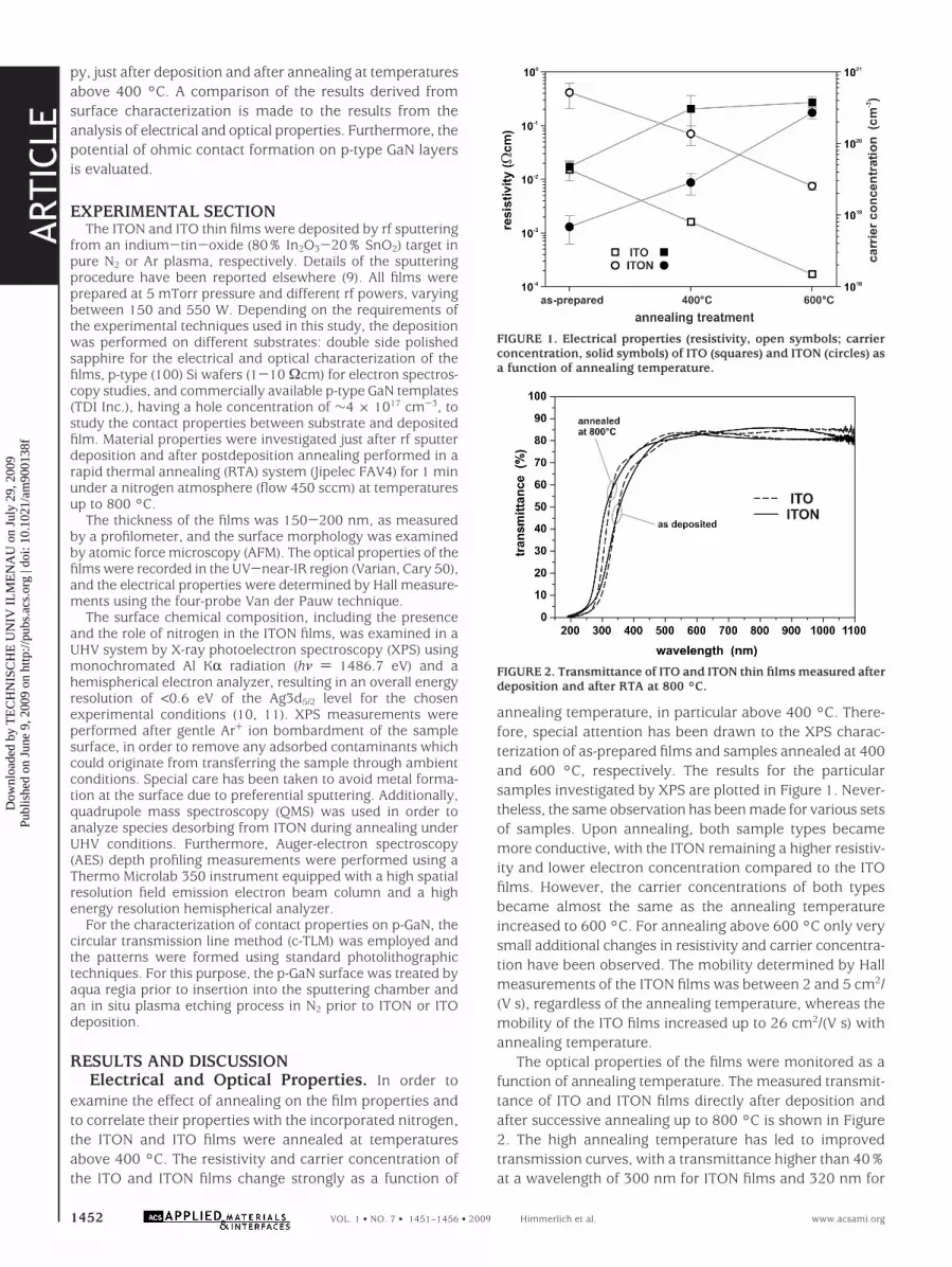
annealing temperature, in particular above 400 °C. There-fore, special attention has been drawn to the XPS charac-terization of as-prepared films and samples annealed at 400and 600 °C, respectively. The results for the particularsamples investigated by XPS are plotted in Figure 1. Never-theless, the same observation has been made for various setsof samples. Upon annealing, both sample types becamemore conductive, with the ITON remaining a higher resistiv-ity and lower electron concentration compared to the ITOfilms. However, the carrier concentrations of both typesbecame almost the same as the annealing temperatureincreased to 600 °C. For annealing above 600 °C only verysmall additional changes in resistivity and carrier concentra-tion have been observed. The mobility determined by Hallmeasurements of the ITON films was between 2 and 5 cm2/(V s), regardless of the annealing temperature, whereas themobility of the ITO films increased up to 26 cm2/(V s) withannealing temperature.
The optical properties of the films were monitored as afunction of annealing temperature. The measured transmit-tance of ITO and ITON films directly after deposition andafter successive annealing up to 800 °C is shown in Figure2. The high annealing temperature has led to improvedtransmission curves, with a transmittance higher than 40%at a wavelength of 300 nm for ITON films and 320 nm for
FIGURE 1. Electrical properties (resistivity, open symbols; carrierconcentration, solid symbols) of ITO (squares) and ITON (circles) asa function of annealing temperature.
FIGURE 2. Transmittance of ITO and ITON thin films measured afterdeposition and after RTA at 800 °C.
ARTIC
LE
1452 VOL. 1 • NO. 7 • 1451–1456 • 2009 Himmerlich et al. www.acsami.org
Dow
nloa
ded
by T
EC
HN
ISC
HE
UN
IV I
LM
EN
AU
on
July
29,
200
9Pu
blis
hed
on J
une
9, 2
009
on h
ttp://
pubs
.acs
.org
| do
i: 10
.102
1/am
9001
38f
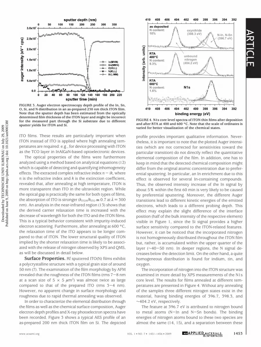
ITO films. These results are particularly important whenITON instead of ITO is applied where high annealing tem-peratures are required: e.g., for device processing with ITONas the TCO layer in InAlGaN-based optoelectronic devices.
The optical properties of the films were furthermoreanalyzed using a method based on analytical equations (12)which is capable of detecting and quantifying inhomogeneityeffects. The extracted complex refractive index n- ik, wheren is the refractive index and k is the extinction coefficient,revealed that, after annealing at high temperature, ITON ismore transparent than ITO in the ultraviolet region. Whilethe optical gap is practically the same for both types of films,the absorption of ITO is stronger (kITON/kITO = 0.7 at λ ) 300nm). An analysis in the near-infrared region (13) shows thatthe derived carrier relaxation time is increased with thedecrease of wavelength for both the ITO and the ITON films.This is a typical behavior consistent with impurity-inducedelectron scattering. Furthermore, after annealing at 600 °C,the relaxation time of the ITO appears to be longer com-pared to that of ITON. The lower structural quality of ITONimplied by the shorter relaxation time is likely to be associ-ated with the release of nitrogen observed by XPS and QMS,as will be discussed in detail below.
Surface Properties. Rf sputtered ITO(N) films exhibita polycrystalline structure with a typical grain size of around50 nm (7). The examination of the film morphology by AFMrevealed that the roughness of the ITON films (rms 7-8 nmat a scan size of 5 × 5 µm2) was almost twice as largecompared to that of the prepared ITO (rms 3-4 nm).However, no apparent change in surface morphology androughness due to rapid thermal annealing was observed.
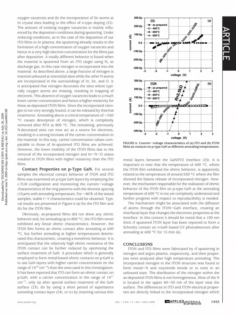
In order to characterize the elemental distribution throughthe films as well as the chemical surface composition, Augerelectron depth profiles and X-ray photoelectron spectra havebeen recorded. Figure 3 shows a typical AES profile of anas-prepared 200 nm thick ITON film on Si. The depicted
profile provides important qualitative information. Never-theless, it is important to note that the plotted Auger intensi-ties (which are not corrected for sensitivities toward theparticular transition) do not directly reflect the quantitativeelemental composition of the film. In addition, one has tokeep in mind that the detected chemical composition mightdiffer from the original atomic concentration due to prefer-ential sputtering. In particular, an In enrichment due to thiseffect is observed for several In-containing compounds.Thus, the observed intensity increase of the In signal byabout 5% within the first 60 min is very likely to be causedby preferential sputtering. Moreover, the different Augertransitions lead to different kinetic energies of the emittedelectrons, which leads to a different probing depth. Thiseffect may explain the slight difference of the interfaceposition (half of the bulk intensity of the respective element)visible in Figure 1, since the Si signal provides a highersurface sensitivity compared to the ITON-related features.However, it can be noticed that the incorporated nitrogenis not homogeneously distributed throughout the ITON filmbut, rather, is accumulated within the upper quarter of thelayer (∼40-50 nm). In deeper regions, the N signal de-creases below the detection limit. On the other hand, a quitehomogeneous distribution is found for indium, tin, andoxygen.
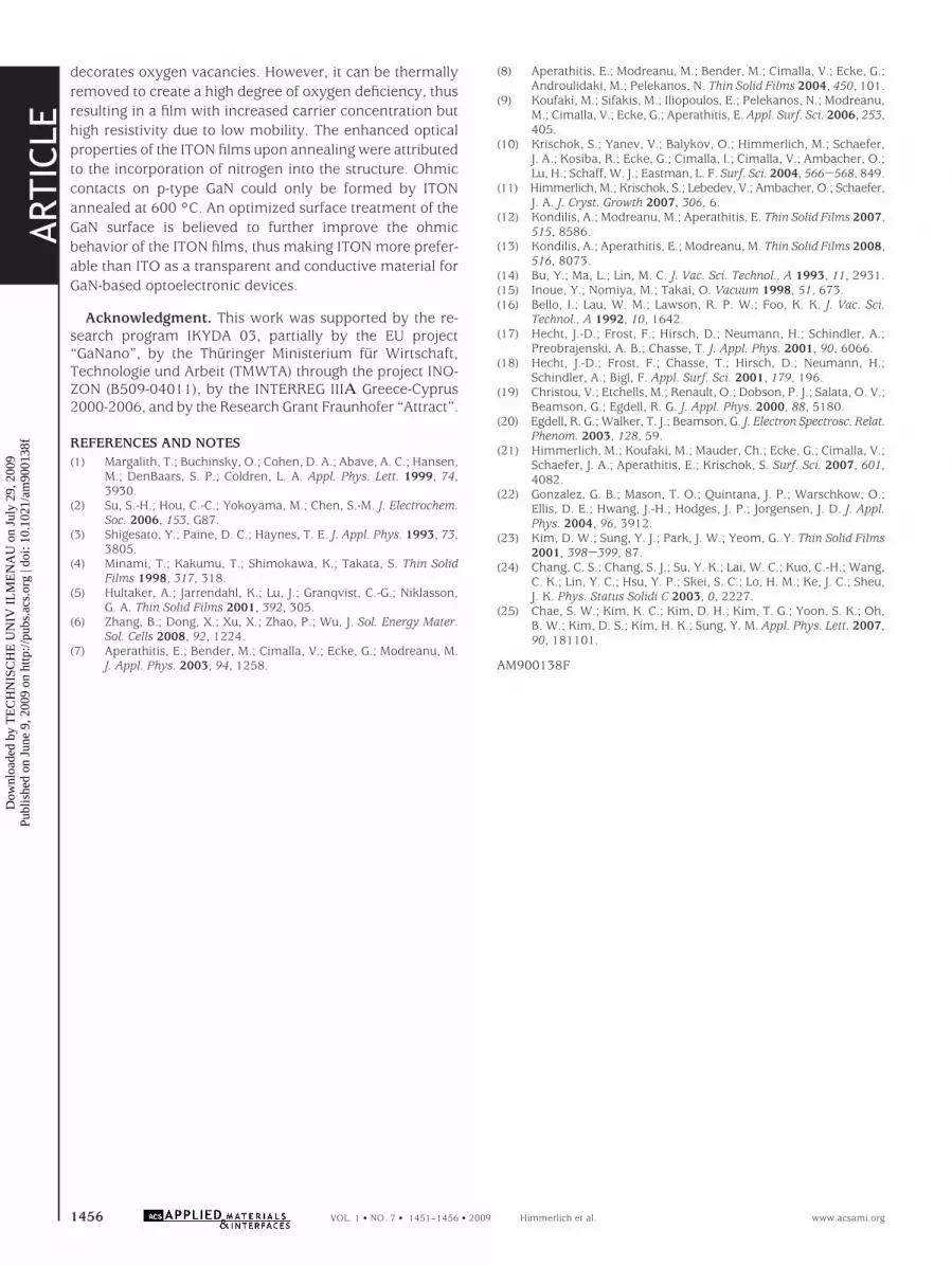
The incorporation of nitrogen into the ITON structure wasexamined in more detail by XPS measurements of the N1score level. The results for films annealed at different tem-peratures are presented in Figure 4. Without any annealingof the samples three different nitrogen states exist in thematerial, having binding energies of 396.7, 398.3, and∼404.2 eV, respectively.
The feature at 396.7 eV is attributed to nitrogen boundto metal atoms (N-In and N-Sn bonds). The bindingenergies of nitrogen atoms bound to these two species arealmost the same (14, 15), and a separation between these
FIGURE 3. Auger electron spectroscopy depth profile of the In, Sn,O, Si, and N distribution in an as-prepared 230 nm thick ITON film.Note that the sputter depth has been estimated from the opticallydetermined film thickness of the ITON layer and might be incorrectfor the measured part through the Si substrate due to differentsputter yields for ITON and Si.
FIGURE 4. N1s core level spectra of ITON thin films after depositionand after RTA at 400 and 600 °C. Note that the scale of ordinates isvaried for better visualization of the chemical states.
ARTIC
LE
www.acsami.org VOL. 1 • NO. 7 • 1451–1456 • 2009 1453
Dow
nloa
ded
by T
EC
HN
ISC
HE
UN
IV I
LM
EN
AU
on
July
29,
200
9Pu
blis
hed
on J
une
9, 2
009
on h
ttp://
pubs
.acs
.org
| do
i: 10
.102
1/am
9001
38f

two contributions is therefore beyond the energy resolutionof the measurement. The second feature at 398.3 eV is foundto originate from oxynitride bonds (16), where oxygen aswell as metal atoms are located in the surroundings of thenitrogen atom (InNxOy). Typical N-O bonds located at 400.0eV were found only on as-loaded samples, prior to the ionbombardment procedure (not shown). They are caused byoxidation of the surface under ambient conditions and canbe easily removed by gentle sputteringswhich has beenperformed in order to remove surface adsorbates and toavoid changes in composition due to preferential sputtering.The peak at 404.2 eV may be caused by two possiblesources: (a) NO2 bonds or (b) unbound nitrogen incorporatedinto the crystal structure. Since the rf sputtering process isperformed in nitrogen plasma and no additional structureis detected in the O1s signal, we assign the feature at 404.2eV to incorporated unbound nitrogen that has been formeddue to the harsh deposition conditions. It is believed that theunbound nitrogen is mostly located at interstitial sites,similar to reports on the nitridation of III-V semiconductorsurfaces (17, 18).
For a quantification of the amount of inserted nitrogenin the near surface region, the core level spectra were fittedusing Gauss-Lorentz functions, after removal of a Shirley-type background. Under the assumption of a homogeneousdistribution of all detected elements through the depthprobed by the XPS measurement (more than 90% of theXPS signal originates from the top 5-6 nm of the film), theelemental proportion of nitrogen was calculated. As seen inFigure 4, in addition to a small reduction of the total nitrogenconcentration from 10% to 9.3%, no changes concerningthe nitrogen states were observed after annealing at 400 °C.This aspect changes drastically after annealing at 600 °C.The state at 404.2 eV disappeared completely as well asalmost the entire oxynitride component and parts of themetal-N signal, reducing the total N content to 1.6%.Finally, after RTA at 800 °C the amount of incorporatednitrogen is below the detection limit of XPS.
QMS measurements during heating under UHV condi-tions were performed to analyze the temperature-dependentdesorption of molecules from the film in situ by measuringthe gas composition in the chamber. At temperatures above550 °C a strong release of molecular nitrogen was observed,while at the same time only minor desorption of N2O wasdetected. Furthermore, no release of NO, NO2, or O2 wasdetected. This finding is in very good agreement with theRTA-induced changes in the N1s signal observed by XPS.
Additionally, more information about the films after theirannealing can be extracted by evaluating the core level peakshape. The as-deposited and the 400 °C annealed ITONsamples exhibit narrow symmetric core level peaks atbinding energies (BE) of 444.7, 486.5, and 530.2 eV forIn3d5/2, Sn3d5/2, and O1s, respectively (not shown). For ITONfilms that have been annealed at T g 600 °C, as well as forall ITO films, independent of sample treatment, all core levelpeaks are broadened and exhibit an asymmetric peak shape,as exemplified for the In3d5/2 core level in Figure 5. Sum-
marizing extensive studies on ITO(N) films prepared be-tween 150 and 550 W rf power, the asymmetry of the corelevels appears for samples that have a relatively high carrierconcentration.
According to previous reports (19, 20) this observationis explained by the response of the conduction electrons tothe ionized atoms generated during the photoelectron emis-sion process, which results in a splitting of the signal into ascreened and an unscreened final state (19, 20). The peakshape of the unscreened contribution at higher bindingenergy is much broader compared to the screened one,since it involves excitation of plasmons. This intrinsic plas-mon excitation is coupled with a certain relaxation rate, andas a result lifetime broadening of this contribution is ex-pected, resulting in a Lorentzian peak profile. Hence, ad-vancing the data analysis compared to the results in ref 21,where a fixed G/L ratio was assumed, resulting in a shift of0.9 eV, and taking the different peak shapes for bothcomponents into account for fitting, the separation of thetwo components is only 0.45 eV, as shown in Figure 5. Notethat the two different peaks, indicated in Figure 5, are notrelated to two different chemical In states but correspondto screened and unscreened final states. Following the modelapproach of ref 19, the energy separation corresponds toan estimated carrier concentration of 2 × 1020 cm-3, whichis in good agreement with the results from Hall measure-ments (see Figure 1). An analysis of the peak shape of ITONfilms annealed at various annealing temperatures leads tothe conclusion that RTA at Tg 600 °C results in an increasein the carrier concentration by about 1 order of magnitude,approaching the values for ITO that has been prepared inthe same system using Ar as process gas. This effect isaccompanied by segregation of Sn toward the surface, whichhas already been discussed in detail elsewhere for the ITONfilms (21).
The high electron concentration in indium-tin-oxide iscaused by two factors: (a) the existence of a high content of
FIGURE 5. In3d5/2 core level spectra of ITON thin films after deposi-tion and after RTA at 600 °C.
ARTIC
LE
1454 VOL. 1 • NO. 7 • 1451–1456 • 2009 Himmerlich et al. www.acsami.org
Dow
nloa
ded
by T
EC
HN
ISC
HE
UN
IV I
LM
EN
AU
on
July
29,
200
9Pu
blis
hed
on J
une
9, 2
009
on h
ttp://
pubs
.acs
.org
| do
i: 10
.102
1/am
9001
38f
oxygen vacancies and (b) the incorporation of Sn atoms atIn crystal sites leading to the effect of n-type doping (22).The amount of existing oxygen vacancies is mainly influ-enced by the deposition conditions during sputtering. Underreducing conditions, as in the case of the deposition of ourITO films in Ar plasma, the sputtering already results in theformation of a high concentration of oxygen vacancies andhence in a very high electron concentration for the films justafter deposition. A totally different behavior is found whenthe material is sputtered from an ITO target using N2 asdischarge gas. In this case nitrogen is incorporated into thematerial. As described above, a large fraction of nitrogen isinserted unbound at interstitial sites while the other N atomsare incorporated in the surroundings of In, Sn, and O. Itis anticipated that nitrogen decorates the sites where typi-cally oxygen atoms are missing, resulting in trapping ofelectrons. This absence of oxygen vacancies leads to a muchlower carrier concentration and hence a higher resistivity forthese as-deposited ITON films. Since the incorporated nitro-gen is not very strongly bound, it can be released by thermaltreatments. Annealing above a critical temperature of ∼550°C causes desorption of nitrogen, which is completelyremoved after RTA at 800 °C. The remaining, previouslyN-decorated sites can now act as a source for electrons,resulting in a strong increase of the carrier concentration inthe material. In this way, carrier concentration values com-parable to those of Ar-sputtered ITO films are achieved.However, the lower mobility of the ITON films due to theremoval of the incorporated nitrogen and In-N-O statesresulted in ITON films with higher resistivity than the ITOfilms.
Contact Properties on p-Type GaN. For severalsamples the electrical contact behavior of ITON and ITOfilms was examined on p-type GaN layers by employing thec-TLM configuration and monitoring the current-voltagecharacteristics of the ring patterns with the shortest spacing(10 µm) with annealing temperature. For ∼80% of the testedsamples, stable I-V characteristics could be obtained. Typi-cal results are presented in Figure 6 (a) for the ITO film and(b) for the ITON film.
Obviously, as-prepared films did not show any ohmicbehavior and, for annealing up to 800 °C, the ITO film neverexhibited any linear ohmic characteristics. However, theITON film forms an ohmic contact after annealing at 600°C, but further annealing at higher temperatures deterio-rated this characteristic, creating a nonohmic behavior. It isanticipated that the relatively high ohmic resistance of theITON contact can be further reduced by optimizing thesurface treatment of GaN. A procedure which is generallyemployed to form metal-based ohmic contacts on p-GaN isto use GaN layers with higher carrier concentration (in therange of 1018 cm-3) than the ones used in this investigation.It has been reported that ITO can form an ohmic contact onp-GaN, with a carrier concentration in the range of 1017
cm-3, only (a) after special surface treatment of the GaNsurface (23), (b) by using a short period of superlatticetunneling contact layer (24), or (c) by inserting various thin
metal layers between the GaN/ITO interface (25). It isimportant to note that the temperature of 600 °C, wherethe ITON film exhibited the ohmic behavior, is apparentlyrelated to the temperature of around 550 °C where the filmshowed the fastest release of incorporated nitrogen. How-ever, the mechanism responsible for the realization of ohmicbehavior of the ITON film on p-type GaN at the annealingtemperature of 600 °C is not yet completely understood andfurther progress with respect to reproducibility is needed.
The mechanism might be associated with the diffusionof atoms through the ITON-GaN interface, creating aninterfacial layer that changes the electronic properties at theinterface. In this context it should be noted that a 100 nmthick rf sputtered ITON layer has been reported to form aSchottky contact on n-GaN based UV photodetectors afterannealing at 600 °C for 15 min (6).
CONCLUSIONSITON and ITO films were fabricated by rf sputtering in
nitrogen and argon plasma, respectively, and their proper-ties were analyzed after high temperature annealing. Theincorporated nitrogen in the ITON structure was found toform metal-N and oxynitride bonds or to exist in anunbound state. The distribution of the nitrogen within theas-deposited ITON films is not homogeneous. Most of the Nis located in the upper 40-50 nm of the layer near thesurface. The differences in ITO and ITON electrical proper-ties are directly linked to the incorporated nitrogen which
FIGURE 6. Current-voltage characteristics of (a) ITO and (b) ITONfilms as contacts on p-type GaN at different annealing temperatures.
ARTIC
LE
www.acsami.org VOL. 1 • NO. 7 • 1451–1456 • 2009 1455
Dow
nloa
ded
by T
EC
HN
ISC
HE
UN
IV I
LM
EN
AU
on
July
29,
200
9Pu
blis
hed
on J
une
9, 2
009
on h
ttp://
pubs
.acs
.org
| do
i: 10
.102
1/am
9001
38f
decorates oxygen vacancies. However, it can be thermallyremoved to create a high degree of oxygen deficiency, thusresulting in a film with increased carrier concentration buthigh resistivity due to low mobility. The enhanced opticalproperties of the ITON films upon annealing were attributedto the incorporation of nitrogen into the structure. Ohmiccontacts on p-type GaN could only be formed by ITONannealed at 600 °C. An optimized surface treatment of theGaN surface is believed to further improve the ohmicbehavior of the ITON films, thus making ITON more prefer-able than ITO as a transparent and conductive material forGaN-based optoelectronic devices.
Acknowledgment. This work was supported by the re-search program IKYDA 03, partially by the EU project“GaNano”, by the Thuringer Ministerium fur Wirtschaft,Technologie und Arbeit (TMWTA) through the project INO-ZON (B509-04011), by the INTERREG IIIΑ Greece-Cyprus2000-2006, and by the Research Grant Fraunhofer “Attract”.
REFERENCES AND NOTES(1) Margalith, T.; Buchinsky, O.; Cohen, D. A.; Abave, A. C.; Hansen,
M.; DenBaars, S. P.; Coldren, L. A. Appl. Phys. Lett. 1999, 74,3930.
(2) Su, S.-H.; Hou, C.-C.; Yokoyama, M.; Chen, S.-M. J. Electrochem.Soc. 2006, 153, G87.
(3) Shigesato, Y.; Paine, D. C.; Haynes, T. E. J. Appl. Phys. 1993, 73,3805.
(4) Minami, T.; Kakumu, T.; Shimokawa, K.; Takata, S. Thin SolidFilms 1998, 317, 318.
(5) Hultaker, A.; Jarrendahl, K.; Lu, J.; Granqvist, C.-G.; Niklasson,G. A. Thin Solid Films 2001, 392, 305.
(6) Zhang, B.; Dong, X.; Xu, X.; Zhao, P.; Wu, J. Sol. Energy Mater.Sol. Cells 2008, 92, 1224.
(7) Aperathitis, E.; Bender, M.; Cimalla, V.; Ecke, G.; Modreanu, M.J. Appl. Phys. 2003, 94, 1258.
(8) Aperathitis, E.; Modreanu, M.; Bender, M.; Cimalla, V.; Ecke, G.;Androulidaki, M.; Pelekanos, N. Thin Solid Films 2004, 450, 101.
(9) Koufaki, M.; Sifakis, M.; Iliopoulos, E.; Pelekanos, N.; Modreanu,M.; Cimalla, V.; Ecke, G.; Aperathitis, E. Appl. Surf. Sci. 2006, 253,405.
(10) Krischok, S.; Yanev, V.; Balykov, O.; Himmerlich, M.; Schaefer,J. A.; Kosiba, R.; Ecke, G.; Cimalla, I.; Cimalla, V.; Ambacher, O.;Lu, H.; Schaff, W. J.; Eastman, L. F. Surf. Sci. 2004, 566-568, 849.
(11) Himmerlich, M.; Krischok, S.; Lebedev, V.; Ambacher, O.; Schaefer,J. A. J. Cryst. Growth 2007, 306, 6.
(12) Kondilis, A.; Modreanu, M.; Aperathitis, E. Thin Solid Films 2007,515, 8586.
(13) Kondilis, A.; Aperathitis, E.; Modreanu, M. Thin Solid Films 2008,516, 8073.
(14) Bu, Y.; Ma, L.; Lin, M. C. J. Vac. Sci. Technol., A 1993, 11, 2931.(15) Inoue, Y.; Nomiya, M.; Takai, O. Vacuum 1998, 51, 673.(16) Bello, I.; Lau, W. M.; Lawson, R. P. W.; Foo, K. K. J. Vac. Sci.
Technol., A 1992, 10, 1642.(17) Hecht, J.-D.; Frost, F.; Hirsch, D.; Neumann, H.; Schindler, A.;
Preobrajenski, A. B.; Chasse, T. J. Appl. Phys. 2001, 90, 6066.(18) Hecht, J.-D.; Frost, F.; Chasse, T.; Hirsch, D.; Neumann, H.;
Schindler, A.; Bigl, F. Appl. Surf. Sci. 2001, 179, 196.(19) Christou, V.; Etchells, M.; Renault, O.; Dobson, P. J.; Salata, O. V.;
Beamson, G.; Egdell, R. G. J. Appl. Phys. 2000, 88, 5180.(20) Egdell, R. G.; Walker, T. J.; Beamson, G. J. Electron Spectrosc. Relat.
Phenom. 2003, 128, 59.(21) Himmerlich, M.; Koufaki, M.; Mauder, Ch.; Ecke, G.; Cimalla, V.;
Schaefer, J. A.; Aperathitis, E.; Krischok, S. Surf. Sci. 2007, 601,4082.
(22) Gonzalez, G. B.; Mason, T. O.; Quintana, J. P.; Warschkow, O.;Ellis, D. E.; Hwang, J.-H.; Hodges, J. P.; Jorgensen, J. D. J. Appl.Phys. 2004, 96, 3912.
(23) Kim, D. W.; Sung, Y. J.; Park, J. W.; Yeom, G. Y. Thin Solid Films2001, 398-399, 87.
(24) Chang, C. S.; Chang, S. J.; Su, Y. K.; Lai, W. C.; Kuo, C.-H.; Wang,C. K.; Lin, Y. C.; Hsu, Y. P.; Skei, S. C.; Lo, H. M.; Ke, J. C.; Sheu,J. K. Phys. Status Solidi C 2003, 0, 2227.
(25) Chae, S. W.; Kim, K. C.; Kim, D. H.; Kim, T. G.; Yoon, S. K.; Oh,B. W.; Kim, D. S.; Kim, H. K.; Sung, Y. M. Appl. Phys. Lett. 2007,90, 181101.
AM900138F
ARTIC
LE
1456 VOL. 1 • NO. 7 • 1451–1456 • 2009 Himmerlich et al. www.acsami.org
Dow
nloa
ded
by T
EC
HN
ISC
HE
UN
IV I
LM
EN
AU
on
July
29,
200
9Pu
blis
hed
on J
une
9, 2
009
on h
ttp://
pubs
.acs
.org
| do
i: 10
.102
1/am
9001
38f