Effect of annealing on the growth dynamics of ZnPc LB thin film and its surface morphology
15
Effect of annealing on the growth dynamics of ZnPc LB thin film and its surface morphology Dhrubojyoti Roy, Nayan Mani Das, and P. S. Gupta Citation: AIP Advances 4, 077126 (2014); doi: 10.1063/1.4891177 View online: http://dx.doi.org/10.1063/1.4891177 View Table of Contents: http://scitation.aip.org/content/aip/journal/adva/4/7?ver=pdfcov Published by the AIP Publishing Articles you may be interested in Impact of annealing on the chemical structure and morphology of the thin-film CdTe/ZnO interface J. Appl. Phys. 116, 024312 (2014); 10.1063/1.4890235 Catalyst free growth of ZnO nanorods by thermal evaporation method AIP Conf. Proc. 1536, 125 (2013); 10.1063/1.4810132 Influence of anneal atmosphere on ZnO-nanorod photoluminescent and morphological properties with self- powered photodetector performance J. Appl. Phys. 113, 204501 (2013); 10.1063/1.4805349 Texture vs morphology in ZnO nano-rods: On the x-ray diffraction characterization of electrochemically grown samples J. Appl. Phys. 110, 124901 (2011); 10.1063/1.3669026 Effect of annealing on the microstructure and optical properties of ZnO / V 2 O 5 composite Appl. Phys. Lett. 98, 111904 (2011); 10.1063/1.3566997 All article content, except where otherwise noted, is licensed under a Creative Commons Attribution 3.0 Unported license. See: http://creativecommons.org/licenses/by/3.0/ Downloaded to IP: 125.20.9.226 On: Tue, 22 Jul 2014 13:30:15
-
Upload
ismdhanbad -
Category
Documents
-
view
0 -
download
0
Transcript of Effect of annealing on the growth dynamics of ZnPc LB thin film and its surface morphology
Effect of annealing on the growth dynamics of ZnPc LB thin film and its surfacemorphologyDhrubojyoti Roy, Nayan Mani Das, and P. S. Gupta
Citation: AIP Advances 4, 077126 (2014); doi: 10.1063/1.4891177 View online: http://dx.doi.org/10.1063/1.4891177 View Table of Contents: http://scitation.aip.org/content/aip/journal/adva/4/7?ver=pdfcov Published by the AIP Publishing Articles you may be interested in Impact of annealing on the chemical structure and morphology of the thin-film CdTe/ZnO interface J. Appl. Phys. 116, 024312 (2014); 10.1063/1.4890235 Catalyst free growth of ZnO nanorods by thermal evaporation method AIP Conf. Proc. 1536, 125 (2013); 10.1063/1.4810132 Influence of anneal atmosphere on ZnO-nanorod photoluminescent and morphological properties with self-powered photodetector performance J. Appl. Phys. 113, 204501 (2013); 10.1063/1.4805349 Texture vs morphology in ZnO nano-rods: On the x-ray diffraction characterization of electrochemically grownsamples J. Appl. Phys. 110, 124901 (2011); 10.1063/1.3669026 Effect of annealing on the microstructure and optical properties of ZnO / V 2 O 5 composite Appl. Phys. Lett. 98, 111904 (2011); 10.1063/1.3566997
All article content, except where otherwise noted, is licensed under a Creative Commons Attribution 3.0 Unported license. See: http://creativecommons.org/licenses/by/3.0/
Downloaded to IP: 125.20.9.226 On: Tue, 22 Jul 2014 13:30:15
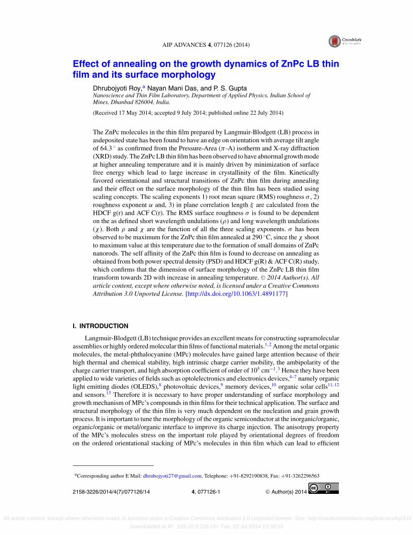
AIP ADVANCES 4, 077126 (2014)
Effect of annealing on the growth dynamics of ZnPc LB thinfilm and its surface morphology
Dhrubojyoti Roy,a Nayan Mani Das, and P. S. GuptaNanoscience and Thin Film Laboratory, Department of Applied Physics, Indian School ofMines, Dhanbad 826004, India.
(Received 17 May 2014; accepted 9 July 2014; published online 22 July 2014)
The ZnPc molecules in the thin film prepared by Langmuir-Blodgett (LB) process inasdeposited state has been found to have an edge on orientation with average tilt angleof 64.3 ◦ as confirmed from the Pressure-Area (π -A) isotherm and X-ray diffraction(XRD) study. The ZnPc LB thin film has been observed to have abnormal growth modeat higher annealing temperature and it is mainly driven by minimization of surfacefree energy which lead to large increase in crystallinity of the film. Kineticallyfavored orientational and structural transitions of ZnPc thin film during annealingand their effect on the surface morphology of the thin film has been studied usingscaling concepts. The scaling exponents 1) root mean square (RMS) roughness σ , 2)roughness exponent α and, 3) in plane correlation length ξ are calculated from theHDCF g(r) and ACF C(r). The RMS surface roughness σ is found to be dependenton the as defined short wavelength undulations (ρ) and long wavelength undulations(χ ). Both ρ and χ are the function of all the three scaling exponents. σ has beenobserved to be maximum for the ZnPc thin film annealed at 290 ◦C, since the χ shootto maximum value at this temperature due to the formation of small domains of ZnPcnanorods. The self affinity of the ZnPc thin film is found to decrease on annealing asobtained from both power spectral density (PSD) and HDCF g(R) & ACF C(R) study,which confirms that the dimension of surface morphology of the ZnPc LB thin filmtransform towards 2D with increase in annealing temperature. C© 2014 Author(s). Allarticle content, except where otherwise noted, is licensed under a Creative CommonsAttribution 3.0 Unported License. [http://dx.doi.org/10.1063/1.4891177]
I. INTRODUCTION
Langmuir-Blodgett (LB) technique provides an excellent means for constructing supramolecularassemblies or highly ordered molecular thin films of functional materials.1, 2 Among the metal organicmolecules, the metal-phthalocyanine (MPc) molecules have gained large attention because of theirhigh thermal and chemical stability, high intrinsic charge carrier mobility, the ambipolarity of thecharge carrier transport, and high absorption coefficient of order of 105 cm−1.3 Hence they have beenapplied to wide varieties of fields such as optolelectronics and electronics devices,4–7 namely organiclight emitting diodes (OLEDS),8 photovoltaic devices,9 memory devices,10 organic solar cells11, 12
and sensors.13 Therefore it is necessary to have proper understanding of surface morphology andgrowth mechanism of MPc’s compounds in thin films for their technical application. The surface andstructural morphology of the thin film is very much dependent on the nucleation and grain growthprocess. It is important to tune the morphology of the organic semiconductor at the inorganic/organic,organic/organic or metal/organic interface to improve its charge injection. The anisotropy propertyof the MPc’s molecules stress on the important role played by orientational degrees of freedomon the ordered orientational stacking of MPc’s molecules in thin film which can lead to efficient
aCorresponding author E Mail: [email protected], Telephone: +91-8292190838, Fax: +91-3262296563
2158-3226/2014/4(7)/077126/14 C© Author(s) 20144, 077126-1
All article content, except where otherwise noted, is licensed under a Creative Commons Attribution 3.0 Unported license. See: http://creativecommons.org/licenses/by/3.0/
Downloaded to IP: 125.20.9.226 On: Tue, 22 Jul 2014 13:30:15
077126-2 ROY, Das, and Gupta AIP Advances 4, 077126 (2014)
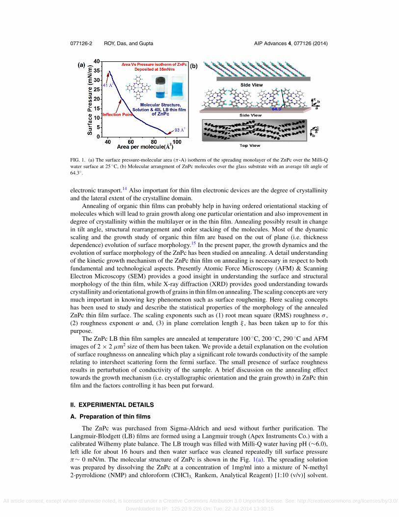
FIG. 1. (a) The surface pressure-molecular area (π -A) isotherm of the spreading monolayer of the ZnPc over the Milli-Qwater surface at 25 ◦C, (b) Molecular arrangment of ZnPc molecules over the glass substrate with an average tilt angle of64.3◦.
electronic transport.14 Also important for thin film electronic devices are the degree of crystallinityand the lateral extent of the crystalline domain.
Annealing of organic thin films can probably help in having ordered orientational stacking ofmolecules which will lead to grain growth along one particular orientation and also improvement indegree of crystallinity within the multilayer or in the thin film. Annealing possibly result in changein tilt angle, structural rearrangement and order stacking of the molecules. Most of the dynamicscaling and the growth study of organic thin film are based on the out of plane (i.e. thicknessdependence) evolution of surface morphology.15 In the present paper, the growth dynamics and theevolution of surface morphology of the ZnPc has been studied on annealing. A detail understandingof the kinetic growth mechanism of the ZnPc thin film on annealing is necessary in respect to bothfundamental and technological aspects. Presently Atomic Force Microscopy (AFM) & ScanningElectron Microscopy (SEM) provides a good insight in understanding the surface and structuralmorphology of the thin film, while X-ray diffraction (XRD) provides good understanding towardscrystallinity and orientational growth of grains in thin film on annealing. The scaling concepts are verymuch important in knowing key phenomenon such as surface roughening. Here scaling conceptshas been used to study and describe the statistical properties of the morphology of the annealedZnPc thin film surface. The scaling exponents such as (1) root mean square (RMS) roughness σ ,(2) roughness exponent α and, (3) in plane correlation length ξ , has been taken up to for thispurpose.
The ZnPc LB thin film samples are annealed at temperature 100 ◦C, 200 ◦C, 290 ◦C and AFMimages of 2 × 2 μm2 size of them has been taken. We provide a detail explanation on the evolutionof surface roughnesss on annealing which play a significant role towards conductivity of the samplerelating to intersheet scattering form the fermi surface. The small presence of surface roughnessresults in perturbation of conductivity of the sample. A brief discussion on the annealing effecttowards the growth mechanism (i.e. crystallographic orientation and the grain growth) in ZnPc thinfilm and the factors controlling it has been put forward.
II. EXPERIMENTAL DETAILS
A. Preparation of thin films
The ZnPc was purchased from Sigma-Aldrich and uesd without further purification. TheLangmuir-Blodgett (LB) films are formed using a Langmuir trough (Apex Instruments Co.) with acalibrated Wilhemy plate balance. The LB trough was filled with Milli-Q water having pH (∼6.0),left idle for about 16 hours and then water surface was cleaned repeatedly till surface pressureπ∼ 0 mN/m. The molecular structure of ZnPc is shown in the Fig. 1(a). The spreading solutionwas prepared by dissolving the ZnPc at a concentration of 1mg/ml into a mixture of N-methyl2-pyrroldione (NMP) and chloroform (CHCl3, Rankem, Analytical Reagent) [1:10 (v/v)] solvent.
All article content, except where otherwise noted, is licensed under a Creative Commons Attribution 3.0 Unported license. See: http://creativecommons.org/licenses/by/3.0/
Downloaded to IP: 125.20.9.226 On: Tue, 22 Jul 2014 13:30:15
077126-3 ROY, Das, and Gupta AIP Advances 4, 077126 (2014)
Then 250 μL solution was spread using a microliter syringe over the water subphase and the solventwas allowed to evaporate for 10–15 min before compression. The spread monolayer over water sur-face was then compressed at a rate of 5 mm/min till the surface pressure attains π∼35 mN/m, thenthe film was subsequently transferred at this pressure. Deposition using the vertical dipping methodwas conducted at a temperature of about 27 oC and at 4 mm/min dipping speed for subsequentup-down strokes of substrate through the air-water interface. Drying time for first up stroke was kept20 min and then for each subsequent upstroke i.e. above subphase was kept 10 min and similarly fordownstroke i.e. below subphase was 5 min. A multilayer film of 40 L ZnPc was deposited on glasssubstrate.
For required structural study of the films X-ray diffraction measurements are performed usingBruker D8 Advance X-ray diffractometer which uses Cu-Kα radiation (λ = 1.543 Å) and a fastcounting detector based on Silicon strip technology (Bruker Lynx Eye detector). Atomic forcemicroscopy (Digital Instruments Nanoscope-IV, with Si3N4 100 μm cantilever, 0.56 N/m forceconstant) study was done to observe the morphological and structural details in contact mode.FESEM (model: Supra 55, Germany, operating voltage 1 kV and 2 kV) was used to record scanningelectron micrograph images of ZnPc LB thin films.
B. Surface morphology study
The surfaces of all deposited films are not ideally smooth and hence they show out-of-planefluctuations, which are measured as roughness σ = 〈[h(x,y) – 〈h〉]2〉1/2, where h(x,y) is the height atpoint (x, y) with respect to mean height 〈z〉. For isotropic rough surfaces, it is also usual to expressthe out-of-plane fluctuations as height difference correlation function (HDCF) g(r), which correlatestwo point heights of two different point on the surface as g(R) = 〈[h(x .y) − h(x ′, y′)]2〉 the pairs ofpoints are laterally separated by R =
√(x − x ′)2 − (y − y′)2 and 〈 〉 denotes the ensemble average
over all possible roughness configurations.16 g(r) shows two different characteristic behavior whichdepends on the relative magnitudes of R and the correlation length ξ , i.e.17
For R � ξ, g(R) = a2R2α (1a)
where ξ is the lateral correlation length which is defined as the largest distance in which the heightis still correlated, and it is expected that it be a power law increase, here a is a typical surface slopeand α is a static roughness exponent and it must lie between 0 to 1, whereas α > 1 is physicallyimpossible because interface fluctuations cannot exceed the length scale of measurement. And
For R � ξ, the g(R) tend to saturate at a value g(R) = 2σ 2. (1b)
ξ provides the length scale to distinguish the short-range and long-range behaviors of the roughsurfaces. This kind of surface roughness is related to self affine surface which is defined by Mandel-brodt in terms of Brownian motion.16, 18 In this formalism α describes the fractal characteristics ofthe random surface and is related to Hausdorff dimension Df by Df = E + 1 – α, with E being thedimension of embedded space, E = 1 for line profile and E = 2 for plane.
Thus the self affine rough surface is characterized by the height difference correlation functionof the form
g (R) = 2σ 2 − 2〈h(x, y)h(x ′, y′)〉,where
⟨h (x, y) h
(x ′, y′)⟩ = C(R) is the autocorrelation function (ACF) and it is defined as
C (R) = σ 2exp
[−
(R
ξ
)]2α
, (2)
therefore,
g (R) = 2σ 20
[1 − exp
{−
(R
ξ
)}2α]
(3)
which is consistent with the asymptotic behavior in terms of eq. (1a).
All article content, except where otherwise noted, is licensed under a Creative Commons Attribution 3.0 Unported license. See: http://creativecommons.org/licenses/by/3.0/
Downloaded to IP: 125.20.9.226 On: Tue, 22 Jul 2014 13:30:15
077126-4 ROY, Das, and Gupta AIP Advances 4, 077126 (2014)
The g(R) can be evaluated from real space images by a spatial average over one or severalregions, which should be much larger than R to avoid edge effects. Large α value corresponds tolocally smooth surface and small α corresponds to locally jagged morphology. When α = 1, C(R)is the Gaussian function, representing random surfaces of Gaussian correlation.
Roughness exponent is calculated by fitting the straight line portion of the HDCF g(R) graph,where slope = 2α.
The ratio of RMS roughness amplitude σ (out-of-plane roughness) and in plane roughnesscorrelation length ξ i.e. σ /ξ , is a measure of slope of the long wavelength undulations on the surfaceand is also called the RMS long wavelength roughness ratio.18, 19 Similarly one can define slope ofshort wavelength undulation (i.e. slope sharp local irregularities) which is also called local surfaceslope ρ ∝ σ /ξα .
III. RESULTS AND DISCUSSION
A. Surface pressure- molecular area (π-A) isotherm of ZnPc.
The π -A isotherm of ZnPc monolayer spread over the water surface at 25 ◦C is shown inFig. 1(a). It is found that the compound form stable floating film at the air/water interface. The π -Aisotherm shown in Fig. 1(a) shows onset of the surface pressure, when the ZnPc molecules attainsan surface area of 93 Å2/molecule in the monolayer over water surface. On compression, the surfacepressure increases gradually upto 10 mN/m, and after this point it increases rapidly which suggestthe formation of the solid monolayer. An inflection point is observed at 19 mN/m which may bean indication of reorientation or certain kind of phase change of ZnPc molecules. From the π -Aisotherm (Fig. 1(a)), the limiting area per molecule of ZnPc was estimated to be 41.0 Å2/molecule atthe deposition pressure. This value is useful for estimating the configuration of ZnPc molecules at theair-water interface. ZnPc molecules have a planar geometry with square type structure (Fig. 1(b)), itsside length is 9.7 Å and diagonal length is 13.7 Å.20 When the molecules of ZnPc are densely stackedin a face-to-face orientation or edge-on to the water surface, the average area per molecule is foundto be approximately 33.0 Å2 (9.7 Å × 3.4 Å), assuming that the thickness of the ZnPc is 3.4 Å.21
However, if the molecules of ZnPc are laid down flat on the water surface, the average area permolecule would be approximately 94.4 Å2 (9.7 Å × 9.7 Å). The limiting area per molecule i.e.41.0 Å2, which is inbetween the area per molecule in edge-on and flat lying configuration. Therefore,it is resonable to consider that as an average the ZnPc molecules are in tilted arrangment over thewater surface in the monolayer. The average tilt angle is found to be 64.3 ◦ w.r.t. water surface. Wecan consider that the ZnPc molecules get deposited over the glass substrate in the same particulararrangement as in the monolayer over the water surface because of weak interacting property of theglass substrate. The schematic model of structural arrangement of ZnPc molecules over the glasssubstrate is shown in Fig. 1(b).
B. Growth mechanism of the asdeposited ZnPc LB thin film
In LB process, the ZnPc molecules to be deposited over the glass substrate is transferred to it atthe air-water-substrate contact line, one dimensional (1D) interface, and a considerable moleculararrangement takes place during this transfer.22, 23 Two Dimensional (2D) layer is formed by thistransferred molecules over the glass substrate and this molecules settles over the substrate throughdesorption process during drying time.23, 24
The molecular arrangements of the MPc molecules in the monolayer or multilayer’s with respectto the substrate surface critically depend on the relative strength of molecule-substrate interactionand the intermolecular interaction.25, 26 The weakly interacting substrates having small surface freeenergy (mainly oxides such as SiO2, Al2O3 and polymeric substrate), preferentially favors the uprightstanding growth of planar and nearly linear extended molecules for thin film deposition. Here, thevan der Waals and π -π interaction with neighbors is energetically preferred over the molecule-substrate interaction. In LB thin film probability of a monolayer growing with characteristic defectsincreases with increase in monolayer numbers.27, 28 As for initial grown monolayer’s the interactionwith the substrate is higher than the subsequent grown upper monolayer, therefore characteristic
All article content, except where otherwise noted, is licensed under a Creative Commons Attribution 3.0 Unported license. See: http://creativecommons.org/licenses/by/3.0/
Downloaded to IP: 125.20.9.226 On: Tue, 22 Jul 2014 13:30:15
077126-5 ROY, Das, and Gupta AIP Advances 4, 077126 (2014)
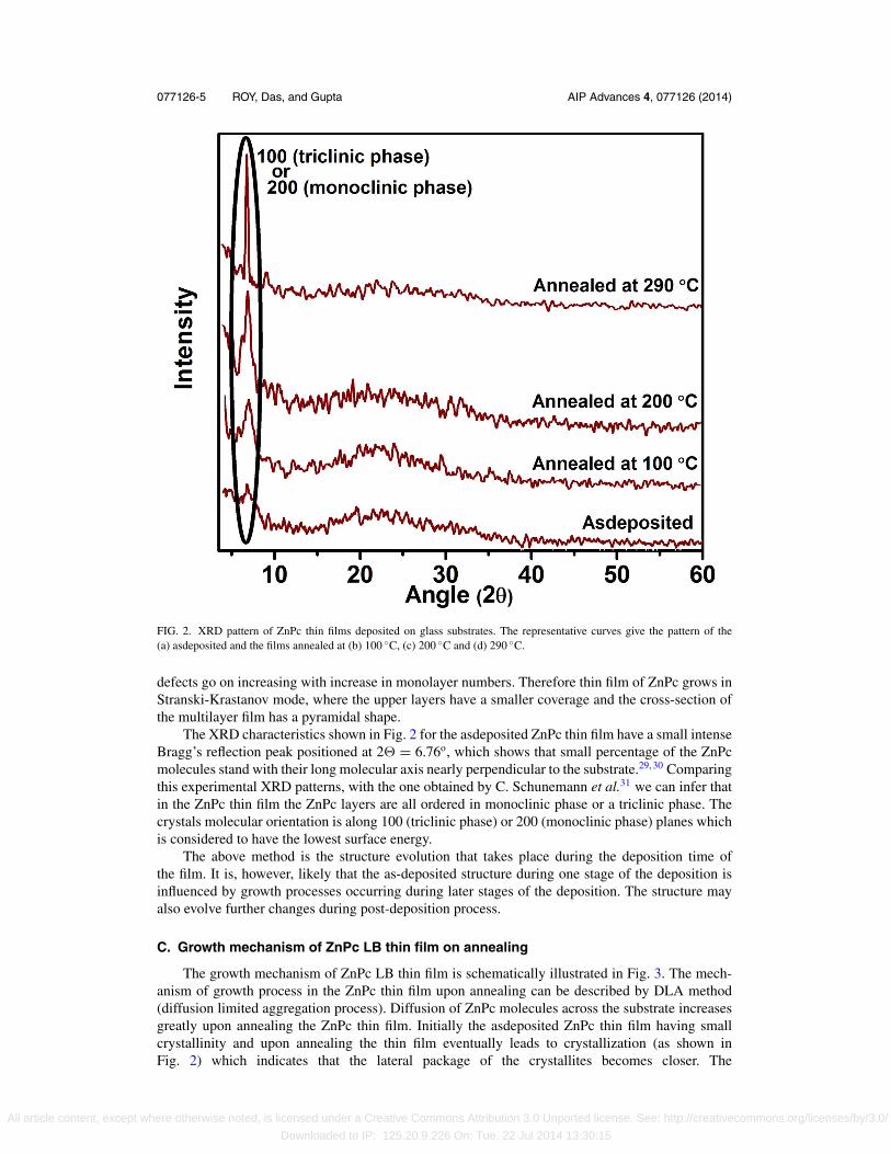
FIG. 2. XRD pattern of ZnPc thin films deposited on glass substrates. The representative curves give the pattern of the(a) asdeposited and the films annealed at (b) 100 ◦C, (c) 200 ◦C and (d) 290 ◦C.
defects go on increasing with increase in monolayer numbers. Therefore thin film of ZnPc grows inStranski-Krastanov mode, where the upper layers have a smaller coverage and the cross-section ofthe multilayer film has a pyramidal shape.
The XRD characteristics shown in Fig. 2 for the asdeposited ZnPc thin film have a small intenseBragg’s reflection peak positioned at 2 = 6.76o, which shows that small percentage of the ZnPcmolecules stand with their long molecular axis nearly perpendicular to the substrate.29, 30 Comparingthis experimental XRD patterns, with the one obtained by C. Schunemann et al.31 we can infer thatin the ZnPc thin film the ZnPc layers are all ordered in monoclinic phase or a triclinic phase. Thecrystals molecular orientation is along 100 (triclinic phase) or 200 (monoclinic phase) planes whichis considered to have the lowest surface energy.
The above method is the structure evolution that takes place during the deposition time ofthe film. It is, however, likely that the as-deposited structure during one stage of the deposition isinfluenced by growth processes occurring during later stages of the deposition. The structure mayalso evolve further changes during post-deposition process.
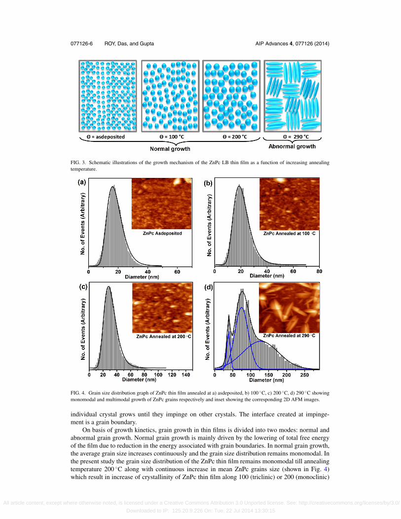
C. Growth mechanism of ZnPc LB thin film on annealing
The growth mechanism of ZnPc LB thin film is schematically illustrated in Fig. 3. The mech-anism of growth process in the ZnPc thin film upon annealing can be described by DLA method(diffusion limited aggregation process). Diffusion of ZnPc molecules across the substrate increasesgreatly upon annealing the ZnPc thin film. Initially the asdeposited ZnPc thin film having smallcrystallinity and upon annealing the thin film eventually leads to crystallization (as shown inFig. 2) which indicates that the lateral package of the crystallites becomes closer. The
All article content, except where otherwise noted, is licensed under a Creative Commons Attribution 3.0 Unported license. See: http://creativecommons.org/licenses/by/3.0/
Downloaded to IP: 125.20.9.226 On: Tue, 22 Jul 2014 13:30:15
077126-6 ROY, Das, and Gupta AIP Advances 4, 077126 (2014)
FIG. 3. Schematic illustrations of the growth mechanism of the ZnPc LB thin film as a function of increasing annealingtemperature.
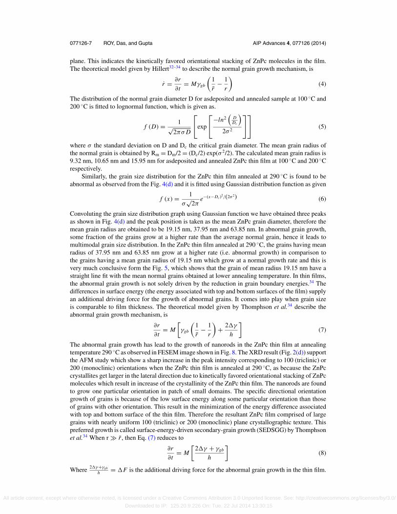
FIG. 4. Grain size distribution graph of ZnPc thin film annealed at a) asdeposited, b) 100 ◦C, c) 200 ◦C, d) 290 ◦C showingmonomodal and multimodal growth of ZnPc grains respectively and inset showing the corresponding 2D AFM images.
individual crystal grows until they impinge on other crystals. The interface created at impinge-ment is a grain boundary.
On basis of growth kinetics, grain growth in thin films is divided into two modes: normal andabnormal grain growth. Normal grain growth is mainly driven by the lowering of total free energyof the film due to reduction in the energy associated with grain boundaries. In normal grain growth,the average grain size increases continuously and the grain size distribution remains monomodal. Inthe present study the grain size distribution of the ZnPc thin film remains monomodal till annealingtemperature 200 ◦C along with continuous increase in mean ZnPc grains size (shown in Fig. 4)which result in increase of crystallinity of ZnPc thin film along 100 (triclinic) or 200 (monoclinic)
All article content, except where otherwise noted, is licensed under a Creative Commons Attribution 3.0 Unported license. See: http://creativecommons.org/licenses/by/3.0/
Downloaded to IP: 125.20.9.226 On: Tue, 22 Jul 2014 13:30:15
077126-7 ROY, Das, and Gupta AIP Advances 4, 077126 (2014)
plane. This indicates the kinetically favored orientational stacking of ZnPc molecules in the film.The theoretical model given by Hillert32–34 to describe the normal grain growth mechanism, is
r = ∂r
∂t= Mγgb
(1
r− 1
r
)(4)
The distribution of the normal grain diameter D for asdeposited and annealed sample at 100 ◦C and200 ◦C is fitted to lognormal function, which is given as.
f (D) = 1√2πσ D
⎡⎣exp
⎡⎣−ln2
(DDc
)2σ 2
⎤⎦
⎤⎦ (5)
where σ the standard deviation on D and Dc the critical grain diameter. The mean grain radius ofthe normal grain is obtained by Rm = Dm/2 = (Dc/2) exp(σ 2/2). The calculated mean grain radius is9.32 nm, 10.65 nm and 15.95 nm for asdeposited and annealed ZnPc thin film at 100 ◦C and 200 ◦Crespectively.
Similarly, the grain size distribution for the ZnPc thin film annealed at 290 ◦C is found to beabnormal as observed from the Fig. 4(d) and it is fitted using Gaussian distribution function as given
f (x) = 1
σ√
2πe−(x−Dc)2/(2σ 2) (6)
Convoluting the grain size distribution graph using Gaussian function we have obtained three peaksas shown in Fig. 4(d) and the peak position is taken as the mean ZnPc grain diameter, therefore themean grain radius are obtained to be 19.15 nm, 37.95 nm and 63.85 nm. In abnormal grain growth,some fraction of the grains grow at a higher rate than the average normal grain, hence it leads tomultimodal grain size distribution. In the ZnPc thin film annealed at 290 ◦C, the grains having meanradius of 37.95 nm and 63.85 nm grow at a higher rate (i.e. abnormal growth) in comparison tothe grains having a mean grain radius of 19.15 nm which grow at a normal growth rate and this isvery much conclusive form the Fig. 5, which shows that the grain of mean radius 19.15 nm have astraight line fit with the mean normal grains obtained at lower annealing temperature. In thin films,the abnormal grain growth is not solely driven by the reduction in grain boundary energies.34 Thedifferences in surface energy (the energy associated with top and bottom surfaces of the film) supplyan additional driving force for the growth of abnormal grains. It comes into play when grain sizeis comparable to film thickness. The theoretical model given by Thomphson et al.34 describe theabnormal grain growth mechanism, is
∂r
∂t= M
[γgb
(1
r− 1
r
)+ 2�γ
h
](7)
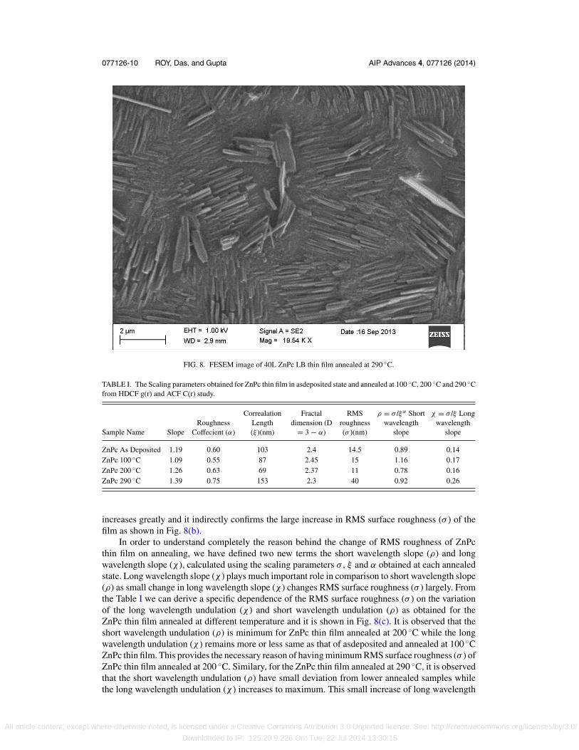
The abnormal grain growth has lead to the growth of nanorods in the ZnPc thin film at annealingtemperature 290 ◦C as observed in FESEM image shown in Fig. 8. The XRD result (Fig. 2(d)) supportthe AFM study which show a sharp increase in the peak intensity corresponding to 100 (triclinic) or200 (monoclinic) orientations when the ZnPc thin film is annealed at 290 ◦C, as because the ZnPccrystallites get larger in the lateral direction due to kinetically favored orientational stacking of ZnPcmolecules which result in increase of the crystallinity of the ZnPc thin film. The nanorods are foundto grow one particular orientation in patch of small domains. The specific directional orientationgrowth of grains is because of the low surface energy along some particular orientation than thoseof grains with other orientation. This result in the minimization of the energy difference associatedwith top and bottom surface of the thin film. Therefore the resultant ZnPc film comprised of largegrains with nearly uniform 100 (triclinic) or 200 (monoclinic) plane crystallographic texture. Thispreferred growth is called surface-energy-driven secondary-grain growth (SEDSGG) by Thomphsonet al.34 When r � r , then Eq. (7) reduces to
∂r
∂t= M
[2�γ + γgb
h
](8)
Where 2�γ+γgb
h = �F is the additional driving force for the abnormal grain growth in the thin film.
All article content, except where otherwise noted, is licensed under a Creative Commons Attribution 3.0 Unported license. See: http://creativecommons.org/licenses/by/3.0/
Downloaded to IP: 125.20.9.226 On: Tue, 22 Jul 2014 13:30:15

077126-8 ROY, Das, and Gupta AIP Advances 4, 077126 (2014)
FIG. 5. Mean radius Rm (nm) as a function of annealing temperature of the ZnPc thin film for both normal and abnormalgrains. The straight line fit is for grains having normal mode of growth.
FIG. 6. 3D Atomic Force Microscopy (AFM) images of 2 × 2 μm2 size of a) asdeposited, b) 100 ◦C, c) 200 ◦C, d) 290 ◦Cfor the annealed 40 L ZnPc LB thin film of thickness 80 nm deposited over glass substrate.
All article content, except where otherwise noted, is licensed under a Creative Commons Attribution 3.0 Unported license. See: http://creativecommons.org/licenses/by/3.0/
Downloaded to IP: 125.20.9.226 On: Tue, 22 Jul 2014 13:30:15
077126-9 ROY, Das, and Gupta AIP Advances 4, 077126 (2014)
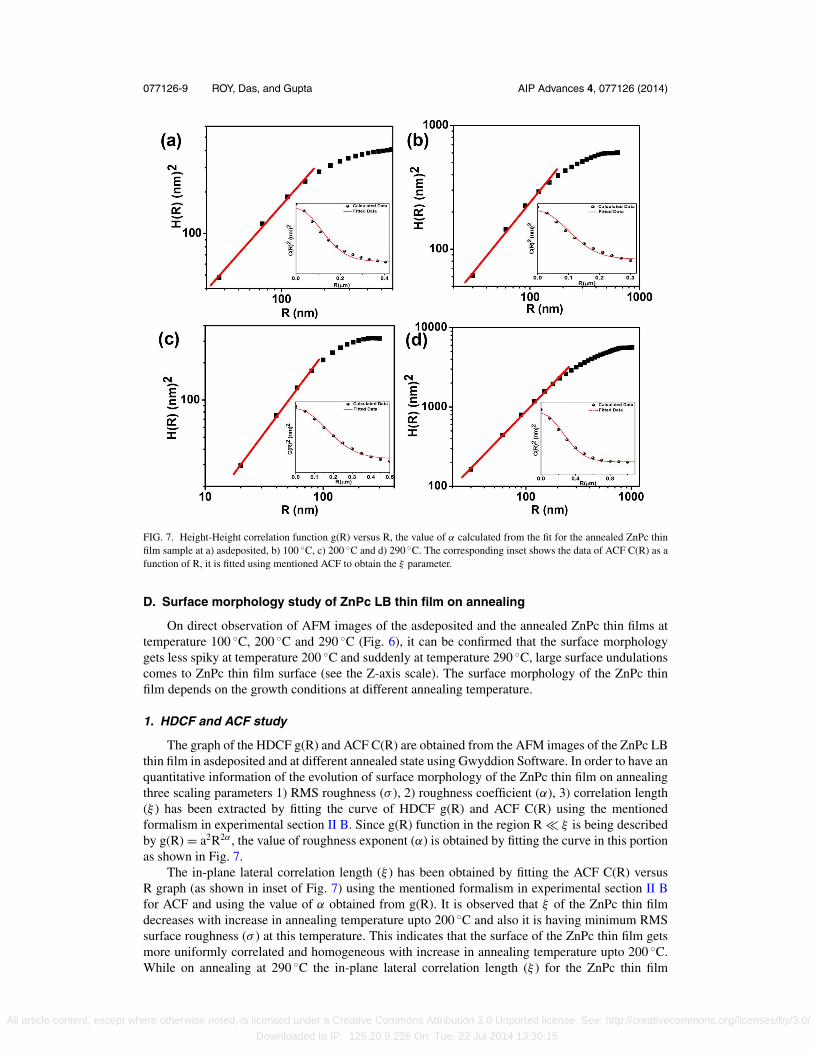
FIG. 7. Height-Height correlation function g(R) versus R, the value of α calculated from the fit for the annealed ZnPc thinfilm sample at a) asdeposited, b) 100 ◦C, c) 200 ◦C and d) 290 ◦C. The corresponding inset shows the data of ACF C(R) as afunction of R, it is fitted using mentioned ACF to obtain the ξ parameter.
D. Surface morphology study of ZnPc LB thin film on annealing
On direct observation of AFM images of the asdeposited and the annealed ZnPc thin films attemperature 100 ◦C, 200 ◦C and 290 ◦C (Fig. 6), it can be confirmed that the surface morphologygets less spiky at temperature 200 ◦C and suddenly at temperature 290 ◦C, large surface undulationscomes to ZnPc thin film surface (see the Z-axis scale). The surface morphology of the ZnPc thinfilm depends on the growth conditions at different annealing temperature.
1. HDCF and ACF study
The graph of the HDCF g(R) and ACF C(R) are obtained from the AFM images of the ZnPc LBthin film in asdeposited and at different annealed state using Gwyddion Software. In order to have anquantitative information of the evolution of surface morphology of the ZnPc thin film on annealingthree scaling parameters 1) RMS roughness (σ ), 2) roughness coefficient (α), 3) correlation length(ξ ) has been extracted by fitting the curve of HDCF g(R) and ACF C(R) using the mentionedformalism in experimental section II B. Since g(R) function in the region R � ξ is being describedby g(R) = a2R2α , the value of roughness exponent (α) is obtained by fitting the curve in this portionas shown in Fig. 7.
The in-plane lateral correlation length (ξ ) has been obtained by fitting the ACF C(R) versusR graph (as shown in inset of Fig. 7) using the mentioned formalism in experimental section II Bfor ACF and using the value of α obtained from g(R). It is observed that ξ of the ZnPc thin filmdecreases with increase in annealing temperature upto 200 ◦C and also it is having minimum RMSsurface roughness (σ ) at this temperature. This indicates that the surface of the ZnPc thin film getsmore uniformly correlated and homogeneous with increase in annealing temperature upto 200 ◦C.While on annealing at 290 ◦C the in-plane lateral correlation length (ξ ) for the ZnPc thin film
All article content, except where otherwise noted, is licensed under a Creative Commons Attribution 3.0 Unported license. See: http://creativecommons.org/licenses/by/3.0/
Downloaded to IP: 125.20.9.226 On: Tue, 22 Jul 2014 13:30:15
077126-10 ROY, Das, and Gupta AIP Advances 4, 077126 (2014)
FIG. 8. FESEM image of 40L ZnPc LB thin film annealed at 290 ◦C.
TABLE I. The Scaling parameters obtained for ZnPc thin film in asdeposited state and annealed at 100 ◦C, 200 ◦C and 290 ◦Cfrom HDCF g(r) and ACF C(r) study.
Sample Name SlopeRoughness
Coffecient (α)
CorrealationLength(ξ )(nm)
Fractaldimension (D
= 3 − α)
RMSroughness(σ )(nm)
ρ = σ /ξα Shortwavelength
slope
χ = σ /ξ Longwavelength
slope
ZnPc As Deposited 1.19 0.60 103 2.4 14.5 0.89 0.14ZnPc 100 ◦C 1.09 0.55 87 2.45 15 1.16 0.17ZnPc 200 ◦C 1.26 0.63 69 2.37 11 0.78 0.16ZnPc 290 ◦C 1.39 0.75 153 2.3 40 0.92 0.26
increases greatly and it indirectly confirms the large increase in RMS surface roughness (σ ) of thefilm as shown in Fig. 8(b).
In order to understand completely the reason behind the change of RMS roughness of ZnPcthin film on annealing, we have defined two new terms the short wavelength slope (ρ) and longwavelength slope (χ ), calculated using the scaling parameters σ , ξ and α obtained at each annealedstate. Long wavelength slope (χ ) plays much important role in comparison to short wavelength slope(ρ) as small change in long wavelength slope (χ ) changes RMS surface roughness (σ ) largely. Fromthe Table I we can derive a specific dependence of the RMS surface roughness (σ ) on the variationof the long wavelength undulation (χ ) and short wavelength undulation (ρ) as obtained for theZnPc thin film annealed at different temperature and it is shown in Fig. 8(c). It is observed that theshort wavelength undulation (ρ) is minimum for ZnPc thin film annealed at 200 ◦C while the longwavelength undulation (χ ) remains more or less same as that of asdeposited and annealed at 100 ◦CZnPc thin film. This provides the necessary reason of having minimum RMS surface roughness (σ ) ofZnPc thin film annealed at 200 ◦C. Similary, for the ZnPc thin film annealed at 290 ◦C, it is observedthat the short wavelength undulation (ρ) have small deviation from lower annealed samples whilethe long wavelength undulation (χ ) increases to maximum. This small increase of long wavelength
All article content, except where otherwise noted, is licensed under a Creative Commons Attribution 3.0 Unported license. See: http://creativecommons.org/licenses/by/3.0/
Downloaded to IP: 125.20.9.226 On: Tue, 22 Jul 2014 13:30:15
077126-11 ROY, Das, and Gupta AIP Advances 4, 077126 (2014)
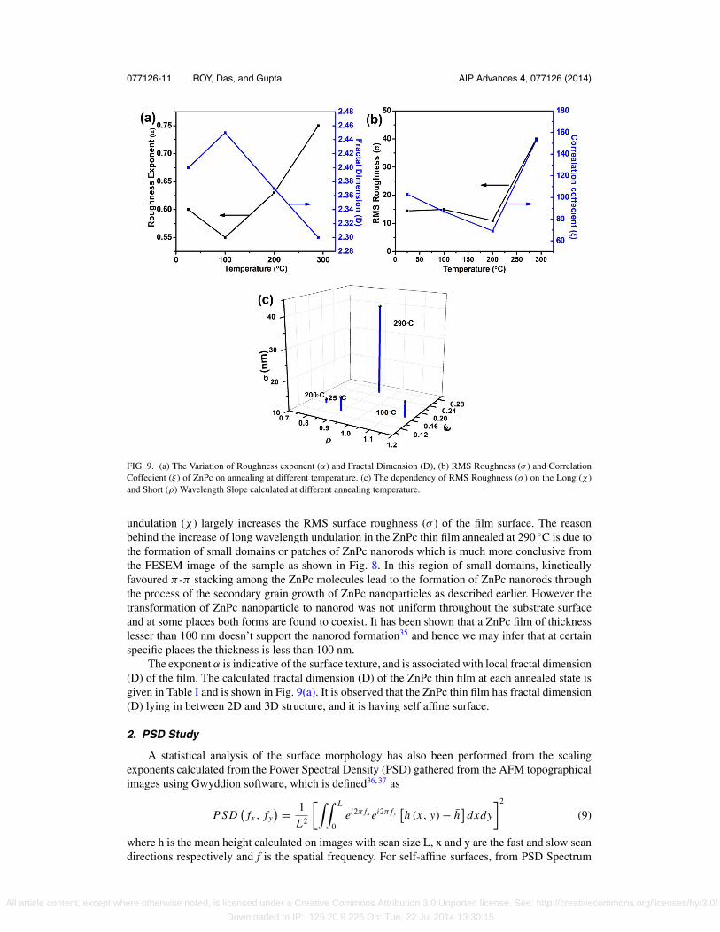
FIG. 9. (a) The Variation of Roughness exponent (α) and Fractal Dimension (D), (b) RMS Roughness (σ ) and CorrelationCoffecient (ξ ) of ZnPc on annealing at different temperature. (c) The dependency of RMS Roughness (σ ) on the Long (χ )and Short (ρ) Wavelength Slope calculated at different annealing temperature.
undulation (χ ) largely increases the RMS surface roughness (σ ) of the film surface. The reasonbehind the increase of long wavelength undulation in the ZnPc thin film annealed at 290 ◦C is due tothe formation of small domains or patches of ZnPc nanorods which is much more conclusive fromthe FESEM image of the sample as shown in Fig. 8. In this region of small domains, kineticallyfavoured π -π stacking among the ZnPc molecules lead to the formation of ZnPc nanorods throughthe process of the secondary grain growth of ZnPc nanoparticles as described earlier. However thetransformation of ZnPc nanoparticle to nanorod was not uniform throughout the substrate surfaceand at some places both forms are found to coexist. It has been shown that a ZnPc film of thicknesslesser than 100 nm doesn’t support the nanorod formation35 and hence we may infer that at certainspecific places the thickness is less than 100 nm.
The exponent α is indicative of the surface texture, and is associated with local fractal dimension(D) of the film. The calculated fractal dimension (D) of the ZnPc thin film at each annealed state isgiven in Table I and is shown in Fig. 9(a). It is observed that the ZnPc thin film has fractal dimension(D) lying in between 2D and 3D structure, and it is having self affine surface.
2. PSD Study
A statistical analysis of the surface morphology has also been performed from the scalingexponents calculated from the Power Spectral Density (PSD) gathered from the AFM topographicalimages using Gwyddion software, which is defined36, 37 as
P SD(
fx , fy) = 1
L2
[∫∫ L
0ei2π fx ei2π fy
[h (x, y) − h
]dxdy
]2
(9)
where h is the mean height calculated on images with scan size L, x and y are the fast and slow scandirections respectively and f is the spatial frequency. For self-affine surfaces, from PSD Spectrum
All article content, except where otherwise noted, is licensed under a Creative Commons Attribution 3.0 Unported license. See: http://creativecommons.org/licenses/by/3.0/
Downloaded to IP: 125.20.9.226 On: Tue, 22 Jul 2014 13:30:15

077126-12 ROY, Das, and Gupta AIP Advances 4, 077126 (2014)
FIG. 10. Evolution of the power spectral sensity (PSD) vs spatial frequency for the annealed ZnPc thin film sample at a)asdeposited, b) 100 ◦C, c) 200 ◦C and d) 290 ◦C.
one can therefore obtain roughness exponent α, correlation length ξ and fractal dimension D of thegiven sample by fitting the power-law decay (in the linear region of the log-log plot) to
P(
f > ξ−1) = const/fγ (10)
and for γ > d′37
α = γ − d ′
2
Where d′ is the dimension of the cross section and here it is equal to 1.The PSDs in Fig. 10 exhibit two distinct regions, (i) a plateau PSD at low spatial frequencies and
(ii) frequency-dependent decaying branch. The steeper portion of the latter is taken as the self affinerange, while the high frequency range with a smaller slope is discarded since it is more affected bynoise and aliasing. From the PSD obtained for the ZnPc thin film at asdeposited state and at differentannealed temperature, the values of γ are obtained and fractal dimension D is also calculated fromthe eq.38
D = (8−γ )/2, (11)
The Table II shows the scaling exponents obtained from the PSD graph of the asdeposited andannealed ZnPc thin film. The fractal dimension D calculated from PSD study shows a similar trendto the one calculated from HDCF g(r) study, which shows that the self affine characteristic of theZnPc thin film firstly increase on annealing at 100 ◦C, then it decreases continuously on annealingand is found to be minimum for the ZnPc thin film annealed at 290 ◦C. This confirms that the ZnPcfilm annealed above 100 ◦C moves towards 2D structure pattern. In fact to characterize, the scale ofcorrelation frequency ξ−1 can be used. It can be evaluated from the PSD graph where the PSD hasfallen to 1/e of its saturation low frequency value and above which σ is correlated. The correlation
All article content, except where otherwise noted, is licensed under a Creative Commons Attribution 3.0 Unported license. See: http://creativecommons.org/licenses/by/3.0/
Downloaded to IP: 125.20.9.226 On: Tue, 22 Jul 2014 13:30:15
077126-13 ROY, Das, and Gupta AIP Advances 4, 077126 (2014)
TABLE II. The Scaling parameters obtained for ZnPc thin film in asdeposited state and annealed at 100 ◦C, 200 ◦C and290 ◦C from PSD study.
Sample Slope(γ ) Roughness Coffecient (α) Correlation Length (ξ )(nm) Fractal dimension (D)
ZnPc Asdeposited 3.33±0.05 0.67 56 2.335ZnPc 100 ◦C 3.26±0.06 0.63 38 2.37ZnPc 200 ◦C 3.50±0.07 0.75 26 2.25ZnPc 290 ◦C 3.61±0.07 0.8 63 2.2
length ξ calculated for the ZnPc sample for the asdeposited and annealed state at 100 ◦C, 200 ◦C,290 ◦C has been mentioned in the Table II. The correlation length show a decreasing trend uptoannealing temperature 200 ◦C and increases suddenly for sample annealed at 290 ◦C, similar to thetrend as obtained from HDCF g(R) and ACF C(R) study.
IV. CONCLUSION
To summarize, we have characterized the morphology of the LB deposited ZnPc thin film of 40layers using atomic force microscopy (AFM) and X-ray diffraction (XRD). The asdeposited LB thinfilm has been found to have an edge on orientation with average tilt angle of 64.3 ◦ as confirmed fromthe Pressure-Area (π -A) isotherm and X-ray diffraction (XRD) study. Growth mechanism concludesthat the factors such as minimization of grain boundary energy and surface energy anisotropy resultsin the growth of ZnPc molecular grains in one specific orientation i.e.100 (triclinic phase) or 200(monoclinic phase) planes with increase in ZnPc grain size on annealing. The AFM and FESEMimages shows that the grains in asdeposited thin film grows to elongated rod shaped grains onannealing at 290 ◦C which reveals that the temperature dependent asymmetric grain growth of theZnPc nanoparticles over the thin film matix at higher temperature. The scaling concepts provide abroad view of the evolution of surface morphology of the ZnPc thin film on annealing. The calculatedscaling exponents from HDCF g(r) and ACF C(r) for ZnPc LB thin film shows a particular trendon annealing. The RMS surface roughness (σ ) is found to be dependent on the as defined shortwavelength undulations (ρ) and long wavelength undulations (χ ). Both ρ and χ are the functionof above mentioned three scaling exponents. The RMS surface roughness (σ ) is observed to beminimum for the ZnPc thin film annealed at 200 ◦C where both the short and long wavelengthundulations are at their lowest value, whereas σ is maximum for the ZnPc thin film annealed at290 ◦C which is due to increase of χ value because of the formation ZnPc nanorods in patch of smalldomains. Nanorods formation takes place due to increase in mobility of the ZnPc grains with risein annealing temperature which kinetically favored the π -π stacking of the ZnPc molecules. Thefractal dimension obtained for both asdeposited and the annealed ZnPc LB thin film from HDCFg(r) and PSD study is found to be lying in between 2D and 3D structure, which confirm that ZnPcLB thin film have a self affine surface. Therefore, it can be predicted that the ZnPc LB thin filmannealed at 200 ◦C will have better conductivity in comparison to film annealed at 290 ◦C inspite ofhaving having much better crystallinity and stacking of ZnPc molecules. The necessary reason forthis can only be because of lower surface roughness of the ZnPc LB thin film annealed at 200 ◦C.
ACKNOWLEDGMENTS
We gratefully thank Dr. Mukul Gupta, UGC-DAE CSR, Indore for his support in taking XRDmeasurements and Dr. V. Ganesan, UGC-DAE CSR, Indore for providing AFM facility. We acknowl-edge UGC-DAE CSR, Indore for giving opportunity to carry out characterization of the samplesunder the CRS project.
1 A. Ulman, An Introduction to ultrathin Organic Films-From Langmuir Blodgett to Self Assembly (Academic Press, Boston,1991).
2 X. Chen, S. Lenthert, M. Hirtz, N. Lu, H. Fuchs, and L. Chi, Acc. Chem. Res. 40, 393 (2007).
All article content, except where otherwise noted, is licensed under a Creative Commons Attribution 3.0 Unported license. See: http://creativecommons.org/licenses/by/3.0/
Downloaded to IP: 125.20.9.226 On: Tue, 22 Jul 2014 13:30:15
077126-14 ROY, Das, and Gupta AIP Advances 4, 077126 (2014)
3 G. A. Chamberlain, Sol. Cells 8, 47 (1983).4 H. M. Zeyada and M. M. El-Nahass, Appl. Surf. Sci. 254, 1852 (2008).5 A. A. Zanfolim, D. Volpati, C. A. Olivati, A. E. Job, and C. J. I. Constantino, J. Phys. Chem. C. 114, 12290 (2010).6 H. Wang, Z. Liu, M. F. Lo, T. W. Ng, C. S. Lee, D. Yan, and S. T. Lee, J. Appl. Phys. 107, 024510 (2010).7 Y. Chen, J. Chen, D. Ma, D. Yan, L. Wang, and F. Zhu, Appl. Phys. Lett. 98, 243309 (2011).8 A. Van Slyke, C. H. Chen, and C. W. Tang, Appl. Phys. Lett. 69, 2160 (1996).9 Y. Zhou, T. Taima, T. Miyadera, T. Yamanari, and Y. Yoshida, J. Appl. Phys. 111, 103117 (2012).
10 S. Choi, S. H. Hong, S. H. Cho, S. Park, S. M. Park, O. Kim, and M. Ree, Adv. Mater. 20, 1766 (2008).11 P. Peumans, and S. R. Forrest, Appl. Phys. Lett. 79, 126 (2001).12 J. G. V. Dijken, M. D. Fleischauer, and M. J. Brett, Org. Electron. 12, 2111 (2011).13 Y. Acikbas, M. Evyapana, T. Ceyhanb, R. Capan, and O. Bekaroglu, Sens. Actuators B 123, 1017 (2007).14 N. Karl, in Organic Electronic Materials, edited by R. Farchioni and G. Grosso (Springer, Berlin, 2001), Vol. II.15 J. Kim, N. Lim, C. R. Park, and S. Yim, Surf. Sci. 604, 1143 (2010).16 B. B. Mandelbrodt, The Fractal Geometry of Nature (Freeman, New York, 1982).17 A. C. Durr, F. Schreiber, K. A. Ritely, V. Kruppa, J. Kurg, H. Dosch, and B. Sruth, Phys. Rev. Lett. 90, 016104 (2003).18 George Palasantzas, Phys. Rev. B. 48, 14472 (1993).19 S. Sarkar, S. Patra, N. Gayathri, and S. Banerjee, Appl. Phys. Lett. 96, 063112 (2010).20 D. R. Tackely, G. Dent, and W. E. Smith, Phys. Chem. Chem. Phys. 2, 3949 (2000).21 K. Xiao, Y. Liu, X. Huang, Y. Xu, G. Yu, and D. Zhu, J. Phys. Chem. B. 107 (2003).22 A. Leuthe and H. Riegler, J. Phys. D. 25, 1766 (1992).23 A. Malik, M. K. Durbin, A. G. Richter, K. G. Huang, and P. Dutta, Phys. Rev. B. 52, 1654 (1995).24 J. E. Riegler and J. D. L. Grange, Phys. Rev. Lett. 61, 2492 (1988).25 D. E. Hooks, T. Fritz, and M. D. Ward, Adv. Mater. 13, 227 (2001).26 G. Witte and C. Woll, J. Mater. Res. 19, 889 (2004).27 D. Roy, N. M. Das, and P. S. Gupta, Appl. Surf. Sci. 271, 394 (2013).28 N. M. Das, D. Roy, and P. S. Gupta, Physica B. 407, 4777 (2012).29 Y. Zhou, T. Taima, T. Miyadera, T. Yamanari, and Yuji Yoshida, J. Appl. Phys. 111, 103117 (2012).30 T. Sakurai, R. Fukasawa, K. Saito, and K. Akimoto, Org. Electron. 8, 702 (2007).31 C. Schunemann, C. Elschner, A. A. Levin, M. Levichkova, K. Leo, and M. Reide, Thin Solid Films 519, 3939 (2011).32 C. V. Thompson, J. Appl. Phys. 58, 763 (1985).33 E. M. Zielinski, R. P. Vinci, and J. C. Bravman, J. Appl. Phys. 76, 4516 (1994).34 C. V. Thompson, J. Floro, and H. I. Smith, J. Appl. Phys. 67, 4099 (1990).35 S. Heutz, S. M. Bayliss, R. L. Middleton, G. Rumbles, and T. S. Jones, J. Phys. Chem. B. 104, 7124 (2000).36 Yi. Zhang, E. Barrena, X. Zhang, A. Turak, F. Maye, and H. Dosch, J. Phys. Chem. C 114, 13752 (2010).37 F. Biscarini, P. Samori, O. Greco, and R. Zamboni, Phys. Rev. Lett. 78, 2389 (1997).38 D. Raoufi, Physica B 405, 451 (2010).
All article content, except where otherwise noted, is licensed under a Creative Commons Attribution 3.0 Unported license. See: http://creativecommons.org/licenses/by/3.0/
Downloaded to IP: 125.20.9.226 On: Tue, 22 Jul 2014 13:30:15