ecole!normale!superieure! d'enseignement!technique! - Zenodo
Upload
khangminh22Category
view
3download
0
ECOLE DE TECHNOLOGIE SUPERIEUR E UNIVERSITE DU QUEBEC
THESIS PRESENTED TO ECOLE DE TECHNOLOGIE SUPERIEUR E
IN PARTIAL FULFILLEMENT OF THE REQUIREMENTS FOR THE DEGREE OF DOCTOR OF PHILOSOPHY
Ph.D
BY KHADKIKAR, VINOD
POWER QUALITY ENHANCEMENT AT DISTRIBUTION LEVEL UTILIZING THE UNIFIED POWER QUALITY CONDITIONER (UPQC )
MONTREAL, 1 3 NOVEMBER 2008
© Copyright 2008 reserved by Vinod Khadkikar

THIS THESIS HAS BEEN EVALUATED
BY THE FOLLOWING BOARD OF EXAMINERS
M. Ambrish Chandra , Thesi s Superviso r Departement d e genie electrique a I'Ecole de technologic superieur e
Mme Marie-Jose Nollet , Presiden t o f the Board of Examiner s Departement d e genie de la construction a FEcole de technologic superieur e
M. Kamal Al-Haddad, Examine r Departement d e genie electrique a FEcole de technologic superieur e
M. Vijay Kuma r Sood , Externa l Examine r Faculty o f Engineering an d Applied Science , University o f Ontario Institut e of Technolog y
THIS THESIS WA S PRESENTE D AN D DEFENDE D
BEFORE A BOARD OF EXAMINERS AN D PUBLI C
NOVEMBER 3 , 200 8
AT ECOLE D E TECHNOLOGIE SUPERIEUR E

ACKNOWLEDGMENT
I woul d lik e t o expres s m y sincer e gratitud e t o m \ thesi s directo r Dr . Ambris h Chandr a fo r
his guidance, support , funding , an d valuabl e time .
A par t o f this wor k wa s don e i n collaboration wit h Hydro-Quebe c an d Institut e d e recherch e
d'Hydro-Quebec (IREQ) , Canada . Specia l thank s t o Mr . Alph a Ouma r Barr y fro m th e IRE Q
and Mr . Thuy Doa n Nguyen fro m Hydro-Quebe c fo r the helpful discussion s an d suggestions .
I wan t t o expres s m y deepes t gratitud e t o m y committe e member s Professo r Kama l Al -
Haddad, Professo r Vija y Soo d an d Professo r Marie-Jos e Nollet . Specia l thank s t o Dr . Kama l
Al-Haddad fo r the discussion an d suppor t during the experimental stage s of this work .
I woul d lik e t o thank s Dr . Pramo d Agarwa l fro m India n Institut e o f Technology , Roorkee ,
India, fo r hi s effort s i n buildin g th e basi c laborator y prototype . 1 would lik e t o sho w m y
gratitude t o Mr . Yve s Robitaill e an d Ms . Johann e Roy , technician s a t th e electrica l
engineering departmen t a t ET S fo r thei r help . 1 woul d als o lik e t o than k m y colleague s Mr .
Etienne Tremblay , Mr . Mukhtia r Sing h an d Mr . Wilso n Santan a fo r th e wonderfu l compan y
and support .
I woul d lik e t o acknowledg e th e Ecol e d e technologi c superieur e fo r providin g m e th e
opportunity t o pursu e m y Ph.D . studie s an d recommendin g m e fo r scholarship s offere d b y
the Ministr y o f Educatio n o f Quebe c (bours e d'exemptio n - 2004 , 2005 ) an d als o providin g
scholarships fro m th e university (bours e aux merite s - 2006 , 2008).
Sincere thanks to my close friends Mr . Dipa k Mahapatra , Mr . Kama l Agrawal , Mr . Yogendr a
Shukla and Ms . Bhavani Madakashir a fo r thei r constan t motivatio n an d support .
Finally an d mos t importantly , I woul d lik e t o than k m y parent s an d famih ' member s fo r
making everythin g possible .
AMELIORATION D E QUALITE D E L'ONDE A U NIVEA U D E DISTRIBUTIO N E N UTILISANT L E CONDITIONNEUR UNIFI E DE QUALITE D E L'ONDE (UPQC )
KHADKIKAR, Vino d
RESUME
Les equipement s base s su r d e Felectroniqu e d e puissanc e emergen t rapidemen t tell e un e composante essentiell e au x systeme s d e distributio n a haut e puissanc e modernes . Le s equipements d e conversio n d e l a puissanc e qu i beneficien t d e cett e technologi c offren t u n eventail d e possibilites e t permetten t entr e autr e une flexibilit e d e controle, un e reduction de s coiats, une optimisation de s Fespac e e t des performances , etc . D'un autr e cote , Foperatio n d e ces equipement s peu t entraine r certain s de s plu s serieu x probleme s d e l a qualit e d e I'ond e tels un e consommatio n d e puissanc e reactiv e e t l a generatio n d"harmonique s qu i polluen t l e reseau d e distribution . D e plus , le s equipements moderne s son t d e plus e n plu s sensible s a la tension d'alimentatio n qu i leu r es t imposee . Augmente r l a capacit e de s poste s d e generatio n d'electricite existant s es t difficil e e t tre s couteux . surtou t lorsqu e Fo n consider e le s contraintes environnementales . Desormais , Famelioratio n d e l a qualit e d e Fond e peu t no n seulement rendr e le s reseau x d e distributio n plu s propre s e t performant s mai s entrain e auss i une reductio n important e de s perte s lor s d u transpor t e t pa r consequent , de s economie s significatives.
Les filtre s actif s d e l a puissance son t largemen t utilise s afi n d e remedie r a quelques un s de s plus important s probleme s d e l a qualit e d e Fonde . L a tendanc e actuell e vis e l a conceptio n d'equipements multitach e qu i permetten t d e remedie r a plusieurs probleme s d e l a qualit e d e I'onde simultanement . L e conditionneu r universe l d e puissance , mieu x conn u sou s Fappellation anglophon e Unifie d Powe r Qualit y Conditione r (UPQC) . es t Fu n de s filtre s actifs de s plu s polyvalent s permettan t d e compense r significativemen t le s probleme s d e l a qualite d e Fond e tel s le s harmoniques d e tensions , hauts e t creux d e tension , desequilibr e d e tension e t papillotements, harmoniques d e courant, puissance reactiv e d e charge, desequilibr e du courant e t courant d e neutre.
Le UPQC consist e en un dispositi f divise en deux onduleur s de tension connecte s dos-a-do s a travers u n bu s d e tensio n continu e commu n autosupporte . L e premie r onduleu r es t control e telle un e sourc e d e tensio n variabl e d e l a meme manier e qu e Fo n fai t regulieremen t ave c u n filtre acti f serie , alors que l e second es t controle e n courant d'un e maniere similair e a un filtr e actif parallele . L a litteratur e existant e su r l e suje t sugger e qu e l e filtr e acti f parallel e soi t assigne a l a compensation d e l a puissance reactiv e consommee pa r l a charge. D'autr e part , l e filtre acti f serie est toujours utilis e afin d e mitiger le s problemes relie s a la tension. Le s hauts, creux e t papillotements d e la tension son t des deteriorations d e l a qualite d e Fonde d e courte s durees. L'approch e traditionnell e d e control e d u UPQ C afi n d'ameliore r le s problemes d e l a qualite d e I'ond e presenten t l e desavantage d e l a sous-utilisatio n d e Fonduleu r d u filtre acti f serie. Pa r consequent , l e facteu r d'utilisatio n d u filtre acti f seri e es t beaucou p plu s ba s qu e celui du filtre parallele .
V
Le present travai l d e doctorat es t base su r l a philosophic d'utilisatio n optimal e de s ressource s disponibles, c'est-a-dir e d e l a maniere l a plus efficace possibl e e t ave c l e meilleur rendemen t afin d'ameliore r Fefficacit e d u systeme e t de reduire l e cout d e fabricatio n e t d'operation. C e travail propos e un concep t d e controle innovateu r appel e Powe r Angl e Contro l (PAC) . ce qui signifie, control e d e Fangl e d e puissance . L e concep t stipul e qu e le s con\'ertisseur s seri e e t parallele s e partagen t l a puissanc e reactiv e d e l a charge , e n parfait e coordination , san s affecter l e fonctionnement fondamenta l d e l a compensation d u UPQC . Cett e situatio n result e en un e meilleure utilisatio n d e Fonduleu r serie . en un e reductio n d e l a capacite d e Fonduleu r parallele e t ultimement , e n un e reductio n d u cou t d e Fensembl e d u UPQC . D e plus , cett e these introdui t un e nouvelle fonctionnalit e a u UPQ C dan s laquell e i l est possible d'etendr e l e concept d u UPQC triphas e a trois fils vers celui triphase a quatre fils.
Le concept PA C developp e dan s ce travail a ete valide avec succe s par simulatio n numeriqu e et extensivemen t pa r d e multiples manipulation s e n laboratoire . Le s resultat s experimentau x montrent que , dans le s conditions presente s a u laboratoir e ave c un e charg e tre s inducti \ e. un redressement d e Fangl e d e puissance 6=28 ° entre l a tension d e sourc e e t cell e resultante a la charge peu t reduir e l a capacit e d u convertisseu r parallel e d e 50% . L"e\aluatio n d e l a performance d u concep t PA C e n presence d e hauts . de creux e t de distorsion d e l a tension d e source e t d'un e charg e non-lineair e es t auss i effectuee . Sou s Feffe t d e l a distorsio n d e l a tension d e sourc e (TH D d e l a tension d e sourc e = 6.6%) ains i qu e d'un e charg e non-lineair e (THD d u couran t d e charg e = 23.4%) , l e UPQ C control e ave c l e concep t PA C compens e efficacement le s harmoniques d e l a tension d e sourc e (TH D d e l a tension d e charge = 3.2% ) et l a distorsion d u courant (TH D d u couran t d e source 2.94% ) e t permet l e partage simultan e de la puissance reactiv e entre le convertisseur parallel e e t serie.
Ce travai l a et e partiellemen t execut e e n collaboratio n ave c Hydro-Quebec , Montreal , Canada e t ITnstitut de recherche d"Hydro-Quebec IREQ , Varennes, Canada .
Mots-cles: Qualit e d e Fonde , filtre actif , conditionneu r unifi e d e l a qualit e d e I'onde , compensation d e puissance reactive , compensation de s hamioniques .
POWER QUALIT Y ENHANCEMEN T A T DISTRIBUTIO N LEVE L UTILIZIN G THE UNIFIE D POWE R QUALIT Y CONDITIONE R (UPQC )
KHADKIKAR. Vino d
ABSTRACT
Povv'er electronics base d equipment s ar e rapidl y emergin g a s ke y component s i n th e presen t modern powe r distributio n system . Powe r processin g utilizin g thes e device s offe r vas t advantages suc h a s flexible control , cos t reduction , overal l siz e optimization , etc . O n th e other hand , operatio n o f thes e device s give s ris e t o som e o f th e seriou s powe r qualit y problems, suc h as . the reactiv e powe r requiremen t an d generatio n o f harmonic s tha t pollute s the powe r distributio n system . Moreover , moder n equipment s ar e becomin g highl y sensiti\ e to th e voltag e supplie d t o them . Increasin g th e generatio n capacitie s o f existin g powe r stations i s difficul t an d expensiv e du e t o environmenta l constraints . Hence , improvin g th e quality o f powe r ca n no t onl y mak e th e powe r distributio n system s healthie r an d mor e efficient, bu t also results i n reduced powe r losses , and thus saving i n terms of costs.
Active power filters ar e widely use d t o tackle som e of the importan t powe r qualit y problems . Recent trend s ar e geare d toward s th e realizatio n o f multitaskin g device s whic h ca n tackl e several powe r qualit y problem s simultaneously . Th e unifie d powe r qualit y conditione r (UPQC) i s on e o f th e mos t versatil e activ e powe r filters tha t ca n compensat e significan t power qualit y issues , suc h as , voltag e harmonics , voltag e sag , voltag e swell , voltag e unbalance, \oltag e flicker, curren t harmonics , loa d reacti\ e power , curren t unbalance , an d neutral current .
A UPQ C consist s o f tw o voltag e sourc e inverter s connecte d bac k t o bac k wit h eac h othe r sharing a commo n self-supportin g D C link . On e inverte r i s controlle d a s a variabl e \oltag e source i n sam e manne r a s i n the serie s activ e powe r filter (APF) . and th e othe r a s a variabl e current sourc e whic h i s simila r i n operation a s tha t o f th e shun t APF . Th e existin g literatur e suggests th e dependenc y o n shun t inverte r t o compensat e th e loa d reacti\ e powe r demand . Moreover, th e serie s inverte r i s always utilize d t o overcome al l the voltag e relate d problems . The voltag e sags , swell s an d th e flickers ar e shor t duratio n powe r qualit y problems . Hence , this traditiona l approac h o f utilizin g th e UPQ C t o compensat e th e powe r qualit > problem s shows a significan t drawbac k o f unde r usag e o f th e availabl e serie s inverter . Therefore , th e utilization facto r o f the series inverte r i s much lowe r than tha t o f the shunt inverter .
The presen t doctora l wor k i s based o n th e philosoph y o f optima l utilizatio n o f th e a \ ailable resources i n a mos t effectiv e an d efficien t wa y t o improv e th e produc t efficienc y an d t o reduce th e overal l cost . Thi s wor k propose s a nove l contro l concept , terme d a s powe r angl e control (PAC) , i n whic h bot h th e serie s an d shun t inverter s shar e th e loa d reactiv e powe r i n co-ordination wit h eac h othe r withou t affectin g th e basi c UPQ C compensatio n capabilities . This eventuall y result s i n a bette r utilizatio n o f th e serie s inverter , reductio n i n th e shun t inverter ratin g t o som e exten t an d ultimatel y i n th e reductio n o f th e overal l cos t o f UPQC .
VII
Moreover, this thesis also introduce s a new functionalit y fo r UPQ C i n which , i t i s possible t o extent the UPQC base d three-phas e three-wir e syste m to a three-phase four-wir e system .
The develope d PA C concep t i s successfull y validate d throug h digita l simulatio n a s wel l a s extensive experimenta l investigations . Th e experimenta l result s sho w tha t fo r th e gi\e n laboratory tes t conditions wit h a highly inductiv e load , a boost i n power angl e 5=28° between the sourc e an d th e resultan t loa d voltag e ca n reduc e th e shun t inverte r ratin g b y 50% . Th e performance evaluatio n o f PA C approac h unde r voltag e sag , voltag e swell , distorte d sourc e voltage an d non-linea r loa d condition s i s als o carrie d out . Unde r distorte d sourc e \oltag e (source voltag e THD=6.6% ) an d th e non-linea r loa d (loa d curren t THD=23.4%) , th e UPQ C with propose d PA C concept , effectivel ) compensate s th e harmonic s i n sourc e voltag e (loa d \oltage THD=3.2%) . load curren t (sourc e curren t THD = 2.94% ) an d share s th e loa d reactiv e power between the series and shun t inverters , simultaneously .
This wor k wa s partiall y conducte d i n collaboratio n wit h Hydro-Quebec . Montrea l an d Institut d e recherche d'Hydro-Quebec (IREQ) . Varennes. Canada .
Keywords: powe r quality , activ e powe r filter , unifie d powe r qualit y conditioner , reactiv e power compensation , harmonic s compensation .
TABLE O F CONTENT S
Page
INTRODUCTION
CHAPTER 1 UPQC BASIC S AND STEADY-STAT E POWE R FLO W ANALYSI S 1 4 1.1 Introductio n 1 4 1.2 UPQ C Concep t an d Operatin g Principl e 1 4
1.2.1 UPQ C Syste m Configuratio n 1 5 1.2.2 Shun t Inverte r Operation 1 7 1.2.3 Serie s Inverter Operatio n 1 9 1.2.4 Th e Role of Shun t Inverte r i n UPQC Operatio n 2 1 1.2.5 Contro l o f UPQC 2 2
1.3 Literatur e Revie w 2 3 1.3.1 Classificatio n o f UPQC 2 5
1.3.1.1 Classificatio n Base d on Suppl y Syste m 2 5 1.3.1.2 Classificatio n Base d on Converter Topolog y 2 7 1.3.1.3 Classificatio n Base d on UPQC Configuratio n 2 8 1.3.1.4 Classificatio n Base d on Control Strateg y 2 9
1.3.2 UPQ C Contro l Strategie s 2 9 1.3.2.1 Frequenc y Domai n Compensatio n Metho d 2 9 1.3.2.2 Tim e domain Compensatio n Method s 3 0
1.3.3 Additiona l Significan t Researc h Wor k 3 2 1.4 Steady-Stat e Powe r Flow Analysis of UPQC 3 7
1.4.1 Case-I : Active-Reactive Powe r Flow during Normal Workin g Condition....4 1 1.4.2 Case-II : Active-Reactive Powe r Flo w durin g Voltage Sa g Condition 4 2 1.4.3 Case-Ill : Active and Reactiv e Powe r Flo w under Voltage Swel l Condition.4 3 1.4.4 Case-IV : Active-Reactive Powe r Flo w unde r Distorte d Voltage s 4 3 1.4.5 Case-V : Active-Reactive Powe r Flow under Distorted Loa d Current s 4 3 1.4.6 Phaso r Representation s o f Different Operatin g Condition s 4 4 1.4.7 UPQ C Operatio n fro m 0 ° to 360° 4 5
1.5 Stead y Stat e Powe r Flo w Analysis : Numerical Stud y 4 7 1.6 Conclusio n 5 2
CHAPTER 2 UPQC FEASIBILIT Y ANALYSI S FO R PRACTICA L APPLICATIO N 5 4 2.1 Introductio n 5 4 2.2 Motivatio n behin d th e Collaboration Projec t 5 4 2.3 UPQ C Controlle r Developmen t 5 6
2.3.1 Referenc e Voltag e Signa l Generatio n 5 6 2.3.2 Referenc e Curren t Signa l Generatio n 5 9 2.3.3 Gatin g Signa l Generation / Modulato r 6 1
2.4 Realisti c Network Detail s 6 2 2.5 Simulatio n Resuh s 6 6
2.5.1 Stead y Stat e Plan t - Networ k Performanc e 6 6
IX
2.5.2 Curren t Harmonic s Compensation 6 8 2.5.3 Reactiv e Power Compensation and Powe r Factor Correction (PFC) 6 9 2.5.4 Dynami c Performance unde r sudden load change 7 0 2.5.5 Voltag e Harmonics Compensation 7 1 2.5.6 Voltag e Sag Compensation 7 3 2.5.7 Voltag e Swel l Compensation 7 5 2.5.8 Voltag e Fluctuation / Flicker Compensation 7 7
2.6 Laborator y Experimenta l Result s 8 0 2.6.1 Curren t Harmonic s Compensation 8 1 2.6.2 Reactiv e Power Compensation 8 5 2.6.3 Dynami c Response under Sudden Load Change 8 5 2.6.4 Voltag e Harmonics Compensation 8 7
2.6.4.1 Performanc e unde r Linear RL Load 8 8 2.6.4.2 Performanc e unde r Non-linear Load 9 1
2.6.5 Voltag e Sag Compensation 9 4 2.6.6 Voltag e Swell Compensation 9 7 2.6.7 Voltag e Fluctuation/ Flicker Compensation 9 9
2.7 Conclusion s 10 1
CHAPTER 3 VOLTAGE SA G COMPENSATION THROUGH REACTIV E POWE R 10 2 3.1 Introductio n 10 2 3.2 UPQC- Q Concept 10 3
3.2.1 UPQC- Q Phasor Representation 10 4 3.2.2 Propose d Approach to Estimate Quadrature Injection Voltag e 10 6 3.2.3 Activ e and Reactive Power Flow during QVI 10 9 3.2.4 Critica l Operating Condition 11 0
3.3 UPQC- Q Controller Development 11 1 3.3.1 Voltag e Harmonics Extraction 11 1 3.3.2 Determinatio n of Quadrature Injection Voltag e 11 3
3.4 Simulatio n Results 11 5 3.4.1 Voltag e Sag Compensation under Sinusoida l Voltages and Linea r Load ...115 3.4.2 Voltag e Sag Compensation under Distorted Conditio n 11 6 3.4.3 Critica l Operating Condition 11 8
3.5 Laborator y Experimenta l Result s 11 9 3.5.1 Real-Tim e Quadrature Injection Voltag e Extraction 11 9 3.5.2 Single-Phas e UPQC-Q System Performanc e 12 1
3.5.2.1 Voltag e Sag Compensation under Sinusoida l Condition 12 1 3.5.2.2 Voltag e Sag Compensation unde r Distorte d Condition 12 3 3.5.2.3 UPQC- Q Dynamic Performance 12 5
3.5.3 Three-Phas e UPQC-Q System Performance 12 7 3.5.3.1 Three-Phas e Voltage Sag Compensation using QVI 12 7 3.5.3.2 Voltag e Harmonics Compensafion usin g d-q Transformafion 13 1
3.6 Discussio n on Voltage Sag Compensation Using UPQC-P and UPQC- Q 13 7 3.7 Conclusion s 14 0

X
CHAPTER 4 A NOVE L SYSTE M CONFIGURATIO N FO R THREE-PHAS E FOUR -WIRE DISTRIBUTIO N SYSTE M 14 1
4.1 Introductio n 14 1 4.2 Three-Phas e Four-Wir e (3P4W ) Distributio n Syste m Configuration s 14 2
4.2.1 Classica l 3P4 W Distributio n Syste m 14 2 4.2.2 Propose d 3P4 W UPQ C Syste m Configuration 14 4
4.3 UPQ C Controlle r Developmen t 14 7 4.3.1 Activ e Filte r Topologies fo r Three-Phas e Four-Wir e Syste m 14 7 4.3.2 Curren t Unbalance Compensatio n 14 9 4.3.3 Propose d Curren t Unbalanc e Compensatio n Approac h 15 0
4.3.3.1 Balance d Referenc e Sourc e Current Signa l Generatio n 15 0 4.3.3.2 Neutra l Curren t Compensation 15 5
4.4 Simulatio n Result s 15 7 4.5 Laborator y Experimenta l Result s 15 9
4.5.1 Syste m unde r Consideration 15 9 4.5.2 Real-Tim e Instantaneou s Fundamenta l Loa d Acti\ e Powe r Extraction 16 2 4.5.3 Curren t Unbalanc e Compensatio n - Stead y Stat e Result s 16 3 4.5.4 Dynami c Performanc e 16 5
4.5.4.1 Loa d Change 16 5 4.5.4.2 Three-Phas e to Single-Phasing Conditio n 16 8
4.6 Conclusio n 17 3
CHAPTER 5 UPQC: POWER ANGL E CONTRO L - A NOVE L CONTRO L PHILOSOPHY 17 4
5.1 Introductio n 17 4 5.2 Powe r Angle Contro l (PAC ) of UPQC 17 5
5.2.1 Backgroun d an d Relevanc e 17 5 5.2.2 Powe r Angle Contro l (PAC ) Concep t 17 6 5.2.3 Phaso r Representatio n o f PAC 17 7
5.3 Mathematica l Formulatio n o f PAC 17 9 5.3.1 Serie s Inverte r Paramete r Estimatio n 17 9 5.3.2 Shun t Inverte r Paramete r Estimatio n 18 2 5.3.3 Boundar y Conditio n fo r Maximu m 5 18 5
5.4 Activ e and Reactiv e Powe r (P-Q) Flow 18 6 5.4.1 P- Q Flow without PA C Approach 18 6 5.4.2 P- Q Flow with PAC Approach 18 7 5.4.3 Percentag e of Reactive Powe r Share d b y Two Inverter s 18 9
5.5 Powe r Angle 8 Determination 19 0 5.6 UPQ C Controlle r Developmen t base d o n PAC 19 3
5.6.1 Instantaneou s S Determination 19 3 5.6.2 Referenc e Voltag e Signa l Generatio n fo r Serie s Inverte r 19 5 5.6.3 Referenc e Curren t Signa l Generatio n fo r Shun t Inverte r 19 6
5.7 Simulafio n Result s 19 9 5.7.1 Loa d Reactiv e Power Compensafion withou t PA C Approach 19 9 5.7.2 Loa d Reactiv e Powe r Compensation wit h PA C Approac h 20 1
XI
5.8 Experimenta l Validatio n o f Proposed Phas e Angle Contro l Approac h 20 5 5.8.1 Real-Tim e Instantaneou s Activ e an d Reactiv e Powe r Computation 20 6 5.8.2 Performanc e o f UPQC withou t Phas e Angle Contro l Approac h 20 6 5.8.3 Performanc e o f UPQC wit h Phas e Angle Contro l Approac h 20 8 5.8.4 Performanc e o f UPQC unde r Differen t Powe r Angle s 21 2
5.9 Conclusion s 22 0
CHAPTER 6 PERFORMANC E O F PA C APPROAC H UNDE R DIFFEREN T OPERATING CONDITION S 22 2
6.1 Introductio n 22 2 6.2 PA C approac h unde r Voltage Sa g Condition 22 3
6.2.1 Phaso r Representatio n unde r Voltage Sa g Condition 22 3 6.2.2 Serie s Inverte r Paramete r Estimatio n unde r Voltage Sa g Condition 22 5 6.2.3 Shun t Inverte r Paramete r Estimatio n unde r Voltage Sa g Condition 22 8
6.3 PA C Approac h unde r Voltage Swel l Conditio n 23 1 6.3.1 Phaso r Representatio n unde r Voltage Swel l Condition 23 1 6.3.2 Shun t Inverte r Paramete r Estimatio n unde r Voltage Swel l Conditio n 23 4
6.4 Summar y o f PAC approach unde r differen t operatin g conditio n 23 6 6.5 Generalize d Equation s fo r Active-Reactive Powe r Flo w utilizin g PA C Approach..23 9 6.6 Differen t Mode s of Operations 24 3 6.7 UPQ C Controlle r Developmen t 24 5
6.7.1 Fixe d Powe r Angle (5/ ) Control Approac h 24 5 6.7.2 Variabl e Power Angle (5v ) Control Approac h 24 6 6.7.3 Generalize d Controlle r fo r Serie s Inverte r 24 7
6.8 Simulatio n Resuh s 24 8 6.8.1 Fixe d Powe r Angl e Base d PA C Performanc e unde r Voltag e Sa g an d Swel l
Conditions 24 8 6.8.2 Variabl e Powe r Angl e Base d PA C Performanc e unde r Voltag e Sa g an d
Swell Condition s 25 1 6.8.3 PA C Performance unde r Distorted Condition s 25 3
6.9 Experimenta l Result s 25 5 6.9.1 Performanc e o f PAC under Voltage Sa g Condition 25 5 6.9.2 Performanc e o f PAC unde r Voltage Swel l Conditio n 25 7 6.9.3 Dynami c Performanc e o f PAC during Voltage Sag\Swel l Conditions 25 9 6.9.4 Performanc e o f PAC under Distorted Sourc e Voltag e 26 1
6.10 Conclusion s 26 3
CONCLUSIONS 26 4
RECOMMENDATIONS 26 8
ANNEXE I LABORATORY EXPERIMENTA L SETU P DETAIL S 27 0
ANNEXE I I PRINCIPAL EXPERIMENTA L PARAMETER S 28 3
LIST OF REFERENCE S 28 6
Table 1. 1
Table 1.2
Table 2. 1
Table 2. 2
Table 2. 3
Table 2. 4
Table 2. 5
Table 2. 6
Table 2. 7
Table 2. 8
Table 2. 9
Table 3. 1
Table 3. 2
Table 4. 1
Table 4. 2
Table 4. 3
Table 4. 4
Table 5. 1
Table 5. 2
Table 5. 3
LIST OF TABLE S
Page
Impact o f %) sag and load VA R variation 4 8
Impact o f %) swel l and loa d VAR variation 5 0
Different loa d bus voltage magnitudes 6 4
Different Transforme r rating s 6 5
Transformer Specification s 6 5
Steady-state loa d power consumption unde r sinusoida l voltag e 6 7
PQ - Current harmonic compensatio n 6 9
PQ - Voltage harmonic compensatio n 7 2
THD values : Voltage harmonic compensatio n 7 2
PQ - Voltage sa g compensation 7 4
PQ - Voltage swel l compensation 7 6
Voltage harmonic s compensatio n - Individua l harmonic s value s a s % o f fundamental 13 5
Current harmonic s compensatio n - Individua l harmonic s value s a s % o f fundamental 13 7
Individual loa d curren t detail s 16 1
Source current detail s before an d afte r compensatio n 16 4
Source curren t detail s befor e an d afte r compensatio n (single-phasin g condition) 16 9
Individual harmonic s value s a s % o f fundamenta l (single-phasin g condition) 17 2
Different voltag e and current magnitud e (pea k values ) 20 4
Phase angle relationship between voltages and current s 20 5
Measured voltag e and current magnitude usin g Fluke 41B 21 1

XllI
1 • Table 5.4 Differen t phas e angle determination
Table 5.5 Performanc e o f PAC approach under different powe r angles 5 21 7
Table 6.1 Summar y of PAC Approach Performance Equation s 23 7
Table 6.2 Possibl e values of factor k/. no and ko 23 9

LIST OF FIGURE S
Page
Figure 1. 1 Detaile d svste m configuratio n o f three-phase UPQ C 1 6
Figure 1. 2 Shun t activ e filter operatin g principl e 1 7
Figure 1. 3 Serie s APF operating principle 1 9
Figure 1. 4 Combine d serie s AP F an d shun t passiv e filter t o compensat e loa d curren t harmonics 2 1
Figure 1. 5 Genera l bloc k diagra m representatio n o f UPQC syste m 2 4
Figure 1. 6 Pictoria l vie w fo r the classification o f UPQC 2 5
Figure 1. 7 Single-phas e two-wir e UPQ C syste m configuratio n 2 6
Figure 1. 8 Three-phas e three-wir e UPQ C syste m configuratio n 2 6
Figure 1. 9 Three-phas e four-wir e UPQ C syste m configuratio n 2 7
Figure 1.1 0 CS I based UPQ C syste m configuration 2 7
Figure 1.1 1 Lef t shun t UPQC svste m configuratio n 2 8
Figure 1.1 2 Equivalen t circui t o f a UPQC 3 7
Figure 1.1 3 Activ e and reactive power flow during steady-stat e conditio n 4 1
Figure 1.1 4 Activ e and reactive power flow during voltag e sag condition 4 2
Figure 1.1 5 Activ e and reactive power flow during voltage swel l condition 4 3
Figure 1.1 6 Phaso r representatio n o f all possible conditions 4 5
Figure 1.1 7 Operatin g zone s o f UPQ C base d o n (psh variatio n fo r Sag/Swel l compensations 4 6
Figure 1.1 8 Variatio n i n system parameter s unde r different % of sags 4 9
Figure 1.1 9 Variatio n i n system parameters under differen t % of swells 5 1
Figure 2.1 Desire d loa d voltages signa l generatio n 5 9
Figure 2. 2 D C lin k contro l an d reference sourc e curren t signa l generafio n 6 0
XV
Figure 2. 3 Hysteresi s controlle r 6 1
Figure 2. 4 Single-lin e diagram: Industria l distributio n networ k unde r consideration.6 2
Figure 2. 5 Plan t loa d 6 3
Figure 2. 6 UPQ C bloc k diagra m 6 4
Figure 2. 7 Simulatio n results : Steady stat e current drawn b y each of the loads 6 7
Figure 2. 8 Simulatio n results : current harmonics compensatio n 6 8
Figure 2.9 Simulatio n results : power facto r correctio n 7 0
Figure 2.1 0 Simulatio n results : dynamic performanc e durin g sudden loa d change 7 0
Figure 2.11 Simulatio n results : voltage harmonics compensation 7 2
Figure 2.12 Simulatio n results : voltage sa g compensation 7 4
Figure 2.1 3 Simulatio n results : voltage swel l compensation 7 6
Figure 2.14 Simulatio n results : flicker compensation 7 8
Figure 2.1 5 Tliree-phas e source and loa d voltage profiles 7 9
Figure 2.16 Hardwar e syste m set-u p diagra m fo r single-phas e UPQ C base d o n developed UVT G controlle r 8 0
Figure 2.17 Experimenta l results : Curren t harmonic s compensatio n an d performanc e with and without us e of low pass filter on sensed D C link voltage 8 3
Figure 2.1 8 Curren t harmonic s compensatio n - harmonic s spectru m an d individua l harmonic value s a s % of fundamenta l 8 4
Figure 2.19 Experimenta l results : Reactive power compensation 8 5
Figure 2.2 0 Experimenta l results : dynamic performanc e o f shunt inverte r 8 6
Figure 2.2 1 Experimenta l setu p to generate harmonics i n source voltage 8 7
Figure 2.2 2 Experimenta l results : simultaneou s voltag e harmonic s an d reactiv e powe r compensation 8 9
Figure 2.2 3 Voltag e harmonic s compensatio n (unde r linea r R L load ) - harmonic s spectrum an d individua l harmoni c value s as % of fundamenta l 9 0
XVI
Figure 2.2 4 Experimenta l results : Voltag e an d curren t harmonic s compensatio n unde r non-linear loa d 9 2
Figure 2.25 Voltag e harmonic s compensatio n (unde r non-linea r load ) - harmonic s spectrum an d individua l harmoni c value s a s % of fundamental 9 3
Figure 2.26 Experimenta l results : voltage sa g compensation (stead y stat e condition).94
Figure 2.2 7 Experimenta l results : voltage sa g compensation (dynami c condiUon ) 9 6
Figure 2.2 8 Experimenta l results : voltage swel l compensation (stead y state ) 9 7
Figure 2.2 9 Experimenta l results : voltage swel l compensation (dynamic ) 9 8
Figure 2.30 Experimenta l results : Voltage flicker compensafio n (dynamic ) 10 0
Figure 3. 1 UPQC- Q concept : phasor representation 10 5
Figure 3. 2 QV I - Detaile d phaso r representation 10 6
Figure 3. 3 QV I - Critica l operation condition 11 0
Figure 3. 4 Voltag e harmoni c extractio n base d o n synchronou s referenc e fram e method 11 3
Figure 3. 5 Overal l contro l diagra m fo r serie s inverte r t o compensat e voltag e sa g an d harmonics 11 4
Figure 3. 6 Simulatio n results : voltag e sa g compensatio n b y QV I unde r sinusoida l source voltages 11 6
Figure 3. 7 Simulatio n results : Voltag e sa g compensatio n b y QV I unde r distorte d condition 11 7
Figure 3. 8 Simulatio n results : critical operatin g conditio n (6=^£ ) 11 8
Figure 3. 9 Develope d Simulin k mode l t o extrac t th e quadratur e injectio n voltag e i n real-time. Figur e als o show s the reference signa l generatio n fo r serie s an d shunt inverter s 12 0
Figure 3.10 Real-tim e extraction o f required quadratur e injectio n voltag e 12 0
Figure 3.11 Experimenta l results : voltag e sa g compensatio n b y QV I unde r sinusoida l condition (single-phas e system ) 12 2
Figure 3.1 2 Experimenta l results : phas e relationship s betwee n differen t parameter s during voltage sag compensation usin g QVI 12 3
XVII
Figure 3.1 3 Experimenta l results : UPQC- Q voltag e an d curren t harmoni c compensation 12 4
Figure 3.1 4 Experimenta l results : performanc e o f QV I t o compensat e voltag e sa g an d voltage harmonic s simultaneously 12 5
Figure 3.1 5 Experimenta l results : Dynamic performance o f UPQC-Q 12 6
Figure 3.1 6 Experimenta l results : Three-phas e stead y stat e sourc e voltage s an d loa d currents 12 8
Figure 3.1 7 Experimenta l results : Individua l phas e performanc e durin g voltag e sa g compensation 12 9
Figure 3.1 8 Experimenta l results : Performanc e o f three-phase UPQC- Q durin g voltag e sag condition 13 0
Figure 3.19 Experimenta l results : voltag e an d curren t harmonic s compensatio n performance o f three-phase UPQ C 13 2
Figure 3.2 0 Experimenta l results : voltag e an d curren t harmonic s compensatio n performance o f three-phase UPQ C 13 3
Figure 3.21 Voltag e harmonic s compensatio n - harmonic s spectru m o f loa d voltage s after compensatio n 13 4
Figure 3.2 2 Curren t harmonic s compensatio n - harmonics spectru m o f sourc e current s after compensatio n 13 6
Figure 3.2 3 Phaso r representation o f UPQC-P an d UPQC- Q 13 8
Figure 4.1 Three-phas e four-wir e distributio n system : neutra l provide d fro m generation statio n 14 3
Figure 4.2 Three-phas e four-wir e distributio n system : neutra l provide d fro m Delta -Star transformer 14 3
Figure 4.3 Three-phas e three-wire UPQ C topolog y 14 3
Figure 4.4 Propose d three-phas e four-wir e (3P4W ) syste m realize d fro m three-phas e three-wire (3P3W ) UPQ C base d syste m 14 6
Figure 4.5 Spli t capacito r topology use d fo r 3P4 W shun t activ e filter 14 8
Figure 4.6 Four-le g topology used fo r 3P4 W shun t activ e filter 14 8
Figure 4.7 3 H bridge topology use d fo r 3P4 W shun t acfive filter 14 9

XVIII
Figure 4.8 Shun t inverte r contro l bloc k diagram 15 6
Figure 4.9 Simulatio n result s - performanc e o f propose d curren t unbalanc e compensation approac h applie d unde r nove l UPQ C topolog y 15 8
Figure 4.10 Experimenta l setu p to generate unbalanced loa d currents 15 9
Figure 4.11 Individua l curren t drawn by each of the loads 16 0
Figure 4.12 Real-tim e extractio n o f instantaneou s fundamenta l loa d activ e powe r an d generated referenc e sourc e current signal s using proposed approac h 16 2
Figure 4.13 Experimenta l result s (steady-stat e condition) : performanc e o f propose d current unbalance compensatio n approac h 16 4
Figure 4.14 Experimenta l result s (dynami c condition) : performanc e o f propose d current unbalanc e compensatio n approac h unde r sudde n increas e i n th e load curren t 16 6
Figure 4.15 Experimenta l result s (dynami c condition) : performanc e o f propose d current unbalanc e compensatio n approac h unde r sudde n decreas e i n th e load curren t 16 7
Figure 4.16 Loa d curren t profile s durin g sudde n occurrenc e o f three-phas e t o single -phasing conditio n 16 8
Figure 4.17 Experimenta l result s (dynami c condition) : performanc e o f propose d current unbalanc e compensatio n approac h unde r sudde n occurrenc e o f three-phase to single-phasing conditio n 17 0
Figure 4.18 Harmonic s spectru m o f source currents under single-phasing condition . 171
Figure 5. 1 Powe r Angle Contro l (PAC ) concept: phaso r representation 17 8
Figure 5. 2 Determinatio n o f Vsr and (ps r 18 0
Figure 5. 3 Powe r Angle Control : current phaso r representation 18 2
Figure 5. 4 Determinafio n o f I'sh and (p'sh_s 18 3
Figure 5. 5 Flo w char t o f step s involve d i n determinatio n o f 5 i n actua l practica l applications 19 2
Figure 5. 6 Instantaneou s power angle 5 determination 19 5
Figure 5. 7 Referenc e voltag e signa l generatio n fo r serie s inverte r base d o n PA C approach 19 6

XIX
Figure 5. 8 Referenc e curren t signa l generatio n base d o n PA C approach 19 8
Figure 5. 9 Overal l contro l bloc k diagra m o f proposed PA C approach 19 8
Figure 5.10 Simulatio n results : loa d reactiv e powe r compensatio n withou t PA C o f UPQC 20 0
Figure 5.1 1 Simulatio n Results : loa d reactiv e powe r compensatio n wit h PA C o f UPQC 20 2
Figure 5.1 2 Simulatio n Result s - activ e an d reactiv e powe r flow durin g PA C o f UPQC 20 4
Figure 5.13 Experimenta l Results : Real-Time Instantaneou s p, & cji Computation.20 6
Figure 5.1 4 Experimenta l Result s - performanc e o f UPQC withou t PA C Approach.20 7
Figure 5.15 Experimenta l Result s - Performanc e o f proposed PA C approac h 20 9
Figure 5.1 6 Phaso r representatio n showin g relativ e phas e angle s betwee n differen t voltages and current with power angle 6=18° 21 1
Figure 5.1 7 Experimenta l Result s - PA C approac h performanc e unde r differen t powe r angles, only serie s inverter i s ON 21 3
Figure 5.1 8 Experimenta l Result s - PA C approac h perfomianc e unde r differen t powe r angles, UPQC O N 21 4
Figure 5.1 9 Experimenta l Result s - sourc e an d loa d voltag e phas e shift s unde r different powe r angle s 21 5
Figure 5.2 0 Experimenta l Resuh s - shun t inverte r compensatin g curren t reductio n under different powe r angles 21 6
Figure 5.2 1 Comparativ e evaluatio n unde r different powe r angle s 21 9
Figure 6.1 Phaso r representation o f PAC approach unde r voltage sa g condition 22 3
Figure 6. 2 Detaile d phaso r representatio n fo r serie s inverte r paramete r estimafio n under voltage sa g condition 22 6
Figure 6. 3 Curren t base d phaso r representatio n o f PA C approac h unde r voltag e sa g condition 22 9
Figure 6. 4 Detaile d phaso r diagra m t o comput e th e shun t inverte r parameter s unde r voltage sa g condition 22 9
XX
Figure 6. 5 Phaso r representation o f PAC approach unde r voltage swel l condition . .232
Figure 6.6 Detaile d phaso r representatio n fo r serie s inverte r paramete r estimatio n under voltage swel l condition 23 3
Figure 6.7 Curren t base d phaso r representatio n o f PA C approac h unde r voltag e swel l condition 23 4
Figure 6.8 Detaile d phaso r diagra m t o comput e th e shun t inverte r parameter s unde r voltage swel l conditio n 23 5
Figure 6. 9 Contro l diagra m fo r fixed powe r angle control approac h 24 5
Figure 6.10 Contro l diagra m fo r variabl e angl e contro l approac h 24 6
Figure 6.11 Generalize d referenc e voltag e signa l generatio n fo r serie s inverte r base d on PAC approac h 24 7
Figure 6.1 2 Simulatio n results : Fixe d powe r angl e base d PA C performanc e durin g voltage sag and swel l conditions 24 9
Figure 6.13 Simulatio n results : activ e - reactiv e powe r flow unde r fixed powe r angl e based PA C approach 25 0
Figure 6.1 4 Simulatio n results : variabl e powe r angl e base d PA C performanc e durin g voltage sag and swel l conditions 25 2
Figure 6.1 5 Simulatio n results : activ e - reactiv e powe r flow unde r variabl e powe r angle based PA C approach 25 3
Figure 6.16 Simulatio n results : performanc e o f PA C approac h unde r distorte d suppl y voltage and non-linea r loa d (using 6/) 25 4
Figure 6.17 Experimenta l results : performance o f PAC (6/ ) approach unde r voltag e sa g condition (Sa g =17%, 6=10°) ! 25 6
Figure 6.1 8 Experimenta l results : performanc e o f PA C (6/ ) approac h unde r differen t voltage sags and power angles 25 7
Figure 6.1 9 Experimenta l results : performanc e o f PA C approac h (6/ ) unde r voltag e swell condifion (Swel l =22% , 6=10°) 25 8
Figure 6.20 Experimenta l results : performanc e o f PA C (6/ ) approac h unde r differen t voltage swell s and power angles 25 9
Figure 6.21 Experimenta l results : dynami c performanc e o f PA C approac h durin g momentary voltag e sa g condition 26 0
XXI
Figure 6.22 Experimenta l results : dynami c performanc e o f PA C approac h durin g momentary voltage swell condition 26 0
Figure 6.23 Experimenta l results : performanc e o f PA C (6/ ) approac h unde r distorte d condition (6=24°) 26 2

LIST OF ABBREVIATION S
1D On e dimensiona l
2D Tw o dimensiona l
3P3W Three-phas e three-wir e
3P4W Three-phas e four-wir e
AC Alternatin g curren t
ANN Artifica l neura l networ k
APF Acfiv e powe r filter
ASD Adjustabl e spee d driv e
AVC Automati c voltag e controlle r
C-DAC Centr e fo r development o f advance computin g
CSI Curren t sourc e inverte r
CUF Curren t unbalanc e facto r
DBR Diod e bridge rectifie r
DC Direc t curren t
DVR Dynami c voltage restore r
FACTS Flexibl e AC transmission system s
FFT Fas t fourier transfor m
GREPCI Grup e de recherche en electronique d e puissance e t commande industriell e
HP Hors e powe r
HPF Hig h pass filter
IGBT Insulate d gat e bipolar transisto r
IREQ Institut e de recherche d'Hydro-Quebe c
XXIII
lUPQC
LPF
LSR
LVRC
NPC
PAC
PCC
p . f
PFC
PI
PEL
PWM
Interline unifie d powe r qualit y co n
Low pass filter
Laboratoire simulatio n d e resaux
Line voltage regulator/conditione r
Neutral poin t clam p
Power angle contro l
Point of common couplin g
Power facto r
Power facto r correctio n
Proportional-Integral
Phase-locked loo p
Pulse width modulatio n
QVI
nns
RPM
SMPS
ssc
Quadrature voltag e injectio n
Root mean squar e
Revoluation pe r minut e
Switch mod e power suppl y
Static serie s compensato r
STATCOM Stati c va r compensato r
THD Tota l harmonic s distortio n
TSC Thyristo r switche d capacito r
TSR Thyristo r switche d reacto r
UAPF Unifie d activ e power filter
UAPLC Universa l activ e power lin e conditione r

XXIV
UPFC Unifie d powe r flow controller
UPQC Unifie d powe r quality conditioner
UPQCS Universa l power quality conditioning system
UVTG Uni t vector template generation
VSl Voltag e source inverter
w.r.t. wit h respect to
L I S T O F S Y M B O L S
5 Powe r angl e betwee n sourc e an d load voltage s
Sf Fixe d powe r angl e techniqu e
6ma\ Maximu m valu e o f power angl e 6
6v Variabl e powe r angl e techniqu e
P Phas e angl e betwee n sourc e voltag e an d load curren t durin g PA C approach
(ps Phas e angl e o f source curren t w.r.t. sourc e voltag e
(Pi Phas e angl e o f load curren t u.r.t. loa d voltag e
(psr Phas e angle o f series injecte d voltag e w.r.t. sourc e voltag e
(p'sr Phas e angle of series injected voltag e w.r.t. sourc e voltage during voltag e sa g
(p"sr Phas e angl e o f serie s injecte d voltag e w.r.t. sourc e voltag e durin g voltag e
swell
(psh Phas e angle of shunt injecte d curren t w.r.t. sourc e voltag e
(psij.s Phas e angl e o f shun t injecte d curren t w.r.t. sourc e voltag e durin g PA C approach (steady-stat e condition )
(psh.L Phas e angl e o f shun t injecte d curren t w.r.t. sourc e loa d voltag e durin g PA C approach (steady-stat e condition )
(p'sh-s Phas e angl e o f shun t injecte d curren t w.r.t. sourc e voltag e durin g PA C approach (voltag e sa g condition )
(p'sh-L Phas e angl e o f shun t injecte d curren t w.r.t. sourc e loa d voltag e durin g PA C approach (voltag e sa g condition )
(p"sh-s Phas e angl e o f shun t injecte d curren t w.r.t. sourc e voltag e durin g PA C approach (voltag e swel l condition )
(p"sh-L Phas e angl e o f shun t injecte d curren t w.r.t. sourc e loa d voltag e durin g PA C approach (voltag e swel l condition )
Cdc D C lin k capacito r

XXVI
C/ Rippl e filter capacito r use d fo r serie s inverte r
icnd Gri d curren t
IL.\ Loa d side neutral curren t
kif ii.h- kc Loa d curren t fo r phase-a , phase-6 , phase- c
h.u.aJLb.a-'Lc.a o-axl s load currcnt fo r phase-a , phase-/?, phase-c
iLa.P'iih.pJLc.p y5-axis.loa d current fo r phase-t/ . phase-/), phase-c
1'^ Sourc e current durin g voltage sa g
11 Sourc e current during voltage swel l
isu- hb, he Sourc e current fo r phase-c/ , phase-/), phase-c
' Sa, i Sb-< i Sc Referenc e sourc e curren t fo r phase-a, phase-/) , phase- c
r^i^ Shun t inverte r curren t durin g voltag e sag
r^i^ Shun t inverte r curren t durin g voltag e swel l
isha- ishb, hhc Shuu t invcrtc r curren t fo r phase-c/. phase-/) , phase- c
/ Sha' i shb, i She Reference shun t inverte r curren t fo r phase-c/, phase-/) , phase- c
/ j / , V Shun t inverte r injecte d neutra l curren t
/ j V Sourc e sid e neutra l curren t
I„j Outpu t o f PI controlle r
hh PAC Generalize d shun t inverte r current usin g PAC approac h
k Desire d loa d voltage magnitud e
kf Voltag e fluctuation facto r
Ksr Facto r t o denot e % o f maximu m serie s inverte r injectio n limi t w.r.t. desire d load voltag e
L - Sourc e inductanc e
XXVII
Lsr Serie s inverte r coupling inducto r
Lsh Shun t inverte r coupling inducto r
PL Acfiv e powe r demanded b y load
PLu.pLb-Pu. Instantaneou s tota l activ e powe r extracte d usin g single-phase/;-c y theor v fo r phase-c/, phase-/), phase-c
Pi.a'Pi.h-Pu Instantaneou s fundamenta l activ e powe r extracte d usin g single-phas e p-q theory fo r phase-c/ , phase-/), phase-c
pLa-Pib'Pu Instantaneou s harmoni c activ e powe r extracte d usin g single-phas e p-q theory fo r phase-c/ , phase-/), phase-c
Ps Activ e power delivered b y sourc e
Psh Activ e powe r handled b y shun t inverte r
^sh.p.\c Generalize d activ e power handled b y shunt inverte r usin g PA C approac h
Psr Activ e power handled by serie s inverte r
^Sr.R.^c Generalize d activ e power handled b y series inverte r usin g PA C approac h
QL Reactiv e power demanded b y loa d
^/.a, <^lLb, qu- Instantaneou s tota l reactiv e powe r extracte d usin g single-phas e p-q theor y fo r phase-c/, phase-/), phase-c
q,^-q,i,,qi,c Instantaneou s fundamenta l reactiv e powe r extracte d usin g single-phas e p-q theory fo r phase-c/ , phase-/), phase-c
^La-'^Lb'^u Instantaneou s harmoni c reactiv e powe r extracte d usin g single-phas e p-q theory fo r phase-c/ , phase-/), phase-c
Qs Reactiv e power delivered b y sourc e
Qsh Reactiv e power handle d b y shunt inverte r
Qsh.max MaxiiTiu m reactive power supported b y shunt inverte r
Qs/iP.4C Generalize d reacfiv e powe r handled b y shunt inverte r using PA C approac h
XXVIII
Qsr Reactiv e power handled b y series inverte r
Qsr,ma.\ Maximu m reactiv e power supporte d b y series inverte r
Qsr.p.AC Generalize d reactiv e power handled b y series inverte r using PA C approac h
Rs Sourc e resistanc e
Sseries_APF Scric s invcrtcr ratin g
^'crid Gri d voltag e
Vdc Actua l D C link voltag e
V d c Referenc e D C link voltag e
V'L Resultan t loa d voltage with PAC approac h
Vi,;, Vib. VLC Loa d voltage fo r phase-c/ , phase-/), phase-c
v La- v'lh^ y Lc Rcfcrenc c loa d voltage for phase-c/ , phase-/), phase-c
"^'La.a^'Lb.a^'Lc.a «-axi s loa d voltagc for phase-c/ , phase-/), phase-c
yLa.P'^'Lb.p^yic.p /?-axis.loa d voltage for phase-c/ . phase-/), phase-c
V,„ Pea k amplitud e o f source voltag e
VLW Pea k amplitude o f desired loa d voltag e
y*quad.a Refcrcnc e serie s inverte r voltag e fo r phase-c / usin g quadratur e voltag e injection (QVI ) approac h
y*quad.b Referenc e serie s inverter voltage fo r phase-/ ) using approac h
v\uadb Referenc e serie s inverter voltage fo r phase-c using QV I approac h
ysa, y.sb- ^Sc Sourc e voltag e fo r phase-c/ . phase-/), phase- c
v*5a, v*sb, v*5 c Referenc e sourc e voltage fo r phase-c/ , phase-/), phase-c
Vs Rate d sourc e voltage during steady-stat e conditio n
V 's Sourc e voltage during sag conditio n
XXIX
V"s Sourc e voltage during swel l conditio n
Vsai-Vsbi,Vsci Positiv e sequenc e voltages fo r phase-c/ , phase-/), phase-c
Vsa2-Vsb2.Vsc2 Negative sequenc e voltage s fo r phase-a , phase-/), phase-c
VsaO.VsbO'.Vsco Zero sequence voltages fo r phase-c/ , phase-/), phase-c
Vsaii.Vsbh-Vsch Harmonics voltage s fo r phase-c/ , phase-/), phase-c
V""sd- V' sq Distorte d sourc e voltage s direc t (d ) an d quadratur e (q ) component s i n synchronous rotatin g fram e
V sd.i- V sq.r Fundamenta l componen t o f source voltage i n synchronous rotatin g fram e
V sd.h. V*sq.h Harmonic s component o f source voltage i n synchronous rotating fram e
V sd - V s q Distorte d sourc e voltage s direc t (d ) an d quadratur e (q ) component s i n stationary fram e
c c
V sd.f , V sq. t Fundamenta l componen t o f source voltage i n stationary fram e
V' sd,h. V sq. h Fundamenta l componen t o f source voltage i n stationary fram e
Vsr Serie s injected voltag e during PAC approac h
Vsri Serie s injected voltag e during PA C approach (steady-stat e condition )
Vsr2 Serie s injected voltag e fo r voltage sag compensatio n
V'sr Resultan t serie s injectio n voltag e fo r voltag e sa g compensatio n wit h PA C
approach
Vsr3 Serie s injected voltag e fo r voltage swel l compensatio n
V"sr Resultan t serie s injectio n voltag e fo r voltag e swel l compensatio n wit h PA C
approach
Vsr.ma,\ Maximu m serie s injection voltag e limi t
Vsr.PAC Generalize d serie s inverte r voltage using PA C approac h
vsra, ^Srb, ^Src Scric s iuvcrtcr voltage fo r phase-c/ , phase-/), phase- c
v*6ra.vV6,v*s/-c Referenc e serie s inverte r voltage fo r phase-c/ , phase-/), phase-c
INTRODUCTION
In recen t years , th e ter m "'Power Quality"' ha s gaine d significan t importance , especiall y i n
electrical engineerin g relate d fields. A s pe r internationa l standards , th e ter m powe r qualit y
can b e define d a s th e physica l characteristic s o f th e electrica l suppl y provide d unde r norma l
operating condition s tha t d o not disrup t o r distur b th e user' s processes . However , th e ter m
power qualit y ca n have different meaning s and significances accordin g t o the requirements o r
environmental conditio n unde r whic h i t ha s bee n defined . Fo r example , fo r th e utility - i t
might b e the concern o f non-linear loa d causing harmonics o n the network; fo r the consumers
- i t might b e the distortion presen t i n the supplied voltage , etc.
The ever-increasing interes t i n the subjec t o f power quality ca n be explained i n the context o f
some of the major ke y issues :
• Traditionally , equipment s wer e simple r an d thu s mor e robus t an d insensitiv e t o mino r
variations i n supply voltage . Most o f the load s o n the earl y electri c distributio n networ k
were dominate d b y non-pollutin g loads . Th e majo r concer n i n earl y electri c powe r
system wa s th e reactiv e powe r support . Th e developmen t o f mode m powe r electronic s
switching device s ha s completel y change d th e loa d characteristics . Th e switc h mod e
power supplie s (SMPS) , dimmers , curren t regulator , frequenc y converters , lo w powe r
consumption lamps , ar c weldin g machines , etc , ar e som e ou t o f th e man y vas t
applications o f powe r electronic s base d devices . Th e operatio n o f thes e loads /
equipments generate s harmonic s an d thus , pollute s th e moder n distributio n svstem .
Additionally, equipment s ar e increasingl y becomin g sophisticated , a t th e sam e tim e
highly sensitiv e to the quality o f voltage supplie d t o them.
• Consumer s o f electricit y hav e becom e muc h mor e awar e o f thei r right s an d deman d
low-cost electricit y o f high reliability an d quality .
• Th e growin g interes t i n the utilizatio n o f renewabl e energ y resource s fo r electri c powe r
generation i s making th e electri c powe r distributio n networ k mor e susceptibl e t o powe r
quality problems . Th e integratio n o f renewabl e energie s (solar , wind , etc. ) an d thei r
accommodation i n the exisfing electri c network s i s often a complex issue .
Major Powe r Quality Problem s
The importan t powe r qualit y problems a t the distribution leve l are discussed belo w (Duga n et
c//.. 1996 . Schlabbach et al, 2001 ; Stones and Collinson , 2001 ; Sankaran, 2002) .
• Voltage Sag : I t i s a decrease i n rms value o f suppl y voltag e fo r a short duration . Th e
duration o f voltag e sa g ma y var y betwee n 5 cycles t o a minute . Voltag e sag s ca n b e
caused b y th e syste m faults , increase d loa d demand , transitiona l event s suc h a s larg e
motor starting , etc.
Voltage Swell : I t i s a n increas e i n rm s valu e o f suppl y voltag e fo r a shor t duration .
The duratio n o f voltage swel l ma y vary between 5 cycles t o a minute. Voltag e swell s
can be by to system faults , switchin g of f of large rated loads , etc.
Transient: I t is an undesirable momentar y deviatio n o f the suppl y voltag e o r current ,
which ca n b e impulsiv e o r oscillatin g i n nature . A n impulsiv e transien t i s a sudden ,
non powe r frequenc y chang e i n voltag e o r curren t whic h i s unipola r i n nature . Thes e
transients are mainly cause d by lighting strikes .
Voltage Flicker : A ver y rapi d chang e i n th e suppl y voltag e i s calle d a s voltag e
flicker. Thes e ar e systemati c rando m variation s i n supply voltages . The arc furnac e i s
one o f th e mos t commo n cause s o f voltag e flicker o n utilit y transmissio n an d
distribution systems .
Waveform Distortion : I t i s a stead y stat e deviatio n i n th e voltag e o r curren t
waveform fro m a n idea l sin e wav e a t a fundamenta l suppl y frequency , characterize d
by th e spectra l conten t o f th e deviation . Thes e distortion s ca n b e classifie d a s D C
offset, harmonics , notching and noise .
• Harmonics : Harmonic s ar e sinusoida l voltage s o r current s havin g frequencie s tha t
are integra l multiple s o f th e fundamenta l suppl y voltag e frequency . Harmoni c
distortion i s caused b y the nonlinear characteristic s o f devices an d load s on the powe r
system. Th e ter m tota l harmonic s distortio n (THD ) give s th e measur e o f harmonic s
content i n a signa l an d i s generall y use d t o denot e th e leve l o f harmonic s presen t i n
the voltage/current . Hig h harmoni c amplitude s ma y not onl y caus e malfunctions ,
additional losse s an d overheafing . but als o overloa d th e powe r distributio n networ k
and overhea t th e neutra l conducto r an d caus e it s bur n out . Th e harmonic s ca n
generate additiona l acousti c nois e fro m motor s an d othe r apparatus , reducin g th e
motor efficiency an d also can cause interference wit h neighboring telephon e lines .
•
•
Unbalance: Th e voltage/curren t unbalanc e i s a conditio n i n whic h th e
voltages/currents o f th e thre e phase s o f th e suppl y ar e not equa l i n magnitude .
Furthermore, the y ma y not eve n b e equall y displace d i n time . Th e primar y caus e o f
voltage/current unbalanc e i s th e single-phas e loa d o n three-phas e circuits . Sever e
imbalance ca n resul t durin g singl e phasin g condition s whe n th e protectio n circui t
opens up one phase of a three-phase supply .
Frequency Deviation : Thes e variation s ar e usuall y cause d b y rapi d change s i n th e
load connecte d t o the system . The suppl y frequenc y ma y dro p during the operation o f
large dra g line s i n a comparatively lo w inerti a system . Th e suppl y frequenc y shoul d
not deviate too much from th e nominal frequenc y (5 0 or 60 Hz).
Interruption: A n interruptio n occur s whe n th e suppl y voltag e o r loa d curren t
decreases t o les s than 0. 1 p. u. for a period o f time not exceedin g 1 min. I t can b e the
result o f faults i n the power system, equipment failures , an d contro l malfunctions .
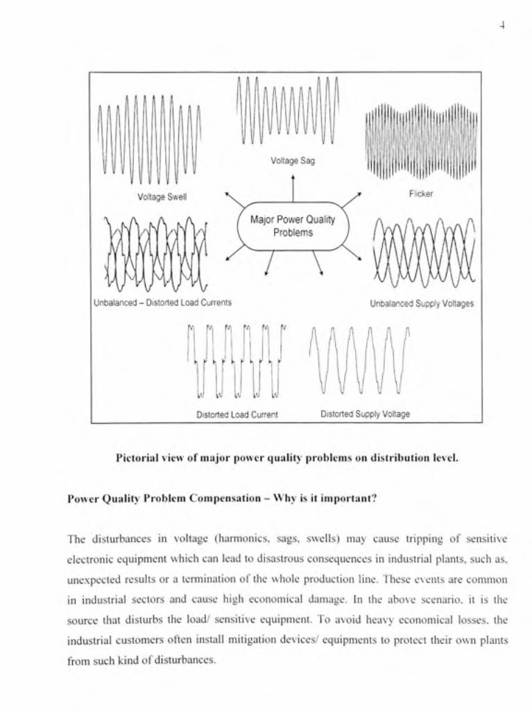
Some of the importan t powe r qualit y problem s are shown i n the followin g Figure .
Voltage Swel l
Unbalanced - Distorte d Load Currents
^1 fA
Unbalanced Supply Voltages
h H
Vl fv i f v
h r
tN w W w
Distorted Load Current Distorted Supply Voltage
Pictorial view of major power quality problem s on distribution level .
Power Quality Problem Compensation - Wh y is it important?
The disturbance s i n voltag e (harmonics , sags , swells ) ma y caus e trippin g o f sensitiv e
electronic equipment whic h can lead to disastrous consequences i n industrial plants , such as,
unexpected result s o r a termination o f the whole productio n line . These event s are common
in industria l sector s an d caus e hig h economica l damage . I n th e abov e scenario , i t i s th e
source tha t disturb s th e load / sensitiv e equipment . T o avoi d heav y economica l losses , th e
industrial customer s ofte n instal l mifigatio n devices / equipments t o protec t thei r ow n plant s
from suc h kind of disturbances.
The presenc e o f powe r electronic s base d equipments / load s a t th e commercia l a s wel l th e
industrial secto r i s quite common . A diode bridg e rectifie r followe d b y a fron t en d capacito r
is one o f the mos t commo n type s o f topologies use d i n all the power electronic s base d powe r
processing applications . Thes e equipment s ar e mor e ofte n insensitiv e t o disturbance s i n
voltage, bu t dra w th e current s whic h ar e highl y distorte d i n nature . Moreover , studie s sho w
that suc h kind s o f equipment s ar e o f majo r concer n sinc e the y produc e distortio n i n suppl y
voltages. Anothe r importan t fac t i s tha t th e harmonic s an d unbalance d current s ultimatel y
result i n distorte d an d unbalance d voltages . I n thi s condition , eve n i f th e plan t doe s no t
experience an y direc t impact , they ar e the main caus e o f deterioration i n the quality o f powe r
supplied t o th e neighborin g customers . Ther e ma y b e man y simila r type s o f load s connecte d
on th e sam e feeder . Th e pollutio n o n th e distributio n networ k i s increasin g graduall y a t th e
extent tha t th e utilit y provider s ca n n o longe r suppor t them . Therefore , stric t standard s ar e
being impose d b y th e utilitie s o n industria l an d domesti c consumer s t o limi t th e amoun t o f
harmonics currents , unbalanc e and/o r flicker tha t a loa d ma y introduc e t o th e network . T o
comply wit h these limits , customers often hav e t o instal l mitigatio n equipment s t o reduce th e
level o f pollution cause d b y their load s and thus, avoid heavy penaltie s force d b y the utility .
The growin g us e o f powe r electronic s base d equipment s i n moder n plant s i s resultin g i n a
load whic h i s sensitiv e an d harmonic s producin g i n nature . Interestinglv' . thes e equipment s
generally produc e distortio n i n current s and/o r voltages . Thus , there i s a new tren d t o instal l
mitigating equipment s tha t ca n serv e th e dua l purpose , t o bot h th e utilit y a s wel l a s t o th e
customer. Th e importan t objectiv e unde r suc h a n environmen t i s t o simultaneousl y protec t
sensitive equipment s fro m voltag e disturbance s an d t o reduc e th e distortio n injecte d b y th e
plant to the network .
Role o f Power Electronic s Device s i n Power Qualit> Enhancemen t
As discusse d i n th e previou s sections , th e powe r electronic s base d devices/equipment s hav e
become ke y component s i n today' s mode m powe r distributio n system . I n spit e o f th e vas t
advantages offere d b y utilizin g th e power electronic s base d equipmen t fo r powe r processing ,
the operatio n o f thes e device s give s ris e t o som e seriou s drawback s i n term s o f powe r
quality. Thes e device s generat e harmonic s pollutin g th e powe r distributio n system , an d
demand reactiv e power . I n orde r t o provid e technica l solution s t o th e ne w challenge s
imposed o n th e powe r systems , th e concep t o f flexible A C transmissio n system s (FACTS )
was introduce d i n th e lat e 1980s . Th e FACT S device s incorporat e powe r electronic s base d
controllers t o enhanc e th e controllabilit y an d t o increas e powe r transfe r capabilit y o f th e
transmission system . There ar e two approache s fo r th e realizatio n o f power electronic s base d
compensators: on e employ s conventiona l thyristor-switche d capacitor s (TSC ) an d reactor s
(TSR), an d th e othe r use s self-commutate d switchin g converters . Bot h th e scheme s hel p t o
efficiently contro l th e rea l an d reactiv e power , but onl y th e secon d on e ca n b e use d t o
compensate curren t an d voltag e harmonics . Moreover , self-commutate d switchin g converter s
present a better response time and more compensation flexibility.
The stati c VA R compensator s (SVC ) ar e use d t o contro l A C voltag e b y generatin g o r
absorbing th e reactiv e powe r b y mean s o f passiv e elements . A SV C consist s o f a n anti -
parallel thyristor s an d passiv e element s suc h a s a capacito r (TSC ) o r a reacto r (TCR) . Th e
effective valu e o f th e capacito r o r inducto r reactanc e i s changed continuousl y b y controllin g
the firin g angl e o f th e thyristors . A majo r drawbac k i n th e us e o f SV C i s tha t th e reactiv e
power handled b y the SV C syste m i s limited by the size of passive elements . On e of the mos t
versatile FACT S device s i s the STATCOM . I t consist s o f a voltage sourc e converte r (VSC) /
voltage sourc e inverte r (VSI ) with puls e widt h modulatio n (PWM ) an d ha s a faste r spee d o f
response. I n th e transmissio n system , i t ca n b e use d t o improv e th e syste m stabilit y an d
damping o r to suppor t th e voltage profile . Th e sam e structur e a t the distributio n level , know n
as D-STATCOM, ca n be used fo r reactiv e power suppor t o r for voltag e regulafion . Th e stati c
series compensato r (SSC ) o r dynami c voltag e restore r (DVR ) i s a VS l connecte d i n serie s
with the supply lin e and act s as a controlled voltag e source to obtain the desired loa d voltage .
When a n externa l D C voltag e sourc e i s utilize d fo r VSI . th e SSC / DV R ca n b e use d t o
compensate harmonic s i n th e voltage , t o regulat e loa d voltage , an d t o compensat e voltag e
unbalance, sa g and flicker.
Another device , the active power filter (APF ) i s the most promising solutio n to mitigate som e
of the major powe r qualit y problem s a t the distributio n level . They ca n b e classifie d a s shun t
APFs, serie s APFs , hybrid APFs , and unifie d powe r qualit y conditione r (UPQC) . The UPQ C
is on e o f th e mos t v ersatile powe r qualit y enhancemen t device s whic h offe r advantage s o f
both th e shun t an d serie s APFs , simultaneously . A detaile d operatin g principl e an d th e vas t
capabilities o f UPQ C ar e discusse d i n CHAPTE R 2 . Th e us e o f an y on e o f thes e APF s i s
slowly becoming a common practice i n modem industria l installations .
Research Objective s
This wor k wa s conducte d partiall y i n collaboratio n wit h Hydro-Quebe c an d IREQ . Th e
present work ha d tw o defined goal s - / ) to carry out the feasibilit y analysi s o f UPQC unde r a
realistic networ k conditio n an d // ) to develop a novel contro l approac h fo r UPQ C t o improv e
the syste m performance , an d thu s t o contribut e i n the o n goin g researc h wor k i n th e are a o f
power qualit y enhancement .
The research objectives ar e summarized below :
• T o carr y out a n in-dept h analytica l stud y o n ho w th e activ e an d reactiv e powe r flows
between th e utility , UPQ C an d th e load . Th e purpos e o f thi s analysi s i s t o understan d
how the UPQC ma y behave under different operatin g conditions .
• T o perfor m feasibilit y analysi s o f UPQ C unde r a realisti c networ k environment . Th e
network Simulin k mode l wa s buil t an d provide d b y Network Simulation Lab (LSR),
IREQ. Varennes , Quebec .
• T o realiz e a nove l syste m conflguratio n fo r th e three-phas e four-wir e UPQ C base d
system. Thi s provide s a n additiona l optio n t o futur e industria l customer s t o realiz e th e
three-phase four-wir e syste m fro m three-phas e three-wir e network .
• T o utiliz e th e serie s inverte r u p t o it s true capabilities , sinc e i t i s reveale d tha t th e serie s
inverter i n almost al l the applications i s underused .
• T o reduc e th e ratin g o f shun t inverte r suc h tha t i t wil l uhimatel y hel p t o optimiz e th e
overall UPQ C cost .
• T o develo p a ne w contro l philosoph y fo r LIPQ C whic h ca n incorporat e th e las t tw o
objectives, (discusse d i n CHAPTER 6 , termed a s Phase Angle Contro l o f UPQC).
Methodology
To accomplish th e objectives highlighte d abov e three importan t step s are followe d whic h ar e
outlined below :
• Thi s thesi s i s mad e o f th e basi c law s o f trigonometry , circui t theor y an d electrica l
engineering. Al l th e develope d contro l approache s ar e first put forwar d throug h adequat e
mathematical formulatio n supporte d wit h detailed vecto r diagram representations .
• Th e develope d contro l approache s ar e the n modele d usin g a digita l simulatio n tool , i n
this work , MATLAB / Simulink . Th e SIMPOWERSYSTE M (SPS ) bloc k set s ar e
predominantly use d t o represen t th e electrica l syste m an d t o buil d th e necessar y
simulation models . Th e performanc e o f UPQ C wit h develope d contro l approache s i s
evaluated unde r differen t operatin g conditions .
• Finally , th e reporte d researc h wor k i s validate d throug h laborator y experimenta l studies .
A rapi d hardwar e prototypin g boar d fro m dSPACE , suc h as , DSl 104 i s used t o interfac e
the hardwar e syste m wit h MATLAB / Simulin k base d contro l models . Th e develope d
controllers ar e tested unde r severa l differen t operatin g conditions .
The flow char t to achieve the proposed researc h work i s shown below .
ET
S-G
RE
PC
I La
b :A
-273
2
r-
Literature Review : Search for researcti problems !
1 r
Controller Development : Theoretical and Analytica l
Study
• "
Simulation: Mode l Development an d Performanc e
Evaluation by Simulation
No / ^ t i s f ^ \ Re s
Yes
actoryX Jits? / ^
>
" Hardware Syste m
Configuration and Setup
' ' Simulink Mode l Developmen t for Real-Time Implementatio n
'' Real-Time Mode l Executio n
V
System Performanc e Evaluation
J ° /S^s f \ ^ Re s
Yes
actoryX Jits? / ^
Performance Evaluatio n unde r several operatin g conditio n
^
^
ET
S-G
RE
PC
I L
ab
: A-2
760
Research work flow chart .
Thesis Contributions
The thesi s wor k wa s initiated wit h th e project o f feasibilit y analysi s o f emerging powe r
quality enhancemen t device s suc h as unified powe r quality conditioner , popularl y know n as
UPQC, for possible practical applications.
The foundatio n o f this thesi s wor k relie s o n the two significant terms , activ e powe r and
reactive power. Hig h importance is given to these two quantities while compensating severa l
important powe r qualit y problems . A t a given time , the source shoul d suppl y onl y activ e
power to the load, while, the reactive power should be locally supported by the active power
filter system . I n the course o f action, severa l controlle r approaches/concept s ar e proposed
10
which ar e applicabl e t o th e shun t APFs , serie s APF s and/o r UPQC . Th e importan t contro l
approaches ar e highlighte d as : uni t vecto r templat e generation , quadratur e voltag e injection ,
generalized single-phase/7-c y theory, power angle control o f UPQC.
The remarkabl e accomplishmen t o f th e propose d wor k i s i n th e developmen t o f a nove l
control philosoph y fo r UPQC . name d as , power angl e contro l (PAC ) approach . CHAPTER S
2, 3 and 4 ar e provide d fo r eas y an d bette r understandin g o f the PA C concep t an d serv e a s a
benchmark fo r th e thesi s work . Th e fundamental s o f th e PA C approac h ar e describe d b y
providing detaile d phaso r representation s an d a n in-dept h mathematica l analysis . Th e
concept o f th e PA C approac h i s supporte d throug h simulatio n studie s an d i s successfull y
validated experimentally . Th e concep t o f PA C approac h i s standardized i n such a way tha t i t
is wel l understoo d unde r varietie s o f condition s whic h include s th e norma l steady-state ,
voltage sag and voltage swell .
An interestin g UPQ C base d syste m configuration/structur e i s also propose d fo r futur e three -
phase four-wir e (3P4W ) distributio n system . I n th e propose d syste m configuration , a 3P4 W
system i s realize d fro m three-phas e three-wir e (3P3W ) UPQ C base d system . Th e neutra l o f
series transformer, use d i n the series part UPQC, is considered a s the neutral fo r the propose d
3P4W system . Thus , even i f the power supplie d b y the utilit y i s 3P3W, a n easy expansio n t o
3P4W system , i n UPQC base d applications, can be achieved .
Finally, a n experimenta l prototyp e i s buil t i n th e Groupe de recherche en electronique de
puissance et commande industrielle, GREPCI , (Powe r Electronic s & Industria l Contro l
Research Group ) laborator y a t Ecol e d e technologi c superieur e t o implemen t th e propose d
control algorithms . Th e prototyp e i s comprise d o f tw o three-phas e voltag e sourc e inverte r
cormected back t o back wit h each other . A kind o f universal activ e power filter whic h house s
14 insulate d gat e bipola r transisto r (IBGT's) , physicall y provide s a n opfio n o f realizin g
almost an y activ e powe r filter syste m configuration , suc h as , single-phas e an d three-phas e
(three-wire o r four-wire ) shun t APF , serie s APF , UPQ C o r an y type s o f hybri d APFs . A
hybrid analog-digita l contro l syste m i s designe d an d buil t particularl y fo r thi s prototype . I t
11
consists o f a digita l signa l processo r board , DS l 104, use d t o realiz e th e develope d contro l
algorithms i n real-time . Th e DS l 104 i s predominantl y utilize d t o generat e referenc e
current/voltage signals . A separat e analo g boar d i s designed an d fabricate d t o perfor m puls e
width modulation . Th e develope d boar d ha s a n optio n t o selec t a triangula r carrie r signa l
based fixed frequenc y PW M (switchin g frequenc y ca n b e se t to IkH z to 20kHz) o r a variable
frequency hysteresi s controller . Severa l loads , bot h linea r an d non-linea r ar e realize d i n th e
laboratory t o produc e a variet y o f loa d profiles . Th e develope d syste m performanc e i s
verified unde r differen t sourc e voltage s an d differen t loadin g conditions . Th e experimenta l
results are promising an d suppor t the findings reporte d i n the proposed work .
Thesis Outlin e
This thesis i s organized a s follows :
CHAPTER I present s a thorough revie w o f the past an d the mos t recen t researc h wor k bein g
done i n the area o f power quality compensatio n usin g UPQC . Reported literatur e on the topi c
is briefl y discussed . Th e UPQ C basics , includin g ke y concept s an d operatin g principles , ar e
explained whic h serve s a s a foundatio n fo r thi s thesi s work . A steady-stat e powe r flow
analysis i s also carrie d ou t and supporte d wit h a numerical example . Thi s chapte r i s partially
based o n two published paper s (Khadkikar et ai, 2006a , Khadkika r and Chandra . 2006e) .
CHAPTER 2 i s full y dedicate d t o th e collaboratio n project . Developmen t o f th e simples t
controller fo r UPQ C i s carrie d out . Extensiv e simulatio n result s wit h UPQ C installe d o n
realistic networ k condition s ar e reported . Th e detaile d experimenta l resuh s o n single-phas e
UPQC syste m unde r severa l la b test s ar e als o discusse d a t th e en d o f th e chapter . Th e wor k
presented i n thi s chapte r (analytica l an d simulatio n studies ) i s base d o n th e pape r entitle d
"Application o f UPQ C t o protec t a sensitiv e loa d o n a pollute d distributio n network" .
(Khadkikar e/a/., 2006b) .

12
In CHAPTE R 3 . specia l attentio n i s give n t o th e voltag e sa g compensatio n usin g reactiv e
power control . A new simplified approac h i s developed t o determine th e quadratur e injectio n
voltage necessar y t o compensat e th e voltag e sa g o n th e system . Interestin g experimenta l
results ar e discusse d bot h fo r single-phas e an d three-phas e UPQ C system . Thi s wor k
(analytical an d simulatio n studies ) i s reporte d i n " A Nove l Contro l Approac h fo r Unifie d
Power Qualit y Conditione r Q withou t Activ e Powe r Injectio n fo r Voltag e Sa g
Compensation". (Khadkika r an d Chandra . 2006e) .
CHAPTER 4 i s the resul t o f an innovativ e topolog y b y which th e futur e industria l customer s
or utilit y provider s wil l hav e a n optio n t o realiz e a three-phase four-wir e syste m o n a three -
phase three-wir e network . A new concep t t o compensate th e unbalance d loa d o n three-phas e
svstem i s also reported . Th e validatio n o f the propose d wor k i s done throug h simulatio n an d
experimental studies . Par t o f the wor k i s already publishe d i n " A Nove l Structur e fo r Three -
Phase Four-Wir e Distributio n Syste m Utilizin g Unifie d Powe r Qualit v Conditione r
(UPQC)". (Khadkikar an d Chandra , 2006d) .
CHAPTER 5 include s th e majo r contributio n o f thi s thesi s work . A ne w concep t an d
philosophy t o suppor t th e loa d reactiv e powe r utilizin g bot h th e shun t an d serie s inverter s o f
UPQC i s proposed . Thi s co-ordinate d loa d reactiv e powe r sharin g featur e o f UPQ C (terme d
as Powe r Angl e Contro l (PAC) ) result s i n th e shun t inverte r ratin g reduction , an d thu s th e
overall cos t o f UPQC. A detailed mathematica l analysis , simulation result s an d experimenta l
investigations ar e given . Th e experimenta l result s sho w tha t fo r a give n laborator y loa d
condition th e shun t inverte r ratin g can be reduced u p to 50% . The reported wor k i s publishe d
in IEE E Transaction s o n Powe r Deliver y (" A Ne w Contro l Philosoph y fo r Unifie d Powe r
Quality Conditione r (UPQC ) t o Co-ordinat e Loa d Reactiv e Powe r Deman d Betwee n Shun t
and Serie s Inverters" , Khadkikar an d Chandra. 2008b) .
In CHAPTE R 6 . th e concep t o f PA C o f UPQ C i s furthe r extende d fo r differen t sourc e
voltage conditions . Generalize d equation s fo r th e PA C approac h ar e als o fomiulated .
Validation o f the reported wor k i s done through simulatio n an d experimenta l studies .

The ke y conclusion s o f thi s thesi s wor k an d recommendation s fo r futur e wor k ar e als o
reported. Finally , a t th e en d o f th e thesis , th e lis t o f ke y reference s an d appendice s ar e
provided.

CHAPTER 1
UPQC BASIC S AND STEADY-STATE POWE R FLO W ANALYSI S
1.1 Introductio n
This chapte r i s aimed t o develop necessar y backgroun d knowledg e an d t o briefl y discus s th e
latest developmen t i n th e field of active power filters (APF) . Th e chapte r begin s wit h a
detailed workin g principl e o f th e UPQC . Late r o n i n th e chapter , a systemati c literatur e
review o n th e activ e powe r filters i s given . I t i s show n tha t th e unified power quality
conditioner (UPQC ) i s truly a versatile devic e amon g th e activ e powe r filters t o compensat e
several differen t powe r qualit y problems , simultaneously . Thi s wa s on e o f the motivations t o
carty ou t th e researc h wor k o n UPQC . A n interestin g analytica l stud y o n ho w th e activ e an d
reactive powe r flows betwee n source . UPQC. and loa d under differen t operatin g conditions i s
done. This conceptua l stud y help s to understand th e power transfe r capabilitie s o f UPQC.
1.2 UPQ C Concept and Operatin g Principl e
There are two importan t type s of active power filters (APF ) - shun t APF and serie s APF. The
shunt AP F i s th e mos t promisin g t o tackl e th e curren t relate d problems , whereas , th e serie s
APF i s th e mos t suitabl e t o handl e voltag e relate d problems . Sinc e th e mode m distributio n
system demand s a bette r qualit y o f voltag e bein g supplie d an d curren t drawn , installatio n o f
these two APFs have grea t scop e i n the near future . However , installing tw o separat e device s
to compensat e voltag e an d curren t relate d powe r qualit y problems , independently , ma y no t
be a cos t effectiv e solution . Mora n (1989) , introduce d a syste m configuratio n i n whic h bot h
series an d shun t APF s wer e connecte d bac k t o bac k wit h commo n D C reacto r i n betwee n
them. H e terme d th e topolog y a s lin e voltag e regulator/conditione r (LVRC) . Th e back-to -
back inverte r syste m configuratio n trul y cam e int o attentio n whe n Fujit a an d Akag i (1998 )
proved th e practica l applicatio n o f this topology wit h 20kV A experimenta l results . Fujit a an d
Akagi name d thi s devic e a s - unifie d powe r qualit y conditione r (UPQC) , an d sinc e the n th e
name UPQ C ha s bee n popularl y use d b y man y researcher s (Che n et al. 2000 ; Elnad y et al..
15
2001; Ghos h et al, 2004 ; Khoo r et al., 2005 ; Kazem i et al., 2006a ; Kolhatka r an d Das ,
2007).
UPQC is the integration of shunt and series APFs with a common self-supporting DC bus.
1.2.1 UPQ C System Configuratio n
Figure 1. 1 show s syste m configuratio n o f a three-phase UPQC . A s marke d i n the figure , th e
key components o f UPQC ca n be highlighted a s follows :
• Conip-A , voltag e sourc e inverte r (VSl) : i t i s connected acros s the loa d an d controlle d
to function a s shunt APF .
• Comp-B , VSI: i t is controlled t o function a s series APF.
Both th e VSl s ar e realize d b y usin g si x insulate d gat e bipola r transistor s (IGBTs )
each and ar e connected t o the network by using coupling inductors .
• Comp-C , D C lin k capacitor : th e two VSIs are connected bac k t o back wit h each othe r
through thi s capacitor . Th e voltag e acros s thi s capacito r provide s th e self-supportin g
DC voltag e fo r prope r operatio n o f bot h th e inverters . Wit h prope r control , th e D C
link voltag e act s a s a sourc e o f activ e a s wel l a s reactiv e powe r an d thu s eliminate s
the need o f extemal D C source (Fo r example: D C battery) .
• Comp-D , couplin g inductor : i t i s utilized t o connec t th e shun t inverte r t o the networ k
and facilitate s th e flow of compensating current . I t also helps i n smoothing the curren t
wave shape .
• Comp-E , L C filter: i t serve s a s a passiv e lo w pas s filter an d help s t o eliminat e hig h
frequency switchin g ripple s on generated inverte r output voltage .
• Comp-F , serie s transformer : th e necessar y voltag e generate d b y th e serie s inverte r t o
maintain th e loa d voltag e pur e sinusoida l an d a t desire d valu e i s injecte d i n th e lin e
through thes e serie s transformers . A suitabl e tur n rati o i s ofte n considere d t o reduc e
the current flowing throug h the series inverter .
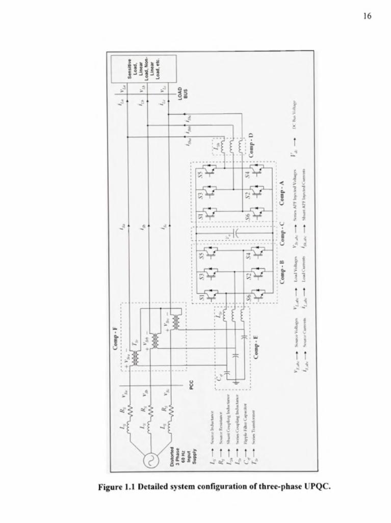
16
Figure 1. 1 Detailed system configuration o f three-phase UPQC .
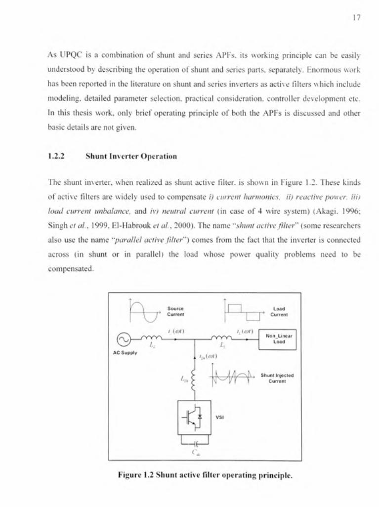
17
As UPQ C i s a combinatio n o f shun t an d serie s APFs , it s workin g principl e ca n b e easil y
understood b y describin g th e operatio n o f shun t an d scrie s parts , separately . Enormou s wor k
has been reported i n the literatur e o n shunt an d serie s inverter s a s active filters w hich includ e
modeling, detaile d paramete r selection , practica l consideration , controlle r developmen t etc .
In thi s thesi s work , onl y brie f operatin g principl e o f bot h th e APF s i s discusse d an d othe r
basic details are not given .
1.2.2 Shunt Inverte r Operatio n
The shun t inverter , whe n realize d a s shun t activ e filter, i s show n i n Figur e 1.2 . Thes e kind s
of activ e filters ar e widel y use d t o compensat e i) current harmonics, ii) reactive power, Hi)
load current unbalance, an d iv) neutral current (i n cas e o f 4 wir e system ) (Akagi . 1996 ;
Singh et al, 1999 , El-Habrouk et al, 2000) . The name '"shunt active filter"" (some researcher s
also us e th e nam e "parallel active filter") come s fro m th e fac t tha t th e inverte r i s connecte d
across (i n shun t o r i n parallel ) th e loa d whos e powe r qualit y problem s nee d t o b e
compensated.
13 AC Suppl y
l^s
Source Current
l.[(Ot)
>
Load Current
/, ( at) Non_Linear
Load
., 'sM^t)
\ I / /'~\\ ) Shun t Injecte d ^ ^ / ^ Curren t
"v VSI
^ • . .
Figure 1. 2 Shun t activ e filte r operatin g principle .
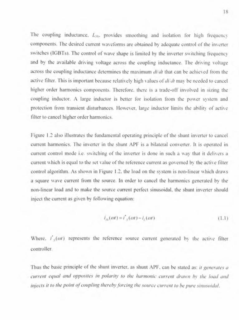
18
The couplin g inductance , L.v, , provide s smoothin g an d isolatio n fo r hig h frequenc v
components. Th e desire d curren t wavefomi s ar e obtained b y adequat e contro l o f the in v erter
switches (IGBTs) . Th e contro l o f wav e shap e i s limite d b y th e inverte r switchin g frequenc y
and b y th e availabl e drivin g voltag e acros s th e couplin g inductance . Th e drivin g voltag e
across th e couplin g inductanc e determine s th e maximu m di/dt tha t ca n b e achieve d fro m th e
active filter. Thi s i s important becaus e relativel y hig h value s ofdi/dl ma y b e needed t o cance l
higher orde r harmonic s components . Therefore , ther e i s a trade-of f involve d i n sizin g th e
coupling inductor . A larg e inducto r i s bette r fo r isolatio n fro m th e powe r svste m an d
protection fro m transien t disturbances . However , larg e inducto r limit s th e abilit v o f activ e
filter t o cancel higher order harmonics .
Figure 1. 2 als o illustrate s th e fundamenta l operatin g principl e o f the shun t inverte r t o cance l
current harmonics . Th e inverte r i n th e shun t AP F i s a bilatera l converter . I t i s operate d i n
current contro l mod e i.e . switchin g o f th e inverte r i s don e i n suc h a way tha t i t deliver s a
current whic h i s equal t o the se t value o f the reference curren t a s govemed b v th e active filter
control algorithm . A s show n i n Figur e 1.2 , th e loa d o n the svste m i s non-linear whic h draw s
a squar e wav e curren t fro m th e source . I n orde r t o cance l th e harmonic s generate d b y th e
non-linear loa d an d t o mak e th e sourc e curren t perfec t sinusoidal , th e shun t inverte r shoul d
inject th e current a s given by following equation :
i,iXoJt) = i',{cot)-i,icot) (1.1 )
Where, i'gicot) represent s th e referenc e sourc e curren t generate d b v th e activ e filter
controller.
Thus th e basi c principl e o f the shun t inverter , a s shun t APF , can b e state d as : it generates a
current equal and opposites in polarity to the harmonic current drawn by the load and
injects it to the point of coupling thereby forcing the source current to be pure sinusoidal.
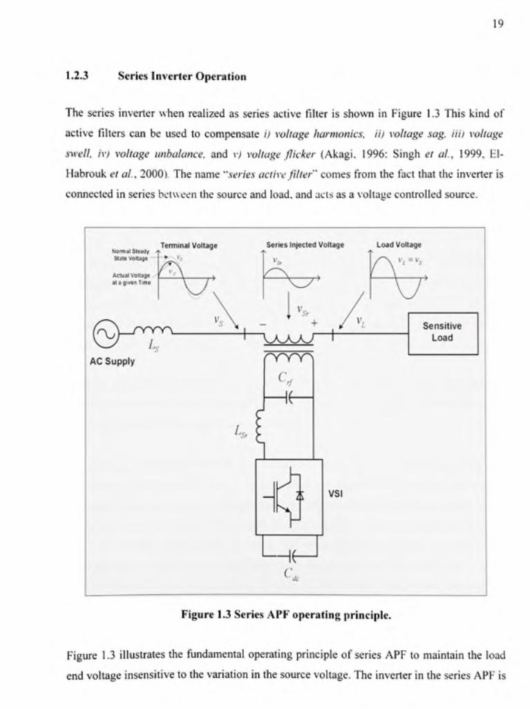
19
1.2.3 Serie s Inverter Operation
The serie s inverte r whe n realize d a s series activ e filter is shown i n Figur e 1. 3 Thi s kin d of
active filters ca n b e use d t o compensat e i) voltage harmonics, ii) voltage sag. Hi) voltage
swell, iv) voltage unbalance, and v ) voltage flicker (Akagi , 1996 : Sing h et al, 1999 , El -
Habrouk et al, 2000) . The name "series active filter" comes from th e fact tha t the inverter is
connected in series between the source and load, and acts as a voltage controlled source.
Normal steady •^ State Voltage
Actual Voltage at a given Time
Terminal Voltage Series Injected Voltage Load Voltage
O. "Sr
+ L
AC Supply
Sensitive Load
L
y ^(r
VSI
C dc
Figure 1.3 Series APF operating principle.
Figure 1. 3 illustrate s the fundamenta l operafin g principl e o f series APF to maintain the load
end voltage insensitive to the variation in the source voltage. The inverter in the series APF is

20
operated i n voltag e contro l mod e i.e . switchin g o f th e inverte r i s don e i n suc h a way tha t i t
delivers a voltage whic h i s equal t o th e se t valu e o f the referenc e voltag e a s goveme d b y th e
APF contro l algorithm . A sa g i n th e sourc e voltag e i s show n i n th e figure. Th e reduce d
voltage i s marke d a s v '5. I n orde r t o kee p th e voltag e a t loa d temiina l equa l t o th e norma l
steady-state voltage , th e serie s inverte r shoul d injec t a voltag e a s give n b y followin g
equation:
v^^{o)t) = v\(cot)-v,((i)t) (1.2 )
Where v /, i s th e desire d voltag e a t th e loa d bus . Thus , t o compensat e a di p i n voltag e th e
series inverte r shoul d suppl y a n in-phas e voltag e (othe r option s ar e als o available) , suc h tha t
the su m o f th e reduce d sourc e voltag e an d serie s injecte d voltag e maintain s th e desire d loa d
voltage. I f the sourc e voltag e contain s th e harmonics , usin g (2.12) . the serie s inverte r shoul d
inject harmoni c par t o f voltage i n order to maintain the load voltage sinusoidal .
Thus th e basi c principl e o f serie s inverter , a s serie s activ e filter, ca n b e state d a s follows : it
generates a voltage and inject in series with line such that the voltage at the load side would
be always sinusoidal, free from distortion, and at desired voltage magnitude.
Sometimes, a s configure d i n Figur e 1.4 , a tuned passiv e L C filter i s connected i n shun t wit h
the loa d alon g wit h th e serie s APF . I n suc h cases , th e serie s AP F compensat e th e curren t
distortion produce d b y th e non-linea r load , b y imposin g a hig h impedanc e pat h t o th e
harmonics current , an d thu s forcin g hig h frequenc y current s t o flow throug h passiv e filter.
The hig h impedanc e impose d b y th e serie s AP F i s create d b y generatin g a voltag e o f th e
same frequenc y tha t th e curten t hamioni c componen t need s t o b e eliminated . Thu s a serie s
APF ca n als o ac t a s a harmonic isolator . I n such application s th e ratin g o f serie s inverte r i s a
small fracfion o f the load kVA rafing .
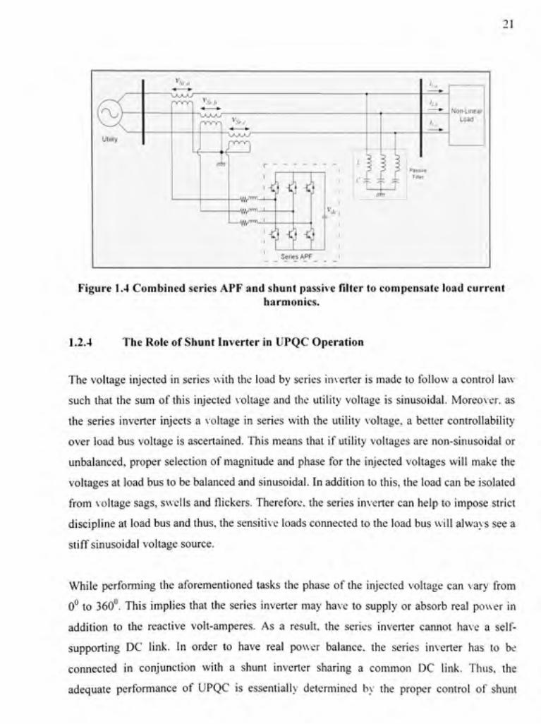
21
"\>.AAy'~
"VAAA^
.1^
i ni fl I i^f/yrn-
il
Non-Linear Load
Series APF
Figure 1.4 Combined series APF and shunt passive filter to compensate load current harmonics.
1.2.4 The Role of Shunt Inverter in UPQC Operation
The voltage injected i n series with the load by series inverter is made to follow a control law
such tha t the su m of this injected voltag e and the utilit y voltag e i s sinusoidal . Moreover , as
the serie s inverte r inject s a voltage i n serie s with th e utilit y voltage , a better controllabilit y
over load bus voltage i s ascertained. Thi s means that i f utility voltages are non-sinusoidal o r
unbalanced, proper selection o f magnitude and phase for the injected vohage s wil l make the
voltages at load bus to be balanced and sinusoidal. In addition to this, the load can be isolated
from voltag e sags, swells and flickers. Therefore, the series inverter can help to impose strict
discipline at load bus and thus, the sensitive loads connected to the load bus will alwav s see a
sfiff sinusoida l voltage source.
While performing th e aforementioned task s the phase o f the injecte d voltag e ca n var y fro m
O' t o 360° . This implie s that the serie s inverte r ma y have to supply o r absorb rea l powe r i n
addition t o th e reactiv e volt-amperes . A s a result , th e serie s inverte r canno t hav e a self -
supporting D C link . I n orde r t o hav e rea l powe r balance , th e serie s inverte r ha s t o b e
connected i n conjunctio n wit h a shun t inverte r sharin g a commo n D C link . Thus , th e
adequate performanc e o f UPQ C i s essentiall y determine d bv ' th e prope r contro l o f shun t

-yi
inverter t o regulat e th e D C bu s voltag e a t a desired value . I n this cas e th e shun t inverte r no t
only supplie s o r absorb s th e requisit e rea l powe r a s demanded b y the serie s inverte r but also ,
at th e sam e time , take s a n activ e rol e i n compensatin g th e loa d curren t relate d powe r qualit y
problems.
1.2.5 Contro l o f UPQ C
The activ e filters d o not nee d t o consum e an y rea l powe r t o cance l curren t an d voltag e
harmonics. Th e harmoni c currents / voltage s t o b e cancelle d ca n b e considere d a s reactiv e
power. I n th e contro l part , th e contro l scheme / algorith m o f UPQ C shoul d assur e - / )
accurate generatio n o f referenc e curren t signal s fo r shun t inverter , // ) accurat e generatio n o f
reference voltag e signal s fo r serie s inverter , /// ) maintai n th e D C lin k voltag e a t constan t se t
level, and iv) generation o f proper switchin g pulse s fo r both the inverter switches .
To generat e accurat e referenc e signal s fo r UPQC , th e contro l schem e ma y b e base d o n th e
combination o f on e o f th e popula r contro l strategies , suc h as , instantaneou s reactiv e powe r
theory, synchronou s referenc e fram e method , symmetrica l componen t theor y etc . Th e D C
link voltage control ca n be achieved by adjusting th e smal l amoun t o f rea l power absorbed b y
the inverters .
Finally, the curren t modulato r generate s the switchin g pattern s fo r inverte r switches . Mos t o f
the modulatio n technique s use d fo r APF s ar e base d o n puls e widt h modulatio n (PWM )
strategies. Th e contro l modulato r ca n b e a periodica l samplin g control . Hysteresi s ban d
control. Triangular carrie r control , space vector control , etc.
In this thesis work, many contro l approache s ar e proposed an d discussed i n detail .

23
1.3 Literatur e Revie w
The earlies t systemati c pape r o n activ e powe r filters ca n b e date d bac k i n 197 6 writte n b y
Gyugyi L . an d E . Strycula . Thi s pape r present s th e PW M converter s base d familv ' o f AP F
circuits whic h ca n functio n eithe r a s idea l curren t o r voltag e generators . Th e APF s wer e
classified a s shun t AP F to cance l ou t the harmonic s generate d b y non-linea r load s an d serie s
APF t o cance l th e harmonic s presen t i n th e sourc e voltage . Sinc e then , ther e ha s bee n
tremendous developmen t i n th e field o f activ e powe r filters wit h laborator y prototype s a s
well a s field installations .
Although considerabl e researc h wor k i n th e are a o f shun t AP F i s takin g place , a s notice d
from th e availabl e literature , the interes t i n the are a o f serie s APF i s not tha t significant . Thi s
is du e t o th e fac t tha t i t i s difficu h t o compensat e th e loa d curren t harmonic s usin g serie s
APF an d thu s ca n onl y b e use d t o compensat e voltag e harmonics . Additionally , th e curren t
harmonic issu e i s mor e dominan t tha n th e voltag e hamionics . Bette r th e profil e o f curren t
drawn fro m th e source , bette r would be the voltage a t the distributio n level . Interestingly , the
improved curren t profil e (clos e t o sinusoidal ) certainl y help s t o improv e th e PC C voltag e
profile, but , the reversa l i s not necessaril y achievable . Moreover , the cos t o f serie s APF . due
to the requirement o f serie s transformer, compare d t o the shun t AP F i s noficeably high . Late r
on, the concept o f hybrid activ e power filter ha s evolved i n order to reduce the overall cos t o f
APF syste m (Akagi , 1996 ; Singh et al, 1999 ; El-Habrouk et al, 2000) .
The mode m powe r distributio n syste m i s becoming highl y vulnerabl e t o the differen t powe r
quality problem s (Duga n et al, 1996 ; Schlabbac h et al, 2001 ; Stones an d Collinson , 2001 ;
Sankaran, 2002) . Therefore, som e kind o f compensation a t all the power level s i s becoming a
common practic e (Hingoran i et al, 2000 ; Emad i et al, 2001 ; Ghos h et al, 2002 ; Sood ,
2004). A t th e distributio n level , UPQ C ca n b e a significantl y attractiv e solutio n t o
compensate severa l powe r qualit y problems .

24
UPQC (Fujit a et al, 1998 ) i s a mitigating devic e tha t i s similar i n construction t o a unifie d
power flow controlle r (UPFC ) (Gyugyi , 1992) . Bot h th e UPQ C an d UPF C emplo y tw o
voltage source inverters (VSIs) that are connected to a common D C energy storag e element ,
such as an inductor or capacitor. UPFC i s employed i n power transmission syste m where as
UPQC i s employe d i n a powe r distributio n system , t o perfor m th e shun t an d serie s
compensation simultaneously . However, a UPFC only needs to provide balance shunt and/or
series compensation, sinc e a power transmission syste m generally operates under a balanced
and distortion free environment . On the other hand, a power distribution syste m may contain
DC components , distortio n an d unbalance . Therefore , a UPQ C shoul d operat e unde r thi s
environment while performing shun t and/or series compensation.
^
utility Voltage
v.
t Non-Linear
Load, Sensitive
Load
^ t^ Series Inverter Shun t Inverter
Figure 1.5 General block diagram representation o f UPQC system.
The genera l bloc k diagra m representation o f a UPQC base d syste m i s shown i n Figure 1.5 .
The main purpose of a UPQC is to compensate for supply voltage power quality issues , such
as, sags , swells , unbalance , flicker, harmonics , etc , an d fo r loa d curren t powe r qualit y
problems, suc h as , harmonics , unbalance , reactiv e current , etc . Differen t article s base d o n
UPQC hav e bee n criticall y reviewe d an d a systemafic stud y i s provided i n orde r t o have a
basic knowledg e o f variou s topologie s an d contro l technique s tha t ar e availabl e i n th e
literature dependin g o n th e syste m configuration , workin g conditions , applicatio n an d loa d
requirements. Variou s author s have give n differen t nam e t o this combine d syste m o f shun t
and serie s APF , suc h as . Lin e Voltag e Regulator / Condifione r (LVRC ) (Moran , 1989) ,

2S
Unified Activ e Powe r Filte r (UAPF ) (Muth u an d Kim , 1997) , Universa l Activ e Powe r Lin e
Conditioner (UAPLC ) (Arede s el al, 1998) , Universa l Powe r Qualit y Conditionin g Syste m
(UPQCS) (Graova c et al, 2Q00).
1.3.1 Classification o f UPQC
In this section , a UPQC i s systematically classifie d considerin g differen t aspects , such as . the
type o f suppl y system , converte r topolog y use d fo r realization , UPQ C syste m configuratio n
and typ e o f contro l strategie s used . Figur e 1. 6 shows th e pictoria l vie w fo r th e classificatio n
of UPQC.
UPQC Classification
1 ' Supply Syste m
- Two Wire
- Three Wire
- Four Wire
' r
Converter Topolog y
- VSI Based
- CSI Based
^ '
Configuration
- VSI Based
- CSI Based
1 '
Control Strategy
- p-q Theory
- d-q Theory
- Symmetrica l Com p Theory
- Fuzzy Logi c
- Wavelet Analysi s
-ANN, etc
Figure 1. 6 Pictoria l view fo r the classification o f UPQC .
1.3.1.1 Classificatio n Base d o n Supply Syste m
The load s or equipments ca n be broadly divided int o single-phas e o r three-phase, supplied b y
single-phase (tw o wire ) o r three-phase (three-wir e o r four-wire ) sourc e o f power . Therefore ,
to compensat e th e powe r qualit y problem s UPQ C ca n b e classifie d base d o n th e typ e o f th e
supply system . Figur e 1. 7 show s a UPQC syste m configuratio n (Bas u et al, 2001 ; Nasiri an d
Emadi, 2003 ; Priet o et al, 2005 ; Kazem i et al. 2006b ; Khoo r an d Machmoum , 2007 )
realized t o compensate the power quality problems in single-phase suppl y system .
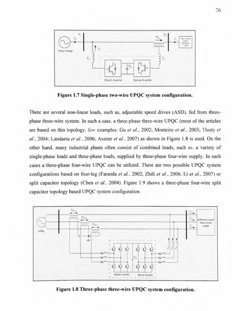
( ^ : '
Ulilrly Voltage
4-,
t'.
H ^ n T
Shunl Inverte r
V. ^ ' . s .
_l
D < / ' v
_J Series Inverte r
ll Non-Lmear Load
Ser>sitive Load
Figure 1.7 Single-phase two-wire UPQC system configuration .
There ar e severa l non-linea r loads , such as , adjustable spee d drive s (ASD) , fed fro m three -
phase three-wire system. In such a case, a three-phase three-wire UPQC (most of the articles
are based o n thi s topology, fe w examples : Gu et al, 2002 ; Monteiro et al, 2003 ; Tlusty et
al. 2004 ; Landaeta et al. 2006 ; Axente et al, 2007 ) as shown i n Figure 1. 8 i s used. On the
other hand , man y industria l plant s ofte n consis t o f combine d loads , suc h as . a variet y o f
single-phase load s and three-phase loads , supplied b y three-phase four-wir e supply . I n such
cases a three-phase four-wir e UPQ C ca n be utilized . Ther e ar e two possibl e UPQ C syste m
configurations base d on four-leg (Farand a et al. 2002 ; Zhili et al. 2006 ; Li et al. 2007 ) or
split capacito r topolog y (Che n et al. 2004) . Figure 1. 9 show s a three-phase four-wir e spli t
capacitor topology based UPQC system configuratio n
' ' , S > , 1
/ ' Y W ^ *.Sr >
.jr::]
-JVyyYYYV_ n
-w^™- Mi -fffl
Hi -J^y/YYYV
_W^^vm_
Different Linea r Non-Linear
Loads
Series Inverte r Shun I Inverter
Figure 1.8 Three-phase three-wire UPQC system configuration .
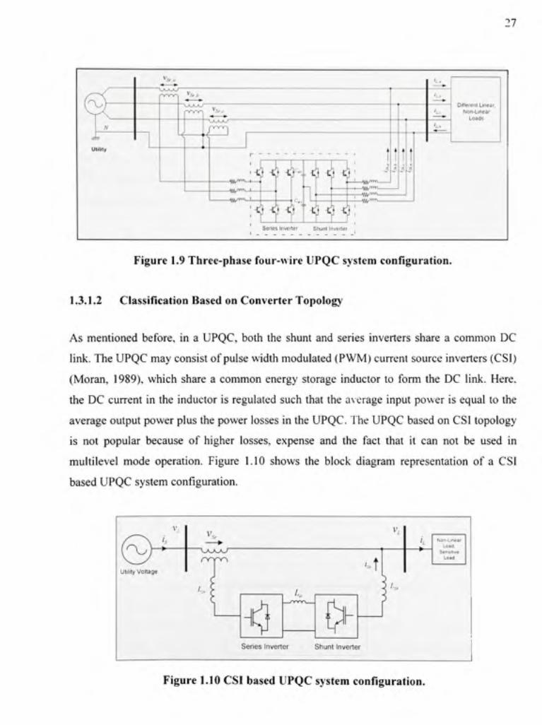
27
\\,
utility
•Xr./.
.ir:]
-tififfjr(y\^ .1 ili Hi ->W^ 1 -vy^ -Vf/^ -tffyfrrf\
DiflerenI Linear, Non-Linear
Loads
Senas Inverter Sttun I Inverter
Figure 1.9 Three-phase four-wire UPQC system configuration .
1.3.1.2 Classificatio n Base d on Converter Topology
As mentioned before , i n a UPQC, both th e shun t an d serie s inverter s shar e a common D C
link. The UPQC may consist of pulse width modulated (PWM) curtent source inverters (CSI)
(Moran, 1989) , which shar e a common energ y storag e inducto r t o for m th e D C link . Here ,
the DC current i n the inductor i s regulated suc h that the average input power i s equal to the
average output power plus the power losses in the UPQC. The UPQC based on CSI topology
is no t popula r becaus e o f highe r losses , expens e an d th e fac t tha t i t ca n no t b e use d i n
multilevel mod e operation . Figur e 1.1 0 show s th e bloc k diagra m representatio n o f a CS I
based UPQC system configuration .
utility Voltag e
Series Inverter
Non-Linea( Load.
Sensitve Load
Figure 1.10 CSI based UPQC system configuration .
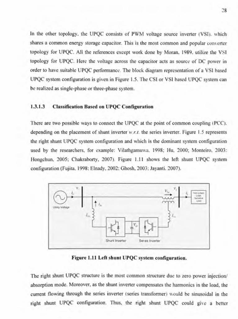
In th e othe r topology , th e UPQ C consist s o f PW M voltag e sourc e inverte r (VSI) , whic h
shares a common energ y storag e capacitor . Thi s i s the most common an d popula r conv erter
topology fo r UPQC . Al l th e reference s excep t wor k don e b y Moran , 1989 . utilize th e VSI
topology fo r UPQC . Her e th e voltag e acros s th e capacito r act s a s sourc e o f D C powe r i n
order to have suitable UPQ C performance. Th e block diagram representatio n o f a VSl based
UPQC system configuration i s given in Figure 1.5 . The CSI or VSI based UPQC system can
be realized as single-phase or three-phase system.
1.3.1.3 Classificatio n Base d on UPQC Configuration
There ar e two possible ways to connect the UPQC a t the point of common coupling (PCC).
depending on the placement o f shunt inverte r w.r.t. the series inverter . Figur e 1. 5 represent s
the right shun t UPQC system configuration an d which i s the dominant syste m configuratio n
used b y th e researchers , fo r example : Vilathgamuvva , 1998 ; Hu , 2000 ; Monteiro , 2003 :
Hongchun, 2005 ; Chakraborty , 2007) . Figur e 1.1 1 show s th e lef t shun t UPQ C syste m
configuration (Fujita , 1998 ; Elnady, 2002; Ghosh, 2003; Jayanti. 2007).
( ^ ; - '
utility Voltage
4*
f . .
^ ;
n Shunt Invert e
1"... T
r
V, ^Sr
j—i
i i —
Series Invert e
}L.
_J -r i
/. Non-Linear Load.
Sensitive Load
Figure 1.11 Left shunt UPQC system configuration .
The right shun t UPQ C structur e i s the most commo n structur e du e to zero power injecfion /
absorption mode . Moreover, as the shunt inverter compensates the harmonics in the load, the
current flowing throug h th e serie s inverte r (serie s transformer ) woul d b e sinusoida l i n th e
right shun t UPQ C configuration . Thus , th e righ t shun t UPQ C coul d giv e a bette r
29
performance unde r a highly distorte d condition . Th e lef t shun t UPQ C structur e i s sometime s
used i n specia l cases , fo r example , t o avoi d th e interferenc e betwee n th e shun t inverte r an d
passive filters. Th e righ t shun t an d th e lef t shun t UPQ C ca n b e realize d usin g CS I o r VS l
topology an d used fo r single-phas e an d three-phase systems .
1.3.1.4 Classificatio n Base d o n Control Strateg y
There ar e man y contro l strategie s tha t ca n b e use d fo r UPQC , suc h as . Instantaneou s
Reactive Powe r Theor y (o r Three-phase p-q Theory) , Synchronou s Referenc e Fram e Metho d
{d-q Theory) , Deadbea t control . Fuzz y Logi c control . Artificia l Neura l Networ k (ANN )
based control . Symmetrica l Componen t Theory , etc . Th e UPQ C controlle r ca n b e base d o n
one o r a combinatio n o f th e abov e contro l strategies . Th e popula r contro l strategies ,
algorithms o r approaches availabl e i n the literature are briefly discusse d i n the next section .
1.3.2 UPQ C Contro l Strategie s
Control strateg y i s the hear t o f an y powe r electronic s base d system . I t i s the contro l strateg y
which decide s the behavior an d the desired operation of a particular device . The effectivenes s
of the APF syste m (shunt , serie s o r UPQC) solel y depends upo n it s control algorithm . I n case
of UPQC, the contro l strateg y determine s the reference signal s (current an d voltage ) and thu s
decides th e switchin g instant s o f inverte r switches , suc h tha t th e desire d performanc e ca n b e
achieved. On e o f th e distinguishin g feature s o f AP F i s tha t i t doe s not consum e an y activ e
power fro m th e source . However , i n actual practic e ther e i s always som e powe r consumptio n
to overcom e th e switchin g losses . Som e o f th e importan t contro l strategie s ar e discusse d i n
the following section .
1.3.2.1 Frequenc y Domai n Compensatio n Metho d
This metho d i s base d o n th e Fas t Fourie r Transformafio n (FFT) . Th e harmoni c conten t o f
voltage o r curren t i s obtaine d b y extractin g A C fundamenta l componen t usin g a lo w pas s
filter. The n th e FF T o f harmonic s i s carrie d ou t an d coefficient s fo r eac h harmoni c ar e
30
computed. Th e disadvantag e o f thi s metho d i s larg e computatio n tim e an d hence , dela y fo r
the calculatio n o f FFT . I n man y case s a minimum on e whol e perio d o f wa v eform i s neede d
to perfor m th e FFT . Therefore , th e controller s base d o n frequenc y domai n method s ar e no t
popular fo r activ e filter application , becaus e th e respons e tim e play s a crucia l role . Th e
UPQC controlle r realize d usin g frequenc y domai n metho d ca n b e foun d i n articles b > Tlust y
et al, 200 4 and Kwan et al, 2007 .
1.3.2.2 Tim e domain Compensatio n Method s
Control method s fo r activ e filters i n the time domain ar e based o n instantaneou s derivatio n o f
compensating command s i n th e for m o f eithe r voltag e o r curren t signals . Ther e ar e a larg e
number o f contro l method s i n th e tim e domain . Onl y th e mos t popula r ar e briefl y discusse d
below.
• Instantaneou s Reactiv e Powe r Theor y
This metho d i s also know n a s a three-phase/?-^ theory , proposed b y Akag i et al, 1984 . Thi s
theory ha s prove n that , wit h prope r contro l o f VSI . withou t energ y storag e device , th e
harmonics generate d b y non-linea r load , and/o r th e loa d reactiv e powe r ca n b e compensate d
effectively. Th e concep t o f 3- ^ p-q theor y i s based o n a variable transformatio n fro m a-b-c
reference fram e t o a-[i co-ordinates. Onc e th e voltage s an d current s ar e transforme d int o th e
a-ft co-ordinates , th e instantaneou s tota l loa d activ e a s wel l a s th e reactiv e power s ar e
computed. Th e fundamenta l an d th e harmonics quantities , fro m th e tota l instantaneou s acti v e
and reactiv e powers , are then separate d usin g a low pass (LPF ) o r high pas s filter (HPF) . Fo r
load reactiv e powe r an d curren t harmoni c compensation , th e compute d instantaneou s tota l
reactive powe r an d th e instantaneou s harmoni c par t o f the loa d activ e powe r ar e considered ,
and transferred bac k to the a-b-c fram e a s reference AP F signals .
The mos t significan t advantag e of p-q theor y i s tha t th e rea l an d reactiv e power s associate d
with fundamenta l component s ar e d c quantities . Thes e quantifie s ca n easil y b e extracte d

31
using a low pass filter. Du e to the DC signa l extraction , filtering o f signal i n the a-P reference
frame i s insensitiv e t o an y phas e shif t error s introduce d b y lo w pas s filter. Bu t thi s metho d
works properl y wit h three-phas e balance d syste m an d whe n three-phas e voltage s ar e pur e
sinusoidal withou t harmonics , otherwise the results are poor .
This theor y ha s bee n extensivel y use d i n th e three-phas e AP F (three-wir e and/o r four-wire )
system. UPQ C controlle r base d o n three-phase/?-<:/ theory ca n be found i n articles by Fujita et
al, 1998 ; Aredes et al, 1998 , 2005; Li u et al, 2003 : Zhil i et al, 2006 ; L i et al, 200 7 an d
Turunen et al. 2007 .
• Synchronou s Referenc e Fram e Metho d {d-q Theory)
This metho d i s als o know n a s d-q metho d an d i s base d o n a-b-c t o d-q transformation ,
proposed b y Bhattachary a et al. 1995 . Thi s metho d ca n b e use d t o extrac t th e harmonic s
contained i n th e suppl y voltage s o r currents . Fo r curren t harmonic s compensation , th e
distorted current s ar e first transferre d int o two-phas e stationar y co-ordinate s usin g a-/ ?
transformation (sam e a s i n p-q theory) . Afte r that , th e stationar y fram e quantitie s ar e
transferred int o synchronou s rotatin g fram e usin g co s an d si n function s fro m th e PLL . Th e
sin and cos function s hel p to maintain th e synchronization wit h suppl y system . Simila r t o the
p-q theory , usin g a LP F o r HPF , the harmonic s an d fundamenta l component s ar e separate d
easily an d transferred bac k to the a~b-c fram e a s reference signal s for the APF.
In p-q theory , to compute the instantaneous activ e and reactive powers the knowledge o f bot h
the sourc e voltag e an d th e loa d curren t i s essential , while , th e d-q theor y deal s wit h th e
current independen t o f the suppl y voltag e (o r vice versa) . Therefore, th e d-q theory perform s
better unde r distorte d suppl y voltages . The UPQC controlle r base d o n d-q transformation ca n
be found i n Vilathgamuw a et al, 1998 ; Graova c et al. 2000 ; Hu et al. 2000 ; L i et al. 2000 :
Elnady et al, 2001b ; Chen et al, 2004 ; Cheng et al, 200 4 and Strzeleck i et al, 2005 .
32
• Symmetrica l Componen t Theor y
An unbalanc e i n th e three-phas e syste m ha s bee n generall y treate d throug h symmetrica l
components. I n this theory , a se t o f unbalanc e a c voltag e o r curren t phasor s ar e converte d t o
three-phase balanc e phasors . Therefore thi s approac h i s very usefu l fo r mitigatin g unbalanc e
problem i n suppl y voltag e an d thu s ca n b e use d t o extrac t th e referenc e voltag e signal s fo r
series APF.
Here, th e three-phas e voltage s ar e resolve d int o positive , negativ e an d zer o sequenc e
components by using a-b-c t o 0-1-2 plane transformation, give n by .
V ao
^'.1
^ ' - 2 .
1 ^ V 3
1
1 1
1
a a'
1 7
a' a
\
\
1
(1.3)
The referenc e signal s ar e obtaine d b y makin g positiv e sequenc e component , Vai equal t o
zero. Then , b y takin g invers e transformatio n th e referenc e signals , whic h wil l b e su m o f
unwanted negativ e an d zer o sequenc e components , ar e computed . Th e UPQ C base d o n th e
above approac h (Che n et al, 2001 ; Haque et al, 2002 ; G u et al, 2002 ; Ghos h et al. 2004 ;
Esfandiari et al, 2004 ; Kazem i et al, 2006b ) ca n compensat e th e voltag e sags , swells ,
unbalance an d flicker.
1.3.3 Additional Significan t Researc h Wor k
The followin g sectio n give s a brie f outlin e o f th e importan t wor k can-ie d out i n th e are a o f
UPQC b y different researchers .
Vilathgamunla et al, 1998 , have modeled UPQ C usin g the state space averaging technique t o
analyze it s behavio r unde r non-linearitie s du e t o loa d an d sourc e disturbanc e condition . Th e
delay i n detectio n an d calculatio n o f referenc e signal s make s i t difficult fo r eithe r serie s
inverter o r shun t inverte r t o achiev e th e perfec t voltag e an d curren t compensation . A
predictive contro l method , propose d b y Che n et al. (2000 ) ca n b e use d t o improv e th e
compensation effects . Thi s metho d i s base d o n takin g a calculate d valu e (th e componen t t o
be compensated ) o f perviou s perio d a s th e compensatin g valu e o f nex t period . Ghos h et al
(2003) hav e use d th e pol e shif t contro l technique . It' s a discrete-tim e contro l techniqu e i n
which th e closed-loo p pole s ar e chose n b y radiall y shiftin g th e ope n loo p pole s toward s th e
origin. Th e kV A rafin g issue s (Che n et al. 2001 ; Ryo o el al, 2004 ; Jayant i et al, 2006) ,
compensator losse s (Farand a et al. 2002 ) an d protectio n issue s (Cha e et al. 2001) , etc. , also
have bee n considere d fo r optimize d desig n o f the UPQC . Farand a el al. (2002 ) hav e give n a
procedure t o calculat e th e operatin g losse s o f inverters . Kwa n et al. (2007 ) hav e propose d a
model predictiv e contro l schem e fo r th e UPQC . I t i s a frequenc y domai n metho d whic h
utilizes th e Kalma n filters t o extrac t th e sourc e voltag e fundamenta l an d th e loa d curren t
harmonics components . A constan t frequenc y integratio n contro l approach , base d o n on e
cycle contro l o f switching converter s concept , i s given fo r the UPQC b y Vadiraiacharya et al.
(2006).
As mentione d i n sectio n 1.2.4 . th e contro l o f D C lin k voltag e play s a n importan t rol e i n
achieving th e desire d UPQ C performance . Severa l contro l technique s hav e bee n utilize d t o
maintain th e D C lin k voltag e a t a constan t level . Durin g th e syste m dynami c conditions , fo r
example, sudde n loa d change , voltag e sa g etc. , th e D C lin k feedbac k controlle r shoul d ac t
immediately t o restor e th e D C lin k voltag e a t se t referenc e valu e wit h a minimu m dela y a s
well a s lowe r overshoot . Th e P I controlle r base d D C lin k voltag e controlle r i s simpl e t o
implement an d henc e widel y use d b y th e researche s (Vilathgamuvv a et al. 1998 ; H u et al,
2000; Jianjun et al. 2002 ; Con-ea et al, 2005 ; Sundeepkumar et al. 2006 ; Xun et al. 2007) .
However, th e respons e tim e o f P I base d UPQ C system s i s slowe r i n natur e an d thus , t o
improve th e respons e time , severa l othe r technique s hav e bee n suggeste d b y differen t
researchers, suc h as , a fuzz y logi c base d controlle r (Sing h el al. 1998 ; Chakrabort y et al,
2005: Laxm i et al. 2006) . PfD ^ controlle r (Zuqua n et al, 2008) , optimize d controlle r
(Zhang e/a/. , 2007) .
34
Artificial neura l network s (ANN ) techniqu e ca n handl e th e multi-inpu t multi-outpu t contro l
system effectively . Thus , a n ANN techniqu e ca n b e utilize d t o develo p th e controlle r fo r th e
UPQC t o compensat e differen t voltage s an d currents . A fee d forwar d AN N schem e i s
reported b y Banae i et al. (2006 ) an d Te y el al. (2002b) , to separat e th e harmonics content s i n
the non-linea r load . Min g et al. (2006 ) hav e suggeste d a Levenberg-Marquard t optimize d
back propagation AN N controlle r fo r UPQC .
The tim e domai n an d frequenc y domai n technique s hav e certai n drawback s an d limitations .
To overcom e thei r problems , wavele t analysi s technique , a ne w too l fo r faul t detection ,
localization an d classificatio n o f differen t powe r syste m transient s i s propose d b y certai n
researchers. Elnad y et al. (2001 ) an d Forghan i et al. (2007 ) hav e introduce d a contro l
algorithm base d o n wavele t transformatio n fo r UPQ C t o compensat e th e loa d curren t
harmonics an d voltag e sags . B y usin g mult i resolutio n analysis , th e wavele t transfor m ca n
represent a time varyin g signa l i n terms o f frequenc y component . I t maps a one-dimensiona l
(ID) signa l o f tim e int o a two-dimensiona l (2D ) signa l o f tim e an d frequency . Thus , th e
wavelet analysi s ca n b e use d t o extrac t th e disturbanc e i n curren t o r voltag e t o generat e th e
reference signa l t o driv e th e shun t activ e an d serie s inverters . S o far , th e performanc e o f
ANN an d wavele t techniques , whe n applie d t o activ e powe r filters, ha s carrie d ou t throug h
simulation studies . Th e real-tim e implementation s o f thes e approache s nee d t o b e don e fo r
practical applications .
Kamran el al. (1995 ) an d Che n et al. (2001b) , hav e propose d a technique base d o n deadbea t
control, wherein , th e UPQ C converte r combinatio n i s treate d a s a singl e unit . A n invers e
system mode l i s use d t o generat e deadbea t contro l respons e fo r bot h th e inpu t curren t an d
output voltage . I n thi s case , converter s ca n reac t t o th e chang e i n PC C voltage s o r currents .
The overal l syste m ha s bee n modele d a s a singl e multi-input , mult i outpu t system . Th e
resultant contro l include s a n automati c fee d forwar d o f th e disturbanc e resultin g fro m th e
dynamics o f th e loadin g converter . Thi s result s i n improve d contro l performance s ove r th e
separately controlle d converter s and/o r reduce d inter-converte r energ y storage . Th e deadbea t
control algorith m ca n easil y b e implemente d o n a singl e microprocesso r a t moderat e
35
switching frequencie s (u p t o 1 0 kHz) . Th e syste m ha s a fas t dynami c respons e an d hig h
steady stat e accuracy . Th e majo r drawbac k o f this contro l strateg y i s that i t cannot b e applie d
for system s havin g unstabl e o r marginally stabl e ope n loo p poles. Also fo r system s wit h ver y
low damping, a deadbeat contro l strateg y ca n result i n large oscillations i n the output .
The voltag e sa g o n th e syste m i s on e o f th e mos t importan t powe r qualit y problem s tha t a
UPQC shoul d compensat e effectively . Man y researcher s hav e give n specia l attentio n o n th e
voltage sa g compensatio n usin g differen t approaches . Tlire e significan t contro l approache s
can b e foun d t o contro l th e sa g o n th e system : i ) active powe r contro l approac h i n whic h a n
in-phase voltag e i s injecte d throug h serie s inverte r (Vilathgamuw a et al, 1998 : Gong et al.
2002; Khoo r et al, 2005 ; Ha n et al. 2006 ; Kazem i et al. 2006) . ii ) reactiv e powe r contro l
approach i n whic h a quadratur e voltag e i s injecte d (Bas u et al. 2002) , an d iii ) a minimu m
VA loadin g approac h i n which a series voltage i s injected a t a certain angl e (Y u el al. 2004 ;
Kolhatkar el al. 2007 ; Kisc k et al, 2007) . Amon g th e abov e state d thre e approache s th e
quadrature voltag e injectio n require s a maximu m serie s injectio n voltage , whereas , th e in -
phase voltag e injectio n require s th e minimu m voltag e injectio n magnitude . Howeve r th e
current draw n b y the shunt inverter , to maintain th e DC lin k voltage a t a constant leve l an d to
maintain th e overal l powe r balanc e i n th e network , play s a n importan t rol e i n th e overal l
UPQC V A loadings . Beside s th e sa g o n the system , th e flicker an d unbalanc e cause d b y th e
arc furnac e ar e one o f the mos t sever e power qualit y problems . Th e UPQ C coul d b e the mos t
effective powe r qualit y conditione r t o solv e th e flicker problem s cause d b y a n ar c furnac e
load (Fujit a et al, 1998 ; Elnad y et al. 2001 ; Ghos h el al. 2003 : Tlust y et al, 2004 ;
Esfandiari e/a/, , 2004) .
An interestin g UPQ C syste m configuration , fo r mediu m voltag e applications , i s proposed b y
Han et al. (2006a) . Th e configuratio n i s realized b y usin g severa l H-bridg e modules . Th e H -
bridge module s fo r shun t par t o f UPQ C ar e connecte d i n serie s throug h a multiwindin g
transformer, while , th e H-bridge s i n th e serie s par t ar e directl y connecte d i n serie s an d
inserted i n th e distributio n lin e withou t a serie s injecte d transformer . Simila r topolog y ha s
been considere d b y Mufio z et al. (2007) . A doubl e cascad e H-bridg e modul e woul d requir e
36
four H-bridge s (1 6 IGBT's ) fo r eac h o f the phases , an d therefore , tota l o f 4 8 IGBT' s woul d
be required t o realize th e propose d structure . A s the numbe r o f module s increas e th e voltag e
handled b y eac h individua l H-brid e woul d reduc e an d thus , ca n b e usefu l i n th e mediu m
voltage application . Rubila r et al. (2007 ) hav e realize d a multilevel UPQ C base d o n a three-
level neutra l poin t clampe d (NPC ) topology . I t ca n b e a goo d choic e fo r mediu m o r hig h
power application s du e t o the reductio n i n voltage acros s eac h o f th e semiconducto r device s
by hal f A three-leve l topolog y require s doubl e semiconducto r device s (2 4 IGBTs ) a s tha t o f
the two-leve l UPQ C system . However , th e cos t involve d i n realizin g th e abov e mentione d
multilevel topologie s woul d b e considerable high . Additionally , th e increase d module s resul t
into increase d numbe r o f sensors , comple x contro l circuitry , highe r losses , an d additiona l
cost fo r multi-winding transformer fo r shun t part .
Obukhov et al. (2003 ) hav e introduce d a concept o f transformerless UPQC . The transforme r
used t o cormec t th e serie s inverte r i n th e lin e i s replace d b y a capacitor . Remova l o f th e
transformer eliminate s th e isolatio n betwee n th e tw o voltag e source s (suppl y voltag e an d
voltage generate d b y UPQC ) an d thus , ofte n i s not considere d b y othe r researchers .
Additionally, withou t a transforme r th e tur n ratio n betwee n th e serie s inverte r generate d
voltage an d actua l injecte d voltag e i n th e lin e act s a s one . Thi s furthe r reduce s th e
possibilities o f reducin g th e curren t rating s o f serie s inverte r switches . Generall y a suitabl e
transformer rati o i s alway s considere d i n UPQ C base d application s t o reduc e th e curren t
handled b y th e serie s inverter . Jinda l et al. (2007 ) hav e introduce d a syste m configuration ,
termed a s a n interlin e UPQ C (lUPQC ) t o improv e th e powe r qualit y o f tw o independen t
feeders (lines ) i n a distributio n system , simultaneously . Th e shun t inverte r o f UPQ C i s
connected acros s on e feeder , while , th e serie s inverte r i s connecte d i n serie s wit h th e line ,
through serie s transformers, i n the other feeder . Th e UPQC unde r suc h a configuration ca n be
utilized t o regulate th e bus voltage of one o f the feeder s an d to protect a senshive loa d o n th e
other feeder .
Recently, increase d attentio n i s bein g give n o n evaluatin g th e UPQ C contro l algorith m
effectiveness an d performanc e evaluatio n unde r differen t loa d an d suppl y voltag e condition s
37
with experimenta l investigation s i n the laborator y (Bas u et al, 2001 ; Liu et al. 2003 ; Che n
et al. 2003 ; Ryo o el al, 2004 ; Prieto et al. 2005 ; Correa et al. 2005 ; Strzelecki et al, 2005 ;
Han et al. 2006 ; Kolhatka r el al. 2007) . A 250kV A UPQ C syste m i s develope d an d unde r
field tes t a t Centr e fo r th e Developmen t o f Advance d Compufin g (C-DAC) , Trivandrum .
India (Suneepkuma r et al, 2006) . Additional significan t UPQ C prototypes : 20kV A (Fujit a el
al. 1998) , lOkV A (L i et al, 2007) , lOkV A (Kisc k et al, 2007) , 6kV A (Zhan g et al. 2007 )
and 4.5 kVA (Arede s et al. 2005).
1.4 Steady-State Powe r Flow Analysi s o f UPQ C
In this section , a comprehensiv e analytica l stud y i s presented . Th e ai m o f thi s analysi s i s t o
develop th e fundamenta l backgroun d an d thu s t o la y dow n th e necessar y foundatio n t o eas e
the concept s presente d i n th e thesi s work . I t als o help s t o understan d ho w th e activ e an d
reactive powe r flows betwee n source , UPQ C an d th e load , unde r som e o f th e importan t
conditions.
Figure 1.1 2 show s th e equivalen t circui t o f UPQC . Th e gir d voltag e an d gir d curren t ar e
denoted b y vorid- an d iond, respectively . Th e voltag e a t PC C i s referre d a s sourc e voltag e V5
(some researcher s refe r i t a s termina l voltage) . Th e loa d voltag e an d loa d curren t ar e
represented b y VL. and //, , while, the voltag e an d curren t injecte d b y UPQ C ar e mentione d a s
vsr. and isi,- Rs and Ls denote the sum of the source and lin e resistance an d inductance .
+ ^V. V .
PCC
T
0 LOAD BUS
Figure 1.1 2 Equivalen t circui t o f a UPQ C

38
Assumptions:
- Th e power s du e t o harmonic s quantitie s ar e negligibl e a s compare d t o th e powe r
at fundamental component , therefore , th e harmonic powe r i s neglected .
- Stead y stat e operatin g analysi s i s don e o n th e basi s o f fundamenta l frequenc y
component only .
- N o losse s are associated wit h UPQC.
The UPQC i s controlled i n such a way that the voltage a t load bus i s always sinusoida l an d a t
desired magnitude . Therefore , th e voltag e injecte d b y serie s inverte r shoul d b e equivalen t t o
a controlle d voltag e sourc e whos e magnitud e i s equa l t o th e differenc e betwee n th e suppl y
voltage an d th e idea l loa d voltage . The functio n o f shun t inverte r i s to maintai n th e D C lin k
voltage a t constan t level . I n additio n t o this , th e shun t inverte r als o provide s th e VA R
required b y th e loa d suc h tha t th e inpu t powe r facto r wil l b e unity . Therefore , onl y
fundamental activ e power wil l be supplied by the source .
The voltag e injecte d b y serie s inverte r ca n var y fro m 0° to 360° . Dependin g o n th e voltag e
injected b y serie s inverter , there can be a phase angle difference betwee n the load voltage an d
the sourc e voltage . I n the followin g analysis , the loa d voltag e i s assumed t o be in-phas e wit h
source voltag e irrespectiv e t o an y variatio n i n suppl y voltage . Thi s i s don e b y injectin g th e
series voltage in-phas e o r out of phase w.r.i. the sourc e voltage , during voltag e sa g and swel l
conditions, respectively . Thi s suggest s th e possibl e rea l powe r flow throug h th e UPQC .
Depending o n the relafive magnitud e o f source voltage over the load voltage, voltage injecte d
by serie s inverte r coul d b e positive o r negative, absorbing o r supplying the rea l power . Unde r
these conditions , the serie s inverte r does not handle an y reactive power an d the shun t inverte r
alone supplie s the load reactive power .
Taking th e loa d voltage , v^, as a reference phaso r an d supposin g th e laggin g powe r facto r o f
the load cos^z. , we can write ,
V, = F ; Z O " (1.4 )
39
i,=l,Z-(p, (1.5 )
F, = r,(i + /)zo'^ (1.6 )
The smal l cas e letter s fo r voltages , current s an d power s denot e th e instantaneou s values ,
while, the capital letter s are used to represent the peak values . In (2.15) facto r kf'is the ratio of
magnitude fluctuation o f source voltage which can be defined as .
^. = ^ 7 ^ (1.7 )
The voltage injecte d b y series inverte r should be equal to .
• \0 Vs>=v,-v, =-^^.i ;ZO " (1.8 )
The UPQC i s assumed t o be lossless and therefore, th e active power demande d fro m th e loa d
{Pi) i s equal t o the active power inpu t a t PCC {Ps). The UPQ C provide s a unity powe r facto r
source current , therefore , fo r a given loa d conditio n th e inpu t activ e powe r ca n b e expresse d
by the following equations ,
Ps = P, (1-9 )
V,.f = \\.f.cos(p, (1.10 )
Vi{\ + k ).f=V^.f.cos(p, (1.11 )
f=—^.cos(p, (1.12 ) 1 + A :

40
The abov e equatio n suggest s tha t th e sourc e curren t 4 i s indirectly proportiona l t o factor/: ,
since, cpi an d Ii ar e load characteristic s an d are constant fo r a particular typ e o f load. The
active {Psr) and reactive powe r {Qsr) handled b y the series inverte r ca n be expressed a s
follow:
P^^=\'^,..f.QOS(p^ ( 1 - 1 3 )
P,^=-kj.]\.f.cos(p, (1.14 )
^ , , = f, , . / , .sin^, (1.15 )
(ps -0, sinc e UPQC is maintaining unit y power factor .
^.s>=0 (1.17 )
The curren t provide d b y the shunt inverte r {ish) is the difference betwee n th e input sourc e
current (afte r compensation ) an d th e loa d current , which include s th e loa d harmonic s curren t
and the reactive current .
Therefore, w e can write:
lk-l-\ (1-18 )
/,, = /,ZO"-/,Z-( , (1.19 )
hh = ^.s -ih.-COS(pi^ - jl,^. sin(p,) (1.20 )
41
(sv, = (Av - If^osg), ) + ./// .sin^, = ls,,^(p. .SVl (1.21)
^5/, represents the phase angle of shunt curren t injecte d w.r.t. the source voltage .
The activ e (Psh) and reactive powe r {Qsi,) handle d b y the shunt inverte r ca n be expressed as
follow:
SV, = f / . • Av, • COS (p,, = 1;. ( / , - / , . CO S (p, 1.22)
Q.^i, = ' /, • - .sv, • sin <Psi, ='•/,.// . sin (p, (1.23)
Based o n above analytica l stud y th e different possibl e mode s o f active an d reactive powe r
flow betwee n source , load and UPQC are discussed in following subsections .
1.4.1 Case-I : Active-Reactive Powe r Flow durin g Normal Workin g Conditio n
Under the normal workin g conditio n {Vy=J'i). without th e voltage sa g or swell , the factor k/
from (1.7 ) will b e zero. UPQ C doe s not exchange an y active powe r throug h UPQC . I n this
condition, i f the UPQC is not connected i n the circuit, the reactive powe r required by the load
{Qi) i s completely supplie d by the source {Qs). When the UPQC i s connected t o the network
with the shunt inverte r i n operation, the reactive powe r require d b y the load i s now provided
Supply
Series Inverter
b\.n, ) Loa d
DC LINK
Figure 1.1 3 Active and reactiv e power flow during steady-stat e condition .
42
by th e shun t inverte r alon e (Qsi,)- Thus, th e reactiv e powe r burde n o n th e sourc e i s handle d
by shun t inverte r (Qs = 0). So , as long a s the shun t inverte r i s ON, i t i s responsible t o suppl y
the loa d reactiv e powe r irrespectiv e t o suppl y voltag e distortio n an d variations . I n thi s case ,
the serie s inverte r i s no t takin g an y activ e par t i n supplyin g th e loa d reactiv e power . Th e
active and reactiv e power flow during the normal workin g condition i s shown i n Figure 1.13 .
1.4.2 Case-II: Active-Reactive Powe r Flo w durin g Voltage Sa g Conditio n
If A: < 0, i.e . l"s < ' / • the n accordin g (1.7 ) an d (1.16) . ^5 , wil l b e positive . I t mean s serie s
inverter supplie s th e activ e powe r t o th e load . Thi s conditio n i s possibl e durin g th e utilit y
voltage sag . From (1.12) . A- will be more than the normal rate d current . Thus , we can sa y tha t
the require d activ e powe r i s take n fro m th e utilit y itsel f b y takin g mor e curten t s o a s t o
maintain th e powe r balanc e i n the networ k an d t o kee p th e D C lin k voltag e a t desire d level .
This activ e powe r flows fro m th e sourc e t o shun t inverter , fro m th e shun t inverte r t o serie s
inverter vi a the DC link , and finally fro m th e series inverte r to the load .
Thus, th e loa d woul d ge t th e require d rate d powe r eve n durin g voltag e sa g condition .
Therefore, i n suc h case s th e activ e powe r absorbe d b y th e shun t inverte r fro m th e sourc e i s
equal t o the acti v e power supplie d b y the serie s inverte r t o the load . A s mentioned i n Case-I .
the loa d reactiv e deman d i s supporte d b v th e shun t inverte r i n additio n t o th e acfiv e
exchange. The overal l activ e and reactive power flow i s shown i n Figure 1.14 .
Supply .' + P.l P,i\ Load
UPQC
Ji [WQ^-Q.
M Stiunt Inverter
DC LIN K
, Powe r supplied by the source to the load during voltage sag condition
/'^ = > Powe r absorbed by the shunt inverter during voltage sag condition
p'. > Powe r Injected by the series inverter during voltage sag condition
P' = P'
p = p ' » l>' = p
Figure 1.1 4 Activ e and reactiv e power flow durin g voltage sa g condition .

43
1.4.3 Case-Ill : Activ e and Reactive Powe r Flow unde r Voltage Swel l Conditio n
If kf> 0. i.e . I's > I'i, the n fro m (1.7 ) an d (1.16) , Psr will b e negative . Thi s mean s tha t th e
series inverte r i s absorbin g th e extr a rea l powe r fro m th e source . Fhi s i s possibl e durin g th e
voltage swel l condition . Fro m (1.12) . 7 , wil l b e les s tha n th e norma l rate d current . I n othe r
words w e ca n sa y tha t th e UPQ C feed s bac k th e extr a powe r t o th e suppl y system . Th e
overall activ e and reactive power tlow is shown i n Figure 1.15 .
Supply p' - p' P'_p-' Z ' Zr
PL.QL Load
UPQC
rr TT &
M Shunt Inverter
DC LIN K
p' = ^ Powe r supplied by the source to the load during voltage swel l condition
p^ = > Powe r delivered by the shunt inverter during voltage swell condition
p'^ => Powe r Injected by the series inverter dunng voltage swell condition
Figure 1.1 5 Activ e and reactiv e power flow durin g voltage swel l condition .
1.4.4 Case-IV: Active-Reactiv e Powe r Flo w unde r Distorted Voltage s
If th e voltag e a t PC C i s distorte d containin g severa l harmonics , i n suc h cases , th e serie s
inverter inject s voltag e equa l t o th e su m o f th e harmonic s voltag e bu t i n opposit e direction .
Thus, th e su m o f voltag e injecte d b y serie s inverte r an d distorte d voltag e a t PC C wil l ge t
cancelled out . Durin g thi s voltag e harmoni c compensatio n mod e o f operatio n th e serie s
inverter doe s not consum e an y activ e power fro m th e sources . Thi s i s due to the fac t tha t th e
harmonics quantitie s contribute to the reactive power .
1.4.5 Case-V: Active-Reactiv e Powe r Flo w unde r Distorte d Loa d Current s
If th e loa d i s a non-linea r producin g harmonics , i n suc h case s th e shun t inverte r inject s
current equal s t o th e su m o f harmonic s curren t bu t i n opposit e direction , an d thu s cancelin g
44
out curren t harmonic s generate d b y no n linea r load . Durin g thi s curren t harmonic s
compensation mod e o f operatio n th e shun t inverte r doe s not consum e rea l powe r fro m th e
source since i t injects onl y harmonic s current .
1.4.6 Phaso r Representations o f Different Operatin g Condition s
The phaso r representation s o f th e abov e discusse d condition s ar e show n i n th e Figur e 1.1 6
Figure 1.1 6 (al ) - (dl) , an d Figur e 1.1 6 (a2 ) - (d2) . fo r inductiv e an d capacitiv e typ e o f
loads, respectively . Figur e 1.1 6 (al ) represent s th e norma l v\orkin g condition , considerin g
the sourc e voltag e U ^ as a reference phasor . (pi is laggin g powe r facto r angl e o f load . Durin g
this conditio n Is i s exactl y equa l t o th e f a s n o compensatio n i s provided . Whe n shun t
inverter i s put int o the operation , i t supplie s th e required loa d VAR s b y injectin g th e leadin g
curtent suc h tha t th e sourc e curten t i s in in-phas e wit h th e sourc e voltag e (Figur e 1.1 6 (bl)) .
The phasor representation s durin g voltag e sa g and voltag e swel l conditions o n the system are
shown i n th e Figur e 1.1 6 (cl ) an d (dl) . respectively . Th e deviatio n o f shun t compensatin g
current phaso r fro m quadratur e relationshi p wit h sourc e voltag e suggest s tha t ther e i s certai n
amount o f activ e powe r involve d durin g thes e conditions . Thi s activ e powe r ca n b e
determined usin g (1.22) .
Phasor i n Figur e 1.1 6 (a2 ) represent s th e norma l workin g condition , considerin g leadin g
power facto r angl e o f the load . Durin g thi s conditio n Is will b e exactl y equa l t o the f. WTie n
shunt inverte r i s put int o th e operation , i t cancel s out th e VAR s generate d b > loa d b y
injecfing a 90* ^ lagging curren t suc h tha t th e sourc e curren t i s i n in-phas e wit h th e termina l
voltage (Figur e 1.1 6 (b2)) . Th e phaso r representation s durin g voltag e sa g an d voltag e swel l
condifions o n the system are shown i n Figure 1.1 6 (c2) , and Figur e 1.1 6 (d2) . respectively .
45
Nomal Working Condition
VVlthout any Compensation
Shunt Inverter ON
UPQC ON Voltage Sag
Condition
UPQC ON Voltage Swell
Condition
' Sr VP:
{dl)
L V. y
Inductive Type Load
•'•> I I ^^^'f^
ffsH
(^2)
/
' ' / .
V.
i i
i;
Capacitive Type Load
Figure 1.16 Phasor representation of all possible conditions.
1.4.7 UPQ C Operation from 0" to 360"
As noticed fro m Figur e 1.16 , the shunt injected curten t can have different phas e angles , (psh,
depending on the voltage deviation as well as the type of the load . The detailed variatio n of
angle (psh durin g differen t mode s o f operation s o f UPQ C i s systematicall y represente d b y
zones in Figure 1.17 . The figure consists of seven zones of operations. The .v-axis represents
the referenc e loa d voltage , whereas , the injecte d shun t inverte r curren t phas e angl e cpsu ca n
vary from O " to 360°. Zones-I. II . and III represent the cases of pure resisfive. inductive , and
capacitive loads , respectively . I f the loa d i s pure resistive , shun t inverte r nee d no t t o injec t
46
any compensatin g curren t sinc e ther e i s n o reactiv e powe r deman d fro m th e load . Fo r thi s
condition, th e operating poin t i s represented b y origin "O"'.
Voltage Swel l Inducti\c Loa d
90° < ^ ^ <180' ' (Leading)
Voltage Swel l Capacitive Loa d
90" < <Ps^ < 180" (Lagging)
1
7 ^ ZON E VI
\ ZON E VI I
^ V „ ^ ^
/
Angle " 5* . Locus
1
^ 70\ 'F - I I Inductne Loa d
V'.v. = 90" (Leading)
ZONE I V y.
O \
ZONE V /
Z O N E i n
* Capaciti\ e Loa d (Ps. = 90" (Lagging)
Voltage Sa g Inductive Loa d 0° < (/>,.,, < 90"
(Leading)
ZONEI ^^^-^ Resistive Loa d
Voltage Sa g Capacitne Loa d 0" < cp,^ < 90"
(Lagging)
Figure 1.1 7 Operatin g zones of UPQC base d o n (psi, variation fo r Sag/Swel l compensations.
Considering th e cas e o f inductiv e load , th e loa d VA R requiremen t i s supplie d b y shun t
inverter b y injectin g 9 0 leadin g current . Th e magnitud e o f th e compensatin g curren t woul d
depend o n th e VAR s t o b e compensated . Thi s conditio n i s represente d b y Zone-II . Now , i f
the load i s capacitive one , theoretically, th e loa d would dra w leading curren t fro m th e source ,
i.e. loa d generate s VARs . Thi s loa d generate d VAR s ar e compensate d b y th e shun t inverte r
by injectin g 90' ^ laggin g curtcnt . Th e magnitud e o f compensatin g curren t depend s o n th e
VARs to be cancelled out , represented b y Zone-Ill . Durin g the operafion o f UPQC i n Zone -
II an d -II I large r th e VA R compensatio n mor e woul d b e th e compensatin g curren t
magnitude.
47
Zone-lV an d Zone- V represent s th e operating regio n o f UPQC durin g the voltag e sa g on th e
system fo r inductiv e an d capacitiv e typ e o f the loads , respectively . Durin g th e voltag e sa g as
discussed previously , th e shun t inverte r draw s th e require d acfiv e powe r fro m th e sourc e b y
taking extr a curten t fro m th e source . I n orde r t o hav e rea l powe r exchang e betwee n source .
UPQC, and load , the angle (psh can not be 90°. For inductive type of the load , this angle could
be anythin g betwee n 0 ° to 90 ° leadin g an d fo r capacitiv e typ e o f th e load , betwee n 0 ° to 90 °
lagging. Thi s angl e variatio n mainl y depend s o n th e % o f sa g nee d t o b e compensate d an d
load VA R requirement . I f th e loa d i s pure resistive , th e (psh woul d b e 0° , however th e shun t
inverter current wil l be on .v-axis.
Zone-VI an d Zone-VI I represent s th e operating regio n o f UPQC durin g the voltage swel l o n
the system , fo r inductiv e an d capacitiv e typ e o f th e loads , respectively . Durin g th e voltag e
swell a s discusse d previously , shun t inverte r feeds bac k th e extr a activ e powe r fro m th e
source b y taking reduce d curren t fro m th e source . I n order t o achieve thi s angle <psh would b e
between 90 ° t o 180 ° leading , an d betwee n 90 ° t o 180 ° lagging fo r inductive , an d capacitiv e
type of load, respectively .
The analytica l stud y carrie d out an d th e zona l representatio n o f UPQ C thu s ca n hel p t o
understand th e behavior o f UPQC based syste m unde r different operatin g conditions .
1.5 Stead y Stat e Powe r Flow Analysis: Numerica l Stud y
In this section , a numerical stud y i s presented t o verify som e o f the importan t point s brough t
into attention . The stead y stat e power flow analysi s i s evaluated usin g digita l simulation . Th e
emphasis i s given on the impac t o f % sag and % swel l variatio n o n the phase angl e ^5/, , shun t
compensating curten t ish , and sourc e curren t is. Table 1. 1 gives th e value s o f cpsi,, ish and is
for differen t loa d VA R requirements . Flere , th e loa d activ e powe r deman d i s kep t constant .
8000 watts . With these conditions the input voltage i s reduced u p to 50 % of the rated value .
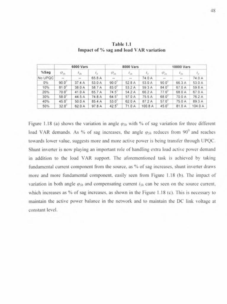
48
Table 1. 1 Impact of Vo sa g and loa d VA R variatio n
%Sag No UPQC
0% 10% 20% 30% 40% 50%
6000 Vars
<Ps>, -
90.0" 81.0" 70.0" 58.0" 45.0" 32.0"
's,
-37.4 A 38 0 A 41.0 A 44.5 A 50.0 A 62.0 A
'6-
65.8 A 53.0 A 58 7 A 65.7 A 74.8 A 85.4 A 97.8 A
8000 Vars
(Ps„ -
90.0" 83.0" 74.5" 64.5" 53.0" 42.5"
'SH
-52.8 A 53 2 A 54.2 A 57 0 A 62.0 A 71.OA
' . •
74.0 A 53.0 A 59.3 A 66.2 A 75.5 A 87 2 A 100.8 A
10000 Vars
(Psh
-90.0" 84.0" 77.0"
',» -
66.3 A 67.0 A 68.0 A
68.0" j 70. 0 A 57.0" 45.0"
75.0 A 81.OA
's
74.0 A 53.0 A 59 8 A 67 0 A 76 2 A 89 3 A 104.0 A
Figure 1.1 8 (a ) show s th e variatio n i n angl e cpsi, wit h % o f sa g variatio n fo r thre e differen t
load VA R demands . A s % o f sa g increases , th e angl e (psi, reduce s fro m 90 ° an d reache s
towards lowe r value , suggest s mor e an d mor e activ e powe r i s being transfe r throug h UPQC .
Shunt inverte r i s now playin g a n importan t rol e o f handling extr a loa d activ e powe r deman d
in additio n t o th e loa d VA R support . Th e aforementione d tas k i s achieve d b y takin g
fundamental curren t componen t fro m th e source , a s % of sa g increases , shun t inverte r draw s
more an d mor e fundamenta l component , easil y see n fro m Figur e 1.1 8 (b) . Th e impac t o f
variation i n bot h angl e (psh an d compensatin g curren t ish can b e see n o n th e sourc e current ,
which increase s a s % o f sa g increases , a s show n i n the Figur e 1.1 8 (c) . Thi s i s necessar y t o
maintain th e activ e powe r balanc e i n th e networ k an d t o maintai n th e D C lin k voltag e a t
constant level .
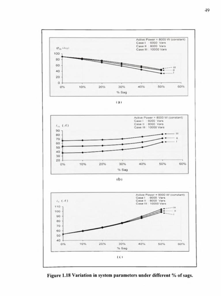
49
Active Powe r = 800 0 W (constant ) Case I 600 0 Var s Case I I aOO O Var s Case II I : 1000 0 Var s
6 0 %
n I
90 80 70 60 -\ 50 40 30 20
0 % 10%
Active Powe r - 800 0 W (cornstant ) Casa I Case I I Case II I
eOOO Var s 8000 Var s 10000 Var s
-i >
r T r-—-—-•— "t
111
~ " " 1
2 0 % 30%
% Sa g
4 0 % 5 0 % 6 0 %
(b l
Active Powe r = 000 0 V\l (constant) Case I 000 0 Var s Case I I : 8000 Var s Case II I 1000 0 Var s
5 0 % 6 0 %
( C I
Figure 1.18 Variation i n system parameters unde r differen t % o f sags.
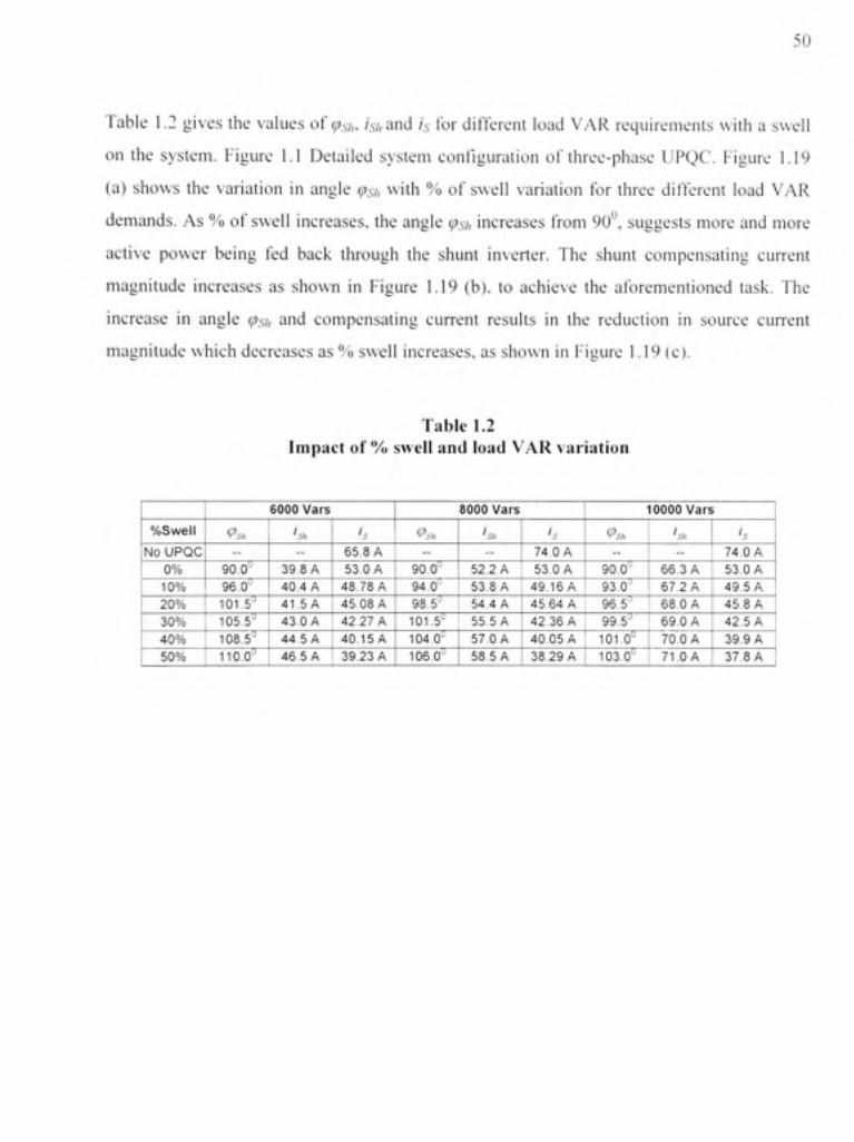
50
Table 1. 2 give s the value s o f v; . /iv, and is for differen t loa d VA R requirement s wit h a swel l
on th e system . Figur e 1. 1 Detaile d syste m configuratio n o f three-phas e UPQC . Figur e 1.1 9
(a) show s th e variatio n i n angl e 5-/ , with % o f swel l variatio n fo r thre e differen t loa d VA R
demands. A s % of swel l increases , the angle (psi, increase s fro m 90° , suggests mor e an d mor e
active powe r bein g fe d bac k throug h th e shun t inverter . Th e shun t compensatin g curren t
magnitude increase s a s show n i n Figur e 1.1 9 (b) , t o achiev e th e aforementione d task . Th e
increase i n angl e (psi, an d compensatin g curren t result s i n th e reductio n i n sourc e curren t
magnitude whic h decrease s as % swell increases , as shown i n Figure 1.19(c) .
Table 1. 2 Impact o f Vo swel l and loa d VA R variatio n
%Swell No UPQC
0% 10% 20% 30% 40% 50%
6000 Vars
(Ps>, --
90.0" 96.0" 101.5" 105.5" 108.5" 110.0"
's„ -
39.8 A 40.4 A 41.5 A 43.0 A 44.5 A 46.5 A
's 65.8 A 53.0 A
48.78 A 45.08 A 42.27 A 40.15 A 39.23 A
8000 Vars
<Psi,
-90.0" 94.0"
's„ -
52.2 A 53.8 A
98.5" ; 54. 4 A 101.5" 55.5 A 104.0" 106.0"
57.0 A 58.5 A
'.-74.0 A 53.0 A
49.16 A
10000 Vars
<Psh
-90.0" 93.0"
's„ -
66.3 A 67.2 A
45.64 A : 96.5 " ' 68. 0 A 42.36 A i 99.5 " 1 69. 0 A 40.05 A 38.29 A
101.0" 103.0"
70.0 A 71.OA
h 74.0 A 53.0 A 49.5 A 45.8 A 42.5 A 39.9 A 37.8 A
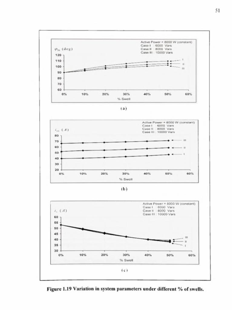
51
V'v, CJeg )
120 -1
110 -
100
90 •
80 -
70
_.—
0 %
-^^^;zr:—'^^=^
' 1 0 %
Active Power = 8000 W (constant ) Case 1 : 6000 Var s Case 11 : 8000 Var s Case II I 1000 0 Vars
_ . 1
s s s £ i = = ^ 3 ^ - ^ ^ - ^ ^ :
20% 30 % 40 % 50 % 60 %
% Swel l
l a . t
'•..,, ( - i )
0 %
Active Powe r = 8000 W (constant ) C-Jse I 600 0 V.^r s Case I I 800 0 Va i s Case II I . 1000 0 Var s
tiO -
7 0 -<
eo -5 0 '-
4 0 <
30 -
?0 -
• • —
, . *-
. •
r 1
—«
#
-^
• - » —
. ^
I l l
11
2 0 % 3 0 %
% S w e l l
6 0 %
(b)
Active Powe r - 800 0 W (constant ) Case 1 600 0 Var s Case I I 800 0 Var s Case- II I ; 10000 Var s
6 0 %
Figure 1.19 Variation in system parameters unde r different % of swells.
52
From Tabl e 1. 1 an d Tabl e 1.2 , whe n th e UPQ C i s not connecte d i n th e circuit , th e sourc e
supplies bot h activ e a s wel l a s reactiv e powe r demande d b y th e load . Wit h UPQ C i n
operation, sourc e supplie s onl y activ e par t o f loa d powe r demand . Durin g thi s VAR
compensation mod e o f operatio n th e sourc e curren t i s almos t constan t i.e . 53A , independen t
of the loa d VAR requirements , as seen from Tabl e 1. 1 and Tabl e 1.2 . for 0 % sag and swell .
In normal operatin g condition , the shun t in v erter provides the loa d VARs . whereas , the serie s
inverter handle s n o activ e o r reactiv e power . Therefore , i n thi s cas e th e ratin g o f th e serie s
inverter woul d b e smal l fractio n o f loa d rating . Th e shun t inverte r ratin g mainl v depend s o n
the compensatin g curten t provide d b y it , whic h depend s o n th e loa d powe r facto r o r loa d
VAR requirement . Highe r th e loa d VA R requiremen t highe r woul d b e th e shun t inverte r
rating. Fro m (1.8) , (1.12) an d (1.16) . the serie s inverte r ratin g depend s o n two factors , sourc e
current is an d facto r kf. The curren t is increase s durin g voltag e sa g condition , whereas ,
decreases durin g voltag e swel l condition . Therefor e th e ratin g o f th e serie s inverte r i s
considerably affecte d b y the % of sa g needed t o b e compensated. A compromise need s to be
made whil e considerin g th e serie s inverte r ratings , whic h directl y affect s th e sa g
compensation capabilit y o f UPQC. Depending o n the loa d requirements , a n optimization ca n
be done o n these tw o issues . Th e shun t inverte r ratin g increase s a s i t handles th e extra activ e
power durin g th e voltag e sag/swel l conditions . Furthermore , fro m Figur e 1.1 8 (b ) and Figur e
1.19 (b) , th e increas e i n % sa g greatl y affect s th e shun t inverte r ratin g a s compare d t o th e
increase i n % swell . Thus , th e analysi s presente d i n thi s chapte r ca n b e verv ' usefu l i n th e
selection o f kVA rating s of both the series and shun t inverter s depending o n the % of sag and
swell neede d t o be compensated .
1.6 Conclusio n
In thi s chapter , th e essentia l basic s t o understan d th e UPQ C concept , it s ke y components ,
operating principle , potentia l application s hav e been highlighted . A n in-dept h an d up-to-dat e
literature revie w o n UPQ C base d article s i s als o provided . Fo r eas y understanding , th e
operating principl e o f UPQ C ha s bee n explaine d b y splittin g i t int o th e shun t an d serie s

:>}
inverter operations . Moreover , i t ha s bee n pointe d out tha t th e mos t importan t tas k o f shun t
inverter i s t o maintai n th e D C lin k voltag e a t constan t leve l withou t whic h th e desire d
performance fro m UPQ C can not be achieved .
Besides buildin g th e first mileston e o f basi c understandin g o f ter m "UPQC" . a n interestin g
analytical stud y o n "ho w th e activ e an d reactiv e powe r flows betwee n source , UPQC , an d
load unde r differen t operatin g condition " has also bee n carried out . Additionally , a numerica l
study ha s bee n carrie d out t o highligh t th e impac t o f sa g an d swel l variation s o n injecte d
shunt filter an d sourc e currents . Eventually , the stud y result s i n hand too l t o selec t the UPQ C
device ratings taking differen t operatin g conditions into consideration .
CHAPTER 2
UPQC FEASIBILIT Y ANALYSI S FO R PRACTICAL APPLICATIO N
2.1 Introductio n
This chapte r i s dedicate d t o validat e th e adaptabilit y o f UPQ C i n a realisti c distributio n
network. Th e presente d wor k wa s don e i n collaboratio n wit h Hydro-Qutebec , Montrea l an d
Institut de recherche d'Hydro-Quebec (IREQ), (Hjdro-Quebec' s Researc h Institute) .
Varennes. Canad a Th e purpos e o f thi s collaboratio n projec t wa s t o evaluate , tliroug h
simulation study , th e feasibilit y an d th e performanc e o f UPQ C whe n installe d i n a realisti c
distribution network . A complex network , wit h realisti c parameters , wa s simulate d a t Powe r
System Simulatio n Laborator y {Laboratoire de simulation de reseaux. LSR) . IREQ ,
Varennes, which imitate s the situation a t one of the Hydro-Quebec's consumer s vicinity .
A simpl e contro l approac h fo r UPQ C i s propose d an d terme d a s Unit Vector Template
Generation (UVTG ) technique . First , th e formulatio n o f uni t vecto r templat e generatio n
controller i s described. Late r on , a brief descriptio n o n realisti c networ k unde r consideratio n
is given . Th e performanc e o f UPQ C unde r differen t operatin g conditions , wit h a thoroug h
simulation study , i s discusse d i n detail . Som e o f th e importan t laborator y experimenta l
results are also given a t the end of the chapter .
2.2 Motivatio n behin d th e Collaboration Projec t
Due t o th e extensiv e us e o f nonlinea r load s o n distributio n networks , Hydro-Quebe c
customers ar e facin g powe r qualit y problems . T o hel p som e o f th e customers , suc h as , a
computer factor y an d a sawmill , Hydro-Quebe c ha s mad e som e attempt s i n th e past .
However, th e installatio n o f availabl e mitigatio n device s di d not giv e expecte d results . Fo r
mitigation o f voltag e sag , a dynamic voltag e restore r (DVR ) wa s suggeste d t o th e customer .
Unfortunately, th e electronic s contro l circui t o f th e devic e faile d t o perfor m a s expecte d
because o f th e harmonic s generate d insid e th e plant . I n anothe r case , a n automati c VA R
3D
controller (AVC ) wa s installe d a t th e custome r en d fo r th e mitigatio n o f sag s an d flickers.
The device could only perform wel l fo r sag s but no t fo r the flicker.
The curren t trend s i n the field o f mitigatio n device s i s towards a unified approach , i n whic h
the mitigatio n devic e tackle s bot h th e curren t an d voltag e relate d powe r qualit y problems ,
simultaneously, suc h as , curren t harmonics , loa d reactiv e power , curren t unbalance ,
excessive neutra l current , voltag e harmonics , voltag e sag , voltag e swell , voltag e unbalance ,
voltage flicker, etc . Therefore , ther e wa s a n urg e t o tr y newl y upcomin g powe r qualit y
enhancement devices , suc h a s the UPQC . The major goa l o f this projec t wa s to carry ou t th e
feasibility o f UPQ C t o b e installe d i n actua l distributio n networ k t o suppor t th e individua l
sensitive customers , an d als o t o hav e readil y availabl e dat a (a s a cas e study ) fo r possibl e
future installations .
The projec t wa s divide d i n two parts , one i n whic h Hydro-Quebe c an d IRE Q wer e involve d
to buil d realisti c networ k Simulin k mode l an d th e othe r i n whic h ET S wa s involve d t o
develop th e necessar y concept , contro l algorithm , an d necessar y testin g b y implementin g th e
experimental setu p in the laboratory .
The projec t goal s are briefly summarize d a s -
• T o develop the Simulin k mode l tha t would represen t th e realistic distributio n networ k
conditions.
• Acquir e th e necessar y backgroun d knowledg e an d t o develo p necessar y contro l
algorithm fo r UPQC .
• In-dept h simulatio n stud y t o evaluat e th e performanc e o f UPQ C whe n installe d o n
realistic distributio n network .
• Laborator y prototypin g o f UPQ C an d th e experimenta l validatio n t o confir m th e
possible practical application .
Thus, this chapter i s the blend o f all the important goal s and discusse s the findings achieved .
56
2.3 UPQ C Controller Developmen t
The contro l strateg y fo r UPQ C i s basically th e wa y t o extrac t th e referenc e signal s fo r bot h
the shun t an d serie s inverters . Th e effectivenes s o f th e UPQ C compensatio n depend s o n it s
controller's abilit y t o calculat e th e referenc e signal s fo r th e shun t an d serie s inverter s wit h a
minimum crto r an d tim e dela y t o compensat e fo r th e curren t an d voltag e distortion , voltag e
variaUon, unbalanc e (voltag e and/o r current ) o r an y othe r undesirabl e condition . I n th e
following section s a simpl e ne w approac h i s explaine d t o extrac t th e referenc e voltag e an d
current signal s for serie s and shun t in v erters (Khadkikar et al. 2004 , 2006b).
2.3.1 Referenc e Voltag e Signa l Generatio n
The majo r functio n o f serie s par t o f UPQ C i s t o strictl y maintai n th e voltag e a t loa d bu s
sinusoidal an d a t th e rate d valu e (magnitude) . Therefore , th e simples t approac h t o generat e
reference signal s fo r serie s inverte r woul d b e directl y imposin g th e loa d bu s voltag e t o b e
perfect sinusoidal . O n a particula r distributio n syste m th e standar d magnitud e o f v oltage
being supplie d i s fixed. Fo r example , hig h powe r rate d industria l load s ar e supplie d wit h
three-phase 208/240/60 0 VA C @60H z voltage s an d a typica l househol d consume r i s
supplied b y single-phas e 120VA C (S)60H z voltage . Therefor e tw o importan t factor s t o
maintain th e precise regulation a t load bus , especially fo r sensitiv e load s to be protected ar e -
/) perfec t sinusoida l voltag e a t 60H z an d // ) fixed loa d voltag e magnitude . Th e suppl y
voltages ca n b e distorted , ma y sho w som e dip s o r ris e i n voltag e du e t o switchin g ON/OF F
of hig h rate d loa d connecte d t o th e sam e feeder , o r ma y ge t unbalance d du e t o sever e
unbalanced loa d o n th e network , etc . Unde r suc h undesirabl e conditions , i f w e coul d forc e
the loa d voltage s t o b e perfectl y sinusoida l an d a t fixed loa d voltag e magnitude , th e
unwanted events / problem ca n be solved easily .
Assuming tha t th e termina l voltage s a t poin t o f commo n couplin g (PCC ) ar e distorted , the y
can b e decompose d a s su m o f fundamenta l an d harmonic s components , an d ca n
mathematically b e represented a s -
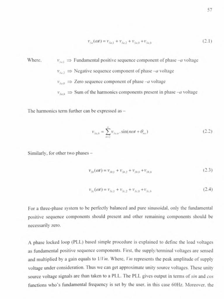
57
',s-. (f^n = V5,, + i;,, 2 + v_,^ 0 + v, , (2.1 )
Where, v ^ , ^ Fundamenta l positive sequence component of phase-a voltage
v , , =i > NegaUve sequence component of phase -a voltag e
v .Q => Zero sequence component of phase-^ voltage
v . ,, = > Sum of the harmonics components present in phase -a voltag e
The harmonics term further ca n be expressed as -
•j-j
Similarly, for other two phases -
'SA ( «0 - V . , , + !•, , , + T , , 0 + V, , , ( 2 . 3 )
V.sv(f^O = V.s,,, , + •,sv, 2 + '.SV, 0 +^'sc.l, ( 2 -4 )
For a three-phase syste m to be perfectly balance d an d pure sinusoidal , only the fundamenta l
positive sequenc e component s shoul d presen t an d othe r remainin g component s shoul d b e
necessarily zero.
A phase locke d loo p (PLL) based simpl e procedure i s explained t o define th e loa d voltage s
as fundamental positiv e sequence components . First , the supply/terminal voltage s are sensed
and multiplied by a gain equals to MVm. Where , ]'m represents the peak amplitude of supply
voltage under consideration. Thus we can get approximate unity source voltages. These unity
source voltage signals are than taken to a PLL. The PLL gives output in terms of sin and cos
functions who' s fundamenta l frequenc y i s se t by the user , i n this cas e 60Hz . Moreover , the
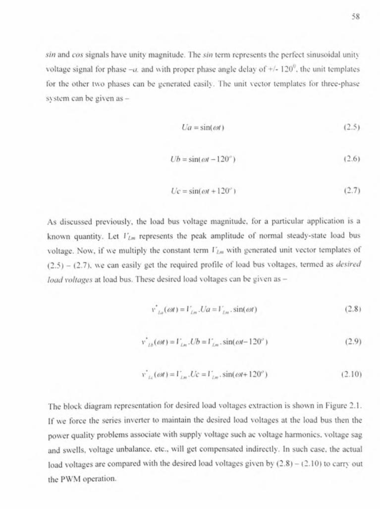
58
sin an d cos signal s have unit y magnitude . The sin ter m represent s the perfec t sinusoida l unit v
voltage signa l fo r phas e -a. an d wit h prope r phas e angl e delay of+/ - 120° . the uni t template s
for th e othe r tw o phase s ca n b e generate d easilv . Th e uni t vecto r template s fo r three-phas e
sv stem can be given a s -
Ua = sm{cot) (2.5 )
Ub = 5m{ cot-120') (2.6 )
L c = sin(r^/ + 120") (2.7 )
As discusse d previously , th e loa d bu s voltag e magnitude , fo r a particula r applicatio n i s a
known quantity . Le t Vi,„ represents th e pea k amplitud e o f norma l steady-stat e loa d bu s
voltage. Now , i f w e multipl y th e constan t ten n Vi,„ wit h generate d uni t vecto r template s o f
(2.5) - (2.7) . we ca n easil y ge t th e require d profil e o f loa d bu s voltages , terme d a s desired
load voltages a t load bus . These desired loa d voltages can be given a s -
^''iJo^n = Vi„, .Ua - I;„, . sinicot) (2.8 )
y'ib(<^t) = r;„, .Ub = f ;„,. sm{cot-\20'') (2.9 )
'''iMt) = V,„,.Uc = }]„,.sm{cot+\20') (2.10 )
The block diagra m representatio n fo r desire d loa d voltage s extractio n i s shown i n Figure 2.1.
If w e forc e th e serie s inverte r t o maintai n th e desire d loa d voltage s a t th e loa d bu s the n th e
power qualit y problem s associat e wit h supply voltag e suc h a c voltage harmonics , voltage sa g
and swells , voltag e unbalance , etc. , wil l ge t compensate d indirectly . I n suc h case , the actua l
load voltage s ar e compared wit h the desired loa d voltage s give n by (2.8 ) - (2.10 ) to canv ou t
the PWM operation .

Desired Loa d Voltage Magnitude
f.^,(w/) .k Us. o Measured Input » ' f f l ( » 0 _ _ ^ _ _ ^
Supply P Voltage v,^Xo}t) k U,^
>
Phase Locked Loop (PLL)
smcot Ua
k = ^-I'm
Ptiase Shift
l/b
Phase Shift
UL
'• ,J^')
V .^(cot)
V ,A0JI)
59
Figure 2.1 Desired load voltages signal generation.
The othe r option , th e direc t approach , i n whic h th e referenc e voltag e signal s fo r serie s
inverter are generated. The reference signal s for series inverter can be extracted as.
^'.s,,.(f'^0 = v,.^(r^/)-V/,^(ft ; 0 (2.11)
V ^,.AQ)t) = Vst{0}t)-V ,^{C0t) (2.12)
' Sr.c^<^') = ^'sA('^f)-^''if^') (2.13)
Here, th e actua l voltage s injecte d b y serie s inverte r ar e sense d an d compare d wit h th e
reference serie s injected voltage s of (2.11) - (2.13 ) to perform the PWM operation.
2.3.2 Referenc e Current Signal Generation
The uni t vecto r template s generate d fo r serie s par t ca n als o b e use d t o generat e referenc e
current signal s fo r shun t inverter . Th e majo r functio n o f shun t inverte r i s t o compensat e
curtent harmonics , reactive power, current unbalance, and neutral curten t b y maintaining the
DC bu s voltag e a t constan t level . Th e simples t wa y t o compensat e abov e mentione d
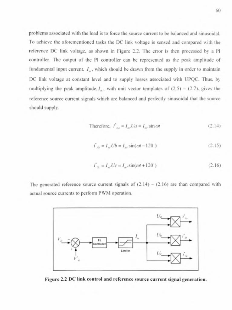
60
problems associated wit h the loa d i s to force th e source curren t t o be balanced an d sinusoidal .
To achiev e th e aforementione d task s th e D C lin k voltag e i s sense d an d compare d wit h th e
reference D C lin k voltage , a s show n i n Figur e 2.2 . Th e erro r i s the n processe d b y a P I
controller. Th e outpu t o f th e P I controlle r ca n b e represente d a s th e pea k amplitud e o f
fundamental inpu t current , /„, , whic h shoul d b e draw n fro m th e suppl y i n orde r t o maintai n
DC lin k voltag e a t constan t leve l an d t o suppl y losse s associate d wit h UPQC . Thus , b y
muUiplying th e pea k amplitude./,,, , wit h uni t vecto r template s o f (2.5 ) - (2.7) . give s th e
reference sourc e curren t signal s whic h ar e balance d an d perfectl y sinusoida l tha t th e sourc e
should supply .
Therefore. / . , = A,,-^" = 1,„-sin cot (2.14)
i',,^im = l„,sm(cot-\20) (2.15)
/••,^=/,„.^c = /„,.sin(f^/ + 120) (2.16)
The generate d referenc e sourc e curren t signal s o f (2.14 ) - (2.16 ) ar e tha n compare d wit h
actual sourc e currents to perform PW M operation .
^J. -*:f<yV-
V' • dc
PI Controller
y— ^
Limiter
/ .
Ua
Ub ^
Uc ^
X X
X
' .?. >
' *
' s.
Figure 2.2 D C link control an d referenc e sourc e curren t signa l generation .

61
As th e extracte d unit y vecto r templates , usin g a simpl e PLL , ar e use d t o generat e th e
reference signal s fo r bot h th e inverters , simultaneously ; thi s metho d i s termed a s Unit Vector
Template Generation (UVTG ) approac h fo r UPQC . Th e significan t advantag e o f thi s
approach i s that i t does no t requir e comple x transformation s an d i t i s very eas y to implemen t
for practica l hardwar e applications .
2.3.3 Gating Signa l Generation / Modulato r
After extractin g th e referenc e voltag e an d curren t signal s fo r serie s an d shun t inverters , th e
next ste p i s t o perfor m th e accurat e switchin g o f bot h th e inverter s t o follo w th e referenc e
signals fo r th e inverter s (direc t approach ) o r t o forc e th e loa d voltage s an d sourc e current s
(indirect approach ) t o accomplis h th e require d tasks . A modulatio n techniqu e i s use d t o
generate th e adequat e gatin g signa l patter n t o perfor m switchin g operatio n o f th e inverte r
switches. A hysteresi s ban d contro l techniqu e base d PW M strateg y i s considere d fo r th e
shunt inverter , while , a triangula r carrie r signa l base d fixed frequenc y PW M techniqu e i s
used fo r th e serie s inverter . Th e bloc k diagra m o f a hysteresi s controlle r i s show n i n Figur e
2.3. Th e hysteresi s controlle r give s th e switchin g instan t wheneve r th e erro r exceed s a fixed
magnitude limi t a s define d b y th e hysteresi s band . T o contro l bot h th e inverters , th e
generated referenc e curren t an d voltag e signals , fo r shun t an d serie s inverter , ar e compare d
with actua l sense d sourc e current s an d th e actua l sense d loa d voltages , respectively . Finally ,
the erro r i s processe d t o generat e th e gatin g signa l patter n fo r shun t an d serie s inverters .
However, a hysteresis controlle r i s required fo r eac h o f the phases o f sourc e current s an d th e
load voltages .
(Ref.) \ ^ 7 \ ^"'>' ,
k
is {cot) (Actual)
Hysteresis Band P W M
Figure 2.3 Hysteresi s controller .

62
2.4 Realistic Network Details
Figure 2. 4 show s th e single-lin e diagra m o f the three-phas e industria l distributio n networ k
under study . Th e voltag e i s generate d a t 120kV , transmitte d an d the n steppe d dow n a t
different voltag e levels based on individual premises requirements. The UPQC is supposed to
be installe d a t a plan t whic h i s locate d a t a considerabl e distanc e fro m th e distributio n
transformer an d there are sev eral loads present in between, represented b v equivalen t MW or
MVA ratings . Th e voltag e whic h i s availabl e a t th e inpu t Bu s Ba r B 3 o f th e plan t i s a t
12.7kV. This voltage is further steppe d down at 600V by using step down transformer T4.
-WV^YYYV
SOXWASC
Souict
BiiS'BZ
MUVA
LOAD
rrrrs -PjraW Feeder
I5km)
3MW
LOAD
Point olConiiecbon
rrfr\ -StaFeeilei
(1)
3 0 I M
LOAD
rfrf\ -BkmFeedei
(21
4UW
LOAD
r Y y r L
UPQC Plant Load
Plait BiisB3
T< Bus-6 4 Loaii
BusBi
PLANT' 7
Y A
Buj.Bt
?5mA
LOAD
@09pf
T!
Y 4 5!*A LOAD
Figure 2.4 Single-line diagram: Industrial distribution networ k under consideration.
The point of connection i s the point at which UPQC is connected to the distribution network .
The UPQC is installed between bus B4 (point of connecfion) and load bus B5. The Simulink
model for this realistic distribution network was built at LSR lab.

63
The plan t unde r consideratio n consist s o f severa l load s amon g whic h th e importan t one s ar e
shown i n Figur e 2.5 . Thes e load s ar e - tw o A C Motor s (L l & L2) . tw o Diod e Bridg e
Rectifiers (DBR ) (L 3 & L4) . and a pure Resistiv e loa d (L5) . The resistiv e loa d L 5 represent s
the sensiti v e loa d t o b e protecte d fro m an y disturbance s i n th e suppl y voltage . O n th e othe r
hand, two DBR load s L3 and L4 are harmonics producing loads . The harmonics generate d b y
them shoul d not reach a t point o f connection. I t is importan t t o note her e tha t the distributio n
network mode l represent s on e of the Hydro-Quebec' s plan t site . but. the load s i n the plant d o
not represen t th e actua l loads . Som e o f th e load s ar e deliberatel y adde d t o perfor m th e
simulation study .
Figure 2.5 Plan t load .
The ratings of all the loads are as given below:
L1: A C Moto r - 50 HP, 177 5 RPM, Tm = 12 5 N.m
L2: AC Moto r - 50 HP, 177 5 RPM, Tm = 75 N.m
L3: Diod e Bridg e Rectifie r - 40 kVA
L4: Diode Bridg e Recfifie r - 25 kVA
L5: Resistive Loa d -2 5 k W
Figure 2. 6 show s th e basi c bloc k diagra m o f th e UPQC . Th e voltag e a t bu s B 4 (befor e
UPQC), th e loa d voltag e a t loa d bu s B5 , voltage injecte d b y serie s inverter , an d th e D C lin k
voltage betwee n tw o inverter s ar e represente d b y vg^ , i^ - v„ y and vj,.. respectively, whereas ,
the curren t a t bu s B4 , tota l loa d curten t draw n b y al l th e loads , an d th e curren t injecte d b y
shunt inverte r ar e represente d b y /gv , ii. an d z' /, . respectively. Ai m i s t o maintai n th e voltag e
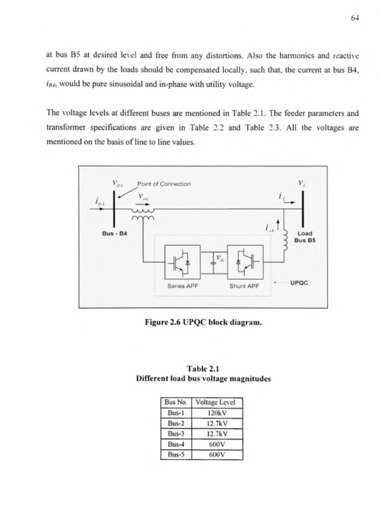
64
at bu s B 5 a t desire d leve l an d fre e fro m an y distortions . Als o th e harmonic s an d reactiv e
curtent draw n by the loads should b e compensated locally , such that, the curtent a t bus B4,
iB4, would be pure sinusoidal and in-phase with ufility voltage.
The voltage level s at different buse s are mentioned i n Table 2.1 . The feeder parameter s and
transformer specification s ar e give n i n Tabl e 2. 2 an d Tabl e 2.3 . Al l th e voltage s ar e
mentioned on the basis of line to line values.
' B 4
V/ 4 Poin t of Connectio n
^ v....
Bus - B4
^J Series APF
V,
V,
L. t
Shunt AP F
Load Bus B 5
UPQC
Figure 2.6 UPQC block diagram.
Table 2.1 Different loa d bus voltage magnitudes
Bus No. Bus-1 Bus-2 Bus-3 Bus-4 Bus-5
Voltage Level 120kV 12.7kV 12.7kV 600V 600V
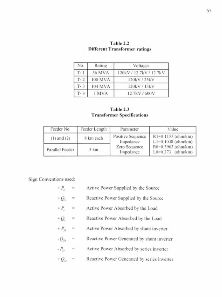
65
Table 2. 2 Different Transforme r rating s
No. T- 1 T- 2 T-3 T-4
Rating 56 MVA 100 MVA 104 MVA IMVA
Voltages 120kV/ 12.7kV / 12.7k V
120kV/25kV 120kV/ 13k V 12.7kV/600V
Table 2. 3 Transformer Specification s
Feeder No,
(l)and(2)
Parallel Feeder
Feeder Length
8 km each
5 km
Parameter Positive Sequence
Impedance Zero Sequence
Impedance
Value Rl-0.n53 (oluii/km ) L1-0.1048 (ohm/km) R0=0.3963 (olim/km) L0=0.273 (ohm/km )
Sign Conventions used :
+ Ps =
+ 0, =
+ P,. =
+a =
-Qsb =
-Psr =
+as> =
Active Power Supplie d b y the Sourc e
Reactive Power Supplie d b y the Sourc e
Active Powe r Absorbed b y the Loa d
Reactive Powe r Absorbed b y the Loa d
Active Power Absorbed b y shunt inverte r
Reactive Power Generated by shunt inverte r
Active Power Absorbed b y serie s inverte r
Reactive Power Generate d b y series inverte r
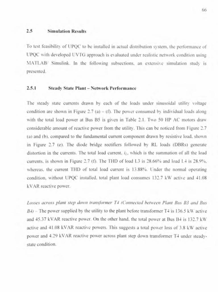
66
2,5 Simulatio n Result s
To tes t feasibilit y o f UPQ C t o b e installe d i n actua l distributio n svstem . th e performanc e o f
UPQC wit h develope d UVT G approac h i s evaluated unde r realisti c networ k conditio n usin g
MATLAB/ Simulink . I n th e followin g subsections , a n extensiv e simulatio n stud v i s
presented.
2.5.1 Stead y Stat e Plant - Net>vor k Performanc e
The stead y stat e current s draw n b y eac h o f th e load s unde r sinusoida l utilitv ' voltag e
condition ar e show n i n Figur e 2. 7 (a ) - (f) . Th e powe r consume d b v individua l load s alon g
with th e tota l loa d powe r a t Bu s B 5 i s give n i n Tabl e 2.1 . Two 5 0 H P A C motor s dra w
considerable amoun t o f reactiv e powe r fro m th e utility . Thi s ca n b e notice d fro m Figur e 2. 7
(a) an d (b) . compared t o th e fundamenta l curren t componen t draw n b y resistiv e load , show n
in Figur e 2. 7 (e) . Th e diod e bridg e rectifier s followe d b v R L load s (DBRs ) generat e
distortion i n th e currents . Th e tota l loa d curtent . //, , which i s th e summatio n o f al l th e loa d
currents, i s show n i n Figur e 2. 7 (t) . Th e TH D o f loa d L 3 i s 28.66 % an d loa d L 4 i s 28.9%,
whereas, th e curren t TH D o f tota l loa d curren t i s 13.88% . Lende r th e norma l operatin g
condition, withou t UPQ C installed , tota l plan t loa d consume s 132. 7 k W activ e an d 41.0 8
kVAR reactiv e power .
Losses across plant step down transformer T4 (Connected between Plant Bus B3 and Bus
B4) - Th e power supplie d b y the utilit y to the plant befor e transforme r T 4 i s 136. 5 kW activ e
and 45.3 7 kVA R reactiv e power . O n th e othe r hand , th e tota l powe r a t Bu s B 4 i s 132. 7 k W
active an d 41.0 8 kVA R reactiv e powers . Thi s suggest s a tota l powe r los s o f 3. 8 k W activ e
power an d 4.2 9 kVA R reactiv e powe r acros s plan t ste p dow n transforme r T 4 unde r steady -
state condition .
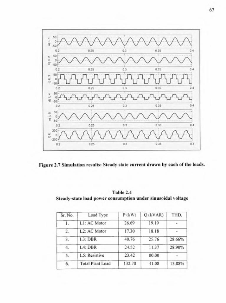
67
^ 5 0 t 0 ' " -5 0
- / \ / / \y
0.2
rxi 5 0 =! 0 •° -5 0
0
r, 5 0 =i 0 ^ -5 0
0
d)I
L4
en e
n o
o o
0
in 5 0 ^ 0 "^ -5 0
0
200
i 0 -200
0
2
'f\f 2
r'~'S-r'" 2
2
A/ 2
\ A-A / V V \ y
0.25 1
0.25
\/wv 0.25
1
\_rHir'\_j 0.25
1
1
0.25 vvv 0.25
v . A . A / \y \/ \y 0.3
1
0.3
\7m7 0.3
0.3
0.3 vw 0,3
\ A A / VVV
0.35
0.35
\/\Kf 0.35
0.35
1
035
W A / 0.35
\A 0.4
04
OT 0 4
\_r'~S_; 0.4
V^ 0 4
\A 0.4
Figure 2.7 Simulation results : Steady state current draw n b y each of the loads.
Table 2.4 Steady-state load power consumption unde r sinusoida l voltage
Sr.No.
1.
2
3.
4.
5.
6.
Load Typ e
Ll: A C Moto r
L2: AC Moto r
L3: DB R
L4: DB R
L5: Resistiv e
Total Plan t Loa d
P(k\V)
26.69
17.30
40.76
24.52
23.42
132.70
Q(kVAR)
19.19
18.18
25.76
11.37
00.00
41.08
THD,
-
-
28.66%
28.90%
-
13.88%
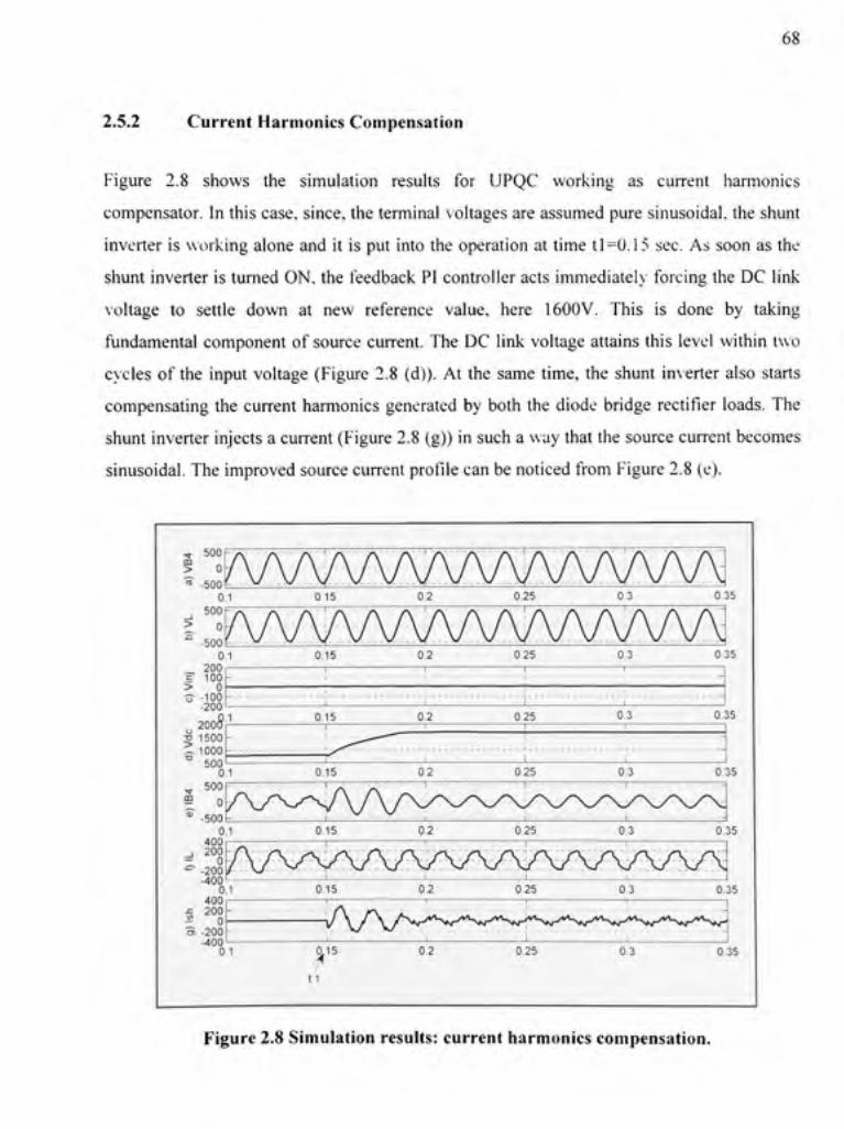
68
2.5.2 Current Harmonics Compensation
Figure 2. 8 show s th e simulatio n result s fo r UPQ C workin g a s curren t harmonic s
compensator. I n this case, since, the temiinal voltages are assumed pure sinusoidal, the shunt
inverter i s working alone and i t is put into the operation a t time 11=0.15 sec. As soon as the
shunt inverter i s turned ON , the feedback P I controller act s immediately forcin g th e DC link
voltage t o settl e dow n a t ne w referenc e value , her e 1600V . Thi s i s don e b y takin g
fundamental componen t o f source current . The DC link voltage attains this leve l within two
cycles o f the inpu t voltag e (Figur e 2. 8 (d)) . At the sam e time, the shun t inverte r als o start s
compensating th e curtent harmonic s generate d b y both the diode bridg e rectifie r loads . The
shunt inverter injects a curtent (Figure 2.8 (g)) in such a way that the source current becomes
sinusoidal. The improved source current profile can be noticed from Figur e 2.8 (e).
I yv\/mEimis/sEi\jxr\r\N 0.1 015 0 2 0.25 0 3 0.35
_, 50 0
> 0 .a -500
0.1 0.15 0.2 025 0.3 035 200
E 10 0 > 0 " -10 0
-200
2000 1 1500 2.1000 •° cn n
1 0.15 1
1
0.2
i
0 25 1
• 1
03
-1
0.3
" " "
035
0.35
-200 -400
/^X/V^^A^A^A.^^^ 400
•^ 20 0 ^ 0 •3 -20 0
-400
0.1
0.1
0.35
0.35
Figure 2.8 Simulation results: current harmonics compensation.
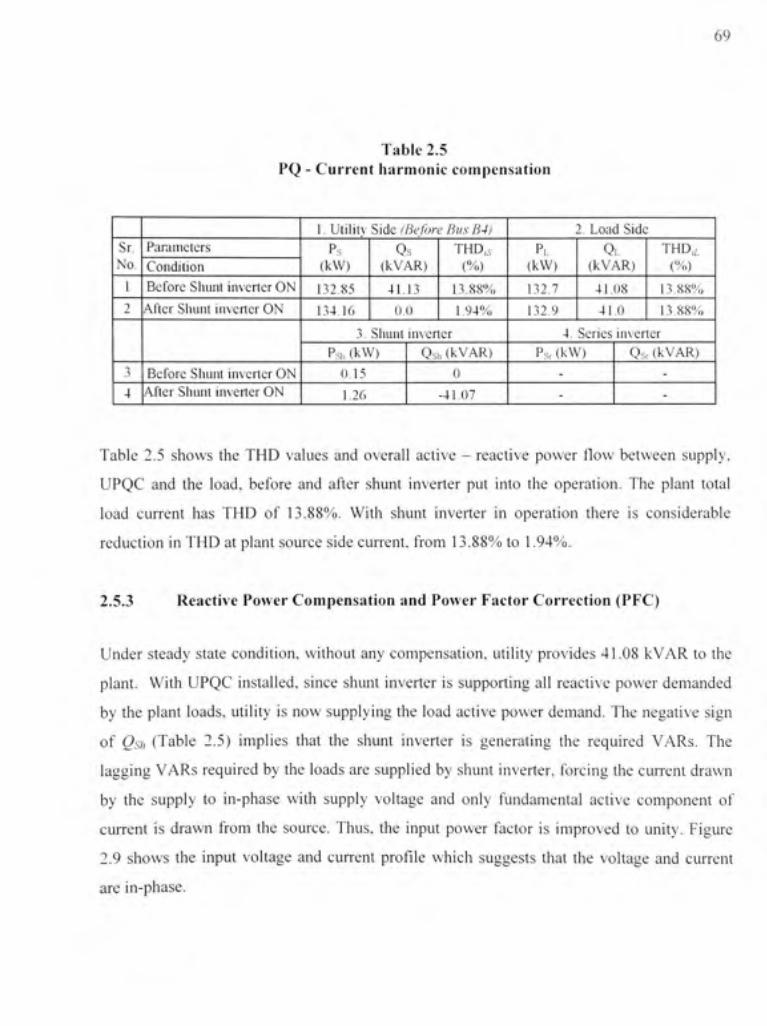
69
Table 2. 5 PQ - Current harmoni c compensatio n
Sr. No.
1
2
3 4
Parameters Condition Before Shun t inverte r O N
After Shun t invcrtc r O N
Before Siuin t inverle r O N After Shun t inverte r O N
L Utilitv ' Side (Before Bus B4) Ps
(kW)
L32.85 L14 1 6
Qs (kVAR)
4 M 3 0.0
THD.s (%)
L3.88% L94%
3. Shun t inverte r Psh (kW)
0.15 L26
QSI, (kVAR) 0
-4L07
2. Loa d Sid e PL
(kW)
132.7 132.9
4.
QL (kVAR)
41.08 41.0
THD,^ (%)
13.88% 13.88%
Series inverte r Psr (kW)
-
-
Qsr (kVAR ) -
-
Table 2. 5 show s th e TH D value s an d overal l activ e - reactiv e powe r flow betwee n supply ,
UPQC an d th e load , befor e an d afte r shun t inverte r put int o th e operation . Th e plan t tota l
load curren t ha s TH D o f 13.88% . Wit h shun t inverte r i n operatio n ther e i s considerabl e
reduction i n THD a t plant sourc e side current, fro m 13.88 % to 1.94% .
2.5.3 Reactive Powe r Compensation an d Power Factor Correction (PFC )
Under stead y stat e condition , withou t an y compensation , utilit y provide s 41.0 8 kVA R t o th e
plant. Wit h UPQ C installed , sinc e shun t inverte r i s supportin g all reactiv e powe r demande d
by the plan t loads , utility i s now supplyin g th e loa d activ e power demand . Th e negativ e sig n
of Qsh (Table 2.5 ) implie s tha t th e shun t inverte r i s generafin g th e require d VARs . Th e
lagging VAR s require d b y the load s are supplied b y shun t inverter , forcin g th e cun-ent draw n
by th e suppl y t o in-phas e wit h suppl y voltag e an d onl y fundamenta l activ e componen t o f
curtent i s draw n fro m th e source . Thus , th e inpu t powe r facto r i s improve d t o unity . Figur e
2.9 show s th e inpu t voltag e an d curren t profil e whic h suggest s tha t th e voltag e an d curren t
are in-phase .
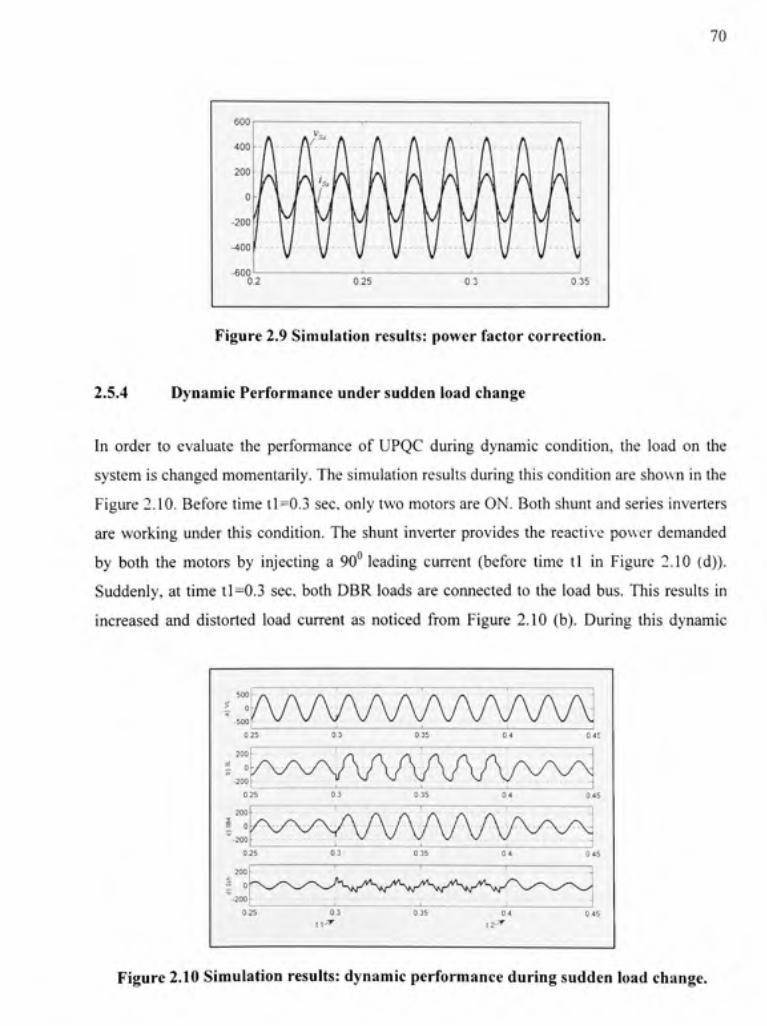
70
Figure 2.9 Simulation results : power factor correction .
2.5.4 Dynamic Performanc e unde r sudden loa d chang e
In orde r t o evaluat e th e performanc e o f UPQ C durin g dynami c condition , th e loa d o n th e
system i s changed momentarily . Th e simulation result s during this condition ar e shown i n the
Figure 2.10 . Before tim e tl=0.3 sec , only two motor s ar e ON. Bot h shun t an d serie s inverter s
are workin g unde r thi s condition . Th e shun t inverte r provide s th e reactiv e powe r demande d
by bot h th e motor s b y injectin g a 90 ° leading curren t (befor e tim e t l i n Figur e 2.1 0 (d)) .
Suddenly, a t tim e 11=0. 3 sec , both DB R load s ar e connecte d t o th e loa d bus . Thi s result s i n
increased an d distorte d loa d curten t a s notice d fro m Figur e 2.1 0 (b) . Durin g thi s dynami c
AAAAAAAAAAAA: 0,25
200
0
200 y \ /
0,3
1
\A/\/ 1/ v /
0.35
\ r\ r\ r \{\\f \J SJ SJ..
0 4
I /\ V A A / SJ V
Q.!
\ / \ -
0.3 1 ^
0.35 0.4 , 2 ^
0 2 5
200
200
/ N / " / \y
0.3
\ / \ A / ^-/V V 1
0,35
\ AA 7 v A/.y 1
0.4
\ A / \ / • V V^ ^
Q.i
\ / ^ \ y \ :
0.25
200
-200
0 3
1
0 3 5
1
0 4
I
0'
Figure 2.10 Simulatio n results : dynamic performanc e durin g sudden loa d change .
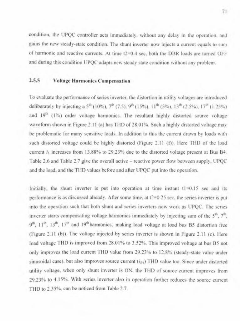
71
condition, th e UPQ C controlle r act s immediately , withou t an y dela y i n th e operation , an d
gains th e ne w steady-stat e condition . Th e shun t inverte r no w inject s a curren t equal s t o su m
of harmoni c an d reactiv e currents . A t tim e t2=0. 4 sec . bot h th e DB R load s ar e turne d OF F
and during this condition UPQ C adapt s new steady stat e condition withou t an y problem .
2.5.5 Voltag e Harmonic s Compensatio n
To evaluate the performance o f series inverter, the distortion i n utility voltages are introduce d
deliberately b y injectin g a 5 '^ (10%), 7 ^ (7.5). 9'^ (15%), 11" " (5%). 13 ' ' (2.5%). 17" " (1.25%)
and 19 ' (1% ) orde r voltag e harmonics . Th e resultan t highl y distorte d sourc e voltag e
waveform show n i n Figure 2.11 (a) has THD of 28.01%. Suc h a highly distorte d voltag e ma y
be problemati c fo r man y sensitiv e loads . I n additio n t o thi s th e curren t draw n b y load s wit h
such distorte d voltag e coul d b e highl y distorte d (Figur e 2.1 1 (f)) . Her e TH D o f th e loa d
current // , increases fro m 13.88 % to 29.23 % du e t o th e distorte d voltag e presen t a t Bu s B4 .
Table 2. 6 and Table 2. 7 give the overall activ e - reactiv e power flow betwee n supply . UPQ C
and the load , and the THD values before an d after UPQ C put int o the operation .
Initially, th e shun t inverte r i s put int o operatio n a t tim e instan t tl=0.1 5 se c an d it s
performance i s as discussed already . After som e time , at t2=0.25 sec . the serie s inverte r i s put
into th e operatio n suc h tha t bot h shun t an d serie s inverter s no w wor k a s UPQC . Th e serie s
inverter start s compensatin g voltag e harmonic s immediatel y b y injectin g su m o f th e 5'* , 7'" ,
ih j^th ^ j.th ^ jyt h ^^^ 19"^harmonics , makin g loa d voltag e a t loa d bu s B 5 distortio n fre e
(Figure 2.1 1 (b)) . Th e voltag e injecte d b y serie s inverte r i s show n i n Figur e 2.1 1 (c) . Her e
load voltag e TH D i s improve d fro m 28.01 % t o 3.52% . Thi s improve d voltag e a t bus B 5 not
only improve s th e loa d curren t TH D valu e fro m 29.23 % t o 12.8 % (steady-state valu e unde r
sinusoidal case) , but als o improve s sourc e curren t (/ v ) THD valu e too . Sinc e unde r distorte d
ufility voltage , whe n onl y shun t inverte r i s ON , th e TH D o f sourc e curren t improve s fro m
29.23%) t o 4.15% . Wit h serie s inverte r als o i n operatio n furthe r reduce s th e sourc e curren t
THD to 2.35%, can be noficed fro m Tabl e 2.7.
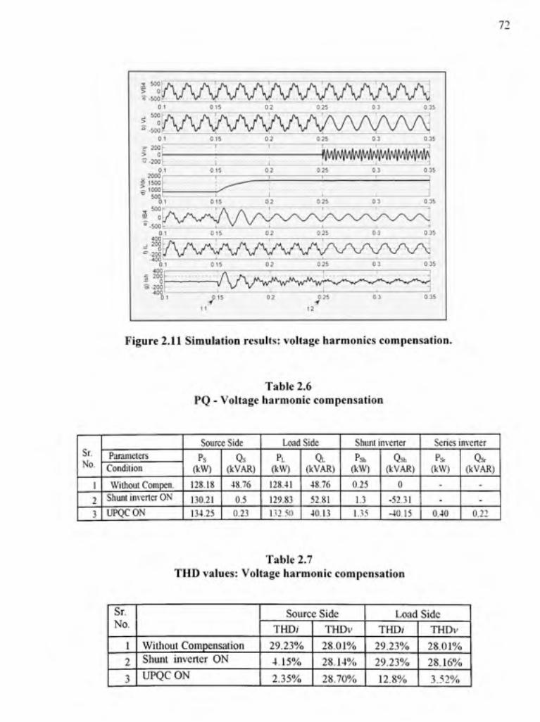
72
a °° F l.:TaAAAAAAAAA^^AAA 0.1 0.15 0.25
.:]rvv\/vv\/vvvvvvvvxj 0.1 0.15 0.2 0.25 0.3 0.35
E- 20 0 > 0 •0-200
IpkJp^^^ 01
2000 r-015 0.2 0.25 0.3
500
0.1 400 200
0.35
0.35
A/VVVVVVVVV\/\A-Ay^ 01
400 200
015 0,2 0,25 0 3 0,35
^ 0 0
•^/xj^^/S^^f^A^^ 0.1 0 15 02
t 2
0.25 0.3 035
Figure 2.11 Simulatio n results : voltage harmonic s compensation .
Table 2. 6 PQ - Voltage harmoni c compensatio n
Sr. No.
1 2 3
Parameters Condition
Without Compen. Shunt inverter ON UPQC ON
Source Side
Ps (kW)
128.18 130.21 134.25
Qs (kVAR) 48.76 0.5 0.23
Loac
PL (kW)
128.41 129.83 132.50
Side
QL (kVAR)
48.76 52,81 40.13
Shunt inverter
Psh (kW)
0,25 1,3 1.35
Qsh (kVAR)
0 -52.31 -40.15
Series inverter
Psr (kW)
--
0.40
Qsr (kVAR)
--
0.22
Table 2. 7 THD values: Voltage harmoni c compensatio n
Sr. No.
1
2
3
Without Compensatio n Shunt inverte r O N
UPQC O N
Source Sid e THD/
29 .23%
4 ,15%
2 .35%
THD\'
2 8 . 0 1 %
28.14%
28.70%
Load Sid e THD/
29 .23%
29 .23%
12.8%
THDv
2 8 . 0 1 %
28.16%
3.52%

73
As viewe d fro m th e Tabl e 2.6 , withou t an y compensation , th e powe r draw n b y th e load s
under distorted sourc e voltag e i s noticed a s 128.4 1 kW +f 48.7 6 kVAR. Whe n UPQ C i s ON,
as the serie s inverte r maintain s th e load voltag e sinusoida l an d a t desired value , the loa d no w
draws it s rate d powe r fro m th e source . A smal l amoun t o f activ e powe r los s occur s acros s
shunt an d serie s inverter s a s switchin g loss , couplin g resistiv e an d inductiv e loss . The shun t
inverter consume s ver y smal l amoun t o f powe r a s compare d t o th e tota l loa d kV A ratin g t o
maintain th e DC lin k voltage a t constant level .
2.5.6 Voltag e Sa g Compensatio n
Figure 2.12 show s the simulatio n result s during a sag condition o n the system . There ar e fou r
instants; t l , t2 , t3 and t4 . At t l =0.1 5 se c an d a t t2 = 0.25 sec . the shun t an d serie s inverter s
are pu t int o operation , respectively . A t instan t t 3 = 0.35 sec . a sag (25% ) i s introduced t o th e
system. Thi s sa g last s til l tim e t 4 = 0.45 sec . Table 2. 8 give s overal l activ e - reactiv e powe r
flow between supply , UPQC an d the loads during differen t operatin g conditions .
During th e voltag e sa g condition , the serie s inverte r inject s a n in-phas e voltag e (25% ) equal s
to th e differenc e betwee n th e desire d loa d voltag e an d actua l sourc e voltage , a s see n fro m
Figure 2.1 2 (c) . Thus , help s t o maintai n th e loa d voltag e profil e (Figur e 2.1 2 (b) ) a t desire d
level suc h tha t th e sa g i n sourc e voltag e doe s no t appea r a t the loa d terminals . A s discusse d
in steady-state powe r flow analysi s (CHAPTERl, Sectio n 1.4) , in order to injec t th e in-phas e
voltage th e UPQ C require s certai n amoun t o f activ e power . Thi s activ e powe r come s fro m
the source , extracte d b y shun t inverter , b y takin g extr a fundamenta l curren t componen t t o
maintain th e D C lin k voltag e a t constan t level . Withou t doin g this , the D C lin k voltag e wil l
fall dow n i n fe w cycles . Th e fundamenta l curten t draw n b y shun t inverte r ca n b e notice d
from Figur e 2.1 2 (g ) (betwee n tim e t 3 an d t4) , an d therefore , th e sourc e curren t magnitud e
also increase s accordingly (Figur e 2.12 (e)) .
In terms o f powers , from Tabl e 2.8 , when ther e i s sag on the system , an d i f the UPQ C i s not
put int o operafion , th e loa d could hardl y dra w 91.53 kV A (88.73 5 k W +j 22.4 5 kVAR ) fro m
the source due to the reduction i n the terminal voltage (25%); instead o f 138.9 1 kVA (132. 7

•* 50 0 m > 0 ro" -500 -
0.1 _, 50 0 ^ 0 ^ -50 0
0.1 E- 20 0 > 0
-200
200
-200 0.1
74
0.15 0.2 0.25 0.3 0.35 0.4
0.15 0.2 0.25 0.3 0.35 0.4
•AAAAAAr
]l\j\j\^\/\/\/^\^^ t i
0.15 0.2
12 13
025 0.3
t 4
0.35 0.4
t 1 - .Shun t ON . ( 2 -.Shun t + .St i ie.s ON , t 3 - 1 4 Su n Cdi n ptnsJti<i n
Figure 2.12 Simulation results: voltage sag compensation.
Table 2.8 PQ - Voltage sag compensation
Sr. No.
1 2 3 3
Parameters Condition Normal Condition UPQC O N (befor e Sag)
tJPQC O N (durin g Sag)
UPQC OF F (Sa g on system)
Source Side Psh
(kW) 133.42 134,35 131,4 89,3
Qsh
(kVAR) 41,15 0,25 0,192 22.713
Load Side Psr
(k\V) 132.7 132.7 126.79 88,735
Qsr (kVAR) 41,10 41,10 36.59 22,45
Shunt Inverte r Psh
(kW) 0,24 1.25
43.197 -
Qsh
(kVAR) 0.03 -41.2
-37.51 -
Series Imerter Psr
(kW) -
04 39 51
-
Qsr
(kVAR) -
0.2 0,73
-
kW +j 41.0 8 kVAR), as in normal workin g condition . I n this case, the source i s supplyin g
only 65.89 %> of rated load power. When the UPQC is put into operation unde r the same sag
condition, the series inverte r i s providing the required power to the load by injecting th e in-
75
phase voltag e (25%)) . This extr a powe r flows fro m sourc e t o shun t inverter , shun t inverte r t o
series inverte r an d finally, fro m serie s inverte r to load, but withou t an y delay i n the operation .
The activ e powe r draw n fro m th e utilit y b y shun t inverte r i s foun d a s 43. 2 kW . Th e majo r
part o f thi s activ e powe r i s supplie d t o th e loa d throug h serie s inverter . Th e serie s in v erter
provides 39.5 1 k W powe r t o th e load . Wit h UPQ C installed , th e combinatio n o f sourc e an d
UPQC coul d suppl y 94.78 % (131.9 6 kVA , 126.7 9 k W +j 36.59 ) o f rate d loa d power . Th e
remaining 3.6 9 k W power i s utilized t o maintain the DC lin k voltag e a t constant leve l (2.79%
of rate d loa d activ e power) . Thus , th e UPQ C act s a s a media t o transfe r activ e powe r t o th e
load via shunt - serie s inverters .
2.5.7 Voltag e Swel l Compensatio n
Figure 2.1 3 show s th e simulatio n result s fo r a swel l condition . Betwee n tim e t 3 =0.2 5 se c
and t 4 =0.35 sec , a swell (25% ) i s introduced o n the system . Tabl e 2. 9 give s overal l activ e -
reactive powe r flow betwee n supply , UPQ C an d th e load s unde r differen t operatin g
conditions.
The voltag e swel l phenomeno n i s exac t opposit e t o th e voltag e sa g condition . Therefore ,
during a swel l o n th e system , th e serie s inverte r no w inject s out-o f phas e voltag e (25% )
equals t o th e differenc e betwee n th e desire d loa d voltag e an d actua l sourc e voltag e (Figur e
2.13 (c)) . Thus , th e UPQ C cancel s th e increase d sourc e voltag e tha t ma y appea r a t th e loa d
side an d maintain s th e loa d voltag e profil e (Figur e 2.1 3 (b) ) a t desire d level . Th e ris e i n
source voltag e mean s th e utilit y no w tr y t o suppl y som e extr a powe r t o th e load . Thi s ma y
damage equipment s an d load s du e to the increas e i n the curten t draw n b y them . A t the sam e
time, th e ris e i n sourc e voltag e als o cause s th e D C lin k voltag e t o increase . Unde r suc h
condition, th e shun t inverte r inject s fundamenta l out-of f phas e curren t componen t (Figur e
2.13 (g) . between time t3 and t4) to maintain the D C lin k voltage a t constant level . Therefore ,
the sourc e curten t magnitud e decrease s (Figur e 2.1 3 (e)) . I n othe r words , th e extr a activ e
power comin g fro m th e utility side , due to the swel l o n the system, i s now fe d bac k b y takin g
reduced sourc e curren t fro m th e source .
76
S 50 0 > 0 'S'-SOO KVWVWV^AMAMAAA/^
0,1 0,15 0,2 0.25 0.3 0.35 0.4 500
-500 AAAAAAAAAAAAAAAAAA 0 1
E- 20 0 -0.15 02 025 0.3 0.35 04
5 0 -200
.A^/>^y-\y^,yXy-y^
_, 20 0
^-200 AAAAAAy\A7\AA/NyVV\A7VS; 0,1
jz 20 0 ^ 0 • S - 2 0 0
0,15
'Ar 1
0.2
1
0.25 0.3 1
1
0.35 1
s^r'N,.r'*S.<^^
0
tf^"^
0.1
t1
ai5 /
0.2
12 /
13
025 /
0.3 035 04
14
I 1 - Shiin l ( IN . 1 2 - S h u n l -I - Sens,- . ( IN . 1 1 - t 4 Swel l Ccinipeii.sjiui n
Figure 2.13 Simulation results : voltage swell compensation.
Table 2.9 PQ - Voltage swell compensation
Sr. No.
1 2 3 3
Parameters Condition
Normal Conditio n LFPQC ON (befor e Suell) LTPQC ON (durin g Swell) UPQC OFF (Swel l on system)
Source Sid e
Psh (ItW) 133.42 134.35
136.00 1867
Osh (kVAR)
41.15 0,25
1,448 66,641
Load Sid e Psr
(kW) 132.7 132.7
132.41 184,29
Qsr (kVAR)
41,10 41,10
42,30 65,75
Shunt Inverte r
Psh (kW) 0,24 1,25
-22,77 0
Qsh (kVAR)
003 -41.2
-43 9 1 0
Series In \ erter
Psr (kW)
-0.4
-254 0
Qsr (kVAR)
-0,2
-0.32 0
From Table 2.9 , during the swel l on the system (UPQ C i n OFF mode), the load i s supplied
up to 195.6 7 (184.29 kW +; 65.75 ) kVA due to the rise in the terminal voltage (25°/o), which
is 140.86 % of its rated power. With UPQC in operation, under this swell condition, the series
inverter i s absorbing th e extr a active power b y injectin g th e out-of phas e voltag e (25%) . In

77
this cas e the serie s inverte r handle s 25. 4 k W activ e power . Th e majo r portio n (22.7 7 kW ) o f
this activ e powe r i s fed bac k t o the sourc e b y shun t inverter . Th e combinatio n o f sourc e an d
UPQC restrict s the power being supplied t o the loa d u p to 99.84% of its rated power .
2.5.8 Voltag e Fluctuatio n / Flicker Compensatio n
Voltage fluctuation o r flicker i s ofte n difficult-to-solv e powe r qualit y problem . I t occurs ,
typically, du e to voltage variatio n o r phase-shifting harmonics , resulting fro m frequen t moto r
starts, switchin g o f capacitor s o r othe r loa d change s a t th e custome r sit e o r a t othe r site s o n
the sam e line , o r fro m momentar y hig h impedanc e fault s lik e tree s brushin g th e line . Rapi d
voltage deviation s coul d produc e extremel y annoyin g fluctuations i n th e outpu t o f lights ,
especially i f th e frequenc y o f repetitiv e deviation s i s 5-1 5 Hz . Motor s an d equipment s ar e
designed t o b e mos t efficien t a t a se t voltag e an d an y mino r fluctuations, u p o r down ,
decreases th e motor' s efficiency , generat e hea t an d electrica l losses . Significan t voltag e
fluctuations ca n caus e equipmen t t o shu t dow n o r fail . Conventiona l flicker contro l i s
accomplished wit h stati c VA R compensators , whic h us e passiv e devices . However , thes e
devices ma y not provid e adequat e protectio n becaus e thei r respons e tim e i s no t fas t enoug h
to regulate the voltage, and ma y allow additional voltag e fluctuation t o occur .
In th e followin g section , th e flicker compensatio n capabilit y o f UPQ C i s tested . Th e
simulated result s are shown i n Figure 2.14. The effect o f a 5Hz flicker envelop s on the sourc e
voltage i s shown i n Figure 2.14 (a) . The tenn flicker index i s defined a s follows :
Fhcker Inde x = — (2.17 ) V ^ '
Where, A v = r^,-F^,, (2.18 )
r^i = Maximum positiv e o r negative pea k
F/,2 = Minimum posifiv e o r negative pea k
78
= Peak amplitude of rated voltage
For the given condition, using Figure 2.14 (a):
r., =55 2 , ['„ , =408 an d ( ' = 480
Therefore, Flicker Index = 0.3 or 30 %
ro -500 0.1
CM 0,2 m 0,3
Hi 0,4
ill 0,5 m 0,6
Hi 0,7
ill 0,8
Mi 0,9 1
illi 0,1 0.2 0. 3 0. 4 0. 5 0. 6 0. 7 0.8 0. 9
^ 200 > 0 " -200
-- - I 4 •
•'-'^>J\f\/\A>»*'A/\f\PJ'*'»^'>A/\^^
2000 I 1500 ^ 100 0 "D
01 0. 2 0. 3 0. 4 0. 5 0, 6 0. 7 0. 8 0. 9
500 0.1 0. 2 0. 3 0, 4 0, 5 0. 6 0, 7 0, 8 0, 9
500 r I of\iMj\fmf\}wwmN^^ *" -500 ^ ^-^ ' ' ' ' ' ' '
0,1 0 2 0, 3 0, 4 0. 5 0, 6 0 7 0. 8 0. 9 1
-200 0.1 0. 2 0. 3 0. 4 0. 5 0. 6 0. 7 0 8 0. 9
^ 2 0 0 -
'^ -20 0
1 1 1 1 1 1 1 1 1 ^
0.1 J 0. 2 0 3 0. 4 0. 5 0. 6
•1 t 2 t 3
0.7 0. 8 0.9
l l - S lu m I O N. l 2 - Sh iu i l + S c r i e s O N . I i - F l i c k e i C c i i i i p c n s a l u u i
Figure 2.14 Simulation results: flicker compensation.
The UPQ C effectivel y compensate d thi s flicker condifio n o n th e svste m b y injectin g
appropriate voltag e throug h serie s inverter . Th e voltag e injecte d b v serie s inverte r t o
79
compensate the flicker effect i s shown in the Figure 2.14 (c) . whereas, the compensated loa d
voltage is as shown in Figure 2.14 (b).
Thus for compensated loa d voltage, using Figure 2.14 (b);
J>, =485 , i ; , =48 0 an d ( ' = 480
Therefore, Flicke r Index = 0.0104 or 1.04 %
Thus with UPQC installed, the flicker index is reduced from 30 % to onlv 1.04 % making load
bus free fro m flicker variation. Th e three-phase sourc e voltage and loa d voltage profiles ar e
as shown in Figure 2.15.
-600-
-600 0,1
0 1 0,1 5 0 2 0,2 5 0, 3 0 35 0 4 0 45 0 5 a) Three Phase Source Voltage Profile ( 5 Hz Flicker)
0 1 5 0. 2 0.2 5 0. 3 0 35 0 4 0 45 0. 5 b) Three Phase Load Voltage Profil e ( After Compensation )
-J L _
0 55 0 6
0,55 0 6
Figure 2.15 Three-phase source and load voltage profiles .
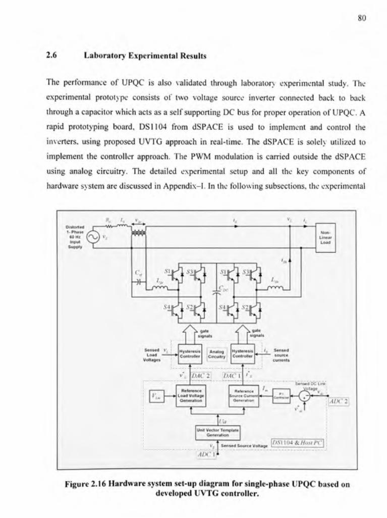
80
2.6 Laboratory Experimental Result s
The performanc e o f UPQ C i s als o validate d throug h laborator y experimenta l study . Th e
experimental prototvp e consist s o f tw o voltag e sourc e inverte r connecte d bac k t o bac k
through a capacitor which acts as a self supporting DC bus for proper operation of UPQC. A
rapid prototypin g board , DS l 104 fro m dSPAC E i s use d t o implemen t an d contro l th e
inverters, usin g propose d UVT G approac h i n real-time . Th e dSPAC E i s solel y utilize d t o
implement th e controlle r approach . Th e PW M modulatio n i s carrie d outsid e th e dSPAC E
using analo g circuitry . Th e detaile d experimenta l setu p an d al l th e ke y component s o f
hardware system are discussed in Appendix-1. In the following subsections , the experimental
A\ /., , Distorted 1-Phase
60 Hz ( ^ \ ^ ) V^ . Input
Supply
ryrri
^h- , , , • ^ 4 5 ^ ^ ' . . i l
'Xlj'^^^
AAX-'-' ,
' ' - ^ ^
/ \
Sensed \' , Load ' >
Voltages
gate signals
< > gat e signals
Hysteresis Controller
Analog I Circuitry
Hysteresis Controller
DAC 2 j \DAC 1
Reference Load Voltag e Generation
/ . Sense d source
currents
Non-Linear Load
Reference Source Curren t
Generation
Sensed D C Link i Voltage _ I
('u
Unit Vecto r Templat e Generation
ADC I v^ Sense d Source Voltag e /5.S'1104&//o.s7Pr
ADC !•
Figure 2.16 Hardware system set-up diagram for single-phase UPQC based on developed UVTG controller .
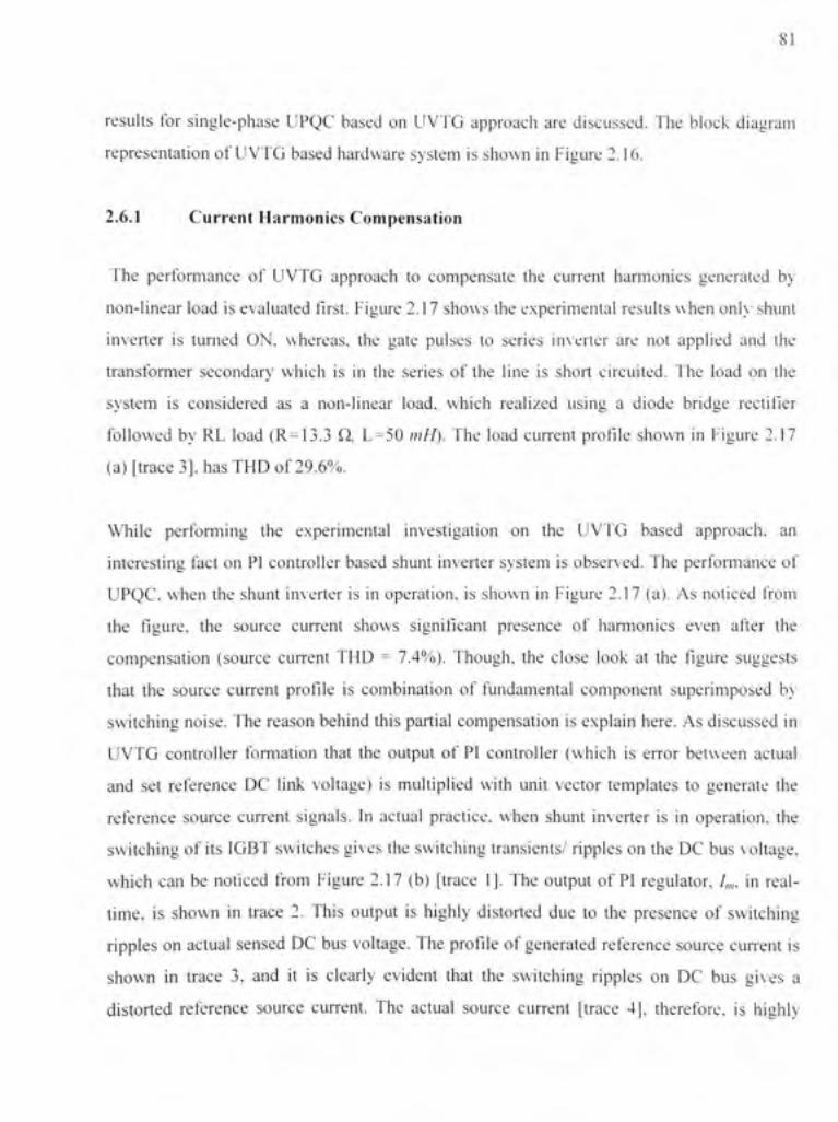
results fo r single-phas e UPQ C base d o n UVT G approac h ar e discussed . Th e bloc k diagra m
representation o f UVTG base d hardwar e syste m i s shown i n Figure 2.16 .
2.6.1 Curren t Harmonic s Compensatio n
The performanc e o f UVT G approac h t o compensat e th e curren t harmonic s generate d b y
non-linear loa d i s evaluated first. Figur e 2.17 shows the experimental result s when onlv shun t
inverter i s turne d ON , whereas , th e gat e pulse s t o serie s inverte r ar e not applie d an d th e
transformer secondar y whic h i s i n th e serie s o f th e lin e i s shor t circuited . Th e loa d o n th e
system i s considere d a s a non-linea r load , whic h realize d usin g a diod e bridg e rectifie r
followed b y R L loa d (R=13. 3 Q, L=50 tnH). Th e loa d curten t profil e show n i n Figur e 2.1 7
(a) [trac e 3] , has THD of 29.6%.
WTiile performin g th e experimenta l investigatio n o n th e UVT G base d approach , a n
interesting fac t o n P l controlle r base d shun t inverte r syste m i s observed. Th e performanc e o f
UPQC. when th e shun t inverte r i s in operation , i s shown i n Figure 2.1 7 (a) . As noticed fro m
the figure, th e sourc e curren t show s significan t presenc e o f harmonic s eve n afte r th e
compensation (sourc e curtcn t TH D = 7.4%) . Though , th e clos e loo k a t th e figur e suggest s
that th e sourc e curren t profil e i s combinatio n o f fundamenta l componen t superimpose d b v
switching noise . The reason behin d thi s partial compensatio n i s explain here . As discussed i n
UVTG controlle r formatio n tha t th e outpu t o f P I controlle r (whic h i s erro r betwee n actua l
and se t referenc e D C lin k voltage ) i s multiplie d wit h uni t vecto r template s t o generat e th e
reference sourc e curren t signals . I n actua l practice , whe n shun t inverte r i s i n operation , th e
switching o f it s IGBT switches give s the switching transients / ripple s on the DC bu s voltage ,
which ca n b e notice d fro m Figur e 2.1 7 (b ) [trac e 1] . Th e outpu t o f P I regulator , /,„ , i n real -
fime, i s show n i n trac e 2 . Thi s outpu t i s highl y distorte d du e t o th e presenc e o f switchin g
ripples o n actua l sense d D C bus voltage . The profil e o f generate d referenc e sourc e curten t i s
shown i n trac e 3 , an d i t i s clearl y eviden t tha t th e switchin g ripple s o n D C bu s give s a
distorted referenc e sourc e current . Th e actua l sourc e curten t [trac e 4] , therefore , i s highl y
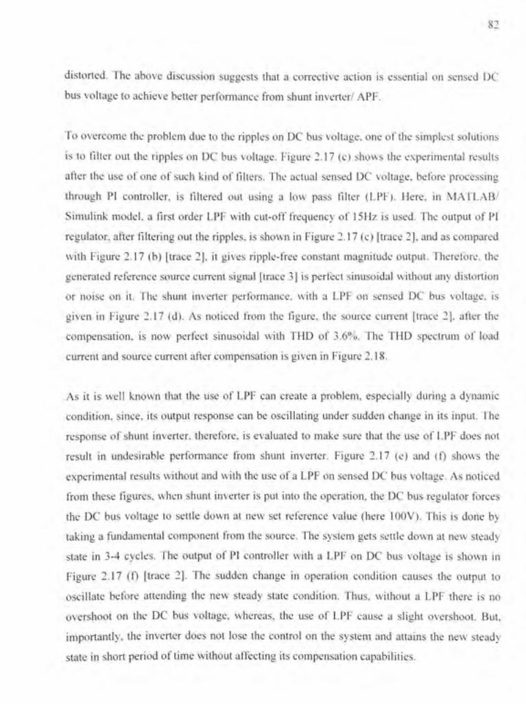
82
distorted. Th e abov e discussio n suggest s tha t a cortectiv e actio n i s essentia l o n sense d D C
bus voltage to achieve better performance fro m shun t inverter / APF .
To overcome th e problem du e to the ripple s on DC bus voltage , one of the simples t solution s
is t o filter ou t th e ripple s o n D C bu s voltage . Figur e 2.1 7 (c ) show s th e experimenta l result s
after th e us e o f on e o f suc h kin d o f filters. Th e actua l sense d D C voltage , befor e processin g
through P I controller , i s filtered ou t usin g a lo w pas s filter (LPF) . Here , i n MATLAB /
Simulink model , a first orde r LP F wit h cut-of f frequenc y o f 15H z i s used . Th e outpu t o f P l
regulator, afte r filtering ou t the ripples, i s shown i n Figure 2.17 (c) [trac e 2]. and as compare d
with Figur e 2.1 7 (b ) [trac e 2] , i t give s ripple-fre e constan t magnitud e output . Therefore , th e
generated referenc e sourc e curren t signa l [trac e 3 ] is perfect sinusoida l withou t an y distortio n
or nois e o n it . Th e shun t inverte r performance , wit h a LP F o n sense d D C bu s voltage , i s
given i n Figur e 2.1 7 (d) . A s notice d fro m th e figure, th e sourc e curten t [trac e 2] , afte r th e
compensation, i s no w perfec t sinusoida l wit h TH D o f 3.6% . Th e TH D spectru m o f loa d
curtent an d source curtent afte r compensatio n i s given in Figure 2.18 .
As i t i s wel l know n tha t th e us e o f LP F ca n creat e a problem , especiall y durin g a dynami c
condition, since , it s outpu t respons e ca n b e oscillating unde r sudde n chang e i n it s input . Th e
response o f shun t inverter , therefore , i s evaluated t o mak e sur e tha t th e us e o f LP F doe s no t
result i n undesirabl e performanc e fro m shun t inverter . Figur e 2.1 7 (e ) an d (f ) show s th e
experimental result s without an d with the use of a LPF on sensed D C bus voltage. As notice d
from thes e figures, whe n shun t inverte r i s put int o the operation , the D C bu s regulato r force s
the D C bu s voltag e t o settl e dow n a t ne w se t referenc e valu e (her e lOOV) . Thi s i s don e b y
taking a fundamental componen t fro m th e source . The syste m get s settl e dow n a t new stead y
state i n 3- 4 cycles . Th e outpu t o f P I controlle r wit h a LP F o n D C bu s voltag e i s show n i n
Figure 2.1 7 ( 0 [trac e 2] . Th e sudde n chang e i n operatio n conditio n cause s th e outpu t t o
oscillate befor e attendin g th e ne w stead y stat e condition . Thus , withou t a LP F ther e i s n o
overshoot o n th e D C bu s voltage , whereas , th e us e o f LP F caus e a sligh t overshoot . But .
importantly, th e inverte r doe s no t los e th e contro l o n th e syste m an d attain s th e ne w stead y
state in shor t period o f fime without affecting it s compensation capabilities .
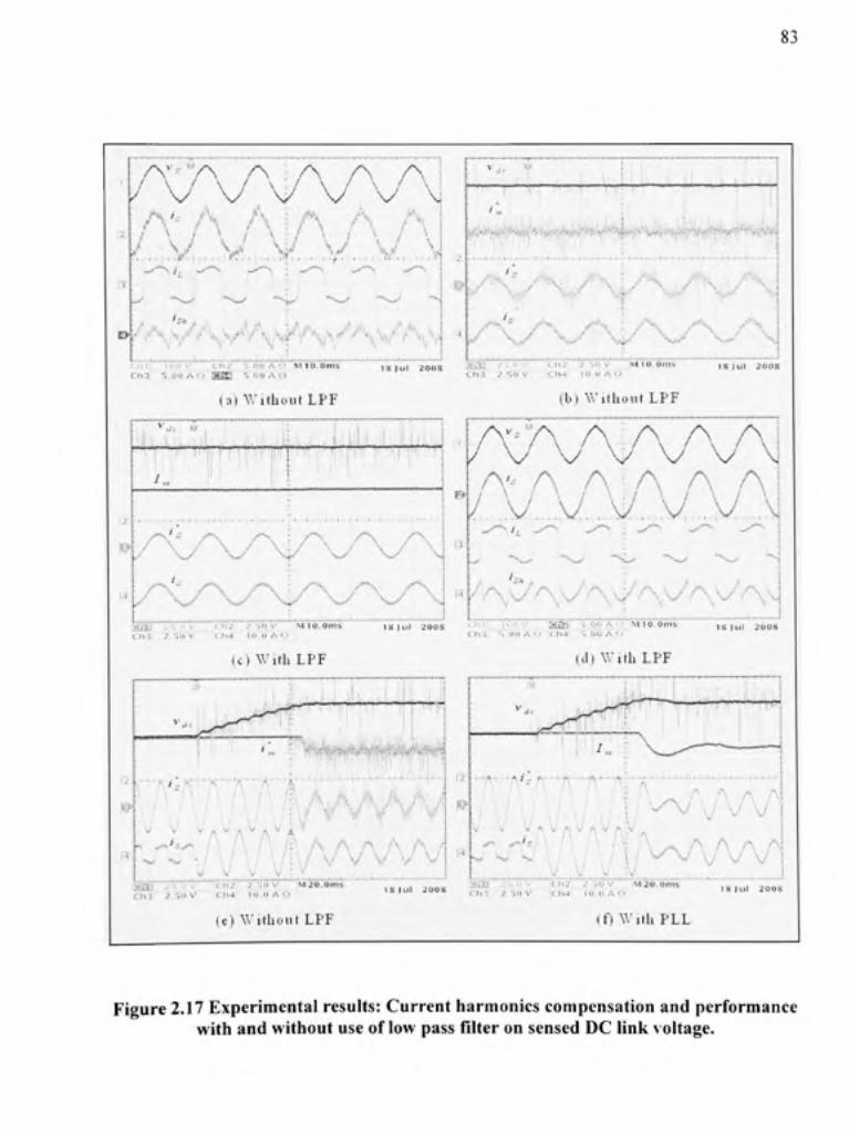
83
/
: A; /\ n i A A A . J M W ; V V v . .
Ar 'A A> Au. / • • • • • '' -
~v • 'A, V^/ \MV^J^M^*^ V' t .
^ . * . - ( - . . . ' • ' • .
i>
> : t l -. . . - 1 , ,
iVv
> \ j ^ Nf* ^ \ i / \»«i ^ \ ^
; , i i i i i5i) V t i l / ' ; ( I0A<. > MlO.Om s Ch3 - i O O A o B i E '-,ri(t,\<!
i s i u l 200 S :iai J ^ • ' • < ll'- 2 ' - 0 V MlO.Om s ChJ .'.'i O V Cll 4 l l l O A r ?
i s ju i 2aa s
(a) Withou t LP F (b) Withou t LP F
••I'f'«'!#'"* I*'if ii'i?.''!'* y ' " i ' i "w.". 'J' -
/"• t^xy - \ , : /^^ , z"^ , , /^ x ••w '-v y " s- / \ .
/
f>
A\ A A A /A A A ^ A A A
/ . .y y y .u ^ y„; \
^ / \ \ / / \
a a j T T u V :cii2 ^ •^.•itiv Mto .Om s i:h,'i J.'i o V Cii 4 i n u A ' >
\S Ju l 2 0 0 S ' ' ' •.. . " l " ' i . h ! S . O O A O r.h J
•aUBT"''"Sj5o"A <, ! iM'l'o~OmT " I S I t l l 20U S
(c) V.'it h LP F (d) Wit h LP F
' '" \ ^ A A A ^"^ J \i ^ ^ / y . V . V :
.aa]- . ; , o v CtTz : 2.3 0 V MZO.Oms"" ' ' I ' s j u l 200 S ' ? , * -"v'/^' , M.au ; s i.> V |ch2 : 2.3 0 v ;M;2o.onis ;
(e) Withou t LP F
ICI14: 10. 0 A o
if) Wit h PL L
ISJUl 20U! i
Figure 2.17 Experimental results : Current harmonic s compensation an d performanc e with and without use of low pass filter on sensed DC link voltage.

84
25 -,
ro 1 5 2 0
ra E
Sii^ E .5 ^
M D •
Load Curren t TH D = 29.6 % Source Curren t TH D = 7 4% [without LPF] Source Curren t TH D = 3.6% [with LPF ]
15
10
•S 5 •
1 -.^-^ ,"''-h3 h 5 h 7 h 9 h1 1 ti1 3 h1 5 ti1 7 h1 9 h2 1 h2 3 h2 5 h2 7 ti2 9 h3 1
Harmonics Order
Harmorttcs 1,:. (witfiout LPF ) l^ {with LPF)
ODD HARMONIC S (% )
3 5 7 9 11 13 15 17 19 21 23 25 27 29 31
23.01 14.04 4.54 6.22 4.11 3 13 1.88 1.54 1.1
0,91 0.76 0.74 0.61 0.55 0.53
4.2 5.17 1.93 0.47 0.65 0.16 0.61 0 1 6 0.47 0.43 0.55 0.16 0.24 0.51 0.1
2.63 2.23 0.95 0.85 0.47 0.22 0.2 0 1 2 008 0.12 0.12 0.22 0.22 0.24 024
EVEN HARMONICS (%)
DC 2 4 8 10
% TH D
0.72 0 15 0.08 0.08 0.08
29.6%
0.65 0.83 1.03 0.26 0.32
7.4%
0.53 0.2
0.06 0.08 0.02
3.6%
* For controller development, with and without low pass filter (LPF) on sensed DC bus voltage
Figure 2.18 Current harmonic s compensation - harmonic s spectrum an d individua l harmonic values as % of fundamental .

85
2.6.2 Reactiv e Power Compensation
The performanc e o f shun t inverter , whe n a linea r R L loa d (R=I3. 3 Q , L=5 0 mH) i s
connected t o th e syste m i s show n i n Figur e 2.19 . Thi s highl y inductiv e loa d draw s a load
curtent [trac e 3] which is at 0.58 lagging power facto r wit h respective to the supply voltage .
When shunt inverte r i s turned ON, it supplies the load reactive power demand by injecting a
leading quadrature curten t [trac e 4]. The shunt inverter compensates the load reactive power
demand locally . Thus, the load seen by the source appears as a linear resistive load supplying
only active power demand o f the load at unity power factor . Th e reduction i n source current
magnitude [trac e 2] as compared t o actual load curtent [trac e 3] magnitude also justifies th e
fact.
/Nyx/\K"vrv/\
<:ii i| TOO'V " "Ch2l "5.0 0 A Q ^M'ldTOm s Ch3r S.0 0 A Q S iE l 5.0 0 A < ISJu l 200 8
Figure 2.19 Experimental results : Reactive power compensation.
2.6.3 Dynamic Response under Sudden Load Change
The response of UPQC system during sudden load change condition i s shown in Figure 2.20.
Assuming th e syste m i s i n steady stat e with a load L i (DB R wit h R=2 0 Q . L=50 mH ) . At
time tl , a resistiv e loa d (R=4 0 Q ) i s suddenl y connecte d acros s th e loa d Ll . Th e paralle l
combination o f load Li an d resistive loa d i s marked a s load L2 . The sudden increas e i n load
curtent profile , a t tim e instan t tl , ca n b e notice d fro m Figur e 2.2 0 (a ) [trac e 3] . Within a
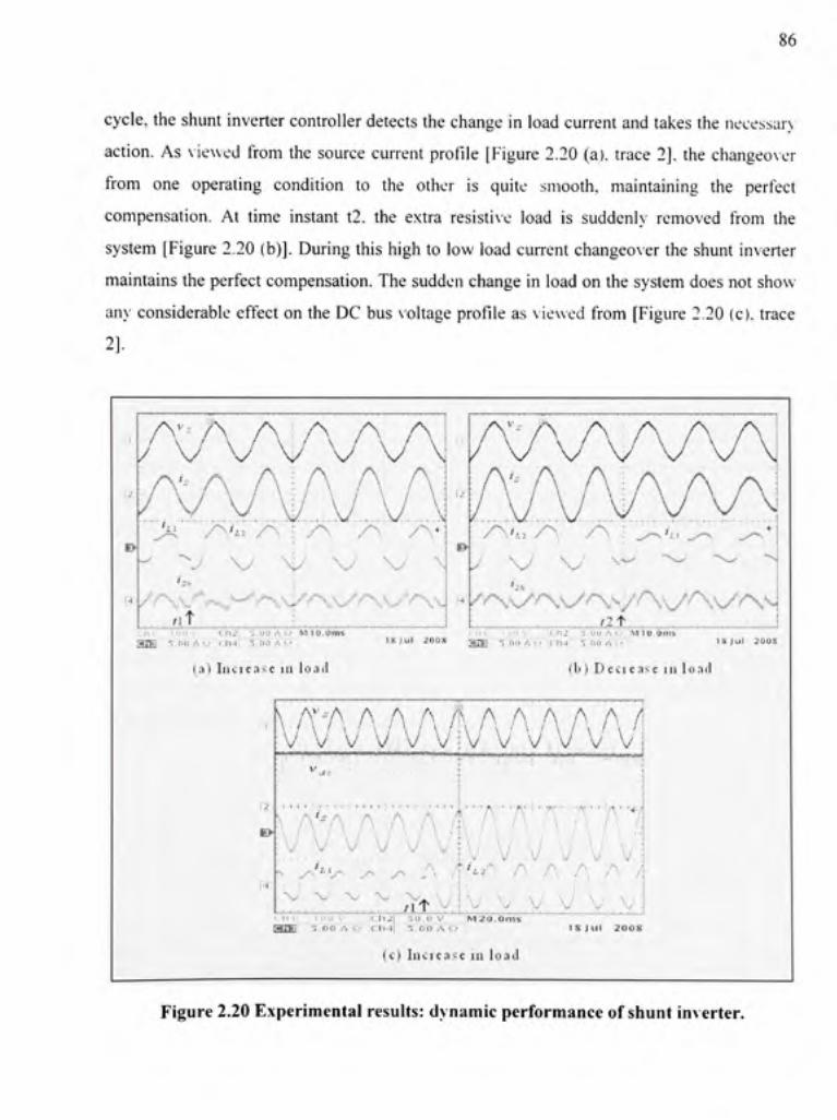
86
cycle, the shunt inverter controller detects the change in load current and takes the necessarv
action. As viewed fro m th e source curren t profil e [Figur e 2.20 (a) , trace 2] . the changeover
from on e operating conditio n t o the other i s quit e smooth , maintainin g th e perfect
compensation. A t time instan t t2 . the extra resistiv e loa d i s suddenly remove d fro m the
system [Figur e 2.20 (b)] . During this high to low load current changeove r th e shunt inverte r
maintains the perfect compensation . The sudden change in load on the system does not show
any considerable effec t o n the DC bus voltage profile as viewed fro m [Figur e 2.20 (c) . trace
2].
A- A ,A A A / V V V V V A'= A A = A A AI AV V.k.,:,U , UA
!. /^.',.J / ^ , ; /^> , /\. Z^;
'^J \J ^ \\J \J \ &
A
/A'» /A / A ; . \J \J ^
A^f\j
/'^y/ANy'^\A\\/'^.\/A\^ h l o i i v Ch2 i 3.0 0 A i ; MIO.Oin s
a i E • .n n A t7"f:h-)[ I^.OIVA\ ^
(a) IiKie.Ts e i n lo.ii l
JL2_IU-;1 i iUU V iCtl 2 5.00A(,. > iMIO.Om! !
I X J u l 200! ( a j g • i 0 0 A i> i rh 4 "i;B o A<> ~
(b ) D e c i en.' e i n loa d
I S i u l 200 S
V V V V V v iV V V V V A, / | V
r2 ' '
\ A'AA . A :A . A /
•s y \ * - v^ y^ ^ ^ \ / \y """ ^ "'v. ' "V. ' 'A- V ' - /
^ ,,. . , / t t, ,y.
m<»m''0¥^*imM<j<f, f I i^!ttmm'itm»¥'m'M't0uf
rA"A^A'-A A' ? A v :V..\/,y,,l/Ly ,
A: A A A A .A .^,./,., A
V V V V V ^ V • i- . 1 0 0 \ - : C l l 2 : i O . £ ) V M i O . O m s
rarg ^:d o A « Icim i "g;oo' A «" ' IS Ju l ZOO S
ii) Inciea.^ e i n lo.it l
Figure 2.20 Experimental results : dynamic performance o f shunt inverter.

87
2.6.4 Voltag e Harmonics Compensation
The performance o f UPQC, especially, under distorted voltag e condition i s discussed i n the
following subsections . Th e distortio n i n suppl y voltag e i s deliberatel y introduced . Th e
experimental setu p t o introduc e harmonic s i n suppl y voltag e i s show n i n Figur e 2.21 . To
cause a voltag e dro p i n th e line , whic h help s t o generat e distortio n i n suppl y voltage , a n
inductive impedance (2.5mH) is connected in the line. A capacitor i s used to form a LC filter
which help s t o reduc e th e hig h frequenc y switchin g ripple s o n th e voltage . Th e vohag e
available at point "X" has THD of 4%.
To further increas e the distortion level in supply voltage, a diode bridge rectifier followe d by
a capacito r i s used . I t i s notice d that , whe n a loa d i s connected acros s th e outpu t o f diod e
bridge rectifie r load , th e voltag e get s severel y distorte d wit h TH D o f 40 % an d more . T o
generated moderated harmonics in supply voltage, the output of diode bridge rectifier i s kept
open circuited . Anothe r interestin g fac t i s that th e distorte d voltag e thu s generate d a t poin t
"Y" i s dependan t o n th e curten t flowing throug h th e line . Thi s i s du e t o th e inserte d
impedance in the line to produce voltage drop across it . Therefore, whe n a linear RL load is
connected to the system, the THD in supply voltage at point "Y" is noficed a s 8.1%, whereas,
with a non-linea r loa d thi s TH D leve l increase s t o 14% . I n th e followin g discussion , th e
voltage at point "Y" is considered as supply voltage.
X
m c i:p 2\ l\
A 2\ A l -o
NO Load
O
o i l
Distorted y Sourc e
^ Voltag e
-O
L^,,, = 2.5mH A C Capacitor , C^,^ = ISiiF D C Capacitor , C^, , = 3200!/ F
Vj, TH D = 8 09% {with Linear RL Loacf) ^ s TH D = 14 09% (with Non-Linear Load)
Figure 2.21 Experimenta l setup to generate harmonics in source voltage.
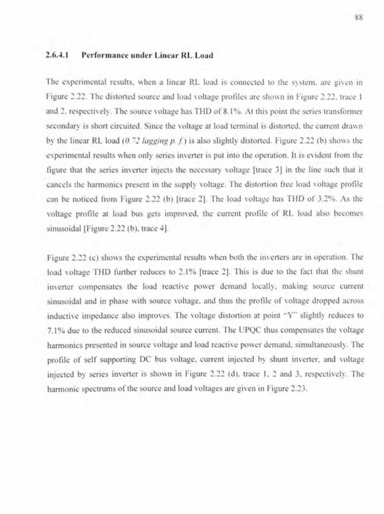
88
2.6.4.1 Performanc e unde r Linea r RL Loa d
The experimenta l results , whe n a linea r R L loa d i s connecte d t o th e svstem . ar e give n i n
Figure 2.22 . Th e distorte d sourc e an d loa d voltag e profile s ar e show n i n Figur e 2.22 , trace 1
and 2 , respectively. Th e source voltag e has THD of 8.1% . A t this point the serie s transforme r
secondary i s short circuited . Sinc e the voltag e a t loa d termina l i s distorted, the curren t draw n
by the linea r R L loa d (0. ! 2 lagging p. f) i s also slightl y distorted . Figur e 2.2 2 (b ) show s th e
experimental result s when onl y serie s inverte r i s put int o the operation . I t is evident fro m th e
figure tha t th e serie s inverte r inject s th e necessar y voltag e [trac e 3 ] i n th e lin e suc h tha t i t
cancels th e harmonic s presen t i n the suppl y voltage . Th e distortio n fre e loa d voltag e profil e
can b e notice d fro m Figur e 2.2 2 (b ) [trac e 2] . Th e loa d voltag e ha s TH D o f 3.2% . A s th e
voltage profil e a t loa d bu s get s improved , th e curren t profil e o f R L loa d als o become s
sinusoidal [Figur e 2.22 (b) . trace 4].
Figure 2.2 2 (c ) show s th e experimenta l result s whe n bot h th e inverter s ar e i n operafion . Th e
load voltag e TH D furthe r reduce s t o 2.1 % [trace 2] . Thi s i s du e t o th e fac t tha t th e shun t
inverter compensate s th e loa d reactiv e powe r deman d locally , makin g sourc e curten t
sinusoidal an d i n phas e wit h sourc e voltage , an d thu s th e profil e o f voltag e droppe d acros s
inductive impedanc e als o improves . Th e voltag e distortio n a t poin t "Y " slightl v reduce s t o
7.1% du e t o the reduce d sinusoida l sourc e current . Th e UPQ C thu s compensate s th e voltag e
harmonics presente d i n sourc e voltage an d loa d reactive powe r demand , simultaneously . Th e
profile o f sel f supportin g D C bu s voltage , curren t injecte d b y shun t inverter , an d voltag e
injected b y serie s inverte r i s show n i n Figur e 2.2 2 (d) . trac e 1 , 2 an d 3 , respectively . Th e
harmonic spectrum s o f the source and loa d voltages are given i n Figure 2.23.
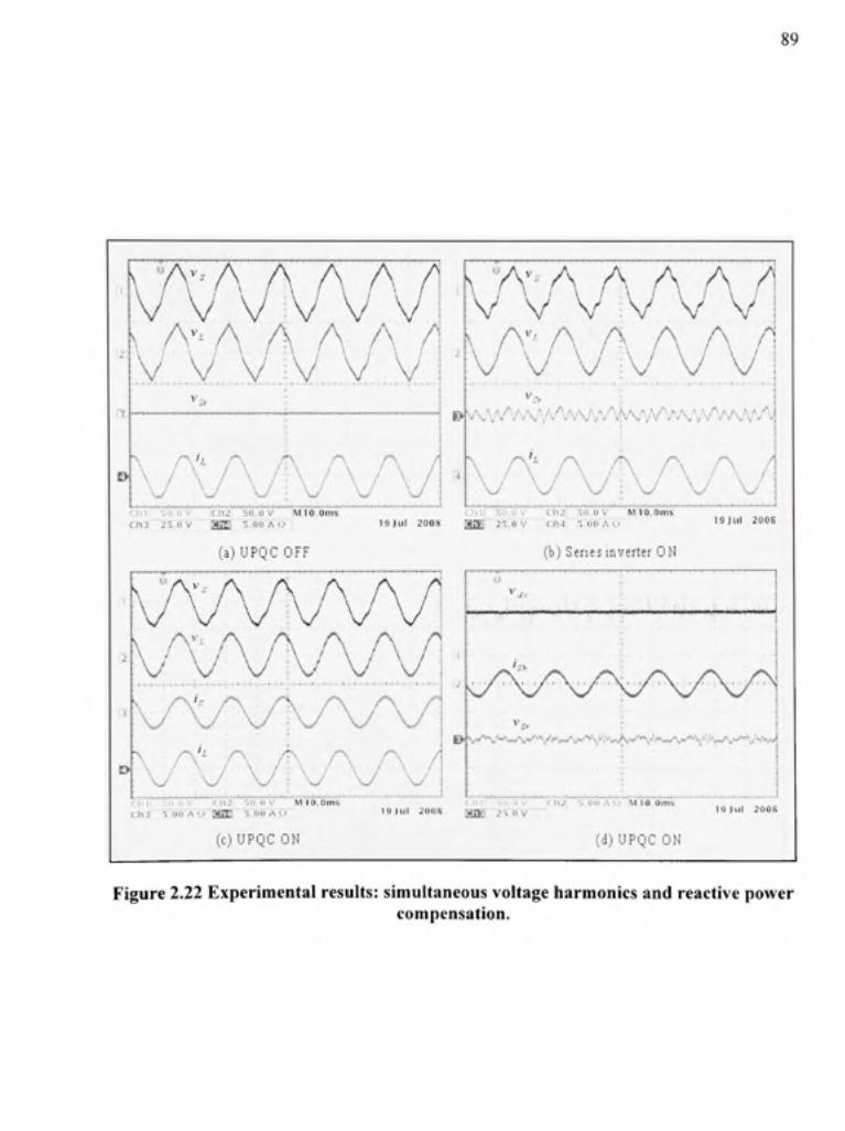
89
A A A A ; V V V \ . ,
„\ A - A A A , A ,/l . V V V ;.V V V
t>
' l i t 3'J.O V c:h 2 30. 0 \ ' M lO .Om s C h i 2 5 . n v a i B =i.noA<, >
^ A"- A A A A ~^
\J w 'U I \j V V .
E>
k A " A A A A A V V _ V ;V,...V y
•v^. \v^^^^AAA^A^Av\aVVA// /VAA^A
\ \ r \ A A A A / V V . / • \ / V
C.ilii 30. » V c:h2 , 30. U V MlO.OlI l S 19 Jul 200 S a i l ; ! 2 S , 0 V ( 'h ' ' i D O A i, ' 19 Jul 200 S
(a) UPQ C OFF (b) Serie s inverte r O N
\ v"v'V%^^y•V ./^A '^• •
V :v / v T v \ y V / h l i "l O 0 V (\xi n id . l l V MIO.Oni ! ;
t h 3' !5Tt J tTX i . '' HUE 5 : o «"A < .>
g>\j-^w"-^w-v»^"^V''''-»' -^A''''A'' ''*'~' ' V''' ^^
IS Jul 2(10$ : 19 Jul 200 8 a j E ^5 :o " v " - ~
(c) UPQ C ON (d) UPQ C ON
Figure 2.22 Experimental results: simultaneous voltage harmonics and reactive power compensation.
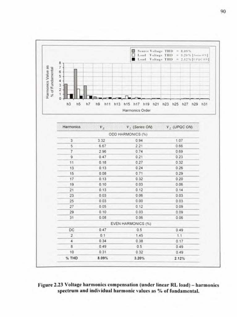
90
" > _ CD TO
•5 ^ > ro in "t 3 o c
'
—
1 1 1 i
--
i
M Soun: e Voltag e T H D = 8.0'J % n Loa d Voltag e T H D = 3.2 0 % [.S'r, « (;,\ ] • Loa d Voltag e T H D = 2.12%[UP(JC O.y]
I
1 1
i !
: 1 1
h3 h 5 h 7 h9 h1 1 h1 3 h1 5 h1 7 h1 9 h2 1 h2 3 h2 5 h2 7 h2 9 hS I
Harmonics Order
• • • • ' - - • •:• :•-. - - 1 . . . - : - . . . . . : • i- ; • • : . . - . - i . . . . ; . . . . . . . . . ^ . , , „ . . , . . , , . • . . . . . . . ••. . . , . , . ; . . . . . . . , ; , , , . . . . . . . . . • . . , . . . . . . . . . . . . •,. . ...• .... , , : - . • : - :
Harmonics .v VI (Seiies OW) V/ (UPQCOI\f} ; :
ODD HARMONICS (% )
3 5 7 9 11 13 15 17 19 21 23 25 27 29 31
3.32 6.67 2.96 0.47 0.18 0.13 0.08 0.13 0.10 0.13 0.03 0.03 0.05 0.10 0.08
0.94 2.21 0.74 0.21 0.27 0.24 0.71 0.32 0.03 0.12 0.06 0.00 0.12 0.03 0.06
1.07 0.66 0.69 0.23 0.32 0.26 0.29 0.20 0.06 0.14 0.03 0.03 0.09 0.09 0.06
EVEN HARMONICS (%)
DC 2 4 8 10
% THD
0.47 0.1
0.34 0.49 0.31
8.09%
0.5 1.45 0.38 0.5 0.32
3.20%
0.49 1.1
0.17 0.49 0.49
2.12%
Figure 2.23 Voltage harmonic s compensatio n (unde r linea r R L load ) - harmonic s spectrum an d individua l harmoni c value s a s % o f fundamental .
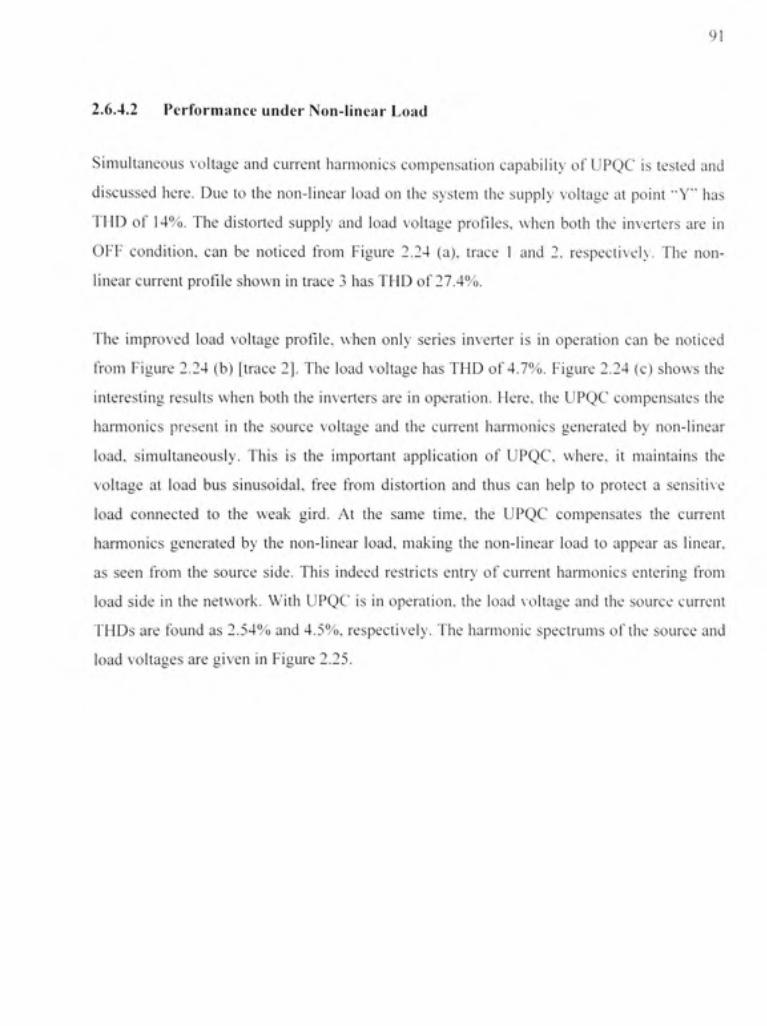
2.6.4.2 Performanc e unde r Non-linear Load
Simultaneous voltag e an d curren t harmonic s compensatio n capabilit y o f UPQ C i s tested an d
discussed here . Du e t o the non-linea r loa d o n th e syste m th e suppl y voltag e a t poin t "Y " ha s
THD o f 14% . The distorte d suppl y an d loa d voltag e profiles , whe n bot h th e inverter s ar e i n
OFF condition , ca n b e notice d fro m Figur e 2.24 (a) , trac e 1 and 2 . respectively . Th e non -
linear current profil e show n in trace 3 has THD of 27.4%.
The improve d loa d voltag e profile , whe n onl y serie s inverte r i s i n operatio n ca n b e notice d
from Figur e 2.2 4 (b ) [trac e 2] . The loa d voltag e ha s THD o f 4.7%. Figur e 2.2 4 (c ) show s th e
interesting result s when bot h th e inverter s ar e in operation. Here , the UPQ C compensate s th e
harmonics presen t i n th e sourc e voltag e an d th e curren t harmonic s generate d b y non-linea r
load, simultaneously . Thi s i s th e importan t applicatio n o f UPQC , where , i t maintain s th e
voltage a t loa d bu s sinusoidal , fre e fro m distortio n an d thu s ca n hel p t o protec t a sensitiv e
load connecte d t o th e wea k gird . A t th e sam e time , th e UPQ C compensate s th e curren t
harmonics generate d b y th e non-linea r load , makin g th e non-linea r loa d t o appea r a s linear ,
as see n fro m th e sourc e side . Thi s indee d restrict s entr y o f curren t harmonic s enterin g fro m
load sid e i n the network . Wit h UPQ C i s in operation, th e loa d voltag e an d th e sourc e curren t
THDs ar e foun d a s 2.54% and 4.5% , respectively. Th e harmonic spectrum s o f the sourc e an d
load voltages are given i n Figure 2.25.
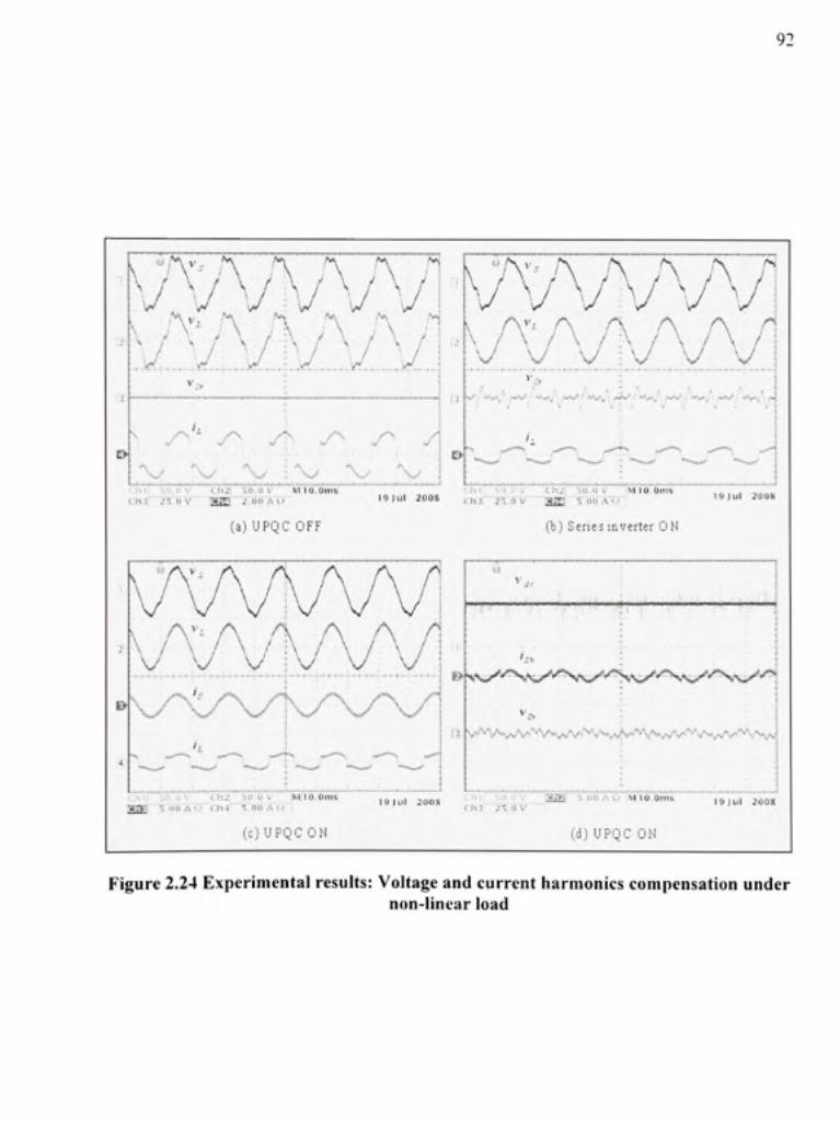
92
vVvA/W VVVvV V
»
Xz-'v A ^ A A ' ^
/~v. .A- yt . y ^ y ^ r
Xy Ny ; \ y : \ y V X
, ; :''• A A A A \J 'J \y •• V ' ^
•' ' "v 'o !
[ J N / .• >v^.' ywv*; , v*/ / T /^j-J- i v^rt*v' - . ' • ' "V ' , ' ' .^'^ - ,<' "»*V'.,'' ' .;">^/ • I •'Vv ' - f
»
f h n ^ y . u v (:h2 ! 30. 0 V M l O . O m s l l ! 5 0 (. i V {.h.! ! ^0 . 0 V M l O . O m s 19 Jul 200 S , „ • , 2 - n V - a m =:"()( f A < f I S J U l 200 K
(a) UPQ C OF F (b) Serie s inverte r O N
V ' ' " ' ' ' > / S . ' V V ' ' ' ' ^ / V ^ , V > V V ^ V S A ' * ' \ A , ^ ' - V V ' " - \ < V ^ \ A - ' » \ ^ . ^ .
C.hll .50. 0 \ t h 2 i SO. U V iMjlO.Om S a iEr~ ' 'S : ( )0"A 'o C h ^ S::n o A I : >
(c) UPQ C O N
I S J u l 200 $ i h i '7,U.<yy_ WS&i 3.0 0 A i. ; .MlO.Om s f.h.i'-'Ts.o V " ' I9JUI 200 X
(d) UPQ C O N
Figure 2.24 Experimental results : Voltage and curren t harmonic s compensation unde r non-linear load
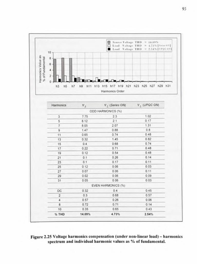
93
M S o u r c e V o l t a g c T H D n L o a d V o l t a g e T H D • L o a d V o l t a g e T H D
U . 0 9 % r . 7 3 % (Serie s 0 /V | 2 . 5 4 % \VPQC 0, Y
h3 h 5 h 7 h 9 h l i h1 3 h1 5 h1 7 h1 9 h2 1 h2 3 h2 5 h2 7 h2 9 h3 1
Harmonics Order
Harmonics ^s Vf {Series ON)
ODD HARMONICS (% )
V^ {UPQC ON)
3 5 7 9 11 13 15 17 19 21 23 25 27 29 31
DC 2 4 8 10
% THD
7.75 8.12 8.05 1.47 0.65 0.32 0.4 0.22 0.12 0.1 0.1 0.12 0.07 0.02 0.05
0.32 0.3 0.57 0.72 0.35
14.09%
2.3 2.1 2.07 0.88 0.74 1.45 0.68 0.71 0.54 0.26 0.17 0.06 0.06 0.06 0.06
EVEN HARMONICS (% ) 0.4 0.68 0.26 0.71 0.65
4.73%
1.02 0.17 1.31 0.8 0.48 082 0.74 0.48 0.48 0.14 0.11 0.03 0.11 0.09 0.03
0.45 0.57 0.06 0.14 0.43
2.54%
Figure 2.25 Voltage harmonics compensation (unde r non-linea r load) - harmonic s spectrum an d individua l harmonic values as % o f fundamental .
94
2.6.5 Voltag e Sag Compensation
In thi s sectio n th e performanc e o f UPQ C t o compensat e sa g o n th e syste m i s discussed .
Figure 2.26 shows the experimental result s during sag on the system. There is sag of 30% on
the system . Th e reduce d sourc e voltag e ca n b e notice d fro m Figur e 2.2 6 (a ) [trac e 1] . As
discussed i n the simulatio n sectio n an d CHAPTE R 1 (Section 1.4) , i n orde r t o compensat e
sag o n th e system , th e serie s inverte r inject s a n in-phas e voltage , whic h i s th e differenc e
between desired load voltage and actual source voltage. Bv injecting the in-phase voltage, the
series inverter is actually supporting the active power to the load. It is very important to have
self supportin g D C bu s durin g thi s sa g condition , i n orde r t o facilitat e th e activ e powe r
transfer. Interestingly , thi s activ e powe r come s fro m th e sourc e only . Th e shun t inverte r
draws the necessar y activ e power an d maintains th e D C bus voltage a t constan t level . This
power i s the n fe d bac k t o th e loa d b y serie s inverter . Figur e 2.2 6 (a ) an d (b ) verifie s th e
above mentioned fact .
(,!ii •,;i . . ! V Ch2 : 30.O V MlO.Om s c^M; ';c i 0 V icna i s.o o A O Miio.om s am 23. 0 v ii 20 Ju l 200 8
(a) (b)
Figure 2.26 Experimental results : voltage sag compensation (steady state condition).
The injected serie s inverter in-phase voltage and the resultant load voltage profiles are shown
in Figur e 2.2 6 (a) . A s alread y discussed , th e inpu t sourc e ha s TH D o f 4% . I n orde r t o
maintain the voltage at load bus sinusoidal and at rated value, the series inverter inject s su m
of in-phas e voltag e an d harmonic s voltage . Th e sel f supportin g D C bu s voltag e an d th e
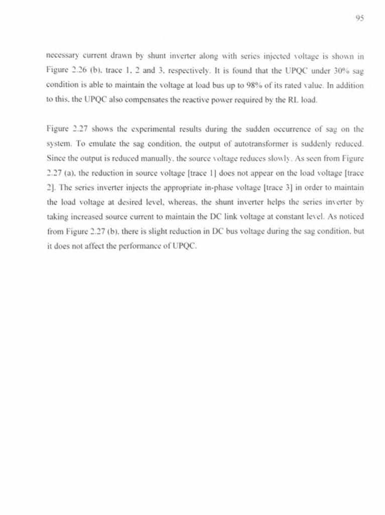
95
necessary curren t draw n b y shun t inverte r alon g wit h serie s injecte d voltag e i s show n i n
Figure 2.2 6 (b) . trac e 1 . 2 an d 3 . respectively . I t i s foun d tha t th e UPQ C unde r 30 % sa g
condition i s able to maintai n th e voltag e a t loa d bu s u p to 98%) of it s rated value . I n additio n
to this, the UPQC als o compensates the reactive power required b y the RL load .
Figure 2.2 7 show s th e experimenta l result s durin g th e sudde n occurrenc e o f sa g o n th e
system. T o emulat e th e sa g condition , th e outpu t o f autotransforme r i s suddenl y reduced .
Since the output i s reduced manually , the source voltag e reduces slowly . As seen fro m Figur e
2.27 (a) , the reductio n i n sourc e voltag e [trac e 1 ] does no t appea r o n th e loa d voltag e [trac e
2]. Th e serie s inverte r inject s th e appropriat e in-phas e voltag e [trac e 3 ] i n orde r t o maintai n
the loa d voltag e a t desire d level , whereas , th e shun t inverte r help s th e serie s inverte r b y
taking increase d sourc e curren t t o maintai n th e D C lin k voltag e a t constan t level . A s notice d
from Figur e 2.2 7 (b) . there i s slight reduction i n DC bus voltage during the sag condition, bu t
it does not affect th e performance o f UPQC.
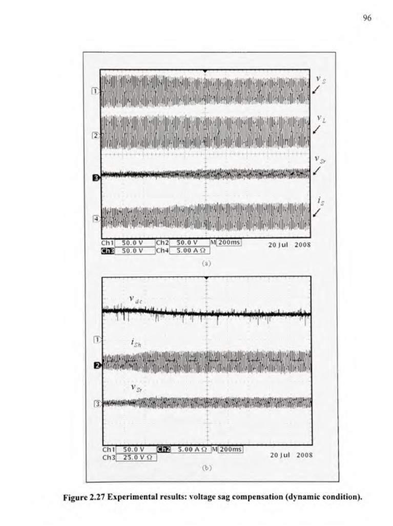
96
1,
IT-
E>
. . . , - . - • i ^
J^^Wtt^.WW(W^
• Ch1| 50. 0 V |Ch2 | 50. 0 V |M|200m s mtm 50. 0 V ^ C h 4 F 5 . 0 0 A Q |
(a)
V r .
Vr
V o
/
/
2 0 j u l 200 8
ro
B
*M
' .s-;!
• ^ j -
i''"iH|i'''i!Hi"«l"'i|gi'i1K )|lln)l|itll|llii)llliiillli«l]llli'llliiilllnllll!iill|
MBwwmtimmmmimii
Chl l 5 0 . 0 V |a!B | 5.0 0 A Q |M|200m s Ch3| 2 5 0 V Q I
(b)
2 0 J u l 200 8
Figure 2.27 Experimental results : voltage sag compensation (dynami c condition) .

97
2.6.6 Voltage Swell Compensatio n
In this sectio n th e performanc e o f UPQC t o compensate swel l o n the syste m i s tested. The
experimental result s are shown in Figure 2.28 and Figure 2.29. A swell of 30% is imposed on
the system. The operating principle of UPQC under swell condition is exactlv opposit e to the
sag condifion . Durin g a swel l o n th e system , i n orde r t o maintai n th e loa d bu s voltag e a t
desired constant level , the series inverter now injects a out-off phas e voltage. Thus the extra
voltage due to the voltage swel l i s cancelled ou t by series inverter . I t is found tha t the ripple
filter use d durin g thi s experimenta l study , introduce s som e distortio n i n injecte d voltage ,
especially durin g voltag e swel l condition . Therefore , th e loa d voltag e i s slightl y distorte d
with TH D o f 5.7% , a s ca n b e notice d fro m Figur e 2.2 8 (a ) [trac e 2] . The serie s injecte d
voltage profil e i s show n i n trac e 3 . Figure 2.2 8 (b ) show s sel f supportin g D C bu s voltag e
profile along with shunt injected curren t and series injected voltage .
The experimenta l result s during the sudden occurtence o f swel l o n the system are shown in
Figure 2.29 . As noficed i n previous secfion , th e sag causes a dip i n the D C bus voltage , on
the other hand, the swel l does not cause reduction i n DC bus voltage [Figur e 2.29 (b) . trace
1]. Nevertheless, UPQC is able to compensate the swell on the system effectivelv. I t is found
that fo r a swel l o f 30% , the UPQ C maintain s th e voltag e a t loa d bu s a t 102 % of it s rate d
value.
cm!' ko.dv iCh2 i so. o v Mjio:om s g ' ^ S t T 6 V "Ch-i' ^ s :0 0 AC ?
(n)
20JUI 200 8 30 o v ' ;aiE~"5'ooA n M,io:6m s ch3r 23;\ ) V fF' 20JU I 200 8
Figure 2.28 Experimental results : voltage swell compensation (stead y state) .

98
( 3 ; W W * M ^ W ^ ^
Chll 50.0 V |Bn B 50.0 V nMnoorn s Ch3| 50. 0 V |Ch4 | 5.0 0 A "A|
( a )
V ,
/
v /
Vrv
/
lc.
20Jul 200 8
rr
V dc
^\%\^\ I |i>ii|Jl|i|J|»i|iiiijilili||tli»iap^4|^* '*< ^
/ Sh
'Sr
m^j^mM^mmtUI^^
Chi 50. 0 V Ch3 25. 0 V Q
WTBI 5.0 0 AQAMnoOm s 2 0 J u l 200 8
(10
Figure 2.29 Experimental results : voltage swell compensation (dynamic) .
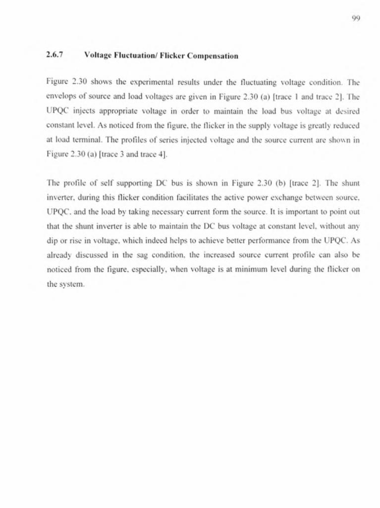
99
2.6.7 Voltag e Fluctuation / Flicker Compensatio n
Figure 2.3 0 show s th e experimenta l resuh s unde r th e fluctuating voltag e condition . Th e
envelops o f sourc e an d loa d voltage s ar e give n i n Figur e 2.3 0 (a ) [trac e 1 and trac e 2] . Fh e
UPQC inject s appropriat e voltag e i n orde r t o maintai n th e loa d bu s voltag e a t desire d
constant level . As noticed fro m th e figure, th e flicker i n the suppl y voltag e i s greatly reduce d
at loa d terminal . Th e profile s o f serie s injecte d voltag e an d th e sourc e curren t ar e show n i n
Figure 2.3 0 (a ) [trac e 3 and trace 4].
The profil e o f sel f supportin g D C bu s i s show n i n Figur e 2.3 0 (b ) [trac e 2] . Th e shun t
inverter, durin g thi s flicker conditio n facilitate s th e activ e powe r exchang e betwee n source ,
UPQC. and th e loa d by takin g necessar y curren t for m th e source . I t i s importan t t o poin t ou t
that th e shun t inverte r i s abl e t o maintai n th e D C bu s voltag e a t constan t level , withou t an y
dip o r ris e i n voltage , which indee d help s to achiev e bette r performanc e fro m th e UPQC . A s
already discusse d i n th e sa g condition , th e increase d sourc e curren t profil e ca n als o b e
noticed fro m th e figure, especially , whe n voltag e i s a t minimu m leve l durin g th e flicker o n
the system .
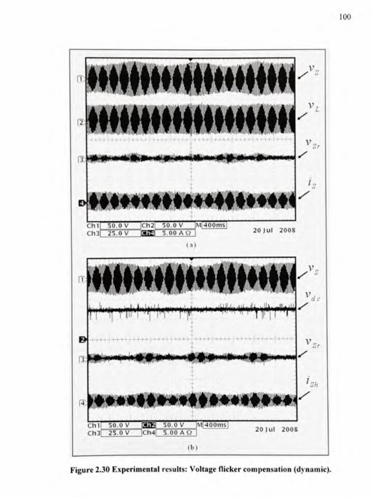
100
Chl l 5 0 0 V |Ch2 | 50. 0 V |M|400r m Ch3| 25^ 0 V IBJE F 5.0 0 A Q |
(a)
f l
20Jul 200 8
IX ' "
^p |i||iiiiwi|U<iiii w»<<iyi|M||ij|H|w#i i>»>iyil ^
V d,
Chi 50. 0 V JBI E Ch3| 25. 0 V |Ch 4
50.0 V IV14Q0m s 5.00 A Q 20Ju l 200 8
(b)
Figure 2.30 Experimental results : Voltage flicker compensatio n (dynamic) .
2.7 Conclusion s
This chapte r explore s th e capabilitie s o f unifie d powe r qualit y conditione r (UPQC) . Th e
UPQC combine s functionalitie s o f shunt and serie s active power filters. Thus , we have bette r
and simultaneou s contro l ove r loa d curren t a s wel l a s sourc e voltag e relate d powe r qualit y
problems. The UPQC can b e installed i n order to isolate and thus to protect th e loads within a
plant fro m an y disturbanc e i n the sourc e voltage . I n addition t o this , i t also act s a s harmoni c
suppressor, an d thu s prevent s th e penetratio n o f curren t harmonic s fro m th e plan t sid e
towards the network .
The performanc e o f UPQ C t o compensat e th e mos t significan t powe r qualit y issue s o n
distribution level , suc h as , curtcn t harmonics , reactiv e current , voltag e harmonics , voltag e
sag, voltag e swel l an d voltag e flickers, i s evaluate d b y simulatio n a s wel l a s wit h
experimental validations . Unde r distorte d suppl y voltag e (TH D = 14.09% ) wit h non-linea r
load o n th e syste m (loa d curren t TH D = 30.14%) , th e UPQ C i s abl e t o reduc e th e TH D i n
load voltage to 2.54%, whereas, the source current THD i s found a s 4.5%.
The wor k presente d her e ma y sho w significan t impac t o n th e feasibilit y o f UPQ C t o b e
installed i n actua l distribufio n networks . Th e develope d controlle r (UVTG) . extensiv e
simulation stud y under realisti c networ k an d the laborator y experimenta l investigatio n highl y
supports th e futur e prospectiv e fo r th e UPQ C bein g commercialize d fo r practica l
applications. Therefore , i n summary , i t ca n b e conclude d tha t th e joint-ventur e projec t
between ETS , IREQ, and Hydro-Quebec wa s a great success .
CHAPTER 3
VOLTAGE SA G COMPENSATIO N THROUG H REACTIV E POWE R
3.1 Introductio n
This chapte r focuse s o n voltag e sa g compensatio n - on e o f th e mos t undesirabl e
phenomenons o n power distributio n level . Recently, stati c compensator s (D-STATCOM ) an d
dynamic voltag e restorer s (DVR ) hav e bee n utilize d t o overcom e th e voltag e sa g proble m
(Haque, 2002 ; Newma n et al, 2003 ; Masd i et al. 2004) . Th e D-STATCO M ca n hel p t o
compensate voltag e sa g alon g wit h loa d curren t harmonics , but it s performanc e ca n b e
affected i n th e presenc e o f voltag e harmonics . O n th e othe r hand , th e DV R ca n effectivel y
compensate voltag e sa g wit h reactiv e powe r contro l an d minimu m activ e powe r injectio n
mode, unde r a distorte d utilit y condition , bu t i t ca n not tackl e th e loa d curren t harmoni c
problem effectively . Th e UPQ C ca n als o b e considere d a s a n integratio n o f D-STATCO M
and DVR .
As highlighte d i n th e CHAPTE R 2 , b y utilizin g UPQC . th e voltag e sa g i s effectivel y
compensated b y injectin g in-phas e voltag e throug h serie s inverte r equal s t o th e differenc e
between th e rate d loa d voltag e an d reduce d voltag e du e t o th e sa g condition . I n orde r t o
achieve th e adequat e voltag e sa g compensatio n th e shun t inverte r draw s th e require d activ e
power fro m th e sourc e side . Since activ e powe r i s involve d i n voltage sa g compensatio n i t i s
termed a s UPQC-P . Th e othe r possibl e approac h t o tackl e th e sa g o n th e syste m i s throug h
reactive powe r contro l an d whe n UPQ C i s controlle d i n suc h mamie r the n i t i s referre d a s
UPQC-Q (Bas u et al, 2002) .
This chapte r deal s wit h th e voltag e sa g compensatio n usin g reactiv e powe r control . A
simplified approac h i s propose d t o estimat e th e require d quadratur e voltag e magnitude . A s
the voltage sa g i s controlled b y reactive power b y injectin g voltag e i n quadrature wit h sourc e
curtent throug h serie s inverter , th e UPQC- Q doe s no t requir e an y activ e power . Detaile d
mathematical formulatio n t o estimat e th e require d quadratur e voltag e i s als o give n i n th e

103
chapter. Th e propose d simplifie d approac h fo r quadratur e voltag e injectio n (QVI ) i s first
validated throug h simulatio n studies . Late r on . in-dept h laborator y experimenta l result s fo r
single-phase a s wel l a s three-phas e UPQC- Q syste m ar e given . Finally , a discussio n o n
voltage sa g compensation usin g active and reactiv e power control approache s i s carried out .
3.2 UPQC- Q Concep t
UPQC i s one of the most effectiv e powe r quality conditionin g device s tha t can be utilized fo r
voltage sa g compensation a t the distribution level . The voltage sa g compensation ca n be done
by usin g activ e powe r a s wel l a s reactive powe r control . Whe n UPQ C i s used t o compensat e
voltage sa g b y reactiv e powe r control , i t i s terme d a s UPQC-Q . Th e concep t i s t o injec t a
quadrature voltag e suc h tha t th e su m o f actua l sourc e voltag e an d th e injecte d voltag e wil l
give th e require d rate d voltag e a t the loa d bu s terminal . Th e shun t par t o f UPQC necessaril y
maintains th e unit y powe r facto r operatio n a t th e sourc e sid e unde r al l kind s o f loads .
Injecting th e serie s inverte r voltag e i n quadratur e wit h th e sourc e thu s essentiall y i s i n
quadrature wit h th e sourc e curren t too . Powe r handle d b y th e serie s inverte r i s goveme d bv -
its injecte d voltag e an d th e curren t flowing throug h th e serie s transformer . Therefore , b y
injecting th e serie s inverte r voltage i n quadrature wit h th e sourc e voltage eliminate s th e nee d
of activ e powe r t o compensat e th e sa g o n th e system . However , th e resultan t voltag e thu s
achieved give s phase angle shif t wit h respective to the source voltage .
There ar e tw o possibl e way s t o injec t th e quadratur e voltage : 90 ° laggin g o r 90 ° leading . I f
the load i s inductive i n nature, the late r has advantage of input power facto r improvemen t du e
to a reductio n i n th e effectiv e phas e angl e betwee n sourc e voltag e an d loa d current , an d
hence, i s considere d i n thi s researc h work . Thus , durin g voltag e sa g compensatio n usin g
UPQC-Q, the reactive powe r burde n o n shunt inverte r ma y ge t reduced. Thi s i s an additiona l
benefit o f QV I contro l o f UPQC- Q whe n compare d t o th e voltag e sa g compensatio n b y th e
active powe r contro l method . Since , i n cas e o f activ e powe r control , th e powe r handle d b y
shunt inverte r increase s wit h increase d percentag e o f sa g (Khadkika r et al, 2006a , 2006c) .
and i t increases the required shun t inverter ratings .
1(J4
3.2.1 UPQC- Q Phaso r Representatio n
The phaso r representatio n fo r basi c understandin g o f operatin g principl e o f quadratur e
voltage injecfio n (QVI ) i s show n i n th e Figur e 3.1 . Fo r simplicity , th e loa d i s considere d a s
linear R L an d i t i s assume d tha t th e loa d remain s sam e durin g steady-stat e a s wel l a s durin g
sag conditions .
Under norma l steady-stat e operatin g condition , th e loa d voltag e Vi,o) i s a t rate d suppl y
voltage Vs(0) value , takin g a loa d curren t li(0) with a laggin g powe r facto r angl e o f ^/, . Now, a
sag conditio n occur s o n th e syste m o r o n PC C suc h tha t th e suppl y voltag e reduce s t o IA,Y/; - I n
order t o maintai n th e loa d voltag e a t rate d valu e {V i), th e serie s inverte r shoul d injec t a n
appropriate compensatin g voltage . Wit h reactiv e powe r contro l approach , th e injecte d
voltage shoul d b e Vsr(i). i n quadratur e wit h th e sourc e curren t suc h tha t th e resultan t loa d
voltage wil l becom e Vifi/. A s notice d fro m th e Figur e 3.1 , the injectio n o f quadratur e voltag e
causes th e resultan t loa d voltag e t o lea d th e sourc e voltage . Th e phas e angl e differenc e thu s
occurs betwee n th e sourc e an d th e resultan t loa d voltage , denote d a s power angl e 5y .
Interestingly, th e powe r angl e 8 / cause s a loa d phas e angl e boos t wit h respec t t o th e sourc e
voltage givin g f^i, a n effectiv e phas e angl e betwee n Vs(i) and hd). A s th e loa d o n th e syste m
is considere d t o b e constan t durin g thi s operation , th e phas e angl e betwee n Vi(0) - li^o) an d
VL(I) - hdj woul d no t ge t affected . Th e phas e advancemen t betwee n loa d current s hfO) an d
lif/j i s equa l t o 5/ . Th e QV I no t onl y compensate s th e voltag e sa g bu t als o improve s th e
effective inpu t powe r facto r angl e an d thus , supplie s a certai n amoun t o f reactiv e powe r
through serie s inverte r too . Fo r highe r % sa g Vso. 6 2 would ge t mor e advanced , reducin g /?.->
further, bu t a t th e sam e tim e increasin g th e serie s compensatin g voltag e magnitud e
{Vsr(2)>^^Sr(l))-
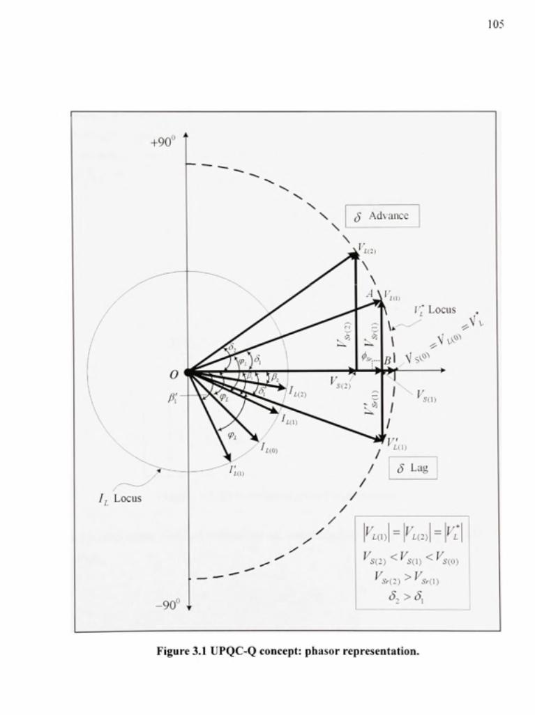
+90"
105
I^ Locu s
-90°
§ Advanc e
S La g
y '^ L{\)
— y ''1(2)
= v: V <v <v '^ S{2) ^ '^ 5(1) ^ S(0)
V >V ^ Sr(2) '^ .S>(1 )
S, > J,
Figure 3.1 UPQC-Q concept: phasor representation.
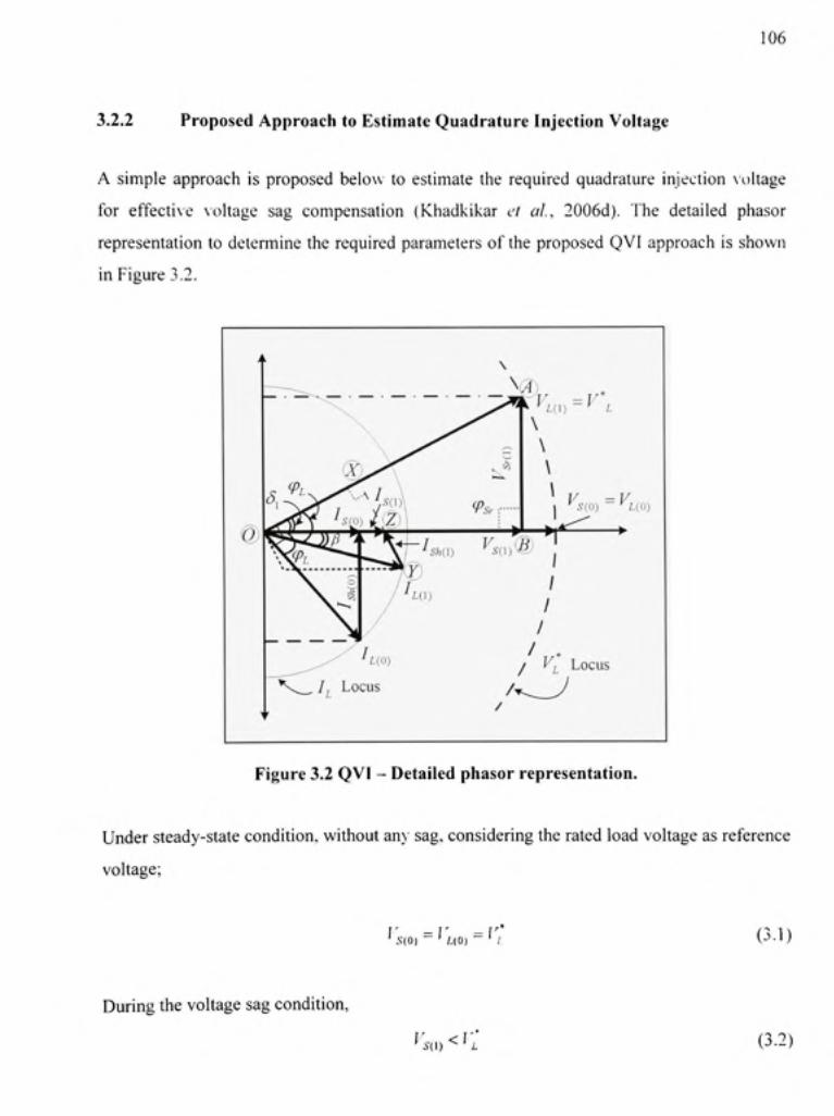
106
3.2.2 Propose d Approach to Estimate Quadrature Injection Voltage
A simple approac h i s proposed belo w t o estimat e th e require d quadratur e injectio n voltag e
for effectiv e voltag e sa g compensatio n (Khadkika r et al, 2006d) . Th e detaile d phaso r
representation t o determine the required parameter s o f the proposed QV I approach i s shown
in Figure 3.2.
Figure 3.2 QVI - Detaile d phasor representation.
Under steady-state condition, without anv' sag, considering the rated load voltage as reference
voltage;
' S(0 ) * /,(0 ) ' / (3.1)
During the voltage sag condition.
^5(1) < ' l (3.2)
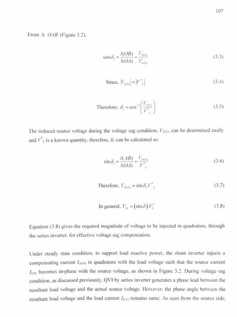
From A OAB (Figur e 3.2) ,
107
cosS, = 1{0B) _Vs l(OA) V,
(1)
L ( l )
(3.3)
Since, 1 id ) v\ (3.4)
Therefore, 6, = cos" .V( I ) (3.5)
The reduce d sourc e voltag e durin g th e voltag e sa g condition , Vs(ij, ca n b e determine d easil y
and V\ is a known quantity , therefore , 8 / ca n be calculated as :
sin<J, 1{AB) nOA)
.SV(I) (3.6)
Therefore, V^^^^^-smSyV\ (3.7)
In general, V^^ - [s'mS).V' (3.8)
Equation (3.8 ) give s th e require d magnitud e o f voltag e t o b e injecte d i n quadrature , throug h
the series inverter , fo r effective voltag e sa g compensation .
Under stead y stat e condition , t o suppor t loa d reactiv e power , th e shun t inverte r inject s a
compensating curren t fhrn i n quadratur e wit h th e loa d voltag e suc h tha t th e sourc e curren t
f(0) become s in-phas e wit h th e sourc e voltage , a s show n i n Figur e 3.2 . Durin g voltag e sa g
condition, as discussed previously , QV I b y serie s inverte r generate s a phase lea d betwee n th e
resultant loa d voltag e an d th e actua l sourc e voltage . However , th e phas e angl e betwee n th e
resultant loa d voltag e an d th e loa d curren t IHD remain s same . A s see n fro m th e sourc e side .
108
this action certainl y cause s the reduction i n load power facto r angl e from tpi to fi. The voltag e
which appear s acros s shun t inverte r i s the resultan t loa d voltage . I n orde r t o compensat e th e
new reactiv e powe r demand , a s see n fro m th e shun t inverte r side , th e shun t inverte r shoul d
now injec t th e compensatin g curren t fhd) i n quadratur e wit h th e resultan t loa d voltage . Thi s
is essential , sinc e th e shun t inverte r shoul d als o no t handl e an y activ e power . No w lookin g
back fro m th e sourc e side , there i s an increas e i n the resultan t sourc e curren t l^o) magnitude.
This i s essential t o maintain the active power balance i n the entire network .
The increased sourc e current magnitud e ca n be calculated as :
In A OXT. cos(p, = ^S9i^ (3.9 ) ' 1{0Y)
/ (aV) = cos^, . / ,„, (3.10 )
In AC>A^Z,cos ^ = ^^^^-^ (3.11 ) hOZ)
COS(p,J,^,^ C0SS = LJ_^A1L (3.12 )
Therefore, / , , , = / , „ , ^^ (3.13 ) cosd
The abov e equatio n give s the magnitud e o f increase d sourc e curren t i n orde r t o maintain th e
power balance i n the entire network .
109
3.2.3 Activ e and Reactive Power Flow during QVI
The active and reactive power flow through the series inverte r during QVI can be computed
as:
^s. = ';>(i,-A-,i)-cos^. v (3-14 )
P,, =0 (since,cos90°=0 ) (3.15 )
.sv = ;s>(i,- ,s-,i,-sin<?'v (3.16 )
a,. = f;vor^.s-,i,{since,sin90"=l) (3.17 )
as>=sin^).r",./,,„ (3.18 )
Q,^=smS.f,,'-^.V', (3.19 ) COS(^
6 ' , .=( tanJ) . (cos^, ) . ( / ,„ , r \ ) (3.20 )
Q^^y-iSinS (3.21 )
The equatio n (3.21 ) suggest s tha t th e reactiv e powe r supporte d b y th e serie s inverte r t o
compensate the voltage sag is the function o f power angle 8. The power angle 8 is dependant
on the % of sag need to be compensated.
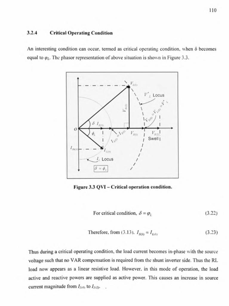
110
3.2.4 Critical Operating Condition
An interesting conditio n ca n occur , termed a s critica l operatin g condition , whe n 8 becomes
equal to (pi- The phasor representation of above situation is shown in Figure 3.3.
/ Swel l I
f Locu s
Figure 3.3 QVI - Critica l operation condition.
For critical condition, 5 = cp. (3.22)
Therefore, from (3.13) . f,^. = f (3.23)
Thus during a critical operating condition, the load curtent becomes in-phase with the source
voltage such that no VAR compensation is required from the shunt inverter side. Thus the RL
load no w appear s a s a linea r resistiv e load . However , i n thi s mod e o f operation , th e loa d
active an d reactiv e power s ar e supplie d a s active power . Thi s cause s a n increas e i n sourc e
curtent magnitude from IsiO) to Isu). .
For an y ris e i n voltag e {Vsf2)>V ij. a s show n i n Figur e 3.3 , th e quadratur e injecte d voltag e
can not intersec t th e reference loa d v oltage locus , suggesting tha t QV I with zero active powe r
consumption doe s not compensat e th e swel l o n th e system . However , wit h minimu m activ e
power involvement , th e swel l ca n b e compensate d easily . Further , i f th e loa d i s having hig h
power facto r (clos e t o unity) , i n suc h a scenario , the voltag e sa g compensatio n ma y resul t i n
leading loa d curren t operatio n wit h respec t t o th e sourc e voltage . I n suc h case s th e shun t
inverter shoul d injec t laggin g compensating curren t t o achieve unit y power facto r operation .
3.3 UPQC-Q Controlle r Dev elopment
The sourc e voltage s ca n b e distorted , therefore , i t i s essentia l t o tak e necessar y correctiv e
action whil e developin g th e controlle r fo r UPQC-Q . A s discusse d i n CHAPTE R 2 , t o
compensate th e voltag e sa g usin g activ e powe r control , th e loa d voltage s wer e force d t o b e
sinusoidal a t a desired rate d value . The advantage i n forcing th e loa d voltage i s the harmonic s
in th e sourc e voltag e (i f any ) get s compensate d indirectlv' . withou t extractin g them . I n
UPQC-Q th e serie s inverte r inject s voltag e i n quadratur e wit h th e sourc e current . Thus , w e
can not forc e th e loa d voltag e to be sinusoidal withou t extractin g th e harmonics present i n the
source voltage . I n th e followin g subsections , th e extractio n o f voltag e harmonics , an d
determination o f th e require d quadratur e injectio n voltag e fo r voltag e sa g compensation , i s
explained i n detail .
3.3.1 Voltage Harmonic s Extractio n
The d-q transformatio n base d approac h (Bhattachary a et al. 2005 ) i s use d t o extrac t th e
harmonic containe d i n the suppl y voltages . The three-phase distorte d sourc e voltages ar e first
transferred int o two-phase stationar y co-ordinate s usin g following eqution :
^'\s<y
V "^1 --f V3
1 -1/ 2 1/ 2
0 V3/ 2 -V3/ 2 (3.24)
12
This transformafio n help s t o represen t th e three-phas e distorte d suppl y voltage s a s direc t {d)
and quadratur e {q) components , v', ^ and v' ^ , respectively. Th e notation s "scf an d "sq" use d
to identity tha t the sourc e voltage d and q quantities are extracted an d the suffix "'.s " is used to
denote that these quantities ar e in stationary referenc e frame .
The stationar y referenc e fram e quantitie s ar e the n converte d int o synchronou s rotatin g
reference fram e b y using (3.25) .
v</ COS 6? - s i n ^ sin^ cos ^
(3.25)
Where, 0 is a time varian t angl e tha t represent s th e angula r positio n o f the referenc e frame .
This referenc e fram e i s rotatin g a t a constan t spee d i n synchronis m wit h th e three-phas e a c
voltages. A PL L ca n b e use d t o extrac t sin^ * an d cos ^ term s necessar y fo r svnchronou s
frame synchronizafion . Th e suffi x "c " " i s use d t o denot e th e quantitie s whic h ar e i n
synchronous rotatin g frame . Th e transformatio n fro m th e stationar y referenc e fram e t o th e
rotating referenc e help s t o separat e th e harmonic s fro m th e fundamenta l component . Th e
term v^'^d and v'^sq can be represented a s sum of AC and D C components :
v' 1' '
u/
• " / -
(Ajy + iy..J A , + 1'' ' ,
sqj sii.hr
(3.26)
The D C quantitie s represen t th e fundamenta l frequenc y component , whereas , th e A C
quantities give s th e tota l hartiionic s presen t i n th e suppl y voltage . Th e fundamenta l an d
harmonics component s ar e denote d b y th e suffi x "f an d "/?/•" , respectively . Th e harmonic s
quantifies ca n easily be extracted b y using a high pas s filter (HPF) . These extracte d hannoni c
components ar e transferre d bac k t o th e stationar y referenc e fram e b y (3.27 ) an d the n t o th e
three-phase referenc e harmoni c component s o f sourc e voltag e 'm a - b - c fram e b y (3.28) .
Figure 3. 4 give s th e bloc k diagra m representatio n o f voltag e harmonic s extractio n usin g
synchronous referenc e fram e base d method .

.•.cl.hr
sq.hr
cosO s\n6
- s i n ^ cos6 sj.hr :3.27)
r • ~ i y ' su.hr
^' .shjir
* l^' sc.hr]
P -1/2
1/2
V3/2 -V3/2
sJ.hr
-q.hr
(3.28)
Transformation
From PLL s i n ^ • cos^-
to
Transformation
T — r
^ HPF | -
<v\ ) • ^ v "
Harmonic Extraction
( ' \ ) ' = > ' ' , j . .
to
Transformation
sJ.hr
sq.hr
2 - ( * to
Transformation
•*V
->• V
--V
Figure 3.4 Voltag e harmonic extractio n base d on synchronous referenc e fram e method .
3.3.2 Determination o f Quadrature Injectio n Voltag e
In thi s section , real-tim e implementatio n o f th e propose d simplifie d approac h fo r direc t
determination o f require d quadratur e injectio n voltag e i s explained . Fo r simplicity , i t i s
assumed tha t th e syste m voltage s ar e balanced . Th e actua l sourc e voltag e i s sense d an d it s
fundamental rms valu e i s continuousl y computed , an d divide d b y th e constan t rate d loa d
voltage magnitude . Th e resultan t quantit y represent s th e ter m cos 8 an d th e powe r angl e 8
thus ca n b e estimate d easily . Th e require d injectio n voltag e magnitud e IV . fo r effectiv e sa g
compensafion. i s the n calculate d usin g standar d mathematica l computations . I f th e suppl y
voltages ar e unbalance d i n nature , th e separat e rms value s o f eac h phas e voltag e an d thu s
separate injectio n voltag e magnitude determinatio n woul d b e required .
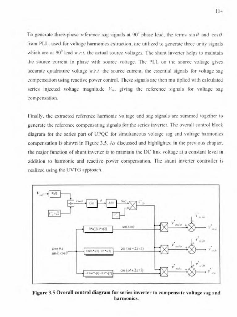
14
To generat e three-phas e referenc e sa g signal s a t 90 ° phas e lead , th e term s sin6 ' an d cos ^
from PLL , use d fo r voltag e harmonic s extraction , ar e utilize d t o generat e thre e unit y signal s
which ar e a t 9 0 lea d w.r.t. th e actua l sourc e voltages . Th e shun t inverte r help s t o maintai n
the sourc e curren t i n phas e wit h sourc e voltage . Th e PL L o n th e sourc e voltag e give s
accurate quadratur e voltag e w.r.t. th e sourc e current , th e essentia l signal s fo r voltag e sa g
compensation usin g reactiv e powe r control . These signal s ar e then multiplie d wit h calculate d
series injecte d voltag e magnitud e Ksv , givin g th e referenc e signal s fo r voltag e sa g
compensation.
Finally, th e extracte d referenc e harmoni c voltag e an d sa g signal s ar e summe d togethe r t o
generate th e referenc e compensatin g signal s fo r th e serie s inverter . Th e overal l contro l bloc k
diagram fo r th e serie s par t o f UPQ C fo r simultaneou s voltag e sa g an d voltag e harmonic s
compensation i s show n i n Figur e 3.5 . A s discusse d an d highlighte d i n th e previou s chapter ,
the majo r functio n o f shun t inverte r i s to maintai n th e D C lin k voltag e a t a constan t leve l i n
addition t o harmoni c an d reactiv e powe r compensation . Th e shun t inverte r controlle r i s
realized usin g the UVTG approach .
^ . V C / — ^ RM S
I'\l\l2
From PLL
Sin<?, cos (
Co.sS (JK ' sm
(}*i{\] + \*ii2]
086r)*u| l | -05*u| : |
• -O.866*«[l]-0.5*»[2 ]
.SDIS
cos (ojl)
cos (cot-2;r/2))
cos ((y/ + 2/T/3)
qud.a
qnd.b
-* V
sb,hr
i + V ,,, , v
-+ V ,T,A
qud .i.
Figure 3.5 Overal l contro l diagra m fo r series inverter to compensate voltag e sa g an d harmonics.
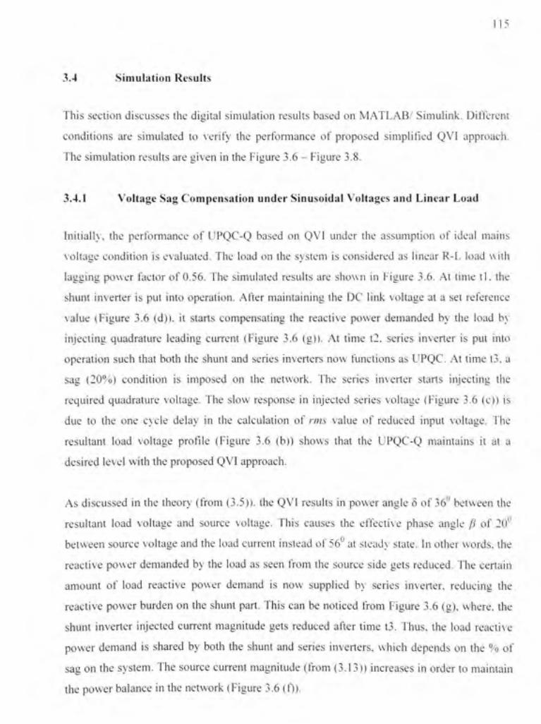
115
3.4 Simulatio n Result s
This sectio n discusse s th e digita l simulatio n result s base d o n MATLAB / Simulink . Differen t
conditions ar e simulate d t o verif y th e performanc e o f propose d simplifie d QV I approach .
The simulation result s are given i n the Figure 3.6 - Figur e 3.8 .
3.4.1 Voltag e Sa g Compensation unde r Sinusoidal Voltage s an d Linea r Loa d
Initiallv', th e performanc e o f UPQC- Q base d o n QV I unde r th e assumptio n o f idea l main s
voltage conditio n i s evaluated. Th e loa d o n th e syste m i s considered a s linea r R- L loa d wit h
lagging powe r facto r o f 0.56 . Th e simulate d result s ar e show n i n Figur e 3.6 . A t tim e t l . th e
shunt inverte r i s put int o operation . Afte r maintainin g th e D C lin k voltag e a t a se t referenc e
value (Figur e 3. 6 (d)) . i t start s compensatin g th e reactiv e powe r demande d b y th e loa d b y
injecting quadratur e leadin g curren t (Figur e 3. 6 (g)) . A t tim e t2 . serie s inverte r i s put int o
operafion suc h tha t bot h th e shun t an d serie s inverter s no w function s a s UPQC. A t tim e t3 , a
sag (20% ) conditio n i s impose d o n th e network . Th e serie s inverte r start s injectin g th e
required quadratur e voltage . Th e slo w respons e i n injecte d serie s voltag e (Figur e 3. 6 (c) ) i s
due t o th e on e cycl e dela y i n th e calculatio n o f rms valu e o f reduce d inpu t voltage . Th e
resultant loa d voltag e profil e (Figur e 3. 6 (b) ) show s tha t th e UPQC- Q maintain s i t a t a
desired leve l with the proposed QV I approach .
As discusse d i n the theor y (fro m (3.5)) . the QVI result s i n power angl e 8 of 36 ° between th e
resultant loa d voltag e an d sourc e voltage . Thi s cause s th e effectiv e phas e angl e / ? o f 20 °
between sourc e voltag e and th e loa d curren t instea d o f 56 ° at steady state . In other words , the
reactive powe r demande d b y the loa d a s see n fro m th e sourc e sid e get s reduced . Th e certai n
amount o f loa d reacfiv e powe r deman d i s no w supplie d bv ' serie s inverter , reducin g th e
reactive powe r burde n o n the shun t part . Thi s ca n b e noticed fro m Figur e 3. 6 (g) , where, th e
shunt inverte r injecte d curten t magnitud e get s reduce d afte r tim e t3 . Thus, th e loa d reactiv e
power deman d i s share d b y bot h th e shun t an d serie s inverters , whic h depend s o n th e % o f
sag on the system . Th e sourc e curtcn t magnitud e (fro m (3.13) ) increase s i n order t o maintai n
the power balanc e i n the network (Figur e 3. 6 (0) .
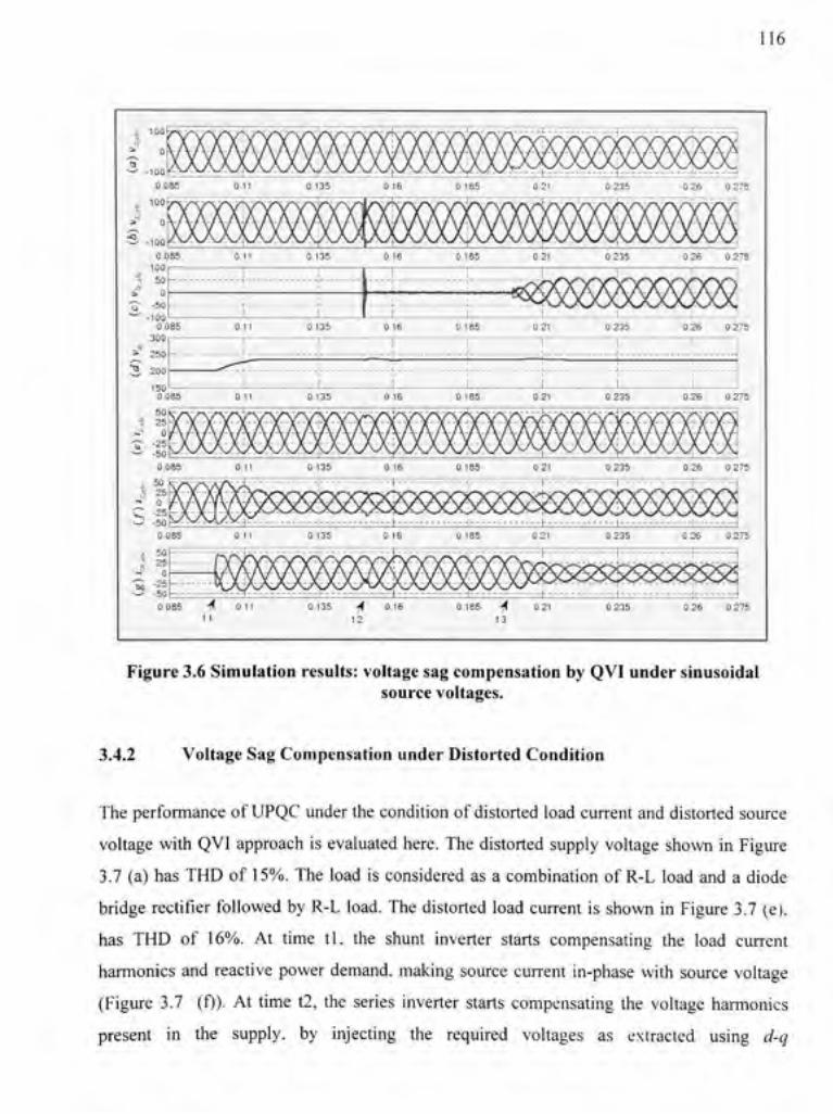
0.085 100
50 0
-50 -100
0 08 5 300
^ 25 0
150 0 08 5
•*->
0.11
0.11
0.11
0,135
_L 0.135
~r
0135
0.16 0.185 021
0.16 0.21
0 18 5 021
0,185 ^ 0.2 1 13
0 23 5
0 23 5
L 1 I
0 23 5
0.235
116
0 08 5
100
0
100 /\ysy
0.11
^Y'VVV" \AJ^^y\J^
0.135 0.16
ifOvTor N^A/fvA/
0.185
J
Y y Y Y
021
"^0000 C A A A A
0 23 5
^ A A A A
0.26
y Y Y
0.2'
0.26 0 275
0.26 0.27 5
0.26 0.27 5
0.26 0.27 5
0,26 0.27 5
0.26 0.27 5
Figure 3.6 Simulation results: voltage sag compensation by QVI under sinusoidal source voltages.
3.4.2 Voltage Sag Compensation unde r Distorted Condition
The performance o f UPQC under the condition of distorted loa d current and distorted sourc e
voltage with QVI approach i s evaluated here . The distorted suppl y voltag e show n i n Figure
3.7 (a ) has THD of 15% . The load i s considered a s a combination o f R-L loa d and a diode
bridge recfifie r followe d b y R-L load . The distorted loa d curren t i s shown in Figure 3.7 (e) .
has TH D o f \6%. A t tim e tl . th e shun t inverte r start s compensatin g th e loa d curren t
harmonics an d reactiv e powe r demand , makin g sourc e curtcn t in-phas e wit h sourc e voltag e
(Figure 3. 7 (f)) - A t tim e t2 , the serie s inverte r start s compensatin g th e voltag e harmonic s
present i n th e supply , b y injectin g th e require d voltage s a s extracte d usin g d-q

117
transformation. Thu s distortion present in the source voltages are isolated by UPQC and does
not appear on the load terminals. The load voltage has THD of 2%.
During th e conditio n o f voltage harmonic s an d voltag e sa g (20%) , after tim e t3 , the serie s
inverter inject s appropriat e voltag e t o maintai n th e loa d voltag e a t a desired constan t leve l
and fre e fro m distortio n (Figur e 3. 7 (b)) . The serie s injecte d voltag e (Figur e 3. 7 (c) ) i s the
summation of harmonic contents in source and the required quadrature voltage to compensate
the 20% of sag.
Figure 3.7 Simulation results : Voltage sag compensation by QVI under distorted condition.
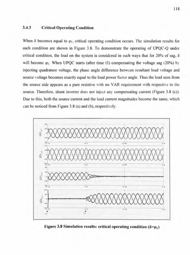
118
3.4.3 Critica l Operating Condition
When 8 becomes equa l t o (pi_. critica l operatin g conditio n occurs . The simulatio n result s fo r
such conditio n ar e show n i n Figur e 3.8 . T o demonstrat e th e operatin g o f UPQC- Q unde r
critical condition , th e loa d o n the syste m i s considered i n suc h way s tha t fo r 20 % of sag , 8
will becom e (pi. Whe n UPQ C start s (afte r tim e t3 ) compensating th e voltag e sa g (20%) by
injecting quadratur e voltage , the phase angl e difference betwee n resultan t loa d voltag e and
source voltage becomes exactly equal to the load power factor angle . Thus the load seen from
the sourc e sid e appear s a s a pure resistive wit h n o VAR requiremen t wit h respective t o the
source. Therefore , shun t inverte r doe s no t injec t an y compensatin g curren t (Figur e 3. 8 (c)) .
Due to this, both the source current and the load current magnitudes become the same, which
can be noticed from Figur e 3.8 (a) and (b), respectively.
Figure 3.8 Simulation results : critical operating condition {b^ipA)
3.5 Laborator y Experimenta l Result s
The performanc e o f UPQC- Q wit h propose d simplifie d approac h t o extrac t th e necessar y
quadrature injectio n voltag e i s als o supporte d throug h laborator y experimenta l study .
Physically, th e syste m configuratio n o f UPQC- Q i s exactl y simila r t o th e on e alread y
discussed i n CHAPTE R 2 . Th e onl y differenc e i s i n th e contro l o f serie s inverte r tha t give s
the nam e UPQC- Q t o basi c UPQC . I n th e followin g subsections , th e real-tim e QV I
extraction, an d th e experimenta l result s fo r single-phas e a s wel l a s three-phas e UPQC- Q ar e
discussed.
3.5.1 Real-Tim e Quadratur e Injectio n Voltag e Extractio n
In this section , the scheme used to extract the necessary quadratur e voltag e t o compensate th e
sag o n th e system , i n real-time , i s explaine d briefly . Figur e 3. 9 show s th e Simulin k mode l
built fo r experimenta l validatio n o f proposed single-phas e QV I approach .
The actua l sourc e voltag e i s sensed an d it s fundamental rms valu e i s continuously compute d
using a "discrete rms value" bloc k fro m MATLAB / Simulink . Th e compute d rms valu e i s
then divide d b y th e desire d loa d voltag e magnitud e t o calculat e th e ter m "cos8" . Takin g th e
inverse o f cos8 , the power angl e 8 is extracted. Ther e ar e two possibl e mode s o f operation -
/) cos8 = 1 , represents the system i s in steady-state, and // ) cos8 < 1 , represents the sag on the
system. Thus , th e invers e operatio n o f cos 8 t o determin e th e angl e 8 ca n hav e tw o
distinguished values , /) 8 = 0, for the condition cos8 = 1 , and // ) 8 > 0, fo r cos 8 < 1 . When th e
system i s i n steady-state , 8 = 0 an d thu s th e 1 ^ = 0 . O n th e othe r hand , whe n th e syste m
voltage fall s belo w th e rate d valu e durin g th e sa g o n th e syste m th e ter m 8 give s th e
necessary powe r angle . For any increas e i n the sourc e voltag e due to the swel l o n the system ,
the inverse o f cos8 using Simulin k "acos" (represent s cos inverse ) block give s zero output . I n
this way , th e simpl e approac h automaficall y take s car e o f all th e possibl e condition s o n th e
network an d th e use r doe s no t nee d t o pa y an y specia l aUentio n t o determin e th e sa g o n th e
system. Figur e 3.1 0 show s th e experimenta l resul t t o demonstrat e th e real-tim e extractio n o f
the required quadratur e injecfio n voltage .
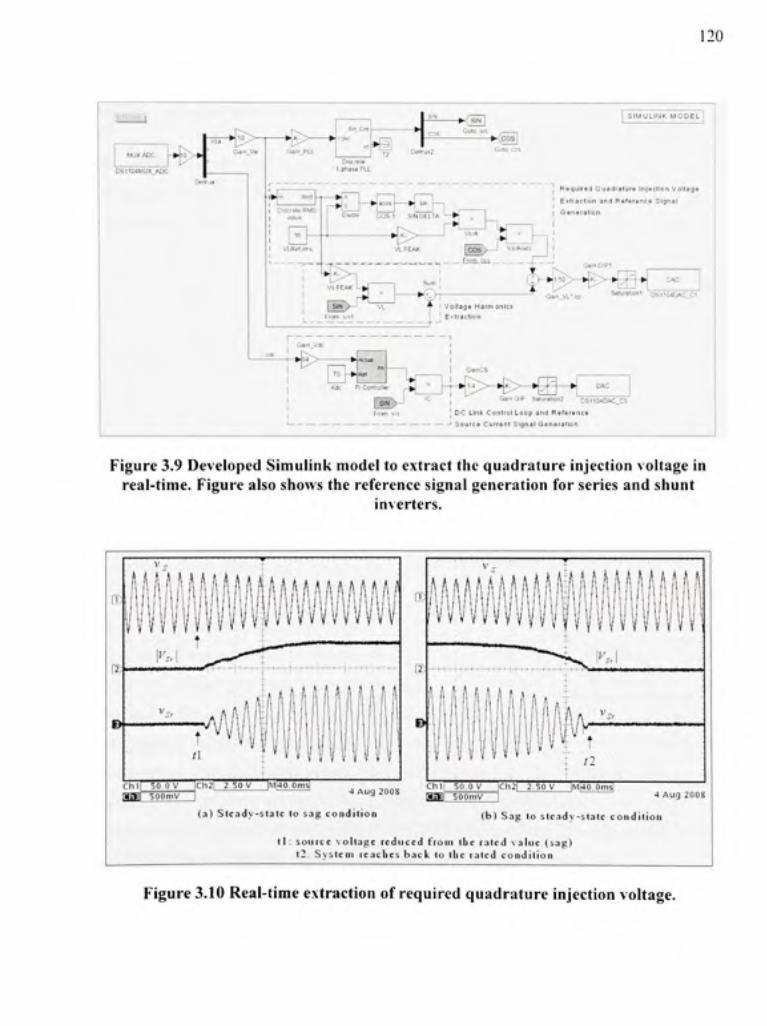
120
m-!iW>
"4^* DSnCMMUX AD C
-H>- .•.*m
}^—•(s " " • l p. ^ Gul o s n , 1
1-^ - Kcos J <cosJ Golo cos
Disc^le 1 [^asePLL
Discrete RMS value DiviD* cOS- 1 SI N DELTA
-b- r^
SIMULINK M O D E L
I Require d Ouadralor e Injectio n Voltag e
' Evtracl lo n an d Reference Slona l I *
Generat ion
VsrA ^ >.
\^og;p—\ vvA{rti ) I I
Voltage Har m onlc s Extract ion
Saturaronl Q S 1104DAC_C1
->B> KOc P i Conliolier
I I GflinC S I
From s i
CAC
Gatn O.P SelJ'Bton 2 DSl104DAC_C 5
DC Lin k Contro l Loo p an d Reference
Source Curren t Signa l Gens ia t lo n
Figure 3.9 Develope d Simulin k mode l to extract th e quadrature injectio n voltag e in real-time. Figur e als o shows th e referenc e signa l generatio n fo r series an d shun t
inverters.
Chl
asEi so.o V SOOmV
Ch2^ 2 5 0 V MrtO.Oms j ' ' ' ' . 4 Aug 200 8
( . i ) S t c . i d y - s t a t c t o s a g c o n d i t i o n
Chl[ 50. 6 V lCh2 r 2.5 0 V iM|40.0ms , [HHj SOOm V I •» Aug 200 8
( b ) S a g t o s t e a d y - s t a t e c o n d i t i o n
t l : s o i i i c c v o l t a g e r e d u c e d f r o m i b e r a t e d v a l u e ( s a g )
t 2 . S y s t e m r e a c h e s b a c k t o i b e l a t c d c o n d i t i o n
Figure 3.10 Real-tim e extractio n o f required quadratur e injectio n voltage .
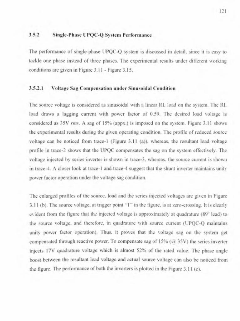
121
3.5.2 Single-Phas e UPQC- Q Syste m Performanc e
The performanc e o f single-phas e UPQC- Q syste m i s discusse d i n detail , sinc e i t i s eas y t o
tackle on e phas e instea d o f thre e phases . Th e experimenta l result s unde r differen t workin g
conditions are given i n Figure 3.11 - Figure 3.15 .
3.5.2.1 Voltag e Sa g Compensation unde r Sinusoidal Conditio n
The sourc e voltag e i s considere d a s sinusoida l wit h a linea r R L loa d o n th e system . Th e R L
load draw s a laggin g curren t wit h powe r facto r o f 0.59 . Th e desire d loa d voltag e i s
considered a s 35 V rms. A sa g o f 15 % (appx. ) i s impose d o n th e system . Figur e 3.1 1 show s
the experimenta l result s durin g th e give n operatin g condition . Th e profil e o f reduce d sourc e
voltage ca n b e notice d fro m trace- 1 (Figur e 3.1 1 (a)) , whereas , th e resultan t loa d voltag e
profile i n trace- 2 show s tha t th e UPQ C compensate s th e sa g o n th e syste m effectively . Th e
voltage injecte d b y serie s inverte r i s show n i n trace-3 , whereas, th e sourc e curren t i s show n
in trace-4. A closer loo k a t trace-1 an d trace-4 sugges t tha t the shun t inverte r maintain s unit y
power facto r operatio n unde r the voltage sag condition .
The enlarge d profile s o f th e source , loa d an d th e serie s injecte d voltage s ar e give n i n Figur e
3.11 (b) . The source voltage , at trigger poin t "T " in the figure , i s at zero-crossing. I t is clearly
evident fro m th e figur e tha t th e injecte d voltag e i s approximatelv a t quadratur e (89 " lead) t o
the sourc e voltage , an d therefore , i n quadratur e wit h sourc e curren t (UPQC- Q maintain s
unity powe r facto r operation) . Thus , i t prove s tha t th e voltag e sa g o n th e syste m ge t
compensated throug h reactiv e power . T o compensate sa g of 15 % {(d. 35V ) the serie s inverte r
injects 17 V quadratur e voltag e whic h i s almos t 52 % o f th e rate d value . Th e phas e angl e
boost betwee n th e resultan t loa d voltag e an d actua l sourc e voltag e ca n als o b e notice d fro m
the figure. Th e performance o f both the inverter s i s plotted i n the Figure 3.11 (c) .

122
: ,\/,4^.H.H.H Vn^H-f+Ai^+^-tH-J-^^Hh-H-^ t
:hM 50. 0 V Ch2 : S O
• A"\ '^ / Y'A V v/ A"i
OV MlO.Om s SJE So. o V Ch 4 S b O A O :
(a)
, ^ ^ „ am i 23. 0 V Ch2 i 25. 0 V M4.00m S 1 Aug 2008 ^ i 2 ^ ( ) ^
tb)
\ n A z" . A A ./I • ^ s f-t-t-j-t-t-t-t-}-^-*"-'-*-r-*'•' ' *••I-—*"•*"•*' +
v / A '^r /%..
\y"'Kj / • • - x
.-"V ' ' / « \ »^w^ X . / '
*1»i»»^,J»f«'*i»«%»t^*«V>*--vi»»«.—^-wii-^
•-H-+-{•-'-'-^-'-l-'-i-'-'-r'*"'*"*"^
V / ^ ' \y' K/ A\... ./ v
Chll__50.0 y_ ^Ch2 [ SO.O V MHO.0ms ; Ch3l 56,T V 'SSE SMKQ'
( C )
1 Aug 200 8
1 Aug 200 8
Figure 3.11 Experimental results : voltage sag compensation by QVI under sinusoidal condition (single-phase system).
During steady-stat e condition , the phase angle between the sourc e and loa d voltage i s zero.
The loa d curren t i s 0.5 9 laggin g (^/.=55° ) t o th e loa d voltag e unde r thi s condition . Th e
relative phas e angle s betwee n differen t voltage s an d current s durin g QV I o f UPQC- Q ar e
demonstrated i n Figure 3.12 . For better understanding , the phasor diagram i s also plotted i n
Figure 3.12 . To compensate th e sa g on the syste m th e serie s inverte r inject s th e quadratur e
voltage. In this experimental stud y the phase angle {(psA i s found a s 89° (verv clos e to 90°).
The serie s injecte d voltag e togethe r wit h th e sourc e voltag e give s the desire d loa d voltag e
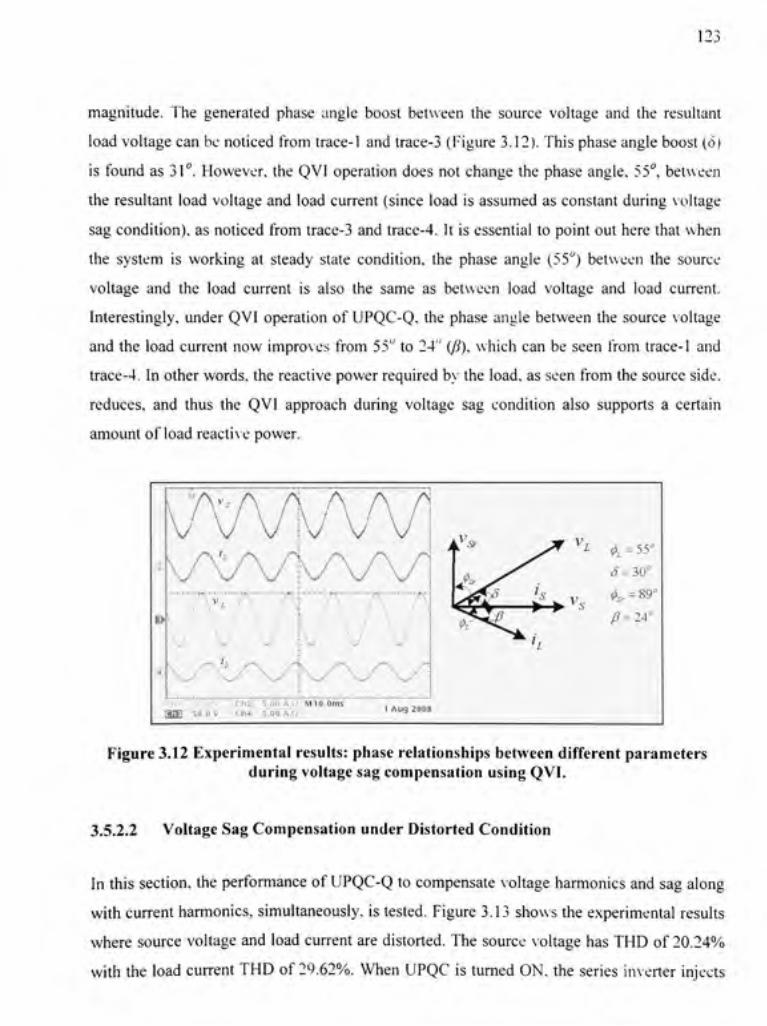
12:
magnitude. Th e generate d phas e angl e boos t betwee n th e sourc e voltag e an d th e resultan t
load voltage can be noticed from trace-1 and trace-3 (Figure 3.12). This phase angle boost (8)
is found a s 31° . However, the QVI operation does not change the phase angle, 55°, between
the resultant loa d voltage and load current (sinc e load i s assumed a s constant during voltage
sag condition), as noticed fro m trace- 3 and trace-4. It is essential to point out here that when
the syste m i s workin g a t stead y stat e condition , th e phas e angl e (55° ) betwee n th e sourc e
voltage an d th e loa d curren t i s als o th e sam e a s betwee n loa d voltag e an d loa d current .
Interestingly, unde r QV I operation o f UPQC-Q, the phase angle between th e source voltage
and the loa d curren t no w improves from 55 " to 24" {fl). which can be seen from trace- 1 and
trace-4. In other words, the reactive power required by the load, as seen from the source side,
reduces, an d thu s th e QV I approac h durin g voltag e sa g conditio n als o support s a certai n
amount of load reactiv e power.
AAA^AAA , &
V^-^-• A^ A / 1 A A : / •
/7 = 24°
i l l " 5i J 0 V _ Ch 2 S.OOAft MlO.Om s 1 Aug 200 8
Figure 3.12 Experimental results : phase relationships between different parameter s during voltage sag compensation usin g QVI.
3.5.2.2 Voltag e Sag Compensation under Distorted Condition
In this section, the performance o f UPQC-Q to compensate voltage harmonics and sag along
with current harmonics , simultaneously, i s tested. Figure 3.13 shows the experimental result s
where source voltage and load current are distorted. The source voltage has THD of 20.24%
with the load current THD of 29.62%. When UPQC i s turned ON , the series inverte r inject s
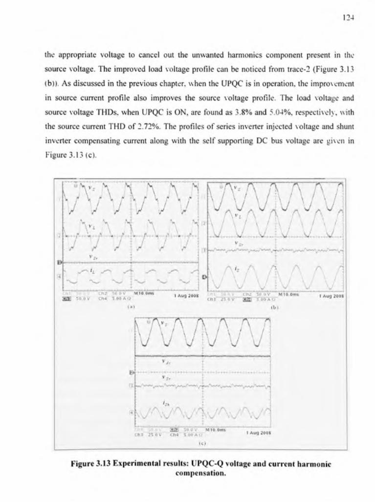
124
the appropriat e voltag e t o cance l ou t th e unwante d harmonic s componen t presen t i n th e
source voltage . The improved loa d voltag e profile ca n be noticed fro m trace- 2 (Figur e 3.13
(b)). As discussed i n the previous chapter, when the UPQC is in operation, the improvement
in sourc e curren t profil e als o improve s th e sourc e voltag e profile . Th e loa d voltag e an d
source voltage THDs. when UPQ C i s ON, are found a s 3.8% and 5.04% , respectiveh , with
the sourc e curren t TH D of 2.72%. The profiles o f series inverte r injecte d voltag e and shun t
inverter compensatin g curren t alon g wit h th e sel f supportin g D C bu s voltag e ar e give n i n
Figure 3.13 (c).
\ AA A A Av A V A A ''
S.
»' \ A \ J 'X 1. ' v .
' A AAy\ ^ '^,-^i-j^.T--^-^.^-+.^•A!-^.-^l^f^-i-^•M-^-^:\•^-^^^
! • * ; I
y ^ : v ^ : y ^
.J..^ L. .
A; W. V . A A^ 12-
M i l 3 0 ( ) V C:h2 i 50. 0 V MlO.Om s aiE 307 b V ;ch4 [ 5 ; ijij7, 0
(a)
\
A ^ A A "^ n s A A A -\- / • \ A A / T V / • • S
|T ~-,A
V /V'A^A : A A^/ 1
\ / " • V, . 1
I WJ \J '^ 1 Aug 200 8 ' h ' ; SO.O V Ch2 : SO.O V MlO.Om s
Ch3; 23. 0 V SUg l 5.0 0 A O
( b )
1 Aug 200 8
\ "f\'' [\ A A A ^ ' AA A ' A A
t i l i! 5b.' o V 'SSSi 5b7o'v''nM!io^oitis c:h3' 2 5 T " v (:h 4 5fbb"AT ? i
( c )
1 Au g 200 8
Figure 3.13 Experimental results : UPQC-Q voltage and current harmonic compensation.

125
The experimenta l result s durin g th e voltag e sa g unde r distorte d sourc e voltag e conditio n ar e
given i n Figure 3.14 . As noticed fro m trace - 3 , the serie s inverte r now inject s a voltage which
is th e summatio n o f quadratur e voltag e a s determine d b y QV I approac h an d voltag e
harmonics presen t i n th e sourc e side . Thu s th e UPQC- Q wit h th e propose d QV I approac h
effectiv ely compensate s th e voltag e sag . voltage harmonic s an d curren t harmonics , al l a t th e
same time.
[3
A V ' ^ Y ^ A
'vlAJAlAA ". V . /^ i • Sr / ' -
t/: V / V / \ / A A : A
\ A' ^ A A A ^ A R)-v / A- f--\ A A\ r A • A.- '
V I V
A \7 \ / \
&
'W
^.v 'v ,
V
AK>/ « • ' \ : / : \ /
A'> A/A' ( h i j 5 0 0 V fa:* ; SO.O V MIO.Om s Chsi 25. 0 V Ch- 4 5.0 0 A O
(.1)
Chli SO.O V wn'^ l 50. 0 V M|10.0rn s I Au g 200 8 p.|3r zi.oV C h C S.0 0 A f j l
lb)
1 Aug 200 8
Figure 3.14 Experimenta l results : performance o f QVI t o compensate voltage sag and voltage harmonics simultaneously .
3.5.2.3 UPQC- Q Dynami c Performanc e
In this sectio n th e dynami c performanc e o f UPQC-Q i s demonstrated. Initially , the UPQ C i s
ON compensating th e voltage and current harmonics . All of a sudden, a voltage sa g conditio n
is impose d o n th e system . I n the laboratory , t o creat e suc h a situation , th e suppl y voltag e i s
reduced b y reducin g th e outpu t o f th e autotransformer , an d therefore , ther e i s a slo w
reduction i n supply voltage magnitude .
The experimenta l result s during suc h transient conditio n ar e given i n Figur e 3.15 . As notice d
from Figur e 3.1 5 (a) , the QV I approac h detect s the sa g on the syste m an d start s injectin g th e
required quadratur e injectio n voltag e i n additio n t o th e voltag e harmonic s component . Th e

126
effect o f the sudde n occurrence o f sa g does not appear acros s the loa d side . Thus UPQC- Q
effectively maintain s th e loa d voltag e a t th e desire d level . Increase d i n th e sourc e curren t
magnitude can also be noticed fro m th e figure. Th e injected serie s voltage and shunt curren t
envelops along with a self supporting DC bus voltage, which are given in Figure 3.15 (b). An
important observatio n durin g voltage sa g compensation usin g QV I approac h i s that the DC
bus voltage during the transient condition remains unaffected .
[3; |fi|»i^xmw>»>i|^i|nnt|(^<rimn%n^ftti^)|<i> ^
C h l j SO.O V |Ch2 | SO.O V |IVl|100ins | Ch3| 50. 0 V IWm i 10. 0 A Q
i n )
y
1 A u g 200 s
i^i«^i^iM}mmik\*y^immm^
B i*f>>Vf#y»1»>W>Vf^V^VM> ^
C h l j SO.O V |Ch 2 C]| 25. 0 V ^Ch 4
50.0 V 5.00 A Q
ivi loom s 1 Aug 200 8
(b)
Figure 3.15 Experimental results : Dynamic performance of UPQC-Q.
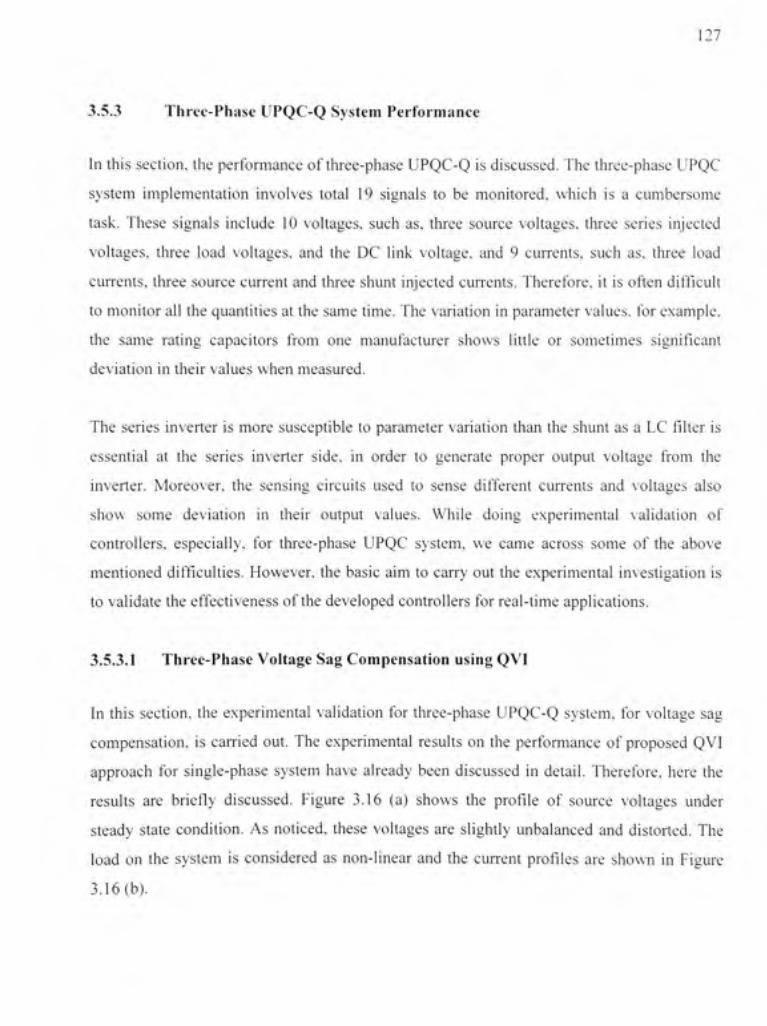
127
3.5.3 Three-Phas e UPQC- Q Syste m Performanc e
In this section , the performance o f three-phase UPQC- Q i s discussed. Th e three-phase UPQ C
system implementatio n involve s tota l 1 9 signal s t o b e monitored , whic h i s a cumbersom e
task. Thes e signal s includ e 1 0 voltages , suc h as . thre e sourc e voltages , thre e serie s injecte d
voltages, thre e loa d voltages , an d th e D C lin k voltage , an d 9 currents , suc h as , thre e loa d
currents, three sourc e curren t an d thre e shun t injecte d currents . Therefore , i t i s often difficul t
to monitor all the quantities a t the same time. The variation i n parameter values , fo r example ,
the sam e ratin g capacitor s fro m on e manufacture r show s littl e o r sometime s significan t
deviation i n their values when measured .
The serie s inverte r i s more susceptibl e t o paramete r variatio n tha n th e shun t a s a LC filte r i s
essential a t th e serie s inverte r side , i n orde r t o generat e prope r outpu t voltag e fro m th e
inverter. Moreover , th e sensin g circuit s use d t o sens e differen t current s an d voltage s als o
show som e deviatio n i n thei r outpu t values . Whil e doin g experimenta l validatio n o f
controllers, especially , fo r three-phas e UPQ C system , w e cam e acros s som e o f th e abov e
mentioned difficulties . However , th e basi c ai m t o carr y out th e experimenta l investigatio n i s
to validate the effectiveness o f the developed controller s fo r real-time applications .
3.5.3.1 Three-Phas e Voltag e Sag Compensation usin g QVI
In thi s section , th e experimenta l validatio n fo r three-phas e UPQC- Q system , fo r voltag e sa g
compensation, i s carried out . Th e experimenta l result s o n th e performanc e o f propose d QV I
approach fo r single-phas e syste m hav e alread y bee n discusse d i n detail . Therefore , her e th e
results ar e briefl y discussed . Figur e 3.1 6 (a ) show s th e profil e o f sourc e voltage s unde r
steady stat e condition . A s noticed , thes e voltage s ar e slightl y unbalance d an d distorted . Th e
load o n th e syste m i s considere d a s non-linea r an d th e curren t profile s ar e show n i n Figur e
3.16(b).
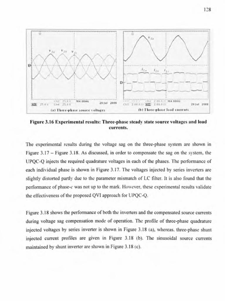
128
S l g 25.b"V " "Ch< 4 25.O V
(n) Tlirec-phas e sourc e \ oltage s
29 Ju l 200 8 ^y^.^ •2.nn AO Wrei i 2.0 0 A ? / 2 9 Jul 200 8
( b ) T h r c c - p b a s c loa d current s
Figure 3.16 Experimental results: Three-phase steady state source voltages and load currents.
The experimenta l result s durin g th e voltage sa g on the three-phase syste m ar e shown in
Figure 3.1 7 - Figur e 3.18 . As discussed, in order to compensate the sag on the system, the
UPQC-Q inject s th e required quadrature voltages in each of the phases. The performance of
each individua l phas e is shown in Figure 3.17 . The voltages injecte d b y series inverters are
slightly distorte d partl> ' due to the parameter mismatc h of LC filter. It is also found tha t the
performance o f phase-c was not up to the mark. However, these experimental result s validate
the effectiveness o f the proposed QVI approach for UPQC-Q.
Figure 3.18 shows the performance o f both the inverters and the compensated source currents
during voltag e sa g compensation mod e of operation. The profile o f three-phase quadratur e
injected voltage s by series inverte r i s shown in Figtire 3.18 (a), whereas, three-phase shun t
injected curren t profile s ar e give n i n Figur e 3.1 8 (b) . The sinusoida l sourc e current s
maintained by shunt inverter are shown in Figure 3.18 (c).
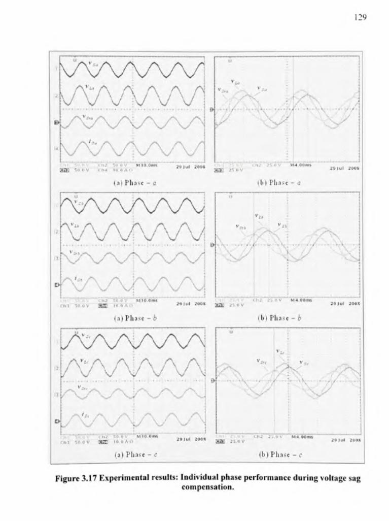
129
/^. r-A A ^VVAAAA'
\ A=-, A A . ,A/A A X/ \y w •• \y \ / V A SSiWSWmtfflBWjSiBM?™
' • ' " " " ^ ' l " ^ ' A ' ^ ' ' ' ' ^ ^A9 - ' ' ^ i - MlO.Om s 'X!f\ '".h n' v T\M' TOTO' A O "
In) Phase - a
& '7 /
29 Ju l 200 8 S' i .OV Ch 2 2S. 0 V MM.OOm s aiE"'"2'^:ft V 29 Ju l 200 S
(b) Pha.'s c - a
AAAAAAAA/
»
i . . . i . . : . L . t . . . i - . : - . . - t .
'A/AA V
" O
l u - ( ! .o v c:li2 i SO.O V Mjio.om s r i n Tn.o v aX E i n . b X r T
iiiiH »iiil i I II I
\
/'""•-. :\\ r A { ./"A W
"''*AS
r j . O V Ch2 i 23 . 0 V MN(.corn s 29)1.1 200 8 5 j j g ^ . ^ u v 2 ! ) Ju l 200 S
(a) Phase -h (b) Pha.s e - h
J
11
o
A V V V V \ ^ :r\A Nwf ''N.v '
/•-..'s: X X / A . / • A/ \ / A '
- \
: h l i 50.1 1 V C'.hZ i Ch3- 50^ 0 V BE B
ns
(a) Phas e - c
SO.OV MilO.Om s 10.0 A n 2 0 ) u l 200 S .; . i j y CM,; : 2v>.(.> v M4.00m s
MrW 2 3 . 0 V 20 Jul 2no s
(b) Phase - c
Figure 3.17 Experimenta l results : Individual phas e performance durin g voltage sa g compensation.

130
:Mni ' " j i j ; - f i i - l sti. u V M|ia.oni s <:h;i " "soToy i:ii4 | - » 6 v~ 20 | u l 200! ,
( a ) Scr ie s inver te r
'\V^<^^
AV^^-^ i ^ V , ^ \ . ^
xV'-^^iy^' . v >^- "v^-AA^ y 'N ;^0U I i l l . - c iTJ i i o . u A < . > M i l O . O m s C l l . l 1 0 . 0 A '. > €:il.4 | l O 0 A ^ • 2 9 J u l 2 0 0 S
(b) Sbii i i l inverte r
O
A^~x;'-^» A ^ 'K^'
/N. \ / ' i \/- ^ A , . t /-, ,
• ^ • ^ y - • - ^ ^
,/ •%,^->.„AA.^--'^^ \A' %/ /
e n J Ch3i Oil A < / :^rE T 5 . oo A < >
(c) Sourc e current s 29 Ju l 200 S
Figure 3.18 Experimental results : Performance o f three-phase UPQC- Q during voltage sag condition.
3.5.3.2 Voltag e Harmonic s Compensatio n usin g d-q Transformatio n
The performanc e o f UPQ C t o compensat e th e harmonic s presen t i n three-phas e sourc e
voltages i s discussed i n this section . The voltage harmonic s presen t i n the source voltages ar e
estimated usin g d-q transformatio n method . Th e loa d o n th e syste m i s als o considere d a s
non-linear. Th e distorte d suppl y voltag e profil e i s show n i n Figur e 3.1 9 (a) . Thes e sourc e
voltages ar e als o unbalance d i n natur e du e t o unequa l impedanc e value s o f inserte d lin e
resistances t o generate harmonic s voltage drop across them. The distorted loa d current profil e
is given i n Figure 3.1 9 (b) .
When UPQ C i s i n operation , th e loa d voltag e profil e i s given i n Figur e 3.1 9 (c) . A s notice d
from th e figure, th e harmonics presen t i n the source voltages ar e reduced a t the loa d side . The
source current profil e i s shown i n Figure 3.19 (d).
The performance o f each o f the phases are given i n Figure 3.2 0 (a) , (b), and (c ) for phase - a,
- b, an d - c. respectively . A s notice d fro m th e figures , i n orde r t o compensat e th e voltag e
harmonics presen t i n the sourc e voltages , the serie s inverte r inject s th e necessar y voltage s a s
determined utilizin g d-q transformation . Th e performance o f UPQ C serie s inverte r an d shun t
inverter i s given in Figure 3.2 0 (d ) and (e) , respectively .
The THD value s o f each o f the sourc e and loa d voltages an d respecfiv e harmonic s spectrum s
are plotte d i n Figur e 3.21 , whereas. Tabl e 3. 1 give s th e detaile d valu e o f individua l voltag e
harmonic a s % o f fundamenta l component . Th e curren t harmonic s generate d b y non-linea r
load togethe r wit h th e sourc e curren t harmonic s spectrum s afte r th e compensatio n i s plotte d
in Figure 3.22 . The individual curren t harmonic values can be noted fro m Tabl e 3.2 .
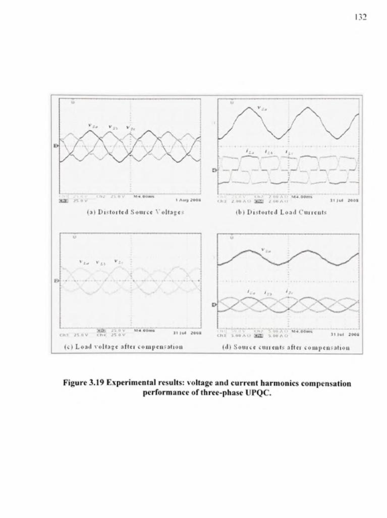
132
:;.ii V c:h* ' .i'^.n V M.4.ooni s a a B 25:'<rv " 1 Aug 200 S
(a) Di.^toite d Sotiic e ^"oltage. s
< l i l , 2 S l i V Ch ^ 2 . 0 U A ( > IVI|4.00m t Ch3; 2.0 0 A <> ?arE 1 2 0 0 A O '
lb) D i s to i t e i l Loat l C u i i e a l s
3 1 Jul 200 S
JSiE; 23. 0 V M4.ooi« s c i i : ! 2 ' v n v ( h l i j ^ o v 3 l ) u l 200 S
(c) Loa d \oltaL' € atte i compei isahoi i
i i i [ '; o i ! V cii. ? - . .OOA' ? M4.coin s Ch3| S . O O A O STTE l 5.0 0 A O 3 1 Ju l 200 S
1(1) S o u i c e c u i i e u t s nfte i c o i u p c n ^ a h o i i
Figure 3.19 Experimenta l results : voltage an d curren t harmonic s compensatio n performance o f three-phase UPQC .
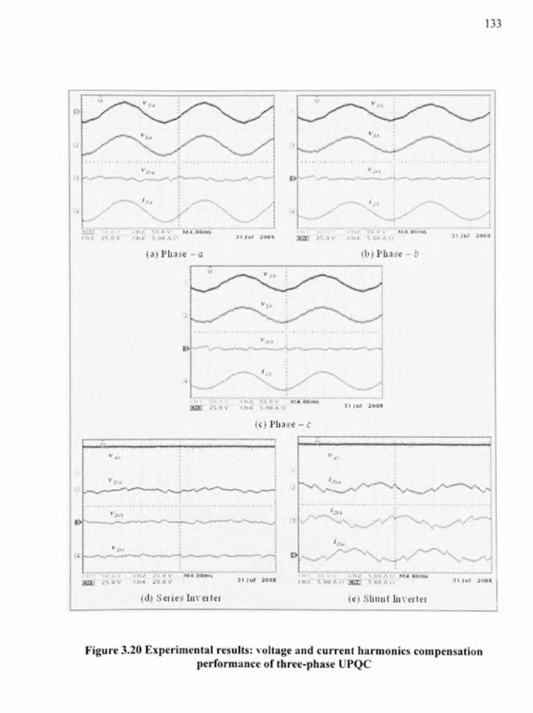
133
.A' 'X..,^''
./
6> •-'••-"x
S U : =;< ) n V r h 2 i s o . n V M4 .oom s i s i T ; ; n ' ^ r h z f s o . o v Mj4.00m s r l i 3 2';: o V Ch4 : s ^ o o A v 3 1 Ju l 200 S g - g 2'-,, o V <-h4 | s r o o A s > 11 Ju l 200 S
(a) Pha!>e -a (b) Pha.se -h
i t ! i - i l ' < h j| 5 0 0 V M4,00m s a J E 2 3 0 V r l l 4 | 5 0 0 A O T I Ju l 200 X
(c) Phase - c
&
T * -
\y^-s*''*v'
I I I i o . O V (..h 2 JS. O V ;iVI4.00m> i Wfitf 2 S . 0 V Ch 4 21. 0 V 31 Ju l 200 S
' 111 ! __50 .(.i_V Ch2 | S . U O A l i M^I.OOni s t l l ' j f 5.0 0 Al '> '~aHE'~"?i ' '0f t 'AT) " : n Ju l 200 S
(d) Sene. s laveite i (e) Shun t Inverte r
Figure 3.20 Experimenta l results : voltage and current harmonic s compensatio n performance o f three-phase UPQ C
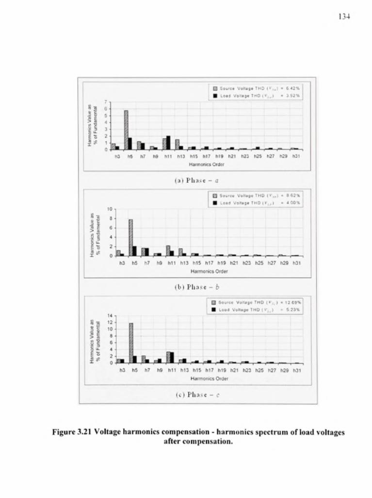
134
1/1 re re 41 c =: o > « in • a
R i E o « - 5
7-| 0 -*i •
/, . 3 •
2 •
1 • 0 4
Source Voltag e TH D (V.v^ ) = 5.42 % Load Voliag e TH D (V-V,„ J = 3.52 %
: « . E ^
h13 h1 5 h1 7 h i s h2 1
Hafmonies Order
h23 h25 h2 7 h2 9 h3 1
(a) Phas e
3 i> 8 •
h
1 i i B. « & i.» I 1 1
@ Sourc u Vollag e TH D ( i ' , . ) = 8 62% • Loa d Vollag e TH D i 1',,.) = 4 00%
r " ^ " — 1 — ^ — 1
1 i 1
'"A" !
fm , . , "" 1 III 1
h3 h 5 h 7 h 9 h1 1 h1 3 h1 5 h1 7 h1 9 h2 1 h2 3 h2 5 h2 7 h2 9 h3 1
Harmonics Orde r
(b) Pha.s e - b
(D TO a; c .2 a . > C D
§ 5 E o - a s
14 12 10
8 6 4 2 ^ 0
Source Voltag e TH D (V .) =. 12.69 % Load Vollag o TH D ( V) i 5.23 %
^L. _EM-
m h 5 h 7 h 9 h l i h1 3 h1 5 h1 7 h1 9 fi2 1 h2 3 h2 5 h2 7 h2 9 h3 1
Harmonics Olde r
(c) Phas e - c
Figure 3.21 Voltage harmonics compensation - harmonics spectrum o f load voltages after compensation .
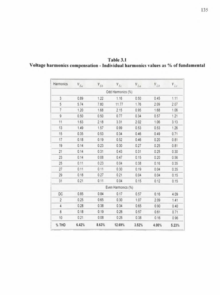
135
Table 3. 1 Voltage harmonic s compensatio n - Individual harmonic s value s a s Vo of fundamenta l
Harmonics
3 5 7 9 11 13 15 17 19 21 23 25 27 29 31
DC 2 4 8 10
% THD
i l l
0.89
5.74
1.20
0.50
1.63
1.49
0,35
0.18
0.14
0.14
0.14
0.11
0.11
0.18
0.21
0.85
0.25
0.28
0.18
0.21
6.42%
^'Sb
1.22
7.80
1.68
0.50
2.18
1.57
0.53
0.19
0.23
0.31
0.08
0.23
0.11
0.27
0.11
0.84
0.65
0.38
0.19
0.08
8.63%
h. Odd Harmonic s
1.16
11.77
2.15
0.77
3.31
0.99
0.34
0.52
0.30
0.43
0.47
0.04
0.30
0.21
0.04
Even Harmonics
0.17
0.30
0.34
0.26
0.26
12.69%
^La
(%) 0.50
1.76
0.95
0.34
2.02
0.53
0.46
0.46
0.27
0.31
0.15
0.38
0.19
0.04
0.15
(%) 0.57
1.07
0.65
0.57
0.38
3.52%
hh
0.45
2.09
1.68
0.57
1.06
0.53
0.49
0.20
0.25
0.25
0.20
0.16
0.04
0.04
0.12
0.16
2.09
0.90
0.61
0.16
4.00%
^'LC
1.11
2.07
1.06
1.21
3.13
1.26
0.71
0.81
0.81
0.30
0.56
0.35
0.35
0.15
0.15
4.09
1.41
0.40
0.71
0.96
5.23%
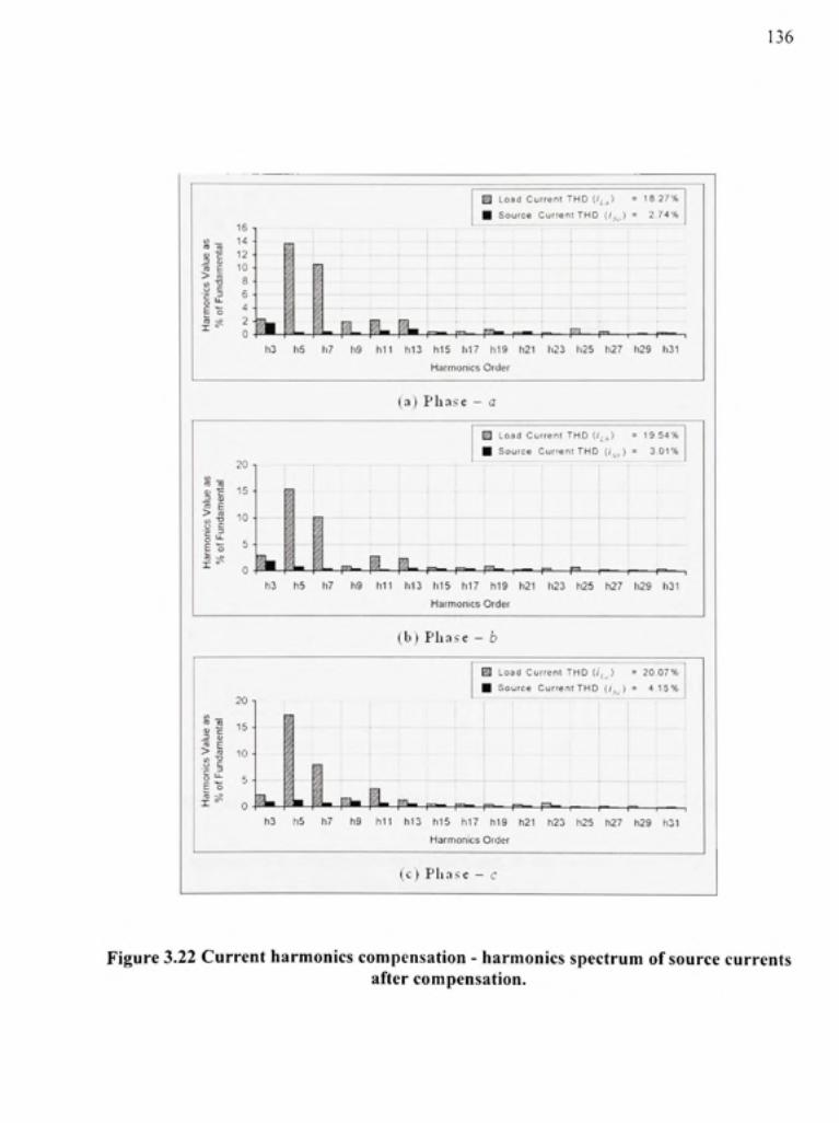
136
h7 h 9 h l i h1 3 h i s h1 7 h1 9 h2 1 h2 3 h2 5 h2 7 h2 9 h3 1
Harmonics Order
in) Phas e - a
re r o Si =
> ro
g re X
20
15
10
S H
0
• Load Curren t TH D (i;, > Source Cur'enrTH D {i ^
- 1 9 54% ,. ) = 3 01 %
I
h3 h 5 h7 h 9 h l i
P^M I I [ I
hi 3 h i s h i 7 h19 h2 1
Harmonics Order
_p= p s ^ , p . h23 h2 5 h2 7 h2 9 h31
( b ) P h a s e - b
> n
S i T
@ Loa d Curren t TH D {/ , ) = 2 0 07% • Sourc e CurienlTH D ( l ^ ) = " ( ' 5 %
i : 1 !
_^ h l i
fs^^—^as^m—Y-\ p^——p n p _ pu . I
h13 h i s h1 7 h1 9 h2 1 h2 3 h2 5 h2 7 h2 9 h3 1
Harmonics Order
(c) P h a s e - c
Figure 3.22 Current harmonic s compensation - harmonics spectrum o f source current s after compensation .
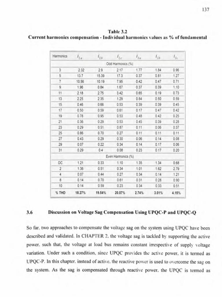
137
Table 3.2 Current harmonics compensation - Individual harmonics >alues as % of fundamental
Harmonics h. hh he hi, hb h. Odd Hamnonics {%)
3 5 7
9
11 13 15 17 19 21 23 25 27 29 31
2.32
13.7
10.56
1.96
2.18
2.25
0.46
0.50
0.78
0.36
0.29
0.86
0.43
0.07
029
2.9 15.39
10.19
0.84
2.75
2.35
0.66
0.59
0.95
0.29
0.51
0.70
0.29
0.22
0.4
2.17
17.3
7.95
1.67
3.42
1.29
0.53
0.61
0.53
0.53
0.87
0.27
0.30
0.34
0.08
1.77
0.37
0.42
0.37
0.65
0.84
0.39
0.17
0.48
0.45
0.11
0.11
0.06
0.14
0.23
1.84
0.81
0.47
0.39
0.19
0.50
0.39
0.47
0.42
0.39
0.06
0.11
0.14
0.17
0.17
0.96
1.27
0.71
1.10
0.73
0.59
0.45
0.42
0.25
0.28
0.37
0.11
0.08
0.06
0.20
Even Hamionics (% )
DC
2 4 8 10
% THD
1.21
1.36
0.07
014 0.14
18.27%
0.33
0.51
0.44
0.70
0.59
19.54%
1.10
0.34
0.27
0.61
0.23
20.07%
1.35
1.01
0.34
0.31
034
2.74%
1.34
1.62
0.14
0.28
0.33
3.01%
0.68
2.79
1.21
0.90
0.51
4.15%
3.6 Discussion on Voltage Sag Compensation Using UPQC-P and UPQC-Q
So far, tw o approaches to compensate the voltage sag on the system using UPQC have been
described an d validated. I n CHAPTER 2 , the voltage sa g is tackled b y supporting the active
power, suc h that , th e voltag e a t loa d bu s remain s constan t irrespecti\ e o f supp h \oltag e
variation. Unde r suc h a condition , sinc e UPQ C pro\ide s th e acti\ e power , i t i s termed a s
UPQC-P. In this chapter, instead of active, the reactive power is used to o\ercome the sag on
the system . A s th e sa g i s compensate d throug h reacti\ e power , th e UPQ C i s terme d a s
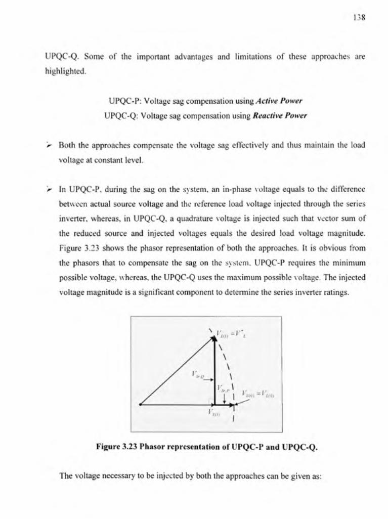
38
UPQC-Q. Som e o f th e importan t advantage s an d limitation s o f thes e approache s ar e
highlighted.
UPQC-P: Voltage sag compensation using Active Power
UPQC-Q: Voltage sag compensation usin g Reactive Power
> Bot h th e approache s compensat e th e voltag e sa g effectivel y an d thu s maintai n th e loa d
voltage a t constant level .
> I n UPQC-P , durin g th e sa g o n th e system , a n in-phas e \oltag e equal s t o th e differenc e
between actua l sourc e voltag e an d th e referenc e loa d voltag e injecte d throug h th e serie s
inverter, whereas , i n UPQC-Q , a quadratur e voltag e i s injecte d suc h tha t vecto r su m o f
the reduce d sourc e an d injecte d voltage s equal s th e desire d loa d voltag e magnitude .
Figure 3.2 3 show s th e phaso r representatio n o f bot h th e approaches . I t i s obviou s fro m
the phasor s tha t t o compensat e th e sa g o n th e system , UPQC- P require s th e minimu m
possible voltage , whereas, the UPQC-Q uses the maximum possibl e voltage . The injecte d
voltage magnitude i s a significant componen t t o determine the series inverte r ratings .
\
yA Sr.Q
V = ( " ' L(\) ' L
\ \
\ \
Sr.P y _ , . 1 1 ' .S(0 ) ~ * i(0 )
V '
Figure 3.23 Phaso r representation o f UPQC-P an d UPQC-Q .
The voltage necessary t o be injected b y both the approaches can be given as:
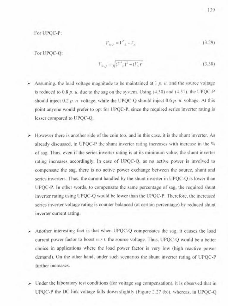
139
For UPQC-P :
For UPQC-Q :
Vsr.P=V'i-ys (3.29 )
f;s>,o = V ( j ' / , ) - ( ' ; >- (3-30 )
Assuming, th e loa d voltag e magnitud e to be maintained a t 1 p. u. and th e sourc e voltag e
is reduced to 0.8/?. // . due to the sa g on the system . Usin g (4.30 ) and (4.31) , the UPQC- P
should injec t 0. 2 p. u. voltage, whil e the UPQC- Q shoul d injec t 0. 6 p. u. voltage. At this
point anyon e woul d prefe r t o op t for UPQC-P. sinc e th e require d serie s inverte r ratin g is
lesser compared to UPQC-Q.
However ther e is another sid e of the coin too . and in this case , it is the shun t inverter . As
already discussed , i n UPQC-P th e shunt inverte r ratin g increase s wit h increas e i n the %
of sag . Thus , even i f the serie s inverte r ratin g is at its minimum value , th e shun t inverte r
rating increase s accordingly . I n case o f UPQC-Q, a s no active powe r i s involve d t o
compensate th e sag, ther e i s no active powe r exchang e betwee n th e source, shun t and
series inverters . Thus , the current handle d b y the shun t inverte r in UPQC-Q is lower tha n
UPQC-P. I n other words , to compensate th e sam e percentag e o f sag, the required shun t
inverter rating usin g UPQC- Q would be lower than the UPQC-P. Therefore, th e increase d
series inverte r voltag e ratin g is counter balance d (a t certain percentage ) b y reduce d shun t
inverter curren t rating .
Another interestin g fac t i s that whe n UPQC- Q compensate s th e sag, i t causes th e load
current powe r facto r t o boos t w.r.t. the sourc e voltage . Thus , UPQC- Q woul d b e a better
choice i n application s wher e th e load powe r facto r i s ver y lo w (high reactiv e powe r
demand). O n the other hand , unde r suc h scenario s th e shunt inverte r ratin g o f UPQC-P
further increases .
Under th e laborator y tes t condition s (fo r voltag e sa g compensation) , i t is observed tha t in
UPQC-P th e D C lin k voltag e fall s dow n slightl y (Figur e 2.2 7 (b)) , whereas , in UPQC-Q

140
the D C lin k voltag e remain s unaffecte d (Figur e 3.1 5 (b)) . Thi s suggest s tha t stres s o n
UPQC-P shun t inverte r switche s shoul d b e much highe r than tha t on UPQC-Q .
A Unfortunately , UPQC- Q ca n no t compensat e th e swel l o n th e system . Therefore ,
modification o r correctiv e actio n i s essentia l whil e developin g th e controlle r fo r UPQC -
Q. Th e sa g an d swel l an d thu s th e flickers ar e easil y compensate d b y UPQC- P withou t
modifying it s controller .
The discussio n o n UPQC- P an d UPQC- Q doe s not full y answe r th e questio n - which
approach should be used to compensate the sag on the system? Though , i t certainh' give s th e
broad vie w t o selec t on e out o f th e tw o approache s base d o n th e particula r loa d an d syste m
requirements.
3.7 Conclusion s
In thi s chapte r i t ha s bee n demonstrate d throug h simulatio n a s wel l a s experimenta l studie s
that voltag e sa g o n th e syste m ca n b e effectivel y compensate d throug h reacti\' e powe r
control. A simplifie d approac h t o extrac t th e require d quadratur e \'oltag e require d t o b e
injected throug h serie s inverter , to achieve the reactive power contro l ha s also been proposed .
The interes t i n selectio n o f QV I approac h i s tha t i t doe s not requir e an y activ e po w er fo r it s
operation. I n additio n t o this , i f th e loa d i s inductiv e i n natur e demandin g hig h reactiv e
power, th e QV I durin g voltag e sa g compensation , als o help s t o improv e th e effectiv e loa d
power facto r angle , i.e . th e serie s inverte r als o take s par t i n loa d reactiv e powe r
compensation. Thu s the reactive power burden o n shun t inverte r during voltage sa g conditio n
reduces considerably .
A brie f discussio n o n voltag e sa g compensatio n usin g UPQC- P an d UPQC- Q ha s bee n als o
reported a t the end o f chapter. I t highlights the advantages and limitation s offere d b y both th e
approaches. Indee d i t helps to make a n adequat e choic e whil e selectin g th e UPQ C t o protec t
sensitive load s from voltag e sag on the network .
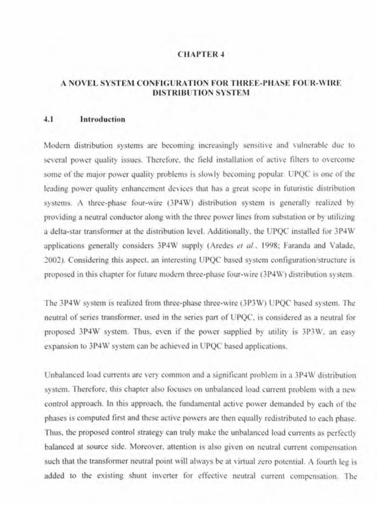
CHAPTER 4
A NOVEL SYSTE M CONFIGURATIO N FO R THREE-PHASE FOUR-WIR E DISTRIBUTION SYSTE M
4.1 Introductio n
Modern distributio n system s ar e becomin g increasingl y sensitiv e an d vulnerabl e du e t o
several powe r qualit y issues . Therefore , th e field installatio n o f activ e filters t o overcom e
some o f th e majo r powe r qualit y problem s i s slowl y becomin g popular . UPQ C i s one o f th e
leading powe r qualit y enhancemen t device s tha t ha s a grea t scop e i n futuristi c distributio n
systems. A three-phas e four-wir e (3P4W ) distributio n syste m i s generall y realize d b y
providing a neutral conducto r alon g with the three power line s from substatio n o r by utilizin g
a delta-sta r transforme r a t th e distributio n level . Additionally , the UPQ C installe d fo r 3P4 W
applications generall y consider s 3P4 W suppl y (Arede s et al. 1998 ; Farand a an d Valade ,
2002). Considerin g thi s aspect , a n interestin g UPQ C base d syste m configuration/structur e i s
proposed i n this chapter fo r futur e moder n tliree-phase four-wire (3P4W ) distributio n system .
The 3P4 W syste m i s realized fro m three-phas e three-wir e (3P3W ) UPQ C base d system . Th e
neutral o f serie s transformer , use d i n th e serie s par t o f UPQC . i s considere d a s a neutra l fo r
proposed 3P4 W system . Thus , eve n i f th e powe r supplie d b y utilit y i s 3P3W , a n eas y
expansion t o 3P4W system ca n be achieved i n UPQC base d applications .
Unbalanced loa d current s ar e very commo n an d a significant proble m i n a 3P4W distributio n
system. Therefore , thi s chapte r als o focuse s o n unbalance d loa d curren t proble m wit h a ne w
control approach . I n thi s approach , th e fundamenta l activ e powe r demande d b y eac h o f th e
phases i s computed first an d these active powers ar e then equally redistribute d t o each phase .
Thus, the proposed contro l strateg y ca n trul y mak e th e unbalance d loa d current s a s perfectl y
balanced a t sourc e side . Moreover , attentio n i s als o give n o n neutra l curren t compensatio n
such tha t the transformer neutra l poin t wil l alway s b e at virtual zer o potential . A fourth le g i s
added t o th e existin g shun t inverte r fo r effectiv e neutra l curren t compensation . Th e
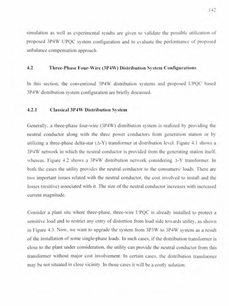
14:
simulation a s wel l a s experimenta l result s ar e give n t o validat e th e possibl e utilizatio n o f
proposed 3P4 W UPQ C syste m configuratio n an d t o evaluat e th e performanc e o f propose d
unbalance compensatio n approach .
4.2 Three-Phas e Four-Wir e (3P4W ) Distributio n Syste m Configuration s
In thi s section , th e conventiona l 3P4 W distributio n system s an d propose d UPQ C base d
3P4W distributio n syste m configuration ar e briefly discussed .
4.2.1 Classica l 3P4W Distributio n Syste m
Generally, a three-phas e four-wir e (3P4W ) distributio n syste m i s realize d b y pro\idin g th e
neutral conducto r alon g wit h th e thre e powe r conductor s fro m generatio n statio n o r b y
utilizing a three-phas e delta-sta r (A-Y ) transforme r a t distributio n le\el . Figur e 4. 1 show s a
3P4W networ k i n which th e neutra l conducto r i s provided fro m th e generatin g statio n itself ,
whereas. Figur e 4. 2 show s a 3P4 W distributio n networ k considerin g A-Y transformer . I n
both th e case s th e utilit y provide s th e neutra l conducto r t o th e consumers / loads . Ther e ar e
two importan t issue s relate d wit h th e neutra l conductor , th e cos t involve d t o instal l an d th e
losses (resitive ) associate d wit h it . The siz e o f the neutra l conducto r increase s wit h increase d
current magnitude .
Consider a plan t site wher e three-phase , three-wir e UPQ C i s alread y installe d t o protec t a
sensitive loa d an d t o restric t an y entr y o f distortio n fro m loa d sid e toward s utility , a s show n
in Figur e 4.3 . Now, w e wan t t o upgrad e th e syste m fro m 3P3 W t o 3P4 W syste m a s a resul t
of the installatio n o f som e single-phas e loads . I n such cases , i f the distribution transforme r i s
close t o the plan t unde r consideration , th e utilit y ca n provid e th e neutra l conducto r fro m thi s
transformer withou t majo r cos t involvement . I n certai n cases , th e distributio n transforme r
may be not situated i n close vicinity . I n those cases i t will be a costly solution .
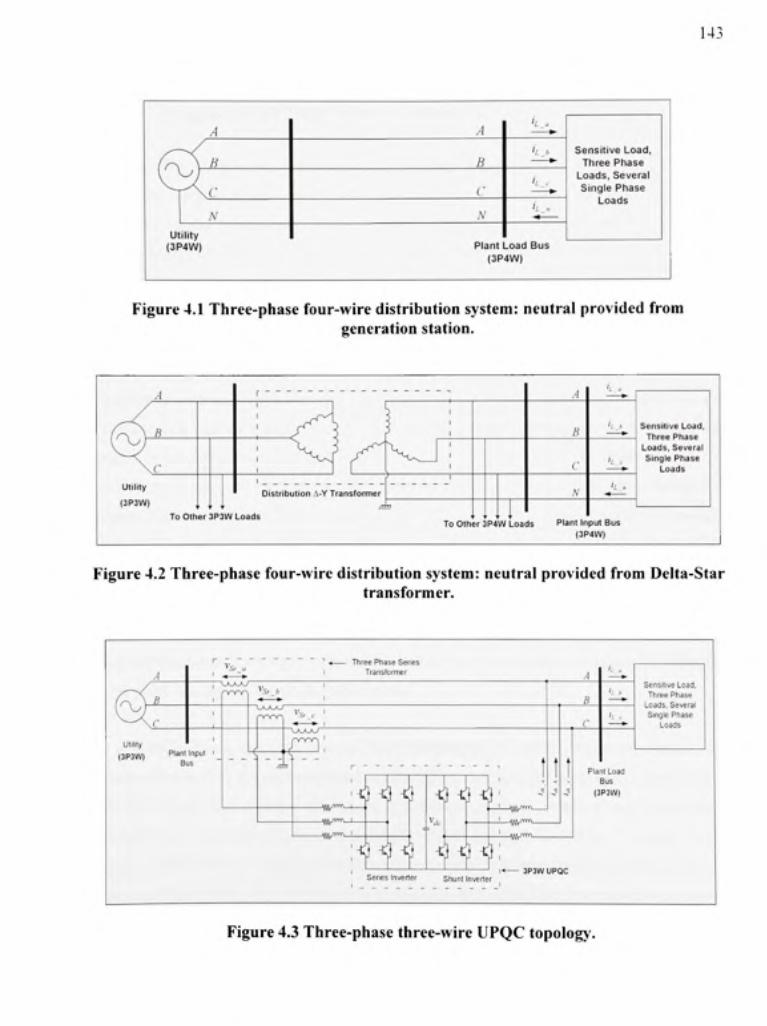
143
.-(
r' s ut
(3F
~ ^ « X iV
ility >4W)
A
B
C
\
''-.-^
'L_^.
>L_.^
h _„
Plant Load Bus (3P4W)
Sensitive Load , Three Phas e
Loads, Several Single Phas e
Loads
Figure 4.1 Three-phase four-wire distributio n system : neutral provide d fro m generation station .
utility
(3P3W) To Other 3P3 W Load s
' i a
To Other 3P4 W Load s Plan t Inpu t Bu s (3P4W)
Sensitive Load , Three Phas e
Loads, Severa l Single Phas e
Loads
Figure 4.2 Three-phase four-wire distributio n system : neutral provided from Delta-Sta r transformer.
Utihiy (3P3W)
3P3W UPQC
Sensitive Load, Three Phase
Loads, Several Single Phase
Loads
Figure 4.3 Three-phase three-wire UPQC topology .
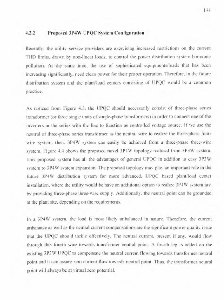
144
4.2.2 Propose d 3P4 W UPQ C Syste m Configuratio n
Recently, th e utilil \ servic e provider s ar e exercisin g increase d restriction s o n th e curren t
THD limits , draw n b y non-linea r loads , t o contro l th e powe r distributio n syste m harmoni c
pollution. A t th e sam e time , th e us e o f sophisticate d equipments/load s tha t ha s bee n
increasing significantly , nee d clea n powe r fo r thei r prope r operation . Therefore , i n the futur e
distribution syste m an d th e plant/loa d center s consistin g o f UPQ C woul d b e a commo n
practice.
As notice d fro m Figur e 4.3 . th e UPQ C shoul d necessarih ' consis t o f three-phas e serie s
transformer (o r tliree singl e unit s o f single-phase transformers ) i n order to connec t on e o f the
inverters i n th e serie s wit h th e lin e t o functio n a s controlle d voltag e source . I f w e us e th e
neutral o f three-phas e serie s transforme r a s th e neutra l wir e t o realiz e th e three-phas e four -
wire system , then , 3P4 W syste m ca n easil y b e achieve d fro m a three-phas e three-wir e
system. Figur e 4. 4 show s th e propose d nove l 3P4 W topolog y realize d fro m 3P3 W system .
This propose d SNSte m ha s al l th e advantage s o f genera l UPQ C i n additio n t o eas \ 3P3 W
system t o 3P4 W s\stem expansion . Th e proposed topolog ) ma\ ' pla \ a n importan t rol e i n the
future 3P4 W distributio n syste m fo r mor e advanced . UPQ C base d plant/loa d cente r
installation, wher e the utilit y would b e have an additional optio n t o realize 3P4\\ ' syste m just
b> providin g three-phas e three-wir e supply . Additionally , th e neutra l poin t ca n b e grounde d
at the plant site , depending o n the requirements .
In a 3P4 W system , th e loa d i s mos t likel y unbalance d i n nature . Therefore , th e curren t
unbalance a s well a s the neutra l curren t compensation s ar e the significan t powe r qualit \ issu e
that th e UPQ C shoul d tackl e effectively . Th e neutra l current , presen t i f any , woul d flow
through thi s fourt h wir e toward s transforme r neutra l point . A fourt h le g i s adde d o n th e
existing 3P3 W UPQ C t o compensate th e neutra l curren t flowing toward s transforme r neutra l
point an d i t can assur e zer o curren t flow toward s neutra l point . Thus , the transformer neutra l
point wil l always be at virtual zero potential .
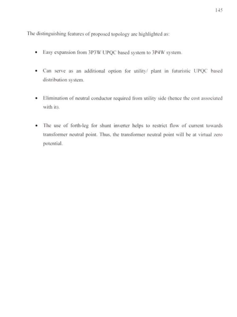
145
The distinguishing feature s o f proposed topolog y ar e highlighted as :
• Eas y expansion fro m 3P3 W UPQC base d syste m t o 3P4W system .
• Ca n serv e a s a n additiona l optio n fo r utility / plan t i n futuristi c UPQ C base d
distribution system .
• Eliminatio n o f neutra l conducto r require d fro m utilit y sid e (henc e th e cos t associate d
with it) .
• Th e us e o f forth-le g fo r shun t inverte r help s t o restric t flow o f curren t toward s
transformer neutra l point . Thus , th e transforme r neutra l poin t wil l b e a t virtua l zer o
potential.
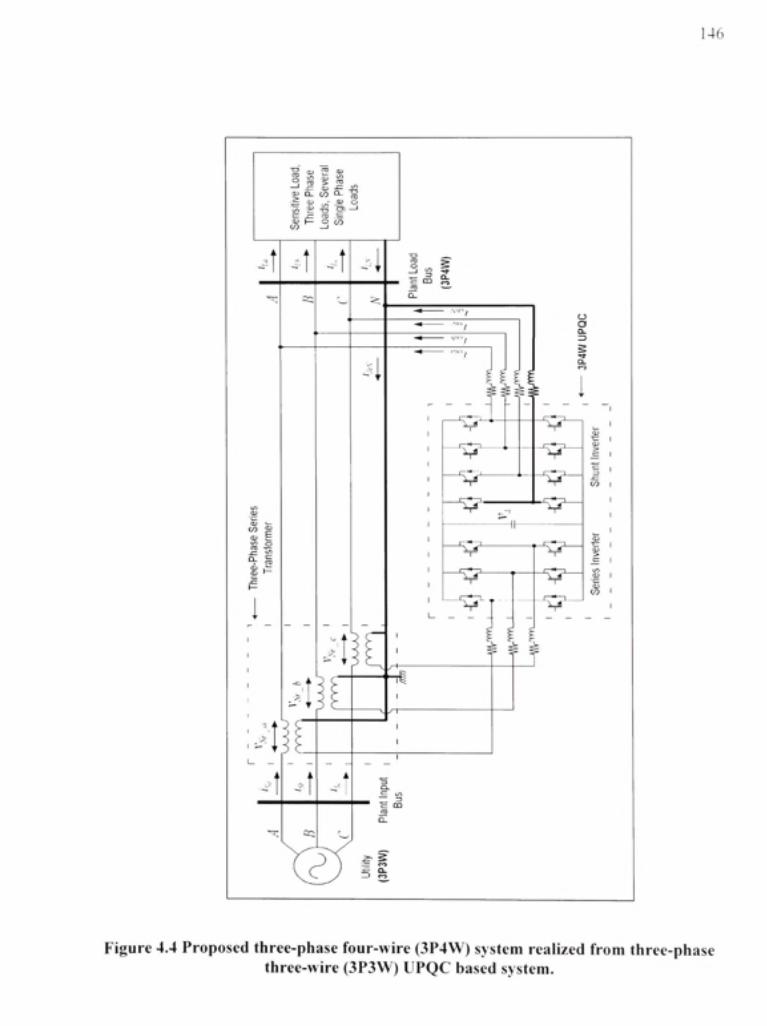
146
"2 ( D 2 O J o ' ^ a > J K O TO > " 3 —' .L r £ . c 4 2 ^ D - 0 0 C L - o
• . = O J „ - ^ o
;?> J ? - a ra - • to O C O
Figure 4.4 Proposed three-phas e four-wire (3P4W ) system realize d fro m three-phas e three-wire (3P3W) UPQC based system .
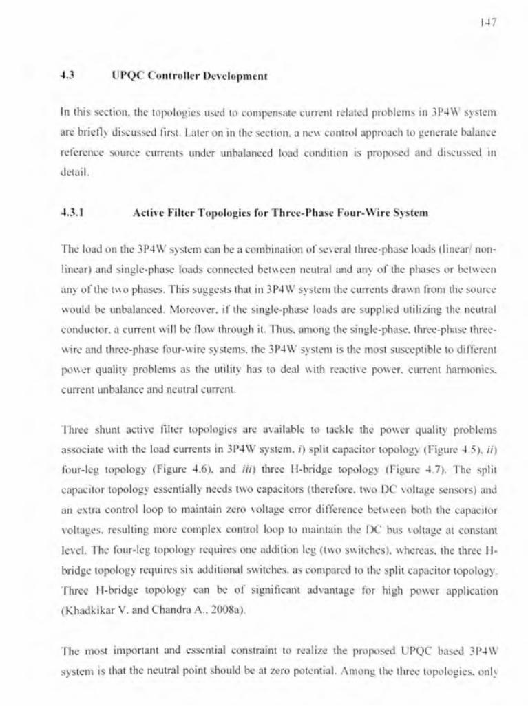
147
4.3 UPQ C Controller Developmen t
In thi s section , th e topologie s use d t o compensat e curren t relate d problem s i n 3P4 W syste m
are briefly discusse d first. Late r on in the section , a new contro l approac h t o generate balanc e
reference sourc e current s unde r unbalance d loa d conditio n i s propose d an d discusse d i n
detail.
4.3.1 Activ e Filte r Topologies fo r Three-Phase Four-Wir e Syste m
The loa d on the 3P4W system can be a combination o f se\eral three-phas e load s (linear/ non -
linear) an d single-phas e load s connecte d betwee n neutra l an d an y o f th e phase s o r betwee n
any of the two phases . This suggest s that i n 3P4W syste m the currents draw n fro m th e sourc e
would b e unbalanced . Moreover , i f th e single-phas e load s ar e supplie d utilizin g th e neutra l
conductor, a current wil l b e flow through it . Thus, among th e single-phase, three-phase three -
wire an d three-phas e four-wir e systems , the 3P4 W syste m i s the mos t susceptibl e t o differen t
power qualit y problem s a s th e utilit y ha s t o dea l wit h reacli\' e power , curren t harmonics ,
current unbalanc e and neutral current .
Three shun t activ e filter topologie s ar e availabl e t o tackl e th e powe r qualit y problem s
associate wit h th e loa d current s i n 3P4 W system , / ) spli t capacito r topolog y (Figur e 4.5) , // )
four-leg topolog y (Figur e 4.6) , an d //'/ ) thre e H-bridg e topolog y (Figur e 4.7) . Th e spli t
capacitor topolog y essentiall y need s tw o capacitor s (therefore , tw o D C voltag e sensors ) an d
an extr a contro l loo p t o maintai n zer o voltag e erro r differenc e betwee n bot h th e capacito r
voltages, resultin g mor e comple x contro l loo p t o maintai n th e D C bu s voltag e a t constan t
level. Th e four-le g topolog y require s on e additio n le g (tw o switches) , whereas , th e thre e H -
bridge topolog y require s si x addifiona l switches , as compared t o the spli t capacito r topology .
Three H-bridg e topolog y ca n b e o f significan t advantag e fo r hig h powe r applicatio n
(Khadkikar V . and Chandr a A. , 2008a).
The mos t importan t an d essentia l constrain t t o realiz e th e propose d UPQ C base d 3P4 W
system i s that th e neutra l poin t shoul d b e a t zero potential . Amon g th e thre e topologies , onl y
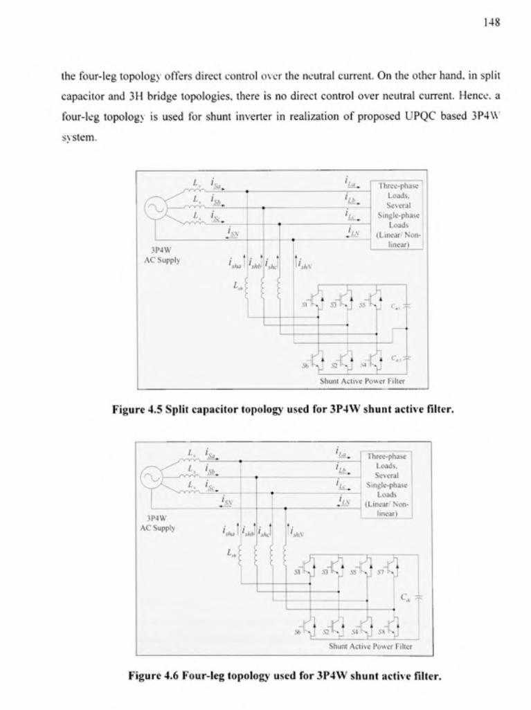
148
the four-leg topolog) ' offers direc t control o\er th e neutral current . On the other hand, in split
capacitor an d 3 H bridge topologies , there i s no direct contro l ove r neutra l current . Hence , a
four-leg topolog y i s use d fo r shun t inverte r i n realizatio n o f propose d UPQ C base d 3P4\\ '
svstem.
L. I,
L. I
'La.
Sb.
L. I Sc.
'i'.V
3P4W AC Suppl y
sha
'Lb.
hhb^
'Lc .
'she'
}LS
Three-phase Loads, Several |
Single-phase '• Loads
(Linear' Non -linear)
I'tftV shN
A\ 2 ] ^ G,
X.\ A^- AJ\ '" Shunt Activ e Power Filter
Figure 4.5 Split capacitor topology used for 3P4W shunt active filter.
3P4W AC Suppl y
L. I
L. I
Sa.
Sh.
L. I Sc.
'5,V
Lai shbl Lc\
'La.
'Lb
'Lc
' / . ,V
Three-phase Loads. Several
Single-phase Loads
(Linear/Non-linear)
C,„ A
h^Af aik ' sA^ sAA^ Shunt Activ e Powe r Filte r
Figure 4.6 Four-leg topology used for 3P4W shunt active filter.
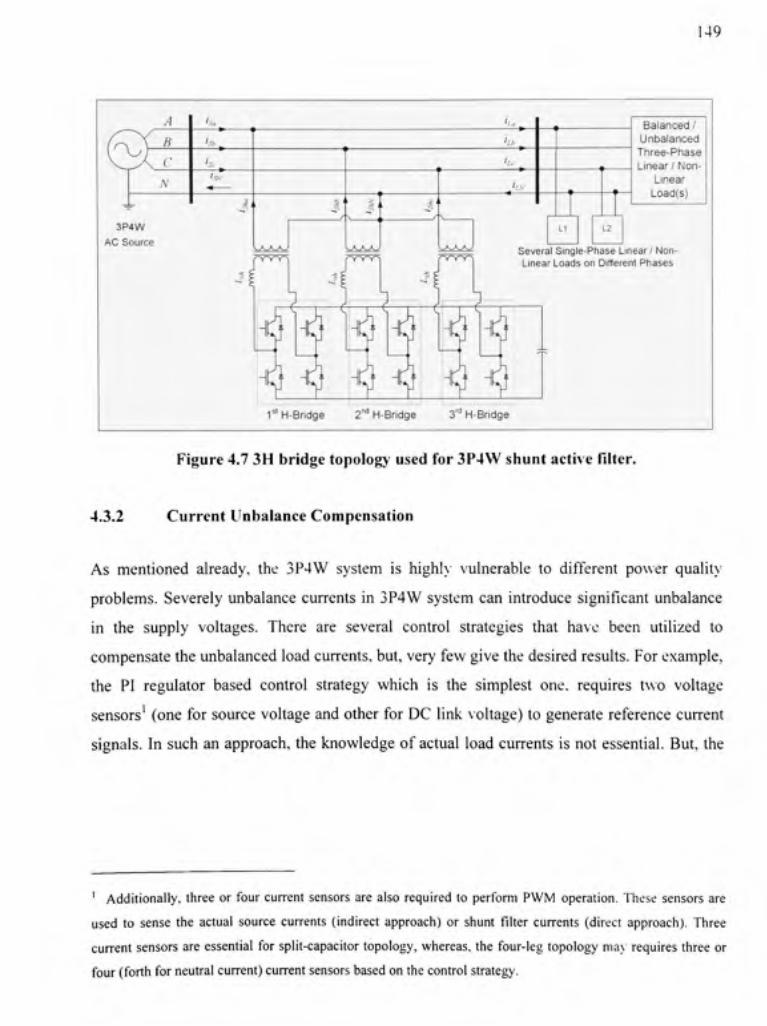
(' A'
3P4W AC Source
149
'.s--.
l,f,
' / .V
Balanced/ Unbalanced Three-Phase Linear/ Non -
Linear Load(s)
Several Single-Phase Linear/ Non-Linear Loads on Different Phase s
1"H-Bndge 2"" ^ H-Bridge 3" ^ H-Bridg e
Figure 4.7 3H bridg e topology use d for 3P4W shun t active filter.
4.3.2 Current Unbalanc e Compensatio n
As mentione d already , th e 3P4 W syste m i s highl y vulnerabl e t o differen t powe r qualit y
problems. Severel y unbalanc e current s i n 3P4 W syste m ca n introduc e significan t unbalanc e
in th e suppl y voltages . Ther e ar e severa l contro l strategie s tha t hav e bee n utilize d t o
compensate the unbalanced loa d currents , but, very fe w giv e the desired results . For example ,
the P l regulato r base d contro l strateg y whic h i s th e simples t one , require s tw o voltag e
sensors' (on e fo r sourc e voltag e an d othe r fo r D C lin k voltage ) to generat e referenc e curren t
signals. I n suc h a n approach , th e knowledg e o f actua l loa d current s i s no t essential . But , th e
' Additionally , thre e o r fou r curren t sensor s ar e also required t o perform PW M operation . Thes e sensor s are
used t o sens e th e actua l sourc e current s (indirec t approach ) o r shun t filte r current s (direc t approach) . Thre e
current sensor s are essential fo r split-capacito r topology , whereas, the four-leg topolog y nia \ require s three or
four (forth for neutral current) current sensors based on the control strategy.

.50
unbalanced curren t injecte d b y th e shun t inverte r cause s th e D C lin k voltag e t o
oscillate/fluctuate. Therefore , i n most case s the perfect curren t unbalanc e compensatio n usin g
PI regulator base d approac h i s uncertain.
The three-phas e p-q theor y base d approac h require s th e knowledg e o f all th e phas e voltage s
and loa d currents . Unde r sinusoida l suppl y voltag e th e p-q theor y perform s well , but it s
performance i s greatl y affecte d whe n suppl y voltage s ar e unbalance d (Khadkika r an d
Chandra, 2008d) . Th e d-q transformation base d approac h ca n giv e a better performanc e a s i t
is independent o f the source voltages .
4.3.3 Propose d Curren t Unbalanc e Compensatio n Approac h
In thi s section , a new contro l approac h t o generat e perfec t balance d referenc e sourc e curren t
signals i s addressed . Th e controlle r fo r shun t inverte r i s develope d base d o n th e propose d
approach. Th e contro l algorith m fo r serie s inverte r i s base d o n uni t vecto r templat e
generation schem e as already discusse d i n CHAPTER 2 .
4.3.3.1 Balance d Referenc e Sourc e Current Signa l Generatio n
Based on the load on 3P4W syste m the currents drawn fro m th e utility ma y b e unbalanced. I n
this chapter , a ne w contro l strateg y i s propose d t o compensat e th e unbalanc e presen t i n th e
load current s b y expandin g th e concep t o f generalize d single-phas e p-q theor y (Khadkika r
and Chandra , 2008c) . According to this theory (Li u et al. 1999 ; Haque et al. 2002) , a signal-
phase syste m ca n be defined a s a pseudo two-phas e syste m b y givin g 7i/2 lead o r TII2 lag. The
resultant tw o phas e syste m i s the n represente d i n a-fi coordinates . Thus , th e concep t of p-q
theory applie d t o balance d three-phas e syste m (Akag i et al, 1984 ) ca n no w als o b e realize d
in single-phas e syste m an d instantaneou s loa d activ e a s wel l a s reactiv e power s ca n b e
determined.
To appl y th e single-phas e p-q theor y base d approac h t o th e tliree-phas e system , eac h o f th e
phase voltage s an d current s o f origina l three-phas e syste m ar e considere d a s thre e
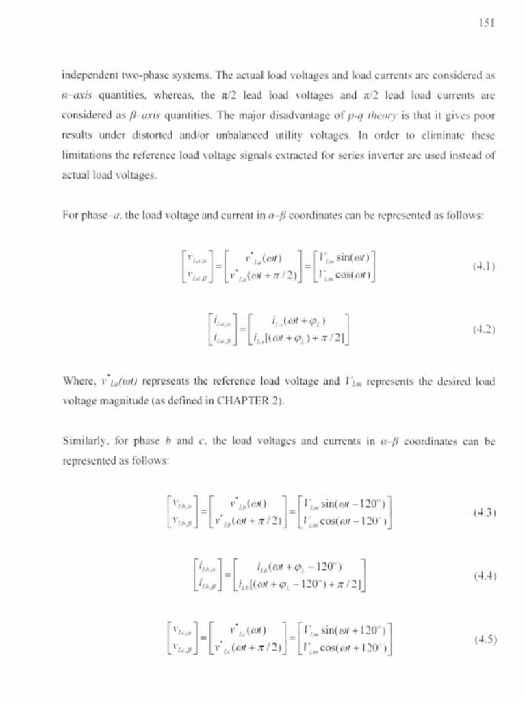
.51
independent two-phas e systems . The actua l loa d voltage s an d loa d current s ar e considered a s
a-axis quantities , whereas , th e 7i/ 2 lea d loa d voltage s an d 7i/ 2 lea d loa d current s ar e
considered a s fi-axis quantities . Th e majo r disadvantag e of p-q theory i s tha t i t give s poo r
results unde r distorte d and/o r unbalance d utilit y voltages . I n orde r t o eliminat e thes e
limitations th e referenc e loa d voltag e signal s extracte d fo r serie s inverte r ar e use d instea d o f
actual loa d voltages .
For phase-c/, the loa d voltag e and current i n a-fi coordinate s can be represented a s follows :
La,a
la.p v'jcot + 7rl2) \]„,sin{o)l) \',^„,QOS{C0t)
(4.1)
'/,!/,,
l.a.P
i,^,{coi + (p,)
i,A{(ot + (p,) + 7r/2] (4.2)
Where, v ia(col) represents th e referenc e loa d voltag e an d I '/.,„ represent s th e desire d loa d
voltage magnitud e (a s defined i n CHAPTER 2) .
Similarly, fo r phas e b an d c, th e loa d voltage s an d current s i n a-fj coordinate s ca n b e
represented a s follows :
Lh.a
Lb.p V i^{cot + nl2)
i;,„sin(r^/-120") i;,„cos(f(>/-120")
(4.3)
'Lh.a
Lb.p
i,j,{(ot + (p,-\20") i,,[{cot + (p,-\20") + Kl2\
(4.4)
l.c.a
l.c,p
V ijcol) v\fcot-hn/2)
V„„sin{cot + \20" r,,„cos(cyr-hl20"
(4.5)

152
'l.c.a
•r^.P
ij^{ojt + (p, +120" )
i,J(cot + (pi +120") + ; r /2 ] (4.6)
By usin g th e definitio n o f 3-phase/:>-c y theory fo r balance d three-phas e syste m (Akag i et al.
1984), the instantaneous powe r components ca n be represented as :
Instantaneous activ e power ,
Pu ~ ^I.x.a-h..x,a '^ ^'/-v,/3-'/.v. / (4.7)
Where, x represent s a. b, or c. for phas e a. b or c. respectively .
Instantaneous reactiv e power .
^/.v '^'Lx.a-h.x.p ^'ix.p-'Lx.a (4.8)
Considering phase-c/ , th e phase-c / instantaneou s loa d activ e an d instantaneou s loa d reactiv e
powers ca n be represented as :
PLU
(ll.a
'^'ia.a ^'ha.p
~^'IM,P ^'lM,a
La.a
'La.p (4.9)
Where,
Pia =Pi.+P l.a (4.10)
^,a = ^lia + 'Iha (4.11
In (4.10 ) an d (4.11) , p,^ an d q,^ represen t th e D C component s tha t ar e responsibl e fo r
fundamental loa d activ e an d reactiv e power , whereas , p^^ an d q,^ represen t th e A C
components tha t ar e responsibl e fo r harmoni c powers . Th e phase- a fundamenta l

153
instantaneous loa d activ e an d reactiv e powe r component s ca n b e extracte d fro m piu an d c//, ,
respectively, by using a low pass filter (LPF) .
Therefore, instantaneou s fundamenta l loa d active power fo r phase -a:
PLa..-P,.a (^-12 )
Similarly, the fundamenta l instantaneou s loa d activ e power s fo r phase- 6 an d phase- c ca n b e
calculated a s follows :
Instantaneous fundamenta l loa d active power for phas e -b:
PLh.^=Pib (4-13 )
Instantaneous fundamenta l loa d active power fo r phas e -c:
PLC.^-PU (^-14 )
Since, th e loa d curren t draw n b y eac h o f th e phase s ma y b e differen t du e t o differen t load s
that ma y b e connecte d t o th e respectiv e phases , th e instantaneou s fundamenta l loa d activ e
power deman d fo r eac h phas e ma y no t b e th e same . I n orde r t o mak e thi s loa d unbalance d
power demand , see n fro m th e utilit y side , a s a perfectl y balance d fundamenta l three-phas e
active power , th e unbalance d loa d powe r shoul d b e properl y redistribute d betwee n utility .
UPQC (shun t inverter ) an d loa d suc h that , th e tota l loa d see n b y th e utilit y woul d b e linea r
and balanced . Th e aforementione d tas k ca n b e achieve d b y summin g instantaneou s
fundamental loa d activ e powe r demand s o f al l the three phase s an d redistributin g i t agai n o n
each o f th e utilit y phases . Th e tota l fundamenta l activ e powe r demande d b y al l th e load s o n
the 3P4W syste m can be computed a s -
154
U..lolul = P/,,,,1 + Plb.^ + Pu, (4.15)
For equal redistributio n o f total loa d active power demand o n each o f the phases .
^L,iuial SI ph (4.16)
Equation (4.16 ) gives the redistributed pe r phase fundamenta l activ e power deman d tha t eac h
of the phase s o f utilit y shoul d suppl y i n orde r t o achiev e perfec t balance d sourc e currents . I t
is also evident tha t unde r al l the conditions , the tota l fundamenta l activ e powe r demande d b y
the load s woul d b e equal t o the total powe r draw n fro m th e utilit y but i n a perfectly balance d
way. Thus, the reference compensatin g current s representing a perfectly balance d three-phas e
system ca n b e extracte d b y replacin g th e instantaneou s tota l loa d activ e powe r {piA i n (4.9 )
with redistributed pe r phase power (/ ; sph) and taking it s inverse transformation .
Sa.a
Sa,P
I.a,a ' La.p
'^La.p ^'ia.a
P SI ph "* " Pjclph
0 (4.17)
In {4.]7).pc/cph is the precise amoun t o f per phase activ e power tha t shoul d b e taken fro m th e
source i n orde r t o maintai n th e D C lin k voltag e a t constan t leve l an d t o overcome th e losse s
associated wit h UPQC . The oscillating instantaneou s activ e power {pj ) shoul d b e exchange d
between th e loa d an d shun t inverter . Th e reactiv e powe r ter m {qi) i n (4.17 ) i s considered a s
zero, since the utility shoul d not suppl y loa d reactiv e power demand . I n the above matrix , th e
a-axis referenc e compensatin g curren t represent s th e instantaneou s fundamenta l sourc e
current, sinc e a-axis quantitie s belon g t o the origina l syste m unde r consideratio n an d th e /? -
axis referenc e compensatin g curren t represent s th e curren t tha t i s a t 7i/ 2 lea d wit h respec t t o
the original system .
155
Therefore, / ' ^ ^ = / ' , , ( / ) = / '^""^ ' ^ [p sipiM) +p,,„{')] (4-18 ) ' La.a ^ ' La.p
Similarly, the reference sourc e current fo r phase- 6 and phase-c ca n be estimated a s follows :
i\hH)= / '""^^. ^ •[// . / , ; ,( 0 + P.w./.(0] (4T9 ) i> -1 - i > L ' ' - I ' /./>, « + ' /./..
i\c(t) = ^^^^'''^'^[p LipiM)^Pj.ip,M)] (4.20 ) ' Lc,a ^ ' Ac,/?
4.3.3.2 Neutra l Curren t Compensatio n
As observed fro m th e previous section , to generate balance d sinusoida l sourc e current s unde r
unbalanced loa d condition , al l the three loa d current s ar e sensed an d utilized. Usin g
symmetry, th e actua l neutra l curren t ca n b e extracte d simpl y b y addin g al l th e sense d loa d
currents, without actua l sensing , as follows :
'L,A'(O = ' / . ( O + ' , * ( 0 + ' ; . ( 0 (4.21 )
The reference neutra l curren t fo r forth le g thus can be given as ,
••• i\h.At)--iL.At) (4.22 )
A bloc k diagra m representatio n o f the propose d balance d pe r phas e fundamenta l activ e
power estimation , D C lin k voltag e contro l loo p base d o n P I regulator , th e referenc e sourc e
current generafio n a s give n b y (4.18 ) - (4.22) , an d th e referenc e neutra l curren t generation s
are shown i n Figure 4.8 (a) , (b), (c), and (d) , respectively .

.56
Y ^ l -I - -I - -I - A HH e f 1 / ' \
A . - / •* ' ^ . . ( I ^ ^ Y 5 ^ ^ c = ^ ::: . -r^ :^
} A A X A A A | j •i\ ^-^ :1 A: : J -.: :1 , r Z^ I I i 1 .- 3 - . 5 . £ .^ ' - ^ =^ ^
"^ 1 — — 1 1 H—h -t - 1 ,. 1, A
=1
1—1 " I - ' - I - n S • =
Q. D - Q _ I Zi - 1 -i S>
rtt^ ri(V)i , r x i i l ' p<>9*] [vS q po> q |
tt ^ ^ = > "= i " > ! i
r-., T 3 ^ J - a r i T 3 r- i " D r , T 3 ( 4 I D 8 5
' ^ a a . . * . a Q a -c - a ,- - ^
. ^ • 3 " , , , , f •-*. , of -^ . o'-^ ^ II I I I I I I I I I I
Figure 4.8 Shunt inverte r contro l block diagram .

157
4.4 Simulatio n Result s
The simulatio n result s fo r propose d UPQ C base d 3P4 W topolog y ar e show n i n Figur e 4. 9
(a)-()). MATLAB/Simulin k i s used a s a simulation tool . Th e utilit y voltage s ar e assume d t o
be distorte d wit h voltag e TH D o f 9.5% . Thes e distorte d voltage s profil e i s show n i n Figur e
4.9 (a) . UPQ C shoul d maintai n th e voltag e a t th e loa d bu s a t a desire d valu e an d fre e fro m
distortion. Th e plan t loa d i s considere d a s th e combinatio n o f a balance d three-phas e diod e
bridge rectifie r followe d b y a R- L load , whic h act s a s a harmonic generatin g load , an d thre e
different single-phas e load s o n eac h phase , wit h differen t loa d activ e an d reactiv e powe r
demands. The resulting loa d current profile show n i n Figure 4.9 (g) has THD of 12.15% .
The shun t inverte r i s turne d O N first a t tim e t=0. 1 se c suc h tha t i t maintain s th e D C lin k
voltage a t se t referenc e value , her e 22 0 V (no t show n i n th e Figur e 4.9) . A t tim e t=0. 2 sec .
the serie s inverte r i s put int o th e operation . Th e serie s inverte r inject s th e require d
compensating voltage s throug h a serie s transformer , makin g th e loa d voltag e fre e fro m
distortion (THD = 1.5% ) an d a t a desired leve l (Figur e 4. 9 (b)) . Th e serie s inverte r injecte d
voltage profil e i s show n i n Figur e 4. 9 (c) . Simultaneously , th e shun t inverte r inject s th e
compensating current s t o achiev e th e balance d sourc e current , fre e fro m distortion , a s
discussed i n th e perviou s section . Th e compensate d sourc e current s show n i n Figur e 4. 9 (f )
are perfectly balance d wit h th e TH D o f 2.3% . Th e current s injecte d b y the shun t inverte r ar e
shown i n Figure 4.9 (g).
Since ther e ar e som e load s connecte d betwee n phas e an d neutral , curren t flows toward s
transformer neutra l point . Th e loa d sid e neutra l conducto r curren t profil e i s shown i n Figur e
4.9. A s notice d fro m Figur e 4. 9 (e) , th e shun t inverte r effectivel y compensate s th e curren t
flowing toward s transforme r neutra l point . Thus , th e serie s transforme r neutra l poin t i s
maintained a t virtua l zer o potential . Th e compensatin g curren t injecte d throug h fourt h le g o f
shunt inverte r i s shown i n Figure 4.9 (j) .

158
0 2 0 22 0 24 0,2 6 0 28 0, 3
300
u 20 0 >
^ 1 0 0 - -
02
50
-50 02
0 22 0 24 0 26 0 28
0 22
02
02
50
; 2 5
^ ° ~ -2 5
03 •50'—
02
50
c 2 5
-I 0 .J2 ^ • 2 5
0 24 02 6 0 28 0, 3 •50
02
0 22 0 24 0 26 0 28 0 3
0 5 0 3
_ 0 12
5" .5 0
fW^jfVU^" \Sl A g V j ^ \ ^ - • ^
'VU'^^V/W'/ ^ J ^ * ^ N . ' ^
-
\ yV\i''/\y\
1
0 22 0 24 0 26 0 28 03
0 22 0 2 4 0 26 0,2 8 03
0 22 0 24 0 26 0 28 03
Figure 4.9 Simulation result s - performanc e o f proposed curren t unbalanc e compensation approac h applie d under nove l UPQC topology .
159
4.5 Laboratory Experimenta l Result s
The performanc e o f propose d curren t unbalanc e compensatio n approach , whe n applie d t o
no\el 3P4 W UPQ C syste m configuration , i s validated i n th e laboratory . Performanc e o f th e
series par t o f UPQ C i s simila r t o tha t discusse d i n th e pre \ ious chapters . I n thi s section ,
attention i s give n t o maintainin g th e serie s neutra l poin t a t virtua l zer o le\el . Interestin g
results are presented an d discussed i n the following subsections .
4.5.1 Svstem unde r Consideratio n
The laborator y experimenta l setu p t o generat e unbalance d loa d current s i s gi\e n i n Figur e
4.10. Th e tota l loa d o n th e syste m consist s of/' ) loa d Ll , three-phas e diod e bridg e rectifie r
(DBR) followed b y a capacitor (ver y common type of load in ASD application) , /'/' ) load L2 . a
highly inductiv e loa d betwee n phas e -a an d neutral , an d /// ) loa d L3 , a single-phas e non -
linear loa d (single-phas e DB R followed b y RL load) between phas e -b an d neutral . I n Figur e
4.10. the magneti c actuato r SW l i s used to connect/disconnec t highl y inducti\ e loa d to/fro m
the network , whereas , the manua l switc h SW 2 i s utilized t o disconnect th e phase -a fro m th e
circuit (three-phas e to single phasing condition) .
A
H
L\\
C,
K\ = 40Q
/;: = 2on lo = 27n /I = 20mH
12 = SOmH
. / < • ]
Figure 4.10 Experimenta l setu p to generate unbalance d loa d currents .
160
The curren t draw n b y the individual load s an d the total loa d on each o f the phase s unde r
steady stat e ar e given i n Figure 4.11 . As seen fro m th e Figure 4.1 1 (a) , the total curren t
drawn b y the phase -a (trace-4 ) i s the combination o f a non-linear curren t (trace-2 ) an d a
highly inducfiv e loa d curren t (0.3 3 lagging , trace-3). Phase -b supplies only three-phas e non -
linear loa d an d its current profil e i s shown i n Figure 4.1 1 (b) , trace-2/trace-3. Phas e -c
current i s the combination o f three-phase (trace-2 ) an d single-phase (trace-3 ) non-linea r
currents (Figur e 4.1 1 (c)) . Sinc e ther e ar e two separate single-phas e load s connecte d t o th e
neutral conductor , th e current flowing throug h i t is the combination o f individual curren t
drawn b y those loads , as ca n be noticed i n Figure 4.1 1 (d) . In Table 4.1 , the rms value of
current, % THD, K factor (rafi o o f maximum valu e to the fundamental value) , an d power
factor of each load current is mentioned.
t>
h^^>-AAA^rih-, '•••^'•/. . , y s . lA
„../_..v. ...•.•i/-,.-v-,"---.'-
V r V AV: - V /\....^\
\y \A- ^ y I V ^ ^ t<4 All'J 2U0 S
(,i) Phn.se -a
\
f>
vx-^y, ' / . . : „_,/ " ^^ ^.r ^/ ^Z-
".JA" ~-\'~ " A " ' ~'-\'" * "^v " ' i < i _ ^ - . ' - . . ^ . . ^ • . ^ .
l i " i f i o v ^ a B '=:.ooA^ > M l o o m s ChJi 3.0 0 A l> t-J H U.O O A i: - 14 Au g 200 8
K) Phai^i e -c
&
A: y ' i » ' ^. \^ ^. ^ - X T ^""^s
' • / . ( . / v ' ^
" X •• 'X" ' • 'X ' ^ , A r
V , , I V , V.. .
f (>: ' • > (I d A . > V I io,oi><< i r*i: ' s .ooAi' j
I-» A u g 3 0 0 S
(b) Phn^i e -b
\ A''"'A A A A / I / r \ )J.... \A '\/..l.)J...'>J. i/,., !
V V ' ''\A'
(d) Ph.i.s e -neutra l
V A A v^ \ y C h 7 | • Y.-i)o A o rh- 5 > no A < • 1-4 A ug JOO S
Figure 4.11 Individua l curren t draw n b y each of the loads .
Table 4.1 Individual loa d curren t detail s
Current
' / , u l
'/„:
'L.
'u,
'/.,
A-•u
RMS
1 68 A
3 33 A
4 1 5 A
1,91 A
1,31 A
1 1 6 A
2,48 A
% TH D
34,89 %
1,12%
14,49%
32 03 %
41.72%
31 05 %
26 27 %
K-factor
4 12
1.01
1.53
3.72
6.56
691
3 8
P.F.
0 94 (lag )
0,33 (lag )
0,65 (lag )
0 94 (lag )
0,90 (lag )
0 95 (lag)
0,95 (lag )
161
The unbalanc e presen t i n the loa d current s i s expressed b y computin g th e curren t unbalanc e
factor (CUF ) which i s calculated a s follow :
CUF^ m a x { / , , , - / , / - / , \h.^.-h (4.23)
av^
Where _{f + f + lj
(4.24)
Using the data from Tabl e 4.1,
_ (4.1 5 + 1.91 + 2.48) (4.25)
L.,-h.a =|2.847-4.15 | = 1.30 3 (4.26)
L.-iu = 2.847-1.9 1 =0.93 7 (4.27)
162
fvg fc 12.847-2.48 =0.36 7 (4.28)
TT • . . ^ . ^rrr ^ max{1.303,0.937,0.367 } 1.30 3 . ,^„ , , , _„^ Usmg (4.23), CUF = ! ^ = = 0.4576 (4.29 ) 2.847 2.847
Therefore, C;7 F = 45.76% (4.30)
Thus, th e unbalanc e presen t i n th e loa d current , o n th e basi s o f curren t rms values , i s
determined as 45.76%.
4.5.2 Real-Time Instantaneous Fundamental Load Active Power Extraction
Figure 4.1 2 (a ) show s th e experimenta l resu U t o demonstrat e th e real-tim e extractio n o f
instantaneous fundamenta l activ e powe r demande d b y eac h phas e an d th e redistribute d pe r
phase fundamenta l activ e power. Note that the computed loa d fundamenta l activ e powers in
a-fi coordinates are DC values. The generated balanced reference sourc e current signals using
proposed approach are shown in Figure 4.12 (b).
E>
P : - yn P:...
Pu,
c,h:ii i.o o V x.:h2 l o o v Mrlo.Om s SBB i . c o v 15 A u q 2 0 0 S
(.T) L o a d inst . fund , act iv e p o w e r s
1 3 AlK j 2 0 0 «
(b) Ref . sourc e cuiTcnt s
Figure 4.12 Real-time extraction of instantaneous fundamental loa d active power and generated reference source current signals using proposed approach.
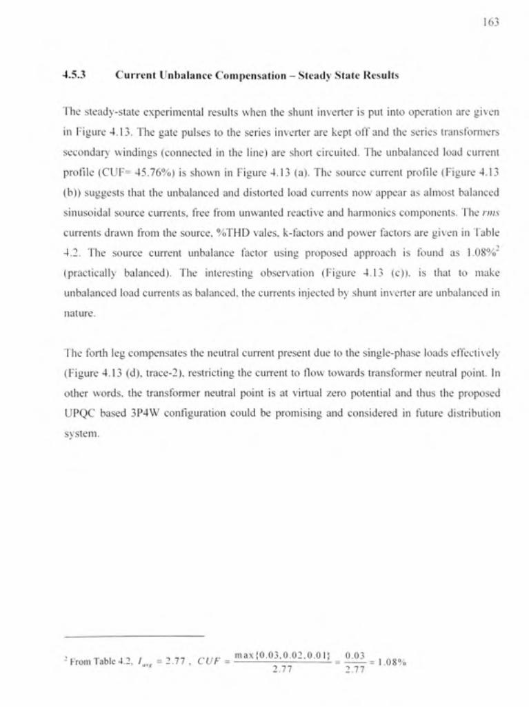
163
4.5.3 Curren t Unbalanc e Compensatio n - Stead y Stat e Result s
The steady-stat e experimenta l result s whe n th e shun t inverte r i s pu t int o operatio n ar e give n
in Figur e 4.13 . The gat e pulse s t o th e serie s inverte r ar e kep t of f an d th e serie s transformer s
secondary winding s (connecte d i n th e line ) ar e shor t circuited . Th e unbalance d loa d curren t
profile (CUF = 45.76% ) i s show n i n Figur e 4.1 3 (a) . The sourc e curren t profil e (Figur e 4.1 3
(b)) suggest s tha t th e unbalance d an d distorte d loa d current s no w appea r a s almos t balance d
sinusoidal sourc e currents , fre e fro m unwante d reactiv e an d harmonic s components . The rms
currents draw n fro m th e source , %TH D vales , k-factors an d powe r factor s ar e give n i n Tabl e
4.2. Th e sourc e curren t unbalanc e facto r usin g propose d approac h i s foun d a s 1.08% '
(practically balanced) . Th e interestin g observatio n (Figur e 4.1 3 (c)) , i s tha t t o mak e
unbalanced loa d currents as balanced, the currents injected b y shun t inverte r are unbalanced i n
nature.
The fort h le g compensates th e neutral curren t presen t du e to the single-phase load s effectixel y
(Figure 4.1 3 (d) , trace-2), restrictin g th e curren t t o flow toward s transforme r neutra l point . I n
other words , th e transforme r neutra l poin t i s a t virtua l zer o potentia l an d thu s th e propose d
UPQC base d 3P4 W configuratio n coul d b e promisin g an d considere d i n futur e distributio n
system.
T K i n / T 77 njinr 0 1 ax{0.03,0.02,0.0 1} 0.0 3 , ^„„ ^ - From Table 4.2, / ^ =111 , CUF = -= = 1.08 % ' 2.7 7 2.7 7

164
Table 4.2 Source current detail s before and afte r compensatio n
Current RMS Peak •io THD K-factor P. F.
Before Compensation
'sa
' »
'sc
4 1 5 A
1.91 A
2.48 A
5.90 A
3.11 A
3.70 A
14.49%
32.03 %
26.27 %
1.53
3.72
3.80
0.65 (lag)
0.94 (lag)
0 95 (lag)
After Compensation
'su
'sb
'.Sc
2.80 A
2 7 5 A
2.76 A
3 95 A
3.81 A
3.87 A
1.53%
2.93 %
2.W %
1.03
1.08
1.14
\.i) (unity)
\.Q (unity)
1.0 (unity)
14 Ali g JOO S
(a) Uiibal. ince d loa d ciiirent s
/\'... A ' AA '• /^ ' " A A ^I. ,....yu- u - i ....u.., ;v,....,i.W A. ,A\rA^gv ^Ax^AA,AV s .•
/ 'A^A/^ VvA^'A A VvA ' A A"
A;'
l ^ i I DO V C1 1 2^ "To o A *• / 1^ 10 ; Om«^ an J] ti;bbAi > cji i i.uu A o '
14 AUQ 200 &
(c) Shun t i m e i t e i cuiieiit ^
la Au' j iiou s
(b) Balnnce d souic e cuireut s
,•1 cpmiWiilliaiiWUkiuJini.tL.i i
V- V AAA/- V ^ V.' V - . 'Ms^r*'f*^>'r'"'T'''^'~''Zli...i' ' '.'.'in '.\'> "Mi l i j .ur t is " Ch i i ' ^ (i o A . * i"li 4 • , no A •- '
/i /
H AUC ] 200 8
(d ) Neuti en l c m i ents
Figure 4.13 Experimental result s (steady-state condition) : performance o f proposed current unbalanc e compensation approach .

165
4.5.4 Dynami c Performanc e
The performanc e o f th e propose d approac h unde r dynami c condition s ar e als o tested . Tw o
different situation s ar e considered , i n one case the loa d o n the syste m i s increased/ decrease d
arbitrarily, whereas , i n th e othe r cas e on e phas e i s removed fro m th e circuit . Thes e test s ar e
carried ou t t o ensur e tha t th e propose d controlle r adapt s th e ne w stead y stat e quickh ,
maintaining balance d sourc e current s an d th e neutra l poin t remain s a t virtua l zer o potentia l
irrespective o f the change i n the loa d conditions .
4.5.4.1 Loa d Chang e
The experimenta l result s durin g momentar y increas e i n th e loa d o n th e syste m ar e gi\e n i n
the Figur e 4.14 . Al l o f a sudde n switc h SW l (Figur e 4.10 ) i s close d suc h tha t th e highl y
inductive single-phas e R L loa d ge t comiecte d t o th e network . Th e chang e i n loa d curren t
profiles ca n b e notice d fro m th e Figur e 4.1 4 (a) . As the loa d i s connected betwee n phas e -a
and th e neutra l conductor , ther e i s increase i n phase -a loa d curren t (trace-1 ) an d th e neutra l
current (trace-4) . The phase -b an d phase -c loa d currents remain unaffected .
The adde d R L loa d demand s hig h reactiv e powe r an d certai n amoun t o f activ e power . I n the
proposed approach , a s discusse d i n th e previou s sections , eac h phas e fundamenta l activ e
power i s summed togethe r an d redistribute d a s balanced activ e powe r o n eac h o f th e phases .
This fac t ca n b e confirme d fro m th e Figur e 4.1 4 (b) , where , there i s sligh t increas e i n sourc e
current magnitud e o f phas e -b an d -c current s i n orde r t o accommodat e th e newl y adde d
fundamental loa d activ e powe r deman d an d thu s t o maintai n th e balance d sourc e currents .
The performanc e o f shun t inverte r i s shown i n Figure 4.14 (c) . Phase -a shun t compensatin g
current no w support s th e loa d reactiv e powe r deman d locall y i n additio n t o th e harmonic s
generated b y non-linea r load . Not e th e D C lin k voltag e strictl y remain s a t constan t value .
Importantly, th e fort h le g of shun t inverte r effectivel y compensate s th e chang e i n the neutra l
current an d does not allow the neutra l curren t to flow toward s transformer neutra l point .
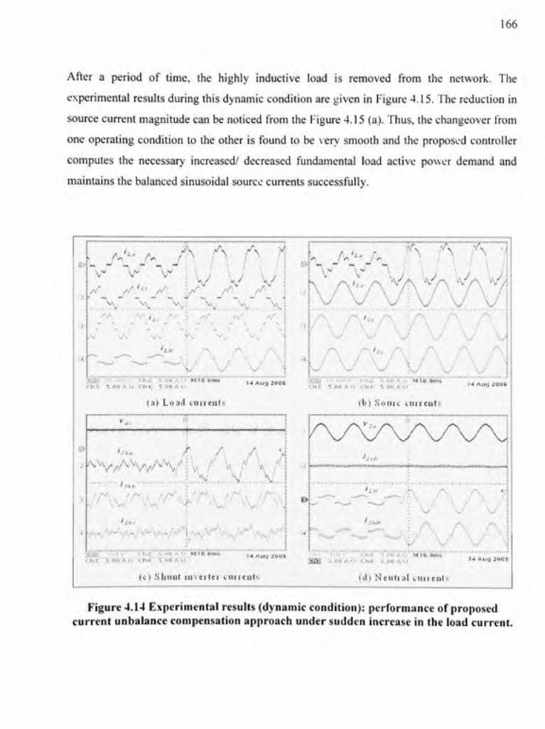
166
After a perio d o f time , th e highl y inductiv e loa d i s remove d fro m th e network . Th e
experimental result s during this dynamic condition are given in Figure 4.15. The reduction in
source current magnitude can be noficed fro m the Figure 4.15 (a). Thus, the changeover fro m
one operafing conditio n to the other i s found t o be \ery smoot h an d the proposed controlle r
computes th e necessar y increased / decrease d fundamenta l loa d activ e powe r deman d an d
maintains the balanced sinusoidal source currents successfully .
A - / v /t N A A V
\A '\r \A r.r''->^ A ^ : A iv ^ > /
^ ._ ^A A : A . , ,.,„^ A.i.-i-,...A....-.-A...i.....-A..-..:-.> ^
V 1 \ ' • •^•\
JA" i A . A A V
a i i j so .y rnv . • f.;h2 i S .UUAf > M|ia.Oni! i C h l i S.O O A O Ch 4 I 0 0 A ( •
14 A ug zoo s
(a) L o ad cu i i eats
^ A / A A A \ ^ A -tSf \ r , ..J-4-A.....-... A H.-...
,v-/VAsVAW '1_ *A''' ' AA A A j j j j j f ' i L M V : i : h i l ' T l T o T T o ' M[iroi.Om s ch:<! S ; on' .< i ? ' < h-i ^ = ; oo A > • 14 Ati< j 2oa x
(c) S lmn t i m e i l e i cu i ie i i t s
K A A ' ^ ^ A A^
(4,
A.'/.^ y
/ • . ^^ A r\ ! i. i • I A i \ i
V V : V i — • J - T t - l — » • -
V AA/\A\ A^ A V V A V V
A A V ^ A\ A
\ / V: SBLI i l ' . ' i i i i V " (.,hj | S . O O A O MlO.Om s
c h : ! rx.aci A<f ch~ r > > no A <•> 14 Au< J 200 8
(b) S o u i c ciii i eat s
E^
•Sr/.'
•: V : A- V
AAAH a i B 3 . 0 0 A O f.h.1 ^ 3 . C 0 A W I 4 A I I 3 2 0 0 S
(d) Nei i t i a l c a n ea t s
Figure 4.14 Experimental result s (dynamic condition): performance of proposed current unbalance compensation approach under sudden increase in the load current.
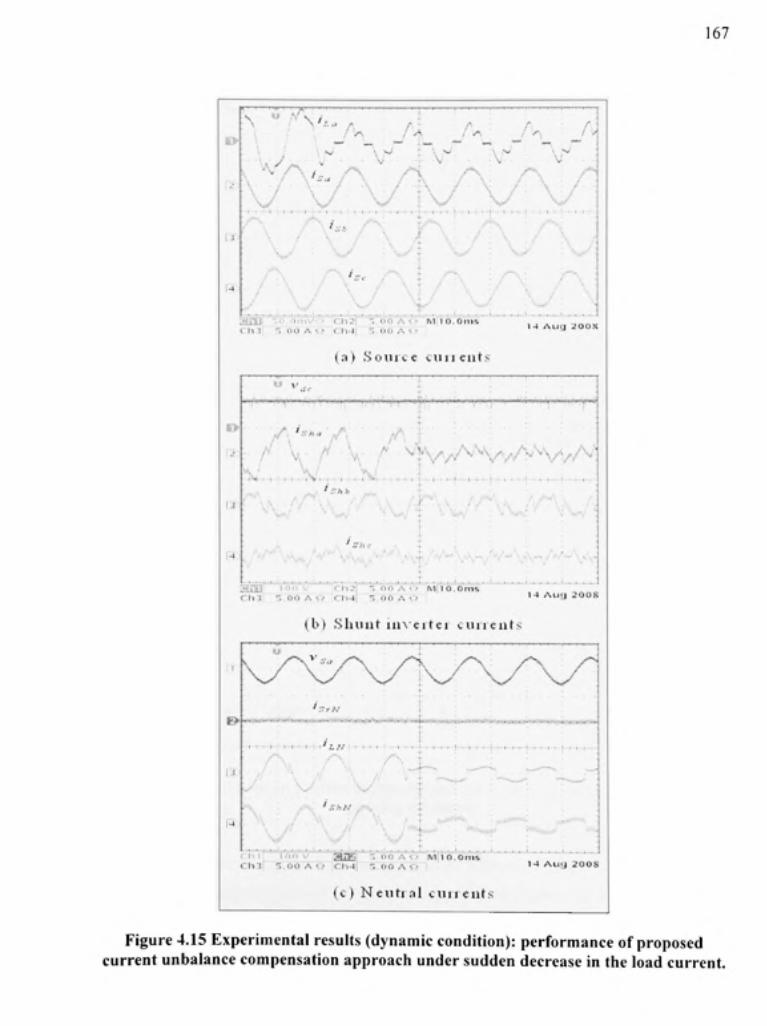
167
i£>
U.
A '^' / ^ V A; v
N •- * A\i,
\ A A,v ' A / A A .' ^ •
A A X / A A^ A^- A A ^ A A- i
,/'..
's^/' \ « ^
^
• V / * \ • /"'-• i.. -r^- i /- ^ • /~^ . - A .
\y; : v^ : V • '• '"> ^r-^S r — ' n ri~A'VT'*'MTi"n'''intVMt'
14 A u g 2O0. S ayaO! so.Tmfv?' " ch2 f 3.0 0 A«'"MiloTom s
(a) .Sourc e cuiieiit. s SJ \r
A ^ - / A ' > k / A V / ^ A \ ^ - / / ^ \ Af^A- f-
(b) .Shuu t i i n e i t e i current s
14 Au< j 2 0 0 s
g>-~,..- ..••^»...^^«l^l^.M»fi|i£wM«M«»i^»£JM«Sa»««*^ .
A • • • -/A, • r\- -/A I - A • \ A \ • / - • i
^ : V A/ ' : R \A • \ y t : : : : "
r i - . ! ! TM^V ''"''T^aEJ'^l"b' o A'O ' '1iiffo".oms"'''"'''"' * ^ ^ ~ " Ch3 l S . O O A Q C h 4 l > : 0 0 A f J 1- 4 A uy 200 S
(c) Neu t ra l currents ;
Figure 4.1 5 Experimenta l result s (dynami c condition) : performanc e o f propose d current unbalanc e compensatio n approac h unde r sudde n decreas e i n the loa d current .
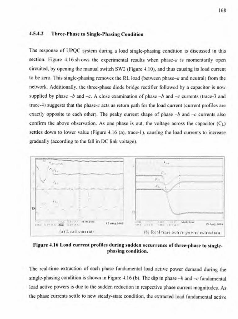
168
4.5.4.2 Three-Phas e to Single-Phasing Condition
The respons e o f UPQ C syste m durin g a loa d single-phasin g conditio n i s discusse d i n thi s
section. Figur e 4.1 6 shows th e experimenta l result s whe n phase-<: / i s momentaril y ope n
circuited, by opening the manual switch SW2 (Figure 4.10), and thus causing its load current
to be zero. This single-phasing removes the RL load (between phase-a an d neutral) from th e
network. Additionally , th e three-phase diod e bridge rectifier followe d b y a capacitor i s now
supplied b y phase -b an d -c. A close examination o f phase -b an d -c current s (trace- 3 and
trace-4) suggests that the phase-c acts as return path for the load current (curren t profiles ar e
exactly opposit e t o eac h other) . Th e peak y curren t shap e o f phas e -b an d -c current s als o
confirm th e abov e observation . A s on e phas e i s out , th e voltag e acros s th e capacito r (CL )
settles dow n t o lowe r valu e (Figur e 4.16 (a) , trace-1), causing th e loa d current s t o increas e
gradually (according to the fall i n DC link voltage).
»
V lb
• t •-.
'Lc
, 'la
.^^.«-?»«ss»^.*«w*»>V*'*ifV.i**
t h 3 ' i .OOAi ' IgiE l ' i.OOA O
(a) Loa d ca n eats '
IS Aug 200 S a<iHi i. i i ' ; V (..h j i . i j u v M40.0m<i ' c h i i i l o o V c:h- > id.oAo IS Aug 200 X
(b) Rea l tiai e activ e powe r extmctio a
Figure 4.16 Load current profiles during sudden occurrence of three-phase to single-phasing condition.
The real-tim e extractio n o f eac h phas e fundamenta l loa d activ e powe r deman d durin g th e
single-phasing condifion i s shown in Figure 4.16 (b). The dip in phase -b an d -c fundamenta l
load active powers is due to the sudden reduction in respective phase current magnitudes. As
the phase currents settle to new steady-state condition , the extracted loa d fundamental acti \ e
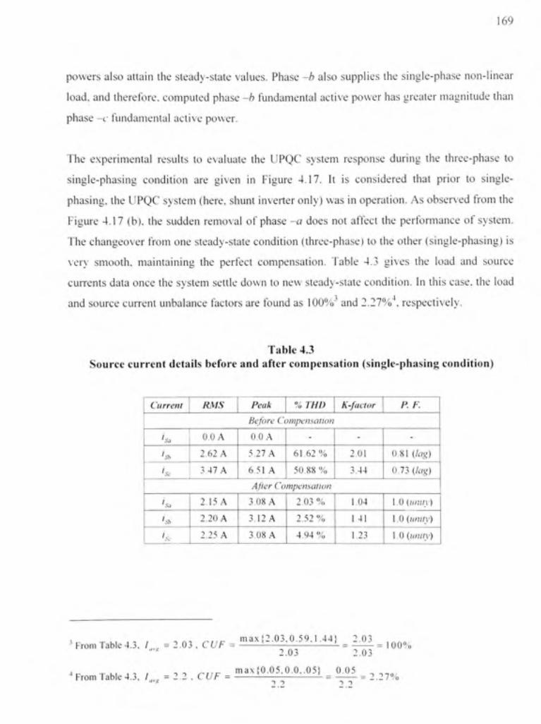
169
powers als o attai n th e steady-stat e values . Phas e -b als o supplie s th e single-phas e non-linea r
load, and therefore , compute d phas e -b fundamenta l activ e power ha s greater magnitud e tha n
phase -c fundamenta l activ e power .
The experimenta l result s t o evaluat e th e UPQ C syste m respons e durin g th e three-phas e t o
single-phasing conditio n ar e give n i n Figur e 4.17 . I t i s considere d tha t prio r t o single -
phasing, the UPQC syste m (here , shunt inverte r only) was in operation. A s observed fro m th e
Figure 4.1 7 (b) . the sudde n remova l o f phase -a doe s no t affec t th e performanc e o f system .
The changeove r fro m on e steady-stat e conditio n (tliree-phase ) t o the other (single-phasing ) i s
very smooth , maintainin g th e perfec t compensation . Tabl e 4. 3 give s th e loa d an d sourc e
currents data once the syste m settl e down to new steady-stat e condition . I n this case , the loa d
and sourc e current unbalanc e factor s ar e found a s 100 % an d 2.27 % , respectively.
Table 4. 3 Source current detail s befor e an d after compensatio n (single-phasin g condition )
Current RMS Peak % THD K-factor P. F. Before Compensation
'sa
'sb
'sc
0.0 A
2.62 A
3.47 A
0.0 A
5.27 A
6.51 A
-
61.62%
50.88 %
-
2.01
3.44
-
0,81 (/«g)
0,73 (lag) After Compensation
'sa
'sb
'.sc
2.15 A
2.20 A
2.25 A
3 08 A
3.12 A
3.08 A
2.03 %
2.52 %
4.94 %
1 04
1 41
1.23
1,0 (unity)
1,0 (unity)
1,0 {imm>)
From Tabl e 4.3 , /,,^ , =2.0Z ,CUF max{2.03,0 .59,1 ,44} 2.0 3
100% 2.03 2.0 3
^ From Tabl e 4.3 , / = 2.2 . CUF . "^a x (0.05,0.0, .05} ^ 0 ^ . 0 .27 % -I ~l • ) - )
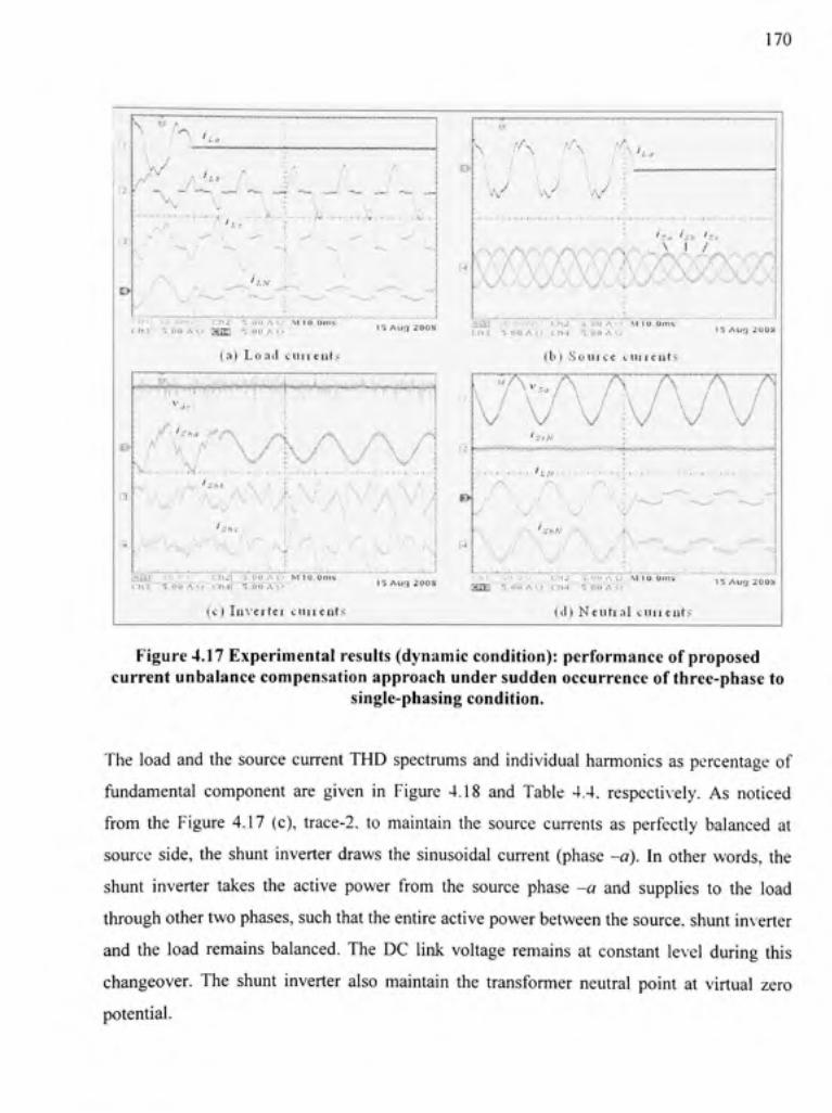
, r,
\ 'A'
E>
A / . ; \ * La
• • \ A ' < / :.. ^ . . . . P. . . . f-_.
V , : \-'. 'A - V "" " ; " ^ ' " :.,..i..,>..U.,....,..i._.,.,. . i . . .._.:.. . ,....-f ,..i.)J....t.,....,..,..^,....|...^.:.^,0... .
>./ / ' i c I . / . ' . ' ; : ; : - ' • • • ' • • ^ - r ' • . ' t
• M • . • . . ^ ^ . « . . . . T - ^ . « - ^ - ^ ,
• ' ' .•/... , f w... ^ * . « . ^ « , ^ w... ^ ' . ^
i /
u /
( I l l i r iu.ui iv. " t h , ^ • 3 00 A (.> " ivi 10.0ms ' c h j i S.ci o A<,, > a J E ' ; ,o o A O '
la) L o a d cii u tat. s
IS A u g 20n. s
iyujy^,ii^«Wi,ji.(iyi|i^lji)j»,t;ii|f'ti^^
0-
H;
V X A A A A A A A A A A A A N? ^ - ^ NJ;^A A ' a m ?io,i,' v ch^ r s.ooAt, ? M;io.oni s <:i»3 5.0 0 A < > t ;h4 | S . n o A ! , r
(c I L n ej te i c a n ea t s
15 A ug ZOO S
170
/•r.
uy \ A V A
iSiiJ vi i . i ' i i iys ? :C.hi : 3.0 0 A O iMIO.Om s <:h .i 3.0 0 A < i C " h.| S . tio A »> 15 A ug ;!001 i
I b I S o a i c e t la j t a t s
I, "Av, , A ~ 7 . \y A y ^ i>
• A
/•\ A , I
v V
"S A/"" " A- A \ / - A \./ f
1 hi _',^^.J£ V Ch2 : S .OUAt J M l O O i n s : a i B 5.0 0 A t i f :h4 : 5.6 0 A o 15 Aug 200 S
(d) Neat i .l l cauea t s
Figure 4.17 Experimental result s (dynamic condition): performance of proposed current unbalance compensation approach under sudden occurrence of three-phase to
single-phasing condition.
The load an d the sourc e curren t TH D spectrum s an d individua l harmonic s a s percentage o f
fundamental componen t ar e give n i n Figur e 4.1 8 an d Tabl e 4.4 , respecti\ely . A s nofice d
from th e Figur e 4.1 7 (c) , trace-2 . t o maintai n th e sourc e current s a s perfectl y balance d a t
source side , the shun t inverte r draw s th e sinusoida l curren t (phas e -a). I n othe r words , the
shunt inverte r take s th e activ e powe r fro m th e sourc e phas e -a an d supplie s t o th e loa d
through other two phases, such that the entire active power between the source, shunt inverter
and th e loa d remain s balanced . Th e D C lin k voltag e remain s a t constan t leve l durin g thi s
changeover. Th e shun t inverte r als o maintai n th e transforme r neutra l poin t a t virtua l zer o
potential.
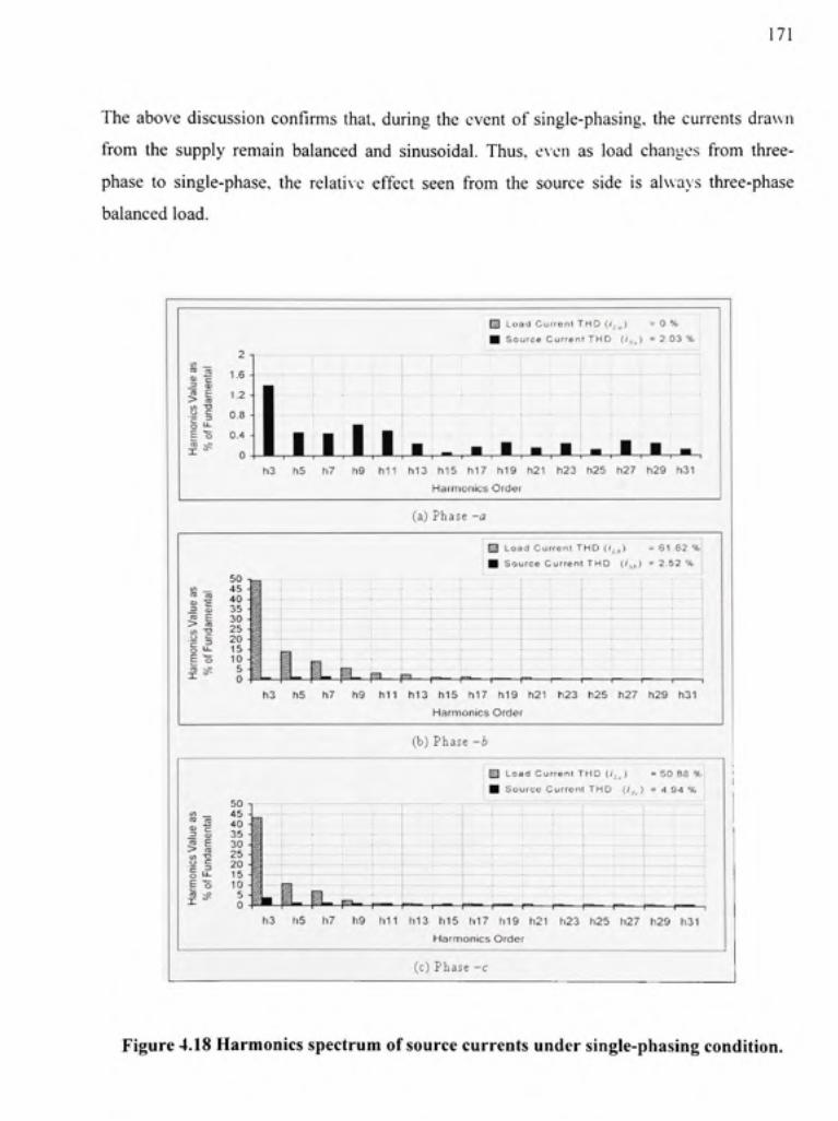
.71
The abov e discussio n confirm s that , durin g the event o f single-phasing, the currents draw n
from th e supply remai n balance d an d sinusoidal. Thus , eve n a s load change s fro m three -
phase t o single-phase , th e relati\e effec t see n fro m th e source sid e i s always three-phas e
balanced load .
2 - , Ul rare , c
.B 4 >
.5 E 1. 2 • > ro
.y § 0. 8 J
E " 5 0. 4 -
• 1 1
1 1 1 1 1
^ L o a d C u i r o n i T H D (/,,, ) = 0 %
• Sourc e Curren t T H D (/.,^ ) • 2 .0 3 %
• • h3 h 5 h 7 h 9 h l i h1 3 h1 5 h1 7 m 9 h2 1 h2 3 h2 5 h2 7 h2 9 h3 1
Haimonics Orde r
fa) Phas e -a
w _ 4 5 • S 4 0 -
= 5 3 5 •
> § ° ' in - o 2 5 • U § 2 0 • § . ^ 1 5 • e " o 1 0 -| a . t 5 -
M L o a d Cu r ren t T H D ( ; , „ ) ^ 6 1 6 2 %
• Sourc e Curren t T H D ( / , , ) = 2 .5 2 %
} ^ • • •
: I
1 , j
i
'M- m- m^ h3 h 5 h 7 h 9 h l i h1 3 h1 5 h1 7 h1 9
Harmonics Ord e
I
' "" 1 I l l l h21 h2 3 h2 5 h2 7 h2 9 h3 1
(b) Phas e -b
Load Curren t TH D ( ( j ,) = 5 0 8 8 % Sourtu CurroM i TH D (/,,. ) = 4 94 %
> C D w " 2
m - 5
hS h 7 f~ r " r -
h9 h l i h i 3 h1 5 ti1 7 h1 9 h2 1 h2 3 h2 5 h2 7 h2 9 h3 1 Harmonics Orde r
(c) Phas e -c
Figure 4.18 Harmonics spectrum of source currents under single-phasing condition.

172
Table 4. 4 Individual harmonic s value s a s % o f fundamental (single-phasin g condition )
Harmonics h.a ' • / , / , h.c ha hh he Odd Harmonics (%)
3 5 7 9 11 13 15 17 19 21 23 25 27 29 31
0 0 0 0 0 0 0 0 0 0 0 0 0 0 0
49.27 13.76 8.91 5.68 3.03 2.39 0.98 1.17 0.57 0.84 0.48 0.41 0.41 0.38 0.24
43.34 10.67 7.07 2.34 1.03 0.94 0,52 0.97 0.76 0.92 0.78 0.92 0.85 0.87 0.79
1.39 0.46 0.44 0.61 0.49 0.23 0.06 0.17 0.26 0.15 0.23 0.12 0.29 0.23 0.12
0.96 1.11 1 33 0.88 0.31 0.20 0.57 0.4 0.37 0.17 0.17 0.14 0.09 0.14 0.23
3.91 1.19 1.14 1.00 0.97 0.61 0,92 0.78 0.92 0.11 0,25 0.53 0.31 0.50 0.78
Even Hamnonics (%)
DC 2 4 8 10
% THD
0 0 0 0 0
0%
0.17 0.60 0.72 0.69 0.33
61.62%
0.72 0.25 0.20 0.14 0.05
50.88%
0.96 0.58 0.09 0.20 0.17
2.03%
0.99 0.37 0.20 0.17 0.28
2.52%
1.08 0.19 0.22 0,03 0,28
4.94%

73
4.6 Conclusio n
This chapte r propose s a nove l functionalit y fo r UPQ C i n whic h i t i s possibl e t o expan d th e
existing UPQ C base d 3P3 W syste m t o 3P4 W an d introduce s a ne w curren t unbalanc e
compensation approach . Th e propose d 3P4 W topolog y woul d b e ver y usefu l t o expan d th e
existing 3P3 W syste m t o 3P4 W syste m wher e UPQ C i s installed t o compensat e th e differen t
power quality problems , which may play an importan t rol e i n future UPQ C based distributio n
system.
The simulatio n an d th e experimenta l result s confir m th e utilizatio n o f gi\e n topolog } fo r
practical applications . Wit h th e propose d approac h th e unbalanc e i n th e sourc e current s i s
reduced fro m 45.76 % t o 1.08% . Moreover , unde r highl y unbalance d (CUF=100% ) an d
distorted (THD s = 61.62% and 50.88% ) conditio n th e UPQ C strictl y maintain s th e balance d
source current s (CUF=2.2%) . I n al l th e conditions , th e neutra l curren t flowing toward s
transformer neutra l poin t i s maintained a t zero \'alue .

CHAPTER 5
UPQC: POWE R ANGL E CONTRO L - A NOVEL CONTRO L PHILOSOPH Y
5.1 Introductio n
As a thum b rul e i n all area s o f engineering , th e prope r utilizatio n o f th e resource s tha t w e
have, a t mos t efficien t way , ha s lea d t o grea t developmen t an d i s the majo r concer n fo r mos t
of th e engineer s i n thei r respectiv e fields. Thi s chapte r i s a n attemp t t o mak e us e o f th e
existing serie s inverte r t o compensat e loa d reactiv e powe r b y introducin g a powe r angl e
difference betwee n th e sourc e an d loa d voltages . I t wil l eventuall y resul t i n a bette r
utilization o f serie s inverter . Thi s ne w reactiv e powe r sharin g featur e betwee n bot h th e
inverters woul d hel p t o reduc e th e burde n o n shun t inverte r an d ultimatel y resul t i n th e
reduction o f shun t inverte r ratin g t o som e extend . Thi s ne w contro l philosoph y i s termed a s
"Power Angle Contro l (PAC ) of Unified Powe r Quality Conditioner" .
The concep t o f propose d PA C theor y i s discussed thoroughl y an d supporte d b y a n i n dept h
mathematical analysis . Informativ e an d usefu l equation s ar e develope d t o comput e th e
achievable maximu m powe r angle , percentages o f loa d reactiv e po w er share d b y eac h o f th e
inverters, percentag e o f reductio n i n shun t inverte r rating , etc . The mos t significan t facto r t o
implement th e PA C approac h rel y o n instantaneou s powe r angl e 5 determination. A contro l
scheme, base d o n instantaneou s loa d fundamenta l activ e an d reactiv e powe r extraction , i s
developed t o compute the power angle 5 in an instantaneous manner . Onc e angl e 6 is known ,
the require d serie s injectio n voltag e wit h adequat e magnitud e an d phas e angl e i s generate d
easily.
The propose d theor y i s validate d throug h simulatio n a s wel l a s experimenta l inxestigation .
To sho w th e effec t o f powe r angl e 5 o n th e shun t inverte r rating , severa l experiment s ar e
carried a t different powe r angles .

175
5.2 Powe r Angle Contro l (PAC ) o f UPQ C
This sectio n introduce s th e fundamenta l concep t o f powe r angl e contro l (PAC ) o f UPQ C
(Khadkikar an d Chandra , 2008b) . Th e conceptua l differenc e betwee n PA C o f UPQ C an d
QVI (CHAPTE R 3 ) o f UPQC- Q i s als o highlighted . Thi s compariso n i s performe d fo r a
better understanding o f the working principles o f these approaches .
5.2.1 Backgroun d an d Relevanc e
The reactiv e powe r compensatio n i s on e o f th e mos t commo n ye t ver y importan t issue s fo r
power syste m engineers a t transmission a s well as at distribution levels . A typical distributio n
network consist s o f distribufio n transformer , moto r loads , etc , whic h demand s th e reactiv e
power. Thi s loa d reactiv e powe r demand leve l i s mainly affecte d b y the type o f load s presen t
on th e network . Capacito r bank s hav e bee n use d t o compensat e th e loa d reactiv e powe r
demand. I t i s the simples t and , unde r certai n conditions , a n effectiv e wa y t o compensat e th e
load reactiv e powe r demand . Thi s traditiona l approac h ha s certai n majo r disadvantages , suc h
as, fixed compensation , possibl e occurrenc e o f resonanc e conditio n wit h nea r b y loads ,
switching transient , bulky size , aging effect , etc .
The rating o f shunt inverter / AP F i s significantly dependan t o n the loa d reactiv e powe r need s
to b e compensate d (Khadkika r an d Chandra , 2006c) . T o suppor t th e loa d reactiv e powe r
demand th e shun t inverter / AP F inject s a curren t whic h i s i n quadratur e wit h th e voltage , i n
order to avoid th e active power involvemen t i n reactive powe r compensation . Th e shun t AP F
has prove n it s capabilitie s t o compensat e th e loa d reactiv e powe r eve n unde r variabl e loa d
conditions an d th e capacitor s hav e successfull y bein g replace d b y shun t APFs . A t thi s
juncture i t i s als o importan t t o poin t out tha t th e STATCO M (simila r i n configuratio n a s
shunt APF) are also widely being used to support the reactive power a s well a s to regulate th e
load voltage . A s th e quadratur e componen t require s highe r valu e compare d t o th e in-phas e
component, th e rating s o f shun t APF s an d STATCOM s ar e completel y determine d b y it s
reactive powe r support . Th e serie s inverters / APF s ar e no t popula r t o suppor t th e loa d
reactive power , a s i t als o involve s certai n amoun t o f activ e powe r too . Anothe r importan t
.76
issue i s that , providin g th e reactiv e powe r throug h serie s APF / inverte r unde r steady-stat e
condition ma y increas e th e magnitud e o f th e resultan t loa d voltage . Therefore , t o thi s date ,
the effort s tha t hav e bee n reporte d t o perfor m th e loa d reactiv e powe r compensatio n usin g
series APFs/ inverters are not significant .
The mos t significan t advantag e o f UPQ C i s tha t i t ha s tw o voltag e sourc e inverters , where ,
one i s controllerd a s variable voltag e sourc e (serie s APF) and othe r as variable curren t sourc e
(shunt inverter) . Thes e bac k t o bac k connecte d inverters , i f controlle d meticulously , ca n
circulate bot h activ e a s wel l a s reactiv e power s betwee n themselves . Howe\er . o n browsin g
the availabl e literatur e i t i s observed tha t mos t o f the researcher s hav e not trie d t o projec t th e
research wor k i n thi s direction . Therefore , th e loa d reactiv e powe r compensatio n i n mos t o f
the UQPC base d powe r quality compensatio n application s i s done by shun t inverter , whereas ,
the serie s inverte r i s generally utilize d t o overcome th e voltag e relate d problems . I n a typical
distribution syste m th e voltag e sa g and/o r swell , flicker, unbalance , etc. . ar e shor t duratio n
power qualit y problems . O n the othe r hand , curren t harmonics , loa d reactiv e powe r demand ,
etc., ar e loa d dependan t issue s whic h ar e constan t fo r a particula r typ e o f load . Hence , th e
utilization facto r o f the shunt inverte r i s much highe r than that o f the series inverter .
5.2.2 Powe r Angle Contro l (PAC ) Concep t
The voltag e sa g o n th e distributio n networ k ca n b e effectivel y compensate d b y bot h th e
reactive (Bas u el al, 2002 ; Khadkikar et al. 2006e ) a s wel l a s the activ e powe r (Khadkika r
and Chandra , 2006b ) approache s throug h UPQC . Wit h th e reactiv e powe r contro l approach ,
the loa d reacfiv e powe r ca n b e compensate d b y a certain percentag e alon g wit h th e voltag e
sag compensation . I n suc h a n approach , th e serie s voltag e i s injecte d i n suc h a wa y tha t i t
maintains th e quadratur e relationshi p wit h sourc e curren t i.e. , n o activ e powe r involvement .
But, thi s approac h i s effectiv e onl y durin g voltag e sa g o n th e system . I f w e injec t a serie s
voltage i n suc h a wa y tha t i t i s not a t quadratur e o f sourc e current , i t cause s a phas e angl e
difference betwee n sourc e voltag e an d loa d voltag e (temie d a s powe r angle ) withou t
changing th e resultan t loa d voltag e magnitude . I n that cas e the n a certain amoun t o f reactiv e

177
as well a s active powe r woul d flow throug h serie s inverter . Thi s chapte r prove s tha t wit h th e
proper contro l o f power angl e difference betwee n sourc e an d loa d voltage , th e serie s inverte r
can als o hel p i n compensatin g th e loa d reactiv e powe r deman d withou t puttin g extr a activ e
power burden on the source .
Thus, th e concep t o f powe r angl e contro l o f UPQ C ca n b e state d a s - "to infect a voltage
through series inverter, with proper magnitude and phase angle, such that both the shunt and
series inverters will share and support the load reactive power demand, without increase or
decrease in the steady-stale load vollage magnitude ".
5.2.3 Phaso r Representatio n o f PA C
The pe r phas e phaso r representatio n o f PA C schem e i s shown i n Figure 5.1 . Considering th e
source voltag e a s referenc e phasor , durin g norma l workin g conditio n th e sourc e \oltag e (a t
the plan t input ) an d th e loa d voltag e wil l b e a t sam e magnitud e an d in-phas e a s represente d
by Vs and VL. respectively . Th e lin e impedanc e i s neglected sinc e th e UPQ C i s suppose d t o
be installe d a t plan t vicinity , ver y clos e t o th e loads . Fo r simplicit y assumin g balanced ,
harmonic fre e sourc e voltage withou t any sag and/or swel l condition .
In order to have a phase angle difference betwee n both the voltages, the series inverte r shoul d
inject th e voltag e Vsr suc h tha t th e resultan t loa d voltag e ]"i wil l b e a t desire d loa d voltag e
magnitude givin g 5 power angl e difference. Thi s causes the loa d curren t phaso r advancemen t
from li t o I'i maintainin g th e sam e loa d phas e angl e (pi relationship wit h loa d voltage .
Therefore, th e effectiv e loa d phas e angl e wit h respec t t o sourc e voltag e boost s fro m cpi t o fi,
resulting i n reduce d reactiv e powe r handle d b y shun t inverter . I n othe r words , wit h 6 powe r
angle lea d betwee n sourc e an d loa d voltages , th e serie s inverte r no w generate s a certai n
amount o f reactiv e power . Thus , bot h th e inverter s o f UPQ C no w tak e par t i n loa d reactiv e
power compensation .
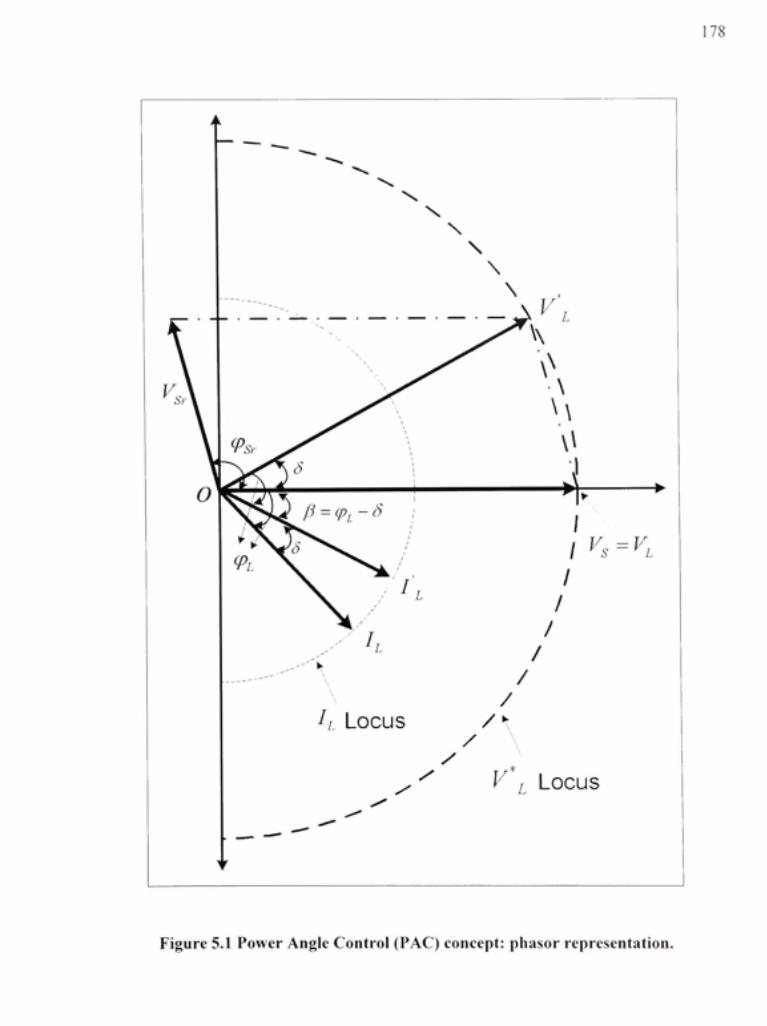
.78
= K
Figure 5.1 Power Angle Control (PAC) concept: phaso r representation .
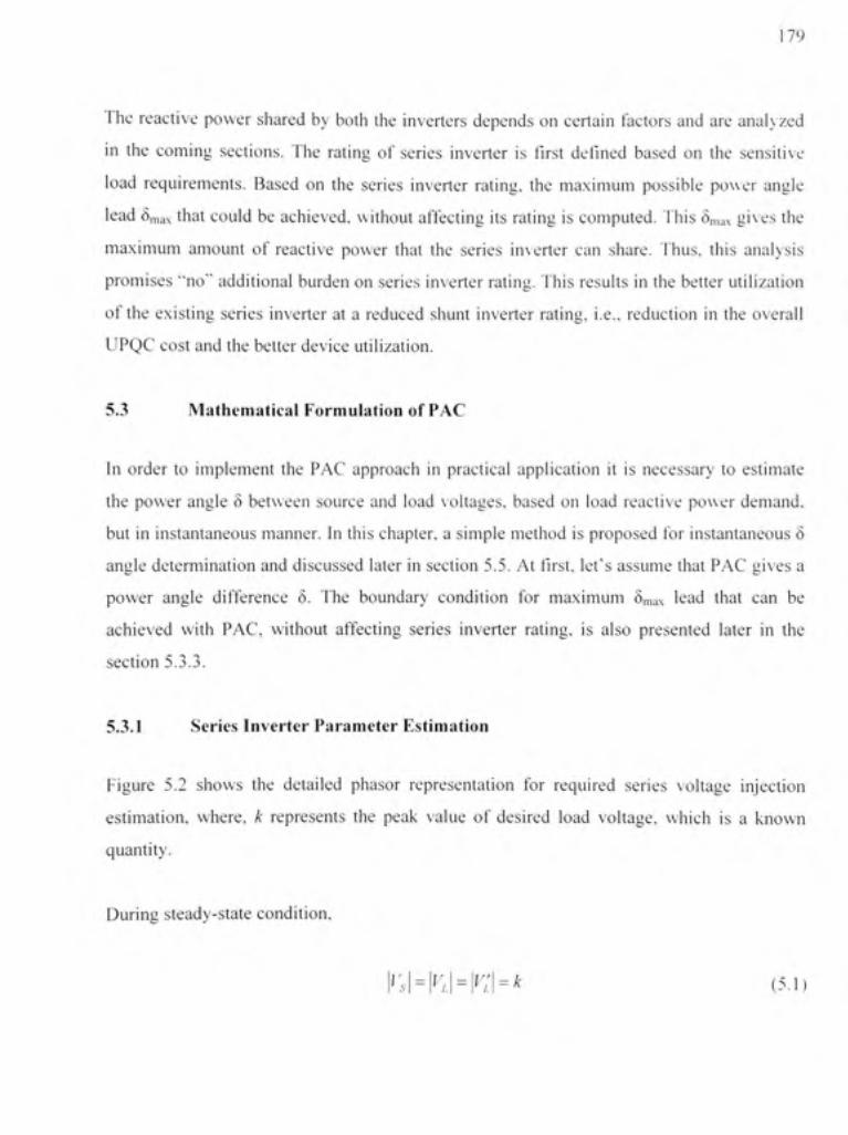
179
The reactiv e powe r share d b y bot h th e inverter s depend s o n certai n factor s an d ar e analyze d
in th e comin g sections . Th e ratin g o f serie s inverte r i s first define d base d o n th e sensitiv e
load requirements . Base d o n th e serie s inverte r rating , th e maximu m possibl e powe r angl e
lead 5ma, x that coul d b e achieved , withou t affectin g it s rating i s computed. Thi s 6niax gi\ t?^ the
maximum amoun t o f reactiv e powe r tha t th e serie s in \ erter ca n share . Thus , thi s analysi s
promises "no " additiona l burde n o n series inverte r rating . This result s i n the better utilizatio n
of th e existin g serie s inverte r a t a reduced shun t inverte r rating , i.e. , reductio n i n th e overal l
UPQC cos t and the better device utilization .
5.3 Mathematica l Formulatio n o f PAC
In orde r t o implemen t th e PA C approac h i n practica l applicatio n i t i s necessar y t o estimat e
the powe r angl e 5 between sourc e an d loa d voltages , base d o n loa d reactiv e powe r demand ,
but i n instantaneous manner . I n this chapter, a simple metho d i s proposed fo r instantaneou s 5
angle determinatio n an d discusse d late r i n section 5.5 . At first, let' s assum e tha t PA C give s a
power angl e differenc e 5 . Th e boundar y conditio n fo r maximu m 5nia, x lea d tha t ca n b e
achieved wit h PAC , withou t affectin g serie s inverte r rating , i s als o presente d late r i n th e
section 5.3.3 .
5.3.1 Serie s Inverter Paramete r Estimatio n
Figure 5. 2 show s th e detaile d phaso r representatio n fo r require d serie s voltag e injectio n
estimation, where , k represent s th e pea k valu e o f desire d loa d voltage , whic h i s a know n
quantity.
During steady-stat e condition ,
!';•! = K h K ' h^ (5.1 )
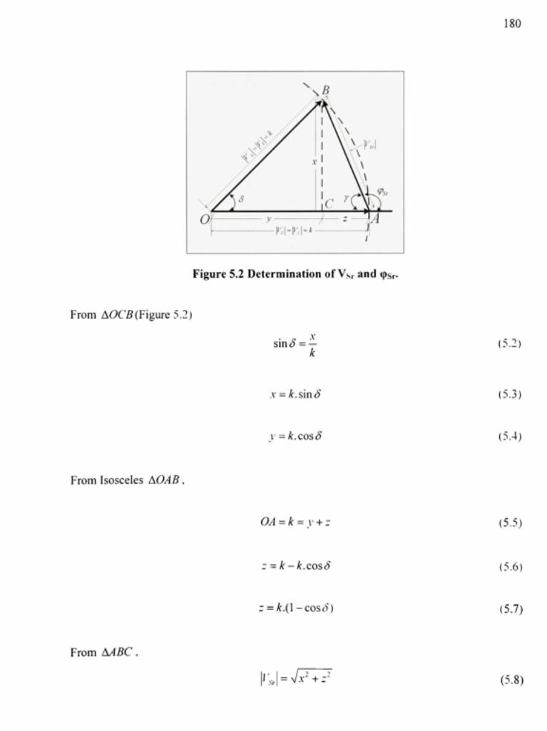
180
Figure 5.2 Determination o f Vsi an d (psr
From A(9C5(Figur e 5.2 )
sin(5 = — k
(5.2)
.Y = k.sinS 15.3)
V = k.cos5 (5.4)
From Isoscele s AOAB
OA = k=v + z (5.5)
= k - k.cosS 15.6)
: = k.{\ -cosS) (5.7)
From AABC
rJ=^/777 (5.8)
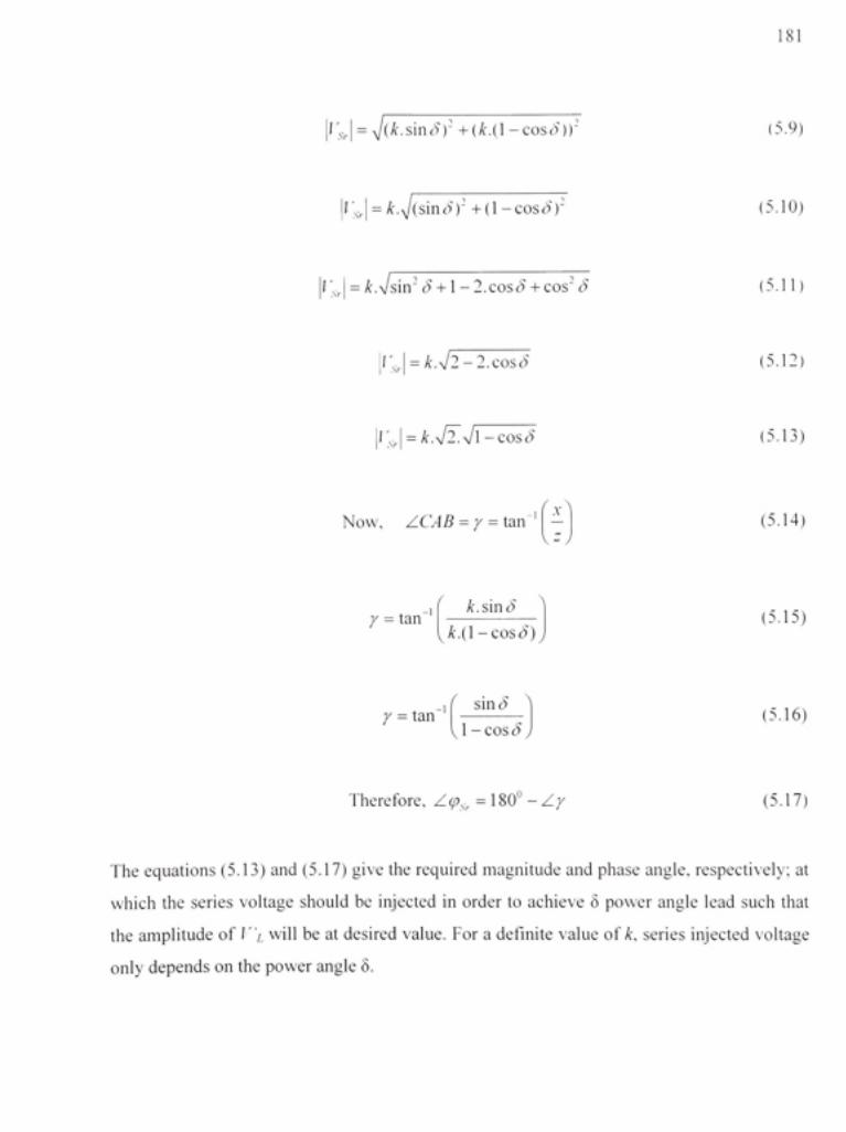
[(;,J = 7(^-sintV)-+(A:.(l-cosc>'))- (5.9)
|r .J = /:.^(sind')" +( 1 -cosS)' (5.10)
|l' I = k.Asin' S + \-2.cosS-^cos' 5 [5.11
ll ' . | = yt.V2-2.cosc5 (5.12)
Ir, l = yt.V2^Vl-coscJ (5.13)
Now, ZCAB = y = tan" ^v^
V - 7 (5.14)
y = tan" t' I • a \ ^.sind
^.(1 -cosS) (5.15)
y = tan" sin<5 - c o s ^
(5.16)
Therefore, Z^^ , =18 0 -Ay (5.17)
The equations (5.13 ) and (5.17 ) give the required magnitud e an d phas e angle , respectively; a t
which th e serie s voltag e shoul d b e injecte d i n orde r t o achiev e 6 power angl e lea d suc h tha t
the amplitude o f V'i will b e at desired value . For a definite valu e of k, series injected voltag e
only depends on the power angle 6.
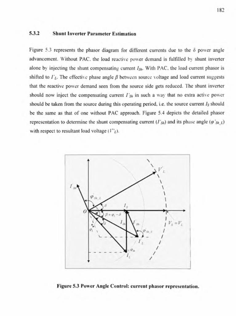
182
5.3.2 Shunt Inverter Parameter Estimation
Figure 5. 3 represent s th e phaso r diagra m fo r differen t current s du e t o th e 6 powe r angl e
advancement. Withou t PAC . the loa d reactiv e powe r deman d i s fulfille d b \ shun t inverte r
alone b \ injectin g th e shun t compensating curren t Isi,- Wit h PAC , the load curren t phaso r i s
shifted t o I'i. Th e effective phas e angle fl between sourc e voltag e and loa d curren t suggest s
that th e reactiv e powe r deman d see n fro m th e sourc e sid e get s reduced , fh e shun t inverte r
should no w injec t th e compensatin g curren t I'sh in suc h a wa y tha t n o extr a activ e powe r
should be taken from the source during this operating period, i.e . the source current Is should
be th e sam e a s tha t o f on e withou t PA C approach . Figur e 5. 4 depict s th e detaile d phaso r
representation to determine the shunt compensating curren t {I'sh) and its phase angle {(/> 'shi)
with respect to resultant load voltage (V'i).
Figure 5.3 Power Angle Control: current phasor representation.
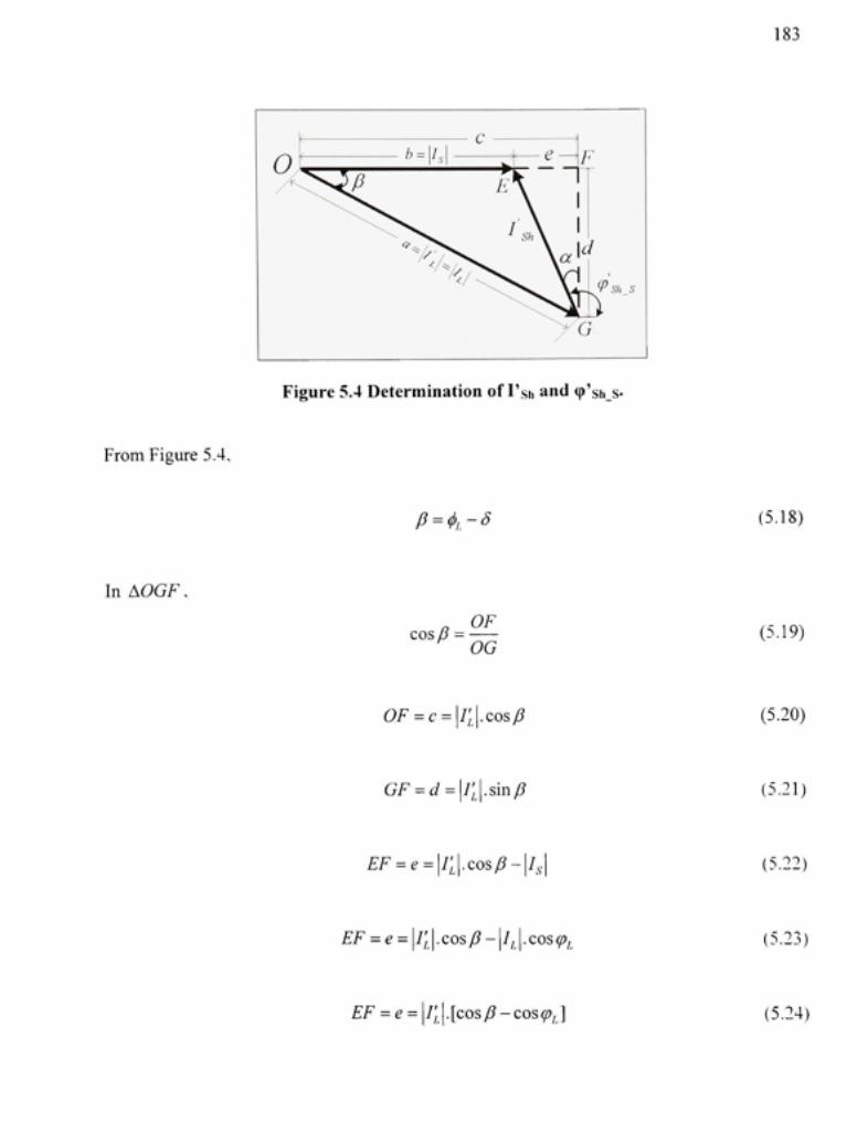
183
From Figure 5.4,
Figure 5.4 Determination of I'sh and (p'shs-
P = <l>,-5 (5.18)
In AOGF.
cos/? OF OG
(5.19)
OF = c^\l[\.cosP (5.20)
GF ^ d = \l[\.sinp (5.21)
EF = e = \l[\.cos p-\l ,\ (5.22)
EF -e = |/[|.cos/?-|//|.cos^; (5.23j
EF = e = |/[|.[cosy5-cos^^] (5.24)
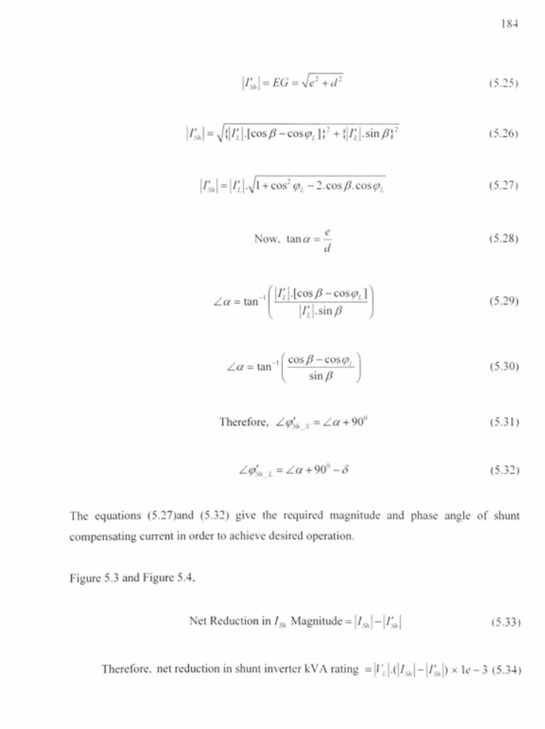
.84
l'J = EG = ^e- +d' ^ . . z •^ '
|/; I = 7{|/;|.[cos/?-cos^jj^ + {|/;|.sin/?}- (5.26)
|/'./,| = |/)|.>/l + COS" (Pi -2.cosp.cos(Pi (5.27)
Now, tan a = d
(5.28)
Aa = tan" '/j|.[cos/? -coscpi ]
|/;|.sin/? (5.29)
Aa = tan cos p -COS(Pi
siw P (5.30)
Therefore, Z^; , ^ = ^« + 90" (5.31)
Z<^; , = Z a + 90°-cJ (5.32)
The equation s (5.27)an d (5.32 ) giv e th e require d magnitud e an d phas e angl e o f shun t
compensating current in order to achieve desired operation.
Figure 5.3 and Figure 5.4,
Net Reduction in hi, Magnitude = |/.s7,|-k.sv Sh :5.33!
Therefore, ne t reduction in shunt inverter kVA rafing = jl' |-(|7.v/J~ K.svJ) x It? - 3 (5.34 )
185
Ir/J.]// |.(sin^/ - ^ 1 + COS" (p, -2.cosp.cos(Pi ) x k -3 (5.35 )
Therefore, Ne t Reductio n i n shunt inverte r kVA ratin g a s % of ful l loa d kVA rating .
= (sin^, - yj\ +COS' (p, -2.cosp.cos(p, ) x I c - l % (5.36 )
Equation (5.36 ) give s th e ne t reductio n i n kV A ratin g o f shun t inverte r a s percentag e o f th e
full loa d kV A ratin g wit h PA C scheme , withou t affectin g th e existin g serie s inverte r rating ,
discussed i n nex t subsection . Equation s (5.13) , (5.17) . (5.27) , an d (5.32 ) ar e performanc e
equations o f PA C approach . Th e effectivenes s o f thi s approac h i s completel y governe d b y
proper referenc e signa l generatio n base d o n thes e quantities , i n rea l tim e withou t dela y i n
computation. Fo r a particula r loa d condition , th e loa d parameter s li an d tpi ar e constant ;
hence, thes e equation s sho w tha t th e PA C approac h i s independen t o f othe r networ k
parameters. Thi s result s i n a highly robus t an d paramete r insensitiv e approac h t o compensat e
the loa d reactiv e powe r deman d b y utilizin g bot h th e shun t an d serie s inverter s
simultaneously.
5.3.3 Boundar y Conditio n fo r Maximum 6
The ratin g o f serie s par t o f UPQ C i s mainl y governe d b y percentag e o f sa g tha t nee d t o b e
compensated. I f the maximum voltag e tha t ca n b e injecte d throug h serie s inverte r i s denote d
by Vsr.max and th e percentag e o f thi s maximu m voltag e limi t i n term s o f desire d loa d voltag e
by factor K^r, then we can write ,
^Scric. Al'l- - ' ,V/-,ma x • "^ .S ' ( 5 . 3 7 )
From (5.13) , \v^\^k.^.^\-cosS^^^^ (5.38 )
186
K„..k = ^.V^Vl-cosd^ since, A\,, = (5.39)
A;,,, = VIVl-cosc), , (5.40)
^ . . = c o s " ' ( l K' (5.41
For a particula r applicatio n i n whic h UPQ C i s t o b e installed , th e serie s inverte r ratin g i s
known. Utilizing (5.41 ) we can calculate the maximum powe r angle 5,,,;, ^ that can be achieve d
without affectin g th e existin g serie s inverte r rating . Thus , 5ma \ limi t wil l guarante e th e
reactive powe r sharin g featur e withou t overloadin g th e serie s inverter , an d hence , n o extr a
series inverte r cos t addition .
5.4 Activ e an d Reactive Powe r (P-Q) Flo w
This sectio n give s th e pe r phas e activ e an d reactiv e powe r flow betwee n shun t an d serie s
inverters.
5.4.1 P- Q Flo w without PA C Approac h
For series inverter .
^sv = f'.sv^,s-COS^ , (5.42)
^,s. = ' 'v , -Asin^, , (5.43)
For shun t inverter .
^sv, = f/.-Av/rCOS^,./ , = k.h,.COS(p. Sh (5.44)
187
Qsh = f /,• hh-sin(Ps„ - k. /,,.sin(p,„ (5.45 )
The shun t inverte r supplie s al l the load reactive power demand b y injectin g 90 ° leading shun t
compensating curren t Isi,.
:. P „ = 0 (5.46 )
Qsh=yL-hh-l^-hh (5.47 )
5.4.2 P- Q Flo w with PAC Approac h
With PA C o f UPQC, bot h activ e a s well a s reactive powe r wil l flow throug h th e serie s
inverter and they are computed a s follow .
P,,. = (/,.A:.V2^Vl-cos).cos^,, (5.48 )
P,, =(Vl/ , . / t .Vl-cosd^) .cos(180"- / ) (5.49 )
P,,. = - (Vl /s . l .Vl -cos( )^) .cos/ (5.50 )
P,=-(VI/ , .^.Vr^^).^^^^^ (5.51 )
P,^^-h.k.{\-cos5) (5.52 )
The negativ e sig n i n (5.52) implie s tha t durin g powe r angl e contro l o f UPQC, th e serie s
inverter consume s certai n amoun t o f active power . Du e t o this activ e powe r th e D C lin k
voltage ca n b e increased . T o maintai n th e D C lin k voltag e a t the constan t level , th e shun t
188
inverter shoul d no w injec t th e compensating curren t i n such a way that the extra active powe r
should b e fed bac k t o the supply side , i.e . should circulate betwee n th e serie s and shun t activ e
inverters throug h th e D C link . Thus , i n a n idea l conditio n withou t an y losses , th e activ e
power consume d b y serie s inverte r shoul d b e equal t o the active powe r fe d bac k b \ th e shun t
inverter an d hence , th e sourc e curren t woul d b e a t a constan t level . I n actua l practic e ther e
can be a slight increas e i n the source curren t magnitud e du e to the losses associated wit h bot h
the inverters , DC link , coupling inductance s and serie s transformer .
^„. =(V2^/,..yt.Vl-cosc)).sin(180"-7 ) (5.53 )
Q^^ =[^.l^.k.yJ\-cosSysmy (5.54 )
Q,^=[42A,.k.4^^^^). ^ '" ^ ^ (5.55 ) ^ ' V2 .v l -cos d
Os,^h-k.sinS (5.56 )
From (5.56) , th e reactiv e powe r injecte d b y serie s inverte r mainl y depend s o n th e powe r
angle 5 . Higher the valu e o f 5, higher wil l b e the reactive powe r compensatio n tliroug h serie s
inverter, bu t a t th e sam e tim e highe r wil l b e th e magnitud e o f serie s injecte d voltag e b y
(5.13).
For shunt inverter ,
sv, = ' /.'•4-cos(^;,_, = k.r,,.cos(p',, , (5.57 )
Q'sh = 'L-4-s in^;, i = ^./;,.sin(^;, , (5.58 )
189
At all condition , O, = Q^,. + O'^,, (5.59 )
5.4.3 Percentag e o f Reactive Powe r Shared b y Two Inverter s
The reactiv e powe r supplie d b y the serie s inverte r a s % o f tota l loa d reactiv e powe r deman d
can be expressed as :
%n = .^xioo % (5.60 ) • Q,
\L\.k.s,m5 ,c /•^s ' " x]00» o (5.61 ) /M.A.sin<;i,
| /J,sinJ , ^ ,„ , xioo% (5.62 ) /M.sin^,
I / , I , c os (Z*, , s in ( J , c r-^s ' " ^ ' -xlOO^ o ( 5 . 6 3 )
/;l.sin(/>.
^^^.sinc5xlOO% (5.64 ) sin ,
Therefore, % g,,„„ = ^ ^ x i o o% (5.65 ) tan(Zi;
Similarly, th e reactiv e powe r supplie d b y shun t inverte r a s % > of tota l loa d reactiv e powe r
demand ca n be expressed as ;
" /oaw„=^^ l00% (5.66 )
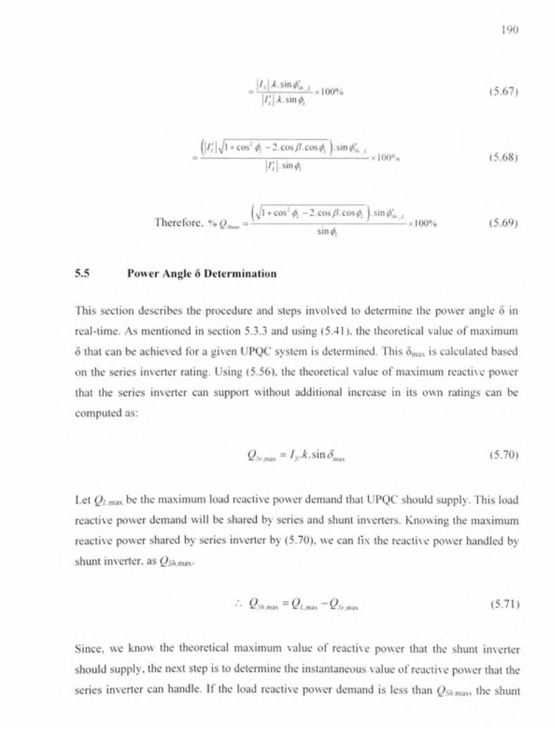
190
IM '^'^"^xlOO % (5.67 ) lI'Ak.smipi
i\/',\^\ + cos' (fii -2.cos/?,COS(z) , •sin(Zi;. ^ , ^ —i — — xioo° » (5.68 )
lI'A.sin^i
j] + COS' ipi -2,cos/?.cos(z!i ^ ,sin ,|., , , Therefore. % Q,,,,,,,, =^ A L^xioo % (5.69 )
sin (pi^
5.5 Powe r Angl e 8 Determinatio n
This sectio n describe s th e procedur e an d step s involve d t o determin e th e powe r angl e 5 i n
real-time. A s mentioned i n sectio n 5.3. 3 an d usin g (5.41) , th e theoretica l valu e o f maximu m
5 tha t ca n b e achieved fo r a given UPQ C syste m i s determined. Thi s 6ma\ is calculated base d
on th e serie s inverte r rating . Usin g (5.56) , the theoretica l valu e o f maximu m reactiv e powe r
that th e serie s inverte r ca n suppor t withou t additiona l increas e i n it s ow n rating s ca n b e
computed as :
as>,,n»-/ .-^-sin^_ (5.70 )
Let OimiLx b e the maximum loa d reactiv e power demand tha t UPQ C shoul d supply . This loa d
reactive powe r deman d wil l b e share d b y serie s an d shun t inverters . Knowin g th e maximu m
reactive powe r share d b y serie s inverte r b y (5.70) , we ca n fix th e reactiv e powe r handle d b y
shunt inverter , as Qsh.m^-
•• i;,SVi,ma x " " i:/..ma x ~ tr.S>,ma x ( 5 . 7 1 )
Since, w e kno w th e theoretica l maximu m valu e o f reactiv e powe r tha t th e shun t inverte r
should supply , the next ste p is to determine the instantaneou s valu e o f reactive powe r that th e
series inverte r ca n handle . I f th e loa d reactiv e powe r deman d i s les s tha n Os/Mnax . the shun t
19]
inverter shoul d compensat e thi s reactive powe r alone . In such cases the series inverte r shoul d
not tak e par t i n reactive powe r compensation . A t a given time , i f the loa d reactiv e powe r
demand increase s above Qsh.max limit , the series inverter shoul d no w take part in load reactiv e
power compensation .
Qs,.=Q,-0„„,,^=ls.k.smS (5.72 )
In th e abov e equation , s/,,ma x is a constant valu e as fixed by (5.71).The instantaneou s valu e
of ^z . can b e computed (discusse d late r i n the sectio n 5.6.1) . and thus the instantaneou s valu e
of Qsr can be known.
Therefore, fro m (5.72) , sinS = ^^^ (5.73 ) 7,.^
sin(5 = % (5.74 )
Since, th e shun t inverte r support s th e loa d reactiv e powe r demand ; th e sourc e supplie s onl y
the activ e par t of load powe r demand . Thus , the apparen t powe r in (5.74) ca n b e replace d by
the active power supplie d b y the source {Ps).
5 = sin Qs, KPSJ
= sin"' Qs^ KPLJ
(5.75)
The sourc e shoul d suppl y onl y th e load activ e powe r deman d a s the load reactiv e powe r
demand wil l b e shared b y both th e inverters . Interestingly , th e 5 determination i s based on
two importan t parameters , th e actual (instantaneous ) loa d reactiv e powe r deman d an d th e
actual (instantaneous ) load/sourc e fundamenta l activ e power . Thus , fro m equatio n (5.72 ) to
(5.75), if we could extrac t th e load active a s well a s reactive powe r demand s instantaneously ,
5 ca n be estimated accordingl y i n instantaneous manner . Figur e 5. 5 gives th e flow char t for
the above discussed step s to determine the 6 in actual practical systems .
192
Determine the Maximum Series Injection Voltage Limit based on UPQC Rating
V Compute 5^
V Compute the Maximum Reactive Power {Q^ ^) tha t can be supported using
Series Inverter
1 Compute the Maximum Shunt Inverter Reactive Power and Fix as &j»! .
>
^
Calculate the load active \p.Jca)\ an d reactive pov^rs [q^iat]], instantaneously, using p-q theory concept
T
An (r,->t\ s •\ N o
n 9 w
Yes' T
Calculate Reactive Power for Series Inverter q^iM) = q.J.M) - 2^,^^
> r r,nmpiitp ln<;tantanpriii«Pnwpr Angl p iKing 5 - : i n ' ' ^ * '• '
{ PSM) j
-A
) In
itial
izat
ion
ik
d = 0'
Figure 5.5 Flow chart of steps involved in determination o f 8 in actual practica l applications.
193
5.6 UPQ C Controller Developmen t base d o n PA C
This sectio n describe s th e generatio n o f th e referenc e signal s fo r bot h serie s an d shun t
inverters o f UPQC.
5.6.1 Instantaneou s S Determinatio n
The loa d on a particular plan t where UPQ C i s to be installed ma y not be constant al l the time.
The loa d reactiv e powe r demand , therefore , ca n var y base d o n th e plan t loads . A s discusse d
in th e previou s section , whe n th e loa d reactiv e powe r deman d i s wel l withi n th e shun t
inverter compensatio n limits , th e serie s inverte r shoul d not ac t (i.e . 6=0°) . Now , i f th e plan t
load change s suc h tha t th e loa d reactiv e powe r deman d exceed s th e shun t inverte r maximu m
limit, th e serie s inverte r shoul d ac t immediatel y t o tak e ove r th e additiona l loa d reactiv e
power demand . Therefore , th e performanc e o f power angl e contro l approac h solel y depend s
on th e extractio n o f powe r angl e 5 i n real-time . I n thi s section , th e instantaneou s 6
detennination i s propose d b y extractin g instantaneou s loa d activ e a s wel l a s instantaneou s
load reactiv e powe r demand . Th e single-phas e p-q theor y (Li u et al. 1999 ; Haque , 2002 )
based concep t i s used to achieve the aforementioned task .
The concep t o f single-phas e p-q theor y i s alread y discusse d i n chapte r 4 . Som e o f th e
important equation s ar e re-emphasize d here . Thi s chapte r assume s a balance d three-phas e
system. Fo r a balance d three-phas e system , th e knowledg e o f on e phas e activ e an d reactiv e
power i s sufficient fo r the determination o f required quantitie s to realize the PAC approach .
Phase-fl loa d voltage representation i n a - p co-ordinates b y 7r/2 lead.
^'ia.a
^La.p
A.ai(Ot)
Vi^{COl + 7tl2)
V,^sin{col)
h.n, COS{0Jt) (5.76)
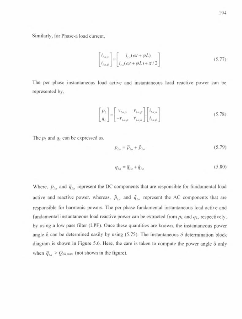
194
Similarly, fo r Phase- a loa d current .
'l.a.a
La.p
iiJojt + tpL) i,^((ot ^-(pL) + n 12
(5.77)
The pe r phas e instantaneou s loa d activ e an d instantaneou s loa d reactiv e powe r ca n b e
represented by .
Pl
'll
lM,a 'La.p
'^'l.a.p ^'l.d.a
La.a
La.p
(5.78)
The Pi an d qi ca n be expressed as .
Pia = Pia + Pia (5.79)
'lia = ^I.a + '1 IAJ (5.80)
Where, Jy,^ and q,^ represen t th e D C component s tha t ar e responsibl e fo r fundamenta l loa d
active an d reactiv e power , whereas , p^^ an d ^ ^ represen t th e A C component s tha t ar e
responsible fo r harmoni c powers . Th e pe r phas e fundamenta l instantaneou s loa d acti v e an d
fundamental instantaneou s loa d reactiv e powe r can b e extracted fro m pi an d qi. respectively ,
by usin g a lo w pas s filter (LPF) . Onc e thes e quantitie s ar e known , th e instantaneou s powe r
angle 6 ca n b e determine d easil y b y usin g (5.75) . Th e instantaneou s S determinatio n bloc k
diagram i s show n i n Figur e 5.6 . Here , th e car e i s take n t o comput e th e powe r angl e 8 onl y
when qi^ > Qsh.max (no t shown i n the figure).
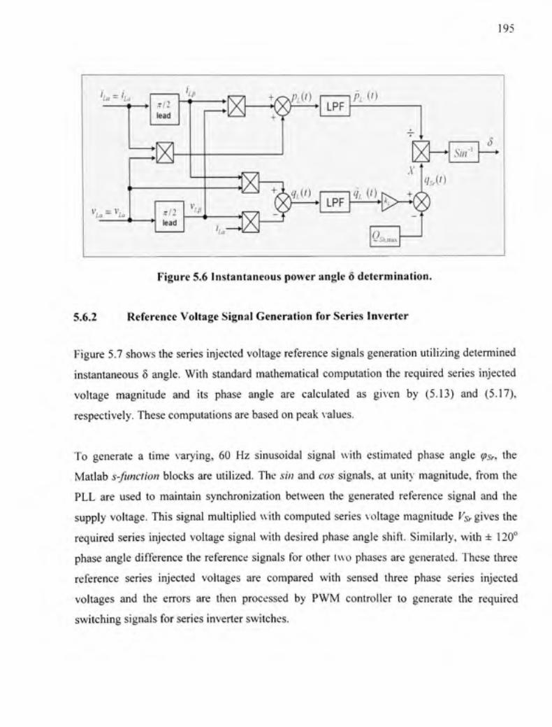
195
'LU = ka * • 7rl2
lead
V, - V, La Lu
:m « •
T / 2 lead
'LU
+/O^A.(') : ^ ^ LPF
PL C )
& - .S7/)"
&T J
s^,(')
'La H LPF
qtii) 9.J0
i/i7i.ma.\
Figure 5.6 Instantaneous power angle 6 determination.
5.6.2 Referenc e Voltage Signal Generation for Series Inverter
Figure 5.7 shows the series injected voltag e reference signal s generafion utilizin g determined
instantaneous 5 angle. With standar d mathematica l computatio n th e require d serie s injecte d
voltage magnitud e an d it s phas e angl e ar e calculate d a s give n b y (5.13 ) an d (5.17) ,
respectively. These computations are based on peak values.
To generat e a tim e varying , 6 0 H z sinusoida l signa l wit h estimate d phas e angl e tpsr, th e
Matlab s-funclion blocks are utilized. Th e sin and cos signals, at unitv- magnitude, from th e
PLL ar e use d t o maintai n synchronizatio n betwee n th e generate d referenc e signa l an d th e
supply voltage . This signal multiplied wit h computed serie s v oltage magnitude Vsr gives the
required serie s injected voltag e signa l with desired phase angle shift . Similarly , with ± 120 °
phase angle difference th e reference signal s fo r othe r two phases are generated . Thes e three
reference serie s injecte d voltage s ar e compare d wit h sense d thre e phas e serie s injecte d
voltages an d th e error s ar e the n processe d b y PW M controlle r t o generat e th e require d
switching signals for series inverter switches.
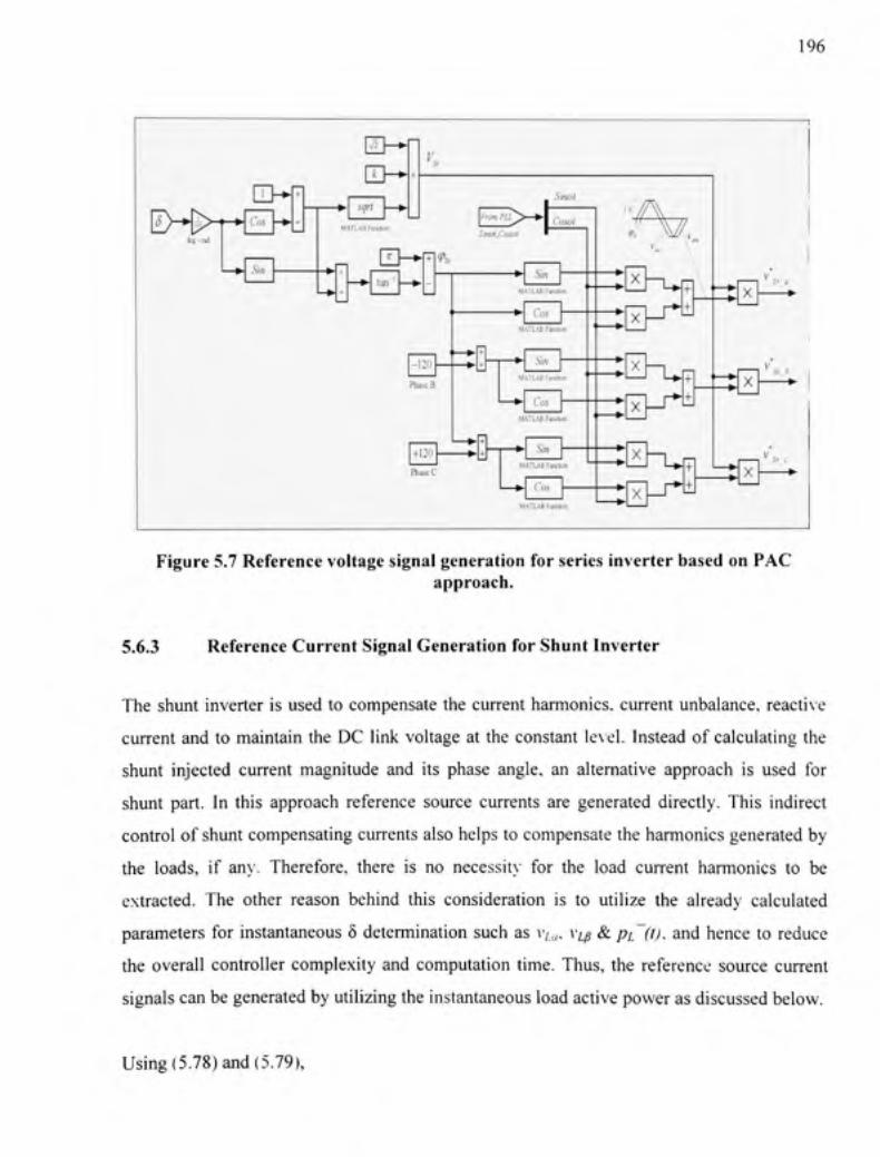
GIW
^ Sill
sqrl
M.^^LABFlu^t),>n
^ Q SllWl,C0SC)! \C>1 •
SifUiH
CosdH
Sm
( (/ ( M.\TLAB FuntfiL T
* Sm ^urLAlillI^,cIlf^
Cos
+I2n * PhdscC
Sm MATIAB Fuicljor .
M.ATUb ruTiiOo r
"A
X
X
X
X
X
X
V,.
196
Figure 5.7 Reference voltage signal generation for series inverter based on PAC approach.
5.6.3 Reference Current Signal Generation for Shunt Inverter
The shun t inverte r i s used to compensate the current harmonics , current unbalance , reactiv e
current an d to maintain th e DC link voltage at the constan t le v el. Instea d o f calculating th e
shunt injecte d curren t magnitud e an d it s phase angle , an alternative approac h i s used for
shunt part . In this approac h referenc e sourc e current s ar e generate d directly . Thi s indirec t
control of shunt compensating currents also helps to compensate the harmonics generated by
the loads , i f any . Therefore , ther e i s no necessity fo r the load curren t harmonic s t o b e
extracted. Th e othe r reaso n behin d thi s consideratio n i s to utilize th e already calculate d
parameters fo r instantaneou s 5 determination suc h a s Vi^. Vip & pi~(l). an d henc e to reduc e
the overal l controlle r complexit y an d computatio n time . Thus , the referenc e sourc e curren t
signals can be generated by utilizing the instantaneous load active power as discussed below.
Using (5.78) and (5.79),
197
La.a
La.p
' La.a ' IAI.P
'^'l.a.P '^'l.a.a
PL
0 (5.81
''La(rol)^^.v,,{cot).[p,{cot)] .4.x
:5.82)
Where, A v = v-, _„ + v,^^^ (5.83)
Equation (5.82 ) give s th e loa d curren t correspondin g t o th e fundamenta l loa d activ e power .
As discussed, PA C approac h give s a power angl e 6 boost betwee n resultan t loa d voltag e an d
source voltage , maintainin g th e sam e voltag e magnitudes . Th e loa d phas e angl e betwee n
yi.abc & 'L.abc and V 'iabc & ' 'i.abc is constant , but . th e phas e angl e betwee n th e resultan t loa d
current i'i,ahc ^y I'.t. source voltag e i s no w booste d t o ft (Figur e 5.1) . Therefore , i n orde r t o
supply onl y require d fundamenta l loa d activ e power , th e activ e powe r deman d see n fro m th e
source sid e shoul d b e equa l t o th e powe r give n i n (5.82 ) plu s losse s associate d wit h UPQ C
(AJ-
The ter m Ax, i n steady-stat e condition , give s a constan t D C value . Now , i f w e replac e th e
load voltage signal s i n (5.82) with actua l sourc e voltage signals , since , both th e voltages hav e
the sam e magnitude , the referenc e signal s fo r sourc e current s ca n b e determine d easily . Thi s
is don e t o maintai n th e synchronis m betwee n th e referenc e sourc e curren t an d th e actua l
voltage to achieve unit y power facto r operation .
Therefore, i's,{(ot) = ""/'"^ . [p,{cot) + Pj^ol)] Ax
(5.84)
i ,Jcoi)^ .4x
[p,{coi)-^p^,^(cot)] (5.85)

198
I ^^(a)l)^^^^\-^.\p,{o)t)^p,Scot)\ Ax
(5.86)
The abov e equation s giv e th e referenc e sourc e curren t signal s tha t woul d suppl y onl y
fundamental loa d active power demand and losses associated with UPQC. The block diagram
for referenc e sourc e current signal s generation i s shown i n Figure 5.8 . For unbalanced load ,
each phas e shoul d b e tackled separatel y an d th e curren t unbalanc e compensatio n approac h
proposed in CHAPTER 4 can be utilized. The overall block diagram of power angle contol of
UPQC is shown in Figure 5.9.
Figure 5.8 Reference current signal generation based on PAC approach.
i,A'^')
vAcot)
instantaneous Fundamental
Load Active an d Reactive Powe r
Estimation
PliOJt)
qi(O)t)
Instantaneous Power Angl e 5 Determination
Using Equatio n (5.75)
Reference Voltage Signa l Generation tor Senes Inverte r
Using (5 13 ) and (5 17)
QSI
AsrJO^n
v.sr.A(on V .Sr.A('J')
Rated Load Vollage (k)
TT From PLL
DC Link Voltage Controller and
Reference Source Cun-ent
Generation Using (5 84) to
(586)
AsaA^l)
i sAf")
i ,AoJt)
Figure 5.9 Overall control block diagram of proposed PAC approach.

199
5.7 Simulatio n Result s
The reactiv e powe r sharin g featur e o f bot h th e inverter s o f UPQ C ha s bee n evaluate d b y
digital simulation . The load i s assumed t o be highly inducti v e to hav e a better visualizatio n o f
the results . The supply voltage which i s available a t the UPQC termina l i s considered a s three
phase, 6 0 Hz , 60 0 V (lin e t o line ) wit h th e maximu m loa d powe r deman d o f 1 5 kW + j 1 5
kVAR (loa d powe r facto r angl e of 0.707 lagging) . The maximum voltag e that ca n be injecte d
by th e serie s inverte r i s assume d t o b e 4 0 % o f th e rate d inpu t voltag e (^5^=0.4) . Thi s give s
the 5ma.\= 23.07^' by (5.41) . Wit h the give n maximum loa d active power deman d (1 5 kW, L =
20.5A rms ) an d b y (5.70) , th e maximu m reactiv e powe r tha t th e serie s inverte r ca n inject ,
without affectin g it' s ratin g i s approximatel y 1.9 6 kVAR s pe r phas e o r 5. 8 kVAR s o f tota l
load kVARs . Here , th e maximu m kVA R tha t th e serie s inverte r shoul d compensat e i s
considered a s 5. 7 kVAR . thus , usin g (5.71) , th e maximu m kVA R compensatio n limi t fo r
shunt inverte r i s fixed a s 9. 3 kVAR s o f tota l loa d kVA R demand . I n th e followin g section s
the simulatio n result s fo r loa d reactiv e powe r compensatio n usin g basic UPQ C operatio n an d
proposed PA C approach ar e discussed .
5.7.1 Loa d Reactiv e Powe r Compensatio n withou t PA C Approac h
Figure 5.1 0 (a ) - (h ) show s th e simulatio n result s durin g norma l workin g conditio n withou t
PAC approach . A t the onset , onl y a pure resistiv e loa d (1 5 kW) i s considered o n the system .
At tim e 11=0. 1 sec , th e shun t inverte r i s put int o th e operation . Th e D C lin k feedbac k
controller act s immediatel y forcin g D C lin k voltag e t o settl e dow n a t se t referenc e voltage ,
here 72 5 V b y takin g th e fundamenta l curren t fro m th e source . Withi n a cycl e th e D C lin k
voltage i s maintaine d a t th e constan t level , a s show n i n th e Figur e 5.1 0 (d) . A t tim e t2=0. 2
sec, the serie s inverte r i s put int o operatio n suc h tha t bot h serie s an d shun t inverter s ar e no w
operating togethe r a s UPQC.
During thi s tim e interva l sinc e ther e i s n o reactiv e loa d o n th e network , th e shun t inverte r
does not injec t an y compensatin g current . A t time t3=0.3 sec , the maximum plan t loa d i.e . 1 5
kW + j l5 kVA R i s switched ON . The shun t inverte r no w inject s a 90° leading compensatin g
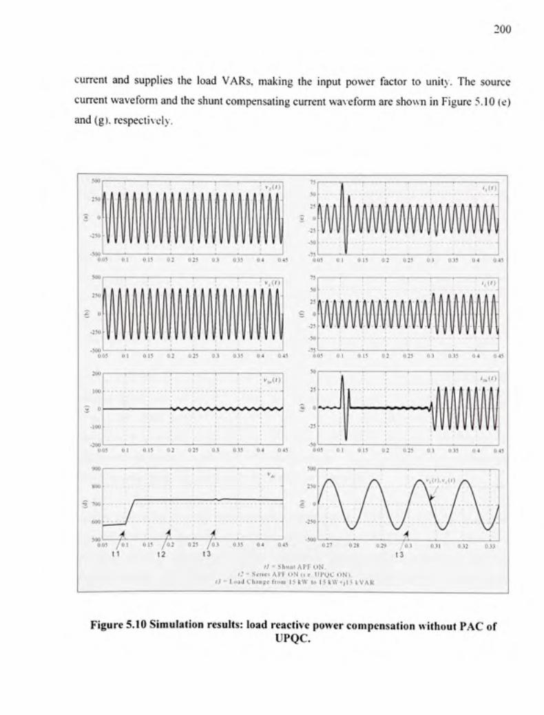
200
current an d supplie s th e loa d VARs , makin g th e inpu t powe r facto r t o unitv . Th e sourc e
current waveform an d the shunt compensating current waveform ar e shown in Figure 5.10 (e)
and (g), respectively.
v,(()
.250 •
-500 0 05 0 1 0 1 5 0. 2 0 25 0. 3 0 35 0 4 0 45 0 05 0 1 0.1 5 0 2 0 25 0 3 0 35 0 4 04 5
500 I , , , , , , , , 7 5
50 250
25
• 25
-50
-75 0.05 0 1 01 5 0. 2 02 5 0. 3 03 5 0 4 0 45 0 05 0 1 01 5 0 2 0 25 0 3 0 35 0 4 0.4 5
50
; ; ; : ; ; : 'lO
; ; i V V V v H v v l
"T" v, . , ( r )
25 -
0 05 0 1 0 1 5 0 2 0 25 0 3 0 35 0 4 0 45 0 05 0 1 0 1 5 0 2 0 25 0 3 0.3 5 0 4 0 45
900
800
500
: ; ; i : ; ; ''^^ 1 1 1 t 1 1 1 . —, , , — , — - , — , — ^
J...... -:^ ....... : tl
/ 0 2 0 25 /0 . 3 0.3 5 0 4 0,4 5
t2 t 3 0 27 0 28 0.2 9 / 0 3 0.3 1 0.3 2 0.3 3
t3 ll = blhmi t A P F (-IN .
/ : = S e r i e s A t ' F O N l i e I I F y C O N I . /,; - I . .a d C h . i n g c trn.i i I J k W t n I J k W + j l . i k V A R
Figure 5.10 Simulation results: load reactive power compensation without PAC of UPQC.
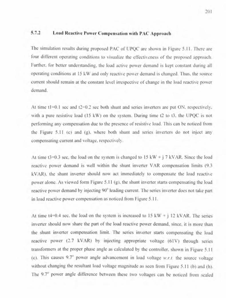
201
5.7.2 Loa d Reactiv e Powe r Compensation wit h PA C Approac h
The simulatio n result s durin g propose d PA C o f UPQ C ar e show n i n Figur e 5.11 . Ther e ar e
four differen t operatin g condition s t o visualiz e th e effectivenes s o f th e propose d approach .
Further, fo r bette r understanding , th e loa d activ e powe r deman d i s kep t constan t durin g al l
operating condition s a t 1 5 kW an d onl y reactiv e power deman d i s changed. Thus , the sourc e
current shoul d remai n a t th e constan t leve l irrespectiv e o f chang e i n th e loa d reactiv e powe r
demand.
At tim e 11=0. 1 se c an d t2=0. 2 se c bot h shun t an d serie s inverter s ar e pu t ON , respectively ,
with a pur e resistiv e loa d (1 5 kW ) o n th e system . Durin g tim e t 2 t o t3 , th e UPQ C i s no t
performing an y compensatio n du e to the presenc e o f resistiv e load . Thi s can b e noticed fro m
the Figur e 5.1 1 (c ) an d (g) , wher e bot h shun t an d serie s inverter s d o no t injec t an y
compensating curren t and voltage , respectively .
At tim e t3=0. 3 sec , the loa d o n th e syste m i s changed t o 1 5 kW + j 7 kVAR. Sinc e th e loa d
reactive powe r deman d i s wel l withi n th e shun t inverte r VA R compensatio n limit s (9. 3
kVAR), th e shun t inverte r shoul d no w ac t immediatel y t o compensat e th e loa d reactiv e
power alone . As viewed for m Figur e 5.11 (g) , the shun t inverte r start s compensating th e loa d
reactive powe r demand b y injecting 90 ° leading current . The serie s inverter does not take par t
in load reactive power compensation a s noticed fro m Figur e 5.11 .
At tim e t4=0. 4 sec , the loa d o n th e syste m i s increase d t o 1 5 kW + j 1 2 kVAR . Th e serie s
inverter shoul d no w shar e th e par t o f the loa d reactiv e powe r demand , since , i t i s more tha n
the shun t inverte r compensatio n limit . Th e serie s inverte r start s compensatin g th e loa d
reactive powe r (2. 7 kVAR ) b y injectin g appropriat e voltag e (61V ) throug h serie s
transformers a t th e prope r phas e angl e a s calculate d b y th e controller , show n i n Figur e 5.1 1
(c). Thi s cause s 9.7 ° powe r angl e advancemen t i n loa d vohag e w.r.t. th e sourc e voltag e
without changin g th e resultan t loa d voltag e magnitud e a s see n fro m Figur e 5.1 1 (b ) an d (h) .
The 9.7 ^ powe r angl e differenc e betwee n thes e tw o voltage s ca n b e notice d fro m scale d

202
Figure 5.11 (h). During this condifion the shunt inverter compensates the load reactive power
up to it s maximum limit . Thus, both the shun t (9.3 kVAR) and serie s (2.7 kVAR) inverter s
share the load reactive power demand effectively .
500
250
-250
-500 il 11 1 • i
800
750
S 7 0 0
650
600 i—
f 12
0.3
t3
0.4 i 14
0.5 i 15
v,(0
06
02
500
250
S ° -250
-500
A A w " -C ) /ns. ;
\JJ \ \J/ 0 48 0 49 0 5 0 51 0 52 0 53 0 54 0 55
t5
t2 = Serie s AP F O N ( i e . UPQ C ON) . t3 = Load Chang e fro m 15k W t o 1. ^ kW+| 7 kVAR ,
t-l = Load Chang e fro m 1 .^ kW + |7 kVA R t o 1 5 k W + j l2 kVAR . l5 = Load Chang e fro m 1 5 k W + j l2 kVA R t o 1 5 kW+J1 5 kVA R
Figure 5.11 Simulation Results: load reactive power compensation with PAC of UPQC.

203
At time t5=0.5 sec , the syste m i s loaded u p to it s maximum rate d conditio n i.e . 1 5 kW + j 1 5
kVAR. Durin g thi s condition , th e serie s inverte r inject s require d voltag e (MOV ) t o
compensate th e increase d loa d reactiv e powe r demand . Thi s causes furthe r increas e i n powe r
angle 5 fro m 9.7 " t o 21. 5 ° between bot h th e sourc e an d loa d voltages , a s discusse d i n th e
theory whic h ca n b e notice d fro m th e Figur e 5.1 1 (h) . Here , th e shun t AP F compensate s 9. 3
kVAR, whil e serie s inverte r compensate s 5. 7 kVA R o f the total loa d reactiv e power demand .
The sourc e current , a s shown i n Figure 5.1 1 (e) , is strictly a t the constant valu e during al l the
above conditions . The loa d curren t profil e unde r differen t loa d condition s i s shown i n Figur e
5.11 (f) . Thus , fro m Figur e 5.1 1 (e ) an d (f) , th e sourc e deliver s onl y th e loa d activ e powe r
demand, i.e . in other words , the PAC approach does not put any extra active power burden o n
the source . The DC link voltage profile i s shown i n Figure 5.11 (d).
Figure 5.1 2 (a ) - (d ) show s compute d differen t activ e an d reactiv e power s unde r th e abov e
mentioned loa d conditions . Al l thes e value s ar e base d o n pe r phas e calculation . Th e powe r
handled b y serie s inverter , til l tim e t 4 i s almos t zero . Thi s i s du e t o th e fac t tha t th e loa d
reactive powe r deman d i s supporte d b y th e shun t inverte r alone . A t tim e t 4 an d t5 , the loa d
reactive powe r demand s ar e change d suc h tha t th e serie s inverte r als o take s par t i n th e loa d
reactive powe r compensation . A s notice d fro m th e Figur e 5.1 2 (b) , the sourc e supplie s onl y
active powe r t o th e load , whereas , th e reactiv e powe r i s share d b y bot h shun t an d serie s
inverters. Moreover , th e activ e powe r handle d b y serie s inverte r i s complemente d b y th e
shunt inverter , suc h that no additional activ e power burden i s put on the source fo r realizatio n
of proposed PA C approach .
The differen t parameter s durin g abov e mentione d condition s ar e show n i n Tabl e 5. 1 an d
Table 5.2 . All the current an d the voltage values are mentioned o n the per phase basi s and ar e
represented a s pea k amplitude . As noticed fro m Tabl e 5. 1 an d Figur e 5.10 , with the ful l loa d
on th e network , withou t considerin g PA C contro l approach , th e require d shun t inverte r
compensafing curren t i n order to compensate the load reactive power demand i s 29A.
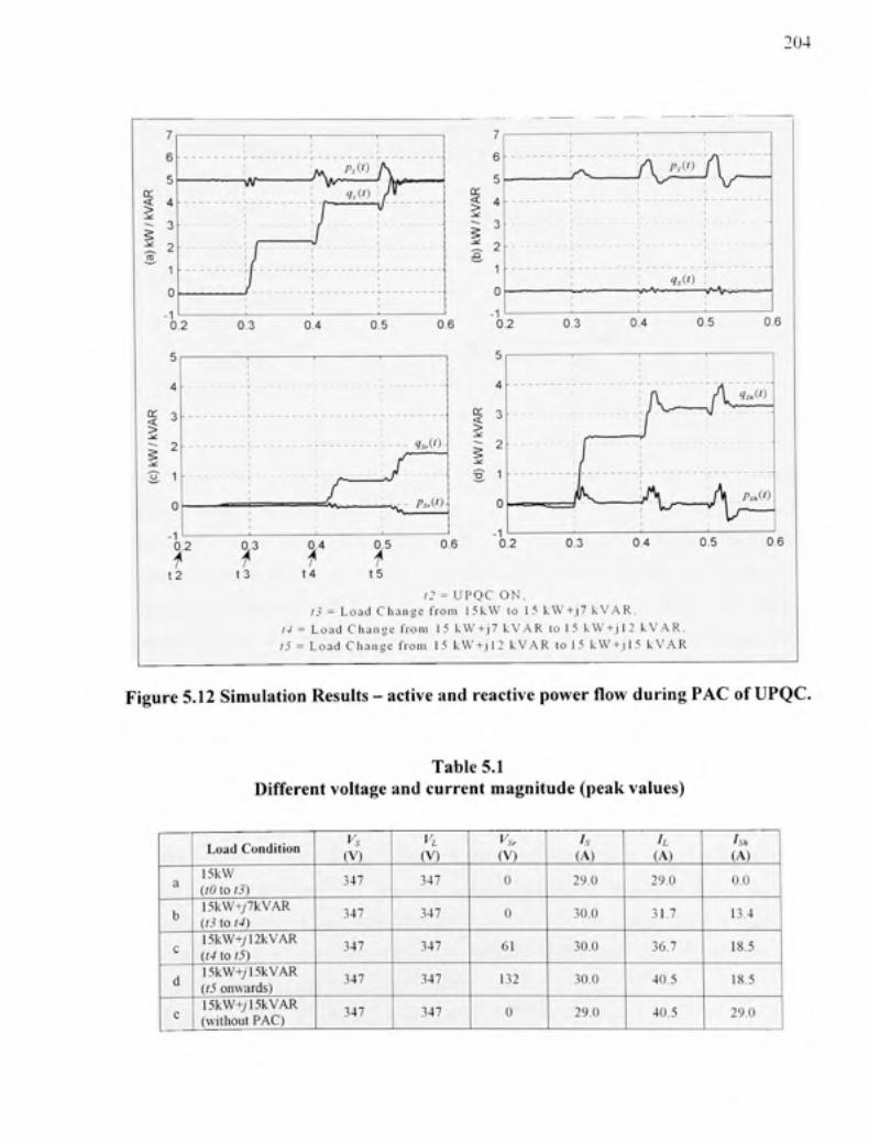
0.2
i 3
2
1
0
-1 0.2
t 2
W^ < >
0.3 0, 4 0. 5 0 6 0.2
HsS')
r i/-""v.
PsM)^
a. < > 2
t 3 r
14
0.5
15
0.6 0.2
/'^^
0 3
0,3
UJ4
yVi2JX.
v^A * * 9.(0
•rf -V^ —
0.4 0.5 0.6
...iiV—
r 1 . I — r ^ - - /S ,
U.r
A ,A0 J
A p -c )
0.4 0.5 0 6
t2 = UPQ C ON . / i = Loa d Chang e fro m 15k W t o 1 5 kW+j 7 kV.-VR ,
14 = Load Chang e fro m 1 5 k\V-i-j 7 kVA R l o 1 5 kV V + jl2 kV.-VR , t5 = Loa d Chang e fro m 1 5 kV V + |12 kVA R t o 1 5 k W + i l5 kVA R
Figure 5.12 Simulation Result s - activ e and reactive power flow durin g PAC of UPQC.
Table 5.1 Different voltag e and curren t magnitud e (peak values)
a
b
c
d
c
Load Conditio n
15kW (to to t3) 15kW+/7kVAR (tS to t4) 15kW+/12kVAR (t4 to t5) 15kW+71.5k VAR (t5 onwards ) 15kW+/15kVAR (without PAC )
i''s (V)
347
347
347
347
347
(V)
347
347
347
347
347
(V)
0
0
61
132
0
Is (A)
29.0
30.0
30,0
30,0
29,0
II (A)
29,0
31,7
36,7
40.5
40.5
Is,, (A)
0.0
13.4
18,5
18,5
29,0
105
Table 5. 2 Phase angl e relationshi p betwee n voltage s an d current s
a
b
c
d
e
Load Condition
l.SkW (to to l.>) 15kVV+/7kVAR (t3 to t4) 15kW+/12kVAR (t4 to i5) 15kW+/15kVAR ((.i onwards) 15kVV+/15kVAR (without PAC)
(PL (dcg.)
o"
-24.6"
-38.3"
-44.7"
-45 ()"
(Ps (dcg.)
0"
()"
0'
0'-*
o"
5 (dcg.)
0"
()"
9.7"
21 -S "
0"
P (dcg.)
1)"
-24.6"
28.6"
23.2"
{)"
'i^Sr
(dcg.)
0"
n"
+95"
-^10l"
0"
(Ps„_s (dcg.)
-
- 90 4
-1(1(1,8
+ 117 5
+V(I4
(Ps'h_L (dcg.)
-
+904
+91.1
+96
+90.4
From Tabl e 5. 1 (d ) an d Figur e 5.1 1 (g) . the propose d PA C approac h result s i n considerabl e
reduction i n shun t inverte r curren t magnitud e fro m 29 A t o 18.5A . Thus , wit h th e propose d
approach th e shun t inverte r curren t ca n b e reduce d b y 10.5A . I n othe r words , wit h th e PA C
approach th e shun t inverte r kV A ratin g ge t reduce d t o 25.6 % o f tota l loa d kV A rating . Th e
source current magnitud e i s almost constan t an d a t unity power facto r durin g al l the operatin g
conditions, since , th e activ e powe r deman d o n th e loa d i s kep t constan t unde r thos e
conditions. Thi s confirm s tha t th e PA C o f UPQ C doe s not deman d additiona l activ e powe r
from th e sourc e fo r it s operation , an d thus , i s prove n t o b e advantageou s i n almos t al l th e
UPQC base d applicafions .
5.8 Experimental Validatio n o f Proposed Phas e Angle Contro l Approac h
The performanc e o f propose d PA C theor y i s als o validate d throug h extensi v e experimenta l
investigation. Th e proposed PA C approach i s equally applicabl e fo r single-phas e system . Fo r
simplicity, th e experimenta l investigatio n i s carrie d out fo r single-phas e system . Th e
hardware setu p i s the sam e as discussed i n Appendix-1. Additionally, a highly inductiv e loa d
is considered fo r bette r visualization o f results.
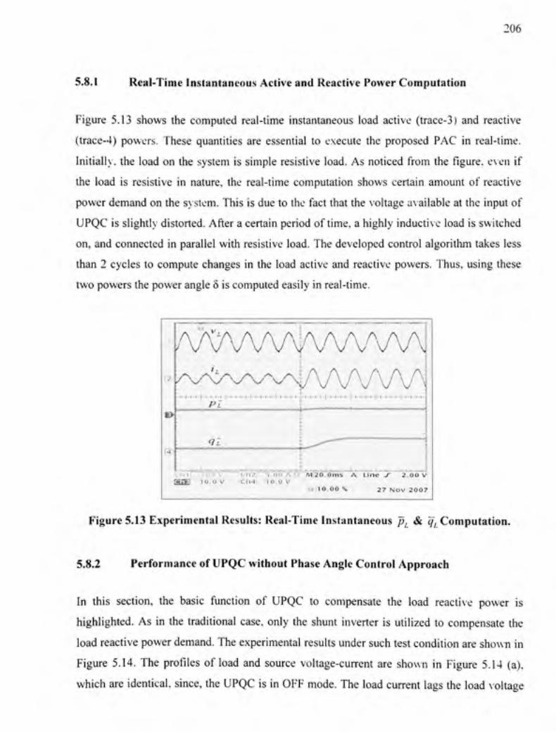
206
5.8.1 Real-Time Instantaneous Active and Reactive Power Computation
Figure 5.1 3 shows the computed real-tim e instantaneou s loa d activ e (trace-3 ) an d reactive
(trace-4) powers . Thes e quantitie s ar e essential t o execute th e proposed PA C in real-time.
Initially, the load on the syste m is simple resistive load . As noticed fro m the figure, even if
the loa d i s resistive i n nature, the real-time computatio n show s certai n amoun t o f reacfive
power demand on the system. This is due to the fact tha t the voltage available at the input of
UPQC is slightly distorted. After a certain period of time, a highly inductive load is switched
on, and connected in parallel with resistive load . The developed contro l algorithm takes less
than 2 cycles to compute change s in the load activ e and reactive powers . Thus , using these
two powers the power angle 5 is computed easily in real-time.
I-;
©"
I-*
P£
QL
A A
AAA A
I — - " " " ' ' ' ' ' ' ' ' "
- . i . . 1 , 1 1 )
t h i i i u o v Ch2 | 5 , 0 0 A ft IVI|20.0m s A L in e S 2 . 0 0 V tsam 10. 0 V lch4 i i o ; o v
1 0,00 % 2 7 No v 200 7
Figure 5.13 Experimental Results : Real-Time Instantaneous p^ & q, Computation.
5.8.2 Performanc e of UPQC without Phase Angle Control Approach
In thi s secfion , th e basi c functio n o f UPQ C t o compensat e th e loa d reactiv e powe r i s
highlighted. As in the traditional case , only the shunt inverte r i s utilized t o compensate the
load reactive power demand. The experimental result s under such test condition are shown in
Figure 5.14 . The profiles o f load and source voltage-curren t ar e shown i n Figure 5.1 4 (a),
which are identical, since, the UPQC is in OFF mode. The load current lag s the load voltage
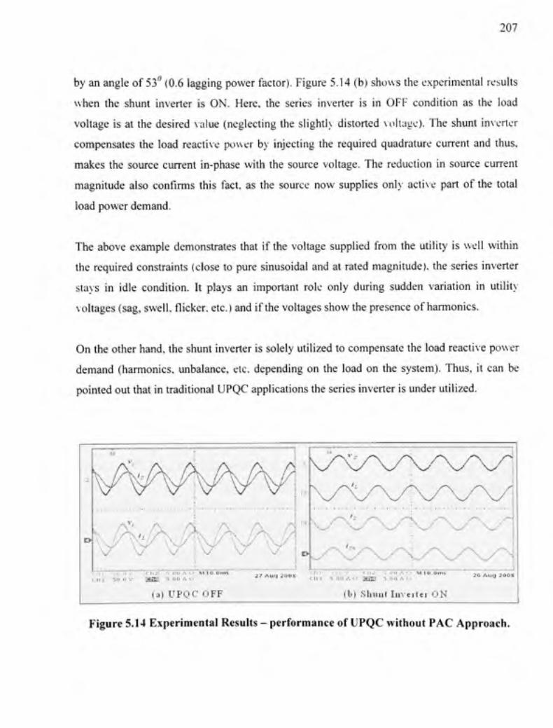
207
by a n angle o f 53' ^ (0.6 lagging power factor) . Figur e 5.1 4 (b ) show s the experimenta l result s
when th e shun t inverte r i s ON . Here , th e serie s inverte r i s i n OF F conditio n a s th e loa d
voltage i s a t th e desire d valu e (neglectin g th e slightl y distorte d voltage) . Th e shun t inverte r
compensates th e loa d reacfiv e powe r bv ' injectin g th e require d quadratur e curren t an d thus ,
makes th e sourc e curren t in-phas e wit h th e sourc e voltage . Th e reductio n i n sourc e curren t
magnitude als o confirm s thi s fact , a s th e sourc e no w supplie s onlv - acti v e par t o f th e tota l
load power demand .
The abov e exampl e demonstrate s tha t i f th e voltag e supplie d fro m th e utilit y i s wel l withi n
the require d constraint s (clos e t o pur e sinusoida l an d a t rate d magnitude) , th e serie s inverte r
stays i n idl e condition . I t play s a n importan t rol e onl y durin g sudde n variatio n i n utilit v
voltages (sag , swell, flicker, etc. ) and i f the voltages sho w the presence of harmonics .
On the other hand , the shun t inverte r i s solely utilize d t o compensate th e loa d reactive powe r
demand (harmonics , unbalance , etc . dependin g o n th e loa d o n th e system) . Thus , i t ca n b e
pointed ou t that i n traditional UPQ C applications the series inverter i s under utilized .
c h j ; 3 0 , d v aUE l s o o A <? 27 AU< | 200! S c I I I 1 0 IS V .r,h 2 tjliii 5 ' 6 b A < > a a H ;
,s 0( 1 A * • M I c o i n s •5,130 A i >
20 Au g 200 S
a) U P Q C OF F (b) .Shun t I i n e i t e i O N
Figure 5.14 Experimenta l Result s - performanc e o f UPQC without PA C Approach .
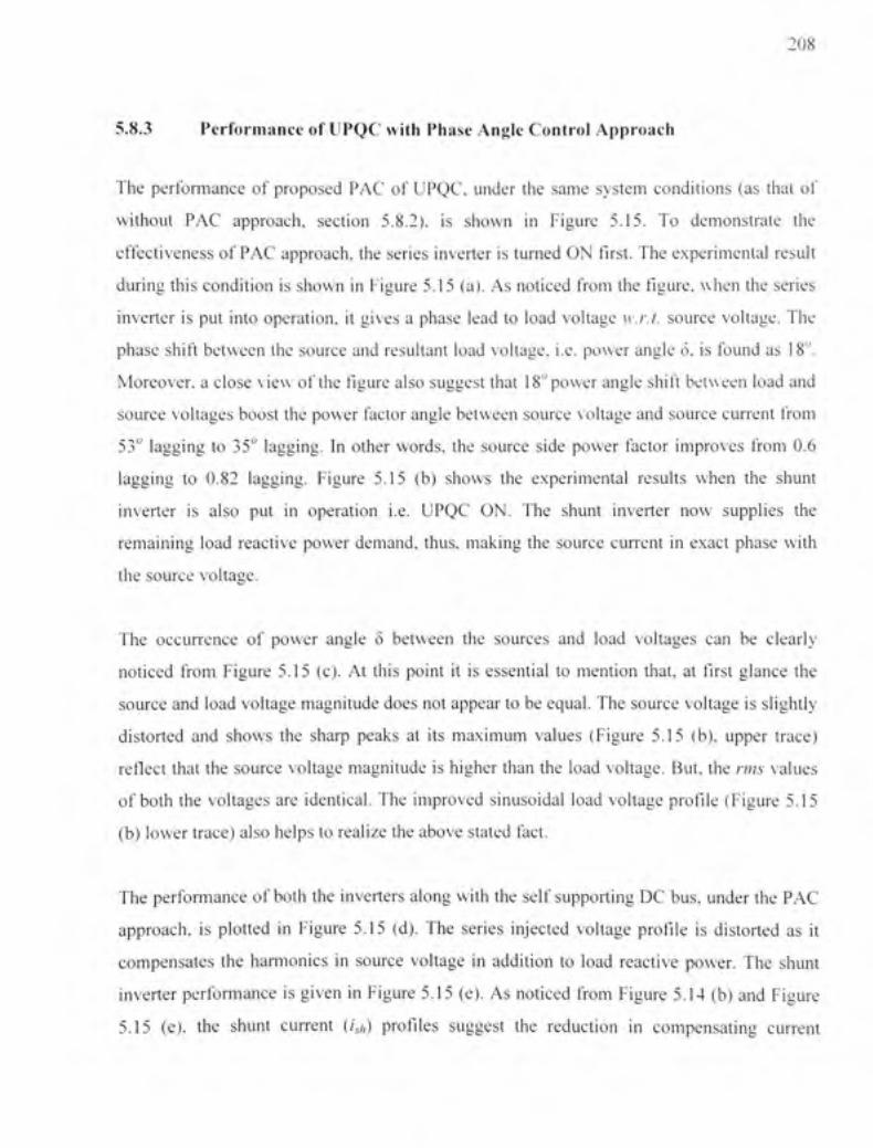
208
5.8.3 Performanc e o f UPQC with Phas e Angle Contro l Approac h
The performanc e o f propose d PA C o f UPQC , unde r th e sam e syste m condition s (a s tha t o f
without PA C approach , sectio n 5.8.2) , i s show n i n Figur e 5.15 . T o demonstrat e th e
effectiveness o f PAC approach , the serie s inverte r i s turned O N first. Th e experimenta l resul t
during thi s condition i s shown i n Figure 5.1 5 (a). As noticed fro m th e figure , whe n th e serie s
inverter i s put int o operation , i t give s a phase lea d t o loa d voltag e w.r.t. sourc e voltage . Th e
phase shif t betwee n th e sourc e an d resultan t loa d voltage , i.e . powe r angl e 6. is found a s 18" .
Moreover, a close view of the figure als o sugges t tha t 18 ° power angle shif t betwee n loa d an d
source voltage s boos t th e power facto r angl e betwee n sourc e v oltage and sourc e curren t fro m
53° laggin g t o 35 ° lagging . I n othe r words , th e sourc e sid e powe r facto r improve s fro m 0. 6
lagging t o 0.8 2 lagging . Figur e 5.1 5 (b ) show s th e experimenta l result s whe n th e shun t
inverter i s als o put i n operafio n i.e . UPQ C ON . Th e shun t inverte r no w supplie s th e
remaining loa d reactiv e powe r demand , thus , makin g th e sourc e curren t i n exac t phas e wit h
the sourc e voltage .
The occurrenc e o f powe r angl e 5 betwee n th e source s an d loa d voltage s ca n b e clearl y
noticed fro m Figur e 5.1 5 (c) . A t thi s poin t i t i s essentia l t o mentio n that , a t first glanc e th e
source and loa d voltage magnitud e doe s not appea r to be equal . The source voltag e i s slightl y
distorted an d show s th e shar p peak s a t it s maximu m value s (Figur e 5.1 5 (b) , uppe r trace )
reflect tha t th e sourc e voltag e magnitud e i s higher tha n th e loa d voltage . But , the rms value s
of bot h th e voltage s ar e identical . Th e improve d sinusoida l loa d voltag e profil e (Figur e 5.1 5
(b) lower trace) also helps to realize the above state d fact .
The performanc e o f both th e inverter s alon g wit h th e sel f supporting D C bus , under th e PA C
approach, i s plotte d i n Figur e 5.1 5 (d) . Th e serie s injecte d voltag e profil e i s distorte d a s i t
compensates th e harmonic s i n sourc e voltag e i n additio n t o loa d reactiv e power . Th e shun t
inverter performanc e i s given i n Figur e 5.1 5 (e) . As noficed fro m Figur e 5.1 4 (b ) an d Figur e
5.15 (e) , th e shun t curren t (4;, ) profile s sugges t th e reductio n i n compensatin g curren t
209
»
••AAAA-' A .' '.
aUlEi 50, 0 V ch<» : 3,6 6 A o 27 Ali q 200 8
(a) Onl y Serie s Inverte r O N
'••J \J
'XSfX 56T 0 V •ch-l f 3r66'A"c > •
(b)UPQC ON
27 Auq 200 s
A: A ,./1
<l__5n_n_V Ch2 | 5 0 0 A 0 MilO.Om s 5l!g " 0 o V rii-i | ' ^ ?)6 A i> 27 Aug 200 ^
(c) 5 Shif t
..'^^XJ>^X./*^A>^'
'-'"X^^X^.' r'rn*""Tno™'^""^tt2l'°"%T,"o'^'^™MW.'oms " ' " " ' n i l - .oov—aTgi'-TT-QirA-?; - ^ ^ ^u g 200 8
(d)UPQC O N
r-ii^ /~^.
a m i 10 0 V Ch2 i S.OOAf t MilO.Om s Ch3| •5;ooA< > rh-l ' S:n 6 A?> 27 Au y 200 s
(e) Shun t Inverte r Performanc e
Figure 5.15 Experimental Result s - Performanc e o f proposed PA C approach .
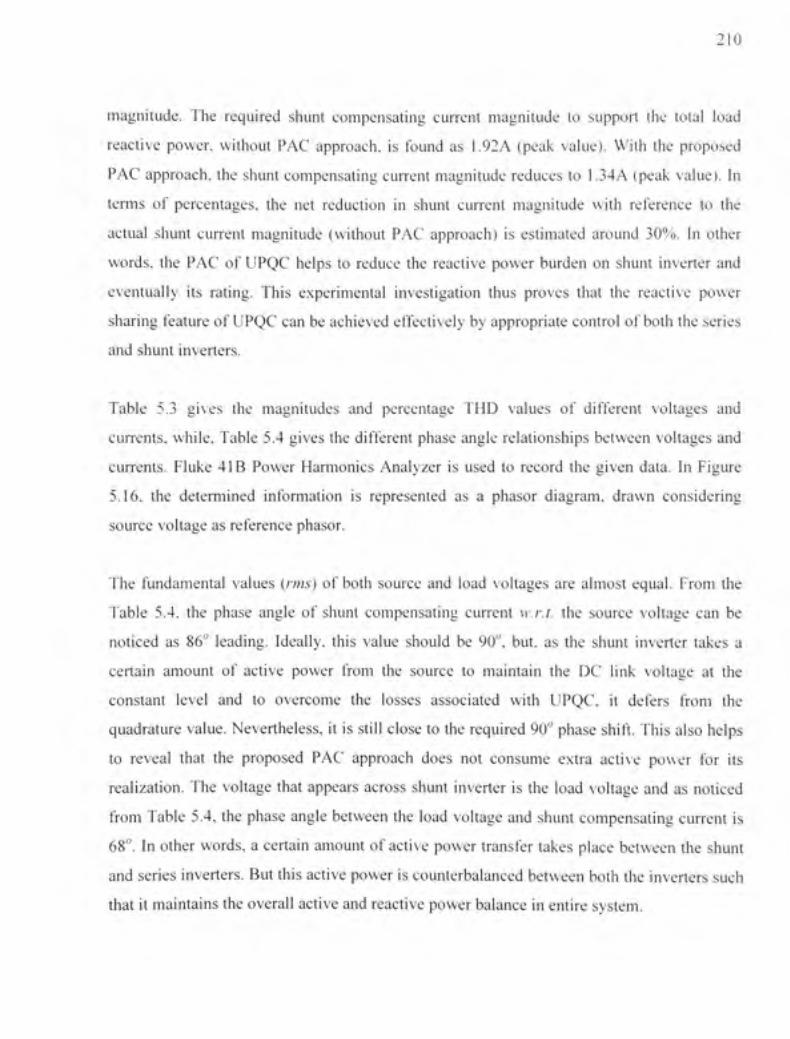
210
magnitude. Th e require d shun t compensatin g curren t magnitud e t o suppor t th e tota l loa d
reacfive power , withou t PA C approach , i s foun d a s 1.92 A (pea k value) . Wit h th e propose d
PAC approach , th e shun t compensatin g curren t magnitud e reduce s t o 1.34 A (pea k value) . I n
terms o f percentages , th e ne t reductio n i n shun t curren t magnitud e wit h referenc e t o th e
actual shun t curren t magnitud e (withou t PA C approach ) i s estimate d aroun d 30% . I n othe r
words, th e PA C o f UPQ C help s t o reduc e th e reactiv e powe r burde n o n shun t inverte r an d
eventually it s rafing . Thi s experimenta l investigatio n thu s prove s tha t th e reactiv e powe r
sharing featur e o f UPQC ca n be achieved effectivel y b y appropriate contro l o f both th e serie s
and shun t inverters .
Table 5. 3 give s th e magnitude s an d percentag e TH D value s o f differen t voltage s an d
currents, while . Table 5. 4 give s th e differen t phas e angl e relationship s betwee n voltage s an d
currents. Fluk e 41 B Powe r Harmonic s Analyze r i s use d t o recor d th e give n data . I n Figur e
5.16, th e determine d informatio n i s represente d a s a phaso r diagram , draw n considerin g
source voltage as reference phasor .
The fundamenta l value s {rms) o f bot h sourc e an d loa d voltage s ar e almos t equal . Fro m th e
Table 5.4 , th e phas e angl e o f shun t compensatin g curren t w.r.t. th e sourc e voltag e ca n b e
noticed a s 86 ° leading . Ideally , thi s valu e shoul d b e 90° , but , a s th e shun t inverte r take s a
certain amoun t o f activ e powe r fro m th e sourc e t o maintai n th e D C lin k voltag e a t th e
constant leve l an d t o overcom e th e losse s associate d wit h UPQC , i t defer s fro m th e
quadrature value . Nevertheless, i t i s stil l clos e to the require d 90 ° phase shift . Thi s also help s
to revea l tha t th e propose d PA C approac h doe s not consum e extr a activ e powe r fo r it s
realization. Th e voltag e tha t appear s acros s shun t inverte r i s the loa d voltag e an d a s notice d
from Tabl e 5.4 , th e phas e angl e betwee n th e loa d voltag e an d shun t compensatin g curren t i s
68°. I n other words , a certain amoun t o f activ e powe r transfe r take s plac e betwee n th e shun t
and serie s inverters . Bu t this active power i s counterbalanced betwee n bot h the inverter s suc h
that i t maintains the overall activ e and reactive power balance i n entire system .

Table 5.3 Measured voltage and curren t magnitud e using Fluke 41B
Measured Paramete r
RMS Valu e
Peak Valu e
% TH D
1
^'s
35.22 V
52.8 V
3.78%
2
' ' .
35.18 V
50.05 V
2.66%
3
^'sr
11.02 V
16.81 V
-
4
A 1.51 A
2.09 A
3.04%
5
A 1.75 A
2.46 A
2.19%
6
A, 0.94 A
1.34 A
-
Table 5.4 Different phas e angle determinatio n
Measured angle between Parameter extracted
Angle (deg)
1
''s~'s
(Ps
0° (unity)
2
^'S-'L
p
35° (lag)
3
''s-'sh
(Psh_s
86° (lead)
4
''L - >s
5
18° (lead)
•j\
''L-'L
(PL
53" (lag)
6
^'L - 'sh
(Psh_L
68° (lead)
7
^'Sr-'S
9s.
100° (lag)
8
^Sr-'L
-
135° (lag)
^Srk\^''
\f>APsh_L
p>-^(p, A
^ A
^L \
^^,
1 /
(PL = 53 °
/^ = 35°
^)'-18°
^s.-100°
^.«,_.=86°
<PsH L = 6 8 °
Figure 5.16 Phasor representatio n showin g relative phase angles between differen t voltages and curren t with power angle 8=18°.

212
5.8.4 Performanc e o f UPQC unde r Different Powe r Angle s
In thi s section , th e summar y o f a n extensiv e experimenta l investigation , unde r severa l
different powe r angle s 6 , i s presented . T o sho w th e effec t o f powe r angl e 5 o n th e shun t
inverter rating , th e experiment s ar e carrie d a t 6 = 10° , 15° , 18° , 23° , an d 28° . Som e o f th e
important experimenta l result s ar e give n i n Figur e 5.1 7 t o Figur e 5.20 . Tabl e 5. 5 give s th e
detailed value s o f eac h o f th e voltage s an d currents . Base d o n th e abov e mentione d
experimental data , a comparative evaluatio n o n UPQ C parameter s (voltage/current ) i s carried
out i n Figure 5.21 .
Figure 5.1 7 gives the experimenta l result s whe n onl y the serie s inverte r i s put int o operation .
In traditiona l UPQ C application s (6=0°) , a s th e serie s inverte r doe s no t tak e par t i n loa d
reactive powe r compensation , th e loa d an d sourc e voltage s ar e in-phase . A s powe r angl e 5
increases graduall y th e effectiv e phas e angl e betwee n th e sourc e voltag e an d th e sourc e
current {fi) reduces accordingly . Thi s suggest s th e increase d loa d powe r facto r see n fro m th e
source side . Th e experimenta l result s whe n bot h th e inverter s ar e O N ca n b e see n i n Figur e
5.18. Th e shun t inverte r no w compensate s th e remainin g loa d reactiv e powe r demand , thus ,
making th e sourc e curren t in-phas e wit h the sourc e voltage . Unde r al l the power angle s 6 the
UPQC maintain s th e unit y powe r facto r operation . Th e importan t poin t t o b e note d her e i s
that th e sourc e curren t magnitud e i s almost constan t irrespectiv e o f th e boos t i n powe r angl e
5 (can als o be verified fro m th e Table 5.5) .
The experimenta l result s showin g th e powe r angl e 8 between sourc e an d loa d voltage s ar e
shown i n Figure 5.19 . Th e presenc e o f power angl e 5 can als o b e observed fro m Figur e 5.1 8
and Figur e 5.1 9 b y comparin g th e loa d voltag e profile s a t th e zer o crossing s o f respectiv e
source voltages . Not e tha t th e fundamenta l value s (rm.s) of bot h th e voltage s ar e strictl y
equal, whic h i s on e o f th e significan t feature s o f propose d powe r angl e contro l theory . Th e
difference i n thes e voltag e magnitude s ma y resul t i n additiona l activ e powe r exchang e
between th e source an d UPQC .
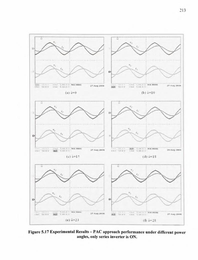
:13
cr>3 soTo v ;Cll4: 5.0 0 A O
( a ) 0 = 0
27 Au q 200 S T ^ C ' p O ^ ' ' ^ ^ - ' ' " " ' " ^ 27 'AUU'20Q K a i B 50^ 0 V :Ch-» j ^:6 6 AC?
(b) 0=10
f>
/ , / ' .^ . ^
.1-y \
„ • , . , » . ' " ' i sn ' ) v :a£ E '>fiOA< > Mi4.O0m s ., „ . . , „ „ „ 27 Au g 20nx f h:!™507 0 V ^Ch-»r~5;WAr o • • ^ ° * " 3 2 " ° ' '
(d)o=lS
r i i ! SO.O V :ch2 i 5.0 0 A o iM4.0Om s c h l sC o V gHO ; sTo o A v? '
27 Au a 200 X 5.",. " '- ^ f:>l2 l ''•n o A ••> MJ.OOm i 2 7 A u g 2 0 0 S g j g 5 0 0 V Ol^ j S Of ) A (> 27Au<J200 S
(e ) 0 = 2.^ lb G=2 S
Figure 5.17 Experimental Result s - PA C approach performanc e unde r differen t powe r angles, only series inverter i s ON.
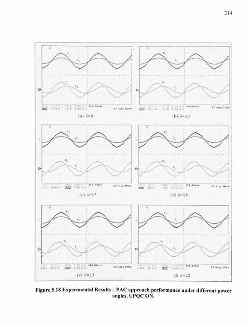
214
n f p 50^ 0 V :c n 12 5 - 0 0 A O 1.4( •••S"0 6 A V . '
M 4 . OOlD S 27 Au g 200 X aSB 30 . 0 V ch-i i S.O O A '. / 27 Au g 200 8
(ni u= 0 (b) 0 = 1 0
- , f , , » , t - ( - * " t - . - t -J,,•.,!".,*,, I
n i l =1 0 n V 1c:h2 i s,o o AT> iM4 .0Om s f i l l 5 0 u V a a S ' ' : 0 0 A ' > 27 Au g 200 S
(c) 5=1. >
!.l-, n Sii.i i V c.h;; ^ 3.Q0A:. > M;4.a0ni s Mft l ' 30 . 0 V (L:il 4 3 ,0 0 A !,>
( d t C>=1 S
27 Au g 200 S
ch3' soTo v aDC i s:60 A «>••
(e) C.=2 3
2 7 A u a 2 O 0 S ' " i i^',;^, > , ' " - ' 1 3,0 0 A«: 7
(f) u=: s
27 Au g 200 s
Figure 5.18 Experimental Result s - PA C approach performanc e unde r differen t powe r angles, UPQC ON.
215
•
; ., „ , . . . : , „
aiEl 50, 0 V c:ii2L
" r.h4 i S^OtJI^AJi Mi4.00in s
' 5 . 66 A o "
( n ) 0 = 0
"'SU I V iC:H 2 5.0 0 A < / M4 .oom s 27 A u g 200K a i B "^OfToV ^ ^Ch4 1 5 .0 0 A Q
(b) 0=i O
27 Aug 200 X
(iTi *; a iT v _ rh2 | s^o o A o_M4.ooins! BTEI 5f i i ) V ' ' c ; h4 r 5 6 6 A <>
27 Au g 2008 (JT.I-
- ( h i "•" y^y rh2 i 5^0 0 A O M 4 . 0 0 m s 27 AU' J 200 8
( c ) C . = l ^ (it) 0 = 1 8
a l g ! SioVO V Ch4 ; 5 6 b A Q
(e) 0 = 23
27 A u g 200 8 g j g 5 0 0 V CIW ; 5 0 0 A O
( f l 0=2 8
27 A u g 200 S
Figure 5.19 Experimental Results - source and load voltage phase shifts under different power angles.
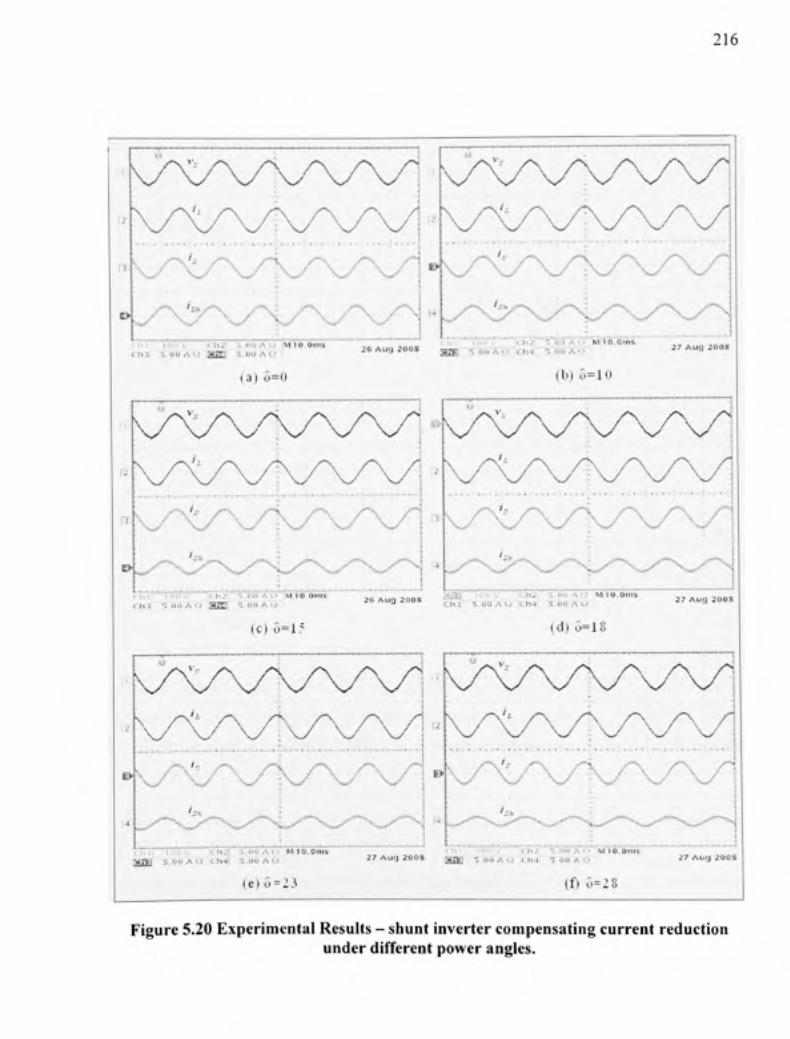
216
/^ \ -^"y y^. V V
; l i i 1!." ! > . ch^ ; :i.oOA<.. > MlO.Om s tITJ 3.0 0 A <,> 2UE 1 3.0UA4. >
I .1 ) U = 0
K i ( i v ~<:\-,2\ 5 ,0 0 A V J MilO.Om s 26 A u g 200 8 g j g -570 0 ^ f r ; c h 4 r S.O O A ':>"
(b) 0 = 1 0
27 A u g 200 X
*w»«r'^""'V*^ < h ; ' i n n v :r."h2 i 5,0fiA< > MlO.Oms ; c.\\:i 5 0 6 A O a iE : 5 : 0 0 A « ' 26 Au g 200 s SJU !_h. ; i , i .>OA' . j M lO .Om s
(c) 5=1 5
ChJ 5.00A<.. I Ch 4 5 ,0 0 A i i
(dl C. = U
27 Aug 200 s
! ;,' i '10':) ' V ^Chif*^'*''- ' AO*"MTo.Onis ' ;ii|fKi 3,0 0 A <.J c;h4 i 5.0 0 A!, ;
( I l l 10 0 v :rn;! : 5.0 0 A o iMio.Om s 27 Au g zoo s a £ g 5 0 0 A Q CH4 ; 5 0 0 A o 27 AU( | 200 s
(e)o=23 (f) C. = 2S
Figure 5.20 Experimental Result s - shun t inverter compensating current reductio n under different powe r angles.

217
Table 5.5 Performance of PAC approach under different powe r angles 6
1
2
3
4
5
6
7
8
9
10
11
12
V^irms) -^
VI (rm.s) -^
\ ;,^ {rms) - >
l,{rms) -^
l^(rms) -^
hh ('•""• ) -^
(p, {lag) -^
^, (unity ) -^
P{lag) -
^,, (lead) -^
(p,i,_,{lead)^
(p„, jilead)^
S = 0"
35.24 V
35.24 V
-
1.74 A
1.47 A
1.36A
-53°
0°
-
-
87°
-
S = \0"
35.10V
35.00 V
06.53 V
1.75 A
1.50 A
1.12 A
53°
0°
43°
96°
86°
75°
S = 15"
35.10V
35.00 V
09.82 V
1.75 A
1.50A
0.98 A
53°
0°
38°
98°
86°
70°
^ = 18"
35.20 V
35.18 V
11.02 V
1.75 A
1.51 A
0.94 A
53°
0°
35°
100°
86°
68°
S = 23"
35.20 V
35.15 V
13.39V
1.75 A
1.52 A
0.84 A
53°
0°
30°
102°
87°
64°
S = 28"
35.04 V
35.05 V
16.82 V
1.75 A
1.54 A
0.68 A
53°
0°
25°
103°
87°
59°
Figure 5.2 0 show s th e mos t interestin g result s o f th e propose d work . Th e shun t inverte r
performance unde r differen t powe r angle s 5 is given an d compared wit h traditiona l UPQ C
(5=0°) performance. I t is clearly visible that as the power angle 5 increases, the shunt inverter
^ Al l the phase angles are computed by taking the reading between the respective voltage s and currents usin g Fluke 4IB . Ther e migh t b e a n erro r o f ± 1 degre e du e t o th e measuremen t erro r a s wel l a s du e t o th e unavailability o f exact phase knowledge as the used instrumen t rounds off the measured phase angle. However , the car e i s take n t o us e exac t sam e methodolog y t o carr y ou t th e experiment s an d t o comput e differen t parameters.
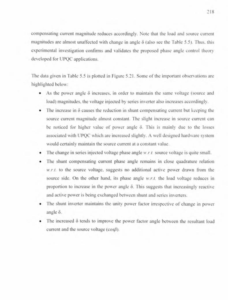
218
compensating curren t magnitud e reduce s accordingly . Not e tha t th e loa d an d sourc e curren t
magnitudes ar e almos t unaffecte d wit h chang e i n angle 5 (also se e th e Tabl e 5.5) . Thus , thi s
experimental invesfigatio n confirm s an d validate s th e propose d phas e angl e contro l theor y
developed fo r UPQ C applications .
The dat a give n i n Table 5. 5 i s plotted i n Figure 5.21 . Some o f the importan t observation s ar e
highlighted below :
• A s th e powe r angl e § increases , i n orde r t o maintai n th e sam e voltag e (sourc e an d
load) magnitudes, the voltage injecte d b y series inverte r also increases accordingly .
• Th e increas e i n 5 causes th e reductio n i n shun t compensatin g curren t bu t keepin g th e
source curren t magnitud e almos t constant . Th e sligh t increas e i n sourc e curren t ca n
be notice d fo r highe r valu e o f powe r angl e 5 . Thi s i s mainl y du e t o th e losse s
associated wit h UPQ C whic h are increased slightly . A well designed hardwar e syste m
would certainl y maintai n th e source curren t a t a constant value .
• Th e change in series injecte d voltag e phase angle w.r.t. source voltage i s quite small .
• Th e shun t compensatin g curren t phas e angl e remain s i n clos e quadratur e relatio n
w.r.t. t o th e sourc e voltage , suggest s n o additiona l activ e powe r draw n fro m th e
source side . O n th e othe r hand , it s phas e angl e w.r.t. th e loa d voltag e reduce s i n
proportion t o increas e i n th e powe r angl e 5 . Thi s suggest s tha t increasingl y reactiv e
and active power i s being exchanged betwee n shun t and series inverters .
• Th e shun t inverte r maintain s th e unit y powe r facto r irrespectiv e o f chang e i n powe r
angle 5.
• Th e increase d 5 tends t o improv e th e powe r facto r angl e betwee n th e resultan t loa d
current an d the source voltage {cosP).
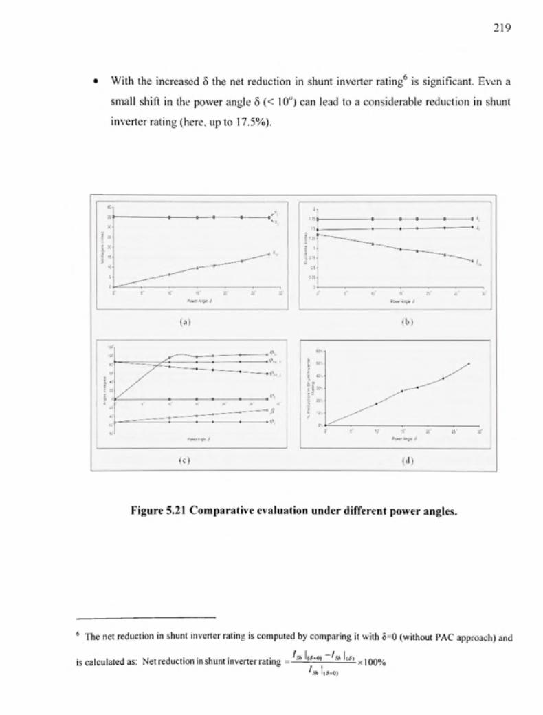
219
With the increased 5 the net reduction i n shunt inverte r rating i s significant. Eve n a
small shif t i n the power angle 5 (< 10° ) can lead to a considerable reductio n i n shunt
inverter rating (here, up to 17.5%).
^Ci
i^
!£•
r 1C
^
_ _ - 6 '
I t
" °
1 ! ' » • a '
• • 1 .
^ - V , 1' . ,
K
(a)
. . ^ ' - - — ' V V .
^
—>'p.
(c)
I l i a -
lu..f-f M 0 i
C5i
;25< 1
1 "
0 « » •
— « » ( — < — . —
~ ~ - f r -
:: ftwe-iftg* d
_-,8 1 ,
• '.
"~*'<»
J , ' '
(bl
(dl
KTS-i
I i *'• •
t «> ,
c 5 31^ .
5 t> im
i ^ - J .
^ D
^'^ ^^^
10"
^^" -
•5' I C
^ ^^
Vi'
j
i
1
Figure 5.21 Comparative evaluation under different powe r angles.
The net reduction i n shunt inverte r rating is computed by comparing it with 5=0 (without PA C approach) and
xlOO% is calculated as: Ne t reduction in shunt inverter rating =^^^' ' ' ' ' ^'' '" ^ / .VA l ( < 5 = 0 )
220
5.9 Conclusion s
This chapte r proposes a new control philosoph y fo r UPQ C i n which bot h th e shun t an d serie s
inverters shar e th e loa d reactiv e powe r demand , terme d a s powe r angl e contro l (PAC ) o f
UPQC. The complete mathematica l analysi s i s presented. Th e proposed approac h i s validated
through extensiv e simulatio n an d experimenta l studies . Th e majo r ke y point s o f PA C theor y
for loa d reactive power compensatio n ar e highlighted below :
• Base d o n the give n system , loa d an d UPQ C constraints , th e maximu m serie s inverte r
VAR compensatio n ca n b e estimated . Thi s help s t o fix th e maximu m shun t inverte r
compensation limi t whic h resul t i n th e reductio n o f th e shun t inverte r rating .
However, i t does not affec t th e existing serie s inverte r rating . Thus , the overall cos t o f
UPQC i s reduced.
• Th e shun t inverte r alway s ha s th e priorit y t o compensat e th e loa d reactiv e powe r
demand u p to it s maximum limit . Thi s assures the ful l utilizatio n o f shun t inverte r fo r
load reactive powe r compensation .
• Whe n th e loa d reactiv e powe r increase s abov e th e shun t inverte r limits , th e serie s
inverter come s int o the role to compensate th e remaining loa d reactiv e powe r deman d
with i n a short period o f time. The half cycle delay i n the serie s inverte r compensatio n
is du e t o th e dela y i n computatio n tim e t o extrac t th e chang e i n loa d reactiv e powe r
demand.
• Th e shun t an d serie s inverter s operat e i n coordinatio n t o achiev e th e commo n tas k -
the loa d reactiv e powe r compensation . Thus , a bette r utilizatio n o f existin g serie s
inverter ca n be done during a normal operatin g condition .
• A powe r angl e differenc e occur s betwee n sourc e an d loa d voltage , bu t th e resultan t
load voltage magnitude i s maintained constan t a t the desired value .
221
The propose d approac h doe s no t put an y extr a activ e powe r burde n o n th e suppl y
system fo r it s operation .
The simulatio n result s fo r ful l loa d o f 1 5 k W + 7 1 5 kVA R sho w tha t th e shun t
inverter kV A ratin g ca n b e reduce d u p t o 25.6% , b y utilizin g propose d PA C
approach. Additionally , th e experimenta l result s sho w tha t fo r hig h inductiv e loa d
(load powe r facto r 0. 6 lagging ) th e shun t inverte r ratin g ca n b e reduce d u p t o 50 %
with power angle 5= 28° .
CHAPTER 6
PERFORMANCE O F PAC APPROACH UNDE R DIFFEREN T OPERATIN G CONDITIONS
6.1 Introductio n
In the previou s chapter , th e concep t o f propose d powe r angl e contro l (PAC ) i s successfull y
designed, developed , an d validate d wit h a consideration o f idea l syste m (i.e . pur e sinusoida l
without voltag e sag , swell , etc. ) unde r linea r R L load . I n thi s chapter , th e theor y o f PA C
approach i s furthe r extende d fo r th e voltag e sa g an d swel l conditions . A complet e
mathematical analysi s i s provided t o compute the different UPQ C parameters .
The performance equation s fo r th e propose d PA C approac h ar e standardize d t o arrange the m
in a generalized manner . Thes e comprehensive equation s can be used t o esfimate th e require d
series injectio n voltag e an d th e shun t compensatin g curren t profile s (magnitud e an d phas e
angle), and the total amoun t o f active and reactive powe r tha t flows throug h th e UPQC unde r
steady-state, voltage sa g and swel l conditions .
This chapte r als o introduce s tw o contro l technique s fo r powe r angl e 5 , especiall y unde r th e
voltage sa g an d swel l condition , t o contro l th e amoun t o f reactiv e powe r share d b y eac h o f
the inverters . Moreover , th e emphasis i s also give n t o overcome th e distortions presen t i n the
source voltage and the load current .
The findings i n thi s chapte r ar e supporte d wit h th e adequat e simulatio n an d th e laborator y
experimental results . I t i s show n tha t th e PA C approac h ca n b e implemente d successfull y t o
compensate th e voltag e sag , voltag e swell , voltag e harmonics , an d th e curren t harmonic s
while both the inverter s share the loa d reactiv e power demand .

223
6.2 PAC approac h unde r Voltage Sa g Conditio n
The analysi s presente d i n th e previou s chapte r wa s base d o n th e steady-stat e condition , i.e .
the sourc e voltag e wa s considere d a t rate d value . Th e concep t o f PA C approac h i s furthe r
extended durin g th e sa g on the system . I n the followin g subsection s a detailed mathematica l
analysis an d th e necessar y equation s t o estimat e th e shun t an d serie s inverte r parameter s ar e
briefly discussed .
6.2.1 Phaso r Representatio n unde r Voltage Sa g Conditio n
From th e previou s chapter , i t i s wel l understoo d tha t th e sa g o n th e syste m ca n b e
compensated throug h activ e (refe r CHAPTER S 2 an d 3 ) a s wel l a s reactiv e powe r (refe r
CHAPTER 4) . Figur e 6. 1 show s th e phaso r representatio n o f PA C approac h wit h activ e
power sa g contro l metho d (Figur e 6. 1 (a) ) an d wit h reactiv e powe r sa g contro l metho d
(Figure 6. 1 (b)) . I t i s eviden t tha t th e combine d operatio n o f PA C concep t an d th e sa g
controlled throug h reactiv e powe r doe s not giv e th e desire d performance . Therefore , th e
active power contro l fo r voltag e sa g and swel l i s considered .
i
^ -
(' \ ' Sr\ \
<Psr \ 0^
\
, r \ \^^
/ , y^ \ \ / ' y^ \ ^^ 1 j f ny 1 \ i - ^ '
^sn *s 1 1
' ' 111) PAC am i sii g c o n l r o l k r u i l h ac i u e p o u e i
T
' " M V ~ "" ^ ' I ' i " ^ • 1 ' ' 1 1 %
1 1 ' 1 1 ' 1 1 '
I'A \ \ >
k i ~
V, i \ \ •" \ 1
'A
\ \ N
\ ,., \ 1 . ,
A ^F '
/y^ ' V o *' ^
\B
/ ^ L \ \ / 1 •' ' '
' ( l i ) l ' .AC ii i i d sii u t i M i l i o l k r Wil l i re . id iv e powe r
Figure 6.1 Phaso r representatio n o f PAC approach unde r voltage sa g condition .
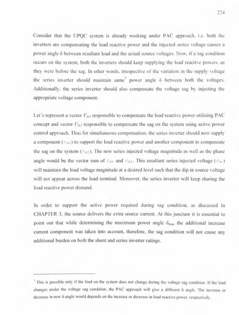
224
Consider tha t th e UPQ C syste m i s alread y workin g unde r PA C approach , i.e . bot h th e
inverters ar e compensatin g th e loa d reactiv e powe r an d th e injecte d serie s voltag e cause s a
power angl e 8 between resultan t loa d an d th e actua l sourc e voltages . Now, i f a sag conditio n
occurs o n th e system , bot h th e inverter s shoul d kee p supplyin g th e loa d reactiv e powers , a s
they wer e befor e th e sag . I n othe r words , irrespectiv e o f th e variatio n i n th e suppl y voltag e
the serie s inverte r shoul d maintai n sam e powe r angl e 8 betwee n bot h th e voltages .
Additionally, th e serie s inverte r shoul d als o compensat e th e voltag e sa g b y injectin g th e
appropriate voltag e component .
Let's represen t a vector Vsri responsibl e t o compensate th e load reactiv e power utilizin g PA C
concept an d vecto r l\s> : responsible t o compensat e th e sa g o n the syste m usin g activ e powe r
control approach . Thu s fo r simultaneou s compensation , th e series inverte r shoul d no w suppl y
a component (r.s , i) t o suppor t th e loa d reactiv e powe r an d anothe r componen t t o compensat e
the sa g on th e syste m (r.s>2) . The ne w serie s injecte d voltag e magnitud e a s wel l a s the phas e
angle woul d b e th e vecto r su m o f r,s,, | an d r.s>2 . This resultan t serie s injecte d voltag e (r.sv )
will maintai n th e load voltage magnitud e a t a desired leve l suc h that the dip in source voltag e
will no t appea r acros s th e loa d terminal . Moreover , th e serie s inverte r wil l kee p sharin g th e
load reactive power demand .
In orde r t o suppor t th e activ e powe r require d durin g sa g condition , a s discusse d i n
CHAPTER 3 , the sourc e deliver s th e extr a sourc e current . A t thi s juncture i t i s essentia l t o
point ou t tha t whil e determinin g th e maximu m powe r angl e 5ma. \ th e additiona l increas e
current componen t wa s take n int o account , therefore , th e sa g conditio n wil l no t caus e an y
additional burde n on both the shunt and series inverte r ratings .
' Thi s i s possible onl y i f the load o n the system doe s no t change during th e voltag e sag condition. I f the load
changes unde r th e voltag e sa g condition , th e PA C approac h wil l giv e a differen t 6 angle . Th e increas e o r
decrease in new 5 angle would depends on the increase or decrease in load reactive power, respectively.
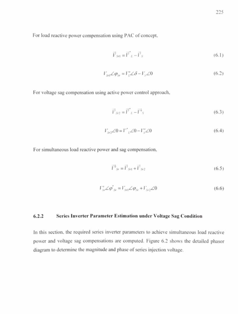
225
For loa d reactiv e power compensation usin g PAC o f concept ,
Vsri=v'i-Vs (6.1 )
V,^,Z<p,^=V;ZS-V,ZO (6.2 )
For voltage sa g compensation usin g active power contro l approach ,
r,>: = r*y, - r.s^ (6.3 )
V,^,Z0 = V',Z0-V;Z0 (6.4 )
For simultaneous loa d reactive power and sag compensation ,
r'.sv = r.vH + Liv: (6.5 )
V;^^Z(p,^ = ]'„.,Zg,„. + V,,.,ZO (6.6 )
6.2.2 Serie s Inverte r Parameter Estimatio n unde r Voltage Sa g Conditio n
In this section , th e require d serie s inverte r parameter s t o achiev e simultaneou s loa d reactiv e
power an d voltag e sa g compensation s ar e computed . Figur e 6. 2 show s th e detaile d phaso r
diagram to determine the magnitude an d phase of series injection voltage .
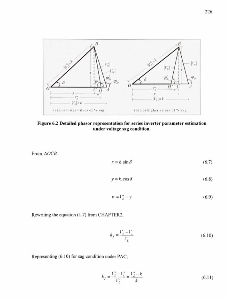
226
(;i) F t) r k ) w e r \ ; i I ii e s o f " o . s ;m ( b ) F o r h i i i hc r v a l u e s o t ' ' ' o .sa t
Figure 6.2 Detaile d phaso r representation fo r series inverter parameter estimatio n under voltage sag condition .
From ^OCB.
X - k.sinS
y = k.cosS
1 '^ f
w = > V - y
(6.7)
(6.8)
(6.9)
Rewriting the equation (1.7 ) from CHAPTER2 ,
k - ' • ^ - ' ' '~~V~
(6.10)
Representing (6.10 ) for sag condition unde r PAC,
V -V k,^-^-A± v;-k (6.11)

OTy
v;^^(\ + k,).k (6.12)
Let's define , \ + k^ = n,, (6.13)
Thus, r ' = n^yk (6.14)
Therefore, w - n,, k - y (6.15)
In ^BCH. | r ; U V.v ' + M- (6.16)
]''\ = J(k.sinS)' +(n,,.k -kcosS)' (6.17)
|[;'..l = k.J\-\-n,,~ -2.n,,.cosS (6.18)
Now. ZCHB = y/ = tan f - 1 (6.19)
tp = tan" sine)
y/7, -cose) (6.20)
Therefore, Zcp'^^ = 180" - Zy/ (6.21)
Equations (6.18 ) and (6.21 ) give the required magnitud e o f series voltage an d it s phase angl e
that shoul d b e injecte d t o achiev e th e voltag e sa g compensatio n whil e supportin g th e loa d
reactive powe r unde r PA C approach . Figur e 6. 2 (b ) represent s th e conditio n fo r th e large r
value o f voltag e sa g o n th e system . Simila r equation s ca n b e wxitte n fro m th e phaso r
diagram.
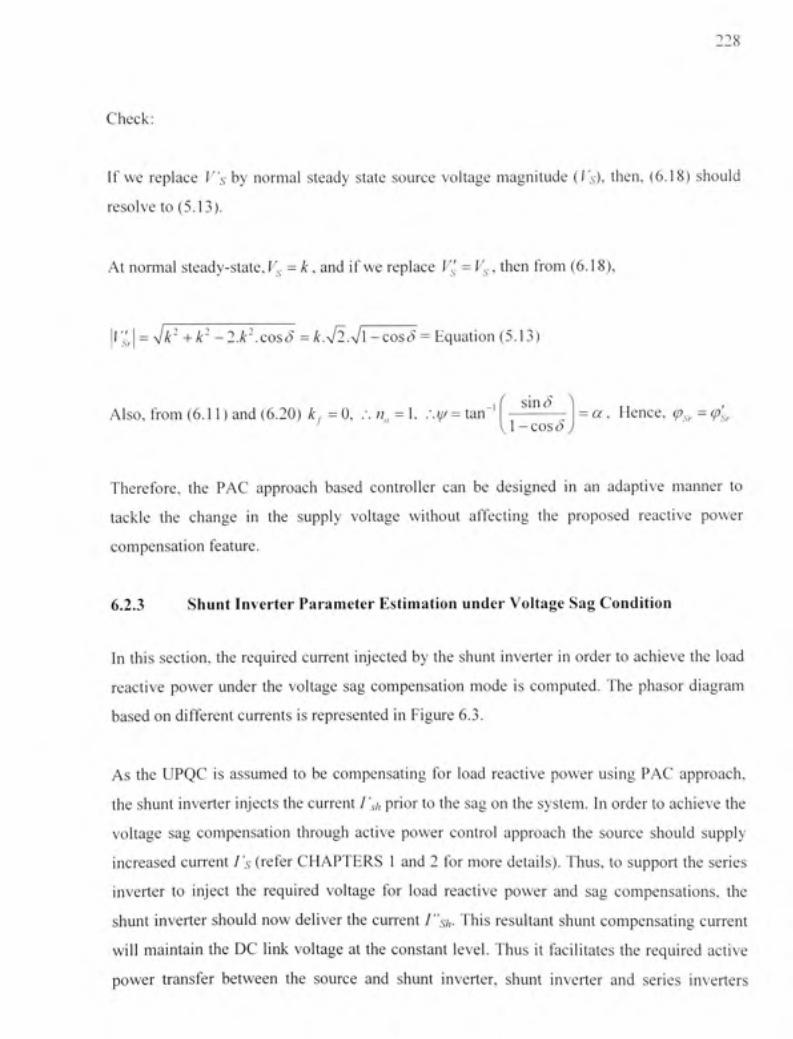
228
Check:
If w e replac e V's b y norma l stead y stat e sourc e voltag e magnitud e {Vs), then, (6.18 ) shoul d
resolve to (5.13) .
At normal steady-state , V. = k, an d i f we replace V!; = K,., then from (6.18) ,
| r ; | = yjk'+k' -2.k\cosS = ^.V2.Vl-cosd = Equation (5.13 )
Also, from (6.11 ) and (6.20 ) k^ = 0, .' . n^^ =1 , . ' .^ ^ tan " ^ sin ^ ^
1 - co s S a. Hence , tp^^ = ^'^
Therefore, th e PA C approac h base d controlle r ca n b e designe d i n a n adaptiv e manne r t o
tackle th e chang e i n th e suppl y voltag e withou t affectin g th e propose d reactiv e powe r
compensation feature .
6.2.3 Shun t Inverte r Paramete r Estimation unde r Voltage Sa g Conditio n
In this section , th e required curren t injecte d b y th e shun t inverte r i n order t o achieve th e loa d
reactive powe r unde r th e voltag e sa g compensatio n mod e i s computed . Th e phaso r diagra m
based o n different current s i s represented i n Figure 6.3.
As th e UPQ C i s assume d t o b e compensatin g fo r loa d reactiv e powe r usin g PA C approach ,
the shunt inverte r inject s th e current I'sh prior to the sag on the system . I n order to achieve th e
voltage sa g compensatio n throug h activ e powe r contro l approac h th e sourc e shoul d suppl y
increased curren t I's (refe r CHAPTER S 1 and 2 for mor e details) . Thus , to suppor t th e serie s
inverter t o injec t th e require d voltag e fo r loa d reactiv e powe r an d sa g compensations , th e
shunt inverte r shoul d no w delive r th e curren t l"sh- This resultan t shun t compensatin g curren t
will maintai n th e D C lin k voltag e a t the constan t level . Thus i t facilitate s th e require d activ e
power transfe r betwee n th e sourc e an d shun t inverter , shun t inverte r an d serie s inverter s
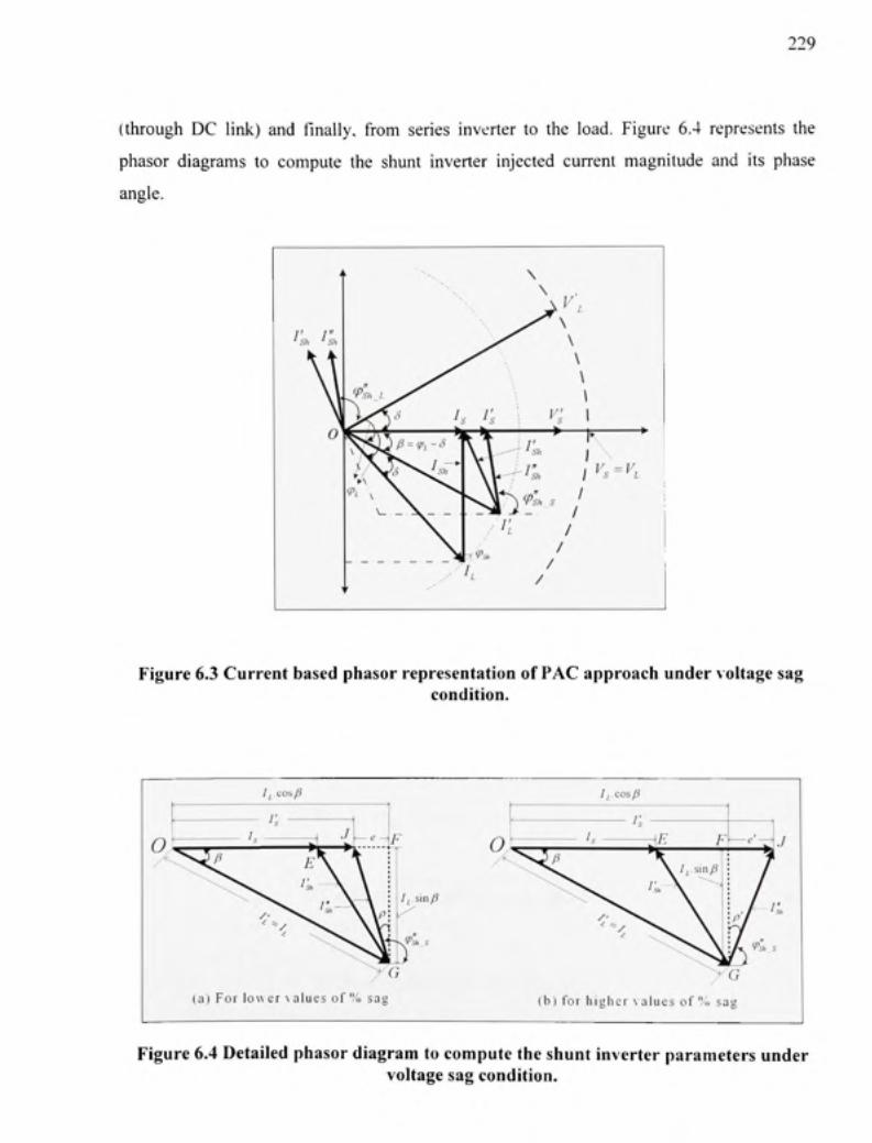
229
(through D C link ) an d finally, fro m serie s inverte r t o th e load . Figur e 6. 4 represent s th e
phasor diagram s t o comput e th e shun t inverte r injecte d curren t magnitud e an d it s phas e
angle.
Figure 6.3 Current based phasor representation of PAC approach under voltage sag condition.
o\
7; cos/ i
A - e —
/^ sin ^
(ai Fo r lo w e r ^ alues o f " n sa ^
/j,cos/i
Ft-A^.i
(b) fo r highe r \ allie s of"/; i sa g
Figure 6.4 Detailed phasor diagram to compute the shunt inverter parameters under voltage sag condition.

From AOFG (Figur e 6.4 (a)).
230
FG = 1]. sin p (6.22)
OF = 1[.cos p (6.23)
Rewriting the equation (1.12), CHAPTERl.
/ ' // > . - .costpi
\ + k. (6.24)
Let, 1 + ,
(6.25)
Therefore, 7 , -k^yli^.zoscp, (6.26)
e ^ 1[.cosp-r, (6.27)
e = r,.{cosP -k,yC0S(Pi) (6.28)
In AGFA, /; = ^{l[.sinP)'+[r,.{cosp-k^yCos(p,)f (6.29 )
A"/, - • /.-v/ ' + ^"(;-cos" (p, -2.kfj.cosp.cos(p, (6.30)
Now, ZJGF = p = tan' f \ ^l[.sinPj
(6.31)
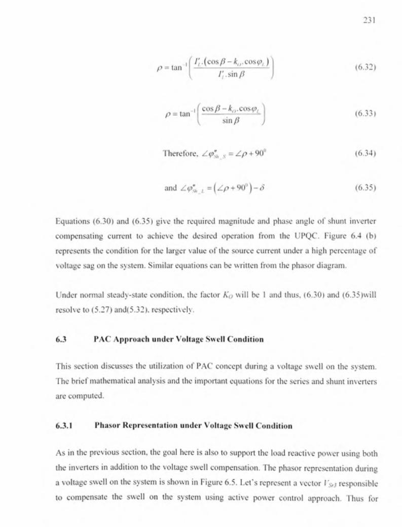
231
p = tan ' V,.{cosp-k^yCosiPf)
/ ' s i n / ? (6.32)
p = tan ' cosP -kfycoscp;
sin/? (6.33)
Therefore, Z < , = Zp + 90" (6.34 )
and Z ^ ; I =[Zp+ 90')-5 (6.35 )
Equations (6.30 ) an d (6.35 ) giv e th e require d magnitud e an d phas e angl e o f shun t inverte r
compensating curren t t o achiev e th e desire d operatio n fro m th e UPQC . Figur e 6. 4 (b )
represents th e conditio n fo r th e large r valu e o f the sourc e curren t unde r a high percentag e o f
voltage sa g on the system. Simila r equations can be written fro m th e phasor diagram .
Under norma l steady-stat e condition , th e facto r KQ wil l b e 1 and thus , (6.30 ) an d (6.35)wil l
resolve to (5.27) and(5.32) , respectively .
6.3 PA C Approach unde r Voltage Swel l Conditio n
This sectio n discusse s th e utilizatio n o f PA C concep t durin g a voltag e swel l o n th e system .
The brief mathematica l analysi s and the important equation s fo r the series and shun t inverter s
are computed .
6.3.1 Phaso r Representation unde r Voltage Swel l Conditio n
As in the previous section , the goal her e i s also to suppor t the loa d reactive power usin g bot h
the inverter s i n addition t o the voltage swel l compensation . Th e phaso r representatio n durin g
a voltage swel l on the system i s shown i n Figure 6.5 . Let' s represent a vector Vsr3 responsible
to compensat e th e swel l o n th e syste m usin g activ e powe r contro l approach . Thu s fo r
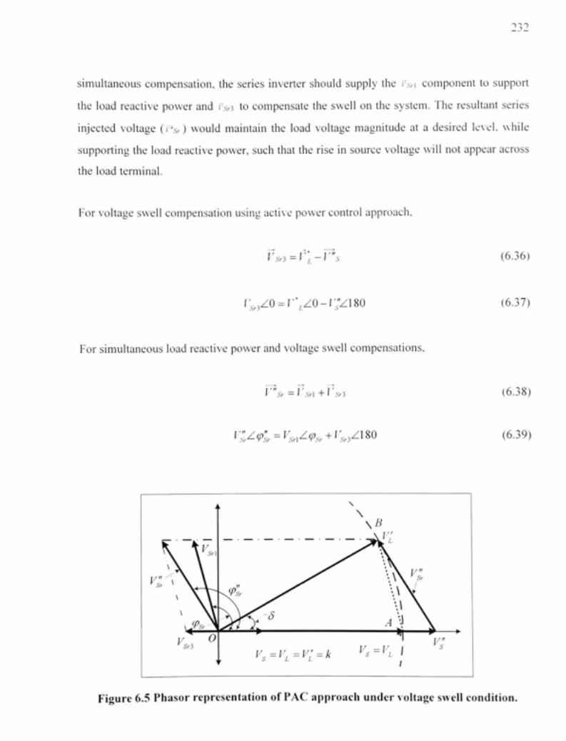
232
simultaneous compensation , th e series inverte r shoul d suppl y th e r.s, i componen t t o suppor t
the load reacfive powe r and r.s> 3 to compensate the swell on the system. The resultant serie s
injected voltag e (r-.sr ) would maintai n th e loa d voltag e magnitud e a t a desired level , whil e
supporting the load reactive power, such that the rise in source voltage will not appear across
the load terminal.
For voltage swell compensation using activ e power control approach.
Vsr, = v[-r, (6.36)
i;- 3ZO = r*,zo-r;zi80 (6.37)
For simultaneous load reactive power and voltagc swell compensations.
V Sr = V Sr] + I S ri
ySr^<Pl=Vsr]^<Psr + ^Ari^^^O
(6.38)
(6.39)
Figure 6.5 Phasor representation of PAC approac h under voltage swell condition.

-s '^ -^
Figure 6.6 Detaile d phaso r representatio n fo r series inverte r paramete r estimatio n under voltage swell condition .
From Figur e 6.6 ,
r = J'!^-k.cosS (6.40)
In ABCL. | r ; l = V.v' + /-' (6.41
\v;:^\ = yl{k.sinS)' +(n,,.k-kcosS)- (•. • V'^^n,,.k] (6.42)
|r ",| = ^.^l + /?,/ -2.n^,.cos5 (6.43)
Now. ZCZi 5 = A ^ tan " f - 1 \'A
(6.44)
f = tan"
sin<J n^i -cos5 (6.45)

234
Therefore, Zt )", . = 180" - Z C (6.46)
Equations (6.43 ) an d (6.46 ) giv e the require d magnitud e o f serie s voltag e an d it s phase angl e
that shoul d b e injecte d t o achiev e th e voltag e swel l compensatio n whil e supportin g th e loa d
reactive power unde r PAC approach .
6.3.2 Shun t Inverte r Paramete r Estimatio n unde r Voltage Swel l Conditio n
In thi s section , th e require d curren t injecte d b y shun t inverte r i n orde r t o achiev e loa d
reactive powe r unde r voltag e swel l compensatio n mod e i s computed . Th e phaso r diagra m
based o n differen t current s i s represente d i n Figur e 6.7 , whereas , th e detaile d phaso r t o
compute the shunt inverte r parameters i s shown i n Figure 6.8 .
1
•' Sh • ' Sh
(T
1
k
V'sh L ^
m / (PL y \
'
\ \ ,
y^ \ > ^ \
\
's S ; '^ s * s
" ^
^
A ,> 4 iv,=v^
Figure 6.7 Curren t base d phaso r representation o f PAC approach unde r voltage swel l condition.
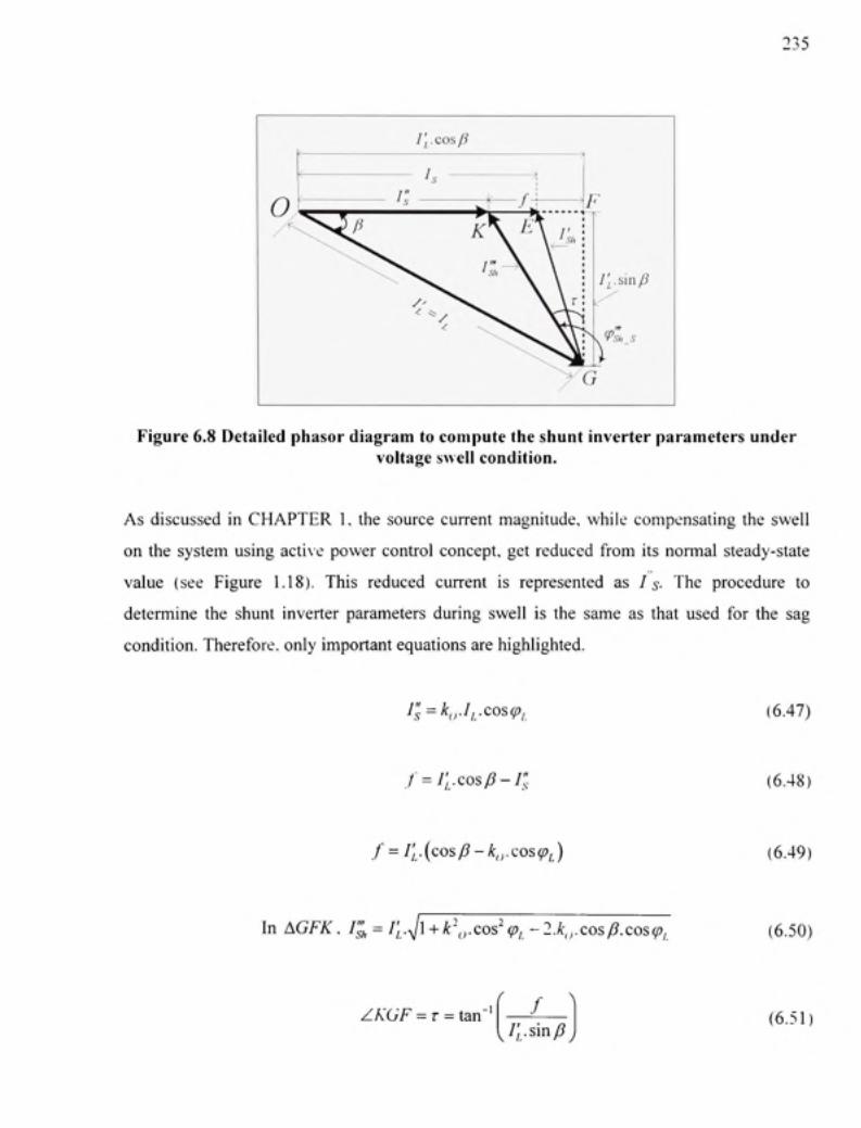
235
Figure 6.8 Detaile d phaso r diagram t o compute th e shunt inverte r parameter s unde r voltage swel l condition .
As discusse d i n CHAPTE R 1 , the sourc e curren t magnitude , whil e compensatin g th e swel l
on th e syste m usin g activ e powe r contro l concept , ge t reduce d fro m it s norma l steady-stat e
value (se e Figur e 1.18) . Thi s reduce d curren t i s represente d a s Is- Th e procedur e t o
determine th e shun t inverte r parameter s durin g swel l i s th e sam e a s tha t use d fo r th e sa g
condition. Therefore , onl y importan t equation s are highlighted .
h=^0-h.-^Q^(PL (6.47)
f = i[. cos p-i; (6.48)
/ = l[.[cosP - k,yCOS(Pi^) (6.49)
In AGFK. I'sf, = l[.yj\ + k\,.cos^(p,-2.k,yCosp.cos(Pi (6.50)
ZKGF = r = tan" / /;.sin/?
(6.51)
236
r = tan 1 cosP -k,,.cos(Pi sin/?
(6.52)
Therefore, Z(pl , = Z r + 90" (6.53)
and Zcpl , = ( Z r + 9 0 " ) - ^ (6.54)
Equations (6.50 ) an d (6.54 ) giv e th e require d magnitud e an d phas e angl e o f shun t inverte r
compensating curren t to achieve the desired operation fro m th e UPQC.
6.4 Summary o f PAC approach unde r different operatin g conditio n
To thi s point , th e analysi s o n phas e angl e contro l theor y applie d unde r steady-state , voltag e
sag and voltage swel l condition s have been thoroughly presented . Here , the brief summary o f
main equation s governing shun t and series parameters i s highlighted i n Table 6.1 .
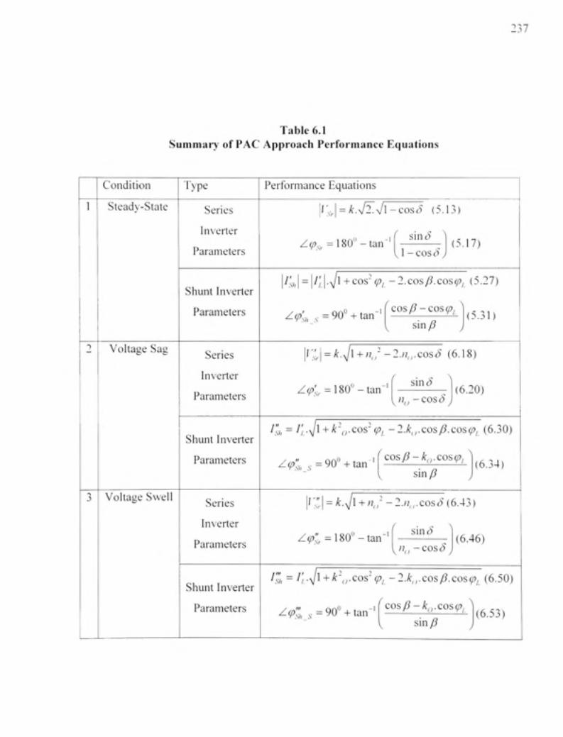
Table 6. 1 Summary o f PAC Approach Performanc e Equation s
237
Condition Type Performance Equation s
Steady-State Series
Inverter
Parameters
Ir, I = y t .VlVr^cos^ (5.13 )
Z^,,. = 180"-ta n -1 sinS 1 -cos (5
(5.17)
Shunt Inverte r
Parameters
l .svil ^\^'L\-\1^ + COS" (p, -2.cos/?.cos^; (5.27 )
Z ^ ; , , = 9 0 " + t a n -1 cos/?-cos ^/ sinp
:5.31
Voltage Sa g Series
Inverter
Parameters
|i;; | = A:.^l+//,/-2./?„.cos^^ (6.18 )
Z(^;,, = 180"-tan " sin^
yn^j -COS( 5 (6.20)
Shunt Inverte r
Parameters
/",, - ri.yj\ + k'i).cos' (Pi -2.kf).cos p.costp, (6.30 )
Z ^ ; , =90"+tan " cosP -kf-,.cos(pi sin/?
(6.34)
Voltage Swel l Series
Inverter
Parameters
\]';\ = k.^\ + nj -2.n,,.cosd (6.A^y^
Z(^;, =180"-tan " ^ si n S ^ y/7,, - C O S ^
(6.46)
Shunt Inverte r
Parameters
Q = l',_-\l\ + k\yCos'(p, -2.kf,.cosp.cos(p, (6.50 )
Z(pl , = 9 0 " + tan" cosP -k(i.cos(Pi sinp
(6.53)
138
r,,;,.,(. = k.yJ\+n,,--2.n,yC0sS (6.55)
Z^, , , , , , .=180"-tan- ' sinS y n^^ - co s d J
(6.56)
hh.i'.^c = li.yj\ + k\y cos- (p, - 2.k^,.cosp.cos(p, (6.57)
0 , . „ „ - ! ^ ^ s / , X/',.( • = 9 0 ^ + t a n cosP -k,i.cos(Pi
sinp (6.58)
As observe d fro m th e Tabl e 6.1 . th e performanc e equation s o f PA C approac h unde r voltag e
sag an d swel l conditio n fo r bot h th e inverter s ar e identical . Th e generalize d performanc e
equations fo r power angle control concep t can be written as :
The terms kf. no and ko are re-written as:
kf = — , n^) = \ + kg. an d k^ \ + k^
Where, I' v r,.. Steady State r j . Voltage Sag
r ; . Voltage Swell (6.59)
The possible values of ^/, no and ko are given i n Table 6.2 .
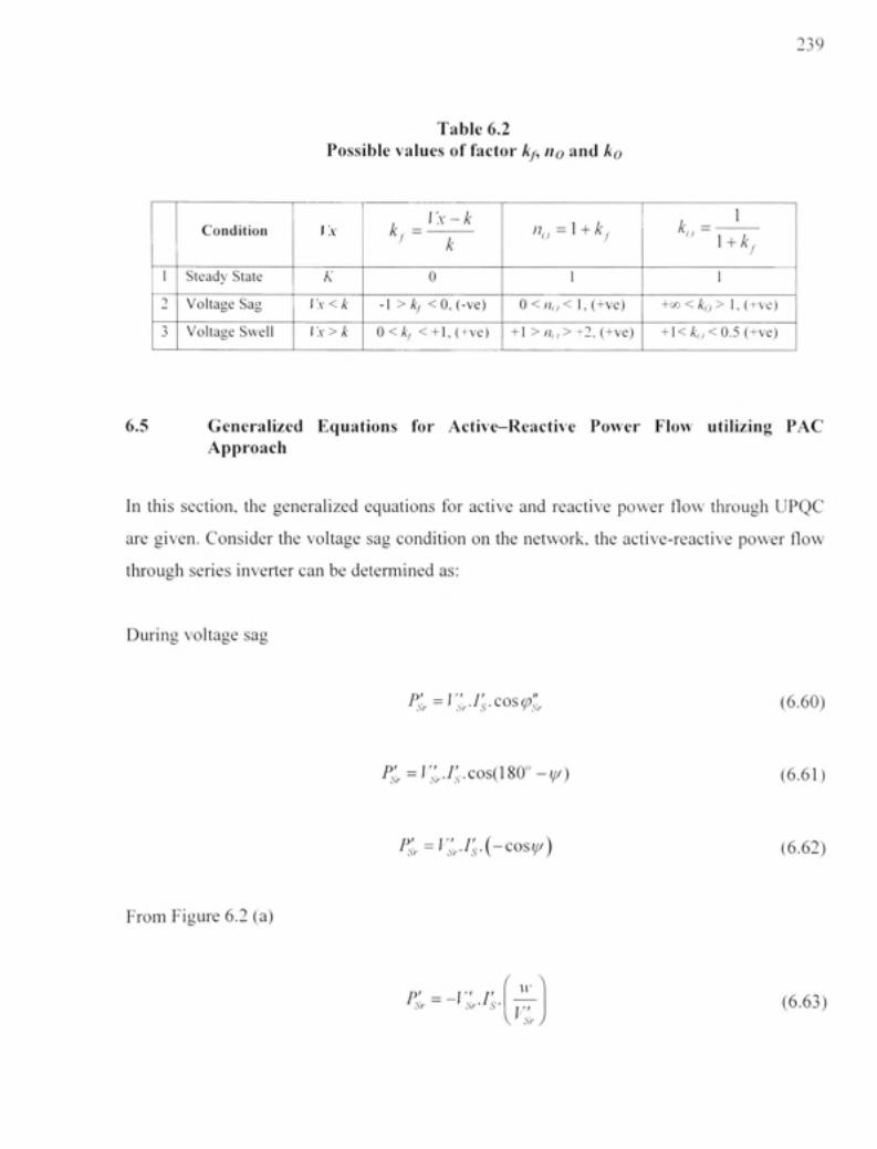
239
Table 6. 2 Possible values of factor A/ , no and ko
1
2
3
Condition
Steady Stat e
Voltage Sa g
Voltage Swel l
r.v
K
l\<k
I x > k
Vx-k ^ k
0
-1 > A: , <0, (-ve )
0<A> < + l , (+ve )
"o = 1 + ^/
1
0 <n,,< 1 , (+ve)
+ 1 > n,,> +2. (+ve)
/. - 1 ^"~\+k,
1
+crj< ko> 1 , (+ve)
+ l<A-,,<0.5 (+ve )
6.5 Generalize d Equation s fo r Active-Reactiv e Powe r Flo w utilizin g PA C Approach
In this section , th e generalize d equation s fo r activ e an d reactiv e powe r flow throug h UPQ C
are given . Conside r th e voltag e sa g conditio n o n the network , th e active-reactiv e powe r flow
through serie s inverte r can be determined as :
During voltage sa g
/ ^ = i ; . / ; . c o s < . (6.60)
/ , = f;;./;.cos(i 80"-v/) (6.61)
/^, = i;;./;.(-cos(^) (6.62)
From Figure 6.2 (a)
p' =-v' r ' Sr * .sy-'.s- K^rJ
(6.63)
240
P,',, =-r^.k.(n,, -cosS) (6.64)
The increase (I's) or decrease (l"s) in the source current magnitude during the voltage sag or
swell condition, respectively, is represented as.
h = h=K>-h.-^^^(pL (6.65)
Therefore, P ', , = -{k,,.l,.cos(pi).k.(n,, -cosS) (6.66)
For a losses system, since the reactive power is handled by UPQC, the source current can be
represented as .
1^ = l,.COS(p, (6.67)
Therefore, P,^,,^. = P; = -k,,.{k.l,).{n,,-cosS) (6.68)
For reactive power.
c'; = f;./;.sin<. (6.69)
^;, = r;./;,.sin(i80"-(//) (6.70)
Q'sr^^l-h-^'^^^ (6.71;
From Figure 6.2 (a)
O' = v r X.S> ' Sr-^S-
f \ X
V Sr ) [6.12)
241
^;=^.^,, ./ , .(sinc^) (•. • . v = A:sinc> ) (6.73 )
••• Qsr.,,,c-l<ir{k-h)-{sinS) (6.74 )
Equations (6.68 ) and (6.74 ) represen t th e generalized equation s fo r activ e an d reactiv e powe r
flow through serie s inverter .
In steady-stat e condition , withou t sa g and swel l o n the system , th e generalize d equation s fo r
the serie s inverte r shoul d resolv e t o norma l steady-stat e equations . O n th e othe r hand ,
without consideratio n o f PA C approach , unde r steady-state , th e activ e a s wel l a s reactiv e
powers handled b y serie s inverte r shoul d b e zero.
Check 1:
For steady-state PA C control , without sag/swell : ko=\. an d no=\
Equation (6.68 ) wil l be Ps>/'.4 ( =-k.h.(l-cosS)^ Equafio n (5.52 )
and (6.74 ) will be Qs^juc = kJs.{sinS) = Equation (5.56 )
Check2:
For steady-state condition , without PA C approach: ko=\, no^\. an d S^O
P,,.,^^. = -^./,..(1 -cosO) = 0 an d Q,,.,^^. = kJ,.(sin0) = 0
The activ e an d reactiv e powe r handle d b y th e shun t inverte r a s see n fro m th e sourc e sid e i s
computed. Thes e powers , under voltage sa g condition, can be determined as :
/'; = r;/;.cos^,;, (6.75 )
P;„=n„.k.i;,.cos{90"+p) {•.A';,^n,,.k) (6.76 )

242
Ps„=no.k.i;,.{-sinp) (6.77)
From Figur e 6.4 ,
Psh=-^cyk-n, J" \Ah J
(6.78)
Psh=->hrk.ll Sh •
{ \
e 1"
(6.79)
T'; = -n,j.k.l I.{cos p-kf^coscp,) (6.80)
p ^ Sh.r.AC
{k.l,).{cosp-k,y cos (p,) (6.81)
For reactive power .
g ; = r-./;.sin^;,, (6.82)
Ql,=nf,.k.h,,sin{90"+p) (6.83)
^ ; = ; 7 , . ^ . / ; . c o s ( p ) (6.84)
Qsh="u-k-Psh-„ Ij.sinP
1" ' Sh
(6.85)
Q.^ {k.l,).{sinP)
Sh.PAC (6.86)
Equations (6.81 ) and (6.86) represen t th e generalize d equation s fo r activ e an d reactiv e powe r
flow throug h shun t inverter .
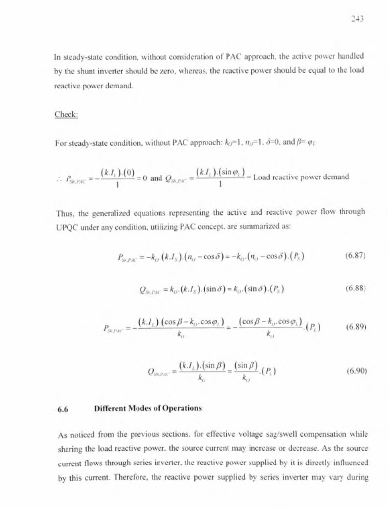
0 4:
In steady-stat e condition , withou t consideratio n o f PA C approach , th e activ e powe r handle d
by the shun t inverte r shoul d b e zero, whereas , the reactiv e powe r shoul d b e equa l t o the loa d
reactive power demand .
Check:
For steady-state condition , withou t PA C approach: ^o=l , no^\. S-0. and/? - tpi
ik-l,).{0) , ^ {kJA.{sin(p,) , J . A A • p =-1 —'•' ^ ' = 0 an d O , „,. = -'^—-"^ — = Load reactive power deman d
• • ^Sh,F.4C , li,S/,,f',-l f , t^
Thus, th e generalize d equafion s representin g th e activ e an d reactiv e powe r flow throug h
UPQC unde r any condition, utilizing PAC concept , are summarized as :
P,^,^,=-k,.{k.h).{nf,-cosS)^-k,,{n,-cosS).{P,) (6.87 )
Q.sr.P.,c=ko-{k-Is)-{^'^nS)^k,,{smS).{P,) (6.88 )
_ {k.l,).{cosp-k^yCos(p,) _ {cosp-k„.cos(p,) ^sh.p.Ac - , ~ 1. yA.)
^o '^c
(6.89)
(k.l,).{sinp) {sinp) , ,
'^o o
6.6 Differen t Mode s o f Operations
As notice d fro m th e previou s sections , fo r effectiv e voltag e sag/swel l compensatio n whil e
sharing th e loa d reactiv e power , th e sourc e curren t ma y increas e o r decrease . A s th e sourc e
current flows throug h serie s inverter , the reactiv e powe r supplie d b y i t i s directly influence d
by thi s current . Therefore , th e reactiv e powe r supplie d b y serie s inverte r ma y var y durin g
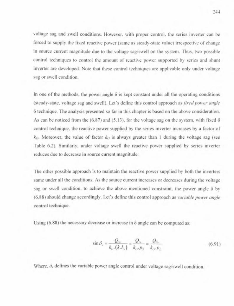
244
voltage sa g an d swel l conditions . However , wit h prope r control , th e serie s inverte r ca n b e
forced t o suppl y th e fixed reactiv e powe r (sam e a s steady-stat e value ) irrespectiv e o f chang e
in sourc e curren t magnitud e du e t o th e voltag e sag/swel l o n th e system . Thus , tw o possibl e
control technique s t o contro l th e amoun t o f reactiv e powe r supporte d b y serie s an d shun t
inverter ar e developed . Not e tha t thes e contro l technique s ar e applicabl e onl y unde r voltag e
sag or swell condition .
In on e o f th e methods , the powe r angl e 6 is kep t constan t unde r al l th e operatin g condition s
(steady-state, voltag e sa g an d swell) . Let' s defin e thi s control approac h as fixed power angle
5 technique. The analysi s presented s o far i n this chapter i s based o n the above consideration .
As can b e notice d fro m th e (6.87 ) an d (5.13) , fo r th e voltag e sa g on th e system , wit h fixed 5
control technique , th e reactiv e powe r supplie d b y th e serie s inverte r increase s b y a facto r o f
ko- Moreover , th e valu e o f facto r ko i s alway s greate r tha n 1 during th e voltag e sa g (se e
Table 6.2) . Similarly , unde r voltag e swel l th e reactiv e powe r supplie d b y serie s inverte r
reduces due to decrease i n source current magnitude .
The othe r possibl e approac h i s to maintai n th e reactiv e powe r supplie d b y bot h th e inverter s
same under al l the conditions. As the source curren t increase s or decreases during the voltag e
sag o r swel l condition , t o achiev e th e abov e mentione d constraint , th e powe r angl e 8 b y
(6.88) shoul d chang e accordingly . Let' s defin e thi s contro l approac h a s variable power angle
control technique .
Using (6.88) the necessary decreas e or increase in 5 angle can be computed as :
sinS^.= ~" = - ^ = -^ ( 6 91) Kj-{k.l,) k,yp^ k,yp,_
Where, S^. defines th e variable power angle control unde r voltage sag/swel l condition .
245
6.7 UPQC Controller Developmen t
The controlle r developmen t t o achiev e fixed an d variabl e powe r angl e contro l technique s i s
given i n thi s section . Th e step s essentia l t o determin e th e necessar y powe r angl e an d
reference serie s injected voltag e signal , to maintain th e loa d voltag e a t desired voltag e profil e
while performing th e load reactive power sharing i s also given .
6.7.1 Fixe d Powe r Angle (6/ ) Control Approac h
The controlle r t o achiev e th e fixed powe r angl e 5 / between th e sourc e an d loa d voltages ,
during th e steady-state , voltag e sa g an d swell , i s exactl y th e sam e a s alread v discusse d i n
CHAPTER 5 . Figure 6.9 i s a re-representation o f Figure 5.6 . I t is essential t o point out tha t a s
the serie s inverte r maintain s th e loa d voltag e a t desire d level , th e reactiv e powe r demande d
by th e loa d remain s constan t irrespectiv e o f change s i n th e sourc e voltag e magnitude .
Moreover, th e reactiv e powe r share d b y shun t inverte r i s fixed t o a predefined value , Qsh.ma.x,
the power angl e 5 remains unchanged . Note that this fixed shun t inverte r reactive power limi t
is use d just t o comput e th e instantaneou s powe r angl e 5 . Th e actua l reactiv e powe r handle d
by the shunt inverte r may vary based on the load requirements . As the power angl e 6 remains
constant unde r differen t operatin g conditions , the reactive powe r share d b y the series inverte r
and hence by the shunt inverte r changes as given by (6.88) and (6.90) .
PA(^')
From Fi g 5, 6
^^(ff lO •— I » . X
Sm" s.
q.Ac^t)
5J = sin '
Q.
^qAcot}} yPAct) J
Figure 6.9 Contro l diagra m fo r fixed powe r angle contro l approach .
M6
6.7.2 Variabl e Power Angle (8,) Control Approach
In cas e o f variable powe r angl e (6,) , th e reactive powe r share d b y series inverte r is
maintained at same level as that of steady-state value. As discussed in the previous section, to
maintain the reactive power shared bv ' series inv erter at normal steadv-stat e value , the power
angle S needs to change.
Figure 6.1 0 show s a block diagra m representatio n t o achiev e th e variabl e powe r angl e 6v
based controller , realize d usin g (6.91) . During norma l workin g condition , th e facto r ko will
be I , therefore, 5,,wil l b e th e sam e a s tha t compute d utilizin g fixed powe r angl e contro l
approach. The increase or decrease in source voltage magnitude will tend to change the value
of factor ko from 1 , and thus, the power angle will change accordingly.
Note that the computed instantaneous reactive power shared bv the series inverter qsA<-'^(> ha s
identical values (Figure 6.9 and Figure 6.10). However , the factor ko in variable power angle
control technique adjusts the instantaneous angle S to maintain the fix value of series inverter
reactive power.
V,(CDt) )
Sensed Inpu t Voltage
Fundamental Voltag e Peak Detection
p,{on) -
From Fig 5 6
<iA(^') X
<?.s>(®')
^
Desired Loa d Voltage Magnitude
Snf
S„ = si n (}sr((^')
kg.p^(cot)
5
Figure 6.10 Control diagram for variable angle control approach.
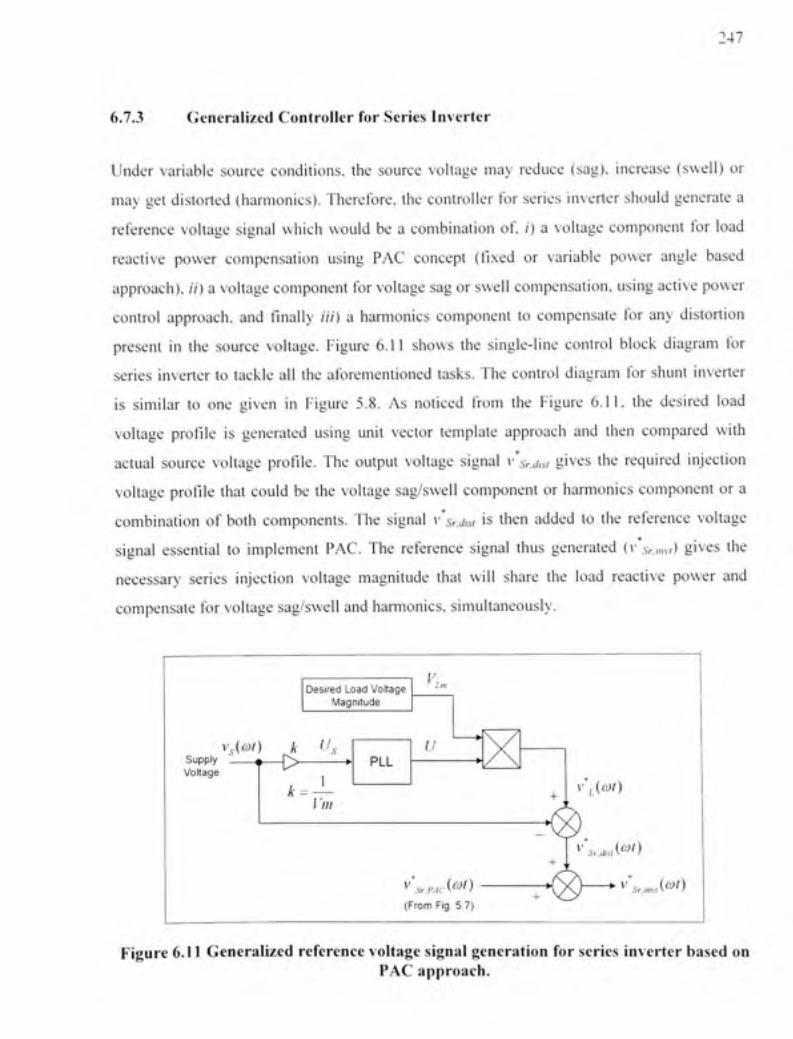
247
6.7.3 Generalized Controlle r for Series Inverte r
Under variabl e sourc e conditions , th e source voltag e ma y reduce (sag) , increas e (swell ) or
may ge t distorted (harmonics) . Therefore , th e controller fo r series inverte r shoul d generat e a
reference voltag e signa l whic h woul d b e a combination of , /) a voltage componen t fo r load
reacfive powe r compensatio n usin g PA C concep t (fi.xe d o r variabl e powe r angl e base d
approach). // ) a voltage component fo r voltage sag or swell compensation , using active powe r
control approach , an d finally /// ) a harmonics componen t t o compensate fo r any distortion
present i n the source voltage . Figur e 6.1 1 show s th e single-lin e contro l bloc k diagra m for
series inverte r t o tackle al l the aforementioned tasks . The control diagra m fo r shunt inverte r
is simila r t o one given i n Figure 5.8 . As noticed fro m th e Figure 6.11 , th e desired loa d
voltage profil e i s generated usin g uni t vecto r templat e approac h an d then compare d wit h
actual sourc e voltag e profile . Th e output voltag e signa l v*sr.cjisi give s th e required injectio n
voltage profil e tha t coul d be the voltage sag/swel l componen t o r harmonics componen t o r a
combination o f both components . Th e signal v*srd,st i s the n adde d t o the reference voltag e
signal essentia l t o implement PAC . Th e reference signa l thu s generate d (v sr.imA give s the
necessary serie s injectio n voltag e magnitud e tha t wil l shar e th e load reactiv e powe r and
compensate fo r voltage sag/swel l and hannonics, simultaneously .
Supply Voltage
Desired Load Voltage Magnitude
V, Lm
Vc(6;0 k ^Is ^
m
PLL U
^' Sr.F.AC^f) (From Fig , 5,7)
+
V ,{cot)
) .
^Asr.dcA^O
—*^''sr.,nJ^')
Figure 6.11 Generalized referenc e voltage signal generatio n for series inverte r base d on PAC approach .
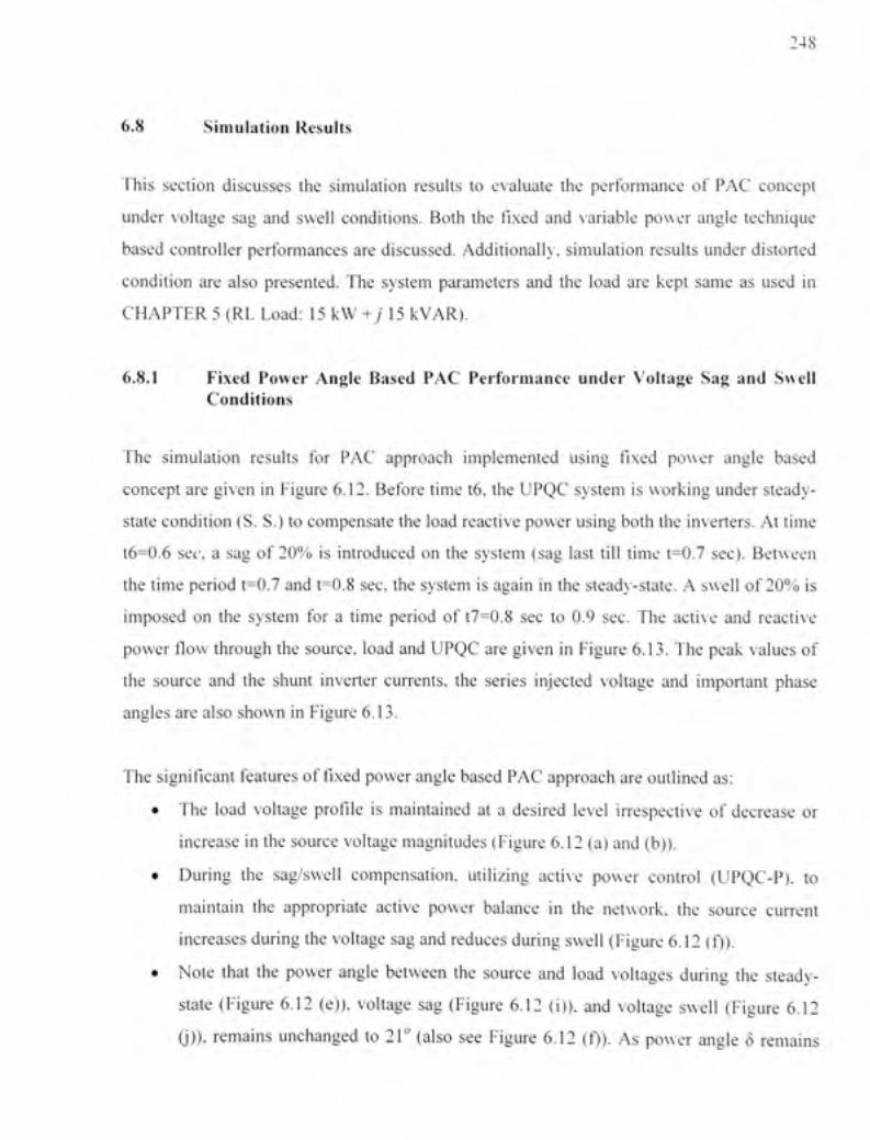
248
6.8 Simulatio n Result s
This sectio n discusse s th e simulatio n result s t o evaluat e th e performanc e o f PA C concep t
under voltag e sa g an d swel l conditions . Bot h th e fixed an d variabl e powe r angl e techniqu e
based controlle r performance s ar e discussed . Additionally , simulatio n result s unde r distorte d
condition ar e als o presented . Th e syste m parameter s an d th e loa d ar e kep t sam e a s use d i n
CHAPTER 5 (RL Load : 1 5 kW +7 1 5 kVAR).
6.8.1 Fixe d Powe r Angl e Base d PA C Performanc e unde r Voltag e Sa g an d Swel l Conditions
The simulatio n result s fo r PA C approac h implemente d usin g fixed powe r angl e base d
concept ar e give n i n Figur e 6.12 . Befor e tim e t6 , the UPQ C syste m i s working unde r steady -
state condition (S . S.) t o compensate th e load reactive power usin g both the inverters . At tim e
t6=0.6 set" , a sa g o f 20 % i s introduce d o n th e syste m (sa g las t til l tim e t=0. 7 sec) . Betwee n
the time period t=0. 7 and t=0.8 sec , the system i s again i n the steadv-state . A swel l o f 20% is
imposed o n th e syste m fo r a tim e perio d o f t7=0. 8 se c t o 0. 9 sec . Th e activ e an d reactiv e
power flow throug h th e source , load an d UPQ C ar e given i n Figure 6.13 . The pea k value s o f
the sourc e an d th e shun t inverte r currents , th e serie s injecte d voltag e an d importan t phas e
angles are also shown i n Figure 6.13 .
The significant feature s o f fixed power angle based PA C approach ar e outlined as :
• Th e loa d voltag e profil e i s maintaine d a t a desire d leve l irrespectiv e o f decreas e o r
increase i n the source voltage magnitudes (Figur e 6.12 (a) and (b)) .
• Durin g th e sag/swel l compensation , utilizin g activ e powe r contro l (UPQC-P) , t o
maintain th e appropriat e activ e powe r balanc e i n th e network , th e sourc e curren t
increases during the voltage sa g and reduces during swel l (Figur e 6.12 (f)) .
• Not e tha t th e powe r angl e betwee n th e sourc e an d loa d voltage s durin g th e steady -
state (Figur e 6.12 (e)) , voltag e sa g (Figur e 6.1 2 (i)) , an d voltag e swel l (Figur e 6.12
(])), remain s unchange d t o 21 " (also se e Figur e 6.1 2 (f)) . A s powe r angl e 5 remain s
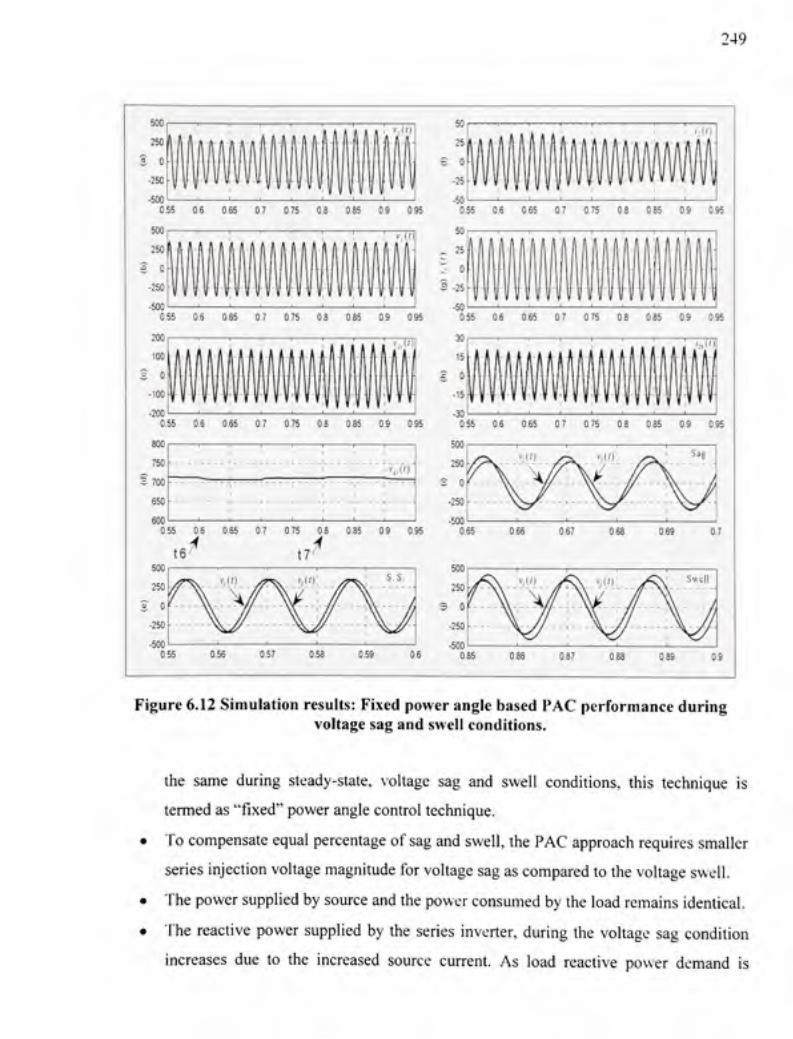
249
500
250
5 0
-250
-500
' ' ' ' ' ' ' / ;
lffVwWi|fl|||||l||fl _J 1 _
0,55 0 6 0.6 5 0 7 0 7 5 0 6 0.8 5 0 9 0 95
500 I : : . , , ,
250
5 O H
-250 -
-500
V 1 / 1
-50 0.55 0 6 0.5 5 0 7 0 7 5 0 8 0 8 5 0 9 0 9 5
200 r
100
2 o f -100
0 5 5 0 6 0 6 5 0. 7 0 7 5 0 8 0 8 5 0 9 0 95
30 r
15
e o | -15
-200 0 5 5 0 6 0.6 5 0 7 0.7 5 0 8 0,8 5 0 9 0 9 5
800 r
-30
1 ) i L ' VC )
750
• 700
650
600 0,55 0 5 0.6 5 0. 7 0 7 5 0 8 0 8 5 0 9 0 95
t6'^ t7 ' 500
_1 L _
0 55 0 6 0 6 5 0. 7 0 7 5 0 8 0 85 0 9 0,9 5
500r
250-
S 0 '
-250-
-500 055
-500 085
y < \ >(( ) y C
f\\f s \ ''•'" ' i / \AA 7/
; N I Swel l
1
0.87 09
Figure 6.12 Simulation results : Fixed power angle based PAC performance durin g voltage sag and swell conditions.
the sam e durin g steady-state , voltag e sa g an d swel l conditions , thi s techniqu e i s
termed as "fixed" power angle control technique.
To compensate equal percentage of sag and swell, the PAC approach requires smaller
series injection voltage magnitude for voltage sag as compared to the voltage swell.
The power supplied by source and the power consumed by the load remains identical.
The reactive powe r supplie d b y the serie s inverter , durin g the voltag e sa g conditio n
increases du e t o th e increase d sourc e current . A s loa d reactiv e powe r deman d i s
250
constant, th e reactiv e powe r supplie d b y the shun t inverte r reduce s accordingly . O n
the other hand , during the voltage swel l condition , the reactiv e powe r share d b y the
series inverter reduces and shunt inverte r increases (see Figure 6.13 (c) and (d)) . The
reduction an d incremen t i n shun t compensatin g curren t magnitud e (Figur e 6.1 3 (e) )
also confirms the abovementioned fact .
Although th e reactiv e powe r share d b y th e serie s an d shun t inverter s i s varied , th e
sum of their reactive powers always equals the reactive power demanded by the load.
Source
' , ' ' • ' •
^' , !
- - — PAD
9.(0
/>,(') ' / l O
0 55 0 6 0 65 0 7 0 75 0 8 0 85 0 9 0 95 0 55 0 6 0 65 0 7 0 75 0 8 0 85 0 9 0 9 6
4
< > o
g •o 0
' Ser ie s
_ ^ . \
fiv erter.
''
:\ PsM).
Q: < 2 2
I S 0
'Shunt Inverter' 1s>W
P«(')
"X 0 5 5 0 6 0 65 0 7 0 75 0 8 0 65 0 9 0 95 5 0 55 0 6 0 65 0 7 0 75 0 8 0 85 0 9 0 9 5
S, 15 0 E
> £ s o
'_j\t^ "Vv-
116'
101 V ' ^
20 9'
; > » 9v : r i
— Z : 70 1 " " " 1
20 r ' ' < 5
12?
f 126 \ >
21* '
0.55 0 6 0 65 0 7 0 75 0 8 0 85 0 9 0 95 0 55 0. 6 0 65 0 7 0 75 0 8 0 85 0 9 0 95 S.S. \* *\ s S l < • • ! s s . S S ] < - ^ » | s S . \* • ! s S
16 Sag
17 16 Sag
17
Figure 6.13 Simulation results: active - reactiv e power flow unde r fixed power angle based PAC approach.

251
6.8.2 Variabl e Powe r Angle Base d PA C Performanc e unde r Voltag e Sa g and Swel l Conditions
The simulatio n result s base d o n variabl e powe r angl e contro l techniqu e ar e give n i n Figur e
6.14 an d Figur e 6.15 . All th e conditions and parameter s ar e kep t identica l t o the one use d fo r
fixed powe r angle contro l technique .
The distinctiv e feature s o f variabl e powe r angl e base d PA C approac h ar e describe d an d
compared wit h fixed powe r angl e control technique :
• Th e loa d voltage profile i s effectively maintaine d a t a desired leve l during voltage sa g
and swel l condition (Figur e 6.14 (a ) and (b)) .
• A s notice d fro m th e Figur e 6.1 5 (e ) an d Figur e 6.1 3 (e) , irrespectiv e o f fixed o r
variable powe r angl e control , th e sourc e deliver s almos t sam e amoun t o f current s t o
compensate fo r voltag e sag and swel l on the system .
• Th e power angl e between th e source and loa d voltage s during the voltage sa g (Figur e
6.14 (i) ) i s reduce d t o 16.5 ° a s compare d t o stead y stat e valu e o f 20.9 " (Figure 6.1 4
(e)). O n th e othe r hand , durin g th e voltag e swell , th e powe r angl e 5 i s increase d t o
26''. Since , powe r angl e 6 change s durin g suppl y voltag e sa g an d swel l conditions ,
this technique i s termed as "variable" power angle control approach .
• T o compensat e equa l percentag e o f sag , the variable 6 control require s slightl y lesse r
series injecfio n voltag e magnitud e compare d t o the fixed 5 control. Fo r equa l amoun t
of voltage swell , the variable 5 control require s highe r magnitud e o f injectio n voltag e
than th e fixed 6 control technique . Thi s i s due t o th e increase d powe r angl e betwee n
the resultant loa d and source voltages .
• Th e powe r handle d b y th e sourc e an d th e loa d remain s identica l t o th e steady-stat e
values.
• Note : The reactive power supplie d b y the serie s and shun t inverter , durin g the voltag e
sag an d swell , maintaine d a t th e constan t leve l equal s t o th e steady-stat e value ,
irrespective o f th e increas e o r decreas e i n the sourc e curren t magnitud e (Figur e 6.1 5
(c) and (d)) . Also, note that the shunt compensating curren t magnitud e remain s almos t
constant durin g al l the conditions .

T ^ - )
• Th e majo r facto r t o achiev e th e fixed reactiv e powe r sharin g (a s i n variabl e powe r
angle control ) an d th e variabl e reactiv e powe r sharin g (a s i n fixed powe r angl e
control) features i s obtained by controlling the magnitude and the phase angles of the
injected voltag e an d curren t o f the UPQC. The difference i n these quantitie s ca n be
noticed from the Figure 6.13 (f) and Figure 6.15 (f).
In summary, the proposed PAC concept effectively compensate s the v oltage sag and swell on
the system . Tw o differen t contro l techniques , namely , variabl e 6 an d fixed 5 contro l ar e
introduced t o giv e hig h degre e o f freedo m fo r optima l utilizatio n o f UPQ C unde r v ariable
V oltage condition.
500 250
S 0 -250
-500
. . . • . . . . . . . fl fl « « • « ' - - • ' " yu/ioaftMMMH \\\\m -l)l)py-yyv-V||-H-yi)ll| - n ^
0 55 0 6 0 65 0 7 0 7 5 0 8 0 65 0 9 0 95 0 55 0 6 0 65 0 7 0 7 5 0 8 0 85 0 9 0 95
0.55 0 6 0 65 0 7 0 7 5 0 8 0 85 0 9 0 95 0.5 5 0 6 06 5 0. 7 0.7 5 0. 8 0 85 0 9 0 95
0.55 0 6 0 65 0. 7 0.7 5 0 8 0 85 0. 9 0 95 0 55 0 6 0 65 0. 7 0.7 5 0 8 0 85 0 9 0.9 5
800
750
§ 70 0
650
600
'A) '
0 55 0 6 0.6 5 0. 7 0.7 5 0 8 0.8 5 0. 9 0 95 0,6 5 0.655 0.56 0.66 5 0.67 0.675 0 68 0 685 069 0 695 0 7
5 ^ U^ 16
Figure 6.14 Simulation results: variable power angle based PAC performance durin g voltage sag and swell conditions.
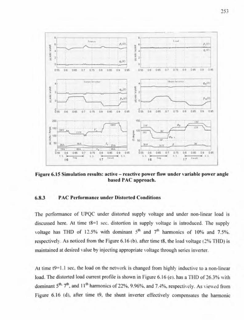
2DJ
- - - - • '
Source
; ;
PsO-
' qsi') l""" , , .
PA)
55 0 6 0 65 0 7 0 75 0 6 0 85 0 9 0 95 0 55 0 6 0 65 0 7 0 75 0 8 0 85 0 9 0 95
Scrics Invcrtc r . 1 i _ .
7 V P,X')
"V
4
< 2 2 > e 0
' Shunl Invt;itc -
. __/ v _ , ! 1
1 \ '
"V
Vi.C)
PsAD
^ 0 55 0 6 0 65 0 7 0 75 0 8 0 85 0 9 0 95 0 55 0 6 0 65 0 7 0 75 0 8 0 85 0 9 0 95
200
g.150 E < « 10 0 o > S 5 0
126 V
29A
19A
'V. : . [ . r • V. f l l i v y ' «
W - . _ L
36A ; / ,
, 20 A , : U
183V ; l
'---yx^
25A 20A ;
150
Q) 10 0
116
lUl
20 9
V -89
1 <P3, S
S
^> ' v /
' ne / •
125-
26
^X. \:r
•^ 0 55 0 6 0 65 0 7 0 75 0 8 0 65 0 9 0 95 0.5 5 0 6 0 65 0 7 0 75 0 8 0 85 0 9 0 95
.s s \* • »• ! s s \* »• ! S. S S . S . I < : • ! s s 1 < • ! s s 16 17 16
Sag 17
Figure 6.15 Simulation results: active - reactiv e power flow under variable power angle based PAC approach.
6.8.3 PAC Performance under Distorted Conditions
The performanc e o f UPQ C unde r distorte d suppl y voltag e an d unde r non-linea r loa d i s
discussed here . A t tim e t8= l sec , distortio n i n suppl y voltag e i s introduced . Th e suppl y
voltage ha s TH D o f 12.5 % wit h dominan t 5 ^ an d 7* ^ harmonic s o f 10 % an d 7.5% ,
respectively. As noticed from the Figure 6.16 (b), after fime t8, the load voltage (2% THD) is
maintained at desired value by injecting appropriat e voltage through series inverter.
At time t9=l.l sec , the load on the network i s changed fro m highl v inductiv e to a non-linear
load. The distorted load current profile i s shown in Figure 6.16 (e). has a THD of 26.3% with
dominant 5* ' 7*, and 11** " harmonics of 22%, 9.96%, and 7.4%, respectively. As viewed fro m
Figure 6.1 6 (d) , afte r fime t9 , th e shun t inverte r effecfivel y compensate s th e harmoni c
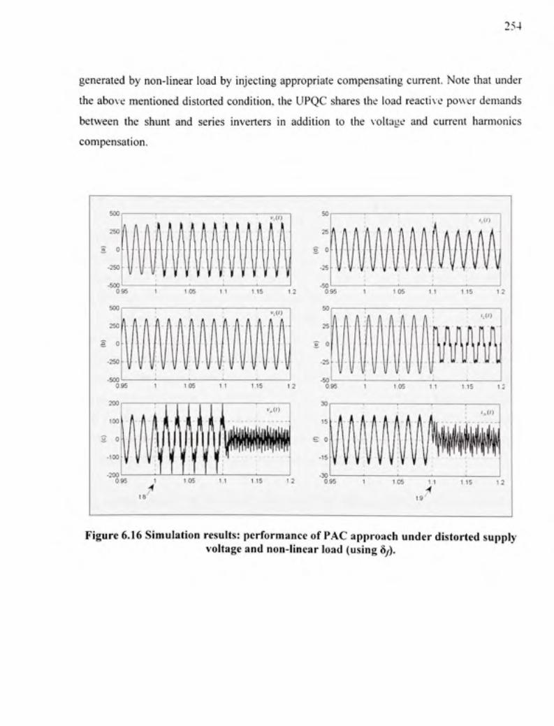
254
generated b y non-linear loa d by injecting appropriat e compensating current . Note that unde r
the above mentioned distorte d condition , the UPQC shares the load reactiv e power demand s
between th e shun t an d serie s inverter s i n additio n t o th e voltag e an d curren t harmonic s
compensation.
500
250
-250
-500 0 95
500
- J 1 _ U_ \i
V ( 0
1 05 1 1 1 1 5 1 2
30
15
t 0
-15
-30 0.95 1
0 95 1 1 0 5 1 1 11 5 1 2
095 1 1.0 5 1. 1 1.1 5 1 2
A n A i i M A M A ' /
1.05 1 1 1.1 5 1. 2
19
Figure 6.16 Simulation results : performance of PAC approach under distorted supply voltage and non-linear load (using 8/).

'• ^
6.9 Experimenta l Result s
In thi s section , th e performanc e o f PA C approach , w ith fixed powe r angl e 5/ . under \ oltage
sag, swel l an d distorte d suppl y voltag e i s validate d throug h experimenta l study . Al l th e
parameters an d the load conditions are identical a s that discussed an d used i n CHAPTER5.
6.9.1 Performanc e o f PAC under Voltage Sag Conditio n
The experimenta l result s durin g the voltag e sa g on the syste m ar e show n i n Figur e 6.17 . I t i s
considered tha t th e UPQ C i s already workin g unde r PA C (wit h fixed powe r angl e 5 / control
technique) an d share s th e loa d reactiv e powe r (loa d powe r facto r 0. 6 lagging ) utilizin g bot h
the inverters . The power angl e 5 between th e loa d an d sourc e voltages i s found a s 10° . Unde r
such condition , a sag of 17 % is introduced o n the system . Th e reduce d sourc e voltag e profil e
can b e notice d fro m th e Figur e 6.1 7 (a ) [uppe r trace] . Th e UPQ C wit h th e propose d PA C
theory maintain s the loa d voltag e a t a desired leve l whil e supportin g th e loa d reacfiv e powe r
using bot h th e inverters . A s discusse d previously , ther e i s a sligh t increas e i n th e sourc e
current magnitud e (fro m 1.5 A t o 1.65A ) i n orde r t o achiev e a n effectiv e sa g compensation .
The resultan t loa d an d sourc e voltag e profile s ar e compare d i n Figur e 6.1 7 (b) . Not e th e
effect o f reduce d suppl y voltag e doe s no t appea r acros s th e loa d terminal . Th e powe r angl e
10° between th e two voltages i s also noticeable i n the figure .
The voltag e injecte d b y th e serie s inverte r an d th e shun t curren t durin g th e voltag e sa g
compensation mod e o f operatio n ar e give n i n Figur e 6.1 7 (c) . Th e presenc e o f in-phas e
voltage componen t (1^2 ) i n additio n t o th e loa d reactiv e powe r componen t (i^y ) ca n b e
observed fro m th e serie s injecte d voltag e profil e (trace-3) . Th e performanc e o f th e shun t
inverter i s plotte d i n Figur e 6.1 7 (d) . Comparin g Figur e 5.2 0 (b ) an d Figur e 6.1 7 (d) , th e
slightly increase d sourc e an d shun t curren t magnitude s ca n b e noticed durin g th e voltag e sa g
compensation. Figur e 6.18 gives the experimenta l result s showin g the source , loa d an d serie s
injected voltage s under 17 % and 28% of sags with power angle s 6=10° and 5=15° .
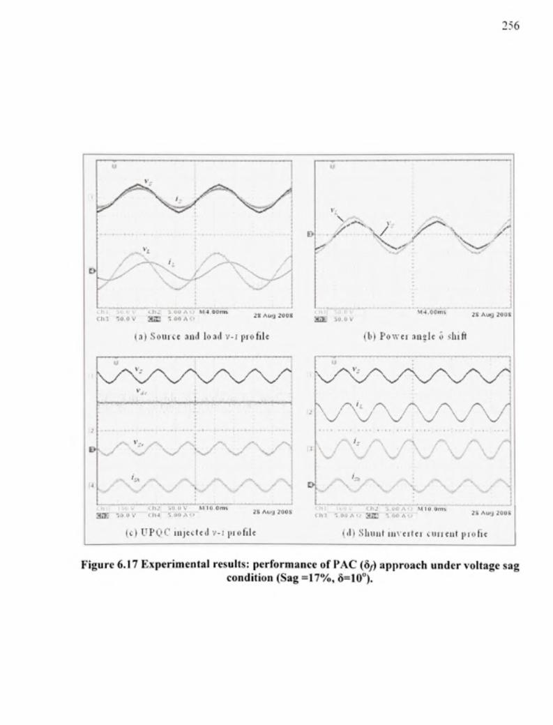
256
i h i 5 0 I J V Ch.: ] S . O O A O M>4.00m s c.hX •50. 0 V a i E " i o n A < , ' 28 AlK j 200 8
In) Souic e niu l lon d v- j piofil e
&•
rfWijiiiii(iy)*wy>»N4««*j i*fWijiiiii(iyfJwy>»N'y«»*;»»»«^^ '
V ^y^AA^^.yA.y^y^K.'^' t-.; i ' i •.«'•. .
y X > • • "%- • y
a i E ~ ^ n , o v c:h4 ; ?;.i)nA <
lc) UPQ C injecte d v- j piofil e
2S AU(| 2aos
E> :\ J"; \>y \
an: 50. 0 v M 4 .00m s 2S AlK J 200 s
(b) Powe i ansl e 0 shif t
V^O^' /
X /* v A . A. / \ A / v V \ y i\ y \ / V
/"
^•y\y \ ' h I _ l i;U_ V ^Ch2[_jS^OO_AJ,J^:M:i0,0m s n r i " '^. .ni iA' . ' a i E 1 nrTA^-r " 28 Au< j 200 s
ll Sluiii f ii u e i k i a n i e n t piofi e
Figure 6.17 Experimental results : performance o f PAC (8/) approach unde r voltage sa g condition (Sa g =17%, 8=10°) .
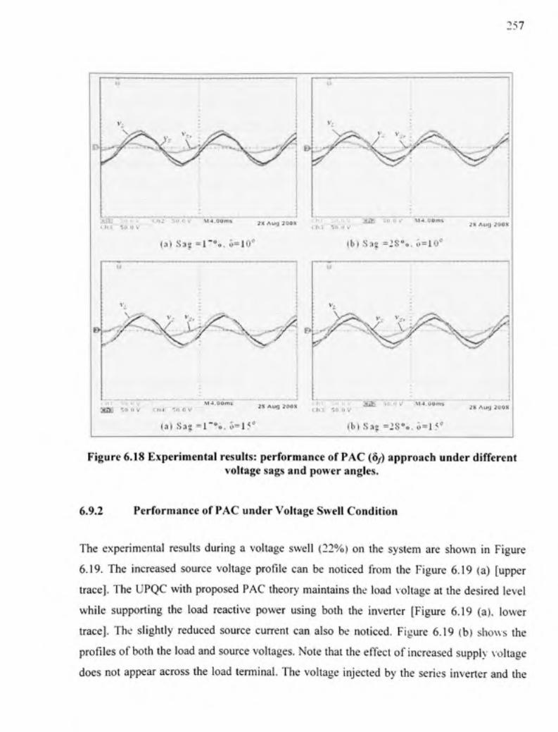
257
(a) Sai : = 1 " % . o=10°
ii.o V MiV v s u . o V \ ) - i , o u m 5
ibl Sa s = 2 8 % . o = iO"
2S A n y 200 X
ana -no v cii-i j 50:0 v 2S Au q 200 X
(a) S a s = 1 " % , 0 = 1 . ^ '
i i o v Ma- J :•;() , 0 V M ^ . o o m s c h : i SO.O V
lb) Sa * = : S « o . c ) = l.^''
2S Ati y 2 0 0 8
Figure 6.18 Experimental results : performance of PAC (8/) approach under differen t voltage sags and power angles.
6.9.2 Performanc e o f PAC under Voltage Swell Condition
The experimenta l result s durin g a voltage swel l (22% ) o n th e syste m ar e show n i n Figur e
6.19. Th e increase d sourc e voltag e profil e ca n b e notice d fro m th e Figur e 6.1 9 (a ) [uppe r
trace]. The UPQC with proposed PA C theory maintains the load voltag e at the desired leve l
while supportin g th e loa d reacfiv e powe r usin g bot h th e inverte r [Figur e 6.1 9 (a) , lowe r
trace]. Th e slightl y reduce d sourc e curren t ca n als o b e noticed . Figur e 6.1 9 (b ) show s th e
profiles o f both the load and source voltages. Note that the effect o f increased suppl y voltag e
does not appear acros s the load terminal . The voltage injecte d b y the series inverte r an d the
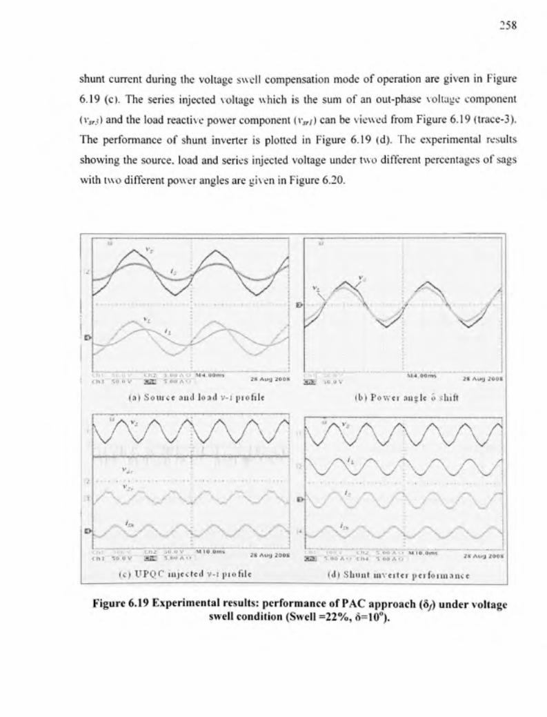
258
shunt curren t durin g the voltag e swel l compensatio n mod e o f operation ar e give n i n Figure
6.19 (c) . Th e serie s injecte d voltag e whic h i s the su m o f a n out-phas e vollag e componen t
(VsrA and the load reacfive powe r component (i^/ ) can be viewed fro m Figur e 6.19 (trace-3).
The performanc e o f shun t inverte r i s plotte d i n Figur e 6.1 9 (d) . Th e experimenta l result s
showing the source , load and serie s injected voltag e under two different percentage s of sags
with two different powe r angles are giv en in Figure 6.20.
<, In 5U. 0 V !C|12 ; 3.0 0 A S? M4.00m s chrt Wo.o'v a m •^.ooACfi
la ) S o u i c e an d loa d v- i prof i l e
2XALKJ200X g ^ l . . ( , y ^ 28 AlK j 200 8
(b) Povve i ansl e o shif t
c h ! ! c u v Ch2 i 3u,o y MICOin s 28 Auy 200 8
lc ) U P Q C in j ec t e d v- i p io f i l e Id) S h u n l i m e i t e i p e i f o i i n a n c e
Figure 6.19 Experimental results : performance of PAC approach (8/) under voltage swell condition (Swell =22%, 8=10°).

259
! TiiM j V 3iii S so,o v M4.oam< i
|a) Swel l =22% , G=tO °
; . h i ,S 0 0 V •aH' i 30,1 1 V \1-4,00m 5 2SAU<J200S C h l 5 0 0 V
lb) Swel l =.>t% . o = t n '
iX A u y 200 X
, ! ' "Si'ft". ! •,• • • affS i 2 5 0 V<- ) Mi4 .co in s Cll3 3 0 . 0 V
2S A u g 2 0 0 S
(a) Swel l =22% , G=15 '
r i i ! -.( i r i V rai K T O n V ,vt4,00m s Ch3 50, 0 V
(b) Sa 2 = . n " o . . ^ l ' "
2S Au q 200 S
Figure 6.20 Experimental results : performance of PAC (8/) approach under differen t voltage swells and power angles.
6.9.3 Dynamic Performance of PAC during Voltage Sag\Swell Condition s
The dynamic performance of UPQC with proposed PAC under momentary occurrence of the
voltage sag and the voltage swel l is given in Figure 6.21 an d Figur e 6.22 , respectively . The
scaled profiles o f the source, load and series injected voltage s are also given in the respective
figures. Note tha t th e UPQC maintain s th e load voltag e a t constan t leve l irrespectiv e of
changes (decrease or increase) in the source voltage. The power angle 5 between the resultant
load voltage and the actual source voltage can also be noticed from the scaled figures. In both
the cases, the UPQC shares the load reactive power utilizing the shunt and series inverters.
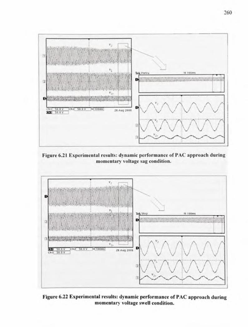
260
Figure 6.21 Experimental results : dynamic performance o f PAC approach durin g momentary voltag e sag condition.
mmmmmmmimmMm!im'!\
2S Au g 200 8
Figure 6.22 Experimental results : dynamic performance o f PAC approach durin g momentary voltag e swell condition .
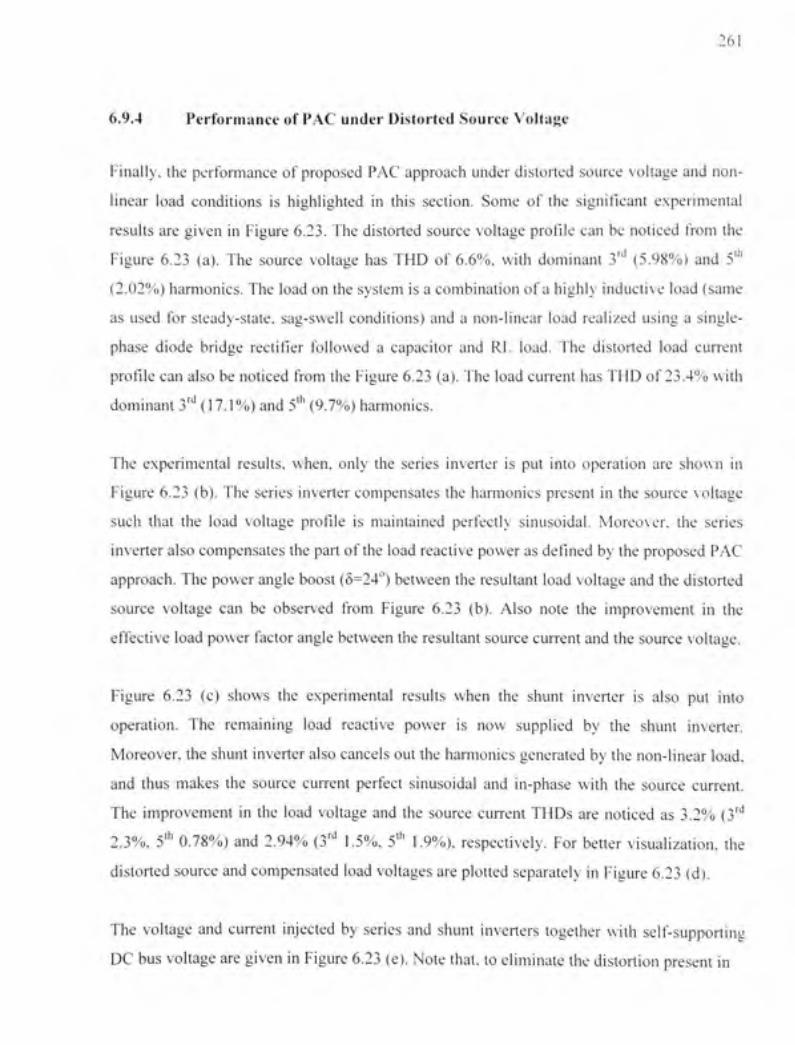
261
6.9.4 Performanc e o f PAC under Distorted Sourc e V oltage
Finally, th e performanc e o f proposed PA C approac h unde r distorte d sourc e voltag e an d non -
linear loa d condition s i s highlighte d i n thi s section . Som e o f th e significan t experimenta l
results ar e give n i n Figur e 6.23 . The distorte d sourc e voltag e profil e ca n b e notice d fro m th e
Figure 6.2 3 (a) . Th e sourc e voltag e ha s TH D o f 6.6% , wit h dominan t 3 ^ (5.98% ) an d 5' ^
(2.02%) harmonics . The loa d on the system i s a combination o f a highly inductiv e loa d (sam e
as use d fo r steady-state , sag-swel l conditions ) an d a non-linear loa d realize d usin g a single -
phase diod e bridg e rectifie r followe d a capacito r an d R L load . Th e distorte d loa d curren t
profile ca n also be noticed fro m th e Figure 6.23 (a) . The load curren t ha s THD of 23.4% with
dominant 3" ^ (17.1%) and 5" ' (9.7%) harmonics .
The experimenta l results , when , onl y th e serie s inverte r i s put int o operatio n ar e show n i n
Figure 6.2 3 (b) . The serie s inverte r compensate s th e harmonic s presen t i n the sourc e v oltage
such tha t th e loa d voltag e profil e i s maintaine d perfectl y sinusoidal . Moreover , th e serie s
inverter als o compensates the part o f the loa d reactive power a s defined b y the proposed PA C
approach. Th e power angl e boost (5=24° ) between the resultant loa d voltage and the distorte d
source voltag e ca n b e observe d fro m Figur e 6.2 3 (b) . Als o not e th e improvemen t i n th e
effective loa d power facto r angl e between the resultant sourc e current and the source voltage .
Figure 6.2 3 (c ) show s th e experimenta l result s whe n th e shun t inverte r i s als o put int o
operation. Th e remainin g loa d reactiv e powe r i s no w supplie d b y th e shun t inverter .
Moreover, the shun t inverte r also cancels out the harmonics generate d b y the non-linear load ,
and thu s make s th e sourc e curren t perfec t sinusoida l an d in-phas e wit h th e sourc e current .
The improvemen t i n th e loa d voltag e an d th e sourc e curren t THD s ar e notice d a s 3.2 % (3" *
2.3%, 5" ^ 0.78%) an d 2.94 % (3 ^ * 1.5%, 5" ^ 1.9%) . respectively. Fo r bette r visualization , th e
distorted sourc e and compensated loa d voltages are plotted separatel y i n Figure 6.2 3 (d) .
The voltag e an d curren t injecte d b y serie s an d shun t inverter s togethe r wit h self-supportin g
DC bu s voltage ar e given i n Figure 6.23 (e) . Note that , to eliminate th e distortion presen t i n
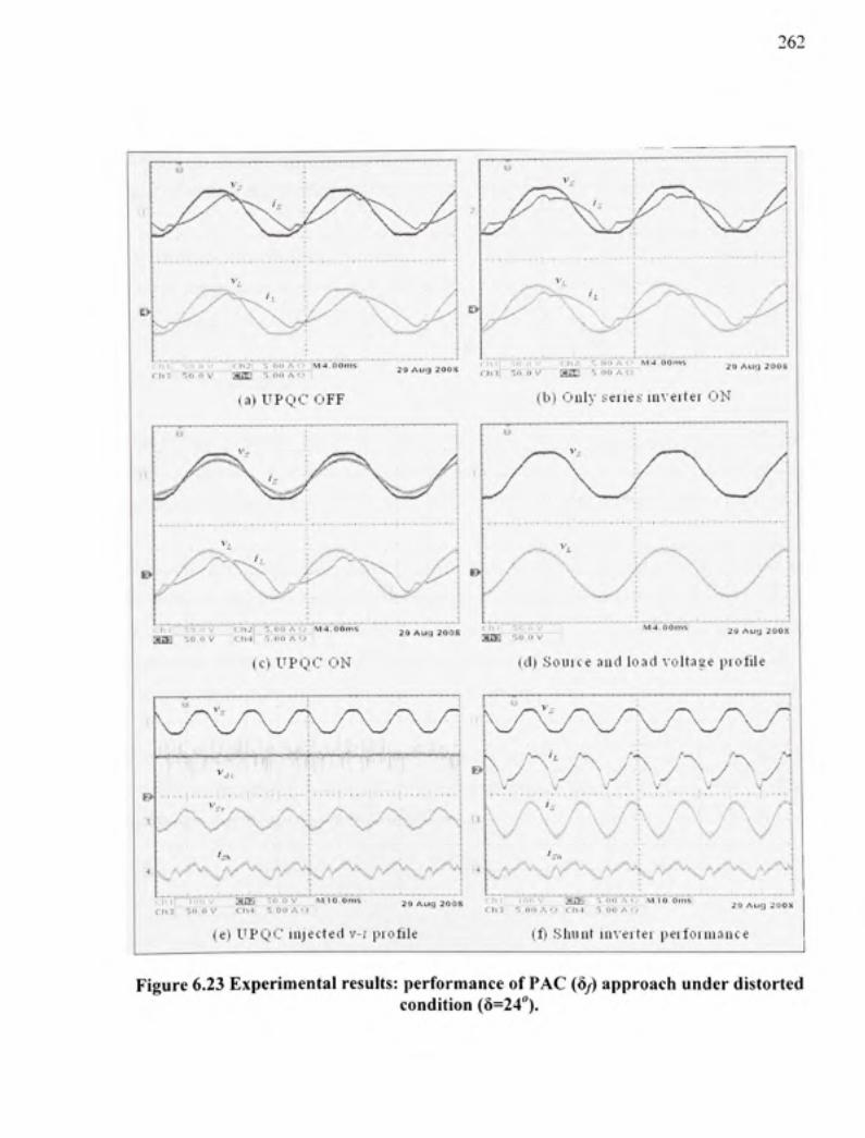
262
f h ? SO.O V SiS i S.OflA^ >
I a) UPQC OF F
2 9 A u g 2 0 0 K clVifSficOV Hngi~"S,0 0 A O
(b) CMil y s^eiie^ inveitei C>N
2 9 All> ) 2 0 0 8
s>
111 10.1 1 V ;Ch2 [ S.0OAV 7 M 4 . 0 0 m s gOB 50 " OV ictw j s"o o A o
29 A u q 2 0 0 S a i B 5 0 , 0 V 29 Au< J 200 X
(c)UPQC ON tct) Souice an d loa d voltag e piotil e
E>
'y-;^-'-.^^^^^i^/^\f/'^^\/A^ V V ^ ' ^ S A A . ^ A V ^ ' ^ N . ^ / N ^ / ^ ( h'l'r" 10 0 v ' a i E ^ ^ " o V ' iMli'o'.Oni's " 2 9 Aua 200 8 ' ' " i " o v aJDE i s.o n A « MfTo.oms r ChSl Srt o V Ch- i • ^o r iA o • ' ch3, : S . O O A O rn- i " J . O O A '
2S A u g 2 0 0 8
(e) UPQtC injected v- j profil e (t) Shun t mveite i peifoiinanc e
Figure 6.23 Experimental results: performance of PAC (8/) approach under distorted condition (8=24").
263
the sourc e voltag e an d th e loa d current , th e UPQ C inject s th e require d harmonic s
components throug h th e serie s an d shun t inverters , respectively . Th e perfonnanc e o f th e
shunt inverte r i s shown i n Figure 6.23 (0 -
As observe d fro m th e abov e experimenta l investigation , th e UPQ C wit h th e propose d PA C
concept compensate s th e voltag e harmonics , curren t harmonic s an d handle s th e loa d reactiv e
power through the series and shun t inverters , simultaneously .
6.10 Conclusion s
This chapte r elaborate s th e propose d theor y o f power angl e contro l o f UPQ C unde r differen t
utility conditions , whic h include s th e steady-state , voltag e sag , voltage swel l an d th e voltag e
distortion, and demonstrates it s capabilities t o overcome differen t powe r qualit y issues .
The develope d generalize d performanc e equation s ar e importan t t o predetermin e th e
performance o f UPQ C unde r variou s operatin g conditions . Th e newl y introduce d fixed an d
variable powe r angl e 5 control technique s ar e usefu l t o estimate th e reactive powe r share d b y
each o f th e inverters , particularly , unde r th e voltag e sa g an d swel l conditions . Moreover , i t
also gives high degree of freedom t o optimize the ratings of both the inverters .
Both th e simulatio n an d th e experimenta l result s confir m th e accomplishmen t o f propose d
reactive powe r sharin g featur e o f th e UPQ C unde r th e voltag e sag , voltag e swell , voltag e
harmonics, and the non-linear loa d conditions .
CONCLUSIONS
This thesi s present s a comprehensiv e researc h wor k i n th e are a o f powe r qualit y
enhancement utilizin g the unifie d powe r qualit y conditione r (UPQC) . I t addresses th e contro l
and real-tim e implementatio n aspect s o f UPQ C fo r possibl e practica l applications . Severa l
new concept s ar e introduced , supporte d b y thoroug h analytica l studies , confirme d usin g
digital simulatio n result s an d finally, validate d throug h experimenta l investigations .
Moreover, th e scop e o f presente d wor k cover s single-phase , three-phas e three-wir e an d
three-phase four-wir e UPQ C base d systems .
The significan t conclusion s of this thesis work are summarized a s follows :
• A conceptua l analysi s t o understan d th e activ e an d reactiv e powe r flow betwee n
source, UPQC an d the loa d unde r differen t operatin g condition s i s carried out . Base d
on the given analytica l study , a numerical exampl e shows the impac t o f sag and swel l
on th e curren t an d voltag e injecte d b y UPQC . Th e purpos e o f thi s analysi s i s t o
predetermine th e amoun t o f powe r (current ) tha t woul d flow durin g differen t
operating conditions . Thi s first ste p help s t o comput e th e rating s o f UPQ C inverter s
based o n the system an d application requirements .
• Th e feasibilit y o f UPQ C fo r practica l distributio n leve l installatio n ha s bee n
validated successfull y unde r realisti c networ k model . Th e reporte d collaboratio n
project wor k betwee n ETS , Hydro-Quebec an d IRE Q support s th e futur e prospectiv e
for the UPQ C being commercialized .
• A relativel y simpl e contro l approac h terme d a s Uni t Vecto r Templat e Generatio n
(UVTG) ha s bee n propose d fo r UPQ C t o tackl e th e mos t importan t powe r qualit y
issues. UVT G schem e utilize s a phas e locke d loo p (PLL ) an d a proportiona l -
integral (PI ) regulator t o generat e th e referenc e signal s fo r shun t an d serie s inverters .
Thus, th e nee d o f comple x mathematica l computatio n t o realiz e th e controlle r wa s

265
been eliminated . Th e performanc e o f UVT G approac h ha s bee n validate d throug h
simulation a s well as experimental results .
A specia l attentio n ha s been give n t o the voltage sa g compensation, i n which, the sa g
is tackle d usin g reactiv e powe r contro l approach . Th e advantag e o f usin g reactiv e
power t o overcom e th e voltag e sa g i s tha t i t doe s not requir e an y activ e powe r an d
hence help s to reduce the burden o n the shunt inverter . A new approach t o extract th e
required quadratur e injectio n voltag e ha s als o bee n develope d an d successfull y
validated throug h simulatio n an d experimental investigation .
A comparativ e evaluatio n o n th e voltag e sa g compensatio n usin g activ e powe r
(UPQC-P) an d reactiv e powe r (UPQC-Q ) approache s ha s als o bee n carrie d out . Th e
summarized advantage s an d limitation s o f bot h th e concept s ca n hel p t o selec t th e
most suitabl e approac h depending o n the particular applicatio n requirements .
An innovativ e topolog y fo r UPQ C based applicatio n ha s bee n presented , i n which , a
three-phase four-wir e (3P4W ) syste m i s realize d fro m a three-phas e three-wir e
(3P3W) system . Th e neutra l o f serie s transformers , use d i n UPQC , i s utilize d t o
provide the neutra l conducto r (fort h wire ) to the load . The newly introduce d topolog y
can play an importan t rol e in future UPQ C base d distributio n system .
The loa d o n th e 3P4 W syste m i s mos t likel y t o b e unbalance d i n nature . I n orde r t o
compensate th e unbalanc e presen t i n th e loa d current s suc h tha t th e sourc e current s
would appea r perfecfiy balanced , a new contro l approac h ha s been proposed . Du e t o
the unbalance d natur e o f th e load , th e loa d acfiv e powe r demande d b y eac h o f th e
phases ma y not b e th e same . Therefore , th e ide a i s t o comput e th e instantaneou s
fundamental activ e power drawn by individua l phase s separatel y usin g the develope d
concept o f generalize d single-phase/7- g theory . Th e tota l instantaneou s fundamenta l
load activ e powe r deman d thu s ca n b e determined b y addin g individua l phas e activ e
powers. Thi s tota l loa d activ e powe r i s then redistribute d betwee n utilit y an d UPQ C

266
(shunt inverter ) a s three-phas e balance d power . Th e experimenta l result s sho w tha t
the unbalanc e o f 45.76 % presen t i n th e loa d curren t ha s bee n reduce d t o 1.08 % a t
source side using the developed approach .
The mos t importan t an d significan t contributio n o f thi s thesi s wor k i s i n th e
development o f a ne w contro l philosophy , terme d a s powe r angl e contro l (PAC ) o f
UPQC. The concep t i s to us e the existin g serie s inverte r a t it s ful l capacity . Th e loa d
reactive powe r deman d i s meticulously supporte d utilizin g bot h th e shun t an d serie s
inverters b y introducin g a phas e angl e boos t betwee n th e sourc e an d th e loa d
voltages. T o achiev e th e aforementione d task , a voltag e throug h serie s inverte r i s
injected i n suc h a wa y tha t i t doe s not caus e a ris e o r decreas e i n th e resultan t loa d
voltage, i.e . i t strictl y maintain s th e equa l magnitude s o f sourc e an d loa d voltages .
This co-ordinate d loa d reactiv e powe r sharin g featur e o f UPQ C result s i n th e shun t
inverter ratin g reduction . Th e simulatio n a s wel l a s th e experimenta l result s validat e
the effectiveness o f the proposed approach . A systematic experimenta l stud y t o sho w
the effec t o f powe r angl e o n differen t UPQ C parameter s ha s als o bee n carrie d out .
Moreover, th e experimenta l result s sho w tha t fo r give n laborator y loa d conditio n
(high inductiv e loa d wit h powe r facto r 0. 6 lagging) , with propose d PA C approac h ( 5
=2S°) th e shun t inverte r ratin g ca n b e reduce d u p t o 50% . I n othe r words , withou t
putting extr a burde n o n th e existin g syste m an d withou t compromisin g th e basi c
functionalities o f UPQC , th e ratin g o f shun t inverte r an d henc e th e overal l cos t o f
UPQC ca n be reduced .
The develope d theor y o f PA C o f UPQ C ha s als o bee n extende d t o incorporat e th e
voltage sa g an d swel l o n th e system . Th e performanc e equation s o f PA C approac h
are arranged i n generalized manne r to accommodate severa l operatin g conditions . O n
the cours e o f controlle r developmen t o f UPQ C unde r th e voltag e sa g an d swel l
conditions, tw o differen t contro l techniques , namely , fixed an d variabl e powe r angl e
5 control s ar e introduced . Bot h th e simulatio n an d experimenta l result s illustrat e th e
capability o f PA C approac h t o achiev e th e voltag e sag/swel l compensatio n whil e

267
sharing th e loa d reactiv e powe r betwee n th e tw o inverters . Th e performanc e o f PA C
is als o demonstrate d unde r distorte d sourc e voltag e an d non-linea r loa d conditions ,
where th e UPQ C compensate s th e voltag e harmonics , loa d curren t harmonic s an d
handles th e loa d reactiv e powe r throug h th e serie s an d shun t inverters ,
simultaneously.
In summary , thi s thesi s wor k put s forwar d a ne w contro l philosoph y whic h not onl y
improves th e UPQ C utilizatio n facto r but als o reduce s th e overal l syste m cost . Moreover , i t
also prove s tha t wit h prope r an d meticulou s contro l o f availabl e resource s (i n thi s cas e th e
series inverter ) significan t advantage s ca n b e achieved . Th e wor k reporte d i n thi s thesi s wit h
extensive experimenta l validatio n woul d certainl y b e considere d a s a remarkabl e
development i n th e field o f powe r qualit y enhancemen t utilizin g th e unifie d powe r qualit y
conditioner.
RECOMMENDATIONS
This thesis work provide s the comprehensive aspect s of the unified powe r qualit y conditione r
to enhanc e th e qualit y o f powe r a t th e distributio n level . Thi s sectio n present s som e
guidelines t o exten d th e researc h wor k a s i t stand s now . A brie f discussio n o n th e direction s
for possibl e futur e wor k i s also outlined .
Recommendations Fo r Thesis Work Extensio n
• A s discussed i n CHAPTE R 1 , a UPQC ca n b e realize d a s a right shun t o r lef t shunt . Th e
work presente d i n thi s thesi s utilize s th e righ t shun t UPQ C topology . Al l th e develope d
concepts (UPQC-P , UPQC-Q , PAC , etc. ) ma y b e equall y applicabl e t o bot h th e UPQ C
topologies. However , applyin g these concepts successfully t o the lef t shun t UPQ C syste m
require modifications . Thi s i s mainl y du e t o th e curren t tha t flows throug h th e serie s
transformer (inverter) . I n th e righ t han d UPQC , a s th e shun t inverte r compensate s th e
load curren t harmonic s an d reactiv e power , th e curren t tha t flows throug h th e serie s
transformer (her e source current ) i s assumed a s sinusoidal . O n the other hand , the curren t
that flows throug h the series transformer, i n case o f the lef t shun t UPQ C i s a load current .
In actua l practice , a s the serie s transforme r possesse s leakag e impedance , th e non-linea r
load may produc e additiona l harmonic s i n the load voltag e or source voltag e (du e to non -
linear voltage dro p across transformer winding) . Thus , the shun t inverte r i n the lef t shun t
UPQC syste m ma y nee d t o provid e th e curren t harmonic s cause d b y th e serie s inverter .
Additionally, a comparativ e evaluation , fo r differen t approaches , wit h th e righ t an d lef t
shunt UPQ C system s can be carried out .
As mentione d already , th e voltag e sa g o n th e distributio n syste m i s on e o f th e mos t
important powe r qualit y problem s tha t UPQ C need s t o compensate effectively . Base d o n
this thesis work, three differen t approaches , such as , active power contro l (CHAPTE R 2) .
reactive powe r contro l (CHAPTE R 3 ) an d active-reactiv e powe r contro l usin g PA C
concept (CHAPTE R 6 ) ca n b e use d t o tackl e th e voltag e sa g problem . A systemati c
269
comparative stud y ca n b e don e o n th e voltag e sa g compensatio n usin g th e thre e abov e
mentioned approaches . Thi s stud y ca n b e focused o n th e advantage s an d limitation s o f
each o f th e approaches . Suc h a kind o f stud y coul d b e o f significan t importanc e an d ca n
act a s a comprehensiv e guid e t o selec t th e bes t suitabl e approac h base d o n th e syste m
requirements (rating , cost , applications, etc.).
Possible Directio n Fo r The Futur e Wor k
Solar an d win d energie s ar e emergin g a s alternate source s o f electricity . A C t o D C o r D C t o
DC voltag e sourc e converter s pla y a n importan t rol e i n thes e technologie s t o transfe r th e
extracted renewabl e energ y t o th e load s o r gird . Th e UPQ C ca n b e combine d wit h on e o r
several distribute d generatio n (DG ) systems . Unde r suc h conditions , th e powe r generate d b y
the wind , sola r o r an y othe r for m o f renewabl e energ y ca n b e fe d directl y t o th e D C bu s o f
the UPQC . Thi s D G powe r ca n b e regulate d an d manage d throug h UPQ C t o suppl y t o th e
loads connecte d t o th e PC C i n additio n t o th e voltag e an d curren t powe r qualit y proble m
compensation. Durin g norma l operatin g condition , th e UPQC-D G syste m ca n provide activ e
power t o th e load s connecte d t o th e PC C an d ca n compensat e th e loa d curren t harmonics ,
load reactive power, curren t unbalance , voltage harmonics , voltage sag s and swell .
Additionally, a batter y ca n b e connecte d t o th e D C bus , suc h tha t th e exces s renewabl e
energy ca n b e store d an d use d a s backup . I n th e even t o f voltag e interruption , th e UPQ C -
DG syste m give s additiona l benefi t b y providin g th e powe r t o th e loa d (Uninterruptibl e
power supply) . Th e D G powe r ca n b e transferre d i n a n interconnecte d mod e (powe r t o th e
gird an d loads ) o r islandin g mod e (powe r t o th e specifi c loads) . Now . researc h i s slowl y
being directe d toward s thi s UPQ C base d applicatio n (Ha n et al, 2006b) . Powe r supplie d b y
the UPQC-D G syste m unde r a norma l workin g condition , lo w energ y generatio n fro m
renewable system , voltag e interruptio n mode , etc. , depend s o n severa l factor s an d thes e
issues nee d t o b e addresse d adequately . However , th e integratio n o f UPQ C an d renewabl e
energy ma y pla y a significan t rol e i n mode m distributio n syste m t o simultaneousl y regulat e
the load power demand a s well a s enhance the quality o f power (voltag e and current) .
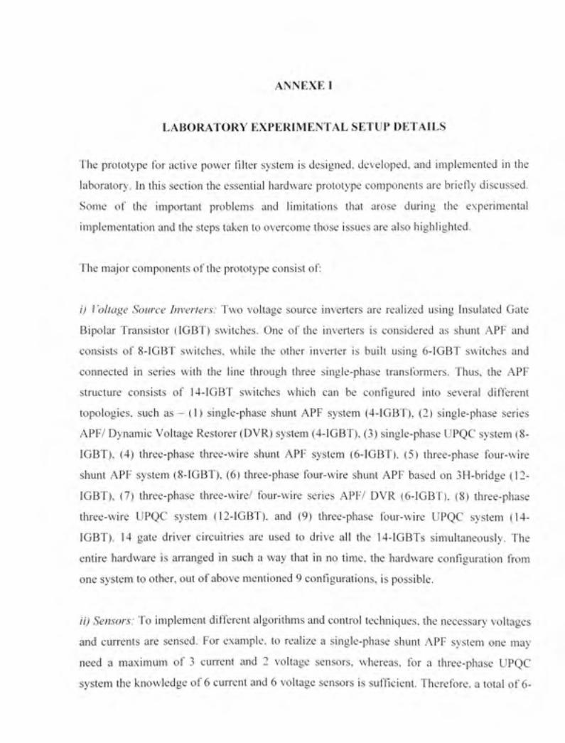
ANNEXE I
LABORATORY EXPERIMENTA L SETU P DETAIL S
The prototyp e fo r activ e powe r filter syste m i s designed, developed , an d implemente d i n th e
laboratory. I n this section the essentia l hardwar e prototyp e component s ar e briefly discussed .
Some o f th e importan t problem s an d limitation s tha t aros e durin g th e experimenta l
implementation an d the steps taken to overcome those issue s are also highlighted .
The major component s o f the prototype consis t of :
i) Vollage Source Inverters: Tw o voltag e sourc e inverter s ar e realize d usin g Insulate d Gat e
Bipolar Transisto r (IGBT ) switches . On e o f th e inverter s i s considere d a s shun t AP F an d
consists o f 8-IGB T switches , whil e th e othe r inverte r i s buil t usin g 6-lGB T switche s an d
connected i n serie s wit h th e lin e throug h thre e single-phas e transformers . Thus , th e AP F
structure consist s o f 14-lGB T switche s whic h ca n b e configure d int o severa l differen t
topologies, suc h a s - (1 ) single-phas e shun t AP F syste m (4-IGBT) , (2 ) single-phas e serie s
APF/ Dynami c Voltag e Restore r (DVR) system (4-IGBT) , (3) single-phase UPQ C syste m (8-
IGBT), (4 ) three-phas e three-wir e shun t AP F syste m (6-IGBT) , (5 ) three-phas e four-wir e
shunt AP F syste m (8-IGBT) , (6 ) three-phas e four-wir e shun t AP F base d o n 3H-bridg e (12 -
IGBT), (7 ) three-phas e three-wire / four-wir e serie s APF / DV R (6-lGBT) , (8 ) tliree-phas e
three-wire UPQ C syste m (12-lGBT) , an d (9 ) three-phas e four-wir e UPQ C syste m (14 -
IGBT). 1 4 gat e drive r circuitrie s ar e use d t o driv e al l th e 14-IGBT s simultaneously . Th e
entire hardwar e i s arrange d i n suc h a way tha t i n n o time , th e hardwar e configuratio n fro m
one system to other, ou t of above mentioned 9 configurations, i s possible.
ii) Sensors: T o implemen t differen t algorithm s an d contro l techniques , the necessar y voltage s
and current s ar e sensed . Fo r example , t o realiz e a single-phas e shun t AP F syste m on e ma y
need a maximu m o f 3 curren t an d 2 voltag e sensors , whereas , fo r a three-phas e UPQ C
system th e knowledge o f 6 current an d 6 voltage sensor s i s sufficient . Therefore , a total o f 6 -
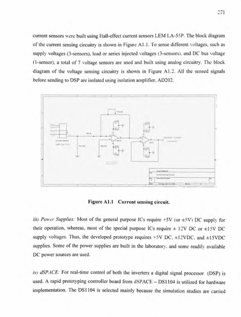
!71
current sensors were built using Hall-effect curren t sensors LEM LA-55P. The block diagram
of the current sensin g circuitry i s shown in Figure ALL T o sense different voltages , such as
supply voltages (3-sensors) , load or series injected voltage s (3-sensors) , and DC bus voltage
(1-sensor), a total o f 7 voltage sensor s ar e use d an d buil t usin g analog circuitry . Th e bloc k
diagram o f th e voltag e sensin g circuitr y i s show n i n Figur e A1.2 . Al l th e sense d signal s
before sending to DSP are isolated using isolation amplifier, AD202.
Sensed Output
Vinod Khadlfi ia r
Current Sansin g Circuitr y
SiZO Documon l NumtM i
Sunday, Apri l 20 . ;0Q 6
Figure Al.l Curren t sensing circuit.
iii) Power Supplies: Most o f the genera l purpos e IC s require +5 V (o r ±5V) D C suppl y fo r
their operation , whereas , mos t o f th e specia l purpos e IC s requir e ± 12 V D C o r ±15 V D C
supply voltages . Thus , the develope d prototyp e require s +5 V DC , ±12VDC. an d ±15VD C
supplies. Some of the power supplies are built i n the laboratory , an d som e readilv ' available
DC power sources are used.
iv) dSPACE: For real-time contro l o f both the inverter s a digital signa l processo r (DSP ) i s
used. A rapid prototyping controlle r board from dSPAC E - DS l 104 is ufilized fo r hardwar e
implementafion. Th e DS l 104 i s selecte d mainl y becaus e th e simulatio n studie s ar e carrie d
272
Figure A1.2 Voltag e sensing circuit.
out usin g MATLAB / Simulink , particularl y usin g SIMPOWERSYSTE M bloc k sets . Sinc e
the MATLAB/ Simulink supports the dSPACE it is easy to implement the developed contro l
algorithms i n real-time . Th e othe r optio n i s th e us e o f a cor e DS P proces s suc h a s
TMS320F2812 DS P fro m Texa s Instruments . Th e TMS320F281 2 require s codin g th e
algorithm usin g C or C + language , whic h i s a time consumin g task . Th e changes , i f any .
need to be carried out in the control algorithm, during later stages of controller development ,
which a time consuming an d tedious task. On the other hand, with MATLAB/ Simulink and
dSPACE combination , th e changes or even a n entirely ne w control algorith m doe s not take
much fime to implemen t i n real-fime. Moreover , i t i s also possibl e t o generat e C-code s fo r
developed MATLAB / Simulin k Mode l an d the n ca n b e use d i n a core DSP . However , th e
273
code generate d i n suc h a manne r i s not eas y t o understan d an d require s optimizatio n fo r a
better utilization o f the DSP processor .
The DS l 104 dSPAC E boar d i s buil t wit h - 1 ) a master microcontrolle r uni t whic h ha s a
Motorola Power PPC 603e processo r (6 4 Bi t Floatin g Poin t Processo r wit h CP U Cloc k
Frequency - 25 0 MHz) , and 2 ) a slave DS P fro m Te.xa s Instrument s - TMS320F24 0 (1 6 Bi t
Fixed Poin t Processor) . Th e DS l 104 boar d consist s o f 8 channel s fo r analo g t o digita l
conversion (ADC) , 8 channel s fo r digita l t o analo g conversio n (DAC) , timers , interrupters ,
and 20 bit inpu t - outpu t (I/O) ports.
The actual integratio n betwee n hardwar e and software i s highlighted her e :
• Th e MATLAB/Simulink i s first use d a s a n offlin e simulatio n too l fo r th e modeling ,
analysis, and design of the controller .
• Th e Real-Time Interface enhance s th e Simulin k bloc k librar y wit h additiona l blocks ,
which provide the link between Simulin k an d the real-time hardware .
• Th e Simulin k mode l i s transferre d int o real-tim e cod e usin g real-time workspace
(RTW) which then generates automatic C-codes fo r developed Simulin k model .
• Th e generated C-code s ar e then automatically loade d i n then dSPACE maste r o r slav e
unit, and are ready to use to achieve the desired tasks .
v) Analog PWM and Hysteresis Controller: Th e majo r limitation s o f dSPAC E base d
hardware syste m whil e performing th e experimental studie s i s discussed below :
• T o realiz e a three-phase UPQ C controlle r i n real-fime , a tota l o f 1 3 signals ( 3 actua l
load currents , 3 sourc e voltage s an d a D C bu s voltag e fo r controlle r development ,
and 3 actual sourc e o r 3 actual shun t filter current s an d 3 load o r serie s filter voltage s
to perfor m PW M operatio n ) nee d t o b e sen t t o th e dSPAC E uni t tliroug h AD C
channels. Th e DS l 104 ha s onl y 8 ADC channel s fo r A/ D Conversio n an d thus , th e
obvious questio n wa s ho w t o implemen t th e UPQ C controlle r i n real-tim e wit h
insufficient AD C channels .
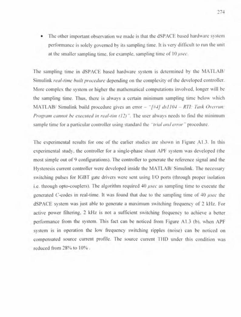
274
• Th e othe r importan t observatio n w e made i s that th e dSPACE base d hardwar e syste m
performance i s solely governe d b y it s sampling time. I t is very difficul t t o run the uni t
at the smalle r samplin g time, for example , sampling time o f \0 jusec.
The samplin g tim e i n dSPAC E based hardwar e syste m i s determine d b y th e MATLAB /
Simulink real-lime built procedure dependin g o n the complexity o f the developed controller .
More comple x th e syste m o r highe r th e mathematica l computation s involved , longe r wil l b e
the samplin g time . Thus , ther e i s alway s a certai n minimu m samplin g tim e belo w whic h
MATLAB/ Simulin k buil d procedur e give s a n erro r - "f#-lf dsl 104 - RTl: Task Overrun:
Program cannot be executed in real-tim (12) ". The use r alway s need s t o find th e minimu m
sample time fo r a particular controlle r usin g standard th e "trial and error" procedure .
The experimenta l result s fo r on e o f th e earlie r studie s ar e show n i n Figur e A1.3 . I n thi s
experimental study , th e controlle r fo r a single-phas e shun t AP F syste m wa s develope d (th e
most simpl e ou t o f 9 configurations) . Th e controlle r t o generat e th e referenc e signa l an d th e
Hysteresis curren t controlle r wer e develope d insid e th e MATLAB / Simulink . Th e necessar y
switching pulse s fo r IGB T gat e driver s wer e sen t usin g I/ O port s (throug h prope r isolatio n
i.e. throug h opto-couplers) . Th e algorith m require d 4 0 fisec a s samplin g tim e t o execut e th e
generated C-code s i n real-time . I t wa s foun d tha t du e t o th e samplin g tim e o f 4 0 jUsec th e
dSPACE syste m wa s jus t abl e t o generat e a maximu m switchin g frequenc y o f 2 kHz . Fo r
active powe r filtering, 2 kH z i s not a sufficien t switchin g frequenc y t o achiev e a bette r
performance fro m th e system . Thi s fac t ca n b e notice d fro m Figur e A1. 3 (b) , whe n AP F
system i s i n operatio n th e lo w frequenc y switchin g ripple s (noise ) ca n b e notice d o n
compensated sourc e curren t profile . Th e sourc e curren t TH D unde r thi s conditio n wa s
reduced fro m 28 % to 10% .
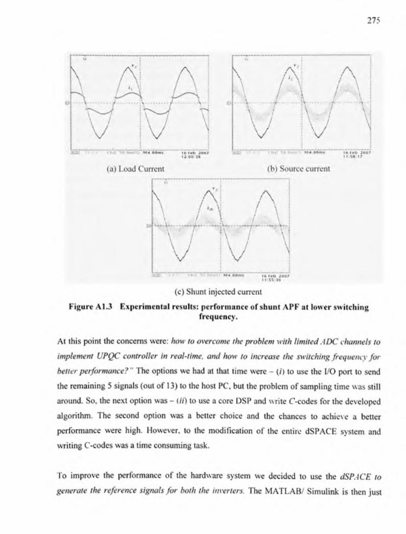
275
a i H r i o . O V : c h 2 r 5 0 . 0 m V f t !M4.00m s 16 Fe b 200 7 12:00:38
A-
(a) Load Curren t
aiaof '^" fo 'Sv "•cii2|"''S'8""0mv b 'M4."bom s
(b) Source curren t
16 Fe b 200 7 1 1:58:17
i j j ] ' i d f l v • Ch2 | 'S iTomvci M4.bOm s 1 6 Fe b 200 7 11:55:36
(c) Shunt injected curren t
Figure A1.3 Experimenta l results : performance o f shunt APF a t lower switchin g frequency.
At thi s poin t th e concern s were : how to overcome the problem with limited ADC channels lo
implement UPQC controller in real-time, and how lo increase the switching frequencv for
better performance? " The option s w e ha d a t tha t tim e wer e - (/ ) to us e th e I/ O por t t o sen d
the remaining 5 signals (out o f 13 ) to the hos t PC , but the problem o f sampling time wa s stil l
around. So , the nex t optio n wa s - (// ) to use a core DS P an d writ e C-code s fo r th e develope d
algorithm. Th e secon d optio n wa s a bette r choic e an d th e chance s t o achiev e a bette r
performance wer e high . However , t o th e modificatio n o f th e entir e dSPAC E syste m an d
writing C-code s wa s a time consuming task .
To improv e th e performanc e o f th e hardwar e syste m w e decide d t o us e th e dSPACE to
generate the reference signals for both the inverters. Th e MATLAB / Simulin k i s the n jus t
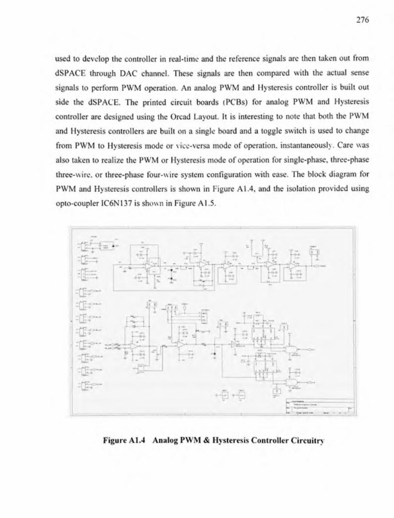
276
used to develop the controlle r i n real-time an d the reference signal s are then taken ou t fro m
dSPACE throug h DA C channel . Thes e signal s ar e the n compare d wit h th e actua l sens e
signals t o perfor m PW M operation . A n analo g PW M an d Hysteresi s controlle r i s buil t ou t
side th e dSPACE . Th e printe d circui t board s (PCBs ) fo r analo g PW M an d Hysteresi s
controller ar e designed usin g the Oread Layout . I t i s interesting t o not e tha t both the PWM
and Hysteresi s controller s ar e buil t on a single board an d a toggle switc h i s used t o change
from PW M to Hysteresi s mod e o r vice-versa mod e of operation, instantaneously . Car e was
also taken to realize the PWM or Hysteresis mode of operation fo r single-phase , three-phase
three-wire, o r three-phase four-wir e syste m configuratio n wit h ease . The bloc k diagra m fo r
PWM an d Hysteresi s controller s i s shown i n Figur e A1.4 , and the isolatio n provide d usin g
opto-coupler IC6N137 is shown in Figure A1.5.
, ^ . ^
E
Figure A1.4 Analo g PWM & Hysteresis Controller Circuitry
177
^ ' ^
3 -pl i T ~
T ? y
1 ^ ^
Tig' - , - . N
I-,-,-,-,-,r;
. - T - ^
TT^
H9. -i^j-waTW B - I ^ I -
Figure A1.5 Gat e pulse isolation circuitry.
The advantages offered b y constructing an analog PWM / Hysteresis board are:
Reduction in the number of signals needed to send to dSPACE through ADC channel
from 1 3 to 7 , thus th e controlle r ca n no w b e implemente d easily , i.e . th e limitatio n
imposed by 8 ADC channels is overcome.
Since th e PW M o r Hysteresi s controlle r fo r inverte r switchin g i s no t carrie d ou t
inside the MATLAB/ Simulink model, the sampling time for a particular controller is
reduced.
The syste m i s work s independen t o f samplin g time . I t i s observe d tha t fo r sam e
control algorithm , a sampling time fro m 3 0 jusec t o 12 0 jusec (wit h ste p of 1 0 /usee),
does not show anyeffect o n the performance o f the APF system.
It is now possible to switch the inverters up to 20 kHz without anv problems.
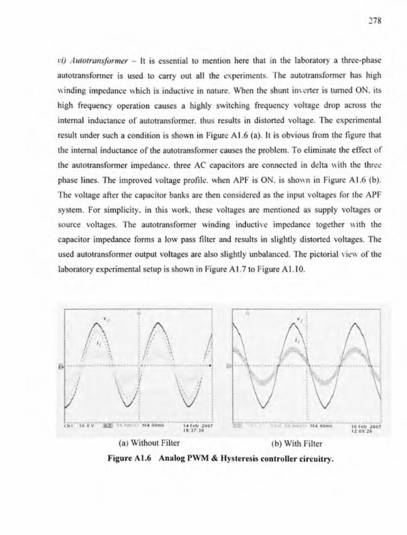
278
vi) .Autotransformer - I t i s essentia l t o mentio n her e tha t i n th e laborator y a three-phas e
autotransformer i s use d t o carr y ou t al l th e experiments . Th e autotransforme r ha s hig h
winding impedanc e whic h i s inductive i n nature . Whe n the shun t inverte r i s turned ON , it s
high frequenc y operatio n cause s a highl y switchin g frequenc y voltag e dro p acros s th e
internal inductanc e o f autotransformer , thu s result s i n distorte d voltage . Th e experimenta l
result unde r suc h a condifion i s shown in Figure AI.6 (a) . It i s obvious fro m th e figure that
the internal inductanc e of the autotransformer cause s the problem. To eliminate the effect o f
the autotransforme r impedance , thre e A C capacitor s ar e connecte d i n delt a wit h th e thre e
phase lines . The improve d voltag e profile , whe n AP F i s ON, i s shown i n Figur e A 1.6 (b) .
The voltage afte r th e capacitor bank s are then considered a s the inpu t voltage s fo r th e APF
system. Fo r simplicity , i n thi s work , thes e voltage s ar e mentione d a s suppl y voltage s o r
source voltages . Th e autotransforme r windin g inductiv e impedanc e togethe r wit h th e
capacitor impedanc e form s a lo w pas s filter and result s i n slightl y distorte d voltages . Th e
used autotransforme r outpu t voltage s are also slightly unbalanced . Th e pictorial vie w of the
laboratory experimental setup is shown in Figure A1.7 to Figure ALIO.
1 J
•*-f+-4-i-(-l-H-(-+-+-+-(-;-(-H-t"t-(~f-1--
\7I V ch i f "o .ov gjE I so.dmv Q M[4.obiTi ^ 14 Fe b 200 7
18:37:39
V . r
a a i " " ' r o T \ / " |cii2f?'oron™<?TS|3"oo'rns : 16 Fe b 200 7 12:09:26
(a) Without Filter (b ) With Filter
Figure A1.6 Analo g PWM & Hysteresis controller circuitry.
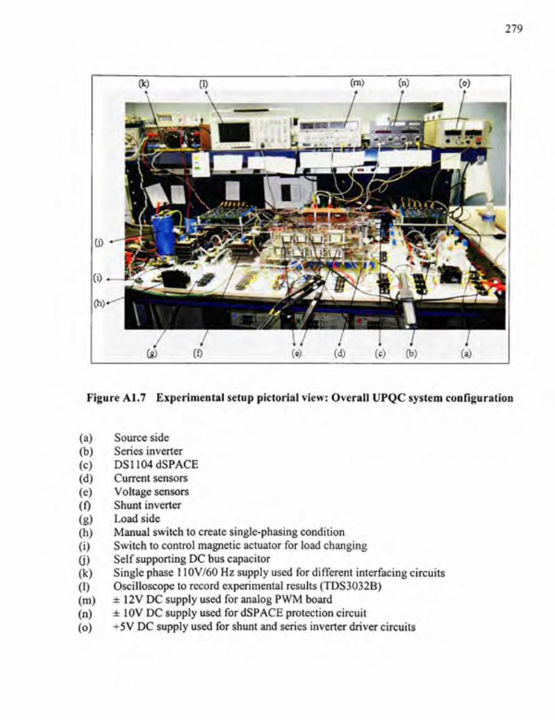
279
Figure A1.7 Experimenta l setup pictorial view: Overall UPQC system configuratio n
(a) Sourc e side (b) Serie s inverter (c) DS110 4 dSPACE (d) Curren t sensors (e) Voltag e sensors (f) Shun t inverter (g) Loa d side (h) Manua l switch to create single-phasing condition (i) Switc h to control magnetic actuator for load changing (j) Sel f supporting DC bus capacitor (k) Singl e phase 1 lOV/60 Hz supply used for different interfacin g circuit s (1) Oscilloscop e to record experimental results (TDS3032B) (m) ± 12 V DC supply used for analog PWM board (n) ± lO V DC supply used for dSPACE protection circuit (o) +5 V DC supply used for shunt and series inverter driver circuits
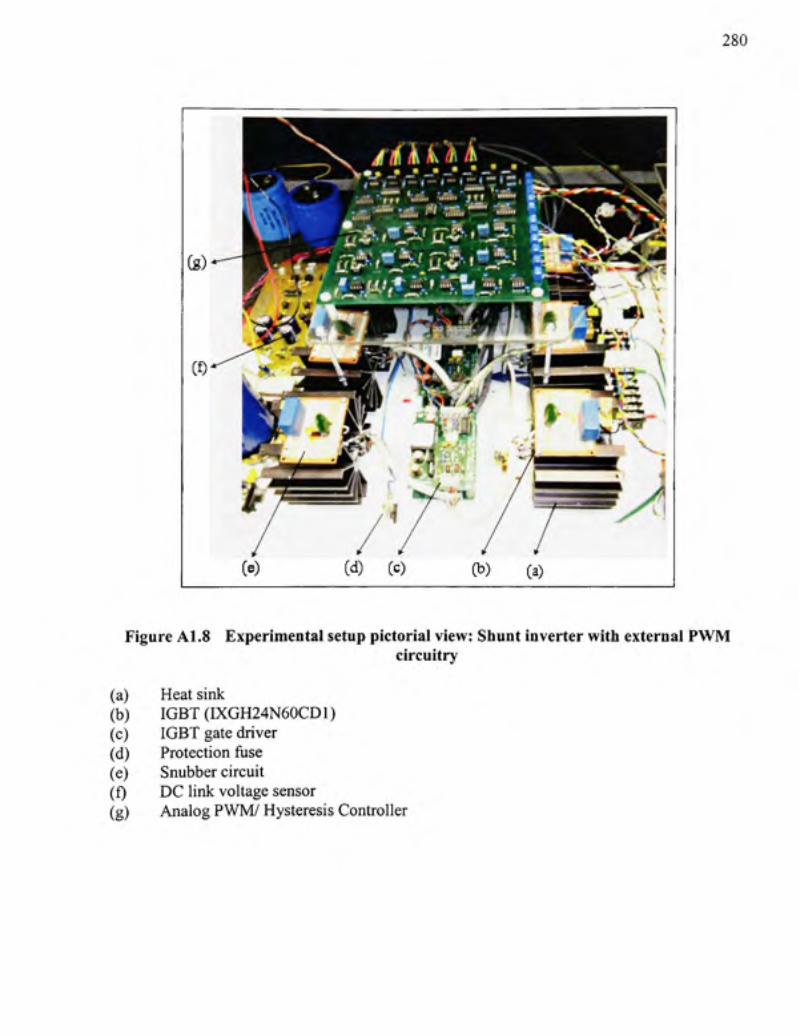
280
Figure A1.8 Experimenta l setup pictorial view: Shunt inverter with external PWM circuitry
(a) (b) (c) (d) (e) (0 (g)
Heat sink IGBT(DCGH24N60CD1) IGBT gate driver Protection fiise Snubber circuit DC link voltage sensor Analog PWM/ Hysteresis Controller
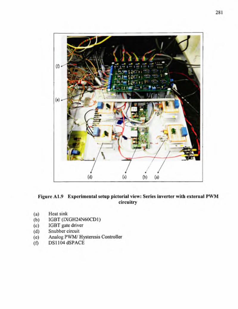
281
Figure Al,9 Experimenta l setup pictorial view: Series inverter with external PWM circuitry
(a) Hea t sink (b) IGBT(DCGH24N60CD1 ) (c) IGB T gate driver (d) Snubbe r circuit (e) Analo g PWM/ Hysteresis Controller (f) DS l 104 dSPACE
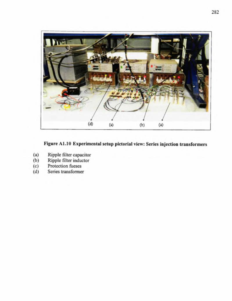
282
Figure ALIO Experimental setup pictorial view: Series injection transformer s
(a) Rippl e filter capacitor (b) Rippl e filter inductor (c) Protectio n fiieses (d) Serie s transformer

ANNEXE I I
PRINCIPAL EXPERIMENTA L PARAMETER S
The principal experimenta l parameter s are listed below :
CHAPTER 2
• A C suppl y voltag e
60V {rms) single-phase , f=60 H z
• Loa d
ORLLoad: R = 13.2 3 Q + L = 50 wH
//•) Non-Linear: DB R followe d b y R = 13.2 3 Q + L = 50 mU
iii) Dynamic: Loa d changed fro m DB R followe d b y R = 20 Q + L = 50 wH to
(R = 20 Q + L = 50 mH) i n parallel wit h R = 40 Q.
• Shun t Inverte r
Switching frequenc y {fsh) = 5-7 kHz (Hysteresis controller) , Lsh= 5 mH
• Serie s Inverte r
Switching frequenc y {fsr) = 5 kHz (Triangular carrie r based PW M controller) ,
L s r = 2 w H , C / = 4 0 n F
• Transforme r tur n ratio =1: 2
• Referenc e D C link voltage = 11 5 V
• dSPAC E samplin g time = 50 |asec
CHAPTER 3
Single-phase Syste m
• A C suppl y voltag e
Source voltage (single-phase ) = 30V {rms). Rated loa d voltage = 35V {rms). f=6 0 H z
284
• UPQ C
fsh = 5-7 k l Iz, Lsh = 5 /7;H, /.v , = 5 kHz, Lsr = 2 mH. C/ = 40 ^iF.
Reference D C lin k Voltage = 70V
• Transforme r tur n rafio =1: 3
• dSPAC E samplin g tim e = 45 f sec
Three-phase Syste m
• A C suppl y voltag e
Source voltage (three-phase ) = 19 V (rms). Rate d loa d voltage = 25V {rms). f=6 0 H z
• Loa d
Non-linear load : DBR followe d b y R = 26.67 O + L = 1 0 mH
• UPQ C
fsH = 5-7 kHz, Lsh = 5 mH, fsr = 5 kHz. Lsr = 1 wH. C/ = 50 ^F .
Reference D C link Voltage = lOOV • Transforme r tur n ratio = 1:3
• dSPAC E samplin g time = 75 isec
CHAPTER 4
• A C suppl y voltag e Source voltag e (three-phase ) = 35V (rms), f=6 0 H z
• UPQ C
fsh = 5-7 kHz , Lsh = 5 mH. fsr = 5 kHz, L,sr= 2 mH. C/ = 5 0 ^F ,
Reference D C lin k Voltag e = 120 V • Transforme r tur n ratio =1: 3 • dSPAC E samplin g tim e = 65 ) sec

285
CHAPTER 5 and CHAPTER 6
• A C supply voltage
Source voltage (single-phase) = 35V {rms). f=60 Hz
• Loa d
Highly inductive load: R = 40 Q in parallel with L = 50 mH
• UPQ C
fs/, = 5-7 kHz, Lsh = 5 mH. fs,- = 5 kHz. Lsr= 2 mH. Cj = 40 ^F,
Reference D C link Voltage = 70V
• Transforme r tur n ratio =1:3
• dSPAC E sampling time = 50 |j.sec
LIST OF REFERENCE S
Akagi H . 1996 . «Ne w trends i n active filters fo r power conditioning » . IEEE Transactions on Industrial Applications, vol . 32, no. 6, p. 1312-1322 .
Akagi H. , Y . Kanazawa d an d A . Nabae . 1984 . «Instantaneou s reactiv e powe r compensator s comprising switchin g device s withou t energ y storag e components)) . IEEE Transactions on Industrial .Applications, vol . 20. no. 3, p. 625-630.
Aredes M. , K . Heuman n an d E . H . Watanabe . 1998 . «A n universa l activ e powe r lin e conditioner)). IEEE Transactions on Power Delivery, vol . 13 , no.2, p.545 -551 .
Aredes M. , J . Moor , J . Ferreira , L . Monteiro , R . Fernande s an d M . Siqueira . 2005 . « A Simplified Contro l Strateg y fo r a Unifie d Powe r Qualit y Conditione r Prototype)) . I n 36" .Annual IEEE Power Electronics Specialists conference, p . 2592-2597.
Axente L , M. Bas u and M . Conlon. 2007 . «A contro l approac h fo r UPQ C comiecte d t o wea k supply point)) . I n 42"' International Universities Power Engineering Conference, p . 619 -623.
Banaei M . an d S . Hosseini . 2006 . «Mitigatio n o f Curren t Hamioni c Usin g Adaptiv e Neura l Network wit h Activ e Powe r Lin e ( and Motion Control Conference. 5 p Network wit h Activ e Powe r Lin e Conditioner)) . I n 5" International Power Electronics
Basu M. , S . P . Das an d G . K . Dubey . 2001 . «Experimental investigatio n o f performance o f a single phase UPQ C fo r voltag e sensitiv e and non-linea r loads)) . In 4''' Annual IEEE Power Electronics and Drive Sysletns Conference, p . 218-222.
Basu M. , S . P . Da s an d G . K . Dubey . 2002 . ((Performanc e stud y o f UPQC- Q fo r loa d compensation an d voltag e sa g mitigation)) . I n 28" Annual IEEE Industrial Electronics Society Conference, p . 698-703.
Basu M. , M . Farrell , F . Conlon , K . Gaughan an d E . Coyle . 2004 . ((Optima l contro l strateg y of UPQ C fo r minimu m operationa l losses)) . I n 39''' Universities Power Engineering Conference, p . 246-250.
Bhattacharya S . an d D . Divan . 1995 . ((Synchronou s fram e base d controlle r implementatio n for a hybri d serie s activ e filter syste m )) . I n 38''' Industry Applications Society .Annual Meeting, p. 2531-2540.
Bollen M . H. J. 2003 . ((Wha t i s Power Quality)) . Electrical Power Systems Research Journal, vol. 66 , no. 1 , pp. 5-14 .
287
Chae B. , T . Le e an d D . Hyun . 2001 . (( A faul t protectio n schem e fo r unifie d powe r qualit y conditioners)). I n Annual IEEE Power Electronics and Drive Systems Conference, p . 66 -71.
Chakraborty S . an d M . Simoes . 2005 . ((Fuzz y ARTMA P base d forecas t o f renewabl e generation fo r a hig h frequenc y A C microgrid)) . I n 36''' Annual IEEE Industrial Electronics Society Conference. 6 p.
Chakraborty S. , M . Weis s an d M . Simoes . 2007 . ((Distribute d Intelligen t Energ y Management Syste m fo r a Single-Phas e High-Frequenc y A C Microgrid)) . I n IEEE Transactions on Industrial Electronics, vol . 54 , no. 1 , p. 97-109.
Chen G. , Y . Chen , L . F . Sanche z an d K . M . Smedley . 2004 . (( A unifie d voltag e qualit y conditioner withou t referenc e calc L Specialists conference, p . 4251-4256. conditioner withou t referenc e calculation)) . I n 35''' Annual IEEE Power Electronics
Chen S u an d G . Joos . 2001a . ((Ratin g issue s o f unifie d powe r qualit y conditioner s fo r loa d bus voltage contro l i n distribution systems)) . In IEEE Power Engineering Society Meeting. p. 944-949 .
Chen S u am d G . Joos . 2001b . (( A unifie d series-paralle l deadbea t contro l techniqu e fo r a n active powe r qualit y conditione r wit h ful l digita l implementation)) . I n 36" Indii.stry Applications Society Annual Meeting, p . 172-178 .
Chen Y. . X . Zha . J . Wang , H . Liu . J . Su n an d H . Tang . 2000 . ((Unifie d Powe r Qualit y Conditioner (UPQC) : th e theory , modelin g an d application)) . I n IEEE Power System Technology Conference, p . 1329-1333.
Cheng Y . an d P . Lataire . 2004 . ((Advance d contro l method s fo r th e 3-phas e unifie d powe r quality co m 4263-4267. quality conditioner)) . I n 35" Annual IEEE Power Electronics Specialists conference, p .
Correa M. , S . Chakraborty , G . Simoe s an d A . Farret . 2003 . (( A singl e phas e hig h frequenc y AC microgri d wit h a n unifie d powe r qualit y conditioner)) . I n Industry Applications Society Annual Meeting, p . 956-962.
Correa J. , F . Farre t an d M . Simoes . 2005 . ((Applicatio n o f a Modifie d Single-Phas e P- Q Theory i n th e Contro l o f Shun t an d Serie s Activ e Filter s i n a 400 H z Microgrid)) . I n 36''' Annual IEEE Power Electronics Specialists conference, p . 2585-2591.
Doncker R . W. , C . Meyer , R . U . Lenk e an d F . Mura . 2007 . ((Powe r Electronic s fo r Futur e Utility Applications)) . I n Annual IEEE Power Electronics and Drive Systems Conference. p. kl-k8 .
288
Dugan C . R. , M . F . McGranagha n an d H . W . Beaty . 1996 . Electrical Power Systems Quality, Ne w York , N. Y. : McGraw-Hill , 26 5 p.
El-Habrouk M. , M . K . Darwis h an d P . Mehta . 2000 . ((Activ e powe r filters: a review)) . lEE Electrical Power Applications Journal, vol . 147 , no. 5, p. 403-413.
Elmitwally A. , S . Abdelkade r an d M . Elkateb . 2000 . ((Performanc e evaluatio n o f fuzz y controlled thre e an d fou r wir e shun t activ e powe r conditioners)) . I n IEEE Power Engineering Society Meeting, p . 1650-1655 .
Elnady A. , A . Goaud a an d M . M . A. Salama . 2001 . ((Unified powe r qualitv ' conditione r wit h a nove l contro l algorith m base d o n wavele t transform)) . I n .Annual IEEE Canadian Conference on Electrical and Computer Engineering, p . 1041-1045 .
Elnady A. , an d M . M . A . Salama . 2001 . ((New functionalitie s o f a n adaptiv e unifie d powe r quality conditioner)) . I n IEEE Transmission and Distribution Conference and Exposition. p. 295-300 .
Elnady A. , W . El-khatta m an d M . M . A . Salama . 2002 . ((Mitigatio n o f A C ar c furnac e voltage flicker usin g th e unifie d powe r qualit y conditioner)) . I n IEEE Power Engineering Society Meeting, p . 735-739.
Emadi A. , A . Nasir i an d S . B . Bekiarov . 2001 . Uninterruptible Power Supplies and .Active Filters, Boc a Raton . Fla. : CRC Press , 276 p.
Esfandiari A. , M . Pamian i an d H . Mokhtari . 2004 . ((Mitigatio n o f electri c ar c furnac e disturbances usin g th e unifie d powe r qualit y conditioner)) . I n 30''' .Annual IEEE Industrial Electronics Society Conference, p . 1469-1474 .
Faranda R . and 1 . Valade. 2002 . ((UPQC compensatio n strateg y an d design aime d a t reducin g losses)). In Annual IEEE International Symposium on Industrial Electronics, p 1264-1270 .
Forghani M . and S . Afshamia. 2007 . ((Online Wavele t Transform-Base d Contro l Strateg y fo r UPQC Contro l System)) . IEEE Transactions on Power Delivery, vol . 22 , no . 1 , p . 481 -491.
Fujita H . an d H . Akagi . 1998 . ((Th e unifie d powe r qualit y conditioner : Th e integratio n o f series an d shunt-activ e filters)). IEEE Trcmsaclion on Power Electronics, vol . 13 , no . 2 . p. 315-322.
Ghandehari R . an d A . Jalilian . 2004 . ((Economica l Impact s o f Powe r Qualit y i n Powe r Systems)). In IEEE Universities Power Engineering Conference, p . 893-897.
Ghosh A . an d G . Ledwich . 2002 . Power Quality Enhancement Using Custom Power Devices, Boston : Kluwe r Academic Publishers , 460 p.
289
Ghosh A. , K . Jinda l an d A . Josh . 2003 . ((Inverte r contro l usin g outpu t feedbac k fo r powe r compensating devices)) . I n Asia-Pacific Region Conference on Convergent Technologies. p. 48-52.
Ghosh A. , K . Jinda l an d A . Joshi . 2004 . (( A unifie d powe r qualit y conditione r fo r voltag e regulation o f critical loa d bus)) . In IEEE Power Engineering Society Meeting, p . 471 -476.
Gong M. , H . Liu , H . Gu and D . Xu Dianguo . 2002. ((Active voltage regulato r base d o n nove l synchronization metho d fo r unbalanc e an d fluctuation compensation)) . I n 28" Annual IEEE Industrial Electronics Society Conference, p . 1374-1379 .
Graovac D. , V . Kati e an d A . Rufer . 2000 . ((Powe r qualit y compensatio n usin g universa l power qualit y conditionin g system)) . IEEE Power Engineering Review, vol . 20 , no. 12 , p. 58-60.
Gu J. , D . Xu , H . Li u an d M . Gong . 2002 . ((Unifie d powe r qualit y conditione r (UPQC) : th e principle, control an d application)) . In Power Conversion Conference, p . 80-85.
Gyugyi L . 1992 . (( A Unifie d Powe r Flo w Controlle r concep t fo r Flexibl e A C Transmissio n System)). lEE Proceedings-c, vol.139 , no. 4, p.
Gyugyi L . an d E. C Strycula . 1976 . ((Activ e A C powe r filters)). I n Industry Applications Society Annual Meeting, p . 529-535.
Han B. , B . Bae , H . Ki m an d S . Back . 2006a . ((Ne w configuratio n o f UPQ C fo r medium -voltage application)) . IEEE Transactions on Power Delivery, vol . 21 , no.3 , p . 1438 -1444.
Han B. , B . Bae, H . Ki m an d S . Back . 2006b . ((Combine d operatio n o f unified power-qualit y conditioner wit h distribute d generation)) . IEEE Transactions on Power Delivery, vol . 21, no.3 , p . 330-338.
Haque M . T . 2002 . ((Single-phas e P Q theory» . I n Annual IEEE Power Electronics Specialists conference, p . 1815-1820 .
Haque M . T. , T . Is e an d S . H . Hosseini . 2002 . (( A nove l contro l strateg y fo r unifie d powe r quality conditione r (UPQC))) . I n Annual IEEE Power Electronics Specialists conference. p. 94-98.
Hingorani G . Natai n an d Laszl o Gyugyi . 2000 . Understanding FACTS: Concepts and Technology of Flexible AC Transmission Systems. Ne w York : Institut e o f Electrica l an d Electronics Engineers , 432p.
Hongchun S. , L . Zuquan , Y . Jila i an d X . Liang . 2005 . (( A Nove l Contro l Strateg y fo r UPQC)). In IEEE Transmission and Distribution Conference and Exposition, p . 1-4 .
290
Hu M . and H . Chen. 2000 . ((Modeling an d controllin g o f unified powe r qualit y conditioner)) . In IEEE Advances in Power System Control, Operation and Management, p . 431 -435.
Jayanti N. , M . Basu , F . Conlo n an d G . Kevin . 2006 . ((Ratin g Requirement s o f a LInifie d Power I n i ' 636.
• Quality Conditione r (UPQC ) fo r Voltag e Rid e Through Capabilit y Enhancement)) . lET International Conference on Power Electronics. Machines and Drives, p . 632-
Jayanti N. , M . Basu , M . Conlo n an d K . Gaughan . 2007 . ((Performanc e compariso n o f a lef t shunt UPQ C an d a right shun t UPQC applie d t o enhance fault-ride-throug h capabilit y o f a fixed spee d win d generator)) . I n European Conference on Power Electronics and Applications. P . 1-9 .
Jindal A. , A . Ghos h an d A . Joshi . 2007 . ((Interlin e Unifie d Powe r Qualit y Conditioner)) . IEEE Transactions on Power Delivery, vol . 22. no. 1 , p. 364-372.
Kamran F . an d T . G . Habetler . 1995 . ((Combine d deadbea t contro l o f a series-paralle l converter combinatio n use d a s a universa l Electronics Specialists conference, p . 196-2 0 converter combinatio n use d a s a universa l powe r filter)). I n 26" Annual IEEE Power
Kazemi A. , M . Sarla k an d M . Barkhordary . 2006a . ((A n Adaptiv e Nois e Cancelin g Metho d for Single-Phas e Unifie d Powe r Qualit y Conditioner)) . I n 7^ ' IEEE Conference on Industricd Electronics and Applications. 6 p.
Kazemi A. , A . Mokhtarpou r an d M . Haque . 2006b . (( A Ne w Contro l Strateg y fo r Unifie d Power Qualit y Conditione r (UPQC ) I n Distributio n Systems)) . I n International Conference on Power System Technology, p . 1-5 .
Khadkikar V. , P . Agarwal , A . Chandra , A . Barr y an d T . Nguyen . 2004 . (( A simpl e ne w control techniqu e fo r unifie d powe r qualit y conditione r (UPQC))) . I n 11''' IEEE Harmonics and Quality of Power Conference. (Ne w York, Sept . 12-1 5 2004) , p. 289-293.
Khadkikar V. . A. Chandra, A . Barry and T. Nguyen. 2005 . ((Steady stat e power flow analysi s of unifie d powe r qualit y conditione r (UPQC))) . I n IEEE International Conference on Industrial Electronics and Control Applications. (Quito , Nov. 29 - Dec.2 2005) , 6 p.
Khadkikar V. , A . Chandra , A . Barr y an d T . Nguyen . 2006a . ((Analysi s o f Powe r Flo w i n UPQC durin g Voltag e Sa g an d Swel l Condition s fo r Selectio n o f Devic e Ratings)) . I n Annual IEEE Canadian Conference on Electrical and Computer Engineering. (Ottawa . May 7-10 2006) , p. 867-872.
Khadkikar V. , A . Chandra , A . Barr y an d T . Nguyen . 2006b . ((Applicatio n o f UPQ C t o protect a sensitiv e loa d o n a polluted distributio n network)) . I n IEEE Power Engineering Society Meeting. (Montreal , 18-2 2 June 2006), 6 p.

291
Khadkikar V. , A . Chandra , A . Barr y an d T . Nguyen . 2006c . ((Conceptua l Stud y o f Unifie d Power Qualit y Conditione r (UPQC))) . I n Annual IEEE International Symposium on Industrial Electronics. (Montreal , 9-12 Jul y 2006) p . 1088-1093 .
Khadkikar V . an d A . Chandra . 2006d . (( A Nove l Structur e fo r Three-Phas e Four-Wir e Distribution Syste m Utilizin g Unifie d Powe r Qualit y Conditione r (UPQC))) . I n Annual IEEE Power Electronics and Drive Systems Conference. (Ne w Delh i Dec . 12-1 5 2006) , 6 P-
Khadkikar V . an d A . Chandra . 2006e . (( A Nove l Contro l Approac h fo r Unifie d Powe r Quality Conditione r Q withou t Activ e Powe r Injectio n fo r Voltag e Sa g Compensation)) . In IEEE International Conference on Industrial Technology . (Mumbai , Dec . 15-1 7 2006), p. 779-784 .
Khadkikar V . an d A . Chandra . 2008a . ((A n Independen t Contro l Approac h fo r Three-Phas e Four-Wire Shun t Activ e Filte r Base d o n Thre e H-Bridg e Topolog y unde r Unbalance d Load Conditions)) . I n IEEE Annual IEEE Power Electronics Specialists conference. (Greece, June 15-1 9 2008), p. 779-784.
Khadkikar V . an d A . Chandra . 2008b . (( A Ne w Contro l Philosoph y fo r Unifie d Powe r Quality Conditione r (UPQC ) t o Co-ordinat e Loa d Reactiv e Powe r Deman d Betwee n Shunt an d Serie s Inverters)) . IEEE Transactions on Power Delivery, vol . 23 , no . 4 . p . 2522-2534.
Khadkikar V. . Chandra A . and Sing h B . N. 2008c. ((Generalized Single-Phasep- ^ Theory fo r Active Powe r Filtering : Simulatio n an d DS P base d Experimenta l Investigation)) . lET PoM'er Electronics Journal, (In Press).
Khadkikar V . an d Chandr a A . 2008d . ((Comparativ e Evaluatio n betwee n 2>-(p an d 1 - tp p-q Theories Applie d t o Three-Phas e Shun t Activ e Powe r Filte r unde r Differen t Operatin g Conditions)). Submitted for possible publication in lET Power Electronics Journal {Under review).
Khoor M. , M . Machmou m an d Y . Abdelli . 2005 . ((Usin g a simpl e analogica l identificatio n method an d PI D controller s fo r unifie d powe r qualit y conditioning)) . I n European Conference on Power Electronics and Applications. 1 0 p.
Khoor M . an d M . Machmoum . 2007 . (( A Nove l Single-Phas e Reduce d Part s On-Lin e UP S with Powe r Qualit y Conditionin g Capability)) . I n Annual IEEE Power Electronics Specialists conference. p . 1170-1175 .
Kolhatkar Y . an d S . Das . 2007 . ((Experimenta l Investigatio n o f a Single-Phas e UPQ C Wit h Minimum V A Loading)) . IEEE Transactions on Power Delivery, vol . 22 , no . 1 . p . 371 -380.
292
Kisck D. , V . Navrapesc u an d M . Kisck . 2007 . ((Single-Phas e Unifie d Powe r Qualit y Conditioner wit h Optimu m Voltag e Angl e Injectio n fo r Minimu m V A requirement)) . I n .Annual IEEE Power Electronics Specialists conference, p . 574-579.
Kwan K. . P . S o an d Y . Chu . 2007 . (( A harmonic selectiv e unifie d powe r qualit y conditione r using MV R wit h Kalma n filters)). I n International Power Engineering Conference, p . 332-337.
Landaeta L. . C . Sepulveda , J . Espinoz a an d C . Baier . 2006 . (( A Mixe d LQR l / P I base d Control fo r Three-Phas e UPQCs)) . InJi'" ^ Annual IEEE Industrial Electronics Society Conference, p . 2494-2499.
La.xnii A. . G . Das , K. Rao , K. Sreekanth i an d K . Rayudu . 2006 . ((Differen t contro l strategie s for Unifie d Powe r Qualit y Conditione r a t load side)) . In F' IEEE Conference on Industrial Electronics and Applications, p . 1-7 .
Li P. , Y . Yang . Z . M a an d H . Li . 2003 . ((Th e stud y an d simulatio n verifyin g o f th e controlling signa l detectin g metho d abou t UPQ ( on Electrical Machines and Systems, p . 657-660. controlling signa l detectin g metho d abou t UPQC)) . I n 6" IEEE International Conference
Li P. , Q . Ba i an d G . Li . 2006 . ((Coordinate d contro l strateg y fo r UPQ C an d it s verification)). I n IEEE Power Engineering Society Meeting. 8 p.
Li R. , A . T . John s an d M . M . Elkateb . 2000 . ((Contro l concep t o f Unifie d Powe r Lin e Conditioner)). In IEEE Power Engineering Society Meeting, p . 2549-2599.
Li X. , G . Zhu , S . Dua n an d J . Chen . 2007 . ((Contro l Schem e fo r Three-Phas e Four-Wir e UPQC i n a Three-Phas e Stationa r Society Conference, p . 1732-1736 . UPQC i n a Three-Phas e Stationar y Frame)) . I n 33"^ Annual IEEE Industrial Electronics
Lin B . R. , C . II . Huan g an d B . R . Yang . 2002 . ((Contro l schem e o f hybri d activ e filter fo r power qualit y improvement)) . I n IEEE International Conference on Industrial Technology, p . 317-322.
Liu J. . J . Yan g an d Z . Wang . 1999 . (( A ne w approac h fo r single-phas e hamioni c curren t detecting an d it s applicatio n i n a hybri d activ e powe r filter)). I n .Annual IEEE Industrial Electronics Society Conference, p . 849-854.
Liu J. , H . Yihong , Y . Yinghu a an d W . Xiaoyu . 2003 . ((A n unifie d schem e an d respectiv e algorithms fo r th e contro l o f DC-linke d doubl e converter s i n a n universa l powe r qualit y controller)). In 34''' Annual IEEE Power Electronics Specialists conference, p . 327-332.
Martinez J . A. 2001 . ((Modeling an d simulatio n o f three-phase activ e filters)). I n IEEE Power Engineering Society Meeting, p . 639-640.
293
Masdi H. , N. Mariun , S . Mahmud, A . Mohame d an d S . Yusu f 2004 . ((Desig n o f a prototvp e D-STATCOM fo r voltage sa g mitigation)). In Power and Energy Conferetice. P . 61-66.
Mastromauro R. , M . Liserr e an d A . Dell'Aquila . 2007 . ((Single-phas e grid-connecte d photovoltaic system s wit h powe r qualit y conditione r functionality)) . I n European Conference on Power Electronics and .Applications. 1 1 p.
Mohan N. , T . M . Undelan d an d W . P . Robbins . 1995 . Power Electronics: Converters, Applications and Design, 2" ^ ed. Hoboken, N. J.: John Wile y & Sons, 802 p.
Monteiro L . F . C , M . Arede s an d J . A . Moo r Neto . 2003 . (( A contro l strateg y fo r unifie d power qualit y conditioner)) . I n Annual IEEE International Symposium on Industrial Electronics, p. 391-396.
Moran L . 2007. ((Power Electronic s Applications i n Utility Systems)) . I n .Annual IEEE Power Electronics Specialists conference, p . 3027-3028.
Moran S . 1989 . ((A line voltag e regulator/conditione r fo r hamionic-sensitiv e loa d isolation)) . In Industry Applications Society .Annual .Meeting, p. 947-951.
Mufioz J. , J . Reyes . J . Espinoza , I . Rubila r an d L . Moran . 2007 . (( A Nove l Multi-Leve l Three-Phase UPQ C Topolog y base d o n Full-Bridg e Single-Phas e Cells)) . I n 33'''^ .Annual IEEE Industrial Electronics Society Conferetice. p . 1787-1792 .
Muthu S . an d J . M . S . Kim . 1997 . ((Steady-stat e operatin g characteristic s o f unifie d activ e power fi l 199-205. power filters)). I n 12" IEEE Annual Power Electronics Conference and Exposition, p .
Nasiri A . an d A . Emadi . 2003 . ((Differen t topologie s fo r single-phas e unifie d powe r qualit y conditioners)). In Industry Applications Society Annual Meeting, p . 976-981 .
Nasiri A . an d A . Emadi . 2004 . ((Ful l digita l contro l o f a single-phas e series-paralle l uninterruptible powe r supply)) . I n 19" IEEE Annual Power Electronics Conference and Exposition, p . 443-449.
Newman M.J. , D . G . Holmes , J . G . Nielse n an d F . Blaabjerg . 2003 . (( A dynami c voltag e restorer (DVR ) wit h selectiv e harmoni c compensatio n a t mediu m voltag e level» . I n Industry Applications Conference, p . 1228-1235.
Ng F. , M . Won g an d Y . Han . 2004 . ((Analysi s an d contro l o f UPQ C an d it s DC-lin k power b y us e of p-q-r instantaneou s powe r theory)) . I n 7 " International Conference on Power Electronics Systems and Applications, p . 43-53.
Obukhov A. , V . Popo v an d G . Zinoviev . 2003 . ((Transformles s conditioner s o f qualit y o f main voltage)) . I n 7" Korea-Russia Sytnposium on Science arid Technology, p . 45-50.
294
Park S. , I . Chung , J . Choi , S . Moo n an d J . Kim . 2003 . ((Contro l scheme s o f th e inverter -interfaced multi-functiona l disperse d generation)) . I n IEEE Power Engineering Society Meeting, p. 1924-1929 .
Pievatolo A. . 1 . Valad e an d G . Ubezio . 2002 . «UPQ C reliabilit y analysis)) . I n IEEE Harmonics and Quality of Power Conference, p. 390-397.
Prieto J. , P . Salmero n an d R . Herrera . 2005 . (( A unifie d powe r qualit y conditione r fo r wid e load range : Practica l desig n an d experimenta l results)) . I n IEEE Power Tech Conference, p. 1-7 .
Rashid M H. 2001. Power Electronics Handbook. Sa n Diego , Calif Academi c Press , 895 p.
Reyes J. , J . Espinoz a an d C . Sepulveda . 2005 . ((Operatin g Regio n o f Single-Phas e UPQCs)) . In 36'' Annual IEEE Power Electronics Specialists conference, p. 1726-1731 .
Rivas D. . L . Moran , J . Dixo n an d J . Espinoza . 2002 . (( A simpl e contro l schem e fo r hybri d active powe r filter)). lEE Proceedings on Generation, Transmission and Distribution, vol . 149, no. 4, p. 485-490.
Rodriguez P. , L . Sain z an d J . Bergas . 2002 . ((Synchronou s doubl e referenc e fram e PL L applied t o a unifie d powe r qualit y conditioner)) . I n 10''' IEEE Harmonics and Quality of Power Conference, p . 614-619.
Rubilar I. , J. Espinoza , J . Muno z an d L . Moran. 2007 . ((DC Lin k Voltag e Unbalanc e Contro l in Three-Phas e UPQC s base d o n NP C Topologies)) . I n 42'"^ IEEE Industry Applications Society Annual Meeting, p. 597-602 .
Ryoo H. , G. Rim, T. Kim an d D . Kisek. 2004. ((Digital-controlled single-phas e unifie d powe r quality conditione r fo r non-linea r an d voltag e sensifiv e loa d » . I n 30''' .Annual IEEE Industrial Electronics Society Conference, p. 24-29.
Sankaran C . 2002. Power Quality. Boc a Raton . Fla: CRC Press , 202 p.
Sannino A. , J. Svensson an d T. Larsson . 2003 . ((Power-Electronic Solufion s t o Power Qualit y Problems)). Electrical Power Systems Research Journal, vol . 66, no. 1 , pp. 71-82.
Schlabbach J. , D . Blum e an d T . Stephanblome . 2001 . Voltage Quality in Electrical Power Systems, London , Angleterre : Institutio n o f Electrica l Engineer , 24 1 p.
Sepulveda C , J . Espinoza , L . Mora n an d R . Ortega . 2004 . ((Analysi s an d desig n o f a linea r control strateg y fo r three-phas e UPQC s )) . I n 30"' Annual IEEE Industrial Electronics Society Conference, p. 3060-3065.
295
Sepulveda C , J . Espinoza , L . Landaet a an d C . Baie r Name . 2006 . ((Operafin g Region s Comparison o f VSC-base d Custo m Powe r Devices)) . I n 32'"^ .Annual IEEE Industrial Electronics Society Conference, p. 5344-5349.
Singh B. , K. Al-Hadda d an d A . Chandra . 1999 . ((A review o f active filters fo r powe r qualit y improvement)). IEEE Transactions on Industrial Electronics, vol . 46, no. 5, p. 960-971.
Singh B . N. . A . Chandra , K . Al-Hadda d an d B . Singh . 1998 . ((Fuzz y contro l algorith m fo r universal activ e filter)). In IEEE Power Quality Conference, p. 73-80.
Sood V . K . 2004 . HVDC and F.ACTS Controllers - .Applications of Static Converters in Power Systems, Boston : Kluwer Academic Publishers , 295 p.
Stones J . an d A . Collinson . 2001 . ((Power Quality)) . Power Engineering Journal, vol . 15 , no. 2, p. 58-64.
Strzelecki R. , G . Benysek , J . Rusinsk i an d II . Debicki . 2005a . ((Modelin g an d experimenta l investigation o f th e smal l UPQ C systems)) . I n IEEE Compatibility in Power Electronics Conference, p. 223-237.
SudeepKumar R . an d P . Ganesan . 2006 . ((250kV A Unifie d Powe r Qualit y Controller)) . I n 10''' IEEE TECON Conference. 4 p.
Tey L.H . an d P . L . So . 2002a . ((DSP-controlle d activ e filters fo r syste m harmonic s compensation)). I n international conference on Power System Technology , p. 453-458.
Tey L . H. , P . L . So and Y . C. Chu. 2002b . ((Neura l network-controlle d unifie d powe r qualit y conditioner fo r syste m harmonic s compensation)) . I n IEEE Transmission and Distribution Conference and Exhibition, p. 1038-1043 .
Tey L. , P . S o an d Y . Chu . 2004 . ((Unifie d powe r qualit y conditione r fo r improvin g powe r quality usin g AN N wit h hysteresi s control)) . I n IEEE Power Conversion Conference, p. 1441-1446.
Tlusty J. , an d V . Valouch . 2004 . ((Effectivenes s o f unifie d powe r qualit y conditione r fo r flicker mitigation)) . I n 4' ^ International Power Electronics and Motion Control Conference, p . 902-907.
Tumnen J . an d H . Tuusa . 2007 . ((Improvemen t o f th e voltag e compensatio n performanc e o f the serie s active power filter usin g a simple Pl-Contro l method)) . In European Conference on Power Electronics and Applications. 9 p.
Vadirajacharya K. , P . Agarwal an d H . Gupta. 2006 . ((Unifie d Constan t frequenc y Integratio n Control o f Universal Powe r Qualit y Conditioner)) . I n Annual IEEE Power Electronics and Drive Systems Conference. 5 p.
296
Vilathgamuwa M. . H . Y . Zhan g an d S . S . Choi . 1998 . ((Modelling , analysi s an d contro l o f unified powe r qualit y conditioner)) . I n 8''' IEEE Harmonics and Quality of Power Conference, p. 1035-1040 .
Watanabe E . H . and M . Aredes. 2002 . ((Powe r quality consideration s o n shunt/serie s curren t and voltag e conditioners)) . I n IEEE Harmonics and Quality of Power Conference, p. 595-600.
Wong M . C . C . J . Zhan , Y . D . Ha n an d L . B . Zhao . 2000 . (( A unifie d approac h fo r distribution syste m conditioning : Distributio n Syste m Unifie d Conditione r (DS -UniCon))). In IEEE Power Engineering Society Meeting, p. 2757-2762.
Yacoubi Lubna . 2004 . ((Contributio n t o th e study , modelin g an d contro l o f a non-pollutin g three-phase converters : applicatio n t o th e three-phas e three-leve l neutra l poin t clampe d rectifier)). Doctora t thesi s i n electrica l engineering , Montreal . Ecol e d e technologi c superieure, 283 p.
Yun M. , W . Lee , I . Sub and D . Hyun. 2004 . (( A new contro l schem e o f unified powe r qualit y compensator-Q wit h minimu m powe r injection)) . I n 30th .Annual IEEE Industrial Electronics Society Conference, p. 51-56 .
Zhang H. . J . Liu , X . Huan g an d Z . Wang . 2007 . ((Desig n o f A Ne w D C Lin k Voltag e Controller fo r Universa l Powe r Qualit y Controllers)) . I n 22'"' IEEE .Annual Power Electronics Conference and Exposition, p. 473-477.
Zhili T. , L . Xun, C . Jian, K . Yong and D . Shanxu. 2006. ((A direct contro l strateg y fo r UPQ C in three-phase four-wir e system)) . In International Power Electronics and Motion Control Conference. 5 p.
Zhou M. , J . Wan . Z . We i an d J . Cui . 2006 . ((Contro l Metho d fo r Powe r Qualit y Compensation Base d o n Levenberg-Marquard t Optimize d B P Neura l Networks)) . I n 5"' International Power Electronics and Motion Control Conference. 4 p.
Zhu P. . X. Li , Y. Kang and J . Chen. 2003 . (( A novel contro l schem e i n 2-phase unifie d powe r quality conditioner)) . I n .Annual IEEE Industricd Electronics Society Conference, p . 1617 -1622.
Zuquan L . an d S . Hongchun . 2008 . (( A nove l PI^D^ ' controller an d it s applicatio n i n UPQ C DC voltag e control)) . I n 3' Electric Utility Deregulation and Restructuring and Power Technologies. 1859-1862 .
Copyright © 2022 FDOKUMEN