EB70 - HDR-60 Base Board- Revision B User's Guide - Lattice ...
34
April 2014 Revision: EB70_01.2 HDR-60 Base Board – Revision B User’s Guide
-
Upload
khangminh22 -
Category
Documents
-
view
3 -
download
0
Transcript of EB70 - HDR-60 Base Board- Revision B User's Guide - Lattice ...

April 2014Revision: EB70_01.2
HDR-60 Base Board – Revision B
User’s Guide

2
HDR-60 Base Board – Revision B
IntroductionThe HDR-60 Base Board provides a low-cost evaluation and demonstration platform to evaluate, test and debug image signal processing user designs or IP, including High Dynamic Range (HDR) cores targeted for the LatticeECP3™-70 FPGA. The HDR-60 Base Board and NanoVesta Head Board have been designed to work together as part of the HDR-60 Video Camera Development Kit. Connections are available on the HDR-60 Base Board for the A-1000 HDRI sensor from Aptina, scalable to future sensors from Aptina, and adaptable to sensors from other manufacturers by redesigning the add-on NanoVesta Head Board. The HDR-60 Base Board features a LatticeECP3-70 FPGA in the 484-ball fpBGA package. The LatticeECP3 I/Os are connected to a rich variety of both generic and application-specific interfaces described later in this document.
Important: This document (including the schematics in Appendix A) describes the HDR-60 Base Board marked as Revision B. This marking can be seen on the silkscreen of the printed circuit board, under the Lattice Semiconduc-tor logo. The following are the changes from Revision A to Revision B.
• Added R136 and R137
• Installed R130 and R131
• Moved DVI_DDC_SCL signal to U2 pin D22
• Moved DVI_DDC_SDA signal to U2 pin G19
• Moved DVI_HPD signal to U2 pin C22
The LatticeECP3 is a third-generation device utilizing reconfigurable SRAM logic technology optimized to deliver high-performance features such as an enhanced DSP architecture, high-speed SERDES and high-speed source synchronous interfaces in an economical FPGA fabric. The LatticeECP3 devices also provide popular building blocks such as LUT-based logic, distributed and embedded memory, Phase Locked Loops (PLLs), Delay Locked Loops (DLLs), and advanced configuration support, including encryption, multi-boot capabilities and TransFR™ field upgrade features. The LatticeECP3 SERDES dedicated PCS functions, high jitter tolerance and low transmit jitter allow the SERDES plus PCS blocks to be configured to support an array of popular data protocols including PCI Express, SMPTE, Ethernet (XAUI, GbE, and SGMII), SATA I/II, OBSAI and CPRI. Transmit Pre-emphasis and Receive Equalization settings make the SERDES suitable for transmission and reception over various forms of media.
For a full description of the LatticeECP3 FPGA, including data sheet, technical notes and more, see the Lattice web site at www.latticesemi.com/products/fpga/ecp3.
Some common uses for the HDR-60 Base Board include:
• Security/surveillance and automotive camera applications
• Evaluation of the Helion NanoVesta Head Board and other camera sensors
• Applications using Aptina Head Boards
• Evaluation of Helion IONOS Imaging Pipeline IP cores
• Ethernet IP camera applications
• Evaluation of Teradek H.264 compression modules
FeaturesKey features of the HDR-60 Base Board include:
• SPI serial Flash device included for low-cost, non-volatile configuration storage
• DDR2 SDRAM: 16-bit data over a 32M address space
• Tri-speed (10/100/1000 Mbit) Ethernet PHY with RJ-45 (includes 12 core magnetics)
3
HDR-60 Base Board – Revision B
• Built-in USB 2.0 download to LatticeECP3
• Can be configured for a flywire ispDOWNLOAD™ cable connection
• HiSPi and parallel video data path connections with selectable VCCIO (1.8 V/2.5 V/3.3 V)
• Connectors for Aptina standard Head Board with USB 2.0 interface
• Connector for Teradek Capella H.264 codec board
• Test point connections to 19 I/O pins for prototyping
• Two MEMS and two crystal oscillators
• HDMI/DVI output using four channels (one quad) of differential SERDES
• 5.0 V, 3.3 V, 2.5 V, 1.8 V, 1.2 V voltages are generated from a single 12 V power source
• ispVM™ System programming support
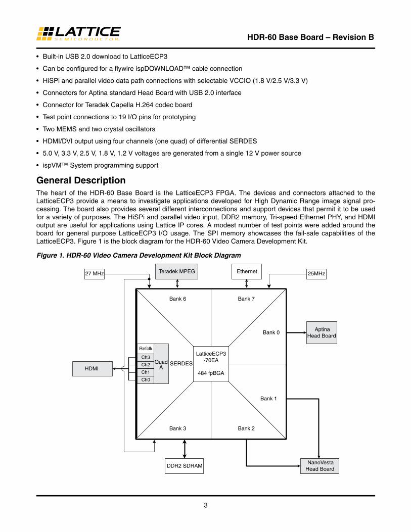
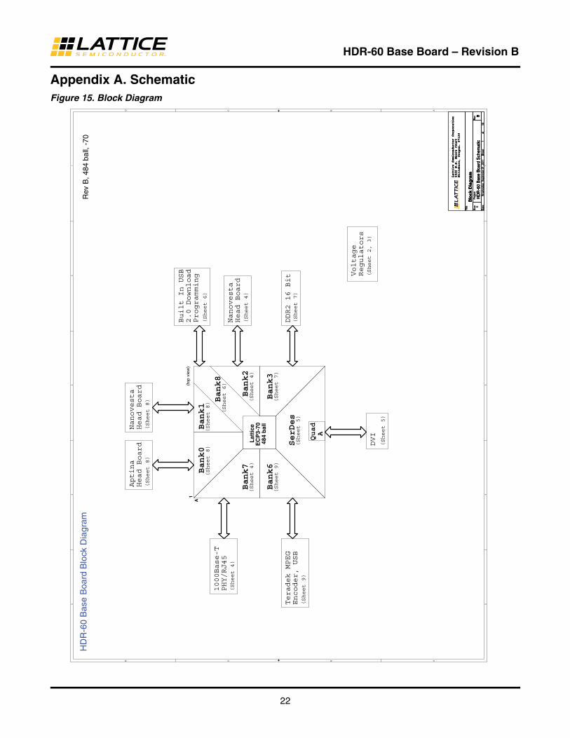
General DescriptionThe heart of the HDR-60 Base Board is the LatticeECP3 FPGA. The devices and connectors attached to the LatticeECP3 provide a means to investigate applications developed for High Dynamic Range image signal pro-cessing. The board also provides several different interconnections and support devices that permit it to be used for a variety of purposes. The HiSPi and parallel video input, DDR2 memory, Tri-speed Ethernet PHY, and HDMI output are useful for applications using Lattice IP cores. A modest number of test points were added around the board for general purpose LatticeECP3 I/O usage. The SPI memory showcases the fail-safe capabilities of the LatticeECP3. Figure 1 is the block diagram for the HDR-60 Video Camera Development Kit.
Figure 1. HDR-60 Video Camera Development Kit Block Diagram
Refclk
QuadA
Bank 6 Bank 7
Bank 0
Bank 1
Bank 2Bank 3
SERDESCh3
Ch2
Ch1
Ch0
Teradek MPEG Ethernet
AptinaHead Board
NanoVestaHead Board
LatticeECP3-70EA
484 fpBGAHDMI
DDR2 SDRAM
27 MHz 25MHz

4
HDR-60 Base Board – Revision B
Initial Setup and HandlingThe following is recommended reading prior to removing the evaluation board from the static shielding bag and may or may not apply to your particular use of the board.
CAUTION: The devices on the board can be damaged by improper handling.
The devices on the evaluation board contain fairly robust ESD (Electro Static Discharge) protection structures within them, able to withstand typical static discharges (see the “Human Body Model” specification for an example of ESD characterization requirements). Even so, the devices are static sensitive to conditions that exceed their designed in protection. For example: higher static voltages, as well as lower voltages with lower series resistance or larger capacitance than the respective ESD specifications can potentially damage or degrade the devices on the evaluation board.
As such, it is recommended that you wear an approved and functioning grounded wrist strap at all times while han-dling the evaluation board when it is removed from the static shielding bag. If you will not be using the board for a while, it is best to put it back in the static shielding bag. Please save the static shielding bag and packing box for future storage of the board when it is not in use.
When reaching for the board, it is recommended that you first touch the ground plane of the board (for example, the metal shielding of the HDMI connector). This will neutralize any static voltage difference between your body and the board prior to any contact with signal I/O.
CAUTION: To minimize the possibility of ESD damage, the first and last electrical connections to the board should always be from test equipment chassis ground to the ground plane of the board.
Before connecting signals or power to the board, attach a cable from chassis ground on grounded test equipment to the ground plane of the board. Connecting the board ground to test equipment chassis ground will decrease the risk of ESD damage to the I/O on the board as the initial connections to the board are made. Likewise, when unplugging cables from the evaluation board, the last connection unplugged, should be the chassis GND connec-tion to the evaluation board GND. If you have a signal source that is floating with respect to chassis GND, attempt to neutralize any static charge on that signal source prior to attaching it to the evaluation board.
If you are holding or carrying the board when it is not in a static shielding bag, please keep one finger on the ground plane of the board, for example the metal shielding of the HDMI connector. This will keep the board at the same voltage potential as your body until you can pick up the static shielding bag and put the board back in it.
Electrical, Mechanical, and Environmental SpecificationsThe nominal board dimensions are 203.2 mm x 42 mm (8.000” x 1.654”). Additional mechanical board dimension information is included on the mechanical drawing shown in Appendix A, Figure 24. On the physical board itself, connectors include pin 1 indictors as either an arrow, or triangle point near pin 1 on the outer layer silk screen. The environmental specifications are as follows:
• Operating temperature: 0 °C to 55 °C
• Storage temperature: -40 °C to 75 °C
• Humidity: <95% without condensation
• 11 V to 18 V DC (20 watts max.)
5
HDR-60 Base Board – Revision B
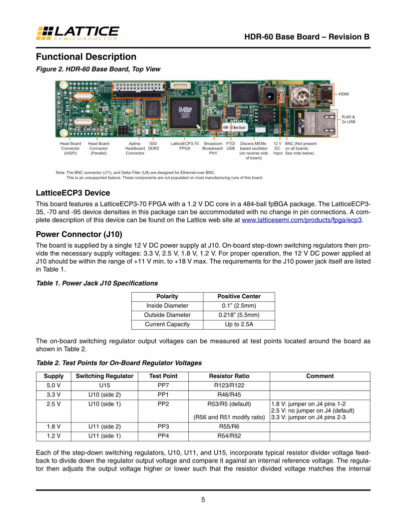
Functional DescriptionFigure 2. HDR-60 Base Board, Top View
HDMI
RJ45 &2x USB
BNC (Not present on all boards. See note below)
Discera MEMs based oscillator(on reverse side
of board)
12 V DC Input
LatticeECP3-70FPGA
ISSI DDR2
BroadcomBroadreach
PHY
FTDIUSB
Aptina HeadboardConnector
Head BoardConnector
(HiSPi)
Head BoardConnector(Parallel)
Note: The BNC connector (J11), and Delta Filter (U8) are designed for Ethernet-over-BNC. This is an unsupported feature. These components are not populated on most manufacturing runs of this board.
LatticeECP3 DeviceThis board features a LatticeECP3-70 FPGA with a 1.2 V DC core in a 484-ball fpBGA package. The LatticeECP3-35, -70 and -95 device densities in this package can be accommodated with no change in pin connections. A com-plete description of this device can be found on the Lattice web site at www.latticesemi.com/products/fpga/ecp3.
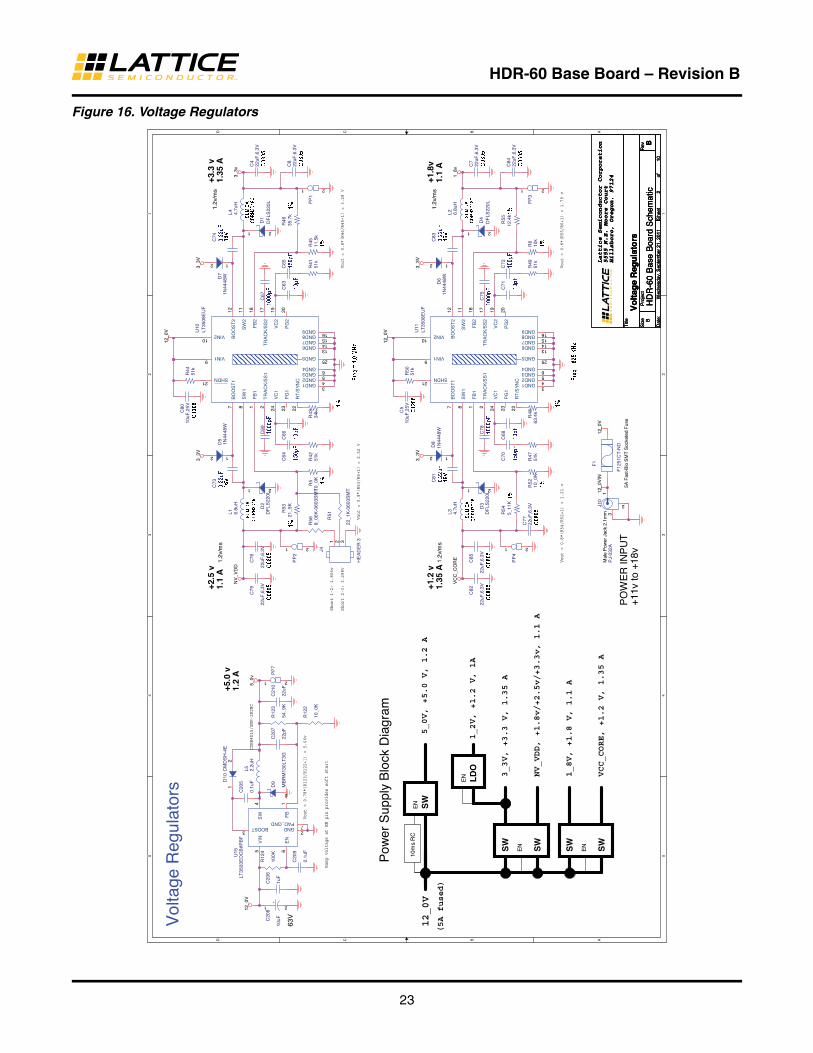
Power Connector (J10) The board is supplied by a single 12 V DC power supply at J10. On-board step-down switching regulators then pro-vide the necessary supply voltages: 3.3 V, 2.5 V, 1.8 V, 1.2 V. For proper operation, the 12 V DC power applied at J10 should be within the range of +11 V min. to +18 V max. The requirements for the J10 power jack itself are listed in Table 1.
Table 1. Power Jack J10 Specifications
Polarity Positive Center
Inside Diameter 0.1” (2.5mm)
Outside Diameter 0.218” (5.5mm)
Current Capacity Up to 2.5A
The on-board switching regulator output voltages can be measured at test points located around the board as shown in Table 2.
Table 2. Test Points for On-Board Regulator Voltages
Supply Switching Regulator Test Point Resistor Ratio Comment
5.0 V U15 PP7 R123/R122
3.3 V U10 (side 2) PP1 R46/R45
2.5 V U10 (side 1) PP2 R53/R5 (default)
(R56 and R51 modify ratio)
1.8 V: jumper on J4 pins 1-22.5 V: no jumper on J4 (default)3.3 V: jumper on J4 pins 2-3
1.8 V U11 (side 2) PP3 R55/R6
1.2 V U11 (side 1) PP4 R54/R52
Each of the step-down switching regulators, U10, U11, and U15, incorporate typical resistor divider voltage feed-back to divide down the regulator output voltage and compare it against an internal reference voltage. The regula-tor then adjusts the output voltage higher or lower such that the resistor divided voltage matches the internal
6
HDR-60 Base Board – Revision B
reference. By doing this, the regulator output voltage remains at a constant voltage value independent of the load driven. Each regulator output voltage follows this equation:
Vout = (1 + resistor ratio) x (regulator internal reference voltage)
See the LT3503 and LT3508 device data sheets for additional details about these devices.
The 2.5 V regulator output voltage can also be set to 1.8 V or 3.3 V by adding a shorting jumper on J4, as shown in Table 2. With no jumper on J4, the voltage divider is set by R53 and R5 and this divider sets up a nominal 2.5 V output voltage. When a shorting jumper is added to J4, the R56 and R51 resistors will be placed in parallel with either R53 or R5, which then changes the resistor divider ratio, and this changes side 1 of the U10 regulator output voltage to become 1.8 V or 3.3 V depending on the placement of the shorting jumper on J4.
The SERDES 1.2 V regulators (U4) are low dropout linear types that deliver a constant 1.2 V output voltage when powered by the 3.3 V input voltage. In contrast to the switching regulators discussed above, the U4 linear regulars do not generate switching noise, so they are a good choice for powering the LatticeECP3 SERDES to give the low-est jitter generation. Also, U4 does not use resistor divider networks to set the output voltage, instead U4 is set up to directly copy its own internal 1.215 V reference voltage to its outputs. The U4 regulator outputs are available for testing at test points PP5 and PP6. See the LT3029 device data sheets for additional details about this device.
When using the various I/O test points located around the board, be sure to not exceed the LatticeECP3 Family Data Sheet specified absolute maximum rating for Output Supply Voltage VCCIO range of -0.5 V to +3.75 V, or damage to the device may occur. Also, for I/O input capability of the various I/O standards supported by the LatticeECP3 sysIO structures, see the LatticeECP3 sysIO Usage Guide.
LatticeECP3 I/O Bank VoltagesMost of the bank voltages on the LatticeECP3 (U2) have been hard-wired to specific power supply values. Excep-tions to this are banks 1 and 2 which can be set to other values used to power the sensor boards that plug into the parallel connector (J2) and HiSPi connector (J1). This is shown in Table 3.
Table 3. LatticeECP3 (U2) Bank Voltage Settings
LatticeECP3 Bank VCCIO Voltage Comment
0 3.3 V Aptina Head Board
1 and 2 Adjustable
Sensor attached to J1 and J21.8 V: Jumper on J4 pins 1-22.5 V: No jumper on J4 (default)3.3 V: Jumper on J4 pins 2-3
3 1.8 V DDR2
Quad A 1.2 V SERDES
6 3.3 V Teradek MPEG Encoder
7 3.3 V Ethernet
8 3.3 V LatticeECP3 programming
7
HDR-60 Base Board – Revision B
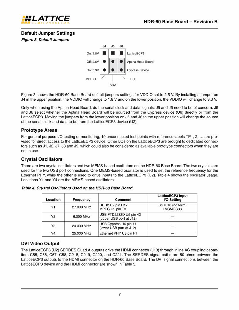
Default Jumper SettingsFigure 3. Default Jumpers
LatticeECP3
Aptina Head Board
Cypress Device
SCL
SDA
On: 1.8V
J4 J5 J6
Off: 2.5V
On: 3.3V
VDDIO
Figure 3 shows the HDR-60 Base Board default jumpers settings for VDDIO set to 2.5 V. By installing a jumper on J4 in the upper position, the VDDIO will change to 1.8 V and on the lower position, the VDDIO will change to 3.3 V.
Only when using the Aptina Head Board, do the serial clock and data signals, J5 and J6 need to be of concern. J5 and J6 select whether the Aptina Head Board will be sourced from the Cypress device (U6) directly or from the LatticeECP3. Moving the jumpers from the lower position on J5 and J6 to the upper position will change the source of the serial clock and data to be from the LatticeECP3 device (U2).
Prototype AreasFor general purpose I/O testing or monitoring, 19 unconnected test points with reference labels TP1, 2, … are pro-vided for direct access to the LatticeECP3 device. Other I/Os on the LatticeECP3 are brought to dedicated connec-tors such as J1, J2, J7, J8 and J9, which could also be considered as available prototype connectors when they are not in use.
Crystal OscillatorsThere are two crystal oscillators and two MEMS-based oscillators on the HDR-60 Base Board. The two crystals are used for the two USB port connections. One MEMS-based oscillator is used to set the reference frequency for the Ethernet PHY, while the other is used to drive inputs to the LatticeECP3 (U2). Table 4 shows the oscillator usage. Locations Y1 and Y4 are the MEMS-based oscillators.
Table 4. Crystal Oscillators Used on the HDR-60 Base Board
Location Frequency CommentLatticeECP3 Input
I/O Setting
Y1 27.000 MHz DDR2 U2 pin R17MPEG U2 pin T3
SSTL18 (no term)LVCMOS33
Y2 6.000 MHz USB FTD2232D U5 pin 43(upper USB port at J12) —
Y3 24.000 MHz USB Cypress U6 pin 11(lower USB port at J12) —
Y4 25.000 MHz Ethernet PHY U3 pin F1 —
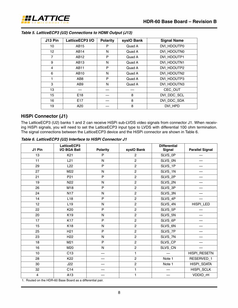
DVI Video OutputThe LatticeECP3 (U2) SERDES Quad A outputs drive the HDMI connector (J13) through inline AC coupling capac-itors C55, C56, C57, C58, C218, C219, C220, and C221. The SERDES signal paths are 50 ohms between the LatticeECP3 outputs to the HDMI connector on the HDR-60 Base Board. The DVI signal connections between the LatticeECP3 device and the HDMI connector are shown in Table 5.
8
HDR-60 Base Board – Revision B
Table 5. LatticeECP3 (U2) Connections to HDMI Output (J13)
J13 Pin LatticeECP3 I/O Polarity sysIO Bank Signal Name10 AB15 P Quad A DVI_HDOUTP0
12 AB14 N Quad A DVI_HDOUTN0
7 AB12 P Quad A DVI_HDOUTP1
9 AB13 N Quad A DVI_HDOUTN1
4 AB11 P Quad A DVI_HDOUTP2
6 AB10 N Quad A DVI_HDOUTN2
1 AB8 P Quad A DVI_HDOUTP3
3 AB9 N Quad A DVI_HDOUTN3
13 — — — CEC_OUT
15 E18 — 8 DVI_DDC_SCL
16 E17 — 8 DVI_DDC_SDA
19 A20 — 8 DVI_HPD
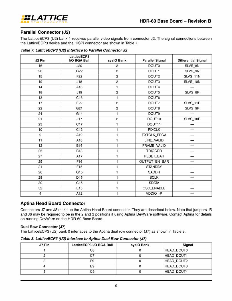
HiSPi Connector (J1)The LatticeECP3 (U2) banks 1 and 2 can receive HiSPi sub-LVDS video signals from connector J1. When receiv-ing HiSPi signals, you will need to set the LatticeECP3 input type to LVDS with differential 100 ohm termination. The signal connections between the LatticeECP3 device and the HiSPi connector are shown in Table 6.
Table 6. LatticeECP3 (U2) Interface to HiSPi Connector J1
J1 PinLatticeECP3 I/O BGA Ball Polarity sysIO Bank
DifferentialSignal Parallel Signal
13 K21 P 2 SLVS_0P —
11 L21 N 2 SLVS_0N —
29 L22 P 2 SLVS_1P —
27 M22 N 2 SLVS_1N —
21 P21 P 2 SLVS_2P —
19 N22 N 2 SLVS_2N —
26 M18 P 2 SLVS_3P —
24 N17 N 2 SLVS_3N —
14 L18 P 2 SLVS_4P —
12 L19 N 2 SLVS_4N HISPI_LED
22 K20 P 2 SLVS_5P —
20 K19 N 2 SLVS_5N —
17 K17 P 2 SLVS_6P —
15 K18 N 2 SLVS_6N —
25 H21 P 2 SLVS_7P —
23 H22 N 2 SLVS_7N —
18 M21 P 2 SLVS_CP —
16 M20 N 2 SLVS_CN —
10 C13 — 1 — HISPI_RESETN
28 K22 — 2 Note 1 RESERVED_1
30 J22 — 2 Note 1 HISPI_SDATA
32 C14 — 1 — HISPI_SCLK
4 A13 — 1 — VDDIO_rH
1. Routed on the HDR-60 Base Board as a differential pair.
9
HDR-60 Base Board – Revision B
Parallel Connector (J2)The LatticeECP3 (U2) bank 1 receives parallel video signals from connector J2. The signal connections between the LatticeECP3 device and the HiSPi connector are shown in Table 7.
Table 7. LatticeECP3 (U2) Interface to Parallel Connector J2
J2 PinLatticeECP3I/O BGA Ball sysIO Bank Parallel Signal Differential Signal
16 J20 2 DOUT0 SLVS_8N
20 G22 2 DOUT1 SLVS_9N
15 F22 2 DOUT2 SLVS_11N
19 J18 2 DOUT3 SLVS_10N
14 A16 1 DOUT4 —
18 J19 2 DOUT5 SLVS_8P
13 C16 1 DOUT6 —
17 E22 2 DOUT7 SLVS_11P
22 G21 2 DOUT8 SLVS_9P
24 G14 1 DOUT9 —
21 J17 2 DOUT10 SLVS_10P
23 C17 1 DOUT11 —
10 C12 1 PIXCLK —
9 A19 1 EXTCLK_FPGA —
11 A18 1 LINE_VALID —
12 B16 1 FRAME_VALID —
25 B18 1 TRIGGER —
27 A17 1 RESET_BAR —
29 F16 1 OUTPUT_EN_BAR —
31 F15 1 STANDBY —
26 G15 1 SADDR —
28 D15 1 SCLK —
30 C15 1 SDATA —
32 E15 1 OSC_ENABLE —
4 A12 1 VDDIO_rP —
Aptina Head Board ConnectorConnectors J7 and J8 make up the Aptina Head Board connector. They are described below. Note that jumpers J5 and J6 may be required to be in the 2 and 3 positions if using Aptina DevWare software. Contact Aptina for details on running DevWare on the HDR-60 Base Board.
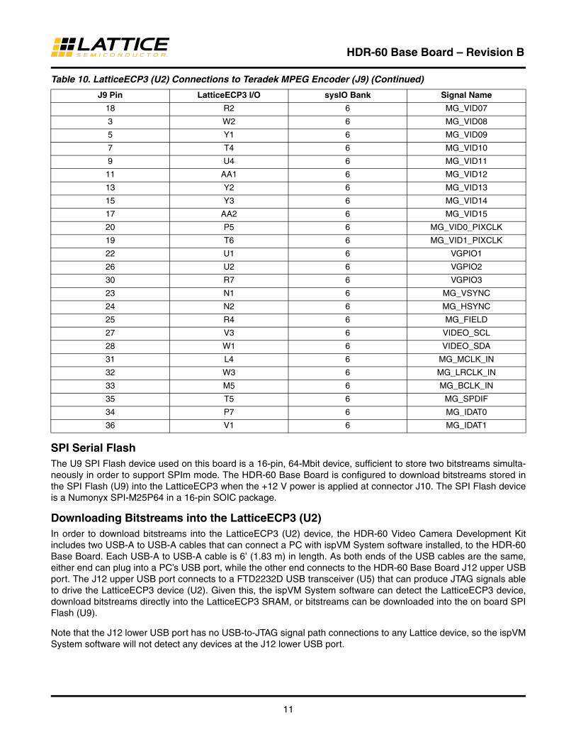
Dual Row Connector (J7)The LatticeECP3 (U2) bank 0 interfaces to the Aptina dual row connector (J7) as shown in Table 8.
Table 8. LatticeECP3 (U2) Interface to Aptina Dual Row Connector (J7)
J7 Pin LatticeECP3 I/O BGA Ball sysIO Bank Signal
1 C8 0 HEAD_DOUT0
2 C7 0 HEAD_DOUT1
3 F9 0 HEAD_DOUT2
4 E9 0 HEAD_DOUT3
5 C9 0 HEAD_DOUT4
10
HDR-60 Base Board – Revision B
Aptina Single Row Connector (J8)The LatticeECP3 (U2) bank 0 interfaces to the Aptina single row connector (J8) as shown in Table 9.
Table 9. LatticeECP3 (U2) Interface to Aptina Single Row Connector (J8)
J2 Pin LatticeECP3 I/O BGA Ball sysIO Bank Signal
1 F10 0 HEAD_DOUT10
2 E10 0 HEAD_DOUT11
3 A9 0 HEAD_DOUT12
4 B10 0 HEAD_DOUT13
5 A10 0 HEAD_DOUT14
6 A11 0 HEAD_DOUT15
7 C5 0 HEAD_SP0
8 B4 0 HEAD_SP1
9 E6 0 HEAD_SP2
10 D5 0 HEAD_GSHT_CTL
11 C6 0 HEAD_TRIGGER
Teradek MPEG Encoder ConnectorThe LatticeECP3 (U2) bank 6 I/Os connect to the Teradek MPEG Encoder Connector (J9). The signal connections are shown in Table 10.
6 C10 0 HEAD_DOUT5
7 B7 0 HEAD_DOUT6
8 A7 0 HEAD_DOUT7
9 B8 0 HEAD_DOUT8
10 A8 0 HEAD_DOUT9
13 A3 0 HEAD_LINE_VALID
14 B6 0 HEAD_SP5
15 G9 0 HEAD_SP7
16 F7 0 HEAD_SENSOR_RESETN
17 A4 0 HEAD_FRAME_VALID
19 E7 0 HEAD_SHIP_CLK
20 F8 0 HEAD_SP6
23 F11 0 HEAD_PIXCLK
26 D6 0 HEAD_MCLK
Table 10. LatticeECP3 (U2) Connections to Teradek MPEG Encoder (J9)
J9 Pin LatticeECP3 I/O sysIO Bank Signal Name
4 N3 6 MG_VID00
6 P3 6 MG_VID01
8 N5 6 MG_VID02
10 P6 6 MG_VID03
12 P1 6 MG_VID04
14 R1 6 MG_VID05
16 R3 6 MG_VID06
Table 8. LatticeECP3 (U2) Interface to Aptina Dual Row Connector (J7) (Continued)
J7 Pin LatticeECP3 I/O BGA Ball sysIO Bank Signal
11
HDR-60 Base Board – Revision B
SPI Serial FlashThe U9 SPI Flash device used on this board is a 16-pin, 64-Mbit device, sufficient to store two bitstreams simulta-neously in order to support SPIm mode. The HDR-60 Base Board is configured to download bitstreams stored in the SPI Flash (U9) into the LatticeECP3 when the +12 V power is applied at connector J10. The SPI Flash device is a Numonyx SPI-M25P64 in a 16-pin SOIC package.
Downloading Bitstreams into the LatticeECP3 (U2)In order to download bitstreams into the LatticeECP3 (U2) device, the HDR-60 Video Camera Development Kit includes two USB-A to USB-A cables that can connect a PC with ispVM System software installed, to the HDR-60 Base Board. Each USB-A to USB-A cable is 6’ (1.83 m) in length. As both ends of the USB cables are the same, either end can plug into a PC’s USB port, while the other end connects to the HDR-60 Base Board J12 upper USB port. The J12 upper USB port connects to a FTD2232D USB transceiver (U5) that can produce JTAG signals able to drive the LatticeECP3 device (U2). Given this, the ispVM System software can detect the LatticeECP3 device, download bitstreams directly into the LatticeECP3 SRAM, or bitstreams can be downloaded into the on board SPI Flash (U9).
Note that the J12 lower USB port has no USB-to-JTAG signal path connections to any Lattice device, so the ispVM System software will not detect any devices at the J12 lower USB port.
18 R2 6 MG_VID07
3 W2 6 MG_VID08
5 Y1 6 MG_VID09
7 T4 6 MG_VID10
9 U4 6 MG_VID11
11 AA1 6 MG_VID12
13 Y2 6 MG_VID13
15 Y3 6 MG_VID14
17 AA2 6 MG_VID15
20 P5 6 MG_VID0_PIXCLK
19 T6 6 MG_VID1_PIXCLK
22 U1 6 VGPIO1
26 U2 6 VGPIO2
30 R7 6 VGPIO3
23 N1 6 MG_VSYNC
24 N2 6 MG_HSYNC
25 R4 6 MG_FIELD
27 V3 6 VIDEO_SCL
28 W1 6 VIDEO_SDA
31 L4 6 MG_MCLK_IN
32 W3 6 MG_LRCLK_IN
33 M5 6 MG_BCLK_IN
35 T5 6 MG_SPDIF
34 P7 6 MG_IDAT0
36 V1 6 MG_IDAT1
Table 10. LatticeECP3 (U2) Connections to Teradek MPEG Encoder (J9) (Continued)
J9 Pin LatticeECP3 I/O sysIO Bank Signal Name

12
HDR-60 Base Board – Revision B
See the “Configuring/Programming the Board” section of this document for details on how to download bitstreams into the LatticeECP3 device. See www.latticesemi.com/hdr60 for additional downloadable project files and bit-streams designed for use with this board.
LEDs There are three LEDs on the HDR-60 Base Board that are used to show the programming state of the LatticeECP3. See Table 11 for information on the programming state LEDs.
Table 11. Programming LEDs
LED Pin Color Function
LED1 PROGRAMN Red On when signal is low
LED2 INITN Red On when initializing
LED3 DONE Green On when configuration is complete
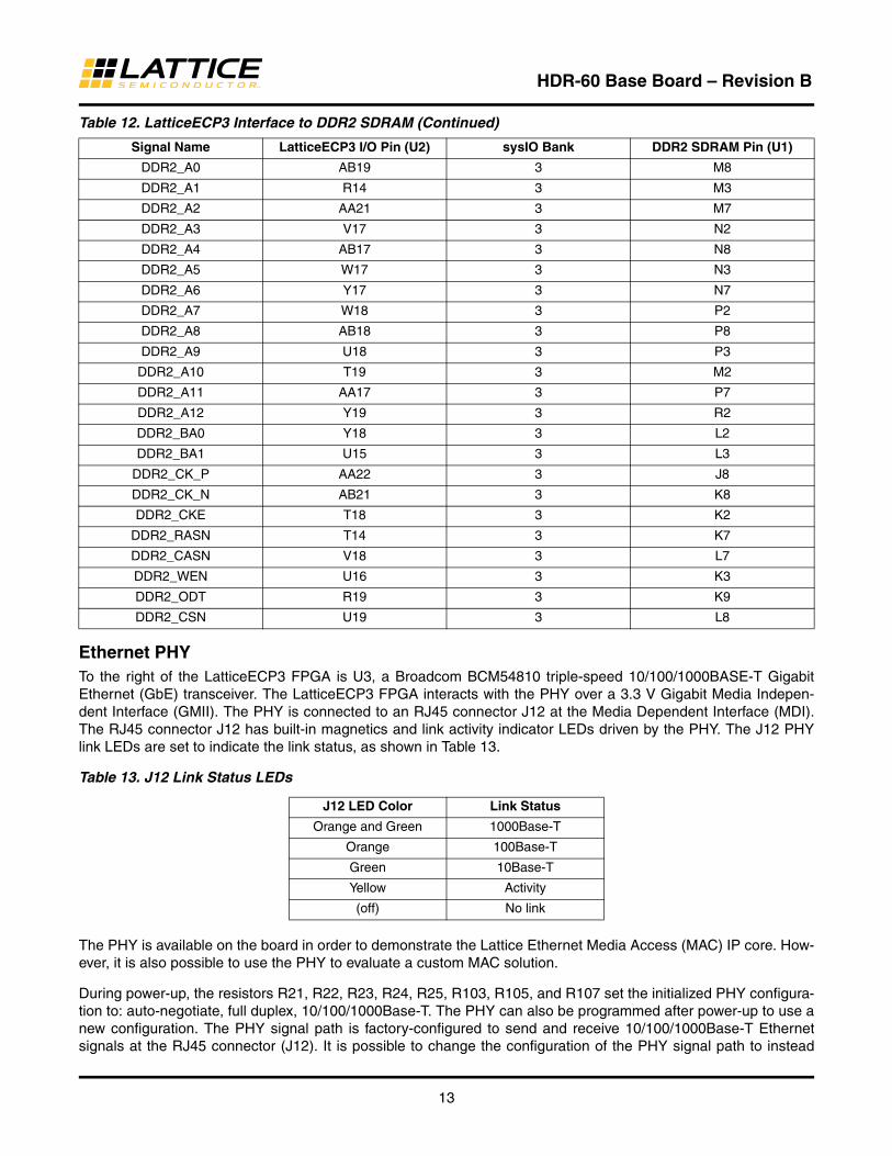
DDR2 MemoryThe HDR-60 Base Board is equipped with an 84-ball BGA DDR2 SDRAM such as the IS43DR16320B, which pro-vides memory resources with16 bits of data width that span a 32M address space. The DDR2 memory is powered by an on-board 1.8 V regulator with a 0.9 V midpoint bias termination regulator (U12). The evaluation board includes terminations for address, command and data signals. The suggested configuration is to set the DDR2 SDRAM (U1) for internal 150 ohms ODT, and the LatticeECP3 (U2) address, control and data signals to slow slew, 8 ma, with no ODT. This gives a low-noise, low-power DDR2 memory configuration usable to over 400 MT/s. Table 12 shows the pin connections for both the LatticeECP3 (U2) and DDR2 SDRAM (U1).
Table 12. LatticeECP3 Interface to DDR2 SDRAM
Signal Name LatticeECP3 I/O Pin (U2) sysIO Bank DDR2 SDRAM Pin (U1)
DDR2_DQ0 R22 3 G8
DDR2_DQ1 R20 3 G2
DDR2_DQ2 T20 3 H7
DDR2_DQ3 T22 3 H3
DDR2_DQ4 R21 3 H1
DDR2_DQ5 N19 3 H9
DDR2_DQ6 P22 3 F1
DDR2_DQ7 M19 3 F9
DDR2_DM0 N20 3 F3
DDR2_DQS0_P N18 3 F7
DDR2_DQS0_N P19 3 E8
DDR2_DQ8 Y21 3 C8
DDR2_DQ9 V22 3 C2
DDR2_DQ10 W22 3 D7
DDR2_DQ11 W21 3 D3
DDR2_DQ12 U22 3 D1
DDR2_DQ13 Y22 3 D9
DDR2_DQ14 R16 3 B1
DDR2_DQ15 P17 3 B9
DDR2_DM1 R18 3 B3
DDR2_DQS1_P T21 3 B7
DDR2_DQS1_N U20 3 A8
DDR2_VREF P20 3 J2
13
HDR-60 Base Board – Revision B
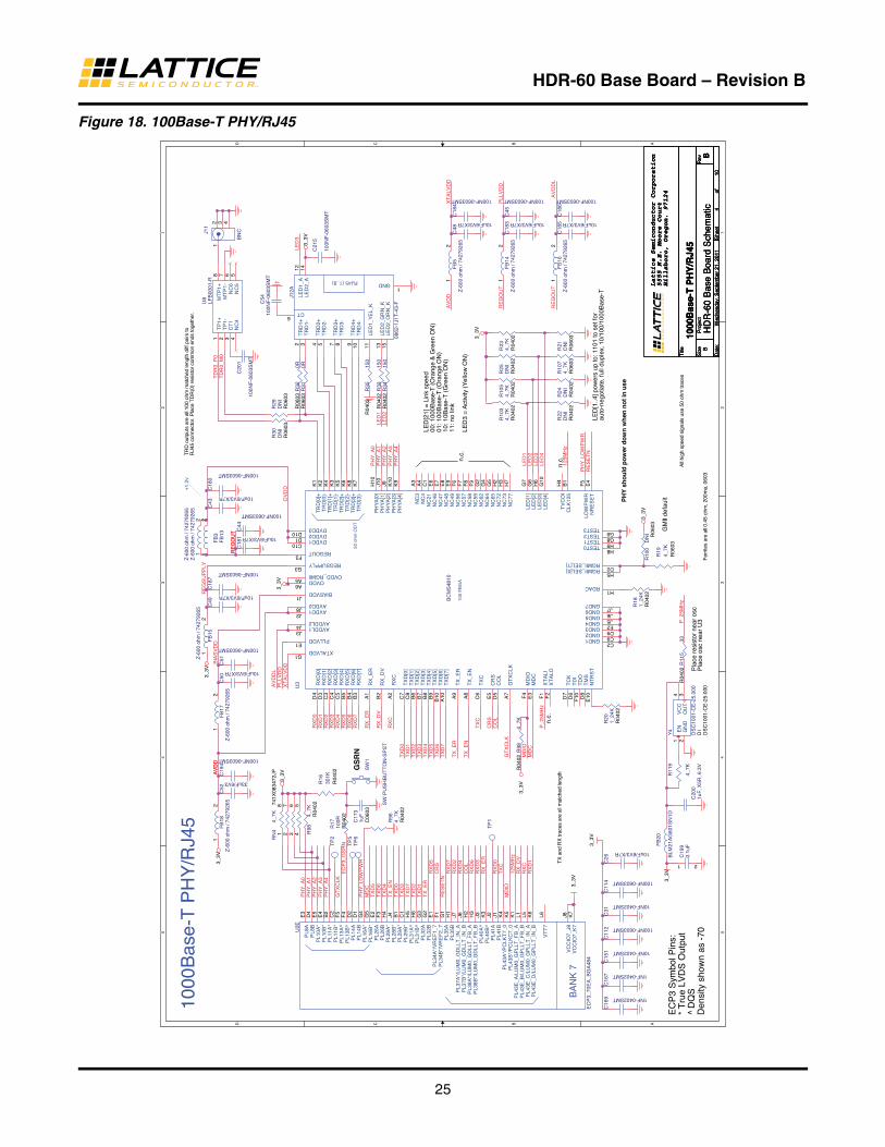
Ethernet PHYTo the right of the LatticeECP3 FPGA is U3, a Broadcom BCM54810 triple-speed 10/100/1000BASE-T Gigabit Ethernet (GbE) transceiver. The LatticeECP3 FPGA interacts with the PHY over a 3.3 V Gigabit Media Indepen-dent Interface (GMII). The PHY is connected to an RJ45 connector J12 at the Media Dependent Interface (MDI). The RJ45 connector J12 has built-in magnetics and link activity indicator LEDs driven by the PHY. The J12 PHY link LEDs are set to indicate the link status, as shown in Table 13.
Table 13. J12 Link Status LEDs
J12 LED Color Link Status
Orange and Green 1000Base-T
Orange 100Base-T
Green 10Base-T
Yellow Activity
(off) No link
The PHY is available on the board in order to demonstrate the Lattice Ethernet Media Access (MAC) IP core. How-ever, it is also possible to use the PHY to evaluate a custom MAC solution.
During power-up, the resistors R21, R22, R23, R24, R25, R103, R105, and R107 set the initialized PHY configura-tion to: auto-negotiate, full duplex, 10/100/1000Base-T. The PHY can also be programmed after power-up to use a new configuration. The PHY signal path is factory-configured to send and receive 10/100/1000Base-T Ethernet signals at the RJ45 connector (J12). It is possible to change the configuration of the PHY signal path to instead
DDR2_A0 AB19 3 M8
DDR2_A1 R14 3 M3
DDR2_A2 AA21 3 M7
DDR2_A3 V17 3 N2
DDR2_A4 AB17 3 N8
DDR2_A5 W17 3 N3
DDR2_A6 Y17 3 N7
DDR2_A7 W18 3 P2
DDR2_A8 AB18 3 P8
DDR2_A9 U18 3 P3
DDR2_A10 T19 3 M2
DDR2_A11 AA17 3 P7
DDR2_A12 Y19 3 R2
DDR2_BA0 Y18 3 L2
DDR2_BA1 U15 3 L3
DDR2_CK_P AA22 3 J8
DDR2_CK_N AB21 3 K8
DDR2_CKE T18 3 K2
DDR2_RASN T14 3 K7
DDR2_CASN V18 3 L7
DDR2_WEN U16 3 K3
DDR2_ODT R19 3 K9
DDR2_CSN U19 3 L8
Table 12. LatticeECP3 Interface to DDR2 SDRAM (Continued)
Signal Name LatticeECP3 I/O Pin (U2) sysIO Bank DDR2 SDRAM Pin (U1)

14
HDR-60 Base Board – Revision B
provide a legacy Ethernet coaxial link using the BNC connector (J11) by removing three resistors off the HDR-60 Base Board and then add back on three resistors as shown in Table 14. However, Ethernet-over-BNC is an unsup-ported feature on this board. The BNC connector and Delta filter (U8) are unpopulated on most production runs of this board. This information is provided as a reference only.
Table 14. Ethernet Connection at J11 or J12
Connector Cable LAN Speed PCB Configuration
J12 (RJ45) Cat5 10/100/1000Base-TR31, R32 = 0 ohmsR23 = 4.7K ohmsR29, R30, R21 = open
J11 (BNC) Coaxial 10/100Base-TR29, R30 = 0 ohmsR21 = 4.7K ohmsR31, R32, R23 = open
1
Refer to the HDR-60 Base Board schematic in Appendix A and the Broadcom BCM54810 Data Sheet for detailed information about the operation of the Ethernet PHY interface on this device. Refer to Table 15 for a description of the Ethernet PHY GMII connections to the LatticeECP3.
1. J11 (BNC) and U8 (Delta filter) are unpopulated on most manufacturing runs of this board. Ethernet-over-BNC is an unsupported feature of this board. The information in this table is for reference only.
Table 15. LatticeECP3 Interface to Ethernet PHY
Signal Name LatticeECP3 I/O Pin (U2) sysIO Bank BCM54810 Pin (U3)
PHY_A0 E3 7 H10
PHY_A1 D4 7 J10
PHY_A2 E5 7 J9
PHY_A3 E4 7 K10
PHY_A4 B2 7 K9
GTXCLK F5 7 A7
ECP3_GSRN F4 7 --
PHY_LOWPWR G4 7 F5
MDC G5 7 E3
TXD0 B1 7 C7
TXD1 G3 7 C8
TXD2 H6 7 B6
TXD3 C1 7 B7
TXD4 H4 7 B8
TXD5 E2 7 B9
TXD6 F3 7 B10
TXD7 H5 7 A10
TX_EN J4 7 A8
TX_ER G2 7 A9
CRS F1 7 E5
COL H2 7 D5
RESETN G1 7 E4
RXD0 J1 7 D4
RXD1 K6 7 D3
RXD2 J7 7 C3
RXD3 J3 7 C4
RXD4 J6 7 C5
15
HDR-60 Base Board – Revision B
Configuring/Programming the BoardRequirements
• PC with Lattice ispVM System software version 17.9 (or later) installed with USB driver. Note: An option to install this driver is included as part of the ispVM System setup.
For a complete discussion of the LatticeECP3 configuration and programming options, refer to the LatticeECP3 sysCONFIG Usage Guide.
Download Procedures for the Lattice HDR-60 Base BoardThe download instructions described below show how to download bitstreams into the LatticeECP3 SRAM using the ispVM System software. Downloads can be either direct through a cable connection to a PC, or indirect by first programming the on-board SPI Flash and then downloading the bitstream to the LatticeECP3 SRAM from SPI Flash. You can download bitstreams through a download cable to the LatticeECP3 SRAM at any time. After a bit-stream has been downloaded to SPI Flash, you can download the bitstream from SPI Flash to the LatticeECP3 SRAM by cycling the power to the evaluation board.
The Lattice HDR-60 Base Board provides support for two types of download cable connections: a standard USB-A to USB-A cable at J12, or a Lattice ispDOWNLOAD cable (USB type or parallel port type with flywire connections) at J3 as described in Appendix C. Given that you might want to download to either the LatticeECP3 SRAM or the SPI Flash, separate LatticeECP3 download procedures will follow that cover each type of download.
Note that the first download procedure shows the menus as viewed on a Windows XP operating system. Follow-on download procedures are very similar and do not show the menus.
LatticeECP3 SRAM Configuration Using a Standard USB Cable at J12The LatticeECP3 SRAM can be configured easily using the ispVM System software to download a bitstream via a standard USB-A to USB-A cable. The LatticeECP3 device is SRAM based, so it must remain powered on to retain its configuration when programming the SRAM.
1. Attach a ground connection from test equipment chassis ground to the ground plane of the board, for example, on the metal HDMI connector.
2. Connect the USB-A to USB-A cable from your PC’s USB connector to the upper USB port on J12 on the HDR-60 Base Board.
3. Connect the 12 V wall power adaptor cable to J10 and check to see that the wall power adapter is plugged in to a 120 VAC source.
4. Start the ispVM System software. Select the menu items Options > Autoscan Options > Custom Scan as shown in Figure 4.
RXD5 E1 7 B5
RXD6 H3 7 B4
RXD7 H1 7 B3
RX_ER K3 7 A1
TXC K4 7 C6
MDIO K5 7 F4
125MHz K1 7 B1
RX_DV L1 7 B2
RXC L5 7 A2
Table 15. LatticeECP3 Interface to Ethernet PHY (Continued)
Signal Name LatticeECP3 I/O Pin (U2) sysIO Bank BCM54810 Pin (U3)

16
HDR-60 Base Board – Revision B
Figure 4. Setting the ispVM Custom Scan Option
5. Select Options > Cable and I/O Port Setup. For the Cable Type, select USB2, then click OK.
6. Push the Scan button. You should now see the LFE3-95/70 device listed in the New Scan Configuration Setup window. In the device list, left-click on the LatticeECP3 device to select it. If offered other selections, select LFE3-70EA. See Figure 5.
Figure 5. ispVM New Scan Configuration Setup
7. Click Edit > Edit Device to edit the device. A Device Information window will be opened. Click the Select but-ton and select the package type 484-ball fpBGA as shown in Figure 6, then click OK.
Figure 6. LatticeECP3 Package Size Selection
8. Check that the Device Access Options drop-down menu control selects the JTAG 1532 Mode. Check that the Operation drop-down menu selects Fast Program.
9. Click the data file Browse button and select the path to the LatticeECP3 “.BIT” bitstream file as shown in Figure 7, then click OK.

17
HDR-60 Base Board – Revision B
Figure 7. Bitstream Ready to Download into LatticeECP3 SRAM
10. Click Project >Download or the green Go button to download the bitstream into the LatticeECP3 device (U2). A small window will appear as shown in Figure 8. It will take about 12 seconds to download the bitstream for a PC with USB 2.0 ports. When the LatticeECP3 has loaded in correctly, the ispVM status window will report “Operation Successful” as shown in Figure 9.
Figure 8. Bitstream Downloading into LatticeECP3
Figure 9. Bitstream Download Operation Successful
LatticeECP3 SRAM Configuration Using SPI Flash and USB Cable at J12The LatticeECP3 SRAM can be configured easily using the ispVM System software to program the on-board SPI Flash via a standard USB cable connected to the upper USB port at J12. The LatticeECP3 device is SRAM-based, so it must remain powered on to retain its configuration when programming the SRAM. The on-board SPI Flash retains its programmed bitstreams when power is off, and can quickly load programmed bitstreams into the LatticeECP3 device when power is applied.
1. Attach a ground connection from test equipment chassis ground to the ground plane of the board, for example on the metal HDMI connector.
18
HDR-60 Base Board – Revision B
2. Connect the USB-A to USB-A cable from your PC’s USB connector to the upper USB port on J12 on the HDR-60 Base Board.
3. Connect the 12 V wall power adaptor cable to J10 and check to see that the wall power adapter is plugged in to a 120 VAC source.
4. Start the ispVM System software. Select the menu items Options > Autoscan Options > Custom Scan.
5. Select Options > Cable and I/O Port Setup. For the Cable Type, select USB2, then click OK.
6. Push the Scan button. You should now see the LFE3-95/70 device listed in the New Scan Configuration Setup window. In the device list, left-click on the LatticeECP3 device to select it. If offered other selections, select LFE3-70EA.
7. Click Edit > Edit Device to edit the device. A Device Information window will be opened. Click the Select but-ton and select the package type 484-ball fpBGA, then click OK.
8. Click the Device Access Options drop-down menu control and select SPI Flash Background Programming. A SPI Serial Flash Device window will open.
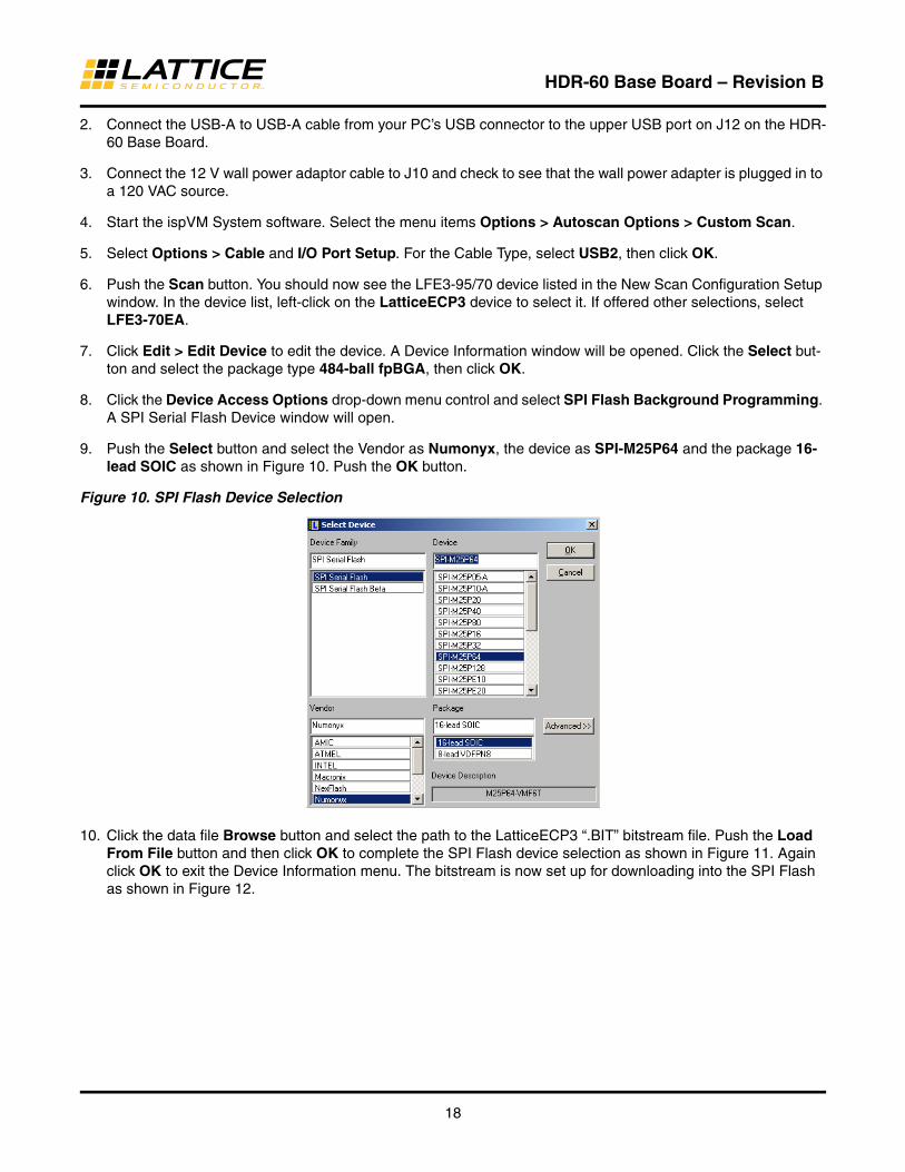
9. Push the Select button and select the Vendor as Numonyx, the device as SPI-M25P64 and the package 16-lead SOIC as shown in Figure 10. Push the OK button.
Figure 10. SPI Flash Device Selection
10. Click the data file Browse button and select the path to the LatticeECP3 “.BIT” bitstream file. Push the Load From File button and then click OK to complete the SPI Flash device selection as shown in Figure 11. Again click OK to exit the Device Information menu. The bitstream is now set up for downloading into the SPI Flash as shown in Figure 12.
19
HDR-60 Base Board – Revision B
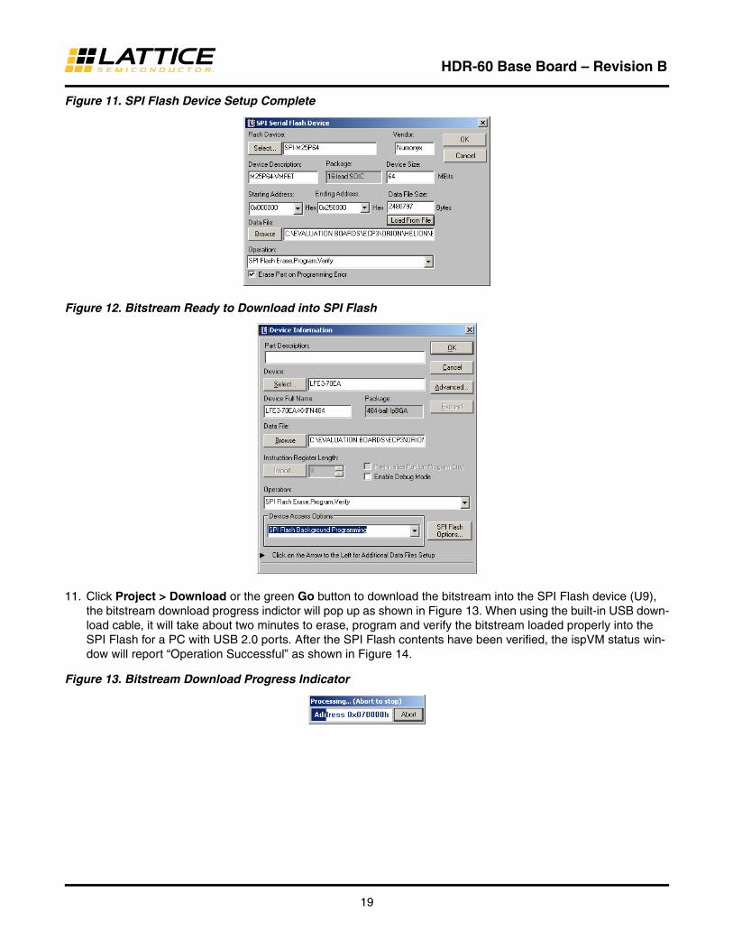
Figure 11. SPI Flash Device Setup Complete
Figure 12. Bitstream Ready to Download into SPI Flash
11. Click Project > Download or the green Go button to download the bitstream into the SPI Flash device (U9), the bitstream download progress indictor will pop up as shown in Figure 13. When using the built-in USB down-load cable, it will take about two minutes to erase, program and verify the bitstream loaded properly into the SPI Flash for a PC with USB 2.0 ports. After the SPI Flash contents have been verified, the ispVM status win-dow will report “Operation Successful” as shown in Figure 14.
Figure 13. Bitstream Download Progress Indicator
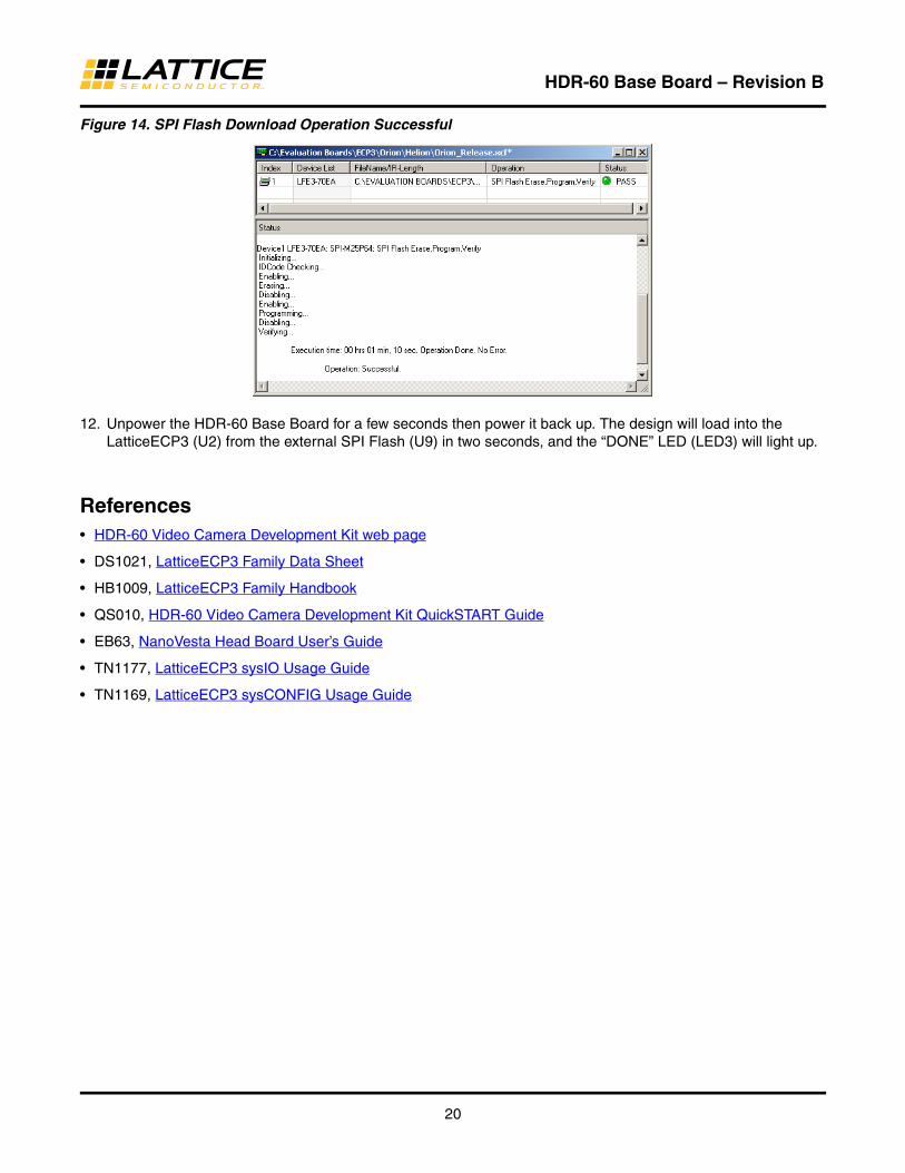
20
HDR-60 Base Board – Revision B
Figure 14. SPI Flash Download Operation Successful
12. Unpower the HDR-60 Base Board for a few seconds then power it back up. The design will load into the LatticeECP3 (U2) from the external SPI Flash (U9) in two seconds, and the “DONE” LED (LED3) will light up.
References• HDR-60 Video Camera Development Kit web page
• DS1021, LatticeECP3 Family Data Sheet
• HB1009, LatticeECP3 Family Handbook
• QS010, HDR-60 Video Camera Development Kit QuickSTART Guide
• EB63, NanoVesta Head Board User’s Guide
• TN1177, LatticeECP3 sysIO Usage Guide
• TN1169, LatticeECP3 sysCONFIG Usage Guide
Description Ordering Part NumberChina RoHS Environment-Friendly
Use Period (EFUP)
HDR-60 Video Camera Development Kit(Contains: HDR-60 Base Board with LatticeECP3 FPGA pre-loaded with Image Signal Processing (ISP)Demo, NanoVesta Head Board with Aptina A-1000 720p HDR Sensor and Sunex lens, two USB cables, HDMI cable with HDMI-to-DVI adapter, 12 V AC adapter power supply, QuickSTART Guide)
LFE3-70EAHDR60-DKN
HDR-60 Video Camera Base Board(Contains: HDR-60 Base Board with LatticeECP3 FPGA pre-loaded with Image Signal Processing (ISP)Demo, two USB cables, HDMI cable with HDMI-to-DVI adapter, 12 V AC adapter power supply, QuickSTART Guide)
Note: Does not include NanoVesta Head Board.
LFE3-70EAHDR60-EVN
21
HDR-60 Base Board – Revision B
Ordering Information
Technical Support Assistancee-mail: [email protected]
Internet: www.latticesemi.com
Revision HistoryDate Version Change Summary
August 2012 01.0 Initial release.
March 2013 01.1 Added HDR-60 Video Camera Base Board in Ordering Information.
April 2014 01.2 Updated references to BNC connector (J11) and Delta filter (U8) to indi-cate these are unpopulated on most boards. Ethernet-over-BNC is an unsupported feature of this board.
Updated Technical Support Assistance information.
© 2014 Lattice Semiconductor Corp. All Lattice trademarks, registered trademarks, patents, and disclaimers are as listed at www.latticesemi.com/legal. All other brand or product names are trademarks or registered trademarks of their respective holders. The specifications and information herein are subject to change without notice.
22
HDR-60 Base Board – Revision B
Appendix A. SchematicFigure 15. Block Diagram
5 5
4 4
3 3
2 2
1 1
DD
CC
BB
AA
HD
R-6
0 B
ase
Boa
rd B
lock
Dia
gram
(Sheet 2, 3)
Voltage
Regulators
SerDes
(Sheet 5)
Quad
A
Lat
tice
EC
P3-
70 4
84 b
all
Bank8
(Sheet 6)
Bank0
Bank1
Bank2
Bank3
(Sheet 4)
(Sheet 8)
(Sheet 8)
(Sheet 7)
Bank7
(Sheet 4)
Bank6
(Sheet 9)
(Sheet 4)
1000Base-T
PHY/RJ45
(Sheet 6)
Built In USB
2.0 Download
Programming
Rev
B, 4
84 b
all,
-70
(top
vie
w)
A1
(Sheet 5)
DVI
(Sheet 8)
Aptina
Head Board
(Sheet 7)
DDR2 16 Bit
(Sheet 9)
Teradek MPEG
Encoder, USB
(Sheet 8)
Nanovesta
Head Board
(Sheet 4)
Nanovesta
Head Board
Title
Siz
eP
roje
ctR
ev
Dat
e:S
heet
of
Lattice Semiconductor Corporation
5555 N.E. Moore Court
Hillsboro, Oregon. 97124
HD
R-6
0 B
ase
Boa
rd S
chem
atic
B
Blo
ck D
iag
ram
C
110
Wed
nesd
ay, S
epte
mbe
r 21
, 201
1
Title
Siz
eP
roje
ctR
ev
Dat
e:S
heet
of
Lattice Semiconductor Corporation
5555 N.E. Moore Court
Hillsboro, Oregon. 97124
HD
R-6
0 B
ase
Boa
rd S
chem
atic
B
Blo
ck D
iag
ram
C
110
Wed
nesd
ay, S
epte
mbe
r 21
, 201
1
Title
Siz
eP
roje
ctR
ev
Dat
e:S
heet
of
Lattice Semiconductor Corporation
5555 N.E. Moore Court
Hillsboro, Oregon. 97124
HD
R-6
0 B
ase
Boa
rd S
chem
atic
B
Blo
ck D
iag
ram
C
110
Wed
nesd
ay, S
epte
mbe
r 21
, 201
1
23
HDR-60 Base Board – Revision B
Figure 16. Voltage Regulators
5 5
4 4
3 3
2 2
1 1
DD
CC
BB
AA
Vol
tage
Reg
ulat
ors
CDRH4D15/SNP-2R2NC
Vout = 0.78*(R123/R122+1) = 5.06v
Ramp voltage at EN pin provides soft start
PO
WE
R IN
PU
T+
11v
to +
18v
+5.0
v1.
2 A
+3.3
v1.
35 A
+1.8
v1.
1 A
Vout = 0.8*(R46/R45+1) = 3.28 v
Vout = 0.8*(R55/R6+1) = 1.79 v
+1.2
v1.
35 A
+2.5
v1.
1 A
Vout = 0.8*(R53/R5+1) = 2.52 v
Vout = 0.8*(R54/R52+1) = 1.21 v
1.2v
/ms
1.2v
/ms
1.2v
/ms
1.2v
/ms
SW
SW
5_0V, +5.0 V, 1.2 A
3_3V, +3.3 V, 1.35 A
Pow
er S
uppl
y B
lock
Dia
gram
12_0V
EN
EN
(5A fused)
10m
s R
C
NV_VDD, +1.8v/+2.5v/+3.3v, 1.1 A
SW
SW
1_8V, +1.8 V, 1.1 A
EN
VCC_CORE, +1.2 V, 1.35 A
SW
LD
O1_2V, +1.2 V, 1A
EN
Short 1-2: 1.806v
Short 2-3: 3.298v
5_0v
12_0
V
12_0
VIN
12_0
V
3_3v
12_0
V
12_0
V
VC
C_C
OR
E
NV
_VD
D
1_8v
3_3V
3_3V
3_3V
3_3V
Titl
e
Siz
eP
roje
ctR
ev
Dat
e:S
heet
of
Lattice Semiconductor Corporation
5555 N.E. Moore Court
Hillsboro, Oregon. 97124
HD
R-6
0 B
ase
Boa
rd S
chem
atic
B
Vo
ltag
e R
egu
lato
rs
B
210
Wed
nesd
ay, S
epte
mbe
r 21
, 201
1
Titl
e
Siz
eP
roje
ctR
ev
Dat
e:S
heet
of
Lattice Semiconductor Corporation
5555 N.E. Moore Court
Hillsboro, Oregon. 97124
HD
R-6
0 B
ase
Boa
rd S
chem
atic
B
Vo
ltag
e R
egu
lato
rs
B
210
Wed
nesd
ay, S
epte
mbe
r 21
, 201
1
Titl
e
Siz
eP
roje
ctR
ev
Dat
e:S
heet
of
Lattice Semiconductor Corporation
5555 N.E. Moore Court
Hillsboro, Oregon. 97124
HD
R-6
0 B
ase
Boa
rd S
chem
atic
B
Vo
ltag
e R
egu
lato
rs
B
210
Wed
nesd
ay, S
epte
mbe
r 21
, 201
1
R51
22_1
K-0
603S
MT
R50
51k
C68
PP
7
1 2
C8
22uF
,6.3
V
R44
51k
C81
C85
22uF
,6.3
V
PP
4
1 2
C74
C20
7
22pF
C77
22uF
,6.3
V
D9
MB
RM
130L
T3G
1 2C20
5
0.1u
F
L3 4.7u
H
R52
10_0
K
C75
C80
10uF
,25V
C20
9
0.1u
F
C21
0
22uF
PP
2
1 2C
70
C64
+C
208
10uF
63V
1 2
D6
1N44
48W
2 1
C69
L1 6.8u
H
R47
51k
R48
63.4
k
D4
DF
LS22
0L
1 2
R41
51k
D3
DF
LS22
0L
1 2
C20
6
1uF
R6
10k
R55
12.4
k
C82
22uF
,6.3
V
R5
10_0
K
C84
22uF
,6.3
V
C66
R12
3
54_9
K
D2
DF
LS22
0L
1 2
PP
1
1 2
C4
22uF
,6.3
V
D8
1N44
48W
2 1
C73
L4 4.7u
H
F1
F12
51C
T-N
D
5A F
ast-
Blo
SM
T S
ocke
ted
Fus
e
R49
51k
C63
R43
34k
C65
C7
22uF
,6.3
V
R12
2
10_0
K
D1
DF
LS22
0L
1 2
J10
PJ-
032A
Mal
e P
ower
Jac
k 2.
1mm
13
2
U11
LT35
08E
UF
FB
218
VC
219
PG
220
RT
/SY
NC
22
SHDN21
FB
11
TR
AC
K/S
S1
2
BO
OS
T1
7
SW
18
VIN19
VC
124
VIN210
PG
123
SW
211
BO
OS
T2
12
TR
AC
K/S
S2
17
GND525
GND613
GND714
GND46GND35GND24GND13
GND815
GND916
C5
10uF
,25V
C67
R45
11.5
kR
568_
06K
-060
3SM
T
R54
5_11
K
C79
22uF
,6.3
V
C83
U10
LT35
08E
UF
FB
218
VC
219
PG
220
RT
/SY
NC
22
SHDN21
FB
11
TR
AC
K/S
S1
2
BO
OS
T1
7
SW
18
VIN19
VC
124
VIN210
PG
123
SW
211
BO
OS
T2
12
TR
AC
K/S
S2
17
GND525
GND613
GND714
GND46GND35GND24GND13
GND815
GND916
D5
1N44
48W
2 1
R42
51k
J4
HE
AD
ER
31 2 3
U15
LT35
03E
DC
B#P
BF
EN
6
SW
4
GND2
FB
1
VIN
5
BOOST3
PAD_GND7
R46
35.7
k
C71
R53
21_5
K
PP
3
1 2
C72
R12
4
100K
C76
22uF
,6.3
V
D7
1N44
48W
2 1
C78
D10
CM
DS
H-4
E2
1
L5 2.2u
H
L2 6.8u
H
24
HDR-60 Base Board – Revision B
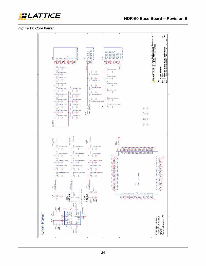
Figure 17. Core Power
5 5
4 4
3 3
2 2
1 1
DD
CC
BB
AA
Cor
e P
ower
28 mA max
100 mA max
302 mA max
0.46 v drop at 500 mA max
25V
6.3V
0805
0805
2.3v minimum input voltage
+1.2
v50
0 m
A
EC
P3
Sym
bol P
ins:
* T
rue
LVD
S O
utpu
t^
DQ
SD
ensi
ty s
how
n as
-70
25V
0805
+1.2
v50
0 m
AV
CC
PLL
PC
SA
_VC
CIB
PC
SA
_VC
CO
B
VC
CA
3_3v
VC
CA
3_3V
VC
C_C
OR
E
3_3V
1_2v
3_3v
Titl
e
Siz
eP
roje
ctR
ev
Dat
e:S
heet
of
Lattice Semiconductor Corporation
5555 N.E. Moore Court
Hillsboro, Oregon. 97124
HD
R-6
0 B
ase
Boa
rd S
chem
atic
B
Co
re P
ow
er
B
310
Wed
nesd
ay, S
epte
mbe
r 21
, 201
1
Titl
e
Siz
eP
roje
ctR
ev
Dat
e:S
heet
of
Lattice Semiconductor Corporation
5555 N.E. Moore Court
Hillsboro, Oregon. 97124
HD
R-6
0 B
ase
Boa
rd S
chem
atic
B
Co
re P
ow
er
B
310
Wed
nesd
ay, S
epte
mbe
r 21
, 201
1
Titl
e
Siz
eP
roje
ctR
ev
Dat
e:S
heet
of
Lattice Semiconductor Corporation
5555 N.E. Moore Court
Hillsboro, Oregon. 97124
HD
R-6
0 B
ase
Boa
rd S
chem
atic
B
Co
re P
ow
er
B
310
Wed
nesd
ay, S
epte
mbe
r 21
, 201
1
C25
1UF-16V-0805SMT
C14
5
10NF-0402SMT
10uF
CO
UT
2
FB
2
BLM
41P
G60
0SN
1
C15
5
1NF-0402SMT
C17
0
100NF-0402SMT
C13
7
100NF-0402SMT
+C
113 22UF-16V-TANTBSMT
GND
GND
GND
GND
U2L
EC
P3_
70E
A_B
GA
484
1R
13
2L1
1
3M
10
4E
8
5U
17
6U
14
7N
13
8A
B16
9N
21
10G
11
11K
10
12C
19
13T
13
14K
11
15P
18
16A
A11
17V
7
18M
3
19L1
0
20V
9
21H
15
22F
6
23L1
3
24F
17
25T11
26R8
27B17
28A1
29R15
30AA14
31V8
32P16
33U6
34N8
35U21
36J21
37K15
38L20
39H13
40L16
41A22
42J5
43V16
44W7
45AA8
46B13
47B5
48AB7
49L7
50H
1051
M11
52W
2053
M7
54V
1555
AA
956
T12
57P
258
E21
59C
1160
AA
1261
Y16
62V
1463
AA
1664
H18
65M
1266
R5
67W
1668
AB
2269
H8
70N
1071
E14
72U
1073
F2
98N11
97K13
96B9
95G12
94V2
93K8
92M16
91Y4
90N12
89AA7
88U13
87AA10
86AA15
85D3
84M13
83AB1
82AA13
81T10
80U9
79L12
78AA18
77K12
76R10
75K2
74Y7
XR
ES
N15
PP
6
1 2
C12
9
10NF-0402SMT
C14
8
10NF-0402SMT
C15
6
100NF-0402SMT
C13
6
10NF-0402SMT
PP
5
1 2
FB
10B
LM41
PG
600S
N1
CB
YP
2
0.01
uF
C14
9
10NF-0402SMT
U2M
EC
P3_
70E
A_B
GA
484
VC
CP
LL_L
_K9
K9
VC
CP
LL_L
_N9
N9
VC
CP
LL_R
_K14
K14
VC
CP
LL_R
_N14
N14
TP
26
C12
8 100NF-0402SMT
C14
4
100NF-0402SMT
C14
6
100NF-0402SMT
C12
6
1NF-0402SMT
FB
1
BLM
41P
G60
0SN
1C
142
1NF-0402SMT
R90
10k1
%
C16
8 1UF-16V-0805SMT
C16
5
100NF-0402SMT
C46
1UF-16V-0805SMT
C13
9
10NF-0402SMT
CB
YP
1
0.01
uF
+C
154 22UF-16V-TANTBSMT
+C
182
22UF-16V-TANTBSMT
1uF
CIN
2
VCC
U2J
EC
P3_
70E
A_B
GA
484
1J1
1
2J9
3P
11
4P
12
5J1
4
6J1
3
7M
14
8M
9
9P
9
10L9
11P
14
12P
10
13J1
2
14J1
0
15L1
4
16P
13
C16
3
10NF-0402SMT
C14
7
10NF-0402SMT
C16
2
10NF-0402SMT
TP
25T
P24
C13
4 10NF-0402SMT
C42
1UF-16V-0805SMT
C16
0
1NF-0402SMT
FB
4
BLM
41P
G60
0SN
1
C13
1
1NF-0402SMT
TP
23
C14
3
10NF-0402SMT
C16
1 1NF-0402SMT
+C
179
22UF-16V-TANTBSMT
10uF
CO
UT
1
U4
LT30
29E
DE
BY
P1
1
VIN1_1313
BY
P2
8
AD
J29
GND5
AD
J116
EN
15
VO
UT
14
EN
210
VO
UT
27
VIN212
VO
UT
1_3
3V
OU
T2_
66
VIN114
VIN2_1111
NC2
GND_PAD17
C15
2
100NF-0402SMT
C17
7
100NF-0402SMT
C15
8
10NF-0402SMT
C15
3
1NF-0402SMT
C13
3
10NF-0402SMT
C41
1UF-16V-0805SMT
C15
9
100NF-0402SMT
C14
1
10NF-0402SMT
C47 100NF-0402SMT
U2K
EC
P3_
70E
A_B
GA
484
VC
CA
UX
_M8
M8
VC
CA
UX
_R11
R11
VC
CA
UX
_H11
H11
VC
CA
UX
_M15
M15
VC
CA
UX
_R12
R12
VC
CA
UX
_H12
H12
VC
CA
UX
_L8
L8
VC
CA
UX
_L15
L15
VC
CA
_V10
V10
VC
CA
_V13
V13
VC
CA
_U12
U12
VC
CA
_U11
U11
+C
178
22UF-16V-TANTBSMT
1uF
CIN
1
25
HDR-60 Base Board – Revision B
Figure 18. 100Base-T PHY/RJ45
5 5
4 4
3 3
2 2
1 1
DD
CC
BB
AA
1000
Bas
e-T
PH
Y/R
J45
PH
Y s
ho
uld
po
wer
do
wn
wh
en n
ot i
n u
se
GM
II de
faul
t
Pla
ce r
esis
tor
near
osc
n.c.
n.c.
n.c.
TR
D o
utpu
ts a
re a
ll 10
0 oh
m m
atch
ed le
ngth
diff
pai
rs to
RJ4
5 co
nnec
tor.
Pla
ce T
DR
(0)
resi
stor
com
mon
end
s to
geth
er.
+1.
2v
EC
P3
Sym
bol P
ins:
* T
rue
LVD
S O
utpu
t^
DQ
SD
ensi
ty s
how
n as
-70
Pla
ce o
sc n
ear
U3
LED
[1..4
] pow
ers
up to
: 110
1 to
set
for
auto
-neg
otia
te, f
ull d
uple
x, 1
0/10
0/10
00B
ase-
T
LED
[21]
= L
ink
spee
d00
: 100
0Bas
e-T
(O
rang
e &
Gre
en O
N)
01: 1
00B
ase-
T (
Ora
nge
ON
)10
: 10B
ase-
T (
Gre
en O
N)
11: n
o lin
k
LED
3 =
Act
ivity
(Y
ello
w O
N)
All
high
spe
ed s
igna
ls u
se 5
0 oh
m tr
aces
TX
and
RX
trac
es a
re a
ll m
atch
ed le
ngth
GS
RN
Fer
rites
are
all
0.45
ohm
, 200
ma,
060
3
RX
D2
RX
D0
RX
D1
RX
D3
RX
D4
RX
D5
RX
D6
RX
D7
RX
_ER
RX
_DV
RX
C
TX
D0
TX
D1
TX
D2
TX
D3
TX
D4
TX
D5
TX
D6
TX
D7
TX
_ER
TX
_EN
TX
C
CR
SC
OL
GT
XC
LK
MD
C
GT
XC
LK
MD
C
RX
D5
CR
S
RX
D7
RX
D4
CO
L
RX
D3
RX
D6
RX
_ER
TX
CR
XD
0
MD
IO
RX
CR
X_D
V
RX
D1
TX
D5
TX
D4
TX
D6
TX
_EN
TX
D0
TX
D7
TX
D3
TX
D2
TX
D1
TX
_ER
P_2
5MH
z
P_2
5MH
z
PH
Y_A
0
RE
SE
TN
LED
4
RE
SE
TN
PH
Y_L
OW
PW
R
PH
Y_A
0P
HY
_A1
PH
Y_A
2P
HY
_A3
PH
Y_A
4
TD
R0_
P0
TD
R0_
M0
LED
1LE
D2
LED
2LE
D3
XT
ALV
DD
PLL
VD
DA
VD
DL
MD
IO
AV
DD
RE
GS
UP
PLY
RE
GO
UT
DV
DD
AV
DD
BIA
SV
DD
AV
DD
XT
ALV
DD
RE
GO
UT
PLL
VD
D
RE
GO
UT
AV
DD
L
RE
GO
UT
125M
Hz
PH
Y_A
1P
HY
_A2
PH
Y_A
3P
HY
_A4
PH
Y_L
OW
PW
R
LED
1
LED
3
EC
P3_
GS
RN
125M
Hz
RX
D2
3_3V
3_3V
3_3V
3_3V
3_3V
3_3V
3_3V
3_3V
3_3V
3_3V
3_3V
Titl
e
Siz
eP
roje
ctR
ev
Dat
e:S
heet
of
Lattice Semiconductor Corporation
5555 N.E. Moore Court
Hillsboro, Oregon. 97124
HD
R-6
0 B
ase
Boa
rd S
chem
atic
B
1000
Bas
e-T
PH
Y/R
J45
B
410
Wed
nesd
ay, S
epte
mbe
r 21
, 201
1
Titl
e
Siz
eP
roje
ctR
ev
Dat
e:S
heet
of
Lattice Semiconductor Corporation
5555 N.E. Moore Court
Hillsboro, Oregon. 97124
HD
R-6
0 B
ase
Boa
rd S
chem
atic
B
1000
Bas
e-T
PH
Y/R
J45
B
410
Wed
nesd
ay, S
epte
mbe
r 21
, 201
1
Titl
e
Siz
eP
roje
ctR
ev
Dat
e:S
heet
of
Lattice Semiconductor Corporation
5555 N.E. Moore Court
Hillsboro, Oregon. 97124
HD
R-6
0 B
ase
Boa
rd S
chem
atic
B
1000
Bas
e-T
PH
Y/R
J45
B
410
Wed
nesd
ay, S
epte
mbe
r 21
, 201
1
R17
100R
R04
02
C31
10NF-0402SMT
R24
DN
IR
0402
R30
DN
IR
0603
R19
4_7K
R06
03
C18
0
100NF-0603SMT
C20
1
100N
F-0
603S
MT
R96
4_7K
R04
02
R16
301K
R04
02
R21
DN
IR
0603
C26
10uF/6V3/X7R
C21
5
100N
F-0
603S
MT
C16
7 1NF-0402SMT
50 o
hm O
DT
100
FB
GA
U3
BC
M54
810
NC
3A
3
NC
4A
4
OVDD_RGMIIA5 OVDDA6
NC
21C
1
GND1C2
GND2C9
DVDD1C10
DVDD2D1
TD
ID
6T
CK
D7
TM
SD
8
DVDD3D10
NC
46E
6
NC
47E
7
NC
48E
8
NC
49E
9
NT
RS
TE
10
XT
ALI
F1
XT
ALO
F2
REGOUTF3
NC
56F
6
NC
57F
7
NC
58F
8
NC
59F
9
TD
OF
10
NC
62G
2
REGSUPPLYG3
NC
64G
4
NC
65G
5
TEST2G8
TEST3G9
RDACH1
NC
72H
2
NC
73H
3
NC
77H
7
TEST0H8
TEST1H9
TR
D[0
]+K
1
TR
D[0
]-K
2
TR
D[1
]-K
3T
RD
[1]+
K4
TR
D[2
]+K
5
TR
D[2
]-K
6
TR
D[3
]-K
7T
RD
[3]+
K8
RX
_ER
A1
RX
CA
2
GT
XC
LKA
7
TX
_EN
A8
TX
_ER
A9
TX
D[7
]A
10
CLK
125
B1
RX
_DV
B2
RX
D[7
]B
3R
XD
[6]
B4
RX
D[5
]B
5
TX
D[2
]B
6
TX
D[3
]B
7
TX
D[4
]B
8
TX
D[5
]B
9
TX
D[6
]B
10
RX
D[2
]C
3
RX
D[3
]C
4
RX
D[4
]C
5
TX
CC
6
TX
D[0
]C
7
TX
D[1
]C
8
RGMII_SEL[1]D2
RX
D[1
]D
3R
XD
[0]
D4
CO
LD
5
MD
CE
3
NR
ES
ET
E4
CR
SE
5
MD
IOF
4
LOW
PW
RF
5
LED
[2]
G6
LED
[1]
G7
LED
[4]
G10
TV
CO
IH
4
RGMII_SEL[0]H5
LED
[3]
H6
PH
YA
[0]
H10
AVDD1J2
AVDDL1J3
PH
YA
[2]
J9P
HY
A[1
]J1
0
PH
YA
[4]
K9
PH
YA
[3]
K10
GND3D9
GND4E2
AVDDL2J4
AVDD2J8
PLLVDDE1
XTALVDDG1
BIASVDDJ1
GND5J5
GND6J6
GND7J7
FB
20
BLM
21A
G60
1SN
1D
RJ45 (1..8)
J12A
0862
-1J1
T-4
3-F
LED
1_Y
EL_
K11
TR
D3+
7
TR
D3-
8
TR
D4+
9
CT6
LED
1_A
12
TR
D4-
10
LED
2_O
RN
_K15
LED
2_G
RN
_K13
GND1
LED
2_A
14
TR
D2+
4
TR
D2-
5
TR
D1+
2
TR
D1-
3
U8
LFB
0001
-R
TP
1+1
CT
13
TP
1-2
NC
44
NC
55
MT
P1-
7
NC
66
MT
P1+
8
Y4
DS
C10
01-C
E-2
5.00
0
DS
C10
01-C
E-2
5-00
0D
I
VC
C4
OU
T3
GN
D2
EN
1
R29
DN
IR
0603
C50
10uF/6V3/X7R
C18
5 10uF/6V3/X7R
C54
100N
F-0
603S
MT
R18
1_24
KR
0402
C44
100NF-0603SMT
C45
100NF-0603SMT
C18
7
100NF-0603SMT
C43
10uF/6V3/X7R
C17
31u
FC
0603
TP
6
SW
1
SW
PU
SH
BU
TT
ON
-SP
ST
FB
16Z
-600
ohm
/ 74
2792
65
12
FB
17Z
-600
ohm
/ 74
2792
65
12
R98
4_7K
R04
02
R23
4_7K
R04
02
C18
4
100NF-0603SMT
C16
9 1NF-0402SMT
C20
01u
F, X
5R, 6
.3V
R35
150
R04
02
BA
NK
7
U2E
EC
P3_
70E
A_B
GA
484
VC
CIO
7_J8
J8
VC
CIO
7_K
7K
7
PL8
AE
3
PL1
0A*
E5
PL8
BD
4
PL1
0B*
E4
PL1
1A*
B2
PL1
3A^
F5
PL1
1B*
C2
PL1
3B^
F4
PL1
4AD
2
PL1
6A*
G4
PL1
4BD
1
PL1
6B*
G5
PL2
6AE
2
PL2
8A*
H4
PL2
6BF
3
PL2
8B*
J4
PL2
9A*
B1
PL3
1A^
H5
PL2
9B*
C1
PL3
1B^
H6
PL3
2AG
3
PL3
4A*/
VR
EF
1_7
E1
PL3
2BG
2
PL3
4B*/
VR
EF
2_7
F1
PL3
5AG
1
PL3
7A*/
LUM
0_G
DLL
T_I
N_A
J7P
L35B
H1
PL3
7B*/
LUM
0_G
DLL
T_I
N_B
J6
PL3
8A*/
LUM
0_G
DLL
T_F
B_A
H2
PL4
0A^
J3P
L38B
*/LU
M0_
GD
LLT
_FB
_BH
3
PL4
0B^
K3
PL4
1AJ2
PL4
3A*/
PC
LKT
7_0
K4
PL4
1BJ1
PL4
3B*/
PC
LKC
7_0
K5
PL4
3E_A
/LU
M0_
GP
LLT
_FB
_AK
1
PL4
3E_C
/LU
M0_
GP
LLT
_IN
_AL5
PL4
3E_B
/LU
M0_
GP
LLT
_FB
_BL1
PL4
3E_D
/LU
M0_
GP
LLT
_IN
_BK
6
VT
T7
L6
FB
13
Z-6
00 o
hm /
7427
9265
12
C18
1 10uF/6V3/X7RC
114 100NF-0603SMT
RN
44_
7K74
1X08
3472
JP1 2 3 4
8 7 6 5
C18
3 10uF/6V3/X7R
R10
74_
7KR
0603
TP
1
TP
5
C19
90.
1uF
1 2
C49
10uF/6V3/X7R
R11
9
4_7K
R10
34_
7KR
0402
C52
33uF/6V3
R20
1_24
KR
0402
C11
2 100NF-0603SMT
FB
14Z
-600
ohm
/ 74
2792
65
12
R32
0RR
0603
C48
10uF/6V3/X7R
R31
0RR
0603
R33
150
R04
02
FB
18Z
-600
ohm
/ 74
2792
65
12
J11
BN
C
12 3 4
FB
15
Z-6
00 o
hm /
7427
9265
12
C15
1 10NF-0402SMT
R11
533
R04
02
R25
DN
IR
0402
R34
150
R04
02
C51
100NF-0603SMT
R22
DN
IR
0402
TP
2
FB
5Z
-600
ohm
/ 74
2792
65
12
R99
4_7K
R04
02
R10
0D
NI R06
03
C18
6
100NF-0603SMT
FB
3
Z-6
00 o
hm /
7427
9265
12
C19
4
100NF-0603SMT
R10
54_
7KR
0402

26
HDR-60 Base Board – Revision B
Figure 19. DVI
5 5
4 4
3 3
2 2
1 1
DD
CC
BB
AA
DV
I
HD
MI/D
VI O
utpu
t
PIN
NO
TM
DS
DA
TA
2+
TM
DS
DA
TA
2 S
HIE
LD
TM
DS
DA
TA
2-
TM
DS
DA
TA
1+
TM
DS
DA
TA
1 S
HIE
LD
TM
DS
DA
TA
1-
TM
DS
DA
TA
0+
TM
DS
DA
TA
0 S
HIE
LD
1
TM
DS
DA
TA
0-
TM
DS
CLO
CK
+
TM
DS
CLO
CK
SH
IELD
TM
DS
CLO
CK
-
CE
C
NC
SC
L
SD
A
DD
C/C
EC
GR
OU
ND
+5V
PO
WE
R
HO
T P
LUG
DE
TE
CT
2 3 4 5 6 7 8 9 10 11 12 13 14 15 16 17 18 19
NA
ME
EC
P3
Sym
bol P
ins:
* T
rue
LVD
S O
utpu
t^
DQ
SD
ensi
ty s
how
n as
-70
All
high
spe
ed s
igna
ls u
se 5
0 oh
m tr
aces
DV
I sig
nals
are
all
mat
ched
leng
th
{6}
DD
C_S
DA
DD
C_S
DA
HP
D
TM
DS
OU
T_D
AT
A2+
TM
DS
OU
T_D
AT
A2-
TM
DS
OU
T_D
AT
A1+
TM
DS
OU
T_D
AT
A1-
TM
DS
OU
T_D
AT
A0+
TM
DS
OU
T_D
AT
A0-
TM
DS
OU
T_D
AT
AC
LK+
TM
DS
OU
T_D
AT
AC
LK-
CE
C_O
UT
DD
C_S
CL
DV
I_H
DO
UT
N3
DV
I_H
DO
UT
P3
DV
I_H
DO
UT
N2
DV
I_H
DO
UT
P2
DV
I_H
DO
UT
N1
DV
I_H
DO
UT
P1
DV
I_H
DO
UT
N0
DV
I_H
DO
UT
P0
5_0V
SH
IELD
5_0V
PC
SA
_VC
CIB
PC
SA
_VC
CO
B
DV
I_D
DC
_SC
L
DV
I_D
DC
_SD
A
DV
I_H
PD
Titl
e
Siz
eP
roje
ctR
ev
Dat
e:S
heet
of
Lattice Semiconductor Corporation
5555 N.E. Moore Court
Hillsboro, Oregon. 97124
HD
R-6
0 B
ase
Boa
rd S
chem
atic
B
DV
I
B
510
Wed
nesd
ay, S
epte
mbe
r 21
, 201
1
Titl
e
Siz
eP
roje
ctR
ev
Dat
e:S
heet
of
Lattice Semiconductor Corporation
5555 N.E. Moore Court
Hillsboro, Oregon. 97124
HD
R-6
0 B
ase
Boa
rd S
chem
atic
B
DV
I
B
510
Wed
nesd
ay, S
epte
mbe
r 21
, 201
1
Titl
e
Siz
eP
roje
ctR
ev
Dat
e:S
heet
of
Lattice Semiconductor Corporation
5555 N.E. Moore Court
Hillsboro, Oregon. 97124
HD
R-6
0 B
ase
Boa
rd S
chem
atic
B
DV
I
B
510
Wed
nesd
ay, S
epte
mbe
r 21
, 201
1
C21
81u
F
C59
100n
F
C60 10
0nF
C56
1uF
C22
2
10nF
C58
1uF
SE
RD
ES
Qu
ad A
U2F
EC
P3_
70E
A_B
GA
484
PC
SA
_HD
INP
3Y
8
PC
SA
_VC
CIB
3W
8
PC
SA
_HD
INN
3Y
9
PC
SA
_VC
CO
B3
W9
PC
SA
_HD
OU
TP
3A
B8
PC
SA
_HD
OU
TN
3A
B9
PC
SA
_VC
CO
B2
W10
PC
SA
_HD
OU
TN
2A
B10
PC
SA
_HD
OU
TP
2A
B11
PC
SA
_VC
CIB
2W
11
PC
SA
_HD
INN
2Y
10P
CS
A_H
DIN
P2
Y11
PC
SA
_RE
FC
LKP
V12
PC
SA
_RE
FC
LKN
V11
PC
SA
_HD
INP
1Y
12
PC
SA
_HD
INN
1Y
13
PC
SA
_VC
CIB
1W
12
PC
SA
_HD
OU
TP
1A
B12
PC
SA
_VC
CO
B1
W13
PC
SA
_HD
OU
TN
1A
B13
PC
SA
_HD
OU
TN
0A
B14
PC
SA
_HD
OU
TP
0A
B15
PC
SA
_VC
CO
B0
W14
PC
SA
_HD
INN
0Y
14
PC
SA
_VC
CIB
0W
15
PC
SA
_HD
INP
0Y
15
R13
2D
NI
R13
010
0R
R36
1M
FB
21
BLM
41P
G60
0SN
1
C21
91u
F
J13
5002
54_1
927
11
22
33
44
55
66
77
88
99
1010
1111
1212
1313
1414
1515
1616
1717
1818
1919
2020
2121
2222
2323
C22
11u
F
R13327K
R1354.7K
C55
1uF
R1344.7K
C22
01u
F
R13
110
0R
C57
1uF
27
HDR-60 Base Board – Revision B
Figure 20. USB Download
5 5
4 4
3 3
2 2
1 1
DD
CC
BB
AA
US
B D
ownl
oad
EC
P3
Sym
bol P
ins:
* T
rue
LVD
S O
utpu
t^
DQ
SD
ensi
ty s
how
n as
-70
Local JTAG header (ispVM)
TMS
TCK
DONE
INITn
+3.3V
TDI
GND
TDO
PROGRAMn
DO
NE
6 M
Hz
PR
OG
INIT
N
PR
OG
RA
MN
{5}
(Upp
er U
SB
, isp
VM
)
{5}
FP
GA
_CS
SP
I0N
_DI
SP
I0_QNW
FLA
SH
_DIS
FP
GA
_MC
LKF
PG
A_S
ISP
I
PR
OG
RA
MN
INIT
N
US
B1_
CS
US
B1_
SK
US
B1_
D
US
B1_
Q
FP
GA
_MC
LK
FP
GA
_SIS
PI
FP
GA
_CS
SP
I0N
_DI
SP
I0_Q
US
B_T
DO
US
B_T
DI
US
B_T
MS
US
B_T
CK
FP
GA
_WR
ITE
N
FP
GA
_CS
NF
PG
A_C
S1N
TX
D_U
AR
TR
XD
_UA
RT
RX
D_U
AR
TT
XD
_UA
RT
DO
NE
3_3V
3_3V
3_3V
5_0V
5_0V
3_3V
3_3V
3_3V
3_3V
3_3V
3_3V
3_3V
3_3V
5_0V
3_3V
3_3V
3_3V
DV
I_D
DC
_SC
L
DV
I_D
DC
_SD
A
DV
I_H
PD
Titl
e
Siz
eP
roje
ctR
ev
Dat
e:S
heet
of
Lattice Semiconductor Corporation
5555 N.E. Moore Court
Hillsboro, Oregon. 97124
HD
R-6
0 B
ase
Boa
rd S
chem
atic
B
US
B D
ow
nlo
ad
B
610
Wed
nesd
ay, S
epte
mbe
r 21
, 201
1
Titl
e
Siz
eP
roje
ctR
ev
Dat
e:S
heet
of
Lattice Semiconductor Corporation
5555 N.E. Moore Court
Hillsboro, Oregon. 97124
HD
R-6
0 B
ase
Boa
rd S
chem
atic
B
US
B D
ow
nlo
ad
B
610
Wed
nesd
ay, S
epte
mbe
r 21
, 201
1
Titl
e
Siz
eP
roje
ctR
ev
Dat
e:S
heet
of
Lattice Semiconductor Corporation
5555 N.E. Moore Court
Hillsboro, Oregon. 97124
HD
R-6
0 B
ase
Boa
rd S
chem
atic
B
US
B D
ow
nlo
ad
B
610
Wed
nesd
ay, S
epte
mbe
r 21
, 201
1
C12
1 1NF-0402SMT
TP
12
R11
31K D
I
R86 0R
R11
42_
2KD
I
LED
2re
d
R65
4_7K
R12
10K
R13
6D
NI
VCC
GND
TDO
TDI
ispEN_N
NC
TMS
TCK
DONE
INITN
J3 HE
AD
ER
10
DN
I
12 3 4 5 6
7
8 9 10
R11 2k
2
R10
20R
R71
4_7K
R13
2k2
C19
0
33nF
R10
40R
TP
11
R10
933
0R
TP
19
TP
13T
P20
TP
15
R11
210
k TP
18
R40
10k
TP
16
R10
10R
R8 2k
2
C18
9
12pF
DI
R12
627
R1
1_0k
U7
M93
C46
-WM
N6T
P
CS
1
CLK
2
DIN
3
QO
UT
4V
SS
5
OR
G6
N.C
.7
VC
C8
J12C
0862
-1J1
T-4
3-F
US
B+
US
B2_
3
GN
DU
SB
2_4
VP
US
B2_
1
US
B-
US
B2_
2
U5
FT
D22
32D
3V3O
UT
6
US
BD
M8
US
BD
P7
NO
T_R
ST
OU
T5
NO
T_R
ST
IN4
XT
IN43
XT
OU
T44
EE
CS
48
EE
SK
1
EE
DA
TA
2
TE
ST
47
SI/W
UB
26B
CB
US
327
BC
BU
S2
28B
CB
US
129
BC
BU
S0
30
BD
BU
S7
32B
DB
US
633
BD
BU
S5
35B
DB
US
436
BD
BU
S3
37B
DB
US
238
BD
BU
S1
39B
DB
US
040
SI/W
UA
10A
CB
US
311
AC
BU
S2
12A
CB
US
113
AC
BU
S0
15
AD
BU
S7
16A
DB
US
617
AD
BU
S5
19A
DB
US
420
AD
BU
S3
21A
DB
US
222
AD
BU
S1
23A
DB
US
024
NO
T_P
WR
EN
41
AGND45
DGND_99
DGND_1818
DGND_2525
DGND_3434
VCCIOB31 VCCIOA14 DVCC_4242 DVCC_33
AVCC46
Y2
AT
S06
0SM
-1 H
C-4
9/U
S-S
M
DI
12
U9
M25
P64
NH
OLD
1
VC
C2
NC
13
NC
24
NC
35
NC
46
NS
7
Q8
NW
9V
SS
10N
C5
11N
C6
12N
C7
13N
C8
14D
15C
16
R39
10k
R10
60R
R3
4_7k
R13
71K
LED
1re
d
C19
3
100n
F
C21
2
33pF
C6
100n
F
C21
1
33pF
C19
1
100n
F
Q1
MM
BT
3904
1
23
C53
100n
F
R9
2k2
R70
4_7K
TP
7
R2
4_7k
LED
3gr
een
R12
527
C19
512
pFD
I
C21
6
100n
F
BA
NK
8
U2G
EC
P3_
70E
A_B
GA
484
VC
CIO
8_H
16H
16V
CC
IO8_
G16
G16
PR
16B
/BU
SY
/SIS
PI
H20
PR
14B
/D6/
SP
ID1
G20
PR
16A
/D7/
SP
ID0
H19
PR
14A
/D5
G19
PR
13B
/D4/
SO
G18
PR
11B
/D2
D22
PR
13A
/D3/
SI
G17
PR
11A
/D1
C22
PR
10B
/D0/
SP
IFA
ST
NH
17
PR
8B/M
CLK
B22
PR
10A
/WR
ITE
NJ1
6
PR
8A/D
OU
T/C
S0N
/CS
SP
I1N
A21
PR
7B/C
SN
/SN
/CO
NT
1NF
18
PR
5B/D
I/CS
SP
I0N
/CS
SP
IND
21
PR
7A/C
S1N
/HO
LDN
/CO
NT
2NF
19
PR
5AC
21
DO
NE
F21
CC
LKF
20
INIT
ND
20
PR
OG
RA
MN
C20
CF
G0
E20
CF
G1
E19
CF
G2
B21
PT
145B
D19
PT
143B
B20
PT
145A
D18
PT
143A
A20
PT
142B
E17
PT
140B
B19
PT
142A
E18
PT
140A
C18
R27
1k5
R11
6
10k
R10 2k
2
C37
100NF-0603SMT
C61
100n
F
C12
3 10NF-0402SMT
R11
01M D
I
R38
10k
U2H
EC
P3_
70E
A_B
GA
484
VC
CJ
H7
TM
SC
4T
DO
C3
TC
KG
7
TD
IG
6
TP
3
C18
8
100n
F
R4
4_7k
R7
2k2
TP
21
C3
100NF-0603SMT
C62
100n
F
R37
10k

28
HDR-60 Base Board – Revision B
Figure 21. DDR2 Memory
5 5
4 4
3 3
2 2
1 1
DD
CC
BB
AA
DD
R2
Mem
ory
EC
P3
Sym
bol P
ins:
* T
rue
LVD
S O
utpu
t^
DQ
SD
ensi
ty s
how
n as
-70
All
high
spe
ed s
igna
ls u
se 5
0 oh
m tr
aces
Pla
ce r
esis
tors
nea
r U
2
Pla
ce D
QS
res
isto
rs
clos
e to
EC
P3
DD
R2_
CK
_PD
DR
2_C
KE
DD
R2_
CS
ND
DR
2_R
AS
ND
DR
2_C
AS
ND
DR
2_W
EN
DD
R2_
BA
0D
DR
2_B
A1
DD
R2_
A0
DD
R2_
A1
DD
R2_
A2
DD
R2_
A3
DD
R2_
A4
DD
R2_
A5
DD
R2_
A6
DD
R2_
A7
DD
R2_
A8
DD
R2_
A9
DD
R2_
A10
DD
R2_
A11
DD
R2_
A12
DD
R2_
DQ
S1_
PD
DR
2_D
QS
1_N
DD
R2_
DQ
S0_
PD
DR
2_D
QS
0_N
DD
R2_
DM
0D
DR
2_D
Q0
DD
R2_
DQ
1D
DR
2_D
Q2
DD
R2_
DQ
3D
DR
2_D
Q4
DD
R2_
DQ
5D
DR
2_D
Q6
DD
R2_
DQ
7
DD
R2_
DQ
13D
DR
2_D
Q14
DD
R2_
DQ
15
DD
R2_
DQ
8D
DR
2_D
Q9
DD
R2_
DQ
10D
DR
2_D
Q11
DD
R2_
DQ
12
DD
R2_
DM
1
DD
R2_
CK
_ND
DR
2_O
DT
DD
R2_
DQ
9_r
DD
R2_
DQ
14_r
DD
R2_
DQ
12_r
DD
R2_
DQ
S1_
N_r
DD
R2_
DQ
10_r
DD
R2_
DQ
S1_
P_r
DD
R2_
DQ
13_r
DD
R2_
DQ
15_r
DD
R2_
DQ
8_r
DD
R2_
WE
N
DD
R2_
A4
DD
R2_
RA
SN
DD
R2_
A11
DD
R2_
A1
DD
R2_
A7
DD
R2_
A0
DD
R2_
A5
DD
R2_
A6
DD
R2_
CA
SN
DD
R2_
BA
0
DD
R2_
A3
DD
R2_
A12
DD
R2_
A9
DD
R2_
A2
DD
R2_
CS
N
DD
R2_
CK
_ND
DR
2_A
10
DD
R2_
CK
_P
DD
R2_
DM
1_r
DD
R2_
DQ
11_r
DD
R2_
DQ
S0_
P_r
DD
R2_
DQ
0_r
DD
R2_
DQ
7_r
DD
R2_
DQ
1_r
DD
R2_
VR
EF
DD
R2_
DQ
2_r
DD
R2_
DQ
S0_
N_r
DD
R2_
DQ
3_r
DD
R2_
DM
0_r
DD
R2_
DQ
5_r
DD
R2_
DQ
6_r
DD
R2_
DQ
4_r
DD
R2_
OD
T
DD
R2_
CK
E
DD
R2_
A8
DD
R2_
BA
1
DD
R2_
CK
_P
DD
R2_
CK
_N
DD
R2_
VR
EF
DD
R2_
WE
ND
DR
2_C
SN
DD
R2_
RA
SN
DD
R2_
OD
TD
DR
2_C
AS
ND
DR
2_C
KE
DD
R2_
BA
1D
DR
2_B
A0
DD
R2_
A0
DD
R2_
A1
DD
R2_
A2
DD
R2_
A3
DD
R2_
A4
DD
R2_
A5
DD
R2_
A9
DD
R2_
A6
DD
R2_
A10
DD
R2_
A7
DD
R2_
A11
DD
R2_
A8
DD
R2_
A12
F_2
7MH
z
DD
R2_
DQ
9
DD
R2_
DQ
14
DD
R2_
DQ
12
DD
R2_
DQ
10
DD
R2_
DQ
13
DD
R2_
DQ
15
DD
R2_
DQ
8
DD
R2_
DQ
11
DD
R2_
DQ
0
DD
R2_
DQ
7
DD
R2_
DQ
1D
DR
2_D
Q2
DD
R2_
DQ
3
DD
R2_
DQ
5D
DR
2_D
Q6
DD
R2_
DQ
4
DD
R2_
DQ
9_r
DD
R2_
DQ
14_r
DD
R2_
DQ
12_r
DD
R2_
DQ
10_r
DD
R2_
DQ
13_r
DD
R2_
DQ
15_r
DD
R2_
DQ
8_r
DD
R2_
DQ
11_r
DD
R2_
DQ
0_r
DD
R2_
DQ
7_r
DD
R2_
DQ
1_r
DD
R2_
DQ
2_r
DD
R2_
DQ
3_r
DD
R2_
DQ
5_r
DD
R2_
DQ
6_r
DD
R2_
DQ
4_r
DD
R2_
DM
0D
DR
2_D
M1
DD
R2_
DM
0_r
DD
R2_
DM
1_r
DD
R2_
DQ
S0_
PD
DR
2_D
QS
0_N
DD
R2_
DQ
S1_
PD
DR
2_D
QS
1_N
DD
R2_
DQ
S1_
N_r
DD
R2_
DQ
S1_
P_r
DD
R2_
DQ
S0_
P_r
DD
R2_
DQ
S0_
N_r
DD
R2_
VR
EF
3_3V
1_8V
1_8V
3_3V
1_8V
1_8V
1_8V
1_8V
DD
R2_
VT
T
DD
R2_
VT
T
DD
R2_
VT
T
DD
R2_
VT
T
DD
R2_
VT
T
DD
R2_
VT
T
DD
R2_
VT
T
F_2
7MH
z
Titl
e
Siz
eP
roje
ctR
ev
Dat
e:S
heet
of
Lattice Semiconductor Corporation
5555 N.E. Moore Court
Hillsboro, Oregon. 97124
HD
R-6
0 B
ase
Boa
rd S
chem
atic
B
DD
R2
Mem
ory
B
710
Wed
nesd
ay, S
epte
mbe
r 21
, 201
1
Titl
e
Siz
eP
roje
ctR
ev
Dat
e:S
heet
of
Lattice Semiconductor Corporation
5555 N.E. Moore Court
Hillsboro, Oregon. 97124
HD
R-6
0 B
ase
Boa
rd S
chem
atic
B
DD
R2
Mem
ory
B
710
Wed
nesd
ay, S
epte
mbe
r 21
, 201
1
Titl
e
Siz
eP
roje
ctR
ev
Dat
e:S
heet
of
Lattice Semiconductor Corporation
5555 N.E. Moore Court
Hillsboro, Oregon. 97124
HD
R-6
0 B
ase
Boa
rd S
chem
atic
B
DD
R2
Mem
ory
B
710
Wed
nesd
ay, S
epte
mbe
r 21
, 201
1
C10
8
100n
f
C15
100n
F
C1910nf
U1
IS43
DR
1632
0B
VD
D_A
1A
1
VD
D_E
1E
1
VD
D_J
9J9
VD
D_M
9M
9
VS
S_A
3A
3
VS
S_E
3E
3
VS
S_N
1N
1V
SS
_J3
J3
VD
DQ
_A9
A9
VD
DQ
_C1
C1
VD
DQ
_C3
C3
VD
DQ
_C7
C7
VS
SQ
_A7
A7
VS
SQ
_B2
B2
VS
SQ
_B8
B8
VS
SQ
_D2
D2
VR
EF
J2
VD
DL
J1
VS
SD
LJ7
OD
TK
9
N.C
.1A
2
N.C
.2E
2
N.C
.3L1
N.C
.4R
3
VD
DQ
_C9
C9
VD
DQ
_E9
E9
VD
DQ
_G1
G1
VD
DQ
_G3
G3
VS
SQ
_D8
D8
VS
SQ
_E7
E7
VS
SQ
_F2
F2
VS
SQ
_F8
F8
VD
DQ
_G7
G7
VD
DQ
_G9
G9
VS
SQ
_H2
H2
VS
SQ
_H8
H8
VD
D_R
1R
1
VS
S_P
9P
9
N.C
.5R
7
N.C
.6R
8
A1
M3
A2
M7
A3
N2
A4
N8
A5
N3
A6
N7
A7
P2
A8
P8
A9
P3
A10
/AP
M2
A11
P7
A12
R2
DQ
0G
8
DQ
1G
2
DQ
2H
7
DQ
3H
3
DQ
4H
1
DQ
5H
9
DQ
6F
1
DQ
7F
9
DQ
8C
8
DQ
9C
2
DQ
10D
7
DQ
11D
3
DQ
12D
1
DQ
13D
9
DQ
14B
1
DQ
15B
9
CLK
J8
CK
EK
2
NO
T_C
SL8
NO
T_R
AS
K7
NO
T_C
AS
L7
NO
T_W
EK
3
BA
1L3
BA
0L2
NO
T_U
DQ
SA
8
LDQ
SF
7
NO
T_C
LKK
8
UD
QS
B7
NO
T_L
DQ
SE
8
UD
MB
3
LDM
F3
A0
M8
R74
33R
R04
02
C94100nF
RN
3
100
OH
M A
RR
AY
DI
1 2 3 4 5 6 7 8910111213141516
R61
50R
C11
1
100n
f
C12
100n
f
R68
33R
R04
02
R64
DN
I
FB
8B
LM41
PG
600S
N1
R82
33R
R04
02
C24100nF
C10
2
22uF
/ 6V
3
R77
33R
R04
02
R84
33R
R04
02
R83
33R
R04
02
FB
9B
LM41
PG
600S
N1
C9710nf
C10
5
10nf
R67
33R
R04
02
C11
10nf
RN
2
100
OH
M A
RR
AY
DI
1 2 3 4 5 6 7 8910111213141516
C11
5
1uf
R72
33R
R04
02
C1710nf
R81
33R
R04
02
R63
33R
R04
02
C11
0
10nf
C96100nF
R73
33R
R04
02
R85
33R
R04
02
R66
33R
R04
02
C14
100n
f
C18100nF
C10
6
10nf
R78
33R
R04
02
RN
1
100
OH
M A
RR
AY
DI
1 2 3 4 5 6 7 8910111213141516 R62
33R
R04
02
R80
33R
R04
02
+C88 47
uF
R76
33R
R04
02
C10
9
1uf
C2210nf
C2010nf
C9810nf
R88
40_2
RR
0402
C10
3
100n
f
R14
33R
R04
02
C1610nf
BA
NK
3
U2I
EC
P3_
70E
A_B
GA
484
VC
CIO
3_P
15P
15V
CC
IO3_
N16
N16
PB
133A
U16
PB
133B
U15
PB
134A
AB
17
PB
136A
T14
PB
134B
AA
17
PB
136B
R14
PB
137A
AB
18
PB
139A
W18
PB
137B
AB
19
PB
139B
W17
PB
140A
Y17
PB
142A
V18
PB
140B
Y18
PB
142B
V17
PB
143A
AA
19
PB
145A
T15
PB
143B
Y19
PB
145B
T16
PR
97B
*A
B20
PR
95B
V19
PR
97A
*A
A20
PR
95A
W19
PR
94B
^Y
20
PR
92B
*U
18
PR
94A
^A
A21
PR
92A
*U
19P
R91
B*
T18
PR
89B
AB
21
PR
91A
*T
19
PR
89A
AA
22P
R61
E_D
/RLM
1_G
PLL
T_I
N_B
T17
PR
61E
_B/R
LM1_
GP
LLT
_FB
_BV
20
PR
61E
_C/R
LM1_
GP
LLT
_IN
_AR
17
PR
61E
_A/R
LM1_
GP
LLT
_FB
_AV
21P
R61
B*
R18
PR
59B
W21
PR
61A
*R
19
PR
59A
Y21
PR
58B
^U
20
PR
56B
*W
22
PR
58A
^T
21
PR
56A
*Y
22P
R55
B*
P17
PR
53B
V22
PR
55A
*R
16
PR
53A
U22
PR
52B
*/V
RE
F2_
3N
20
PR
50B
R20
PR
52A
*/V
RE
F1_
3P
20
PR
50A
T20
PR
49B
^P
19
PR
47B
*T
22
PR
49A
^N
18
PR
47A
*R
22P
R46
B*/
PC
LKC
3_0
M19
PR
44B
R21
PR
46A
*/P
CLK
T3_
0N
19
PR
44A
P22
VT
T3
M17
U12
LP29
98
GN
D1
NS
D2
VS
EN
SE
3
VR
EF
4V
DD
Q5
AV
IN6
PV
IN7
VT
T8
C11
7
10nf
C100100nF
+C89 47
uF
R79
33R
R04
02
C10
100n
F
R91
49_9
RR
0402
R15
33R
R04
02
C10
7
100n
f
C23100nF
FB
11B
LM41
PG
600S
N1
+C
93
47uF
C11
6
22uF
/ 6V
3
C21100nf
C99100nF
R75
33R
R04
02
+C
13
47uF
C11
8
100n
f
R60
50R
C9510nf
C92
10nf
C9100nF
C10
1
22uF
/ 6V
3
R59
1k
C10
4
1uf
R69
33R
R04
02

29
HDR-60 Base Board – Revision B
Figure 22. Head Board5 5
4 4
3 3
2 2
1 1
DD
CC
BB
AA
Hea
d B
oard
EC
P3
Sym
bol P
ins:
* T
rue
LVD
S O
utpu
t ̂D
QS
Den
sity
sho
wn
as -
70
{9}
{9}
Par
alle
l
HiS
PI
Apt
ina
Pla
ce 1
00 o
hm r
esis
tors
as
clos
e as
pos
sibl
e to
EC
P3
pins
All
high
spe
ed s
igna
ls u
se 5
0 oh
m tr
aces
U2-J22 and U2-K22 are routed
as a matched length diff pair
HE
AD
_DO
UT0
HE
AD
_DO
UT2
HE
AD
_DO
UT4
HE
AD
_DO
UT6
HE
AD
_DO
UT8
HE
AD
_LIN
E_V
ALI
DH
EA
D_S
P7
HE
AD
_FR
AM
E_V
ALI
DH
EA
D_S
HIP
_CLK
HE
AD
_PIX
CLK
HE
AD
_DO
UT1
HE
AD
_DO
UT3
HE
AD
_DO
UT5
HE
AD
_DO
UT7
HE
AD
_DO
UT9
HE
AD
_SP
5H
EA
D_S
EN
SO
R_R
ES
ETN
HE
AD
_SH
IP_D
ATA
HE
AD
_SP
6
HE
AD
_MC
LK
HE
AD
_DO
UT1
0H
EA
D_D
OU
T11
HE
AD
_DO
UT1
2H
EA
D_D
OU
T13
HE
AD
_DO
UT1
4H
EA
D_D
OU
T15
HE
AD
_SP
0H
EA
D_S
P1
HE
AD
_SP
2H
EA
D_G
SH
T_C
TLH
EA
D_T
RIG
GE
R
STA
ND
BY
OU
TPU
T_E
N_B
AR
RE
SE
T_B
AR
TRIG
GE
RD
OU
T11
DO
UT6
LIN
E_V
ALI
DE
XTC
LK_F
PG
A
OS
C_E
NA
BLE
SD
ATA
SC
LKS
AD
DR
DO
UT9
DO
UT4
FR
AM
E_V
ALI
DP
IXC
LK
SLV
S_3
PS
LVS
_3N
SLV
S_5
P
SLV
S_C
P
SLV
S_4
NH
ISP
I_LE
D
SLV
S_C
NS
LVS
_4P
VD
DIO
_rH
SLV
S_5
NS
LVS
_6P
SLV
S_6
NS
LVS
_0P
SLV
S_1
P
SLV
S_0
N
SLV
S_1
N
SLV
S_2
PS
LVS
_2N
HE
AD
_VB
US
_OU
T
SLV
S_C
PS
LVS
_CN
SLV
S_0
PS
LVS
_0N
SLV
S_1
PS
LVS
_1N
SLV
S_2
PS
LVS
_2N
SLV
S_3
PS
LVS
_3N
SLV
S_4
PS
LVS
_4N
SLV
S_5
NS
LVS
_5P
RE
SE
RV
ED
_1H
ISP
I_S
DA
TAS
LVS
_6N
SLV
S_6
PS
LVS
_7N
SLV
S_7
PS
LVS
_8N
SLV
S_8
PS
LVS
_9N
SLV
S_9
PS
LVS
_10N
SLV
S_1
0PS
LVS
_11N
SLV
S_1
1P
SLV
S_1
1PD
OU
T7S
LVS
_11N
DO
UT2
SLV
S_9
PD
OU
T8S
LVS
_9N
DO
UT1
SLV
S_1
0ND
OU
T3S
LVS
_10P
DO
UT1
0
SLV
S_8
ND
OU
T0S
LVS
_8P
DO
UT5
HIS
PI_
SD
ATA
RE
SE
RV
ED
_1
SLV
S_7
NS
LVS
_7P
HIS
PI_
SC
LK
HIS
PI_
RE
SE
TN
VD
DIO
_rP
PIX
CLK
EX
TCLK
_FP
GA
LIN
E_V
ALI
DD
OU
T6D
OU
T11
TRIG
GE
RR
ES
ET_
BA
RO
UTP
UT_
EN
_BA
RS
TAN
DB
YF
RA
ME
_VA
LID
DO
UT4
DO
UT9
SA
DD
RS
CLK
SD
ATA
OS
C_E
NA
BLE
VD
DIO
_rP
HE
AD
_DO
UT0
HE
AD
_DO
UT2
HE
AD
_DO
UT4
HE
AD
_DO
UT6
HE
AD
_DO
UT8
HE
AD
_LIN
E_V
ALI
D
HE
AD
_SP
7
HE
AD
_FR
AM
E_V
ALI
D
EC
P3_
SH
IP_C
LK
HE
AD
_PIX
CLK
HE
AD
_DO
UT1
HE
AD
_DO
UT3
HE
AD
_DO
UT5
HE
AD
_DO
UT7
HE
AD
_DO
UT9
HE
AD
_SP
5
HE
AD
_SE
NS
OR
_RE
SE
TNE
CP
3_S
HIP
_DA
TA
HE
AD
_SP
6
HE
AD
_DO
UT1
0H
EA
D_D
OU
T11
HE
AD
_DO
UT1
2H
EA
D_D
OU
T13
HE
AD
_DO
UT1
4H
EA
D_D
OU
T15
HE
AD
_SP
0H
EA
D_S
P1
HE
AD
_SP
2H
EA
D_G
SH
T_C
TLH
EA
D_T
RIG
GE
R
HE
AD
_SY
S_3
_3V
HE
AD
_SH
IP_D
ATA
HE
AD
_SH
IP_C
LK
EC
P3_
SH
IP_D
ATA
EC
P3_
SH
IP_C
LK
CY
P_S
DA
CY
P_S
CL
HE
AD
_MC
LK
VD
DIO
_rH
DO
UT9
SA
DD
R
DO
UT4
FR
AM
E_V
ALI
D
TRIG
GE
RR
ES
ET_
BA
R
OU
TPU
T_E
N_B
AR
STA
ND
BY
HIS
PI_
RE
SE
TNH
ISP
I_S
CLK
5_0V
3_3V
3_3V
3_3V
NV
_VD
D
NV
_VD
D
5_0V
5_0V
5_0V
5_0V
5_0V
NV
_VD
D
NV
_VD
D
5_0V
5_0V
5_0V
5_0V
5_0V
3_3V
3_3V
CY
P_S
CL
CY
P_S
DA
Title
Siz
eP
roje
ctR
ev
Dat
e:S
heet
of
Lattice Semiconductor Corporation
5555 N.E. Moore Court
Hillsboro, Oregon. 97124
HD
R-6
0 B
ase
Boa
rd S
chem
atic
B
Hea
d B
oar
dC
810
Wed
nesd
ay, S
epte
mbe
r 21
, 201
1
Title
Siz
eP
roje
ctR
ev
Dat
e:S
heet
of
Lattice Semiconductor Corporation
5555 N.E. Moore Court
Hillsboro, Oregon. 97124
HD
R-6
0 B
ase
Boa
rd S
chem
atic
B
Hea
d B
oar
dC
810
Wed
nesd
ay, S
epte
mbe
r 21
, 201
1
Title
Siz
eP
roje
ctR
ev
Dat
e:S
heet
of
Lattice Semiconductor Corporation
5555 N.E. Moore Court
Hillsboro, Oregon. 97124
HD
R-6
0 B
ase
Boa
rd S
chem
atic
B
Hea
d B
oar
dC
810
Wed
nesd
ay, S
epte
mbe
r 21
, 201
1
BA
NK
2
U2C
EC
P3_
70E
A_B
GA
484
VC
CIO
2_15
J15
VC
CIO
2_K
16K
16
PR
43E
_D/R
UM
0_G
PLL
T_IN
_BN
17
PR
43E
_B/R
UM
0_G
PLL
T_F
B_B
N22
PR
43E
_C/R
UM
0_G
PLL
T_IN
_AM
18
PR
43E
_A/R
UM
0_G
PLL
T_F
B_A
P21
PR
43B
*/P
CLK
C2_
0M
20
PR
41B
M22
PR
43A
*/P
CLK
T2_0
M21
PR
41A
L22
PR
40B
^L1
9
PR
38B
*/R
UM
0_G
DLL
T_F
B_B
L21
PR
40A
^L1
8
PR
38A
*/R
UM
0_G
DLL
T_F
B_A
K21
PR
37B
*/R
UM
0_G
DLL
T_IN
_BK
19
PR
35B
K22
PR
37A
*/R
UM
0_G
DLL
T_IN
_AK
20
PR
35A
J22
PR
34B
*/V
RE
F2_
2K
18
PR
32B
H22
PR
34A
*/V
RE
F1_
2K
17
PR
32A
H21
PR
31B
^J2
0
PR
29B
*G
22
PR
31A
^J1
9
PR
29A
*G
21P
R28
B*
J18
PR
26B
F22
PR
28A
*J1
7
PR
26A
E22
VTT
2L1
7
C87
100n
F
C33
10NF-0402SMT
R89
100_
RD
NI
HRS-DF12A(3.0)-40D*-0.5V**
J2 DF
12(4
.0)-
40D
P-0
.5V
_HE
AD
ER
PIN
11
PIN
22
PIN
33
PIN
44
PIN
55
PIN
66
PIN
77
PIN
88
PIN
99
PIN
1010
PIN
1111
PIN
1212
PIN
1313
PIN
1414
PIN
1515
PIN
1616
PIN
1717
PIN
1818
PIN
1919
PIN
2020
PIN
2121
PIN
2222
PIN
2323
PIN
2424
PIN
2525
PIN
2626
PIN
2727
PIN
2828
PIN
2929
PIN
3030
PIN
3131
PIN
3232
PIN
3333
PIN
3434
PIN
3535
PIN
3636
PIN
3737
PIN
3838
PIN
3939
PIN
4040
SH
IELD
_1S
HIE
LD1
SH
IELD
_2S
HIE
LD2
J5
HE
AD
ER
3
1 2 3
C15
7 1NF-0402SMT
R93
100_
RD
NI
TP8
C34
10NF-0402SMT
C86
100n
F
TP4
C40
10NF-0402SMT
R87
100_
RD
NI TP
22
C13
8 1NF-0402SMT
C12
7 1NF-0402SMT
C39
10NF-0402SMT
R94
33_R
0402
J7
PIN
HD
-2X
13-F
EM
ALE
-RO
UN
D
12
34
56
78
910
1112
1314
1516
1718
1920
2122
2324
2526
C12
0 100NF-0603SMT
C32
100NF-0603SMT
C15
0 1NF-0402SMT
C35
10uF/6V3/X7R
C91
100n
F
R57
4_7K
J6
HE
AD
ER
3
1 2 3
C29
10uF/6V3/X7R
TP17
C17
5 100NF-0603SMT
J8
PIN
HD
-1X
13-F
EM
ALE
-RO
UN
D
11
22
33
44
55
66
77
88
99
1010
1111
1212
1313
BA
NK
0
EC
P3_
70E
A_B
GA
484
U2A
U2 VC
CIO
0_H
9H
9V
CC
IO0_
G10
G10
PT7
3B/P
CLK
C0_
0F
12
PT7
1BA
11
PT7
3A/P
CLK
T0_0
F11
PT7
1AA
10P
T70B
^D
11
PT6
8BB
10
PT7
0A^
E11
PT6
8AA
9P
T67B
E10
PT6
5BA
8
PT6
7AF
10
PT6
5AB
8P
T64B
E7
PT6
2BA
7
PT6
4AD
8
PT6
2AB
7P
T61B
^D
10
PT5
9BC
10
PT6
1A^
D9
PT5
9AC
9P
T58B
E9
PT5
6BC
7
PT5
8AF
9
PT5
6AC
8P
T14B
A6
PT1
4AA
5P
T13B
G8
PT1
1BA
4
PT1
3AF
7
PT1
1AA
3P
T10B
D7
PT8
BA
2
PT1
0AD
6
PT8
AB
3P
T7B
^G
9
PT5
BB
6
PT7
A^
F8
PT5
AC
6P
T4B
/VR
EF
2_0
D5
PT2
BB
4
PT4
A/V
RE
F1_
0E
6
PT2
AC
5
C2 1NF-0402SMT
C17
4 10uF/6V3/X7R
C12
5 100NF-0603SMT
HRS-DF12A-(3.0)-40D*-0.5V**
J1 DF
12__
-40D
S-0
.5V
_RE
CE
PTA
CLE
PIN
11
PIN
22
PIN
33
PIN
44
PIN
55
PIN
66
PIN
77
PIN
88
PIN
99
PIN
1010
PIN
1111
PIN
1212
PIN
1313
PIN
1414
PIN
1515
PIN
1616
PIN
1717
PIN
1818
PIN
1919
PIN
2020
PIN
2121
PIN
2222
PIN
2323
PIN
2424
PIN
2525
PIN
2626
PIN
2727
PIN
2828
PIN
2929
PIN
3030
PIN
3131
PIN
3232
PIN
3333
PIN
3434
PIN
3535
PIN
3636
PIN
3737
PIN
3838
PIN
3939
PIN
4040
SH
IELD
_1S
HIE
LD1
SH
IELD
_2S
HIE
LD2
R92
100_
RD
NI
FB
6
BLM
41P
G60
0SN
1
C12
2 1NF-0402SMT
C1 1NF-0402SMT
FB
7
BLM
41P
G60
0SN
1
C13
5 1NF-0402SMT
C90
100n
F
C13
2 10NF-0402SMT
C30
100NF-0603SMT
R58
4_7K
TP10
BA
NK
1
U2B
EC
P3_
70E
A_B
GA
484
VC
CIO
1_H
14H
14V
CC
IO1_
G13
G13
PT1
36B
/VR
EF
2_1
D17
PT1
34B
A19
PT1
36A
/VR
EF
1_1
D16
PT1
34A
A18
PT1
33B
^C
16
PT1
31B
B18
PT1
33A
^C
17
PT1
31A
A17
PT1
30B
F16
PT1
28B
B16
PT1
30A
F15
PT1
28A
A16
PT9
1BG
14
PT8
9BD
15
PT9
1AG
15
PT8
9AC
15P
T88B
^E
15
PT8
6BB
15
PT8
8A^
E16
PT8
6AA
15P
T85B
F14
PT8
3BB
14
PT8
5AF
13
PT8
3AA
14P
T82B
D14
PT8
0BC
14
PT8
2AD
13
PT8
0AC
13P
T79B
^E
13
PT7
7BA
13
PT7
9A^
E12
PT7
7AA
12P
T76B
/PC
LKC
1_0
D12
PT7
4BB
12
PT7
6A/P
CLK
T1_0
C12
PT7
4AB
11
C17
6 100NF-0603SMT
C36
10NF-0402SMT
30
HDR-60 Base Board – Revision B
Figure 23. Teradek MPEG Encoder
5 5
4 4
3 3
2 2
1 1
DD
CC
BB
AA
Ter
adek
MP
EG
Enc
oder E
CP
3 S
ymbo
l Pin
s:*
Tru
e LV
DS
Out
put
^ D
QS
Den
sity
sho
wn
as -
70
24 M
Hz
6.3v
0603
All
high
spe
ed s
igna
ls u
se 5
0 oh
m tr
aces
Pla
ce r
esis
tor
near
pin
T3
of U
1
Rou
te s
igna
l F_2
7MH
z to
R97
firs
t, th
en to
the
DD
R2
clo
ck in
put r
esis
tors
Pla
ce Y
1 ne
ar U
2
(spare)
(spare)
(spare)
(spare)
(spare)
(Low
er U
SB
)
CY
P
MG
_VID
00
MG
_VID
02M
G_V
ID03
MG
_VID
04M
G_V
ID05
MG
_VID
07M
G_V
ID0_
PIX
CLK
VG
PIO
1M
G_H
SY
NC
VG
PIO
2
MG
_LR
CLK
_IN
MG
_ID
AT
0
VID
EO
_SD
AV
GP
IO3
MG
_ID
AT
1
MG
_VID
06
MG
_VID
01M
G_V
ID08
MG
_VID
10M
G_V
ID11
MG
_VID
12M
G_V
ID13
MG
_VID
15M
G_V
ID1_
PIX
CLK
MG
_VS
YN
CM
G_F
IELD
VID
EO
_SC
L
MG
_SP
DIF
MG
_VID
14
MG
_VID
09
MG
_MC
LK_I
NM
G_B
CLK
_IN
RD
Y0
RD
Y1
CY
P_S
CL
CY
P_S
DA
FN
_HI
PA
1P
A0
PA
4P
A5
PA
6
PA
2
CT
L0
CY
P_S
CL
CY
P_S
DA
MG
_VID
00
MG
_VID
02M
G_V
ID03
MG
_VID
04M
G_V
ID05
MG
_VID
07
MG
_VID
0_P
IXC
LK
VG
PIO
1
MG
_HS
YN
C
VG
PIO
2
VID
EO
_SD
AV
GP
IO3
MG
_ID
AT
1
MG
_VID
06
MG
_VID
01
MG
_LR
CLK
_IN
MG
_ID
AT
0
MG
_VID
08
MG
_VID
10M
G_V
ID11
MG
_VID
12M
G_V
ID13
MG
_VID
15
MG
_VID
1_P
IXC
LK
MG
_VS
YN
C
MG
_FIE
LD
VID
EO
_SC
L
MG
_SP
DIF
MG
_VID
14
MG
_VID
09
MG
_MC
LK_I
N
MG
_BC
LK_I
N
FD
8F
D9
FD
11F
D12
FD
13F
D14
FD
10
FD
15
FD
0F
D1
FD
3F
D4
FD
5F
D6
FD
2
FD
7
CT
L0P
A6
PA
5
PA
4
PA
2
PA
1P
A0
FD
8
FD
11F
D12
FD
13F
D14
FD
15
FD
0F
D1
FD
3F
D4
FD
5F
D6
FD
2
FD
7
FD
109D
F9
DF
RD
Y0
RD
Y1
IFC
LK
CY
P_S
CL
CY
P_S
DA
F_2
7MH
z
F_2
7MH
z
PA
7
PA
3
PA
3P
A7
CT
L1C
TL2
CT
L3
CT
L1C
TL2
CT
L3
IFC
LK
3_3V
3_3V
3_3V
3_3V
3_3V
5_0V
5_0V
3_3V
3_3V
3_3V
3_3V
3_3V
5_0V
3_3V
3_3V
3_3V
3_3V
CY
P_S
CL
CY
P_S
DA
F_2
7MH
z
Titl
e
Siz
eP
roje
ctR
ev
Dat
e:S
heet
of
Lattice Semiconductor Corporation
5555 N.E. Moore Court
Hillsboro, Oregon. 97124
HD
R-6
0 B
ase
Boa
rd S
chem
atic
B
Ter
adek
MP
EG
En
cod
er
B
910
Wed
nesd
ay, S
epte
mbe
r 21
, 201
1
Titl
e
Siz
eP
roje
ctR
ev
Dat
e:S
heet
of
Lattice Semiconductor Corporation
5555 N.E. Moore Court
Hillsboro, Oregon. 97124
HD
R-6
0 B
ase
Boa
rd S
chem
atic
B
Ter
adek
MP
EG
En
cod
er
B
910
Wed
nesd
ay, S
epte
mbe
r 21
, 201
1
Titl
e
Siz
eP
roje
ctR
ev
Dat
e:S
heet
of
Lattice Semiconductor Corporation
5555 N.E. Moore Court
Hillsboro, Oregon. 97124
HD
R-6
0 B
ase
Boa
rd S
chem
atic
B
Ter
adek
MP
EG
En
cod
er
B
910
Wed
nesd
ay, S
epte
mbe
r 21
, 201
1
C38 10uF/6V3/X7R
C14
01u
F, X
5R, 6
.3V
2.2u
FC
196
TP
9 R97
49_9
RR
0402
C21
7
100n
F
R26
10k
R12
010
KD
I
U6
CY7C68013A-100AXC
CLK
OU
T10
0
RD
Y0/
SLR
D3
RD
Y1/
SLR
W4
RD
Y2
5
RD
Y3
6
RD
Y4
7
RD
Y5
8
AV
CC
_99
XT
ALO
UT
10X
TA
LIN
11
AG
ND
_12
12
AV
CC
_16
16
DP
LUS
17D
MIN
US
18
AG
ND
_19
19
INT
422
T0
23
T1
24
T2
25
IFC
LK26
RE
SE
VE
D27
BK
PT
28
SC
L29
SD
A30
TX
D0
40
TX
D1
42
RX
D0
41
RX
D1
43
RE
SE
T77
INT
584
WA
KE
UP
79
RD
31
WR
32
PB
0/F
D0
34
PB
1/F
D1
35
PB
2/F
D2
36
PB
3/F
D3
37
PB
4/F
D4
44
PB
5/F
D5
45
PB
6/F
D6
46
PB
7/F
D7
47
CT
L351
CT
L452
CT
L0/F
LAG
A54
CT
L1/F
LAG
B55
CT
L2/F
LAG
C56
PC
0/G
PIF
AD
R0
57
PC
1/G
PIF
AD
R1
58
PC
2/G
PIF
AD
R2
59
PC
3/G
PIF
AD
R3
60
PC
4/G
PIF
AD
R4
61
PC
5/G
PIF
AD
R5
62
PC
6/G
PIF
AD
R6
63
PC
7/G
PIF
AD
R7
64
PA
0/IN
T0
67
PA
1/IN
T1
68
PA
2/S
LOE
69
PA
3/W
U2
70
PA
4/F
IFO
AD
R0
71
PA
5/F
IFO
AD
R1
72
PA
6/P
KT
EN
D73
PA
7/F
LAG
D/S
LCS
74
CT
L576
PD
0/F
D8
80
PD
1/F
D9
81
PD
2/F
D10
82
PD
3/F
D11
83
PD
4/F
D12
95
PD
5/F
D13
96
PD
6/F
D14
97
PD
7/F
D15
98
PE
0/T
0OU
T86
PE
1/T
1OU
T87
PE
2/T
2OU
T88
PE
3/R
XD
0OU
T89
PE
4/R
XD
1OU
T90
PE
5/IN
T6
91
PE
6/T
2EX
92
PE
7/G
PIF
AD
R8
93
VCC_8585
VCC_7878
VCC_5353
VCC_6666
VCC_4949
VCC_3838
VCC_3333
VCC_2020
VCC_11
GND_9999
GND_9494
GND_7575
GND_3939
GND_6565
GND_5050
GND_4848
GND_2121
GND_22
NC
_13
13
NC
_14
14
NC
_15
15
C13
00.
1uF
1 2
C20
3
100NF-0603SMT
J12B
0862
-1J1
T-4
3-F
US
B+
US
B1_
3
GN
DU
SB
1_4
VP
US
B1_
1
US
B-
US
B1_
2
R10
82_
2KR
0402
U14
TP
S38
36L3
0
CT
1
GN
D2
NM
R3
NR
ES
ET
4
VD
D5
C20
4
100NF-0603SMT
FB
19
BLM
21A
G60
1SN
1D
C12
4
10NF-0402SMT
R11
71M
DN
I
Y1
DS
C10
01-A
C2-
027.
0000
DI
VC
C4
OU
T3
GN
D2
EN
1
C19
210
NF
C16
6
1NF-0402SMT
R28
1M
C11
9
10NF-0402SMT
R12
80
C20
212
pFD
I
C28 100NF-0603SMT
R12
1
1M
C17
2
10NF-0402SMT
R12
70
Y3
AT
S24
AS
M-1
HC
-49/
US
-SM
DI
12
C27 10NF-0402SMT
C21
3
DN
I
R11
80R D
I
Hirose DF17 Series
J9
DF
17(4
.0)-
40D
P-0
.5V
(5?)
PIN
11
PIN
22
PIN
33
PIN
44
PIN
55
PIN
66
PIN
77
PIN
88
PIN
99
PIN
1010
PIN
1111
PIN
1212
PIN
1313
PIN
1414
PIN
1515
PIN
1616
PIN
1717
PIN
1818
PIN
1919
PIN
2020
PIN
2121
PIN
2222
PIN
2323
PIN
2424
PIN
2525
PIN
2626
PIN
2727
PIN
2828
PIN
2929
PIN
3030
PIN
3131
PIN
3232
PIN
3333
PIN
3434
PIN
3535
PIN
3636
PIN
3737
PIN
3838
PIN
3939
PIN
4040
FIT
TIN
G1
FIT
TIN
G1
FIT
TIN
G2
FIT
TIN
G2
BO
SS
1B
OS
S1
BO
SS
2B
OS
S2
R12
9D
NI
C16
4
1NF-0402SMT
C19
8
100NF-0603SMT
C21
4
DN
I
C19
7
12pF
DI
FB
12
BLM
21A
G60
1SN
1D
C17
1
100NF-0603SMT
BA
NK
6
U2D
EC
P3_
70E
A_B
GA
484
VC
CIO
6_N
7N
7
VC
CIO
6_P
8P
8
PL4
4AL3
PL4
6A*/
PC
LKT
6_0
L4P
L44B
L2
PL4
6B*/
PC
LKC
6_0
M4
PL4
7A*
M2
PL4
9A^
M5
PL4
7B*
M1
PL4
9B^
N6
PL5
0AN
2
PL5
2A*/
VR
EF
1_6
N4
PL5
0BN
1
PL5
2B*/
VR
EF
2_6
P4
PL5
3AN
3
PL5
5A*
N5
PL5
3BP
3
PL5
5B*
P6
PL5
6A*
P1
PL5
8A^
P5
PL5
6B*
R1
PL5
8B^
R6
PL5
9AR
3
PL6
1A*
U1
PL5
9BR
2
PL6
1B*
U2
PL6
1E_A
/LLM
1_G
PLL
T_F
B_A
T2
PL6
1E_C
/LLM
1_G
PLL
T_I
N_A
T3
PL6
1E_B
/LLM
1_G
PLL
T_F
B_B
T1
PL6
1E_D
/LLM
1_G
PLL
T_I
N_B
U3
PL8
2B*
P7
PL8
3A*
V1
PL8
5A^
R7
PL8
3B*
W1
PL8
5B^
T7
VT
T6
M6
PL8
6AV
3
PL8
8A*
R4
PL8
6BW
3
PL8
8B*
T5
PL8
9AW
2
PL9
1A*
T4
PL8
9BY
1
PL9
1B*
U4
PL9
2A*
AA
1
PL9
4A^
T6
PL9
2B*
Y2
PL9
4B^
U5
PL9
5AY
3
PL9
7A*
V4
PL9
5BA
A2
PL9
7B*
V5
RE
SE
RV
E_A
B2
AB
2R
ES
ER
VE
_AA
3A
A3
PB
2AA
B3
PB
4AW
4P
B2B
AB
4
PB
4BY
5
PB
5AA
A4
PB
7AW
5P
B5B
AA
5
PB
7BW
6
PB
8AA
B5
PB
10A
V6
PB
8BA
B6
PB
10B
U7
PB
11A
Y6
PB
13A
U8
PB
11B
AA
6
PB
13B
T8
PB
16A
R9
PB
16B
T9
R95
4_7K
U13
24LC
64I/S
N
A0
1
A1
2
A2
3
VS
S4
SD
A5
SC
L6
WP
7V
CC
8
R11
12_
2KR
0402
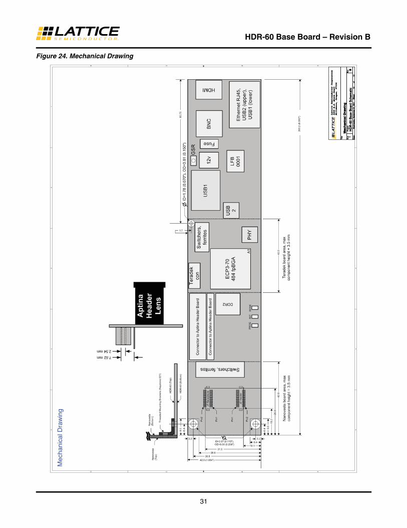
31
HDR-60 Base Board – Revision B
Figure 24. Mechanical Drawing5 5
4 4
3 3
2 2
1 1
DD
CC
BB
AA
Mec
hani
cal D
raw
ing
Title
Siz
eP
roje
ctR
ev
Dat
e:S
heet
of
Lattice Semiconductor Corporation
5555 N.E. Moore Court
Hillsboro, Oregon. 97124
HD
R-6
0 B
ase
Boa
rd S
chem
atic
B
Mec
han
ical
Dra
win
gC
1010
Wed
nesd
ay, S
epte
mbe
r 21
, 201
1
Title
Siz
eP
roje
ctR
ev
Dat
e:S
heet
of
Lattice Semiconductor Corporation
5555 N.E. Moore Court
Hillsboro, Oregon. 97124
HD
R-6
0 B
ase
Boa
rd S
chem
atic
B
Mec
han
ical
Dra
win
gC
1010
Wed
nesd
ay, S
epte
mbe
r 21
, 201
1
Title
Siz
eP
roje
ctR
ev
Dat
e:S
heet
of
Lattice Semiconductor Corporation
5555 N.E. Moore Court
Hillsboro, Oregon. 97124
HD
R-6
0 B
ase
Boa
rd S
chem
atic
B
Mec
han
ical
Dra
win
gC
1010
Wed
nesd
ay, S
epte
mbe
r 21
, 201
1
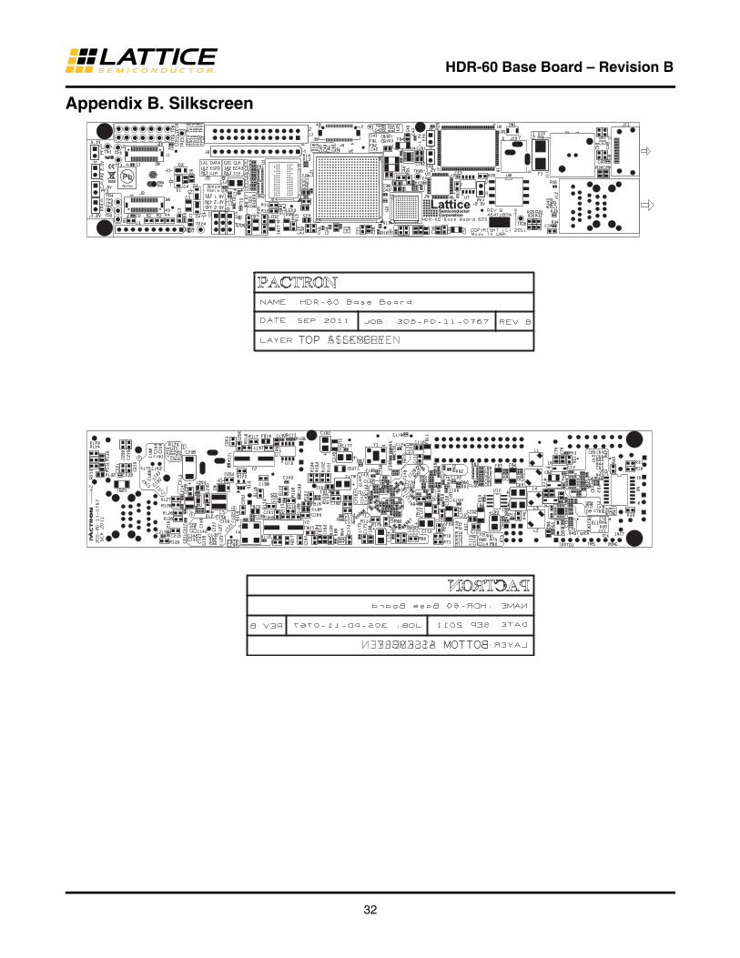
32
HDR-60 Base Board – Revision B
Appendix B. Silkscreen
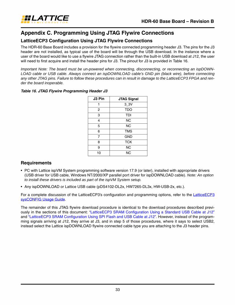
33
HDR-60 Base Board – Revision B
Appendix C. Programming Using JTAG Flywire ConnectionsLatticeECP3 Configuration Using JTAG Flywire ConnectionsThe HDR-60 Base Board includes a provision for the flywire connected programming header J3. The pins for the J3 header are not installed, as typical use of the board will be through the USB download. In the instance where a user of the board would like to use a flywire JTAG connection rather than the built-in USB download at J12, the user will need to first acquire and install the header pins for J3. The pinout for J3 is provided in Table 16.
Important Note: The board must be un-powered when connecting, disconnecting, or reconnecting an ispDOWN-LOAD cable or USB cable. Always connect an ispDOWNLOAD cable’s GND pin (black wire), before connecting any other JTAG pins. Failure to follow these procedures can in result in damage to the LatticeECP3 FPGA and ren-der the board inoperable.
Table 16. JTAG Flywire Programming Header J3
J3 Pin JTAG Signal
1 3_3V
2 TDO
3 TDI
4 NC
5 NC
6 TMS
7 GND
8 TCK
9 NC
10 NC
Requirements
• PC with Lattice ispVM System programming software version 17.9 (or later), installed with appropriate drivers (USB driver for USB cable, Windows NT/2000/XP parallel port driver for ispDOWNLOAD cable). Note: An option to install these drivers is included as part of the ispVM System setup.
• Any ispDOWNLOAD or Lattice USB cable (pDS4102-DL2x, HW7265-DL3x, HW-USB-2x, etc.).
For a complete discussion of the LatticeECP3’s configuration and programming options, refer to the LatticeECP3 sysCONFIG Usage Guide.
The remainder of this JTAG flywire download procedure is identical to the download procedures described previ-ously in the sections of this document: “LatticeECP3 SRAM Configuration Using a Standard USB Cable at J12”and “LatticeECP3 SRAM Configuration Using SPI Flash and USB Cable at J12”. However, instead of the program-ming signals arriving at J12, they arrive at J3, and in step 5 of those procedures, where it says to select USB2, instead select the Lattice ispDOWNLOAD flywire connected cable type you are attaching to the J3 header pins.

34
HDR-60 Base Board – Revision B
Appendix D. Known IssuesThe following resistors should not be populated by default: R87, R89, R92 and R93. The location of these resistors is on the bottom side of the HDR-60 Base Board Revision B (reverse side of the LatticeECP3-70). These resistors may have been installed on some boards and may cause issues for custom designs that use the signals connected to these resistors.