E< MC2: less energy through multi-copy cache
10
ABSTRACT Caches are known to consume a large part of total microprocessor power. Traditionally, voltage scaling has been used to reduce both dynamic and leakage power in caches. However, aggressive voltage reduction causes process-variation-induced failures in cache SRAM arrays, which compromise cache reliability. We present Multi-Copy Cache (MC 2 ), a new cache architecture that achieves significant reduction in energy consumption through aggressive voltage scaling, while maintaining high error resilience (reliability) by exploiting multiple copies of each data item in the cache. Unlike many previous approaches, MC 2 does not require any error map characterization and therefore is responsive to changing operating conditions (e.g., Vdd-noise, temperature and leakage) of the cache. MC 2 also incurs significantly lower overheads compared to other ECC-based caches. Our experimental results on embedded benchmarks demonstrate that MC 2 achieves up to 60% reduction in energy and energy-delay product (EDP) with only 3.5% reduction in IPC and no appreciable area overhead. Categories and Subject Descriptors B.3.1 [Semiconductor Memories]: Static Memory (SRAM) B.3.2 [Design Styles] Cache Memories, B.1.3 [Control Structure Reliability, Testing and Fault-Tolerance]: Error Checking, Redundant Design. General Terms Algorithm, Design, Reliability, Theory Keywords Variation Aware Cache, Low Power Cache, Low Power Memory Organization, Low Power Design, Fault Tolerance 1. INTRODUCTION As ITRS roadmap predicts [1] [4], in the continued pursuit of Moore’s law, power densities will continue to affect reliability of both embedded SoCs and high performance desktop/server processors. Although the logic content and throughput of the systems will continue to increase exponentially, a flat curve must be maintained for dynamic and leakage power in order to prolong battery life, maintain cooling costs and mitigate the adverse effects of increased power densities on reliability. The resulting Power Management Gap must be addressed through various means including architectural techniques. Caches are already known to consume a large portion (about 30-70%) of total processor power [2] [3] and on-chip cache size will continue to grow due to device scaling coupled with performance requirements. Therefore, in order to manage total power consumption and reliability of the system, it is important to manage power and reliability of the caches. Traditionally, voltage scaling has been used to reduce the dynamic and leakage power consumption of the cache. However, aggressive voltage scaling causes process-variation-induced failures in SRAM cells such as read access failures, destructive read failures and write failures [5] [19]. Since executing applications may not be tolerant to even a single bit error, caches must be operated at a high Vdd with a very low probability of failure leading to high energy consumption. However, by exploiting mechanisms that allow a cache to become inherently resilient to large number of cell failures, we can operate the cache at a lower Vdd and thus gain significant energy savings. In this work, we propose Multi-Copy Cache (MC 2 ), a novel cache architecture that significantly enhances the reliability of the cache by maintaining multiple copies of every data item. Whenever a data is accessed, multiple copies of the accessed data are processed to detect and correct errors. MC 2 is particularly useful for embedded applications since their working set sizes are often much smaller than existing cache sizes, and the unused cache space can be effectively used for storing multiple copies, achieving error resiliency through redundancy. Such a cache has high reliability and can be subject to aggressive voltage scaling resulting in significant reduction in energy consumption. Moreover, since errors are dynamically detected and corrected, MC 2 does not need any apriori error characterization of the cache. Also, compared to other existing cache architectures exploiting redundancy (e.g., ECC), MC 2 incurs minimal performance and area overheads. Our experimental results on embedded benchmarks show that, compared to a conventional cache at nominal Vdd, MC 2 reduces energy consumption by up to 60%, with only about 3.5% loss in performance and no appreciable area overhead. The rest of the paper is organized as follows: Section 2 discusses the opportunity for efficiently increasing cache reliability and some background related to SRAM reliability. Section 3 introduces the MC 2 architecture and Section 4 discusses the related work. In Section 5 presents the hardware implementation and its overheads. Section 6 evaluates the architecture in terms of performance and energy for a set of embedded applications, and Section 7 concludes the paper. E < MC 2 : Less Energy through Multi-Copy Cache Arup Chakraborty, Houman Homayoun, Amin Khajeh, Nikil Dutt, Ahmed Eltawil, Fadi Kurdahi Center for Embedded Computer Systems, University of California, Irvine, CA, USA {arup, hhomayou, akhajed, dutt, aeltawil, kurdahi}@uci.edu Permission to make digital or hard copies of all or part of this work for personal or classroom use is granted without fee provided that copies are not made or distributed for profit or commercial advantage and that copies bear this notice and the full citation on the first page. To copy otherwise, or republish, to post on servers or to redistribute to lists, requires prior specific permission and/or a fee. CASES’10, October 24–29, 2010, Scottsdale, Arizona, USA. Copyright 2010 ACM 978-1-60558-903-9/10/10...$10.00. 237
-
Upload
independent -
Category
Documents
-
view
2 -
download
0
Transcript of E< MC2: less energy through multi-copy cache
ABSTRACT Caches are known to consume a large part of total microprocessor power. Traditionally, voltage scaling has been used to reduce both dynamic and leakage power in caches. However, aggressive voltage reduction causes process-variation-induced failures in cache SRAM arrays, which compromise cache reliability. We present Multi-Copy Cache (MC2), a new cache architecture that achieves significant reduction in energy consumption through aggressive voltage scaling, while maintaining high error resilience (reliability) by exploiting multiple copies of each data item in the cache. Unlike many previous approaches, MC2 does not require any error map characterization and therefore is responsive to changing operating conditions (e.g., Vdd-noise, temperature and leakage) of the cache. MC2 also incurs significantly lower overheads compared to other ECC-based caches. Our experimental results on embedded benchmarks demonstrate that MC2 achieves up to 60% reduction in energy and energy-delay product (EDP) with only 3.5% reduction in IPC and no appreciable area overhead. Categories and Subject Descriptors B.3.1 [Semiconductor Memories]: Static Memory (SRAM) B.3.2 [Design Styles] Cache Memories, B.1.3 [Control Structure Reliability, Testing and Fault-Tolerance]: Error Checking, Redundant Design.
General Terms Algorithm, Design, Reliability, Theory
Keywords Variation Aware Cache, Low Power Cache, Low Power Memory Organization, Low Power Design, Fault Tolerance
1. INTRODUCTION As ITRS roadmap predicts [1] [4], in the continued pursuit of Moore’s law, power densities will continue to affect reliability of both embedded SoCs and high performance desktop/server processors. Although the logic content and throughput of the systems will continue to increase exponentially, a flat curve must be maintained for dynamic and leakage power in order to prolong battery life, maintain cooling costs and mitigate the adverse effects
of increased power densities on reliability. The resulting Power Management Gap must be addressed through various means including architectural techniques. Caches are already known to consume a large portion (about 30-70%) of total processor power [2] [3] and on-chip cache size will continue to grow due to device scaling coupled with performance requirements. Therefore, in order to manage total power consumption and reliability of the system, it is important to manage power and reliability of the caches.
Traditionally, voltage scaling has been used to reduce the dynamic and leakage power consumption of the cache. However, aggressive voltage scaling causes process-variation-induced failures in SRAM cells such as read access failures, destructive read failures and write failures [5] [19]. Since executing applications may not be tolerant to even a single bit error, caches must be operated at a high Vdd with a very low probability of failure leading to high energy consumption. However, by exploiting mechanisms that allow a cache to become inherently resilient to large number of cell failures, we can operate the cache at a lower Vdd and thus gain significant energy savings. In this work, we propose Multi-Copy Cache (MC2), a novel cache architecture that significantly enhances the reliability of the cache by maintaining multiple copies of every data item. Whenever a data is accessed, multiple copies of the accessed data are processed to detect and correct errors. MC2 is particularly useful for embedded applications since their working set sizes are often much smaller than existing cache sizes, and the unused cache space can be effectively used for storing multiple copies, achieving error resiliency through redundancy. Such a cache has high reliability and can be subject to aggressive voltage scaling resulting in significant reduction in energy consumption. Moreover, since errors are dynamically detected and corrected, MC2 does not need any apriori error characterization of the cache. Also, compared to other existing cache architectures exploiting redundancy (e.g., ECC), MC2 incurs minimal performance and area overheads. Our experimental results on embedded benchmarks show that, compared to a conventional cache at nominal Vdd, MC2 reduces energy consumption by up to 60%, with only about 3.5% loss in performance and no appreciable area overhead.
The rest of the paper is organized as follows: Section 2 discusses the opportunity for efficiently increasing cache reliability and some background related to SRAM reliability. Section 3 introduces the MC2 architecture and Section 4 discusses the related work. In Section 5 presents the hardware implementation and its overheads. Section 6 evaluates the architecture in terms of performance and energy for a set of embedded applications, and Section 7 concludes the paper.
E < MC2: Less Energy through Multi-Copy Cache
Arup Chakraborty, Houman Homayoun, Amin Khajeh, Nikil Dutt, Ahmed Eltawil, Fadi Kurdahi
Center for Embedded Computer Systems, University of California, Irvine, CA, USA {arup, hhomayou, akhajed, dutt, aeltawil, kurdahi}@uci.edu
Permission to make digital or hard copies of all or part of this work for personal or classroom use is granted without fee provided that copies are not made or distributed for profit or commercial advantage and that copies bear this notice and the full citation on the first page. To copy otherwise, or republish, to post on servers or to redistribute to lists, requires prior specific permission and/or a fee. CASES’10, October 24–29, 2010, Scottsdale, Arizona, USA. Copyright 2010 ACM 978-1-60558-903-9/10/10...$10.00.
237

2. BACKGROUND
A. Opportunity: Small Working Set Sizes We exploit the fact that the working set sizes of many
embedded applications are much lower than available cache space in modern embedded processors. Fritts et al., [8] showed that for multimedia applications, working set size for instructions is less than 8KB and that for data is less than 32 KB. Guthaus et al., [9] showed that for most embedded applications, instruction and data working set size is less than 4-8KB. Our own investigation for MiBench embedded suite (Figure 2.1) shows that although there are a few benchmarks with a working set size of 16-32K, most of the benchmarks have a working set size of 8K or less, with about 50% of the applications having less than 2K as working set size. On the other hand, as Table 2.1 shows, modern SoCs and processors typically have L1 cache of sizes 16-64KB and L2 cache sizes up to 2MB, demonstrating a significant portion of the cache – outside of the working set -- is not used for many embedded applications. We exploit this opportunity to utilize the extra cache space to create an efficient error control mechanism embedded in the cache by maintaining multiple copies of each data item. A number of techniques have been previously proposed to increase reliability of caches and SRAM memories. Some of these techniques like parity and ECC [10] [11] [12] have the ability to dynamically detect and correct only a limited number of errors but incur high penalty in access latency and area. Other techniques [6] [13] [14] [15] [16] [17] [27] provide high error tolerance but require a cache error-map of various resolutions (per-byte to per-cache line) that must be generated by BIST whenever there is a change in operating conditions such as Vdd and frequency. Since SRAM failures are highly dynamic and influenced by several conditions beyond the control of users, such failures may not be captured by infrequent BIST characterizations (as explained later). In contrast to previous and related works, our MC2 architecture:
• can dynamically detect a very high number of errors in SRAM arrays,
• does not require any BIST characterization, • is responsive to dynamic changes in SRAM error pattern. • unlike SECDED, incurs only a minimal impact on both
access latency and SRAM area and yet has high error tolerance, and
• enables aggressive Vdd scaling, yielding significant reduction in energy consumption.
Table 2.1: L1 and L2 cache sizes for modern microprocessors Processor Intel
Xscale ARM
Cortex A8 ARM
Cortex A9 Freescale QorIQ P2
L1 size 32K 16-32K 16-64K 32K L2 size 512K 2M 2M 512K
B. Process Variation and SRAM Reliability A dominant cause of SRAM cell failures is process variation [14] [20] [21]. Random intra-die variations, mostly caused by Random Dopant Fluctuations (RDF), lead to mismatches between neighboring transistors resulting in failures in SRAM cells. Due to process variation, SRAM cell failures may be of different types: a) read access failure: reduction in bitline voltage differential during read within the allowed read time, b) write access failure:
unsuccessful write within the allowed write time, c) read stability failure: an increase in the pmos/nmos node voltage beyond the trip voltage of the inverter pair causing a bit flip during read, and d) hold failure: bit flip while in standby mode caused by decrease in data retention voltage. Our proposed MC2 architecture is effective against all such failures.
Figure 2.1: Minimum cache size with assoc. 8 needed for < 2% miss rate
Figure 2.2: Unexpected increase in failure as Vdd is increased due to interaction between leakage power and temperature [22]
Figure 2.3: Interrelationship of Vdd, frequency, temperature, leakage/dynamic power, etc and their effect on SRAM failure probability (based on [22]) Dynamic nature of SRAM failures: As shown by Khajeh et al. [22], the probability of SRAM failure is highly dependent on Vdd, frequency of operation, and temperature. It is well known that a decrease in Vdd increases failure probability of SRAM failures [14] [20]. However, an increase in Vdd increases the dynamic and leakage power dissipation, which in turn increases the temperature. Increase in temperature causes an increase in cell delay resulting in a higher probability of failure. Moreover, the increase in temperature increases the leakage power further resulting in a positive feedback loop between the two [22]. Therefore, as Vdd is increased, temperature as well as leakage and dynamic powers may increase in an interdependent fashion, increasing the failure probability unexpectedly. Additionally, if a set of SRAM cells are accessed very frequently or if they are located near hotspots such as execution units, the dynamic power dissipation of those cells will increase, leading to an increase in temperature and inducing the cells towards failure [40]. Figure 2.3 (based on [22]) pictorially depicts the relationships between Vdd,
238

frequency, temperature, memory activity, power dissipation and probability of failure. From the above discussion, we note that SRAM failures are very dynamic: not only affected by user-controlled operating conditions such as Vdd and frequency, but also by other conditions such as voltage irregularities, leakage, temperature, nearby hotspots, memory access pattern, drift in frequency -- all of which may be constantly changing and are beyond the control of the user. It is therefore crucial that any error control mechanism in SRAM caches be responsive to dynamic changes in error patterns, without being dependent on static error maps – which MC2 accomplishes.
3. MC2 ARCHITECTURE
A. Basic Mechanism The basic idea behind multi-copy cache (MC2) is to maintain
multiple copies of each data item in the cache. Such a mechanism makes the cache resilient to a high number of SRAM failures. As long as same bit-position of every copy is not affected by failures, the errors can always be detected and may also be corrected1
In this paper, we present the RDT (Redundancy through Duplication and Triplication) policy for MC2. We assume a writeback data cache with write-allocate policy and true LRU replacement policy. MC2 with RDT policy maintains 2 copies of each clean data and 3 copies of each dirty data in the same set. If a data in the cache is clean (i.e, unmodified by the processor), a correct copy of that data is also available in the lower level of memory (LLM). Therefore only 2 copies of the clean data need to be maintained in the cache. Whenever a clean data is read by the processor, both copies are compared with each other. If there is any mismatch, an error is detected and the requested data is read from the LLM and is forwarded to the processor. On the other hand, if the requested data in the cache is dirty (i.e., modified by processor), the most updated version of that data is in the cache and not in the LLM. Hence for dirty data, 3 copies are be maintained in the cache so that in the event of error(s), the correct data can be generated by majority voting logic using all 3 copies. Thus, the use of RDT policy would result in 2 or 3 cache lines with same data in a given set.
. This high error-resiliency technique allows the cache to operate under aggressive low Vdd leading to reduction in energy and power consumption. The multi-copy mechanism may be implemented in many different ways, depending on cache organization, type of cache (instruction or data), write policy (write-through or write-back), write-miss policy (write-allocate or no write-allocate) and replacement policy of the cache; each implementation of MC2 will incur some overhead and potentially some performance degradation. Thus the MC2 architecture must be designed carefully to minimize these overheads while achieving low energy with high resiliency.
Example: Figure 3.1 shows the physical contents of a particular set s of an 8 way set associative MC2 for a sequence of reads and writes. Each of the eight rectangles represents a cache line in the given set. Initially the cache is cold and the set is empty. Then four cache lines A, B, C and D, belonging to set s, are read one
1 It is very rare that same bit-positions of more than one copy will be
affected by failures. For a bit failure rate of 10-6, failure rate for two copies of a 32-bit word is over 1 million times lower than that with single copy.
after another from the memory and placed in the set. At that point, the set s contains 4 clean data, each with two adjacent copies. Assume that there are multiple read accesses such that D becomes the LRU data (marked by dots). Now the processor writes to data A. After the write is completed, A would become dirty. Hence, it would need 3 copies instead of its present 2 copies, requiring a new copy of A to be created. This is done by evicting both copies of LRU data D and using one of the freed cache lines to store the 3rd copy of A. Next, the processor writes to data C. A new copy of C is created using the empty cache line present in the set s. As the example shows, all copies of a given data may not be physically adjacent. We now describe the detailed MC2 RDT cache architecture operation and overheads.
Figure 3.1: Example of Reads and Writes to MC2
Figure 3.2: Conventional cache architecture
Figure 3.3: Multi-Copy cache architecture
239
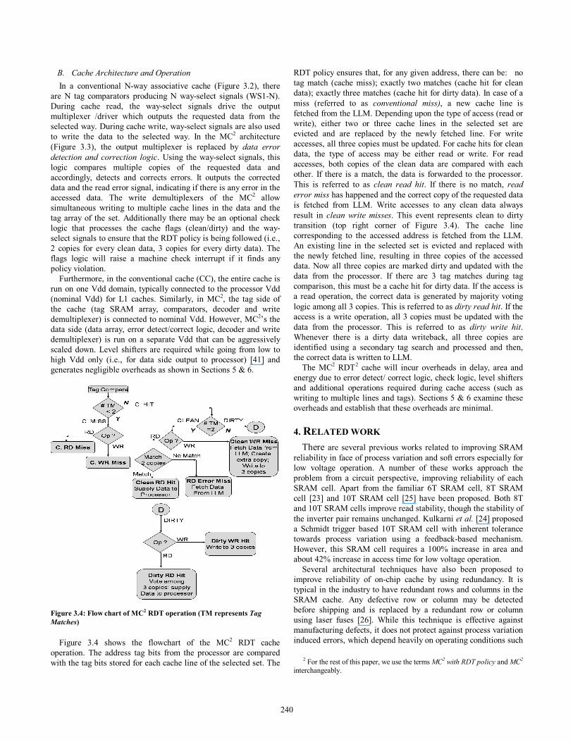
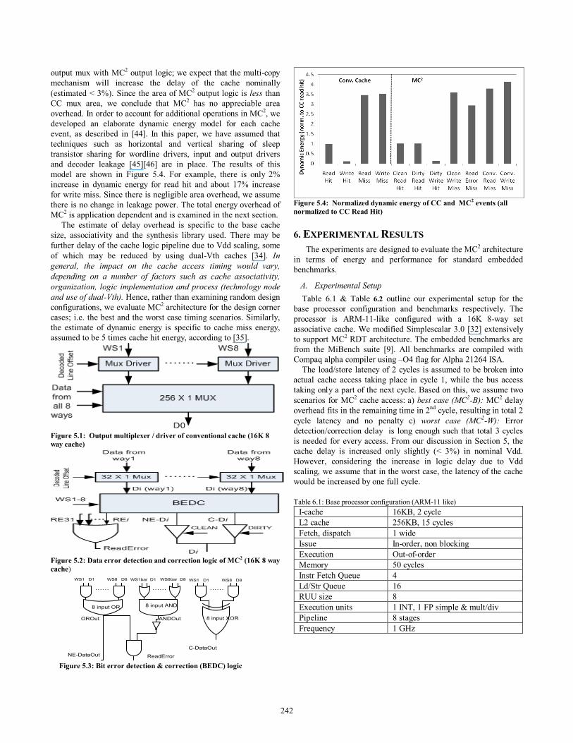
B. Cache Architecture and Operation In a conventional N-way associative cache (Figure 3.2), there
are N tag comparators producing N way-select signals (WS1-N). During cache read, the way-select signals drive the output multiplexer /driver which outputs the requested data from the selected way. During cache write, way-select signals are also used to write the data to the selected way. In the MC2 architecture (Figure 3.3), the output multiplexer is replaced by data error detection and correction logic. Using the way-select signals, this logic compares multiple copies of the requested data and accordingly, detects and corrects errors. It outputs the corrected data and the read error signal, indicating if there is any error in the accessed data. The write demultiplexers of the MC2 allow simultaneous writing to multiple cache lines in the data and the tag array of the set. Additionally there may be an optional check logic that processes the cache flags (clean/dirty) and the way-select signals to ensure that the RDT policy is being followed (i.e., 2 copies for every clean data, 3 copies for every dirty data). The flags logic will raise a machine check interrupt if it finds any policy violation.
Furthermore, in the conventional cache (CC), the entire cache is run on one Vdd domain, typically connected to the processor Vdd (nominal Vdd) for L1 caches. Similarly, in MC2, the tag side of the cache (tag SRAM array, comparators, decoder and write demultiplexer) is connected to nominal Vdd. However, MC2’s the data side (data array, error detect/correct logic, decoder and write demultiplexer) is run on a separate Vdd that can be aggressively scaled down. Level shifters are required while going from low to high Vdd only (i.e., for data side output to processor) [41] and generates negligible overheads as shown in Sections 5 & 6.
Figure 3.4: Flow chart of MC2 RDT operation (TM represents Tag Matches)
Figure 3.4 shows the flowchart of the MC2 RDT cache operation. The address tag bits from the processor are compared with the tag bits stored for each cache line of the selected set. The
RDT policy ensures that, for any given address, there can be: no tag match (cache miss); exactly two matches (cache hit for clean data); exactly three matches (cache hit for dirty data). In case of a miss (referred to as conventional miss), a new cache line is fetched from the LLM. Depending upon the type of access (read or write), either two or three cache lines in the selected set are evicted and are replaced by the newly fetched line. For write accesses, all three copies must be updated. For cache hits for clean data, the type of access may be either read or write. For read accesses, both copies of the clean data are compared with each other. If there is a match, the data is forwarded to the processor. This is referred to as clean read hit. If there is no match, read error miss has happened and the correct copy of the requested data is fetched from LLM. Write accesses to any clean data always result in clean write misses. This event represents clean to dirty transition (top right corner of Figure 3.4). The cache line corresponding to the accessed address is fetched from the LLM. An existing line in the selected set is evicted and replaced with the newly fetched line, resulting in three copies of the accessed data. Now all three copies are marked dirty and updated with the data from the processor. If there are 3 tag matches during tag comparison, this must be a cache hit for dirty data. If the access is a read operation, the correct data is generated by majority voting logic among all 3 copies. This is referred to as dirty read hit. If the access is a write operation, all 3 copies must be updated with the data from the processor. This is referred to as dirty write hit. Whenever there is a dirty data writeback, all three copies are identified using a secondary tag search and processed and then, the correct data is written to LLM.
The MC2 RDT2
4. RELATED WORK
cache will incur overheads in delay, area and energy due to error detect/ correct logic, check logic, level shifters and additional operations required during cache access (such as writing to multiple lines and tags). Sections 5 & 6 examine these overheads and establish that these overheads are minimal.
There are several previous works related to improving SRAM reliability in face of process variation and soft errors especially for low voltage operation. A number of these works approach the problem from a circuit perspective, improving reliability of each SRAM cell. Apart from the familiar 6T SRAM cell, 8T SRAM cell [23] and 10T SRAM cell [25] have been proposed. Both 8T and 10T SRAM cells improve read stability, though the stability of the inverter pair remains unchanged. Kulkarni et al. [24] proposed a Schmidt trigger based 10T SRAM cell with inherent tolerance towards process variation using a feedback-based mechanism. However, this SRAM cell requires a 100% increase in area and about 42% increase in access time for low voltage operation.
Several architectural techniques have also been proposed to improve reliability of on-chip cache by using redundancy. It is typical in the industry to have redundant rows and columns in the SRAM cache. Any defective row or column may be detected before shipping and is replaced by a redundant row or column using laser fuses [26]. While this technique is effective against manufacturing defects, it does not protect against process variation induced errors, which depend heavily on operating conditions such
2 For the rest of this paper, we use the terms MC2 with RDT policy and MC2 interchangeably.
240
as Vdd. A number of other techniques have been proposed to improve SRAM array reliability against process variation failures. Wilkerson et al. [6] proposed multiple techniques using part of a cache line as a redundancy for defective bits for the rest of cache lines in the same set. It disables the faulty words and replaces them with non-faulty words in the same set. Agarwal et al. [13] proposed a fault tolerant cache architecture in which the column multiplexers are programmed to select non-faulty block in the same row, if the accessed block is faulty. A similar work is PADed caches [17] which use programmable address decoders that are programmed to select non-faulty blocks as replacements of faulty blocks. Makzhan et al. [15] and Sasan et al.,[16] [27] proposed a number of cache architectures in which the error-prone part of the cache is fixed using either a separate redundancy cache or parts of the same cache or using charge pumps to increase Vdd of the defective wordlines. However all the techniques proposed in these works [6] [13] [15] [16] [17] [27] require BIST characterization of the cache and generation of some form of a cache error map with various levels of granularity: per wordline, per cache line, per byte etc. Whenever Vdd is scaled up or down, the BIST engine is run and the entire cache memory is characterized generating an error map. Every time BIST characterization is run, the cache has to be flushed of its current contents followed by writing, reading and comparing by the BIST engine before the cache is ready for use. The time overhead of the BIST characterization would limit the frequency at which Vdd can be scaled up or down. The storage of error map, depending upon its granularity, also increases the area overhead of the cache. Even with these costs, a basic assumption behind the above works is that, once the BIST characterization is done, the error map perfectly describes the locations of process variation errors until the next change in Vdd. As discussed in Section 2, this assumption is not valid because of the dynamic nature of SRAM failures.
In order to improve SRAM reliability against such dynamic failures, dynamic error detection and correction ability is required without using any static error map. One of most popular mechanism for such dynamic error detection/correction is error control coding (ECC), which is widely used in caches and memories. The simplest form of ECC is one-bit parity which detects odd number of errors in the data and is often used in L1 caches [28]. Since such one-bit parity mechanisms do not have any correction capability, it is not useful except for instruction caches or data caches with write through policy. Another form of ECC used in caches is SECDED (single error correction, double errors detection). Hsiao et al. [10] proposed an optimal minimum-odd weight column SECDED code that is suitable for fast implementation in memory. However, inspite of its optimality, the Hsaio code incurs multiple clock cycle latencies for caches and significant area overhead (about 30%), as we show later in the results. Kim et al. [29] and Naseer et al. [30] have proposed ECC schemes to correct multiple error bits and further improve reliability beyond SECDED. However, as it has been shown by Mazumder [31] and Agarwal et al. [13], ECC mechanism beyond one-bit correction capability cannot be implemented in memory because of the area and delay overheads. Zhang et al. [18] used replication of some “hot” frequently used cache lines to mitigate soft errors. Such a technique has non-uniform error tolerance and is ineffective towards process variation-induced failures. Moreover, it requires additional error control mechanism such as
parity for its operation. A recent work uses configurable part of the cache for storing multiple ECC check bits for different segments of cache line using an elaborate Orthogonal Latin Square Code ECC [42] to enable dynamic error correction. This requires upto 8 levels of XOR gates for decoding, resulting in significant increase in cache critical path delay.
In contrast to previous works, our MC2 architecture which can detect and correct errors dynamically without requiring any BIST characterization and error map storage. MC2 provides better reliability than SECDED cache with minimal area overhead and much less latency to detect/correct errors. Compared to elaborate ECC mechanisms such as [42], MC2 architecture has a simple detection/correction mechanism resulting in much lower delay overhead. Indeed, as we show in the next section, MC2 incurs less than 3% overhead in cache delay and less than 2% increase in read hit dynamic energy with negligible area overhead.
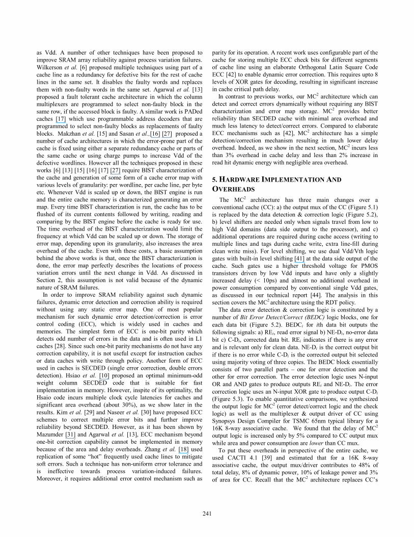
5. HARDWARE IMPLEMENTATION AND OVERHEADS The MC2 architecture has three main changes over a conventional cache (CC): a) the output mux of the CC (Figure 5.1) is replaced by the data detection & correction logic (Figure 5.2), b) level shifters are needed only when signals travel from low to high Vdd domains (data side output to the processor), and c) additional operations are required during cache access (writing to multiple lines and tags during cache write, extra line-fill during clean write miss). For level shifting, we use dual Vdd/Vth logic gates with built-in level shifting [41] at the data side output of the cache. Such gates use a higher threshold voltage for PMOS transistors driven by low Vdd inputs and have only a slightly increased delay (< 10ps) and almost no additional overhead in power consumption compared by conventional single Vdd gates, as discussed in our technical report [44]. The analysis in this section covers the MC2 architecture using the RDT policy.
The data error detection & correction logic is constituted by a number of Bit Error Detect/Correct (BEDC) logic blocks, one for each data bit (Figure 5.2). BEDCi for ith data bit outputs the following signals: a) REi, read error signal b) NE-Di, no-error data bit c) C-Di, corrected data bit. REi indicates if there is any error and is relevant only for clean data. NE-Di is the correct output bit if there is no error while C-Di is the corrected output bit selected using majority voting of three copies. The BEDC block essentially consists of two parallel parts – one for error detection and the other for error correction. The error detection logic uses N-input OR and AND gates to produce outputs REi and NE-Di. The error correction logic uses an N-input XOR gate to produce output C-Di (Figure 5.3). To enable quantitative comparisons, we synthesized the output logic for MC2 (error detect/correct logic and the check logic) as well as the multiplexer & output driver of CC using Synopsys Design Compiler for TSMC 65nm typical library for a 16K 8-way associative cache. We found that the delay of MC2 output logic is increased only by 5% compared to CC output mux while area and power consumption are lower than CC mux.
To put these overheads in perspective of the entire cache, we used CACTI 4.1 [39] and estimated that for a 16K 8-way associative cache, the output mux/driver contributes to 48% of total delay, 8% of dynamic power, 10% of leakage power and 3% of area for CC. Recall that the MC2 architecture replaces CC’s
241
output mux with MC2 output logic; we expect that the multi-copy mechanism will increase the delay of the cache nominally (estimated < 3%). Since the area of MC2 output logic is less than CC mux area, we conclude that MC2 has no appreciable area overhead. In order to account for additional operations in MC2, we developed an elaborate dynamic energy model for each cache event, as described in [44]. In this paper, we have assumed that techniques such as horizontal and vertical sharing of sleep transistor sharing for wordline drivers, input and output drivers and decoder leakage [45][46] are in place. The results of this model are shown in Figure 5.4. For example, there is only 2% increase in dynamic energy for read hit and about 17% increase for write miss. Since there is negligible area overhead, we assume there is no change in leakage power. The total energy overhead of MC2 is application dependent and is examined in the next section.
The estimate of delay overhead is specific to the base cache size, associativity and the synthesis library used. There may be further delay of the cache logic pipeline due to Vdd scaling, some of which may be reduced by using dual-Vth caches [34]. In general, the impact on the cache access timing would vary, depending on a number of factors such as cache associativity, organization, logic implementation and process (technology node and use of dual-Vth). Hence, rather than examining random design configurations, we evaluate MC2 architecture for the design corner cases; i.e. the best and the worst case timing scenarios. Similarly, the estimate of dynamic energy is specific to cache miss energy, assumed to be 5 times cache hit energy, according to [35].
Figure 5.1: Output multiplexer / driver of conventional cache (16K 8 way cache)
Figure 5.2: Data error detection and correction logic of MC2 (16K 8 way cache)
……
8 input OR
……
8 input AND
……WS1 D1 WS8 D8 WS1bar D1 WS8bar D8 WS1 D1 WS8 D8
NE-DataOut ReadError
C-DataOut
OROut ANDOut 8 input XOR
Figure 5.3: Bit error detection & correction (BEDC) logic
Figure 5.4: Normalized dynamic energy of CC and MC2 events (all normalized to CC Read Hit)
6. EXPERIMENTAL RESULTS The experiments are designed to evaluate the MC2 architecture in terms of energy and performance for standard embedded benchmarks.
A. Experimental Setup Table 6.1 & Table 6.2 outline our experimental setup for the
base processor configuration and benchmarks respectively. The processor is ARM-11-like configured with a 16K 8-way set associative cache. We modified Simplescalar 3.0 [32] extensively to support MC2 RDT architecture. The embedded benchmarks are from the MiBench suite [9]. All benchmarks are compiled with Compaq alpha compiler using –O4 flag for Alpha 21264 ISA.
The load/store latency of 2 cycles is assumed to be broken into actual cache access taking place in cycle 1, while the bus access taking only a part of the next cycle. Based on this, we assume two scenarios for MC2 cache access: a) best case (MC2-B): MC2 delay overhead fits in the remaining time in 2nd cycle, resulting in total 2 cycle latency and no penalty c) worst case (MC2-W): Error detection/correction delay is long enough such that total 3 cycles is needed for every access. From our discussion in Section 5, the cache delay is increased only slightly (< 3%) in nominal Vdd. However, considering the increase in logic delay due to Vdd scaling, we assume that in the worst case, the latency of the cache would be increased by one full cycle.
Table 6.1: Base processor configuration (ARM-11 like)
I-cache 16KB, 2 cycle L2 cache 256KB, 15 cycles Fetch, dispatch 1 wide Issue In-order, non blocking Execution Out-of-order Memory 50 cycles Instr Fetch Queue 4 Ld/Str Queue 16 RUU size 8 Execution units 1 INT, 1 FP simple & mult/div Pipeline 8 stages Frequency 1 GHz
242
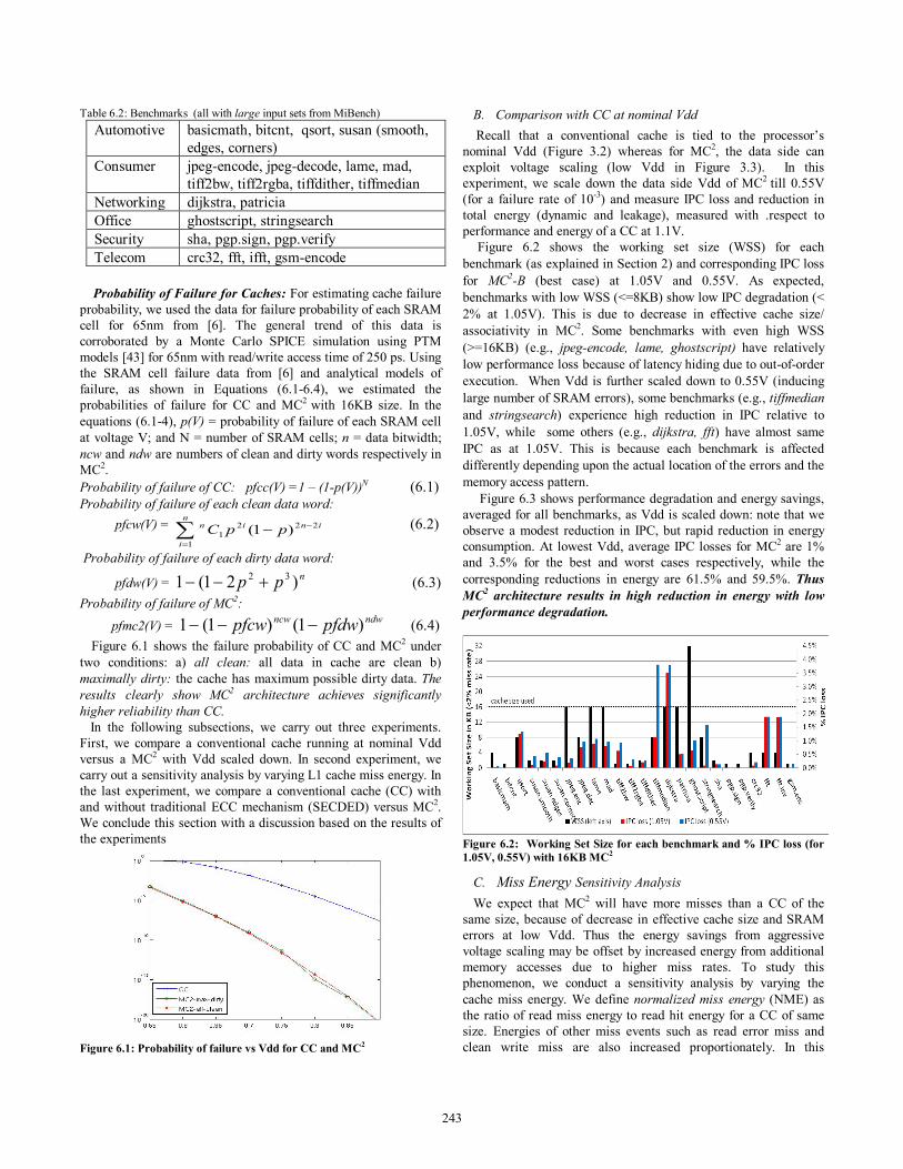
Table 6.2: Benchmarks (all with large input sets from MiBench) Automotive basicmath, bitcnt, qsort, susan (smooth,
edges, corners) Consumer jpeg-encode, jpeg-decode, lame, mad,
tiff2bw, tiff2rgba, tiffdither, tiffmedian Networking dijkstra, patricia Office ghostscript, stringsearch Security sha, pgp.sign, pgp.verify Telecom crc32, fft, ifft, gsm-encode
Probability of Failure for Caches: For estimating cache failure
probability, we used the data for failure probability of each SRAM cell for 65nm from [6]. The general trend of this data is corroborated by a Monte Carlo SPICE simulation using PTM models [43] for 65nm with read/write access time of 250 ps. Using the SRAM cell failure data from [6] and analytical models of failure, as shown in Equations (6.1-6.4), we estimated the probabilities of failure for CC and MC2
with 16KB size. In the equations (6.1-4), p(V) = probability of failure of each SRAM cell at voltage V; and N = number of SRAM cells; n = data bitwidth; ncw and ndw are numbers of clean and dirty words respectively in MC2. Probability of failure of CC: pfcc(V) =1 – (1-p(V))N (6.1) Probability of failure of each clean data word: pfcw(V) = ini
n
i
n ppC 222
11 )1( −
=
−∑
(6.2)
Probability of failure of each dirty data word:
pfdw(V) = npp )21(1 32 +−− (6.3) Probability of failure of MC2:
pfmc2(V) = ndwncw pfdwpfcw )1()1(1 −−− (6.4) Figure 6.1 shows the failure probability of CC and MC2 under two conditions: a) all clean: all data in cache are clean b) maximally dirty: the cache has maximum possible dirty data. The results clearly show MC2 architecture achieves significantly higher reliability than CC. In the following subsections, we carry out three experiments. First, we compare a conventional cache running at nominal Vdd versus a MC2 with Vdd scaled down. In second experiment, we carry out a sensitivity analysis by varying L1 cache miss energy. In the last experiment, we compare a conventional cache (CC) with and without traditional ECC mechanism (SECDED) versus MC2. We conclude this section with a discussion based on the results of the experiments
Figure 6.1: Probability of failure vs Vdd for CC and MC2
B. Comparison with CC at nominal Vdd Recall that a conventional cache is tied to the processor’s
nominal Vdd (Figure 3.2) whereas for MC2, the data side can exploit voltage scaling (low Vdd in Figure 3.3). In this experiment, we scale down the data side Vdd of MC2 till 0.55V (for a failure rate of 10-3) and measure IPC loss and reduction in total energy (dynamic and leakage), measured with .respect to performance and energy of a CC at 1.1V.
Figure 6.2 shows the working set size (WSS) for each benchmark (as explained in Section 2) and corresponding IPC loss for MC2-B (best case) at 1.05V and 0.55V. As expected, benchmarks with low WSS (<=8KB) show low IPC degradation (< 2% at 1.05V). This is due to decrease in effective cache size/ associativity in MC2. Some benchmarks with even high WSS (>=16KB) (e.g., jpeg-encode, lame, ghostscript) have relatively low performance loss because of latency hiding due to out-of-order execution. When Vdd is further scaled down to 0.55V (inducing large number of SRAM errors), some benchmarks (e.g., tiffmedian and stringsearch) experience high reduction in IPC relative to 1.05V, while some others (e.g., dijkstra, fft) have almost same IPC as at 1.05V. This is because each benchmark is affected differently depending upon the actual location of the errors and the memory access pattern.
Figure 6.3 shows performance degradation and energy savings, averaged for all benchmarks, as Vdd is scaled down: note that we observe a modest reduction in IPC, but rapid reduction in energy consumption. At lowest Vdd, average IPC losses for MC2 are 1% and 3.5% for the best and worst cases respectively, while the corresponding reductions in energy are 61.5% and 59.5%. Thus MC2 architecture results in high reduction in energy with low performance degradation.
Figure 6.2: Working Set Size for each benchmark and % IPC loss (for 1.05V, 0.55V) with 16KB MC2
C. Miss Energy Sensitivity Analysis We expect that MC2 will have more misses than a CC of the same size, because of decrease in effective cache size and SRAM errors at low Vdd. Thus the energy savings from aggressive voltage scaling may be offset by increased energy from additional memory accesses due to higher miss rates. To study this phenomenon, we conduct a sensitivity analysis by varying the cache miss energy. We define normalized miss energy (NME) as the ratio of read miss energy to read hit energy for a CC of same size. Energies of other miss events such as read error miss and clean write miss are also increased proportionately. In this
243
experiment, NME is varied from 5 to 100. Though the exact value of NME depends on the implementation, typically for L1 cache, NME of 5 indicates an on-chip L2 cache [35], while NME of 100 or more is likely if the L2 cache is off-chip [3].
Figure 6.3: IPC loss and Energy Savings of MC2 vs Vdd (w.r.t CC at 1.1V) (average of all benchmarks) Figure 6.4 shows % reduction in Energy-Delay-Product (EDP) of MC2 at 0.55V (measured w.r.t. CC at nom Vdd) for the top 8 benchmarks with highest number of misses. We observe that for some benchmarks (e.g., tiffmedian & dijsktra), EDP increases significantly when cache miss energy increases. We also measure the trend in EDP reduction, averaged over all benchmarks, for different Vdd and different NME, as shown in Figure 6.5. We observe that for even high NME (50-100), MC2 consumes less energy than CC, when operated at Vdd 0.95V or lower. Therefore, for a wide range of NME and hence with both offchip and onchip L2 cache, there exists a wide range of Vdd for which energy and EDP of MC2 are significantly less than that of CC at nominal Vdd.
Figure 6.4: % Savings in EDP at 0.55V for varying normalized miss energy
D. Comparison with SECDED Cache with Equal Area In this experiment, we compare MC2 with SECDED ECC,
which is commonly used in caches for dynamic error detection and correction. Use of SECDED ECC for caches leads to significant area overhead because of extra parity bit storage (8 parity bits for 64 data bits) and associated logic. It also increases cache access timing significantly due to SECDED decoding logic on every read access. For a 16KB 8-way associative cache, based on synthesis
results for 65nm and estimates from CACTI 4.1, SEDED ECC logic increases the delay of output mux/driver by 135% and total cache delay by 65%. Area overhead of the SECDED cache is 45% over conventional cache without any ECC.
Figure 6.5: % Reduction in EDP for different Vdd and different NME (average of all benchmarks)
In order to carry out a fair comparison, we scale up SRAM
transistor width, such that total area of the SECDED cache with smaller transistors is equal to the area of a CC and MC2 with bigger transistors. We determined failure probabilities of both SRAM cells (bigger and smaller) using a Monte Carlo SPICE simulation with PTM models [43] for 65nm. Then, we used our analytical models of failure to determine the failure probability of 1) SECDED cache 2) CC and 3) MC2, all with equal area. The results, as shown in Figure 6.6, demonstrate that, at given voltage, MC2 is the most reliable cache, while SECDED is the least reliable cache. In fact, we observe that, SECDED cache is worse than a CC of equal area for process variation-induced failures.
Figure 6.6: Probability of failure vs Vdd for SECDED cache, CC and MC2 under iso-area constraint
In order to compare performance and energy, we further constrain that all three caches (SECDED, CC, MC2) have equal failure rate. Since SECDED is least reliable, it is run at nominal Vdd 1.1V while aggressive voltage reduction is applied to CC and MC2, such that probabilities of failure of all three caches are same at the respective Vdd. We assume the data side Vdd of CC can be scaled, like MC2, as explained in Section 3. The latency of CC is assumed to be 2 cycles while that of SECDED cache is assumed to be 3 cycles, because of the timing overhead of ECC logic. For MC2, like previous experiments, we consider two different cases –
244
2 cycles (best case: MC2-B) and 3 cycles (worst case: MC2-W), as discussed earlier.
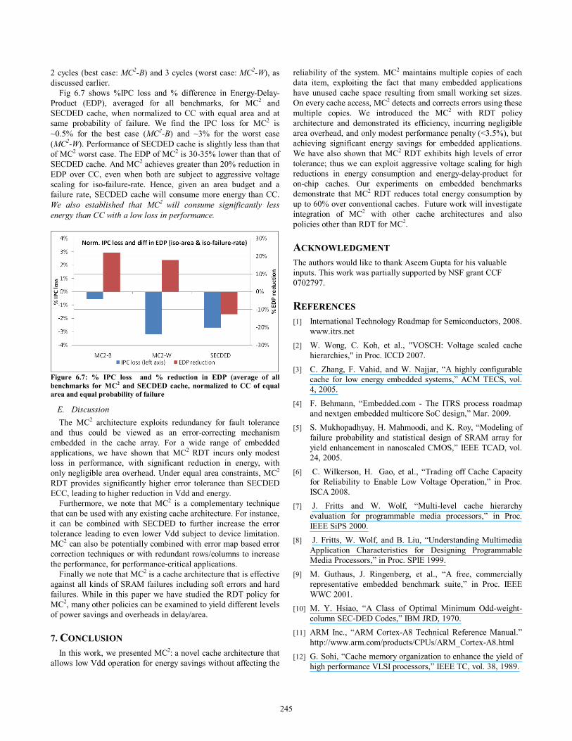
Fig 6.7 shows %IPC loss and % difference in Energy-Delay-Product (EDP), averaged for all benchmarks, for MC2 and SECDED cache, when normalized to CC with equal area and at same probability of failure. We find the IPC loss for MC2 is ~0.5% for the best case (MC2-B) and ~3% for the worst case (MC2-W). Performance of SECDED cache is slightly less than that of MC2 worst case. The EDP of MC2 is 30-35% lower than that of SECDED cache. And MC2 achieves greater than 20% reduction in EDP over CC, even when both are subject to aggressive voltage scaling for iso-failure-rate. Hence, given an area budget and a failure rate, SECDED cache will consume more energy than CC. We also established that MC2 will consume significantly less energy than CC with a low loss in performance.
Figure 6.7: % IPC loss and % reduction in EDP (average of all benchmarks for MC2 and SECDED cache, normalized to CC of equal area and equal probability of failure
E. Discussion The MC2 architecture exploits redundancy for fault tolerance
and thus could be viewed as an error-correcting mechanism embedded in the cache array. For a wide range of embedded applications, we have shown that MC2 RDT incurs only modest loss in performance, with significant reduction in energy, with only negligible area overhead. Under equal area constraints, MC2 RDT provides significantly higher error tolerance than SECDED ECC, leading to higher reduction in Vdd and energy.
Furthermore, we note that MC2 is a complementary technique that can be used with any existing cache architecture. For instance, it can be combined with SECDED to further increase the error tolerance leading to even lower Vdd subject to device limitation. MC2 can also be potentially combined with error map based error correction techniques or with redundant rows/columns to increase the performance, for performance-critical applications.
Finally we note that MC2 is a cache architecture that is effective against all kinds of SRAM failures including soft errors and hard failures. While in this paper we have studied the RDT policy for MC2, many other policies can be examined to yield different levels of power savings and overheads in delay/area.
7. CONCLUSION In this work, we presented MC2: a novel cache architecture that
allows low Vdd operation for energy savings without affecting the
reliability of the system. MC2 maintains multiple copies of each data item, exploiting the fact that many embedded applications have unused cache space resulting from small working set sizes. On every cache access, MC2 detects and corrects errors using these multiple copies. We introduced the MC2 with RDT policy architecture and demonstrated its efficiency, incurring negligible area overhead, and only modest performance penalty (<3.5%), but achieving significant energy savings for embedded applications. We have also shown that MC2 RDT exhibits high levels of error tolerance; thus we can exploit aggressive voltage scaling for high reductions in energy consumption and energy-delay-product for on-chip caches. Our experiments on embedded benchmarks demonstrate that MC2 RDT reduces total energy consumption by up to 60% over conventional caches. Future work will investigate integration of MC2 with other cache architectures and also policies other than RDT for MC2.
ACKNOWLEDGMENT The authors would like to thank Aseem Gupta for his valuable inputs. This work was partially supported by NSF grant CCF 0702797.
REFERENCES [1] International Technology Roadmap for Semiconductors, 2008.
www.itrs.net [2] W. Wong, C. Koh, et al., "VOSCH: Voltage scaled cache
hierarchies," in Proc. ICCD 2007. [3] C. Zhang, F. Vahid, and W. Najjar, “A highly configurable
cache for low energy embedded systems,” ACM TECS, vol. 4, 2005.
[4] F. Behmann, “Embedded.com - The ITRS process roadmap and nextgen embedded multicore SoC design,” Mar. 2009.
[5] S. Mukhopadhyay, H. Mahmoodi, and K. Roy, “Modeling of failure probability and statistical design of SRAM array for yield enhancement in nanoscaled CMOS,” IEEE TCAD, vol. 24, 2005.
[6] C. Wilkerson, H. Gao, et al., “Trading off Cache Capacity for Reliability to Enable Low Voltage Operation,” in Proc. ISCA 2008.
[7] J. Fritts and W. Wolf, “Multi-level cache hierarchy evaluation for programmable media processors,” in Proc. IEEE SiPS 2000.
[8] J. Fritts, W. Wolf, and B. Liu, “Understanding Multimedia Application Characteristics for Designing Programmable Media Processors,” in Proc. SPIE 1999.
[9] M. Guthaus, J. Ringenberg, et al., “A free, commercially representative embedded benchmark suite,” in Proc. IEEE WWC 2001.
[10] M. Y. Hsiao, “A Class of Optimal Minimum Odd-weight-column SEC-DED Codes,” IBM JRD, 1970.
[11] ARM Inc., “ARM Cortex-A8 Technical Reference Manual.” http://www.arm.com/products/CPUs/ARM_Cortex-A8.html
[12] G. Sohi, “Cache memory organization to enhance the yield of high performance VLSI processors,” IEEE TC, vol. 38, 1989.
245
[13] A. Agarwal, B. Paul, et al., “A process-tolerant cache architecture for improved yield in nanoscale technologies,” IEEE TVLSI, vol. 13, 2005.
[14] A.K. Djahromi, A.M. Eltawil, et al., “Cross Layer Error Exploitation for Aggressive Voltage Scaling,” in Proc. ISQED 2007.
[15] M. Makhzan, A. Khajeh, et al., “Limits on voltage scaling for caches utilizing fault tolerant techniques,” in Proc. ICCD 2007.
[16] A. Sasan, H. Homayoun, et al., “A fault tolerant cache architecture for sub 500mV operation: resizable data composer cache (RDC-cache),” in Proc. CASES 2009.
[17] P. Shirvani and E. McCluskey, “PADded cache: a new fault-tolerance technique for cache memories,” in Proc. IEEE VTS, 1999.
[18] Wei Zhang, S. Gurumurthi, et al., “ICR: in-cache replication for enhancing data cache reliability,” in Proc. IEEE DSN 2003.
[19] Q. Chen, H. Mahmoodi, et al., “Modeling and testing of SRAM for new failure mechanisms due to process variations in nanoscale CMOS,” in Proc. IEEE VTS 2005.
[20] S. Mukhopadhyay, H. Mahmoodi, and K. Roy, “Modeling of failure probability and statistical design of SRAM array for yield enhancement in nanoscaled CMOS,” IEEE TCAD vol. 24, 2005.
[21] B. Calhoun and A. Chandrakasan, “A 256kb Sub-threshold SRAM in 65nm CMOS,” in Proc. ISSCC 2006.
[22] A. Khajeh, A. Gupta, et al., “TRAM: A tool for Temperature and Reliability Aware Memory Design,” in Proc. DATE 2009.
[23] L. Chang, D. Fried, et al., “Stable SRAM cell design for the 32 nm node and beyond,” in Proc. VLSI Tech 2005.
[24] J. Kulkarni, K. Kim, and K. Roy, “A 160 mV Robust Schmitt Trigger Based Subthreshold SRAM,” IEEE JSSC, vol. 42, 2007.
[25] B. Calhoun and A. Chandrakasan, “A 256kb Sub-threshold SRAM in 65nm CMOS,” in Proc. ISSCC 2006.
[26] S. Schuster, “Multiple word/bit line redundancy for semiconductor memories,” IEEE JSSC, vol. 13, 1978.
[27] A. Sasan, H. Homayoun, et al., “Process Variation Aware SRAM/Cache for aggressive voltage-frequency scaling,” in Proc. DATE 2009.
[28] P. Genua, “A Cache Primer,” Application Note, Freescale Semiconductors, 2004.
[29] J. Kim, N. Hardavellas, et al.., “Multi-bit Error Tolerant Caches Using Two-Dimensional Error Coding,” in Proc. MICRO 2007.
[30] R. Naseer and J. Draper, “Parallel double error correcting code design to mitigate multi-bit upsets in SRAMs,” in Proc. ESSCIRC 2008.
[31] P. Mazumder, “Design of a Fault-Tolerant Three-Dimensional Dynamic Random-Access Memory with On-Chip Error-Correcting Circuit,” IEEE TC, vol. 42, 1993.
[32] T. Austin, E. Larson, and D. Ernst, “SimpleScalar: an infrastructure for computer system modeling,” IEEE Computer, vol. 35, 2002.
[33] W. Zhao and Y. Cao, “Predictive technology model for nano-CMOS design exploration,” J. Emerg. Technol. Comput. Syst., vol. 3, 2007.
[34] M. Mamidipaka and N. Dutt, “eCACTI: An enhanced power estimation model for on-chip caches,” in Technical Report R-04-28, CECS, UCI, 2004.
[35] M. Huang, J. Renau, et al., “L1 data cache decomposition for energy efficiency,” in Proc. ISLPED, 2001.
[36] N. AbouGhazaleh, A. Ferreira, et al., “Integrated CPU and L2 cache voltage scaling using machine learning,” in Proc. LCTES 2007.
[37] S. Lin and D.J. Costello, Error control coding: fundamentals and applications, Prentice Hall, 1983.
[38] M. Khellah, D. Somasekhar, et al., “A 256-Kb Dual-VCC SRAM Building Block in 65-nm CMOS Process With Actively Clamped Sleep Transistor,” IEEE JSSC, vol. 42, 2007.
[39] D. Tarjan, S. Thoziyoor, and N.P. Jouppi, “CACTI 4.0,” HP Laboratories, Technical Report, 2006.
[40] M. Meterelliyoz, J. P. Kulkarni, et al., “Thermal analysis of 8-T SRAM for nano-scaled technologies”, in Proc. ISLPED 2008.
[41] A. Diril, Y.S. Dhillon, et al., “Level-Shifter Free Design of Low Power Dual Supply Voltage CMOS Circuits Using Dual Threshold Voltages”, in Proc. VLSID 2005.
[42] Z. Chishti, A. Alameldeen, et al., “Improving cache lifetime reliability at ultra-low voltages”, in Proc. MICRO 2009.
[43] Predictive Technology Model (PTM) http://ptm.asu.edu [44] A. Chakraborty, H. Homayoun, et al., "Multi-Copy Cache: A
Highly Energy Efficient Cache Architecture" CECS, UC Irvine, Technical Report CECS-TR-10-05, 2010
[45] H. Homayoun, Mohammad Makhzan, Alex Veidenbaum, "Multiple sleep mode leakage control for cache peripheral circuits in embedded processors", in Proc. CASES 2008
[46] H. Homayoun et al., ZZ-HVS: “Zig-Zag Horizontal and Vertical Sleep Transistor Sharing to Reduce Leakage Power in On-chip SRAM Peripheral Circuits”. In Proc. IEEE International Conference on Computer Design, ICCD, 2008.
246