Download (22Mb) - Warwick WRAP
434
warwick.ac.uk/lib-publications A Thesis Submitted for the Degree of PhD at the University of Warwick Permanent WRAP URL: http://wrap.warwick.ac.uk/80923 Copyright and reuse: This thesis is made available online and is protected by original copyright. Please scroll down to view the document itself. Please refer to the repository record for this item for information to help you to cite it. Our policy information is available from the repository home page. For more information, please contact the WRAP Team at: [email protected]
-
Upload
khangminh22 -
Category
Documents
-
view
1 -
download
0
Transcript of Download (22Mb) - Warwick WRAP

warwick.ac.uk/lib-publications
A Thesis Submitted for the Degree of PhD at the University of Warwick
Permanent WRAP URL:
http://wrap.warwick.ac.uk/80923
Copyright and reuse:
This thesis is made available online and is protected by original copyright.
Please scroll down to view the document itself.
Please refer to the repository record for this item for information to help you to cite it.
Our policy information is available from the repository home page.
For more information, please contact the WRAP Team at: [email protected]

i
The High Deposition Rate Additive
Manufacture of Nickel Superalloys and Metal
Matrix Composites
by
David Edward Cooper MEng
A thesis submitted in partial fulfilment of the requirements for the degree of
Doctor of Philosophy in Engineering
University of Warwick, Warwick Manufacturing Group
May 2016

i
Abstract: The deposition rate of Additive Manufacture (AM) processes are a significant factor for the economic production of metallic materials by AM. Higher deposition rates must be achieved if the technology as a whole and nickel alloys in particular are to be more widely adopted within industry. This thesis investigates the potential of two techniques, high power (>1kW) laser beams within a powder bed laser melting (LM) configuration and Plasma Transferred Arc Welding (PTAW) using a wire fed approach for the deposition of Inconel 625, a widely used nickel superalloy. The processing parameters required for stable deposition of material in both single welds and multiple layers was determined, and the deposited material characterised.
High deposition rate powder bed LM using 500µm layer thicknesses was conducted and a process stability map for single welds was characterised. Multi-layer multi-weld samples achieved an acceptable relative material density of 99.8%, using a reduction in laser power with increasing height as a thermal control strategy to achieve a deposition rate of 0.023cc/s, an order of magnitude increase in productivity over existing low deposition rate powder bed LM (0.0036cc/s). Deposition at 500µm layers was found to impart a secondary alignment to the microstructure due to a lower ratio of beam diameter vs. layer thickness, thus conductive cooling into previously deposited weld tracks within the same layer becomes significant.
PTAW deposition of Inconel 625 was investigated and a process map characterising single bead on plate experiments has been compiled and presented. Deposition strategies for multi-layer, multi-weld features have also been investigated and the importance of thermal control due to thermal isolation from the substrate shown. PTAW deposited material has been characterised by tensile testing at elevated temperatures using both conventional tensile tests and by electrical resistance heating of specimens using a Gleeble thermo-mechanical simulator, validating the novel use of infra-red thermography to measure the thermal gauge length.
In addition to a need for increased deposition rate, the limits of material performance in AM with respect to nickel alloys are currently constrained by superalloy related weldability and cracking problems. The work presented in this thesis examines the potential for production of an Inconel 625 based Metal Matrix Composite, which may offer benefits to material properties. Candidate ceramic reinforcement materials were identified and a feasibility study was conducted, identifying TiC as the most promising candidate. Feedstock powders were mixed and assessed, mixing TiC directly with Inconel 625 and mixing pure Ti and carbon in the form of graphite with Inconel 625 to investigate an in-situ reactive processing route.
The process parameter windows were characterised for both MMC feedstocks at both 100µm and 500µm layer thickness and with the use of pre-heating to establish the relationships present. Process stability maps were created and significantly the presence of TiC affected the ability of the laser to penetrate the powder bed, not due to its high melting point, but due to its high absorptivity which results in greater melting within the powder bed which hinders penetration and wetting with the substrate. The in-situ forming of TiC was partially successful, but unwanted Mo2C carbides were formed and the matrix structure affected due to the homogenous presence of carbon during processing.
The power density of the laser beam was identified as the critical factor in determining the dissolution and re-precipitation behaviour of TiC within the matrix, as opposed to the commonly used energy density metric.

ii
Table of Contents
Abstract: .................................................................................................................................... i
Table of Contents ...................................................................................................................... ii
List of Abbreviations ............................................................................................................... vii
List of Figures ............................................................................................................................ x
List of Tables ......................................................................................................................... xxiv
List of Equations .................................................................................................................... xxvi
Acknowledgements .............................................................................................................. xxvii
Declaration ......................................................................................................................... xxviii
1 Introduction ...................................................................................................................... 1
2 Literature Review .............................................................................................................. 5
2.1 Additive Manufacture (AM) ....................................................................................... 5
2.1.1 Overview of Metal AM ....................................................................................... 5
2.1.2 Adoption of Metal-based AM Within Industry .................................................... 6
2.1.3 Technical Benefits/Challenges ............................................................................ 7
2.1.4 Economic/Business Benefits ............................................................................. 12
2.1.5 Environmental and Social Benefits ................................................................... 13
2.1.6 Benefits with Respect to Nickel Based Superalloys ........................................... 14
2.1.7 Evaluation of Metal AM Technologies .............................................................. 17
2.1.8 State of the Art Superalloy AM ......................................................................... 40
2.1.9 State of the Art Superalloy MMC Additive Manufacture ................................... 46
2.2 Superalloys .............................................................................................................. 51
Page

iii
2.2.1 Overview.......................................................................................................... 51
2.2.2 Nickel Based Alloys ........................................................................................... 52
2.2.3 Superalloy Strengthening Mechanisms ............................................................. 52
2.2.4 Review of Superalloys ...................................................................................... 56
2.2.5 Nickel Superalloy Phenomena & Characteristics ............................................... 61
2.3 Metal Matrix Composite Materials ........................................................................... 73
2.3.1 Categories of MMC .......................................................................................... 73
2.3.2 MMC Strengthening Mechanisms and Phenomena. ......................................... 76
2.3.3 Processing of MMCs ......................................................................................... 84
2.3.4 MMC Problems and Obstacles .......................................................................... 91
2.3.5 Candidate reinforcement materials for MMCs .................................................. 91
2.3.6 Superalloy based MMCs ................................................................................. 102
2.4 Conclusions............................................................................................................ 107
3 Experimental Methodology ........................................................................................... 108
3.1 Sample Manufacture ............................................................................................. 109
3.1.1 Powder preparation ....................................................................................... 110
3.1.2 Powder Bed Laser Melting .............................................................................. 111
3.1.3 Wire and Arc Additive Manufacture ............................................................... 129
3.2 Powder Analysis ..................................................................................................... 140
3.2.1 Powder Characterisation ................................................................................ 140
3.3 Deposited Sample Analysis .................................................................................... 145
3.3.1 Metallographic Preparation............................................................................ 145

iv
3.3.2 Stereo Microscopy ......................................................................................... 148
3.3.3 Optical Microscopy ........................................................................................ 149
3.3.4 Hardness Analysis .......................................................................................... 150
3.3.5 SEM Imaging .................................................................................................. 152
3.3.6 Compositional Analysis................................................................................... 156
3.3.7 Micro Computed Tomography........................................................................ 157
3.3.8 Tensile testing ................................................................................................ 159
4 Experimental Results & Discussion ................................................................................ 173
4.1 Raw Materials & Feedstock Preparation................................................................. 173
4.1.1 Characterisation of powder materials............................................................. 173
4.1.2 Characterisation of wire materials .................................................................. 205
4.2 Powder Bed Laser Melting of Inconel 625 .............................................................. 206
4.2.1 Single track melting of 100µm layers .............................................................. 206
4.2.2 Single track melting of 500µm layers .............................................................. 214
4.2.3 Discussion of single track melting for IN625 ................................................... 220
4.2.4 Multi-Layer deposits at 100µm layers ............................................................. 222
4.2.5 Multi-Layer deposits at 500µm layers ............................................................. 230
4.2.6 Discussion of multi-layer deposits for IN625 ................................................... 246
4.3 Powder Bed Laser Melting of Inconel 625 MMCs ................................................... 250
4.3.1 Reinforcement Down-Selection ...................................................................... 250
4.3.2 Single track melting of 100µm layers IN625+TiC ............................................. 269
4.3.3 Single track melting of 100µm layers IN625+Ti+C ........................................... 273
v
4.3.4 Single track melting of 500µm layers IN625+TiC ............................................. 274
4.3.5 Single track melting of 500µm layers IN625+Ti+C ........................................... 278
4.3.6 Multi-Layer deposits of IN625+TiC at 100µm layers ........................................ 286
4.3.7 Multi-Layer deposits of IN625+TiC at 500µm layers ........................................ 289
4.3.8 Multi-Layer deposits of IN625+Ti+C at 500µm layers ...................................... 306
4.3.9 Discussion of IN625 MMCs ............................................................................. 327
4.4 PTAW Deposition of Inconel 625 ............................................................................ 333
4.4.1 Single Track Deposition of Inconel 625 ........................................................... 333
4.4.2 Multi-Layer Deposition of Inconel 625 ............................................................ 344
4.4.3 Discussion of PTAW IN625 Deposition ............................................................ 367
4.5 Discussion & Comparison of materials & manufacturing routes ............................. 369
4.5.1 Mechanical Properties.................................................................................... 369
4.1.1. Deposition rates ............................................................................................. 372
5 Conclusions & Future Work ........................................................................................... 375
5.1 Inconel 625 MMCs ................................................................................................. 375
5.1.1 Conclusions .................................................................................................... 375
5.1.2 Future Work ................................................................................................... 376
5.2 Deposition of Inconel 625 ...................................................................................... 377
5.2.1 Powder bed laser melting ............................................................................... 377
5.2.2 PTAW Deposition ........................................................................................... 378
5.3 Concluding Remarks .............................................................................................. 381
5.3.1 Objective 1: High depositon rate powder bed LM of IN625 ............................. 381

vi
5.3.2 Objective 2: High deposition rate powder bed LM of IN625 MMC .................. 381
5.3.3 Objective 3: High deposition rate WAAM of IN625 ......................................... 381
6 References .................................................................................................................... 383

vii
List of Abbreviations
AM Additive Manufacture
BCT Body Centred Tetragonal
BSE Back Scattered Electron
CMT Cold Metal Transfer
CNC Computer Numerically Controlled
CNT Carbon Nano Tube
CT Computed Tomography
CTE Co-efficient of Thermal Expansion
DDC Ductility Dip Cracking
DED Directed Energy Deposition
DMLS Direct Metal Laser Sintering
EBM Electron Beam Melting
EBSD Electron Back Scattered Diffraction
EBSP Electron Back Scattered diffraction Patterns
EDM Electrical Discharge Machining
EDS Energy Dispersive Spectroscopy
EWW Effective Wall Width
FCC Face Centred Cubic
FDM Fused Deposition Modelling
FEM Finite Element Methods
GMAW Gas Metal Arc Welding
GTAW Gas Tungsten Arc Welding
HAZ Heat Affected Zone
HCP Hexagonally Close Packed

viii
HIP Hot Isostatic Pressing
HVOF High Velocity Oxy Fuel
LD Laser Diffractometry
LED Linear Energy Density
LEIPUL Linear Energy Input Per Unit Length
LENS Laser Engineered Net Shape
LM Laser Melting
MIG Metal Inert Gas
MMC Metal Matrix Composite
MWCNT Multi-Walled Carbon Nano Tube
NDT Non Destructive Testing
ODS Oxide Dispersion Strengthened
PM Powder Metallurgy
PSD Particle Size Distribution
PTAW Plasma Transferred Arc Welding
ROI Region Of Interest
SAC Strain Age Cracking
SE Secondary Electron
SEM Scanning Electron Microscopy
SHS Self-propagating High temperature Synthesis
SLA Stereo Lithography
SLM Selective Laser Melting
TIG Tungsten Inert Gas
TWW Total Wall Width
UTS Ultimate Tensile Stress

ix
VED Volumetric Energy Density
WAAM Wire and Arc Additive Manufacture
WED Weld Energy Density
W-EDM Wire- Electrical Discharge Machining
XRD X-Ray Diffraction

x
List of Figures
Figure 1: Cost comparison between high pressure die casting and a powder bed fusion
technology [40] ................................................................................................. 13
Figure 2: Schematic representation of a powder bed LM process [102] ............................. 17
Figure 3 : Heat transfer in powder bed laser melting AM process [61] ............................... 20
Figure 4: Schematic of the powder bed EBM process [109] ............................................... 23
Figure 5: Schematic of a DED process using laser and wire [113] ....................................... 27
Figure 6:Deposition rate vs. material delivery rate at different laser powers for wire and
powder feed deposition [48] ............................................................................. 29
Figure 7: Powder fed PTAW deposition showing significant overspray and weld spatter.... 33
Figure 8: Comparison of GMAW (left) and GTAW (right) welding processes [151].............. 36
Figure 9: Comparative schematic of GTAW v PTAW arc plasma constriction [152] ............. 37
Figure 10: Schematic of a PTAW based WAAM process [125] ............................................ 37
Figure 11: Comparison of materials utilisation and layer height for available AM
technologies [79] ............................................................................................... 40
Figure 12: Effect of strengthening precipitates on high temperature strength (recreated
from [1] ) ........................................................................................................... 57
Figure 13: Yield strength vs temperature for common superalloys – colour indicates
weldability (data from [174]) ............................................................................. 62
Figure 14: Crack mechanisms for nickel alloys (adapted from [13]) .................................... 67
Figure 15 : Liquation cracking in a) fusion zone of laser welded Inconel 617 [218] b) HAZ of
laser welded Inconel 738 [220] .......................................................................... 69
Figure 16 : Weldability of Nickel-Based Superalloys as a function of Ti/Al content [15] ...... 71
Figure 17 : Correlation of alloying elements, and so γ’ phase to elongation [181] .............. 72
Figure 18: Ellingham diagram for oxides/carbides of alloying elements and reinforcements
of interest [246-248] ......................................................................................... 81
Page

xi
Figure 19: Typical MMC stress strain curves for a 2080 aluminium alloy MMC with
increasing SiC volume fraction [227] .................................................................. 82
Figure 20: Overview of MMC processing routes (adapted from [229]) ............................... 85
Figure 21: Relationship between ball mill speed settings and jar rpm .............................. 111
Figure 22: Adapted Z-Corp 3D Printer with inert atmosphere build chamber & full remote
control ............................................................................................................ 113
Figure 23 : Experimental equipment in-situ with remote laser welding source and robot
(home position) ............................................................................................... 113
Figure 24 : Experimental equipment in-situ with remote laser welding source and robot
(exposure position) ......................................................................................... 114
Figure 25: Beam diagnostic – 2011 .................................................................................. 115
Figure 26: Beam diagnostic - 2013 ................................................................................... 116
Figure 27: Relationship between programmed laser power and actual power delivered.. 116
Figure 28: Substrate design for powder bed laser melting experiments ........................... 117
Figure 29 : View of powder bed LM build platform and recoated first layer ..................... 118
Figure 30: Laser Melting experimental configuration with high speed photography ........ 119
Figure 31 : Schematic of laser exposure program for single track welds, relative to centre
point of substrate. ........................................................................................... 122
Figure 32: Characteristic weld behaviours illustrated by PTAW bead on plate welds a)
stable, b) humping, c) balling, d) wavy, e) unstable. ......................................... 125
Figure 33: Schematic of weld bead measurement positions ............................................ 126
Figure 34: Laser path for multi-layer sample .................................................................... 128
Figure 35: 3-axis CNC machine with welding torches in position a) Wire fed torch "parked",
b) Powder fed torch "welding" ........................................................................ 130
Figure 36: Available material delivery systems a) "push" type wire feeder, b) wheel and
bucket powder feeder (x2) .............................................................................. 130

xii
Figure 37: Angular TiC morphology encourages agglomeration and prevents powder flow
....................................................................................................................... 131
Figure 38: Wheel & bucket powder feeder - segregation of powder mixtures with vibratory
assistance ........................................................................................................ 132
Figure 39: Heat build-up in material deposited in a weave pattern using powder fed torch –
material remains red-hot after deposition of layer three has ceased. .............. 133
Figure 40: Parallel line deposition strategy using wire fed torch with inter-pass cooling
strategy to achieve a two layer deposit without overheating ........................... 134
Figure 41: Revised wire fed PTA configuration for single bead on plate tests ................... 137
Figure 42: Welding speed variation in Y direction ............................................................ 139
Figure 43: Section position for analysis of deposited samples .......................................... 145
Figure 44: Reference frames for deposited samples and micrograph sections. ................ 146
Figure 45: Example of indentations made and spacing .................................................... 151
Figure 46: SEM sample in chamber at loading position .................................................... 153
Figure 47: Tensile sample geometry for Gleeble & Instron testing (1mm thick)................ 161
Figure 48: PTA IN625 deposited "billet" (top) machined profile (bottom) ........................ 161
Figure 49: W-EDM cut tensile samples, labelled according to build number and position
within the build. .............................................................................................. 163
Figure 50: Schematic of failure mode categorisation ....................................................... 165
Figure 51: Tensile testing configuration on Instron 5800R frame with ambient heating oven
and control thermocouple in place .................................................................. 165
Figure 52 : Specimen prior to Gleeble testing – L-gauge extensometer installed to measure
cross-head displacement ................................................................................. 167
Figure 53 : Optimised specimen design vs ideal profile for thermal gauge length [349] ... 169
Figure 54 : Gleeble test chamber with IR thermal camera to record thermal gauge length
....................................................................................................................... 169
xiii
Figure 55: Thermal profiles measured by IR Thermography were corroborated by
thermocouple measurement ........................................................................... 170
Figure 56: Measured thermal gauge length at 1000oC using IR Thermography................. 172
Figure 57 : Back scattered electron image of IN625 feedstock powder ............................ 174
Figure 58: PSD of IN625 feedstock powder ...................................................................... 175
Figure 59: Back scattered electron image of TiC powders - low magnification ................. 176
Figure 60: Back scattered electron image of TiC powders – high magnification ............... 176
Figure 61: PSD for TiC feedstock powder ......................................................................... 177
Figure 62: Back scattered electron image of commercially pure plasma atomised Ti powders
....................................................................................................................... 178
Figure 63: PSD of TiCp feedstock powder .......................................................................... 179
Figure 64: Back scattered electron image of graphite powders ........................................ 180
Figure 65: PSD of graphite feedstock powder .................................................................. 181
Figure 66: Back scattered electron image of low energy ball milled Inconel 625 + TiC
powders - 250x (1hr) ....................................................................................... 182
Figure 67: Back scattered electron image of IN625+TiC powder (alumina jar & steel media -
72hrs) .............................................................................................................. 183
Figure 68: Back scattered electron image of IN625+TiC mixture ...................................... 183
Figure 69: PSD of IN625+TiC powder after 72hrs of mixing .............................................. 185
Figure 70: Back scattered electron image of IN625+TiC mixed powders and associated
element map showing Ti distribution .............................................................. 186
Figure 71: Back scattered electron image of Ti+C after 1hr mixing (alumina jar & media) 187
Figure 72: Secondary electron image of Ti+C after 24hrs mixing (alumina jar & media) ... 188
Figure 73: Back scattered electron image of Ti+C after 24hrs mixing (alumina jar & media)
....................................................................................................................... 188

xiv
Figure 74: Back scattered electron image of Ti+C powders after 72hrs mixing (alumina jar &
media) ............................................................................................................. 189
Figure 75: High magnification back scattered electron image of Ti+C after 18hrs mixing
(alumina jar & steel media) ............................................................................. 190
Figure 76: Back scattered electron image of Ti+C after 72hrs mixing (alumina jar & steel
media) ............................................................................................................. 190
Figure 77: Ti + graphite powder mixture after 72hrs mixing ............................................. 192
Figure 78: Back scattered electron image and EDS Map of Ti+C after 4hrs milling (alumina
jar & steel media) ............................................................................................ 193
Figure 79: Back scattered electron image and associated EDS map of Ti+C after 72hrs
milling (alumina jar & steel media) .................................................................. 193
Figure 80: Back scattered electron image and associated EDS map of Ti+C after 72hrs
milling ............................................................................................................. 194
Figure 81 : Back scattered electron image of IN625+Ti+C after 72hrs mixing (alumina jar &
steel media) .................................................................................................... 195
Figure 82: Back scattered electron image of IN625+Ti+C after 72hrs mixing (alumina jar &
steel media) .................................................................................................... 195
Figure 83: PSD for IN625 powder mixed with Ti + Graphite mixture (Alumina Jar & Steel
Media after 72hrs) .......................................................................................... 197
Figure 84: Low magnification EDS maps of IN625+Ti+C after 72 hours mixing .................. 198
Figure 85: XRD spectra of IN625+Ti+C powder ................................................................. 200
Figure 86: Volume fraction of matrix vs reinforcement powders measured by LD............ 202
Figure 87: Compositional variation between ideal and EDS measurements for IN625+TiC
and IN625+Ti+C ............................................................................................... 204
Figure 88: Compositional variation between IN625 powder and wire .............................. 206

xv
Figure 89: IN625 100µm Single track welds Build 2 a) prior to removal from powder bed, b)
after removal from powder bed ...................................................................... 207
Figure 90: Parameter window characterisation 100µm layers of IN625 ........................... 208
Figure 91: Weld width related to process parameters - stable welds ............................... 209
Figure 92: Weld height related to process parameters - stable welds .............................. 210
Figure 93: Weld Width vs. LED for 100µm IN625 single track welds ................................. 212
Figure 94: Weld Height vs. LED for 100µm IN625 single track welds ................................ 212
Figure 95: Denudation of surrounding powder bed in single track melting of 100µm IN625
....................................................................................................................... 213
Figure 96: Laser/Powder bed interaction with multiple tracks [350] ................................ 214
Figure 97: Single track welds in 500µm IN625 powder bed .............................................. 214
Figure 98: Process stability map for laser melting of 500µm IN625 layer ......................... 215
Figure 99: Comparison of weld bead width compared to beam width for stable welds .... 216
Figure 100: Difference in weld bead height compared to original powder bed height for
stable parameters ........................................................................................... 216
Figure 101: Variation in weld width with LED for 500µm IN625 weld tracks ..................... 218
Figure 102: Variation in weld height with LED for 500µm IN625 weld tracks .................... 218
Figure 103: Trend in weld height with LED for 500µm IN625 weld tracks at stable LED values
only ................................................................................................................. 219
Figure 104: Weld Energy Density stability ranges for IN625 ............................................. 222
Figure 105: IN625 100µm Multi-Layer samples ................................................................ 223
Figure 106: Optical micrograph montage of IN625 100µm sample................................... 223
Figure 107: Low magnification back scattered electron image of IN625 on steel substrate
....................................................................................................................... 224
Figure 108: Back scattered electron image and associated EDS mapping of substrate
interface region ............................................................................................... 225

xvi
Figure 109: EBSD Band contrast and Euler colour map for 100µm IN625 at sample/substrate
interface.......................................................................................................... 226
Figure 110: Back scattered electron image of IN625 microstructure at approx. Z=0.5mm 226
Figure 111: Back scattered electron image and EDS mapping of region at approx. Z=5mm
showing γ-phase Mo/Nb carbides at grain boundaries..................................... 227
Figure 112: Variation in material hardness for 100µm IN625 ........................................... 229
Figure 113: 500µm IN625 multi-layer samples a) 0.5mm hatch, b) 0.8mm hatch ............. 231
Figure 114: Optical montage of 500µm IN625 samples a) 0.5mm hatch b) 0.8mm hatch c)
1.1mm hatch ................................................................................................... 232
Figure 115: Effect of hatching distance on average porosity as measured by optical
microscopy ...................................................................................................... 234
Figure 116: Effect of hatch distance and Z height on porosity as measured by optical
microscopy ...................................................................................................... 235
Figure 117: Variation in average porosity with volumetric energy density ....................... 236
Figure 118: Reconstructed 2D slice from µ-CT scan of 500µm IN625 at 0.5mm hatch ...... 238
Figure 119: Reconstructed 3D sample volume and corresponding defect visualisation a)
solid material with voids, b) voids only ............................................................ 238
Figure 120: Defect volume distribution for 500µm IN625 at 0.5mm hatch ....................... 239
Figure 121: Back scattered electron image of 500µm IN625 at 0.5mm hatch ................... 240
Figure 122: Back scattered electron image of last deposited layer for 500µm IN625 at
0.5mm hatch ................................................................................................... 241
Figure 123: High magnification back scattered electron image of IN625 microstructure
showing <1µm porosity ................................................................................... 241
Figure 124: EDS Linescan of interface region (500µm at 0.5mm hatch) IN625 .................. 242
Figure 125: Hardness variation with Hatch Distance for 500µm IN625 ............................. 243

xvii
Figure 126: Hardness distribution for 500µm IN625 a) 0.5mm Hatch b) 0.8mm Hatch c)
1.1mm Hatch................................................................................................... 244
Figure 127: Schematic representation of weld bead deposition a) first weld in a layer, b)
subsequent welds in a layer............................................................................. 247
Figure 128: Productivity vs material quality for powder bed LM of IN625 ........................ 248
Figure 129: Material hardness for powder bed LM IN625 ................................................ 249
Figure 130: Volumetric Energy Density ranges for LM systems ........................................ 250
Figure 131: Back scattered electron images of mixed MMC candidates a)IN625+Al2O3,
b)IN625+SiC, c)IN625+TiC ................................................................................ 252
Figure 132: Frames from high speed video of melt pool processing a) IN625+Al2O3, b)
IN625+SiC, c) IN625+TiC .................................................................................. 253
Figure 133: IN625+SiC deposited samples ....................................................................... 254
Figure 134: Macro photography of as deposited samples a) IN625, b) IN625+Al2O3, c)
IN625+SiC, d) IN625+TiC .................................................................................. 255
Figure 135: Optical micrographs of candidate MMC materials ......................................... 257
Figure 136: Back scattered electron image of cracks at interface of substrate and
IN625+Al2O3 composite and associated EDS maps ........................................... 259
Figure 137: Back scattered electron image of entrapped gas bubble porosity and associated
EDS maps ........................................................................................................ 260
Figure 138: Back scattered electron image of un-melted Al2O3 particles and associated EDS
maps ............................................................................................................... 261
Figure 139: Back scattered electron images of IN625+SiC composite a) low magnification, b)
high magnification ........................................................................................... 262
Figure 140: Secondary electron image of ceramic particles in IN625+SiC material and
associated EDS maps ....................................................................................... 263

xviii
Figure 141: Back scattered electron images of IN625+TiC composite a) undissolved TiC
agglomerations, b) matrix infiltration of agglomerations, c) dispersed re-
precipitated reinforcement particles ............................................................... 264
Figure 142: Hardness of candidate MMC materials.......................................................... 266
Figure 143: Back scattered electron imaging of hardness indentations in context with
reinforcement distribution .............................................................................. 267
Figure 144: Parameter window characterisation for 100µm IN625+TiC ........................... 270
Figure 145: Variation in weld bead width with LED for 100µm IN625+TiC single track welds
....................................................................................................................... 271
Figure 146: Variation in weld bead height with LED for 100µm IN625+TiC single track welds
....................................................................................................................... 271
Figure 147: Recoating of IN625+Ti+C powder at differing layer thicknesses a) 100µm b)
300µm c) 500µm ............................................................................................. 273
Figure 148: Process window characterisation for 500µm IN625+TiC single track welds .... 275
Figure 149: Variation in weld bead width with LED for 500µm IN625+TiC single track welds
....................................................................................................................... 276
Figure 150: Variation in weld bead height with LED for 500µm IN625+TiC single track welds
....................................................................................................................... 276
Figure 151: Example of single track laser welds from a 500µm powder bed of IN625+Ti+C
....................................................................................................................... 278
Figure 152: Parameter window characterisation for 500µm IN625+Ti+C.......................... 279
Figure 153: Substrate temperature during IN625+Ti+C single track welding .................... 280
Figure 154: Parameter window characterisation for pre-heated 500µm IN625+Ti+C ....... 281
Figure 155: Substrate temperature during pre-heated IN625+Ti+C single track welding .. 281
Figure 156: Weld bead width related to LED for un-heated 500µm IN625+Ti+C ............... 282

xix
Figure 157: Relationship between weld height and LED for un-heated 500µm IN625+Ti+C
....................................................................................................................... 282
Figure 158: Relationship between weld width and LED for pre-heated IN625+Ti+C ......... 284
Figure 159: Relationship between LED and weld height for pre-heated 500µm IN625+Ti+C
....................................................................................................................... 284
Figure 160: Effect of LED on weld width for ambient and pre-heated IN625+Ti+C based on
averaged equations ......................................................................................... 286
Figure 161: Average porosity for IN625+TiC at 100µm layers compared to IN625 matrix . 287
Figure 162: Cross-sectional hardness distribution for 100µm IN625+TiC at 0.5mm Hatch 288
Figure 163: 500µm layer IN625+TiC samples as built a) 0.5mm hatch b) 0.8mm hatch c)
1.1mm hatch ................................................................................................... 290
Figure 164: Optical microscope montages of 500µm IN625+TiC samples at a) 0.5mm hatch
b) 0.8mm hatch c) 1.1mm hatch ...................................................................... 291
Figure 165: Increase of porosity with hatching distance for 500µm IN625+TiC ................ 292
Figure 166: Porosity variation with respect to Z height and hatching distance for 500µm
IN625+TiC........................................................................................................ 292
Figure 167: Variation of porosity with volumetric energy density for 500µm IN625+TiC .. 293
Figure 168: Volume distribution of defects in IN625+TiC sample ..................................... 295
Figure 169: Reconstructed 2D slice of IN625+TiC ............................................................. 296
Figure 170: Reconstructed 3D sample volume and corresponding defect visualisation for
IN625+TiC a) solid material with voids, b) voids only........................................ 296
Figure 171: Back scatter electron image of IN625+TiC microstructure (top layer) ............ 297
Figure 172: High magnification back scatter electron image of IN625+TiC microstructure 298
Figure 173: High magnification back scatter electron image of IN625+TiC microstructure 298
Figure 174: EDS Linescan of interface dilution for 500µm IN625+TiC ............................... 299
Figure 175: Back scattered electron image and associated EDS Maps for IN625+TiC ........ 300
xx
Figure 176: XRD Spectra for deposited IN625+TiC material .............................................. 302
Figure 177: Variation of material hardness with hatch spacing for IN625+TiC .................. 303
Figure 178: Hardness distribution for IN625+TiC a) 0.5mm hatch b) 0.8mm hatch c)1.1mm
hatch ............................................................................................................... 304
Figure 179: Comparison of material density and specific hardness between matrix,
reinforcement and composite vs. law of mixtures prediction using data for
0.5mm hatch sample ....................................................................................... 306
Figure 180: Photographs of IN625+Ti+C samples at a) 0.5mm hatch b) 0.8mm hatch c)
1.1mm hatch ................................................................................................... 307
Figure 181: Stereomicrograph montage of un-heated 500µm IN625+Ti+C cracking - 0.8mm
hatch ............................................................................................................... 307
Figure 182: Substrate temperature during multi-layer IN625+Ti+C build ......................... 308
Figure 183: Photographs of pre-heated IN625+Ti+C at a) 0.5mm hatch b) 0.8mm hatch c)
1.1mm hatch ................................................................................................... 309
Figure 184: Stereomicrograph montage of pre-heated 500µm IN625+Ti+C sample cracking -
0.8mm hatch ................................................................................................... 309
Figure 185: Substrate temperature during pre-heated multi-layer IN625+Ti+C build ....... 310
Figure 186: Variation in porosity with hatching distance for 500µm IN625+Ti+C .............. 311
Figure 187: Variation in areal porosity with Z height and hatching distance for 500µm
IN625+Ti+C ...................................................................................................... 311
Figure 188: Variation in porosity with volumetric energy density for 500µm IN625+Ti+C . 312
Figure 189: Variation in porosity with hatch distance for pre-heated 500µm IN625+Ti+C 313
Figure 190: Variation in porosity with Z height and hatch distance for pre-heated 500µm
IN625+Ti+C ...................................................................................................... 313
Figure 191: Variation in areal porosity with volumetric energy density for pre-heated
500µm IN625+Ti+C .......................................................................................... 314

xxi
Figure 192: Volume distribution of defects in IN625+Ti+C sample ................................... 315
Figure 193: Reconstructed 2D slice of IN625+Ti+C sample ............................................... 316
Figure 194: Reconstructed 3D sample volume and corresponding defect visualisation for
IN625+Ti+C a) solid material with voids, b) voids only ...................................... 316
Figure 195: High magnification back scattered electron image of IN625+Ti+C (lower) ..... 317
Figure 196: Back scattered electron image of IN625+Ti+C microstructure (mid) .............. 318
Figure 197: Low magnification back scattered electron image of IN625+Ti+C microstructure
(upper) ............................................................................................................ 319
Figure 198: High magnification back scattered electron image of carbide particles in
IN625+Ti+C material ........................................................................................ 319
Figure 199: Back scattered electron image and associated EDS maps for 500µm IN625+Ti+C
....................................................................................................................... 321
Figure 200: XRD Spectra for IN625+Ti+C deposited material ............................................ 323
Figure 201: Hardness variation with hatch distance for IN625 & MMCs ........................... 324
Figure 202: Hardness distribution for IN625+Ti+C and pre-heated samples a) 0.5mm Hatch
b) 0.8mm Hatch c)1.1mm Hatch ...................................................................... 325
Figure 203: Single track weld samples deposited by PTAW using IN625 wire ................... 334
Figure 204: Welding stability map at 1m/min wire feed rate ........................................... 335
Figure 205: Welding stability map at 1.5m/min wire feed rate ........................................ 335
Figure 206: Weld stability map at 2m/min wire feed rate ................................................ 335
Figure 207: Effect of welding speed and current on weld width at 1m/min wire feed rate
....................................................................................................................... 337
Figure 208: Effect of welding speed and current on weld width at 1.5m/min wire feed rate
....................................................................................................................... 337
Figure 209: Effect of welding speed and current on weld width at 2m/min wire feed rate
....................................................................................................................... 337

xxii
Figure 210: Effect of welding speed and current on weld height at 1m/min wire feed rate
....................................................................................................................... 339
Figure 211: Effect of welding speed and current on weld height at 1.5m/min wire feed rate
....................................................................................................................... 339
Figure 212: Effect of welding speed and current on weld height at 2m/min wire feed rate
....................................................................................................................... 339
Figure 213: Influence of material feed rate on hardness distribution for PTAW IN625 single
tracks .............................................................................................................. 340
Figure 214: Influence of material feed rate on average material hardness ....................... 341
Figure 215: Influence of welding current on hardness distribution for PTAW IN625 single
tracks .............................................................................................................. 342
Figure 216: Influence of welding current on average material hardness .......................... 342
Figure 217: Influence of welding speed on hardness distribution for PTAW IN625 single
tracks .............................................................................................................. 343
Figure 218: Influence of welding speed on average material hardness ............................ 343
Figure 219: PTAW deposited IN625 at a) two layers b) eight layers.................................. 345
Figure 220: Substrate temperature log for multi-layer PTAW IN625 ................................ 346
Figure 221: Substrate temperature variation during one layer ......................................... 347
Figure 222: Areal porosity measurements with increasing Z height for PTAW IN625........ 348
Figure 223: Areal porosity at relative sample position PTAW vs LM IN625 ....................... 349
Figure 224: Defect volume frequency distribution for PTAW IN625 ................................. 350
Figure 225: Reconstructed 2D slices of PTAW IN625 ........................................................ 351
Figure 226: Reconstructed 3D sample volume and corresponding defect visualisation for
PTAW deposited IN625 a) solid material with voids, b) voids only .................... 351
Figure 227: High magnification back scattered electron image of PTAW IN625
microstructure ................................................................................................ 352

xxiii
Figure 228: Back scattered electron image of substrate interface for PTAW IN625 – base
layer ................................................................................................................ 353
Figure 229: EBSD band contrast from lower third of PTAW IN625 sample........................ 353
Figure 230: Back scattered electron image of PTAW IN625 microstructure – mid layer.... 354
Figure 231: Back scattered electron image of PTAW microstructure - top layer ............... 355
Figure 232: EBSD - band contrast from upper third of PTAW IN625sample ...................... 356
Figure 233: EDS linescan of substrate/deposit interface .................................................. 357
Figure 234: Average hardness distribution with Z height for PTAW IN625........................ 358
Figure 235: Cross-sectional variation in hardness for PTAW IN625................................... 359
Figure 236: PTAW IN625 machined build. ........................................................................ 361
Figure 237: Fracture surface after tensile test at 700oC ................................................... 363
Figure 238: Fracture surface after tensile test at 1000oC ................................................. 363
Figure 239: Stress-Strain curves vs. temperature from Gleeble high temperature tensile
testing ............................................................................................................. 364
Figure 240: Mechanical properties at temperature for PTAW IN625 (combined Instron &
Gleeble data) ................................................................................................... 365
Figure 241: Effect of annealing heat treatment on room temperature mechanical properties
....................................................................................................................... 366
Figure 242: Comparison of mechanical properties obtained by Instron vs. Gleeble testing at
200oC .............................................................................................................. 367
Figure 243: Comparison of hardness and relative density for IN625 & MMCs .................. 370
Figure 244: Comparison of high temperature mechanical properties for IN625. .............. 371
Figure 245: Comparison of room temperature mechanical properties for IN625 by different
process routes ................................................................................................. 372
Figure 246: Melting rate "deposition" compared to material density. .............................. 373
Figure 247: Approximate deposition rates for IN625 for different AM processes ............. 374

xxiv
List of Tables Table 1: Current commercial platforms – outline ( adapted from [88]) .............................. 15
Table 2: Comparison of commercial platform specifications (data collated from [89-95] ... 16
Table 3 : Commercially available alloys processed by AM to a reliable standard ................ 43
Table 4: Common alloy compositions and strengthening phases (data from [1, 191]) ........ 58
Table 5: Reported properties for TiC reinforced IN718 compared to parent alloy [333] ... 106
Table 6 : EDS measurement of powder composition after 1hr mixing in different jars/media
....................................................................................................................... 110
Table 7 : Baseline IN625 parameters at 100µm................................................................ 120
Table 8: Single track deposition experiments performed ................................................. 121
Table 9: Linear Energy Density (J/m) for all experimental parameter combinations ......... 121
Table 10: Randomised allocation of parameter combinations & positions ....................... 123
Table 11: Powder bed LM hatch spacing and beam overlap values utilised ...................... 127
Table 12: Multi-layer powder bed LM parameters ........................................................... 128
Table 13: Experimental matrix for PTAW single track welds ............................................. 136
Table 14 : Build Parameter variation with Z height for PTAW Multi-Layer builds .............. 140
Table 15 : Sample polishing procedure ............................................................................ 146
Table 16: Complete PSD data for all feedstock powders .................................................. 173
Table 17 : Comparative EDS Quantification of elements present in powder samples ....... 203
Table 18 : Composition of wire feedstock compared to specification and powder material
....................................................................................................................... 205
Table 19: ANOVA for 100µm IN625 weld tracks ............................................................... 211
Table 20 : ANOVA for 500µm IN625 weld tracks .............................................................. 217
Table 21: IN625 100µm areal porosity measurement ...................................................... 224
Table 22: Compositional comparison 100µm IN625 ......................................................... 228
Table 23: Build parameter comparison ............................................................................ 230
Page

xxv
Table 24: Porosity values for 500µm layer IN625 at 0.5mm, 0.8mm and 1.1mm hatch
spacing compared to 100µm layer IN625 at 0.5mm hatch spacing, as measured
by optical microscopy ...................................................................................... 233
Table 25: Porosity measurement by µ-CT for IN625 ......................................................... 237
Table 26: EDS measurement of bulk composition for 500µm IN625 ................................. 242
Table 27: Ratio of weld width to height for differing powder bed LM layer thicknesses ... 246
Table 28: PSD of matrix material and candidate reinforcements ...................................... 250
Table 29: Comparison of key material properties [191] ................................................... 265
Table 30: ANOVA of weld bead geometry for 100µm IN625+TiC single track welds ......... 272
Table 31: ANOVA of weld bead geometry for 500µm IN625+TiC single track welds ......... 277
Table 32: ANOVA results for un-heated 500µm IN625+Ti+C single track welds ................ 283
Table 33: ANOVA results for pre-heated 500µm IN625+Ti+C ........................................... 285
Table 34: Composition of LM IN625+TiC at 100µm layers ................................................ 288
Table 35: Volumetric porosity of 500µm IN625+TiC ......................................................... 294
Table 36: Composition of LM IN625+TiC at 500µm layers ................................................ 299
Table 37 : Volumetric porosity data for IN625+Ti+C ......................................................... 314
Table 38: EDS measurement of bulk material for 500µm IN625+Ti+C .............................. 320
Table 39 : IN625+TiC Process parameter comparison ...................................................... 329
Table 40: Comparison of laser power density .................................................................. 330
Table 41: ANOVA results for PTAW IN625 single track weld geometry ............................. 338
Table 42: Areal porosity values for PTAW IN625 compared to LM IN625 ......................... 348
Table 43: Volumetric porosity data for PTAW IN625 ........................................................ 349
Table 44: Composition of PTAW IN625 ............................................................................ 357

xxvi
List of Equations
Equation 1: Volumetric Energy Density E(J/m3) [21] .......................................................... 19
Equation 2: Linear Energy Density E(J/m) [101] ................................................................. 19
Equation 3 : Interfacial reaction layer thickness [228]........................................................ 80
Equation 4 : Laser power at workpiece as a function of programmed laser power ........... 116
Equation 5 : Back scattered electron contrast C calculated from backscatter intensity
coefficients of two phases η1 and η2 [341] ....................................................... 153
Equation 6: Young’s Modulus .......................................................................................... 159
Equation 7: Weld width as a function of Linear Energy Density for 100µm IN625 ............ 212
Equation 8 : Weld width as a function of linear energy density for 500µm IN625 ............ 218
Equation 9: Weld height as a function of LED for 500µm IN625 weld tracks at stable LED
values only ...................................................................................................... 219
Equation 10 : Relative density as a function of Volumetric Energy Density for 500µm IN625
....................................................................................................................... 237
Equation 11: Weld width as a function of linear energy density for 500µm IN625+TiC ..... 276
Equation 12: Weld width as a function of linear energy density for 500µm IN625+Ti+C ... 283
Equation 13: Weld width as a function of linear energy density for pre-heated 500µm
IN625+Ti+C ...................................................................................................... 284
Equation 14: Relative density as a function of VED for 500µm IN625+TiC ........................ 293
Equation 15: Relative Density as a function of VED for 500µm IN625+Ti+C ...................... 312
Equation 17 : Laser energy input per unit length (kJ/m), laser power (W) divided by
scanning speed (mm/min) ............................................................................... 328
Page

xxvii
Acknowledgements
The sincerest thanks are due to the University of Warwick, Warwick Postgraduate Research
Scholarship and Warwick Manufacturing Group’s Materials and Manufacturing Theme
Group for supporting this research.
With the greatest of thanks to Dr. Greg Gibbons and Dr. Steve Maggs, for their supervision,
encouragement and assistance throughout this project.
With thanks to everyone at WMG: academics, students or staff who have helped make this
research possible, in particular: Sanjeev Sharma, Dr. Richard Beaumont, Neill Raath, Carlos
Moreno, Elspeth Keating, Scott Taylor, Craig Carnegie, Yanglin Shi, John Pillier, Dave
Williams, and Dr. Jason Jones.
In particular for their assistance with the following: Nic Blundell (Laser Welding), Dr. John
Thornby (µ-CT scaning), Prof. Darren Hughes (XRD scanning) and Dr. Mike Keeble
(Metallographic preparation).
A significant vote of thanks to Ed Carter and Swansea University for access to and
assistance with Gleeble testing.
To Mum and Dad, for all of their support, past present and future.
To Claire, for all her (constructive) criticism and (kind) words of motivation…..

xxviii
Declaration
This thesis is submitted to the University of Warwick in support of my application for the
degree of Doctor of Philosophy. It has been composed by myself and has not been
submitted in any previous application for any degree.
The work presented (including data generated and data analysis) was carried out by the
author.
Parts of this thesis have been published by the author:
D.E. Cooper, N. Blundell, S. Maggs, G.J. Gibbons, Additive layer manufacture of Inconel 625 metal matrix composites, reinforcement material evaluation, Journal of Materials Processing Technology, Volume 213, Issue 12, December 2013, Pages 2191-2200, ISSN 0924-0136, http://dx.doi.org/10.1016/j.jmatprotec.2013.06.021.

1
1 Introduction
Superalloys are a class of material which maintain appreciable mechanical properties and
corrosion resistance at elevated temperatures, up to significant proportions of the base
elements melting point [1]. Such alloys may be based on steel, cobalt or nickel alloy
systems, and have seen significant increases in usage and development since the
widespread adoption of the modern jet turbine in the 1940’s [1, 2].
For high temperature applications, nickel based superalloys have become established as
the material of choice in the aero engine, power generation and automotive industries. All
of these industries utilise nickel alloys for components which must support mechanical
loads in a high temperature and corrosive environment over substantial service lifetimes. In
order to improve efficiency, both aircraft and power generation industries are using higher
turbine temperatures and pressures [2-4], with the average turbine blade temperature
increasing by approximately 2oC per year [5], therefore requiring materials with higher
performance or improved design [2]. In the automotive industry, more aggressive
turbocharging of engines improves efficiency as manufacturers seek to reduce CO2
emissions [6], requiring higher turbine temperatures and an accompanying increase in the
properties of the materials used [7]. The rise in service temperatures across these
industries therefore requires high temperature materials and efficient high performance
component designs to enable these potential efficiency improvements.
Nickel based superalloys are notoriously difficult to manufacture, exhibiting poor
machinability, due to low thermal conductivity and high work hardening rates [5, 8-12].
Fabrication by welding processes is also limited to certain alloys of particular material
composition, due to cracking phenomena [13-15].

2
For the economic production of components, investment casting is currently the preferred
method, with an estimate 25-45% of nickel superalloy based components manufactured by
casting [16], though geometric freedom is limited and the process labour and time
intensive.
Additive Manufacturing (AM) is an alternative manufacturing method to conventional
processes which are based on casting or subtractive machining. AM is defined as “a process
of joining materials to make objects from 3D model data, usually layer upon layer, as
opposed to subtractive manufacturing methodologies” [17]. While initially developed
around polymeric materials, the AM of high density functional metallic materials using a
variety of essentially welding based technologies is now commercially available, with a
growing adoption into high value added manufacturing industries, such as aerospace,
medical, premium automotive and motorsport [18-20].
AM of such materials is therefore highly desirable as a near-net shape processing route.
The increased geometric freedom which is available with AM also provides significant
advantages for component design, permitting complex internal structures, integrated
cooling channels and optimal material distribution [21-25]. It is thought that complex
structures which enable effective cooling of turbine blades at high temperatures are likely
to yield performance and efficiency benefits for future turbine blade designs for example
[26], AM may be able to provide such an advantage. If these benefits can be realised,
lighter more effective components can be designed and manufactured, improving
performance and efficiency during manufacture and importantly during service for many
engineering components [25, 27-29].
However, AM is currently limited to the manufacture of weldable alloys, which do not
experience post-weld cracking [22, 30-38]. The polycrystalline nature of AM materials also
prevents them from competing with the highest performance single crystal alloys.

3
There is however a need for high performing components for service temperatures <600oC,
with durability and corrosion resistance which are superior to that of titanium [2]. If the
current specific strength and stiffness properties of materials available via AM in this
temperature range can be increased, opportunities for component optimisation exist.
This thesis aims to address two key areas of the AM processing of high temperature
materials for such applications; deposition rates and material availability.
Firstly, deposition rates; contemporary AM systems build parts in 20-100µm layers
providing high resolution, but at the cost of slow deposition rates, which increase the cost
of AM built products and affect the break-even point compared to other manufacturing
processes [39, 40]. However components still often require post process machining to
achieve the required tolerances and surface finish. The use of high deposition rate
technologies such as high power (>1kW) laser melting, or Plasma Transferred Arc Welding
(PTAW) may enable higher deposition rates and larger build envelopes, if the need for post-
processing is accepted [39]. This would permit larger components (> 250 x 250 x 300 mm)
to be manufactured more cost effectively.
Secondly, the components which can be manufactured by AM are also currently limited by
materials availability [39]. Superalloys which have high mechanical properties at high
temperature rely on a variety of strengthening mechanisms, which can impact their
weldability. Unfortunately alloys with higher properties have a correspondingly lower
weldability and are therefore not available for AM processing [13-15]. If a Metal Matrix
Composite (MMC) material based on a weldable alloy can be developed, then AM can
potentially be applied to greater effect.
While the potential for AM of MMCs has been demonstrated using other alloy systems [41-
46], nickel matrix composites have not been extensively investigated with regard to

4
structural applications. Nearly all investigations of AM nickel MMCs have focussed around
wear resistance of functionally graded materials or coatings [47], rather than the
deposition of bulk material. Even a modest increase in strength or stiffness properties will
be further magnified when considered in terms of specific strength or stiffness (the ratio of
strength or stiffness compared to density), as the addition of lower density ceramic to the
alloy reduces its density.
The following chapters provide a more detailed background on the current state of the art
of AM, MMCs and the processing problems surrounding the manufacture of nickel
superalloys.
Based on this review of the available literature a series of scoping experiments are then
described and the results presented. Initially investigating the fundamental relationship of
processing parameters for each material in the formation of single weld beads and then
investigating the manufacture and characterisation of multi-layer, multi-weld bulk material
samples.
In addressing the two primary issues identified, three key sets of experimental
investigations are presented and contrasted in this thesis:
High deposition rate powder bed laser melting of a nickel superalloy
High deposition rate powder bed laser melting of a nickel superalloy based MMC
High deposition rate Wire and Arc Additive Manufacture of a nickel superalloy
using PTAW

5
2 Literature Review
The following chapter provides a review of current literature and research in the fields of
Additive Manufacturing (AM), Superalloys and Metal Matrix Composites (MMCs).
Examining the technical obstacles and relevant materials and process characteristics
involved, and identifying their relevance and potential.
Three streams have been researched and are presented in the following order:
1. AM technologies – overview and technical elements with respect to deposition
rate, superalloys and MMCs.
2. Superalloys – overview and background on the metallurgy and processing of nickel
based superalloys.
3. MMCs – overview of MMC strengthening mechanisms, processing and composite
systems in general and with respect to nickel based alloys in particular.
2.1 Additive Manufacture (AM)
This section details the background and relevant technical aspects of current AM
technologies for the manufacture of metallic components. Specific sections are included on
the use of AM for processing superalloys and superalloy based MMCs, though further detail
on superalloys and MMCs is contained in subsequent sections.
2.1.1 Overview of Metal AM
AM has emerged in the last 20 years as a viable production route for fully functional
metallic components [48], either utilising a powder bed type methodology, or a directed
energy/material route. Though often named under the umbrella of “Rapid Prototyping”,
the development of such technologies is now undeniably moving towards the use of
additive processes for functional parts [18, 21, 27, 49].

6
The fundamental principle of AM is as “a process of joining materials to make objects from
3D model data, usually layer upon layer, as opposed to subtractive manufacturing
methodologies” [17]. Once “built” or “grown” parts are then normally subjected to some
form of post-processing to achieve an acceptable surface finish or geometric tolerance for
end use. In particular laser based powder bed fusion type technologies emerged in the late
90’s for the production of metallic components [21].
Metal-based AM processes fit within two distinct principles of operation, powder bed
fusion or directed energy deposition. The powder bed fusion process is similar to more
“traditional” Rapid Prototyping technologies, whereby a build chamber is filled with a layer
of powder to be selectively sintered/melted onto a substrate or previous layer. DED
technologies instead utilise a nozzle to blow a powder stream or feed a wire into the focal
point of a laser beam or other focussed thermal energy source, constructing the
components by manipulating the position of the material/energy interaction.
It is important to note that in essence almost all AM processes for the deposition of
metallic materials are fundamentally repetitive welding processes.
2.1.2 Adoption of Metal-based AM Within Industry
Within industry, metal-based AM is often still regarded as a prototyping technology, and
used for the production of one-off components, or mould tooling to provide a shorter time
to market [21]. Metal AM is often used for the production of small complex high value
components on short lead times for the medical, dental or motorsports industries [18-20].
With respect to material properties, AM processes are capable of manufacturing material
comparable to wrought product [50, 51] and often superior to that manufactured by
casting or Hot Isostatic Pressing (HIP) [50]. Mechanical properties tend to be approximately
equal or superior to those of the same material processed by more conventional routes
(cast or HIP) [22, 52]. HIP is a near net shape process whereby powdered feedstock
7
material is placed into a canister having the shape of the desired component, then
consolidated by the evacuation of atmosphere and application of heat and pressure, the
pressure is applied from all directions, hence isostatic.
Though the static material properties of AM materials may be equal or superior to wrought
product, fatigue properties in the as-built state are generally inferior to wrought, but still
superior to cast [51]. The fatigue performance of AM materials are limited by the as-built
surface roughness, which serves to initiate crack propagation, if the surface roughness is
reduced post-process by polishing or subtractive machining for example, then fatigue
performance is comparable to wrought product and crack initiation is then caused by
internal porosity [53] .
2.1.3 Technical Benefits/Challenges
AM brings certain advantages to the manufacture of metallic components. Layer-by-layer
manufacture permits significant freedom in the geometry which can be achieved, removing
many traditional limitations on the production of shapes and features, though imposing
certain limitations of its own [54]. The tool-less nature of the process also permits the
production of significantly more complicated component geometries without the usual
increase in manufacturing complexity and time.
The geometric freedom of AM provides a capability to produce complex features which
might otherwise be impossible, or highly challenging by other process routes [21-24]. For
example complex internal cavities, lattice structures and internally routed pressure
tappings or fluid flow channels are possible, but overhangs below a critical angle require
support structures and residual stresses are typically difficult to manage or predict.
Features such a bores with strict dimensional and form tolerances are often subtractively
machined post process to meet tolerance requirements.

8
2.1.3.1 Density and Mechanical Properties
The process parameters utilised affect the stability, dimensions and behaviour of the melt
pool, process parameters coupled with the characteristics of the material feedstock and
the processing atmosphere ultimately determine the levels of porosity and surface
roughness present in the component (except surface roughness effects due to stair-
stepping) [21]. Both the geometry of the solidified material and its microstructure dictate
the overall mechanical properties of the bulk deposited material. Depending upon the
process parameters used, differing cooling rates may be experienced by the melt pool, and
so differing microstructures and properties will result. Therefore understanding and
controlling deposition behaviour in all AM processes is crucial to repeatability and
performance.
2.1.3.2 Surface Roughness
The surface roughness of AM components is affected by both the processing parameters of
the energy source and layer thickness. Sidewall surface roughness is determined primarily
by the layer thickness and surface orientation [55], due to the stair stepping effect and
attached but unmelted powder particles. Angled surfaces are influenced most strongly by
the stair stepping affect, as a function of surface angle and layer thickness which
determines the final surface roughness. Top surfaces are influenced by processing
parameters such as hatching distance between weld passes. The differences between
available technologies are commented on for each case in the following section.
2.1.3.3 Feedstock Powder Characteristics
2.1.3.3.1 For Metal AM
The density, surface roughness and mechanical properties of AM materials are dependent
upon the characteristics of the feedstock powders utilised [56]. Powder morphology and
Particle Size Distribution (PSD) have a direct influence on the powder bed behaviour during

9
re-coating and its resulting packing density, or upon powder flow during blown powder
DED.
The packing density in powder bed fusion can have a significant influence upon the
interaction of the energy source with the powder bed, determining absorption,
transmission and extinction behaviour [57] and therefore melt characteristics.
2.1.3.3.2 For MMC AM
The mixing/milling behaviour of MMC powders for AM is an important factor in the
production of MMC materials. The work of Kühnle and Partes [58] examined the
preparation of a powder feedstock for the in-situ production of TiB2 + TiC reinforced
titanium from a mixture of Ti+B4C powders blended using high energy ball milling. One of
the few papers to fully characterise the feedstock powder prior to laser melting;
morphology was examined by SEM, while PSD was measured and related to the theoretical
proportions of each powder phase to establish homogeneity and the effects of milling. X-
Ray Diffraction (XRD) was also utilised to determine if any new metallurgical phases were
formed during milling and were subsequently compared with the laser melted material.
The morphology of the powder was identified as an important factor for flowability and the
resulting minimum layer thickness which could be utilised in achieving an evenly recoated
powder bed was determined to be 100µm, due to agglomeration of irregularly shaped
ceramic particulates [58].
2.1.3.4 Residual Stresses and Thermal effects
AM uses localised high heat inputs, for short time periods, which influences the local
cooling rate and so the microstructure of the material produced [21]. The high thermal
gradients present in the AM process cause a build-up of thermal stress, while the rapid
solidification of the melt can result in segregation within the material, or the presence of
non-equilibrium phases. For example Thijs et al., [21] observed the segregation of
10
aluminium during the laser powder bed fusion of Ti-6Al-4V, leading to the presence of
unexpected Ti3Al precipitates formed during laser powder bed fusion, the magnitude of
which were related to the processing parameters used (specifically heat input). The high
heat input may also generate spatter, or even material vaporisation during processing [22,
59, 60]. The use of a build substrate aids in counteracting the distortion of the material due
to thermal stress accumulation [21], however the level of stresses present can compromise
material properties, or even cause failure of the material during build, as stresses exceed
the UTS of the material.
As the deposited layers can often have a lower thermal conductivity than the substrate,
either due to the material or the area available for conduction, heat is retained in the
component geometry rather than escaping into the environment, gradually reaching a
steady state in between thermal exposures. Ambient temperature increases with the
number of deposited layers (measured at the first deposited layer), due to this net heat
input [61]. The thermal gradient at the melt pool will therefore be dependent not only
upon the conductivity of the deposited material, but also the local temperature of the
material, which will be determined by a combination of part geometry, the distance from
the substrate and the dwell time between layers.
A complete understanding of the development of residual stress levels in AM parts is
currently lacking. Although the general principles and mechanisms are understood, the
ability to predict, monitor or measure the precise stresses in differing geometries is still the
subject of extensive research. Several approaches to the measurement or prediction of
residual stress are currently being pursued, these include the following techniques
Strain gauging to measure substrate distortion [62].
Instrumented surface micro-indentation [38, 63, 64], more recently combined with
predictive FEM and neural network approaches [65].

11
Thermo-mechanical finite element simulation of various AM processes [61, 66, 67]
(along with experimental validation [68-70]).
Neutron diffraction techniques for stress measurement of deposited material [71]
(although these techniques are complex, they are currently the best NDT
measurement available).
While residual stresses exist in all metals AM processes, the magnitude varies dependent
upon the specific combination of deposition technique, the processing parameters used,
the material being processed, the processing environment and any post process heat
treatments. The differing advantages of each deposition route with respect to residual
stresses are examined in the following comparison of current AM technologies.
2.1.3.5 Process Control/Inspection
In-process quality control is an area of ongoing research for AM. In the case of Wire and Arc
Additive Manufacture (WAAM), passive machine vision systems are able to ensure a
constant torch offset distance, as well as weld bead width during thin wall deposition [72-
75]. Similar systems are also in development for powder bed laser melting (LM) processes
[76] to detect individual error events such as incomplete melting or incorrect recoating
during processing.
Line or area scanning infrared pyrometry can be used to monitor and feedback information
about the thermal profile surrounding the weld pool in WAAM processes (typically
monitoring the temperature of the solidified weld bead) [75, 77].
Online process monitoring in the form of two-colour infrared pyrometers for melt pool
temperature monitoring has been researched with DED technologies, as the melt pool is
large enough (~1mm) for an accurate reading to be taken, so aiding in analytical model

12
verification, and online process control [78], such techniques could also be applied to
WAAM, whereas smaller melt pool sizes (~100µm) in powder bed LM make it impractical.
For any AM technology, understanding of the process parameter effects on the quality of
deposited material is essential in defining parameter windows and optimising deposition
rates, material quality, repeatability and stress levels for commercial exploitation of new
materials.
2.1.4 Economic/Business Benefits
AM enables the production of mixed batches of components with different geometry, so
making manufacturing more flexible [21]. It also has a high material efficiency, with
minimal waste, and is able to achieve near-net shape components without expensive
moulds or tooling [21]. The degree of material efficiency is highly dependent upon the
deposition process utilised, with some achieving closer to net shape than others, or
achieving greater levels of feedstock recycling/utilisation [79]. In contrast to subtractive
machining, AM can save up to 90% of the raw material required to produce a component
[27], reducing buy-to-fly ratios for the aerospace industry during manufacture and
providing further savings during service through more functionally efficient light weight
component designs [27, 28].
The economics of AM do not conform to conventional cost-modelling, with the expense of
producing a part being highly variable, dependent upon the design/geometry and the batch
size. Once both part design and manufacturing process are optimised the unit cost of parts
produced by AM remains consistent, as shown by Atzeni and Salmi [40], who compared the
cost of manufacturing an aerospace component by high pressure die casting or AM, as
shown in Figure 1. The physical and technical boundaries of the process (particularly
powder bed sizes) tend to limit its application to producing relatively low numbers of
moderately sized components however.

13
Figure 1: Cost comparison between high pressure die casting and a powder bed fusion technology [40]
AM provides a high added value, fitting the trend of high value, short series production
which is emerging in Europe, as mass production moves to lower cost third world countries
[27, 28].
2.1.5 Environmental and Social Benefits
The basis of the process is to produce components additively, rather than by the
subtraction of material to form the final component. Therefore providing a significant
opportunity for waste reduction, as unused feedstock may be largely recycled within the
process. Waste material generated by the process is generally minimal, depending upon
the extent of post-process machining, though it is usually regarded as being only 2-4% for
powder bed LM or EBM, and up to ~7% for larger scale WAAM techniques [79]. Overall,
significant improvements in environmental impact are anticipated with the adoption of AM
technologies [80], particularly if considering the potential fuel savings throughout
component life if AM can be used to produce lighter parts for the automotive or aerospace
industry [27, 28], even when considering higher financial and energy usage costs of the
feedstock material and processing [40].
14
2.1.6 Benefits with Respect to Nickel Based Superalloys
One of the most significant problems in the production of nickel based superalloys, is the
difficulty of machining such a hard material (~300Hv) with low thermal conductivity and
high work hardening as well as strength retention at high temperatures [81, 82] (the
machinability of superalloys is discussed in more detail in Section 2.2.5.3). Machining of
superalloys is generally found to be highly expensive and time consuming, particularly for
small batch or one-off production where casting is not a viable route. Methods of easing
the problems of successfully and economically machining superalloys therefore remain an
active area of research [83-86]. However many of these obstacles may be circumvented
through the use of AM, for components which would conventionally require large
quantities of material to be removed by subtractive machining. AM has been identified by
many as a promising production route for components with complex geometries or short
production runs [87] using these difficult to process materials [82].
An overview of the comparative characteristics of the basic technologies is presented in
Table 1, for use as a reference during the following discussion of each technologies relative
merits.

15
Table 1: Current commercial platforms – outline ( adapted from [88])
Criteria Powder Bed (Laser Melting)
Powder Bed (Electron Beam
Melting)
DED (Laser Melting)
DED (TIG-WAAM)
DED (PTAW-WAAM)
Energy Source Laser Beam Electron Beam Laser Beam Electric Arc Electric Arc Envelope Small/Moderate
630x400x500mm Small/Moderate 200x200x380mm
Large 900x1500x900mm +
Large 900x1500x900m
m+
Large 900x1500x900m
m+ Materials Steel, Al, Ti, CoCr,
Ni-base, Bronze, Ceramics, MMCs
Ti, CoCr, TiAl Steel, Ti, Ni-base, MMCs, Ceramics.
Steel, Al, Ti, Ni-base, MMCs,
Steel, Ti, Ni-base
Multi-Material No No Yes Yes Yes Accuracy High Medium Medium Low Low Surface Roughness Good Medium Medium Poor Poor Productivity vs Cost
Poor Medium Medium/High High Very High
Residual Stresses High Low Medium Medium/Low Low Part Complexity High Medium Medium Low Low Typical Applications
Tooling, prototypes, Near-
net parts, Functional parts
Implants, Near-net parts,
Functional Parts
Near-net parts, component repair
Large Near-net parts,
component repair
Large Near-net parts,
component repair

16
Table 2: Comparison of commercial platform specifications (data collated from [89-95]
Powder Bed (LM) (EOS M280)
Powder Bed (LM) (EOS M400)
Powder Bed (EBM) (Arcam A2)
Powder Bed (EBM) (Arcam Q20)
DED (Laser) (Optomec LENS
MR-7)
DED (Laser) (Optomec LENS
850-R)
Energy Source Laser Beam Laser Beam Electron Beam Electron Beam Laser Beam Laser Beam Max Envelope 250x250x300mm 400x400x400mm ø300x200mm Ø350x380mm 300x300x300mm 900x1500x900mm
Build Rate (Ti-6Al-4V)
13.5-32.4cm3/h >M280? 55-80cm3/h >A2? 440cm3/h 2200cm3/h
Processing atmosphere
<10ppm O2 <10ppm O2 Vacuum <1x10⁻⁴mbar
Vacuum <1x10⁻⁴mbar
<10ppm O2 <10ppm O2
Focal Spot 0.1-0.5mm >0.09mm 0.2-1.0mm 0.2-1.0mm 0.5-1.0mm 0.5-1.0mm Number of spots 1 1 1-100 1-100 1 1
Beam Power 50-400W 50-1000W 50-3500W 50-3000W 500-2000W 1000-4000W Scanning Speed 7m/s 7m/s 8000m/s 8000m/s 0.06m/s 0.06m/s
Substrate Pre-heat 200oC NA 900oC 900oC NA NA Min wall thickness 0.3-0.4mm 0.3-0.4mm ? ? >0.5mm >0.5mm
Part accuracy ±0.05mm ±0.05mm ±0.20mm ±0.20mm ? ? Layer thickness 20-60µm 20-60µm 100µm 100µm 250µm 250µm
Surface Roughness (vertical)
Ra 9µm Ra 9µm Ra 25µm Ra 25µm ? ?
Surface Roughness (Horizontal)
Ra 12µm Ra 12µm Ra 35µm Ra 35µm ? ?

17
2.1.7 Evaluation of Metal AM Technologies
2.1.7.1 Powder Bed Fusion
2.1.7.1.1 Laser Melting
2.1.7.1.1.1 General
Powder bed based systems have evolved from the principles of SLA, through selective laser
sintering of polymers, to indirect sintering of metallic materials primarily for use as
prototypes or tooling moulds [96-98]. Powder bed fusion for metals manufacture operates
on the principle of complete melting and re-solidification of the feedstock powder [21] to
produce a fully dense metallic component, rather than sintering a binder [99]. The standard
expected of current commercial powder bed laser melting systems is to consistently
produce materials of a relative density in excess of 99%, if any confidence is to be had in
their use for functional or safety critical components [21, 100, 101]. Of all the metal AM
technologies available powder bed fusion using laser melting appears the most likely to be
the first adopted for serious mainstream production of aerospace components, as
confidence grows in the technology [18, 100]. A generic schematic of a powder bed type
Laser Melting (LM) process is shown in Figure 2.
Figure 2: Schematic representation of a powder bed LM process [102]

18
2.1.7.1.1.2 Deposition Technology
The maximum size of parts produced by laser melting powder bed systems has until
recently been limited to approx. 250x250x200mm, with recent commercial developments
extending this to an increased build height of 300mm using the same machine platform.
Most recently machine build chambers have been expanded to approx. 500x500x500mm to
meet customer demand for the ability to produce larger monolithic structures, or more
importantly to provide reduced parts cost for higher manufacturing volumes than have
been seen on conventional systems to date [103].
All current commercial AM platforms in the powder bed laser melting sector employ a
continuous wave Nd:YAG fibre laser as the energy source, with a wavelength of ~1064-
1080nm [101], though pulsed laser sources are also used on occasion [104]. Typical beam
parameters allow a focal spot diameter measuring 50-500µm [21], with traverse speeds on
the order of 10mm/s [104] up to several m/s for continuous wave lasers [21] and nominal
powers of 200-400W [21] (though typically lower powers and speeds than the maximum
available are actually utilised in processing materials). Recently an increase to 400W beams
was made by most manufacturers at the same time as increasing the available Z height of
their 250x250mm platforms to approx. 300mm. The current state of the art for commercial
platforms released to the general market now include a higher power 1kW beam, of a
similar Nd:YAG type, operating over a single 400x400mm field, to increase productivity in
comparison with conventional machines. Anticipated future machines will likely provide
multi-field 400W laser sources to cover the same 400x400mm area, to allow shorter
exposure durations per layer and greater detail/surface finish than the 1kW single field
machine variant [103].
Re-coating systems can vary dependent upon the system in question, but typically utilise
either a roller [99], or more often a rigid metallic or ceramic blade is utilised. Where the

19
re-coater can physically touch the component during build, the parts require a sufficiently
strong connection to the substrate, either through the part geometry or additional
supporting structures – which can dictate minimum wall thicknesses [101]. Support
structures may also be required where overhanging geometry is present, or where high
residual stresses are anticipated.
In order to successfully process a material by LM, the appropriate process parameters must
be determined, to provide a window of parameters within which the resulting material
reaches full density and provides suitable mechanical properties.
The energy density is a measure often used in both powder bed LM or laser based DED, it
quantifies the energy provided to the material, providing a metric which combines the
various scanning parameters to give a single value which can be related to density for
example. It is a measure of the average energy provided per unit volume per unit time as
shown in Equation 1, where: Volumetric Energy Density 𝐸 (J/m3), Laser Power 𝑃 (J/s),
Scanning speed 𝑣 (m/s), Hatch spacing ℎ (m), Layer thickness 𝑡 (m).
𝐸 =𝑃
𝑣. ℎ. 𝑡
Equation 1: Volumetric Energy Density E(J/m3) [21]
Or for single tracks, the above may be simplified into the form describing linear energy
density:
𝐸 =𝑃
𝑣
Equation 2: Linear Energy Density E(J/m) [101]
Typically weld track width is related to the linear energy input, with higher powers or
slower scanning speeds producing a wider weld bead, while lower energy densities tend to
increase porosity due to deviation in weld bead width, poor fusion with previously
deposited material, or instabilities such as segmentation or balling of the weld bead [104,

20
105]. While the relationship of higher material density to higher energy density is broadly
true, the independent effects of extreme scan speeds, laser powers and hatch spacings
should also be considered [97, 99].
Top surface roughness is affected by the laser scanning parameters, and is based upon the
behaviour of the liquid melt pool, due to heat and laser scanning. The liquid melt pool is in
motion, and as the laser passes it attempts to settle back to its original height as the
thermal gradient reduces, however due to viscosity, it is unable to do so completely before
solidification occurs and so complete relaxation is not achieved [22].
Figure 3 : Heat transfer in powder bed laser melting AM process [61]
As successive layers of powder are exposed, previous layers undergo a temperature spike,
resulting in a build-up of temperature in the lower layers [61]. Thermal conductivity within
the powder bed is largely independent of the material present, rather its morphology and
the gas fraction within the bed are significant, as is the gas’s thermal conductivity, though
no clear correlation has been established [106].

21
Although convection within the molten pool occurs, the transient nature of laser scanning
reduces its significance, radiation losses at the surface of the melt pool have been
previously ignored by investigations as minimal compared to the conductive effect of the
machine/powder bed [61].
The use of laser re-melting of each layer or selected layers in powder bed technologies has
been shown to provide increased material density, mechanical properties, lower residual
stresses and improved surface finish, as well allowing altered microstructures [107].
Although there are no particular barriers to the adoption of laser re-melting, sufficient
benefit must be derived to justify the increased build time.
The use of pre-heated substrates has also shown improvements to residual stress levels,
and surface finish, as even a small increase in ambient/substrate temperatures can have a
significant impact upon melt pool behaviour, not only reducing the energy input required
from the laser source, but also a reduced thermal gradient and therefore cooling effect
[108].
2.1.7.1.1.3 Products
Components and materials produced by commercial powder bed LM are generally
regarded to be of a quality which now enables their final end use in demanding
applications. The fine focal spot diameter of the lasers used enables accurate consolidation
of small features, with free standing walls down to a minimum thickness of 0.4mm
achievable [89]. Typically processing in 20µm powder layers [101], this enables a detailed
vertical (Z) resolution as well. The typical density of materials produced by this process is
now regarded as being consistently over 99.5% of the theoretical material density and
often exceeding 99.9% relative density.
Residual stresses induced by the thermal processing of materials are regarded as a
significant problem in powder bed LM materials and components. Large section thicknesses

22
or significant alterations in section are known to lead to part distortion and inaccuracy, or
at worst case complete material failure and subsequent cracking. The degree of residual
stress present is known to be highly material dependent as well, with some materials
exhibiting relatively low residual stresses (maraging steel) and others frequently
experiencing catastrophic failures during or after the build process (titanium).
2.1.7.1.1.4 Economics
The economics of AM processes are difficult to establish, however it is generally held that
the primary factor in influencing cost is the machine time required to build a component.
While exotic materials are frequently processed, the low material scrap ratio associated
with the process means that substantially smaller quantities of feedstock material are
required when compared to conventional subtractive machining, and this cost itself is
typically a small proportion of the overall part cost when compared to machine time.
Powder bed LM is ideally suited to the production of complex components with a geometry
that is difficult to achieve or impossible by any other route, and typically in a material
which is hard to machine or cast. It is currently ideally suited to applications for the batch
production of small components with different individual geometries [21], such as dental
crowns in the medical industry [104].
The most recent generation of 250x250x300mm platform machines with 400W lasers
enables layer thickness of 30µm and 60µm to be utilised, so increasing deposition rates in
an attempt to compete with EBM technologies, though sacrificing z resolution to do so.
Although powder bed LM has an advantage in being able to provide high accuracy and
resolution, its disadvantage is that deposition rates are very low in comparison to other
technologies, typically in the region of 5-120g/hr depending upon the material in question
[79, 90].

23
2.1.7.1.2 Electron Beam
2.1.7.1.2.1 General
Powder bed fusion using Electron Beam Melting (EBM) was established on the same
principles as many other powder bed fusion AM technologies. The significant difference is
in the energy source and processing environment utilised.
EBM has been readily employed as a manufacturing method for the production of bio-
medical implants, such as acetabular cups or cranial reconstructions, taking advantage of
the ability to customise implant geometry [20]. The configuration of a typical commercial
EBM system is shown in Figure 4 and discussed in detail below.
Figure 4: Schematic of the powder bed EBM process [109]

24
2.1.7.1.2.2 Deposition Technology
The use of an electron beam requires that the process be conducted in a vacuum, but does
enable much shorter exposure times than comparable laser based technologies. Potential
scanning speeds of the beam are much higher than laser beam technology (up to 8000m/s),
and the ability to electro-magnetically manipulate the electron beam means that it is
possible to maintain several simultaneous melt pools in the powder bed, which improves
productivity compared to LM technologies. The beam power is also variable from around
50-3500W, while individual spot size can be varied from 0.2-1.0mm (generally larger than
powder bed LM).
In contrast to powder bed LM, EBM requires that the substrate and powder bed be
pre-heated to a significant proportion of the materials melting point, with commercial
platforms providing bed temperatures of up to 900oC. Parts are generally processed in
100µm layers, and coupled with higher beam scanning speeds this generally gives an
advantage in deposition rates compared to LM processes.
EBM powder bed processes have a broadly similar maximum part dimension when
compared to LM processes, although a circular build chamber is often favoured in
commercial platforms. While lower residual stresses remove this as a barrier to part size,
the requirement to evenly heat a large area/mass of material can be problematic. The need
to seal a large enclosure and provide a high vacuum is also difficult and costly [110], while
LM processes require an inert atmosphere, it is significantly easier to provide this by local
inert gas flow to compensate for chamber sealing.
Due to the pre-heating of the powder bed, substrates are generally not restrained to the
machine bed, as parts build without significant stresses or curl, and are re-coated in a soft
manner compared to LM processes. This results not only in a superior as-built product
(having lower residual stresses) which can be more reliably built first time without failure

25
due to stress, but also reduces the need for post-process stress relief heat treatments
which are almost always used after LM processes. HIPing post-process treatments are more
common for EBM parts though, as the vacuum atmosphere during build means that any
porosity can be compressed and closed, whereas gas porosity in LM parts does not
experience the same degree of reduction.
The range of materials available on commercial EBM platforms is notably smaller than
those for current commercial LM platforms. Partly this is due to the presence of only a
single machine manufacturer in this arena for EBM compared to several LM manufacturers,
but also the difficulties of chamber pre-heating for high temperature melting point
materials, and the general availability of systems for independent research into new
materials.
2.1.7.1.2.3 Products
Materials from EBM processes are generally regarded as having a high relative density. The
surface finish of EBM parts is often rougher than comparable LM parts, due to the larger
layer thicknesses used (though the move in LM towards 30µm and 60µm layers for
increased build speed has reduced this performance gap).
The relatively “poor” surface finish of EBM parts is typically of concern for conventional
mechanical engineering applications [110], and fatigue sensitive applications. Surface finish
is of less concern in bio-medical implants, where it can be advantageous for
osseointegration. The ability of EBM titanium components to replicate bone structure and
mechanical behaviour, and produce implants with longer service lives has been
investigated [20], as the technology gains acceptance for increasing application within the
medical sector. The introduction of controlled porosity (up to 23%) has also been
investigated for improved implant performance [111].

26
2.1.7.1.2.4 Economics
The high beam scanning speeds and larger layer thicknesses of EBM parts result in higher
deposition rates, and thus generally influence the cost model for this process in comparison
to LM, making parts notably cheaper, as all the benefits of material efficiency remain. The
degree of post process machining or surface finishing required may then alter the cost
model back in favour of LM parts, depending upon the component complexity and surface
finish requirements. However, the relatively high capital cost of an EBM system is a barrier
to adoption, EBM systems are approximately 30% more costly than powder bed LM
systems, costing in excess of £750,000, whereas comparable powder bed LM systems can
be purchased for less than £450,000.
2.1.7.2 Directed Energy Deposition
2.1.7.2.1 Laser based
2.1.7.2.1.1 General
Directed Energy Deposition (DED) technologies are a family of processes which derive from
a cladding basis, whereby a directed energy and material source move relative to a
workpiece and so build up a coating, cladding or by repeat layer deposition a component.
While technologies such as Plasma Spraying or High Velocity Oxy Fuel (HVOF) are often
utilised for applying coatings, their use for complete parts in the sense of AM has not found
any particular mainstream exploitation. More commonly, laser beam energy sources are
utilised in conjunction with a coaxial type “blown powder” material delivery system,
whereby powder material is fluidised into a carrier gas stream and directed at the beams
focal spot to produce a weld bead. A CNC platform enables movement of either the head
(or more commonly) the substrate to generate part geometry [112]. A generic schematic
for a laser based DED technology, in this case using wire feed, is shown in Figure 5.

27
Figure 5: Schematic of a DED process using laser and wire [113]
2.1.7.2.1.2 Deposition Technology
Energy sources utilised are typically laser beams, though unlike powder bed LM they are
not exclusively Nd:YAG in type, with CO2 based lasers also utilised. Commercial DED
platforms are typically manufactured by companies who have a background in high power
lasers for more conventional laser welding/joining processes, AM being an extension of
welding/cladding technologies in this scenario. This basis in industrial lasers means that
typical laser powers are much higher than the headline figures found in powder bed LM,
with systems utilising up to 8kW Nd:YAG (~1070nm) fibre lasers [114, 115], 5kW CO2
(~10.6µm) systems [116] or 1.5kW diode lasers (~808-940nm) [48, 117]. Though more
typically 500W-750W Nd:YAG sources are used in commercial systems (Optomec LENS)
with spot sizes between 0.5-1.0mm [95, 118], as this provides a reasonable balance of
deposition rate and resolution for the processing of most conventional alloys, for example
the 8kW fibre laser used by Miranda et al., [115] was only operated up to 2kW in practice.
Generally higher powers of several kW are usually accompanied by a larger focal spot
diameter on the order of 1-3mm [116]. The combination of a higher power over a larger
area means that the actual energy density delivered to the melt pool is generally

28
comparable with that provided by the smaller spot size lasers used in powder bed LM. The
large spot size utilised does limit the minimum features size available by laser-DED to
something on the order of >1mm.
As deposition is not constrained by a powder bed material delivery, then the theoretical
maximum part dimensions are unlimited, though commercial machines have so far utilised
fairly conventional CNC machine type platforms, giving practical maximum dimensions of
approximately 1m3.
The use of wire feedstock material either in combination with powder [119, 120], or as an
alternative to powder for laser-DED type processes has received significant attention in
recent years [48, 115, 117]. Combining metallic and ceramic powder feeds or ceramic
powders and metallic wires is a relatively convenient route to producing MMCs. For purely
metallic deposition, the use of wire has significant benefits in terms of material efficiency,
as no over spray can occur, as well as potentially producing a higher quality deposit [121].
Wire feedstock is also typically cheaper per kg, and able to achieve high deposition rates
[121] and does not suffer from any material waste during recycling/sieving [48]. Wire fed
deposition systems are particularly sensitive to the position and angle of the wire in
relation to the melt pool [48, 117, 122], whereas powder delivery is not. As a result, some
research efforts are focussed on adaptive process control which can monitor wire position
(using 3D scanning or machine vision systems) and adjust “on-the-fly” to improve
deposition results or avoid defects [123, 124]. A comparison of powder and wire feeding in
laser-DED type systems shows that the quality and repeatability of weld tracks using wire
feed is superior to that found using powder feed. Powder delivery rates are not always
constant, and particles can interact with the melt pool in a variety of ways, and the carrier
gas can impinge upon the melt pool surface; in contrast with wire feed, where the material

29
feed rate to the melt pool is constant and more precisely controlled, leading to a more
consistent melt pool and deposition [48].
Work conducted by Syed et al., [48] shows that in all cases considered, material deposition
efficiency was always higher in the case of wire feed compared to powder feed on the
same equipment (shown in Figure 6). Zhang et al., [116] have studied the formation of
alloys from elemental powders delivered by blown powder deposition routes, and show
that care must be taken in the control of delivery angles and carrier gas flows, for different
powder densities and particle sizes, to ensure that the desired composition is achieved in
the deposited material.
Figure 6:Deposition rate vs. material delivery rate at different laser powers for wire and powder feed deposition [48]
2.1.7.2.1.3 Products
Parts produced by laser-DED generally have a high density, comparable to powder bed LM
or EBM materials. The range of materials commercially available is perhaps slightly
restricted compared to powder bed LM, though this is due to commercial interest/activity
rather than any particular technical barrier. The method of deposition with larger spot sizes
means that the construction of supporting scaffolds to enable overhangs to be produced is

30
not available to laser-DED processes, and as such the geometric freedom is limited
compared to powder bed LM or EBM. However, the introduction of multi-axis beds to this
technology may well provide not only comparable geometries to be produced, but indeed
support free builds with fewer restrictions than powder bed processes.
The larger melt pool means that much higher sidewall roughness is to be expected from
laser-DED, as layer thicknesses are on the order of several hundred µm or even a few mm.
2.1.7.2.1.4 Economics
The initial economics of laser-DED are generally advantageous, as systems require no
powder feedstock overhead, having no chamber to fill, only the material required for the
part and to fill the powder delivery system is required. Support free building also means a
lower material waste compared to powder bed technologies where supports are required.
However, the rougher surface texture does mean that for final applications where
geometrical accuracy or surface finish are important, significantly more material must be
removed by post-process subtractive machining steps, resulting in a lower material
efficiency. In some cases, the need to flood much larger chamber volumes with inert gas is
a running cost disadvantage compared to powder bed LM or EBM.
The blown powder delivery method can also result in overspray of feedstock material,
further reducing efficiency and accuracy of the process.
2.1.7.2.2 Wire and Arc Additive Manufacture
2.1.7.2.2.1 General
Wire and Arc AM (WAAM), also known as Shape Metal Deposition (SMD), is based upon the
use of conventional arc based welding processes and a wire feedstock (although the term
WAAM is used for simplicity, this review also considers that powder feedstock might be
used with such energy sources). Again these technologies derive from the use of welding

31
processes for cladding being extended to use for AM, and while there is not so far the same
degree of commercial exploitation as seen in powder bed technologies, WAAM is a
promising future technology for the production of large near net components which are
beyond the scope of other “Rapid Prototyping” derived technologies.
2.1.7.2.2.2 Deposition Technology
The energy sources used can vary in their precise nature, but are generally based on the
formation of an electric arc to produce the heat required to melt and consolidate the
feedstock. Gas Metal Arc Welding (GMAW)/Gas Tungsten Arc Welding (GTAW) has so far
formed the basis of most research into WAAM techniques, due to its widespread
availability and existence of substantial knowledge and equipment solutions in the welding
industry [110]. Other welding processes such as Plasma Transferred Arc Welding (PTAW)
may provide potential as well though [79]. The energy sources used are generally based on
conventional off-the-shelf welding equipment, and as such are optimised towards the
efficient formation of a weld bead on the scale of a few mm, and are available at relatively
low cost [125]. The emergence of WAAM as a serious AM technique may well drive
development of smaller scale torches for fine detail work, but more likely much larger
deposition heads to take advantage of the processes already high deposition rates. WAAM
processes are typically based upon either a robotised mechanism or CNC gantry/bed type
platform, providing similar practical limits to part size as laser-DED processes. While again
there is no theoretical limit on part size, WAAM processes are better able to take
advantage of this due to their higher deposition rates for producing very large components
in realistic timescales compared to laser-DED processes. Where WAAM processes suffer is
in the minimum feature size that can be produced, with minimum wall thicknesses on the
order of several mm, and other minimum features (holes) of a similar size [126].

32
The use of wire feedstock is normal for most conventional arc based welding processes and
WAAM, with current research also investigating its use with laser-DED [79, 121]. Indeed the
work of Baufeld et al., [110] contrasts WAAM with a wire-fed laser-DED technique, having
approximately similar deposition rates (0.7kg/h of Ti64), which was claimed to be higher
than any powder based process. A variation in properties with increasing Z height was
noted for the laser-DED technique, in contrast to WAAM which does not exhibit this
variation. The strain to failure was found to be anisotropic for both techniques (having
higher ductility in the Z direction), with WAAM showing a higher elongation to failure than
laser-DED. The mechanical properties of material produced by both processes were
evaluated and found to meet or exceed the requirements for cast material, with WAAM
approaching the specifications of wrought material [79]. This would suggest that WAAM
may well permit a higher quality product for similar deposition rates to a laser-DED
method. It is worth noting however that material properties can be strongly influenced by
the deposition paths used, with significant anisotropy introduced if a unidirectional
deposition pattern is used compared to an alternating strategy [127]. The scale of WAAM
processes means that this anisotropy becomes more significant compared to laser-DED
technologies, where the same anisotropy may exist, but on a smaller scale.
The deposition strategy is also significant in influencing part surface roughness, based on
bead width and overlap, surprisingly good top surface flatness can be obtained from weld
beads several mm in width, if the correct overlap ratios are obtained [128].
The potential for hybrid WAAM and laser-DED has been investigated by Qian et al., [125],
on the mistaken premise that neither a laser melting or PTAW process alone is able to fully
melt high temperature alloys. However the additional complexity of two interacting energy
sources would seem to complicate the deposition process excessively, particularly when
existing deposition methods have been shown to be effective in their own right for the

33
manufacture of high melting point alloys using either laser [32, 38, 129] or PTAW
techniques [130-133].
One significant problem with the use of powder fed deposition technologies is in
quantifying the actual material delivered to the melt pool. As can be seen in Figure 7, there
can be significant overspray of material. The introduction of material in a carrier gas stream
may also influence the behaviour of the molten pool’s surface and the shield gas curtain,
disturbing its desired annular form. As with laser-DED technologies, WAAM techniques also
offer the potential to produce mixed or multi-material parts, either through the use of two
independent deposition heads utilising wire feeds of different metals [134], by blending
pre-mixed metallic or metallic & ceramic powders [135-138], or feeding ceramic powders
into a weld pool formed by an independent metallic feedstock. Typically ceramics are fed
from the rear of the melt pool in powder form to avoid excessive melt/dissolution, or
unfavourable reactions, although metallic wires with a ceramic powder core can be utilised.
Figure 7: Powder fed PTAW deposition showing significant overspray and weld spatter
Depending upon the deposition technology utilised, structures with low or even no support
can be built, enabling the production of completely enclosed geometries without the
34
required supports of a powder bed type process. This may be achieved due to the inherent
characteristics of the welding process/material combination, or even by the application of
electromagnetic fields to prevent the distortion of the molten weld bead due to gravity
while it solidifies [139]. In the case of Cold Metal Transfer (CMT) welding technologies,
even horizontal walls with no support are possible. Although published works display
evidence of support free shapes by CMT [140], no explanation of the process mechanism is
given, presumably though this is due to the highly independent droplet transfer and rapid
solidification under high surface tension which is seen in CMT. In order to maintain a
relatively consistent weld bead section, it is typical to employ some form of ramp in/out at
the start and end of each deposition track, as the surface tension behaviour differs to the
central section of the weld bead, due to colder substrate temperatures at the start and
higher temperatures combined with the need to detach the wire feed from the molten
pools surface at the end [111].
Due to the high heat input of WAAM type processes, it is also typical to employ some form
of interpass cooling strategy when making multiple welds, either on top of or adjacent to
each other, such that substrate temperatures remain within a controlled window where
the existing process parameters allow for consistent deposition quality and form.
Significant research is required in the planning of deposition strategies for the scenarios of
weld bead intersection, and the construction of overhangs. However, the application of 5-
axis or greater platforms may enable “support free” geometric constraints. Currently a
decision between CNC based or robotised platforms is not clear for a commercial system. A
robotised solution is relatively simple, with many existing robotic welding solutions
available. However, the comparatively poor surface finish and accuracy of WAAM
processes make CNC machining a required process step for nearly all components,
providing a strong argument for an integrated additive/subtractive platform, as no change

35
in work holding is required [127, 141]. Components may be machined at the end of
deposition, or in between the deposition of several or single layers. Indeed machining
between layers may help in controlling torch offset distances and final part accuracy, as
well as allowing the potential for adaptive layer thicknesses which vary according to the
requirements of the particular geometry and aid in reducing anisotropy [141].
The potential to introduce large scale stress relieving technologies mid-process is also
attractive, with their application to DED processes likely to be simpler than in powder bed
processes. Several potential processes have been investigated for differing welding or AM
processes, for example thermal tensioning using a heat source [142], active cooling using a
heat sink [143, 144], cryogenic treatment [145], or mechanical stress relief based on rolling
[146] or ultrasonic impact treatment [147], as well as defocussed laser heating [148].
Although material efficiency is likely reduced compared to other AM techniques (as lower
resolutions mean more material must be removed to achieve the final net shape), WAAM
provides a very attractive route compared to large billet subtractive machining or forging in
terms of material usage or “buy-to-fly” for component sizes unachievable by other AM
technologies.
Several different arc welding techniques have been investigated for WAAM. Gas Metal Arc
Welding, more commonly known as Metal Inert Gas (MIG) welding utilises a consumable
wire electrode, forming an electric arc between the filler wire and the workpiece, usually
shielded by some form of inert gas. As the filler material forms a consumable electrode,
material transfer takes place as a series of discreet droplets, with droplet transfer
mechanisms forming an important fundamental characteristic of the GMAW process (Cold
Metal Transfer being an extension of GMAW welding). Material transfer may either be
achieved by a variety of either direct contact or free flight transfer modes, depending upon

36
the combination of electrical arc, surface tension, gravitational or electromagnetic forces
acting on the weld material [149].
Gas Tungsten Arc Welding (GTAW), often known simply as Tungsten Inert Gas (TIG) welding
differs from GMAW welding, in that the electrical arc is formed between the work piece
and a non-consumable Tungsten electrode. The filler material is therefore delivered to the
melt pool independently, as shown in Figure 8.
Figure 8: Comparison of GMAW (left) and GTAW (right) welding processes [150]
Plasma Transferred Arc Welding is achieved by establishing a plasma between the
electrode and nozzle within the torch using a pilot arc of relatively low current, and an inert
plasma gas (typically argon) [130]. The arc is then transferred from the torch to the
workpiece, forming a highly directional and stable column of plasma, with temperatures of
up 30,000oC [130]. PTAW can achieve relatively narrow and deep welds for an arc based
process, due to the plasma’s high energy concentration, or alternatively wide welds can be
made, depending upon anode diameter and plasma gas flow combination (the layout of a
PTAW torch is compared with a GTAW head in Figure 9). This lends itself to use for WAAM,
as varying configurations of deposition head could be utilised for production of thin walls
compared to large sections.

37
Figure 9: Comparative schematic of GTAW v PTAW arc plasma constriction [151]
While substantial research and commercial exploitation has been achieved with PTAW
techniques for the deposition of surface coatings with various materials [130, 135, 152]
including superalloys [153], for the purposes of corrosion or wear resistance, surprisingly
little work exists on its use for AM when compared with other welding processes such as
GMAW/GTAW. The configuration of the PTAW process for a wire feed configuration is
shown in Figure 10.
Figure 10: Schematic of a PTAW based WAAM process [125]

38
The work of Martina et al., [79] on deposition of Ti-6Al-4V has established a comprehensive
knowledge of the processing parameter window for PTAW deposited single beads/walls,
however while others have used PTAW to deposit IN625 from powder and wire [130, 154],
no such comprehensive exploration of the processing behaviour exists. In comparison with
other welding processes, PTAW provides low thermal distortion and residual stresses, high
welding speeds (2-16mm/s) and low dilution ratios (5-10%) with substrate material [130].
High deposition rates [130] and material efficiency of 93% [79] (based upon the effective
wall width) can be achieved when using PTAW for WAAM deposition. Deposition rates in
the region of 1.8kg/hr for Ti-6Al-4V using PTAW with wire feed have been achieved [79], in
comparison to rates of approximately 0.7-1kg/hr for laser based wire fed deposition and
<0.5kg/hr for laser based powder fed systems [94]. Fine microstructures compared to
casting are typical due to high cooling rates, though not to the same degree as laser based
processing [130].
2.1.7.2.2.3 Products
Material produced by WAAM is generally found to be of a high relative density, although
no commercial AM platforms exist, substantial work over more than a decade at Cranfield
University among others lends a confidence to the material quality which can be produced.
Many case studies of WAAM components are based around a symmetric part on substrate
approach, building identical structures onto either side of a substrate to give a finished
part. While this is effective in reducing the geometric distortion due to residual thermal
stresses to near zero, it does not in fact remove the stresses themselves. Given the large
scale of parts which are produced by WAAM, there are corresponding high stresses in the
components due to the large gradients between substrate and the final layer. There is also
a motivation to utilise thin substrates, as for a 500mm high component a comparably thick
substrate to those used in LM to restrain distortion would be large, awkward to handle and
39
expensive in its own right. In single sided (normal) deposition upon a substrate, significant
deformations of 10’s of mm can be seen over large components in excess of several meters
long. However, thick sections which would otherwise be impossible from DED or powder
bed LM/EBM are achievable.
2.1.7.2.2.4 Economics
Components produced by WAAM have significant advantages over other AM technologies,
in that large parts can be produced quickly. This opens new applications in for example
airframe or chassis manufacture, where previously very large forgings or billets were
required. The low cost of wire materials compared to powdered materials also brings a
significant cost advantage when compared with other AM powder based systems.
(although the range of materials readily available in wire form is smaller, the quantity of
powder material available for serious industrial production is insufficient at this time – a
serious industry concern) as powder feedstock becomes more readily available and the
quality established, the cost is likely to reduce, though not to the level of wire feedstock
given the extra processing required to produce it.
The fundamental advantage of WAAM methods though is in their deposition rate,
potentially reducing the largest element of the cost to manufacture, machine time.
Figure 11 provides a comparison of several metrics for assessing the productivity of current
AM technologies. Total Wall Width (TWW) represents the range of feature sizes which can
be produced for each technology, while Effective Wall Width (EWW) is the functional
material remaining after post process machining (the difference between TWW and EWW
being a measure of material efficiency for the process). Layer height provides a notional
metric for assessing relative deposition rates and resolution of the systems shown. As can
be seen, powder bed LM represents the highest resolution (smallest layer thickness), while
DED can produce similar wall sizes at slightly higher rates of productivity (for lower Z

40
resolution). GMAW/GTAW based processes enable larger features and deposition rates,
however PTAW appears to show a highly advantageous range of feature sizes, high
material efficiency and resolution vs productivity for a high deposition rate process.
Figure 11: Comparison of materials utilisation and layer height for available AM technologies [79]
2.1.8 State of the Art Superalloy AM
2.1.8.1 Low Deposition Rate – powder bed LM/EBM and laser-DED
The AM of nickel based superalloys has recently been developed and released as a
commercially available material/process combination, capable of producing a material
which matches relevant standards for a wrought material.
Given the close resemblance between AM and welding processes, it is unsurprising that the
alloys most readily developed for production by AM techniques are readily weldable solid-
solution strengthened and dilute precipitation strengthened alloys.
IN625 as a solid solution strengthened alloy is favourable for AM due to its high weldability
and low titanium and aluminium content (effectively nil), and significant research has been
done to optimise the parameters needed for its production to provide the best results [22].
As a result, it has been researched for production with both powder bed LM and laser-DED,

41
and due to its readily weldable chemistry and solidification behaviour is now widely
understood [22, 30-33]. In other cases un-named solid-solution strengthened alloys have
been processed, although their composition indicates an alloy not dissimilar to IN625 [155].
Static mechanical properties are well quantified by individual manufacturers, although the
precise processing parameters utilised can cause measurable variations in properties
between material produced on the same system [51].
Rene’ 41 has been investigated for production through a blown powder laser-DED process,
although this alloy is precipitation strengthened, the quantity of strengthening precipitates
is low and processing is achievable without excessive defects [34]. However mechanical
properties in the as-built state for Rene’41 are surpassed by IN718 with respect to strength
while having similar ductility, providing little motivation for its uptake over that of IN718.
IN718 is also a heavily researched alloy for AM, with both laser and electron beam power
sources, and again by laser-DED and powder bed fusion technologies [35-38]. Although
there is limited uptake of superalloys by EBM, due to the higher chamber temperatures
needed. Notably, recent research has moved from determining the basic processing and
properties of IN718 using powder bed LM or laser-DED towards the reliability and
consistency of the materials quality [101], with a view to its use as a main stream
manufacturing technology in the near future. The work of Krauss et al., [101] examines the
effect of laser scanning strategy, recoating and part layout during build on the repeatability
of fragile thin walled components in terms of their geometric finish side wall variations,
surface roughness etc.
Processing by either EBM or LM results in columnar grain growth perpendicular to the
layers [35], as does laser-DED, although grain sizes are typically larger. Processing by
WAAM is reported to result in larger grain sizes (although still relatively fine compared to
casting [156]), which exhibit a similar directional microstructure.
42
Other superalloys which have been researched to a lesser degree include Hastelloy X [157,
158] and Waspaloy [159], with research into the wire fed laser-DED of Waspaloy using high
powered diode lasers (2kW) producing good pore and crack free deposits [160].
Carter et al., [87] have investigated the deposition of CM247LC (a γ’ superalloy) using
powder bed LM in an effort to characterise the microstructure and reduce the presence of
micro-cracking, however cracking could not be eliminated. More recent work into the
densification and cracking of Hastelloy X in academia [100, 161, 162], as well as commercial
research, has now resolved this problem to the extent that it joins IN625 and IN718 as a
commercially available material for AM [163]. Both Tomus et al., [100] and
Harrison et al., [162] found that it was necessary to alter both the processing parameters
(laser speed) and material composition to achieve high density crack free results. Cracking
was determined to be due to microsegregation of Mn, Si, S and C to the grain boundaries
during solidification, and resulted in cracking due to the typically high residual stresses,
crack free results were obtained by reducing the quantities of Mn and Si present in the
feedstock alloy, although the effect of the altered composition on hardness or mechanical
properties has yet to be assessed. Ultimately though compared to the currently available
IN625 and IN718 materials, Hastelloy X has both lower tensile properties at high
temperature, and is less creep resistant, however feedstock powders may be cheaper as
there are fewer exotic alloying elements (Nb, Ti).
Inconel 738 deposited by laser-DED has been found susceptible to liquation cracking,
however optimisation of the process parameters achieved good crack free results [164].
The work of Yang et al., [165] deposited Rene 104, a high Ti/Al content γ’ strengthened
alloy using a laser-DED process. It was found to be impossible to produce crack free as-built
material, due to the complex interaction between the three known cracking mechanisms

43
(SAC, liquation cracking and DDC) and the thermal cycling of the material in previously
deposited layers.
The alloys listed in Table 3 represent the current cutting edge of superalloys which can be
reliably processed by AM, commercially or within academia. Though different primary
strengthening mechanisms are represented (solid solution, γ’ and γ’’), the limits imposed
by cracking mean that all of the alloys currently available lie within the lower range in
terms of mechanical properties, compared to the wider superalloy market.
Table 3 : Commercially available alloys processed by AM to a reliable standard
Material UTS (MPa) Yield Strength (MPa) Elongation (%)
Rene’ 41 [34] 855 682 30.3 IN718 [166] 980 634 31.0 IN625 [167] 990 615 35 C263 931 517 30.0
Hastelloy X [163] 850 570 29.0
Though it is often found that alloys processed by an AM route tend to have higher strength
than their conventionally wrought counterparts [30, 38], often with no effect on ductility
[30], or even an increase compared to the minimum specification [38].
Notably a recent paper by Kanagarajah et al., [168] outlines the material properties of
Inconel 939 (IN939) produced by LM. While other alloys such as IN718 are commonly used
in cast, or wrought form up to 650oC, IN939 is almost exclusively utilised in cast form at
temperatures up to 850oC for turbine combustion components. IN939 is a γ’ strengthened
alloy, containing 3.7wt% titanium and 1.9wt% aluminium, and as such would normally be
considered “un-weldable” or at least at high risk of SAC. Kanarajah et al., produced a single
dog bone geometry in two build orientations, and observed that the y’ precipitates were
present in the as built condition, but returned into solution with the y phase during heat
treatment. For the γ’ precipitates to be present in the as built state shows that at least
some age hardening has occurred in the material as a result of heat input during

44
subsequent layers, and could potentially lead to SAC problems if the quantity or duration of
heat input were to be increased. The geometry of the components built would not typically
suggest excessively high residual stresses (which would encourage cracking), it would be
interesting to see if the process parameters utilised in depositing these samples were
transferable to a geometry of increased complexity or thicker section, where SAC may
manifest as the combination of geometry induced and material induced (γ’ precipitation)
stresses may near the UTS of the material. Although full details of the processing
parameters are not disclosed, the paper notes some steps were taken to reduce build
stresses, pre-heating the substrate to 100oC, as well as building upon a thick 4mm pad of
deposited material.
2.1.8.2 High Deposition Rate – WAAM
The use of MIG based deposition for common materials such as IN718 has been attempted
in research [169]. However, despite IN718’s usual weldability, the prolonged time at high
temperature encountered during WAAM type deposition resulted in the formation of
brittle Laves and δ-phases, leading to materials defects, although these may well be
controllable with further investigation.
Relatively limited investigation of the PTAW process has been made for use with nickel
superalloys, with some work has been conducted on PTAW for deposition of Haynes C276
and Inconel 625 [130].
The largest single body of work conducted in this area has looked at pulsed PTAW with
Inconel 625 wire [154], evaluating the effect of deposition strategy (raster direction) on the
tensile properties of the material. The work describes a typical perpendicular columnar
dendritic microstructure, which coarsens with Z height (presumably due to retained heat
giving lower cooling rates). Z height was found to produce a decrease in hardness, and was
corroborated with a reduction in measured tensile properties; while raster direction had an

45
effect it was minor in comparison. However, changes were not made in processing
parameters to account for differing thermal conditions/weld behaviour away from the
substrate, nor was any interpass cooling/dwell utilised, or substrate temperatures
monitored to ensure consistent weld pool behaviour and solidification. Later work by the
same authors addresses this by comparing the properties of material deposited with and
without an interpass cooling strategy, demonstrating that more consistent properties are
found with more consistent processing conditions, variations in hardness between layers &
at layer interfaces was also minimised by implementing interpass dwells. It was reported
that an interpass cooling time of 300s was utilised “to make the temperature of previous
layers material decreased to about room temperature”, it is not clear if this 300s dwell was
in between each individual weld bead, or in between each layer. However, given the high
input current (pulsed from 140A to 230A) and low welding speeds (0.23m/min), it is
uncertain that “room temperature” would have been achieved at any point during
deposition, and no evidence of measured substrate or deposited material temperatures is
given. Continuous duty cycle (not pulsed) PTAW may provide the potential for lower total
heat inputs which would reduce the need for interpass cooling and enable higher
deposition speeds. It also appears that only one material “billet” was manufactured for
each of the deposition strategies, and only one tensile test for each combination of
deposition strategy and heat treatment was made, while the overall conclusions are
believable, there is no apparent rigor to lend confidence that the same deposition
conditions can be duplicated, or that results are robust.
GH163, a high Co content and relatively low γ’ content, has also been deposited by PTAW
using powder feed [170], with the variation of micro hardness across layer interfaces found
to be minimal and free of defects, showing that such issues can be controlled [170].

46
2.1.9 State of the Art Superalloy MMC Additive Manufacture
2.1.9.1 Zirconia/Waspaloy graded material by SLM
Mumtaz et al., [47] have used powder bed LM to produce a functionally graded material
based upon a Waspaloy matrix with zirconia reinforcement, grading the material from
100% Waspaloy up to 10% zirconia. The processing was reported as successful, with an
average 0.34% porosity, and no interface defects detected. The choice of zirconia
reinforcement was motivated by a desire for a thermal barrier effect, utilising zirconia’s low
thermal conductivity, but avoiding the bonding issues usually associated with a coating by
including the barrier material within the top layers of the component. 7-9% yttria was also
included to stabilise the ceramic at high temperature. Ceramic was not homogenously
distributed, potentially due to small particle agglomeration, or melt pool flow effects;
however the surrounding matrix was well consolidated and showed good particle wetting.
The work conducted examined the use of 400µm powder layers for what was essentially a
functionally graded coating, using an unaltered parameter set from that of the matrix
deposition, it did not go so far as to investigate a full MMC material and the processing
parameters required for a continual deposition of MMC material [47].
This research shows an initial investigation into the potential for nickel alloy based MMC
graded materials, however no optimisation, or further research. There is also a particular
focus on functionally graded materials in particular for applications as a fully integrated
thermal barrier coating, rather than monolithic homogeneous MMCs, which will likely
exhibit differing processing characteristics [47].
2.1.9.2 Inconel 690 + TiC by laser-DED
The work of Wilson and Shin [171] using a laser-DED system has successfully produced a
functionally graded TiC reinforced Inconel 690 material, using varied powder feed rates. In
order to enable adequate powder feeding, one feeder was filled with IN690, while the

47
other was loaded with a pre-mixed IN690+TiC blend, using 49 vol% TiC. The pre-mixing of
powders was found to be difficult using a roller mill at such high TiC volume fractions, and
the mixture was eventually “shaken by hand for 30min until the powders were visibly
blended”. The blending of lower volume fraction mixtures for direct powder bed deposition
is likely to be easier to homogenously blend, as well as providing a more flowable powder
feedstock for delivery to the powder bed. The programmed delivery of material was
compared to the actual distribution of TiC in the sample, and although in general there was
little difference between the programmed and delivered material, there were some
notable fluctuations, presumably due to random inconsistencies in the powder feed due to
agglomerations, inhomogeneity, or powder overspray. The position of the IN690+TiC
powder feed in relation to the melt pool was not disclosed, therefore, given that no melting
or dissolution of TiC particles was observed, it could be assumed that the powder was
injected at the rear of the molten pool in order to avoid excessive particle melting,
considered by Wilson and Shin [171] to be detrimental to material properties. The use of
IN690 as the matrix alloy was however detrimental, as minor cracking and void defects
were observed due to the material’s known susceptibility to hot cracking during repeat
pass welding, a more weldable alloy might have made a more forgiving candidate.
2.1.9.3 Inconel 718 + TiC by laser-DED
The work of Hong et al., [172] examined the formation of IN718+TiC MMCs, using a high
powered Nd:YAG laser blown powder fed DED process. On the basis of some preliminary
experiments, a 25 wt% TiC mixture was selected for investigation, on the basis that <20
wt% TiC would provide no strengthening effect, and that >30 wt% TiC could not be
processed due to porosity and cracking. This initial premise is flawed, as many other
researchers have reported significant strength improvements with as little as 1 to 5 wt% TiC
[114, 173]. At 30 wt% TiC, the material is a Ceramic Matrix Composite, as the volume
fraction of TiC would exceed that of the metallic “matrix”.

48
Powders were pre-mixed at 25 wt% TiC in a ball mill for 4 hours, however no discussion of
powder homogeneity, or its delivery to the melt pool in the desired quantities was entered
in to, despite the known difficulties of delivering irregularly shaped particles by blown
powder methods [171, 173].
The experimental work considered only one welding speed (500mm/min) and only a
narrow range of laser power (0.7-1.3kW) with a fixed material delivery rate (2.4g/min). If
this experimental window was utilised to determine the processability of differing TiC
contents, there is virtually no way to know if other TiC weights may have processed
acceptably by utilising a much wider parameter window. The weld deposit behaviour (weld
bead widths, heights etc) was evaluated and described only in terms of linear energy
density, rather than exploring the complete potential parameter window, and the
independent effects of laser power or speed on the weld behaviour.
Two distinct TiC behaviours were observed, the majority of TiC dissolved in the molten pool
and re-formed as flower/star shaped particulates, while some larger particles survived
without melting, but formed a thick interfacial reaction layer of several micro-meters. An
attempt to measure the hardness of the interfacial layer was made, but given that it was
only 2-3µm thick, and the hardness indents shown were on the order of 20µm, the
reported variation is inconclusive, and could be attributable to overlap with the reinforcing
particle. Although bulk material hardness was reported to increase from 390HV up to
453HV, and was found to increase with higher energy densities.
It was claimed that the material was “fully dense”, despite the high TiC content which
might have been considered to increase the risk of γ’ Ni3Ti formation and SAC,
unfortunately no measurement of the materials relative density was presented. Ni3Ti was
detected by XRD, but attributed to the matrix alloys original chemistry, rather than the

49
dissolution and reaction of TiC, presumably as the dissolved Ti and C are in proximity to
each other, and there is a high driving force for them to reform as TiC.
Overall this research showed the feasibility of producing a TiC reinforced material, where
the TiC has undergone melt and resolidification, providing a thermally stable phase with
good interfacial bonding. However, the process parameter window and processing
behaviour has not been investigated, and the TiC content used is exceptionally high, such
that ductility is likely to be poor. The material may also be vulnerable to SAC or ductility dip
cracking during intensive exposure processing, or post processing heat treatments. Though
IN718 has impressive mechanical properties in its own right, the use of a more easily
weldable and generally ductile alloy such as IN625 may provide a better balance of process
window, and final material properties (strength vs. ductility).
2.1.9.4 Inconel 625 + TiC by laser-DED
The use of AM for Inconel 625 - TiC composites has been evaluated by Zheng et al., [173]
using a blown powder laser-DED system, but due to problems with powder
delivery/flowability, Ni coated TiC particles were required to ensure a consistent molten
pool. The use of a powder bed fusion process could remove the need for Ni coating and
remove potential “overspray”, where the proportion of TiC content actually delivered to
the molten pool is difficult to determine. Notably the use of a nickel coating on the TiC
particles has protected them from melting, becoming dissolved in the molten pool and re-
precipitating during solidification. No significant agglomeration of TiC particles was noted,
with the violent melt pool convection created by a highly focussed laser beam providing
good mixing and randomisation of the reinforcement. Tensile test results showed a
substantial increase in tensile strength from 560MPa for the control matrix alloy, up to
655MPa for +10 wt% TiC and 690MPa for +20 wt% TiC additions, although a corresponding
reduction in elongation to failure was measured from 46% down to 5.5% and 3.5% for the
50
+10 wt% and +20 wt% TiC samples respectively. XRD results indicated that only Ni and TiC
phases were present, suggesting the possibility of only a limited interfacial reaction,
uncoated TiC particles may enable a greater matrix/reinforcement bond to be established
during the molten stage. If a higher efficiency of load transfer can be achieved, then it may
be possible to provide a similar strength increase with a smaller volume fraction of
reinforcement particulates, so potentially providing a better balance of strength and
ductility.
The work of Bi et al., [114] examined the production of IN625 with additions of nano-
particulate sized TiC (<150nm),using a DED process with a 6kW fibre laser source. The
quantity of TiC utilised was varied, but within a small range and at relatively low
proportions (<1 wt%), the TiC powder utilised was spherical, avoiding any problems with
powder delivery due to morphology, and presumably reducing agglomeration, after
thorough mixing. An increase in microhardness of 12% between the matrix alloy and the
composite material was observed, although differences between TiC contents were too
marginal to determine any trend with confidence. The nano-TiC was largely segregated at
the grain boundaries, and resulted in a refined grain structure, as would be expected if the
small particles acted as nucleation sites for grain growth, therefore it is difficult to attribute
the improved material performance (up to 30% improvement in yield strength) exclusively
to load carrying by TiC particulates over the refined microstructure or vice versa. Indeed it
is more likely that ODS type strengthening mechanisms would be present than MMC
behaviour, given the scale of the particulates. SEM and EDX examination of particulates in
the deposited material was made, and particulates of a similar size to the feedstock were
analysed to be high in Ti and C, unfortunately no XRD analysis was made to more accurately
determine what phases were present in the deposited material. Although the author has
not reported the process parameters used in this study, it can be seen from the results
presented that a reasonably low energy/power density has resulted in minimal ablation or

51
dissolution of the TiC particles. The use of nano-TiC does of course raise concerns for the
health and safety implications of fine powder handling, and also presumably increases the
cost of the feedstock powder, particularly in a spherical morphology.
The most recent published research on IN625+TiC MMC’s by Hong et al., [174] using a
laser-DED process was published since the work contained in this thesis was completed;
therefore it is discussed in detail alongside the experimental results in Section 4.3.9.
2.2 Superalloys
This section of the literature review is intended to provide a background on commonly
utilised high temperature superalloys, their strengthening mechanisms and processing
characteristics, with particular thought to strengthening and cracking mechanisms in the
context of AM processing.
2.2.1 Overview
Superalloys are defined as a class of metals exhibiting high strength at elevated
temperatures. The superalloy class can be further broken down according to their base
element. Iron based superalloys (generally heat-resistant stainless steels), cobalt based
superalloys and nickel based superalloys are the mainstream [175], primarily with additions
of chromium to improve oxidation and corrosion resistance [176], depending on the alloy a
wide variety of other elements may be included, of which molybdenum, titanium,
aluminium and niobium are the most commonly utilised [1]. Though superalloys are costly
to manufacture and develop, the engineering requirements often necessitate their use,
particularly within the aerospace sector.
Common applications for high-temperature alloys include turbines, rockets and heat
exchangers, or indeed any application which demands strength or corrosion resistance at

52
elevated temperature. Improvements to material properties enable corresponding
improvements to thrust and fuel economy within aero engines [1, 175].
Corrosion resistance is particularly important within the hostile environments of turbine
engines, due to the highly corrosive nature of the gasses (e.g. sulphur in coal fired power
plants or sea-water ingestion in aero engines) [1]. For land based gas turbines the
properties of interest are high temperature creep, tensile strength, ductility and oxidation
resistance, all of which contribute to the potential service life of a component or its
performance capability [15]. Indeed the interest in improved performance of service life is
so high in the aerospace and power generation industries, that significant investment in the
development of bespoke alloy systems for specific component applications is often
undertaken [177].
2.2.2 Nickel Based Alloys
Nickel has excellent inherent corrosion resistance and high-temperature strength [178],
making it a desirable starting point for the development of superalloys, these alloys have
become the material of choice for high temperature applications (above 800oC),
particularly within the gas turbine sector [1] and aero engine sector [5].
2.2.3 Superalloy Strengthening Mechanisms
Superalloys can be strengthened by either a single mechanism, or more commonly two or
more acting together to varying degrees; the primary strengthening mechanisms present in
superalloys typically fall into one of three categories:
1. Solid Solution Strengthening.
2. Precipitation Hardening or Age Hardening.
3. Oxide Dispersion Strengthening (ODS).

53
2.2.3.1 Solid Solution Strengthened.
Solid solution hardening strengthens an alloy by forming a solid-solution of two or more
elements, solute atoms introduce a stress field into the material which restricts the motion
of dislocations and so increases the yield stress.
Solid solution strengthened alloys usually exhibit maximum Ultimate Tensile Strength (UTS)
values of about 830MPa, and yield strengths from 345-480MPa [14].
Solid solution alloys for structural engineering applications are more often based upon
nickel with a chromium solute at a ratio of approximately 2 : 1 depending upon the
particular alloy and the other alloying elements added. This forms the γ-phase, a solid
solution alloy system based upon Ni-Cr-Fe which is the basis of most nickel based
superalloys [179]. The γ-phase is of an austenitic Face Centred Cubic (FCC) type and may
often contain significant concentrations of other alloying elements. The FCC crystal
structure has atoms at the corner points of the cube and in the centre of each face, giving a
dense packing factor of 0.74, it is the most stable crystal structure for nickel. The γ-phase is
the matrix phase for almost all superalloys, and is most stable in the FCC form, alloying
elements of cobalt, iron, chromium, ruthenium, molybdenum, rhenium and tungsten all
partition to the austenitic γ-phase, as their atomic radii are similar to that of nickel [1].
2.2.3.2 Precipitation Strengthened
Precipitation strengthened alloys contain aluminium, titanium, niobium or tantalum for the
formation of strengthening precipitates. The precipitates are coherent with the matrix,
meaning that the crystal lattice at the interface is continuous, precipitates create strains
which substantially increase the materials strength [14].
The gamma prime (γ’-phase) precipitate is the most common [178]. The precipitates are
formed usually from the Al and Ti content, γ’-Ni3(Al,Ti), though Nb and Ta content may also
form γ’ if present. The precipitates impart stiffness to the alloy up to the limit of the aging

54
temperature, beyond which precipitates coarsen, coalesce and lose their effectiveness. The
strengthening effect correlates to γ’ particle size, with the high temperature strengthening
effect of the γ’ phase also increasing with the volume fraction of γ’ present within the
material, which in turn is determined by the amount of precipitate element available within
the alloy composition [179].
If supersaturated in Ti, Nb or Ta, other precipitates may form from the metastable γ’-phase.
Excess Ti can form a Hexagonally Close Packed (HCP) η-phase Ni3Ti, with excess Nb
available, this metastable η-phase transforms to a Gamma-double-prime phase, γ’’ (Ni3Nb),
with Body Centred Tetragonal (BCT) structure and disc shaped morphology. If over-aged,
this forms an equilibrium Ni3Nb phase, which ultimately decreases the hardness previously
provided by the γ’ and γ’’ phases [179]. For Ni-Fe alloys or those rich in Nb, γ’’ is generally
the preferred strengthening phase rather than γ’ [1].
The γ’’ particulates are coherent with the matrix, but impose high coherency strains (the
misfit between phases) of several %, which provide high temperature strength by
restricting the motion of dislocations through phases. γ’’ has a limited number of slip
planes available for the movement of dislocations, precipitating in thin discs in the region
of 50nm diameter to 10nm in thickness having a single orientation in relation to the matrix
crystal structure [1].
At high temperatures, γ’’ alloys are susceptible to the formation of an incoherent over-aged
δ phase and so provide no such strengthening effect. The δ phase forms at 650-980oC,
below 700oC it nucleates at grain boundaries and grows at the expense of γ’’. At 700-885oC
the γ’’ rapidly coarsens, and beyond the solvus temperature of 885oC γ’’ is unstable [1].
Compared to the γ’ phase, γ’’ precipitates more slowly (due to the high coherency strains
[1]) in Inconel 718 [180], so providing a resistance to Strain Age Cracking (SAC, is caused by

55
precipitate growth post weld and is discussed in more detail in Section 2.2.5.4.3), as
welding or heat treatment processes are typically completed before excessive precipitates
can form and reduce the material’s ductility.
2.2.3.3 Dispersion Strengthening – ODS Superalloys
In Oxide Dispersion Strengthened (ODS) alloys, small oxide particles have a strengthening
effect by impeding dislocation motion, due to the effects of Orowan bowing mechanisms.
Orowan bowing is the process by which closely spaced, hard particles resist the passage of
dislocations, forcing them to wrap around the particles and leaving dislocation loops
surrounding the particles once they have passed [181, 182]. These loops then build a dense
tangle of dislocations, which decrease the mobility of any given dislocation so contributing
further to the materials strength. The Orowan stress required to force a dislocation past
the obstacle is inversely proportional to the distance between the particles.
In comparison to γ’ alloys, which lose strength as the γ’ precipitates aggregate and coarsen,
ODS alloys maintain their strength to higher temperatures (>1000oC) as the oxide particles
suffer less coarsening and remain discrete, almost until the melting point of the material
[183]. Pure ODS alloys tend to exhibit greater stability than the precipitation hardened
alloys, improving properties at temperatures above 900oC [182]. In general precipitation
hardened alloys have greater strength at moderately elevated temperature (~750oC), whilst
at higher temperatures (>900oC) the precipitates coarsen and re-dissolve, while ODS alloys
retain a greater strengthening effect [182], which can be beneficial to long term creep
properties [9, 59].
For commercial use, ODS alloys are formed essentially by the addition of fine particles to a
more basic γ/γ’ alloy system. The particulates are most often Y2O3, Al2O3 or Hf, and usually
have a median particle size of less than 10nm [184, 185] and are present in low volume
fractions of 0.1-1.0% [186]. Strength is then derived from the existing solution

56
strengthening and γ’ precipitates at moderate temperatures and by the very fine oxide
particulates at higher temperatures. Particulates are typically on the order of a few 10’s of
nm, and spaced at distances of around 5x the particle diameter, the presence of fine
particulates not only provides an Orowan strengthening mechanism, but can also act as a
grain refiner and so provide an indirect strengthening effect [187, 188].
ODS materials are conventionally processed by mechanical alloying/blending of powders,
hence the “MA” designation of many of the commercial alloys e.g. MA6000, MA760 etc.
During mechanical alloying, particles are successively welded, fractured and re-welded,
until the mixture becomes homogenous. ODS alloys typically exhibit fine grain structures
due to the heavy cold working during mechanical alloying. Components are then produced
by hot extrusion, hot compaction, hot rolling or hot isostatic pressing (HIPing) stages [182].
As the dispersed particles must be of a small size <1µm, though typically in the region of
10nm [189] [184, 185], ODS effects are regarded as absent in the strengthening of MMC
materials with micro-scale reinforcement particles [181]. The difference between an ODS
alloy or a MMC is therefore in essence one of scale.
2.2.4 Review of Superalloys
2.2.4.1 Standard Alloys
Depending upon the alloy, strengthening mechanisms employed can include one or more
of the following to varying degrees. Solid solution strengthening with some combination of
molybdenum, niobium, cobalt or tungsten; γ’ based precipitation strengthening from
titanium, aluminium and occasionally Tanatalum additions; or γ’’ precipitation
strengthening from additions of Niobium. Some variants also utilise ODS derived from the
effect of very small oxide particles in trapping dislocations, and in influencing the materials
grain structure.

57
A range of commercially available nickel superalloys, their composition and the active
strengthening mechanisms of each are listed in Table 4. The yield strength of these alloys at
high temperature is also presented as a function of combined γ’ and γ’’ precipitate fraction
in Figure 12, illustrating the significance of these phases in improving mechanical
properties.
Figure 12: Effect of strengthening precipitates on high temperature strength (recreated from [1] )
In general, alloy strength increases with a larger fraction of strengthening precipitates;
which unfortunately also increases the difficulties found during welding due to cracking
phenomena (the specific problems of superalloy weldability are presented in detail in
Section 2.2.5.4). Of particular interest are the alloys Inconel 625 and 718, as they are both
known to process well by AM.

58
Table 4: Common alloy compositions and strengthening phases (data from [1, 190])
Alloy Strengthening mechanisms/phases present
Ni Cr Fe Co Mo W Nb Ti Al C B Other
Inconel 625 Solution (Mo, Nb, Fe) 58 21.5 <5.0 <1.0 9.0 3.65 <0.4 <0.5 0.1 - -
C-276 Solution (Mo, Fe, W, Co) bal 15.5 5.5 2.5 16.0 3.75 - - - 0.02 - 0.35V
Inconel 600 Solution (Fe, Cu) 72 16.0 8.0 - - - 0.15 - 0.5Cu
Hastelloy X Solution (Fe, Mo, Co, W) bal 21.75 18.5 1.5 9.0 0.6 - - - 0.10 - -
Inconel 718 γ’’ (Ni3Nb)
+ γ’ (Ni3Al, Ni3Ti)
+Solution (Mo, Co, Fe)
52.5 19 bal 1 3.05 - 5.13 0.35 0.6 0.08 0.06 0.3Cu
Inconel 713 γ’ (Ni3Al, Ni3Ta, Ni3Ti)
+ Solution (Mo, Nb)
74 12.5 - - 4.2 - 0.9 0.8 6 0.12 0.012 1.75Ta
Inconel 738 γ’ (Ni3Ti, Ni3Al)
+ Solution (Co, W, Mo)
61.5 16 - 8.5 1.75 2.6 2 3.4 3.4 0.17 0.01 -
Inconel
MA6000
ODS + γ’ (Ni3Ti, Ni3Al)
+ Solution (W, Mo)
bal 15.5 - - 2.0 3.8 - 2.5 4.5 0.06 0.01 1.9Ta,
1.1Y2O3
Rene 41 γ’ (Ni3Ti, Ni3Al)
+ Solution (Co, Mo)
55 19 - 11 10 - - 3.1 1.5 0.09 0.01 -
Rene 80 γ’ (Ni3Ti, Ni3Al)
+ Solution (Co, Mo, W)
60 14 - 9.5 4 4 - 5 3 0.17 0.015 -
Udimet 500 Solution (Co, W, Mo)
+ γ’ (Ni3Ti, Ni3Al)
53 18 2 18 17 4 - 3 3 0.1 0.3 -
Udimet 700 γ’ (Ni3Ti, Ni3Al)
+ Solution (Co, Mo)
53.5 15 - 18.5 5.25 - - 3.5 4.25 0.1 0.03 -
Nimonic 80 γ’ (Ni3Ti, Ni3Al)
+ Solution (Co)
73 19.5 1.5 1 - - - 2.25 1.4 0.05 - 0.1Cu
Nimonic 90 γ’ (Ni3Ti, Ni3Al)
+ Solution (Co)
55.5 19.5 1.5 18 - - - 2.4 1.4 0.06 - -

59
2.2.4.2 Solution Strengthened (IN625)
Inconel 625 (IN625) is a solid-solution strengthened alloy, consisting of niobium and
molybdenum within a Ni-Cr-Fe matrix [178]. It has a FCC structure, and may contain
carbides (MC and M6C) inherently found in such an alloy [129]. IN625 exhibits good yield,
creep and fatigue strength, with high corrosion resistance, along with a very wide service
temperature (cryogenic to 982oC) and excellent weldability [32, 129, 178]. Typically IN625
finds applications within the aerospace, chemical, petrochemical, marine and nuclear
industries [1, 32, 129].
AM of IN625 is commercially available from a variety of suppliers in the AM industry. The
work of Dinda et al., [32] provides an insight into the current state of the art. It was found
that IN625 can be processed to have minimal porosity and to be crack free within a very
wide window of process parameters, making it ideal for AM and as a base alloy for
materials development by providing a significant freedom with process parameters which
may be more restrictive with other materials. The current state of the art for AM superalloy
materials, including IN625 is discussed in more detail in Section 2.1.8.
2.2.4.3 Precipitation Strengthened (IN718)
Inconel 718 (IN718) is a precipitation strengthened nickel alloy, with an FCC γ matrix, with
strengthening γ’ (Ni3(Al, Ti, Nb)) and γ’’ (Ni3Nb) phases. The use of primarily γ’’
strengthening aids in avoiding Strain Age Cracking (discussed in more detail in Section
2.2.5.4.3), due to the significantly slower aging rate for γ’’ [35].
Applications for IN718 include components in liquid fuelled rockets, rings, castings, aero
and land based turbines and cryogenic containers. Although developed as a “weldable”
alternative to many γ’ reinforced alloys, it does not exhibit the same forgiving welding
behaviour as IN625, although its mechanical properties exceed those of IN625 [35].

60
Some researchers have attempted to improve the temperature capability of IN718 by fine
compositional changes, improving its service temperature from 650oC to 680-700oC [191].
However the conversion of γ’’ to detrimental δ-Ni3Nb at service temperatures above 650oC
[1, 192] places a practical limit upon the use of γ’’ based materials, which is unlikely to be
overcome without resorting to the use of γ’, and so reducing the fabricability of the
material.
Waspaloy, Rene 41 and Udimet 700 are widely used γ’ strengthened commercial alloys.
While each of these exhibits high strength at high temperatures, they are all known to be
highly susceptible to strain-age cracking, which limits the potential for production by
fabrication or for their in-service repair [192, 193].
2.2.4.4 Current alloy research and usage
As turbine temperatures are predicted to increase, research is always ongoing into new
high temperature nickel superalloys for specific applications [194, 195] or to address
specific aspects of their mechanical properties [196, 197].
For general engineering use and for use in lower temperature regions of modern gas
turbines a small group of well known and well characterised alloys remain relevant today
even though their original patents are more than half a century old. Specifically the Inconel,
Hastelloy, Nimonic and Waspaloy alloy families are the most readily available and widely
used alloys [12]. These established alloys are used widely and consistently in high
performance applications such as rocket engines [198], Formula One exhausts [199],
turbochargers[200], and engine valves [201]. A review of recent patents for nickel based
superalloys indicates that even the newest alloys are based around the same fundamental
γ/γ’ alloy system and are often derivatives of long established alloys such as Waspaloy or
Inconel 718 with specific alterations to suit a given application [202-204].

61
2.2.5 Nickel Superalloy Phenomena & Characteristics
2.2.5.1 High Temperature Mechanical Properties
Possibly the most important property for a superalloy is the ability to maintain a high yield
strength and UTS, as well as high Young’s Modulus at high temperatures. Figure 13 shows
the effect of temperature upon each material’s yield strength, with titanium and stainless
steel alloys shown for context. Colours indicate the relative weldability of the alloys based
upon strengthening phase (details of weldability discussed fully in Section 2.2.5.4). In
general it can be seen that higher strength alloys become more difficult to process, while
IN718 has impressive high temperature properties and is weldable, the mechanisms
involved are more complex than those of primarily solid solution strengthened alloys,
which could complicate its potential use as an MMC matrix in the context of this review.
IN718 contains relatively high quantities of the strong carbide forming element Nb (Section
2.3.2.4 explains the relative thermodynamic stability of potential alloying and/or carbide
forming elements in more detail), which is likely to form in preference to any other added
carbide reinforcement, so depleting the matrix of Nb and preventing formation of the γ’’
phase which provides IN718’s high temperature strengthening. The need to age IN718 at
high temperature in order to allow the γ’’ phase to form may also further complicate the
thermal processing of an MMC based on this alloy. Therefore a simpler solid-solution
strengthened alloy (such as IN625) may be a better initial matrix alloy candidate, to allow
the effect of the MMC reinforcement to be assessed in isolation from the effects of other
complex phases.

62
Figure 13: Yield strength vs temperature for common superalloys – colour indicates weldability (data from [174])

63
2.2.5.2 Porosity
Porosity is of significant concern in high performance engineering and aerospace
applications, if porosity is present in a material, component design must compensate with
increased section thicknesses and therefore weight, to ensure an adequate safety margin.
While casting may prove a cheaper production route than wrought, components will be
heavier to account for this safety need. Controlling porosity is increasingly difficult in more
complex casting geometries, leaving wrought product as the only viable route for some
components [193], while those with internal features must be investment cast. Although
other characteristics such as surface roughness, wear resistance or corrosion resistance are
important, in the development of a new AM material, minimising porosity is the primary
interest before addressing other performance factors.
There is currently no unified standard for the assessment or qualification of AM
components with regards to porosity, therefore the most relevant standards for
comparison are those for welding (as AM is based upon repetitive fusion welding) and
casting as the traditional processing route for complex geometries with internal features
According to BS EN 4678 [205], which covers the quality of laser welds for aerospace, and
BS ISO 24394 [206] which covers the qualification of manual welders for Steel or Nickel
materials, any defects larger than 0.2mm in diameter, identified by metallographic
sectioning or radiography require reworking or scrapping. Any significant visually inspected
defects, such as a variation of more than 25% in weld width or other undesirable weld bead
geometry, or a lack of fusion also require scrapping or rework. BS EN ISO 10675-1 [207]
defines acceptance levels for defects in welds, as inspected by radiographic techniques for
steel, titanium or nickel alloys. Acceptance level 1 (the highest quality) requires that for
porosity in a multi-layer deposit or coating, the sum of projected areas must be less than

64
2%, and that the maximum diameter of any single defect is less than 0.2x the nominal
material thickness (for a butt weld).
Quality of production aerospace castings is defined by BS EN ISO 2103 [208], and requires
inspection by radiographic techniques to quality level 2, grade B or higher, in accordance
with the previously mentioned standards for radiographic inspection [207].
2.2.5.3 Machinability
The machinability of superalloys is known to be relatively poor, at approximately 8-20%
that of steels making subtractive processes expensive as a production route [5, 11].
Manufacturers undertake significant research to quantify and understand the factors which
influence their machinability, or to exploit opportunities to manufacture by a cast route
instead [16, 193].
The machinability of superalloys is made difficult for several reasons [5, 8-12]:
High hardness and strength which is retained at high temperatures.
Low thermal conductivity can generate temperatures of up to 1200oC at the cutting
point.
Alloys often contain abrasive carbide particles, increasing tool wear rates.
Significant work hardening of alloys.
Alloys may also react with the tool materials, causing additional diffusion wear.
This increases the cost of machining such alloys, as tool life is short while surface abuse
results in poor quality finishes without expensive or time consuming measures.
A great deal of past and current research has investigated the development of nickel
superalloy specific machining techniques in order to improve quality and reduce costs [5,
12, 16, 175, 209-211]. For example specific ceramic matrix composites to increase tool life

65
during the machining of Inconel 718 [8, 9]. Laser assisted machining (using laser beams to
heat the material surface before/during cutting) has been researched and found to
increase tool life and cutting performance, but is again costly and likely to require
homogenising post-machining heat treatments [83-85]. The use of hybrid machining,
whereby the work piece is subjected to plasma heating to soften it, while cryogenic cooling
of the tool with liquid nitrogen is conducted has also been investigated and shown great
improvement over traditional processing [10]. Ultra-sonically assisted drilling for high
aspect ratio holes has also been found to be beneficial [86].
The near-net or net shape manufacture of components would therefore serve to
dramatically reduce the quantity of material to be removed to a level which would be more
readily and economically achieved with conventional machining processes.
The low machinability of Inconel 718 and other superalloys means their use for highly
complex geometries within turbine engines is expensive, due to the extensive machining
required. Press and sinter based powder metallurgy routes are also inadequate for highly
complex geometries, requiring machining, though other PM routes (such as powder
injection moulding) show potential as a more cost-effective manufacturing route for
Inconel 718 [212]. While investment casting remains and is likely to remain the production
method of choice for complex turbine blades, there are numerous other high temperature
components where AM may be effectively applied in the future to realise a performance or
cost benefit [213].
2.2.5.4 Weldability
The AM of metallic materials is in essence a repetitive welding process [113]. Therefore at
this point it is worthwhile considering the processes, mechanisms and phenomena
associated with the welding of nickel based superalloys, as many of them are consistent
with their AM processing characteristics [87].

66
The welding of nickel based superalloys is an important property for both the fabrication of
components from stock material, and for the repair of cast or wrought components [15].
Depending upon the composition of the alloy, its level of weldability varies, generally those
which utilise solid solution strengthening (such as IN625) are found to be weldable [179],
as are those with low volume fractions of precipitate among the precipitation hardened
alloys (C263, Haynes 230, Nimonic 75, Rene 80) [15].
However, more complex higher performance alloys (Waspaloy, Inconel 939, Inconel 738,
Udimets and Nimonics) which utilise higher fractions of precipitates or more complex
strengthening mechanisms become more difficult to weld, due to differing and complex
cracking phenomena which will be discussed in detail in this section. Weldability issues for
γ’ strengthened alloys are complex, with several mechanisms acting either during
multi-pass welding or later as a result of required post-weld heat treatment [15].
The difference in weldability is significant, with BS EN ISO 24394 [206], which covers the
qualification of manual welders for particular materials in aerospace production dividing
non-precipitation hardenable and precipitation hardenable high alloyed austenitic steel,
nickel alloys and cobalt alloys into two separate groups for the purposes of qualification.
Robinson et al., [13] and Dupont et al., [14], provide an excellent overview of the differing
mechanisms involved in the cracking of nickel superalloy weldments. Figure 14 has been
adapted from Robinson et al., to include post weld cracking mechanisms and shows the
range of crack formation mechanisms and their typical locations (weld material or Heat
Affected Zone (H.A.Z)). A more detailed explanation of the relevant cracking mechanisms
follows.
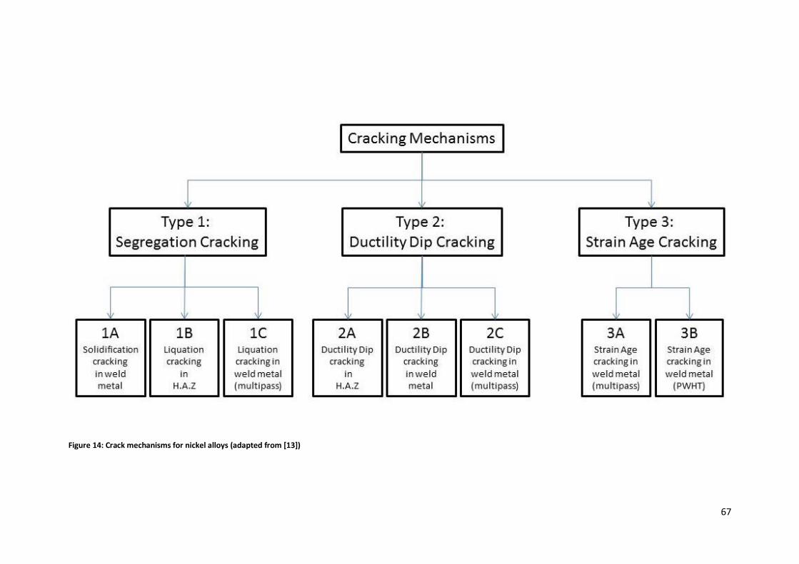
67
Figure 14: Crack mechanisms for nickel alloys (adapted from [13])

68
2.2.5.4.1 Solidification Cracking
Solidification cracking occurs within the fusion zone of a weld either during or after the
material solidifies, as the weld material is weakened due to its high temperature and so it is
susceptible to cracking. After solidification, cooling of the material post-weld can introduce
sufficient stresses due to material contraction such that cracking occurs [14, 15, 214].
Overall due to their already high strength at high temperatures, nickel superalloys are not
susceptible to solidification cracking unless the weld material properties are degraded by a
defect such as element segregation due to low solidification rates, porosity or other
material impurities or defects.
2.2.5.4.2 Liquidation or Liquation Cracking
Liquation cracking occurs due to the constitutional liquation of secondary phases (such as
γ’ precipitates, M5B3 borides, MC or M23C6 carbides or M2SC sulfocarbides [215, 216])
within an alloy, forming liquid films along grain boundaries within the partially melted zone
of a weld [13-15, 214]. Liquation cracking tends to occur in the heat affected zone (HAZ) or
previously deposited fusion material which is re-heated during subsequent weld passes,
localised intergranular or interdendritic films form and reduce the materials ductility,
leading to cracking as a result of residual welding stresses in the material [13, 215-217] .
Although the scenario of re-heating deposited material is similar to AM, the high cooling
rates of AM may counter liquation cracking susceptibility, as the material is likely to re-
solidify before low melting point alloying elements can segregate to the grain boundaries.
However “Laser Rapid Forming” of Rene 88DT, a highly alloyed γ’ strengthened alloy
containing over 40% γ’, along with Co, Mo, and W in solution, has been shown to
experience liquation based cracking within previously deposited layers, while laser cladding
has also experienced cracking between layers [218]. Laser welding of Inconel 718 [192],
Inconel 617 [217], Rene 80 [215] and Inconel 738 [216, 219] have all shown susceptibility to

69
liquation cracking, the root cause of which is the presence of complex secondary alloy
phases. The highly alloyed nature of such superalloys means that liquation cracking can be
an intrinsic problem, rather than the result of un-desired impurities or improper processing
[14, 15].
Figure 15 : Liquation cracking in a) fusion zone of laser welded Inconel 617 [217] b) HAZ of laser welded
Inconel 738 [219]
2.2.5.4.3 Strain-Age Cracking (SAC)
Strain age cracking occurs specifically in precipitation strengthened alloys, either during
re-heat in multi-pass welding [180], or during post-weld heat treatment [14, 15], and is
prevalent within γ’ reinforced superalloys which have high levels of alloying elements [13].
a)
b)
HAZ
Fusion zone

70
SAC occurs when γ’ forming elements which are in solution begin to precipitate during
post-weld annealing, or due to heating from additional nearby weld passes. The presence
of these precipitates reduces the materials ductility, making it vulnerable to cracking. This
problem is compounded further, as the material undergoes a volume contraction during
the precipitation of γ’, which add to the strains already present due to thermal contraction
[180]. Coarse grains or an oxidising atmosphere may also increase the problem – so
cracking is more likely within the HAZ where liquidation occurs and coarse grains are
formed [180].
Welding can be achieved by using a filler material with low levels of alloying elements in
order to locally dilute the parent alloy and reduce its susceptibility to SAC and so reduce
the extent of cracking, however for strength and corrosion reasons usage of the parent
material as the filler is preferred if possible [13]. For example, with careful control of
process parameters it is possible to weld “un-weldable” alloys such as Inconel 939, using
IN625 (a Ni-Cr-Fe alloy with minimal γ’ forming elements) as a filler, however micro-
cracking (up to 0.5mm in length) does still occur, and so weld repairs to turbine
components are strictly controlled in terms of the permissible length of weld which may be
used on any one component [15].
While generally weldability decreases with the increasing presence of strengthening
precipitates, the notable exception to this rule is in cases where γ’’ is the strengthening
phase [179], as its precipitation kinetics are much slower. Figure 16 shows a generally
accepted chart of the weldability of nickel based superalloys as a function of combined
titanium and aluminium content (and thus total γ’ volume fraction). Solid solution
strengthened alloys such as IN625 and C263 lie well within the “weldable” zone. Alloys such
as IN713 or IN738 which rely upon high percentages of γ’ forming elements suffer from

71
significant welding problems, while alloys such as Waspaloy and Rene 41 lie upon the
boundary of weldability.
Figure 16 : Weldability of Nickel-Based Superalloys as a function of Ti/Al content [15]
As the weldability of the alloy depends upon the quantity of γ’ particulates, and this in turn
depends upon the availability of precipitate forming elements available within the alloy,
the weldability of a nickel based superalloy can be qualitatively assessed by the combined
quantity of Ti + Al content, (and to a lesser extent Nb) with ~ 4 wt% taken as a practical
limit for the transition between alloys generally regarded as weldable or unweldable [15,
179]. This limit has been further investigated by Rowe, correlating ductility to the presence
of γ’ and so susceptibility to SAC [180]. The ductility of several key superalloys is correlated
to the presence of γ’ forming elements and γ’ fraction in Figure 17, we can see that
although the use of γ’’ in IN718 does enable the alloy to avoid the problem of SAC, its Nb
content means that ductility remains low compared to solid solution alloys such as C263.

72
Figure 17 : Correlation of alloying elements, and so γ’ phase to elongation [180]
2.2.5.4.4 Ductility Dip Cracking (DDC)
While the solid solution and γ’’ strengthened alloys are relatively immune to SAC, they are
however susceptible to Ductility Dip Cracking [14, 220]. DDC results when the materials
ductility experiences a brief drop at temperatures approaching the solidus temperature
(Ts). This is often over a narrow temperature range, and can occur within any of the three
areas, (weld material, HAZ and re-heated material). DDC is independent of precipitate
formation, or grain boundary impurities [14].
Though there are many suggestions as to the precise mechanism of DDC, there is no
general agreement on the mechanism, and some suggestion that it varies between
materials [14]. The mechanism which has been proposed based on work in nickel alloys in

73
particular is one of a grain boundary shear effect, similar to a creep-rupture type failure.
This was proposed by Rhines and Wray [14], and more recently by Ramirez and Lippold
[221], as well as Noecker and DuPont [220].
While DDC is a particular temperature related phenomenon, it is also worth noting that any
general decrease in a material’s ductility (for example due to higher γ’ fraction) is also likely
to reduce weldability. With lower ductility and/or tensile strength, material becomes more
susceptible to crack formation as a result of the expected residual tensile stresses present
due to differential thermal contraction of weld material after fusion welding.
2.3 Metal Matrix Composite Materials
This section of the literature review provides a background on MMCs, their strengthening
mechanisms and processing. A short summary of known reinforcement materials is
presented in order to shortlist three candidates for feasibility study experiments and
downselection.
2.3.1 Categories of MMC
MMCs are formed by the addition of a ceramic reinforcement to a metallic matrix. A wide
variety of matrix/reinforcement combinations exist, but are usually based around a single
metal base system. Steel, titanium, aluminium, magnesium or nickel are the most usual
matrix materials [222]. With oxides/carbides/nitrides the most usual reinforcement
materials utilised (SiC, Al2O3, TiC, TiB, TiB2, WC, Zr2O3, Y2O3, TiN) [223, 224].
2.3.1.1 Continuous Fibre Reinforced
MMCs may be reinforced by the inclusion of continuous fibres (wires or filaments), running
the length of the material specimen. The principal reinforcement mechanism of a
continuous fibre composite is that the fibre should carry the primary loading, rather than
strengthening the matrix or preventing dislocation movement [225]. Continuous fibre

74
reinforcements provide the most effective strengthening of any mechanism for a given
direction [226]. However interest declined during the 1970’s due to their high cost and the
production limitations [227].
2.3.1.2 Discontinuous (short) Fibre Reinforced
Discontinuous fibres do not run the full length of the material, with fibres terminating
within the matrix material. This category of composite does not rely solely on the
reinforcement for its strength, as the matrix must transfer stresses between the
disassociated fibres and across the matrix/fibre interface [225].
Typical fibres used (SiC) have diameters of a few µm (microns) and lengths of a few
hundred µm and have been used in Al-SiC composites to produce diesel engine pistons for
example. Properties depend significantly upon the interfacial bonding, and coated fibres
are often used to control the interfacial reactions during processing. Short fibre composites
are more readily post-processed than continuous, however their formability is much less
than that of a particle reinforced system. Short fibres do exhibit advantages over
particulates in the areas of creep resistance and wear resistance if aligned in the direction
of loading or wear, as their greater surface area allows for more effective load transfer to
the reinforcement [228].
2.3.1.3 Particulate Reinforced
Raw feedstock for particulate reinforced composites is used in powder form, which is
comparatively low cost versus the use of short fibres or whiskers. While short fibres or
whiskers are both difficult to manufacture and size, powders can be simply ground then
sieved to obtain the desired particle sizes, so making them more cost-effective [226].
Typical powder sizes are from one to tens of micro-metres [229].

75
Particulate reinforced composites are so far focussed on Al, Ti, Fe and Mg based alloys,
with the common use of SiC or Al2O3 as the reinforcing particulate [228]. Other particulates
which have been investigated include TiB2, B4C, SiO2, TiC, WC, BN, ZrO2 and W [228].
The interface between particle and matrix is of course vital in ensuring good load transfer.
The processing of MMCs should aim to avoid excessive interfacial reaction and minimise
defects such as poor interfacial bonding, internal voids and inhomogeneous distribution of
reinforcement [228].
Compared to fibre or whisker reinforced composites, particulate systems generally exhibit
more isotropic properties, as no alignment effects are present, and can be processed using
many of the processes used for monolithic materials [226]. However, unlike continuously
reinforced composites, the matrix strength plays a more important role in determining the
overall material strength [227]. Discontinuously reinforced composites tend to be more
suitable than continuous for applications where directional properties are not required, or
are not desired [230].
Particle reinforced composites are distinct from oxide dispersion strengthened systems due
to their larger particle size (~1-100µm), resulting in negligible Orowan strengthening, and
their high volume fraction (5-40%) [227].
Particulate reinforced systems (and other discontinuous short fibre/whisker) have the
advantage over continuous systems in that their processing is easier, they may be
machined, extruded, rolled or forged, though the process parameters may differ from
those used for the matrix alloys [231].
2.3.1.4 Whisker Reinforced
Whiskers have been found to provide an intermediary step between homogenous
discontinuous reinforced materials and continuous reinforced materials. Whiskers have

76
small sizes, with high aspect ratios up to several hundred to one [228], (e.g. 20-50nm
diameter and 30µm long) whisker based composites tend to be easily formed and
machined [225]. Single crystal whiskers provide extremely high strengths, close to
theoretical maximum values as they are mono-crystalline and so contain minimal
dislocations [228, 229, 232]. Their higher strength contributes directly to the bulk
properties of the final composite and are generally more effective than low aspect ratio
particulates as whiskers provide a higher surface to volume ratio to enable better load
transfer between matrix and reinforcement.
The processing of whisker based reinforced composites can prove difficult though, due to
the tendency of the reinforcement to cluster, or resist attempts to form an aligned
structure [228].
However the most significant problem whiskers pose is as a health hazard during handling.
Whiskers are very fine and liable to become airborne, being able to reach and damage the
human respiratory system; they are therefore not desirable on this basis. For this reason,
most research involving whisker based reinforcement ceased during the early 1990’s, with
minimal commercial exploitation [228, 232, 233].
2.3.2 MMC Strengthening Mechanisms and Phenomena.
2.3.2.1 Direct Strengthening
The direct strengthening effect of a reinforcement material within the matrix is provided by
allowing the higher strength reinforcement to carry the loading on the material.
For a discontinuous reinforcement system the load is transferred through the matrix,
across the interface to the generally higher strength/stiffness reinforcement, which then
“carries” much of the loading. Particulates have a lower aspect ratio than fibres, so the load
transfer is less efficient, but still provides a significant strengthening effect [226].

77
It is generally accepted that the bond between matrix and reinforcement is key to the
transfer of load to the reinforcement, and the strength of the bond is an important factor
in determining the overall strength of the composite [234]. However, excessive interfacial
reaction is known to be detrimental to overall properties, as the matrix alloy system
becomes contaminated with impurities from the dissolved reinforcement [135].
2.3.2.2 Indirect Strengthening
Due to the significant difference in thermal expansion between matrix and particle, upon
cooling if sufficient residual stress is generated, then dislocations form at the
matrix/particle interface, in order to relax the stress (plastic relaxation) [182, 235-237]. This
causes thermally-induced dislocation punching, or dislocation loops as the material is
locally work-hardened and so results in an indirect strengthening of the matrix [226, 227,
238]. The dislocation density increases close to the reinforcement, and increases generally
within the matrix with a larger volume fraction of reinforcement [236, 239].
The level of indirect strengthening provided may be increased by a higher volume fraction
of reinforcement, or by a reduction in the particulate size, as this provides a greater
interfacial area for the dislocation punching to occur [226]. The difference in coefficient of
thermal expansion (CTE) has also been identified as a possible factor in the degree of
dislocation punching present, while stress concentrations due to reinforcement
morphology may also affect dislocation density and location [182].
The density of dislocations generated has been studied and theoretical models established
which enable the prediction of dislocation densities and the increase in tensile strength due
to differential thermal contraction of the matrix and reinforcement [236].
The presence of dislocations around the reinforcement may also be affected by post
process heat treatment, with some uncertainty as to whether the dislocations may be
annihilated, or if the reinforcement could serve to trap them and maintain the high

78
dislocation density after annealing. The difference in CTE between matrix and
reinforcement, as well as the matrix properties at high temperature mean that this
behaviour can be highly specific for a given matrix and reinforcement combination.
It was observed that the intensity of dislocation generation varied with particle size and
shape [240]; smaller spherical particles generating the lowest intensity of dislocations,
sharp corners aid dislocation generation by acting as stress concentrations [236].
The dislocations formed may also provide nucleation sites for the formation of precipitates
during an aging heat treatment [226, 227], and may also alter the aging times, significantly
accelerating the aging process [241].
Orowan bowing has also been identified as a possible reinforcement mechanism, however
its contribution to the strength of micro-sized particulate reinforced materials is regarded
as negligible, as particles are too large, spaced too loosely, and lie on grain boundaries, it is
regarded that Orowan bowing cannot function [181, 240]. However for smaller nano-scale
particulates which may inadvertently occur during powder metallurgy processing the
mechanism may be operative [242].
2.3.2.3 Interfacial Region
“In composites the role of the interface is crucial. Stiffening and strengthening rely on load
transfer across the interface, toughness is influenced by crack detection/fibre pull-out, and
ductility is affected by relaxation of peak stresses near the interface.” – Clyne and Withers
1993 [227].
Stresses present at the interface arise either due to thermal expansion mismatch, or due to
applied load. Interface bonding is important to the direct strengthening effect, affecting
elastic-modulus, and work hardening rate by determining the level of load transfer possible
between matrix and reinforcement [227].
79
Progressive interfacial chemical reaction either during processing or in service is also able
to alter the behaviour of the composite and bonding strength [227]. Interface failure
usually occurs by local cavitation, de-bonding or crack propagation, which may occur in
shear, or normal to the reinforcement surface [227]. Although with particular fabrication
processes and reaction kinetics, it is possible to produce viable composites with
thermodynamically unstable constituents [227].
2.3.2.4 Thermodynamic Stability
Interfacial reactions can be important within MMCs, as they can affect interface strength
and so overall material strength. If interfacial reactions occur during processing or service,
they may have a detrimental effect on the interface if the finished products are
thermodynamically unstable. Ideally a reinforcement material will not react with the matrix
at high processing or service temperatures [223].
The relative thermodynamic stability of the elements present at the interface zone will
determine the nature of the interface, with the potential for films of new compounds to be
formed if sufficient driving force exists for the reaction to take place [234]. Thermodynamic
stability of carbides/oxides may be presented in the form of an Ellingham diagram, these
illustrate the Gibb’s free energy of formation for each compound as a function of
temperature [243, 244]. Compounds with higher energies of formation reside lower on the
diagram, and will remain stable compared to those above them on the diagram, assuming
sufficient time is allowed for the reaction to occur, and the elements are able to mix freely
without being segregated by any other physical effects for example.
If ΔGo has a large negative value, then a large thermodynamic driving force for reaction to
occur will exist (at that temperature), though the speed at which the reaction will occur
may differ. If ΔGo is positive, the constituents are stable and no reaction will occur [227]. So
for a Ni-Cr-Fe matrix alloy such as IN625, if there were an abundance of carbon available,
80
according to the Ellingham diagram presented in Figure 18, this would react to form Nb2C
in preference to TiC, followed by TiC once all the available Nb had been consumed, then
Cr7C3 and so on as each of the available elements was exhausted. On a micro-scale the local
availability of elements to react with will have an influence as well, as they may be kept
physically separate during the melt or solidification process, or limited by the quantity of
reactants available. From the Ellingham diagram it can therefore be seen that TiC is a highly
stable choice of reinforcement compared to SiC or Al2O3 when compared to the other
carbide forming elements present in a typical superalloy matrix.
The level of reaction (or reaction layer thickness x) which occurs can be determined given
the rate constant k for a particular reaction, and a given time t, as given in Equation 3.
𝑥 = 𝑘√𝑡
Equation 3 : Interfacial reaction layer thickness [227]
The brief processing times at high temperature (T>0.4Tmp) found within AM processing will
be advantageous in controlling interfacial reaction layer thickness, as cooling rates are
typically high, and t is therefore small [172].

81
Figure 18: Ellingham diagram for oxides/carbides of alloying elements and reinforcements of interest [245-
247]
Cr23C6
Cr3C2
Cr7C3
TiC
MoC
SiC
NbC
Nb2C
Al2O3
Mo2C
-50000
-45000
-40000
-35000
-30000
-25000
-20000
-15000
-10000
-5000
0
0 500 1000 1500 2000 2500 3000 3500
Gib
bs
Ener
gy p
er g
fwC
/O (
cal/
mo
le)
Temperature (K)
Simplified Ellingham Diagram

82
2.3.2.5 Effect on Mechanical Properties
The stress-strain curves of MMC materials differ from those of the un-reinforced alloy in a
variety of aspects. An example of a stress strain curve for an MMC material is given in
Figure 19, taken from the work of Chawla and Shen [226]; though some elements of the
behaviour are not easily visible, they are explained in more detail by Clyne and Withers
[227] and are summarised below.
Typically MMCs exhibit a steep but brief linear work-hardening regime, given their highly
effective load transfer. The work-hardening rate is then reduced as relaxation processes
are activated earlier (secondary dislocations, diffusion and reinforcement fracture) [227].
Ultimate Tensile Strength (UTS) and yield strength is improved, as a greater degree of work
hardening occurs when compared with the matrix alloy alone. The effects of increased
work hardening are greater in fibre based reinforcements, as the high aspect ratio
(compared to particulates) enables more effective load transfer [227].
Figure 19: Typical MMC stress strain curves for a 2080 aluminium alloy MMC with increasing SiC volume fraction [226]
83
2.3.2.6 Effect on Creep Properties
The use of discontinuous short fibre or particulate reinforcement has been seen to improve
the creep resistance of both magnesium [248, 249] and aluminium [230, 240, 242, 250]
alloys, and some investigations have shown this to hold true for nickel based composites
[251].
The morphology of the particulate reinforcement has been noted to affect creep
resistance, with irregularly shaped Al2O3 particles in aluminium showing less resistance
than spherical (though always superior to un-reinforced matrix alloy) [240].
There is only limited data available on elevated temperature MMC creep behaviour, as
most research to focuses on light alloy (aluminium or magnesium) matrices designed for
low temperature use. At elevated temperatures the behaviour of the light alloy matrix
changes (often over-aging), so limited information on the effect of the reinforcement is
available [240, 242]. This is potentially less of an issue for the use of a superalloy matrix
which is designed for such temperatures and so is more stable.
Though similarity to dispersion strengthened alloys has been noted [227], this supports the
theory that some small degree of Orowan bowing occurs due to the unintended presence
of nano-scale reinforcement particulates. For example some aluminium MMCs enhanced
creep resistance has been attributed to the generation of fine precipitates as the result of
interfacial reactions [230, 240].
Interface strength/bonding also has a significant effect on creep properties, if there is poor
load transfer the composite is observed to have a lower strength/creep resistance than the
matrix alone, as its effective cross section has been reduced [224].

84
2.3.2.7 Discontinuous MMC Failure Mechanisms
Failure mechanisms for discontinuous MMCs are more complex than those for continuous,
failure originates as a result of voids forming and linking within the matrix. Depending on
the material, failure can also be caused by fracture of the reinforcement particles, (more
likely with large particles as likelihood of a flaw increases). Voids can form around
reinforcement particulates, as work-hardening in the local region is greater. If the interface
between matrix and reinforcement has a high integrity, voids will nucleate in the adjacent
matrix. If the matrix/particulate bond is poor then failure will take the form of de-bonding
between the two. If a thick reaction layer is present, this is usually more brittle, and may
favour debonding/cracking [227].
2.3.3 Processing of MMCs
Figure 20 shows a variety of the traditionally available process routes used in the
manufacture of MMCs, each having its own thermal processing history and resultant
material characteristics. Figure 20 has been adapted from Clyne and Withers [228] to
include AM as a processing route. The most common processing routes for manufacture of
MMCs are discussed in the following sections.

85
Figure 20: Overview of MMC processing routes (adapted from [228])

86
2.3.3.1 Stir Casting
Stir casting forms a discontinuously reinforced composite, by the addition of reinforcement
to a stirred liquid melt, the homogenous mixture is then available for casting if the
particulate content has not excessively increased viscosity [222]. Inhomogeneity can be
caused by sedimentation or agglomeration in the melt, or by particle pushing ahead of an
advancing solidification front. Particle pushing is reduced when solidification is rapid, as
above a critical “growth velocity” particles are enveloped rather than pushed [228].
The prolonged liquid-ceramic contact required for stir casting can also be problematic in
allowing excessive interfacial reaction to take place [227, 228].
2.3.3.2 Squeeze Casting
Squeeze casting processes apply high pressure and increased cooling rates to a solidifying
MMC, providing a fine microstructure, while pressuring of the liquid phase reduces
porosity. Squeeze casting may be performed on a stir-cast material, or heated powder
mixture, while squeeze infiltration is the injection of liquid matrix into a fibre pre-form
[222, 227, 228].
2.3.3.3 Spray Deposition
Spray deposition is defined as either the introduction of reinforcement into a liquid metal
stream to deposit on a substrate, or feeding of cold material into a heated zone. Thermal
spraying utilises the feeding of wire or powder into a hot torch and acceleration of the
molten material by a gas stream to deposit on a substrate [222, 227, 228]. Spray deposition
is also characterised by high cooling rates, producing a fine microstructure and having the
potential for forming non-equilibrium phases and a lack of macro segregation [222].
2.3.3.4 Liquid Phase Sintering
Liquid phase sintering is an established powder metallurgy manufacturing route. A green
powder pre-form is pressed to form a green body, then heated until a liquid phase is

87
created, this liquid phase moves by capillary action to fill pores in the structure, the body’s
solid elements coalesce and eventually grain growth further reduces porosity. Typical
sintering times are 1hr, while sintering time, temperature and compaction pressures are
the primary process variables [252]. Achieving full density however can be difficult if the
liquid phase is unable to penetrate areas of porosity due to surface tension effects [252].
2.3.3.5 Powder Based Processing
MMCs by powder based methods begin with the blending of matrix and reinforcement
(either powder, platelet or short fibre). By traditional routes, processing usually involves a
cold compaction, canning and evacuation/degassing followed by a high temperature
consolidation (e.g. Hot Isostatic Pressing) [222, 228].
Preparation of powders is usually achieved either by simple mixture, or by mechanical
alloying within a high energy ball mill (attritor). Mechanical alloying is used for the
production of dispersion strengthened alloys, as it can produce fine dispersions of small
(<1µm) particles, it is also suitable for introducing hard reinforcement to a softer matrix
[222]. Milling of MMC powders can have a significant effect on the Particle Size Distribution
(PSD) and morphology, as milling media or hard reinforcement particles impact and
influence each other [253]. Generally the PSD decreases as particles are deformed or
fractured, although in the case of some materials cold welding between matrix material
powders may increase the PSD [170, 253, 254]. Eventually a steady state may be reached,
whereby the rate of size reduction by particle fracture is equal to the rate of size increase
due to cold welding and no net change in particle size for the mixture occurs [253].
Reduction of reinforcement particle size may improve material properties (providing
greater surface area and therefore more efficient load transfer), while work hardening of
matrix material particles during milling may also influence properties [254].

88
Efficient mixing of MMC powders can be influenced by both milling/mixing speed (energy)
and duration, with generally a longer mixing time and higher energy resulting in a more
randomly and homogenously mixed powder [255].
Homogeneity of powder feedstock can be difficult to assess, most often a visual or
optical/SEM microscope examination is made for a qualitative assessment [170, 254], with
the distribution of reinforcement and matrix often more easily quantified in the
consolidated sample. Overall powder mixtures are difficult to quantify with absolute
certainty [256].
In some cases, the degree of mechanical alloying which takes place can be sufficient to
form new phases “in-situ”, this typically occurs in “high energy” milling where impacts are
capable of fusing the constituent powders into a new phase either by diffusion/welding or
as the result of a self-propagating reaction [253].
Production of MMCs by extrusion can often produce an alignment effect, compromising
homogeneity. Rolling or forging imposes significant strains on the material, which can
cause cavitation, particle fracture and macroscopic cracking. At high temperature
processing can also experience macroscopic hot tearing. Production by HIP does not
impose such violent stresses upon the material, it is a common process for the removal of
residual porosity however, it is less effective at removing enclosed porosity such as pores
containing gasses, or porosity within particle clusters. HIPing also tends to leave oxide films
intact, providing poor inter-particle bonding [228].
2.3.3.6 In-Situ formation and Self-propagating High temperature Synthesis (SHS)
Reactive Processing or “in-situ” forming is any method by which a reaction is initiated to
create a “compound from pure elements or compounds” [252]. If the rate of heat
generation is sufficient the reactions can become self-propagating, producing a
“combustion front” which travels through the material, known as self-propagating high

89
temperature synthesis (SHS). If the rate of heat loss is great enough, compared to the heat
generation, or the species are consumed, then the reaction will no longer be self-sustained
[252].
For a powder bed fusion process this raises the question of whether a reactive processing
route is feasible, should the reaction be sufficiently self-sustaining, it may move beyond the
desired laser scanning area, or even propagate out of control to react the entire powder
bed. The investigations of Persson et al., [252] indicate that sufficiently high porosity within
green components can slow or extinguish a self-propagating reaction; so the relatively
loose uncompressed powder bed may or may not be susceptible to a “run-away” reaction if
a reactive process were to be investigated.
The use of the SHS reaction to produce in-situ reinforcement has been the subject of
widespread research, forming either one or a combination of TiC, TiB and TiB2 from
elemental powders or B4C [257-259] within traditional production methods and blown
powder AM processes [95, 260].
For the formation of Ti borides/carbides the formation is generally conducted within Ti or a
Ti alloy (Ti64) to produce titanium matrix composites [258-261], although elemental
powders have been used within other matrices to provide TiC/TiB reinforcement for base
matrices such as steel [257], iron [262], magnesium [263], aluminium and nickel [118].
In-situ formation also provides a route to the use of whisker type reinforcement without
the associated health hazards of handling whisker particles, and at lower cost [233, 259].
However, the formation of high aspect ratio whiskers by in-situ reactions generally require
processing times of several hours to achieve the necessary directional crystal growth [233].
Although TiB has been formed in-situ by the Laser Engineered Net Shaping (LENS) process
(a blown powder laser-DED process), the needles formed have a high aspect ratio, but are
90
of small scale (2-10µm long by 30-50nm wide) [264]. Given the brief processing time
involved in AM larger needles are likely unattainable as there is little opportunity for crystal
growth as exists during a lengthy hot pressing operation.
Powder metallurgy introduced reinforcements tend to suffer problems with contaminated
particle/matrix interfaces (oxidation or other contamination), which reduces the interface’s
strength, this may be overcome by the in-situ formation of the reinforcement [118, 262].
Porosity can be relatively high in materials processed using an SHS reaction though as
gaseous by-products can become trapped during solidification [262].
The work of Dadbakhsh et al., [265] demonstrates the potential for in situ reinforcement of
aluminium alloys in a powder bed type AM process. Of particular note are the effect of
such a processing route on the resulting phases present in the material, and its relative
density, as in situ reactions provide several mechanisms by which voids may be formed in
the material during solidification [265]. Again the use of high cooling rate laser processing
was shown to result in fine reinforcement particulates on the order of 100nm [265].
Porosity was inspected by CT scanning, and attributed to oxides which had not been able to
vaporise out of the melt pool, some variation was found in the characteristics of the
porosity based upon the matrix alloy composition, with a lower thermal conductivity
promoting higher melt pool temperatures and more complete melting between previously
deposited material and the current layer. Spherical micro-porosity was noted as a result of
gas bubble entrapment. Significant densification problems were encountered, with a
maximum relative density of 80% achieved through this in situ processing route, with
porosity showing a highly interconnected nature.
Ideally an in-situ formation of the reinforcement, but without the occurrence of a self-
propagating reaction may well be beneficial to the properties of the composite, and has
been shown possible during the short melt environment of an additive process [118, 265].

91
2.3.4 MMC Problems and Obstacles
It is important in the selection of reinforcement to try and avoid too great a mismatch of
the thermal expansion co-efficient, which can cause internal residual stresses after
processing [225]. Generally metals have greater thermal expansion coefficients than
ceramic materials, once consolidated from high temperature processing, this will inevitably
result in a level of residual stress once cooled [227].
Difficulty has been found in examining the creep-resistance of MMCs processed by a
powder route, the processing and handling of the powders can generate small oxide
particles, which provide a level of ODS, not normally present when other process routes are
used and often provide anomalous results [227].
Excessive interfacial reactions, and an inability to provide a robust protective coating have
proven problematic in achieving MMCs using SiC or Al2O3 in any high temperature matrix
(Ti, Ni) [266]. However it is worth noting the processing method used – HIPing at ~1000oC,
HIPing usually requires extended processing times, providing ample opportunity for
reactions to occur – AM processing endures only brief periods of local high temperature
during processing, so may avoid any significant issue in this area.
MMCs tend to have a lower fracture toughness than the matrix material, while also
experiencing thermal fatigue – this is particularly relevant to materials which will
experience high temperature cyclic usage (e.g compressor blades), in particular thermal
fatigue has been noted in tungsten fibre superalloy composites [235].
2.3.5 Candidate reinforcement materials for MMCs
The following section reports upon a background literature review of the materials used to
reinforce MMCs within any given matrix material or alloy system and in particular within
nickel based matrices. The intent is to identify the most promising candidate reinforcement
materials to enhance the performance of a nickel based superalloy.

92
2.3.5.1 Commonly Utilised Reinforcements: Al2O3, SiC and TiC
2.3.5.1.1 Aluminium Oxide (Al2O3)
Al-Al2O3 discontinuous composite systems have been widely exploited, given their desirable
low density, high specific stiffness, low thermal expansion and increased fatigue resistance.
They are also relatively low cost to produce in high volumes [231]. Their use is seen in many
applications, including the automotive industry, for the production of engine components
such as connecting rods or pistons.
Continuous alumina fibres within Al matrices have been found to improve specific stiffness
and specific strength, while maintaining low elongation (possibly due to local clustering of
fibres). The improvement to properties was taken as an indication of good interface
wetting during a flow-casting process [267].
Al2O3 reinforced materials have been produced by electro-deposition with a pure nickel
matrix [268, 269] for increased wear resistance when compared to the parent nickel
material [270].
The addition of nano scale Al2O3 particulates in small quantities (<1.0wt%) to nickel hard
facing alloys also results in an improvement to wear resistance, however in this case the
particulates serve to act as a grain refiner rather than a composite material [271].
The potential for a detrimental interfacial reaction between Al2O3 and nickel has also been
observed, whereby dissolution of the Al2O3 can result in oxidation of the nickel alloy and
the presence of free aluminium within the matrix, however it is worth noting this may be
process dependant due to the ample time for reaction during HIP type operations [266].
2.3.5.1.2 Silicon Carbide (SiC)
Aluminium-SiC whisker composites show a heterogenous formation of the matrix alloy’s
precipitates near to reinforcement particles, attributed to a local depletion of the

93
nucleation species, and uneven distribution of vacancies. This heterogeneous phase
distribution is likely to cause unstable crack propagation during failure, and local
heterogeneous plastic flow. Similar effects should potentially be expected in γ’
strengthened superalloys as mechanisms of precipitate formation are similar [272].
SiC retains high strength and is thermodynamically stable (at least compared to Iron) up to
high temperature of 1100oC. Often used where abrasion or wear resistance is required, but
also improves UTS and yield strength in iron matrix materials [223].
SiC reinforced nickel materials have been widely produced by electro-deposition as a
coating within a pure nickel matrix, for wear and corrosion protection applications. The
composites generally exhibit an increase in hardness (benefitting wear resistance). An
improved resistance to hot oxidation has also been observed within gradated electro-
deposited Ni-SiC coatings [268, 273-277].
Ni-SiC nano-composites (again formed by electro-deposition processing) have also been
investigated, showing an improvement to properties from both sub-micron (0.4µm) sized
reinforcement and from nano-crystalline grain structured Ni matrix. Historically even
moderate volume fractions of reinforcement caused a drop-off in mechanical performance
due to particle agglomeration [278]. But more recent research has improved
homogenisation and reduced agglomeration by stirring and ultrasonic agitation of the
electroplating bath [279], such that up to 10vol% SiC in nickel is now achievable for wear
resistant coatings [280].
The addition of SiC increased yield strength in conventional Ni, but was overshadowed by
the effect of reduced grain size in the nano-crystalline Ni. While SiC is themochemically
stable within a pure Ni matrix [278], considering it as a reinforcement in the context of

94
more complex nickel alloys, alloying elements such as Cr, Nb and Ti are more reactive
carbide formers [281], as can be seen in Figure 18 in Section 2.3.2.4.
More recently, the efforts of some researchers have focussed on the use of Al+Al2O3 coated
SiC fibres within a nickel alloy matrix, to provide an intermediate bonding layer which can
bond well with both matrix and reinforcement, but limits the potential for excessive
reactions to take place [282].
2.3.5.1.3 Titanium Carbide (TiC)
Titanium carbide offers high hardness (up to 3200Hv), modulus and flexural strength [283],
and within aluminium matrices has been found to provide a greater benefit to tensile
strength and modulus than equivalent SiC, B4C and TiB2 reinforcements [284]. Its uses are
typically for high temperature applications, with good thermal-shock and oxidation
resistance [225].
TiC may be added directly to the matrix, or may be formed in-situ, if its constituent
elements are provided. This in-situ formation has been achieved by exothermal reaction in
an SHS process. This has been achieved in isolation under inert atmosphere, as well as
within molten magnesium as part of the production of a TiC-Mg composite [263].
The AM of TiC reinforced commercially pure titanium has been previously investigated to
produce functionally graded materials through using a laser-DED process, successfully
producing a crack free, and high density material, depending upon the volume percentage
of TiC, above 80% volume significant cracking problems were observed. At high TiC volume
fractions it was found that gradually introducing the TiC reinforcement from 0% volume up
to 95% volume over several millimetres of build height reduced the likelihood of cracking
due to thermal stresses and material mismatch [95]. Although the work of Liu et al., [95]
shows that the laser-DED process is capable of producing MMC materials with TiC.
95
Moreover the precise volume of TiC reinforcement present in the finished material was not
quantified, with no quantifiable relationship between the input parameters (powder feed
speeds) and the actual deposited composite, and no account taken of powder flow
behaviour or overspray for example. Forming TiC by adding C to a Ti matrix also provides a
simple chemistry, with complete availability of Ti to form TiC, and no issues of
stoichiometric imbalance to consider. Achieving the in-situ formation of TiC within a
differing matrix alloy will however limit the quantity of Ti available, particularly if excess Ti
were detrimental to the matrix alloy (as in the case of γ’ weldability for superalloys). A
precise stoichiometry of Ti and C would be required, if no other carbides were formed in
preference to TiC with other alloying elements, and that no significant proportion of the
elements were vaporised during processing, leaving a non-stoichiometric mix of Ti and C
available in the melt pool. In the case of Ni superalloys (with reference to Figure 18 in
Section 2.3.2.4), of the common alloying elements present, only Nb is a stronger carbide
former than Ti, and should already exist at stoichiometric ratio within the matrix alloy, so
such a processing route is feasible.
The use of TiC within a single layer surface coating in a nickel alloy matrix has been
investigated by Yang et al., [283], through both the addition of TiC and by in-situ forming
from Ti and C. A stoichiometric mix of Ti and C (in the form of graphite) were included in
the powder. The intent of in-situ formation being to produce a more thermally stable end
product, with a cleaner interface, better able to transfer stress at the particle/matrix
boundary, however no experimental results or comparison is given to confirm if this was
the case. However the research has successfully produced an in-situ TiC reinforced nickel
alloy, though issues are noted with the motion of the reinforcement within the molten
pool, due to its lower density the TiC particles tend to float to the surface faster than the
advancing solidification front, resulting in an uneven distribution of particles and particle
size. A fluxing element (CaF2) was also found to permit the formation of a cladding without

96
excessive porosity [283]. Although the Nickel alloy utilised was not named, its composition
(Ni, Cr, Fe, B, Si, C), having no typical superalloy alloying elements such as Mo, Co, Nb, Ti or
Al would indicate a hardfacing corrosion resistant alloy rather than a complex superalloy,
and so no conclusions can be drawn with regards to interactions with carbide forming
elements such as Mo or Nb contained in superalloys.
More recent work by Guang et al., [285] examining the use of in-situ formed TiC-TiB2
reinforced nickel coatings for steel, included molybdenum and chromium as part of the
feedstock material, this potentially gives some insight into the interactions between TiC
and the alloying elements found in superalloys (namely Cr and Mo). The lower Gibb’s free
energy of TiC allowed for the majority of the elemental powders to form TiC as intended,
although some additional C2MoTi, MoNi or MoNi4 phases were identified as the Mo content
approached 8wt%. However this is inconsistent with typical Mo behaviour as an alloying
element in most superalloys, where MoC would be expected to form in preference to
MoNi. However identification of such phases is hindered by complex XRD spectrum
interpretation, as many of the minor phases exhibit peaks at similar positions to other
expected phases such as TiC, and the peak shifts or broadening associated with lattice
strains due to in-situ TiC formation are largely unknown and make interpretation of these
small peaks difficult with any certainty. These additional phases do however only form with
high quantities of Mo available, whereas typical superalloys contain smaller quantities –
the work by Guang et al., is relevant in showing that TiC will be preferentially formed in the
presence of Mo and Cr. Energy Dispersive Spectroscopy (EDS) results for the presence of
carbon and boron are referred to, despite admissions that carbon cannot be accurately
measured using EDS, this is also true of boron, though the author makes no
acknowledgement of this, limiting confidence in their interpretation of the results. As a
result the distribution of elements within the microstructure of the material is difficult to
judge, and no examination is made of the interface between matrix and particle. The
97
method of adding Mo as part of a feedstock powder appears to produce results which
differ from the expected behaviour of a Mo containing superalloy, differing results should
be anticipated for a pre-alloyed metallic powder mixed with a ceramic reinforcement, to
forming from several separate mixed powders.
The production of a TiC reinforced pure Ni matrix via a laser-DED process has also been
successful, using elemental (Ti and graphite) powders for in-situ formation of the
reinforcement. The material showed an increase in hardness and a reduction in its co-
efficient of friction compared to pure nickel, providing potential for low friction high wear
surface applications [118]. Notably the author refers to the “nominal” composition of the
deposited material, given that no measurement of final composition was made, and the
difficulties of accurately delivering three feedstock powders of differing densities and
morphologies. More traditional melting/casting routes have been used to successfully
produce TiC reinforced superalloy composites, again to produce a wear resistant low
friction material [286, 287].
2.3.5.2 Other Reinforcements
2.3.5.2.1 Tungsten Carbide (WC)
Primarily used for cutting tools, tungsten carbide has high “rigidity, compressive strength,
hardness and abrasion resistance” WC can bring benefits to abrasion resistance and impact
strength [225]. Recent research by Li et al., [288] has investigated the use of WC as a
reinforcement phase within a Ti matrix alloy, manufactured by a laser-DED system feeding
WC powders into a Ti melt pool generated from wire feedstock, providing improved
hardness and wear resistance compared to the parent alloy.
WC reinforced coatings have been produced by electro-deposition [268, 289] and Laser
cladding using a pure nickel matrix [290] and Ni-Cr matrix [291]. Again the benefit sought
was as a wear/corrosion resistant coating [289, 291]. It is noted that WC/Ni composites

98
have also been produced by high velocity oxygen fuel, thermal spraying, plasma spraying,
hot isostatic pressing and chemical vapour deposition [289] as well as by mechanical
alloying and spark plasma sintering [292].
For laser cladding, a high crack sensitivity was noted, the cladding process showed a
tendency for WC to sink within the melt pool, and high degrees of entrapped gas porosity.
The main reason for cracking though was thermal stress, which was reduced by pre-heating
the substrate [290].
PTAW cladding has been performed with three simple Ni alloys, having nil, low and high Cr
content, combined with WC reinforcement for wear resistant coatings [135]. Difficulty was
encountered in producing a functional product however, as WC particles passing through
the plasma column dissolved, creating a brittle secondary phase upon solidification [135].
Reinforcement of Ni and Co based alloys with WC particles has shown a tendency for
recrystallization to occur, causing weakening of the material, due to the formation of brittle
secondary phases such as W2C and M6C carbides formed with Cr and particularly Mo [227,
293, 294].
2.3.5.2.2 Chromium Carbide (Cr3C2)
Chromium carbide (Cr3C2 also formed as Cr7C3 or Cr23C6) provides extremely high resistance
to oxidation and corrosion. Its density is higher (6.68g/cm3) and melting point lower in
comparison to many other ceramics (1895oC) [225], while hardness varies depending on
the composition from 975Hv to 2250Hv. However with reference to the Ellingham diagram
in Figure 18 all three carbide compositions are less chemically stable compared to other
alloying elements commonly found in nickel superalloys.
99
2.3.5.2.3 Tantalum Carbide (TaC)
TaC is characterised by a high melting point (4014oC) and high hardness (up to 2000Hv)
[225]. However the high density of TaC at 14.3gcm-3 compared to the density of nickel
alloys ~8.4gcm-3 would be a potential disadvantage in producing an MMC with a superior
specific strength or stiffness to the original alloy. The high raw material cost of tantalum (as
a rare earth material) is also likely to make the availability and price of TaC prohibitive.
2.3.5.2.4 Thorium Oxide, Zirconium Oxide and Yttrium Oxide (ThO2, ZrO2 and
Y2O3)
A review of previously classified Soviet materials research in the MMC field noted the use
of thorium oxide within nickel alloys as beneficial to high temperature durability [229].
However thorium oxide possesses a level of radioactivity, and is classified under UN2912,
Hazard Class 7, effectively restricting its practical use.
Heat resistant nickel alloys have been combined with ThO2, ZrO2 and Y2O3 particulates, to
the benefit of heat-resistance and durability in tests at 1100-1300oC [229]. Y2O3 reinforced
MMCs have also been produced in-situ by PM methods with a pure nickel matrix,
demonstrating improved creep resistance [251].
2.3.5.2.5 Titanium Boride (TiB) and Titanium Diboride (TiB2)
TiB has a low density (4.5gcm-3), high hardness (3000Hv) and stiffness (520GPa), as well as
chemical stability [264, 295] and high melting point (3000oC), while TiB2 has a particularly
high melting point (3230oC), stiffness, and lower density (4.451gcm-3) [296]. As such both
are desirable candidate materials for use within an MMC.
Of the two compounds, the available literature shows that TiB2 has been added to a matrix
directly [296, 297], or may be formed in-situ with the correct elements available. For
example, TiB2 has been combined with a Nickel base matrix to produce a coating by HVOF
spraying from elemental powders. The TiB2 reinforcement was created by an SHS reaction

100
within a simple Ni-Cr matrix, improving wear resistance compared to the matrix material
alone. Significantly high volume fractions of TiB2 (65%) were seen to be detrimental though
compared to those at 40% [298].
Production by pulsed plasma sintering has also been investigated, again utilising an SHS
reaction for the formation of TiB2 within a pure nickel matrix, achieving 99.8% density with
no excess phases (eg. Ni3Ti or NiB) formed [299].
2.3.5.2.6 Carbon Nano-Tubes / Graphene
Carbon Nano Tubes (CNTs) have generally been researched to reinforce polymer
composites, with some work now emerging for the more complex metallic systems [300,
301]. A similar disparity has been noted with the new material graphene, primarily being
utilised with polymer materials, and minimal work published relating to the use of
graphene to strengthen MMCs [301, 302]. CNTs are essentially rolled graphene sheets,
either single or multi-walled [300].
The production of CNT reinforced MMCs is generally achieved by a powder metallurgy
route, although agglomeration can limit the proportion which may be included (generally
<8%wt) [300, 303]. Solid state processing via HIP or extrusion is most usual, while matrix
materials tend to be selected for their low melting point (Al, Mg, Cu) as high processing
temperatures may cause damage to the CNTs, formation of an interface layer, or clustering
[300, 301, 303-308]; the materials may even be formed by cold compaction and extrusion
techniques [309].
Overall there is some disagreement about the behaviour of CNT within a metal matrix and
the resulting effect upon mechanical properties. Work by Ci et al., [310] identifies a good
interfacial bond after heat treatment (up to 950oC) of an Al-CNT material produced by
sputtering aluminium onto CNTs. George et al., [238] identified a similarly effective bonding
without the presence of carbides in an Al-CNT material produced by powder metallurgy,

101
ball milling and HIP. In contrast Kwon et al., [311] attribute the enhanced properties of a
spark plasma sintered Al-CNT material to the presence of a carbide interface layer which
allows improved load transfer between matrix and reinforcement. However,
Chunfeng et al., [312] observed complete dissolution of the CNTs to form Al4C3 carbides
when manufactured by HIP, thus reducing rather than improving material properties.
The work of Bartolucci et al., [302] compares the strength of aluminium, produced by a
powder route, to that of a Multi-Walled CNT (MWCNT) composite, and a graphene platelet
composite, a 12% improvement in UTS was noted for MWCNTs, but a dramatic reduction in
strength for the graphene platelets, even in very small quantities (0.1%wt), due to the
formation of aluminium carbide and destruction of the graphene.
However, the work of Bastwros et al., [313] has shown an improvement in the properties of
a base 6061 aluminium alloy due to the addition of between 1.0 and 2.0 wt% of graphene.
Similarly to Kwon et al., Bastwros et al., suggest that the improvement in strength is
enabled by an aluminium carbide bonding layer between the matrix and reinforcement
which allows load transfer.
2.3.5.2.7 Carbon Nano-Tube/Nickel
Electro deposition [314] and blown powder DED techniques [315, 316] have been
investigated for the production of CNT reinforced nickel, for the advantage of their self-
lubricating properties for use as bearing surfaces in need of low friction [315].
The work of Hwang et al., [316] compares Ni-CNT with Ni-Graphite composites produced by
a blown powder laser-DED technique, the tubes were in bundles, and formed using the
same parameters as those for Ni-Graphite. Good matrix/CNT wetting was observed, with
no significant reaction layer noted, and the MWCNTs survived the melt process without
dissolving, unlike graphite. The minimal reaction layer was attributed to the form of the
CNTs, with only the ends un-bonded (unlike graphite), as well as the short dwell time within

102
the molten pool, due to the use of the DED process. Although Hwang et al., have
established that MWCNTs may be processed by a melt route without significant interfacial
reaction or dissolution, no evaluation of mechanical properties was made to identify any
potential improvement to be gained by the use of CNTs in Ni matrices.
However CNTs have a large aspect ratio, similar to whiskers (for short CNTs) or asbestos
fibres (for long CNTs), suggesting potential for serious long term damage to the human
respiratory system if inhaled (e.g. mesothelioma or cell death) [317, 318]. Limited research
exists on the assessment of the potential health risk posed by the handling and processing
of loose CNTs, but similarities in behaviour of certain CNT forms to asbestos have been
confirmed [319]. This raises the concern that their use may pose a health hazard, or at least
increase the cost and complexity required to safely handle the smaller nano-scale material
compared to that needed for the current micron sized materials [320]. Overall the level of
risk is still relatively uncertain [318], prompting some companies to discontinue
nanotechnology research [317, 321], while their use and handling may be safe within a
research environment, this may not readily translate to a production environment.
2.3.6 Superalloy based MMCs
A review of available literature specifically in the context of MMCs based upon nickel
superalloy matrices has been conducted and the specifics presented in this section. While
active research was conducted in the 1980s and early 1990s, very little has been published
regarding the conventional manufacture of superalloy based MMCs since. This is
presumably due to improvements in the properties of the superalloys through methods
such as investment cast directionally solidified and single crystal materials, which have
reduced the motivation for development of a conventionally manufactured superalloy
MMC [1].

103
2.3.6.1 Zirconia Particle Reinforced Rene 95.
ZrO2 particle reinforced Rene 95 is used as graded interfaces to reduce thermal stress
where dissimilar materials join, particularly looking to the application of thermal barrier
coatings to superalloy substrates. Composites follow a powder metallurgy preparation
route. It was found that the ZrO2 reacted with the γ’ (Ni3Al), forming Al2O3, depleting the
matrix of its strengthening γ’ phase, although MMC strength is higher than unreinforced
alloy at low strain rates, the MMC is weaker at high strain rates. The changes in strength
are thought to be due to grain refinement and chemical changes in the matrix more so than
particulate strengthening effects [322]. Zirconia was used as its thermal expansion
mismatch with Ni-based alloys is relatively small [322].
2.3.6.2 Tungsten Fibre Reinforced Superalloys
At high temperatures both the fibres and matrix are ductile, eliminating problems with
notch sensitivity in brittle materials. High CTE mismatch results in susceptibility to thermal
cycling damage [323]. For continuous fibre reinforced Waspaloy and Incoloy 907
composites, the fibres negated the effect of surface cracks due to thermal shock and
provided a barrier to fatigue crack propagation, however this mechanism is not anticipated
in discontinuous composites [324].
Other researchers have shown the need for interface coatings (in this case Hafnium Nitride)
to prevent a loss of strength in the tungsten fibres due to re-crystallisation which is induced
by contact with nickel above 1000oC [325]. This can result in significant problems with
decreased mechanical properties due to excessive interfacial reaction during in-service
thermal cycling [323].
Additionally significant difficulties exist in producing components from such a material,
being extremely difficult to machine, they are typically produced by PM/HIP routes or hot
forging, where the latter can result in significant damage to the reinforcing fibres or the

104
bond between matrix and fibre. Therefore for practical production there are highly
restrictive forming limit criteria for the shapes which can be produced in these materials by
such a manufacturing route [325].
2.3.6.3 Alumina Fibre and Particulate Reinforced Superalloys
The strength and upper temperature limit of superalloys may be improved by
reinforcement with strong high-modulus ceramic fibres. Alumina has been identified by
some researchers as promising candidate, due to its chemical compatibility with the
superalloys. The use of fibre coatings was examined as a method of reducing residual
interface stresses during thermal cycling, with some benefit being shown for some
coatings. The analytical study presented indicates that under thermal cycling the thermal
expansion mismatch between fibre and matrix is highly problematic, creating residual
stresses with the potential for crack formation at the interface between matrix and
reinforcement [326].
The use of α-AL2O3 (sapphire) fibres within a Haynes 230 superalloy matrix has been
investigated, laminating fibres in sequential layers of Haynes 230 foil and powder. Boron
was utilised to suppress the melting point of the nickel matrix to achieve a Transient-Liquid-
Phase process, although excess boron produced a heterogeneous material, the process was
described as feasible, though no mechanical properties were recorded to indicate the
potential of this material/process combination [327].
Both single crystal and polycrystalline Al2O3 fibres have been utilised within an Inconel 718
matrix, produced by pressure casting [328]. While other researchers have investigated the
use of sapphire, YAG and sapphire-YAG fibres within a matrix of a γ/γ’ based superalloy,
again produced by pressure casting. The pressure casting route provided reasonable
homogeneity in the fibres distribution, for a highly simplistic cylindrical sample geometry,
while wetting of the fibres was deemed acceptable. However some voids were still present
105
at the interface, an issue which would be more problematic in complex geometry if high
integrity components were to be manufactured [329].
Laser cladding has been used to produce a nano-particulate Al2O3 reinforced Ni-based
superalloy coating, while the coating did appear to have potentially improved hardness,
this was primarily due to a highly altered grain structure (from large columnar to fine
equiaxed) caused by the presence of nano-particulates acting as nucleation sites during
solidification [330].
2.3.6.4 SiC Particulate or Fibre Reinforced Superalloys
Electron Beams (EB) have been used to surface harden IN625/SiCp composites, novel
microstructures were observed, attributed to the localised melt and “supercooling”.
Ahmad et al., [331] have modified bulk superalloys by EB melting the surface and
introducing SiC particulates to Inconel 625, Hastelloy C-276 and Zircaloy-4. The high energy
of the EB was deemed to provide strong interfacial bonding, although some of the
improvement to properties can be attributed to the refined microstructure, not solely the
reinforcement addition. Rapid solidification also meant that the γ’’ precipitates which
dissolved during melt had insufficient time to re-precipitate after melt, while the SiC
particles either partially or completely dissociated and reacted with the matrix.
The use of SiC as a reinforcing phase in several superalloy matrix materials (Inconel 718,
Hastelloy X) produced by hot pressing has been noted to produce reaction layers, at
temperatures of 700oC to 1150oC, with a significant increase in the reaction after 1150oC
[266]. The reactions produced silicides of Ni, Ti and Cr, as well as M6C phases in reaction
with the alloying elements present. The presence of minor reaction products was noted
after 100h at 700oC and under a pressure of 7MPa, but not in any significant quantity,
increasing the temperature to 1150oC to simulate hot pressing resulted in significant
quantities of reaction products. As processing by AM takes place in a significantly shorter

106
time frame, the production of MMCs without any significant reaction products for service
temperatures of under 700oC may well be feasible.
2.3.6.5 Titanium Carbide Particulate Reinforced Superalloys (IN718)
Yang et al., [332] investigated the reinforcement of IN718 with TiC particulates of 10-50µm
which were wet blended at 20% volume with IN718 powder before HIPing and extrusion.
Homogeneous distribution of the TiC particles was found difficult to achieve, with
agglomerations occurring, which permitted voids to form within the agglomerations as they
prevented infiltration of matrix during processing. The MMC produced exhibited higher
modulus, but lower yield and UTS, while ductility was greatly reduced.
Table 5: Reported properties for TiC reinforced IN718 compared to parent alloy [332]
Material Young’s modulus (GPa)
Yield strength (MPa)
Tensile strength (MPa)
Ductility (%)
TiC(P)/IN718 227 955 1200 1.4 IN718 207 980 1430 19
Examination of tensile test samples showed that this was due to the TiC agglomerations,
reinforcement de-cohered or cracked at these sites to cause premature failure [332].
Although room temperature properties were inferior to the matrix alloy, at elevated
temperatures (650oC) the MMC exhibited excellent retention of strength compared to the
matrix alone [332].
Although this MMC did exhibit some benefit to high temperature properties, the
processing route has compromised its performance, which would be improved if a more
even distribution of reinforcement could be achieved. A more detailed review of TiC
reinforced superalloys is conducted in Section 2.1.9.2, as part of a discussion of current AM
research on superalloy MMCs.

107
2.4 Conclusions
As a result of the literature review, several conclusions may be draw in relation to the three
streams investigated (AM technologies, Superalloys and MMCs). In summary while AM has
great potential, a combination of higher processing rates and available material properties
would be beneficial to the application of the technology for superalloy components.
The AM processing of nickel based superalloys is highly desirable compared to
traditional casting or subtractive processes for component geometries with
complex features, short production runs or high material removal from solid.
Despite low deposition rates, powder bed LM processes are likely to be adopted for
moderate sized complex aerospace component production using nickel superalloys.
Higher power lasers and thicker build layers may provide benefits in productivity,
but no research has yet been conducted to establish the process parameter
window and potential material density.
Current mainstream powder bed LM or EBM techniques do not have sufficient
deposition rates or build envelopes for the economical near net shape production
of large components.
For high deposition rate WAAM processes PTAW shows some advantages, but
understanding of processing parameters, strategies and material properties are still
limited.
High performance γ’ strengthened superalloys cannot be processed by AM due to
weldability restrictions, limiting current AM materials to the low end of materials
performance.
MMC materials may offer an effective route to improving materials performance, if
their processing behaviour can be understood and refined to produce high relative
density material.

108
3 Experimental Methodology
This chapter details the methodology and reasoning behind the experimental work
conducted, covering feedstock material preparation, the scope and intent of
experimentation and the analysis techniques used to evaluate the deposited materials.
Three core research areas were identified as a result of the literature review in Section 2.
1. Can high deposition rate powder bed laser melting of a solid solution strengthened
superalloy be achieved?
2. Can a process map for PTAW deposition of a solid solution strengthened superalloy
be developed and what are the characteristics of the material produced?
3. What is the processing behaviour of a solid solution strengthened superalloy based
MMC within a high deposition rate powder bed LM system?
To date powder bed laser melting technologies have not achieved deposition rates in
excess of grams per hour and it is unkown if the use of layer thicknesses in excess of 100µm
would be practical or capable of producing material of acceptable density. The experiments
conducted as described in Section 3.1.2 are designed to assess the feasibility of high
deposition rate powder bed LM and to establish an understanding of relevant process
parameters and deposition behaviour for the selected IN625 alloy.
While PTAW deposition has been utilised for the WAAM of IN625, current research has not
fully characterised a process parameter map for this material, for example in a manner
similar to the comprehensive work on Ti-6Al-4V by Martina et al., [79]. To date only limited
investigations of deposition parameters [125] and single weld width walls have been
conducted by PTAW for IN625 or similar superalloys [126], with no detailed process
parameter window characterisation having been undertaken for single weld tracks or for

109
the deposition of large multi-layer, multi-weld width features. The experiments conducted
as described in Section 3.1.3 are designed to address these gaps.
Alongside the need for higher deposition rates for powder bed LM processes, the range of
materials performance is limited by an inability to process alloys with high γ’ phase
content. There exists therefore an opportunity for MMC materials to aid in improving the
properties of solid solution strengthened alloys such as IN625 which can be successfully
processed to achieve a high relative density and crack free product. Therefore concurrent
research into the high deposition rate powder bed LM of an IN625 based MMC will also be
conducted in order to compare and contrast with current research into the laser-DED
processing of similar materials [114, 171-174].
3.1 Sample Manufacture
In order to evaluate the potential for high deposition rate AM, powder bed laser melting of
IN625 was investigated using 100µm and 500µm layers at up to 4kW.
To evaluate the potential for improvements to material properties, the laser melting of an
IN625 MMC was also investigated alongside this, down selecting a candidate reinforcement
material (TiC). The manufacture of the selected TiC reinforced IN625 was then assessed for
both a two component powder mixture, and a reactive “in-situ” powder feedstock.
Experiments were conducted to determine the appropriate process parameter window for
all three powder bed materials, followed by multi-layer deposition to manufacture samples
for analysis of microstructure, composition and hardness.
The use of WAAM in the form of PTAW deposition for the manufacture of IN625 from wire
feedstock was also investigated, the intent being to establish a process parameter window
and manufacture material for analysis and mechanical testing.
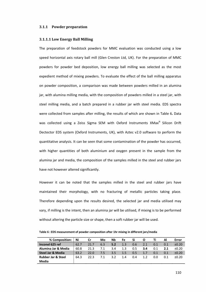
110
3.1.1 Powder preparation
3.1.1.1 Low Energy Ball Milling
The preparation of feedstock powders for MMC evaluation was conducted using a low
speed horizontal axis rotary ball mill (Glen Creston Ltd, UK). For the preparation of MMC
powders for powder bed deposition, low energy ball milling was selected as the most
expedient method of mixing powders. To evaluate the effect of the ball milling apparatus
on powder composition, a comparison was made between powders milled in an alumina
jar, with alumina milling media, with the composition of powders milled in a steel jar, with
steel milling media, and a batch prepared in a rubber jar with steel media. EDS spectra
were collected from samples after milling, the results of which are shown in Table 6. Data
was collected using a Zeiss Sigma SEM with Oxford Instruments XMaxN Silicon Drift
Dectector EDS system (Oxford Instruments, UK), with Aztec v2.0 software to perform the
quantitative analysis. It can be seen that some contamination of the powder has occurred,
with higher quantities of both aluminium and oxygen present in the sample from the
alumina jar and media, the composition of the samples milled in the steel and rubber jars
have not however altered significantly.
However it can be noted that the samples milled in the steel and rubber jars have
maintained their morphology, with no fracturing of metallic particles taking place.
Therefore depending upon the results desired, the selected jar and media utilised may
vary, if milling is the intent, then an alumina jar will be utilised, if mixing is to be performed
without altering the particle size or shape, then a soft rubber jar will be used.
Table 6 : EDS measurement of powder composition after 1hr mixing in different jars/media
% Composition: Ni Cr Mo Nb Fe Si O Ti Al Error
Inconel 625 ref 62.7 21.7 6.3 5.2 1.3 0.6 2.1 0.1 0.1 ±0.20 Alumina Jar & Media 60.8 21.3 7.1 3.4 1.3 0.5 3.4 0.1 2.1 ±0.20 Steel Jar & Media 63.2 22.0 7.5 3.5 1.5 0.5 1.7 0.1 0.1 ±0.20 Rubber Jar & Steel Media
64.3 22.3 7.1 3.2 1.4 0.4 1.2 0.0 0.1 ±0.20

111
A calibration of ball milling speeds was also undertaken utilising high speed photography
(Photron SA1.1, Photron, Japan) to measure the rotational speed of the jar, as controlled by
the ball mills rotary potentiometer. For milling of powders speed 4 (~150rpm) was selected,
as this permitted the highest energy to be imparted to the media, while still allowing them
to “tumble” during milling, rather than be centrifuged against the jar wall.
Figure 21: Relationship between ball mill speed settings and jar rpm
Other than for materials down selection, preparation of powders for laser melting was
conducted for up to 72 hours, with samples taken at 24, 48 and 72 hours for observation by
SEM, and mixing determined by a combination of SEM examination, EDS measurement and
particle size analysis after the full 72 hours mixing.
3.1.2 Powder Bed Laser Melting
3.1.2.1 Powder Bed Laser Melting Equipment
In order to conduct experiments into the Laser Melting of materials, a bespoke powder-bed
type machine was designed and constructed by the author specifically for this work. A
Remote Laser Welding facility was available to provide a high powered laser source, based
0
50
100
150
200
250
300
0 1 2 3 4 5 6 7 8 9
Jar
spe
ed
(rp
m)
Ball Mill speed setting
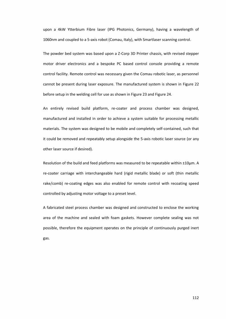
112
upon a 4kW Ytterbium Fibre laser (IPG Photonics, Germany), having a wavelength of
1060nm and coupled to a 5-axis robot (Comau, Italy), with Smartlaser scanning control.
The powder bed system was based upon a Z-Corp 3D Printer chassis, with revised stepper
motor driver electronics and a bespoke PC based control console providing a remote
control facility. Remote control was necessary given the Comau robotic laser, as personnel
cannot be present during laser exposure. The manufactured system is shown in Figure 22
before setup in the welding cell for use as shown in Figure 23 and Figure 24.
An entirely revised build platform, re-coater and process chamber was designed,
manufactured and installed in order to achieve a system suitable for processing metallic
materials. The system was designed to be mobile and completely self-contained, such that
it could be removed and repeatably setup alongside the 5-axis robotic laser source (or any
other laser source if desired).
Resolution of the build and feed platforms was measured to be repeatable within ±10µm. A
re-coater carriage with interchangeable hard (rigid metallic blade) or soft (thin metallic
rake/comb) re-coating edges was also enabled for remote control with recoating speed
controlled by adjusting motor voltage to a preset level.
A fabricated steel process chamber was designed and constructed to enclose the working
area of the machine and sealed with foam gaskets. However complete sealing was not
possible, therefore the equipment operates on the principle of continuously purged inert
gas.

113
Figure 22: Adapted Z-Corp 3D Printer with inert atmosphere build chamber & full remote control
Figure 23 : Experimental equipment in-situ with remote laser welding source and robot (home position)

114
Figure 24 : Experimental equipment in-situ with remote laser welding source and robot (exposure position)
Processing of material was conducted under an inert Argon (Pureshield, BOC, UK)
atmophere. The O2 level within the chamber was monitored and logged continuously using
a calibrated Rapidox 2100 oxygen sensor (Cambridge Sensotec Ltd, UK) accurate to 1ppm.
Laser exposure was commenced once the chamber atmosphere recorded less than 300ppm
of O2, in order to maintain a low oxygen content within the chamber atmosphere during
processing, argon was continually purged at a flow rate of 15-20lpm, such that the
maximum concentration of oxygen remained below 1000ppm during deposition. The
oxygen limit of 1000ppm (0.1%) was selected for parity with commercial equipment
currently available on the market, the 300ppm start measurement was determined as the
highest 02 concentration permissible so as not to exceed 0.1% during exposure due to
convection within the process chamber. For deposition utilising 500µm powder layers, the
atmosphere preparation procedure was somewhat altered. The chamber was flooded with
argon to an O2 concentration of under 150ppm for a duration of at least 2minutes before
deposition of the first layer, to ensure that a reasonable effort had been made to purge the
powder bed with Argon. A higher flow rate of argon was maintained throughout the
deposition process (30-35lpm), with no more than 300ppm of O2 observed at any time, and

115
no more than 150ppm of O2 present before commencing deposition. The 300ppm limit was
selected as the lowest practical O2 concentration achievable with the current equipment.
Laser power and focal spot was measured using Primes PowerMonitor and FocusMonitor
equipment (Primes GmbH, Germany) and the data evaluated using Primes
LaserDiagnoseSoftware v2.9 to provide an evaluation of beam shape and the magnitude of
any power losses in the beam line. Beam diagnostics were performed in both 2011 and
2013, and showed near identical results for power and focal spot size, with the latter being
slightly higher than manufacturer’s specification (ranging from 0.876mm to 0.890mm
rather than 0.60mm). Comparing Figure 25 and Figure 26, it can be seen that the beam
diameter has varied by less than 1.6% over the course of all experimentation performed
using this equipment, and can therefore be deemed consistent. The relationship between
the programmed laser power and that delivered to the work-piece is shown in Figure 27,
however for simplicity the programmed value will be referred to throughout this thesis. An
equation for the relationship between programmed and delivered power is provided in
Equation 4, should the reader desire to calculate the actual power delivered at the
workpiece for any of the experiments described.
Figure 25: Beam diagnostic – 2011

116
Figure 26: Beam diagnostic - 2013
Figure 27: Relationship between programmed laser power and actual power delivered
𝑀𝑒𝑎𝑠𝑢𝑟𝑒𝑑 𝑃𝑜𝑤𝑒𝑟 =𝑃𝑟𝑜𝑔𝑟𝑎𝑚𝑚𝑒𝑑 𝑃𝑜𝑤𝑒𝑟
1.11− 23.35
Equation 4 : Laser power at workpiece as a function of programmed laser power
Mild steel substrates of 80 x 100 x 10 mm, were restrained against thermal stress induced
deformation. The mild steel substrates were bolted into a larger aluminium platform (240 x
320 x 20 mm) to act as a moderate thermal sink during repeated deposition runs.
0
500
1000
1500
2000
2500
3000
3500
4000
4500
0 1000 2000 3000 4000
Pro
gram
med
Las
er P
ow
er (
W)
Measured Laser Power (W)

117
Substrate temperature was monitored and recorded using a K-Type thermocouple and
handheld thermocouple reader/logger. To obtain a measurement reasonably close to the
deposition site, build plates were machined from the reverse side to allow the
thermocouple to be placed within the plate at a distance of 4mm from the upper surface.
Figure 28: Substrate design for powder bed laser melting experiments
The material to be consolidated was deposited upon the substrate by a spring loaded steel
“blade” re-coater mechanism; with the layer thickness set at either 100 µm or 500µm as
required, as shown in Figure 29. Initial deposition experiments revealed that unless
adequate top surface flatness of the deposited material could be guaranteed, then
interference with the rigid steel re-coater occurred, causing damage & eventally jamming
the machine. Thereafter a “soft-re-coater” based upon a thin metallic comb was utilised for
all experiments, with the comb replaced when visibly damaged by contact with deposited
material.

118
Figure 29 : View of powder bed LM build platform and recoated first layer
3.1.2.1.1 High speed photography
In order to examine the melt processing behaviour of the candidate MMC materials a high
speed camera (Photron SA1.1, Photron, Japan) was utilised to record the weld passes.
Given the high brightness of the welding process, high intensity lighting was used to reduce
the contrast between the ambient light level and that generated by the weld process. This
enabled a reasonable image of the weld pool to be obtained. A moderate frame rate of
50,000fps was selected in order to maintain sufficient image resolution (256x128pixels)
over the region of interest.
Build area
75mm

119
Figure 30: Laser Melting experimental configuration with high speed photography
3.1.2.2 Reinforcement Down Selection
3.1.2.2.1 Objectives
To determine the “processability” and potential benefits of three possible MMC
reinforcement materials (Al2O3, SiC and TiC)
3.1.2.2.2 Methodology
In order to determine a potential MMC reinforcement material for further research, three
candidate materials were selected for evaluation, Al2O3, SiC and TiC. Each was blended at
5wt% with IN625 powder for 1hr, until visual inspection showed them to be well mixed.
Baseline process parameters for the deposition of IN625 were established from single track
deposition experiments as detailed in Section 3.1.2.3, with four multi-layer samples
produced according to the parameters in Table 7, these were used for the processing of the
candidate MMC materials to provide a direct comparison.

120
Table 7 : Baseline IN625 parameters at 100µm
Sample Power (W) Scan (mm/min)
1 800 6000
2 800 7000
3 1000 6000
4 1000 7000
Each material was processed using the same parameters; deposition was continued in all
cases until interrupted by excessive material build-up which caused jamming of the re-
coating mechanism. Manufactured samples were then analysed using optical microscopy,
SEM, EDS and hardness indentation to evaluate the best candidate for further work.
3.1.2.3 Powder Bed Laser Melting Single Track Deposition
As a result of the material down selection experiments, three materials were identified for
further research.
IN625 as a baseline for deposition at both 100µm and 500µm layer thicknesses
IN625+TiC a TiC reinforced MMC with 5wt% TiC added
IN625+Ti+C a powder blend for the in-situ forming of TiC from Ti and Graphite
(mixed to provide 5wt% TiC at a stochimetric ratio)
Single track deposition experiments were conducted as outlined in Table 8. Three materials
were evaluated, IN625, IN625 blended with 5wt% TiC and IN625 blended with a
stoichiometric mixture of Ti and carbon in the form of graphite at 5wt%. Two layer
thicknesses were investigated for each material, the minimum practical thickness of 100µm
(where possible) and a thicker 500µm layer.
The IN625+Ti+C in-situ formed MMC material was also evaluated in combination with a
pre-heated substrate as significant cracking problems were observed. Pre-Heating was
achieved by defocussing the laser beam to ~10mm diameter and rastering over the
substrate surface until a temperature of 300oC was obtained.

121
Table 8: Single track deposition experiments performed
Material 100µm Layer 500µm Layer
IN625 Completed Completed IN625+TiC Completed Completed IN625+Ti+C Unable to re-coat Completed IN625+Ti+C Pre-Heated (300oC)
Unable to re-coat Completed
3.1.2.3.1 Objectives:
To determine the effect of laser power and speed upon the stability of the resulting
weld bead.
To relate the weld power and speed used to the resulting weld bead geometry.
To identify an appropriate parameter set for use in depositing multi-layer samples.
3.1.2.3.2 Methodology:
Single track welds were produced on mild steel substrates at a variety of laser powers and
speeds (1-4kW at 2-10m/s). A full factorial approach was adopted to ensure that all areas
of the process map were investigated and all interactions would be apparent.
Table 9: Linear Energy Density (J/m) for all experimental parameter combinations
Laser Power (W) Welding speed (m/min)
2 4 5 6 10
1000 500 250 200 166.7 100
1750 875 437.5 350 291.7 175
2500 1250 625 500 416.7 250
3250 1625 812.5 650 541.7 325
4000 2000 1000 800 666.7 400
The full factorial experimental matrix for five levels of power and five levels of speed is 5x5,
giving 25 individual combinations of parameters for experimentation. Three repeats of
each parameter combination were made, giving 75 individual welds, which were randomly
allocated to a position on the required four build plates according to the order shown in

122
Table 10. The sample ordering shown in Table 10 was utilised for all single track laser
melting experiments in each material/layer thickness combination.
A total of 75 weld beads were therefore produced, with a maximum of 20 weld beads
deposited sequentially upon each substrate. A laser exposure program was written, such
that welds were conducted on alternating sides of the centre point, increasing X offset by
3mm for each weld as shown in Figure 31. In order to minimise thermal effects between
tracks, a 10 second dwell was included between each exposure as well as the alternating
exposure strategy, each repeat of a given parameter set was also randomised to a different
position on the substrate.
Figure 31 : Schematic of laser exposure program for single track welds, relative to centre point of substrate.

123
Table 10: Randomised allocation of parameter combinations & positions
Build 1 Build 2 Build 3 Build 4
Sample Number
Power (W)
Speed (mm/min)
Power (W)
Speed (mm/min)
Power (W)
Speed (mm/min)
Power (W)
Speed (mm/min)
1 1750 4000 2500 10000 3250 8000 1750 4000
2 1000 8000 2500 4000 3250 4000 1000 6000
3 1750 2000 1000 10000 1750 10000 1750 8000
4 3250 2000 2500 10000 1000 2000 3250 6000
5 3250 2000 1000 10000 4000 8000 1000 4000
6 4000 6000 3250 8000 4000 10000 3250 8000
7 1750 2000 1000 2000 3250 4000 4000 8000
8 4000 4000 2500 8000 3250 2000 1000 8000
9 3250 4000 2500 2000 4000 2000 4000 6000
10 4000 2000 1750 2000 2500 6000 4000 10000
11 3250 10000 1000 6000 3250 10000 1000 6000
12 1750 6000 3250 6000 1750 6000 2500 6000
13 1750 8000 1750 8000 4000 10000 2500 8000
14 2500 10000 1750 4000 2500 8000 4000 6000
15 4000 2000 1000 4000 1750 10000 1750 6000
16 2500 6000 1000 8000 2500 2000
17 2500 4000 2500 4000 1000 10000
18 4000 4000 1750 10000 2500 2000
19 3250 10000 3250 6000 1000 4000
20 4000 8000 4000 4000 1000 2000

124
Immediately after deposition and removal from the build chamber, each weld was assessed
based on the criteria listed below as falling into one of five distinct categories. An example
of each weld type is shown in Figure 32, PTAW deposited welds have been used to
illustrate the differing behaviours due to the larger welds, making behaviour easier to
identify, the same forms and behaviour operate in powder bed LM.
1. Stable: a continuous bead with no notable deviation from a straight line, having a
continuous section shape (Figure 32a).
2. Humping: a continuous bead, but having significant fluctuations in section shape,
typically creating a wave or characteristic hump back effect (Figure 32b).
3. Balling: discontinuous bead which has broken down into approximately spherical
sections (Figure 32c).
4. Wavy: continuous bead with some transverse deviation from the intended straight
line (Figure 32d).
5. Unstable: a continuous section shape which has segmented on occasion along its
length or exhibits other defects (Figure 32e).

125
Figure 32: Characteristic weld behaviours illustrated by PTAW bead on plate welds a) stable, b) humping, c) balling, d) wavy, e) unstable.
A transverse section was then taken at the welds mid-point (Y=0) for analysis by optical
microscopy and SEM. The width of the weld bead was measured manually using Vernier
a)
b)
c)
d)
e)

126
callipers at three points, near the start of the track, the centre and the end. To avoid
measuring start or end effects the approximate positions of measurement were Y=-20, Y=0
and Y=+20.
Optical microscopy was utilised to measure the weld bead width, height above the
substrate surface and the weld penetration depth into the substrate as shown in Figure 33.
As can be seen in the illustration below, the width measured by Vernier calliper and by
optical microscopy may differ depending upon the weld beads geometry. Where
measurements do not agree, the optical microscopy value has been used.
Figure 33: Schematic of weld bead measurement positions
3.1.2.4 Powder Bed Laser Melting Multi-Layer Deposition
Multi-layer deposition was conducted at 100µm for reinforcement down selection, then at
both 100µm (where possible) and 500µm for the further investigation of IN625, IN625+TiC
and IN625+Ti+C.
Due to cracking observed in the IN625+Ti+C experiments, pre-heating was also utilised to
evaluate its effect if any. The intent being to decrease the thermal gradient between the
top and bottom surfaces of the sample and so reduce the degree of thermally induced
residual stress, as suggested by Tahmasbi et al., [333].

127
The process parameter evaluations performed on single track welds established a good
overlap in the process windows of both matrix and TiC reinforced MMCs, as such the same
process parameters were utilised for all materials such that the deposited material can be
compared like for like, rather than observing any variations in material characteristics or
properties due to parameter changes.
3.1.2.4.1 Objectives:
To determine if the stable parameter set identified by single track deposition is
viable for producing larger components
To provide material samples for compositional and structural analysis
To obtain an understanding of the process parameters in a multi-layer scenario for
use in AM
3.1.2.4.2 Methodology:
Samples were defined as a series of parallel lines measuring a total of 10 mm wide by 30
mm long, with a variable hatch spacing between lines and a 0.85 mm diameter laser focal
spot. The hatch distances and corresponding beam overlap values are presented in Table
11, for each hatch distance the number of lines was selected such that the overall sample
geometry remained the same (10mm x 30mm).
Table 11: Powder bed LM hatch spacing and beam overlap values utilised
Hatch Spacing (mm) Beam diameter (mm) Beam overlap (area fraction)
0.5 0.85 15% 0.8 0.85 1% 1.1 0.85 0%
The raster pattern utilised to produce the samples is shown in Figure 34, with X & Y values
defined as off-sets from a single centre point.

128
Figure 34: Laser path for multi-layer sample
To prevent excessive material deposition at the start and end of each track, a linear ramp in
and out of laser power was employed over a distance of 1mm, with this portion of the
sample being disregarded during all further analysis. Each hatch distance was investigated
by the production of four samples on each substrate, according to the parameters shown in
Table 12. However the order of exposure was seen to influence the deposition behaviour of
subsequent samples (i.e. two samples with identical parameters on the same substrate
differed in their geometry and processing behaviour, due to variation in substrate
temperatures). Therefore subsequent analysis of the samples compares only the first
sample on each substrate, produced at 4000W and a scan speed of 5500mm/min, at three
hatch spacings, 0.5mm, 0.85mm and 1.1mm for each material. Although this means that
the effect of laser power and scan speed upon deposited multi layer samples is not
evaluated, the effect of differing materials and differing hatch spacings can still be
assessed.
Table 12: Multi-layer powder bed LM parameters
Sample Laser Power (W) Laser Speed (mm/min)
1 4000 5500 2 4000 6500 3 4000 5500 4 4000 6500

129
Deposition of multilayer samples was conducted until a fixed number of layers had been
achieved, or the samples had interrupted the build process by way of a re-coater crash.
Once deposition was completed, substrates were removed from the chamber and allowed
to finish cooling to room temperature. Samples were examined by Stereomicroscopy
before sectioning for metallographic preparation and examination by Optical microscopy,
SEM, EDS and hardness testing.
3.1.3 Wire and Arc Additive Manufacture
3.1.3.1 PTAW Equipment
To conduct experiments into the WAAM of material, a bespoke Plasma Transferred Arc
Welding (PTAW) based deposition system was constructed and developed. The system
being based upon a conventional 3-axis CNC machine, coupled to a PTA welding set
(Eutronic GAP, Castolin Eutectic GmbH, Germany). Two welding torches were available for
experimentation, an E152 powder fed torch and an E15N wire fed torch, shown mounted
to the stripped down CNC machine in Figure 35 during commissioning. The associated
material feeders are shown in Figure 36.

130
Figure 35: 3-axis CNC machine with welding torches in position a) Wire fed torch "parked", b) Powder fed torch "welding"
Figure 36: Available material delivery systems a) "push" type wire feeder, b) wheel and bucket powder feeder (x2)
The powder fed torch was fed by two independent powder feeders, utilising a rotary wheel
and bucket type metering system, and being purged with inert carrier gas. Initial
experiments found that powder delivery rates were inconsistent when the powder feed
units were placed remotely from the torch. While vibratory assistance did improve
consistency (measured by recording the weight of powder delivered to a container in
1minute), it was decided that the feeders should be located directly above the torch,

131
providing the minimum of disruption to material feed rates. The delivery rate of spherical
metallic powders was found to be consistent to within ±1%.
The feeding of the available ceramic powders was found to be problematic with standard
equipment, with the angular morphology causing powders to agglomerate in their free
condition (Figure 37), or to interlock and form a blockage at any orifice. While vibratory
assistance was beneficial to the consistency of the delivery rate of spherical metallic
powders, angular ceramics simply interlocked more rapidly.
Figure 37: Angular TiC morphology encourages agglomeration and prevents powder flow
Blended metallic/ceramic powders were also attempted, but despite the small proportion
of ceramic powders, a consistent feed rate of material could not be established and
vibration was found to encourage separation of the two powders as shown in Figure 38.
60mm

132
Figure 38: Wheel & bucket powder feeder - segregation of powder mixtures with vibratory assistance
Wire feeding of Inconel 625 wire was found to be advantageous in comparison to powder
feeding, both in consistency and sample quality. Having a lower surface to volume ratio,
wire feedstock carries lower proportions of surface oxidation into the molten pool, so
increasing the quality of deposited material, particularly on repeat passes. The lower cost
of raw material (approximately 30% that of powder) also contributed to the decision to
base future experiments around a wire fed deposition system.
Two deposition strategies were considered for PTA experimentation, the deposition of a
series of parallel lines, or the use of a weave strategy. While a weave strategy can produce
a relatively flat deposit, problems can occur with heat build-up, as movement of the torch
is quite slow and heat input is continuous until the layer is completed. This is particularly
noticeable in low thermal conductivity materials such as nickel, as evidenced in Figure 39,
after three to four layers are deposited, significant heat is retained towards the end of the
deposition pass, altering welding parameters and permitting oxidation of the material once
the torch and shield gas has been removed.
5mm
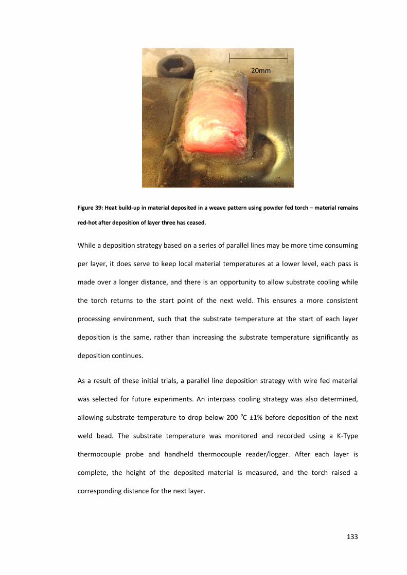
133
Figure 39: Heat build-up in material deposited in a weave pattern using powder fed torch – material remains
red-hot after deposition of layer three has ceased.
While a deposition strategy based on a series of parallel lines may be more time consuming
per layer, it does serve to keep local material temperatures at a lower level, each pass is
made over a longer distance, and there is an opportunity to allow substrate cooling while
the torch returns to the start point of the next weld. This ensures a more consistent
processing environment, such that the substrate temperature at the start of each layer
deposition is the same, rather than increasing the substrate temperature significantly as
deposition continues.
As a result of these initial trials, a parallel line deposition strategy with wire fed material
was selected for future experiments. An interpass cooling strategy was also determined,
allowing substrate temperature to drop below 200 oC ±1% before deposition of the next
weld bead. The substrate temperature was monitored and recorded using a K-Type
thermocouple probe and handheld thermocouple reader/logger. After each layer is
complete, the height of the deposited material is measured, and the torch raised a
corresponding distance for the next layer.
20mm

134
Figure 40: Parallel line deposition strategy using wire fed torch with inter-pass cooling strategy to achieve a
two layer deposit without overheating
3.1.3.2 WAAM – Single Track Deposition
3.1.3.2.1 Objectives:
To determine the effect of welding current, welding speed and material feed rate
upon weld stability.
To relate weld power, weld speed and material feed rate to the resulting weld bead
geometry.
To determine a parameter set and deposition procedure for use in multi-layer
deposits.
3.1.3.2.2 Methodology
The methodology for investigation of welding stability followed the concept of a bead on
plate experiment, depositing weld material upon a substrate in a single straight weld bead.
The substrate used was 100mm x 12mm mild steel flat stock, with welds defined as an
80mm traverse located centrally on the 100mm wide substrate. Individual substrate strips

135
were used for each weld in order to maintain similar test conditions, measuring 100mm x
25mm x 12mm, which were held in a vice, with the top surface positioned flush with the
top of the vice jaws using a straight edge, to provide a repeatable position. While some
variation in substrate temperature was observed due to heat soak into the vice, substrate
temperature was always below 40oC before welding commenced.
The intent of the experiment being to investigate the PTAW process window for deposition
of IN625 wire, the experimental matrix shown in Table 13 outlines the full factorial
combination of parameters, investigating Welding Speed at six levels, Welding Current at
three levels and Wire Feed rate at three levels.
After deposition, each weld was characterised using the same five categories as for similar
powder bed LM experiments (as described in Section 3.1.2.3)

136
Table 13: Experimental matrix for PTAW single track welds
Welding Speed (mm/min) Weld Current (A) Wire Feed rate (m/min)
650 147 2.0 650 147 1.5 650 147 1.0 650 124 2.0 650 124 1.5 650 124 1.0 650 101 2.0 650 101 1.5 650 101 1.0 550 147 2.0 550 147 1.5 550 147 1.0 550 124 2.0 550 124 1.5 550 124 1.0 550 101 2.0 550 101 1.5 550 101 1.0 450 147 2.0 450 147 1.5 450 147 1.0 450 124 2.0 450 124 1.5 450 124 1.0 450 101 2.0 450 101 1.5 450 101 1.0 350 147 2.0 350 147 1.5 350 147 1.0 350 124 2.0 350 124 1.5 350 124 1.0 350 101 2.0 350 101 1.5 350 101 1.0 250 147 2.0 250 147 1.5 250 147 1.0 250 124 2.0 250 124 1.5 250 124 1.0 250 101 2.0 250 101 1.5 250 101 1.0 150 147 2.0 150 147 1.5 150 147 1.0 150 124 2.0 150 124 1.5 150 124 1.0 150 101 2.0 150 101 1.5 150 101 1.0

137
Final experiments were conducted utilising a bespoke wire-feed nozzle design with
increased stiffness and positional accuracy, with welds placed upon independent substrates
in order to increase the repeatability of the equipment and test conditions. The revised
torch assembly is shown in Figure 41.
Figure 41: Revised wire fed PTA configuration for single bead on plate tests
After deposition, the width and height of each weld was measured using Vernier Callipers
(±0.05mm) in the centre of the weld, and approximately 15mm from either end. Specific
samples were then selected for metallographic sectioning, preparation and observation by
microscopy to determine weld penetration depth and dilution. Samples were selected for
sectioning which covered a reasonable range of weld power, weld speed and wire feed,
such that interactions could be explored, however all samples were not sectioned due to
the high number available.
10mm
138
3.1.3.3 WAAM – Multi Layer Deposition
3.1.3.3.1 Objectives:
To demonstrate the stability of chosen weld parameters and deposition strategy in
a multi-layer scenario.
To provide material for analysis and evaluation by metallography, SEM, EDS, XRD,
µ-CT and tensile testing.
3.1.3.3.2 Methodology
Multi-layer deposition was conducted upon substrates of 100mmx180mmx12mm, to
produce material for the purposes of tensile testing.
Based upon the results of single bead on plate tests and multi-bead, multi-layer feasibility
trials, a hatch spacing of 3.5mm was selected using a welding speed of 450mm/min a
current of 147Amps and a wire feed rate of 2.03m/min. A parallel series of 8 x 145mm long
weld beads were deposited to provide a layer measuring approximately 30mm by 150mm
as a near-net billet for the machining of tensile samples. To control excessive bead height
at the start of welds, the welding speed was increased to 650mm/min for the first 20mm
before switching to 450mm/min for the central section. To control weld height drop off
towards the end of the weld bead, welding speed was reduced to 350mm/min for the final
20mm, as shown in Figure 42. A 5ms dwell was also utilised at the end of the weld to build
up a small amount of material and prevent accumulated drop off in weld height with
multiple layers. While a 5mm overrun was attempted to ensure removal of the wire from
the molten pool, the movement of the pilot plasma arc tended to drag the molten material,
particularly after several layers. Therefore a programmed 10mm retraction of the welding
wire 1second before turning off the main arc was utilised to ensure removal from the weld
pool and a clean separation.

139
Figure 42: Welding speed variation in Y direction
An end of line dwell of 5s was utilised to ensure complete shielding of the solidifying weld
pool, before returning the torch for the start of the next weld bead. At this point a 25s
dwell was included in the deposition program, as this was sufficient to allow the substrate
temperature to return to <200oC, as monitored by thermocouple readings.
Additional first and last weld beads were deposited on occasion to build up the side wall
geometry when notable sloping had occurred (approx. every two to three layers as
needed).
As the build progressed, thermal conduction out of the previously deposited layer and into
the substrate & machine bed was reduced due to the lower thermal conductivity of IN625
compared to steel, the reduced sectional area available for heat transfer and the greater
distance of material through which heat must be conducted. To prevent an excessive
accumulation of heat in the previously deposited layer which might influence the
deposition of the next layer the welding current was reduced according to the schedule
shown in Table 14. The torch offset increase was made after each layer and was varied
slightly according to manual measurements of the deposited material in order to maintain
0
100
200
300
400
500
600
700
0 20 40 60 80 100 120 140 160
Tra
vers
e S
pe
ed
(mm
/min
)
Y Position (mm)

140
a constant torch offset distance of 7mm from the work piece. Welding voltage was
therefore maintained within the range of 25.5V to 28V (nominal target 26.5V), with a lower
voltage indicating a smaller torch offset than ideal and a higher voltage indicating a larger
offset.
The schedule shown in Table 14 was determined after a series of trial builds during which
differing weld currents were attempted to identify which values produced a visually
consistent weld at each layer compared to the previous layer.
Table 14 : Build Parameter variation with Z height for PTAW Multi-Layer builds
Layer Approx. torch offset increase
(mm)
Welding Current (A)
Welding Speed (mm/min)
Wire Feed Rate (%)
0 0 – (7mm from
Substrate) NA NA NA
1 2 147 450 20.3 2 4 147 450 20.3 3 6 142 450 20.3 4 9 136 450 20.3 5 12 136 450 20.3 6 14 136 450 20.3 7 16 131 450 20.3 8 18 131 450 20.3
3.2 Powder Analysis
3.2.1 Powder Characterisation
3.2.1.1 Objectives
To characterise feedstock powders utilised.
To determine the homogeneity/mixing of MMC powders.
3.2.1.2 Methodology
Feedstock powders were analysed by Laser Diffractometry (LD), to determine particle size
distribution, SEM and EDS to determine morphology and provide a qualitative examination

141
of homogeneity, and XRD to determine the bulk composition/phases present for later
comparison with deposited material.
3.2.1.2.1 Particle Size Distribution - Laser Diffractometry
Laser Diffractometry particle size analysis was selected in order to quantify the Particle Size
Distribution (PSD) of the feedstock powders and the powder mixtures resulting from low
energy ball milling. While mechanical sieving was available, the technique is limited to
describing the proportion of particles between the available sieve mesh sizes. Initial trials
using a vibratory sieving station were attempted, however the vibration applied to allow
particles to pass through the mesh was found to encourage and increase agglomeration of
TiC powders, so influencing the results. On this basis the technique was rejected for the
measurement of PSD.
While other methods of particle sizing based upon mechanical and imaging methods are
available, the use of light scattering in the form Laser Diffraction is probably the most
widespread and commonly utilised laboratory method [334, 335]. Also known as small
angle light scattering, this technique utilises the fundamental principles of the interaction
of a monochromatic light source with a particle suspended in a liquid or air, with the
diffraction pattern produced by a particle varying dependent upon its size. However a
simple diffraction pattern is not all that is produced, in reality a complex scattering pattern
is produced based upon the combination of absorption, diffraction, refraction and
reflection which has taken place depending upon specific interaction of the light source,
particle and suspension medium in question.
Lorenz-Mie theory (more commonly known as Mie theory), in particular provides the most
accurate method of determining particle size from a complex scattering pattern, however
this depends upon the optical properties of both the suspension media and the particulate
being a known value. Unfortunately in many cases the data for complex refractive index is

142
unavailable and so results determined using Mie theory without an accurate optical model
of the material are, at best, unreliable.
As an alternative to Mie theory for the deconvolution of measured diffraction patterns, a
simpler Fraunhofer diffraction model can be utilised. This is valid only for particles which
are significantly larger than the wavelength of the light source (at least five to six times
greater), but does produce results which agree with Mie theory when this limitation is
observed [335, 336]. The benefit of the Fraunhofer model is that the optical properties of
the material are not required and it may therefore be used on samples of unknown
refractive index, or samples which contain materials with differing refractive indices, both
of which are the case for several of the powders to be examined.
LD methods are based upon the approximation of particle shape to an ideal sphere and
while this is a reasonable assumption for spherical gas atomised metallic powders, ceramic
powders are usually of an angular morphology. However diffractive scattering techniques
are relatively insensitive to particle shape when using forward scattering up to a particle
aspect ratio of 2:1 [335].
Initial examinations of the powders to be measured under SEM identified aspect ratios
below (2:1) and therefore Laser Diffraction using Fraunhofer de-convolution was
determined to be appropriate for the measurement of PSD.
The equipment utilised was a Beckman Coulter LD 13 320 Laser Diffraction particle size
analyser (Beckman Coulter, USA) with a liquid dispersion system, utilising distilled water
with a known refractive index of 1.3. Prior to measurement the system was purged and
rinsed using the in-built functions to ensure cleanliness, with a de-bubbling routine to
remove any air bubbles from the media which may have affected the measurement.
Optical alignment and background measurement were also conducted as necessary before

143
measurements. Powders were loaded until an obscuration of between 8-12% was achieved
in line with the instrument manufacturer’s recommendations. For each measurement, a
duration of 60 seconds was selected, with a pause of 30 seconds before each measurement
run was made. Each powder measurement was repeated a minimum of three times to
ensure a representative value was obtained.
Individual feedstock powders were measured, as were the powder mixtures resulting from
ball milling experiments in order to enable a comparison and assessment of mixed powder
fractions in a similar manner to the work of Kuhnle et al., [58].
LD measurements may be shown as a frequency distribution, showing the proportions of
the sample which exist at each size. Additionally the PSD may also be described in terms of
percentiles, giving d10, d50 and d90 values. These values represent the maximum particle
size, below which either 10%, 50% or 90% of the sample volume resides respectively, and
so provide an overview of any typical bell curve distribution by defining the upper and
lower limits and the centre point.
3.2.1.2.2 Morphology Investigation by SEM & Homogeneity Using EDS
Homogeneity of mixed powders was found to be difficult to determine, both in terms of
distribution, and material proportions. Examination by SEM was conducted, sampling
powder batches using adhesive carbon tabs. However the difference in material density
results in a significant proportion of ceramic powders adhering to the tab over metallic
powders. While SEM imagery can provide an indication of ceramic agglomeration, or the
level of embedding in the surface of metallic particles, overall homogeneity of the mixture
cannot be declared with any confidence. A visual inspection of the powders, coupled with
PSD measurement was found to be more effective.

144
3.2.1.2.3 Compositional Analysis – XRD
The composition of each feedstock powder was assessed using X-Ray Diffraction (XRD), to
identify the phases present before processing. A Panalytical Empyrean XRD system with
Highscore software (Spectris Plc, UK) was utilised with scans run from 5o to 100o 2θ using
fine steps of 0.01o. Scans were conducted with a cobalt anode material at a working current
and voltage of 40mA and 40kW respectively, with samples positioned in a vertical
goniometer.
Although XRD can potentially be utilised to determine relative proportions of a powder
mixture, this requires a Rietveld analysis of the scan data, unfortunately the required
software module was not available for use in this work. However the data is of use in
determining if any mechanical alloying has taken place during powder mixing, and for
comparison with the deposited sample material.
XRD is a crystallographic technique, whereby the interactions of an incident X-ray source on
a sample produce a diffraction pattern which can be interpreted to provide information
about the arrangement of electrons/atoms within the material. As each compound or
phase has a differing arrangement of atomic bonds, XRD is able to provide information on
the chemical compounds or metallurgical phases present, whereas EDS can only provide
information on the elements present and their relative proportions.
Powders were randomly sampled from each of the purchased materials before mixing, and
again after each stage of mixing conducted, before laser melting was conducted. Powders
were placed in a powder sample holder, and the top smoothed flat and compressed using a
flat block.
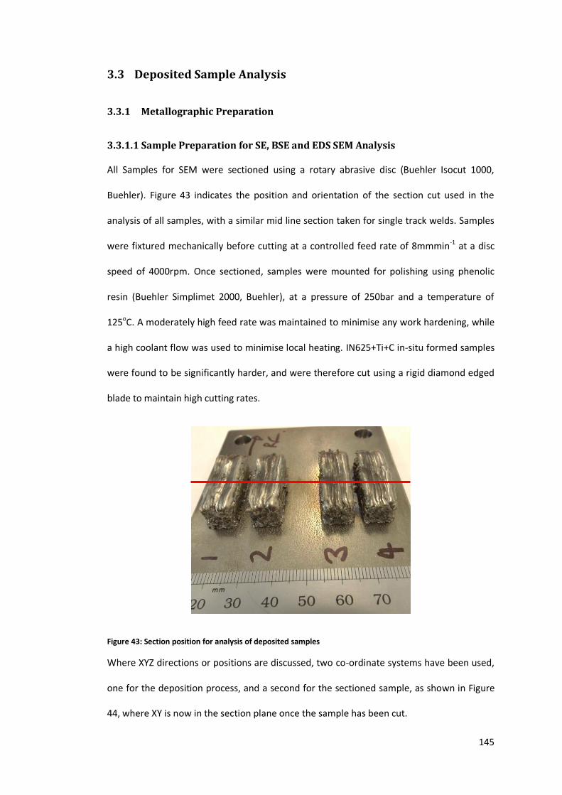
145
3.3 Deposited Sample Analysis
3.3.1 Metallographic Preparation
3.3.1.1 Sample Preparation for SE, BSE and EDS SEM Analysis
All Samples for SEM were sectioned using a rotary abrasive disc (Buehler Isocut 1000,
Buehler). Figure 43 indicates the position and orientation of the section cut used in the
analysis of all samples, with a similar mid line section taken for single track welds. Samples
were fixtured mechanically before cutting at a controlled feed rate of 8mmmin-1 at a disc
speed of 4000rpm. Once sectioned, samples were mounted for polishing using phenolic
resin (Buehler Simplimet 2000, Buehler), at a pressure of 250bar and a temperature of
125oC. A moderately high feed rate was maintained to minimise any work hardening, while
a high coolant flow was used to minimise local heating. IN625+Ti+C in-situ formed samples
were found to be significantly harder, and were therefore cut using a rigid diamond edged
blade to maintain high cutting rates.
Figure 43: Section position for analysis of deposited samples
Where XYZ directions or positions are discussed, two co-ordinate systems have been used,
one for the deposition process, and a second for the sectioned sample, as shown in Figure
44, where XY is now in the section plane once the sample has been cut.

146
Figure 44: Reference frames for deposited samples and micrograph sections.
Mounted samples were ground and polished before analysis, according to recommended
procedures given below in Table 15.
Table 15 : Sample polishing procedure
Step Media Fluid Rotation Force Duration
Grinding 320 grit wet & dry
Water 250rpm
Complimentary 26N Until Plane
Grinding Beuhler Hercules S rigid grinding
disc
9µm diamond suspension
150rpm Complimentary
26N 5:00
Polishing Beuhler Ultrapol
3µm diamond suspension
150rpm Complimentary
26N 3:00
Polishing Buehler Ultrapol
0.05µm colloidal silica
150rpm Contra-rotating
26N 2:00

147
Samples were inspected under an optical microscope between each step in the procedure,
with additional time given to steps as necessary to remove all scratches at that size. An
ultrasonic bath was utilised between each stage to prevent contamination and ensure
cleanliness.
Once polished, samples were immersed in the ultrasonic bath for 15 minutes and then
cleaned with Acetone and dried prior to being placed into a de-humidified cabinet.
3.3.1.2 Gold Sputtering
The examination of samples by SEM relies upon sufficient conduction of electrons from the
sample surface to ground. In the case of non-conductive samples such as ceramics, this can
be achieved by sputtering a layer of carbon or gold onto the surface, in order to provide a
conductive pathway.
While initial observations of MMC samples were performed without sputtering, it was
found that the surface became locally charged, presenting difficulties in focussing at high
magnifications, and creating a degree of “beam wandering”. Beam wandering occurs when
a charged area of the sample deflects the imaging beam slightly, this is particularly
noticeable when conducting multiple pass EDS scans, as the beam does not return to the
intended position on subsequent passes, creating a blurred image. Samples were therefore
gold sputter coated to prevent this, gold was selected in preference to carbon as some of
the samples of interest contained carbide particles, therefore it is easier to distinguish the
spectra of the coating and the material of interest.
A commercial sputtering machine was utilised (Agar Auto Sputter Coater 103A, Agar
Scientific) with a maximum of 3x 25mm diameter samples processed at any one time. The
sample surface was kept between 20mm and 30mm from the gold sputtering target.
Sputtering was conducted for a duration of 40 seconds, utilising Argon atmosphere and a
sputtering current of 20mA.
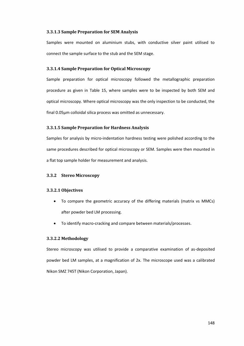
148
3.3.1.3 Sample Preparation for SEM Analysis
Samples were mounted on aluminium stubs, with conductive silver paint utilised to
connect the sample surface to the stub and the SEM stage.
3.3.1.4 Sample Preparation for Optical Microscopy
Sample preparation for optical microscopy followed the metallographic preparation
procedure as given in Table 15, where samples were to be inspected by both SEM and
optical microscopy. Where optical microscopy was the only inspection to be conducted, the
final 0.05µm colloidal silica process was omitted as unnecessary.
3.3.1.5 Sample Preparation for Hardness Analysis
Samples for analysis by micro-indentation hardness testing were polished according to the
same procedures described for optical microscopy or SEM. Samples were then mounted in
a flat top sample holder for measurement and analysis.
3.3.2 Stereo Microscopy
3.3.2.1 Objectives
To compare the geometric accuracy of the differing materials (matrix vs MMCs)
after powder bed LM processing.
To identify macro-cracking and compare between materials/processes.
3.3.2.2 Methodology
Stereo microscopy was utilised to provide a comparative examination of as-deposited
powder bed LM samples, at a magnification of 2x. The microscope used was a calibrated
Nikon SMZ 745T (Nikon Corporation, Japan).

149
3.3.3 Optical Microscopy
3.3.3.1 Objectives
To examine sample sectional geometry and accuracy (sidewall/top surface
straightness/roughness).
To measure areal porosity and determine variations due to Z height, material or
processing route.
3.3.3.2 Methodology
Optical microscopy has been conducted as part of many of the experiments within this
study. All samples examined were prepared according to the metallographic sectioning and
polishing procedures laid out in Table 15.
The microscope used was a Leica DM400M (Leica Microsystems, Germany), with samples
imaged using Buehler Omnimet v9.0 (Buehler, USA) image acquisition software at a
magnification of 2.5x. The Omnimet software being able to provide calibrated
measurement of features and generate image montages to provide a greater appreciation
of the entire sample. The microscope was periodically calibrated at all magnifications
throughout the duration of this study.
Porosity measurement was made at a magnification of 10x, at six positions on each cross
section; twice within the top third, twice in the central section and twice in the bottom
third, just above any cracking or dilution with the substrate. Contrast thresholding was
used to distinguish material from voids in the optical micrograph captured, with data
gathered on the number of individual voids and their areas. Contrast thresholding analysis
selects regions of an image based upon their contrast values compared to the rest of the
image. For a micrograph where solid material appears “bright” whereas porosity and
defects appear dark, a threshold may be set such that the image analysis software will
select only the darker areas which may be judged to be defects of some kind (both

150
porosity, inclusions and optical artefacts may therefore be included). The proportion of the
image which has been selected, based upon the thresholds set, may then be reported as a
proportion of the overall image and an areal porosity measurement obtained. For this
investigation a threshold was selected and maintained for all samples, unless significant
polishing defects or a non-flat sample was noted, in which case the threshold values were
adjusted to give a realistic representation of the material defects visible.
3.3.4 Hardness Analysis
3.3.4.1 Objectives
To identify any potential changes in the mechanical properties of the deposited
material due to reinforcement addition to matrix materials when processed by
powder bed LM.
To measure the extent of variation in material properties due to processing
technique (powder bed LM vs PTAW).
3.3.4.2 Methodology
Micro-Indentation Hardness measurement is an accepted method for determining the
hardness of materials using a micro sized indenter, with measurements made by optical
microscopy. For this study indents were performed using a Buehler Micromet 5101 micro-
indentation hardness tester (Buehler, USA) with Vickers indenter at a load of 500g for 10s.
Measurement of the indent, and calculation of the Vickers hardness was made using
Buehler Omnimet MHT software (Buehler, USA)
Hardness testing in order to evaluate a material’s strength is an established methodology,
being more expedient than manufacture and testing of tensile specimens [337-339]. Of
course it must be remembered that hardness is only an indication of relative properties.

151
Fully automatic indentation hardness testing was also conducted using a Wilson Hardness
Tukon 1102 micro-indentation hardness tester (Wilson Hardness, USA) with Buehler WIN-
Control v2.98.6 software (Buehler, USA). Image recognition capability within the software
enabled fully automatic hardness testing, such that significantly higher numbers of indents
were realistically possible. To obtain an appreciation of the variation in material properties
within a sample, a matrix pattern of indents was used, with a regular 0.25mm spacing,
adhering to the appropriate standards with regards to minimum indent spacing [282], as
can be seen in Figure 45 each indent is effectively made in isolation with no interaction
between adjacent indents. In order therefore to examine the hardness distribution within a
complete sample cross-section, over 2500 indents were made, with a manual check of the
reported values made and a variety of the reported measurements re-examined manually
to ensure accuracy. Indents were made using 300gf for a duration of 10s.
Figure 45: Example of indentations made and spacing
Various proprietary image recognition and auto-focussing algorithms were utilised, and an
optimised combination of edge/corner identification methods was selected based upon
trials with the appropriate samples. However the need to manually check values meant a

152
practical limit of a 5mmx5mm sample area was used for comparing hardness distribution
measurements between multiple samples.
3.3.5 SEM Imaging
3.3.5.1 SE/BSE SEM Imaging
3.3.5.1.1 Objectives
To examine the microstructure formed during processing of both LM and PTAW
samples of IN625 and MMCs in context with EDS measurement to identify
composition.
To make a qualitative assessment of reinforcement distribution, homogeneity and
form.
3.3.5.1.2 Methodology
Scanning Electron Microscopy (SEM) utilises an electron beam to probe the surface of a
sample, providing both topographical and compositional imaging. This permits an
evaluation of the materials microstructure to be made for the purposes of comparing
processing parameters or the differing characteristics of materials. Although optical
microscopy typically requires a simpler and easier sample preparation in order to obtain
similar microstructural information, in the case of highly corrosion resistant superalloys
highly aggressive etchants are required to obtain a suitable image. As samples were to be
prepared for SEM in order to obtain EDS information anyway, the microstructural
information required was also gathered using SEM at the same time, enabling it to be
assessed in context with the compositional information.
The SEM utilised for this investigation was a Carl Zeiss Sigma microscope column, utilising
the Field Emission Gun – SEM principle. Although the exact working distance of each
sample may differ slightly, all images were taken at a beam voltage of 20-25kV, with

153
aperture sizes of either 30µm or 60µm at a working distance of approximately 6-8mm. The
parameters were selected on a sample by sample basis to provide sufficient count rates for
reliable EDS measurement, or to reduce any charging effect if present.
Figure 46: SEM sample in chamber at loading position
Samples were imaged using both Secondary Electron detection (for topographical contrast)
and Back Scattered Electron detection (for atomic number contrast) [340]. After polishing a
slight relief between phases may be apparent in the secondary electron image, while the
difference in phase composition is readily seen in the back scattered electron image. A
difference in the average atomic number of an area imaged results in a difference in back
scattered electron intensity (η), if different portions of the inspected area have a differing
composition, then this may be represented as a difference in contrast according to
Equation 5.
𝐶 =(𝜂1 − 𝜂2)
𝜂2
Equation 5 : Back scattered electron contrast C calculated from backscatter intensity coefficients of two phases η1 and η2 [340]
30mm

154
3.3.5.2 EDS Analysis
3.3.5.2.1 Objectives
To quantify the degree of substrate dilution with deposited material.
To quantify compositional homogeneity of deposited material & relate to
feedstock/specifications.
To aid in identifying phases formed during MMC processing.
3.3.5.2.2 Methodology
Energy Dispersive X-Ray Spectroscopy (EDS) is an analytical technique often coupled with
SEM. EDS is able to identify the elemental composition of a sample, based upon the X-ray
spectra emitted when a volume is probed by the electron beam. Probing the sample with
the electron beam of the microscope excites the electrons of an atom, such that an
electron is ejected from its inner energy shell. When an electron drops back to fill this hole
from a higher energy shell, a characteristic X-ray is emitted, which can be used to identify
the element being probed.
When coupled with SEM imagery, this technique is particularly useful for examining the
distribution of elements within an area of a sample, as well as their relative proportions
from either specific points or areas.
For this investigation, an Oxford Instruments XMaxN Silicon Drift Dectector EDS system
(Oxford Instruments, UK) was utilised, having a 50mm2 detector area, with Aztec v2.0
software analysis suite providing data processing. Where samples were gold sputtered, this
was noted in the software and the peaks devolved from the spectra obtained.
It is worth noting that the detection of light elements can be exceptionally difficult by
conventional EDS systems. Theoretically all elements from atomic number 4(Be) up to
92(U) can be detected by EDS, however most general purpose EDS detectors have a lower

155
limit of atomic number 10, ruling out the accurate detection of carbon, nitrogen or oxygen.
The XMaxN detector is potentially capable of light element detection. However the
measurement of carbon remains an issue due to background and sample contamination,
therefore no accurate measurement could be obtained and was not considered accurate.
For the examination of small features by EDS, particularly in the case of 1µm sized particles,
it is important to consider that SEM is not a purely 2D technique, and that the beam will
have a 3D interaction volume within the material, whereby X-rays are emitted from atoms
down to a certain depth within the material, dependent upon beam parameters and the
materials composition. The depth, diameter and shape of this interaction volume is a
unique function of beam parameters and sample composition and may be controlled by
the beam voltage and aperture sizes.
Therefore any measurement of small ~1µm particles will not be precise, but will be able to
give an indication of relative compositions if this interaction volume effect is considered
when interpreting results. Increasing the accelerating voltage of the electron beam will
serve to increase the depth and diameter of the interaction volume, whilst the same beam
incident on a material of higher atomic number will have a smaller interaction volume than
that of a lighter element. For the analysis of bulk composition over an area, the interaction
volume does not influence the interpretation of results.
3.3.5.3 EBSD Analysis
Electron Backscatter Diffraction analysis (EBSD) is able to identify crystallographic
orientation at points in a sample, as well as identifying different phases of a material. EBSD
analysis is performed when coupled to an SEM, with a highly polished sample oriented at
~70o to the incident electron beam. A phosphor screen (at 90o to the beam) is then able to
detect Electron Backscatter Diffraction Patterns (EBSPs). EBSPs are formed by electrons
which leave the sample and are diffracted in a particular pattern according to the atomic

156
lattice planes present in the sample. These diffracted patterns hit the phosphor screen,
which fluoresces, the images from which are captured by a camera on the other side. Also
known as Kikuchi bands, this pattern can then be indexed to identify the phase and
crystallographic information, such as lattice parameters. By gathering EBSPs from a sample
area, a map of crystal orientations and phases can be compiled, though scanning times for
a high resolution image can be high (>100hrs).
Sample preparation for EBSD follows a similar regime to that used for SEM, however a final
stage of vibratory polishing is included. This removes any surface deformation of the crystal
structure caused by previous mechanical polishing stages, enabling detection of Kikuchi
bands. Vibratory polishing was conducted using a Buehler Chemomet cloth, with 0.05µm
colloidal silica polishing media on a Buehler Vibromet 1000 (Buehler USA). Given the high
hardness of Inconel 625, the best results and polishing rates were found with additional
weight of 100g added to the sample holders, with a polishing time of 4hrs.
3.3.6 Compositional Analysis
3.3.6.1 X-Ray Diffraction
3.3.6.1.1 Objectives
To compare feedstock material phases with those formed in deposited material.
To identify which phases are formed in MMC processing.
3.3.6.1.2 Methodology
X-Ray diffraction was also utilised in determining the phases present in deposited material,
for comparison with the original feedstock powders. Deposited samples were sectioned by
abrasive saw to provide a flat surface, cleaned and placed into a sample holder such that
the sample surface was flat and parallel with the holder surface. As with the powder

157
analysis, scans were made from 5o to 100o 2θ, using 0.01o steps on the same Panalytical
Empyrean equipment and Highscore software.
3.3.7 Micro Computed Tomography
3.3.7.1 Objectives
To provide a qualitative assessment of the distribution and nature of porosity in
both powder bed LM and PTAW deposited materials (including MMCs).
To provide a quantitative analysis of bulk material defects, material relative density
and the size distribution of defects.
3.3.7.2 Methodology
CT scanning is a method of non-destructive 3D imaging, developed initially as a diagnostic
tool for medicine [341] but subsequently refined and applied successfully to a host of other
fields [342]. The underlying principle is that an object is imaged from many different
directions using penetrating radiation (typically X-rays), a computer is then employed to
reconstruct the internal 3D structure of the object from the intensity values in the
projected images. This is achieved by rotating the object through 360° about a fixed axis,
such that the X-rays are able to penetrate it from all directions. Object reconstruction is
achieved using filtered back-projection [343].
Samples were scanned using an XT H 320 LC X-ray system (X-Tek Systems Ltd, UK; now
owned by Nikon Metrology, UK) which utilises a cone beam configuration. Ideally, the
reconstructed model should have the best possible resolution – i.e. the volume element
(voxel) size in the reconstructed volume should be as small as possible to allow
differentiation of physical features on the smallest possible length scale. This is achieved by
exploiting geometric magnification of the projection images, made possible by the
divergence of the conical X-ray beam.

158
Samples were scanned with 160kV X-ray energy, 2.9W beam power, 2s exposure per
projection and a ×22 geometric magnification factor with 30dB detector gain. A 0.125mm
tin filter was used in order to remove lower energy X-rays from the beam; this serves to
lower the background intensity below saturation and reduces beam hardening artefacts in
the reconstructed volume. The combination of settings and sample projections (between
2189 and 2612 projections per sample depending on geometry) yielded a reconstructed
voxel size of 9.09μm, with an approximate geometric un-sharpness of 9.16µm (<1%). The
smallest resolvable object is typically regarded to be 8 voxels in size (although this can be
arranged either as a cube or long rod shaped aspect ratio).
Samples were positioned in the scanner vertically with their central axis coincident with the
axis of rotation. This facilitates the greatest possible magnification, but results in sub-
optimal X-ray conditions [344].
Data was reconstructed by Dr. John Thornby, WMG using CTPro (Nikon Metrology, UK),
yielding a 3-dimensional voxelised representation in which the grey value of each volume
element represents the X-ray attenuation characteristics of material within that volume. A
grey level thresholding process identifies the presence of voxels containing material, from
those which do not (voids), data can then be visualised as a model in 3D (or in any one of
three orthogonal 2D cross-section views) within Volume Graphics Studio Max 2.2 (Volume
Graphics GmbH, Germany). This software facilitates dimensional measurement and visual
inspection of features within the volume. Virtual tools are also available to perform a more
precise defect characterisation, in the form of crack detection and porosity analysis.
For each sample, a Region of Interest (ROI) was identified, as the exterior surfaces, which
was then eroded by 18 voxels to remove surface deviations and noise from the
measurement volume. The input data was smoothed using a 3 voxel median filter, which
set the grey values of each 3x3x3 cube of adjacent voxels to their median value. While this

159
filtering does reduce the volume of measured defects slightly compared to their absolute
size, it is a requirement of the analysis process in order that defect detection can be
conducted, thus reported values will be an under-estimation. Defect analysis was
performed using the v2.1 Enhanced algorithm within Volume Graphics, and considered
defects larger than 15 voxels in size in order to remove the majority of falsely identified
noise defects.
3.3.8 Tensile testing
3.3.8.1 Objectives
To determine the mechanical properties of PTAW deposited IN625 from room
temperature, up to and beyond expected service temperatures.
To provide an assessment of the material properties variability between differing
positions within built material and between differing builds.
3.3.8.2 Methodology
To begin to characterise and understand a materials properties with a view to practical use
in engineering applications, three important values should be obtained.
Yield strength: the stress at which a materials deformation changes from elastic to
plastic.
Ultimate Tensile Strength: the stress at which the material fractures.
Stiffness or Young’s Modulus: the ratio of stress applied to deformation produced
in a material (as expressed in Equation 6).
𝑌 =𝑠𝑡𝑟𝑒𝑠𝑠
𝑠𝑡𝑟𝑎𝑖𝑛=
𝐹 𝐴⁄
∆𝑙 𝑙𝑜⁄
Equation 6: Young’s Modulus

160
The data for these properties can be obtained by means of tensile testing, whereby an
instrumented sample of known geometry is placed in tension, at a controlled rate, while
force and extension are measured to provide a stress vs. strain plot.
In order to conduct a tensile test, equipment constructed to meet the relevant standards is
usually used, while room temperature testing frames are relatively common place,
elevated temperature testing equipment is less readily available. Two pieces of equipment
were used in this work, a standard Instron test frame capable of oven heating a sample
from room temperature to 200oC, and a hydraulically driven machine known as a Gleeble
capable of quickly heating samples by electrical resistance to over 1000oC.
3.3.8.2.1 Specimen Geometry & Manufacture
The geometry of specimens and test procedures for tensile testing can be defined from
international standards. BS EN ISO 6892 parts 1 and 2 provide guidelines for the tensile
testing of metallic materials (part 1) and tensile testing at high temperature (part 2). While
no specific geometry and gripping method is stipulated, ASTM E21/09 suggests that pin &
clevis type grips provide good axial alignment for high temperature testing. As two differing
tests were to be conducted on different equipment to characterise the materials properties
over a wide temperature range, it was necessary to utilise a sample geometry which was
suitable for both pieces of equipment.
All samples were machined to within ±0.1mm of the dimensions shown in Figure 47, the
geometry used was recommended based upon the experience of existing users of the
Gleeble system at Swansea University, with initial tests conducted to confirm its suitability
in this material (further discussion on the sample geometry requirements for Gleeble based
tensile testing in Section 3.3.8.2.3)
To achieve sufficient geometric accuracy and surface finish, samples were machined to the
required profile by conventional CNC processes, and the top of the deposit milled flat and

161
parallel with the substrate. Conventional solid carbide tooling was utilised, with a wear
resistant and thermally conductive coating, a new tool was utilised for the finishing cut to
ensure geometric accuracy and a high quality surface finish with the minimum possible
work hardening. A feed speed of 150mm/min was utilised, at a spindle speed of 450rpm, to
provide a cutting speed of 14m/min.
Figure 47: Tensile sample geometry for Gleeble & Instron testing (1mm thick)
Figure 48: PTA IN625 deposited "billet" (top) machined profile (bottom)
25mm
25mm

162
Wire - Electrical Discharge Machining (W-EDM) was utilised to slice samples from the
profiled deposit at approximately 1mm thicknesses, with the exact dimensions confirmed
by measurement with a handheld micrometer before testing (Mitutoyo, etc) (±0.01mm).
The material batch and position within the deposited material was recorded for each
sample as they were cut. Figure 49 shows the samples from one PTAW build (labelled in
this case as B3), with each sample labelled according to its removal from the billet, with #1
at the top surface and #16 the last sample cut close to the substrate. If any visually
detectable defects, such as those highlighted in Figure 49 were observed in the
manufactured samples, they were utilised for setup/trial runs rather than forming part of
the final dataset. As can be seen in Figure 49, such defects occurred only in the top
sample(s) from the deposited pre-form as a result of the shape of the top surface, not any
internal defects. Sample 1 from each batch was therefore typically discarded as being
outside of the bulk material.
The use of W-EDM to manufacture tensile test samples from MMC materials has been
previously reported by Zheng et al., [173], who then polished the surface of the samples to
remove any surface defects. In order to minimise the effect of the EDM re-cast layer the
surface of each sample was therefore lightly abraded with 600 grit silicon carbide paper
before measurement and testing.

163
Figure 49: W-EDM cut tensile samples, labelled according to build number and position within the build.
3.3.8.2.2 High Temperature Testing – Ambient Heating(Instron)
While ISO 6892:1 describes procedures for room temperature tensile testing (< 35 oC), part
2 of the standard expands upon this, giving guidelines for testing at elevated temperature,
with which the 5800R tensile testing frame and 2525 Series 100kN load cell (Instron, USA)
utilised complied.
ASTM E21-09 indicates that any measurement of yield strength obtained using cross-head
displacement alone is of “inferior accuracy”, with significant compliance in the
measurement column and cross head at temperature producing a significant measurement
error. Therefore the use of accurate extensometry is highly desirable, though conventional
mechanical extensometers are difficult to apply within high temperature radiant furnaces
not already equipped for the purpose.
Testing may be conducted at constant cross-head velocity or at constant strain rate. Testing
at constant strain rate is preferred for accuracy, providing feedback from extensometry is
available during the test.

164
Practically however, high temperature extensometry was not available to use for this
experimentation, with cross head position being relied upon and tests conducted at a
constant 2mm/min cross head velocity. To reduce the inaccuracies associated with this test
method, sample geometry was designed such that the maximum load was small (~10%)
compared to the maximum rating of the test frame, jaws/load path and load cell, in order
to minimise any systematic compliance. Ambient heating was also therefore only utilised
up to 200oC such that machine compliance was not significantly increased by any decrease
in the frames materials properties at temperature. To avoid sample buckling due to
thermal expansion, samples were allowed to reach a steady thermal condition in the test
chamber prior to installation in the grips.
Although testing was conducted at a load of approximately 10kN, being comparatively
“low” load for the capability of the frame and load cell employed, the sensitivity and
accuracy of the load cell is still sufficient to measure the forces involved. Having a ±0.25%
linearity and repeatability of measurement over 0.4-100% of the load cell rating (so in this
case >400N)[345].
Room temperature testing was conducted using a standard clip on extensometer (Instron,
USA), although to maintain parity with higher temperature testing, a 2mm/min cross head
velocity was still utilised.
Each test was described according to its failure mode, A, B or C, dependent upon the
initiation point of the failure shown schematically in Figure 50. An A failure is one which
occurs in the central portion of the gauge length, a B failure initiates in the gauge length
but propagates outside of the gauge length, whereas a C failure initiates and propagates
outside of the gauge length. Where a C failure occurs, this indicates a need to repeat the
test, while a B failure is notionally acceptable (as failure has occurred in the reduced gauge

165
length section), it should be repeated if possible. Where necessary, tests were repeated
such that a minimum of 3 A-B class failures were obtained for each test temperature.
Figure 50: Schematic of failure mode categorisation
Ambient heating tensile tests were conducted at Room Temperature (21oC), 100oC and
200oC, (±2%) as measured by a thermocouple attached to the samples surface, in the
configuration shown in Figure 51. Three room temperature tests were also conducted using
samples which had been annealed at 870oC for 1hr and slowly cooled.
Figure 51: Tensile testing configuration on Instron 5800R frame with ambient heating oven and control thermocouple in place
250mm

166
3.3.8.2.3 High Temperature Testing – Resistance Heating (Gleeble)
To achieve high temperature tensile testing beyond 200oC, a Gleeble 3500 Thermo-
mechanical simulator was utilised. The Gleeble heats the specimen by passing a current
through it and utilising the specimens’ electrical resistance to generate heat within the
material. The temperature of the sample is controlled by feedback from a thermocouple
spot welded to the surface of the specimen at its centre point.
The significant advantage in using resistive specimen heating is in the speed with which
tests can be performed, with sample changeover significantly simplified compared to a
furnace heating arrangement. The relatively small heated zone also reduces extensometer
inaccuracy when using cross head displacement, as the samples gripped ends remain close
to room temperature as the machine jaws are actively cooled to 18oC.
The load capacity of the Gleeble system is given by the manufacturer’s specifications as
98kN, which is comparable to that of the Instron frame at 100kN. Samples were designed
such that the expected load at failure fell within a range from 5kN to 15kN depending upon
the test temperature. Importantly this load range is low enough so as not to cause
significant deflection of the cross-heads or machine frame, but high enough that the
measured load falls within the systems sensitivity. The Gleeble 3500 system used was
capable of a resolution of 0.01kN ±1% force measurement and 0.002mm ±0.5%
displacement measurement [346]. This high displacement accuracy was achieved by using
an “L-gauge” extensometer as shown in Figure 52 to measure displacement between the
cross-head jaws, rather than relying upon the displacement of the cross-heads measured
internally to the machine.
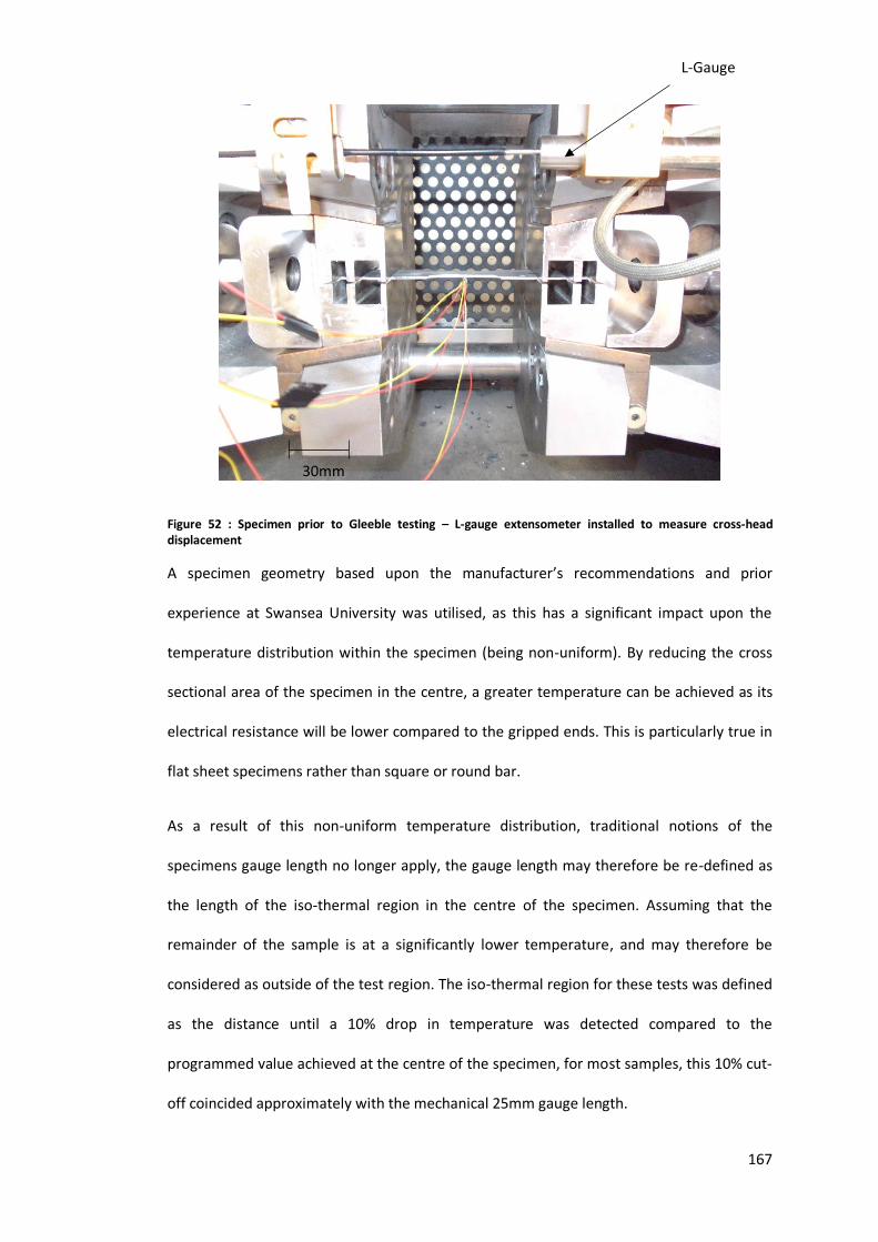
167
Figure 52 : Specimen prior to Gleeble testing – L-gauge extensometer installed to measure cross-head displacement
A specimen geometry based upon the manufacturer’s recommendations and prior
experience at Swansea University was utilised, as this has a significant impact upon the
temperature distribution within the specimen (being non-uniform). By reducing the cross
sectional area of the specimen in the centre, a greater temperature can be achieved as its
electrical resistance will be lower compared to the gripped ends. This is particularly true in
flat sheet specimens rather than square or round bar.
As a result of this non-uniform temperature distribution, traditional notions of the
specimens gauge length no longer apply, the gauge length may therefore be re-defined as
the length of the iso-thermal region in the centre of the specimen. Assuming that the
remainder of the sample is at a significantly lower temperature, and may therefore be
considered as outside of the test region. The iso-thermal region for these tests was defined
as the distance until a 10% drop in temperature was detected compared to the
programmed value achieved at the centre of the specimen, for most samples, this 10% cut-
off coincided approximately with the mechanical 25mm gauge length.
30mm
L-Gauge

168
The specimen geometry therefore serves two purposes, firstly to determine the specimen
gauge length mechanically, and secondly to determine the thermal gauge length. Ideally
therefore a specimen geometry which results in both the physical and thermal gauge
lengths coinciding is deemed to be ideal. Due to the effects of resistive heating, and the
constant thermal transfer out of the sample towards the machines water cooled grips,
there is a temperature difference between the surface of the specimen and its centre.
The work of Zhang et al., [116] provides a detailed examination of the temperature
distribution within a 10mm diameter steel bar specimen. At 1200oC a temperature
difference of 28oC (2.3%) was measured between the sample surface and core, while at
900oC the difference is only 5oC (0.55%) over a 5mm radius. For this reason a thin specimen
geometry was selected, such that the temperature decrease between core and surface
could be regarded as negligible. The work of Farup et al., [347] shows the variation in strain
rate through a cylindrical sample during tensile creep testing, again illustrating that at high
temperatures there is a significant difference in conditions and mechanical behaviour with
radial distance from the centre of a sample, this is small at less than 1mm, but increasingly
large beyond this.
Research into an optimum specimen design for the purposes of high temperature tensile
testing has been conducted by Norris and Wilson [348], who showed through both
numerical simulation and physical validation that a flat specimen with a high gauge length
to thickness ratio and small corner radii provides the closest temperature distribution to
the theoretical optimum (shown in Figure 53). Therefore the specimen design
recommended and utilised in this work followed these guidelines and confirmed the
thermal profile not only by the placement of thermocouples, but also through the use of IR
Thermography, which is able to make a continuous measurement of the thermal profile at
the samples surface. The equipment configuration for IR Thermography of samples under

169
test is shown in Figure 54, while the placement of additional thermocouples to corroborate
the thermograph recordings is shown in Figure 55.
Figure 53 : Optimised specimen design vs ideal profile for thermal gauge length [348]
Figure 54 : Gleeble test chamber with IR thermal camera to record thermal gauge length
The thermal gauge length of each individual tensile test was determined using Infra-Red
Thermography (FLIR T425, FLIR Systems Inc, USA), typical accuracy ±2oC or 2%. The
challenges of accurate IR Thermography are well known, with temperature measurement
150mm

170
based upon not only the emissivity of the materials surface (which varies with temperature
and surface texture), but also the distance from the specimen and the relative humidity of
the atmosphere through which the specimen is viewed. However the materials emissivity is
also dependent not only upon its temperature, but also its surface texture. As a result, the
emissivity of the specimen varies within the frame based upon temperature (with a
differential of several hundred degrees between the sample centre and gripped ends). The
emissivity also alters with time throughout the duration of the tensile test, as a variation in
surface texture occurs when the material is strained.
Figure 55: Thermal profiles measured by IR Thermography were corroborated by thermocouple measurement
It was therefore decided that the emissivity value be updated throughout the test, such
that the temperature recorded in the centre of the specimen was the same as that
recorded by the control thermocouple, to within an accuracy of 5%. It was found necessary
that the side of the specimen monitored by IR Thermography was not the same as that to
which the thermocouple was welded, as the spot welds were of a different emissivity and
so altered the temperature recorded.
30mm

171
The thermal gauge length could then be determined post-test based upon the temperature
profile recorded by IR Thermography. The temperature distribution was measured along
three lines placed down the specimens’ length, the average of which was then taken as the
distribution along the length, an example for a test at 1000oC is shown in Figure 56. The
temperature of the specimen does also vary across the width, however the actual
difference between the centre and edge of the specimen is on the order of 10oC to 20oC (a
variation of <2% from the target temperature) and so the average was deemed a sufficient
representation.
IR thermograph measurements were calibrated against the known gauge length to provide
a value of pixels/mm for each individual test to an accuracy of 2% (thus accounting for any
movement of the camera between tests). This procedure was conducted for every test
temperature, and every repeat at that temperature with thermal and mechanical gauge
lengths recorded for each test to ensure the best possible accuracy for calculation of yield
and ultimate strengths, as well as Young’s Modulus.
Specimens were installed in the wedge & pin jaws, and clamped with a pre-load force
exerted by two threaded spacers, which serve to clamp the wedge jaws around the sample.
A pre-load of approximately 50kg was utilised. Specimens were then heated at
10oC/second to the desired test temperature, during which a small traverse of the grips
was made to account for thermal expansion of the specimens and so avoid compressive
buckling. A dwell of one minute allowed the temperature within the specimen to stabilise
before test was commenced. A strain rate of 2mm/min was utilised, with extension
continuing until complete failure of the specimen. A minimum of five repeats was made for
each test temperature, at every 100oC from 200oC up to 900oC, (the maximum realistic
operating temperature for any IN625 component) with a minimum of three A-B class
failures at each temperature.

172
A one-off test was also conducted at 1000oC, and another at 1100oC to provide some data
for these extreme temperatures.
Figure 56: Measured thermal gauge length at 1000oC using IR Thermography

173
4 Experimental Results & Discussion
4.1 Raw Materials & Feedstock Preparation
4.1.1 Characterisation of powder materials
The following section details the results of an investigation into feedstock powder
characteristics, and their mixing behaviour in order to form MMC powder mixtures for use
in powder bed LM.
Statistics for the overall PSD from the LD measurements are given in Table 16, showing the
variations between the individual powders and mixed batches, these will be referred to in
the following section.
Table 16: Complete PSD data for all feedstock powders
Powder d10 (µm)
d25 (µm)
d50 (µm)
d75 (µm)
d90 (µm)
Mean (µm)
Error (µm)
IN625 54.1 60.29 68.57 78.38 89.07 70.58 ±8.4 TiC 2.12 3.85 9.24 50.45 68.57 25.72 ±15.9 IN625+TiC 22.37 32.02 40.46 52.12 102.8 49.88 ±18.8 Ti (Cp) 56.46 67.58 80.47 92.45 102.6 80.05 ±9.9 C (graphite) 7.98 17.07 37.38 69.29 112.4 49.91 ±25.0 Ti+C 6.65 11.13 19.55 42.03 85.38 33.67 ±20.2 IN625+Ti+C 4.06 7.82 50.06 68.54 87.19 45.65 ±23.3
4.1.1.1 IN625 feedstock powder:
The powder utilised as the IN625 matrix material was supplied by LPW technology (LPW
Technology Ltd, UK), having been produced by gas atomisation under inert nitrogen
atmosphere. Powder was supplied with a particle size specification of between 44-88µm,
as reported by the supplier based upon a sieving test.

174
4.1.1.1.1 Morphology – SEM- IN625
The SEM micrograph shown in Figure 57 shows spherical IN625 powder particles, as
expected from a gas atomised powder. However, one significant feature is apparent and
aids in explaining the PSD behaviour seen during powder mixing with TiC (Section 4.1.1.5).
A high proportion of the particles do not approximate an ideal sphere, with spatter-like
satellite particles or irregularities. These additions served to increase the average particle
sizes measured in the powders original state, but were easily knocked off/smoothed during
mixing, effectively reducing the observed powder size without significantly altering the
primary morphology.
Figure 57 : Back scattered electron image of IN625 feedstock powder
4.1.1.1.2 Particle Size Distribution – LD – IN625
An assessment of the PSD using LD was conducted, with results shown in Figure 58, and the
d90 value is 89µm, as shown in Table 16, confirming that the powders are supplied to
specification (an explanation of LD techniques and d90 is given in Section 3.2.1.2.1).
Notably the distribution extends significantly beyond 88µm with a small volume of particles

175
up to ~150µm; this was assessed to be an over-estimation due to the satellite irregularities
noted as part of the powders morphology.
Figure 58: PSD of IN625 feedstock powder
4.1.1.2 TiC feedstock powder
The Titanium Carbide (TiC) feedstock powder utilised was supplied by Pi Kem Ltd, UK,
having been produced by milling/grinding and supplied as having a range of 60-200µm,
with a more precise specification of d90<179.3µm, d50<115.7µm and d10<41.68µm.
4.1.1.2.1 Morphology – SEM- TiC
A qualitative examination of Figure 59 showed few larger particles in the region of 40µm,
while a higher magnification image shown in Figure 60 shows that the majority of particles
appear to be significantly smaller than 10µm, as confirmed by LD measurement of PSD.

176
A typical angular morphology as expected from a ground/milled ceramic powder was
observed. While particles do have an angular irregular shape, their overall aspect ratio does
not deviate significantly from 1:1, with no notable long or short axis evident.
Figure 59: Back scattered electron image of TiC powders - low magnification
Figure 60: Back scattered electron image of TiC powders – high magnification

177
4.1.1.2.2 Particle Size Distribution – LD- TiC
The PSD measurements shown in Figure 61 illustrate that unlike the tightly controlled gas
atomised powders, ceramics produced by milling/grinding processes have a wider multi-
modal size distribution unless smaller particulates are sieved out. Although, as seen in
Table 16, 90% of the powder by volume is under 68µm, there is a significant proportion
(50%) under 10µm. This differs significantly from the manufacturers quoted distribution
with measurements reporting a generally lower particle size than the supplied datasheets,
which may be due to segregation during transport or sampling.
Figure 61: PSD for TiC feedstock powder
4.1.1.3 Ti feedstock powder
The powder utilised as the Ti component for in-situ forming of TiC was commercially pure
Ti, supplied by LPW technology (LPW Technology Ltd, UK), having been produced by plasma
atomisation under inert atmosphere.

178
4.1.1.3.1 Morphology – SEM - Ti
Investigation of the powders morphology shown in Figure 62, shows the expected spherical
morphology for an atomised powder. The satellite type irregularities seen in the IN625
powder are present, however to a much smaller degree, and overall powder particles are
closer to an idealised sphere.
Figure 62: Back scattered electron image of commercially pure plasma atomised Ti powders
4.1.1.3.2 Particle Size Distribution – LD - Ti
Powder was supplied with a specification of 45-106µm, according to sieving tests
conducted by the supplier, 0.3% of the material was larger than 106µm, whilst 4.3% was
smaller than 45µm in diameter. This specification is largely is confirmed by the PSD shown
in Figure 63, and distribution statistics in Table 16.

179
Figure 63: PSD of TiCp feedstock powder
4.1.1.4 Graphite (C) feedstock powder
The powder utilised for the C component for the in-situ forming of TiC was commercially
available graphite, supplied by The Graphite Trading Company (Graphite Trading Company
Ltd, UK), having been synthetically produced at 99% purity, and sieved to <106µm.
4.1.1.4.1 Morphology – SEM - C
The SEM micrograph in Figure 64 shows the expected flake/platelet morphology for
graphite powders. However, in addition to these flakes are a significant proportion of
smaller particulates with a mixture of morphologies; from low aspect ratio fragments,
which are angular but essentially blocky/cubic, through to acicular high aspect ratio needle
like particles.

180
Figure 64: Back scattered electron image of graphite powders
4.1.1.4.2 Particle Size Distribution – LD - C
The PSD shown in Figure 65 is significantly skewed towards an over-estimate of the particle
sizes present, due to the flake morphology of graphite powder which is unsuited to
measurement by LD. However the d90 value given in Table 16 of 111µm shows that the
majority of powder is in the desired range.

181
Figure 65: PSD of graphite feedstock powder
4.1.1.5 IN625+TiC mixed powder
To produce an MMC powder mixture, TiC was added to IN625 at 5wt% (8 vol%), with
mixing/milling conducted using an alumina jar and steel media for up to 72hrs.
4.1.1.5.1 Morphology – SEM – IN625+TiC
An inspection of powders after only 1hrs mixing in Figure 66, shows an already well
distributed mixture. There are no notable TiC agglomerations, nor any significant alteration
in particle morphology.

182
Figure 66: Back scattered electron image of low energy ball milled Inconel 625 + TiC powders - 250x (1hr)
After a full 72hrs of mixing, powders are thoroughly distributed, additionally as shown in
Figure 67 the previously identified satellite particles have been removed from the IN625
primary particles bringing their morphology closer to an idealised sphere. There is still no
change in the primary morphology of either powder though. Some larger TiC particles are
present, and appear to be thoroughly coated in smaller TiC particulates, as can be seen in
Figure 68.
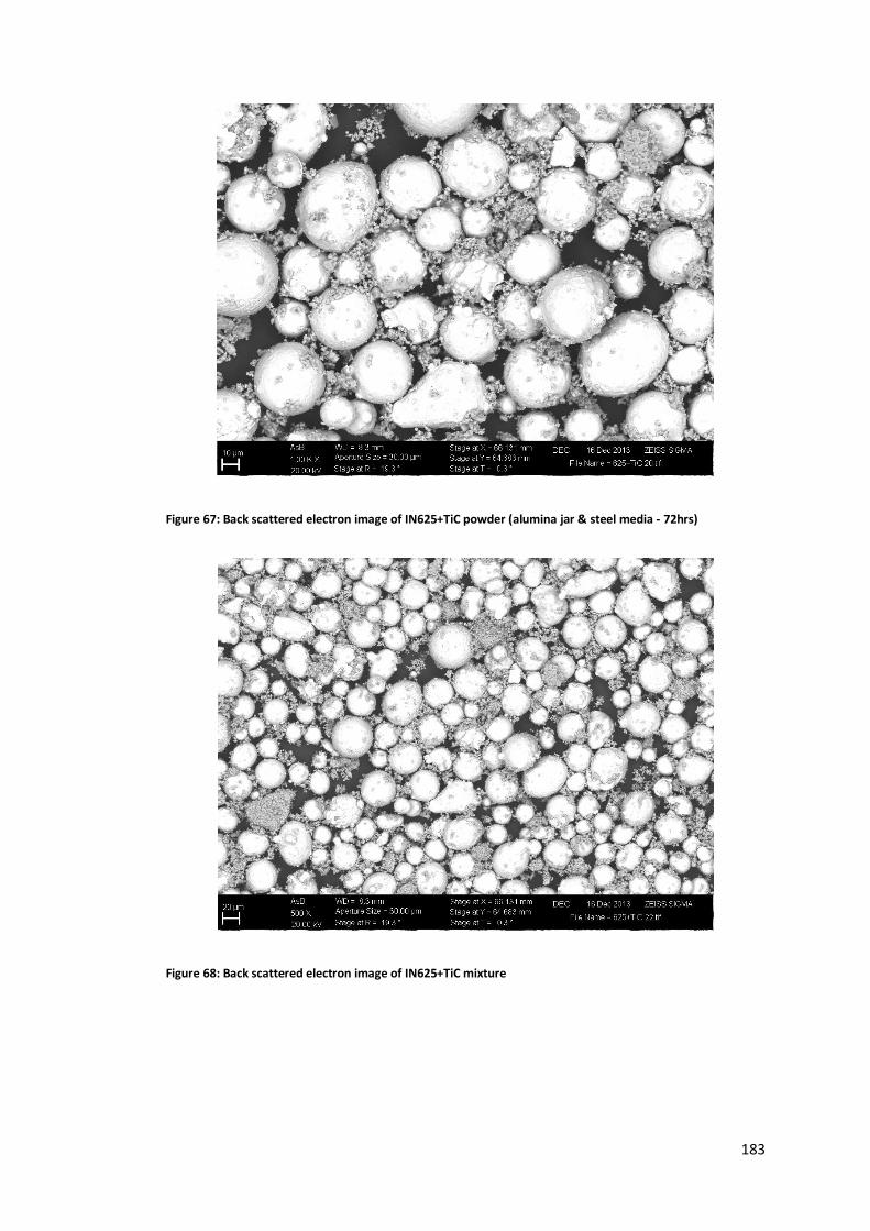
183
Figure 67: Back scattered electron image of IN625+TiC powder (alumina jar & steel media - 72hrs)
Figure 68: Back scattered electron image of IN625+TiC mixture

184
4.1.1.5.2 Particle Size Distribution – LD – IN625+TiC
After mixing, the PSD shown in Figure 69 was obtained. The large peak at 20-60µm
represents the majority of IN625 particles, with a smaller proportion of large TiC particles.
The size distribution of IN625 appears to have decreased from 40-88µm, based upon
evaluation of the powders morphology, it can be seen that this was likely an initial over-
estimate in the PSD measurement of the IN625 feedstock powder, due to spatter-like
satellites as described in 4.1.1.1. Mixing has altered the powders morphology slightly,
resulting in a more idealised spherical particle, and so a more accurate LD measurement.
The flat broad peak between 0.5-10µm comprises of free TiC particles, whose size has not
been significantly altered from the original feedstock. The larger particles observed at 70-
180µm are considered to be IN625 coated in TiC, or a combination of large TiC particles
with associated coatings of smaller TiC particles. This is confirmed by examination of the
powders by SEM to identify minor changes in morphology and the mixing behaviour.

185
Figure 69: PSD of IN625+TiC powder after 72hrs of mixing
4.1.1.5.3 Composition – EDS – IN625+TiC
The composition of several sample areas was measured by EDS, along with element
mapping to aid in phase identification and qualitative evaluations of homogeneity. Figure
70 shows that, as described above, there is a good distribution of unaffected IN625 and TiC
particles, with two secondary phases, larger IN625 particles coated in small TiC particulates
TiC
Unaffected IN625 + TiC
TiC coated IN625

186
and larger TiC particles with their own coating of smaller TiC. The element map shows an
even intensity of Ti across the sample area, indicating a well mixed and homogenous
feedstock material has been achieved. Compositional spectra for all sample areas have
been collected, and are presented in Table 17 in Section 4.1.1.8.2.
Figure 70: Back scattered electron image of IN625+TiC mixed powders and associated element map showing
Ti distribution
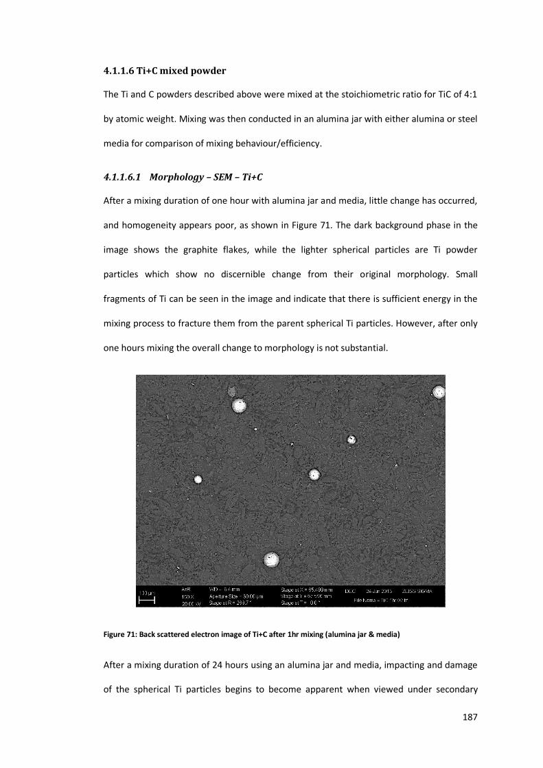
187
4.1.1.6 Ti+C mixed powder
The Ti and C powders described above were mixed at the stoichiometric ratio for TiC of 4:1
by atomic weight. Mixing was then conducted in an alumina jar with either alumina or steel
media for comparison of mixing behaviour/efficiency.
4.1.1.6.1 Morphology – SEM – Ti+C
After a mixing duration of one hour with alumina jar and media, little change has occurred,
and homogeneity appears poor, as shown in Figure 71. The dark background phase in the
image shows the graphite flakes, while the lighter spherical particles are Ti powder
particles which show no discernible change from their original morphology. Small
fragments of Ti can be seen in the image and indicate that there is sufficient energy in the
mixing process to fracture them from the parent spherical Ti particles. However, after only
one hours mixing the overall change to morphology is not substantial.
Figure 71: Back scattered electron image of Ti+C after 1hr mixing (alumina jar & media)
After a mixing duration of 24 hours using an alumina jar and media, impacting and damage
of the spherical Ti particles begins to become apparent when viewed under secondary

188
electron imaging (Figure 72), the large Ti particle shown in the image is no longer spherical
and abrasion damage can be seen on its surface. There is an improvement in the
distribution of small Ti fragments, however larger Ti particles are still the dominant form,
and distribution is still poor (Figure 73).
Figure 72: Secondary electron image of Ti+C after 24hrs mixing (alumina jar & media)
Figure 73: Back scattered electron image of Ti+C after 24hrs mixing (alumina jar & media)

189
After a mixing duration of 72 hours, Ti particles have a flattened disc or barrel/cylinder
morphology (Figure 74). The distribution of the larger particles has improved significantly
compared to samples at 24 hours and 48 hours mixing duration. The quantity of smaller Ti
fragments has also reached a more homogenous distribution and have increased in
quantity.
Mixing using steel media was attempted as the higher density of steel will result in higher
impact energies. After only 18 hours duration using an alumina jar and steel media the
platelet morphology has been achieved (Figure 75), whereas this was not apparent until
between 48 and 72 hours when mixing using an alumina jar & media.
After a full 72 hours of mixing with an alumina jar & steel media (Figure 76), an improved
distribution of both disc and cylinder shaped large particles and finer fragments can be
observed compared to the same duration of mixing using alumina media.
Figure 74: Back scattered electron image of Ti+C powders after 72hrs mixing (alumina jar & media)

190
Figure 75: High magnification back scattered electron image of Ti+C after 18hrs mixing (alumina jar & steel
media)
Figure 76: Back scattered electron image of Ti+C after 72hrs mixing (alumina jar & steel media)

191
4.1.1.6.2 Particle Size Distribution - LD – Ti+C
The PSD obtained after a full 72 hours mixing duration in an alumina jar with steel media is
shown in Figure 77, as this was found to be the most homogenous and well mixed powder
prepared, while further mixing for up to 120 hours duration showed no measurable change
in the distribution of the powder mixture or the particle morphology
The primary graphite peak has shifted from around 40µm to 10-20µm showing an overall
reduction in particle size. The Ti particles, previously distributed from 50-100µm have been
broken into two observed behaviours, one peak which is centred around 60µm, and
consists of fractured and size reduced Ti particles and/or a proportion of unaffected
particles. While a secondary smaller peak centred around 150µm exists, which may consist
of undamaged Ti particles combined with graphite and/or graphite agglomerations. The
majority of the contribution to this peak may also be a measurement over-estimation due
to unsuitable particle aspect ratios of new disc shaped Ti particles.
SEM/EDS investigation presented in Figure 80 also shows that there is a proportion of
much smaller <10µm Ti fragments which have been generated as a result of milling, which
will contribute to the large “graphite” peak and be included in overestimating that phase’s
proportion.

192
Figure 77: Ti + graphite powder mixture after 72hrs mixing
4.1.1.6.3 Composition – EDS – Ti+C
Milling time has a significant effect on the morphology and characteristics of the Ti+C
powders examined. As can be seen in Figure 78, after 4 hours mixing duration virtually no
alteration of particle morphology has occurred, and homogeneity of the mixture is poor,
with only a few Ti particles present in the sample.
Size reduced graphite
Size reduced Ti
Disc like Ti + graphite

193
Figure 78: Back scattered electron image and EDS Map of Ti+C after 4hrs milling (alumina jar & steel media)
After 72hrs mixing however the distribution of Ti in the powder sample has greatly
improved, while its morphology has changed to a disc or platelet type due to impact with
the milling media, as shown in Figure 79.
Figure 79: Back scattered electron image and associated EDS map of Ti+C after 72hrs milling (alumina jar &
steel media)
Additionally, higher magnification inspection (Figure 80) shows a distribution of finer
<10µm Ti fragments as a result of milling, which were not present in samples which had
undergone shorter milling times.

194
Figure 80: Back scattered electron image and associated EDS map of Ti+C after 72hrs milling
4.1.1.7 IN625+Ti+C mixed powder
The Ti+C powder mixture prepared in the preceding section was added to IN625 at 5wt%
(equivalent to 11vol%), and milled in an alumina jar for a duration of 72 hours with steel
media, given the higher mixing efficiency shown by this combination in mixing Ti+C.
4.1.1.7.1 Morphology – SEM – IN625+Ti+C
After 72 hours of mixing (shown in Figure 81), the IN625+Ti+C mixture appears to be well
mixed, although not to the degree seen in IN625+TiC mixing. It is difficult to discern if the
graphite rich regions of the sample are due to agglomeration or preferential pickup during
sampling of the lighter graphite particles. Ti platelets were present, and appeared to have a
more irregular shape than the disc morphology achieved after the 72 hours of preparatory
mixing. As no distinct change in morphology between 18 hours and 72 hours of mixing was
observed in blending Ti+C, this is therefore thought to be due to interaction with the
harder IN625 particles, rather than an effect of the cumulative 144 hours duration of
mixing. Figure 81 shows a well-mixed distribution of carbon (dark phase) with titanium
(disc like platelets) amongst spherical IN625 particles.

195
Figure 81 : Back scattered electron image of IN625+Ti+C after 72hrs mixing (alumina jar & steel media)
After 72 hours of mixing, there is no appreciable change in the morphology of IN625
particles, however graphite particles have reduced in size. While the majority of graphite is
freely distributed throughout the samples taken, a certain proportion have adhered to the
spherical IN625 and platelet type Ti particles, shown in Figure 82.
Figure 82: Back scattered electron image of IN625+Ti+C after 72hrs mixing (alumina jar & steel media)

196
4.1.1.7.2 Particle Size Distribution – LD – IN625+Ti+C
The PSD resulting from a full 72 hours mixing duration is shown in Figure 83. Compared to
the pre-mixing of Ti+C, the graphite size distribution is further reduced, with a slight
secondary peak at 20µm, but very few particles between 30-40µm, a larger proportion of
these smaller <15µm particulates are Ti fragments generated by the milling process. The
secondary 20µm peak might well be graphite, or a mixture of graphite and Ti particles
which have been further reduced in size after the initial Ti+C mixing. The IN625 particles
have not been particularly affected by mixing. A small peak between 100-200µm are
presumably intact IN625 with added graphite coatings/agglomerations. Also a proportion
may be new disc shaped Ti particles after milling impacts which register as larger particle
sizes depending upon orientation during LD.
The size distribution of the IN625 powder phase remains largely unaffected after 72 hours
of mixing. This may be due to the lubricating effect of the graphite present, which might
change the dynamics of powder/media interaction, or it may be that any size reduction
which has occurred has been compensated for by the cladding of IN625 particles in
graphite. It may also be the case that the IN625 particles are simply too hard/strong to be
affected by impact with the steel milling media, without the presence of harder TiC
particles which could have been acting as a grinding media, creating the size reduction seen
in IN625+TiC mixing/milling.

197
Figure 83: PSD for IN625 powder mixed with Ti + Graphite mixture (Alumina Jar & Steel Media after 72hrs)
4.1.1.7.3 Composition - EDS – IN625+Ti+C
The results of examination of the IN625+Ti+C powders by EDS are shown in Figure 84.
Distribution of the elements in the sample appears quite uniform, with no large
agglomerations of any one phase. An initial examination of the BSE image in Figure 84
would suggest a disproportionately high graphite content to the powder mixture. However,
the known difficulties of mixed powder sampling (as mentioned in Section 3.2.1.2.2) such
Size reduced
graphite + small Ti
fragments
Unaffected IN625
Graphite coated IN625 +
disc like Ti
Size reduced Ti + graphite

198
as a higher proportion of graphite present in the thief sample due to preferential pick up,
coupled with the inaccuracies of carbon measurement by EDS (particularly sampling using
adhesive carbon tabs) falsely indicate a high proportion of carbon when viewed under SEM
– the carbon content is therefore not shown in Figure 84.
Figure 84: Low magnification EDS maps of IN625+Ti+C after 72 hours mixing
4.1.1.7.4 Composition – XRD – IN625+Ti+C
To identify if any mechanical alloying or in-situ reactions during ball milling had occurred,
XRD scans were conducted on each of the virgin as-received feedstocks for comparison

199
with the mixed/milled powder, the spectra obtained are shown in Figure 85. The XRD
results collected indicate that the composition of the powder is close to the desired volume
ratios, as the peaks for Ti and C are of a small magnitude in comparison to those of IN625,
indicating a minor proportion of the sample volume was attributable to these phases. The
primary peaks for Ti and C can be identified however, whereas those for TiC cannot, which
would indicate that no reaction between the two has taken place to form TiC at this stage
of processing.
Had the Ti and C content formed TiC during mixing, identifiable peaks in the XRD spectra
would be expected at 42o, 48.8o, 72o, 86.0o and 91o but are not observed in the spectra
shown in Figure 85. An absence of the strong carbon peak at 30.8o would also be expected
had TiC been formed during mixing.

200
Figure 85: XRD spectra of IN625+Ti+C powder
5000
7000
9000
11000
13000
15000
17000
19000
21000
23000
25000
20 30 40 50 60 70 80 90 100
Co
un
ts
Position 2 Theta (Cobalt (Co))
IN625
Ti
C
IN625+Ti+C powder

201
4.1.1.8 Powder mixing discussion
4.1.1.8.1 PSD discussion
The relative volumes of each powder phase for mixed MMC feedstocks are presented in
Figure 86, and were calculated from LD measurements. For the powder mixtures including
graphite, the estimated volume proportions of each particulate phase are difficult to
quantify. As a result, they show significantly higher proportions of graphite than would be
expected. This is presumably due to the difficulty in obtaining an accurate measurement
because of their flake morphology with a high aspect ratio, which is unsuitable for
measurement by LD. The significant difference in density and surface area may also
influence the sampling behaviour during the measurement run, if for example the lighter
graphite particles with a greater surface area were to be circulated past the measurement
window more frequently than the heavier more streamlined IN625 or Ti particles.
The agreement between calculated and measured volume proportions of IN625 mixed with
TiC is however excellent. Although a slight over estimation of the IN625 proportion has
probably been made as some TiC adhered/impacted on the particles surfaces will have
been included in this proportion. Measurement accuracy is also superior to that of the
IN625+Ti+C powders, as all powder phases in this case have a suitable aspect ratio. Also
sample separation in the liquid flow is likely to be to a lesser degree, if at all, as the surface
area to density/weight ratio is closer for both particle phases.
The error in the measured values shown in Figure 86 has been calculated from the
differences between each of the three repeat powder measurement runs. As mentioned,
there is of course a further inaccuracy in the measurement of Ti+C phases beyond this
variance, due to the unsuitable particle morphology.

202
Figure 86: Volume fraction of matrix vs reinforcement powders measured by LD
Overall therefore it is possible to quantify the powders homogeneity and the degree of
mixing using LD for the IN625+TiC powder combination, with a high degree of confidence.
IN625+TiC powders can be categorised as well mixed, and having the desired relative
proportions of matrix and reinforcement powders.
However, the homogeneity and mixing of the IN625+Ti+C powder remains suspect due to
the significant measurement accuracy difficulties. While visual inspection and XRD
measurement would indicate acceptable mixing, the degree of measurement uncertainty
using LD for PSD measurement makes it difficult to draw any firm conclusions and suggests
a higher degree of inhomogeneity in the powder mixture.
4.1.1.8.2 Composition Discussion
Table 17 presents the composition of the powder mixtures discussed, along with that of
IN625 for comparison. With the exception of the Ti+C samples, the C content was not
measured due to a high background measurement (>25wt%), an innate problem of EDS
measurement when not equipped specifically for the measurement of light elements,
0
10
20
30
40
50
60
70
80
90
100
IN625+(TiC) IN625+(Ti+C)
Po
wd
er
volu
me
%
Matrix Predicted
Matrix Measured
Reinforcement Predicted
Reinforcement Measured

203
coupled with the use of carbon adhesive tabs which will provide an erroneous C
measurement.
Table 17 : Comparative EDS Quantification of elements present in powder samples
Powder Element wt% Deviation Error
Ni Cr Mo Nb Fe Ti Al C
IN625 61.9 22.2 8.4 3.5 3.9 0.0 0.1 -- 0.4 ±0.16 IN625+TiC (72hrs)
46.5 16.3 5.2 2.6 2.3 26 0.3 -- 0.3 ±0.12
Ti+C (4hrs) -- -- -- -- -- 0.8 -- 99.2 0.1 ±0.04 Ti+C (72hrs) -- -- -- -- 0.1 6.5 0 93.4 0.1 ±0.04 IN625+Ti+C 57.4 21.5 8.1 3.2 4.1 5.5 0.3 -- 0.2 ±0.08
Comparing the Ti content of the Ti+C samples mixed at 4hrs and 72hrs respectively, a
significant increase in the presence of Ti can be seen. As no Ti content has actually been
added to the powder mixture, this higher Ti measurement is considered to be a result of
improved homogeneity reflected in more representative powder sampling.
Figure 87 presents the composition of final mixed powders shown in Table 17 graphically,
having combined the individual element measurements of the matrix (IN625) phase, and
the reinforcement phase which is indicated using only the Ti wt% in this case.
By excluding the C measurement, it can be seen that the distribution of IN625 and Ti
particles for the in-situ feedstock powder is close to the desired proportions. The
measurement of Ti for the IN625+TiC powder is however still influenced by the preferential
sampling of the low density TiC powders, which therefore make up a disproportionately
large fraction of the sampling area measured.

204
Figure 87: Compositional variation between ideal and EDS measurements for IN625+TiC and IN625+Ti+C
The EDS results presented are inconclusive in the case of IN625+TiC, as preferential powder
sampling due to differing particle densities and contact areas with the adhesive tabs
provide a non-representative sample.
In the case of IN625+Ti+C, the IN625 and Ti particles have a similar morphology and so
contact angle with the adhesive, and are much closer in density, providing a more
representative sampling, with EDS indicating that at least the distribution of Ti within the
matrix can be regarded as homogenous and well mixed, as the expected relative
proportions of each phase have been identified, although no quantitative comment can be
made on graphite distribution or mixing.
The relative magnitude of the peaks shown by XRD measurement for each phase would
indicate that the relative proportions of IN625, Ti and graphite are closer to the desired
quantities than EDS appears to show.
0
10
20
30
40
50
60
70
80
90
100
IN625+TiC IN625+(Ti+C)
Co
mp
osi
tio
n (w
t%)
Matrix Predicted
Matrix Measured
Reinforcement Predicted
Reinforcement Measured

205
4.1.2 Characterisation of wire materials
The composition of IN625 welding filler wire was assessed by EDS after metallographic
preparation, the results of which are presented in Table 18. The composition measured by
EDS is also compared here with that of the IN625 powder utilised, as well as the max/min
specification ranges for IN625. Although limits are placed on other trace or contaminant
elements (e.g. Co, Ta, Si, Mn etc), they are not presented as no measurable quantity was
detected.
Table 18 : Composition of wire feedstock compared to specification and powder material
Material Element wt% Deviation Error
Ni Cr Mo Nb Fe Ti Al
IN625 (max specification)
68.85 23.0 10.0 4.15 5.0 0.4 0.4
IN625 (min specification)
58.0 20.0 8.0 3.15 0.0 0.0 0.0
IN625 Powder 61.9 22.2 8.4 3.5 3.9 0.0 0.1 0.4 ±0.16 IN625 Wire 64.0 22.0 9.0 3.5 0.4 0.2 0.1 0.4 ±0.16
The only significant difference between the two is a reduced quantity of Fe present in the
welding filler wire. This is typical of superalloy filler wires, as the lower melting point Fe can
cause liquation segregation/cracking problems during repair welding, particularly when
using IN625 as a filler for more complex less weldable alloys. Therefore the Fe content is
reduced as weldability not mechanical properties are most desirable.
This reduction in Fe results in a relative increase in the other alloying element proportions,
however both the IN625 wire and powder used are well within the compositional
specification for “Inconel 625”. This variation is shown in Figure 88, which presents the
difference in composition as calculated by subtracting the composition of IN625 powder
from that of IN625 wire, as discussed this shows that IN625 wire is comparatively richer in
Ni, due to its lower Fe content.
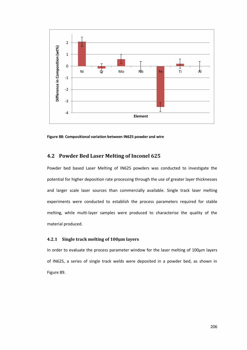
206
Figure 88: Compositional variation between IN625 powder and wire
4.2 Powder Bed Laser Melting of Inconel 625
Powder bed based Laser Melting of IN625 powders was conducted to investigate the
potential for higher deposition rate processing through the use of greater layer thicknesses
and larger scale laser sources than commercially available. Single track laser melting
experiments were conducted to establish the process parameters required for stable
melting, while multi-layer samples were produced to characterise the quality of the
material produced.
4.2.1 Single track melting of 100µm layers
In order to evaluate the process parameter window for the laser melting of 100µm layers
of IN625, a series of single track welds were deposited in a powder bed, as shown in
Figure 89.
-4
-3
-2
-1
0
1
2
Ni Cr Mo Nb Fe Ti Al
Dif
fere
nce
in C
om
po
siti
on
(wt%
)
Element
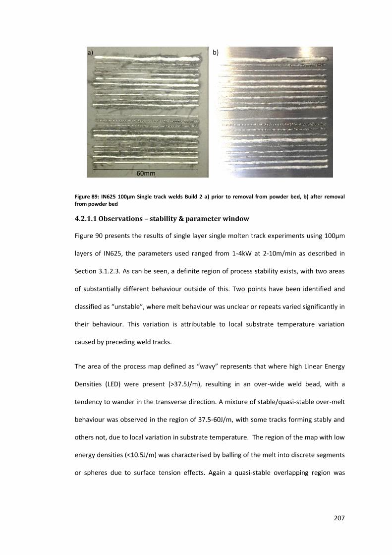
207
Figure 89: IN625 100µm Single track welds Build 2 a) prior to removal from powder bed, b) after removal from powder bed
4.2.1.1 Observations – stability & parameter window
Figure 90 presents the results of single layer single molten track experiments using 100µm
layers of IN625, the parameters used ranged from 1-4kW at 2-10m/min as described in
Section 3.1.2.3. As can be seen, a definite region of process stability exists, with two areas
of substantially different behaviour outside of this. Two points have been identified and
classified as “unstable”, where melt behaviour was unclear or repeats varied significantly in
their behaviour. This variation is attributable to local substrate temperature variation
caused by preceding weld tracks.
The area of the process map defined as “wavy” represents that where high Linear Energy
Densities (LED) were present (>37.5J/m), resulting in an over-wide weld bead, with a
tendency to wander in the transverse direction. A mixture of stable/quasi-stable over-melt
behaviour was observed in the region of 37.5-60J/m, with some tracks forming stably and
others not, due to local variation in substrate temperature. The region of the map with low
energy densities (<10.5J/m) was characterised by balling of the melt into discrete segments
or spheres due to surface tension effects. Again a quasi-stable overlapping region was
a) b)
60mm

208
observed between 7.5-10.5J/m. Consistent weld stability was achieved in the window of
15-30J/m.
Figure 90: Parameter window characterisation 100µm layers of IN625
The general trend shows a process stability window which may continue beyond the
parameters which were investigated, indicating that powder bed LM of IN625 at 100µm
layer thicknesses is not only stable for single welds at laser powers of up to 4kW, but may
still be stable at higher powers and weld speeds. The occurrence of balling at lower weld
powers and higher speeds indicates that higher laser powers will certainly be required if
faster weld speeds were to be investigated.
4.2.1.2 Weld bead geometry & variation
Figure 91 relates the average width of each weld to the programmed laser power and
speed used to produce it. The laser spot size of 850µm was subtracted from the measured
weld width to give a width delta describing over/under melt in relation to the actual laser
500
1000
1500
2000
2500
3000
3500
4000
4500
0 2000 4000 6000 8000 10000 12000
Pro
gram
me
d L
ase
r P
ow
er
(W)
Welding Speed (mm/min)
Stable Wavy Unstable Balling
Lin
ear
En
ergy
Den
sity
(J/
m)
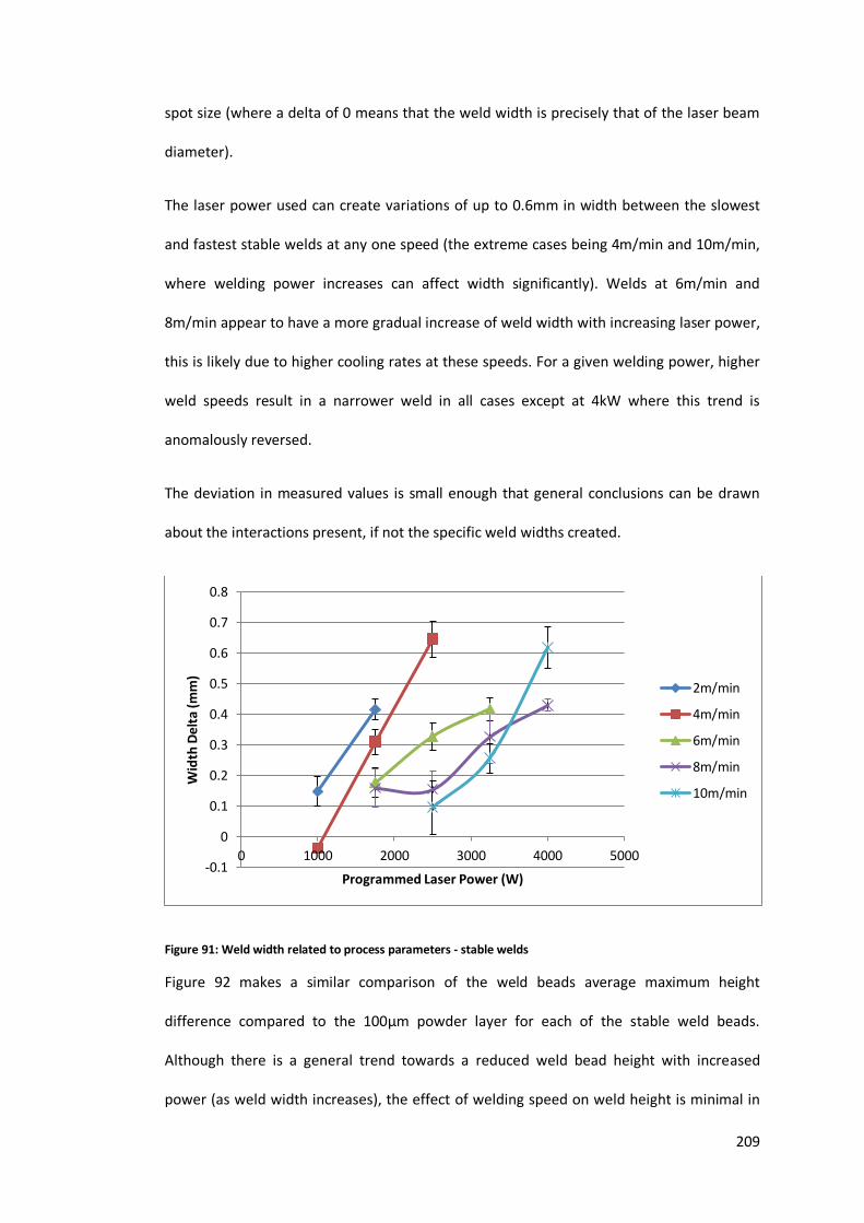
209
spot size (where a delta of 0 means that the weld width is precisely that of the laser beam
diameter).
The laser power used can create variations of up to 0.6mm in width between the slowest
and fastest stable welds at any one speed (the extreme cases being 4m/min and 10m/min,
where welding power increases can affect width significantly). Welds at 6m/min and
8m/min appear to have a more gradual increase of weld width with increasing laser power,
this is likely due to higher cooling rates at these speeds. For a given welding power, higher
weld speeds result in a narrower weld in all cases except at 4kW where this trend is
anomalously reversed.
The deviation in measured values is small enough that general conclusions can be drawn
about the interactions present, if not the specific weld widths created.
Figure 91: Weld width related to process parameters - stable welds
Figure 92 makes a similar comparison of the weld beads average maximum height
difference compared to the 100µm powder layer for each of the stable weld beads.
Although there is a general trend towards a reduced weld bead height with increased
power (as weld width increases), the effect of welding speed on weld height is minimal in
-0.1
0
0.1
0.2
0.3
0.4
0.5
0.6
0.7
0.8
0 1000 2000 3000 4000 5000
Wid
th D
elta
(m
m)
Programmed Laser Power (W)
2m/min
4m/min
6m/min
8m/min
10m/min

210
comparison. There is no particular trend with respect to welding speed. All weld bead
heights sit within the range of 200µm-350µm.
Figure 92: Weld height related to process parameters - stable welds
The degree of variance in the measured values is almost on the same order of magnitude
as the measurements themselves, reducing confidence that any significant conclusions can
be drawn from the data for weld height. However, it can be seen that all the measured
values are significantly in excess of the intended 100µm. This is due to the phenomena of
powder bed denudation, whereby additional powder from around the weld track is
consumed into the melt, so providing additional material which contributes to the overall
height and volume of the weld track.
An Analysis of Variance (ANOVA) of the experimental data (shown in Table 19) indicates
that for weld width, the dominant factor is the interaction of laser power and welding
speed (a 79.3% contribution) rather than either of the factors alone (11.6% and 6.0%
respectively). The degree of error was calculated to be only 3.1%, providing a high
confidence in the observed interactions.
0
0.05
0.1
0.15
0.2
0.25
0.3
0 1000 2000 3000 4000 5000
He
igh
t D
elt
a (m
m)
Laser Power (W)
2m/min
4m/min
6m/min
8m/min
10m/min

211
For weld height, the interaction of laser power and welding speed was also observed as the
dominant factor (66.7%), however the error was high 21.5%, reducing confidence in the
observed interactions.
All of the parameters for power, speed and the power/speed interaction may be
considered as significant, with P values of less than 0.05.
Table 19: ANOVA for 100µm IN625 weld tracks
Source Weld Width Weld Height
% Contribution
P (significance)
% Contribution
P (significance)
Power 11.6% 0.0 4.9% 0.033 Speed 6.0% 0.0 6.9% 0.007 Power/Speed interaction 79.3% 0.0 66.7% 0.0 Error 3.1% 21.5%
The interaction of laser power and welding speed can be readily characterised by Linear
Energy Density (LED), the energy input per unit length of weld. The dependence of weld
width and weld height as a function of LED is illustrated below in Figure 93 and Figure 94
respectively, showing only the data points from well formed, fully stable welds to avoid
anomalous measurements from weld tracks with significant variation along their length
due to instabilities. The equation for the linear fit shown in Figure 93 is given in Equation 7
to describe the increase in weld width with increasing energy density. As no significant fit
or equation can be determined from the data points for weld height, no equation is given
for this relationship.

212
Figure 93: Weld Width vs. LED for 100µm IN625 single track welds
𝑊𝑒𝑙𝑑 𝑊𝑖𝑑𝑡ℎ = 0.0115 × 𝐿𝐸𝐷 + 0.8533
Equation 7: Weld width as a function of Linear Energy Density for 100µm IN625
Figure 94: Weld Height vs. LED for 100µm IN625 single track welds
4.2.1.3 Discussion of 100µm layer thickness IN625 single track experiments
The significant error or variability in the measurement of weld height may be due in part to
the inherent variability found when measuring a single cross section of a weld. If height has
0.7
0.8
0.9
1
1.1
1.2
1.3
1.4
1.5
1.6
10 15 20 25 30 35 40 45 50 55
Wel
d W
idth
(mm
)
Linear Energy Density (J/m)
0.15
0.2
0.25
0.3
0.35
0.4
10 15 20 25 30 35 40 45 50 55
Wel
d H
eigh
t(m
m)
Linear Energy Density (J/m)

213
varied significantly along the weld track, the section may not be wholly representative,
however the same variability in measurements was not found for weld width as might be
expected if this were the case. An examination of the weld tracks in-situ in the powder bed
by stereomicroscopy (example shown in Figure 95) reveals that significant quantities of
powder from alongside the welds have been entrained or absorbed into the melt, leaving a
denuded area of substrate to either side of the weld track. This excess material has
therefore contributed to the volume of the weld bead, increasing weld height above the
desired 100µm, and introducing the observed variance in height measurement.
Figure 95: Denudation of surrounding powder bed in single track melting of 100µm IN625
Figure 96 was taken from the work of Yadroitsev and Smurov [349], who examined the
formation of single and multiple adjacent welds in a powder bed (at a much smaller scale).
They observed that although significant powder bed denudation occurs around a single
track, by utilising a hatch distance which is smaller than that of the weld width formed, the
weld tracks again interact directly with the powder bed, and a steady state of material
deposition is reached.

214
Figure 96: Laser/Powder bed interaction with multiple tracks [349]
It can be concluded therefore, that this same behaviour remains true for thicker powder
bed layers and much larger weld beads. The implications of this effect on a larger scale will
be assessed in the following section on the experimental deposition of multi-layer samples.
4.2.2 Single track melting of 500µm layers
To further explore the potential for high deposition rate AM of IN625, experiments were
conducted to establish the process parameter window for 500µm thickness layers.
4.2.2.1 Observations – stability & parameter window
A series of single track welds were made in a 500µm IN625 powder bed, an example of
which is shown in Figure 97.
Figure 97: Single track welds in 500µm IN625 powder bed
60mm

215
Figure 98 presents the range of weld behaviour observed for the entire range of process
parameters under investigation. A clearly defined window of stability exists above an LED
of 30J/m, below this energy input the behaviour changes to humping, and at a LED below
~15J/m balling occurs, with the exception of welds at 1kW and 2m/min where consistent
balling has occurred at 30J/m of energy input in each repeat.
Figure 98: Process stability map for laser melting of 500µm IN625 layer
4.2.2.2 Weld bead geometry & variation
Once sectioned and polished, stable welds were measured by optical microscopy. The laser
beam diameter was subtracted from the measured width to give width delta, a measure of
over/under melting, which is presented in Figure 99 for the stable welds.
500
1000
1500
2000
2500
3000
3500
4000
4500
0 2000 4000 6000 8000 10000 12000
Pro
gram
me
d L
ase
r P
ow
er
(W)
Welding Speed (mm/min)
Stable Unstable Humping Balling
Lin
ear
Ener
gy D
ensi
ty (
J/m
)

216
Figure 99: Comparison of weld bead width compared to beam width for stable welds
A similar delta value between the measured weld height and the layer thickness was also
calculated, and is presented in Figure 100 for the stable welds.
Figure 100: Difference in weld bead height compared to original powder bed height for stable parameters
The results of an ANOVA analysis on the width and height data sets for stable weld beads
indicates that Welding Speed is the most influential factor on both weld width and weld
0
0.2
0.4
0.6
0.8
1
1.2
1.4
0 1000 2000 3000 4000 5000
Wid
th D
elt
a (m
m)
Programmed Laser Power (W)
2m/min
4m/min
6m/min
-0.15
-0.1
-0.05
0
0.05
0.1
0.15
0.2
0.25
0 1000 2000 3000 4000 5000He
igh
t D
elta
(u
m)
Programmed Laser Power (W)
2m/min
4m/min
6m/min

217
height (having a 47.7% and 44.8% contribution respectively), as shown in Table 20. The
degree of error for weld width assessment was low 0.66%, while for weld height, the error
is slightly higher 5.7%, though much lower than that observed for 100µm layers (21.5%),
the low P value for all interactions (<0.05) indicates that all are significant. Unlike the
results for 100µm layer weld tracks, the interaction of power and speed in the form of LED
was not the dominant factor, providing only a 25.5% and 29.3% contribution to weld width
and weld height respectively.
Table 20 : ANOVA for 500µm IN625 weld tracks
Source Weld Width Weld Height
% Contribution
P (significance)
% Contribution
P (significance)
Power 26.2% 0.0 20.2% 0.0 Speed 47.7% 0.0 44.8% 0.0 Power/Speed interaction 25.5% 0.0 29.3% 0.0 Error 0.66% 5.7%
Plotting weld bead width against LED in Figure 101 illustrates that weld width is still
proportional to the energy input. However, a similar comparison of weld height and LED in
Figure 101 shows only a weak trend towards increasing height with energy input.
The equation for the linear fit of weld width as a function of LED is presented in Equation 8,
the high degree of scatter in the results for weld height mean that no such relationship can
be defined between LED and weld height.

218
Figure 101: Variation in weld width with LED for 500µm IN625 weld tracks
𝑊𝑒𝑙𝑑 𝑊𝑖𝑑𝑡ℎ = 0.01 × 𝐿𝐸𝐷 + 1.0196
Equation 8 : Weld width as a function of linear energy density for 500µm IN625
Figure 102: Variation in weld height with LED for 500µm IN625 weld tracks
4.2.2.3 Discussion of 500µm layer thickness IN625 single track experiments
While the laser melting of 100µm layer thickness single tracks showed no trend in the data
for weld height compared to the LED used and a high degree of error in the measured
results, a trend can be identified in the data for 500µm layer thickness experiments.
1
1.2
1.4
1.6
1.8
2
2.2
0 20 40 60 80 100 120 140
Wel
d W
idth
(mm
)
Linear Energy Density (J/m)
0.35
0.4
0.45
0.5
0.55
0.6
0.65
0.7
0.75
0 20 40 60 80 100 120 140
Wel
d H
eigh
t (m
m)
Linear Energy Density (J/m)
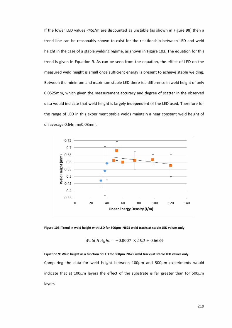
219
If the lower LED values <45J/m are discounted as unstable (as shown in Figure 98) then a
trend line can be reasonably shown to exist for the relationship between LED and weld
height in the case of a stable welding regime, as shown in Figure 103. The equation for this
trend is given in Equation 9. As can be seen from the equation, the effect of LED on the
measured weld height is small once sufficient energy is present to achieve stable welding.
Between the minimum and maximum stable LED there is a difference in weld height of only
0.0525mm, which given the measurement accuracy and degree of scatter in the observed
data would indicate that weld height is largely independent of the LED used. Therefore for
the range of LED in this experiment stable welds maintain a near constant weld height of
on average 0.64mm±0.03mm.
Figure 103: Trend in weld height with LED for 500µm IN625 weld tracks at stable LED values only
𝑊𝑒𝑙𝑑 𝐻𝑒𝑖𝑔ℎ𝑡 = −0.0007 × 𝐿𝐸𝐷 + 0.6684
Equation 9: Weld height as a function of LED for 500µm IN625 weld tracks at stable LED values only
Comparing the data for weld height between 100µm and 500µm experiments would
indicate that at 100µm layers the effect of the substrate is far greater than for 500µm
layers.
0.35
0.4
0.45
0.5
0.55
0.6
0.65
0.7
0.75
0 20 40 60 80 100 120 140
Wel
d H
eigh
t (m
m)
Linear Energy Density (J/m)

220
The threshold for stable welding in 100µm layers is only 15J/m, compared to 45J/m for
500µm layers, however, even when considering only the data for weld width and height for
100µm layers in the stable LED range of 15-30J/m, there is no measurable relationship
between LED and weld height. In contrast for 500µm layers weld height remains near to
constant with an increase in LED within the stable welding window of 45-120J/m. It may be
concluded that the high input energy compared to the material available in the 100µm
experiments has had two influential effects. Firstly considering a weld bead in isolation, the
high heat input results in significant dilution and welding with the substrate material, which
depending on welding speed and surface tension effects may be incorporated into the weld
above the plane of the substrate surface, so contributing to weld height over and above
that which would be seen in cases where the energy input was adequate for melting of the
powder bed and only a small proportion substrate material. Secondly the experimental
configuration placed welds 3mm apart from each other, in the 100µm experiments the high
heat input compared to the powder bed thickness was seen to result in significant
denudation of the powder bed which will influence the material available to subsequent
welds. The excess heat has in all probability also significantly raised the substrate
temperature and so in effect later welds were performed on a pre-heated substrate.
These effects are not observed in the experiments for 500µm layers as the energy input is
sufficient to fully melt the powder bed and wet the substrate, but not so great as to result
in and high energy instabilities in the weld or overheating of the substrate, as input energy
is primarily used to melt the powder feedstock. Therefore a less scatter is seen in the
measured weld bead widths and heights and a trend can be identified.
4.2.3 Discussion of single track melting for IN625
The stability and parameter window for the single track laser melting of IN625 can be seen
to vary significantly between 100µm and 500µm powder bed layers. In both cases it is

221
possible to define stability in terms of Linear Energy Density (LED), although at the
boundaries of stability LED is not sufficient to determine if a weld is stable or not, and
precise power or speed parameters will have a deciding influence on stability.
To enable a comparison of stability for energy input between 100µm and 500µm layer
experiments, the LED can be divided by the layer thickness to provide a Weld Energy
Density (WED). While not a true measure of volumetric energy density, WED provides a
metric for the laser energy input related to the layer thickness to enable comparison.
Figure 104 illustrates the ranges of WED which were evaluated for IN625 in these
experiments, and the resulting behaviours observed.
For 500µm layers there is a distinct transition between low energy instability behaviours
such as humping or balling, and stable weld beads, achieved at 60-65kJ/m.mm, it can be
seen from the range of values presented, that further investigation of the 500µm process
stability would be possible with higher power laser beams, in order to find the upper
stability limit.
For 100µm layers, there is a distinct transition from low energy instability to stable welding
at between 105-150kJ/m.mm, however a wide overlap range (400-525kJ/m.mm) exists
between stable welding and high energy instabilities, such as, transverse weld deviation or
significant over melt.
In general terms, there is a parity between the energy density which results in stable weld
tracks for both 100µm and 500µm powder bed thicknesses. The lower bound of stability for
500µm layers is approximately 65% lower than that for 100µm layers, however the
calculated value for WED does not take into account the effects of powder packing density
in the powder bed, which could effectively increase the WED value in reality for 500µm
layers. The interaction of the laser energy with the substrate is also not accounted for in

222
WED, and could in effect decrease the actual WED for 100µm layers at high LED values
where a significant portion of the molten material is from the substrate.
Figure 104: Weld Energy Density stability ranges for IN625
4.2.4 Multi-Layer deposits at 100µm layers
Upon deposition of multiple track and multiple layer samples, it was found necessary to
decrease the welding power to prevent excessive thermal build up, therefore values just at
the lower edge of the process stability map defined in Section 4.2.1.1 were utilised. As
indicated by the work of Yadroitsev and Smurov [349], a hatch distance of 0.5mm was
utilised as this was smaller than the weld bead width.
4.2.4.1 Observations – Stability
Figure 105 shows manufactured IN625 samples using 100µm layers. Although differing
parameters were used for each sample (800-1000W, 6-7m/min) there is no significant
visual difference in the deposited material. Variation in sidewall parallelism, straightness
and roughness are assessed to be in the sub 1mm range, while variation in the top surface
flatness is in the range of 1-1.5mm, as samples one and two show a cumulative increase in
height at the end of each weld bead, samples three and four do not exhibit the same
0
200
400
600
800
1000
1200
1400
1600
1800
100um Lowenergy
100um stable 100um Highenergy
500um lowenergy
500um Stable
WED
(kJ
/m.m
m)

223
variation, having a top surface flatness closer to the 1mm range. End wall variation and
roughness is significantly higher, due to the laser power ramp in/out utilised.
Figure 105: IN625 100µm Multi-Layer samples
4.2.4.2 Porosity
The porosity within the samples cross-section (shown in Figure 106) was measured by
image analysis using contrast thresholding and is reported for each of the measured
locations in Table 21. The sample was divided into 6 regions and examined at a
magnification of 5.0x, the overall average porosity for the sample cross section is 0.8±0.2%.
Figure 106: Optical micrograph montage of IN625 100µm sample
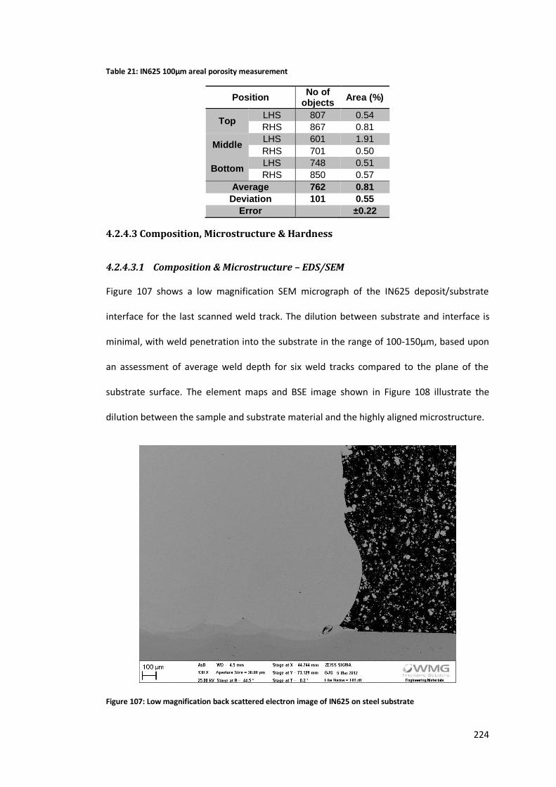
224
Table 21: IN625 100µm areal porosity measurement
Position No of
objects Area (%)
Top LHS 807 0.54
RHS 867 0.81
Middle LHS 601 1.91
RHS 701 0.50
Bottom LHS 748 0.51
RHS 850 0.57
Average 762 0.81
Deviation 101 0.55
Error ±0.22
4.2.4.3 Composition, Microstructure & Hardness
4.2.4.3.1 Composition & Microstructure – EDS/SEM
Figure 107 shows a low magnification SEM micrograph of the IN625 deposit/substrate
interface for the last scanned weld track. The dilution between substrate and interface is
minimal, with weld penetration into the substrate in the range of 100-150µm, based upon
an assessment of average weld depth for six weld tracks compared to the plane of the
substrate surface. The element maps and BSE image shown in Figure 108 illustrate the
dilution between the sample and substrate material and the highly aligned microstructure.
Figure 107: Low magnification back scattered electron image of IN625 on steel substrate

225
As can be seen in the element maps and BSE image, contamination from the steel substrate
extends only 100-200µm into the sample material. The EBSD band contrast and Euler
colour map shown in Figure 109 confirm the fine grained and aligned microstructure seen
by BSE imaging. At the boundary between substrate and weld material grains are on the
order of a few 10’s of micrometers, while in the centre of the weld track grains are
approximately 100-150µm in length and only 10-20µm in width, aligned towards the
substrate.
Figure 108: Back scattered electron image and associated EDS mapping of substrate interface region

226
Figure 109: EBSD Band contrast and Euler colour map for 100µm IN625 at sample/substrate interface
Closer examination of the deposited material just above this interface region reveals a
typical γ phase IN625 microstructure, consisting of a Ni-Cr-Fe matrix with Mo/Nb carbides
precipitated at the grain boundaries, as shown in Figure 110. In this case, the grains are
highly aligned in the cooling direction (i.e. towards the substrate) as would be expected.
Figure 110: Back scattered electron image of IN625 microstructure at approx. Z=0.5mm
Examination of the microstructure near the top of the sample shows the same γ-phase
microstructure, consisting of a Ni-Cr-Fe matrix with Mo/Nb carbides, the location of the
Mo/Nb carbides was confirmed by EDS mapping and is shown in Figure 111. The

227
microstructure at this distance from the substrate remains nominally aligned towards the
substrate, though not as strongly as at lower Z heights.
Figure 111: Back scattered electron image and EDS mapping of region at approx. Z=5mm showing γ-phase Mo/Nb carbides at grain boundaries
The bulk composition of the deposited material is given in Table 22, alongside the
previously reported specification for IN625 and the measured composition of IN625
feedstock powders. The composition measured for the deposited sample shows a relative
reduction in the quantity of Fe and Cr present, resulting in higher values for the other
alloying elements. However, the overall composition remains within specification for
IN625.

228
Table 22: Compositional comparison 100µm IN625
Material Element wt% Deviation
Error
Ni Cr Mo Nb Fe Ti Al
IN625(max spec) 68.85 23.0 10.0 4.15 5.0 0.4 0.4 IN625(min spec) 58.0 20.0 8.0 3.15 0.0 0.0 0.0 IN625 Powder 61.9 22.2 8.4 3.5 3.9 0.0 0.1 0.4 ±0.16 IN625 100µm LM 63.4 21.8 9.4 4.0 1.4 0.0 0.0 0.4 ±0.16
4.2.4.3.2 Variation in properties - Hardness
The variation in measured material hardness for a transverse cross-section through a
100µm layer IN625 sample is shown in Figure 112, the sample was sectioned as described
in Figure 43 in Section 3.3.1. The hardness mapping was produced from a 0.25x0.25mm
grid of micro-hardness measurement indentations across the entire section. A definite
increase in hardness (above 400HV) can be seen at the interface between sample and
substrate, as a result of the expected Heat Affected Zone (HAZ) and potentially higher Fe
content of this region. A repeating pattern of vertical bands showing marginally increased
hardness from the average is also present throughout the sample, aligning with weld
tracks. There is a gradual decrease in average hardness between 3-5mm in Z height, after
which the sample appears to have reached a steady state, as cooling rates due to thermal
conduction into the now “remote” substrate have stabilised. These harder bands are also
more pronounced in the centre of the sample. The average hardness within the deposited
sample material was measured to be 312HV0.3±7.6HV0.3.

229
Figure 112: Variation in material hardness for 100µm IN625
4.2.4.4 Discussion of 100µm layer thickness IN625 multi-layer experiments
Overall it can be seen that stable deposition has been achieved for IN625 in 100µm layer
thicknesses. Geometrically samples were of the intended size and shape, while density was
assessed to be above 99%. Material properties have some variability within the sample
section, due to differing cooling rates, with an average hardness of approximately . For the
stable deposition parameters used, the variation in top surface height was not found to
impact the ability of the equipment to re-coat the samples.
An approximate calculation for deposition rate based upon laser exposure time, hatch
distance and layer thickness can be made, so as to provide a value independent of
re-coating technology and speed. Defined as “exposure rate”, this is the volume rate of
material consolidation during the laser exposure phase of powder bed LM, assuming
continuous exposure. Values for a commercial parameter set alongside those used for
deposition of the samples presented are given in Table 23. Despite a significantly slower
scanning speed by several orders of magnitude, the combination of a larger laser spot size
(and therefore larger hatch spacing), and a five-fold increase in layer thickness result in a
233% higher deposition rate than using commercially available technology. There is of
Har
dn
ess
(HV
0.3
)

230
course a corresponding reduction in geometrical accuracy for potential features sizes,
sidewall or top-surface roughness.
Table 23: Build parameter comparison
Parameter Commercial parameters (EOS M270)
100µm IN625
Laser Power (W) 195 1000 Scan Speed (m/s) 1000 0.12 Hatch distance (mm) 0.09 0.5 Layer Thickness (µm) 20 100 Exposure rate (cc/s) 0.018 0.060
It can be suggested therefore that the deposition of IN625 in 100µm layers as a route to
higher deposition rate AM is feasible with only moderate increases in the required laser
power, and an actual decrease in the energy density utilised.
4.2.5 Multi-Layer deposits at 500µm layers
For the production of multi-layer 500µm IN625 deposits, a parameter set was selected with
the fastest possible welding speed to minimise thermal input into the sample over the
duration of the build. Samples were produced using 4kW and either 5.5m/min or 6.5m/min
welding speed.
4.2.5.1 Observations – Stability
During the build of 500µm multi-layer samples, it was found that a reduction in laser power
with increasing Z height was necessary to prevent excessive local heat accumulation in the
current/previous layer. The analytical work of Tahmasbi et al., [333] demonstrates the
effect of thermal isolation from the substrate when manufacturing a low thermal
conductivity superalloy. Therefore for each set of samples the laser power was reduced
from 4kW to 3.5kW on the sixth layer, and then to 3kW on the eleventh layer. A reduction
in laser power was chosen as the most practical deposition strategy, given the low thermal
conductivity of IN625 and the requirement to achieve a high deposition rate, an interpass

231
dwell to permit cooling of the part was not considered to be expedient in this case. Figure
113 shows samples built in 500µm layers using 0.5mm and 0.8mm hatch spacings, a
variation in the top surface form of up to 1mm can be seen.
Figure 113: 500µm IN625 multi-layer samples a) 0.5mm hatch, b) 0.8mm hatch
Sample 1 from each build was selected for further analysis by optical microscopy, as in each
case, the first sample built maintained the most consistency, while other samples were
affected by the heat input to the build substrate from previous samples during that
exposure.
A difference in the weld penetration of the substrate can be seen for some weld tracks
within each of the three samples shown in Figure 114. The greatest difference in weld
penetration can be seen in the first weld track of each sample, where penetration into the
substrate is significantly greater than in subsequent weld passes (note image a is inverted
compared to b and c, such that the first weld pass in image a is on the left of the image, but
first weld passes for images b and c were on the right of the image). Absorption of the laser
energy and welding in the first layer is a result of several complex interactions, while the
first weld pass is welding into and through a reasonably homogenous powder bed,
subsequent passes are incident upon a variety of differing features which will impact the
resulting weld penetration [350, 351]. Differing reflection and absorption of the beam will
be seen between the powder bed, denuded regions of the substrate and previously
a) b)

232
deposited weld material, which in turn will vary with differing hatch spacings as steady
processing conditions are established.
Figure 114: Optical montage of 500µm IN625 samples a) 0.5mm hatch b) 0.8mm hatch c) 1.1mm hatch
a)
b)
c)

233
4.2.5.2 Porosity
4.2.5.2.1 Cross-sectional porosity – Optical Microscopy
A contrast thresholding analysis was performed for each of the 500µm layer IN625 samples
produced with varying hatch spacing. Porosity has a predominantly spherical gas bubble
form, ranging from <1µm to 50µm. The analysis was conducted according to the
methodology described in 3.3.3.
Data for the thresholding analyses are presented in Table 24, alongside that already
reported for 100µm IN625. Immediate inspection of the data for comparable 0.5mm hatch
distances at 100µm and 500µm layers shows a counter-intuitive reduction in the porosity
and its variability for 500µm layers. The greater porosity in the 100µm layer samples may
be attributed to sub-optimal processing parameters. However, it is pertinent to note that
the Argon shielding was conducted at a much higher flow rate and for longer pre-flow
durations to purge the thicker powder bed and so may a contributing factor to the lower
porosity seen in the 500µm layer samples.
Table 24: Porosity values for 500µm layer IN625 at 0.5mm, 0.8mm and 1.1mm hatch spacing compared to
100µm layer IN625 at 0.5mm hatch spacing, as measured by optical microscopy
100µm IN625 (0.5mm Hatch)
500µm IN625 (0.5mm Hatch)
500µm IN625 (0.8mm Hatch)
500µm IN625 (1.1mm Hatch)
Position No of objects
Area (%)
No of objects
Area (%)
No of objects
Area (%)
No of objects
Area (%)
Top LHS 807 0.54 29 0.28 157 0.28 288 1.15
RHS 867 0.81 14 0.14 87 0.35 1148 2.08 Middle LHS 601 1.91 24 0.15 229 0.38 461 1.47
RHS 701 0.50 53 0.22 255 0.31 213 1.26 Bottom LHS 748 0.51 57 0.21 175 0.26 183 0.56
RHS 850 0.57 41 0.2 230 0.36 405 1
Average 762 0.81 36 0.20 189 0.32 450 1.25 Deviation 101 0.55 17 0.05 62 0.05 359 0.51
Error ±0.22 ±0.02 ±0.02 ±0.21

234
The overall the effect of hatching distance on the porosity of 500µm layer samples is
readily apparent (shown in Figure 115), with a small increase between 0.5mm and 0.8mm.
There is a significant increase in porosity for the 1.1mm sample, as well as increased
variation in measured values between micrographs.
Figure 115: Effect of hatching distance on average porosity as measured by optical microscopy
Figure 116 illustrates the variation in porosity in relation to position in the ‘Z’ direction
(location in the build height), and the hatch distance utilised in each case. For a 0.5mm
hatch, there is no measurable variation in average porosity between regions of the sample
in the Z direction; however, the deviation or variability in the average value indicates that
within each strata there is increasing variation with Z height. With reference to the data in
Table 24, it can be observed that although the number of recorded defects decreases with
Z height, the areal porosity remains constant, indicating fewer but larger defects. For a
0.8mm hatch spacing, the average porosity is higher (60%) than that of a 0.5mm hatch
sample, although the same variation within the cross section was not readily apparent. For
a 1.1mm hatch distance, the average porosity has increased significantly with Z height, as
has the degree of variation.
0
0.2
0.4
0.6
0.8
1
1.2
1.4
0.4 0.5 0.6 0.7 0.8 0.9 1 1.1 1.2
Po
rosi
ty (%
)
Hatch Distance (mm)

235
Figure 116: Effect of hatch distance and Z height on porosity as measured by optical microscopy
The porosity measurements were made at relatively low magnification, so are aimed at
providing an appreciation of overall defect distribution and enable comparison between
processing parameters. Therefore small defects below the resolution of the microscope
and imaging hardware will not have been included in these measurements. Spierings et
al.,[23] discuss the relative merits and pit falls of differing magnifications for the
examination of porosity. Whereas a low magnification will not account for very small
defects, a high magnification is only able to measure the presence of defects in an isolated
area and so may avoid or include areas of high defect density if their distribution is not
homogenous. As inspection of the micrographs presented will show, there is a wide
variation in defect size and distribution throughout the samples, therefore a low
magnification which can account for virtually the entire sample cross-section was utilised.
From the variation in porosity with Z height, it can be suggested that the variation in build
parameters utilised (decreasing laser power to prevent excessive melting) in order to
control thermal accumulation has been successful in both the 0.5mm and 0.8mm hatch
spacing samples and has not caused a significant increase in material porosity. For 1.1mm
0
0.5
1
1.5
2
2.5
Low Mid Upper
Po
rosi
ty (%
)
0.5mm Hatch
0.8mm Hatch
1.1mm Hatch

236
hatch samples, the resulting decrease in energy density has shown a significant increase in
porosity as a result, the greater porosity is more notable as Z increases due to the decrease
in laser power used for these layers. However future investigation may wish to consider
that a delay between exposure of each weld line, or the use of an actively cooled substrate,
may allow the use of a higher energy density (providing greater density as shown in
Figure 117 and described by Spierings et al., [23]) without the associated thermal
accumulation.
Examination of Figure 117 indicates that a volumetric energy density of 8MJ/m3 provides a
critical transition between high porosity and significant variability to consistently low
porosity (<0.4%). Above this energy, some improvement in density can be seen, however
for a 118% increase in energy (up to 17.5MJ/m3) there is only a 25% decrease in porosity
from 0.32%±0.04% to 0.21%±0.005%, showing that the increase in energy density has
provided a decrease in variability. The optimum energy density which provides the highest
relative material density for the least heat input is therefore at 8.2MJ/m3.
Figure 117: Variation in average porosity with volumetric energy density
𝑅𝑒𝑙𝑎𝑡𝑖𝑣𝑒 𝑑𝑒𝑛𝑠𝑖𝑡𝑦=1−2.7522𝑒−2×10⁻⁷ × VED
0
0.5
1
1.5
2
2.5
0.00E+00 5.00E+06 1.00E+07 1.50E+07 2.00E+07
Po
rosi
ty (
%)
Volumetric Energy Density (J/m3)

237
Equation 10 : Relative density as a function of Volumetric Energy Density for 500µm IN625
4.2.5.2.2 Volumetric porosity - µ-CT
The porosity of a sample produced using a 0.5mm hatch distance was measured by µ-CT
scanning, which observed a void volume of approx. 0.15mm3 out of a total sample volume
of approx. 274mm3, giving a 0.05% ±0.005% volume porosity (full details presented in
Table 25).
Table 25: Porosity measurement by µ-CT for IN625
Total Volume (mm3) 274.0277 Void Volume (mm3) 0.1474 Number of Voids 171 Calculated Porosity 0.05%
The minimum detection limit of µ-CT scanning must of course be recalled to be 9.09µm
±1%, therefore the calculated porosity will be a slight underestimation, as small voids
below the detection limit will not be accounted for.
Visualisation of the distribution of defects within the sample shows that larger defects are
clustered in the centre of the sample towards the upper third (see Figure 118), attributable
to faster solidification rates in the centre of a sample compared to the edges, which do not
allow sufficient time for gas bubbles to escape the melt pool, as suggested by
Spierings et al., [23] the reasons for the difference in melt cooling are discussed in Section
4.2.6.
A comparison of both 2D (Figure 118) and 3D ((Figure 119) visualisation of defects indicates
that the largest defects were created due to an abnormality during a single weld track,
rather than being systematic. This “row” of defects is highlighted in both figures with the
direction indicated on the 3D void representation being through the “thickness” of the
sample in the direction of welding, such that the defects lie within a single weld pass. The
volume distribution frequency of the detected defects is presented in Figure 120, and

238
shows that with the exception of four large defects, the other defects are of less than
0.01mm3 in size, down to the detection limit.
Figure 118: Reconstructed 2D slice from µ-CT scan of 500µm IN625 at 0.5mm hatch
Figure 119: Reconstructed 3D sample volume and corresponding defect visualisation a) solid material with voids, b) voids only
a)
1.5mm
1mm 1mm
b)

239
Figure 120: Defect volume distribution for 500µm IN625 at 0.5mm hatch

240
4.2.5.3 Composition, Microstructure & Hardness
4.2.5.3.1 Microstructure - SEM
Examination by SEM shows a typical IN625 γ phase microstructure for laser processed
material when compared with literature [32], with a strong alignment in the direction of
the substrate due to the expected thermal gradient. Grains have a high aspect ratio,
measuring on the order of 50-100µm across, but up to several hundred micro-metres in
length. Figure 121 shows complete melting between layers, despite their thickness.
Figure 121: Back scattered electron image of 500µm IN625 at 0.5mm hatch
Figure 122 shows the microstructure present in the last deposited weld track within the top
layer of a sample, while the primary direction of alignment remains towards the substrate,
a number of grains are also aligned diagonally, showing the effects of secondary cooling
within the same layer. Examination at higher magnifications in Figure 123 shows the
expected y phase structure, consisting of a Ni-Cr-Fe matrix with small sub-micron sized Mo
and Nb carbides. It can be seen that the majority of <1µm porosity has formed among the

241
Mo/Nb rich veins. This <1µm porosity has not been included in any porosity measurement
by optical microscopy or µ-CT, being below the resolutions used.
Figure 122: Back scattered electron image of last deposited layer for 500µm IN625 at 0.5mm hatch
Figure 123: High magnification back scattered electron image of IN625 microstructure showing <1µm porosity

242
4.2.5.3.2 Composition – EDS
In contrast to the 100µm IN625 samples, the substrate dilution extends much further into
the deposited material, as shown in the linescan presented in Figure 124. An initial 400µm
Fe rich dilution zone exists, below the plane of the substrate surface, where IN625 has
mixed with molten substrate material. Above this plane there is a steady decrease in Fe
content, reaching a normal IN625 composition at a Z height greater than 1.0mm above the
original substrate surface.
Figure 124: EDS Linescan of interface region (500µm at 0.5mm hatch) IN625
The bulk composition, measured at Z>5mm is presented in Table 26. The composition does
not differ significantly from that measured for the feedstock powder, and remains well
within the compositional range required for IN625.
Table 26: EDS measurement of bulk composition for 500µm IN625
Material Element wt% Deviation Error
Ni Cr Mo Nb Fe Ti Al
IN625(max spec) 68.85 23.0 10.0 4.15 5.0 0.4 0.4 IN625(min spec) 58.0 20.0 8.0 3.15 0.0 0.0 0.0 IN625 Powder 61.9 22.2 8.4 3.5 3.9 0.0 0.1 0.4 ±0.16 IN625 500µm LM 61.2 21.8 8.8 3.9 4.1 0.0 0.1 0.1 ±0.06
Un
affe
cte
d s
ub
stra
te
Fe r
ich
zo
ne
Tran
siti
on
zo
ne
IN6
25
Bu
lk m
ater
ial
Substrate Deposited material

243
4.2.5.3.3 Hardness
The average material hardness for each of the hatch distances investigated is presented in
Figure 125. There is a slight trend towards increased hardness with wider hatch spacing,
coupled with a small increase in the variability between hardness measurements. The
increase in hardness may be due to a slightly higher solidification rate, as fewer welding
passes at larger hatch spacing will result in a slightly cooler substrate. However the
variation is small, particularly considering the typical error associated with hardness
measurements in general.
Figure 125: Hardness variation with Hatch Distance for 500µm IN625
The distribution of material hardness within a 5x5mm area of the samples cross-sections is
shown in Figure 126. While the hardness measured is relatively consistent at both 0.5mm
and 0.8mm hatch distances, the contribution to variation can be seen for 1.1mm hatch
distance, in the form of a few isolated points of low hardness. These low points are a direct
result of increased porosity, permitting a larger indent to be made than would be the case
in higher density material. The material on the whole does however possess a higher
hardness than for that at closer hatch distances, suggesting a microstructural effect due to
the differences in processing conditions.
250
255
260
265
270
275
280
285
0.4 0.9 1.4 1.9 2.4 2.9 3.4
Har
dn
ess
(HV
)
Hatch Distance (mm)

244
Figure 126: Hardness distribution for 500µm IN625 a) 0.5mm Hatch b) 0.8mm Hatch c) 1.1mm Hatch
a)
b)
c)
Har
dn
ess
(HV
0.3
) H
ard
nes
s (H
V0
.3)
Har
dn
ess
(HV
0.3
)

245
4.2.5.4 Discussion of 500µm layer thickness IN625 multi-layer experiments
Deposition of multi-layer, multi-weld “bulk” material in 500µm layer thicknesses for IN625
has been shown to produce material of reasonable density and hardness. The geometric
accuracy and form of the deposited samples was poorer than for comparable 100µm layer
thickness samples, with a distinct waviness along the length of the samples as shown in
Figure 113. This would indicate that although the thermal control strategy implemented
has been successful with regards to material density (which remains nominally constant
with Z height) the process parameters are not fully optimised when considering the
thermal isolation from the substrate. The analytical work of Tahmasbi et al., [333] clearly
shows that for a low thermal conductivity material (such as IN625) the maximum
temperatures seen within each layer are strongly influenced by Z height, as previously
deposited material serves to insulate the current layer from the substrate. Although an
interpass dwell to allow cooling of previously deposited material would be effective in
reducing this effect, this represents a corresponding decrease in deposition rate and overall
productivity. Therefore by using a reduction in laser power productivity is maintained,
while density has not been affected, with the exception of samples manufactured at a
hatch spacing of 1.1mm, indicating a lower boundary for energy density after which
porosity will increase. However, further optimisation of the process parameters at 0.5mm
hatch distance could improve the top surface form without a loss of density.
Material hardness was seen to vary with hatch spacing, however average hardness of
samples deposited at the same hatch spacing in 500µm layer thickness (261HV0.3±6.6HV0.3)
was lower than that for material deposited at 100µm layers (312HV0.3±7.6HV0.3). The
greater heat input required to achieve stable welding for 500µm layers causes a slower
solidification rate and larger grain size, thereby reducing hardness in the as deposited
material.

246
4.2.6 Discussion of multi-layer deposits for IN625
4.2.6.1 Weld cooling
The examination of the materials microstructure and porosity distribution for 500µm layer
deposits of IN625 conducted in Section 4.2.5 highlighted a difference in porosity
distribution and microstructural alignment between the outer edges of the sample and the
central region. The centre of the sample exhibits a secondary alignment of some grains in a
diagonal orientation towards previously deposited weld beads in the same layer, as well as
a slight increase in porosity.
It is considered that welds in the central region of the sample experience a greater
solidification rate due to greater thermal conduction into the previously deposited material
not only in the layer below, but also into the previous weld bead of the same layer – so
providing a greater area for heat transfer than for a single weld bead within the powder
bed. Figure 127, schematically shows the differences in the cooling paths available from the
weld beads. Cooling into the powder bed and argon atmosphere present in the denuded
regions is a less effective cooling path (via radiation and convection) compared to
conduction into the deposited material. During deposition of subsequent weld tracks there
is a larger proportion more effective conduction cooling into the previous weld bead and
previous layer than is available to the first weld bead in a given layer.
This difference in cooling rate and direction is more apparent in powder bed LM at 500µm
layers than at 100µm layers, as the ratio of cooling into previous layers compared to
previous weld beads within the same layer is significantly different to that seen in thinner
layers. This can be demonstrated by a comparison of the approximate ratio of weld width
to weld height for differing powder bed LM systems shown in Table 27.
Table 27: Ratio of weld width to height for differing powder bed LM layer thicknesses

247
Deposition System
Nominal weld width
Nominal layer thickness
Ratio (width:height)
M270 0.1mm 0.02mm 5:1 100µm 1mm 0.1mm 10:1 500µm 1mm 0.5mm 2:1
The higher cooling rate results in a greater quantity of entrapped gas bubble porosity, while
the difference in conduction paths out of the weld bead has a moderate influence on
microstructural orientation.
Figure 127: Schematic representation of weld bead deposition a) first weld in a layer, b) subsequent welds in a layer
4.2.6.2 Material density and deposition rate
Figure 128 presents data for relative material density for all of the samples produced by LM
in this research, and compares with commercially available ALM material. The melt rate or
exposure rate is also given as an indicator of potential productivity. The comparative
material hardness for each process is given in Figure 129.
On balance, the use of 500µm layers and a hatch spacing of 0.5mm in a high powered laser
powder bed system is capable of producing material of a comparable relative density to
a)
b)

248
that of current commercial systems, but with a much higher potential productivity, being
able to expose material at a rate of 0.023cc/s compared to current commercial systems
which can achieve only 0.002cc/s.
Figure 128: Productivity vs material quality for powder bed LM of IN625
4.2.6.3 Material hardness
The hardness of IN625 samples produced during this work was similar to that of material
produced by Dinda et al., [32] using a blown powder laser-DED system, at approx. 250HV,
however the work of Paul et al., [30] (using a CO2 laser in a similar blown powder
configuration) reports a much higher hardness (~500HV) for IN625 in the as built condition.
Commercially available data indicates a hardness of approx. 290HV for current powder bed
deposition routes, after the material has undergone a solution annealing heat treatment.
Therefore hardness of material produced by 500µm powder bed deposition would appear
to indicate a reasonable balance of mechanical properties in line with that expected from
an AM process, the exact balance of strength and ductility present must now be
established.
90
91
92
93
94
95
96
97
98
99
100
0
0.01
0.02
0.03
0.04
0.05
M270 100um 500um0.5mm
500um0.8mm
500um1.1mm
Re
lati
ve D
en
sity
(%
)
Me
lt R
ate
(cc
/s)
Melt rate
RelativeDensity

249
The variation in hardness between samples produced at 500µm at varying hatch distances
would appear to indicate an increase in hardness with larger hatch spacings. This may be
due to higher cooling rates, as fewer laser passes are made, therefore the hardness for
0.5mm hatch spacing samples may be increased if further work were conducted on the
thermal control strategy, or the material were naturally allowed to cool locally between
exposures as may occur on larger components or multiple component builds.
Figure 129: Material hardness for powder bed LM IN625
Figure 130 shows the range of volumetric energy densities investigated during this research
for 500µm powder bed layers, compared with that for current commercial 20µm layer
systems. As can be seen, despite the use of “high power” lasers, the actual energy density
capability is significantly lower than that of commercial high resolution systems, due to the
larger focal spot size of the laser used, and the thicker powder bed layers. Although using
lower energy ranges, it would appear that high deposition rate powder bed LM would not
result in a reduction in material density compared with current commercial high resolution
processes, particularly if conducted in a production quality sealed chamber machine.
230
240
250
260
270
280
290
300
M270 100um 500um 0.5mm 500um 0.8mm 500um 1.1mm
Ave
rage
Ha
rdn
ess
(HV
)

250
Figure 130: Volumetric Energy Density ranges for LM systems
4.3 Powder Bed Laser Melting of Inconel 625 MMCs
4.3.1 Reinforcement Down-Selection
Three ceramic materials were selected for comparison and were supplied by Pi Kem Ltd,
Alumina (99 % Al2O3,), Silicon Carbide (95 % SiC) and Titanium Carbide (99 % TiC), with the
remainder composed of unkown impurities.
4.3.1.1 Powder homogeneity & behaviour
The particle size distributions for all powders were measured by laser diffraction
techniques, using a Mastersizer 2000, with Sirocco 2000 dry dispersion system (Malvern
instruments Ltd, UK), results are given in Table 28.
Table 28: PSD of matrix material and candidate reinforcements
Sample D0.1(µm) D0.5 (µm) D0.9(µm) Error (µm)
IN625 23.17 31.28 43.76 ±2.0
Al2O3 5.85 8.48 14.41 ±1.0
SiC 3.07 4.60 8.10 ±1.0
TiC 0.22 0.44 1.18 ±0.5
1.00E+08
1.00E+09
1.00E+10
1.00E+11
1.00E+12
1.00E+13
1.00E+14
0 1000 2000 3000 4000 5000
Vo
lum
etr
ic E
ne
rgy
De
nsi
ty (
J/m
3 )
Laser Power (W)
High Resolution(upper limit)
High Resolution(lower limit)
High Deposition(upper limit)
High Deposition(lower limit)

251
Prior to deposition, the reinforcement powders were each mixed at 5 wt% (approx. 10
vol%) with IN625, using alumina jars and media, at a speed of 150 rpm for a duration of 1
hour. Powders appeared visually well mixed. Investigation by SEM shows even mixing of
both the Al2O3 and SiC reinforcement with the matrix material. However a proportion of
the significantly smaller TiC particles demonstrated a propensity to agglomerate, while the
rest are distributed evenly.

252
Figure 131: Back scattered electron images of mixed MMC candidates a)IN625+Al2O3, b)IN625+SiC, c)IN625+TiC

253
4.3.1.2 Observations of samples
4.3.1.2.1 Melt processing behaviour – High speed video/photography
Frames extracted from a high speed video recording of the melt pool during processing of
the samples show a qualitative difference in behaviour between each material. While both
IN625+SiC and IN625+TiC melt pools exhibit a degree of ejecta (weld spatter), in contrast
the proportion of gaseous discharge (vapour plume) from the IN625+Al2O3 melt pool is
much greater than for the other materials.
Figure 132: Frames from high speed video of melt pool processing a) IN625+Al2O3, b) IN625+SiC, c) IN625+TiC
4.3.1.2.2 Deposited samples – visual inspection
Figure 133 shows an example of deposited MMC samples immediately after removal from
the build chamber.
a)
b)
c)
Vapour plume
1mm
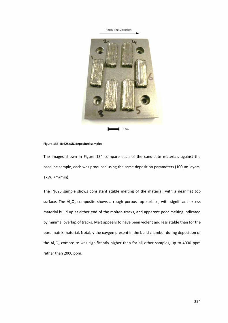
254
Figure 133: IN625+SiC deposited samples
The images shown in Figure 134 compare each of the candidate materials against the
baseline sample, each was produced using the same deposition parameters (100µm layers,
1kW, 7m/min).
The IN625 sample shows consistent stable melting of the material, with a near flat top
surface. The Al2O3 composite shows a rough porous top surface, with significant excess
material build up at either end of the molten tracks, and apparent poor melting indicated
by minimal overlap of tracks. Melt appears to have been violent and less stable than for the
pure matrix material. Notably the oxygen present in the build chamber during deposition of
the Al2O3 composite was significantly higher than for all other samples, up to 4000 ppm
rather than 2000 ppm.

255
Figure 134: Macro photography of as deposited samples a) IN625, b) IN625+Al2O3, c) IN625+SiC, d) IN625+TiC
The SiC composite has a smooth top surface, although closer inspection reveals significant
macro-cracking of the sample both vertical to the substrate and transversely to the laser
scanning direction.
The TiC composite shows a consistent and stable molten track, with no significant edge or
end of line build-up of material, no cracking is evident and the top surface is relatively flat
compared to the other composite samples, although not quite as consistent as the IN625
samples.
Build of both the Al2O3 and SiC samples was interrupted at between 15 and 20 layers
respectively, as excess sample material from the uneven top surface obstructed the re-
coating process; build of the TiC composite was voluntarily ended at 40 layers, with no
evidence to indicate that the build could not continue indefinitely.

256
4.3.1.3 Porosity & Microstructure
4.3.1.3.1 Optical Microscopy evaluation
The optical micrographs presented in Figure 135 provide an appreciation of a
representative cross section of each candidate MMC material, compared to the matrix
alloy.
Most notably the SiC composite exhibits significant macro-cracks which have propagated
both horizontally and vertically, often interconnected in nature. These seem to have
formed independently of the large porosity voids which are present, clustered
preferentially at either edge of the sample, while the cracks are dominant in the centre of
the sample.
The Al2O3 composite material shows much lower porosity, although some large defects are
present. Cracks are seen at the interface with the substrate, aligned vertically, and located
centrally in several molten tracks. The top surface of the sample can be seen to be highly
irregular, with build-up at the edges, but under-deposition in the centre (attributable to
insufficient powder deposition in the lee of the higher edges), this irregular deposition
eventually caused the build to fail, as the higher edges protruded above the next 100µm
layer and jammed the recoating mechanism.
The TiC composite can be seen to vary significantly from the Al2O3 and SiC composites,
having a relatively consistent top surface with only minor deviations in height between
molten tracks, the outer edges have not over-built significantly and material density
appears to be relatively high.

257
Figure 135: Optical micrographs of candidate MMC materials

258
4.3.1.3.2 SEM & EDS evaluation
4.3.1.3.2.1 IN625+Al2O3
Observation of the vertical interface cracking in the Al2O3 samples shows them to have
occurred at grain boundaries in the centre of the molten track. It may be concluded to be
an example of liquation cracking, whereby lower melting point elements have accumulated
in the hottest zone of the cooling weld pool during re-solidification, and having lower
tensile strength and melting point than the surrounding material, have failed during
subsequent passes, as described by both Robinson and Scott [13] and DuPont [14]. A more
detailed examination using EDS mapping, indicates that the edges of the cracks are rich in
Nb and Mo, but poor in Ni and Cr, which would confirm liquation cracking as the cause,
whereby the substrate is serving as a restraint in the welding process, hence the cracking
appears only within the first few layers. A more detailed explanation of liquation cracking
mechanisms is contained in the literature review, Section 2.2.5.4.2.

259
Figure 136: Back scattered electron image of cracks at interface of substrate and IN625+Al2O3 composite and associated EDS maps
The porosity present in the sample has a surrounding high concentration of both
aluminium and oxygen, as can be seen in Figure 137. Coupled with the high oxygen
content noted in the build chamber, this indicates the likely thermal destruction of the
Al2O3, releasing oxygen into the process chamber, and capturing some bubbles formed
during solidification.

260
Figure 137: Back scattered electron image of entrapped gas bubble porosity and associated EDS maps
Examination using EDS mapping (see Figure 138), of what appeared to be large irregular
shaped defects when viewed with optical microscopy, reveals the presence of small
clusters of alumina particles which have remained intact after the melting process,
agglomerations in the feedstock powder have offered mutual protection against complete
dissolution in the molten pool when compared with isolated particles.

261
Figure 138: Back scattered electron image of un-melted Al2O3 particles and associated EDS maps
4.3.1.3.2.2 IN625+SiC
Figure 139 shows SEM micrographs of the IN625 - SiC composite, while ceramic particles
are obviously present, their distribution is far from homogenous, forming bands across the
sample, which have acted as heterogeneous nucleation sites, resulting in localised
columnar growth. The particles are also significantly smaller than the original
reinforcement particles added to the powder feedstock, indicating either partial or
complete dissolution during the melting phases, and subsequent re-precipitation.

262
Figure 139: Back scattered electron images of IN625+SiC composite a) low magnification, b) high
magnification
Micro-cracking of the specimens seen in Figure 139a appears not to be particularly aligned
with grain boundaries, freely cutting through grains, nor does it appear localised to the high
SiC particle concentrations, although a change of crack direction/orientation seems to
occur often when it passes through the SiC rich bands. Smaller voids seen in the high
magnification image shown in Figure 139b (imaging the area indicated in Figure 139a) do

263
not exhibit the angular fracture form of post-weld cracks, but have a smoother form
considered to be lack of fusion defects during solidification.
Examination of the ceramic particulates by EDS can be seen in Figure 140, showing that
Mo, Nb and Si are all co-located at the sites of the ceramic particles. This would indicate
that the particles are in fact a combination of Nb2C, NbC, MoC and SiC formed re-
precipitated during solidification from the molten state. Recalling the Ellingham diagram
given in the literature review (Figure 18), this should be expected as both Nb and Mo are
stronger carbide formers than Si at the elevated temperatures such found during
processing of the material.
Figure 140: Secondary electron image of ceramic particles in IN625+SiC material and associated EDS maps
4.3.1.3.2.3 IN625+TiC
Inspection by SEM of the TiC composite in Figure 141a at first appears to have TiC present
only in large agglomerations; however higher magnification inspection of the samples
shows very fine TiC particles are evenly distributed throughout the matrix, with their size
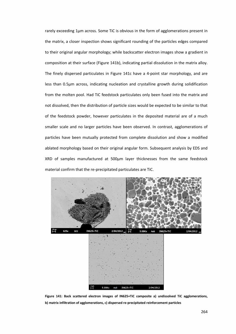
264
rarely exceeding 1µm across. Some TiC is obvious in the form of agglomerations present in
the matrix, a closer inspection shows significant rounding of the particles edges compared
to their original angular morphology; while backscatter electron images show a gradient in
composition at their surface (Figure 141b), indicating partial dissolution in the matrix alloy.
The finely dispersed particulates in Figure 141c have a 4-point star morphology, and are
less than 0.5µm across, indicating nucleation and crystalline growth during solidification
from the molten pool. Had TiC feedstock particulates only been fused into the matrix and
not dissolved, then the distribution of particle sizes would be expected to be similar to that
of the feedstock powder, however particulates in the deposited material are of a much
smaller scale and no larger particles have been observed. In contrast, agglomerations of
particles have been mutually protected from complete dissolution and show a modified
ablated morphology based on their original angular form. Subsequent analysis by EDS and
XRD of samples manufactured at 500µm layer thicknesses from the same feedstock
material confirm that the re-precipitated particulates are TiC.
Figure 141: Back scattered electron images of IN625+TiC composite a) undissolved TiC agglomerations,
b) matrix infiltration of agglomerations, c) dispersed re-precipitated reinforcement particles

265
4.3.1.3.2.4 Discussion of microstructure
All the ceramic materials have been melted to some degree by exposure to the laser beam,
and dissolved into the molten pool; in the case of SiC and TiC, to re-precipitate back as
smaller particles upon cooling and solidification. The greater absorptivity of ceramics such
as TiC to laser radiation than most metallic materials has been previously noted by Zheng et
al., [173] and explains the phenomena of TiC particle melting under laser radiation. The
work of Tahmasbi et al., [333] considers the behaviour of an IN738 + CeO2 composite in a
purely theoretical model, by considering only the difference in melting points of the
constituents the computational analysis predicts a lower maximum temperature for the
composite material in comparison to the matrix alloy alone. In contrast the experiments
performed in this thesis demonstrate a higher temperature has been reached, as indicated
by the greater weld width and lower input energy required to produce the MMC. The
experimental results shown here therefore concur with those of Zheng et al., who cite the
higher absorptivity of the TiC to laser radiation, a brief examination of relative melting
points, thermal conductivity and absorptivity coefficients is presented in Table 29, which
corroborates this observation.
Table 29: Comparison of key material properties [190]
Material Density (kg/m3)
Young’s Modulus
(GPa)
Hardness (HV)
Melting Point (oC)
Absorptivity to 1064nm
laser radiation
Thermal Conductivity
(W/m.K)
IN625 8400 207 200 1355 0.23-0.25 [352]
11.4-21.3
Al2O3 3960 220-350 1200-2000 2072 0.68 [353] 16-28
SiC 3160 386-414 2400-2500 2730 0.7-0.9 [354] 42.5
TiC 4938 310-462 2620-3200 3167 0.46 [43] 17-21

266
4.3.1.4 Hardness
The mean hardness values for a set of samples processed with the same laser power and
speed (1000 W at 7 m/min) are shown in Figure 142. Both micro and macro indentation
methods provide similar results, with indent sizes being at least one order of magnitude
larger than the size of the reinforcement particulates. Figure 143 shows the relative scale of
reinforcement size and distribution compared to hardness indentations.
Figure 142: Hardness of candidate MMC materials
The hardness results show a significant variation in hardness between the composite
materials. It can be seen that the addition of Al2O3 to the Inconel 625 matrix has provided
no significant increase in material hardness. The greatest increase is seen in the case of
IN625 - SiC, with mean hardness increased by 129±4 % compared to the pure matrix
material. The addition of TiC shows a measurable and consistent improvement of 32±5 %
when compared to the matrix alone. Variability of material hardness is significant in the SiC
reinforced material, with a standard deviation of 99 HV0.3, while the TiC composite has a
standard deviation of 28 HV0.3, increased by 47 % compared to the deviation of 19 HV0.3 for
the matrix alloy. This inconsistency can be attributed to the un-even distribution of TiC at
the powder stage, caused by agglomeration of the relatively small reinforcement particles.
0
100
200
300
400
500
600
700
800
IN625 IN625 - Al2O3 IN625 - SiC IN625 - TiC
Vic
kers
Har
dn
ess
(HV
)
Sample Composition
HV 20.0
HV 0.3
kg
kg

267
In general though, it can be seen from Figure 143, that the hardness indentations cover an
area including both matrix and reinforcement, where an even distribution exists.
While the SiC reinforcement did not exhibit the same poor particle distribution during
powder preparation, the examination by SEM of the material both pre and post hardness
test shows a high level of segregation of the re-formed particulates, explaining the high
variation in material hardness. As can be seen in Figure 143c an indent may be performed
in a carbide rich or poor area, with a pre-existing crack or defect. This particle clustering has
been observed in the work of Zimmerman et al., [278], who found that clustering occurred
above 2 vol% of SiC, although these AM samples exhibit a similar increase in hardness,
Zimmerman et al., [278] noted no significant cracking or porosity in their MMC produced
by electrodeposition.
Figure 143: Back scattered electron imaging of hardness indentations in context with reinforcement
distribution

268
4.3.1.5 Discussion & Evaluation of Candidate MMCs
Upon evaluation of the three composite systems investigated, the addition of titanium
carbide to an Inconel 625 matrix was found to be preferable to additions of either
aluminium oxide or silicon carbide particulates. The TiC composite demonstrates higher
density, an absence of micro cracking, and an appreciable increase in the material hardness
compared to the alternative reinforcements examined in this paper. Compared to
contemporary AM systems using ~200 W lasers with small spot sizes of the order of 100
µm, the use of a higher power beam (4 kW over 850 µm spot size) appears to more readily
melt any ceramic particulates included in the material, when compared to the level of
dissolution shown by the work of Gaard et al., [43]. In the case of SiC or TiC these appear to
reform during the solidification process, but at a much smaller size than the original
particulates. In the case of Al2O3, the oxygen does not remain dissolved in the molten pool
as carbon is able to, so is not present to permit the ceramic to reform, resulting in a
compromised metallic alloy. This is supported by photographic recording of the melt pool
during processing which shows a higher discharge of vapour from the Al2O3 reinforced
material and EDS mapping of the remaining entrapped gas bubble porosity.
If indeed completely dissolving the ceramic does not impact the mechanical properties
significantly, this may allow for the production of composites with significantly smaller
ceramic reinforcement (<500 nm), which may be beneficial to the material properties, but
without the need to utilise “nano” materials at the powder processing stage.
It has been generally considered that the Orowan strengthening effect is not present in
most micro-reinforced MMC materials [227], as the particulate reinforcements are of too
great a size and too widely spaced to prevent the motion of dislocations [181]. However, if
particulate reinforcements on a sufficiently small scale can be achieved, the presence of
the Orowan strengthening effect may be reconsidered. Zhang et al., [355] noted that for

269
particles of 1 µm the Orowan effect is minimal, whereas decreasing particle size down to
10 nm results in significant improvements to the strengthening effect, with Orowan
strengthening becoming relatively more significant than enhanced dislocation density as
the method by which properties are improved as particle size decreases. AM using micro
sized particulates as the feedstock, where the processing parameters are such that the
laser completely dissolves the ceramic constituents and re-precipitates them at a smaller
scale may well be a viable process route to such a “nano reinforced” composite without the
associated hazards, costs and agglomeration difficulties associated with such small
particulates.
As IN625+TiC was identified as the most promising MMC candidate, its use at both 100µm
and 500µm layers was assessed for comparison with the IN625 baseline established in the
preceding section. To further investigate the potential for forming MMCs from lower cost
feedstocks, an investigation into the laser melting of an MMC reinforced with a Ti and
carbon (graphite) mix was also investigated and will be discussed in the following sections.
4.3.2 Single track melting of 100µm layers IN625+TiC
4.3.2.1 Observations – stability & parameter window
The process parameter window can be characterised according to the range of behaviours
presented in Figure 144. No low energy instability types such as balling or humping were
observed, although welds at low speeds and high laser powers do exhibit some high energy
instability, characterised by excessive melting and transverse deviation at Linear Energy
Densities above 50J/m. The absence of low energy instabilities may be explained by the
higher absorptivity of TiC to laser radiation at this wavelength, as shown earlier in Table 29.

270
Figure 144: Parameter window characterisation for 100µm IN625+TiC
4.3.2.2 Weld bead geometry & variation
An evaluation of the weld bead geometry compared to the processing parameters utilised
is presented in terms of linear energy density (LED) in Figure 145 and Figure 146. Weld
width shows a slight correlation with LED, however a high degree of error and uncertainty
is present between repeats in the measured values. For weld height, a similar degree of
uncertainty is present, with virtually no trend in the measured values compared to LED.
500
1000
1500
2000
2500
3000
3500
4000
4500
0 2000 4000 6000 8000 10000 12000
Pro
gram
me
d la
ser
po
we
r (W
)
Welding Speed (mm/min)
Stable Wavy
Lin
ear
En
ergy
Den
sity
(J/
m)

271
Figure 145: Variation in weld bead width with LED for 100µm IN625+TiC single track welds
Figure 146: Variation in weld bead height with LED for 100µm IN625+TiC single track welds
The results of an ANOVA analysis of the measured values for stable welds are presented in
Table 30. The interaction of welding power and speed is still the dominant factor in both
cases (24.1% and 32.3% respectively for weld width and height), with only minor
contributions from either weld power or welding speed alone. However the significance of
these values is highly dubious, with P values for weld width well beyond the 0.05 limit. The
0.2
0.7
1.2
1.7
2.2
2.7
0 20 40 60 80 100 120 140
Wel
d w
idth
(m
m)
Linear energy density (J/m)
0.05
0.07
0.09
0.11
0.13
0.15
0.17
0.19
0.21
0.23
0.25
0 20 40 60 80 100 120 140
Wel
d h
eigh
t (m
m)
Linear energy density (J/m)

272
P values for weld height are however within the 0.05 limit, and may be regarded as
significant, although the error is still high.
Table 30: ANOVA of weld bead geometry for 100µm IN625+TiC single track welds
Source Weld Width Weld Height
% Contribution
P (significance)
% Contribution
P (significance)
Power 5.0% 0.463 12.7% 0.012 Speed 2.9% 0.709 10.7% 0.026 Power/Speed interaction 24.1% 0.375 32.3% 0.014 Error 68.0% 44.3%
The high absorptivity of TiC to infrared laser radiation, coupled with the comparatively thin
powder bed layer (only 100µm compared to a laser spot size of 850µm) have resulted in
excessive melting of both the powder material and surrounding substrate, such that the
majority of weld bead material is actually entrained from the substrate itself. In addition,
the relatively wide welds coupled with entrainment of powder material from beyond the
weld width have had an influence upon subsequent weld bead formation during laser
exposure, so introducing error into the observed results.
4.3.2.3 Discussion of 100µm layer thickness IN625+TiC single track experiments
It is difficult to draw any conclusions from the data presented for 100µm single tracks using
IN625+TiC powder, due to the interaction of nearby tracks and the high degree of melting
with the substrate. However, it can be concluded from the process stability chart and
general welding behaviour that the mixed MMC powder requires a far lower LED in order
to achieve a stable welding regime. Whereas 100µm thick IN625 requires between
15-30J/m to enable stable welding, the same material with a 5wt% addition of TiC requires
only 6J/m or less (although no welding runs were conducted at a lower energy). This
behaviour is consistent with expectations based upon the reinforcement down selection
experiments and comparison with existing work in Section 4.3.1.5, due to the greater
absorptivity of TiC to infra-red wavelengths.

273
4.3.3 Single track melting of 100µm layers IN625+Ti+C
Practical re-coating of IN625+Ti+C powders could not be achieved at 100µm. Further
investigation showed that substrate coverage increased with increasing layer thickness,
and was qualitatively deemed consistent at greater than 400µm layer thicknesses.
Figure 147: Recoating of IN625+Ti+C powder at differing layer thicknesses a) 100µm b) 300µm c) 500µm
a)
b)
c)
20mm
20mm
20mm

274
The difficulties encountered during re-coating may be attributed to the volume fraction of
graphite present in the powder mixture, lacking the spherical morphology of metallic
powders which provide their high flowability.
4.3.4 Single track melting of 500µm layers IN625+TiC
4.3.4.1 Observations – stability & parameter window
Single track welds were made in a 500µm IN625+TiC powder bed to characterise the
process window, the results of which are shown in Figure 148. The region of stability for
500µm IN625+TiC is confined a small window of parameters at 3250W at 4m/min and
4000W at 6m/min. Stability is not improved at higher energy densities. Consistent welding
stability was only observed for linear energy densities of 40J/m and 48.75J/m welds of
52.5J/m demonstrated inconsistently stable welds, whilst an LED of 60J/m or greater
resulted in balling, which would typically be associated with low energy instability, rather
than high energy. Welds below 40J/m exhibited typical low energy instability, with balling
in the powder bed layer, often not penetrating to the substrate in the case of low energy
densities.

275
Figure 148: Process window characterisation for 500µm IN625+TiC single track welds
4.3.4.2 Weld bead geometry & variation
The relationship between weld width and LED is presented in Figure 149, with the variation
in weld height due to LED shown in Figure 150. With the exception of a single outlier, there
is a linear relationship between weld width and LED, the associated linear functions for
which is presented in Equation 11, indicating that at least where stable, conventional
relationships are followed. The data for weld height shows no significant or measurable
relationship and uncertainty in the measured values prevents a firm conclusion.
500
1000
1500
2000
2500
3000
3500
4000
4500
0 2000 4000 6000 8000 10000 12000
Pro
gram
me
d L
ase
r P
ow
er
(W)
Welding Speed (mm/min)
Stable Unstable Balling
Lin
ear
En
ergy
Den
sity
(J/
m)

276
Figure 149: Variation in weld bead width with LED for 500µm IN625+TiC single track welds
𝑊𝑒𝑙𝑑 𝑊𝑖𝑑𝑡ℎ = 0.0118 × 𝐿𝐸𝐷 + 1.0183
Equation 11: Weld width as a function of linear energy density for 500µm IN625+TiC
Figure 150: Variation in weld bead height with LED for 500µm IN625+TiC single track welds
The ANOVA analysis of these results presented in Table 31 confirms that LED is the
dominant factor in determining weld bead geometry, but also indicates the high degree of
uncertainty present in the results, with only the power/speed interaction for weld height
being significant in the analysis.
0.75
0.95
1.15
1.35
1.55
1.75
1.95
2.15
0 10 20 30 40 50 60 70
Wel
d w
idth
(m
m)
Linear energy density (J/m)
0
0.2
0.4
0.6
0.8
1
0 10 20 30 40 50 60 70
We
ld h
eig
ht
(mm
)
Linear energy density (J/m)
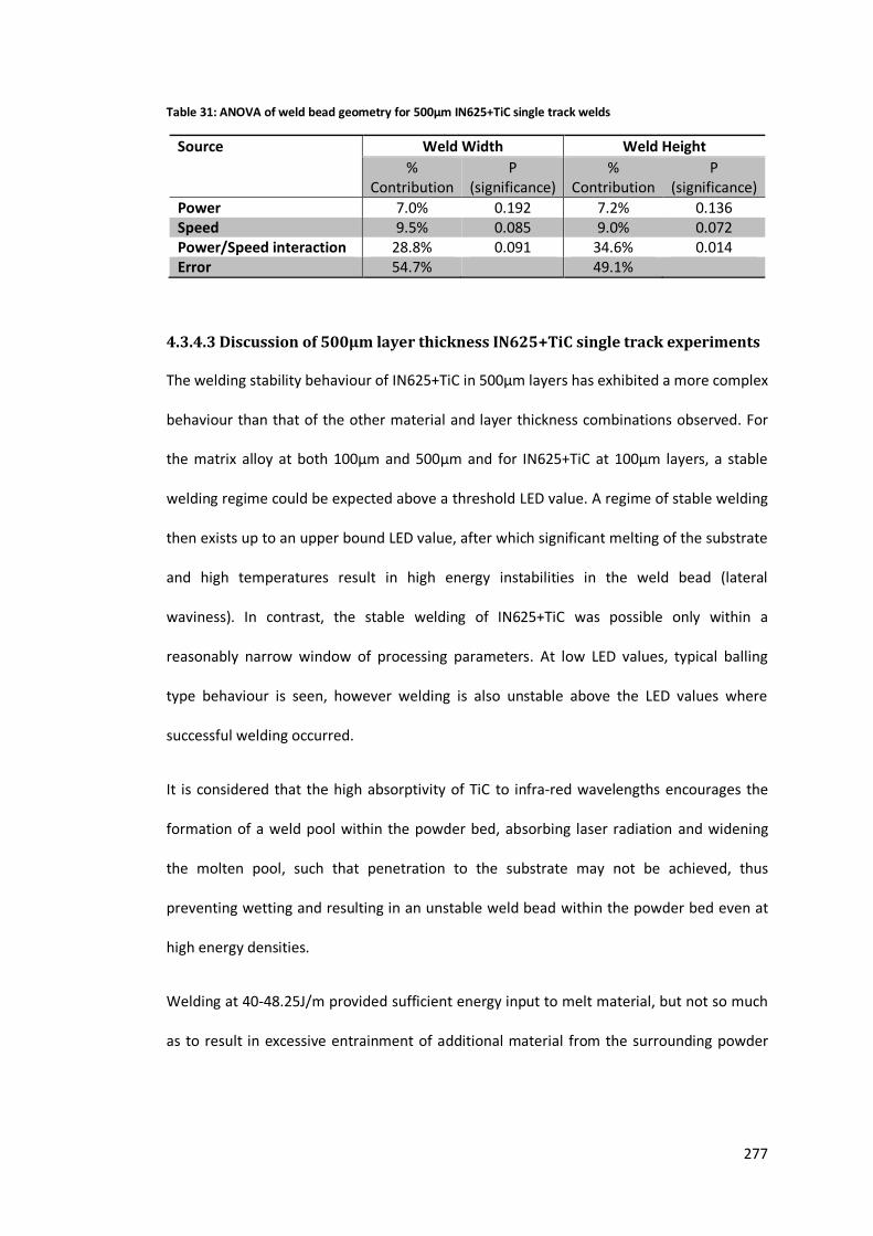
277
Table 31: ANOVA of weld bead geometry for 500µm IN625+TiC single track welds
Source Weld Width Weld Height
% Contribution
P (significance)
% Contribution
P (significance)
Power 7.0% 0.192 7.2% 0.136 Speed 9.5% 0.085 9.0% 0.072 Power/Speed interaction 28.8% 0.091 34.6% 0.014 Error 54.7% 49.1%
4.3.4.3 Discussion of 500µm layer thickness IN625+TiC single track experiments
The welding stability behaviour of IN625+TiC in 500µm layers has exhibited a more complex
behaviour than that of the other material and layer thickness combinations observed. For
the matrix alloy at both 100µm and 500µm and for IN625+TiC at 100µm layers, a stable
welding regime could be expected above a threshold LED value. A regime of stable welding
then exists up to an upper bound LED value, after which significant melting of the substrate
and high temperatures result in high energy instabilities in the weld bead (lateral
waviness). In contrast, the stable welding of IN625+TiC was possible only within a
reasonably narrow window of processing parameters. At low LED values, typical balling
type behaviour is seen, however welding is also unstable above the LED values where
successful welding occurred.
It is considered that the high absorptivity of TiC to infra-red wavelengths encourages the
formation of a weld pool within the powder bed, absorbing laser radiation and widening
the molten pool, such that penetration to the substrate may not be achieved, thus
preventing wetting and resulting in an unstable weld bead within the powder bed even at
high energy densities.
Welding at 40-48.25J/m provided sufficient energy input to melt material, but not so much
as to result in excessive entrainment of additional material from the surrounding powder

278
bed. Therefore the energy input is not dissipated into melting more powder than desired,
and wetting of the molten pool and substrate can take place.
4.3.5 Single track melting of 500µm layers IN625+Ti+C
As recoating could only be achieved at 400µm layers or greater, experiments were
conducted for 500µm layers only in the case of IN625+Ti+C powders (example build plate
shown in Figure 151).
Figure 151: Example of single track laser welds from a 500µm powder bed of IN625+Ti+C
4.3.5.1 Observations – stability & parameter window
Figure 152 presents the characterisation of the process window for single track laser
melting of IN625+Ti+C powder mixtures in 500µm layers. The window is dominated by high
speed, low power instability in the form of balling or mixed-mode instabilities
(discontinuous welds/balling behaviour). Welding appears most stable at the slowest
possible speeds and highest power, although some welds do not follow this trend (e.g.
1kW, 4m/min and 3.25kW, 4m/min as highlighted in Figure 152) this may be attributed to
differences in substrate temperature between repeats. A parameter set using 4kW and a
speed of 4-6m/min would appear to provide a stable weld at the highest possible
deposition rate, without excessive heat input. Two uncertain results are highlighted in
60mm

279
Figure 152, where repeats are unclear as to the dominant behaviour for the parameter set.
This variability is considered to be due to local variations in substrate temperatures due to
preceding welds.
Figure 152: Parameter window characterisation for 500µm IN625+Ti+C
The measured substrate temperature during single track welding of an IN625+Ti+C build is
presented in Figure 153. For the duration of the build, a maximum temperature of 44oC
was recorded in the centre of the substrate at a depth of 4mm from the surface.
500
1000
1500
2000
2500
3000
3500
4000
4500
0 2000 4000 6000 8000 10000 12000
Pro
gram
me
d L
ase
r P
ow
er
(W)
Welding Speed (mm/min)
Stable Unstable Humping Balling
Lin
ear
En
ergy
Den
sity
(J/
m)

280
Figure 153: Substrate temperature during IN625+Ti+C single track welding
4.3.5.1.1 Pre-Heated
In an effort to provide a more favourable welding environment for the reduction of residual
stress cracking, repeat trials were conducted with a pre-heated substrate. The effect upon
welding stability was unclear; some of the parameter combinations previously
characterised as “stable” for ambient temperature welding appeared to demonstrate some
instability, however this was deemed to be a case of inconsistency in repeats on the
boundary between stable and unstable behaviour (4-6m/min welding speeds). Although
some variation in behaviour was seen for repeat welds around the boundary between
instability and stability, in general welds at or above 30J/m are stable for at least two out of
three repeats, with balling or humping occurring on occasion. It is only at 100-120J/m that
welds become consistently stable in every repeat. It may therefore be suggested that
higher energy densities may result in a broader parameter window could this be
investigated. A single parameter set lies outside of the definitively stable region
(highlighted in Figure 154), with two out of three repeats exhibiting stable behaviour, but
one unstable, due to variations in substrate temperature.
20
25
30
35
40
45
50
00:00:00 00:02:53 00:05:46 00:08:38 00:11:31 00:14:24
Tem
pe
ratu
re (o
C)
Build Time (hh:mm:ss)

281
The temperature measured in the substrate for pre-heated IN625+Ti+C single track welds is
shown in Figure 155. Although a pre-heat temperature of up to 530oC was achieved, the
temperature recorded during welding continued to decrease from 300oC to approximately
250oC, despite the input of laser energy during welding (noted to be minimal during
un-heated experiments).
Figure 154: Parameter window characterisation for pre-heated 500µm IN625+Ti+C
Figure 155: Substrate temperature during pre-heated IN625+Ti+C single track welding
500
1000
1500
2000
2500
3000
3500
4000
4500
0 2000 4000 6000 8000 10000 12000
Pro
gram
med
lase
r p
ow
er
(W)
Welding speed (mm/min) Stable Unstable Balling
0
100
200
300
400
500
Tem
pe
ratu
re (o
C)
Build Time (hh:mm:ss)
Pre-Heat
Welding
Post-Weld Cooling
Lin
ear
Ener
gy D
ensi
ty (
J/m
)

282
4.3.5.2 Weld bead geometry & variation
In general an increase in LED results in an increased weld width, as shown in Figure 156.
The trend shown is significant, with little variation between repeats. The variation of
welding height with LED exhibits no particular trend, with the degree of variability between
repeat measurements often high, this is confirmed by the high P value in the ANOVA
presented in Table 32. The linear function for weld width is given in Equation 12, however
no reliable trend can be determined for weld height, so none is presented.
Figure 156: Weld bead width related to LED for un-heated 500µm IN625+Ti+C
Figure 157: Relationship between weld height and LED for un-heated 500µm IN625+Ti+C
0.5
1
1.5
2
2.5
0 20 40 60 80 100 120 140
Wel
d w
idth
(m
m)
Linear Energy Density (J/m)
0.35
0.4
0.45
0.5
0.55
0.6
0.65
0.7
0.75
0 20 40 60 80 100 120 140
Wel
d H
eigh
t (m
m)
Linear Energy Density (J/m)

283
𝑊𝑒𝑙𝑑 𝑤𝑖𝑑𝑡ℎ = 0.0132 × 𝐿𝐸𝐷 + 0.7879
Equation 12: Weld width as a function of linear energy density for 500µm IN625+Ti+C
In contrast to the behaviour of IN625 or IN625+TIC materials, the weld width for
IN625+Ti+C is most strongly influenced by the effect of welding speed (29.6%) and welding
power (25.9%) independently, with the interaction effect bearing a significance of 19.2%,
comparatively low. The welding height is still primarily influenced by the power/speed
interaction effect, however welding power and welding speed are proportionally more
influential in determining weld height than has been noted for other materials so far. The
degree of error in this ANOVA analysis is moderately high, 25.3% and 45.2% for width and
height respectively, while the analysis of weld width is significant (P<0.05), only the power
and speed analysis for weld height is significant, with a high value of P=0.102 for the
weld/speed interaction removing any confidence in the data for that interaction.
Table 32: ANOVA results for un-heated 500µm IN625+Ti+C single track welds
Source Weld Width Weld Height
% Contribution
P (significance)
% Contribution
P (significance)
Power 25.9% 0.000 18.3% 0.002 Speed 29.6% 0.000 13.2% 0.011 Power/Speed interaction 19.2% 0.010 23.2% 0.102 Error 25.3% 45.2%
4.3.5.2.1 Pre-Heated
The variation of weld width with LED is presented in Figure 158, and appears to be highly
consistent with that recorded for welds on ambient temperature substrates. The only
notable difference being that welds at low energy densities (<10J/m) exhibit a greater
width than for ambient temperature substrates. The trend line is however virtually
identical regardless of substrate pre-heating at higher linear energy densities.

284
Figure 158: Relationship between weld width and LED for pre-heated IN625+Ti+C
𝑊𝑒𝑙𝑑 𝑊𝑖𝑑𝑡ℎ = 0.012 × 𝐿𝐸𝐷 + 0.9244
Equation 13: Weld width as a function of linear energy density for pre-heated 500µm IN625+Ti+C
With the exception of a few individual parameter sets, the variation in weld height is not
excessive, however no trend is shown with the increase of LED, as shown in Figure 159. The
average height is 0.63mm, 24% higher than the intended layer thickness, consistent with
the known entrainment behaviour of a single isolated weld in a powder bed.
Figure 159: Relationship between LED and weld height for pre-heated 500µm IN625+Ti+C
0.6
0.8
1
1.2
1.4
1.6
1.8
2
2.2
2.4
2.6
0 20 40 60 80 100 120 140
Wel
d w
idth
(m
m)
Linear energy density (J/m)
0.2
0.4
0.6
0.8
1
1.2
1.4
1.6
0 20 40 60 80 100 120 140
Wel
d H
eigh
t (m
m)
Linear Energy Density (J/m)

285
An ANOVA analysis of the measured data for stable welds is presented in Table 33, and
indicates that welding speed is the dominant factor in determining weld width and height,
although welding power and the interaction of power and speed are also significant. Again
a high error is present, with all of the interactions regarded as significant with the
exception of the power/speed interaction for weld height.
Table 33: ANOVA results for pre-heated 500µm IN625+Ti+C
Source Weld Width Weld Height
% Contribution
P (significance)
% Contribution
P (significance)
Power 20.0% 0.000 19.6% 0.001 Speed 31.2% 0.000 20.7% 0.001 Power/Speed interaction 18.4% 0.045 15.8% 0.359 Error 30.5% 43.9%
4.3.5.3 Discussion of 500µm layer thickness IN625+Ti+C single track
experiments
The single track laser melting experiments for mixed IN625+Ti+C exhibit a similar behaviour
to that of the matrix alloy, in so far as there is a simple threshold LED value, above which
stable welding can be achieved, unlike the more complex laser/powder bed interactions
observed for IN625+TiC at 500µm layer thickness. It is interesting to note however that the
threshold value differs between single tracks upon an substrate at ambient temperature
and single tracks upon the pre-heated substrate. A stable welding regime is achieved above
an LED of 40J/m for the ambient temperature experiments and above 55J/m for the pre-
heated experiments. This difference in the stability threshold is counterintuitive, as the
substrate maintained a temperature above 250oC, it should be expected that the stability
threshold should decrease as a reduced energy input is required to reach the melting point
of the material. Figure 160 presents the calculated weld width based on input LED using the
equations defined by experimental data, the percentage difference in weld width between
ambient and pre-heated behaviour is plotted on the second axis.

286
Figure 160: Effect of LED on weld width for ambient and pre-heated IN625+Ti+C based on averaged equations
As the LED increases, the width of the welds converges, however, at lower LED values it can
be seen that the width of molten material in the pre-heated case always exceeds that of
the ambient material. This would indicate a similar behaviour as seen in IN625+TiC, where
the interaction of the laser and powder bed results in greater melting within the powder
bed, entraining material from either side of the weld, as it is already at an elevated
temperature. As energy is used to melt and entrain more material from the powder bed
this results in reduced penetration through the powder and limits subsequent wetting with
the substrate. At higher energy densities, the difference in pre-heat temperature becomes
less significant as a proportion of the overall energy input and the laser is able to penetrate
the powder bed and the effect of substrate material dominates, so no measurable
difference in weld width is observed.
4.3.6 Multi-Layer deposits of IN625+TiC at 100µm layers
4.3.6.1 Observations – Stability
General observations of 100µm IN625+TiC samples were presented in Section 4.3.1 during
the down-selection of reinforcement materials.
-2.00%
0.00%
2.00%
4.00%
6.00%
8.00%
10.00%
12.00%
1
1.2
1.4
1.6
1.8
2
2.2
2.4
10 30 50 70 90 110 130
Pe
rce
nta
ge d
iffe
ren
ce in
we
ld w
idth
(%
)
Wel
d w
idth
(m
m)
Linear Energy Density (J/m)
Ambient
Pre-Heated
Difference

287
4.3.6.2 Porosity
The areal porosity measured by optical microscopy for IN625+TiC at 100µm layers is
compared to that of the IN625 matrix material in Figure 161. The average of the measured
values indicate a slightly lower relative density than that of IN625, although variation
between differing heights within the sample is on the same order as that observed for
IN625. However, it should be recalled from the down-selection of reinforcement materials,
that TiC agglomerations appear in the 100µm IN625+TiC samples and could easily add a
false contribution to this porosity measurement.
Figure 161: Average porosity for IN625+TiC at 100µm layers compared to IN625 matrix
4.3.6.3 Composition, Microstructure & Hardness
As discussed in Section 4.3.1 the powder mixing for 100µm IN625+TiC was not sufficient to
produce a homogenous distribution of TiC particulates. The bulk composition as measured
by EDS for 100µm IN625+TiC is given in Table 34, significant deviations from the desired
composition can be noted when comparing the deposited material with the intended 5wt%
TiC content of the original powder mixture, the high Ti content of 19wt% in the deposited
sample and 26wt% Ti content in the feedstock mixture (reported in Section 4.1.1.5.3)
0
0.5
1
1.5
2
2.5
Low Mid Upper
Po
rosi
ty (%
)
IN625 100um
IN625+TiC 100um

288
indicates that the inhomogeneous distribution of reinforcement is responsible for the
unusual measurements.
Table 34: Composition of LM IN625+TiC at 100µm layers
Material Element wt% Deviation Error
Ni Cr Mo Nb Fe Ti Al
IN625 (max spec) 68.85 23.0 10.0 4.15 5.0 0.4 0.4 IN625 (min spec) 58.0 20.0 8.0 3.15 0.0 0.0 0.0 IN625 Powder 61.9 22.2 8.4 3.5 3.9 0.0 0.1 0.4 ±0.16 IN625+TiC 100µm LM 59.2 16.2 3.2 1.6 0.9 19.0 0.1 0.5 ±0.35
The hardness distribution within a full sample cross-section was evaluated, and is mapped
in Figure 162. The average deposited material hardness was calculated to be 387HV0.3, an
increase of 24% over the matrix material processed under the same conditions. As can be
seen in the hardness map, while the majority of the cross section has a relatively even
distribution of hardness, occasional high hardness points introduce a high level of
variability compared to that of the matrix material alone. These high hardness regions are
attributable to the clustering of reinforcement particulates, as observed by SEM.
Figure 162: Cross-sectional hardness distribution for 100µm IN625+TiC at 0.5mm Hatch
4.3.6.4 Discussion of 100µm layer thickness IN625+TiC multi-layer experiments
The processing behaviour and resulting material for 100µm layer thickness multi-layer
deposition of IN625+TiC was dominated by the effect of inhomogeneous powder mixing.
Har
dn
ess
(HV
0.3
)

289
However, as a result of the poor feedstock mixing in this case, two differing TiC behaviours
can be observed. Agglomerations of TiC remain after molten processing, showing an
ablated rounded morphology, this demonstrates that TiC is dissolved to some degree
within the molten pool, but as agglomerations are able to mutually protect each particle
from complete dissolution a differing behaviour is noted to smaller independent particles
which are fully dissolved and re-precipitated with a differing morphology to those only
partially dissolved. Therefore further investigations into achieving fully mixed powder were
conducted in Section 4.1.1 and the more homogeneously mixed powders used for
subsequent experiments at 500µm layer thicknesses.
The benefit to hardness was shown on average to be a 24% increase compared to the
matrix material alone. However, a more modest increase is expected for samples where
agglomeration is prevented, as this average will have been skewed by the inclusion of
unusually high hardness regions as shown in Figure 162.
4.3.7 Multi-Layer deposits of IN625+TiC at 500µm layers
4.3.7.1 Observations – Stability
Figure 163 shows photographs of 500µm IN625+TiC samples as removed from the build
chamber. Different hatching distances have produced noticeable changes in the geometry
of the samples built. At 0.5mm hatch distance, although the ends of each sample have a
significant slope, the overall form appears stable with top surface deviation on the order of
0.5mm. Samples at 0.8mm hatch distance have a more variable end condition to each weld
and surface variations on the order of 1mm. At 1.1mm hatch distance, samples are on the
boundary of instability, with significant waviness along the weld direction on the order of
several millimetres, particularly at higher welding speeds of 6.5m/min, compared to
5.5m/min.

290
Figure 163: 500µm layer IN625+TiC samples as built a) 0.5mm hatch b) 0.8mm hatch c) 1.1mm hatch
4.3.7.2 Porosity
4.3.7.2.1 Cross-Sectional porosity – Optical Microscopy
The micrograph montages presented in Figure 164 show sample cross sections at all three
hatch distances utilised. Samples at 0.5mm hatch distance may be qualitatively assessed as
closest to the intended rectangular cross section shape, with decreasing geometrical
accuracy as hatch distance was increased.
Contrast thresholding of micrographs from all three samples provided measurements for
porosity, which are presented in Figure 165 as a function of hatch distance. As can be seen
from the micrographs, the porosity present increases with hatch spacing.
b) a) c)

291
Figure 164: Optical microscope montages of 500µm IN625+TiC samples at a) 0.5mm hatch b) 0.8mm hatch c) 1.1mm hatch
a)
b)
c)

292
Figure 165: Increase of porosity with hatching distance for 500µm IN625+TiC
The variation of porosity with build height is shown in Figure 166 for all three hatch
distances, as well as a trend to increased porosity with hatching distance, it can be noted
that porosity increases with build height, particularly for samples at 0.5mm hatch. This
would indicate that further optimisation of process parameters for deposition at each layer
is required to maintain a stable and consistent melt and solidification behaviour.
Figure 166: Porosity variation with respect to Z height and hatching distance for 500µm IN625+TiC
0.4
0.6
0.8
1
1.2
1.4
1.6
1.8
0.4 0.5 0.6 0.7 0.8 0.9 1 1.1 1.2
Po
rosi
ty (%
)
Hatch Distance (mm)
0
0.5
1
1.5
2
2.5
3
Low Mid Upper
Po
rosi
ty (%
)
0.5mm Hatch
0.8mm Hatch
1.1mm Hatch
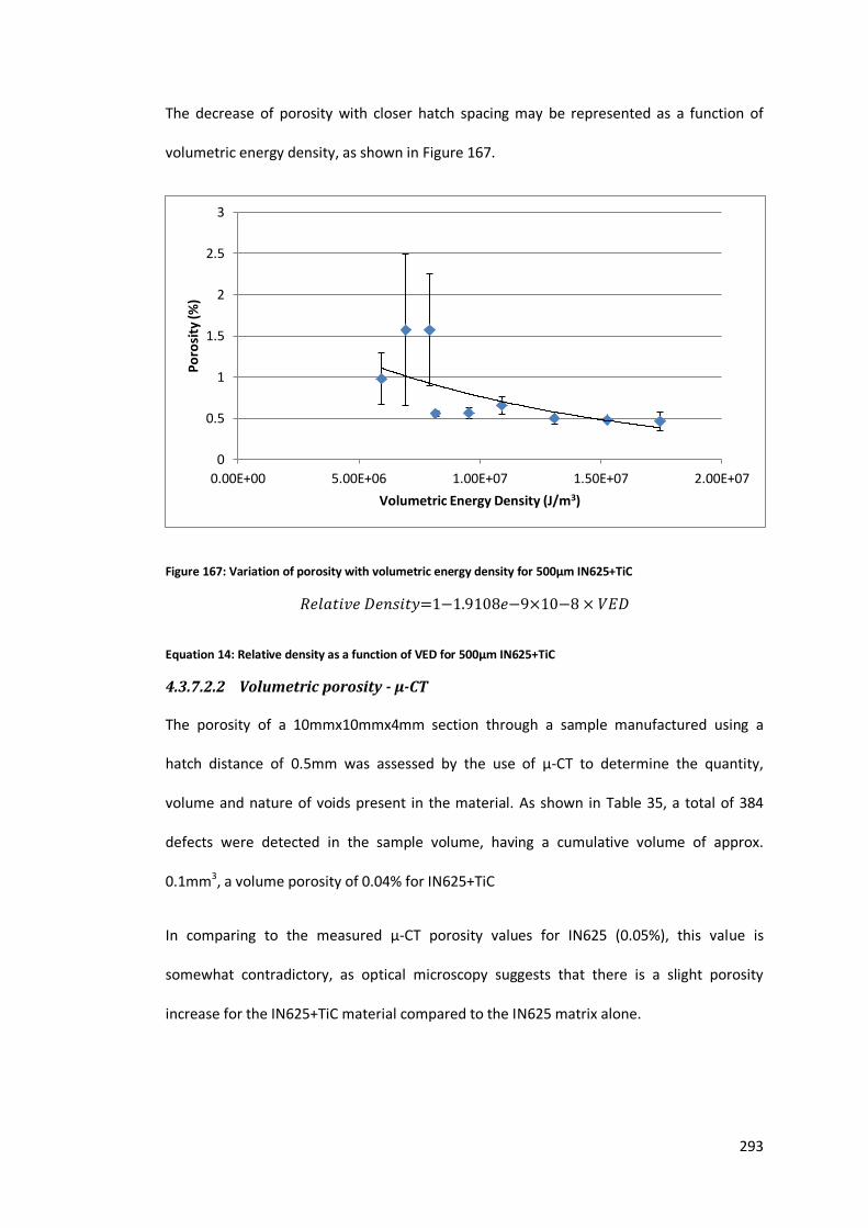
293
The decrease of porosity with closer hatch spacing may be represented as a function of
volumetric energy density, as shown in Figure 167.
Figure 167: Variation of porosity with volumetric energy density for 500µm IN625+TiC
𝑅𝑒𝑙𝑎𝑡𝑖𝑣𝑒 𝐷𝑒𝑛𝑠𝑖𝑡𝑦=1−1.9108𝑒−9×10⁻⁸ × 𝑉𝐸𝐷
Equation 14: Relative density as a function of VED for 500µm IN625+TiC
4.3.7.2.2 Volumetric porosity - µ-CT
The porosity of a 10mmx10mmx4mm section through a sample manufactured using a
hatch distance of 0.5mm was assessed by the use of µ-CT to determine the quantity,
volume and nature of voids present in the material. As shown in Table 35, a total of 384
defects were detected in the sample volume, having a cumulative volume of approx.
0.1mm3, a volume porosity of 0.04% for IN625+TiC
In comparing to the measured µ-CT porosity values for IN625 (0.05%), this value is
somewhat contradictory, as optical microscopy suggests that there is a slight porosity
increase for the IN625+TiC material compared to the IN625 matrix alone.
0
0.5
1
1.5
2
2.5
3
0.00E+00 5.00E+06 1.00E+07 1.50E+07 2.00E+07
Po
rosi
ty (%
)
Volumetric Energy Density (J/m3)

294
Table 35: Volumetric porosity of 500µm IN625+TiC
Total Volume (mm3) 274.0622 Void Volume (mm3) 0.0979 Number of Voids 384 Calculated Porosity 0.04%
The histogram shown in Figure 168 shows the size distribution of all the voids detected in
the sample, as can be seen, only one defect is larger than 0.02mm3, with all other defects
significantly below 0.01mm3, but with an increasing frequency of defects detected at
smaller sizes. The difference in measured porosity by µ-CT compared to optical microscopy
is likely therefore due to a high number of small defects below the detection limit being
present in the IN625+TiC sample, whereas the IN625 sample exhibited fewer, larger defects
and thus the µ-CT measurement agrees more closely with optical microscopy in that case.
Examination of Figure 169 and Figure 170 indicate that porosity in the IN625+TiC material is
predominantly of a gas bubble type morphology and located near to the side walls and
substrate. The majority of porosity is distributed along the sidewall which experienced laser
exposure last, indicating that thermal accumulation during the layer exposure may be
affecting the weld stability and resulting in increased porosity.

295
Figure 168: Volume distribution of defects in IN625+TiC sample

296
Figure 169: Reconstructed 2D slice of IN625+TiC
Figure 170: Reconstructed 3D sample volume and corresponding defect visualisation for IN625+TiC a) solid material with voids, b) voids only
4.3.7.3 Composition, Microstructure & Hardness
4.3.7.3.1 Microstructure - SEM
The microstructure of deposited IN625+TiC material exhibits similar characteristics to that
of the IN625 matrix material. High aspect ratio grains on the order of 50µm wide by
100µm+ long, with a strong alignment towards the substrate direction.
1mm 1mm
1.5mm
a) b)

297
Figure 171: Back scatter electron image of IN625+TiC microstructure (top layer)
Examination at higher magnifications shows small angular and star/flower shaped
particulates, as shown in Figure 172. Particle sizes vary in magnitude from 1-2µm down to
approximately 0.25µm, although distinguishing porosity and particulates at this scale can
be difficult unless the angular morphology is readily apparent. The distribution of
particulates within the matrix appears to be quite homogenous, with none of the particle
clustering observed in the 100µm IN625+TiC samples, as a result of the longer powder pre-
mixing time.
Closer examination of the TiC reinforcement particles reveals that as their size increases,
their morphology undergoes a change from angular cubic, and begins to form star or flower
like particulates. There also appears to be a preference for TiC particles to co-locate with
Mo/Nb carbides within the y phase matrix.

298
Figure 172: High magnification back scatter electron image of IN625+TiC microstructure
Figure 173: High magnification back scatter electron image of IN625+TiC microstructure
4.3.7.3.2 Composition - EDS & XRD
The linescan of the sample/substrate interface in Figure 174 shows a clear demarcation in
composition between successive layers, with the bulk material composition achieved after

299
4 layers, at a Z height of approximately 1.0-1.5mm, similar to the behaviour observed for
the 500µm layer processing of IN625.
Figure 174: EDS Linescan of interface dilution for 500µm IN625+TiC
EDS Spectra of the bulk material provides an approximate composition for the deposited
material, given in Table 36. As expected, the proportion of Ti present in the sample has
increased above that of the matrix material alone. Notably however the proportion of Nb
and to a lesser extent Mo have also increased, which may indicate some inhomogeneity in
the distribution of carbides, which could account for this.
Table 36: Composition of LM IN625+TiC at 500µm layers
Material Element wt% Deviation Error
Ni Cr Mo Nb Fe Ti Al
IN625 (max spec) 68.85 23.0 10.0 4.15 5.0 0.4 0.4 IN625 (min spec) 58.0 20.0 8.0 3.15 0.0 0.0 0.0 IN625 Powder 61.9 22.2 8.4 3.5 3.9 0.0 0.1 0.4 ±0.16 IN625+TiC 500µm LM 58.6 21.6 8.6 5.2 4.2 1.3 0.1 0.1 ±0.05
EDS inspection of the bulk material at a distance remote from the substrate (Z>5mm)
shows particulates with a high Ti content, indicating the presence of TiC. Notably the
Un
affe
cted
su
bst
rate
Fe d
iluti
on
into
laye
r
IN6
25
Bu
lk m
ater
ial
Substrate Deposited material
IN62
5 di
luti
on in
to s
ub
stra
te

300
carbide forming Mo and Nb elements have also located at the same nucleation sites, as
shown by the EDS mapping in Figure 175, though it should be remembered that particles
are close to the size of the interaction volume and so the limits of resolution for EDS.
Figure 175: Back scattered electron image and associated EDS Maps for IN625+TiC
In order to confirm the composition of the sample, XRD scans were conducted, and
compared to XRD scans of the powder constituents in their pure as received form. The

301
spectra for IN625+TiC shown in Figure 176 confirms the presence of TiC in the deposited
material, peaks representing each of the feedstocks are superimposed in the spectra for
the MMC material. Though the peaks for TiC at 87o and 91o overlap slightly with the IN625
peak at 89o, it is still possible to distinguish the two phases clearly. The magnitude of TiC
peaks is of course reduced compared to the pure feedstock, recalling a 5wt% fraction of TiC
compared to IN625 should be present.

302
Figure 176: XRD Spectra for deposited IN625+TiC material
5000
10000
15000
20000
25000
30000
35000
40000
20 30 40 50 60 70 80 90 100
Co
un
ts
Position 2 Theta (Cobalt (Co))
IN625+TiC
IN625
TiC

303
4.3.7.3.3 Hardness
The cross sectional hardness distribution for each of the three hatch distances are
presented in Figure 178. The sample exposed at 0.5mm hatch would appear to possess a
more even distribution of hardness, than those at 0.8mm and 1.1mm, while hardness
would also appear to increase with hatch distance.
The increase in average hardness with hatch distance (shown in Figure 177) is attributable
to the increase in matrix hardness already established rather than the effect of the
reinforcement. Compared to the hardness variation with hatch distance for the IN625
matrix alone however the IN625+TiC sample exhibits less variation at 0.5mm hatch
distance, but greater variation at higher hatch distances. Although IN625+TiC deposited at
100µm shows a higher average hardness, its variability is much higher than that of either
IN625 or IN625+TiC produced at 500µm layers.
The low variation in measured hardness values across the 5x5mm area measured would
indicate that as observed by SEM, the reinforcement particulates are well distributed on
both a micro and macro scale.
Figure 177: Variation of material hardness with hatch spacing for IN625+TiC
230
250
270
290
310
330
350
370
390
410
0.4 0.6 0.8 1 1.2
Har
dn
ess
(HV
0.3)
Hatch Distance (mm)
500um IN625+TiC
100um IN625+TiC
500um IN625
100um IN625

304
Figure 178: Hardness distribution for IN625+TiC a) 0.5mm hatch b) 0.8mm hatch c)1.1mm hatch
a)
b)
c)
Har
dn
ess
(HV
0.3
) H
ard
nes
s (H
V0
.3)
Har
dn
ess
(HV
0.3
)

305
4.3.7.4 Discussion of 500µm layer thickness IN625+TiC multi-layer experiments
As can be seen from the results presented, the more homogeneous powder mixture used
as feedstock for the 500µm layer thickness experiments has resulted in a consistent and
homogeneous deposited material. TiC particulates have been dissolved and reformed
throughout the material with no agglomerations noted in contrast to the 100µm layer
thickness samples. The consistent porosity measurements for 0.5mm and 0.8mm hatch
spacing have shown that the thermal control strategy implemented has been successful.
The XRD scans conducted show that the deposited material has not formed any significant
quantity of unwanted phases such as Mo2C or NbC, and that the desired IN625 and TiC
phases have re-formed after melting.
The average hardness of the material has increased by 19% for the 0.5mm hatch spacing,
22% for the 0.8mm hatch spacing and 25% for the 1.1mm hatch spacing. Figure 179
presents data for the 0.5mm hatch sample at 500µm layer thickness alongside that of the
same processing conditions for the matrix and reported hardness and density for pure TiC.
Using the law of mixtures an increase in hardness from 261HV0.3 as measured for IN625
deposited in previous experiments to 456HV should be expected, assuming a volume
fraction of 8% TiC, having a theoretical hardness in the region of 2700HV. Again using the
law of mixtures the density of the composite should be expected to be 8.26g/cm3,
providing a specific hardness of 55HV per unit weight, which would be an increase of 78%
over the matrix material alone.
In reality, the experimental results show a more moderate increase in hardness to
335HV0.3, at an average relative density of 99.5% as measured by optical microscopy, which
gives a 32% increase in specific hardness to 41HV per unit weight compared to the 31HV
per unit weight of the matrix material alone. It is unsurprising that the manufactured MMC
does not attain the properties suggested by a simple law of mixtures approach, as in reality

306
defects, porosity and the inherent variability in hardness measurement (particularly for an
MMC) will all contribute to uncertainty. The law of mixtures approach is also highly
idealised, so should only serve as an indication of the expected properties. Given that
expectation, the analysis of the manufactured samples shows a reasonable improvement in
properties over the matrix alloy alone.
Figure 179: Comparison of material density and specific hardness between matrix, reinforcement and composite vs. law of mixtures prediction using data for 0.5mm hatch sample
4.3.8 Multi-Layer deposits of IN625+Ti+C at 500µm layers
4.3.8.1 Observations – Stability
Figure 180 shows post-build samples of multi-layer IN625+Ti+C produced on un-heated
substrates. Of the two welding speeds used to produce these samples, the slower
(5.5m/min) exhibit the greatest stability, whilst those at 6.5m/min were discontinued
before the complete build height was achieved due to instability.
There is a trend towards increased geometrical accuracy and apparent welding stability at
closer hatch distances (0.5mm), with a poor quality deposition at wider hatch distances.
0
1
2
3
4
5
6
7
8
9
0
100
200
300
400
500
600
IN625 TiC Law ofmixtures
Actual
De
nsi
ty (
g/cm
3 )
Spe
cifi
c H
ard
ne
ss (H
V/g
)
Specific Hardness
Density

307
It may be immediately observed that macro-cracking is present in the samples, either at
the substrate/sample interface or within 2mm. Finer secondary cracks are also present
transverse to the welding direction in the centre of the sample, and pass through all layers
to the top surface in some cases. The frequency and severity of cracking is greater near to
the substrate, and in some areas, its interconnected nature has caused small portions of
the samples to be separated from the majority of the deposited material (see Figure 181).
Figure 180: Photographs of IN625+Ti+C samples at a) 0.5mm hatch b) 0.8mm hatch c) 1.1mm hatch
Figure 181: Stereomicrograph montage of un-heated 500µm IN625+Ti+C cracking - 0.8mm hatch
The recorded substrate temperature for a build at 0.8mm hatch distance is presented in
Figure 182. Substrate temperature increases during deposition of the first eight layers,
after which there is a net decrease in substrate temperature, as the low thermal
conductivity and build geometry isolate the melt pool heat from reaching the substrate.
a) b) c)
5mm

308
During repeated layer deposition the substrate temperature remains relatively consistent
at an average of 110oC, and on the whole within the range of 100-140oC.
Figure 182: Substrate temperature during multi-layer IN625+Ti+C build
4.3.8.1.1 Pre-Heated samples
Inspection of the samples produced using a pre-heated substrate (in Figure 183) show that
in contrast with samples deposited upon an un-heated substrate, those produced using a
pre-heated substrate are more stable at higher welding speeds (6.5m/min) whist without
substrate heating samples at 5.5m/min show the greatest stability. Samples at 0.5mm
hatch distance still appear to be the most stable though. The most interesting feature of
the samples however is the degree of cracking at the substrate interface, which is far
greater for samples with a pre-heated substrate than without. Cracking appears to increase
with greater hatch distances, and in the case of some samples leads to partial delamination
of sections of the deposited sample from the substrate, due to the thermal stresses present
(shown in Figure 184).
0
20
40
60
80
100
120
140
160
00:00:00 00:02:53 00:05:46 00:08:38 00:11:31 00:14:24 00:17:17 00:20:10
Tem
pe
ratu
re (o
C)
Build Time (hh:mm:ss)
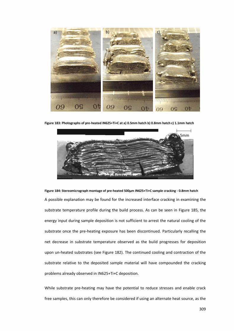
309
Figure 183: Photographs of pre-heated IN625+Ti+C at a) 0.5mm hatch b) 0.8mm hatch c) 1.1mm hatch
Figure 184: Stereomicrograph montage of pre-heated 500µm IN625+Ti+C sample cracking - 0.8mm hatch
A possible explanation may be found for the increased interface cracking in examining the
substrate temperature profile during the build process. As can be seen in Figure 185, the
energy input during sample deposition is not sufficient to arrest the natural cooling of the
substrate once the pre-heating exposure has been discontinued. Particularly recalling the
net decrease in substrate temperature observed as the build progresses for deposition
upon un-heated substrates (see Figure 182). The continued cooling and contraction of the
substrate relative to the deposited sample material will have compounded the cracking
problems already observed in IN625+Ti+C deposition.
While substrate pre-heating may have the potential to reduce stresses and enable crack
free samples, this can only therefore be considered if using an alternate heat source, as the
a) b) c)
5mm

310
laser beam can no longer be employed to maintain substrate temperatures once powder is
deposited. The use of a dissimilar substrate material (steel) may also be a contributory
factor as difference in CTE between deposited material and substrate will increase the
stresses present.
Figure 185: Substrate temperature during pre-heated multi-layer IN625+Ti+C build
4.3.8.2 Porosity
4.3.8.2.1 Cross-sectional porosity – Optical Microscopy
The variation of areal porosity for the hatch distances utilised is presented in Figure 186.
There is a significant variation in the measured values at all hatch distances, as well as a
steady increase in porosity with hatch distance.
0
100
200
300
400
500
00:0
0:10
00:0
3:00
00:0
5:50
00:0
8:40
00:1
1:30
00:1
4:20
00:1
7:10
00:2
0:00
00:2
2:50
00:2
5:40
00:2
8:30
00:3
1:20
00:3
4:10
00:3
7:00
00:3
9:50
Tem
pe
ratu
re (o
C)
Build Time (hh:mm:ss)
Pre-Heating
Deposition
Post Build Cooling

311
Figure 186: Variation in porosity with hatching distance for 500µm IN625+Ti+C
Comparing the areal porosity measured within the sample cross section, it can be observed
that there is a trend towards a porosity increase with Z height, particularly for samples at
0.5mm hatch distances (see Figure 187). This would suggest that local melt pool conditions
have not remained consistent during the build, despite efforts to reduce the heat input by
reducing laser power Z height increases.
Figure 187: Variation in areal porosity with Z height and hatching distance for 500µm IN625+Ti+C
1
2
3
4
5
6
7
0.4 0.5 0.6 0.7 0.8 0.9 1 1.1 1.2
Po
rosi
ty (%
)
Hatch Distance (mm)
0
1
2
3
4
5
6
7
8
9
Low Mid Upper
Po
rosi
ty (%
)
0.5mm Hatch
0.8mm Hatch
1.1mm Hatch

312
Despite the apparent increase of porosity due to excess heat input for the 0.5mm hatch
samples, Figure 188 still shows a definite correlation between energy density and porosity.
Figure 188: Variation in porosity with volumetric energy density for 500µm IN625+Ti+C
𝑅𝑒𝑙𝑎𝑡𝑖𝑣𝑒 𝐷𝑒𝑛𝑠𝑖𝑡𝑦 = 4 × 10⁻⁷ × 𝑉𝐸𝐷 − 7.2571
Equation 15: Relative Density as a function of VED for 500µm IN625+Ti+C
4.3.8.2.1.1 Pre-Heated samples
For samples deposited upon a pre-heated substrate, the general trend for an increase in
porosity and variation with hatch distance shown in previous experiments remains true, as
shown in Figure 189. The porosity is however relatively high, up to 10% for samples at
1.1mm hatch distance, and no greater than 96% average relative density achieved at
0.5mm hatch distance.
0
1
2
3
4
5
6
7
8
9
0.00E+00 5.00E+06 1.00E+07 1.50E+07 2.00E+07
Po
rosi
ty (%
)
Volumetric Energy Density (J/m3)

313
Figure 189: Variation in porosity with hatch distance for pre-heated 500µm IN625+Ti+C
The variation in areal porosity with Z height is substantial for pre-heated samples, however
no particular trend is evident, with highest porosities seen in either lower or mid Z height
regions of the sample depending upon hatch distance (as shown in Figure 190).
Figure 190: Variation in porosity with Z height and hatch distance for pre-heated 500µm IN625+Ti+C
The high variations in porosity shown in Figure 189 do vary with energy density, but no
conclusive trend can be drawn.
2
4
6
8
10
12
14
0.4 0.5 0.6 0.7 0.8 0.9 1 1.1 1.2
Po
rosi
ty (%
)
Hatch Distance (mm)
0
2
4
6
8
10
12
14
16
18
Low Mid Upper
Po
rosi
ty (%
)
0.5mm Hatch
0.8mm Hatch
1.1mm Hatch

314
Figure 191: Variation in areal porosity with volumetric energy density for pre-heated 500µm IN625+Ti+C
4.3.8.2.2 Volumetric porosity - µ-CT
To establish the nature of porosity and defects within a IN625+Ti+C sample, a sample
produced at 0.5mm hatch spacing upon an un-heated substrate was measured by µ-CT
scanning. The total void volume detected was approx. 53mm3 from a sample volume of
approx. 266mm3, a volume percentage of 19.94% porosity.
Table 37 : Volumetric porosity data for IN625+Ti+C
Total Volume (mm3) 265.7546 Void Volume (mm3) 52.9945 Number of Voids 12217 Calculated Porosity 19.94%
The volume frequency distribution shown in Figure 192 indicates that this is likely a
significant underestimation, as the frequency of defects increases at smaller sizes and is
likely to continue doings so below the detection limit for µ-CT.
0
2
4
6
8
10
12
14
16
18
0.00E+00 5.00E+06 1.00E+07 1.50E+07 2.00E+07
Po
rosi
ty (%
)
Volumetric Energy Density (J/m3)

315
Figure 192: Volume distribution of defects in IN625+Ti+C sample

316
It is evident from inspection of the distribution of defects and their morphology (shown in
Figure 193 and Figure 194) that the majority of large spherical gas bubble type porosity is
present towards the edges of the deposited sample, and more so toward the final weld
track than the first. The majority of defects present in the lower regions of the sample are
due to cracking. There is a lower concentration of voids in the central region of the sample,
indicating that processing conditions are more favourable in this region.
Figure 193: Reconstructed 2D slice of IN625+Ti+C sample
Figure 194: Reconstructed 3D sample volume and corresponding defect visualisation for IN625+Ti+C a) solid material with voids, b) voids only
1.5mm
1mm 1mm
a) b)

317
4.3.8.3 Composition, Microstructure & Hardness
4.3.8.3.1 Microstructure – SEM
Inspection of the microstructure close to the substrate interface (<1mm Z height) reveals a
Ni-Cr-Fe matrix which has formed in a globular dendritic structure, without the Mo/Nb
carbide veins typically seen in γ phase IN625. Small (<1µm) rounded cubic carbide particles
are distributed between dendrite arms. Cracking near the substrate appears to be as a
result of liquation type cracking on the boundaries between dendrite cells.
Figure 195: High magnification back scattered electron image of IN625+Ti+C (lower)
Images of the microstructure at the samples mid Z height (approx. 3mm) in Figure 196
reveals a transition from the globular dendritic structure described to a more conventional
dendrite layout. Reinforcement particles appear to be well distributed, and on the order of
2µm in size.
Ni-Cr-Fe matrix Carbides

318
Figure 196: Back scattered electron image of IN625+Ti+C microstructure (mid)
Within the top third of the samples, there still appears to be a Ni-Cr-Fe matrix Figure 197,
however its structure is different again, exhibiting an unfamiliar irregular form and not the
expected y-phase microstructure as seen for the matrix alloy of TiC reinforced material.
There is a degree of segregation of matrix alloying elements on the 100µm scale, with some
bands of material showing slightly differing contrast under back scatter electron imaging.
The particulates identified close to the substrate interface appear to have altered in
structure as well, while some of the rounded cubic morphology are still present, a large
proportion of the particulates have taken on a flower/star morphology, growing between
the matrix phase boundaries. Particles have a size range from <1µm up to 3-5µm, and
appear to be well distributed throughout the material.
Closer inspection of the reinforcement particulates observed (Figure 198) shows that they
do indeed position on the boundaries of y phase grains. The particles themselves appear to
be of mixed types, with slight differences in contrast between particles indicating some
compositional differences. In some cases it can be seen that carbide particles of differing
Ni-Cr-Fe dendrites Carbides

319
composition have grown from the same nucleation site, giving a flower morphology where
“petals” are composed of different individual carbides as indicated by a difference in BSE
contrast seen in Figure 198.
Figure 197: Low magnification back scattered electron image of IN625+Ti+C microstructure (upper)
Figure 198: High magnification back scattered electron image of carbide particles in IN625+Ti+C material
Ni-Cr-Fe matrix
Carbides
Segregation
Ni-Cr-Fe matrix
Light carbide petal Darker carbide petal
Segregation

320
4.3.8.3.2 Composition – EDS
The bulk composition of the IN625+Ti+C material presented in Table 38 shows a slightly
lower Ti content compared to that for the IN625+TiC (Ti=1.5wt%) material, indicating that
mixing of the material was not completely homogenous.
Table 38: EDS measurement of bulk material for 500µm IN625+Ti+C
Material Element wt% Deviation Error
Ni Cr Mo Nb Fe Ti Al
IN625 (max spec) 68.85 23.0 10.0 4.15 5.0 0.4 0.4 IN625 (min spec) 58.0 20.0 8.0 3.15 0.0 0.0 0.0 IN625 Powder 61.9 22.2 8.4 3.5 3.9 0.0 0.1 0.4 ±0.16 IN625+Ti+C 500µm LM 60.1 21.9 8.5 4.0 4.2 1.0 0.0 0.2 ±0.12
The co-location of Ti, Mo and Nb to form the particulates seen in the SEM images is
confirmed in Figure 199. Whereas the IN625+TiC material showed a high concentration of
Ti, with smaller quantities of Mo and Nb located at the particle site, the IN625+Ti+C
material appears to be predominantly Mo and Nb with a lower concentration of Ti.

321
Figure 199: Back scattered electron image and associated EDS maps for 500µm IN625+Ti+C

322
4.3.8.3.3 Composition - XRD
The spectra of an XRD scan from deposited IN625+Ti+C material is shown in Figure 200.
Accounting for some peak shift (which would indicate high lattice strains compared to
spectra from the IN625 matrix material alone), the peaks for IN625 and TiC can be
identified, establishing that TiC has been formed in-situ during the LM process.
In addition small peaks for Ti may also be seen, although discerning such a small quantity in
the complex spectra is difficult with certainty, however this indicates that not all Ti may
have been consumed in forming TiC. The peaks for graphitic carbon cannot be noted,
although the small quantity and complexity of the spectra may be masking its presence, or
it may no longer be in the form of graphite. Some additional unexpected peaks are present,
which are not attributable to either IN625, Ti, C or TiC. These peaks represent molybdenum
carbides (Mo2C), being close to patterns reported in literature [356], although not precisely
aligning. The peak shift may be explained by lattice strains which will undoubtedly be
present in the MMC samples compared to any pure reference pattern. The Mo rich
particulates observed by SEM/EDS would tend to support the idea that Mo2C is present in
larger quantities than in the matrix material alone, or that in this larger particulate form its
presence is more readily detected by XRD, whereas in γ-phase IN625, Mo2C are significantly
smaller and distributed at grain boundaries, which would make their detection by XRD
more difficult.

323
Figure 200: XRD Spectra for IN625+Ti+C deposited material
5000
10000
15000
20000
25000
30000
35000
20 30 40 50 60 70 80 90 100
Co
un
ts
Position 2 Theta (Cobalt (Co))
IN625+Ti+C Spectra
IN625
TiC
Ti
Mo2C

324
4.3.8.3.4 Hardness
The material hardness for IN625+Ti+C is significantly higher than that previously measured
for IN625+TiC material, and beyond twice that of the IN625 matrix material alone, as
shown in Figure 201, variation in hardness increases strongly with hatch distance. For pre-
heated samples, the variation in hardness is high regardless of hatch distance. The high
hardness and corresponding reduction in ductility have left the material highly susceptible
to crack formation, not only due to liquation cracking at the substrate as observed by SEM,
but also post weld stress cracking through layers.
Figure 201: Hardness variation with hatch distance for IN625 & MMCs
The distribution of hardness within 5x5mm sample sections for both ambient condition and
pre-heated IN625+Ti+C samples is presented in Figure 202, and shows the effects of high
porosity and cracking where indents could not be measured. The most consistent
distribution of hardness can be observed in samples produced at 0.5mm hatch spacing and
with ambient temperature substrates.
230
280
330
380
430
480
530
580
630
0.4 0.6 0.8 1 1.2
Har
dn
ess
(HV
0.3
)
Hatch Distance (mm)
IN625+Ti+C
IN625+Ti+C (PH)
IN625+TiC
IN625

325
Figure 202: Hardness distribution for IN625+Ti+C and pre-heated samples a) 0.5mm Hatch b) 0.8mm Hatch c)1.1mm Hatch
4.3.8.4 Discussion of 500µm layer thickness IN625+Ti+C multi-layer experiments
The deposition of IN625+Ti+C has been significantly affected by the distribution of carbon
throughout the material. Most importantly large Mo2C carbides have formed at the same
nucleation sites as TiC, rather than remaining as smaller MoC or Mo2C carbides distributed
at the grain boundaries within the conventional γ phase of IN625. The absence of these
a)
b)
c)
Pre-Heated
Pre-Heated
Pre-Heated
Har
dn
ess
HV
(0.3
)
Har
dn
ess
HV
(0.3
)
Har
dn
ess
HV
(0.3
)
Har
dn
ess
HV
(0.3
) H
ard
nes
s H
V(0
.3)
Har
dn
ess
HV
(0.3
)

326
carbides and the presence of excessive carbon has resulted in the formation of a dendritic
microstructure based on a Ni-Cr-Fe phase, but not recognisable as γ phase IN625.
The work of Hong et al., [64] noted the presence of Mo and Nb Carbides within the
interfacial region between TiC particles and the matrix, as the TiC particles were not
dissolved fully during their experiments. The fully molten processing route during this
investigation has therefore allowed Ti, Mo, Nb and C to mix more freely, resulting in a
greater Mo2C volume fraction and differing morphology and scale.
These differences in structure have caused embrittlement of the material as a whole, and
in all probability increased strains between the larger carbide particles and the matrix, so
leading to macro-cracking of the material during deposition of subsequent layers.

327
4.3.9 Discussion of IN625 MMCs
Very little is reported in literature regarding the additive manufacture or welding of TiC
reinforced Inconel 625 MMCs, though other nickel superalloys have been processed.
Hong et al., [172] investigated the formation of TiC reinforced IN718 MMCs using a blown
powder deposition route, and were able to manufacture a high density material. Some
dissolution and re-precipitation of TiC was seen for small particulates, while larger particles
remained mostly intact, but fully bonded into the matrix. In contrast, despite the use of
lower linear energy densities the laser melting of TiC reinforced IN690 MMCs by Wilson and
Shin [171] found that although the TiC particles were not fully dissolved in the matrix
during processing, small particles of TiC begin to form in the interfacial region. Zheng et al.,
[173] were also able to produce IN625+TiC MMCs, and found Ni coated TiC particles
beneficial to ensure matrix/reinforcement wetting. The observation of results from the
experiments performed in this thesis are broadly similar, however a greater degree of
reinforcement dissolution has occurred, resulting in finer precipitates of TiC and a higher
material density along with faster deposition rates has also been shown.
To comprehend the reasons for these differences a more detailed assessment of the
process parameters and equipment is required and is provided in context with more recent
and relevant literature in Section 4.3.9.1.
4.3.9.1 Discussion of IN625+TiC processing
Since the original submission of this thesis, work by Hong et al., [174] and Jiang et al., [357]
has studied the deposition of pre-mixed IN625+TiC at 5wt% using a blown powder laser-
DED system. Similarly to Wilson and Shin [171], Hong et al., and Jiang et al., found that the
TiC particulates ablated and dissolved with the matrix alloy, but did not observe as great a
degree of dissolution and re-precipitation of TiC particles as was seen in the work
conducted for this thesis. The morphology of the TiC particles in the as-deposited

328
IN625+TiC material produced by laser-DED experiments exhibited an ablated nodular form,
whereas the morphology shown in the powder bed experiments for this thesis was an
angular star/flower form, indicating nucleation and subsequent growth during
solidification.
The improvement to mechanical properties (namely hardness) for IN625+TiC composites
shown in this investigation agrees closely with the work of Hong et al., and Wilson and
Shin, being in the region of 350-380HV. In contrast however the powder bed process route
has resulted in a more homogenous distribution of finer (<1µm) precipitated reinforcing
particles, than that seen in other work (where a mixture of large (>1µm)
undissolved/ablated particulates and finer (<1µm) precipitated TiC particles are seen).
In order to understand the reasons for the differences seen it is necessary to analyse and
compare the differing process parameters used for the contrasting experiments.
Hong et al., characterise the process in terms of Linear Energy Input Per Unit Length
(LEIPUL), calculated as shown in Equation 16. However, LEIPUL represents only the laser
power and speed used, not the complete interaction of all significant process parameters
for the deposition of more than a single weld (i.e. the volume of material present).
𝐿𝐸𝐼𝑃𝑈𝐿 = 𝑃/𝑣
Equation 16 : Laser energy input per unit length (kJ/m), laser power (W) divided by scanning speed (mm/min)
Jiang et al., characterise the process parameters in terms of energy density per unit mass of
material, ranging from zero to 25.3kJ/g, which is a more useful metric for assessing the
energy density used and is the simplest to derive in a laser-DED system where the mass
flow rate of material is controlled rather than the volume of material available as in a
powder bed system.

329
In contrast the work conducted in this thesis characterises the processing parameters by
the Volumetric Energy Density, which accounts for the quantity of material present
(determined by layer thickness) and most importantly the laser beam focal spot diameter
and hatching distance between deposition welds. VED can be readily converted to energy
density per unit mass for comparison with the laser-DED based work of Hong et al., and
Jiang et al., the full comparison of input process parameters and resulting energy densities
is presented in Table 39. As has been demonstrated in Section 4.3.7.2, specifically Figure
165, material density is most strongly influenced by hatching distance as a significant factor
for determining VED. The smaller focal spot size of the laser used in this work (0.85mm
compared to 1mm for the laser-DED system) as well as higher laser powers (1-4kW rather
than 500-800W) and faster scanning speeds (2000-10,000mm/min rather than 300-
900mm/min) have resulted in some distinct differences in the observed results.
Table 39 : IN625+TiC Process parameter comparison
Power (W)
Hatch (mm)
Speed (m/min)
Layer thickness
(mm)
Deposition rate
(kg/hr)
Energy Density (kJ/g)
Relative Density
(%)
Powder Bed (Max)
4000 0.5 5.5 0.5 0.70 20.68 99.80
Powder Bed (Min)
4000 1.1 5.5 0.5 1.53 9.40 98.75
DED (Max) 800 0.75 0.3 1.0 0.11 25.28 99.50
DED (Min) 500 0.75 0.9 0.5 0.17 10.53 96.80
Counterintuitively, a comparison of all the relative process parameters between the two
deposition systems shows that the powder bed system and high powered laser actually
effected a lower energy density per unit mass of material, this is due to the much higher
scanning speeds used. The higher degree of TiC dissolution seen in the as-deposited
material cannot be attributed to any substantial difference in TiC particle sizes either, the
feedstock utilised by Hong et al., ranged from 5-7µm, while the feedstock utilised in these
experiments was distributed from 2-10µm (with the exception of agglomerations in both

330
cases). The larger particles should therefore take longer to dissolve; given the higher scan
speeds and so shorter exposure/melt time for the powder bed system, a lesser degree of
dissolution should be expected, but in fact the opposite has been observed.
A more complete understanding of the process can be found in comparing the power
density of the laser sources used, as shown in Table 40. The high degree of TiC dissolution
can therefore be attributed to the higher intensity of the smaller laser spot diameter
coupled with higher laser power, which generates a power density approximately seven
times greater than that used in the laser-DED based work. This greater power density is
therefore responsible for more fully melting the TiC particles present within the scale of
weld pool, despite the overall lower energy density per unit mass of material.
Table 40: Comparison of laser power density
Power (W)
Focal Spot Diameter (cm)
Power Density (kW/cm2)
Powder Bed 4000 0.085 705
DED (Max) 800 0.1 102
DED (Min) 500 0.1 64
While the laser-DED system was able to manufacture an IN625+TiC composite of good
mechanical strength, processing rates remain relatively slow, in the range of 0.11-
0.17kg/hr, in contrast to the deposition rates achieved by the powder bed system (0.7-
1.5kg/hr). The final material density seen in the powder bed samples was also higher than
that of the laser-DED samples, despite the higher energy density used in the laser-DED
process, whereas all else being equal material density should usually be expected to
increase with energy density. Therefore the power density of the laser source should be
considered as a critical process parameter for materials with a high melting point
component such as TiC, where lower intensity laser sources may not be able to achieve
complete melting within the weld.

331
The use of energy density as a metric for parity between differing AM systems is common
within industry and academia [21], and for near identical hardware the same energy
density achieved by differing laser powers or speeds will provide a close correlation. The
work conducted in this thesis does however show that in the case of systems with only
slightly dissimilar energy sources, such metrics should be treated with caution.
4.3.9.2 Discussion of in-situ IN625+Ti+C processing
The investigation into the in-situ formation of TiC reinforcement from elemental Ti and C
powders has however shown the significant difficulties present in obtaining a homogenous
material with the desired TiC reinforcing phase. Despite the large difference in the free
energy of formation for TiC in preference to MoC and Mo2C, the distribution of elements
during the molten phase and the potential stoichiometric imbalance caused by poor
powder mixing has resulted in the unexpected formation of Mo2C alongside some TiC, in
much larger quantities than expected. However the TiC feedstock powders used for
manufacturing the IN625+TiC MMC did not form these additional Mo/Nb carbides in the
same way as the in-situ formed material. Although in both cases Ti and C are dissolved in
the matrix during processing, for the TiC feedstock mixture, the Ti and C proportions are
precisely stoichiometric, and are also highly localised, rather than being freely distributed
during melting and rapid re-solidification, hence Ti and C are able to combine and
preferentially reform as TiC, rather than Mo or Nb carbides.
It is considered probable that the well distributed presence of carbon throughout the
material, combined with the formation of large Mo2C carbides (as opposed to the
conventionally expected small carbides usually seen in γ phase IN625) have significantly
reduced the ductility of the material. Examination of the microstructure also shows a
chaotic dendritic type structure as opposed to the conventional γ phase structure. The
combination of these factors has led to post-weld cracking, as the ductility of the matrix

332
has been reduced and residual stresses caused during processing and by growth of large
carbide particles exceed the UTS of the compromised material.
Attempts to relieve the residual stresses by pre-heating the substrate were found to be
unsuccessful, indicating that the reduced ductility of the material is potentially the primary
factor.
The distributed presence of carbon is considered to be the fundamental issue in the
unusual processing behaviour observed. While mixing powders in an attempt to achieve a
homogenous mixture of matrix and reinforcement is desirable, for the formation of TiC a
heterogeneous powder mixture would be desirable. The dissolution and re-precipitation of
TiC in the experiments using TiC powders show that if Ti and C are in local proximity to each
other in the correct stoichiometric ratio during the molten phase then the desired TiC
carbides are able to form without unduly affecting the γ phase.
Therefore if TiC reinforced IN625 is to be formed from Ti and C powders, it should be via a
two stage mixing process, whereby Ti and C are mechanically alloyed in a high energy ball
milling process, before mixing with IN625 in a low energy mixing process.

333
4.4 PTAW Deposition of Inconel 625
4.4.1 Single Track Deposition of Inconel 625
The deposition of single track welds was attempted using PTAW and IN625 wire feedstock,
to determine the processing parameter window and the influence of welding speed,
welding current and material feed rate upon the process stability and the geometry of the
deposited weld bead. The weld beads produced on individual substrates are shown in
Figure 203, each of the welds shown were repeated a total of three times, with minimal
variation in observed behaviour between repeats.
4.4.1.1 Observations – stability & parameter window
The process of PTAW deposition has been characterised at three material feed rates,
1m/min, 1.5m/min and 2m/min with results presented in Figure 204, Figure 205 and
Figure 206 respectively. Where repeat runs do not exhibit the same behaviour, these are
indicated in the figures. The wavy behaviour at 100Amps and 150m/min for both 1m/min
and 1.5m/min wire feed are due to the slow welding speed, compared to the material
delivery, a trend which becomes apparent as a distinct region of the process window when
considering a 2m/min material feed rate. The process map for 1m/min wire feed rate is
characterised by segmenting instability at high welding speeds due to insufficient material
feed rate, which caused the weld bead to break down due to surface tension. At higher
material feed rates, insufficient welding current or excessive speed for the material
available were the main causes of instability, resulting in either humping or balling as less
energy is utilised in the melt pool. At low welding speeds, transverse “over-melt” type
instabilities (lateral waviness) manifest, and were increasingly prevalent at higher material
feed rates. In all cases, welding with high currents provided a stable weld, suggesting the
potential for a much larger region of stability at higher welding speeds and material feed
rates if higher welding currents were available.

334
Figure 203: Single track weld samples deposited by PTAW using IN625 wire
Increasing welding speed
Incr
easi
ng
mat
eria
l fee
d
Increasing welding current
150mm/min 750mm/min
1m/min
2m/min
147A 126A 101A
1.5m/min
450mm/min
75mm

335
Figure 204: Welding stability map at 1m/min wire feed rate
Figure 205: Welding stability map at 1.5m/min wire feed rate
Figure 206: Weld stability map at 2m/min wire feed rate
90
100
110
120
130
140
150
160
100 200 300 400 500 600 700 800
Wel
d C
urr
en
t (A
)
Speed (mm/min)
Stable
Humping
Balling
Wavy
Unstable
90
100
110
120
130
140
150
160
100 200 300 400 500 600 700 800
Wel
d C
urr
ent
(A)
Speed (mm/min)
Stable
Humping
Balling
Wavy
90
100
110
120
130
140
150
160
100 200 300 400 500 600 700 800
Wel
d C
urr
ent
(A)
Speed (mm/min)
Stable
Humping
Balling
Wavy
Stable Low energy/material instabilities
Low energy instability
Stable
Stable
Low energy instability

336
4.4.1.2 Weld bead geometry variation
The following section presents the variations in measured weld bead width for all welds,
with the exception of those where balling was observed. The figures show the variation in
weld width for differing welding speeds and welding currents at each of the three material
feed rates utilised: 1m/min (Figure 207), 1.5m/min (Figure 208) and 2m/min (Figure 209).
In general, an increase in welding speed resulted in a decrease in weld width, whereas an
increase in welding current provided a corresponding increase in weld width. There is only
minimal variation in weld width with material feed rate however, although there is some
increase in width with additional material, the effects of welding speed and current
dominate.
A similar series of figures examining the effect of welding speed, current and material feed
rate upon weld bead height are presented in Figure 210, Figure 211 and Figure 212. In
contrast to the behaviour observed for weld width, increases in weld current resulted in a
decreased weld height, as the aspect ratio of the weld alters to accommodate the same
volume of material but in a wider weld. The effect of welding speed remains similar to that
seen for weld width, however the magnitude of its influence is smaller. Notably differing
material feed rates result in a more significant variation in weld height, particularly at
slower welding speeds (150mm/min), where a 100% increase in material feed rate provides
a resulting 70-95% increase in weld height depending upon welding current. At higher
welding speeds (750mm/min) more moderate increases occur (approx. 15% height increase
for a 50% increase in material feed rate).

337
Figure 207: Effect of welding speed and current on weld width at 1m/min wire feed rate
Figure 208: Effect of welding speed and current on weld width at 1.5m/min wire feed rate
Figure 209: Effect of welding speed and current on weld width at 2m/min wire feed rate
2
3
4
5
6
7
8
0 50 100 150 200 250 300 350 400
Wel
d W
idth
(mm
)
Speed (mm/min)
147A
126A
101A
2
3
4
5
6
7
8
0 100 200 300 400 500 600 700 800
Wel
d W
idth
(mm
)
Speed (mm/min)
147A
126A
101A
2
3
4
5
6
7
0 100 200 300 400 500 600 700 800
Wel
d W
idth
(mm
)
Speed (mm/min)
147A
126A
101A

338
These observations are confirmed by the results of an ANOVA analysis (Table 41) which
shows welding speed as the dominant factor in determining both weld width (50.2%) and
to a lesser degree weld height (21.3%). The second most significant process parameter for
weld width is welding current (25.2%), whilst material feed rate is the secondary factor for
weld height (9.4%). ANOVA shows virtually no effect on weld width due to material feed
rate (1.3%). The significance of interaction effects between each of the three parameters
appears to be quite low, unlike the behaviour noted in Laser Melting of IN625, which was
dominated by the interaction of welding power and welding speed. The degree of error in
the relationships established was estimated to be low for welding width (0.3%), but much
higher for welding height (63.2%). A similar high significance was found for all the welding
width effects, whereas the P values shown in Table 41 indicate that the effect of material
feed rate, and some of the higher order interactions are not significant in this analysis.
Table 41: ANOVA results for PTAW IN625 single track weld geometry
Source Width Height
% Contribution
P (significance)
% Contribution
P (significance)
Material Feed Rate 1.3% 0.000 9.4% 0.062 Welding Speed 50.2% 0.000 21.3% 0.000 Welding Current 25.2% 0.000 2.0% 0.000 Material/Speed interaction 7.2% 0.000 0.8% 0.003 Material/Current interaction 5.1% 0.000 1.6% 0.000 Speed/Current interaction 4.5% 0.000 0.6% 0.142 Material/Speed/Current interaction
6.3% 0.000 1.1% 0.613
Error 0.3% 63.2%

339
Figure 210: Effect of welding speed and current on weld height at 1m/min wire feed rate
Figure 211: Effect of welding speed and current on weld height at 1.5m/min wire feed rate
Figure 212: Effect of welding speed and current on weld height at 2m/min wire feed rate
1
1.2
1.4
1.6
1.8
2
2.2
0 50 100 150 200 250 300 350 400
Wel
d H
eig
ht
(mm
)
Speed (mm/min)
147A
126A
101A
1
1.5
2
2.5
3
3.5
0 100 200 300 400 500 600 700 800
Wel
d H
eigh
t (m
m)
Speed (mm/min)
147A
126A
101A
1
1.5
2
2.5
3
3.5
4
4.5
5
0 100 200 300 400 500 600 700 800
We
ld H
eig
ht
(mm
)
Speed (mm/min)
147A
126A
101A

340
4.4.1.3 Characterisation of weld bead – Composition, Hardness & dilution
Figure 213 presents the centreline hardness distribution for weld cross sections produced
at the same welding speed (450mm/min) and welding current (126Amps), but with varying
material feed rates.
Figure 213: Influence of material feed rate on hardness distribution for PTAW IN625 single tracks
Figure 214 shows the variation in the average hardness of deposited weld material for the
varying material feed rates. A moderate increase in hardness is apparent with increasing
material feed rate, on the order of a 20% hardness increase for a 100% increase in material
feed rate. The additional material will provide a moderate melt pool quenching effect when
compared to a weld with less material, therefore a more rapid cooling rate may be
assumed as the cause of the resulting hardness increase.
150
200
250
300
350
400
450
0 0.5 1 1.5 2 2.5 3
Har
dn
ess
(HV
0.3)
Z Height (mm)
1m/min
1.5m/min
2m/min

341
Figure 214: Influence of material feed rate on average material hardness
Figure 215 presents the average hardness along the weld centreline cross-section for a
series of welds produced at 1.5m/min material feed rate and 250mm/min welding speed,
with differing welding currents. There is an overall reduction in hardness along the centre
line with increasing current, which is particularly noticeable in the hardness of the HAZ. The
HAZ is typically characterised as a region of re-formed microstructure due to weld heat and
cooling. A small but hard HAZ indicates rapid weld pool solidification and cooling rates,
whereas a deeper HAZ with lower hardness is generated by slower weld cooling due to
higher heat inputs and more gradual thermal gradients.
For the deposited material, there is a small decrease in overall weld material hardness with
increasing welding current, with a highly linear relationship, a 50% increase in weld current
results in an approximate 12% decrease in material hardness. The higher welding current
will cause a general increase in the temperature of the substrate, resulting in a reduced
thermal gradient between melt pool and substrate, thus the weld material solidifies at a
slightly slower rate, yielding a slightly larger grain size and lower hardness.
180
185
190
195
200
205
210
215
220
225
230
0.8 1 1.2 1.4 1.6 1.8 2 2.2
Har
dn
ess
(HV
0.3)
Material feed rate (m/min)

342
Figure 215: Influence of welding current on hardness distribution for PTAW IN625 single tracks
Figure 216: Influence of welding current on average material hardness
Figure 217 shows the centreline hardness for a series of welds produced at the same
material feed rate (1.5m/min) and welding current (126Amps), at varying welding speeds.
Higher weld speeds have resulted in faster melt pool solidification, and a corresponding
increase in HAZ hardness.
150
170
190
210
230
250
270
0 0.5 1 1.5 2 2.5 3 3.5
Har
dn
ess
(HV
0.3)
Z Height (mm)
101 A
126 A
147 A
190
195
200
205
210
215
220
225
95 105 115 125 135 145
Ha
rdn
ess
(HV
0.3
)
Weld current (Amps)

343
Figure 217: Influence of welding speed on hardness distribution for PTAW IN625 single tracks
Figure 218 displays the average hardness of the deposited material (excluding HAZ and
substrate) as a function of welding speed. The increase of welding speed has resulted in
higher cooling rates, and so a general increase in the hardness of deposited material of
approximately 13% for a three fold increase in welding speed.
Figure 218: Influence of welding speed on average material hardness
150
200
250
300
350
400
450
0 1 2 3 4
Har
dn
ess
(HV
0.3)
Z Height (mm)
150mm/min
250mm/min
350mm/min
450mm/min
550mm/min
650mm/min
200
205
210
215
220
225
230
235
100 200 300 400 500 600 700
Har
dn
ess
(HV
0.3
)
Welding speed (mm/min)

344
Overall the variation in material hardness created by differing processing parameters is not
excessive, with variations of only 10-20% between the minimum and maximum hardness
observed, despite large variations in processing parameters.
Almost regardless of the processing parameters utilised, the variation in material hardness
along the weld centre line was minimal, with fluctuations on the order of 6% between
maximum and minimum hardness observed within any single cross-section and often
below this.
4.4.1.4 Discussion of PTAW IN625 single track experiments
Single bead on plate tests conducted using PTAW for IN625 have shown clear relationships
between the input process parameters and both weld width and weld height, whereas in
powder bed LM experiments the relationship (particularly to weld height) is not so direct.
This may be attributed to the strict control of the available feedstock material when using a
wire feedstock and so powder bed interactions which then define the quantitiy of material
within the melt pool (such as those seen in IN625+TiC single track experiments) are not
possible. Notably the consistency of both welding regime stability when repeating runs and
the consistency of weld centreline hardness between repeats is high, lending a high
confidence to the trends and relationships observed.
The welding behaviour observed is consistent with that for powder bed LM experiments, in
that higher energy inputs enable faster traverse speeds without loss of stability, up to the
limits of the equipment in this case.
4.4.2 Multi-Layer Deposition of Inconel 625
4.4.2.1 Observations – stability & deposition strategy
Figure 219 shows photographs of deposited IN625 material after two layers and eight
layers. Top surface roughness, waviness and flatness is small, given the overall dimensions

345
of each weld bead, adjacent beads overlap such that their top surfaces deviate by only
~0.75mm at any point. At either end of the deposited material, the melt pool shape due to
initiation and termination means a small degree of variation, on the order of 1-2mm at
initiation, and 2-5mm at termination. The Z height at the welds initiation point is
approximately 1mm higher than weld material formed during steady welding, whilst that at
the termination point slopes to approximately 3mm lower, cumulatively after eight layers.
This would indicate that on the whole, efforts to control weld bead shape by varying
welding speed over the weld beads length have been effective, compared to welding with a
constant speed, where variations in top surface height were in excess of 10mm after
approximately five layers.
Figure 219: PTAW deposited IN625 at a) two layers b) eight layers
a) b)
30mm

346
Figure 220 shows the variation in substrate temperature, as recorded by a thermocouple
placed on the substrate surface adjacent to the first weld bead, at its Y mid point. Each
layer was deposited in a cycle lasting 11 minutes 20 seconds from start to finish, with a
short dwell between each layer as the substrate temperature decreased to <100oC.
Temperature logging shows the heat input of each layer did not exceed a substrate
temperature of 337oC, with the highest temperatures recorded during the first weld pass of
each layer, as it was the closest to the thermocouple position. The linear trend line shown
indicates no significant tendency towards an increase in substrate temperature throughout
the build process, showing that the thermal control strategies in place are sufficient to
keep substrate (and by inference deposited material) temperatures under adequate
control. The average substrate temperature is approximately 130oC. The effect of welding
current used on each layer can be observed, while the first layer has a lower peak
temperature (as the substrate was cold prior to build) the peak temperature drops off at
layer five, coinciding with the reduction in welding current used to control welding
behaviour.
Figure 220: Substrate temperature log for multi-layer PTAW IN625
25
75
125
175
225
275
325
00:0
0:00
00:14:24
00:28:48
00:4
3:12
00:5
7:36
01:1
2:00
01:2
6:24
01:4
0:48
01:5
5:12
02:0
9:36
Sub
stra
te T
emp
era
ture
(oC
)
Build Time (hh:mm:ss)

347
Figure 221 shows the typical substrate temperature variation over the course of a single
layer in more detail. The decreasing saw tooth profile clearly shows the heat input of each
individual weld bead, with decreasing overall temperatures as the deposition moves away
from the thermocouple position.
Figure 221: Substrate temperature variation during one layer
4.4.2.2 Characterisation – Microstructure, Hardness, Composition & dilution
4.4.2.2.1 Porosity
The porosity of samples taken from PTAW IN625 material was measured in a similar
manner to that of the LM samples produced.
4.4.2.2.1.1 Cross-sectional porosity – Optical Microscopy
The cross sectional porosity was measured by optical microscopy with contrast
thresholding to identify defects. The results presented in Figure 222 show a high relative
density, but an increase in porosity and its variation within layers as Z height increases,
although the absolute value remains low (below 0.2% porosity). The number of defects
detected and their total area is presented in Table 42, alongside the previously reported
0
50
100
150
200
250
300
00:00:00
00:01:26
00:02:53
00:04:19
00:05:46
00:07:12
00:08:38
00:10:05
00:11:31
00:12:58
Sub
stra
te T
em
pe
ratu
re (o
C)
Time (hh:mm:ss)

348
data for LM IN625 for comparison. The average defect area for LM IN625 is approximately
0.0056%, whilst that of PTAW IN625 is 0.011%, indicating the presence of fewer, but larger
defects in the PTAW deposited material.
Figure 222: Areal porosity measurements with increasing Z height for PTAW IN625
Table 42: Areal porosity values for PTAW IN625 compared to LM IN625
100µm IN625
(0.5mm Hatch) 500µm IN625
(0.5mm Hatch) PTAW IN625
Position No of
objects Area (%)
No of objects
Area (%)
No of objects
Area (%)
Top LHS 807 0.54 29 0.28 32 0.18
RHS 867 0.81 14 0.14 21 0.13
Middle LHS 601 1.91 24 0.15 2 0.12
RHS 701 0.50 53 0.22 4 0.11
Bottom LHS 748 0.51 57 0.21 5 0.11
RHS 850 0.57 41 0.2 10 0.13
Average 762 0.81 36 0.20 12 0.13 Deviation 101 0.55 17 0.05 12 0.03
Error ±0.21 ±0.02 ±0.01
Figure 223 displays the areal porosity of PTAW IN625 at differing relative sample positions,
alongside that for LM IN625. Whereas the variability of the measured porosity increases
with Z height for LM IN625, the same degree of increase is not seen for PTAW IN625,
0.1
0.11
0.12
0.13
0.14
0.15
0.16
0.17
0.18
0.19
0 5 10 15 20 25 30
Po
rosi
ty (%
)
Approximate Z Height (mm)

349
indicating that the progression of process parameters with Z height for PTAW deposition is
more closely optimised, maintaining a more stable deposition regime.
Figure 223: Areal porosity at relative sample position PTAW vs LM IN625
4.4.2.2.1.2 Volumetric porosity - µ-CT
In addition to cross-sectional porosity measurement, a sample of PTAW material was taken
from the centre of a PTAW deposited sample, from approx. Z=10-20mm, for µ-CT scanning
to identify the nature of the defects present. The volumetric data and frequency
distribution of defects are presented in Table 43 and Figure 224 respectively. In comparison
with powder bed LM IN625, it can be seen that there are a greater proportion of defects
over 0.01mm3 in size. The µ-CT measurement is also likely to be more accurate in this case,
as there are a smaller proportion of defects at or below the detection threshold.
Table 43: Volumetric porosity data for PTAW IN625
Total Volume (mm3) 277.4976 Void Volume (mm3) 0.2404
Number of Voids 56 Calculated Porosity 0.09%
0
0.05
0.1
0.15
0.2
0.25
0.3
Low Mid Upper
Po
rosi
ty (%
)
PTAW IN625
SLM IN625

350
Figure 224: Defect volume frequency distribution for PTAW IN625

351
2D and 3D reconstructions of the observed porosity are presented in Figure 225 and
Figure 226 respectively. It can be seen that the defects observed differ significantly from
the small gas bubble type porosity previously seen in LM IN625 samples. The defects
present here are a result of insufficient weld overlap, such that voids are formed as a
“tunnel” between adjacent weld tracks as the surface tension of the weld pool does not
allow infiltration or wetting of material into the undercut between weld beads before
solidification has occurred. A simple decrease in hatching distance between weld tracks
may well be sufficient to further reduce the porosity observed now that its morphology and
nature of formation have been identified.
Figure 225: Reconstructed 2D slices of PTAW IN625
Figure 226: Reconstructed 3D sample volume and corresponding defect visualisation for PTAW deposited IN625 a) solid material with voids, b) voids only
1.5mm
1mm 1mm
a) b)

352
4.4.2.2.2 Composition, Microstructure & Hardness
4.4.2.2.2.1 Microstructure – SEM
Inspection of the microstructure at high magnifications shows the typically expected
microstructure for γ phase IN625, a Ni-Cr-Fe matrix, with small Mo/Nb carbides as shown in
Figure 227. The presence of <1µm voids are also notable, similarly to the microstructure of
LM IN625 these voids have formed in proximity to the Mo/Nb carbides regions, having a
gas bubble type morphology.
Figure 227: High magnification back scattered electron image of PTAW IN625 microstructure
Inspection of the overall microstructure at lower magnifications indicates that the first
deposited layer possesses a highly aligned grain structure. Grains have a high aspect ratio,
measuring on the order of 50-100µm across and up to several hundred µm in length, being
strongly aligned towards the substrate as shown in Figure 228. The EBSD band contrast
image shown in Figure 229 also provides an indication of the grain size, aspect ratio and
alignment within the first 2-3layers of PTAW deposited material.
Voids Carbides

353
Figure 228: Back scattered electron image of substrate interface for PTAW IN625 – base layer
Figure 229: EBSD band contrast from lower third of PTAW IN625 sample
At a distance from the substrate, the microstructure differs significantly from the aligned
form seen in the first layer. As weld beads are deposited, they may cool from two
directions; either directly downwards as heat transfers into the previously deposited layer,
or transversely, as heat passes into the adjacent previously deposited weld bead within the
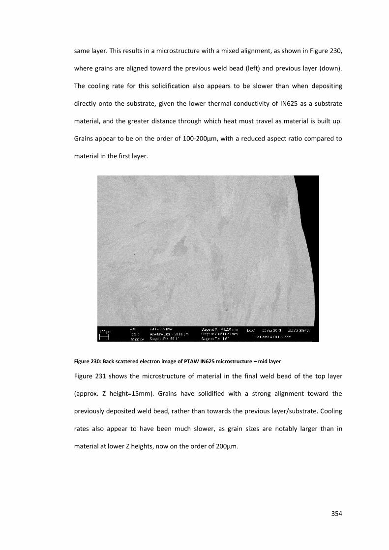
354
same layer. This results in a microstructure with a mixed alignment, as shown in Figure 230,
where grains are aligned toward the previous weld bead (left) and previous layer (down).
The cooling rate for this solidification also appears to be slower than when depositing
directly onto the substrate, given the lower thermal conductivity of IN625 as a substrate
material, and the greater distance through which heat must travel as material is built up.
Grains appear to be on the order of 100-200µm, with a reduced aspect ratio compared to
material in the first layer.
Figure 230: Back scattered electron image of PTAW IN625 microstructure – mid layer
Figure 231 shows the microstructure of material in the final weld bead of the top layer
(approx. Z height=15mm). Grains have solidified with a strong alignment toward the
previously deposited weld bead, rather than towards the previous layer/substrate. Cooling
rates also appear to have been much slower, as grain sizes are notably larger than in
material at lower Z heights, now on the order of 200µm.

355
Figure 231: Back scattered electron image of PTAW microstructure - top layer
In all cases, the welding process has resulted in re-melting and grain growth across layers
and between weld beads, such that they are largely indistinguishable when examining the
bulk central regions of the sample.
The alignment and size of grains differs somewhat from that of LM IN625, which maintains
a strong grain alignment in the direction of the substrate at all times, PTAW deposited
material has a mixed alignment between the direction of the previous layer and the
direction of the previous weld bead within the same layer. Due to the highly localised heat
source in LM, grains remain small with a high aspect ratio, whereas the heat input in PTAW
welding is on a much larger scale, having slower local cooling rates.
Figure 232 shows the band contrast obtained for an EBSD scan near the top of the PTAW
deposited material (Z>15mm), as can be seen, although some small isolated <250µm grains
are present, the bulk structure consists of grains on the order of >250µm in their smallest
dimension, up to large proportions of a millimetre in length in some cases.

356
Figure 232: EBSD - band contrast from upper third of PTAW IN625sample
4.4.2.2.2.2 Composition - EDS
EDS line scans were performed to identify the degree of substrate/deposit dilution, the
results of which are present in Figure 233. The Steel substrate material is readily
identifiable on the right of the linescan, with a clearly defined boundary between the
deposited material and substrate. Fe contamination was found to extend further than the
range which could be examined by a single linescan, so was assessed by a series of spectra
taken at increasing Z height positions. A Fe content similar to that of the filler wire utilised
was seen at a Z height of approximately 1.5-2.0mm above the plane of the substrate,
indicating that substrate dilution remains within the first layer.

357
Figure 233: EDS linescan of substrate/deposit interface
The bulk material composition at a sample position remote from the substrate is presented
in Table 44. There is a very slight difference in composition between the filler wire utilised
and the resulting deposited material, however it is not significant, given the measurement
error. The composition of the deposited material is well within the specification for IN625.
Table 44: Composition of PTAW IN625
Material Element wt%
Deviation Error Ni Cr Mo Nb Fe Ti Al
IN625 (max spec) 68.85 23.0 10.0 4.15 5.0 0.4 0.4 IN625 (min spec) 58.0 20.0 8.0 3.15 0.0 0.0 0.0 IN625 Wire 64 22 9 3.5 0.4 0.2 0.1 0.3 ±0.12
PTAW IN625 64 22.5 8.5 3.5 0.4 0.2 0.1 0.5 ±0.20
4.4.2.2.2.3 Hardness
Figure 234 presents the average hardness with increasing Z height for a PTAW IN625
sample, the average hardness within the bulk deposited material remains consistent,
between 240-260HV0.5 at all times. The relatively high degree of measurement variability is
due to a high sample size, measuring the average across 40 points (10mm) at each Z height,
Deposited material Substrate

358
so providing some indication of variation in the X direction as well, the cross-sectional
hardness distribution from this data is mapped in Figure 235 to provide an appreciation of
the variation in hardness across weld beads and layers. While the EDS measurements
showed a distinct boundary between the substrate and weld material composition,
hardness measurements show a slight decrease through a relatively short dilution zone,
and an increase due to the expected HAZ. Stable properties are achieved at a Z height of
approximately 3mm above the original plane of the substrate surface.
Figure 234: Average hardness distribution with Z height for PTAW IN625
210
220
230
240
250
260
270
0 2 4 6 8 10 12 14 16
Har
dn
ess
(HV
0.3
)
Z Height (mm)
Sub
stra
te
Dilu
tio
n
HA
Z
Deposited material

359
Figure 235: Cross-sectional variation in hardness for PTAW IN625
The variation in hardness indicates the presence of an additional effect on material
properties, beyond that of compositional dilution. The grain direction and size may be
expected to differ immediately adjacent to the substrate in comparison with the bulk
deposited material, due to local cooling and solidification rates/direction. However, the
relatively consistent average hardness would appear to indicate that after the first
deposited layer, a consistent deposition with consistent material properties has been
achieved, at least on the scale of the hardness measurements made (0.25mm steps). This
Z
Har
dn
ess
HV
(0.3
)

360
would indicate that efforts to control cooling rates by reducing welding current and
maintaining an inter-pass dwell time have been largely successful in producing a consistent
material. The smaller periodic variations in hardness within the bulk material are
considered to be the result of microstructural variations between the boundaries and core
of each successive layer, and will create some variation in material properties.
4.4.2.2.3 Discussion of multi-layer, multi-weld IN625 PTAW deposition
experiments
Multi-layer, multi-weld IN625 samples were deposited using PTAW, up to eight layers in
height. Showing the need not only for interpass dwell time to control thermal accumulation
as in the work of Xu et al., [358], but also the importance of parameter control at weld
initiation and termination when considering large deposition features in order to prevent
cumulative deviations from the desired layer thickness.
An examination of the materials microstructure showed a primary alignment towards the
substrate, but also a secondary alignment in the direction of the previously deposited weld
bead within the same layer. This is considered to be due to the same increase in available
area for more effective conductive cooling over purely convective and radiation based
cooling from the exposed surface of the weld bead in a similar manner to that seen in the
500µm layer powder bed LM experiments and discussed in detail in Section 4.2.6.1,
specifically Figure 127. The PTAW deposited material does of course differ in that grain
sizes are of a larger size altogether due to the greater heat input in PTAW which raises the
temperature of both previously deposited material and substrate to a greater degree than
is seen in powder bed LM. Since the original submission of this thesis, similar effects have
been noted in the deposition of Ti-6Al-4V using TiG based WAAM [359].
Some variation in hardness with Z height can be noted, this is due to the formation of a
localised HAZ for each successive layer, as described in the recent work by Szost et al.,

361
[360], published after the original submission of this thesis. As discussed by Szost et al., the
layer banding HAZ is of a larger scale in WAAM deposition and is therefore visible in
contrast to the microstructure observed in powder bed LM samples. In the work conducted
in this thesis, the layer banding can be seen in the average hardness measurements shown
in Figure 234, although some definition is lost as layer banding is not purely horizontal, but
curved when viewed in the transverse section due to the shape of the molten pool.
4.4.2.3 Characterisation – Tensile Testing
In order to evaluate the mechanical properties of PTAW IN625, tensile test samples were
cut from material deposited in several builds of up to 25mm in height, deposited material
was machined by conventional processes achieving the form shown in Figure 236, from
which flat samples were wire EDM cut. The mechanical properties of these samples
between room temperature and 1100oC were then evaluated by a combination of ambient
condition tensile testing (“Instron”) and resistance heated tensile testing (“Gleeble”).
Figure 236: PTAW IN625 machined build.
Instron based testing was conducted from Room Temperature (21oC) up to 200oC, while
Gleeble testing was conducted from 200oC up to 1100oC, the practicalities of each test
method enforcing the respective upper and lower temperature limits.
130mm

362
The samples used for testing were randomised, such that tests were conducted with
samples from various batches and build heights, to avoid a systematic error. It should be
noted that any variation in properties related to Z height within a build or variation
between builds will therefore become part of the complete averaged data set. The intent
of these tests is to establish baseline data on PTAW IN625, so for any practical purpose, the
variation of material properties needs to be considered on an averaged basis.
Representative stress-strain curves for each Gleeble test temperature are shown in
Figure 239, a change in failure behaviour occurs in samples tested at 800oC and above. The
plastic region of the curve is no longer approximately linear but approaches a failure point
and then decreases gradually rather than abruptly as seen below 800oC. Lower
temperature tests resulted in an abrupt and complete failure of the sample. However
higher temperature tests failed progressively, as necking became more extreme and
significant plastic flow occurred.
Examination of fracture surfaces by SEM shows some difference in tests performed above
the materials oxidation temperature (900oC), with what appears to be a different surface
morphology after testing. Tests under 700oC exhibit the expected cup and cone ductile
fracture mechanism, as shown in Figure 237. Tests at higher temperatures appear to have
undergone a similar cup and cone type failure, but have then been coated in some form of
oxide reaction layer (see Figure 238), however the inability of EDS to measure and quantify
oxygen, as well as the time elapsed between testing and SEM examination (several days)
make it impossible to determine if this change in fracture surface is inherent in the failure
mechanism, or has merely occurred immediately post-test as the sample cooled. It could
also possibly be the result of arcing between points on the sample as it failed, due to the
electrical current passing through the sample during failure.

363
Figure 237: Fracture surface after tensile test at 700oC
Figure 238: Fracture surface after tensile test at 1000oC
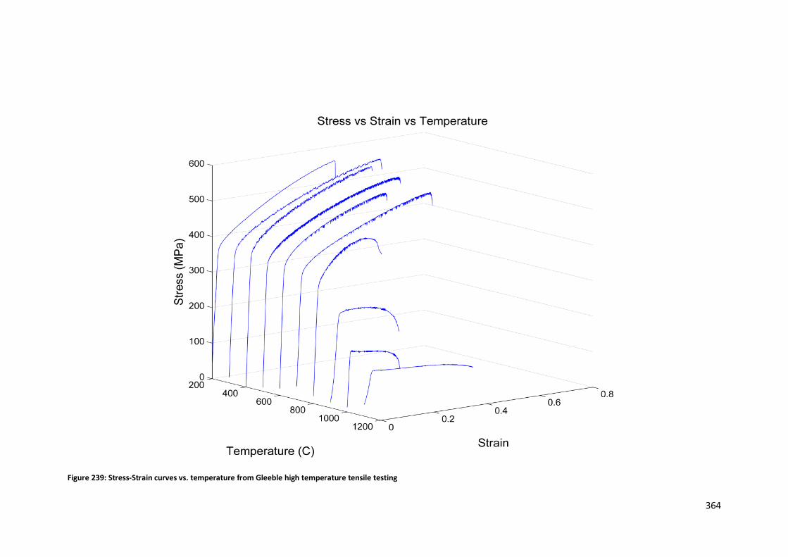
364
Figure 239: Stress-Strain curves vs. temperature from Gleeble high temperature tensile testing

365
The measured yield strength and UTS from both Instron and Gleeble testing are plotted
against test temperature in Figure 240. The variation in measured results is low, given the
mixed material batches and the known potential for differences in microstructures
between samples from different Z heights, as shown in the preceding microstructural
evaluation. The high variation in results at 100oC is a function of sample design, in order to
achieve the desired thermal profile for Gleeble testing, the samples utilised a
comparatively small shoulder radius, which initiated fracture early in some tests at 100oC
during Instron testing. There is a gradual decrease in material properties with temperature
up to 700oC (the typical service temperature for IN625 being 650oC), after which properties
deteriorate.
Figure 240: Mechanical properties at temperature for PTAW IN625 (combined Instron & Gleeble data)
While all samples tested were in the as-built condition, an annealing heat treatment was
applied to three samples before Instron testing at room temperature, the results of which
are shown in Figure 241. As a result of the annealing heat treatment, the consistency of
material properties has improved compared to samples tested in the as-built state, with a
much smaller deviation between the measured values of yield and UTS. Annealing has
0
100
200
300
400
500
600
700
800
0 200 400 600 800 1000 1200
Stre
ss (
MP
a)
Temperature (oC)
Yield Strength
Tensile Strength

366
provided a 7.6% increase in yield strength and an 11% increase in UTS compared to
material in the as built state. There is a corresponding decrease in ductility however, with
Elongation at failure dropping by 27%, although the variability between measurements for
elongation is significantly higher than that for yield and UTS.
Figure 241: Effect of annealing heat treatment on room temperature mechanical properties
4.4.2.4 Discussion of tensile testing
Where both Instron and Gleeble testing could be conducted at 200oC, a comparison
between the values obtained has been made in Figure 242. The average yield strength
measured differs by 4%, whilst the measured UTS differs by 3%. The difference in the
Elongation measured is somewhat higher at 13%, however the variability of elongation
measured using Gleeble testing is also high.
Overall the average values measured for yield and UTS between Instron and Gleeble
methods do not differ significantly, although the variation in measurements is slightly
higher for Gleeble testing. The close correlation between samples at 200oC using both test
methodologies validates the use of Gleeble testing for high temperature tensile tests and
0
100
200
300
400
500
600
700
800
900
Yield UTS Elongation
Stre
ss (
MP
a), E
lon
gati
on
(%)
PTAW As Built
PTAW Annealed

367
the novel use of IR thermography in determining the thermal gauge length of samples on a
case by case basis for improved accuracy.
Figure 242: Comparison of mechanical properties obtained by Instron vs. Gleeble testing at 200oC
4.4.3 Discussion of PTAW IN625 Deposition
While a large body of research exists around the use of PTAW for surface coatings and
repair with a variety of materials, including Ni-based alloys [130, 132, 152, 361-366], little
literature exists with regards to the manufacture of multi-layer deposits using Inconel
based materials with a view to AM. The most comprehensive work using PTAW deposition
has been conducted by Martina et al., [79], and has characterised a process window for the
deposition of Ti-6Al-4V materials both as single beads and for thin walls, the research in
this thesis achieves a similar contribution for IN625 materials, as well as providing
information on the mechanical properties at high temperature.
The work of Xinhong et al., [133] does demonstrate the feasibility of superalloy
manufacture for components using this route, however no comprehensive mechanical
testing or examination of the process parameter window was undertaken.
0
100
200
300
400
500
600
700
Yield Strength Tensile Strength Elongation
Stre
ss (
MP
a), E
lon
gati
on
(%)
Instron
Gleeble

368
Zhao and Liu [131] have conducted a more in depth assessment of PTAW deposition for
superalloy GH163, a dilute γ’ strengthened superalloy, which demonstrates a stable
deposition is possible, but again no detailed characterisation of the process window was
presented, nor the mechanical properties across the full temperature range.
The largest single body of work conducted in this area by Xu et al., [358] has looked at
Pulsed PTAW with Inconel 625 wire, evaluating the effect of deposition strategy (raster
direction) on the tensile properties of the material. While the work of Xu et al., did
implement an interpass dwell to control substrate temperatures, this was “to make the
temperature of previous layers material decreased to about room temperature”, it is not
clear if this 300s dwell was in between each individual weld bead, or in between each layer.
However, given the high input current (pulsed from 140A to 230A) and low welding speeds
(0.23m/min), it is uncertain that “room temperature” would have been achieved at any
point during deposition, and no evidence of measured substrate or deposited material
temperatures is given. The work conducted in this thesis has implemented a similar dwell
strategy, however substrate temperatures were monitored and process parameters varied
on a layer by layer basis to obtain consistent melt behaviour. Compared to the work
conducted by Xu et al., the work conducted in this thesis did not observe a decrease in
hardness with increasing Z height, despite varying the welding current used. This would
suggest that a more consistent and stable deposition was achieved using a thermal control
strategy employing not only an interpass dwell, but also reducing the energy input as
thermal isolation from the substrate increased. Xu et al., have reported some mechanical
properties for PTAW deposited IN625 at room temperature, in both the as built and
solution treated state, and the work conducted here would broadly agree.
However, none of the work identified to date has provided a comprehensive assessment of
the process parameter window for single weld beads, and the effect of welding parameters

369
on weld bead geometry. While some mechanical properties have been reported, again
none of the work to date provides reported values for mechanical properties over a large
temperature range, as would be of interest should PTAW IN625 be utilised for the
production of components.
4.5 Discussion & Comparison of materials & manufacturing routes
4.5.1 Mechanical Properties
4.5.1.1 Density & Hardness
Figure 243 shows a comparison of material density and hardness, as an indicator of
mechanical properties. It can clearly be seen that the best relative density is achieved for
the IN625 matrix alone, while the addition of any reinforcing phases results in more
significant material porosity. For any functional product the best balance of material
strength (indicated here by hardness) compared to density will be advantageous.
Of the three manufacturing routes attempted for the production of a TiC reinforced IN625
MMC, the use of a TiC feedstock shows the best balance of material properties and relative
density, providing a 48% increase in hardness over the matrix material alone processed in
the same manner. If further optimisation of the process parameters were conducted, then
a fully dense IN625+TiC MMC is feasible. Zheng et al., [173] found that while a 10wt% TiC
reinforced IN625 material provided a greatly increased Yield Strength, the materials
ductility was severely compromised. By using only 5wt% TiC and producing a more
homogenous distribution of fine particulates, the IN625+TiC composite produced in this
work may achieve a more desirable balance of strength and ductility.
The in-situ formation of IN625+TiC has resulted in poor density, with macro defects and
cracking, due to reduced ductility in the material, although the formation of Mo2C
particulates (as verified by XRD) has increased hardness dramatically, significant further

370
work would be required to produce a material of high relative density, given the narrow
stable parameter window seen during single track experiments for this material, if indeed it
is possible.
Figure 243: Comparison of hardness and relative density for IN625 & MMCs
4.5.1.2 Mechanical Properties - Tensile
A comparison of mechanical properties at temperature for PTAW deposited IN625 against
reported data for GTAW deposited material of a similar composition, and the “Gold
standard” Wrought material are presented in Figure 244. While the mechanical properties
of PTAW IN625 are, as expected, below those of wrought material, they are close to and
competitive with that of GTAW weld material. The effect of annealing in homogenising
material and improving its mechanical properties shows promise however, not only
increasing the absolute values for yield and UTS, but also reducing the variability between
samples, as the differing microstructures seen depending upon Z height are homogenised
to some degree.
95
95.5
96
96.5
97
97.5
98
98.5
99
99.5
100
0
100
200
300
400
500
600
700
IN625 PTAW IN625 IN625+TiC IN625+Ti+CIN625+Ti+C PH
Re
lati
ve D
en
sity
(%
)
Har
dn
ess
(HV
0.3)
Hardness
Density

371
Figure 244: Comparison of high temperature mechanical properties for IN625.
Figure 245 compares the room temperature properties of PTAW IN625 in both the as-built
and annealed condition against reported values for material deposited by the LENS
process, and nominal industry standard values for cast and wrought material. PTAW IN625
shows comparable if not superior properties to cast material in the as-built state with
regards to both strength and ductility. As built PTAW IN625 appears inferior to the
reported data for DMLS and LENS deposited material if considering strength alone,
however the ductility of as-built PTAW material is equivalent or higher. Once annealed, the
properties of PTAW material align more closely with other AM materials, indicating that
with optimised heat treatment, there is potential for PTAW to be competitive with other
AM technologies in terms of its material properties.
0
200
400
600
800
1000
1200
0 200 400 600 800 1000 1200
Stre
ss (
MP
a)
Temperature (oC)
PTAW UTS
PTAW Yield
GTAW UTS
GTAW Yield
Wrought UTS
Wrought Yield

372
Figure 245: Comparison of room temperature mechanical properties for IN625 by different process routes
4.1.1. Deposition rates
Figure 246 compares the exposure rate of a commercial powder bed laser melting system
with that found for the processes which were investigated in this thesis. The exposure rate
is expressed as the volume of material which can be deposited per second in a given
exposure, and so does not account for re-coating or dwell periods, as there is no parity in
recoating times/methods across the technologies. The relative density of IN625 produced
by each process is also shown, to give an appreciation of the cost/quality tradeoff which
may exist between them.
Comparing deposition rate with material density, it can be seen that high powered laser
melting of IN625 at 100µm layer thicknesses provides only a small deposition rate increase
(0.006cc/s) compared to commercial 40µm layer based systems (approx. 0.0036cc/s for an
EOS M280 – 400W), while producing a material of inferior density (<99.0%).
High powered laser melting at 500µm layers provides an order of magnitude increase in
deposition rate, regardless of the hatch spacing used. Although high melt rates of up to
0.05cc/s can be achieved with a 1.1mm hatch spacing the material density is compromised
0
100
200
300
400
500
600
700
800
900
Yield UTS Elongation
Stre
ss (
MP
a), E
lon
gati
on
(%)
PTAW As Built
PTAW Annealed
LENS
DMLS
Cast
Wrought

373
(<99%). A hatch spacing of 0.5mm provides a material with comparable density to that of
commercial systems (particularly considering the difference in process chamber sealing
between a commercial system and the experimental equipment used here), with an
appreciable six to seven fold increase in exposure rate (0.023cc/s) compared to current
40µm layer 400W systems.
In contrast, the use of PTAW based deposition provides a further order of magnitude
increase in exposure rate compared to 500µm layer based laser deposition (up to
approximately 0.53cc/s). The density of PTAW material is still competitive with current
commercial systems, and the experimental 500µm, 0.5mm hatch samples produced by
powder bed LM.
This would indicate that there is an upper limit on the exposure rate which can be achieved
using powder bed based laser melting systems, beyond which PTAW based deposition can
offer higher exposure rates without a loss in material density.
Figure 246: Melting rate "deposition" compared to material density.
Figure 247 presents the deposition rates for three mainstream commercial AM processes
(DMLS, EBM and LENS), and compares with those found during experimentation with high
90
91
92
93
94
95
96
97
98
99
100
0
0.1
0.2
0.3
0.4
0.5
M280 100um 500um0.5mm
500um0.8mm
500um1.1mm
PTAW
Re
lati
ve D
ensi
ty (
%)
Exp
osu
re R
ate
(cc/
s)
ExposureRate
RelativeDensity

374
powered powder bed laser melting and PTAW based deposition. Conventionally EBM and
LENS have been competitive against powder bed LM processes such as “DMLS” on the basis
of greater productivity. The promising combination of high material density and deposition
rate found when melting IN625 using 500µm layers at a hatch spacing of 0.5mm would
indicate that it is possible for powder bed laser melting to be competitive in terms of
productivity. PTAW based deposition using the available equipment has demonstrated a
higher productivity as measured by deposition rate, the use of actively heated or cooled
substrates could potentially double the productivity of PTAW based methods, by
eliminating the dwell times required to maintain suitable substrate temperatures.
Figure 247: Approximate deposition rates for IN625 for different AM processes
0
200
400
600
800
1000
1200
DMLS EBM LENS 500um 0.5mm PTAW
Dep
osi
tio
n r
ate
(g/
hr)

375
5 Conclusions & Future Work
5.1 Inconel 625 MMCs
5.1.1 Conclusions
The work presented has so far demonstrated the feasibility of IN625 based MMCs
produced using powder bed laser melting. A high density material can be achieved on a par
with that of the matrix alloy alone, and a moderate benefit to material hardness is
observed, along with a good matrix/reinforcement bonding.
A feasibility study into the most suitable reinforcement material was conducted, neither
Al2O3 or SiC were found to be suitable. Al2O3 was thermally destroyed, releasing oxygen into
the process chamber and resulting in high porosity. SiC was dissolved into the matrix and
an unknown mixture of carbides re-precipitated, although a high hardness was achieved,
significant micro-cracking was present. TiC was found to produce a high density material
with improvements to hardness and so was selected for further evaluation.
Powder mixing for 72hrs was found to be sufficient to produce a homogenous powder
mixture that was processed in 500µm layer thicknesses by powder bed LM. An evaluation
of the process parameter window for single bead on plate tests was undertaken and the
interactions of process parameters characterised where possible.
The presence of TiC was found to have a strong influence on processing behaviour, despite
having a higher melting point than the IN625 matrix, lower energy densities resulted in
more complete melting of the material and stable welding. This was determined to be due
to the high absorptivity of TiC to the infra-red laser wavelengths employed. This high
absorptivity also resulted in a narrower process window, as it hampered weld penetration
through the powder bed and wetting with the substrate.

376
Multi-layer, multi-pass deposition was conducted at 500µm layers, reducing laser power to
control deposition stability once thermally isolated from the substrate, an important
consideration in this case. It was found that TiC particulates in the feedstock powder were
dissolved and re-precipitated as TiC, verified by XRD. Particulates, displayed a star-shaped
morphology and greatly reduced scale (<1µm), with good interface bonding with the matrix
verified by SEM. The influence of processing parameters on material density and hardness
was evaluated, with a 0.5mm hatch spacing found to produce the highest relative density.
The work conducted in this thesis has shown that the commonly utilised energy density
metric is relevant only in comparing AM systems utilising similar energy sources on a like
for like hardware basis. Laser power density was shown to be a critical factor influencing
the processing behaviour of TiC reinforcement particulates when contrasted with similar
research using differing laser sources, with little correlation between the energy densities
used and the processing behaviour.
The in-situ formation of IN625 MMCs from a mixture of Ti and C to form TiC was found to
result in an abnormal microstructure and unexpected phases, leading to significant macro-
cracking and porosity. Mo2C was found to form more readily than the intended TiC
reinforcement, it can be concluded that rapid melting and solidification means local
imbalances in the proportions of reactants available allow the formation of compounds
with a higher Gibb’s energy of formation (i.e. Mo2C forms in the absence of Ti). Improved
homogeneity of the powder mixture is not considered to be effective in resolving this issue,
as the localised presence of Ti and C is desired, rather than a distribution of C throughout
the matrix.
5.1.2 Future Work
If the production of IN625+TiC MMCs is to be pursued, further work is now required to
more completely assess the degree to which the materials mechanical properties are

377
improved, beyond the simple indications provided by hardness testing in this work. The
production of tensile test specimens for the evaluation of specific stiffness and strength
would be highly informative, as would test results for material ductility to determine what
trade-offs exist between strength and ductility. In particular the materials stability at high
temperature and mechanical properties at high temperatures would be of interest, to aid
in understanding to what applications the material might be suited.
If the production of IN625+Ti+C MMCs using an in-situ formation method is to be
investigated further, then the issues in powder mixing must first be solved, however it is
likely that a two stage process firstly mechanical alloying by high energy ball milling for Ti+C
followed by mixing of this powder with IN625 is a more realistic solution to product an
in-situ TiC reinforced MMC.
5.2 Deposition of Inconel 625
5.2.1 Powder bed laser melting
5.2.1.1 Conclusions
The deposition of IN625 by powder bed laser melting using high powered lasers to achieve
high deposition rates has been shown to be feasible and to provide acceptable material
quality.
The process parameter window for 500µm layer thickness deposition of IN625 has been
evaluated and relationships between weld width and processing parameters characterised
by single bead on plate tests. The variability of weld height was found to be too great to
establish a meaningful relationship, as weld geometry is sensitive to local substrate
temperatures and so influenced by previous welds.
Multi-layer, multi-pass deposition of IN625 at 500µm layer thicknesses was conducted,
successfully implementing a thermal control strategy based upon the reduction of laser

378
power with increasing Z height until a steady thermal state was achieved once isolated
from the substrate. By reducing laser power rather than introducing an interpass dwell
deposition rates were unaffected and no change in material density was observed.
The effect of weld aspect ratio on microstructural alignment within a multi-pass, multi-
layer deposition scenario has been shown, with decreasing aspect ratio, increased
conductive cooling laterally into previous weld passes within the same layer affects
microstructural alignment – an effect not typically observed in lower deposition rate
powder bed LM.
5.2.1.2 Further Work
To further develop the application of high powered laser melting on powder bed systems, a
high quality commercial processing environment is needed to ensure a tighter control over
the inert atmosphere, and so improve the materials density and quality to a commercial
production standard. If high powered laser melting were to be implemented for the
production of component geometries, this would best be achieved using a multi-laser
system and a skin/core strategy, whereby a 200-400W laser could be utilised to produce
the components skin at 40µm layers, while bulky core regions might be exposed only every
500µm using a higher powered laser. Obviously significant work is required to understand
the interaction between skin and core exposure in such a system.
5.2.2 PTAW Deposition
5.2.2.1 Conclusions
The deposition of IN625 using PTAW and wire feedstock has been shown to be feasible
with high relative material density and deposition rates compared to powder bed LM.
A process parameter map detailing the effect of welding current, traverse speed and
material feed rate has been established for single bead on plate deposition. The

379
relationships between input process parameters and resulting weld bead geometry and
material hardness have been characterised.
Strategies for the deposition of multi-layer and multi-weld width forms have been
investigated; without active control of workpiece or substrate temperatures, an interpass
dwell is required between subsequent welds within a layer. Consistent deposition was
achieved by decreasing welding current as an effective solution to maintaining stable
deposition without affecting part density once thermally isolated from the machine bed.
This indicates the need in WAAM processes to consider geometry specific processing
parameters, particularly in materials with low thermal conductivity.
Tensile testing at high temperatures has characterised the tensile properties of PTAW
deposited IN625 using novel high temperature testing methods (Gleeble), coupled with IR
thermography. The accuracy of this test method was compared with conventional ambient
heating at lower temperatures and an acceptable correlation was shown, so validating this
novel methodology.
5.2.2.2 Further Work
To further investigate the material properties available using PTAW deposition, it is
suggested that the effect of heat treatments be investigated upon the mechanical
properties of the material, given the potential benefits shown so far.
To further develop the deposition technology, it is firstly suggested that a higher current
deposition head be investigated, as the work presented could not investigate higher
material feed rates due to the limited welding currents available.
Beyond this, the use of actively heated or cryogenically cooled machine beds may aid in
dramatically reducing the cycle time between individual welds when producing geometries
which require multiple welds in close proximity. The use of magnetic plasma manipulation

380
to serve as either a pre-heating device (using the same deposition head) or as a post-
deposition heat treatment to relieve stresses in large components may also be of great
benefit.
The work presented considers only the deposition of very simple approximate near net
shape geometries. The understanding of deposition paths and techniques to produce more
complex geometries more accurately is a significant undertaking, and would need to
address several points:
Effect of other parameters such as anode diameter, torch off-set and wire feed
angle upon weld bead geometry.
Minimum and maximum repeatable weld bead width/height achievable with
differing deposition heads (e.g <1mm welds/walls using smaller anode diameters
and wires, or >5mm welds/walls using larger anode diameters and wires with
higher currents). Indeed since the completion of this thesis work by Jhavar et al.,
[367]on µ-PTA using steel alloys has begun to explore the lower limits of
geometrical features available through PTAW based WAAM).
Mechanism of deposition head manipulation to manufacture contours (e.g. robotic
manipulation or 4/5-axis CNC beds to ensure consistent material feed orientation).
Deposition strategies for complex parts which deal with weld cross-over and
contour/core overlap, the most up to date research since the original submission of
this thesis by Alberti et al., [126] examines only single weld width walls.
Software pre-processing methods to generate the deposition paths and provide the
required control code.
Limitations on geometrical features such as overhangs.

381
The strategies and methods for incorporating subtractive machining would also require
some investigation, with a view to the effect upon material quality and cycle time, if
coolant may be required during machining for example.
5.3 Concluding Remarks
5.3.1 Objective 1: High depositon rate powder bed LM of IN625
This thesis was intended to establish if the high deposition rate powder bed laser melting
of IN625 at 500µm layer thicknesses was feasible and if so to characterise the process map
and set out a strategy for the production of bulk material.
This was fully achieved using a bespoke AM system and a strategy and process parameters
were defined to deliver consistently high density material at deposition rates greater than
current commercial equipment. A new understanding of thick layer deposition behaviour
was contributed.
5.3.2 Objective 2: High deposition rate powder bed LM of IN625 MMC
To establish if the high deposition rate powder bed laser melting of an IN625 based MMC
was possible and to characterise the process map and understand the processing
differences between matrix and reinforcement material.
This was achieved for a mixed feedstock of IN625+TiC, however the in-situ reactive
processing of IN625+Ti+C was not successful. This work contributed an insight into the
importance of power density as a critical factor for the processing behaviour of MMCs.
5.3.3 Objective 3: High deposition rate WAAM of IN625
To characterise the process map for PTAW deposition of IN625 and to establish a strategy
for the deposition of large multi-layer, multi-weld features and characterise the properties
of the deposited material.

382
This was achieved through single bead on plate experiments to fully characterise the
process window, the novel use of IR thermography to determine thermal gauge length for
resistance heated tensile samples enabled the characterisation of the materials tensile
properties to be completed. A greater understanding of the thermal behaviour during
multi-layer multi-weld width features and the necessary deposition strategies has been
contributed.

383
6 References
1. Reed, R.C., The Superalloys Fundamentals and Applications. 2006, New York: Cambridge University Press.
2. Xu, L., S. Bo, Y. Hongde and W. Lei, Evolution of Rolls-royce Air-cooled Turbine Blades and Feature Analysis. Procedia Engineering, 2015. 99: pp. 1482-1491.
3. Masanori, Y.J., Masada. Keizo, Tsukagoshi. Eisaku, Ito. Satoshi, Hada., Development of 1600oC-Class High-efficiency gas turbine for power generation applying J-type technology, in Mitsubishi Heavy Industries Technical Review. 2013. pp. 1-10.
4. Fadok, J., 1 - Advanced gas turbine materials, design and technology, in Advanced Power Plant Materials, Design and Technology, D. Roddy, Editor. 2010, Woodhead Publishing. pp. 3-31.
5. Zhu, D., X. Zhang and H. Ding, Tool wear characteristics in machining of nickel-based superalloys. International Journal of Machine Tools and Manufacture, 2013. 64(0): pp. 60-77.
6. Subramanian, G. and M. Jondhale, The latest trend of turbocharging technologies for emissions compliance and fuel economy, in Innovations in Fuel Economy and Sustainable Road Transport, I.o.M. Engineers, Editor. 2011, Woodhead Publishing. pp. 187-197.
7. Pint, B.A., J.A. Haynes and B.L. Armstrong, Performance of advanced turbocharger alloys and coatings at 850–950 °C in air with water vapor. Surface and Coatings Technology, 2013. 215: pp. 90-95.
8. Thakur, D.G., B. Ramamoorthy and L. Vijayaraghavan, Study on the machinability characteristics of superalloy Inconel 718 during high speed turning. Materials and Design, 2009. 30(Copyright 2009, The Institution of Engineering and Technology): pp. 1718-25.
9. Benn, R.C. and G.M. McColvin. The Development of ODS Superalloys for Industrial Gas Turbines. in Superalloys 1998 (6th International Symposium). 1988. The Minerals, Metals and Materials Society.
10. Baufeld, B., O.V.d. Biest and R. Gault, Additive manufacturing of Ti–6Al–4V components by shaped metal deposition: Microstructure and mechanical properties. Materials & Design, 2010. 31, Supplement 1(0): pp. S106-S111.
11. Ezugwu, E.O., Key improvements in the machining of difficult-to-cut aerospace superalloys. International Journal of Machine Tools and Manufacture, 2005. 45(12–13): pp. 1353-1367.
12. Thakur, A. and S. Gangopadhyay, State-of-the-art in surface integrity in machining of nickel-based super alloys. International Journal of Machine Tools and Manufacture, 2015.
13. Robinson, J.L. and M.H. Scott, Liquation Cracking during the Welding of Austenitic Stainless Steels and Nickel Alloys. Philosophical Transactions of the Royal Society of London. Series A, Mathematical and Physical Sciences, 1980. 295(1413): pp. 105-117.
14. Dupont, J.N., J.C. Lippold and S.D. Kiser, Welding metallurgy and weldability of nickel-base alloys. 2009: John Wiley & Sons Inc.
15. M.B. Henderson, D.A., M. Heobel, R. Larsson, G. Marchant,, Nickel-Based Superalloy Welding Practices for Industrial Gas Turbine Applications, in International Conference on Microstructure and Performance of Joints in High-Temperature Alloys. 2002: London.
16. Motorcu, A.R., A. Kuş and İ. Durgun, The evaluation of the effects of control factors on surface roughness in the drilling of Waspaloy superalloy. Measurement, 2014. 58(0): pp. 394-408.

384
17. ASTM_International, F2792-12a Standard Terminiology for Additive Manufacturing Technologies. 2012.
18. Cooper, D.E., M. Stanford, K.A. Kibble and G.J. Gibbons, Additive Manufacturing for product improvement at Red Bull Technology. Materials & Design, 2012. 41(0): pp. 226-230.
19. Gebhardt, A., F.-M. Schmidt, J.-S. Hötter, W. Sokalla and P. Sokalla, Additive Manufacturing by selective laser melting the realizer desktop machine and its application for the dental industry. Physics Procedia, 2010. 5, Part B(0): pp. 543-549.
20. Mazzoli, A., M. Germani and R. Raffaeli, Direct fabrication through electron beam melting technology of custom cranial implants designed in a PHANToM-based haptic environment. Materials & Design, 2009. 30(8): pp. 3186-3192.
21. Thijs, L., F. Verhaeghe, T. Craeghs, J. Van Humbeeck and J.P. Kruth, A study of the micro structural evolution during selective laser melting of Ti-6Al-4V. Acta Materialia, 2010. 58(9): pp. 3303-3312.
22. Mumtaz, K. and N. Hopkinson, Top surface and side roughness of Inconel 625 parts processed using selective laser melting. Rapid Prototyping Journal, 2009. 15(Copyright 2009, The Institution of Engineering and Technology): pp. 96-103.
23. Spierings, A.B., M. Schneider and R. Eggenberger, Comparison of density measurement techniques for additive manufactured metallic parts. Rapid Prototyping Journal, 2011. 17(5): pp. 380-386.
24. Hazlehurst, K.B., C.J. Wang and M. Stanford, The potential application of a Cobalt Chrome Molybdenum femoral stem with functionally graded orthotropic structures manufactured using Laser Melting technologies. Medical Hypotheses, 2013. 81(6): pp. 1096-1099.
25. Gao, W., Y. Zhang, D. Ramanujan, K. Ramani, Y. Chen, C.B. Williams, C.C.L. Wang, Y.C. Shin, S. Zhang and P.D. Zavattieri, The status, challenges, and future of additive manufacturing in engineering. Computer-Aided Design, 2015. 69: pp. 65-89.
26. Wang, W., Efficiency study of a gas turbine guide vane with a newly designed combined cooling structure. International Journal of Heat and Mass Transfer, 2015. 80(0): pp. 217-226.
27. Mellor, S., L. Hao and D. Zhang, Additive manufacturing: A framework for implementation. International Journal of Production Economics, 2014. 149: pp. 194-201.
28. Petrovic, V., J. Vicente Haro Gonzalez, O. Jorda Ferrando, J. Delgado Gordillo, J. Ramon Blasco Puchades and L. Portoles Grinan, Additive layered manufacturing: sectors of industrial application shown through case studies. International Journal of Production Research, 2011. 49(Copyright 2011, The Institution of Engineering and Technology): pp. 1061-79.
29. Gebler, M., A.J.M. Schoot Uiterkamp and C. Visser, A global sustainability perspective on 3D printing technologies. Energy Policy, 2014. 74: pp. 158-167.
30. Paul, C.P., P. Ganesh, S.K. Mishra, P. Bhargava, J. Negi and A.K. Nath, Investigating laser rapid manufacturing for Inconel-625 components. Optics and Laser Technology, 2007. 39(Compendex): pp. 800-805.
31. Mumtaz, K. and N. Hopkinson, Selective laser melting of Inconel 625 using pulse shaping. Rapid Prototyping Journal, 2010. 16(Compendex): pp. 248-257.
32. Dinda, G.P., A.K. Dasgupta and J. Mazumder, Laser aided direct metal deposition of Inconel 625 superalloy: Microstructural evolution and thermal stability. Materials Science and Engineering A, 2009. 509(Compendex): pp. 98-104.

385
33. Zhang, C., L. Li and A. Deceuster, Thermomechanical analysis of multi-bead pulsed laser powder deposition of a nickel-based superalloy. Journal of Materials Processing Technology, 2011. 211(9): pp. 1478-1487.
34. Li, J. and H.M. Wang, Microstructure and mechanical properties of rapid directionally solidified Ni-base superalloy Rene'41 by laser melting deposition manufacturing. Materials Science and Engineering: A, 2010. 527(18-19): pp. 4823-4829.
35. Strondl, A., R. Fischer, G. Frommeyer and A. Schneider, Investigations of MX and '/" precipitates in the nickel-based superalloy 718 produced by electron beam melting. Materials Science and Engineering: A (Structural Materials: Properties, Microstructure and Processing, 2008. 480(Copyright 2008, The Institution of Engineering and Technology): pp. 138-47.
36. Minlin, Z., Y. Lin, L. Wenjin, H. Ting and H. Jingjiang. Laser rapid manufacturing of special pattern Inco 718 nickel-based alloy component. in Lasers in Material Processing and Manufacturing II, 10 Nov. 2004. 2005. USA: SPIE - The International Society for Optical Engineering.
37. Liu, F., X. Lin, C. Huang, M. Song, G. Yang, J. Chen and W. Huang, The effect of laser scanning path on microstructures and mechanical properties of laser solid formed nickel-base superalloy Inconel 718. 2011(Compendex).
38. Liu, F., X. Lin, G. Yang, M. Song, J. Chen and W. Huang, Microstructure and residual stress of laser rapid formed Inconel 718 nickel-base superalloy. Optics & Laser Technology, 2011. 43(1): pp. 208-213.
39. Pinkerton, A.J., Lasers in additive manufacturing. Optics & Laser Technology, 2015. 40. Atzeni, E. and A. Salmi, Economics of additive manufacturing for end-usable metal
parts. The International Journal of Advanced Manufacturing Technology, 2012. 62(9-12): pp. 1147-1155.
41. Dongdong, G., S. Yifu and L. Zhijian, Microstructural characteristics and formation mechanism of direct laser-sintered Cu-based alloys reinforced with Ni particles. Materials and Design, 2009. 30(Copyright 2009, The Institution of Engineering and Technology): pp. 2099-107.
42. Ghosh, S.K., P. Saha and S. Kishore, Influence of size and volume fraction of SiC particulates on properties of ex situ reinforced Al-4.5Cu-3Mg metal matrix composite prepared by direct metal laser sintering process. Materials Science and Engineering A, 2010. 527(Compendex): pp. 4694-4701.
43. Gaard, A., P. Krakhmalev and J. Bergstrom, Microstructural characterization and wear behavior of (Fe,Ni)-TiC MMC prepared by DMLS. Journal of Alloys and Compounds, 2006. 421(Copyright 2006, The Institution of Engineering and Technology): pp. 166-71.
44. Gu, D., Y. Shen and J. Xiao, Influence of processing parameters on particulate dispersion in direct laser sintered WC-Cop/Cu MMCs. International Journal of Refractory Metals and Hard Materials, 2008. 26(Compendex): pp. 411-422.
45. Ghosh, S.K. and P. Saha, Crack and wear behavior of SiC particulate reinforced aluminium based metal matrix composite fabricated by direct metal laser sintering process. Materials and Design, 2011. 32(Compendex): pp. 139-145.
46. Srinivasa, C.K., C.S. Ramesh and S.K. Prabhakar, Blending of iron and silicon carbide powders for producing metal matrix composites by laser sintering process. Rapid Prototyping Journal, 2010. 16(Copyright 2010, The Institution of Engineering and Technology): pp. 258-67.
47. Mumtaz, K.A. and N. Hopkinson, Laser melting functionally graded composition of Waspaloy® and Zirconia powders. Journal of Materials Science, 2007. 42(Compendex): pp. 7647-7656.

386
48. Syed, W.U.H., A.J. Pinkerton and L. Li, A comparative study of wire feeding and powder feeding in direct diode laser deposition for rapid prototyping. Applied Surface Science, 2005. 247(1–4): pp. 268-276.
49. Cooper, D.E., Dickens, M., Dipple, S., Gibbons, G.J., Gibson, A.T., Maggs, S., Wakelin, M.P., Wilkins, M.G.,, Additive Manufacture for the Design of a Single Seat Racing Car, in 11th National Conference on Rapid Design, Prototyping and Manufacturing. 2010, CRDM Ltd: Lancaster University.
50. Murr, L.E., E.V. Esquivel, S.A. Quinones, S.M. Gaytan, M.I. Lopez, E.Y. Martinez, F. Medina, D.H. Hernandez, E. Martinez, J.L. Martinez, S.W. Stafford, D.K. Brown, T. Hoppe, W. Meyers, U. Lindhe, and R.B. Wicker, Microstructures and mechanical properties of electron beam-rapid manufactured Ti–6Al–4V biomedical prototypes compared to wrought Ti–6Al–4V. Materials Characterization, 2009. 60(2): pp. 96-105.
51. Theriault, A., L. Xue and J.R. Dryden, Fatigue behavior of laser consolidated IN-625 at room and elevated temperatures. Materials Science and Engineering: A, 2009. 516(1–2): pp. 217-225.
52. Kempen, K., L. Thijs, J. Van Humbeeck and J.P. Kruth, Mechanical Properties of AlSi10Mg Produced by Selective Laser Melting. Physics Procedia, 2012. 39: pp. 439-446.
53. Wycisk, E., A. Solbach, S. Siddique, D. Herzog, F. Walther and C. Emmelmann, Effects of Defects in Laser Additive Manufactured Ti-6Al-4V on Fatigue Properties. Physics Procedia, 2014. 56: pp. 371-378.
54. Adam, G.A.O. and D. Zimmer, Design for Additive Manufacturing—Element transitions and aggregated structures. CIRP Journal of Manufacturing Science and Technology, 2013(0).
55. Strano, G., L. Hao, R.M. Everson and K.E. Evans, Surface roughness analysis, modelling and prediction in selective laser melting. Journal of Materials Processing Technology, 2013. 213(4): pp. 589-597.
56. Seyda, V., N. Kaufmann and C. Emmelmann, Investigation of Aging Processes of Ti-6Al-4 V Powder Material in Laser Melting. Physics Procedia, 2012. 39(0): pp. 425-431.
57. Kharanzhevskiy, E. and S. Kostenkov, Modeling of laser radiation transport in powder beds with high-dispersive metal particles. Journal of Alloys and Compounds, 2014. 586, Supplement 1(0): pp. S246-S249.
58. Kühnle, T. and K. Partes, In-Situ Formation of Titanium Boride and Titanium Carbide by Selective Laser Melting. Physics Procedia, 2012. 39(0): pp. 432-438.
59. Elzey, D.M. and E. Arzt. Oxide Dispersion Strengthened Superalloys: The role of grain structure and dispersion during high temperature low cycle fatigue. in Superalloys 1998 (6th International Symposium). 1988. The Minerals, Metals and Materials Society.
60. Verhaeghe, F., T. Craeghs, J. Heulens and L. Pandelaers, A pragmatic model for selective laser melting with evaporation. Acta Materialia, 2009. 57(20): pp. 6006-6012.
61. Roberts, I.A., C.J. Wang, R. Esterlein, M. Stanford and D.J. Mynors, A three-dimensional finite element analysis of the temperature field during laser melting of metal powders in additive layer manufacturing. International Journal of Machine Tools and Manufacture, 2009. 49(Compendex): pp. 916-923.
62. Shiomi, M., K. Osakada, K. Nakamura, T. Yamashita and F. Abe, Residual Stress within Metallic Model Made by Selective Laser Melting Process. CIRP Annals - Manufacturing Technology, 2004. 53(1): pp. 195-198.

387
63. Suresh, S. and A.E. Giannakopoulos, A new method for estimating residual stresses by instrumented sharp indentation. Acta Materialia, 1998. 46(16): pp. 5755-5767.
64. Chen, X., J. Yan and A.M. Karlsson, On the determination of residual stress and mechanical properties by indentation. Materials Science and Engineering: A, 2006. 416(1–2): pp. 139-149.
65. Mahmoudi, A.H., M. Ghanbari-Matloob and S. Heydarian. A neural networks approach to measure residual stresses using spherical indentation. in International conference on residual stresses 9 (ICRS 9). 2013. Materials Science Forum.
66. Hussein, A., L. Hao, C. Yan and R. Everson, Finite element simulation of the temperature and stress fields in single layers built without-support in selective laser melting. Materials & Design, 2013. 52(0): pp. 638-647.
67. Zhao, H., G. Zhang, Z. Yin and L. Wu, Finite element analysis of temperature field during multi-layer multi-pass weld-based rapid prototyping. China Welding (English Edition), 2011. 20(4): pp. 1-5.
68. Gusarov, A.V., M. Pavlov and I. Smurov, Residual Stresses at Laser Surface Remelting and Additive Manufacturing. Physics Procedia, 2011. 12, Part A(0): pp. 248-254.
69. Zhao, H., G. Zhang, Z. Yin and L. Wu, A 3D dynamic analysis of thermal behavior during single-pass multi-layer weld-based rapid prototyping. Journal of Materials Processing Technology, 2011. 211(3): pp. 488-495.
70. Bai, X., H. Zhang and G. Wang, Improving prediction accuracy of thermal analysis for weld-based additive manufacturing by calibrating input parameters using IR imaging. International Journal of Advanced Manufacturing Technology, 2013. 69(5-8): pp. 1087-1095.
71. Moat, R.J., A.J. Pinkerton, L. Li, P.J. Withers and M. Preuss, Residual stresses in laser direct metal deposited Waspaloy. Materials Science and Engineering: A, 2011. 528(6): pp. 2288-2298.
72. Jun, X. and Z. Guangjun, Online measurement of bead geometry in GMAW-based additive manufacturing using passive vision. Measurement Science and Technology, 2013. 24(11): pp. 115103.
73. Xiong, J. and G. Zhang, Adaptive control of deposited height in GMAW-based layer additive manufacturing. Journal of Materials Processing Technology, 2013(0).
74. Xiong, J., G. Zhang, Z. Qiu and Y. Li, Vision-sensing and bead width control of a single-bead multi-layer part: material and energy savings in GMAW-based rapid manufacturing. Journal of Cleaner Production, 2013. 41(0): pp. 82-88.
75. Doumanidis, C. and Y.-M. Kwak, Multivariable adaptive control of the bead profile geometry in gas metal arc welding with thermal scanning. International Journal of Pressure Vessels and Piping, 2002. 79(4): pp. 251-262.
76. Lott, P., H. Schleifenbaum, W. Meiners, K. Wissenbach, C. Hinke and J. Bültmann, Design of an Optical system for the In Situ Process Monitoring of Selective Laser Melting (SLM). Physics Procedia, 2011. 12, Part A(0): pp. 683-690.
77. Kwak, Y.-M. and C.C. Doumanidis, Geometry Regulation of Material Deposition in Near-Net Shape Manufacturing by Thermally Scanned Welding. Journal of Manufacturing Processes, 2002. 4(1): pp. 28-41.
78. Hua, T., C. Jing, L. Xin, Z. Fengying and H. Weidong, Research on molten pool temperature in the process of laser rapid forming. Journal of Materials Processing Technology, 2008. 198(1–3): pp. 454-462.
79. Martina, F., J. Mehnen, S.W. Williams, P. Colegrove and F. Wang, Investigation of the benefits of plasma deposition for the additive layer manufacture of Ti–6Al–4V. Journal of Materials Processing Technology, 2012. 212(6): pp. 1377-1386.

388
80. Morrow, W.R., H. Qi, I. Kim, J. Mazumder and S.J. Skerlos, Environmental aspects of laser-based and conventional tool and die manufacturing. Journal of Cleaner Production, 2007. 15(10): pp. 932-943.
81. Thakur, D., B. Ramamoorthy and L. Vijayaraghavan, Machinability investigation of Inconel 718 in high-speed turning. The International Journal of Advanced Manufacturing Technology, 2009. 45(5-6): pp. 421-429.
82. Jia, Q. and D. Gu, Selective laser melting additive manufacturing of Inconel 718 superalloy parts: Densification, microstructure and properties. Journal of Alloys and Compounds, 2014. 585(0): pp. 713-721.
83. Shin, Y.C., M. Anderson and R. Patwa, Laser-assisted machining of Inconel 718 with an economic analysis. International Journal of Machine Tools and Manufacture, 2006. 46(Copyright 2006, The Institution of Engineering and Technology): pp. 1879-91.
84. Venkatesan, K., R. Ramanujam and P. Kuppan, Analysis of Cutting Forces and Temperature in Laser Assisted Machining of Inconel 718 Using Taguchi Method. Procedia Engineering, 2014. 97: pp. 1637-1646.
85. Garcí, V. a Navas, I. Arriola, O. Gonzalo and J. Leunda, Mechanisms involved in the improvement of Inconel 718 machinability by laser assisted machining (LAM). International Journal of Machine Tools and Manufacture, 2013. 74: pp. 19-28.
86. Baghlani, V., P. Mehbudi, J. Akbari and M. Sohrabi, Ultrasonic Assisted Deep Drilling of Inconel 738LC Superalloy. Procedia CIRP, 2013. 6(0): pp. 571-576.
87. Carter, L.N., M.M. Attallah and R.C. Reed. Laser powder bed fabrication of nickel-base superalloys: Influence of parameters; characterisation, quantification and mitigation of cracking. 2012.
88. Mueller, B. Advances in Metal Additive Manufacturing. in 3D Printing & Additive Manufacturing Industrial applications global summit 2013. 2013. London.
89. EOS_GmbH. System Datasheet EOSINT M280. 2013 06/12/2013]; Available from: http://ip-saas-eos-cms.s3.amazonaws.com/public/b1a64caa0c54d208/bc2d30d3f7b4b821634dfafa303ee441/systemdatasheet_M280.pdf.
90. EOS_GmbH. Materials Datasheet EOS Titanium Ti64. 2013 06/12/2013]; Available from: http://ip-saas-eos-cms.s3.amazonaws.com/public/fe8d0271508e1e03/0d07ed985f00db42e2d405de93d22c77/EOS_Titanium_Ti64_en.pdf.
91. Arcam_AB. Arcam A2 Technical Data. 2013 06/12/2013]; Available from: http://www.arcam.com/wp-content/uploads/Arcam-A2.pdf.
92. Arcam_AB. Arcam Q20 Technical Data. 2013 06/12/2013]; Available from: http://www.arcam.com/wp-content/uploads/Arcam-Q20.pdf.
93. Optomec_Inc. LENS MR-7 Datasheet. 2013 6/12/13]; Available from: http://www.optomec.com/downloads/Optomec_LENS_MR7_Datasheet.pdf.
94. Optomec_Inc. LENS 850R Datasheet. 2013 06/12/13]; Available from: http://www.optomec.com/downloads/Optomec_LENS_850R_Datasheet.pdf.
95. Liu, W. and J.N. DuPont, Fabrication of functionally graded TiC/Ti composites by laser engineered net shaping. Scripta Materialia, 2003. 48(9): pp. 1337-1342.
96. Rossi, S., F. Deflorian and F. Venturini, Improvement of surface finishing and corrosion resistance of prototypes produced by direct metal laser sintering. Journal of Materials Processing Technology, 2004. 148(Copyright 2004, IEE): pp. 301-9.
97. Song, Y.-A. and W. Koenig, Experimental Study of the Basic Process Mechanism for Direct Selective Laser Sintering of Low-Melting Metallic Powder. CIRP Annals - Manufacturing Technology, 1997. 46(1): pp. 127-130.

389
98. Hanninen, J., DMLS moves from rapid tooling to rapid manufacturing. Metal Powder Report, 2001. 56(9): pp. 24-26.
99. Li, R., Y. Shi, J. Liu, H. Yao and W. Zhang, Effects of processing parameters on the temperature field of selective laser melting metal powder. Powder Metallurgy and Metal Ceramics, 2009. 48(Compendex): pp. 186-195.
100. Tomus, D., T. Jarvis, X. Wu, J. Mei, P. Rometsch, E. Herny, J.F. Rideau and S. Vaillant, Controlling the Microstructure of Hastelloy-X Components Manufactured by Selective Laser Melting. Physics Procedia, 2013. 41(0): pp. 823-827.
101. Krauss, H. and M.F. Zaeh, Investigations on Manufacturability and Process Reliability of Selective Laser Melting. Physics Procedia, 2013. 41(0): pp. 815-822.
102. Van Elsen, M., F. Al-Bender and J.P. Kruth, Application of dimensional analysis to selective laser melting. Rapid Prototyping Journal, 2008. 14(1): pp. 15-22.
103. Woodcock, J., EOS Two decades of Risk and Rewards, in The TCT Magazine. 2013, Rapid News Publications. pp. 45-51.
104. Shiomi, M. and K. Osakada, Flexible manufacturing of metallic products by selective laser melting of powder. International Journal of Machine Tools and Manufacture, 2006. 46(Copyright 2006, The Institution of Engineering and Technology): pp. 1188-93.
105. Yadroitsev, I., A. Gusarov, I. Yadroitsava and I. Smurov, Single track formation in selective laser melting of metal powders. Journal of Materials Processing Technology, 2010. 210(Compendex): pp. 1624-1631.
106. Rombouts, M., L. Froyen, A.V. Gusarov, E.H. Bentefour and C. Glorieux, Light extinction in metallic powder beds: Correlation with powder structure. Journal of Applied Physics, 2005. 98(Compendex): pp. 1-9.
107. Yasa, E. and J.P. Kruth, Microstructural investigation of Selective Laser Melting 316L stainless steel parts exposed to laser re-melting. Procedia Engineering, 2011. 19(0): pp. 389-395.
108. Zaeh, M.F. and M. Ott, Investigations on heat regulation of additive manufacturing processes for metal structures. CIRP Annals - Manufacturing Technology, 2011. 60(1): pp. 259-262.
109. Arcam_AB. EBM Hardware - Schematic EBM setup. 2013 7/12/13]; Available from: http://www.arcam.com/technology/electron-beam-melting/hardware/.
110. Baufeld, B., O.V.d. Biest and R. Gault, Additive manufacturing of Ti-6Al-4V components by shaped metal deposition: Microstructure and mechanical properties. Materials and Design, 2010. 31(Compendex): pp. S106-S111.
111. Marin, E., M. Pressacco, S. Fusi, A. Lanzutti, S. Turchet and L. Fedrizzi, Characterization of grade 2 commercially pure Trabecular Titanium structures. Materials Science and Engineering: C, 2013. 33(5): pp. 2648-2656.
112. Zhang, K., S. Wang, W. Liu and X. Shang, Characterization of stainless steel parts by Laser Metal Deposition Shaping. Materials & Design, 2014. 55(0): pp. 104-119.
113. Brandl, E., F. Palm, V. Michailov, B. Viehweger and C. Leyens, Mechanical properties of additive manufactured titanium (Ti-6Al-4V) blocks deposited by a solid-state laser and wire. Materials and Design, 2011. 32(Compendex): pp. 4665-4675.
114. Bi, G., C.N. Sun, M.L. Nai and J. Wei, Micro-structure and Mechanical Properties of Nano-TiC Reinforced Inconel 625 Deposited using LAAM. Physics Procedia, 2013. 41(0): pp. 828-834.
115. Miranda, R.M., G. Lopes, L. Quintino, J.P. Rodrigues and S. Williams, Rapid prototyping with high power fiber lasers. Materials & Design, 2008. 29(10): pp. 2072-2075.

390
116. Zhang, F., J. Chen, H. Tan, X. Lin and W. Huang, Composition control for laser solid forming from blended elemental powders. Optics & Laser Technology, 2009. 41(5): pp. 601-607.
117. Mok, S.H., G. Bi, J. Folkes and I. Pashby, Deposition of Ti–6Al–4V using a high power diode laser and wire, Part I: Investigation on the process characteristics. Surface and Coatings Technology, 2008. 202(16): pp. 3933-3939.
118. Gopagoni, S., J.Y. Hwang, A.R.P. Singh, B.A. Mensah, N. Bunce, J. Tiley, T.W. Scharf and R. Banerjee, Microstructural evolution in laser deposited nickel-titanium-carbon in situ metal matrix composites. Journal of Alloys and Compounds, 2011. 509(Compendex): pp. 1255-1260.
119. Syed, W.U.H., A.J. Pinkerton and L. Li, Combining wire and coaxial powder feeding in laser direct metal deposition for rapid prototyping. Applied Surface Science, 2006. 252(13): pp. 4803-4808.
120. Wang, F., J. Mei, H. Jiang and X. Wu, Laser fabrication of Ti6Al4V/TiC composites using simultaneous powder and wire feed. Materials Science and Engineering A, 2007. 445-446: pp. 461-466.
121. Zhang, C., M. Bellet, M. Bobadilla, H. Shen and B. Liu, A Coupled Electrical–Thermal–Mechanical Modeling of Gleeble Tensile Tests for Ultra-High-Strength (UHS) Steel at a High Temperature. Metallurgical and Materials Transactions A, 2010. 41(9): pp. 2304-2317.
122. Syed, W.U.H. and L. Li, Effects of wire feeding direction and location in multiple layer diode laser direct metal deposition. Applied Surface Science, 2005. 248(1–4): pp. 518-524.
123. Heralić, A., A.-K. Christiansson and B. Lennartson, Height control of laser metal-wire deposition based on iterative learning control and 3D scanning. Optics and Lasers in Engineering, 2012. 50(9): pp. 1230-1241.
124. Heralić, A., A.-K. Christiansson, M. Ottosson and B. Lennartson, Increased stability in laser metal wire deposition through feedback from optical measurements. Optics and Lasers in Engineering, 2010. 48(4): pp. 478-485.
125. Xu, F.J., Y.H. Lv, B.S. Xu, Y.X. Liu, F.Y. Shu and P. He, Effect of deposition strategy on the microstructure and mechanical properties of Inconel 625 superalloy fabricated by pulsed plasma arc deposition. Materials and Design, 2013. 45(0): pp. 446-455.
126. Alberti, E.A., B.M.P. Bueno and A.S.C.M. D’Oliveira, Additive manufacturing using plasma transferred arc. The International Journal of Advanced Manufacturing Technology, 2015: pp. 1-11.
127. Song, Y.-A., S. Park and S.-W. Chae, 3D welding and milling: part II—optimization of the 3D welding process using an experimental design approach. International Journal of Machine Tools and Manufacture, 2005. 45(9): pp. 1063-1069.
128. Xiong, J., G. Zhang, H. Gao and L. Wu, Modeling of bead section profile and overlapping beads with experimental validation for robotic GMAW-based rapid manufacturing. Robotics and Computer-Integrated Manufacturing, 2013. 29(2): pp. 417-423.
129. Ganesh, P., R. Kaul, C.P. Paul, P. Tiwari, S.K. Rai, R.C. Prasad and L.M. Kukreja, Fatigue and fracture toughness characteristics of laser rapid manufactured Inconel 625 structures. Materials Science and Engineering A: Structural Materials: Properties, Microstructures and Processing, 2010. 527(29-30): pp. 7490-7497.
130. Gatto, A., E. Bassoli and M. Fornari, Plasma transferred Arc deposition of powdered high performances alloys: process parameters optimisation as a function of alloy and geometrical configuration. Surface and Coatings Technology, 2004. 187(2-3): pp. 265-71.

391
131. Lin, L. and Z. Wei, Structural characterization of Ni-based superalloy manufactured by plasma transferred arc-assisted deposition. Surface and Coatings Technology, 2006. 201(3-4): pp. 1783-7.
132. Fernandes, F., B. Lopes, A. Cavaleiro, A. Ramalho and A. Loureiro, Effect of arc current on microstructure and wear characteristics of a Ni-based coating deposited by PTA on gray cast iron. Surface and Coatings Technology, 2011. 205(16): pp. 4094-106.
133. Xinhong, X., Z. Haiou, W. Guilan and W. Guoxian, Hybrid plasma deposition and milling for an aeroengine double helix integral impeller made of superalloy. Robotics and Computer-Integrated Manufacturing, 2010. 26(4): pp. 291-295.
134. Song, Y.-A. and S. Park, Experimental investigations into rapid prototyping of composites by novel hybrid deposition process. Journal of Materials Processing Technology, 2006. 171(1): pp. 35-40.
135. Liyanage, T., G. Fisher and A.P. Gerlich, Microstructures and abrasive wear performance of PTAW deposited Ni-WC overlays using different Ni-alloy chemistries. Wear, 2012. 274-275: pp. 345-354.
136. Just, C., E. Badisch and J. Wosik, Influence of welding current on carbide/matrix interface properties in MMCs. Journal of Materials Processing Technology, 2010. 210(2): pp. 408-14.
137. Liu, Y.F., J.S. Mu, X.Y. Xu and S.Z. Yang, Microstructure and dry-sliding wear properties of TiC-reinforced composite coating prepared by plasma-transferred arc weld-surfacing process. Materials Science and Engineering A, 2007. 458(1-2): pp. 366-370.
138. Qing Yu, H., H. Zhenyi and W. Jing Tao, Influence of nano-Al2O3 particles on the microstructure and wear resistance of the nickel-based alloy coating deposited by plasma transferred arc overlay welding. Surface & Coatings Technology, 2011. 205(8-9): pp. 2806-12.
139. Bai, X.W., H.O. Zhang and G.L. Wang. Electromagnetically confined weld-based Additive Manufacturing. 2013.
140. Kazanas, P., P. Deherkar, P. Almeida, H. Lockett and S. Williams, Fabrication of geometrical features using wire and arc additive manufacture. Proceedings of the Institution of Mechanical Engineers, Part B: Journal of Engineering Manufacture, 2012. 226(6): pp. 1042-1051.
141. Song, Y.-A., S. Park, D. Choi and H. Jee, 3D welding and milling: Part I–a direct approach for freeform fabrication of metallic prototypes. International Journal of Machine Tools and Manufacture, 2005. 45(9): pp. 1057-1062.
142. Richards, D.G., P.B. Prangnell, S.W. Williams and P.J. Withers, Global mechanical tensioning for the management of residual stresses in welds. Materials Science and Engineering A, 2008. 489(1-2): pp. 351-362.
143. Van Der Aa, E.M., M.J.M. Hermans, I.M. Richardson, N.M. Van Der Pers and R. Delhez, Experimental study of the influence of a trailing heat sink on the welding residual stress distribution. 2006. pp. 479-484.
144. Richards, D.G., P.B. Prangnell, P.J. Withers, S.W. Williams, T. Nagy and S. Morgan, Efficacy of active cooling for controlling residual stresses in friction stir welds. Science and Technology of Welding and Joining, 2010. 15(2): pp. 156-165.
145. Amuda, M.O.H. and S. Mridha, Comparative evaluation of grain refinement in AISI 430 FSS welds by elemental metal powder addition and cryogenic cooling. Materials & Design, 2012. 35(0): pp. 609-618.
146. Colegrove, P.A., H.E. Coules, J. Fairman, F. Martina, T. Kashoob, H. Mamash and L.D. Cozzolino, Microstructure and residual stress improvement in wire and arc

392
additively manufactured parts through high-pressure rolling. Journal of Materials Processing Technology, 2013. 213(10): pp. 1782-1791.
147. Morgan, S., Mitigation of distortion and microstructure improvement, in 3D Printing & Additive Manufacturing - Industrial applications global summit 2013. 2013, London Business Conferences: London.
148. Tölle, F., A. Gumenyuk, M.O. Gebhardt and M. Rethmeier, Post-Weld Residual Stress Mitigation by Scanning of a Defocused Laser Beam. Physics Procedia, 2011. 12, Part A(0): pp. 410-418.
149. Scotti, A., V. Ponomarev and W. Lucas, A scientific application oriented classification for metal transfer modes in GMA welding. Journal of Materials Processing Technology, 2012. 212(6): pp. 1406-1413.
150. Kennametal_Stellite. Welding Processes. 2013 7/12/13]; Available from: http://www.stellite.com/ProductsServices/HardfacingAlloys/WeldingProcesses/tabid/321/Default.aspx.
151. Massey, S. Cladding with Plasma Arc Welding (PAW). 2012 7/12/13]; Available from: http://ewi.org/cladding-with-plasma-arc-welding-paw/paw-schematic/.
152. Guoqing, C., F. Xuesong, W. Yanhui, L. Shan and Z. Wenlong, Microstructure and wear properties of nickel-based surfacing deposited by plasma transferred arc welding. 2012.
153. Yoon, B.H., Y.S. Ahn and C.H. Lee, The effect of dilution on HAZ liquation cracking in PTAW Ni-base superalloys overlay deposit. ISIJ International, 2002. 42(2): pp. 178-183.
154. Xu, F., Y. Lv, Y. Liu, F. Shu, P. He and B. Xu, Microstructural Evolution and Mechanical Properties of Inconel 625 Alloy during Pulsed Plasma Arc Deposition Process. Journal of Materials Science & Technology, 2013. 29(5): pp. 480-488.
155. Li, R.D., Y.S. Shi, Z.G. Wang and J.H. Liu. Selective laser melting of multi-component Ni-Based powder mixture for building metallic parts. in 7th International Forum on Advanced Material Science and Technology, IFAMST-7, June 26, 2010 - June 28, 2010. 2011. Dalian, China: Trans Tech Publications Ltd.
156. Zhao, W. and L. Liu, Structural characterization of Ni-based superalloy manufactured by plasma transferred arc-assisted deposition. Surface and Coatings Technology, 2006. 201(3-4): pp. 1783-1787.
157. On direct laser deposited Hastelloy X: dimension, surface finish, microstructure and mechanical properties. Materials Science and Technology, 2011. 27: pp. 344-356.
158. Harrison, N.J., I. Todd and K. Mumtaz, Reduction of micro-cracking in nickel superalloys processed by Selective Laser Melting: A fundamental alloy design approach. Acta Materialia, 2015. 94(0): pp. 59-68.
159. Mumtaz, K.A., P. Erasenthiran and N. Hopkinson, High density selective laser melting of Waspaloy. Journal of Materials Processing Technology, 2008. 195(Copyright 2007, The Institution of Engineering and Technology): pp. 77-87.
160. Hussein, N.I.S., J. Segal, D.G. McCartney and I.R. Pashby, Microstructure formation in Waspaloy multilayer builds following direct metal deposition with laser and wire. Materials Science and Engineering: A, 2008. 497(1–2): pp. 260-269.
161. Wang, F., X.H. Wu and D. Clark, On direct laser deposited Hastelloy X: Dimension, surface finish, microstructure and mechanical properties. Materials Science and Technology, 2011. 27(1): pp. 344-356.
162. Harrison, N.J., I. Todd and K. Mumtaz, Reduction of micro-cracking in nickel superalloys processed by Selective Laser Melting: A fundamental alloy design approach. Acta Materialia, 2015. 94: pp. 59-68.
163. EOS_GmbH. Materials Datasheet EOS NickelAlloy-HX. 2013 06/12/2013]; Available from: http://ip-saas-eos-

393
cms.s3.amazonaws.com/public/d64dc18017dc7f23/326ba9227a60aeb0478298c53c8fc58a/EOS_NickelAlloy-HX_en.pdf.
164. Zhong, M., H. Sun, W. Liu, X. Zhu and J. He, Boundary liquation and interface cracking characterization in laser deposition of Inconel 738 on directionally solidified Ni-based superalloy. Scripta Materialia, 2005. 53(2): pp. 159-164.
165. Yang, J., F. Li, Z. Wang and X. Zeng, Cracking behavior and control of Rene 104 superalloy produced by direct laser fabrication. Journal of Materials Processing Technology, 2015. 225: pp. 229-239.
166. EOS GmbH, EOS NickelAlloy IN718 for EOSINT M270 Systems. 2008. 167. EOS_GmbH. Materials Datasheet EOS NickelAlloy-IN625. 2013 06/12/2013];
Available from: http://ip-saas-eos-cms.s3.amazonaws.com/public/d1327facdca0e32a/373a60ec4f5c891b7dbcdf572e37d3b0/EOS_NickelAlloy_IN625_en.pdf.
168. Kanagarajah, P., F. Brenne, T. Niendorf and H.J. Maier, Inconel 939 processed by selective laser melting: Effect of microstructure and temperature on the mechanical properties under static and cyclic loading. Materials Science and Engineering: A, 2013. 588(0): pp. 188-195.
169. Suryakumar, S., K. Karunakaran, U. Chandrasekhar and M. Somashekara, A study of the mechanical properties of objects built through weld-deposition. Proceedings of the Institution of Mechanical Engineers, Part B: Journal of Engineering Manufacture, 2013. 227(8): pp. 1138-1147.
170. Zhao, L., J. Zwick and E. Lugscheider, The influence of milling parameters on the properties of the milled powders and the resultant coatings. Surface and Coatings Technology, 2003. 168(2–3): pp. 179-185.
171. Wilson, J.M. and Y.C. Shin, Microstructure and wear properties of laser-deposited functionally graded Inconel 690 reinforced with TiC. 2012.
172. Hong, C., D. Gu, D. Dai, A. Gasser, A. Weisheit, I. Kelbassa, M. Zhong and R. Poprawe, Laser metal deposition of TiC/Inconel 718 composites with tailored interfacial microstructures. Optics & Laser Technology, 2013. 54(0): pp. 98-109.
173. Zheng, B., T. Topping, J. Smugeresky, Y. Zhou, A. Biswas, D. Baker and E. Lavernia, The Influence of Ni-Coated TiC on Laser-Deposited IN625 Metal Matrix Composites. Metallurgical and Materials Transactions A, 2010. 41(3): pp. 568-573.
174. Hong, C., D. Gu, D. Dai, M. Alkhayat, W. Urban, P. Yuan, S. Cao, A. Gasser, A. Weisheit, I. Kelbassa, M. Zhong and R. Poprawe, Laser additive manufacturing of ultrafine TiC particle reinforced Inconel 625 based composite parts: Tailored microstructures and enhanced performance. Materials Science and Engineering: A, 2015. 635(0): pp. 118-128.
175. Choudhury, I.A. and M.A. El-Baradie, Machinability of nickel-base super alloys: a general review. Journal of Materials Processing Technology, 1998. 77(1–3): pp. 278-284.
176. Álvarez Tejedor, T., 9 - Gas turbine materials selection, life management and performance improvement, in Power Plant Life Management and Performance Improvement, J.E. Oakey, Editor. 2011, Woodhead Publishing. pp. 330-419.
177. Shuangqun, Z., X. Xishan, G.D. Smith and S.J. Patel, Gamma prime coarsening and age-hardening behaviors in a new nickel base superalloy. Materials Letters, 2004. 58(Copyright 2004, IEE): pp. 1784-7.
178. Shackelford, J.F., Introduction to Materials Science for Engineers. 6th ed. 2005: Pearson Education International.
179. G. Cam, M.K., Progress in joining of advanced materials. International Materials Reviews, 1998. 43: pp. 1-44.

394
180. Rowe, M.D., Ranking the Resistance of Wrought Superalloys to Strain-Age Cracking. The Welding Journal, 2006(February ): pp. 27-34.
181. Zhang, Z. and D.L. Chen, Consideration of Orowan strengthening effect in particulate-reinforced metal matrix nanocomposites: A model for predicting their yield strength. Scripta Materialia, 2006. 54(7): pp. 1321-1326.
182. Hertzberg, R.W., Deformation and fracture mechanics of engineering materials. 1996: John Wiley & sons.
183. He, X.D., Y. Xin, M.W. Li and Y. Sun, Microstructure and mechanical properties of ODS Ni-based superalloy foil produced by EB-PVD. Journal of Alloys and Compounds, 2009. 467(Copyright 2009, The Institution of Engineering and Technology): pp. 347-50.
184. Oono, N., S. Ukai, S. Kondo, O. Hashitomi and A. Kimura, Irradiation effects in oxide dispersion strengthened (ODS) Ni-base alloys for Gen. IV nuclear reactors. Journal of Nuclear Materials, 2015.
185. London, A.J., S. Santra, S. Amirthapandian, B.K. Panigrahi, R.M. Sarguna, S. Balaji, R. Vijay, C.S. Sundar, S. Lozano-Perez and C.R.M. Grovenor, Effect of Ti and Cr on dispersion, structure and composition of oxide nano-particles in model ODS alloys. Acta Materialia, 2015. 97: pp. 223-233.
186. Van Sluytman, J.S. and T.M. Pollock, Optimal precipitate shapes in nickel-base γ–γ′ alloys. Acta Materialia, 2012. 60(4): pp. 1771-1783.
187. Nakagawa, Y.G., H. Terashima and K. Min. Abnormal grain growth of ODS superalloys enhanced by boron doping or torsional strain. in Superalloys 1998 (6th International Symposium). 1988. The Minerals, Metals and Materials Society.
188. Schneibel, J.H., M. Heilmaier, W. Blum, G. Hasemann and T. Shanmugasundaram, Temperature dependence of the strength of fine- and ultrafine-grained materials. Acta Materialia, 2011. 59(3): pp. 1300-1308.
189. Schaffer, G.B., M.H. Loretto, R.E. Smallman and J.W. Brooks, Stability of the oxide dispersion in INCONEL alloy MA6000. Acta Metallurgica, 1989. 37(Compendex): pp. 2551-2558.
190. Werner Marteinssen, H.W., Springer Handbook of Condensed Matter and Materials Data. 2005, Springer Berlin Heidelberg.
191. Xie, X.S., J.X. Dong and M.C. Zhang, Research and development of Inconel 718 type superalloy. Materials Science Forum, 2007. 539-543(Copyright 2007, The Institution of Engineering and Technology): pp. 262-9.
192. Cao, X., B. Rivaux, M. Jahazi, J. Cuddy and A. Birur, Effect of pre- and post-weld heat treatment on metallurgical and tensile properties of Inconel 718 alloy butt joints welded using 4 kW Nd:YAG laser. Journal of Materials Science, 2009. 44(Copyright 2010, The Institution of Engineering and Technology): pp. 4557-71.
193. Paulonis, D.F.S., J.J. Alloy 718 at Pratt & Whitney - Historical perspective and future challenges. in Superalloys 718, 625, 706 and Various Derivatives. 2001. TMS.
194. Detrois, M., J. Rotella, R.L. Goetz, R.C. Helmink and S. Tin, Grain boundary engineering of powder processed Ni-base superalloy RR1000: Influence of the deformation parameters. Materials Science and Engineering: A, 2015. 627: pp. 95-105.
195. Tian, C., G. Han, C. Cui and X. Sun, Effects of Co content on tensile properties and deformation behaviors of Ni-based disk superalloys at different temperatures. Materials & Design, 2015. 88: pp. 123-131.
196. Cai, Y., C. Tian, S. Fu, G. Han, C. Cui and Q. Zhang, Influence of γ′ precipitates on Portevin–Le Chatelier effect of NI-based superalloys. Materials Science and Engineering: A, 2015. 638: pp. 314-321.
395
197. Shi, Z.-x., J.-x. Dong, M.-c. Zhang and L. Zheng, Solidification characteristics and hot tearing susceptibility of Ni-based superalloys for turbocharger turbine wheel. Transactions of Nonferrous Metals Society of China, 2014. 24(9): pp. 2737-2751.
198. Space_Exploration_Technologies_Corp. SpaceX launches 3D-Printed part to space, creates printed engine chamber. 2014 [cited 2015 13/9/15]; Press Release]. Available from: http://www.spacex.com/news/2014/07/31/spacex-launches-3d-printed-part-space-creates-printed-engine-chamber-crewed.
199. Ward, W., Focus: Exhausts. Race Engine Technology, 2015(085): pp. 34-44. 200. Ward, W., Focus: Advanced Metals. Race Engine Technology, 2015(083): pp. 36-49. 201. Cooper, D., Focus: Valves. Race Engine Technology, 2015(086): pp. 32-40. 202. Bain, K.R., D.P. Mourer, R. DiDomizio, T. Hanlon, L. Cretegny and A.E. Wessman,
Nickel-base superalloys and components formed thereof. 2015, Google Patents. 203. Helmink, R.C., High temperature niobium-bearing nickel superalloy. 2015, Google
Patents. 204. Hardy, M.C., Nickel alloy. 2013, Google Patents. 205. Standardisation, E.C.f., BS EN 4678:2011 (E) Weldments and brazements for
aerospace - Joints of metallic materials by laser beam welding - Quality of weldments. 2011, BSI Standards.
206. ISO, BS ISO 24394:2008+A1:2012 (E) Welding for aerospace applications - Qualification test for welders and welding operators - Fusion welding of metallic components. 2012, BSI Standards.
207. ISO, BS EN ISO 10765-1:2013 (E) Non-destructive testing of welds - Acceptance levels for radiographic testing, in Part 1: Steel, nickel, titanium and their alloys. 2013, BSI Standards.
208. BSI, BS EN 2103-3:1992 Steel, nickel base and cobalt base alloy remelting stock and castings - Technical specification, in Part 3: Pre-production and production castings. 1992, British Standards Institution.
209. Devillez, A., F. Schneider, S. Dominiak, D. Dudzinski and D. Larrouquere, Cutting forces and wear in dry machining of Inconel 718 with coated carbide tools. Wear, 2007. 262(7–8): pp. 931-942.
210. Zetek, M., I. Česáková and V. Švarc, Increasing Cutting Tool Life when Machining Inconel 718. Procedia Engineering, 2014. 69: pp. 1115-1124.
211. Biermann, D. and M. Kirschner, Experimental investigations on single-lip deep hole drilling of superalloy Inconel 718 with small diameters. Journal of Manufacturing Processes, 2015.
212. J.J. Valencia, J.S., R. Schmees. Sintering effect on the microstructure and mechanical properties of alloy 718 processed by powder injection moulding. in 4th International Symposium on Superalloys 718, 625, 706, and Various Derivatives 1997. Pittsburgh Pensylvania: TMS.
213. TCT_Magazine. MTU aeroengines uses 3D Printing for series component production. 2015 06/10/15]; Available from: http://www.tctmagazine.com/3D-printing-news/mtu-aero-engines-uses-3d-printing-for-series-comp/.
214. Kou, S., Solidification and liquation cracking issues in welding. JOM Journal of the Minerals, Metals and Materials Society, 2003. 55(6): pp. 37-42.
215. Rush, M.T., P.A. Colegrove, Z. Zhang and D. Broad, Liquation and post-weld heat treatment cracking in Rene 80 laser repair welds. Journal of Materials Processing Technology, 2012. 212(1): pp. 188-197.
216. Zhang, H.R., O.A. Ojo and M.C. Chaturvedi, Nanosize boride particles in heat-treated nickel base superalloys. Scripta Materialia, 2008. 58(3): pp. 167-170.
217. Ren, W., F. Lu, R. Yang, X. Liu and Z. Li, Liquation cracking in fiber laser welded joints of inconel 617. Journal of Materials Processing Technology, 2015. 226: pp. 214-220.

396
218. Zhao, X., J. Chen, F. He, H. Tan and W. Huang, The cracking mechanism of Rene88DT superalloy by laser rapid forming. Rare Metal Materials and Engineering, 2007. 36(Copyright 2007, The Institution of Engineering and Technology): pp. 216-20.
219. Egbewande, A.T., R.A. Buckson and O.A. Ojo, Analysis of laser beam weldability of Inconel 738 superalloy. Materials Characterization, 2010. 61(5): pp. 569-574.
220. Noecker Ii, F.F. and J.N. DuPont, Metallurgical investigation into ductility dip cracking in Ni-based alloys: Part I. Welding Journal (Miami, Fla), 2009. 88(Compendex): pp. 7S-20S.
221. Ramirez, A.J. and J.C. Lippold, High temperature behavior of Ni-base weld metal Part II - Insight into the mechanism for ductility dip cracking. Materials Science and Engineering A, 2004. 380(Compendex): pp. 245-258.
222. Kaczmar, J.W., K. Pietrzak and W. Wlosinski, Production and application of metal matrix composite materials. Journal of Materials Processing Technology, 2000. 106(1-3): pp. 58-67.
223. Pelleg, J., Reactions in the matrix and interface of the Fe-SiC metal matrix composite system. Materials Science and Engineering A (Structural Materials: Properties, Microstructure and Processing), 1999. A269(Copyright 1999, FIZ Karlsruhe): pp. 225-41.
224. Goto, S. and M. McLean, Role of interfaces in creep of fibre-reinforced metal-matrix composites--II short fibres. Acta Metallurgica et Materialia, 1991. 39(2): pp. 165-177.
225. Schwartz, M., Composite Materials Handbook. Second Edition ed. 1992: McGraw Hill, Inc.
226. N. Chawla, Y.S., Mechanical Behaviour of Particle Reinforced Metal Matrix Composites. Advanced Engineering Materials, 2001. 3(6): pp. 357-370.
227. Clyne, T.W., Withers, P.J, An Introduction to Metal Matrix Composites. 1993: Cambridge University Press.
228. Clyne, T.W., Metal Matrix Composites: Matrices and Processing, in Encyclopaedia of Materials: Science and Technology. 2001, Elsevier.
229. Fridlyander, J.N., ed. Metal Matrix Composites. Soviet Advanced Composites Technology Series, ed. I.H.M. J.N. Fridlyander. 1995, Chapman & Hall.
230. Park, K.-T., E.J. Lavernia and F.A. Mohamed, High temperature creep of silicon carbide particulate reinforced aluminum. Acta Metallurgica et Materialia, 1990. 38(11): pp. 2149-2159.
231. Murty, S.V.S.N., B.N. Rao and B.P. Kashyap, On the hot working characteristics of 2014 Al-20 vol% Al2O3 metal matrix composite. Journal of Materials Processing Technology, 2005. 166(2): pp. 279-285.
232. M.D. Huda, M.S.J. Hashmi and M.A. El-Baradie, MMCs: Materials, Manufacturing and Mechanical Properties. Key Engineering Materials, 1995. 104-107: pp. 37-64.
233. Gorsse, S., J.P. Chaminade and Y. Le Petitcorps, In situ preparation of titanium base composites reinforced by TiB single crystals using a powder metallurgy technique. Composites - Part A: Applied Science and Manufacturing, 1998. 29(9-10): pp. 1229-1234.
234. Arsenault, R.J. and C.S. Pande, Interfaces in metal matrix composites. Scripta metallurgica, 1984. 18(10): pp. 1131-1134.
235. Taya, M. and R.J. Arsenault, Metal Matrix Composites Thermomechanical Behaviour. 1989: Pergamon Press.
236. Arsenault, R.J. and N. Shi. Dislocation generation due to differences between the coefficients of thermal expansion. in Proceedings of the International Conference on Low Energy Dislocation Structures, 10-14 Aug. 1986. 1986. Switzerland.

397
237. Shibata, S., M. Taya, T. Mori and T. Mura, Dislocation punching from spherical inclusions in a metal matrix composite. Acta Metallurgica et Materialia, 1992. 40(11): pp. 3141-3148.
238. George, R., K.T. Kashyap, R. Rahul and S. Yamdagni, Strengthening in carbon nanotube/aluminium (CNT/Al) composites. Scripta Materialia, 2005. 53(10): pp. 1159-1163.
239. Chawla, K.K. and M. Metzger, Initial dislocation distributions in tungsten fibre-copper composites. Journal of Materials Science, 1972. 7(1): pp. 34-39.
240. Li, Y. and T.G. Langdon, Creep behavior of an Al-6061 metal matrix composite reinforced with alumina particulates. Acta Materialia, 1997. 45(11): pp. 4797-4806.
241. Christman, T. and S. Suresh, Microstructural development in an aluminum alloy-SiC whisker composite. Acta Metallurgica, 1988. 36(7): pp. 1691-1704.
242. Fernández, R. and G. González-Doncel, Additivity of reinforcing mechanisms during creep of metal matrix composites: Role of the microstructure and the processing route. Journal of Alloys and Compounds, 2009. 475(1-2): pp. 202-206.
243. Coltters, R.G., THERMODYNAMICS OF BINARY METALLIC CARBIDES: A REVIEW. Materials science and engineering, 1985. 76(Compendex): pp. 1-50.
244. Shatynski, S.R., The thermochemistry of transition metal carbides. Oxidation of Metals, 1979. 13(2): pp. 105-118.
245. Haiyong, L. and G. Selvaduray. Ellingham Diagram Web Project. 2013 7/12/13]; Available from: http://www.engr.sjsu.edu/ellingham/.
246. Evans., O.K.a.E.L., Metallurgical Thermochemistry. Science. Vol. 114. 1951, New York: Butterworth-Springer. 698.
247. Howard, S. The Ellingham Diagram Maker. 2009 7/12/13]; Available from: http://showard.sdsmt.edu/MET320/Handouts/EllinghamDiagrams/_Directory_EllinghamDiagrams.htm.
248. Dieringa, H., Y. Huang, P. Maier, N. Hort and K.U. Kainer, Tensile and compressive creep behaviour of Al2O3 (Saffil®) short fiber reinforced magnesium alloy AE42. Materials Science and Engineering: A, 2005. 410-411: pp. 85-88.
249. Sklenicka, V., M. Svoboda, M. Pahutová, K. Kucharová and T.G. Langdon, Microstructural processes in creep of an AZ 91 magnesium-based composite and its matrix alloy. Materials Science and Engineering A, 2001. 319-321: pp. 741-745.
250. Karni, N., G.B. Barkay and M. Bamberger, Structure and properties of metal-matrix composite. Journal of Materials Science Letters, 1994. 13(7): pp. 541-544.
251. Sun, L.-C. and L.L. Shaw, Processing and creep resistance of nickel/yttria composites. Journal of Materials Science, 1998. 33(Compendex): pp. 4893-4903.
252. Persson, P., A.E.W. Jarfors and S. Savage. Self-propagating high-temperature synthesis and liquid-phase sintering of TiC/Fe composites. 2002. Elsevier Ltd.
253. Gu, D., Z. Wang, Y. Shen, Q. Li and Y. Li, In-situ TiC particle reinforced Ti-Al matrix composites: Powder preparation by mechanical alloying and Selective Laser Melting behavior. Applied Surface Science, 2009. 255(22): pp. 9230-9240.
254. Ekinci, V.S., C. Bagci and H. Arik, Effect of Al2O3 Content and Milling Time on Microstructure and Mechanical Properties of Aluminum Metal Matrix Composites. 2011.
255. Obadele, B.A., Z.H. Masuku and P.A. Olubambi, Turbula mixing characteristics of carbide powders and its influence on laser processing of stainless steel composite coatings. Powder Technology, 2012. 230(0): pp. 169-182.
256. Huang, A.-N. and H.-P. Kuo, Developments in the tools for the investigation of mixing in particulate systems – A review. Advanced Powder Technology, (0).
257. Yang, Y.-F., H.-Y. Wang, R.-Y. Zhao, Y.-H. Liang and Q.-C. Jiang, In Situ TiC/TiB2 Particulate Locally Reinforced Steel Matrix Composites Fabricated Via the SHS

398
Reaction of Ni–Ti–B4C System. International Journal of Applied Ceramic Technology, 2009. 6(3): pp. 437-446.
258. Bhat B.V, R., B. Prasad V.V and J. Subramanyam, Preparation of Ti-TiB-TiC and Ti-TiB composites by in-situ reaction hot processing. Materials Science and Engineering A, 2002. 325(1-2): pp. 126-130.
259. Morsi, K. and V.V. Patel, Processing and properties of titanium-titanium boride (TiB<sub>w</sub>) matrix composites - A review. Journal of Materials Science, 2007. 42(6): pp. 2037-2047.
260. Banerjee, R., P.C. Collins, A. Genc and H.L. Fraser, Direct laser deposition of in situ Ti-6Al-4V-TiB composites. Materials Science and Engineering A (Structural Materials: Properties, Microstructure and Processing), 2003. A358(Copyright 2003, IEE): pp. 343-9.
261. Liu, H., B. Yao, L. Wang, A. Wang, B. Ding and Z. Hu, In situ formation of nanometer size TiC reinforcements in Ti matrix composites. Materials Letters, 1996. 27(4-5): pp. 183-186.
262. Wang, J. and Y. Wang, In-situ production of Fe-TiC composite. Materials Letters, 2007. 61(Compendex): pp. 4393-4395.
263. Wang, H.Y., Q.C. Jiang, X.L. Li and F. Zhao, Effect of Al content on the self-propagating high-temperature synthesis reaction of Al-Ti-C system in molten magnesium. Journal of Alloys and Compounds, 2004. 366(1-2): pp. L9-L12.
264. Genc, A., R. Banerjee, D. Hill and H.L. Fraser, Structure of TiB precipitates in laser deposited in situ, Ti-6Al-4V-TiB composites. Materials Letters, 2006. 60(7): pp. 859-863.
265. Dadbakhsh, S. and L. Hao, Effect of Al alloys on selective laser melting behaviour and microstructure of in situ formed particle reinforced composites. Journal of Alloys and Compounds, 2012. 541(0): pp. 328-334.
266. Mehan, R. and R. Bolon, Interaction between silicon carbide and a nickel-based superalloy at elevated temperatures. Journal of Materials Science, 1979. 14(10): pp. 2471-2481.
267. Abis, S., Characteristics of an aluminium alloy/alumina metal matrix composite. Composites Science and Technology, 1989. 35(1): pp. 1-11.
268. Spyrellis, N., E.A. Pavlatou, S. Spanou and A. Zoikis-Karathanasis, Nickel and nickel-phosphorous matrix composite electrocoatings. Transactions of Nonferrous Metals Society of China, 2009. 19(4): pp. 800-804.
269. Vidrine, A.B. and E.J. Podlaha, Composite Electrodeposition of Ultrafine γ-Alumina Particles in Nickel Matrices; Part I: Citrate and chloride electrolytes. Journal of Applied Electrochemistry, 2001. 31(4): pp. 461-468.
270. Shrestha, N.K., K. Sakurada, M. Masuko and T. Saji, Composite coatings of nickel and ceramic particles prepared in two steps. Surface and Coatings Technology, 2001. 140(Copyright 2001, IEE): pp. 175-81.
271. Hou, Q.Y., Z. Huang and J.T. Wang, Influence of nano-Al2O3 particles on the microstructure and wear resistance of the nickel-based alloy coating deposited by plasma transferred arc overlay welding. Surface and Coatings Technology, 2011. 205(8–9): pp. 2806-2812.
272. Nutt, S.R. and R.W. Carpenter, Non-equilibrium phase distribution in an Al-SiC composite. Material Science and Engineering, 1985. 75(Copyright 1986, IEE): pp. 169-77.
273. Benea, L., P.L. Bonora, A. Borello and S. Martelli, Wear corrosion properties of nano-structured SiC-nickel composite coatings obtained by electroplating. Wear, 2001. 249(10-11): pp. 995-1003.

399
274. Lee, H.-K., H.-Y. Lee and J.-M. Jeon, Codeposition of micro- and nano-sized SiC particles in the nickel matrix composite coatings obtained by electroplating. Surface and Coatings Technology, 2007. 201(8): pp. 4711-4717.
275. Rudnik, E., L. Burzynska, L. Dolasinski and M. Misiak, Electrodeposition of nickel/SiC composites in the presence of cetyltrimethylammonium bromide. Applied Surface Science, 2010. 256(24): pp. 7414-7420.
276. Orlovskaja, L., N. Periene, M. Kurtinaitiene and S. Surviliene, Ni-SiC composite plated under a modulated current. Surface and Coatings Technology, 1999. 111(Copyright 1999, FIZ Karlsruhe): pp. 234-9.
277. Lin, C.S. and K.C. Huang, Codeposition and microstructure of nickel-SiC composite coating electrodeposited from sulphamate bath. Journal of Applied Electrochemistry, 2004. 34(Copyright 2005, IEE): pp. 1013-19.
278. Zimmerman, A.F., G. Palumbo, K.T. Aust and U. Erb, Mechanical properties of nickel silicon carbide nanocomposites. Materials Science and Engineering A, 2002. 328(1-2): pp. 137-146.
279. Cai, C., X.B. Zhu, G.Q. Zheng, Y.N. Yuan, X.Q. Huang, F.H. Cao, J.F. Yang and B. Zhang, Electrodeposition and characterization of nano-structured Ni-SiC composite films. Surface and Coatings Technology, 2011. 205(Compendex): pp. 3448-3454.
280. Gül, H., F. Kılıç, M. Uysal, S. Aslan, A. Alp and H. Akbulut, Effect of particle concentration on the structure and tribological properties of submicron particle SiC reinforced Ni metal matrix composite (MMC) coatings produced by electrodeposition. Applied Surface Science, 2012. 258(10): pp. 4260-4267.
281. Mehan, R.L., M.R. Jackson and M.D. McConnel, USE OF Y2O3 COATINGS IN PREVENTING SOLID-STATE Si-BASE CERAMIC/METAL REACTION. Journal of Materials Science, 1983. 18(Compendex): pp. 3195-3205.
282. Zhang, L., N. Shi, J. Gong and C. Sun, Preparation of SiC Fiber Reinforced Nickel Matrix Composite. Journal of Materials Science & Technology, 2012. 28(3): pp. 234-240.
283. Yang, S., N. Chen, W. Liu, M. Zhong, Z. Wang and H. Kokawa, Fabrication of nickel composite coatings reinforced with TiC particles by laser cladding. Surface and Coatings Technology, 2004. 183(2-3): pp. 254-260.
284. Kuruvilla, A.K., K.S. Prasad, V.V. Bhanuprasad and Y.R. Mahajan, Microstructure-property correlation in Al/TiB2 (XD) composites. Scripta Metallurgica et Materialia, 1990. 24(Compendex): pp. 873-878.
285. Yang, G., Z. Liu and Y. Wang, Influence of molybdenum on the microstructure and mechanical properties of TiC-TiB2 reinforced metal matrix composite coatings. Science China Technological Sciences, 2013: pp. 1-9.
286. Skolianos, S., T.Z. Kattamis, M. Chen and B.V. Chambers, Cast microstructure and tribological properties of particulate TiC-reinforced Ni-base or stainless steel matrix composites. Materials Science and Engineering A (Structural Materials: Properties, Microstructure and Processing), 1994. A183(Copyright 1994, IEE): pp. 195-204.
287. Yin, F.S., X.F. Sun, J.G. Li, H.R. Guan and Z.Q. Hu, Preparation of a (Ti, Nb, W)C particulate reinforced nickel-base superalloy via super-high temperature treatment of melt. Materials Letters, 2003. 57(Copyright 2003, IEE): pp. 3377-80.
288. Li, F., Z. Gao, L. Li and Y. Chen, Microstructural study of MMC layers produced by combining wire and coaxial WC powder feeding in laser direct metal deposition. Optics & Laser Technology, 2016. 77: pp. 134-143.
289. Stroumbouli, M., P. Gyftou, E.A. Pavlatou and N. Spyrellis, Codeposition of ultrafine WC particles in Ni matrix composite electrocoatings. Surface and Coatings Technology, 2005. 195(2-3): pp. 325-332.

400
290. Shengfeng, Z., Z. Xiaoyan, H. Qianwu and H. Yongjun, Analysis of crack behavior for Ni-based WC composite coatings by laser cladding and crack-free realization. Applied Surface Science, 2008. 255(Copyright 2009, The Institution of Engineering and Technology): pp. 1646-53.
291. St-Georges, L., Development and characterization of composite Ni-Cr+WC laser cladding. Wear, 2007. 263(1-6): pp. 562-6.
292. Genç, A., E. Ayas, M.L. Öveçoğlu and S. Turan, Fabrication of in situ Ni(W)–WC nano composites via mechanical alloying and spark plasma sintering. Journal of Alloys and Compounds, 2012. 542(0): pp. 97-104.
293. Kvernes, I. and P. Kofstad, HIGH-TEMPERATURE STABILITY OF Ni/W-FIBRE COMPOSITES IN OXYGEN ATMOSPHERES. Scandinavian Journal of Metallurgy, 1973. 2(Compendex): pp. 291-297.
294. Lou, D., J. Hellman, D. Luhulima, J. Liimatainen and V.K. Lindroos, Interactions between tungsten carbide (WC) particulates and metal matrix in WC-reinforced composites. Materials Science and Engineering A (Structural Materials: Properties, Microstructure and Processing), 2003. A340(Copyright 2003, IEE): pp. 155-62.
295. Feng, H.B., D.C. Jia, Y. Zhou and J. Huo, Microstructural characterisation of in situ TiB/Ti matrix composites prepared by mechanical alloying and hot pressing. Materials Science and Technology, 2004. 20(Copyright 2004, IEE): pp. 1205-10.
296. Wang, Y., H.-Y. Wang, K. Xiu, H.-Y. Wang and Q.-C. Jiang, Fabrication of TiB2 particulate reinforced magnesium matrix composites by two-step processing method. Materials Letters, 2006. 60(Compendex): pp. 1533-1537.
297. Wang, H.Y., Q.C. Jiang, Y. Wang, B.X. Ma and F. Zhao, Fabrication of TiB2 particulate reinforced magnesium matrix composites by powder metallurgy. Materials Letters, 2004. 58(Copyright 2005, IEE): pp. 3509-13.
298. Lotfi, B., P.H. Shipway, D.G. McCartney and H. Edris, Abrasive wear behaviour of Ni(Cr)-TiB2 coatings deposited by HVOF spraying of SHS-derived cermet powders. Wear, 2003. 254(Copyright 2003, IEE): pp. 340-9.
299. Jaroszewicz, J. and A. Michalski, Preparation of a TiB2 composite with a nickel matrix by pulse plasma sintering with combustion synthesis. Journal of the European Ceramic Society, 2006. 26(Copyright 2006, The Institution of Engineering and Technology): pp. 2427-30.
300. Bakshi, S.R., Lahiri, D., Agarwal, A.,, Carbon nanotube reinforced metal matrix composites ‐ a review International Materials Reviews, 2010. 55(1): pp. 41-64.
301. Dorri Moghadam, A., E. Omrani, P.L. Menezes and P.K. Rohatgi, Mechanical and tribological properties of self-lubricating metal matrix nanocomposites reinforced by carbon nanotubes (CNTs) and graphene – A review. Composites Part B: Engineering, 2015. 77: pp. 402-420.
302. Bartolucci, S.F., J. Paras, M.A. Rafiee, J. Rafiee, S. Lee, D. Kapoor and N. Koratkar, Graphene-aluminum nanocomposites. Materials Science and Engineering A, 2011. 528(Compendex): pp. 7933-7937.
303. Carvalho, O., M. Buciumeanu, S. Madeira, D. Soares, F.S. Silva and G. Miranda, Optimization of AlSi–CNTs functionally graded material composites for engine piston rings. Materials & Design, 2015. 80: pp. 163-173.
304. Choi, H.J., G.B. Kwon, G.Y. Lee and D.H. Bae, Reinforcement with carbon nanotubes in aluminum matrix composites. Scripta Materialia, 2008. 59(Compendex): pp. 360-363.
305. Deng, C.F., D.Z. Wang, X.X. Zhang and A.B. Li, Processing and properties of carbon nanotubes reinforced aluminum composites. Materials Science and Engineering A, 2007. 444(Compendex): pp. 138-145.
401
306. Fukuda, H., K. Kondoh, J. Umeda and B. Fugetsu, Interfacial analysis between Mg matrix and carbon nanotubes in Mg-6wt.% Al alloy matrix composites reinforced with carbon nanotubes. Composites Science and Technology, 2011. 71(Compendex): pp. 705-709.
307. Rajkumar, K. and S. Aravindan, Tribological behavior of microwave processed copper–nanographite composites. Tribology International, 2013. 57: pp. 282-296.
308. Han, G., Z. Wang, K. Liu, S. Li, X. Du and W. Du, Synthesis of CNT-reinforced AZ31 magnesium alloy composites with uniformly distributed CNTs. Materials Science and Engineering: A, 2015. 628: pp. 350-357.
309. Sridhar, I. and K.R. Narayanan, Processing and characterization of multi-wall carbon nanotubes reinforced aluminum matrix composites. Journal of Materials Science, 2009. 44(Copyright 2010, The Institution of Engineering and Technology): pp. 1750-6.
310. Ci, L., Z. Ryu, N.Y. Jin-Phillipp and M. Rühle, Investigation of the interfacial reaction between multi-walled carbon nanotubes and aluminum. Acta Materialia, 2006. 54(20): pp. 5367-5375.
311. Kwon, H., D.H. Park, J.F. Silvain and A. Kawasaki, Investigation of carbon nanotube reinforced aluminum matrix composite materials. Composites Science and Technology, 2010. 70(3): pp. 546-550.
312. Chunfeng, D., Z. Xuexi and W. Dezun, Chemical stability of carbon nanotubes in the 2024Al matrix. Materials Letters, 2007. 61(3): pp. 904-907.
313. Bastwros, M., G.-Y. Kim, C. Zhu, K. Zhang, S. Wang, X. Tang and X. Wang, Effect of ball milling on graphene reinforced Al6061 composite fabricated by semi-solid sintering. Composites Part B: Engineering, 2014. 60: pp. 111-118.
314. Chen, X.H., J.C. Peng, X.Q. Li, F.M. Deng, J.X. Wang and W.Z. Li, Tribological behavior of carbon nanotubes-reinforced nickel matrix composite coatings. Journal of Materials Science Letters, 2001. 20(Copyright 2002, IEE): pp. 2057-60.
315. Scharf, T.W., A. Neira, J.Y. Hwang, J. Tiley and R. Banerjee, Self-lubricating carbon nanotube reinforced nickel matrix composites. Journal of Applied Physics, 2009. 106(Copyright 2009, The Institution of Engineering and Technology): pp. 013508 (7 pp.).
316. Hwang, J.Y., A. Neira, T.W. Scharf, J. Tiley and R. Banerjee, Laser-deposited carbon nanotube reinforced nickel matrix composites. Scripta Materialia, 2008. 59(Copyright 2008, The Institution of Engineering and Technology): pp. 487-90.
317. Matsui, Y., K. Miyaoi, T. Hayashi and Y. Yamaguchi. Material scientific approach to predict nano materials risk of adverse health effects. in Nanosafe 2008: International Conference on Safe Production and use of Nanomaterials, 3-7 Nov. 2008. 2009. UK: IOP Publishing Ltd.
318. Kostarelos, K., The long and short of carbon nanotube toxicity. Nature Biotechnology, 2008. 26(Compendex): pp. 774-776.
319. Poland, C.A., R. Duffin, I. Kinloch, A. Maynard, W.A.H. Wallace, A. Seaton, V. Stone, S. Brown, W. MacNee and K. Donaldson, Carbon nanotubes introduced into the abdominal cavity of mice show asbestos-like pathogenicity in a pilot study. Nat Nano, 2008. 3(7): pp. 423-428.
320. Akerstedt, H.O., T. Staffan Lundstrom and S.M. Hogberg, Electrostatic filtration of air-borne nano-particles. Journal of Nanostructured Polymers and Nanocomposites, 2007. 3(Compendex): pp. 111-115.
321. Matsui, Y. Cross-sectional risk assessment of various nano materials and production stages. in 2010 10th IEEE Conference on Nanotechnology, NANO 2010, August 17, 2010 - August 20, 2010. 2010. Ilsan, Gyeonggi-Do, Korea, Republic of: IEEE Computer Society.

402
322. Oruganti, R.K. and A.K. Ghosh, Fabrication and creep properties of superalloy-zirconia composites. Metallurgical and Materials Transactions A: Physical Metallurgy and Materials Science, 2003. 34 A(Compendex): pp. 2643-2653.
323. Wetherhold, R.C. and L.J. Westfall, Thermal cycling of tungsten-fibre-reinforced superalloy composites. Journal of Materials Science, 1988. 23(Copyright 1988, IEE): pp. 713-17.
324. Yuen, J.L. and D.W. Petrasek, Elevated temperature fatigue behavior of tungsten fiber reinforced superalloy composites. Journal of Composites Technology and Research, 1994. 16(Copyright 1994, IEE): pp. 343-51.
325. Mamalis, A.G., W. Wallace, A. Kandeil, M.C. de Malherbe and J.P.A. Immarigeon, Spread and fracture patterns in forging superalloy fibre-reinforced composites. Journal of Mechanical Working Technology, 1981. 5(1–2): pp. 15-30.
326. Misra, A.K., Effect of thermal cycling on interface bonding requirements in Al2O3 fiber-reinforced superalloy composites. Scripta Metallurgica et Materialia, 1993. 28(10): pp. 1189-1194.
327. Tseng, M.W., D.B. Williams, K.K. Soni and R. Levi-Setti, Microstructural evolution during transient liquid-phase bonding in a Ni-base superalloy/sapphire fiber composite. Journal of Materials Science, 1999. 34(Copyright 1999, IEE): pp. 5187-97.
328. Nourbakhsh, S., O. Sahin, W.H. Rhee and H. Margolin, Microstructure of Al2O3 fiber-reinforced superalloy (INCONEL 718) composites. Metallurgical and Materials Transactions A (Physical Metallurgy and Materials Science), 1996. 27A(Copyright 1996, IEE): pp. 451-8.
329. Mileiko, S.T., V.M. Kiiko, A.A. Kolchin, A.V. Serebryakov, V.P. Korzhov, M.Y. Starostin and N.S. Sarkissyan, Oxide-fibre/nickel-based matrix composites—part I: fabrication and microstructure. Composites Science and Technology, 2002. 62(2): pp. 167-179.
330. Li, M.-X., Y.-Z. He and G.-X. Sun, Al2O3 nanocrystalline/Ni-based alloy composite coatings produced by laser cladding. Zhongguo Jiguang/Chinese Journal of Lasers, 2004. 31(Compendex): pp. 1149-1152.
331. Ahmad, M., G. Ali, E. Ahmed, M.A. Haq and J.I. Akhter, Novel microstructural growth in the surface of Inconel 625 by the addition of SiC under electron beam melting. Applied Surface Science, 2011. 257(Copyright 2011, The Institution of Engineering and Technology): pp. 7405-10.
332. Yang, J.M., C. Smith and K. Davis, Tensile and stress rupture behavior of a TiC particulate-reinforced superalloy 718 composite. Journal of Materials Science Letters, 2000. 19(Copyright 2001, IEE): pp. 2175-7.
333. Tahmasbi, H.R. and G.R. Fayaz, Three dimensional finite element modeling of laser solid freeform fabrication of turbine blades. Optik - International Journal for Light and Electron Optics, 2015. 126(22): pp. 3382-3384.
334. Ma, Z., H.G. Merkus, J.G.A.E. de Smet, C. Heffels and B. Scarlett, New developments in particle characterization by laser diffraction: size and shape. Powder Technology, 2000. 111(1–2): pp. 66-78.
335. Keck, C.M. and R.H. Müller, Size analysis of submicron particles by laser diffractometry—90% of the published measurements are false. International Journal of Pharmaceutics, 2008. 355(1–2): pp. 150-163.
336. Lee Black, D., M.Q. McQuay and M.P. Bonin, Laser-based techniques for particle-size measurement: A review of sizing methods and their industrial applications. Progress in Energy and Combustion Science, 1996. 22(3): pp. 267-306.
337. Lai, M.O. and K.B. Lim, On the prediction of tensile properties from hardness tests. Journal of Materials Science, 1991. 26(8): pp. 2031-2036.

403
338. ASM Handbook: Volume 8: Mechanical Testing and Evaluation. Vol. 8. 2000, ASM International.
339. Tabor, D., The Hardness of Metals. 1951, Oxford, UK: Clarendon Press. 340. Microanalysis, C.F.f.A.M.a. Introduction to SEM principles. 2013 11/12/13];
Available from: http://micron.ucr.edu/public/manuals/Sem-intro.pdf. 341. Hounsfield, G.N., Computerized transverse axial scanning (tomography); Part 1.
Description of system. British Journal of Radiology, 1973. 46.552: pp. 1016-1022. 342. Stock, S.R., Recent advances in X-ray microtomography applied to materials.
International Materials Reviews, 2008. 53(3): pp. 129-181. 343. Feldkamp, I.A., I.C. Davis and J.W. Kress, Practical cone-beam algorithm. J. Opt. Soc.
Am., 1984. 1(6). 344. J.Kumar, A.Attridge, P.K.C.Wood and M.A.Williams, Analysis of the effect of cone-
beam geometry and test object configuration on the measurement accuracy of a computed tomography scanner used for dimensional measurement. Measurement Science and Technology, 2011. 22(3).
345. Instron. 2525 Series Drop-Through Static Load Cell (100 kN) Specifications. 2015 23/06/2015]; Available from: http://www.instron.com/en-gb/products/testing-accessories/load-cells/static/2525-series-drop-through/2525-801.
346. Dynamic_Systems_Inc, Gleeble 3500 System Product Description and Specifications. 2014.
347. Farup, I., J. Drezet, M. A and T. Iveland, Gleeble Machine determination of creep law parameters for thermally induced deformations in aluminium DC casting. Journal of Thermal Stresses, 2000. 23: pp. 47-58.
348. Norris, S.D. and I. Wilson, Application of 3D numerical modelling for thermal profile optimization on the Gleeble thermomechanical simulator. Modelling and Simulation in Materials Science and Engineering, 1999. 7(3): pp. 297.
349. Yadroitsev, I. and I. Smurov, Surface Morphology in Selective Laser Melting of Metal Powders. Physics Procedia, 2011. 12, Part A(0): pp. 264-270.
350. Kim, J. and H. Ki, Scaling law for penetration depth in laser welding. Journal of Materials Processing Technology, 2014. 214(12): pp. 2908-2914.
351. Suder, W.J. and S. Williams, Power factor model for selection of welding parameters in CW laser welding. Optics & Laser Technology, 2014. 56: pp. 223-229.
352. Boyden, S.B. and Y. Zhang, temperature and Wavelength-Dependent Spectral Absorptivities of Metallic Materials in the Infrared. Journal of Thermophysics and Heat Transfer, 2006. 20(1): pp. 9-15.
353. Lawrence, J., An analysis of the beam interaction characteristics of selected lasers with an alpha-alumina bioceramic. Optics and Lasers in Engineering, 2004. 41(3): pp. 505-514.
354. Zhang, Z. and M.F. Modest, Temperature-dependent absorptances of ceramics for Nd : YAG and CO2 laser processing applications. Journal of Heat Transfer-Transactions of the Asme, 1998. 120(2): pp. 322-327.
355. Zhang, Z. and D.L. Chen, Contribution of Orowan strengthening effect in particulate-reinforced metal matrix nanocomposites. Materials Science and Engineering: A, 2008. 483–484(0): pp. 148-152.
356. Zhiwei, Y. and S. Chuan, Development of a Catalytic Cycle in Molybdenum Carbide Catalyzed NO/CO Reaction. Catalysis Letters, 2009.
357. Jiang, D., C. Hong, M. Zhong, M. Alkhayat, A. Weisheit, A. Gasser, H. Zhang, I. Kelbassa and R. Poprawe, Fabrication of nano-TiCp reinforced Inconel 625 composite coatings by partial dissolution of micro-TiCp through laser cladding energy input control. Surface and Coatings Technology, 2014. 249(0): pp. 125-131.

404
358. BSI, EN ISO 6507-1:2005 Metallic materials - Vickers hardness test - Part 1: Test Method. 2005, BSI.
359. Bermingham, M.J., D. Kent, H. Zhan, D.H. StJohn and M.S. Dargusch, Controlling the microstructure and properties of wire arc additive manufactured Ti–6Al–4V with trace boron additions. Acta Materialia, 2015. 91(0): pp. 289-303.
360. Szost, B.A., S. Terzi, F. Martina, D. Boisselier, A. Prytuliak, T. Pirling, M. Hofmann and D.J. Jarvis, A comparative study of additive manufacturing techniques: Residual stress and microstructural analysis of CLAD and WAAM printed Ti–6Al–4V components. Materials & Design.
361. Deuis, R.L., J.M. Yellup and C. Subramanian, Aluminium composite coatings produced by plasma transferred arc surfacing technique. Materials Science and Technology, 1997. 13(6): pp. 511-22.
362. Bourithis, L., A. Milonas and G.D. Papadimitriou, Plasma transferred arc surface alloying of a construction steel to produce a metal matrix composite tool steel with TiC as reinforcing particles. Surface and Coatings Technology, 2003. 165(3): pp. 286-95.
363. d'Oliveira, A.S.C.M., R. Vilar and C.G. Feder, High temperature behaviour of plasma transferred arc and laser Co-based alloy coatings. Applied Surface Science, 2002. 201(1-4): pp. 154-60.
364. Gurumoorthy, K., M. Kamaraj, K.P. Rao and S. Venugopal, Microstructure and wear characteristics of nickel based hardfacing alloys deposited by plasma transferred arc welding. Materials Science and Technology, 2006. 22(8): pp. 975-80.
365. Kamaraj, M., K. Gurumoorthy, K.P. Rao, A.S. Rao and S. Venugopal, Microstructural aspects of plasma transferred arc surfaced Ni-based hardfacing alloy. Materials Science and Engineering A (Structural Materials: Properties, Microstructure and Processing), 2007. 456(1-2): pp. 11-19.
366. Su, C.Y., C.P. Chou, B.C. Wu and W.C. Lih, Plasma transferred arc repair welding of the nickel-base superalloy IN-738LC. Journal of Materials Engineering and Performance, 1997. 6(5): pp. 619-627.
367. Jhavar, S., N.K. Jain and C.P. Paul, Development of micro-plasma transferred arc (μ-PTA) wire deposition process for additive layer manufacturing applications. Journal of Materials Processing Technology, 2014. 214(5): pp. 1102-1110.