
DEVELOPING AN INTEGRATED ENVIRONMENT FOR DETECTING ...
177
DEVELOPING AN INTEGRATED ENVIRONMENT FOR DETECTING AND MITIGATING SIDE-CHANNEL AND FAULT ATTACKS ON HARDWARE PLATFORMS by Rajesh Velegalati A Dissertation Submitted to the Graduate Faculty of George Mason University In Partial fulfillment of The Requirements for the Degree of Doctor of Philosophy Electrical and Computer Engineering Committee: Dr. Jens-Peter Kaps, Dissertation Director Dr. Kris Gaj, Committee Member Dr. Jill Nelson, Committee Member Dr. Angelos Stavrou, Committee Member Dr. Monson H. Hayes, Department Chair Dr. Kenneth S. Ball, Dean, The Volgenau School of Engineering Date: Spring Semester 2015 George Mason University Fairfax, VA
-
Upload
khangminh22 -
Category
Documents
-
view
1 -
download
0
Transcript of DEVELOPING AN INTEGRATED ENVIRONMENT FOR DETECTING ...

DEVELOPING AN INTEGRATED ENVIRONMENT FOR DETECTING ANDMITIGATING SIDE-CHANNEL AND FAULT ATTACKS ON
HARDWARE PLATFORMS
by
Rajesh VelegalatiA Dissertation
Submitted to theGraduate Faculty
ofGeorge Mason UniversityIn Partial fulfillment of
The Requirements for the Degreeof
Doctor of PhilosophyElectrical and Computer Engineering
Committee:
Dr. Jens-Peter Kaps, Dissertation Director
Dr. Kris Gaj, Committee Member
Dr. Jill Nelson, Committee Member
Dr. Angelos Stavrou, Committee Member
Dr. Monson H. Hayes, Department Chair
Dr. Kenneth S. Ball, Dean, The VolgenauSchool of Engineering
Date: Spring Semester 2015George Mason UniversityFairfax, VA

Developing an Integrated Environment for Detecting and Mitigating Side-channel andFault attacks on Hardware Platforms
A dissertation submitted in partial fulfillment of the requirements for the degree ofDoctor of Philosophy at George Mason University
By
Rajesh VelegalatiMaster of Science
George Mason University, 2009Bachelor of Science
SIR C.R.R College of Engineering, Eluru, Andhra Pradesh, India, 2006
Director: Dr. Jens-Peter Kaps, ProfessorDepartment of Electrical and Computer Engineering
Spring Semester 2015George Mason University
Fairfax, VA

Copyright c⃝ 2015 by Rajesh VelegalatiAll Rights Reserved
ii

Dedication
I dedicate my dissertation to my mother Janaki and my father Siva Rama Gopal Velegalati.Their constant support, patience and advice all these years were instrumental to my success.To my wife Sai Mahathi, my mother-in-law Madhavi, my father-in-law Vasu and my brother-in-law Sainath who always believe that I will succeed in everything even when it soundsremotely crazy.
iii

Acknowledgments
”Why do you write like how yodaspeaks?””rerun these tests, you have to do, myyoung padawan”
Dr. Jens-Peter Kaps
Where to start from! There are so many people, who were influential directly or indirectly,in finishing this part of my research.
First and foremost, my Adviser Prof. Jens-Peter Kaps who has been a great mentorboth academically and personally throughout my time at George Mason University. Hisconstant support, guidance and encouragement made my PhD research very interesting.My thanks to Prof. Kris Gaj for being the voice of reason in our research discussions.All the remarks, comments and advice were given in constructive manner and helped a lotduring my research. I would also thank my other dissertation committee members Prof.Jill Nelson, Prof. Angelos Stavrou for their timely comments and suggestions.
I would like to thank my colleagues (and room-mates) Panasayya, Mahidhar and Susheelfor supporting and encouraging me through my PhD research. I would also like to thank mycolleagues at CERG for providing a friendly, constructive atmosphere for doing research.This is a must for every researcher and I am very happy that I worked with such colleaguesat CERG. My special thanks to Ahmad for giving me so many nick names (Velagalaaazy!).I would also like to thank my friends Venu, Sabari and Naveen for providing me a pleasantdistraction and lots of home cooked food! I would like to thank Jasper van Woudenburgand Robert van Spyk from Riscure for their valuable discussions.
Finally, I would like to thank my family and my uncle/godfather Dr. Chalapathi RaoGudipati for taking care of me during my PhD study.
iv

Table of Contents
Page
List of Tables . . . . . . . . . . . . . . . . . . . . . . . . . . . . . . . . . . . . . . . . ix
List of Figures . . . . . . . . . . . . . . . . . . . . . . . . . . . . . . . . . . . . . . . . x
Abstract . . . . . . . . . . . . . . . . . . . . . . . . . . . . . . . . . . . . . . . . . . . xiv
1 Introduction . . . . . . . . . . . . . . . . . . . . . . . . . . . . . . . . . . . . . . 1
1.1 Introduction . . . . . . . . . . . . . . . . . . . . . . . . . . . . . . . . . . . . 1
1.1.1 Motivation . . . . . . . . . . . . . . . . . . . . . . . . . . . . . . . . 3
1.1.2 Contribution . . . . . . . . . . . . . . . . . . . . . . . . . . . . . . . 6
2 Background . . . . . . . . . . . . . . . . . . . . . . . . . . . . . . . . . . . . . . . 9
2.1 Background – DPA . . . . . . . . . . . . . . . . . . . . . . . . . . . . . . . . 9
2.1.1 Power Analysis Attacks . . . . . . . . . . . . . . . . . . . . . . . . . 9
2.1.2 Power Consumption in FPGAs . . . . . . . . . . . . . . . . . . . . . 10
2.1.3 Types of Power Analysis Attacks . . . . . . . . . . . . . . . . . . . . 12
2.2 Background – Xilinx FPGAs . . . . . . . . . . . . . . . . . . . . . . . . . . 14
2.3 Background –EMFI . . . . . . . . . . . . . . . . . . . . . . . . . . . . . . . 15
3 FOBOS . . . . . . . . . . . . . . . . . . . . . . . . . . . . . . . . . . . . . . . . . 20
3.1 Introduction and Motivation . . . . . . . . . . . . . . . . . . . . . . . . . . . 20
3.1.1 Previous Work . . . . . . . . . . . . . . . . . . . . . . . . . . . . . . 21
3.1.2 Our Approach . . . . . . . . . . . . . . . . . . . . . . . . . . . . . . 24
3.1.3 Architecture of FOBOS . . . . . . . . . . . . . . . . . . . . . . . . . 25
3.1.4 FOBOS Data Analysis Module: . . . . . . . . . . . . . . . . . . . . . 31
3.2 CPA Attack on AES using FOBOS . . . . . . . . . . . . . . . . . . . . . . . 36
4 SDDL for FPGAs . . . . . . . . . . . . . . . . . . . . . . . . . . . . . . . . . . . 45
4.1 Previous Work . . . . . . . . . . . . . . . . . . . . . . . . . . . . . . . . . . 45
4.1.1 Wave Dynamic Differential Logic (WDDL) . . . . . . . . . . . . . . 45
4.1.2 Double Wave Dynamic Differential Logic (DWDDL) . . . . . . . . . 47
4.1.3 Separated Dynamic Differential Logic (SDDL) . . . . . . . . . . . . 47
4.1.4 Isolated Wave Dynamic Differential Logic (iWDDL) . . . . . . . . . 48
4.1.5 Balanced Cell based Dual-rail Logic (BCDL) . . . . . . . . . . . . . 49
v
4.2 Proposed SDDL Model . . . . . . . . . . . . . . . . . . . . . . . . . . . . . . 50
4.2.1 Pre-Charge . . . . . . . . . . . . . . . . . . . . . . . . . . . . . . . . 50
4.2.2 Duplication . . . . . . . . . . . . . . . . . . . . . . . . . . . . . . . . 51
4.2.3 Complementing the Logic . . . . . . . . . . . . . . . . . . . . . . . . 52
4.2.4 Secure Design Flow . . . . . . . . . . . . . . . . . . . . . . . . . . . 52
4.3 Test Circuit Implementation and Attack . . . . . . . . . . . . . . . . . . . . 53
4.3.1 Test Circuit . . . . . . . . . . . . . . . . . . . . . . . . . . . . . . . . 53
4.3.2 SBOX implementations . . . . . . . . . . . . . . . . . . . . . . . . . 54
4.3.3 Experimental Setup . . . . . . . . . . . . . . . . . . . . . . . . . . . 54
4.3.4 Attack Methodology . . . . . . . . . . . . . . . . . . . . . . . . . . . 55
4.4 Results and Analysis . . . . . . . . . . . . . . . . . . . . . . . . . . . . . . . 55
4.5 Conclusions . . . . . . . . . . . . . . . . . . . . . . . . . . . . . . . . . . . . 58
5 DPA on BRAM and DDL with BRAM . . . . . . . . . . . . . . . . . . . . . . . 60
5.1 DDL with BRAMs . . . . . . . . . . . . . . . . . . . . . . . . . . . . . . . . 60
5.1.1 Implementation Options . . . . . . . . . . . . . . . . . . . . . . . . . 61
5.1.2 Test Setup and Attack Method . . . . . . . . . . . . . . . . . . . . . 64
5.1.3 Results and Conclusions . . . . . . . . . . . . . . . . . . . . . . . . . 67
5.2 DPA on BRAMs . . . . . . . . . . . . . . . . . . . . . . . . . . . . . . . . . 69
5.3 Small Scale Design (Test Design) . . . . . . . . . . . . . . . . . . . . . . . . 69
5.3.1 AES 128-bit Implementation . . . . . . . . . . . . . . . . . . . . . . 73
5.4 Results and Conclusions . . . . . . . . . . . . . . . . . . . . . . . . . . . . . 76
6 Partial DPL . . . . . . . . . . . . . . . . . . . . . . . . . . . . . . . . . . . . . . 82
6.1 Partial DDL . . . . . . . . . . . . . . . . . . . . . . . . . . . . . . . . . . . . 82
6.1.1 Partitioning the Data path . . . . . . . . . . . . . . . . . . . . . . . 83
6.1.2 Principle Rules for Partial DDL . . . . . . . . . . . . . . . . . . . . . 83
6.2 SDDL for FPGA . . . . . . . . . . . . . . . . . . . . . . . . . . . . . . . . . 84
6.2.1 Hard-Macro for Register Pre-Charging . . . . . . . . . . . . . . . . . 85
6.2.2 Duplicating and Complementing . . . . . . . . . . . . . . . . . . . . 86
6.2.3 Secure Design Flow for Partial SDDL . . . . . . . . . . . . . . . . . 87
6.3 AES Implementation and Attack Methodology . . . . . . . . . . . . . . . . 89
6.3.1 AES Implementation . . . . . . . . . . . . . . . . . . . . . . . . . . . 89
6.3.2 Design Consideration for AES- Partial SDDL . . . . . . . . . . . . . 90
6.3.3 Attack Methodology . . . . . . . . . . . . . . . . . . . . . . . . . . . 91
6.3.4 Placement of AES Modules . . . . . . . . . . . . . . . . . . . . . . . 93
6.4 Results and Analysis . . . . . . . . . . . . . . . . . . . . . . . . . . . . . . . 94
vi
6.4.1 Experimental Setup . . . . . . . . . . . . . . . . . . . . . . . . . . . 94
6.4.2 Analysis of the AES Test Circuit . . . . . . . . . . . . . . . . . . . . 94
6.5 Conclusion . . . . . . . . . . . . . . . . . . . . . . . . . . . . . . . . . . . . 97
7 Glitch Detection . . . . . . . . . . . . . . . . . . . . . . . . . . . . . . . . . . . . 100
7.1 Introduction & Motivation . . . . . . . . . . . . . . . . . . . . . . . . . . . . 100
7.2 Previous Work . . . . . . . . . . . . . . . . . . . . . . . . . . . . . . . . . . 102
7.2.1 Glitch Estimation Techniques . . . . . . . . . . . . . . . . . . . . . . 102
7.2.2 Glitch Reduction Techniques . . . . . . . . . . . . . . . . . . . . . . 103
7.2.3 Delay Based Sampling . . . . . . . . . . . . . . . . . . . . . . . . . . 104
7.3 Glitch Capture Circuit . . . . . . . . . . . . . . . . . . . . . . . . . . . . . . 105
7.3.1 Basic Glitch Detection Circuit . . . . . . . . . . . . . . . . . . . . . 107
7.3.2 Choosing the Right Placement . . . . . . . . . . . . . . . . . . . . . 108
7.3.3 Resolution Enhancement using DCM . . . . . . . . . . . . . . . . . . 109
7.3.4 Glitch Capture Circuit with Calibration . . . . . . . . . . . . . . . . 111
7.4 Results & Analysis . . . . . . . . . . . . . . . . . . . . . . . . . . . . . . . . 114
7.4.1 Test Circuit and Experimental Setup . . . . . . . . . . . . . . . . . . 114
7.4.2 Analysis of the Test Circuit . . . . . . . . . . . . . . . . . . . . . . . 115
7.5 Conclusion . . . . . . . . . . . . . . . . . . . . . . . . . . . . . . . . . . . . 117
8 ISDDL . . . . . . . . . . . . . . . . . . . . . . . . . . . . . . . . . . . . . . . . . 119
8.1 Introduction . . . . . . . . . . . . . . . . . . . . . . . . . . . . . . . . . . . . 119
8.2 Placement Configuration . . . . . . . . . . . . . . . . . . . . . . . . . . . . . 119
8.2.1 Placement Options . . . . . . . . . . . . . . . . . . . . . . . . . . . . 120
8.3 Workflow . . . . . . . . . . . . . . . . . . . . . . . . . . . . . . . . . . . . . 121
8.3.1 Placement Blocking Algorithm . . . . . . . . . . . . . . . . . . . . . 122
8.3.2 Routing Blocker . . . . . . . . . . . . . . . . . . . . . . . . . . . . . 123
8.4 Test Designs . . . . . . . . . . . . . . . . . . . . . . . . . . . . . . . . . . . . 123
8.4.1 Small Test Circuit . . . . . . . . . . . . . . . . . . . . . . . . . . . . 124
8.4.2 Attack on Small Test Circuit and Results . . . . . . . . . . . . . . . 124
8.4.3 AES . . . . . . . . . . . . . . . . . . . . . . . . . . . . . . . . . . . . 125
8.4.4 Attack on AES and Results . . . . . . . . . . . . . . . . . . . . . . . 126
8.5 Conclusion . . . . . . . . . . . . . . . . . . . . . . . . . . . . . . . . . . . . 127
9 EMFI . . . . . . . . . . . . . . . . . . . . . . . . . . . . . . . . . . . . . . . . . . 132
9.1 Introduction . . . . . . . . . . . . . . . . . . . . . . . . . . . . . . . . . . . . 132
9.2 EMFI in Literature . . . . . . . . . . . . . . . . . . . . . . . . . . . . . . . . 133
9.3 EMFI Experimental Setup . . . . . . . . . . . . . . . . . . . . . . . . . . . . 134
9.3.1 EMFI Test Bench . . . . . . . . . . . . . . . . . . . . . . . . . . . . 135
vii
9.3.2 Target . . . . . . . . . . . . . . . . . . . . . . . . . . . . . . . . . . . 135
9.4 Impact of Different Probe Tips . . . . . . . . . . . . . . . . . . . . . . . . . 137
9.4.1 Probe Tip Study . . . . . . . . . . . . . . . . . . . . . . . . . . . . . 138
9.4.2 EMFI on Android 4.4 Running on ARM Core . . . . . . . . . . . . . 143
9.5 Conclusion . . . . . . . . . . . . . . . . . . . . . . . . . . . . . . . . . . . . 145
10 Conclusions and Future Work . . . . . . . . . . . . . . . . . . . . . . . . . . . . . 146
10.1 Conclusions . . . . . . . . . . . . . . . . . . . . . . . . . . . . . . . . . . . . 146
10.2 Future Research . . . . . . . . . . . . . . . . . . . . . . . . . . . . . . . . . 150
10.2.1 Measurement and Evaluation Methodologies . . . . . . . . . . . . . 150
10.2.2 DPA on Cryptographic Functional Primitives . . . . . . . . . . . . . 150
10.2.3 EMFI . . . . . . . . . . . . . . . . . . . . . . . . . . . . . . . . . . . 151
viii

List of Tables
Table Page
1.1 Comparison Between Different DDL Styles on FPGAs . . . . . . . . . . . . 5
3.1 SASEBO Boards with FPGAs as Victims . . . . . . . . . . . . . . . . . . . 22
3.2 FOBOS FPGA Control Boards . . . . . . . . . . . . . . . . . . . . . . . . . 26
3.3 FOBOS FPGA Victims . . . . . . . . . . . . . . . . . . . . . . . . . . . . . 28
4.1 Results of LFSR and SBOX Implementations . . . . . . . . . . . . . . . . . 56
5.1 Implementation Results of our Test Design . . . . . . . . . . . . . . . . . . 64
5.2 Implementation Results of Basic Test Design . . . . . . . . . . . . . . . . . 71
5.3 Summary of Implementation Results from AES-128 Designs . . . . . . . . . 80
5.4 Comparison with Other Published Results . . . . . . . . . . . . . . . . . . . 80
6.1 Estimated Slice Consumption of Individual Components in AES . . . . . . 91
6.2 Results of AES-Partial SDDL Implementation . . . . . . . . . . . . . . . . . 95
7.1 Glitches Generated in a Single LUT Based on Input Changes . . . . . . . . 106
7.2 Single vs Double, Vertical vs Horizontal . . . . . . . . . . . . . . . . . . . . 112
7.3 Calibrated Delay Values . . . . . . . . . . . . . . . . . . . . . . . . . . . . . 115
8.1 Minimum Number of Available Connections Between CLBs of the Same Part 121
8.2 Implementation Results of Basic Test Design . . . . . . . . . . . . . . . . . 125
8.3 Summary of Implementation Results from AES-128 Designs . . . . . . . . . 127
9.1 Probe Tips used for Testing . . . . . . . . . . . . . . . . . . . . . . . . . . . 136
9.2 The Parameter Values which Induced Faults . . . . . . . . . . . . . . . . . . 144
ix

List of Figures
Figure Page
1.1 Side-Channel Leakage . . . . . . . . . . . . . . . . . . . . . . . . . . . . . . 2
1.2 Fault Injections . . . . . . . . . . . . . . . . . . . . . . . . . . . . . . . . . . 3
1.3 Countermeasures at Different Levels . . . . . . . . . . . . . . . . . . . . . . 4
1.4 Research Flow . . . . . . . . . . . . . . . . . . . . . . . . . . . . . . . . . . 8
2.1 Output transitions of a CMOS inverter . . . . . . . . . . . . . . . . . . . . . 10
2.2 Xilinx Spartan 3E FPGA Structure . . . . . . . . . . . . . . . . . . . . . . . 16
2.3 EMFI - Harmonic Type . . . . . . . . . . . . . . . . . . . . . . . . . . . . . 17
2.4 EMFI - Transient Type . . . . . . . . . . . . . . . . . . . . . . . . . . . . . 17
2.5 Mutual Induction between Two Coils . . . . . . . . . . . . . . . . . . . . . . 18
2.6 Research Flow . . . . . . . . . . . . . . . . . . . . . . . . . . . . . . . . . . 19
3.1 Components of FOBOS . . . . . . . . . . . . . . . . . . . . . . . . . . . . . 24
3.2 Schematic Diagram of FOBOS Hardware . . . . . . . . . . . . . . . . . . . 26
3.3 FOBOS Protocol . . . . . . . . . . . . . . . . . . . . . . . . . . . . . . . . . 29
3.4 FOBOS Control Flow . . . . . . . . . . . . . . . . . . . . . . . . . . . . . . 30
3.5 Capture Modes . . . . . . . . . . . . . . . . . . . . . . . . . . . . . . . . . . 30
3.6 Sample Space Disposition . . . . . . . . . . . . . . . . . . . . . . . . . . . . 32
3.7 Compression . . . . . . . . . . . . . . . . . . . . . . . . . . . . . . . . . . . 33
3.8 Trace Expunge . . . . . . . . . . . . . . . . . . . . . . . . . . . . . . . . . . 34
3.9 Trace Wise vs Sample Wise . . . . . . . . . . . . . . . . . . . . . . . . . . . 35
3.10 Block Diagram of the AES Core . . . . . . . . . . . . . . . . . . . . . . . . 36
3.11 AES Core with Wrapper on Victim FPGA . . . . . . . . . . . . . . . . . . . 37
3.12 Snippet of config.txt . . . . . . . . . . . . . . . . . . . . . . . . . . . . . . . 37
3.13 Plaintext, Key & Ciphertext Sent to FOBOS in hex format . . . . . . . . . 38
3.14 Snippet of osc config.txt . . . . . . . . . . . . . . . . . . . . . . . . . . . . . 38
3.15 Aligned Power Trace . . . . . . . . . . . . . . . . . . . . . . . . . . . . . . . 39
3.16 Snippet of Signal Processing Module Parameters . . . . . . . . . . . . . . . 39
3.17 Power Trace after Trace Expunge . . . . . . . . . . . . . . . . . . . . . . . . 40
3.18 Power Trace after Sample Space Disposition . . . . . . . . . . . . . . . . . . 41
x
3.19 Power Trace after Compression . . . . . . . . . . . . . . . . . . . . . . . . . 41
3.20 Hypothetical Power Model . . . . . . . . . . . . . . . . . . . . . . . . . . . . 42
3.21 CPA using Pearson’s r Log file . . . . . . . . . . . . . . . . . . . . . . . . . 42
3.22 CPA using Spearman’s RHO Log file . . . . . . . . . . . . . . . . . . . . . 42
3.23 Results of Pearson’s r . . . . . . . . . . . . . . . . . . . . . . . . . . . . . . 43
3.24 Results of Spearman’s RHO . . . . . . . . . . . . . . . . . . . . . . . . . . . 43
3.25 Research Flow . . . . . . . . . . . . . . . . . . . . . . . . . . . . . . . . . . 44
4.1 WDDL Nand Gate Operation . . . . . . . . . . . . . . . . . . . . . . . . . . 46
4.2 WDDL vs SDDL Nand Gate . . . . . . . . . . . . . . . . . . . . . . . . . . 48
4.3 Isolated WDDL . . . . . . . . . . . . . . . . . . . . . . . . . . . . . . . . . . 49
4.4 SDDL For FPGAs – Model . . . . . . . . . . . . . . . . . . . . . . . . . . . 51
4.5 SDDL Design Flow . . . . . . . . . . . . . . . . . . . . . . . . . . . . . . . . 53
4.6 Block Diagram of Test Circuit . . . . . . . . . . . . . . . . . . . . . . . . . . 54
4.7 Power Traces (5mV/div, 1µs/div) . . . . . . . . . . . . . . . . . . . . . . . 56
4.8 DPA Attack on MUX-4 SE Implementation . . . . . . . . . . . . . . . . . . 57
4.9 DPA Attack on MUX-16 SE Implementation . . . . . . . . . . . . . . . . . 57
4.10 Research Flow . . . . . . . . . . . . . . . . . . . . . . . . . . . . . . . . . . 59
5.1 LUT with Precharge . . . . . . . . . . . . . . . . . . . . . . . . . . . . . . . 62
5.2 Flip-Flop with Precharge . . . . . . . . . . . . . . . . . . . . . . . . . . . . 62
5.3 Block RAM with Precharge Through Address . . . . . . . . . . . . . . . . . 63
5.4 Block RAM with Precharge Through Clear . . . . . . . . . . . . . . . . . . 63
5.5 Flip-Flop with Precharge Using Single Clock . . . . . . . . . . . . . . . . . 64
5.6 Block Diagrams of Test Design . . . . . . . . . . . . . . . . . . . . . . . . . 65
5.7 SE Design with BRAM . . . . . . . . . . . . . . . . . . . . . . . . . . . . . 66
5.8 SDDL Design w/o BRAM . . . . . . . . . . . . . . . . . . . . . . . . . . . . 66
5.9 SDDL Design with SSR, Attack Point 1, 1 Clock Cycle . . . . . . . . . . . . 67
5.10 SDDL Design with SSR, Attack Point 1, 2 Clock Cycles . . . . . . . . . . . 67
5.11 SDDL Design with SSR, Attack Point 2, 1 Clock Cycle . . . . . . . . . . . . 68
5.12 SDDL Design with Address, Attack Point 1, 1 Clock Cycle . . . . . . . . . 68
5.13 Block Diagram of Test Design . . . . . . . . . . . . . . . . . . . . . . . . . . 69
5.14 Pre-charged Block RAM for SDDL on FPGAs . . . . . . . . . . . . . . . . . 73
5.15 Block Diagram of the AES-128 Test Circuit . . . . . . . . . . . . . . . . . . 74
5.16 Correlation after 1,600 Samples (Design 6a) . . . . . . . . . . . . . . . . . . 76
5.17 Measurements to Disclosure (Design 6a) . . . . . . . . . . . . . . . . . . . . 76
5.18 Correlation after 16,000 Samples (Design 6b) . . . . . . . . . . . . . . . . . 77
xi

5.19 Measurements to Disclosure (Design 6b) . . . . . . . . . . . . . . . . . . . . 77
5.20 Correlation after 16,000 Samples (Design 6c) . . . . . . . . . . . . . . . . . 78
5.21 Measurements to Disclosure (Design 6c) . . . . . . . . . . . . . . . . . . . . 78
5.22 Correlation after 40,000 Samples (Design 6d) . . . . . . . . . . . . . . . . . 79
5.23 Measurements to Disclosure (Design 6d) . . . . . . . . . . . . . . . . . . . . 79
5.24 Research Flow . . . . . . . . . . . . . . . . . . . . . . . . . . . . . . . . . . 81
6.1 Block Diagram of Partial DDL Implementation . . . . . . . . . . . . . . . . 83
6.2 Proposed SDDL Model . . . . . . . . . . . . . . . . . . . . . . . . . . . . . . 85
6.3 Hard-Macro of Four Flip-Flops with Pre-Charge . . . . . . . . . . . . . . . 86
6.4 Controlled Complementing of Logic . . . . . . . . . . . . . . . . . . . . . . . 87
6.5 SDDL Design Flow . . . . . . . . . . . . . . . . . . . . . . . . . . . . . . . . 88
6.6 Block Diagram of AES Module . . . . . . . . . . . . . . . . . . . . . . . . . 89
6.7 AES Module With a Wrapper Circuit . . . . . . . . . . . . . . . . . . . . . 90
6.8 Placement of AES Modules on FPGA Fabric . . . . . . . . . . . . . . . . . 92
6.9 Power Traces (5mV/div, 1µs/div) . . . . . . . . . . . . . . . . . . . . . . . 95
6.10 AES SE – Key Correlation after 500 Measurements . . . . . . . . . . . . . . 96
6.11 AES SDDL – Key Correlation after 30,000 Measurements . . . . . . . . . . 96
6.12 AES Partial SDDL – Key Correlation after 30,000 Measurements . . . . . . 97
6.13 AES SE – Measurements to Disclosure . . . . . . . . . . . . . . . . . . . . . 97
6.14 AES SDDL – Measurements to Disclosure . . . . . . . . . . . . . . . . . . . 98
6.15 AES Partial SDDL – Measurements to Disclosure . . . . . . . . . . . . . . . 98
6.16 Research Flow . . . . . . . . . . . . . . . . . . . . . . . . . . . . . . . . . . 99
7.1 Glitch Analysis Basic Implementation . . . . . . . . . . . . . . . . . . . . . 106
7.2 Basic Glitch Capture Circuit . . . . . . . . . . . . . . . . . . . . . . . . . . 107
7.3 Routings in a FPGA . . . . . . . . . . . . . . . . . . . . . . . . . . . . . . . 108
7.4 Single Route in Horizontal Direction . . . . . . . . . . . . . . . . . . . . . . 109
7.5 Double Route in Horizontal Direction . . . . . . . . . . . . . . . . . . . . . 109
7.6 Single Route in Vertical Direction . . . . . . . . . . . . . . . . . . . . . . . . 110
7.7 Double Route in Vertical Direction . . . . . . . . . . . . . . . . . . . . . . . 111
7.8 Resolution Enhancement Timing Diagram . . . . . . . . . . . . . . . . . . . 112
7.9 Glitch Capture Circuit with Calibration . . . . . . . . . . . . . . . . . . . . 113
7.10 Measurement Matrix . . . . . . . . . . . . . . . . . . . . . . . . . . . . . . . 113
7.11 Post PAR Simulation of DUT Shows no Glitch on Output Bit 3 . . . . . . . 116
7.12 Glitch Captured Using Oscilloscope . . . . . . . . . . . . . . . . . . . . . . . 116
7.13 Glitch Captured Using Glitch Capture Circuit . . . . . . . . . . . . . . . . . 117
xii
7.14 Research Flow . . . . . . . . . . . . . . . . . . . . . . . . . . . . . . . . . . 118
8.1 Number of Connections between a CLB and Its Surrounding Counterparts . 128
8.2 Patterns for Placing original (A) and Complementary (A) paths . . . . . . 128
8.3 Work Flow . . . . . . . . . . . . . . . . . . . . . . . . . . . . . . . . . . . . 129
8.4 Placement Blocking Algorithm . . . . . . . . . . . . . . . . . . . . . . . . . 130
8.5 Block Diagram of Test Circuit . . . . . . . . . . . . . . . . . . . . . . . . . . 130
8.6 Block Diagram of AES Module . . . . . . . . . . . . . . . . . . . . . . . . . 131
9.1 EMFI Experimental Setup . . . . . . . . . . . . . . . . . . . . . . . . . . . . 134
9.2 Cylindrical Core and EP7 Core . . . . . . . . . . . . . . . . . . . . . . . . . 136
9.3 EMFI Perturbation Measurement Coil . . . . . . . . . . . . . . . . . . . . . 137
9.4 Target: Exynos 4412 ARM Processor . . . . . . . . . . . . . . . . . . . . . . 137
9.5 Observed Response on the Measurement Coil Due to EM Pulse . . . . . . . 138
9.6 Cylindrical Core vs EP7 Core . . . . . . . . . . . . . . . . . . . . . . . . . . 139
9.7 4mm Area Coil Vertical vs Horizontal Orientation . . . . . . . . . . . . . . 140
9.8 Polarity Comparision between Different Coils . . . . . . . . . . . . . . . . . 141
9.9 Coil Area Comparison between Different Coils . . . . . . . . . . . . . . . . . 142
9.10 Coil Core Comparison between Different Coils . . . . . . . . . . . . . . . . . 143
9.11 Graphic Error . . . . . . . . . . . . . . . . . . . . . . . . . . . . . . . . . . . 144
xiii
Abstract
DEVELOPING AN INTEGRATED ENVIRONMENT FOR DETECTING AND MITI-GATING SIDE-CHANNEL AND FAULT ATTACKS ON HARDWARE PLATFORMS
Rajesh Velegalati, PhD
George Mason University, 2015
Dissertation Director: Dr. Jens-Peter Kaps
Recent years have seen a dramatic increase of market adoption and utility of so called
”smart” devices by people from all walks of life. These devices play a central role in how
people are entertained, communicate, network, work, bank and shop. There are billions of
applications which provide users unprecedented ease of access to a plethora of programs,
they also are providing a fertile environment for the distribution of hostile applications or
malware. Additionally, the increased power of these mobile devices makes them more suit-
able for a host of business purposes, which can also result in the exposure and compromise
of corporate data and systems. Finally, the very portability of mobile devices means that
they are highly susceptible to loss and theft. The information accessed by these devices
is secured using cryptographic algorithms. Advances in Field Programmable Gate Array
(FPGA) technology have led to reduction in power and cost making them a suitable al-
ternative for mobile devices. The reconfigurability of FPGAs facilitates quick changes or
upgrades in the security requirements to mitigate any newly found vulnerabilities. A hall-
mark of FPGAs is that parallelized architectures can be implemented efficiently, and thus
they are an attractive platform for implementations of cryptographic algorithms.

However, physical implementations of encryption algorithms on any hardware device are
proven to leak secret information in the form of so called Side channels and also during sud-
den change in operational characteristics of the crypto-device i.e. via Fault Injection. The
research in this area shows that Side Channel Analysis (SCA) attacks and Fault Injection
(FI) pose a major threat because the physical implementations of the cryptographic devices
are difficult to control and often result in unintended leakage of information. Generally,
all hardware implementations of cryptographic algorithms are assumed to be vulnerable to
SCA and FI attacks, if there are no special precautions in the implementation. Differential
Power Analysis (DPA) attacks are an efficient form of SCA attacks. Several countermea-
sures against DPA were proposed, however development of countermeasures which makes
use of FPGA features are at an infancy stage. As a part of this dissertation we developed
a new countermeasure against DPA which has low-area overhead and makes use of FPGA
intrinsic features. In order to validate the new countermeasure proposed, we developed an
open-source tool called Flexible Opensource workBench fOr Sidechannel analysis - FOBOS.
FOBOS can not only be used for research, but also for educational purposes. We pro-
pose a methodology for detecting glitches in hardware implementations on FPGAs using a
delay based sampling technique. We use this methodology to validate that our proposed
countermeasure is free from early evaluation effects.
Additionally, a new class of fault attacks was explored, which uses an electro magnetic
field to induce faults in the target device. The Electro Magnetic Fault Injection (EMFI)
perturbation is effective and non-invasive in nature. In this dissertation, we describe the
background, methodology and experimental setup required to conduct EMFI. The impact of
different types of probes used in EMFI attacks is explored and a calibration process used for
lab experiments is presented. We discuss our preliminary results and conclude that EMFI
is a viable strategy for an attacker attempting to break a cryptographic implementation.
Chapter 1: Introduction
1.1 Introduction
Recent years have seen a dramatic increase of market adoption and utility of so called
”smart” devices by people from all walks of life. These devices play a central role in
how people are entertained, communicate, network, work, bank and shop. Yet for every
positive outcome from these devices, there is often a corollary risk. For example, let us
consider a smart phone. On one hand, there are billions of applications which provide
unprecedented ease of access to a plethora of applications or simply termed apps to meet
any user requirements. On the other hands, they are also are providing a fertile environment
for the distribution of hostile apps or malware. Also, the increased power of these smart
phones makes them more suitable for a host of business purposes, which can also result in
the exposure and compromise of corporate data and systems. Finally, the very portability
of mobile devices means that they are highly susceptible to loss and theft. Thus there
is great need in protecting information accessed by these devices and this information is
usually secured using cryptographic algorithms.
According to Kerchoff’s Law (or Shannon’s Maxim) [1],
a cryptosystem’s security must be solely based on the secret key even if everything about the
underlying encryption algorithm is public knowledge.
However, physical implementations in hardware as well as in software of such encryption
algorithms have been shown to leak secret information in the form of so called side-channels
and also during sudden change in operational characteristics of the crypto-device i.e. via
Fault Injection. The side-channel leakage could be in the form of power consumption [2],
electro magnetic radiation [3] or timing [2] of the device. The side-channels leak sensi-
tive information whenever the device performs an operation using the secret data. Attacks
1
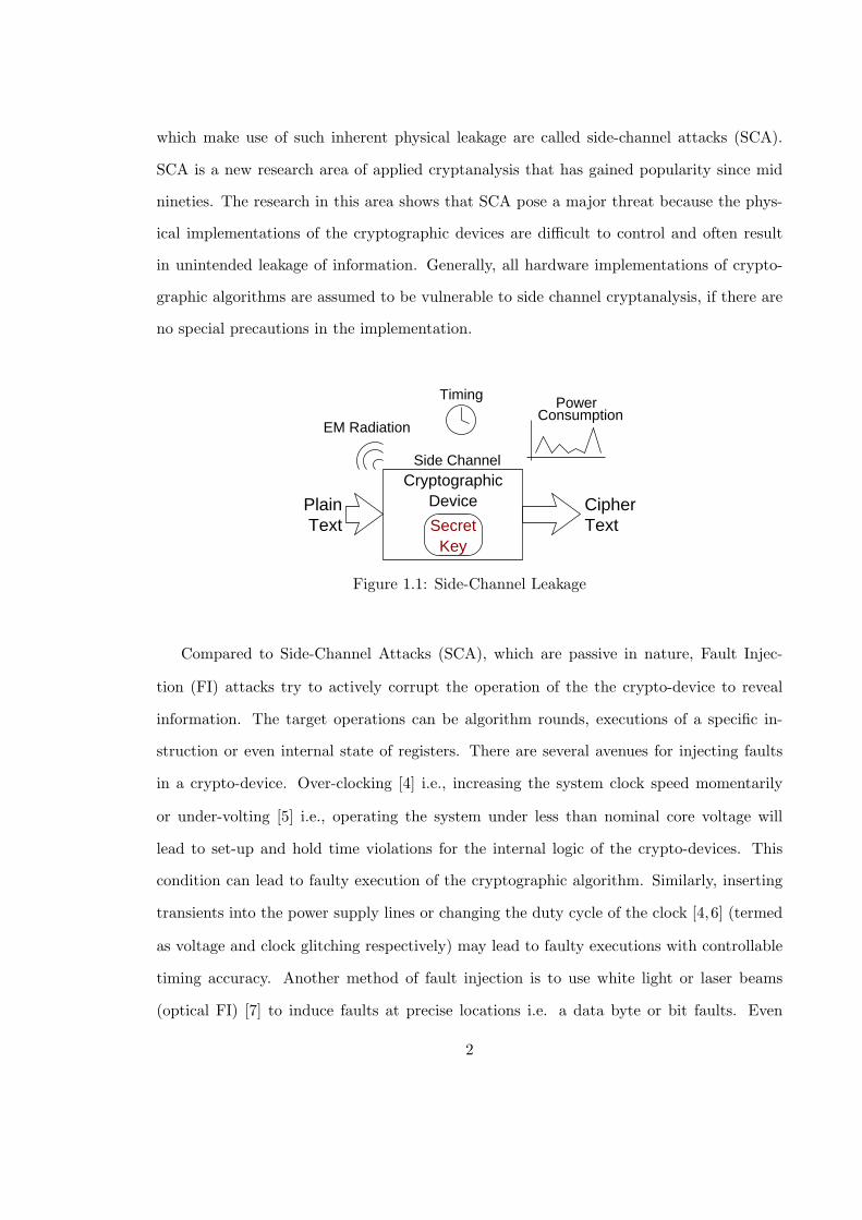
which make use of such inherent physical leakage are called side-channel attacks (SCA).
SCA is a new research area of applied cryptanalysis that has gained popularity since mid
nineties. The research in this area shows that SCA pose a major threat because the phys-
ical implementations of the cryptographic devices are difficult to control and often result
in unintended leakage of information. Generally, all hardware implementations of crypto-
graphic algorithms are assumed to be vulnerable to side channel cryptanalysis, if there are
no special precautions in the implementation.
TimingConsumption
Power
SecretKey
DeviceCryptographic
TextCipherPlain
Text
EM Radiation
Side Channel
Figure 1.1: Side-Channel Leakage
Compared to Side-Channel Attacks (SCA), which are passive in nature, Fault Injec-
tion (FI) attacks try to actively corrupt the operation of the the crypto-device to reveal
information. The target operations can be algorithm rounds, executions of a specific in-
struction or even internal state of registers. There are several avenues for injecting faults
in a crypto-device. Over-clocking [4] i.e., increasing the system clock speed momentarily
or under-volting [5] i.e., operating the system under less than nominal core voltage will
lead to set-up and hold time violations for the internal logic of the crypto-devices. This
condition can lead to faulty execution of the cryptographic algorithm. Similarly, inserting
transients into the power supply lines or changing the duty cycle of the clock [4,6] (termed
as voltage and clock glitching respectively) may lead to faulty executions with controllable
timing accuracy. Another method of fault injection is to use white light or laser beams
(optical FI) [7] to induce faults at precise locations i.e. a data byte or bit faults. Even
2

varying the temperature [6] of the crypto-device to the extremes i.e. exposing the device to
either hot or cold environment compared to its typical operating temperature will lead to
fault injections.
Plain Text Cipher TextSecret
Key
DeviceCryptographic
(Message) (Signature)
Plain Text Cipher Text
(Signature)Secret
Key
DeviceCryptographic
(Message)
Figure 1.2: Fault Injections
1.1.1 Motivation
Field Programmable Gate Arrays (FPGAs) are fast becoming a popular choice for a wide
variety of applications ranging from digital cameras to aero-space and defense systems.
Because of the outstanding feature of combining the programmability of processors with
the performance of custom hardware, FPGAs have become an essential part of critical sys-
tems. Recent architectural advances of FPGAs are making them an alternative choice for
low power applications where Application Specific Integrated Circuits (ASICs) are primarily
used. A hallmark of FPGAs is the ability to implement parallelized architectures efficiently,
and they also posses excellent resistance against invasive attacks since the underlying plat-
form is regular and does not reveal information on the actual design content. Because
of these features, FPGAs have become an attractive hardware platform for cryptographic
implementations.
Introduced by Kocher et al. [2] in 1999, Differential Power Analysis (DPA) attacks
exploits the data dependency between power consumption of cryptographic device and
3

secret. Power analysis attacks are passive and non-invasive, and hence have received the
most amount of attention by the research community. DPA attacks are very powerful, can
easily be conducted, and have been used successfully many times. They can be applied
to dedicated cryptographic processors as well as to general purpose processors running a
cryptographic software. When it turned out that the cryptographic devices are vulnerable to
power analysis, there has been great effort in the development of countermeasures against
DPA. Countermeasures proposed till date can be broadly classified at different levels of
design abstraction as shown in Fig 1.3.
Protocol
Algorithm
Architecture
Logic Style
Low Effectiveness
High Effectiveness
against DPA
Figure 1.3: Countermeasures at Different Levels
• Protocol: Continuously refresh/update the secret information so that the attacker is
never able to obtain sufficient information
• Algorithm: Change the order of operations of the cryptographic algorithms, not using
any branch instruction etc.
• Architecture: Using techniques like ”Masking”, to mask the power consumption of the
device running cryptographic algorithm by XORing the sensitive data with a pseudo
random variable. Recently, it was shown that the masking schemes were broken [8].
• Logic Style: Using techniques like ”Hiding”, where the power consumption of the
crypto device is constant at each and clock cycle.
The lower the level of countermeasure implemented the higher the effectiveness of coun-
termeasure against DPA. That is, out of all countermeasures proposed, the logic style coun-
termeasure provides considerable security against DPA attacks. An example of a logic style
4
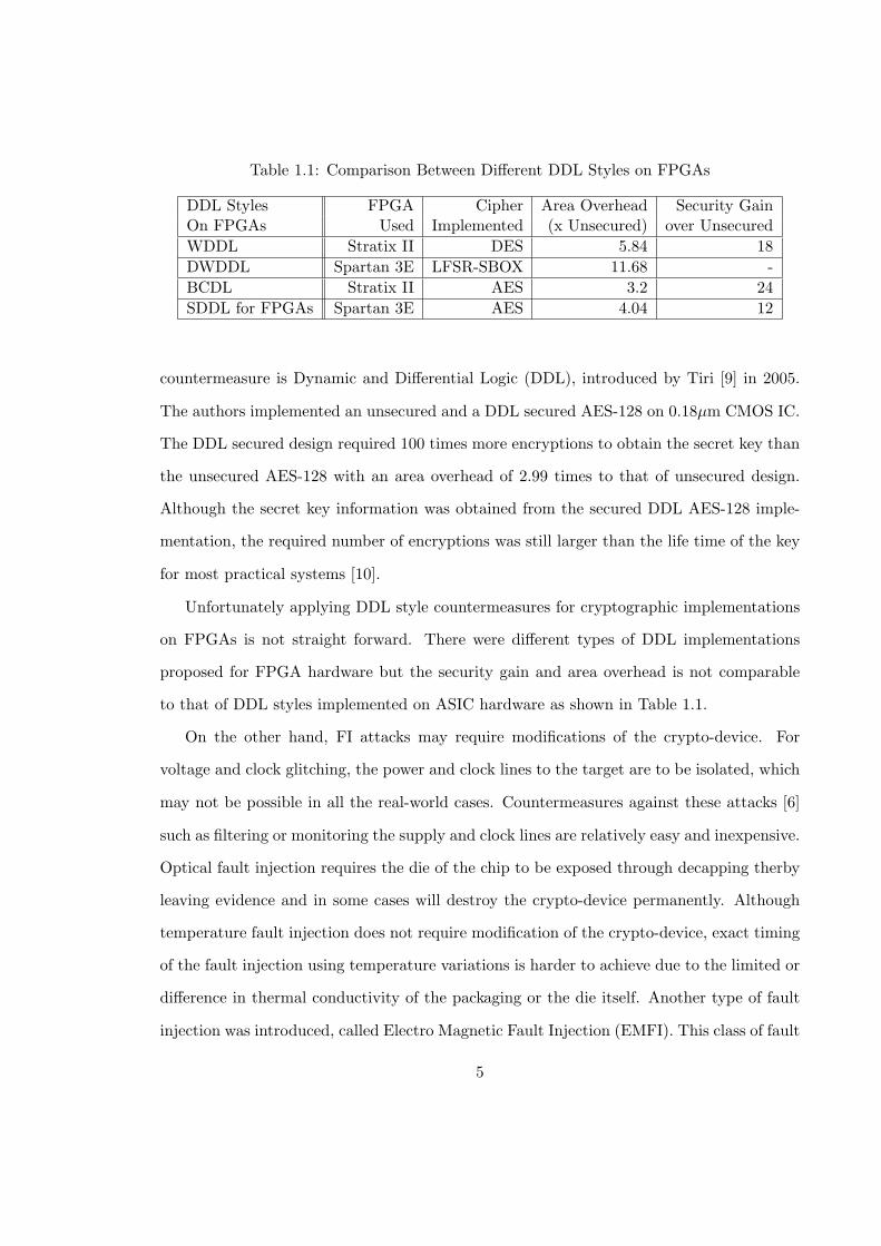
Table 1.1: Comparison Between Different DDL Styles on FPGAs
DDL Styles FPGA Cipher Area Overhead Security GainOn FPGAs Used Implemented (x Unsecured) over Unsecured
WDDL Stratix II DES 5.84 18
DWDDL Spartan 3E LFSR-SBOX 11.68 -
BCDL Stratix II AES 3.2 24
SDDL for FPGAs Spartan 3E AES 4.04 12
countermeasure is Dynamic and Differential Logic (DDL), introduced by Tiri [9] in 2005.
The authors implemented an unsecured and a DDL secured AES-128 on 0.18µm CMOS IC.
The DDL secured design required 100 times more encryptions to obtain the secret key than
the unsecured AES-128 with an area overhead of 2.99 times to that of unsecured design.
Although the secret key information was obtained from the secured DDL AES-128 imple-
mentation, the required number of encryptions was still larger than the life time of the key
for most practical systems [10].
Unfortunately applying DDL style countermeasures for cryptographic implementations
on FPGAs is not straight forward. There were different types of DDL implementations
proposed for FPGA hardware but the security gain and area overhead is not comparable
to that of DDL styles implemented on ASIC hardware as shown in Table 1.1.
On the other hand, FI attacks may require modifications of the crypto-device. For
voltage and clock glitching, the power and clock lines to the target are to be isolated, which
may not be possible in all the real-world cases. Countermeasures against these attacks [6]
such as filtering or monitoring the supply and clock lines are relatively easy and inexpensive.
Optical fault injection requires the die of the chip to be exposed through decapping therby
leaving evidence and in some cases will destroy the crypto-device permanently. Although
temperature fault injection does not require modification of the crypto-device, exact timing
of the fault injection using temperature variations is harder to achieve due to the limited or
difference in thermal conductivity of the packaging or the die itself. Another type of fault
injection was introduced, called Electro Magnetic Fault Injection (EMFI). This class of fault
5

injections uses transients in EM fields to induce faults into the crypto-device. The EMFI
are completely non-invasive in nature, are harder to detect during run-time and leave little
evidence of tampering on the crypto-device as compared to voltage or clock fault injections.
The equipment cost to conduct EMFI is relatively lower than that required for Optical fault
injections.
1.1.2 Contribution
The Goal of this thesis to develop an integrated environment for detecting and mitigating
SCA and FI attacks on hardware platforms. First and foremost, to validate the security
of the cryptographic primitives and proposed countermeasures against DPA in a fair and
comprehensive fashion, we propose an open-source tool called FOBOS. Secondly, we propose
to investigate and develop a methodology for implementing cryptographic algorithms on
FPGAs which is secure against SCA attacks. To achieve this, we propose a two phase
approach.
• Phase 1: Investigate the inherent resistance of the intrinsic features of FPGAs against
DPA.
• Phase 2: Implement DDL countermeasure on cryptographic algorithms using secure
implementation options obtained from phase-1 with an added factor of low area over-
head.
FPGAs also have several inherent features like Block RAMs, fast carry chains, Wide
dedicated Multiplexers (WDMs) which can be used to implement logic which are consider-
ably faster and consume less area than standard implementations which do not use these
features. Phase 1 essentially involves evaluating the security of these inherent features of
FPGAs against DPA. In Phase 2, we will develop a new Dynamic and Differential Logic
(DDL) style countermeasure tailored for FPGAs. It will use the most DPA resistant imple-
mentations obtained from Phase 1. DDL is a type of DPA countermeasure which eliminates
the correlation between the data being processed and the instantaneous power consumption
6

of the device (FPGAs) by maintaining constant power consumption in every clock cycle of
it’s operation.
By the end of these two phases we will have developed a secure design flow for imple-
menting cryptographic algorithms on FPGAs through a iterative design methodology, which
enables us to achieve resistance against DPA. We also propose a run-time glitch measure-
ment methodology to further test the effectiveness of our proposed DDL countermeasures.
Finally, we will study the effect of Electro Magnetic Fault Injection (EMFI) on an
ARM core. We describe the background, methodology and experimental set-up required
to conduct EMFI attacks. The impact of different types of probes used in EMFI attacks
is explored and a calibration process used for lab experiments is studied. We discuss our
preliminary results and conclude EMFI is a viable strategy for an attacker attempting to
break a cryptographic implementation.
7
Interleaved SDDL
On BoardReal−time
Glitch Detection
Partial DDL
FPGAs Intrinsic FeaturesWDMsBRAMs
Fast Carry ChainsSRL
SDDL for FPGAsFOBOS
Research GoalDDL for FPGAs
Check!
Estimation
Idea!Usage?
Early Precharge/Evaluation
Glitches
Large Area overhead
Problems:
Evaluation Methodology
Figure 1.4: Research Flow
8

Chapter 2: Background
2.1 Background – DPA
The first side-channel attack was reported in early 1956 [11] in which Peter Wright describes
how he helped the British secret services to break a rotor machine (early model of crypto
device used for encryption) by listening to the clicking sound with a microphone. Later,
in the mid 1980s, there was a lot of concern and commotion about the electromagnetic
emanation of video screens [12]. In 1996, Paul Kocher described an attack methodology to
compromise the security of RSA by exploiting the timing information [13].
2.1.1 Power Analysis Attacks
In the year 1999, Kocher et al. proposed more powerful Side-Channel Attack (SCA) i.e.
power analysis attacks [2,14]. The authors have discovered that the power consumption of
cryptographic devices can be exploited to reveal secret information. In 2000/2001, the use
of electromagnetic radiation as a side channel was introduced by Jean-Jacques Quisquater,
David Samyde and Karine Ganndolfi et al. [3, 15]. However, measurements of electromag-
netic fields have been performed since the 1950s for military purposes under the codeword
TEMPEST by the government of USA. The research on Side-Channel attacks is primarily
can be broadly divided into two directions. In one direction advanced analysis and process-
ing techniques were developed to enhance Side-Channel attacks and in the other direction
countermeasures against Side-Channel attacks are being developed at all levels of design
abstraction. Due to the fact that power analysis attacks are very powerful, do not require
expensive equipment, and are almost always successful, these attacks have been given the
maximum amount of attention by the research community.
9
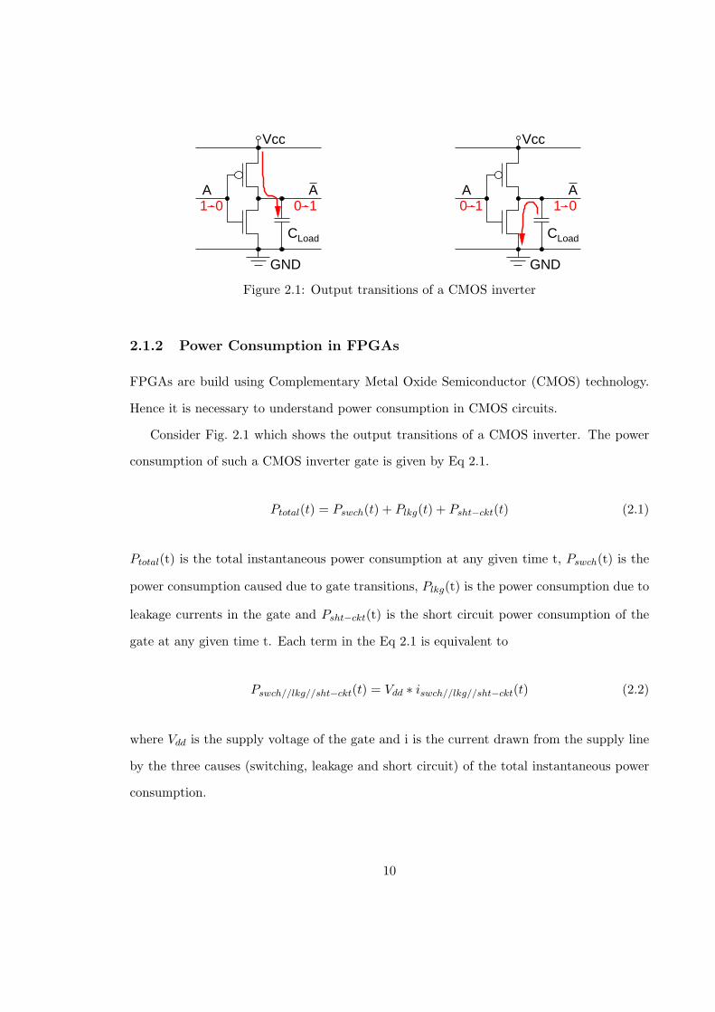
A
Vcc
GND
CLoad
01A
10A
Vcc
GND
CLoad
A010 1
Figure 2.1: Output transitions of a CMOS inverter
2.1.2 Power Consumption in FPGAs
FPGAs are build using Complementary Metal Oxide Semiconductor (CMOS) technology.
Hence it is necessary to understand power consumption in CMOS circuits.
Consider Fig. 2.1 which shows the output transitions of a CMOS inverter. The power
consumption of such a CMOS inverter gate is given by Eq 2.1.
Ptotal(t) = Pswch(t) + Plkg(t) + Psht−ckt(t) (2.1)
Ptotal(t) is the total instantaneous power consumption at any given time t, Pswch(t) is the
power consumption caused due to gate transitions, Plkg(t) is the power consumption due to
leakage currents in the gate and Psht−ckt(t) is the short circuit power consumption of the
gate at any given time t. Each term in the Eq 2.1 is equivalent to
Pswch//lkg//sht−ckt(t) = Vdd ∗ iswch//lkg//sht−ckt(t) (2.2)
where Vdd is the supply voltage of the gate and i is the current drawn from the supply line
by the three causes (switching, leakage and short circuit) of the total instantaneous power
consumption.
10

Switching Power
also called as Dynamic power is caused due to gate output transitions. This can explained
with the help of four gate transitions (refer to Fig 2.1) occurring in a CMOS inverter.
• When the input changes from logic ’1’ to logic ’0’ the output of the gate transitions
from logic ’0’ to logic ’1’ thereby ”charging” the load capacitance Cload.
• When the input changes from logic ’0’ to logic ’1’ the output of the gate transitions
from logic ’1’ to logic ’0’ thereby ”discharging” the load capacitance Cload. In ideal
cases no current is drawn from the supply.
• When the input is maintained at logic ’0’ the output of the gate is maintains at logic
’1’ and no current flows
• When the input is maintained at logic ’1’ the output of the gate is maintains at logic
’0’ and no current flows
Leakage Power
is caused due to gate leakage and sub-threshold leakage which occurs in every transistor.
The gate leakage is caused due to the current flowing from the gate to drain and is inversely
dependent on gate-oxide thickness. The sub-threshold leakage from source to drain of the
transistor and is caused due to parasitic capacitances and is inversely proportional to the
threshold voltage drops.
Short circuit Power
occurs whenever the nMOS and pMOS transistors change states. There exist a range
of input voltages for which both pMOS and nMOS transistors conduct current as these
transistors are not perfect switches. When both transistors are ”on”, a current flows from
the power supply to ground and is called short circuit current.
It is proven that switching power which is data dependent [16] (due to transitions of
gates) causes the data—power correlation which forms the basis of power analysis attacks.
11

For newer CMOS technologies (90 nm and lower) leakage power also becomes a dominant
factor because of the drop in threshold voltages and gate-oxide thickness which indicates
that not only gate output transitions but also the logic levels of gate outputs i.e. signals of
the device must also be taken into account.
2.1.3 Types of Power Analysis Attacks
According to Kocher et al. [2, 14], power analysis attacks are classified into two types
1. Simple Power Analysis (SPA)
2. Differential Power Analysis (DPA).
Simple Power Analysis involves direct interpretation of power traces generated by an
algorithm run on hardware. Because of the reason that different operations performed by
a processor have different power consumption characteristics [17, 18], the adversary can
identify the operation just by observing the power trace. However, SPA attacks are quite
challenging as the adversary needs to have detailed knowledge about the implementation of
the cryptographic algorithm that is being executed by the hardware.
Differential Power Analysis
(DPA) are the most popular and powerful type of power analysis attacks due to the fact
that they do not require detailed knowledge about the attacked device. DPA exploits the
data dependency of the instantaneous power consumption of cryptographic device. Unlike
SPA which requires one or few traces, DPA attack works with large number of power traces.
The DPA attack methodology can be generalized in four steps.
• STEP:1 Choose an intermediate result of the algorithm being executed which should
be function of input data and key.
• STEP:2 Measure the power consumption when the algorithm computes the interme-
diate result.
12

• STEP:3 Calculate the hypothetical values and build a power model.
• STEP:4 Compare the hypothetical power model with power consumption through
statistical tests.
The articles [19,20] are good sources of information SPA and DPA attacks.
Attack Models
In order to simulate the power consumption of the cryptographic device i.e. to relate the
power consumption with the data being processed we use the following two generic models.
Hamming Weight Model is a simple power model, which assumes that the power
consumptions is directly proportional to the Hamming Weight (HW) i.e. number of bits
that are set in the corresponding data word [21]. If D is binary data of length i
D =i−1∑i=0
di2i
then the Hamming weight of D is simply, the number of bits that are set to ’1’ as shown in
(2.3).
HW (D) =
i−1∑i=0
Di (2.3)
This model is typically used when the attacker knows only the data value at a given
time, but not it’s previous or the next state value.
Hamming Distance Model uses the number of bits changed between two subsequent
states of data Di and Di+1
13

HD(Di, Di+1) =
j−1∑j=0
(Di ⊕Di+1)j (2.4)
As shown in Fig. 2.1, bit transitions effect the power consumption of the device. As the
Hamming Distance (HD) model is based on the bit transitions between two states, it more
accurately reflects the power consumption of the device than HW model.
Security Metrics
The security of a design against DPA attacks is determined by the number of measurements
required to recover the key, also known as Measurements To Disclosure (MTD). We count
one encryption as one measurement independent of the number of samples the oscilloscope
takes during one encryption. MTDs, are to a certain extent depend upon the message and
secret key used.
Success of DPA Attacks on Various Cryptographic Implementations
Kocher et al. successfully attacked DES in [2, 14] and was able to recover the key. In
the years following mid nineties, successful DPA attacks against cryptographic algorithms
implemented in software and on ASICs were published. Four years later, successful DPA at-
tacks against DES and RSA [22] and ECC [23] implementations on FPGAs were reported.
The first practical DPA attack on SHA-2 HMAC implemented on FPGA was published
in [24]. Even all the eSTREAM candidates were susceptible to DPA attacks [25]. Ex-
perimental results of DPA attacks on IDEA and RC6 were published in [26]. Advanced
Encryption Standered (AES) was successfully attacked on FPGAs in [27–30]
2.2 Background – Xilinx FPGAs
There are a wide verity of FPGAs manufactured by different vendors like Xilinx, Altera,
Actel etc. This section describes the underlying structure of Xilinx Spartan series FPGA
14
which we are using for laboratory testing. We also note that the architecture is similar to
that Altera FPGAs.
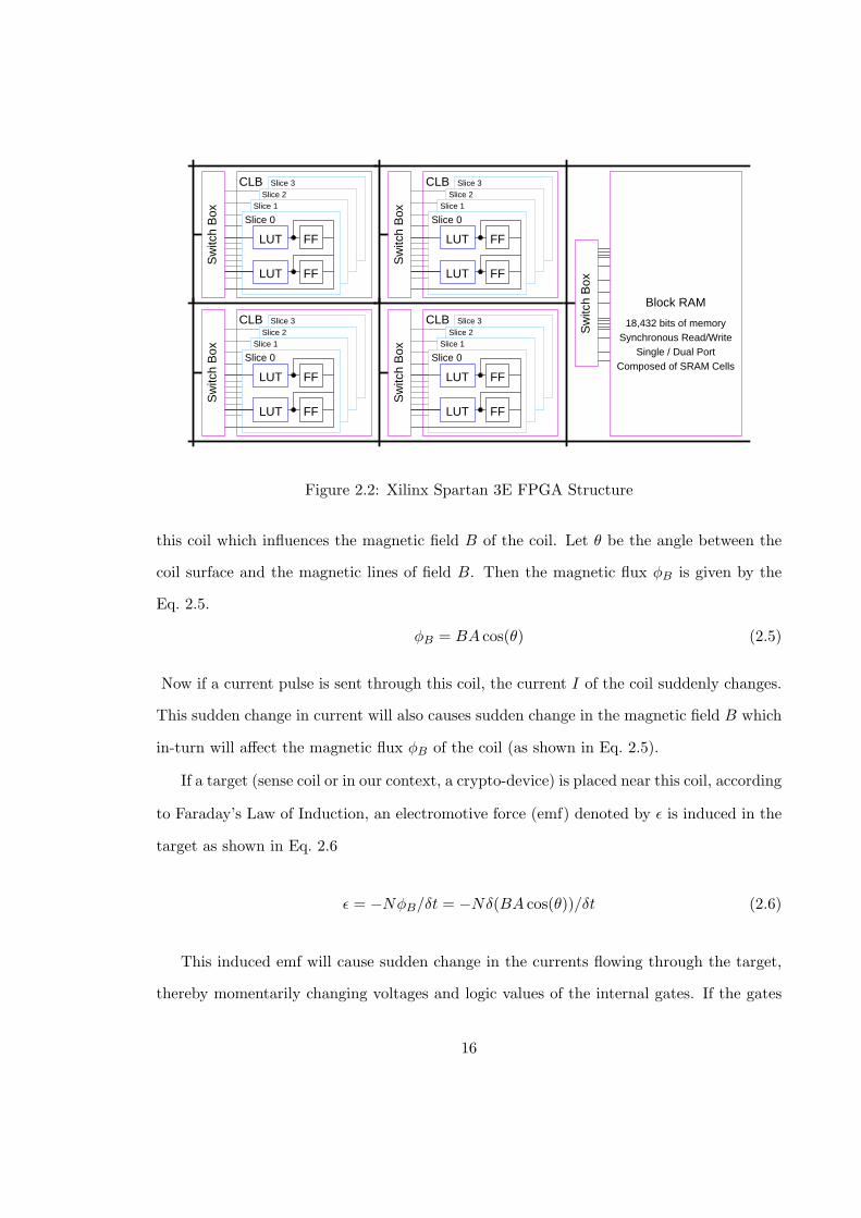
The Configuration Logic Blocks (CLBs) contains the main logic resources for implement-
ing a wide variety of logic functions as well as for storing information. CLBs are arranged
in arrays of rows and columns and their densities varies from one FPGA to another. In
Xilinx Spartan3E FPGAs, a CLB is comprised of four slices, each containing two look-up
tables (LUT) and two storage elements that can be used as either flip-flops or latches. It
also contains two wide function multiplexers, fast carry logic and other miscellaneous ele-
ments. The LUTs in some special slices are used not only to implement logic but can also
be configured as 16-bit Distributed RAM or 16-bit Shift Register LUT (SRL).
The Block RAMs (BRAMs) are organized in columns inside the Xilinx FPGAs [31].
Special interconnects are provided between a BRAM and its adjacent CLBs. Also pro-
visions are provided to allow multiple BRAMs to be cascaded to form wider memories.
BRAMs consist of static RAM cells and contain 18,432 bits of total RAM. Each has two
completely independent access ports called Port A and Port B. The BRAM’s structure is
fully symmetrical and both ports support data read/write operations. Each port is syn-
chronous with its own clock, clock enable and write enable [31]. BRAMs can be used as
data storage, FIFOs, large (LUTs), data width converters, circular buffers, shift registers,
wide logic functions and other basic functional primitives of cryptographic algorithms.
2.3 Background –EMFI
There are two types of EM perturbations used to inject fault into the target devices. They
are transient pulses ans shown in Fig 2.4 and harmonic emmisions as shown in Fig 2.3
The scope of this research is constrained to Transient Type of EM fault injections.
The idea behind Transient Type of EMFI is to inject fault(s) into the crypto-device or
target using an electromagnetic pulse (magnetic flux) generated by a coil. For example, let
us consider a loop of coil, having the surface area A. Let I be the current flowing through
15
Slice 0
LUT FF
LUT FF
Sw
itch
Box Slice 0
LUT FF
LUT FF
Slice 1Slice 2
Slice 3
Sw
itch
Box
CLB
Slice 0
LUT FF
LUT FF
Slice 1Slice 2
Slice 3
Sw
itch
Box
CLB
Slice 0
LUT FF
LUT FF
Slice 1Slice 2
Slice 3
Sw
itch
Box
CLB
Slice 1Slice 2
Slice 3CLB
Sw
itch
Box
Block RAM
18,432 bits of memorySynchronous Read/Write
Single / Dual PortComposed of SRAM Cells
Figure 2.2: Xilinx Spartan 3E FPGA Structure
this coil which influences the magnetic field B of the coil. Let θ be the angle between the
coil surface and the magnetic lines of field B. Then the magnetic flux ϕB is given by the
Eq. 2.5.
ϕB = BA cos(θ) (2.5)
Now if a current pulse is sent through this coil, the current I of the coil suddenly changes.
This sudden change in current will also causes sudden change in the magnetic field B which
in-turn will affect the magnetic flux ϕB of the coil (as shown in Eq. 2.5).
If a target (sense coil or in our context, a crypto-device) is placed near this coil, according
to Faraday’s Law of Induction, an electromotive force (emf) denoted by ϵ is induced in the
target as shown in Eq. 2.6
ϵ = −NϕB/δt = −Nδ(BA cos(θ))/δt (2.6)
This induced emf will cause sudden change in the currents flowing through the target,
thereby momentarily changing voltages and logic values of the internal gates. If the gates
16
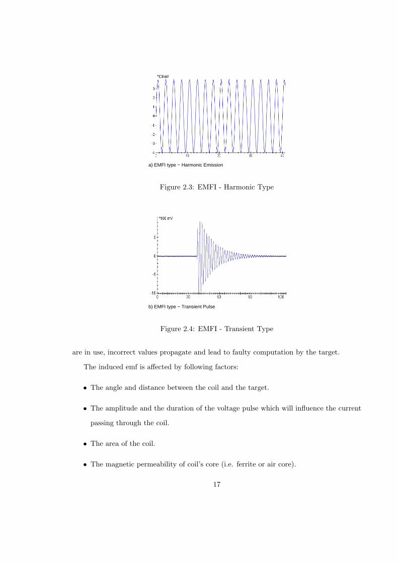
a) EMFI type − Harmonic Emission
Figure 2.3: EMFI - Harmonic Type
b) EMFI type − Transient Pulse
Figure 2.4: EMFI - Transient Type
are in use, incorrect values propagate and lead to faulty computation by the target.
The induced emf is affected by following factors:
• The angle and distance between the coil and the target.
• The amplitude and the duration of the voltage pulse which will influence the current
passing through the coil.
• The area of the coil.
• The magnetic permeability of coil’s core (i.e. ferrite or air core).
17

I1
N2
B1
ε
Coil 1
Coil 2
N1
(Induced)2
Figure 2.5: Mutual Induction between Two Coils
Hence the above mentioned factors become relevant parameters when conducting an
EMFI attacks.
18

FOBOS
Interleaved SDDL
On BoardReal−time
Glitch Detection
Partial DDL
FPGAs Intrinsic FeaturesWDMsBRAMs
Fast Carry ChainsSRL
SDDL for FPGAs
Research GoalDDL for FPGAs
Evaluation Methodology
Check!
Estimation
Idea!Usage?
Early Precharge/Evaluation
Glitches
Large Area overhead
Problems:
Figure 2.6: Research Flow
19

Chapter 3: Flexible Opensource workBench fOr Sidechannel
analysis - FOBOS
3.1 Introduction and Motivation
While a few FPGA boards designed for SCA exist, many research groups from academia and
industry use their own hardware harness, their own software for data acquisition and data
analysis and sometimes their own FPGA boards or generic FPGA boards. This increases
the complexity and effort needed to obtain a working SCA setup. Another, but costly
option is the use of commercial SCA workstations.
Due to the importance of the topic of Side-Channel attacks, they became part of the
curriculum of cryptography courses in many universities. However, only very few have
associated laboratory exercises and hands-on examples due to the cost and complexity of
current SCA setups.
To our knowledge no complete software package exists that contains everything needed
for evaluating the side-channel attack resistance of FPGA implementations from data ac-
quisition to analysis (see Sect:3.1.1). In this chapter, we are presenting a framework for
efficient side-channel evaluation of cryptographic implementations on hardware and soft-
ware. Such an environment should be flexible, open-source and low cost and beneficial to
both research and educational communities.
20
3.1.1 Previous Work
SCA - Hardware Platforms
The Side-Channel Analysis Board (SCAB) introduced in [32], was one of the early efforts
in developing evaluation platforms for conducting SCA attacks on implementations of cryp-
tographic algorithms. This board housed an FPGA on which the cryptographic algorithms
can be implemented along with an unrestricted access to power and clock pins to perform the
following SCA attacks: Differential Power Analysis (DPA) and fault analysis. Information
about the board design and the status of the project is currently not available.
The Side-Channel Attack Standard Evaluation Board (SASEBO) [33],[34] was devel-
oped by the Research Center for Information (RCIS) of National Institute of Advanced
Industrial Science and Technology (AIST) and Tohoku University as a common platform
for evaluating Side-Channel attacks. These boards were developed with the intent of per-
forming side channel attacks on various hardware platforms like FPGAs, ASICs and Smart
cards. SASEBO boards are designed with two FPGAs, a cryptographic FPGA (or an
ASIC/Smart card) where the algorithm can be implemented and a control FPGA which
directs the data flow between the software and the cryptographic FPGA. The data acquisi-
tion software which comes with SASEBO is written in C#. It does not provide support for
different brands of oscilloscopes. Hence the user is required to tweak the code to provide
support for his/her own oscilloscope. Only four different types of SASEBO boards with
FPGAs as victims (shown in Table 3.1) are available. Early this year, AIST announced
that it discontinued support for the SASEBO project. Morita Tech [35] recently announced
SAKURA as a successor to SASEBO project.
SCA - Data Analysis Platforms
The DPA Contest [36] organized jointly by VLSI research group of Telecom ParisTech uni-
versity and AIST, is an online-based contest with the aim of having a fair confrontation
21

Table 3.1: SASEBO Boards with FPGAs as Victims
WiresBoard Control Victim Control– Host Data
FPGA FPGA Techn. Victim Communication
SASEBO Virtex-2 Pro Virtex-2 Pro 130 nm 54 RS232SASEBO-G Virtex-2 Pro Virtex-2 Pro 130 nm 53 RS232, FT245RLSASEBO-GII Spartan-3A Virtex-5 65 nm 46 FT2232DSASEBO-B Stratix-2 Stratix-2 90 nm 53 RS232, FT245RL
between different attack methodologies. Currently three editions of this contest were intro-
duced of which the first two deal primarily with attacking DES (v1) and AES (v2) using
different techniques where as the goal of the third edition is to compare acquisition plat-
forms and techniques. The results for the third edition was recently announced at COSADE
2012. For the v1 & v2 editions, the acquired data was provided by the contest organizers
where as in v3 only the RTL description of AES was provided. Data acquisition was left
to the the participant choice. This contest provides a wealth of information regarding DPA
statistical techniques, although all the data acquisition is obtained from SASEBO GII only.
The OpenSCA Toolbox [37] is an open source project which consists of set of Matlab
codes and objects to perform DPA attacks. Using this toolbox one can conduct not only first
order power analysis attacks but also the higher order and template attacks. The toolbox
also comes with several examples, demonstrating the attacks. Currently the supported sta-
tistical testing procedures are Difference-of-Means, Correlation Power Analysis and Baysian
analysis. All codes are written in Matlab and does not include data acquisition. In short,
we can perform only data analysis using OpenSCA.
The DPA WorkstationTM [38] is a state-of-the art proprietary SCA testing platform by
Cryptography Research, Inc. DPA WorkstationTMcan perform data acquisition, processing
and analysis and also has the ability to generate hypothesis models for a range of ciphers
like AES, DES, RSA, ECC etc. It also provides support for data capture for a wide range
of sampling devices like oscilloscopes and PCI A/D converters. Additionally, it supports
22

multiple hardware platforms (FPGAs, SoC etc.) and different sensors (current, field probes)
and hence both power and EM attacks can be performed using this workstation. The major
drawback is that this tool is not freely available and licensing is very costly, thus not usable
for educational purposes. Also, collaborations between research groups are difficult as they
might not all have access to the DPA WorkstationTM.
Drawbacks of Current SCA Evaluation Platforms
An efficient SCA evaluation platform should have the following criteria:
• Flexibility: Able to support multiple hardware platforms/technologies/vendors.
• Open Source: Community support will allow for rapid development and adoption of
the latest devices and technologies.
• Reproducibility: Results published in research should be reproducible to obtain a fair
SCA analysis of cryptographic algorithms.
• Broad-Spectrum Acceptance: Should be accepted by both educational (low-cost) and
research/industry (state-of-the-art) communities.
We have shown in Sect. 3.1.1 and Sect. 3.1.1 that a complete (acquisition to analysis), free
and open source solution is not available. Therefore, research groups and industry who
do not want to invest in the proprietary DPA WorkstationTMemploy home grown scripts,
programs and platforms. Their main disadvantages are that they are mostly written in an
ad-hoc fashion and therefore difficult to maintain and extend. These scripts and platforms
are also proprietary and hence, their results are not reproducible by other research groups.
SASEBO currently has limited hardware support. OpenSCA toolbox can perform data
analysis only. The DPA contest provides information about different attack strategies only.
Hence there is a need for a flexible and complete open-source framework for SCA that
allows fair and comprehensive evaluation of implementations on hardware platforms with
reproducible results.
23
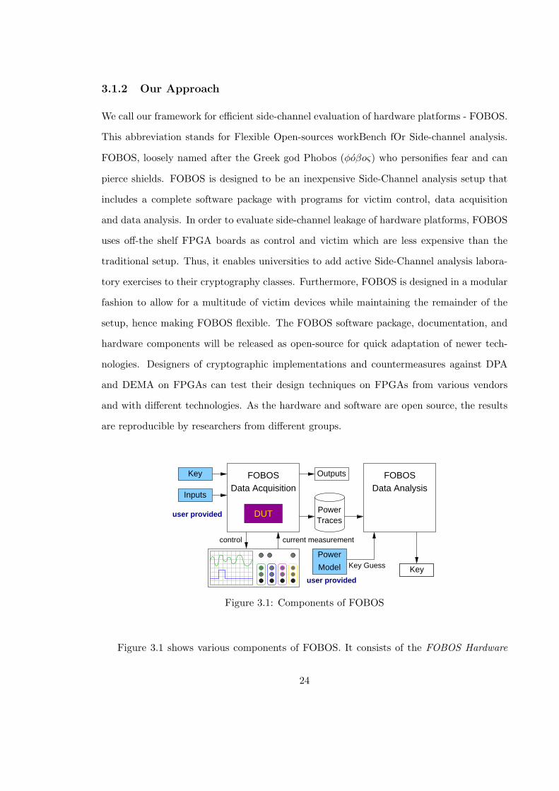
3.1.2 Our Approach
We call our framework for efficient side-channel evaluation of hardware platforms - FOBOS.
This abbreviation stands for Flexible Open-sources workBench fOr Side-channel analysis.
FOBOS, loosely named after the Greek god Phobos (ϕoβoς) who personifies fear and can
pierce shields. FOBOS is designed to be an inexpensive Side-Channel analysis setup that
includes a complete software package with programs for victim control, data acquisition
and data analysis. In order to evaluate side-channel leakage of hardware platforms, FOBOS
uses off-the shelf FPGA boards as control and victim which are less expensive than the
traditional setup. Thus, it enables universities to add active Side-Channel analysis labora-
tory exercises to their cryptography classes. Furthermore, FOBOS is designed in a modular
fashion to allow for a multitude of victim devices while maintaining the remainder of the
setup, hence making FOBOS flexible. The FOBOS software package, documentation, and
hardware components will be released as open-source for quick adaptation of newer tech-
nologies. Designers of cryptographic implementations and countermeasures against DPA
and DEMA on FPGAs can test their design techniques on FPGAs from various vendors
and with different technologies. As the hardware and software are open source, the results
are reproducible by researchers from different groups.
Key
Inputs
Outputs
PowerTraces
Power
Model Key
Data AnalysisFOBOS
Data AcquisitionFOBOS
DUT
control
user provided
current measurement
Key Guess
user provided
Figure 3.1: Components of FOBOS
Figure 3.1 shows various components of FOBOS. It consists of the FOBOS Hardware
24

as well as software for Data Acquisition and Control and Data Analysis. The FOBOS
Hardware consists of two FPGA boards that are connected to each other. It is also possible
to use the SASEBO GII board instead. The user has to provide the hardware description
of the cipher under investigation, the key, a set of inputs and a power model. The Data
Acquisition and Control module configures and controls the FOBOS Hardware and the
Oscilloscope. It takes the user provided key and inputs and sends them to the FOBOS
Hardware which in turn encrypts the inputs with the key and returns the outputs (i.e.
ciphertext). As soon as the FOBOS Hardware starts with the encryption, it sends a trigger
signal to start data acquisition of the oscilloscope. The Data Analysis module uses the user
supplied power model, which can be based on inputs and/or outputs, and the power traces
collected by the oscilloscope to recover the key.
3.1.3 Architecture of FOBOS
FOBOS has two parts, the FOBOS Hardware and the FOBOS Software. The following
sections describe the functionality of various components of FOBOS.
FOBOS Hardware
A schematic diagram of the FOBOS hardware is shown in Fig. 3.2. It consists of two
boards Victim Board & Control Board connected together by the so called bridge connector.
The cryptographic algorithms whose security needs to be evaluated are to be implemented
on the FPGA of the Victim board. Data i.e. plaintext and/or key is sent from the PC
via USB to the control FPGA, which then forwards the data to the Victim FPGA. After
processing, the Victim FPGA sends the results back to the Control FPGA which in turn
forwards the results to the PC for verification. The control board also sends a trigger signal
to the oscilloscope to capture power measurement data.
Control Board: The control board used by FOBOS is either a Nexys2 or a Nexys3
board. Table 3.2 shows details of the both boards. The control board contains several
modules (see Fig. 3.2) and two clock domains. It uses the on-board 50MHz oscillator as
25
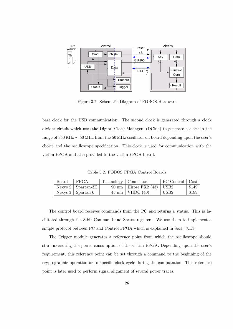
Control Victimresetclk
k dFIFOw
wFIFO
PC
clk div.Key Data
Cmd.
CoreFunction
TriggerStatus
Timeout
USB
Result
Data
Figure 3.2: Schematic Diagram of FOBOS Hardware
base clock for the USB communication. The second clock is generated through a clock
divider circuit which uses the Digital Clock Managers (DCMs) to generate a clock in the
range of 350KHz ∼ 50MHz from the 50MHz oscillator on board depending upon the user’s
choice and the oscilloscope specification. This clock is used for communication with the
victim FPGA and also provided to the victim FPGA board.
Table 3.2: FOBOS FPGA Control Boards
Board FPGA Technology Connector PC-Control Cost
Nexys 2 Spartan-3E 90 nm Hirose FX2 (43) USB2 $149Nexys 3 Spartan 6 45 nm VHDC (40) USB2 $199
The control board receives commands from the PC and returns a status. This is fa-
cilitated through the 8-bit Command and Status registers. We use them to implement a
simple protocol between PC and Control FPGA which is explained in Sect. 3.1.3.
The Trigger module generates a reference point from which the oscilloscope should
start measuring the power consumption of the victim FPGA. Depending upon the user’s
requirement, this reference point can be set through a command to the beginning of the
cryptographic operation or to specific clock cycle during the computation. This reference
point is later used to perform signal alignment of several power traces.
26
A Timeout module makes sure that PC receives a status (of TIMEOUT) if an exception
occurs during the communication with the victim or if the victim does not respond within a
given time. This timeout value can be specified through a command. The timeout counter
is automatically reset each time the victim returns data.
The Reset module is used to send a reset signal to the crypto core implemented on the
victim FPGA depending upon the value specified by the user. This is useful if for example
a cryptographic operation takes 1,000 clock cycles to complete, however, the interesting
event happens in the 30th clock cycle. The user can then reset the victim automatically
every 35 clock cycles and start a new encryption without having to wait for the encryption
to complete.
Victim Board: We are investigating several FPGA boards available in the market,
which can be used as Victim boards for FOBOS. Table 3.3 shows some potential Victim
boards. The column “VCore Jumper” indicates whether the board contains a jumper on the
core power line which allows for by-passing the on board core power supply and inserting a
current sensor (resistor or current probe) to measure the power consumption of the victim
FPGA. So far, we have successfully used the Spartan 3E Starter Kit, Spartan 3E-1600
Developer Board, and the Altera DE1 board as FOBOS Victim boards. As the Altera DE1
does not have VCore Jumper, we had to de-solder the voltage regulator for core voltage.
On all boards we also removed several capacitors. Our preliminary investigation (shown in
Table 3.3) into the other boards have shown that it is possible to modify them in order to
measure the current of the core supply.
For each victim board we plan on publishing instructions on how to modify it for DPA
and the printed circuit board (PCB) layout of the bridge connector which connects the
victim board securely to the control board.
FOBOS Control-Victim Protocol uses a simple FIFO interface to transfer data to
and from the control and victim FPGAs. The functionality of the input and output ports
of the protocol is described in [39], [40]. All data and key to and from the FPGA is broken
into segments. The first 2 bytes (16-bit) of each segment is a command word, which decides
27

Table 3.3: FOBOS FPGA Victims
Techn- VCore
Board FPGA ology Jumper Cost
Spartan 3E Starter Spartan-3E 90 nm yes $159Spartan 3E-1600 Dvlp. Spartan-3E 90 nm yes $225Altera DE1 Cyclone-II 90 nm no $150Cyclone III Starter Cyclone-III 65 nm yes $199Genesys Board Virtex-5 65 nm no $449Altera DE2-115 Cyclone-IV 60 nm no $299Altys Board Spartan-6 45 nm no $199Altera DE4 Stratix-IV 40 nm no $2,995Xilinx ML605 Virtex-6 40 nm no $1,795Xilinx KC705 Virtex-7 28 nm no $1,695
the nature of the segment and the number of bytes being sent. The format of the 16-bit
command words is shown in Fig 3.3. A ‘0’ value in the LSB and a ‘0’ value in the MSB
of the command word indicates that a key is being sent. Similarly a ‘1’ value in the LSB
indicates that data is send. The bit in position ‘1’ indicates with a ‘0’ that more segments
are following the current one, a ‘1’ indicates that the current segment is the last. The MSB
bit value ‘1’ for a 16-bit command for loading the key is left explicitly for future use. This
protocol does not require the control board to know what the block size of the cryptographic
function is. The widths of the buses for ‘k’ and data ‘d’ indicated in Fig 3.2 can be defined
by the user according to the requirement of the cryptographic implementation.
FOBOS Software:
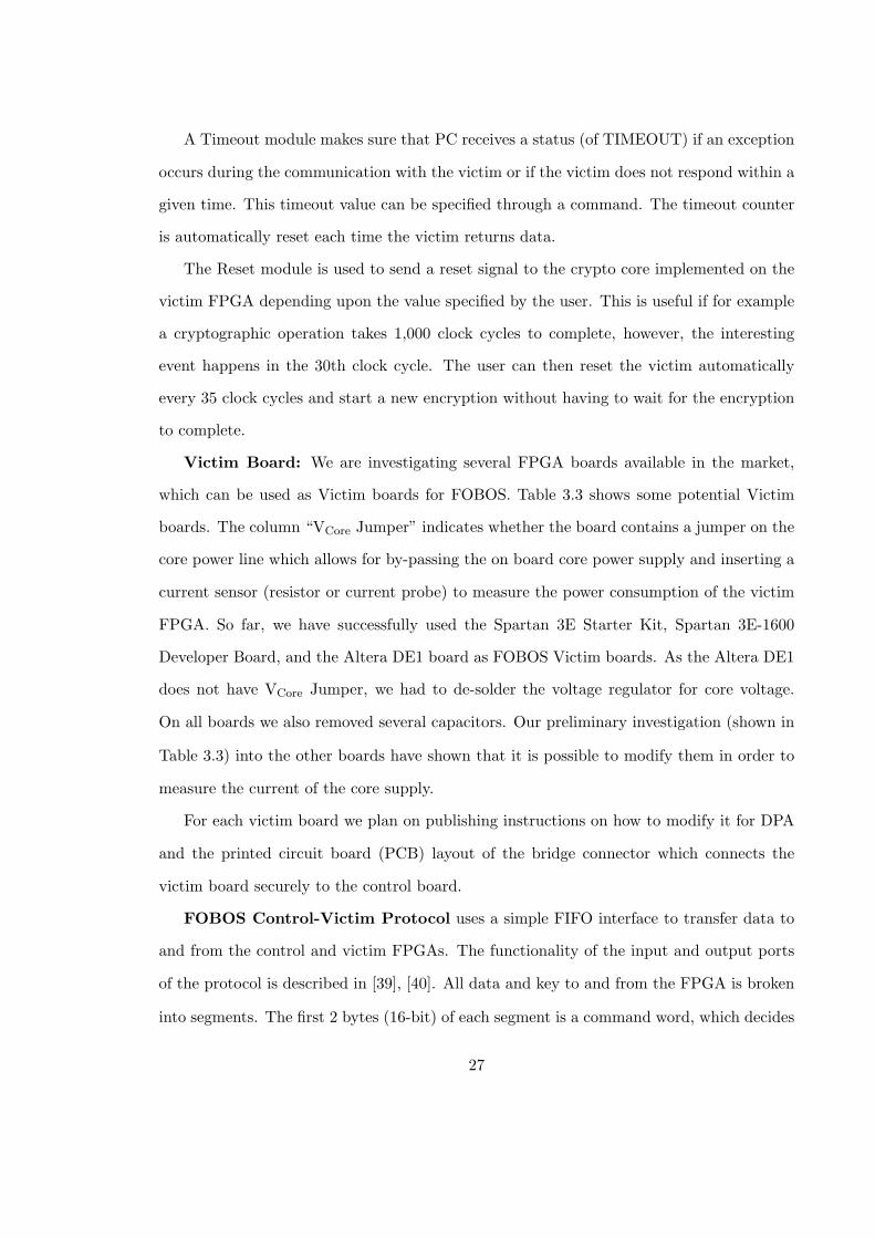
FOBOS Software Control Flow: The FOBOS control flow is shown in Fig. 3.4. The
control script parses the configuration files and initializes the FOBOS environment. It
performs a simple tool check to verify whether the necessary library files essential for data
transfer and oscilloscope control are installed and only continues when the check passes
successfully. The control script then assigns the hardware and oscilloscope attribute values
as specified by the user in the configuration files. The FOBOS hardware then performs
28

EC
ECFK 0
0 − Continuation1 − Key End
0 − Key
Number of Bytes
1 − Future Use
16−bit Command for Loading Key
015
115 0
Number of Bytes
0 − Continuation1 − Message End
16−bit Command for Loading / Writing Data
Size
Size
Figure 3.3: FOBOS Protocol
a built-in self test to check whether all the attributes are set accordingly and issues an
appropriate status message to the control script. The status message can be a success or
an error code. If the control receives an error code it exits the program displaying proper
error message. On receiving a success code, the control script instructs the oscilloscope to
digitize its analog inputs which then in turn waits for the trigger signal from the control
board to start capturing data. The plaintext and the key are then transferred to the FOBOS
hardware and the control script waits until it receives data from the oscilloscope. Once
the oscilloscope data is captured, the control script writes the outputs from the FOBOS
hardware to a file.
FOBOS has support for two data capturing modes, called Single Capture and Multi
Capture to capture the power traces. Single Capture mode, as shown in Fig. 3.5a), assumes
that a power trace contains a single encryption whereas Multi Capture mode, as shown in
Fig. 3.5b), contains multiple encryptions per power trace. Once all data has been captured
the control is transferred to data analysis module.
FOBOS PC- Control Communication Protocol: FOBOS uses the command &
status registers to control the PC- Control communication. The command register is used
(shown in Fig. 3.2) to pass the option values to the modules inside the control FPGA and to
signal the control board that PC is ready to transmit the data. The status register (shown
29
Data Analysis
Initialize & Tool Check
Set Oscilloscope &
Parse Config
Hardware Attributes
Start Oscilloscope Send Data to Ctrl Brd
Measurements (Digitize)
waits for trigger
generates trigger
Capture Waveforms Get Data from Ctrl Brd
= 0 ?N Y# of traces
Figure 3.4: FOBOS Control Flow
in Fig. 3.2) on the other hand, is used for signaling the PC that the control FPGA is ready
to transmit the data obtained from victim FPGA or to report errors.
Encryption_1 Encryption_2 Encryption_3 Encryption_4
Power Trace_1
b) Multi Capture
Power Trace_1 Power Trace_2 Power Trace_3 Power Trace_4
Encryption_1 Encryption_2 Encryption_4Encryption_3
a) Single Capture
Figure 3.5: Capture Modes
FOBOS Data Acquisition Module The data acquisition module configures the os-
cilloscope and retrieves its data. Its behaviour is determined by a configuration file which
uses a generic, oscilloscope brand independent description. A special, oscilloscope dependent
sub-module translates the configuration file to commands which are oscilloscope specific.
30

The sub-module of our prototype uses the Virtual Instrument Software Architecture (VISA)
library which is a standard for configuring and programming instruments using a variety
of interfaces. Presently, the FOBOS prototype supports communication for oscilloscopes
from Agilent Technologies. In future we plan to provide support for oscilloscopes from other
manufacturers.
3.1.4 FOBOS Data Analysis Module:
The Data Analysis module consists of 3 sub-modules as shown below:
• Signal Alignment Module
• Post processing Module
• SCA Module
• Statistics Module
Signal Alignment Module
As the name indicates, the main function of this module is to align all the measured power
traces with respect to time using a reference signal called the ”Trigger” signal. Depending
upon the type of capture mode used i.e. Single capture or Multi capture its functionality
varies. In Single capture mode as each measurement trace contains only one encryption, the
power traces are aligned when the ”Trigger” signal becomes logic high. In the Multi capture
mode, as each measurement trace contains multiple encryptions, the start of each encryption
is indicates by the Trigger signal. To be exact, the measurement point from one trigger high
to the subsequent trigger high is equivalent to one encryption. The measurement module
chops up the trace accordingly and aligns them.
Post processing Module
Currently FOBOS supports three Post processing sub modules. They are:
1. Sample Space Disposition
31
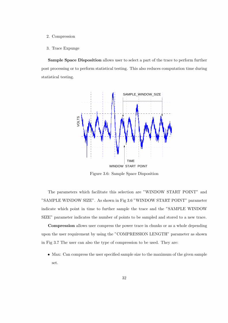
2. Compression
3. Trace Expunge
Sample Space Disposition allows user to select a part of the trace to perform further
post processing or to perform statistical testing. This also reduces computation time during
statistical testing.
SAMPLE_WINDOW_SIZE
VO
LTS
WINDOW_START_POINT
TIME
Figure 3.6: Sample Space Disposition
The parameters which facilitate this selection are ”WINDOW START POINT” and
”SAMPLE WINDOW SIZE”. As shown in Fig 3.6 ”WINDOW START POINT” parameter
indicate which point in time to further sample the trace and the ”SAMPLE WINDOW
SIZE” parameter indicates the number of points to be sampled and stored to a new trace.
Compression allows user compress the power trace in chunks or as a whole depending
upon the user requirement by using the ”COMPRESSION LENGTH” parameter as shown
in Fig 3.7 The user can also the type of compression to be used. They are:
• Max: Can compress the user specified sample size to the maximum of the given sample
set.
32
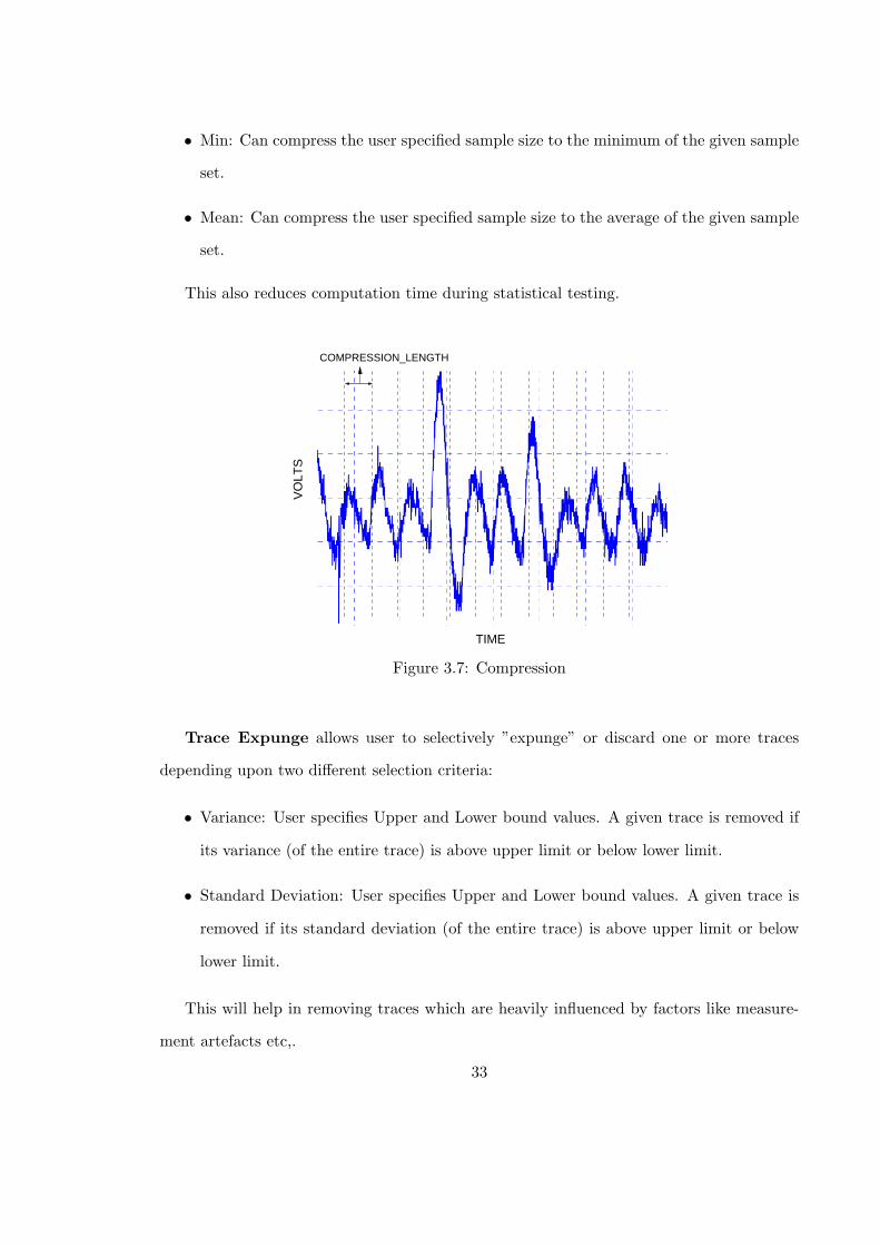
• Min: Can compress the user specified sample size to the minimum of the given sample
set.
• Mean: Can compress the user specified sample size to the average of the given sample
set.
This also reduces computation time during statistical testing.
COMPRESSION_LENGTH
TIME
VO
LTS
Figure 3.7: Compression
Trace Expunge allows user to selectively ”expunge” or discard one or more traces
depending upon two different selection criteria:
• Variance: User specifies Upper and Lower bound values. A given trace is removed if
its variance (of the entire trace) is above upper limit or below lower limit.
• Standard Deviation: User specifies Upper and Lower bound values. A given trace is
removed if its standard deviation (of the entire trace) is above upper limit or below
lower limit.
This will help in removing traces which are heavily influenced by factors like measure-
ment artefacts etc,.
33

2σ1σ
3σ
ΜΕΑΝ
LOWER_BOUNDS
UPPER_BOUNDS
TRACES
VA
R
Figure 3.8: Trace Expunge
SCA Module
Currently FOBOS supports following Side-channel distinguishers:
• Pearson’s r
• Spearman’s RHO
Pearson’s r We assume a linear relationship between the power consumption of the device
and the data being processed. Hence we use Pearson product-moment correlation coefficient
(r), commonly known as Pearson’s correlation to correlate instantaneous power consumption
with hamming distance model [41].
The Pearson’s correlation (r) between the the power consumption of the device P and
the hypothetical power model H is given by the Eq. 3.1
r(P,H) =n∑n
i PiHi −∑n
i Pi∑n
i Hi√n∑n
i P2i − (
∑ni Pi)2
√n∑n
i H2i − (
∑ni Hi)2
(3.1)
Correlation Power Analysis (CPA) is a form of DPA where we use a different statistical
test to obtain the secret key. Henceforth, we use the term DPA and CPA alternatively
throughout this document.
34

Spearman Rank coefficient, on the other hand, is a measure of monotonic relation-
ship between two variables, in this case between power consumption and power model. The
Rank correlation between power consumption samples P and power consumption hypothesis
samples G is given by
RHO(P,G) = 1−6∑n
i d2i
n(n2 − 1)(3.2)
where di =Pi - Gi, and Pi, Gi are ranks of the variables P and G
Statistics Module
FOBOS currently supports following statistic functions.
• Mean : Calculates mean of the trace, both trace and sample wise, as shown in Fig 3.9.
• Standard Deviation : Calculates Standard Deviation of the trace, both trace and
sample wise, as shown in Fig 3.9.
• Variance : Calculates Variance of the trace, both trace and sample wise, as shown in
Fig 3.9.
TRACE WISE
SA
MP
LE W
ISE
Figure 3.9: Trace Wise vs Sample Wise
35

3.2 CPA Attack on AES using FOBOS
This section describes a Correlation Power Analysis (CPA) attack of an implementation of
the Advanced Encryption Standard (AES) [42] using FOBOS. AES is an symmetric-key
cipher used extensively in security sensitive applications world wide. AES applies four dif-
ferent transformations, SubBytes, ShiftRows, MixColumns, and AddRoundKey, per round
and iterates through several such rounds depending upon the key size. An intermediate
key called ”round key” is generated and used per round which is derived from the original
key through a reversible key scheduling function. We have implemented a basic iterative
architecture i of AES with 128-bit key length and 128-bit wide datapath requiring 11 clock
cycles for one encryption. Key scheduling is done on-the-fly and the SubBytes function is
realized through look-up-tables. The block diagram for this design is shown in Fig. 3.10.
Ap
FF2128128
FF1S−Boxes128
128
ColumnsMixShift
Rows
PT Round Key
Q
CT
128
Figure 3.10: Block Diagram of the AES Core
We attack our AES design during the first round at the output of the register FF1 indi-
cated by Ap in Fig. 3.10. The equation for calculating the Hamming Distance (HD) is shown
in 5.7. We use Pearson’s Correlation to correlate the instantaneous power consumption with
the HD model.
Pest. = HD(SBOX(CTi), SBOX(kguess ⊕ PTi+1)) (3.3)
Figure 3.12 shows a snippet of hardware attributes specified in the FOBOS configuration
file. FOBOS Control sends data from datain.txt and a key from keyin.txt, which are both
36
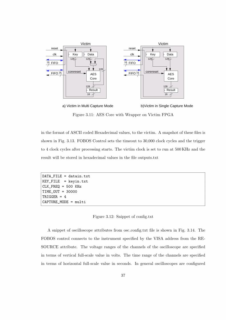
b)Victim in Single Capture Mode
Victim
FIFO16
16FIFO
reset
clk
corereset
128
128
16
128
a) Victim in Multi Capture Mode
FIFO16
16FIFO
reset
clk
corereset
128128
128
128
16
Victim
Core
Result
AESCoreAES
Result
DataKey KeyData
Figure 3.11: AES Core with Wrapper on Victim FPGA
in the format of ASCII coded Hexadecimal values, to the victim. A snapshot of these files is
shown in Fig. 3.13. FOBOS Control sets the timeout to 30,000 clock cycles and the trigger
to 4 clock cycles after processing starts. The victim clock is set to run at 500KHz and the
result will be stored in hexadecimal values in the file outputs.txt
DATA_FILE = datain.txt
KEY_FILE = keyin.txt
CLK_FREQ = 500 KHz
TIME_OUT = 30000
TRIGGER = 4
CAPTURE_MODE = multi
Figure 3.12: Snippet of config.txt
A snippet of oscilloscope attributes from osc config.txt file is shown in Fig. 3.14. The
FOBOS control connects to the instrument specified by the VISA address from the RE-
SOURCE attribute. The voltage ranges of the channels of the oscilloscope are specified
in terms of vertical full-scale value in volts. The time range of the channels are specified
in terms of horizontal full-scale value in seconds. In general oscilloscopes are configured
37
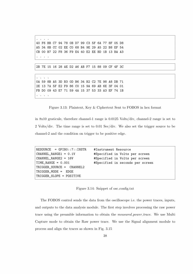
. . . .
40 F6 BB C7 94 78 0B D7 99 C3 5F 6A 77 8F 05 D8
A5 34 8B CC 02 EE C0 68 B4 9E 29 A5 22 B8 EF 54
CB 00 B7 22 F8 36 F9 E4 40 E2 EE BD 1B 13 BA A3
. . . .
2B 7E 15 16 28 AE D2 A6 AB F7 15 88 09 CF 4F 3C
. . . .
0A 59 8B A5 3D B3 0D B6 34 B2 C2 7E 98 A8 DB 71
2E 13 7A 5F E2 F9 86 C0 15 9A 69 AB 6E 3F 04 01
FB D0 09 43 E7 71 59 4A 15 37 53 33 A3 EF 74 1B
. . . .
Figure 3.13: Plaintext, Key & Ciphertext Sent to FOBOS in hex format
in 8x10 graticule, therefore channel-1 range is 0.0125 Volts/div, channel-2 range is set to
2 Volts/div. The time range is set to 0.01 Sec/div. We also set the trigger source to be
channel-2 and the condition on trigger to be positive edge.
RESOURCE = GPIB0::7::INSTR #Instrument Resource
CHANNEL_RANGE1 = 0.1V #Specified in Volts per screen
CHANNEL_RANGE2 = 16V #Specified in Volts per screen
TIME_RANGE = 0.001 #Specified in seconds per screen
TRIGGER_SOURCE = CHANNEL2
TRIGGER_MODE = EDGE
TRIGGER_SLOPE = POSITIVE
Figure 3.14: Snippet of osc config.txt
The FOBOS control sends the data from the oscilloscope i.e. the power traces, inputs,
and outputs to the data analysis module. The first step involves processing the raw power
trace using the preamble information to obtain the measured power trace. We use Multi
Capture mode to obtain the Raw power trace. We use the Signal alignment module to
process and align the traces as shown in Fig. 3.15
38
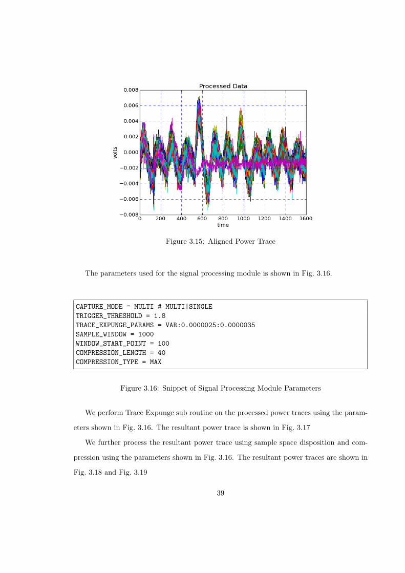
Figure 3.15: Aligned Power Trace
The parameters used for the signal processing module is shown in Fig. 3.16.
CAPTURE_MODE = MULTI # MULTI|SINGLE
TRIGGER_THRESHOLD = 1.8
TRACE_EXPUNGE_PARAMS = VAR:0.0000025:0.0000035
SAMPLE_WINDOW = 1000
WINDOW_START_POINT = 100
COMPRESSION_LENGTH = 40
COMPRESSION_TYPE = MAX
Figure 3.16: Snippet of Signal Processing Module Parameters
We perform Trace Expunge sub routine on the processed power traces using the param-
eters shown in Fig. 3.16. The resultant power trace is shown in Fig. 3.17
We further process the resultant power trace using sample space disposition and com-
pression using the parameters shown in Fig. 3.16. The resultant power traces are shown in
Fig. 3.18 and Fig. 3.19
39
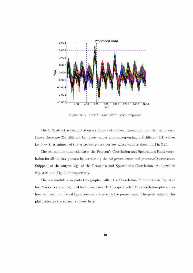
Figure 3.17: Power Trace after Trace Expunge
The CPA attack is conducted on a sub-byte of the key depending upon the user choice.
Hence there are 256 different key guess values and correspondingly 9 different HD values
i.e. 0 → 8. A snippet of the est power traces per key guess value is shown in Fig 3.20.
The sca module than calculates the Pearson’s Correlation and Spearman’s Rank corre-
lation for all the key guesses by correlating the est power traces and processed power trace.
Snippets of the output logs of the Pearson’s and Spearman’s Correlation are shown in
Fig. 3.21 and Fig. 3.22 respectively.
The sca module also plots two graphs, called the Correlation Plot shown in Fig. 3.23
for Pearson’s r and Fig. 3.24 for Spearman’s RHO respectively. The correlation plot shows
how well each individual key guess correlates with the power trace. The peak value of this
plot indicates the correct sub-key byte.
40
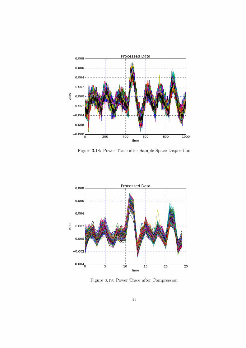
Figure 3.18: Power Trace after Sample Space Disposition
Figure 3.19: Power Trace after Compression
41
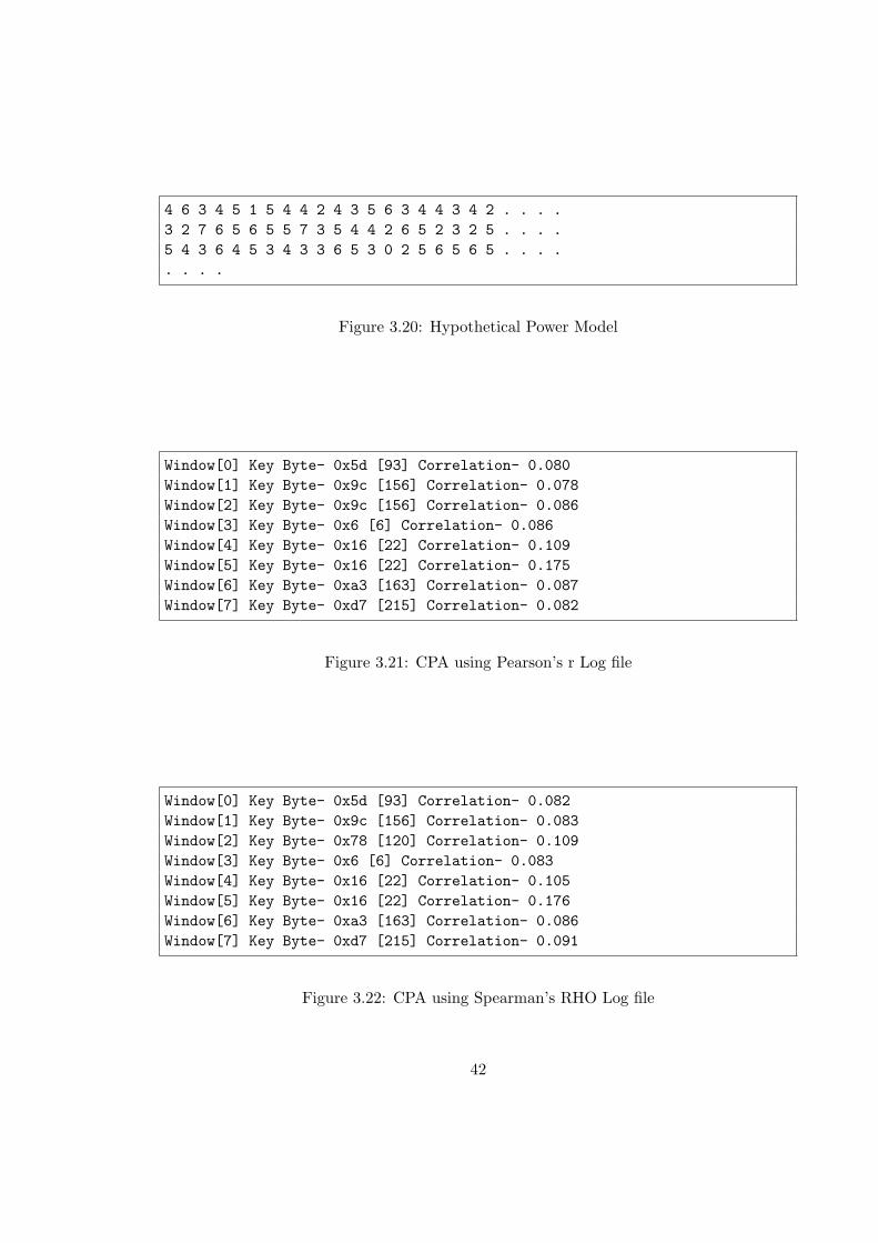
4 6 3 4 5 1 5 4 4 2 4 3 5 6 3 4 4 3 4 2 . . . .
3 2 7 6 5 6 5 5 7 3 5 4 4 2 6 5 2 3 2 5 . . . .
5 4 3 6 4 5 3 4 3 3 6 5 3 0 2 5 6 5 6 5 . . . .
. . . .
Figure 3.20: Hypothetical Power Model
Window[0] Key Byte- 0x5d [93] Correlation- 0.080
Window[1] Key Byte- 0x9c [156] Correlation- 0.078
Window[2] Key Byte- 0x9c [156] Correlation- 0.086
Window[3] Key Byte- 0x6 [6] Correlation- 0.086
Window[4] Key Byte- 0x16 [22] Correlation- 0.109
Window[5] Key Byte- 0x16 [22] Correlation- 0.175
Window[6] Key Byte- 0xa3 [163] Correlation- 0.087
Window[7] Key Byte- 0xd7 [215] Correlation- 0.082
Figure 3.21: CPA using Pearson’s r Log file
Window[0] Key Byte- 0x5d [93] Correlation- 0.082
Window[1] Key Byte- 0x9c [156] Correlation- 0.083
Window[2] Key Byte- 0x78 [120] Correlation- 0.109
Window[3] Key Byte- 0x6 [6] Correlation- 0.083
Window[4] Key Byte- 0x16 [22] Correlation- 0.105
Window[5] Key Byte- 0x16 [22] Correlation- 0.176
Window[6] Key Byte- 0xa3 [163] Correlation- 0.086
Window[7] Key Byte- 0xd7 [215] Correlation- 0.091
Figure 3.22: CPA using Spearman’s RHO Log file
42
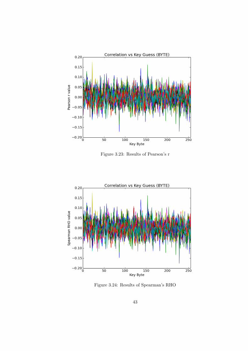
Figure 3.23: Results of Pearson’s r
Figure 3.24: Results of Spearman’s RHO
43

Interleaved SDDL
On BoardReal−time
Glitch Detection
Partial DDL
FPGAs Intrinsic FeaturesWDMsBRAMs
Fast Carry ChainsSRL
SDDL for FPGAsFOBOS
Research GoalDDL for FPGAs
Check!
Estimation
Idea!Usage?
Early Precharge/Evaluation
Glitches
Large Area overhead
Problems:
Evaluation Methodology
Figure 3.25: Research Flow
44
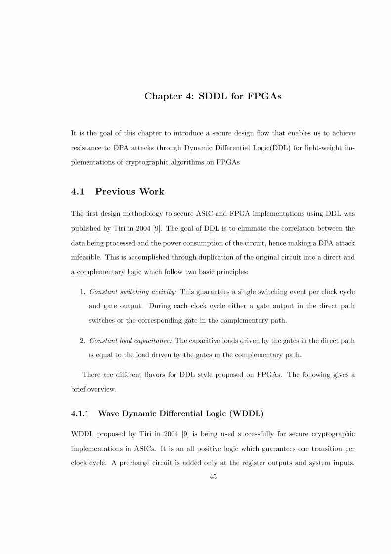
Chapter 4: SDDL for FPGAs
It is the goal of this chapter to introduce a secure design flow that enables us to achieve
resistance to DPA attacks through Dynamic Differential Logic(DDL) for light-weight im-
plementations of cryptographic algorithms on FPGAs.
4.1 Previous Work
The first design methodology to secure ASIC and FPGA implementations using DDL was
published by Tiri in 2004 [9]. The goal of DDL is to eliminate the correlation between the
data being processed and the power consumption of the circuit, hence making a DPA attack
infeasible. This is accomplished through duplication of the original circuit into a direct and
a complementary logic which follow two basic principles:
1. Constant switching activity: This guarantees a single switching event per clock cycle
and gate output. During each clock cycle either a gate output in the direct path
switches or the corresponding gate in the complementary path.
2. Constant load capacitance: The capacitive loads driven by the gates in the direct path
is equal to the load driven by the gates in the complementary path.
There are different flavors for DDL style proposed on FPGAs. The following gives a
brief overview.
4.1.1 Wave Dynamic Differential Logic (WDDL)
WDDL proposed by Tiri in 2004 [9] is being used successfully for secure cryptographic
implementations in ASICs. It is an all positive logic which guarantees one transition per
clock cycle. A precharge circuit is added only at the register outputs and system inputs.
45
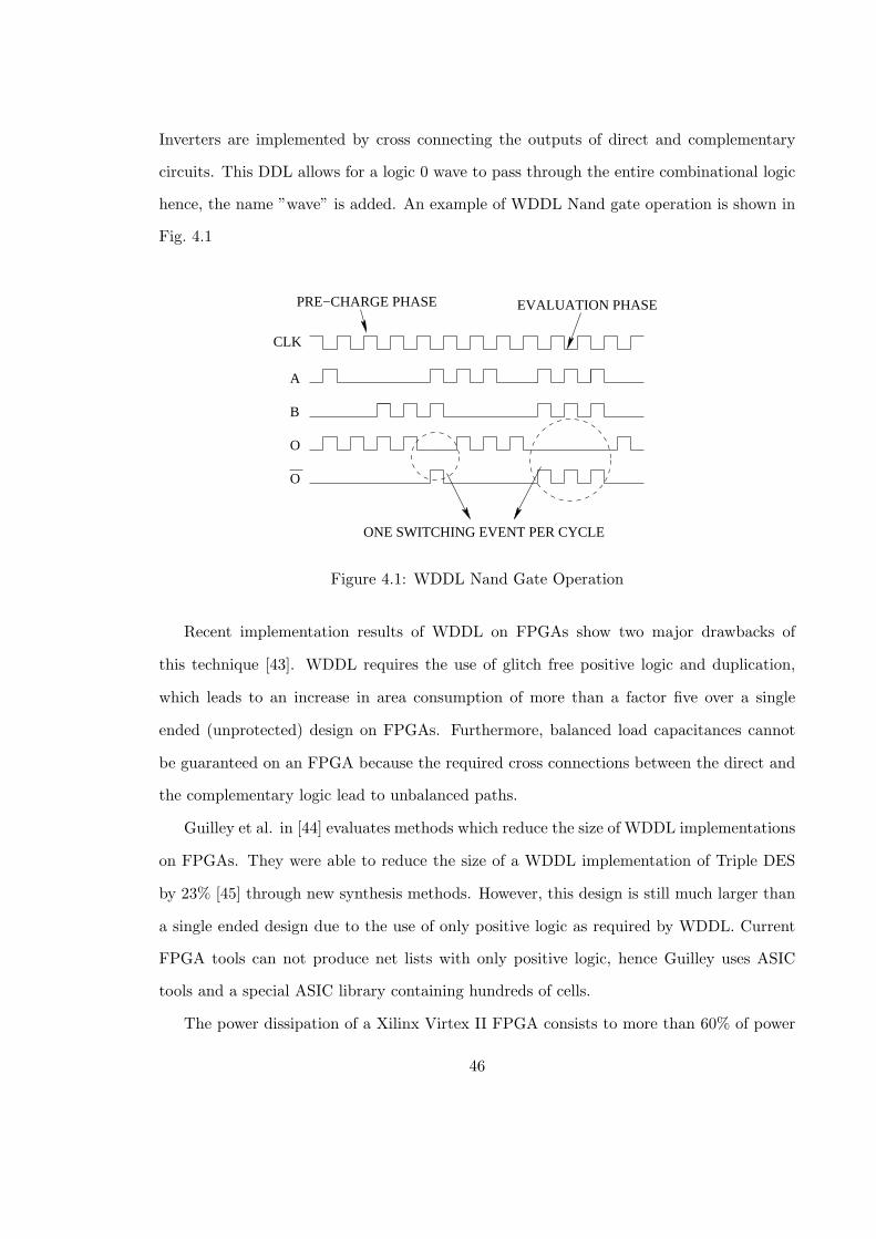
Inverters are implemented by cross connecting the outputs of direct and complementary
circuits. This DDL allows for a logic 0 wave to pass through the entire combinational logic
hence, the name ”wave” is added. An example of WDDL Nand gate operation is shown in
Fig. 4.1
O
CLK
A
B
O
ONE SWITCHING EVENT PER CYCLE
PRE−CHARGE PHASE EVALUATION PHASE
Figure 4.1: WDDL Nand Gate Operation
Recent implementation results of WDDL on FPGAs show two major drawbacks of
this technique [43]. WDDL requires the use of glitch free positive logic and duplication,
which leads to an increase in area consumption of more than a factor five over a single
ended (unprotected) design on FPGAs. Furthermore, balanced load capacitances cannot
be guaranteed on an FPGA because the required cross connections between the direct and
the complementary logic lead to unbalanced paths.
Guilley et al. in [44] evaluates methods which reduce the size of WDDL implementations
on FPGAs. They were able to reduce the size of a WDDL implementation of Triple DES
by 23% [45] through new synthesis methods. However, this design is still much larger than
a single ended design due to the use of only positive logic as required by WDDL. Current
FPGA tools can not produce net lists with only positive logic, hence Guilley uses ASIC
tools and a special ASIC library containing hundreds of cells.
The power dissipation of a Xilinx Virtex II FPGA consists to more than 60% of power
46

consumed by the routing resources [46]. This illustrates that it is important to balance
the paths of the direct and complementary logic. As this is not a trivial problem on
FPGAs, masking schemes have been proposed specifically to overcome the routing prob-
lem [47]. However, it has been shown in 2005 that circuits protected only by masking are
not secure [8]. Later publications demonstrated that masking does not remove the need for
balanced routing in WDDL designs [48,49].
The impact of current place-and-route methods on the security of a WDDL design was
explored in [50] with respect to balancing the timing delays. In [51] the authors propose
a new switch box design for FPGAs that enables balanced routing and is secure against
power as well as EM attacks.
4.1.2 Double Wave Dynamic Differential Logic (DWDDL)
Double Wave Dynamic Differential Logic (DWDDL) proposed by Yu et al [52] has all the
characteristics of WDDL logic style. The difference between original WDDL and DWDDL
is that both direct and complementary gate of DWDDL is a full WDDL gate by itself. Due
to this reason we can have a much relaxed placement constraints and unconstrained routing
of individual WDDL module. However, it leads to an area increase of more than eleven
times.
4.1.3 Separated Dynamic Differential Logic (SDDL)
SDDL, also proposed by Tiri in 2004 [9], allows the use of negative logic thus making it more
flexible than WDDL. However, each time negative logic is used a precharge circuit should
be added because negative logic stops the precharge wave. Thus, unlike WDDL, SDDL
needs precharge circuit to be added not only at register outputs and at system inputs but
also a every gate output. In ASIC circuits this leads to an increase in the area compared
to WDDL. Unfortunately SDDL is not considered secure as WDDL because negative logic
can produce glitches therefore SDDL cannot guarantee one switching event per clock cycle.
An example of SDDL Nand gate is shown in Fig.4.2.
47

A
BQ
AB
AB
AB
AB
Q
Q
WDDL NAND Gate
Q
SDDL NAND Gate
Q
Figure 4.2: WDDL vs SDDL Nand Gate
4.1.4 Isolated Wave Dynamic Differential Logic (iWDDL)
In the paper [53] the authors propose a new variant of WDDL called Isolated WDDL
(iWDDL). iWDDL allows the usage of negative logic there by removing the requirement of
cross connections between the direct and complementary circuits. An example of iWDDL
xor gate is shown in Fig 4.3. The following steps are taken to modify the circuit if any
negative logic found in the LUTs.
• The Boolean equation form the LUT function is extracted from the netlist.
• If an input variable is inverted within the Boolean expression, this variable is renamed
and treated as a new input to the function.
• The Boolean equation is rewritten in terms of the original inputs and the new inputs.
The equation is now in positive monotonic form, and the original LUT is replaced
with hazard-free LUTs implementing this new equation.
• Inverters are used to create the new variables from the original inputs, but the inverter
outputs are registered before connecting them to the new LUTs. These extra registers
will prevent the inverters from halting the precharge wave, because the output of each
register is precharged. As the inputs to the LUTs are modified additional measures
are taken to insure proper functioning of the circuits by adding registers.
After the completion of above steps the circuit or the design is now precharged, comple-
mented and duplicated to produce direct and complementary circuits. Because the design
48
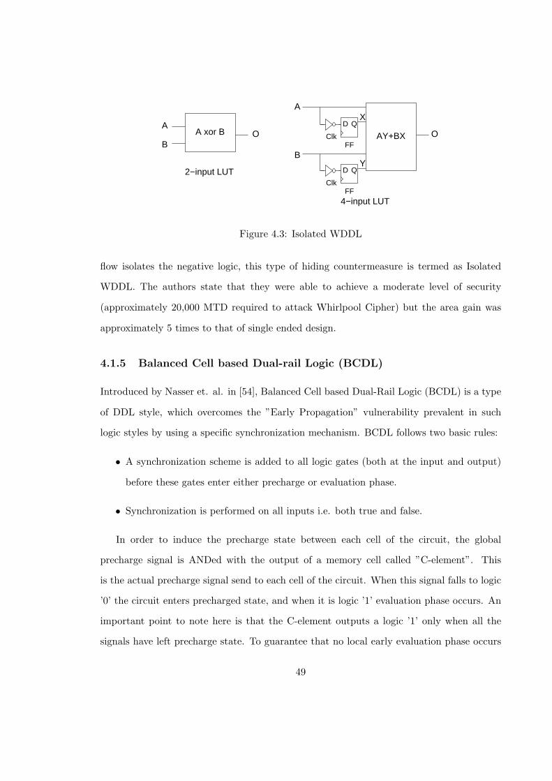
A xor B
2−input LUT
A
BO
4−input LUT
A
O
B
QD
ClkFF
X
QD
ClkFF
Y
AY+BX
Figure 4.3: Isolated WDDL
flow isolates the negative logic, this type of hiding countermeasure is termed as Isolated
WDDL. The authors state that they were able to achieve a moderate level of security
(approximately 20,000 MTD required to attack Whirlpool Cipher) but the area gain was
approximately 5 times to that of single ended design.
4.1.5 Balanced Cell based Dual-rail Logic (BCDL)
Introduced by Nasser et. al. in [54], Balanced Cell based Dual-Rail Logic (BCDL) is a type
of DDL style, which overcomes the ”Early Propagation” vulnerability prevalent in such
logic styles by using a specific synchronization mechanism. BCDL follows two basic rules:
• A synchronization scheme is added to all logic gates (both at the input and output)
before these gates enter either precharge or evaluation phase.
• Synchronization is performed on all inputs i.e. both true and false.
In order to induce the precharge state between each cell of the circuit, the global
precharge signal is ANDed with the output of a memory cell called ”C-element”. This
is the actual precharge signal send to each cell of the circuit. When this signal falls to logic
’0’ the circuit enters precharged state, and when it is logic ’1’ evaluation phase occurs. An
important point to note here is that the C-element outputs a logic ’1’ only when all the
signals have left precharge state. To guarantee that no local early evaluation phase occurs
49

at the LUT level, the precharge signal is used as one of the inputs to the LUTs. Due to
this there are no glitches, no local early evaluation or precharge, and reduction of techno-
logical bias effects in BCDL.Another important aspect of BCDL is that it is not confined to
use only positive logic unlike WDDL. The authors also managed to speed up their BCDL
implementation by varying the clock with uneven duty cycle.
BCDL is also immune to fault and set-up violation attacks. The authors were able to
achieve a security gain of 20 over an unprotected AES implementation compared to a BCDL
protected AES implementation. The experiments were carried out using Altera Stratic IV
FPGA.
4.2 Proposed SDDL Model
In our proposed SDDL model FPGA CAD tools are given the maximum flexibility to
optimize a given design for the target FPGA. Such an optimized design will allow logic
packing in LUTs and also make use of all the intrinsic features present in the FPGA. In this
chapter we are exploring the usage of Wide Dedicated Multiplexer (WDM). Using WDMs
reduces the area consumed by our design however, their effect on DPA resistance has not
been explored yet. SDDL for FPGAs makes use of the following assumptions
• The wire connecting the LUT and the flip-flop/latch will not leak any information.
• The wire connecting two slices in the same CLB will not leak any information.
• Any wire between CLBs i.e. wire connecting a slice in one CLB to a slice in another
CLB will leak information.
Our proposed SDDL for FPGAs model is shown in Fig. 4.4
4.2.1 Pre-Charge
Pre-charge insertion is done using the technique introduced by Yu and Schaumont in [43].
An FPGA consists of programmable elements, so called Configurable Logic Block (CLB),
50
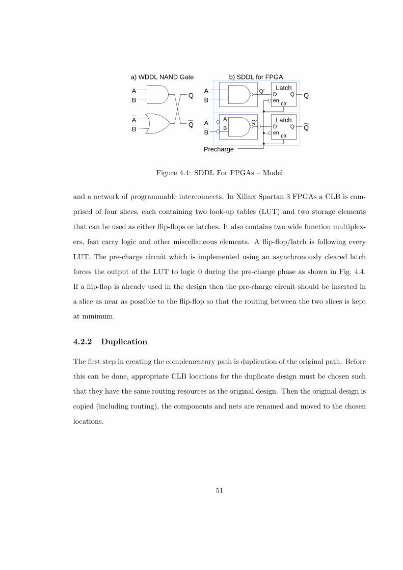
Q
D QLatch
en clr
D QLatch
en clr
AB
AB
Q
Q
a) WDDL NAND Gate
AB
AB
A
BQ’
QQ’
Precharge
b) SDDL for FPGA
Figure 4.4: SDDL For FPGAs – Model
and a network of programmable interconnects. In Xilinx Spartan 3 FPGAs a CLB is com-
prised of four slices, each containing two look-up tables (LUT) and two storage elements
that can be used as either flip-flops or latches. It also contains two wide function multiplex-
ers, fast carry logic and other miscellaneous elements. A flip-flop/latch is following every
LUT. The pre-charge circuit which is implemented using an asynchronously cleared latch
forces the output of the LUT to logic 0 during the pre-charge phase as shown in Fig. 4.4.
If a flip-flop is already used in the design then the pre-charge circuit should be inserted in
a slice as near as possible to the flip-flop so that the routing between the two slices is kept
at minimum.
4.2.2 Duplication
The first step in creating the complementary path is duplication of the original path. Before
this can be done, appropriate CLB locations for the duplicate design must be chosen such
that they have the same routing resources as the original design. Then the original design is
copied (including routing), the components and nets are renamed and moved to the chosen
locations.
51

4.2.3 Complementing the Logic
The complemented path should produce outputs inverse to that of the direct path. If f(x)
is the equation which defines a LUT in the direct path, then it’s complimentary equation
g(x) is given by
g(x) = f(x) = f(x) (4.1)
This principle is indicated in Fig. 4.4. WDMs use LUTs and slice internal multiplexers.
Equation 6.1 holds for LUTs however, for the slice internal multiplexers only the select lines
should be inverted.
4.2.4 Secure Design Flow
Our design flow for implementing SDDL on FPGAs uses Xilinx ISE Design suite 10.1 and
Perl scripts. It consists of three phases as show in Fig 6.5.
In the first phase, the single ended design is synthesized and implemented. Area con-
straints are applied which limit the design to one section of the FPGA fabric. It also
specifies that the locations near registers should be left empty as they will be needed to
insert pre-charge in the next phase.
In the second phase, the circuit description file from the first phase is converted into
ASCII representation format with help of XDL (Xilinx Design language) tool . Perl scripts
interpret the XDL file and insert pre-charge. Subsequently only Place and Route is executed.
In the third phase, the I/O connections are removed and the design is converted into
XDL format. Perl scripts duplicate and complement the original circuit resulting in an
SDDL implementation. However, as the I/O pins are still disconnected, and all the routing
has to be preserved, we use re-entrant routing only.
52

VHDLAreaCon−straint
Insert Precharge
Remove I/O Connections
Place & Route
Duplicate and Complement
Re−entrantRouting
SynthesisPlace & Route
SDDL Implementation
Phase 3
Phase 2
Phase 1
Figure 4.5: SDDL Design Flow
4.3 Test Circuit Implementation and Attack
4.3.1 Test Circuit
The Advanced Encryption Standard (AES) [42] is one of the most widely used block ciphers.
It was designed to be resistant towards linear and differential cryptanalysis. However,
unprotected AES hardware implementations are susceptible to DPA attacks. The test
circuit for our proposed SDDL model is shown in Fig. 8.5. It consists of some of the main
building blocks of AES i.e. SBOX and key XORing. The test circuit allows us to replicate
a DPA attack on AES on a smaller scale. An 8-bit LFSR is used to supply inputs to the
SBOX. The output of the SBOX is XORed with key and stored in register FF1. The dashed
line in Fig. 8.5 indicates the part of the circuit that we want to protect. The register FF2
drives the outputs of the chip and is implemented in I/O blocks (IOB).
53
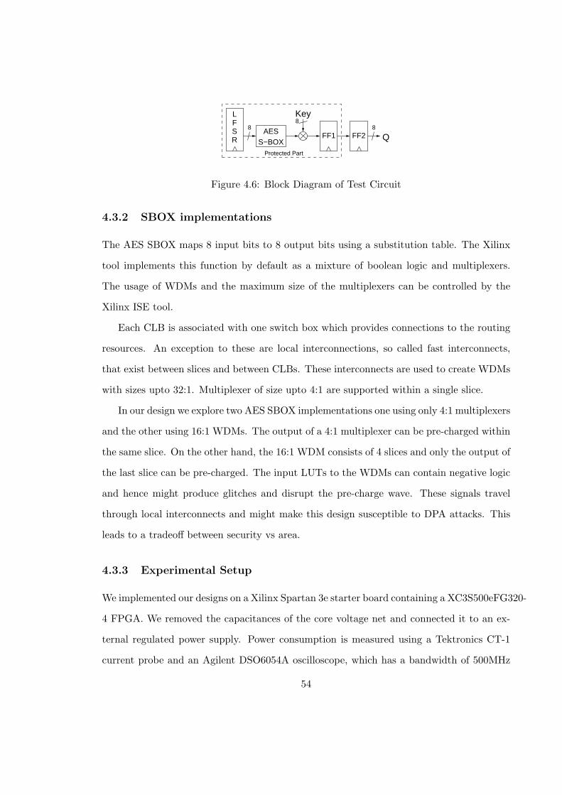
FL
SR
AESS−BOX
8
Key8
FF1 FF2 Q8
Protected Part
Figure 4.6: Block Diagram of Test Circuit
4.3.2 SBOX implementations
The AES SBOX maps 8 input bits to 8 output bits using a substitution table. The Xilinx
tool implements this function by default as a mixture of boolean logic and multiplexers.
The usage of WDMs and the maximum size of the multiplexers can be controlled by the
Xilinx ISE tool.
Each CLB is associated with one switch box which provides connections to the routing
resources. An exception to these are local interconnections, so called fast interconnects,
that exist between slices and between CLBs. These interconnects are used to create WDMs
with sizes upto 32:1. Multiplexer of size upto 4:1 are supported within a single slice.
In our design we explore two AES SBOX implementations one using only 4:1 multiplexers
and the other using 16:1 WDMs. The output of a 4:1 multiplexer can be pre-charged within
the same slice. On the other hand, the 16:1 WDM consists of 4 slices and only the output of
the last slice can be pre-charged. The input LUTs to the WDMs can contain negative logic
and hence might produce glitches and disrupt the pre-charge wave. These signals travel
through local interconnects and might make this design susceptible to DPA attacks. This
leads to a tradeoff between security vs area.
4.3.3 Experimental Setup
We implemented our designs on a Xilinx Spartan 3e starter board containing a XC3S500eFG320-
4 FPGA. We removed the capacitances of the core voltage net and connected it to an ex-
ternal regulated power supply. Power consumption is measured using a Tektronics CT-1
current probe and an Agilent DSO6054A oscilloscope, which has a bandwidth of 500MHz
54

Powerguess = HD(lfsr − output(i−1), (SBOX−1(Keyguess ⊕Output))i
)(4.2)
Powerguess = HD(0x00, (SBOX−1(Keyguess ⊕Output))i
)(4.3)
and samples at 4GSa/sec.
4.3.4 Attack Methodology
We use correlation attacks to test the effectiveness of our design [41]. The power model
for the single ended cases is given by Equation 4.2. It calculates the Hamming distance
between the previous output of the LFSR and the estimated following output. We estimate
the following output of the LFSR for all possible key guesses. We use a different power
model to mount a DPA attack on SDDL designs, given by Equation 4.3. The pre-charge
phase sets all logic outputs to 0 therefore, the Hamming distance is computed between 0
and the estimated outputs of the LFSR for all possible key guesses. This is equal to their
Hamming weight. We use Pearson’s product moment correlation to compare the measured
power and the power model [41].
4.4 Results and Analysis
We have implemented six different designs of our test circuit. MUX-4 SE and MUX-16
SE are single ended implementations of our test circuit which use 4:1 multiplexer and
16:1 WDM for the AES SBOX respectively. MUX-4 SDDL and MUX-16 SDDL are two
symmetrically routed SDDL designs of the said single ended. Table 6.2 shows the results
of our implementations and measurements to disclosure (MTD) of the key.
The MUX-16 and MUX-32 design is much smaller than the MUX-4 design and also has
a shorter critical path delay. Both SDDL designs are little bit more than a factor 2 larger
than the single ended designs. This is due to the fact that the outputs of the flip-flops
need to be pre-charged. This increases the area by one slice per two flip-flops. The delay
of the SDDL designs is roughly 2 times larger than the single ended designs because all
computations have to be performed during the evaluation phase which is half a clock cycle
55
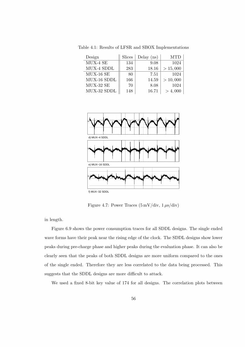
Table 4.1: Results of LFSR and SBOX Implementations
Design Slices Delay (ns) MTD
MUX-4 SE 134 9.08 1024MUX-4 SDDL 283 18.16 > 15, 000
MUX-16 SE 80 7.51 1024MUX-16 SDDL 166 14.59 > 10, 000MUX-32 SE 70 8.08 1024MUX-32 SDDL 148 16.71 > 4, 000
d) MUX−4 SDDL
f) MUX−32 SDDL
e) MUX−16 SDDL
Figure 4.7: Power Traces (5mV/div, 1µs/div)
in length.
Figure 6.9 shows the power consumption traces for all SDDL designs. The single ended
wave forms have their peak near the rising edge of the clock. The SDDL designs show lower
peaks during pre-charge phase and higher peaks during the evaluation phase. It can also be
clearly seen that the peaks of both SDDL designs are more uniform compared to the ones
of the single ended. Therefore they are less correlated to the data being processed. This
suggests that the SDDL designs are more difficult to attack.
We used a fixed 8-bit key value of 174 for all designs. The correlation plots between
56
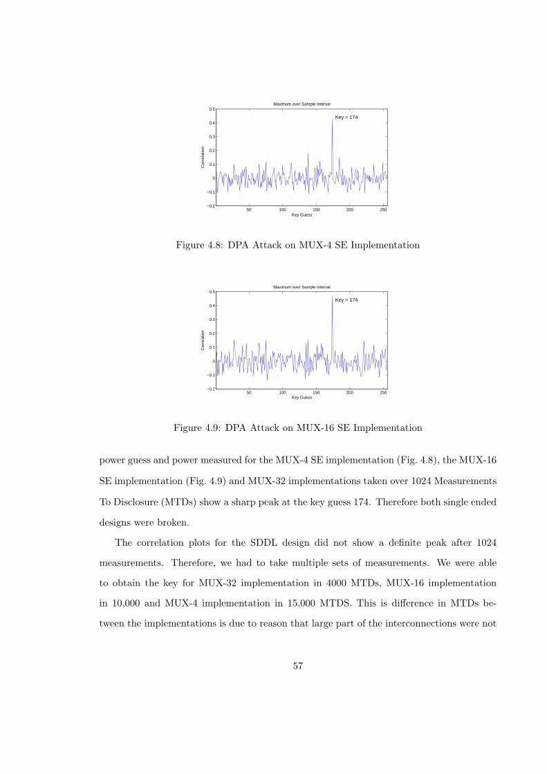
50 100 150 200 250−0.2
−0.1
0
0.1
0.2
0.3
0.4
0.5Maximum over Sample Interval
Key Guess
Co
rre
latio
n
Key = 174
Figure 4.8: DPA Attack on MUX-4 SE Implementation
50 100 150 200 250−0.2
−0.1
0
0.1
0.2
0.3
0.4
0.5Maximum over Sample Interval
Key Guess
Cor
rela
tion
Key = 174
Figure 4.9: DPA Attack on MUX-16 SE Implementation
power guess and power measured for the MUX-4 SE implementation (Fig. 4.8), the MUX-16
SE implementation (Fig. 4.9) and MUX-32 implementations taken over 1024 Measurements
To Disclosure (MTDs) show a sharp peak at the key guess 174. Therefore both single ended
designs were broken.
The correlation plots for the SDDL design did not show a definite peak after 1024
measurements. Therefore, we had to take multiple sets of measurements. We were able
to obtain the key for MUX-32 implementation in 4000 MTDs, MUX-16 implementation
in 10,000 and MUX-4 implementation in 15,000 MTDS. This is difference in MTDs be-
tween the implementations is due to reason that large part of the interconnections were not
57

precharged in MUX-32 as compared to MUX-16 and MUX-4 type implementations. Sim-
ilarly, some part of the interconnections were not precharged in MUX-16 implementations
as compared to MUX-4 implementations. All the interconnections are fully precharged in
MUX-4 implementation.
4.5 Conclusions
Our results show that it is possible to apply Dynamic and Differential logic styles to low
area implementations on FPGAs. Our SDDL can still be broken mainly due to glitches.
We also conclude that Wide Dedicated Multiplexers should not be used in conjunction with
SDDL. Our results show that we were able to achieve a moderate level of security by using
our design flow at an area increase by a factor of just greater than 4 (MUX-32 SE vs MUX-4
SDDL).
58
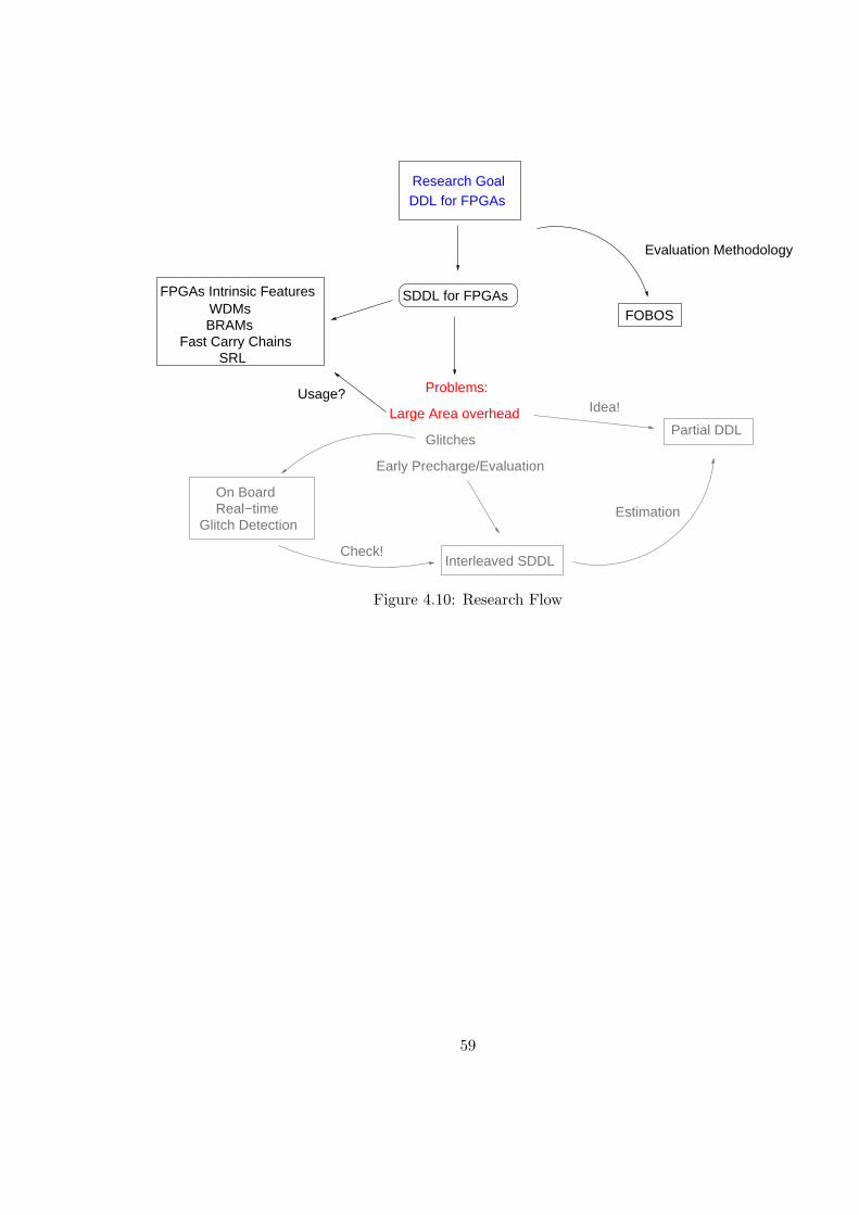
FOBOSSDDL for FPGAsFPGAs Intrinsic Features
WDMsBRAMs
Fast Carry ChainsSRL
Interleaved SDDL
On BoardReal−time
Glitch Detection
Partial DDL
Research GoalDDL for FPGAs
Evaluation Methodology
Problems:
Large Area overheadUsage?
Check!
Estimation
Early Precharge/Evaluation
Glitches
Idea!
Figure 4.10: Research Flow
59

Chapter 5: DPA on BRAM and BRAM with DDL
5.1 DDL with BRAMs
Several features of BRAMs indicate that their use might lead to implementations that
are more resistant to DPA attacks than implementations using other resources such as
LUTs or Distributed RAMs. One such feature is that BRAMs are glitch free. Glitches
are unexpected output transitions due to hazards, resulting from combinational logic gates
delays and routing delays. Therefore, glitches are data dependent and influence the dynamic
power consumption. This results in information leakage which can be exploited by DPA.
Implementations of the AES 8x8 S-Box (table with 256 8-bit entries) using LUTs occupy
nearly 64 slices, similarly an 8x32 T-Box (table with 256 32-bit entries) occupies about
256 slices. Both implementations exhibit glitches. On the other hand, two of these S-Boxes
or even T-Boxes can fit in one single BRAM. Therefore, it is common practice to use BRAM
implementations in order to conserve slice area. This area reduction leads to less utilization
of corresponding routing resources, which eventually helps avoiding glitches. Furthermore,
BRAM cells do not have any combinational path from address to the output, hence they
don’t propagate glitches. In addition the output ports are latched with a self-timed circuit
providing glitch-free read operations.
The second feature is that BRAMs consist of fast static SRAM cells. Konur et al. [55]
explain in detail the structure of an SRAM cell, its operation and leakage power consumption
during memory read and write operations. After preforming various experiments, they
concluded that power consumed by SRAM cells during memory read operations remains
almost the same, irrespective of reading ’0’ or ’1’. Therefore, using a BRAM as a ROM
should provide higher security against power analysis attacks than using combinational
logic.
60
The main research focus of this chapter is to verify whether BRAMs in DDL implemen-
tations enhance or diminish their security. We propose several implementation techniques
which facilitate the use of BRAMs in DDL implementations in Sect. 5.1.1. We test our de-
signs on a circuit which uses basic functional primitives of the AES block cipher (Sect. 5.1.2)
and analyze our results in Sect. 6.4.
5.1.1 Implementation Options
In this section we describe several implementation options for precharging the output of
LUTs, flip-flops, and BRAMs.
One Clock Cycle Operation
In this method, the precharge and evaluation phase share one clock cycle. The evaluation
phase is defined by the ”low” clock signal and the precharge phase by the ”high” clock
signal. This allows flip-flops to clock in new data at the rising edge of the clock as this is
the transition from evaluation to precharge. The advantage of the one clock cycle operation
is that the precharged circuit can be clocked with the same clock signal clk as external
non-precharged circuits. The Pre input of the circuits in Fig. 5.1–Fig. 5.3 is connected to
the clk signal.
In order to precharge the output of a LUT we use the technique proposed in [43]. The
flip-flop following the LUT is configured as an asynchronously cleared latch. It forces the
output of the slice to logic ’0’ during the precharge phase as shown in Fig. 5.1.
We precharge the output of a flip-flop in a similar manner and connect the flip-flop
output to an asynchronously cleared latch (Fig. 5.2). Because the flip-flops within a slice
share a common enable, clear, and clock input, we have to use a flip-flop of a different slice
for the precharge latch. In earlier experiments [56] we discovered that connections within
a CLB do not leak any exploitable information, however, connections between CLBs do.
Therefore, we place the precharge latch in a flip-flop within the same CLB as shown in [27].
61

4OutQ
LatchDenclr
LoutLUT
Pre
In
Out
Lout
In 0 5 0A
Pre Eval PreEval Pre
Figure 5.1: LUT with Precharge
OutQLatchDenclr
FoutFF
Pre
In
Out
Fout
In
Eval PrePre
Pre
EvalPre
Figure 5.2: Flip-Flop with Precharge
Unfortunately we cannot use the approach that we used for LUTs and flip-flops to
precharge BRAMs If we use a precharge latch for a BRAM, wiring resources would be used
to connect the non-precharged BRAM output to a CLB. This leads to information leakage.
Nassar [54] uses a bit of the address to select a region of memory in which all data values
are ’0’. We use the MSB of the address for this as shown in Fig. 5.3. However, this doubles
the memory usage within a BRAM which might not be feasible for memory demanding
applications.
Therefore, we developed the precharge circuit shown in Fig 5.4 which does not double
the memory usage. The outputs of the BRAMs are cleared to logic ’0’ by connecting the
clock of the circuit to the synchronous set/reset (SSR) inputs of the BRAM. In both cases
we have to operate BRAMs at twice the clock frequency (Dclk) compared to the rest of
the circuit. One rising edge of Dclk resets the outputs of the BRAM to ’0’, the following
62

80
80
7
88
OutFFBRAM
DoAddr
CLK
A’
Dclk
Pre
PreIn
Out
A’
In
Eval PrePreEval
C7 00 5F 00
84 2A
000 184
0000
000 12A
DclkPre
Figure 5.3: Block RAM with Precharge Through Address
8 8
Out
Fo
In
Pre Eval PrePreEval
Dclk
C7 00 5F 00
84 2A
00 84
0000
00 2A
OutIn Fo
PreFF
Dclk
BRAMDoAddr
SSRCLK
Pre
Figure 5.4: Block RAM with Precharge Through Clear
releases the data stored at the address given in the previous Dclk cycle. This introduces
a delay for the address by one Dclk cycle which we compensate for with a flip-flop. The
flip-flop output is connected using leaky wiring resources to the BRAM, however, as can
be seen in Fig. 5.4 this signal is precharged. Even though this precharge occurs during the
evaluation phase this does not violate the goal of constant switching activity. The contents
of the BRAMs are complemented using Eq. (5.6).
BRAM(addr) = BRAM(addr
)(5.1)
Two Clock Cycle Operation
In this method, each phase, precharge and evaluate, takes a full clock cycle. Therefore, the
precharged circuit has to run at twice the clock speed of external circuits. The precharge
63

Table 5.1: Implementation Results of our Test Design
4 input Minimum SecurityDesign Slices FFs LUTs BRAMs Delay MTD Gain
1. SE design w/o BRAM 82 24 155 0 8.088 ns > 450 12. SE design with BRAM 23 16 27 1 5.710 ns > 7, 000 153. SDDL w/o BRAM 283 80 502 0 18.352 ns > 10, 000 224. SDDL with SSR 1 CC 51 100 54 2 16.138 ns > 27, 000 605. SDDL with Address 1 CC 51 100 54 2 16.138 ns > 27, 000 606. SDDL with SSR 2 CC 51 100 54 2 8.069 ns > 27, 000 607. SDDL with Address 2 CC 51 100 54 2 8.069 ns > 27, 000 60
signal Pre reflects the phases and is low for one clock cycle and high for one clock cycle.
The circuit for precharging the output of a LUT shown in Fig. 5.1 does not need to
change for this method. Only the Pre input needs to be connected to the Pre signal. As we
have now one full clock cycle for each phase, we can simplify the precharge circuit for flip-
flops by just adding another flip-flop instead of a latch as shown in Fig. 5.5. The placement
constraint we had for flip-flop precharge can now be relaxed as all signals are precharged.
FF1
FF2 Out
Fout
clk
In
Pre
Out
Fout
In
Eval PrePreEvalPre
clk
Figure 5.5: Flip-Flop with Precharge Using Single Clock
For precharging the BRAM outputs in this method the circuits shown in Fig. 5.3 and
Fig. 5.4 apply. However, the Dclk input must be connected to the clk signal and the Pre
input to the Pre signal.
5.1.2 Test Setup and Attack Method
The Test Design circuit consists of a synchronous (Sync.) S-Box whose input is connected
to an 8-bit LFSR and output is XORed with an 8-bit Key. The result is stored in a
64

FL
SR
FL
SR FF1 Pre Pre
(LUTs)S−BoxAES
8 AESS−Box
8
8FF1
FF2
FF2
8
8
Pre8
1
FL
SR FF1
(BRAM)S−BoxAES 8
Pre FF28
Pre8
1 2
8
Key
Sync. S−Box
Q
Q
(a) Single Ended Test Design
(b) Precharged Test Design w/o BRAM
8
Q
Key
(c) Precharged Test Design with BRAM
8
Key
Figure 5.6: Block Diagrams of Test Design
register. The block diagram of this circuit is shown in Fig. 5.6(a). The Sync. S-Box can
be implemented using look-up tables and a register as in Fig. 5.6(b), or a BRAM as in
Fig. 5.6(c). The later option absorbs the register. The “Pre” blocks indicated in Fig. 5.6
are implemented using the different precharge options discussed in Sect. 5.1.1. We use the
term Single Ended (SE) design to refer to the unprotected designs in this paper. In order
to implement the SDDL versions of the SE designs we use the secure design flow described
in [27]. It describes the step-by-step process of precharging, duplicating and complementing
the logic. In our attacks we use Pearson’s correlation to correlate instantaneous power
consumption with hamming distance model [41]. The hamming distance equation for the
attack on single ended implementations is shown in Eq. (5.2) and for SDDL implementations
65
in Eq. (5.3).
Pest. = HD(lfsr(i−1), SBOX−1(kguess ⊕Qi)) (5.2)
Pest. = HD(0x00, SBOX−1(kguess ⊕Qi)) (5.3)
Attack point 1, indicated in Fig. 5.6 by arrow 1, is the precharged output of the LFSR.
At attack point 2 data arrives half a clock cycle later than at point 1 during single cycle
clock operation. In case of two clock cycle operation the data arrives at point 2 one clock
cycle later compared to point 1. Hence, in order to attack the design at point 2 appropriate
adjustments must be made while correlating the data with the power models.
20 40 60 80 100 120 140 160
−0.1
−0.05
0
0.05
0.1
0.15
Number of Measurements x 28
Co
rre
latio
n
Key = 173
MTD
Figure 5.7: SE Design with BRAM
20 40 60 80 100 120 140 160
−0.1
−0.05
0
0.05
0.1
0.15
Number of Measurements x 28
Co
rre
latio
n
MTD
Key = 173
Figure 5.8: SDDL Design w/o BRAM
66

20 40 60 80 100 120 140 160
−0.1
−0.05
0
0.05
0.1
0.15
Number of Measurements x 28C
orr
ela
tio
n Key = 173
MTD
Figure 5.9: SDDL Design with SSR, Attack Point 1, 1 Clock Cycle
20 40 60 80 100 120 140 160
−0.1
−0.05
0
0.05
0.1
0.15
Number of Measurements x 28
Co
rre
latio
n
MTD
Key = 173
Figure 5.10: SDDL Design with SSR, Attack Point 1, 2 Clock Cycles
5.1.3 Results and Conclusions
Table 5.1 compares the results of SE designs with several SDDL implementations with
regards to area consumption, speed and Measurements to Disclosure (MTD) of the key.
The results for MTD were obtained from the plots.By comparing the MTD of the key
between between the SE Designs 1 and 2, it is clear that BRAMs provide some inherent
resistance against DPA attacks. All SDDL implementations of Design 2, namely Designs
4–7, have a 4 times higher MTD compared to the unprotected Design 2. Furthermore, they
are more secure than Design 3 which is also an SDDL implementation but does not use
BRAMs. We note that there is no difference in security between using address or SSR to
force the BRAM output to ’0’ during precharge as can be seen from Fig. 5.9 and Fig. 5.12.
67
20 40 60 80 100 120 140 160
−0.1
−0.05
0
0.05
0.1
0.15
Number of Measurements x 28C
orr
ela
tio
n Key = 173
MTD
Figure 5.11: SDDL Design with SSR, Attack Point 2, 1 Clock Cycle
20 40 60 80 100 120 140 160
−0.1
−0.05
0
0.05
0.1
0.15
Number of Measurements x 28
Co
rre
latio
n Key = 173
MTD
Figure 5.12: SDDL Design with Address, Attack Point 1, 1 Clock Cycle
Hence, we can conclude that lowering memory usage by using SSR does not impact security
in a negative way. At attack point 2 the output of the flip-flop is precharged during the
evaluation phase and the data evaluates during precharge phase. At attack point 1 the data
follows the phases normally. Fig. 5.9 and Fig. 5.11 show that this has no impact on security
as the MTDs at both points are equivalent.
We proposed and analyzed different implementation techniques for using BRAMs in
DDL designs. Our results indicate that DDL implementations with BRAMs increase the
MTDs by a factor 4 over unprotected designs which use BRAMs and a factor 2.5 over DDL
implementations which do not use BRAMs.
68
5.2 DPA on BRAMs
Experiment Designs
We implemented several designs varying the utilizations of LUTs, Distributed RAMs and
BRAMs. Our designs are divided into two groups, small scale implementations (Test De-
sign) and real world implementations (AES-128 cipher). The advantage of small scale
implementations is that they are very easy to control, manipulate and analyze. Our Test
Design is similar to designs used by Yu et al. [43] and Velegalati et al. [56] for WDDL and
SDDL countermeasures respectively. The Test Design incorporates essential components
of the block cipher AES. The real world implementations are of the AES-128 bit cipher
[42] with a standard S-Box design and a T-box design. Analysis on larger-scale/real-world
implementations allows us to relate and confirm whether the use of BRAMs leads to more
DPA resistant implementation.
5.3 Small Scale Design (Test Design)
FL
SR
FL
SR FF1 Pre Pre
(LUTs)S−BoxAES
8 AESS−Box
8
8FF1
FF2
FF2
8
8
Pre8
1
FL
SR FF1
(BRAM)S−BoxAES 8
Pre FF28
Pre8
1 2
8
Key
Sync. S−Box
Q
Q
(a) Single Ended Test Design
(b) Precharged Test Design w/o BRAM
8
Q
Key
(c) Precharged Test Design with BRAM
8
Key
Figure 5.13: Block Diagram of Test Design
The Test Design circuit consists of a synchronous (Sync.) S-Box whose input is con-
nected to an 8-bit LFSR and output is XORed with an 8-bit Key. The result is stored in
69

register FF2. The block diagram of this circuit is shown in Fig. 5.13. A Sync. S-Box is an
S-Box followed by a register. It can be implemented using look-up tables and a register,
Distributed RAMs or a BRAM. The later two options absorb the register. A Sync. XOR
is an XOR gate followed by a register. In order to implement a Sync. XOR using BRAMs,
the logic gate is replaced by a precomputed look-up table. We attack the design at the
output of the LFSR.
The hamming distance equation for this attack on single ended implementations is shown
in Eq. (8.1) and for SDDL implementations in Eq. (8.2).
Pest. = HD(lfsr(i−1), SBOX−1(kguess ⊕Qi)) (5.4)
Pest. = HD(0x00, SBOX−1(kguess ⊕Qi)) (5.5)
Basic Test Design Circuits
We implemented three versions of the Test Design: (1.) S-Box and XOR in LUTs, (2.) ex-
plores the use of Distributed RAMs, and (3.) explores the use of BRAMs for (a) S-Box, (b)
XOR , or (c) both. The post place-and-route results of these seven implementations are
summarized in the top half of Table 8.2.
The best results for minimum area are achieved by design (3a) and (3c). Both designs
implement the S-Box in a BRAM, thus resulting in slice area reduction by over a factor of 5
compared to LUT implementations. Implementing the XOR in BRAM does not lead to any
significant reduction in slice count because 8 XORs consume only 4 slices. Design (3a) and
(3c) are also the fastest designs. The critical path of a LUT based S-Box implementation
consist of multiple LUTs and corresponding connections, leading to a slower design.
The security of a design against DPA attacks is determined by the number of measure-
ments required to recover the key, also known as Measurements To Disclosure (MTD). We
count one encryption as one measurement independent of the number of samples the oscil-
loscope takes during one encryption. The MTDs shown in Table 8.2 indicate the maximum
70

Table 5.2: Implementation Results of Basic Test Design
4 input Minimum
Design Slices FFs LUTs BRAMs Delay MTD
1. S-Box and XOR in LUTs 85 24 161 0 7.737 ns > 456
2a. Only S-Box in DRAMs 95 23 191 0 7.727 ns > 256
2b. Only XOR in DRAMs 117 32 219 0 9.115 ns > 256
2c. S-Box and XOR in DRAMs 128 32 247 0 6.695 ns > 256
3a. Only S-Box in BRAM 16 16 29 1 5.710 ns > 13, 000
3b. Only XOR in BRAM 81 16 157 1 8.350 ns > 256
3c. S-Box and XOR in BRAMs 12 8 25 2 5.569 ns > 13, 000
4a. Duplicate of Design (3a.) 26 32 41 2 5.710 ns > 6, 000
4b. Triplicate of Design (3a.) 35 48 53 3 5.710 ns > 3, 000
4c. Quadruplicate of Design (3a.) 44 64 65 4 5.710 ns > 500
4d. Design (3a.) with dummy circuit 101 32 194 1 6.839 ns > 14, 000
5a. SDDL (1.) 283 64 502 0 18.160 ns > 10, 000
5b. SDDL (3a.) 24 64 32 2 19.120 ns > 25, 000
values obained from several independent experiments.
It is clearly visible that S-Box in BRAM implementations (3a) and (3c) have about 26
times higher MTD compared to S-Box in LUTs, hence they provide an increased resistance
against DPA. It is an important point to note that implementing only XOR in BRAM does
not increase the security of the design.
Duplicate Test Design Circuits
The results from basic design implementations show that designs (3a) and (3c) have best
resistance against DPA, occupy least slice area and have minimum critical path delay.
Hence, an argument can be made that the low area consumption which leads to lower
dynamic power consumption might also lead to a higher DPA resistance. Therefore, in order
to verify this claim, we increase the area consumption through replication of the design (3a).
Design (4a), (4b) and (4c) are duplication, triplication and quadruplication of design (3a)
respectively, as shown in Table 8.2. A slight variation is observed in the slice area because
71
the control logic of design (3a) is not replicated. From the implementation results shown in
Table 8.2, we observe drastic reduction in MTD due to increase in related logic. However,
replicating design (3a) creates an unfair scenario. It increases the signal strength along with
data dependent power consumption by applying the same data to multiple inputs.
In order to cross-verify these results we created design (4d). In this design, we increased
the area consumption of design (3a) by adding a LUT based S-Box whose inputs are con-
nected to an LFSR with different feedback coefficients. Hence this LFSR produces data
which is independent from the original design. The results of this design in Table 8.2 show
that increasing the area, and with it the total dynamic power consumption, leads to an
only marginally increased DPA resistance compared to design (3a). This confirms that the
resistance to DPA does not depend on the total amount of power consumption but on the
power consumed by related logic.
SDDL for FPGAs on Test Designs
We implemented a countermeasure proposed in [56] against DPA called Separated Dynamic
and Differential Logic for FPGAs (SDDL for FPGAs) on the test designs (1) and (3a) as (5a)
and (5b). SDDL for FPGAs eliminates the correlation between the data being processed
and the power consumption of the circuit by ensuring a constant power consumption per
clock cycle. This is achieved through duplication of the original circuit into direct and
complementary parts. During one half of the clock cycle the inputs to the circuit and the
outputs of LUTs and memory elements in the circuit are pre-charged to logic ’0’. During
the next half of the clock cycle the original computations takes place. Thus guaranteeing
constant switching activity per clock cycle. We followed the design flow described in [56][27]
to implement pre-charge, duplicate and complement of the logic circuits in the test designs
with the exception of BRAMs.
The pre-charge circuit for BRAMs is implemented using the circuit shown in Fig 5.14
which is based on [57]. The outputs of the BRAMs are synchronously cleared to logic
’0’ by connecting the clock of the circuit to the set/reset (SSR) inputs if the BRAM. We
72

8 8ADDR
BRAM
SSRCLK
DOCLK
DCLKADDR
CLK
DO
DCLK
8400
C7
00 2A
5F 0000
Pre. Eval.Eval. Pre.
Figure 5.14: Pre-charged Block RAM for SDDL on FPGAs
operate BRAMs at twice the clock frequency compared to the rest of the circuit in order to
compensate for the clock cycle delay indicated by the arrow in the wave form of Fig. 5.14.
The contents of the duplicated BRAM is computed using Eq. (5.6).
BRAMduplicate(addr) = BRAMoriginal
(addr
)(5.6)
The last rows of Table 8.2 shows the results for designs (5a) and (5b). The results for the
design (5a.) are from [56]. We observe that implementing SDDL on design (1) increases the
MTD by 22 times. This is less than the improvement achieved by implementing the S-Box
in BRAM (3a). Also the slice area for (5a) is more than 3 times larger than (1) due to
circuit duplication and the addition of pre-charge logic. However, SDDL can also be applied
to the design (3a) which approximately doubles its MTD. The number of BRAMs doubles
but the number of slices is less than doubled. Compared to design (5a), (5b.) improves the
MTDs by a factor 2.5 and needs less than 1/10th the slice area.
5.3.1 AES 128-bit Implementation
Advanced Encryption Standard (AES) [42] is an iterative block cipher that applies a round
function several times. The round function consists of four different transformations: Sub-
Bytes, ShiftRows, MixColumns and AddRoundKey. Each round uses an intermediate key
called “round key” which is derived from the original key through key scheduling.
We have implemented the AES cipher with 128-bit key length and 128-bit wide datapath.
It is an encryption only design with on-the-fly key scheduling and it requires 11 clock cycles
73
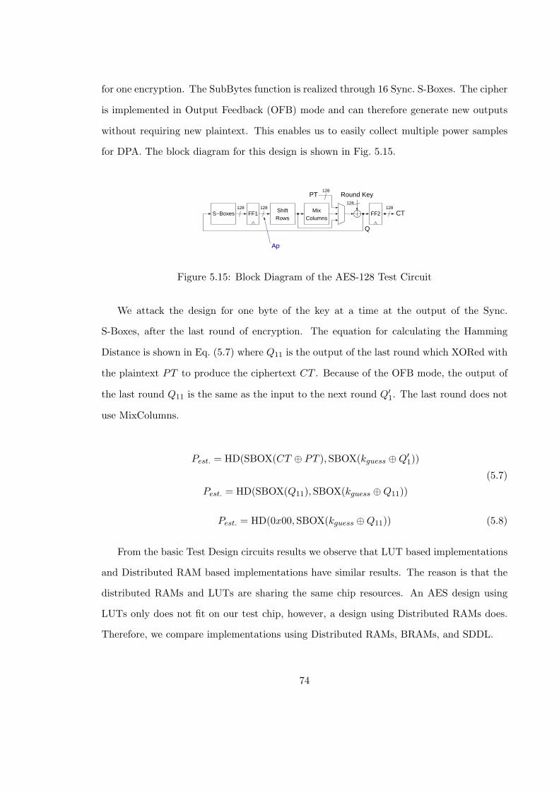
for one encryption. The SubBytes function is realized through 16 Sync. S-Boxes. The cipher
is implemented in Output Feedback (OFB) mode and can therefore generate new outputs
without requiring new plaintext. This enables us to easily collect multiple power samples
for DPA. The block diagram for this design is shown in Fig. 5.15.
Ap
FF2128128
FF1S−Boxes128
128
ColumnsMixShift
Rows
PT Round Key
Q
CT
128
Figure 5.15: Block Diagram of the AES-128 Test Circuit
We attack the design for one byte of the key at a time at the output of the Sync.
S-Boxes, after the last round of encryption. The equation for calculating the Hamming
Distance is shown in Eq. (5.7) where Q11 is the output of the last round which XORed with
the plaintext PT to produce the ciphertext CT . Because of the OFB mode, the output of
the last round Q11 is the same as the input to the next round Q′1. The last round does not
use MixColumns.
Pest. = HD(SBOX(CT ⊕ PT ), SBOX(kguess ⊕Q′1))
Pest. = HD(SBOX(Q11), SBOX(kguess ⊕Q11))
(5.7)
Pest. = HD(0x00, SBOX(kguess ⊕Q11)) (5.8)
From the basic Test Design circuits results we observe that LUT based implementations
and Distributed RAM based implementations have similar results. The reason is that the
distributed RAMs and LUTs are sharing the same chip resources. An AES design using
LUTs only does not fit on our test chip, however, a design using Distributed RAMs does.
Therefore, we compare implementations using Distributed RAMs, BRAMs, and SDDL.
74
Standard S-Box Implementation using Distributed RAMs
In design (6a.), the S-Box is implemented using distributed RAMs. The design uses 20
S-Boxes each of size 28x8 (2K bits), 16 S-Boxes performing the SubBytes operation on 16
bytes of data simultaneously and 4 S-Boxes performing the SubBytes operation in the key
scheduling section.
Standard S-Box Implementation using Block RAMs
In design (6b), the Sync. S-Box is implemented using BRAM. We implemented 20 S-Boxes
using 10 partially filled BRAMs in dual port mode. This reduces slice area by approximately
20 · (64 slices) = 1280 slices.
T-box Implementation using Block RAMs
This design was proposed by the authors of AES in [58] for software implementations on
32-bit micro-processors. In 2001, Fischer demonstrated its hardware implementation in
[59]. The T-box design computes one complete AES round just by using look-up tables
followed by a large XOR network. The SubBytes operation and MixColumns operation are
reformulated and implemented as 8x32 look-up tables. The T-box operation with the T-box
equations is explained in [58] and [60]. In design (6c.), the 20 T-Boxes are implemented
using 10 completely filled BRAMs.
SDDL for FPGAs on T-box Implementation
Table 8.3 shows clearly that AES T-box implementation (6c) is more secure compared to
standard AES-128 implementations (6a)(6b). Hence we implemented SDDL for FPGAs
countermeasure on the T-box implementation as design (6d). Design (6d.) consumes ap-
proximately 3.2 times the slice area and twice the number of BRAMs compared to design
(6c.). We use Eq.(5.8) to calculate the Hamming Distance for the SDDL design.
75
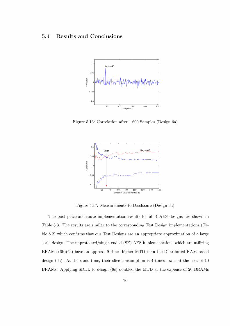
5.4 Results and Conclusions
50 100 150 200 250
−0.1
−0.05
0
0.05
0.1
key guess
cor
rela
tion
Key = 45
Figure 5.16: Correlation after 1,600 Samples (Design 6a)
20 40 60 80 100 120 140 160
−0.1
−0.05
0
0.05
0.1
Number of Measurements x 102
Cor
rela
tion
Key = 45MTD
Figure 5.17: Measurements to Disclosure (Design 6a)
The post place-and-route implementation results for all 4 AES designs are shown in
Table 8.3. The results are similar to the corresponding Test Design implementations (Ta-
ble 8.2) which confirms that our Test Designs are an appropriate approximation of a large
scale design. The unprotected/single ended (SE) AES implementations which are utilizing
BRAMs (6b)(6c) have an approx. 9 times higher MTD than the Distributed RAM based
design (6a). At the same time, their slice consumption is 4 times lower at the cost of 10
BRAMs. Applying SDDL to design (6c) doubled the MTD at the expense of 20 BRAMs
76

50 100 150 200 250
−0.1
−0.05
0
0.05
0.1
key guess
cor
rela
tion
Key = 45
Figure 5.18: Correlation after 16,000 Samples (Design 6b)
20 40 60 80 100 120 140 160
−0.1
−0.05
0
0.05
0.1
Number of Measurements x 102
Cor
rela
tion
MTD
Key = 45
Figure 5.19: Measurements to Disclosure (Design 6b)
and a 3 times higher slice count. Therefore (6d) has an 18 fold increase in security over
(6a) and uses fewer slices.
Table 5.4 shows a comparison of our results with other published secure implementations
on FPGAs. R.P. McEvoy et al.[53] achieves a similar increase in security with iWDDL over
their SE design compared to our results at the cost of more than 4 times increase in area.
iWDDL is deeply pipelined, hence the delay is smaller than of their SE design. Kaps et
al.[27] AES design has an 8-bit datapath and a low MTD. However their security increase for
Partial SDDL as well as SDDL for FPGAs is similar to that of the designs presented in this
paper. Their area increase is 2.3 to 3.1 times. Nassar et al.[54] WDDL implementation of
77
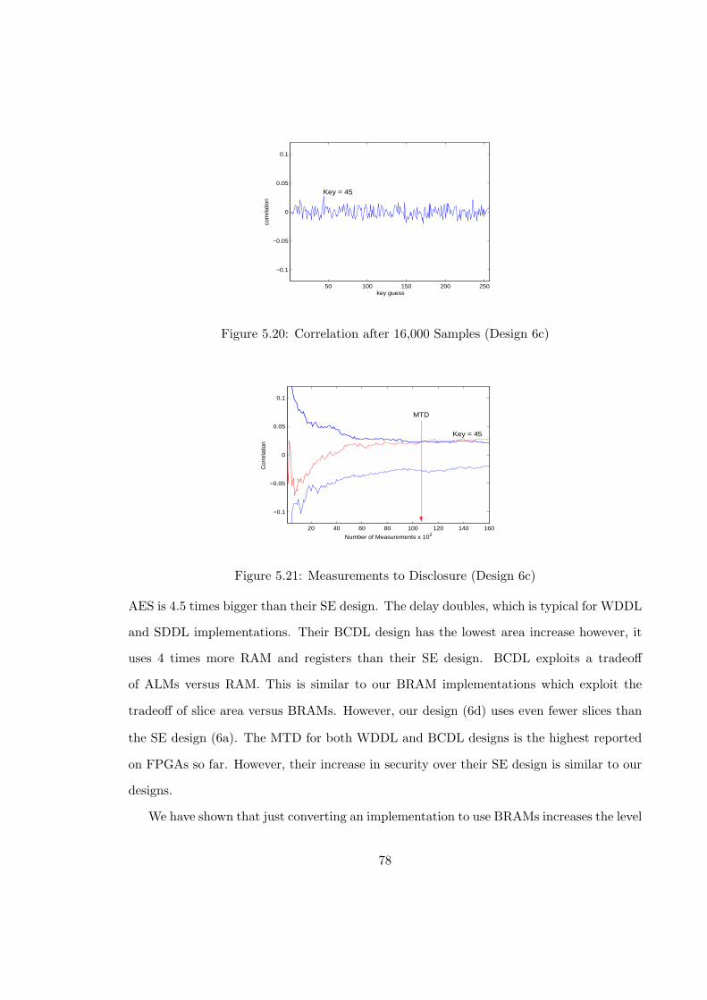
50 100 150 200 250
−0.1
−0.05
0
0.05
0.1
key guess
cor
rela
tion
Key = 45
Figure 5.20: Correlation after 16,000 Samples (Design 6c)
20 40 60 80 100 120 140 160
−0.1
−0.05
0
0.05
0.1
Number of Measurements x 102
Cor
rela
tion
Key = 45
MTD
Figure 5.21: Measurements to Disclosure (Design 6c)
AES is 4.5 times bigger than their SE design. The delay doubles, which is typical for WDDL
and SDDL implementations. Their BCDL design has the lowest area increase however, it
uses 4 times more RAM and registers than their SE design. BCDL exploits a tradeoff
of ALMs versus RAM. This is similar to our BRAM implementations which exploit the
tradeoff of slice area versus BRAMs. However, our design (6d) uses even fewer slices than
the SE design (6a). The MTD for both WDDL and BCDL designs is the highest reported
on FPGAs so far. However, their increase in security over their SE design is similar to our
designs.
We have shown that just converting an implementation to use BRAMs increases the level
78
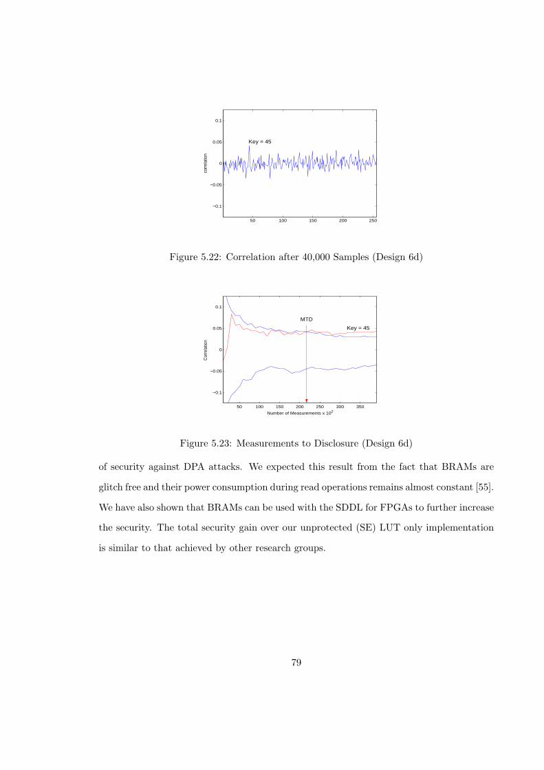
50 100 150 200 250
−0.1
−0.05
0
0.05
0.1
cor
rela
tion
Key = 45
Figure 5.22: Correlation after 40,000 Samples (Design 6d)
50 100 150 200 250 300 350
−0.1
−0.05
0
0.05
0.1
Number of Measurements x 102
Cor
rela
tion
MTD
Key = 45
Figure 5.23: Measurements to Disclosure (Design 6d)
of security against DPA attacks. We expected this result from the fact that BRAMs are
glitch free and their power consumption during read operations remains almost constant [55].
We have also shown that BRAMs can be used with the SDDL for FPGAs to further increase
the security. The total security gain over our unprotected (SE) LUT only implementation
is similar to that achieved by other research groups.
79

Table 5.3: Summary of Implementation Results from AES-128 Designs
4 input Minimum
Design Slices FFs LUTs BRAMs Delay MTD
6a. AES-128, DRAMs 1,727 422 3,374 0 15.876 ns 300-1,300
6b. AES-128, BRAMs 412 262 787 10 13.875 ns > 9, 500
6c. T-box AES-128, BRAMs 370 262 705 10 13.461 ns > 11, 500
6d. SDDL of (6c.) 1,236 518 1,410 20 26.922 ns > 23, 000
Table 5.4: Comparison with Other Published Results
Delay Security
Authors Technology Implementations Area (ns) MTD Gain
Nassar et al. Stratix II SE 1,078 ALMs 13.91 8k 1
[54] +40 Kb RAM
AES-128 WDDL 4,885 ALMs 26.97 > 150k 20
BCDL 1,841 ALMs 19.74 > 150k 20
+160 Kb RAM
McEvoy et al. Spartan 3E SE 761 Slices 19.50 1k 1
[53] Whirlpool iWDDL 3,300 Slices 7.70 > 20k 20
Kaps et al. Spartan 3E SE 393 Slices — 500 1
[27] AES-128 Partial DDL 928 Slices — > 12k 24
SDDL for FPGAs 1,222 Slices — > 12k 24
This Paper Spartan 3E S-Box DRAM 1,727 Slices 15.88 300- 1.3k 1
AES-128 S-Box BRAM 412 Slices 13.88 > 9, 500 7
+10 BRAMs
Tbox BRAM 370 Slices 13.46 > 11, 500 9
+10 BRAMs
SDDL Tbox BRAM 1,236 Slices 26.99 > 23, 000 18
+20 BRAMs
80
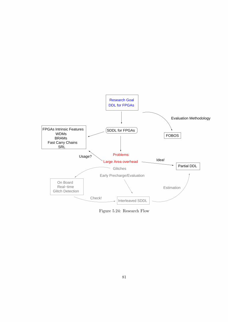
FOBOSSDDL for FPGAsFPGAs Intrinsic Features
WDMsBRAMs
Fast Carry ChainsSRL
Partial DDL
Interleaved SDDL
On BoardReal−time
Glitch Detection
Research GoalDDL for FPGAs
Evaluation Methodology
Problems:
Large Area overheadUsage?
Idea!
Check!
Estimation
Early Precharge/Evaluation
Glitches
Figure 5.24: Research Flow
81

Chapter 6: Partial Dual Rail with Precharge Logic
In this chapter we introduce Partial DDL, propose principle design rules of Partial DDL,
and show its effectiveness in terms of area saving and DPA resistance through a proof-of-
concept implementation of a lightweight AES design using SDDL for FPGAs and comparing
it with one using Partial SDDL for FPGAs.
The rest of the chapter is structured as follows. Section 6.1 explains the concept of
Partial DDL and the principle rules for implementing Partial DDL. The secure design flow
for implementing Partial DDL on FPGAs is described in Section 6.2. Next, in Section 6.3 the
lightweight implementation of AES, the attack methodology, and the design considerations
for AES Partial SDDL are discussed. In Section 6.4 we present the implementation results
secured AES using Partial SDDL. Section 9.5 concludes the chapter and discusses future
research perspectives related to Partial DDL.
6.1 Partial DDL
Partial DDL describes the notion that DDL is applied to only a part of the cryptographic
implementation. Consider the block diagram shown in Fig 6.1. The data path of the
cryptographic implementation is divided into two parts, Data Path Protected and Data
Path Unprotected. DDL is implemented only on the protected data path splitting it into
a direct and a complementary part (indicated as DataPath). DDL is not applied to the
unprotected path and the control block of the implementation. It is already a common
practice [44,50] to not protect the control logic as it manipulates only public information of
the algorithm. The protected and unprotected data paths are interconnected but there is
no connection between the complementary data path and the unprotected data path, shown
as crossed out line in Fig 6.1. The advantage of Partial DDL is that the area overhead is
82
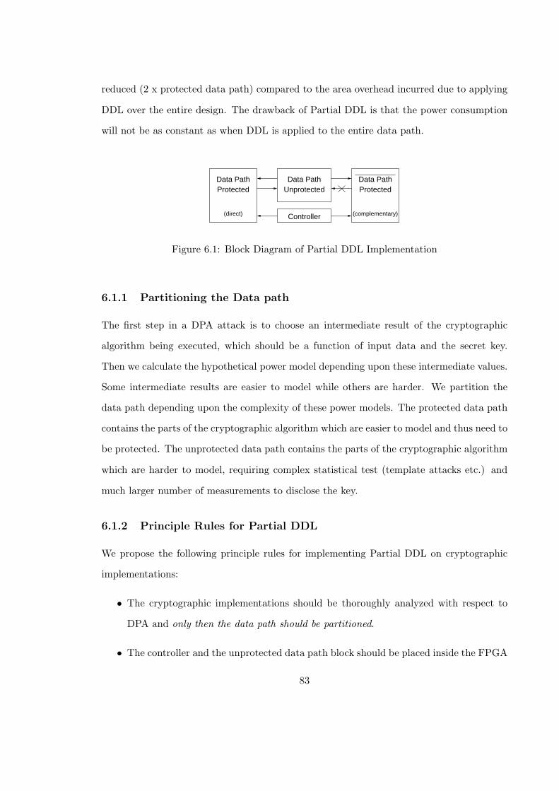
reduced (2 x protected data path) compared to the area overhead incurred due to applying
DDL over the entire design. The drawback of Partial DDL is that the power consumption
will not be as constant as when DDL is applied to the entire data path.
UnprotectedData Path
Controller
Data PathProtected
Data PathProtected
(complementary)(direct)
Figure 6.1: Block Diagram of Partial DDL Implementation
6.1.1 Partitioning the Data path
The first step in a DPA attack is to choose an intermediate result of the cryptographic
algorithm being executed, which should be a function of input data and the secret key.
Then we calculate the hypothetical power model depending upon these intermediate values.
Some intermediate results are easier to model while others are harder. We partition the
data path depending upon the complexity of these power models. The protected data path
contains the parts of the cryptographic algorithm which are easier to model and thus need to
be protected. The unprotected data path contains the parts of the cryptographic algorithm
which are harder to model, requiring complex statistical test (template attacks etc.) and
much larger number of measurements to disclose the key.
6.1.2 Principle Rules for Partial DDL
We propose the following principle rules for implementing Partial DDL on cryptographic
implementations:
• The cryptographic implementations should be thoroughly analyzed with respect to
DPA and only then the data path should be partitioned.
• The controller and the unprotected data path block should be placed inside the FPGA
83
fabric in such a way that the distance of the signals from the control block and the
output signals from the unprotected data path to the direct and complementary part
should be as similar as possible, so that there would not be any delay of operation be-
tween the direct and complementary part. As the routing of these signals is performed
by the FPGA tools in our design flow, we can not control the routing precisely.
• Special care must be taken when connecting the unprotected data path to the com-
plementary circuit. The output signals from unprotected data path should either be
inverted (which will result in additional area consumption) or appropriate changes in
the LUT logic equation must be made. Control signals to the complementary part
should not be inverted.
• Output signals from the complementary circuit either to the unprotected data path
or to the IOBs will be terminated in the slice itself.
We demonstrate the partial DDL approach on a lightweight implementation of AES on
FPGA in the next sections.
6.2 SDDL for FPGA
Our SDDL model [56] is shown in Fig. 6.2. Instead of applying De-Morgan’s law to obtain
the duplicate part we simply invert the inputs and outputs of the original logic gate. This
technique is not suitable for ASICs because placing a inverter on both inputs and outputs
will increase the area consumption. Whereas in FPGAs, we need to modify only the logic
equation in the LUTs, which will not cause any area overhead. FPGA CAD tools are given
the maximum flexibility to optimize a given design for the target FPGA thus, allowing logic
packing in LUTs and also make use of all the intrinsic features present in the FPGA with
the exception of WDMs.
84
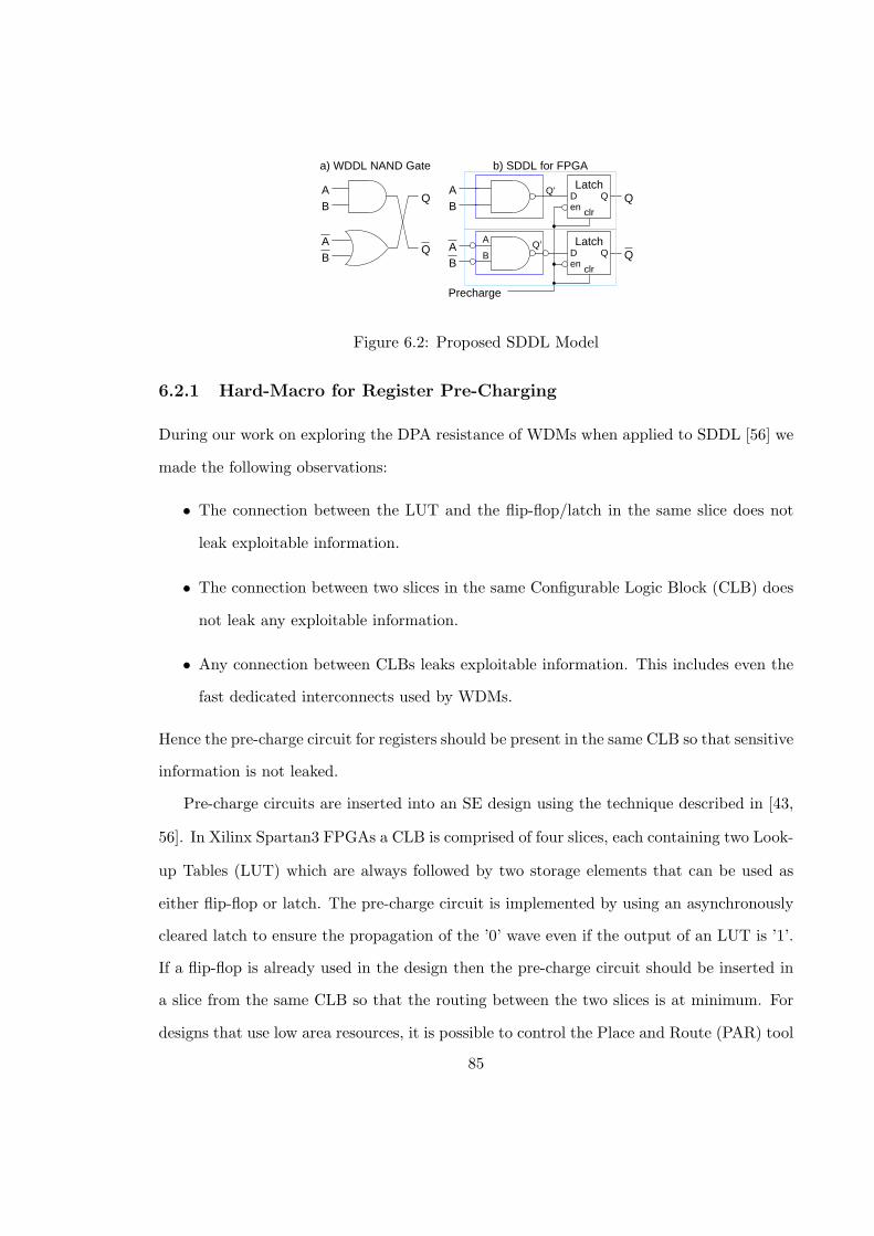
Q
D QLatch
en clr
D QLatch
en clr
AB
AB
Q
Q
a) WDDL NAND Gate
AB
AB
A
BQ’
QQ’
Precharge
b) SDDL for FPGA
Figure 6.2: Proposed SDDL Model
6.2.1 Hard-Macro for Register Pre-Charging
During our work on exploring the DPA resistance of WDMs when applied to SDDL [56] we
made the following observations:
• The connection between the LUT and the flip-flop/latch in the same slice does not
leak exploitable information.
• The connection between two slices in the same Configurable Logic Block (CLB) does
not leak any exploitable information.
• Any connection between CLBs leaks exploitable information. This includes even the
fast dedicated interconnects used by WDMs.
Hence the pre-charge circuit for registers should be present in the same CLB so that sensitive
information is not leaked.
Pre-charge circuits are inserted into an SE design using the technique described in [43,
56]. In Xilinx Spartan3 FPGAs a CLB is comprised of four slices, each containing two Look-
up Tables (LUT) which are always followed by two storage elements that can be used as
either flip-flop or latch. The pre-charge circuit is implemented by using an asynchronously
cleared latch to ensure the propagation of the ’0’ wave even if the output of an LUT is ’1’.
If a flip-flop is already used in the design then the pre-charge circuit should be inserted in
a slice from the same CLB so that the routing between the two slices is at minimum. For
designs that use low area resources, it is possible to control the Place and Route (PAR) tool
85
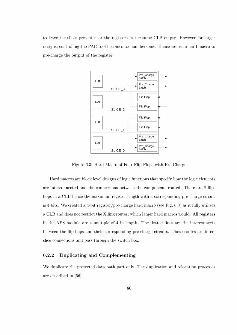
to leave the slices present near the registers in the same CLB empty. However for larger
designs, controlling the PAR tool becomes too cumbersome. Hence we use a hard macro to
pre-charge the output of the register.
Pre_ChargeLatch
Pre_ChargeLatch
LUT
SLICE_3
LUT
Pre_ChargeLatch
Pre_ChargeLatch
LUT
LUT
SLICE_1
Flip Flop
Flip Flop
SLICE_0
SLICE_2
Flip Flop
Flip Flop
Figure 6.3: Hard-Macro of Four Flip-Flops with Pre-Charge
Hard macros are block level designs of logic functions that specify how the logic elements
are interconnected and the connections between the components routed. There are 8 flip-
flops in a CLB hence the maximum register length with a corresponding pre-charge circuit
is 4 bits. We created a 4-bit register/pre-charge hard macro (see Fig. 6.3) as it fully utilizes
a CLB and does not restrict the Xilinx router, which larger hard macros would. All registers
in the AES module are a multiple of 4 in length. The dotted lines are the interconnects
between the flip-flops and their corresponding pre-charge circuits. These routes are inter-
slice connections and pass through the switch box.
6.2.2 Duplicating and Complementing
We duplicate the protected data path part only. The duplication and relocation processes
are described in [56].
86
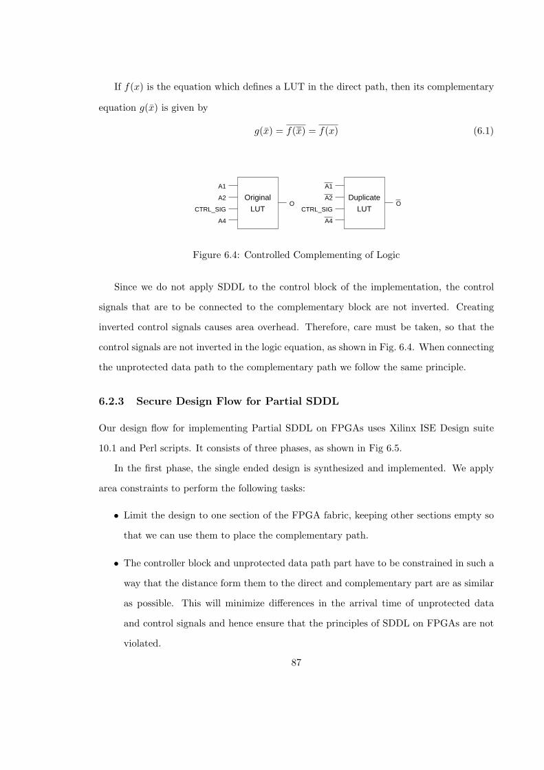
If f(x) is the equation which defines a LUT in the direct path, then its complementary
equation g(x) is given by
g(x) = f(x) = f(x) (6.1)
O OA2 Original
A1
CTRL_SIG
A4
LUT
A2
A1
CTRL_SIG
A4
LUT
Duplicate
Figure 6.4: Controlled Complementing of Logic
Since we do not apply SDDL to the control block of the implementation, the control
signals that are to be connected to the complementary block are not inverted. Creating
inverted control signals causes area overhead. Therefore, care must be taken, so that the
control signals are not inverted in the logic equation, as shown in Fig. 6.4. When connecting
the unprotected data path to the complementary path we follow the same principle.
6.2.3 Secure Design Flow for Partial SDDL
Our design flow for implementing Partial SDDL on FPGAs uses Xilinx ISE Design suite
10.1 and Perl scripts. It consists of three phases, as shown in Fig 6.5.
In the first phase, the single ended design is synthesized and implemented. We apply
area constraints to perform the following tasks:
• Limit the design to one section of the FPGA fabric, keeping other sections empty so
that we can use them to place the complementary path.
• The controller block and unprotected data path part have to be constrained in such a
way that the distance form them to the direct and complementary part are as similar
as possible. This will minimize differences in the arrival time of unprotected data
and control signals and hence ensure that the principles of SDDL on FPGAs are not
violated.
87
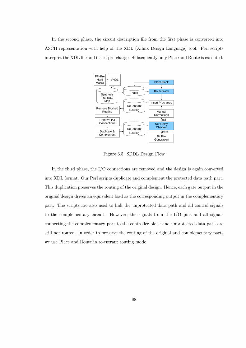
In the second phase, the circuit description file from the first phase is converted into
ASCII representation with help of the XDL (Xilinx Design Language) tool. Perl scripts
interpret the XDL file and insert pre-charge. Subsequently only Place and Route is executed.
Remove BlockedRouting
Remove I/OConnections
Duplicate &Complement
Place
Re−entrantRouting
Re−entrantRouting
Insert Precharge
Bit FileGeneration
ManualCorrections
SynthesisTranslate
Map
MacroHard
FF−PreVHDL
fail
pass
PlaceBlock
RouteBlock
Net DelayChecker
Figure 6.5: SDDL Design Flow
In the third phase, the I/O connections are removed and the design is again converted
into XDL format. Our Perl scripts duplicate and complement the protected data path part.
This duplication preserves the routing of the original design. Hence, each gate output in the
original design drives an equivalent load as the corresponding output in the complementary
part. The scripts are also used to link the unprotected data path and all control signals
to the complementary circuit. However, the signals from the I/O pins and all signals
connecting the complementary part to the controller block and unprotected data path are
still not routed. In order to preserve the routing of the original and complementary parts
we use Place and Route in re-entrant routing mode.
88

6.3 AES Implementation and Attack Methodology
6.3.1 AES Implementation
The Advanced Encryption Standard (AES) [42] is one of the most widely used block ciphers.
It was designed to be resistant towards linear and differential cryptanalysis. AES is a block
cipher of fixed input size of 128 bits and key length of either 128 or 192 or 256 bits. For our
AES implementation [61] we chose to use a key length of 128 bits. AES applies the same
round function ten times to its inputs during encryption. The round function consists of
four different transformations SubBytes, ShiftRows, MixColumns and AddRoundKey each
changing the input by applying linear, non linear and key dependent transformations. Our
AES implementation also assumes that the data input and the secret key are stored in
memory. The AES transformations are grouped into four stages
1. Initial AddRoundKey-SubBytes-ShiftRows
2. MixColumns
3. AddRoundKey-SubBytes-ShiftRows
4. FinalAddRoundKey
R3
R2
R4
R1
data
bus
Data Store
XOR
SBox
Mix Column
Key Gen
Key Store
Control
Rcon
Protected Unprotected
R0
Figure 6.6: Block Diagram of AES Module
89

The data path of our AES implementation is shown in Fig. 8.6. It is characterized by a
pipelined architecture for stages 1 and 3. This enables us to re-use registers and minimize
the number of internal memory accesses which in turn reduces the number of clock cycles.
Five registers R0, R1, R2, R3, R4 are used of which R0 is used exclusively for RotWord
operation. R1 is used for key computation and state computation inMixColumns operation,
R2, R3, R4 are used for state computation. The boxes labeled as Key store and Data store
are 128 bit registers used for Round keys and State Memory respectively.
In order to provide different plain text and key as input to the AES module we built
a wrapper circuit, as shown in Fig. 6.7. A 128-bit Linear Feedback Shift Register (LFSR)
provides input data to the AES module. An 8-bit wide 32:1 multiplexer is used to select
data or key depending upon the address from the AES module.
COUNTER
128−bit LFSR
SECRET KEY
AES
MODULE
ADDRESSLINES
DATAIN
RESET
CLOCK
128
1
8 DATA OUT
8
5
Figure 6.7: AES Module With a Wrapper Circuit
6.3.2 Design Consideration for AES- Partial SDDL
The implementation of the single ended AES design (AES SE) consumes 393 slices ex-
cluding the wrapper circuit. Table 6.1 breaks down the area consumption of AES into its
components. The pre-charge design is the result of the second step of our SDDL design
flow.
Pre-charging increases the slices consumed by a register by factor 2. In our design we
substituted the registers with the hard macro. For example the data store register which
is 128-bits in length can be implemented in 64 slices in the SE design. After pre-charging
90
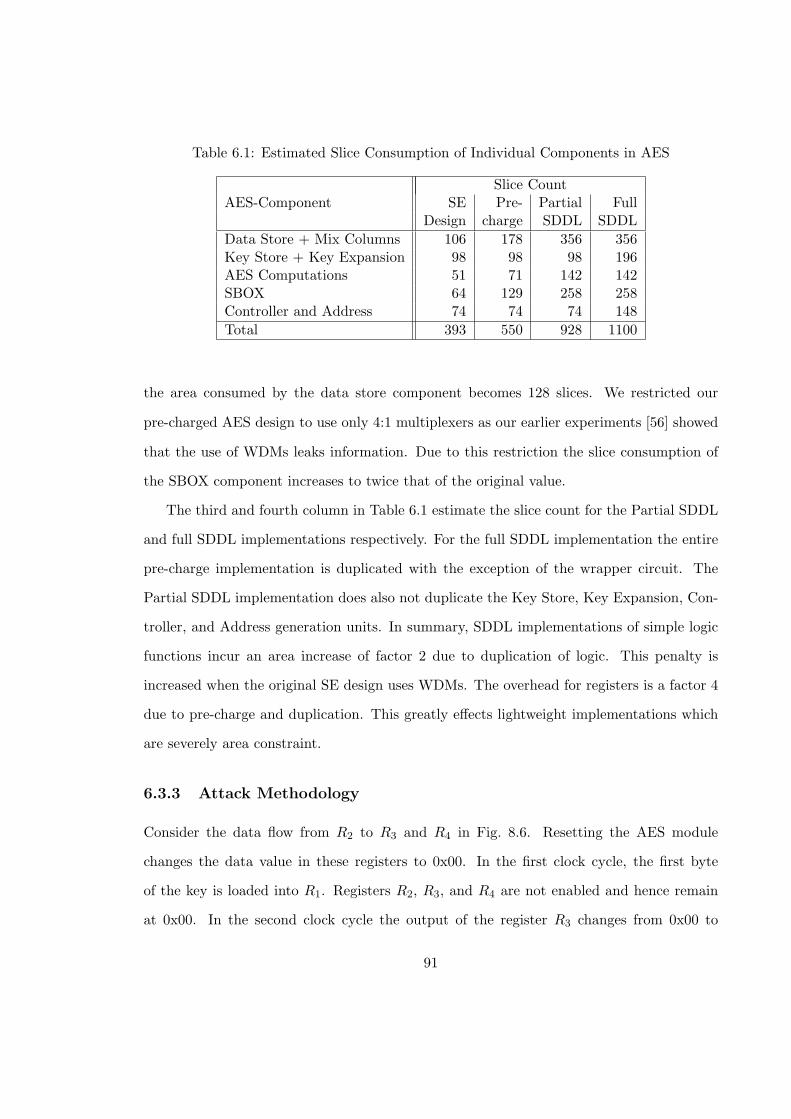
Table 6.1: Estimated Slice Consumption of Individual Components in AES
Slice CountAES-Component SE Pre- Partial Full
Design charge SDDL SDDL
Data Store + Mix Columns 106 178 356 356Key Store + Key Expansion 98 98 98 196AES Computations 51 71 142 142SBOX 64 129 258 258Controller and Address 74 74 74 148
Total 393 550 928 1100
the area consumed by the data store component becomes 128 slices. We restricted our
pre-charged AES design to use only 4:1 multiplexers as our earlier experiments [56] showed
that the use of WDMs leaks information. Due to this restriction the slice consumption of
the SBOX component increases to twice that of the original value.
The third and fourth column in Table 6.1 estimate the slice count for the Partial SDDL
and full SDDL implementations respectively. For the full SDDL implementation the entire
pre-charge implementation is duplicated with the exception of the wrapper circuit. The
Partial SDDL implementation does also not duplicate the Key Store, Key Expansion, Con-
troller, and Address generation units. In summary, SDDL implementations of simple logic
functions incur an area increase of factor 2 due to duplication of logic. This penalty is
increased when the original SE design uses WDMs. The overhead for registers is a factor 4
due to pre-charge and duplication. This greatly effects lightweight implementations which
are severely area constraint.
6.3.3 Attack Methodology
Consider the data flow from R2 to R3 and R4 in Fig. 8.6. Resetting the AES module
changes the data value in these registers to 0x00. In the first clock cycle, the first byte
of the key is loaded into R1. Registers R2, R3, and R4 are not enabled and hence remain
at 0x00. In the second clock cycle the output of the register R3 changes from 0x00 to
91

S−Box
S−Box
UnitControl
Core
AESCore
AES
StoreKey
Store
Wrapper
StoreData
AES
Data
Figure 6.8: Placement of AES Modules on FPGA Fabric
0x63 i.e. SBOX(R2) and the data value in R2 changes to the input data XORed with
key from R1. In the subsequent clock cycle the data value in the register R3 changes
from 0x63 to SBOX(R2). This sequence of change in the data values of the register R3 i.e
0x00 → 0x63 → SBOX(Key ⊕ Inputdata) occurs every time the AES module is reseted.
Thus we know two consecutive data values of a register and can apply the Hamming Distance
(HD) model to simulate the power consumption of the register. Therefore, we use a counter
to reset the AES module after every 10 clock cycles. The power model for the single ended
design is given by Equation (8.3). It calculates the HD between the SBOX value of key
guess XOR data and the hex value of 0x63.
The key register R0 is a probable attack point, although the attack itself will be difficult,
i.e. it will probably require more Measurements To Disclosure (MTD) compared to attacking
the registers R3 or R4. The reason is that we cannot compute an HD model as the key
store register output is always an unknown value (Round Keys). In this case the Hamming
weight (HW) model as shown in Equation (6.4) can be used. In order to attack the register
R0 the adversary has to identify the power consumption levels corresponding to the HW of
92
the data being processed. This requires complex statistical testing [62]. Due to this reason
and the fact that the SDDL version of the key store register will cause a large area over
head, we decided not to duplicate the key store register. This is a risk we are taking to
limit the area overhead although the security of the final SDDL design may decrease. We
also decided not to duplicate the controller as it leaks only the public information of the
algorithm. The Controller does not manipulate any sensitive information. Fig. 8.6 shows
the blocks which are pre-charged and duplicated on the left and the unprotected blocks on
the right.
We perform Correlation Power Analysis [41] using Pearson’s Correlation [41,63] in con-
junction with either Hamming Distance model or Hamming Weight model (depending upon
the situation).
Pguess = HD(0x63, (SBOX((Keyguess ⊕ Input))i) (6.2)
Pguess = HD(0x00, (SBOX((Keyguess ⊕ Input))i) (6.3)
Pguess = HD(0x00, (Keyguess)i) = HW(Keyguess) (6.4)
We estimate the output of the SBOX for all possible key guesses and mount a DPA
attack on SE design using Equation (8.3). We use a different power model to mount a
DPA attack on SDDL designs, given by Equation (8.4). The pre-charge phase sets all logic
outputs to ’0’ therefore, the Hamming distance is computed between ’0’ and the estimated
outputs of the SBOX for all possible key guesses.
6.3.4 Placement of AES Modules
The placement of the AES modules of our partial SDDL design is shown in Fig. 6.8. The
SBOX, Data Store, and AES Computation (AES Core) are duplicated and complemented
such that they use the same CLB and routing resources. We placed these closely connected
parts near each other. The location of the controller and the key store register inside the
93

FPGA fabric has an impact on the DPA resistance. We placed the control unit close to the
AES Core which it controls. The key store is placed between the data stores as they all
have to communicate with the AES wrapper. It can clearly be seen that it is impossible
to have symmetrical connections from the protected modules SBOX, Data Store, and AES
computation to the unprotected path.
6.4 Results and Analysis
6.4.1 Experimental Setup
The target platform for our designs is a Xilinx Spartan 3e starter board containing a
XC3S500eFG320-4 FPGA. We removed the capacitances of the core voltage net and con-
nected it to an external regulated power supply in order to obtain a clear power mea-
surement. Power consumption is measured using a Tektronics CT-1 current probe and
an Agilent DSO6054A oscilloscope, which has a bandwidth of 500MHz and samples at
4GSa/sec.
6.4.2 Analysis of the AES Test Circuit
We implemented three different designs of our AES circuit. AES-SE is a single ended design
which use 32:1 WDMs. AES-Partial SDDL is the symmetrically routed design of the said
single ended and AES SDDL is a full SDDL implementation. Figure 6.9 shows the power
consumption traces for all three designs. The single ended wave form has its peaks near
the rising edge of the clock. The SDDL designs show lower peaks during pre-charge phase
and higher peaks during the evaluation phase. It can also be clearly seen that the peaks of
the SDDL designs are more uniform compared to the ones of the single ended. The largest
peaks in the waveform of both designs occur when the 128-bit LFSR is clocked.
The key byte which we are attacking is a fixed value of 10 for all designs. The correla-
tion plot between power guess and power measured for the AES SE implementation taken
over 500 measurements shows a sharp peak at the key guess 10, as shown in Fig. 6.10.
94
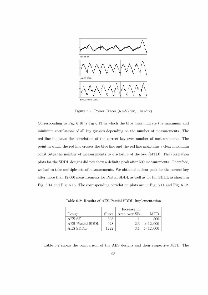
b) AES SDDL
c) AES Partial SDDL
a) AES SE
Figure 6.9: Power Traces (5mV/div, 1µs/div)
Corresponding to Fig. 6.10 is Fig 6.13 in which the blue lines indicate the maximum and
minimum correlations of all key guesses depending on the number of measurements. The
red line indicates the correlation of the correct key over number of measurements. The
point in which the red line crosses the blue line and the red line maintains a clear maximum
constitutes the number of measurements to disclosure of the key (MTD). The correlation
plots for the SDDL designs did not show a definite peak after 500 measurements. Therefore,
we had to take multiple sets of measurements. We obtained a clear peak for the correct key
after more than 12,000 measurements for Partial SDDL as well as for full SDDL as shown in
Fig. 6.14 and Fig. 6.15. The corresponding correlation plots are in Fig. 6.11 and Fig. 6.12.
Table 6.2: Results of AES-Partial SDDL Implementation
Increase inDesign Slices Area over SE MTD
AES SE 393 1 500AES Partial SDDL 928 2.3 > 12, 000AES SDDL 1222 3.1 > 12, 000
Table 6.2 shows the comparison of the AES designs and their respective MTD. The
95

final AES Partial SDDL implementation is larger than the AES SE by a factor of 2.3. The
area consumption of AES Full SDDL is 3.1 times larger then the single ended design. The
partial SDDL is 76% of the total area consumed by AES Full SDDL implementation. The
security provided by the AES Partial SDDL is 30 times to that of the AES SE design and
similar to the full SDDL implementation. The area consumption of the SDDL designs are
very close to the ones we expected from our estimation in Table 6.1.
0 50 100 150 200 250
−0.1
−0.05
0
0.05
0.1
0.15
0.2
0.25
Key Guess
Co
rre
latio
n
Key = 10
Figure 6.10: AES SE – Key Correlation after 500 Measurements
50 100 150 200 250−0.2
−0.15
−0.1
−0.05
0
0.05
0.1
0.15
0.2
Key Guess
Cor
relat
ion
Key = 10
Figure 6.11: AES SDDL – Key Correlation after 30,000 Measurements
96

50 100 150 200 250−0.2
−0.15
−0.1
−0.05
0
0.05
0.1
0.15
0.2
Key Guess
Cor
relat
ion
Key = 10
Figure 6.12: AES Partial SDDL – Key Correlation after 30,000 Measurements
5 10 15 20 25 30−0.8
−0.6
−0.4
−0.2
0
0.2
0.4
0.6
0.8
Number of Measurements x 10
Corre
lation
Key = 10
MTD
Figure 6.13: AES SE – Measurements to Disclosure
6.5 Conclusion
Securing cryptographic implementations using DDL logic leads to a large area penalty. We
have shown through our example implementation of AES using SDDL for FPGAs, that
partial DDL can significantly reduce the area consumption of a DDL implementation by
24%, yet maintain the same level of resistance against DPA. Our Partial SDDL can still
be broken due to glitches and imbalance of power consumption between the direct and
complementary circuits.
97
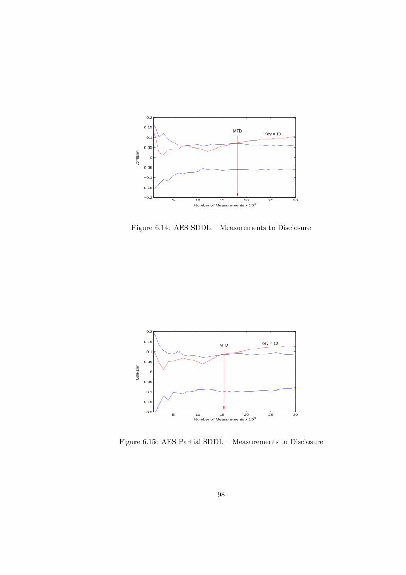
5 10 15 20 25 30−0.2
−0.15
−0.1
−0.05
0
0.05
0.1
0.15
0.2
Number of Measurements x 103
Corre
lation
Key = 10
MTD
Figure 6.14: AES SDDL – Measurements to Disclosure
5 10 15 20 25 30−0.2
−0.15
−0.1
−0.05
0
0.05
0.1
0.15
0.2
Number of Measurements x 103
Corre
lation
Key = 10MTD
Figure 6.15: AES Partial SDDL – Measurements to Disclosure
98
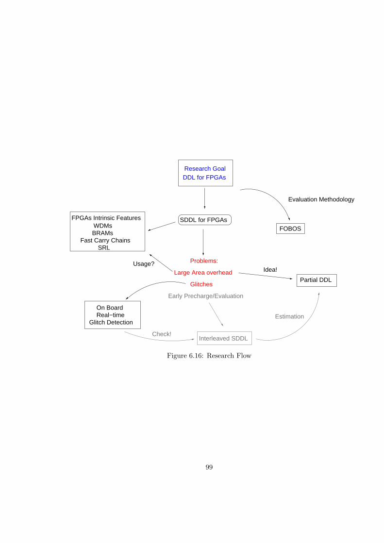
FOBOSSDDL for FPGAsFPGAs Intrinsic Features
WDMsBRAMs
Fast Carry ChainsSRL
Partial DDL
On BoardReal−time
Glitch Detection
Interleaved SDDL
Research GoalDDL for FPGAs
Evaluation Methodology
Problems:
Large Area overhead
Glitches
Usage?Idea!
Check!
Estimation
Early Precharge/Evaluation
Figure 6.16: Research Flow
99

Chapter 7: Glitch Detection using Delay Based Sampling
Techniques
7.1 Introduction & Motivation
It is estimated that an FPGA design consumes overall 10 times more power than a func-
tionally equivalent ASIC design [64]. This disadvantage is emphasized because power has
become a significant design constraint in digital designs due to the demand of portable,
battery-powered devices. If advantages of FPGAs are to be fully exploited, the amount of
power they consume must be reduced or carefully controlled.
In FPGAs and other devices which are manufactured using CMOS technology, the
dynamic power consumption constitutes a large portion of the total power consumption.
Dynamic power consumption is mainly caused by signal transitions at gate outputs due to
charging and discharging of load capacitances (wires, gate inputs) and short-circuit currents.
These signal transitions are further classified into two types: Functional and Spurious tran-
sitions. Functional transitions are the signal transitions necessary to perform the required
logic function. On the other hand, Spurious transitions are glitches, which are the unpro-
ductive signal transitions due to unbalanced path delays at the inputs of a gate, causing the
gate’s output to transition briefly to an intermediate state. If the input signals to a gate are
skewed in time, a glitch may be generated and if a glitch arrives to an input of a gate and
that input is sensitive at that moment, the glitch is propagated to the output of the gate.
Typically, the number of propagated glitches exceeds the number of generated glitches in a
circuit [65].
Glitches in a digital system lead to an increase in the number of signal transitions,
thereby increasing the dynamic power consumption of the system. Consequently, over-
all power consumption is increased. A study conducted on Xilinx XC4003A FPGAs[66]
100

indicates that the amount of power consumed by the programmable interconnect can ac-
count for up to 65% of total dissipated power. As a result, glitches occurring in hardware
implementations on FPGAs have a significant impact on power cost.
Hardware implementations of mathematically secure cryptographic algorithms are sus-
ceptible to Side-Channel Attacks (SCA). Differential Power Analysis (DPA) attacks, a type
of SCA, correlates the power consumption of the device with data dependent operations to
obtain the secret information. These attacks are powerful, easy to launch, and are known
to have a high success rate. Glitches, occurring in cryptographic implementations, have
been shown to be a source of side-channel leakage [67,68] and can be exploited to enhance
the success rate of DPA attacks even in presence of side-channel countermeasures especially
hiding countermeasures like Dynamic and Differential Logic (DDL) [8,48,69]. Presence of a
glitch in either direct or complementary paths results in an imbalanced power consumption
per clock cycle, thereby defeating the DPA countermeasure.
Current post Place And Route (PAR) simulations use a generic model for a given family
of FPGAs and hence, do not take the factor of process variation into consideration. Recent
studies in [69–71] show that two designs with identical resources implemented at different
locations but on the same chip have different speed of propagation for the corresponding
signals which suggests that process variations play a major role in signal propagations in-
cluding glitch propagation. The propagation delays in the actual chip can cause signal
arrival time imbalances at a gate that can cause a glitch which was not exposed by simu-
lation. Therefore, only measuring signals of the actual hardware implementation will show
all glitches. Determining the sections of a circuit that are prone to generate glitches, when
measured over several FPGAs, allows the designer to target the application of glitch min-
imization techniques. These measurements are typically made with high quality, fast, and
therefore expensive oscilloscopes.
In this chapter, we propose a methodology for detecting glitches in hardware implemen-
tations on FPGAs using a delay based sampling technique. Our proposed methodology not
only detects the presence of glitches but also captures the glitch waveform, which provides
101
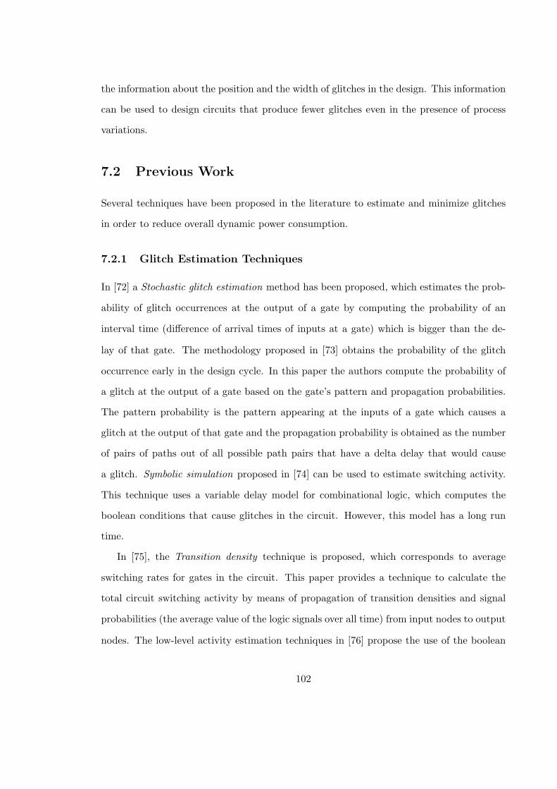
the information about the position and the width of glitches in the design. This information
can be used to design circuits that produce fewer glitches even in the presence of process
variations.
7.2 Previous Work
Several techniques have been proposed in the literature to estimate and minimize glitches
in order to reduce overall dynamic power consumption.
7.2.1 Glitch Estimation Techniques
In [72] a Stochastic glitch estimation method has been proposed, which estimates the prob-
ability of glitch occurrences at the output of a gate by computing the probability of an
interval time (difference of arrival times of inputs at a gate) which is bigger than the de-
lay of that gate. The methodology proposed in [73] obtains the probability of the glitch
occurrence early in the design cycle. In this paper the authors compute the probability of
a glitch at the output of a gate based on the gate’s pattern and propagation probabilities.
The pattern probability is the pattern appearing at the inputs of a gate which causes a
glitch at the output of that gate and the propagation probability is obtained as the number
of pairs of paths out of all possible path pairs that have a delta delay that would cause
a glitch. Symbolic simulation proposed in [74] can be used to estimate switching activity.
This technique uses a variable delay model for combinational logic, which computes the
boolean conditions that cause glitches in the circuit. However, this model has a long run
time.
In [75], the Transition density technique is proposed, which corresponds to average
switching rates for gates in the circuit. This paper provides a technique to calculate the
total circuit switching activity by means of propagation of transition densities and signal
probabilities (the average value of the logic signals over all time) from input nodes to output
nodes. The low-level activity estimation techniques in [76] propose the use of the boolean
102

difference function to find the output transition densities of a logic component based on its
input transition density. The techniques in [75] and [76] can be computationally expensive
for large combinational circuits.
The method for modelling glitch activity inside arithmetic circuits using word-level
statistics of signals is proposed in [77] using Glitch Profile metric. This metric is based on
transition density [75] technique. The proposed method models the propagation of glitch
activity in signals through the arithmetic components in circuits.
[78] introduces a glitch capture technology based on FPGA, which uses dual-jump-edge
detection principle. In this principle, the logic level sampled at the beginning of the sampling
period is considered as reference level. During the same sampling cycle, if there is a change
in logic level from the reference level, a glitch is detected. It also provides a technique for
logic analyzer based glitch capture, but it is complex and expensive. Glitch estimation using
statistical techniques can be accurate and can be built around an existing simulation model
but is input dependent. On the other hand glitch estimation using probabilistic techniques
is comparatively not as accurate but faster than statistical techniques [79].
7.2.2 Glitch Reduction Techniques
The basic technique to reduce the occurrence of a glitches is to align the inputs to a gate by
balancing their respective delay paths. GlitchMap [80] is an FPGA technology mapper that
is glitch aware. In this technique glitches are minimized by favoring mapping solutions that
balance Look-Up Table (LUT) levels between different paths. The optimum mapping depth
can be computed during cut enumeration by computing depth of every node and every cut.
The technique proposed in [81] works at technology mapping level in FPGAs. Power can be
reduced by covering connections with high toggle rates within a LUT and minimizing logic
replication. The Gate Freezing [72] technique eliminates glitches by suppressing transitions
until the freeze gate is enabled. This technique is less suitable for FPGAs since the appli-
cations implemented on FPGAs are not known until after fabrication. Glitchless [82, 83]
proposed inserting programmable delay elements into configuration logic blocks (CLBs) of
103
FPGAs. After a glitch-unaware routing stage, these delays are used to align signal arrival
times. GlitchReroute [84] proposed an approach to reduce dynamic power in FPGAs by
reducing glitches during routing. It finds alternative routes for early arriving signals so
that signal arrival times at look-up tables are aligned. The authors developed an algorithm
to find routes with target delays and then built a glitch-aware router. [79] presented a
Don’t-care-based synthesis technique for reducing glitch power in FPGAs. This technique
takes advantages of don’t-cares in the circuit by setting their values based on the circuit’s
simulated glitch behavior. [85] proposed a technique to address power dissipation due to
glitches post-routing, where the delays between LUTs are known. Their algorithm reduces
glitches by inserting negative edge triggered flip-flops (FFs) at the output of LUTs of FP-
GAs that produce glitches. This prevents unnecessary logic transitions from propagating to
the general routing network and subsequent LUTs. [86] presents an FPGA-targeted, glitch-
aware, high-level binding algorithm for power and area reduction. In [87], pipelining and
re-timing have been used to balance the path delays and reduce wire toggle rates. The path
balancing [72] algorithm reduces glitches using the statistical gate sizing technique that con-
siders the probability of glitch occurrence and calculates an optimal delay amount of sizing.
In [88], the authors proposed several techniques that attempt to reduce glitching power con-
sumption by minimizing propagation of glitches in the RTL circuit. The techniques include
restructuring multiplexer networks (to enhance data correlations and eliminate glitches in
the control signals), clocking control signals, and inserting selective delays, in order to kill
the propagation of glitches from control as well as data signals.
7.2.3 Delay Based Sampling
Time-to-Digital Converters (TDC) are used in applications where time measurement is
necessary in intervals with precision as high as few picoseconds. The TDC applications
range from time-of-flight sensors to positron emission tomography instruments. On an
FPGA, there are several methods to implement TDCs, the most popular ones are Tapped
Delay Line or Delay Based Sampling [89–91]. The basic logic blocks of FPGAs are arranged
104
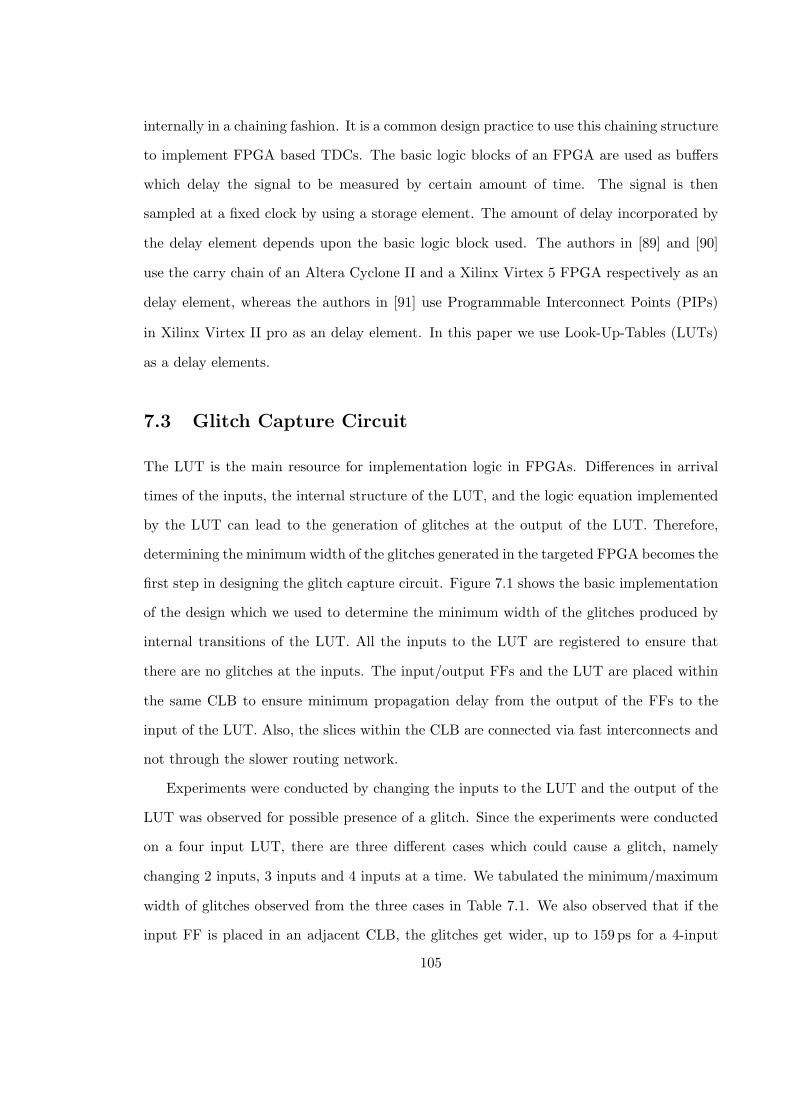
internally in a chaining fashion. It is a common design practice to use this chaining structure
to implement FPGA based TDCs. The basic logic blocks of an FPGA are used as buffers
which delay the signal to be measured by certain amount of time. The signal is then
sampled at a fixed clock by using a storage element. The amount of delay incorporated by
the delay element depends upon the basic logic block used. The authors in [89] and [90]
use the carry chain of an Altera Cyclone II and a Xilinx Virtex 5 FPGA respectively as an
delay element, whereas the authors in [91] use Programmable Interconnect Points (PIPs)
in Xilinx Virtex II pro as an delay element. In this paper we use Look-Up-Tables (LUTs)
as a delay elements.
7.3 Glitch Capture Circuit
The LUT is the main resource for implementation logic in FPGAs. Differences in arrival
times of the inputs, the internal structure of the LUT, and the logic equation implemented
by the LUT can lead to the generation of glitches at the output of the LUT. Therefore,
determining the minimum width of the glitches generated in the targeted FPGA becomes the
first step in designing the glitch capture circuit. Figure 7.1 shows the basic implementation
of the design which we used to determine the minimum width of the glitches produced by
internal transitions of the LUT. All the inputs to the LUT are registered to ensure that
there are no glitches at the inputs. The input/output FFs and the LUT are placed within
the same CLB to ensure minimum propagation delay from the output of the FFs to the
input of the LUT. Also, the slices within the CLB are connected via fast interconnects and
not through the slower routing network.
Experiments were conducted by changing the inputs to the LUT and the output of the
LUT was observed for possible presence of a glitch. Since the experiments were conducted
on a four input LUT, there are three different cases which could cause a glitch, namely
changing 2 inputs, 3 inputs and 4 inputs at a time. We tabulated the minimum/maximum
width of glitches observed from the three cases in Table 7.1. We also observed that if the
input FF is placed in an adjacent CLB, the glitches get wider, up to 159 ps for a 4-input
105
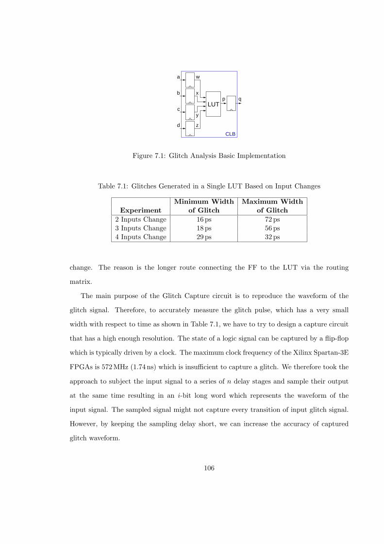
LUTc
d
y
a
b
z
x
w
p q
CLB
Figure 7.1: Glitch Analysis Basic Implementation
Table 7.1: Glitches Generated in a Single LUT Based on Input Changes
Minimum Width Maximum WidthExperiment of Glitch of Glitch
2 Inputs Change 16 ps 72 ps3 Inputs Change 18 ps 56 ps4 Inputs Change 29 ps 32 ps
change. The reason is the longer route connecting the FF to the LUT via the routing
matrix.
The main purpose of the Glitch Capture circuit is to reproduce the waveform of the
glitch signal. Therefore, to accurately measure the glitch pulse, which has a very small
width with respect to time as shown in Table 7.1, we have to try to design a capture circuit
that has a high enough resolution. The state of a logic signal can be captured by a flip-flop
which is typically driven by a clock. The maximum clock frequency of the Xilinx Spartan-3E
FPGAs is 572MHz (1.74 ns) which is insufficient to capture a glitch. We therefore took the
approach to subject the input signal to a series of n delay stages and sample their output
at the same time resulting in an i-bit long word which represents the waveform of the
input signal. The sampled signal might not capture every transition of input glitch signal.
However, by keeping the sampling delay short, we can increase the accuracy of captured
glitch waveform.
106
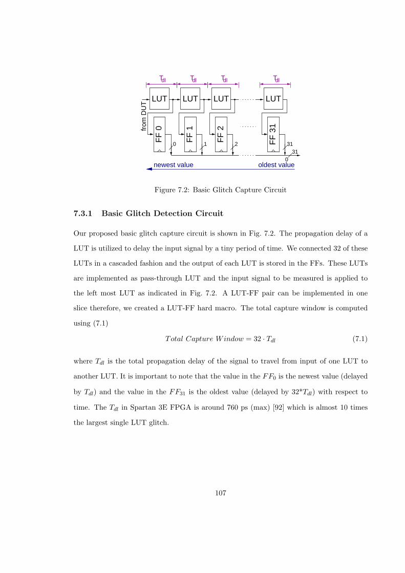
LUT
FF
1
1
LUT
FF
2
231
0
LUT
FF
31
31
LUT
FF
0
0
dlTdlTdlTdlT
from
DU
T
newest value oldest value
Figure 7.2: Basic Glitch Capture Circuit
7.3.1 Basic Glitch Detection Circuit
Our proposed basic glitch capture circuit is shown in Fig. 7.2. The propagation delay of a
LUT is utilized to delay the input signal by a tiny period of time. We connected 32 of these
LUTs in a cascaded fashion and the output of each LUT is stored in the FFs. These LUTs
are implemented as pass-through LUT and the input signal to be measured is applied to
the left most LUT as indicated in Fig. 7.2. A LUT-FF pair can be implemented in one
slice therefore, we created a LUT-FF hard macro. The total capture window is computed
using (7.1)
Total Capture Window = 32 · Tdl (7.1)
where Tdl is the total propagation delay of the signal to travel from input of one LUT to
another LUT. It is important to note that the value in the FF0 is the newest value (delayed
by Tdl) and the value in the FF31 is the oldest value (delayed by 32*Tdl) with respect to
time. The Tdl in Spartan 3E FPGA is around 760 ps (max) [92] which is almost 10 times
the largest single LUT glitch.
107
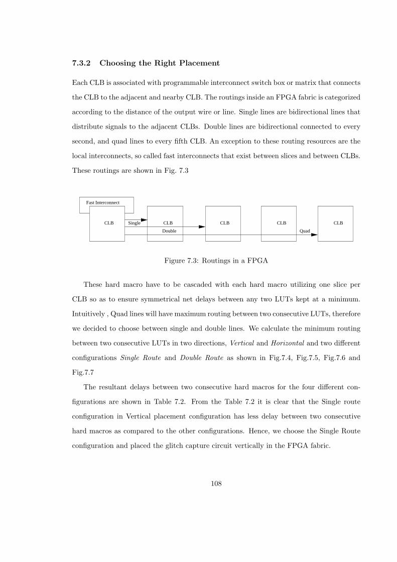
7.3.2 Choosing the Right Placement
Each CLB is associated with programmable interconnect switch box or matrix that connects
the CLB to the adjacent and nearby CLB. The routings inside an FPGA fabric is categorized
according to the distance of the output wire or line. Single lines are bidirectional lines that
distribute signals to the adjacent CLBs. Double lines are bidirectional connected to every
second, and quad lines to every fifth CLB. An exception to these routing resources are the
local interconnects, so called fast interconnects that exist between slices and between CLBs.
These routings are shown in Fig. 7.3
Fast Interconnect
QuadDouble
SingleCLB CLB CLB CLB CLB
Figure 7.3: Routings in a FPGA
These hard macro have to be cascaded with each hard macro utilizing one slice per
CLB so as to ensure symmetrical net delays between any two LUTs kept at a minimum.
Intuitively , Quad lines will have maximum routing between two consecutive LUTs, therefore
we decided to choose between single and double lines. We calculate the minimum routing
between two consecutive LUTs in two directions, Vertical and Horizontal and two different
configurations Single Route and Double Route as shown in Fig.7.4, Fig.7.5, Fig.7.6 and
Fig.7.7
The resultant delays between two consecutive hard macros for the four different con-
figurations are shown in Table 7.2. From the Table 7.2 it is clear that the Single route
configuration in Vertical placement configuration has less delay between two consecutive
hard macros as compared to the other configurations. Hence, we choose the Single Route
configuration and placed the glitch capture circuit vertically in the FPGA fabric.
108

Figure 7.4: Single Route in Horizontal Direction
Figure 7.5: Double Route in Horizontal Direction
7.3.3 Resolution Enhancement using DCM
The main drawback of our proposed glitch capture circuit is that the circuit cannot capture
glitches of width less than Tdl. Therefore, in order to enhance the resolution of our capture
circuit we repeatedly apply the same input change to the Design Under Test (DUT) but
each time we start the sampling process a little bit later, i.e., we shift the phase of the
Trigger signal sent to the measurement FFs m times. Consider the timing diagram shown
in Fig. 7.8. DUT Delay is the propagation delay of the DUT i.e., the time it takes for the
DUT Output to become stable and valid after a change at the DUT Input. In order detect
and capture the glitches present in DUT, the initial phase shift value of the DCM should
be chosen in such a way that the Measurement Window includes the DUT delay and shift
the phase of the Trigger signal forward in time i.e., towards right.
We use Digital Clock Managers (DCMs) [92] to produce this phase shift. DCMs are one
109
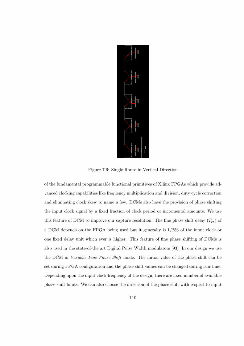
Figure 7.6: Single Route in Vertical Direction
of the fundamental programmable functional primitives of Xilinx FPGAs which provide ad-
vanced clocking capabilities like frequency multiplication and division, duty cycle correction
and eliminating clock skew to name a few. DCMs also have the provision of phase shifting
the input clock signal by a fixed fraction of clock period or incremental amounts. We use
this feature of DCM to improve our capture resolution. The fine phase shift delay (Tps) of
a DCM depends on the FPGA being used but it generally is 1/256 of the input clock or
one fixed delay unit which ever is higher. This feature of fine phase shifting of DCMs is
also used in the state-of-the art Digital Pulse Width modulators [93]. In our design we use
the DCM in Variable Fine Phase Shift mode. The initial value of the phase shift can be
set during FPGA configuration and the phase shift values can be changed during run-time.
Depending upon the input clock frequency of the design, there are fixed number of available
phase shift limits. We can also choose the direction of the phase shift with respect to input
110

Figure 7.7: Double Route in Vertical Direction
clock of the DCM.
7.3.4 Glitch Capture Circuit with Calibration
The schematic diagram of the glitch capture with calibration is shown in Fig. 7.9. Data i.e.,
inputs to the Design Under Test (DUT) is send from PC to the circuit via USB. These inputs
are stored in registers Value1 and Value2. DUT is the test circuit which is analyzed for
the presence of glitches. If the DUT is a large design, then we might want to check several
signals (both internal and I/O) for the presence of glitches. In this case, we can multiplex
these signals and feed it to the Glitch capture circuit one at a time. The trigger signal
for the measurement FFs in the Capture Circuit is produced by the Phase module. The
BRAM stores the calibration and the measurement data obtained from the Capture Circuit
which is later sent back to PC via USB for post processing and waveform generation. All
111
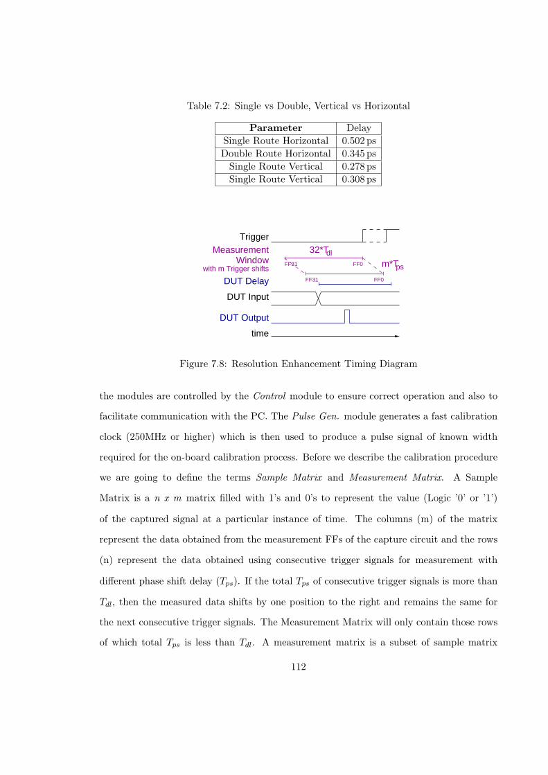
Table 7.2: Single vs Double, Vertical vs Horizontal
Parameter Delay
Single Route Horizontal 0.502 ps
Double Route Horizontal 0.345 ps
Single Route Vertical 0.278 ps
Single Route Vertical 0.308 ps
DUT Input
DUT Output
Measurement
time
Trigger
DUT Delay
Windowwith m Trigger shifts
FF31 FF0
FF0FF31
dl32*T
psm*T
Figure 7.8: Resolution Enhancement Timing Diagram
the modules are controlled by the Control module to ensure correct operation and also to
facilitate communication with the PC. The Pulse Gen. module generates a fast calibration
clock (250MHz or higher) which is then used to produce a pulse signal of known width
required for the on-board calibration process. Before we describe the calibration procedure
we are going to define the terms Sample Matrix and Measurement Matrix. A Sample
Matrix is a n x m matrix filled with 1’s and 0’s to represent the value (Logic ’0’ or ’1’)
of the captured signal at a particular instance of time. The columns (m) of the matrix
represent the data obtained from the measurement FFs of the capture circuit and the rows
(n) represent the data obtained using consecutive trigger signals for measurement with
different phase shift delay (Tps). If the total Tps of consecutive trigger signals is more than
Tdl, then the measured data shifts by one position to the right and remains the same for
the next consecutive trigger signals. The Measurement Matrix will only contain those rows
of which total Tps is less than Tdl. A measurement matrix is a subset of sample matrix
112
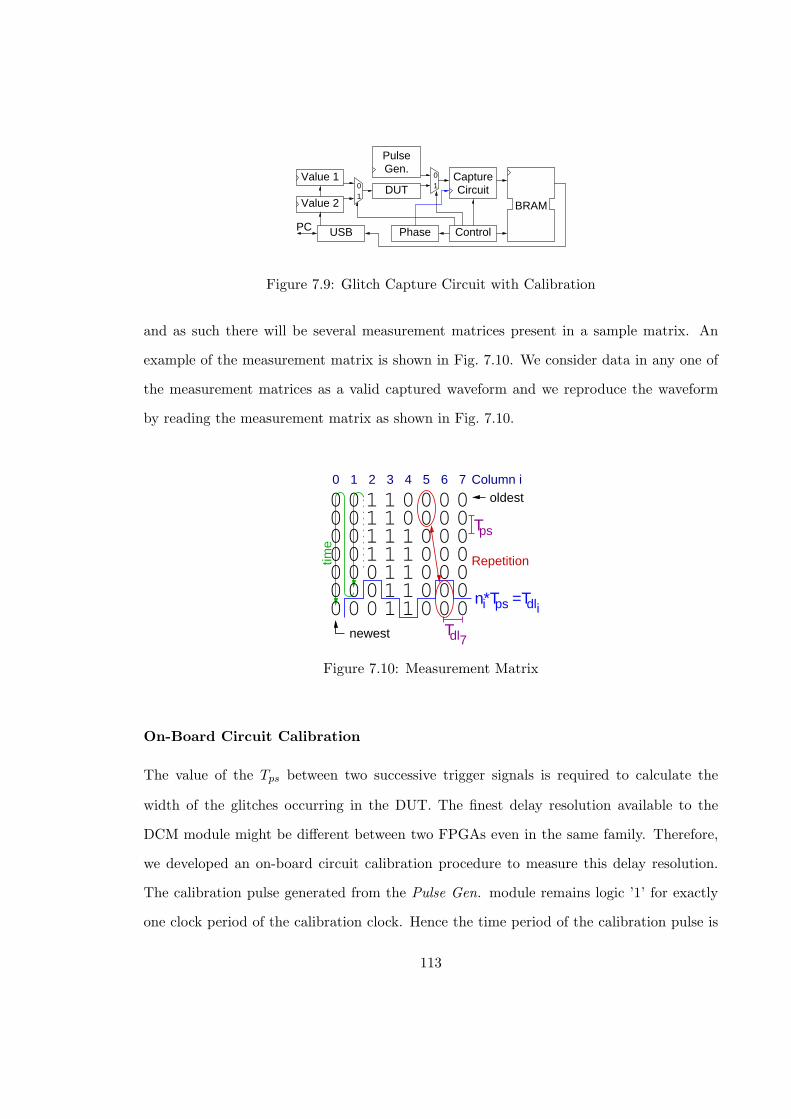
CircuitCapture0
1
Control
DUT
Gen.Pulse
Phase
Value 1
Value 2
USB
BRAM
01
PC
Figure 7.9: Glitch Capture Circuit with Calibration
and as such there will be several measurement matrices present in a sample matrix. An
example of the measurement matrix is shown in Fig. 7.10. We consider data in any one of
the measurement matrices as a valid captured waveform and we reproduce the waveform
by reading the measurement matrix as shown in Fig. 7.10.
Tps
=Tdli
dlT7
0 1 1 0 0 0 00 0 1 1 0 0 0 00 0 1 1 1 0 0 00 0 1 1 1 0 0 00 1 1 0 0 0000 0 1 1 0 0 00 0 0 1 1 0 00
oldest
newest
psn*Ti
0 1 2 53 4 76 Column i
Repetitiontime
0
0
Figure 7.10: Measurement Matrix
On-Board Circuit Calibration
The value of the Tps between two successive trigger signals is required to calculate the
width of the glitches occurring in the DUT. The finest delay resolution available to the
DCM module might be different between two FPGAs even in the same family. Therefore,
we developed an on-board circuit calibration procedure to measure this delay resolution.
The calibration pulse generated from the Pulse Gen. module remains logic ’1’ for exactly
one clock period of the calibration clock. Hence the time period of the calibration pulse is
113

the time period of the clock. The calibration pulse is captured using the capture circuit.
We count the number of 1’s present in the first columns of the sample matrix containing
the calibration pulse and denote this number as cp. We calculate the Tps using (7.2).
Tps =Time Period of Pulse
cp(7.2)
We calculate Tdl using (7.3)
Tdl =(MMR1 +MMR2 + · · ·+MMRn) · Tps
MMt(7.3)
where MMRi is the total number of rows in the Measurement Matrixi and MMt is the total
number of the measurement matrices present in one sample matrix. The position of the
glitch detected in a given signal can be obtained by correlating the signal under observation
with the system clock.
7.4 Results & Analysis
7.4.1 Test Circuit and Experimental Setup
The Advanced Encryption Standard (AES) [42] is one of the most widely used block ciphers.
SBOX or Substitution BOX, one of the basic functional primitive of AES, introduces nonlin-
earity to an encryption process. SBOXes also increase the resistance of AES towards linear
and differential cryptanalysis. We tested our proposed glitch capture methodology on an
AES SBOX implemented using three stage Positive Polar Reed-Muller form (combinational
logic based on AND-XOR) [94]. We implemented our designs on Nexys2 Board contain-
ing a XC3S500EFG320-4 FPGA. Post place and route simulation is performed using ISIM
simulator provided by Xilinx ISE. In order to detect and measure the output signals with
external test equipment, we use an Aglient DSO6054A oscilloscope which has a bandwidth
114

of 500MHz and a sampling rate of 4 GSa/sec.
7.4.2 Analysis of the Test Circuit
We calibrated our Glitch Capture Circuit on Spartan 3E FPGA using a calibration clock
of period 4 ns and tabulated our readings in Table 7.3.
Table 7.3: Calibrated Delay Values
Calibrated Data Sheet +Description Value Reports
Phase Shift Delay Tps 21.74 ps 20(min) to 40(max) ps
413 ps 760 ps (Max) +Delay Tdl (incl. wiring) 7.5 ps wiring (approx)
Total Capture Window 13.216 ns 24.560 ns (Max)
Post Place-and-Route (PAR) simulation was performed on the AES SBOX test circuit
implementation to detect the presence of glitches. A snapshot of post PAR simulation
waveform is shown in Fig. 7.11. We applied an input change of 0xCA → 0x74 → 0xCA
to the test circuit and observed that glitches were present in the internal signal of the test
circuit. They were in the order of few ten’s of pico seconds in width. We also noticed
that there were no glitches shown by the simulator on the output bit 3 of the test circuit,
indicated by highlighted signal in the Fig. 7.11. The output bit 3 remains at logic ’0’ for
the given cycle of input changes. We captured the signal propagation of the output bit 3
using oscilloscope and observed that there are two glitches (shown in Fig. 7.12) occurring,
one when the input changes from 0xCA → 0x74 and another one in the next clock cycle
when the input changes from 0x74 → 0xCA. We captured the first of these two glitches
using our proposed circuit and discovered that this glitch actually consists of two separate
glitches (see Fig. 7.13). By using the calibrated delay values we calculated width of the two
glitches as 434.80 ps and 217.4 ps respectively. The RC low pass filtering of the I/O logic
distorted these two glitches to a single one which we captured with the oscilloscope. Our
proposed glitch detection circuit can be used to precisely scan the signals in the direct and
115
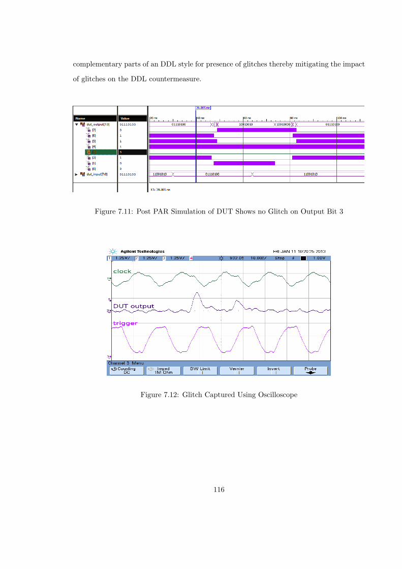
complementary parts of an DDL style for presence of glitches thereby mitigating the impact
of glitches on the DDL countermeasure.
Figure 7.11: Post PAR Simulation of DUT Shows no Glitch on Output Bit 3
Figure 7.12: Glitch Captured Using Oscilloscope
116

Figure 7.13: Glitch Captured Using Glitch Capture Circuit
7.5 Conclusion
Glitches are unproductive signal transitions which not only increase the overall power con-
sumption of the devices but also increase security risks, if the device is used in critical appli-
cations. Post place and route simulations performed to detect glitches cannot take the effect
of process variations into consideration. In this paper we introduce an innovative method
to detect glitches in hardware implementation on FPGAs. Our circuit not only detects
the presence of glitches but also captures the glitch waveform. We propose a methodology
to increase the resolution of the captured waveform and also show the calibration process
needed to obtain accurate values for width of glitches occurring in the hardware implemen-
tations on a given FPGA. Our results indicate that we can reliably reproduce the glitch
waveform and also provide an approximation regarding width of the observed glitches. This
information can be used to design circuits that produce fewer glitches even in the presence
of process variations.
117
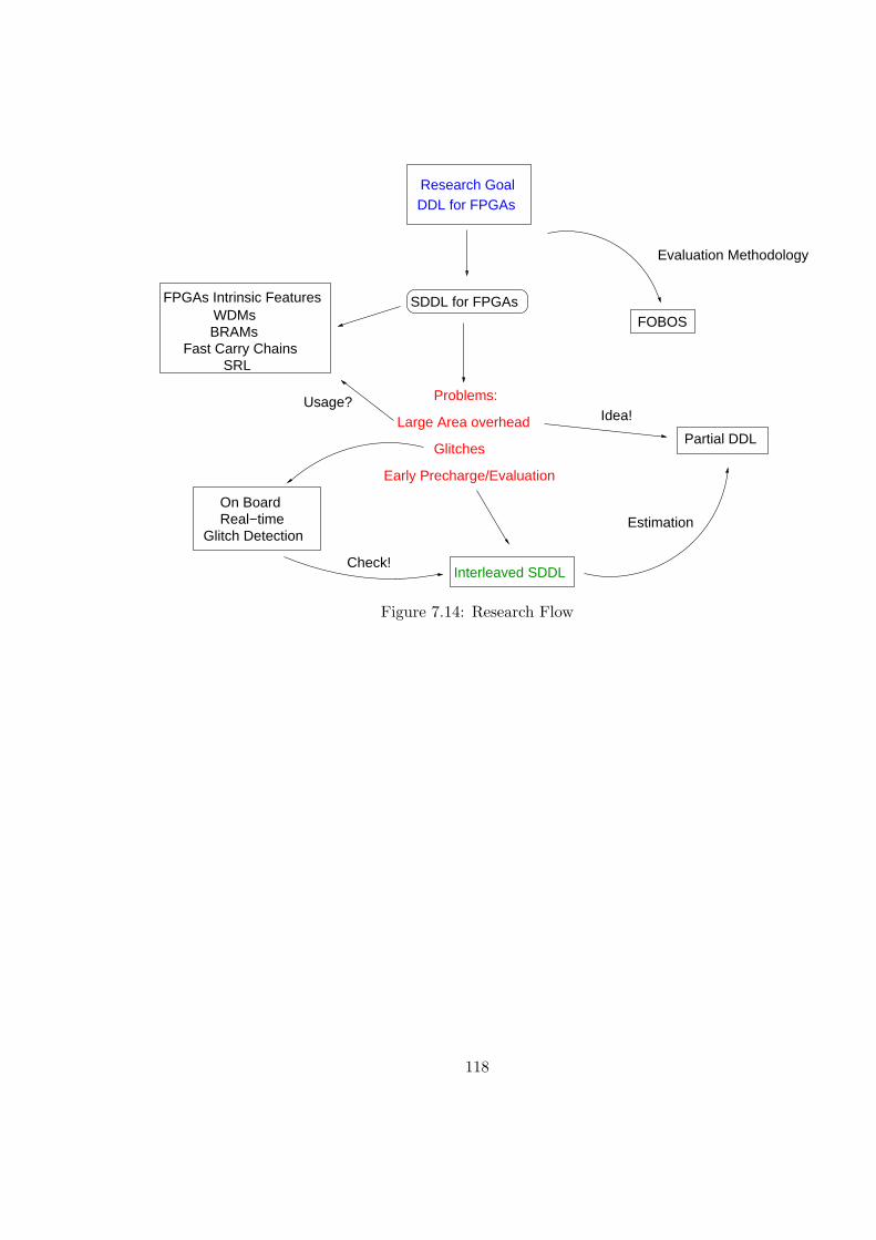
FOBOSSDDL for FPGAsFPGAs Intrinsic Features
WDMsBRAMs
Fast Carry ChainsSRL
Partial DDL
On BoardReal−time
Glitch Detection
Research GoalDDL for FPGAs
Evaluation Methodology
Problems:
Large Area overhead
Glitches
Early Precharge/Evaluation
Usage?Idea!
Interleaved SDDLCheck!
Estimation
Figure 7.14: Research Flow
118
Chapter 8: Interleaved SDDL
8.1 Introduction
In this chapter we introduce a new design methodology for implementing SDDL for FPGAs
with interleaved placement which considers the factor of process variations called Interleaved
SDDL or ISDDL. In order to achieve this goal we explore different placement configura-
tion for the Direct and Complementary parts of the design. We also evaluate our design
methodology against DPA by implementing interleaved SDDL for FPGAs on the Advanced
Encryption Standard (AES) block cipher.
8.2 Placement Configuration
The effect of place and route on security of WDDL designs on FPGAs was studied in [50].
The authors note that constrained placement does not have any effect on the unbalance
between the Direct and Complementary parts of the design however, routing does effect
it. This is due to fact that WDDL which is placed in interleaved patterns requires cross
connections between Direct and Complementary parts to implement negative logic. Hence
symmetrical routing is not possible in WDDL style on FPGAs [43]. Different interleaved
placement strategies for WDDL designs were explored in [95]. Unlike WDDL, SDDL for
FPGAs allows negative logic, hence there is no requirement of any cross connections between
Direct and Complementary parts. Thus it is possible to have symmetrical routing between
Direct and Complementary parts of SDDL designs on FPGAs.
It is common design practice to separate the two parts of an SDDL design and place
them side-by-side as in [43, 56]. Such placement strategy ensures that the two parts would
have sufficient resources to obtain symmetrical delays. The relative location of similar
119
components and nets in such placement configurations is rather far and thus have different
delays due to process variations. This increases the susceptibility of SDDL designs against
DPA. Additionally such placement configurations lead to the possibility of isolating and
attacking the Direct part of the design using Electromagnetic Analysis (EMA) [96].
8.2.1 Placement Options
The Spartan-3E FPGA fabric consists of Block RAMs, Multipliers and Configurable Logic
Blocks (CLBs). The CLBs are arranged in a regular 2D array of rows and columns through-
out the FPGA. All CLBs are connected with each other via switch matrices and special
interconnects. The availability of these connections has a significant effect on delay, area
and routability of a design implemented on an FPGA. Fig. 8.1 shows the interconnections
between a specific CLB and its neighboring counterparts. Each square in Fig. 8.1 is equiv-
alent to one CLB. The number of connections from the specific CLB (indicated by filled
square) to any particular CLB is given by the number present inside the square. Absence
of a number indicates that there are no direct connections between the specific CLB to this
square.
In order to interleave the Direct and Complementary parts, we explored four different
placement configurations shown in Fig. 8.2. Each square in Fig. 8.2 is equivalent to one
CLB. Table 8.1 shows the minimum number of connections between CLBs and their clos-
est neighbor in the same part (i.e. either Direct or Complementary) of the SDDL design.
Connections can be either in north-south (N-S), east-west (E-W) or diagonal (X) directions.
[1 x 1] Configuration is a patterned like a Chess board in which each square is
equivalent to one CLB. For each CLB in the Direct part (A) its complementary CLB (A)
is located in an adjacent CLB shown in Fig. 8.2a. The number of connections between two
adjacent CLBs in each direction is least compared to the other configurations. The distance
between the Direct and Complementary CLBs is 1 CLB.
[2 x 2] Configuration is also patterned like a Chess board. However, in this config-
uration each square is equivalent to four CLBs. For each CLB in the Direct part (A) its
120
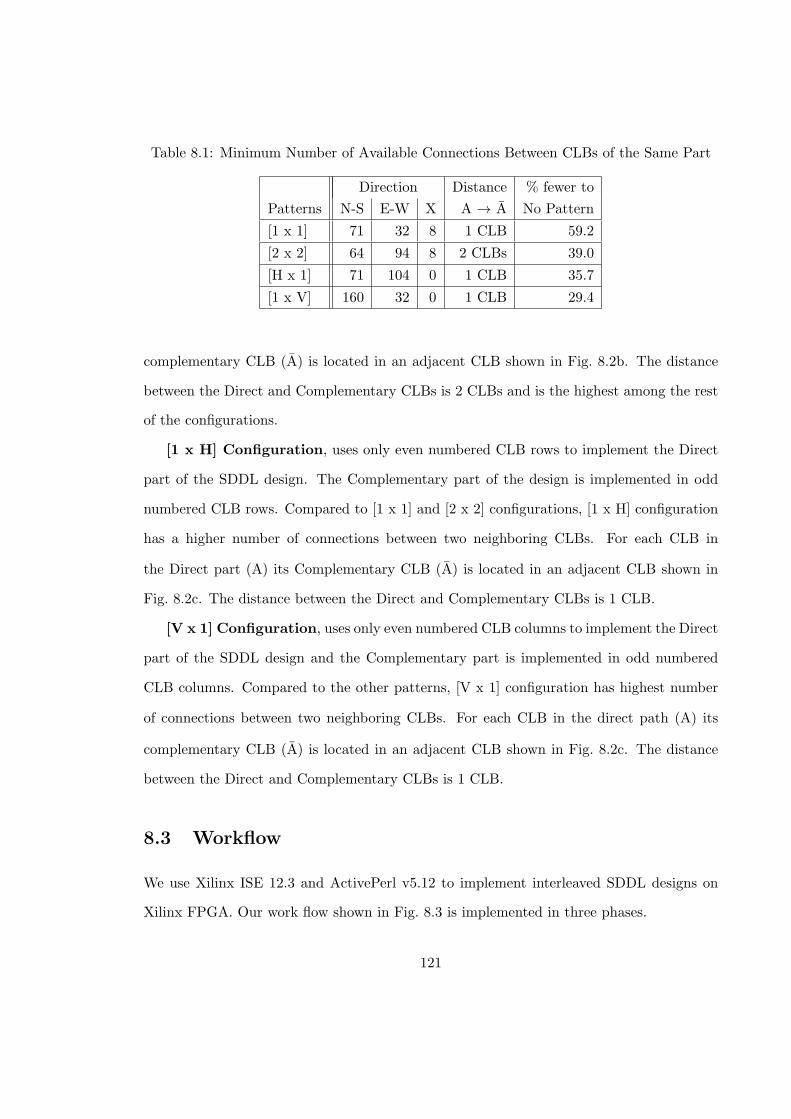
Table 8.1: Minimum Number of Available Connections Between CLBs of the Same Part
Direction Distance % fewer to
Patterns N-S E-W X A → A No Pattern
[1 x 1] 71 32 8 1 CLB 59.2
[2 x 2] 64 94 8 2 CLBs 39.0
[H x 1] 71 104 0 1 CLB 35.7
[1 x V] 160 32 0 1 CLB 29.4
complementary CLB (A) is located in an adjacent CLB shown in Fig. 8.2b. The distance
between the Direct and Complementary CLBs is 2 CLBs and is the highest among the rest
of the configurations.
[1 x H] Configuration, uses only even numbered CLB rows to implement the Direct
part of the SDDL design. The Complementary part of the design is implemented in odd
numbered CLB rows. Compared to [1 x 1] and [2 x 2] configurations, [1 x H] configuration
has a higher number of connections between two neighboring CLBs. For each CLB in
the Direct part (A) its Complementary CLB (A) is located in an adjacent CLB shown in
Fig. 8.2c. The distance between the Direct and Complementary CLBs is 1 CLB.
[V x 1] Configuration, uses only even numbered CLB columns to implement the Direct
part of the SDDL design and the Complementary part is implemented in odd numbered
CLB columns. Compared to the other patterns, [V x 1] configuration has highest number
of connections between two neighboring CLBs. For each CLB in the direct path (A) its
complementary CLB (A) is located in an adjacent CLB shown in Fig. 8.2c. The distance
between the Direct and Complementary CLBs is 1 CLB.
8.3 Workflow
We use Xilinx ISE 12.3 and ActivePerl v5.12 to implement interleaved SDDL designs on
Xilinx FPGA. Our work flow shown in Fig. 8.3 is implemented in three phases.
121
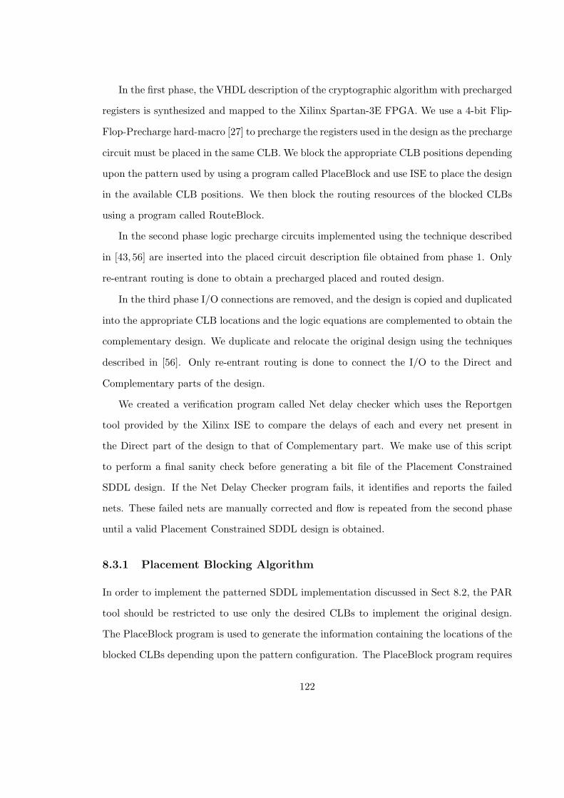
In the first phase, the VHDL description of the cryptographic algorithm with precharged
registers is synthesized and mapped to the Xilinx Spartan-3E FPGA. We use a 4-bit Flip-
Flop-Precharge hard-macro [27] to precharge the registers used in the design as the precharge
circuit must be placed in the same CLB. We block the appropriate CLB positions depending
upon the pattern used by using a program called PlaceBlock and use ISE to place the design
in the available CLB positions. We then block the routing resources of the blocked CLBs
using a program called RouteBlock.
In the second phase logic precharge circuits implemented using the technique described
in [43, 56] are inserted into the placed circuit description file obtained from phase 1. Only
re-entrant routing is done to obtain a precharged placed and routed design.
In the third phase I/O connections are removed, and the design is copied and duplicated
into the appropriate CLB locations and the logic equations are complemented to obtain the
complementary design. We duplicate and relocate the original design using the techniques
described in [56]. Only re-entrant routing is done to connect the I/O to the Direct and
Complementary parts of the design.
We created a verification program called Net delay checker which uses the Reportgen
tool provided by the Xilinx ISE to compare the delays of each and every net present in
the Direct part of the design to that of Complementary part. We make use of this script
to perform a final sanity check before generating a bit file of the Placement Constrained
SDDL design. If the Net Delay Checker program fails, it identifies and reports the failed
nets. These failed nets are manually corrected and flow is repeated from the second phase
until a valid Placement Constrained SDDL design is obtained.
8.3.1 Placement Blocking Algorithm
In order to implement the patterned SDDL implementation discussed in Sect 8.2, the PAR
tool should be restricted to use only the desired CLBs to implement the original design.
The PlaceBlock program is used to generate the information containing the locations of the
blocked CLBs depending upon the pattern configuration. The PlaceBlock program requires
122

the pattern configuration and the target area in which we want to implement patterned
placement as inputs. It generates an UCF file which contains the CLB prohibit locations
depending upon the pattern. The PlaceBlock program uses the algorithm described in
Fig. 8.4.
8.3.2 Routing Blocker
It is particularly hard to constrain the PAR tool from using routing resources of a blocked
CLB. We require these resources when we have to place the complementary part of the
design in these CLBs. Hence, we place a self contained dummy hard-macro in all the
blocked CLB positions to prevent the PAR tool from utilizing any of the blocked CLB
resources. The dummy hard-macro is built using Relationally Placed Macros (RPMs) and
Directed Routing (DIRT) Constraints. RPMs lock the driver and load pins of the CLB,
whereas DIRT constraints utilize the routing resources of the blocked CLB. The RouteBlock
script uses the UCF file generated by the PlaceBlock program to locate the positions of the
blocked CLBs and generates an XDL file which contains the description of the dummy
hard-macros.
8.4 Test Designs
We implemented all our test designs on the Xc3s500efg320-4 FPGA available on Digilent
Spartan-3E starter kit. The instantaneous power consumption of the FPGA during encryp-
tion was measured using a Tektronics CT-2 current probe and an Agilient 6054A, 500MHz
oscilloscope with a sampling frequency of 4G Samples/second. An external power supply
was used to power the FPGA core, and the FPGA was clocked at frequency of 200KHz–
400KHz. It is an important point to note that one encryption is counted as one measurement
irrespective of the number of samples the oscilloscope measures. We use the term Single-
Ended (SE) design to denote an unprotected design throughout this paper. Measurement
to Disclosure (MTD) is a security metric used to determine the resistance of the designs
against power analysis attacks. MTDs are the number of encryptions required to correctly
123

predict the secret key. These MTDs are dependent on factors like the secret key used, target
platforms and the order in which the input plaintext is fed to a cryptographic algorithm.
Hence we use a more robust metric called security gain (SG) [95] or gain over SE to assess
the effect of different interleaved placement configurations against DPA attacks. SG is the
ratio of MTDs of protected to MTDs of unprotected designs.
8.4.1 Small Test Circuit
The Test Circuit (TC) shown in Fig. 8.5 consists of an AES S-Box implemented using
combinational logic whose input is connected to an 8-bit LFSR and output is XORed with
an 8-bit Key. The result is stored in register FF1. The dashed box indicates the part
of the test circuit on which SDDL is implemented. The register FF2 is implemented in
Input/Output Blocks (IOB) simply to drive the output ports.
8.4.2 Attack on Small Test Circuit and Results
We attack the design at the output of the LFSR indicated by the arrow Ap. We use Pearson’s
correlation to compute the statistical dependence of the instantaneous power consumption
with the hypothetical power model i.e the hamming distances [41]. In order to attack the
SDDL implementations of the test design we attack the precharged outputs of the LFSR
i.e. the precharged inputs to the AES S-Box (Logic). The Hamming Distance (HD) equation
for the attack on SE implementations is shown in (8.1) and for SDDL implementations
in (8.2).
Pest. = HD(lfsr(i−1), SBOX−1(kguess ⊕Qi)) (8.1)
Pest. = HD(0x00, SBOX−1(kguess ⊕Qi)) (8.2)
The post place-and-route implementation results of the SE and SDDL implementations
are shown Table 8.2. The test circuit design consumes 49 slices because the AES S-Box
is implemented using combinational logic, however this leads to slow designs. The SDDL
designs consume 2.3 times more area compared to SE designs because of the extra slices
124

required to precharge the register outputs.
Table 8.2: Implementation Results of Basic Test Design
FFs/ 4 input Minimum Minimum Gain
Design Slices Latches LUTs Delay MTD over SE
1. TC w/ Pattern [1 X 1] 49 71 27 14.534 ns 1500 1
2. TC w/ Pattern [2 X 2] 49 71 27 14.412 ns 1500 1
3. TC w/ Pattern [1 X V] 49 71 27 14.317 ns 1500 1
4. TC w/ Pattern [H X 1] 49 71 27 14.666 ns 1500 1
5. SDDL of (1.) 114 142 86 28.486 ns 23,000 15
6. ISDDL of (1.) 114 142 86 29.068 ns 50,000 33
7. ISDDL of (2.) 114 142 86 28.824 ns 50,000 33
8. ISDDL of (3.) 114 142 86 28.634 ns 50,000 33
9. ISDDL of (4.) 114 142 86 29.332 ns 50,000 33
The MTDs of SE and SDDL designs given in Table 8.2 indicate the minimum number
i.e. the lower bound of MTDs required to obtain the correct key. The Design (5.) is a non
interleaved SDDL implementation of our test circuit using pattern [1 x 1]. The distance
between the Direct and Complementary parts of the design was 16 CLBs. Designs (6. to
9.) require more MTDs compared to Design (5.). This conforms our hypothesis that even
when the logic and routing of the Direct and Complementary parts are similar, there is a
difference in delays due to process variation. It is to be noted that all interleaved designs
require a similar number of MTDs irrespective of the pattern configuration. Thus, a user
can choose any of the placement patterns show in this paper depending on the design’s
requirement i.e. availability of routing resources, critical path etc.
8.4.3 AES
The Advanced Encryption Standard (AES) [42] is one of the most widely used block ciphers.
In this paper we use the AES implementation from [61] which uses a key length of 128 bits.
AES applies the same round function ten times to its state during encryption. The round
125

function consists of four different transformations SubBytes, ShiftRows, MixColumns and
AddRoundKey each changing the state by applying linear, non linear and key dependent
transformations.
The data path of the AES implementation is shown in Fig. 8.6. It is characterized by
a pipelined architecture which enables the re-use of registers and minimize the number of
internal memory accesses which in turn reduces the number of clock cycles. Five registers
R0, R1, R2, R3, R4 are used of which R0 is used exclusively for RotWord operation. R1
is used for key computation and state computation in MixColumns operation, R2, R3, R4
are used for state computation. The boxes labeled as Key store and Data store are 128 bit
registers used for Round keys and State Memory respectively.
8.4.4 Attack on AES and Results
The point of attack Ap for the AES designs is indicated in Fig.8.6. Consider the data flow
from registers R2 to R3. On reset the data in these registers is 0x00. In the first clock
cycle, the output of R3 changes from 0x00 to 0x63 i.e. SBOX(R2) and the data in R2
changes to Input data XORed with the key from R1. In the subsequent clock cycle the
data in R3 changes from 0x63 to SBOX(R2). This sequence of change in the data of R3 i.e.
0x00 → 0x63 → SBOX (Key ⊕ Input data) occurs every time the AES module is reset.
Hence, we can apply the HD model to estimate the power consumption of the register R3.
The power model for the SE cases is given by (8.3) and for SDDL designs, given by (8.4).
Pest. = HD(0x63, (SBOX((Keyguess ⊕ Input))i) (8.3)
Pest. = HD(0x00, (SBOX((Keyguess ⊕ Input))i) (8.4)
Table 8.3 shows the post place-and-route results of the SE and SDDL implementations.
Both AES SDDL designs consume an area 2.92 times larger than the AES SE design. The
MTDs from Table 8.3 confirm our results from the test circuit namely, that interleaved
SDDL is more secure than SDDL without any placement constraints. Also Design (12.)
126
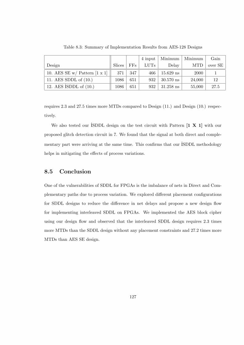
Table 8.3: Summary of Implementation Results from AES-128 Designs
4 input Minimum Minimum Gain
Design Slices FFs LUTs Delay MTD over SE
10. AES SE w/ Pattern [1 x 1] 371 347 466 15.629 ns 2000 1
11. AES SDDL of (10.) 1086 651 932 30.570 ns 24,000 12
12. AES ISDDL of (10.) 1086 651 932 31.258 ns 55,000 27.5
requires 2.3 and 27.5 times more MTDs compared to Design (11.) and Design (10.) respec-
tively.
We also tested our ISDDL design on the test circuit with Pattern [1 X 1] with our
proposed glitch detection circuit in 7. We found that the signal at both direct and comple-
mentary part were arriving at the same time. This confirms that our ISDDL methodology
helps in mitigating the effects of process variations.
8.5 Conclusion
One of the vulnerabilities of SDDL for FPGAs is the imbalance of nets in Direct and Com-
plementary paths due to process variation. We explored different placement configurations
for SDDL designs to reduce the difference in net delays and propose a new design flow
for implementing interleaved SDDL on FPGAs. We implemented the AES block cipher
using our design flow and observed that the interleaved SDDL design requires 2.3 times
more MTDs than the SDDL design without any placement constraints and 27.2 times more
MTDs than AES SE design.
127

80
32 16 52 52 16 32
47
37
80
16 16
18
14
3 123 1 2
332112
1
1
1
1
37
47
14
7
7
18
Figure 8.1: Number of Connections between a CLB and Its Surrounding Counterparts
AA A A AA
A
A
a) Pattern [1 x 1] b) Pattern [2 x 2] c) Pattern [H x 1] d) Pattern [1 x V]
Figure 8.2: Patterns for Placing original (A) and Complementary (A) paths
128
Remove BlockedRouting
Remove I/OConnections
Duplicate &Complement
Place
Re−entrantRouting
Re−entrantRouting
Insert Precharge
Bit FileGeneration
ManualCorrections
SynthesisTranslate
Map
MacroHard
FF−PreVHDL
fail
pass
PlaceBlock
RouteBlock
Net DelayChecker
Figure 8.3: Work Flow
129

Require: Initial CLB-(X,Y) PositionsRequire: Final CLB-(X,Y) PositionsRequire: [CLB X Config x CLB Y Config] for e.g.[1 x 1]1: j = 0;2: while CLB Y Initial ≤ CLB Y Final do3: i = 0;4: if j%2 = 0 then5: CLB X Var = CLB X Initial;6: else7: CLB X Var = CLB X Initial + (2∗ CLB X Config);8: end if9: CLB Y Var = CLB Y Initial;
10: while CLB X Initial ≤ CLB X Final do11: X1p = CLB X Var + (2∗ CLB X Config);12: X2p = CLB X Var + (4∗ CLB X Config)-1;13: Y1p = CLB Y Var;14: Y2p = CLB Y Var + (2∗ CLB Y Config)-1;15: if i%2 = 0 then16: BLOCK CLB from (X1p, Y1p) to (X2p, Y2p)17: end if18: i++;19: CLB X Var ← X1p, CLB Y Var ← Y1p;20: end while21: CLB Y Initial = CLB Y Initial + CLB Y Config;22: j++;23: end while
Figure 8.4: Placement Blocking Algorithm
8FF2
8FL
SR
Ap
8
(Logic)S−BoxAES
FF1 Q
Protected Section
Key8
Figure 8.5: Block Diagram of Test Circuit
130
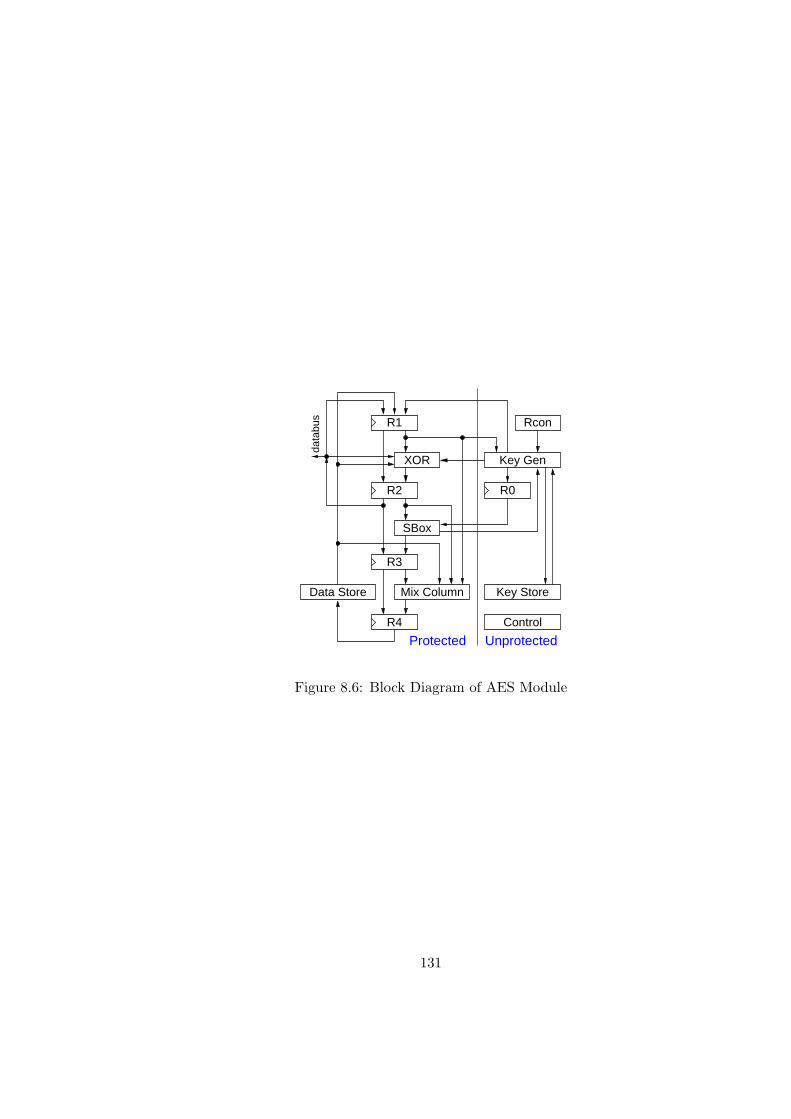
R3
R2
R4
R1
data
bus
Data Store
XOR
SBox
Mix Column
Key Gen
Key Store
Control
Rcon
Protected Unprotected
R0
Figure 8.6: Block Diagram of AES Module
131

Chapter 9: Electro Magnetic Fault Injection
9.1 Introduction
Historically, cryptographic modules were embedded in Hardware Security Modules (HSMs)
and secured by placing them in a physically secure environment. Nowadays, tokens are
becoming more ubiquitous outside of secure environments: smart cards, and various USB
and standalone tokens offer cryptographic services. Even though these devices protect con-
fidential information using cryptographic algorithms that withstand rigorous cryptanalytic
attacks, an adversary that has physical access to a device can obtain secret information
by modifying the behavior of the chip through hardware attacks such as Fault Injection.
These faults can be induced by over-clocking, introducing transients in power and clock
lines (power and clock glitches) or through optical radiations. The setup required to induce
these faults is invasive in nature. The power and clock lines to the target are to be isolated
to induce faults, which may not be possible in real-world cases. Although fault injection
through optical radiation can be very precise in time and space, the die of the chip needs
to exposed through decapping.
A new class of fault attacks was introduced, which uses an electro magnetic field to
induce faults in the target device. The Electro Magnetic field Fault Injection (EMFI)
perturbation is effective and non-invasive in nature. In this chapter, we describe the back-
ground, methodology and experimental setup required to conduct EMFI. The impact of
different types of probes used in EMFI attacks is explored and a calibration process used
for lab experiments is presented. We discuss our preliminary results and conclude EMFI is
a viable strategy for an attacker attempting to break a cryptographic implementation.
132

9.2 EMFI in Literature
The idea of EM Fault Injection was first introduced by J.J. Quisquater and D. Samyde [97]
in 2002. They showed that it is possible to influence the computations performed by the
crypto device by using a home-grown EM probe. A camera flash was used to induce high
voltage into the coil of the probe. This high voltage causes a magnetic field which in
turn induced eddy currents on the surface of the crypto chip. These eddy currents lead to
injection of faults into transistor and memory cells of a smart-card processor. Later in 2007,
authors of [98] proposed the usage of high frequency spark gaps instead of magnetic fields
to cause perturbation on the crypto device. These spark gaps induce very fast changing
current which causes strong bursts of EM radiation. The authors noted that the wider
the gap of the spark the stronger the EM radiation, which has the potential to destroy
the crypto chip. The authors were able to induce a single fault on a CRT-based RSA and
recover the private key successfully.
Alaeldine et al. in 2009 [99] studied the immunity of electromagnetic emissions on the
IC logic core to a near-field injection. They investigated the effect of electric and magnetic
fields in x, y and z directions to field injections ranging from 10MHz to 1GHz. Their results
indicated that not only bond-wires and package but the die itself was also sensitive to
magnetic and to an certain extent, electric fields. Poucheret et al. in [100] studied the effect
of direct power injection on the CMOS logic. The EM probe used for their experiments was
a thin tungsten rod instead of a typical coil. A 1GHz sinusoidal electric field was applied
to the CMOS IC and the output frequency of the Ring Oscillators (RO) present in the
IC was observed. Due to the EM perturbation, the authors found that the RO frequency
was increased by 46.6%. The authors also noted that the RO frequency changes with the
change in position of the EM probe and also that irrespective of the probe position there
is a minimal increase in frequency. This indicates that the EM injection has both localized
and global impacts on the target.
Dehbaoui et al. in [101] conducted an EM fault injection on the software and hardware
implementation of AES on a micro-controller and an FPGA respectively. The authors
133
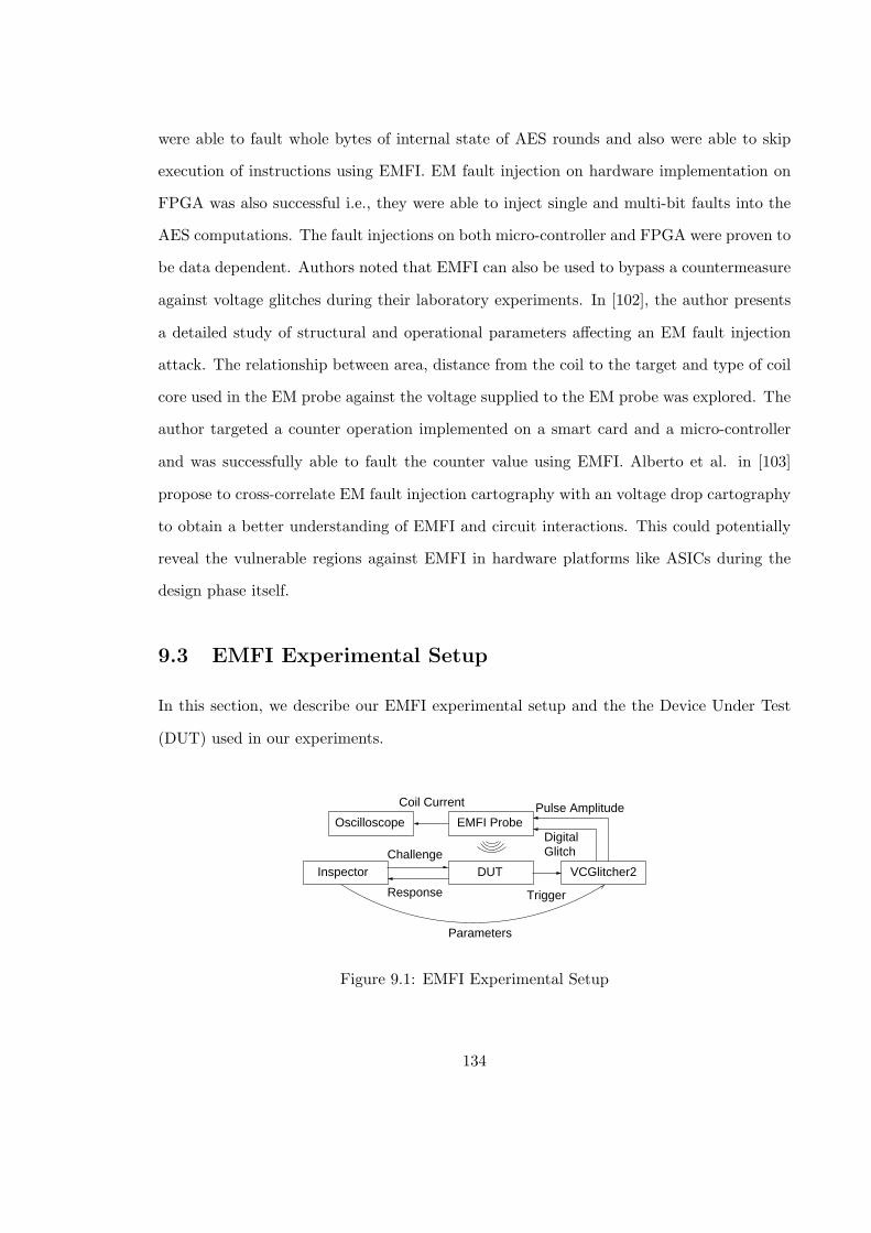
were able to fault whole bytes of internal state of AES rounds and also were able to skip
execution of instructions using EMFI. EM fault injection on hardware implementation on
FPGA was also successful i.e., they were able to inject single and multi-bit faults into the
AES computations. The fault injections on both micro-controller and FPGA were proven to
be data dependent. Authors noted that EMFI can also be used to bypass a countermeasure
against voltage glitches during their laboratory experiments. In [102], the author presents
a detailed study of structural and operational parameters affecting an EM fault injection
attack. The relationship between area, distance from the coil to the target and type of coil
core used in the EM probe against the voltage supplied to the EM probe was explored. The
author targeted a counter operation implemented on a smart card and a micro-controller
and was successfully able to fault the counter value using EMFI. Alberto et al. in [103]
propose to cross-correlate EM fault injection cartography with an voltage drop cartography
to obtain a better understanding of EMFI and circuit interactions. This could potentially
reveal the vulnerable regions against EMFI in hardware platforms like ASICs during the
design phase itself.
9.3 EMFI Experimental Setup
In this section, we describe our EMFI experimental setup and the the Device Under Test
(DUT) used in our experiments.
Inspector
Response Trigger
VCGlitcher2
EMFI ProbePulse Amplitude
DigitalGlitchChallenge
DUT
Parameters
Oscilloscope
Coil Current
Figure 9.1: EMFI Experimental Setup
134
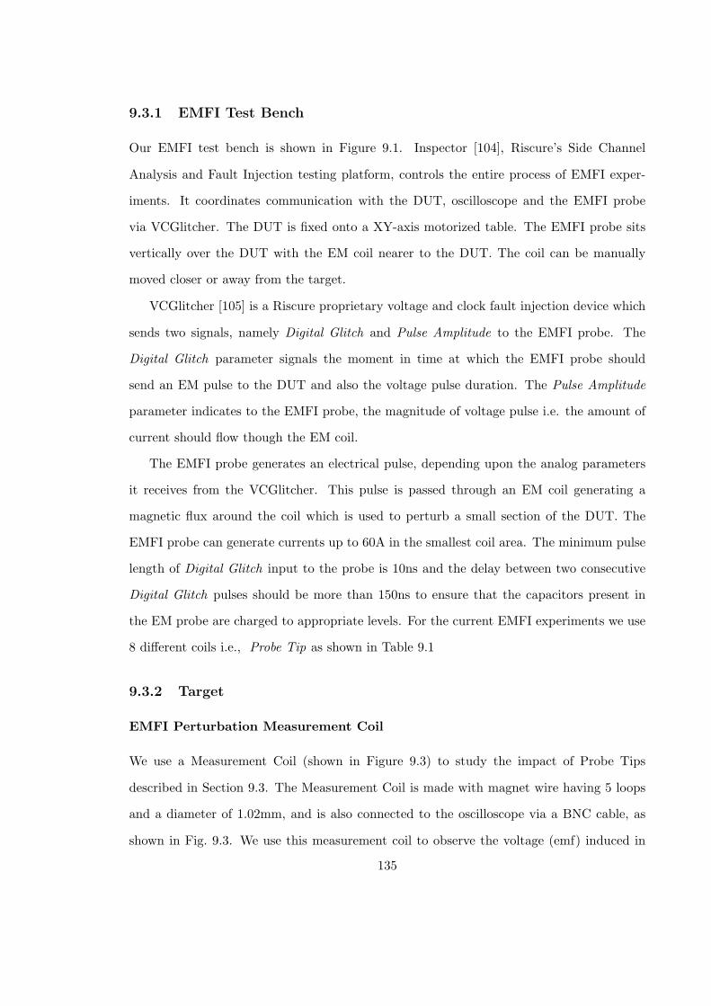
9.3.1 EMFI Test Bench
Our EMFI test bench is shown in Figure 9.1. Inspector [104], Riscure’s Side Channel
Analysis and Fault Injection testing platform, controls the entire process of EMFI exper-
iments. It coordinates communication with the DUT, oscilloscope and the EMFI probe
via VCGlitcher. The DUT is fixed onto a XY-axis motorized table. The EMFI probe sits
vertically over the DUT with the EM coil nearer to the DUT. The coil can be manually
moved closer or away from the target.
VCGlitcher [105] is a Riscure proprietary voltage and clock fault injection device which
sends two signals, namely Digital Glitch and Pulse Amplitude to the EMFI probe. The
Digital Glitch parameter signals the moment in time at which the EMFI probe should
send an EM pulse to the DUT and also the voltage pulse duration. The Pulse Amplitude
parameter indicates to the EMFI probe, the magnitude of voltage pulse i.e. the amount of
current should flow though the EM coil.
The EMFI probe generates an electrical pulse, depending upon the analog parameters
it receives from the VCGlitcher. This pulse is passed through an EM coil generating a
magnetic flux around the coil which is used to perturb a small section of the DUT. The
EMFI probe can generate currents up to 60A in the smallest coil area. The minimum pulse
length of Digital Glitch input to the probe is 10ns and the delay between two consecutive
Digital Glitch pulses should be more than 150ns to ensure that the capacitors present in
the EM probe are charged to appropriate levels. For the current EMFI experiments we use
8 different coils i.e., Probe Tip as shown in Table 9.1
9.3.2 Target
EMFI Perturbation Measurement Coil
We use a Measurement Coil (shown in Figure 9.3) to study the impact of Probe Tips
described in Section 9.3. The Measurement Coil is made with magnet wire having 5 loops
and a diameter of 1.02mm, and is also connected to the oscilloscope via a BNC cable, as
shown in Fig. 9.3. We use this measurement coil to observe the voltage (emf) induced in
135
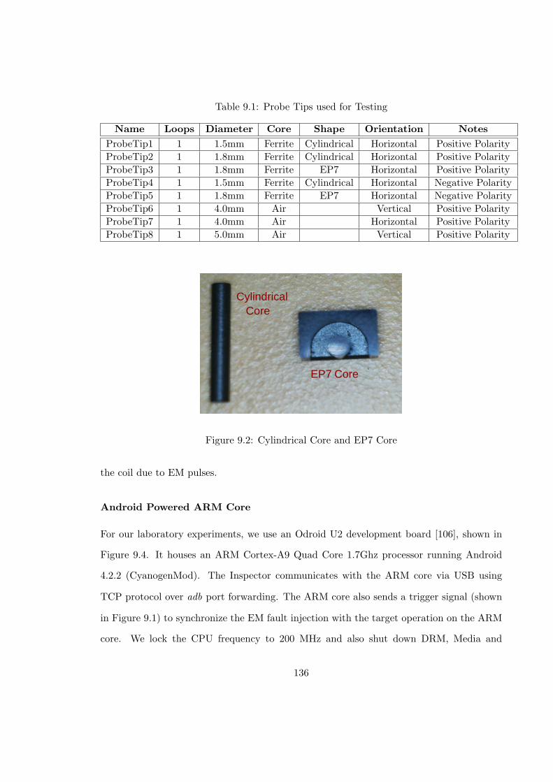
Table 9.1: Probe Tips used for Testing
Name Loops Diameter Core Shape Orientation Notes
ProbeTip1 1 1.5mm Ferrite Cylindrical Horizontal Positive Polarity
ProbeTip2 1 1.8mm Ferrite Cylindrical Horizontal Positive Polarity
ProbeTip3 1 1.8mm Ferrite EP7 Horizontal Positive Polarity
ProbeTip4 1 1.5mm Ferrite Cylindrical Horizontal Negative Polarity
ProbeTip5 1 1.8mm Ferrite EP7 Horizontal Negative Polarity
ProbeTip6 1 4.0mm Air Vertical Positive Polarity
ProbeTip7 1 4.0mm Air Horizontal Positive Polarity
ProbeTip8 1 5.0mm Air Vertical Positive Polarity
CylindricalCore
EP7 Core
Figure 9.2: Cylindrical Core and EP7 Core
the coil due to EM pulses.
Android Powered ARM Core
For our laboratory experiments, we use an Odroid U2 development board [106], shown in
Figure 9.4. It houses an ARM Cortex-A9 Quad Core 1.7Ghz processor running Android
4.2.2 (CyanogenMod). The Inspector communicates with the ARM core via USB using
TCP protocol over adb port forwarding. The ARM core also sends a trigger signal (shown
in Figure 9.1) to synchronize the EM fault injection with the target operation on the ARM
core. We lock the CPU frequency to 200 MHz and also shut down DRM, Media and
136
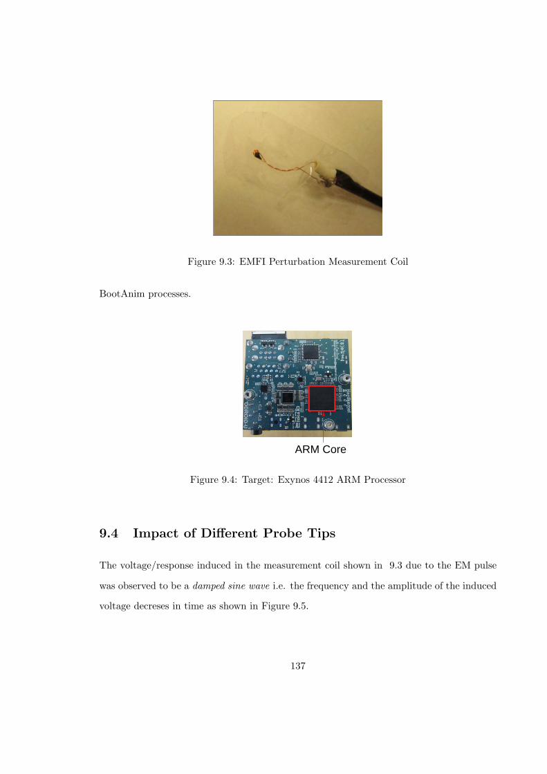
Figure 9.3: EMFI Perturbation Measurement Coil
BootAnim processes.
ARM Core
Figure 9.4: Target: Exynos 4412 ARM Processor
9.4 Impact of Different Probe Tips
The voltage/response induced in the measurement coil shown in 9.3 due to the EM pulse
was observed to be a damped sine wave i.e. the frequency and the amplitude of the induced
voltage decreses in time as shown in Figure 9.5.
137
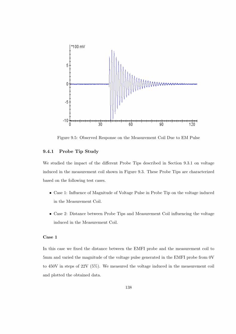
Figure 9.5: Observed Response on the Measurement Coil Due to EM Pulse
9.4.1 Probe Tip Study
We studied the impact of the different Probe Tips described in Section 9.3.1 on voltage
induced in the measurement coil shown in Figure 9.3. These Probe Tips are characterized
based on the following test cases.
• Case 1: Influence of Magnitude of Voltage Pulse in Probe Tip on the voltage induced
in the Measurement Coil.
• Case 2: Distance between Probe Tips and Measurement Coil influencing the voltage
induced in the Measurement Coil.
Case 1
In this case we fixed the distance between the EMFI probe and the measurement coil to
5mm and varied the magnitude of the voltage pulse generated in the EMFI probe from 0V
to 450V in steps of 22V (5%). We measured the voltage induced in the measurement coil
and plotted the obtained data.
138

Comparison between ProbeTip Core Shapes: We wanted to observe the impact
of ProbeTip core shape on the voltage induced in the measurement coil. For this purpose
we compared ProbeTip2 and ProbeTip3. As shown in Tab 9.1 the only difference between
two coils is that ProbeTip2 core shape is cylindrical whereas ProbeTip3 is EP7 [107]. We
observe that there is a linear increase of the voltage induced in the measurement coil as the
voltage pulse in the EM probe is gradually increased, as shown in Figure 9.6. An interesting
observation is that ProbeTip2 induces more voltage than ProbeTip3 i.e. cylindrically shaped
core induces more voltage than EP7 core.
a)Distance between EM Probe andMeasurement Coil is Fixed to 5mm
b)Voltage pulse generated in theEM Probe is fixed to 225V
Figure 9.6: Cylindrical Core vs EP7 Core
Comparison between ProbeTip Coil Orientations: We wanted to observe the im-
pact of ProbeTip core orientations on the voltage induced in the measurement coil. For this
purpose we compared ProbeTip6 and ProbeTip7. As shown in Tab 9.1 the only difference
between two coils is that ProbeTip6 coil orientation is horizontal whereas ProbeTip7 is ver-
tical. We observe that there is a linear increase of the voltage induced in the measurement
coil as the voltage pulse in the EM probe is gradually increased, as shown in Figure 9.7.
An interesting observation is that ProbeTip6 induces more voltage than ProbeTip7 i.e.
horizontal orientation of coil induces more voltage than vertical orientation.
Comparison between ProbeTip polarity: We wanted to observe the impact of
139

a)Distance between EM Probe andMeasurement Coil is Fixed to 5mm
b)Voltage pulse generated in theEM Probe is fixed to 225V
Figure 9.7: 4mm Area Coil Vertical vs Horizontal Orientation
ProbeTip coil polarity on the voltage induced in the measurement coil. For this purpose we
compared ProbeTip1,3,4 and 5. As shown in Tab 9.1 the difference between ProbeTip1 -
ProbeTip4 and ProbeTip3 - ProbeTip5 is that the polarity i.e. the current flowing through
these two sets of coil is in opposite direction to that of each other. We observe that there
is a linear increase of the voltage induced in the measurement coil as the voltage pulse in
the EM probe is gradually increased, as shown in Figure 9.8. An interesting observation is
that voltage induced in the measurement coil is more in ProbeTips with positive polarity
than with negative polity types.
Comparison between ProbeTip Areas: We also infer from Figure 9.9 that the
larger the area of the Probe Tip i.e. the diameter of the Probe Tip coil, the higher the
voltage induced in the measurement coil, which can be explained using Eq. 2.6.
Comparison between ProbeTip Core Type: We also infer from Figure 9.10 that
the larger the permeability of the Probe Tip i.e. the ferrite core of the Probe Tip coil, the
higher the voltage induced in the measurement coil as compared to air core type.
140
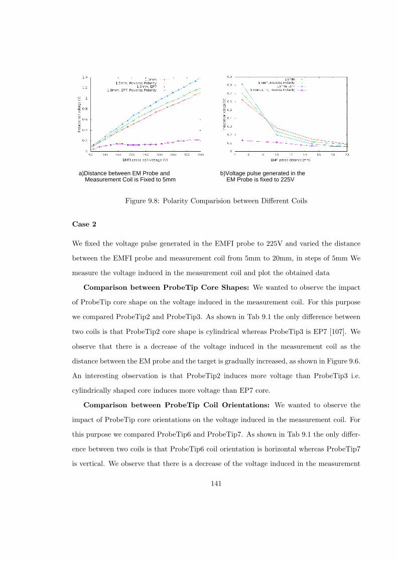
a)Distance between EM Probe andMeasurement Coil is Fixed to 5mm
b)Voltage pulse generated in theEM Probe is fixed to 225V
Figure 9.8: Polarity Comparision between Different Coils
Case 2
We fixed the voltage pulse generated in the EMFI probe to 225V and varied the distance
between the EMFI probe and measurement coil from 5mm to 20mm, in steps of 5mm We
measure the voltage induced in the measurement coil and plot the obtained data
Comparison between ProbeTip Core Shapes: We wanted to observe the impact
of ProbeTip core shape on the voltage induced in the measurement coil. For this purpose
we compared ProbeTip2 and ProbeTip3. As shown in Tab 9.1 the only difference between
two coils is that ProbeTip2 core shape is cylindrical whereas ProbeTip3 is EP7 [107]. We
observe that there is a decrease of the voltage induced in the measurement coil as the
distance between the EM probe and the target is gradually increased, as shown in Figure 9.6.
An interesting observation is that ProbeTip2 induces more voltage than ProbeTip3 i.e.
cylindrically shaped core induces more voltage than EP7 core.
Comparison between ProbeTip Coil Orientations: We wanted to observe the
impact of ProbeTip core orientations on the voltage induced in the measurement coil. For
this purpose we compared ProbeTip6 and ProbeTip7. As shown in Tab 9.1 the only differ-
ence between two coils is that ProbeTip6 coil orientation is horizontal whereas ProbeTip7
is vertical. We observe that there is a decrease of the voltage induced in the measurement
141
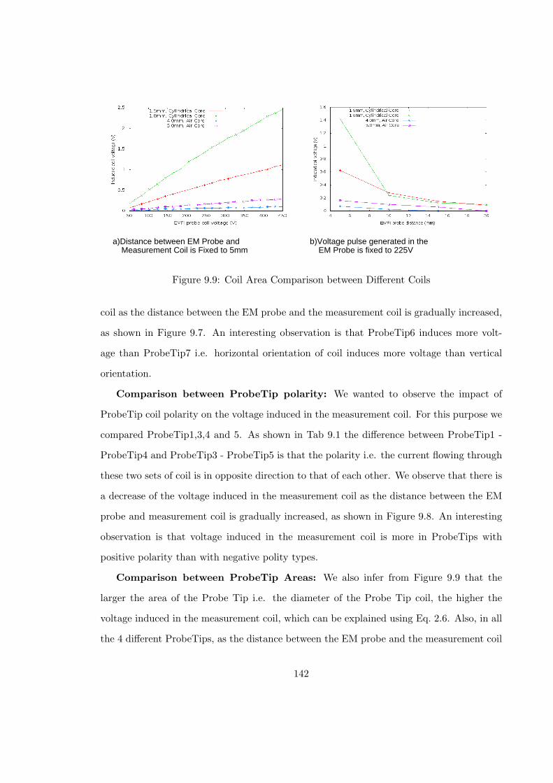
a)Distance between EM Probe andMeasurement Coil is Fixed to 5mm
b)Voltage pulse generated in theEM Probe is fixed to 225V
Figure 9.9: Coil Area Comparison between Different Coils
coil as the distance between the EM probe and the measurement coil is gradually increased,
as shown in Figure 9.7. An interesting observation is that ProbeTip6 induces more volt-
age than ProbeTip7 i.e. horizontal orientation of coil induces more voltage than vertical
orientation.
Comparison between ProbeTip polarity: We wanted to observe the impact of
ProbeTip coil polarity on the voltage induced in the measurement coil. For this purpose we
compared ProbeTip1,3,4 and 5. As shown in Tab 9.1 the difference between ProbeTip1 -
ProbeTip4 and ProbeTip3 - ProbeTip5 is that the polarity i.e. the current flowing through
these two sets of coil is in opposite direction to that of each other. We observe that there is
a decrease of the voltage induced in the measurement coil as the distance between the EM
probe and measurement coil is gradually increased, as shown in Figure 9.8. An interesting
observation is that voltage induced in the measurement coil is more in ProbeTips with
positive polarity than with negative polity types.
Comparison between ProbeTip Areas: We also infer from Figure 9.9 that the
larger the area of the Probe Tip i.e. the diameter of the Probe Tip coil, the higher the
voltage induced in the measurement coil, which can be explained using Eq. 2.6. Also, in all
the 4 different ProbeTips, as the distance between the EM probe and the measurement coil
142

a)Distance between EM Probe andMeasurement Coil is Fixed to 5mm
b)Voltage pulse generated in theEM Probe is fixed to 225V
Figure 9.10: Coil Core Comparison between Different Coils
increases, the induced voltage in the measurement coil decreases.
Comparison between ProbeTip Core Type: We also infer from Figure 9.10 that
the larger the permeability of the Probe Tip i.e. the ferrite core of the Probe Tip coil, the
higher the voltage induced in the measurement coil as compared to air core type. Also in
both cases as the distance between the EM probe and the measurement coil increases, the
induced voltage in the measurement coil decreases.
9.4.2 EMFI on Android 4.4 Running on ARM Core
We conducted preliminary tests to observe the impact of these Probe Tips on an ARM core
running Android operating system. We calibrate the impact of the three different Probe
Tips on the ARM core by determining the values for parameters discussed above. Our
target operation for fault injection on the ARM core is a simple counter program running
natively (native-c) on Android.
We were not able to corrupt the counter operation using EM fault injection using any
of the three different Probe Tips. The only faults we observed using Probe Tip2 and Probe
Tip3 is total system crash, screen turn-off and shutdown of the ARM core independent of
the position of the EMFI probe over the target location. The values for the parameter
143
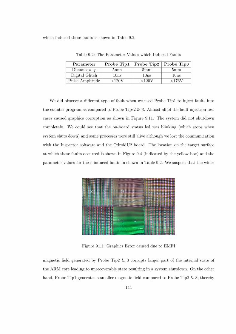
which induced these faults is shown in Table 9.2.
Table 9.2: The Parameter Values which Induced Faults
Parameter Probe Tip1 Probe Tip2 Probe Tip3
DistanceP−T 5mm 5mm 5mm
Digital Glitch 10ns 10ns 10ns
Pulse Amplitude >120V >120V >176V
We did observe a different type of fault when we used Probe Tip1 to inject faults into
the counter program as compared to Probe Tips2 & 3. Almost all of the fault injection test
cases caused graphics corruption as shown in Figure 9.11. The system did not shutdown
completely. We could see that the on-board status led was blinking (which stops when
system shuts down) and some processes were still alive although we lost the communication
with the Inspector software and the OdroidU2 board. The location on the target surface
at which these faults occurred is shown in Figure 9.4 (indicated by the yellow-box) and the
parameter values for these induced faults in shown in Table 9.2. We suspect that the wider
Figure 9.11: Graphics Error caused due to EMFI
magnetic field generated by Probe Tip2 & 3 corrupts larger part of the internal state of
the ARM core leading to unrecoverable state resulting in a system shutdown. On the other
hand, Probe Tip1 generates a smaller magnetic field compared to Probe Tip2 & 3, thereby
144
leading to relatively smaller internal state corruption resulting in graphics freeze but not
a total system shutdown. Although EMFI does affect the ARM core, we observe that we
were not able to corrupt the counter operation.
9.5 Conclusion
The goal of this chapter is to introduce readers to a new class of fault injection, called
Electro Magnetic Fault Injection, which use transients in EM field to inject faults on a
target device. The literature survey shows us that hardware platforms like micro-controller,
smart cards, FPGA and also ASICs are susceptible to fault injections via EMFI. Also,
the countermeasures employed against other avenues of fault injections, for e.g. Voltage
Glitching may be circumvented using EMFI.
We present our experimental setup and study the impact of various types of Probe Tips
(or coils) on the voltage induced in the target. We note that not only the coil area and
coil’s core but also the shape of the coil’s core affects the voltage induced in the target
(measurement coil). We also present the steps used for the calibration of our experimental
setup’s operational parameters and conduct an EM fault injection attack on a simple counter
program running in Android operating system on the Exynos4412 ARM core. Although we
were not able to successfully fault the counter operation using EMFI, we were able to cause
several other faults indicating that EMFI does affect the ARM core. As future work, we
plan on fine-tuning our experimental setup parameters to induce faults in counter operation
and eventually cryptographic algorithms.
145
Chapter 10: Conclusions and Future Work
In this chapter, we provide a summary for the research presented in this dissertation and
also recommend several future avenues of research.
10.1 Conclusions
In this research, we made an effort in developing an integrated environment for detecting
and mitigating side-channel and fault attacks on the hardware platform. We introduced
new measuring and evaluation techniques, proposed a new countermeasure against DPA
tailored for FPGAs and also explored a new class of fault injection attacks called Electro
Magnetic Fault Injection.
In this dissertation, we developed a framework for efficient side-channel evaluation of
hardware platforms, called Flexible Open-sources workBench fOr Side-channel analysis -
FOBOS. FOBOS is designed to be an inexpensive side channel analysis setup that includes
a complete software package with programs for victim control, data acquisition and data
analysis. In order to evaluate side-channel leakage of hardware platforms, FOBOS uses off-
the shelf FPGA boards as control and victim which are less expensive than the traditional
setup. Thus, it enables universities to add active side channel analysis laboratory exercises
to their cryptography classes. Furthermore, FOBOS is designed in a modular fashion to
allow for a multitude of victim devices while maintaining the remainder of the setup, hence
making FOBOS flexible. As the hardware and software are open source, the results are
reproducible by researchers from different groups. We used FOBOS to conduct SCA on our
laboratory test circuits and the new countermeasure against SCA.
We also introduced an innovative method to detect glitches in hardware implementa-
tion on FPGAs. Our circuit not only detects the presence of glitches but also captures
146

the glitch waveform. We propose a methodology to increase the resolution of the captured
waveform developed from delay-based sampling techniques. We also show the calibration
process needed to obtain accurate values for width of glitches occurring in the hardware
implementations on a given FPGA. Our results indicate that we can reliably reproduce
the glitch waveform and also provide an approximation regarding width of the observed
glitches. We used this methodology extensively to determine the effectiveness of our pro-
posed countermeasure against SCA.
In order to achieve our research goal of developing a new countermeasure against DPA
tailored for FPGAs we followed a two phase approach. We implemented unprotected (no
countermeasures used) functional primitives of cryptographic algorithm using the most
secured options. These implementation options were limited to FPGA intrinsic features
like Wide Dedicated Multiplexers (WDMs), Block RAMS (BRAMs) etc., due to the reason
that usage of FPGA intrinsic feature in conjunction with our proposed counter measure will
decrease the area overhead as compared to countermeasure implemented using standard
LUTs and Flip-Flops only implementation. Then we applied our proposed countermeasure
on such inherently secure implementations to increase the effectiveness of our proposed
countermeasure.
Wide Dedicated Multiplexers (WDMs) are used to effectively combine complex logic
operations. These WDMs are implemented using the dedicated two input multiplexers in
the slice and the fast interconnects, that exist between slices and between CLBs. We have
implemented three different levels of WDMs and evaluated their inherent resistance against
DPA. The results indicate that WDMs do not provide any resistance against DPA. Only
4:1 WDMs do not degrade the resistance of DDL implementations against DPA.
We implemented the AES SBOX in Block RAMs (BRAMs) of Xilinx FPGAs and inves-
tigated their resistance against DPA attacks. Our results indicate that the AES SBOX in
BRAMs are more resistant to DPA attacks than the AES SBOX implemented in Composite
field. In order implement DDL countermeasure in conjunction with BRAMs we developed
the precharge circuit for BRAMs. Our results indicate that DDL implementations with
147
BRAMs increase the MTDs by a factor 4 over unprotected designs which use BRAMs and
a factor 2.5 over DDL implementations which do not use BRAMs.
We developed a new countermeasure against DPA specially tailored for FPGAs in a
step wise and iterative manner. We proposed a negative DDL style for lightweight imple-
mentations on FPGAs called SDDL for FPGAs. In such a DDL style, FPGA CAD tools
are given the maximum flexibility to optimize a given design for the target FPGA. Unlike
WDDL, SDDL for FPGAs allows optimal usage of the intrinsic features inside the FPGAs.
The other advantages of SDDL for FPGAs over WDDL is that there is no cross connection
between direct and complementary parts, hence symmetrical routing is possible. SDDL for
FPGAs uses FPGA CAD tools only to implement DDL designs. But SDDL for FPGAs
is still vulnerable to DPA attacks due to glitches and the effect of early precharge and
evaluation caused due to process variations.
We also introduce Partial DDL, propose principle design rules of Partial DDL, and show
its effectiveness in terms of area saving and DPA resistance through a proof-of-concept
implementation of a lightweight AES design using SDDL for FPGAs and comparing it with
one using Partial SDDL for FPGAs. Partial DDL describes the notion that DDL is applied
to only a part of the cryptographic implementation. The advantage of Partial DDL is that
the area overhead is reduced (2 x protected data path) compared to the area overhead
incurred due to applying DDL over the entire design. The drawback of Partial DDL is that
the power consumption will not be as constant as when DDL is applied to the entire data
path. We have shown through our example implementation of AES using SDDL for FPGAs,
that partial DDL can significantly reduce the area consumption of a DDL implementation
by 24%, yet maintain the same level of resistance against DPA.
It is common design practice to separate the two parts so called Direct and Comple-
mentary parts of an SDDL design and place them side-by-side. Such placement strategy
ensures that the two parts would have sufficient resources to obtain symmetrical delays. The
relative location of similar components and nets in such placement configurations is rather
148
far and thus have different delays due to process variations. This increases the susceptibil-
ity of SDDL designs against DPA. Additionally such placement configurations lead to the
possibility of isolating and attacking the Direct part of the design using Electromagnetic
Analysis. We explored different placement configurations for SDDL designs to reduce the
difference in net delays and propose a new design flow for implementing interleaved SDDL
on FPGAs. We implemented the AES block cipher using our design flow and observed
that the interleaved SDDL design requires 2.3 times more MTDs than the SDDL design
without any placement constraints and 27.2 times more MTDs than AES SE design. All
positive DDL logic styles like WDDL, IWDDL and BCDL suffer from a vulnerability called
”Early Evaluation” due to fact that there exists no symmetrical routing between direct
and complementary path. We used our proposed glitch detection circuit and observed that
neither the logic in direct or the complementary path is getting ”evaluated” early. We be-
lieve that because of the symmetrical routing and the interleaved placement of direct and
complementary path, ISDDL does not have ”Early Evaluation”
We also explore a new class of fault injection, called Electro Magnetic Fault Injection
(EMFI) [97], to inject faults on a target device. In this dissertation we concentrate only
on transient type of EMFI. The literature survey shows us that hardware platforms like
micro-controller, smart cards, FPGA and also ASICs are susceptible to fault injections via
EMFI. Also, the countermeasures employed against other avenues of fault injections, for
e.g. Voltage Glitching may be circumvented using EMFI.
We present our experimental setup and study the impact of various types of Probe Tips
(or coils) on the voltage induced in the target. We note that not only the coil area and coil’s
core but also the shape, polarity and orientation of the coil’s core affects the voltage induced
in the target (measurement coil). We also present the steps used for the calibration of our
experimental setup’s operational parameters and conduct an EM fault injection attack on
a simple counter program running in Android operating system on the Exynos4412 ARM
core. Although we were not able to successfully fault the counter operation using EMFI,
we were able to cause several other faults indicating that EMFI does affect the ARM core.
149

10.2 Future Research
In this section we discuss possible extensions for the work presented in this dissertation.
10.2.1 Measurement and Evaluation Methodologies
One perspective of future work in glitch detection is to increase the measurement accuracy
of glitch detection circuit and estimate the effect of adding the capture circuit on the signals
being observed. Also observing the behaviour of the glitch detection circuit across various
FPGA vendors will lead to a more robust glitch detection circuit.
FOBOS currently supports SPA and DPA on cryptographic algorithms implemented on
FPGA platforms only. This work can be extended to include not only FPGAs but also micro
controllers, smart cards and ARM development boards. Another direction would be to add
support for Electro Magnetic Analysis attacks and Fault Injection attacks including EMFI.
The data analysis module can also be improved by adding state-of-the-art side channel
distinguishers and signal processing algorithms.
10.2.2 DPA on Cryptographic Functional Primitives
In this area of research, future direction of research would involve evaluating the DPA
resistance of implementation options for adders like hybrid adders etc. The DPA attack
on shift registers could be further enhanced my mutiplying the signal strength by placing
multiple data path instantiations which may (or may not) lead to successful DPA attack.
Current architecture advancements of the so called Hybrid Processors like Xilinx’s Zynq,
Altera’s SoC FPGAs and Intel’s Xeon E5-FPGA combine the performance and power saving
capabilities of an Application Specific Integrated Circuit (ASICs) and the flexibility of Field
Programmable Gate Arrays (FPGAs). Porting the countermeasure against DPA proposed
in this dissertation to FPGAs in such processors would also be an interesting line of future
research.
150

10.2.3 EMFI
This area of research offers many perspectives. Further research work in the area of devel-
oping Probe Tips or coils might help in targeting concentrated area of a target platform.
Another area of research would be to fine-tuning our experimental setup parameters to
induce faults in Android and UBoot and also on the memory of the ARM core. EMFI on
BRAMs present in FPGAs will also lend an interesting perspective to the effect of EMFI
on contents of embedded memories.
151

Bibliography
[1] “Kerckhoffs’s principle - wikipedia,” http://en.wikipedia.org/wiki/Kerckhoffs
[2] P. Kocher, J. Jaffe, and B. Jun, “Differential power analysis,” in Advances in Cryp-tology - CRYPTO’99, ser. Lecture Notes in Computer Science (LNCS), vol. 1666.Berlin: Springer Verlag, Aug 1999, pp. 388–397.
[3] J.-J. Quisquater and D. Samyde, “Electromagnetic analysis (EMA): Measures andcounter-measures for smart cards,” in Smart Card Programming and Security, Pro-ceedings of E-smart, ser. Lecture Notes in Computer Science (LNCS), vol. 2140.Berlin: Springer-Verlag, 200–210 2001.
[4] M. Agoyan, J.-M. Dutertre, D. Naccache, B. Robisson, and A. Tria, “When clocks fail:On critical paths and clock faults,” in Smart Card Research and Advanced Application,ser. Lecture Notes in Computer Science, D. Gollmann, J.-L. Lanet, and J. Iguchi-Cartigny, Eds. Springer Berlin Heidelberg, April 2010, pp. 182–193.
[5] A. Barenghi, G. Bertoni, E. Parrinello, and G. Pelosi, “Low voltage fault attacks onthe rsa cryptosystem,” inWorkshop on Fault Diagnosis and Tolerance in Cryptography(FDTC), Sept 2009, pp. 23–31.
[6] H. Bar-El, H. Choukri, D. Naccache, M. Tunstall, and C. Whelan, “The sorcerer’sapprentice guide to fault attacks,” Proceedings of the IEEE, vol. 94, no. 2, pp. 370–382,2006.
[7] S. Skorobogatov and R. Anderson, “Optical fault induction attacks,” in CryptographicHardware and Embedded Systems - CHES 2002, ser. Lecture Notes in Computer Sci-ence, B. Kaliski, Jr., C. K.. Koc, and C. Paar, Eds., vol. 2523. Berlin, Heidelberg,New York: Springer-Verlag, August 2002, pp. 2–12.
[8] D. Suzuki, M. Saeki, and T. Ichikawa, “DPA leakage models for CMOS logic circuits,”in Cryptographic Hardware and Embedded Systems – CHES 2005, ser. LNCS, J. R.Rao and B. Sunar, Eds., vol. 3659. Heidelberg: Springer, 2005, pp. 366–382.
[9] K. Tiri and I. Verbauwhede, “A logic level design methodology for a secure DPAresistant ASIC or FPGA implementation,” in Proc. Design, Automation and Test inEurope (DATE’04). IEEE Computer Society, Feb 2004, pp. 246–251.
[10] K. Tiri, D. Hwang, A. Hodjat, B. Lai, S. Yang, P. Schaumont, and I. Verbauwhede, “Aside-channel leakage free coprocessor IC in 0.18µm CMOS for embedded AES-basedcryptographic and biometric processing,” in 42nd Design Automation Conference,2005, pp. 222–227.
152

[11] P. Wright, Spycatcher: The Candid Autobiography of a Senior Intelligence Officer.Penguin Viking, July 1987.
[12] W. V. Eck and N. Laborato, “Electromagnetic radiation from video display units: Aneavesdropping risk?” Computers & Security, vol. 4, pp. 269–286, 1985.
[13] P. C. Kocher, “Timing attacks on implementations of Diffie-Hellman, RSA, DSS,and other systems,” in Advances in Cryptology - CRYPTO 96, ser. Lecture Notes inComputer Science (LNCS), vol. 1109. Berlin: Springer-Verlag, 1996, pp. 104–113.
[14] P. Kocher, J. Jaffe, and B. Jun, “Introduction to differential power analysis andrelated attacks,” Cryptography Research, pp. 1–5, 1998.
[15] K. Gandolfi, C. Mourtel, and F. Olivier, “Electromagnetic analysis: Concrete results,”in Cryptographic Hardware and Embedded Systems–CHES 2001, ser. Lecture Notes inComputer Science (LNCS), c. K. Koc, D. Naccache, and C. Paar, Eds., vol. 2162.Springer-Verlag, 2001, pp. 251–261.
[16] J. M. Rabaey, A. Chandrakasan, and B. Nokolic, Digital Integrated Circuits, A DesignPerspective, 2nd ed. Pearson Education, 2003.
[17] C. Giraud, “An RSA implementation resistant to fault attacks and to simple poweranalysis,” IEEE Transactions on Computers, vol. 55, no. 9, pp. 1116–1120, Sep 2006.
[18] X. Lu and H. Howard M, “A simple power analysis attack against the key scheduleof the camellia block cipher,” in Information Processing Letters-IPL 2005, 2005, pp.409–412.
[19] A. Manfred and O. Elisabeth, “Power analysis tutorial,” July 2007,www.iaik.tugraz.at/aboutus/people/oswald/papers/dpa tutorial.pdf.
[20] S. Mangard, E. Oswald, and T. Popp, Power Analysis Attacks, Revealing the Secretsof Smart Cards. Springer, 2007.
[21] T. S. Messerges, E. A. Dabbish, and R. H. Sloan, “Investigations of power analysisattacks on smartcards,” in USENIX Workshop on Smartcard Technology, 1999, pp.151–161.
[22] F.-X. Standaert, L. van Oldeneel tot Oldenzeel, D. Samyde, and J.-J. Quisquater,“Power analysis of FPGAs: How practical is the attack?” in Field ProgrammableLogic and Applications – FPL 2003, ser. Lecture Notes in Computer Science (LNCS),P. Y. K. Cheung, G. A. Constantinides, and J. T. de Sousa, Eds., vol. 2778. Berlin/ Heidelberg: Springer, 2003, pp. 701–711.
[23] S. B. Ors, E. Oswald, and B. Preneel, “Power-analysis attacks on an FPGA – firstexperimental results,” in Workshop on Cryptographic Hardware and Embedded Sys-tems, CHES 2003, ser. Lecture Notes in Computer Science (LNCS), C. D. Walter,Cetin K. Koc, and C. Paar, Eds., vol. 2779. Berlin: Springer-Verlag, Sep 2003, pp.35–50.
153

[24] R. P. McEvoy, M. Tunstall, C. C. Murphy, and W. P. Marnane, “Differential poweranalysis of HMAC based on SHA-2 on an FPGA, and countermeasures,” in Workshopon Information Security Applications – WISA 2007, ser. LNCS, S. Kim, M. Yung,and H.-W. Lee, Eds., vol. 4867. Springer-Verlag, 2007, pp. 317–332.
[25] B. Gierlichs, L. Batina, C. Clavier, T. Eisenbarth, A. Gouget, H. Handschuh,T. Kasper, K. Lemke-Rust, S. Mangard, A. Moradi, and E. Oswald, “Susceptibil-ity of estream candidates towards side channel analysis,” in ECRYPT Workshop,SASC - The State of the Art of Stream Ciphers, C. D. Cannire and O. Dunkelman,Eds., Lausanne,CH, 2008, p. 28.
[26] K. Lemke, K. Schramm, and C. Paar, “DPA on n-bit sized boolean and arithmeticoperations and its application to IDEA, RC6, and the HMAC-construction,” in Cryp-tographic Hardware and Embedded Systems - CHES 2004, ser. LNCS, vol. 3156. Berlin/ Heidelberg: Springer, 2004, pp. 205–219.
[27] J.-P. Kaps and R. Velegalati, “DPA resistant AES on FPGA using partial DDL,”in IEEE Symposium on Field-Programmable Custom Computing Machines – FCCM2010. IEEE, May 2010, pp. 273–280.
[28] J. Jaffe, “A first- order DPA attacks against AES in counter mode with unknowninitial counter,” CHES, pp. 1–14, 2007.
[29] M. Renauld, F.-X. Standaert, and N. Veyrat-Charvillon, “Algebraic side-channel at-tacks on the AES: Why time also matters in DPA,” in Cryptographic Hardware andEmbedded Systems - CHES 2009, ser. Lecture Notes in Computer Science, C. Clavierand K. Gaj, Eds., vol. 5747. Berlin / Heidelberg: Springer, Sept 2009, pp. 97–111.
[30] S. Shah, R. Velegalati, J.-P. Kaps, and D. Hwang, “Investigation of DPA resistance ofBlock RAMs in cryptographic implementations on FPGAs,” in International Confer-ence on ReConFigurable Computing and FPGAs – ReConFig’10. IEEE, Dec 2010,pp. 274–279.
[31] Using Block RAM in Spartan-3 Generation FPGAs, Xapp463 (v2.0) ed., Xilinx, Inc.,Mar 2005.
[32] J. Anderson and H. M. Heys, “Side channel analysis of cryptographic hardware us-ing SCAB,” in The Seventeenth Newfoundland Electrical and Computer EngineeringConference, NECEC-2007, Newfoundland, Canada, Nov 2007.
[33] Side-channel Attack Standard Evaluation Board SASEBO-GII Specification, Version1.01 ed., Research Centre for Information Security (RCIS), National Institute of Ad-vanced Industrial Science and Technology (AIST), Nov 2009.
[34] T. Katashita, A. Satoh, K. Kikuchi, H. Nakagawa, and M. Aoyagi, “Evaluation ofDPA charactersitics of SASEBO for board level simulations,” in First InternationalWorkshop on constructive side channel analysis an secure design. COSADE, 2010.
[35] M. Tech, “Sakura hardware project,” http://www.morita-tech.co.jp/SAKURA/en/index.html.
154
[36] “DPA contest,” http://www.dpacontest.org/home/.
[37] “OpenSCA,” http://www.cs.bris.ac.uk/home/eoswald/opensca.html.
[38] “DPA Workstation,” http://www.cryptography.com/technology/dpa-workstation.html.
[39] Hardware Interface of a Secure Hash Algorithm (SHA), v. 1.4 ed., CryptographicEngineering Research Group, George Mason University, Jan 2010.
[40] K. Gaj, E. Homsirikamol, and M. Rogawski, “Fair and comprehensive methodologyfor comparing hardware performance of fourteen round two SHA-3 candidates usingFPGA,” in Cryptographic Hardware and Embedded Systems, CHES 2010, ser. LNCS,S. Mangard and F.-X. Standaert, Eds., vol. 6225. Springer Berlin / Heidelberg, 2010,pp. 264–278.
[41] E. Brier, C. Clavier, and F. Olivier, “Correlation power analysis with a leakagemodel,” in Cryptographic Hardware and Embedded Systems – CHES 2004, ser. Lec-ture Notes in Computer Science, vol. 31. Berlin / Heidelberg: Springer, Aug 2004,pp. 135–152.
[42] Advanced Encryption Standard (AES), National Institute of Standards and Technol-ogy (NIST), FIPS Publication 197, Nov 2001, http://csrc.nist.gov/publications/fips/fips197/fips-197.pdf.
[43] P. Yu and P. Schaumont, “Secure FPGA circuits using controlled placement and rout-ing,” in CODES+ISSS ’07: Proceedings of the 5th IEEE/ACM international confer-ence on Hardware/software codesign and system synthesis. New York, NY, USA:ACM, 2007, pp. 45–50.
[44] S. Guilley, L. Sauvage, J. Danger, T. Graba, and Y. Mathieu, “Evaluation of power-constant dual-rail logic as a protection of cryptographic applications in FPGAs,” inSecure System Integration and Reliability Improvement (SSIRI ’08). IEEE, Jul 2008,pp. 16–23.
[45] S. Guilley, L. Sauvage, J.-L. Danger, and P. Hoogvorst, “Area optimization of cryp-tographic co-processors implemented in dual-rail with precharge positive logic,” inField Programmable Logic and Application – FPL 2008, U. Kebschull, M. Platzner,and J. Teich, Eds. IEEE, Sep 2008, pp. 161–166.
[46] L. Shang, A. S. Kaviani, and K. Bathala, “Dynamic power consumption in VirtexTM-II FPGA family,” in International symposium on Field-programmable gate arrays –FPGA ’02, ACM/SIGDA. New York, NY, USA: ACM, 2002, pp. 157–164.
[47] T. Popp and S. Mangard, “Masked dual-rail pre-charge logic: DPA-resistance with-out routing constraints,” in Cryptographic Hardware and Embedded Systems – CHES2005, ser. Lecture Notes in Computer Science (LNCS), J. R. Rao and B. Sunar, Eds.,vol. 3659. Heidelberg: Springer, 2005, pp. 172–186.
155
[48] D. Suzuki and M. Saeki, “Security evaluation of DPA countermeasures using dual-railpre-charge logic style,” in Cryptographic Hardware and Embedded Systems - CHES2006, ser. LNCS, L. Goubin and M. Matsui, Eds., vol. 4249. Heidelberg: Springer,2006, pp. 255–269.
[49] P. Schaumont and K. Tiri, “Masking and dual-rail logic don’t add up,” in Crypto-graphic Hardware and Embedded Systems - CHES 2007, ser. LNCS, P. Paillier andI. Verbauwhede, Eds., vol. 4727. Heidelberg: Springer, 2007, pp. 95–106.
[50] S. Guilley, S. Chaudhuri, L. Sauvage, T. Graba, J.-L. Danger, P. Hoogvorst, Vinh-Nga,and M. Nassar, “Place-and-route impact on the security of DPL designs in FPGAs,”in Hardware-Oriented Security and Trust, HOST 2008. IEEE, 2008, pp. 26–32.
[51] S. Chaudhuri, S. Guilley, P. Hoogvorst, J.-L. Danger, T. Beyrouthy, A. Razafindraibe,L. Fesquet, and M. Renaudin, “Physical design of FPGA interconnect to prevent infor-mation leakage,” in Reconfigurable Computing: Architectures, Tools and Applications– ARC 2008, ser. Lecture Notes in Computer Science (LNCS), R. Woods, K. Comp-ton, C. Bouganis, and P. C. Diniz, Eds., vol. 4943. Berlin / Heidelberg: Springer,2008, pp. 87–98.
[52] P. Yu, “Implementation of DPA-resistant circuit for FPGA,” Master’s thesis, Vir-ginia Polytechnic Institute and State University, Blacksburg, Virginia, 2007, mastersThesis.
[53] R. P. McEvoy, C. C. Murphy, W. P. Marnane, and M. Tunstall, “Isolated WDDL:A hiding countermeasure for differential power analysis on FPGAs,” ACM Trans.Reconfigurable Technol. Syst., vol. 2, no. 1, pp. 1–23, Mar 2009.
[54] M. Nassar, S. Bhasin, J.-L. Danger, G. Duc, and S. Guilley, “BCDL: A high speedbalanced DPL for FPGA with global precharge and no early evaluation,” in Design,Automation and Test in Europe, DATE 2010. IEEE, Mar 2010, pp. 849–854.
[55] E. Konur, Y. Ozelci, E. Arikan, and U. Eksi, “Power analysis resistant SRAM,” inWorld Automation Congress (WAC), July 2006.
[56] R. Velegalati and J.-P. Kaps, “DPA resistance for light-weight implementations ofcryptographic algorithms on FPGAs,” in Field Programmable Logic and Applications,FPL 2009, M. Danek, J. Kadlec, and B. Nelson, Eds. IEEE, Aug 2009, pp. 385–390.
[57] ——, “Techniques to enable the use of block RAMs on FPGAs with dynamic anddifferential logic,” in International Conference on Electronics, Circuits, and Systems,ICECS 2010. IEEE, Dec 2010, accepted, to be published.
[58] J. Daemen and V. Rijmen, “AES proposal: Rijndael,” in First Advanced EncryptionStandard AES Conference, Ventura, California, USA, 1999.
[59] V. Fischer and M. Drutarovsk, “Two methods of Rijndael implementation in reconfig-urable hardware,” in Cryptographic Hardware and Embedded Systems – CHES 2001,ser. LNCS, vol. 2162. Springer Berlin / Heidelberg, January 2001, pp. 77–92.
156
[60] K. Gaj and P. Chodowiec, Cryptographic Engineering. Springer, 2009, ch. FPGAand ASIC Implementations of AES, pp. 235–294.
[61] J.-P. Kaps and B. Sunar, “Energy comparison of AES and SHA-1 for ubiquitouscomputing,” in Embedded and Ubiquitous Computing (EUC-06) Workshop Proceed-ings, ser. Lecture Notes in Computer Science (LNCS), X. Z. et al., Ed., vol. 4097.Springer, Aug 2006, pp. 372–381.
[62] S. Mangard, “A Simple Power-Analysis (SPA) Attack on Implementations of the AESKey Expansion,” in Information Security and Cryptology ICISC 2002, ser. LectureNotes in Computer Science, P. Lee and C. Lim, Eds., vol. 2587. Berlin: Springer,Nov 2002, p. 343358.
[63] S. Aumonier, “Generalized correlation power analysis,” in Ecrypt Workshop Tools ForCryptanalysis 2007, 2007.
[64] I. Kuon and J. Rose, “Measuring the gap between fpgas and asics,” IEEE Transactionson Computer-Aided Design of Integrated Circuits and Systems, vol. 26, no. 2, pp. 203–215, Feb 2007.
[65] H. Eriksson and P. Larsson-Edefors, “Glitch-conscious low-power design of arithmeticcircuits,” in IEEE International Symposium on Circuits and Systems. IEEE, 2004,pp. 281–284.
[66] E. Kusse and J. Rabaey, “Low-energy embedded FPGA structures,” in Proceedings ofthe 1998 international symposium on Low power electronics and design, ser. ISLPED’98. New York, NY, USA: ACM, 1998, pp. 155–160.
[67] S. Mangard and K. Schramm, “Pinpointing the side channel leakage of masked AEShardware implementations,” ECRYPT, vol. IST 2002, no. 507932, pp. 1–15, 2002.
[68] S. Mangard, T. Popp, and B. M. Gammel, “Side-channel leakage of masked CMOSgates,” in RSA Conference 2005 Cryptographers’ Track, ser. LNCS, vol. 3376.Springer, Feb 2005, pp. 351–365.
[69] R. Velegalati and J.-P. Kaps, “Improving security of SDDL designs through inter-leaved placement on Xilinx FPGAs,” in Field Programmable Logic and Applications,FPL 2011, P. Athanas, D. Pnevmatikatos, and N. Sklavos, Eds. IEEE, Sep 2011,pp. 506–511.
[70] A. Maiti and P. Schaumont, “Improving the quality of a physical unclonable functionusing configurable ring oscillators,” in Field Programmable Logic and Applications –FPL 2009, 2009, pp. 703–707.
[71] X. Xin, J.-P. Kaps, and K. Gaj, “A configurable ring-oscillator-based PUF for XilinxFPGAs,” in 14th EUROMICRO Conference on Digital System Design – DSD’11.IEEE, Aug 2011, pp. 651–657.
[72] H. Shin, N. Zang, and J. Kim, “Stochastic glitch estimation and path balancing forstatistical optimization,” in SOC Conference, 2006 IEEE International, Sep 2006, pp.85–88.
157
[73] A. Sayed and H. Al-Asaad, “A new statistical approach for glitch estimation in com-binational circuits,” in Circuits and Systems, 2007. ISCAS 2007. IEEE InternationalSymposium on, May 2007, pp. 1641–1644.
[74] J. Monteiro, S. Devadas, A. Ghosh, K. Keutzer, and J. White, “Estimation of averageswitching activity in combinational logic circuits using symbolic simulation,” IEEETransactions on Computer-Aided Design of Integrated Circuits and Systems, vol. 16,no. 1, pp. 121–127, Jan 1997.
[75] F. Najm, “Transition density: a new measure of activity in digital circuits,” IEEETransactions on Computer-Aided Design of Integrated Circuits and Systems, vol. 12,no. 2, pp. 310–323, Feb 1993.
[76] ——, “Power estimation techniques for integrated circuits,” in Computer-Aided De-sign, 1995. ICCAD-95. Digest of Technical Papers., 1995 IEEE/ACM InternationalConference on, Nov 1995, pp. 492–499.
[77] A. Gaffar, J. Clarke, and G. Constantinides, “Modeling of glitch effects in FPGA basedarithmetic circuits,” in 5th IEEE International Conference On Field ProgrammableTechnology. IEEE, Dec 2006, pp. 349–352.
[78] D. Zhijian, W. Houjun, and L. Bing, “Research and implementation of a glitch capturetechnology,” in IEEE Circuits and Systems International Conference on Testing andDiagnosis, 2009 (ICTD), Apr 2009, pp. 1–3.
[79] W. W.-K. Shum and J. H. Anderson, “FPGA glitch power analysis and reduction,”in Proceedings of the 17th IEEE/ACM international symposium on Low-power elec-tronics and design, ser. ISLPED ’11. Piscataway, NJ, USA: IEEE Press, 2011, pp.27–32.
[80] L. Cheng, D. Chen, and M. Wong, “GlitchMap: an FPGA technology mapper forlow power considering glitches,” in 44th ACM/IEEE Design Automation Conference.IEEE, 2007, pp. 318–323.
[81] J. Anderson and F. Najm, “Power-aware technology mapping for lut-based fpgas,” inField-Programmable Technology, 2002. (FPT). Proceedings. 2002 IEEE InternationalConference on, Dec 2002, pp. 211–218.
[82] J. Lamoureux, G. G. Lemieux, and S. J. Wilton, “GlitchLess: An active glitch min-imization technique for FPGAs,” in 15th International Symposium on Field Pro-grammable Gate Arrays - FPGA’07, ACM/SIGDA. New York, NY, USA: ACM,Feb 2007, pp. 156–165.
[83] J. Lamoureux, G. Lemieux, and S. Wilton, “Glitchless: dynamic power minimizationin FPGAs through edge alignment and glitch filtering,” IEEE Transactions on VeryLarge Scale Integration (VLSI) Systems, vol. 16, no. 11, pp. 1521–1534, Nov 2008.
[84] Q. Dinh, D. Chen, and M. D. Wong, “A routing approach to reduce glitches in lowpower FPGAs,” in International Symposium on Physical Design, ISPD’09. ACM,Mar 2009, pp. 99–105.
158

[85] T. Czajkowski and S. Brown, “Using negative edge triggered FFs to reduce glitchingpower in FPGA circuits,” in 44th ACM/IEEE Design Automation Conference. IEEE,Jun 2007, pp. 324–329.
[86] S. Cromar, J. Lee, and D. Chen, “FPGA-targeted high-level binding algorithm forpower and area reduction with glitch-estimation,” in 46th ACM/IEEE Design Au-tomation Conference (DAC-2009). IEEE, Jul 2009, pp. 838–843.
[87] J. Leijten, J. van Meerbergen, and J. Jess, “Analysis and reduction of glitches insynchronous networks,” in European Design and Test Conference, 1995. ED TC 1995,Proceedings., Mar 1995, pp. 398–403.
[88] A. Raghunathan, S. Dey, and N. Jha, “Register transfer level power optimization withemphasis on glitch analysis and reduction,” IEEE Transactions on Computer-AidedDesign of Integrated Circuits and Systems, pp. 1114–1131, Aug 1999.
[89] J. Wu and Z. Shi, “The 10-ps wave union TDC: Improving FPGA TDC resolutionbeyond its cell delay,” in Nuclear Science Symposium Conference Record, 2008. NSS’08. IEEE, Oct 2008, pp. 3440–3446.
[90] C. Favi and E. Charbon, “A 17ps time-to-digital converter implemented in 65nmFPGA technology,” in Proceedings of the ACM/SIGDA international symposium onField programmable gate arrays, ser. FPGA ’09. New York, NY, USA: ACM, Feb2009, pp. 113–120.
[91] M.-A. Daigneault and J. P. David, “A high-resolution time-to-digital converter onFPGA using dynamic reconfiguration,” IEEE Transactions on Instrumentation andMeasurement, vol. 60, no. 6, pp. 2070–2079, June 2011.
[92] X. Inc, Xilinx DS312 Spartan 3E FPGA Family Data Sheet, Aug 2009.
[93] A. de Castro and E. Todorovich, “DPWM based on FPGA clock phase shifting withtime resolution under 100 ps,” in Power Electronics Specialists Conference, 2008.PESC 2008. IEEE, Jun 2008, pp. 3054–3059.
[94] S. Morioka and A. Satoh, “An optimized S-box circuit architecture for low power AESdesign,” in Cryptographic Hardware and Embedded Systems – CHES 2002, ser. LNCS,J. Burton S. Kalisk, Cetin K. Koc, and C. Paar, Eds., vol. 2523. Springer-Verlag,2003, pp. 172–186.
[95] L. Sauvage, M. Nassar, S. Guilley, F. Flament, J.-L. Danger, and Y. Mathieu, “Ex-ploiting dual-output programmable blocks to balance secure dual-rail logics,” Inter-national Journal of Reconfigurable Computing, vol. 2010, p. 12, Oct 2010.
[96] L. Sauvage, S. Guilley, J.-L. Danger, Y. Mathieu, and M. Nassar, “Successful attack onan FPGA -based WDDL DES cryptoprocessor without place and route constraints.”HAL Archives, Sep 2008.
[97] J.-J. Quisquater and D. Samyde, “Eddy current for magnetic analysis with activesensor,” in Proceedings of EuroSmart, Esmart 2002, Nice, France, Sept 2002.
159
[98] J.-m. Schmidt and M. Hutter, “Optical and EM Fault-Attacks on CRT-based RSA:Concrete Results,” in 15th Austrian Workhop on Microelectronics, Austrochip 2007,Oct 2007, pp. 61–67.
[99] A. Alaeldine, T. Ordas, R. Perdriau, P. Maurine, M. Ramdani, L. Torres, andM. Drissi, “Assessment of the immunity of unshielded multi-core integrated circuitsto near-field injection,” in 20th International Zurich Symposium on ElectromagneticCompatibility, EMC 2009, Jan 2009, pp. 361–364.
[100] F. Poucheret, K. Tobich, M. Lisarty, L. Chusseau, B. Robisson, and P. Maurine,“Local and direct em injection of power into cmos integrated circuits,” in WorkshoponFault Diagnosis and Tolerance in Cryptography, FDTC 2011, Sept 2011, pp. 100–104.
[101] A. Dehbaoui, J.-M. Dutertre, B. Robisson, and A. Tria, “Electromagnetic transientfaults injection on a hardware and a software implementations of aes,” in Workshopon Fault Diagnosis and Tolerance in Cryptography, FDTC - 2012, Sept 2012, pp.7–15.
[102] S. Carlier, “Electro magnetic fault injection,” Research Project, Universiteit van Am-sterdam, Jan 2012.
[103] D. Alberto, P. Maistri, and R. Leveugle, “Investigation of electromagnetic fault injec-tion effects on embedded cryptosystems,” in First Workshop on Trustworthy Manu-facturing and Utilization of Secure Devices, TRUDEVICE 2013, May 2013.
[104] Inspector, “Riscure,” http://www.riscure.com/tools/inspector.
[105] VCGlitcher, “Riscure,” http://riscure.com/tools/inspector/inspector-fi.
[106] ODROIDU2, “Hardkernel,” http://www.hardkernel.com.
[107] A. U. G. Soft Ferrites, “Magnetic materials producers association,” www.intl-magnetics.org/pdfs/SFG-98.pdf.
160

Curriculum Vitae
Rajesh Velegalati received his Bachelor Degree in Electrical and Electronics Engineeringfrom Sir C.R.Reddy College on Engineering, Andhra University, India in 2006. He receivedhis Master of Science Degree in Computer Engineering , Department of ECE, from GeorgeMason University, USA, in 2009. He started his PhD program in George Mason Universityin Fall 2009 where he served as a research assistant, developing methodologies for secureimplementations against side channel attacks, and a teaching assistant for several under-graduate/graduate courses. He received his PhD from George Mason University in Spring2015. He has joined as a Security Analyst at Riscure, Delft, The Netherlands on April 2015.
161