
Optical Properties of Rotationally Twinned InP Nanowire Heterostructures
Upload
independentCategory
view
2download
0
Detailed analysis of the influence of an inductively coupled plasmareactive-ion etching process on the hole depth and shape of photoniccrystals in InP/ InGaAsP
P. Strasser,a� R. Wüest, and F. RobinCommunication Photonics Group, Electronics Laboratory (IfE), ETH Zurich, CH-8092 Zurich, Switzerland
D. ErniGeneral and Theoretical Electrical Engineering (ATE), Faculty of Engineering,University of Duisburg-Essen, D-47048 Duisburg, Germany
H. JäckelCommunication Photonics Group, Electronics Laboratory (IfE), ETH Zurich, CH-8092 Zurich, Switzerland
�Received 5 October 2006; accepted 30 January 2007; published 6 March 2007�
The authors report on the fabrication of photonic crystals in the InP/ InGaAsP/InP material systemfor applications at telecommunication wavelengths. To achieve low optical loss, the photonic crystalholes must demonstrate smooth sidewalls and should be simultaneously deep and cylindrical. Theauthors present the etching process of these structures based on a Cl2 /Ar/N2 chemistry with aninductively coupled plasma reactive-ion etching system. A systematic analysis is provided on thedependency of the hole sidewall roughness, depth, and shape on the process parameters such asetching power, pressure, and chemical composition of the plasma. They found that a low plasmaexcitation power and a low physical etching are beneficial for achieving deep holes, whereas for thenitrogen content in the plasma, a delicate balance needs to be found. Nitrogen has a negative impacton the hole shape and surface roughness but is capable of preventing underetching below the maskby passivation of the sidewalls. With the authors’ process more than 4 �m deep holes with low
conicity have been demonstrated. © 2007 American Vacuum Society. �DOI: 10.1116/1.2712198�I. INTRODUCTION
Photonic crystal �PhC� devices have gained a large inter-est as they offer the possibility to tailor the dispersion rela-tion of light and to achieve ultracompact devices and newoptical features.1–3 Planar PhC �PPhCs� are often studied asthey are relatively easy to fabricate using standard semicon-ductor technology. In PPhCs, light is controlled by the PhCin the horizontal direction, whereas the guiding in the verti-cal direction relies on total internal reflection, either within amembrane �air/semiconductor/air� or a semiconductor layerstack. InP �Refs. 4–6� or GaAs are suitable materials for thefabrication of PPhCs due to the possibility to monolithicallyintegrate optically active and passive sections on the samechip. We fabricate PPhCs in the InP/ InGaAsP/InP low re-fractive index system for the telecommunication wave-lengths ��=1550 nm�. The main challenge of this verticallayer stack is the low refractive index contrast �nInP=3.17,nInGaAsP=3.35, �n=0.18�. Therefore, the vertical light modeextends several micrometers deep into the substrate7 andholes with diameters of 200–500 nm have to be etcheddeeper than �2.5 �m �Refs. 6 and 8� for passive devices toensure a sufficient overlap of the holes with the optical field.For electrically pumped active devices a thick upper clad-ding is commonly used to reduce absorption by the metalliccontacts, and therefore PhC holes deeper than 4 �m are re-quired typically.
a�
Electronic mail: [email protected]387 J. Vac. Sci. Technol. B 25„2…, Mar/Apr 2007 1071-1023/2007
An important criterion for PhC-based waveguides is a lowpropagation loss,9–11 e.g., for light traveling along W1 �Ref.12� waveguides �PhC waveguides with one missing row ofholes�. Propagation losses originate from sidewall roughness,and vertically tapered or shallow holes.10 Therefore, the PhCholes need to be simultaneously cylindrical, very deep, andwith a smooth surface. Because low-damage dry-etch pro-cesses that yield smooth surfaces are not suitable for deepetching, it is not possible to optimize all three criteria simul-taneously. Depending on the application, however, their rela-tive weighting is different. For membrane-type PhCs holedepth is not an issue, but the sidewalls need to be very ver-tical and with low roughness. For active applications holedepth is crucial. Smooth sidewalls are also important toavoid a reduction of the carrier lifetime at surface defects.13
Overall, the knowledge of the dependence of these hole char-acteristics on the process parameters is crucial for anapplication-specific process optimization.
In this article, we report on the influence of process pa-rameters for the inductively coupled plasma �ICP� reactive-ion etching �RIE� of PhC holes in InP/ InGaAsP/InP layerson InP substrates. The samples were etched with various pro-cess parameters and the hole shape, depth, and surfaceroughness were evaluated by scanning electron microscopy.To the best of our knowledge, this is the first detailed inves-tigation on the impact of the ICP process parameters basedon a Cl2 /Ar/N2 chemistry on the PhC hole quality. In thisarticle, we will first discuss the fabrication and the character-
ization of the samples. We will then present our findings387/25„2…/387/7/$23.00 ©2007 American Vacuum Society
388 Strasser et al.: Detailed analysis of the influence of an ICP-RIE process 388
regarding the etching of large-area structures, followed bydescription of the effect of the etching parameters on theresulting holes. Finally, we present the high quality holes weachieved with the optimized process.
II. SAMPLE FABRICATION AND EXPERIMENT
Details of the sample fabrication have been publishedelsewhere.14 The wafer growth, mask fabrication, electronbeam lithography �EBL� exposure, and mask etching werekept identical for all experiments. Samples were fabricatedboth in pure InP and in an InP �200 nm� / InGaAsP�400 nm,n=3.35� / InP vertical layer stack grown by metal-organic vapor phase epitaxy.15 Both InP andInP/ InGaAsP/InP samples were covered with silicon nitride�SiNx�, a thin titanium film, and an electron beam resist�polymethylmetacrylate�. After EBL exposure of 100�30 �m2 arrays of holes of different lattice constants with afilling factor �percentage covered by holes of a unit cell� of35%, the pattern was transferred by RIE into the siliconnitride.16 The 400 nm thick SiNx layer acts as the hard etch-ing mask for the subsequent semiconductor etching in theICP-RIE.
The ICP-RIE was performed on a Plasmalab 100 systemfrom Oxford Instruments. The samples were glued on top ofa 500 �m thick 4 in. silicon carrier wafer with Dow Corningvacuum grease. The etching time was kept constant withinthe series of samples. The grease was removed after etchingusing trichloroethylene, and the samples were cleavedthrough the PhC structures. The structures were imaged witha scanning electron microscope �SEM� Zeiss Ultra 55 withGemini electron optics and 1.5 nm resolution.
The process optimizations are based on the design of ex-periment �DOE� approach.14,17 With the DOE technique, asubset of parameter combinations is chosen instead of pro-cessing all possible combinations. The distribution of this
TABLE I. Ranges of process parameters for the DOE runs and the derivedparameters for the subsequent investigations, including the improvementsfrom Ref. 14.
Parameter
Process parameters
UnitDOEOptimizedprocess
Cl2 flux 10 10 or 15 SCCMTotal neutral flux 7–16 �7.1 SCCM% of N2 in theneutrals
0%–100% �30%
Ar flux 7–16 5 SCCMN2 flux 7–16 �2.1 SCCMHe flux 0 15 SCCMICP power 1000–
2000600 W
rf power 140–215 160 WPressure 3–6 2.2 mTorrStage temperature 200 200 °C
subset in the parameter landscape is chosen to be evenly
J. Vac. Sci. Technol. B, Vol. 25, No. 2, Mar/Apr 2007
distributed. The influence of a process parameter is calcu-lated by averaging the results of the individual samples withthe same value for this process parameter. The even distribu-tion of the parameter combinations in the parameter spaceguarantees to a certain extent the elimination of the influenceof the other process parameters during averaging. The DOEtechnique allows one to gain a comprehensive overview overthe relative influence of the process parameters on the holeproperties with only a few experiments. For a fine-tuning ofthe etching recipe, a systematic scan of the region of interestin the parameter landscape is mandatory, as the interactionbetween the process parameters is very complex.
For etching of InP, different plasma chemistries have beenstudied. Well known are CH4-containing18 and pureCl2-based19,20 chemistries. However, even low methanefluxes strongly lower the etch rate of InGaAsP layers, andtherefore etching deep holes in the InP/ InGaAsP/InP struc-ture is not possible.14 We therefore concentrate our analysison the Cl2-based chemistry in this article.
The DOE runs use the parameters shown in Table I. Whilekeeping the Cl2 flux constant, pressure, ICP and rf powers,and amount and composition of the neutrals were varied. AnL16 �Ref. 17� DOE was used, allowing us to evaluate thefive input parameters over four equidistant setting valueswith only 16 etching runs.
As we will show later, sidewall passivation is crucial forPhC etching with Cl2. The etching product InClx could beused for sidewall passivation, as its sublimation temperaturein the low-pressure reactor is around 150 °C.21 However,balancing the amount of passivation with temperature is dif-ficult to achieve as an accurate temperature control of thesample is not possible. Therefore the temperature was chosento be 200 °C, above the temperature for the InClx sublima-tion, and sidewall passivation was provided by nitrogenaddition.
III. EVALUATION METHOD
All quantities of interest are measured using SEM micro-graphs which have the advantage of a fast in situ character-ization technique compared to time-consuming optical char-
15
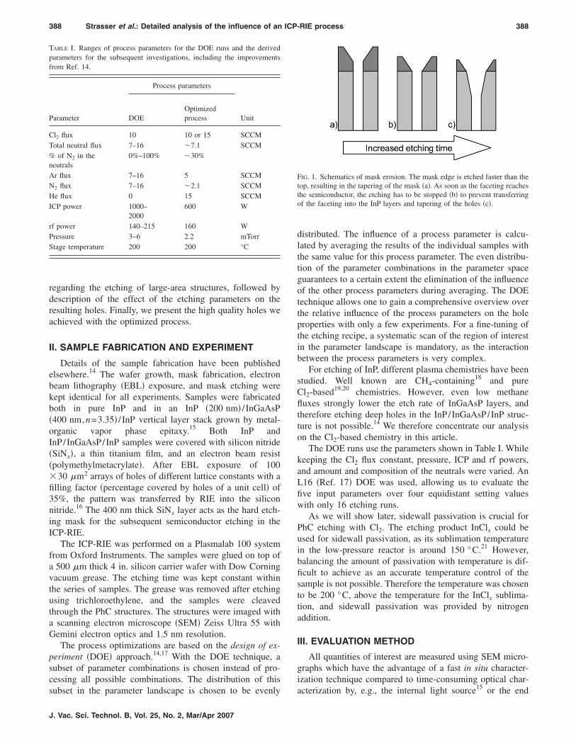
FIG. 1. Schematics of mask erosion. The mask edge is etched faster than thetop, resulting in the tapering of the mask �a�. As soon as the faceting reachesthe semiconductor, the etching has to be stopped �b� to prevent transferringof the faceting into the InP layers and tapering of the holes �c�.
acterization by, e.g., the internal light source or the end

389 Strasser et al.: Detailed analysis of the influence of an ICP-RIE process 389
fire7 techniques, although they do not deliver loss figures forPhC waveguides. They, however, provide an accurate three-dimensional picture of the exact hole geometry. The linkbetween the extracted figures of merit from SEM images andthe loss values has to be made using a corresponding set ofoptical calibration experiments or with theoretical lossmodels,10,11 where loss caused by hole depth and conicalshape can be predicted.
Next to the standard quantities of interest in process de-velopment such as InP and InGaAsP etch rates, sidewallangles, and mask etch rate, some additional figures of meritfor this investigation have been defined as follows:
1. Mask selectivity= �InP etch rate� / �mask etch rate�.2. Quaternary material selectivity= �InGaAsP etch rate� /
�InP etch rate�.3. The extrapolated maximal etch depth (eMED)
��measured depth��total mask thickness/�total maskthickness���remaining mask thickness�� accounts for alonger etching time due to the remaining mask materialafter the etching. This figure of merit is computed as allsamples were etched for 90 s, and depending on therecipe, the plasma may be diversely aggressive against themask. The eMED is calculated based on the measuredlarge area or hole depth and the remaining mask thicknessat the structure edge, as mask faceting �Fig. 1� is the lim-
TABLE II. Influence of the process parameters on quantities of interest forlarge-area etching. ↗ and ↘ indicate a larger parameter value to be benefi-cial and detrimental, respectively. The number of arrows relates to thestrength of the trend. For the sidewall angle verticality is optimal. Therefore↗/↘ means that higher parameter values lead to a smaller/larger anglebetween the sidewall and the plumb line.
ICP power rf power Neutral flux % of N2
Sidewall angle ↘↘ ↘↘↘Surface quality ↘↘Sidewall quality ↗ ↗ ↘ ↘Maximal achievableetch depth/selectivityagainst the mask
↘ ↘
FIG. 2. Influence of the process parameters on the sidewall angle. The pa-rameter levels are according to Table I: ICP power of 1000–2000 W, rfpower of 140–215 W, neutral flux of 7–15 SCCM, and N2 percentage of
0%–100%.JVST B - Microelectronics and Nanometer Structures
iting factor for the etching time. The eMED calculationhas, however, a limited accuracy of ±400 nm as the mea-surement of the remaining mask thickness is unreliabledue to the mask rounding off at the facet. Additionally, forholes the etching rate may slow down with increasingdepth due to aspect-ratio dependent etch rates.22
4. Surface roughness, hole shape, and undercut8 are quanti-fied by comparing and ranking the SEM micrographs.
IV. LARGE-AREA ETCHING PROPERTIES OF ACl2/Ar/N2 PLASMA
During the PhC device fabrication for optical port-to-portend fire measurements,7 photonic wires �PhWs� are etchedsimultaneously with the PhC holes. Of special interest forPhWs is the etch depth, the roughness of the etched bottomsurface and of the sidewalls, and the verticality of thesidewalls.
The impact of the etching parameters is summarized inTable II. Both high rf and ICP powers are beneficial forsidewall quality, whereas a high neutral flux and a high ni-trogen content have a negative overall impact on all figuresof interest.
Before further analysis, we should mention that increasingthe percentage of N2 in the neutrals has two effects: �i� it
FIG. 3. Influence of the process parameter on the sidewall quality. Theparameter levels are according to Table I: ICP power of 1000–2000 W, rfpower of 140–215 W, neutral flux of 7–15 SCCM, and N2 percentage of0%–100%.
FIG. 4. Influence of the process parameter on the eMED for �200 nm holes.The parameter levels are according to Table I: ICP power of 1000–2000 W,rf power of 140–215 W, neutral flux of 7–15 SCCM, and N2 percentage of
0%–100%.
390 Strasser et al.: Detailed analysis of the influence of an ICP-RIE process 390
passivates the sidewalls and the surface by preferentiallyforming N–P bonds and therefore inhibits Cl2–In bonds19,23
and �ii� it reduces the sputter efficiency of the total neutralflux, as heavy argon ions �atomic mass: 40� are replaced bylight nitrogen �atomic mass: 14� ions.
All measured values for the etch rates in this DOE run liebetween 1 and 3 �m/min. While higher rf and ICP powersincrease the etch rate, they do not improve the maximumachievable etch depth, as the mask is also etched faster. Onthe other hand, a high chemical content in the plasma isadvantageous for a larger etch depth due to the enhancedselectivity of the chemical etching processes against themask. In addition, the sidewall passivation by nitrogen,19
which enhances micromasking and results in a rough bottomsurface and reduced maximal etch depth, is limited. It shouldbe mentioned that reducing the neutral flux is equivalent toincreasing the Cl2 flux, as the total flux has a negligibleimpact on the etching result.
Figure 2 presents the influence of the process parameterson the sidewall angle based on the DOE evaluation. Theneutral content and the amount of N2 in the plasma predomi-nantly determine the sidewall angle. Indeed, by adding neu-trals or passivating sidewalls with nitrogen, we reduce thechemical etching by chlorine ions and therefore less verticalsidewalls are obtained. Underetching is not observed.
The chemical composition of the plasma has the mostpronounced influence on the quality of the etching, as shownin Table II. Whereas the bottom etched surface quality ismainly determined by the nitrogen content in the plasma dueto passivation of the surface and the subsequent micromask-ing or grass formation, the sidewall quality is in additionpositively influenced by a high ICP power and a low neutralflux �Fig. 3�.
We found no distinct influence of the process parameteron the quaternary material selectivity. The value for the qua-ternary material selectivity lies mostly between 0.8 and 0.9over the 16 etching experiments of the L16 DOE in contrastto methane-based plasmas for which the selectivity is 0.25.18
Also pressure has no significant influence on any quantity of
TABLE III. Influence of the process parameters on quaa larger parameter value to be beneficial and detrimoptimal. Therefore ↗ and ↘ mean that higher paramThe number of arrows relates to the strength of the t
ICP power rf
eMED ↘Hole shape conicality ↗UndercutHole surface qualityGrasslike verticalstripes on the surface
interest.
J. Vac. Sci. Technol. B, Vol. 25, No. 2, Mar/Apr 2007
V. HOLE ETCHING
For holes, the figures of merit are hole shape, surfaceroughness, and hole depth. Typical hole diameters for wave-lengths of �=1550 nm are in the range of 150–500 nm. Inaddition, a low quaternary material selectivity is favorable toavoid differential etching of the core and the claddings.
The qualitative behavior of the etching is assumed to beindependent of the hole size and thus the measured valuescan be averaged over different diameters. Table III summa-rizes the impact of the process parameters on the hole char-acteristics. Again, the pressure has a minor impact except forundercut.
A. Hole depth
Figure 4 shows the impact of the process parameters onthe eMED for �200 nm holes. The trends are similar for�500 nm holes.
The calculated eMED ranges in the individual runs of theDOE are 0.8–4.4 �m and 1.3–4.8 �m for �200 and hole�500 nm holes, respectively.
Whereas nitrogen has a negative impact on the eMED forlarge-area etching �Table II� due to micromasking, it is ben-eficial for holes �Table III and Fig. 4�. These seemingly con-tradictory results can be explained as follows: due to theenhanced surface passivation with higher nitrogen content,
s of interest for PhC hole etching. ↗ and ↘ indicaterespectively. For holes, the absence of undercut is
alues enhance and reduce the undercut, respectively.
rNeutral
flux % of N2 Pressure
↘ ↗↗↘ ↘
↘↘ ↗↘↘
FIG. 5. Correlation between the rf power and eMED for large-area structures
ntitieental,eter vrend.
powe
↘↘
↗
and two different hole sizes.

391 Strasser et al.: Detailed analysis of the influence of an ICP-RIE process 391
ions are deflected toward the center of the holes. The aug-mented ion bombardment allows cracking of the passivationlayer at the bottom and increases the overall etching rate.The drawback is a more conical shape as will be shown inthe next section.
Comparing Table II with Table III and Fig. 4, the rf andICP powers have a more significant influence on the holedepth than for large-area etching, for which no clear effectwas observed. A low power is favorable for deep hole etch-ing, unambiguously for the rf power, and less pronounced inthe case of ICP power. This behavior cannot be explained bya selectivity enhancement against the mask due to a lower dcbias as we do not observe a reduction in etch depth forhigher power in the case of large-area etching. We explainthis phenomenon as follows:
At higher power, the plasma density and the amount ofactive species accelerated towards the sample are increased.This enhances the etch rate of the semiconductor but also theetch rate of the mask. Whereas this is not a limitation inetching large-area openings, it gets increasingly difficult todiffuse neutral etch species into or remove the etch productsout of the high-aspect-ratio holes, and therefore the etchingrate slows down when the holes get deeper. This hypothesisis supported by the fact that the hole depth reduction athigher power is more pronounced for small holes as shownin Fig. 5. For large-area structures, a slight decrease with the
FIG. 7. Depth of holes etched with a Cl2 /Ar/N2/He process �Ref. 14� vs Cl2
flux. All other parameters are kept constant. The N2 and Ar fluxes are 2.1and 5 SCCM, respectively. The pressure is 2.2 mTorr except for the highestflux where it is increased to 2.5 mTorr. Insets: SEM micrographs of the hole
cross sections and the undercut.JVST B - Microelectronics and Nanometer Structures
power of the eMED is observed, which can be caused byother parameters in the DOE. For holes, we measure a cleardecrease of the eMED with increasing rf powers of 12 and22 nm/W for �500 and �200 nm holes, respectively.
The ICP power shows less influence on the hole depth.While a lower rf power not only reduces the plasma densitybut also the dc bias, a lower ICP power reduces the plasmadensity but increases the dc bias, leading to a higher sputterefficiency of the mask. This reduces the selectivity of InPagainst the mask and the eMED.
B. Hole quality
All quantities of interest �hole shape, sidewall roughness,undercut� are strongly influenced by the nitrogen content inthe neutral flux. The impact of nitrogen on the sidewall pas-sivation of the holes and of large-area structures and thereduction of the undercut will now be discussed. As will beshown later, a higher Cl2 flux increases the undercut whilethis effect is not seen for a lower neutral content. The effect
FIG. 6. Holes etched with a Cl2 /Ar/N2/He process�Ref. 14�. The nitrogen flow is varied from 1.3, 2.1, and2.9 SCCM to 6 SCCM for �a� to �d�, respectively. Allother process parameters are kept constant. The Cl2 andAr fluxes are 15 and 5 SCCM, respectively. All relatedimages have the same scale.
FIG. 8. PhC etched in InP. The holes have a diameter of 180 nm and a depth
of 2.9 �m, resulting in an aspect ratio of 1:16.
392 Strasser et al.: Detailed analysis of the influence of an ICP-RIE process 392
is shadowed in the DOE run by the strong impact of N2 andthe strong correlation between the neutral flux and the con-tent of N2 in the neutrals.
VI. SIDEWALL PASSIVATION
Besides the DOE runs, additional investigations showedthat N2 prevents undercuts just below the SiNx mask �Figs.6�a� and 6�b��. As the undercut is only visible in holes butnot at the sidewalls of large-area structures, we believe that itis caused by the deflection of the incoming chlorine ionsfrom the opposite sidewalls.8 As the mode intensity at the topof the holes is relatively strong due to the asymmetric slabwaveguide structure,7 the undercut may significantly contrib-ute to optical scattering losses due to its very rough surface.The nitrogen passivation can prevent undercuts as shown inFig. 6 by formation of N–P bonds at the sidewalls.19,23 Onthe other hand too large nitrogen fluxes increase the sidewallroughness and the hole conicity �Fig. 6�d��.
As shown in Fig. 7, with an increased amount of chlorine�which has the same effect as decreasing the overall neutralflux�, the etch depth is improved, but more nitrogen is nec-essary to prevent the undercut at the top of the holes. Also,the small N2 flux of 2.1 SCCM �SCCM denotes cubic centi-meter per minute at standard temperature and pressure� isenough to protect the sidewalls for low Cl2 fluxes but isinsufficient for higher Cl2 fluxes.
VII. IMPROVED PROCESS AND CONCLUSION
As we are aiming for applications in the low refractiveindex system, deep holes are crucial. Using the knowledgewe gained, we optimized the process for deep holes pre-sented in Fig. 8. The holes have depths of 4.2, 3.8, and2.9 �m for diameters of 417, 310, and 180 nm, respectively.The parameters of Table I are used, with Cl2 and N2 fluxes of15 and 2.9 SCCM, respectively.
To summarize, we have investigated the impact of theplasma power, pressure, and plasma chemistry on the etchingof structures and holes for PhCs in InP/ InGaAsP/InP.Samples were compared in terms of maximal achievablehole depth, hole shape, surface roughness, and undercut.
The chemistry of the plasma has been identified as themost crucial etching parameter. Deep holes can be achievedwith a highly chemical process, demanding a high Cl2 con-
TABLE IV. Dependencies and the effects of the proce
Parameter Function
Power Determines plasma density
PressureArgon Physical etchingNitrogen Sidewall passivation
Lower chemical etching
Chlorine Physical and chemical etching
tent. However, pure Cl2 /Ar plasmas at 200 °C are not ca-
J. Vac. Sci. Technol. B, Vol. 25, No. 2, Mar/Apr 2007
pable of forming a passivation layer at the sidewalls, whichresults in a lateral etching of the semiconductor below themask. Adding a small amount of nitrogen prevents the un-dercut but is detrimental for surface quality, as it promotesroughness at the sidewalls and at the bottom of large-areastructures. Therefore a delicate balance needs to be found.
The rf and ICP powers should be kept low to achieve deepholes by reducing the etch rate and giving the reaction spe-cies time to sublimate and diffuse out of the holes. Our find-ings can be summarized in the following qualitative etchmodel displayed in Table IV.
ACKNOWLEDGMENTS
This work was carried out in the framework of the Euro-pean Network of Excellence ePIXnet and the Swiss NationalScience Foundation program NCCR Quantum Photonics.Devices were fabricated at the FIRST Center of Micro- andNanoscience of the ETH Zurich. The authors would like toacknowledge E. Gini �FIRST� for the epitaxy and O. Homan�FIRST� for technical support.
1J. D. Joannopoulos, R. D. Meade, and J. N. Winn, Photonic Crystals—Molding the Flow of Light �Princeton University Press, Princeton, 1995�,pp. 1–137.
2F. Robin et al., Proc. SPIE 6124, 612415 �2006�.3T. F. Krauss, Phys. Status Solidi A 197, 688 �2003�.4A. Talneau, L. L. Gouezigou, and N. Bouadma, Opt. Lett. 26, 1259�2001�.
5M. Mulot, S. Anand, M. Swillo, M. Qiu, B. Jaskorzynska, A. Talneau,L. L. Gouezigou, and N. Bouadma, J. Vac. Sci. Technol. B 21, 900�2003�.
6C. F. Carlström, R. v. d. Heijden, F. Karouta, R. W. v. d. Heijden,H. W. M. Salemink, and E. v. d. Drift, J. Vac. Sci. Technol. B 24, L6�2006�.
7K. Rauscher, thesis ETH Zurich, 2006.8M. Mulot, S. Anand, C. F. Carlström, M. Swillo, and A. Talneau,Phys. Scr., T T101, 106 �2002�.
9R. Ferrini, A. Berrier, L. A. Dunbar, R. Houdré, M. Mulot, S. Anand, S.d. Rossi, and A. Talneau, Appl. Phys. Lett. 85, 3998 �2004�.
10R. Ferrini, B. Lombardet, B. Wild, R. Houdre, and G.-H. Duan, Appl.Phys. Lett. 82, 1009 �2003�.
11H. Benisty, D. Labilloy, C. Weisbuch, C. J. M. Smith, T. F. Krauss, D.Cassagne, A. Béraud, and C. Jouanin, Appl. Phys. Lett. 76, 532 �2000�.
12M. V. Kotlyar, T. Karle, M. D. Settle, L. O’Faolain, and T. F. Krauss,Appl. Phys. Lett. 84, 3588 �2004�.
13J. F. Holzman, P. Strasser, R. Wüest, F. Robin, D. Erni, and H. Jäckel,Proceedings of the 17th International Conference of IPRM, 2005, p. 570
14
rameters on PhC holes.
esult
educes eMED due to exhaust limitationsnhances the surface qualityrevents undercut at low pressureputters the mask, dilutes the plasmarevents undercutecreases the quality of the holes due micromasking
nd passivationroduces deep holes, favors undercut
ss pa
R
REPSPDaP
P. Strasser, R. Wüest, F. Robin, K. Rauscher, B. Wild, D. Erni, and H.

393 Strasser et al.: Detailed analysis of the influence of an ICP-RIE process 393
Jäckel, Proceedings of the 17th International Conference of IPRM, 2005,p. 242
15R. Ferrini, D. Leuenberger, M. Mulot, M. Qiu, J. Moosburger, M. Kamp,A. Forchel, S. Anand, and R. Houdré, IEEE J. Quantum Electron. 38, 786�2002�.
16R. Wüest, P. Strasser, F. Robin, D. Erni, and H. Jäckel, J. Vac. Sci.Technol. B 23, 3197 �2005�.
17G. Z. Yin and D. W. Jille, Solid State Technol. 30�5�, 127 �1987�.18P. Strasser, R. Wüest, F. Robin, C. Widmeier, D. Erni, and H. Jäckel,
Proceedings of the 16th International Conference of IPRM, 2004 p. 175.
JVST B - Microelectronics and Nanometer Structures
19R. v. d. Heijden et al., Proceedings of the Symposium of IEEE/LEOS,2004, p. 287.
20J. Lin, A. Leven, N. G. Weimann, Y. Yang, R. F. Kopf, R. Reyes, Y. K.Chen, and F.-S. Choa, J. Vac. Sci. Technol. B 22, 510 �2004�.
21A. Matsutani, H. Ohtsuki, F. Koyama, and K. Iga, Jpn. J. Appl. Phys., Part1 38, 4260 �1999�.
22R. A. Gottscho, C. W. Jurgensen, and D. J. Vitkavage, J. Vac. Sci. Tech-nol. B 10, 2133 �1992�.
23R. v. d. Heijden et al., Proc. SPIE 5450, 523 �2004�.
Copyright © 2022 FDOKUMEN


![Investigation of InP etching mechanisms in a Cl[sub 2]/H[sub 2] inductively coupled plasma by optical emission spectroscopy](https://static.fdokumen.com/doc/165x107/6341a38bfb2d3e0a380c77e8/investigation-of-inp-etching-mechanisms-in-a-clsub-2hsub-2-inductively-coupled.jpg)