Designing a Crossbar Scheduler for HPC Applications
14
58 Massively parallel high-performance computing (HPC) systems require large-scale, high-bandwidth, low-latency interconnection networks. The Corning-IBM joint Optical Shared Memory Supercomputer Interconnect System (Osmosis) project explores the oppor- tunity to advance the role of optical-switch- ing technologies in such systems. 1 There are two strong reasons for preferring an optical interconnect over an electrical one: • Distance. High-end HPC systems— supercomputers—are typically very large and highly distributed, with diameters spanning tens to hundreds of meters, so the capability of covering such distances with high bandwidth and low latency is a significant advantage. For transmitting high data rates over long distances, fiber is far better suited than copper. Also, opti- cal interconnects neither generate nor are sensitive to electromagnetic interfer- ence—a clear benefit at multigigabit rates. • Power. An optical switch typically con- sumes significantly less power than a com- parable electronic switch does, because its power consumption is proportional to the cell rate rather than the bit rate. Given that the ability to power and cool the package increasingly constrains chip design, this is a key advantage. On the other hand, optical switching has three main drawbacks: the absence of a prac- tical, dense, fast-access optical-memory tech- nology; the complexity of optical control and arbitration; and the cost of fast optical- switching components. In the Osmosis pro- ject, our objective is to address these drawbacks by adopting a hybrid electro-opti- cal approach using electronics for buffering and scheduling, and optics for transmission and switching. First, we plan to solve the technical challenges of building a demon- Cyriel Minkenberg François Abel Peter Müller Raj Krishnamurthy Mitchell Gusat Peter Dill Ilias Iliadis Ronald Luijten IBM Zurich Research Laboratory B. Roe Hemenway Richard Grzybowski Corning Inc. Enrico Schiattarella Politecnico di Torino A CRUCIAL PART OF ANY HIGH-PERFORMANCE COMPUTING (HPC) SYSTEM IS ITS INTERCONNECTION NETWORK. CORNING AND IBM ARE JOINTLY DEVELOPING A DEMONSTRATION INTERCONNECT BASED ON OPTICAL CELL SWITCHING WITH ELECTRONIC CONTROL. KEY INNOVATIONS IN THE SCHEDULER ARCHITECTURE DIRECTLY ADDRESS THE MAIN HPC REQUIREMENTS: LOW LATENCY , HIGH THROUGHPUT , EFFICIENT MULTICAST SUPPORT , AND HIGH RELIABILITY . DESIGNING A CROSSBAR SCHEDULER FOR HPC APPLICATIONS Published by the IEEE Computer Society 0272-1732/06/$20.00 © 2006 IEEE
-
Upload
independent -
Category
Documents
-
view
5 -
download
0
Transcript of Designing a Crossbar Scheduler for HPC Applications

58
Massively parallel high-performancecomputing (HPC) systems require large-scale,high-bandwidth, low-latency interconnectionnetworks. The Corning-IBM joint OpticalShared Memory Supercomputer InterconnectSystem (Osmosis) project explores the oppor-tunity to advance the role of optical-switch-ing technologies in such systems.1 There aretwo strong reasons for preferring an opticalinterconnect over an electrical one:
• Distance. High-end HPC systems—supercomputers—are typically very largeand highly distributed, with diametersspanning tens to hundreds of meters, sothe capability of covering such distanceswith high bandwidth and low latency is asignificant advantage. For transmittinghigh data rates over long distances, fiberis far better suited than copper. Also, opti-cal interconnects neither generate nor aresensitive to electromagnetic interfer-
ence—a clear benefit at multigigabit rates.• Power. An optical switch typically con-
sumes significantly less power than a com-parable electronic switch does, because itspower consumption is proportional to thecell rate rather than the bit rate. Giventhat the ability to power and cool thepackage increasingly constrains chipdesign, this is a key advantage.
On the other hand, optical switching hasthree main drawbacks: the absence of a prac-tical, dense, fast-access optical-memory tech-nology; the complexity of optical control andarbitration; and the cost of fast optical-switching components. In the Osmosis pro-ject, our objective is to address thesedrawbacks by adopting a hybrid electro-opti-cal approach using electronics for bufferingand scheduling, and optics for transmissionand switching. First, we plan to solve thetechnical challenges of building a demon-
Cyriel MinkenbergFrançois AbelPeter Müller
Raj KrishnamurthyMitchell Gusat
Peter DillIlias Iliadis
Ronald LuijtenIBM Zurich Research
Laboratory
B. Roe HemenwayRichard Grzybowski
Corning Inc.
Enrico SchiattarellaPolitecnico di Torino
A CRUCIAL PART OF ANY HIGH-PERFORMANCE COMPUTING (HPC) SYSTEM IS
ITS INTERCONNECTION NETWORK. CORNING AND IBM ARE JOINTLY
DEVELOPING A DEMONSTRATION INTERCONNECT BASED ON OPTICAL CELL
SWITCHING WITH ELECTRONIC CONTROL. KEY INNOVATIONS IN THE
SCHEDULER ARCHITECTURE DIRECTLY ADDRESS THE MAIN HPC
REQUIREMENTS: LOW LATENCY, HIGH THROUGHPUT, EFFICIENT MULTICAST
SUPPORT, AND HIGH RELIABILITY.
DESIGNING A CROSSBARSCHEDULER FOR
HPC APPLICATIONS
Published by the IEEE Computer Society 0272-1732/06/$20.00 © 2006 IEEE

strator interconnection network that meets aspecific set of ambitious target requirements,using components and technologies current-ly available. Second, we aim to accelerate thecost reduction of all-optical switches for HPCby achieving denser optical integration andfinding—in addition to the low-volumeHPC market—a high-volume market forthese optical components. In previous publi-cations, we explained how we chose theswitch architecture and showed that the sys-tem design is feasible.1-3 Here, we address thetechnical issues we encountered in the elec-tronic domain.
Osmosis architectureFirst, we review the Osmosis interconnection
network’s architectural requirements, our result-ing design choices, and the general architecture.
RequirementsHPC interconnects must handle the arrival,
buffering, routing, forwarding, and errormanagement of high-rate data and controlstreams in scalable local networks. HPCswitches must deliver very low latency, anextremely low bit-error rate, a high data rate,and extreme scalability. Moreover, they musthandle bursty traffic efficiently, with demandsranging from very small messages (such as col-lectives and syncs) to bulk data set transfers(such as memory pages).
The specific HPC-based requirements forour demonstrator system include
• less than 1-μs latency, measured applica-tion to application;
• switch ports operating at 40 Gbps with75 percent available for user payload;
• 10–21 bit-error rate;• optical data path;• scalability to at least 2,048 nodes and to
higher line rates (at least 160 Gbps); and• FPGA-only implementation of all elec-
tronic logic for flexibility and acceptablecost.
The system’s memory model imposes addi-tional requirements. Shared-memory, cache-coherent, HPC multiprocessor systems,whether they have uniform or nonuniformmemory access, rely on hardware support toenforce memory coherency and cache-line
granularity consistency. Consequently, theinterconnection network needs the following:
• Communication must be fine-grained;typical coherent transactions comprise atotal payload of 100 to 300 bytes, exclud-ing the interconnection network’s inter-nal overhead.
• Transaction ordering must usually bestrictly enforced. Although costly toimplement in hardware, the sequentialconsistency model is generally accepted,so supporting it in the interconnectionnetwork is a strong benefit.
• Efficient support for multicast andbroadcast is a basic requirement forsnoop-based multiprocessors as well ascollective and synchronization opera-tions—barriers, reductions, locks—usedin HPC applications.
Design choicesWe previously provided a top-down expo-
sition of the design decisions shaping theOsmosis architecture.2 Let us briefly reviewthe key points.
Switch degree. The most important require-ment in an HPC interconnection network islow latency, typically measured application toapplication across the network. We had todesign the system to achieve low end-to-endlatency, even with 2,048 nodes. Scaling a sin-gle-stage network to 2,048 nodes is generallynot cost-effective, because of the quadraticcomplexity involved, so we turned to multi-stage topologies. Given our challenging 1-μslatency target, we chose a fat-tree topology,which has the advantages of being nonblock-ing and offering high path diversity and shortpaths to neighboring nodes. We selected theswitch degree N = 64, which allows scaling to2,048 nodes with 96 switches in only two lev-els; thus, there are at most three hops betweenany two nodes.
Switching paradigm. The latency and effi-ciency requirements were the main deter-mining factors in our choice of cell switching.In this respect, Osmosis is fundamentally dif-ferent from other optical switches, most ofwhich use techniques such as meshing, circuitswitching, provisioning (bandwidth reserva-
59MAY–JUNE 2006

tion), or aggregation (burst or containerswitching). These approaches are prohibitivelyexpensive (meshing), are too inefficient(meshing and circuit switching), or introducetoo much latency (aggregation). Instead,Osmosis switches fixed-size cells by reconfig-uring the optical core on a cell-by-cell basis.The key enabler is the fast switching time (afew nanoseconds) achieved by state-of-the-artsemiconductor optical amplifiers (SOAs),which now, for the first time, allow low-over-head optical cell switching.
Cell overhead. We selected a 256-byte fixed cellsize. The cell format comprises user data andoverhead, which includes SOA switchingtime, preamble, cell header, forward error cor-rection (FEC), line coding, and jitter budget.The resulting efficiency is about 75 percent.The Osmosis demonstrator can sustain full-link bandwidth with traffic consisting only of256-byte cells.
Switch fabric structure. SOAs are well suitedto implement the optical equivalent of a cross-bar using a broadcast-and-select (B&S) datapath architecture combining space- and wave-length-division multiplexing.1 A B&S archi-tecture is strictly nonblocking, inherentlyoffers broadcast capability, and can (indepen-dently) scale in the space and wavelengthdimensions. The crossbar equivalence deter-mines queuing and scheduling.
Buffer placement. Because optical buffering isnot yet mature, we cannot satisfactorily resolvecontention for such a large switch degree (N = 64) in the optical domain. We thereforedecided to use electronic buffers placed at theinputs as well as the outputs of the opticalcore. To eliminate head-of-line (HOL) block-ing at the input buffers, we arrange them asvirtual output queues (VOQs). These buffersare located in the corresponding port’s adaptercard, which performs all interfacing functionsbetween the attached computing node andthe interconnection network. We distinguishbetween ingress and egress adapters, althoughthey are typically located on the same card.
Maximum throughput. Maximum throughputis a relative measure that expresses how muchof the aggregate raw data rate can be used with-
out saturating (overloading) the switch. Thisis determined by the traffic pattern, which wecannot influence, and the control path’s sched-uling-related properties—the queuing struc-ture, the control channel protocol, and thescheduling algorithm. The first step towardhigh throughput is to prevent HOL blocking,which we accomplish with the input queues’VOQ organization. The second step is toensure that the scheduler has an accurate viewof the current VOQ state, which we accom-plish with a special control channel protocol(an incremental request grant protocol, orΔRGP).4 The third and final step is to use cen-tralized, efficient scheduling.
Scheduling. The cell-switching nature of theswitch implies that for high maximumthroughput and low latency, the switch needsa centralized scheduler to compute a high-quality (near-optimal) matching of inputs andoutputs. This problem has been studied exten-sively, and there are practical heuristic, itera-tive algorithms to solve it.5,6 This class ofalgorithms achieves up to 100 percentthroughput under uniform traffic patterns,although they are not strictly work-conserv-ing for any arbitrary traffic pattern. Howev-er, they need O[log2(N)] iterations to convergeon a maximal matching. The challenge is toperform the full scheduling process once ineach time slot of 51.2 ns (2,048 bits at 40Gbps). Compounding this problem is thelarge switch radix, which means not only thateach iteration takes longer (because moreports must be considered) but also that achiev-ing satisfactory latency and throughput char-acteristics requires more iterations. To increaseboth the scheduling rate and quality, we usethe FLPPR (fast, low-latency, parallel,pipelined arbitration) scheme, which operatesa set of identical subschedulers in parallel. TheOsmosis demonstrator doesn’t support trafficpriorities, yet.
Single-stage architectureFigure 1 shows the high-level Osmosis
switch architecture in a single-stage configu-ration. It supports 64 nodes and operates insynchronous, time-slotted fashion with fixed-sized cells. Adapter cards, which form theinterface between the computing nodes andthe interconnection network, include an
60
HIGH-PERFORMANCE INTERCONNECTS
IEEE MICRO

optical-network interface card (ONIC) forelectro-optical and opto-electrical conversions.Each adapter consists of a full set of N VOQswith a corresponding set of N reliable deliveryqueues, as well as an egress queue. (AlthoughFigure 1 shows separate ingress and egressadapters, they typically share the same card.)Each adapter has a dedicated optical controllink to the centralized scheduler, which carriesthe control channel protocols. The schedulerresides on a separate card close to the opticalswitching modules (OSMs), which it config-ures via the switch command channels (SCCs).
We implemented the routing function witha B&S architecture that combines eight-wayspace-division and eight-way wavelength-divi-sion multiplexing to form a 64-port fabric.We assign each adapter a specific wavelength,λi; we group the adapters by eight so that eachadapter in a group has a unique wavelength.The optical signals per group are multiplexedonto a single fiber. An erbium-doped fiberamplifier (EDFA) amplifies the resulting sig-nal, which a 128-way coupler then broadcaststo 128 OSMs.
Each OSM has fiber and wavelength selec-tion stages. The fiber selection stage consistsof eight SOAs, which select the fiber that car-ries the cell to be received. A planar light-wave
circuit combines the output of all SOAs to acommon port, and the resulting stream is thendemultiplexed and passed through the wave-length selection stage (also consisting of eightSOAs), which selects the desired wavelength.The stream is then remultiplexed onto a com-mon output port and delivered to the broad-band receiver residing at the egress ONIC.Synchronously with cell transmission, the cen-tralized scheduler resolves contention onrequests it receives via optical control channelsand provides control signals (via the SCCs)that drive the fiber and wavelength selectionSOAs just as the cells arrive at each OSM.
A special feature of Osmosis is the presenceof two OSMs and two receivers per egressadapter, which allows delivery of up to twocells to the same adapter in one time slot; inother words, the output speedup equals 2.Hence, the crossbar is asymmetric; it has 64inputs and 128 outputs. The egress adaptershandle the required rate conversion. The pur-pose of this arrangement is to improve per-formance, as we will explain later.
To prevent overflow of the egress buffers,we use an on/off flow control (FC) loopbetween the egress buffers and the scheduler.The FC information is embedded in theupstream control-channel messages.
61MAY–JUNE 2006
Optical switch controller module(scheduler)
ON
IC
ON
IC
WDMmultiplexer
Starcoupler
Opticalamplifier
8x1 1x128
λ1λ2λ3λ4λ5λ6λ7
λ8
τdDC
Control
VOQs + RDQs
1
64
ON
IC
Control
VOQs + RDQs
1
64
Control
RXEQ
ON
IC
Control
RXEQ
τuDC
τdCC
τuCCτSCC
8x1 8x11x8
Combiner
Optical broadcast modules (8x) Egress adapters (64x)Optical switching modules (128x)Ingress adapters (64x)
EDFA
Fast SOA 1x8Fiber selector
gates
Fast SOA 1x8Wavelength
selector gates
Erbium-doped fiber amplifierEgress queueOptical-network interface cardReliable delivery queueReceiverSemiconductor optical amplifier
EDFAEQ
ONICRDQ
RXSOA
Virtual-output queueWavelength division multiplexingDownstream control-channel latencyDownstream data-channel latencySwitch-command-channel latencyUpstream control-channel latencyUpstream data-channel latency
VOQWDM
τdCCτdDCτSCCτuCCτuDC
Control channels Switch-commandchannels
Figure 1. Osmosis architecture.
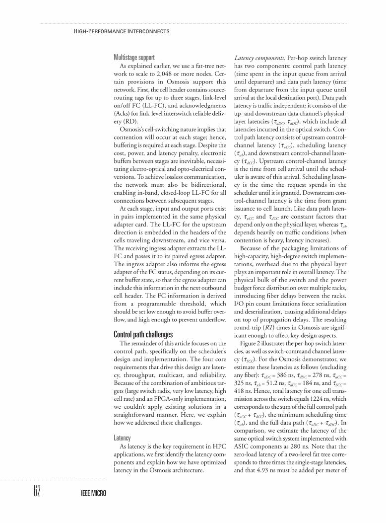
Multistage supportAs explained earlier, we use a fat-tree net-
work to scale to 2,048 or more nodes. Cer-tain provisions in Osmosis support thisnetwork. First, the cell header contains source-routing tags for up to three stages, link-levelon/off FC (LL-FC), and acknowledgments(Acks) for link-level interswitch reliable deliv-ery (RD).
Osmosis’s cell-switching nature implies thatcontention will occur at each stage; hence,buffering is required at each stage. Despite thecost, power, and latency penalty, electronicbuffers between stages are inevitable, necessi-tating electro-optical and opto-electrical con-versions. To achieve lossless communication,the network must also be bidirectional,enabling in-band, closed-loop LL-FC for allconnections between subsequent stages.
At each stage, input and output ports existin pairs implemented in the same physicaladapter card. The LL-FC for the upstreamdirection is embedded in the headers of thecells traveling downstream, and vice versa.The receiving ingress adapter extracts the LL-FC and passes it to its paired egress adapter.The ingress adapter also informs the egressadapter of the FC status, depending on its cur-rent buffer state, so that the egress adapter caninclude this information in the next outboundcell header. The FC information is derivedfrom a programmable threshold, whichshould be set low enough to avoid buffer over-flow, and high enough to prevent underflow.
Control path challengesThe remainder of this article focuses on the
control path, specifically on the scheduler’sdesign and implementation. The four corerequirements that drive this design are laten-cy, throughput, multicast, and reliability.Because of the combination of ambitious tar-gets (large switch radix, very low latency, highcell rate) and an FPGA-only implementation,we couldn’t apply existing solutions in astraightforward manner. Here, we explainhow we addressed these challenges.
LatencyAs latency is the key requirement in HPC
applications, we first identify the latency com-ponents and explain how we have optimizedlatency in the Osmosis architecture.
Latency components. Per-hop switch latencyhas two components: control path latency(time spent in the input queue from arrivaluntil departure) and data path latency (timefrom departure from the input queue untilarrival at the local destination port). Data pathlatency is traffic independent; it consists of theup- and downstream data channel’s physical-layer latencies (τuDC, τdDC), which include alllatencies incurred in the optical switch. Con-trol path latency consists of upstream control-channel latency (τuCC), scheduling latency(τsch), and downstream control-channel laten-cy (τdCC). Upstream control-channel latencyis the time from cell arrival until the sched-uler is aware of this arrival. Scheduling laten-cy is the time the request spends in thescheduler until it is granted. Downstream con-trol-channel latency is the time from grantissuance to cell launch. Like data path laten-cy, τuCC and τdCC are constant factors thatdepend only on the physical layer, whereas τsch
depends heavily on traffic conditions (whencontention is heavy, latency increases).
Because of the packaging limitations ofhigh-capacity, high-degree switch implemen-tations, overhead due to the physical layerplays an important role in overall latency. Thephysical bulk of the switch and the powerbudget force distribution over multiple racks,introducing fiber delays between the racks.I/O pin count limitations force serializationand deserialization, causing additional delayson top of propagation delays. The resultinground-trip (RT) times in Osmosis are signif-icant enough to affect key design aspects.
Figure 2 illustrates the per-hop switch laten-cies, as well as switch-command channel laten-cy (τSCC). For the Osmosis demonstrator, weestimate these latencies as follows (excludingany fiber): τuDC = 386 ns, τdDC = 278 ns, τuCC =325 ns, τsch = 51.2 ns, τdCC = 184 ns, and τSCC =418 ns. Hence, total latency for one cell trans-mission across the switch equals 1224 ns, whichcorresponds to the sum of the full control path(τuCC + τdCC), the minimum scheduling time(τsch), and the full data path (τuDC + τdDC). Incomparison, we estimate the latency of thesame optical switch system implemented withASIC components as 280 ns. Note that thezero-load latency of a two-level fat tree corre-sponds to three times the single-stage latencies,and that 4.93 ns must be added per meter of
62
HIGH-PERFORMANCE INTERCONNECTS
IEEE MICRO

fiber. Moreover, these latencies are significantmultiples of the cell duration.
The potential negative performance impactof long RTs can be prevented by implement-ing an incremental request grant protocol(ΔRGP).4 The protocol communicates relativeVOQ state updates, encoded with log2N bits,rather than an absolute request vector (N bits).Consequently, the scheduler must keep trackof the number of pending requests per VOQ.
Speculation. As explained, minimum latencyin Osmosis consists of control path latenciesand data path latencies, which are both fargreater than the cell duration. To meet thelatency requirements, Osmosis features anarchitectural novelty called speculative trans-mission (STX). This scheme significantlyreduces average control path latency by let-ting cells proceed, under certain conditions,without waiting for a grant. It operates in con-junction with a traditional centralized match-ing algorithm to achieve high maximumutilization, and incorporates a retransmission
mechanism to deal with failed speculations.Here, we provide a brief overview of thisscheme. Precise details and an in-depth analy-sis are available in another publication.7
Traditionally, an ingress adapter transmits acell only upon receipt of a scheduled grant,thus incurring full control path latency. Theidea of STX is to also allow each ingressadapter to send a cell if it does not have agrant. Instead of letting the time slot go idle,the adapter selects a cell and launches it.Simultaneously, it sends a speculative requestto the scheduler. To conserve the matchingalgorithm’s desirable characteristics, the sched-uler must resolve conflicts among scheduledand speculative cells so that the former are notaffected. Therefore, the scheduler gives pref-erence to scheduled connections, and onlyunmatched outputs can accept a speculativerequest. If multiple speculative cells competefor the same free output, the scheduler selectsone winner— according to a round-robin pol-icy, for example. The scheduler then acknowl-edges all successful speculations via the
63MAY–JUNE 2006
τuDC
τuCC τsch τdCC
τSCC
τdDC
Fiber40 Gbits/s
Fiber40 Gbits/sSwitch
Shufflemodule
Shufflephysical
Fiber 2x2.5 Gbits/s
OSCIphysical
OSCIphysical
Fiber2.5 Gbits/s
Controltransmission
physical
Controltransmission
physical
VOQhandler
OSCIphysical
Fiber2.5 Gbits/s
Receivehandler
D1 D2 D3 D5 D6 D7D4
S2
S1
S3
S4
C3C2C1 C4 C6 C7 C8 C9C5
Protocol layerPhysical layerOptical layerControl pathData pathOptical-switch controller interconnectSwitch command pathVirtual-output queue
CD
OSCI
SVOQ
Datatransmission
protocol
Datareceptionprotocol
Datatransmission
physical
Datareceptionphysical
Arbiter
Figure 2. Latency components.

downstream control channel.To obtain the full latency benefit, we allow
pipelined speculation; that is, the next specu-lation can start without waiting for the pre-ceding one’s result. This introducesout-of-order and duplicate deliveries. Toensure reliable, in-order, single-copy delivery,the ingress adapters have per-output retrans-mission queues that store the speculative cellsuntil they are either acknowledged or granted.To avoid performance degradation and col-lapse due to excessive retransmissions, a cellcan be sent speculatively only once. When agrant arrives, the scheduler gives cells in theretransmission queue precedence over thosein the VOQ.
The second receiver that Osmosis providesat every output supports speculation: Allow-ing up to two cells to arrive at every outputper time slot significantly increases the likeli-hood of a successful speculation because eachoutput can accept one speculative cell in addi-tion to a scheduled cell. If there is no sched-uled cell, an output can accept even twospeculative cells.
Our analytical and simulation results showthat STX almost completely eliminates con-trol path latency up to 50 percent utilization.7
Achievable performance beyond 50 percentutilization strongly depends on the VOQselection policy used at the input.
Figure 3 shows the performance of a gener-ic 64-node crossbar switch employing STX,with RT = 64 time slots; and one, two, andeight receivers per output. The scheduler usesan oldest-cell-first selection policy and a go-back-N reliable-delivery scheme. At very lowutilization, all curves with speculation exhibit64 time slots of latency (the minimum transitlatency) in contrast to 128 without speculation.As utilization increases, STX becomes less effec-tive; but with more than one receiver, STX stillreduces latency by almost half. At 50 percentload, latency increases sharply; beyond thispoint, delay until a speculation opportunityarises increases drastically. However, STXachieves the primary objective of reducinglatency at low utilization.
ThroughputThe term throughput has several connota-
tions: data rate, cell rate, and maximum uti-lization (saturation load). From a controlperspective, the latter two present significantchallenges.
Distribution. Achieving a high saturation loadand good overall delay-throughput perfor-mance requires a centralized matching algo-rithm. The well-known class of parallel,iterative, round-robin matching algorithms5,6
have several notable advantages: They achievereasonable performance, they are fair, and,most important, they are generally practical.From this class, we selected the DRRM (dualround-robin matching) algorithm as a basis forthe scheduler because of its proven practicali-ty, speed, modularity, and good performance.However, a monolithic implementation for a64-port switch is not feasible in the FPGAtechnology we selected.2 Therefore, distribu-tion is unavoidable. The scheduler consists of2N round-robin selectors—N input and Noutput selectors—which are basically pro-grammable-priority encoders.8 Further sizingexperiments showed that a single FPGA devicecan hold N = 64 selectors (but not 128). Thisfinding suggests that we can master complex-ity by separating the input from the outputselectors.
In addition, because the input selectors oper-ate completely independently, we can separatethem from one another without consequences.Separating the output selectors from one
64
HIGH-PERFORMANCE INTERCONNECTS
IEEE MICRO
48
64
80
96
112
128
144
160
176
192
0 0.1 0.2 0.3 0.4 0.5 0.6 0.7 0.8 0.9 1.0
Late
ncy
(tim
e sl
ots)
Throughput
No speculative transmission1 receiver per output2 receivers per output8 receivers per output
Figure 3. Delay-throughput performance using speculation with uniformindependent and identically distributed (IID) Bernoulli arrivals.

another is not feasible, because they requireaccess to shared information (as to which inputshave been matched in previous iterations) tobe effective. This leads to the distributed sched-uler architecture outlined in Figure 4a.
Nevertheless, distributing input and outputselectors over different devices entails somecomplications. In particular, it introduces asignificant delay between a request and its cor-responding result, as Figure 4b shows. InOsmosis, we estimate this delay at about fourcell slots. By using the history of pipelinedrequests to select the output to request in eachiteration, this distributed scheduler architec-ture copes with very long delays while main-taining robust performance.9
Parallelism. Another difficulty is accommodat-ing the cell rate, which determines the rate atwhich the scheduler must produce matchings:once every 51.2 ns. Because iterative matchingalgorithms such as DRRM require O(log2N)iterations to converge to a maximal match, theminimum cell duration Tc is a significant mul-tiple of a single iteration’s duration. When therequired cell duration is too short to completethe desired number of iterations, applyingpipelining or parallelism can relax this con-straint. For example, two proposed schemes,pipelined maximal-sized matching (PMM)10
and FLPPR,11 operate K independent alloca-tors (subschedulers) to increase the rate atwhich the scheduler produces matchings by afactor of K. In each time slot, one of the K allo-
cators, say Ai, completes a matching, whichdetermines the grants to issue in the currenttime slot. In the next time slot, Ai+1 completesa matching and issues it, and so on.
Figure 5 illustrates a parallel implementa-tion of the FLPPR scheme. The schedulercontains N2 counters to keep track of thenumber of cells awaiting service per VOQ.We label these counters collectively as theVOQ state in Figure 5. K allocators arrangedin parallel perform the matching algorithm.As a result, each allocator has K time slots atits disposal to compute a matching, thus relax-ing the timing by a factor of K. We refer to a
65MAY–JUNE 2006
Input status updateand selection
Inputselector (IS)
Outputselector (OS)
Output selectionand status update
OS1
OS2
OS3
OS4
IS1
IS4
IS3
IS2
(a)
Grant
Time
Request
(b)
Delay
Figure 4. Distributed scheduler architecture (a); delay between input selectors and outputselectors (b).
CCI… A…
A1
A0
CCIN−2
CCIN−1
AK−1
M…
M1
M0
MK−1CCI0
MultiplexerAllocatorsControl
channelsVirtual outputqueue state
Grants
Pointer
CCI Control-channel interface
Figure 5. Fast, low-latency, parallel, pipelined arbitration (FLPPR) scheme.

sequence of K time slots in which a given allo-cator computes a matching as a matchingepoch. All allocators’ matching epochs aretemporally staggered, such that in each timeslot, exactly one allocator completes a match-ing epoch. At the end of an epoch, an alloca-tor discharges its matching—whichdetermines the set of transmission grantsissued in the current time slot—and startswith an empty matching for the next epoch.
There are two main differences betweenPMM and FLPPR. First, FLPPR significant-ly reduces the mean pipelining latency penal-ty because it allows the VOQs to submit newrequests to any stage of the (virtual) pipeline,thus contributing to meeting the latency tar-get. Second, in PMM, the allocators don’tcommunicate with the VOQ state unit dur-ing the epoch; no new requests are considered,and no intermediate results are divulged. InFLPPR, on the other hand, allocators canreceive additional requests in each time slot,and they announce the newly added edgesafter each time slot. This allows immediateVOQ state updating based on new arrivals aswell as scheduled departures, so that therequest decisions to be made in the next slothave access to accurate, up-to-date state infor-
mation. PMM, with feedback occurring onlyat the end of each epoch, takes a conservativeapproach by assuming a priori that everyrequest is successful. This leads to poorer per-formance because an unsuccessful request canbe resubmitted only in the next epoch.
System synchronization. A large distributed sys-tem’s latencies also make it difficult to ensurethat the entire system is cell synchronous. Weuse a central reference clock, distributed to allmodules via the control channel’s InfiniBandphysical layer. The cell launch timing must beprecisely coordinated with issuance of the cor-responding switch command, so that the cor-responding SOAs are switched exactly in thecell gap. Figure 6 illustrates this timing issuefor scheduled and speculative modes.
In scheduled mode, the following sequenceof events takes place:
1. The scheduler issues a grant for a specif-ic VOQ(i, j) via the downstream controlchannel to adapter i. Simultaneously, itputs the command to switch the SOAscorresponding to crosspoint (i, j) into adelay line. The command is issued fromthis delay line after τGrtDel.
2. The grant arrives at adapter i. It dequeuesthe HOL cell of VOQ(i, j). After delayτTxDel, which accounts for latency incurredby grant processing, cell dequeuing, head-er insertion, forward error correction(FEC), and serialization/deserialization,the adapter launches the cell onto theupstream data channel.
3. After a delay of τSCC since issuance, thecommand becomes effective and theSOAs are switched on. Individual laten-cies must be precisely matched so thatτdCC +τTxDel + τuDC = τGrtDel + τSCC.
In speculative mode, the event sequence isas follows:
1. The ingress adapter sends a speculativerequest, which arrives at the schedulerafter τuCC. The speculative cell’s launch isdelayed by τTxDel.
2. The scheduler arbitrates among specula-tive requests for the same port, taking τstx.Assuming there is no scheduled cell, thescheduler issues a switch command as
66
HIGH-PERFORMANCE INTERCONNECTS
IEEE MICRO
Optical switching moduleAdapter Scheduler
τ TxD
el δ SC
H
δ ST
X
τGrtDel
τsch
τdCC
τuCC
τuDC
τuDC
τSCC
τSCC
τ TxD
el
τGrtDelτTxDelτdCCτuCC
τschτSCCτuDCδSTXδSCH
Scheduled modeSpeculative modeGrant issuance delayCell launch delayDownstream control-channel latencyUpstream control-channel latency
Scheduler latencySwitch command-channel latencyUpstream data-channel latencySpeculative cell latencyScheduled cell latency
Figure 6. Grant timing.

well as an Ack (not shown in Figure 6)for the winning request.
3. After a delay of τSCC since issuance, thecommand becomes effective and theSOAs are switched on. The individuallatencies must be precisely matched sothat τuCC +τstx + τSCC = τTxDel + τuDC.
MulticastSupport for efficient multicast and broad-
cast communication is important for collectiveoperations or snoop-based coherency in paral-lel computers. The Osmosis data path’s B&Sarchitecture is highly suitable for efficient mul-ticast operations. However, scheduling multi-cast is a complicated issue. So far, there appearsto be no practical algorithm that can efficient-ly schedule multicast and unicast simultane-ously. As a result, the typical approach has beento implement separate unicast and multicastschedulers, and combine their results to arriveat a valid crossbar configuration.
Unfortunately, existing approaches eitherrequire a priori knowledge of traffic charac-teristics (particularly the ratio of unicast tomulticast traffic) to achieve high perfor-mance12 or suffer from fairness issues.13 Wehave developed a feedback-based scheme thatoperates fully independent unicast and mul-ticast schedulers in parallel. A merge unitcombines the unicast and multicast match-ings. Multicast has precedence over unicast,improving overall performance, because themulticast algorithm is more sensitive torestrictions in scheduling freedom. To avoidstarvation of unicast traffic, unicast connec-tions eliminated by conflicts with multicastconnections (we call this set the remainder)are fed back to a filtering unit. In the next timeslot, this filter removes all multicast and uni-cast requests that conflict with the remainder,so that in the following time slot, all unicastconnections eliminated in the preceding timeslot can be served. This approach attains highperformance under any traffic mix, whileensuring fairness. Another publication pre-sents further details and improvements on thisbasic scheme.14
The FLPPR architecture supports thisapproach by dedicating one of the parallelallocators to a multicast matching algorithm,such as the weight-based algorithm.15 Theother allocators implement unicast matching.
Moreover, the Osmosis architecture combinesthe merge function with the FLPPR multi-plexer function in the same physical unit.
ReliabilityTo meet the objective of an error rate better
than 10–21, we adopted a two-tier approach toreliable delivery (RD). We expect the opticalpath’s raw bit-error rate to be between 10–10
and 10–12, so we use an FEC on the cell’s head-er and data parts to reduce the bit-error rate toan estimated 10–17. Any errors detected but notcorrected by the FEC are handled by a win-dow-based, link-level retransmission schemethat performs up to three retries per cell. Thisreduces the probability of a cell’s not beingdelivered correctly at the application level tofar less than 10–21. Together, these schemesmeet the extremely low error rate requirement.
Data-channel coding. We solve the problem ofcoding on the data channel with three ele-ments, using a physical line code, an align-ment marker, and FEC. The line code satisfiesthe clock-and-data-recovery unit at the receiv-ing side by providing a defined maximum runlength and a maximum DC offset in the databitstream. The marker is a unique pattern inthe data stream to lock on at a cell’s start.Because the clock-and data recovery unit nec-essarily loses its lock at the end of each cell,the receiver finds the word alignment of thenext cell’s data by using this pattern. FEC cor-rects single-bit and detects double-bit errorsin a single cell, and also detects or even cor-rects many higher-order errors. This approachcreates about 4 percent overhead for the phys-ical line code, 1.6 percent for the alignmentmarker, and 6 percent for FEC. The align-ment marker can be processed on the fly,whereas the physical line code and FECrequire processing latencies of about one andfour cell cycles, respectively.
Intraswitch reliable delivery. We distinguishbetween intra- and interswitch RD. Inter-switch RD covers the links from the egressadapters of one stage to the ingress adaptersof the next stage (N connections in total). Theintraswitch RD mechanism ensures that thedata flow from any ingress adapter to anyegress adapter within one switching node (N2
connections in total) is in order and error free.
67MAY–JUNE 2006

For error detection, we rely on FEC. Cells thatFEC cannot correct must be retransmitted;for this purpose, the sender stores cells in anRD queue until the receiver acknowledgesthem. We use a go-back-N retransmission pol-icy, with per-cell Acks being returned via thecontrol channels. This policy has the advan-tage of deterministic Ack latency as well asreduced cell overhead.
Control path reliability. We must ensure thatthe ΔRGP protocol remains consistent in thepresence of errors. That is, the actual VOQstate at the adapters should be consistent withthe state maintained by the scheduler, withinthe bounds of the RT time. To this end, weuse a census mechanism that determineswhether a specific VOQ’s state is consistent,and, if not, indicates the error’s magnitude.We also incorporated this census mechanismin the control message format.
ImplementationThe parallel and pipelined implementation
of multiple unicast, multicast, and specula-tive schedulers presents significant challenges.In Osmosis, we refer to this combination ofschedulers as the optical-switch controllermodule (OSCM).
In every cell slot, 96 bits of control infor-
mation must be delivered from all 64 adaptercards to the OSCM. Furthermore, grants andspeculation Acks, along with census protocolupdates, are delivered from the OSCM to theingress adapters in the same cell slot. Thisrequires an aggregate full-duplex bandwidthof 256 Gbps. The OSCM must also issue 128switch commands to the OSMs, requiring 32Gbps of bandwidth. The challenge is to limitthe OSCM board size, while aggregatingenough link transceivers to deliver therequired bandwidth. We use a midplane calledthe optical-switch controller board (OSCB)for scheduling functions. Daughter boardscalled optical-switch controller interface(OSCI) cards plug into the OSCB for I/O andinterface functions.
Figure 7 shows a schematic of the OSCM.It consists of 47 FPGAs, distributed as follows:
• 32 control channel interface chips, eachimplementing logic for two control chan-nels (CCs) to adapter cards, including thelink management unit, ΔRGP, the cen-sus mechanism, the RD protocol, andthe egress buffer FC loop. Also, CCIchips implement input-selector logicaccording to the distribution of thematching algorithm proposed earlier.Because of PCB area limitations, we
68
HIGH-PERFORMANCE INTERCONNECTS
IEEE MICRO
Controlchannel[62:63]
RX
TX Ser
Des
A[0]
A[1]
A[2]
A[3]
Controlchannel[00:01]
Spe
cula
tive
tran
smis
sion
arbi
trat
ion
Switch-commandinterface [07]
Switch-commandinterface [00] Switch-
commandchannel [00:01]
Switch-commandchannel [14:15]
Clockand
control
Optical- switchcontroller board
Optical-switchcontroller interface
Optical-switchcontroller interface
Optical-switchcontroller interface
Optical-switchcontroller interface
Pointer
Merger
RX
TX Ser
Des
Ser
Des TX
Ser
Des TX
FLP
PR
Mul
tiple
xer
Control-channel
interface [00]
Control-channel
interface [31]
FLPPRRX
SerDesTX
Fast, low-latency, parallel, pipelined arbitrationReceiverSerialization/deserializationTransmission
Figure 7. Logical optical-switch controller module (OSCM) architecture.

implement each CCI chip on an indi-vidual (22 × 15 cm2) OSCI daughterboard. Each OSCI implements twophysical channels, each providing a 2-Gbps, full-duplex control rate.
• eight switch-command interface chips, eachimplementing the physical-layer interfacefor the switch-command channel from theOSCM to an OSM. To optimize designtime and cost, we reused the OSCI cardand its programmable FPGA. We usedeight OSCIs to transport all 128 com-mands to the OSMs. SCI FPGAs alsoimplement a programmable delay line thatprecisely matches latencies of data, con-trol, and switch-command channels toensure correct and timely switching.
• four subscheduler (A[0]…A[3] in Figure7) chips, which implement the FLPPRscheduler. Each allocator completes twoiterations per time slot, for a total of eightiterations per matching epoch (or six ifone of the four allocators is dedicated toscheduling multicast requests).
• one merger chip, which implements themultiplexing function to select grant sig-nals from allocators, as well as the mergefunction to integrate unicast and multi-cast matchings.
• one speculative transmission (STX) arbi-tration chip, which implements STXarbitration.
• one clocking and control chip, responsiblefor system-wide distribution of a phase-synchronized reference frequency(156.25 MHz, 8 clock cycles per cell) anda cell start signal (51.2 ns), to ensure cell-synchronous operation. All synchroniza-tion is distributed from the OSCM’scentral high-precision clock.
Figure 8 shows the OSCM prototype’s assem-bly with a large (57 × 43 cm2) midplane popu-lated with four OSCI cards. The OSCBmidplane has 40 slots for OSCIs, one slot forthe power supply card, one slot for the micro-processor card, six scheduling FPGAs(A[0]…A[3], merger, and STX), and the clock-ing and control FPGA. A total of 11,400 signalpins are required to interconnect the OSCBwith the 40 OSCI cards. This amounts to 285signal pins per OSCI, of which 160 signal pins(80 differential pairs) are necessary to imple-
ment the communication channels to theschedulers, 92 to implement the intraswitch RDand FC loop, and 33 for system managementand control.
The number of OSCI slots and FPGAs sig-nificantly affects the OSCB’s wiring and boardcomplexity. The board contains 13,000 wires,of which 4,000 are differential pairs, for a totaltrace length of 2.6 km. The board requires 36layers, of which 20 are signal and the rest arepower or ground layers, and a total of 45,000through-hole and blind vias. We usedmatched lengths for clocking domains. Weused the Mentor Expedition autorouter toroute all 13,000 nets.
The OSCM represents several architectur-al innovations in crossbar scheduler archi-
tecture. Although we developed these solutions
69MAY–JUNE 2006
Serialization/deserialization
CCI Connectors
OSCI
OSCI
OSCI
OSCI
OSCB
2.5 Gbits/s opticaltransceivers
Figure 8. Physical scheduler (OSCM) demonstrator packaging, includingprototype of OSCB midplane and four OSCI port interface cards.

to specifically address the challenges posed bythe Osmosis design, we believe they are valu-able in a more general context, enabling con-struction of larger and faster crossbar schedulersthan formerly considered feasible. The chal-lenges remaining in the implementation of theOsmosis demonstrator are manufacturing theOSCB, integrating and testing the OSCM, andintegrating and testing the OSCM with theoptical data path. MICRO
AcknowledgmentsWe thank our sponsors and acknowledge
the technical contributions of everybodyinvolved at IBM, Corning, Photonic Con-trols, and G&O. This research is supportedin part by the University of California undersubcontract B527064. Parts of this articlewere previously published.2
References1. R. Hemenway et al., “Optical Packet-
Switched Interconnect for SupercomputerApplications,” OSA J. Optical Networks, vol.3, no. 12, Dec. 2004, pp. 900-913.
2. C. Minkenberg et al., “Control PathImplementation of a Low-Latency OpticalHPC Switch,” Proc. 13th Symp. HighPerformance Interconnects (HI 13), IEEEPress, 2005, pp. 29-35.
3. R. Luijten et al., “Viable Opto-Electronic HPCInterconnect Fabrics,” Proc. Supercomputing(SC 05), IEEE Press, 2005, p. 18.
4. C. Minkenberg, “Performance of i-SLIPScheduling with Large Roundtrip Latency,”Proc. IEEE Workshop on High-PerformanceSwitching and Routing (HPSR 03), IEEEPress, 2003, pp. 49-54.
5. N. McKeown, “The iSLIP SchedulingAlgorithm for Input-Queued Switches,”IEEE/ACM Trans. Networking, vol. 7, no. 2,Apr. 1999, pp. 188-201.
6. H. Chao and J. Park, “Centralized ContentionResolution Schemes for a Large-CapacityOptical ATM Switch,” Proc. IEEE ATMWorkshop, IEEE Press, 1998, pp. 11-16.
7. I. Iliadis and C. Minkenberg, Performance ofa Speculative Transmission Scheme forArbitration Latency Reduction, ResearchReport RZ 3650, IBM Zurich ResearchLaboratory, 2006.
8. P. Gupta and N. McKeown, “Designing andImplementing a Fast Crossbar Scheduler,”
IEEE Micro, vol. 19, no. 1, Jan./Feb. 1999,pp. 20-28.
9. C. Minkenberg, F. Abel, and E. Schiattarella,“Distributed Crossbar Schedulers,” to bepublished in Proc. 2006 IEEE Workshop HighPerformance Switching and Routing (HPSR06), IEEE Press, 2006.
10. E. Oki, R. Rojas-Cessa, and H. Chao, “PMM:A Pipelined Maximal-Sized MatchingScheduling Approach for Input-BufferedSwitches,” Proc. Global TelecommunicationsConf. (Globecom 01), vol. 1, IEEE Press,2001, pp. 35-39.
11. C. Minkenberg, I. Iliadis, and F. Abel, “Low-Latency Pipelined Crossbar Arbitration,” Proc.Global Telecommunications Conf. (Globecom04), IEEE Press, 2004, pp. 1174-1179.
12. R. Angle et al., Multicast and UnicastScheduling for a Network Device, US patent6,477,169 B1, 2002.
13. A. Andrews, S. Khanna, and K. Kumaran,“Integrated Scheduling of Unicast andMulticast Traffic in an Input-QueuedSwitch,” to be published in Proc. IEEEInfocom, IEEE Press, 1999, pp. 1144-1151.
14. E. Schiattarella and C. Minkenberg, “FairIntegrated Scheduling of Unicast andMulticast Traffic in an Input-QueuedSwitch,” to be published in Proc. 2006 IEEEInt’l Conf. Comm. (ICC 06), IEEE Press,2006.
15. B. Prabhakar, N. McKeown, and R.Ahuja,“Multicast Scheduling for Input-QueuedSwitches,” IEEE J. Selected Areas inCommunications, vol. 15, no. 5, June 1997,pp. 855-866.
Cyriel Minkenberg is a research staff mem-ber at the IBM Zurich Research Laboratory,where he is responsible for the architectureand performance evaluation of the Osmosiscrossbar scheduler. His research interestsinclude switch architectures, networking pro-tocols, performance modeling, and simula-tion. Minkenberg has a PhD in electricalengineering from Eindhoven University ofTechnology, the Netherlands.
François Abel is a research staff member at theIBM Zurich Research Laboratory, where he isresponsible for the architecture and imple-mentation of the Osmosis scheduler. Hisresearch interests include the architecture and
70
HIGH-PERFORMANCE INTERCONNECTS
IEEE MICRO

VLSI design of high-speed, low-latencyswitching systems. Abel has a BS in engineer-ing from the École Nationale d’Ingénieurs,Belfort, France, and an MS in electrical engi-neering from the École Supérieured’Ingénieurs, Marseille, France. He is a mem-ber of the IEEE.
Peter Müller is a research staff member at theIBM Zurich Research Laboratory. Hisresearch interests include distributed com-puting systems architecture, communicationsand interconnect technology, device physics,nanoscience, and computer modeling.Mueller has a diploma in computer sciencefrom Brugg University. He is a member of theIEEE, the ECS, and the SPS.
Raj Krishnamurthy is a visiting scientist atthe IBM Zurich Research Laboratory, wherehe works on the US Department of EnergyOsmosis program and the DARPA HPCSprogram. His research interests includeoperating systems, computer architecture, andsystem implementation complexity. Krishna-murthy has a PhD from the Georgia Instituteof Technology.
Mitchell Gusat is a researcher at the IBMZurich Research Laboratory. His researchinterests include scheduling, flow control, andcongestion management for interconnectionnetworks. Gusat has an MS in electrical engi-neering from the University of Timisoara,Romania, and in computer engineering fromthe University of Toronto. He is a member ofthe IEEE and the ACM.
Peter Dill is a researcher at the IBM ZurichResearch Laboratory. His research interestsinclude design of communications and net-working system prototypes and design ofhigh-speed and RF printed circuit boards. Dillhas a diploma as a physics technician from theSwiss Federal Institute.
Ilias Iliadis is a research staff member at theIBM Zurich Research Laboratory. Hisresearch interests include performance evalu-ation of computer communication networks,traffic control and engineering for networks,switch architectures, and stochastic systems.Iliadis has a PhD in electrical engineering
from Columbia University. He is a seniormember of the IEEE and a member of IFIPWG 6.3, Sigma Xi, and the Technical Cham-ber of Greece.
Ronald Luijten manages the server intercon-nect fabrics team at the IBM Zurich ResearchLaboratory, where he is working on the Osmo-sis optical switch demonstrator. His researchinterests include high-speed switching systemdesign, including electronic crossbars and all-optical switches, and high-speed, high-densi-ty electro-optical interconnects. Luijten has anMSc in electronic engineering from the Eind-hoven University of Technology.
B. Roe Hemenway manages Optical PhysicsResearch at Corning Inc. His research inter-ests include high-power fiber lasers and ampli-fiers, photonic crystal structures, scalableintegrated WDM networks, MOEM devicessilicon optical modulators, and high-speedlaser diodes. Hemenway has a PhD from Stan-ford University. He is a member of the Opti-cal Society of America and IEEE.
Richard Grzybowski is the research director ofsystems engineering and program manage-ment at Corning Inc. His research interestsinclude optical interconnect networks forhigh-performance supercomputers, and sys-tem applications for operation in harsh envi-ronments. Grzybowski has a PhD in electricalengineering, electromagnetics and antennadesign from the University of Connecticut.He is a senior member of the IEEE and pres-ident of the Finger Lakes Chapter of the Inter-national Council on Systems Engineering(INCOSE).
Enrico Schiattarella is a postdoctoralresearcher at Politecnico di Torino, Italy. Hisresearch interests include high-performanceswitching architectures and interconnectionnetworks. Schiattarella has a PhD in elec-tronics and communication engineering.
Direct questions and comments about thisarticle to Cyriel Minkenberg, IBM ResearchGmbH, Zurich Research Laboratory, CH-8803 Rueschlikon, Switzerland; [email protected].
71MAY–JUNE 2006