Design of Current Transformer Energy Harvesting Power Supply
43
Design of Current Transformer Energy Harvesting Power Supply Oscar Bäckman Engineering Physics and Electrical Engineering, master's level 2021 Luleå University of Technology Department of Computer Science, Electrical and Space Engineering
-
Upload
khangminh22 -
Category
Documents
-
view
0 -
download
0
Transcript of Design of Current Transformer Energy Harvesting Power Supply

Design of Current Transformer Energy
Harvesting Power Supply
Oscar Bäckman
Engineering Physics and Electrical Engineering, master's level
2021
Luleå University of Technology
Department of Computer Science, Electrical and Space Engineering

1 SummaryThis thesis explores the possible method to harvest energy from ambient sources around power trans-formers. These include magnetic induction and vibration. The objective is to create an energy harvesterdevice that can output enough energy to power multiple sensors, wireless connectivity and an MCU.
Energy harvesting is prone to have low power output. To continuously run sensors and other electronicscan be tough to achieve. Instead of powering the electronics continuously the option of storing theharvested energy from the environment into an intermediate energy buffer, a supercapacitor was explored.Using vibration energy generated from the power transformer showed that the vibration magnitude wastoo low to power the device.
Two options of using magnetic induction have been investigated. The first option using a coil that canbe placed on the side of the power transformer. Secondly, a design using a current transformer clampedaround one of the power transformers high-current transmission line.
The coil-design would use the stray magnetic field which the transformer transmits. To know the magni-tude of the magnetic flux, measurements were done using a microcontroller with a magnetic sensor. Theresult showed that 7µTrms was present around the transformer.To use this very low magnetic flux to power an MCU a large coil with thousands of windings would beneeded but due to the high impedance and low power output, it was deemed not practical to use this asa power extraction method.
The second option explored is to use a current transformer which normally uses the magnetic field arounda transmission line to measure the current level in the transmission line. Instead, the current transformerwas explored to be used as a power supply. To test the viability of using a current transformer as a powersupply a test-station that simulates a transmission line up to 200A was constructed.
Using a current transformer showed that it would be possible to extract enough energy. Though thecurrent transformer’s power rating would easily be exceeded and possibly breaking the device.
Regardless, electronics and a PCB was designed to use the power output of the current transformer topower an MCU and its sensors continuously. The design has several flaws as the CT power rating isexceeded and possibly unsafe to install on a substation in its current form.
i

Table of Contents
1 Summary i
2 Introduction 1
2.1 Background . . . . . . . . . . . . . . . . . . . . . . . . . . . . . . . . . . . . . . . . . . . . 1
2.2 Motivation . . . . . . . . . . . . . . . . . . . . . . . . . . . . . . . . . . . . . . . . . . . . 1
2.3 Limitations . . . . . . . . . . . . . . . . . . . . . . . . . . . . . . . . . . . . . . . . . . . . 1
2.4 Research Questions . . . . . . . . . . . . . . . . . . . . . . . . . . . . . . . . . . . . . . . . 2
2.5 Thesis Outline . . . . . . . . . . . . . . . . . . . . . . . . . . . . . . . . . . . . . . . . . . 2
3 Frame of reference 3
3.1 Thermal . . . . . . . . . . . . . . . . . . . . . . . . . . . . . . . . . . . . . . . . . . . . . . 3
3.2 Piezoelectric - Vibration . . . . . . . . . . . . . . . . . . . . . . . . . . . . . . . . . . . . 3
3.3 EEH - Electrical field Energy Harvesting . . . . . . . . . . . . . . . . . . . . . . . . . . . . 3
3.4 MEH - Magnetic Energy Harvesting . . . . . . . . . . . . . . . . . . . . . . . . . . . . . . 3
4 Energy harvesting possibilities around power transformers 5
4.1 Vibration . . . . . . . . . . . . . . . . . . . . . . . . . . . . . . . . . . . . . . . . . . . . . 5
4.2 Magnetic field around transformers . . . . . . . . . . . . . . . . . . . . . . . . . . . . . . . 5
4.2.1 Learning experience of simulation by using the simulation tool FEMM . . . . . . . 5
4.2.2 Measuring the magnetic field using a sensor . . . . . . . . . . . . . . . . . . . . . 7
4.2.3 Measurements on small transformer . . . . . . . . . . . . . . . . . . . . . . . . . . 7
4.2.4 Measurements around power transformers . . . . . . . . . . . . . . . . . . . . . . . 9
4.3 Magnetic induction harvester and low power electronics . . . . . . . . . . . . . . . . . . . 12
4.3.1 FEMM simulation of free standing design . . . . . . . . . . . . . . . . . . . . . . . 12
4.3.2 Electronics to rectify and boost low voltages . . . . . . . . . . . . . . . . . . . . . 13
4.4 Current transformer . . . . . . . . . . . . . . . . . . . . . . . . . . . . . . . . . . . . . . . 16
5 Current-transformer as a power supply 18
5.1 Current transformer operation . . . . . . . . . . . . . . . . . . . . . . . . . . . . . . . . . 18
5.1.1 Simplified electrical current transformer model . . . . . . . . . . . . . . . . . . . . 18
5.2 Test-station . . . . . . . . . . . . . . . . . . . . . . . . . . . . . . . . . . . . . . . . . . . . 18
5.3 Test of Current Transformer . . . . . . . . . . . . . . . . . . . . . . . . . . . . . . . . . . . 20
5.4 Design and Theory of Operation of the Current Transformer Harvester . . . . . . . . . . . 23
5.4.1 Theory of operation for the plug and play method . . . . . . . . . . . . . . . . . . 23
5.4.2 Theory of operation for the revised circuitry . . . . . . . . . . . . . . . . . . . . . . 23
5.4.3 AC/DC . . . . . . . . . . . . . . . . . . . . . . . . . . . . . . . . . . . . . . . . . . 25
5.4.4 Overvoltage and overcurrent protection . . . . . . . . . . . . . . . . . . . . . . . . 25
5.4.5 Supercapacitor . . . . . . . . . . . . . . . . . . . . . . . . . . . . . . . . . . . . . . 27
5.4.6 Undervoltage lockout . . . . . . . . . . . . . . . . . . . . . . . . . . . . . . . . . . . 27
ii

5.4.7 Boost converter . . . . . . . . . . . . . . . . . . . . . . . . . . . . . . . . . . . . . . 27
5.4.8 Schmitt trigger - harvesting or measurement mode . . . . . . . . . . . . . . . . . . 28
5.4.9 Burden/Shunt resistor . . . . . . . . . . . . . . . . . . . . . . . . . . . . . . . . . . 29
5.4.10 Instrumental amplifier . . . . . . . . . . . . . . . . . . . . . . . . . . . . . . . . . . 30
6 Result of current transformer harvester 31
7 Discussion and Future work for the CT Harvester 34
8 Conclusion 36
A Schematic of CT Harvester 39
iii

2 Introduction
2.1 BackgroundThe company OKTO Acoustic produces monitoring solutions for transformers at substations. Theirproducts uses an internet connected micro-controller in proximity to the transformers. The currentsolution to power these devices is to use a long extension cable connected to the mains. Even thoughthe substations are surrounded by high voltage cables there are not necessarily any mains output in closeproximity to the power transformer and the micro-controller.
The second alternative is to use an external battery pack but this also has a limited life span and wouldmean that regular maintenance would be needed to change the batteries.
The third option would be to try to harvest energy from the surrounding area. A substation is inabundance of high voltage and current cables which are producing electromagnetic fields. Perhaps itwould be possible to use the stray magnetic field to power a micro-controller, and perhaps even to chargea battery in case of a power outage at the substation. The initial research of this paper will be to exploreif is possible to power an MCU using a energy harvesting from sources as heat, vibration or magneticinduction.
One way to harvest energy is to use magnetic induction. An application using inductive charging isa Qi charger used in commercial products today. The Qi-charger works by using resonant inductivecharging, the transmitter coil functions in the range of 110-205kHz depending on the the power neededfor the receiving coil and application [1]. The power stations however works at 50Hz, and another typeof structure will be needed for that kind of coil.
2.2 MotivationThe objective is to research if it is possible to use an energy harvesting method to power the MCU.The MCU and its sensors requires at maximum power output up to 200mW at 5V . Due to many highcurrent transmission lines surrounding the transformer the main interest is to focus on electromagneticinduction. Other types of energy harvesting(EH) explored are thermal and vibration. The initial objectiveis to research if it is possible to install the EH on the side of a transformer. This could either use magneticinduction, thermal, or vibration to harvest energy. If this is not possible a more intrusive design is puttingthe EH on top of the transformer box close to the output of the 400V high current line. Here, options asusing a current transformer that surrounds the transmission line can be explored.
2.3 LimitationsCoil mounted on the side of the transformer:
• The research to deduct if it is possible to use magnetic induction included no electromagneticcalculations. Instead, data and conclusion from other research papers were used to form an under-standing.
• No actual physical model of a coil or other design was tested on the side of transformer. This wasdone as other studies already had provided similar information.
Current-Transformer harvester:
• The finished CT-harvester didn’t undergo any test by letting it run for a prolonged time.
• Not tested on an actual 10 kV/400 V transformer in the field due to the wrong choice of currenttransformer.
• No review of how to safely install it on an actual transformer.
1

2.4 Research QuestionsThe objective is create a energy harvesting device that can deliver enough power to power a micro-controller. For this the following research question is to be answered:
• Is it possible to power an MCU by using the stray magnetic field around the transformer box?
• Will vibration generate enough energy to power an micro controller?
• Will it be possible to use a current transformer to harvest energy, and can it be done safely?
• If using a CT is it possible to also monitor the current/load on the wire with the same CT used asa power supply?
2.5 Thesis OutlineIn Chapter 3, the different energy harvesting techniques that could scavenge power from a power trans-former will be explored and the state of the art of these methods will be presented.
In Chapter 4, a thorough investigation into the useability of the different energy harvesting techniques willbe done. This include simulations, measurements, and conclusions. The investigated parts are vibrationspresented in Section 4.1 and the magnetic field and its strength around a transformer is presented in 4.2.
In Section 4.3, a design for a coil that could be placed on the side of the transformer is introduced. Furtherin Section 4.3.2 low power electronics that would be needed for a coil energy harvester is presented.Lastly, the CT will be explored in Section 4.4 which will be chosen action to continue working on due toa higher rate of success.
The design of a Current transformer harvester will be explored in Chapter 5. This will start with designinga test-station in Section 5.2 this to safely be able to simulate a 200A, 400V line that can be present at atransformer. In Section 5.4 the theory of operation of the circuit to harvest energy from the CT will bepresented. In Chapter 6 the result of the CT-harvester will be shown. Lastly the discussion and futurework is presented in Chapter 7 and a conclusion in Chapter 8.
2

3 Frame of reference
3.1 ThermalThe temperature difference between two surfaces can be used to convert thermal energy into electricalenergy. The device to do this is called a Thermoelectric Generator(TEG) that uses the Seeback effect.A TEG has one side towards the hot surface and the other side uses a heat-sink to remove excess heat.When the TEG generates power from the thermal energy it will also heat the cold side, why a heat-sinkcan be used.
In [2] a TEG was placed outdoors in the sun. The temperature difference between the hot and cold sideswas at a maximum of ∆T = 7°. During a full day by using an IC specified for energy harvesting (theLTC3108) the authors were able to charge a supercapacitor with 7 J .
3.2 Piezoelectric - VibrationHarvesting energy from a vibrating source can be done with piezoelectric materials. The vibration energyis harvested through a cantilever that bends up and down producing an AC across the EH terminals.The cantilever is usually tuned for a specific frequency to maximize the power output due to resonance.
Analog Devices have several vibration harvesting IC’s. For example one of their products can generatearound 100µW at 120Hz with a vibration source at 0.1 g. Or up to 900µW at 600Hz at 0.5 g [3].
3.3 EEH - Electrical field Energy HarvestingThe high-voltage terminals on substations will emit an electrical field, the strength of the field is dependenton the voltage level and frequency. As the grid is at a constant voltage level the electrical field presentwill be very stable and not fluctuate. This is one of the major advantages of EEH a stable and reliablesource, which potentially always can be used by an energy harvester device. Another term for EEH iscapacitive energy harvesting as this is the method for harvesting. When a capacitor is made up of twocopper plates in close proximity to the transmission line a displacement current will be induced in thecopper plates which charge this capacitor. In [4] the authors attached an EH to a 35 kV transmissionline and were able to extract 17mW with a 50 Ω load.
3.4 MEH - Magnetic Energy HarvestingWhen an alternating current passes through a transmission line a magnetic field will be induced. For auniform wire, the induced magnetic field is
B =µµr
2πrI, (3.1)
where I is the current in the wire, µ is the permeability of air and µr the relative permeability of thematerial.
In contrast to EEH capacitive harvesting, magnetic harvesting uses induction to harvest energy. This isdue to the AC generating a magnetic field that can potentially be harvested from a coil/inductor. Theinductive harvesting can be split into two categories, high and low potential MEH. The high potentialMEH is achieved by wrapping a toroid core with a high permeability material around the transmissionline. The toroid core will act as a transformer with one primary winding and multiple secondary windings.This type of construction is usually called a current transformer (CT) as it is normally used to measurecurrent. Figure 3.1 depicts a model of a CT. When the AC transmission line ip passes through the core ofthe CT a magnetic field Θ will be induced in the core. Due to the induced flux in the core the secondarywinding will induce its own current is through its terminals.
The main advantage with this design is the closeness to the transmission line and therefore a high magneticfield as shown in eq 3.1. There it can be seen that the magnetic field strength loses its strength as afunction of 1
r . Further, the effective closed permeability path created is continuous around the line whichpotentially can deliver a high power output.
The authors in [5] installed a current transformer around a conductor for an electric motor. In this set-upat 100A at 50Hz they were able to extract 12W .
A company that uses a current transformer to power their products is OTLM [6]. The device is installedaround a transmission line on the electrical grid for monitoring and can transmit data to the user.
3

Figure 3.1: ip is the input through the Current transformer, this will induce a magnetic flux Θ . The flux Θwill in turn induce a current is across the secondary terminals.
The disadvantage with using a current transformer is that for installation one needs to power off thatspecific part of the grid. Also, consideration for the safety aspect has to be taken as installing a CTaround a high voltage line could be dangerous.
The second option is to have an inductor/coil on the side of the conductor. This gives higher flexibilityfor installation. The major disadvantage of this type of design is that the effective permeability/magneticpath is reduced by a huge factor which therefore reduces the possible generated power output.
The author in [7] placed a coil next to an electric cabinet that supplies an apartment building with elec-tricity. He concluded that the best place for magnetic induction harvesting was on the input transmissionline that carried both active and neutral wiring. Here he could achieve a 115.4mV output.
The shape of the coil is also important as shown in [8]. They used a uniform 7µT alternating magneticfield to test several designs. The design that was tested was a cylinder, a bow-tie design, and a helicalcore. The result showed that the helical core would get the highest power output by a large margin. Thebow-tie on second place and the cylinder shape performed worst.
A study was made using a flux concentrator that was zip-tied to a transmission line with the current inthe range of 60A to 1000A [9]. It was able to provide enough power to run sensors and being able totransmit the gathered data.
4

4 Energy harvesting possibilities around power transformersTwo possible methods of charging the device are researched these are vibration, and magnetic harvestingwhich will be presented below. The MCU module to be powered has a default software from the manu-facture that is running several sensors continuously and storing it onto an SD-card. The default firmwareconsumes 200mW in use. The firmware OKTO is using does not run the sensor continuously though itis transmitting data wireless which does need a significant amount of power.
The device has a battery on board that can be used if the power disappears in case of a power outage.The primary method to power the device is through a micro-USB port. This is running on 5V and usesa battery management system that provides the MCU its 3.3V and charges the battery if needed. Thedefault mode of charging is 100mA. It is possible to change the charging speed by changing a resistoron the board.
4.1 VibrationData from the vibration of a power transformer was gathered. This showed that the vibration reached40mG − 60mG peak value at 200Hz. The root-mean-square of this is therefore in the range 29mG −42mG. A manufacture of vibration energy harvesting equipment is Revibe. From their product specifi-cations a vibration of 50mG at 60Hz would be able to achieve a power output of 1mW [10]. Due to thelow power output that could be achieved and the wrong frequency, no further research was conductedinto this subject.
4.2 Magnetic field around transformersA transformer operates by having two separate coils around a ferrite core or other high permeabilitymaterial. The current ip on the primary side will induce a magnetic flux Θ through the core. Due tothe presence of Θ in the core, the secondary side will induce a current is into its terminals. In Section3.4 the equation 3.1 for magnetic field around a wire was presented. For multiple windings of the wire,the equation can be multiplied by the amount of windings N . The intuition would be that a lot of themagnetic field will be radiated outward of the wingdings. But as it is connected to the core a magneticpath to the second winding is where most of the flux will go. This is due to the magnetic path of leastmagnetic reluctance being chosen. What controls this path is a concept called magnetic reluctance whichcould be compared to resistance in electrical wirings.
Transformers have an efficiency of up to 98 %, also the maximum leakage of magnetic flux is restrictedfor safety as stated in [11]. That is, it is in the manufactures interest to limit the magnetic flux leveloutside.
In the literature, measurements of substations and transformers have been made. In [11] the authorsshowed that up to 50µT was present at a substation. In another study in [12] the authors showed thatup to 10µT could be measured outside of a substation-housing.
To verify the amount of flux outside of the transformer firstly a simulation tool will be used and thenactual measurements on a transformer will be done. The simulation tool Comsol has a simulation profilefor a 3-phase transformer [13]. For this project the open-source simulation tool FEMM was used, wherethis transformer profile was attempted to be recreated.
4.2.1 Learning experience of simulation by using the simulation tool FEMMA simplified simulation profile of a transformer was created in FEMM. This profile included a one-phasetransformer. The design and simulation are shown in Figure 4.1. The profile uses a high permeabilitycore of the material 27-steel. Encircling the core is two copper wires with a ratio of 1:25 to simulatethe 10 kV to 400V transformation. The number of turns in the primary and secondary was also set toNp = 1 and Ns = 25. The current through these windings was set to ip = 5A on the primary line andis = 121A on the secondary. The current was chosen to simulate the halfway to the maximum workingpoint of a 100 kW transformer. Surrounding the transformer core is a metallic box of material steel type2-S. The chosen material is an educated guess.
The magnetic flux intensity just outside the box and 600mm away is shown in Figure 4.2. The resultfor this specific configuration shows that 30µT is presented next to the box. Though changing variableas turn ratio will greatly increase the field intensity. From this kind of simulation, no real conclusioncan be done as the variables chosen for example in the number of turns and materials characteristics isunknown.
5

Figure 4.1: Simulation of magnetic field generated by a single phase transformer.
Figure 4.2: FEMM simulation of magnetic field outside of the transformer box.
6

4.2.2 Measuring the magnetic field using a sensorMeasurement of the magnetic field around transformers was done using a development kit with a mi-crocontroller and magnetic sensor onboard. The onboard magnetometer is the IIS2MDC. This IC has arange of ± 5000µT , and 16-bit resolution. The max output data rate of the IIS2MDC is 150Hz, thoughthis can only be achieved in single-shot-mode. For continuous mode 10, 20, 50 and 100Hz is available.
Included in the development kit was firmware which can be used for continuous testing. This firmwareworked by continuously sampling all the sensors onboard and either storing it on an SD-card or data-logging it through USB to a computer.The frequency of the mains output is 50Hz and according to the Nyquist sampling theorem to be ableto restore the signal the sampling frequency fs needs to be at least twice the max frequency of the mainsfmax, that is
fs > 2fmax. (4.1)
For proper sampling the 150Hz mode should be chosen and the single-shot-mode should be used. The IChas three modes of operation which are selected in a configuration register the modes are Idle, Continuousmode, and single-shot mode. To use the single-shot mode one needs first to put the device in low-powermode in another register. To use the maximum sampling rate a timer interrupt function would be calledat the intervals t = 1
150Hz = 6.67mS. The timer interrupt function would then write to register to setthe IC into single shot mode making it perform a measurement of the magnetic field. When this is done aDRDY-pin(data ready) is set high and the working mode is returned to idle. Another interrupt functionwould then sample the data and store it on the SD-card or transmit it through USB to a computer.
Modifying the firmware provided by the manufacture to incorporate this change was not entirely suc-cessful. The problem seemed to be that firmware relied on an I2C-queue which initially was tried tobe bypassed and just send the data over the I2C-bus. This made the code malfunction and no datawas received. Trying to incorporate the single-shot mode to work through the I2C-bus was deemed totime-consuming. In conclusion, the single-shot mode was abandoned and the continuous mode was used.
By using the lower sampling rate it is not possible to recreate the full signal but as this is a stable 50Hzmains line with known properties this was shown to not be too big of an issue. In the initial testingshowed in the following section 4.2.3 a sampling rate of 20Hz was used. Later for the actual test on areal power transformer presented in section 4.2.4, a sampling rate of 100Hz was used.
Even though undersampling was done at these sample rates it was possible to find the rms-value of themagnetic field by sampling for a long time(>30s).
4.2.3 Measurements on small transformerFor testing the software on the device and to get an intuition of the magnetic field around a transformer,a small 230V to 15V transformer was used for initial testing. The set-up is shown in Figure 4.3. Thetransformer is connected to the mains voltage and put into a plastic box. On the other side of the box,the microcontroller measures the magnetic field. Data is further transferred to a laptop. A time plot fora measurement of a distance 2.5 cm away from the transformer is shown in Figure 4.4. The plots showa 6 s time interval of the full 60s recorded. The setting of the sampling is at 20Hz. Same tests weremade for multiple distances of 1, 2.5, 4, 6, 8 cm. The data gathered is in 3 dimensions, X in direction ofthe USB-cable or horizontally, Y vertically, and Z pointing outward.The shape of the sampled data can be contributed to undersampling of the system.
7

Figure 4.3: Set-up of testing magnetic field generated by a transformer.
Figure 4.4: Magnetic field strength on small transformer at a distance of 2.5 cm, sampling frequency f = 20Hz.
8

To find the root mean square(RMS) value of the magnetic field the top 2.5 % of the absolute values wasextracted from the data. From the top 2.5 % a median value where taken and divided by
√2 to get the
RMS-value. The axis Y and Z had the greatest value, these two are plotted in Figure 4.5 for the variousdistances.
0 1 2 3 4 5 6 7 8
cm
0
200
400
600
800
1000
1200
µT
rms
Magnetic strength for small transformer for the y-axis
(a) Y-axis
0 1 2 3 4 5 6 7 8
cm
0
100
200
300
400
500
600
µT
rms
Magnetic strength for small transformer for the z-axis
(b) Z-axis
Figure 4.5: Magnetic field rms strength on small transformer for different distances.
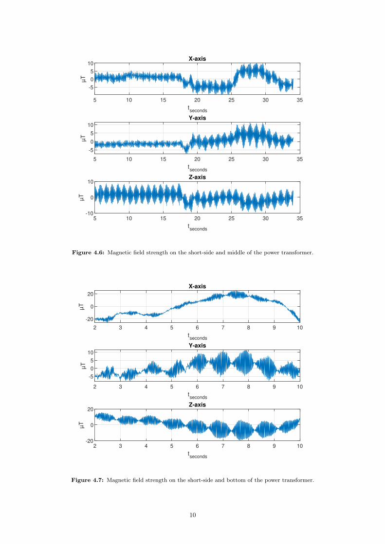
4.2.4 Measurements around power transformersTesting on actual power transformer was done in Danmarks Tekniske Universitet(DTU) PowerLab facility.The test was conducted with a 100Hz sampling rate on the microcontroller. Due to safety concern thedata gathered was only taken on the short side of the transformer. In Figure 4.6 the recording is on theshort side at the middle of the transformer, the MCU is slowly moved closer to the transformer. Thesame test in Figure 4.7 but on the bottom side of the power transformer. For both tests the MCU wasaccidentally turned during sampling, creating an offset which is quite obvious in the X-axis for the secondtest. The test was carried out at around 5-10cm distance to the transformer box.The mean rms-value of the magnetic field for this was around 7µT .
No test of the flux was done in any other areas like the walkway or further away from the transformer.It is possible that the flux originates from the transmission line on top of the box and not from the coilsinside the transformer.
9
5 10 15 20 25 30 35
tseconds
-5
0
5
10
µT
X-axis
5 10 15 20 25 30 35
tseconds
-5
0
5
10
µT
Y-axis
5 10 15 20 25 30 35
tseconds
-10
0
10
µT
Z-axis
Figure 4.6: Magnetic field strength on the short-side and middle of the power transformer.
2 3 4 5 6 7 8 9 10
tseconds
-20
0
20
µT
X-axis
2 3 4 5 6 7 8 9 10
tseconds
-5
0
5
10
µT
Y-axis
2 3 4 5 6 7 8 9 10
tseconds
-20
0
20
µT
Z-axis
Figure 4.7: Magnetic field strength on the short-side and bottom of the power transformer.
10

A measurement for a transmission line conducting 140A at 400V was also tested. An image of thetransmission lines is shown in Figure 4.8. The measurement is shown in Figure 4.9 where the measurementdevice is slowly approaching the brown cable until the measurement device reaches the wire. This resultshowed a greatly higher magnetic field versus outside the transformer box. Comparing the theoretical eq3.1 and the result in Figure 4.9, assuming 5cm from the center of the transmission line and the device.The theoretical created magnetic field is
B =4 · π · 10−7
2 · π · 0.05140 = 560µT. (4.2)
which is a bit off the max rms from the measurement of 340µT shown in Figure 4.9.
Figure 4.8: Transmission line for the transformers.
11

52 54 56 58 60 62 64 66
tseconds
-500
0
500µ
T
X-axis
52 54 56 58 60 62 64 66
tseconds
-200
0
200
µT
Y-axis
52 54 56 58 60 62 64 66
tseconds
-50
0
50
µT
Z-axis
Figure 4.9: Magnetic field strength on a transmission line carrying 140A.
4.3 Magnetic induction harvester and low power electronicsThe following section will introduce a free standing design as developed by another report [14]. The namefree-standing referring to a coil that can easily be installed anywhere where magnetic flux is present. Twodifferent structures will be simulated to understand the flux induced through the core of the material.The two different designs to be compared are the bow-tie design versus a normal cylindrical design. Thesimulated value will then be used to get an estimate of possible voltage and power output that could beextracted from the designs. The voltage induced across the copper wire that surrounds the coils was notable to be simulated. This due to limitations in the chosen software FEMM. The copper wire can be seenon the edges of the FEMM simulation in Figure 4.10 and 4.11. Instead of getting the voltage from theprogram, a review of other studies is done to conclude the possible voltage output.
Further, a review into the viability of using it and some low power electronics will be introduced forpossible energy extraction. This will only take focus on how to rectify the alternating voltage efficiently.
4.3.1 FEMM simulation of free standing designFor the free standing design a 16 cm long cylinder of diameter 0.8 cm was put into the simulation profile.The core permeability is set to a constant µr = 2000. The design of this is shown in Figure 4.10 anda design with the bow-tie shape is presented in Figure 4.11. The magnetic field in the simulations is aconstant 30µT -field at 50Hz.
From the coil in Figure 4.11 a maximum of around 600µT was induced in the core. For the bow-tiedesign the maximum was 900µT and also showed property of having a more even distribution of theinduced field. That is an increase of 50 % can be seen in the bow-tie design. The software used doesnot support what voltage could be induced in the terminals of the copper wires surrounding the twodifferent coil design. Though using information from [14] that has similar design and a magnetic field of7µT showed that an open voltage of 0.5V could be achieved with 5000 windings around the coil for thebow-tie design.
12

Figure 4.10: Induced flux Θ in a cylindrical coil for a 30µT uniform field.
Figure 4.11: Induced flux Θ in a bow-tie for a 30µT uniform field.
4.3.2 Electronics to rectify and boost low voltagesThe voltage that is possible to be induced in a coil mounted on the side of a transformer is low. For thisparticular device the voltage needs to be boosted up to 5V . Figure 4.12 shows a possible solution. Theinduced voltage from the coil is rectified and stored in a supercapacitor. This is done as the EH-coil willnot be able to sustain enough power output to continuously power the MCU. After enough energy havebeen stored in the supercapacitor it can further be transmitted to a DC/DC booster and the device.
Figure 4.12: Possible free-standing energy harvesting design.
The first step in the block diagram is rectification of the input voltage and is what will be explored thor-oughly in this section. The possible sources where this is relevant is either vibration or an electromagneticsource due to the alternating voltage they produce.
13

For this, a traditional full-bridge rectifier will be compared with a cross connected bridge using mosfetsused in CMOS construction as specified in [15]. An active bridge using mosfet and external power supplywill also be explored. Lastly, an IC specified for boosting low voltages in energy harvesting applicationsis investigated to conclude if any of the options are viable for powering an MCU.
For the forthcoming section a peak voltage of Vp = 0.4V will be assumed as the input source to comparethe different AC/DC approaches. This particular voltage can be hard to achieve on a free-standing coilnext to a transformer, the value is chosen as a best-case scenario. Also the efficiency where assumptionsare needed will have a 100 % efficiency.
The full-bridge rectifier consists of 4 diodes connected as shown in Figure 4.13a. The main issue withusing a diode is the voltage drop across the diode. Though the voltage drop can be as low as 0.15V forsome specific schottky diodes. This means that at least 0.3V is lost during the conversion to DC. Forthe low voltage that the energy harvesting produces this could be a significant loss. Another option is touse a cross-connected bridge using mosfets, shown here in Figure 4.13b.
(a) diode bridge
(b) cross-connected
Figure 4.13: Schematic of two types of rectifiers.
The third option is to use mosfets as active diodes. Due to the low conducting resistance Rds of themosfets, there is very little loss of voltage compared to a diode. To choose the ON/OFF state of theactive diodes a comparator can be used as shown in Figure 4.14. The issue with this approach is that anexternal power supply is needed to power the comparators and the two negative charge-pumps to makethe P-channel mosfets conduct.
The major issue with active diodes is the external power supply which in power consumption terms couldexceed the power harvested from a coil or a vibration source. Another issue is what happens if the batteryor external power supply gets depleted then it is not possible to start the operation again without theneed for a start-up circuit.
For these three possible designs a spice simulation is shown in Figure 4.15. For an input of V = 0.4Vppand an output of a 22µF capacitor in parallel with a 10kΩ resistor.The cross-connected bridge was theworst to retain the voltage. The cross-connected bridge was followed by the diode bridge and the bestwas the active diode.
14

(a) Active diode configuration
(b) Schematic
Figure 4.14: Schematic of active diode
Figure 4.15: Comparison between diode bridge, cross connected and active diode bridge
The objective of the presented methods is that should be able to power an MCU. Assuming that theMCU can do the required measurement and transmit this data during a 10 s period and it is using 10mAat 3.3V . The required energy for this operation would be
Emcu = 3.3 · 0.010 · 10 = 330mJ. (4.3)
For a capacitor charged to 0.3V the required size to hold this energy would be
C =2 · Emcu
V 2cap
= 2 · 0.330
0.32= 6.67F. (4.4)
To boost up the voltage from 0.3V to 3.3V will be very inefficient. This could either be done with acharge-pump or a specialized IC for low-voltage DC/DC. Both require an external power supply. As-suming further that getting the boosted voltage is possible and for the sake of the argument that theconversion is 100 % efficient.
The charge-up time to reach 270mV for a 6.67F for the diode bridge using the spice simulation takes10000min or 7h. A simulation for the active rectifier would take to long to execute. Instead, assumingsimilar behavior as in Figure 4.15 the charge-up time for the active diode would be around 3.5h or halfthe time of the diode bridge.
A more efficient option is to go with a specified IC for energy harvesting. Linear technology has multiplechoices. For example the LTC3108 that was used in [7] for induction and in [2] for a thermoelectric
15

generator.In this project a similar module, the LTC3109 will be explored as it can handle low-frequency AC voltage,an ability that the LTC3108 is lacking. With the same set-up as earlier an ideal input voltage sourceof 0.4V is used as the input voltage. For the LTC3109 it would take 1h to charge the capacitor to 2V.Which is both faster and gives a higher voltage than the other circuits presented.Using an input voltage of 0.2V instead it would take 3.25h to reach 2V .Additionally, at 2V the efficiency to boost the voltage to either 3.3V or 5V would be much greaterversus an initial voltage of 0.4V.
A coil energy harvester will have a certain source impedance from the inductor. To maximize the poweroutput to the rectifier and the load the source impedance and the load impedance should be matchedRL = Rs according to the power transfer theorem
PL = V 2s
RL
R2L +R2
S
. (4.5)
Where RL is the load and RS is the source impedance. To test how the source impedance affects thecharging characteristic of the IC, a test where the internal resistance of the voltage source is changed inthe spice simulation was made. By using the previous Spice profile but changing the internal resistanceof the voltage source to 1 Ω it could be concluded that the charging time changed from 3.25h to 3.5h forthe LTC3109.Increasing the internal resistance to 5 Ω resulted in the IC malfunction and not generating any output.
In conclusion to be able to power an MCU from a coil two feature are required:
1. High enough voltage to be able to run an IC like the LTC3109 to further boost up the voltage. Thestart-up voltage for the LTC3109 is 200mV .
2. Low impedance of the coil due to the power transfer theorem stated in eq 4.5. The impedance is afactor of the number of turns around the coil by the copper wire.
The level for the magnetic field found around a transformer that was measured in section 4.2.4 of 7 µT isvery low. To reach the level of 200 mV required for the start-up of the LTC3109 a lot of winding arounda coil would be needed and therefore creating a high impedance.
For example in [14] with a magnetic field of 7µT the authors could achieve 0.5Vrms with 5000 turns of acopper wire which resulted in resistance of 500 Ω. This is probably too high of source impedance to runthe LTC3109 according to the power transfer theorem.
No further test by wiring coil thousands of turns and testing it close to a transformer was done. This asprevious studies as the one stated above in [14] and a master thesis from KTH [7] where they alreadyconcluded that a low voltage output will be produced from a low flux source like a power transformer.
Due to the high number of turns required, the high impedance and low voltage that could be produced,another method of power extraction will be explored in the next section.
4.4 Current transformerA current transformer build-up and operation was shown in section 3.4 and in Figure 3.1. The normaloperation of a CT is to use it to measure current on high current lines.
By utilizing a current transformer as an energy harvester device, the available B-field increases drasticallyversus the free-standing one. From section 4.2.4 and Figure 4.9 the available magnetic field is muchhigher with up to 340µT versus the 7µT for the free-standing one that would be possible outside ofthe transformer. But more importantly is that the CT surrounds the wiring making the magnetic pathcircular and highly efficient versus a free-standing design where the magnetic path isn’t as obvious. Thelarge difference makes it theoretically possible to power the MCU easily as well as to charge the batteryonboard of the module.
Multiple studies have created this type of energy harvester. Texas Instrument(TI) has created an appli-cation note/reference design to use [16]. The TI application note does not however have any protectiontowards overcurrent for the supercapacitor which could potentially be a problem. Also, this design doesnot take into regard the possibility of a very high voltage being induced in the terminals of the CT whenused for charging a capacitor. The high voltage issue will later be presented in eq 5.2.
16

Another study which focuses on being able to use the same CT for harvesting and measuring the currenton the transmission line have shown to be successful [17] [18] .
Due to the higher rate of success using a current transformer energy harvester versus a free-standingdesign, the CT-harvester design will be chosen as the next step.
The following section presents the design of the current transformer energy harvester. This will largelybe based on the plug and play design [18]. It will explain the operation and also the modifications of thedesign to suit the device under test better.
17

5 Current-transformer as a power supplyThe work presented in this chapter is based on the Plug And Play method [18]. This uses a CT to harvestenergy from a transmission lines induced magnetic field. The energy is stored in a supercapacitor whichat a selected voltage will transfer the energy to a device.
The choice of CT will firstly be presented in the next subsection 5.1 and the bare formulas regarding it. Alimitation in this study is that the mathematical and electrical model that describes a current transformerwill not be explored thoroughly. Instead the approach is to take an of-the-shelf CT to find out if a highenough voltage can be produced to charge a supercapacitor and in turn power a microcontroller.
To test which voltage levels the CT can reach a test-station is constructed. This is presented in Section5.2. The test-station will also be used for testing the circuitry and PCB that gets its power from theterminals of the CT.
The design of the PCB and the theory of operation is lastly presented in section 5.4.
5.1 Current transformer operationIn the Plug and Play [18] a CT with the specifications: 0A − 60A, 0A − 1A, 0.25VA was used. Thename Plug and Play refers to using a split-core CT that can easily be installed on a transmission line.
Working from the same principle with a split-core, the chosen CT adhered to the specification in atransmission line carrying 400V max 250A.
To comply with these requirements a CT from Wago [19] was chosen, the specification of the CT ispresented below:
• Primary current: 0A− 250A
• Secondary current: 0A− 5A
• Rated power: 1VA
• Accuracy class 0.5
5.1.1 Simplified electrical current transformer modelFrom the ideal power equation of transformers we have
IpIs
=VsVp
=Ns
Np. (5.1)
This equation holds true for when the efficiency in the transformer is 100 %. Assuming this to be trueand that the CT will act as an ideal current source the voltage generated in the secondary terminal is
Vs = RLIs = RLIpNp
Ns. (5.2)
The actual voltage induced is quite different, this behavior has been explored further in [17]. For anactual CT, the core of the CT will saturate due to the magnetic flux at a specific point, stopping furthervoltage increase. In this study, the knee-point at which the CT saturates will not be explored.
The simplistic eq 5.2 would for an open circuit equal a high RL and therefore a high voltage. This meansthat for safety purpose the terminals of the CT should always be connected to a low impedance source.
5.2 Test-stationFor testing the CT and later the PCB a test-station was designed. The test-station would simulate themagnetic field generated from the transmission line at 400V , and up to 200A.
The design of the test-station is shown in Figure 5.1. It uses a transformer that transforms the mainsvoltage 230VAC to 15VAC . A busbar splits the current into four lines, these are directed to four 50Wresistors with different resistances. The current is then moved into a Raspberry Pi Relay board [20]. Therelays are in turn connected to a neutral busbar that combines them into one power line again.
18

Figure 5.1: Schematic of test-station. The current transformer will be placed around the "loops of wire".
The transformer used has dual outputs rated to 3.6A per line at 15VAC . To maximize the power outputthey were connected in parallel achieving a maximum of 7.2A output. The CT chosen operates in the0A-250A range, as the transformer can’t reach these currents an apparent current method is used. Bylooping the output wire N times through the CT the apparent current and the induced magnetic fieldwill be multiplied by N .
To be able to change the current to test how the CT and circuitry works under different currents therelay board is used. The current and the corresponding resistance is shown in table 5.1. The table alsoshows the apparent current when the wire is looped around N times.
Table 5.1: Apparent current induced on the four lines for the CT for different turn ratios.
Turns/Resistance R1 = 22Ω R2 = 11Ω R3 = 7.5Ω R4 = 5.6Ω1 0.68 1.36 2.0 2.685 3.41 6.82 10.0 13.3910 6.82 13.64 20.0 26.7915 10.23 20.45 30.0 40.1820 13.64 27.27 40.0 53.5725 17.05 34.09 50.0 66.9630 20.45 40.91 60.0 80.36
The default value is N = 30 turns. Possible current levels here are 20A−200A with a resolution of 20A.To control the relays a Raspberry pi zero is used. It communicates through I2C with the relay board.For this, a python library [21] is used. Using the library a code-set was constructed making it possible towrite in a value of 20, 40, 60...180, 200 in a terminal and the relay would switch into the specific position.A thorough list is presented in table 5.2 showing which lines are activated for a certain mode and theircorresponding current.
Table 5.2: At N = 30 the following modes can be set by the code. The table shows the activated lines and thecurrent output.
R1 R2 R3 R4 R2R3 R2R4 R3R4 R1R3R4 R2R3R4 R1R2R3R4
20.45A 40.91A 60.00A 80.36A 100.91A 121.27A 140.36A 160.81A 181.27 201.72A
The test station is shown in Figure 5.2. A heat-sink is used as a base where the resistors and two DIN-rails are glued to the base using thermal-conductive glue. DIN-rails are placed for easy attachment ofthe busbars. The raspberry pi and its relay board are also connected on the DIN-rail using a 3D-printedmount-case. The wiring used is 1.5mm2 and should be able to withstand current up to 22A in well-ventilated areas. Due to the small terminal blocks at the relay, smaller red wiring was used for some ofthe resistors.
19

Figure 5.2: Test-station build up with CT on the bottom right with 6 wingdings through it.
5.3 Test of Current TransformerTo check how well the CT compares to an ideal current source as in eq 5.2 and how much it is affectedby the core saturation a test was set-up. The set-up is shown in Figure 5.3, using the test-station set onan apperent current of ip = 2A. The CT is connected to a potentiometer, anmeter, and a voltmeter.
Starting with the potentiometer at 0 Ω the current through the Anmeter was 0.2A. The resistance inthe potentiometer was steadily increased up to 64 Ω, the result is shown in Figure 5.4. The figure showsthe voltage, current, and power through the system. As can be seen in the figure at 10 Ω the voltageand current leaves the linear region. This is also obvious from the power graph. At this point, the corepossibly starts to saturate.
Figure 5.3: Test set-up for testing CT
20

Figure 5.4: Test of CT for an input current of its = ip = 2A for different resistance in the terminals of the CT.Voltage, current induced in the terminals and power is presented.
To be able to use the CT as a power supply it needs to generate a high enough voltage level.To find the voltage level produced at a specific load, a test was done with a 1Ω resistor where the currentin the test station was changed in the range Ip = 2A− 60A.The result of the voltage and current induced in the load is shown in Figure 5.5. The maximum voltageand current induced in the load was 1.75V with is = 1A through the CT at ip = 60A. This is a poweroutput of PL = 1.75W . Though as the resistor used is only rated for 1W as well as the CT for 1W dueto this no higher current testing was done at this level.
Figure 5.5: Plots of voltage and current induced of the CT for a RL = 1Ω load on the CT’s terminals.
Assuming that the voltage can be increased further linearly and not saturates at this load, the voltage
21

induced could be written as the linear relationship
VL =1.75
60ip. (5.3)
At ip = 100A for example the voltage would reach 2.9V . From test 1 in Figure 5.4 it could be assumedthat the lower value resistance < 1 Ω would be in close proximity to this value.
The values presented in Figure 5.5 seems to break Ohm’s law if compered directly to the schematic inFigure 5.3. For example the max value in the graph on the right shows that resistance and the currentis RL = 1 Ω and is = 1A. That is a VL = 1 Ω · 1A = 1V should be present, but the left graph records avalue of VL = 1.75V .Possible reason for this could be the due to the voltmeter is measuring the voltage across both theanmeter and the potentiometer. An anmeter is made of a shunt resistor with a value in the range of0.2 Ω. Moreover the potentiometer might not be exactly set to 1 Ω, further as its only rated for 0.25Wperhaps this affects the resistance when excess power is put through it. These factors could all contributeto the difference in expected result.
22

5.4 Design and Theory of Operation of the Current Transformer HarvesterIn the forthcoming sections the electronics to harvest the energy from the current transformer powersupply will be presented. This will start with introducing the previous work from [18]. Where a brieftheory of operation will be given.To fit the specification for the device under test better a revised circuitry will be presented. The revisedcircuitry will have added feature as continuously charging/powering an MCU and some simplifications ofthe design from [18].The schematic and operation of the different parts/circuits in the system will then presented one by one.
5.4.1 Theory of operation for the plug and play methodThe circuitry used in Plug and Play [18] works by using a half-wave rectifier for the input of the CT. Thisis then transferred to a supercapacitor as an intermediate step to store the energy. When the voltagein the capacitor reaches 2.5V the stored energy is transferred to a boost converter by an undervoltagelockout(UVLO) module. The boost converter has two tasks:
1. Power the MCU
2. Start the short-circuit/measurement mode, this entails using a shunt resistor to measure the currentwith the help of an instrumental amplifier that is connected to the MCU.
The MCU will measure the current and send data wirelessly over to the user. When the voltage in thecapacitor depletes down to 1.5V the boost converter will shut off and in turn shutting off the MCU. Onceagain the process restarts and starts charging the capacitor until 2.5V is reached. A timing diagram ofthe operation is shown in Figure 5.6. The red line is showing when the UVLO starts conducting andthe blue is representing when it stops conducting. The short circuit mode represents the "measurementmode".
Figure 5.6: Timing diagram of plug and play. Red line representing when ULVO goes high and blue low.
5.4.2 Theory of operation for the revised circuitryAs seen in Figure 5.6 the boost converter will shut off, and as a consequence, the MCU will shut off whenthe capacitor charging mode starts.For the revised circuitry a continuous on-mode will be added for the MCU/Battery Charging.
This is achieved by adding a schmitt trigger that switches modes at specific voltages in the supercapacitor.The revised timing diagram is shown in Figure 5.7.Similar to earlier, red and blue represent the undervoltage lockout. Here the schmitt trigger operationhas been added as shown with green and pink lines. The benefit is that if enough power is present in thetransmission line that the CT can use, then the MCU/device can continuously be on and transmit datato the user.At the end of the timing diagram, it is assumed that the current through the transmission line is removedmomentarily thereby causing the design to shut off the MCU.
Other feature and changes made to the design are:
• AC/DC is changed to a full bridge rectifier.
23

• Undervoltage Lockout is changed from a patterned circuitry [22] to an IC.
• Boost converter outputs 5V instead of 3.3V .
• Feature for being able to measure the current have been removed.
A block level scheme of the circuit is shown in Figure 5.8.
Figure 5.7: Timing diagram of revised CT harvester. The end of timing diagram shows how the design acts ifthe current through the transmission line is removed momentarily. The dotted lines represents Red = VH , Blue= VL, Green = VSH , Pink = VSL.
Figure 5.8: Block level scheme of revised plug and play circuitry.
24

5.4.3 AC/DCRectification of the input voltage is performed using a full-bridge rectifier with schottky diodes. Theschottky diodes need to be rated above the maximum CT input of 5A. The input and the burdenschematic are shown in Figure 5.9. The burden schematic will further be explored in section 5.4.9.Schottky diode is used to lower the voltage-drop versus normal diodes. This will help slightly to keep thevoltage level down and in turn the reduce the strain on the CT.
Figure 5.9: Input of a current transformer on the left. The CT’s terminals are then connected in parallel withthe burden module and the bridge rectifier. The Mode Selector will decide which path the current will take.
5.4.4 Overvoltage and overcurrent protectionIn Figure 5.11 the circuitry for overcurrent and overvoltage protection is presented on the left. Theovercurrent protection is the same design as in plug and play [18]. It uses a PNP transistor, a P-channelmosfet, and a shunt resistor.
The PNP transistor will conduct in the active region when there is voltage difference of 0.6−0.7V betweenthe base and the emitter VBE . The shunt resistor Rs will control when Q3 conducts. This value is currentcontrolled and is determined by ohm’s law(using VBE = 0.6V )
Rs =VBE
is=
0.6
is. (5.4)
When the current through the system reaches is, the PNP-channel will open and charge the gate ofthe P-channel mosfet Q4. This forces the P-channel mosfet to stop conducting which in turn limits thecurrent.
The circuit is added to protect the supercapacitor from overcurrent as the chosen supercapacitor is limitedby a maximum charging current.
In the schematic three different lines Rs1, Rs2, Rs3 have been added for testing. These represent in total7 possible charging modes for 100mA, 200mA...700mA. These have been added for verification of thecircuitry. Table 5.3 shows the resistance and the corresponding maximal current that will pass throughthe resistors. A simulation of the different charging-modes available is shown in Figure 5.10.
Table 5.3: Overcurrent shunt resistors control
Ω ishuntRS1 6 100mARS2 3 200mARS3 1.5 400mA
25

Figure 5.10: Spice simulation of the 7 available modes. A current source is increased from 0A to 1A linearlyduring 1 s.
The overvoltage-protection operates using a zener diode D6 with a breakdown voltage of 3.9V . Thesimulation in Figure 5.10 shows an increasing input of 0A−1A during 1 s where the current is limited bythe transistors. Assuming an ideal current source the excess current has to go somewhere or to create avery high voltage as stated in eq 5.2. The zener diode is placed as protection to remove the excess powerduring the charging operation.
The zener diode has a breakdown voltage of 3.9V and a maximum of 5W continuous power dissipation.Thus the maximum current through the zener diode until the 5W limit is reached is
izen = 5W/3.9V = 1.24A. (5.5)
This would mean that if the CT acts as an ideal current source the maximum current allowed into thecircuit is 0.7 + 1.24 = 1.94A, where 0.7A refers to is as presented in eq 5.4. When the Rs shunts are setto the maximum of 0.7A. This corresponds to a maximum of ip = 97A in the primary line.
Figure 5.11: Schematic of Overcurrent/voltage protection, supercap and the undervoltage lockout.
26

5.4.5 SupercapacitorThe supercapacitor is an intermediate point for energy until enough energy has been stored and further istransmitted to the device. The use of this makes it possible to keep the voltage level down in the CT andtherefore decreasing the strain on it. Additionally, if not enough power can be harvested from the CTit can charge up to a specific point and then transmit the power at discrete time intervals. The chosencapacitor has an value of C = 0.47F.
5.4.6 Undervoltage lockoutThe undervoltage lockout is used to prevent a state where the boost converter and the charging mechanismconnected to it does not flicker on and off. This could occur when the voltage level is low in thesupercapacitor. Specifically for this build, the power required to charge the battery as stated in theintroduction of Chapter 4 is 200mW . This is quite high and would require high enough voltage to notmake the charging mechanism switch off instantaneously.Additionally the efficiency of boost converter depends partly on the voltage level in the source, that ishigher efficiency at a higher voltage meaning a higher voltage is preferred.
In Plug and Play [18] a patented electric circuit [22] was used. In this report, a design using an IC withsimilar characteristics was opted for. The MIC2779L [23] is a voltage supervisor that can detect twoseparate voltages. The IC is not relying on specific external voltage as 3.3V or similar as is common.Instead, it can work on a variable power source down to 1.5V . The variable power source here would bethe supercapacitor. This makes it ideal to use as a schmitt trigger for undervoltage lockout.The operation of the undervoltage lockout IC was shown earlier in the timing diagram in Figure 5.7. Thered and blue lines shows the levels when the ULVO switches ON/OFF. VH is the red line and representsthe high level and VL the low level. When the capacitor voltage is above VH the output of the IC are sethigh. When the voltage drops below VL the output is set low.
The schematic is shown Figure 5.11. The VH and VL are set by the three resistors R10, R11 and R12.The voltage is set according to equation 5.6, 5.7 and 5.8 below where Vref = 1.24V and Rtotal is set to1MegΩ.
VL = VrefR10 +R11 +R12
R11 +R12(5.6)
VH = VrefR10 +R11 +R12
R12(5.7)
andRtotal = R10 +R11 +R12 (5.8)
The trigger values are set to VL = 1.5V and VH = 2.5V . The resistor values is then set to
• R10 = 496kΩ
• R11 = 330kΩ
• R12 = 173.3kΩ .
The output \RST is connected to an NMOS Q5. When the output is set high the mosfet conductsand opens the channel of the PMOS Q6 to let the supercapacitor conduct to the boost converter. Thechannel will be open until VL = 1.5V in the supercapacitor is reached, at this point \RST will go lowand stopping the flow of power to the boost converter.
5.4.7 Boost converterThe boost converter used is the TPS61322[24], which boosts voltage from voltage level as low as 0.9Vup to 5V . At the lowest level the efficiency is too low to be able to charge the battery. The minimumvoltage required is 1.5V to be able to output a stable 100mA at a reasonable efficiency.
The schematic is shown in Figure 5.12. A snubber circuit is added to the design but not required.
27

Figure 5.12: Boost converter schematic.
5.4.8 Schmitt trigger - harvesting or measurement modeTo change between the harvesting(charging supercapacitor) mode and the short-circuit/measurementmode, a comparator with hysteresis (schmitt trigger) will be used. For this purpose, a TLV7031 [25]comparator is used. The schematic is shown in Figure 5.13. It is set in the inverting configuration, R13
and R22 sets the reference voltage Vref .
In Figure 5.7 the green and pink lines represent when the schmitt trigger switches. These are representedas VSH = 2.7V , when this value is reached the comparator switches to short-circuit/measurement mode.When the value goes below VSL = 1.7V the comparator switches back to charging.
To decide the resistors needed for the configuration stated above the following three equations can beused. Equation 5.9 chooses the higher voltage value, eq 5.10 chooses the lower threshold, and eq 5.11decides the ∆V between the two set values.
Where Vcc = 5V is the boost voltage output.
VSH = R8VrefR9
+ Vref (5.9)
VSL =Vref (R8 +R9)− VccR8
R9(5.10)
∆V = VccR8
R9(5.11)
The set reference voltage is Vref = 2.25V . In Figure 5.14 a spice simulation of the output voltage isshown versus an alternating input voltage.
28

Figure 5.13: Schematic of mode selector/comparator
Figure 5.14: Simulation of schmitt trigger where red is input voltage and blue is output voltage. The switchingoccurs at the specified VSH = 2.7V and goes low at VSL = 1.7V .
5.4.9 Burden/Shunt resistorWhen the capacitor has charged to VSH = 2.7V the schmitt trigger will open a channel through twoN-channel mosfets as depicted earlier in Figure 5.9. Using the two mosfet in this configuration will let ACvoltage flow through them by utilizing the internal diode of the mosfets. The maximum power output ofthe specified CT is 1W . The largest allowed load connected to it is to keep within the boundary of thepower specification of the CT is
Rmax =P
I2max
=1W
5A= 40mΩ. (5.12)
This shunt resistor is added as the short-circuit mode.
29

5.4.10 Instrumental amplifierIn Plug and Play [18] an instrumental amplifier was used to measure the current. As that design reliedupon only using a half-wave rectification the ground plane was the same on the input of the CT as therest of the circuit. This made it possible to use the shunt resistor to measure the voltage difference acrossthe shunt. In the design for this report, a full-wave rectifier was opted for making the same approachof measuring the voltage difference across the shunt resistor more difficult and it was thus not exploredfurther.
If instead only the half-wave rectifier was to be used a solution with fewer components is presented belowin Figure 5.15. The input is from the shunt resistor of size 40mΩ. The output could be connected to themicrocontroller under test.
Figure 5.15: Schematic of a instrumental amplifier. Input from a shunt resistor, the signal is amplified to0.3V-3V at maximum current of 5A.
30

6 Result of current transformer harvesterThe PCB is shown in Figure 6.1. Some mistakes can be seen, the IC in the air is the comparator wherethe VCC and the VEE line got mixed up in the schematic. Secondly, a capacitor was placed on the wrongside of the inductor of the boost converter.
Figure 6.1: Populated PCB of the CT-harvester.
In Figure 6.2 a test of the overcurrent circuitry is done. The voltage is increased with steps of 0.5V ona test-point located at the input of the Overcurrent/overvoltage protection that can be seen in Figure5.11. The current consumption is monitored using the power supply.A 5 Ω load is connected at the 5V output terminals. For the modes 100mA and 200mA the modes reachthe saturation of their respective values. The 400mA and 700mA is never able to reach their respectivesaturation current.At 3V and higher, the zener diode seems to start to conduct or possibly something internal in theprotection circuitry increasing the current flow. From 3.5V to 4V a high increase can be seen for allmodes except the 700mA-mode. This is caused by zener diode reaching its breakdown voltage of 3.9V .
31

Figure 6.2: Test of overcurrent/overvoltage protection for the three separate modes 100mA, 200mA, 400mAand all of them combined. Tested with a 5 Ω load.
In Figure 6.3 the PCB is connected to a DC power through the CT-input terminal, the power-supply isset to 3.7V and current limited to 0.2A. The 5V output is connected to a 100 Ω load. In the figure,four nodes are measured, Capacitor voltage, Undervoltage lockout mode, mode selector, and the 5Voutput line. When the capacitor reaches VH = 2.5V the UVLO(pink line) goes high. This causes theboost converter and the mode selector to go high. This stops the charging process of the capacitor andredirects the input voltage through the burden resistor of 40mΩ. When the capacitor voltage decreases toVSL = 1.7V the mode selector goes low and starts charging the capacitor. This happens until VSH = 2.7Vis reached again. Then the process is repeated.
The start-up is not working correctly as the mode selector is not supposed to go high at VH = 2.5V butat VSH = 2.7V . This only occurs at start-up when the overcurrent protection is active. When the boostis powered on directly by a power supply from the input where the capacitor is placed this issue does notoccur at start-up. This could perhaps be solved by adding a 5V Low-dropout regulator smoothing outthe output voltage if a high transient voltage is present initially. Possibly the behaviour caused by eitherthe boost or the overcurrent limiter. A second option might be to add a snubber circuit on the boostconverter as the PCB was designed for this but not populated.Although this behaviour only occur once at start-up so not a critical problem.
Figure 6.4 shows what happens if the power supply is shut off momentarily. The red opaque line indicateswhen supply is turned off causing the undervoltage lockout to turn off further causing the 5V output toturn off. The white line indicating that the DC power supply is turned on again. Same issue here, theUVLO, Boost converter, Mode selector all turn on at the same time at VH = 2.5V .
32

Figure 6.3: Operation of system for a continuous input current, Yellow - Capacitor voltage, Pink - Undervoltagelockout, Blue - Mode selector, Green - 5V output voltage for load
Figure 6.4: Operation of system when input supply is shut off. The opaque red line shows when power supplyis shut off and white when its turned on again. Yellow - Capacitor voltage, Pink - Undervoltage lockout, Blue -Mode selector, Green - 5V output voltage for load
The full set-up using the test-station and current transformer can be seen in Figure 6.5. The minimumapparent current through the test-station needed to start the boost converter and power a load wasreached at Ip = 20A. At this point, the supercapacitor reached a maximum of 2.6V . At this level, itwasn’t able to switch to short-circuit/measurement mode. Operation where the device switched betweenharvesting mode and short-circuit mode as shown in figure 6.3 could be reached at a slightly higher
33

current Ip = 20.45A. The device was tested up to Ip = 67.27A and functioned correctly.
During the harvesting mode, the CT made a buzzing sound due to the high load across its terminals.Assuming that the CT is ideal then at Ip = 67.27A a secondary current of Is = 1.34A is induced.Neglecting the voltage drop over the diodes the capacitor voltage reaches 2.7V . The maximum powerdissipation is then P = 3.6W which greatly exceeds the rated power dissipation of 1VA.
Figure 6.5: Set-up of test-station and current transformer to power and test the board.
7 Discussion and Future work for the CT HarvesterThe prototype produced in this report has multiple issues on the schematic level. The mistakes being thewrong placement of a capacitor for the boost converter and the mix-up with the VCC and the VEE linefor the mode selector. For a second iteration, the two wrong designs should be resolved. Moreover, thePCB was designed for testing, that is, lots of 0 Ω resistors, pin headers, LEDs, and testpoints to test thedifferent IC’s separately, and for troubleshooting. These can all be removed which will greatly decreasethe size of the PCB.
The current-limiter test that was presented in Figure 6.2 was flawed. The issue is that it was not verifiedthe amount of current that went through the overcurrent circuitry versus the zener diode. This couldeasily have been done by measuring the current through the load to get the proportion of the direction ofthe current. For the test done only an assumption was made that the 3.9V zener diode began to slightlyconduct at the level of 3V − 3.5V .Further no analysis have been made of why the overcurrent-circuitry didn’t conduct as expected fromthe simulations for the higher level of 400mA and 700mA. That is, comparison between simulations inFigure 5.10 and the results in Figure 6.2.
The issue with the mode selector going high prematurely shown in both Figure 6.3 and 6.4 could beinvestigated further. Though this is not critical to the operation. A possible solution could be to use a5V low dropout regulator if the start-up gives a high short transient pulse to the mode selector.
The super-capacitor of 0.47F used in this work would degrade max 30% of the capacitance after 500.000charges and discharges. In this design, the capacitor is never charged fully nor fully depleted. Assumingthe worst-case scenario that the capacitor reaches the 30% degradation rate at the specified recharges.
34

For a continuous 50mA output this would mean that in 24 days this number of charges would have beenreached. That is, care needs to be taken of choosing a high-quality capacitor of a size that suits the powerconsumption and the time it needs to be out on the field. Also, consideration should be taken to createpower-efficient firmware to extend the longevity of the capacitor.
The current transformer has an output in the current of 0A − 5A and is rated for 1V A. The highcurrent output is a significant problem which makes this particular CT not safe to use for anything aboveip = 97A as specified in Section 5.4.4. This is due to the max power rating is reached on the zener diodeat this current. A more proper choice of CT would have been to choose the model with an output of is0A− 1A that the same manufacturer produces.
Another option to lessen the strain on the CT is to keep the voltage down. This can be achieved byletting the UVLO and mode selector work on a lower voltage. Though this will decrease the amount ofavailable energy for the output. The equation for energy in a capacitor is
E =C · V 2
2. (7.1)
For the current model where energy is stored in the range VSL = 1.7V to VSH = 2.7V thus equals
E =0.47
2· (2.72 − 1.72) = 1.03400J (7.2)
If instead the levels are lowered to VSL = 1.4V to VSH = 2.4V the available energy would be
E =0.47
2· (2.42 − 1.42) = 0.893J. (7.3)
A slight decrease of 14 %. But this would also affect the efficiency of the boost converter due to lowervoltage in the capacitor creating a higher need for recharges. Therefore it could also possibly be puttinga higher strain on the CT due to the greater need for recharges.
As mentioned in the result the rated power of the CT is greatly exceeded for this build. Using a CT inthe range of 0-1A would possibly also exceed a rating of 1VA but not as excessively. It would also makeit possible to handle the full 0A− 250A and not be limited to 97A as in this build.This project was limited to taking an off-the-shelf CT and then quickly test if could achieve the desiredvoltages as was done in section 5.3. More testing of the physics regarding the CT could have beenmade for a greater understanding of the full system and its limitations. This was done in [17] where thesaturation effect and the excitation current ie were explored.
If this device is to be installed on a transmission line at 400V some care needs to be taken on how toinstall the MCU, the PCB, and the CT. If the CT malfunctions and becomes live at 400V this could posedanger to maintenance personal.
In Plug and Play [18] a half-wave rectifier was used making it possible to use an instrumental amplifierto measure the current in the transmission line. In this report this was considered unsafe due to possiblebreakage of the CT. But if it can be shown that it is safe using a half-wave rectifier it would be possibleto add this to the design as described in Section 5.4.10.
The use of a CT as a power supply on a continuously running transmission line would make it easy totransmit enough power to run a device. The prototype developed in this report would make it possibleto remove any battery that normally could be attached to an IoT device or similar. The removal of thebattery has several advantages it could possible be cheaper and could require less maintenance as no needto replace a battery. Further, if the device is connected wirelessly to a server no cable is required at alland even less maintenance can be expected.
35

8 ConclusionA current transformer power supply is developed that can harvest power from a transmission line thatcarries up to 250A at 400V . The power supply is based on another design but with modifications and theadded benefit of continuously being able to power the MCU versus the original design. The CT-harvesterhas been designed on a PCB and has been tested on a test-station where a current up to 67A presentin the transmission line has been tested. The CT-harvester have function correctly and could power anMCU or charge a battery.
The presented CT-harvester in its existing form will probably not work safely at a 400V transmissionline carrying up to 250A, it will only be considered safe up to 97A. But with some minor modifications,the full range should be achievable. Still, this method of power extraction can be dangerous if the CT inany way is faulty it could become live at 400V posing a great danger for personal.
In this study also the possibility to use a design placed on the side of the transformer was examined.Using sensor data from a microcontroller it could be deduced that vibration on a transformer is notenough to power an MCU.Examination of the magnetic field showed that only 7µT was present around a power transformer. Thislow value would mean that a large coil with thousands of windings would need to be placed next to thetransformer to achieve a high enough voltage to be useful. Though a large number of windings around thecoil would create a high impedance making the efficiency to transfer the power to electronics extremelylow and the possibility to power an MCU very low and probably not useful.
36

References[1] B. Johns, “An introduction to the wireless power consortium standard and ti’s compliant solutions,”
2011.
[2] P. C. Dias, F. J. O. Morais, M. B. de Morais França, E. C. Ferreira, A. Cabot, and J. A. SiqueiraDias, “Autonomous multisensor system powered by a solar thermoelectric energy harvester withultralow-power management circuit,” IEEE Transactions on Instrumentation and Measurement,vol. 64, no. 11, pp. 2918–2925, 2015.
[3] J. Drew, “MicroGen’s Piezo-MEMS Vibration Energy Harvesters Enable Linear TechnologySmartMesh IP Wireless Sensor Network.”https://www.analog.com/en/technical-articles/microgen-s-piezo-mems-vibration-energy-harvesters-enable-linear-technology-smartmesh-ip-wireless.html [2020-02-01].
[4] A. I. R. Moghe, “A low-cost electric-field energy harvester for an mv/hv asset-monitoring smart-sensor,” Annalen der Physik, vol. 322, no. 10, pp. 891–921, 2013.
[5] J. Ahola, T. Ahonen, V. Sarkimaki, A. Kosonen, J. Tamminen, R. Tiainen, and T. Lindh, “Designconsiderations for current transformer based energy harvesting for electronics attached to electricmotor,” in 2008 International Symposium on Power Electronics, Electrical Drives, Automation andMotion, pp. 901–905, 2008.
[6] OTLM, “ Overhead Transmission Line Monitoring).”https://www.otlm.eu/ [2021-01-30].
[7] O. Thorin, “Master thesis - power line induction energy harvesting powering small sensor nodes,”2016.
[8] S. Yuan, Y. Huang, J. Zhou, Q. Xu, C. Song, and G. Yuan, “A high-efficiency helical core for magneticfield energy harvesting,” IEEE Transactions on Power Electronics, vol. 32, no. 7, pp. 5365–5376,2017.
[9] R. Moghe, Y. Yang, F. Lambert, and D. Divan, “Design of a low cost self powered “stick-on” currentand temperature wireless sensor for utility assets,” in 2010 IEEE Energy Conversion Congress andExposition, pp. 4453–4460, 2010.
[10] “Revibe - Model D.”https://revibeenergy.com/modeld/ [2021-01-31].
[11] I. Said, H. B. Hussain, and V. Dave, “Characterization of magnetic field at distribution substations,”in 2010 9th International Conference on Environment and Electrical Engineering, pp. 423–426, 2010.
[12] D. Graubner, D. D. Filistovich, D. S. Hiebel, and R. Wengerter, “Practical examples of magneticfield measurements in industrial and environmental surroundings,” 2015.
[13] J. Wargo, “Evaluating Transformer Designs with Electromagnetics Simulation .”https://www.comsol.com/blogs/evaluating-transformer-designs-with-electromagnetics-simulation/[2020-12-29].
[14] S. Yuan, Y. Huang, J. Zhou, Q. Xu, C. Song, and P. Thompson, “Magnetic field energy harvestingunder overhead power lines,” IEEE Transactions on Power Electronics, vol. 30, no. 11, pp. 6191–6202, 2015.
[15] H. Rabén, J. Borg, and J. Johansson, “Improved efficiency in the cmos cross-connected bridge rectifierfor rfid applications,” in Proceedings of the 18th International Conference Mixed Design of IntegratedCircuits and Systems - MIXDES 2011, pp. 334–339, 2011.
[16] Texas-Instrument, “Energy Harvesting from Current Transformer with Super Capacitor for FaultIndicator Reference Design.”https://www.ti.com/tool/TIDA-01385#technicaldocuments [2020-12-15], 2017.
[17] D. Hauer, “Master thesis - energy harvesting und lastflussmessung in verteilnetzstationen mittelsstromwandler,” 2017.
37

[18] D. Hauer, K. Diwold, M. Schuss, L. Krammer, and T. Sauter, “Plug play monitoring for distributionsubstations,” in 2020 IEEE International Conference on Industrial Technology (ICIT), pp. 624–629,2020.
[19] “Wago - Split-core current transformer; Primary rated current: 250 A;.”https://www.wago.com/global/current-transformers-and-voltage-taps/split-core-current-transformer/p/855-4005_250-100 [2021-02-01].
[20] Seed-studios, “Raspberry Pi Relay Board v1.0.”https://wiki.seeedstudio.com/Raspberry_Pi_Relay_Board_v1.0/ [2020-12-25].
[21] J. Wargo, “Python library for the Seeed Studio Relay Board.”https://github.com/johnwargo/seeed-studio-relay-board [2020-12-26].
[22] P. W. Giovanni Biancuzzi, Martin Wischke, “Electrical circuit - de102011014512b4.” https://patents.google.com/patent/DE102011014512B4/en.
[23] MICROSHIP, “MIC2779 Voltage Monitor with Adjustable Hysteresis.”https://www.microchip.com/wwwproducts/en/MIC2779 [2020-12-20].
[24] Texas-Instrument, “TPS61322 - Switch Current Boost Converter, 6-uA Quiescent Current, 1.8-A.”https://www.ti.com/product/TPS61322 [2020-12-20].
[25] Texas-Instrument, “TLV7031 - Nanopower, small size comparator with push-pull output.”https://www.ti.com/product/TLV7031 [2020-12-20].
38

A Schematic of CT Harvester
39