Design of an integrated low-noise read-out system for DNA capacitive sensors
8
Design of an integrated low-noise read-out system for DNA capacitive sensors Daniela De Venuto a, , Sandro Carrara b , Bruno Ricco ` c a Dipartimento di Electtrotecnica ed Elettronica, Politecnico di Bari, Via Orabona 4, 70125 Bari, Italy b Swiss Federal Institute of Technology, EPFL, Lausanne, Switzerland c DEIS Universita ` di Bologna, Bologna, Italy article info Article history: Received 7 May 2008 Accepted 29 July 2008 Available online 18 September 2008 Keywords: DNA biosensor read-out Charge-sensitive front-end Differential read-out system Low-noise read-out. abstract This paper presents an electronic system for a fast DNA label-less detection. The sensitivity of the capacitive sensor in use is improved by depositing an insulating self-assembled monolayer (SAM) over the golden electrodes. The capacitance shift due to the hybridization effect is monitored by means of a charge-sensitive amplifier and digitalized by means of a comparator and a counter. The read-out solution demonstrates the ability to identify a 0.01% variation on the capacitive value of the sensor. Results from measurements with the optimized sensor show the reliability of the electronics. The investigated solution is suitable for monolithic systems or for a micro-fabricated array of sensors. An example of the integrated front-end is described and performances and noise evaluation are reported here. & 2008 Elsevier Ltd. All rights reserved. 1. Introduction Alterations in gene expression have profound effects on biological functions. These variations in gene expression are at the core of altered physiologic and pathologic processes. DNA array technologies provide the most effective means of identifying gene expression and genetic variations. DNA is prepared from a wide variety of samples such as tissue, bacteria, saliva, etc. For genotyping analysis, the sample is genomic DNA. For expression analysis, the sample is complementary DNA (cDNA), DNA copies of RNA. The DNA samples are tagged with a radioactive or fluorescent label and applied to the array. Single- stranded DNA (ssDNA) will bind to a complementary strand of DNA. At positions on the array where the immobilized DNA recognizes a cDNA in the sample, binding or hybridization occurs. The labeled sample DNA marks the exact positions on the array where binding occurs, allowing automatic detection. The output consists of series of hybridization events, indicating the presence or the relative abundance of specific DNA sequences that are present in the sample. Conventional arrays often rely on the detection of fluorescence from a molecular fluorophore. Electronic detection of hybridiza- tion is expected to require less complicated instrumentation and feature similar detection limits compared with the traditional optical methods. When a conductor is placed in an electrolytic solution, a potential is generated due to an unequal distribution of charges across the interface. Two oppositely charged layers, one on the electrode surface and one inside the electrolyte form a ‘‘double layer,’’ which behaves as a parallel-plate capacitor. When an additional layer is present at the electrode, such as an oxide or a self-assembled monolayer (SAM), an additional capacitance and/or resistance associated with that layer is added to the circuit. In principle, the introduction of molecules, such as DNA, to that interfacial region, will affect the measured complex impedance through changes of the local geometry, the dielectric constant, and the amount of charges at the electrode/electrolyte interface. A robust sensor must be able to measure the impedance change with a signal-to-noise ratio (S/N) that yields the desired sensitivity [1–4]. A perfect bio-molecule recognition layer, for example, a SAM of ssDNA, would cover the electrode completely and the selective binding of complementary bio-molecules to that layer (i.e., hybridization in the given example) would be the only contribut- ing impedance element. Nevertheless, impedance-based sensors can also give a clear detection in presence of non-selective binding. In order to remove the non-specific signal, an experimental set-up including a reference sensor may be used. This sensor, functionalized, implemented in exactly the same way as the working sensor (except with non-complementary DNA or a non-binding protein), is expected to have the same behavior as the working sensor towards non-specific interactions, and therefore to allow a specific differential measurement. For label-less impedance sensing of bio-molecule binding, both functionalized insulators and metals have been attempted. ARTICLE IN PRESS Contents lists available at ScienceDirect journal homepage: www.elsevier.com/locate/mejo Microelectronics Journal 0026-2692/$ - see front matter & 2008 Elsevier Ltd. All rights reserved. doi:10.1016/j.mejo.2008.07.071 Corresponding author. Fax: +39 80596 3410 E-mail addresses: [email protected] (D. De Venuto), sandro.carrara@epfl.ch (S. Carrara), [email protected] (B. Ricco `). Microelectronics Journal 40 (2009) 1358–1365
Transcript of Design of an integrated low-noise read-out system for DNA capacitive sensors
ARTICLE IN PRESS
Microelectronics Journal 40 (2009) 1358–1365
Contents lists available at ScienceDirect
Microelectronics Journal
0026-26
doi:10.1
� Corr
E-m
(S. Carr
journal homepage: www.elsevier.com/locate/mejo
Design of an integrated low-noise read-out system for DNA capacitive sensors
Daniela De Venuto a,�, Sandro Carrara b, Bruno Ricco c
a Dipartimento di Electtrotecnica ed Elettronica, Politecnico di Bari, Via Orabona 4, 70125 Bari, Italyb Swiss Federal Institute of Technology, EPFL, Lausanne, Switzerlandc DEIS Universita di Bologna, Bologna, Italy
a r t i c l e i n f o
Article history:
Received 7 May 2008
Accepted 29 July 2008Available online 18 September 2008
Keywords:
DNA biosensor read-out
Charge-sensitive front-end
Differential read-out system
Low-noise read-out.
92/$ - see front matter & 2008 Elsevier Ltd. A
016/j.mejo.2008.07.071
esponding author. Fax: +39 80 596 3410
ail addresses: [email protected] (D. De Ve
ara), [email protected] (B. Ricco).
a b s t r a c t
This paper presents an electronic system for a fast DNA label-less detection. The sensitivity of the
capacitive sensor in use is improved by depositing an insulating self-assembled monolayer (SAM) over
the golden electrodes. The capacitance shift due to the hybridization effect is monitored by means of a
charge-sensitive amplifier and digitalized by means of a comparator and a counter. The read-out solution
demonstrates the ability to identify a 0.01% variation on the capacitive value of the sensor. Results from
measurements with the optimized sensor show the reliability of the electronics. The investigated
solution is suitable for monolithic systems or for a micro-fabricated array of sensors. An example of the
integrated front-end is described and performances and noise evaluation are reported here.
& 2008 Elsevier Ltd. All rights reserved.
1. Introduction
Alterations in gene expression have profound effects onbiological functions. These variations in gene expression are atthe core of altered physiologic and pathologic processes. DNAarray technologies provide the most effective means of identifyinggene expression and genetic variations.
DNA is prepared from a wide variety of samples such as tissue,bacteria, saliva, etc. For genotyping analysis, the sample is genomicDNA. For expression analysis, the sample is complementary DNA(cDNA), DNA copies of RNA. The DNA samples are tagged with aradioactive or fluorescent label and applied to the array. Single-stranded DNA (ssDNA) will bind to a complementary strand of DNA.At positions on the array where the immobilized DNA recognizes acDNA in the sample, binding or hybridization occurs. The labeledsample DNA marks the exact positions on the array where bindingoccurs, allowing automatic detection. The output consists of series ofhybridization events, indicating the presence or the relativeabundance of specific DNA sequences that are present in the sample.
Conventional arrays often rely on the detection of fluorescencefrom a molecular fluorophore. Electronic detection of hybridiza-tion is expected to require less complicated instrumentation andfeature similar detection limits compared with the traditionaloptical methods.
ll rights reserved.
nuto), [email protected]
When a conductor is placed in an electrolytic solution, apotential is generated due to an unequal distribution of chargesacross the interface. Two oppositely charged layers, one on theelectrode surface and one inside the electrolyte form a ‘‘doublelayer,’’ which behaves as a parallel-plate capacitor. When anadditional layer is present at the electrode, such as an oxide or aself-assembled monolayer (SAM), an additional capacitance and/orresistance associated with that layer is added to the circuit. Inprinciple, the introduction of molecules, such as DNA, to thatinterfacial region, will affect the measured complex impedancethrough changes of the local geometry, the dielectric constant, andthe amount of charges at the electrode/electrolyte interface. Arobust sensor must be able to measure the impedance change witha signal-to-noise ratio (S/N) that yields the desired sensitivity [1–4].
A perfect bio-molecule recognition layer, for example, a SAMof ssDNA, would cover the electrode completely and the selectivebinding of complementary bio-molecules to that layer (i.e.,hybridization in the given example) would be the only contribut-ing impedance element.
Nevertheless, impedance-based sensors can also give a cleardetection in presence of non-selective binding. In order to removethe non-specific signal, an experimental set-up including areference sensor may be used. This sensor, functionalized,implemented in exactly the same way as the working sensor(except with non-complementary DNA or a non-binding protein),is expected to have the same behavior as the working sensortowards non-specific interactions, and therefore to allow a specificdifferential measurement.
For label-less impedance sensing of bio-molecule binding, bothfunctionalized insulators and metals have been attempted.
ARTICLE IN PRESS
Fig. 1. Layout of the bio-chip: (a) optical image of the whole chip and (b) SEM
image of a spot
D. De Venuto et al. / Microelectronics Journal 40 (2009) 1358–1365 1359
The feasibility of using electrochemical impedance measure-ments on functionalized hetero-structures (semiconductor/dielectric/electrolyte) to directly detect hybridization betweencomplementary homo-oligomer DNA strands without labels wasdemonstrated. When metal electrodes such as Pt and Au are usedas the substrate for bio-layers they showed stronger signals. Atypical example is the work by Bergren [4] who demonstrated thefeasibility of a biosensor for direct detection of DNA hybridizationon gold, but even here, the detection capability was not very highand the reproducibility of the sensors was poor. Janata et al. [5,6]show how small variations in the electrolyte could affect theimpedance signal not because of a double-layer capacitancevariation but because of electron-transport resistance instability.The latter gives an indication of the typical signal level one canexpect when detecting bio-molecules using the differential-impedance method without the use of any label. With suitablesignal-amplification methods much higher impedance differences(orders of magnitude) can be obtained. Charge-transfer effectsalways confound label-less impedance results and often dominatethe total system impedance. To reduce this effect one mustattempt to use a well-polarized electrode. The ability to fabricatea perfectly polarized membrane [6] is still in an explorativephase. With the introduction of different grafting techniquessuch as SAM or polypyrrole functionalization, it has beendemonstrated that it is possible to reach a higher level ofelectrode polarization, avoiding the Faradic or diffusive currentvariations to a significant degree. Nevertheless, commercialproducts remain elusive though reproducibility and selectivityremain as major obstacles. Recently, a sequence-specific DNAbiosensor based on capacitance monitoring of the hybridizationevent has been developed [7–10].
The approach is based on the detection of capacitance changesproduced by the DNA hybridization events onto the sensinginterface. This approach is particularly suitable for the realizationof a complete, single-chip solution through the integration of thesensing element with the micro-fluidic and electronic parts thatcomplete the system.
The hybridization of targets increases the quantity of biologicalmaterial that insulate the gold electrode from the electrolytesolution, hence the thickness of the capacitance dielectric.Furthermore, it also changes the relative dielectric constant ofthe insulating layer.
Variation of the sensor capacitance in the order of 30–50% areexpected as result of DNA hybridization. However, the sensing-system capability depends on the appropriate choice of electro-nics read-out. Several geometries for the sensor electrodes havebeen investigated. The one shown here allows the sensorcapacitance values to range between around 10 up to 50 nF,depending on the electrodes area, solution concentration, andbiological material quantity.
Since it was realized as a single board to measure differentkinds of sensors, the electronics has been implemented such tofollow the capacitive swing saving the needed linearity andreaching the desired resolution (410 bit).
Moreover, the read-out system has been designed to offer thepossibility to perform an absolute-capacitive measurement andalso to compare the value of the changed capacitance of the sensorwith the starting one to have a fast detection of the amount of thecapacitive shift and then of hybridization occurrence.
In this paper, the focus is on the read-out system for the sensorand the possibility to integrate it. The designed electronic systemis able to detect the absolute value of the capacitance of the sensorwith a resolution better than 1% and also the capacitance shiftwith a resolution better then 0.01%. The electronic systemsdescribed here is suitable for integration allowing a completesingle-chip solution together with the micro-fabricated sensor.
In this work, measurements were performed on a prototypebio-chip with gold electrodes on a silicon substrate. To obtain aproper DNA-probe coverage, the gold electrodes were functiona-lized by using COOH-terminated ethylene-glycol alkanethiols, andDNA single-stranded molecules terminated with NH2 group. DNAhybridization was tested by using complementary and non-complementary single strand target DNA molecules. Details ofthe fabrication, functionalization, and hybridization experimentsare reported in the following subsections.
2. Chip fabrication
The bio-chip used in this work is depicted in Fig. 1 and wasfabricated by Olivetti I-Jet. A standard etching process is used topattern the gold electrodes on the silicon substrate. To improveadhesion between the substrate and the electrodes, a 20 nm layerof chromium was deposited, followed by a 560 nm layer of goldusing thermal evaporation. A standard chemical-etching processwas performed in order to pattern the interdigitated electrodes.Then, a passivation layer of silicon nitrate was realized on top ofthe fabricated structures in order to define the proper areas ofeach sensing spots.
ARTICLE IN PRESS
D. De Venuto et al. / Microelectronics Journal 40 (2009) 1358–13651360
The nitrate film was obtained by plasma-enhanced chemicalvapor deposition (PECVD) [6].
The chip contains five spot areas with interdigitated electrodes.The spot diameter is equal to 2.5 mm.
The electrodes are 500mm wide and with a distance of 6mmfrom each other. In Fig. 1(b), the dark zone on the interdigitatedelectrodes shows the nitrate passivation, while the shiny zoneshows the spot-active electrodes area.
2.1. Thiols monolayer
Prior to the deposition of the first functionalization layer ontothe gold electrodes, the bio-chip has been cleaned by exposing thechip to Piranha solution.
Following this step, a SAM was formed by using the newethylene-glycol thiols (Prochimia, Sopot, and Poland). The thiolsform an insulating SAM onto the electrode. The monolayers wereprepared starting from a mixture of two modified alkanethiolmolecules. Both molecules present an alkyl part of 11 Carbons,and a ethylene-glycol part terminated with an OH group or with aCOOH group (31).
The mixture is required to improve the hybridization ratewhich may decrease if the anchoring groups (COOH) are too closeto each other. For SAM formation, the samples were incubatedovernight, under dark conditions, in such a mixture. Then rinsedand sonicated in ethanol.
2.2. DNA-probe immobilization
After the ethylene-glycol thiols monolayer formation, the bio-chip was incubated in a water solution containing 0.05 M of NHS(N-hydroxysuccinimidyl esters) and 0.2 M of ethyl-dimethyl-aminopropyl. After the incubation, the bio-chip was washed inmilliQ water and successively was dried under nitrogen flux. A TEbuffer solution containing 30 nucleotides ssDNA moleculesterminated with NH2 groups at a concentration equal to 3mMwere heated for 5 min up to 75 1C in a water bath. Individual dropsof 10ml were then spread by means of a micropipette onto eachsingle bio-chip spot and the chip was incubated with these dropsfor 2 h at room temperature. After this second incubation, the bio-chip was washed with TE buffer and successively it was driedunder nitrogen flux.
2.3. DNA target hybridization
Target DNA solution (3mM DNA 30-mer and TE 0, 3 M NaCl pH7) was heated up to 75 1C, spread on the electrodes and cooled
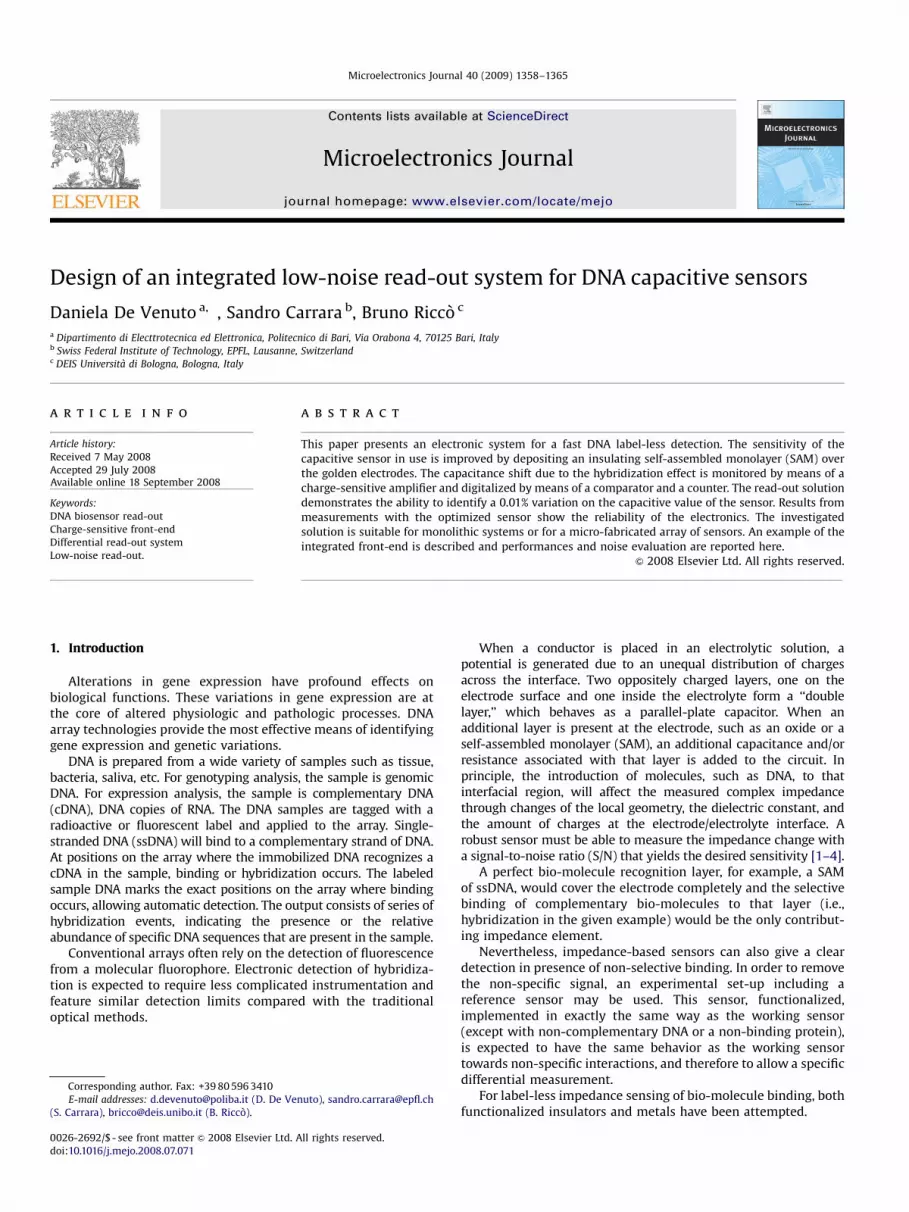
Fig. 2. Schematic representation of th
down to room temperature (for about 10 min). Finally, the samplewas washed in the TE buffer solution in order to remove theunbound target DNA. As in the past, the procedure was alsochecked with an independent standard optical-detection testbased on fluorescence molecules bound to DNA molecules [6].The efficiency of the hybridization reaction was tested in caseof target molecules presenting complementary and non-complementary oligonucleotides sequence with respect to theimmobilized DNA probes.
3. Read-out systems for the capacitive biosensor
Due to the peculiarity of the biosensor described above, a read-out system is required to detect the occurrence of DNAhybridization through the caused capacitance shift and toquantify the amount of such an event, recognizing in this waythe target concentration.
The hybridization determines the biosensor capacitance valuereduction from 30% to 50% of the nominal value by the amount ofthe solution.
The configurations for the read-out electronics proposed in[9,10] comprises of an analog section, including the front-end, theconditioning electronics and the digital section mainly comprisingof a binary counter. A micro-controller allows the calibration ofthe parameters once it is known that the parameters selected arenot the optimal ones (clock frequency, feedback dischargingimpedance, etc.).
An absolute measurement of the value of the biosensorcapacitance, before and after the hybridization occurrence canbe performed by using a charge-sensitive amplifier followed by acomparator and a counter (Fig. 2).
This read-out can also allow the differential measurement,which directly gives the capacitance shift detection, just byduplicating the channel and making them the input of aninstrumentation amplifier or of an EXOR. In the differential mode,two sensors are needed, one will operate as probe sensorperforming the chemical detection, the other is a dummy sensor,functionalized and in a TE solution not including any DNAsequences, to represent the capacitive reference value withrespect to which evaluate the shift.
3.1. Sensor front-end
The common interface between the sensor and the read-outsystem is the proposed solution, based upon a charge-sensitiveamplifier.
e single-channel read-out system.
ARTICLE IN PRESS
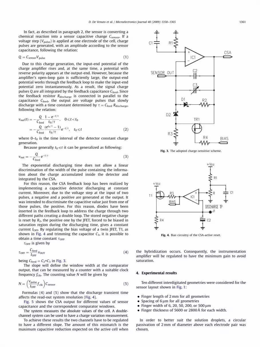
Fig. 3. The adopted charge-sensitive scheme.
Fig. 4. Bias circuitry of the CSA-active reset.
D. De Venuto et al. / Microelectronics Journal 40 (2009) 1358–1365 1361
In fact, as described in paragraph 2, the sensor is converting achemical reaction into a sensor capacitive change Csensor. If avoltage step (Vpulse) is applied at one electrode of the cell, chargepulses are generated, with an amplitude according to the sensorcapacitance, following the relation:
Q ¼ CsensorVpulse (1)
Due to this charge generation, the input-end potential of thecharge amplifier rises and, at the same time, a potential withreverse polarity appears at the output-end. However, because theamplifier’s open-loop gain is sufficiently large, the output-endpotential works through the feedback loop to make the input-endpotential zero instantaneously. As a result, the signal chargepulses Q are all integrated by the feedback capacitance Cfeed. Sincethe feedback resistor Rdischarge is connected in parallel to thecapacitance Cfeed, the output are voltage pulses that slowlydischarge with a time constant determined by t ¼ Cfeed Rdischarge,following the relation:
voutðtÞ ¼ �Q
Cfeed
1� e�t=t
t0=t; 0ptot0
¼ �Q
Cfeed
ðet0=t � 1Þ
t0=te�t=t; t0pt (2)
where 0–t0 is the time interval of the detector constant chargegeneration.
Because generally t05t it can be generalized as following:
vout ¼ �Q
Cfeede�t=t (3)
The exponential discharging time does not allow a lineardiscrimination of the width of the pulse containing the informa-tion about the charge accumulated inside the detector andintegrated by the CSA.
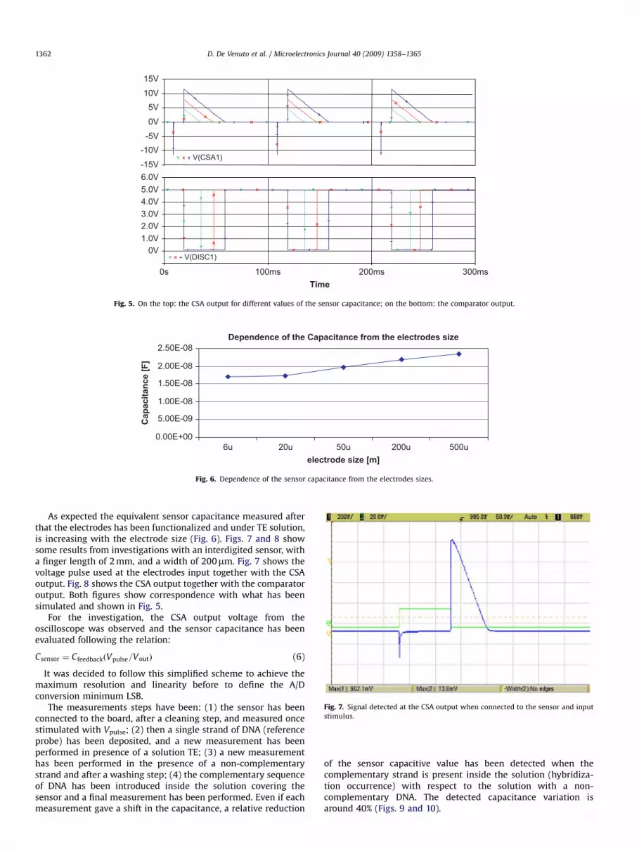
For this reason, the CSA feedback loop has been realized byimplementing a capacitive detector discharging at constantcurrent. Moreover, due to the voltage step at the input of twopulses, a negative and a positive are generated at the output. Itwas intended to discriminate the capacitive value just from one ofthose pulses, the positive. For this reason, diodes have beeninserted in the feedback loop to address the charge through twodifferent paths creating a double loop. The stored negative chargeis reset by R2, the positive one by the JFET, forced to be biased insaturation region during the discharging time, gives a constantcurrent IOFF. By regulating the bias voltage of a twin JFET, T1, asshown in Fig. 4 and trimming the capacitor C3, it is possible toobtain a time constant tOFF
tOFF is given by
tOFF ¼Cfeed
IOFFvOUT (4)
being Cfeed ¼ C2+C3 in Fig. 3.The slope will define the window width at the comparator
output, that can be measured by a counter with a suitable clockfrequency fclk. The counting value N will be given by
N ¼vpulse
IOFFf clk
� �Csensor (5)
Formulas (4) and (5) show that the discharge transient timeaffects the read-out system resolution (Fig. 4).
Fig. 5 shows the CSA output for different values of sensorcapacitance and the correspondent comparator windows.
The system measures the absolute values of the cell. A double-channel system can be used to have a charge variation measurement.
To achieve these results the two channels have to be regulatedto have a different slope. The amount of this mismatch is themaximum capacitive reduction expected on the active cell when
the hybridization occurs. Consequently, the instrumentationamplifier will be regulated to have the minimum gain to avoidsaturation.
4. Experimental results
Ten different interdigitated geometries were considered for thesensor layout shown in Fig. 1:
�
Finger length of 2 mm for all geometries � Spacing of 6mm for all geometries � Finger width of 6, 20, 50, 200, or 500mm � Finger thickness of 5600 or 2800 A for each width.In order to better suit the solution droplets, a circularpassivation of 2 mm of diameter above each electrode pair waschosen.
ARTICLE IN PRESS
Time0s 100ms 200ms 300ms
V(DISC1)0V
1.0V2.0V3.0V4.0V5.0V6.0V
V(CSA1)-15V
-10V-5V
0V
5V10V
15V
Fig. 5. On the top: the CSA output for different values of the sensor capacitance; on the bottom: the comparator output.
0.00E+00
5.00E-09
1.00E-08
1.50E-08
2.00E-08
2.50E-08
6uelectrode size [m]
Cap
acita
nce
[F]
Dependence of the Capacitance from the electrodes size
20u 50u 200u 500u
Fig. 6. Dependence of the sensor capacitance from the electrodes sizes.
Fig. 7. Signal detected at the CSA output when connected to the sensor and input
stimulus.
D. De Venuto et al. / Microelectronics Journal 40 (2009) 1358–13651362
As expected the equivalent sensor capacitance measured afterthat the electrodes has been functionalized and under TE solution,is increasing with the electrode size (Fig. 6). Figs. 7 and 8 showsome results from investigations with an interdigited sensor, witha finger length of 2 mm, and a width of 200mm. Fig. 7 shows thevoltage pulse used at the electrodes input together with the CSAoutput. Fig. 8 shows the CSA output together with the comparatoroutput. Both figures show correspondence with what has beensimulated and shown in Fig. 5.
For the investigation, the CSA output voltage from theoscilloscope was observed and the sensor capacitance has beenevaluated following the relation:
Csensor ¼ CfeedbackðVpulse=VoutÞ (6)
It was decided to follow this simplified scheme to achieve themaximum resolution and linearity before to define the A/Dconversion minimum LSB.
The measurements steps have been: (1) the sensor has beenconnected to the board, after a cleaning step, and measured oncestimulated with Vpulse; (2) then a single strand of DNA (referenceprobe) has been deposited, and a new measurement has beenperformed in presence of a solution TE; (3) a new measurementhas been performed in the presence of a non-complementarystrand and after a washing step; (4) the complementary sequenceof DNA has been introduced inside the solution covering thesensor and a final measurement has been performed. Even if eachmeasurement gave a shift in the capacitance, a relative reduction
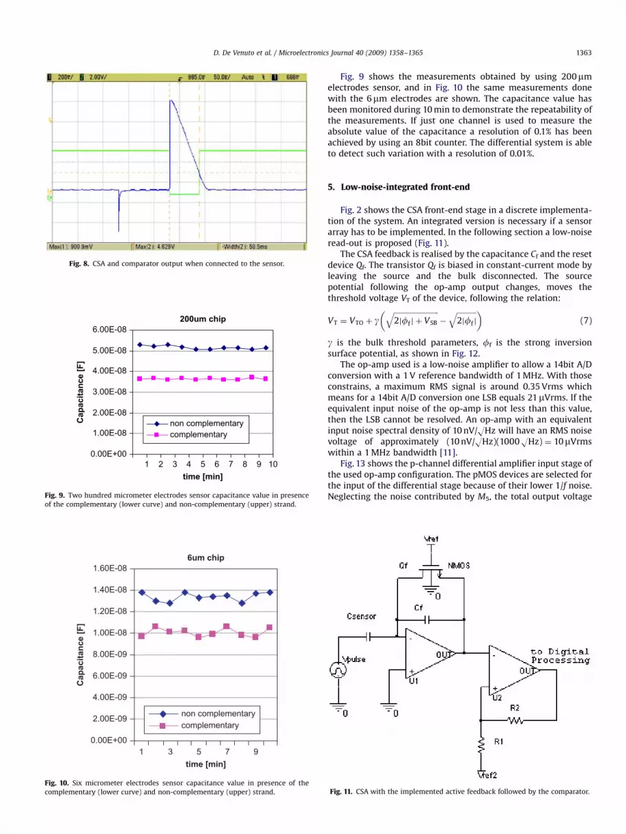
of the sensor capacitive value has been detected when thecomplementary strand is present inside the solution (hybridiza-tion occurrence) with respect to the solution with a non-complementary DNA. The detected capacitance variation isaround 40% (Figs. 9 and 10).
ARTICLE IN PRESS
Fig. 8. CSA and comparator output when connected to the sensor.
200um chip
0.00E+00
1.00E-08
2.00E-08
3.00E-08
4.00E-08
5.00E-08
6.00E-08
1time [min]
Cap
acita
nce
[F]
non complementary complementary
2 3 4 5 6 7 8 9 10
Fig. 9. Two hundred micrometer electrodes sensor capacitance value in presence
of the complementary (lower curve) and non-complementary (upper) strand.
6um chip
0.00E+00
2.00E-09
4.00E-09
6.00E-09
8.00E-09
1.00E-08
1.20E-08
1.40E-08
1.60E-08
1time [min]
Cap
acita
nce
[F]
non complementarycomplementary
3 5 7 9
Fig. 10. Six micrometer electrodes sensor capacitance value in presence of the
complementary (lower curve) and non-complementary (upper) strand.
D. De Venuto et al. / Microelectronics Journal 40 (2009) 1358–1365 1363
Fig. 9 shows the measurements obtained by using 200mmelectrodes sensor, and in Fig. 10 the same measurements donewith the 6mm electrodes are shown. The capacitance value hasbeen monitored during 10 min to demonstrate the repeatability ofthe measurements. If just one channel is used to measure theabsolute value of the capacitance a resolution of 0.1% has beenachieved by using an 8bit counter. The differential system is ableto detect such variation with a resolution of 0.01%.
5. Low-noise-integrated front-end
Fig. 2 shows the CSA front-end stage in a discrete implementa-tion of the system. An integrated version is necessary if a sensorarray has to be implemented. In the following section a low-noiseread-out is proposed (Fig. 11).
The CSA feedback is realised by the capacitance Cf and the resetdevice Qf. The transistor Qf is biased in constant-current mode byleaving the source and the bulk disconnected. The sourcepotential following the op-amp output changes, moves thethreshold voltage VT of the device, following the relation:
VT ¼ VTO þ gffiffiffiffiffiffiffiffiffiffiffiffiffiffiffiffiffiffiffiffiffiffiffiffiffi2jff j þ VSB
q�
ffiffiffiffiffiffiffiffiffiffiffi2jff j
q� �(7)
g is the bulk threshold parameters, ff is the strong inversionsurface potential, as shown in Fig. 12.
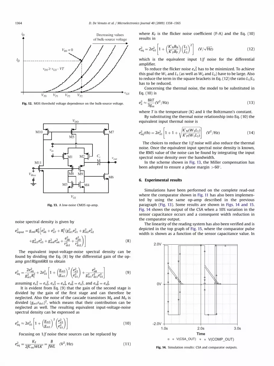
The op-amp used is a low-noise amplifier to allow a 14bit A/Dconversion with a 1 V reference bandwidth of 1 MHz. With thoseconstrains, a maximum RMS signal is around 0.35 Vrms whichmeans for a 14bit A/D conversion one LSB equals 21mVrms. If theequivalent input noise of the op-amp is not less than this value,then the LSB cannot be resolved. An op-amp with an equivalentinput noise spectral density of 10 nV/OHz will have an RMS noisevoltage of approximately (10 nV/OHz)(1000OHz) ¼ 10mVrmswithin a 1 MHz bandwidth [11].
Fig. 13 shows the p-channel differential amplifier input stage ofthe used op-amp configuration. The pMOS devices are selected forthe input of the differential stage because of their lower 1/f noise.Neglecting the noise contributed by M5, the total output voltage
Fig. 11. CSA with the implemented active feedback followed by the comparator.
ARTICLE IN PRESS
ID
VT0
�DS ≥ �GS - VT
VBS = 0
VT1 VT2 VT2�GS
iD Decreasing valuesof bulk-source voltage
Fig. 12. MOS threshold voltage dependence on the bulk-source voltage.
VDD
vin
VBias
VSS
Cc vout
M5M7
M2M1
M8 M9
M4
M6
M11
M3
M10
Fig. 13. A low-noise CMOS op-amp.
Time1.0s 2.0s 3.0s
V(CSA_OUT) V(COMP_OUT)
-2.0V
0V
2.0V
Fig. 14. Simulation results: CSA and comparator outputs.
D. De Venuto et al. / Microelectronics Journal 40 (2009) 1358–13651364
noise spectral density is given by
e2eqout ¼ gm6R2
II e2n6 þ e2
n7 þ R2I g2
m1e2n1 þ g2
m2e2n2
�h
þg2m3e2
n3 þ g2m4e2
n4 þe2
n8
r2ds1
þe2
n9
r2ds2
!#(8)
The equivalent input-voltage-noise spectral density can befound by dividing the Eq. (8) by the differential gain of the op-amp gm1RIgm6RII to obtain
e2eq ¼
2e2n6
g2m1R2
I
þ 2e2n1 1þ
gm3
gm1
� �2 e2n3
e2n1
!þ
e2n8
g2m1r2
ds1e2n1
" #(9)
assuming en12¼ en2
2, en32¼ en4
2, en62¼ en7
2, and en82¼ en9
2.It is evident from Eq. (9) that the gain of the second stage is
divided by the gain of the first stage and can therefore beneglected. Also the noise of the cascade transistors M8 and M9 isdivided (gm1rds1)2, which means that their contribution can beneglected as well. The resulting equivalent input-voltage-noisespectral density can be expressed as
e2eq � 2e2
n1 1þgm3
gm1
� �2 e2n3
e2n1
!" #(10)
Focusing on 1/f noise these sources can be replaced by
e2eq ¼
KF
2fCoxWLK 0¼
B
fWLðV2=HzÞ (11)
where KF is the flicker noise coefficient (F-A) and the Eq. (10)results in
e2eq ¼ 2e2
n1 1þK 0NBN
K 0PBP
� �L1
L3
� �2" #
ðV=ffiffiffiffiffiffiffiHzpÞ (12)
which is the equivalent input 1/f noise for the differentialamplifier.
To reduce the flicker noise en12 has to be minimized. To achieve
this goal the W1 and L1 (as well as W2 and L2) have to be large. Alsoto reduce the term in the square brackets in Eq. (12) the ratio L1/L3
has to be reduced.Concerning the thermal noise, the model to be substituted in
Eq. (10) is
e2n �
8kT
3gm
ðV2=HzÞ (13)
where T is the temperature (K) and k the Boltzmann’s constant.By substituting the thermal noise relationship into Eq. (10) the
equivalent input thermal noise is
e2eqðthÞ ¼ 2e2
n1 1þ 1þ
ffiffiffiffiffiffiffiffiffiffiffiffiffiffiffiffiffiffiffiffiffiffiffiK 0NðW3L1Þ
K 0PðW1L3Þ
s" #ðV2=HzÞ (14)
The choices to reduce the 1/f noise will also reduce the thermalnoise. Once the equivalent input spectral noise density is known,the RMS value of the noise can be found by integrating the inputspectral noise density over the bandwidth.
In the scheme shown in Fig. 13, the Miller compensation hasbeen adopted to ensure a phase margin 4601.
6. Experimental results
Simulations have been performed on the complete read-outwhere the comparator shown in Fig. 11 has also been implemen-ted by using the same op-amp described in the previousparagraph (Fig. 13). Some results are shown in Figs. 14 and 15.Fig. 14 shows the output of the CSA when a 10% variation in thesensor capacitance occurs and a consequent width reduction inthe comparator output.
The linearity of the reading system has also been verified and isdepicted in the top graph of Fig. 15, where the comparator pulsewidth is shown as a function of the sensor capacitance value. In
ARTICLE IN PRESS
8.5
9
9.5
10
T low
(ms)
90 92 94 96 98 100-1
-0.5
0
0.5
1
Csensor (pF)
90 92 94 96 98 100Csensor (pF)
Res
olut
ion
(%)
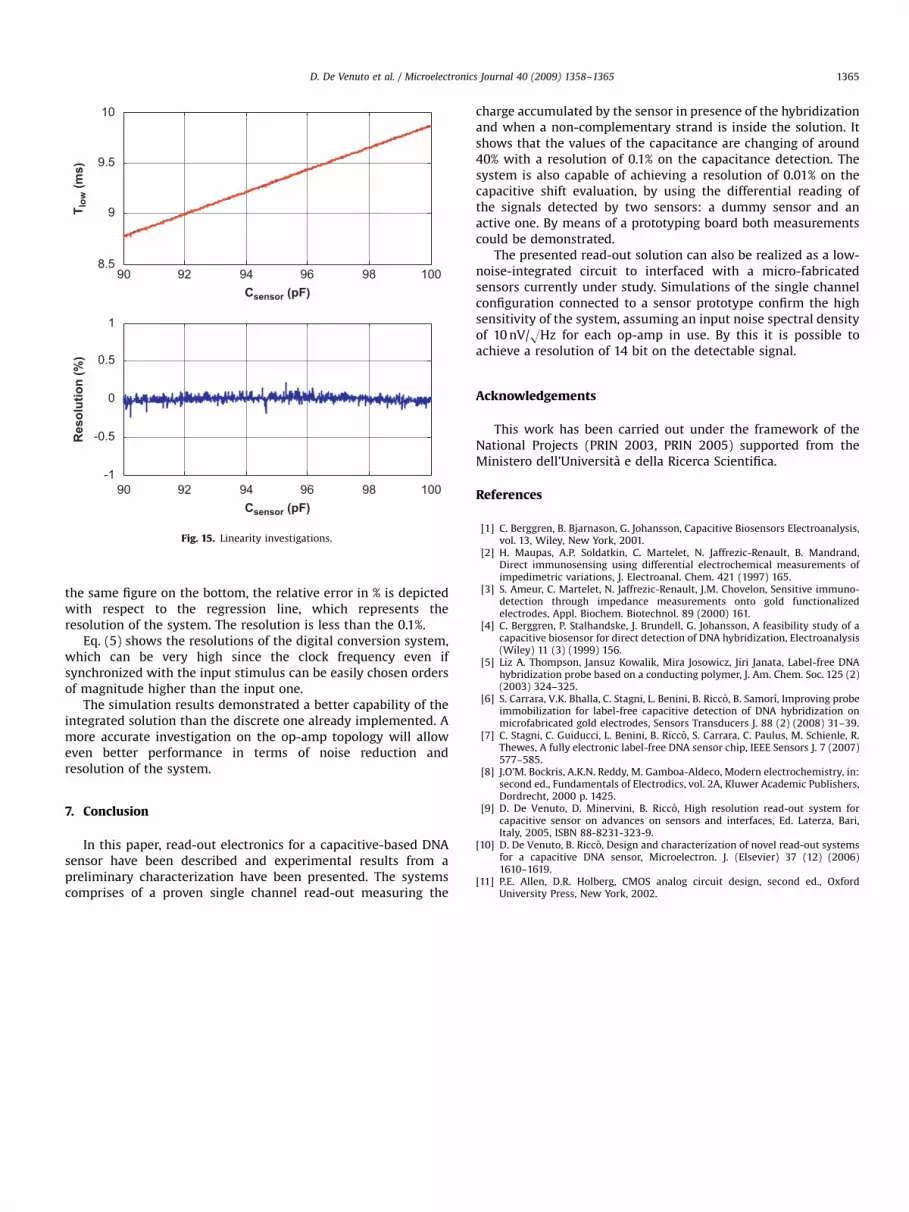
Fig. 15. Linearity investigations.
D. De Venuto et al. / Microelectronics Journal 40 (2009) 1358–1365 1365
the same figure on the bottom, the relative error in % is depictedwith respect to the regression line, which represents theresolution of the system. The resolution is less than the 0.1%.
Eq. (5) shows the resolutions of the digital conversion system,which can be very high since the clock frequency even ifsynchronized with the input stimulus can be easily chosen ordersof magnitude higher than the input one.
The simulation results demonstrated a better capability of theintegrated solution than the discrete one already implemented. Amore accurate investigation on the op-amp topology will alloweven better performance in terms of noise reduction andresolution of the system.
7. Conclusion
In this paper, read-out electronics for a capacitive-based DNAsensor have been described and experimental results from apreliminary characterization have been presented. The systemscomprises of a proven single channel read-out measuring the
charge accumulated by the sensor in presence of the hybridizationand when a non-complementary strand is inside the solution. Itshows that the values of the capacitance are changing of around40% with a resolution of 0.1% on the capacitance detection. Thesystem is also capable of achieving a resolution of 0.01% on thecapacitive shift evaluation, by using the differential reading ofthe signals detected by two sensors: a dummy sensor and anactive one. By means of a prototyping board both measurementscould be demonstrated.
The presented read-out solution can also be realized as a low-noise-integrated circuit to interfaced with a micro-fabricatedsensors currently under study. Simulations of the single channelconfiguration connected to a sensor prototype confirm the highsensitivity of the system, assuming an input noise spectral densityof 10 nV/OHz for each op-amp in use. By this it is possible toachieve a resolution of 14 bit on the detectable signal.
Acknowledgements
This work has been carried out under the framework of theNational Projects (PRIN 2003, PRIN 2005) supported from theMinistero dell’Universita e della Ricerca Scientifica.
References
[1] C. Berggren, B. Bjarnason, G. Johansson, Capacitive Biosensors Electroanalysis,vol. 13, Wiley, New York, 2001.
[2] H. Maupas, A.P. Soldatkin, C. Martelet, N. Jaffrezic-Renault, B. Mandrand,Direct immunosensing using differential electrochemical measurements ofimpedimetric variations, J. Electroanal. Chem. 421 (1997) 165.
[3] S. Ameur, C. Martelet, N. Jaffrezic-Renault, J.M. Chovelon, Sensitive immuno-detection through impedance measurements onto gold functionalizedelectrodes, Appl. Biochem. Biotechnol. 89 (2000) 161.
[4] C. Berggren, P. Stalhandske, J. Brundell, G. Johansson, A feasibility study of acapacitive biosensor for direct detection of DNA hybridization, Electroanalysis(Wiley) 11 (3) (1999) 156.
[5] Liz A. Thompson, Jansuz Kowalik, Mira Josowicz, Jiri Janata, Label-free DNAhybridization probe based on a conducting polymer, J. Am. Chem. Soc. 125 (2)(2003) 324–325.
[6] S. Carrara, V.K. Bhalla, C. Stagni, L. Benini, B. Ricco, B. Samorı, Improving probeimmobilization for label-free capacitive detection of DNA hybridization onmicrofabricated gold electrodes, Sensors Transducers J. 88 (2) (2008) 31–39.
[7] C. Stagni, C. Guiducci, L. Benini, B. Ricco, S. Carrara, C. Paulus, M. Schienle, R.Thewes, A fully electronic label-free DNA sensor chip, IEEE Sensors J. 7 (2007)577–585.
[8] J.O’M. Bockris, A.K.N. Reddy, M. Gamboa-Aldeco, Modern electrochemistry, in:second ed., Fundamentals of Electrodics, vol. 2A, Kluwer Academic Publishers,Dordrecht, 2000 p. 1425.
[9] D. De Venuto, D. Minervini, B. Ricco, High resolution read-out system forcapacitive sensor on advances on sensors and interfaces, Ed. Laterza, Bari,Italy, 2005, ISBN 88-8231-323-9.
[10] D. De Venuto, B. Ricco, Design and characterization of novel read-out systemsfor a capacitive DNA sensor, Microelectron. J. (Elsevier) 37 (12) (2006)1610–1619.
[11] P.E. Allen, D.R. Holberg, CMOS analog circuit design, second ed., OxfordUniversity Press, New York, 2002.


![Bles.ppt [Read-Only]](https://static.fdokumen.com/doc/165x107/633bffc7197a6737f10ceddf/blesppt-read-only.jpg)