
Design of a current oversampling board for electrical drives
81
UNIVERSIT ´ A DEGLI STUDI DI PADOVA Dipartimento di Ingegneria Industriale DII Laurea Magistrale in Ingegneria dell’Energia Elettrica Design of a current oversampling board for electrical drives Experimental testing in a machine parameters evaluation Progetto di una scheda per il sovracampionamento della corrente di un azionamento elettrico Sperimentazione nella valutazione dei parametri di macchina Relatore: Ch.mo prof. Bolognani Silverio Correlatore: Dr. Ing. Luca Peretti, ABB Corporate Research - V¨ aster˚ as - SE Laureando: Michielin Diego 1132373
-
Upload
khangminh22 -
Category
Documents
-
view
0 -
download
0
Transcript of Design of a current oversampling board for electrical drives

UNIVERSITA DEGLI STUDI DI PADOVA
Dipartimento di Ingegneria Industriale DII
Laurea Magistrale in Ingegneria dell’Energia Elettrica
Design of a current oversamplingboard for electrical drives
Experimental testing in amachine parameters evaluation
Progetto di una scheda per ilsovracampionamento
della corrente di un azionamento elettrico
Sperimentazione nella valutazionedei parametri di macchina
Relatore: Ch.mo prof. Bolognani Silverio
Correlatore: Dr. Ing. Luca Peretti, ABB Corporate Research - Vasteras - SE
Laureando: Michielin Diego 1132373

ii
Anno Accademico 2017/2018

iii
This project deals with the design of an electronic apparatus capable of high-speedoversampling (in the order of MHz) of the stator currents in an electric machine. Theproject includes the experimental evaluation of the design for a subsequent real-timeestimation of machine parameters. The following list specifies the main parts of theproject:
• Review of the current sensing technologies capable of oversampling.
• Current PCB design upgrade for oversampling capabilities.
• Prototype realization and mounting into the laboratory setup.
• Experimental validation through the measurement of current ripple.
The thesis was performed at the ABB Corporate Research in Vasteras, Sweden,from September 25, 2017 to March 23, 2018.

iv

Contents
List of abbreviations vii
Introduction ix
1 Current sensing techniques 1
1.1 Introduction . . . . . . . . . . . . . . . . . . . . . . . . . . . . . . . . . . 1
1.2 Hall-effect based sensor . . . . . . . . . . . . . . . . . . . . . . . . . . . 2
1.2.1 Open loop . . . . . . . . . . . . . . . . . . . . . . . . . . . . . . . 3
1.2.2 Closed loop . . . . . . . . . . . . . . . . . . . . . . . . . . . . . . 3
1.3 Rogowski coil . . . . . . . . . . . . . . . . . . . . . . . . . . . . . . . . . 4
1.4 HOKA principle . . . . . . . . . . . . . . . . . . . . . . . . . . . . . . . 5
1.5 Current Viewing Resistor (CVR) . . . . . . . . . . . . . . . . . . . . . . 7
2 Sensitec CMS3050 11
2.1 The magneto-resistive effect . . . . . . . . . . . . . . . . . . . . . . . . . 11
2.2 Data of CMS3050 . . . . . . . . . . . . . . . . . . . . . . . . . . . . . . . 13
3 Current sensor filtering 15
3.1 Introduction . . . . . . . . . . . . . . . . . . . . . . . . . . . . . . . . . . 15
3.2 Testing Signal Generator Agilent Tech 33120A . . . . . . . . . . . . . . 17
3.2.1 Investigation of a proper set up: Brockhaus MPG 200D AC/DC 19
3.2.2 Investigation of a proper set up: IGBT short circuit tests . . . . 19
3.3 Test on Inverter-fed SynRMs . . . . . . . . . . . . . . . . . . . . . . . . 20
3.4 Choice of the analog filter . . . . . . . . . . . . . . . . . . . . . . . . . . 28
3.4.1 Butterworth . . . . . . . . . . . . . . . . . . . . . . . . . . . . . . 29
3.4.2 Bessel . . . . . . . . . . . . . . . . . . . . . . . . . . . . . . . . . 29
3.4.3 Sallen-Key configuration . . . . . . . . . . . . . . . . . . . . . . . 30
3.4.4 Multiple-Feedback configuration . . . . . . . . . . . . . . . . . . 30
3.5 Design of the analog filter . . . . . . . . . . . . . . . . . . . . . . . . . . 31
4 PCB design upgrade 33
4.1 Introduction . . . . . . . . . . . . . . . . . . . . . . . . . . . . . . . . . . 33
4.2 Structure of the PCB . . . . . . . . . . . . . . . . . . . . . . . . . . . . 34
4.2.1 Power supply . . . . . . . . . . . . . . . . . . . . . . . . . . . . . 34
4.2.2 Current stage . . . . . . . . . . . . . . . . . . . . . . . . . . . . . 35
4.2.3 Voltage stage . . . . . . . . . . . . . . . . . . . . . . . . . . . . . 36
4.2.4 Output pins . . . . . . . . . . . . . . . . . . . . . . . . . . . . . . 36
4.3 PCB design . . . . . . . . . . . . . . . . . . . . . . . . . . . . . . . . . . 38
v

vi CONTENTS
5 PCB testing 415.1 Experimental outcomes: first motor . . . . . . . . . . . . . . . . . . . . 415.2 Experimental outcomes: second motor . . . . . . . . . . . . . . . . . . . 515.3 Experimental outcomes: third motor . . . . . . . . . . . . . . . . . . . . 535.4 Experimental outcomes: fourth motor . . . . . . . . . . . . . . . . . . . 555.5 Remarks on the results . . . . . . . . . . . . . . . . . . . . . . . . . . . . 57
6 Conclusions 59
7 Future work 617.1 Improvement for voltage measurements . . . . . . . . . . . . . . . . . . 617.2 Power supplies improvement . . . . . . . . . . . . . . . . . . . . . . . . . 617.3 Tests with the THS3001CD . . . . . . . . . . . . . . . . . . . . . . . . . 627.4 Box . . . . . . . . . . . . . . . . . . . . . . . . . . . . . . . . . . . . . . 62
A Appendix A 63
B Appendix B 65

List of abbreviations
AMR Anisotropic magneto resistiveCMRR Common Mode Voltage RejectionCS Current sensorEMF Electromotive forceEMI Electromagnetic interferenceFFt Fast Fourier TransformFPGA Field-programmable gate arrayFSF Frequency scale factorIIR Infinite Impulse ResponseIM Induction motorIPM Interior Permanent Magnet motorI/O Input/outputop− amp Operational amplifierPCB Printed circuit boardPMASynRM Permanent Magnet Assisted Synchronous Reluctance MotorPWM Pulse width modulationRMS Root mean squareSynRM Synchronous reluctance motortf Transfer function
vii

viii LIST OF ABBREVIATIONS

Introduction
Motivation
The good performances achieved by modern variable speed electric drives is obtain atexpenses of more stress and degradation of the machine. Due to this fact, the analysisof stress phenomena is an active research area.
The steep voltage edges induced by the PWM output of the inverter produce surgesat the machine terminal. The insulation of the machine suffers under these transientovervoltages. Studies showed that it is possible to assess the degradation on statorinsulators by analyzing the magnitude of the initial peak appearing in the phase currentat the switching instants: indeed the high frequency content of this response is relatedto the parasitic capacitances model of the machine, and thus informations about thequality of the stator insulation can be gleaned [1]. In particular the ringing phenomenain the early stage, visible in the figure 1, is due to the stray capacitances that changeas a function of the ageing of insulators [2].
The overshoot typically consists of high frequencies in the range of (4-6 MHz) (seefigure 2). The measuring system must have high bandwidth and fast sampling in-orderto capture interesting transients - at least double of the maximum expected frequency,according to the Nyquist theorem. This high resolution can be used for verify the agingmodel.
More-over, a large current harmonic content could be used to build more accuratesensor-less drives by using an intrinsic high-frequency injection due to the PWM. Theidea, proposed in several papers [3] and [4], concerns the exploitation of the PWMharmonics - developed by the stator currents - in order to assess the electrical rotorposition estimation. The oversampling of motor currents allows furthermore a low-noise calculation of the current derivative (di/dt), which improves the measurementresolution and allows smooth operation down to zero speed without negative side-effects, such as acoustic noise [5]. This concept requires best performance characteristicsfor phase current sensing in terms of dynamic range and bandwidth. An upgradedhardware is thus necessary.
ix

x INTRODUCTIONZOELLER et al.: EVALUATION AND CURRENT-RESPONSE-BASED IDENTIFICATION OF INSULATION DEGRADATION 2683
Fig. 7. Normalized change in percentage of capacitance of formette type II –after six thermal aging cycles.
the lower dielectric constant of air (∼1) compared to typicalinsulation materials, which is about 3–5, the average dielectricconstant decreases and as a consequence the capacitance of thespecimen.
The total capacitance value is influenced at low voltage levelsby solid insulation and cavities. At higher voltage levels, abovethe corona starting voltage, the capacitance values are increasingand only the solid insulation is influencing the measurement,because the voids have been shorted by partial discharge.
D. Results of Formette Type II Investigations
The thermal aging cycles, as described in Fig. 2, are appliedto the four formettes of type II. In Fig. 7, the mean values of thecapacitance and dissipation factor measurements are depicted.The left subfigure shows the normalized change of the capac-itance values between the actual cycle Cx and the initial stateC0 (ΔC = (Cx − C0)/C0) for different voltage levels. Aftersix aging cycles, the formettes failed the withstand voltage tests.This results in a maximum capacitance change of about 25%.
The results of these experiments provide information aboutthe behavior and changes of the electrical properties of a deterio-rated winding insulation system. Through better understanding,the results help to improve the developed insulation monitoringprocedure. In Section III, the proposed stator insulation moni-toring method for inverter fed machines is presented.
III. INSULATION MONITORING METHOD
An inverter delivers the ability to control the angular velocityof the rotor shaft by supplying the stator winding with voltageof variable frequency/magnitude using the pulse width modu-lation (PWM). The steep voltage edges induced by the PWMoutput of the inverter produce surges at the machine terminal[22], [23]. The insulation system of the machine suffers underthese transient overvoltages. The short rise time of newer up-coming inverter semiconductor technologies, e.g., SiC or GaNwould cause a dramatic increase of this issue. Due to the highfrequencies applied to the winding system with a voltage step, anonlinear voltage distribution occurs, because the impedance ofthe series inductances is relatively large compared to the capac-itive impedance [1], [24]. This results in an unbalanced voltage
Fig. 8. Current response after step excitation, healthy machine state (solidblue), and degraded insulation (dashed green).
stress along the coils of a phase, with higher stress for the firstcoils near to the phase terminal. For higher inhomogeneous volt-age distribution the probability of ∗∗partial discharges (PD’s)rises.
The proposed monitoring method for the insulation state es-timation is based on analysis of the transient current reaction asa result of voltage step excitation separately in every phase. Thehigh dv/dt of the voltage steps and the impedance mismatch ofthe supply cables between inverter and machine cause a tran-sient overvoltage at the machine terminals. A transient is alsoobservable in the current transducer’s response and the charac-teristic depends beside the switching transition—common modeor differential mode [25], [26], on the condition of the motor’sinsulation system. According to the aforementioned analyzes inSection II, the parasitic components of a winding system, e.g.,turn-to-turn, winding-to-ground capacitances etc., significantlychange after a specific number of aging cycles have been ap-plied. These changes can be analyzed with the observation ofthe transients.
In this paper the degradation of the insulation system for the1.4 MW induction machine is emulated with a capacitor placedparallel to the winding system implemented at a special threephase induction machine equipped with taps. In Fig. 8, twocurrent responses measured in phase L1, after a voltage step isapplied with the inverter, starting all phases at the lower dc-linkvoltage followed by a transition of the corresponding inverterlag by turning OFF the low side transistor and turn ON the highside one.
The solid blue trace depicts a healthy machine and the dashedgreen the same machine with a capacitor placed parallel to thefirst coil of phase L1. The capacitor with a size of 3 nF par-allel to the first coil of phase L1 emulates a change of theparasitic winding capacitances and influences the shape of thehigh-frequency oscillation. The total winding-to-ground capac-itance is estimated with 63nF. According to studies in this paperand referenced in the paper, e.g., [18] and [19], change in capac-itance over lifetime is around 20% to 25% of initial value whatwould result in around 12 nF to 16 nF for the whole machine
Figure 1: Current response after step excitation, comparison between healthy statemachine and degraded insulation [2].
ZOELLER et al.: EVALUATION AND CURRENT-RESPONSE-BASED IDENTIFICATION OF INSULATION DEGRADATION 2687
Fig. 16. Stator slot cross section with inserted form-wound coil and indicatedparasitic capacitances.
Fig. 17. Influence of temperature (25–200 °C) on current responses spectrameasured at state 2.
insulation material is deteriorated, for instance due to PD re-sulting in changes of the chemical bonds. By using a simplecapacitive voltage divider, the single capacitances are calculatedlike a parallel plate capacitor with the permittivity ε = εr ε0 ,the permittivity of the free space ε0 and relative permittivityεr (dielectric constant) of the material in combination with thegeometrical factors cross-sectional area and thickness of insula-tion material. The dielectric constants of the insulation materialand air, which can be encased in voids, are different by a fac-tor of 4. However, due to sparks the occurrence of residualproducts, through rupture of chemical bonds is possible and theclassification in air and insulation material is not feasible. Ad-ditionally, since the geometrical properties cannot be accuratelydetermined, the model is only a rough approximation.
B. Influence of Temperature
In Fig. 17, the spectra of the formette after state “2” at dif-ferent temperature levels are depicted. The measurements areconducted during the cooling process to analyze the influenceof temperature on the results. Four different temperatures 200,100, and 75 °C and ambient temperature 25 °C are analyzed.From the curves the influence of the temperature on the pro-posed monitoring method is visible. Only the magnitude in thespectra has changed and the second resonance peak is mainly
Fig. 18. (a) Formette after humidity chamber (b) frequency characteristicmeasurement of the formette in dry and moist state (c) calculated ISI values forall aging states (0–3) and comparison of dry and moist state.
decreasing with the temperature in contrast to the shift of theresonance caused by a decreasing capacitance value. At highertemperatures the resistance values are mainly influenced and asa consequence the damping of the system.
The indicators in the right subfigure show clear increase andin worst case with 200 °C winding temperature of the fromette,a value of 1.64 a.u. is reached, which corresponds more thanthe deviation after the state “1” with a ΔC of approximately200 pF. Due to the simple algorithm of the RMSD calculationthis difference is not considered and thus the temperature ormore precisely the change caused by temperature is not negligi-ble. In order to increase the reliability and to prevent interference
Figure 2: FFt of the sampled current, comparison between different temperatures [2].
Scope
The work aims at building an upgraded measuring printed circuit board for the phasecurrent oversampling. Although both these problems have been already studied inseveral papers (up to this point), hardware limitations occur through poor dynamicfeatures of the measuring system [6] [7].
The first stage of the work focuses on the choice of the best current sensor - interms of bandwidth the target set at 5 MHz - available on the market. Differentcurrent sensing techniques are compared, taking into account the system requirements.The Sensitec CMS3050 is chosen, whose declared frequency bandwidth is 2 MHz (whenon-board RC filtering is applied). Later on, the chosen device is tested in order toknow its dynamic behavior without RC filter. Analog filters are designed to reach thetargeted time response at the instant of switching.

xi
Starting from the previous measurement box the PCB design is upgraded with theadvanced requirements: the current sensors and the analog filters are embedded, a newgeometry is chosen and a new type of connectors is mounted. The board is tested inthe lab and at the end some remarks on the work and on future applications are done.
Structure
This report has the following structure.The Introduction (this section) describes the motivation and scope of this document.The Chapter 1 presents the review of current sensing technologies for high-speed
oversampling. The main requirements taken into account are discussed for each con-sidered technique.
The Chapter 2 describes in details the chosen current sensor, Sensitec CMS3050.The physical aspects are explained and the electrical data are summarized.
The Chapter 3 analyses frequency response and conditioning of the new deviceoutput.
The Chapter 4 describes the upgraded design of the printed circuit board. ThePCB design is done with KiCad and new requirements are embedded in the board.
The Chapter 5 describes the tests carried out on the PCB: good results is reachedalthough some further investigations are required.
The Conclusions reports conclusive remarks on the work.The Future works indicates how the results of this report will be used in future
activities.The References specifies some material for further reading.

xii INTRODUCTION
Chapter 1
Current sensing techniques
The project starts by searching a current sensor with a bandwidth suitable for theoversampling task. Therefore, this first chapter provides an overview of state-of-artcurrent sensing techniques, taking into account system requirements. The followingchapter instead will concern the choice and the explanation of the magneto-resistivesensor ”Sensitec CMS3050”.
1.1 Introduction
Current sensing is required in a wide range of electrical and electronics applications.The measurement of current ranges from µA to tens of thousands Amperes. It is self-evident that each technology has different performance in terms of cost, sensitivity,precision, bandwidth, measurement range and size. These features are factors thatshould be weighted along with the specific requirements of the application in makingthe selection. More-over, the current information needs to be available in a digital formfor control or monitoring purposes and this means that output signal has to be acquiredby an analog-to-digital converter.Nowadays the research in the current technology area is focusing on devices with arange of several hundreds of amps, compact dimensions and high bandwidth. Therequirements for this last parameter is rising into the MHz range in order to increasethe power density and to sense high-speed current arising from static converters [5].A common way to classify the current sensors is based upon the underlying physicalprinciple:
• Magnetic field sensors
• Faraday’s law of induction
• Ohm’s law
The general requirements are instead:
• High sensitivity and high accuracy
• High bandwidth
• DC and AC measurements
• Low power consumption
1
2 CHAPTER 1. CURRENT SENSING TECHNIQUES
• Reasonable price
• EMI rejection
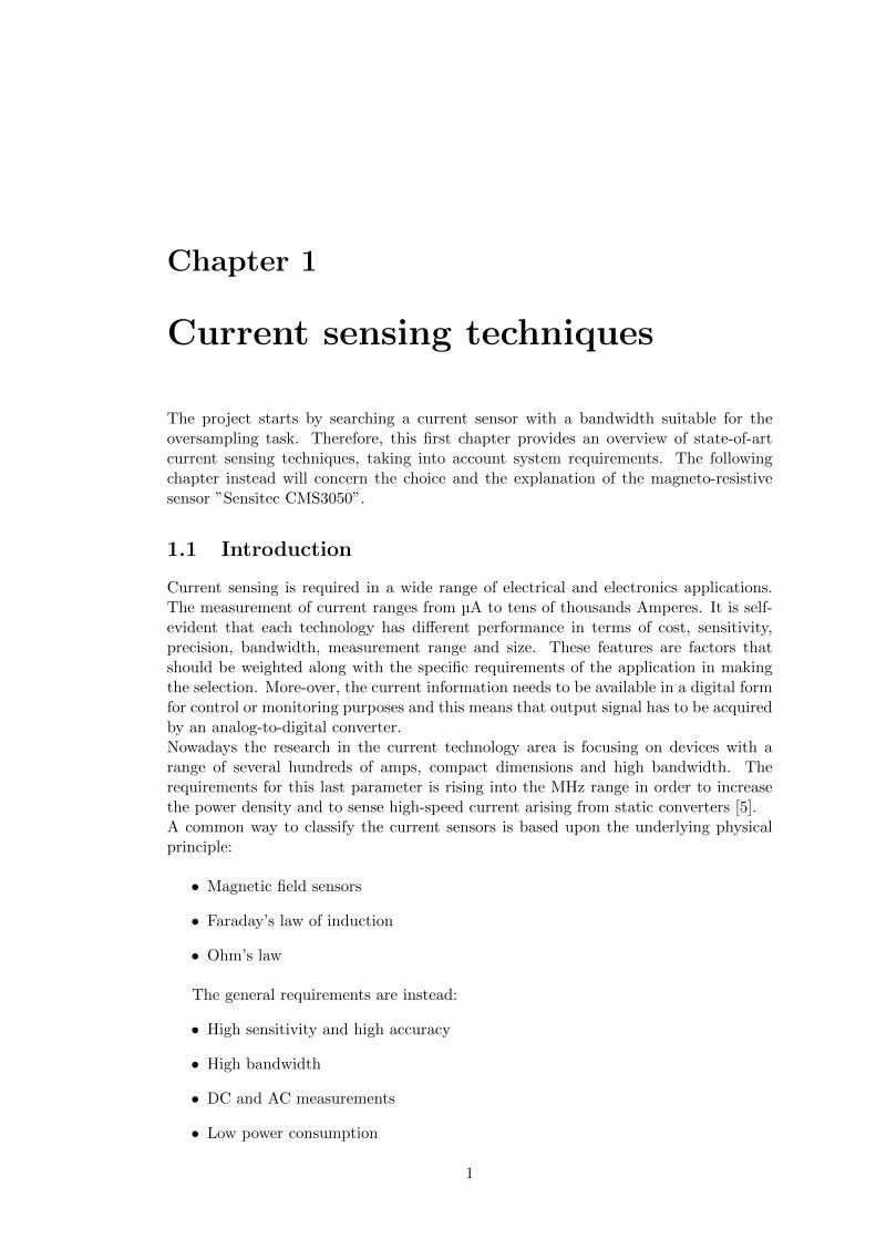
In this project, only the techniques suitable for the purpose have been considered.The system (see figure Figure 1.1) is installed in the Motors and drives laboratory, lo-cated in ABB Corporate Research Vasteras, Sweden. The application concerns the fieldof motor control. In particular, the set up consists of a motor (SynRM, PMASynRM,IM, IPM) fed by a three-phase inverter; the voltage in the DC-bus of the static converteris 560 V while the nominal RMS value of the current is around 50 A.
ConverterElectrical motor
Converter
Power cables
Interface board
Sensors and signal conditioning PCB
Figure 1.1: Inverter-fed motor with the current sensors.
The technologies taken into account from an oversampling perspective are:
• Hall-effect sensor
• Rogowski coil
• HOKA principle
• Current Viewing Resistor
• Magneto-resistive sensor
1.2 Hall-effect based sensor
This device, present in the previous measurement box [?], senses the primary currentflowing through it thanks to the variation of a magnetic field. It is a common devicein the current sensing technology.The Hall effect was discovered in 1879 and states that if a current B flows through aconductive material permeated by a magnetic flux density B, a voltage υ appears onthe two faces of the material, in a direction perpendicular to both current and field.The equation states
υ =IB
nqd(1.1)
where n is the charge density, q is the charge carrier and d the thickness of the materialwhere current flows.
1.2. HALL-EFFECT BASED SENSOR 3
The physical principle behind this effect is the renowned Lorentz force, stated belowin a vectorial form:
F = q · (B × v) (1.2)
In fact the electrical current consists in the motion of charge carriers (electrons, holesor ions) which, in the presence of a magnetic field, experience the above-mentioned forceand curve their paths, accumulating in one layer of the conductive material. Therefore,on the two faces a voltage gradient - called Hall voltage and proportional to the magneticfield - is created: by measuring and conditioning this, it is possible to get the value ofcurrent.This device - by measuring the magnetic field - can sense DC current, AC current andeven pulsed current waveform. Typically the bandwidth can go up to 1 MHz, in thebest cases (for instance [8]). Galvanic insulation is guaranteed.There are two types of this sensor: 1) open loop and 2) closed loop.
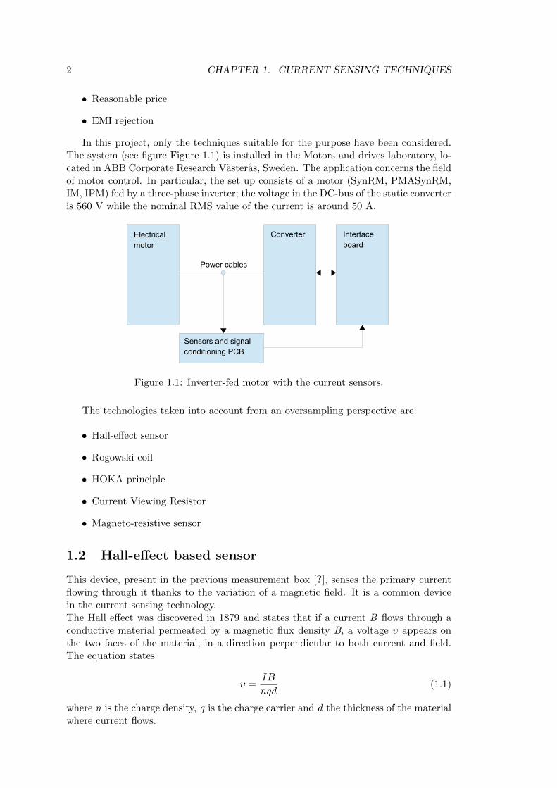
1.2.1 Open loop
In this configuration, the magnetic flux created by the primary current is concentratedin a core made with soft magnetic material: in this way almost all of the magnetic fieldis concentrated in the core. The magnetic field is measured by an Hall device located inan air gap (see figure 1.2). The output from the Hall device is then signal conditionedby using an operational amplifier in order to provide an exact representation of theprimary current at the output. The advantages of this technology include low cost,small size and low power consumption. They are advantageous in applications wherehigh currents (till 300A) have to be measured. The limitations of open loop transducersare instead the poor bandwidth, the poor response time - due to the magnetic losses inthe magnetic circuit - and a relatively large gain drift with respect to temperature [9].
Figure 1.2: Concept of the open-loop Hall-effect based current sensor, courtesy of [9].
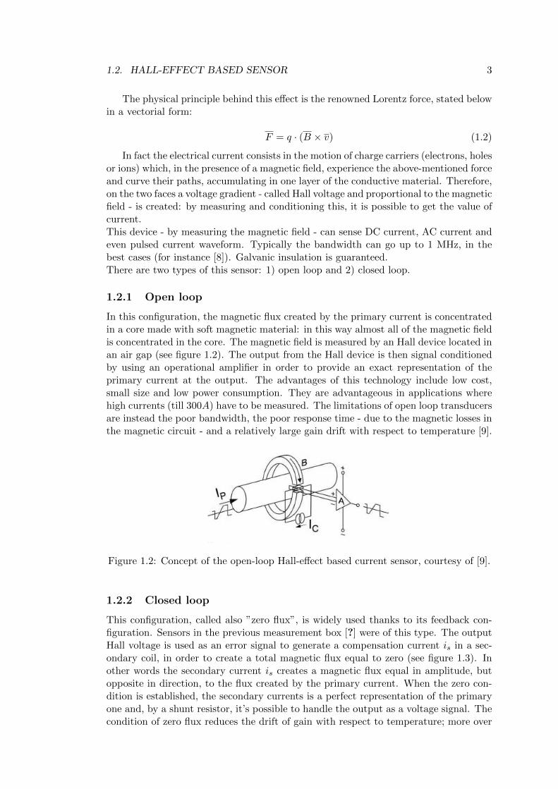
1.2.2 Closed loop
This configuration, called also ”zero flux”, is widely used thanks to its feedback con-figuration. Sensors in the previous measurement box [?] were of this type. The outputHall voltage is used as an error signal to generate a compensation current is in a sec-ondary coil, in order to create a total magnetic flux equal to zero (see figure 1.3). Inother words the secondary current is creates a magnetic flux equal in amplitude, butopposite in direction, to the flux created by the primary current. When the zero con-dition is established, the secondary currents is a perfect representation of the primaryone and, by a shunt resistor, it’s possible to handle the output as a voltage signal. Thecondition of zero flux reduces the drift of gain with respect to temperature; more over

4 CHAPTER 1. CURRENT SENSING TECHNIQUES
bandwidth is larger, thanks to the presence of the secondary winding that acts as acurrent transformer at high frequency, as well as accuracy and linearity. [9]
Figure 1.3: Concept of the closed-loop Hall-effect based current sensor, courtesy of [9].
Although Hall sensors are very widespread, the limitation in bandwidth - with acommercial maximum equal to 1 MHz for the sensor Allegro ACS730 [8] - represents aproblem for the oversampling purpose.
1.3 Rogowski coil
Named after German physicist Walter Rogowski which proposed in 1912 the first ap-paratus of this kind, the Rogowski Coil is an electrical device used for measuring alter-nating current (AC) such as high speed transient, pulsed currents or power frequencysinusoidal currents.The advantages of this device are multiples:
• Fast response, due to its low inductance.
• Wide bandwidth, even over 20 MHz.
• Excellent linearity, thanks to the absence of ferromagnetic material.
• Non-intrusive for the circuit and galvanic isolated, due to the geometry.
The Rogowski coil is an air core toroid, which measures EMF voltage generatedby magnetic flux of a time-varying current signal. The physical principle behind thedevice is Faraday’s law of induction, more specifically Ampere’s circuital law [10]:∮
(H · ds) ≈ Ienclosed (1.3)
The primary current I1(t) causes therefore a flux density B(t), through the magneticfield strength H(t) −→
B (t) = µ0 ·−→H (t) (1.4)
and, for the Faraday’s law of induction∮c
−→E · d−→s = −dφ
dt(1.5)
a voltage, related to the time derivative of the current, is induced between the ends ofthe coil. By integrating this coil voltage the current is obtained.
1.4. HOKA PRINCIPLE 5
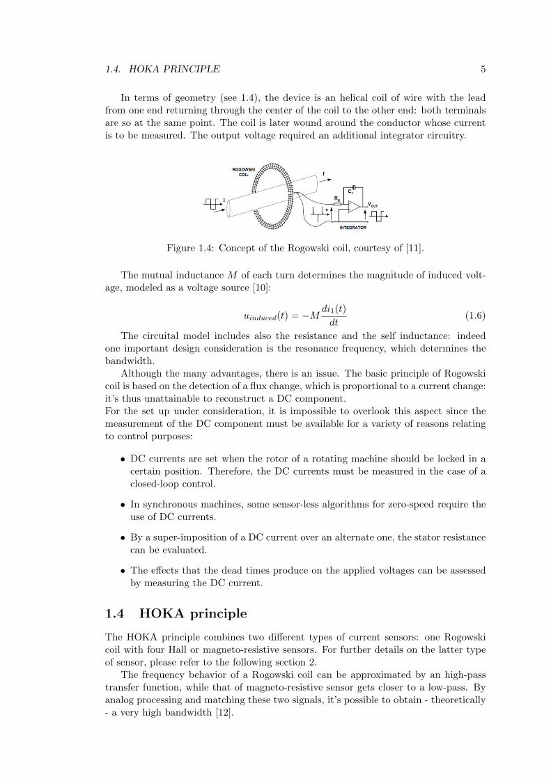
In terms of geometry (see 1.4), the device is an helical coil of wire with the leadfrom one end returning through the center of the coil to the other end: both terminalsare so at the same point. The coil is later wound around the conductor whose currentis to be measured. The output voltage required an additional integrator circuitry.
Figure 1.4: Concept of the Rogowski coil, courtesy of [11].
The mutual inductance M of each turn determines the magnitude of induced volt-age, modeled as a voltage source [10]:
uinduced(t) = −Mdi1(t)
dt(1.6)
The circuital model includes also the resistance and the self inductance: indeedone important design consideration is the resonance frequency, which determines thebandwidth.
Although the many advantages, there is an issue. The basic principle of Rogowskicoil is based on the detection of a flux change, which is proportional to a current change:it’s thus unattainable to reconstruct a DC component.For the set up under consideration, it is impossible to overlook this aspect since themeasurement of the DC component must be available for a variety of reasons relatingto control purposes:
• DC currents are set when the rotor of a rotating machine should be locked in acertain position. Therefore, the DC currents must be measured in the case of aclosed-loop control.
• In synchronous machines, some sensor-less algorithms for zero-speed require theuse of DC currents.
• By a super-imposition of a DC current over an alternate one, the stator resistancecan be evaluated.
• The effects that the dead times produce on the applied voltages can be assessedby measuring the DC current.
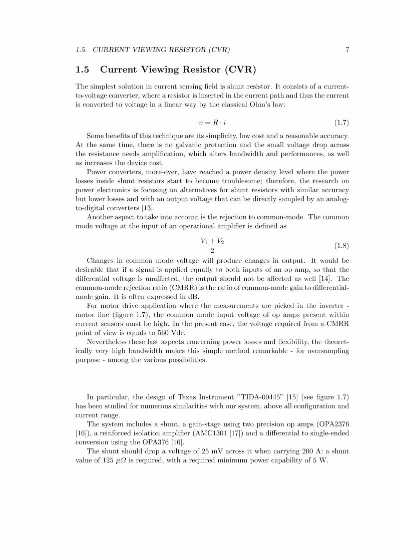
1.4 HOKA principle
The HOKA principle combines two different types of current sensors: one Rogowskicoil with four Hall or magneto-resistive sensors. For further details on the latter typeof sensor, please refer to the following section 2.
The frequency behavior of a Rogowski coil can be approximated by an high-passtransfer function, while that of magneto-resistive sensor gets closer to a low-pass. Byanalog processing and matching these two signals, it’s possible to obtain - theoretically- a very high bandwidth [12].
6 CHAPTER 1. CURRENT SENSING TECHNIQUES
The two sensors signals have to be matched to get a flat frequency response. This is done by the gain factors T/M and 1/KDC and the choice of the time constant T of the lowpass filter of first order. Important is the following criteria:
g,DC1 << fT
(9)
Since the corner frequency of the low frequency capture is g,DC =723kHzf , the time constant of the
lowpass filter is chosen to 10kHz1 =T
.
Figure 10: Frequency response
Current sensor The magnetic field sensor (HOKA principle) used for this current senor is put into the coaxial housing (see Figure 11). The output signals of the four TMR sensors are summed up and added to the output signal of the Rogowski coil (see Figure 9).
Figure 11: Conceptual design of the current sensor
In Figure 12 there is a picture of the magnetic field capture and the signal processing of the current sensor. The coaxial current sensor is depicted in Figure 13.
High Bandwidth Current Sensor with a low Insertion Inductance based on the HOKAPrinciple
TRÖSTER Nathan
EPE'17 ECCE Europe ISBN: 9789075815269 and CFP17850-USB P.6© assigned jointly to the European Power Electronics and Drives Association & the Institute of Electrical and Electronics Engineers (IEEE)
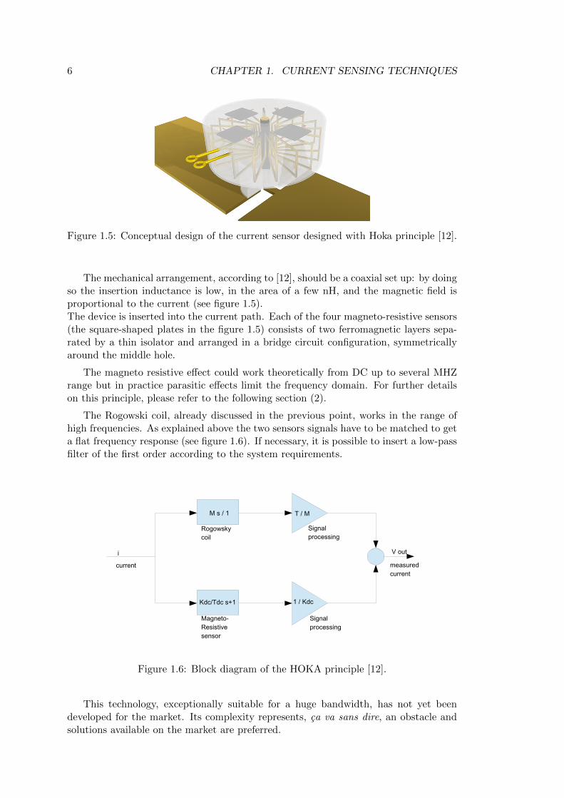
Figure 1.5: Conceptual design of the current sensor designed with Hoka principle [12].
The mechanical arrangement, according to [12], should be a coaxial set up: by doingso the insertion inductance is low, in the area of a few nH, and the magnetic field isproportional to the current (see figure 1.5).The device is inserted into the current path. Each of the four magneto-resistive sensors(the square-shaped plates in the figure 1.5) consists of two ferromagnetic layers sepa-rated by a thin isolator and arranged in a bridge circuit configuration, symmetricallyaround the middle hole.
The magneto resistive effect could work theoretically from DC up to several MHZrange but in practice parasitic effects limit the frequency domain. For further detailson this principle, please refer to the following section (2).
The Rogowski coil, already discussed in the previous point, works in the range ofhigh frequencies. As explained above the two sensors signals have to be matched to geta flat frequency response (see figure 1.6). If necessary, it is possible to insert a low-passfilter of the first order according to the system requirements.
i
current measured current
V out
Rogowsky coil
Signal processing
Signal processing
Magneto-Resistive sensor
M s / 1 T / M
Kdc/Tdc s+1 1 / Kdc
Figure 1.6: Block diagram of the HOKA principle [12].
This technology, exceptionally suitable for a huge bandwidth, has not yet beendeveloped for the market. Its complexity represents, ca va sans dire, an obstacle andsolutions available on the market are preferred.
1.5. CURRENT VIEWING RESISTOR (CVR) 7
1.5 Current Viewing Resistor (CVR)
The simplest solution in current sensing field is shunt resistor. It consists of a current-to-voltage converter, where a resistor is inserted in the current path and thus the currentis converted to voltage in a linear way by the classical Ohm’s law:
υ = R · i (1.7)
Some benefits of this technique are its simplicity, low cost and a reasonable accuracy.At the same time, there is no galvanic protection and the small voltage drop acrossthe resistance needs amplification, which alters bandwidth and performances, as wellas increases the device cost.
Power converters, more-over, have reached a power density level where the powerlosses inside shunt resistors start to become troublesome; therefore, the research onpower electronics is focusing on alternatives for shunt resistors with similar accuracybut lower losses and with an output voltage that can be directly sampled by an analog-to-digital converters [13].
Another aspect to take into account is the rejection to common-mode. The commonmode voltage at the input of an operational amplifier is defined as
V1 + V22
(1.8)
Changes in common mode voltage will produce changes in output. It would bedesirable that if a signal is applied equally to both inputs of an op amp, so that thedifferential voltage is unaffected, the output should not be affected as well [14]. Thecommon-mode rejection ratio (CMRR) is the ratio of common-mode gain to differential-mode gain. It is often expressed in dB.
For motor drive application where the measurements are picked in the inverter -motor line (figure 1.7), the common mode input voltage of op amps present withincurrent sensors must be high. In the present case, the voltage required from a CMRRpoint of view is equals to 560 Vdc.
Nevertheless these last aspects concerning power losses and flexibility, the theoret-ically very high bandwidth makes this simple method remarkable - for oversamplingpurpose - among the various possibilities.
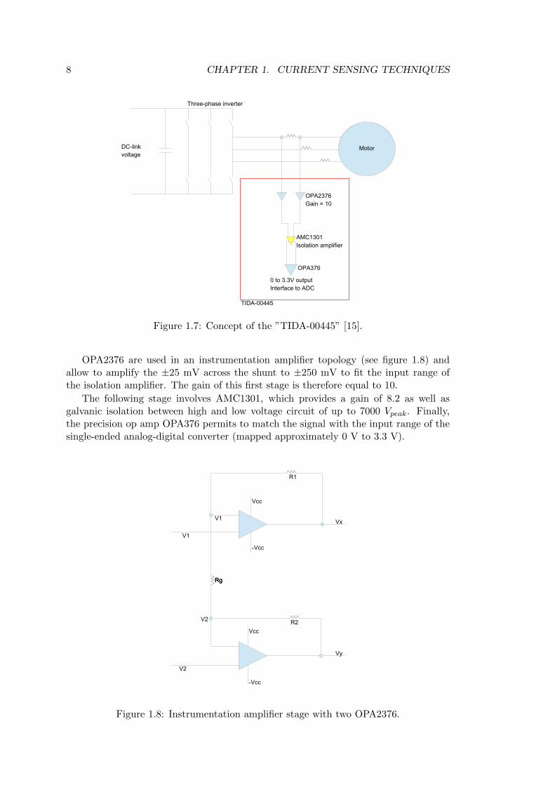
In particular, the design of Texas Instrument ”TIDA-00445” [15] (see figure 1.7)has been studied for numerous similarities with our system, above all configuration andcurrent range.
The system includes a shunt, a gain-stage using two precision op amps (OPA2376[16]), a reinforced isolation amplifier (AMC1301 [17]) and a differential to single-endedconversion using the OPA376 [16].
The shunt should drop a voltage of 25 mV across it when carrying 200 A: a shuntvalue of 125 µΩ is required, with a required minimum power capability of 5 W.
8 CHAPTER 1. CURRENT SENSING TECHNIQUES
DC-link voltage
Three-phase inverter
Motor
OPA2376Gain = 10
AMC1301Isolation amplifier
OPA376
0 to 3.3V outputInterface to ADC
TIDA-00445
Figure 1.7: Concept of the ”TIDA-00445” [15].
OPA2376 are used in an instrumentation amplifier topology (see figure 1.8) andallow to amplify the ±25 mV across the shunt to ±250 mV to fit the input range ofthe isolation amplifier. The gain of this first stage is therefore equal to 10.
The following stage involves AMC1301, which provides a gain of 8.2 as well asgalvanic isolation between high and low voltage circuit of up to 7000 Vpeak. Finally,the precision op amp OPA376 permits to match the signal with the input range of thesingle-ended analog-digital converter (mapped approximately 0 V to 3.3 V).
Rg
V1
Rg
V1
R1
R2V2
V2
Vcc
-Vcc
Vcc
-Vcc
Vx
Vy
Figure 1.8: Instrumentation amplifier stage with two OPA2376.

1.5. CURRENT VIEWING RESISTOR (CVR) 9
In the figure 1.9 the practical implementation of the ”TIDA-00445” is shown.
This solution is eventually shelved for a bandwidth reason. This parameter, inthis design, is uniquely determined by the four op amps (figure 1.7) and the isolationamplifier AMC1301 according to the data sheet [17] has a bandwidth equal to 200 kHz,certainly too few for oversampling purposes.
SN6501
LM4040-N
REF2033
TIDA-00912
+5 V
+2.5 V ±2.5 V
+3.3 V
+1.65 V
AMC1301
OPA376
OPA2376+2.5 V t2.5 V
Isolation Amplifier
0- to 3.3-V Output
Interface to ADC
Gain = 10
M
Three-Phase Inverter
DC-LinkVoltage
Shunt
Copyright © 2016, Texas Instruments Incorporated
1TIDUBV1A–September 2016–Revised September 2016Submit Documentation Feedback
Copyright © 2016, Texas Instruments Incorporated
Shunt-Based, 200-A Peak Current Measurement Reference Design UsingReinforced Isolation Amplifier
TI DesignsShunt-Based, 200-A Peak Current Measurement ReferenceDesign Using Reinforced Isolation Amplifier
DescriptionThis TI Design provides a complete reference solutionfor isolated current measurement using externalshunts, reinforced isolation amplifiers, and an isolatedpower supply. The shunt voltage is limited to 25 mVmaximum. This limit reduces power dissipation in theshunt to enable a high current measurement range upto 200 A. The shunt voltage is amplified by aninstrumentation amplifier configuration with a gain of10 to match the input range of the isolation amplifierfor a better signal-to-noise ratio (SNR). The output ofthe isolation amplifier is level shifted and scaled to fitthe complete input range of 3.3-V analog-to-digitalconverters (ADCs). This design uses a free-runningtransformer driver that operates at 410 kHz togenerate an isolated supply voltage in a small formfactor to power the high voltage side of the circuit.
Resources
TIDA-00912 Design FolderAMC1301 Product FolderOPA2376 Product FolderOPA376 Product FolderREF2033 Product FolderSN6501 Product FolderLM4040-N Product Folder
Design Features• Shunt-Based, 200-A Peak Current Measurement
Solution With Reinforced Isolation• Limiting Shunt Voltage to 25 mV Reduces Power
Dissipation• High-Side Current Sense Circuit With High
Common-Mode Voltage of 1500-VPEAK; Supports upto 690-V AC Mains-Powered Drives
• Calibrated AC Accuracy of < 1% AcrossTemperatures of –25˚C to 85˚C
• Interfaces Directly With Differential or Single-EndedADC
• Small-Form-Factor, Push Pull-Based IsolatedPower Supply to Power High-Side Circuit
• Built-in 1.65-VREF to Level Shift Output
Featured Applications• Active Front-End Converters• Uninterruptable Power Supply (UPS)• Variable Speed Drives
ASK Our E2E Experts
Figure 1.9: Practical implementation of the ”TIDA-00445” [15].

10 CHAPTER 1. CURRENT SENSING TECHNIQUES

Chapter 2
Sensitec CMS3050
In this section the magneto-resistive current sensor ”Sensitec CMS3050” is explained.Starting from the underlying physical principle and the reasons why the sensor is chosen,features and parameters are reviewed.
2.1 The magneto-resistive effect
In thin films of some material, for instance permalloy (a nickel (80%) - iron (20%) mag-netic alloy) the electrical impedance changes when an external magnetic field is appliedin the plane of the film. The variation is due to the rotation of film magnetization; ifthe magnetic field is external, the effect is called anisotropic magneto resistive (AMR)effect. It was first discovered in 1857 by Lord Kelvin.
In the four permalloy strips (cerulean color in the figure 2.1), the resistance changesin a proportional way to the applied magnetic field. By adopting a proper design, smallmagnetic fields can be detected with very high accuracy: there is no need to use aniron core to concentrate the magnetic field generated by the conductor carrying current,avoiding thus the disadvantages of hysteresis. Galvanic isolation and low power lossesare others advantages of this technique [5].
A MR current sensor works with a differential field measurement with compensation.
over a wide range. This means that by adept design of the sensor structure very small magnetic fields can be detected with very high accuracy. However, the MR-effect did not experience widespread use until the early 1980s, when the first MR-based read heads were implemented in hard disc drives. The first industrial applications for MR-based sensors followed at the beginning of the 1990s, since when the number of applications has increased dramatically. The applications are not only limited to terrestrial use – MR sensors are used to control the electric drives used on “Curiosity”, the Planetary Rover that landed successfully on Mars in August 2012. MR sensors are also used extensively in safety-critical automotive applications, for example in wheel speed sensors for the ABS-system or in steering angle sensors for the ESC-system. The magnetoresistive effect is particularly attractive in the field of electrical current measurement. The very high sensitivity means that there is no need to use an iron core to concentrate the magnetic field generated by the conductor carrying the current. This means that MR-based current sensors do not suffer from hysteresis and that they have a significantly higher bandwidth, enabling current sensors with bandwidths in the MHz area. Compared to shunt resistors MR-based sensors have the benefit of galvanic isolation and dramatically lower power losses. This is particularly important in high voltage applications and where overall power efficiency is a major design driver. The increased demand for very dynamic current sensors generated by the recent trends in the field of renewable energy and electromobility was the driver for the development of a highly integrated current sensor (CMS3000 Family) comprising an AMR sensor chip, a high speed control circuit and two biasing permanent magnets (Fig. 1). The latter are necessary for maintaining the initial magnetization direction of the AMR structures in the case of overcurrent situations. The quantity to be measured is a differential magnetic field, also referred to as field gradient that is generated by two currents with opposed current flow directions. The primary current conductor is typically U-shaped, with its straight parallel parts positioned underneath the sensor. For current measurement four AMR “resistors” are connected to form a Wheatstone bridge. The resistors on the silicon chip are placed so that they constitute a differential field sensor. This is necessary because interference fields can be eliminated this way. Combined with a signal conditioning circuit the chip is assembled on a ceramic substrate, incorporating a hybrid circuit (Fig. 2).
Fig. 2: Principle of operation Furthermore, a compensation conductor is integrated on the chip with which a magnetic field can be generated close to the resistors. On the opposite side of the substrate the primary current conductor is attached below the MR chip in a U-shape. The geometry of the primary conductor defines the measurement range of the current sensor. Based on the output signal from the MR chip, the signal conditioning circuit (shown in Fig. 2 schematically as an operational amplifier) generates a current icomp in the compensation conductor, which compensates the magnetic field generated by the primary conductor in the plane of the AMR resistors. With this method the signal achieves a high linearity
Figure 2.1: Principle of a magneto - resistive current sensor [5].
The primary current conductor is U-shaped, positioned underneath the sensor. Thechip is assembled on a ceramic substrate. Four AMR resistors are connected to form aWheatstone bridge and are combined with a signal conditioning circuit.
This last generates a current icomp in the compensation conductor, which compen-sates the magnetic field generated by the primary conductor in the permalloy strips
11
12 CHAPTER 2. SENSITEC CMS3050
plane. icomp is directly proportional to the current to be measured and is used togenerate the output voltage signal.
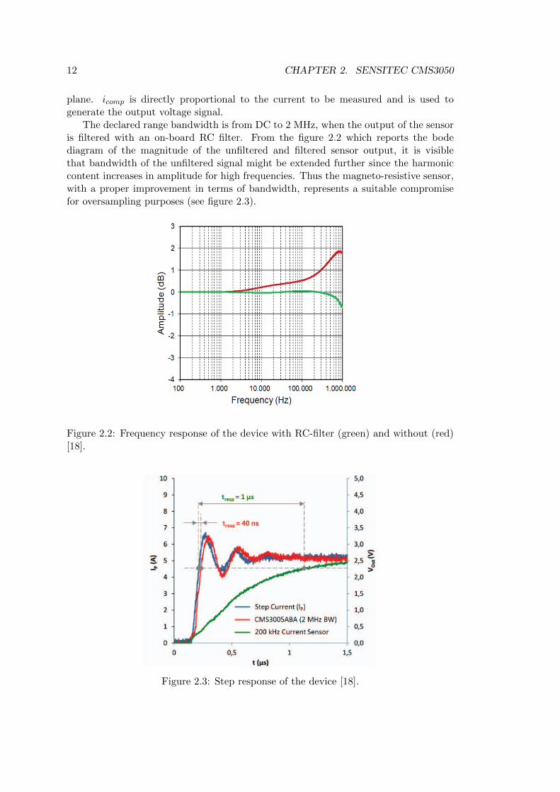
The declared range bandwidth is from DC to 2 MHz, when the output of the sensoris filtered with an on-board RC filter. From the figure 2.2 which reports the bodediagram of the magnitude of the unfiltered and filtered sensor output, it is visiblethat bandwidth of the unfiltered signal might be extended further since the harmoniccontent increases in amplitude for high frequencies. Thus the magneto-resistive sensor,with a proper improvement in terms of bandwidth, represents a suitable compromisefor oversampling purposes (see figure 2.3).
CMS3050highly Dynamic MagnetoResistive Current Sensor (IPN = 50 a)
CMS3050.DSE.05 Subject to technical changesJune 13th 2015
Data sheetPage 6 of 12
Da
ta
Sh
EE
t
Fig. 2: Definition of reaction time (treac), rise time (trise) and response time (tresp).
Da
ta
Sh
EE
t
Fig. 3: dV/dt (3.7 kV/µs; 530 V voltage on primary conductor; filter configuration acc. to Tab. 1).
typical Performance Characteristics
Fig. 4: Step response (IP = 50 A; di/dt ≈ 400 A/µs; filter configuration acc. to Tab. 1).
Fig. 5: Step response (IP = 50 A; di/dt ≈ 170 A/µs; filter configuration acc. to Tab. 1).
Fig. 6: Typical frequency response with RC-filter (green) and without (red). Filter configuration acc. to Tab. 1.Figure 2.2: Frequency response of the device with RC-filter (green) and without (red)
[18].
(0.1 %) and is largely independent of temperature. This compensation current is directly proportional to the primary current to be measured and is used to generate the output signal from the current sensor. This “closed-loop” principle results in an extremely compact sensor that is largely insensitive to homogeneous interference fields and temperature changes, with a low power consumption and very high efficiency. The AMR-based current sensor exhibits no hysteresis as observed in iron core based Hall-sensor solutions and no remaining magnetic offset after overcurrent events. Due to the high sensitivity of the AMR sensor chip, a flux concentrator is not necessary. The sensor is designed for high accuracy and very fast electronic measurement from DC up to 2 MHz AC. Fig. 3 shows a typical step response of a CMS3000 compared to a 200 kHz current sensor, demonstrating a response time of just 40 ns.
Fig. 3: Step response of CMS3000 current sensor To enable the current sensor to measure high bandwidth signals a number of further modifications are necessary to the internal circuitry of the sensor and, most importantly, to the design of the primary conductor. Increasing frequency of the primary current generates eddy currents that lead to a current redistribution in the conductor due to both skin and proximity effects. This changes the magnetic field around the conductor and so leads to measurement errors if not corrected. Fig. 4 shows that the rapidly changing current in one leg of the U-shaped conductor generates eddy currents iskin (skin effect) that are aligned in the opposite direction to the primary current iprim in the core of the conductor and are aligned in the same direction as the primary current at the conductor surface.
Fig. 4: Skin and proximity effects due to eddy currents
Figure 2.3: Step response of the device [18].

2.2. DATA OF CMS3050 13
2.2 Data of CMS3050
Among magneto-resistive current sensor family the Sensitec CMS3050 is chosen [18].In the following table 2.1 the main features are resumed.
Parameter Min Max or typical
Supply voltage ±12 V ±15 V
Primary measuring range - 200 A + 200 A
Primary nominal current IPN 50 Arms
Frequency bandwidth (- 3 dB) 2 MHz
Accuracy (as % of IPN ) ±0.8
Nominal output voltage VoutN with IPN 2.5 Vrms
Output gain between IoutN and VoutN 1/20
Nominal current consumption 50 mA
Maximal current consumption, within the measuring range 110 mA
Maximal current consumption, outside the bounds 105 mA
Internal burden resistor for output signal RM 126 Ω
Rise time, from 10 %IoutN to 90 %IoutN 0.05 µs
Response time, from 90 %IPN to 90 %IoutN 0.04 µs
Table 2.1: Electrical data of the Sensitec CMS3050.
Sensitec GmbH offers the possibility to buy, together with the sensor, an evaluationboard ready for use [19], whose dimensions are 75 mm in width and 90 mm in length.In this way the current to be measured can be directly connected via screw connectorsto a busbar. On the secondary side, there are three output signals available, both asscrew terminals to connect to the board and test pins: an unfiltered output voltage, apre-assembled filtered output voltage and a customized filtered output voltage.
The CMK3000 demoboard offers the opportunity to learn the features and benefi ts of the CMS3000 current sensors in a quick a simple manner.
CMS3050highly Dynamic MagnetoResistive Current Sensor (IPN = 50 a)
CMS3050.DSE.05 Subject to technical changesJune 13th 2015
Data sheetPage 10 of 12
Da
ta
Sh
EE
t
Fig. 12: The CMK3000 demoboards are available for different current ranges.
the CMS3000 Product Family
The CMS3050 is a member of the CMS3000 product family offering PCB-mountable THT current sensors from 5 A up to 100 A nominal current with a typical bandwidth of 2 MHz for various industrial applications.
CMS3005aBa CMS3015aBa CMS3025aBa CMS3050aBa CMS3100aBa
IPN 1) 5 A 15 A 25 A 50 A 100 A
IPR 2) 20 A 60 A 100 A 200 A 400 A
2) Measurement range.
1) Nominal primary current (RMS).
Figure 2.4: The CMK3000 board: in yellow the current sensor [18].
Since the maximum bandwidth is not declared in the data sheet, the following stephas involved the assessment of the frequency response. Once the bandwidth is known,it is possible to think about the board design upgrade.

14 CHAPTER 2. SENSITEC CMS3050

Chapter 3
Current sensor filtering
In this section the sensor is tested in order to verify its dynamic response. This firstinvestigation is performed in the time domain, where a proper analog filter at the outputof the unfiltered voltage is used to increase the declared bandwidth of the sensor.
3.1 Introduction
The frequency response of a system G(jω) - in our case a sensor - is the complex ratioof the output and the input of the system. It is expressed as function of frequency andit is used to characterize the dynamics of the system in terms of spectrum.
Briefly, if a signal is injected into a system at a given frequency, the system (repre-sented in the figure 3.1) will respond at the same frequency with a certain magnitudeand a certain phase shift relative to the input. Repeating this test for different valuesof frequency (sweep), the frequency response can be plotted.
Assuming two I/O sinusoidal signals where u(t) is the input and y(t) is the output,
u(t) = A · sin(ωt+ ϕ) (3.1)
y(t) = B · sin(ωt+ Υ ) (3.2)
the relation between them is
B = A · |G(jω)| (3.3)
Υ = ϕ · ∠G(jω) (3.4)
Sinewave high-frequencies generatorSinewave high-frequencies generator
Current sensorTransfer function = G(jw)
Load
Dual channels oscilloscope
Reference for the current, with a probe
Current measured with the sensor
Figure 3.1: Ideal set up to detect the frequency response.
15

16 CHAPTER 3. CURRENT SENSOR FILTERING
This comparison is often made through a process known as Fast Fourier Transform(FFT), an algorithm that samples a signal over a time period and it divides into itsfrequency components by a Fourier analysis.The frequency response consists of two parts: the system’s response magnitude, mea-sured in dB, and the phase, measured in radians. These two are typically plotted intwo rectangular plots as functions of frequency, obtaining thus a Bode plot.
Knowing the frequency response makes feasible to find the current sensor bandwidthand, consequently, the harmonic content available for oversampling purpose.

3.2. TESTING SIGNAL GENERATOR AGILENT TECH 33120A 17
3.2 Testing Signal Generator Agilent Tech 33120A
A first test is performed using a 15 MHz synthesized function generator, the Agilent33120A [20] (front panel in figure 3.2), connected with a 50 Ω resistance load. Twoprobes are connected, one for the voltage and one for the current. The purpose ofthe test is to detect the behavior of current and voltage at high different frequencies,evaluating if the amplitude is in a sufficient resolution to test later on the current sensor.The Front Panel at a Glance
1 Function / Modulation keys 2 Menu operation keys 3 Waveform modify keys 4 Single / Internal Trigger key (Burst and Sweep only)
5 Recall / Store instrument state key 6 Enter Number key 7 Shift / Local key8 Enter Number “units” keys
2
Figure 3.2: The front panel of the Agilent 33120, [20].
The theoretical peak to peak voltage supplied by the signal generator is:
Vpp = 5V (3.5)
and consequently the current, in a 50 Ω load was:
Ipp = 200mA (3.6)
In the following table measurements are reported.

18 CHAPTER 3. CURRENT SENSOR FILTERING
Freq[Hz] IRMS [mA] VRMS [V ] |Z|[Ω] Phase− shift[degree]50 70.614 1.750 24.78 +7.2
100 69.881 1.751 25.06 +3.6
200 69.826 1.75 25.06 +1.5
300 69.679 1.748 25.09 +1.4
400 69.664 1.747 25.10 +1.2
500 69.505 1.745 25.11 +1.2
1 k 69.399 1.733 24.97 -1.3
10 k 69.401 1.685 24.28 -2.4
100 k 68.641 1.702 24.80 -4.3
500 k 68.067 1.766 25.95 -20.9
1 M 64.169 1.944 30.30 -38.2
2 M 59.266 2.161 36.46 -50.8
3 M 42.972 2.616 60.88 -72.4
4 M 33.724 2.718 80.60 -80.7
5 M 26.216 2.715 103.56 -86.4
The outcomes show that:
• Current drops from the initial value of 70 mA to 25 mA.
• Voltage rises from the initial value of 1.75 V to 2.75 V.
• Impedance rises from the initial value of 25 Ω (resulting from the parallel of the50 Ω load plus the internal load of 50 Ω) to 100 Ω.
• Phase shift changes from the initial inductive behavior (+10°) to a completecapacitive behavior (-90°).
In the figure 3.3, the current detected with the scope at 5 MHz is showed.
Figure 3.3: Current on the 50 Ω resistance at 5 MHz.
Sensitec CMS3050 (see the data sheet [18]) has an output of 2.5 V when it measuresthe nominal current of 50 Arms. The gain of the device is therefore 1/20. Testing thecurrent sensor with Agilent 31022 would have meant to obtain, at 5 MHz, a primarycurrent equals to 25 mArms and so a voltage output signal of 1.3 mV. The noise level(RMS) of the device is equal to 0.25 mV (see [18]), almost 20% of the signal.
Therefore, the amount of current available with Agilent 31022 is too weak to makean accurate comparison. Decreasing the resistance (f.i. 1 Ω), in order to have more

3.2. TESTING SIGNAL GENERATOR AGILENT TECH 33120A 19
current, is not feasible since the fuse inside the signal generator stops currents greaterthan 500 mA.
A possible alternative is to build a resonant circuit, inserting an inductance inparallel and tuned on the desired frequency. This can theoretically boosts current bythe magnifying factor Q but, at high frequency (f.i. 5 MHz), a simple inductanceintroduces some parasitic capacitances as well.
Audio generators on the market may reach high frequency but at the same timethey do not possess a large current magnitude. An alternative is sought.
3.2.1 Investigation of a proper set up: Brockhaus MPG 200D AC/DC
A signal able to run into the domain of high frequency with a fair current amplitudeis required. Brockhaus MPG 200D AC/DC is a test bench for the measurements ofmagnetic proprieties of materials. Embedded with the device there is one wave formgenerator, with two stages of power amplifiers. The maximum frequency using this lastis equal to 20 kHz (fundamental) for PWM signals, with a maximum declared currentof 50 A, using the second stage amplifier.
Even exploiting harmonics in the high frequency domain, the combination of fre-quency/amplitude is still feeble.
3.2.2 Investigation of a proper set up: IGBT short circuit tests
A short circuit test on IGBT modules permits to assess the capability of IGBT towithstand extremely severe condition. By doing this, IGBTs can switch in some casewith a significant slew rate (13 kA/µs). Theoretically, it is possible to use this signalin order to develop a large harmonic content to inject in the current sensor.The double switching on/off of an IGBT can be approximate to a triangular pulse.Assuming a slew rate of 12.5 kA/µs means a rise time (0 - 50 A) of 4 ns. In thefollowing figures 3.4 and 3.5 the pulse and its FFT are shown.
0 0.2 0.4 0.6 0.8 1Time [s] 10-8
0
10
20
30
40
50
Cur
rent
[A]
Figure 3.4: Triangular pulse
Building a new set up is possible, but with evident complexities: a switching timeof 4 ns is not possible with off-the-shelf components, fast switches (e.g. SiC MOSFET)can achieve in best cases 50 ns, with a trapezoidal-shape signal. The construction of anew set up, more-over, requires more time that the available one. The easy trade off isfound in using inverter-fed motors already in place in the laboratory.

20 CHAPTER 3. CURRENT SENSOR FILTERING
0 2 4 6 8 10Frequency [Hz] 109
10-20
10-10
100
1010
Cur
rent
[A]
Figure 3.5: FFT of the triangular signal
3.3 Test on Inverter-fed SynRMs
The experiments are carried in the Motor Lab, in the ABB Corporate Research inVasteras, Sweden. The first part involves the choice of the best motor in terms ofharmonic content: that means, paradoxically, to identify the most aged machine.
The second part concerns instead the elaboration of data in order to find a properfilter.
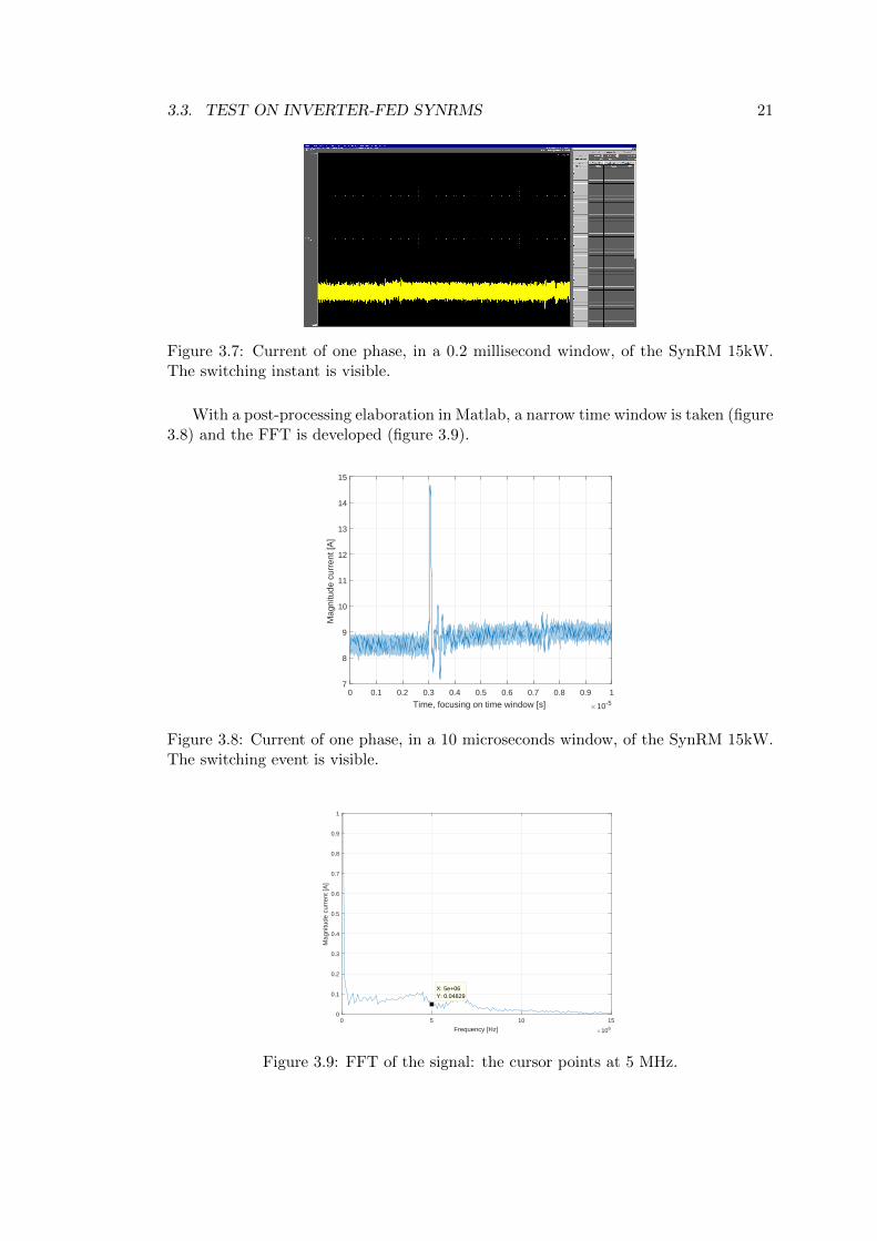
Two synchronous reluctance motors are fed by an inverter controlled by a scalarPWM. With a probe, one current phase is detected. Two observation windows arechosen: one long (1 sec) and one short (0.2 msec). The following pictures 3.6 and 3.7show the measurements for one machine.
Figure 3.6: Current of one phase, in a 1 second window, of the SynRM 15kW.
3.3. TEST ON INVERTER-FED SYNRMS 21
Figure 3.7: Current of one phase, in a 0.2 millisecond window, of the SynRM 15kW.The switching instant is visible.
With a post-processing elaboration in Matlab, a narrow time window is taken (figure3.8) and the FFT is developed (figure 3.9).
0 0.1 0.2 0.3 0.4 0.5 0.6 0.7 0.8 0.9 1
Time, focusing on time window [s] 10-5
7
8
9
10
11
12
13
14
15
Mag
nitu
de c
urre
nt [A
]
Figure 3.8: Current of one phase, in a 10 microseconds window, of the SynRM 15kW.The switching event is visible.
0 5 10 15
Frequency [Hz] 106
0
0.1
0.2
0.3
0.4
0.5
0.6
0.7
0.8
0.9
1
Mag
nitu
de c
urre
nt [A
]
X: 5e+06Y: 0.04829
Figure 3.9: FFT of the signal: the cursor points at 5 MHz.

22 CHAPTER 3. CURRENT SENSOR FILTERING
The figure 3.9 shows that short interval means more magnitude in frequency but,at the same time, less resolution in the frequency domain.
The 11 kW motor presents more noise and disturbances and so an higher harmoniccontent and it is therefore chosen for the subsequent trials. Another test is carried: thecurrent sensor is connected in one phase of the inverter-motor line. One current clampand two voltage probes are arranged in different position:
• channel 1 - yellow trace: positioned in the line motor-inverter. This measurementrepresents the actual current ia, unaffected by the current sensor and measuredwith a high-bandwidth (100 MHz [21]) current clamp.
• channel 2 - green trace: positioned in the test pin on the board CMK3000 (see fig.2.4). This measurement, performed by a voltage probe, represents the unfilteredcurrent of CMS3050 ia,unfiltered.
• channel 3 - pink trace: positioned in the test pin on the board CMK3000 (seefig. 2.4). This measurement, performed by a voltage probe, represents the pre-assembled RC filtered current of CMS3050 ia,filtered.
The machine is then fed by the inverter.Make a comparison with different TFs is problematic because of the noise present
in the system. A time domain is therefore selected in order to build the best analogfilter to apply at the sensor in order for the green curve - unfiltered current - to followthe yellow one - actual current - as close as possible. As matter of fact, detecting thecurrent at the switching instant and then building a proper filter around it, allows toachieve the suitable filter and time response.
In the following figures 3.10, 3.11 and 3.12 different time windows are shown.
Figure 3.10: Current of one phase detected by three clamps, 1 second window observa-tion, SynRM 11kW.

3.3. TEST ON INVERTER-FED SYNRMS 23
Figure 3.11: Current of one phase detected by three clamps, 0.2 milliseconds windowobservation, SynRM 11kW. It is visible, zoomed, the switching instant.
Figure 3.12: Current of one phase detected by three clamps, 5 microseconds windowobservation, SynRM 11kW. It is visible, zoomed, the switching instant.

24 CHAPTER 3. CURRENT SENSOR FILTERING
The oscilloscope data are then elaborated in Matlab, with the aim of finding outa transfer function - representation of a filter - able to follow the signal. Assuming asinput ia,unfiltered and as output ia, the transfer function is estimated with the command”tfest”, which permits to define the number of poles and of zeros of the TF.
A model in Simulink (see figure 3.13) allows to compare ia with ia,unfiltered combinedwith the filter.
[t ia unfiltered]
[t ia]
[t ia filtered]
State-Space
To Workspace
x' = ax + Bu
y = Cx + Du
Figure 3.13: Simulink model that compares ia with ia,unfiltered plus the filter (blockState-Space).
In the following figures 3.14, 3.15 and 3.16, some elaborations are shown. The actualcurrent ia is printed in blue, while the ia,filtered, made by the chain of ia,unfiltered andthe filter, is printed in orange.
0 0.05 0.1 0.15 0.2Time [s]
-20
-10
0
10
20
Cur
rent
[A]
Figure 3.14: Processed-data in a 0.2 s window, transfer function estimated with twopoles.

3.3. TEST ON INVERTER-FED SYNRMS 25
0 0.5 1 1.5 2Time [s] 10-6
-16
-14
-12
-10
-8
-6
-4
Cur
rent
[A]
Figure 3.15: Processed-data in a 2 us window, transfer function estimated with twopoles.
0 1 2 3 4 5Time [s] 10-6
-12
-10
-8
-6
-4
-2
0
2
Cur
rent
[A]
Figure 3.16: Processed-data in a 5 us window, transfer function estimated with threepoles and one zero.
The so-simulated filters can follow the actual current.
Another comparison method is made using the Matlab application ”System Iden-tification”. This allows to insert I/O data in order to estimate a transfer functionspecifying poles and zeros.
In the following figures 3.17 and 3.18, some elaborations are shown.
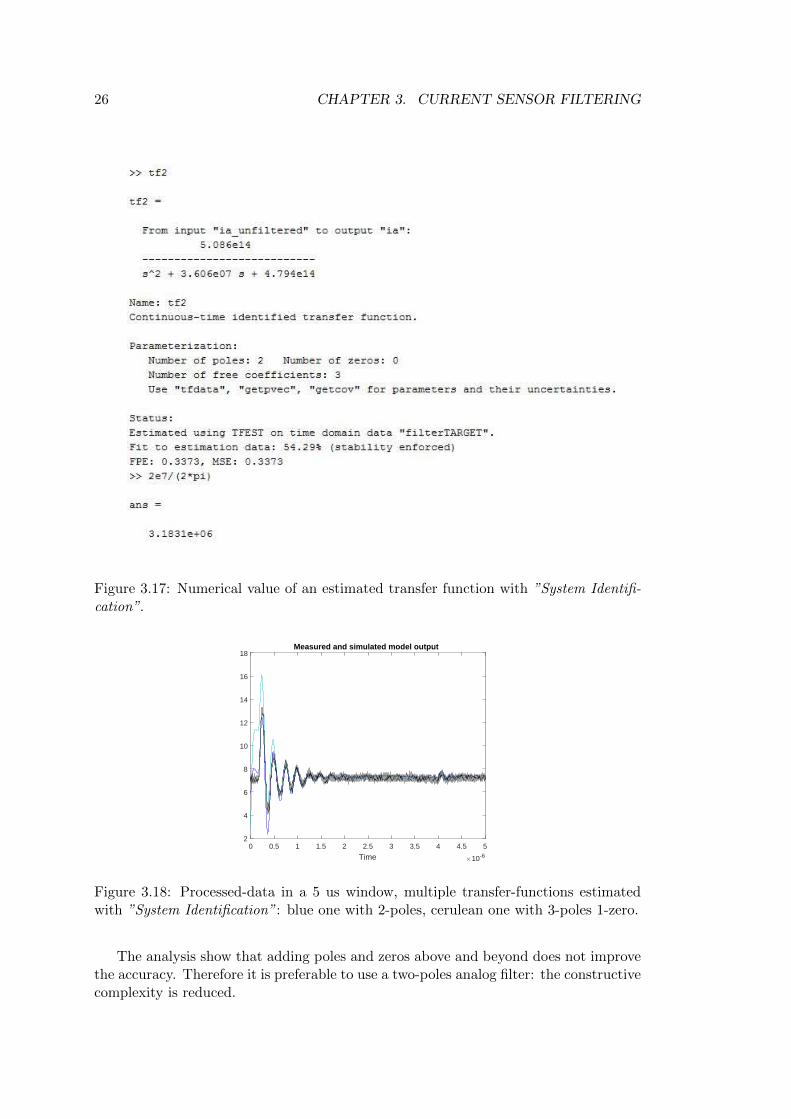
26 CHAPTER 3. CURRENT SENSOR FILTERING
Figure 3.17: Numerical value of an estimated transfer function with ”System Identifi-cation”.
0 0.5 1 1.5 2 2.5 3 3.5 4 4.5 5
Time 10-6
2
4
6
8
10
12
14
16
18Measured and simulated model output
Figure 3.18: Processed-data in a 5 us window, multiple transfer-functions estimatedwith ”System Identification”: blue one with 2-poles, cerulean one with 3-poles 1-zero.
The analysis show that adding poles and zeros above and beyond does not improvethe accuracy. Therefore it is preferable to use a two-poles analog filter: the constructivecomplexity is reduced.

3.3. TEST ON INVERTER-FED SYNRMS 27
At that point, a comparison with different transfer functions is run. Each TFrepresents a filter. In the following table 3.1 only the four best solutions are resumed.For the sake of completeness all the TFs used are reported in the appendix A; for anin-depth explanation of the filters please instead refer to the next section 3.4.
Filter-type Numerator Denominator Cut-off frequency
Bessel,M − FB 1.4e15 s2 + s · 33.3e6 + 3.6e14 2.3MHz
Butterworth,M − FB 1.5e15 s2 + s · 27.3e6 + 3.7e14 3MHz
Bessel, Sellen−Key 2.3e15 s2 + s · 41.4e6 + 5.7e14 3MHz
Butterworth, Sellen−Key 1.4e15 s2 + s · 26.6e6 + 3.5e14 3.4MHz
Table 3.1: Features of the four transfer functions used.
With the Simulink model (see figure 3.13), the two signals ia and ia,filtered aretested for all the measurements and then the Root-Mean-Square Deviation (RMSD) iscomputed:
RMSD =
√∑(ia − ia,filtered)2
N· 1
ia,RMS(3.7)
The mean of the RMSDs, calculated for each measurement, shows that filters havealmost the same error.
Filter-type RMSD
Bessel,Multiple− Feedback 10.53
Butterworth,Multiple− Feedback 11.15
Bessel, Sellen−Key 11.78
Butterworth, Sellen−Key 10.93
With the aim of improving the accuracy of the simulation, the same filters are madedigital with the Matlab command ”c2d”. The results are reported:
Filter-type RMSD
Bessel,Multiple− Feedback 12.29
Butterworth,Multiple− Feedback 12.03
Bessel, Sellen−Key 12.48
Butterworth, Sellen−Key 12.03
Digitalization adds more noise but solely in a range of 1%.
Last elaboration concerns the addition of noise with the Matlab command ”awgn”.Results are reported:
Filter-type RMSD
Bessel,Multiple− Feedback 36.73
Butterworth,Multiple− Feedback 37.33
Bessel, Sellen−Key 37.49
Butterworth, Sellen−Key 37.30
Last values confirm the obvious fact that inserting a white noise carries a significantgrowth in terms of error. Nevertheless the filters can still roughly follow the input signal.

28 CHAPTER 3. CURRENT SENSOR FILTERING
3.4 Choice of the analog filter
The analog filter theory [22] has been studied in order to choose the best design solu-tion. The main requirement is a large bandwidth to detect the current high frequencybehavior. The approximation should be a low-pass filter since the sensors must be ableto measure both DC and AC currents.
A second-order low-pass filter has a pair of complex conjugate poles on the left sideof the S-plane. S-plane is the complex plane on which Laplace transforms are graphed:the real-axis, horizontal, is denoted by σ while the imaginary-axis, vertical, is denotedby ω.
Re(σ)
Im(ω)
Figure 3.19: Pole location in S-plane: the choice of left side is due to stability.
The typical Bode diagram of a low pass filter is:
-60
-40
-20
0
20
Mag
nitu
de (
dB)
105 106 107 108-180
-135
-90
-45
0
Pha
se (
deg)
Bode Diagram
Frequency (Hz)
System: sysFrequency (Hz): 3.25e+06Magnitude (dB): 8.51
Figure 3.20: Bode diagram of a second-order low-pass filter.
The transfer function of a second order low-pass filter is:
H(s) =G
s2 + ω0Q · s+ ω2
0
(3.8)
where G is the gain, Q is the quality factor of the filter and ω0 = 2 · π · fcutoff is thecut-off angular frequency (in rad/sec).
Two typologies of filters related to two topologies have been examined.

3.4. CHOICE OF THE ANALOG FILTER 29
3.4.1 Butterworth
This response is one of the best known and one of the most widely used at once. Ithas no ripple neither in the pass band nor in the stop band; because of this is termedmaximally flat filter. At the same time the response exhibits a poor roll-off rate,compared to others filters not taken into account in this analysis (f.i. Chebyshev orElliptic).
The transient response of a Butterworth filter to a pulse input shows moderateovershoot and ringing and the quality factor Q is equal to 0.707. The values of theelements of this filter are more practical and less critical than other filter types.
Figure 3.21: Comparison of magnitude bode diagram: Chebyshev has not been dealtwith in the report [22].
Figure 3.22: Comparison of step response: Chebyshev has not been dealt with in thereport [22].
3.4.2 Bessel
The Bessel has the best phase response, even better than the Butterworth. The Besselfilter achieves this flatness at the expense of the roll-off rate, which is the slowest oneamong the other filters.
This solution, more-over, shows the best behavior in the time domain (figure 3.22)[22]. Indeed the impulse response of a filter (and so the step response, integral of

30 CHAPTER 3. CURRENT SENSOR FILTERING
the last one), in the time domain, is proportional to the bandwidth in the frequencydomain. The narrower the impulse, the wider the bandwidth of the filter.
The quality factor Q is equal to 0.577. The frequency scale factor (FSF) is defined- in the Sallen-Key configuration - as:
FSF · fcutoff =1
2 · π · √R1 ·R2 · C1 · C2(3.9)
The Butterworth filter has FSF equal to 1 - as it was already said this typology ofresponse has an inherent simplicity. For a Bessel instead the FSF is equal to 1.274.
3.4.3 Sallen-Key configuration
This configuration, termed also voltage control voltage source (VCVS), is one of themost widely used. Its popularity is due to its least dependence on the op amp per-formance, that is not configured as an integrator but as an amplifier: this leads to aminimization of the op amp gain-bandwidth requirements. In this way the filter canwork till higher frequency compared to other topologies. In the following figure 3.23 asecond order low pass Sallen-Key configuration is shown.
V in R 1 R 2
R 3
R 4
C 2
V outC 1
+
-
Figure 3.23: Second order low pass active filter in the Sallen-Key configuration.
The ideal gain of a low-pass filter in Sallen-Key architecture is:
K =R3 +R4
R3(3.10)
while the cutoff frequency is:
FSF · fcutoff =1
2 · π · √R1 ·R2 · C1 · C2(3.11)
3.4.4 Multiple-Feedback configuration
In this architecture the op amp is used as an integrator, as shown in the figure 3.24. Inthis case the dependence of the transfer function to the op amp performance is substan-tial. Working at high frequencies results consequently harder due to the limitations ofthe open-loop gain of the op amp. More-over the multiple feedback configuration willinvert the phase of the signal.
The ideal gain of a low-pass filter in Multiple-Feedback architecture is:
K = −R2
R1(3.12)
while the cutoff frequency is:
FSF · fcutoff =1
2 · π · √R2 ·R3 · C1 · C2(3.13)

3.5. DESIGN OF THE ANALOG FILTER 31
V in R 1 R 3
R 2
C 1
V outC 2 +
-
Figure 3.24: Second order low pass active filter in the Multiple-Feedback configuration
3.5 Design of the analog filter
Considering the analysis carried out above, a Bessel filter is chosen because it shows thebest behavior in the time domain. Sallen-Key configuration instead is chosen thanksto the least dependence on the op amp performance.
For the practical design, two on-line softwares have been used together: ”FilterDesign and Analysis” of Okawa [23] and ”Webench Designer” [24] of Texas Instrument.
As shown in the figure 3.21, the Bessel typology has a -3 db cut-off frequency shiftedcompared to the other filters. So, in order to have the -3 db corner frequency at 3 MHz(obtained by the transfer function in the table 3.1), the FSF must be considered inthe analysis (see subsection 3.4.2). In the Sallen-Key configuration the FSF is equal to1.274.
The filter is therefore designed with a break frequency of 3 MHz · 1.274 ' 3.8 MHz.The gain voltage to voltage is set instead at 4 for reasons concerning the board interface(see subsequent section 4.2.2).
The Bode diagram is the same shown in the figure 3.20.In the electrical scheme of the figure 3.25 the values of resistances and capacitances
are displayed.
V in R 11.4 kOhm
R 2464 Ohm
C 227 pF
V out
R 32.49 kOhm
-
+C 1100 pF
R 47.5 kOhm
Figure 3.25: Second order low pass Bessel filter in the Sallen-Key configuration. Cut-offfrequency is set at 3.8 MHz while the voltage to voltage gain is set at 4. Element valuesare shown.
Recapping, at this point the current sensor has been chosen - Sensitec CMS3050 -as well the proper analog filter - second-order low-pass Bessel in Sallen-Key architec-ture - to implement in the PCB. In the following chapter, the PCB design upgrade isexplained.

32 CHAPTER 3. CURRENT SENSOR FILTERING
0 0.05 0.1 0.15 0.2Time [s]
-20
-10
0
10
20
Cur
rent
[A]
Figure 3.26: The designed Bessel filter (in orange) follows correctly the actual current(in blue). 0.2 s window.
0 1 2 3 4 5Time [s] 10-6
-14
-12
-10
-8
-6
-4
-2
Cur
rent
[A]
Figure 3.27: The deisgned Bessel filter (in orange) follows correctly the actual current(in blue). 5 us window. The rising at the beginning is due to a residual offset.

Chapter 4
PCB design upgrade
Once the device and the filter to implement are set, the PCB design is done startingfrom the previous measurement device design. The employed software is KiCad, afree software suite for electronic design automation. After a briefly view of the entiremeasurement system, the PCB design is explained step by step.
4.1 Introduction
The structure of the measurement system containing the PCB is shown in the figure:
230 Vac
2 x 24 Vdc
fan
± 24 V± 15 V
generation
3 x current filters
3 x current sensors
inverter
SynRM4 x voltage sensors
4 x voltage filters
± 15 V
3 x unfiltered currents
3 x filtered currents
4 x voltages
3 x primary voltages
3 x primary currents
Star point of the machine
± DC bus
to OP5600
to XILINX ZC702
Figure 4.1: Schematic of the measurement system. The PCB is highlighted in green;arrows indicate the power supply line; solid lines indicate the signal
33

34 CHAPTER 4. PCB DESIGN UPGRADE
The power supply of the PCB is granted by two MeanWell MDR 60 ±24 VDC [25]which feed:
• The four analog filters of the voltage measurements, if present
• The three analog filters of the current measurements
• The cooling fan
• The power supply converters which transform ±24 VDC into ±15 VDC
That in turn feed:
• The three current sensors
• The four voltage sensors, if present
Primary currents and voltages come in from the three power cables located in theinverter-motor line. These enter in the three current sensors and - if devices are mounted- in the four voltage sensors.
At the output side ten signals are available: three filtered current signals, threeunfiltered current signals and - if present - four voltages signals. The PCB has twotypologies of output: one through DB7 connector, to interface with the analog input ofan OPAL-RT OP5600 [26], and one through SMA connectors, to interface with FPGAXILINX ZC702 [27].
4.2 Structure of the PCB
The main part of the measurement system is the PCB, in which currents and possiblyvoltages are measured and filtered. The following section describes the board in details.
4.2.1 Power supply
The PCB is supplied by two MeanWell MDR-60-24 (24 V/ 2.5 A) [25] power supplies,connected in series to obtain a ±24 V voltage source. For protection against over-voltages two Schottky diodes are mounted. The midpoint voltage of the two powersupplies establishes the ground potential of the board. Figure 4.2 shows the schematic.
Current and voltage sensors require a power supply of ±15 V. Additionally, thepossibility to feed the fan with 15 V is included with a terminal block header. Thisstage (see figure 4.3) is realized by two LM2594HVM-ADJ [28] voltage regulators,supplied by the +24V line; one of them is designed to invert the voltage to -15V.
The first stage is made by the input capacitors, followed by a delayed start-up.Then the LM2594HVM-ADJ are mounted. At the output, a low-pass filter and oneLED for each polarity is mounted to indicate whether the voltage is present or not.
The ±15 V can supply a maximum current of 500 mA. The maximum currentconsumption within bounds for each Sensitec CMS3050 current sensor is 100 mA whileeach voltage sensor requires a maximum current of 32.2 mA in worst case operation.The total amount is so 3 · 100 mA + 4 · 32.2 mA = 428.8 mA and the limit of 500 mAis complied.

4.2. STRUCTURE OF THE PCB 35
Figure 4.2: Schematic of power supplies ±24 V.
Figure 4.3: Schematic of the ±15 V regulation.
4.2.2 Current stage
The three current sensors Sensitec CMS3050 (look at chapter 2 for electrical data) aremounted in CMK boards (figure 2.4). These in turn are seated on the PCB throughscrews and the three unfiltered currents, by wires and terminal block headers, routedto the board.
Before the filtering stage, these unaltered signals are made available at the outputstage.
In order to obtain an accurate measurement, the three 2nd-order Bessel low-passfilter in Sallen-Key configuration - designed in the section 3.5 - have been arrangedwith a cut-off frequency of fc= 3.8 MHz and a gain (voltage/voltage) of A = 4. Theschematic of the filter is shown in the next image 4.4.

36 CHAPTER 4. PCB DESIGN UPGRADE
Figure 4.4: Current stage schematic: on the left, the current sensor that feeds theanalog filter.
To match analog signals with the input of the OP5600, two factors were taken intoaccount:
• The analog input of OP5600 has a voltage range of ±20 V.
• The op amp OPA552 [29] has a gain-bandwidth of 12 MHz. Considering thatthis parameter is the product of the op amp bandwidth - set for oversamplingreason around 3 MHz - and the gain at which the bandwidth is measured, thebest compromise concerns settling the gain at 4 V/V.
If the primary current is 50 Arms, the sensor output voltage is, according to thedata sheet, 2.5 V. The peak value consequently is 2.5 V ·
√2 = 3.535 V and so the
signal available at the output is 3.535 V · 4 = 14.142 V.Bypass capacitors are used to eliminate transient voltage peaks of the power supply
which could affect the sensors. In the design one 10µF electrolytic capacitor and one 0.1µF ceramic capacitor are mounted. Due to the different high-frequency characteristics,a ceramic and an electrolyte capacitor are needed to ensure a proper reduction oftransient voltages of several types.
The output signals of the filters are connected to the PCB output.
4.2.3 Voltage stage
The measurement device, although is able to measure voltage, wasn’t designed to testit. This means that, while in the PCB the filtering voltage stage is anyhow present,the voltage sensors aren’t mounted within the system.
In the previous version four LEM CV 3-1500 sensors were used. The supply voltageof these device is ±15 V, equal to the one for current sensors. Four terminal blockheaders ±15 V are present in the PCB just in case. The voltage range is 0 - ±1500 V.
The filtering stage is made by four 2nd-order Butterworth low-pass filter in Sallen-Key configuration, with a cut-off frequency of fc= 200 kHz and a gain (voltage/voltage)of A = 2. The design is taken from the previous device. The schematic of the voltagefilter is shown in the figure 4.5.
Voltage signals are available at the output in the same way as the current signals.
4.2.4 Output pins
The output pins are ten: three unfiltered current signals, three filtered current signalsand - if present - four voltage signals. There are two connection possibilities, depending

4.2. STRUCTURE OF THE PCB 37
Figure 4.5: Voltage stage schematic: on the left the Faston connectors where voltagesensors can be connected.
on the used control device: with SMA connectors and with a DB37 connector. Theschematic is resumed in the figure 4.6.
A shielded flat cable is assumed to connect the wire-to-board connector with 40contacts to a DB37 plug at the case. For the XILINX ZC702 the same considerationfor the gain (4 for current stage and 2 for voltage stage) is set but the possibility toconnect the cable straight in the outside surface of the case is not covered.
Figure 4.6: Left side: SMA connectors, right part: DB37 output.

38 CHAPTER 4. PCB DESIGN UPGRADE
4.3 PCB design
Figure 4.7 shows the top side of the PCB upgraded to the version 3.0. The bottomlayer, where there are just the ±24 V traces, is shown in the image 4.8: as many wiresas possible are routed on the top layer. The design is made using KiCad 4.0.7, stablerelease of 28 August 2017.
Current sensors
Plugs for power supply voltage sensors
± 15V regulation-24V plug +24V plugVoltage filters
Current filters
Plugs for power supply voltage sensors
Bypass capacitors
24V fan plug
DB37 out
SMA out
Figure 4.7: Top side of the PCB with description of the main area.
Copper traces have a width of 0.254 mm while the ±24 V power supply lines havea width of 0.508 mm. The board is grounded by the bottom copper layer and the viasbetween top and bottom layer ensure a optimal grounding. In certain spots of the board,test pins are mounted in order to detect signals and power supplies with an oscilloscope.The PCB is made of six layers. The top and bottom copper layers, connected each otherby vias; here the wiring traces are routed. The top and bottom solder mask, which areoverlaid onto the copper layers to insulate the traces from accidental contact with othermetal. The top and bottom silk layer, with the component legends added in order tohave an easier assembly. In this regard, in future board projects a positive symbol canbe inserted in the power supply terminal blocks silk for the sake of clarity.
The dimensions of the new board are 230.5mm x 230mm, while the previous onewere 174mm in length and 129.5mm in height. This is mainly due to accommodate thesize of the current sensor evaluation boards.

4.3. PCB DESIGN 39
Figure 4.8: Bottom side of the PCB
Regarding the upgrades in this new PCB, the improvements concern:
• The magneto-resistive current sensors mounted in the CMK boards, visible onthe bottom.
• The three analog filters of the currents.
• An added output, via SMA connectors.
• A new layout, due to the different geometrical disposition of the current sensors.
The general rules followed to design, with particular reference to high frequencybehavior [30], are instead:
• To minimize the trace length
• A gap between traces of 0.2 mm
• To avoid right angles, preferring rather 45°
• A component tolerance (especially for capacitors) of 1%
• A capacitor range of [10pF, 10µF]
• A resistance range of [100Ω, 1MΩ]

40 CHAPTER 4. PCB DESIGN UPGRADE

Chapter 5
PCB testing
Once the PCB is designed and mounted, several tests were made in order to study itsbehavior.
5.1 Experimental outcomes: first motor
An induction motor, present at the bench, is connected to a converter.
Each phase of the converter is connected to the input side of the current sensorboard while the output is connected to the machine. Figure 5.1 shows the set up undertesting. Figure 5.2 show instead the line diagram of the set up.
Figure 5.1: Set up for testing the board: power cables are visible on the bottom, PCBpower supplies at the top.
41

42 CHAPTER 5. PCB TESTING
Inverter PCB under test
Motor
Oscilloscope
Current clamp
Voltage probes
Figure 5.2: Line diagram of the set up. In solid-line the power cables, in dotted-linethe measurements.
One current clamp (with bandwidth of 100 MHz [21]) and two voltage probes (withbandwidth of 100 MHz [31]) are connected to an oscilloscope: the current clamp mea-sures the actual current in one of the phase (yellow trace in figure 5.3), one of thevoltage probes is connected to the unfiltered current sensor output (green trace in fig-ure 5.3) and the last voltage probe is connected to the filtered current sensor outputon the designed PCB (magenta trace in figure 5.3).
Figure 5.3: Current measurements for one phase. The difference in amplitude is due tothe different current sensors gain; compensating this aspect, magnitudes are equivalent.
Two ripples repeating at 150 kHz, ringing at 2 MHz, are visible (marked by redcircles) in the filtered current sensor output. The ripple phenomenon is due to theswitching of the two step-down regulators present in the ±24 V to ±15 V voltageregulation (see section 4.3). The ringing frequency at 2 MHz is traced back instead togeneric stray elements present in the op amp and the board surrounding it, which arisein the high frequency domain. Supplementary investigations (see figures 5.4 and 5.5)are performed in order to further assess this problem. Knowing that oscillations aredue to a board problem - in particular to the switching of the two step-down regulators- only the PCB is fed for these last inspections.
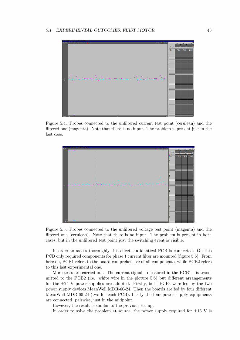
5.1. EXPERIMENTAL OUTCOMES: FIRST MOTOR 43
Figure 5.4: Probes connected to the unfiltered current test point (cerulean) and thefiltered one (magenta). Note that there is no input. The problem is present just in thelast case.
Figure 5.5: Probes connected to the unfiltered voltage test point (magenta) and thefiltered one (cerulean). Note that there is no input. The problem is present in bothcases, but in the unfiltered test point just the switching event is visible.
In order to assess thoroughly this effect, an identical PCB is connected. On thisPCB only required components for phase 1 current filter are mounted (figure 5.6). Fromhere on, PCB1 refers to the board comprehensive of all components, while PCB2 refersto this last experimental one.
More tests are carried out. The current signal - measured in the PCB1 - is trans-mitted to the PCB2 (i.e. white wire in the picture 5.6) but different arrangementsfor the ±24 V power supplies are adopted. Firstly, both PCBs were fed by the twopower supply devices MeanWell MDR-60-24. Then the boards are fed by four differentMeanWell MDR-60-24 (two for each PCB). Lastly the four power supply equipmentsare connected, pairwise, just in the midpoint.
However, the result is similar to the previous set-up.In order to solve the problem at source, the power supply required for ±15 V is
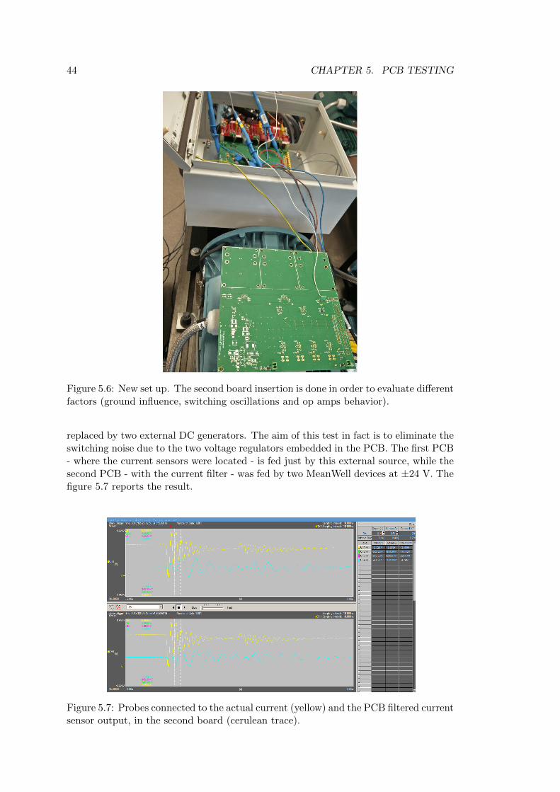
44 CHAPTER 5. PCB TESTING
Figure 5.6: New set up. The second board insertion is done in order to evaluate differentfactors (ground influence, switching oscillations and op amps behavior).
replaced by two external DC generators. The aim of this test in fact is to eliminate theswitching noise due to the two voltage regulators embedded in the PCB. The first PCB- where the current sensors were located - is fed just by this external source, while thesecond PCB - with the current filter - was fed by two MeanWell devices at ±24 V. Thefigure 5.7 reports the result.
Figure 5.7: Probes connected to the actual current (yellow) and the PCB filtered currentsensor output, in the second board (cerulean trace).
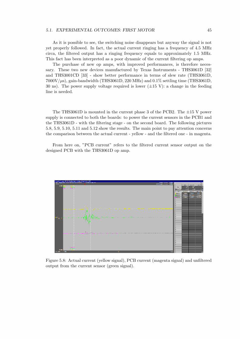
5.1. EXPERIMENTAL OUTCOMES: FIRST MOTOR 45
As it is possible to see, the switching noise disappears but anyway the signal is notyet properly followed. In fact, the actual current ringing has a frequency of 4.5 MHzcirca, the filtered output has a ringing frequency equals to approximately 1.5 MHz.This fact has been interpreted as a poor dynamic of the current filtering op amps.
The purchase of new op amps, with improved performances, is therefore neces-sary. These two new devices manufactured by Texas Instruments - THS3061D [32]and THS3001CD [33] - show better performance in terms of slew rate (THS3061D,7000V/µs), gain-bandwidth (THS3061D, 220 MHz) and 0.1% settling time (THS3061D,30 ns). The power supply voltage required is lower (±15 V): a change in the feedingline is needed.
The THS3061D is mounted in the current phase 3 of the PCB2. The ±15 V powersupply is connected to both the boards: to power the current sensors in the PCB1 andthe THS3061D - with the filtering stage - on the second board. The following pictures5.8, 5.9, 5.10, 5.11 and 5.12 show the results. The main point to pay attention concernsthe comparison between the actual current - yellow - and the filtered one - in magenta.
From here on, ”PCB current” refers to the filtered current sensor output on thedesigned PCB with the THS3061D op amp.
Figure 5.8: Actual current (yellow signal), PCB current (magenta signal) and unfilteredoutput from the current sensor (green signal).

46 CHAPTER 5. PCB TESTING
Figure 5.9: Actual current (yellow signal), PCB current (magenta signal), unfilteredoutput from the current sensor (green signal) and filtered - by the pre-assembled RCfilter - output from the evaluation CMK board (cerulean signal).
Figure 5.10: Actual current (yellow signal) and PCB current (magenta signal).

5.1. EXPERIMENTAL OUTCOMES: FIRST MOTOR 47
Figure 5.11: Actual current (yellow signal), PCB current (magenta signal), unfilteredoutput from the current sensor (green signal) and filtered - by the pre-assembled RCfilter - output from the evaluation CMK board (cerulean signal).
Figure 5.12: Actual current (yellow signal), PCB current (magenta signal), unfilteredoutput from the current sensor (green signal) and filtered - by the pre-assembled RCfilter - output from the evaluation CMK board (cerulean signal).

48 CHAPTER 5. PCB TESTING
With both a different power supply and an improved op amp, the results show amuch improved behavior. Although some ripples are still present, the measurementstaken using current sensors on PCB roughly follow the actual current. The cursors inprevious images help this analysis.
This test is repeated at different speeds and had no effect on the measurements.This is due to the fact that the speed is related to the fundamental frequency while thedevice is tested in the high frequency domain (i.e. 4.5 MHz).
The measured data is than post-processed (i.e. compensation for gain and offset)using Matlab. The figures 5.13 and 5.14, shows comparison between actual current andcurrent measured using newly developed PCB.
1 2 3 4 5Time [s] 10-6
-0.5
0
0.5
1
Cur
rent
[A]
Figure 5.13: Actual current (blue) with the PCB current (orange).
0 1 2 3 4 5Time [s] 10-6
-2.5
-2
-1.5
-1
-0.5
Cur
rent
[A]
Figure 5.14: Actual current (blue) with the PCB current (orange).
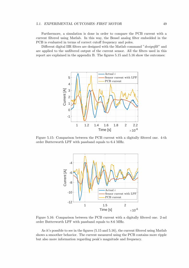
5.1. EXPERIMENTAL OUTCOMES: FIRST MOTOR 49
Furthermore, a simulation is done in order to compare the PCB current with acurrent filtered using Matlab. In this way, the Bessel analog filter embedded in thePCB is evaluated in terms of correct cutoff frequency and poles.
Different digital IIR filters are designed with the Matlab command ”designfilt” andare applied to the unfiltered output of the current sensor. All the filters used in thisreport are explained in the appendix B. The figures 5.15 and 5.16 show the outcomes:
1 1.2 1.4 1.6 1.8 2 2.2Time [s] 10-6
-1
0
1
2
3
4
5
Cur
rent
[A]
Figure 5.15: Comparison between the PCB current with a digitally filtered one. 4-thorder Butterworth LPF with passband equals to 6.4 MHz.
1 1.5 2Time [s] 10-6
-12
-10
-8
-6
-4
Cur
rent
[A]
Figure 5.16: Comparison between the PCB current with a digitally filtered one. 2-ndorder Butterworth LPF with passband equals to 8.6 MHz.
As it’s possible to see in the figures (5.15 and 5.16), the current filtered using Matlabshows a smoother behavior. The current measured using the PCB contains more ripplebut also more information regarding peak’s magnitude and frequency.

50 CHAPTER 5. PCB TESTING
A digital filter is applied even in the current measured using PCB. Results arereported in the figures below:
1 1.5 2Time [s] 10-6
-12
-10
-8
-6
-4C
urre
nt [A
]
Figure 5.17: Comparison between the PCB current - beyond digitally filtered - with adigitally filtered one. 8-th order LPF with passband equals to 6 MHz.
0 1 2 3 4 5Time [s] 10-6
-2.5
-2
-1.5
-1
-0.5
Cur
rent
[A]
Figure 5.18: The PCB current - beyond digitally filtered. 4-th order LPF with passbandequals to 6 MHz.
A digital filtering stage on the PCB current can improve the behavior in terms ofsmoothness.
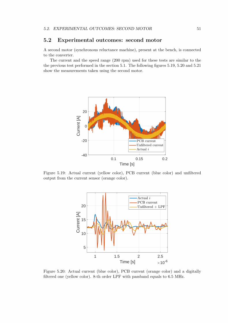
5.2. EXPERIMENTAL OUTCOMES: SECOND MOTOR 51
5.2 Experimental outcomes: second motor
A second motor (synchronous reluctance machine), present at the bench, is connectedto the converter.
The current and the speed range (200 rpm) used for these tests are similar to thethe previous test performed in the section 5.1. The following figures 5.19, 5.20 and 5.21show the measurements taken using the second motor.
0.1 0.15 0.2Time [s]
-40
-20
0
20
Cur
rent
[A]
Figure 5.19: Actual current (yellow color), PCB current (blue color) and unfilteredoutput from the current sensor (orange color).
1 1.5 2 2.5Time [s] 10-6
5
10
15
20
Cur
rent
[A]
Figure 5.20: Actual current (blue color), PCB current (orange color) and a digitallyfiltered one (yellow color). 8-th order LPF with passband equals to 6.5 MHz.

52 CHAPTER 5. PCB TESTING
0.5 1 1.5 2 2.5Time [s] 10-6
-15
-10
-5
Cur
rent
[A]
Figure 5.21: Actual current (blue color), PCB current (orange color) and a digitallyfiltered one (yellow color). 8-th order LPF with passband equals to 6.5 MHz.
The outcomes show that, even in this case, the PCB current has a better behaviorin terms of frequency content in spite of its noisier performance. The first peak revealsitself as the most troublesome (compare the tests with the first motor 5.1). At the endof the ringing stage some information is missed and the current sensor starts to losethe actual signal. This phenomenon is traced back to a physical inherent limit of themeasurement device, that has anyway a limited bandwidth; further investigations inthis direction should be done.

5.3. EXPERIMENTAL OUTCOMES: THIRD MOTOR 53
5.3 Experimental outcomes: third motor
Similar tests are carried out on a third machine (Interior Permanent Motor).The current and the speed range (200 rpm) used for these tests is similar to the
previous tests. The figures 5.22, 5.23 and 5.24 provide to show the outcomes.
0.12 0.14 0.16 0.18 0.2 0.22 0.24Time [s]
-40
-20
0
20
40
Cur
rent
[A]
Figure 5.22: Actual current (yellow color), PCB current (blue color) and unfilteredoutput from the current sensor (orange color).
0 1 2 3 4 5Time [s] 10-6
10
15
20
25
30
35
Cur
rent
[A]
Figure 5.23: Actual current (blue color), PCB current (orange color) and a digitallyfiltered one (yellow color). 8-th order LPF with passband equals to 5.0 MHz.

54 CHAPTER 5. PCB TESTING
1 1.5 2 2.5Time [s] 10-6
8
10
12
14
16
18
Cur
rent
[A]
Figure 5.24: Actual current (blue color), PCB current (orange color) and a digitallyfiltered one (yellow color). 8-th order LPF with passband equals to 5.0 MHz.
In this case the actual current ringing has a frequency value equals to 6 MHz, morethan the 4.5 MHz of previous investigations. A fortiori the device can not follow thesignal properly, having a physical limitation in terms of bandwidth. Therefore, this lastparameter should be in a range of 4.5 MHz - 6 MHz, since the signal can be reproducedwith acceptable accuracy till 4.5 MHz.
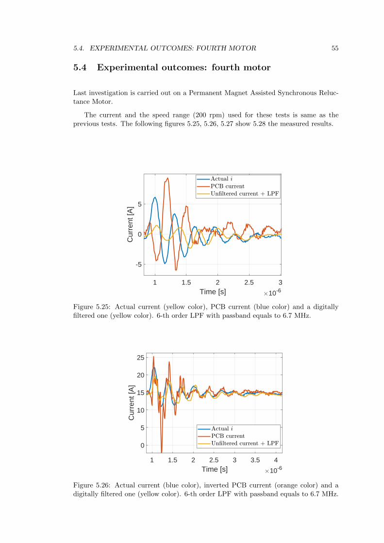
5.4. EXPERIMENTAL OUTCOMES: FOURTH MOTOR 55
5.4 Experimental outcomes: fourth motor
Last investigation is carried out on a Permanent Magnet Assisted Synchronous Reluc-tance Motor.
The current and the speed range (200 rpm) used for these tests is same as theprevious tests. The following figures 5.25, 5.26, 5.27 show 5.28 the measured results.
1 1.5 2 2.5 3Time [s] 10-6
-5
0
5
Cur
rent
[A]
Figure 5.25: Actual current (yellow color), PCB current (blue color) and a digitallyfiltered one (yellow color). 6-th order LPF with passband equals to 6.7 MHz.
1 1.5 2 2.5 3 3.5 4Time [s] 10-6
0
5
10
15
20
25
Cur
rent
[A]
Figure 5.26: Actual current (blue color), inverted PCB current (orange color) and adigitally filtered one (yellow color). 6-th order LPF with passband equals to 6.7 MHz.
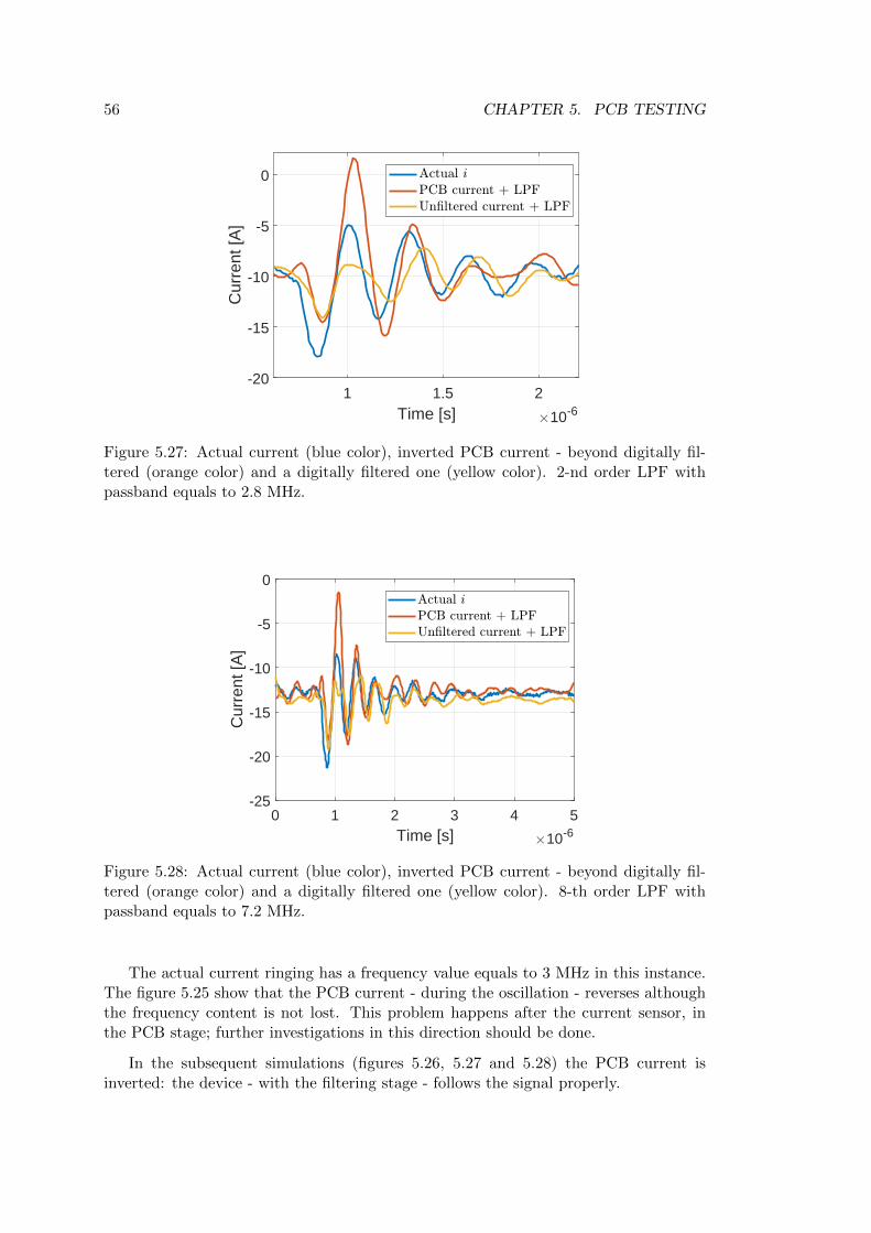
56 CHAPTER 5. PCB TESTING
1 1.5 2Time [s] 10-6
-20
-15
-10
-5
0
Cur
rent
[A]
Figure 5.27: Actual current (blue color), inverted PCB current - beyond digitally fil-tered (orange color) and a digitally filtered one (yellow color). 2-nd order LPF withpassband equals to 2.8 MHz.
0 1 2 3 4 5Time [s] 10-6
-25
-20
-15
-10
-5
0
Cur
rent
[A]
Figure 5.28: Actual current (blue color), inverted PCB current - beyond digitally fil-tered (orange color) and a digitally filtered one (yellow color). 8-th order LPF withpassband equals to 7.2 MHz.
The actual current ringing has a frequency value equals to 3 MHz in this instance.The figure 5.25 show that the PCB current - during the oscillation - reverses althoughthe frequency content is not lost. This problem happens after the current sensor, inthe PCB stage; further investigations in this direction should be done.
In the subsequent simulations (figures 5.26, 5.27 and 5.28) the PCB current isinverted: the device - with the filtering stage - follows the signal properly.

5.5. REMARKS ON THE RESULTS 57
5.5 Remarks on the results
After fixing several issues with the new design, such as ripple due to voltage regulatorand slow dynamic of the op amp, several tests are carried out on four different typemotors. The current sensors are mounted on PCB1 which is power by an external ± 15V power supply. The conditioning stage is assembled on PCB2 which is also poweredby the ± 15 V power supply. The output of PCB1 is fed to PCB2 via jumpers.
The measured quantities are: actual current, unfiltered output from the currentsensor, filtered current - by pre-assembled RC filter - output from the evaluation CMKboard, PCB current (in some case beyond digitally filtered) and the digitally filteredcurrent from the unfiltered output.
The current in the first machine 5.1 is well-reproduced except the troublesome firstpeak. The addition of a digital filter offers the possibility to have a cleaner signal (figure5.18).
In the second machine 5.2, in spite of the same harmonic content, the current sensorcan roughly reproduce the signal (see figure 5.21). However the issue primarily man-ifested when the oscillations are ending. Further investigations to solve this problemare required.
The ringing frequency in the third machine investigated in section 5.3 is instead 6MHz, which is higher than previous cases. This change in terms of frequency is due tothe different high-frequency circuital models that each machine has. The signal doesnot follow the actual current (figure 5.24). That is due to the intrinsic limit in termsof bandwidth and the only way to solve it concerns an upgraded current sensor.
In the last machine, i.e. section 5.4, the actual current ringing has a frequency of3 MHz. However, the PCB current results are reversed during the switching instants.This could be traced back to a problem in the designed board or in the set up; thusrequires further investigation to solve this problem. Anyway once the current is invertedthe actual current is reproduced correctly (figure 5.26).
The new current sensors and PCB design can detect - in magnitude and frequency -the switching instant with its subsequent oscillations. Some issues are highlighted in thisreport and are yet to be solved. The work has therefore shown that an hardware upgradeof drive measurement boards has good potential in an oversampling perspective.

58 CHAPTER 5. PCB TESTING
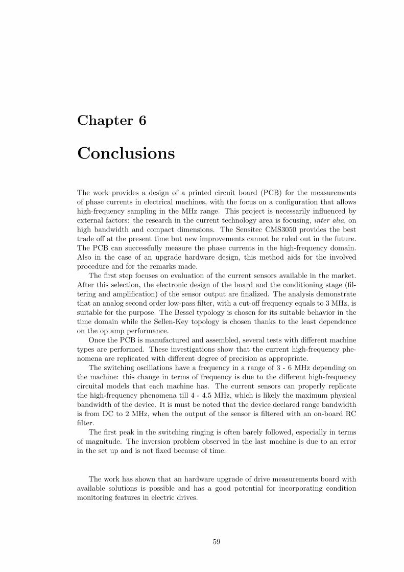
Chapter 6
Conclusions
The work provides a design of a printed circuit board (PCB) for the measurementsof phase currents in electrical machines, with the focus on a configuration that allowshigh-frequency sampling in the MHz range. This project is necessarily influenced byexternal factors: the research in the current technology area is focusing, inter alia, onhigh bandwidth and compact dimensions. The Sensitec CMS3050 provides the besttrade off at the present time but new improvements cannot be ruled out in the future.The PCB can successfully measure the phase currents in the high-frequency domain.Also in the case of an upgrade hardware design, this method aids for the involvedprocedure and for the remarks made.
The first step focuses on evaluation of the current sensors available in the market.After this selection, the electronic design of the board and the conditioning stage (fil-tering and amplification) of the sensor output are finalized. The analysis demonstratethat an analog second order low-pass filter, with a cut-off frequency equals to 3 MHz, issuitable for the purpose. The Bessel typology is chosen for its suitable behavior in thetime domain while the Sellen-Key topology is chosen thanks to the least dependenceon the op amp performance.
Once the PCB is manufactured and assembled, several tests with different machinetypes are performed. These investigations show that the current high-frequency phe-nomena are replicated with different degree of precision as appropriate.
The switching oscillations have a frequency in a range of 3 - 6 MHz depending onthe machine: this change in terms of frequency is due to the different high-frequencycircuital models that each machine has. The current sensors can properly replicatethe high-frequency phenomena till 4 - 4.5 MHz, which is likely the maximum physicalbandwidth of the device. It is must be noted that the device declared range bandwidthis from DC to 2 MHz, when the output of the sensor is filtered with an on-board RCfilter.
The first peak in the switching ringing is often barely followed, especially in termsof magnitude. The inversion problem observed in the last machine is due to an errorin the set up and is not fixed because of time.
The work has shown that an hardware upgrade of drive measurements board withavailable solutions is possible and has a good potential for incorporating conditionmonitoring features in electric drives.
59

60 CHAPTER 6. CONCLUSIONS
Regardless some aspects ought to be considered by possible future users:
• The reproduction of the current high-frequency behavior, in this work is analyzedin absolute terms, should be reasoned according to the used model i.e. in relativeterms. This means that the informations carried by the current sensor may ormay not be used in the ageing model or in the intrinsic PWM injection method.Further investigations ought to be done because this aspect isn’t considered inthis work.
• In the case of new advances in technology, the current sensor must have an outputthat can be easily embedded in a PCB. More-over the system requirements shouldbe fulfill.
• The board conditioning stage ought to be designed according to the measuringdevice features. The filter cut-off frequency (in this work is set at 3 MHz) dependson the sensor’s features; the gain (in this work: 4) must take into account insteadthe input range of the drive control unit.

Chapter 7
Future work
7.1 Improvement for voltage measurements
The device is meant for current measurements. However there’s the possibility, withfew adjustments, to detect voltages.
The set up consists mainly of three parts: the inverter, the measurement board anda motor. There are two power cables: from converter to board and from board to themachine. If the board functionality will be extended to measure even voltages, the starpoint of the machine should be available at the box as well.
Voltage sensors should be mounted inside the box by screwing. In the previousbox, the chosen devices were the LEM CV 3-1500 but it is possible to use differentsensors with improved features. The new box is meant to be enough large to installthese devices likewise.
The voltage filtering stage is already present in the PCB (see 4.2). The voltages,from the sensors, can be connected to the board by Faston terminals. The second orderButterworth LPFs have a cut-off frequency of 200 kHz and a gain equal to 2. In thecase of a power supplies improvement (see next section 7.2), the voltage stage op ampshave to be improved in order to fulfill the new voltage requirements (± 15 V).
7.2 Power supplies improvement
The PCB was initially designed with the op amp OPA552 in the current stage. However,due to the poor performances of this OPA552, the THS3061D is used as replacement.All the tests are performed using this new op amp.OPA552 and THS3061D require different power supplies, one ± 24 V and the otherone ± 15 V. Furthermore the - hypothetical - voltage conditioning stage requires ± 24V while the current sensors ± 15 V.If other tests should be carried (without voltage measurements), the PCB can be pow-ered only by two power supplies at ± 15 V, taking care to disconnect the voltageregulators line, source of noise.That could be done by making an open circuit. The easiest way is the removal of aboard component upstream and downstream of the voltage regulators.
In future, this stage can be redesigned according to the new requirements for sensorsand op amps. If the devices used will remain the same, the voltage regulators are notneeded, since the only power supply required is ± 15 V.
61

62 CHAPTER 7. FUTURE WORK
7.3 Tests with the THS3001CD
Another op amp (THS3001CD [33]) is also purchased but it wasn’t tested. Its featuresare similar to THS3061D [32]: slew rate of 6300V/µs, settling time (0.1 %) of 40 nsand gain-bandwidth equals to 350 MHz. Since both are extremely well-performing interms of dynamic proprieties the results shouldn’t be different. Further investigationcould be done anyway for the sake of completeness.
It must be noted that the PCB1 is complete of all components while the PCB2 hasonly two current conditioning stages: one in the phase 1 (with OPA552) and one inthe phase 2 (with THS3061D). In case of future use, the PCB1 should be upgraded byreplacing the OPA552 with new op amps.More-over, in the case of a re-design of the conditioning current stage, the filter gaincan be set to higher values since the limit in the gain-bandwidth (see section 4.2.2)should no longer be accomplished.
7.4 Box
Since the task required more effort in testing the PCB, the box wasn’t assembled. Theadditional material, which is already purchased, is:
• The alluminium case. The dimensions are 400 x 400 x 200 mm
• For the power supply two MeanWell MDR-60-24 V voltage sources are used. Dueto the project changes, these devices should probably be replaced in future works.
• The power entry module, in order to connect the power supplies with the 230 Vacgrid. A fuse holder is included [34].
• An axial fan, designed for 24 V [35].
• The input and output of both currents and voltages was thought connectorsmanufactured by ”Phoenix Contact” [36].

Appendix A
Appendix A
This appendix provides the list of different TFs used in the frequency analysis (see 3).In the body of the report only the last four filters are compared in terms of RMSD. Atthe end a Bessel filter in a Sallen-Key configuration - marked with a star - was chosen.
−−−−−−−−−−−−−−−−−−−−−−−−−−−−−−−−−−−−−−−−−−−−−−−−−−−−−−−−
% the RC two−p o l e s f i l t e r a l r e a d y in p l a c e in the boardnumRC = [ 4 9 0 0 6 5 3 9 4 3 2 6 . 2 2 ] ;denRC = [ 1 8823921.4640802 490065394326 .22 ] ;G RC = t f (numRC, denRC ) ;
−−−−−−−−−−−−−−−−−−−−−−−−−−−−−−−−−−−−−−−−−−−−−−−−−−−−−−−−% 1 s y s i d n t f 2−p o l e f o r TARGET (3MHz)num1 = 5.086 e14 ;den1 = [ 1 3 .606 e7 4 .794 e14 ] ;G1 = t f (num1 , den1 ) ;
% 2 RC cascade two−p o l e s to implement (1 .25 MHz)num2 = 6.25 e14 ;den2 = [ 1 87500000 6 .25 e14 ] ;G2 = t f (num2 , den2 ) ;
% 3 shor t 5 , 3 p o l e s 1 zero (3 MHz)num3 = [1 .039222992325427 e+15 1.120683192130224 e +22] ;den3 = [ 1 1 .13918 e+08 1.1976706 e+15 1.10376483 e +22] ;G3 = t f (num3 , den3 ) ;
% 4 short , 2 p o l e snum4 = 5.085745506253996 e +14;den4 = [ 1 3.6055679 e+07 4.79426367 e +14] ;G4 = t f (num4 , den4 ) ;
% 5 shor t 4 , 3 p o l e s 1 zeronum5 = [6 .593767228138800 e+14 1.724896629436997 e +21] ;den5 = [ 1 5.557371 e+07 6.2179524 e+14 1.696130 e +21] ;G5 = t f (num5 , den5 ) ;
63

64 APPENDIX A. APPENDIX A
% 6 B e s s e l 2−nd order , MFB c o n f i g u r a t i o nnum6 = 3.6075036075036 e15 ;den6 = [ 1 43963150.670468 6.5990919649456 e14 ] ;G6 = t f (num6 , den6 ) ;
% 7 Butterworth 2−nd order , MFB c o n f i g u r a t i o nnum7 = 2.2878059940517 e15 ;den7 = [ 1 28507696.833023 4.0853678465209 e14 ] ;G7 = t f (num7 , den7 ) ;
% RMSD( long . . . s h o r t 8 ) = [ 1 3 . 9 8 13.15 17.01 1 3 . 9 8 . . .. . . 12 .81 16 .08 1 2 . 9 4 ]−−−−−−−−−−−−−−−−−−−−−−−−−−−−−−−−−−−−−−−−−−−−−−−−−−−−−−% B e s s e l MFB ( with minus s i g n )num81 = 3.7515388812491 e15 ;den81 = [ 1 53058585.619475 9.3248126924874 e14 ] ;
% Butterworth MFB (w. minus s i g n )num9 = 1.4682778569016 e15 ;den9 = [ 1 27327687.170532 3.6525677551319 e14 ] ;
% B e s s e l SKnum101 = 1.4095909329016 e15 ;den101 = [ 1 26593858.966829 3.5133948177426 e14 ] ;
% Butterworth SKnum11 = 1.4095909329016 e15 ;den11 = [ 1 26593858.966829 3.5133948177426 e14 ] ;
% RMSD ( long . . . s h o r t 8 ) = [ 1 9 . 8 4 11.82 11.78 1 1 . 7 8 ]% RMSD (m1 . . . m12) = [NaN 10.53 10.16 1 0 . 1 6 ]
−−−−−−−−−−−−−−−−−−−−−−−−−−−−−−−−−−−−−−−−−−−−−−−−−−−−−% 8 B e s s e l MFB (w. minus s i g n )num8 = 1.412728685456 e15 ;den8 = [ 1 33292197.99808 3.6010731197897 e14 ] ;
% 10∗ B e s s e l SKnum10 = 2.2874750232457 e15 ;den10 = [ 1 41361395.225126 5.701514322204 e14 ] ;
% RMSD ( long . . . m12) = [ 1 0 . 5 3 11.15 11.78 1 0 . 9 3 ]% d i g i t a l l y ( long . . . m12) = [ 1 2 . 2 9 12.03 12.48 1 2 . 0 3 ]% noisy ( long . . . m12) = [ 3 6 . 7 3 37.33 37.49 3 7 . 3 0 ]

Appendix B
Appendix B
This appendix provides the list with the features of different digital filters used in thePCB testing analysis (see 5). In the core of the report only some outcomes are shown.
−−−−−−−−−−−−−−−−−−−−−−−−−−−−−−−−−−−−−−−−−−−−−−−−−−−−−−−−−−
% F i r s t motor , IM
1) LPF, 2nd order , f c u t o f f= 3 MHz, passbandr ipp l e= 0 .12) LPF, 4 th order , f c u t o f f= 3 MHz, passbandr ipp l e= 0 .13) LPF, 4 th order , f c u t o f f= 5 MHz, passbandr ipp l e= 0 .14) LPF, 2nd order , f c u t o f f= 10 MHz, passbandr ipp l e= 0 .15) LPF, 8 th order , f c u t o f f= 4 .5 MHz, pas sbandr ipp le= 0 .16) LPF, 8 th order , f c u t o f f= 3 MHz, passbandr ipp l e= 0 .17) LPF, 8 th order , f c u t o f f= 10 MHz, passbandr ipp l e= 0 .18) LPF, 2nd order , f c u t o f f= 5 MHz, passbandr ipp l e= 0 .1
Butterworth f i l t e r s (LPF)9) ha l f−power frequency= 4 MHz10) ha l f−power frequency= 6 MHz11) ha l f−power frequency= 4 .5 MHz, 2nd order12) ha l f−power frequency= 4 .8 MHz, 6 th order
PCB+LPF w u n f i l t e r e d+LPF13) ha l f−power frequency= 5 MHz, 2nd order14) ha l f−power frequency= 6 MHz, 6 th order15) ha l f−power frequency= 4 MHz, 4 th order16) butterworth , ha l f−power frequency= 4 .8 MHz, 2nd order17) butterworth , ha l f−power frequency= 6 .4 MHz, 4 th order18) butterworth , ha l f−power frequency= 8 .6 MHz, 2nd order19) passband= 9 .2 MHz, 4−th order
20) passband= 6 MHz, 8−th order21) passband= 7 MHz, 2−nd order22) passband= 4 .5 MHz, 4−th order
−−−−−−−−−−−−−−−−−−−−−−−−−−−−−−−−−−−−−−−−−−−−−−−−−−−−−
65

66 APPENDIX B. APPENDIX B
% Second motor , SynRM
1) LPF, 8 th order , f c u t o f f= 5 MHz2) LPF, 8 th order , f c u t o f f= 6 .5 MHz3) LPF, 8 th order , f c u t o f f= 4 .8 MHz4) LPF, 4 th order , f c u t o f f= 5 .8 MHz
−−−−−−−−−−−−−−−−−−−−−−−−−−−−−−−−−−−−−−−−−−−−−−−−−−−−−
% Third motor , IPM
1) LPF, 8 th order , f c u t o f f= 5 MHz2) LPF, 4 th order , f c u t o f f= 3 .5 MHz
−−−−−−−−−−−−−−−−−−−−−−−−−−−−−−−−−−−−−−−−−−−−−−−−−−−−
% Foruth motor , PMASynRM
1) LPF, 6 th order , f c u t o f f= 6 .7 MHz2) LPF, 2nd order , f c u t o f f= 2 .8 MHz3) LPF, 8 th order , f c u t o f f= 7 .2 MHz
−−−−−−−−−−−−−−−−−−−−−−−−−−−−−−−−−−−−−−−−−−−−−−−−−−−
References
[1] J. Bjorngreen, A. Reinap, and Z. Huang, “PMSM diagnostic and prognostic.”
[2] C. Zoeller, M. A. Vogelsberger, R. Fasching, W. Grubelnik, and T. M.Wolbank, “Evaluation and current-response-based identification of insulationdegradation for high utilized electrical machines in railway application,” IEEETrans. Ind. Appl., vol. 53, no. 3, pp. 2679–2689, 2017. [Online]. Available:https://doi.org/10.1109/TIA.2017.2661718
[3] A. Faggion and S. Bolognani, “A new proposal of rotor position estimation inIPM motor drives based on PWM current harmonics,” in 2010 First Symposiumon Sensorless Control for Electrical Drives (SLED), Padova, Italy, Aug. 9-102010, pp. 1–7. [Online]. Available: https://doi.org/10.1109/SLED.2010.5542797
[4] A. Faggion, S. Bolognani, and L. Sgarbossa, “Rotor position estimationin IPM motor drives based on PWM current harmonics,” in 2011 IEEEInternational Electrical Machines and Drives Conferance (IEMDC), NiagaraFalls, Canada, May 15-18 2011, pp. 430–435. [Online]. Available: https://doi.org/10.1109/IEMDC.2011.5994633
[5] R. Slatter, M. Brusius, and H. Knoll, “Development of high bandwidthcurrent sensors based on the magnetoresistive effect,” in 2016 18th EuropeanConference on Power Electronics and Applications (EPE’16 ECCE Europe),Karlsruhe, Germany, Sep. 5-9 2016, pp. 1–10. [Online]. Available: https://doi.org/10.1109/EPE.2016.7695648
[6] C. Zoeller, M. Vogelsberger, J. Bellingen, P. Nussbaumer, and T. Wolbank,“Investigation of sampling frequency and jitter effects on transient currentsignal evaluation for insulation condition monitoring,” in 2015 17th EuropeanConference on Power Electronics and Applications (EPE’15 ECCE Europe),Geneve, Switzerland, Sep. 8-10 2015, pp. 1–9. [Online]. Available: https://doi.org/10.1109/EPE.2015.7309193
[7] P. Nussbaumer, T. Wolbank, and M. Vogelsberger, “Sensitivity analysis ofinsulation state indicator in dependence of sampling rate and bit resolutionto define hardware requirements,” in 2013 IEEE International Conference onIndustrial Technology (ICIT), Cape Town, South Africa, Feb. 8-10 2013, pp. 1–6.[Online]. Available: https://doi.org/10.1109/ICIT.2013.6505704
[8] AllegroMicroSystem, “ACS730, 1 MHz bandwidth, galvanically isolated currentsensor IC in small footprint SOIC8 package.” [Online]. Available: http://pdf1.alldatasheet.com/datasheet-pdf/view/848428/ALLEGRO/ACS730.html
67

68 REFERENCES
[9] C. Gudel, “Taking transducer technology to the limits of current measure-ment accuracy,” May 2008. [Online]. Available: http://www.powerguru.org/taking-transducer-technology-to-the-limits-of-current-measurement-accuracy/
[10] J. N. Fritz, C. Neeb, and W. D. Doncker, “A PCB integrated differential Rogowskicoil for non-intrusive current measurement featuring high bandwidth and dv/dtimmunity,” pp. 1–6. [Online]. Available: https://eldorado.tu-dortmund.de/bitstream/2003/33955/1/S05.2.pdf
[11] KeysightTechnology, “What is a Rogowski coil current probe?” [Online]. Avail-able: https://community.keysight.com/community/keysight-blogs/oscilloscopes/blog/2017/11/29/what-is-a-rogowski-coil-current-probe
[12] N. Troster, J. Wolfle, J. Ruthardt, and J. Roth-Stielow, “High bandwidthcurrent sensor with a low insertion inductance based on the HOKA principle,” in2017 19th European Conference on Power Electronics and Applications (EPE’17ECCE Europe), Warsaw, Poland, Sep. 11-14 2017, pp. 1–9. [Online]. Available:https://doi.org/10.23919/EPE17ECCEEurope.2017.8099003
[13] S. Ziegler, R. C. Woodward, H. H. Iu, and L. J. Borle, “Current sensingtechniques: a review,” IEEE Sensors J., vol. 9, pp. 354 – 376, 2009. [Online].Available: https://doi.org/10.1109/JSEN.2009.2013914
[14] AnalogDevice, “Op Amp Common-Mode Rejection Ratio (CMRR).” [On-line]. Available: http://www.analog.com/media/en/training-seminars/tutorials/MT-042.pdf
[15] N. Alexander, N. Nain, and W. Navaeeth-Kumar, “Shunt based, 200-A peakcurrent measurement reference design using reinforced isolation amplifier,” pp.1–27. [Online]. Available: http://www.ti.com/tool/TIDA-00445
[16] TexasInstrument, “OPAx376 low-noise, low quiescent current, precisionoperational amplifier e-trim series, data sheet.” [Online]. Available: http://www.ti.com/lit/ds/symlink/opa2376.pdf
[17] ——, “AMC 1220/B fully-differential isolation amplifier, data sheet.” [Online].Available: http://www.ti.com/lit/ds/symlink/amc1200.pdf
[18] SensitecSolutions, “CMS3050 data sheet.” [Online]. Avail-able: https://www.sensitec.com/fileadmin/sensitec/Service and Support/Downloads/Data Sheets/CMS3000/SENSITEC CMS3050 DSE 05.pdf
[19] ——, “CMK3000 data sheet.” [Online]. Available: http://docs-europe.electrocomponents.com/webdocs/1275/0900766b812751bc.pdf
[20] Agilent, “33120A user guide.” [Online]. Available: https://www.keysight.com/upload/cmc upload/All/6C0633120A USERSGUIDE ENGLISH.pdf
[21] Hioki, “Clamp on probe 3276.” [Online]. Available: https://www.hioki.com/en/products/detail/?product key=5783
[22] AnalogDevices, “Basic Linear Design, Chapter 8.” [Online]. Avail-able: http://www.analog.com/media/en/training-seminars/design-handbooks/Basic-Linear-Design/Chapter8.pdf
REFERENCES 69
[23] Okawa, “2nd order CR Low-pass filter design tool.” [Online]. Available:http://sim.okawa-denshi.jp/en/CRCRkeisan.htm
[24] TexasInstrument, “WEBENCH Design Center.” [Online]. Available: http://www.ti.com/design-tools/overview.html
[25] MeanWell, “MDR-60-24 - 60 W 24 V miniature din rail powersupply.” [Online]. Available: https://www.meanwelldirect.co.uk/product/60W-24V-2-5A-Miniture-DIN-Rail-Power-Supply/MDR-60-24/default.htm
[26] OPAL-RT, “OP5600 V2 user manual.” [Online]. Available: https://www.opal-rt.com/wp-content/themes/enfold-opal/pdf/L00161 0335.pdf
[27] XILINX, “ZC702 evaluation board for the Zynq-7000 XC7Z020 all programmableSoC.” [Online]. Available: https://www.xilinx.com/support/documentation/boards and kits/zc702 zvik/ug850-zc702-eval-bd.pdf
[28] TexasInstrument, “LM2594 simple switcher power converter 150-kHz 0.5Astep-down voltage regulator.” [Online]. Available: http://www.ti.com/lit/ds/symlink/lm2594.pdf
[29] ——, “OPA55x high-voltage, high-current operational amplifiers.” [Online].Available: http://www.ti.com/lit/ds/sbos100b/sbos100b.pdf
[30] ——, “PCB design guidelines for reduced EMI.” [Online]. Available: http://www.ti.com/lit/an/szza009/szza009.pdf
[31] Yokogawa, “700929 Isolated passive probe 100V / 100MHz.” [On-line]. Available: https://tmi.yokogawa.com/ca/solutions/products/oscilloscopes/voltage-probes/700929-101-probe/
[32] TexasInstrument, “THS3061 low-distortion, high slew rate, current-feedbackamplifiers.” [Online]. Available: http://www.ti.com/lit/ds/symlink/ths3061.pdf
[33] ——, “THS3001 420 MHz high-speed current-feedback amplifier.” [Online].Available: http://www.ti.com/lit/ds/symlink/ths3001.pdf
[34] KEC, “IEC Appliance Inlet C14 with fuseholder 1- or 2- pole and voltageselector.” [Online]. Available: http://www.farnell.com/datasheets/1719090.pdf
[35] W2G107-AD03-01, “EC axial compact fan.” [Online]. Available: https://eu.mouser.com/ds/2/120/ebm-papst W2G107AD0301-DB-ENG-1165451.pdf
[36] PhoenixContact, “PV-CM-S 6-16.” [Online]. Available: http://www.farnell.com/datasheets/1700815.pdf